Scalable general high voltage MOSFET model including quasi-saturation and self-heating effects
Upload
independentCategory
view
3download
0
Available online at www.sciencedirect.com
www.elsevier.com/locate/sse
Solid-State Electronics 52 (2008) 196–204
Review
An area efficient body contact for low and high voltageSOI MOSFET devices
Arash Daghighi a,*, Mohamed Osman b, Mohamed A. Imam c
a Department of Electrical Engineering, Islamic Azad University Majlesi Branch, Isfahan, Iranb School of Electrical Engineering and Computer Science, Washington State University, Pullman, WA 99164-2752, USA
c ON Semiconductor, 5005 East McDowell Road, MD D145, Phoenix, AZ 85008, USA
Received 7 January 2007; received in revised form 14 September 2007; accepted 24 October 2007Available online 21 December 2007
The review of this paper was arranged by Prof. S. Cristoloveanu
Abstract
A simple and high-performance area efficient body-tied-source (BTS) contact for SOI MOSFET is presented. By simple modificationto the physical layout and without introducing any increase to the fabrication process steps, the proposed body contact can be imple-mented. Three-dimensional (3D) non-isothermal simulation on SOI CMOS devices showed higher current drive while floating bodyeffects were completely suppressed. In addition, improved performance is achieved when comparing on-resistance (RON) and breakdownvoltage (VBR) with the conventional BTS structures. The new body contact structure is applicable to both low and high voltage (planar ortrench) SOI and bulk devices. Experimental results obtained from fabricated bulk MOSFET devices utilizing the proposed body contactstructure agreed well with the simulation findings.� 2007 Elsevier Ltd. All rights reserved.
Keywords: High voltage; Low voltage; Partially depleted SOI MOSFET; On-resistance; Breakdown voltage; Floating body effects; Body contact; Three-dimensional simulation; Non-isothermal drift-diffusion model
Contents
1. Introduction . . . . . . . . . . . . . . . . . . . . . . . . . . . . . . . . . . . . . . . . . . . . . . . . . . . . . . . . . . . . . . . . . . . . . . . . . . . . . . 1962. Three-dimensional simulation model . . . . . . . . . . . . . . . . . . . . . . . . . . . . . . . . . . . . . . . . . . . . . . . . . . . . . . . . . . . . . 1983. Simulation results . . . . . . . . . . . . . . . . . . . . . . . . . . . . . . . . . . . . . . . . . . . . . . . . . . . . . . . . . . . . . . . . . . . . . . . . . . 199
0038-1
doi:10.
* CoE-m
3.1. New body contact . . . . . . . . . . . . . . . . . . . . . . . . . . . . . . . . . . . . . . . . . . . . . . . . . . . . . . . . . . . . . . . . . . . . . . 2003.2. Body contact misalignment . . . . . . . . . . . . . . . . . . . . . . . . . . . . . . . . . . . . . . . . . . . . . . . . . . . . . . . . . . . . . . . 201
4. Experimental results. . . . . . . . . . . . . . . . . . . . . . . . . . . . . . . . . . . . . . . . . . . . . . . . . . . . . . . . . . . . . . . . . . . . . . . . . 2035. Conclusion . . . . . . . . . . . . . . . . . . . . . . . . . . . . . . . . . . . . . . . . . . . . . . . . . . . . . . . . . . . . . . . . . . . . . . . . . . . . . . . 203
References . . . . . . . . . . . . . . . . . . . . . . . . . . . . . . . . . . . . . . . . . . . . . . . . . . . . . . . . . . . . . . . . . . . . . . . . . . . . . . . 204
101/$ - see front matter � 2007 Elsevier Ltd. All rights reserved.
1016/j.sse.2007.10.052
rresponding author. Tel.: +98 311 6268408.ail address: [email protected] (A. Daghighi).
1. Introduction
Recently, there has been a growing interest in using SOIfor high speed digital and RF circuits because it offers per-formance gain over Bulk CMOS in terms of speed, isola-tion, density, yield and performance gain in low/high

A. Daghighi et al. / Solid-State Electronics 52 (2008) 196–204 197
power electronics [1]. Additionally, SOI MOSFET hasbeen the technology of choice for radiation hard, spaceand hostile environment applications. As the technologymoves to the deep sub-micron generation, its applicationis spreading to microprocessors, memories, RF CMOSand low power electronics.
However, compared to bulk MOSFETs, the static anddynamic performances of SOI MOSFETs are considerablydifferent due to various effects that are introduced by thecomplete isolation of the devices. The presence of buriedoxide layer results in a floating body region and its lowthermal conductivity causes self-heating effects [2]. Thearea efficiency of floating body design configuration makesit more desirable in high-density applications. However,floating body device design complicates device perfor-mance and suffers from several floating body modulationeffects such as drain voltage induced fluctuations in bodypotential which give rise to reduction of the breakdownvoltage, variations in the threshold voltage, current kink,increased noise and disturbances in the static and dynamiccharacteristics of the device. The body potential modula-tion and the associated effects are critical especially forpartially depleted (PD) SOI devices [3] where dependingon the device bias condition, the body potential may be ele-vated and attain a positive value which causes the conduc-tion of a parasitic lateral bipolar junction transistor (BJT)formed with the source as emitter, floating body as base,and drain as collector. This lateral BJT in the SOIMOSFET structure is important as it accounts for the lossof the gate control and poor breakdown voltagecharacteristics.
Several approaches have been proposed to suppress thefloating body effects in PD SOI. These include introducing
Fig. 1. SOI body contacts (arrows show the current flow in the channel), (A
recombination centers for the holes below the source, usingGe implantation in the source region, or making a path forthe generated holes in the body to escape to contact(s) [4–9]. The first method adds to the fabrication process com-plexity while the Ge implanted source structure is notCMOS compatible. All of the methods that have beendeveloped to make a path for the generated holes (suchas H-gate and body-tied-source structures) suffer fromone or more of the following drawbacks: (1) increased fab-rication process complexity, (2) larger device area, or (3)lower effective device width. For high voltage power ICsthe impact is translated to the ‘‘RON · area’’ figure ofmerit. This indicates that for the same area devices, theone with the lower RON (higher current drive) has a smallerfigure of merit. A lower ‘‘RON · area’’ allows a designer touse a smaller high voltage MOSFET to meet ON-resistancerequirements for a given application, which reduces thearea and cost of a power integrated-circuit.
In this paper, we propose a novel area efficient bodycontact for SOI devices and investigate its performanceusing three-dimensional simulation study. Additionally,to confirm the simulation findings, we also fabricated bulkn-MOSFET structures with both conventional and the pro-posed body contacts. Fig. 1 shows the layout view of fewconventional SOI body contact structures and our pro-posed body contact. The H-gate body contact shown inFig. 1A, has considerably large footprint (i.e. area ineffi-cient) whereas allowing independent control of the bodyvoltage. Body-tied-source (BTS) structure controls bodyvoltage by introducing P+ regions in the source end ofthe device to allow low resistance path(s) for the holes atthe expense of reduced current drive for the device asdepicted in Fig. 1B and C shows the proposed area efficient
) H-gate, (B) conventional body-tied-source and (C) novel body contact.
198 A. Daghighi et al. / Solid-State Electronics 52 (2008) 196–204
body contact, which can be implemented by simple modifi-cation to the physical layout design [10]. Compared to theH-gate body contact (Fig. 1A), the novel body-contacteddevice occupies a smaller silicon area whereas the currentdrives are approximately equal. This is due to the smallcontact area at the edge of the P+ doped region to the bodyof the device, which results in almost equal effective devicewidths. In comparison with the conventional body-tied-source structure (Fig. 1B), the proposed body-contacteddevice has a larger effective width and as a result a highercurrent drive for the same drawn widths.
In this work, we investigate the performance of the pro-posed body contact structure and analyze its effect in sup-pressing floating body effects using three-dimensional (3D)device simulation. In the following sections, we review the3D simulation model and analyze the simulation results ofthe proposed structure and the conventional structures.The three-dimensional simulation model is explained inSection 2, simulation results of the new body contact andthe effect of process misalignment on the performance ofthe device as obtained from simulations are presented inSection 3, followed by discussion of the measurementresults on fabricated bulk n-MOSFETs in Section 4 anda conclusion in Section 5.
2. Three-dimensional simulation model
The Body of BTS SOI MOSFET is not uniformly atground potential due to the high sheet resistance of thebody. As holes generated in impact ionization processmove toward the body contacts, a potential gradient buildsup along the device width [7]. The increase in body voltagedecreases the threshold voltage and consequently increasesthe channel current and portions of the device away fromthe body contacts pass higher channel current. Thischanges the operation characteristics of the device in thethird dimension (along device width). In addition,body-contacted devices can be viewed as a series of diodesP+/P/N+ (inactive regions) and regular active MOSFETs.Therefore, three-dimensional simulation is required tosimulate body-contacted devices.
In an earlier investigation, we proposed a simple 2Dmodel for simulation of body-contacted devices using ficti-tious photo-generated e-h pairs to induce the floating bodyvoltage [11]. The 2D model provides a computational effi-cient approach to get a first order estimate of the bodypotential profile, but does not allow investigating I–V char-acteristics, accurate carrier potential and charge distribu-tions. This makes it necessary to use three-dimensionalsimulation for our detailed analysis.
The low thermal conductivity of the buried oxide layerbeneath the active silicon film layer in SOI MOSFETscauses self-heating effect, which strongly affects carriermobility and electron-hole generation rates. Better compre-hensibility, we used non-isothermal drift-diffusion model totake into account the impact of lattice temperature varia-tion on performance of the device. The three-dimensional
simulation was performed using ISE TCAD’s device simu-lator (DESSIS) [12]. It is well known that drift-diffusionapproach overestimates the impact ionization process.The model for generation due to impact ionization, imple-mented in DESSIS, is given by [12]
Gk ¼ annV n þ appV p ð1Þ
where Vn,p denotes drift velocity and n (p) denotes the car-rier concentration of electrons (holes). The model for im-pact ionization generation coefficients (an, ap) suitable forsimulation at high temperatures (300–700 K) is given by
an;pðF ; T Þ ¼F
aðT Þ þ bðT ÞedðT Þ=ðFþCðT ÞÞ ð2Þ
where F is the driving force, a(T), b(T), c(T) and d(T) arethe temperature dependent model parameters. They canbe defined by constant coefficient functions. The tempera-ture dependence of model parameters, for electrons, canbe read as [12]:
aðT Þ ¼ a0 þ a1T a2 ; bðT Þ ¼ b0; cðT Þ ¼ c0 þ c1T þ c2T 2;
dðT Þ ¼ d0 þ d1T þ d2T 2 ð3Þ
In order to reduce the impact ionization generation rate, wenoticed that drift-diffusion approach can not reproducevelocity overshoot. In this case, the hydrodynamic modelprovides a very good compromise. As a result, we modifiedthe coefficients (ai, bi, ci and di) to get a first order estimateof avalanche generation using hydrodynamic model. Forthis purpose, the generation rate in the pinch-off region oftwo identical devices using non-isothermal drift-diffusionand hydrodynamic models were compared. Having modifiedthe above coefficients, the avalanche generation rates usingboth the models were equal in the biasing points of interest.
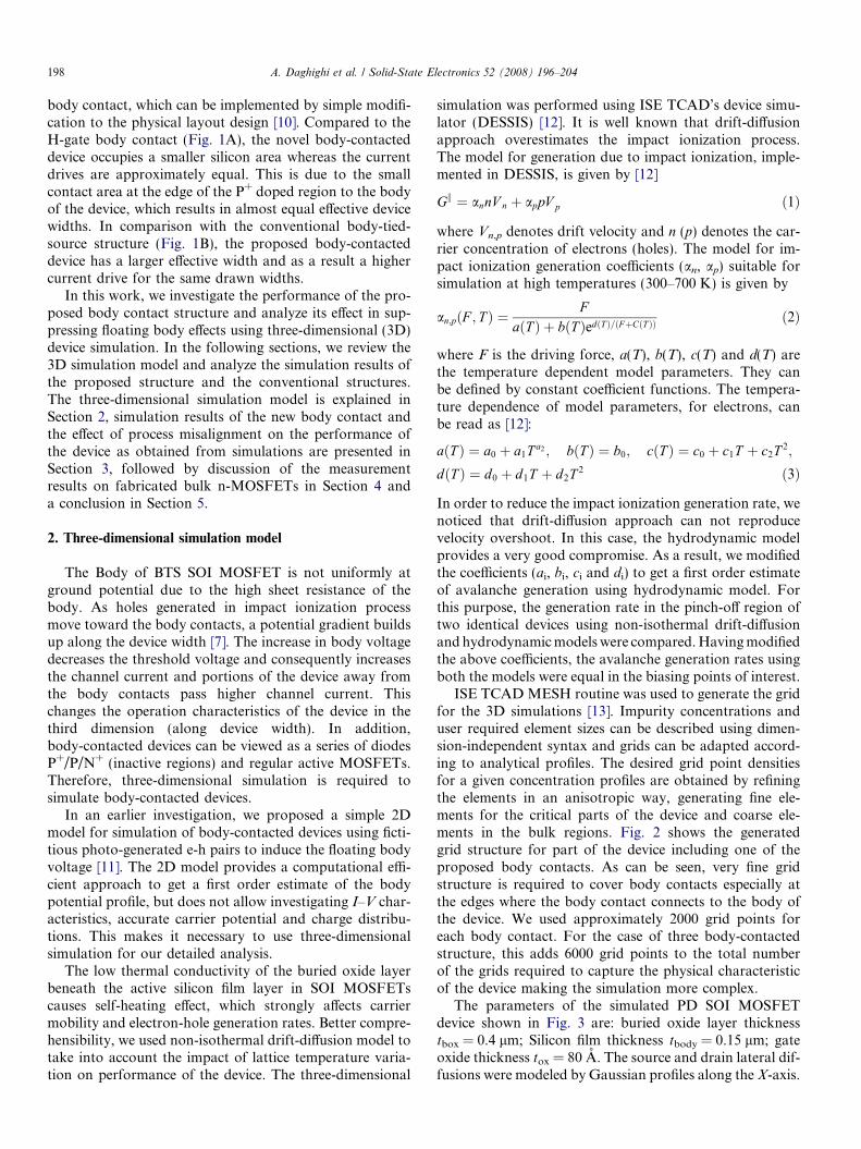
ISE TCAD MESH routine was used to generate the gridfor the 3D simulations [13]. Impurity concentrations anduser required element sizes can be described using dimen-sion-independent syntax and grids can be adapted accord-ing to analytical profiles. The desired grid point densitiesfor a given concentration profiles are obtained by refiningthe elements in an anisotropic way, generating fine ele-ments for the critical parts of the device and coarse ele-ments in the bulk regions. Fig. 2 shows the generatedgrid structure for part of the device including one of theproposed body contacts. As can be seen, very fine gridstructure is required to cover body contacts especially atthe edges where the body contact connects to the body ofthe device. We used approximately 2000 grid points foreach body contact. For the case of three body-contactedstructure, this adds 6000 grid points to the total numberof the grids required to capture the physical characteristicof the device making the simulation more complex.
The parameters of the simulated PD SOI MOSFETdevice shown in Fig. 3 are: buried oxide layer thicknesstbox = 0.4 lm; Silicon film thickness tbody = 0.15 lm; gateoxide thickness tox = 80 A. The source and drain lateral dif-fusions were modeled by Gaussian profiles along the X-axis.

Fig. 2. 3D Mesh structure (part of the device including one of the novel body contacts is shown in the picture).
Fig. 3. 3D BTS SOI structure.
A. Daghighi et al. / Solid-State Electronics 52 (2008) 196–204 199
The gate of the devices was an n+polysilicon with dimen-sions L = 0.35 lm and W = 5 lm. The bulk contact was anelectrical contact at zero volt and thermal contact at 300 K.
3. Simulation results
Using non-isothermal drift-diffusion model, three-dimensional simulations of body-contacted to source struc-tures were examined. All the simulation results on current
drive, body voltage and breakdown voltage are presentedat gate voltage of 1.0 V. This is due to the fact that the larg-est impact ionization rate happens at low gate voltageswhere the body effect is the largest [7,11]. In the following,Section 3.1 shows the simulation results of a floating body,two conventional BTS structures and the new body con-tact. In Section 3.2, the effect of process misalignment onthe performance variation of the new body-contacteddevices is discussed.

Fig. 5. Body potential variation along the device width.
200 A. Daghighi et al. / Solid-State Electronics 52 (2008) 196–204
3.1. New body contact
Four device structures were simulated: (1) a floatingbody (FB) device, (2) a conventional body-contacted devicewith two body contacts (one at each end of the source asshown in Fig. 1B, and each had a width WB = 0.35 lm),(3) a conventional body-contacted device with three bodycontacts, one at each source end and one in the middle ofsource with WB = 0.35 lm as depicted in Fig. 3, and (4) adevice with three of the proposed novel body contacts,one at both ends and one in the middle of the source.Fig. 4A has already been reported [16] and it shows the cur-rent–voltage characteristic (IDS vs. VDS) of the four simu-lated devices. As can be seen, the proposed body contacteliminates the kink inherent in the FB device characteristic.Also the novel body-contacted device has a higher currentdrive than the device with three conventional body contactsstructure. Reducing the number of conventional contactsto two, increases current drive at the expense of increasedbody voltage, dynamic variation of threshold voltage,
Fig. 4. (A) Drain current vs. drain voltage; (B) sub-thresholdcharacteristic.
and lower breakdown voltage. Notice that the drain cur-rent starts increasing at higher rate for drain voltagesbeyond 2 V indicating lower breakdown voltage.
The sub-threshold characteristics of the simulateddevices are shown in Fig. 4B. Significant sub-thresholdslope variation of DS = 16.8 mV/dec can be observed whenthe drain voltage changes from 50 mV to 1.5 V for thefloating body device. This value decreases to DS =3.3 mV/dec for the proposed novel body-contacted deviceand DS = 1.1 mV/dec for the three conventional body con-tacts structure. This indicates that novel body contact (nar-row contact) is as effective as conventional body contacts(wide contacts) in controlling the body voltage [14].
The magnitude of the resulting floating body voltagenear the source body junction provides a more accurateway of comparing the different BTS structures. Fig. 5shows the magnitude of the electrostatic potential along aline close to and parallel to the body/source junction forthe FB and BTS structures. This provides a measure ofthe floating body voltage at gate voltage of 1 V and drainvoltage of 3 V. Note that introducing two conventionalbody contacts at the ends of the source reduces maximumfloating body voltage from about 770–480 mV. The maxi-mum body voltage reduces to 390 mV and 170 mV forthe novel proposed body contact and three conventionalbody contact structures, respectively.
The breakdown voltage and on-resistance of the devicesare also investigated and the simulation results are summa-rized in Table 1. The on-state breakdown voltage shows theimpact of floating body voltage on the breakdown charac-teristic while the device is turned on. The breakdown volt-age characteristic of the proposed body contact is clearlybetter than that of the floating body and the conventionaltwo body-contacted structures. In order to simulate the on-resistance, gate voltage is ramped to 3 V and drain voltageto 50 mV. Faced with consistent divergence of non-isother-mal drift-diffusion simulation during ramping gate voltage,we ran 2D simulations to determine the magnitude of the

Table 1Breakdown voltage, drive current and on-resistance of the devices
Floating body 2 Body contacts 3 Body contacts Novel body contact Comment
VBR (V) 4 5 6 6.7 VGS = 1V (on-state breakdown)
Drive current 163% 86% 79% 104% Ratio of IDS at VGS = 1 V,VDS = 2 V to the reference SOI
RON (X) 203 235 250 221 VGS = 3 V, VDS = 50 mV
A. Daghighi et al. / Solid-State Electronics 52 (2008) 196–204 201
drain current and the role of self-heating. The 2D non-iso-thermal simulation on a floating body device revealednegligible self-heating effects. Consequently, we used iso-thermal drift-diffusion model for our 3D simulations ofthe on-resistance (RON). The proposed novel body-con-tacted device showed smaller RON compared to both con-ventional body-contacted devices due to the increasedchannel current. However, it’s less than the floating bodydevice, which has the best RON.
Furthermore, we also examined influence of differentbody contact structures on the device current. The strongdependence of the current on the floating body voltage,which is determined by the geometry and location of bodycontacts, requires defining a suitable structure to act as areference. To overcome this problem, we chose as a refer-ence a SOI device with uniform body voltage distributionalong the device width. A uniform body voltage distribu-tion can be achieved in a device structure with a narrowand continues P+ implant under the source region and con-nected to the source contact. The drain current for thisdevice was then determined at a gate voltage of 1 V anddrain voltage of 2 V through simple two-dimensional sim-ulations and then scaled to determine the desired currentfor any device width. Table 1 shows the ratios of currentdrives of the body-contacted devices (obtained fromthree-dimensional simulations) to that of the referencebody-contacted SOI device. Notice that the floating bodydevice exhibits a significant current drive increase (63%)due to lowering of threshold voltage and activation of lat-eral BJT. The proposed novel body-contacted device showsa slight increased current (104%) drive due to the modula-tion in body voltage. On the other hand, there is largereduction in the current drives of both two conventionalbody-contacted (86%) and three conventional body-con-tacted (79%) devices due to the decreased effective devicewidth.
Influence of the new body contact on the output conduc-tance and transistor parasitic capacitances were also inves-tigated. Body-contacted devices are the major componentof analog circuits using partially depleted SOI MOSFETs.One of the main device characteristics, which directlyaffects the gain of amplifiers is the output conductance(gDS) at the biasing point of interest. It has been shown thatthe new body contact and the three conventional body-con-tacted structures show the lowest variation in drain con-ductance as drain voltage changes [16]. However, drainconductance of the two conventional body-contacted
device showed drain voltage dependency. For analogapplications this translates to the undesired reduction ofintrinsic gain of transistor. In addition to the output con-ductance, parasitic capacitances have an important impacton the performance of the circuits especially for high speedapplications such as microprocessors and analog radio fre-quency (RF) circuits. Total extrinsic plus intrinsic gate-source (CGS) capacitance as the most sensitive capacitanceto the geometry of the body-tied-source contacts were alsoexamined [16]. It was shown that CGS of the new body con-tact in saturation region is equal to that of the conventionalbody contact structures and it was constant as drain volt-age increased. This was different with the floating bodydevice where CGS increased as drain voltage increaseddue to the variation of the body voltage.
3.2. Body contact misalignment
One major concern regarding the proposed body con-tact is the effect of process misalignment of P+ dopedregions on device performance. The ideal situationoccurs when the tip of the P+ implant diamond regiontouches the source/body junction as shown in Fig. 6(structure B) which lead to zero misalignment (DX = 0).Two other possible situations are when the tip shiftsaway from junction and in this situation there is nodirect contact between the P-body and the P+ contacts(Structure A where DX = �50 nm). The other situationis where the tip shifts inside the P-body making a widercontact to the body (structure C where DX = 50 nm).Fig. 7 shows the simulation results of drain current vs.drain-source voltage for these three cases. It’s interestingto note that for structure A, the I–V characteristic inFig. 7, does not exhibit a well defined kink as in floatingbody device (see Fig. 4A) and instead shows a gradualincrease beyond 1.3 V at rates well below that for theFB device. This is due to the fact that accumulated holesin the body region face low potential barrier to escape tobody contacts. Note that in this case, part of the sourcenear the tip of body contact is depleted and this reducesthe effective device width even smaller than the effectivedevice width in Structure B. However, at higher drainvoltages, body voltage increases resulting in increasedchannel current. Structure C, on the other hand, resultsin smaller effective device width which leads to currentdrive that is lower than the perfectly aligned contacts(structure B).

202 A. Daghighi et al. / Solid-State Electronics 52 (2008) 196–204
The body voltage distributions provide more insight intohow body contact misalignment can affect performance ofthe devices and can be determined from the three-dimen-
Fig. 7. Novel body contact, IDS vs. VDS for three different misalignmentschemes.
Fig. 8. Body voltage distribution along the device width for the threedifferent misalignment schemes.
Fig. 6. Top view of three misalignment structures, (A) DX = �50 nm, (B)DX = 0 and (C) DX = +50 nm.
sional simulations. Fig. 8 shows the body voltage variationalong the device width at VGS = 1 V and VDS = 3 V. Ascan be seen from the figure, the body voltage for structureA increases to a maximum of 650 mV. On the other hand,when P+ implant tip reaches to the body region as case C,the maximum body voltage drops to 310 mV. Thisamounts to a reduction of 80 mV from that of perfectlyaligned body contact and is due to the wider body contact,which leads to less body contact resistance for the structureC.
The higher body potential for situation A leads to lowerbreakdown voltage in comparison to structure B due to theactivation of lateral bipolar at lower drain voltages. Fur-thermore, the breakdown voltage is equal for both thestructures B and C since the average body voltage is almostequal. Comparing the current drives in Table 2 with struc-ture B, one can see higher current drive for structure A(107%) and less for structure C (95%). The increased bodyvoltage and decreased threshold voltage results in highercurrent and slight reduction in breakdown voltage. Onthe other hand, the reduced effective device width is respon-sible for the decrease in current drive in structure C com-pared to perfectly aligned body contact case. However,the on-resistance of the devices with structures B and Care relatively equal.
Based on the above discussion, it is desirable to avoidthe situation where the body contacts moves away fromthe body as in situation A of Fig. 6. This can be achievedby intentionally shifting the P+ implant diamond regionin physical layout design to target structure C (DX =+50 nm) as the ideal body-contacted structure, thereforeavoiding the effect of (negative) misalignment. Althoughthis comes at the expense of a relatively reduced drivecurrent capability (reduced effective width), it insures thepresence of a body contact region with better transistor celldensity and performance compared to conventionalstructures.

Table 2Effect of body contact misalignment on characteristic of the device
Structure A Structure B Structure C Comment(DX = �50 nm) (DX = 0) (DX = + 50 nm)
VBR (V) 6.4 6.7 6.7 VGS = 1 V (on-state breakdown)Drive current 107% 104% 95% Ratio of IDS at VGS = 1 V, VDS = 2 V to the reference SOIRON (X) 212 221 221 VGS = 3 V, VDS = 50 mV
Table 3Breakdown voltage measurement
Floatingbody
Conventionalbody contact
Novel bodycontact
Comment
VBR (V) 4.6 13.75 13.78 Off-state
Fig. 10. Drain current vs. drain voltage for the three devices.
A. Daghighi et al. / Solid-State Electronics 52 (2008) 196–204 203
4. Experimental results
Floating body effects can also be observed in Bulk highvoltage devices due to the large impact ionization currentand high substrate resistance. Body contacts are used toincrease breakdown voltage and eliminate the kink in theoutput current. Furthermore, to increase the latch-upimmunity in CMOS technology body contacts arerequired. In order to demonstrate the performance func-tionality of the proposed structure, a test chip containinga set of NMOS devices with different body P+ contactstructures (floating, CMOS conventional BTS, and pro-posed BTS) along with several CMOS and LDMOSdevices is designed. The technology is based on a fully man-ufacturable bulk CMOS process targeting power conver-sion markets [15] with a high resistivity P-type float-zonewafer substrate, on which an N-well implant is performedwith a subsequent drive. To form the body region of thetested NMOS devices, a P-tub implant and a subsequentdrive are performed. The P-tub is implanted in the N-wellregion prior to growing the field oxide. The gate regions arethen formed. To produce the source and drain regions, aP+ and N+ implants are performed followed by a 900 �C
Fig. 9. Cross-section of the three NMOS devices fabricated: (A) bulk, (B)conventional body-contacted (top view) and (C) novel body-contacteddevice (top view).
breakdown
anneal and the subsequent formation of interlayer dielec-tric, metal, and final passivation layers. Fig. 9 depicts thecross-section of the three NMOS devices tested.
A test setup employing a probe station with HP4156Semiconductor Parameter Analyzer is used for the mea-surements of IDS–VDS output curves and the breakdownvoltage of the three devices. Fig 10 displays the outputcurves of the tested structures at a gate voltage of 5.0 V.Here, the N-well is tied to 5.0 V supply and the substrateis grounded. As evident from the Figure, the proposedstructure yields almost identical current drive results asthe conventional one and that the FB effects are clearlynot present. This is further supported by the breakdownvoltage results shown in Table 3. These findings clearlydemonstrate the viability of the structure for SOI CMOStype devices.
5. Conclusion
A simple body contact structure is described to opti-mally suppress the floating body effects in partiallydepleted SOI devices. The structure requires only a novellayout design for the P+ diffusion region; no manufacturing

204 A. Daghighi et al. / Solid-State Electronics 52 (2008) 196–204
process modification is required. Using the proposed struc-ture, 3D simulations were performed and showed improvedperformance in comparison to floating body structures.Experimental data of the fabricated devices confirmed thesimulation results. The simple nature of the describedstructure offers the possibility of its extension to other typeof device structures and technologies.
References
[1] Shahidi GG. SOI technology for the GHz era, IBM J Res Dev2002;42(2/3):121–31.
[2] Dallman DA, Shenai K. Scaling constraints imposed by self-heatingin sub-micron SOI MOSFET’s. IEEE Trans Electron Dev1995;42(March):489–96.
[3] Colinge JP. Silicon-on-insulator technology: materials to VLSI.Kluwer Academic Publishers; 1997.
[4] Horiuchi M, Tamura M. BESS: a source structure that fullysuppresses the floating body effects in SOI CMOSFET’s. IEEE TransElectron Dev 1998;45(May):1077–83.
[5] Nishiyama A, Arisumi O, Yoshimi M. Suppression of the floatingbody effect in partially depleted SOI MOSFET’s with SiGe sourceand its mechanism. IEEE Trans Electron Dev 1997;44(December):2187–92.
[6] Yunlong L, Xinyu L, Zhiyong Z, He Q. A novel Salicide body-contacted structure for partially depleted SOI nMOSFETs. In: Procof 6th international conference on solid-state and integrated-circuittechnology, vol. 1; 2001. p. 531–34.
[7] Kuehne SC, Chan ABY, Nguyen CT, Wong SS. SOI MOSFET withburied body strap by wafer bonding. IEEE Trans Electron Dev1998;45(May):1084–91.
[8] Lee J, Kim H, Kim J, Lee W, Oh J, Kang D, et al. Performanceimprovements in high-density DRAM application using 0.15 lmbody-contacted SOI technology. In: Proc of IEEE international SOIconference; 2000. p. 76–7.
[9] Kotani N, Ito S, Yasui T, Wada A, Yamaoka T, Hori T. Suppressionof leakage current in SOI CMOS LSIs by using silicon sidewall bodycontact (SSBC) technology. In: Symposium on VLSI technologydigest of technical papers; 2002. p. 44–5.
[10] Daghighi A. Area efficient body contact for partially depleted SOIMOSFETs. Ph.D. Thesis 2004. Washington State University.
[11] Daghighi A, Osman MA. A two-dimensional model for investigatingbody contact structures in PD SOI MOSFETs. J Microelectron Eng2003;70(October):83–92.
[12] DESSIS Manual. ISE integrated system engineering, Version 7.0;2001.
[13] MESH Manual. ISE integrated system engineering, Version 7.0;2001.
[14] Daghighi A, Osman MA. Three-dimensional simulation of bodycontact structures in PD SOI MOSFETs. In: Proc of the 15tth IEEEUGIM symposium; July 2003. p. 288–91.
[15] Imam M, Hossain Z, Quddus M, Adams J, Hoggatt C, Ishiguro T,et al. Design and optimization of double-resurf high-voltage lateraldevices for a manufacturable process. IEEE Trans Electron Dev2003;50(July):1697–701.
[16] Daghighi A, Osman MA. Small signal analysis of a SOI MOSFETdevice with a novel area efficient body contact. Proc IEEE South-eastCon 2005:88–91.
Copyright © 2022 FDOKUMEN