SOI Technologies Overview for Low-Power Low-Voltage Radio-Frequency Applications
22
Analog Integrated Circuits and Signal Processing, 25, 93–114, 2000 # 2000 Kluwer Academic Publishers. Manufactured in The Netherlands. SOI Technologies Overview for Low-Power Low-Voltage Radio-Frequency Applications O. ROZEAU, 1,2,3 J. JOMAAH, 1,2 S. HAENDLER, 1 J. BOUSSEY 1 AND F. BALESTRA 1 1 LPCS, B.P. 257, F-38016 Grenoble Cedex1, France 2 LEMO, B.P. 257, F-38016 Grenoble Cedex1, France 3 STMicroelectronics, F-38920 Crolles, France Received April 8, 2000; Revised April 14, 2000; Accepted April 20, 2000 Abstract. Thanks to their structure, the SOI technologies present several intrinsic advantages for analog and RF applications. Indeed, as it is well established now, these technologies allow the reduction of the power consumption at a given operating frequency. Moreover, the high-insulating properties of SOI substrates, in particular when high resistivity substrate is used, make that these technologies are perfect candidates for mixed- signal applications. In the present paper, we will discuss the performances of the SOI technologies in radio-frequency range. First of all, the high-frequency behavior of SOI substrates, thanks to the characterization of transmission lines, will be shown. The impact of the SOI substrate resistivity on the performances of passive components will also be analyzed. Then, an overview of RF performances of SOI MOSFETs for two different architectures, fully- and partially-depleted, will be achieved and compared to the bulk ones. Finally, the influence of some specific parasitic effects, such as the kink effect, the self-heating effect and the kink-related excess noise, on the RF performances of SOI devices will be studied, thanks to a specific high-frequency characterization. Key Words: SOI technologies, SIMOX, Unibond, SOI MOSFETs, substract losses, cut-off frequency, noise, self-heating 1. Introduction The most obvious difference between SOI and bulk technologies is the vertical isolation from the substrate in the SOI technology achieved by the buried oxide film (Fig. 1). As a consequence, integrated devices on SOI substrates can be totally isolated with a dielectric material. This full (lateral and vertical) isolation prevents the well-known latch- up effect observed in bulk technology and suppresses the substrate coupling mechanisms at low frequency. Therefore, a higher integration density can be achieved with SOI technologies in comparison with bulk substrates. This increase of the integration density is particularly significant for high voltage applications, since the lateral isolation schemes, required for such applications in bulk technology, consume a substantial proportion of the total chip area. Moreover, thanks to the buried oxide, the control of junction depths is more efficient than in bulk silicon and as a consequence the parasitic capacitances in SOI are much lower than those of bulk. In this way, the SOI technologies are adapted for low power low-voltage mixed signal applications. At the present time, the market of RF circuits is still essentially provided by III–V devices. This is mainly due to the semi-insulating behavior of gallium arsenide substrates and also to the very high speed of GaAs circuits. However, silicon use in this domain is steadily increasing since the last few years. This trend is mainly supported by the silicon properties themselves (dielectric constant is higher than the AsGa one, and is weakly dependent on the tempera- ture and the frequency) and by the enormous efforts afforded by the microelectronics industry to reach a high degree of technological maturity. As a matter of fact, the reduction of the dimensions allows to reach very attractive performances and a cut-off frequency
-
Upload
independent -
Category
Documents
-
view
5 -
download
0
Transcript of SOI Technologies Overview for Low-Power Low-Voltage Radio-Frequency Applications

Analog Integrated Circuits and Signal Processing, 25, 93±114, 2000
# 2000 Kluwer Academic Publishers. Manufactured in The Netherlands.
SOI Technologies Overview for Low-Power Low-VoltageRadio-Frequency Applications
O. ROZEAU,1,2,3 J. JOMAAH,1,2 S. HAENDLER,1 J. BOUSSEY1 AND F. BALESTRA1
1LPCS, B.P. 257, F-38016 Grenoble Cedex1, France2LEMO, B.P. 257, F-38016 Grenoble Cedex1, France
3STMicroelectronics, F-38920 Crolles, France
Received April 8, 2000; Revised April 14, 2000; Accepted April 20, 2000
Abstract. Thanks to their structure, the SOI technologies present several intrinsic advantages for analog and RF
applications. Indeed, as it is well established now, these technologies allow the reduction of the power
consumption at a given operating frequency. Moreover, the high-insulating properties of SOI substrates, in
particular when high resistivity substrate is used, make that these technologies are perfect candidates for mixed-
signal applications.
In the present paper, we will discuss the performances of the SOI technologies in radio-frequency range. First
of all, the high-frequency behavior of SOI substrates, thanks to the characterization of transmission lines, will be
shown. The impact of the SOI substrate resistivity on the performances of passive components will also be
analyzed. Then, an overview of RF performances of SOI MOSFETs for two different architectures, fully- and
partially-depleted, will be achieved and compared to the bulk ones. Finally, the influence of some specific
parasitic effects, such as the kink effect, the self-heating effect and the kink-related excess noise, on the RF
performances of SOI devices will be studied, thanks to a specific high-frequency characterization.
Key Words: SOI technologies, SIMOX, Unibond, SOI MOSFETs, substract losses, cut-off frequency, noise,
self-heating
1. Introduction
The most obvious difference between SOI and bulk
technologies is the vertical isolation from the
substrate in the SOI technology achieved by the
buried oxide ®lm (Fig. 1). As a consequence,
integrated devices on SOI substrates can be totally
isolated with a dielectric material. This full (lateral
and vertical) isolation prevents the well-known latch-
up effect observed in bulk technology and suppresses
the substrate coupling mechanisms at low frequency.
Therefore, a higher integration density can be
achieved with SOI technologies in comparison with
bulk substrates. This increase of the integration
density is particularly signi®cant for high voltage
applications, since the lateral isolation schemes,
required for such applications in bulk technology,
consume a substantial proportion of the total chip
area. Moreover, thanks to the buried oxide, the
control of junction depths is more ef®cient than in
bulk silicon and as a consequence the parasitic
capacitances in SOI are much lower than those of
bulk. In this way, the SOI technologies are adapted
for low power low-voltage mixed signal applications.
At the present time, the market of RF circuits is
still essentially provided by III±V devices. This is
mainly due to the semi-insulating behavior of gallium
arsenide substrates and also to the very high speed of
GaAs circuits. However, silicon use in this domain is
steadily increasing since the last few years. This trend
is mainly supported by the silicon properties
themselves (dielectric constant is higher than the
AsGa one, and is weakly dependent on the tempera-
ture and the frequency) and by the enormous efforts
afforded by the microelectronics industry to reach a
high degree of technological maturity. As a matter of
fact, the reduction of the dimensions allows to reach
very attractive performances and a cut-off frequency

as high as 100 GHz has been obtained from a deep
submicrometer CMOS device [1]. However, CMOS
silicon technologies suffer of the very low resistivity
(lower than 10 Ocm) of silicon substrates currently
available which drastically affects the RF perform-
ances of passive devices and increases the substrate
noise coupling.
The recent published works on the SOI tech-
nologies show the high potentialities of these
technologies for radio-frequency applications [2±4].
In fact, for these applications, the main advantage of
the SOI technology is its compatibility with the use of
the high-resistivity substrates which allow a high
reduction of the crosstalk without any increase of
latch-up phenomena [5,6] and an increase of the
inductor quality factor [3].
However, these technologies suffer from the
¯oating body effects, the self heating effect and the
``high'' access resistances. Nevertheless, these para-
sitic effects have a more or less pronounced impact
on the circuit behavior according to the used
technology (fully- or partially-depleted technologies)
and should be taken into account at the circuit design
level. That is why it is very important to understand
the ¯oating body and the self heating mechanisms in
order to be able to predict their impact on the analog
and radio-frequency parameters.
All these points will be discussed in the following
sections. In the ®rst part, the performances of passive
components integrated in SOI technologies will be
investigated and the expected advantages from using
a high resistivity substrate will be demonstrated. The
second part will be consecrated to the RF perform-
ance of SOI MOSFET with a comparison between
fully- and partially-depleted SOI and bulk
MOSFETs. Finally, the last part deals with the
speci®c SOI MOSFET properties where the impact of
¯oating body effects and self-heating effect on analog
and radio-frequency performances will be discussed.
The in¯uence of speci®c MOSFET/SOI design will
be also treated.
2. Passive Components: High Resistivity SOISubstrates
The passive components play a consequent role in the
RF circuit development. For example, in silicon
technology, the integration of inductors with high
performance is a challenge in RF integrated circuits
because of the silicon substrate losses and series
resistance. Basically, the inductor quality factor
affects the noise ®gure and the gain of low noise
ampli®er using an inductive degeneration architec-
ture [7] or affects the level of phase noise of
harmonic voltage controlled oscillator (VCO) [8]. A
good quality factor (higher than 40) allows to reduce
the DC power thanks to the reduction of the gain of
active devices [9].
The performances of coplanar transmission lines
are directly linked to the substrate losses and the
series resistance. The substrate losses are dependent
on the substrate resistivity in silicon technology while
the serial resistances depend strongly on the back-end
process. Fig. 2(a) shows measured transmission line
losses vs. frequency for SOI substrates (with several
resistivities), quartz and standard bulk substrates. The
transmission lines used here, have a separation
distance (S) of 49 mm and a width (W) of 86 mm.
(Fig. 2(b)). Notice that the buried oxide becomes
transparent for frequency higher than 300 MHz and
consequently the substrate losses are only due to the
substrate resistivity [6].
Fig. 2(a) highlights the large impact of the
substrate resistivity. The SOI substrates allow much
higher resistivity values than the bulk ones. Indeed, at
the very low impurity concentrations required to
obtain high-resistivity material, the diffusion of even
Fig. 1. Schematic cross-section of the SOI technologies.
94 O. Rozeau et al.

small quantities of dopants degrades substantially the
resistivity. SOI technology provides an interesting
alternative: the insulating layer ef®ciently preserves
the high purity of the substrate during the fabrication
process. As a consequence, SOI coplanar transmis-
sion lines do achieve better performances than the
bulk fabricated ones. The quartz substrate shows the
best performances thanks to its insulating properties.
To evaluate the impact of substrate resistivity on
transmission line performances, the losses have been
simulated and plotted versus the substrate resistivity
(Fig. 3) at 1, 5 and 10 GHz for a SOI substrate, using
an analytical model [10].
The variations of losses with the silicon substrate
resistivity show the large impact of this resistivity. At
10 GHz, the transmission losses are at about 2.3 dB/
mm for a 10 O cm of silicon substrate resistivity,
while for rSi higher than 500 Ocm, the losses are
lower than 0.2 dB/mm. Moreover, we can notice that
it is not necessary to use substrate resistivity value
higher than 1 kOcm.
In addition, the silicon substrate properties and
series resistance have a large in¯uence on quality
factor and resonant frequency of inductors. This is
why, the most published works concerning the Qenhancement are based on the decrease of metal
resistances with the use of thick gold metallization
[11], multiple metal layers in parallel [12±14] or with
the use of high resistivity substrates [11,15,16]
(Qmax � 11:5 for L � 13 nH with 2 mm Al and
2 kOcm of substrate resistivity). The last solution
seems to be the best for obtaining good Q factor
inductors but this substrate type can not be used in
bulk technology because it increases latch-up phe-
nomena and does not facilitate the control of
the junction depth. Moreover, new designs of the
inductor allow to increase the quality factor, as the
patterned ground shields (PGS) [17,18] (Qmax � 7:3for L� 7.4 nH with 2 mm Al) or the layout optimiza-
tion [19]. However, these last methods are limited to
an increase of the inductor quality factor only up to
33% due to an increase of coupling capacitances, and
therefore, do not allow to attain large quality factors
necessary for the RF design. The quality factor of
inductors coming from several technologies have
been compared, as illustrated by Fig. 4 [16,18,20].Fig. 3. Simulated transmission line losses vs. substrate resistivity.
(a) (b)
Fig. 2. (a) Measured transmission line losses for standard SIMOX, high resistivity SIMOX, quartz and bulk substrates and (b) cross-section
of coplanar transmission line on SOI substrate.
Low-Power Low-Voltage Radio-Frequency Applications 95

Clearly, the best results are obtained on a semi-
insulating substrate, such as GaAs or sapphire, and
with an extremely thick low resistivity metal-layer,
such as gold. The advantages of the insulating
substrate, have been shown by Johnson et al.
Thanks to a comparison between inductors built on
SOS and bulk silicon substrate where the quality
factor of SOS inductor is 13 while the bulk silicon
inductor's one is near 4 [21]. This trend has been
con®rmed on capacitor and resistor performances too
[22].
In SOI technology, the transistors are built in a
thin silicon ®lm which is separated from the substrate
by a buried oxide layer. Each transistor is totally
isolated and consequently, this technology is insensi-
tive to latch-up problems and does not need a heavily
doped buried layer, therefore, it is compatible with
the high resistivity silicon substrate. The ®rst studies
concerning the use of this substrate types have been
realized by Eggert et al. [3].
For this study, planar inductors have been realized
on two different substrate types. Fig. 5 shows the
quality factor vs. frequency of 5.2 nH inductors
(3 turns) fabricated on standard SIMOX and high-
resistivity SIMOX.
The measured inductors are de®ned in a 1.4 mm
aluminum metallization, with a 15 mm line width and
10 mm of spacing between the metal stripes. The
difference between standard SIMOX and high-
resistivity SIMOX is noticeable on maximal quality
factor Qmax and the frequency at this quality factor
value fQmax. Thanks to the use of high resistivity SOI
substrate, the Qmax is multiplied by almost 2.5 and
the fQmax increases from 1.7 to 4.5 GHz. Note that the
inductor must be optimized, in term of layout for a
given application, in order to obtain the best quality
factor.
Fig. 4. Reported peak-Q values of monolithic inductor as a function of inductance [16,18,20].
Fig. 5. Quality factor of 5.2 nH inductor on standard SIMOX
(20±30 O cm) and high resistivity SIMOX (4 1 kO cm).
96 O. Rozeau et al.
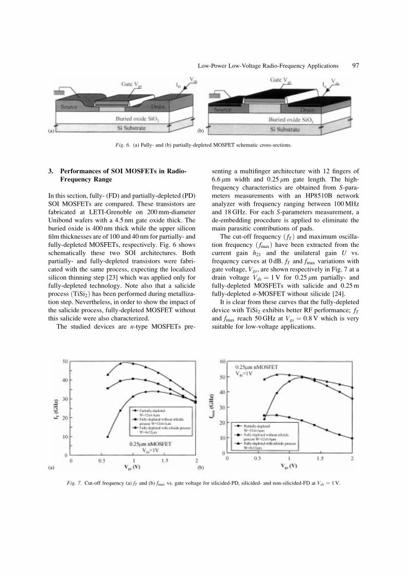
3. Performances of SOI MOSFETs in Radio-Frequency Range
In this section, fully- (FD) and partially-depleted (PD)
SOI MOSFETs are compared. These transistors are
fabricated at LETI-Grenoble on 200 mm-diameter
Unibond wafers with a 4.5 nm gate oxide thick. The
buried oxide is 400 nm thick while the upper silicon
®lm thicknesses are of 100 and 40 nm for partially- and
fully-depleted MOSFETs, respectively. Fig. 6 shows
schematically these two SOI architectures. Both
partially- and fully-depleted transistors were fabri-
cated with the same process, expecting the localized
silicon thinning step [23] which was applied only for
fully-depleted technology. Note also that a salicide
process �TiSi2� has been performed during metalliza-
tion step. Nevertheless, in order to show the impact of
the salicide process, fully-depleted MOSFET without
this salicide were also characterized.
The studied devices are n-type MOSFETs pre-
senting a multi®nger architecture with 12 ®ngers of
6.6 mm width and 0.25 mm gate length. The high-
frequency characteristics are obtained from S-para-
meters measurements with an HP8510B network
analyzer with frequency ranging between 100 MHz
and 18 GHz. For each S-parameters measurement, a
de-embedding procedure is applied to eliminate the
main parasitic contributions of pads.
The cut-off frequency � fT� and maximum oscilla-
tion frequency � fmax� have been extracted from the
current gain h21 and the unilateral gain U vs.
frequency curves at 0 dB. fT and fmax variations with
gate voltage, Vgs, are shown respectively in Fig. 7 at a
drain voltage Vds � 1 V for 0.25 mm partially- and
fully-depleted MOSFETs with salicide and 0.25 m
fully-depleted n-MOSFET without silicide [24].
It is clear from these curves that the fully-depleted
device with TiSi2 exhibits better RF performance; fT
and fmax reach 50 GHz at Vgs � 0:8 V which is very
suitable for low-voltage applications.
(a) (b)
Fig. 6. (a) Fully- and (b) partially-depleted MOSFET schematic cross-sections.
(a) (b)
Fig. 7. Cut-off frequency (a) fT and (b) fmax vs. gate voltage for silicided-PD, silicided- and non-silicided-FD at Vds � 1 V.
Low-Power Low-Voltage Radio-Frequency Applications 97

In addition, partially-depleted transistor shows
also a good RF performance, but at higher voltages
than fully-depleted ones (Vgs � 1:4 V and
Vds � 1:8 V) (Table 1). This shift is mainly due to a
difference of threshold voltage values which are
* 0.65 V and * 0.45 V for partially- and fully-
depleted MOSFETs respectively.
To compare accurately these three SOI MOSFETs,
the parameters of small signal equivalent circuit, as
illustrated in Fig. 8, are extracted with an analytical
calculation method. The residual pad admittances
(Ypg; Ypd and Ypgd), which may be not taken into
account during the de-embedding procedure, are
included in this equivalent circuit in order to improve
the extraction procedure accuracy.
The main elements are given in Table 2 at
Vgs � Vds � 1 V. The gate resistance values show
clearly the impact of the salicide process. This
explains the considerable difference between fmax
values of these three technologies.
From another part, a very weak difference is
obtained between the gate±source, gate±drain and
drain±source capacitances (Cgs;Cgd and Cds, respec-
tively), which is due to a dispersion of channel length
between all devices mainly caused by the difference
of thermal budget between these three technologies.
Thanks to Cgs;Cgd capacitance values, a more
important LDD extension in the case of
the silicided-partially- and silicided-fully-depleted.
MOSFET's has been noticed with regard to the fully-
depleted MOSFET without salicide process. This
difference has been con®rmed by a static character-
ization. Moreover, the transconductance, gm, is
higher for fully-depleted devices (at least 20% for
FD transistor higher than PD one). That is a well-
known advantage of the fully-depleted technology
and this explains the high values of f ? for these
devices.
In addition, the extracted values of the drain
conductance are nearly identical for non-silicided
fully- and silicided-partially-depleted MOSFETs, but
are found to be higher for silicided-fully depleted.
This is due to the prevalence of the short channel
effects.
To evaluate the potentialities of the SOI tech-
nologies, the previous extracted transconductance can
Table 1. Maximum of cut-off frequencies fT and fmax for silicided-PD, silicided-FD and non-silicided-FD SOI MOSFET.
FD without TiSi2 FD with TiSi2 PD with TiSi2
Vgs (V) 0.8 0.8 1.4
Vds (V) 1.0 1.0 1.8
fT,max (GHz) 41 49 37
fmax, max (GHz) 23 51 47
Fig. 8. Small-signal equivalent circuit of an SOI MOSFET.
98 O. Rozeau et al.

be compared with that of bulk technologies. Fig. 9
shows the product of the normalized transconduct-
ances with the gate oxide thickness vs. the effective
channel length. These curves highlight the higher
transconductance values of fully-depleted technolo-
gies than partially-depleted and advanced bulk
technology ones [1,25].
4. SOI Speci®c Mechanisms Behavior in Radio-Frequency Applications
4.1. Floating Body Effects
A consequence of the complete isolation, in parti-
cular in partially depleted SOI CMOS technologies,
is that the part of the silicon ®lm taken up by the
MOSFET body is not electrically connected, unless
the device design explicitly includes a contact to this
region, whereas in bulk CMOS technology, the
device bodies are inherently connected to the well
or to the back substrate. During normal MOSFET
operation, charges will be injected into body
region via several mechanisms (Fig. 10(a)).
In SOI MOSFET without body contacts, the
impedance of the ¯oating body region will be very
high and largely capacitive, as long as the body-
source and body-drain junctions are not forward
biased. Consequently, any charge injected into this
¯oating body region during device operation will
cause a change in the potential of this body region
and hence will result in a change in the behavior of
the MOSFET as shown in Fig. 10(b). For p-channel
MOSFET, this effect is lower due to the weak impact
ionization of holes.
In small-signal applications, this effect depends on
the operating frequency. The body potential is
de®ned by a capacitances and resistances network,
as shown in Fig. 10(a). This network is formed by
body-to-source and drain-to-body junction capaci-
tances and by depletion capacitances depending on
the bias voltage conditions. At high drain voltage and
¯oating body potential, the body-to-source junction is
forward biased, which explains the presence of the
body-source junction resistance Rjbs. From this
description, it is easy to see that the body potential
is ®xed by the drain and gate biases and by the
frequency [26±30].
Fig. 11 shows the drain conductance of a 0.8 mm
partially-depleted SOI MOSFET (multi®nger archi-
tecture) versus DC drain voltage at Vgs � 1 V and for
several frequencies. This output conductance can be
divided into two terms, a ®rst one summarizing the
bulk MOSFET effects (short channel effects,
avalanche, . . .) and a second one depending on the
¯oating body effects. For a 0.8 mm PD n-MOSFET,
Table 2. Extracted values of gate resistances, capacitances, drain conductances and transconductances for 0.25mm for silicided-PD, silicided-
FD and non-silicided-FD SOI MOSFETs at Vgs�Vds� 1V.
FD without TiSi2 FD with TiSi2 PD with TiSi2
Rg�O� 83 (126 6.6mm) 31 (46 12mm) 17 (126 6.6mm)
Cgs (pF/mm) 1.02 1.06 1.09
Cgd ( fF/mm) 330 354 400
Cds (mS/mm) 290 312 290
gm (mS/mm) 366 450 303
gds (mS/mm) 35 42 34
Fig. 9. Normalized transconductance of FD and PD SOI and bulk
MOSFETs vs. effective channel length.
Low-Power Low-Voltage Radio-Frequency Applications 99

the DC drain conductance gdsDC variation presents a
consequent kink effect for Vds > 1:7 V, (gds is
multiplied by 10 as illustrated on the inset of Fig.
11). Nevertheless, when the frequency of the applied
small signal on the drain node increases, the
maximum of AC drain conductance in kink region,
noted gdskink, is reduced and the drain voltage Vdskink
is increased. Consequently, this device can be used at
``high'' frequency without dynamic kink effect.
An other effect of the ¯oating body is the parasitic
bipolar transistor (BJT). The drain-body-source
structure forms a bipolar transistor and, consequently,
the equivalent circuit of SOI MOSFET becomes
more complex at high drain voltage. The impact of
this parasitic transistor is an increase of the drain
current such as the reduction of the breakdown
voltage and the increase of apparent short channel
effects. Thus, this parasitic bipolar transistor
increases the drain conductance and reduces sig-
ni®cantly the transistor gain (gm=gds) as shown by
Tenbroek [30].
The parasitic BJT can be detected thanks to drain
conductance characteristics as function of frequency
and drain voltage. Fig. 12 shows the drain conduct-
ance variations with frequency for several drain
voltages. At low drain voltage values (lower than
3.6 V), the maximal conductance is reduced and the
pole frequency is strongly increased when the applied
(a) (b)
Fig. 10. (a) Cross-section of SOI MOSFET showing the resistances-capacitances network at low-frequency and (b) current drain variations
with drain voltage for a 1 mm partially-depleted n-MOSFET.
Fig. 11. Dynamic and static output conductance vs. Vds for a
0.8mm mult®nger PD MOSFET at Vgs � 1 V.
Fig. 12. AC drain conductance of 5 mm PD n-MOSFET vs.
frequency at Vgs � 2 V [30].
100 O. Rozeau et al.

voltage increases. This behavior is typically due to
the kink effect as seen previously. However, at higher
drain voltage, when the impact ionization current is
signi®cant, the maximal output conductance
increases with the drain voltage and the dependence
of the pole frequency with bias, is much weaker than
that in the kink region. That can be explained by the
increase of the BJT intrinsic cut-off frequency and
intrinsic current gain due to the increase of
collector(drain)-base(body) voltage [31]. This fre-
quency can be estimated and its value is nearly equal
to 3 GHz for a 0.25 mm n-MOSFET. This frequency is
very high and seems to foresee some problems even
in radio-frequency range for large signal ampli®ca-
tions. Notice that this effect can occur in fully-
depleted technologies contrary to the kink effect
which is a speci®c effect of partially-depleted
technologies.
Several works have shown that the ¯oating body
effects, and in particular the kink effect, have a
signi®cant impact on low-frequency noise properties.
In MOS transistors of modern CMOS processes, it
is generally possible to distinguish two noise
components: the white noise and, at lower frequency,
the 1/f noise or ¯icker noise. In the noise spectrum of
SOI technologies (essentially for partially-depleted
technologies), an additional noise contribution is
superposed to the other two components. This
additional component, that appears as a hump in the
noise spectrum, composed by a ¯at plateau followed
by a 1=f 2 roll-off, can be fully characterized by a set
of two parameters: the noise level at the plateau �Spl�and the cut-off frequency � fc�, where the noise is 3 dB under its value at the plateau, as shown in Fig.
13 [32].
There are two noise sources in the ¯oating body,
one results from the impact ionization current �Iii�while the other is associated with the body-source
diode current �Ibs�. Although both are shot noise
generated by ¯ow of carriers surmounting energy
barriers, they are independent noise sources.
Fortunately, these two noise sources are basically
the same in RMS value, because in SOI Iii is roughly
equal to Ibs as a result of current balancing. Shot
noise itself is insigni®cant compared to 1/f noise,
however, it is ampli®ed through the following
processes. The two noise currents ¯ow through the
body-ground impedance (ceq and Req) and change the
body potential; the ¯uctuation in the body potential
modulates the threshold voltage of the device and
consequently causes the excess noise in the drainFig. 13. Typical noise spectrum of a SOI MOSFET with ¯oating
body effect [32].
(b)
Fig. 14. (a) Schematic presentation of equivalent capacitances
and resistances network and (b) their contribution to the noise
source.
(a)
Low-Power Low-Voltage Radio-Frequency Applications 101
current (Fig. 14), so, the total low frequency drain
current noise is the superimposition of 1/f noise and
the excess noise [33]. It is clear that this excess noise
depends on the temperature. Indeed, the frequency fcis shifted towards the high-frequency range when the
temperature rises as noted by Tseng et al. [34].
At a given frequency, the variation of the
normalized drain current noise with the drain voltage
exhibits an excess noise due to the kink effect as
illustrated by Fig. 15 which is a consequent problem
in analog and RF circuits. The maximum of drain
current noise decreases and shifts towards high drain
voltage when the frequency increases.
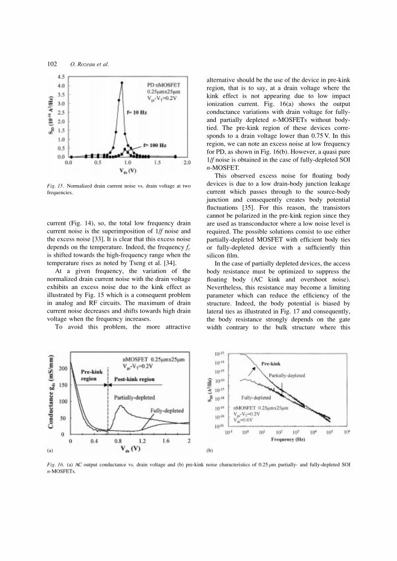
To avoid this problem, the more attractive
alternative should be the use of the device in pre-kink
region, that is to say, at a drain voltage where the
kink effect is not appearing due to low impact
ionization current. Fig. 16(a) shows the output
conductance variations with drain voltage for fully-
and partially depleted n-MOSFETs without body-
tied. The pre-kink region of these devices corre-
sponds to a drain voltage lower than 0.75 V. In this
region, we can note an excess noise at low frequency
for PD, as shown in Fig. 16(b). However, a quasi pure
1/f noise is obtained in the case of fully-depleted SOI
n-MOSFET.
This observed excess noise for ¯oating body
devices is due to a low drain-body junction leakage
current which passes through to the source-body
junction and consequently creates body potential
¯uctuations [35]. For this reason, the transistors
cannot be polarized in the pre-kink region since they
are used as transconductor where a low noise level is
required. The possible solutions consist to use either
partially-depleted MOSFET with ef®cient body ties
or fully-depleted device with a suf®ciently thin
silicon ®lm.
In the case of partially depleted devices, the access
body resistance must be optimized to suppress the
¯oating body (AC kink and overshoot noise).
Nevertheless, this resistance may become a limiting
parameter which can reduce the ef®ciency of the
structure. Indeed, the body potential is biased by
lateral ties as illustrated in Fig. 17 and consequently,
the body resistance strongly depends on the gate
width contrary to the bulk structure where this
Fig. 15. Normalized drain current noise vs. drain voltage at two
frequencies.
(a) (b)
Fig. 16. (a) AC output conductance vs. drain voltage and (b) pre-kink noise characteristics of 0.25mm partially- and fully-depleted SOI
n-MOSFETs.
102 O. Rozeau et al.
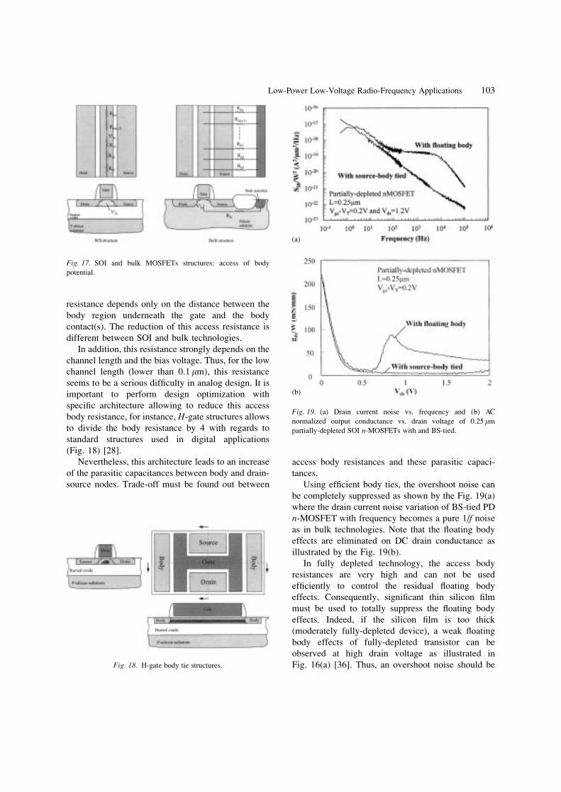
resistance depends only on the distance between the
body region underneath the gate and the body
contact(s). The reduction of this access resistance is
different between SOI and bulk technologies.
In addition, this resistance strongly depends on the
channel length and the bias voltage. Thus, for the low
channel length (lower than 0.1 mm), this resistance
seems to be a serious dif®culty in analog design. It is
important to perform design optimization with
speci®c architecture allowing to reduce this access
body resistance, for instance, H-gate structures allows
to divide the body resistance by 4 with regards to
standard structures used in digital applications
(Fig. 18) [28].
Nevertheless, this architecture leads to an increase
of the parasitic capacitances between body and drain-
source nodes. Trade-off must be found out between
access body resistances and these parasitic capaci-
tances.
Using ef®cient body ties, the overshoot noise can
be completely suppressed as shown by the Fig. 19(a)
where the drain current noise variation of BS-tied PD
n-MOSFET with frequency becomes a pure 1/f noise
as in bulk technologies. Note that the ¯oating body
effects are eliminated on DC drain conductance as
illustrated by the Fig. 19(b).
In fully depleted technology, the access body
resistances are very high and can not be used
ef®ciently to control the residual ¯oating body
effects. Consequently, signi®cant thin silicon ®lm
must be used to totally suppress the ¯oating body
effects. Indeed, if the silicon ®lm is too thick
(moderately fully-depleted device), a weak ¯oating
body effects of fully-depleted transistor can be
observed at high drain voltage as illustrated in
Fig. 16(a) [36]. Thus, an overshoot noise should be
Fig. 17. SOI and bulk MOSFETs structures: access of body
potential.
Fig. 18. H-gate body tie structures.
(a)
(b)
Fig. 19. (a) Drain current noise vs. frequency and (b) AC
normalized output conductance vs. drain voltage of 0.25mm
partially-depleted SOI n-MOSFETs with and BS-tied.
Low-Power Low-Voltage Radio-Frequency Applications 103

identi®ed at low frequency and at high drain voltage,
but, no ¯oating body effects have been noticed on
low-frequency noise characteristics. Fig. 20 shows
the drain current power spectral density normalized
by the gate width W vs. drain voltage at f� 10 Hz for
partially and fully-depleted SOI devices. No over-
shoot noise for FD transistor has been noticed at the
measured frequency. Moreover, the fully-depleted
MOSFET has lower noise spectrum density than
partially-depleted one in the pre-kink region due to
lower drain-body junction leakage current
(tSi � 40 nm and 100 nm for fully- and partially-
depleted SOI MOSFETs respectively). In this way,
the fully-depleted SOI MOSFET can be designed for
low-frequency analog applications but at low-drain
voltage in order to avoid the ¯oating body effects.
In radio-frequency range, the ¯oating body effects
have an impact on the RF behavior of SOI MOSFET.
Typical output characteristics ID�Vds� for 1 mm
n-channel MOSFETs are shown in Fig. 21(a) [37].
One can see from this curve that n-MOSFETs output
characteristics present a sudden increase (appearance
of a kink) in the saturation region at low gate voltage
�Vgs � 1 V�. For higher Vgs, the kink effect has been
attenuated because of the further extension of the
depletion region under the gate, and also due to the
short-channel effects which give rise to drain current
(DIBL effect) and thus masks the excess drain current
associated with the kink.
The DC-¯oating body effect may have signi®cant
impact on SOI MOSFET behavior at the RF
operation domain due to threshold voltage variation
which increases, mainly, the transconductance in
kink region and at low gate voltage. In fact, the two
gains (current gain h21 and unilateral gain U ) will be
modi®ed with increasing Vbs, inducing thereby a
change of the cut-off frequencies. This is clearly
shown in Fig. 21(b) where cut-off frequencies
variations with Vds are plotted. Moreover, the input
capacitance (effective Cgs) is also affected by the
kink effect, the other capacitances are weakly
in¯uenced [37]. Fig. 22 show the gate±source
capacitance and the transcondcutance variation with
drain voltage. This increase of capacitance values is
due to the intrinsic coupling between gate-body and
body-source that must be taken into account in RF
model.
It is important to note that the three-terminals
MOSFET model remains valid in the kink region
Fig. 20. Drain current noise spectral density normalized by the
width W at 10 Hz, of FD and PD MOSFETs, vs. drain bias.
Fig. 21. (a) Transfer ID�Vds� characteristics and (b) Cut-off frequencies fT and fmax vs. drain voltage Vds at various Vgs for 1mm n-channel
SOI MOSFET.
104 O. Rozeau et al.

with a good accuracy, as illustrated by Fig. 23. So,
the partially-depleted SOI MOSFET, with ¯oating
body, can be used at high frequency provided that the
circuit performances are not limited by the low
frequency noise.
However, in the case where the low frequency
noise level is a signi®cant parameter such as for the
VCO [38], the ¯oating body may strongly increase the
phase noise of the circuit type. In this case, the body
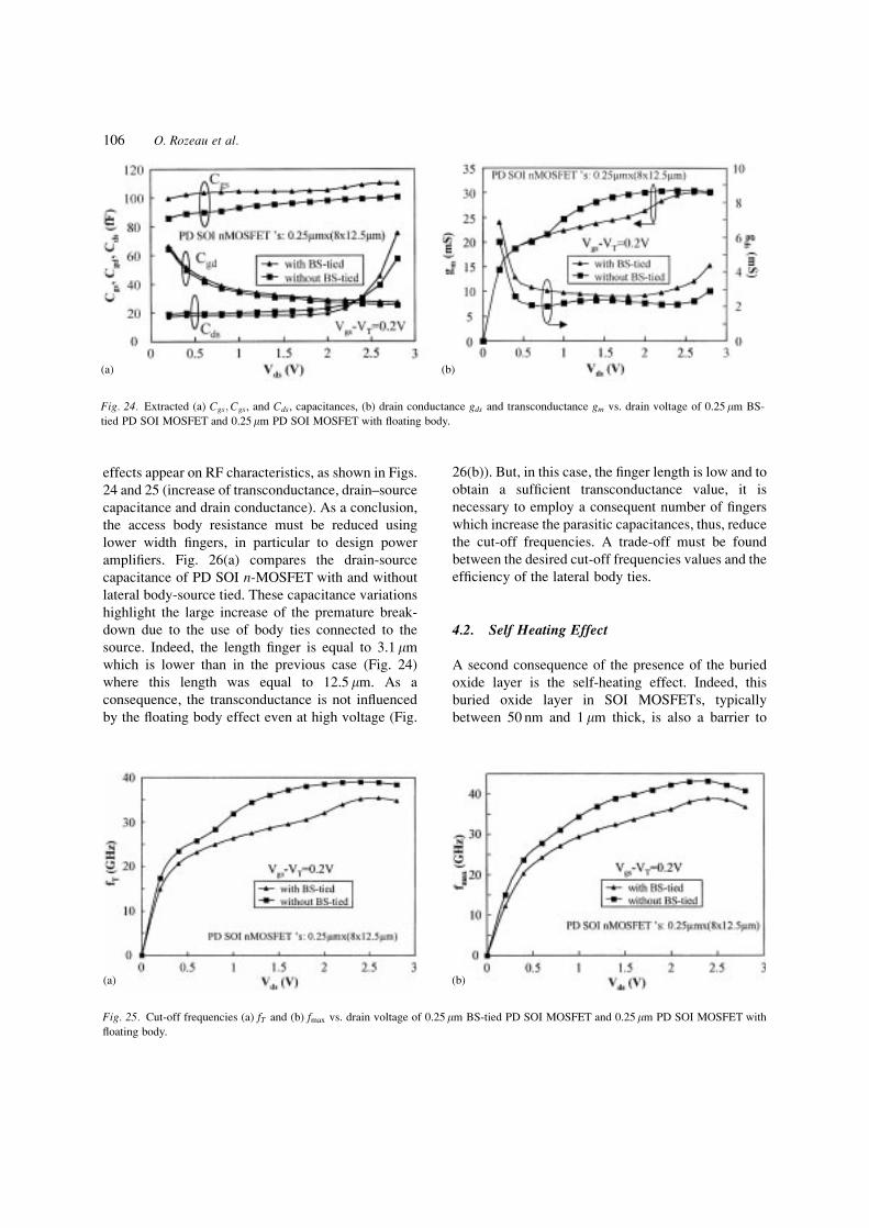
tied structure is preferred. Fig. 24 compares the
extracted effective capacitances Cgs;Cgd and Cds,
drain conductance gds and transconductance gm of
body-source tied partially-depleted SOI MOSFET and
partially-depleted SOI MOSFET with ¯oating body.
We can see, in this ®gure, that the BS-tied increases
the Cgs capacitance and the gds conductance, in the
pre-kink region, and suppresses the impact of the kink
effect on transconductance and drain conductance.
Notice that the drain conductance is affected by the
kink effect, for 0.25 mm n-MOSFET, when the body
potential is ¯oating. This increase of drain conduc-
tance is due to capacitive coupling effects which are
not negligible in RF range.
The kink effect affects the effective gate-source
capacitance, transconductance and drain conductance
(with low impact and only for short channel
MOSFET). This effect can be suppressed using BS-
ties which increases the effective gate-source capa-
citance and drain conductance, reducing in turn the
cut-off frequencies fT and fmax, as plotted in Fig. 25.
Nevertheless, when the transistor is used only at high
frequency, the kink effect is not a problem because
the behavior of such transistor is similar than that of
bulk one, but it must be modeled in RF range in term
of steady state contribution.
Moreover, at high drain voltage, the ¯oating body
Fig. 22. Extracted gate-source capacitance and transconductance using S-parameters measurements.
Fig. 23. S-parameters of partially-depleted SOI 0.25mm n-MOSFET at Vgs � Vds � 1 V between 100 MHz and 18 GHz.
Low-Power Low-Voltage Radio-Frequency Applications 105
effects appear on RF characteristics, as shown in Figs.
24 and 25 (increase of transconductance, drain±source
capacitance and drain conductance). As a conclusion,
the access body resistance must be reduced using
lower width ®ngers, in particular to design power
ampli®ers. Fig. 26(a) compares the drain-source
capacitance of PD SOI n-MOSFET with and without
lateral body-source tied. These capacitance variations
highlight the large increase of the premature break-
down due to the use of body ties connected to the
source. Indeed, the length ®nger is equal to 3.1 mm
which is lower than in the previous case (Fig. 24)
where this length was equal to 12.5 mm. As a
consequence, the transconductance is not in¯uenced
by the ¯oating body effect even at high voltage (Fig.
26(b)). But, in this case, the ®nger length is low and to
obtain a suf®cient transconductance value, it is
necessary to employ a consequent number of ®ngers
which increase the parasitic capacitances, thus, reduce
the cut-off frequencies. A trade-off must be found
between the desired cut-off frequencies values and the
ef®ciency of the lateral body ties.
4.2. Self Heating Effect
A second consequence of the presence of the buried
oxide layer is the self-heating effect. Indeed, this
buried oxide layer in SOI MOSFETs, typically
between 50 nm and 1 mm thick, is also a barrier to
(a) (b)
Fig. 24. Extracted (a) Cgs;Cgs, and Cds, capacitances, (b) drain conductance gds and transconductance gm vs. drain voltage of 0.25mm BS-
tied PD SOI MOSFET and 0.25mm PD SOI MOSFET with ¯oating body.
(a) (b)
Fig. 25. Cut-off frequencies (a) fT and (b) fmax vs. drain voltage of 0.25mm BS-tied PD SOI MOSFET and 0.25mm PD SOI MOSFET with
¯oating body.
106 O. Rozeau et al.

heat ¯ow from the channel, due to the lower thermal
conductivity of SiO2 than that of silicon, approxi-
mately 100 times less. Thus, the thermal resistance of
SOI devices can be signi®cantly larger than the
resistance of bulk devices (Fig. 27). Consequently, at
high dissipated DC power (due to Joule heating only
[39]), the SOI MOSFET warms up and leads to
electrical parameter variations, such as effective
mobility, threshold voltage, saturation velocity,
leakage junction current, impact ionization current
and thermal noise, due to the channel temperature rises.
At the present time, the impact of self-heating
effect on the static characteristics is well known and
this effect leads to reduce the drain current at high
power dissipation [40,41], as shown in Fig. 28 where
the drain conductance is negative at high applied
power. This effect is more pronounced in short-
channel devices owing to their higher current drive
and smaller volume of silicon [39,41]. Moreover, the
effect is increasing in the case of thin silicon ®lm and
thick buried oxide layer [42] and it must be taken into
account in models as expected by some works [43]
(FD), [44,45] (SOISPICE) and [46] (BSIM3SOI).
Physically, there are only three ways for thermal
energy to be transferred from the die to the package:
crossing the substrate, the material on the top
(typically protection gas) or the bonding wires.
Considering the free convection in a closed cavity,
the total ratio between substrate thermal conductivity
and surrounding air has been evaluated at 103. The
heat transfer through the gas on the top of the device
can be neglected. Moreover, it seems that 10% only is
evacuated through metal lines [47]. In steady state
behavior, the heat ¯ow through the buried oxide is
(a) (b)
Fig. 26. (a) Drain-source capacitances of PD n-MOSFET with and without body-source tied and (b) transconductance of n-MOSFET with
ef®cient body-source tied.
(b)(a)
Fig. 27. Heat transfer in the (a) SOI and (b) bulk substrates due to the self-heating effect in MOSFET.
Low-Power Low-Voltage Radio-Frequency Applications 107

controlled by a thermal resistance Rth and the device
temperature depends on the dissipated power
�Id6Vds� and the ambient temperature Tamb as
illustrated in Fig. 29.
Nevertheless, the lattice temperature along the
channel beneath the gate oxide is not uniform, the
heat is generated at the drain and diffuses to the
source [39]. As a consequence, for an accurate
modeling, the lateral evacuation must be taken into
account, which increases the complexity of the
model, in particular for analog simulations where
the lateral diffusion is signi®cant.
Notice that the thermal capacitance Cth charac-
terizes the thermal response of the device in dynamic
behavior. Indeed, the channel temperature does not
follow the device power dissipation instantaneously
and consequently, an unusual behavior due to
dynamic self-heating is observed in both time and
frequency domains. This phenomenon can be char-
acterized by a time constant, typically 1 ms to 10 s
[40,44,48±50], and leads to a frequency dependence
of the transconductance and the output conductance.
Fig. 30 shows the dynamic drain conductance
variations with frequency [51]. This ®gure highlights
the frequency dependence of drain conductance due
to the thermal substrate capacitance. The drain
conductance increases with frequency and becomes
constant at high frequency, as investigated by several
works [29,48,49,51]. At high frequency, the drain
conductance (usual analog parameter) is not affected
by the AC self-heating, that is to say, the self-heating
feedback. However, following the used MOSFET
geometry (drain and source lateral dimensions, width
and length and interconnecting wiring), the drain
conductance can be characterized by several time
Fig. 28. Calculated static drain current of BS-tied PD SOI
MOSFET with and without self-heating effect.
Fig. 30. Output conductance characteristics of PD SOI MOSFET
with source connected body-tie vs. frequency (W � 20 mm;
L � 3mm) [29].
Fig. 29. Equivalent circuit for self heating simulation.
Fig. 31. Calculated transconductance gm with and without self-
heating effect.
108 O. Rozeau et al.
constants, typically 2 or 3 time constants as
investigated by [50,52,53]. These time constants are
extracted using speci®c measurement method based
on the AC conductance measurement. Thus, a
complete model taking into account the thermal
behaviour must be developed, allowing the optimiza-
tion of the device architecture to reduce signi®cantly
the self-heating impact and the simpli®cation of the
frequency behavior.
In radio-frequency range, the DC self-heating due
to the DC biases (in small-signal) increases the
channel temperature and, consequently, reduces the
effective mobility and the saturation velocity. Thus,
the maximal transconductance is reduced at high
dissipated power, as shown in Fig. 31 where a
reduction of near 15% has been estimated using
analytical models for a 0.5 mm n-MOSFET.
Nevertheless, this reduction strongly depends on the
device volume and can be largely reduced using an
appropriate multi®nger architectures.
To highlight the self-heating effect in RF be-
havior, 0.4 mm FD SOI MOSFET with two buried
oxide thicknesses have been compared. These
transistors are fabricated on p-type silicon wafer at
KansaõÈ University (Osaka-Japan). The SOI substrates
are elaborated using low-dose and high-dose SIMOX
processes and consequently, the buried oxide thick-
nesses are 100 and 380 nm, respectively. A silicon
®lm thickness of 100 nm and a front gate oxide
thickness of 7 nm are used in this study. N-channel
SOI MOSFETs with a 0.4 mm gate length and 70
®ngers of 5 mm gate width, have been especially
designed for RF applications. The output character-
istics of these two devices are shown in Fig. 32. No
signi®cant difference has been noticed at low and
moderate gate voltages. However, a drain current
decrease has been observed for high-dose SIMOX
transistor at high Vgs. This reduction is attributed to
the self-heating effect.
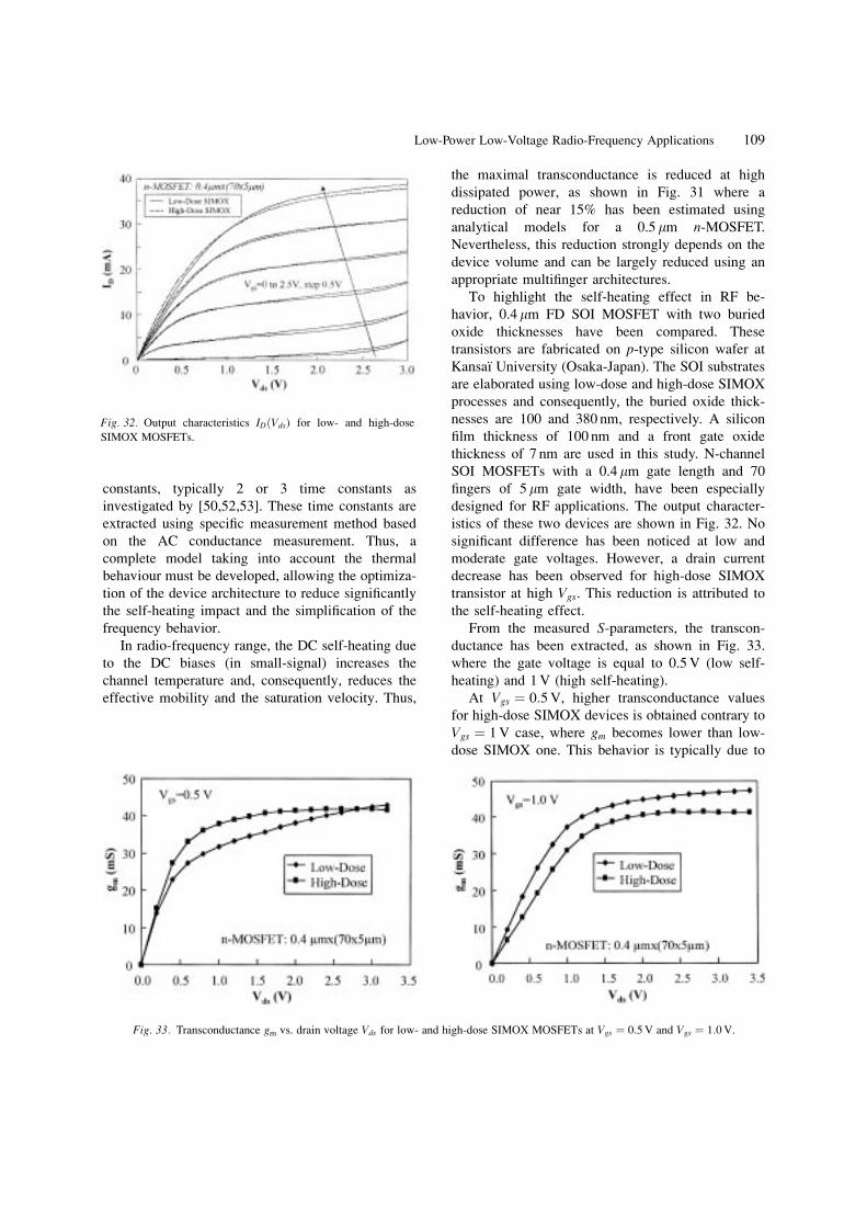
From the measured S-parameters, the transcon-
ductance has been extracted, as shown in Fig. 33.
where the gate voltage is equal to 0.5 V (low self-
heating) and 1 V (high self-heating).
At Vgs � 0:5 V, higher transconductance values
for high-dose SIMOX devices is obtained contrary to
Vgs � 1 V case, where gm becomes lower than low-
dose SIMOX one. This behavior is typically due to
Fig. 33. Transconductance gm vs. drain voltage Vds for low- and high-dose SIMOX MOSFETs at Vgs � 0:5 V and Vgs � 1:0 V.
Fig. 32. Output characteristics ID�Vds) for low- and high-dose
SIMOX MOSFETs.
Low-Power Low-Voltage Radio-Frequency Applications 109

the self-heating effect [54]. Indeed, the low thermal
conductivity of the buried oxide inhibits cooling of
SOI devices and causes severe self-heating effects.
The device mobility is reduced as a result of the
higher channel temperature reducing the transcon-
ductance. Notice that the temperature rise is reduced
when buried oxide thickness is reduced [55].
We can conclude that this effect must be taken
into account in RF SOI model considering that
the MOSFETs are multi®nger architectures where
the self-heating effect is lower than single ®nger
structures. In this case, this effect is not a limiting
parameter but speci®c heat ¯ow model is
necessary, as developed for EOS/ESD applications
[56].
5. Conclusion
In this paper, an overview of SOI technologies
performances for radio-frequency applications has
been achieved. From several studies concerning
passive and active components on SOI substrates,
the trends of RF performances have been evaluated.
The ®rst advantage of fully- and partially-depleted
SOI technologies are the suppression of the latch-up
problem and the large reduction of substrate noise
coupling at low frequency compared to bulk. In
addition, the low thermal coupling properties of SOI
substrates due to the low thermal conductivity of the
buried oxide and the low dependence with tempera-
ture of SOI MOSFET behavior (especially for fully-
depleted) allow to bring closer two devices with a
better matching than in bulk. However, the con-
sequences of this electrical and thermal isolation are
the ¯oating body (larger in partially depleted) and
self-heating (larger in fully depleted) effects, which,
in some case, can degrade the performances of SOI
MOSFETs, as low frequency noise or off-state
currents. Note that, the ¯oating body effects and, in
particular, the kink effect can be used to increase the
dynamic performances of digital circuits. Moreover,
the low junction capacitances offer a good dynamic
behavior of circuit for low voltage mixed signal
applications. All theses points have been discussed in
this article. For analog applications, the ¯oating body
effects must be completely suppressed when low-
frequency noise level is required. These effects
depend on the frequency and require a speci®c
physical model compared to bulk. Moreover, it is
necessary to have a constant body potential, using
either ef®cient body ties or fully-depleted architec-
tures. This constraint entails two problems. The ®rst
one is the ef®ciency of body ties, which can be
obtained with a ``thick'' silicon ®lm only (partially-
depleted technologies). In this case, the access body
resistances are higher than in bulk and must be
optimized using speci®c structures (multi®nger) to
detriment of parasitic capacitances. The second
problem is, from the timing, the dif®culty to
manufacture ICs with good yields using very thin
silicon ®lm (fully-depleted) on SOI. Notice that the
fully-depleted SOI technologies seem to be the best
candidate for analog and RF applications. Indeed,
the total depletion enables a complete suppression of
the kink effect and increases the intrinsic trans-
conductance. However, the important questions
are about the access resistance values (access to
the drain and source) and the parasitic bipolar
transistor.
Another problem of SOI is the self-heating effect.
This effect can reduce the saturation velocity and the
mobility. But, using adequate architecture as multi-
®nger, this effect can be largely decreased.
To summarize, the partially-depleted SOI tech-
nologies has a large ¯exibility for analog and RF
design as DTMOS, body±source tied or body
polarized by an external potential. In fully-depleted
devices which exhibit very good analog performances
with high cut-off frequencies, the design is simpler
than in bulk and partially-depleted. In both cases, the
SOI substrates have very good insulating properties at
low frequency and become very interesting with the
use of high resistivity substrates compared to bulk.
Indeed, the main advantage of SOI for the RF
applications is its compatibility with the insulating or
semi-insulating substrates. Moreover, the silicon
volume of the SOI substrate can be completely
substituted by an insulating substrate (glass, quartz
. . .) as developed by Philips (Silicon On Anything).
In this case, the process is similar as in bulk, but
the last step of the process is a transfer of the active
layer to an insulating substrate. This technology
guarantees very good performances for passive
components (high quality factor of inductors and
low losses of transmission lines) with lower costs
than in GaAs and with digital analog integration
facilities.
110 O. Rozeau et al.

Acknowledgments
The authors gratefully acknowledge LETI for the
Unibond SOI samples used in this study. They would
like also to thank Drs. J. L. Pelloie, C. Raynaud, J. de
Pontcharra (LETI-Grenoble, France), Dr. D. Van-
hoenacker (UCL-Louvain la Neuve, Belgium), Dr. V.
Ferlet-Cavrois (CEA-BruyeÁre La Chapellel, France),
V. Le Goascoz (STMicroelectronics-Crolles, France)
and Y. Omura (KansaõÈ University-Osaka, Japan) for
their valuable discussions.
References
1. Y. Taur, S. Wind, Y. J. Mii, Y. Lii, D. Moy, K. A. Jenkins, C. L.
Chen, P. J. Coane, D. Klaus, J. Bucchignano, M. Rosen®eld, M.
G. R. Thomson, and M. Polcari, ``High performance 0.1mm
CMOS devices with 1.5 V power supply,'' in Proc. IEDM Tech.Dig., p. 127, December 93.
2. A. K. Agarwal, M. C. Driver, M. H. Hanes, H. M. Hodgood, P.
G. McMullin, H. C. Nathanson, T. W. O'Keeffe, T. J. Smith, J.
R. Szedon, and R. N. Thomas, ``MICROX2 Ð An advanced
silicon technology for microwave circuits up to X-band,'' in
Proc. IEDM Tech. Dig., pp. 687±690, 1991.3. D. Eggert, P. Huebler, A. Huerrich, H. Kuerck, W. Budde, and
M. Vorwerk, ``A SOI-RF-CMOS technology on high resistivity
SIMOX substrates for microwave applications to 5 GHz.''
IEEE Trans. on Electron Devices 44(11), pp. 1981±1989,
1997.
4. M. Harada, C. Yamaguchi, and T. Tsuchiya, ``Investigation of a
multigigahertz MOSFET ampli®er with an on-chip inductor
fabricated on a SIMOX wafer.'' IEEE Trans. Electron Devices45(1), pp. 173±177, 1998.
5. A. Viviani, J.-P. Raskin, D. Flandre, J.-P. Colinge, and
D. Vanhoeneker, ``Extended study of crosstalk in SOI-
SIMOX substrates,'' in Proc. IEDM Tech. Dig., pp. 713±716,
1995.
6. J. P. Raskin, A. Viviani, D. Flandre, and J. P. Colinge,
``Substrate crosstalk reduction using SOI technology.''
IEEE Trans. Electron Devices 44(12), pp. 2252±2261,
1997.
7. D. K. Shaeffer and T. H. Lee, ``A 1.5-V, 1.5-GHz CMOS low
noise ampli®er.'' IEEE Solid-State Circuits 32(5), pp. 745±759,
1997.
8. J. Cranincks and M. Steyeart, ``Low-noise voltge-controlled
oscillators using enhanced LC-tanks.'' IEEE Trans. Circuitsand Systems 42(12), pp. 794±804, 1995.
9. J. N. Burghartz, D. C. Edelstein, M. Soyuer, H. A. Ainspan, and
K. A. Jenkins, ``RF circuit design aspects of spiral inductors on
silicon.'' IEEE. Solid-State Circuits, 33(12), pp. 2028±2033,
1998.
10. J. Lescot, O. Rozeau, J. Boussey, J. Jomaah, and F.
Ndagijimana, ``Coplanar transmission lines on SOI technolo-
gies for RF applications: modeling and experiments,'' in Proc.ESSDERC'98, 1998.
11. K. B. Ashby, I. A. Koullias, W. C. Finley, J. J. Bastek, and S.
Moinian, ``High Q-inductors for wireless applications in a
complementary silicon bipolar process.'' IEEE. Solid-StateCircuits 31(1), pp. 4±8, 1996.
12. M. Soyuer, J. N. Burghartz, K. A. Jenkins, S. Pannapalli, J. F.
Ewen, and W. E. Pence, ``Multilevel monolithic inductor in
silicon technology.'' Electronics Letters 32(5), pp. 359±360,
1995.
13. J. N. Burghartz, M. Soyuer, and K. A. Jenkins, ``Microwave
inductors and capacitors in standard multilevel interconnect
silicon technology.'' IEEE Trans. Microwave Theory andTechniques, 44(1), pp. 100±104, 1996.
14. J. N. Burghartz, M. Soyuer, and K. A. Jenkins, ``Integrated RF
and microwave components in BiCMOS technology.'' IEEETrans. Electron Devices 43(9), pp. 1559±1570, 1996.
15. M. Park, S. Lee, H. K. Hu, J. G. Koo, and K. S. Nam, ``High Q-
CMOS-compatible microwave inductors using double-metal
interconnection silicon technology.'' IEEE Microwave andGuided Wave Letters 7(2), pp. 45±47, 1997.
16. M. Park, C. S. Kim, J. M. Park, H. K. Yu, and K. S. NaICs,
``High Q microwave inductors in CMOS double-metal
technology and its substrate bias effects for 2 GHz
RF applications,'' in Proc. IEDM Tech. Dig., pp. 59±62,
1997.
17. F. Mermyei, F. Darrer, M. Pardoen, and A. Sibrai, ``Reducing
the substrate losses of RF integrated inductors.'' IEEEMicrowave and Guided Wave Letters 8(9), pp. 300±301,
1998.
18. C. P. Yue and S. S. Wong, ``On-chip spiral inductors with
patterned ground shields for Si-based RFICs.'' IEEE Journal ofSolid-State Circuits 33(5), pp. 743±751, 1998.
19. J. M. Lopez, J. Samitier, C. Cane, and P. Losantos,
``Improvement of the quality factor of RF integration inductors
by layout optimization,'' in Proc. 1998 IEEE Radio FrequencyIntegrated Circuits Symp., pp. 169±172, 1998.
20. L. E. Larson, ``Integrated circuit technology options for RFICs
ÐPresent status and future directions.'' IEEE. Solid-StateCircuits 33(3), pp. 387±399, 1998.
21. R. A. Johnson, C. E. Chang, P. M. Asbeck, M. E. Wood, G. A.
Garcia, and I. Lagnado, ``Comparison of microwave inductors
fabricated on silicon-on-sapphire and bulk silicon.'' IEEEMicrowave and Guided Wave Letters 6(9), pp. 323±325, 1996.
22. M. Stuber, M.Megahed, J.J. Lee, T. Kobayashi, and H. Domyo,
``SOI CMOS with high-performance passive components for
analog, RF, and mixed signal design,'' in Proc. 1998 IEEE Int.SOI Conf., pp. 99±100, 1998.
23. C. Raynaud, O. Faynot, J. L. Pelloie, S. Deleonibus, D.
Vanhoenacker, R. Gillon, J. Sevenhans, E. Compagne, G.
Fletcher, and E. Mackowiak, ``Fully-depleted 0.25mm SOI
devices for low power RF mixed analog-digital circuits,'' in
Proc. IEEE 1998 Int. SOI Conf., pp. 67±68, 1998.
24. O. Rozeau, J. Jomaah, J. Boussey, C. Raynaud, J.-L. Pelloie and
F. Balestra, ``Comparison between fully- and partially-depleted
SOI MOSFETs for low-power radio-frequency applications,''
in Proc. 1999 Int. SOI Conf., 1999.
25. T. Ohguro, H. Naruse, H. Sugaya, E. Morifuji, S. Nakamura, T.
Yoshitomi, T. Norimoto, S. Momose, Y. Katsumata, and H.
IwaiÈ, ``0.18mm low/low power RF CMOS with zero Vth analog
MOSFETs made by undoped epitaxial channel technique,'' in
Proc. IEDM Tech. Dig., pp. 837±840, 1997.
26. D. Sinitsky, R. Tu, C. Liang, M. Chan, J. Bokor, and C. Hu,
Low-Power Low-Voltage Radio-Frequency Applications 111

``AC output conductance of SOI MOSFETs and impact on
analog applications.'' IEEE Electron Device Letters 18(2),
pp. 36-38, 1999.
27. R. Howes and W. Rebman-White, ``A small-signal model for
the frequency-dependent drain admittance in ¯oating-substrate
MOSFETs.'' IEEE. Solid-State Circuits 27(8), pp. 1186±1193,
1992.
28. W. Redman-White, ``Some dos and don'ts for analog design in
SOI CMOS,'' in Short Course 1999. IEEE Int. SOI Conf.,1999.
29. B. M. Tenbroek, W. Rebman-White, M. J. Uren, M. S. L. Lee,
and M. C. L. Ward, ``Identi®cation of thermal and electrical
time constants in SOI MOSFETS from small signal measure-
ments,'' in Proc. ESSDERC' 93, pp. 189±192, 1993.
30. B. M. Tenbroek, ``Characterisation and parameter extraction of
silicon-on-insulator MOSFETs for analog circuit modelling.''
Thesis of University of Southampton, 1997.
31. D. J. Roulston, 1990. Bipolar Semiconductor Devices.
McGraw-Hill Publishing Company. 1990.
32. F. Faccio, F. Anghinol®, E. H. M. Heijne, P. Jarron, and S.
Cristoloveanu, ``Noise contribution of the body resistance in
partially-depleted SOI MOSFETs.'' IEEE Trans. ElectronDevices 45(5), pp. 1033±1038, 1998.
33. W. Jin, P. C. H. Chan, S. K. H. Samuel, K. H. Fung, and P. K.
Ko, ``A physically-based low-frequency noise model for NFD
SOI MOSFETs,'' in Proc. 1998 IEEE Int. SOI Conf., pp. 23±24,
1998.
34. Y.-C. Tseng, W. M. Huang, C. Hwang, P. Welch, and J. C. S.
Woo, ``Temperature dependence of AC ¯oating body effects in
PD SOI nMOS,'' in Proc. 1999 IEEE Int. SOI Conf., pp. 26±27,
1999.
35. Y.-C. Tseng, W. M. Huang, V. Ilderem, and J. C. S. Woo,
``Floating body induced pre-kink excess low-frequency noise
in submicron SOI CMOSFET technology.'' IEEE ElectronDevice Letters 20(9), pp. 484±486, 1999.
36. S. Haendler, J. Jomaah, F. Balestra, J. L. Pelloie, C. Raynaud,
and J. Boussey, ``Thorough investigation of kink-related excess
noise in deep submicron SOI N-MOSFETs on Unibond
Substrate,'' in Proc. 1999 Int. Conf. Solid State Devices,Materials, SSDM'99, 1999.
37. O. Rozeau, J. Jomaah, J. Boussey, and C. Raynaud, ``Impact of
¯oating-body effect on RF performances of SOI MOSFET,'' in
Proc. ESSDERC'99, 1999.
38. A. A. Abidi, 1997. ``Analog circuit design-RF analog digital
converters, sensor and actuator interfaces.'' Low NoiseOscillators, PLLs and Synthesizers Kluwer Academic
Publishers, Boston, 1997.
39. D. A. Dallman and K. Shenai, ``Scaling constraints imposed by
self-heating in submicron SOI MOSFETs.'' IEEE Trans.Electron Devices 42(3), pp. 489±496, 1995.
40. O. Le NoÄel and M. Haond, ``Electrical transient study of
negative resistance in SOI MOS transistors.'' ElectronicsLetters 26(1), pp. 73±74, 1990.
41. L. J. McDaid, S. Hall, P. H. Mellor, and W. Eccleston,
``Physical origin of negative differential resistance in SOI
transistors.'' Electronics Letters 25(13), pp. 827±828, 1989.
42. L. T. Su, J. E. Chaung, D. A. Antoniadis, K. E. Goodson and M.
I. Flik, ``Measurement and modeling of self-heating in SOI
NMOSFETs.'' IEEE Trans. Electron Devices 41(1), pp. 69±75,
1994.
43. Y. Chen and T. A. Fjeldly, ``Uni®ed physical I-V model
including self-heating effect for fully depleted SOI/
MOSFETs.'' IEEE Trans. Electron Devices 43(8), pp. 1291±
1296, 1996.
44. L. T. Su, D. A. Antoniadis, N. D. Arora, B. S. Doyle, and D. B.
Krakauer, ``SPICE model and parameters for fully-depleted
SOI MOSFETs including self-heating.'' IEEE Electron DeviceLetters 15(10), pp. 374±376, 1994.
45. G. O. Workman, J. G. Fossum, S. Krishnan, and M. M. Pellela,
``Physical modeling of temperature dependences of SOI CMOS
devices and circuits including self heating.'' IEEE Trans. onElectron Devices 45(1), pp. 125±132, 1998.
46. D. Sinitshy, S. Tang, A. Jangity, F. Assaderaghi, G. Shahidi, and
C. Hu, ``Simulation of SOI devices and circuits using
BSIM3SOI.'' IEEE Electron Device Letters 19(9), pp. 323±
325, 1998.
47. M. Berger and Z. Chai, ``Estimation of heat transfer in SOI-
MOSFETs.'' IEEE Trans. Electron Devices 384, pp. 871±875,
1991.
48. R. H. Tu, C. Wann, J. C. King, P. K. Ko, and C. Hu, ``An AC
conductance technique for measuring self-heating in SOI
MOSFETs.'' IEEE Electron Device Letters 16(2), pp. 67±69,
1995.
49. W. Jin, S. K. H. Fung, W. Liu, P. C. H. Chan, and C. Hu, ``Self-
heating characterization for SOI MOSFET based on AC output
conductance,'' in Proc. IEDM Tech. Dig., pp. 175±178,
1999.
50. A. L. Caviglia and A. A. Iliadis, ``A large-signal SOI MOSFET
model including self-heating based on small-signal model
parameters.'' IEEE Trans. Electron Devices 46(4), pp. 762±
768, 1999.
51. W. Redman-White, M. S. L. Lee, B. M. Tenbroek, M. J. Uren,
and R. J. T. Bunyan, ``Direct extraction of MOSFET dynamic
thermal characteristics from standard transistor structures using
small signal measurements.'' Electronics Letters 29(13),
pp. 1180±1181, 1993.
52. A. L. Caviglia and A. A. Iliadis, ``Linear dynamic self heating
in SOI MOSFETs.'' IEEE Electron Device letters 14(3),
pp.133±135, 1993.
53. B. M. Tenbroek, M. S. L. Lee, W. Redman-White, R. J. T.
Bunyan, and M. J. Uren, ``Self-heating in SOI MOSFETs and
their measurement by small signal conductance techniques.''
IEEE Trans. Electron Devices 43(12), pp. 2240±2248, 1996.
54. J. Jomaah, G. Ghibaudo, and F. Balestra, ``Analysis and
modeling of self-heating effects in thin-®lm SOI MOSFETs
as a function of temperature.'' Solid-State Electronics 38(3),
pp. 615±618, 1995.
55. O. Rozeau, J. Jomaah, J. Boussey, and C. Raynaud, ``Impact of
¯oating-body effect on RF performances of SOI MOSFET.'' in
Proc. ESSDERC'99, 1999.
56. P. Raha, S. Ramaswamy, and E. Rosenbaum, ``Heat ¯ow
analysis for EOS/ESD protection device design in SOI
technology.'' IEEE Trans. Electron Devices 44(3), pp. 464±
471, 1997.
112 O. Rozeau et al.

Olivier Rozeau was born in Saumur, France, in
1974. He graduated from the Ecole Nationale
SupeÂrieure de Physique de Grenoble (ENSPG-
INPG) in 1997. He joined the ``Laboratoire de
Physique des Composants aÁ Semiconducteurs
(LPCS)'' and the ``Laboratoire d'ElectromagneÂt-
isme, de Microonde et d'OptoeÂlectronique
(LEMO),'' Grenoble, in 1997, where he is presently
working towards the Ph.D. Degree. His research
interests are in the ®eld of characterization and
modeling of SOI devices ( passive and MOSFET
components) in radio-frequency ranges. These
researches are supported by STMicroelectronics.
Jalai Jomaah was born in Lebanon, in 1967. He
graduated from the Institut National Polytechnique de
Grenoble (INPG), France, in 1992. He received M.S.
and Ph.D. degrees in Electronics from the same
University, in 1992 and 1995, respectively.
He joined the Laboratoire de Physique des
Composants aÁ Semiconducteurs (LPCS), INP
Grenoble, in 1992, where he has been involved in
research on the characterization, modeling, and
simulation of fully- and partially-depleted Silicon-
On-Insulator MOS transistors. He become MaõÃtre de
ConfeÂrences (Associate Professor) at INPG in 1996
where he continues now his research activities at
Laboratories of semiconductor devices (LPCS/
ENSERG) and of electromagnetic and microwave
(LEMO/ENSERG).
His main research activities were and are in the
®eld MOS/SOI device physics, ¯uctuations and low
and high frequencies noise and radio-frequencies
applications. He is presently supervising 3 Ph.D. and
is involved in several national and international
research projects on the low- and high-frequencies
noise, reliability, modeling and characterization of
SOI devices for RF applications and low-temperature
physics.
SeÂbastien Haendler was born in Metz, France, in
1970. He graduated from the Ecole Nationale
SupeÂrieure de Physique de Grenoble (ENSPG-
INPG) in 1995. He joined the Laboratoire de
Physique des Composants aÁ Semiconducteurs
(LPCS), Grenoble, in 1998, where he is presently
working towards the Ph.D. degree. His research
interests are in the ®eld of characterization and
modeling of SOI devices (MOSFET) and especially
the Low Frequency Noise area.
Jumana Boussey is a CNRS researcher within the
Laboratoire de Physique des Composants a
Semiconducteurs (LPCS) in Grenoble. She received
her Engineering Diploma and her Ph.D. degrees
from the INPG, Institut National Polytechnique de
Grenoble, in 1984 and 1990, respectively. She joined
the LPCS in 1986 where she carried out several
works on the electrical properties of heavily ion
implanted semiconductor materials. Since 1992, she
Low-Power Low-Voltage Radio-Frequency Applications 113

has been involved in silicon and SOI materials
technology and characterization. Her latest research
domain is focusing on microsystems and micro-
technologies.
Francis Balestra was born in Digne, France, in
1960. He received the B.S. degree from the
University of Provence, Marseille, France, in 1981
and M.S. and Ph.D. degrees in electronics from the
Institut National Polytechnique, Grenoble, France, in
1982 and 1985, respectively. In 1989, he obtained the
Habilitation diploma from the INPG authorizing him
to supervise Ph.D. dissertations.
He joined the Laboratoire de Physique des
Composants aÁ Semiconducteurs (LPCS), INP
Grenoble, in 1982, where he has been involved in
research on the characterization, modeling, and
simulation of fully depleted silicon-on-sapphire
MOS transistors.
He became Charge de Recherche C.N.R.S. (Centre
National de la Recherche Scienti®que) in 1985. In
1993±94, he joined the Research Center for Integrated
Systems at Hiroshima University as a visiting
researcher, and worked on sub-0.1 mm MOSFETs
and thin ®lm SIMOX devices.
Between 1996 and 1998, he has been Deputy
Director of the LPCS, and he is Director of the LPCS
since January 1999.
He had several research teams on deep submicron
CMOS, silicon on insulator devices, low temperature
electronics and polysilicon emitter bipolar transistor
for BiCMOS technology. He has supervised 15
research projects and 17 Ph.D. He is presently
coordinating an European project (ESPRIT Working
Group ``Ultimate Integration of Silicon'') and a
project supported by the RhoÃne-Alpes region
``Silicon Nanoelectronics''. He was the organizer of
the ®rst European Workshop on Low Temperature
Electronics (WOLTE), Grenoble, France, June
1994.
Dr. Balestra has coauthored over 80 publications
in international scienti®c journals and 120 commu-
nications at national and international conferences
(20 invited papers and review articles).
114 O. Rozeau et al.