Low-voltage CMOS circuits for analog iterative decoders
13
IEEE TRANSACTIONS ON CIRCUITS AND SYSTEMS—I: REGULAR PAPERS, VOL. 53, NO. 4, APRIL 2006 829 Low-Voltage CMOS Circuits for Analog Iterative Decoders Chris Winstead, Member, IEEE, Nhan Nguyen, Member, IEEE, Vincent C. Gaudet, Member, IEEE, and Christian Schlegel, Senior Member, IEEE Abstract—Iterative decoders, including Turbo decoders, provide near-optimal error protection for various communication chan- nels and storage media. CMOS analog implementations of these decoders offer dramatic savings in complexity and power con- sumption, compared to digital architectures. Conventional CMOS analog decoders must have supply voltage greater than 1 V. A new low-voltage architecture is proposed which reduces the required supply voltage by at least 0.4 V. It is shown that the low-voltage architecture can be used to implement the general sum-product algorithm. The low-voltage analog architecture is then useful for implementing Turbo and low-density parity check decoders. The low-voltage architecture introduces new requirements for signal normalization, which are discussed. Measured results for two fabricated low-voltage analog decoders are also presented. Index Terms—Analog decoding, iterative decoding, low-density parity check (LDPC) decoder, low voltage, low power, Turbo de- coder. I. INTRODUCTION T URBO codes, introduced in 1993, are a class of error control codes which achieve performance very close to a long sought-after limit known as the Shannon bound [1]. The decoding algorithms used in Turbo codes have since been generalized into a class of algorithms operating on graphs [2], [3]. These algorithms are commonly referred to as mes- sage-passing algorithms. Turbo-style decoders which employ message passing algorithms are generally referred to as itera- tive decoders. An important general form of message passing algorithms is the sum-product algorithm [4], which implements probability propagation on a code’s graph. The sum-product algorithm pro- vides a general framework which describes decoders for many codes, including Trellis codes, low-density parity check (LDPC) codes, block product codes, and Turbo codes. The sum-product Manuscript received January 24, 2005; revised June 24, 2005, This work was supported by the Alberta Informatics Circle of Research Excellence (iCORE), by Science and Engineering Research Canada (NSERC), by the Canadian Mi- croelectronics Corporation (CMC), by the Canada Foundation for Innovation (CFI), and by the Alberta Science and Research Authority (ASRA). This paper was recommended by Associate Editor G. Cauwenberghs. C. Winstead is with the Electrical and Computer Engineering Department, Utah State University, Logan, UT 84322-4120 USA (e-mail: winstead@engi- neering.usu.edu). N. Nguyen was with with the High Capacity Digital Communications Labo- ratory (HCDC), Electrical and Computer Engineering Department, University of Alberta, Edmonton AB T6G 2V4, Canada. V. C. Gaudet and C. Schlegel are with the High Capacity Digital Com- munications Laboratory (HCDC), Electrical and Computer Engineering Department, University of Alberta, Edmonton AB T6G 2V4, Canada (e-mail: [email protected]; [email protected]). Digital Object Identifier 10.1109/TCSI.2005.859773 algorithm is also a form of belief propagation, a class of algo- rithms used in artificial intelligence [5]. There has been great interest in implementing iterative de- coders, but conventional digital implementations are often com- plex, demanding significant silicon area and power. Analog cir- cuits for iterative decoding have been proposed and demon- strated by various researchers in recent years [6]–[12]. CMOS circuits are of particular interest for some applications because they can be implemented in ordinary (digital) CMOS processes, which are low-cost compared to high-end alternatives such as BiCMOS and SiGe. Because they are implemented in conven- tional processes, CMOS analog decoders can be more easily in- tegrated with other CMOS components for single-chip receiver solutions. In many cases, analog decoders offer significant advantages over digital designs. The operations required for implementing the sum-product or algorithms can be implemented in analog with a small number of transistors. Analog circuits also require significantly fewer wire connections between components. Such efficient use of space allows decoding operations to occur com- pletely in parallel, which enables high data throughput. Some example CMOS analog decoders have been recently published, which demonstrate the savings gained by analog decoders as opposed to digital approaches [10], [12]. CMOS analog de- coders are also intrinsically low-power, and eliminate the need for high speed analog-to-digital (A/D) conversion in the receiver front-end. A typical A/D converter by itself consumes a signifi- cant amount of power and silicon area. An analog decoder may thus be thought of as an “information A/D converter,” specially designed to convert coded analog channel information into de- coded bits. As CMOS process technology advances, feature sizes and oxide thickness are constantly shrinking. This also reduces the “voltage ceiling”—the maximum allowable supply voltage. This is of some benefit to digital designs, because their power consumption is proportional to . Low-power digital circuits are increasingly being designed for very low supply voltages, even below 1 V. At present, CMOS analog decoding architec- tures must have a supply voltage greater than about 1 V. This requirement may limit their use in the most advanced sub- micron processes. This is also unattractive in system-on-chip applications in which ultra-low-power digital circuits may be used with sub-1-V supply voltages. Integrating a decoder with a separate, higher supply voltage is an unwanted complication. CMOS analog decoders also require extra reference voltages which must be generated, regulated, and globally distributed on-chip. There is no exact requirement for what these reference 1057-7122/$20.00 © 2006 IEEE
-
Upload
independent -
Category
Documents
-
view
1 -
download
0
Transcript of Low-voltage CMOS circuits for analog iterative decoders

IEEE TRANSACTIONS ON CIRCUITS AND SYSTEMS—I: REGULAR PAPERS, VOL. 53, NO. 4, APRIL 2006 829
Low-Voltage CMOS Circuits forAnalog Iterative Decoders
Chris Winstead, Member, IEEE, Nhan Nguyen, Member, IEEE, Vincent C. Gaudet, Member, IEEE, andChristian Schlegel, Senior Member, IEEE
Abstract—Iterative decoders, including Turbo decoders, providenear-optimal error protection for various communication chan-nels and storage media. CMOS analog implementations of thesedecoders offer dramatic savings in complexity and power con-sumption, compared to digital architectures. Conventional CMOSanalog decoders must have supply voltage greater than 1 V. A newlow-voltage architecture is proposed which reduces the requiredsupply voltage by at least 0.4 V. It is shown that the low-voltagearchitecture can be used to implement the general sum-productalgorithm. The low-voltage analog architecture is then useful forimplementing Turbo and low-density parity check decoders. Thelow-voltage architecture introduces new requirements for signalnormalization, which are discussed. Measured results for twofabricated low-voltage analog decoders are also presented.
Index Terms—Analog decoding, iterative decoding, low-densityparity check (LDPC) decoder, low voltage, low power, Turbo de-coder.
I. INTRODUCTION
TURBO codes, introduced in 1993, are a class of errorcontrol codes which achieve performance very close to
a long sought-after limit known as the Shannon bound [1].The decoding algorithms used in Turbo codes have since beengeneralized into a class of algorithms operating on graphs[2], [3]. These algorithms are commonly referred to as mes-sage-passing algorithms. Turbo-style decoders which employmessage passing algorithms are generally referred to as itera-tive decoders.
An important general form of message passing algorithms isthe sum-product algorithm [4], which implements probabilitypropagation on a code’s graph. The sum-product algorithm pro-vides a general framework which describes decoders for manycodes, including Trellis codes, low-density parity check (LDPC)codes, block product codes, and Turbo codes. The sum-product
Manuscript received January 24, 2005; revised June 24, 2005, This work wassupported by the Alberta Informatics Circle of Research Excellence (iCORE),by Science and Engineering Research Canada (NSERC), by the Canadian Mi-croelectronics Corporation (CMC), by the Canada Foundation for Innovation(CFI), and by the Alberta Science and Research Authority (ASRA). This paperwas recommended by Associate Editor G. Cauwenberghs.
C. Winstead is with the Electrical and Computer Engineering Department,Utah State University, Logan, UT 84322-4120 USA (e-mail: [email protected]).
N. Nguyen was with with the High Capacity Digital Communications Labo-ratory (HCDC), Electrical and Computer Engineering Department, Universityof Alberta, Edmonton AB T6G 2V4, Canada.
V. C. Gaudet and C. Schlegel are with the High Capacity Digital Com-munications Laboratory (HCDC), Electrical and Computer EngineeringDepartment, University of Alberta, Edmonton AB T6G 2V4, Canada (e-mail:[email protected]; [email protected]).
Digital Object Identifier 10.1109/TCSI.2005.859773
algorithm is also a form of belief propagation, a class of algo-rithms used in artificial intelligence [5].
There has been great interest in implementing iterative de-coders, but conventional digital implementations are often com-plex, demanding significant silicon area and power. Analog cir-cuits for iterative decoding have been proposed and demon-strated by various researchers in recent years [6]–[12]. CMOScircuits are of particular interest for some applications becausethey can be implemented in ordinary (digital) CMOS processes,which are low-cost compared to high-end alternatives such asBiCMOS and SiGe. Because they are implemented in conven-tional processes, CMOS analog decoders can be more easily in-tegrated with other CMOS components for single-chip receiversolutions.
In many cases, analog decoders offer significant advantagesover digital designs. The operations required for implementingthe sum-product or algorithms can be implemented in analogwith a small number of transistors. Analog circuits also requiresignificantly fewer wire connections between components. Suchefficient use of space allows decoding operations to occur com-pletely in parallel, which enables high data throughput. Someexample CMOS analog decoders have been recently published,which demonstrate the savings gained by analog decoders asopposed to digital approaches [10], [12]. CMOS analog de-coders are also intrinsically low-power, and eliminate the needfor high speed analog-to-digital (A/D) conversion in the receiverfront-end. A typical A/D converter by itself consumes a signifi-cant amount of power and silicon area. An analog decoder maythus be thought of as an “information A/D converter,” speciallydesigned to convert coded analog channel information into de-coded bits.
As CMOS process technology advances, feature sizes andoxide thickness are constantly shrinking. This also reduces the“voltage ceiling”—the maximum allowable supply voltage.This is of some benefit to digital designs, because their powerconsumption is proportional to . Low-power digital circuitsare increasingly being designed for very low supply voltages,even below 1 V. At present, CMOS analog decoding architec-tures must have a supply voltage greater than about 1 V. Thisrequirement may limit their use in the most advanced sub-micron processes. This is also unattractive in system-on-chipapplications in which ultra-low-power digital circuits may beused with sub-1-V supply voltages. Integrating a decoder witha separate, higher supply voltage is an unwanted complication.
CMOS analog decoders also require extra reference voltageswhich must be generated, regulated, and globally distributedon-chip. There is no exact requirement for what these reference
1057-7122/$20.00 © 2006 IEEE

830 IEEE TRANSACTIONS ON CIRCUITS AND SYSTEMS—I: REGULAR PAPERS, VOL. 53, NO. 4, APRIL 2006
Fig. 1. Canonical sum-product circuit topology. Fig. 2 provides an explanation of the box notation used in this diagram.
voltages should be, and it is not known how the performancewill be affected if the reference voltages are wrong. This is an-other unwanted design complication. In this paper, we present alow-voltage CMOS analog decoding topology which eliminatesthe global reference voltages, and reduces by at least 0.4 V,and by as much as 0.56 V. This architecture is expected to bemore applicable to low-voltage CMOS processes, and more in-tegrable with low-voltage digital circuits.
This paper is organized as follows. In Section II, we brieflyexplain code graphs and the sum-product algorithm. In Sec-tion III we examine the canonical CMOS analog sum-producttopology, and study the effect of eliminating its reference volt-ages. In Section IV we present a circuit correction which com-pensates for the zero reference voltages, leading to the low-voltage topology. In Section V, we study application of the low-voltage topology to BCJR and LDPC decoder architectures. InSection VI, we present design details and measurement resultsfor two low-voltage analog decoders.
II. SUM-PRODUCT ALGORITHM
The sum-product algorithm [3], [4] is a general frameworkfor expressing probability propagation on graphs. The purposeof the algorithm is to compute global conditional probabilitiesusing only local constraints. Constraints are expressed by factorgraphs [3], [4], [13]. Special cases of factor graphs includeTrellis graphs and Tanner graphs (a.k.a. constraint graphs).We are interested in implementing the sum-product algorithmon graphs which express Boolean functions on discrete-typevariables.
A. Constraint Graphs
A constraint graph expresses the logical relationships amongthe bits in a codeword. The constraint graph contains circlesand squares connected by edges. An example constraint graphis shown later in Fig. 9. Circles in the constraint graph are calledvariable nodes. Each circle represents one bit in a codeword.The squares are referred to as function nodes or constraintnodes. In this work, we restrict our attention to graphs whichcan be simplified to local Boolean constraints on three vari-ables, i.e., nodes with only three edges. Multi-edge nodes can
almost always be reduced to a cascade of three-edge nodes [4],[14].
Each three-edge function node is associated with a func-tion, , which expresses a relationship between three randomvariables , , and , which can take values from discretealphabets , , , respectively. We say that isa Boolean constraint on if forall , , and . We say that the constraint is satisfied if andonly if . The random variables arecharacterized by discrete probability mass vectors, written ,
and , respectively.To implement the sum-product algorithm, the constraint is
mapped to a processing node which receives and . Letbe the set of combinations of for which issatisfied. Let be the subset of for which , where
. We then compute, for each , the function
or equivalently (1)
where and , is any nonzero constant realnumber, and refers to the th element of the probabilitymass vector . The constant is usually chosen so that
. The local computation (1) is the heart ofthe sum-product algorithm. A fully-rigorous description of thealgorithm is given elsewhere [4]. The form of (1) is adequate todescribe all or most interesting iterative decoders. A completesum-product decoder consists of many interconnected instancesof (1).
III. CANONICAL ANALOG SUM-PRODUCT CIRCUIT
An approach for CMOS analog decoder designs, elaboratedin [6], has emerged as a popular topology for analog decoderdesigns. This topology, which is based on a generalized Gilbertmultiplier, is shown in Fig. 1. Because of its popularity, the ar-chitecture of Fig. 1 will be referred to as the canonical topology.Fig. 1 uses a simplified “box notation,” explained in Fig. 2, inwhich an array of source-connected transistors is replaced by alarge box.

WINSTEAD et al.: LOW-VOLTAGE CMOS CIRCUITS FOR ANALOG ITERATIVE DECODERS 831
Fig. 2. Box symbol use to indicate a source-connected transistor array.
In Fig. 1, denotes the ordered sequence of row inputs(nodes) , and denotes the ordered sequenceof column inputs (nodes) . The current inputs
and arrive at input nodes and , respectively.The diode-connected transistors on the left, correspondingto transistor labels M1 and M3, perform current-to-voltageconversion. Each input current is proportional to a probability:
, where is a globally designated unit currentwhich represents a probability of one.
Intermediate outputs emerge from the top of the source-con-nected boxes in Fig. 1. There are such outputs, referredto as . These outputs represent multiplication of row andcolumn inputs
(2)
thus performing the “product” portion of (1). To complete thecomputation of (1), summation is accomplished by shortingwires (indicated by the “Connectivity” block). Unused products(those for which the constraint is not satisfied) must beshorted to .
In canonical analog decoders, a renormalization stage is usu-ally required to restore current levels at the circuit’s output.Let refer to the th output of the Connectivity block inFig. 1. For a sum-product circuit, . This is be-cause , but the outputs from the Connectivityblock represent only a subset of the . We refer to the sumover output currents as the current magnitude, in units of
(3)
To correct for the loss in current magnitude, a simple circuitsuch as that of Fig. 3 is often used [6], [14]. The parametersand are geometry factors, i.e., . Incanonical designs, one would typically choose . InSection IV-D we show that different geometry constraints applyto the new low-voltage architecture.
A. Weak-Inversion (Subthreshold) Devices
The Gilbert multiplier consists of MOS transistors biased inthe subthreshold region, meaning for each transistor( refers to the voltage between the gate and source of anMOS device, and is the threshold voltage). In digital design,
Fig. 3. Simple renormalization circuit.
subthreshold transistors are usually regarded as turned off. Amore precise model of their behavior is given by
where (4)
and are the device’s width and length, respectively,is a unitless technology constant [15], is a
technology constant with units of V , is the nominalthreshold voltage, and mV is the well-known thermalvoltage. More details of this model are discussed in [16].Circuits based on this subthreshold model were popularized byVittoz, et al. [17]and Mead [15].
The equation for can also be expressed in terms of forwardand reverse components [18]
where
(5)
If is sufficiently large (around 150 mV), then . In thiscase, the device is said to be in saturation.
B. Supply Voltage in Canonical Circuits
The canonical topology requires that all devices are in sat-uration. This imposes a minimum allowed supply voltage oncanonical sum-product circuits. The minimum supply voltagehas been probed experimentally for some designs [19], but an-alytical bounds are not given in the available literature. Such ananalysis is supplied in this section.
It is common practice to use one canonical circuit made ofnMOS devices, of which the outputs are “folded” into a secondcanonical circuit made of pMOS devices. A “slice” of thisfolded topology is illustrated in Fig. 4. The pMOS canonicalcircuit can perform either a second sum-product operation orprovide renormalization of currents. The pMOS transistorsmust also be in saturation, and must have a separate . InFig. 4, the voltages are indicated by and .
In Fig. 4, the D-S terminals of M5, M4 and M2 are traversedbetween and ground. These three devices must always

832 IEEE TRANSACTIONS ON CIRCUITS AND SYSTEMS—I: REGULAR PAPERS, VOL. 53, NO. 4, APRIL 2006
Fig. 4. A “slice” of the canonical topology.
be in saturation for the circuit to function properly. Let us as-sume that mV for each device. We further assumethat is chosen so that mV. To simplify thenotation, we refer to as the “gap” between and :
. Then V. Alsonote that and are greatest when , i.e., when all ofthe circuit’s current is steered through a single slice. From (5),assuming , we derive an equation for
(6)
V
V (7)
V (8)
The result (8) can be arranged in a more useful form by ex-panding . It is also helpful to express relative to a realisticoperating current, such as 100 nA. By expanding the division inthe logarithm, and incorporating the device model (4), we arriveat the bound
VnA
nA
(9)
1) Approximations: We now provide an approximation tothe bound (9). Note that , where and arethe permittivity and thickness, respectively, of the oxide dielec-tric. Then . If and are expressed inunits of and m, respectively, then, based on typicalprocess values
m(10)
Using parameters for several CMOS processes, ranging infeature size from 1.5 to 0.18 m, the ratio (10) is found to bewithin the range of 0.6 to 2 for all processes. The data for theseprocesses is available through MOSIS.
It is therefore reasonable, to a first approximation, to neglectthe effect of (10) in (9). Finally, we substitute approximatevalues for and , and neglect the relatively smallterm, arriving at the final bound
V (11)
As a concrete example, a typical 0.18- m CMOS logicprocess has V. For a canonical analog sum-productdecoder implemented in this process, with a 100 nA oper-ating current, (11) requires . At best,
V. Therefore, V is required.
C. Eliminating
It is clear from Section III-B that the voltage needs of thecanonical circuit can be reduced if in (11). If
, M2 and related transistors are not in saturation. When thishappens, the reverse current term becomes significant in (5).
This situation is analyzed for ordinary Gilbert multipliers in[18], and can be immediately applied to the sum-product circuitof Fig. 1. The resulting behavior is
(12)
The result (12) is almost the same as the normal canonicaloutput (2), except there is an additional term in the denom-inator. This extra term corrupts the probability calculation.
IV. LOW-VOLTAGE SUM-PRODUCT CIRCUITS
To solve the problem posed by the denominator of (12), ad-ditional dummy transistors may be added with their sourcesconnected to . If these transistors represent a current
, then the output becomes
(13)
(14)
In probability terms, the denominator of (14) is a constant andcan be neglected. The addition of redundant transistors thereforecorrects the probability calculation when . The outputsof these new transistors are of no use, so we refer to them asdummy transistors. The drains of these transistors are connectedto .
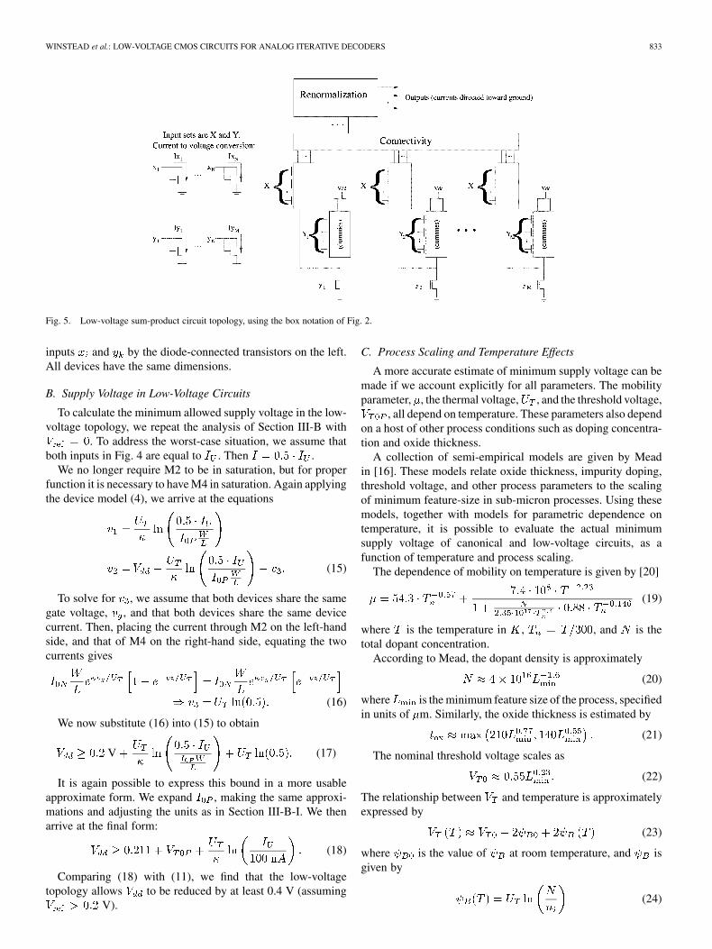
A. General Low-Voltage Sum-Product Topology
Fig. 5 displays a general low-voltage sum-product circuittopology based on these results. In Fig. 5, denotes the set ofcolumn inputs (voltages) whichexcludes the input . The members of have no particularorder. The current inputs and are converted into voltage
WINSTEAD et al.: LOW-VOLTAGE CMOS CIRCUITS FOR ANALOG ITERATIVE DECODERS 833
Fig. 5. Low-voltage sum-product circuit topology, using the box notation of Fig. 2.
inputs and by the diode-connected transistors on the left.All devices have the same dimensions.
B. Supply Voltage in Low-Voltage Circuits
To calculate the minimum allowed supply voltage in the low-voltage topology, we repeat the analysis of Section III-B with
. To address the worst-case situation, we assume thatboth inputs in Fig. 4 are equal to . Then .
We no longer require M2 to be in saturation, but for properfunction it is necessary to have M4 in saturation. Again applyingthe device model (4), we arrive at the equations
(15)
To solve for , we assume that both devices share the samegate voltage, , and that both devices share the same devicecurrent. Then, placing the current through M2 on the left-handside, and that of M4 on the right-hand side, equating the twocurrents gives
(16)
We now substitute (16) into (15) to obtain
V (17)
It is again possible to express this bound in a more usableapproximate form. We expand , making the same approxi-mations and adjusting the units as in Section III-B-I. We thenarrive at the final form:
(18)
Comparing (18) with (11), we find that the low-voltagetopology allows to be reduced by at least 0.4 V (assuming
V).
C. Process Scaling and Temperature Effects
A more accurate estimate of minimum supply voltage can bemade if we account explicitly for all parameters. The mobilityparameter, , the thermal voltage, , and the threshold voltage,
, all depend on temperature. These parameters also dependon a host of other process conditions such as doping concentra-tion and oxide thickness.
A collection of semi-empirical models are given by Meadin [16]. These models relate oxide thickness, impurity doping,threshold voltage, and other process parameters to the scalingof minimum feature-size in sub-micron processes. Using thesemodels, together with models for parametric dependence ontemperature, it is possible to evaluate the actual minimumsupply voltage of canonical and low-voltage circuits, as afunction of temperature and process scaling.
The dependence of mobility on temperature is given by [20]
(19)
where is the temperature in , , and is thetotal dopant concentration.
According to Mead, the dopant density is approximately
(20)
where is the minimum feature size of the process, specifiedin units of m. Similarly, the oxide thickness is estimated by
(21)
The nominal threshold voltage scales as
(22)
The relationship between and temperature is approximatelyexpressed by
(23)
where is the value of at room temperature, and isgiven by
(24)

834 IEEE TRANSACTIONS ON CIRCUITS AND SYSTEMS—I: REGULAR PAPERS, VOL. 53, NO. 4, APRIL 2006
Fig. 6. Allowable supply voltages for canonical and low-voltage topologies, as a function of process feature size and temperature.
Fig. 7. Difference in minimum supply voltage between low-voltage and canonical sum-product circuits, as a function of temperature.
and where is the density of carriers in intrinsic (undoped)silicon cm . The subthreshold slope factor,
, is a function of , , , and the gate-to-bulk voltage. Weapproximate by its near-minimum value, which occurs nearthe boundary between weak-inversion and depletion. We beginwith the depletion depth under the gate, which is [16]
(25)
where is the permittivity of silicon, and is the charge on theelectron. The corresponding depletion-layer capacitance is then
given by . The oxide capacitance is ,and is defined as the capacitive divider relation betweenand : .
These equations are collected and solved numerically,yielding estimates of (17) and (9) as functions of temperatureand feature size. The results of this calculation are reportedin Fig. 6. The difference in allowable supply voltage betweencanonical and low-voltage circuits is shown in Fig. 7 as a func-tion of temperature. The supply-voltage advantage achieved bylow-voltage circuits is approximately 0.56 V. This differencedepends only weakly on temperature.

WINSTEAD et al.: LOW-VOLTAGE CMOS CIRCUITS FOR ANALOG ITERATIVE DECODERS 835
D. Renormalization
In a low voltage circuit described by (14), the denominator isequivalent to two, substantially reducing the current magnitudeat the output of each module. Renormalization is also imple-mented with a low-voltage circuit. If the circuit Fig. 3 is used inthe conventional way, with , then it will only worsenthe attenuation. In this Section it is demonstrated that the atten-uation is reversed as long as . It is also shown that theresulting current amplification does not lead to instability in thedecoder.
In principle, linear attenuation will not change the resultof decoding. The sum-product algorithm only depends on therelative proportions among input currents (relative to eachother), not on their precise magnitude. Consistent attenuationin a large network, however, will cause the outputs to approachzero, causing the decoder to fail. In a practical setting, thesum-product algorithm is carried out repeatedly in a large net-work of sum-product nodes. The output of one node providesinput for the next. By “unwrapping” the decoding network, thedecoder may be regarded as a cascaded array of sum-productnodes. In terms of current magnitude, the circuit becomes aniteration of attenuation and renormalization.
By inserting a suitably designed renormalization circuit be-tween modules, the currents are prevented from approachingzero. We utilize the circuit of Fig. 3 with . Thecircuit is now a form of the low-voltage topology described by(14), so that the output is
(26)
It is possible to choose and in Fig. 3 so that upon iter-ation the current magnitude, (defined by (3)), converges to acontrolled fixed point greater than zero. This allows us to treat(26) as a simple one-dimensional iterated function
(27)
To determine the dynamic behavior of this system, we iden-tify the fixed points (where ) and determine whetherthey are stable. It is easy to verify that the fixed points occur at
, and . It is well known that a fixed pointis stable and nonoscillating if the slope of the transfer function,
, is real and satisfies at the fixed point. Also, a fixed point is unstable (i.e., it is a repeller) if
. Evaluated at the fixed points, the slopes of thetransfer function (27) are
(28)
(29)
The results (28) and (29) show that there is always a stablefixed point above zero when . The canonical renormal-izer uses , in which case there is no fixed point greaterthan zero, thus driving all currents to zero in a low-voltage net-work. By simply using this can be avoided. The transferfunction (27) is shown for various values of in Fig. 8, inwhich . The iterated behavior is also illustrated, with
Fig. 8. Current magnitude transfer function for the low-voltagerenormalization circuit.
fixed points represented by circles. Fig. 8 demonstrates that,with sufficiently large , the normalized current magnitude canbe driven very close to the desired operating point with only oneiteration. This ensures that the current magnitude is never farfrom at the output of any module.
V. DECODER ARCHITECTURES
A. Trellis Decoders
Many codes are constructed from Trellis descriptions. Theseinclude the component codes needed for Turbo codes, as wellas convolutional codes that are used in many applications. De-coding algorithms for these codes are derived directly from theirTrellis descriptions. The most powerful Trellis decoding methodis the BCJR algorithm named for the authors who introduced itin [21], which is often used in Turbo decoders. The BCJR algo-rithm is a special case of the sum-product algorithm (1) [4].
A Trellis graph for the (8,4) Hamming code is shown in Fig. 9,alongside the structure of the corresponding sum-product de-coder. The triangles in Fig. 9 represent comparators. A com-plete implementation of this decoder is presented in Section VI.Fig. 9 also illustrates how the Trellis is decomposed into dis-tinct sections. A Trellis section is a portion of the Trellis graphwhich describes a Boolean constraint function. The graph of aTrellis section consists of two columns of states, connected bybranches.
Example Trellis sections are shown in Fig. 9 and in the upperleft corner of Fig. 10. In each Trellis section, the states on the leftrepresent the possible values of a random state variable . Thestates on the right represent the possible values of the outputvariable. The labels on branches represent the possible valuesof a third variable, . If a branch exists for a particular com-bination , then the constraint is satisfied for thatcombination. Using the constraint specified by the Trellis sec-tion, a sum-product circuit is constructed using the proceduresoutlined in Section II-A.
A low-voltage sum-product circuit for one Trellis section isshown in Fig. 10. The branch variable takes values from the set

836 IEEE TRANSACTIONS ON CIRCUITS AND SYSTEMS—I: REGULAR PAPERS, VOL. 53, NO. 4, APRIL 2006
Fig. 9. Trellis graph and decoder structure for an (8,4) Hamming code.
Fig. 10. Low-voltage circuit for Trellis decoding based on the BCJRalgorithm.
. The sum-product equation for this particularTrellis section can be written in matrix form [22], resulting in
(30)
Every stage of the Trellis decoder consists of a matrix multipli-cation of the form (30), which are straightforward to implementusing low-voltage multipliers.
Fig. 11. Tanner graph for an (8,4) Hamming code.
Fig. 12. Implementation of equality and parity-check nodes for LDPC-styledecoders.
B. LDPC (Tanner Graph) Decoders
Decoders for binary LDPC codes are mapped from the code’s“normalized” Tanner Graph, which is a direct visualization ofthe code’s binary parity-check matrix [13]. The Tanner Graphcontains two types of constraint nodes, parity-check nodes andequality nodes. A variable node denotes a particular bit in acodeword. A parity-check node represents a parity-check equa-tion, which is specified by a single row in the parity-check ma-trix. All variables in the graph are binary. For implementation,this means that all probability masses have two components.An example Tanner graph is shown in Fig. 11. A correspondinglow-voltage analog implementation is reported in Section VI.
For a three-edge parity-check node, the constraint functionis a logical XOR operation. Applying this to the sum-productalgorithm (1), and labeling the three edges , , and , therequired operations are
(31)
(32)
The sum-product operations for an equality node are
(33)
(34)
Applying the general circuit of Fig. 5, and varying the con-nectivity to produce the appropriate functions, we arrive at thecircuits of Fig. 12. As before, the “ ” inputs are the columninputs, and the “ ” inputs are the row inputs. M3 and M4 are
WINSTEAD et al.: LOW-VOLTAGE CMOS CIRCUITS FOR ANALOG ITERATIVE DECODERS 837
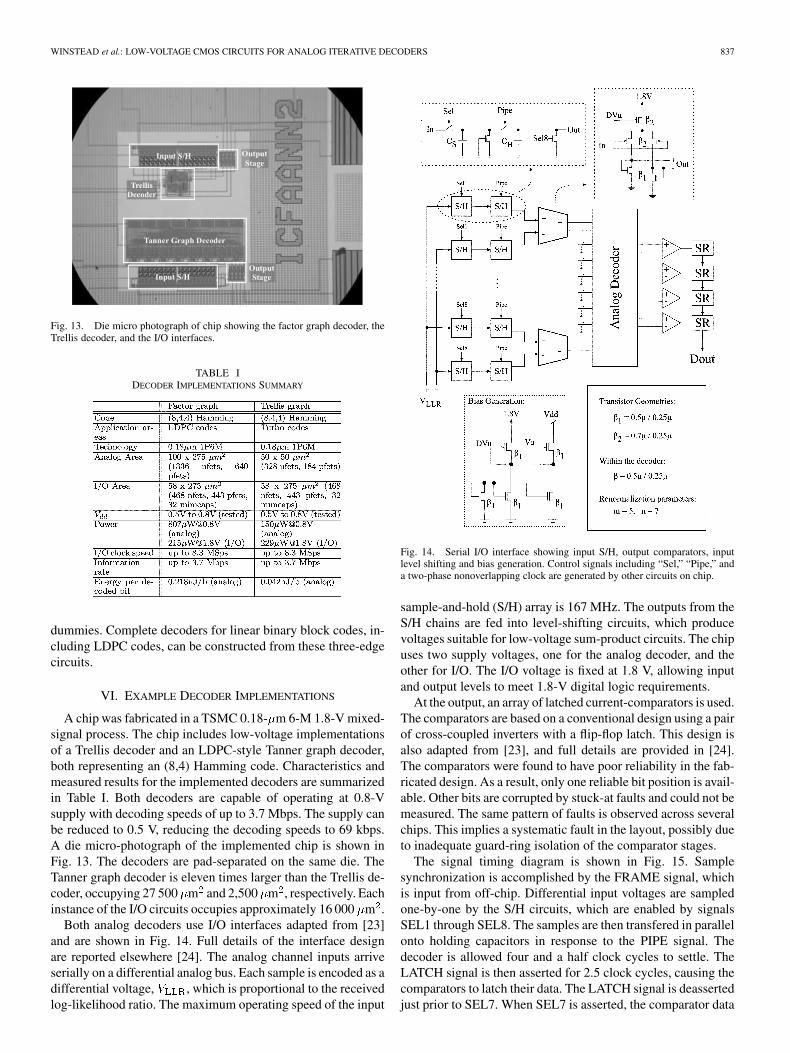
Fig. 13. Die micro photograph of chip showing the factor graph decoder, theTrellis decoder, and the I/O interfaces.
TABLE IDECODER IMPLEMENTATIONS SUMMARY
dummies. Complete decoders for linear binary block codes, in-cluding LDPC codes, can be constructed from these three-edgecircuits.
VI. EXAMPLE DECODER IMPLEMENTATIONS
A chip was fabricated in a TSMC 0.18- m 6-M 1.8-V mixed-signal process. The chip includes low-voltage implementationsof a Trellis decoder and an LDPC-style Tanner graph decoder,both representing an (8,4) Hamming code. Characteristics andmeasured results for the implemented decoders are summarizedin Table I. Both decoders are capable of operating at 0.8-Vsupply with decoding speeds of up to 3.7 Mbps. The supply canbe reduced to 0.5 V, reducing the decoding speeds to 69 kbps.A die micro-photograph of the implemented chip is shown inFig. 13. The decoders are pad-separated on the same die. TheTanner graph decoder is eleven times larger than the Trellis de-coder, occupying 27 500 m and 2,500 m , respectively. Eachinstance of the I/O circuits occupies approximately 16 000 m .
Both analog decoders use I/O interfaces adapted from [23]and are shown in Fig. 14. Full details of the interface designare reported elsewhere [24]. The analog channel inputs arriveserially on a differential analog bus. Each sample is encoded as adifferential voltage, , which is proportional to the receivedlog-likelihood ratio. The maximum operating speed of the input
Fig. 14. Serial I/O interface showing input S/H, output comparators, inputlevel shifting and bias generation. Control signals including “Sel,” “Pipe,” anda two-phase nonoverlapping clock are generated by other circuits on chip.
sample-and-hold (S/H) array is 167 MHz. The outputs from theS/H chains are fed into level-shifting circuits, which producevoltages suitable for low-voltage sum-product circuits. The chipuses two supply voltages, one for the analog decoder, and theother for I/O. The I/O voltage is fixed at 1.8 V, allowing inputand output levels to meet 1.8-V digital logic requirements.
At the output, an array of latched current-comparators is used.The comparators are based on a conventional design using a pairof cross-coupled inverters with a flip-flop latch. This design isalso adapted from [23], and full details are provided in [24].The comparators were found to have poor reliability in the fab-ricated design. As a result, only one reliable bit position is avail-able. Other bits are corrupted by stuck-at faults and could not bemeasured. The same pattern of faults is observed across severalchips. This implies a systematic fault in the layout, possibly dueto inadequate guard-ring isolation of the comparator stages.
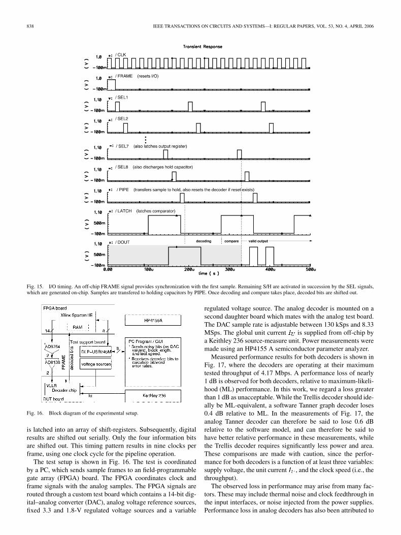
The signal timing diagram is shown in Fig. 15. Samplesynchronization is accomplished by the FRAME signal, whichis input from off-chip. Differential input voltages are sampledone-by-one by the S/H circuits, which are enabled by signalsSEL1 through SEL8. The samples are then transfered in parallelonto holding capacitors in response to the PIPE signal. Thedecoder is allowed four and a half clock cycles to settle. TheLATCH signal is then asserted for 2.5 clock cycles, causing thecomparators to latch their data. The LATCH signal is deassertedjust prior to SEL7. When SEL7 is asserted, the comparator data
838 IEEE TRANSACTIONS ON CIRCUITS AND SYSTEMS—I: REGULAR PAPERS, VOL. 53, NO. 4, APRIL 2006
Fig. 15. I/O timing. An off-chip FRAME signal provides synchronization with the first sample. Remaining S/H are activated in succession by the SEL signals,which are generated on-chip. Samples are transfered to holding capacitors by PIPE. Once decoding and compare takes place, decoded bits are shifted out.
Fig. 16. Block diagram of the experimental setup.
is latched into an array of shift-registers. Subsequently, digitalresults are shifted out serially. Only the four information bitsare shifted out. This timing pattern results in nine clocks perframe, using one clock cycle for the pipeline operation.
The test setup is shown in Fig. 16. The test is coordinatedby a PC, which sends sample frames to an field-programmablegate array (FPGA) board. The FPGA coordinates clock andframe signals with the analog samples. The FPGA signals arerouted through a custom test board which contains a 14-bit dig-ital–analog converter (DAC), analog voltage reference sources,fixed 3.3 and 1.8-V regulated voltage sources and a variable
regulated voltage source. The analog decoder is mounted on asecond daughter board which mates with the analog test board.The DAC sample rate is adjustable between 130 kSps and 8.33MSps. The global unit current is supplied from off-chip bya Keithley 236 source-measure unit. Power measurements weremade using an HP4155 A semiconductor parameter analyzer.
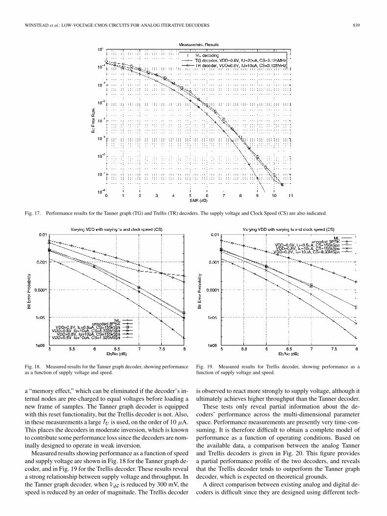
Measured performance results for both decoders is shown inFig. 17, where the decoders are operating at their maximumtested throughput of 4.17 Mbps. A performance loss of nearly1 dB is observed for both decoders, relative to maximum-likeli-hood (ML) performance. In this work, we regard a loss greaterthan 1 dB as unacceptable. While the Trellis decoder should ide-ally be ML-equivalent, a software Tanner graph decoder loses0.4 dB relative to ML. In the measurements of Fig. 17, theanalog Tanner decoder can therefore be said to lose 0.6 dBrelative to the software model, and can therefore be said tohave better relative performance in these measurements, whilethe Trellis decoder requires significantly less power and area.These comparisons are made with caution, since the perfor-mance for both decoders is a function of at least three variables:supply voltage, the unit current , and the clock speed (i.e., thethroughput).
The observed loss in performance may arise from many fac-tors. These may include thermal noise and clock feedthrough inthe input interfaces, or noise injected from the power supplies.Performance loss in analog decoders has also been attributed to
WINSTEAD et al.: LOW-VOLTAGE CMOS CIRCUITS FOR ANALOG ITERATIVE DECODERS 839
Fig. 17. Performance results for the Tanner graph (TG) and Trellis (TR) decoders. The supply voltage and Clock Speed (CS) are also indicated.
Fig. 18. Measured results for the Tanner graph decoder, showing performanceas a function of supply voltage and speed.
a “memory effect,” which can be eliminated if the decoder’s in-ternal nodes are pre-charged to equal voltages before loading anew frame of samples. The Tanner graph decoder is equippedwith this reset functionality, but the Trellis decoder is not. Also,in these measurements a large is used, on the order of 10 A.This places the decoders in moderate inversion, which is knownto contribute some performance loss since the decoders are nom-inally designed to operate in weak inversion.
Measured results showing performance as a function of speedand supply voltage are shown in Fig. 18 for the Tanner graph de-coder, and in Fig. 19 for the Trellis decoder. These results reveala strong relationship between supply voltage and throughput. Inthe Tanner graph decoder, when is reduced by 300 mV, thespeed is reduced by an order of magnitude. The Trellis decoder
Fig. 19. Measured results for Trellis decoder, showing performance as afunction of supply voltage and speed.
is observed to react more strongly to supply voltage, although itultimately achieves higher throughput than the Tanner decoder.
These tests only reveal partial information about the de-coders’ performance across the multi-dimensional parameterspace. Performance measurements are presently very time-con-suming. It is therefore difficult to obtain a complete model ofperformance as a function of operating conditions. Based onthe available data, a comparison between the analog Tannerand Trellis decoders is given in Fig. 20. This figure providesa partial performance profile of the two decoders, and revealsthat the Trellis decoder tends to outperform the Tanner graphdecoder, which is expected on theoretical grounds.
A direct comparison between existing analog and digital de-coders is difficult since they are designed using different tech-

840 IEEE TRANSACTIONS ON CIRCUITS AND SYSTEMS—I: REGULAR PAPERS, VOL. 53, NO. 4, APRIL 2006
TABLE IIENERGY EFFICIENCY FIGURES OF DIGITAL (TOP 2) AND ANALOG DECODERS (BOTTOM 4). ADC FIGURES WERE NOT INCLUDED FOR DIGITAL DECODERS, AND
WOULD RESULT IN GREATER ENERGY CONSUMPTION
Fig. 20. Comparison of E =N losses for the Tanner graph (TG) and Trellis(TR) decoders at differentV as a function of clock speed. Losses are estimatedfrom performance measurements at E =N = 8 dB.
nologies, operate on different codes, sometimes implement dif-ferent decoding algorithms, and are intended for a wide rangeof throughput and applications. A general figure of merit com-monly used is the energy efficiency measured in Joules per bit.Table II examines this metric for existing digital and analog de-coders. The power consumption has been divided into analogdecoder and I/O components to give a better comparison topreviously implemented decoders. Comparing our energy effi-ciency results to existing decoders in Table II, we find the Trellisdecoder to be 3 better than the best analog decoder and 30better than the best digital decoder in terms of energy efficiency.
VII. CONCLUSION
In this paper, we presented an overview of low-power CMOSanalog circuits for iterative decoding, and developed a new low-voltage form of the translinear sum-product circuit. The newtopology allows the supply voltage to be reduced by at least0.4 V relative to the canonical approach. We showed how toapply the low-voltage topology to implement a diverse familyof iterative error-control codes, including LDPC codes, Trelliscodes and, consequently, Turbo codes. We also demonstratedour new method with implementations of two simple decoders,
representing the LDPC and Trellis families. The Trellis decoderwas found to have the lowest energy per bit of any reportediterative decoder.
ACKNOWLEDGMENT
The authors would like to thank K. Leung for his assistancewith power measurements.
REFERENCES
[1] C. Berrou, A. Glavieux, and P. Thitimajshima, “Near shannonlimit error-correcting coding and decoding: Turbo codes,” IEEE Trans. Commun.,vol. 44, no. 10, pp. 1261–1271, Oct. 1996.
[2] J. Hagenauer, E. Offer, and L. Papke, “Iterative decoding of binary blockand convolutional codes,” IEEE Trans. Inf. Theory, vol. 42, no. 3, pp.429–445, Mar. 1996.
[3] N. Wiberg, H. A. Loeliger, and R. Kotter, “Codes and iterative decodingon general graphs,” Eur. Trans. Telecomm., pp. 513–525, Sep./Oct. 1995.
[4] F. R. Kschischang, B. J. Frey, and H. A. Loeliger, “Factor graphs andthe sum-product algorithm,” IEEE Trans. Inf. Theory, vol. 47, no. 2, pp.498–519, Feb. 2001.
[5] J. Pearl, Probabilistic Reasoning in Intelligent Systems : Networks ofPlausible Inference. New York: Morgan Kaufmann, 1988.
[6] H. A. Loeliger, F. Lustenberger, M. Helfenstein, and F. Tarkoy, “Prob-ability propagation and decoding in analog VLSI,” IEEE Trans. Inf.Theory, vol. 47, no. 2, pp. 837–843, Feb. 2001.
[7] J. Hagenauer and M. Winklhofer, “The analog decoder,” in Proc. Int.Symp. Inf. Theory, Cambridge, MA, Aug. 1998.
[8] F. Lustenberger, M. Helfenstein, G. S. Moschytz, H. A. Loeliger, and F.Tarkoy, “All analog decoder for (18,9,5) tail-biting Trellis code,” in Proc.Eur. Solid-State Circuits Conf. (ESSCIRC), Sep. 1999, pp. 362–365.
[9] M. Moerz, T. Gabara, R. Yan, and J. Hagenauer, “An analog 0.25 �mBiCMOS tailbiting MAP decoder,” in Proc. Int. Solid-State CircuitsConf., Feb. 2000, pp. 356–357.
[10] C. Winstead, J. Dai, S. Yu, R. Harrison, C. J. Myers, and C. Schlegel,“CMOS analog decoder for (8,4) hamming code,” IEEE J. Solid-StateCircuits, no. 1, pp. 122–131, Jan. 2004.
[11] A. F. Mondragon-Torres, E. Sanchez-Sinencio, and K. R. Narayanan,“Floating-gate analog implementation of the additive soft-inputsoft-output decoding algorithm,” IEEE Trans. Circuits Syst. I, Fundam.Theory Appl., vol. 50, no. 10, pp. 1256–1269, Oct. 2003.
[12] V. C. Gaudet and P. G. Gulak, “A 13.3-Mb/s 0.35-�m CMOS analogTurbo decoder IC with a configurable interleaver,” IEEE J. Solid-StateCircuits, vol. 38, pp. 2010–2015, Nov. 2003.
[13] G. D. Forney, “Codes on graphs: Normal realizations,” IEEE Trans. Inf.Theory, pp. 520–548, Feb. 2001.
[14] F. Lustenberger, “On the design of analog VLSI iterative decoders,”Ph.D. dissertation, Swiss Federal Institute of Technology, Zurich, 2000.
[15] C. Mead, Analog VLSI and Neural Systems. Reading, MA: Addison-Wesley, 1989.
[16] S.-C. Liu, J. Kramer, G. Indiveri, T. Delbrück, and R. Douglas, AnalogVLSI: Circuits and Principles. Cambridge, MA: MIT Press, 2002.
[17] E. Vittoz and J. Fellrath, “CMOS analog integrated circuits based onweak-inversion operation,” IEEE J. Solid-State Circuits, vol. SC-12, no.2, pp. 224–231, Apr. 1977.
WINSTEAD et al.: LOW-VOLTAGE CMOS CIRCUITS FOR ANALOG ITERATIVE DECODERS 841
[18] E. Seevinck, E. Vittoz, M. du Plessis, T.-H. Joubert, and W. Beetge,“CMOS translinear circuits for minimum supply voltage,” IEEE Trans.Circuits Syst. II, Analog Digit. Signal Process., vol. 47, no. 12, pp.1560–1564, Dec. 2000.
[19] M. Frey, H.-A. Loeliger, F. Lustenberger, P. Merkli, and P. Strebel,“Analog-decoder experiments with subthreshold CMOS soft-gates,” inProc. 2003 Int. Symp. Circuits Syst. (ISCAS’03), Bangkok, Thailand,May 2003, pp. 85–88.
[20] R. S. Muller and T. I. Kamins, Device Electronics for Integrated Cir-cuits. New York: Wiley, 1977.
[21] L. R. Bahl, J. Cocke, F. Jelinek, and J. Raviv, “Optimal decoding of linearcodes for minimizing symbol error rate,” IEEE Trans. Info. Theory, vol.20, no. 3, pp. 284–287, Mar. 1974.
[22] J. B. Anderson and S. M. Hladik, “Tailbiting MAP decoders,” IEEE J.Select. Areas in Commun., vol. 16, no. 2, pp. 297–302, Feb. 1998.
[23] S. Yu, “Design and test of error control decoders in analog CMOS,”Ph.D. dissertation, Univ. of Utah, Logan, 2004.
[24] C. Winstead, “Analog Iterative Decoders,” Ph.D., University of Alberta,Edmonton, AB, Canada, 2005.
[25] A. J. Blanksby and C. J. Howland, “A 690-mW 1-Gb/s 1024-b, rate-1/2low-density parity-check code decoder,” IEEE J. Solid-State Circuits,vol. 37, no. 3, pp. 404–412, Mar. 2002.
[26] M. Bickerstaff, D. Garrett, T. Prokop, C. Thomas, B. Widdup, G. Zhou,C. Nicol, and R.-H. Yan, “A unified Turbo/Viterbi channel decoder for3 GPP mobile wireless in 0.18-�m CMOS,” in Proc. 2002 IEEE Int.Solid-State Circuits Conf. (ISSCC’02), Feb. 2002, pp. 90–91.
[27] D. Vogrig, A. Gerosa, A. Neviani, A. G. Amat, G. Montorsi, and S.Benedetto, “A 0.35-�m CMOS analog Turbo decoder for the 40-bit rate1/3 UMTS channel code,” IEEE J. Solid-State Circuits, vol. 40, no. 3,pp. 753–762, Mar. 2005.
Chris Winstead (S’96–M’05) received the Ph.D.degree from the University of Alberta in Edmonton,AB, Canada, in 2005.
In 2004, he joined the faculty of Electrical andComputer Engineering at Utah State Universityin Logan, where he is currently an Assistant Pro-fessor. His research interests include low-powerVLSI circuits, translinear analog circuits, iterativeerror-control algorithms, reliable computation andefficient simulation of nonlinear mixed-signal sys-tems.
Dr. Winstead is a member of the Tau Beta Pi.
Nhan Nguyen (S’98–M’06) received a B.App.Sc.(Co-op) degree from the University of Regina, SK,Canada in 2001 (working with various telecommu-nications companies), and the M.Sc. degree from theUniversity of Alberta, Edmonton, AB, Canada, in2004.
He served as a Research Assistant with the HighCapacity Digital Communications Laboratory, Uni-versity of Alberta, until June 2005. His research in-terests include analog and mixed-signal circuits.
Vincent C. Gaudet (S’97–M’03) received the B.Sc.degree in computer engineering from the Universityof Manitoba, Winnipeg, MB, Canada, in 1995, andthe M.Appl.Sci. and Ph.D. degrees from the Univer-sity of Toronto, Toronto, ON, Canada in 1997 and2003, respectively.
From February to July 2002, he was a ResearchAssociate in the Department Electronique, Ecole Na-tionale Superieure des Telecommunications de Bre-tagne, Brest, France. He is currently an Assistant Pro-fessor in the Department of Electrical and Computer
Engineering, University of Alberta, Edmonton, AB, Canada. His research in-terests include the design of algorithms and integrated circuits for high-speeddigital communications.
Dr. Gaudet received the Natural Sciences and Engineering Research Councilof Canada Postgraduate Scholarship, the Ontario Graduate Scholarship in Sci-ence and Technology, and the Walter Sumner Memorial Fund Scholarship, andwas awarded the University of Manitoba’s University Gold Medal in 1995.
Christian Schlegel (S’86–M’89–SM’96) receivedthe Dipl. El. Ing. ETH degree from the FederalInstitute of Technology, Zurich, Switzerland, in1984, and the M.S. and Ph.D. degrees in electricalengineering from the University of Notre Dame,Notre Dame, IN, in 1986 and 1989, respectively.
In 1988, he joined the Communications Group atthe research center of Asea Brown Boveri, Ltd., inBaden, Switzerland, where he was involved in mobilecommunications research. He spent the 1991/1992academic year as Visiting Assistant Professor at the
University of Hawaii at Manoa, HI, before joining the Digital Communica-tions Group at the University of South Australia in Adelaide, Australia from1992–1994, as head of the Mobile Communications Research Centre. From1994–1996, he was with the University of Texas at San Antonio, and in 1996 hejoined the University of Utah, Salt Lake City. In 2001, he was named iCOREProfessor for High-Capacity Digital Communications at the University of Al-berta, Edmonton, Canada. His interests are in the area of error control codingand applications, multiple access communications, basic digital communica-tions, mobile radio systems and implementations, and analog implementationsof digital systems.