Beyond-CMOS Technologies for Next Generation Computer ...
279
Rasit O. Topaloglu · H.-S. Philip Wong Editors Beyond-CMOS Technologies for Next Generation Computer Design
-
Upload
khangminh22 -
Category
Documents
-
view
0 -
download
0
Transcript of Beyond-CMOS Technologies for Next Generation Computer ...

Rasit O. Topaloglu · H.-S. Philip Wong Editors
Beyond-CMOS Technologies for Next Generation Computer Design

Beyond-CMOS Technologies for Next GenerationComputer Design

Rasit O. Topaloglu • H.-S. Philip WongEditors
Beyond-CMOS Technologiesfor Next GenerationComputer Design
123

EditorsRasit O. TopalogluIBMHopewell Junction, NY, USA
H.-S. Philip WongDepartment of Electrical EngineeringStanford UniversityStanford, CA, USA
ISBN 978-3-319-90384-2 ISBN 978-3-319-90385-9 (eBook)https://doi.org/10.1007/978-3-319-90385-9
Library of Congress Control Number: 2018946645
© Springer International Publishing AG, part of Springer Nature 2019This work is subject to copyright. All rights are reserved by the Publisher, whether the whole or part ofthe material is concerned, specifically the rights of translation, reprinting, reuse of illustrations, recitation,broadcasting, reproduction on microfilms or in any other physical way, and transmission or informationstorage and retrieval, electronic adaptation, computer software, or by similar or dissimilar methodologynow known or hereafter developed.The use of general descriptive names, registered names, trademarks, service marks, etc. in this publicationdoes not imply, even in the absence of a specific statement, that such names are exempt from the relevantprotective laws and regulations and therefore free for general use.The publisher, the authors and the editors are safe to assume that the advice and information in this bookare believed to be true and accurate at the date of publication. Neither the publisher nor the authors orthe editors give a warranty, express or implied, with respect to the material contained herein or for anyerrors or omissions that may have been made. The publisher remains neutral with regard to jurisdictionalclaims in published maps and institutional affiliations.
Printed on acid-free paper
This Springer imprint is published by the registered company Springer International Publishing AG partof Springer Nature.The registered company address is: Gewerbestrasse 11, 6330 Cham, Switzerland

Foreword
This book surveys and summarizes recent research aimed at new devices, circuits,and architectures for computing. Much of the impetus for this research stems froma remarkable development in information technology that played out in the briefperiod between 2003 and 2005. After decades of rapid exponentially compoundingimprovement, microprocessor clock frequencies abruptly plateaued—a stunningbreak from a long-established and highly desirable trend in computing performance.The proximate cause was the increasing difficulty and cost of powering andremoving the waste heat from ever denser and faster transistor circuits. The rootcause—the reason for excessive heat generation—was the inability, for fundamentalreasons, to reduce transistor threshold voltage in proportion to reductions in powersupply voltage. As a result, standby (or passive) power had grown exponentiallyfrom technology generation to technology generation until it equaled or exceededactive power, which was also increasing. Further increases would have drivenunacceptable costs for power and cooling across many product categories. Instead,development teams pivoted and began to optimize each new technology generationfor operation in this new power-constrained environment. While many had foreseenthe need and developed strategies for highly power-constrained device-, circuit-,and system-level design, the net outcome of the power-performance trade-offs at alllevels of the design hierarchy was difficult to predict. Thus the complete and abruptcessation of advances in clock frequency came as a surprise.
This event sent ripples throughout the worldwide microelectronics industry.Since 2005, integration density and cost per device have continued to improve,and manufacturers have emphasized the increasing number of processors and theamount of memory they can place on a single die. However, with clock frequenciesstagnant, the resulting performance gains have been muted compared to those of theprevious decades. The return on investment for development of each new generationof ever-smaller transistors has therefore been reduced, and the number of companiesmaking that investment has declined. To be clear, the total effort remains enormousby the standards of any industry, with the vast majority of R&D dollars going
v

vi Foreword
toward further advancement of silicon CMOS field effect transistor technology and,increasingly, toward advancement of circuit and system architectures.
But the experience of 2003–2005 also sparked a bold new industry initiative. In2005, the Nanoelectronics Research Initiative (NRI) was chartered by a consortiumof Semiconductor Industry Association (SIA) member companies to develop andadminister a university-based research program to address the increasingly evidentlimitations of the field effect transistor. In partnership with the National ScienceFoundation (NSF), NRI would fund university research to “Demonstrate novelcomputing devices capable of replacing the CMOS FET as a logic switch in the2020 timeframe.” In 2007, the National Institute of Standards and Technology(NIST) joined the private-public partnership, resulting in the creation of four multi-university, multidisciplinary research centers. NRI’s bold and clearly articulatedresearch goals caught the attention of funding agencies in Europe and Asia andhelped to spark new initiatives in those geographies. In 2013 the Defense AdvancedResearch Projects Agency (DARPA) joined with industry to fund STARnet, furtherfocusing US university researchers on the exploration of post-CMOS devices. Asthe NRI and STARnet programs evolved, the interest of the industrial sponsorsshifted from exploration of isolated devices toward co-development of new devices,circuits, and architectures. This was made explicit with new programs announcedwith NSF in 2016 and with NIST and DARPA in 2017.
The research initiatives and results described in Beyond-CMOS Technologiesfor Next Generation Computer Design reflect and address this broad industry needfor new approaches to energy-efficient computing. Indeed, much of the work wasfunded to a greater or lesser extent through NRI, STARnet, or programs withclosely related goals. The research ranges from new materials and the devices theyenable, to novel circuits and architectures for computing. In many cases, the resultsspan two or more levels in this hierarchy. For example, Subhasish Mitra describesthe novel fabrication processes that made it possible to build a simple computerfrom transistors based on carbon nanotubes. Xueqing Li and coauthors tell us whyand how the negative capacitance field effect transistor (NCFET) and other “steepslope” devices are poised to open a new circuit design space for ultra-low-powerelectronics. Two sets of authors provide perspectives on the interplay betweenemerging nonvolatile memory devices, 3D integration schemes, and “compute inmemory” architectures. Looking beyond conventional FETs and the traditionalcomputing architecture, it seems there is still a lot to explore!
Department of Electrical Engineering, Columbia University Thomas N. TheisNew York, NY, USAApril 15, 2018
Preface
Advances of traditional CMOS devices may be hitting a bottleneck soon dueto electrostatic control, power, device density, and variability limitations. It maybe necessary to complement silicon transistors with beyond-CMOS counterpartsin integrated circuits. Yet, a straightforward replacement may not yield optimalarchitecture and system response. Hence, circuits need to be redesigned in thecontext of beyond-CMOS devices. This book in particular targets to bridge the gapbetween device availability and architecture/system considerations. With this book,readers should be able to understand:
– Why we need to consider beyond-CMOS devices,– What are the challenges of beyond-CMOS options,– How should architecture and systems be designed differently,– How would designs take advantage of beyond-CMOS benefits.
The book consists of the following seven chapters from distinguished authors:
Hills, Mitra, and Wong focus on carbon nanotube transistors. They further analyzea monolithic 3D integration with carbon nanotube transistors. A new deviceintegration enabled by carbon nanotube transistors would lead to three ordersof magnitude energy delay product improvement.
Resta, Gaillardon, and de Micheli discuss a novel device (MIG-FET) with intrinsicdoping where the device type is not fixed at manufacture but is adjustable usinginputs to the gate. The authors analyze this functionality-enhanced MIG-FETdevice.
Nourbakhsh, Yu, Lin, Hempel, Shiue, Englund, and Palacios study devices of 2Dlayered materials that have weak van der Waals forces between the layers. Theydiscuss not only electrical but also optoelectrical and biological applications intheir chapter.
Khwa, Lu, Dou, and Chang discuss nonvolatile memories including resistive RAM(ReRAM), phase change memory, and spin-torque transfer magnetic RAM (STT-RAM), and their circuit implementations such as nonvolatile SRAM.
vii

viii Preface
Ghose, Hsieh, Boroumand, Ausavarungnirun, and Mutlu study processing-in-memory to avoid CPU to memory transfers. They propose and discuss an in-memory accelerator for pointer chasing and a data coherence support mechanism.
Li, Kim, George, Aziz, Jerry, Shukla, Sampson, Gupta, Datta, and Narayananinvestigate tunneling FET (TFET), negative capacitance FET (NCFET), andHyperFET as steep-slope device candidates to achieve low power consumption.
Finally, Zografos, Vaysset, Soree, and Raghavan analyze spin-wave devices andspin-torque majority gates including circuit benchmarking against silicondevices.
Hopewell Junction, NY, USA Rasit O. TopalogluStanford, CA, USA H.-S. Philip Wong

Contents
1 Beyond-Silicon Devices: Considerations for Circuitsand Architectures . . . . . . . . . . . . . . . . . . . . . . . . . . . . . . . . . . . . . . . . . . . . . . . . . . . . . . . . . . . . 1Gage Hills, H.-S. Philip Wong, and Subhasish Mitra
2 Functionality-Enhanced Devices: From Transistors toCircuit-Level Opportunities . . . . . . . . . . . . . . . . . . . . . . . . . . . . . . . . . . . . . . . . . . . . . . . . 21Giovanni V. Resta, Pierre-Emmanuel Gaillardon,and Giovanni De Micheli
3 Heterogeneous Integration of 2D Materials and Devices on a SiPlatform . . . . . . . . . . . . . . . . . . . . . . . . . . . . . . . . . . . . . . . . . . . . . . . . . . . . . . . . . . . . . . . . . . . . . . . 43Amirhasan Nourbakhsh, Lili Yu, Yuxuan Lin, Marek Hempel,Ren-Jye Shiue, Dirk Englund, and Tomás Palacios
4 Emerging NVM Circuit Techniques and Implementations forEnergy-Efficient Systems . . . . . . . . . . . . . . . . . . . . . . . . . . . . . . . . . . . . . . . . . . . . . . . . . . . . 85Win-San Khwa, Darsen Lu, Chun-Meng Dou, and Meng-Fan Chang
5 The Processing-in-Memory Paradigm: Mechanisms to EnableAdoption . . . . . . . . . . . . . . . . . . . . . . . . . . . . . . . . . . . . . . . . . . . . . . . . . . . . . . . . . . . . . . . . . . . . . . 133Saugata Ghose, Kevin Hsieh, Amirali Boroumand,Rachata Ausavarungnirun, and Onur Mutlu
6 Emerging Steep-Slope Devices and Circuits: Opportunitiesand Challenges . . . . . . . . . . . . . . . . . . . . . . . . . . . . . . . . . . . . . . . . . . . . . . . . . . . . . . . . . . . . . . . 195Xueqing Li, Moon Seok Kim, Sumitha George, Ahmedullah Aziz,Matthew Jerry, Nikhil Shukla, John Sampson, Sumeet Gupta,Suman Datta, and Vijaykrishnan Narayanan
7 Spin-Based Majority Computation . . . . . . . . . . . . . . . . . . . . . . . . . . . . . . . . . . . . . . . . 231Odysseas Zografos, Adrien Vaysset, Bart Sorée, and Praveen Raghavan
Index . . . . . . . . . . . . . . . . . . . . . . . . . . . . . . . . . . . . . . . . . . . . . . . . . . . . . . . . . . . . . . . . . . . . . . . . . . . . . . . 263
ix

Chapter 1Beyond-Silicon Devices: Considerationsfor Circuits and Architectures
Gage Hills, H.-S. Philip Wong, and Subhasish Mitra
1.1 Introduction
While beyond-silicon devices promise improved performance at the device level,leveraging their unique properties to realize novel circuits and architectures providesadditional benefits. In fact, the benefits afforded by the new architectures thatbeyond-silicon devices enable can far exceed the benefits any improved deviceby itself could achieve. As a case study, we provide an overview of carbonnanotube (CNT) technologies, and highlight the importance of understanding—and leveraging—the unique properties of CNTs to realize improved devices,circuits, and architectures. In this chapter, we begin by reviewing state-of-the-artCNT technologies and summarizing their benefits. We then discuss the obstaclesfacing CNT technologies and the solutions for overcoming these challenges, whilehighlighting their circuit-level implications. We end by illustrating how CNTs canimpact computing architectures, and the considerations that must be taken intoaccount to fully realize the benefits of this emerging nanotechnology.
G. Hills (�) · H.-S. P. WongDepartment of Electrical Engineering, Stanford University, Stanford, CA, USAe-mail: [email protected]
S. MitraDepartment of Electrical Engineering, Stanford University, Stanford, CA, USA
Department of Computer Science, Stanford University, Stanford, CA, USA
© Springer International Publishing AG, part of Springer Nature 2019R. O. Topaloglu, H.-S. P. Wong (eds.), Beyond-CMOS Technologies for NextGeneration Computer Design, https://doi.org/10.1007/978-3-319-90385-9_1
1

2 G. Hills et al.
1.2 Carbon Nanotube Field-Effect Transistors
For decades, improvements in computing performance and energy efficiency (char-acterized by the energy-delay product, EDP, of very-large-scale-integration (VLSI)digital systems) have relied on physical and equivalent scaling of silicon-basedfield-effect transistors (FETs). This “equivalent scaling” path included strainedsilicon, high-k gate dielectric and metal gate, and advanced device geometries(e.g., FinFETs, and potentially nanowire FETs). However, continued scaling isbecoming increasingly challenging, spurring the search for beyond-silicon emergingnanotechnologies to supplement—and 1 day supplant—silicon CMOS. One suchpromising emerging nanotechnology for VLSI digital systems is carbon nanotubefield-effect transistors (CNFETs). CNFETs are excellent candidates for continuingto improve both the performance and energy efficiency of digital VLSI systems,as CNFETs are expected to improve digital VLSI EDP by and order of magnitudecompared to silicon-CMOS (at the same technology node for both CNFETs andsilicon-CMOS). Moreover, CNFETs are projected to scale beyond the limitationsof silicon-CMOS, providing an additional opportunity for further EDP benefits [1].A full description of the device-level advantages of CNTs falls beyond the scopeof this chapter, but we summarize some of the key benefits below (note that, thefollowing list is not exhaustive):
1. CNTs achieve ultrahigh carrier transport (e.g., mobility and velocity) even withultrathin (∼1 nm) bodies. In contrast, when bulk materials, such as silicon,are scaled below sub-10 nm dimensions, the carrier transport (e.g., mobility)degrades dramatically, resulting in reduced drive current (not to mention thechallenges of robust manufacturing of sub-10 nm thin silicon). In contrast, a CNTnaturally has an ultrathin body of ∼1 nm, dictated by the diameter of the CNT,while still achieving ultrahigh carrier mobility. This enables CNFETs to achievehigh drive current even with an ultrathin body.
2. Ultrathin CNTs for CNFET channels result in improved electrostatic control,which is necessary for controlled off-state leakage current and steep subthresholdslope (SS). CNFETs can therefore maintain controlled off-state leakage currentand steep SS due to their thin body while simultaneously maintaining highdrive current (discussed above). In contrast, silicon channels incur a fundamentaltrade-off: thin bodies for improved electrostatic control, but thicker bodies forimproved drive current.
3. Leveraging a planar device structure for CNFETs (in contrast to today’s three-dimensional silicon FinFETs or stacked nanowire FETs) results in both reducedgate-to-channel capacitance and also reduced parasitic capacitance, improvingboth circuit speed and energy consumption.
A schematic of a CNFET is shown in Fig. 1.1. Multiple CNTs composethe transistor channel, whose conductance is modulated by the gate, as with aconventional metal-oxide-semiconductor FET (MOSFET). The gate, source, anddrain are defined using conventional photolithography, while the doping of the CNT

1 Beyond-Silicon Devices: Considerations for Circuits and Architectures 3
Fig. 1.1 Carbon nanotube FET (CNFET) schematic. (a) Carbon nanotube (CNT), indicatingultrathin ∼1–2 nm CNT diameter; (b) CNFET, with multiple parallel CNTs comprising the CNFETchannel; (c) scanning electron microscopy (SEM) image of CNTs in the channel region
is typically controlled via electrostatic doping, instead of interstitial doping (as istypically the case for silicon CMOS). The inter-CNT spacing is determined by theCNT growth, and can therefore exceed the minimum lithographic pitch. For highdrive current, the target inter-CNT spacing is 4–5 nm, corresponding to CNT densityof ∼200–250 CNTs/μm [2].
There has been significant progress worldwide toward physically realizing ahigh-performance VLSI CNFET technology. Recent experimental demonstrationshave shown: CNFETs with 5 nm gate lengths [3] while simultaneously maintainingstrong electrostatic control of the channel (with subthreshold slope = 70 mV/decadefor both PMOS and NMOS CNFETs), high-performance CNFETs with current den-sities both competing with and exceeding silicon-based FETs (simultaneously withhigh on/off current ratio) [3–8]), techniques to reduce hysteresis with high-k gatedielectrics (with nm-scale thickness, deposited at low temperatures through atomiclayer deposition (ALD)) [9], and negative capacitance CNFETs with subthresholdslope = 55 mV/decade (exceeding the 60 mV/decade limit at 300◦K) [10].
Importantly, CNFETs are unique among emerging nanotechnologies, as com-plete and complex digital systems fabricated entirely using CNFETs have beenexperimentally demonstrated (descriptions in Sect. 1.4 and in Fig. 1.9). The firstcomplete digital subsystem, a digital implementation of a sensor/sensor-interfacecircuit, was demonstrated by Shulaker et al. [13]. Since then, increasingly complexsystems, including a simple microprocessor built entirely using CNFETs [14], havebeen demonstrated. Furthermore, as discussed in Sect. 1.4 of this chapter, CNFETshave been exploited to realize new system architectures, such as monolithic three-dimensional (3D) integrated systems, where multiple vertical layers of CNFETcircuits are fabricated directly overlapping one another, interleaved with layers ofmemory, resulting in even larger EDP benefits at the system level [1].

4 G. Hills et al.
1.3 Circuit-Level Implications
Despite the promise of CNFETs, substantial imperfections and variations inherentwith CNTs had previously prevented the realization of larger-scale CNFET circuits,and thus had to be overcome to demonstrate the experimental CNFET circuitsdescribed above [2]. The substantial imperfections and variations associated withCNFETs are
1. Mis-positioned CNTs: Mis-positioned CNTs can lead to stray conducting paths.These unwanted and incorrect connections in a circuit can cause incorrect logicfunctionality [15].
2. Metallic CNTs (m-CNTs): Due to imprecise control over CNT properties, CNTscan be either semiconducting (s-CNT) or metallic (m-CNT); m-CNTs, whichhave little or no bandgap due to their chirality and diameter, lead to degraded(decreased) on/off ratio (drive current/off-state leakage current), increased leak-age power, and incorrect logic functionality [16].
3. CNT-specific variations: In addition to variations that exist in conventionalsilicon CMOS circuits (such as channel length variation and oxide thickness vari-ations), CNTs suffer from CNT-specific variations [2, 17]. These are discussedin detail later in this section.
To overcome these inherent CNT imperfections, researchers developed theimperfection-immune design paradigm [2], which relies on both understandingand leveraging CNT-specific circuit-design techniques to overcome the aboveimperfections and realize larger-scale CNFET circuits.
1.3.1 Overcoming Mis-Positioned CNTs
It is currently impossible to guarantee exact alignment and positioning of all CNTson a wafer, especially for VLSI CNFET circuits that potentially require billionsof CNTs. The resulting mis-positioned CNTs introduce stray conducting paths,resulting in incorrect logic functionality. While improved CNT synthesis techniquesto improve the CNT alignment have been developed, they remain insufficient.Therefore, the remaining mis-positioned CNTs must be dealt with through designand are a major consideration for circuit design.
As a first measure to address mis-positioned CNTs, wafer-scale aligned CNTgrowth is accomplished by growing the CNTs on a quartz crystalline substrate(Fig. 1.2a) [18]. The CNTs grow preferentially along the crystalline plane of thesubstrate, and >99.5% of CNTs are synthesized aligned [18]. Importantly, aftergrowth, the CNTs are transferred to a traditional amorphous SiO2/Si substrate, toremain silicon-CMOS compatible (Fig. 1.2b). However, as discussed above, 99.5%aligned CNTs are insufficient for digital VLSI systems. Thus, a circuit designtechnique can also be leveraged to overcome the remaining <0.5% mis-positioned

1 Beyond-Silicon Devices: Considerations for Circuits and Architectures 5
Fig. 1.2 Overcoming mis-positioned CNTs. (a) Wafer-scale aligned CNT growth on crystallinequartz substrate, yielding 99.5% aligned CNTs; (b) low-temperature CNT transfer process fromquartz onto wafer used for final circuit fabrication; (c) mis-positioned CNT-immune design(example shown for a NAND gate)
CNTs. Specifically, the mis-positioned CNT-immune design technique can be used,which ensures that the resulting circuit is immune to any mis-positioned CNTs[15] (Fig. 1.2c). Important points of consideration for circuit design techniques,which mis-positioned CNT-immune design satisfies, are that the design techniquecan be (1) applied to any arbitrary logic function, (2) is compatible with VLSIdesign flows (e.g., is implemented entirely within the standard cell and does notrequire die-specific customization), and (3) has minimal cost (in terms of area,power, and speed; mis-positioned CNT-immune design has significantly smallerimpact compared with traditional redundancy-based defect- and fault-tolerancetechniques).
1.3.2 Overcoming Metallic CNTs
In addition to mis-positioned CNTs, m-CNTs are also inherent to every CNTsynthesis, resulting in up to 50% m-CNTs depending on the growth conditions.While advancements in CNT synthesis can yield >99% semiconducting CNTs (s-CNTs), it is currently impossible to grow 100% s-CNTs. Thus, m-CNTs mustbe removed post growth. To meet digital VLSI requirements, 99.99% of all m-CNTs must be removed [19]. Several methods exist for m-CNT removal, suchas solution-based sorting and single-device electrical breakdown, SDB. SDB—whereby a sufficiently large source–drain voltage is pulsed to break down m-CNTsthrough self-Joule heating (while the gate turns off all s-CNTs)—has shown theability to remove the required 99.99% of m-CNTs for VLSI applications. However,while SDB can achieve such a high degree of m-CNT removal, it simultaneouslyposes several scalability challenges: It is infeasible to perform SDB on individualdevices, due to both probing time and the inability to physically contact the source,

6 G. Hills et al.
Fig. 1.3 Schematic illustrations of Scalable Metallic CNT Removal (SMR) design and processingsteps (details in [20])
drain, and gate of every transistor in a logic circuit, particularly those within logicgates where there does not exist a contact for each of the terminals, as can be thecase with series transistors.
To perform electrical breakdown in a VLSI-compatible manner, a combinedCNFET processing and circuit design technique can be used, called ScalableMetallic CNT Removal (SMR) [20], which selectively removes >99.99% of all m-CNTs across an entire wafer, all at once. Importantly, SMR meets the same threerequirements described above for mis-positioned CNT-immune design: (1) It canbe applied to any arbitrary logic function, (2) it is compatible with VLSI designflows, and (3) has minimal area, energy, and delay cost at the system level. SMRinvolves three steps, shown in Fig. 1.3: (1) Fabricate “SMR electrodes” for m-CNTremoval; (2) cover all CNTs with a protective mask, then apply source–drain biasusing the SMR electrodes at full wafer scale while turning off s-CNTs via transistorgates; this causes selective heating of m-CNTs (m-CNTs flow current since theydo not turn “off”) and the protective mask around the m-CNTs sublimates, leavingthem exposed so they can be etched away from the wafer (extensive design andprocess details in [20]); (3) fabricate final CNFET circuits after m-CNT removal.This follows VLSI processing and design flows with no die-specific customization.Using SMR, 99.99% of m-CNTs can be removed selectively versus inadvertentremoval of 1% of s-CNTs (Fig. 1.3) [20].
1.3.3 CNT-Specific Variations
In addition to variations that exist in silicon CMOS circuits, CNTs are also subjectto CNT-specific variations, including variations in CNT type (m-CNT or s-CNT),CNT density, diameter, alignment, and doping [2]. These CNT-specific variationscan lead to significantly reduced circuit yield, increased susceptibility to noise, andlarge variations in CNFET circuit delays. Such variations are common for emergingnanotechnologies, owing to imprecise synthesis of nanomaterials today. One methodto counteract these effects is to upsize all transistors in a circuit. However, suchnaïve upsizing incurs large energy and delay costs that diminish potential beyond-

1 Beyond-Silicon Devices: Considerations for Circuits and Architectures 7
Fig. 1.4 CNT density variations. (a) SEM of CNTs with nonuniform inter-CNT spacing. (b)Illustration of nonuniform inter-CNT spacing. (c) Experimentally extracted inter-CNT spacingdistribution [21]
silicon technology benefits. Rather, various process improvement options, whencombined with new circuit design techniques, provide an energy-efficient methodof overcoming variations. As an example, without such strategies, CNT variationscan degrade the potential speed benefits of CNFET circuits by ≥20% at sub-10 nmnodes, even for circuits with upsized CNFETs to achieve ≥99.9% yield [17]. Byleveraging CNT process improvements, together with CNFET circuit design, theoverall speed degradation can be limited to ≤5% with ≤5% energy cost whilesimultaneously meeting circuit-level noise margin and yield constraints [2, 17].
As an example, we summarize circuit design considerations for overcoming thedominant source of CNT variations. The dominant source of variations in CNFETcircuit is due to CNT count variations, that is, variations in the number of CNTsper CNFET. CNT count variations lead to increased delay variations, reduced noisemargin, and possible functional failure of devices (e.g., CNFETs with no s-CNTsin the channel). There are multiple sources of CNT count variations, including theprobabilistic presence of m-CNTs in a CNFET, and the probabilistic removal ofboth m-CNTs and inadvertent s-CNT removal. Additionally, CNT count variationsare caused by nonuniform inter-CNT spacing from the CNT growth (Fig. 1.4). Thisresults in local density variations across a wafer. Therefore, CNFETs with a specificwidth will not always be comprised of a fixed number of CNTs.
As mentioned above, a naïve solution to overcoming functional failures is upsiz-ing CNFETs. Increasing the width of a CNFET increases the average number ofCNTs per CNFET, thus exponentially reducing the probability of CNFET functionalfailure [22]. Yet upsizing all CNFETs leads to significant energy penalties.
While naïve upsizing improves circuit yield, it overlooks the opportunity toimprove yield through taking advantage of properties unique to CNTs. Specifically,due to the fact that CNTs are one-dimensional nanostructures with lengths typicallymuch longer than the length of a CNFET, CNTs exhibit asymmetric correlations[22]. For instance, if the active region (area of channel which has CNTs) of multipleCNFETs is aligned perpendicular to the direction of CNT growth, the CNFETs arecomprised of different and distinct CNTs. These CNFETs are thus uncorrelated.However, if the active regions of CNFETs are aligned along the direction of CNTgrowth, then all CNFETs are comprised of essentially the same set of CNTs,

8 G. Hills et al.
Fig. 1.5 Aligned-active layouts illustration (example AOI222_X1 standard cell), with and withoutaligned-active layout [22]. (a) Without aligned-active layout. The CNT counts of FET1 and FET2are uncorrelated since each FET is comprised of different CNTs. (b) With aligned-active layout.The CNT counts of FET1 and FET2 are correlated, reducing CNT count variations
and thus their electrical properties are highly correlated. This asymmetric CNTcorrelation provides a unique opportunity to improve yield otherwise limited byCNT count variations with only minimal upsizing, resulting in smaller energypenalty than naively upsizing all CNFETs in a circuit. Special layouts, calledaligned-active layouts (illustrated in Fig. 1.5), constrain the active regions of theCNFETs within the standard cell to be aligned along the direction of CNT growth[22]. By aligning the active regions of the CNFETs, the probability of having theentire column of CNFETs function or fail is approximately at the probability ofjust a single CNFET functioning or failing, irrespective of the actual number ofCNFETs in the column (for CNTs oriented in the vertical direction). It has beenshown that aligned-active layouts and selective upsizing can improve (i.e., reduce)the probability of functional failures by multiple orders of magnitude at significantlyreduced energy penalties associated versus naïve CNFET upsizing [22]. The costs ofimplementing aligned-active layouts at the standard cell level and at the system levelare minimal (<5% energy cost). Additionally, the locations of I/O pins are mostlyretained, minimizing the impact on intercell routing during circuit-level place-and-route. For a detailed description of the aligned-active layout design technique forlarge-scale designs (aligned-active regions inside each standard cell, aligned-activeregions between different cells on the same set of CNTs, and selective upsizing toensure high yield given that all standard cells cannot share the same set of CNTs ina large design), please refer to previous work in [22].
To further reduce the impact of CNT variations, CNFET processing shouldcontinue to be improved, and so a combination of improved CNT processingand CNFET circuit design should be leveraged simultaneously [2]. However, thisraises two key questions: (1) which processing parameters should be improved?and (2) by how much? Without a systematic methodology to evaluate the circuit-level impact of CNT variations, one might blindly pursue difficult CNT processingpaths with diminishing returns, while overlooking other processing parameters

1 Beyond-Silicon Devices: Considerations for Circuits and Architectures 9
that enable larger performance gains. For example, much research has focusedsolely on improving the initial purity of the CNT synthesis (e.g., reducing thepercentage of grown m-CNTs and preferentially grown s-CNTs). However, reducingthe percentage of grown m-CNTs (for instance, beyond 1% m-CNTs) suffers fromdiminishing returns and can be insufficient to meet digital VLSI system designtargets [2]. Previously, co-optimization of processing and design has been performedvia a trial-and-error-based approach. However, such a brute-force approach canbe prohibitively time-consuming, potentially requiring months of simulation time.Therefore, a framework and methodology that efficiently selects effective combina-tions of processing options and circuit design techniques to overcome variations isessential for emerging nanotechnologies.
An example of such a methodology is described in detail in [17]. To fullyunderstand the importance of systematic searches for effective combinations ofprocessing options and circuit design techniques for overcoming variations, wefirst describe a brute-force approach. A designer would iterate over many designpoints (design point: a combination of values for the processing parameters of atechnology, and the transistor design parameters, such as upsizing). Each designpoint would be analyzed until a design point that satisfies a target delay penalty(i.e., the increase in critical path delay due to variations) with small energy cost isfound. To analyze each design point, computationally expensive models to calculatedelay penalties would be exploited. However, this has two major bottlenecks: (1)the time required to calculate delay penalties limits to a number of design pointsthat can be explored, and (2) as the number of processing and design parametersincrease, the number of required simulations can increase exponentially leveraginga brute-force search of all design points. In stark contrast, the methodology in[17], implemented for CNFETs, relies on a gradient descent search algorithm,based on key metrics such as delay and noise margin sensitivity information withrespect to CNT processing parameters (i.e., parameters to quantify CNT countvariations, e.g., due to variations in CNT spacing or due to the presence of m-CNTs), to systematically guide the exploration of design points (example illustrationin Fig. 1.6). This drastically decreases the number of design points that need to beexplored. Moreover, the delay penalties are calculated >100× faster that previousapproaches by leveraging computation approximations and techniques (such ashighly-efficient sampling methods and variation-aware timing models). This enablesexploration of many more design points, while still maintaining sufficient accuracyto make correct design decisions. An important consequence of efficient search ofvast design spaces is that it allows finding more than a single target design pointthat meets the required specifications. Such efficient search is critical, as it allowsmultiple acceptable design points to be found. Therefore, if processing constraintsresult in one design point becoming infeasible, an alternative design point thatrelaxes the constraint that is difficult to achieve can be chosen. Such a frameworkthen guides experimental work, motivating and setting concrete processing targetsto realize digital VLSI systems with emerging nanotechnologies.

10 G. Hills et al.
Fig. 1.6 Gradient descent illustration to overcome CNT variations at the circuit level (by achieving5% delay penalty with <5% energy increase) [17]. Multiple gradient descent paths (red) areinitialized from the initial delay penalty vs. energy trade-off curve (blue) and descend until delaypenalty ≤5% (extensive details in [17])
1.4 Architectural-Level Implications
While CNFETs promise improved devices and consequently more energy-efficientcircuits, they also present a new opportunity in realizing new system architectures.In this section, we describe how the unique properties of CNTs (specifically, theirlow-temperature fabrication [23]) enable new three-dimensional (3D) integratedsystems with ultradense and fine-grained connectivity between vertical circuitlayers. Such systems are key to addressing the major sources of inefficiencies in sys-tems today. As an example: system-level performance today is severely constrainedby the growing memory-logic communication bottleneck (referring to the limitedconnectivity and bandwidth connecting processors to off-chip memory). This isparticularly true for future abundant-data applications, which are characterized bytheir reliance on massive amounts of data with little data locality [1]. Even with animproved transistor or memory cell, this growing communication bottleneck wouldcontinue to limit system performance. Rather than rely on improved devices alone,revolutionary digital system architectures—such as three-dimensional integrationwith fine-grained vertical connectivity—are key for providing massive bandwidthbetween computation and memory.
Three-dimensional (3D) integration, whereby circuits are layered vertically overone another in a three-dimensional fashion, is typically achieved today throughchip-stacking. Using a chip-stacking approach, each vertical layer of the 3D chipis prefabricated on separate two-dimensional (2D) substrates. Afterward, the final2D substrates are physically stacked and bonded on top of one another (either at thedie-level or entire wafer-level). Through-silicon vias (TSVs) are used to connect thedifferent vertical layers of the chip (particularly if multiple layers (>2) are used in the3D chip). Unfortunately, however, these TSVs occupy a large footprint area (due tothe limited aspect ratio processing used to define them, typical TSV dimensions are>5 μm diameter with >20 μm TSV pitch). This large footprint and sparse TSV pitchlimits the density of vertical connections between the vertical layers of the 3D chip.

1 Beyond-Silicon Devices: Considerations for Circuits and Architectures 11
This limit in physical connectivity directly translates into an equally-limited databandwidth between layers, limiting the potential benefits afforded by conventional3D chip-stacking techniques for 3D integration.
In contrast, monolithic 3D integration enables new 3D system architectures,whereby layers of vertically-layered circuits are fabricated directly over one another,all over the same starting substrate. Therefore, no wafer-stacking or wafer-bondingis necessary, and thus TSVs are not required in order to connect vertical layersof the monolithic 3D chip. Rather, conventional back-end-of-line (BEOL) denseinterlayer vias (ILVs) can be used to connect vertical layers of the chip, similarto how ILVs are used to connect multiple layers of metal wiring in the BEOL.These ILVs are fabricated with a traditional damascene process (similar to the globalmetal wiring in chips today), or can leverage advanced interconnect technologies(e.g., emerging nanotechnologies, such as vertically-oriented CNTs, have beenproposed as next-generation ILVs). Importantly, these ILVs have the same pitchand dimensions as tight-pitched metal layer vias used for routing in the BEOL,and are therefore orders of magnitudes denser than TSVs. For instance, given theratio between state-of-the-art TSV and ILV pitch, monolithic 3D integration enablesover >1000× denser vertical connections compared to 3D chip-stacking today. Thismassive increase in vertical connectivity translates into an equally large increasein the data bandwidth between vertical layers of a chip. When monolithic 3Dintegration is used to interleave layers of computation, memory access circuitry,and data storage, such massive vertical connectivity results in a massive increasein the logic-memory data bandwidth. This results in significant performance andenergy efficiency benefits, due to the true immersion of computation and memoryin a fine-grained manner. In particular, monolithic 3D integration systems offerdramatic benefits for a wide range of next-generation abundant-data applications,that is, applications that access and process massive amounts of loosely structureddata, and which thus expose the communication bottleneck between computingengines and memory: the memory wall [24]. For these abundant-data applications,projections suggest that monolithic 3D systems can result in ∼1000× application-level energy efficiency benefits (quantified by the product of application executiontime and energy consumption) compared to 2D silicon-based chips [1] (a case studycomparing an example monolithic 3D system vs. a 2D baseline is discussed below).
Despite the promise of monolithic 3D integration, it is extremely challenging torealize with today’s silicon-based technologies. With chip-stacking, the fabricationof separate 2D substrates is decoupled, as they are fabricated independently ofone another. In contrast, for monolithic 3D integration, the bottom layer of themonolithic 3D chip is exposed to the same processing conditions as the upper layers(since those upper layers are fabricated directly over the circuits on the bottomlayers). This imposes stringent limitations on the allowable processing for the upper-layer circuits for monolithic 3D integrated circuits, as the processing on the upperlayers cannot impact the devices on the bottom-layer circuits. Specifically, all of thefabrication of the upper-layer circuits must be low-temperature (e.g., <400 ◦C), so asto not damage or destroy the bottom-layer transistors (e.g., dopant profiles, metal–semiconductor junctions at the MOSFET contacts, or high-k gate dielectrics) and

12 G. Hills et al.
metal interconnects (which can be destroyed or diffused at high processing tem-peratures). Silicon CMOS circuit fabrication can require temperatures >1000 ◦C,for steps such as dopant activation annealing after implantation for doping. Whiletechniques for fabricating silicon CMOS below 400 ◦C have been pursued, theysuffer from severe inherent limitations. For instance, they can result in transistorswith degraded performance, they have only been demonstrated for a maximumof two vertically-stacked layers, or they constrain the BEOL metal to higher-temperature metals (such as Tungsten) which increase BEOL metal resistancescompared to today’s copper metal wires (or aluminum, for relaxed technologynodes).
In contrast, many emerging nanotechnologies can be fabricated at low processingtemperatures <400 ◦C, well within the thermal budget for monolithic 3D integration[23]. While the CNT growth process requires high temperature (e.g., >800 ◦C),the CNTs can be transferred onto a target substrate (e.g., monolithic 3D integratedcircuit (IC)) through low-temperature CNT transfer processes (described above andshown in Fig. 1.2a) or low-temperature CNT deposition techniques (e.g., solution-based processing [4]). Importantly, these low-temperature processes decouple thehigh-temperature CNT growth from the final wafer used for circuit fabrication of themonolithic 3D IC. Therefore, the low-temperature processing of CNFETs naturallyenables monolithic 3D integrated circuits (alternative transistor options, e.g., withchannels built using 2D materials such as MoS2 or black phosphorus [25], canalso be used for monolithic 3D ICs, provided that they can be fabricated at lowtemperatures, although their energy efficiency benefits may not be as significant asCNFETs). Moreover, all of the circuit design techniques to overcome CNT obstaclesdescribed previously can be implemented BEOL on upper layers of a monolithic 3DIC (fabrication flowchart shown in Fig. 1.7).
In addition to fabricating the upper layers of computation (or memory access cir-cuitry) at low temperatures, upper layers of memory must also be fabricated withinthe thermal budget for monolithic 3D computing systems. Conventional trench orstacked-capacitor DRAM and FLASH are therefore not suitable (moreover, thephysical height of the device layers must be small enough to enable dense vias,
Fig. 1.7 Monolithic 3D fabrication flowchart (details in [23])

1 Beyond-Silicon Devices: Considerations for Circuits and Architectures 13
as the aspect ratio of vertical interconnect wires is finite; stacked-capacitor DRAMand stacked control gate FLASH are not suitable for monolithic 3D integrationdue to this limitation as well). Therefore, emerging memory technologies, such asspin-transfer torque magnetic RAM (STT-MRAM), resistive RAM (RRAM), andconductive-bridging RAM (CB-RAM), are promising options to be integrated asthe upper layers of memory [26].
By capitalizing on emerging logic and memory technologies to realize mono-lithic 3D integration, architectural-level benefits are supplemented by benefitsgained at the device level. Therefore, such an approach realizes greater gainsthan by focusing on improving devices or architectures alone, to realize trans-formative nanosystems that combine advances from across the computing stack:(a) nanomaterials such as carbon nanotubes for high-performance and energy-efficient transistors, (b) high-density on-chip nonvolatile memories, (c) fine-grained3D integration of logic and memory with ultradense connectivity, (d) new 3Darchitectures for computation immersed in memory, and e) integration of newmaterials technologies for efficient heat removal solutions. Figure 1.8 shows anexample 3D nanosystem enabled by the logic and memory device technologiesmentioned above. The computing elements and memory access circuitry are built
Fig. 1.8 Example monolithic 3D nanosystem, enabled by the low-temperature fabrication ofemerging nanotechnologies. Center: schematic illustration of a monolithically-integrated 3Dnanosystem. Right side: key components to enable massive energy efficiency benefits of monolithic3D nanosystems [1]. Left side: transmission electron microscopy (TEM) and scanning electronmicroscopy (SEM) images of experimental technology demonstrations; (a) TEM of a 3D RRAMfor massive storage [26], (b) SEMs of nanostructured materials for efficient heat removal: (left)microscale capillary advection and (right) copper nanomesh with phase change thermal storage[27], and (c) SEM of a monolithic 3D chip integrating two million CNFETs and 1 Megabit RRAMover a starting silicon substrate [28]

14 G. Hills et al.
using layers of high-performance and energy-efficient CNFET logic. The memorylayers are chosen to best match the properties of the memory technology tothe function of the memory subsystem. For instance, STT-MRAM can be usedfor caches (e.g., L2 cache) to utilize its fast access time, energy retention, andendurance characteristics. RRAM (specifically 3D RRAM [26]) can be used formassive on-chip storage to minimize off-chip communication. The various layersof the 3D nanosystem are connected with conventional fine-grained and denseILVs, permitting massive connectivity between the vertical layers. Additionally,appropriate interlayer cooling techniques must also be integrated (details below andin [1]).
Recent experimental demonstrations have illustrated the feasibility of thisapproach. Most recently, a monolithic 3D system, integrating greater than twomillion CNFETs, >1 Mbit of RRAM, all fabricated over a silicon CMOS substrate,has been experimentally demonstrated (shown in Fig. 1.8c) [28]. While thisdemonstration highlights the proof-of-concept of 3D nanosystems, these fastmaturing demonstrations highlight the promise of exploiting beyond-siliconemerging nanotechnologies to realize improved system architectures (additionalexperimental demonstrations are shown in Fig. 1.9).
As a case study for quantifying the energy efficiency benefits of 3D nanosystemsdensely integrating emerging logic and memory technologies, we compare the twosystem configurations shown in Fig. 1.10: a baseline system and a monolithic 3Dnanosystem. Specifically, these systems implement state-of-the-art 16-bit comput-ing engines to perform inference using deep neural networks (DNNs) [29] such asconvolutional neural networks (CNNs, e.g., for embedded computer vision), andlong short-term memory (LSTM, e.g., for speech recognition and translation).
Fig. 1.9 Larger-scale experimental CNFET circuit and 3D nanosystem demonstrations. (a) Four-layer monolithic 3D nanosystem with CNFET + RRAM layers over the bottom layer of siliconFETs [7]; (b) three-layer IC implementing static complementary CNFET logic gates (i.e., withboth PMOS and NMOS CNFETs), with circuit schematics and voltage transfer curves shown in(c) [11]; (d) complete microprocessor built entirely out of CNFETs [14]

1 Beyond-Silicon Devices: Considerations for Circuits and Architectures 15
Fig. 1.10 System configurations used to quantify EDP benefits of monolithic 3D nanosystems.(a) Monolithic 3D nanosystem, (b) baseline, and (c) summary of architecture parameters andperformance metrics for each subsystem
Both systems are designed using the same values for the architectural parametersshown in Fig. 1.10c. In particular, each system contains an array of 1024 processingelements (PEs, organized as 2 × 2 clusters, with 16 × 16 PEs per cluster); eachPE comprises a 16-bit multiply and accumulate (MAC) unit to perform computeoperations, and a local 1-kB SRAM (to store temporary variables). A 2-MB globalmemory is shared by all PEs, and a 4-GB main memory is used to store the DNNmodel and input data used during inference. The difference between the two systemsis in the physical design, including the FET technologies, memories, memory accesscircuits, and the interfaces between processing elements and memory; these directlyaffect system-level performance metrics such as read/write access energy/latency,energy per operation, and clock frequency, which are also provided in Fig. 1.10c.These metrics are extracted from physical designs (following place-and-route andparasitic extraction) using 28 nm node process design kits (PDKs) for both Si- andCNFET-based technologies (CNFET PDKs are developed using the tools in [30]).We use ZSim for architectural-level simulations [12], and the trace-based simulationframework in [29] to analyze accelerator cores. We perform thermal simulationsusing 3D-ICE [31].
Our analysis shows that for abundant-data applications running on acceleratorcores, 3D nanosystems offer EDP benefits in the range of 1000× compared tocomputing systems today (Fig. 1.11a). These results are consistent with EDPbenefits for general-purpose computing engines analyzed in [1]. Note that, theexample 3D nanosystem configuration (Fig. 1.10a) and applications analyzed hereare demonstrations of 3D nanosystem energy efficiency benefits, although a wide

16 G. Hills et al.
Fig. 1.11 (a) 3D nanosystem energy efficiency benefits for convolutional neural networks (CNNs)and long short-term memory (LSTM) abundant-data applications (corresponding to the configura-tions in Fig. 1.10). EDP benefits are typically more significant for applications whose executiontime and energy consumption are more highly constrained by memory accesses (e.g., LanguageModel). Relative energy consumption (b) and execution time (c) for 3D nanosystem vs. baseline,for a representative abundant-data application (AlexNet)
range of 3D nanosystem configurations are generally applicable to alternativearchitectures, application domains, and workloads.
Fig. 1.11b, c provides insight into the sources of such massive EDP benefits,shown for the AlexNet application (a representative abundant-data application forCNN workloads, with multiple neural network layers comprising convolutional,pooling, and fully-connected layers for inference). The limited connectivity to off-chip DRAM increases the execution time significantly in the 2D baseline, with 91%of the total time spent in memory accesses (for typical CNN workloads). As aresult, the accelerator cores waste considerable energy (33.6% of the total energyconsumption) due to leakage power dissipated while stalling for memory accesses(i.e., core idle energy in Fig. 1.11). In contrast, the 3D nanosystem configurationleverages wide data buses (i.e., with many bits in parallel, enabled by ultradenseand fine-grained monolithic 3D integration), together with quick access to on-chip3D RRAM, reducing the cumulative time spent accessing memory by 85.8× (dueto enhanced memory bandwidth and access latency). Not only does the reducedmemory access time contribute to 24.2× application execution time speedup,but also it reduces core idle energy (by 30.3×) since less time is spent stallingduring memory accesses. Additional energy benefits include 126× reduced dynamicenergy of memory accesses (for on-chip 3D RRAM vs. off-chip DRAM), and 2.9×reduced dynamic energy of accelerator cores executing compute operations (usingenergy-efficient CNFETs). In total, the application energy is reduced by 21.6× (withsimultaneous 24.2× execution time speedup) resulting in 521× EDP benefit.
Furthermore, 3D nanosystems achieve these significant benefits while maintain-ing similar average power density (∼10 W/cm2 of footprint) and peak operatingtemperature (∼35 ◦C) as the baseline system; as shown in Fig. 1.8, the computing

1 Beyond-Silicon Devices: Considerations for Circuits and Architectures 17
engines, which account for most of the power consumption, are implementedonly on the bottom layer, whereas the upper layers consist of memory accesscircuits and memories (relatively lower power). Thus, the average power densityfor the 3D nanosystem is 9.5 W/cm2 and the peak operating temperature is35 ◦C (vs. 10.4 W/cm2 and 36 ◦C for the baseline), even without integratingadvanced heat removal solutions (e.g., on upper circuit layers as shown in Fig. 1.8).Potential heat removal solutions include (but are not limited to) 2D materials withimproved heat conduction [32], and advanced convective structures such as coppernanowire arrays and copper-based nanostructures [27], which not only can manageheat flux densities from 10 to 5000 W/cm2 [33] but also can encapsulate phasechange materials (e.g., paraffin) to suppress thermal transients. The capability tomeet system-level temperature constraints despite higher power densities (e.g.,for computing engines integrated on multiple layers) can enable additional EDPbenefits. Moving forward, opportunities for even larger benefits exist when makingadditional modifications across the computing stack, for example, through rethink-ing algorithms, co-design of hardware and software, brain-inspired architectures,domain-specific languages, compilers targeting computation immersed in memory,and new computing paradigms.
1.5 Outlook
It should be clear to the reader that emerging nanotechnologies promise to rev-olutionize computing by enabling significant gains in EDP. Yet it should alsobe clear that to do so, circuit-level and architectural-level considerations of theseemerging nanotechnologies must be taken into account. On the one hand, doing sois key for overcoming their inherent imperfections and variations in order to realizeworking systems. On the other hand, leveraging the unique properties of theseemerging nanotechnologies to realize novel system architectures allows device-level benefits to be combined with architectural-level benefits, realizing EDP gainsthat far exceed the sum of their individual parts. Using CNTs as a case study,circuit-level considerations allow one to design circuits that are immune to themajor challenges facing a VLSI CNFET technology, such as mis-positioned andmetallic CNTs. Moreover, exploiting low-temperature fabrication of CNFETs (aswell as the low-temperature fabrication of several beyond-silicon emerging memorytechnologies) enables monolithic 3D chips, with fine-grained interleaved layersof computing, memory access circuitry, and data storage. Such new architectures,which are enabled by using these emerging nanotechnologies, are key to enablingthe new generation of impactful abundant-data applications. While challenges stillexist, this vision is quickly morphing from ideas to reality.

18 G. Hills et al.
References
1. M.M.S. Aly et al., Energy-efficient abundant-data computing: The N3XT 1,000. Computer48(12), 24–33 (2015)
2. J. Zhang et al., Robust digital VLSI using carbon nanotubes. IEEE Trans. Comput. Aided Des.Integr. Circuits Syst. 31(4), 453–471 (2012)
3. C. Qiu et al., Scaling carbon nanotube complementary transistors to 5-nm gate lengths. Science355(6322), 271–276 (2017)
4. G.J. Brady et al., Quasi-ballistic carbon nanotube array transistors with current densityexceeding Si and GaAs. Sci. Adv. 2(9), e1601240 (2016)
5. A.D. Franklin et al., Sub-10 nm carbon nanotube transistor. Nano Lett. 12(2), 758–762 (2012)6. M.M. Shulaker et al., Sensor-to-digital interface built entirely with carbon nanotube fets. IEEE
J. Solid State Circuits 49(1), 190–201 (2014)7. M.M. Shulaker et al., Monolithic 3D integration of logic and memory: Carbon nanotube
FETs, resistive RAM, and silicon FETs, in 2015 IEEE International Electron Devices Meeting(IEDM) (IEEE, 2015), pp. 27.4.1–27.4.4
8. M.M. Shulaker et al., High-performance carbon nanotube field-effect transistors, in 2014 IEEEInternational Electron Devices Meeting (IEDM) (IEEE, 2014)
9. R. Park et al., Hysteresis-free carbon nanotube field-effect transistors. ACS Nano 11(5),4785–4791 (2017)
10. T. Srimani, G. Hills, M.D. Bishop, U. Radhakrishna, A. Zubair, R.S. Park, Y. Stein, T. Palacios,D. Antoniadis, M.M. Shulaker, Negative capacitance carbon nanotube FETs. IEEE ElectronDevice Lett 39(2), 304–307 (2017). https://doi.org/10.1109/LED.2017.2781901
11. H. Wei et al., Monolithic three-dimensional integration of carbon nanotube FET complemen-tary logic circuits, in 2013 IEEE International Electron Devices Meeting (IEDM), (IEEE,2013), pp. 511–514
12. D. Sanchez et al., ZSim: fast and accurate microarchitectural simulation of thousand-coresystems, in ISCA ‘13, (ACM, New York, 2013)
13. M. Shulaker et al., Experimental demonstration of a fully digital capacitive sensor interfacebuilt entirely using carbon-nanotube FETs. IEEE Int. Solid State Circuits Conf. 56, 112–113(2013)
14. M.M. Shulaker et al., Carbon nanotube computer. Nature 501(7468), 526–530 (2013)15. N. Patil et al., Design methods for misaligned and mispositioned carbon-nanotube immune
circuits. IEEE Trans. Comput. Aided Des. Integr. Circuits Syst. 27(10), 1725–1736 (2008)16. N. Patil et al., VMR: VLSI-compatible metallic carbon nanotube removal for imperfection-
immune cascaded multi-stage digital logic circuits using carbon nanotube FETs, in 2009 IEEEInternational Electron Devices Meeting (IEDM) (IEEE, 2009)
17. G. Hills et al., Rapid co-optimization of processing and circuit design to overcome carbonnanotube variations. IEEE Trans. Comput. Aided Des. 34(7), 1082–1095 (2015)
18. N. Patil et al., Wafer-scale growth and transfer of aligned single-walled carbon nanotubes.IEEE Trans. Nanotechnol. 8(4), 498–504 (2009)
19. J. Zhang et al., Probabilistic analysis and design of metallic-carbon-nanotube-tolerant digitallogic circuits. IEEE Trans. Comput. Aided Des. Integr. Circuits Syst. 28(9), 1307–1320 (2009)
20. M.M. Shulaker et al., Efficient metallic carbon nanotube removal for highly-scaled technolo-gies, in 2015 IEEE International Electron Devices Meeting (IEDM) (IEEE, 2015)
21. J. Zhang et al., Carbon nanotube circuits in the presence of carbon nanotube density variations,in 46th Annual Design Automation Conference (DAC), (IEEE, 2009) pp. 71–76
22. J. Zhang et al., Carbon nanotube correlation: promising opportunity for CNFET circuit yieldenhancement, in 47th Annual Design Automation Conference (DAC) (IEEE, 2010), pp.889–892
23. H. Wei et al., Monolithic three-dimensional integrated circuits using carbon nanotube FETs andinterconnects, in 2009 IEEE International Electron Devices Meeting (IEDM) (IEEE, 2009), pp.577–580

1 Beyond-Silicon Devices: Considerations for Circuits and Architectures 19
24. P. Stanley-Marble et al., Pinned to the walls – Impact of packaging and application propertieson the memory and power walls, in ISLPED 2011 (IEEE, 2011)
25. G. Fiori et al., Electronics based on two-dimensional materials. Nat. Nanotechnol. 9(10),768–779 (2014)
26. H.Y. Chen et al., HfOx based vertical resistive random access memory for cost-effective 3Dcross-point architecture without cell selector, in 2012 IEEE International Electron DevicesMeeting (IEDM) (IEEE, 2012)
27. M.T. Barako et al., Thermal conduction in vertically aligned copper nanowire arrays andcomposites. ACS Appl. Mater. Interfaces 7(34), 19251–19259 (2015)
28. M.M. Shulaker et al., Three-dimensional integration of nanotechnologies for computing anddata storage on a single chip. Nature 547(7661), 74–78 (2017)
29. M. Gao et al., TETRIS: scalable and efficient neural network accelerator with 3D memory, inASPLOS, (ACM, New York, 2017)
30. G. Hills, Variation-aware nanosystem design kit, https://nanohub.org/resources/2258231. A. Sridhar et al., 3D-ICE: A compact thermal model for early-stage design of liquid-cooled
ICs. IEEE Trans. Comput. 63(10), 2576–2589 (2014)32. E. Pop et al., Thermal properties of graphene: fundamentals and applications. MRS Bull.
37(12), 1273–1281 (2012)33. M. Fuensanta et al., Thermal properties of a novel nanoencapsulated phase change material for
thermal energy storage. Thermochim. Acta 565, 95–101 (2013)

Chapter 2Functionality-Enhanced Devices:From Transistors to Circuit-LevelOpportunities
Giovanni V. Resta, Pierre-Emmanuel Gaillardon, and Giovanni De Micheli
2.1 Introduction
Since the invention of the complementary metal-oxide-semiconductor field-effecttransistor (CMOS-FET), the main drive of the semiconductor industry has been thedownscaling of the devices, exemplified by Moore’s law, which allowed to greatlyreduce the cost per transistor, by increasing the number of transistors per unit area.Conventional CMOS logic circuits are based on doped, n or p, unipolar devices.The doping is introduced by ion-implantation: Boron atoms lead to p-type FET,while Arsenic is used to realize n-type devices. The doping process irreversibly setsthe transistor polarity by providing an excess of majority carriers, electrons for n-doping, and holes for p-doping, and moreover, allows the creation of Ohmic contactsat source and drain. With physical gate length as small as 14 nm in modern devices,doping processes have become increasingly complicated to control. Very abruptdoping profiles are needed, and due to random fluctuations in the number of dopantsin the channel, that cause an undesired shift in the threshold voltage of the FET,device variability has been increasing. Moreover, short channel effects have alreadyforced the transition to a 3D geometry (Fin-FETs) in order to improve the gatecontrol over the transistor channel. As further downscaling has become increasingly
G. V. Resta (�) · G. De MicheliIntegrated System Laboratory (LSI), École Polytechnique Fédérale de Lausanne (EPFL),Lausanne, Switzerlande-mail: [email protected]; [email protected]
P.-E. GaillardonLaboratory of NanoIntegrated System (LNIS), University of Utah, Salt-Lake City, UT, USAe-mail: [email protected]
© Springer International Publishing AG, part of Springer Nature 2019R. O. Topaloglu, H.-S. P. Wong (eds.), Beyond-CMOS Technologies for NextGeneration Computer Design, https://doi.org/10.1007/978-3-319-90385-9_2
21

22 G. V. Resta et al.
more expensive in terms of fabrication and facility costs,1 an alternative path toMoore’s Law has been proposed, that, instead of focusing on further decreasingthe transistor dimensions, aims at increasing their functionality per unit area. Usingthe words of Shekhar Borkar, former head of Intel’s microprocessor technologyresearch: “Moore’s law simply states that user value doubles every 2 years”, and inthis form, the law will continue as long as the industry will be able to keep increasingthe device functionality [1].
This alternative scaling approach is based on the concept of multiple-independent-gate (MIG) FETs which introduce novel functionalities at the devicescale and innovative circuit-level design opportunities. MIG-FETs are a novel classof devices with multiple gate regions that independently control the switchingproperties of the device. The key enabler of such concept is the exploitationand control of the inherently ambipolar behavior, also known as ambipolarity, ofSchottky-barrier transistors (SB-FETs). Here we will only focus on SB-FETs as thebuilding block of MIG-FETs, and for a more general coverage of Schottky-barrierphysics and applications, the interested reader can refer to [2]. Ambipolarity arisesin SB-FETs since the conduction property is determined by the bands alignment atthe source and drain contacts, and by the gate-induced modulation of the Schottkybarriers. Both electrons and holes can be injected in the intrinsic device channeldepending on the voltage applied to the gate. Ambipolarity is usually considered adrawback in standard CMOS devices, since it allows the conduction of both chargecarriers in the same device, deteriorating the OFF-state of the transistor. As a result,ambipolarity is suppressed thanks to the doping process that creates strictly unipolardevices. In MIG-FETs instead, the device polarity is not set during the fabricationprocess, and can be dynamically changed thanks to the additional gate electrodes,which modulate the SB at source and drain and therefore enable to select thecarrier type injected in the device. In principle, no dopant implantation is requiredin the fabrication process of the device, thus there is no need for the separatedevelopment of n- and p-type devices, to the benefit of fabrication simplicity anddevice regularity. The gate-induced modulation of the SB enables dynamic controlof the polarity and of the threshold voltage of the device at run-time. Moreover,with the peculiar gates configuration, the subthreshold slope (SS) can be controlledwhen increasing the VDS applied to the device. In particular, a dynamic control ofthe transistor polarity enables the realization of compact binate operators, such as4-transistor XOR operator, that can be used as the building block to realize circuitswith higher computational density with respect to CMOS.
The chapter is organized as follows. In Sect. 2.2, MIG devices realized withsilicon nanowires and silicon Fin-FETs, which are appealing for near-term scaling,are presented. Particular focus is given to the explanation of the main operationprinciple and to the different operation modes of such MIG-FETs. Section 2.3is focused on long-term scaling opportunities for beyond-CMOS electronics anddifferent promising materials for the realization of the next-generation MIG-FETs
1For example, a state-of-the-art research clean room, such as the one of IMEC research center inBelgium, calls for more than e1 billion investment.

2 Functionality-Enhanced Devices: From Transistors to Circuit-Level Opportunities 23
are presented. Finally, Sect. 2.4 illustrates the circuit design opportunities allowedby the use of MIG-FETs, such as compact arithmetic logic gates and novel designmethodology. The chapter is concluded in Sect. 2.5 with a brief summary.
2.2 Multiple-Independent-Gate Silicon NanowiresTransistors
As introduced in Sect. 2.1, MIG FETs are devices whose conduction propertiescan be dynamically controlled via additional gate terminals. These additional gates,usually referred to as polarity (or program) gates (PG), act on the Schottky barrierspresent at the drain and source contact and allow to exploit different functionalityand selecting different operation modes. Here we focus on double-independent-gate(DIG) devices, with different gates configurations, for polarity and subthresholdswing control mode, Sects. 2.2.1 and 2.2.2, and then, as a natural evolution, wehighlight three-independent-gate (TIG) transistors, which additionally allow thecontrol of the threshold voltage of the device, Sect. 2.2.3.
2.2.1 Polarity Control
The first experimental reports on silicon-nanowires double-independent-gate (DIG)devices were presented in [3, 4] and both adopted a double-gate geometry with atop gate acting as control gate in the central region of the channel and the wafersubstrate acting as program gate at the source and drain contacts. These first reportspaved the way for the realization of more advanced design with �-gates for bothcontrol and program terminals first realized in [5] and optimized in [6], as shownin Fig. 2.1a, b. The devices were fabricated using a bottom-up approach, with asingle silicon nanowire grown and transferred on a final substrate where two �-gateswere then patterned. In this reconfigurable device (RFET), one Schottky junctionis controlled to block the undesired charge carrier type, while the other junctioncontrols the injection of the desired carriers into the channel, which is ungatedin the central region. In the p-type configuration, shown in Fig. 2.1c, the programgate (PG) is set to a negative value and blocks the injection of electrons from thedrain contact. The ON/OFF status of the device is then determined by the voltageapplied to the control gate (CG) at source. In a similar fashion, when PG is keptat a positive voltage, it blocks hole injection from the drain, while the CG actingat source controls the injection of electrons, Fig. 2.1c. It should also be noted thatwith this gate configuration, in order to switch the device from p-type to n-typebehavior, both the polarization of the PG at drain contact and VDS and have to bereversed. The experimental transfer characteristics for both p- and n-type operationof the RFET are reported in Fig. 2.1d and show extremely low leakage current andnegligible hysteresis.

24 G. V. Resta et al.
10-6
10-9
10-12
10-15Dra
in c
urre
nt lo
g. (
A)
VPG = -3VVDS = -1V
VPG = 3VVDS = 1V
p - program
SiO2NiSi2
n - program
-3 -2 -1 0 1 2 3Control gate voltage, VCG (V)
hole conduc�on(p-configura�on)
“ON”
“OFF”
CG PG = -3V-1V 1V0V0V
electron conduc�on(n-configura�on)
“ON”
“OFF”
CG PG = 3V
CG
Source PG
Drain
Si
a b
c d
Fig. 2.1 The reconfigurable silicon nanowire FET with independent gates. (a) Tilted SEM viewof a fabricated device. (b) Schematic description of the device structure, highlighting the differentmaterials and terminals. (c) Schematic band diagram of the different operation state of thereconfigurable nanowire FET. Arrows indicate electron (n-type) and hole (p-type) injection fromcontacts to the channel. The voltage values of all terminal are reported. (d) Measured transfercharacteristics of the reconfigurable nanowire FET. The characteristics are plotted in both forwardand backward sweeping and show insignificant hysteresis. Adapted with permission from Heinziget al. [5, 6]. Copyright (2012) and (2013), American Chemical Society
Although the devices reported in [3–6] show the great potential of reconfigurabletransistors, in order to realize a viable alternative to standard CMOS technology,a scalable top-down fabrication process that doesn’t require using bottom-gateelectrodes or complex transfer procedure of pre-grown nanowires is necessary.The first experimental demonstration of a top-down fabrication method for silicon-nanowires polarity-controllable devices was reported by De Marchi et al. [7] usingvertically stacked nanowires, which represent a natural evolution of current Fin-FET technology, and provide greater electrostatic control on the channel, thanks tothe gate-all-around (GAA) structure. The fabrication process starts from a lightlyp-doped (1015 cm−3) silicon-on-insulator (SOI) wafer, where the vertically-stackedsilicon nanowires are defined using a Bosch process based on deep reactive ionetching (DRIE) [7, 8]. The nominal length of the defined nanowires is 350 nm witha diameter of 50 nm, while the typical vertical spacing between them is 40 nm.15 nm of SiO2 is then formed via thermal oxidation of the silicon nanowires toact as gate oxide. The polarity gates are then patterned on conformal depositedpolycrystalline silicon. A second thermal oxidation is performed in order to ensure

2 Functionality-Enhanced Devices: From Transistors to Circuit-Level Opportunities 25
Fig. 2.2 Double-independent-gates silicon nanowires. (a) 3D conceptual view of the vertically-stacked silicon nanowires FETs. (b) Tilted SEM micrograph of the fabricated devices. The SEMview shows several devices fabricated with regular arrangement. For a single device the main ter-minals are indicated, and the same terminals can also be visually identified on the other transistors.Adapted with permission from De Marchi et al. [7, 8]. Copyright (2012) and (2014) IEEE
the separation between the polarity gates and the control gate, which is patterned onpolycrystalline silicon in a self-aligned way with respect to the polarity gates. At theend of the process, considering the silicon consumed during the oxidation process,the diameter of the nanowires has been reduced to around 30 nm. After the definitionof the nanowires and the gates, a nickel layer is sputtered and then annealed to formnickel silicide contacts at source and drain. The annealing temperature and durationare controlled in order to ensure the formation of the proper Ni1Si1 phase whichprovides a near mid-gap work function (∼4.8 eV) and low resistivity [9, 10]. Theprocess can be further optimized to replace the SiO2 with a high-k dielectric andto more aggressively scale both the oxide thickness and the channel length. A 3Dschematic view and a SEM micrograph of the final fabricated device are shown inFig. 2.2. As can be appreciated in Fig. 2.2, the device geometry is different fromthe one reported in [5, 6], as now the polarity gate is acting simultaneously on bothsource and drain Schottky junctions, while the CG is now acting in the central regionof the channel. With this particular gate configuration, the device polarity, n- or p-type, can be dynamically set by only the voltage applied to the PG, without havingto invert the applied VDS. This new gate configuration will enable tremendousadvantages at the circuit level, as it will be further elucidated in Sect. 2.4. The devicehas four regions of operation, corresponding to the four combinations of high/lowbias voltages applied on the two gates, namely CG and PG. In order to clearlyillustrate the operation principle and the band structure relative to each operationmode, we refer to Fig. 2.3:
1. p-type ON state: For low voltage values (logic ‘0’) of the PG, the band bendingat source and drain allows for holes conduction in the channel, which are injectedthrough the thin tunneling barrier at drain, while electron conduction is blockedby the thick Schottky barrier at source (see Fig. 2.3a). In this configuration, theCG is kept at a low bias allowing for holes conduction through the channel.

26 G. V. Resta et al.
Fig. 2.3 Conceptual band diagrams for the DIG-FET in the different operation modes. Adaptedwith permission from De Marchi et al. [7]. Copyright (2012) IEEE
2. p-type OFF state: To switch off hole conduction, the voltage applied to theCG is inverted to high values (logic ‘1’). The potential barrier created in thecentral region of the channel does not allow for hole conduction, while electronconduction is still blocked by the Schottky barrier at source (see Fig. 2.3b).
3. n-type OFF state: For high voltage values of the PG, the band bending atsource and drain allows for injection of electrons in the channel through thethin tunneling barrier at the source contact, while hole conduction is blockedby the thick Schottky barrier at drain. Similarly to the p-type OFF state, electronconduction is blocked by the potential barrier created by the CG, which is nowkept at logic ‘0’ (see Fig. 2.3c).
4. n-type ON state: The bias on the PG gate is not changed with respect to the n-type OFF state, and conduction of electrons is enabled by applying a high voltagevalue to CG. In this bias configuration, no potential barrier is created in the CGregion, and electrons are able to flow from source to drain (see Fig. 2.3d).
The device transfer characteristics are presented in Fig. 2.4 and show the polarity-controllable behavior of the fabricated DIG-SiNWFET. The device showed

2 Functionality-Enhanced Devices: From Transistors to Circuit-Level Opportunities 27
Fig. 2.4 DIG-FET transfer characteristics obtained at different bias voltage of the PG gate,sweeping the CG voltage. The device shows controllable unipolar behavior with subthresholdslopes for both n- and p-type conduction branches below 70 mV/dec. ION/IOFF ratios for bothpolarities are above 106. Adapted with permission from De Marchi et al. [7]. Copyright (2012)IEEE
subthreshold slope (SS) of 64 mV/dec with ION/IOFF ratio of 106 for p-typeconduction and SS of 70 mV/dec with ION/IOFF ratio of 107 for n-type conductionin the same device.
2.2.2 Subthreshold Slope Control
Using the same gating configuration described in [7], we can also exploit thepossibility of controlling the subthreshold slope (SS) of the device and operatewith sub-60 mV/dec subthreshold swings [11]. This feature can be achieved byincreasing the VDS voltage in order to create enough electric field in the channel totrigger weak-impact ionization [12], and thanks to a positive-feedback mechanismprovided by the potential well created by the CG region. This operation regime wasfirst demonstrated on DIG-FETs in [11] using a DIG-FinFET device, but the sameworking principle is applicable to silicon-nanowires FETs.

28 G. V. Resta et al.
Drai
n cu
rren
t [μA
]
VPG= 5 VWfin= 40 nm
VDS= 5 VSSmin= 3.4 mV/dec
VDS= 4 VSSmin= 7.7 mV/decVDS= 3 VSSmin= 44 mV/dec
VDS= 2 VSSmin= 54 mV/dec
VDS= 1 VSSmin= 61 mV/dec
-1.0 0.5 0.0VCG (V)
0.5 1.0
10-6
10-7
10-8
10-9
10-10
10-11
10-12
10-13
10-14
n-type
ON
e-
3
1
2
PG CG PG h+
a b
Fig. 2.5 Subthreshold-slope control mechanisms and experimental transfer characteristics. (a)Band diagram of n-type behavior highlighting the main switching mechanisms. (b) Transfercharacteristics of the device in the subthreshold control operation mode measured at different VDSand at room temperature. Adapted with permission from Zhang et al. [11]. Copyright (2014) IEEE
The operation principle of the n-type device is depicted in Fig. 2.5a, with aschematic band diagram of the device structure, and the same operation principleapplies in the case of p-type operation. For n-type behavior, corresponding to apositive voltage (‘1’) applied to the PG, electrons are injected in the channel fromthe source contact. When sweeping VCG from logic ‘0’ to logic ‘1’, the full transitionbetween OFF and ON states occurs when the threshold value VTH is reached. Atthis point, electrons flowing in the channel gain enough energy to trigger weak-impact ionization, generating a greater number of electron–hole pairs, see step 1in Fig. 2.5a. The generated electrons drift to the drain, thanks to the high electricfield in the channel, while holes accumulate in the potential well induced by theCG in the central region of the channel (Fig. 2.5 step 2). A net positive chargeis thus created in this region, which lowers the potential barrier in the channel,providing more electrons for the impact ionization process. A positive feedbackmechanism is thus created: The generation of more electron–hole pairs leads to agreater amount of holes accumulating under the potential well which continue tolower the potential barrier, providing even more electrons injected in the channel[13]. Parts of the generated holes are swept toward the source, increasing the holedensity in the PG region at source and thinning the Schottky barrier at source evenfurther. In the meantime, the potential well under the CG gate is kept until the finalON state (Fig. 2.5 step 3). The positive feedback mechanism described ultimatelyenables the steep device turn-on as it is able to provide a faster modulation of theSchottky barriers at source and drain. The operation for p-type behavior is similarbut for VPG set to logic ‘0’. The positive feedback mechanism allows to break thetheoretical limit of 60 mV/dec subthreshold swing and, as shown in Fig. 2.5b, forVDS = 5 V the minimum subthreshold slope measured is 3.4 mV/dec and remains

2 Functionality-Enhanced Devices: From Transistors to Circuit-Level Opportunities 29
below 10 mV/dec over five decades of current. However, further research on theoperation principle and scaling of the device dimensions would be needed to reducethe VDS necessary to achieve steep subthreshold slope operation.
2.2.3 Threshold Voltage Control
Control over the threshold voltage (VTH) of the device can be achieved thanks tothe separate modulation of the two Schottky barriers at drain and source. To do so,each device has now three-independent-gates (TIG), namely polarity gate at source(PGS), control gate (CG), and polarity gate at drain (PGD) [14, 15], as depictedin Fig. 2.6. The experimental demonstration of dual-VTH operation was done onTIG vertically-stacked SiNWFETs built with the same top-down process describedin Sect. 2.2.1, with the only key difference that the two program gates were notconnected together. It is straightforward to see that this device concept embeds thepolarity-control function described in Sect. 2.2.1, which is achieved when the samevoltage is applied on PGS and PGD. A total of eight operation modes are possibleby independently biasing the three gates to either ‘0’ (GND) or ‘1’ (VDD). We canidentify two ON states, n- and p-type, two low-VTH OFF states, two high-VTH OFFstates, and two uncertain states which are not going to be used. Referring to the banddiagrams reported in Fig. 2.7, where all the relevant operation modes are depicted,we have
1. ON states: As shown in Fig. 2.7a, b, when PGS = PGD = CG, one of theSchottky barriers is thin enough to allow injections of holes from the drain(p-type) or of electrons from the source (n-type), and there is no potentialbarrier created by the CG. Remarkably, and in contrast to multi-threshold CMOSdevices, where the shift in threshold voltage is achieved by changing the channeldoping, the ON state remains the same for both low- and high-VTH operationmodes.
Fig. 2.6 Three-independent-gate FET. (a) Schematic structure of the device. (b) Tilted SEM viewof the fabricated device, with gates and contacts marked. Adapted with permission from Zhanget al. [15]. Copyright (2014) IEEE

30 G. V. Resta et al.
Fig. 2.7 Band diagrams relative to the six allowed operation modes. Adapted with permissionfrom Zhang et al. [15]. Copyright (2014) IEEE
2. Low-V TH OFF states: Current flow is blocked by the potential barrier createdby the opposite biasing of the control gate with respect to the polarity gates(Fig. 2.7c, d). However, the tunneling barrier at drain (p-type) or at source (n-type) is still thin enough to allow tunneling of carriers in the channel, and few ofthem can still be transmitted through the channel, thanks to thermionic emissionover the potential barrier created by the CG. This OFF-state is identical to theone presented in Sect. 2.2.1 for the DIG-SiNWFET [7].
3. High-V TH OFF states: As presented in Fig. 2.7e, f, this operation mode ischaracterized by the PGS being kept at the same potential of the source contactand the PGD at the same potential of the drain contact. The voltage applied to theCG discriminates between p-type OFF state (CG = ‘0’) and n-type OFF state (CG= ‘1’). In this configuration, thick tunneling barriers at source and drain preventcarriers to be injected in the channel, lowering even more the current leakage.This OFF-state closely resembles the one presented in [5, 6].
4. Uncertain states: When PGS = ‘1’ and PGD = ‘0’, both barriers are thin enoughfor tunneling. However, this condition may also create an unexpected barrier inthe inner region that will block the current flow, and cause signal degradation.Hence, the uncertain states should be prohibited by always fixing PGD =‘1’ (PGS=‘0’) for n-FET (p-FET), or using PGD = PGS.
The experimental transfer characteristics are shown in Fig. 2.8. Both p- and n-type behaviors with different threshold voltages (low-VTH and high-VTH) were

2 Functionality-Enhanced Devices: From Transistors to Circuit-Level Opportunities 31
ba
VDS = 2 Vn-type
VDS = 2 Vp-type
LVTHVPGS=VPGD=0V
VCG=[0,2]V
HVTHVPGS=VCG=0VVPGD=[0,2]V
HVTHVPGD=VCG=3VVPGS=[--0.5,3]V
Sweeping Gate Voltage (V) Sweeping Gate Voltage (V)VPGD for HVTH – VCG for LVTH VPGS for HVTH – VCG for LVTH
LVTHV =V =3VPGS PGDV =[--0.5,3]VCG
Dra
in C
urre
nt (μ
A)
Dra
in C
urre
nt (μ
A )
Fig. 2.8 Experimental transfer characteristics of the three-independent-gate device, showing thethreshold-voltage control mode. (a) p-Type transfer characteristics. (b) n-Type transfer characteris-tics. The reader can appreciate how, for both n- and p-type operation, there is no current degradationin the device ON-state between the low- and high-VTH modes. Adapted with permission fromZhang et al. [15]. Copyright (2014) IEEE
observed in the same device. By extracting the threshold voltages at 1 nA draincurrent the threshold difference in p-FET configuration is 0.48 and 0.86 V in n-FETconfiguration. As mentioned previously, the device ON-state is unchanged whenswitching from low- and high-VTH and there is no degradation in the device ON-current, as can be appreciated in Fig. 2.8. This represents a competitive advantagefor this technology, as the transistor is able to maintain the same current drive inboth configurations.
2.3 Novel Materials for Polarity-Controllable Devices
Scaling of conventional silicon-based electronics is reaching its ultimate limit andthe quest for a new material, with the potential to outperform silicon, is now open.Here, we focus on materials that have been proven to be adaptable for beyond-CMOS polarity-controllable electronics and show the most recent experimentalresults achieved by worldwide research groups.
2.3.1 Carbon Nanotubes
Carbon nanotubes FETs (CNFETs) with Schottky metal contacts have been fre-quently reported in literature and their ambipolar switching behavior has beenstudied extensively (see [16–18] for a in-depth review). Electrostatic doping was

32 G. V. Resta et al.
a
b
c
d
CG PG PG
CG PG PG
h+
e-
Vgs-Al > 0
Vgs-Al < 0
Vds < 0
Vds > 0
Vgs-Al < 0
Vgs-Al > 0
Vgs-Si > 0
Vgs-Si < 0
Vgs-Si = Vgs-Al Vds = -0.6 V
Vgs-Al (V)
Vgs-Al (V)
Cur
rent
(A)
Cur
rent
(A)
p-branchVgs-Si = -2V
n-branchVgs-Si = 1.6V
BTBT
Vds = -0.6 V
10-8
10-9
10-10
10-11
10-12
10-13
-2 -1 0 1 2
10-8
10-9
10-10
10-11
10-12
10-13-2 -1 0 1 2
Fig. 2.9 Polarity control in carbon nanotubes FETs. (a) SEM view of the CNFET fabricated. (b)Schematic band diagram of the different operation modes. (c) Ambipolar transfer characteristicmeasured without the use of the program gate. (d) Transfer characteristics of the same dual-gate CNFET exploiting the polarity-control mechanisms and showing clear p- and n-typeunipolar behavior. Band-to-band tunneling (BTBT) can be observed in n-type operation mode forVgs − Al < −1 V. Adapted with permission from Lin et al. [20]. Copyright (2005) IEEE
first used in CNTs to demonstrate tunable p-n junction diodes [19]. Researchers atIBM then exploited electrostatic doping for the realization of field-effect transistorswith tunable polarity, using a double-independent-gate (DIG) CNFET [20]. In theproposed DIG device structure, an aluminum back-gate is fabricated on a Si/SiO2substrate to act as the control gate and a single CNT is transferred on the substrateand aligned with respect to the pre-patterned gate. The silicon substrate acts as aprogram gate in the contact region, creating a gate configuration similar to the onepresented in [7], where the program gate is acting simultaneously on the sourceand drain Schottky barrier. The control-gate, placed in the central region of thechannel, controls the ON/OFF state of the device, as shown in Fig. 2.9a, b. Aspreviously discussed in Sect. 2.1, Schottky-barrier undoped FETs are intrinsicallyambipolar, as they permit to have conduction of both charge carriers. The additionalPG allows to selectively choose the charge carriers that are injected in the channel.This effect is clearly shown by the comparison between the experimental transfer

2 Functionality-Enhanced Devices: From Transistors to Circuit-Level Opportunities 33
characteristics shown in Fig. 2.9c, d. When the PG bias (Vgs − Si) is set to be equalto the CG (Vgs − Al), the polarity control mechanism is not used, and the deviceshows its ambipolar behavior, see Fig. 2.9c. Instead when using PG as a secondindependent gate, the selection of the charge carriers can be used to create twoseparate unipolar behaviors on the same device, as shown in Fig. 2.9d. The devicetransfer characteristics obtained show low ON-current values, 3 nA for p-type and0.1 nA for n-type behavior, with low current leakage (0.1 pA) for both polarities.The low ON-currents are a consequence of the reduced dimensionality of the CNT,and could be improved by placing multiple CNTs between the source and draincontacts.
2.3.2 Graphene
Graphene is a two-dimensional allotrope of carbon first discovered in 2005 by Geimand Novoselov at Manchester University [21]. Graphene has been used to realizeelectronics devices, but due to the absence of a semiconducting bandgap, it hasbeen difficult to achieve low OFF-current and subsequently high ON/OFF currentratios. An improvement in the performances of graphene devices can come frommanaging to open a transport bandgap in graphene. In [22, 23], a defect-inducedbandgap was created in a graphene flake by helium ion-beam irradiation [24]. Byusing a structure with two independent top gates, similar to what already describedfor silicon nanowires in Fig. 2.1a, b, polarity-controllable behavior on the grapheneFET was demonstrated (Fig. 2.10c, d). For both polarities the ON-currents are lowerthan 0.1 nA, indicating how the creation of the defect-induced bandgap causes anincreased scattering rate in the channel, and destroys the conventional high mobilityof graphene. Moreover the characteristics were measured at 200 K, indicating thatbehavior at room temperature might be even more degraded.
2.3.3 Two-Dimensional Transition Metal Dichalcogenides
Two-dimensional graphene-like monolayers and few-layers semiconducting transi-tion metal dichalcogenides (TMDCs) have recently drawn considerable attentionas viable candidates for flexible and beyond-CMOS electronics and have shownthe potential for the realization of polarity controllable devices. The most studiedmaterial among TMDCs, molybdenum disulphide (MoS2), suffers from Fermi-level pinning to the conduction band at the metal-semiconductor interface whichmakes it challenging to achieve an ambipolar behavior, necessary for the realizationof polarity-controllable devices. Thus, researchers have focused on different 2D-TMDCs, such as tungsten diselenide (WSe2) and molybdenum telluride (MoTe2),that have shown the ability to efficiently conduct both types of charge carriers.Electrostatically-reversible polarity transistors have been realized with multilayer

34 G. V. Resta et al.
Fig. 2.10 Polarity-control in graphene FETs. (a) Schematic representation of the device and ofthe voltages applied at the terminals for p-type operation. (b) Transfer characteristics of the p-typeoperation mode with representation of the distribution of the charge carriers at the contacts. Themeasurements were taken at 200 K and the applied VDS was 200 mV. (c) Schematic depiction of thedevice and of the voltages applied at the terminals for n-type operation. (d) Transfer characteristicsof the n-type operation mode with representation of the distribution of the charge carriers at thecontacts. The measurements were taken at 200 K and the applied VDS was 200 mV. Adapted withpermission from Nakaharai et al. [22]. Copyright (2012) IEEE
MoTe2 [25, 26], but with ION/IOFF ratios of the order of 102 for hole conductionand 103 for electron conduction. WSe2 has been explored for the realization ofboth CMOS-like devices [27] and Schottky-barrier ambipolar FETs [28], and hasshown excellent electrical properties for both p- and n-type conduction. Recently,the ambipolar behavior of WSe2 has been exploited to realize double-independentback-gated devices and polarity-controllable behavior has been demonstrated withON/OFF current ratios > 106 for both polarities, on the same device [29]. Thedevice was realized on multilayer WSe2 flake (7.5 nm thick), which was transferredand aligned on a substrate where buried metal lines were used as PG and the siliconsubstrate as CG (Fig. 2.11a). The metal contacts were realized using evaporatedTitanium (Ti)/Palladium (Pd), which provide a band-alignment suitable for theinjection of both charge carriers (near mid-gap contacts). The ambipolar behaviorof the device can be seen in Fig. 2.11b, where the PG and CG gates were kept at the

2 Functionality-Enhanced Devices: From Transistors to Circuit-Level Opportunities 35
Fig. 2.11 Polarity-control in 2D-WSe2 DIG-FETs. (a) 3D-schematic view of the device. Thesilicon wafer acts as CG, while the PG have been patterned before the flake transfer. (b)Experimental transfer characteristic of the device measured with the same bias applied to CG andPG. The gate leakage current is also plot. (c) p-Type transfer characteristics obtained for multiplenegative biases of the PG gate and sweeping the CG. The leakage currents of both gates are alsoplotted. (d) n-Type transfer characteristics obtained for multiple positive biases of the PG gate andsweeping the CG. The leakage currents of both gates are also plotted. Adapted with permissionfrom Resta et al. [29]. Copyright (2016) Nature publishing group
same potential during the voltage sweep. When using the two gates independently,the transistor polarity could be dynamically changed by the PG, while the CGcontrolled the ON/OFF status of the device (Fig. 2.11c, d). The experimental transfercharacteristics measured showed a p-type behavior for VPG < −6 V, Fig. 2.11c,while n-type conduction properties are shown for VPG > 4 V, Fig. 2.11d, on thesame device.
The proposed approach of controlling the polarity of an undoped SB-FETthrough an additional gate is relatively simple to implement, as Schottky barriersare much easier to create than Ohmic contacts in low-dimensionality materials,and is adaptable to any 2D-semiconductor. For example, promising work on 2D-phosphorene (black phosphorus) has shown ambipolar conduction [30], which,as explained when discussing Figs. 2.9c and 2.11b, is a key step toward thedemonstration of controllable-polarity.

36 G. V. Resta et al.
2.4 Circuit-Level Opportunities
This section is focused on logic gates and circuit design using polarity-controllableDIG-FETs, with the particular geometry presented in [7] (see Figs. 2.2 and 2.3) anddescribed in depth in Sect. 2.2.1. The enhanced functionality of the devices willbe addressed, and it will be shown how they translate into innovative circuit-levelopportunities. For further references on design with MIG devices and dual-thresholdoperation, presented in Sect. 2.2.3, interested readers can refer to the followingarticles [31–33].
Digital circuits based on polarity-controllable DIG-FETs can exploit both PGand CG as inputs, thereby enabling more expressive switching properties. Indeed,while a standard 3-terminal device behaves as a binary switch, the DIG-FET is a 4-terminal device, with the PG being the additional input (see Fig. 2.12a). Accordingto the value of PG, the device abstraction can be either a p-MOS or a n-MOSdevice, as shown in Fig. 2.12b. The general switching properties of the single devicecan be regarded as a comparison-driven switch, that is, the DIG-FET compares thevoltages applied at the two independent gates [7, 32], and when loaded implementsan exclusive OR function (XOR), see Fig. 2.13. Indeed, when the transistor is notconducting, cases B and C in Fig. 2.13 corresponding to opposite logic values of CGand PG, the output is kept at logic ‘1’. When the voltages on CG and PG have thesame logic value, cases A and D in Fig. 2.13, the transistor is conducting and theoutput voltage drops to logic ‘0’.
The unique switching properties of the device are the key for the realization offully-complementary compact logic gates that can be used for the realization ofdigital circuits. Adopting a pass-transistor configuration we can realize both unate(NAND) and binate functions (XOR), together with highly compact majority-gates,see Fig. 2.14. As it can be appreciated in Fig. 2.14a, there is no real advantage inusing DIG-FETs to realize unate functions such as NAND gates. In this case thepolarity of the devices is set, polarity gates are not connected to any logic-input, andthe number of transistors used, 4, is the same as in the standard CMOS realizationof NAND gates. As previously mentioned, the real advantage of DIG-FETs canbe appreciated in the implementation of binate functions, such as XOR, where
DSPG
CGCG
S
D
PG = 0
PG = 1 CG
S
D
CG PG
S
D
p-FET
n-FET
a b
Fig. 2.12 Device abstraction. (a) Stick diagram of the DIG-FETs showing the four terminals. (b)Circuit symbol of the DIG-FETs and effect of PG gate on device behavior

2 Functionality-Enhanced Devices: From Transistors to Circuit-Level Opportunities 37
Fig. 2.13 XOR behavior of the DIG-FET when loaded with resistor. (a) Circuit schematic ofthe loaded device, with logic-level abstraction and summary of the different bias points. (b)Experimental characteristic showing the XOR-behavior. Adapted with permission from De Marchiet al. [8]. Copyright (2014) IEEE
Gnd
Vdd
Gnd
Vdd
A
a b c
B
A
B
A B
A
A
B
BA B
A
B
A
MAJ ( A,B,C )
AA
B
BA B
A
BA⊕B
Fig. 2.14 Fully complementary logic gates. (a) Schematic for a NAND gate realized using DIG-FETs. (b) Schematic of a fully-complementary 4-transistor XOR gate realized with DIG-FETs. (c)Highly compact implementation of a 3-input majority gate with only four DIG-FETs
both transistor gates can be used as logic inputs. Figure 2.14b shows the efficientimplementation of a XOR logic gate with only four DIG-FETs (in regular CMOS,we would need eight transistors) that will be used as the building block for theimplementation of XOR-rich circuits. Experimental demonstration of NAND andXOR logic gates realized using DIG-SiNWFETs [34] can be found in Fig. 2.15. Itshould be noted that in order to obtain fully cascadable logic gates only positivegate voltages would be required to be applied to both CG and PG. To achieve thistuning of the process, parameters would be needed to obtain the desired PG and CGthresholds. This problem could be addressed by applying strain to the nanowires ortuning the work function of the metal gate.

38 G. V. Resta et al.
Fig. 2.15 Experimental demonstartion of NAND and XOR logic gates with DIG-FETs. (a) SEMmicrograph of the fabricated devices with PAD names and zoomed view on the gated region of thetransistor. The voltages applied to each PAD in both NAND and XOR operation are also listed. (b)Experimental characteristics showing NAND behavior. (c) Experimental behavior of XOR logicgate. Reprinted with permission from De Marchi et al. [34]. Copyright (2014) IEEE
The impact of this device concept on circuit and logic gates design does notonly come from its peculiar switching properties, but also from the doping-freeprocess that can be used for the realization of DIG-FETs. The great advantage inthe realization of reconfigurable devices is that they eliminate the need to separatep- and n-type devices, that is, in standard CMOS technology, p-type devices need to

2 Functionality-Enhanced Devices: From Transistors to Circuit-Level Opportunities 39
be realized on a n-doped region (n-well), opening alternative ways to place devicesand allowing to achieve a much higher degree of regularity in the design of digitalcircuits [35, 36].
The observant reader might, at this point, have noticed that from a device-level perspective the additional polarity gate introduces larger parasitic capacitanceand area consumption (a DIG-FET is intrinsically larger than a conventionalsingle-gate device). Thus, to unlock the full potential of DIG-FETs and ultimatelyachieve a higher computational density than CMOS technology, not only logicfunctions need to be redesigned, but also novel circuit synthesis techniques haveto be developed [37]. Current logic-synthesis techniques derive from the abili-ties of CMOS technology, that is, compact and efficient realization of NAND,NOR, and, in general, unate inverting functions, and tend to be less effectivein synthesizing XOR-rich circuits, such as arithmetic operators and data paths.The compact implementations of XOR and MAJ functions with DIG-FETs bearthe promise for superior automated design of arithmetic circuits and datapaths.However, conventional logic synthesis tools are not adequate to take full advantageof the possibilities opened by controllable-polarity feature, as they are missingsome optimization opportunities. To overcome these limitations, it is necessary tobetter integrate the efficient primitives of controllable-polarity FETs (XOR andMAJ) in the logic synthesis tools. On the one hand, it is possible to proposeinnovations in the data representation form. For instance, biconditional binarydecision diagrams (BBDDs) [38, 39] are a canonical logic representation form basedon the biconditional (XOR) expansion. They provide a one-to-one correspondencebetween the functionality of a controllable-polarity transistor and its core expansion,thereby enabling an efficient mapping of the devices onto BBDD structures.On the other hand, it is also possible to identify the logic primitives efficientlyrealized by controllable-polarity FETs in existing data structures. In particular, BDDDecomposition System based on MAJority decomposition (BDS-MAJ) [40] is alogic optimization system driven by binary decision diagrams that support integratedMUX, XOR, AND, OR, and MAJ logic decompositions. Since it provides bothXOR and MAJ decompositions, BDS-MAJ is an effective alternative to standardtools to synthesize datapath circuits. In the controllable-polarity transistor context,BDS-MAJ natively and automatically highlights the efficient implementation ofarithmetic gates. Finally, very efficient logic optimization can be directly performedon data structures supporting MAJ operator. In [41], a novel data structure,called Majority-Inverter-Graph (MIG), exploiting only MAJ and INV operatorshas been introduced. Such data structure is supported by an expressive Booleanalgebra allowing for powerful logic optimization of both standard general logic andarithmetic oriented logic. By applying these logic-synthesis techniques to variousindustry-standard benchmark circuits, such as adders, multipliers, compressors,and counters, an average improvement in both area (32%) and delay (38%),with respect to conventional CMOS technology, can be achieved using MIG-FETs [31].

40 G. V. Resta et al.
2.5 Summary
This chapter was dedicated to functionality-enhanced devices in the form ofmultiple-independent-gate field-effect transistors, which have been referredthroughout as MIG-FETs. We aimed at giving a broad overlook of the field, and ofthe advantages that this technology could bring to future electronic-circuit design.We focused on experimental devices realized with different materials and structures,and showed how the device concept is flexible and adaptable to both silicon andnovel emerging semiconductors. Some of the key aspects that have been elucidatedin this chapter are
1. Undoped Schottky-barrier (SB) FETs for the conduction of both types ofcharge carriers (ambipolar behavior).
2. The ambipolar behavior provides an added degree of freedom for the realiza-tion of doping-free or lightly-doped devices.
3. Double-independent-gate (DIG) devices allow to control both the polarity andthe subthreshold slope of the transistor.
4. Three-independent-gate (TIG) transistors also enable the control of the thresh-old voltage of the device. The low- and high-VTH operation mode share thesame ON-state avoiding any degradation in the drive capability of the device.
5. Novel materials can be adapted to this technology as Schottky-contacts areeasily created (realizing Ohmic contacts to 1D and 2D materials is still a greatchallenge).
6. With particular gate configurations, the device switching properties lead tohighly compact logic gates, that is, XOR and MAJ, and create the opportunityto explore novel design styles and tools for logic synthesis.
The unique properties of the proposed technology are routed in the fine-grainreconfigurability of the single device and, when paired with novel semiconductingmaterials and innovative logic-synthesis techniques, could provide a significantadvantage over standard silicon-based CMOS logic circuits.
References
1. M.M. Waldrop, The chips are down for Moore’s law. Nat. News 530(7589), 144 (2016)2. B. Sharma, Metal-Semiconductor Schottky Barrier Junctions and Their Applications (Springer
Science & Business Media, Berlin, 2013)3. S.-M. Koo, Q. Li, M.D. Edelstein, C.A. Richter, E.M. Vogel, Enhanced channel modulation in
dual-gated silicon nanowire transistors. Nano Lett. 5(12), 2519 (2523)4. J. Appenzeller, J. Knoch, E. Tutuc, M. Reuter, S. Guha, Dual-gate silicon nanowire transistors
with nickel silicide contacts, in Electron Devices Meeting, 2006. IEDM’06. International(IEEE, New York, 2006), pp. 1–4
5. A. Heinzig, S. Slesazeck, F. Kreupl, T. Mikolajick, W.M. Weber, Reconfigurable siliconnanowire transistors. Nano Lett. 12(1), 119–124 (2011)

2 Functionality-Enhanced Devices: From Transistors to Circuit-Level Opportunities 41
6. A. Heinzig, T. Mikolajick, J. Trommer, D. Grimm, W.M. Weber, Dually active silicon nanowiretransistors and circuits with equal electron and hole transport. Nano Lett. 13(9), 4176–4181(2013)
7. M. De Marchi, D. Sacchetto, S. Frache, J. Zhang, P.-E. Gaillardon, Y. Leblebici, G. De Micheli,Polarity control in double-gate, gate-all-around vertically stacked silicon nanowire FETs, in2012 IEEE International Electron Devices Meeting (IEDM) (IEEE, New York, 2012), pp. 8–4
8. M. De Marchi, D. Sacchetto, J. Zhang, S. Frache, P.-E. Gaillardon, Y. Leblebici, G. De Micheli,Top-down fabrication of gate-all-around vertically stacked silicon nanowire fets with control-lable polarity. IEEE Trans. Nanotechnol. 13(6), 1029 (1038)
9. Y.-J. Chang, J. Erskine, Diffusion layers and the schottky-barrier height in nickel silicide–silicon interfaces. Phys. Rev. B 28(10), 5766 (1983)
10. Q. Zhao, U. Breuer, E. Rije, S. Lenk, S. Mantl, Tuning of NiSi/Si Schottky barrier heights bysulfur segregation during Ni silicidation. Appl. Phys. Lett. 86(6), 62108 (62108)
11. J. Zhang, M. De Marchi, P.-E. Gaillardon, G. De Micheli, A Schottky-barrier silicon FinFetwith 6.0 mv/dec subthreshold slope over 5 decades of current, in Proceedings of theInternational Electron Devices Meeting (IEDM’14), no. EPFL-CONF-201905 (2014)
12. S.M. Sze, K.K. Ng, Physics of Semiconductor Devices (Wiley, New York, 2006)13. Z. Lu, N. Collaert, M. Aoulaiche, B. De Wachter, A. De Keersgieter, J. Fossum, L. Altimime,
M. Jurczak, Realizing super-steep subthreshold slope with conventional fdsoi cmos at low-biasvoltages, in 2010 IEEE International Electron Devices Meeting (IEDM) (IEEE, New York,2010), pp. 16–6
14. J. Zhang, P.-E. Gaillardon, G. De Micheli, Dual-threshold-voltage configurable circuits withthree-independent-gate silicon nanowire FETs, in 2013 IEEE International Symposium onCircuits and Systems (ISCAS) (IEEE, New York, 2013), pp. 2111–2114
15. J. Zhang, M. De Marchi, D. Sacchetto, P.-E. Gaillardon, Y. Leblebici, G. De Micheli, Polarity-controllable silicon nanowire transistors with dual threshold voltages. IEEE Trans. ElectronDevices 61(11), 3654–3660 (2014)
16. S. Heinze, J. Tersoff, R. Martel, V. Derycke, J. Appenzeller, P. Avouris, Carbon nanotubes asschottky barrier transistors. Phys. Rev. Lett. 89(10), 106801 (2002)
17. R. Martel, V. Derycke, C. Lavoie, J. Appenzeller, K. Chan, J. Tersoff, P. Avouris, Ambipolarelectrical transport in semiconducting single-wall carbon nanotubes. Phys. Rev. Lett. 87(25),256805 (2001)
18. P. Avouris, Z. Chen, V. Perebeinos, Carbon-based electronics. Nat. Nanotechnol. 2(10), 605–615 (2007)
19. J.U. Lee, P. Gipp, C. Heller, Carbon nanotube p-n junction diodes. Appl. Phys. Lett. 85(1),145–147 (2004)
20. Y.-M. Lin, J. Appenzeller, J. Knoch, P. Avouris, High-performance carbon nanotube field-effecttransistor with tunable polarities. IEEE Trans. Nanotechnol. 4(5), 481–489 (2005)
21. K. Novoselov, A.K. Geim, S. Morozov, D. Jiang, M. Katsnelson, I. Grigorieva, S. Dubonos,A. Firsov, Two-dimensional gas of massless dirac fermions in graphene. Nature 438(7065),197–200 (2005)
22. S. Nakaharai, T. Iijima, S. Ogawa, S. Suzuki, K. Tsukagoshi, S. Sato, N. Yokoyama,Electrostatically-reversible polarity of dual-gated graphene transistors with He ion irradiatedchannel: toward reconfigurable CMOS applications, in 2012 IEEE International ElectronDevices Meeting (IEDM) (IEEE, New York, 2012), pp. 4–2
23. S. Nakaharai, T. Iijima, S. Ogawa, S.-L. Li, K. Tsukagoshi, S. Sato, N. Yokoyama, Electrostat-ically reversible polarity of dual-gated graphene transistors. IEEE Trans. Nanotechnol. 13(6),1039–1043 (2014)
24. S. Nakaharai, T. Iijima, S. Ogawa, S. Suzuki, S.-L. Li, K. Tsukagoshi, S. Sato, N. Yokoyama,Conduction tuning of graphene based on defect-induced localization. ACS Nano 7(7), 5694–5700 (2013)
25. Y.-F. Lin, Y. Xu, S.-T. Wang, S.-L. Li, M. Yamamoto, A. Aparecido-Ferreira, W. Li, H. Sun,S. Nakaharai, W.-B. Jian et al., Ambipolar mote2 transistors and their applications in logiccircuits. Adv. Mater. 26(20), 3263–3269 (2014)

42 G. V. Resta et al.
26. S. Nakaharai, M. Yamamoto, K. Ueno, Y.-F. Lin, S.-L. Li, K. Tsukagoshi, Electrostaticallyreversible polarity of ambipolar α-mote2 transistors. ACS Nano 9(6), 5976–5983 (2015)
27. L. Yu, A. Zubair, E.J. Santos, X. Zhang, Y. Lin, Y. Zhang, T. Palacios, High-performancewse2 complementary metal oxide semiconductor technology and integrated circuits. Nano Lett.15(8), 4928–4934 (2015)
28. S. Das, J. Appenzeller, Wse2 field effect transistors with enhanced ambipolar characteristics.Appl. Phys. Lett. 103(10), 103501 (2013)
29. G.V. Resta, S. Sutar, Y. Blaji, D. Lin, P. Raghavan, I. Radu, F. Catthoor, A. Thean, P.-E.Gaillardon, G. De Micheli, Polarity control in wse2 double-gate transistors. Sci. Rep. 6, 29448(2016)
30. S. Das, M. Demarteau, A. Roelofs, Ambipolar phosphorene field effect transistor. ACS Nano8(11), 11730–11738 (2014)
31. P.-E. Gaillardon, L. Amaru, J. Zhang, G. De Micheli, Advanced system on a chip design basedon controllable-polarity FETs, in Proceedings of the Conference on Design, Automation & Testin Europe (European Design and Automation Association, Leuven, 2014), p. 235
32. P.-E. Gaillardon, L.G. Amarù, S. Bobba, M. De Marchi, D. Sacchetto, G. De Micheli, Nanowiresystems: technology and design. Philos. Trans. R. Soc. Lond. A Math. Phys. Eng. Sci.372(2012), 20130102 (2014)
33. J. Zhang, X. Tang, P.-E. Gaillardon, G. De Micheli, Configurable circuits featuring dual-threshold-voltage design with three-independent-gate silicon nanowire FETs. IEEE Trans.Circuits Syst. Regul. Pap. 61(10), 2851–2861 (2014)
34. M. De Marchi, J. Zhang, S. Frache, D. Sacchetto, P.-E. Gaillardon, Y. Leblebici, G. De Micheli,Configurable logic gates using polarity-controlled silicon nanowire gate-all-around FETs.IEEE Electron Device Lett. 35(8), 880–882 (2014)
35. S. Bobba, P.-E. Gaillardon, J. Zhang, M. De Marchi, D. Sacchetto, Y. Leblebici, G. De Micheli,Process/design co-optimization of regular logic tiles for double-gate silicon nanowire transis-tors, in 2012 IEEE/ACM International Symposium on Nanoscale Architectures (NANOARCH).(IEEE, New York, 2012), pp. 55–60
36. O. Zografos, P.-E. Gaillardon, G. De Micheli, Novel grid-based power routing scheme forregular controllable-polarity fet arrangements, in 2014 IEEE International Symposium onCircuits and Systems (ISCAS) (IEEE, New York, 2014), pp. 1416–1419
37. L. Amarú, P.-E. Gaillardon, S. Mitra, G. De Micheli, New logic synthesis as nanotechnologyenabler. Proc. IEEE 103(11), 2168–2195 (2015)
38. L. Amarú, P.-E. Gaillardon, G. De Micheli, Biconditional BDD: a novel canonical BDD forlogic synthesis targeting XOR-rich circuits, in Proceedings of the Conference on Design,Automation and Test in Europe (EDA Consortium, 2013), pp. 1014–1017
39. L. Amarú, P.-E. Gaillardon, G. De Micheli, An efficient manipulation package for biconditionalbinary decision diagrams, in Proceedings of the conference on Design, Automation & Test inEurope (European Design and Automation Association, Leuven, 2014), p. 296
40. L. Amarú, P.-E. Gaillardon, G. De Micheli, BDS-MAJ: a BDD-based logic synthesis toolexploiting majority logic decomposition, in Proceedings of the 50th Annual Design AutomationConference (ACM, New York, 2013), p. 47
41. L. Amarú, P.-E. Gaillardon, G. De Micheli, Majority-inverter graph: a novel data-structureand algorithms for efficient logic optimization, in Proceedings of the 51st Annual DesignAutomation Conference (ACM, New York, 2014), pp. 1–6

Chapter 3Heterogeneous Integration of 2DMaterials and Devices on a Si Platform
Amirhasan Nourbakhsh, Lili Yu, Yuxuan Lin, Marek Hempel, Ren-Jye Shiue,Dirk Englund, and Tomás Palacios
3.1 Introduction
Two-dimensional (2D) materials are atomically thin films originally derived fromlayered crystals such as graphite, hexagonal boron nitride (h-BN), and the family oftransition metal dichalcogenides (TMDs, such as MoS2, WSe2, MoTe2, and others).Atomic planes in such crystals are weakly stacked on each other by van der Waalsforces so that they can be easily isolated, leaving no dangling bonds. This is indistinct contrast to their counterpart, quasi-low-dimensional semiconductors, whichare produced by thinning down conventional bulk or epitaxial crystals. The lack ofdangling bonds at the interfaces and surfaces of 2D materials enables new deviceswith unprecedented performance.
The merits of 2D materials are not limited to the absence of dangling bonds.They also show a high degree of mechanical stability, as well as unique electronicand optoelectronic properties. This makes 2D materials highly suitable for a widerange of applications, from high performance transistors to extremely sensitivephotodetectors and sensors. In addition, the few-atom thickness of many of thesenovel devices and systems and the low temperatures required during the devicefabrication allow their seamless integration with conventional silicon electronics.It is possible to fabricate many of these devices on top of a fully fabricatedsilicon CMOS wafer without degrading the Si transistors underneath, bringing newfunctionality to the silicon chip. This integration process can be repeated numeroustimes to build complex 3D systems.
This chapter provides an overview of the technology and advantages of theheterogeneous integration of various 2D materials-based devices with a standard
A. Nourbakhsh · L. Yu · Y. Lin · M. Hempel · R.-J. Shiue · D. Englund · T. Palacios (�)Department of Electrical Engineering and Computer Science, Massachusetts Institute ofTechnology, Cambridge, MA, USAe-mail: [email protected]
© Springer International Publishing AG, part of Springer Nature 2019R. O. Topaloglu, H.-S. P. Wong (eds.), Beyond-CMOS Technologies for NextGeneration Computer Design, https://doi.org/10.1007/978-3-319-90385-9_3
43

44 A. Nourbakhsh et al.
Si platform. Some of the system-level examples that will be discussed includechemical and infrared sensors, large area electronics, and optical communicationsystems. Section 3.1 describes the advantages of wide bandgap MoS2 and otherTMDs over conventional semiconductors for aggressive scaling of the transistorschannel length as well as for ultra-low power applications. Section 3.2 summarizesthe research on graphene-based infrared sensors and the methods for building suchsensors on top of conventional Si-CMOS readout chips. Section 3.3 focuses on theheterogeneous integration of 2D materials with Si nanophotonics, while Sect. 3.4discusses different approaches on how 2D materials can be used as chemical orbiological sensors.
3.2 Scaling and Integration of MoS2 Transistors
3.2.1 MoS2 Transistors for Ultimate Scaling and Power Gating
As the channel length of transistors has shrunk over the years, short-channel effectshave become a major limiting factor to further the transistor miniaturization. Currentstate-of-the-art silicon-based transistors at the 14-nm technology node have channellengths of around 20 nm, and several technological reasons are compromisingfurther reductions in the channel length. In addition to the inherent difficulties ofhigh-resolution lithography, the direct source-drain tunneling is expected to becomea very significant fraction of the off-state current in sub-10-nm silicon transistors,dominating in this way the standby power. Therefore, new transistor structures thatreduce the direct source-drain tunneling are needed to achieve further reductions inthe transistor channel length. Transistors based on high mobility III–V materials [1,2], nanowire field-effect transistors (FETs) [3, 4], internal gain FETs [5, 6] (suchas negative capacitance devices), and tunnel FETs are among those that have beenconsidered to date. More recently, layered 2D semiconducting crystals of transitionmetal dichalcogenides (TMDs), such as molybdenum disulfide (MoS2) and tungstendiselenide (WSe2), have also been proposed to enable aggressive miniaturizationof FETs [7–10]. In addition to the reduced direct source-drain tunneling currentpossible in these wide-bandgap materials, the atomically thin body of these novelsemiconductor materials is expected to improve the transport properties in thechannel thanks to the lack of dangling bonds. Some studies have reported, forexample, that single and few layer MoS2 could potentially outperform ultrashortchannel and ultrathin body silicon at similar thicknesses [11].
Moreover, the atomically thin body thickness of TMDs also improves the gatemodulation efficiency. This can be seen in their characteristic scaling length (λ =√
εsemiεox
tox.tsemi), which determines important short channel effects such as the drain-
induced barrier lowering (DIBL) and the degradation of the subthreshold swing(SS). In particular, MoS2 has low dielectric constant ε = 4 − 7 [12, 13] and anatomically thin body (tsemi = 0.7 nm × number of layers) which facilitate thedecrease of λ while its relatively high bandgap energy (1.85 eV for a monolayer)and high effective mass allow for a high on/off current ratio (Ion/Ioff) via reduction

3 Heterogeneous Integration of 2D Materials and Devices on a Si Platform 45
of direct source–drain tunneling. These features make MoS2 in particular, and wide-bandgap 2D semiconductors in general, highly desirable for low-power subthresholdelectronics.
Ni et al. [14] used first principles quantum transport investigations to predictthat monolayer MoS2 FETs would show good performance at sub-10-nm channellengths and also display small SS values, comparable to the current best sub-10-nmsilicon FETs. In addition, its large bandgap makes MoS2 an excellent semiconductorfor low power applications, while its ability to form atomically thin films allowsexcellent electrostatic gate control over the FET channel.
To experimentally demonstrate and benchmark MoS2 transistors with channellengths below 10 nm, two important challenges need to be overcome. Firstly, asuitable lithography technology is required; secondly, a low-contact resistance isneeded for the source and drain to prevent the channel resistance from dominatingthe device behavior.
Liu et al. [15] demonstrated channel length scaling in MoS2 FETs from 2 μmdown to 50 nm in devices built with a 300-nm SiO2 gate dielectric. Despite thethick dielectric oxide layer used in this study, short channel effects were limited forchannel lengths as low as 100 nm. However, devices with channels below 100 nmshowed a high off current and DIBL (Fig. 3.1).
Fig. 3.1 (a, b) Transfer and output characteristics of a 12-nm layer of MoS2 with a channel lengthof 50 nm. (c, d) Channel length dependence of the current on/off ratio and DIBL for MoS2 deviceswith channel thickness of 5 and 12 nm. Liu et al. [15]

46 A. Nourbakhsh et al.
Fig. 3.2 (a) Schematic cross section of a short channel double-gate (DG) MoS2 FET withgraphene source/drain contacts. (b) AFM images showing 10, 15, 20 nm graphene slits that definethe channel length. (c) Transfer characteristics (Id–Vg) for a 15-nm 4-layer DG- MoS2 FET withSSmin = 90 mV/dec and Ioff < 10 pA. Nourbakhsh et al. [9]
Fig. 3.3 (a) SEM image of MoS2 channel lengths ranging from 10 to 80 nm after deposition ofNi contacts. (b, c) Output and transfer characteristics of the 10-nm nominal channel length MoS2FET built on a 7.5-nm HfO2 gate dielectric. Yang et al. [10]
Similar to Si and III-V FETs, reducing the channel length of MoS2 FETs towardthe sub-10 nm regime requires state-of-the-art high-k dielectric thin films to be usedin the place of SiO2 dielectrics. Nourbakhsh et al. [9] demonstrated a MoS2 FETwith a channel length as low as 15 nm, using graphene as the immediate source/draincontacts and 10 nm HfO2 as the gate dielectric. As shown in Fig. 3.2, short channeleffects were limited in this device, which showed high on/off ratio of 106 and anSSmin of 90 mV/dec.
This performance indicated that further scaling to a sub-10-nm channel lengthmight be possible. In a different attempt Yang et al. [10] successfully reduced theMoS2 channel length to 10 nm, in a device with a Ni source/drain contacts anda 7.5-nm HfO2 gate dielectric. The device maintained its low off-current to about100 pA/μm (Fig. 3.3).
Another approach for aggressive scaling is to extend the channels of transistorsin the third dimension, including nanowire gate-all-around (NW GAA) FETs [3, 4],finFETs [16], etc. A surface free of dangling bonds and a low-temperature synthesismethod also make MoS2 a promising candidate as the channel material in finFETs.

3 Heterogeneous Integration of 2D Materials and Devices on a Si Platform 47
Chen et al. have demonstrated a CMOS-compatible process for few-layer MoS2/Sihybrid finFETs with improved on-current and good threshold voltage (Vt) matching[17]. In subsequent work, the same group improved the process and realized 4-nm-thick ultrathin body MoS2 finFETs in the sub-5 nm technology node with reducedcontact resistance and good Vt control with back-gate biasing [18].
In all of the aforementioned devices, standard lithography, including e-beamtechniques, was used to define the source/drain electrodes in the MoS2 FETs. Real-izing ultra-short channels in MoS2 transistors using lithography can be challenging.Electron beam lithography can potentially provide sub-10-nm patterning resolution;however, it has a low throughput and it is difficult to control at these dimensions.Alternatively, Nourbakhsh et al. [19] used a directed self-assembly (DSA) of blockcopolymers (BCPs) to push MoS2 channel lengths to the sub-10 nm regime. Unlikeconventional lithography methods, DSA-BCP is a bottom-up approach in whichsmaller building block molecules associate with each other in a coordinated fashionto form more complex supramolecules. Using this fabrication approach to MoS2FETs, a MoS2 layer was patterned with metallic and semiconducting phases toachieve channel lengths as low as 7.5 nm.
The stable metallic phase of MoS2 can be achieved by chemically treatingthe semiconducting phase with n-butyllithium solution. As shown in Fig. 3.4, theMoS2 channel was first patterned with BCP, then a chemical treatment was usedto convert the MoS2 film to a chain of alternating metallic and semiconductingMoS2. The semiconducting regions, 7.5 nm across, acted as the FET channel andthe metallic portions acted as the immediate source/drain contacts. This methodproduced a chain of MoS2 FETs with a record-low channel length of 7.5 nm. Thisdevice structure permitted experimental probing of the transport properties of MoS2in the sub-10-nm channel length regime for the first time. As predicted, MoS2FETs demonstrated superior subthreshold characteristics with lower off-currents
Fig. 3.4 (a) SEM image showing lines of BCP (polystyrene-b-dimethylsiloxane) with a 15 nmpitch formed on a MoS2 film contacted by a pair of Au electrodes. (b) Schematic of short channelFET comprising a semiconducting (2H) MoS2 channel contacted to two adjacent metallic (1 T′)MoS2 regions that form internal source/drain contacts. (c) Id–Vg of the final MoS2 device (aftersemiconductor to metallic MoS2 phase transition) the chain transistor was composed of six MoS2FETs having a channel length of 7.5 nm. Nourbakhsh et al. [19]

48 A. Nourbakhsh et al.
than devices based on Si and III-V materials, at the same channel lengths. ThisMoS2 composite transistor with six FETs in series possessed an off-state current of100 pA/μm and an Ion/Ioff ratio greater than 105. Modeling of the resulting current-voltage characteristics revealed that the metallic/semiconducting MoS2 junction hada low resistance of 75 � μm. These experimental results reveal the remarkablepotential of 2D MoS2 for future developments of sub-10 nm technology. Althoughthe structure studied by Nourbaksh et al. was composed of a chain of short channeltransistors rather than an individual device, the same short channel effects that occurin single transistors were also active in this series of transistors, because of metallicregions present between any two devices in the chain.
An alternative approach for self-aligned MoS2 transistors was recently demon-strated by English et al. [20] In this work, an MoS2 FET with a self-aligned 10 nmtop gate was fabricated by using a self-passivated Al2O3 layer around an Al gateelectrode as the gate dielectric (Fig. 3.5). This allowed for a decrease of the ungatedregions to 10 nm.
To reduce the gate length of these devices even further and probe the ultimatelimit of scaling, a nanotube-gated MoS2 FET was demonstrated by Desai et al. [21]In their work, a metallic single-wall carbon nanotube (SWCNT) with a diameterof 1 nm was used as the gate electrode enabling a physical gate length down to1 nm to be achieved (see Fig. 3.6). However, because of the fringing electric fieldinduced by the SWCNTs, the effective channel length in the off-state, calculatedby simulation, was 3.9 nm. This ultrashort channel MoS2 FET showed excellentswitching characteristics with a subthreshold swing of 65 mV/dec (Fig. 3.6). Inthis device structure, the SWCNT gate underlapped the source/drain electrodes bysome hundreds of nanometers, which caused an extremely large access region. Todecrease this resistance, the ungated regions were electrostatically doped by the Siback-gate during electrical measurements.
These initial experimental results show the great promise of MoS2 devicesto push Moore’s law beyond the scaling limits of silicon. In addition, as all ofthese devices can be fabricated at low temperature (<400 ◦C) on top of a fullyfabricated Si wafer, they can provide a high performance transistor interposer tobe used in 3D chip architectures to drive memory planes, interconnects or power-gate the entire chip. However, before these complex circuits can be fabricated onthis novel technology, it is necessary to improve the material, device, and circuityield. For these novel fabrication technologies more-robust circuit topologies arebeing investigated as described in the following section.
3.2.2 Designing Complex Circuits with Immature Technologies
Despite its promising material characteristics and initial device performance, MoS2-based circuits to date have been limited to a single or few-transistors [22–25] dueto the many challenges associated with the uniformity and yield control in bothmaterial growth and device technology. To significantly improve the fabrication

3 Heterogeneous Integration of 2D Materials and Devices on a Si Platform 49
Fig. 3.5 Fabrication steps of the self-aligned top-gate MoS2 FET with a minimum 10 nm gatelength. (a) Deposition of Al gate electrode with seed layer, (b) formation of self-passivated Al2O3gate dielectric, (c) self-aligned Au source and drain. (d) SEM image (top view) of the device.(e) Colorized cross-sectional TEM of the device with the channel length of 10 nm. (f) TLMstructure used to extract mobility and contact resistance. English et al. [20]
yield and be able to increase the complexity of these circuits, it is necessary to followan integrated approach where all the main steps to make functional MoS2 circuits,including material synthesis, device technology, compact modeling, circuit design,layout automation, chip fabrication, and circuit measurement are connected (Fig.3.7) [25–28]. Such an end-to-end design flow allows for the rapid optimization of thematerial synthesis, device technology, and circuit layout/design to ensure maximumsystem yield.

50 A. Nourbakhsh et al.
Fig. 3.6 Schematic of SWCNT-gated MoS2 FETs. (b) Optical image showing a device built on aMoS2 flake (indicated by dashed lines) and its SWCNT top gate. (c, d) ID–VGS and ID–VDS of theSWCNT-gated FET with bilayer MoS2 as a channel. Desai et al. [21]
A main challenge for MoS2 circuit development is that MoS2 is natively n-type, as the material is subject to sulfur vacancies during the CVD growth processresulting in intrinsic electron concentration. Therefore, most MoS2 transistorsreported in literature are n-MOS with negative threshold voltage [22, 23]. Althoughtremendous efforts have been made to realize p-MOS with MoS2 [29] and new2D semiconductors have been discovered with improved ambipolar conduction [30,31], n-type MoS2 has so far been the most advanced technology for large-scaleintegrated circuits. Despite chemical doping of MoS2 in both n type and p type in acontrolled manner is key to realize a CMOS technology, it is beyond the scope of thischapter. Nevertheless, enhancement mode FETs with positive threshold voltage arenecessary to cascade logic circuits and complete a stand-alone system. Furthermore,FETs made of new materials such as MoS2 often suffer from large process variationsand hysteresis, which result in significant performance degradation and poor long-term reliability. This problem should be addressed in both device technology andcircuit design.

3 Heterogeneous Integration of 2D Materials and Devices on a Si Platform 51
Fig. 3.7 Design flow for MoS2-based electronics. The flow connects material growth, devicetechnology, compact modeling, circuit design, layout generation, chip fabrication and circuit’smeasurement. This speeds up the iteration between different development stages of new materialtechnology. The interactions between different developments stages are indicated as dashed arrow[26]
Most 2D transistors today are fabricated with a gate-last process. Dramaticimprovement can be achieved by making the gate structure first, and depositingand annealing the gate dielectric before transferring large area, single layer MoS2.This technology, when compared with the conventional gate-last technology, greatlyimproves the device uniformity. Statistical study of the transistor performance showsthat gate-first devices have an average Vt of 2.41 V with a standard deviation of0.17 V while those from gate-last process have an average Vt of −4.20 V and amuch larger standard deviation of 1.75 V [26].
To demonstrate the high uniformity of the new technology, various combinational(NAND, NOR, AND, OR, XOR, XNOR) and sequential (latches, edge-triggeredregisters) digital circuit as well as switch capacitor voltage regulators based onMoS2 were fabricated on a silicon wafer [25, 26]. Figure 3.8 shows the performanceof an edge-triggered register, which is designed using two latches in a master–slave configuration. When the clock is low, the master (connected to the input) istransparent while the slave is in hold mode. When the CLK turns high, the masteris in hold mode while the slave latch is transparent. Thus, the output of the edge-triggered register will capture the input value at the positive edge of the CLK. Themeasurement results of the designed circuits fit well with the simulation, indicatingthe great promise of our technology and CAD flow for realizing large-scale complexMoS2 systems. The complex four-stage integrated circuits evidence the robustnessand scalability of the technology.
The flow as shown in Fig. 3.7 provides an end-to-end guidance to implementfunctional MoS2 circuits from scratch. However, the availability of more complexcircuits is still limited by the poor circuit yield. In the case of MoS2, this yield islimited by variations in the MoS2 material quality, non-uniform doping level across
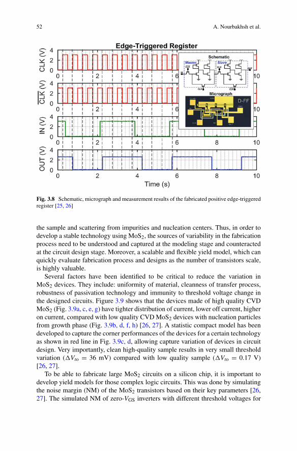
52 A. Nourbakhsh et al.
Fig. 3.8 Schematic, micrograph and measurement results of the fabricated positive edge-triggeredregister [25, 26]
the sample and scattering from impurities and nucleation centers. Thus, in order todevelop a stable technology using MoS2, the sources of variability in the fabricationprocess need to be understood and captured at the modeling stage and counteractedat the circuit design stage. Moreover, a scalable and flexible yield model, which canquickly evaluate fabrication process and designs as the number of transistors scale,is highly valuable.
Several factors have been identified to be critical to reduce the variation inMoS2 devices. They include: uniformity of material, cleanness of transfer process,robustness of passivation technology and immunity to threshold voltage change inthe designed circuits. Figure 3.9 shows that the devices made of high quality CVDMoS2 (Fig. 3.9a, c, e, g) have tighter distribution of current, lower off current, higheron current, compared with low quality CVD MoS2 devices with nucleation particlesfrom growth phase (Fig. 3.9b, d, f, h) [26, 27]. A statistic compact model has beendeveloped to capture the corner performances of the devices for a certain technologyas shown in red line in Fig. 3.9c, d, allowing capture variation of devices in circuitdesign. Very importantly, clean high-quality sample results in very small thresholdvariation (�Vto = 36 mV) compared with low quality sample (�Vto = 0.17 V)[26, 27].
To be able to fabricate large MoS2 circuits on a silicon chip, it is important todevelop yield models for those complex logic circuits. This was done by simulatingthe noise margin (NM) of the MoS2 transistors based on their key parameters [26,27]. The simulated NM of zero-VGS inverters with different threshold voltages for

3 Heterogeneous Integration of 2D Materials and Devices on a Si Platform 53
Fig. 3.9 Performance of the transistor arrays with (a) high (sample A) and (b) low (sample B)quality MoS2 in linear (c, d) and log (e, f) scales. The red solid lines are the compact modelscapturing the slow and fast corners of devices on each sample. Threshold voltage distribution ofsample A (g) and sample B (h). Both threshold voltage distributions are fitted using Gaussiandistribution with average value of Vto and standard deviation value of �Vt0. The fitted parametersfor both samples are shown in the images [26, 27]
Fig. 3.10 (a) Color map of noise margin/VDD for the zero-VGS inverter as a function of variousthreshold voltage values for top (Vt1) and bottom (Vt2) transistors. The probability of a given noisemargin is the joint probability of (Vt1, Vt2) pair, e.g., for the probability of the highlighted point,NM (Vt1 = 1.7 V, Vt2 = 1.8 V), ρ(NM) = ρ(Vt1 = 1.7 V)* ρ(Vt2 = 1.8 V). (b). Yield model fordifferent circuit complexities for both pseudo CMOS and zero-VGS design, with various Vt0 andconstant Vt0 of 1.8 V. Both topologies show close-to-unit yield for wide range of Vt0 and �Vt0 [26,27]
top and bottom transistors are summarized in the color map shown in Fig. 3.10. Thedark blue region indicates NM < 0, that is circuit failure. By combining the NMplot with the statistical distribution of Vt’s in the MoS2 technology, it is possibleto determine the circuit yield as a function of transistor count (N). All transistorsin the circuit are assumed to be independent from each other, and their thresholdvoltages are sampled according to the sample statistical distribution (with measuredVt0 and �Vt0). The simulation results for both zero-VGS and pseudo CMOS [32]design are summarized in Fig. 3.10b. As expected, for both topologies, the yielddecreases with increasing the circuit complexity (N) and global and local variations.

54 A. Nourbakhsh et al.
Fig. 3.11 Experimental and simulated performance of circuits fabricated on two different samples(A, C) with high quality material. No circuit failure is observed across those two samples,indicating the high performance and robustness of the technology. The good match betweenthe measurement and simulation demonstrates the power of the variation-aware design platform[26, 27]. (a) Zero-VGS inverters; (b) Psuedo-CMOS inverters; (c) NAND gates; (d) XNOR gates
Figure 3.10b shows the yield for different standard deviation of the threshold voltage(�Vt0 from 0.05 V to 0.3 V) for both designs, with Vt0 of 1.8 V. For �Vt0 smallerthan 0.15 V, both designs show close-to-unity yield and pseudo CMOS design ismore robust to larger �Vt0. Figure 3.11 depicts the simulation and the measurementresults of part of the combination circuits and from inverters from two samples (Aand C) made with high quality material. No circuit failure is observed across thesetwo samples, indicating the high performance and robustness of the technology.The good match between the measurement and simulation evidences the power ofthe proposed variation-aware design platform when designing large area complexcircuits with new material systems such as MoS2.

3 Heterogeneous Integration of 2D Materials and Devices on a Si Platform 55
3.3 2D Materials for IR Detectors on a Si Platform
Infrared (IR) sensing technologies, originally used mainly for night vision, surveil-lance, and remote controlling in military applications, have gradually shifted toapplications for civilian use, including medical, industry, earth resources, andautomotive. For example, medical diagnostics can be assisted by IR thermography,in which IR scanning is used to detect spatial temperature abnormality and identifyin this way cancers and other trauma [33]. The use of high resolution IR imagersand/or spectrographs on aircrafts and satellites has also allowed the chemicalmapping of the surface of earth, with important applications in mineral search[34], as well as geological and environmental survey [35], and inspection of naturalhazards and disasters [36]. However, in spite of the large number of applicationswhere IR sensing is key, its use is still limited by the high cost of high performanceIR detectors.
The bandgap of 2D materials spans from 0 electron volts (eV) in the caseof monolayer graphene, all the way to around 5 eV in the case of hexagonalboron nitride (Fig. 3.12). The energy gaps of graphene and black phosphorus, inparticular, lie in the mid- to far-infrared range, and exhibit abundant novel light–matter interaction phenomena, such as thermoelectric effect, photothermoelectriceffect, and various other optoelectronic effects related to hot carrier dynamics. Theuse of these novel phenomena could lead to ultrasensitive and/or fast-responseIR detectors with the potential to outperform today’s state-of-the-art IR detectiontechnologies.
An IR imaging system is usually made of a large number of detectors, whichneed to be routed to readout integrated circuits (ROICs) that amplify the signalsand implement analog-to-digital conversion. The integration of the detector arraysand the ROICs has traditionally been a major challenge in IR system design, dueto material integration and noise issues. As a result, in a conventional IR imaging
Fig. 3.12 Summary of band gaps (Ebg in eV) of various 2D materials and correspondingwavelength each material is capable of detecting

56 A. Nourbakhsh et al.
system, the detector array and the ROIC are usually fabricated on separate wafersand then integrated in a hybrid fashion. However, recent advances of wafer-scalesynthesis of graphene and other 2D materials, the easiness of transferring 2Dmaterials onto arbitrary substrates and their low-temperature fabrication technologymake it possible to monolithically integrate 2D material-based IR detectors withCMOS integrated circuits. This is expected to reduce the noise and the cost forthese systems.
In this section, we will first summarize the current research on 2D material-basedIR detectors, and then we will focus on graphene thermopiles as an example to inves-tigate their potential as compared to the state-of-the-art mainstream technologies.Finally, we will discuss the possibility and benefits of monolithically integrating 2Dmaterial image arrays and CMOS integrated circuits.
3.3.1 2D Material for Infrared Detectors
Due to its linear electronic dispersion relation, monolayer graphene can show ultra-high mobility (up to 200,000 cm2/Vs [37–39]), which makes graphene an excellentcandidate for high-speed electronic or optoelectronic applications. Moreover, theinterband optical absorption of suspended, near-intrinsic monolayer graphene isπα ≈ 2.3% for a wide range of incident photon energy, determined by the finestructure constant, α = e2/-hc ≈ 1/137 [40]. As for heavily doped graphene, theinterband transition is forbidden by Pauli blocking, whereas the intraband, free-carrier absorption could lead to a resonant absorption, called surface plasmonpolariton, in which free electrons and holes in graphene vibrate in-plane with respectto incident light. The resonant absorption can be enhanced efficiently by spatiallyconfining the electromagnetic wave excitation [41–45]. Table 3.1 summarized thekey performance metrics of different 2D material infrared detectors.
3.3.2 Graphene Thermopiles
Figure 3.13 shows the basic structure of a widely used graphene photodetectordesign. This device, made of a sheet of graphene with dual split-backgates, developsa photovoltage across electrodes M1–M2 as a function of the voltage applied tothe backgates. A photovoltage is measured for laser illumination wavelengths of0.83 μm, 1.55 μm, and 10.6 μm, respectively [64]. The fact that graphene shows aclear response even at 10.6 μm wavelength at which graphene absorption should bevery limited due to Pauli blocking [65, 66] indicates that most of the light absorptionis happening not in the graphene itself but in the substrate underneath, while thegraphene devices are using the thermoelectric effect to convert the temperature risein the substrate to a voltage difference [47, 64, 67]. This voltage is described byVTE = �S·�T, where �S is the difference of the Seebeck coefficient between the

3 Heterogeneous Integration of 2D Materials and Devices on a Si Platform 57
Table 3.1 Summary of performances of various 2D material-based infrared detectors
Devicestructure Wavelength Responsivity
Specificdetectivity
Responsetime
Operatingtemperature Ref.
Gr. p–n junct.PTE
Visible,NIR
10 mA/W – 50 fs Room T [46–48]
Gr.-metalplasmonic
MIR 0.5 V/W – 60 ns Room T [49]
Gr.thermopile
MIR 10 V/W 8 × 10⁸ cmHz1/2 W−1
23 ms Room T [50]
Biased gr.bolometer
Visible,NIR
0.2 mA/W – – Room T [51, 52]
Dual-gated2 L gr.bolometer
MIR 105 V/W 3 × 10¹⁰ cmHz1/2 W−1
<1 ns <10 K [52]
Gr./QDsphoto-gating
VisibleNIR
108 A/W 7 × 10¹³ cmHz1/2 W−1
10 ms Room T [53, 54]
Gr./insulator/gr.photo-gating
Visible,NIR, MIR
>1 A/W 5 × 10⁷ cmHz1/2 W−1
1 s Room T [55]
Gr./insulator/gr.thermionic
NIR 0.01–0.2 mA/W
– 10 fs Room T [56, 57]
Gr./semi. PV Visible,NIR
0.7 A/W 5 × 10¹³ cmHz1/2 W−1
0.3 ms Room T [58, 59]
Gr./pyroelectric MIR 0.27 mA/W 6 × 10⁴ cmHz1/2 W−1
20 ms Room T [60]
Gr./NEMSresonator
MIR – 1 × 10¹⁰ cmHz1/2 W−1
3 ns Room T [61]
BP photocon-ductor
Visible,NIR
5 mA/W – 40 μs Room T [62, 63]
p- and n-region of graphene, and �T is the temperature difference between thegraphene p–n junction and the metal contacts. Because the Seebeck coefficient ofgraphene has an “S” shaped dependence on the Fermi level, the split-gate sweepingmaps as shown in Fig. 3.13c, d, e indicate a non-monotonic six-lobe pattern, whichis not true if the photovoltaic effect dominated the photocurrent generation.
In a related work, the spectral response of graphene on SiO2 was measuredand it was found to match the absorption spectrum of SiO2 very well in themid-IR. However, the detectivity of these devices was only 102 cm Hz1/2 s−1.By optimizing the device structure, a follow-up study achieved a detectivity of105 cm Hz1/2 s−1 [50]. The observed three orders of magnitude improvement inperformance was attributed to two structural changes. First, the absorption in the8–12 μm spectral range was increased by >40%, as compared to less than 1%absorption in the previous work, thanks to the use of an optimized IR absorptionlayer made of a SiO2/Si3N4/SiO2 combination instead of a single dielectric layer,which allowed strong resonant absorption at 9 and 11.5 μm, respectively. Secondly,the deposition of the SiO2/Si3N4/SiO2 tri-layer absorber was done with plasmaenhanced chemical vapor deposition (PECVD) under an optimized high-frequency

58 A. Nourbakhsh et al.
Fig. 3.13 Graphene split-gate thermopile with supported substrate. (a) Schematic and (b) micro-scopic image of the device. M1 and M2 are metal contacts to graphene, and G1 and G2 are splitgates that electrostatically dope the graphene channel to form a p-n junction. (c–e) Photovoltage(VPH) as a function of the split gate voltages VG1 and VG2, for different wavelength of incident light.(c) 10.6 μm, (d) 0.83 μm, and (e) 1.55 μm. The six-lobe feature indicates that the photoresponseis dominated by thermoelectric effect in graphene [64]
to low-frequency plasma ratio to make the thin film stress-free. This allowed forthe fabrication of a free-standing absorber membrane after undercutting the siliconunderneath with XeF2 isotropic etching. When measured in vacuum (less than10−2 torr), both thermal conduction and convection in the vertical direction wereefficiently attenuated. As a result, the temperature generated by the IR irradiance atthe absorber is maximized.
Multiple graphene photodetectors can be combined into the thermopile shown inFig. 3.14a, composed of an infrared absorber that is suspended from the substrate,a series of thermal arms that connect the absorber and the surrounding, withinterleaved p- and n- type graphene channels on top. The schematic of the structureand the key geometrical parameters are shown in Fig. 3.14b. The graphene channels

3 Heterogeneous Integration of 2D Materials and Devices on a Si Platform 59
Fig. 3.14 Graphene thermopile with suspended IR absorber. (a) Schematic of a graphene ther-mopile. The red and blue regions indicate the p-type and n-type region of graphene, and the squarein the center is the dielectric absorber. The whole structure is suspended on the substrate to reducethe thermal conductance in the vertical direction. (b) A geometrical abstraction of the graphenethermopile with geometrical parameters listed below
are parallel in terms of temperature gradient, but connected in series electrically.When IR radiation is present, the IR absorber (dielectric multilayer thin film) isheated up, which can then be probed electrically by the graphene p–n junctions dueto the thermoelectric effect. The specific detectivity (D*), considering the Johnson–Nyquist noise, can be expressed as
D∗=Nj�S�T
Pin
√v2n
√D2
abs�f =(αabs
t
)·(
�S√ρ2D
)·(
1
kth
)·⎛⎝ L1/2Dabs
N1/2j W 1/2
⎞⎠
√1
32kBT
(3.1)
Here the first term (αabs/t) is absorbance per thickness, indicating the capabilityof IR absorption of the absorber; the second term (�S/ρ2D
1/2), with ρ2D the 2Dresistivity of graphene, is determined by the electrical and thermoelectric propertiesof the sensing material; the third term (1/κ th) indicates the quality of thermalisolation, with κ th denoting the thermal conductivity of the absorber; and the fourthterm is made of geometrical parameters in the parallel direction, where Nj is thetotal number of graphene p–n junctions at the hot spot. The response time of such adevice can be written as
τ = Rth·Cth = 1
2
(cV
kth
) (LD2
abs
NjW
)(3.2)
with the heat capacitance Cth, and the specific heat capacity cV . Notice that (D*2/τ )is independent of the lateral geometries:

60 A. Nourbakhsh et al.
(D∗)2
τ=
(αabs
t
)·(
�S2
ρ2D
)·(
1
kthcV
)· 1
16kBT(3.3)
with light–matter interaction factor (αabs/t), the figure of merits of the thermoelectricmaterial (FOM = �S2/ρ2D) and the thermal transport factor (1/κ thcV ).
According to Eq. 3.3, the thermoelectric figure of merit FOM plays a significantrole in thermopile IR detectors. In order to benchmark graphene-based thermoelec-tric detectors with respect to the other material systems, the Seebeck coefficientand the FOM are plotted as a function of resistivity in Fig. 3.15. Note that theFOM for today’s standard CVD graphene on SiO2, with the average mobility of2000 cm2 V−1 s−1, can already outperform the performance of any thermopilesmade with metals and most of TE materials. The use of higher quality graphene andproperly passivating the dangling bonds on the substrate with hexagonal BN couldmake the FOM two orders of magnitude higher than that of all the other materialsystems. Also, the FOM of TMDs in 2D form is higher than in their 3D counterparts,which also shows great potential for thermal detection and other thermoelectricapplications.
Note from Eq. 3.3 that the optical absorption per thickness (αabs/t) and thethermal transport factor (1/κ thcV ) of a graphene thermopile can be improvedthrough properly engineering the IR absorber. Current work used the inherit strongabsorption of SiO2/SiN layers [50, 64, 68]. It is also possible to use metal-basedmetamaterial absorbers in the mid-infrared range [69–71]. The surface plasmonpolariton (SPP) in graphene [41, 45, 72, 73] and phonon polariton (PP) in hBN[74, 75] have been studied recently. With appropriate engineering of the light fieldto enhance the light–matter interaction, it is possible to achieve strong resonantabsorption based on these mechanisms with negligible loss.
Figure 3.16 compares the specific detectivity (D*) and the response time (τ )of graphene thermopiles with different types of state-of-the-art thermal detectortechnologies, including bolometers (VOx, CMOS-MEMS, etc.) [6–8], thermopiles[9, 10] (poly-Si, Al, thermoelectric materials, etc.), and pyroelectric devices (PZTand other piezoelectric materials). Note that photon detectors, such as mercurycadmium telluride (MCT) photoconductors, were not included in this comparison,because they would suffer from high dark current and consequently high noiseat room temperature [76]. Here we exploit the dimensionless relation from Eq.3.2 to represent each technology node of graphene thermopiles. Although currentgraphene thermopile technology is still not as good as the state-of-the-art thermaldetectors, the performance is predicted to be competitive, or even better thantoday’s state-of-the-art technologies. For example, a 100-fold improvement in theFOM = �S2/ρ could be achieved by encapsulating large area, high-quality CVDgraphene with hexagonal boron nitride, which would increase the mobility and See-beck coefficient to 100,000 cm2 V−1 s−1 and 200 μV/K, respectively. Furthermore,the absorber can be thinned down to 10 nm with good mechanical stability, and100% perfect absorption can be achieved through nano-photonic structures, whichwould make graphene thermopiles better than any existing bolometers.

3 Heterogeneous Integration of 2D Materials and Devices on a Si Platform 61
Fig. 3.15 (a) Seebeck coefficient and (b) thermoelectric figures of merit as a function of resistivityfor various materials

62 A. Nourbakhsh et al.
Fig. 3.16 Specific detectivity (D*)—response time (τ ) plots for different technology nodes ofgraphene thermopiles in comparison with mainstream uncooled thermal IR detectors
3.3.3 Heterogeneous Integration of Graphene and SiliconIntegrated Circuits for Thermal Imaging Application
One important application of IR detection technology is to image the black-bodyradiation of ordinary objects, as in night vision goggles, automotive imagingsystems, surveillance cameras, and temperature-control systems. A 2D imagingsystem could be implemented by either spatially modulating the optical path to mapthe pixelated 2D object information into a time series of signal, called 2D scanning,or directly mapping the pixelated 2D object into a 2D array of image sensors at thefocal plane, called real-time imaging. Figure 3.17a shows a scanning IR imagingsystem using a single graphene thermopile IR detector. With this system, a black-body source at 472 K could be imaged, as shown in Fig. 3.17b, c.
A real-time image sensor is made of a focal plane array (FPA), that is a 2D arrayof IR detectors at the focal plane of the optical system, and a readout integrated

3 Heterogeneous Integration of 2D Materials and Devices on a Si Platform 63
Fig. 3.17 Scanning thermal imaging system based on a single graphene thermopile. (a) Schemat-ics of the scanning imaging setup. (b) “MIT” log aperture to be measured. (c) Scanning thermalimage of the 472 K black-body source passing through the “MIT” log aperture
circuit (ROIC) that controls the operation of the FPAs and converts the analogsignals from the FPA into digital signals that can be transmitted to and processed bya microprocessor. The integration between the FPA and the ROIC could be discrete,hybrid, or monolithic. The discrete integration is impractical because the number ofconnections between the FPA and the ROIC is on the order of thousands or evenmillions, which could hardly be routed through a PCB board. At present, most ofthe mainstream IR image sensors have separate FPA and ROIC chips, and integratethem through flip chip bonding. This limits the pixel size, increases the system noise,and reduces the speed of the device. The monolithic integration of the FPA andthe ROIC could solve these challenges, however the thermal budget of the ROICdemands that the deposition temperature of the sensing material has to be lowerthan 400 ◦C, which degrades the material quality of most 3D semiconductors usedin these applications.
Given that 2D materials can be synthesized by chemical vapor deposition ona metal foil, and wet-transferred onto any substrates, it is possible to integrate2D material-based IR FPAs with CMOS ROICs monolithically without sacrificingthe performance of either component. The back-end-of-line process of graphenethermopile FPAs fabricated directly on CMOS ROIC chips is schematically shownin Fig. 3.18a and the optical images of the completed graphene thermopile-CMOSimage sensor are shown in Fig. 3.18b, c. This hybrid graphene/Si system enablesnew opportunities for low cost, high performance IR detection.

64 A. Nourbakhsh et al.
Fig. 3.18 Graphene thermopile/CMOS monolithic integration. (a) Back-end-of-line process ofthe graphene thermopile FPA fabricated directly onto a CMOS ROIC chip. PASS passivation, ILDinterlayer dielectric, M6 Metal 6 (Cu), M5 Metal 5 (Cu), blue PECVD SiO2, grey line is graphene.The left and right images are the side and top view of the pixel area, respectively. (b) Photograph ofthe CMOS ROIC chip. (c) Microscopic images of the completed Graphene thermopile FPA/CMOSROIC chip
3.4 Heterogeneous Integration of 2D Materials with SiNanophotonics
Graphene can serve as core materials combined with Si or other conventionalsemiconductor photonic structures for ultrafast photodetection and optical mod-ulation on a CMOS platform for high speed, low power optical interconnects.Early demonstrated graphene optoelectronics normally rely on a vertical incidentconfiguration to couple light into graphene, therefore resulting in a low absorptioncoefficient of 2.3% due to the atomic thickness of graphene [77]. Although thosedevices show promising properties of strong electro-absorptive effect [65, 66]and high-speed photodetection [78, 79], the low total absorption in those devicesdoes not meet the requirement of practical applications. To tackle this issue,nanophotonic devices, including waveguides and cavities, can squeeze optical fieldin a subwavelength volume, providing a promising platform to enhance light–matterinteraction in 2D materials.
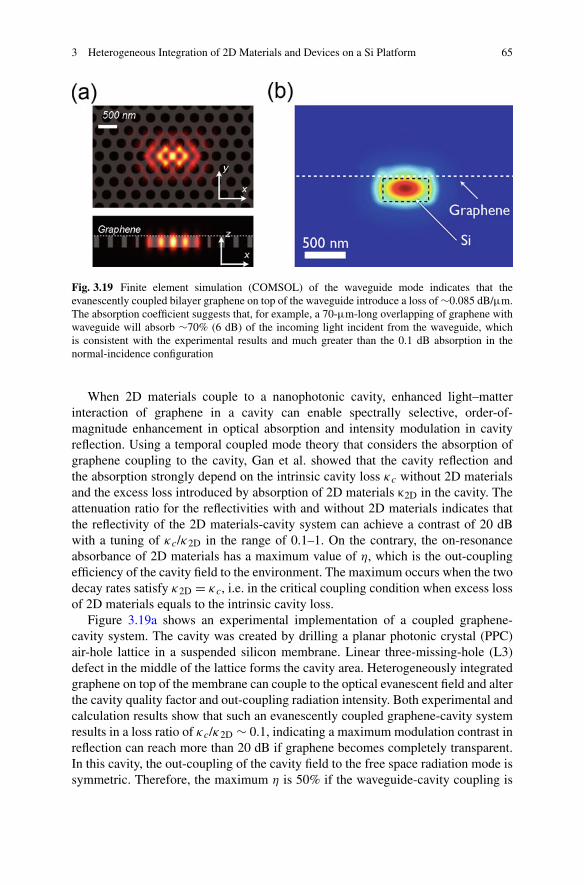
3 Heterogeneous Integration of 2D Materials and Devices on a Si Platform 65
Fig. 3.19 Finite element simulation (COMSOL) of the waveguide mode indicates that theevanescently coupled bilayer graphene on top of the waveguide introduce a loss of ∼0.085 dB/μm.The absorption coefficient suggests that, for example, a 70-μm-long overlapping of graphene withwaveguide will absorb ∼70% (6 dB) of the incoming light incident from the waveguide, whichis consistent with the experimental results and much greater than the 0.1 dB absorption in thenormal-incidence configuration
When 2D materials couple to a nanophotonic cavity, enhanced light–matterinteraction of graphene in a cavity can enable spectrally selective, order-of-magnitude enhancement in optical absorption and intensity modulation in cavityreflection. Using a temporal coupled mode theory that considers the absorption ofgraphene coupling to the cavity, Gan et al. showed that the cavity reflection andthe absorption strongly depend on the intrinsic cavity loss κc without 2D materialsand the excess loss introduced by absorption of 2D materials κ2D in the cavity. Theattenuation ratio for the reflectivities with and without 2D materials indicates thatthe reflectivity of the 2D materials-cavity system can achieve a contrast of 20 dBwith a tuning of κc/κ2D in the range of 0.1–1. On the contrary, the on-resonanceabsorbance of 2D materials has a maximum value of η, which is the out-couplingefficiency of the cavity field to the environment. The maximum occurs when the twodecay rates satisfy κ2D = κc, i.e. in the critical coupling condition when excess lossof 2D materials equals to the intrinsic cavity loss.
Figure 3.19a shows an experimental implementation of a coupled graphene-cavity system. The cavity was created by drilling a planar photonic crystal (PPC)air-hole lattice in a suspended silicon membrane. Linear three-missing-hole (L3)defect in the middle of the lattice forms the cavity area. Heterogeneously integratedgraphene on top of the membrane can couple to the optical evanescent field and alterthe cavity quality factor and out-coupling radiation intensity. Both experimental andcalculation results show that such an evanescently coupled graphene-cavity systemresults in a loss ratio of κc/κ2D ∼ 0.1, indicating a maximum modulation contrast inreflection can reach more than 20 dB if graphene becomes completely transparent.In this cavity, the out-coupling of the cavity field to the free space radiation mode issymmetric. Therefore, the maximum η is 50% if the waveguide-cavity coupling is
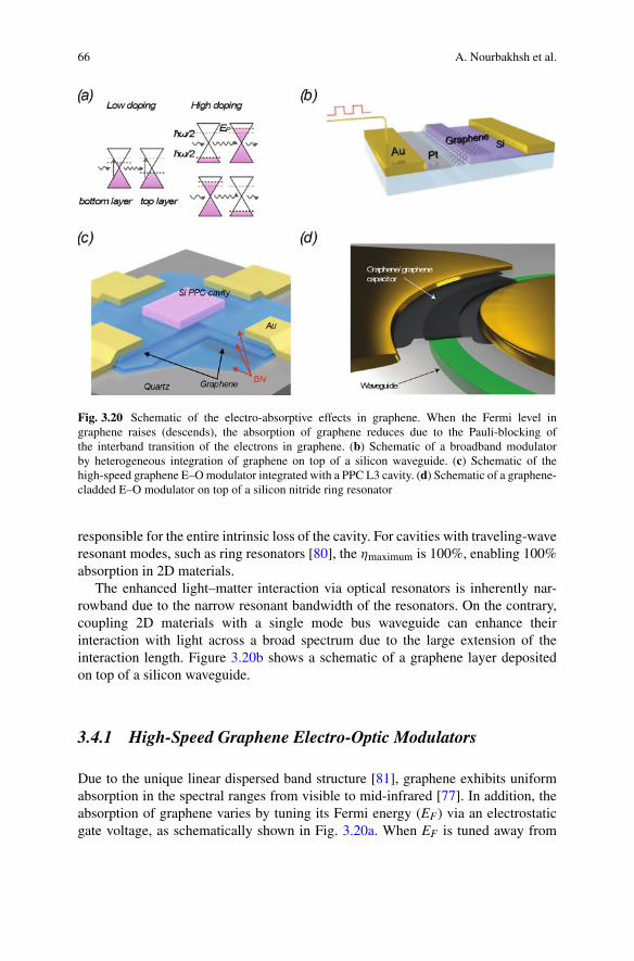
66 A. Nourbakhsh et al.
Fig. 3.20 Schematic of the electro-absorptive effects in graphene. When the Fermi level ingraphene raises (descends), the absorption of graphene reduces due to the Pauli-blocking ofthe interband transition of the electrons in graphene. (b) Schematic of a broadband modulatorby heterogeneous integration of graphene on top of a silicon waveguide. (c) Schematic of thehigh-speed graphene E–O modulator integrated with a PPC L3 cavity. (d) Schematic of a graphene-cladded E–O modulator on top of a silicon nitride ring resonator
responsible for the entire intrinsic loss of the cavity. For cavities with traveling-waveresonant modes, such as ring resonators [80], the ηmaximum is 100%, enabling 100%absorption in 2D materials.
The enhanced light–matter interaction via optical resonators is inherently nar-rowband due to the narrow resonant bandwidth of the resonators. On the contrary,coupling 2D materials with a single mode bus waveguide can enhance theirinteraction with light across a broad spectrum due to the large extension of theinteraction length. Figure 3.20b shows a schematic of a graphene layer depositedon top of a silicon waveguide.
3.4.1 High-Speed Graphene Electro-Optic Modulators
Due to the unique linear dispersed band structure [81], graphene exhibits uniformabsorption in the spectral ranges from visible to mid-infrared [77]. In addition, theabsorption of graphene varies by tuning its Fermi energy (EF) via an electrostaticgate voltage, as schematically shown in Fig. 3.20a. When EF is tuned away from

3 Heterogeneous Integration of 2D Materials and Devices on a Si Platform 67
the Dirac point by more than half of the photon energy ω/2, the interband transitionsbecome forbidden by Pauli blocking, reducing the graphene absorption [65, 66].
Heterogeneously integrated graphene E–O modulators first appear in a structureconsisting of a silicon waveguide and ∼50-μm-long graphene overlapping [82], asshown in Fig. 3.20b. The enhanced total absorption of the graphene layer on topof the waveguide results in enhanced electro-absorptive effects, enabling broadbandintensity modulation for wavelengths from 1.35 to 1.6 μm with 3 dB modulationdepths. The 3 dB cut-off speed of this device is about 1 GHz. An improved dual-layer graphene capacitor structure on waveguide shows improved modulation depthsof 6 dB [83] and 16 dB [84] with low insertion loss of 3 dB, demonstrating thescalability to acquire higher modulation depth with stacking of multiple singlegraphene layers.
In these waveguide-based E–O modulators, the footprint of the devices isintrinsically limited by the coupling strength of the waveguide and the graphenelayers, which commonly requires a device area of 50 μm2. To reduce the footprintof the E–O modulator, therefore reducing the switching energy and increasing theoperation speed, a resonator-coupled graphene structure is desired. When graphenestrongly absorbs the optical field in a cavity, i.e., κc/κcg 1, the cavity reflection Ris strongly attenuated. While the Fermi level in graphene increases (decreases) dueto electrostatic gating, the optical absorption in graphene reduces (κc/κcg increases).Therefore the reflection R of the cavity recovers. This modulation mechanism canin principle provide more than 20 dB modulation depths for a cavity area around0.5 μm2.
We discuss an example of a multilayer graphene/boron nitride heterostructureintegrated a PPC L3 cavity. In this architecture, mutually gated dual-layer grapheneparallel capacitor could provide high doping strength while operating at high speeddue to high carrier mobility of graphene [85]. Figure 3.20c shows the schematic ofthe high-speed graphene E–O modulators consisting of a dual-layer graphene capac-itor and a PPC nanocavity [86]. A BN/Graphene/BN/Graphene/BN five-layer stackwas built by the van der Waals (vdW) assembly technique and then transferred ontoa quartz substrate [85]. The two graphene sheets were positioned as crossed stripesin order to be contacted individually. The metal contacts to the graphene employ aone-dimensional edge contact technique. In this encapsulated dual-layer graphenestructure, each one of the graphene sheets can supply gate voltage to each other.
The device showed in Fig. 3.20c exhibits a maximum modulation depth of 3.2 dBwith a high-speed cut-off frequency around 1.2 GHz. The operation frequencyresponse of the device indicates a RC-limited time constant of the dual-layergraphene capacitor, as deduced by the impedance measurement of the device. Inthis device, the graphene capacitor has an area of ∼100 μm2 and a capacitance of320 fF. The switching energy of this device is approximately 1 pJ/bit. For L3 PPCcavities, the overlap between the resonant mode and the graphene capacitor hasan area of only ∼0.5 μm2, corresponding to the three-missing-hole defect region.The graphene capacitor could therefore be reduced in size to match this cavityarea to lower the capacitance by approximately 200 times, which should reducethe switching energy to 5 fJ/bit and increase the 3 dB cut-off frequency to 70 GHz

68 A. Nourbakhsh et al.
[86]. The cavity bandwidth in this work exceeds 600 GHz for a Q value of 300, i.e.,it would be possible to obtain a relatively large modulation contrast without the needfor particularly high-Q cavities, as is required in silicon carrier-depletion (injection)modulators. This broader bandwidth would also improve temperature stability,which is a limiting factor in the carrier-modulation of Si modulators [87–89].
The electro-absorptive effect in graphene can not only induce tunable loss ofthe cavity, but also the cavity coupling efficiency to external optical modes, as thedevice demonstrated by Phare et al. [90] Fig. 3.20d shows the dual-layer graphenecapacitor covering a silicon nitride ring resonator. The ring resonator is intentionallydesigned to be under-coupled to a bus waveguide when the graphene introduces lossto the cavity. While the absorption in graphene reduces, the resonant field becomesstronger and the coupling of the resonator to the waveguide increases. The tuning ofboth cavity internal field and out-coupling to the waveguide gives extra tuning of thelight transmission, resulting a modulation depth of 15 dB with 10 V voltage swing.The speed of modulator exceeds 30 GHz due to reduced capacitance area of ∼45 μm2. Other resonator-coupled graphene E–O modulators have also shown bothhigh modulation depth and small device footprint, including graphene-silicon ringresonator structures [91, 92], and silicon Mach-Zehnder interferometers-integratedstructures [93].
3.4.2 On-Chip Graphene Photodetectors
On-chip graphene photodetectors could enable on-chip optical interconnects atunprecedented speeds. Although early demonstration of graphene-based photode-tector for these applications has shown promising operation speed and broadbandresponse [78, 79], the responsivity of the photodetector is low due to weakabsorption in graphene in a vertical incident configuration. To address this, graphenehas been integrated with nanocavities [94], microcavities [95], and plasmon resonantstructures [49, 72]. In these examples, a range of responsivity of 10–30 mA/Wis possible, with a trade-off for limited spectral response due to the narrowbandenhancement of the resonant structures. To implemented broadband photodetectors,heterogeneous integrated graphene with waveguides is most promising for broad-band spectral response while enhancing the photoresponse of the detector.
Here, we describe a waveguide-coupled graphene photodetector [96, 97], asschematically illustrated in Fig. 3.21a. The silicon waveguides were fabricated in anSOI wafer with a CMOS compatible process. The chip was planarized by backfillingwith a thick SiO2 layer, followed by chemical mechanical polishing to reach thetop silicon surface. Multilayered hBN/SLG/hBN stack were assembled onto thephotonic chip using van der Waals (vdW) assembly [85]. The single layer graphene(SLG) channel spans 40 μm of the waveguide, inducing ∼2.2 dB absorption,consistent with simulation results. One-dimensional edge contacts (Fig. 3.21b) tothe encapsulated graphene layer is applied to hBN/SLG/hBN stack and the drain
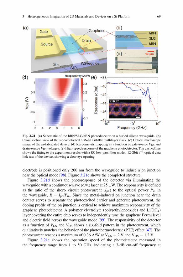
3 Heterogeneous Integration of 2D Materials and Devices on a Si Platform 69
Fig. 3.21 (a) Schematic of the hBN/SLG/hBN photodetector on a buried silicon waveguide. (b)Cross section view of the side-contacted hBN/SLG/hBN multilayer stack. (c) Optical microscopeimage of the as-fabricated device. (d) Responsivity mapping as a function of gate-source VGS anddrain-source VDS voltages. (e) High-speed response of the graphene photodetector. The dashed lineshows the fitting to the experiment results with a RC low-pass filter model. 12 Gbit s−1 optical datalink test of the device, showing a clear eye opening
electrode is positioned only 200 nm from the waveguide to induce a pn junctionnear the optical mode [98]. Figure 3.21c shows the completed structure.
Figure 3.21d shows the photoresponse of the detector via illuminating thewaveguide with a continuous-wave (c.w.) laser at 25 μW. The responsivity is definedas the ratio of the short- circuit photocurrent (Iph) to the optical power Pin inthe waveguide, R = Iph/Pin. Since the metal-induced pn junction near the draincontact serves to separate the photoexcited carrier and generate photocurrent, thedoping profile of the pn junction is critical to achieve maximum responsivity of thegraphene photodetector. A polymer electrolyte (poly(ethyleneoxide) and LiClO4)layer covering the entire chip serves to independently tune the graphene Fermi leveland electric field across the waveguide mode [99]. The responsivity of the detectoras a function of VGS and VDS shows a six-fold pattern in the photocurrent, whichqualitatively matches the behavior of the photothermoelectric (PTE) effect [47]. Thephotocurrent reaches a maximum of 0.36 A/W at VGS = 2 V and VDS = 1.2 V.
Figure 3.21e shows the operation speed of the photodetector measured inthe frequency range from 1 to 50 GHz, indicating a 3-dB cut-off frequency at

70 A. Nourbakhsh et al.
42 GHz. To gauge the viability of the waveguide-integrated graphene photodetectorin realistic optical applications, an optical data transmission was performed. Apulsed pattern generator with a maximum 12 Gbit/s internal electrical bit streammodulated a 1550 nm CW laser via an electro-optic modulator, which was launchedinto the waveguide-graphene detector. The output electrical data stream from thegraphene detector was amplified and sent to a wide-band oscilloscope to obtain aneye diagram. As shown in the inset of Fig. 3.21e, a clear eye-opening diagram at12 Gbit/s was obtained.
To date, waveguide-integrated graphene photodetectors have been extensivelystudied, showing possible integration in CMOS-compatible processes [98]. Inaddition, large-scale epitaxial graphene samples integrated with waveguides canachieve photodetection with a data rate of 50 GHz [100], and high-responsivityby integrating with a silicon slot waveguide [101]. Owing to the broadbandabsorption of graphene, waveguide-integrated graphene heterostructure also enablesphotodetectors for mid-infrared wavelengths [102]. For other 2D materials, blackphosphorus (BP)-based photodetectors have drawn great attention due to its smallbandgap that is promising for telecommunication and mid-IR wavelength ranges[103, 104]. Heterogeneously integrated BP-silicon photodetectors have shown up to6 A/W responsivity with more than 3 GHz speed.
In addition to E–O modulators and photodetectors, other on-chip devices includ-ing all-optical modulators [105], mode-locked ultrafast laser [106], thermo-opticmodulators [107], light-emitting diodes [108], and single photon sources [109]could be integrated on a silicon platform in the future, thanks to 2D materialssuch as transition metal dichalcogenides (TMDs) [110], black phosphorus [104,111], and superconducting 2D niobium diselenide [112] (NbSe2). The seamlessheterogeneous integration enabled by the low processing temperatures of 2Dmaterials will allow an efficient optical interconnect with conventional siliconCMOS technology for inter- and intra-chip communication, back-end depositedsilicon photonics [113], mid-infrared photonics [114], and also flexible photonics[115].
3.5 2D Material-Based Chemical and Biological Sensors
Chemical and biological sensors are ubiquitous in every aspect of our lives—fromhealth care and environmental monitoring all the way to transportation and industry.Sensors translate a physical, chemical, or biological input signal, for example a gasconcentration, into an electrical signal such as a change in voltage or current. Inorder to benchmark the performance of this transduction process, different metricsexist. One of the most important parameters is the sensitivity of a sensor, which isdefined as proportionality factor between input signal and electrical output signal.A sensor’s selectivity is given by its ability to respond to only one input signal andto be insensitive to all other relevant environmental changes. Another importantcharacteristic is the detection limit, which marks the lower bound of what can

3 Heterogeneous Integration of 2D Materials and Devices on a Si Platform 71
be measured with confidence. Lastly, sensors exhibit a finite response time andrecovery time. They are defined as the delay between a step increase or decreaseof the input signal, respectively, and the output reaching a steady state [116, 117].
The integration of chemical and biological sensors with silicon chips couldplay an important role in the goal of extending the capabilities of the traditionalCMOS platform. However this heterogeneous integration has traditionally beendifficult due to the instability of SiO2 dielectrics in the presence of many analytesof interest, as well as the large thickness of the interconnect and back-end layers instate-of-the-art silicon chips, which increase the distance between the chip surfaceand the transistors. 2D materials such as graphene or molybdenum disulfide couldchange this, and make the seamless integration of chemical and biological sensorswith silicon chips a reality. These materials have excellent physical and chemicalproperties that make them perfectly suited as sensor materials. They are atomicallythin, resulting in the highest possible surface to volume ratio and making themextremely sensitive to environmental changes. Furthermore, 2D materials haveintrinsically low electronic noise, are biocompatible and mechanically strong and,as mentioned in other sections of these chapter, they can be seamlessly integratedwith Silicon microsystems.
This section is organized into two parts. The first half gives an overview of gasand chemical sensors based on 2D materials. The second half focuses on biologicalsensors made of these materials. The aim of this section is to highlight a fewpromising sensor concepts rather than to give detailed account of all the extensiveresearch work. In addition, it focuses on sensor solutions that can be eventuallyintegrated with CMOS electronics.
3.5.1 Gas and Chemical Sensors
Gas and chemical sensors are used, for example, in our homes to detect carbonmonoxide, in security applications to identify explosives or in cars to monitorexhaust and lower hazardous emissions. Sensors can exploit different physicalphenomena to detect and quantify a certain gas or chemical, for example changes inthe optical, magnetic, or electrical properties of the sensor material. Electrical gassensors are arguably one of the most common types. They use changes in sensorresistance or capacitance in a variety of materials such as semiconductors, metalthin film, metal oxides, and polymers to facilitate the sensing [118].
Recently, 2D materials have attracted a large amount of interest as gas orchemical sensor due to their high sensitivities and low electronic noise. Both ofthese properties are rooted in their atomic thickness which yields a very large surfaceto volume ratio. This makes 2D material very susceptible to the environment withmolecules adsorbing on the surface which leads to a charge transfer and dopes thechannel with electrons or holes. This increase in carrier concentration strongly altersthe channel resistance of the device [119].

72 A. Nourbakhsh et al.
In the following paragraphs, a few promising examples of gas sensors usinggraphene and other 2D materials are given. For a more in-depth discussion, theinterested reader is referred to comprehensive literature review papers by Yuan andShi and Verghese et al. [120, 121] covering graphene-based gas sensors as well asanother review paper by Verghese et al. [119] which focuses on gas sensors basedon 2D materials (in addition to graphene).
In 2007 Schedin et al. demonstrated the first graphene gas sensor based on asimple Hall bar structure. In this device, gas molecules adsorb on the surface ofgraphene which dope the material and change its electrical properties. Based onan optimized design and the intrinsically low noise level of graphene, the groupwas able to detect individual molecule ad- and desorption events which is theultimate sensitivity limit [122]. More recently, Chen et al. simplified the sensordesign to a two-terminal chemically sensitive resistor, or chemiresistor, and addedUV-illumination for continuous cleaning of the graphene surface. This way, theywere able to demonstrate a detection limit as low as 0.16 parts-per-trillion for nitricoxide gas molecules [123].
Another way to sense gases using graphene is to exploit the influence of specificanalytes on the low frequency noise of graphene [124]. Using a back-gated transistorconfiguration, Rumyantsev et al. found that besides changing the channel resistance,certain gases introduce a Lorentzian noise bulge at a distinctive center frequency(see Fig. 3.22) that differs for each gas and is reproducible across samples. Thisadds another sensing parameter to chemically sensitive field effect transistors, orchemFETs, which holds the promise of achieving better sensor selectivity throughrecognizing a distinctive signature of Lorentzian center frequency and change inchannel resistance.
Reduced graphene oxide is a graphite-derived material that can be easilysolution-processed. Fowler et al. used it to create gas sensors on a chip with an
Fig. 3.22 (a) Scanning electron microscope (SEM) image and (b) Noise spectral density SI /I2
multiplied by frequency f versus frequency f for the device in open air and under the influence ofvarious solvent vapors. Different vapors induce noise with different characteristic frequencies fc.The difference in the frequency fc is sufficient for reliable identification of different gases with thesame graphene transistor [124]

3 Heterogeneous Integration of 2D Materials and Devices on a Si Platform 73
integrated heater for temperature control by spin coating a graphene oxide solutionon the chip and reducing it with anhydrous hydrazine. They found the device tohave a detection limit of 52 ppb to 2,4-dintrotoluene (DNT), which is a moleculerelated to explosive detection. Furthermore, their temperature experiments showedthat a substrate temperature of 149 ◦C helps to decrease the response and recoverytime significantly in comparison to room temperature. The benefit however comesas the expense of lowered sensitivity [125]. More recently, reduced graphene oxidesensors were also successfully fabricated by inkjet printing [126, 127].
2D material based gas and chemical sensor are not just limited to graphene.With the exploration of other 2D materials like transition metal dichalcogenides,viable sensors were also shown with molybdenum disulfide (MoS2) [128–131] andphospherene [132] on top of a silicon wafer. Late et al. analyzed the responseof MoS2 chemFETs to ammonia and nitrogen dioxide gas while exploring theinfluence of light illumination, gate bias and number of atomic layers. Theyfound that five-layer MoS2 devices were more sensitive to gas analytes than theirbilayer counterparts. Furthermore, applying a gate bias helps to increase the devicesensitivity by electrostatically changing the carrier concentration in the channel toan optimal point [129]. In a related study by Perkins et al. the authors demonstratedsingle-layer MoS2 chemiresistors that are sensitive to different organic compoundssuch as triethylamine (TEA) or acetone with a detection limit of 10 ppb and500 ppm, respectively. They also found that the response to these organic vapors isoften complementary in polarity to carbon nanotube sensors [130]. Another way totailor the selectivity of MoS2 to a specific gas is by grafting functional groups ontoits surface. Kim et al. demonstrated this approach by attaching a thiolated ligandcalled mercaptoundecanoic acid (MUA) to chemiresistor devices. The sensors werebuilt with interdigitated electrodes on a layer of vacuum-filtrated MoS2 flakes withor without this functionalization that results in different responses towards volatileorganic compounds (see Fig. 3.23a). In particular, the untreated chemiresistorsshowed an increase in channel resistance being exposed to oxygen-functionalized
Fig. 3.23 (a) Schematic of MoS2 exfoliation and functionalization with MUA. The chemiresistorswere built by vacuum filtration and placed in a test chamber that was exposed to different organicvolatile compounds (VOC). (b) Relative change in channel resistance of untreated and MUA-treated MoS2 chemiresistors as a result of exposure to different VOCs [131]

74 A. Nourbakhsh et al.
VOCs while the MUA treated samples showed a decreasing resistance as shown inFig. 3.23b. Furthermore, the group showed a detection limit of these sensors below1 ppm. Considering different available thiolated ligands, this work demonstrates thepotential of targeted MoS2 functionalization to create sensor arrays that are sensitiveto a variety of gaseous compounds [131].
3.5.2 Biological Sensors
Biological sensors are another important subgroup of sensors, which is mainly usedin medicine to determine blood sugar levels, identify bacteria, cancer cells, andother analytes of interest in the laboratory. There is a large variety of biosensortechnologies, although many use optical detection through labeling with fluorescentdyes or electrochemical detection techniques using functionalized electrode surfaces[133, 134].
Recently, 2D materials such as graphene have been extensively explored asbiosensors. Besides their low intrinsic noise and large surface to volume ratio,2D materials are especially compelling to use as biosensors because of theirchemical inertness and easier handling compared to other new materials such ascarbon nanotubes. The paragraphs below summarize some of the approaches to usegraphene, MoS2, and other 2D materials in monitoring cells or pH levels and detectDNA, biomolecules and other proteins. Most of these devices were fabricated ontop of silicon wafers and could easily be integrated with silicon electronic chips.This could eventually enable small, inexpensive diagnostic tests for laboratory andpersonal use. For a more detailed literature review, the interested reader is referredto more comprehensive review papers by Liu et al. and Moldvan et al. [135].
Being able to sense pH levels is important in biology and medicine, for examplefor cell monitoring or diagnosing disease in humans [133]. Ang et al. demonstratedthat graphene electrolyte gated FETs (EGFETs) can be used to measure pH levels.In particular, they found that the hydroxyl (OH−) and hydronium (H3O+) changethe channel carrier concentration through capacitive coupling and hence changethe neutrality point of the chemFET transfer characteristics with a sensitivity of99 mV/pH [136]. In a similar work with monolayer graphene, Ohno et al. were ableto improve the sensitivity down to 25 mV/pH [137].
In the realm of biological cell detection, Huang et al. demonstrated a graphenechemiresistor that can sense E. coli bacteria by functionalizing the graphenesurface with anti-E. coli antibodies. This approach is much simpler and faster thantraditional solution-based techniques for detecting bacteria. Huang’s device wasable to detect bacteria concentrations as low as 10 colony-forming cells per milliliter(cfu/mL) and also showed high selectivity against other bacteria [138]. Anotherinteresting graphene biosensor application was highlighted by Ang et al. whofabricated a microfluidic channel equipped with protein-functionalized graphenechemFETs that could detect malaria infected red blood cells. The group showedthe selective capture of infected blood cells to a transistor channel, with a much

3 Heterogeneous Integration of 2D Materials and Devices on a Si Platform 75
simpler setup compared to traditional optical detection methods. This capture eventchanges the channel conductance when in contact with a cell due to capacitivecharging. By analyzing the dwell time and magnitude of the conductivity change,they could also distinguish between two different stages of the infected blood cells[139]. Graphene transistors can also be used to monitor the action potential ofcells for neural prosthesis application [140]. Hess et al., for example, demonstratedgraphene EGFET arrays that are very biocompatible and are able to monitor theaction potential of cells grown on top of the channel [140]. In their experiments,the graphene arrays proved to be more chemical resistant and exhibit far higher gatesensitivities than traditional silicon FET arrays. Lastly, Jiang et al. fabricated hemin-functionalized graphene chemFETs with integrated microfluidic delivery systemto sense nitric oxide (NO), an important by-product of many cell reactions. Withtheir devices, they demonstrated nanomolar NO sensitivity with sensor areas of0.25–1 μm2, which is similarly sensitive but much smaller than state-of-the-artelectrochemical sensors. Hence, this approach paves the way to a specially resolvedcell monitoring [141].
DNA sensors are becoming a vital tool for genetic screening and pathogendetection that help diagnose diseases. However, the current technology for DNAsensing relies on marking it with fluorescent dyes and optically detecting it.Recently, 2D materials have been intensively studied for this application due totheir easy functionalization and electronic integration, which could lead to compactbiochips that can detect DNA in real time. In 2008, Mohanty and Berry usedreduced graphene oxide (rGO) functionalized with single-stranded DNA to buildhighly sensitive and selective DNA chem-FETs that changed between 60–200% inchannel conductance after DNA hybridization [142]. A slightly different design byStine et al. improved the selectivity of this sensor concept by introducing a secondreference transistor without functionalization that could compensate for sensor driftand non-specific binding [143]. In an effort to make graphene DNA sensors morescalable, Ping et al. recently reported on graphene transistor arrays with 52 devicesfunctionalized with single-stranded DNA as depicted in Fig. 3.24a. The sensorsmeasure DNA concentration by a positive shift Dirac voltage, see Fig. 3.24b, whichis ascribed to an increase in positive carrier concentration induced by the negativelycharged phosphate groups of the target DNA molecules. In their experiments, thetransistor arrays had a device yield of over 90%, good reproducibility and couldachieve a detection limit of down to 1 fM for 60mer DNA strands. Furthermore,the sensor selectivity was tested by analyzing the response to DNA strands that hadone or two mismatching base pairs either at the center or the end of the stand. Thegroup found that a mismatch at the end or the center of a sequence resulted in a 20%reduction or 90% reduction in Dirac voltage shift, respectively, which highlights thegood selectivity of the sensor to even small mismatches [144].
Detecting proteins and biomolecule such as glucose or immunoglobulin has alsobeen demonstrated with 2D materials by using different kinds of functionalization[145–149]. Hunag et al., for example, used graphene chemFETs decorated withglucose oxidase to sense glucose in solution down to a level of 100 μM which iscomparable to common electrochemical sensors. Using glutamic dehydrogenase as

76 A. Nourbakhsh et al.
Fig. 3.24 (a) Schematic of back-gated graphene transistor with single-strand DNA functionaliza-tion and hybridized DNA strand. (b) Relative Dirac voltage shift of transistor as a function of DNAconcentration and DNA strand length [144]
immobilized enzyme, they could furthermore measure glutamate with a detectionlimit of 5 μM [145, 147]. A group around Mao et al. chose a different approachto detect immunoglobulin G (IgG). They build reduced graphene oxide chemire-sistors and deposited gold nanoparticles by a combination of electrospraying andelectrostatic assembly that were decorated with matching antibodies.
After exposing the devices to an IgG solution for 1 h, washing and dryingthe chemiresistors, the group was able to show statistically significant changes inchannel resistance at IgG concentrations as low as 2 ng/mL while maintaininga good selectivity against other types of immunoglobulin [147]. Using exfoliatedMoS2, Lee et al. recently demonstrated a prostate specific antigen biosensor whichis an important tool to detect prostate cancer. The group functionalized the MoS2transistors by using PSA antibodies that nonspecifically physisorb on the sensorsurface. Compared to the pristine devices this leads to an increased baseline off-current of the transistor due to doping of the positively charged antibodies. Oncethe biosensors are exposed to a PSA solution, the negatively charged PSA antigensselectively bind to their respective antibodies, which decreases the transistor off-current again and is illustrated in Fig. 3.25. With this approach, the researchers wereable to demonstrate a detection limit of 1 pg/mL which is three orders of magnitudebelow the clinical cut-off level [149].
Many of the aforementioned biosensors are based on electrolyte gated field effecttransistors (EGFETs). To better understand the variations that are associated withbuilding these arrays, large-scale sensor systems based on graphene EGFETs havebeen fabricated [150]. These systems contain up to 256 individual devices thatcan be analyzed by DC-measurements within minutes, which enables meaningfulstatistical analysis. Given the low thermal budget involved in the fabrication of thesesensor arrays, their integration with fully fabricated silicon chips is expected to beimminent, and very similar to what has already happened with infrared detectors.

3 Heterogeneous Integration of 2D Materials and Devices on a Si Platform 77
Fig. 3.25 (a) Schematic of a MoS2 biosensor functionalized with prostate specific antigen (PSA)antibody on MoS2 surface (top) and subsequent binding of PSA antigen with antibody receptors(bottom). (b) Transistor current in off-state (Vgs − 40 V and Vds + 1 V) as a function of PSAconcentration. The off-current increases with the functionalization and then decreases as antigensconnect to the immobilized antibodies [149]
3.6 Conclusion
2D materials, thanks to their atomically thin nature and diverse electronic properties,are promising candidates for a variety of applications. Semiconducting MoS2 is,for example, an ideal channel material to both provide power gating in future Sichips and replace Si in sub-10 nm technology. At the same time, graphene, agapless semiconductor, can serve as a core material combined with a Si photonicstructure for fast photodetection and optical modulation on a CMOS platform.The transferable nature of atomically thin 2D materials and the low thermalbudget of their processing technology allows seamless integration of these andother 2D devices, circuits and systems on a Si platform to develop complex 3Dsystems. Such 3D integration will significantly increase the performance of futureSi microsystems, enabling exciting new opportunities for hybrid systems.
References
1. J.A. del Alamo, Nanometre-scale electronics with III-V compound semiconductors. Nature479, 317–323 (2011)
2. J.A.d. Alamo, D. Antoniadis, A. Guo, D.H. Kim, T.W. Kim, J. Lin et al., InGaAs MOSFETsfor CMOS: Recent advances in process technology, in Electron Devices Meeting (IEDM),2013 IEEE International (2013), pp. 2.1.1–2.1.4
3. J.P. Colinge, C.W. Lee, A. Afzalian, N.D. Akhavan, R. Yan, I. Ferain, et al., Nanowiretransistors without junctions. Nat. Nanotechnol. 5, 225–229 (2010)
78 A. Nourbakhsh et al.
4. J. Xiang, W. Lu, Y.J. Hu, Y. Wu, H. Yan, C.M. Lieber, Ge/Si nanowire heterostructures ashigh-performance field-effect transistors. Nature 441, 489–493 (2006)
5. S. Salahuddin, S. Dattat, Use of negative capacitance to provide voltage amplification for lowpower nanoscale devices. Nano Lett. 8, 405–410 (2008)
6. A.I. Khan, K. Chatterjee, B. Wang, S. Drapcho, L. You, C. Serrao, et al., Negative capacitancein a ferroelectric capacitor. Nat. Mater. 14, 182–186 (2015)
7. Y. Yoon, K. Ganapathi, S. Salahuddin, How good can monolayer MoS2 transistors be? NanoLett. 11, 3768–3773 (2011)
8. W. Cao, J. Kang, D. Sarkar, W. Liu, K. Banerjee, 2D semiconductor FETs: Projections andDesign for sub-10 nm VLSI. IEEE Trans Electron Devic 62, 3459–3469 (2015)
9. A. Nourbakhsh, A. Zubair, S. Huang, X. Ling, M.S. Dresselhaus, J. Kong, et al., 15-nmchannel length MoS2 FETs with single- and double-gate structures, in 2015 symposium onVlsi Technology (Vlsi Technology) (2015)
10. L. Yang, R.T. Lee, S.P. Rao, W. Tsai, P.D. Ye, 10 nm nominal channel length MoS2 FETswith EOT 2.5 nm and 0.52 mA/μm drain current, in 2015 73rd Annual Device ResearchConference (DRC) (2015), pp. 237–238
11. G. Fiori, F. Bonaccorso, G. Iannaccone, T. Palacios, D. Neumaier, A. Seabaugh, et al.,Electronics based on two-dimensional materials. Nat. Nanotechnol. 9, 768 (2014)
12. X.L. Chen, Z.F. Wu, S.G. Xu, L. Wang, R. Huang, Y. Han, et al., Probing the electron statesand metal-insulator transition mechanisms in molybdenum disulphide vertical heterostruc-tures. Nat. Commun. 6, 6088 (2015)
13. E.J.G. Santos, E. Kaxiras, Electrically driven tuning of the dielectric constant in MoS2 layers.ACS Nano 7, 10741–10746 (2013)
14. Z. Ni, M. Ye, J. Ma, Y. Wang, R. Quhe, J. Zheng, L. Dai, J.S. Dapeng Yu, J. Yang, S.Watanabe, J. Lu, Performance upper limit of sub-10 nm monolayer MoS2 transistors. AdvElectron Mater 2, 1600191 (2016)
15. H. Liu, A.T. Neal, P.D.D. Ye, Channel length scaling of MoS2 MOSFETs. ACS Nano 6,8563–8569 (2012)
16. D. Hisamoto, L. Wen-Chin, J. Kedzierski, H. Takeuchi, K. Asano, C. Kuo, et al., FinFET-aself-aligned double-gate MOSFET scalable to 20 nm. IEEE Trans Electron Devic 47, 2320–2325 (2000)
17. M.C. Chen, C.Y. Lin, L. Kai-Hsin, L.J. Li, C.H. Chen, C. Cheng-Hao, et al., Hybrid Si/TMD2D electronic double channels fabricated using solid CVD few-layer-MoS2 stacking for Vthmatching and CMOS-compatible 3DFETs, in 2014 IEEE International Electron DevicesMeeting (2014), pp. 33.5.1–33.5.4
18. M.C. Chen, K.S. Li, L.J. Li, A.Y. Lu, M.Y. Li, Y.H. Chang, et al., TMD FinFET with 4 nmthin body and back gate control for future low power technology, in 2015 IEEE InternationalElectron Devices Meeting (IEDM) (2015), pp. 32.2.1–32.2.4
19. A.Z.A. Nourbakhsh, A. Tavakkoli, R. Sajjad, X. Ling, M. Dresselhaus, J. Kong, K.K.Berggren, D. Antoniadis, T. Palacios, Serially connected monolayer MoS2 FETs with channelpatterned by a 7.5 nm resolution directed self-assembly lithography, in 2015 Symposium onVlsi Technology (VLSI Technology) (2016)
20. C.D. English, K.K. Smithe, R.L. Xu, E. Pop, Approaching ballistic transport in monolayerMoS2 transistors with self-aligned 10 nm top gates, in 2016 IEEE International ElectronDevices Meeting (IEDM) (2016), p. 131
21. S.R.M. Sujay, B. Desai, A.B. Sachid, J.P. Llinas, Q. Wang, G.H. Ahn, G. Pitner, M.J. Kim, J.Bokor, H. Chenming, H.-S. Philip Wong, A. Javey, MoS2 transistors with 1-nanometer gatelengths. Science 354, 99–102 (2016)
22. L. Yu, Y.-H. Lee, X. Ling, E.J.G. Santos, Y.C. Shin, Y. Lin, et al., Graphene/MoS2 hybridtechnology for large-scale two-dimensional electronics. Nano Lett. 14, 3055–3063 (2014)
23. H. Wang, L. Yu, Y.-H. Lee, Y. Shi, A. Hsu, M.L. Chin, et al., Integrated circuits based onbilayer MoS2 transistors. Nano Lett. 12, 4674–4680 (2012)
24. R. Kappera, D. Voiry, S.E. Yalcin, B. Branch, G. Gupta, A.D. Mohite, et al., Phase-engineeredlow-resistance contacts for ultrathin MoS2 transistors. Nat. Mater. 13, 1128–1134 (2014)

3 Heterogeneous Integration of 2D Materials and Devices on a Si Platform 79
25. L. Yu, D. El-Damak, S. Ha, X. Ling, Y. Lin, A. Zubair, et al., Enhancement-mode single-layer CVD MoS2 FET technology for digital electronics, in 2015 IEEE International ElectronDevices Meeting (IEDM) (2015)
26. L. Yu, D. El-Damak, U. Radhakrishna, X. Ling, A. Zubair, Y. Lin, et al., Design, modeling,and fabrication of chemical vapor deposition grown MoS2 circuits with E-mode FETs forlarge-area electronics. Nano Lett. 16, 6349–6356 (2016)
27. L. Yu, D. El-Damak, U. Radhakrishna, A. Zubair, D. Piedra, X. Ling, et al., High-yieldlarge area MoS2 technology: Material, device and circuits co-optimization, in 2016 IEEEInternational Electron Devices Meeting (IEDM) (2016), pp. 5.7.1–5.7.4
28. L. Yu, D. El-Damak, U. Radhakrishna, X. Ling, A. Zubair, Y. Lin, et al., Design, modelingand fabrication of CVD grown MoS2 circuits with E-mode FETs for large-area electronics.Nano Lett. 16, 6349–6356 (2016)
29. S. Chuang, C. Battaglia, A. Azcatl, S. McDonnell, J.S. Kang, X. Yin, et al., MoS2 P-typetransistors and diodes enabled by high work function MoOx contacts. Nano Lett. 14, 1337–1342 (2014)
30. L. Yu, A. Zubair, E.J.G. Santos, X. Zhang, Y. Lin, Y. Zhang, et al., High-performance WSe2complementary metal oxide semiconductor technology and integrated circuits. Nano Lett. 15,4928–4934 (2015)
31. G. Long, D. Maryenko, S. Pezzini, S. Xu, Z. Wu, T. Han, et al., Ambipolar quantum transportin few-layer black phosphorus. Phys. Rev. B 96, 155448 (2017)
32. T.C. Huang, K. Fukuda, C.M. Lo, Y.H. Yeh, T. Sekitani, T. Someya, et al., Pseudo-CMOS:A design style for low-cost and robust flexible electronics. IEEE Trans Electron Devic 58,141–150 (2011)
33. B.B. Lahiri, S. Bagavathiappan, T. Jayakumar, J. Philip, Medical applications of infraredthermography: a review. Infrared Phys. Technol. 55, 221–235 (2012)
34. J.L. Thomson, J.W. Salisbury, The mid-infrared reflectance of mineral mixtures (7–14 μm).Remote Sens. Environ. 45, 1–13 (1993)
35. Q. Weng, Thermal infrared remote sensing for urban climate and environmental studies:Methods, applications, and trends. ISPRS J. Photogramm. Remote Sens. 64, 335–344 (2009)
36. K.E. Joyce, S.E. Belliss, S.V. Samsonov, S.J. McNeill, P.J. Glassey, A review of the statusof satellite remote sensing and image processing techniques for mapping natural hazards anddisasters. Prog. Phys. Geogr. 33, 183–207 (2009)
37. K.I. Bolotin, K.J. Sikes, Z. Jiang, M. Klima, G. Fudenberg, J. Hone, et al., Ultrahigh electronmobility in suspended graphene. Solid State Commun. 146, 351–355 (2008)
38. C.R. Dean, A.F. Young, L.C. MericI, L. Wang, S. Sorgenfrei, et al., Boron nitride substratesfor high-quality graphene electronics. Nat Nanotechnol 5, 722–726 (2010)
39. L. Banszerus, M. Schmitz, S. Engels, J. Dauber, M. Oellers, F. Haupt, et al., Ultrahigh-mobility graphene devices from chemical vapor deposition on reusable copper. Sci. Adv. 1,e1500222 (2015)
40. R.R. Nair, P. Blake, A.N. Grigorenko, K.S. Novoselov, T.J. Booth, T. Stauber, et al., Finestructure constant defines visual transparency of graphene. Science 320, 1308–1308 (2008)
41. F.H.L. Koppens, D.E. Chang, F.J. García de Abajo, Graphene plasmonics: A platform forstrong light–matter interactions. Nano Lett. 11, 3370–3377 (2011)
42. L. Ju, B. Geng, J. Horng, C. Girit, M. Martin, Z. Hao, et al., Graphene plasmonics for tunableterahertz metamaterials. Nat Nanotechnol 6, 630–634 (2011)
43. Z. Fei, A.S. Rodin, G.O. Andreev, W. Bao, A.S. McLeod, M. Wagner, et al., Gate-tuning ofgraphene plasmons revealed by infrared nano-imaging. Nature 487, 82–85 (2012)
44. J. Chen, M. Badioli, P. Alonso-Gonzalez, S. Thongrattanasiri, F. Huth, J. Osmond, et al.,Optical nano-imaging of gate-tunable graphene plasmons. Nature 487, 77–81 (2012)
45. A.N. Grigorenko, M. Polini, K.S. Novoselov, Graphene plasmonics. Nat Photon 6, 749–758(2012)
46. M.C. Lemme, F.H.L. Koppens, A.L. Falk, M.S. Rudner, H. Park, L.S. Levitov, et al., Gate-activated photoresponse in a graphene p–n junction. Nano Lett. 11, 4134–4137 (2011)

80 A. Nourbakhsh et al.
47. N.M. Gabor, J.C.W. Song, Q. Ma, N.L. Nair, T. Taychatanapat, K. Watanabe, et al., Hotcarrier–assisted intrinsic photoresponse in graphene. Science 334, 648–652 (2011)
48. M. Freitag, T. Low, P. Avouris, Increased responsivity of suspended graphene photodetectors.Nano Lett. 13, 1644–1648 (2013)
49. Y. Yao, R. Shankar, P. Rauter, Y. Song, J. Kong, M. Loncar, et al., High-responsivity mid-infrared graphene detectors with antenna-enhanced photocarrier generation and collection.Nano Lett. 14, 3749–3754 (2014)
50. A.L. Hsu, P.K. Herring, N.M. Gabor, S. Ha, Y.C. Shin, Y. Song, et al., Graphene-basedthermopile for thermal imaging applications. Nano Lett. 15, 7211–7216 (2015)
51. M. Freitag, T. Low, F. Xia, P. Avouris, Photoconductivity of biased graphene. Nat Photon 7,53–59 (2013)
52. J. Yan, M.H. Kim, J.A. Elle, A.B. Sushkov, G.S. Jenkins, H.M. Milchberg, et al., Dual-gatedbilayer graphene hot-electron bolometer. Nat Nanotechnol 7, 472–478 (2012)
53. G. Konstantatos, M. Badioli, L. Gaudreau, J. Osmond, M. Bernechea, F.P.G. de Arquer, etal., Hybrid graphene-quantum dot phototransistors with ultrahigh gain. Nat Nanotechnol 7,363–368 (2012)
54. Z. Sun, Z. Liu, J. Li, G.-A. Tai, S.-P. Lau, F. Yan, Infrared photodetectors based on CVD-grown graphene and PbS quantum dots with ultrahigh responsivity. Adv. Mater. 24, 5878–5883 (2012)
55. C.-H. Liu, Y.-C. Chang, T.B. Norris, Z. Zhong, Graphene photodetectors with ultra-broadbandand high responsivity at room temperature. Nat Nanotechnol 9, 273–278 (2014)
56. Q. Ma, T.I. Andersen, N.L. Nair, N.M. Gabor, M. Massicotte, C.H. Lui, et al., Tuning ultrafastelectron thermalization pathways in a van der Waals heterostructure. Nat. Phys. 12, 455–459(2016)
57. M. Massicotte, P. Schmidt, F. Vialla, K. Watanabe, T. Taniguchi, K.J. Tielrooij, et al., Photo-thermionic effect in vertical graphene heterostructures. Nat. Commun. 7, 12174 (2016)
58. X. An, F. Liu, Y.J. Jung, S. Kar, Tunable graphene–silicon heterojunctions for ultrasensitivephotodetection. Nano Lett. 13, 909–916 (2013)
59. X. Li, M. Zhu, M. Du, Z. Lv, L. Zhang, Y. Li, et al., High detectivity graphene-siliconheterojunction photodetector. Small 12, 595–601 (2016)
60. U. Sassi, R. Parret, S. Nanot, M. Bruna, S. Borini, D. De Fazio, et al., Graphene-based mid-infrared room-temperature pyroelectric bolometers with ultrahigh temperature coefficient ofresistance. Nat. Commun. 8, 14311 (2017)
61. Z. Qian, Y. Hui, F. Liu, S. Kang, S. Kar, M. Rinaldi, Graphene–aluminum nitride NEMSresonant infrared detector. Microsyst Nanoeng 2, 16026 (2016)
62. H. Yuan, X. Liu, F. Afshinmanesh, W. Li, G. Xu, J. Sun, et al., Polarization-sensitivebroadband photodetector using a black phosphorus vertical p–n junction. Nat Nanotechnol10, 707–713 (2015)
63. T. Low, M. Engel, M. Steiner, P. Avouris, Origin of photoresponse in black phosphorusphototransistors. Phys. Rev. B 90, 081408 (2014)
64. P.K. Herring, A.L. Hsu, N.M. Gabor, Y.C. Shin, J. Kong, T. Palacios, et al., Photoresponseof an electrically tunable ambipolar graphene infrared thermocouple. Nano Lett. 14, 901–907(2014)
65. Z.Q. Li, E.A. Henriksen, Z. Jiang, Z. Hao, M.C. Martin, P. Kim, et al., Dirac charge dynamicsin graphene by infrared spectroscopy. Nat. Phys. 4, 532–535 (2008)
66. F. Wang, Y.B. Zhang, C.S. Tian, C. Girit, A. Zettl, M. Crommie, et al., Gate-variable opticaltransitions in graphene. Science 320, 206–209 (2008)
67. J.C.W. Song, M.S. Rudner, C.M. Marcus, L.S. Levitov, Hot carrier transport and photocurrentresponse in graphene. Nano Lett. 11, 4688–4692 (2011)
68. M. Badioli, A. Woessner, K.J. Tielrooij, S. Nanot, G. Navickaite, T. Stauber, et al., Phonon-mediated mid-infrared photoresponse of graphene. Nano Lett. 14, 6374–6381 (2014)
69. Y. Yao, R. Shankar, M.A. Kats, Y. Song, J. Kong, M. Loncar, et al., Electrically tunablemetasurface perfect absorbers for ultrathin mid-infrared optical modulators. Nano Lett. 14,6526–6532 (2014)

3 Heterogeneous Integration of 2D Materials and Devices on a Si Platform 81
70. I.J. Luxmoore, P.Q. Liu, P. Li, J. Faist, G.R. Nash, Graphene-metamaterial photodetectors forintegrated infrared sensing. ACS Photonics 3(6), 936–941 (2016)
71. S. Song, Q. Chen, L. Jin, F. Sun, Great light absorption enhancement in a graphenephotodetector integrated with a metamaterial perfect absorber. Nanoscale 5, 9615–9619(2013)
72. T.J. Echtermeyer, L. Britnell, P.K. Jasnos, A. Lombardo, R.V. Gorbachev, A.N. Grigorenko,et al., Strong plasmonic enhancement of photovoltage in graphene. Nat. Commun. 2, 458(2011)
73. T. Low, P. Avouris, Graphene plasmonics for terahertz to mid-infrared applications. ACSNano 8, 1086–1101 (2014)
74. P. Li, M. Lewin, A.V. Kretinin, J.D. Caldwell, K.S. Novoselov, T. Taniguchi, et al., Hyperbolicphonon-polaritons in boron nitride for near-field optical imaging and focusing. Nat. Commun.6, 7507 (2015)
75. S. Dai, Z. Fei, Q. Ma, A.S. Rodin, M. Wagner, A.S. McLeod, et al., Tunable phonon polaritonsin atomically thin van der Waals crystals of boron nitride. Science 343, 1125–1129 (2014)
76. A. Rogalski, HgCdTe infrared detector material: History, status and outlook. Rep. Prog. Phys.68, 2267 (2005)
77. K.F. Mak, M.Y. Sfeir, Y. Wu, C.H. Lui, J.A. Misewich, T.F. Heinz, Measurement of the opticalconductivity of graphene. Phys. Rev. Lett. 101, 196405 (2008)
78. T. Mueller, F.N.A. Xia, P. Avouris, Graphene photodetectors for high-speed optical commu-nications. Nat. Photonics 4, 297–301 (2010)
79. F. Xia, T. Mueller, Y.M. Lin, A. Valdes-Garcia, P. Avouris, Ultrafast graphene photodetector.Nat. Nanotechnol. 4, 839–843 (2009)
80. C. Manolatou, M.J. Khan, S.H. Fan, P.R. Villeneuve, H.A. Haus, J.D. Joannopoulos, Couplingof modes analysis of resonant channel add-drop filters. IEEE J. Quantum Electron. 35, 1322–1331 (1999)
81. A.H. Castro Neto, F. Guinea, N.M.R. Peres, K.S. Novoselov, A.K. Geim, The electronicproperties of graphene. Rev. Mod. Phys. 81, 109–162 (2009)
82. M. Liu, X. Yin, E. Ulin-Avila, B. Geng, T. Zentgraf, L. Ju, et al., A graphene-based broadbandoptical modulator. Nature 474, 64–67 (2011)
83. M. Liu, X.B. Yin, X. Zhang, Double-layer graphene optical modulator. Nano Lett. 12, 1482–1485 (2012)
84. M. Mohsin, D. Schall, M. Otto, A. Noculak, D. Neumaier, H. Kurz, Graphene based lowinsertion loss electro-absorption modulator on SOI waveguide. Opt. Express 22, 15292–15297 (2014)
85. L. Wang, I. Meric, P.Y. Huang, Q. Gao, Y. Gao, H. Tran, et al., One-dimensional electricalcontact to a two-dimensional material. Science 342, 614–617 (2013)
86. Y. Gao, R.J. Shiue, X. Gan, L. Li, C. Peng, I. Meric, et al., High-speed electro-optic modulatorintegrated with graphene-boron nitride heterostructure and photonic crystal nanocavity. NanoLett. 15, 2001–2005 (2015)
87. J. Teng, P. Dumon, W. Bogaerts, H.B. Zhang, X.G. Jian, X.Y. Han, et al., Athermal silicon-on-insulator ring resonators by overlaying a polymer cladding on narrowed waveguides. Opt.Express 17, 14627–14633 (2009)
88. G.T. Reed, G. Mashanovich, F.Y. Gardes, D.J. Thomson, Silicon optical modulators. Nat.Photonics 4, 518–526 (2010)
89. S. Manipatruni, R.K. Dokania, B. Schmidt, N. Sherwood-Droz, C.B. Poitras, A.B. Apsel, etal., Wide temperature range operation of micrometer-scale silicon electro-optic modulators.Opt. Lett. 33, 2185–2187 (2008)
90. C.T. Phare, Y.H.D. Lee, J. Cardenas, M. Lipson, Graphene electro-optic modulator with 30GHz bandwidth. Nat. Photonics 9, 511 (2015)
91. Y.H. Ding, X.L. Zhu, S.S. Xiao, H. Hu, L.H. Frandsen, N.A. Mortensen, et al., Effectiveelectro-optical modulation with high extinction ratio by a Graphene-Silicon MicroringResonator. Nano Lett. 15, 4393–4400 (2015)

82 A. Nourbakhsh et al.
92. C.Y. Qiu, W.L. Gao, R. Vajtai, P.M. Ajayan, J. Kono, Q.F. Xu, Efficient modulation of 1.55 mum radiation with gated graphene on a silicon microring resonator. Nano Lett. 14, 6811–6815(2014)
93. N. Youngblood, Y. Anugrah, R. Ma, S.J. Koester, M. Li, Multifunctional graphene opticalmodulator and photodetector integrated on silicon waveguides. Nano Lett. 14, 2741–2746(2014)
94. R.J. Shiue, X.T. Gan, Y.D. Gao, L.Z. Li, X.W. Yao, A. Szep, et al., Enhanced photodetectionin graphene-integrated photonic crystal cavity. Appl. Phys. Lett. 103, 241109 (2013)
95. M. Furchi, A. Urich, A. Pospischil, G. Lilley, K. Unterrainer, H. Detz, et al., Microcavity-integrated graphene photodetector. Nano Lett. 12, 2773–2777 (2012)
96. X.T. Gan, R.J. Shiue, Y.D. Gao, I. Meric, T.F. Heinz, K. Shepard, et al., Chip-integratedultrafast graphene photodetector with high responsivity. Nat. Photonics 7, 883–887 (2013)
97. R.J. Shiue, Y.D. Gao, Y.F. Wang, C. Peng, A.D. Robertson, D.K. Efetov, et al., High-responsivity graphene-boron nitride photodetector and autocorrelator in a silicon photonicintegrated circuit. Nano Lett. 15, 7288–7293 (2015)
98. A. Pospischil, M. Humer, M.M. Furchi, D. Bachmann, R. Guider, T. Fromherz, et al., CMOS-compatible graphene photodetector covering all optical communication bands. Nat. Photonics7, 892–896 (2013)
99. C.G. Lu, Q. Fu, S.M. Huang, J. Liu, Polymer electrolyte-gated carbon nanotube field-effecttransistor. Nano Lett. 4, 623–627 (2004)
100. D. Schall, D. Neumaier, M. Mohsin, B. Chmielak, J. Bolten, C. Porschatis, et al., 50 GBit/sphotodetectors based on wafer-scale graphene for integrated silicon photonic communicationsystems. ACS Photonics 1, 781–784 (2014)
101. J.Q. Wang, Z.Z. Cheng, Z.F. Chen, X. Wan, B.Q. Zhu, H.K. Tsang, et al., High-responsivitygraphene-on-silicon slot waveguide photodetectors. Nanoscale 8, 13206–13211 (2016)
102. X.M. Wang, Z.Z. Cheng, K. Xu, H.K. Tsang, J.B. Xu, High-responsivity graphene/silicon-heterostructure waveguide photodetectors. Nat. Photonics 7, 888–891 (2013)
103. Q.S. Guo, A. Pospischil, M. Bhuiyan, H. Jiang, H. Tian, D. Farmer, et al., Black phosphorusmid-infrared photodetectors with high gain. Nano Lett. 16, 4648–4655 (2016)
104. N. Youngblood, C. Chen, S.J. Koester, M. Li, Waveguide-integrated black phosphorusphotodetector with high responsivity and low dark current. Nat. Photonics 9, 247–252 (2015)
105. W. Li, B.G. Chen, C. Meng, W. Fang, Y. Xiao, X.Y. Li, et al., Ultrafast all-optical graphenemodulator. Nano Lett. 14, 955–959 (2014)
106. Z.P. Sun, T. Hasan, F. Torrisi, D. Popa, G. Privitera, F.Q. Wang, et al., Graphene mode-lockedultrafast laser. ACS Nano 4, 803–810 (2010)
107. S. Gan, C.T. Cheng, Y.H. Zhan, B.J. Huang, X.T. Gan, S.J. Li, et al., A highly efficient thermo-optic microring modulator assisted by graphene. Nanoscale 7, 20249–20255 (2015)
108. F. Withers, O. Del Pozo-Zamudio, A. Mishchenko, A.P. Rooney, A. Gholinia, K. Watanabe,et al., Light-emitting diodes by band-structure engineering in van der Waals heterostructures.Nat. Mater. 14, 301–306 (2015)
109. T.T. Tran, C. Elbadawi, D. Totonjian, C.J. Lobo, G. Grosso, H. Moon, et al., Robust multicolorsingle photon emission from point defects in hexagonal boron nitride. ACS Nano 10, 7331–7338 (2016)
110. K.F. Mak, J. Shan, Photonics and optoelectronics of 2D semiconductor transition metaldichalcogenides. Nat. Photonics 10, 216–226 (2016)
111. L.K. Li, Y.J. Yu, G.J. Ye, Q.Q. Ge, X.D. Ou, H. Wu, et al., Black phosphorus field-effecttransistors. Nat. Nanotechnol. 9, 372–377 (2014)
112. M.M. Ugeda, A.J. Bradley, Y. Zhang, S. Onishi, Y. Chen, W. Ruan, et al., Characterization ofcollective ground states in single-layer NbSe2. Nat. Phys. 12, 92–U126 (2016)
113. Y.H.D. Lee, M. Lipson, Back-end deposited silicon photonics for monolithic integration onCMOS. IEEE J Sel Top Quantum Electron 19, 8200207 (2013)
114. R. Shankar, R. Leijssen, I. Bulu, M. Loncar, Mid-infrared photonic crystal cavities in silicon.Opt. Express 19, 5579–5586 (2011)

3 Heterogeneous Integration of 2D Materials and Devices on a Si Platform 83
115. L. Li, H.T. Lin, S.T. Qiao, Y. Zou, S. Danto, K. Richardson, et al., Integrated flexiblechalcogenide glass photonic devices. Nat. Photonics 8, 643–649 (2014)
116. J.S. Wilson, Sensor technology handbook (Newnes, New South Wales, 2004)117. J. Fraden, Handbook of modern sensors, 4th edn. (Springer, Berlin, 2010)118. G. Korotcenkov, Handbook of gas sensor materials (Springer, Berlin, 2013)119. S.S. Varghese, S.H. Varghese, S. Swaminathan, K.K. Singh, V. Mittal, Two-dimensional
materials for sensing: graphene and beyond. Electronics 4, 651–687 (2015)120. W. Yuan, G. Shi, Graphene-based gas sensors. J. Mater. Chem. A 1, 10078–10091 (2013)121. S.S. Varghese, S. Lonkar, K.K. Singh, S. Swaminathan, A. Abdala, Recent advances in
graphene based gas sensors. Sensors Actuators B Chem. 218, 160–183 (2015)122. F. Schedin, A.K. Geim, S.V. Morozov, E.W. Hill, P. Blake, M.I. Katsnelson, et al., Detection
of individual gas molecules adsorbed on graphene. Nat. Mater. 6, 652–655 (2007)123. G. Chen, T.M. Paronyan, A.R. Harutyunyan, Sub-ppt gas detection with pristine graphene.
Appl. Phys. Lett. 101, 053119 (2012)124. S. Rumyantsev, G. Liu, M.S. Shur, R.A. Potyrailo, A.A. Balandin, Selective gas sensing with
a single pristine graphene transistor. Nano Lett. 12, 2294–2298 (2012)125. J.D. Fowler, M.J. Allen, V.C. Tung, Y. Yang, R.B. Kaner, B.H. Weiller, Practical chemical
sensors from chemically derived graphene. ACS Nano 3, 301–306 (2009)126. V. Dua, S.P. Surwade, S. Ammu, S.R. Agnihotra, S. Jain, K.E. Roberts, et al., All-organic
vapor sensor using inkjet-printed reduced graphene oxide. Angew. Chem. Int. Ed. 49, 2154–2157 (2010)
127. F. Ricciardella, B. Alfano, F. Loffredo, F. Villani, T. Polichetti, M.L. Miglietta, et al., Inkjetprinted graphene-based chemi-resistors for gas detection in environmental conditions, in TheAISEM Annual Conference (2015), p. XVIII
128. H. Li, Z. Yin, Q. He, H. Li, X. Huang, G. Lu, et al., Fabrication of single- and multilayerMoS2 film-based field-effect transistors for sensing NO at room temperature. Small 8, 63–67(2012)
129. D.J. Late, Y.-K. Huang, B. Liu, J. Acharya, S.N. Shirodkar, J. Luo, et al., Sensing behavior ofatomically thin-layered MoS2 transistors. ACS Nano 7, 4879–4891 (2013)
130. F.K. Perkins, A.L. Friedman, E. Cobas, P.M. Campbell, G.G. Jernigan, B.T. Jonker, Chemicalvapor sensing with monolayer MoS2. Nano Lett. 13, 668–673 (2013)
131. J.-S. Kim, H.-W. Yoo, H.O. Choi, H.-T. Jung, Tunable volatile organic compounds sensor byusing thiolated ligand conjugation on MoS2. Nano Lett. 14, 5941–5947 (2014)
132. S. Cui, H. Pu, S.A. Wells, Z. Wen, S. Mao, J. Chang, et al., Ultrahigh sensitivity and layer-dependent sensing performance of phosphorene-based gas sensors. Nat. Commun. 6, 8632(2015)
133. X. Zhang, H. Ju, J. Wang, Electrochemical sensors, biosensors and their biomedicalapplications (Elsevier, New York, 2008)
134. D. Grieshaber, R. MacKenzie, J. Vörös, E. Reimhult, Electrochemical biosensors – sensorprinciples and architectures. Sensors (Basel) 8, 1400–1458 (2008)
135. O. Moldovan, B. Iniguez, M.J. Deen, L.F. Marsal, Graphene electronic sensors – review ofrecent developments and future challenges. IET Circuits Devices Syst 9, 446–453 (2015)
136. P.K. Ang, W. Chen, A.T.S. Wee, K.P. Loh, Solution-gated epitaxial graphene as pH sensor. J.Am. Chem. Soc. 130, 14392–14393 (2008)
137. Y. Ohno, K. Maehashi, K. Matsumoto, Chemical and biological sensing applications basedon graphene field-effect transistors. Biosens. Bioelectron. 26, 1727–1730 (2010)
138. Y. Huang, X. Dong, Y. Liu, L.-J. Li, P. Chen, Graphene-based biosensors for detection ofbacteria and their metabolic activities. J. Mater. Chem. 21, 12358–12362 (2011)
139. P.K. Ang, A. Li, M. Jaiswal, Y. Wang, H.W. Hou, J.T.L. Thong, et al., Flow sensing of singlecell by graphene transistor in a microfluidic channel. Nano Lett. 11, 5240–5246 (2011)
140. L.H. Hess, M. Seifert, J.A. Garrido, Graphene transistors for bioelectronics. Proc. IEEE 101,1780–1792 (2013)
141. S. Jiang, R. Cheng, X. Wang, T. Xue, Y. Liu, A. Nel, et al., Real-time electrical detectionof nitric oxide in biological systems with sub-nanomolar sensitivity. Nat. Commun. 4, 2225(2013)

84 A. Nourbakhsh et al.
142. N. Mohanty, V. Berry, Graphene-based single-bacterium resolution biodevice and DNAtransistor: interfacing graphene derivatives with nanoscale and microscale biocomponents.Nano Lett. 8, 4469–4476 (2008)
143. R. Stine, Real-time DNA detection using reduced graphene oxide field effect transistors. Adv.Mater. 22, 5297–5300 (2010)
144. J. Ping, Scalable production of high sensitivity, label-free DNA biosensors based on back-gated graphene field effect transistors. ACS Nano 10, 8700–8704 (2016)
145. Y. Huang, X. Dong, Y. Shi, C.M. Li, L.-J. Li, P. Chen, Nanoelectronic biosensors based onCVD grown graphene. Nanoscale 2, 1485–1488 (2010)
146. S. Mao, G. Lu, K. Yu, Z. Bo, J. Chen, Specific protein detection using thermally reducedgraphene oxide sheet decorated with gold nanoparticle-antibody conjugates. Adv. Mater. 22,3521–3526 (2010)
147. S. Mao, G. Lu, K. Yu, Z. Bo, J. Chen, Specific protein detection using thermally reducedgraphene oxide sheet decorated with gold nanoparticle-antibody conjugates. Adv. Mater. 22,3521–3526 (2010)
148. Y. Ohno, K. Maehashi, K. Inoue, K. Matsumoto, Label-free aptamer-based immunoglobulinsensors using graphene field-effect transistors. Jpn. J. Appl. Phys. 50, 070120 (2011)
149. J. Lee, P. Dak, Y. Lee, H. Park, W. Choi, M.A. Alam, et al., Two-dimensional layered MoS2biosensors enable highly sensitive detection of biomolecules. Sci. Rep. 4, 7352 (2014)
150. C. Mackin, T. Palacios, Large-scale sensor systems based on graphene electrolyte-gated field-effect transistors. Analyst 141, 2704–2711 (2016)
151. X. Gan, K. F. Mak, Y. Gao, Y. You, F. Hatami, J. Hone, et al., Strong enhancement of light-matter interaction in graphene coupled to a photonic crystal nanocavity. Nano Lett. 12, 5626–5631 (2012).

Chapter 4Emerging NVM Circuit Techniquesand Implementations forEnergy-Efficient Systems
Win-San Khwa, Darsen Lu, Chun-Meng Dou, and Meng-Fan Chang
4.1 Introduction
With ever-increasing amount of data being transferred and stored in today’s datacenters, it is imminent to develop low-cost, low-power, and high-speed storage hard-ware. Due to the rapidly diminishing cost per bit, NAND flash memory is beginningto replace hard disk drive as large-capacity nonvolatile storage. The programmingspeed of NAND flash is still limited due to the fundamental write mechanismbased on quantum mechanical tunneling [1]. Emerging nonvolatile memory (NVM)devices such as phase change memory (PCM), spin-torque transfer memory (STT-MRAM), and resistive memory (ReRAM) are being intensively studied to overcomethe challenges faced by current mainstream memories. The figure-of-merit ofvarious emerging NVMs, NAND flash, and DRAM are summarized in Table 4.1.Generally, the emerging NVMs exhibit superior write performance with fast speedand low power compared to conventional ones. Among them, while STT-MRAMshows particularly fast write operation and good endurance, PCM and ReRAMshow advantages on the storage density. Based on their different characteristics,emerging NVMs have a broad range of applications and further enrich the memoryhierarchy, as shown in Fig. 4.1. In particular, emerging NVMs are expected to serveas embedded memory for low-power SoC (system-on-chip) designs due to theirfast speed and high-energy efficiency. Besides, the recent progress of emergingNVMs toward high density and low cost has further enabled their applications onthe storage class memory and high-density storage. Furthermore, these new storage
W.-S. Khwa · C.-M. Dou · M.-F. Chang (�)National Tsing-Hua University, Hsinchu, Taiwane-mail: [email protected]
D. LuNational Cheng-Kung University, Tainan, Taiwan
© Springer International Publishing AG, part of Springer Nature 2019R. O. Topaloglu, H.-S. P. Wong (eds.), Beyond-CMOS Technologies for NextGeneration Computer Design, https://doi.org/10.1007/978-3-319-90385-9_4
85

86 W.-S. Khwa et al.
Table 4.1 Device metric comparison for emerging memory (PCM, STT-MRAM, ReRAM),NAND flash, and DRAM
Device metric PCMSTT-MRAM ReRAM NAND DRAM
Power Writeenergy/bit
18 pJ [2]a 1.0 pJ [3] 0.1 pJ [3] 100 pJ [4] <1.0 pJ [5]
Performance Writecurrent
100 μA[2]
50 μA [6] 1.0 μA [7]
Writelatency
150 ns [2] 5 ns [8] 50 ns [3] >100 μs 5 ns [9]
Reliability Readlatency
50 ns [10] 10 ns [11] <10 ns [12] 15–50 μs [13] 20–80 ns [13]
Programwindow
3 bit/cell[14]
Good [15] Variable [16] 4 bit/cell [17] Good
Density Endurance 108–109
[5, 18]Unlimited[19]
105–1010 [19] 105–106 [20] Unlimited
Retention R-drift[14]
Good [8] RTN [21] Good 64 ms
Cell size 4 F2 [2] 12 F2 [6] 4–6 F2 [22] <4 F2 [2] 7 F2 [2]aWrite energy estimated using IRESET × VDD × tRESET
Fig. 4.1 Applications of emerging nonvolatile memories
devices can be basis of novel applications such as nonvolatile logic, computing-in-memory, neuromorphic circuits, or hardware security.
Several bit cell configurations of emerging NVMs have been developed fordifferent applications. Typical one-transistor-one-resistor (1T1R) for PCRAM, STT-MRAM, and RRAM is shown in Fig. 4.2, in which the memory cells are integratedin the drain sides of transistors though the back-end-of-line (BEOL) process. Here,the cell access is controlled by word lines (WLs), and the write/read operationscan be done by controlling bit lines (BLs) and source lines (SLs). The 1T1Rconfiguration is commonly adopted for embedded memory systems because of its(1) high compatibility with CMOS process, (2) good immunity of write/read disturb,

4 Emerging NVM Circuit Techniques and Implementations for Energy. . . 87
Fig. 4.2 1T + 1R bit cell configurations of emerging NVMs
and (3) effective suppression of leakage currents. Other configurations are alsounder developments. For example, one-diode-one-resistor (1S1R) and one-selector-one-resistor (1S1R) [9] can benefit from high-density storage, though specificdiodes/selectors are required. In this chapter, we mainly focus on the 1T1R array forenergy-efficient systems, but it is noteworthy that the circuit techniques introducedhere can be extended to other configurations.
In the rest of this section, we begin with discussing the physical principles,figure of merits, and key technological challenges for PCM, STT-MRAM, andReRAM devices. Subsequently, in the next section, we will analyze these emergingmemory technologies from a circuit perspective for storage as well as various otherinnovative applications.
4.1.1 Phase Change Memory Device
Ge2Sb2Te5 (germanium-antimony-telluride), or GST, is a type of phase changematerial often used in re-writable DVDs. By applying a short laser pulse to melt thematerial locally and have it quickly cooled, it enters the amorphous phase (darker incolor). On the other hand, when heated above its crystallization temperature (Tcryst)but below the melting point (Tmelt) for a longer duration, the material enters thecrystalline phase (lighter in color). Information is stored in the form of a sequence ofGST material phase, or dark/light spots on the DVD disk. Since the change in phaseof GST material can be repeated many times, these DVD disks are “re-writable.”
The operation of PCM is based on similar principles. As shown in Fig. 4.3a, thePCM device consists of two conductors (electrodes) that are connected to the topand bottom parts of the GST material, respectively. The SiO2 serves the purpose ofreducing bottom contact dimensions for reasons that will be discussed later in thissubsection. GST material has higher electrical resistivity in its amorphous phase ascompared to the crystalline phases. Therefore, with the dome-shaped amorphousregion shown in Fig. 4.3a, the PCM device is in its high-resistance state. Figure4.3b illustrates real PCM devices in the “SET” and “RESET” states, respectively[23]. GST material in amorphous and crystalline phases can be clearly distinguishedby optical contrast. Figure 4.3c, d shows temperature as a function of time for“SET,” “RESET,” and read operations for PCM devices. When a large current pulseis applied between the top and bottom electrodes, the device is heated above its

88 W.-S. Khwa et al.
Fig. 4.3 PCM device (a) Schematic illustration of device structure (b) Cross-sectional micrographof a real PCM cell in the “SET” (crystalline) or “RESET” (amorphous) states, after [23], andtemperature cycle applied to program (set/reset) and read the PCM with (c) rectangular set pulseand (d) slow-quench pulse
melting temperature for a short duration, and the amorphous region is formed. Thisbrings the device to its high-resistance “RESET” state. Subsequently, a mediumcurrent pulse is applied to heat the device only slightly above its crystallizationtemperature. The amorphous region crystallizes and the device is back to its low-resistance “SET” state. Note that by using slow-quench set pulses, multilevel cell(MLC) operation can be achieved by writing the cell to different resistance levels.For read operation, an even lower current is adopted to sense the cell resistances.
One of the key challenges for PCM for memory applications is that very largecurrent is required to melt the GST material to “RESET” it to amorphous state.This current is often referred to as RESET current (IRESET). At 40 nm dimensions,IRESET is about 100 μA [2]. In a memory array, one select device is required for eachmemory cell to reduce leakage current through unselected cells. For best isolation,we typically use the MOS transistor as the select device. However, for PCM, it isan immense challenge to design a MOS transistor that delivers 100 μA at 40 nm.An alternative is to use a diode selector device [2]. However, for density’s sake,nonvolatile memory typically requires the cells to be programmed at four or morelevels. This is known as MLC. In such cases, leakage requirement is even morestringent, and diode may not provide sufficient isolation. Fortunately, IRESET is

4 Emerging NVM Circuit Techniques and Implementations for Energy. . . 89
Fig. 4.4 eM-metric distribution after a PCM device is programmed at eight different levels for3-bits-per-cell storage [14]. Even though resistance drift causes the eight levels to shift from itsinitial value 10 days (5 × 10⁵ s) after programming, the spacing is sufficient to distinguish onelevel from another
reduced as we scale the contact dimension, making use of MOS selector devicepossible, provided contact area can be scaled [24]. It has been demonstrated thatwith a 3 nm contact IRESET can be reduced to 5 μA [25].
Another issue of PCM is retention problem, known as resistance drift. Asshown in Fig. 4.4, the programmed voltage distribution is shifted from its originalone about 10 days after programming. Physically, crystalline state is the lowerenergy configuration; therefore, PCM material gradually shifts toward that state.To overcome resistance drift, a novel programming scheme known as eM-metric[14] allows PCM to be programmed and read properly in spite of resistance drift.
PCM is superior compared to NAND or NOR flash in terms of endurance. Ingeneral, PCM can be written around 108–109 cycles. There are even reports of PCMcells that can be programmed 1010–1011 times [26, 27]. Lower IRESET is one ofthe key contributing factors to further improved endurance. Hence, PCM can beexpected to be used as storage class memory or on-chip embedded NVM.
4.1.2 Spin-Torque Transfer Memory Device
Ferromagnetic materials have been widely used as information storage mediumsince the invention of magnetic tapes, magnetic core memories, and hard disk drives.The operation principle of the magnetic tunneling junction (MTJ) is similar to hard

90 W.-S. Khwa et al.
Fig. 4.5 (a) STT-MRAM cell structure consists of a tunnel barrier (insulator) and “free” and“pinned” ferromagnetic layers, (b) MTJ resistance versus injected current, (c) the low resistivestate with parallel polarization, and (d) the high resistive state with antiparallel polarization
disk drives. It consists of a layer of tunnel barrier (insulator) sandwiched betweentwo ferromagnetic layers. The insulator is thin enough to allow quantum mechanicaltunneling of electrons. Tunneling current, or effectively resistance across the MTJdepends on the relative spin polarization of the top and bottom ferromagnetic layer.If the two layers have the same spin polarization, resistance is small. On the otherhand, if the two layers are polarized oppositely, resistance is larger. The relativeresistance change is defined as tunneling magnetoresistance (TMR).
STT-MRAM cell consists of an MJT junction with free and pinned (reference)ferromagnetic layers, as shown in Fig. 4.5a. The free layer’s magnetization can bechanged, whereas the pinned layer’s magnetization is fixed. Most of successfuldemonstrations of STT-MRAM use CoFeB as free/pin layer material and MgOas the tunnel barrier. Besides, additional layers are usually required to fix thepolarization of the pin layer.

4 Emerging NVM Circuit Techniques and Implementations for Energy. . . 91
Writing of information is done by simply passing current across the MTJ withdifferent directions, as illustrated in Fig. 4.5b. Figure 4.5c, d shows the low (logic“0”) and high (logic “1”) resistive states with parallel and antiparallel magneticpolarizations. In order to write “0,” the electrons are injected from the side ofthe pinned layer. The spin-polarized electrons that aligned with the pin layer arethen generated, which will force the magnetization of the free layer to be parallelwith the pin layer. On the other hand, the current is passed from the free layer tothe pinned layer for writing “1.” While the electrons whose spin is aligned withthe pinned layer’s magnetization direction pass through, the oppositely-polarizedelectrons are accumulated in the free layer. These oppositely-polarized electronsflip the magnetization of the free layer, and the magnetic polarizations of the twolayers become opposite.
One of the key advantages of STT-MRAM is its endurance—STT-MRAM canbe written 1015 times or more. For this reason, STT-MRAM may be suitable forDRAM applications, embedded DRAM in SoC (system-on-chip) applications, oreven SRAM due to the comparable access time [28] and smaller cell size. Non-volatility is an added benefit. Commercial DRAM products based on STT-MRAMare available [29].
In general, the size of MRAM cell is larger than that of any other nonvolatilememory or DRAM. Non-STT MRAM, where write operation is conducted bypassing current through a wire to induce magnetic field, requires large cell-to-cellspacing to avoid interference and prevent electromigration [30]. The aforementionedspin-torque transfer writing mechanism had already reduced MRAM cell sizesignificantly. However, STT-MRAM is still larger than NAND or DRAM [6] (Table4.1). Most successful demonstrations show cell size larger than 12 F2 [6, 8, 11],where F (feature size) is the minimum feature size of the process technology.Besides, STT-MRAM usually has a relatively small current difference between highand low resistance values compared to other emerging NVMs (Table 4.1). Moreover,the cell characteristics are sensitive to variations due to process and temperature,which further degrades the sensing margin (Fig. 4.6). Sensing circuits with smalloffset are necessary to tackle this issue.
Another drawback of STT-MRAM is process complexity. Typically, multiplelayers of magnetic materials are required to construct the pinned layer. In addition,magnetically hard material is required on top of the pinned layer to limit externalinterference and magnetic field leakage. Such process complexity may limit thescaling of STT-MRAM into three dimensions.
4.1.3 Resistive Memory Device
ReRAM is a two-terminal device with programmable resistance. Bipolar resistiveswitching has been widely observed in transition metal oxide [9]. Basic physicalmechanism for bipolar-switching ReRAM is illustrated in Fig. 4.7a. By applying alarge voltage across the device, conductive filament (CF) forms, which links the top

92 W.-S. Khwa et al.
Fig. 4.6 (a) Resistance variations of the MJT junction [31] and (b) its temperature dependence[32]
10-4
10-5
10-6
10-7
10-8
Cur
rent
(A
)
-1 0 1Voltage (V)
HRS HRS
LRS LRS
(b)
Fig. 4.7 Illustration of ReRAM (a) programming mechanism (b) I–V curve for an HfOx-basedbipolar-switching ReRAM device [12] (c) high-resistance state and (d) low-resistance state of anMCTO-based ReRAM in STEM-HAADF images [33]
and bottom electrodes, dramatically reducing device resistance. This step is knownas “Forming.” Subsequently, if voltage with opposite polarity is applied, CF will bebroken and resistance will become large again (“RESET operation). If we switch

4 Emerging NVM Circuit Techniques and Implementations for Energy. . . 93
voltage polarity again and apply intermediate voltage (lower than the “Forming”voltage), CF will re-form, bringing ReRAM back to the low-resistance state (“SET”operation).
Figure 4.7b shows the typical I–V characteristics of a bipolar-switching ReRAMdevice, with arrow indicating sweep direction. Starting from 0 V, by increasing thevoltage past 1.0 V, ReRAM switches from the high-resistance state (HRS) to thelow-resistance state (LRS). Afterward the voltage is decreased from 1.0 to −1.0 V,and the I–V follows the LRS trajectory. At −1.0 V, the ReRAM switches backto HRS. Subsequent forward sweep now follows the HRS trajectory. Fig. 4.7c, dillustrates the observation of CF formation in an MCTO-based ReRAM device [33].Crystalline In2O3 CF in the low-resistance state is clearly visible from the STEM(scanning transmission electron microscopy) image.
ReRAM requires the lowest write energy among all memory technologies (Table4.1). Unlike PCM where a significant portion of the device material must switchstates, ReRAM relies on the formation of conductive filament with dimension as lowas 2–3 nm [34]. As a result, write current for ReRAM can be 1 μA or less with writeenergy less than 0.1 pJ [3, 7]. For NAND, assuming Fowler–Nordheim tunnelingcurrent of 1.0 A/cm2 [35] is required to program a 20 nm by 20 nm floating gatetransistor, the total current is only 4 pA. However, with large programming voltageand relatively long programming duration, the average energy to write a bit is on theorder of 100 pJ including external overhead, which is much larger than ReRAM.
The low switching energy comes at an expense of retention problems and largedevice variability. As shown in [16], cell-to-cell variation makes it difficult todistinguish LRS from HRS unless we use a large current to program the ReRAM. Inaddition, even for a single cell resistance distribution varies from one programmingcycle to another. Iterative sense-and-write mechanism may not work if randomtelegraphic noise (RTN) causes single-event driven current fluctuation [21]. In fact,the same programmed resistance value may change overtime due to RTN. This isno surprise, as the conductive path in the LRS is typically a very narrow path. Theuse of conductive-bridge RAM (CBRAM), a special type of ReRAM, design helpsovercome the variability problem by enlarging the window between LRS and HRS[36]. A 4 Mb single-level ReRAM array has been demonstrated successfully [12].Multiple-bits-per-cell is still challenging due to the variability problem.
In summary, unlike PCM or STT-MRAM, ReRAM is a technology for whichmaterial exploration is still underway. Given the wide variety of materials that canbe used as ReRAM [9], significant research opportunity exists for both academiaand industry.
4.2 Read Circuits for Emerging Resistive NVM
Voltage-mode sense amplifier (VSA) and current-mode sense amplifier (CSA) aretwo frequently used configurations in NVM. Here we provide an introduction onthe circuit structure and the operation waveform of both SA types. Afterward, we

94 W.-S. Khwa et al.
Fig. 4.8 Circuit schematic and conceptual waveform of a typical voltage-mode sensing scheme
discuss some of the challenges associated with each sensing scheme, and reviewexamples of advanced circuit techniques.
4.2.1 Voltage-Mode and Current-Mode Sensing Schemes
Figure 4.8 illustrates the circuit schematic and the conceptual waveform of a typicalVSA. The read operation could be separated into three phases: (1) precharge, (2)voltage development, and (3) sensing. First, precharge transistors are switched on tocharge the bit-line voltage (VBL) from 0 V to a read voltage (VREAD). In the secondphase, the word-line (WL) is turned on, and the VBL starts to discharge through theReRAM device. If the ReRAM cell is in the logic-1 (HRS) state, the cell read current(IREAD) is small and the VBL is maintained near VPRE. On the contrary, the VBL willdecrease at a more rapid pace if the ReRAM cell is in the logic-0 (LRS) state, inwhich the IREAD is larger. When a considerable voltage swing is developed for theLRS cell, we entered the sensing phase. The VSA is used to compare VBL with apredefined reference voltage (VREF), the digital comparison result is generated atdata-out (DOUT).
Figure 4.9 illustrates the circuit schematic and conceptual waveform of a typicalcurrent-mode sensing scheme. Unlike the VSA scheme, in which the sensing resultdepends on the discharging of VBL, the CSA employs a fixed VBL at the clampingvoltage (VCLP) to induce an IREAD through the ReRAM device for reading. When theWL is turned on, the ReRAM device will induce an IREAD according to its resistancestate. The CSA result is obtained by comparing the IREAD with a predefined refer-ence current (IREF). Clamping the VBL allows the IREAD to be transferred to the CSAwithout discharging the large BL capacitance. As a result, for longer BL length, thecurrent-mode sensing scheme usually has smaller sensing delay and power.

4 Emerging NVM Circuit Techniques and Implementations for Energy. . . 95
Fig. 4.9 Circuit schematic and conceptual waveform of a typical current-mode sensing scheme
Two commonly used bit-line voltage clamping approaches are static clampingand dynamic clamping. Figure 4.10 illustrates their circuit structures. In staticclamping, the clamping transistor (NCLP) is controlled by supplying a constantvoltage (VCLP) at the gate terminal. In dynamic bias clamping, the VBL fluctuationis suppressed by the negative feedback to the gate of NCLP. The latter approach iscapable of achieving a larger NCLP gate swing and a more rapid BL bias speed, atthe cost of area and power overhead.
Choosing the appropriate sensing scheme is a design decision that depends onboth the ReRAM device resistance and the cell array structure. The rule of thumbis to choose VSA over CSA for shorter BL, because smaller BL loading favors theVBL discharge phase used in VSA. Figure 4.11 compares the ReRAM read accesstime of VSA and CSA schemes with different BL lengths. When reading a 0.18 μmReRAM LRS cell (IREAD = 20 μA) on a BL with over 128 cells, the CSA providesa faster read speed than the VSA.
4.2.2 Challenges for Voltage-Mode Sensing Scheme
The VSA scheme faces design challenges associated with sensing margin and lowVDD read latency. In conventional memory technologies, such as SRAM and logic-ROM, the bit-line voltage (VBL) swing for the read-0 operation is significantlylarger than that for the read-1 operation. This advantage is attributed to their highon–off current ratio (IRATIO = ICELL-0/ICELL-1). This characteristics allows SRAMand logic-ROM to employ traditional voltage-mode sense amplifiers (VSA) fordifferential sensing or single-ended sensing using a reference voltage (VREF). In
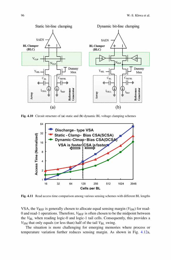
96 W.-S. Khwa et al.
Fig. 4.10 Circuit structure of (a) static and (b) dynamic BL voltage clamping schemes
Fig. 4.11 Read access time comparison among various sensing schemes with different BL lengths
VSA, the VREF is generally chosen to allocate equal sensing margin (VSM) for read-0 and read-1 operations. Therefore, VREF is often chosen to be the midpoint betweenthe VBL when reading logic-0 and logic-1 tail cells. Consequently, this provides aVSM that only equals (or less than) half of the tail VBL swing.
The situation is more challenging for emerging memories where process ortemperature variation further reduces sensing margin. As shown in Fig. 4.12a,

4 Emerging NVM Circuit Techniques and Implementations for Energy. . . 97
Preharge
Time
a b
VBL Developing
Cell-1
Cell-0
Variations
Variations
VSM
VBLS_TAIL
VB
L
VREF
VBLS_CELL-1_TAILVBLS_CELL-0_TAIL
÷
125 VSA Time
Precharge Time
BL Developing Time100
75
50
25
00.4 0.5 0.6 0.7 0.8 0.9 1
Rea
d T
ime
(ns)
512Cell/BL
VDD (V)
Fig. 4.12 (a) Variations in BL voltage swing during read operation due to tailing cells. (b) Readtime breakdown of a typical VSA under various VDD
emerging memories suffer from smaller VBL difference between tail cells whenreading logic-0 and logic-1 cells (�VBLS_TAIL). In particular, both read-1 and read-0operations experience dynamic VBL swings during the VBL development phase. Thisprevents emerging memories from employing traditional fixed-value VREF sensingscheme [37–42] or other novel VSAs that requires the read-1 VBL to be maintainednear VPRE or VDD [43–46].
Second, lowering the VDD has a profound impact on read time. The dynamicVBL swings for both read-1 and read-0 require a longer VBL development time toensure sufficient �VBLS_TAIL for accurate sensing. The decrease in VDD reducesthe transistor driving strength and VSM, which further increases the macro-levelread time. Figure 4.12b breaks down the read time of a conventional voltage-modesensing scheme using a 65 nm emerging memory macro with a bit-line length of 512cells. Under low VDD, the precharge time and the BL developing time dominate theread time, while the VSA response time remains relatively unchanged. This trendbecomes more prominent in macros with longer BL lengths. Therefore, speed andyield improvements of low VDD voltage-mode sensing should emphasize on bit-linedevelopment time reduction, while maintaining a VSM sufficient to tolerate the inputoffset voltage of the VSA.
4.2.3 Challenges for Current-Mode Sensing Scheme
The current-mode sensing scheme has three design challenges associated with (1)BL clamping voltage, (2) reference current, and (3) voltage head room. Conven-tional current-mode sensing requires the BL voltage clamping. To ensure robust andhigh-speed read operations, it is desirable to have VBL clamped as high as possibleto compensate for the bit-line unselected cells leakage current, and the CSA input

98 W.-S. Khwa et al.
Fig. 4.13 An example of the replica cell current sensing circuit for emerging NVM cell array
offset. However, the VBL must be kept considerably smaller than the typical programvoltage to prevent read disturbance, which might modify the existing cell content.This imposes a trade-off between read speed and read disturbance.
As previously mentioned, current-mode sensing usually involves comparing thecell current (ICELL) with a predefined reference current (IREF). However, using afixed IREF cannot accommodate for the ICELL fluctuations across various process,voltage, and temperature (PVT) variations. Several publications address this issueusing the replica cell schemes [47–53]. In the replica cell schemes, because boththe memory cells and the replica cells experience similar conditions, allowingthe generated IREF to fluctuate along with ICELL across different PVT variations.Figure 4.13 presents an example of the replica cell current sensing circuit foremerging NVM cell array. The replica array includes both active and inactive replicacells. The active replica cell generates replica current (ICELL_REPLICA) matches thatfrom regular main cell array. The purpose of inactive replica cells is to minimizemismatch between ICELL and ICELL_REPLICA by providing similar neighboringgeometric patterns and parasitic loads to what a regular memory cell experiencesin the main cell array.
If a hard defect or a significant process variation occurs in the replica array, theIREF could be inaccurate and susceptible to high die-to-die variation. This could leadto read failure or increase in read access time and power consumption. Therefore,

4 Emerging NVM Circuit Techniques and Implementations for Energy. . . 99
Fig. 4.14 (a) Concept of voltage budget and (b) bit-line voltage vs. bit-line current in a typical65 nm current-mode sensing scheme
read reference current generation is a crucial challenge in the design of emergingNVM.
Figure 4.14a outlines the concept of voltage budge in a current-mode sensingscheme, which consists of current-mirror (CM) headroom, BL clamper headroom,and BL bias VBL. The amount of supply voltage (VDD) reduction is limited bythe voltage headroom of the diode-connected CM and the BL voltage clampingcircuitry. As illustrated in Fig. 4.14b, a 3 μA bit-line current would require a voltageheadroom of 400 mV for a typical 65 nm CM circuit [54]. Lowering VDD suppressesthe effective VBL as well as the voltage across the emerging memory device. Thisleads to smaller cell current during read operation, which further reduces the sensingmargin and read speed.
4.2.4 Advanced Circuit Design Techniques for VSA and CSA
4.2.4.1 Low-VDD Swing-Sample-and-Couple VSA (SSC-VSA)
Figure 4.15 illustrates the concept of a low-VDD swing-sample-and-couple (SSC)VSA [55]. While conventional VSA utilizes only half the bit-line voltage swing ofthe tailing cells (½ �VBLS_TAIL), this SSC-VSA is capable of exploiting the full�VBLS_TAIL for sensing margin (VSM). The SSC circuit comprises of one PMOStransistor (T1), two switches (SW1 and SW2), and one capacitor (C1). Unlikemidpoint VREF in conventional VSA, SSC-VSA places the VREF below the midpoint.In phase-1 (VBLS sampling), the BL develops a voltage swing VBLS (=VDD − VBL)during a time (TBL), and SW1 is turned on to transfer VBL to node IN1 of VSA andnode A of C1, while node B of C1 is maintained at VREF.
In phase-2 (VBLS coupling), SW1 is turned off for isolation betweennode A and BL. Then T1 is turned on to pull node A up from VBL toVDD. Node A’s voltage shift boosts the node IN2 voltage from VREF to(VREF + VBLS). In phase-3 (comparison), the SAEN signal enables the

100 W.-S. Khwa et al.
Fig. 4.15 (a) Circuits and (b) waveforms of a low-VDD swing-sample-and-couple (SSC) VSA
VSA to detect the differential voltage between its two inputs, which is�VSA = (VREF + VBLS) − (VDD − VBLS) = 2VBLS − (VBLS-H_TAIL + VBLS-L_TAIL).The increase in VSM (nearly double) lowers VDD minimal requirement and achievesread speed exceeding those of conventional VSA at low VDD.

4 Emerging NVM Circuit Techniques and Implementations for Energy. . . 101
4.2.4.2 Reference Current Generation
Most floating gate (FG)-based replica cells connect selected floating gates to theircontrol gate at the edge of replica array. This avoids the need for additional erasecycle and allows the replica cell FG voltage potential to be maintained throughoutmultiple access cycles. However, the sharp corners and the special shapes of the FGlayer in split-gate flash technology make it difficult to maintain uniformity and lowerresistances in metal-to-FG contact and FG poly. Therefore, the resistance (RDWL_FG)between control-gate (dummy word-line) and FG of the accessed replica cells oftenexhibits significant variation across rows/dies. The RDWL_FG variation affects theselected replica cell turn-on time and produces IREF settling time fluctuation. Thiscould potentially lead to many issues, including data-out (DOUT) ringing, long-address access times, and increased power consumption. To overcome these issues,FG-always-high and prestable current sensing (PSCS) schemes have been proposed.
The FG-always-high scheme is a straightforward concept such that the FGreplica cells are kept high at all times [56]. This makes it a non-switchingapproach and eliminates the IREF settling time completely. However, it exposesthe replica cell FG oxide to longer voltage-stress time than the regular flash cells.Consequently, the replica cells in FG-always-high scheme are more susceptible toaging degradation. Moreover, the IREF generation in FG-always-high scheme ismore power consuming, because one of the replica cells is always on, even duringnon-read operations (erase and program).
Figure 4.16 illustrates the conceptual waveform of the PSCS scheme [53].The IREF generation and the replica cell switching occur in the final phase of anerase/program cycle or during the device power-up, instead of the beginning of everyread operation. The time required to complete the erase/program operation is usuallymuch longer than the worst-case IREF settling time in eFlash macros provided byfoundries [57, 58]. Therefore, it is feasible to hide the replica cell FG switchingtime and the IREF settling time near the end of an erase/program operation prior tosubsequent read operations. Because the replica cells are not always turned on, theyexperience less voltage-stress and consume less power than those in the FG-always-high scheme. Moreover, narrow IREF distribution could be achieved with multiplereplica cells turning on simultaneously.
Several IREF generation schemes based on replica cells have been proposed foremerging resistive NVM. Figure 4.17 illustrates three IREF generation schemes:k-parallel-cell, high-low-average, and parallel-series reference cell (PSRC). Thek-parallel-cell scheme provides the average ICELL of k replica LRS cells. The high-low-average schemes provide the average ICELL of LRS and HRS cells, as longas their R-ratio is small. In the presence of large-cell resistance variation, bothk-parallel-cell and high-low-average schemes suffer from wide IREF distribution,because IREF will be dominated by the tailing LRS replica cell. The PSRC schemeeliminates this concern by having two parallel LRS sets connected in series. Thisenables the PSRC scheme to generate a narrower IREF distribution even with HRSand LRS cell variations.

102 W.-S. Khwa et al.
Fig. 4.16 Conceptual illustration of the prestable current sensing (PSCS) scheme
4.2.4.3 Current-Mode Sensing with Small Input-Offsets
Several CSA schemes with small input-offset were reported for high-speed or smallcell-current emerging resistive NVM sensing. Figure 4.18 presents a small-offsetCSA sampling scheme using the threshold voltage (VTH) of M1 and M2 [59].The MOS latch (M1/M2) VTH is stored in capacitors C1/C2 to provide offset

4 Emerging NVM Circuit Techniques and Implementations for Energy. . . 103
Fig. 4.17 IREF generation scheme based on replica cells for resistive emerging NVM: (a) k-parallel-cell, (b) high-low-average, and (c) parallel-series reference cell (PSRC) schemes
Fig. 4.18 Small-offset CSA using threshold-voltage (VTH) sampling scheme
compensation. This scheme achieves small input offset but requires considerablearea overhead due to its use of numerous switches.
Figure 4.19 presents two CSA schemes based on current-sampling (IS-CSA).As shown in Fig. 4.19a, IS-CSA [60] employs two capacitors (C1/C2) to storethe gate-source voltage (VGS) of critical transistors (M1/M2) to generate ICELL andIREF. IS-CSA then uses the sampled ICELL and IREF for second-stage amplificationoperations, which are insensitive to the VTH variations of M1/M2. Figure 4.19bshows the time-differential IS-CSA (TD-IS-CSA) [61] uses a single capacitor forthe sampling of IREF. In the subsequent timing phase, TD-IS-CSA compares thesampled IREF with ICELL in order to achieve robust sensing with small input offset.

104 W.-S. Khwa et al.
Fig. 4.19 Two current-sampling CSA: (a) 2-capacitor IS-CSA and (b) single-capacitor time-differential IS-CSA
Figure 4.20 shows two digital-calibration-based CSAs (DC-CSA) designed forhigh-speed sensing without the requirement of run-time offset-cancellation oper-ation. A digital offset cancellation CSA (DOC-CSA) [62] implements additionaloffset-cancel current (IOC) on the differential input (LBLL or LBLR) of thecomparator. The amount of IOC is digitally calibrated with respect to the comparatormismatch in the wafer testing stage. In the calibration-based asymmetric-voltage-biased CSA (AVB-CSA) [63], the differential nodes (CP and RP) of a latch-typecomparator are biased at different precharge voltages (VAP_CP and VAP_RP) priorto the sensing operation. VAP_CP and VAP_RP are calibrated during wafer testing inaccordance with the offset voltage of the read-path detected at nodes CP and RP. Asa result, AVB-CSA suppresses the offset caused by the comparator and the entireread-path (IOS_SUM).

4 Emerging NVM Circuit Techniques and Implementations for Energy. . . 105
OSLD
SAE
YRL
PCN
YRR
LBLR RSTN
PCN
SAE
LBLR/LBLL
OSLD
Init. Valid
Phase-1
SWEQ
M2T
M2
SC/SR-A-A
CMEN
DOUT
DOUT
DBL
SRSC
SWEQ
M3M1
MIT
IM1
M4
MSECMENV1 V1
BL/DBL
RP
Phase-2 Phase-3
PC/EQ
LBLL
Icell
IOC IOC
IRef
IREF
CBL
ICELL
BL
CDBL
VAP-RP
RP
VAP-CP
CP
IM2
RSTN
OCDL OCDR
OCDL/R
CP
TPRE
IM2
IM1
TSAEN
IM1/IM2
Fig. 4.20 Two digital-calibration-based CSAs (DC-CSA): (a) digital offset cancellation CSA(DOC-CSA), and (b) asymmetric-voltage-biased CSA (AVB-CSA)
4.2.4.4 Low-Voltage Current-Mode Sensing Schemes
Figure 4.21 illustrates a low-voltage, body-drain-driven (BDD) CSA [54]. TheBDD-based current-mirror (CM) circuit needs a smaller voltage headroom thantypical diode-connected current mirrors. As a result, the BDD-CSA is capable ofallocating more voltage budget to the voltage across NVM devices. This generatessufficient ICELL that enables sensing even at low VDD.
4.3 Write Circuits for Emerging Resistive NVM
In this section, we introduce the basic operations of key sub-circuits used in thewrite operations of emerging resistive NVM. Afterward, we describe the variouscircuit design challenges and review some of the advanced circuit techniques.

106 W.-S. Khwa et al.
Fig. 4.21 Low-voltage, body-drain-driven CSA (BDD-CSA)
4.3.1 Key Sub-Circuits Used in Write Operations
Figure 4.22 illustrates functional blocks along the write-path in a typical emergingresistive NVM macro. The key sub-circuits used for write operation include levelshifters, write drivers, and charge-pump circuits. Depending on the memory device,some might require voltages higher than the supply voltage (VDD). In such cases,a charge-pump (CP) circuit is implemented for voltage conversion. Write driversprovide the required write voltage to the cell array. For read and write operations,write drivers supply different output voltage levels to word-lines (WL) or source-lines (SL). As a result, level shifters are commonly employed along with WL/SLdrivers.
Because the generation of high voltage and high current is generally inefficient,the high-voltage path current load should be minimized to reduce power consump-tion. As a result, low-power emerging resistive NVM generally requires advancedcircuit techniques to reduce the DC/leakage current of level shifters and writedrivers. In addition, designing an energy-efficient CP with small peak current isalso important when these low-power emerging NVM macros are embedded on achip.

4 Emerging NVM Circuit Techniques and Implementations for Energy. . . 107
Fig. 4.22 Illustration offunctional blocks alongwrite-path in a typicalemerging resistive NVMmacro
4.3.1.1 Challenges and Advanced Circuits in Level-Shifters
Level shifters are implemented for converting the row decoder logic signals (0 V orVDD) to voltage higher than VDD (VDDH). VDDH could be the write voltage requiredfor NVM devices. Generally, level shifters (LS) have two challenges: (1) generatinga high VDDH for write operation from a low input voltage (VDDL), and (2) consuminga large DC current due to the VDDH path charge loss for conventional low-VDDLlevel shifters in unselected rows. These challenges potentially lead to an increaseof current load and power consumption, particularly in NVM macros with a largenumber of rows. In the following texts, we will examine a number of existing levelshifters.
Figure 4.23 illustrates the circuit and waveform of a common half-latch levelshifter (HL-LS) [64, 65]. The HL-LS comprises of two pull-down NMOS transistors(MNM, MNR), a PMOS cross-coupled transistor pair (MPL, MPR), an input inverter(INV1), and an output buffer (BUF). When SEL = 1, MNL is turned on to pullthe node OB voltage (VOB) down to ground. This turns on MPR and raises thevoltage at node OT (VOT) to VDDH. Thereafter, the cross-coupled feedback ensuresthe MPR remains turned off and the output (VO) of HL-LS is VDDH. When SELb = 1,MNR turns on and creates a discharge current (ID) to lower VOT to below VDDH. IfID is large, the current contention between MPR and MNR can cause MNR to pullVOT down to 0 V. When VDD is low (i.e., below or near the threshold voltageof MNL/MNR), ID is too small to win the current contention over MPL/MPR. Thischallenge prevents the HL-LS from being implemented in applications requiringlow VDDL. In addition, HL-LS also requires the ultra-large sizing for MNL and MNRtransistors.

108 W.-S. Khwa et al.
MNL MNR
MPL MPR
VOBVOT
VDDH VDDH
VDDL
VDDH VDDH
CLoad
VO
SEL
Delay
VDDL
VDDH
VSS
VDDH
VSS
VDDH
VSS
VDDH
VSS
CurrentFighting
Current Fighting Fail
SEL
VOT
VO
VOT
Fig. 4.23 Circuit and waveform of a typical half-latch level shifter (HL-LS)
MNL MNR
MPL MPRVM
VOT
VDDH VDDH
VDDHVDDH
VDDL
VO
SEL CLoad
Delay
VDDL
VDDH
VSS
VDDH
VSS
VDDH
VSS
SEL
VM
VO
Fig. 4.24 Circuit and waveform of a typical current-mirror-based level shifter (CM-LS)
Figure 4.24 shows typical current-mirror-based level shifters (CM-LS) weredeveloped to reduce VDDL for low-VDD applications [64]. CM-LS comprises twopull-down NMOS transistors (MNL and MNR), a pair of PMOS current-mirrortransistors (MPL and MPR), an inverter, and an output buffer (BUF). When SEL = 1,MNL is enabled to turn on MPR by lowering the voltage of node M (VM). Thevoltage of node OT (VOT) is then raised to VDDH. When SEL = 0, MNL is off andMPL slowly pulls down VM to VDDH minus the threshold voltage of MPL (VDDH–VTH_MPL). This reduces the current through MPR significantly and enables MNR topull down VOT beyond the trip-point of the output buffer without incurring seriescurrent contention. As a result, CM-LS is capable of achieving a low VDDL usingsmaller MNL/MNR compared to HL-LS design.
However, there is still DC current in selected and unselected CM-LSs. WhenSEL = 1 (selected row), we have DC current flowing through MPL and MNL(IDC_PLNL). When SEL = 0, the weakly turned-off MPR (ILEAK_PR) conducts aDC leakage current, because its gate is biased at VDDH–VTH_MPL. In the case ofan emerging NVM macro with k rows, the DC leakage current on the VDDH pathof the CM-LSs is IDC_PLNL + (k − 1) ILEAK_PR. For large k, the high current load

4 Emerging NVM Circuit Techniques and Implementations for Energy. . . 109
VDDH VDDH
MNL MNR
MPL MPR
MPM
MPS
VOTVM
VML
VO
SEL CLoad
VDDHVDDH
VDDL
Delay
VDDL
VDDH
VSS
VDDH
VSS
VDDH
VSS
SEL
VM
VO
Fig. 4.25 Circuit and waveform of a pseudo-diode-mirrored level shifter (PDM-LS)
on VDDH path weakens the charge pump and prevents it from providing the currentand voltage required in write operations. A Wilson CM-LS [66] has been proposedto suppress the DC current when SEL = 1, but the DC current leakage issue whenSEL = 0 remains unsolved.
Figure 4.25 shows the pseudo-diode-mirrored level shifter (PDM-LS) proposedto accommodate lower VDDL, while suppressing DC current [67]. The PDM-LSstructure comprises of two pull-down NMOS transistors (MNL and MNR), a pseudo-diode PMOS transistor (MPS), a current-cutoff PMOS transistor (MPM), and pseudoPMOS current-mirror transistors (MPL and MPR), an inverter, and a buffer. Whileone source/drain terminal of MPS is connected to the gate of MPL, the gate and theother source/drain terminal of MPS are connected to the gate of MPR and the drainof MNL, respectively. MPM is controlled by VOT and placed between MPL and MNL.
For SEL = 1, MNL is turned on to pull VM down to 0 V. This consequently turnson MPR and charges the voltage of node OT (VOT) to VDDH. When VM = 0 V, MPSforms a diode-connected structure, causing VML to be equal to the threshold voltageof MPS (VTH_MPS). Low VM also turns on MPR pulling VOT to VDDH, which turnsMPM off. For SEL = 0, MNR is turned on to pull VOT down, this slightly turns onMPM and charges VM. Consequently, this causes MPS to enter cutoff mode. VM thenapproaches VDDH, which is higher than the level of CM-LS and suppresses the DCleakage current flowing through MPR. By cutting of the DC current at SEL = 1 andsuppressing DC leakage current at SEL = 0, the PDM-LS is able to operate underlower minimum VDDL and consume less DC current than the conventional CM-LS.
4.3.1.2 Challenges and Advanced Circuits in Write Drivers
In a typical emerging NVM macro, multiple cells on the same row are selectedfor write operation. Consequently, these cells experienced the same voltage biasconditions on word-line (WL) and source-line (SL). Figure 4.26a, b illustrate

110 W.-S. Khwa et al.
Fig. 4.26 Program timevariation for (a) OTP and (b)resistive-type emerging NVMdevices. (c) Current andvoltage waveform duringprogram operation
5
10
15
20
25
Perc
enta
ge(%
)
Programming time(a.u.)2 4 6 8 10
(a)
1st bitswitch
2nd bitswitch
K-th bitswitch
SL voltage
TSET[K]
TSET[1]
VSET
SL current
Time
(b)
(c)
process variation can cause considerable variability in the write durations, suchas program time (TPROG), SET time (TSET), and RESET time (TRESET). To coverthese tailing cells, the voltage bias for WL and SL must be maintained untilthe switching completes. For one-time programmable (OTP) and resistive-typememory, the switching of an emerging NVM cell from HRS to LRS causes aconsiderable DC current (IDC_CELL). As a result, cells with shorter TPROG/TSETexperience large IDC_CELL even after switching to accommodate for the tailing cells.As shown in Fig. 4.26c, this unnecessary IDC_CELL increases energy consumption,degrades output voltage, and potentially causes write failure in tailing cells.
Several cell-by-cell write termination schemes [55, 68, 69] have been proposedto suppress IDC_CELL by terminating the program/SET operation as soon as the

4 Emerging NVM Circuit Techniques and Implementations for Energy. . . 111
Polarity SEL
Control
Memory Cell Array
VREFVBIAS IWRITE
FB
VR
RCELL
VREF
Fig. 4.27 Circuits and waveforms of the OP-based current-mode write termination (OP-CWT)scheme
switching completes. In the following, we review three write-termination schemes:(1) operational amplified (OP)-based current-mode termination, (2) negative-resistance-based current mode termination, and (3) voltage-mode termination.
Figure 4.27 shows the circuits and waveforms of the OP-based current-modewrite termination (OP-CWT) scheme [69]. The current mirror (CM) copies thecell current to a resistive load. Then the OP compares a predefined referencevoltage (VREF) with the voltage across the resistive load. The voltage bias circuit isdisabled when the induced voltage is higher than the VREF. This OP-CWT scheme iseffective in suppressing IDC_SET; however, the multiple usages of OP and CM incursignificant area overhead, slow response time, and lead to considerable DC currentconsumption.
Figure 4.28 illustrates the negative-resistance-based current mode termination(NR-CWT) scheme reported in [68]. NR-CWT employs a current-mirror-basednegative-resistance (−R) circuit to provide feedback for write current control. Whenwriting 1 from LRS to HRS (WR1 = high and WR0 = low), current flows throughthe cell from SL to BL. When writing 0 from HRS to LRS (WR1 = low andWR0 = high), the current flows from BL to SL. The −R driver reflects on the BLwith a current proportional to the cell resistance. When the cell resistance reachesLRS, an increase of cell current pulls down the BL voltage and reduces the currentthrough the current mirror. This further lowers the BL voltage, thereby forming apositive feedback loop. It should be mentioned that the current mirror and positivefeedback loop only moderate, rather than terminate, the write current. The currentcontinues to flow through the −R driver.
Figure 4.29 illustrates the voltage-mode write-termination (VWT) scheme forthe SET operation [55]. This scheme is implemented using only four transistors tomonitor BL voltage for termination. At the beginning of the write operation, theSEL control signal turns on the NRSD transistor to discharge the residue chargeson the data-line (DL). During the write operation, the transition from HRS to LRSdramatically drops the voltage across the ReRAM cell, because VWT and ReRAMform a voltage divider network. As a result, the gate voltage of P1 rises dramatically

112 W.-S. Khwa et al.
WL
-R
BLSL
W1
W1
Cell
VBIAS
-R Driver
W0
NVM
Time
Time
IWRITE
VBL
IWRITE
w/o NR
Fig. 4.28 Circuits and waveforms of the negative-resistance-based current mode termination (NR-CWT) scheme
NSD NRSD
P1
N1
MUXDL<K>
FB SEL
VREF
NSD NRSD
P1
N1
MUXDL<K+1>
FB SEL
V REF
WL
NV
M
NV
M
NV
M
NV
M
SL
Memory Cell Array
SEL
SL
WL
DL<K>
DL<K+1>
FB<K>FB<K+1>
ISL
ISL w/o WT
Fig. 4.29 Circuits and waveforms of the voltage-mode write-termination (VWT) scheme
to turn itself off. Meanwhile, the gate of N1 is biased at VREF, it turns off NSD bypulling down its gate terminal. The use of voltage-mode operation and the reuse ofIDC_CELL minimize the area overhead, reduce the power consumption, and improvethe response time.

4 Emerging NVM Circuit Techniques and Implementations for Energy. . . 113
4.4 Emerging Resistive NVM for Energy-Efficient Systems
Energy-efficient systems aim to exploit the combined benefits of low-latencyvolatile memory for power-on computing and low-power nonvolatile memory.However, the expensive write operation and the limited endurance of conventionalnonvolatile memory become a bottleneck in the implementation of such low-powersystems. Resistive random access memory (ReRAM) is a promising nonvolatilememory candidate for energy-efficient computing because of its low-latency writeand low-power operations. This section discusses first the two-macro and one-macroapproaches, then the implementation of ReRAM device in nonvolatile SRAM andnonvolatile logic.
4.4.1 Two-Macro and One-Macro Approaches
Effective design of the power-on/off transition is one of the most essential compo-nents toward low-power systems. Because critical data must be transferred to NVMduring the power-off event and recalled when power returns, the data backup/restoreoperation must be power-efficient. As illustrated in Fig. 4.30, many low-powersystems use the two-macro scheme with volatile memory (SRAM and DRAM) forfast low-voltage access, and nonvolatile flash memory for power-off data storage.The two-macro scheme relaxes the endurance requirement of NVM, because regularaccesses and computations will be performed on SRAM/DRAM. If the emergingNVM device has fast random read/write speeds and high endurance, an alternative3D-IC architecture can be proposed without the need for DRAM. This wouldeliminate the DRAM self-refresh power during system standby mode, as shownin Fig. 4.30b.
The two-macro approach is not energy-efficient, because the power-off data-backoperations consume too much energy. The word-by-word SRAM read/write andthe long-latency NVM read/write operations demand long store/restore durations[70–73]. This renders the two-macro approach susceptible to data loss after suddenpower failure. Furthermore, the high peak current required by the flash memorywrite operations can lead to power integrity concerns. In the worst-case scenario,the system may be unable to recover its previous state.
To tackle this challenge, researchers have proposed the concept of nonvolatilelogic (nvLogic) and nonvolatile SRAM (nvSRAM) [70–75] to improve the store/re-store performances in the traditional two-macro schemes. Figure 4.30 illustratesthe chip architecture based on the one-macro solution enabled by nvLogic andnvSRAM. The nonvolatile flip-flop (nvFF) and nvSRAM are new devices thatare realized by combining logic devices with NVM devices. This implementationallows parallel data transferring between logic circuits and NVMs, and thusimproves the latency and the power efficiency during power-on and power-off.Besides, by integrating NVM cells on top of the logic devices though the BEOL

114 W.-S. Khwa et al.
Fig. 4.30 Conceptual (a) illustration and (b) power comparison of a low-power system using thetwo-macro approach and the one-macro approach using nonvolatile memory
process, the approach can provide an alternative low-power architecture with areliable data-backup scheme with a small area overhead. Figure 4.30 shows thecomparison on the performances of the volatile processor based on conventionaltwo-macro solution and the nonvolatile processor (nv-Processor) based on theone-macro solution based on nvLogic [76]. It can be seen that while the volatileprocessor stops the computation in the frequency power-interrupted scenario, the

4 Emerging NVM Circuit Techniques and Implementations for Energy. . . 115
Fig. 4.31 Comparison onperformances of volatile andnonvolatile processors withpower interruption [76]
Fig. 4.32 nvLogic using nonvolatile latch or nonvolatile flip-flop
nv-Processor is capable to proceed with the computation because it requires verylow power and latency to store/restore the data during power switching (Fig. 4.31).
4.4.2 Nonvolatile Logic and Nonvolatile SRAM
One challenge of NVM devices preventing them from being directly implementedas computing or accessing units is their limited endurance. Many NVM devices(Flash memory, MRAM, PCRAM, and ReRAM) have many orders of magnitudelesser endurance than volatile memory (SRAM and DRAM) or CMOS logic (latch,flip-flop, and logic-gates). Consequently, endurance-aware designs should performregular computing/accessing in volatile memory and use nvLogic/nvSRAM only aspower-off storages, as shown in Fig. 4.32.
Figure 4.33 illustrates (a) the conventional 6T SRAM cell, along with (b)several reported nonvolatile latch (nvLatch) cells. These nvLatch cells are generallydesigned with dedicated transistors to isolate the NVM devices during normal modeand provide store/restore functionalities during power-off/on mode. In addition,because the store/restore are bit-to-bit parallel operations, they enable low-latencystore/restore operations than the conventional two-macro approaches. We willbriefly mention the challenges of these configurations in the following paragraph.

116 W.-S. Khwa et al.
Fig. 4.33 Comparison between (a) conventional 6T latch/SRAM cell and (b) reported nonvolatilelatch (nvLatch) and nonvolatile SRAM (nvSRAM) cells
The SONOS-12T cell [77] not only occupies a large area, the slow SONOSdevice write operation causes its store operation to be high voltage and long latency(TSTORE). Similarly, the MRAM-19T2R latch [78] also suffers from expensive storeoperation and large area. Compared with the previous two devices, the Fe-capacitor-6T2C cell [79] requires a much smaller area, but it needs an additional ½ VDDvoltage bias to access NVM and read SRAM. This necessitates a dedicated voltageregulator that consumes a significant amount of DC current. The PCM-7T2R cell[80] offers a relatively compact area, but the PCM device write characteristicsrequire a large store current and a moderate store time. Furthermore, the PCM-7T2Rcell also suffers from cell-VDD (CVDD) integrity degradation. Lastly, even thoughthe ReRAM-6T2R cell [81] is the most compacted design by eliminating the NVMswitches, it suffers from cell leakage current and SRAM stability issues.

4 Emerging NVM Circuit Techniques and Implementations for Energy. . . 117
Fig. 4.34 Nonvolatile flip-flop with memristor in (a) master-stage (nvFF-M) and (b) slave-stage(nvFF-S)
As previously mentioned, the purpose of additional transistors is to enableisolation and store/restore functionalities. These transistors, however, not onlyincrease the area overhead, but also impose high parasitic loads that increaseslatency and power consumption of logic gates. Consequently, it is impractical toimplement NVM devices to every logic gate. Alternatively, nvLogic gates shouldonly be applied on latches or flip-flops that are on the critical path. Figure 4.34 showsthe two nonvolatile flip-flops (nvFF) circuit structures for logic libraries—master-stage nvFF (nvFF-M) and slave-stage nvFF (nvFF-S) [82]. The nvFF-M implementsthe master-stage using Rnv8T cell [83] and the slave-stage using conventionalCMOS circuit, while the nvFF-S employs the exact opposite. These two nvFFconfigurations can be incorporated in various power-on procedures to accommodatelower VDD, while requiring only 16% of the area overhead using traditional FFs ornvFFs.
4.4.3 nvSRAM Example: Rnv8T Cell
A 3D-stacked resistive nonvolatile 8T2R SRAM cell (Rnv8T) had been proposed[83]. This Rnv8T design achieves low-latency and low-power store operations. Thework also suggests a bit-line control-line (BL-CL) sharing scheme to simplify thecontrol of the resistive memory device and a write-assist operation to relax the writeconstraints. These features allow the Rnv8T to be sized favoring read and suppressread/write failure at a reduced VDD. In the following, we first describe the basicoperations of the Rnv8T cell, before moving on to discuss cell stability and restoreyield. Lastly, we also review some of the recent nvSRAM cell structures.
4.4.3.1 Rnv8T Cell Basic Operations
The Rnv8T cell structure consists of a typical 6T SRAM cell, 2T ReRAM-switch(RSW), and two resistive memory devices. This design preserves the 6T SRAMadvantages, including its low-latency read/write and low-voltage operation. The

118 W.-S. Khwa et al.
Fig. 4.35 The Rnv8T (a) cell structure and (b) operation flowchart
direct connection between ReRAM and SRAM storage nodes (Q and QB) enablesnonvolatile storage of both original and complementary data. While other nvSRAMcell designs require a dedicated control line (CL) to carry out the store operations,the Rnv8T scheme shares BLs with the NVM CLs for a more compact cell area.This BL-CL sharing scheme provides SRAM-mode write-assist operation throughRSWs. To make the cell area more compact, the two ReRAM devices can bearranged in a 3D configuration on top of the 8T SRAM cell.
Figure 4.35 illustrates the Rnv8T cell structure and operation flowchart. Inthe SRAM normal mode, the Rnv8T cell executes the typical SRAM read/writeoperations. During read operations, the switch-line (SWL) is pulled low to turnoff RSWs for providing ReRAM device isolation and preventing the SRAM celldisturbance. The differential read in the Rnv8T cell is identical to that in a typical6T SRAM. When the system switches to standby mode, the Rnv8T macro initiatesthe store operation by transferring the SRAM data into the ReRAM device. Afterthe data transfer completes, the standby leakage can be completely eliminated by

4 Emerging NVM Circuit Techniques and Implementations for Energy. . . 119
Fig. 4.36 Write margin under various supply voltage VDD and technology nodes
shutting down the whole macro. During the system wake-up, a restore operationfetches data from ReRAM devices back to the SRAM storage nodes Q and QB.
The write operation initiates by pulling both SWL and WL high. RSWs providean extra write path and reduce the pulled-up ratio (PR), which is defined as the sizeratio of pull-up PMOS to pass-gate NMOS. The BL and BLB data are transferredinto the SRAM cell through RSWs and pass gates. As a result, this approachprovides a larger write margin (WM) and a faster write speed than that providedby the 6T SRAM cell. In this work, the WM is also referred to as the write trip-point (WTP), which is the voltage between the BL and VSS required for flippingthe cell data to the opposite state. To inspect the worst-case WM, we performedMonte Carlo simulation using 10,000 points. The transistor size of both the 6Tand the Rnv8T cells are chosen to be the same as a commercial 6T SRAM cellunder various technology nodes. Figure 4.36 shows the Rnv8T cell, compared to 6TSRAM cell, the WM is increased by 4.13× at 0.5 V (0.18 μm) and 5.78× at 0.35 V(65 nm).
Figure 4.37a illustrates the Rnv8T cell store operation. In the store mode, datatransfer from SRAM to ReRAM requires both SET and RESET operations. For bothSET and RESET operations, the SWL is kept high. The SET operation raises bothBL and BLB to a high voltage (VSET) to switch the RL (if Q = 0) to a low-resistancestate (LRS). On the contrary, in RESET operation, the BL and BLB are pulled toground and the CVDD is biased to VRESET. This switches the RR (if QB = 1) to ahigh-resistance (LRS) state.
Figure 4.37b illustrates the Rnv8T cell restore operation. The purpose of therestore mode is to recall data to the SRAM storage nodes (Q and QB) from theReRAM devices (RL and RR). First, the rise of SWL turns on RSWs (RSWL andRSWR) to pull both BL and BLB to ground. This clears the remaining charges at thestorage nodes and ensures both nodes are at equal states for a later stage comparison.When the CVDD rises, the PMOS transistors charge nodes Q and QB while the RRand RL provide discharge path to ground. The resistance difference between RLand RR generates a voltage differential (VQ–QB) at Q and QB during power-on. Thelarge discharge current of RL lowers the storage-node voltage rapidly. The RH, on

120 W.-S. Khwa et al.
Fig. 4.37 The (a) store and (b) restore operation waveforms of the Rnv8T cell
the other hand, provides a small discharge current, the storage-node voltage is keptat a higher level. Finally, the cross-coupled latch amplifies VQ-QB and restores thedata to the SRAM storage nodes.
4.4.3.2 Rnv8T Cell Stability
In read operations, the cell stability imposes a minimum VDD (VDDmin) limitation.The write-assist feature improves WM and allows trading WM for better readstability by using a read-favored-sizing (RFS) scheme. Using the same amountof area, the Rnv8T transistor sizing can be adjusted to enhance read stabilityperformance through (1) increasing the size ratio of PDL (PDR) over PGL (PGR) tosuppress read disturbance, and (2) raising the trip-point of the latch (inv1 and inv2)to prevent data from flipping.
Figure 4.38 compares the read static noise margin (RSNM) [84], WM, and cellVDDmin for Rnv8T cells with and without the RFS scheme. To include processvariation into our analysis, we performed a Monte Carlo simulation with 10,000points. Without the RFS scheme, the VDDmin of the nominal 6T and the Rnv8Tcell is limited to 0.55 V. Applying the BL-CL sharing scheme on the Rnv8T cellimproves the WM by 4.08× at 0.5 V. It should be mentioned that although WMimproved, the VDDmin does not decrease because the RSNM does not benefit fromthis approach.
After applying the RFS scheme, the WM improvement reduces slightly to 3.32×,whereas the RSNM increases by 11.1× at VDD = 0.6 V. As a result, the Rnv8Tcell with the RFS scheme achieved a VDDmin 150 mV lower than that without theRFS scheme. Therefore, the Rnv8T cell with BL-CL sharing and RFS schemesdemonstrates superior cell stability and lower SRAM read/write VDDmin thanconventional 6T SRAM or other nvSRAM cells.

4 Emerging NVM Circuit Techniques and Implementations for Energy. . . 121
Fig. 4.38 Trade-off between VDDmin, WM, and RSNM in the Rnv8T cell structure
4.4.3.3 Rnv8T Restore Yield
During restore operation, the Rnv8T cell behaves a latch sensing the output fromthe two ReRAM devices. The sensing margin can be significantly improved byusing a differential sensing scheme on two ReRAM devices with opposite states.To include process variation in our analysis, we performed a 40,000-point MonteCarlo simulation. Figure 4.39 shows when the resistance ratio exceeds 3, the restoreyield can reach up to 99.6%. In this study, ReRAM devices have a resistive ratioover 10, which ensures a 100% restore yield in the Rnv8T cell. However, because ofthe read stability limitation, the Rnv8T cell is only capable of achieving VDDmin of0.45 V for processes with smaller threshold voltage (VTH) variation. For nanometerprocesses, the larger VTH variation causes the VDDmin of Rnv8T cells to degrade.This highlights the need for a new nvSRAM cell structure for low VDD applications,and particularly for nanometer chips.
4.4.3.4 nvSRAM Design Comparisons
A resistive nonvolatile 9T2R SRAM cell (Rnv9T) was reported to solve the readand write failure at low VDD [82]. This Rnv9T cell combines the features of thepreviously proposed Rnv8T nvSRAM and low-voltage L-shaped 7T SRAM cells[85]. Figure 4.40 shows the circuit structure and the waveform of the low-voltage7T SRAM cell developed form the Zigzag 8T cell [86].
The Rnv9T cell in Fig. 4.40 uses decoupled 1T read-port and pseudo read word-line (RWL) schemes to eliminate read disturbance. Similar to the Rnv8T cell, theRnv9T cell also relies on the 2T ReRAM switch for simpler ReRAM control andbetter WM. Because this structure eliminates read disturbance, the Rnv9T cell

122 W.-S. Khwa et al.
Fig. 4.39 Restore yield ofthe Rnv8T cells
Fig. 4.40 (a) The proposed low-voltage 7T SRAM cell and (b) its operation waveform
does not need to rely on the read-favored-sizing (RFS) scheme to improve its readstability. Consequently, this enables a larger WM than that achieved by the Rnv8T.Therefore, with improved read stability and WM, the Rnv9T cell can achieve a lowerVDDmin than conventional 6T, low-voltage 7T, and Rnv8T cells.
Figure 4.41a compares the WMs of various nvSRAM designs using a 10,000-point Monte Carlo simulation under various VDD’s. The nvSRAM cells wereconfigured as described in previous literatures [78–80, 87], [77, 88], with the sametransistor sizing as a conventional 6T SRAM cell. The simulation result shows thatthe Rnv8T cell can achieve a 3.3× WM improvement, compared to other nvSRAMcells. Figure 4.41b shows that the write time of the Rnv8T cell is also shorter thanthose of other nvSRAM cells. Finally, Table 4.2 summarizes the performance ofdifferent nvSRAM cells. It can be seen that Rnv8T and Rnv9T show superior speedand energy efficiency for store operations compared to other reported cells.

4 Emerging NVM Circuit Techniques and Implementations for Energy. . . 123
Fig. 4.41 (a) Write margin and (b) normalized write time comparison between different nvSRAMcell structures under various VDD
Table 4.2 Performance comparison of various nvSRAM cell structures
4.4.4 nvFF Example: SWT1R-nvFF
The low-latency energy-efficient system requires nonvolatile flip-flops (nvFFs)that are capable of achieving parallel data transfer between flip-flops (FFs) andnonvolatile memory (NVM) devices. Conventional two-NVM-based nvFFs face thechallenges of excessive store energy (ES) and overwrite stability degradation. Toresolve these issues, a SWT1R-nvFF that incorporates a single NVM (1R) withself-write-termination (SWT) had been proposed [89]. This SWT1R-nvFF designreduces ES by 99% and a 2.7 ns termination latency. The following subsections willdescribe the nvFFs in detail.

124 W.-S. Khwa et al.
Fig. 4.42 (a) Illustration of the conventional nvFF wide write time distribution challenges, and(b) write behavior of a log-process ReRAM
4.4.4.1 SWT1R-nvFF Basic Operations
Figure 4.42 illustrates the wide write time distribution challenges of conventionalnvFFs. Conventional NVM-based nvFFs usually employ long write duration toaccommodate the slower cells. This approach raises several concerns on energyand reliability. First, the store energy (ES) is high for writing the original and thecomplementary data to two NVM devices. This excessive waste of ES is furtherexacerbated when NVM devices have large variations in SET and RESET duration[90]. In addition, these long write operations may cause cell degradation that leadsto endurance and reliability issues.
Figure 4.43 shows the proposed SWT1R-nvFF, it comprises of a master-latch(M-Latch), a dual-mode slave latch (S-Latch), two switches (SW1 and SW2), andan NVM-control unit (NVMCU) with one ReRAM on the left side (RL). There arethree modes in this design—(1) regular flip-flop operations, (2) store operations forNVM write, and (3) restore operations for data recall from NVM to FF.

4 Emerging NVM Circuit Techniques and Implementations for Energy. . . 125
Fig. 4.43 Structure and operation modes of the proposed SWT1R-nvFF
The flip-flop mode is simple, both switches are on to connect M0-M3 to form across-coupled S-Latch. The restore and store signals (RSTR and STR) are kept lowto disable M12/M6/M11 from causing voltage and current stress on RL. The devicebehaves like a typical FF. In the restore mode, RSTR is asserted and the voltage atnode NQ (VNQ) is determined by the voltage divider network formed by M9-RL-M11. During the rise of VDD, if RL is HRS, the high voltage of VNQ will keep Q ata higher state to restore Q = 1. If RL is LRS, then the low voltage of VNQ will keepQ at a lower state to restore Q = 0.
During store operation, both switches are turned off, while STR is high andSTRB is low. In the case of SET program, the path (M9-RL-M6-M7-M3) forms thevoltage divider that biases the voltage at node NX (VNX) to VDDHV–VSET. In thecase of a mismatch, VNX is kept low to supply VSET across RL with M3 providing theSET current (ISET), while M10 is weakly turned on to maintain QB = 1. When RLswitches from HRS to LRS, a large DC-current causes Q to rise. The SET-feedback(SFB) circuit (M0, M3, and M4) then turns off M3 to terminate the SET operation.In the case of RESET program, the write path voltage divider (M9-RL-M6-M8) isactivated to bias VNX at VDDHV–VRESET. When RL switches from LRS to HRS,VNX is pulled low to turn on M10 and cause QB to rise and Q1 to drop. The RESET-feedback (RFB) circuit (M1, M2, and M5) then turns off M1 and M8 to terminatethe RESET operation.

126 W.-S. Khwa et al.
Fig. 4.44 Simulated average store energy versus (a) write-time variation ratio (TW-Ratio) and (b)LRS resistance
4.4.4.2 SWT1R-nvFF Performance and Comparison
Figure 4.44a shows that the SWT scheme reduced the store energy (ES) by 27×and store latency (TS) by 10× shorter than the worst-case nvFF. Figure 4.44bpresents store energy versus various LRS resistance (RLRS) values. During RESEToperations, a lower RLRS device consumes large DC current and consumes morepower than do devices with a higher RLRS. The increase in minimum RLRS enablesthe SWT scheme to reduce wasted power by 8.77× when the minimum RLRS is1 k�. Lastly, Table 4.3 compares the performances of recent nvFF macros [76, 89,91–93].
4.5 Conclusion
Emerging NVMs can offer potential advantages of low cost, low power, and highspeed over conventional NVMs. However, some challenges must be overcomebefore successfully realizing these memory technologies in practical applications.In this chapter, we first explained the circuit design challenges and reviewedadvanced circuit techniques associated with both read and write operations. Thenwe compared two-macros and one-macro approaches for energy-efficient systems.Lastly, we discussed and compared multiple implementations of nonvolatile logicand nonvolatile SRAM using emerging memory technologies.

4 Emerging NVM Circuit Techniques and Implementations for Energy. . . 127
Tabl
e4.
3C
ompa
riso
nof
silic
on-v
erifi
ednv
FFs
Publ
icat
ions
[89]
[91]
[92]
[93]
[76]
Cir
cuits
(Sla
ve-L
atch
Onl
y)
Ori
gina
lNV
Mde
vice
ReR
AM
FeR
AM
FeR
AM
MT
JR
eRA
MC
MO
Ste
chno
logy
65nm
130
nm13
0nm
90nm
65nm
Add
ition
alde
vice
s13
T+
1NV
M(1
3T+
1R)
22T
+2N
VM
(22T
+2R
)18
T+
4NV
M(1
8T+
4R)
17T
+2N
VM
(17T
+2R
)15
T+
2NV
M(1
5T+
2R)
Self
-wri
tete
rmin
atio
nY
esN
oN
oN
oY
esSt
ress
onN
VM
infli
p-flo
pm
ode
No
No
No
Cur
rent
No

128 W.-S. Khwa et al.
Acknowledgements The authors would like to thank MXIC, TSMC, and ITRI for their supports.
References
1. R.H. Fowler, L. Nordheim, Electron emission in intense electric fields. Proc R Soc A 119(781),173–181 (1928)
2. Y. Choi et al., A 20 nm 1.8 V 8 Gb PRAM with 40 MB/s program bandwidth, in Proceedingsof the IEEE International Solid-State Circuits Conference (ISSCC) (2012), pp. 46–47
3. H.-S.P. Wong, C. Ahn, J. Cao, H.-Y. Chen, S.W. Fong, Z. Jiang, C. Neumann, S. Qin, J. Sohn,Y. Wu, S. Yu, X. Zheng, H. Li, J.A. Incorvia, S.B. Eryilmaz, K. Okabe, Stanford memorytrends, https://nano.stanford.edu/stanford-memory-trends, Accessed 12 Oct 2016
4. R. Atiken, System requirements for memories, in International Electron Devices MeetingsShort Course Material (2015)
5. B.C. Lee, E. Ipek, O. Mutlu, D. Burger, Architecting phase change memory as a scalableDRAM alternative, in Proceedings of International Symposium on Computer Architecture(ISCA) (2009)
6. K. Ikegami et al., Low power and high density STT-MRAM for embedded cache memory usingadvanced perpendicular MTJ integrations and asymmetric compensation techniques, in IEEEInternational Electron Devices Meeting Technical Digest (2014), pp. 650–653
7. Y. Wu, B. Lee, H.-S.P. Wong, Al2O3-based RRAM using atomic layer deposition (ALD) with1-μA RESET current. IEEE Electron Devic Lett 31(12), 1449–1451 (2010)
8. G. Jan et al., Demonstration of fully functional 8Mb perpendicular STT-MRAM chips withsub-5ns writing for non-volatile embedded memories, in Proceedings of Symposium on VLSITechnology (2014)
9. D. Ielmini, Emerging memory technologies: ReRAM and PCM, in International ElectronDevices Meetings Short Course Material (2015)
10. K.J. Lee et al., A 90nm 1.8V 512Mb diode-switch PRAM with 266 MB/s read throughput.IEEE J. Solid State Circuits 43(1), 150–162 (2008)
11. K. Tsuchida et al., A 64 Mb MRAM with clamped-reference and adequate-reference schemes,in Proceedings of the IEEE International Solid-State Circuits Conference (ISSCC) (2010), pp.258–269
12. S.S. Sheu et al., A 4 Mb embedded SLC resistive-RAM macro with 7.2 ns read-write random-access time and 160ns MLC-access capability, in Proceedings of the IEEE International Solid-State Circuits Conference (ISSCC) (2011), pp. 200–201
13. C.-Y. Lee, DRAM life extension challenge and response, in International Electron DevicesMeetings Short Course Material (2015)
14. M. Stanisavljevic, H. Pozidis, A. Athmanathan, N. Papandreou, T. Mittelholzer, E. Eleftheriou,Demonstration of reliable Triple-Level-Cell (TLC) phase-change memory, in InternationalMemory Workshop (2016)
15. D. Worledge et al., Switching distributions and write reliability of perpendicular spin torqueMRAM, in IEEE International Electron Devices Meeting Technical Digest (2010), pp.296–299
16. A. Fantini et al., Intrinsic switching variability in HfO2 RRAM, in IEEE International MemoryWorkshop (IMW) (2013)
17. T. Cuong et al., A 7.8 MB/s 64 Gb 4-Bit/cell NAND flash memory on 43 nm CMOStechnology, in Non-volatile Memory Workshop (2010)
18. P. Zhou, B. Zhao, J. Yang, Y. Zhang, A durable and energy efficient main memory using phasechange memory, in Proceedings of International Symposium on Computer Architecture (ISCA)(2009)
19. Y. Xie, Introduction, in Emerging Memory Technologies Design, Architecture And Applica-tions, (Springer, Berlin, 2014)

4 Emerging NVM Circuit Techniques and Implementations for Energy. . . 129
20. Y. Xie, NVSim: A Circuit-Level Performance, Energy, and Area Model for Emerging Non-volatile Memory, a Chapter in Emerging Memory Technologies Design, Architecture andApplications (Springer, Berlin, 2014)
21. S. Ambrogio et al., Understanding switching variability and random telegraph noise in resistiveRAM, in IEEE International Electron Devices Meeting (IEDM) Technical Digest (2013), pp.782–785
22. T.-Y. Liu et al., A 130.7-mm 2-layer 32-Gb ReRAM memory device in 24-nm technology.IEEE J. Solid State Circuits 49(1), 140–153 (2014)
23. M. J. Breitwisch, “Phase Change Random Access Memory Integration,” a Phase ChangeMaterials: Science and Applications, Springer; Berlin, 2009
24. H.-S.P. Wong et al., Phase change memory. Proc. IEEE 98(12), 2201–2227 (2010)25. F. Xiong, A.D. Liao, D. Estrade, E. Pop, Low-power switching of phase-change materials with
carbon nanotube electrodes. Sci Mag 332, 568–570 (2011)26. M. Brightsky, et al., Crystalline-as-deposited ALD phase change material confined PCM
cell for high density storage class memory, in IEEE International Electron Devices MeetingTechnical Digest (2015), pp. 60–63
27. D.H. Im, et al., A unified 7.5 nm dash-type confined cell for high performance PRAM device,in Proceedings of IEEE International Electron Devices Meeting (2008)
28. J.J. Nowak et al., Demonstration of ultralow bit error rates for spin-torque magnetic random-access memory with perpendicular magnetic anisotropy. IEEE Magn. Lett. 2, 3000204 (2011)
29. Everspin, the MRAM Company, https://www.everspin.com/. Accessed 6 Nov 201630. T. Devolder, Basics of STT-MRAM, in International Electron Devices Meetings Short Course
Material (2015)31. C. Kim et al., A covalent-bonded cross-coupled current-mode sense amplifier for STT-MRAM
with 1T1MTJ common source-line structure array, in IEEE International Solid-State CircuitsConference (ISSCC) Digest of Technical Papers (2015), pp. 134–136
32. R. Tekemura et al., A 32-Mb SPRAM with 2T1R memory cell, localized bi-directional writedriver and ‘1’/‘0’ dual-array equalized reference scheme. IEEE J. Solid State Circuits 45(4),869–879 (2010)
33. Z.-H. Lin, Y.-H. Wang, Observation of indium ion migration-induced resistive switching inAl/Mg0.5Ca0.5TiO3/ITO. Appl. Phys. Lett. 109(5), 053507 (2016)
34. J. Park et al., Quantized conductive filament formed by limited Cu source in sub-5nm era, inIEEE International Electron Devices Meeting Technical Digest (2011), pp. 64–67
35. C.M. Compagnoni et al., First evidence for injection statistics accuracy limitations inNAND Flash constant-current Fowler-Nordheim programming, in IEEE International ElectronDevices Meeting Technical Digest (2007), pp. 165–168
36. A. Calderoni, S. Sills, N. Ramaswamy et al., Performance comparison of O-based and Cu-based ReRAM for high-density applications, in International Memory Workshop (2014)
37. N. Verma, A.P. Chandrakasan, A 256 kb 65 nm 8T subthreshold SRAM employing sense-amplifier redundancy. IEEE J. Solid State Circuits 43(1), 141–149 (2008)
38. T.H. Kim, J. Liu, C.H. Kim, A voltage scalable 0.26 V, 64 kb 8T SRAM with Vmin loweringtechniques and deep sleep mode. IEEE J. Solid State Circuits 44(6), 1785–1795 (2009)
39. B. Zhai, S. Hanson, D. Blaauw, et al., A variation-tolerant Sub-200 mV 6-T subthresholdSRAM. IEEE J. Solid State Circuits 43(10), 2338–2348 (2008)
40. I.J. Chang, J.J. Kim, S.P. Park, et al., A 32 kb 10T sub-threshold SRAM array with bit-interleaving and differential read scheme in 90 nm CMOS. IEEE J. Solid State Circuits 44(2),650–658 (2009)
41. Y. Morita, H. Fujiwara, H. Noguchi et al., An area-conscious low-voltage-oriented 8T-SRAMdesign under DVS environment, in Symposium on VLSI Circuits Digest Technical Papers(2007), pp. 256–257
42. J.H. Chen, L.T. Clark, T.H. Chen, An ultra-low-power memory with a subthreshold powersupply voltage. IEEE J. Solid State Circuits 41(10), 2344–2353 (2006)
43. K. Takeuchi, Y. Kameda, S. Fujimura, et al., A 56-nm CMOS 99-mm2 8-Gb multi-level NANDflash memory with 10-MB/s program throughput. IEEE J. Solid State Circuits 42(1), 219–232(2007)

130 W.-S. Khwa et al.
44. D.S. Byeon, S.S. Lee, Y.H. Lim et al., An 8 Gb multi-level NAND flash memory with 63 nmSTI CMOS process technology, in IEEE International Solid-State Circuits Conference (ISSCC)Digest Technical Papers, vol 1 (2005), pp. 46–47
45. S.H. Chang, S.K Lee, S.J. Park et al., A 48 nm 32 Gb 8-level NAND flash memory with5.5 MB/s program throughput, in IEEE International Solid-State Circuits Conference (ISSCC)Digest Technical Papers (2009), pp. 240–241,241a
46. G.G. Marotta, A. Macerola, A. d’Alessandro et al., A 3bit/cell 32 Gb NAND flash memory at34 nm with 6 MB/s program throughput and with dynamic 2b/cell blocks configuration modefor a program throughput increase up to 13 MB/s, in IEEE International Solid-State CircuitsConference (ISSCC) Digest Technical Papers (2010), pp. 444–445
47. K. Kobayashi, T. Nakayama, Y. Miyawaki, et al., A high-speed parallel sensing architecturefor multi-megabit flash E2PROMs. IEEE J. Solid State Circuits 25(1), 79–83 (1990)
48. M. Bauer, R. Alexis, G. Atwood et al., A multilevel-cell 32 Mb flash memory, in IEEEInternational Solid-State Circuits Conference (ISSCC) Digest Technical Papers (1995), pp.132–133
49. R. Micheloni, L. Crippa, M. Sangalli, et al., The flash memory read path: building blocks andcritical aspects. IEEE Proc 91(4), 537–553 (2003)
50. B.Q. Le, M. Achter, C.G. Chng, et al., Virtual-ground sensing techniques for a 49-ns/200-MHzaccess time 1.8-V 256-Mb 2-bit-per-cell flash memory. IEEE J. Solid State Circuits 39(11),2014–2023 (2004)
51. T. Ogura, M. Hosoda, T. Ogawa, et al., A 1.8-V 256-Mb multilevel cell NOR flash memorywith BGO function. IEEE J. Solid State Circuits 41(11), 2589–2600 (2006)
52. C.C. Chung, H.C. Lin, Y.T. Lin, A multilevel read and verifying scheme for bi-NAND flashmemories. IEEE J. Solid State Circuits 42(5), 1180–1188 (2007)
53. M.F. Chang, S.J. Shen, A process variation tolerant embedded split-gate flash memory usingpre-stable current sensing scheme. IEEE J. Solid State Circuits 44(3), 987–994 (2009)
54. M.F. Chang, C.W. Wu, C.C. Kuo, et al., A low-voltage bulk-drain-driven read scheme for Sub-0.5 V 4 Mb 65 nm logic-process compatible embedded resistive RAM (ReRAM) macro. IEEEJ. Solid State Circuits 48(9), 2250–2259 (2013)
55. M.F. Chang, J.J. Wu, T.F. Chien et al., 19.4 embedded 1Mb ReRAM in 28nm CMOS with 0.27-to-1V read using swing-sample-and-couple sense amplifier and self-boost-write-terminationscheme, in IEEE International Solid-State Circuits Conference (ISSCC) Digest TechnicalPapers (2014), pp. 332–333
56. Y.D. Chih, C.H. Wang, C.H. Kuo, Reference cell circuit for split gate flash memory, U.S. Patent6,396,740 (2002)
57. Datasheet, “sfc 0064_08b9_he” Taiwan Semiconductor Manufacturing Company (TSMC)(2001)
58. Datasheet, AF64K8AF25, v1.0 1st Silicon Sdn. Bhd. (X-Fab) (2005)59. J. Javanifard, T. Tanadi, H. Giduturi et al., A 45nm self-aligned-contact process 1Gb NOR flash
with 5MB/s program speed, in IEEE International Solid-State Circuits Conference (ISSCC)Digest Technical Papers (2008), pp. 424–624
60. M.-F. Chang, S.-S. Sheu, K.-F. Lin, et al., A high-speed 7.2-ns read-write random access 4-Mbembedded resistive RAM (ReRAM) macro using process-variation-tolerant current-mode readschemes. IEEE J. Solid State Circuits 48, 878–891 (2013)
61. M. Jefremow, T. Kern, W. Allers et al., Time-differential sense amplifier for sub-80 mV bitlinevoltage embedded STT-MRAM in 40 nm CMOS, in IEEE International Solid-State CircuitsConference (ISSCC) Digest Technical Papers (2013), pp. 216–217
62. T. Kono, T. Ito, T. Tsuruda, T. Nishiyama, T. Nagasawa, T. Ogawa, Y. Kawashima, H. Hidaka,T. Yamauchi, 40-nm embedded split-gate MONOS (SG-MONOS) flash macros for automotivewith 160-MHz random access for code and endurance over 10 M cycles for data at the junctiontemperature of 170◦C. IEEE J. Solid State Circuits 49, 154–166 (2013)
63. M.F. Chang, Y.F. Lin, Y.C. Liu, et al., An asymmetric-voltage-biased current-mode sensingscheme for fast-read embedded flash macros. IEEE J. Solid State Circuits 50(9), 2188–2198(2015)

4 Emerging NVM Circuit Techniques and Implementations for Energy. . . 131
64. S.N. Wooters, B.H. Calhoun, T.N. Blalock, et al., An energy-efficient subthreshold levelconverter in 130-nm CMOS. IEEE Trans Circuits Syst II Exp Briefs 57(4), 290–294 (2010)
65. I.J. Chang, J.J. Kim, K. Kim, et al., Robust level converter for sub-threshold/super-thresholdoperation:100 mV to 2.5 V. IEEE Trans Very Larg Scale Integr (VLSI) Syst 19(8), 1429–1437(2011)
66. S. Lütkemeier, U. Ruckert, et al., A subthreshold to above-threshold level shifter comprising aWilson current mirror. IEEE Trans Circuits Syst II Exp Briefs 57(9), 721–724 (2010)
67. M.F. Chang et al., A low-power subthreshold-to-superthreshold level-shifter for sub-0.5Vembedded resistive RAM (ReRAM) macro in ultra low-voltage chips, in 2014 IEEE AsiaPacific Conference on Circuits and Systems (APCCAS), Ishigaki (2014), pp. 695–698
68. D. Halupka, S. Huda, W. Song et al., Negative-resistance read and write schemes for STT-MRAM in 0.13μm CMOS, in IEEE International Solid-State Circuits Conference (ISSCC)Digest Technical Papers (2010), pp. 256–257
69. X.Y. Xue, W.X. Jian, J.G. Yang, et al., A 0.13 μm 8 Mb logic-based CuxSiyO ReRAMwith self-adaptive operation for yield enhancement and power reduction. IEEE J. Solid StateCircuits 48(5), 1315–1322 (2013)
70. M.-F. Chang et al., Circuit design challenges in embedded memory and resistive RAM(RRAM) for mobile SoC and 3D-IC, in Proceedings 2011 IEEE Asia South Pacific DesignAutomation Conference (ASP-DAC) (2011), pp. 197–203
71. M.-F. Chang et al., Challenges and trends of resistive memory (Memristor) based circuits for3D-IC applications, in 2011 Symposium on Solid State Devices and Materials (SSDM) (2011),pp. 1053–1054
72. M.-F. Chang et al., Challenges and trends in low-power 3D die-stacked IC designs using RAM,memristor logic, and resistive memory (ReRAM), in The IEEE 9th International Conferenceon ASIC (ASICON) (2011), pp. 327–330
73. P.-F. Chiu, M.-F. Chang et al., A low store energy, low VDDmin, nonvolatile 8T2R SRAM with3D stacked RRAM devices for low power mobile applications, in Symposium on VLSI CircuitsDigest Technical Papers (2010), pp. 229–230
74. H. Ohno et al., Magnetic tunnel junction for nonvolatile CMOS logic, in IEEE InternationalElectron Devices Meeting (IEDM) (2010), pp. 9.4.1–9.4.4
75. S.-M. Yoon et al., Phase-change-driven programmable switch for nonvolatile logic applica-tions. IEEE Electron Device Lett 30(4), 371–373 (2009)
76. Y. Liu et al., A 65nm ReRAM-enabled nonvolatile processor with 6× reduction in restoretime and 4× higher clock frequency using adaptive data retention and self-write-terminationnonvolatile logic, in IEEE International Solid-State Circuits Conference (ISSCC) Digest ofTechnical Papers (2016), pp. 84–86
77. M. Fliesler et al., A 15ns 4Mb NVSRAM in 0.13u SONOS technology, in Non-VolatileSemiconductor Memory Workshop (NVSMW) (2008), pp. 83–86
78. N. Sakimura et al., Nonvolatile magnetic Flip-flop for standby-power-free SoCs. IEEE J. SolidState Circuits 44(8), 2244–2250 (2009)
79. T. Miwa et al., NV-SRAM: A nonvolatile SRAM with backup ferroelectric capacitors. IEEE J.Solid State Circuits 36(3), 522–527 (2001)
80. M. Takata et al., Nonvolatile SRAM based on phase change, in Non-Volatile SemiconductorMemory Workshop (NVSMW) (2006), pp. 95–96
81. W. Wang et al., Nonvolatile SRAM cell, in International Electron Device Meeting (IEDM)(2006), pp. 1–4
82. M.-F. Chang et al., Endurance-aware circuit designs of nonvolatile logic and nonvolatileSRAM using resistive memory (Memristor) device, in 2012 IEEE Asia South Pacific DesignAutomation Conference (ASP-DAC) (2012), pp. 329–334
83. P.-F. Chiu, M.-F. Chang, C.-W. Wu, C.-H. Chuang, S.-S. Sheu, Y.-S. Chen, M.-J. Tsai, Lowstore energy, low VDDmin, 8T2R nonvolatile latch and SRAM with vertical-stacked resistivememory (Memristor) devices for low power mobile applications. IEEE J Solid State Circ 47(6),1483–1496 (2012)

132 W.-S. Khwa et al.
84. E. Seevinck, F.J. List, J. Lohstroh, Static-noise margin analysis of MOS SRAM cells. IEEE J.Solid State Circuits 22(5), 748–754 (1987)
85. L.-F. Chen, A 7T SRAM Circuit Design for Low Voltage Applications., M.S. thesis (Institute ofElectronics Engineering, National Tsing Hua University, Hsinchu, 2011)
86. J.-J. Wu et al., A large σVTH/VDD tolerant ZigZag 8T SRAM with area-efficient decoupleddifferential sensing and fast write-back scheme. IEEE J. Solid State Circuits 46(4), 815–827(2011)
87. W. Wang et al., Nonvolatile SRAM cell, in International Electron Devices Meeting (IEDM)Technical Digest Papers (2006), pp. 27–30
88. S. Yamamoto et al., Nonvolatile SRAM (NV-SRAM) Using Functional MOSFET Mergedwith Resistive Switching Devices, in IEEE Custom Integrated Circuits Conference (CICC)Technical Digest Papers (2009), pp. 531–534
89. S.P. Lo et al., A ReRAM-based Single-NVM nonvolatile flip-flop with reduced stress-time andwrite-power against wide distribution in write-time by using self-write-termination scheme fornonvolatile processors in IoT Era, in IEEE International Electron Devices Meeting (IEDM)Digest Technical Papers (2016), pp. 420–423
90. M.F. Chang et al., Embedded 1Mb ReRAM in 28nm CMOS with 0.27-to-1V read usingswing-sample-and-couple sense amplifier and self-boost-write-termination scheme, in IEEEInternational Solid-State Circuits Conference (ISSCC) Digest of Technical Papers (2014), pp.332–333
91. M. Qazi, A. Amerasekera, A. P. Chandrakasan, A 3.4 pJ FeRAMenabled D flip-flop in 0.13μmCMOS for nonvolatile processing in digital systems, in IEEE International Solid-State CircuitsConference (ISSCC) Digest of Technical Papers (2013), pp. 192–193
92. S.C. Bartling et al., An 8MHz 75μA/MHz zero-leakage non-volatile logic-based Cortex-M0MCU SoC exhibiting 100% digital state retention at VDD=0V with <400ns wakeup and sleeptransitions, in IEEE International Solid-State Circuits Conference (ISSCC) Digest of TechnicalPapers (2013), pp. 432–433
93. N. Sakimura et al., A 90nm 20MHz fully nonvolatile microcontroller for standby-power-critical applications, in IEEE International Solid-State Circuits Conference (ISSCC) Digestof Technical Papers (2014), pp. 184–185

Chapter 5The Processing-in-Memory Paradigm:Mechanisms to Enable Adoption
Saugata Ghose, Kevin Hsieh, Amirali Boroumand, Rachata Ausavarungnirun,and Onur Mutlu
DRAM, the predominant technology used to build main memory, is a majorcomponent of modern computer systems. As the data working set sizes of modernapplications grow [37, 48, 79, 225], the need for higher memory capacity and highermemory performance continues to grow as well. However, even though CMOStechnology scaling has yet to come to an end, DRAM technology scaling has beenunable to keep up with the increasing memory demand from applications [2, 3,26, 29, 37, 65, 66, 68, 79, 82, 89–91, 110, 114, 116, 117, 120, 125, 129, 137, 138,143, 151, 152, 160, 226, 233, 239, 240]. For example, if we study the latency andthroughput of Double Data Rate (DDR) DRAM over the last 15–20 years, we seethat neither has been able to keep up with the growth in application working set sizeor CPU computational power [26, 28, 107, 114, 125].
A major bottleneck to improving the overall system performance is the high costof data movement. Currently, in order to perform an operation on data that is storedwithin memory, the CPU must issue a request to the memory controller, whichin turn sends a series of commands across an off-chip bus to the DRAM module.The data is then read from the DRAM module, at which point it is returned to thememory controller and typically stored within the CPU cache. Only after the datais placed in the CPU cache can the CPU operate (i.e., perform computation) on thedata. The long latency to retrieve data from DRAM is exacerbated by two factors.First, it is difficult to send a large number of requests to memory in parallel, in partbecause of the narrow bandwidth of the off-chip bus between the memory controllerand main memory. Second, despite the time spent on bringing the data into thecache, which is substantial [62, 63], much of the data brought into the caches is
S. Ghose · K. Hsieh · A. Boroumand · R. AusavarungnirunCarnegie Mellon University, Pittsburgh, PA, USA
O. Mutlu (�)ETH Zürich, Zürich, SwitzerlandCarnegie Mellon University, Pittsburgh, PA, USA
© Springer International Publishing AG, part of Springer Nature 2019R. O. Topaloglu, H.-S. P. Wong (eds.), Beyond-CMOS Technologies for NextGeneration Computer Design, https://doi.org/10.1007/978-3-319-90385-9_5
133

134 S. Ghose et al.
not reused by the CPU [177, 178], rendering the caching either very inefficient orsometimes even unnecessary. Ultimately, there is significant time and energy wastedon moving data between the CPU and memory, many times with little benefit inreturn, especially in workloads where caching is not very effective [2, 3].
Recent advances in memory design have unlocked the potential to avoid theunnecessary data movement. In an attempt to improve the scalability of capacityand bandwidth, memory manufacturers have turned to 3D-stacked memories, wheremultiple layers of memory arrays are stacked on top of each other [119, 132]. Theselayers are connected together using through-silicon vias (TSVs), which providemuch greater internal memory bandwidth than the narrow off-chip bus to the CPU.Some prominent examples of these 3D-stacked memory architectures [71, 72, 74,75, 92, 119] include a logic layer, which provides an opportunity to embed general-purpose computational logic directly within main memory to take advantage of thehigh internal bandwidth available.
The idea of performing processing-in-memory (PIM), or near-data processing(NDP), has been proposed for at least several decades [39, 44, 45, 56, 80, 100, 140,166, 171, 208, 218]. However, these past efforts were not adopted at large scale dueto the difficulty of integrating processing elements with DRAM. As a result of thepotential enabled by the inclusion of a logic layer in modern memory architectures,various recent works explore a range of PIM architectures for multiple differentpurposes (e.g., [1–4, 9, 12, 20, 22, 27, 30, 47, 51, 52, 58, 59, 62–64, 67, 68, 81, 93,95, 96, 98, 118, 123, 124, 131, 133, 149, 163, 172, 176, 195, 196, 200, 202, 203, 205,221, 243, 246]).
While PIM avoids the need to move data from memory to the CPU for a numberof data-intensive functions, it introduces new challenges for system architects andprogrammers. In particular, PIM processing logic does not have quick access toimportant mechanisms that exist within the CPU, such as address translation andcache coherence, which greatly aid the programmer. Preserving the functionalityand efficiency of such mechanisms is essential for PIM, as these mechanisms can(1) preserve the traditional programming models that application developers rely onto productively write programs, and (2) provide significant performance benefits..As we show in this work (see Sect. 5.4), simply forcing PIM processing logic tosend queries to the CPU to accomplish address translation and cache coherence isvery inefficient, since the overhead of a query can almost completely eliminate thebenefits of moving computation to memory. Therefore, it is essential that we providePIM-specific mechanisms that efficiently support the functionality of traditionaladdress translation and cache coherence mechanisms and thus provide support forthe use of existing programming models to program PIM architectures. Our goal isto design general-purpose address translation and cache coherence mechanisms thatcan be exploited by any PIM processing logic to provide low-overhead support forcommon functions, such as pointer chasing in virtual memory and cache coherence.
To this end, we propose two mechanisms to support PIM. The first mechanism,IMPICA, is an in-memory accelerator for pointer chasing, which exploits thehigh bandwidth available within 3D-stacked memory. IMPICA can traverse achain of virtual memory pointers within DRAM, without having to look up

5 The Processing-in-Memory Paradigm: Mechanisms to Enable Adoption 135
virtual-to-physical address translations in the CPU translation lookaside buffer(TLB) or without using the page walkers within the CPU. The second mechanism,LazyPIM, maintains cache coherence between PIM processing logic and CPU coreswithout sending coherence requests for every memory access. Instead, LazyPIMefficiently provides coherence by having PIM processing logic speculatively acquirecoherence permissions, and then later sends compressed batched coherence lookupsto the CPU to determine whether or not its speculative permission acquisitionviolated the memory ordering defined by the programming model.
In Sect. 5.1, we cover common design principles of modern PIM architectures.In Sect. 5.2, we discuss key issues that impact the flexibility and adoption of PIMarchitectures. In Sect. 5.3, we discuss IMPICA, an accelerator that we propose toefficiently support pointer-chasing operations within PIM architectures. In Sect. 5.4,we discuss LazyPIM, a mechanism that we propose to efficiently support cachecoherence between PIM processing logic and the CPU cores. In Sect. 5.5, wediscuss related work in the area, and in Sect. 5.6 we briefly discuss some futureresearch challenges, with a focus on system-level challenges for the adoption ofPIM architectures.
5.1 Designing Processing-in-Memory Architectures
Processing-in-memory (PIM) architectures place some form of processing logic(typically accelerators, simple cores, or reconfigurable logic) inside the DRAMsubsystem. This PIM processing logic, which we also refer to as PIM cores or PIMengines, interchangeably, can execute portions of applications or entire applicationkernels, depending on the design of the architecture. In this section, we first discusshow the PIM processing logic is integrated within DRAM modules (Sect. 5.1.1),and then we discuss how applications make use of this PIM processing logic(Sect. 5.1.2).
5.1.1 Placing Processing Logic Within the DRAM Subsystem
Modern PIM architectures rely on implementing processing logic in the DRAM chipitself (e.g., [2–4, 12, 20, 22, 27, 30, 47, 51, 52, 58, 59, 64, 67, 68, 93, 95, 96, 98, 117,118, 124, 131, 133, 149, 172, 176, 195, 196, 198–200, 202, 203, 221, 243, 246]) oron the DRAM module or the DRAM controller [9, 62, 63, 203]. DRAM consists ofmultiple arrays of capacitive cells, where each cell holds one bit of data. By placingprocessing logic in close proximity of the cell arrays, PIM architectures are notrestricted to the limited bandwidth offered by the narrow off-chip bus between theDRAM module and the CPU. Instead, PIM processing logic benefits from the muchwider buses that are available within the chip and/or module in modern DRAMarchitectures.

136 S. Ghose et al.
CPU
Logic Layer
wide channel withThrough-Silicon
Vias (TSVs)
DRAM
Lay
ers
narrowMemory Channel
Fig. 5.1 High-level overview of a 3D-stacked DRAM based architecture
Figure 5.1 shows an overview of a 3D-stacked DRAM based architecture. Exam-ples of 3D-stacked DRAM include High-Bandwidth Memory (HBM) [75, 119]and the Hybrid Memory Cube (HMC) [2, 71, 72]. As the figure shows, a 3D-stacked DRAM consists of multiple layers. 3D-stacked DRAM has a much greaterinternal data bandwidth than conventional memory, due to its use of through-silicon vias (TSVs), which are vertical links that connect the multiple layers ofa DRAM stack together [119, 132]. In addition to containing multiple layers ofDRAM, a number of 3D-stacked DRAM architectures, such as HBM [75, 119]and HMC [71, 72], include a logic layer, typically the bottommost layer, wherearchitects can implement functionality that interacts with both the processor andthe DRAM cells [2, 3, 71, 72]. Currently, 3D-stacked DRAM makes limited use ofthe logic layer (e.g., HMC implements command scheduling logic within the logiclayer [71, 72]).
Recent PIM proposals (e.g., [2–4, 12, 20, 22, 30, 47, 51, 52, 58, 59, 64, 67,68, 93, 95, 96, 98, 118, 131, 133, 149, 163, 172, 176, 196, 221, 243, 246]) addprocessing logic to the logic layer to exploit the high bandwidth available betweenthe logic layer and the DRAM cell arrays. The proposed PIM processing logicdesign varies based on the specific architecture, and can range from fixed-functionaccelerators to simple in-order cores, and to reconfigurable logic. The complexity ofthe processing logic that can be added to the logic layer is currently limited by themanufacturing process technology and thermal design points, which may preventhighly sophisticated processors (e.g., out-of-order processor cores with large cachesand sophisticated instruction-level parallelism techniques) from being implementedwithin the logic layer at this time [43, 172, 243].
5.1.2 Using PIM Processing Logic Functionality inApplications
In order for applications to make use of PIM processing logic that resides withinDRAM, each PIM architecture exposes an interface to the CPU. While therecurrently is no standardization of this interface, most contemporary works on PIM
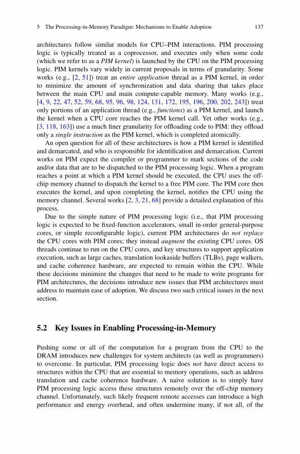
5 The Processing-in-Memory Paradigm: Mechanisms to Enable Adoption 137
architectures follow similar models for CPU–PIM interactions. PIM processinglogic is typically treated as a coprocessor, and executes only when some code(which we refer to as a PIM kernel) is launched by the CPU on the PIM processinglogic. PIM kernels vary widely in current proposals in terms of granularity. Someworks (e.g., [2, 51]) treat an entire application thread as a PIM kernel, in orderto minimize the amount of synchronization and data sharing that takes placebetween the main CPU and main compute-capable memory. Many works (e.g.,[4, 9, 22, 47, 52, 59, 68, 95, 96, 98, 124, 131, 172, 195, 196, 200, 202, 243]) treatonly portions of an application thread (e.g., functions) as a PIM kernel, and launchthe kernel when a CPU core reaches the PIM kernel call. Yet other works (e.g.,[3, 118, 163]) use a much finer granularity for offloading code to PIM: they offloadonly a single instruction as the PIM kernel, which is completed atomically.
An open question for all of these architectures is how a PIM kernel is identifiedand demarcated, and who is responsible for identification and demarcation. Currentworks on PIM expect the compiler or programmer to mark sections of the codeand/or data that are to be dispatched to the PIM processing logic. When a programreaches a point at which a PIM kernel should be executed, the CPU uses the off-chip memory channel to dispatch the kernel to a free PIM core. The PIM core thenexecutes the kernel, and upon completing the kernel, notifies the CPU using thememory channel. Several works [2, 3, 21, 68] provide a detailed explanation of thisprocess.
Due to the simple nature of PIM processing logic (i.e., that PIM processinglogic is expected to be fixed-function accelerators, small in-order general-purposecores, or simple reconfigurable logic), current PIM architectures do not replacethe CPU cores with PIM cores; they instead augment the existing CPU cores. OSthreads continue to run on the CPU cores, and key structures to support applicationexecution, such as large caches, translation lookaside buffers (TLBs), page walkers,and cache coherence hardware, are expected to remain within the CPU. Whilethese decisions minimize the changes that need to be made to write programs forPIM architectures, the decisions introduce new issues that PIM architectures mustaddress to maintain ease of adoption. We discuss two such critical issues in the nextsection.
5.2 Key Issues in Enabling Processing-in-Memory
Pushing some or all of the computation for a program from the CPU to theDRAM introduces new challenges for system architects (as well as programmers)to overcome. In particular, PIM processing logic does not have direct access tostructures within the CPU that are essential to memory operations, such as addresstranslation and cache coherence hardware. A naive solution is to simply havePIM processing logic access these structures remotely over the off-chip memorychannel. Unfortunately, such likely frequent remote accesses can introduce a highperformance and energy overhead, and often undermine many, if not all, of the

138 S. Ghose et al.
benefits that PIM architectures provide. A second naive solution is to limit thefunctionality of the PIM processing logic such that it cannot perform addresstranslation or cache coherence, and to expose these limitations to programmers.However, this alters the programming model of the system, and can lead to greatdifficulty for the widespread adoption of PIM as an execution model. In this section,we focus on the address translation and cache coherence challenges, and discusswhy naive solutions are not practical. We discuss new PIM-specific solutions thatcan overcome these challenges in Sects. 5.3 and 5.4.
5.2.1 Address Translation
A large amount of code relies on pointers, which are stored as virtual memoryaddresses. When the application follows a pointer, a core must perform addresstranslation, which converts the pointer’s stored virtual address into a physicaladdress within main memory. If PIM processing logic relies on existing CPU-sideaddress translation mechanisms, any performance gains from performing pointerchasing in memory could easily be nullified, as the processing logic needs to senda long-latency translation request to the CPU via the off-chip channel for eachmemory access. The translation can sometimes require a page table walk, wherethe CPU must issue multiple memory requests to read the page table, which furtherincreases traffic on the memory channel.
A naive solution is to simply duplicate the TLB and page walker withinmemory (i.e., within the PIM processing logic). Unfortunately, this is prohibitivelydifficult or expensive for three reasons: (1) coherence would have to be maintainedbetween the CPU and memory-side TLBs, introducing extra complexity and off-chip requests; (2) the duplicated hardware is very costly in terms of storage overheadand complexity; and (3) a memory module can be used in conjunction with manydifferent processor architectures, which use different page table implementationsand formats, and ensuring compatibility between the in-memory TLB/page walkerand all of these different designs is difficult.
We explore a tractable solution for PIM address translation as part of our in-memory pointer chasing accelerator, which we discuss in Sect. 5.3.
5.2.2 Cache Coherence
PIM processing logic can modify the data it processes, and this data may also beneeded by CPU cores. In a traditional multithreaded execution model that usesshared memory between threads, writes to memory must be coordinated betweenmultiple cores, to ensure that threads do not operate on stale data values. Due tothe per-core caches used in CPUs, this requires that when one core writes datato a memory address, cached copies of the data held within the caches of other

5 The Processing-in-Memory Paradigm: Mechanisms to Enable Adoption 139
cores must be updated or invalidated, which is known as cache coherence. Cachecoherence involves a protocol that is designed to handle write permissions foreach core, invalidations and updates, and arbitration when multiple cores requestexclusive access to the same memory address. Within a chip multiprocessor (CMP),the per-core caches can perform coherence actions over a shared interconnect. Bothsnoopy [57, 167] and directory-based [23] coherence mechanisms are employed inexisting multiprocessor systems.
Cache coherence is a major system challenge for enabling PIM architecturesas general-purpose execution engines. If PIM processing logic is coherent withthe processor, the PIM programming model is relatively simple, as it remainssimilar to conventional shared memory multithreaded programming, which makesPIM architectures easier to adopt in general-purpose systems. Thus, allowingPIM processing logic to maintain such a simple and traditional shared memoryprogramming model can facilitate the widespread adoption of PIM. However, itis impractical for PIM to perform traditional fine-grained cache coherence, asthis forces a large number of coherence messages to traverse a narrow off-chipinterconnect, potentially undoing the benefits of high-bandwidth and low-latencyPIM execution, as we show in Sect. 5.4. Prior works have proposed intermediatesolutions that sidestep coherence by either requiring the programmer to ensure datacoherence or making PIM data non-cacheable in the CPU (e.g., [2–4, 27, 47, 51, 52,59, 67, 68, 149, 163, 172, 195, 196, 200, 202, 243]). Unfortunately, these solutionseither place some restrictions on the programming model or limit the performanceand energy gains achievable by a PIM architecture.
In this chapter, we describe a new coherence protocol, which allows PIMprocessing logic to efficiently perform coherence without incurring high overheador changing the programming model, which we discuss in Sect. 5.4.
5.3 IMPICA: An In-Memory Pointer-Chasing Accelerator
Linked data structures such as trees, hash tables, and linked lists are commonly usedin many important applications [5, 35, 46, 50, 54, 63, 142, 155, 157, 227, 235]. Forexample, many databases use B/B+-trees to efficiently index large data sets [46, 54],key-value stores use linked lists to handle collisions in hash tables [50, 142], andgraph processing workloads [2, 3, 209] use pointers to represent graph edges.These structures link nodes using pointers, where each node points to at least oneother node by storing its address. Traversing the link requires serially accessingconsecutive nodes by retrieving the address(es) of the next node(s) from thepointer(s) stored in the current node. This fundamental operation is called pointerchasing in linked data structures.
Pointer chasing is currently performed by the CPU cores, as part of an applicationthread. While this approach eases the integration of pointer chasing into largerprograms, pointer chasing can be inefficient within the CPU, as it introduces severalsources of performance degradation: (1) dependencies exist between memory

140 S. Ghose et al.
requests to the linked nodes, resulting in serialized memory accesses and limitingthe available instruction-level and memory-level parallelism [63, 154–156, 187];(2) irregular allocation or rearrangement of the connected nodes leads to accesspattern irregularity [35, 40, 78, 83, 155, 157, 238], causing frequent cache andTLB misses; and (3) link traversals in data structures that diverge at each node(e.g., hash tables, B-trees) frequently go down different paths during differentiterations, resulting in little reuse, further limiting cache effectiveness [136]. Due tothese inefficiencies, a significant memory bottleneck arises when executing pointerchasing operations in the CPU, which stalls on a large number of memory requeststhat suffer from the long round-trip latency between the CPU and the memory.
Many prior works (e.g., [33–35, 40, 69, 70, 78, 83, 128, 135, 136, 155, 157,186, 187, 213, 232, 238, 242, 248]) proposed mechanisms to predict and prefetchthe next node(s) of a linked data structure early enough to hide the memorylatency. Unfortunately, prefetchers for linked data structures suffer from severalshortcomings: (1) they usually do not provide significant benefit for data structuresthat diverge at each node [83, 155, 157], due to low prefetcher accuracy and lowmiss coverage; (2) aggressive prefetchers can consume too much of the limited off-chip memory bandwidth and, as a result, slow down the system [40–42, 62, 78,109, 113, 204, 216]; and (3) a prefetcher that works well for some pointer-baseddata structure(s) and access patterns (e.g., a Markov prefetcher designed for mostly-static linked lists [78]) usually does not work efficiently for different data structuresand/or access patterns. Thus, it is important to explore new solution directions toalleviate the significant performance and efficiency loss due to pointer chasing.
Our goal in this section is to accelerate pointer chasing by directly minimizingthe memory bottleneck caused by pointer chasing operations. To this end, wepropose to perform pointer chasing inside main memory by leveraging processing-in-memory (PIM) mechanisms, avoiding the need to move data to the CPU.In-memory pointer chasing greatly reduces (1) the latency of the operation, asan address does not need to be brought all the way into the CPU before it canbe dereferenced; and (2) the reliance on caching and prefetching in the CPU,which are largely ineffective for pointer chasing over large data structures. In thissection, we describe an in-memory accelerator for chasing pointers in any linkeddata structure, called the In-Memory PoInter Chasing Accelerator (IMPICA) [67].IMPICA leverages the low memory access latency at the logic layer of 3D-stackedmemory to speed up pointer chasing operations.
We identify two fundamental challenges that we believe exist for a wide rangeof in-memory accelerators, and evaluate them as part of a case study in designing apointer chasing accelerator in memory. These fundamental challenges are (1) howto achieve high parallelism in the accelerator (in the presence of serial accessesin pointer chasing), and (2) how to effectively perform virtual-to-physical addresstranslation on the memory side without performing costly accesses to the CPU’smemory management unit. We call these, respectively, the parallelism challengeand the address translation challenge.

5 The Processing-in-Memory Paradigm: Mechanisms to Enable Adoption 141
The Parallelism Challenge Parallelism is challenging to exploit in an in-memoryaccelerator even with the reduced latency and higher bandwidth available within3D-stacked memory, as the performance of pointer chasing is limited by depen-dent sequential accesses. The serialization problem can be exacerbated when theaccelerator traverses multiple streams of links: while traditional out-of-order ormulticore CPUs can service memory requests from multiple streams in paralleldue to their ability to exploit high levels of instruction- and memory-level par-allelism [55, 63, 153, 154, 156, 158, 159, 222], simple accelerators are unable toexploit such parallelism unless they are carefully designed (e.g., [2, 47, 176, 246]).
We observe that accelerator-based pointer chasing is primarily bottleneckedby memory access latency, and that the address generation computation for linktraversal takes only a small fraction of the total traversal time, leaving the acceleratoridle for a majority of the traversal time. In IMPICA, we exploit this idle time bydecoupling link address generation from the issuing and servicing of a memoryrequest, which allows the accelerator to generate addresses for one link traversalstream while waiting on the request associated with a different link traversal streamto return from memory. We call this design address-access decoupling. Note thatthis form of decoupling bears resemblance to decoupled access/execute architec-tures [210–212], and we in fact take inspiration from past works [36, 102, 210–212],except our design is specialized for building a pointer chasing accelerator in 3D-stacked memory, and this paper solves specific challenges within the context ofpointer chasing acceleration.
The Address Translation Challenge An in-memory pointer chasing acceleratormust be able to perform address translation, as each pointer in a linked data structurenode stores the virtual address of the next node, even though main memory isphysically addressed. To determine the next address in the pointer chasing sequence,the accelerator must resolve the virtual-to-physical address mapping. As we discussin Sect. 5.2.1, relying on existing CPU-side address translation mechanisms orduplicating the TLB and page walker within DRAM are impractical solutions.
We observe that traditional address translation techniques do not need to beemployed for pointer chasing, as link traversals are (1) limited to linked datastructures, and (2) touch only certain data structures in memory. We exploit this inIMPICA by allocating data structures accessed by IMPICA into contiguous regionswithin the virtual memory space, and designing a new address translation mecha-nism, the region-based page table, which is optimized for in-memory acceleration.Our approach provides translation within memory at low latency and low cost, whileminimizing the cost of maintaining TLB coherence.
Evaluation By solving both key challenges, IMPICA provides significant perfor-mance and energy benefits for pointer chasing operations and applications that usesuch operations. First we examine three microbenchmarks, each of which performspointer chasing on a widely used data structure (linked list, hash table, B-tree), andfind that IMPICA improves their performance by 92%, 29%, and 18%, respectively,on a quad-core system over a state-of-the-art baseline. Second, we evaluate IMPICAon a real database workload, DBx1000 [241], on a quad-core system, and show

142 S. Ghose et al.
that IMPICA increases overall database transaction throughput by 16% and reducestransaction latency by 13%. Third, IMPICA reduces overall system energy, by 41%,23%, and 10% for the three microbenchmarks and by 6% for DBx1000. These ben-efits come at a very small hardware cost: our evaluations show that IMPICA com-prises only 7.6% of the area of a small embedded core (the ARM Cortex-A57 [7]).
Our IMPICA proposal, originally published in the ICCD 2016 conference [67],makes the following major contributions:
• This is the first work to propose an in-memory accelerator for pointer chasing.Our proposal, IMPICA, accelerates linked data structure traversal by chasingpointers inside the logic layer of 3D-stacked memory, thereby eliminatinginefficient, high-latency serialized data transfers between the CPU and mainmemory.
• We identify two fundamental challenges in designing an efficient in-memorypointer chasing accelerator (Sect. 5.3.2). These challenges can greatly hamperperformance if the accelerator is not designed carefully to overcome them.First, multiple streams of link traversal can unnecessarily get serialized atthe accelerator, thereby degrading performance (the parallelism challenge).Second, an in-memory accelerator needs to perform virtual-to-physical addresstranslation for each pointer, but this critical functionality does not exist on thememory side (the address translation challenge).
• IMPICA solves the parallelism challenge by decoupling link address generationfrom memory accesses, and utilizes the idle time during memory accesses toservice multiple pointer chasing streams simultaneously. We call this approachaddress-access decoupling (Sect. 5.3.3.1).
• IMPICA solves the address translation challenge by allocating data structuresit accesses into contiguous virtual memory regions, and using an optimized andlow-cost region-based page table structure for address translation (Sect. 5.3.3.3).
• We evaluate IMPICA extensively using both microbenchmarks and a realdatabase workload. Our results (Sect. 5.3.6) show that IMPICA improves bothsystem performance and energy efficiency for all of these workloads, whilerequiring only very modest hardware overhead in the logic layer of 3D-stackedDRAM.
5.3.1 Motivation
To motivate the need for a pointer chasing accelerator, we first examine the usageof pointer chasing in contemporary workloads. We then discuss opportunities foracceleration within 3D-stacked memory.
5.3.1.1 Pointer Chasing in Modern Workloads
Pointers are ubiquitous in fundamental data structures such as linked lists, trees, andhash tables, where the nodes of the data structure are linked together by storing the

5 The Processing-in-Memory Paradigm: Mechanisms to Enable Adoption 143
addresses (i.e., pointers) of neighboring nodes. Pointers make it easy to dynamicallyadd/delete nodes in these data structures, but link traversal is often serialized, as theaddress of the next node can be known only after the current node is fetched. Theserialized link traversal is commonly referred to as pointer chasing.
Due to the flexibility of insertion/deletion, pointer-based data structures and linktraversal algorithms are essential building blocks in programming, and they enable avery wide range of workloads. For instance, at least seven different types of moderndata-intensive applications rely heavily on linked data structures: (1) databases andfile systems use B/B+-trees for indexing tables or metadata [46, 53, 54, 183]; (2) in-memory caching applications based on key-value stores, such as Memcached [50]and Masstree [142], use linked lists to resolve hash table collisions and tree-like B+-trees as their main data structures; (3) graph processing workloads use pointersto represent the edges that connect the vertex data structures together [2, 209];(4) garbage collectors in high level languages typically maintain reference relationsusing trees [76, 77, 227]; (5) 3D video games use binary space partitioning trees todetermine the objects that need to be rendered [76, 164]; (6) dynamic routing tablesused by networks employ balanced search trees for high-performance IP addresslookups [224]; and (7) hash table based DNA read mappers that store and findpotential locations of a read in a reference genome index [5, 6, 96, 98, 115, 235, 236].
While linked data structures are widely used in many modern applications, chas-ing pointers is very inefficient in general-purpose processors. There are three majorreasons behind the inefficiency. First, the inherent serialization that occurs whenaccessing consecutive nodes limits the available instruction-level and memory-level parallelism [78, 128, 136, 153–159, 186, 187]. As a result, out-of-orderexecution provides only limited performance benefit when chasing pointers [155–158]. Second, as nodes can be inserted and removed dynamically, they can getallocated to different regions of memory. The irregular memory allocation causespointer chasing to exhibit irregular access patterns, which lead to frequent cacheand TLB misses [40, 78, 83, 155, 238]. Third, for data structures that diverge ateach node, such as B-trees, link traversals often go down different paths duringdifferent iterations, as the inputs to the traversal function change. As a result,lower-level nodes that were recently referenced during a link traversal are unlikelyto be reused in subsequent traversals, limiting the effectiveness of many cachingpolicies [99, 128, 136], such as LRU replacement.
To quantify the performance impact of chasing pointers in real-world workloads,we profile two popular applications that heavily depend on linked data structures,using a state-of-the-art Intel Xeon system1: (1) Memcached [50], an in-memorycaching system, using a real Twitter dataset [48] as its input; and (2) DBx1000 [241],an in-memory database system, using the TPC-C benchmark [223] as its input. Weprofile the pointer chasing code within the application separately from other parts
1We use the Intel® VTune™ profiling tool on a machine with a Xeon® W3550 processor (3 GHz,8-core, 8 MB LLC) [73] and 18 GB memory. We profile each application for 10 min after it reachessteady state.

144 S. Ghose et al.
0%
20%
40%
60%
80%
100%
Memcached DBx1000
Execution Time
0
5
10
15
Memcached DBx1000
Cycles Per Instruction
0%
10%
20%
30%
40%
50%
Memcached DBx1000
LLC Miss Cycle Fraction
ed DBx10000
Me
Pointer Chasing Rest of the Application
Fig. 5.2 Profiling results of pointer chasing portions of code vs. the rest of the application code inMemcached and DBx1000. Figure adapted from [67]
of the application code. Figure 5.2 shows how pointer chasing compares to the restof the application in terms of execution time, cycles per instruction (CPI), and theratio of last-level cache (LLC) miss cycles to the total cycles.
We make three major observations from Fig. 5.2. First, both Memcached andDBx1000 spend a significant fraction of their total execution time (7% and 19%,respectively) on pointer chasing, as a result of dependent cache misses [63, 155,157, 187]. Though these percentages might sound small, real software often doesnot have a single type of operation that consumes this significant a fraction of thetotal time. Second, we find that pointer chasing is significantly more inefficientthan the rest of the application, as it requires much higher cycles per instruction(6× in Memcached, and 1.6× in DBx1000). Third, pointer chasing is largelymemory-bound, as it exhibits much higher cache miss rates than the rest of theapplication and as a result spends a much larger fraction of cycles waiting forLLC misses (16× in Memcached, and 1.5× in DBx1000). From these observations,we conclude that (1) pointer chasing consumes a significant fraction of executiontime in two important sophisticated applications, (2) pointer chasing operations arebound by memory, and (3) executing pointer chasing code in a modern general-purpose processor is very inefficient and thus can lead to a large performanceoverhead. Other works made similar observations for different workloads [35, 63,155, 157, 187].
Prior works (e.g., [33–35, 40, 69, 70, 78, 83, 128, 135, 136, 155, 157, 186,187, 213, 232, 238, 242, 248]) proposed specialized prefetchers that predict andprefetch the next node of a linked data structure to hide memory latency. Whileprefetching can mitigate part of the memory latency problem, it has three majorshortcomings. First, the efficiency of a prefetcher degrades significantly when thetraversal of linked data structures diverges into multiple paths and the access orderis irregular [83, 155, 157]. Second, prefetchers can sometimes slow down theentire system due to contention caused by inaccurate as well as accurate prefetch

5 The Processing-in-Memory Paradigm: Mechanisms to Enable Adoption 145
requests [40–42, 62, 78, 109, 113, 204, 216]. Third, these specialized hardwareprefetchers are usually designed for specific data structure implementations, andtend to be very inefficient when dealing with other data structures. For example, aMarkov prefetcher [78] can potentially be very effective for static linked lists, butit becomes very inefficient for trees with dynamic access patterns. It is difficultto design a prefetcher that is efficient and effective for all types of linked datastructures. Our goal in this work is to improve the performance of pointer chasingapplications without relying on prefetchers, regardless of the types and accesspatterns of linked data structures used in an application.
5.3.1.2 Accelerating Pointer Chasing in 3D-Stacked Memory
We propose to improve the performance of pointer chasing by leveragingprocessing-in-memory (PIM) to alleviate the memory bottleneck. Instead ofsequentially fetching each node from memory and sending it to the CPU whenan application is looking for a particular node, PIM-based pointer chasing consistsof (1) traversing the linked data structures in memory, and (2) returning only thefinal node found to the CPU.
Unlike prior works that proposed general architectural models for in-memorycomputation by embedding logic in main memory [1, 3, 9, 20, 27, 47, 51, 52, 59, 62–64, 68, 81, 123, 131, 149, 163, 172, 195, 196, 200, 202, 203, 205, 221, 243], wepropose to design a specialized In-Memory PoInter Chasing Accelerator (IMPICA)that exploits the logic layer of 3D-stacked memory [71, 72, 74, 75, 119]. 3D die-stacked memory achieves low latency (and high bandwidth) by stacking memorydies on top of a logic die, and interconnecting the layers using through-siliconvias (TSVs). Figure 5.3 shows a binary tree traversal using IMPICA, comparedto a traditional architecture where the CPU traverses the binary tree. The traversalsequentially accesses the nodes from the root to a particular node (e.g., H→E→Ain Fig. 5.3a). In a traditional architecture (Fig. 5.3b), these serialized accesses to thenodes miss in the caches and three memory requests are sent to memory seriallyacross a high-latency off-chip channel. In contrast, IMPICA traverses the tree insidethe logic layer of 3D-stacked memory, and as Fig. 5.3c shows, only the final node(A) is sent from the memory to the host CPU in response to the traversal request.Doing the traversal in memory minimizes both traversal latency (as queuing delaysin the on-chip interconnect and the CPU-to-memory bus are eliminated) and off-chip bandwidth consumption, as shown in Fig. 5.3c.
Our accelerator architecture has three major advantages. First, it improvesperformance and reduces memory bandwidth consumption by eliminating the roundtrips required for memory accesses over the CPU-to-memory interconnects. Second,it frees the CPU to execute other work than linked data structure traversal, therebyincreasing system throughput. Third, it minimizes the cache contention caused bypointer chasing operations.

146 S. Ghose et al.
H
E
A F M T
Q
find(A, root)
(a) Binary tree
Miss H
HMiss E
EMiss A
A
CPU Memory
(b) Traditional architecture
find(A, root)
ACPU
Logic in DRAM
Memory
(c) IMPICA architecture
Fig. 5.3 Pointer chasing (a) in a traditional architecture (b) and in IMPICA with 3D-stackedmemory (c). Figure adapted from [67]
5.3.2 Design Challenges
We identify and describe two new challenges that are crucial to the performance andfunctionality of our new pointer chasing accelerator in memory: (1) the parallelismchallenge, and (2) the address translation challenge. Section 5.3.3 describes ourIMPICA architecture, which centers around two key ideas that solve these twochallenges.
5.3.2.1 Challenge 1: Parallelism in the Accelerator
A pointer chasing accelerator supporting a multicore system needs to handlemultiple link traversals (from different cores) in parallel at low cost. A simpleaccelerator that can handle only one request at a time (which we call a non-parallelaccelerator) would serialize the requests and could potentially be slower than usingmultiple CPU cores to perform the multiple traversals. As depicted in Fig. 5.4a,while a non-parallel accelerator speeds up each individual pointer chasing operationdone by one of the CPU cores due to its shorter memory latency, the accelerator isslower overall for two pointer chasing operations, as multiple cores can operate inparallel on independent pointer chasing operations.
To overcome this deficiency, an in-memory accelerator needs to exploit par-allelism when it services requests. However, the accelerator must do this at lowcost and low complexity, due to its placement within the logic layer of 3D-stackedmemory, where complex logic, such as out of order execution circuitry, is currentlynot feasible. The straightforward solution of adding multiple accelerators to serviceindependent pointer chasing operations (e.g., [99]) does not scale well, and also canlead to excessive energy dissipation (and, thus, potentially thermal violations) anddie area usage in the logic layer.
A key observation we make is that pointer chasing operations are bottleneckedby memory stalls, as shown in Fig. 5.2. In our evaluation, the memory accesstime is 10–15× the computation time (see Sect. 5.3.5 for our methodology). As aresult, the accelerator spends a significant amount of time waiting for memory,causing its compute resources to sit idle. This makes typical in-order or out-of-order

5 The Processing-in-Memory Paradigm: Mechanisms to Enable Adoption 147
time
CPUCores
Core 1 Comp 1 Memory Access Comp
1
Core 2 Comp 2 Memory Access
Non-Parallel Accelerator
Comp 1
Comp 2Memory Access 1
Comp 2
timeComp
1 Memory Access 2 Comp 2
slower fortwo opera�ons
faster for one opera�on
AddressEngine
AccessEngine
Comp 1
Comp 2
time
Memory Access 1
Comp 1
Memory Access 2
Comp 2
faster for two opera�ons
IMPICA
(a)
(b)
Fig. 5.4 Execution time of two independent pointer chasing operations, broken down into addresscomputation time (Comp) and memory access time. Figure adapted from [67]. (a) Pointer chasingon two CPU cores vs. one non-parallel accelerator. (b) Pointer chasing using our IMPICA proposal
execution engines inefficient for an in-memory pointer-chasing accelerator. If weutilize the hardware resources in a more efficient manner, we can enable parallelismby handling multiple pointer chasing operations within a single accelerator.
Based on our observation, we decouple address generation from memoryaccesses in IMPICA using two engines (the address engine and the access engine),allowing the accelerator to generate addresses from one pointer chasing operationwhile it concurrently performs memory accesses for a different pointer chasingoperation (as shown in Fig. 5.4b). We describe the details of our decoupledaccelerator design in Sect. 5.3.3.
5.3.2.2 Challenge 2: Virtual Address Translation
A second challenge arises when pointer chasing is moved out of the CPU cores,which are equipped with facilities for address translation. Within the program datastructures, each pointer is stored as a virtual address, and requires translation to aphysical address before its memory access can be performed. This is a challengingtask for an in-memory accelerator, which has no easy access to the virtual addresstranslation engine that sits in the CPU core. While sequential array operations couldpotentially be constrained to work within page boundaries or directly in physicalmemory, indirect memory accesses that come with pointer-based data structuresrequire some support for virtual memory address translation, as they might touchmany parts of the virtual address space.

148 S. Ghose et al.
There are two major issues when designing a virtual address translation mech-anism for an in-memory accelerator. First, different processor architectures havedifferent page table implementations and formats. This lack of compatibilitymakes it very expensive to simply replicate the CPU page table walker in the in-memory accelerator as this approach requires replicating TLBs and page walkersfor many architecture formats. Second, a page table walk tends to be a high-latencyoperation involving multiple memory accesses due to the heavily layered formatof a conventional page table. As a result, TLB misses are a major performancebottleneck in data-intensive applications [10, 11, 13, 15–17, 139, 173, 175, 215].If the accelerator requires many page table walks that are supported by the CPU’saddress translation mechanisms, which require high-latency off-chip accesses forthe accelerator, its performance can degrade greatly.
To address these issues, we completely decouple the page table of IMPICAfrom that of the CPU, thereby obviating the need for compatibility between thetwo page tables. This presents us with an opportunity to develop a new page tabledesign that is much more efficient for our in-memory accelerator. We make twokey observations about the behavior of a pointer chasing accelerator. First, theaccelerator operates only on certain data structures that can be mapped to contiguousregions in the virtual address space, which we refer to as IMPICA regions. As aresult, it is possible to map contiguous IMPICA regions with a smaller, region-based page table without needing to duplicate the page table mappings for the entireaddress space. Second, we observe that if we need to map only IMPICA regions, wecan collapse the hierarchy present in conventional page tables, which allows us tolimit the hardware and storage overhead of the IMPICA page table. We describe theIMPICA page table in detail in Sect. 5.3.3.3.
5.3.3 IMPICA Architecture
We propose a new in-memory accelerator, IMPICA, that addresses the two designchallenges that face in-memory accelerators for pointer chasing. The IMPICA archi-tecture consists of a single specialized core designed to decouple address generationfrom memory accesses. Our approach, which we call address-access decoupling,allows us to efficiently overcome the parallelism challenge (Sect. 5.3.3.1). TheIMPICA core uses a novel region-based page table design to perform efficientaddress translation locally in the accelerator, which allows us to overcome theaddress translation challenge (Sect. 5.3.3.3).
5.3.3.1 IMPICA Core Architecture
Our IMPICA core uses what we call address-access decoupling, where we separatethe core into two parts: (1) an address engine, which generates the address specifiedby the pointer; and (2) an access engine, which performs memory access operations

5 The Processing-in-Memory Paradigm: Mechanisms to Enable Adoption 149
Address Engine
Data RAM
to/f
rom
CPU
IMPICA Cache
Response Queue
Access QueueAccess Engine
to/from memory
RequestQueue
from
mem
ory
Inst RAM❷
❸
❺
❹
❻
Fig. 5.5 IMPICA core architecture. Figure adapted from [67]
using addresses generated by the address engine. The key advantage of this designis that the address engine supports fast context switching between multiple pointerchasing operations, allowing it to utilize the idle time during memory access(es)to compute addresses from a different pointer chasing operation. As Fig. 5.4bshows, an IMPICA core can process multiple pointer chasing operations faster thanmultiple cores because it has the ability to overlap address generation with memoryaccesses.
Our address-access decoupling has similarities to, and is in fact inspired by, thedecoupled access-execute (DAE) architecture [210–212], with two key differences.First, the goal of DAE is to exploit instruction-level parallelism (ILP) within a singlethread, whereas our goal is to exploit thread-level parallelism (TLP) across pointerchasing operations from multiple threads. Second, unlike DAE, the decoupling inIMPICA does not require any programmer or compiler effort. Our approach is muchsimpler than both general-purpose DAE and out-of-order execution [169, 170, 222],as it can switch between different independent execution streams, without the needfor dependency checking.
Figure 5.5 shows the architecture of the IMPICA core. The host CPU initializes apointer chasing operation by moving its code to main memory, and then enqueuingthe request in the request queue (❶ in Fig. 5.5). Section 5.3.4.1 describes the detailsof the CPU interface.
The address engine services the enqueued request by loading the pointer chasingcode into its instruction RAM (❷). This engine contains all of IMPICA’s functionalunits, and executes the code in its instruction RAM while using its data RAM (❸)as a stack. All instructions that do not involve memory accesses, such as ALUoperations and control flow, are performed by the address engine. The number ofpointer chasing operations that can be processed in parallel is limited by the size ofthe stack in the data RAM.
When the address engine encounters a memory instruction, it enqueues theaddress (along with the data RAM stack pointer) into the access queue (❹), andthen performs a context switch to an independent stream. For the switch, the enginepushes the hardware context (i.e., architectural registers and the program counter)into the data RAM stack. When this is done, the address engine can work on adifferent pointer chasing operation.
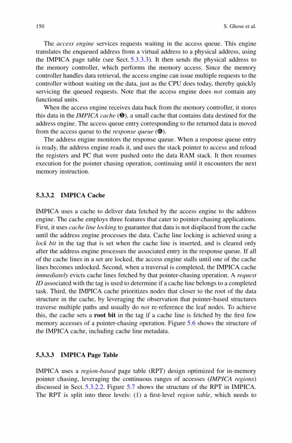
150 S. Ghose et al.
The access engine services requests waiting in the access queue. This enginetranslates the enqueued address from a virtual address to a physical address, usingthe IMPICA page table (see Sect. 5.3.3.3). It then sends the physical address tothe memory controller, which performs the memory access. Since the memorycontroller handles data retrieval, the access engine can issue multiple requests to thecontroller without waiting on the data, just as the CPU does today, thereby quicklyservicing the queued requests. Note that the access engine does not contain anyfunctional units.
When the access engine receives data back from the memory controller, it storesthis data in the IMPICA cache (❺), a small cache that contains data destined for theaddress engine. The access queue entry corresponding to the returned data is movedfrom the access queue to the response queue (❻).
The address engine monitors the response queue. When a response queue entryis ready, the address engine reads it, and uses the stack pointer to access and reloadthe registers and PC that were pushed onto the data RAM stack. It then resumesexecution for the pointer chasing operation, continuing until it encounters the nextmemory instruction.
5.3.3.2 IMPICA Cache
IMPICA uses a cache to deliver data fetched by the access engine to the addressengine. The cache employs three features that cater to pointer-chasing applications.First, it uses cache line locking to guarantee that data is not displaced from the cacheuntil the address engine processes the data. Cache line locking is achieved using alock bit in the tag that is set when the cache line is inserted, and is cleared onlyafter the address engine processes the associated entry in the response queue. If allof the cache lines in a set are locked, the access engine stalls until one of the cachelines becomes unlocked. Second, when a traversal is completed, the IMPICA cacheimmediately evicts cache lines fetched by that pointer-chasing operation. A requestID associated with the tag is used to determine if a cache line belongs to a completedtask. Third, the IMPICA cache prioritizes nodes that closer to the root of the datastructure in the cache, by leveraging the observation that pointer-based structurestraverse multiple paths and usually do not re-reference the leaf nodes. To achievethis, the cache sets a root bit in the tag if a cache line is fetched by the first fewmemory accesses of a pointer-chasing operation. Figure 5.6 shows the structure ofthe IMPICA cache, including cache line metadata.
5.3.3.3 IMPICA Page Table
IMPICA uses a region-based page table (RPT) design optimized for in-memorypointer chasing, leveraging the continuous ranges of accesses (IMPICA regions)discussed in Sect. 5.3.2.2. Figure 5.7 shows the structure of the RPT in IMPICA.The RPT is split into three levels: (1) a first-level region table, which needs to

5 The Processing-in-Memory Paradigm: Mechanisms to Enable Adoption 151
Fig. 5.6 Structure of theIMPICA cache Cache Tag Cache Data
Cache Tag Cache Data
Cache Tag Cache Data
...
...
Address Tag D V
Dirty Bit Valid Bit Request ID Lock Bit Root Bit
L RRID
Virtual Address Space
IMPICARegion
IMPICARegion
Region Address Flat Table AddressRegion Address
--Flat Table Address
--
Bit [47:41] Bit [40:21] Bit [20:12] Bit [11:0]
-- --
1100
Virtual Address
=
valid
Flat 2MBPage Table + 4KB
Page Table +
Physical Address
29 entries220 entries
+
❶
❷ ❸❹
Region Table
Region-Based Page Table
Fig. 5.7 IMPICA virtual memory architecture. Figure adapted from [67]
map only a small number of the contiguously allocated IMPICA regions; (2) asecond-level flat page table for each region with a larger (e.g., 2 MB) page size; and(3) third-level small page tables that use conventional small (e.g., 4 kB) pages. Inthe example in Fig. 5.7, when a 48-bit virtual memory address arrives for translation,bits 47–41 of the address are used to index the region table (❶ in Fig. 5.7) to find thecorresponding flat page table. Bits 40–21 are used to index the flat page table (❷),providing the location of the small page table, which is indexed using bits 20–12(❸). The entry in the small page table provides the physical page number of thepage, and bits 11–0 specify the offset within the physical page (❹).
The RPT is optimized to take advantage of the properties of pointer chasing. Theregion table is almost always cached in the IMPICA cache, as the total number ofIMPICA regions is small, requiring small storage (e.g., a 4-entry region table needsonly 68 B of cache space). We employ a flat table with large (e.g., 2 MB) pages at thesecond level in order to reduce the number of page misses, though this requires morememory capacity than the conventional 4-level page table structure. As the numberof regions touched by the accelerator is limited, this additional capacity overheadremains constrained. Our page table can optionally use traditional smaller pagesizes to maximize memory management flexibility. The OS can freely choose large

152 S. Ghose et al.
(2 MB) pages or small (4 kB) pages at the last level. Thanks to this design, a pagewalk in the RPT usually results in only two misses, one for the flat page table andthe other for the last-level small page table. This represents a 2× improvement overa conventional four-level page table, while our flattened page table still providescoverage for a 2 TB memory range. The size of the IMPICA region is configurableand can be increased to cover more virtual address space. We believe that our RPTdesign is general enough for use in a variety of in-memory accelerators that operateon a specific range of memory regions.
We discuss how the OS manages the IMPICA RPT in Sect. 5.3.4.3.
5.3.4 Interface and Design Considerations
In this section, we discuss how we expose IMPICA to the CPU and the operatingsystem (OS). Section 5.3.4.1 describes the communication interface between theCPU and IMPICA. Section 5.3.4.3 discusses how the OS manages the page tablesin IMPICA. In Sect. 5.3.4.4, we discuss how cache coherence is maintained betweenthe CPU and IMPICA caches.
5.3.4.1 CPU Interface and Communication Model
We use a packet-based interface between the CPU and IMPICA. Instead of com-municating individual operations or operands, the packet-based interface buffersrequests and sends them in a burst to minimize the communication overhead.Executing a function in IMPICA consists of four steps on the interface. (1) The CPUsends to memory a packet comprising the function call and parameters. (2) Thispacket is written to a specific location in memory, which is memory-mapped tothe data RAM in IMPICA and triggers IMPICA execution. (3) IMPICA loadsthe specific function into the instruction RAM with appropriate parameters, byreading the values from predefined memory locations. (4) Once IMPICA finishes thefunction execution, it writes the return value back to the memory-mapped locationsin the data RAM. The CPU periodically polls these locations and receives theIMPICA output. Note that the IMPICA interface is similar to the interface proposedfor the Hybrid Memory Cube (HMC) [2, 71, 72].
5.3.4.2 IMPICA Programming Model
The programming model for IMPICA is similar to the CPU programming model.An IMPICA program can be written in C with a new API that handles passing theparameters and returning the results to the IMPICA accelerator. Figure 5.8a showsthe pseudocode for a B-tree traversal in the CPU, and Fig. 5.8b shows the equivalentpseudocode for IMPICA. We observe that the code fragments are very similar,

5 The Processing-in-Memory Paradigm: Mechanisms to Enable Adoption 153
1 2
(a) Conventional B-tree traversal pseudocode
bt_node *find_leaf(bt_node *root, uint64_t key){
bt_node *c = root;uint64_t = i;while (!c->is_leaf) {
for (i = 0; i < c->num_keys; i++) {if (key < c->keys[i])
break;}c = c->pointers[i];
}return c;
}
void pica_find_leaf()bt_node *c = __param(ROOT);uint64_t key = __param(KEY);uint64_t i;while (!c->is_leaf) {
for (i = 0; i < c->num_keys; i++) {if (key < c->keys[i])
break;}c = c->pointers[i];
}__param(RESULT) = c;
}
Get parameterswith special API
Write resultswith special API
(b) B-tree traversal pseudocode in IMPICA
Fig. 5.8 B-tree traversal pseudocode demonstrating the differences between the (a) conventionaland (b) IMPICA programming models
differing in only two places. First, the parameters passed in the function call ofthe CPU code are accessed with the __param API call in IMPICA (❶ in Fig. 5.8).The __param API call ensures that the program explicitly reads the parametersfrom the predefined memory-mapped locations of the data RAM. Second, insteadof using the return statement, IMPICA uses the same __param API call to writethe return value to a specific memory location (❷). This API call makes sure thatthe CPU can receive the output through the IMPICA interface.

154 S. Ghose et al.
5.3.4.3 Page Table Management
In order for the RPT to identify IMPICA regions, the regions must be tagged bythe application. For this, the application uses a special API to allocate pointer-based data structures. This API allocates memory to a contiguous virtual addressspace. To ensure that all API allocations are contiguous, the OS reserves a portionof the unused virtual address space for IMPICA, and always allocates memory forIMPICA regions from this portion. The use of such a special API requires minimalchanges to applications, and it allows the system to provide more efficient virtualaddress translation. This also allows us to ensure that when multiple memory stacksare present within the system, the OS can allocate all IMPICA regions belonging toa single application (along with the associated IMPICA page table) into one memorystack, thereby avoiding the need for the accelerator to communicate with a remotememory stack.
The OS maintains coherence between the IMPICA RPT and the CPU page table.When memory is allocated in the IMPICA region, the OS allocates the IMPICApage table. The OS also shoots down TLB entries in IMPICA if the CPU performsany updates to IMPICA regions. While this makes the OS page fault handler morecomplex, the additional complexity does not cause a noticeable performance impact,as page faults occur rarely and take a long time to service in the CPU.
5.3.4.4 Cache Coherence
Coherence must be maintained between the CPU and IMPICA caches, and withmemory, to avoid using stale data and thus ensure correct execution. We maintaincoherence by executing every function that operates on the IMPICA regions in theaccelerator. This solution guarantees that no data is shared between the CPU andIMPICA, and that IMPICA always works on up-to-date data. Other PIM coherencesolutions (e.g., LazyPIM in Sect. 5.4, or those proposed by prior works [3, 52]) canalso be used to allow the CPU to update the linked data structures, but we choosenot to employ these solutions in our evaluation, as our workloads do not performany such updates.
5.3.4.5 Handling Multiple Memory Stacks
Many systems need to employ multiple memory stacks to have enough memorycapacity, as the current die-stacking technology can integrate only a limited numberof DRAM dies into a single memory stack [145]. In systems that use multiplememory stacks, the efficiency of an in-memory accelerator such as IMPICA couldbe significantly degraded whenever the data that the accelerator accesses is placedon different memory stacks. Without any modifications, IMPICA would have to gothrough the off-chip memory channels to access the data, which would effectivelyeliminate the benefits of in-memory computation.

5 The Processing-in-Memory Paradigm: Mechanisms to Enable Adoption 155
Table 5.1 Major simulation parameters used for IMPICA evaluations
Baseline main processor (CPU)
ISA ARMv8 (64-bits)
Core configuration 4 OoO cores, 2 GHz, 8-wide issue, 128-entry ROB
Operating system 64-bit Linux from Linaro [127]
L1 I/D cache 32 kB/2-way each, 2-cycle
L2 cache 1 MB/8-way, shared, 20-cycle
Baseline main memory parameters
Memory configuration DDR3-1600, 8 banks/device, FR-FCFS scheduler [182, 249]
DRAM bus bandwidth 12.8 GB/s for CPU, 51.2 GB/s for IMPICA
IMPICA accelerator
Accelerator core 500 MHz, 16 entries for each queue
Cachea 32 kB/2-way
Address translator 32 TLB entries with region-based page table
RAM 16 kB data RAM and 16 kB instruction RAMaBased on our experiments on a real Intel Xeon machine, we find that this is large enough tosatisfactorily represent the behavior of 1,000,000 transactions
Fortunately, this challenge can be tackled with our proposed modifications tothe operating system (OS) in Sect. 5.3.4.3. As we can identify the memory regionsthat IMPICA needs to access, the OS can easily map all IMPICA regions of anapplication into the same memory stack. In addition, the OS can allocate all IMPICApage tables into the same memory stack. This ensures that an IMPICA acceleratorcan access all of that data that it needs from within the memory stack that it residesin without incurring any additional hardware cost or latency overhead.
5.3.5 Evaluation Methodology for IMPICA
We use the gem5 [18] full-system simulator with DRAMSim2 [185] to evaluate ourproposed design. We choose the 64-bit ARMv8 architecture, the accuracy of whichhas been validated against real hardware [60]. We conservatively model the internalmemory bandwidth of the memory stack to be 4× that of the external bandwidth,similar to the configuration used in prior works [47, 243]. Our simulation parametersare summarized in Table 5.1. Our source code is available openly at our researchgroup’s GitHub site [188, 190]. This distribution includes the source code of ourmicrobenchmarks as well.
5.3.5.1 Workloads
We use three data-intensive microbenchmarks, which are essential building blocksin a wide range of workloads, to evaluate the native performance of pointer-chasing

156 S. Ghose et al.
operations: linked lists, hash tables, and B-trees. We also evaluate the performanceimprovement in a real data-intensive workload, measuring the transaction latencyand transaction throughput of DBx1000 [241], an in-memory OLTP database. Wemodify all four workloads to offload each pointer chasing request to IMPICA. Tominimize communication overhead, we map the IMPICA registers to user modeaddress space, thereby avoiding the need for costly kernel code intervention.
Linked List We use the linked list traversal microbenchmark [247] derived fromthe health workload in the Olden benchmark suite [184]. The parameters areconfigured to approximate the performance of the health workload. We measurethe performance of the linked list traversal after 30,000 iterations.
Hash Table We create a microbenchmark from the hash table implementationof Memcached [50]. The hash table in Memcached resolves hash collisions usingchaining via linked lists. When there are more than 1.5n items in a table of n buckets,it doubles the number of buckets. We follow this rule by inserting 1.5 × 220 randomkeys into a hash table with 220 buckets. We run evaluations for 100,000 random keylook-ups.
B-Tree We use the B-tree implementation of DBx1000 for our B-tree microbench-mark. It is a 16-way B-tree that uses a 64-bit integer as the key of each node.We randomly generate 3,000,000 keys and insert them into the B-tree. After theinsertions, we measure the performance of the B-tree traversal with 100,000 randomkeys. This is the most time-consuming operation in the database index lookup.
DBx1000 We run DBx1000 [241] with the TPC-C benchmark [223]. We set upthe TPC-C tables with 2000 customers and 100,000 items. For each run, we spawnfour threads and bind them to four different CPUs to achieve maximum throughput.We run each thread for a warm-up period for the duration of 2000 transactions, andthen record the software and hardware statistics for the next 5000 transactions perthread,2 which takes 300–500 million CPU cycles.
5.3.5.2 Die Area and Energy Estimation
We estimate the die area of the IMPICA processing logic at the 40 nm processnode based on recently published work [134]. We include the most importantcomponents: processor cores, L1/L2 caches, and the memory controller. We usethe area of ARM Cortex-A57 [7, 49], a small embedded processor, for the baselinemain CPU. We conservatively estimate the die area of IMPICA using the area ofthe Cortex-R4 [8], an 8-stage dual issue RISC processor with 32 kB I/D caches.We believe the actual area of an optimized IMPICA design can be much smaller.Table 5.2 lists the area estimate of each component.
2We sweep the size of the IMPICA cache from 32 to 128 kB, and find that it has negligible effecton our results.

5 The Processing-in-Memory Paradigm: Mechanisms to Enable Adoption 157
Table 5.2 Die area estimates using a 40 nm process for IMPICA evaluations
Baseline CPU core (Cortex-A57) 5.85 mm2 per core
L2 cache 5 mm2 per MB
Memory controller 10 mm2
Complete baseline chip 38.4 mm2
IMPICA Core (including 32 kB I/D caches) 0.45 mm2 (1.2% of the baseline chip area)
IMPICA comprises only 7.6% the area of a single baseline main CPU core,or only 1.2% the total area of the baseline chip (which includes four CPU cores,1 MB L2 cache, and one memory controller). Note that we conservatively modelIMPICA as a RISC core. A much more specialized engine can be designed forIMPICA to solely execute pointer chasing code. Doing so would reduce the area andenergy overheads of IMPICA greatly, but can reduce the generality of the pointerchasing access patterns that IMPICA can accelerate. We leave such optimizations,evaluations, and analyses for future work.
We use McPAT [122] to estimate the energy consumption of the CPU, caches,memory controllers, and IMPICA. We conservatively use the configuration of theCortex-R4 to estimate the energy consumed by IMPICA. We use DRAMSim2 [185]to analyze DRAM energy.
5.3.6 Evaluation of IMPICA
We first evaluate the effect of IMPICA on system performance, using both ourmicrobenchmarks (Sect. 5.3.6.1) and the DBx1000 database (Sect. 5.3.6.2). Weinvestigate the impact of different IMPICA page table designs in Sect. 5.3.6.3,and examine system energy consumption in Sect. 5.3.6.4. We compare a systemcontaining IMPICA to an accelerator-free baseline that includes an additional128 kB of L2 cache (which is equivalent to the area of IMPICA) to ensure area-equivalence across evaluated systems.
5.3.6.1 Microbenchmark Performance
Figure 5.9 shows the speedup of IMPICA and the baseline with extra 128 kB ofL2 cache over the baseline for each microbenchmark. IMPICA achieves significantspeedups across all three data structures—1.92× for the linked list, 1.29× for thehash table, and 1.18× for the B-tree. In contrast, the extra 128 kB of L2 cacheprovides very small speedup (1.03×, 1.01×, and 1.02×, respectively). We concludethat IMPICA is much more effective than the area-equivalent additional L2 cachefor pointer chasing operations.

158 S. Ghose et al.
0.00.51.01.52.0
Linked List Hash Table B-Tree
Spee
dup
Baseline + Extra 128KB L2 IMPICA
Fig. 5.9 Microbenchmark performance with IMPICA. Figure adapted from [67]
To provide insight into why IMPICA improves performance, we present total(i.e., combined CPU and IMPICA) TLB misses per kilo instructions (MPKI), cachemiss latency, and total memory bandwidth usage for these microbenchmarks inFig. 5.10. We make three observations.
First, a major factor contributing to the performance improvement is the reduc-tion in TLB misses. The TLB MPKI in Fig. 5.10a depicts the total (i.e., combinedCPU and IMPICA) TLB misses in both the baseline system and IMPICA. Thepointer chasing operations have low locality and pollute the CPU TLB. This leads toa higher overall TLB miss rate in the application. With IMPICA, the pointer chasingoperations are offloaded to the accelerator. This reduces the pollution and contentionat the CPU TLB, reducing the overall number of TLB misses. The linked list hasa significantly higher TLB MPKI than the other data structures because linked listtraversal requires far fewer instructions in an iteration. It simply accesses the nextpointer, while a hash table or a B-tree traversal needs to compare the keys in thenode to determine the next step.
Second, we observe a significant reduction in last-level cache miss latencywith IMPICA. Figure 5.10b compares the average cache miss latency between thebaseline last-level cache and the IMPICA cache. On average, the cache miss latencyof IMPICA is only 60–70% of the baseline cache miss latency. This is becauseIMPICA leverages the faster and wider TSVs in 3D-stacked memory as opposed tothe narrow, high-latency DRAM interface used by the CPU.
Third, as Fig. 5.10c shows, IMPICA effectively utilizes the internal memorybandwidth of 3D-stacked memory, which is cheap and abundant. There are tworeasons for high bandwidth utilization: (1) IMPICA runs much faster than thebaseline so it generates more traffic within the same amount time; and (2) IMPICAalways accesses memory at a larger granularity, retrieving each full node in a linkeddata structure with a single memory request, while a CPU issues multiple requestsfor each node as it can fetch only one cache line at a time. The CPU can avoidusing some of its limited memory bandwidth by skipping some fields in the datastructure that are not needed for the current loop iteration. For example, some keysand pointers in a B-tree node can be skipped whenever a match is found. In contrast,IMPICA utilizes the wide internal bandwidth of 3D-stacked memory to retrieve afull node on each access.
We conclude that IMPICA is effective at significantly improving the performanceof important linked data structures.

5 The Processing-in-Memory Paradigm: Mechanisms to Enable Adoption 159
0.00
0.25
0.50
1.00
List
Base
line
+ Ex
tra
128K
B L2
IMPI
CA
050100
150
List
0.0
0.5
1.0
1.5
2.0
List
Fig
.5.1
0K
eyar
chite
ctur
alst
atis
tics
for
the
eval
uate
dm
icro
benc
hmar
ks.
Figu
read
apte
dfr
om[6
7].
(a)
Tota
lT
LB
mis
ses
per
kilo
-ins
truc
tion
(MPK
I).
(b)
Ave
rage
last
-lev
elca
che
mis
sla
tenc
y.(c
)To
talD
RA
Mm
emor
yba
ndw
idth
utili
zatio
n

160 S. Ghose et al.
0.951.001.051.101.151.20
Baseline + Extra 128KB L2
Baseline + Extra 1MB L2
IMPICA
Nor
mal
ized
Thro
ughp
ut
0.80
0.85
0.90
0.95
1.00
Baseline + Extra 128KB L2
Baseline + Extra 1MB L2
IMPICA
Nor
mal
ized
Late
ncy
Fig. 5.11 Performance results for DBx1000, normalized to the baseline. Figure adapted from [67].(a) Database transaction throughput. (b) Database transaction latency
5.3.6.2 Real Database Throughput and Latency
Figure 5.11 presents two key performance metrics for our evaluation of DBx1000:database throughput and database latency. Database throughput represents howmany transactions are completed within a certain period, while database latencyis the average time to complete a transaction. We normalize the results of threeconfigurations to the baseline. As mentioned earlier, the die area increase ofIMPICA is similar to a 128 kB cache. To understand the effect of additional LLCspace better, we also show the results of adding 1 MB of cache, which takes about8× the area of IMPICA, to the baseline. We make two observations from ouranalysis of DBx1000.
First, IMPICA improves the overall database throughput by 16% and reduces theaverage database transaction latency by 13%. The performance improvement is dueto three reasons: (1) database indexing becomes faster with IMPICA, (2) offloadingdatabase indexing to IMPICA reduces the TLB and cache contention due to pointerchasing in the CPU, and (3) the CPU can do other useful tasks in parallel whilewaiting for IMPICA. Note that our profiling results in Fig. 5.2 show that DBx1000spends 19% of its time on pointer chasing. Therefore, a 16% overall improvementis very close to the upper bound that any pointer chasing accelerator can achieve forthis database.
Second, IMPICA yields much higher database throughput than simply providingadditional cache capacity. IMPICA improves the database throughput by 16%, whilean extra 128 kB of cache (with a similar area overhead as IMPICA) does so by only2%, and an extra 1 MB of cache (8× the area of IMPICA) by only 5%.
We conclude that by accelerating the fundamental pointer chasing operation,IMPICA efficiently improves the performance of a sophisticated real data-intensiveworkload.
5.3.6.3 Sensitivity to the IMPICA TLB Size and Page Table Design
To understand the effect of different TLB sizes and page table designs in IMPICA,we evaluate the speedup in the amount of time spent on address translation forIMPICA when different IMPICA TLB sizes (32 and 64 entries) and accelerator page

5 The Processing-in-Memory Paradigm: Mechanisms to Enable Adoption 161
0.000.250.500.751.001.251.50
LinkedList
HashTable
B-Tree DBx1000Addr
ess T
rans
latio
nSp
eedu
p32-Entry TLB + 4-Level 64-Entry TLB + 4-Level 32-Entry TLB + RPT 64-Entry TLB + RPT
Fig. 5.12 Speedup of address translation with different TLB sizes and page table designs. Figureadapted from [67]
table structures (the baseline 4-level page table; and the region-based page table, orRPT) are used inside the accelerator. Figure 5.12 shows the speedup in addresstranslation time relative to IMPICA with a 32-entry TLB and the conventional 4-level page table. Two observations are in order.
First, the performance of IMPICA is largely unaffected from small changes inthe IMPICA TLB size. Doubling the IMPICA TLB entries from 32 to 64 barelyimproves the address translation time. This observation reflects the irregular natureof pointer chasing. Second, the benefit of the RPT is much more significant in asophisticated workload (DBx1000) than in microbenchmarks. This is because theworking set size of the microbenchmarks is much smaller than that of the databasesystem. When the working set is small, the operating system needs only a smallnumber of page table entries in the first and second levels of a traditional page table.These entries are used frequently, so they stay in the IMPICA cache much longer,reducing the address translation overhead. This caching benefit goes away with alarger working set, which would require a significantly larger TLB and IMPICAcache to reap locality benefits. The benefit of RPT is more significant in such a casebecause RPT does not rely on this caching effect. Its region table is always smallirrespective of the workload working set size and it has fewer page table levels.Thus, we conclude that RPT is a much more efficient and high-performance pagetable design for our IMPICA accelerator than conventional page table design.
5.3.6.4 Energy Efficiency
Figure 5.13 shows the system power and system energy consumption for themicrobenchmarks and DBx1000. We observe that the overall system powerincreases by 5.6% on average, due to the addition of IMPICA and higher utilizationof internal memory bandwidth. However, as IMPICA significantly reduces theexecution time of the evaluated workloads, the overall system energy consumptionreduces by 41%, 24%, and 10% for the microbenchmarks, and by 6% for DBx1000.We conclude that IMPICA is an energy-efficient accelerator for pointer chasing.

162 S. Ghose et al.
0.00.20.40.60.81.0
LinkedList
HashTable
B-Tree DBx1000
Nor
mal
ized
Syst
em E
nerg
y
Baseline + Extra 128KB L2 IMPICA
0.00.20.40.60.81.01.2
LinkedList
HashTable
B-Tree DBx1000
Nor
mal
ized
Syst
em P
ower
(a) (b)
Fig. 5.13 Effect of IMPICA on system power (a) and system energy consumption (b). Figure (b)adapted from [67]
5.3.7 Summary of IMPICA
We introduce the design and evaluation of an in-memory accelerator, calledIMPICA, for performing pointer chasing operations in 3D-stacked memory. Weidentify two major challenges in the design of such an in-memory accelerator: (1)the parallelism challenge and (2) the address translation challenge. We providenew solutions to these two challenges: (1) address-access decoupling solves theparallelism challenge by decoupling the address generation from memory accessesin pointer chasing operations and exploiting the idle time during memory accessesto execute multiple pointer chasing operations in parallel, and (2) the region-based page table in 3D-stacked memory solves the address translation challengeby tracking only those limited set of virtual memory regions that are accessedby pointer chasing operations. Our evaluations show that for both commonly-used linked data structures and a real database application, IMPICA significantlyimproves both performance and energy efficiency. We conclude that IMPICA isan efficient and effective accelerator design for pointer chasing. We also believethat the two challenges we identify (parallelism and address translation) exist invarious forms in other in-memory accelerators (e.g., for graph processing), and,therefore, our solutions to these challenges can be adapted for use by a broadclass of (in-memory) accelerators. We believe ample future work potential existson examining other solutions for these two challenges as well as our solutions forthem within the context of other in-memory accelerators, such as those described in[2, 22, 68, 96, 98, 195, 196, 200, 202]. We also believe that examining solutions likeIMPICA for other, non-in-memory accelerators is a promising direction to examine.
5.4 LazyPIM: An Efficient Cache Coherence Mechanism forProcessing-in-Memory
As discussed in Sect. 5.2.2, cache coherence is a major challenge for PIM archi-tectures, as traditional coherence cannot be performed along the off-chip memorychannel without potentially undoing the benefits of high-bandwidth and low-energy
5 The Processing-in-Memory Paradigm: Mechanisms to Enable Adoption 163
PIM execution. To work around the limitations presented by cache coherence, mostprior works assume a limited amount of sharing between the PIM kernels and theprocessor threads of an application. Thus, they sidestep coherence by employingsolutions that restrict PIM to execute on non-cacheable data (e.g., [2, 47, 51, 149,243]) or force processor cores to flush or not access any data that could potentiallybe used by PIM (e.g., [3, 4, 27, 47, 52, 59, 67, 68, 163, 172, 195, 196, 200, 202]).In fact, the IMPICA accelerator design, described in Sect. 5.3, falls into the lattercategory.
To understand the trade-offs that can occur by sidestepping coherence, weanalyze several data-intensive applications. We make two key observations basedon our analysis: (1) some portions of the applications are better suited for executionin processor threads, and these portions often concurrently access the same regionof data as the PIM kernels, leading to significant data sharing; and (2) poor handlingof coherence eliminates a significant portion of the performance benefits of PIM. Asa result, we find that a good coherence mechanism is required to ensure the correctexecution of the program while maintaining the benefits of PIM (see Sect. 5.4.2).Our goal in this section is to describe a cache coherence mechanism for PIMarchitectures that logically behaves like traditional coherence, but retains all of thebenefits of PIM.
To this end, we propose LazyPIM, a new cache coherence mechanism thatefficiently batches coherence messages sent by the PIM processing logic. DuringPIM kernel execution, a PIM core speculatively assumes that it has acquiredcoherence permissions without sending a coherence message, and maintains all dataupdates speculatively in its cache. Only when the kernel finishes execution, theprocessor receives compressed information from the PIM core, and checks if anycoherence conflicts occurred. If a conflict exists (see Sect. 5.4.3), the dirty cachelines in the processor are flushed, and the PIM core rolls back and re-executes thekernel. Our execution model for PIM processing logic is similar to chunk-basedexecution [24] (i.e., each batch of consecutive instructions executes atomically),which prior work has harnessed for various purposes [24, 38, 61, 161, 174, 192].Unlike past works, however, the processor in LazyPIM executes conventionally andnever rolls back, which can make it easier to enable PIM.
We make the following key contributions in this section:
• We propose a new hardware coherence mechanism for PIM. Our approach(1) reduces the off-chip traffic between the PIM cores and the processor,(2) avoids the costly overheads of prior approaches to provide coherence for PIM,and (3) retains the same logical coherence behavior as architectures without PIMto keep programming simple.
• LazyPIM improves average performance by 49.1% (coming within 5.5% of anideal PIM mechanism), and reduces off-chip traffic by 58.8%, over the best priorcoherence approach.

164 S. Ghose et al.
5.4.1 Baseline PIM Architecture
In our evaluation, we assume that the compute units inside memory consist ofsimple in-order cores. These PIM cores, which are ISA-compatible with the out-of-order processor cores, are much weaker in terms of performance, as they lacklarge caches and sophisticated ILP techniques, but are more practical to implementwithin the DRAM logic layer, as we discussed earlier in Sect. 5.1.1. Each PIM corehas private L1 I/D caches, which are kept coherent using a MESI directory [23, 167]within the DRAM logic layer. A second directory in the processor acts as the maincoherence point for the system, interfacing with both the processor cache and thePIM coherence directory. Like prior PIM works [2–4, 47, 51, 68, 172], we assumethat direct segments [13] are used for PIM data, and that PIM kernels operate onlyon physical addresses.
5.4.2 Motivation for Coherence Support in PIM
Applications benefit the most from PIM execution when their memory-intensiveparts, which often exhibit poor locality and contribute to a large portion of executiontime, are dispatched to PIM processing logic. On the other hand, compute-intensiveparts or those parts that exhibit high locality must remain on the processor cores tomaximize performance [3, 68].
Prior work mostly assumes that there is only a limited amount of sharing betweenthe PIM kernels and the processor. However, this is not the case for many importantapplications, such as graph and database workloads. For example, in multithreadedgraph frameworks, each thread performs a graph algorithm (e.g., connected com-ponents, PageRank) on a shared graph [2, 209, 237]. We study a number of thesealgorithms [209], and find that (1) only certain portions of each algorithm are wellsuited for PIM, and (2) the PIM kernels and processor threads access the sharedgraph and intermediate data structures concurrently. Another example is modern in-memory databases that support Hybrid Transactional/Analytical Processing (HTAP)workloads [144, 193, 203, 219]. The analytical portions of these databases are wellsuited for PIM execution [99, 148, 234]. In contrast, even though transactionalqueries access the same data, they perform better if they are executed on the mainprocessor (i.e., the CPU), as they are short-lived and latency sensitive, accessingonly a few rows each. Thus, concurrent accesses from both PIM kernels (analytics)and processor threads (transactions) are inevitable.
The shared data needs to remain coherent between the processor and PIMcores. Traditional, or fine-grained, coherence protocols (e.g., MESI [23, 167]) haveseveral qualities well suited for pointer-intensive data structures, such as those ingraph workloads and databases. Fine-grained coherence allows the processor orPIM to acquire permissions for only the pieces of data that are actually accessed.In addition, fine-grained coherence can ease programmer effort when developing

5 The Processing-in-Memory Paradigm: Mechanisms to Enable Adoption 165
0.0
1.00.5
1.52.0
PageRank Radii Connected Components
PageRank Radii Connected Components
alletunGkoobecaF
Spee
dup
CPU-onlyFG
UCPUC l
CG
-oU-CPUC nlyFG
NC
mponentsnnected
mponentsnnected
FGCCGNNCIdeal-PIM
Fig. 5.14 PIM speedup with 16 threads, normalized to CPU-only, with three different and idealcoherence mechanisms. Figure adapted from [20]
PIM applications, as multithreaded programs already use this programming model.Unfortunately, if a PIM core participates in traditional coherence, it would haveto send a message for every cache miss to the processor over a narrow sharedinterconnect (we call this type of interconnect traffic as PIM coherence traffic).
We study four mechanisms to evaluate how coherence protocols impact PIM:(1) CPU-only, a baseline where PIM is disabled; (2) FG, fine-grained coherence,which is the MESI protocol, variants of which are employed in many state-of-the-art systems; (3) CG, coarse-grained lock based coherence, where PIM cores gainexclusive access to all PIM data during PIM kernel execution; and (4) NC, non-cacheable, where the PIM data is not cacheable in the CPU. We describe CG andNC in more detail below. Figure 5.14 shows the speedup of PIM with these fourmechanisms for certain graph workloads, normalized to CPU-only.3 To illustratethe impact of inefficient coherence mechanisms, we also show the performance ofan ideal mechanism where there is no performance penalty for coherence (Ideal-PIM). As shown in Fig. 5.14, employing PIM with a state-of-the-art fine-grainedcoherence (FG) mechanism always performs worse than CPU-only execution.
To reduce the impact of PIM coherence traffic, there are three general alternativesto fine-grained coherence for PIM execution: (1) coarse-grained coherence, (2)coarse-grained locks, and (3) making PIM data non-cacheable in the processor. Webriefly examine these alternatives.
Coarse-Grained Coherence One approach to reduce PIM coherence traffic is tomaintain a single coherence entry for all of the PIM data. Unfortunately, this canstill incur high overheads, as the processor must flush all of the dirty cache lineswithin the PIM data region every time the PIM core acquires permissions, even if thePIM kernel may not access most of the data. For example, with just four processorthreads, the number of cache lines flushed for PageRank is 227× the number of
166 S. Ghose et al.
lines actually required by the PIM kernel.3 Coherence at a smaller granularity, suchas page-granularity [52], does not cause flushes for pages not accessed by the PIMkernel. However, many data-intensive applications perform pointer chasing, wherea large number of pages are accessed non-sequentially, but only a few lines in eachpage are used, forcing the processor to flush every dirty page.
Coarse-Grained Locks Another drawback of coarse-grained coherence is thatdata can ping-pong between the processor and the PIM cores whenever the PIM dataregion is concurrently accessed by both. Coarse-grained locks avoid ping-pongingby having the PIM cores acquire exclusive access to a region for the duration ofthe PIM kernel. However, coarse-grained locks greatly restrict performance. Ourapplication study shows that PIM kernels and processor threads often work inparallel on the same data region, and coarse-grained locks frequently cause threadserialization. PIM with coarse-grained locks (CG in Fig. 5.14) performs 8.4% worse,on average, than CPU-only execution. We conclude that using coarse-grained locksis not suitable for many important applications for PIM execution.
Non-Cacheable PIM Data Another approach sidesteps coherence by marking thePIM data region as non-cacheable in the processor [2, 47, 51, 149, 243], so thatDRAM always contains up-to-date data. For applications where PIM data is almostexclusively accessed by the PIM processing logic, this incurs little penalty, butfor many applications, the processor also accesses PIM data often. For our graphapplications with a representative input (arXiV) (see footnote 3), the processorcores generate 42.6% of the total number of accesses to PIM data. With so manyprocessor accesses, making PIM data non-cacheable results in a high performanceand bandwidth overhead. As shown in Fig. 5.14, though marking PIM data asnon-cacheable (NC) sometimes performs better than CPU-only, it still loses up to62.7% (on average, 39.9%) of the improvement of Ideal-PIM. Therefore, while thisapproach avoids the overhead of coarse-grained mechanisms, it is a poor fit forapplications that rely on processor involvement, and thus restricts the applicationswhere PIM is effective.
We conclude that prior approaches to PIM coherence eliminate a significantportion of the benefits of PIM when data sharing occurs, due to their high coherenceoverheads. In fact, they sometimes cause PIM execution to consistently degradeperformance. Thus, an efficient alternative to fine-grained coherence is necessary toretain PIM benefits across a wide range of applications.
5.4.3 LazyPIM Mechanism for Efficient PIM Coherence
Our goal is to design a coherence mechanism that maintains the logical behaviorof traditional coherence while retaining the large performance benefits of PIM. To
3See Sect. 5.4.5 for our experimental evaluation methodology.

5 The Processing-in-Memory Paradigm: Mechanisms to Enable Adoption 167
this end, we propose LazyPIM, a new coherence mechanism that lets PIM kernelsspeculatively assume that they have the required permissions from the coherenceprotocol, without actually sending off-chip messages to the main (processor)coherence directory during execution. Instead, coherence states are updated onlyafter the PIM kernel completes, at which point the PIM core transmits a singlebatched coherence message (i.e., a compressed signature containing all addressesthat the PIM kernel read from or wrote to) back to the processor coherence directory.The directory checks to see whether any conflicts occurred. If a conflict exists, thePIM kernel rolls back its changes, conflicting cache lines are written back by theprocessor to DRAM, and the kernel re-executes. If no conflicts exist, speculativedata within the PIM core is committed, and the processor coherence directory isupdated to reflect the data held by the PIM core. Note that in LazyPIM, the processoralways executes non-speculatively, which ensures minimal changes to the processordesign, thereby likely enabling easier adoption of PIM.
LazyPIM avoids the pitfalls of the coherence mechanisms discussed in Sect. 5.4.2(FG, CG, NC). With its compressed signatures, LazyPIM causes much less PIMcoherence traffic than traditional fine-grained coherence. Unlike coarse-grainedcoherence and coarse-grained locks, LazyPIM checks coherence only after itcompletes PIM execution, avoiding the need to unnecessarily flush a large amountof data. Unlike non-cacheable, LazyPIM allows processor threads to cache the dataused by PIM kernels within the processor cores as well, avoiding the need for theprocessor to perform a large number of off-chip accesses that can hurt performancegreatly. LazyPIM also allows for efficient concurrent execution of processor threadsand PIM kernels: by executing speculatively, the PIM cores do not invoke coherencerequests during concurrent execution, avoiding data ping-ponging between the PIMcores and the processor.
Conflicts In LazyPIM, a PIM kernel speculatively assumes during execution thatit has coherence permissions on a cache line, without checking the processorcoherence directory. In the meantime, the processor continues to execute non-speculatively. To resolve PIM kernel speculation, LazyPIM provides coarse-grainedatomicity, where all PIM memory updates are treated as if they all occur at themoment that a PIM kernel finishes execution. (We explain how LazyPIM enablesthis in Sect. 5.4.4.) If, before the PIM kernel finishes, the processor updates a cacheline that the PIM kernel read during its execution, a conflict occurs. LazyPIM detectsand handles all potential conflicts once the PIM kernel finishes executing.
Figure 5.15 shows an example timeline where a PIM kernel is launched on PIMcore PIM0 while execution continues on processor cores CPU0 and CPU1. Due tothe use of coarse-grained atomicity, PIM kernel execution behaves as if the entirekernel’s memory accesses take place at the moment coherence is checked (i.e., atthe end of kernel execution), regardless of the actual time at which the kernel’saccesses are performed. Therefore, for every cache line read by PIM0, if CPU0or CPU1 modifies the line before the coherence check occurs, PIM0 unknowinglyuses stale data, leading to incorrect execution. Figure 5.15 shows two examples ofthis: (1) CPU0’s write to line C during kernel execution; and (2) CPU0’s write to

168 S. Ghose et al.
Fig. 5.15 Example timelineof LazyPIM coherencesequence. Figure reproducedfrom [20]
Wr(A)
Rd(A)Wr(C)
...
Wr(E)Rd(B)
...
Wr(A)
Wr(B)
Rd(A)Wr(D)
...
Wr(F)Rd(D)
...
Wr(D)
CPU0 CPU1 PIM0
Rd(C)Wr(B)Rd(A)
Rd(C)Wr(B)Rd(A)
(1) Send PIM kernel
(2) Send PIMReadSet
and PIMWriteSet(3) Roll back PIM,restart kernel
CONFLICT DETECTIONCPUs flush A, C
(4) Send PIMReadSet
and PIMWriteSet(5) Commit PIM data
CONFLICT DETECTIONno conflicts
line A before kernel execution, which was not written back to DRAM. To detect suchconflicts, we record the addresses of processor writes and PIM kernel reads into twosignatures, and then check to see if any addresses in them match (i.e., conflict) afterthe PIM kernel finishes (see Sect. 5.4.4.2).
If the PIM kernel writes to a cache line that is subsequently read by the processorbefore the kernel finishes (e.g., the second write by PIM0 to line B in Fig. 5.15),this is not a conflict. With coarse-grained atomicity, any read by the processorduring PIM execution is ordered before the PIM kernel’s write. LazyPIM ensuresthat the processor cannot read the PIM kernel’s writes, by marking the PIM kernelwrites as speculative inside the PIM processing logic until the kernel finishes (seeSect. 5.4.4.2). This is also the case when the processor and a PIM kernel write to thesame cache line. Note that this ordering does not violate consistency models, suchas sequential consistency.4
If the PIM kernel writes to a cache line that is subsequently written to by theprocessor before the kernel finishes, this is not a conflict. With coarse-grainedatomicity, any write by the processor during PIM kernel execution is ordered beforethe PIM core’s write since the PIM core write effectively takes place after the PIMkernel finishes. When the two writes modify different words in the same cache line,LazyPIM uses a per-word dirty bit mask in the PIM L1 cache to merge the writes,similar to prior work [108]. Note that the dirty bit mask is only in the PIM L1 cache;processor caches remain unchanged.
More details on the operation of the LazyPIM coherence mechanism are providedin our arXiv paper [21].
4A thorough treatment of memory consistency [106] is outside the scope of this work. Our goal isto deal with the coherence problem in PIM, not handle consistency issues.

5 The Processing-in-Memory Paradigm: Mechanisms to Enable Adoption 169
5.4.4 Architectural Support for LazyPIM
5.4.4.1 LazyPIM Programming Model
We provide a simple interface to port applications to LazyPIM. We show theimplementation of a simple LazyPIM kernel within a program in Code Example 5.1.The programmer selects the portion(s) of the code to execute on PIM cores, usingtwo macros (#PIM_begin and #PIM_end). The compiler converts the macrosinto instructions that we add to the ISA, which trigger and end PIM kernelexecution. LazyPIM also needs to know which parts of the allocated data mightbe accessed by the PIM cores, which we refer to as the PIM data region.5 Weassume that either the programmer or the compiler can annotate all of the PIM dataregion using compiler directives or a PIM memory allocation API (@PIM). Thisinformation is saved in the page table using per-page flag bits, via communicationto the system software using the system call interface.
Code Example 5.1 shows a portion of the compute function used by PageRank, asmodified for execution with LazyPIM. All of our modifications are shown in bold.In this example, we want to execute only the edgeMap() function (Line 13) on thePIM cores. To ensure that LazyPIM tracks all data accessed during the edgeMap()call, we mark all of this data using @PIM, including any objects passed by value(e.g., GA on Line 1), any objects allocated in the function (e.g., those on Lines 4–6), and any objects allocated during functions that are executed on the PIM cores(e.g., the PR_F<vertex> object on Line 13). To tell the compiler that we want toexecute only edgeMap() on the PIM cores, we surround it with the #PIM_beginand #PIM_end compiler directives on Lines 11 and 15, respectively. No othermodifications are needed to execute our example code with LazyPIM.
5.4.4.2 Speculative Execution
When an application reaches a PIM kernel trigger instruction, the processordispatches the kernel’s starting PC to a free PIM core. The PIM core checkpoints thestarting PC and registers, and starts executing the kernel. The kernel speculativelyassumes that it has coherence permissions for every line it accesses, without actuallychecking the processor directory. We add a one-bit flag to each line in the PIM corecache, to mark all data updates as speculative. If a speculative line is selected foreviction, the core rolls back to the starting PC and discards the updates.
LazyPIM tracks three sets of addresses during PIM kernel execution. These arerecorded into three signatures, as shown in Fig. 5.16: (1) the CPUWriteSet (allCPU writes to the PIM data region), (2) the PIMReadSet (all PIM reads), and
5The programmer should be conservative in identifying PIM data regions, and should not miss anypossible data that may be touched by a PIM core. If any data not marked as PIM data is accessedby the PIM core, the program can produce incorrect results.

170 S. Ghose et al.
1 PageRankCompute(@PIM Graph GA) { // GA is accessed by PIMcores in edgeMap()
2 const int n = GA.n; // not accessed by PIM cores3 const double damping = 0.85, epsilon = 0.0000001; // not
accessed by PIM cores4 @PIM double* p_curr, p_next; // accessed by PIM cores in
edgeMap()5 @PIM bool* frontier; // accessed by PIM cores in
edgeMap()6 @PIM vertexSubset Frontier(n, n, frontier); // accessed by
PIM in edgeMap()7 double L1_norm; // not accessed by PIM cores8 long iter = 0; // not accessed by PIM cores9 ...
10 while(iter++ < maxIters) {11 #PIM_begin12 // only the edgeMap() function is offloaded to the PIM
cores13 vertexSubset output =
edgeMap(GA, Frontier, @PIM PR_F<vertex>(p_curr,p_next, GA.V), 0);
14 // PR_F<vertex> object allocated during edgeMap() call,needs annotation
15 #PIM_end16 vertexMap(Frontier, PR_Vertex_F(p_curr, p_next, damping,
n)); // run on CPU1718 // compute L1-norm between p_curr and p_next19 L1_norm = fabs(p_curr - p_next); // run on CPU20 if(L1_norm < epsilon) break; // run on CPU21 ...22 }23 Frontier.del();24 }
Listing 5.1 Example PIM program implementation. Modifications for PIM execution are shownin bold
(3) the PIMWriteSet (all PIM writes). When the kernel starts, the dirty lines in theprocessor cache containing PIM data are recorded in the CPUWriteSet, by scanningthe tag store (potentially using a Dirty-Block Index [201]). The processor uses thepage table flag bits from Sect. 5.4.4.1 to identify which writes need to be addedto the CPUWriteSet during kernel execution. The PIMReadSet and PIMWriteSetare updated for every read and write performed by the PIM kernel. When thekernel finishes execution, the three signatures are used to resolve speculation (seeSect. 5.4.4.3)
The signatures use parallel Bloom filters [19], which employ simple Booleanlogic to hash multiple addresses into a single (256B) fixed-length register. If thespeculative coherence requests were sent back to the processor without any sort ofcompression at the end of PIM kernel execution, the coherence messages would still

5 The Processing-in-Memory Paradigm: Mechanisms to Enable Adoption 171
Processor
through-silicon via
Core 0
Core N
...
Shared Last-Level CacheConflict
Detect HW CPUWriteSet
PIM Core 0
L1 Cache
PIMWriteSetPIMReadSet
PIM Core M
L1 Cache
PIMWriteSetPIMReadSet
. . .
specula�vewrite bitsDRAM Logic Layer
DRAM Cell Layer
DRAM Cell Layer
Fig. 5.16 High-level additions (in bold) to PIM architecture to support LazyPIM. Figure adaptedfrom [20]
consume a large amount of off-chip traffic, nullifying most of the benefits of thespeculation. Bloom filters allow LazyPIM to compress these coherence messagesinto a much smaller size, while guaranteeing that there are no false negatives [19](i.e., no coherence messages are lost during compression). The addresses of all dataaccessed speculatively by the PIM cores can be extracted and compared from theBloom filter [19, 24]. The hashing introduces a limited number of false positives,with the false positive rate increasing as we store more addresses in a single fixed-length Bloom filter. In our evaluated system, each signature is 256B long, and canstore up to 607 addresses without exceeding a 20.0% false positive rate (with nofalse negatives). To store more addresses, we use multiple filters to guarantee anupper bound on the false positive rate.
5.4.4.3 Handling Conflicts
As Fig. 5.15 shows, we need to detect conflicts that occur during PIM kernelexecution. In LazyPIM, when the kernel finishes executing, both the PIMReadSetand PIMWriteSet are sent back to the processor.
If no matches are detected between the PIMReadSet and the CPUWriteSet (i.e.,no conflicts have occurred), PIM kernel commit starts. Any addresses (includingfalse positives) in the PIMWriteSet are invalidated from the processor cache. Amessage is then sent to the PIM core, allowing it to write its speculative cache linesback to DRAM. During the commit process, all coherence directory entries for thePIM data region are locked to ensure atomicity of commit. Finally, all signatures areerased.
If an overlap is found between the PIMReadSet and the CPUWriteSet, a conflictmay have occurred. At this point, only the dirty lines in the processor that matchin the PIMReadSet are flushed back to DRAM. During this flush, all PIM data

172 S. Ghose et al.
directory entries are locked to ensure atomicity. Once the flush completes, a messageis sent to the PIM core, telling it to invalidate all speculative cache lines, and to rollback the PC to the checkpointed value. Now that all possibly conflicting cache linesare written back to DRAM, all signatures are erased, and the PIM core restarts thekernel. After re-execution of the PIM kernel finishes, conflict detection is performedagain.
Note that during the commit process, processor cores do not stall unless theyaccess the same data accessed by PIM processing logic. LazyPIM guaranteesforward progress by acquiring a lock for each line in the PIMReadSet after anumber of rollbacks (we empirically set this number to three rollbacks). This simplemechanism ensures there is no livelock even if the sharing of speculative data amongPIM cores might create a cyclic dependency. Note that rollbacks are caused by CPUaccesses to conflicting addresses, and not by the sharing of speculative data betweenPIM cores. As a result, once we lock conflicting addresses following three rollbacks,the PIM cores will not roll back again as there will be no conflicts, guaranteeingforward progress.
5.4.4.4 Hardware Overhead
LazyPIM’s overhead consists mainly of (1) 1 bit per page (0.003% of DRAMcapacity) and 1 bit per TLB entry for the page table flag bits (Sect. 5.4.4.1); (2) a0.2% increase in PIM core L1 size to mark speculative data (Sect. 5.4.4.2); (3) a1.6% increase in PIM core L1 size for the dirty bit mask (Sect. 5.4.3); and (4) in theworst case, 12 kB for the signatures per PIM core (Sect. 5.4.4.2). This overhead canbe greatly optimized (as part of future work): for PIM kernels that need multiplesignatures, we could instead divide the kernel into smaller chunks where eachchunk’s addresses fit in a single signature, lowering signature overhead to 512B. Weleave a detailed evaluation of LazyPIM hardware overhead optimization to futurework. Some ideas related to this and a detailed hardware overhead analysis arepresented in our arXiv paper [21].
5.4.5 Methodology for LazyPIM Evaluation
We study two types of data-intensive applications: graph workloads and databases.We use three Ligra [209] graph applications (PageRank, Radii, Connected Com-ponents), with input graphs constructed from real-world network datasets [217]:Facebook, arXiV High Energy Physics Theory, and Gnutella25 (peer-to-peer). Wealso use an in-house prototype of a modern in-memory database (IMDB) [144, 193,203, 219] that supports HTAP workloads. Our transactional workload consists of200K transactions, each randomly performing reads or writes on a few randomlychosen tuples. Our analytical workload consists of 256 analytical queries that usethe select and join operations on randomly-chosen tables and columns.
PIM kernels are selected from these applications with the help of OProfile [165].We conservatively select candidate PIM kernels, choosing portions of functions

5 The Processing-in-Memory Paradigm: Mechanisms to Enable Adoption 173
Table 5.3 Evaluated system configuration for LazyPIM evaluation
Main processor (CPU)
ISA x86-64
Core configuration 4–16 cores, 2 GHz, 8-wide issue
Operating system 64-bit Linux from Linaro [127]
L1 I/D cache 64 kB per core, private, 4-way associative, 64B blocks, 2-cycle lookup
L2 cache 2 MB, shared, 8-way associative, 64B blocks, 20-cycle lookup
Cache coherence MESI directory [23, 167]
PIM cores
ISA x86-64
Core configuration 4–16 cores, 2 GHz, 1-wide issue
L1 I/D cache 64 kB per core, private, 4-way associative, 64B blocks, 2-cycle lookup
Cache coherence MESI directory [23, 167]
Main memory parameters
Memory configuration HMC 2.0 [72], one 4 GB cube, 16 vaults per cube, 16 banks per vault,
FR-FCFS scheduler [182, 249]
where the application (1) spends the majority of its cycles, and (2) generates themajority of its last-level cache misses. From these candidates, we pick kernelsthat we believe minimize the coherence overhead for each evaluated mechanism,by minimizing data sharing between the processor and PIM processing logic. Wemodify each application to ship the selected PIM kernels to the PIM cores. Wemanually annotate the PIM data set.
For our evaluations, we modify the gem5 simulator [18]. We use the x86-64architecture in full-system mode, and use DRAMSim2 [185] to perform detailedtiming simulation of DRAM. Table 5.3 shows our system configuration.
5.4.6 Evaluation of LazyPIM
We first analyze the off-chip traffic reduction of LazyPIM. This off-chip reductionleads to bandwidth and energy savings. We then analyze LazyPIM’s effect on systemperformance. We show system performance results normalized to a processor-only baseline (CPU-only, as defined in Sect. 5.4.2), and compare LazyPIM’sperformance with using fine-grained coherence (FG), coarse-grained locks (CG),or non-cacheable data (NC) for PIM data.
5.4.6.1 Off-Chip Memory Traffic
Figure 5.17a shows the normalized off-chip memory traffic of the PIM coherencemechanisms for a 16-core architecture (with 16 processor cores and 16 PIM cores)Fig. 5.17b shows the normalized off-chip memory traffic as the number of threads

174 S. Ghose et al.
0.0
0.5
1.0
1.5
2.0
0.0
0.5
1.0
1.5
2.0
2.5
48
16N
umbe
r of T
hrea
ds
CPU
-onl
yFG
CGN
CLa
zyPI
M
Fig
.5.1
7E
ffec
tof
Laz
yPIM
onof
f-ch
ipm
emor
ytr
affic
,no
rmal
ized
toC
PU-o
nly.
Figu
read
apte
dfr
om[2
0].
(a)
16-T
hrea
dof
f-ch
ipm
emor
ytr
affic
.(b
)O
ff-c
hip
mem
ory
traf
ficse
nsiti
vity
toth
read
coun
tfor
Page
Ran
k
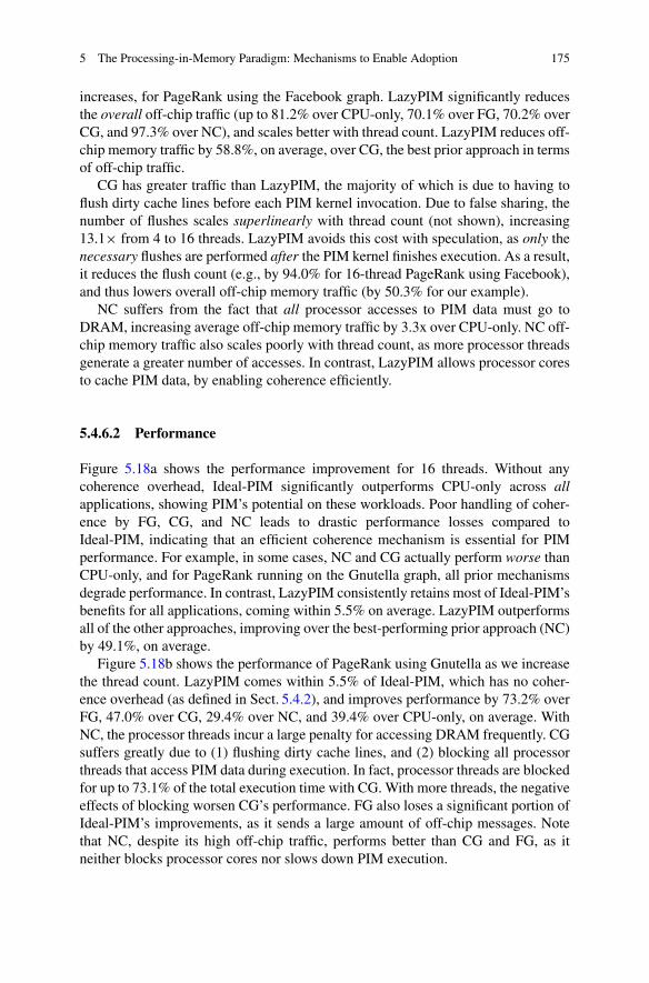
5 The Processing-in-Memory Paradigm: Mechanisms to Enable Adoption 175
increases, for PageRank using the Facebook graph. LazyPIM significantly reducesthe overall off-chip traffic (up to 81.2% over CPU-only, 70.1% over FG, 70.2% overCG, and 97.3% over NC), and scales better with thread count. LazyPIM reduces off-chip memory traffic by 58.8%, on average, over CG, the best prior approach in termsof off-chip traffic.
CG has greater traffic than LazyPIM, the majority of which is due to having toflush dirty cache lines before each PIM kernel invocation. Due to false sharing, thenumber of flushes scales superlinearly with thread count (not shown), increasing13.1× from 4 to 16 threads. LazyPIM avoids this cost with speculation, as only thenecessary flushes are performed after the PIM kernel finishes execution. As a result,it reduces the flush count (e.g., by 94.0% for 16-thread PageRank using Facebook),and thus lowers overall off-chip memory traffic (by 50.3% for our example).
NC suffers from the fact that all processor accesses to PIM data must go toDRAM, increasing average off-chip memory traffic by 3.3x over CPU-only. NC off-chip memory traffic also scales poorly with thread count, as more processor threadsgenerate a greater number of accesses. In contrast, LazyPIM allows processor coresto cache PIM data, by enabling coherence efficiently.
5.4.6.2 Performance
Figure 5.18a shows the performance improvement for 16 threads. Without anycoherence overhead, Ideal-PIM significantly outperforms CPU-only across allapplications, showing PIM’s potential on these workloads. Poor handling of coher-ence by FG, CG, and NC leads to drastic performance losses compared toIdeal-PIM, indicating that an efficient coherence mechanism is essential for PIMperformance. For example, in some cases, NC and CG actually perform worse thanCPU-only, and for PageRank running on the Gnutella graph, all prior mechanismsdegrade performance. In contrast, LazyPIM consistently retains most of Ideal-PIM’sbenefits for all applications, coming within 5.5% on average. LazyPIM outperformsall of the other approaches, improving over the best-performing prior approach (NC)by 49.1%, on average.
Figure 5.18b shows the performance of PageRank using Gnutella as we increasethe thread count. LazyPIM comes within 5.5% of Ideal-PIM, which has no coher-ence overhead (as defined in Sect. 5.4.2), and improves performance by 73.2% overFG, 47.0% over CG, 29.4% over NC, and 39.4% over CPU-only, on average. WithNC, the processor threads incur a large penalty for accessing DRAM frequently. CGsuffers greatly due to (1) flushing dirty cache lines, and (2) blocking all processorthreads that access PIM data during execution. In fact, processor threads are blockedfor up to 73.1% of the total execution time with CG. With more threads, the negativeeffects of blocking worsen CG’s performance. FG also loses a significant portion ofIdeal-PIM’s improvements, as it sends a large amount of off-chip messages. Notethat NC, despite its high off-chip traffic, performs better than CG and FG, as itneither blocks processor cores nor slows down PIM execution.

176 S. Ghose et al.
0.0
0.5
1.0
1.5
2.0Sp
eedu
p
0.0
0.5
1.0
1.5
2.0
4 8 16
Spee
dup
Number of Threads
CPU-only FG CGNC LazyPIM Ideal-PIM
Fig. 5.18 Speedup of cache coherence mechanisms, normalized to CPU-only. Figure adaptedfrom [20]. (a) Speedup for all applications with 16 threads. (b) Speedup sensitivity to thread countfor Gnutella
One reason for the difference in performance between LazyPIM and Ideal-PIMis the number of conflicts that are detected at the end of PIM kernel execution. Aswe discuss in Sect. 5.4.4.3, any detected conflict causes a rollback, where the PIMkernel must be re-executed. We study the number of commits that contain conflictsfor two representative 16-thread workloads: Components using the Enron graph,and HTAP-128 (results not shown). If we study an idealized version of full kernelcommit, where no false positives exist, we find that a relatively high percentage ofcommits contain conflicts (47.1% for Components and 21.3% for HTAP). Usingrealistic signatures for full kernel commit, which includes the impact of falsepositives, the conflict rate increases to 67.8% for Components and 37.8% for HTAP.Despite the high number of commits that induce rollback, the overall performanceimpact of rollback is low, as LazyPIM comes within 5.5% of the performance ofIdeal-PIM. We find that for all of our applications, a kernel never rolls back morethan once, limiting the performance impact of conflicts. We can further improve theperformance of LazyPIM by optimizing the commit process to reduce the rollbackoverhead, which we explore in our arXiv paper [21].
5.4.7 Summary of LazyPIM
We propose LazyPIM, a new cache coherence mechanism for PIM architectures.Prior approaches to PIM coherence generate very high off-chip traffic for importantdata-intensive applications. LazyPIM avoids this by avoiding coherence lookupsduring PIM kernel execution. The key idea is to use compressed coherencesignatures to batch the lookups and verify correctness after the kernel completes.As a result of the more efficient approach to coherence employed by LazyPIM,applications that performed poorly under prior approaches to PIM coherence cannow take advantage of the benefits of PIM execution. LazyPIM improves averageperformance by 49.1% (coming within 5.5% of an ideal PIM mechanism), andreduces off-chip traffic by 58.8%, over the best prior approach to PIM coherencewhile retaining the conventional multithreaded programming model.

5 The Processing-in-Memory Paradigm: Mechanisms to Enable Adoption 177
5.5 Related Work
We briefly survey related work in processing-in-memory, accelerator design, mech-anisms for handling pointer chasing, and techniques for pointer chasing.
Early Processing-in-Memory (PIM) Proposals Early proposals for PIM archi-tectures had limited to no adoption, as the proposed logic integration was too costlyand did not solve many of the obstacles facing the adoption of PIM. The earliestsuch proposals date from the 1970s, where small processing elements are combinedwith small amounts of RAM to provide a distributed array of memories that performcomputation [208, 218]. Some of the other early works, such as EXECUBE [100],Terasys [56], IRAM [171], and Computational RAM [44, 45], add logic withinDRAM to perform vector operations. Yet other early works, such as FlexRAM [80],DIVA [39], Smart Memories [140], and Active Pages [166], propose more versatilesubstrates that tightly integrate logic and reconfigurability within DRAM itself toincrease flexibility and the available compute power.
Processing in 3D-Stacked Memory With the advent of 3D-stacked memories,we have seen a resurgence of PIM proposals [133, 199]. Recent PIM proposalsadd compute units within the logic layer to exploit the high bandwidth available.These works primarily focus on the design of the underlying logic that is placedwithin memory, and in many cases propose special-purpose PIM architecturesthat cater only to a limited set of applications. These works include acceleratorsfor MapReduce [176], matrix multiplication [246], data reorganization [4], graphprocessing [2, 163], databases [12], in-memory analytics [52], genome sequenc-ing [96, 98], data-intensive processing [58], consumer device workloads [22], andmachine learning workloads [30, 93, 118]. Some works propose more genericarchitectures by adding PIM-enabled instructions [3], GPGPUs [68, 172, 243],single-instruction multiple-data (SIMD) processing units [149], or reconfigurablehardware [47, 51, 59] to memory.
Processing Using Memory A number of recent works have examined how toperform memory operations directly within the memory array itself, which werefer to as processing using memory [199]. These works take advantage of inherentarchitectural properties of memory devices to perform operations in bulk. Whilesuch works can significantly improve computational efficiency within memory, theystill suffer from many of the same programmability and adoption challenges thatPIM architectures face, such as the address translation and cache coherence chal-lenges that we focus on in this chapter. Mechanisms for processing using memorycan perform a variety of functions, such as bulk copy and data initialization forDRAM [27, 28, 197, 200], bulk bitwise operations for DRAM [124, 195, 196, 202]and phase-change memory (PCM) [123], and simple arithmetic operations forSRAM [1, 81] and memristors [103–105, 121, 205].

178 S. Ghose et al.
Processing in the DRAM Module or Memory Controller Several works haveexamined how to embed processing functionality near memory, but not within theDRAM chip itself. Such an approach can reduce the cost of PIM manufacturing,as the DRAM chip does not need to be modified or specialized for any particularfunctionality. However, these works (1) are often unable to take advantage of thehigh internal bandwidth of 3D-stacked DRAM, which reduces the efficiency ofPIM execution, and (2) may still suffer from many of the same challenges facedby architectures that embed logic within the DRAM chip. Examples of this workinclude Chameleon [9], which proposes a method of integrating logic within theDRAM module but outside of the chip to reduce manufacturing costs, Gather-Scatter DRAM [203], which embeds logic within the memory controller to remap asingle memory request across multiple rows and columns within DRAM, and workby Hashemi et al. [62, 63] to embed logic in the memory controller that acceleratesdependent cache misses and performs runahead execution [153, 154, 156, 158].
Addressing Challenges to PIM Adoption Recent work has examined designchallenges for systems with PIM support that can affect PIM adoption. A numberof these works improve PIM programmability, such as LazyPIM [20, 21], whichprovides efficient cache coherence support for PIM (as we described in detail inSect. 5.4) the study by Sura et al. [221], which optimizes how programs accessPIM data, and work by Liu et al. [131], which designs PIM-specific concurrentdata structures to improve PIM performance. Other works tackle hardware-leveldesign challenges, including IMPICA [67], which introduces in-memory supportfor address translation and pointer chasing (as we described in detail in Sect. 5.3),work by Hassan et al. [64] to optimize the 3D-stacked DRAM architecture for PIM,and work by Kim et al. [95] to enable the distribution of PIM data across multiplememory stacks.
Coherence for PIM Architectures In order to avoid the overheads of fine-grainedcoherence, many prior works on PIM architectures design their systems in sucha way that they do not need to utilize traditional coherence protocols. Instead,these works use one of two alternatives. Some works restrict PIM processing logicto execute on only non-cacheable data (e.g., [2, 47, 51, 149, 243]), which forcescores within the CPU to read PIM data directly from DRAM. Other works usecoarse-grained coherence or coarse-grained locks, which force processor cores tonot access any data that could potentially be used by the PIM processing logic,or to flush this data back to DRAM before the PIM kernel begins executing (e.g.,[3, 4, 27, 47, 52, 59, 67, 67, 68, 163, 172, 195, 196, 200, 202]). Both of theseapproaches generate significant coherence overhead, as discussed in Sect. 5.4.2.Unlike these approaches, LazyPIM (Sect. 5.4) places no restriction on the way inwhich processor cores and PIM processing logic can access data. Instead, LazyPIMuses PIM-side coherence speculation and efficient coherence message compressionto provide cache coherence, which avoids the communication overheads associatedwith traditional coherence protocols.

5 The Processing-in-Memory Paradigm: Mechanisms to Enable Adoption 179
Accelerators in CPUs There have been various CPU-side accelerator proposalsfor database systems (e.g., [32, 99, 230, 231]) and key-value stores [126]. Widx [99]is a database indexing accelerator that uses a set of custom RISC cores in theCPU to accelerate hash index lookups. While a hash table is one of our datastructures of interest, IMPICA (Sect. 5.3) differs from Widx in three major ways.First, it is an in-memory (as opposed to CPU-side) accelerator, which poses verydifferent design challenges. Second, we solve the address translation challenge forin-memory accelerators, while Widx uses the CPU address translation structures.Third, we enable parallelism within a single accelerator core, while Widx achievesparallelism by replicating several RISC cores.
Prefetching for Linked Data Structures Many works propose mechanisms toprefetch data in linked data structures to hide memory latency. These proposalsare hardware-based (e.g., [34, 35, 69, 70, 78, 155, 157, 186, 242]), software-based (e.g., [128, 136, 187, 232, 238]), pre-execution-based (e.g., [33, 135, 213,248]), or software/hardware-cooperative (e.g., [40, 83, 186]) mechanisms. Theseapproaches have two major drawbacks. First, they usually rely on predictabletraversal sequences to prefetch accurately. As a result, many of these mechanismscan become very inefficient if the linked data structure is complex or when accesspatterns are less regular. Second, the pointer chasing or prefetching is performed atthe CPU cores or at the memory controller, which likely leads to pollution of theCPU caches and TLBs by these irregular memory accesses.
5.6 Other System-Level Challenges for PIM Adoption
IMPICA (Sect. 5.3) and LazyPIM (Sect. 5.4) demonstrate the need for and gainsthat can be achieved by designing system-level solutions that are applicable acrossa wide variety of PIM architectures. In order for PIM to achieve widespreadadoption, we believe there are a number of other system-level challenges that mustbe addressed. In this section, we discuss six research directions that aim towardssolving these challenges: (1) the PIM programming model, (2) data mapping,(3) runtime scheduling support for PIM, (4) the granularity of PIM scheduling,(5) evaluation infrastructures and benchmark suites for PIM, and (6) applying PIMto emerging memory technologies.
PIM Programming Model Programmers need a well-defined interface to incor-porate PIM functionality into their applications. Determining the programmingmodel for how a programmer should invoke and interact with PIM processinglogic is an open research direction. Using a set of special instructions allows forvery fine-grained control of when PIM processing logic is invoked, which canpotentially result in a significant performance improvement. However, this approachcan potentially introduce overheads while taking advantage of PIM, due to theneed to frequently exchange information between PIM processing logic and theCPU. Hence, there is a need for researchers to investigate how to integrate PIM

180 S. Ghose et al.
instructions with other compiler-based methods or library calls that can supportPIM integration, and how these approaches can ease the burden on the programmer.For example, one of our recent works [68] examines compiler-based mechanismsto decide what portions of code should be offloaded to PIM processing logic in aGPU-based system. Another recent work [172] examines system-level techniquesthat decide which GPU application kernels are suitable for PIM execution.
Data Mapping Determining the ideal memory mapping for data used by PIMprocessing logic is another important research direction. To maximize the benefitsof PIM, data that needs to be read from or written to by a single PIM kernelinstance should be mapped to the same memory stack. Hence, it is important toexamine both static and adaptive data mapping mechanisms to intelligently map(or remap) data. Even with such data mapping mechanisms, it is beneficial toprovide low-cost and low-overhead data migration mechanisms to facilitate easierPIM execution, in case the data mapping needs to be adapted to execution and accesspatterns at runtime. One of our recent works provides a mechanism that providesprogrammer-transparent data mapping support for PIM [68]. Future work can focuson developing new data mapping mechanisms, as well as designing systems that cantake advantage of these new data mapping mechanisms.
PIM Runtime Scheduling Support At least four key runtime issues in PIM are todecide (1) when to enable PIM execution, (2) what to execute near data, (3) howto map data to multiple (hybrid) memory modules such that PIM execution isviable and effective, and (4) how to effectively share/partition PIM mechanism-s/accelerators at runtime across multiple threads/cores to maximize performanceand energy efficiency. It is possible to build on our recent works that employlocality prediction [3] and combined compiler and dynamic code identification andscheduling in GPU-based systems [68, 172]. Several key research questions thatshould be investigated include:
• What are simple mechanisms to enable and disable PIM execution? How can PIMexecution be throttled for highest performance gains? How should data locationsand access patterns affect where/whether PIM execution should occur?
• Which parts of the application code should be executed on PIM? What are simplemechanisms to identify such code?
• What are scheduling mechanisms to share PIM accelerators between multiplerequesting cores to maximize PIM’s benefits?
Granularity of PIM Scheduling To enable the widespread adoption of PIM, wemust understand the ideal granularity at which PIM operations can be scheduledwithout sacrificing PIM execution’s efficiency and limiting changes to the sharedmemory programming model. Two key issues for scheduling code for PIM execu-tion are (1) how large each part of the code should be (i.e., the granularity of PIMexecution), and (2) the frequency at which code executing on a PIM engine shouldsynchronize with code executing on the CPU cores (i.e., the granularity of PIMsynchronization).

5 The Processing-in-Memory Paradigm: Mechanisms to Enable Adoption 181
The optimal granularity of PIM execution remains an open question. Forexample, is it best to offload only a single instruction to the PIM processing logic?Should PIM kernels consist of a set of instructions, and if so, how large is each set?Do we limit PIM execution to work only on entire functions, entire threads, or evenentire applications? If we offload too short a piece of code, the benefits of executingthe code near memory may be unable to overcome the overhead of invoking PIMexecution (e.g., communicating registers or data, taking checkpoints).
Once code begins to execute on PIM processing logic, there may be times wherethe code needs to synchronize with code executing on the CPU. For example,many shared memory applications employ locks, barriers, or memory fences tocoordinate access to data and ensure correct execution. PIM system architectsmust determine (1) whether code executing on PIM should allow the support ofsuch synchronization operations; and (2) if they do allow such operations, howto perform them efficiently. Without an efficient mechanism for synchronization,PIM processing logic may need to communicate frequently with the CPU whensynchronization takes place, which can introduce overheads and undermine thebenefits of PIM execution. Research on PIM synchronization can build upon ourprior work, where we limit PIM execution to atomic instructions to avoid theneed for synchronization [3], or where provide support within LazyPIM to performsynchronization during PIM kernel execution [21].
PIM Evaluation Infrastructures and Benchmark Suites To ease adoption, it iscritical that we accurately assess the benefits of PIM. Accurate assessment for PIMrequires (1) a set of real-world memory-intensive applications that have the potentialto benefit significantly when executed near memory, and (2) a simulation/evaluationinfrastructure that allows architects and system designers to precisely analyze thebenefits and overhead of adding PIM processing logic to memory and executingcode on this processing logic.
In order to identify what processing logic should be introduced near memory, andto know what properties are ideal for PIM kernels, we must begin by developing areal-world benchmark suite of applications that can potentially benefit from PIM.While many data-intensive applications, such as pointer chasing and bulk memorycopy, can potentially benefit from PIM, it is crucial to examine important candidateapplications for PIM execution, and for researchers to agree on a common set ofthese candidate applications to focus the efforts of the community. We believe thatthese applications should come from a number of popular and emerging domains.Examples of potential domains include data-parallel applications, neural networks,machine learning, graph processing, data analytics, search/filtering, mobile work-loads, bioinformatics, Hadoop/Spark programs, and in-memory data stores. Many ofthese applications have large data sets and can benefit from high memory bandwidthand low memory latency benefits provided by PIM mechanisms. As an example,in our prior work, we have started analyzing mechanisms for accelerating graphprocessing [2, 3]; pointer chasing [62, 67]; databases [20, 21, 67, 203]; consumerworkloads [22], including web browsing, video encoding/decoding, and machinelearning; and GPGPU workloads [68, 172].

182 S. Ghose et al.
Once we have established a set of applications to explore, it is essential forresearchers to develop an extensive and flexible application profiling and simulationinfrastructure and mechanisms that can (1) identify parts of these applications forwhich PIM execution can be beneficial; and (2) simulate in-memory acceleration.A systematic process for identifying potential PIM kernels within an applicationcan not only ease the burden for performing PIM research, but could also inspiretools that programmers and compilers can use to automate the process of offloadingportions of existing applications to PIM processing logic. Once we have identifiedpotential PIM kernels, we need a simulator to accurately model the energy andperformance consumed by PIM hardware structures, available memory bandwidth,and communication overhead when we execute the kernels near memory. Highly-flexible memory simulators (e.g., Ramulator [92, 189], SoftMC [66, 191]) can becombined with full-system simulation infrastructures (e.g., gem5 [18]) to providea robust environment that can evaluate how various PIM architectures affect theentire compute stack, and can allow designers to identify memory characteristics(e.g., internal bandwidth, trade-off between number of PIM engines and memorycapacity) that affect the efficiency of PIM execution.
Applicability to Emerging Memory Technologies As DRAM scalability issuesare becoming more difficult to work around [2, 3, 26, 29, 37, 65, 66, 68, 79, 82, 89–91, 110, 114, 116, 117, 120, 125, 129, 137, 138, 143, 151, 152, 160, 226, 233,239, 240], there has been a growing amount of work on emerging non-volatilememory technologies to replace DRAM. Examples of these emerging memorytechnologies include phase-change memory (PCM) [110–112, 179, 228, 240, 245],spin-transfer torque magnetic RAM (STT-MRAM) [101, 162], metal-oxide resistiveRAM (RRAM) [229], and memristors [31, 220]. These memories have the potentialto offer much greater memory capacity and high internal memory bandwidth.Processing-in-memory techniques can take advantage of this potential, by exploitingthe high available internal memory bandwidth, and by making use of the underlyingmemory device behavior, to perform computation.
PIM can be especially useful in single-level store settings [14, 88, 146, 181, 206,207, 244], where multiple memory and storage technologies (including emergingmemory technologies) are presented to the system as a single monolithic memory,which can be accessed quickly and at high volume by applications. By performingsome of the computation in memory, PIM can take advantage of the high bandwidthand capacity available within a single-level store without being bottlenecked bythe limited off-chip bandwidth between the various memory and system softwarecomponents of the single-level store and the CPU.
Given the worsening DRAM scaling issues, and the limited bandwidth availablebetween memory and the CPU, we believe that there is a growing need to investigatePIM processing logic that is designed for emerging memory technologies. Webelieve that many PIM techniques can be applicable in these technologies. Already,several prior works propose to exploit memory device behavior to perform process-ing using memory, where the memory consists of PCM [123] or memristors [103–

5 The Processing-in-Memory Paradigm: Mechanisms to Enable Adoption 183
105, 121, 205]. Future research should explore how PIM can take advantage ofemerging memory technologies in other ways, and how PIM can work effectivelyin single-level stores.
5.7 Conclusion
Circuit and device technology scaling for main memory, built predominantlywith DRAM, is already showing signs of coming to an end, with three majorissues emerging. First, the reliability and data retention capability of DRAMhave been decreasing, as shown by various error characterization and analysisstudies [25, 66, 82, 84–87, 97, 107, 129, 130, 141, 147, 150, 152, 168, 180, 194, 214],and new failure mechanisms have been slipping into devices in the field (e.g.,Rowhammer [89, 91, 94, 152]). Second, main memory performance improvementshave not grown as rapidly as logic performance improvements have for several yearsnow, resulting in significant performance bottlenecks [2, 26, 28, 107, 114, 116, 117,120, 125, 143, 151, 160, 197, 233]. Third, the increasing application demand formemory places even greater pressure on the main memory system in terms of bothperformance and energy efficiency [2, 3, 22, 26, 29, 37, 68, 79, 82, 89–91, 110,114, 116, 117, 120, 125, 129, 137, 138, 143, 151, 152, 160, 226, 233, 239, 240].To solve these issues, there is an increasing need for architectural and system-levelapproaches [151, 152, 160].
A major hindrance to memory performance and energy efficiency is the highcost of moving data between the CPU and memory. Currently, this cost must bepaid every time an application needs to perform an operation on data that is storedwithin memory. The recent advent of 3D-stacked memory architectures, whichcontain a layer dedicated for logic within the same stack as memory layers, opennew possibilities to reduce unnecessary data movement by allowing architects toshift some computation into memory. Processing-in-memory (PIM), or near-dataprocessing, allows architects to introduce simple PIM processing logic (which canbe specialized acceleration logic, general-purpose cores, or reconfigurable logic)into the logic layer of the memory, where the PIM processing logic has access tothe high internal bandwidth and low memory access latency that exist within 3D-stacked memory. As a result, PIM architectures can reduce costly data movementover the memory channel, lower memory access latency, and thereby also reduceenergy consumption.
A number of challenges exist in enabling PIM at the system level, such thatPIM can be adopted easily in many system designs. In this work, we examine twosuch key design issues, which we believe require efficient and elegant solutions toenable widespread adoption of PIM in real systems. First, because applications storememory references as virtual addresses, PIM processing logic needs to performaddress translation to determine the physical addresses of these references duringexecution. However, PIM processing logic does not have an efficient way of

184 S. Ghose et al.
accessing to the translation lookaside buffer or the page table walkers that residein the CPU. Second, because PIM processing logic can often access the samedata structures that are being accessed and modified by the CPU, a system thatincorporates PIM cores needs to support cache coherence between the CPU and PIMcores to ensure that all of the cores are using the correct version of the data. Naivesolutions to overcome the address translation and cache coherence challenges eitherplace significant restrictions on the types of computation that can be performed byPIM processing logic, which can break the existing multithreaded programmingmodel and prevent the widespread adoption of PIM, or force PIM processinglogic to communicate with the CPU frequently, which can undo the benefits ofmoving computation to memory. Using key observations about the behavior ofaddress translation and cache coherence for several memory-intensive applications,we propose two solutions that (1) provide general purpose support for translationand coherence in PIM architectures, (2) maintain the conventional multithreadedprogramming model, and (3) do not incur high communication overheads. The firstsolution, IMPICA, provides an efficient in-memory accelerator for pointer chasingthat can perform efficient address translation from within memory. The secondsolution, LazyPIM, provides an efficient cache coherence protocol that does notrestrict how PIM processing logic and the CPU share data, by using speculationand coherence message compression to minimize the overhead of PIM coherencerequests.
We hope that our solutions to the address translation and cache coherencechallenges can ease the adoption of PIM-based architectures, by easing both thedesign and programmability of such systems. We also hope that the challenges andideas discussed in this chapter can inspire other researchers to develop other novelsolutions that can ease the adoption of PIM architectures.
Acknowledgements We thank all of the members of the SAFARI Research Group, and ourcollaborators at Carnegie Mellon, ETH Zürich, and other universities, who have contributed tothe various works we describe in this chapter. Thanks also goes to our research group’s industrialsponsors over the past 9 years, especially Google, Huawei, Intel, Microsoft, NVIDIA, Samsung,Seagate, and VMware. This work was also partially supported by the Intel Science and TechnologyCenter for Cloud Computing, the Semiconductor Research Corporation, the Data Storage SystemsCenter at Carnegie Mellon University, and NSF grants 1212962, 1320531, and 1409723.
References
1. S. Aga, S. Jeloka, A. Subramaniyan, S. Narayanasamy, D. Blaauw, R. Das, Compute caches,in HPCA (2017)
2. J. Ahn, S. Hong, S. Yoo, O. Mutlu, K. Choi, A scalable processing-in-memory accelerator forparallel graph processing, in ISCA (2015)
3. J. Ahn, S. Yoo, O. Mutlu, K. Choi, PIM-enabled instructions: a low-overhead, locality-awareprocessing-in-memory architecture, in ISCA (2015)
4. B. Akin, F. Franchetti, J.C. Hoe, Data reorganization in memory using 3D-stacked DRAM, inISCA (2015)

5 The Processing-in-Memory Paradigm: Mechanisms to Enable Adoption 185
5. C. Alkan et al., Personalized copy number and segmental duplication maps using next-generation sequencing. Nat. Genet. 41, 1061 (2009)
6. M. Alser, H. Hassan, H. Xin, O. Ergin, O. Mutlu, C. Alkan, GateKeeper: a new hardwarearchitecture for accelerating pre-alignment in DNA short read mapping. Bioinformatics 33,3355–3363 (2017)
7. ARM Holdings, ARM Cortex-A57. http://www.arm.com/products/processors/cortex-a/cortex-a57-processor.php
8. ARM Holdings, ARM Cortex-R4. http://www.arm.com/products/processors/cortex-r/cortex-r4.php
9. H. Asghari-Moghaddam, Y.H. Son, J.H. Ahn, N.S. Kim, Chameleon: versatile and practicalnear-DRAM acceleration architecture for large memory systems, in MICRO (2016)
10. R. Ausavarungnirun, J. Landgraf, V. Miller, S. Ghose, J. Gandhi, C.J. Rossbach, O. Mutlu,Mosaic: a GPU memory manager with application-transparent support for multiple page sizes,in MICRO (2017)
11. R. Ausavarungnirun, V. Miller, J. Landgraf, S. Ghose, J. Gandhi, A. Jog, C.J. Rossbach,O. Mutlu, MASK: redesigning the GPU memory hierarchy to support multi-applicationconcurrency, in ASPLOS (2018)
12. O.O. Babarinsa, S. Idreos, JAFAR: near-data processing for databases, in SIGMOD (2015)13. A. Basu, J. Gandhi, J. Chang, M.D. Hill, M.M. Swift, Efficient virtual memory for big
memory servers, in ISCA (2013)14. A. Bensoussan, C.T. Clingen, R.C. Daley, The Multics virtual memory: concepts and design,
in CACM (1972)15. A. Bhattacharjee, Large-reach memory management unit caches, in MICRO (2013)16. A. Bhattacharjee, M. Martonosi, Inter-core cooperative TLB for chip multiprocessors, in
ASPLOS (2010)17. A. Bhattacharjee, D. Lustig, M. Martonosi, Shared last-level TLBs for chip multiprocessors,
in HPCA (2011)18. N. Binkert, B. Beckman, A. Saidi, G. Black, A. Basu, The gem5 Simulator, in CAN (2011)19. B.H. Bloom, Space/time trade-offs in hash coding with allowable errors. Commun. ACM 13,
422–426 (1970)20. A. Boroumand, S. Ghose, M. Patel, H. Hassan, B. Lucia, K. Hsieh, K.T. Malladi, H. Zheng,
O. Mutlu, LazyPIM: an efficient cache coherence mechanism for processing-in-memory, inCAL (2016)
21. A. Boroumand, S. Ghose, M. Patel, H. Hassan, B. Lucia, N. Hajinazar, K. Hsieh, K.T.Malladi, H. Zheng, O. Mutlu, LazyPIM: efficient support for cache coherence in processing-in-memory architectures (2017). arXiv:1706.03162 [cs:AR]
22. A. Boroumand, S. Ghose, Y. Kim, R. Ausavarungnirun, E. Shiu, R. Thakur, D. Kim,A. Kuusela, A. Knies, P. Ranganathan, O. Mutlu, Google workloads for consumer devices:mitigating data movement bottlenecks, in ASPLOS (2018)
23. L.M. Censier, P. Feutrier, A new solution to coherence problems in multicache systems, inIEEE TC (1978)
24. L. Ceze, J. Tuck, P. Montesinos, J. Torrellas, BulkSC: bulk enforcement of sequentialconsistency, in ISCA (2007)
25. K.K. Chang, D. Lee, Z. Chishti, A.R. Alameldeen, C. Wilkerson, Y. Kim, O. Mutlu,Improving DRAM performance by parallelizing refreshes with accesses, in HPCA (2014)
26. K.K. Chang, A. Kashyap, H. Hassan, S. Ghose, K. Hsieh, D. Lee, T. Li, G. Pekhimenko,S. Khan, O. Mutlu, Understanding latency variation in modern DRAM chips: experimentalcharacterization, analysis, and optimization, in SIGMETRICS (2016)
27. K.K. Chang, P.J. Nair, D. Lee, S. Ghose, M.K. Qureshi, O. Mutlu, Low-cost inter-linkedsubarrays (LISA): enabling fast inter-subarray data movement in DRAM, in HPCA (2016)
28. K.K. Chang, Understanding and improving the latency of DRAM-based memory systems.Ph.D. dissertation, Carnegie Mellon University, 2017

186 S. Ghose et al.
29. K.K. Chang, A.G. Yaglıkçı, S. Ghose, A. Agrawal, N. Chatterjee, A. Kashyap, D. Lee,M. O’Connor, H. Hassan, O. Mutlu, Understanding reduced-voltage operation in modernDRAM devices: experimental characterization, analysis, and mechanisms, in SIGMETRICS(2017)
30. P. Chi, S. Li, C. Xu, T. Zhang, J. Zhao, Y. Liu, Y. Wang, Y. Xie, PRIME: a novel processing-in-memory architecture for neural network computation in ReRAM-based main memory, inISCA (2016)
31. L. Chua, Memristor—the missing circuit element, in IEEE TCT (1971)32. E.S. Chung, J.D. Davis, J. Lee, LINQits: big data on little clients, in ISCA (2013)33. J.D. Collins, H. Wang, D.M. Tullsen, C.J. Hughes, Y. Lee, D.M. Lavery, J.P. Shen, Speculative
precomputation: long-range prefetching of delinquent loads, in ISCA (2001)34. J.D. Collins, S. Sair, B. Calder, D.M. Tullsen, Pointer cache assisted prefetching, in MICRO
(2002)35. R. Cooksey, S. Jourdan, D. Grunwald, A stateless, content-directed data prefetching mecha-
nism, in ASPLOS (2002)36. N.C. Crago, S.J. Patel, OUTRIDER: efficient memory latency tolerance with decoupled
strands, in ISCA (2011)37. J. Dean, L.A. Barroso, The tail at scale, in CACM (2013)38. J. Devietti, B. Lucia, L. Ceze, M. Oskin, DMP: deterministic shared memory multiprocessing,
in ASPLOS (2009)39. J. Draper, J. Chame, M. Hall, C. Steele, T. Barrett, J. LaCoss, J. Granacki, J. Shin, C. Chen,
C.W. Kang, I. Kim, G. Daglikoca, The architecture of the DIVA processing-in-memory chip,in SC (2002)
40. E. Ebrahimi, O. Mutlu, Y. Patt, Techniques for bandwidth-efficient prefetching of linked datastructures in hybrid prefetching systems, in HPCA (2009)
41. E. Ebrahimi, O. Mutlu, C.J. Lee, Y.N. Patt, Coordinated control of multiple prefetchers inmulti-core systems, in MICRO (2009)
42. E. Ebrahimi, C.J. Lee, O. Mutlu, Y.N. Patt, Prefetch-aware shared resource management formulti-core systems, in ISCA (2011)
43. Y. Eckert, N. Jayasena, G.H. Loh, Thermal feasibility of die-stacked processing in memory,in WoNDP (2014)
44. D.G. Elliott, W.M. Snelgrove, M. Stumm, Computational RAM: a memory-SIMD hybrid andits application to DSP, in CICC (1992)
45. D. Elliott, M. Stumm, W.M. Snelgrove, C. Cojocaru, R. McKenzie, Computational RAM:implementing processors in memory, in IEEE Design & Test (1999)
46. R. Elmasri, Fundamentals of Database Systems (Pearson, Boston, 2007)47. A. Farmahini-Farahani, J.H. Ahn, K. Morrow, N.S. Kim, NDA: near-DRAM acceleration
architecture leveraging commodity DRAM devices and standard memory modules, in HPCA(2015)
48. M. Ferdman, A. Adileh, O. Kocberber, S. Volos, M. Alisafaee, D. Jevdjic, C. Kaynak,A.D. Popescu, A. Ailamaki, B. Falsafi, Clearing the clouds: a study of emerging scale-outworkloads on modern hardware, in ASPLOS (2012)
49. M. Filippo, Technology preview: ARM next generation processing, in ARM TechCon (2012)50. B. Fitzpatrick, Distributed caching with memcached. Linux J. 2004, 5 (2004)51. M. Gao, C. Kozyrakis, HRL: efficient and flexible reconfigurable logic for near-data
processing, in HPCA (2016)52. M. Gao, G. Ayers, C. Kozyrakis, Practical near-data processing for in-memory analytics
frameworks, in PACT (2015)53. S. Ghemawat, H. Gobioff, S.-T. Leung, The Google file system, in SOSP (2003)54. D. Giampaolo, Practical File System Design with the BE File System (Morgan Kaufmann
Publishers Inc., San Francisco, 1998)55. A. Glew, MLP yes! ILP no!, in ASPLOS WACI (1998)56. M. Gokhale, B. Holmes, K. Iobst, Processing in memory: the Terasys massively parallel PIM
array. IEEE Comput. 28, 23–31 (1995)

5 The Processing-in-Memory Paradigm: Mechanisms to Enable Adoption 187
57. J.R. Goodman, Using cache memory to reduce processor-memory traffic, in ISCA (1983)58. B. Gu, A.S. Yoon, D.-H. Bae, I. Jo, J. Lee, J. Yoon, J.-U. Kang, M. Kwon, C. Yoon, S. Cho,
J. Jeong, D. Chang, Biscuit: a framework for near-data processing of big data workloads, inISCA (2016)
59. Q. Guo, N. Alachiotis, B. Akin, F. Sadi, G. Xu, T.M. Low, L. Pileggi, J.C. Hoe, F. Franchetti,3D-stacked memory-side acceleration: accelerator and system design, in WoNDP (2014)
60. A. Gutierrez, J. Pusdesris, R.G. Dreslinski, T. Mudge, C. Sudanthi, C.D. Emmons,M. Hayenga, N. Paver, Sources of error in full-system simulation, in ISPASS (2014)
61. L. Hammond, V. Wong, M. Chen, B.D. Carlstrom, J.D. Davis, B. Hertzberg, M.K. Prabhu,H. Wijaya, C. Kozyrakis, K. Olukotun, Transactional memory coherence and consistency, inISCA (2004)
62. M. Hashemi, O. Mutlu, Y.N. Patt, Continuous runahead: transparent hardware accelerationfor memory intensive workloads, in MICRO (2016)
63. M. Hashemi, Khubaib, E. Ebrahimi, O. Mutlu, Y.N. Patt, Accelerating dependent cachemisses with an enhanced memory controller, in ISCA (2016)
64. S.M. Hassan, S. Yalamanchili, S. Mukhopadhyay, Near data processing: impact and optimiza-tion of 3D memory system architecture on the uncore, in MEMSYS (2015)
65. H. Hassan, G. Pekhimenko, N. Vijaykumar, V. Seshadri, D. Lee, O. Ergin, O. Mutlu,ChargeCache: reducing DRAM latency by exploiting row access locality, in HPCA (2016)
66. H. Hassan, N. Vijaykumar, S. Khan, S. Ghose, K. Chang, G. Pekhimenko, D. Lee, O. Ergin,O. Mutlu, SoftMC: a flexible and practical open-source infrastructure for enabling experi-mental DRAM studies, in HPCA (2017)
67. K. Hsieh, S. Khan, N. Vijaykumar, K.K. Chang, A. Boroumand, S. Ghose, O. Mutlu,Accelerating pointer chasing in 3D-stacked memory: challenges, mechanisms, evaluation,in ICCD (2016)
68. K. Hsieh, E. Ebrahimi, G. Kim, N. Chatterjee, M. O’Conner, N. Vijaykumar, O. Mutlu,S. Keckler, Transparent offloading and mapping (TOM): enabling programmer-transparentnear-data processing in GPU systems, in ISCA (2016)
69. Z. Hu, M. Martonosi, S. Kaxiras, TCP: tag correlating prefetchers, in HPCA (2003)70. C.J. Hughes, S.V. Adve, Memory-side prefetching for linked data structures for processor-in-
memory systems, in JPDC (2005)71. Hybrid Memory Cube Consortium, HMC Specification 1.1 (2013)72. Hybrid Memory Cube Consortium, HMC Specification 2.0 (2014)73. Intel, Intel Xeon Processor W3550 (2009)74. J. Jeddeloh, B. Keeth, Hybrid memory cube: new DRAM architecture increases density and
performance, in VLSIT (2012)75. JEDEC, High bandwidth memory (HBM) DRAM, Standard No. JESD235 (2013)76. J. Joao, O. Mutlu, Y.N. Patt, Flexible reference-counting-based hardware acceleration for
garbage collection, in ISCA (2009)77. R. Jones, R. Lins, Garbage Collection: Algorithms for Automatic Dynamic Memory Manage-
ment (Wiley, New York, 1996)78. D. Joseph, D. Grunwald, Prefetching using Markov predictors, in ISCA (1997)79. S. Kanev, J.P. Darago, K. Hazelwood, P. Ranganathan, T. Moseley, G.-Y. Wei, D. Brooks,
Profiling a warehouse-scale computer, in ISCA (2015)80. Y. Kang, W. Huang, S.-M. Yoo, D. Keen, Z. Ge, V. Lam, P. Pattnaik, J. Torrellas, FlexRAM:
toward an advanced intelligent memory system, in ICCD (1999)81. M. Kang, M.-S. Keel, N.R. Shanbhag, S. Eilert, K. Curewitz, An energy-efficient VLSI
architecture for pattern recognition via deep embedding of computation in SRAM, in ICASSP(2014)
82. U. Kang, H.-S. Yu, C. Park, H. Zheng, J. Halbert, K. Bains, S. Jang, J. Choi, Co-architectingcontrollers and DRAM to enhance DRAM process scaling, in The Memory Forum (2014)
83. M. Karlsson, F. Dahlgren, P. Stenström, A prefetching technique for irregular accesses tolinked data structures, in HPCA (2000)

188 S. Ghose et al.
84. S. Khan, D. Lee, Y. Kim, A.R. Alameldeen, C. Wilkerson, O. Mutlu, The efficacy of errormitigation techniques for DRAM retention failures: a comparative experimental study, inSIGMETRICS (2014)
85. S. Khan, D. Lee, O. Mutlu, PARBOR: an efficient system-level technique to detect datadependent failures in DRAM, in DSN (2016)
86. S. Khan, C. Wilkerson, D. Lee, A.R. Alameldeen, O. Mutlu, A case for memory content-baseddetection and mitigation of data-dependent failures in DRAM, in CAL (2016)
87. S. Khan, C. Wilkerson, Z. Wang, A. Alameldeen, D. Lee, O. Mutlu, Detecting and mitigatingdata-dependent DRAM failures by exploiting current memory content, in MICRO (2017)
88. T. Kilburn, D.B.G. Edwards, M.J. Lanigan, F.H. Sumner, One-level storage system. IRETrans. Electron Comput. 2, 223–235 (1962)
89. Y. Kim, Architectural techniques to enhance DRAM scaling. Ph.D. dissertation, CarnegieMellon University, 2015
90. Y. Kim, V. Seshadri, D. Lee, J. Liu, O. Mutlu, A case for exploiting subarray-level parallelism(SALP) in DRAM, in ISCA (2012)
91. Y. Kim, R. Daly, J. Kim, C. Fallin, J.H. Lee, D. Lee, C. Wilkerson, K. Lai, O. Mutlu, Flippingbits in memory without accessing them: an experimental study of DRAM disturbance errors,in ISCA (2014)
92. Y. Kim, W. Yang, O. Mutlu, Ramulator: a fast and extensible DRAM simulator, in CAL (2015)93. D. Kim, J. Kung, S. Chai, S. Yalamanchili, S. Mukhopadhyay, Neurocube: a programmable
digital neuromorphic architecture with high-density 3D memory, in ISCA (2016)94. Y. Kim, R. Daly, J. Kim, C. Fallin, J.H. Lee, D. Lee, C. Wilkerson, K. Lai, O. Mutlu,
RowHammer: reliability analysis and security implications (2016). arXiv:1603.00747[cs:AR]
95. G. Kim, N. Chatterjee, M. O’Connor, K. Hsieh, Toward standardized near-data processingwith unrestricted data placement for GPUs, in SC (2017)
96. J.S. Kim, D. Senol, H. Xin, D. Lee, S. Ghose, M. Alser, H. Hassan, O. Ergin, C. Alkan,O. Mutlu, GRIM-Filter: fast seed filtering in read mapping using emerging memory technolo-gies. arXiv:1708.04329 [q-bio.GN] (2017)
97. J. Kim, M. Patel, H. Hassan, O. Mutlu, The DRAM latency PUF: quickly evaluating physicalunclonable functions by exploiting the latency–reliability tradeoff in modern DRAM devices,in HPCA (2018)
98. J.S. Kim, D. Senol, H. Xin, D. Lee, S. Ghose, M. Alser, H. Hassan, O. Ergin, C. Alkan,O. Mutlu, GRIM-Filter: fast seed location filtering in DNA read mapping using processing-in-memory technologies, in BMC Genomics (2018)
99. Y.O. Koçberber, B. Grot, J. Picorel, B. Falsafi, K.T. Lim, P. Ranganathan, Meet the walkers:accelerating index traversals for in-memory databases, in MICRO (2013)
100. P.M. Kogge, EXECUBE-a new architecture for scaleable MPPs, in ICPP (1994)101. E. Kültürsay, M. Kandemir, A. Sivasubramaniam, O. Mutlu, Evaluating STT-RAM as an
energy-efficient main memory alternative, in ISPASS (2013)102. L. Kurian, P.T. Hulina, L.D. Coraor, Memory latency effects in decoupled architectures with
a single data memory module, in ISCA (1992)103. S. Kvatinsky, A. Kolodny, U.C. Weiser, E.G. Friedman, Memristor-based IMPLY logic design
procedure, in ICCD (2011)104. S. Kvatinsky, D. Belousov, S. Liman, G. Satat, N. Wald, E.G. Friedman, A. Kolodny, U.C.
Weiser, MAGIC—memristor-aided logic, in IEEE TCAS II: Express Briefs (2014)105. S. Kvatinsky, G. Satat, N. Wald, E.G. Friedman, A. Kolodny, U.C. Weiser, Memristor-based
material implication (IMPLY) logic: design principles and methodologies, in TVLSI (2014)106. L. Lamport, How to make a multiprocessor computer that correctly executes multiprocess
programs, in IEEE TC (1979)107. D. Lee, Reducing DRAM latency at low cost by exploiting heterogeneity. Ph.D. dissertation,
Carnegie Mellon University, 2016108. J. Lee, Y. Solihin, J. Torrettas, Automatically mapping code on an intelligent memory
architecture, in HPCA (2001)

5 The Processing-in-Memory Paradigm: Mechanisms to Enable Adoption 189
109. C.J. Lee, O. Mutlu, V. Narasiman, Y.N. Patt, Prefetch-aware DRAM controllers, in MICRO(2008)
110. B.C. Lee, E. Ipek, O. Mutlu, D. Burger, Architecting phase change memory as a scalableDRAM alternative, in ISCA (2009)
111. B.C. Lee, E. Ipek, O. Mutlu, D. Burger, Phase change memory architecture and the quest forscalability, in CACM (2010)
112. B.C. Lee, P. Zhou, J. Yang, Y. Zhang, B. Zhao, E. Ipek, O. Mutlu, D. Burger, Phase-changetechnology and the future of main memory, in IEEE Micro (2010)
113. C.J. Lee, O. Mutlu, V. Narasiman, Y.N. Patt, Prefetch-aware memory controllers, in IEEE TC(2011)
114. D. Lee, Y. Kim, V. Seshadri, J. Liu, L. Subramanian, O. Mutlu, Tiered-latency DRAM: a lowlatency and low cost DRAM architecture, in HPCA (2013)
115. D. Lee, F. Hormozdiari, H. Xin, F. Hach, O. Mutlu, C. Alkan, Fast and accurate mapping ofcomplete genomics reads, in Methods (2014)
116. D. Lee, Y. Kim, G. Pekhimenko, S. Khan, V. Seshadri, K. Chang, O. Mutlu, Adaptive-latencyDRAM: optimizing DRAM timing for the common-case, in HPCA (2015)
117. D. Lee, L. Subramanian, R. Ausavarungnirun, J. Choi, O. Mutlu, Decoupled direct memoryaccess: isolating CPU and IO traffic by leveraging a dual-data-port DRAM, in PACT (2015)
118. J.H. Lee, J. Sim, H. Kim, BSSync: processing near memory for machine learning workloadswith bounded staleness consistency models, in PACT (2015)
119. D. Lee, S. Ghose, G. Pekhimenko, S. Khan, O. Mutlu, Simultaneous multi-layer access:improving 3D-stacked memory bandwidth at low cost, in TACO (2016)
120. D. Lee, S. Khan, L. Subramanian, S. Ghose, R. Ausavarungnirun, G. Pekhimenko,V. Seshadri, O. Mutlu, Design-induced latency variation in modern DRAM chips: charac-terization, analysis, and latency reduction mechanisms, in SIGMETRICS (2017)
121. Y. Levy, J. Bruck, Y. Cassuto, E.G. Friedman, A. Kolodny, E. Yaakobi, S. Kvatinsky, Logicoperations in memory using a memristive Akers array. Microelectron. J. 45, 1429–1437(2014)
122. S. Li, J.H. Ahn, R.D. Strong, J.B. Brockman, D.M. Tullsen, N.P. Jouppi, The McPATframework for multicore and manycore architectures: simultaneously modeling power, area,and timing, in TACO (2013)
123. S. Li, C. Xu, Q. Zou, J. Zhao, Y. Lu, Y. Xie, Pinatubo: a processing-in-memory architecturefor bulk bitwise operations in emerging non-volatile memories, in DAC (2016)
124. S. Li, D. Niu, K.T. Malladi, H. Zheng, B. Brennan, Y. Xie, DRISA: a DRAM-basedreconfigurable in-situ accelerator, in MICRO (2017)
125. K. Lim, J. Chang, T. Mudge, P. Ranganathan, S.K. Reinhardt, T.F. Wenisch, Disaggregatedmemory for expansion and sharing in blade servers, in ISCA (2009)
126. K.T. Lim, D. Meisner, A.G. Saidi, P. Ranganathan, T.F. Wenisch, Thin servers with smartpipes: designing SoC accelerators for memcached, in ISCA (2013)
127. Linaro, 64-Bit Linux Kernel for ARM (2014)128. M.H. Lipasti, W.J. Schmidt, S.R. Kunkel, R.R. Roediger, SPAID: software prefetching in
pointer- and call-intensive environments, in MICRO (1995)129. J. Liu, B. Jaiyen, R. Veras, O. Mutlu, RAIDR: retention-aware intelligent DRAM refresh, in
ISCA (2012)130. J. Liu, B. Jaiyen, Y. Kim, C. Wilkerson, O. Mutlu, An experimental study of data retention
behavior in modern DRAM devices: implications for retention time profiling mechanisms, inISCA (2013)
131. Z. Liu, I. Calciu, M. Harlihy, O. Mutlu, Concurrent data structures for near-memorycomputing, in SPAA (2017)
132. G.H. Loh, 3D-stacked memory architectures for multi-core processors, in ISCA (2008)133. G.H. Loh, N. Jayasena, M. Oskin, M. Nutter, D. Roberts, M. Meswani, D.P. Zhang,
M. Ignatowski, A processing in memory taxonomy and a case for studying fixed-functionPIM, in WoNDP (2013)

190 S. Ghose et al.
134. P. Lotfi-Kamran, B. Grot, M. Ferdman, S. Volos, Y.O. Koçberber, J. Picorel, A. Adileh,D. Jevdjic, S. Idgunji, E. Özer, B. Falsafi, Scale-out processors, in ISCA (2012)
135. C. Luk, Tolerating memory latency through software-controlled pre-execution in simultane-ous multithreading processors, in ISCA (2001)
136. C. Luk, T.C. Mowry, Compiler-based prefetching for recursive data structures, in ASPLOS(1996)
137. Y. Luo, S. Govindan, B. Sharma, M. Santaniello, J. Meza, A. Kansal, J. Liu, B. Khessib,K. Vaid, O. Mutlu, Characterizing application memory error vulnerability to optimizedatacenter cost via heterogeneous-reliability memory, in DSN (2014)
138. Y. Luo, S. Ghose, T. Li, S. Govindan, B. Sharma, B. Kelly, A. Boroumand, O. Mutlu, UsingECC DRAM to adaptively increase memory capacity (2017). arXiv:1706.08870 [cs:AR]
139. D. Lustig, A. Bhattacharjee, M. Martonosi, TLB improvements for chip multiprocessors:inter-core cooperative prefetchers and shared last-level TLBs, in ACM TACO (2013)
140. K. Mai, T. Paaske, N. Jayasena, R. Ho, W.J. Dally, M. Horowitz, Smart memories: a modularreconfigurable architecture, in ISCA (2000)
141. J.A. Mandelman, R.H. Dennard, G.B. Bronner, J.K. DeBrosse, R. Divakaruni, Y. Li, C.J.Radens, Challenges and future directions for the scaling of dynamic random-access memory(DRAM), in IBM JRD (2002)
142. Y. Mao, E. Kohler, R.T. Morris, Cache craftiness for fast multicore key-value storage, inEuroSys (2012)
143. S.A. McKee, Reflections on the memory wall, in CF (2004)144. MemSQL, Inc., MemSQL. http://www.memsql.com145. M.R. Meswani, S. Blagodurov, D. Roberts, J. Slice, M. Ignatowski, G.H. Loh, Heterogeneous
memory architectures: a HW/SW approach for mixing die-stacked and off-package memories,in HPCA (2015), pp. 126–136
146. J. Meza, Y. Luo, S. Khan, J. Zhao, Y. Xie, O. Mutlu, A case for efficient hardware-softwarecooperative management of storage and memory, in WEED (2013)
147. J. Meza, Q. Wu, S. Kumar, O. Mutlu, Revisiting memory errors in large-scale production datacenters: analysis and modeling of new trends from the field, in DSN (2015)
148. N. Mirzadeh, O. Kocberber, B. Falsafi, B. Grot, Sort vs. hash join revisited for near-memoryexecution, in ASBD (2007)
149. A. Morad, L. Yavits, R. Ginosar, GP-SIMD processing-in-memory, in ACM TACO (2015)150. J. Mukundan, H. Hunter, K.H. Kim, J. Stuecheli, J.F. Martínez, Understanding and mitigating
refresh overheads in high-density DDR4 DRAM systems, in ISCA (2013)151. O. Mutlu, Memory scaling: a systems architecture perspective, in IMW (2013)152. O. Mutlu, The RowHammer problem and other issues we may face as memory becomes
denser, in DATE (2017)153. O. Mutlu, J. Stark, C. Wilkerson, Y.N. Patt, Runahead execution: an alternative to very large
instruction windows for out-of-order processors, in HPCA (2003)154. O. Mutlu, J. Stark, C. Wilkerson, Y.N. Patt, Runahead execution: an effective alternative to
large instruction windows, in IEEE Micro (2003)155. O. Mutlu, H. Kim, Y.N. Patt, Address-value delta (AVD) prediction: increasing the effec-
tiveness of runahead execution by exploiting regular memory allocation patterns, in MICRO(2005)
156. O. Mutlu, H. Kim, Y.N. Patt, Techniques for efficient processing in runahead executionengines, in ISCA (2005)
157. O. Mutlu, H. Kim, Y.N. Patt, Address-value delta (AVD) prediction: a hardware technique forefficiently parallelizing dependent cache misses, in TC (2006)
158. O. Mutlu, H. Kim, Y.N. Patt, Efficient runahead execution: power-efficient memory latencytolerance, in IEEE Micro (2006)
159. O. Mutlu, T. Moscibroda, Parallelism-aware batch scheduling: enhancing both performanceand fairness of shared DRAM systems, in ISCA (2008)
160. O. Mutlu, L. Subramanian, Research problems and opportunities in memory systems, inSUPERFRI (2014)

5 The Processing-in-Memory Paradigm: Mechanisms to Enable Adoption 191
161. A. Muzahid, D. Suárez, S. Qi, J. Torrellas, SigRace: signature-based data race detection, inISCA (2009)
162. H. Naeimi, C. Augustine, A. Raychowdhury, S.-L. Lu, J. Tschanz, STT-RAM scaling andretention failure. Intel Technol. J. 17, 54–75 (2013)
163. L. Nai, R. Hadidi, J. Sim, H. Kim, P. Kumar, H. Kim, GraphPIM: enabling instruction-levelPIM offloading in graph computing frameworks, in HPCA (2017)
164. B. Naylor, J. Amanatides, W. Thibault, Merging BSP trees yields polyhedral set operations,in SIGGRAPH (1990)
165. OProfile, http://oprofile.sourceforge.net/166. M. Oskin, F.T. Chong, T. Sherwood, Active pages: a computation model for intelligent
memory, in ISCA (1998)167. M.S. Papamarcos, J.H. Patel, A low-overhead coherence solution for multiprocessors with
private. Cache memories, in ISCA (1984)168. M. Patel, J. Kim, O. Mutlu, The reach profiler (REAPER): enabling the mitigation of DRAM
retention failures via profiling at aggressive conditions, in ISCA (2017)169. Y.N. Patt, W.-M. Hwu, M. Shebanow, HPS, a new microarchitecture: rationale and introduc-
tion, in MICRO (1985)170. Y.N. Patt, S.W. Melvin, W.-M. Hwu, M.C. Shebanow, Critical issues regarding HPS, a high
performance microarchitecture, in MICRO, (1985)171. D. Patterson, T. Anderson, N. Cardwell, R. Fromm, K. Keeton, C. Kozyrakis, R. Thomas,
K. Yelick, A case for intelligent RAM, in IEEE Micro (1997)172. A. Pattnaik, X. Tang, A. Jog, O. Kayiran, A.K. Mishra, M.T. Kandemir, O. Mutlu, C.R.
Das, Scheduling techniques for GPU architectures with processing-in-memory capabilities,in PACT (2016)
173. B. Pichai, L. Hsu, A. Bhattacharjee, Architectural support for address translation on GPUs:designing memory management units for CPU/GPUs with unified address spaces, in ASPLOS(2014)
174. G. Pokam, C. Pereira, K. Danne, R. Kassa, A.-R. Adl-Tabatabai, Architecting a chunk-basedmemory race recorder in modern CMPs, in MICRO (2009)
175. J. Power, M.D. Hill, D.A. Wood, Supporting x86-64 address translation for 100s of GPUlanes, in HPCA (2014)
176. S.H. Pugsley, J. Jestes, H. Zhang, R. Balasubramonian, V. Srinivasan, A. Buyuktosunoglu,A. Davis, F. Li, NDC: analyzing the impact of 3D-stacked memory+logic devices onmapreduce workloads, in ISPASS (2014)
177. M.K. Qureshi, M.A. Suleman, Y.N. Patt, Line distillation: increasing cache capacity byfiltering unused words in cache lines, in HPCA (2007)
178. M.K. Qureshi, A. Jaleel, Y.N. Patt, S.C. Steely Jr., J. Emer, Adaptive insertion policies forhigh-performance caching, in ISCA (2007)
179. M.K. Qureshi, V. Srinivasan, J.A. Rivers, Scalable high performance main memory systemusing phase-change memory technology, in ISCA (2009)
180. M.K. Qureshi, D.H. Kim, S. Khan, P.J. Nair, O. Mutlu, AVATAR: a variable-retention-time(VRT) aware refresh for DRAM systems, in DSN (2015)
181. J. Ren, J. Zhao, S. Khan, J. Choi, Y. Wu, O. Mutlu, ThyNVM: enabling software-transparentcrash consistency in persistent memory systems, in MICRO (2015)
182. S. Rixner, W.J. Dally, U.J. Kapasi, P. Mattson, J.D. Owens, Memory access scheduling, inISCA (2000)
183. O. Rodeh, C. Mason, J. Bacik, BTRFS: the Linux B-tree filesystem, in TOS (2013)184. A. Rogers, M. C. Carlisle, J.H. Reppy, L.J. Hendren, Supporting dynamic data structures on
distributed-memory machines, in TOPLAS (1995)185. P. Rosenfeld, E. Cooper-Balis, B. Jacob, DRAMSim2: a cycle accurate memory system
simulator, in CAL (2011)186. A. Roth, G.S. Sohi, Effective jump-pointer prefetching for linked data structures, in ISCA
(1999)

192 S. Ghose et al.
187. A. Roth, A. Moshovos, G.S. Sohi, Dependence based prefetching for linked data structures,in ASPLOS (1998)
188. SAFARI Research Group, IMPICA (in-memory pointer chasing accelerator) – GitHubrepository. https://github.com/CMU-SAFARI/IMPICA/
189. SAFARI Research Group, Ramulator: A DRAM simulator – GitHub repository. https://github.com/CMU-SAFARI/ramulator/
190. SAFARI Research Group, SAFARI software tools – GitHub repository. https://github.com/CMU-SAFARI/
191. SAFARI Research Group, SoftMC v1.0 – GitHub repository. https://github.com/CMU-SAFARI/SoftMC/
192. D. Sanchez, L. Yen, M.D. Hill, K. Sankaralingam, Implementing signatures for transactionalmemory, in MICRO (2007)
193. SAP SE, SAP HANA. http://www.hana.sap.com/194. B. Schroeder, E. Pinheiro, W.-D. Weber, DRAM errors in the wild: a large-scale field study,
in SIGMETRICS (2009)195. V. Seshadri, D. Lee, T. Mullins, H. Hassan, A. Boroumand, J. Kim, M.A. Kozuch, O. Mutlu,
P.B. Gibbons, T.C. Mowry, Buddy-RAM: improving the performance and efficiency of bulkbitwise operations using DRAM (2016). arXiv:1611.09988 [cs:AR]
196. V. Seshadri, D. Lee, T. Mullins, H. Hassan, A. Boroumand, J. Kim, M.A. Kozuch, O. Mutlu,P.B. Gibbons, T.C. Mowry, Ambit: in-memory accelerator for bulk bitwise operations usingcommodity DRAM technology, in MICRO (2017)
197. V. Seshadri, Simple DRAM and virtual memory abstractions to enable highly efficientmemory systems. Ph.D. dissertation, Carnegie Mellon University, 2016
198. V. Seshadri, O. Mutlu, The processing using memory paradigm: In-DRAM bulk copy,initialization, bitwise AND and OR (2016). arXiv:1610.09603 [cs:AR]
199. V. Seshadri, O. Mutlu, Simple operations in memory to reduce data movement. Adv. Comput.106, 107–166 (2017)
200. V. Seshadri, Y. Kim, C. Fallin, D. Lee, R. Ausavarungnirun, G. Pekhimenko, Y. Luo, O. Mutlu,M.A. Kozuch, P.B. Gibbons, T.C. Mowry, RowClone: fast and energy-efficient in-DRAMbulk data copy and initialization, in MICRO (2013)
201. V. Seshadri, A. Bhowmick, O. Mutlu, P.B. Gibbons, M.A. Kozuch, T.C. Mowry, The dirty-block index, in ISCA (2014)
202. V. Seshadri, K. Hsieh, A. Boroumand, D. Lee, M.A. Kozuch, O. Mutlu, P.B. Gibbons, T.C.Mowry, Fast bulk bitwise AND and OR in DRAM, CAL (2015)
203. V. Seshadri, T. Mullins, A. Boroumand, O. Mutli, P.B. Gibbons, M.A. Kozuch, T.C. Mowry,Gather-scatter DRAM: in-DRAM address translation to improve the spatial locality of non-unit strided accesses, in MICRO (2015)
204. V. Seshadri, S. Yedkar, H. Xin, O. Mutlu, P.B. Gibbons, M.A. Kozuch, T.C. Mowry,Mitigating prefetcher-caused pollution using informed caching policies for prefetched blocks.ACM TACO 11(4), 51:1–51:22 (2015)
205. A. Shafiee, A. Nag, N. Muralimanohar, R. Balasubramonian, J.P. Strachan, M. Hu, R.S.Williams, V. Srikumar, ISAAC: a convolutional neural network accelerator with in-situ analogarithmetic in crossbars, in ISCA (2016)
206. J.S. Shapiro, J. Adams, Design evolution of the EROS single-level store, in USENIX ATC(2002)
207. J.S. Shapiro, J.M. Smith, D.J. Farber, EROS: a fast capability system, in SOSP (1999)208. D.E. Shaw, S.J. Stolfo, H. Ibrahim, B. Hillyer, G. Wiederhold, J. Andrews, The NON-VON
database machine: a brief overview. IEEE Database Eng. Bull. 4, 41–52 (1981)209. J. Shun, G.E. Blelloch, Ligra: a lightweight graph processing framework for shared memory,
in PPoPP (2013)210. J.E. Smith, Decoupled access/execute computer architectures, in ISCA (1982)211. J.E. Smith, Dynamic instruction scheduling and the astronautics ZS-1, in Computer (1986)212. J.E. Smith, S. Weiss, N.Y. Pang, A simulation study of decoupled architecture computers, in
IEEE TC (1986)

5 The Processing-in-Memory Paradigm: Mechanisms to Enable Adoption 193
213. Y. Solihin, J. Torrellas, J. Lee, Using a user-level memory thread for correlation prefetching,in ISCA (2002)
214. V. Sridharan, N. DeBardeleben, S. Blanchard, K.B. Ferreira, J. Stearley, J. Shalf, S. Guru-murthi, Memory errors in modern systems: the good, the bad, and the ugly, in ASPLOS (2015)
215. S. Srikantaiah, M. Kandemir, Synergistic TLBs for high performance address translation inchip multiprocessors, in MICRO (2010)
216. S. Srinath, O. Mutlu, H. Kim, Y.N. Patt, Feedback directed prefetching: improving theperformance and bandwidth-efficiency of hardware prefetchers, in HPCA (2007)
217. Stanford Network Analysis Project, http://snap.stanford.edu/218. H.S. Stone, A logic-in-memory computer, in TC (1970)219. M. Stonebraker, A. Weisberg, The VoltDB main memory DBMS. IEEE Data Eng. Bull. 36,
21–27 (2013)220. D.B. Strukov, G.S. Snider, D.R. Stewart, R.S. Williams, The missing memristor found. Nature
453, 80 (2008)221. Z. Sura, A. Jacob, T. Chen, B. Rosenburg, O. Sallenave, C. Bertolli, S. Antao, J. Brunheroto,
Y. Park, K. O’Brien, R. Nair, Data access optimization in a processing-in-memory system, inCF (2015)
222. R.M. Tomasulo, An efficient algorithm for exploiting multiple arithmetic units, in IBM JRD(1967)
223. Transaction Processing Performance Council, TPC benchmarks. http://www.tpc.org224. M. Waldvogel, G. Varghese, J. Turner, B. Plattner, Scalable high speed IP routing lookups, in
SIGCOMM (1997)225. L. Wang, J. Zhan, C. Luo, Y. Zhu, Q. Yang, Y. He, W. Gao, Z. Jia, Y. Shi, S. Zhang, C. Zheng,
G. Lu, K. Zhan, X. Li, B. Qiu, BigDataBench: a big data benchmark suite from internetservices, in HPCA (2014)
226. M.V. Wilkes, The memory gap and the future of high performance memories, in CAN (2001)227. P.R. Wilson, Uniprocessor garbage collection techniques, in IWMM (1992)228. H.-S.P. Wong, S. Raoux, S. Kim, J. Liang, J.P. Reifenberg, B. Rajendran, M. Asheghi, K.E.
Goodson, Phase change memory. Proc. IEEE 98, 2201–2227 (2010)229. H.-S.P. Wong, H.-Y. Lee, S. Yu, Y.-S. Chen, Y. Wu, P.-S. Chen, B. Lee, F.T. Chen, M.-J. Tsai,
Metal-oxide RRAM. Proc. IEEE 100, 1951–1970 (2012)230. L. Wu, R.J. Barker, M.A. Kim, K.A. Ross, Navigating big data with high-throughput, energy-
efficient data partitioning, in ISCA (2013)231. L. Wu, A. Lottarini, T.K. Paine, M.A. Kim, K.A. Ross, Q100: the architecture and design of
a database processing unit, in ASPLOS (2014)232. Y. Wu, Efficient discovery of regular stride patterns in irregular programs, in PLDI (2002)233. W.A. Wulf, S.A. McKee, Hitting the memory wall: implications of the obvious, CAN (1995)234. S.L. Xi, O. Babarinsa, M. Athanassoulis, S. Idreos, Beyond the wall: near-data processing for
databases, in DaMoN (2015)235. H. Xin, D. Lee, F. Hormozdiari, S. Yedkar, O. Mutlu, C. Alkan, Accelerating read mapping
with FastHASH, in BMC Genomics (2013)236. H. Xin, J. Greth, J. Emmons, G. Pekhimenko, C. Kingsford, C. Alkan, O. Mutlu, Shifted ham-
ming distance: a fast and accurate SIMD-friendly filter to accelerate alignment verification inread mapping. Bioinformatics 31, 1553–1560 (2015)
237. J. Xue, Z. Yang, Z. Qu, S. Hou, Y. Dai, Seraph: an efficient, low-cost system for concurrentgraph processing, in HPDC (2014)
238. C. Yang, A.R. Lebeck, Push vs. pull: data movement for linked data structures, in ICS (2000)239. H. Yoon, R.A.J. Meza, R. Harding, O. Mutlu, Row buffer locality aware caching policies for
hybrid memories, in ICCD (2012)240. H. Yoon, J. Meza, N. Muralimanohar, N.P. Jouppi, O. Mutlu, Efficient data mapping and
buffering techniques for multilevel cell phase-change memories, in ACM TACO (2014)241. X. Yu, G. Bezerra, A. Pavlo, S. Devadas, M. Stonebraker, Staring into the abyss: an evaluation
of concurrency control with one thousand cores, in VLDB (2014)242. X. Yu, C.J. Hughes, N. Satish, S. Devadas, IMP: indirect memory prefetcher, in MICRO
(2015)

194 S. Ghose et al.
243. D.P. Zhang, N. Jayasena, A. Lyashevsky, J.L. Greathouse, L. Xu, M. Ignatowski, TOP-PIM:throughput-oriented programmable processing in memory, in HPDC (2014)
244. J. Zhao, O. Mutlu, Y. Xie, FIRM: fair and high-performance memory control for persistentmemory systems, in MICRO (2014)
245. P. Zhou, B. Zhao, J. Yang, Y. Zhang, A durable and energy efficient main memory using phasechange memory technology, in ISCA (2009)
246. Q. Zhu, T. Graf, H.E. Sumbul, L. Pileggi, F. Franchetti, Accelerating sparse matrix-matrixmultiplication with 3D-stacked logic-in-memory hardware, in HPEC (2013)
247. C.B. Zilles, Benchmark health considered harmful, in CAN (2001)248. C.B. Zilles, G.S. Sohi, Execution-based prediction using speculative slices, in ISCA (2001)249. W.K. Zuravleff, T. Robinson, Controller for a synchronous DRAM that maximizes throughput
by allowing memory requests and commands to be issued out of order. US Patent No.5,630,096 (1997)

Chapter 6Emerging Steep-Slope Devicesand Circuits: Opportunitiesand Challenges
Xueqing Li, Moon Seok Kim, Sumitha George, Ahmedullah Aziz,Matthew Jerry, Nikhil Shukla, John Sampson, Sumeet Gupta, Suman Datta,and Vijaykrishnan Narayanan
6.1 Introduction
Supply voltage reduction for dynamic power reduction has been the key enablerin Dennard scaling of semiconductors to lower the power density in the pastyears. While the technology is approaching toward the node of a few nanometers,further supply voltage scaling has become extremely challenging. This is essentiallybecause of the scaling switching characteristics of CMOS transistors. With conven-tional CMOS technologies, either in planar or FinFET structure, the device currentas a function of the gate control voltage, as shown in Fig. 6.1, has a fundamentalbottleneck in the subthreshold swing (SS), which is defined as the amount ofrequired gate voltage to change the device current by a decade in the subthresholdregion. This definition could be numerically expressed as
SS = dVGS
dlog10IDS. (6.1)
X. Li · M. S. Kim · S. George · J. Sampson · V. Narayanan (�)Department of Computer Science and Engineering, The Pennsylvania State University, UniversityPark, PA, USAe-mail: [email protected]; [email protected]; [email protected];[email protected]; [email protected]
A. Aziz · S. GuptaDepartment of Electrical Engineering, The Pennsylvania State University, University Park, PA,USAe-mail: [email protected]; [email protected]
M. Jerry · N. Shukla · S. DattaDepartment of Electrical Engineering, The University of Notre Dame, Notre Dame, IN, USAe-mail: [email protected]; [email protected]; [email protected]
© Springer International Publishing AG, part of Springer Nature 2019R. O. Topaloglu, H.-S. P. Wong (eds.), Beyond-CMOS Technologies for NextGeneration Computer Design, https://doi.org/10.1007/978-3-319-90385-9_6
195

196 X. Li et al.
Fig. 6.1 Shifting the transistor IDS–VGS curves with threshold voltage (VT) tuning in (a) and witha steep switching slope in (b)
In conventional MOSFETs, the thermionic emission of carriers, in which onlythe high energy carriers with energy exceeding the source-channel energy barriercontribute to the overall current, limits SS to be no less than kT/q*ln10, or60 mV/dec at the room temperature, regardless of process optimizations appliedsuch as High-K, 3D FinFET, etc.
Through the transistor threshold VTH tuning, it is yet still practical to shift thecurves in Fig. 6.1a horizontally, so that the transistor is able to work with a differentsupply voltage and the same performance of speed or delay. When shifted to the leftwith a lower VTH, the transistor’s ON current, ION, could be obtained at a lowervoltage, but the problem is the exponentially increased OFF-current, or leakagepower by ten times per reduction of supply voltage equal to SS. While variousoptimizations could be applied in the process, circuit, and architecture tuning levels,the SS is now fundamentally discontinuing the voltage and power scaling in CMOSsystems.
Fortunately, the advent of steep-slope devices has brought new opportunitiesfor continuing the voltage scaling beyond CMOS. A steep-slope device has theintrinsic SS lower than 60 mV/dec. As shown in Fig. 6.1b, with a steep slope, thesupply voltage could be lowered while keeping the ON current and the OFF currentthe same. At this point of time, reported steep-slope devices include tunnelingFETs (TFETs) [1–10], ferroelectric negative capacitance FETs (FerroFETs orNCFETs) [11–21], mechanical gates [22–24], impact ionization [25–28], and phasetransition material and FETs [29, 30], for example, Hyper-FETs based on VO2,etc. While exhibiting a steep slope for lower digital power consumption, thesedevices also present other different features that not only change the story ofexisting conventional analog/RF and memory design, but also enable a set ofemerging circuits and applications. Meanwhile, there are still challenges on theway toward replacing CMOS using these emerging devices, from device fabricationand integration, characterization and modeling, to circuit design and architecture

6 Emerging Steep-Slope Devices and Circuits: Opportunities and Challenges 197
optimizations. Thus, it is still of significance to continue the device–circuit co-design to mitigate side effects and make use of new features.
In this chapter, we focus on TFETs, NCFETs, and VO2 devices, which are thethree most promising emerging steep-slope devices that have the potential to replaceCMOS. We will briefly summarize the state-of-the-art device research results inSect. 6.2, review their operation mechanisms and circuits designs in Sects. 6.3, 6.4,and 6.5, discuss the modeling and benchmarking methodology in Sect. 6.6, anddiscuss the application opportunities and challenges in Sect. 6.7.
6.2 Steep-Slope Devices: State-of-the-Art
6.2.1 Mechanism Toward Steep Slope
There are a few different ways to achieve a steep slope. For a silicon-basedMOSFET, the ideal subthreshold swing SS defined in Eq. 6.1 could be furtherinvestigated as
SS = dVGS
dlog10IDS= dVGS
dψS
∂ψS
dlog10IDS=
(1 + Cs
Cinv
)kT
qln 10, (6.2)
where ψS is the silicon surface potential, Cs is the silicon capacitance, and Cinv is thegate insulator capacitance [31, 32]. Tunneling diodes operate with a band-to-band-tunneling (BTBT)-based different switching mechanism and is thus not limitedby the kT/q Boltzmann thermodynamics. Negative capacitance materials providea negative gate insulator capacitance Cinv which can lead to the internal gate voltageamplification. Correlation or phase-transition diodes introduce additional currentenhancement when the applied voltage crosses the phase-transition threshold. Thosethree approaches are now being explored in TFETs, NCFETs, and phase transitiondevices, respectively. Sections 6.3, 6.4, and 6.5 will describe the device operatingmechanism in more detail so as to understand how steep slope is achieved. Whilefabricated devices with the concurrent use of two or more of these effects arestill being developed [33], the understanding of these effects alone has improvedsignificantly recently. In [34, 35], the non-idealities that lead to degradation of ONcurrent and SS are analyzed, such as the impact of tunnel junction abruptness andsource dopant fluctuations.
6.2.2 State-of-the-Art Devices
After the first discussions of TFETs around 2004 [2–4], <60 mV/dec TFET deviceshave been reported based on carbon nanotube [4], Si [5], Ge [6], III-V materials[7, 8], etc. In [36], reported <60 mV/dec TFET results till the year 2014 were

198 X. Li et al.
Fig. 6.2 Comparisons of recent published steep-slope TFETs [8], with P-type TFET in (a) andN-type TFET in (b)
summarized, showing ON current up to 10−2 μA/μm for n-type TFET [9], anda few 10−4 μA/μm for p-type TFET [10]. In 2015, the first demonstration ofcomplementary TFET was shown with 275 μA/μm ION and sub-60 mV/dec up toa few 10−2 μA/μm current for n-type TFET, and 10 μA/μm ION and 115 mV/decminimum SS for p-type TFET [8]. The comparisons are shown in Fig. 6.2.
The NCFET research emerged more recently. In 2008, when Salahuddin et al.proposed the concept of using negative differential capacitance as a gate capacitorin a MOSFET [12], it was shown that it could potentially reduce SS to below60 mV/dec. Since then, a few demonstrations of negative capacitance-based FETs

6 Emerging Steep-Slope Devices and Circuits: Opportunities and Challenges 199
are shown. Theoretical NCFET projections were reported, such as those in [11]and [13]. In [14], the anti-ferroelectricity in HfZrO2 (HZO) annealed at 600 ◦Cwith an abrupt turn ON of FET characteristics with SSmin = 23 mV/dec andSSavg = 50 mV/dec over four decades of IDS was experimentally demonstrated.In [15], NCFET with organic/ferroelectric materials in a MOS gate stack wasexperimentally demonstrated with SS ∼ 18 mV/dec at 300 K. In [16], SS as lowas 8.5 mV/decade over as eight orders of magnitude of drain current in 100 nmgate length FinFET structure was experimentally measured with wide hysteresis.In [17], a nearly hysteresis-free 48 mV/dec NCFET in a p-type bulk MOSFETexternally connected to a ferroelectric capacitor was reported. In [18], the firstnegative-capacitance FinFET with ALD Hf042Zr058O2 added on top of the FinFET’sgate stack was reported, showing 55–87 mV/dec SS and 25% ION improvement.In [19], Ferroelectric HfZrOx (FE-HZO) FETs were experimentally demonstratedwith small hysteresis window shift <0.1 V, forward SS = 42 mV/dec, and reverseSS = 28 mV/dec.
The Hyper-FET was initially proposed [29], after the introduction of vanadiumdioxide (VO2) in [30]. In a Hyper-FET, the metallic state VO2 has little impact onthe ON current, while the insulator state VO2 significantly reduces the OFF current.By proper threshold voltage tuning of the MOSFET, the Hyper-FET could havethe same OFF current, while presenting higher ON current. More details would bediscussed in Sect. 6.5. In [29], the ON current has improved by 20% and 60%for n-type and p-type Hyper-FETs over conventional MOSFETs. In [30], vanadiumdioxide was monolithically integrated with silicon MOSFET to demonstrate a steep-slope transition of 8 mV/dec, leading to 36% increase in ON current over thebaseline MOSFET.
6.3 TFET
6.3.1 Device Introduction
A III-V HTFET is essentially a gated tunnel diode with asymmetric source/draindoping [1]. A double-gate conceptual implementation is illustrated in Fig. 6.3a, b[37], in which the field-effect gate control, band-to-band tunneling interface, andthe asymmetrical doping are shown. The energy band diagram is shown in Fig.6.3c, d for OFF state and ON state, respectively [38]. At a low gate bias voltage, theenergy barrier is wide enough to suppress the band-to-band tunneling probability,and the device current is small. As the gate voltage increases, the bands are loweredin energy, narrowing the tunneling barrier and allowing more tunneling current toflow. Such a quantum-mechanical phenomenon of band-to-band tunneling (BTBT)provides an abrupt transition between the ON and OFF states, which has beentheoretically and experimentally demonstrated to be less than the 60 mV/decadeMOSFET limit at the room temperature.

200 X. Li et al.
Fig. 6.3 HTFET schematic in (a) for P-type and (b) for N-type with the energy band diagram in(c) and (d) for OFF state and ON state, respectively [37, 38]
Table 6.1 HTFET model parameters [37]
Si FinFET N-HTFET P-HTFET
Gate length (Lg) 20 nm 20 nm 20 nmEOT (HfO2) 0.7 nm 0.7 nm 0.5 nmBody thickness (Tb) 10 nm 7 nm 7 nmSource dopingconcentration
1 × 1020 cm−3 4 × 1019 cm−3 5 × 1018 cm−3
Drain doping concentration 1 × 1020 cm−3 2 × 1017 cm−3 5 × 1019 cm−3
Gate work-function 4.55 eV 4.85 eV 4.285 eVHetero-junction bandalignment
– Eg, GaSb = 0.845 eV, Eg, InAs = 0.49 eV,�Ec = 0.439 eV
The conceptual TFET device structure in Fig. 6.3a does not necessarily restricta TFET to be built in a lateral fashion like conventional CMOS transistors. In fact,the state-of-the-art III-V HTFETs are fabricated with source, channel, and draindeposited vertically [7, 8, 35]. This is mainly to help build high-quality tunnelinterface with fewer traps so as to enable a steep slope [35].
In order to do circuit and architecture evaluations, a model that is supported bySPICE is necessary. A Verilog-A model based on these parameters was built withSynopsys TCAD Sentaurus tools for SPICE circuit simulations [37]. Sentaurus isa tool that simulates the fabrication, operation, and reliability of semiconductordevices, using physical models to represent the wafer fabrication steps and deviceoperation [39]. Table 6.1 gives the device parameters for a projected HTFETprocess in comparison with conventional Si FinFET [37]. The parameter values havebeen calibrated according to experimental results, and verified through atomisticsimulations.

6 Emerging Steep-Slope Devices and Circuits: Opportunities and Challenges 201
Fig. 6.4 HTFET current–voltage (IV) curves for P-type HTFET in (a) and N-type HTFET in (b)[37]
Fig. 6.5 HTFET IV curve in (a) in comparison with Si FinFET in (b) [37]
The modeled HTFET device characteristics are shown in Fig. 6.4 and Fig. 6.5 forDC current, and Fig. 6.6 for intrinsic capacitance. Comparing with the conventional20 nm Si FinFET performance, HTFETs show different features as discussed below.
Steep-Slope Switching As shown in Fig. 6.4, the HTFET shows an average SS of30 mV/decade over two decades of current, and 7× improvement of on-state currentover FinFET at a 0.30 V power supply [37, 40]. Accordingly, transconductance,that is, gm, is also larger. Due to such characteristics, HTFET has the potential for

202 X. Li et al.
Fig. 6.6 HTFET C-V curves in (a) in comparison with Si FinFET in (b) [37]
low-voltage low-power applications. Meanwhile, it is also observed that the SS ofHTFET in the subthreshold region is not constant, which differs from conventionalCMOS. While a varying SS is not preferred in some applications like the linearlog-domain current-mode circuits, it opens up room for some functions requiringnonlinearity, such as mixers, and neural networks.
Unidirectional Tunneling Conduction Due to the asymmetrical p-i-n structure,with reduced drain doping to restrain the ambipolar transport, when the p-i-n diodeis biased within a range of −0.4 V < VDS = VNEG < 0 V, the current is a few ordersless than the current when VDS = |VNEG|, as shown in Fig. 6.5.
Negative Differential Resistance (NDR) When zoomed into the bias region witha moderate negative VDS, the amount of current decreases with the increase of theabsolute bias VDS. Such negative resistance does not exist with a positive VDS. Thisis shown in Fig. 6.5.
Late and Flat Saturation It is also observed that in order to make the HTFET tosaturate, the required VDS is larger than what is required in conventional MOSFET.1
This is shown in Fig. 6.5. Meanwhile, after the HTFET enters saturation, the outputresistance is considerably larger than MOSFET, reducing the cost of a high-gainamplifier and high-accuracy current mirror.
1For conventional MOSFETs, the required minimum VDS to meet the saturation requirement isaround VGS – VTH. For HTFETs, a widely-accepted VTH is not yet defined. This statement ofcomparison, however, is still meaningful, because for HTFETs, the required VDS needs to be largerthan VGS to enable saturation, which is intuitively much larger than that of conventional MOSFETs[37, 41].

6 Emerging Steep-Slope Devices and Circuits: Opportunities and Challenges 203
Capacitance On the one hand, HTFETs show higher CGD than conventionalMOSFETs, at a moderate to high voltage bias. One result of this in the digital logicis the increase of glitches during switching because of enhanced miller effect. Incomparison, the CGS in this range is much smaller than conventional MOSFET. Onthe other hand, during a low voltage bias < 0.25 V, the CGS and thus the total gatecapacitance CGG is much less (close to 50%) than conventional MOSFET, as shownin Fig. 6.6. Such a feature could provide superior high-frequency performanceregarding output impedance and cutoff frequency fT .
6.3.2 Circuits Design
Digital Logics and Current-Mode Logic When used to build complementarylogic gates or current-mode logic gates, HTFETs present significant energy-delayimprovement for low-voltage applications. This has been confirmed at differentdesigns [40, 42–45], such as gate, memory, flip-flop, and processors. Such a lower-power feature also extends the design space considering power, yield, and thermallimits [44], with the consideration of variation [46] and parasitics [47]. It is notedthat for pass-transistor logic that requires bidirectional current conduction, theunidirectional TFET feature should be backed up with another transistor for currentconduction in the other direction. For low-voltage digital logic, variation can havea much more significant impact. For example, a work function shifting of TFETsoperating at a low voltage can cause significant increase in the off-state leakagecurrent or decrease in the on-state current. Some reports have shown that, with thisimpact considered, TFET-based digital logics and memories may still enable bettertrade-offs for lower power [48].
Rectifiers and DC-DC Charge Pumps A rectifier is an AC-to-DC converter anda DC-DC charge pump converts a DC voltage to another. For energy harvestingapplications, they are both designed so as to get high power conversion efficiency(PCE) [37, 49]. Some conventional structures for rectifiers and DC-DC chargepumps are shown in Fig. 6.7a, b. While there are other structures making useof off-chip conductors, these structures get rid of them and are more suitable forsystem integration. However, in some scenarios where the input power is low, theirPCE is seriously degraded because of low input voltage that makes the transistorshard to fully switch on. Making use of the steep-slope switching characteristicsof HTFETs, these switches could be turned on at a lower voltage, leading toless resistive power loss. Meanwhile, the unidirectional tunneling conduction helpsprevent reverse current, in a way that the harvested charge at the output node andinternal nodes becomes less likely to be drained to the input. Such a unidirectionaltunneling conduction feature could be further explored, leading to a new HTFETDC-DC charge pump as shown in Fig. 6.7c, where the gate control of the outputPMOS pair is connected to the bottom plate of the coupling capacitors Cc. Such anew topology is able to provide twice the gate driving voltage, which could further
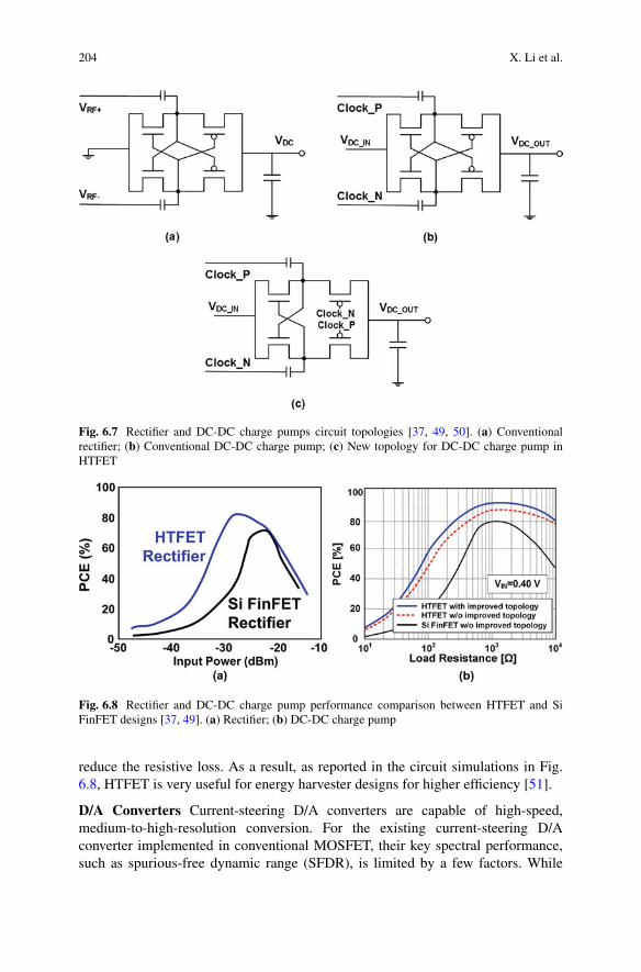
204 X. Li et al.
Fig. 6.7 Rectifier and DC-DC charge pumps circuit topologies [37, 49, 50]. (a) Conventionalrectifier; (b) Conventional DC-DC charge pump; (c) New topology for DC-DC charge pump inHTFET
Fig. 6.8 Rectifier and DC-DC charge pump performance comparison between HTFET and SiFinFET designs [37, 49]. (a) Rectifier; (b) DC-DC charge pump
reduce the resistive loss. As a result, as reported in the circuit simulations in Fig.6.8, HTFET is very useful for energy harvester designs for higher efficiency [51].
D/A Converters Current-steering D/A converters are capable of high-speed,medium-to-high-resolution conversion. For the existing current-steering D/Aconverter implemented in conventional MOSFET, their key spectral performance,such as spurious-free dynamic range (SFDR), is limited by a few factors. While

6 Emerging Steep-Slope Devices and Circuits: Opportunities and Challenges 205
Fig. 6.9 Current-steering D/A converter design using HTFET [52]. (a) Circuit topology; (b)SFDR comparison
some D/A converters have a bottleneck given by the current source mismatches,calibration or trimming can help to mitigate this impact. Other factors include theoutput impedance of the current source and switches (circuit structure shown inFig. 6.9a), as well as the switching distortions because of nonideal switching of theswitches. Conventional CMOS-based designs need complex techniques to mitigatethese effects [52–55]. When switched to HTFET, the capability of low-voltageoperation enables a smaller device size that leads to less capacitance. In addition,the low-capacitance density, as shown in Fig. 6.6, makes the total capacitance evensmaller when operating at a low voltage. As a result, with less capacitance, HTFEThelps to not only improve the output impedance, but also reduce the couplingglitches during switching [52]. Reported circuit simulation results in [52] confirmthe SFDR performance advantage with HTFET, as shown in Fig. 6.9b.
A/D Converters and Low-Noise Amplifiers The benefit of using HTFETs in A/Dconverters and amplifiers originates from their high gain, especially with a low-voltage supply. The gain of transconductance operational amplifiers (OTA) relieson the transconductance of the input transistor pair, and the output resistance of theoutput current branch. When implemented in HTFET, the output resistance is higherafter saturation, and a higher transconductance is obtained directly from the steep-slope switching. It is noted that, with HTFET, the transistors biased in saturationshould be provided with sufficient drain–source voltage to guarantee saturation.While the HTFET single-device noise performance is reported to be comparablewith conventional MOSFET [56], the noise with HTFET at the amplifier level issuperior [57]. This is because of the higher gain by HTFET that turns out to suppressthe equivalent noise at the input port (usually called the input referred noise) [57].Figure 6.10 shows the evaluation results of an example design of an A/D converter[58], and a low-noise bio-signal amplifier in which the HTFET device noise wasconsidered in the simulation [57].
Cellular Neural Network (CNN) CNN is useful when dealing with computation-intensive information processing application, such as pattern recognition and motion
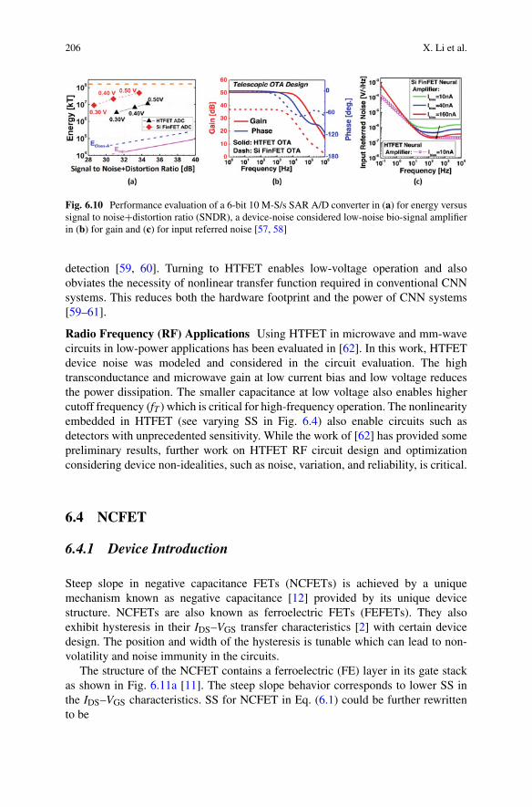
206 X. Li et al.
Fig. 6.10 Performance evaluation of a 6-bit 10 M-S/s SAR A/D converter in (a) for energy versussignal to noise+distortion ratio (SNDR), a device-noise considered low-noise bio-signal amplifierin (b) for gain and (c) for input referred noise [57, 58]
detection [59, 60]. Turning to HTFET enables low-voltage operation and alsoobviates the necessity of nonlinear transfer function required in conventional CNNsystems. This reduces both the hardware footprint and the power of CNN systems[59–61].
Radio Frequency (RF) Applications Using HTFET in microwave and mm-wavecircuits in low-power applications has been evaluated in [62]. In this work, HTFETdevice noise was modeled and considered in the circuit evaluation. The hightransconductance and microwave gain at low current bias and low voltage reducesthe power dissipation. The smaller capacitance at low voltage also enables highercutoff frequency (fT ) which is critical for high-frequency operation. The nonlinearityembedded in HTFET (see varying SS in Fig. 6.4) also enable circuits such asdetectors with unprecedented sensitivity. While the work of [62] has provided somepreliminary results, further work on HTFET RF circuit design and optimizationconsidering device non-idealities, such as noise, variation, and reliability, is critical.
6.4 NCFET
6.4.1 Device Introduction
Steep slope in negative capacitance FETs (NCFETs) is achieved by a uniquemechanism known as negative capacitance [12] provided by its unique devicestructure. NCFETs are also known as ferroelectric FETs (FEFETs). They alsoexhibit hysteresis in their IDS–VGS transfer characteristics [2] with certain devicedesign. The position and width of the hysteresis is tunable which can lead to non-volatility and noise immunity in the circuits.
The structure of the NCFET contains a ferroelectric (FE) layer in its gate stackas shown in Fig. 6.11a [11]. The steep slope behavior corresponds to lower SS inthe IDS–VGS characteristics. SS for NCFET in Eq. (6.1) could be further rewrittento be

6 Emerging Steep-Slope Devices and Circuits: Opportunities and Challenges 207
Fig. 6.11 NCFET. (a) Device structure [11]; (b) Transistor capacitance model [63]; (c) PE loop[64]
SS ≈ dVGS
dψS
dψS
dlog10 (IDS), (6.3)
where VG is the gate voltage and ψS is the channel surface potential. dVGS/dψS anddψS/dlog10(IDS) are usually called body factor and transport factor, respectively. InTFET-like technologies, the lower SS is obtained by modifying the transport factor.In NCFET, the lower subthreshold is achieved by changing the body factor, usingthe concept of negative capacitance to get voltage step-up action of the gate voltage[12].
NCFET can be modeled as a combination of the ferroelectric (FE) layer capac-itance in series with a MOSFET (Fig. 6.11b. Ferroelectrics are highly polarizablematerials. The polarization (P) vs electric field (E) relation of the ferroelectrics canbe represented using time-dependent Landau–Khalatnikov (LK) equation [12] givenin
E = αP + βP3 + γ P5 + ρdP/dt. (6.4)
The PE loop of the ferroelectric capacitor is shown in Fig. 6.11c. The dotted lineshows the part of PE loop where CFE is negative. The entire system is made stableby adding the positive capacitance from the MOSFET (CMOS). The voltage in theintermediate node is amplified by the factor |CFE|/(|CFE| − CMOS) [64].
FinFETs are the preferable devices for sub-20 nm technologies due theirhigher potential for scalability. Building NCFETs using FinFET as the underlyingtransistor is expected to perform as ultralow voltage devices [13]. The suggestedschematic of the NC-FinFET is given in Fig. 6.12 [64]. The experimental validationof the NC-FinFET concept is given in [18].
The change in device parameters can bring a significant impact in the character-istics of NCFET devices. For example, tuning the new FE layer thickness parameterwhich is absent in traditional transistors makes the device operate as a low power

208 X. Li et al.
Fig. 6.12 (a) NCFinFET structure [64]; (b) NCFinFET layers [64]
Fig. 6.13 (a) Load line Analysis [12, 65]; (b) Voltage step-up action of NCFET [63]; (c) IDS–VGScharacteristics of NCFET with different FE layer thickness [63]
logic device or a nonvolatile memory device. So device analysis is crucial for thedesign of efficient, functionally valid NCFET circuits.
Device design plays a crucial role in determining the characteristics of theNCFET device. For example, increasing the FE layer thickness beyond a pointintroduces hysteresis in the IDS–VGS characteristics of the NCFET device. Thehysteretic jump which occurs when the magnitude of the FE layer capacitanceequals the MOSFET capacitance. The occurrence of hysteresis can be predictedby doing a load line analysis of the device. An example of a load line plot is givenin Fig. 6.13a. The ‘S’ shaped curve of the FE capacitor is plotted by solving theLK equation. It can be predicted that hysteresis will not be occurred when theFE layer thickness is small (TFE = 1 nm in the Fig. 6.13a) as there is only oneintersection point with the MOSFET load line [12, 65]. With increase in FE layerthickness, the FE capacitance is lowered due to which two intersection points areoccurred resulting in hysteresis. Non-hysteretic operation is preferred for low powerlogic devices while hysteretic mode of operation is preferred for memory and noiseimmune logic.

6 Emerging Steep-Slope Devices and Circuits: Opportunities and Challenges 209
6.4.2 Low Power Logic
Reduction of supply voltage is one crucial factor to minimize the power density(dynamic power proportional to CV2). NCFET’s negative capacitance mechanismenables steep slope operation and thereby reduces the power supply voltage. Figure6.13b shows the steep slope operation in NCFETs. With the application of VGS,a negative voltage gets developed across the FE layer capacitor. This leads tothe development of a higher potential larger than the applied voltage V in theintermediate node (VMOS) [63, 66] (Fig. 6.13b). Increase in the ferroelectric layerthickness leads to decrease in |CFE| which amplifies the potential in the intermediategate leading to high gain in IDS. Increasing the thickness of the FE layer furtherleads to hysteresis. [13] has predicted around six orders magnitude of differencein the ION to IOFF ratio at 0.2 V operation. For logic devices, it is preferable tohave hysteresis free mode of operation. However, it has to be noted that the gatecapacitance of the NCFET is higher compared to that of conventional CMOS. Thespeed of operation of a device is roughly related to CV/I metric where C is thedevice gate capacitance, V supply voltage operation, and I is the drive current. So itis essential to optimize the C, V, I components for the optimum performance [47].Figure 6.14 shows the energy delay of a simulated 8-bit NCFinFET-based Kogge–Stone adder. NCFinFET shows better performance at low voltages compared to theregular FinFET adders [66].
For applications where noise is a key concern, using the hysteresis feature ofNCFET to build logic helps the noise immunity. This is because with the hysteresisin the positive voltage region, the gate output does not update until the input voltageexceeds beyond the hysteresis window, indicating more noise margin [67].
Fig. 6.14 Energy vs carry delay diagram of the 8-bit KSA: (a) 1fF wireload; (b) 0.001fF wireload[66]

210 X. Li et al.
6.4.3 NCFET Memory, DFF, and Processor
NCFET devices can be used as nonvolatile devices as the polarization can beretained in the FE layer of the gate stack even in the absence of electric field, withthe proper device design. Hysteresis is an essential condition for non-volatility. Forthe NCFET to be stable, the overall capacitance (1/CTOT = 1/CFE + 1/CMOSFET)of the device should be positive and hysteretic jump occurs to keep the |CFE| to behigher than CMOS such that overall capacitance is positive [11, 65]. Therefore, it iscrucial to maintain the proper ratio of CFE/CMOS for non-volatility.
In a nonvolatile design, increasing the VGS beyond coercive voltage of the deviceswitches the polarization stored in the gate stack and subsequent withdrawal ofVGS to zero volts retains the polarity. Similar application of VGS in the negativedirection beyond the coercive voltage reverses the polarization direction and retainsthe polarity even when VGS is removed to zero volts. Figure 6.15a shows an exampleof hysteresis in the transfer characteristics centered origin, which is an essentialcondition for non-volatility, and Fig. 6.15b shows polarization is retained in the FElayer when applied VGS is brought to zero volts leading to nonvolatile design [65].Such characteristics lead to two solutions for the IDS when VGS is zero volts. Thetwo distinctive resistance points (A and B in Fig. 6.15a) can be interpreted as logichigh and logic low states of the memory [11, 65]. Figure 6.16 shows that positionof the hysteresis is also important for nonvolatile designs as hysteresis, which is notcentered zero gate voltage, does not lead to non-volatility. [16] has reported morethan 6 orders of magnitude difference in the ION to IOFF ratio of drain current inthe hysteresis region. The huge difference in the drain current can be translated tohigh distinguishability of logic states by using current sensing in the memory designscheme [65, 68].
Nonvolatile processors (NVP) are processors with built-in nonvolatile memory(NVM) to back up the intermediate processor states when a power failure occurs andto restore the processor state when power comes back [69, 70]. Energy harvesting
Fig. 6.15 65 nm N-type FEFET with 2.25 nm ferroelectric layer thickness: (a) hysteresis; (b)non-volatility [65]

6 Emerging Steep-Slope Devices and Circuits: Opportunities and Challenges 211
Fig. 6.16 65 nm N-type FEFET with 1.90 nm ferroelectric layer thickness: (a) hysteresis; (b) nonon-volatility [65]
systems typically use NVPs as they have to work with frequent power interruption[71]. Both the memory and logic should be optimized to accomplish more forwardprogress in computation in NVPs. For example, energy savings from a low energymemory can be utilized to make more forward progress [65] in computation. Asdiscussed in the previous section, NCFET has the potential to be utilized as memorywith its polarization retention in the gate. A simulation study shows that replacingFERAM memory with NCFET memory in an NVP can achieve better forwardprogress due to the energy savings from NCFET memory [65].
An alternate method to the backup and restoration of the processor states tothe memory in NVPs is using a nonvolatile flip-flop. Integrating non-volatilityinside or nearby the flip-flop reduces the overheads of data transfer to the mem-ory. Nonvolatile flip-flops can also be used for power gating in general-purposeprocessors in order to eliminate leakage power consumption. Spin-based memories[72] and ferroelectric capacitors [70] have been proposed to use in the designnonvolatile flip-flops. One of the advantages of NCFET-based NVFF design overother technologies is the high distinguishability between two logic states that theNCFET inherently offers. Also using the three-terminal NCFET device with built-in storage mechanism significantly reduces design complexity of the backup/restorecircuits [73–75].
With more architectural optimizations, it has shown that NVP exhibits moreadvantage over conventional volatile processors [76–79], which highlights thebenefits of using NCFET for future processor design.
6.4.4 Logic in Memory and Security Applications
Tunable hysteresis property of the NCFET opens up the possibility of potentialcircuit features like memory in logic, where logic operations could be done close

212 X. Li et al.
to or at the memory cells to reduce the number of memory accesses by fetchingonly the results of logic operations [80].
The potential to build simpler and power-efficient memory in logic/logic inmemory circuits can find immediate applications in the field of hardware security[68]. The potential dynamic tuning from a nonvolatile cell to a volatile cell can helpto achieve logic obfuscation. Also employing logic in memory cell to store the keysreduces the communication overhead for key accessing and verification betweenmemory and logic [68]. Retention time of the data is a very important aspect insecurity applications. The retention time is dependent on multiple device factorslike coercive voltage, remnant polarization, area of the design etc.; the cell can beoptimized for energy and retention by tuning the cell parameters [65, 81].
6.5 Phase Transition Devices and Hyper-FET
6.5.1 Device Introductions
A recent addition to the family of steep switching devices is the Hyper-FET [29] orthe Phase-transition-FET [82]. Hyper-FET can be visualized as a transistor with aphase transitioning correlated material (CM) attached to the source terminal (Fig.6.17). The steep switching behavior of the Hyper-FET arises from the collectivecarrier dynamics of the assisting CM which undergoes selective phase switchingduring transistor operation. A discussion on Hyper-FET requires a prior discussionon correlated materials which is as follows.
Correlated materials are unique entities which exhibit a strong correlationbetween their inherent electrons. Therefore, they possess exotic electronic andmagnetic properties such as metal–insulator transitions, spin–charge separation,and half-metallicity. A group of such materials (e.g., VO2, V2O3, NbO2, TiO,Ti2O3, doped chalcogenide, Cu-doped HfO2, etc. [83–86]) manifest insulator tometal phase transition driven by external perturbations like temperature, pressure,or electrical stimulus. These materials have highly nonlinear electrical behavioras shown in Fig. 6.18. In response to a sufficiently high applied electric field (or
Fig. 6.17 Hyper-FETstructure and schematics

6 Emerging Steep-Slope Devices and Circuits: Opportunities and Challenges 213
Fig. 6.18 Typical I–Vcharacteristics of a correlatedmaterial
Fig. 6.19 (a) Transfer and (b) output characteristics of Hyper-FET, in comparison with FinFET
current), the CM undergoes abrupt (not instantaneous) insulator–metal transition(IMT) and illustrates an immense rise in current attributed to the significant changein resistivity. On the other hand, below a critical level of electric field (or current),the CM switches back to the insulating state (naturally default). Since, the twotransitions occur at different threshold levels, the I-V response becomes hysteretic.A wide variety of such phase transitioning CMs (having diverse resistivity andswitching thresholds) have already been reported, and further exploration is stillgoing on. There has been demonstration of effective tuning of the properties ofexisting CM using physical agitation like strain [87].
Hyper-FET ingeniously utilizes the above mentioned characteristics of CM tooperate well below the Boltzmann limit for SS (60 mV/decade). Its principle ofoperation can be explained using the transfer and output characteristics presented inFig. 6.19.
• During the OFF state of the transistor, the CM stays in insulating state (due toabsence of stimuli). The high insulating state resistivity of the CM substantiallysuppresses the OFF current of the transistor (IOFF).
• With rising voltage at the gate terminal, drain current of the transistor increasesand as the current exceeds a critical level for triggering IMT, the CM turns metal-lic. While manifesting the transition, the CM generates a negative differentialresistance (NDR) effect at the source terminal. By dint of this NDR, effective

214 X. Li et al.
VGS across the transistor structure increases beyond the applied value and hencethe transistor turns ON with a sharper subthreshold slope.
• Beyond the bias condition for IMT, CM operates in its metallic phase andpresents a low resistance in series with the innate resistance of the transistor.In effect, it very slightly reduces the ON state current of the transistor (ION).However, the reduction in ON current is negligibly small compared to strongreduction in OFF current. Thus, Hyper-FET eventually achieves higher ION/IOFFand performs as a better switch than the conventional transistor. From anotherviewpoint, for matched IOFF condition, Hyper-FET will have higher ION com-pared to the standard transistor.
The functionality of Hyper-FET has already been shown experimentally bothwith discrete [29] and monolithic [82] incorporation of CM with transistor. An SSof 8 mV/decade has been reported in the monolithically integrated version of Hyper-FET.
6.5.2 Hyper-FET Circuits
Being an emerging device with a completely new phenomenon, Hyper-FETdemands proper device–circuit co-design for optimum performance. Due to thehysteretic behavior of the CM itself, Hyper-FET exhibits hysteresis in its transfercharacteristics. This hysteresis has a strong influence on the performance of Hyper-FET-based circuits. The size and position of the hysteresis window are importantaspects to consider while designing Hyper-FET-based logic devices. But it isassuring to note that the hysteresis can be tuned and modified by changing thegeometry of the CM. In addition, as mentioned earlier, a wide variety of CMs areavailable and there is ample scope to choose the best-suited material or artificiallytune the material properties to some extent.
Implementation of logic devices with Hyper-FET is one of the immediate stepsto verify their feasibility in circuit domain. Figure 6.20a shows transient waveformsfor a ring oscillator (RO) made of a Hyper-FET-based inverter along with that withregular CMOS. The energy-delay benchmark for Hyper-FET-based RO (Fig. 6.20b)shows superior performance over regular CMOS at low VDD (<0.35 V) [82]. Athigh VDD, cutting-edge CMOS transistors exhibit faster operation but the Hyper-FET suffers from additional delay infusing from the phase switching dynamics ofthe CM. However, at low VDD, as transistors tend to incur higher intrinsic delay, suchtransition time no longer remains as a bottleneck. [82] reported 1.86× reduction inenergy (compared to 14 nm ULP FinFET) in a Hyper-FET-based ring oscillator atiso-delay (2.18 ns).
The unique properties of Hyper-FET or more precisely the inherent CM makethem a favorable candidate for brain-inspired neuromorphic computing. The currentdriven phase transition in between two states of CM can be utilized to designcircuits that behave like biological neuron [88, 89]. The neuron cells generate spikes

6 Emerging Steep-Slope Devices and Circuits: Opportunities and Challenges 215
Fig. 6.20 (a) Transient waveforms for RO based on Hyper-FET and FinFET (b) Energy delaycharacteristics of these two versions of RO [82].
Fig. 6.21 Circuit diagram ofa Hyper-FET-based neuroncell [88]
in response to incoming excitements exceeding a certain threshold. Likewise, asdiscussed earlier, CMs exhibit phase transition driven by electrical agitation beyonda certain level. This selective phase transition can give rise to voltage spikes in anelectrical neuron circuit. The concept has been illustrated in Fig. 6.21. The CMshown in this circuit diagram undergoes phase transition depending on the intensityof the input(s) and the transition gives rise to a spike in the output node voltage(V0). While a single neuron has very limited computational capability, a collectivenetwork of them (known as neural network) is of more practical interest.
In addition to the possibility of neuromorphic computing, Hyper-FET can alsobe used to design nano-oscillator circuits [30, 88], as shown in Fig. 6.22. Withappropriate design, it is possible to invoke the CM of a Hyper-FET to keep switchingits phase for a certain gate bias of the host transistor. The relentless phase transitionsresult in continuous charging and discharging of the corresponding node. Thus,an oscillatory voltage waveform is generated. For sustained oscillation, the metal–insulator transition (MIT) and insulator–metal transition (IMT) should occur beforethe output voltage stabilizes. The gate bias of the Hyper-FET can be tuned to provideconfigurable impedance to control the frequency of oscillation. Moreover, two ormore relaxation oscillators can be used to make coupled oscillator systems whichare more capable for computation.

216 X. Li et al.
Fig. 6.22 Circuit diagram ofa Hyper-FET-based relaxationoscillator [88]
6.6 Modeling and Benchmarking Emerging Devices
6.6.1 Modeling Emerging Devices
Compact device models have been widely used to capture their electrical behaviorswithin circuit SPICE simulators [47, 63, 88, 90–93]. To describe electrical behaviorsin SPICE-compatible compact-device models, there are two broad approaches:(a) the physics-based compact modeling and (b) numerical-based look-up tables(LUT) modeling. The physics-based compact modeling approach includes twocomplementary roles in nanoscale electronic devices [94, 95]. First, an analyticaldescription in a physics-based compact model helps interpret its electrical or behav-ioral characteristics; second, this approach forms the basis of a simple SPICE modelfor simulators. This physics-based modeling is predictive and has a small number ofparameters, incorporating with the process-defined device structure and well-knownmaterial properties while the Berkeley Spice (BSIM) model requires such a largenumber of model parameters. Another modeling approach is the numerical-basedlook-up tables (LUT) modeling. It provides an alternative to analytical models andis particularly useful for emerging technologies if the electrical characteristics arebased on simulations and measurements and the basis of a simple SPICE model likephysics-based modeling. This modeling approach employs the predefined numericalvalues with respect to operating conditions. For the SPICE device modeling, twotypes of modeling approaches can be combined. For example, ideal electrical devicebehavior can be modeled with LUT-based modeling and geometry and material-dependent RC parasitics can be modeled with analytical descriptions.
Among two types of approaches, as briefly depicted above, if physics-basedmathematical expressions go along with the precise electrical behaviors for anemerging device technology in a broad range of operational conditions, the physics-based compact modeling methodology is commonly employed in not only exam-inations of a device itself but also device–circuit SPICE simulations because itgenerally provides an efficient way to predict behaviors and a shorter simulationtime for device–circuit interactions compared to numerical-based LUT modeling

6 Emerging Steep-Slope Devices and Circuits: Opportunities and Challenges 217
[47, 93, 96]. However, unfortunately, some of emerging technologies are strenuousto model with the physics-based compact modeling since some of the devices suchas TFETs, NCFETs, Hyper-FET, etc. are still under development and have onlyvalid mathematical expressions in a short range of operating conditions. In thiscase, computer-aided simulations of devices and circuits are usually carried outwith a LUT-based approach, which is computationally demanding for simulationand testing of large device count circuits because this approach can provide moreaccurate results than physics-based compact modeling [63, 88, 96].
BSIM models and Verilog-A models are widely used for device modeling tosupport SPICE circuit simulations [90, 91, 97–99]. Over the past few decades,amongst numerous types of compact modeling methodologies, the analog subset ofVerilog-AMS [91] has become the preferred compact modeling language for bothacademic and industrial research groups [29, 30, 63, 88, 90, 99]. Many of emergingdevices have been continuously modeled by using Verilog-A [29, 30, 88, 90, 92, 93,100]. The Verilog-A is a naturally explicit language for an electromechanical devicein not only physics-based but also numerical LUT-based compact models and it hasbeen demonstrated as a promising language for analog device model developments[90, 91, 101]. An important key feature of emerging device modeling with Verilog-Ais that this language can be expanded with BSIM and other SPICE models. Verilog-A models can also support device features of noise, variation, and parasitics. Someprior modeling such as gate-all-around nanowire FETs, NCFETs, and Hyper-FETsuses BSIM as a base of a transistor and uses Verilog-A language to add uniquefeatures of emerging devices, geometry- and material-dependent RC parasitics, andtweak parameters of BSIM models [63, 88, 92, 102, 103].
While building the LUT-based Verilog-A model for emerging devices, providinga dense LUT helps to improve the accuracy of circuit simulation results at thecost of slower simulation speed. It also helps to reduce the chances of simulationconvergence failures. Sometime the LUT is based on measured results which canbe more or less distorted by the measuring accuracy; some preprocessing of theLUT data can also be helpful to prevent simulation convergence failures. Suchpreprocessing can include data smoothing, and also correction. For example, thedrain–source current IDS direction should match that of the voltage applied. Also,IDS be zero with a zero VDS.
Unlike the simple ideal modeling for emerging devices to capture intrinsicelectrical behaviors [90–95, 99, 101–107], the practical device modeling needs toinclude such subthreshold characteristics, ballisticity dependency, noise, parasitics,and process variations terms into the emerging device model since the increaseddevice sensitivity to noise, parasitics, and process variations at reduced VDD andphysical device dimension pose further challenge on robust circuit operation usingemerging devices [40, 102, 107]. In particular, electrical noise and paratisics posesa growing reliability concern for optimal system design at emerging technologies[40, 56, 102, 107]. Hence, the detailed analysis of electrical noise and parasitics inemerging devices is required and the accurate device modeling taking into accountelectrical noise and process variations needs to be applied to evaluate emergingtechnology because the noise figure and parasitics is one of the key design factors in

218 X. Li et al.
determining the performance for not only analog/mixed-signal and RF circuits butalso memories and processors [40, 56, 102, 107–110].
6.6.2 Benchmarking: From Device to Architecture
The post-CMOS device research has continuously brought the immense benefitsof higher integration density, higher energy efficiency, and superior performance[40, 46, 47, 63, 88, 93, 102, 104, 107]. Such benefits at the device-level andsmall-scale circuits have been widely investigated with SPICE device modeling[29, 30, 40, 63, 88, 91–93, 102]. Aside from benefits at the device level, theexaminations of architecture designs accompany challenges with practical layoutissues such as complexity and restrictions, and interconnect routing, noise, andincreased susceptibility of circuits to process variations [47]. In order to understandapplicability of emerging devices across a broad design space of architecture-leveldesigns, the abstraction through a device-logic-architecture benchmarking frame-work is crucial in such large-scale designs. The benchmark processing is broadlyclassified into three different paradigms [46, 104]: (1) general power estimationin use of architecture simulators such as GEMS [46, 105] and McPAT [46, 106],(2) examination of performance metrics in use of hardware synthesis process,and (3) variation studies in architectures with different datapath configurations byvarying parameters (e.g., the issue width, pipeline depth, etc.) within EDA tools(e.g., Fabscalar [46, 111] and plus hardware synthesis process). The appropriateparadigm, depending on application and benchmark characteristics, has to be chosento capture the impacts with emerging devices at processor architecture level.
Figure 6.23 presents the succinct flow for cell characterization process. Logicgate designs and cell characterization are the critical portion in architecture-leveldesigns because the logic gates are a key factor to determine the performancemetrics (e.g., energy, critical path delay, and chip area) in architecture designsthrough a synthesis process with synthesizable hardware description language(HDL). Logic gate designs and cell characterization are strongly dependent on celllayouts because of considerations of floorplanning and routing for full-chip designsand benchmarks. At sub-10 nm technologies and emerging devices, generatinglayouts for cells becomes immensely difficult because of challenges with regardto smaller physical dimension, different device structures, routing complexity, andcomplex design rules [47]. Hence, the cell designs with geometry parameters shouldbe carried out carefully while maintaining the full-functionality of each cell.
Several works have already explored the potential design spaces in medium-to-large-scale systems such as adders, ring-oscillators, application-specific accelera-tors, processors nonvolatile memory, and logics with emerging devices [29, 30, 40,46, 63, 88, 105, 107]. This device-to-architecture framework reveals that the SPICEmodeling-to-logic and logic-architecture benchmarking provide profound insightsinto impacts and help predict unique behavior and potentiality of future computingsystems with emerging devices.

6 Emerging Steep-Slope Devices and Circuits: Opportunities and Challenges 219
ProcessVariations
Electrical Noise
RC parasitics
Circuit
Architecture
Device
LUT-based Modeling
Physics-based Modeling
SPICE Modeling
TCAD Model& Measurement
Circuit Design & Behavior Abstrac�on
Logic Characteriza�on & Library Genera�on
Architecture Synthesize(HDL + Standard Cell Library)
Existing Core Models(Ivybridge, UltraSparc)
Architecture Simulation(Sniper, GEM5, GEMS)
Timing and Power Evaluation(McPAT)
Floorplanning & Routing & Op�mza�on
Timing and Power Evaluation
Parasi�c Extractions(StarRC, Mentor Calibre)
Cell Characteriza�on(Cadence Liberate)
Library DataBase(Synopsys Library Compiler)
Library Genera�onCell Layout Generations
(INV, NAND, NOR, DFF, etc.)
Fig. 6.23 Brief flow of the device-to-architecture benchmarking
6.7 Opportunities and Challenges of Emerging Devicesin Circuits and Systems
6.7.1 Opportunities
Steep-slope emerging technologies have brought the unique opportunities to beatlimitations in the performance and energy efficiency of traditional CMOS transistorsat subthreshold voltages. Exploring the potential design space with such steep-slope technologies has been demonstrated through the detailed device modeling andimplementation to circuits in many prior works [29, 30, 40, 42, 46, 47, 58, 63, 88,104, 107] as outlined in Sects. 6.3, 6.4, 6.5, and 6.6. The most direct applicationscenario for these steep-slope devices is similar to that of the traditional CMOS, inthat they could be used as three-terminal switching transistor with On-Off drain–source mechanism by the gate controls [29, 88]. These block level examinationsin various fields such as analog/RF/mixed-signal domains (e.g., Rectifiers, DC-DCcharge pumps, DAC, ADC, LNA, etc.), Boolean and non-Boolean logics, memory,brain-inspired neural networks, and specific-purpose processor (e.g., nonvolatileprocessor) bring broad insights to explore the optimum design space in the scenarioof energy-efficient and low-voltage systems for not only portable battery-poweredsystems and highly energy-efficient applications (i.e., implantable medical devicesand wearable bio-activity monitoring platforms, etc.) but also general-purposeprocessors.

220 X. Li et al.
Wired Power Energy Storage(Ba�ery)
Smart PowerControl Units
DC-DC Converter&
Low-Drop VoltageRegulator (LDO)
AC-DCConverter
RF signalHarvester
Solar Cells
Thermo-electricity
Piezo-electricity Computa�onal
Processors
InternalMemory
Power Management
Computa�on
ExternalMemory
DAC
ADC
AMP
RF
AMP
RF
27
I/O Processing
Boolean Logics
Neuron Network
Coupled Oscillator
Alterna�ve Processor Architectures
Poten�al Design SpacesPower ManagementProcessorsI/O ProcessingMemory
Fig. 6.24 Using emerging devices for future system designs
Figure 6.24 presents the potential design spaces for emerging technologies in asystem. An integrated circuit (IC) generally comprises multiple small componentssuch as the controlling logics, memory, digital signal processor (DSP), mixed-signal circuits, etc. The block-level advantages through a detailed examination ofthese components with such steep-slope emerging technologies in terms of energyand delay at a range of low voltages directly deliver magnificent benefits andopportunities with superior energy-efficiency and low-voltage operations. Energyharvesting systems, for example, require the high power conversion efficiency inthe limited ambient RF power and low energy computations to extend functionalityand to operational time for use at a given energy and consist of multiple circuits forenabling the utilization of the ambient RF signal power and signal processing unitssuch as Rectifier, LNA, ADC, DAC, DSP, etc. [37, 51, 57].
As depicted in Fig. 6.24, the compatibility of emerging technologies is notlimited to small signal processing components. A broad range of large-scaledigital computation units such as general-purpose processors, hardware-specificaccelerator, and brain-inspired neural network and nonvolatile memory can employsuch steep-slope emerging technologies (TFET, NCFET, Hyper-FET, VO2, etc.) forenergy-efficient computing at low voltages. Compared to CMOS-based computationhardware, scaling supply voltages to reduce the power consumption leads to asignificant increase in delay performance. Also, to retain performance, anotherattempt such as scaling VT affects not only noise performance but also overallstandby leakage power dissipations on ICs. In contrast, steep switching mechanismat low voltages can provide the remarkable delay reductions in computationhardware while maintaining low power consumption of both dynamic switchingand standby leakage, leading to high energy-efficiency in such large-scale integratedcircuits. In addition, integration with nonvolatile memory by taking hysteresisin ferroelectric emerging technologies also provides additional opportunities forsignificant reduction of power and replacement of conventional memory systems

6 Emerging Steep-Slope Devices and Circuits: Opportunities and Challenges 221
in large-scale ICs. Some benchmarks using these emerging devices in system-leveldesigns [40, 44, 46, 88, 104, 107] reveal that steep-slope emerging technologies canprovide the significant reduction in energy and become the promising candidates fornumerous types of applications and systems while keeping the same functionalityand better noise immunity compared to conventional CMOS [30, 42, 43, 58, 88,107, 112].
6.7.2 Challenges
Although numerous emerging devices (i.e., TFETs, NCFETs, Hyper-FETs, etc.)hint at a bright future [40, 42, 46, 47, 104, 107], given the practical device challengessuch as the unidirectional conduction behavior, biasing- and material-dependenthysteresis and fabrication complexity and cost in circuits and system-level designsstill remain. This chapter covers how these challenges affect in circuits and systemsnot only at device level.
Unidirectional Conduction Foremost challenges in logic gates stemming fromthe unidirectional conduction can be broadly categorized by three aspects: (a) therouting complexity, (b) chip area overhead, and (c) more power consumption byincreased capacitances. Although the routing complexity and chip area overheadare unavoidable, the power consumption and energy can be reduced by VDDscaling because TFETs are inherently capable of operating at very low voltages(e.g., VDD < 0.3 V) compared to non-steep switching devices. Unidirectionalconduction induced from the asymmetrical device architecture of TFETs become akey limitation factor for the full-functionality in TFET gates (i.e., SRAMs, latch,DFF, pass-transistor, and transmission gate logics) and connectivity at over twostacked transistors because of incomplete charging/discharging paths and limita-tions of sharing contacts/active regions originating from this unique characteristic[47]. In order to make logic gates operate with full-functionality, modificationsof logic designs are required for TFET circuit implementation. The simple wayto modify logics for charging/discharging paths is adding an additional transistoron a path, resulting in additional power dissipation and area overhead of logics.Since sequential logics like DFFs, for example, comprise a large fraction of thetotal gates in a design, the additional transistors for each charging/discharging pathaffect significant chip area and power dissipation overheads. Fortunately, addingan additional transistor is not an only option for DFFs. The static C2MOS DFF,for instance, can be employed instead of the use of transmission gates-basedmaster/slave DFF. However, to retain the read/write functions in TFET SRAM,the implementation of additional transistors is inevitable. For the TFET SRAM,numerous works have already explored its alternative options to acquire read/writeoperations fully [40, 42, 107]. At an iso-area perspective in processors, the capacityof TFET SRAM cells is smaller than that of other devices, which have bidirectionalconduction behaviors.

222 X. Li et al.
SRAM Noise Margin Another challenge in TFET SRAM is lower static noisemargin (SNM) from a simultaneous turned-on transmission gate in operation ofread/write [40, 107]. To alleviate this SNM issue, alternative schemes have beenexplored in [40, 107] while sacrificing SRAM area by using additional transistors toapply additional controlling signals. Another challenge induced from unidirectionalconduction is the penalty with isolations between two transistors. As mentionedabove, TFET cannot share contact and diffusion area at >2 stacked transistors dueto unidirectional conduction, resulting in additional isolation by placing shallowtrench isolation (STI) between two adjunct transistors and area overhead in logicgates. This is becoming more severe when the driving ability of logic gates needsto be high enough to meet timing requirements in processors at a harsh operationenvironment (e.g., high frequency range, low voltage ranges, etc.) because the cellshould be bigger to minimize the computation delay, resulting in an area penaltywith a number of additional isolations.
Undesirable Hysteretic Characteristic and Speed in Boolean NCFETand Hyper-FET Logics As described in Sects. 6.4 and 6.5, NCFET and Hyper-FET exhibit the unique hysteresis switching and hysteretic polarization in presentingtwo states in certain biasing voltages. The hysteresis switching and hystereticpolarization characteristics provide superb nonvolatile characteristics in memoryapplications [113]. Hysteresis can be ingeniously used to harness additional benefitsin holding the stored data. The possibility of hysteresis, for instance, in the transfercharacteristics (ID–VGS) of NCFET is actually governed by the relative capacitivematching between the gate of the transistor and the ferroelectric layer. Load lineanalysis considering conservation of charge between these two mutually connectedcapacitances yields two stable physical solutions (origin of hysteresis) beyonda critical thickness of the ferroelectric. Also, these hysteresis characteristics canbe employed in some specific-purpose non-Boolean logics. However, except inspecific-purpose non-Boolean logics and memory applications, these hysteresischaracteristics in Hyper-FETs and NCFETs associated with the negative differentialcapacitance generally pose adverse effects in Boolean functioned logics because ofthe metastable states, although they provide superior device performance such assteep-subthreshold switching, high ION while maintaining low IOFF current. Hence,some literatures have aimed to minimize the hysteresis by using various techniquessuch as by threshold VT shift adapting different ferroelectric materials [19],adjustment of thickness of the thin ferroelectric layer, annealing [18, 19], etc. whileretaining device performance. For example, the adjustment of critical thicknessworks as upper bound for hysteresis free operation. Hence, geometry (especiallythickness) of the ferroelectric layer is a vital aspect to traverse between hystereticand non-hysteretic modes. The critical thickness differs among materials and isdirectly linked to the corresponding remnant polarization and coercive field. Thesenumerous techniques result in the increase of additional fabrication process control,complexity, and cost. Hence, the minimizing hysteresis and development of efficientfabrication process control to augment the current state-of-the-art technology will

6 Emerging Steep-Slope Devices and Circuits: Opportunities and Challenges 223
be key factors in realizing a NCFET and Hyper-FET-based hardware platform [29,88], albeit sacrificing some degree of current fabrication complexity and cost.
Additional Phase/State Change Delay Another concern is the delay stemmingfrom the introduction of the additional layer stacks and extra delay for state/phasechanges within transistors. For example, this delay challenge of NCFET arises fromthe considerable increase in gate capacitance, which is a direct consequence ofintroducing the additional layer of ferroelectric material. Although NCFETs providesteeper switching and enhanced ION (at lower VDD), they also incur additional delaydue to large gate capacitance. In addition, polarization switching transients demandextra time during dynamic switching operation of logic circuits. Hence, materialswith lower kinetic coefficient are desired for optimum operation in NCFET-basedlogic designs. In spite of these specific concerns, at low VDD, as the inherent circuitdelay immensely increases in conventional CMOS, these additional aspects of delayno longer remain a bottleneck to performance. In such a scenario, NCFETs garnerbenefits due to their steep switching operation.
Variation For mass production, variation is an important factor that limits the yieldand thus cost, especially for circuits with minimized device dimensions. Variationbetween different devices, or between different operating points of time for the samedevice, can also cause reliability issues. There have been some recent researchreports on these topics [48, 114–116]. However, further modeling, experimentalverification, fabrication process optimization, and also circuit design techniques tomitigate the impact can be of great significance.
Fabrication Complexity and Cost With enormous efforts (i.e., device con-cepts, SPICE modeling, single transistor measurement, etc.) in emerging deviceresearches, examinations of the device impacts on circuit and systems have beenexplored by using computer-aided simulations in many literatures. However, thereare still many challenges facing the fabrication complexity of emerging transistorsand increased difficulty and cost in the large-scale integration of the technology[117–119]. For example, the introduction of new materials such as III–V com-pounds, ferroelectric, insulator-to-metal transition (IMT) materials leads to otherfabrication steps and techniques to guarantee device functionality and performance,resulting in increased fabrication complexity and immense cost.
NCFETs and Hyper-FETs are compatible to CMOS or FinFET technologies[29, 30, 63, 88]. They stack certain materials for exploring unique electricalcharacteristics onto the transistor. NCFET and FEFETs, for example, add thepiezoelectric and ferroelectric materials (i.e., ALD HfZrO2, Pb(Zr,Ti)O3, BaTiO3,SrBi2Ta 2O9, etc.) [18, 80] to ferroelectric layers between gate electrode anddielectric, and Hyper-FET uses the insulator-to-metal transition in vanadium dioxide(VO2) onto the source of CMOS to design a hybrid-phase-transition FET. However,for measurements and evaluations in [29, 30, 63, 88], these newly formed materialsand structure are connected to CMOS using metals rather than fabricated into asingle transistor due to the fabrication complexity and cost, leading to challenges inlarge-scale integration for circuits and systems.

224 X. Li et al.
The fabrication of III-V materials in TFETs has been reported in literatures withvarious techniques [40, 107]. The doping and electrical behaviors are well controlledby the fabrication process for a single transistor [40, 107]. However, they do notfollow the conventional CMOS fabrication process since they are naturally vertical-oriented devices and use III–V and other materials. Another issue for fabricationin TFETs is that the integration of such n-type and p-type transistors on the samewafer is still questionable because there are some fabrication ranging from growingIII–V materials, different material stacks, and other fabrication process issues suchas extreme ultraviolet lithography (EUV), X-ray, imprint, projection electron-beam,or projection ion-beam lithography. These issues, nevertheless, tackle the advent ofemerging technology in realistic applications like other emerging devices mentionedabove.
As emerging devices offer the unique opportunities over conventional CMOS,the restrictions and features of new fabrication technologies are becoming thekey challenges to bring these emerging technologies to apply in real circuits andsystems. To advance the appearance of circuits and systems with emerging devices,such limitations and challenges of new fabrication technologies should be resolvedin the future.
6.8 Conclusion
Three types of emerging devices, that is, TFET, NCFET, and Hyper-FET, have beeninvestigated for next-generation low-power applications. The device mechanism,device–circuit co-design, as well as related architecture implications are discussedin detail. Evaluation results show that the steep-slope characteristics, together withnew features, have brought great low-power opportunities for both conventionalBoolean logic and nonconventional circuits and architectures. The challenges forfuture implementation with these emerging devices are also discussed in detail.
Acknowledgment This work is supported in part by the Center for Low Energy SystemsTechnology (LEAST), one of the six SRC STARnet centers, sponsored by MARCO and DARPA,by NSF awards 1160483 (ASSIST), and NSF Expeditions in Computing Award-1317560.
References
1. A.C. Seabaugh, Q. Zhang, Low-voltage tunnel transistors for beyond CMOS logic. Proc.IEEE 98(12), 2095–2110 (2010)
2. P.-F. Wang, K. Hilsenbeck, T. Nirschl, M. Oswald, C. Stepper, M. Weiss, D. Schmitt-Landsiedel, W. Hansch, Complementary tunneling transistor for low power application. SolidState Electron. 48(12), 2281–2286 (2004)
3. K.K. Bhuwalka, J. Schulze, I. Eisele, Performance enhancement of vertical tunnel field-effecttransistor with SiGe in the pþ layer. Jpn. J. Appl. Phys. 43, 4073–4078 (2004)

6 Emerging Steep-Slope Devices and Circuits: Opportunities and Challenges 225
4. J. Appenzeller, Y.-M. Lin, J. Knoch, P. Avouris, Band-to-band tunneling in carbon nanotubefield-effect transistors. Phys. Rev. Lett. 93(19), 196805-1–196805-4 (2004)
5. W.Y. Choi, B.-G. Park, J.D. Lee, T.-J.K. Liu, Tunneling field-effect transistors (TFETs) withsubthreshold swing (SS) less than 60 mV/dec. IEEE Electron. Device Lett. 28, 743–745(2007)
6. T. Krishnamohan, D. Kim, S. Raghunathan, K. Saraswat, Double-gate strained-Ge het-erostructure tunneling FET (TFET) with record high drive currents and G 60 mV/decsubthreshold slope, in Proc. Int. Electron Devices Meeting (IEDM) (2008), pp. 947–949
7. R. Pandey et al., Demonstration of p-type In0.7Ga0.3As/GaAs0.35Sb0.65 and n-typeGaAs0.4Sb0.6/In0.65Ga0.35As complimentary heterojunction vertical tunnel FETs for ultra-low power logic, in 2015 Symposium on VLSI Technology (VLSI Technology), Kyoto (2015),pp. T206–T207
8. R. Bijesh et al., Demonstration of In0.9Ga0.1As/GaAs0.18Sb0.82 near broken-gap tun-nel FET with ION=740μA/μm, GM=70μS/μm and gigahertz switching performance atVDS=0.5V, in 2013 IEEE International Electron Devices Meeting (IEDM), Washington, DC(2013), pp. 28.2.1–28.2.4
9. G. Dewey et al., Fabrication, characterization, and physics of III-V heterojunction tunnelingfield effect transistors (H-TFET) for steep sub-threshold swing, in Proc. IEDM Tech. Dig.,Washington, DC (2011), pp. 33.6.1–33.6.4
10. R. Gandhi, Z. Chen, N. Singh, K. Banerjee, S. Lee, CMOS-compatible vertical-silicon-nanowire gate-all-around p-type tunneling FETs with ≤50-mV/decade subthreshold swing.IEEE Electron Device Lett. 32(11), 1504–1506 (2011)
11. A.I. Khan, C.W. Yeung, C. Hu, S. Salahuddin, Ferroelectric negative capacitance MOSFET:Capacitance tuning & antiferroelec- tric operation, in Proc. IEEE IEDM, Dec. (2011), pp.11.3.1–11.3.4
12. S. Salahuddin, S. Datta, Use of negative capacitance to provide voltage amplification for lowpower nanoscale devices. Nano Lett. 8(2), 405–410 (2008)
13. H. Chenming, S. Salahuddin, C.-I. Lin, A. Khan, 0.2 V adiabatic NC-FinFET with 0.6mA/μm ION and 0.1 nA/μm IOFF, in Device Research Conference (DRC) (2015), pp. 39–40
14. M.H. Lee et al., Steep slope and near non-hysteresis of FETs with antiferroelectric-like HfZrOfor low-power electronics. IEEE Electron Device Lett. 36(4), 294–296 (2015)
15. J. Jo, W.Y. Choi, J.-D. Park, J.W. Shim, H.-Y. Yu, C. Shin, Negative capacitance inorganic/ferroelectric capacitor to implement steep switching MOS devices. Nano Lett. 15(7),4553–4556 (2015)
16. A.I. Khan et al., Negative capacitance in short-channel FinFETs externally connected to anepitaxial ferroelectric capacitor. IEEE Electron Device Lett. 37(1), 111–114 (2016)
17. J. Jo, C. Shin, Negative capacitance field effect transistor with hysteresis-free Sub-60-mV/decade switching. IEEE Electron Device Lett. 37(3), 245–248 (2016)
18. K.S. Li et al., Sub-60mV-swing negative-capacitance FinFET without hysteresis, in 2015IEEE International Electron Devices Meeting (IEDM), Washington, DC (2015), pp. 22.6.1–22.6.4
19. M.H. Lee et al., Prospects for ferroelectric HfZrOx FETs with experimentally CET=0.98nm,SSfor=42mV/dec, SSrev=28mV/dec, switch-off <0.2V, and hysteresis-free strategies, in 2015IEEE International Electron Devices Meeting (IEDM), Washington, DC (2015), pp. 22.5.1–22.5.4
20. S. Dasgupta, A. Rajashekhar, K. Majumdar, N. Agrawal, A. Razavieh, S. Trolier-Mckinstry,S. Datta, Sub-kT/q switching in strong inversion in PbZr0.52Ti0.48O3 gated negativecapacitance FETs. IEEE J. Explor. Solid-State Computat. Devices Circuits 1, 43–48 (2015)
21. P.-G. Chen, Y.-T. Wei, M. Tang, M.H. Lee, Experimental demonstration of ferroelectric gate-stack AlGaN/GaN-on-Si MOS-HEMTs with voltage amplification for power applications.IEEE Trans. Electron Devices 61(8), 3014–3017 (2014)
22. H. Nathanson, W. Newell, R. Wickstro, J. Davis, Resonant gate transistor. IEEE Trans.Electron Devices ED-14(3), 117–133 (1967)

226 X. Li et al.
23. A.M. Ionescu, V. Pott, R. Fritschi, K. Banerjee, M.J. Declercq, P. Renaud, C. Hilbert, P.Fluckiger, G.A. Racine, Modeling and design of a low-voltage SOI suspended-gate MOSFET(SG-MOSFET) with a metal-over-gate architecture, in Proc. Int. Symp. Quality Elecron.Design (2002), pp. 496–501
24. H. Kam, D.T. Lee, R.T. Howe, T.-J. King, A new nano-electro-mechanical field effecttransistor (NEMFET) design for low-power electronics, in Proc. Int. Electron DevicesMeeting (IEDM) (2005), pp. 463–466
25. K. Gopalakrishnan, P.B. Griffin, J.D. Plummer, I-MOS: A novel semiconductor device witha subthreshold slope lower than kT/q, in Proc. Int. Electron Devices Meeting (IEDM) (2002)pp. 289–292
26. W.Y. Choi, J.D. Lee, B.-G. Park, Integration process of impact ionization metal-oxide-semiconductor devices with tunneling field-effect transistors and metal-oxide-semiconductorfield-effect transistors. Jpn. J. Appl. Phys. 46(1), 122–124 (2007)
27. C.-W. Lee, A.N. Nazarov, I. Ferain, N.D. Akhavan, R. Yan, P. Razavi, R. Yu, R.T. Doria, J.-P.Colinge, Low subthreshold slope in junctionless multigate transistors. Appl. Phys. Lett. 96,102106 (2010)
28. E.-H. Toh, G.H. Wang, L. Chan, D. Weeks, M. Bauer, J. Spear, S.G. Thomas, G. Samudra,Y.-C. Yeo, Cointegration of in situ doped silicon-carbide source and silicon-carbon i-regionin p-channel silicon nanowire impact-ionization transistor. IEEE Electron Device Lett. 29(7),731–733 (2008)
29. N. Shukla, A. Thathachary, A. Agrawal, H. Paik, A. Aziz, D. Schlom, S. Gupta, R. Engel-Herbert, S. Datta, A steep-slope transistor based on abrupt electronic phase transition. Nat.Commun. 6, 7812-1–7812-6 (2015)
30. N. Shukla et al., Pairwise coupled hybrid vanadium dioxide-MOSFET (HVFET) oscillatorsfor non-boolean associative computing, in 2014 IEEE International Electron Devices Meeting(IEDM), San Francisco, CA (2014), pp. 28.7.1–28.7.4
31. J.H. Park, G.S. Jang, H.Y. Seok, et al., Sub-kT/q subthreshold-slope using negative capac-itance in low-temperature polycrystalline-silicon thin-film transistor. Sci. Rep. 6, 24734(2016)
32. J.P. Colinge, Subthreshold slope of thin-film SOI MOSFET’s. IEEE Electron Device Lett.7(4), 244–246 (1986)
33. M.H. Lee et al., Ferroelectric negative capacitance hetero-tunnel field-effect-transistors withinternal voltage amplification, in 2013 IEEE International Electron Devices Meeting (IEDM),Washington, DC (2013), pp. 4.5.1–4.5.4
34. U.E. Avci et al., Study of TFET non-ideality effects for determination of geometry anddefect density requirements for sub-60mV/dec Ge TFET, in 2015 IEEE International ElectronDevices Meeting (IEDM), Washington, DC (2015), pp. 34.5.1–34.5.4
35. R. Pandey et al., Tunnel junction abruptness, source random dopant fluctuation and PBTIinduced variability analysis of GaAs0.4Sb0.6/In0.65Ga0.35As heterojunction tunnel FETs,in 2015 IEEE International Electron Devices Meeting (IEDM), Washington, DC (2015), pp.14.2.1–14.2.4
36. H. Lu, A. Seabaugh, Tunnel field-effect transistors: State-of-the-art. IEEE J. Electron DevicesSoc. 2(4), 44–49 (2014)
37. H. Liu, X. Li, R. Vaddi, K. Ma, S. Datta, V. Narayanan, Tunnel FET RF rectifier design forenergy harvesting applications. IEEE Trans. Emerg. Sel. Topics Circuits Syst. 4(4), 400–411(2014)
38. A.M. Ionescu, Tunnel FETs and emerging device concepts for subthermal switching, in 2013IEEE International Electron Devices Meeting (IEDM) (2013)
39. Synopsys TCAD, http://www.synopsys.com/tools/tcad40. S. Datta et al., Tunnel transistors for energy efficient computing, in IEEE Int. Reliability
Physics Symp. (IRPS) (2013), pp. 6A.3.1–6A.3.741. B. Sedighi, X.S. Hu, H. Liu, J.J. Nahas, M. Niemier, Analog circuit design using tunnel-FETs.
IEEE Trans. Circuits Syst. I 62(1), 39–48 (2015)

6 Emerging Steep-Slope Devices and Circuits: Opportunities and Challenges 227
42. V. Saripalli, S. Datta, V. Narayanan, J.P. Kulkarni, Variation-tolerant ultra low-powerheterojunction tunnel FET SRAM design, in 2011 IEEE/ACM International Symposium onNanoscale Architectures, San Diego, CA (2011), pp. 45–52
43. M.S. Kim, H. Liu, K. Swaminathan, X. Li, S. Datta, V. Narayanan, Enabling power-efficientdesigns with III-V tunnel FETs, in 2014 IEEE Compound Semiconductor Integrated CircuitSymposium (CSICS), La Jolla, CA (2014), pp. 1–4
44. K. Swaminathan, H. Liu, J. Sampson, V. Narayanan, An examination of the architecture andsystem-level tradeoffs of employing steep slope devices in 3D CMPs, in 2014 ACM/IEEE41st International Symposium on Computer Architecture (ISCA), Minneapolis, MN (2014),pp. 241–252
45. W.Y. Tsai, H. Liu, X. Li, V. Narayanan, Low-power high-speed current mode logic usingtunnel-FETs, in 2014 22nd International Conference on Very Large Scale Integration (VLSI-SoC), Playa del Carmen (2014), pp. 1–6
46. K. Swaminathan, H. Liu, X. Li, M.S. Kim, J. Sampson, V. Narayanan, Steep slope devices:Enabling new architectural paradigms, in 2014 51st ACM/EDAC/IEEE Design AutomationConference (DAC), San Francisco, CA (2014), pp. 1–6
47. M.S. Kim, W. Cane-Wissing, X. Li, J. Sampson, S. Datta, S.K. Gupta, V. Narayanan,Comparative area and parasitics analysis in FinFET and Heterojunction vertical TFETstandard cells. ACM J. Emerg. Technol. Comput. Syst. 12(4), 38 (2016)
48. S. Datta, H. Liu, V. Narayanan, Tunnel FET technology: A reliability perspective. Microelec-tron. Reliab. 54(5), 861–874 (2014)
49. U. Heo, X. Li, H. Liu, S. Gupta, S. Datta, V. Narayanan, A high-efficiency switched-capacitance HTFET charge pump for low-input-voltage applications, in 2015 28th Interna-tional Conference on VLSI Design, Bangalore (2015), pp. 304–309
50. X. Li, K. Ma, S. George, J. Sampson, V. Narayanan, Enabling internet-of-things: Opportuni-ties brought by emerging devices, circuits, and architectures, in 2016 IFIP/IEEE InternationalConference on Very Large Scale Integration (VLSI-SoC) (Springer, Cham, 2016), pp. 1–23
51. X. Li, U. Dennis Heo, K. Ma, V. Narayanan, H. Liu, S. Datta, Rf-powered systems usingsteep-slope devices, in New Circuits and Systems Conference (NEWCAS), 2014 IEEE 12thInternational, Trois-Rivieres, QC (2014), pp. 73–76
52. M.S. Kim, X. Li, H. Liu, J. Sampson, S. Datta, V. Narayanan, Exploration of low-power high-SFDR current-steering D/A converter design using steep-slope heterojunction tunnel FETs.IEEE Trans. VLSI Syst. 24(6), 2299–2309 (2016)
53. X. Li, Q. Wei, Z. Xu, J. Liu, H. Wang, H. Yang, A 14 bit 500 MS/s CMOS DAC usingcomplementary switched current sources and time-relaxed interleaving DRRZ. IEEE Trans.Circuits Syst. I 61(8), 2337–2347 (2014)
54. X. Li, Q. Wei, H. Yang, Code-independent output impedance: A new approach to increasingthe linearity of current-steering DACs, in 2011 18th IEEE International Conference onElectronics, Circuits and Systems (ICECS), Beirut (2011), pp. 216–219
55. J. Liu, X. Li, Q. Wei, H. Yang, A 14-bit 1.0-GS/s dynamic element matching DAC with >80dB SFDR up to the Nyquist, in 2015 IEEE International Symposium on Circuits and Systems(ISCAS), Lisbon (2015), pp. 1026–1029
56. R. Pandey, B. Rajamohanan, H. Liu, V. Narayanan, S. Datta, Electrical noise in heterojunctioninterband tunnel FETs. IEEE Trans. Electron Devices 61(2), 552–560 (2014)
57. H. Liu, S. Datta, M. Shoaran, A. Schmid, X. Li, V. Narayanan, Tunnel FET-based ultra-lowpower, low-noise amplifier design for bio-signal acquisition, in 2014 IEEE/ACM InternationalSymposium on Low Power Electronics and Design (ISLPED), La Jolla, CA (2014), pp. 57–62
58. M.S. Kim, H. Liu, X. Li, S. Datta, V. Narayanan, A steep-slope tunnel FET based SAR analog-to-digital converter. IEEE Trans. Electron Devices 61(11), 3661–3667 (2014)
59. P. Mazumder et al., Tunneling-based cellular nonlinear network architectures for imageprocessing. IEEE Trans. VLSI Syst. 17(4), 487–495 (2009)
60. A.R. Trivedi, S. Datta, S. Mukhopadhyay, Application of silicon-germanium source tunnel-FET to enable ultralow power cellular neural network-based associative memory. IEEE Trans.Electron Devices 61(11), 3707–3715 (2014)

228 X. Li et al.
61. A.R. Trivedi, S. Mukhopadhyay, Potential of ultralow-power cellular neural image processingwith Si/Ge tunnel FET. IEEE Trans. Nanotechnol. 13(4), 627–629 (2014)
62. P.M. Asbeck, K. Lee, J. Min, Projected performance of heterostructure tunneling FETs in lowpower microwave and mm-wave applications. IEEE J. Electron Devices Soc. 3(3), 122–134(2015)
63. A. Aziz, S. Ghosh, S. Datta, S.K. Gupta, Physics-based circuit-compatible SPICE model forferroelectric transistors. IEEE Electron Device Lett. 37(6), 805–808 (2016)
64. Aziz, S. Ghosh, S. Datta, S.K. Gupta, Polarization charge and coercive field dependentperformance of negative capacitance FETs, in 2016 74th Annual Device Research Conference(DRC) (2016), pp. 1–2
65. S. George, K. Ma, A. Aziz, X. Li, A. Khan, S. Salahuddin, M.-F. Chang, et al., Nonvolatilememory design based on ferroelectric FETs, in Proceedings of the 53rd Annual DesignAutomation Conference (DAC) (2016), p. 118
66. S. George, A. Aziz, X. Li, et al., Device circuit co design of FEFET based logic for lowvoltage processors, in ISVLSI (2016), pp. 649–654
67. S. George, X. Li, et al., NCFET based logic for energy harvesting systems, in SRC TECHCON2015 (SRC, Durham, 2015)
68. X. Li et al., Design of Nonvolatile SRAM with ferroelectric FETs for energy-efficient backupand restore. IEEE Trans. Electron Devices 64(7), 3037–3040 (2017)
69. K. Ma, Y. Zheng, S. Li, K. Swaminathan, X. Li, Y. Liu, J. Sampson, Y. Xie, V. Narayanan,Architecture exploration for ambient energy harvesting nonvolatile processors, in 2015 IEEE21st International Symposium on High Performance Computer Architecture (HPCA) (2015),pp. 526–537
70. Y. Wang, Y. Liu, S. Li, D. Zhang, B. Zhao, M.-F. Chiang, Y. Yan, B. Sai, H. Yang, A 3uswake-up time nonvolatile processor based on ferroelectric flip-flops, in 2012 Proceedings ofthe ESSCIRC (ESSCIRC) (2012), pp. 149–152
71. Y. Liu et al., Ambient energy harvesting nonvolatile processors: From circuit to system, inProceedings of the 52nd Annual Design Automation Conference (2015), p. 150
72. K.-W. Kwon, S.H. Choday, Y. Kim, X. Fong, S.P. Park, K. Roy, SHE-NVFF: Spin hall effect-based nonvolatile flip-flop for power gating architecture. IEEE Electron Device Lett. 35(4),488–490 (2014)
73. D. Wang et al., Ferroelectric transistor based non-volatile flip-flop, in Proceedings of the2016 International Symposium on Low Power Electronics and Design (ISLPED’16) (2016),pp. 10–15
74. X. Li, J. Sampson, A. Khan, K. Ma, S. George, A. Aziz, S. Gupta, S. Salahuddin, M.-F. Chang, S. Datta, V. Narayanan, Enabling energy-efficient nonvolatile computing withnegative capacitance FET. IEEE Trans. Electron Devices 64(8), 3452–3458 (2017)
75. X. Li, S. George, K. Ma, W.-Y. Tsai, A. Aziz, J. Sampson, S. Gupta, M.-F. Chang, Y. Liu, S.Datta, V. Narayanan, Advancing nonvolatile computing with nonvolatile NCFET latches andflip-flops. IEEE Trans. Circuits Syst. I 64(11), 2907–2919 (2017)
76. K. Ma et al., Nonvolatile processor architecture exploration for energy-harvesting applica-tions. IEEE Micro 35(5), 32–40 (2015)
77. K. Ma et al., Nonvolatile processor architectures: Efficient, reliable progress with unstablepower. IEEE Micro 36(3), 72–83 (2016)
78. K. Ma, X. Li, et al., Nonvolatile processor optimization for ambient energy harvestingscenarios, in The 15th Non-volatile Memory Technology Symposium (NVMTS) (2015)
79. K. Ma et al., Dynamic machine learning based matching of nonvolatile processor microarchi-tecture to harvested energy profile, in Proceedings of the IEEE/ACM International Conferenceon Computer-Aided Design (2015), pp. 670–675
80. M.H. Park, Y.H. Lee, H.J. Kim, Y.J. Kim, T. Moon, K.D. Kim, J. Müller, A. Kersch, U.Schroeder, T. Mikolajick, C.S. Hwang, Ferroelectricity and antiferroelectricity of doped thinHfO2-based films. Adv. Mat. 27(11), 1811–1831 (2015)
81. A. Chen, X. Sharon Hu, Y. Jin, M. Niemier, X. Yin, Using emerging technologies for hardwaresecurity beyond PUFs, in 2016 Design, Automation & Test in Europe Conference & Exhibition(DATE) (2016), pp. 1544–1549

6 Emerging Steep-Slope Devices and Circuits: Opportunities and Challenges 229
82. J. Frougier, N. Shukla, D. Deng, M.J. Jerry, A. Aziz, L. Liu, G. Lavallee, T.S. Mayer, S.K.Gupta, S. Datta, Phase-transition-FET exhibiting steep switching slope of 8mV/decade and36% enhanced ON current, in 2016 Symposia on VLSI Technology and Circuits (2016)
83. F.J. Morin, Oxides which show a metal-to-insulator transition at the Neel temperature. Phys.Rev. Lett. 3, 34–36 (1959)
84. Y. Tomioka et al., Phase diagrams of perovskite-type manganese oxides. J. Phys. Chem. Solids67(9–10), 2214–2221 (2006)
85. Q. Luo et al., Cu BEOL compatible selector with high selectivity (>107), extremely lowoff-current (pA) and high endurance (>1010), in 2015 IEEE International Electron DevicesMeeting (IEDM), Washington, DC (2015), pp. 10.4.1–10.4.4
86. Yang et al., Novel selector for high density non-volatile memory with ultra-low holdingvoltage and 107 on/off ratio, in 2015 Swymposium on VLSI Technology (VLSI Technology),Kyoto (2015), pp. T130–T131
87. J. Cao et al., Strain engineering and one-dimensional organization of metal-insulator domainsin single-crystal vanadium dioxide beams. Nature Nanotechnol. 4(11), 732–737 (2009)
88. W.Y. Tsai, X. Li, M. Jerry, B. Xie, N. Shukla, H. Liu, N. Chandramoorthy, M. Cotter,A. Raychowdhury, D.M. Chiarulli, S.P. Levitan, S. Datta, J. Sampson, N. Ranganathan, V.Narayanan, Enabling new computation paradigms with HyperFET - an emerging device.IEEE Trans. Multi-Scale Comput. Syst. 2(1), 30–48 (2016)
89. M. Jerry et al., Phase transition oxide neuron for spiking neural networks, in DRC 2016 74thAnnual (2016)
90. C.C. McAndrew et al., Best practices for compact modeling in Verilog-A. IEEE J. ElectronDevices Soc. 3(5), 383–396 (2015)
91. Verilog-AMS language reference manual [Online]. Available: http://www.accellera.org/downloads/standards/v-ams. Accessed Jun 2015
92. M.A. Wahab, M.A. Alam, A Verilog-A Compact Model for Negative CapacitanceFET [Online]. (nanoHUB, 2016), https://doi.org/10.4231/D3PV6B79V. Available: https://nanohub.org/publications/95/2
93. H. Liu, V. Saripalli, V. Narayanan, S. Datta, III-V Tunnel FET Model [Online]. (nanoHUB,2015), https://doi.org/10.4231/D30Z70X8D. Available: https://nanohub.org/publications/12/2
94. S. Rakheja, D. Antoniadis, Physics-based compact modeling of charge transport in nanoscaleelectronic devices, in 2015 IEEE International Electron Devices Meeting (IEDM), Washing-ton, DC (2015), pp. 28.6.1–28.6.4
95. V.P. Trivedi, G. Fossum, L. Mathew, M.M. Chowdhury, W. Zhang, G.O. Workman, B.-Y. Nguyen, Physics-based compact modeling for nonclassical CMOS, in ICCAD-2005.IEEE/ACM International Conference on Computer-Aided Design (2005), pp. 211–216
96. J.U. Mehta, W.A. Borders, H. Liu, R. Pandey, S. Datta, L. Lunardi, III–V tunnel FET modelwith closed-form analytical solution. IEEE Trans. Electron Devices 63(5), 2163–2168 (2016)
97. J.D. Harms, F. Ebrahimi, X. Yao, J.P. Wang, SPICE macromodel of spin-torque-transfer-operated magnetic tunnel junctions. IEEE Trans. Electron Devices 57(6), 1425–1430 (2010)
98. G.D. Panagopoulos, C. Augustine, K. Roy, Physics-based SPICE-compatible compact modelfor simulating hybrid MTJ/CMOS circuits. IEEE Trans. Electron Devices 60(9), 2808–2814(2013)
99. M. Mierzwinsk, P.O. Halloran, B. Troyanovsky, R. Dutton, Changing the paradigm forcompact model integration in circuit simulators using Verilog-A, in Tech. Proceeding of2003 Nanotechnology Conference and Trade Show, Vol. 2, Chap. 7 (Compact Modeling, SanFrancisco, CA, 2003), pp. 376–379
100. .V.K. Chavali, J. Joseph, V.K. Chaubey, A.K. Saini, Compact drain current modeling in longchannel SOI double gate FET for sub 40nm gate width, in 15th International Workshop onPhysics of Semiconductor Devices (2009)
101. L. Lemaitre, C. McAndrew, S. Hamm, ADMS-automatic device model synthesizer, in CustomIntegrated Circuits Conference, 2002. Proceedings of the IEEE 2002 (2002), pp. 27–30

230 X. Li et al.
102. D. Yakimets, G. Eneman, P. Schuddinck, T.H. Bao, M.G. Bardon, P. Raghavan, A. Veloso,N. Collaert, A. Mercha, D. Verkest, A.V.-Y. Thean, K.D. Meyer, Vertical GAAFETs for theultimate CMOS scaling. IEEE Trans. Electron Devices 62(5), 1433–1439 (2015)
103. A. Akturka, M. Peckerara, K. Engb, J. Hamletb, S. Potbharea, E. Longoriab, R. Youngb,T. Gurrierib, M.S. Carrollb, N. Goldsmana, Compact modeling of 0.35μm SOI CMOStechnology node for 4K DC operation using Verilog-a. J. Microelectron. Eng. 87(12), 2518–2524 (2010)
104. K. Swaminathan, M.S. Kim, N. Chandramoorthy, B. Sedighi, R. Perricone, J. Sampson, V.Narayanan, Modeling steep slope devices: From circuits to architectures, in 2014 Design,Automation & Test in Europe Conference & Exhibition (DATE), Dresden (2014), pp. 1–6
105. M. Martin, D.J. Sorin, B.M. Beckmann, M.R. Marty, M. Xu, A.R. Alameldeen, K.E. Moore,M.D. Hill, D.A. Wood, Multifacet’s general execution-driven multiprocessor simulator(GEMS) toolset. ACM SIGARCH Comput. Archit. News 33, 92–99 (2005)
106. S. Li, J.H. Ahn, R.D. Strong, J.B. Brockman, D.M. Tullsen, N.P. Jouppi, McPAT: An inte-grated power, area, and timing modeling framework for multicore and manycore architectures,in 2009 42nd Annual IEEE/ACM International Symposium on Microarchitecture (MICRO),New York, NY (2009), pp. 469–480
107. S. Datta, H. Liu, V. Narayanan, Tunnel FET technology: A reliability perspective. Microelec-tron. Reliab. 54, 861–874 (2014)
108. K. Hung, P.-K. Ko, C. Hu, Y. Cheng, A physics-based MOSFET noise model for circuitsimulators. IEEE Trans. Electron Devices 37(5), 1323–1333 (1990)
109. M. Agostinelli, J. Hicks, J. Xu, B. Woolery, K. Mistry, K. Zhang, et al., Erratic fluctuationsof SRAM cache VMIN at the 90 nm process technology node, in Electron Devices Meeting,2005. IEDM Technical Digest (IEEE International, 2005), pp. 655–658
110. M.S. Kim et al., Comparative area and parasitics analysis in FinFET and heterojunctionvertical TFET standard cells. ACM J. Emerg. Technol. Comput. Syst. 4, 38 (2016)
111. N. Choudhary et al., Fabscalar: Composing synthesizable RTL designs of arbitrary coreswithin a canonical superscalar template, in International Symposium on Computer Architec-ture (ISCA) (2011), pp. 11–22
112. M.S. Kim, W. Cane-Wissing, J. Sampson, S. Datta, V. Narayanan, S.K. Gupta, Comparingenergy, area, delay tradeoffs in going vertical with CMOS and asymmetric HTFETs, in 2015IEEE Computer Society Annual Symposium on VLSI (ISVLSI), Montpellier (2015), pp. 303–308
113. D. Damjanovic, Hysteresis in piezoelectric and ferroelectric materials, in The Science ofHysteresis, ed. by I. Mayergoyz, G. Bertotti (Eds), vol. 3 (Elsevier, New York, 2005)
114. K.J. Kuhn, Reducing variation in advanced logic technologies: Approaches to process anddesign for manufacturability of nanoscale CMOS, in 2007 IEEE International ElectronDevices Meeting, Washington, DC (2007), pp. 471–474
115. U.E. Avci, R. Rios, K. Kuhn, I.A. Young, Comparison of performance, switching energyand process variations for the TFET and MOSFET in logic, in 2011 Symposium on VLSITechnology - Digest of Technical Papers, Honolulu, HI (2011), pp. 124–125
116. N. Damrongplasit, S.H. Kim, T.J.K. Liu, Study of random dopant fluctuation inducedvariability in the raised-Ge-source TFET. IEEE Electron Device Lett. 34(2), 184–186 (2013)
117. S. Bampi, R. Reis, Challenges and emerging technologies for system integration beyond theend of the roadmap of Nano-CMOS, in VLSI-SoC: Technologies for Systems Integration Vol.360 of the Series IFIP Advances in Information and Communication Technology (Springer,Hiedelberg, 2011), pp. 21–33
118. M.H. Ben Jamaa, Regular Nanofabrics in Emerging Technologies: Design and FabricationMethods for Nanoscale Digital Circuits, vol 82, 1st edn. (Springer, Amsterdam, 2011)
119. R. Compaño, L. Molenkamp, D.J. Paul, Roadmap for Nanoelectronics, in Future andEmerging Technologies. Microelectronics Advanced Research Initiative Melari Nano (2001)

Chapter 7Spin-Based Majority Computation
Odysseas Zografos, Adrien Vaysset, Bart Sorée, and Praveen Raghavan
7.1 Introduction
The exploration and study of novel non-charge-based logic devices has been a mainresearch focus in the past decade [1]. The purpose is to identify concepts that canextend the semiconductor industry roadmap beyond the complementary metal oxidesemiconductor (CMOS) technology [1]. Since CMOS scaling, dictated by Moore’sLaw [2], will reach its limits in the following decade [3], there is a need for logiccomponents that can operate at high frequencies, be extremely compact, and alsoconsume ultralow power [4]. A variety of magnetic devices have been benchmarkedas promising candidates for low-power applications [4–8].
The goal of this chapter is to introduce, analyze, and discuss two spin-basedlogic concepts that utilize majority-based computation. Namely, the Spin WaveDevice (SWD) and Spin Torque Majority Gate (STMG) concepts, which were firstproposed by Khitun et al. in [9] and Nikonov et al. in [6] respectively. This sectionintroduces some terms and concepts which are useful for establishing the frameworkof this chapter. More specifically, Sect. 7.1.1 introduces basic physics terminology.Important spin-based logic concepts, different from SWD and STMG, are describedin Sect. 7.1.2. Finally, Sect. 7.1.3 introduces majority-based logic, which is usedextensively by SWD and STMG logic as elaborated in Sects. 7.2 and 7.3.
O. Zografos (�) · A. Vaysset · P. Raghavanimec, Leuven, Belgiume-mail: [email protected]
B. SoréeKU Leuven, ESAT, Leuven, Belgium
imec, Leuven, Belgium
Universiteit Antwerpen, Physics Department, Condensed Matter Theory, Antwerpen, Belgium
© Springer International Publishing AG, part of Springer Nature 2019R. O. Topaloglu, H.-S. P. Wong (eds.), Beyond-CMOS Technologies for NextGeneration Computer Design, https://doi.org/10.1007/978-3-319-90385-9_7
231

232 O. Zografos et al.
7.1.1 Spin and Magnetism Basics
In this part, we will introduce the most important physics terms required tounderstand the rest of the chapter. This introduction is by no means exhaustive andwe invite the interested reader to look for further information and insight at thereferenced manuscripts.
7.1.1.1 From Angular Momentum to Ferromagnetism
The angular momentum (L) of a particle is generally defined as the cross-productof the particle’s position (r) and momentum (p) [10]:
L = r × p, (7.1)
where p = mv is the linear momentum of the particle. When the particle carriesa charge q and is flowing in a circular loop with radius R and area A = πR2,carrying a current I = qv/2πR where v is the velocity of the charged particle,the magnitude of the orbital angular momentum |L| = mvR, while the associatedmagnetic moment is
μL = IAen = qv
2πRπR2en = qvR
2en = q
2mL = γLL, (7.2)
where γL = q/2m is the gyromagnetic ratio.In classical mechanics, a rigid object admits two kinds of angular momentum:
orbital (see Eq. (7.1)), associated with the motion of the center of mass, and spin,associated with motion about the center of mass [10]. Similarly, in quantum mechan-ics there is also another kind (other than the orbital) of angular momentum occurringcalled spin angular momentum [11]. However, the spin angular momentum of aparticle cannot be decomposed into orbital angular momenta of constituent parts[10] and should not be pictured as due to some internal motion of the particle. In thatsense the description of a particle’s spin angular momentum is completely differentfrom the one of a rigid object (in classical mechanics) and hence it is considered apurely quantum mechanical phenomenon.
As a quantum mechanical entity, the spin of a particle is described by a set ofcomplete Hermitian operators corresponding to the magnitude of the spin S and onecomponent of the spin vector conventionally along the z-direction, that is, Sz. Thespin state is then completely described by a state vector |sms〉 being the eigenstateof the aforementioned Hermitian operators, that is
S2|sms〉 = �2s(s + 1)|sms〉 (7.3)
Sz|sms〉 = �ms |sms〉, (7.4)

7 Spin-Based Majority Computation 233
where the eigenvalue s assumes an integer value for Bosons and half integernumber for Fermions, while the eigenvalue can assume the following values ms =−s,−s + 1, . . . , s − 1, s (e.g., for electrons s = 1/2, ms = +1/2,−1/2). Theeigenvalues s and ms are the possible quantized outcomes of a measurement witha probability given by the modulus squared of the corresponding amplitudes. For aspin 1/2 system, if the spin state is given by
|�〉 = α|1/2, 1/2〉 + β|1/2,−1/2〉, (7.5)
where |α|2 + |β|2 = 1 due to normalization, the probability of measuring the spins = 1/2 with spin along the +z-direction (spin-up), that is, Sz = �/2, is given by|α|2, while for spin down, that is, Sz = −�/2, the corresponding probability is |β|2.
According to Pauli’s exclusion principle [12], no two fermions in an atom canhave all their quantum numbers equal [13]. This means that in order for twoelectrons to fill the same orbital in an atom they have to have opposite spins (onewill occupy the quantum state of spin-up and the other of spin down).
A charged particle with spin angular momentum constitutes a magnetic dipole[10], meaning that an electron acts also as a tiny magnet. The magnetic dipolemoment associated with spin, μS is proportional to its spin angular momentum S.The proportionality is defined by a constant called gyromagnetic ratio γS [14],that is
μS = γSS. (7.6)
Both the intrinsic spin as well as the orbital angular momentum will contribute tothe total magnetic moment of an electron. The total angular momentum J = L + Sis related to the total magnetic moment μ as follows:
μ = γ J. (7.7)
where γ is the gyromagnetic ratio relating the total magnetic moment and totalangular momentum. Two magnetic dipoles can interact in two different ways:by exchange interaction, when the dipoles are close together or by dipole–dipoleinteraction (i.e., dipolar coupling), when the dipoles are far from each other. Theexchange interaction arises from the overlap of the two particles’ wave functionscombined with the Coulomb interaction and the Pauli exclusion principle. If thesetwo particles are at a fixed close distance then the interaction tends to change theirspin eigenstates so that they either have the same or parallel orientation (bothspin-up or spin down) or an opposite or antiparallel orientation. On the otherhand, dipolar coupling tends to align spins of far-away magnetic moments in anantiparallel fashion. The competition between the long-range dipolar interactionand the short-range exchange interaction gives rise to magnetic configurations thatstrongly depend on the size of the magnet. For submicron sizes, exchange interac-tion dominates, which leads to uniform magnetization distribution at equilibrium.For larger magnets, the dipolar interaction favors multidomain states.

234 O. Zografos et al.
Table 7.1 Ferromagneticcrystals [13]
Substance Curie temperature in K
Fe 1043
Co 1388
Ni 627
Gd 292
Dy 88
MnAs 318
CrO2 386
EuO 69
Y3Fe5O12 560
Ferromagnetism is the basic mechanism by which certain materials (see Table7.1) form permanent magnets due to the aforementioned exchange interaction,which means that they can be magnetized in the absence of an external magneticfield. Ferromagnetism involves the magnetic dipoles associated with the spins ofunpaired electrons [10] (electrons that partially fill the outer shell of the atoms).The magnetic dipoles of neighboring atoms interact via exchange interaction andare strongly aligned to the same orientation. So ferromagnetism is one of themacroscopic expressions of the quantum mechanical spin and exchange phenomena.Other possible long-range magnetic ordering driven by the exchange interactionare antiferromagnetism and ferrimagnetism which are not considered here as theyare out of scope and for the purpose of this chapter we will refrain for elaboratingfurthermore. The reader is encouraged to look into [14] and [15] for more insights.
Ferromagnetism is found in the binary and ternary alloys of Fe, Co, and Ni withone another, in alloys of Fe, Co, and Ni with other elements, and in a relativelyfew alloys which do not contain any ferromagnetic elements [15]. Table 7.1enumerates a few examples of known ferromagnetic materials, along with theirCurie temperature.1
A phenomenon occurring to ferromagnetic materials, which is important forthe introduction of this chapter, is magnetostriction. Magnetostriction is the phe-nomenon whereby the shape of a ferromagnetic specimen changes during theprocess of magnetization [16]. In other words, the dimensions and magneticproperties of magnetostrictive materials are intertwined. This class of materials issignificant to any spin-based technology and their integrated application because incombination with piezoelectric materials they offer a way of voltage-induced mag-netic control. Table 7.2 enumerates a few examples of magnetostrictive materialsalong with their respective magnetostriction constants.2
1Curie temperature of a ferromagnetic material is the temperature over which the material loses itsmagnetic ordering [14].2Magnetostriction constants define how much the material deforms [16].

7 Spin-Based Majority Computation 235
Table 7.2 Magnetostrictiveferrites [16]
Substance λ100 λ111
MnFe2O4 −31 6.5
Fe3O4 −20 78
Co0.8Fe2.2O4 −590 120
NiFe2O4 −42 −14
CuFe2O4 −57.5 4.7
MgFe2O4 −10.5 1.7
7.1.1.2 Magnetization Dynamics and the Landau–Lifshitz–GilbertEquation
A magnetic moment μ subjected to an effective magnetic induction field Beffexperiences a torque τ = μ × Beff. Due to μ = γ J, where γ is the gyromagneticratio, the equation of motion for the magnetic moment is
dJdt
= τ = μ × Beff ⇒ dμ
dt= γμ × Beff. (7.8)
When the magnetic moment μ is at an angle ϕ with the effective magneticinduction field Beff, it will make a precessional motion around the Beff fieldvector. The effective magnetic induction field accounts for all external appliedfields as well as internal fields due to exchange and anisotropy and is related tothe magnetic field by Beff = μ0Heff. The magnetization or magnetic moment perunit volume of a magnetic material is given by M = Nμ where N is the numberof magnetic moments per unit volume. As a result, the equation of motion for themagnetization is
dMdt
= −γμ0M × Heff. (7.9)
This equation is known as the dampless Landau equation for the magnetizationand does not take into account the presence of damping processes that occurin real magnetic materials. In order to account for such damping, an additionalphenomenological term is added to the equation of motion which tends to pull themagnetization in the direction of the effective magnetic field:
dMdt
= −γμ0M × Heff + α
Ms
×(
M × dMdt
). (7.10)
This equation is known as the Landau–Lifshitz–Gilbert equation. The strength ofthe damping is quantified by the damping parameter α and Ms is the saturationmagnetization.

236 O. Zografos et al.
7.1.1.3 Anisotropy
Crystal symmetries can induce preferred magnetization directions. Thisphenomenon is called magnetocrystalline anisotropy, and the preferred directionsare referred to as easy axes. In the common case of uniaxial anisotropy, themagnetization tends to align along one particular axis. The anisotropy energy isthen expressed as
Eanis = KuV sin2 θ, (7.11)
where Ku is the anisotropy constant in J/m3 and θ is angle between the magnetiza-tion and the easy axis.
Magnetocrystalline anisotropy is a bulk effect. However, in thin films, someinterface effects can dominate over bulk. For example, the interfaces MgO–CoFeB and Co–Ni induce a perpendicular anisotropy. The energy of this interfaceanisotropy is expressed as
Eanis = Ks
tV
(1 − cos2 θ
), (7.12)
where Ks is the surface anisotropy coefficient in J/m2, t is the thickness, and θ isthe out-of-plane angle.
In thin films, the aforementioned dipolar interaction favors in-plane magneti-zation. It is therefore opposite to the interface anisotropy. As a consequence, aneffective anisotropy coefficient can be expressed as
Keff = Ks
t− 1
2μ0M
2s . (7.13)
At equilibrium, the magnetization is perpendicular to the plane if Keff > 0 (out-of-plane easy axis) and in-plane if Keff < 0 (in-plane easy axis).
7.1.1.4 Spin Transfer Torque
The Spin Transfer Torque (STT) [17] is the effect induced by a spin polarized currenton the magnetization. The spin polarization is created by a thick ferromagnetic layercalled polarizer, or reference layer. The torque is exerted on the magnetization ofthe free layer, bringing it along the direction of the spin polarization. In simulations,the spin torque is modeled as an additional term in the Landau–Lifshitz–Gilbertequation (7.10).
In a Magnetic Tunnel Junction (MTJ), a thin oxide layer is sandwiched betweenthe free layer and the polarizer. The tunneling of the current through the oxidebarrier is spin-dependent [18], leading to enhanced spin torque efficiency, inparticular for coherent tunneling through crystallized MgO barrier [19–21].

7 Spin-Based Majority Computation 237
7.1.1.5 Tunnel Magnetoresistance
The magnetic state of the free layer can be detected via Tunnel Magnetoresistance(TMR). If the free layer magnetization is parallel to the magnetization of thereference layer, a low-resistance state is detected. In contrast, antiparallel alignmentleads to a high-resistance state. The TMR ratio is defined as
TMR = RAP − RP
RP, (7.14)
where RP and RAP are the resistances of the parallel and antiparallel states.
7.1.2 Spin-Based Logic Concepts
As shown in [5] and [4], there exists a variety of novel spin-based devices andcomponents. Three of the most important concepts, as potential IC applications,are presented here below.
7.1.2.1 SpinFET
The SpinFET was first proposed by Datta and Das in [22]. It consists of a quasi-one-dimensional semiconductor channel with ferromagnetic source and drain contactsFig. 7.1a. The concept makes use of the Rashba spin–orbit interaction [23], wherespin polarized electrons are injected from the source to the channel and then detectedat the drain. The electron transmission probability depends on the relative alignmentof its spin with the fixed magnetization of the drain. This alignment is controlled bythe gate voltage and the induced Rashba interaction, meaning that also the source–drain current is controlled. This first proposal had several impediments towardexperimental demonstration, such as low spin-injection efficiency due to resistancemismatch [24], spin relaxation and the spread of spin precession angles, whichresulted in alternative proposals such as [25] (see Fig. 7.1b, c). Recently, Chuanget al. in [26] have shown experimentally an all-electric and all-semiconductor spinfield-effect transistor in which aforementioned obstacles are overcome by using twoquantum point contacts as spin injectors and detectors.
7.1.2.2 Nanomagnetic Logic
Among the most prominent concepts investigated for beyond-CMOS applicationsis the NanoMagnetic Logic (NML) (also known as Magnetic Quantum CellularAutomata) that was first introduced by Cowburn et al. [27] and Csaba et al. [28].In NML, the information is encoded in the perpendicular magnetization (along

238 O. Zografos et al.
Fig. 7.1 Schematic of the spintronic modulator of [22]. (b) Side view of the spintronic modulatorproposed in [25]. (c) Top view showing the split gates [25]
+z or −z) of ferromagnetic dots. The computation is mediated through dipolarcoupling between nanomagnets. Although NML devices can be beneficial in termsof power consumption and non-volatility [4], they have an operating frequencylimited to about 3 MHz and an area around 200 nm×200 nm [29], limitations whichare imposed by the nanomagnet material properties. However, a functional 1-bit fulladder based on NML majority gates has been shown experimentally in [29] and aschematic is depicted in Fig. 7.2.

7 Spin-Based Majority Computation 239
Fig. 7.2 Inverter (a) and majority gate (b) as basic building blocks for perpendicular NML. A 1-bit full adder (c) with inputs A, B and carry-in Cin and outputs sum S and carry-out Cout is realizedby three majority gates and four inverter structures connected by wires [29]
7.1.2.3 All-Spin Logic
Proposed by Behin-Aein et al. in [30] as a logic device with built-in memory, All-Spin Logic (ASL) is a concept that combines magnetization states of nanomagnetsand spin injection through spin-coherent channels. A schematic of the device isshown in Fig. 7.3. The input logic bit controls the state of the corresponding outputlogic bit with the energy coming from an independent source. Information is storedin the bistable states of magnets. Corresponding inputs and outputs communicatewith each other via spin currents through a spin-coherent channel, and the stateof the magnets is determined by the spin-torque phenomenon. The aforementionedchallenges of SpinFET and NML are also present in the ASL concept. Existingnanomagnet material properties and spin-transfer channel properties fall short ofthe energy and delay targets [31] dictated by modern advanced CMOS devices [32].

240 O. Zografos et al.
Fig. 7.3 Schematic of the all-spin logic device [30]
However, a scaling path of ASL material targets has been outlined in [31] whichif achieved can enable radical improvements in computing throughput and energyefficiency.
7.1.3 Majority Logic Synthesis
New logic synthesis methods are required to both evaluate emerging technologiesand to achieve the best results in terms of area, power, and performance [33].Majority gates enhance logic power of a design since they can emulate both ANDand OR operation and are one of the basis for basic operation of binary arithmetic[34]. In order to build complete circuits composed from MAJ gates, we need toemploy specific synthesis methodologies. In the results shown in this chapter, theprinciple of synthesis is based on Majority-Inverter Graph (MIG) [35]. A novel logicrepresentation structure for efficient optimization of Boolean functions, consistingof three-input majority nodes and regular/complemented edges. This means thatonly two logic components are required for this representation, a MAJ gate andinverter (INV). In this way, it’s possible to reduce the total chip area by utilizingfunctional scaling [36]. Meaning that instead of scaling down single gates anddevices, these single blocks gain functionality.
Also, MIG has proven to be an efficient synthesis methodology for CMOS designoptimization [35] and can be further exploited for SWD technology, as shown in[37]. Other novel synthesis tools for majority logic exist, such as [38] but it’s specificto a certain technology (QCA), while MIG representation and optimization that istechnology-agnostic can be straightforwardly used to evaluate circuit perspectivesfor any majority-based technology.

7 Spin-Based Majority Computation 241
7.2 Spin Wave Device Circuits
Introduced in 2011 [9], a Spin Wave Device (SWD) is a concept logic device thatis based on the propagation and interference of spin waves in a ferromagneticmedium. As a concept that employs wave computing, a SWD circuit consists of(a) wave generators; (b) propagation buses; and (c) wave detectors. One of themost compelling properties of SWDs is the potential of using the same voltage-controlled element for spin wave generation and detection, called Magnetoelectric(ME) Cell. Both spin waves and ME cells are described in Sect. 7.2.1. An overviewof experimental results, that can lead to the complete implementation of the SWDcircuit concept, is given in Sect. 7.2.2. The potential benefits of such SWD circuitsare presented and discussed in Sects. 7.2.3 and 7.2.4.
7.2.1 Concept Definition
7.2.1.1 Spin Waves
Spin waves are usually known as the low-energy dynamic eigen-excitations of amagnetic system [39]. The spin-wave quasi-particle, the magnon, is a boson whichcarries a quantum of energy �ω and possesses a spin �. Incoherent thermal magnonsexist in any magnetically ordered system with a temperature above absolute zero.Here, in the context of spin wave devices the spin waves are rather classicalwave excitations of the macroscopic magnetization in a magnetized ferromagnet.In the context of spin-based applications (like SWD), thus, the main interestis not in thermal excitations, but externally excited spin-wave signals: coherentmagnetization waves which propagate in ferromagnets over distances which arelarge in comparison with their characteristic wavelength [40].
Spin wave propagation depends on the nonlinear dispersion relation of theexcitation ω(k), which is strongly affected by the dimensions and geometry ofthe magnetic medium [40]. This dispersion can be characterized into three distinctregimes, depending on which spin interaction mechanism dominates (dipolar orexchange). These regimes are the magnetostatic (dipolar-dominated) regime [41],exchange regime [42], and an intermediate regime of dipole-exchange waves, whereexcitations are affected by both contributions [43].
As wave entities, spin waves (or magnons) have a specific wavelength andamplitude. The SWD concept exploits the interference of spin waves, where thelogic information is encoded in one of the spin wave properties and two or morewaves are combined into an interfered result. Consider two waves �A and �B withthe same frequency and amplitude and a certain phase shift φ relative to each other.Interference of these two waves can be elaborated as follows:
�tot(r, t) = �A + �B = A · ei(kr−ωt) + B · ei(kr−ωt+φ). (7.15)

242 O. Zografos et al.
If we assume that the two waves have equal amplitude (A = B):
for φ = 0 : �tot(r, t) = 2A · ei(kr−ωt) (7.16a)
for φ = π : �tot(r, t) = 0 (7.16b)
Equation (7.16) show that in a spin wave concept we can define a logic ‘0’ as aspin wave with phase φ = 0 and a logic ‘1’ as a spin wave with phase φ = π . Thischoice is arbitrary but serves as an example of how spin wave (or wave, in general)interference can be used in a logic application, with the information being encodedinto the phase of the waves.
7.2.1.2 Magnetoelectric Cell
Aside from the propagation of spin waves, in order for the SWD concept to beintegrated as an IC technology, there has to be a way to generate and detectspin waves that is amenable to scaling and is preferably voltage-driven [4]. Oneof the most prominent concepts that seem to satisfy the above criteria is theMagnetoelectric (ME) cell [44].
The magnetoelectric effect has been studied [45] and applied in several conceptsas an interface between the electric and the spin domains [8, 9, 44]. An example ofan ME cell is shown in Fig. 7.4. It usually consists of a stack with a magnetostrictivelayer at the bottom, a piezoelectric layer above it, and a metal contact on top. Whenvoltage is applied across the stack, the piezoelectric layer is strained and the strainis transferred to the magnetostrictive layer, which modifies its magnetic anisotropy.By modifying the anisotropy, the easy axis goes from out-of-plane to in-plane,which rotates the magnetization and a spin wave is generated and can be propagatedthrough adjacent spin waveguide (stripe of ferromagnetic material). The spin wavedetection exploits the inverse phenomenon.
Bistable Magnetization
Basic spin wave generation and detection can be achieved by the aforementionedmagnetostrictive/piezoelectric interaction. However, in order to enable SWDs as acomplete logic concept, the generators and detectors used need to offer information-
Fig. 7.4 Schematic view ofME cell stack connected tospin wave ferromagnetic bus[46]

7 Spin-Based Majority Computation 243
encoding controllability. This means that it should be possible to controllablygenerate/detect spin waves with phase φ = 0 or φ = π . To realize this feature,the ME stacks proposed [8, 44] always include a magnetostrictive material with twostable magnetization states. Each magnetization state is associated with one of thespin wave phases (and also with a logic ‘0’ or ‘1’). With a bistable magnetization,when a specific (e.g., positive) voltage is applied on the ME cell the magnetostrictivelayer’s magnetization switches on the associated state (e.g., ‘0’) which generates aspin wave with the equivalent phase (e.g., φ = 0). When an opposite voltage isapplied (e.g., negative), then magnetostrictive layer’s state will become ‘1’ and aspin wave with phase φ = π will be generated. Hence, bistable magnetization isrequired to enable the controllable operation of information-encoded spin wavesand ME cells. Two options have been proposed for the implementation of bistablemagnetization of the magnetostrictive layer each coming with their inheritedadvantages and disadvantages.
In [9, 37, 46, 47] the bistability of the ME cell magnetization was assumed tobe in canted magnetization states, as shown in Fig. 7.5a. Since the two stable statesare separated by a relatively small angle (from θme � 1◦ [9] to θme � 5◦ [48]),energy required to switch between these states is also small leading to an ultralow-power device [48]. On the other hand, the small state separation indicates that thisconfiguration will be very sensitive to thermal noise.
In [8], the bistability of the ME cell was implemented in in-plane magnetization(±x—Fig. 7.5b). The magnetostrictive layer of the ME cell has two low-energystable in-plane magnetization states along the ±x direction, favored by the shapeanisotropy of the structure. In order for the magnetization to switch, it first has tobe put in a meta-stable state (i.e., along +z). Since this proposal employs two in-plane magnetization states which are well separated, the result is a thermally stableand nonvolatile ME cell. However, the ME cell operation becomes slightly morecomplicated (compared to the canted state ME cell) since putting the magnetizationto the meta-stable state (along +z) requires an extra “step” before spin wavegeneration or detection.
Fig. 7.5 Proposed bistability of the magnetostrictive layer. (a) Canted magnetization states asshown in [9] where θme is the canting angle between a stable magnetization state and z. (b) In-plane bistable magnetization as proposed in [8]

244 O. Zografos et al.
Table 7.3 Overview of propagation characteristics of different spin wave regimes
Regime Propagation length Waveguide Reference
Magnetostatic 6 mm YIG [49]
Magnetostatic 7 mm YIG thin film [50]
Dipole-exchange 5 μm Py—2.5 μm wide [51]
Dipole-exchange 10 μm CoFeB—0.5 μm wide [52]
Dipole-exchange Up to 4 μm Py—500 nm wide [53]
Dipole-exchange 12 μm Py—2.5 μm wide [54]
7.2.2 Experimental Demonstrations
There has been no experimental proof for the complete SWD concept, containingall necessary parts of excitation, propagation, logic computation, and detection.However, these parts have been separately studied and experimentally shown. Herewe give a brief overview of the most relevant experimental work done in spinwaves, that is closely related to the realization of SWD circuits. As aforementionedin Sect. 7.2.1, spin waves can be observed in three different regimes, each havingdifferent propagation characteristics. Table 7.3 presents a comprehensive overviewof these propagation characteristics shown in literature.
Magnetostatic spin waves can propagate for long distances but cannot beconfined in nanometer scale structures due to their long wavelengths. Dipole-exchange spin waves have shorter wavelengths and thus can be more confined butalso have much shorter propagation lengths. Spin waves in the exchange regimehave the shortest wavelengths from the three regimes and that is why it is notpossible yet to experimentally observe them.3 However, the propagation lengths ofeither dipole-exchange or exchange spin waves do not guarantee signal integrityover more than several circuit stages [46]. This means that in a realistic SWDcircuit concept spin wave amplification or regeneration has to be included to enablecascading of SWD gates.
As described in Sect. 7.2.1, ME cells can serve as a generator and a detector,which means they can be used for regeneration of spin waves to ensure propagation.Despite the importance of ME cells to the SWD concept and to spin-based technolo-gies in general, to our knowledge the only experimental work showing spin wavesgenerated by ME material was done by Cherepov et al. in 2014. Where voltage-induced strain-mediated generation and detection of propagating spin waves usingmulti-ferroic magnetoelectric cells was experimentally demonstrated by fabricating5 μm wide Ni/NiFe waveguides on top of a piezoelectric substrate, Fig. 7.6.
Although the spin waves amplitudes measured in [55] are rather small, the factthat the ME cell functionality was experimentally proven is significant. However,
3Either with an optical measurement setup or with an electrical one, the exchange spin waveswould be lower than the resolution of a state-of-the-art measurement setup.

7 Spin-Based Majority Computation 245
Fig. 7.6 (a) Schematic of the studied device: Spin wave generation and propagation measurementsusing a vector network analyzer were performed on the 5 μm wide Ni/NiFe bus lithographicallydefined on a PMN-PT piezoelectric substrate. Inset shows cross-sectional view of the ME cell.(b) The schematic of two-port measurements of transmission (S21 and S12) and reflection (S11and S22) measurements between conventional loop antennas and voltage-driven magnetoelectriccells [55]
the cross section shown in Fig. 7.6a is quite different from the ME cell conceptdepicted in Fig. 7.4 which means that the ME cell field has to take major strides inorder to reach a functional but also IC integrable stack.
The dynamic behavior and propagation is strongly dependent on the geometryof the spin wave structure. In the same way, spin wave interference behavior hasa high geometry and material dependence. Several experimental and simulationstudies have explored the behavior of spin wave interference [56–59] but are allin the order of microns. More specifically, the work presented in [57, 58] shows

246 O. Zografos et al.
simulation of two spin wave Majority gate structures, which can be realisticallyfabricated. Meaning that the spin waves are generated and detected by micron-sizedantennas (or coplanar waveguides) and propagated in micron-sized ferromagneticwaveguides. The field of spin wave devices and spin wave majority gates includesa variety of simulation and experimental proof of concepts. In many publications[8, 9, 37, 44, 46, 47, 60], the feature sizes of the assumed and studied concepts arein the order of nanometers. However, the whole spin wave computation concept(meaning spin wave generation, propagation, and detection) has not yet been shownexperimentally in these dimensions.
7.2.3 SWD Circuit Benchmarking
One important aspect of exploring novel technologies (especially non-charge-based)is the projection and evaluation of a complete logic circuit of each technology andhow it compares with the current CMOS technology. This evaluation serves as auseful guideline toward how much effort should be put in and in which aspects ofan emerging technology. Such evaluations and benchmarking have been presentedin [4] and [5], and are based in several assumptions for each emerging technology.Obviously, studies like these cannot foresee the exact designs and layouts of allnovel technologies but help in painting a picture of where each technology standswith respect to the others. The following section is a circuit evaluation of spin wavedevices making use of the canted state ME cells [9, 47].
7.2.3.1 Assumptions
Since all experimental proof necessary for a complete nanometer-scaled SWDcircuit do not exist yet, we need to consider several assumptions in order to evaluatethe circuit benefits of SWD. These assumptions include the interface between thespin and electric domains, the geometry of SWD gates, and their cascadability.The block diagram, depicted in Fig. 7.7, provides a frame in which SWD can beintegrated with CMOS devices in a realistic IC environment.
We assume that the spin wave domain of the block diagram shown in Fig. 7.7consists of ME cell gates, presented in Fig. 7.8, and spin wave amplifiers [61].However, since spin wave amplification is a complex issue, we will ignore theimpact of amplifiers for the rest of this evaluation.
In Fig. 7.8a, we present the INV component which is a simple wave bus, with amagnetically pinned layer on top, that inverts the phase of the propagating signal.The MAJ gate (Fig. 7.8b) is the merging of three wave buses. For the gates presentedin Fig. 7.8, we assume minimum propagation length equal to one wavelength ofthe spin wave which in our study is assumed at 48 nm, since the wavelengthis defined/confined by the width of the spin wave bus. As aforementioned in

7 Spin-Based Majority Computation 247
CellSignalSource
SEL
INPUTS
N
N
SWAs
MEC
ells
MEC
ells
M
AmpStage
M
OUTPUTS
SWD
‘0’
‘1’
+10mV
-10mV
Fig. 7.7 Block Diagram that integrates SWD with CMOS and digital interfaces [47]
Fig. 7.8 Gate primitives usedfor SWD circuits. (a) INV.(b) MAJ
Sect. 7.1.3, with an inverter and a majority gate as the only primitive components,one can re-create any possible logic circuit that is traditionally (with CMOStechnology) composed with NAND/NOR or other gates.
In [9, 47], the operational voltage levels of an ME cell were considered to be±10 mV. This was because the angle of the canted magnetization was assumed tobe θme � 1◦. However, in [48] a larger and more feasible canted magnetization wascalculated and according to that study we assume that the operational voltage levelof an ME cell is 119 mV. This means that the minimum energy needed to actuate aninverter or a majority operation (Fig. 7.8) is given by
EINV = CME · V 2ME = 14.4 aJ (7.17a)
EMAJ = 3 · CME · V 2ME = 43.3 aJ, (7.17b)
where CME is assumed at 1 fF [48].For this assumption of ME cell output voltage, the final output stage of the spin
wave domain (Fig. 7.7) to the electric domain, a sense amplifier (SA) was designedand used in [48] to accommodate a peak-to-peak input signal of 119 mV with a yieldabove 1–10−5, assuming a Pelgrom constant A�VT = 1.25 mV μm. The amplifierconsists of two stages. The first stage consists of a PMOS differential pair, with onePMOS gate connected to the input signal and the other PMOS gate connected toa 0 mV reference voltage. This first stage operates in a pulsed mode: The currentsource is activated during only 3 ps. During this time, an amplified version of the

248 O. Zografos et al.
Table 7.4 Specifications ofSWD circuit components,mostly from [48]
Component Area (μm2) Delay (ns) Energy (fJ)
INV 0.006912 0.42 1.44×10⁻²
MAJ 0.03456 0.42 4.33×10⁻²
SA 0.050688 0.03 2.7
input signal is developed on the output nodes of the first stage. The second stage isa drain-input latch-type SA that acts as a latch, amplifying the signals from the firststage to full logic levels. This signal is buffered by two minimal-size inverters todrive amplifier’s outputs. Better options might be possible with calibration or offsetcompensation. The sensing circuitry and the core SWDs of the circuit are consideredto be integrated side by side.
The specifications of the components (INV, MAJ, SA) described above are givenin Table 7.4.
7.2.3.2 Benchmarks
The benchmarks used for the SWD circuit evaluation are selected from a set ofrelatively large combinational designs. All designs have been synthesized with MIG[35] for a straightforward mapping with the gate primitives shown in Fig. 7.8. Theten benchmarks selected are shown in Table 7.5. These benchmarks have varyinginput and output number of bits (I/O bits), which is critical in order to quantifythe impact of the CMOS peripheral circuitry that enables digital I/O to the SWDcircuits. The list includes three 64-bit adders (BKA264, HCA464, CSA464), three32- and 64-bit multipliers (DTM32, WTM32, DTM64—Dadda tree and Wallacetree), a Galois-Field multiplier (GFMUL), a 32-bit MAC module (MAC32), a32-bit divider (DIV32), and a cyclic redundancy check XOR tree (CRC32). Allbenchmarks (except DIV32 and CRC32) were generated using the Arithmeticmodule generator [62].
7.2.3.3 Circuit Estimations
The specifications in Table 7.4 are used to calculate the results presented inTable 7.6. It’s important to note that in these results energy and power metrics ofSWD are calculated including the interconnection capacitances for each benchmark.This means that contrary to [48], here a more realistic sum of capacitances isaccounted to calculate the minimum energy and power consumption of the SWDcircuits. To quantify the benefits of SWD circuits, the same benchmarks wereexecuted using a state-of-the-art CMOS technology of 10 nm feature size (hereafternamed N10) [63]. All N10 reference results are provided post-synthesis by SynopsysDesign Compiler. Table 7.6 includes the area metric for both technologies, theenergy calculated to be consumed in the SWD circuits, the delay metric, and thepower consumption metric.

7 Spin-Based Majority Computation 249
Table 7.5 Benchmark designs with I/O bits and MIG synthesis results ordered by size [48]
Codename Input bits Output bits MIG size MIG depth
CRC32 64 32 786 12
BKA264 128 65 1030 12
GFMUL 34 17 1269 17
CSA464 256 66 2218 18
HCA464 256 66 2342 19
WTM32 64 64 7654 49
MAC32 96 65 8524 58
DTM32 64 64 9429 35
DIV32 64 128 26,001 279
DTM64 128 128 34,485 43
First, we observe that for all benchmarks the SWD circuits give smaller area(on average 3.5× smaller). This is based on two main factors: (1) the Majoritysynthesis in conjunction with the MAJ SWD gate yield great results, and (2) theoutput voltage assumed doesn’t require bulky output SAs. Second, we note that forall benchmarks the SWD circuits are much slower than the reference circuits (onaverage 12× slower). This is due to the large ME cell switching delay (0.42 ns forINV/MAJ operation—Table 7.4) which is accumulated according to the longest pathof the MIG netlists. However, due to the low energy consumption of both the SWDgates and the SA design, the power consumption metrics are in large favor of theSWD circuits for all the benchmarks (on average 51× lower).
Table 7.7 contains two important product metrics which help compare the twotechnologies, one is the product of area and energy (A·E—divided by 1000 forease of presentation) and the other is the area, delay, and energy product (A·D·E—again divided by 1000). A·E serves as an indicator of the low-power applicationbenefits of this technology, where the performance (delay) is the critical metric. Thesecond product metric A·D·E combines all aspects of circuit evaluation. The energyconsumption of the N10 reference benchmarks is not directly given by the synthesistool, so it’s calculated as the product of delay and power (from Table 7.6).
Figure 7.9 depicts the results of Table 7.7. On average in both product metrics, theSWD circuits outperform the N10 counterparts. Consider the A·E product, exceptone benchmark (BKA264), SWD technology produces smaller and less energy-consuming designs. However, when accounting for the long SWD delays with theA·D·E product, the benefits of the SWD technologies hold only for the two deepestbenchmarks (CSA464 and DIV32). This means that SWD circuits outperform N10ones only in the cases of large and complex benchmarks where CMOS circuitperformance is not easily optimized (note the quite large delays of 1.78 ns and 14 nsfor CSA464 and DIV32, respectively—Table 7.6).
These results compel us to characterize SWD (with CMOS overhead circuitry)as a technology extremely adept for ultralow-power applications, where latency isa secondary objective. SWD circuits perform in a way that CMOS circuits are not

250 O. Zografos et al.
Tabl
e7.
6Su
mm
ary
ofbe
nchm
arki
ngre
sults
Nam
eA
rea
(μm
2)
Ene
rgy
(fJ)
Del
ay(n
s)Po
wer
(μW
)
SWD
core
CM
OS
SASW
Dto
tal
N10
SWD
core
CM
OS
SASW
Dto
tal
SWD
N10
SWD
N10
CR
C32
27.6
11.
5429
.14
95.8
845
.73
86.4
013
2.13
5.07
0.22
26.0
630
4.30
BK
A26
436
.48
3.12
39.6
011
8.55
63.3
217
5.50
238.
825.
070.
2147
.10
133.
92
GFM
UL
44.0
90.
8244
.91
162.
9876
.31
45.9
012
2.21
7.17
0.16
17.0
443
3.92
CSA
464
78.4
23.
1781
.59
240.
2615
2.55
178.
2033
0.75
7.59
1.78
43.5
866
3.17
HC
A46
482
.71
3.17
85.8
826
2.63
162.
0617
8.20
340.
268.
010.
2942
.48
594.
28
WT
M32
264.
963.
0726
8.04
1163
.37
635.
0317
2.80
807.
8320
.61
0.58
39.2
035
71.9
0
MA
C32
295.
253.
1229
8.37
1372
.83
727.
3217
5.50
902.
8224
.39
0.66
37.0
238
72.1
0
DT
M32
326.
313.
0732
9.38
1183
.64
822.
3217
2.80
995.
1214
.73
0.52
67.5
636
67.5
0
DIV
3289
9.04
6.14
905.
1833
47.7
330
09.0
334
5.60
3354
.63
117.
2114
.00
28.6
253
46.1
0
DT
M64
1192
.69
6.14
1198
.83
3459
.32
4373
.85
345.
6047
19.4
518
.09
0.63
260.
8912
,793
.10
Ave
rage
s32
4.76
3.34
328.
0911
40.7
210
06.7
518
7.65
1194
.40
22.7
91.
9160
.95
3138
.03

7 Spin-Based Majority Computation 251
Table 7.7 Summary of benchmarking products
NameA·E (/1000) A·D·E (/1000)
SWD N10 Impr. (×) SWD N10 Impr. (×)
CRC32 3.9 6.4 1.7 6.8 1.4 0.2
BKA264 9.5 3.3 0.4 12.7 0.7 0.1
GFMUL 5.5 11.3 2.1 24.6 1.8 0.1
CSA464 27.0 283.6 10.5 94.5 504.8 5.3
HCA464 29.2 45.3 1.5 111.5 13.1 0.1
WTM32 216.5 2410.2 11.1 3508.0 1397.9 0.4
MAC32 269.4 3508.4 13.0 5292.9 2315.5 0.4
DTM32 327.8 2257.3 6.9 3989.7 1173.8 0.3
DIV32 3036.5 250,562.2 82.5 319,246.9 3,507,871.1 11.0
DTM64 5657.8 27,880.9 4.9 94,854.9 17,565.0 0.2
Averages 958.3 28,696.9 13.5 42,714.3 353,084.5 1.8
able to even if their optimized only for power consumption. Just their innate leakagepower would be enough in large designs to exceed the power consumption of theirSWD equivalents.
7.2.4 Discussion
In Sect. 7.2.2, we presented several experimental advancements toward the real-ization of the SWD concept, and in Sect. 7.2.3 we showcased the potential of theSWD with circuit evaluations. In order for these projections to become a reality,there should be several more steps implemented at the experimental level. The twomain benefits the SWD concept has to offer are smaller area and lower energy thanCMOS. In order for the first to be realized, more experimental work is needed forstudying the behavior of exchange spin waves, which due to their short wavelengthwould have the ability to propagate in narrow and short waveguides (less than100 nm wide). For SWD to deliver their low energy potential, the most crucialcomponent to be experimentally verified is the ME cell spin wave generation anddetection. Having experimental proof that the operational ME cell stack consistingof thin layers (not bulk piezoelectric as in [55]) can be integrated next to (or ontop of) a ferromagnetic waveguide and that this cell would produce (and detect)well-controlled spin waves would be ideal. However, there are many challengesremaining for an ME cell realization. Such challenges include (but are not limitedto) stacking a piezoelectric layer with other layers, maintaining its piezoelectricproperties. Additionally, an ME cell should be optimized for spin wave detection,so that the read-out voltage is more than a few mV [9].

252 O. Zografos et al.
a)
b)
1E+0
1E+2
1E+1
1E+3
1E+4
1E+5
1E+6
CRC32 BKA264 GFMUL CSA464 HCA464 WTM32 MAC32 DTM32 DIV32 DTM64
AE
prod
uct (
a.u.
)
SWD N10
1E+0
1E+1
1E+2
1E+3
1E+4
1E+5
1E+6
1E+7
CRC32 BKA264 GFMUL CSA464 HCA464 WTM32 MAC32 DTM32 DIV32 DTM64
AD
E pr
oduc
t (a.
u.)
SWD N10
Fig. 7.9 Product metrics for all benchmarks, ordered according to benchmark size. (a) Area-Energy product. (b) Area-Delay-Energy product
In conclusion, the SWD circuit can be promising and be very useful as CMOStechnology is reaching its limits, especially for low-power applications. Paving theway for the realization of this concept has started but there is a lot for improvementand necessary advancements.

7 Spin-Based Majority Computation 253
7.3 Spin Torque Majority Gate
The concept of Spin Torque Majority Gate (STMG) was introduced by Nikonovet al. in 2011 [6]. Before introducing the working principle of STMG, two keyspintronics notions will be explained: the Spin Transfer Torque and the TunnelMagnetoresistance, which are the write and read mechanisms of STMG.
7.3.1 Working Principle of STMG
7.3.1.1 Device Description
The STMG consists of a perpendicularly magnetized free layer shared by fourMagnetic Tunnel Junctions. The logic state (‘0’ or ‘1’) is represented by theorientation of the free layer magnetization (‘UP’ or ‘DOWN’), as illustrated inFig. 7.10. The input magnetic states are written by STT via the three input MagneticTunnel Junctions. The output magnetization state is detected by the fourth MTJ viaTunnel Magnetoresistance (TMR). The cross shape of the free layer has a mainadvantage: It should allow for easy cascading by utilizing the output arm of thecross as an input arm for the next gate. Several types of cross were simulated [64].However, the “simple cross” remained the most reliable.
It is important to note that the current is perpendicular to the plane of the freelayer. In practice, a voltage is applied between the top and the bottom electrodes.
Fig. 7.10 Schematic view of a Spin Torque Majority Gate. The red layer is the oxide tunnelbarrier. The reference layer and the free layer (both in blue) have perpendicular magneticanisotropy. The reference layer induces the spin polarization, and the free layer carries information.The input MTJs convert information from charge to spin while the output MTJ converts it fromspin to charge

254 O. Zografos et al.
Depending on the voltage polarity, the current flows either downward or upward,creating a torque that pushes the magnetization either up or down, representing a ‘1’or a ‘0’. Contrary to other concepts of DW logic [65–67], here, no current is injectedin-plane. The vertical current flows in the areas defined by the input MTJs. Thus,the spin torque is exerted only at the inputs, while the rest of the free layer is mainlydriven by the exchange interaction. Since exchange is a short-range interaction, theMTJs have to be close enough to each other for correct STMG operation. Howclose? This question will be addressed in the following section.
7.3.1.2 Micromagnetic Simulations and Analytical Model
Extensive micromagnetic simulations were performed to simulate the magnetizationdynamics of the free layer [68]. The size and the main material parameters werevaried for every possible input combination. The device is a functional majoritygate if the majority of inputs is ‘1’ lead to an output state UP (i.e., ‘1’), and if themajority is ‘0’ lead to an output state DOWN (i.e., ‘0’).
An example of simulation is shown in Fig. 7.11. The initial state is pointingUP (red). A negative voltage (i.e., ‘0’) is applied to two input MTJs, pushingthe magnetization down. A positive voltage (i.e., ‘1’) is applied to the third MTJ,holding the magnetization up. These input signals, sent for 2 ns, are followed byrelaxation time of 4 ns. At the end of the simulation, the magnetization under theoutput MTJ has switched to a down state (blue), as expected.
Fig. 7.11 Micromagnetic simulation of a Spin Torque Majority Gate having a strip width of 10 nmand typical material parameters of CoFeB. At the top: simulation snapshots. The color representsthe magnetization orientation; red: up; blue: down. Here, the combination of inputs induces a downstate in the top and bottom arms of the cross and an up state in the left arm. At the end of the pulse,the majority state down has been transferred to the output arm. This output state remains stableafter turning off the current

7 Spin-Based Majority Computation 255
a = 10 nm 20 nm 30 nm 60 nm
C out
D out
E out
Fig. 7.12 From [68]. Final magnetic states of the STMG free layer for four different sizes, forthree combinations of inputs that are supposed to switch the output arm. For a strip width of 10 nm,no failure is observed
For simplicity, all the simulations were started from an initial UP state. Therefore,it is expected that, for a majority of ‘1’, the output does not switch, and that itswitches for majority ‘0’. The expected behavior has been confirmed by simulationfor all the trivial combinations that do not induce any switching. However, severalfailures have been observed when output switching is expected. In some cases,the failure can be easily explained by a current density being too small or a pulseduration being too short. However, in other cases, failure is observed even at largepulse duration and amplitude. This is illustrated in Fig. 7.12 for the combinations“C”, “D” and “E” that are supposed to switch the output. Interestingly, the failuresalways disappear below a critical size, confirming the essential role of the short-range exchange interaction. “E” (last line of Fig. 7.12) has the largest critical size,while “C” (first line of Fig. 7.12) is the most critical input combination. In thelatter, a domain wall (shown in white) is pinned at the center of the cross, alongthe diagonal. In magnetism, “domain wall” refers to the transition region betweentwo magnetic domains. Here the two magnetic domains are pointing up (in red) anddown (in blue), while the domain wall is in-plane (in white).
The results of the micromagnetic simulations for the input combination “C” havebeen summarized in the phase diagram of Fig. 7.13. The failure region correspondsto a final state with a domain wall pinned at the center of the cross. The workingregion corresponds to a switched output. In the simulations, the width a of thecross has been varied, as well as the exchange parameter Aex and the anisotropyconstant Keff. For a given size, it was found that
√Aex/Keff is a relevant parameter

256 O. Zografos et al.
Fig. 7.13 From [68]. Phasediagram of a STMG of aspectratio k = 5 obtained frommicromagnetic simulations.Switched (working) andnon-switched (failure) outputstates are given as a functionof the strip width a and√
Aex/Keff
15 20 25 30 35 40 45
10
15
20
25
30
35
(Aex/Keff)1/2 (nm)
a (n
m)
failure
working
that discriminates between failure and success. This parameter is known as beingproportional to the domain wall width. Therefore, Fig. 7.13 reveals that majorityoperation is determined by a particular relation between the size of the device andthe width of the domain wall. More specifically, for an aspect ratio k = 7, STMG isfunctional if
√Aex/Keff < 1.21a.
Further investigation showed that STMG is very likely to fail when the domainwall is energetically stable at the center of the cross. In contrast, if the domain wallis unstable, the device exhibits majority operation, provided that the pulse of currentis sufficiently large and long. Thus, STMG functionality is determined by the energylandscape.
Based on this conclusion, an analytical model was developed to derive themagnetic energy of the domain wall state [69] along the diagonal of the cross.Describing the domain wall as a function of two parameters, its position x0 andits width �, the total energy was obtained.
E = 2t ζ(Aex + Keff�
2)
+ cst, (7.18)
where t is the thickness of the free layer, cst is a constant, and ζ is given by
ζ=3d
�+ ln
⎛⎝ 1 + e
2x0�
ed� +e
2x0�
⎞⎠ + ln
⎛⎝ 1 + e− 2x0
�
ed� +e− 2x0
�
⎞⎠ −2d
�
⎛⎝ e
2x0�
eL� +e
2x0�
+ e− 2x0�
eL� +e− 2x0
�
⎞⎠
(7.19)
where d = √2a and L = ka/
√2. The function ζ reveals the major differences
with the common 1D model of domain wall. Here, the center of the cross acts like apinning site. Moreover, the effect of the finite length L is included in the last term.
The dependence of the energy with respect to the domain wall position x0 isdirectly given by ζ . Figure 7.14 shows ζ as a function of x0 for several domain wallwidths �. For � = 10 nm, the domain wall is clearly a minimum of the energy in

7 Spin-Based Majority Computation 257
Fig. 7.14 ζ as a function of the domain wall position for several domain wall widths. The laterallength L and the distance d correspond to a cross of aspect ratio k = 6 and arm width a = 14 nm
Table 7.8 The operatingcondition expressed as afunction of a (arm width) and,equivalently, as a function ofka (total length of the cross)
k = 5 k = 7 k = 9√AexKeff
> 0.95 a 1.27 a 1.57 a√
AexKeff
> 0.190 ka 0.181 ka 0.174 ka
x0 = 0. In other words, it is pinned at the center of the cross, along its diagonal,which leads to STMG failure. In contrast, for � = 20 and 30 nm, the domain wallstate is not in a minimum, which means that it cannot be pinned at the center. Asmentioned previously, in that case, a pulse of current sufficiently large and longleads to the expected output. The case of � = 15 nm is uncertain: The domain wallis in a shallow energy minimum in x0 = 0, but it can be overcome when the STT isapplied. For reliable STMG, this state should also be avoided.
The analytical model is valid for any aspect ratio k. The condition for the domainwall not being an energy minimum has been solved numerically at several values ofk. The results are summarized in Table 7.8. These results are in very good agreementwith the micromagnetic simulations at k = 7, confirming the validity of theanalytical model. Interestingly, the ratio of the total length ka and the domain widthdetermines the operating condition. In summary, the domain wall width should belarger than about 0.2 ka to be unstable at the center, leading to functional STMG.
7.3.2 Circuit Outlook of STMGs
As mentioned in Sect. 7.2.3, it is important to evaluate each emerging technologyand identify potential advantages and drawbacks of their circuit implementation.The following section introduces the results of such benchmarking calculations

258 O. Zografos et al.
Fig. 7.15 Energy over delay, for a 32-bit adder, all data from [4, 70]. CMOS HP is the CMOSHigh-Performance implementation, STT [4] is the original proposal of STMG implementation,MULTI-F [4] assumes use of multi-ferroic input and output elements, ME [70] assumes use ofmagnetoelectric input and output elements
along with the requirements STMG technology has to fill in order to fully exploit itspotential.
7.3.2.1 Benchmarking
STMGs have been benchmarked several times [4, 5, 70] versus CMOS and otherbeyond-CMOS technologies. A summary of the benchmarking results presentedover the years is shown in Fig. 7.15. Energy and delay of a 32-bit full adder are usedas metrics to compare CMOS High-Performance (CMOS HP) implementations todifferent flavors of STMG.
The first version of STMG shown in Fig. 7.15 (STT) is the one that uses MTJs andSTT for generating the inputs. This version has been the original proposal [6] and theone studied in this chapter so far. We can clearly see that the circuit modeling of thisversion produces a result which is inferior to CMOS by one order of magnitude inenergy and two orders of magnitude in delay. However, in [4], an alternative versionof STMGs was modeled, which used voltage-controlled multi-ferroic elements forsignal generation (Fig. 7.15 (MULTI-F)). These elements consume less energy andproduce an 11× more energy-efficient result.
Lastly, Nikonov and Young presented in [70] a model of an STMG technologythat utilizes Magnetoelectric cells (ME) as inputs and outputs. Taking this intoaccount, the targeted 32-bit full adder can be implemented with an order of

7 Spin-Based Majority Computation 259
magnitude improvement in energy compared to CMOS HP. From the results inFig. 7.15, two statements can be made: (a) the appropriate application of STMGs ison designs that target low-energy operation and not high-performance, and (b) theinput/output elements of STMG circuit should be voltage-controlled and as energy-efficient as possible to maximize the benefits of the technology.
7.3.2.2 Discussion
With the aforementioned results in mind, we can define a set of requirements forefficient implementation of STMGs from a circuit perspective. To be a seriouscontender to CMOS, STMG-based circuits should be reliable and consume lessenergy, but they should also meet the need of an application that exploits its intrinsicnon-volatility. More specifically, the following points should be addressed.
1. Energy-efficient generation and detection of domainsIn the original concept, proposed in [6], MTJs are used to generate the
input domains by STT and detect the output domain by TMR. These twomechanisms require current to flow through a tunnel barrier, which leads toa substantial energy consumption, especially at the inputs where the currentdensity is larger. Instead, domains could be nucleated using Voltage-ControlledMagnetic Anisotropy, magnetoelectric effect or Spin-Orbit Torques, for instance.These effects have been actively studied in recent years as they are promisingalternatives to STT.
2. Energy-efficient domain propagationThe majority domain should propagate as fast as possible between the inputs
and the output. This is critical for delay but also for energy, as the input signalmust be activated until the end of the operation. In the present concept of STMG,the domains are switched via the exchange interaction that couples the STT-driven spins to their neighbors. The efficiency of this method is not very wellknown but it could certainly be increased by a more direct coupling between theinput signal and the magnetization to switch. Improving the domain propagationwould also enable easier cascading of the gates. All in all, the STMG could beoperated with two independent mechanisms: One that would switch the inputsand another one that would assist the propagation of the majority domain. Thus,both could be optimized independently without trade-off.
3. Wider operating rangeThe STMG can operate only when a domain wall is not stable inside the cross.
This is a restrictive condition that implies small anisotropy and small size, hencesmall thermal stability. A device that would allow a domain wall could have amuch wider operating range and would give much more flexibility for circuitdesign.
4. Use of non-volatilityHaving a magnetic domain as the information carrier lends itself to inherit
non-volatility at each gate output. In order to maximize the benefits of STMG,

260 O. Zografos et al.
this non-volatility has to be exploited by the circuit design. A common way ofdoing this is to utilize non-volatility to reduce static/leakage energy consumption[71]. This aspect of STMG has not been addressed yet but should yield significantadvantages compared to CMOS and other volatile emerging technologies.
References
1. J. Hutchby, G. Bourianoff, V. Zhirnov, J. Brewer, IEEE Circuits Devices Mag. 18, 28 (2002)2. G. Moore, Electronics 38, 114 (1965)3. V. Zhirnov, R. Cavin, J. Hutchby, G. Bourianoff, Proc. IEEE 9, 1934 (2003)4. D.E. Nikonov, I.A. Young, IEEE Proc. 101(12), 2498 (2013)5. K. Bernstein, R.K. Cavin, W. Porod, A. Seabaugh, J. Welser, Proc. IEEE 98, 2169 (2010)6. D.E. Nikonov, G.I. Bourianoff, T. Ghani, IEEE Electron Device Lett. 32(8), 1128 (2011)7. M. Manfrini, J.V. Kim, S. Petit-Watelot, W. Van Roy, L. Lagae, C. Chappert, T. Devolder, Nat.
Nanotechnol. 9(20), 121 (2014)8. S. Dutta, S.C. Chang, N. Kani, D.E. Nikonov, S. Manipatruni, I.A. Young, A. Naeemi, Sci.
Rep. 5, 9861 (2015)9. A. Khitun, K.L. Wang, J. Appl. Phys. 110(3), 034306 (2011)
10. D. Griffiths, Introduction to Quantum Mechanics. Pearson International Edition (PearsonPrentice Hall, Upper Saddle River, 2005)
11. P. Dirac, The Principles of Quantum Mechanics. International Series of Monographs onPhysics (Clarendon, Oxford, 1981)
12. W. Pauli, Z. Phys. 31(1), 765 (1925)13. C. Kittel, Introduction to Solid State Physics (Wiley Eastern Pvt Limited, New York, 1966)14. D. Griffiths, Introduction to Electrodynamics (Prentice Hall, Upper Saddle River, 1999)15. B. Cullity, C. Graham, Introduction to Magnetic Materials (Wiley, New York, 2011)16. S. Chikazumi, Physics of Ferromagnetism. International Series of Monographs on Physics
(Oxford University Press, Oxford, 2009)17. J. Slonczewski, J. Magn. Magn. Mater. 159(1–2), L1 (1996)18. M. Julliere, Phys. Lett. A 54(3), 225 (1975)19. W.H. Butler, X.G. Zhang, T.C. Schulthess, J.M. MacLaren, Phys. Rev. B 63(5), 054416 (2001).
http://link.aps.org/doi/10.1103/PhysRevB.63.05441620. S. Yuasa, T. Nagahama, A. Fukushima, Y. Suzuki, K. Ando, Nat. Mater. 3(12), 868 (2004).
https://doi.org/10.1038/nmat1257. http://www.ncbi.nlm.nih.gov/pubmed/1551692721. S. Yuasa, D.D. Djayaprawira, J. Phys. D Appl. Phys. 40(21), R337 (2007). https://doi.org/10.
1088/0022-3727/40/21/R01. http://stacks.iop.org/0022-3727/40/i=21/a=R01?key=crossref.5e4ad43797a155e306a576b1744a6d26
22. S. Datta, B. Das, Appl. Phys. Lett. 56(7), 665 (1990)23. Y.A. Bychkov, E.I. Rashba, J. Phys. C Solid State Phys. 17(33), 6039 (1984)24. G. Schmidt, D. Ferrand, L.W. Molenkamp, A.T. Filip, B.J. van Wees, Phys. Rev. B 62, R4790
(2000)25. S. Bandyopadhyay, M. Cahay, Appl. Phys. Lett. 85(10), 1814 (2004)26. P. Chuang, S.C. Ho, L.W. Smith, F. Sfigakis, M. Pepper, C.H. Chen, J.C. Fan, J.P. Griffiths, I.
Farrer, H.E. Beere, G.A.C. Jones, D.A. Ritchie, T.M. Chen, Nat. Nano 10(1), 35 (2015)27. R.P. Cowburn, M.E. Welland, Science 287(5457), 1466 (2000)28. G. Csaba, A. Imre, G. Bernstein, W. Porod, V. Metlushko, IEEE Trans. Nanotechnol. 1(4), 209
(2002)29. S. Breitkreutz, J. Kiermaier, I. Eichwald, C. Hildbrand, G. Csaba, D. Schmitt-Landsiedel,
M. Becherer, IEEE Trans. Magn. 49(7), 4464 (2013)30. B. Behin-Aein, D. Datta, S. Salahuddin, S. Datta, Nat. Nano 5(4), 266 (2010)

7 Spin-Based Majority Computation 261
31. S. Manipatruni, D.E. Nikonov, I.A. Young, Appl. Phys. Rev. 5, 014002 (2016)32. S. Natarajan, M. Agostinelli, S. Akbar et al., 2014 IEEE International Electron Devices
Meeting (2014), pp. 3.7.1–3.7.333. L. Amarú, P.E. Gaillardon, S. Mitra, G. De Micheli, Proc. IEEE 103(11), 2168 (2015)34. J. Von Neumann, Non-linear capacitance or inductance switching, amplifying, and memory
organs. US Patent 2815488 (1957)35. L. Amarú, P.E. Gaillardon, G. De Micheli, Proceedings of Design Automation Conference
(DAC), 201536. I.T.R. for Semiconductors. Executive summary (2013)37. O. Zografos, L. Amarú, P.E. Gaillardon, P. Raghavan, G.D. Micheli, 2014 17th Euromicro
Conference on Digital System Design (DSD) (2014), pp. 691–69438. K. Kong, Y. Shang, R. Lu, IEEE Trans. Nanotechnol. 9(2), 170 (2010)39. B. Hillebrands, K. Ounadjela, Spin Dynamics in Confined Magnetic Structures I. Topics in
Applied Physics (Springer, Berlin, 2001)40. Y. Xu, D. Awschalom, J. Nitta, Handbook of Spintronics (Springer, Dordrecht, 2015)41. D. Stancil, A. Prabhakar, Spin Waves: Theory and Applications (Springer, Berlin, 2009)42. A. Gurevich, G. Melkov, Magnetization Oscillations and Waves (Taylor & Francis, Boca
Raton, 1996)43. B.A. Kalinikos, A.N. Slavin, J. Phys. C: Solid State Phys. 19, 7013 (1986)44. A. Khitun, M. Bao, K.L. Wang, IEEE Trans. Magn. 44(9), 2141 (2008)45. T. Wu, A. Bur, K. Wong et al., J. Appl. Phys. 109(7), 07D732 (2011)46. O. Zografos, P. Raghavan, Y. Sherazi, A. Vaysset, F. Ciubatoru, B. Sorée, R. Lauwereins,
I. Radu, A. Thean, in 2015 International Conference on IC Design Technology (ICICDT)(2015), pp. 1–4
47. O. Zografos, P. Raghavan, L. Amarú, B. Sorée, R. Lauwereins, I. Radu, D. Verkest, A. Thean,2014 IEEE/ACM International Symposium on Nanoscale Architectures (NANOARCH) (2014),pp. 25–30
48. O. Zografos, B. Sorée, A. Vaysset, S. Cosemans, L. Amarú, P.E. Gaillardon, G.D. Micheli,R. Lauwereins, S. Sayan, P. Raghavan, I.P. Radu, A. Thean, 2015 IEEE 15th InternationalConference on Nanotechnology (IEEE-NANO) (2015), pp. 686–689
49. S.O. Demokritov, B. Hillebrands, A.N. Slavin, Phys. Rep. 348(6), 441 (2001)50. S.O. Demokritov, A.A. Serga, A. André, V.E. Demidov, M.P. Kostylev, B. Hillebrands, A.N.
Slavin, Phys. Rev. Lett. 93(4), 047201 (2004)51. F. Ciubotaru, T. Devolder, M. Manfrini, C. Adelmann, I.P. Radu, Appl. Phys. Lett. 109(1)
(2016)52. F. Ciubotaru, O. Zografos, G. Talmelli, C. Adelmann, I. Radu, T. Fischer, et al., Spin waves
for interconnect applications, in Interconnect Technology Conference (IITC), 2017 IEEEInternational (IEEE, 2017), pp. 1–4
53. V.E. Demidov, S. Urazhdin, R. Liu, B. Divinskiy, A. Telegin, S.O. Demokritov, Nat. Commun.7, 10446 (2016)
54. A.V. Chumak, P. Pirro, A.A. Serga, M.P. Kostylev, R.L. Stamps, H. Schultheiss, K. Vogt, S.J.Hermsdoerfer, B. Laegel, P.A. Beck, B. Hillebrands, Appl. Phys. Lett. 95(26) (2009)
55. S. Cherepov, P. Khalili Amiri, J.G. Alzate et al., Appl. Phys. Lett. 104(8), 082403 (2014)56. T. Schneider, A.A. Serga, B. Leven, B. Hillebrands, R.L. Stamps, M.P. Kostylev, Appl. Phys.
Lett. 92(2), 022505 (2008)57. S. Klingler, P. Pirro, T. Brächer, B. Leven, B. Hillebrands, A.V. Chumak, Appl. Phys. Lett.
105(15), 152410 (2014)58. S. Klingler, P. Pirro, T. Brächer, B. Leven, B. Hillebrands, A.V. Chumak, Appl. Phys. Lett.
106(21), 212406 (2015)59. G. Csaba, A. Papp, W. Porod, R. Yeniceri, 2015 45th European Solid State Device Research
Conference (ESSDERC) (2015), pp. 101–104

262 O. Zografos et al.
60. O. Zografos, M. Manfrini, A. Vaysset, B. Sorée, F. Ciubotaru, C. Adelmann, R. Lauwereins,P. Raghavan, I.P. Radu, Sci. Rep. 7(1), 12154 (2017). https://doi.org/10.1038/s41598-017-12447-8
61. A. Khitun, D.E. Nikonov, K.L. Wang, J. Appl. Phys. 106(12), 123909 (2009)62. T.U. Aoki Laboratory. Arithmetic module generator. http://www.aoki.ecei.tohoku.ac.jp/arith/63. J. Ryckaert, P. Raghavan, R. Baert et al., 2014 IEEE Proceedings of the Custom Integrated
Circuits Conference (CICC) (2014), pp. 1–864. D.E. Nikonov, S. Manipatruni, I.A. Young, J. Appl. Phys. 115(17), 2014 (2014)65. D.M. Bromberg, D.H. Morris, L. Pileggi, J.G. Zhu, IEEE Trans. Magn. 48(11), 3215 (2012).
https://doi.org/10.1109/TMAG.2012.219718666. J.A. Currivan, Y. Jang, M.D. Mascaro, M.A. Baldo, C.A. Ross, IEEE Magn. Lett. 3, 3 (2012).
https://doi.org/10.1109/LMAG.2012.218862167. J.A. Currivan-Incorvia, S. Siddiqui, S. Dutta, E.R. Evarts, J. Zhang, D. Bono, C.A. Ross, M.A.
Baldo, Nat. Commun. 7, 10275 (2016). http://dx.doi.org/10.1038/ncomms10275. http://www.nature.com/doifinder/10.1038/ncomms10275
68. A. Vaysset, M. Manfrini, D.E. Nikonov, S. Manipatruni, I.A. Young, G. Pourtois, et al., Towarderror-free scaled spin torque majority gates. AIP Adv. 6(6), 065304 (2016). https://doi.org/10.1063/1.4953672
69. A. Vaysset, M. Manfrini, D.E. Nikonov, S. Manipatruni, I.A. Young, I.P. Radu, et al. Operatingconditions and stability of spin torque majority gates: analytical understanding and numericalevidence. J. Appl. Phys. 121(4), 043902 (2017). https://doi.org/10.1063/1.4974472
70. D.E. Nikonov, I.A. Young, IEEE J. Explor. Solid-State Comput. Devices Circuits 1, 3 (2015)71. M. Natsui, D. Suzuki, N. Sakimura, R. Nebashi, Y. Tsuji, A. Morioka, T. Sugibayashi, S. Miura,
H. Honjo, K. Kinoshita et al., IEEE J. Solid-State Circuits 50(2), 476 (2015)

Index
AAbundant-data application (AlexNet), 16Access engine, 147, 148, 150A/D converters, 205, 206Address-access decoupling, 141, 148, 149, 162Addressing challenges, 178Address translation, 138Address translation challenge, 162ALD, see Atomic layer deposition (ALD)AlexNet application, 16Aligned-active layouts, 8All-Spin Logic (ASL), 239–240Ambipolarity, 22Anisotropy, 236ASL, see All-Spin Logic (ASL)Asymmetric-voltage-biased CSA (AVB-CSA),
104, 105Atomic layer deposition (ALD), 3Atomic planes, 43AVB-CSA, see Asymmetric-voltage-biased
CSA (AVB-CSA)
BBack-end-of-line (BEOL), 10–12, 86Band-to-band-tunneling (BTBT), 197, 199BBDDs, see Biconditional binary decision
diagrams (BBDDs)BDD-based current-mirror (CM) circuit, 105BDD decomposition system based on majority
decomposition (BDS-MAJ), 39BDS-MAJ, see BDD decomposition system
based on majority decomposition(BDS-MAJ)
Benchmarking, 218–219
BEOL, see Back-end-of-line (BEOL)Berkeley Spice (BSIM) model, 216, 217Biconditional binary decision diagrams
(BBDDs), 39Biological sensors, 74–77Bipolar resistive switching, 9132-bit divider (DIV32), 24832-bit MAC module (MAC32), 248Body-drain-driven (BDD) CSA, 105Boltzmann thermodynamics, 197Brute-force approach, 9BTBT, see Band-to-band-tunneling (BTBT)B-Tree, 141, 143, 156, 158, 161
CCache coherence, 138–139Calibration-based asymmetric-voltage-biased
CSA (AVB-CSA), 104Carbon nanotube field-effect transistors
(CNFETs), 2–3, 31–33Carbon nanotube (CNT) technologies
architectural-level implicationsbaseline system, 14BEOL, 11CB-RAM, 13execution time, 16fine-grained vertical connectivity, 10high-density on-chip nonvolatile
memories, 13massive EDP benefits, 16monolithic 3D integration, 11monolithic 3D nanosystem, 14nanomaterials, 13RRAM, 13, 14Silicon CMOS circuit fabrication, 12
© Springer International Publishing AG, part of Springer Nature 2019R. O. Topaloglu, H.-S. P. Wong (eds.), Beyond-CMOS Technologies for NextGeneration Computer Design, https://doi.org/10.1007/978-3-319-90385-9
263

264 Index
Carbon nanotube (CNT) technologies (cont.)STT-MRAM, 13, 14system configurations, 15system-level performance, 103D integration, 103D nanosystem energy efficiency,
15–163D nanosystem vs. baseline, 163D RRAM vs. off-chip DRAM, 16TSV dimensions, 10two-dimensional (2D) substrates, 10VLSI CNFET technology, 17
circuit-level implicationsCNT-specific variations, 4, 6–10metallic CNTs, 4mis-positioned CNTs, 4overcoming metallic CNTs, 5–6overcoming mis-positioned CNTs, 4–5
FETs, 2–3CB-RAM, see Conductive-bridging RAM
(CB-RAM)Cellular neural network (CNN), 205–206Chip multiprocessor (CMP), 139Chip-stacking approach, 10CMOS-FET, see Complementary metal-oxide-
semiconductor field-effect transistor(CMOS-FET)
CMOS technology scaling, 39, 133CNFETs, see Carbon nanotube field-effect
transistors (CNFETs)CNN, see Cellular neural network (CNN)CNT count variations, 7CNT processing parameters, 9CNT synthesis, 9CNT technologies, see Carbon nanotube
(CNT) technologiesCoarse-grained coherence, 165–166Coarse-grained locks, 166Complementary metal oxide semiconductor
(CMOS), 231Complementary metal-oxide-semiconductor
field-effect transistor (CMOS-FET),21
Conductive-bridging RAM (CB-RAM), 13, 93Context switch, 149Control gate (CG), 29 101Convolutional neural networks (CNNs), 14CPU translation lookaside buffer (TLB), 135CPUWriteSet, 169–171Current-mirror-based level shifter (CM-LS),
108Current-mode logic, 203Current-mode sense amplifier (CSA), 93–95,
99–105
DD/A converters, 204–205Database latency, 160Database throughput, 160Data RAM, 149DBx1000, 141–144, 156 157DC-CSA, see Digital-calibration-based CSAs
(DC-CSA)DC-DC charge pump, 203–204Decoupled access-execute (DAE) architecture,
149Deep neural networks (DNNs), 14Deep reactive ion etching (DRIE), 24Dependent sequential accesses, 141Detection limit, 70 73–75Device abstraction, 36Device-to-architecture benchmarking, 218, 219DIG-FinFET device, 27Digital-calibration-based CSAs (DC-CSA),
104, 105Digital circuits, 36 51Digital logics, 203Digital offset cancellation CSA (DOC-CSA),
104, 105Digital signal processor (DSP), 220Digital system architectures, 9Digital VLSI systems, 2, 4 9Directed self-assembly (DSA), 47Directly within main memory, 134DNA sensors, 75DOC-CSA, see Digital offset cancellation CSA
(DOC-CSA)Double data rate (DDR), 133Double-independent-gate (DIG) devices, 23,
25, 32Drain-induced barrier lowering (DIBL), 44 45DRAM chip, 178DVD disks, 87
EEGFETs, see Electrolyte gated field effect
transistors (EGFETs)Electrical gas sensors, 71Electrolyte gated field effect transistors
(EGFETs), 76Electron beam lithography, 47Electrostatic doping, 2, 31–32Emerging NVM circuit techniques
device metric comparison, 85–86DVD disks, 87eM-metric distribution, 89energy-efficient systems
nonvolatile logic, 115–117

Index 265
nonvolatile SRAM, 115–117Rnv8T cell (see Rnv8T cell)SWT1R-nvFF, 123–126two-macro and one-macro approaches,
113–115high-resistance “RESET” state, 88low-resistance “SET” state, 88PCM devices, 85, 87–89read circuits, VSA, CSAcircuit schematic and conceptual
waveform, 94–95CSA, challenges for, 97–99dynamic clamping, 95Low-VDD swing-sample-and-couple
VSA, 99–100low-voltage current-mode sensing
schemes, 105precharge transistors, 94reference current generation, 101–102small input-offsets, 102–105static clamping, 95VSA, challenges for, 95–97word-line, 94
ReRAM, 85, 91–93STT-MRAM, 85, 89–911T + 1R bit cell configurations, 86–87write circuits
charge-pump (CP) circuit, 106CM-LS, 108HL-LS, 108NR-CWT, 111, 112OP-CWT scheme, 111PDM-LS, 109RESET time (TRESET), 110SET time (TSET), 110VDDH, 107VWT scheme, 111, 112WL/SL drivers, 106
Emerging steep-slope devices and circuitsbenchmarking, 218–219challenges, 221–224conventional MOSFETs, 196Dennard scaling, 195FinFET structure, 195hyper-FETs, 196modeling emerging devices, 216–218NCFET
device design, 208device structure, 207FE layer capacitance, 207FinFET, 207load line analysis, 208low power logic, 209
memory and security applications,211–212
memory, DFF, and processor, 210–211NCFinFET structure, 208steep slope behavior, 206transistor capacitance model, 207voltage step-up action, 208
opportunities, 219–221phase-transition-FET and hyper-FET
circuits, 213–216correlated materials, 212IMT, 213structure and schematics, 212
state-of-the-artdevices, 197–199mechanism, 197
subthreshold swing, 195TFET
asymmetrical doping, 199band-to-band tunneling interface, 199capacitance, 203circuits design, 203–206energy band diagram, 199–200field-effect gate control, 199HTFET IV curve, 201HTFET schematic, 199–200late and flat saturation, 202NDR, 202N-type HTFET, 201P-type HTFET, 201Sentaurus, 200steep-slope switching, 201–202unidirectional tunneling conduction,
202Verilog-A model, 200
TFETs, 196Energy harvesting systems, 210–211, 220Equivalent scaling, 2Experimental transfer characteristics, 30–31Extreme ultraviolet lithography (EUV), 224
FFermi energy (EF), 66Ferroelectric HfZrOx (FE-HZO) FETs, 199Ferroelectrics (FE), 207Fine-grained vertical connectivity, 9Finite response time, 71Focal plane array (FPA), 624-GB main memory, 15Functionality-enhanced devices
circuit-level opportunities, 36–39CMOS-FET, 21MIG-FETs, 22

266 Index
Functionality-enhanced devices (cont.)DIG devices, 23polarity control, 23–26polarity/program gates, 23SS control, 27–29TIG transistors, 23VTH control, 29–31
polarity-controllable devicesCNFETs, 31–33graphene, 33TMDCs, 33–35
SB-FETs, 22
GGalois-Field multiplier (GFMUL), 248Gas and chemical sensors, 71–74Gate-all-around (GAA) structure, 24GEMS, architecture simulators, 218Graphene, 33Graphene-based gas sensors, 72Graphene chemFETs, 75Graphene electrolyte gated FETs (EGFETs),
74–76Graphene thermopiles
dual split-backgates, 56FOM, 60Johnson–Nyquist noise, 59MCT photoconductors, 60multiple graphene photodetectors, 58PECVD, 57Seebeck coefficient, 56, 57, 60, 61SPP, 60XeF2 isotropic etching, 58
HHalf-latch level shifter (HL-LS), 108Half-metallicity, 212Hardware description language (HDL), 218Hardware overhead, 172Hash table, 139–141 156–158Heterogeneous integration, 2D materials and
devicesbiological sensors, 74–77gas and chemical sensors, 71–74graphite, 43h-BN, 43IR detectors
CMOS monolithic integration, 63, 64FPA and ROIC chips, 63graphene thermopiles (see Graphene
thermopiles)
medical diagnostics, 55optoelectronic effects, 55photothermoelectric effect, 55ROICs, 55, 56scanning thermal imaging system,
62–63thermoelectric effect, 552D material, 56–57
MoS2 transistors, scaling and integration ofaverage VT of–4.20 V, 51design flow, 51DIBL, 44direct source-drain tunneling, 44e-beam techniques, 47edge-triggered register, 51–52high mobility III–V materials, 44internal gain FETs, 44monolayer MoS2 FETs, 45MoS2 circuits, 49, 50nanowire FETs, 44noise margin, 52–53NW GAA FETs, 46sample statistical distribution, 53Si and III-V FETs, 46subthreshold swing, 44SWCNT gate, 48thick dielectric oxide layer, 45
Si nanophotonicscoupled graphene-cavity system, 65graphene optoelectronics, 64high-speed graphene electro-optic
modulators, 66–68on-chip graphene photodetectors,
68–70optical resonators, 66temporal coupled mode theory, 652D materials-cavity system, 65
TMDCs, 43Hexagonal boron nitride (h-BN), 43 60High-bandwidth memory (HBM), 136High-K, 2, 3, 11, 196High-resistance state (HRS), 87, 93 237High-VTH OFF states, 30HTFET IV curve, 201HTFET schematic, 199–200Hybrid memory cube (HMC), 136,
152Hyper-FET, 196, 199
circuits, 213–216correlated materials, 212IMT, 213structure and schematics, 212
Hysteresis, 23, 24, 50, 208–210221, 222

Index 267
IImmunoglobulin G (IgG), 76IMPICA, see In-memory pointer-chasing
accelerator (IMPICA)IMPICA cache, 150IMPICA core architecture, 148–149IMPICA programming model, 152–153Infrared (IR) sensing technologies, 55
CMOS monolithic integration, 63, 642D material, 56–57FPA and ROIC chips, 63graphene thermopiles (see Graphene
thermopiles)medical diagnostics, 55optoelectronic effects, 55photothermoelectric effect, 55ROICs, 55, 56scanning thermal imaging system, 62–63thermoelectric effect, 55
In-memory pointer-chasing accelerator(IMPICA), 134
accelerating pointer chasingaddress translation challenge, 140–141aggressive prefetchers, 140architecture
cache, 150core architecture, 148–150page table, 150–152
B/B+-trees, 139design challenges
non-parallel accelerator, 146–147single accelerator, 147virtual address translation, 147–148
evaluation methodologydie area and energy estimation, 156–157workloads, 155–156
evaluation of, 141–142database latency, 160database throughput, 160energy efficiency, 161–162microbenchmark performance, 157–160page table designs, 160–161TLB sizes, 160–161
hash tables, 139interface and design considerations
cache coherence, 154CPU interface and communication
model, 152multiple memory stacks, 154–155page table management, 154programming model, 152–153
linked lists, 139memory bottleneck, 140motivation
pointer chasing, 142–1453D-stacked memory, 145–146
parallelism challenge, 140–141Instruction-level parallelism (ILP), 149Instruction RAM, 149 152, 155Insulator-metal transition (IMT), 213, 215,
223Intel® VTune™ profiling tool, 143Intel Xeon system, 143Internal gain FETs, 44Interstitial doping, 3IR sensing technologies, see Infrared (IR)
sensing technologies
JJohnson–Nyquist noise, 59
KKey architectural statistics, 158–159
LLandau–Lifshitz–Gilbert equation, 235Last-level cache (LLC), 143LazyPIM, 135, 154
architectural supporthandling conflicts, 171–172hardware overhead, 172LazyPIM programming model,
169speculative execution, 169–171
baseline PIM architecture, 164coherence support, 164–166efficient PIM coherence, 166–168evaluation of
off-chip memory traffic, 173–175performance, 175–176
methodology for, 172–173PIM kernels, 163significant data sharing, 163
LazyPIM programming model, 169Linear three-missing-hole (L3), 65Linked list, 142, 143, 145, 156–158Logic layer, 134Long short-term memory (LSTM), 14, 16Look-up tables (LUT) modeling, 216,
217Low-noise amplifiers, 205Low-resistance state (LRS), 93Low-temperature CNT, 4–5Low-VTH OFF states, 30LUT-based Verilog-A model, 217

268 Index
MMagnetic tunneling junction (MTJ), 89–90,
236, 253Magnetocrystalline anisotropy, 236Magnetoelectric (ME) cell, 242–244Majority-inverter graph (MIG), 39, 240Markov prefetcher, 140, 145Masstree, 143Master-stage nvFF (nvFF-M), 1172-MB global memory, 15McPAT, architecture simulators, 218MCT photoconductors, see Mercury cadmium
telluride (MCT) photoconductorsMemcached, 143Memory controller, 150, 156, 157, 178 179Memristors, 177, 182Mercaptoundecanoic acid (MUA), 73Mercury cadmium telluride (MCT)
photoconductors, 60Metal-insulator transition (MIT), 212, 215Metallic (m-CNT), 4, 5Metal-oxide resistive RAM (RRAM), 182Metal-oxide-semiconductor FET (MOSFET),
2Mis-positioned CNT-immune design
technique, 5Modeling emerging devices, 216–218Molybdenum disulfide (MoS2), 44, 73Molybdenum telluride (MoTe2), 33Monolithic 3D integration, 10–13Monolithic three-dimensional (3D) integrated
systems, 3Moore’s Law, 21, 22, 231Multiple-independent-gate (MIG) FETs, 22
NNAND gates, 36, 38NanoMagnetic Logic (NML), 237–239Nano-oscillator circuits, 215Nanowire field-effect transistors (FETs), 44Nanowire gate-all-around (NW GAA) FETs,
46NCFETs, see Negative capacitance FETs
(NCFETs)Near-data processing (NDP), 134Negative capacitance FETs (NCFETs)
device design, 208device structure, 207FE layer capacitance, 207FinFET, 207load line analysis, 208low power logic, 209memory and security applications, 211–212
memory, DFF, and processor, 210–211NCFinFET structure, 208steep slope behavior, 206transistor capacitance model, 207voltage step-up action, 208
Negative differential resistance (NDR), 202,213
Negative-resistance-based current modetermination (NR-CWT), 111
Non-cacheable PIM data, 166Nonvolatile flip-flops (nvFF), 113, 117, 211Nonvolatile logic (nvLogic), 113Nonvolatile processors (NVP), 210Nonvolatile SRAM (nvSRAM), 113N-type HTFET, 201n-type OFF state, 26n-type ON state, 26n-type TFET, 198n-type transfer characteristics, 31
OOne-diode-one-resistor (1S1R), 87One-selector-one-resistor (1S1R), 87OP-based current-mode write termination
(OP-CWT) scheme, 111
PPCM-7T2R cell, 116Phase change memory (PCM) devices, 85,
87–89, 182Phase-transition-FET
circuits, 213–216correlated materials, 212IMT, 213structure and schematics, 212
Phonon polariton (PP), 60PIM architectures, see Processing-in-memory
(PIM) architecturescoherence, 178
PIM coherence, 176PIM kernels, 137PIM paradigm, see Processing-in-memory
(PIM) paradigmPIM programming model, 179PIMReadSet, 169, 171PIMWriteSet, 170Planar photonic crystal (PPC), 65Plasma enhanced chemical vapor deposition
(PECVD), 57Polarity gate at drain (PGD), 29Polarity gate at source (PGS), 29Polarity/program gates (PG), 23Positive feedback mechanism, 28

Index 269
Power conversion efficiency (PCE), 203Prestable current sensing (PSCS) schemes, 101Processing-in-memory (PIM) architectures,
135HBM and HMC, 136logic layer, 136processing logic, 136–1373D-stacked DRAM based architecture,
135–136Processing-in-memory (PIM) paradigm
address translation, 138architectures
3D-stacked DRAM based architecture,135–136
HBM and HMC, 136logic layer, 136processing logic, 136–137
cache coherence, 138–139CMOS technology scaling, 133CPU cache, 133CPU-TLB, 135DRAM module, 133DRAM technology scaling, 133IMPICA (see In-memory pointer-chasing
accelerator (IMPICA))LazyPIM, 135 (see LazyPIM)NDP, 134system-level challenges
benchmark suites, 181–182data mapping, 180emerging memory technologies,
182–183granularity, 180optimal granularity, 181PIM evaluation infrastructures, 181–182PIM programming model, 179runtime scheduling support, 180
3D-stacked memories, 134Processing-in-memory (PIM) proposals, 177Processing using memory, 177Pseudo-diode-mirrored level shifter (PDM-
LS), 109p-type configuration, 23P-type HTFET, 201p-type OFF state, 26p-type ON state, 25–26p-type TFET, 198p-type transfer characteristics, 31
RRadio frequency (RF) applications, 206Random telegraphic noise (RTN), 93Rashba spin–orbit interaction, 237
Read circuitscircuit schematic and conceptual waveform,
94–95CSA, challenges for, 97–99dynamic clamping, 95Low-VDD swing-sample-and-couple VSA,
99–100low-voltage current-mode sensing schemes,
105precharge transistors, 94reference current generation, 101–102small input-offsets, 102–105static clamping, 95VSA, challenges for, 95–97word-line, 94
Read-favored-sizing (RFS) scheme, 120Readout integrated circuits (ROICs), 55, 56, 62Read static noise margin (RSNM), 120Reconfigurable device (RFET), 23Recovery time, 71Rectifiers, 203–204Region-based page table (RPT), 141, 150ReRAM-6T2R cell, 116Resistive memory (ReRAM), 85Resistive RAM (RRAM), 13Resistive random access memory (ReRAM),
113Rnv8T cell
basic operations, 117–120nvSRAM design comparisons, 121–123restore yield, 121stability, 120–121
SScalable metallic CNT removal (SMR), 6Scanning electron microscopy (SEM), 13Schematic band diagram, 24 28, 32Schottky-barrier ambipolar FETs, 34Schottky-barrier transistors (SB-FETs), 22Semiconducting (s-CNT), 4, 5Sentaurus, 200Silicon-based field-effect transistors (FETs), 2Silicon-CMOS, 2 4Silicon-on-insulator (SOI) wafer, 24Si nanophotonics
coupled graphene-cavity system, 65graphene optoelectronics, 64high-speed graphene electro-optic
modulators, 66–68on-chip graphene photodetectors, 68–70optical resonators, 66temporal coupled mode theory, 652D materials-cavity system, 65

270 Index
Single-wall carbon nanotube (SWCNT), 48Slave-stage nvFF (nvFF-S), 117SONOS-12T cell, 116Source-lines (SL), 106SPICE model, 216Spin-based majority computation
spin and magnetism basicsangular momentum to ferromagnetism,
232–235anisotropy, 236CMOS scaling, 231Landau–Lifshitz–Gilbert equation,
235magnetization dynamics, 235MTJ, 236STMG, 231STT, 236SWD and STMG, 231TMR ratio, 237
spin-based logic conceptsASL, 239–240MIG, 240NML, 237–239SpinFET, 237
STMGanalytical model, 254–257benchmarking, 258–259detection of domains, 259energy-efficient domain propagation,
259energy-efficient generation, 259micromagnetic simulations,
254–257MTJ, 253non-volatility, 259–260TMR, 253wider operating range, 259
SWD circuitassumptions, 246–248benchmarks, 248bistable magnetization, 242–244circuit estimations, 248–251experimental demonstrations,
244–246ME cells, 241–244spin waves, 241–242
Spin–charge separation, 212Spin Torque Majority Gate (STMG), 231
analytical model, 254–257benchmarking, 258–259detection of domains, 259energy-efficient domain propagation, 259energy-efficient generation, 259micromagnetic simulations, 254–257
MTJ, 253non-volatility, 259–260TMR, 253wider operating range, 259
Spin-torque transfer memory (STT-MRAM),85, 89–91
Spin transfer torque (STT), 236Spin-transfer torque magnetic RAM
(STT-MRAM), 13, 182Spin Wave Device (SWD), 231, 241
assumptions, 246–248benchmarks, 248bistable magnetization, 242–244circuit estimations, 248–251experimental demonstrations, 244–246ME cells, 241–244spin waves, 241–242
Spin waves, 241–242Spurious-free dynamic range (SFDR), 204 205Static noise margin (SNM), 222Steep-slope switching, 201–202STMG, see Spin Torque Majority Gate
(STMG)STT-MRAM, see Spin-transfer torque
magnetic RAM (STT-MRAM)Subthreshold slope (SS), 22, 27–29Subthreshold swing (SS), 44, 195Surface plasmon polariton (SPP), 60SWT1R-nvFF, 123–126
TTFETs, see Tunneling FETs (TFETs)Thermal oxidation, 24Thread-level parallelism (TLP), 1493D chip, 10 11, 17, 483D FinFET, 1963D geometry (Fin-FETs), 213D nanosystem energy efficiency, 15–163D video games, 1433D integration, 10–13, 16, 773D-stacked memory, 145–146, 162, 177Three-independent-gate (TIG) transistors, 23,
29Threshold voltage (VTH), 29–31Through-silicon vias (TSVs), 10, 134, 1364-transistor XOR operator, 22Transition metal dichalcogenides (TMDCs),
33–35, 43, 44, 70Translation lookaside buffers (TLBs), 137Transmission electron microscopy (TEM), 13
49Trial-and-error-based approach, 9Triethylamine (TEA), 73
Index 271
9T2R SRAM cell (Rnv9T), 121Tungsten diselenide (WSe2), 33, 44Tunneling FETs (TFETs), 196
asymmetrical doping, 199band-to-band tunneling interface, 199capacitance, 203circuits design, 203–206energy band diagram, 199–200field-effect gate control, 199HTFET IV curve, 201HTFET schematic, 199–200late and flat saturation, 202NDR, 202N-type HTFET, 201P-type HTFET, 201Sentaurus, 200steep-slope switching, 201–202unidirectional tunneling conduction, 202Verilog-A model, 200
Tunnel magnetoresistance (TMR), 90, 237,253
2D material-based infrared detectors, 56–572D scanning, 622D substrates, 10 11
UUltrahigh carrier mobility, 2Ultrathin CNTs, 2Uncertain states, 29, 30
VVerilog-A models, 200, 217Very-large-scale-integration (VLSI), 2VLSI digital systems, 2Voltage-mode sense amplifier (VSA), 93Voltage-mode write-termination, 111
WWafer-scale aligned CNT, 4–5Word-lines (WL), 106Write circuits
charge-pump (CP) circuit, 106CM-LS, 108HL-LS, 108NR-CWT, 111, 112OP-CWT scheme, 111PDM-LS, 109RESET time (TRESET), 110SET time (TSET), 110VDDH, 107VWT scheme, 111, 112WL/SL drivers, 106
XXeon® W3550 processor, 143XOR-behavior, 37XOR logic gate, 37, 38X-ray, 224