Analytical model for threshold voltage and I– V characteristics of fully depleted short channel...
19
Microelectronic Engineering 56 (2001) 241–259 www.elsevier.com / locate / mee Analytical model for threshold voltage and I –V characteristics of fully depleted short channel cylindrical / surrounding gate MOSFET a, b a * Abhinav Kranti , S. Haldar , R.S. Gupta a Semiconductor Devices Research Laboratory, Department of Electronic Science, University of Delhi South Campus, Benito Juarez Road, New Delhi 110 021, India b Department of Physics Motilal Nehru College, University of Delhi, Benito Juarez Road, New Delhi 110 021, India Received 2 June 2000; accepted 4 October 2000 Abstract The present paper proposes an analytical model of threshold voltage and current voltage characteristics for short channel fully depleted cylindrical / surrounding gate MOSFET based on the solution of Poisson’s equation in cylindrical coordinates. The analysis takes into account the field-dependent mobility, velocity saturation and the effect of source / drain resistance. Advantages of surrounding / cylindrical structure over the conventional planar structure are investigated in detail. The results so obtained are in good agreement with simulated data available in the literature. 2001 Elsevier Science B.V. All rights reserved. Keywords: MOSFET; Double gate MOSFET; Surrounding / Cylindrical gate MOSFET; Short channel effects 1. Introduction As conventional MOSFETs are scaled down to submicrometer region, device size and isolation length become approximately equal to the depletion widths and leads to short channel effects causing severe problems, such as threshold voltage lowering and increased substrate bias effect [1,2]. Devices fabricated on SOI substrate offer superior characteristics such as increased channel mobility and suppressed short channel effects over bulk devices. The advantages of single gate SOI structures in terms of subthreshold characteristics and current drive seem to vanish in ultra-short gate length limit [3,4]. Double gate SOI structures have introduced the concept of volume inversion, which provides tremendous advantages like higher current and increased transconductance [5], but its extensive use seems to be limited by high cost and process complexity [6]. In order to overcome all these problems several novel geometrical structures were proposed. One such structure is the three-dimensional surrounded gate / cylindrical gate transistor (SGT / CGT) [7–9]. *Corresponding author. 0167-9317 / 01 / $ – see front matter 2001 Elsevier Science B.V. All rights reserved. PII: S0167-9317(00)00419-6
-
Upload
independent -
Category
Documents
-
view
2 -
download
0
Transcript of Analytical model for threshold voltage and I– V characteristics of fully depleted short channel...
Microelectronic Engineering 56 (2001) 241–259www.elsevier.com/ locate /mee
Analytical model for threshold voltage and I–V characteristics offully depleted short channel cylindrical / surrounding gate MOSFET
a , b a*Abhinav Kranti , S. Haldar , R.S. GuptaaSemiconductor Devices Research Laboratory, Department of Electronic Science, University of Delhi South Campus,
Benito Juarez Road, New Delhi 110 021, IndiabDepartment of Physics Motilal Nehru College, University of Delhi, Benito Juarez Road, New Delhi 110 021, India
Received 2 June 2000; accepted 4 October 2000
Abstract
The present paper proposes an analytical model of threshold voltage and current voltage characteristics for short channelfully depleted cylindrical / surrounding gate MOSFET based on the solution of Poisson’s equation in cylindrical coordinates.The analysis takes into account the field-dependent mobility, velocity saturation and the effect of source /drain resistance.Advantages of surrounding/cylindrical structure over the conventional planar structure are investigated in detail. The resultsso obtained are in good agreement with simulated data available in the literature. 2001 Elsevier Science B.V. All rightsreserved.
Keywords: MOSFET; Double gate MOSFET; Surrounding/Cylindrical gate MOSFET; Short channel effects
1. Introduction
As conventional MOSFETs are scaled down to submicrometer region, device size and isolationlength become approximately equal to the depletion widths and leads to short channel effects causingsevere problems, such as threshold voltage lowering and increased substrate bias effect [1,2]. Devicesfabricated on SOI substrate offer superior characteristics such as increased channel mobility andsuppressed short channel effects over bulk devices. The advantages of single gate SOI structures interms of subthreshold characteristics and current drive seem to vanish in ultra-short gate length limit[3,4]. Double gate SOI structures have introduced the concept of volume inversion, which providestremendous advantages like higher current and increased transconductance [5], but its extensive useseems to be limited by high cost and process complexity [6].
In order to overcome all these problems several novel geometrical structures were proposed. Onesuch structure is the three-dimensional surrounded gate /cylindrical gate transistor (SGT/CGT) [7–9].
*Corresponding author.
0167-9317/01/$ – see front matter 2001 Elsevier Science B.V. All rights reserved.PI I : S0167-9317( 00 )00419-6
242 A. Kranti et al. / Microelectronic Engineering 56 (2001) 241 –259
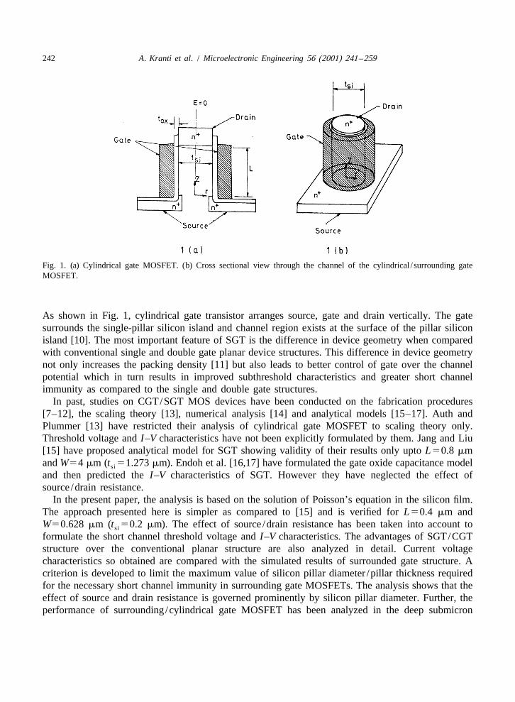
Fig. 1. (a) Cylindrical gate MOSFET. (b) Cross sectional view through the channel of the cylindrical / surrounding gateMOSFET.
As shown in Fig. 1, cylindrical gate transistor arranges source, gate and drain vertically. The gatesurrounds the single-pillar silicon island and channel region exists at the surface of the pillar siliconisland [10]. The most important feature of SGT is the difference in device geometry when comparedwith conventional single and double gate planar device structures. This difference in device geometrynot only increases the packing density [11] but also leads to better control of gate over the channelpotential which in turn results in improved subthreshold characteristics and greater short channelimmunity as compared to the single and double gate structures.
In past, studies on CGT/SGT MOS devices have been conducted on the fabrication procedures[7–12], the scaling theory [13], numerical analysis [14] and analytical models [15–17]. Auth andPlummer [13] have restricted their analysis of cylindrical gate MOSFET to scaling theory only.Threshold voltage and I–V characteristics have not been explicitly formulated by them. Jang and Liu[15] have proposed analytical model for SGT showing validity of their results only upto L50.8 mmand W54 mm (t 51.273 mm). Endoh et al. [16,17] have formulated the gate oxide capacitance modelsi
and then predicted the I–V characteristics of SGT. However they have neglected the effect ofsource /drain resistance.
In the present paper, the analysis is based on the solution of Poisson’s equation in the silicon film.The approach presented here is simpler as compared to [15] and is verified for L50.4 mm andW50.628 mm (t 50.2 mm). The effect of source /drain resistance has been taken into account tosi
formulate the short channel threshold voltage and I–V characteristics. The advantages of SGT/CGTstructure over the conventional planar structure are also analyzed in detail. Current voltagecharacteristics so obtained are compared with the simulated results of surrounded gate structure. Acriterion is developed to limit the maximum value of silicon pillar diameter /pillar thickness requiredfor the necessary short channel immunity in surrounding gate MOSFETs. The analysis shows that theeffect of source and drain resistance is governed prominently by silicon pillar diameter. Further, theperformance of surrounding/cylindrical gate MOSFET has been analyzed in the deep submicron

A. Kranti et al. / Microelectronic Engineering 56 (2001) 241 –259 243
region. Authors could not compare some of the predicted results due to non-availability ofexperimental / simulated data.
2. Theoretical considerations
2.1. Short channel threshold voltage and subthreshold swing model
Fig. 1 shows the cross-sectional view of cylindrical gate MOSFET. The Poisson’s equation in thecylindrical coordinates is given by
2 qN1 ≠ ≠ ≠ a] ] ] ] ]]Sr w(r,z)D1 w(r,z) 5 (1)2r ≠r ≠r ´≠z si
where w(r,z) is the potential distribution in the silicon film, N is the doping in the silicon film, q isa
electron charge and ´ is the dielectric permittivity of silicon.si
The potential distribution in the fully depleted silicon film is assumed to be a parabolic profile [18]in the radial direction, under the boundary conditions of fully depleted cylindrical / surrounding gateMOSFETs analogous to that developed by Auth and Plummer [13] for a cylindrical gate MOSFETand is given by
2w(r,z) 5 P (z) 1 P (z) ? r 1 P (z) ? r (2)0 1 2
where the coefficients P , P and P are functions of z.0 1 2
The boundary conditions required for the solution of potential w(r,z) are
(i) Center potential is a function of z only.
w(r 5 0,z) 5 P (z) 5 w (z) (3a)0 c
(ii) Electric field at the center of silicon film is zero.
dw(r,z)U]]] 5 0 5 P (z) (3b)1dr r50
(iii) Electric field at the silicon/oxide interface is given by
w 2 w (z)dw(r,z) gs sU]]] ]]]]5 5 t ? P (z) (3c)si 2r5t / 2dr si ´ (C )si ox cyl
where (C ) is the gate oxide capacitance per unit area of surrounding/cylindrical gate MOSFETox cyl
and is given as
2´ox]]]]]](C ) 5ox cyl 2tox
]]t ln 1 1S S DDsi tsi
where w denotes the potential at the surface of silicon film, w is the potential in the center of thes c

244 A. Kranti et al. / Microelectronic Engineering 56 (2001) 241 –259
silicon film, w ( 5V 2V ) is the gate potential, V is the flatband voltage, ´ is the dielectricgs GS fb fb ox
permittivity of oxide, t is the silicon film thickness and t is the oxide layer thickness.si ox
Using the above boundary conditions the potential in silicon film is obtained as
22´ rox]]]]]]w(r,z) 5 w (z) 1 ? (w 2 w (z)) (4)c gs s2tox2
]]´ t ln 1 1S Dsi si tsi
As the inversion layer is formed on the surface of the silicon film, substituting (4) in (1) andsimplifying one obtains
2 w 2 wd w qNgs ss a]] ]]] ]]1 5 (5)2 2 ´dz l sicyl
where l is the characteristic /natural length for cylindrical / surrounding MOSFETs and is analogouscyl
to the characteristic length (l) developed by Yan et al. [19] (for single gate MOSFET) and Suzuki etal. [20] (for double gate MOSFET). l gives the measure of the short channel effects inherent incyl
cylindrical / surrounded gate MOSFETs.
2tox2]]´ t ln 1 1S Dsi si tsi2
]]]]]]l 5 (6)cyl 8´ox
Simplifying (5) we get
2d h(z) h(z)]] ]]2 5 0 (7)2 2dz l cyl
where
2qN la cyl]]]h(z) 5 w (z) 2 w 1s gs ´si
The boundary conditions at source and drain required to solve (7) are
h(0) 5 g and h(L) 5 g 1VDS
where
g 5V 1 rbi
with V and V denoting the built in voltage and drain voltage, respectively, andbi D
2qN la cyl]]]r 5 2 wgs´si
On solving (7) using the above boundary conditions, we get
A. Kranti et al. / Microelectronic Engineering 56 (2001) 241 –259 245
2L /l L /lcyl cylg(1 2 e ) 1V g(e 2 1) 2Vz 2 zDS DS]]]]]]] ]] ]]]]]] ]]h(z) 5 exp 1 exp (8)S D S Dl l2 sinh(L /l ) 2 sinh(L /l )cyl cylcyl cyl
The position of minimum surface potential z can then be calculated asm
L]]g ? exp 2 1 2VS S D D DSl lcyl cyl
]] ]]]]]]]]]z 5 ln (9)m 2 2 L1 2]]g ? 1 2 exp 1VS S DD DSlcyl
and the potential at z becomesm
]]]]]]]]]]]]]]]]1 L 2 L
]]]] ]] ]]w (z ) 5 2 r 1 g ? exp 2 1 ? g g ? 1 2 exp 1V (10)S S S D D S S S DD Ds m DSL l lcyl cylœ]]sinhS Dlcyl
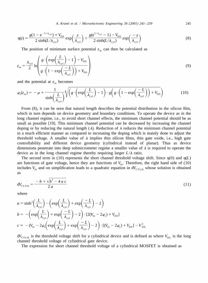
From (8), it can be seen that natural length describes the potential distribution in the silicon film,which in turn depends on device geometry and boundary conditions. To operate the device as in thelong channel regime, i.e., to avoid short channel effects, the minimum channel potential should be assmall as possible [19]. This minimum channel potential can be decreased by increasing the channeldoping or by reducing the natural length (l). Reduction of l reduces the minimum channel potentialin a much efficient manner as compared to increasing the doping which is mainly done to adjust thethreshold voltage. A smaller value of l implies thin silicon films, thin gate oxide, i.e., high gatecontrollability and different device geometry (cylindrical instead of planar). Thus as devicedimensions penetrate into deep submicrometer regime a smaller value of l is required to operate thedevice as in the long channel regime thereby requiring larger L /l ratio.
The second term in (10) represents the short channel threshold voltage shift. Since h(0) and h(L)are functions of gate voltage, hence they are functions of V . Therefore, the right hand side of (10)th
includes V and on simplification leads to a quadratic equation in dV whose solution is obtainedth CYLth
as]]]2Œ2 b 1 b 2 4 a c
]]]]]]dV 5 (11)CLYth 2 a
where
L L 2 L2]] ]] ]]a 5 sinh 2 exp 1 exp 2 2S D S S D S D Dl l lcyl cyl cyl
L 2 L]] ]]b 5 2 exp 1 exp 2 2 ? [2(V 2 2w ) 1V ]S S D S D D bi s DSl lcyl cyl
L 2 L 2]] ]]c 5 2 (V 2 2w exp 1 exp 2 2 ? [(V 2 2w ) 1V ] 2VS S D S D Dbi s bi s DS DSl lcyl cyl
dV is the threshold voltage shift for a cylindrical device and is defined as where V is the longCYLth thL
channel threshold voltage of cylindrical gate device.The expression for short channel threshold voltage of a cylindrical MOSFET is obtained as

246 A. Kranti et al. / Microelectronic Engineering 56 (2001) 241 –259
2tox2]]qN t ln 1 1S S DDa si tsi
]]]]]]]V 5V 1 2w 1 2 dV (12)thCYL fb f CYLth*´ox
This shows that threshold voltage of a cylindrical device is dependent on the silicon film thickness,i.e., on the width of the device (W 5 pt ). Conventional planar devices (single and double gatesi
structures) do not have such dependence on channel width. Thus in case of SGT, threshold voltagedecreases with decrease in channel width.
Following [20,21], the threshold voltage for a double gate MOSFET is derived as
24´ qN t 4´kT si a si si] ]]] ]] ]]]V 5V 1 2w 1 ln 1 1 1 2 dV (13)thDG fb f 2 2 DGthS D S Da 8´t kTN t kTNsisi a si a
where dV is obtained by (11), in which the characteristics length (l) takes the formDGth
]]]´ t tsi si ox]]]l 5 (14)dg 2´œ ox
instead of (6). It can be seen that l becomes smaller than l for the same set of parameters and thiscyl dg
is due to the difference in device geometry. Thus smaller value of l gives comparatively bettercyl
short channel immunity to cylindrical structure in comparison to planar device structures (single /double gate structures).
Further, the dependence of characteristic length (l ) on gate oxide capacitance per unit area for acyl
cylindrical / surrounding gate MOSFET is obtained as
´ tsi si2]]]l 5cyl 4(C )ox cyl
The same relationship for a double gate MOSFET is
´ tsi si2]]]l 5dg 2(C )ox dg
where (C ) is the gate oxide capacitance per unit area of a double gate MOSFET((C ) 5´ /t ).ox dg ox dg ox ox
As the silicon film thickness is reduced, the gate oxide capacitance per unit area of surrounding/cylindrical gate MOSFET increases. This further reduces the natural length (l ) of surrounding gatecyl
MOSFET. Thus the ratio L /l increases thereby signifying greater short channel immunity incyl
comparison to conventional planar structures. In the case of conventional planar MOSFETs (i.e.,single and double gate MOSFETs), gate oxide capacitance per unit area is independent of silicon filmthickness. Thus the rate of decrease of l with scaling down of silicon film thickness (t ) will be muchsi
more in cylindrical / surrounded gate MOSFET in comparison to double gate MOSFET. This in turnresults in smaller value of l and suppressed short channel effects in SGT MOSFETs.cyl
An important parameter characteristic of subthreshold region of MOSFET operation is subthresholdswing (S). The subthreshold swing primarily depends on the carrier concentration [20] and is definedas

A. Kranti et al. / Microelectronic Engineering 56 (2001) 241 –259 247
ln 10 1]]]]]]S 5 (15)
b ≠w (z )s min]]]S D≠VGS
Using (10) in (15) S-swing for a cylindrical gate structure becomes
2 L L]] ]exp 2 1 (V 1 r) exp 2 1 2VS S D DS S S D D Dbi DSl lln(10) cyl cyl
]] ]]]]]]]]]]]]]]]]]]]]]]]S 5 1 1 ]]]]]]]]]]]]]]]]]]]b L L 2 L1 ] ] ]]2 sinh (V 1 r) exp 2 1 2V V 2 (V 1 r) exp 2 1S D SS S S D D DS S S DDDbi DS DS bil l lcyl cyl cylœ212 L L
]] ]2 V 2 (V 1 r) exp 2 1 exp 2 1S S S D DDS S D DDS bi l lcyl cyl]]]]]]]]]]]]]]]]]]]]]]] (16)]]]]]]]]]]]]]]]]]]]
L L 2 L 2] ] ]]2 sinh (V 1 r) exp 2 1 2V V 2 (V 1 r) exp 2 1S D S S S D D DS S S D DDbi DS DS bil l lcyl cyl cylœThe first term in the above equation is the long channel result, which states that the subthreshold
slope is 60 mV/decade for a long channel device. The second term is due to the short channel effects.The subthreshold slope for a double gate device can be calculated similarly considering l instead ofdg
l .cyl
2.2. I–V formulation
For an enhancement mode MOSFET the current is given by [22]
dV(z)]]I 5 W m Q (17)D eff INV dz
where W is the effective channel width, m is the field-dependent mobility, V(z) represents the potentialalong the channel and Q is the inversion charge density defined asINV
Q 5 Q 2 QINV TOTAL BULK
where Q is the total gate charge and Q is the depletion charge.TOTAL BULK
The field-dependent mobility is given by [15,22]
m]]]]]m 5 (18)eff dV(z)1
]]]1 1 E dzC
where
mo]]]]]m 51 1u(V 2V )GS th
with m as the low field mobility. E , the critical field is given by E 52v /m where v is theo C C sat sat
saturation velocity. u is a fitting parameter and dV(z) /dz denotes the channel electric field.The inversion layer charge in the linear region is given by [22]

248 A. Kranti et al. / Microelectronic Engineering 56 (2001) 241 –259
Q 5 (C (V 2V 2 2w 2V(z)) 1 Q (19)INV ox cyl GS fb f BULK
where Q is the effective bulk charge and can be obtained from (12).BULK
2tox2]]qN t ln 1 1S S DDa si tsi
]]]]]]]Q 5 (C ) 1 2 dV 2 (20)BULK ox cyl CLYth8´ox
In short channel devices, the voltage drop across the source /drain resistance is not negligible.9Therefore considering the source /drain resistance, the effective drain voltage becomes V 5V 2 ID DS D
R where R is the drain resistance.D D
Substituting (18)–(20) in (17), one obtains
V 2I R V 2I R V 2I RD D D L D D D D D D
ID]E dV 1E I dz 5 E W m (C ) (V 2V 2 2w 2V ) dV 1 E W m Q dVD ox cyl GS fb f BULKEC
I R 0 I R I RD s D s D s
This equation when integrated between the limits and simplified, results in a quadratic equation inI whose solution isD
]]]]2Œ2 B 2 B 2 4 A C]]]]]]]I 5 (21a)D 2 A
where
W m (C )R ox cylt 2 2] ]]]]A 5 2 (R 1 R ) (21b)D sE 2C
W m (C )V ox cylDS]] ]]]]B 5 2 L 2 2 W m (C ) (V 2V 2 2w )R 1 2 V R 2 W m Q R (21c)ox cyl GS fb f DS D BULKE 2C
W m (C )ox cyl 2]]]]C 5 W m (C ) (V 2V 2 2w ) V 2 V 1 W m Q V (21d)ox cyl G fb f DS DS BULK DS2
with R 5 R 1 Rt s
The general form of current in the saturation region is given as
I 5 W v Q (22)DSAT sat sat
where I is the saturation current and Q is the inversion charge at V 5V .DSAT sat DS DSAT
The saturation charge density is given by
(Q ) 5 (C ) (V 2V 2 2w 2V ) 1 (Q ) (23)INV SAT ox cyl GS fb f DSAT BULK SAT
where (Q ) is the bulk charge at V 5V . Equating (21) and (22) at V 5V when theBULK SAT D DSAT DS DSAT
carriers get velocity saturated an equation in V can be obtained asDSAT
W m Cox]]]B 1 2 A (W m (C ) ) (V 2V 2 2 w )v 2 v VSAT SAT ox cyl GS fb f sat sat DSAT2 (24)
]]]]]]21 W v (Q ) ) 1 B 2 4 A C 5 0œsat BULK SAT SAT SAT SAT
A. Kranti et al. / Microelectronic Engineering 56 (2001) 241 –259 249
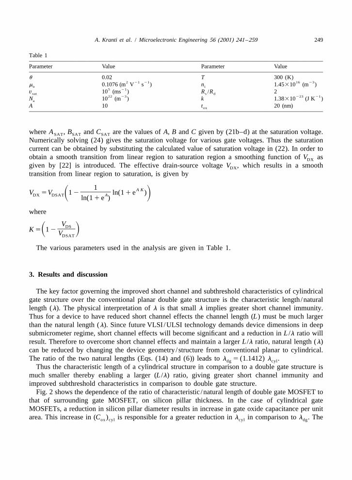
Table 1
Parameter Value Parameter Value
u 0.02 T 300 (K)2 21 21 16 23
m 0.1076 (m V s ) n 1.45310 (m )o i5 21v 10 (ms ) R /R 2sat s d22 23 223 21N 10 (m ) k 1.38310 (J K )a
A 10 t 20 (nm)ox
where A , B and C are the values of A, B and C given by (21b–d) at the saturation voltage.SAT SAT SAT
Numerically solving (24) gives the saturation voltage for various gate voltages. Thus the saturationcurrent can be obtained by substituting the calculated value of saturation voltage in (22). In order toobtain a smooth transition from linear region to saturation region a smoothing function of V asDX
given by [22] is introduced. The effective drain-source voltage V , which results in a smoothDX
transition from linear region to saturation, is given by
1 A K]]]]V 5V 1 2 ln(1 1 e )DX DSAT AS Dln(1 1 e )
where
VDS]]K 5 1 2S DVDSAT
The various parameters used in the analysis are given in Table 1.
3. Results and discussion
The key factor governing the improved short channel and subthreshold characteristics of cylindricalgate structure over the conventional planar double gate structure is the characteristic length /naturallength (l). The physical interpretation of l is that small l implies greater short channel immunity.Thus for a device to have reduced short channel effects the channel length (L) must be much largerthan the natural length (l). Since future VLSI /ULSI technology demands device dimensions in deepsubmicrometer regime, short channel effects will become significant and a reduction in L /l ratio willresult. Therefore to overcome short channel effects and maintain a larger L /l ratio, natural length (l)can be reduced by changing the device geometry /structure from conventional planar to cylindrical.The ratio of the two natural lengths (Eqs. (14) and (6)) leads to l 5 (1.1412) l .dg cyl
Thus the characteristic length of a cylindrical structure in comparison to a double gate structure ismuch smaller thereby enabling a larger (L /l) ratio, giving greater short channel immunity andimproved subthreshold characteristics in comparison to double gate structure.
Fig. 2 shows the dependence of the ratio of characteristic /natural length of double gate MOSFET tothat of surrounding gate MOSFET, on silicon pillar thickness. In the case of cylindrical gateMOSFETs, a reduction in silicon pillar diameter results in increase in gate oxide capacitance per unitarea. This increase in (C ) is responsible for a greater reduction in l in comparison to l . Theox cyl cyl dg

250 A. Kranti et al. / Microelectronic Engineering 56 (2001) 241 –259
Fig. 2. Variation of ratio of characteristic length of double gate to cylindrical gate MOSFET with silicon film thickness.
smaller value of l is responsible for improved performance of surrounding/cylindrical gatecyl
MOSFET over double gate MOSFET.Fig. 3 shows the relation between the ratio of channel length to characteristic length for various
values of silicon film thickness. As silicon film thickness is scaled down, L /l ratio increases to agreater extent in surrounding/cylindrical gate MOSFET as compared to double gate MOSFET. The
Fig. 3. Variation of ratio of channel length to characteristic length with silicon film thickness for double gate and surroundedgate MOSFET.

A. Kranti et al. / Microelectronic Engineering 56 (2001) 241 –259 251
Fig. 4. Variation of threshold voltage shift with channel length for cylindrical and double gate devices for different drainvoltages. Inset: dependence of threshold voltage on L /2l for different values of drain voltage for cylindrical MOSFET.
large value of L /l is responsible for better short channel performance of surrounding gate MOSFETcyl
over conventional planar MOSFETs.Fig. 4 shows the threshold voltage shift as a function of channel length for different drain voltages
for both cylindrical and double gate devices. As the channel length is increased the threshold voltageshift decreases and eventually approaches zero signifying long channel operation. In cylindrical /surrounding gate MOSFET the short channel effect, i.e., threshold voltage roll-off is significant belowchannel length of 0.2 mm, whereas for double gate MOSFET the short channel effect is significantbelow 0.3 mm for the parameters given in the figure. Thus cylindrical device has reduced shortchannel effects when compared with double gate structure. This improvement is due to the smallercharacteristic length in case of cylindrical gate MOSFET in comparison to double gate MOSFET.
Fig. 4 (inset) shows short channel threshold voltage as a function of the ratio of channel length tocharacteristic length for t 520 nm and t 50.1 mm for two different drain voltages. The increase inox si
drain bias causes lowering down of channel barrier, which further results in threshold voltagelowering.
Fig. 5 shows the variation of threshold voltage shift with the ratio of channel length to characteristiclength for various drain biases. As L /l ratio decreases, the shift in threshold voltage increases. Thisshift in threshold voltage is dominating below L 5 8l . Above L 5 8l short channel effectscyl cyl
become negligible and device operates in long channel regime.Fig. 6 shows the relationship between silicon film thickness and gate oxide thickness for various
values of channel lengths alleviating short channel effects. As L /l $ 8 implies long channel regime, arelation between silicon film thickness and gate oxide thickness for a particular gate length can beobtained by using Eq. (6) in the above relation. At a given channel length, silicon film thickness and

252 A. Kranti et al. / Microelectronic Engineering 56 (2001) 241 –259
Fig. 5. Variation of threshold voltage shift with L /l for different drain voltages.cyl
gate oxide thickness should be selected in the lower region of the corresponding L curve. As thechannel length decreases, allowable region for short channel immunity decreases.
Fig. 7 shows the plot of short channel threshold voltage as a function of channel length for different
Fig. 6. Relationship between silicon film thickness and gate oxide thickness for various channel lengths alleviating shortchannel effects.

A. Kranti et al. / Microelectronic Engineering 56 (2001) 241 –259 253
Fig. 7. Dependence of short channel threshold voltage on channel length for different values of silicon pillar radii. Inset:variation of threshold voltage with drain voltage for cylindrical and double gate MOSFET.
silicon pillar radii (silicon film thickness). Threshold voltage decreases with decrease in silicon pillarradius. This decrease is due to the fact that reduction in pillar radius causes a reduction in depletioncharge, which further reduces the threshold voltage. Moreover, it can be seen from the geometry ofcylindrical / surrounded gate MOSFET that the reduction in silicon film thickness results in an increasein the gate oxide capacitance per unit area which further increases the electric field, which results inthreshold voltage reduction. Close proximity with simulated result [17] confirms the validity of ourapproach.
Fig. 7 (inset) shows the plot of short channel threshold voltage for double and cylindrical gatedevices with drain voltage. This gives a measure of drain-induced barrier lowering (DIBL) effectpresent in two device structures. In case of double gate MOSFET the drain voltage has a greatercontrol over the channel, whereas the effect of drain voltage on cylindrical structure is less prominent.Thus DIBL effects will be less dominant in the case of surrounded gate structure in comparison todouble gate structure. This is due to the fact that gate has a greater control over the channel potentialin the case of SGT MOSFET. This improvement is reflected in the lower value of natural length (l )cyl
of cylindrical structure when compared with planar double gate structures.Fig. 8 depicts the variation of threshold voltage with channel length for different values of silicon
pillar doping. As doping in the silicon film is increased, threshold voltage increases. For the given setof parameters, short channel effects are dominate upto a channel length of 50 nm in surrounding gateMOSFET whereas short channel effects are considerable upto a channel length of 70 nm in the case ofdouble gate MOSFET. The threshold voltage can be raised by increasing the channel impurityconcentration and/or by gate workfunction control.
Fig. 9 shows the drain current–drain voltage characteristics for a cylindrical device for different

254 A. Kranti et al. / Microelectronic Engineering 56 (2001) 241 –259
Fig. 8. Dependence of threshold voltage on channel length for different values of silicon film doping.
gate voltages for two different channel lengths and silicon pillar radii. For a given gate voltage thedrain current initially increases and reaches maximum value and finally saturates. In the saturationregion the charge carriers reach velocity saturation. The graphs so obtained are in good agreementwhen compared with simulated results of [17], thus confirming the validity of our approach.Decreasing the channel length leads to an increase in drain current, whereas the decrease in siliconpillar radius (i.e., silicon film thickness) leads to a decrease in drain current. This drawback of SGTMOSFET can be overcome by using a multi pillar structure as proposed by Nitayama et al. [12],which employ many cylindrical / surrounded MOSFETs. Fig. 9c shows the effect of source and drainresistance on device characteristics. Only slight variation in extrinsic and intrinsic characteristics isobtained at a gate bias of 3 and 4 V. For source and drain resistance to be effective, channel resistanceshould be small. This implies a high drain current (.1 mA). Hence source and drain resistance willbe effective only when the drain current .1 mA.
Fig. 10a shows the variation of drain current with silicon film thickness for different values ofchannel lengths. Fig. 10b shows the dependence of drain current of channel length for different valuesof silicon pillar diameter. Drain current increases as the silicon film thickness is increased and channellength is decreased. However, for a given value of channel length and gate oxide thickness, themaximum value of silicon film thickness is limited by the necessary short channel immunity.
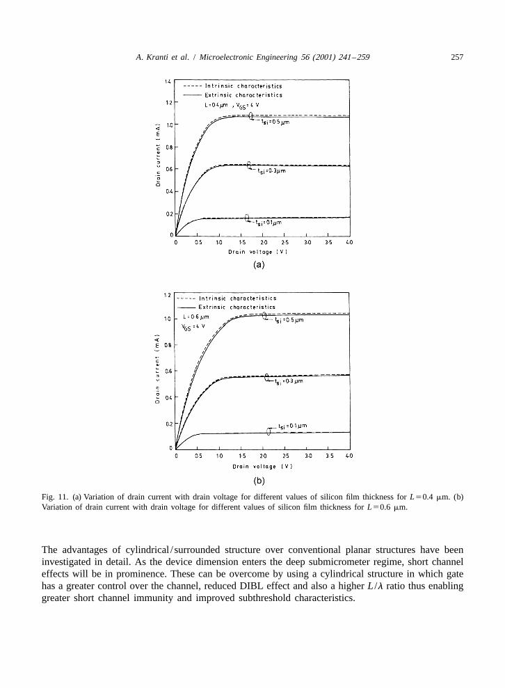
Fig. 11 shows the variation of drain current with drain bias for different values of silicon pillarthickness. Difference between extrinsic and intrinsic characteristics is significant only for t 50.5 mm.si
Thus the effect of source and drain resistance can be neglected when the device is scaled down andoperated in the deep submicron region.

A. Kranti et al. / Microelectronic Engineering 56 (2001) 241 –259 255
Fig. 9. (a) Variation of drain current with drain voltage for R50.1 mm (t 52r) and L50.4 mm with different drain voltagessi
for various gate voltages. (b) Variation of drain current with drain voltage for R50.2 mm (t 52r) and L50.6 mm withsi
different drain voltages for various gate voltages. (c) Intrinsic and extrinsic output characteristics for R50.4 mm (t 52r) andsi
L50.6 mm with different drain voltages for various gate voltages.

256 A. Kranti et al. / Microelectronic Engineering 56 (2001) 241 –259
Fig. 10. (a) Dependence of drain current on silicon film thickness for different channel lengths. (b) Dependence of draincurrent on channel length for various values of silicon film thickness.
4. Conclusions
An accurate physics based model for surrounded/cylindrical gate fully depleted MOSFET isdeveloped. The model has been verified by comparing the results so obtained with the simulated data.
A. Kranti et al. / Microelectronic Engineering 56 (2001) 241 –259 257
Fig. 11. (a) Variation of drain current with drain voltage for different values of silicon film thickness for L50.4 mm. (b)Variation of drain current with drain voltage for different values of silicon film thickness for L50.6 mm.
The advantages of cylindrical / surrounded structure over conventional planar structures have beeninvestigated in detail. As the device dimension enters the deep submicrometer regime, short channeleffects will be in prominence. These can be overcome by using a cylindrical structure in which gatehas a greater control over the channel, reduced DIBL effect and also a higher L /l ratio thus enablinggreater short channel immunity and improved subthreshold characteristics.
258 A. Kranti et al. / Microelectronic Engineering 56 (2001) 241 –259
Acknowledgements
The authors are grateful to Defence Research and Development Organisation, Ministry of Defence,Government of India for necessary financial assistance to carry out this research work.
References
[1] K. Kimura, K. Itoh, R. Hori, J. Etoh, Y. Kawajiri, H. Hisamoto, K. Sato, T. Matsumoto, Power reduction techniques inmegabit DRAM’s, IEEE J. Solid State Circuits 21 (1986) 381–389.
[2] C. Hu, Hot electron effects in MOSFET’s, IEDM Tech. Dig. (1983) 176–179.[3] T. Ohno, Y. Kado, M. Harda, T. Tuschiya, 0.25-mm gate fully depleted CMOS/SIMOX process using a experimental
new two step LOCOS isolation technique, IEEE Trans. Electron Devices 42 (1995) 1481.[4] T.C. Hsio, J.C.S. Woo, Subthreshold characteristics of fully depleted submicrometer SOI MOSFET’s, IEEE Trans.
Electron Devices 42 (1995) 1120.[5] P. Francis, A. Tero, D. Flandre, F. Vande Wiele, Modeling of ultrathin double-gate nMOS/SOI transistors, IEEE Trans.
Electron Devices 41 (1994) 715–719.[6] C. Fiegna, H. Iwai, T. Wada, M. Saito, E. Sangiori, B. Ricco, Scaling the MOS transistor below 0.1 mm: methodology,
device structure and technology requirements, IEEE Trans. Electron Devices 41 (1994) 941–951.[7] H. Takato, K. Sunouchi, N. Okabe, A. Nitayama, K. Hieda, F. Horiguchi, F. Masuoka, High performance CMOS
surrounding gate transistor (SGT) for ultra high density LSI’s, IEDM Tech. Dig. (1988) 222.[8] H. Takato, K. Sunouchi, N. Okabe, A. Nitayama, K. Hieda, F. Horiguchi, F. Masuoka, Impact of surrounding gate
transistor (SGT) for ultra high density LSI’s, IEEE Trans. Electron Devices 38 (1991) 573–578.[9] K. Sunnouchi, H. Takato, N. Okaba, T. Yamada, T. Ozaki, S. Inoue, K. Hashimoto, K. Hieda, A. Nitayama, F.
Horiguchi, F. Masuoka, A surrounding gate transistor (SGT) cell 64 /256Mbit DRAMs, IEDM Tech. Dig. (1989) 23.[10] S. Watanabe, K. Tsuchida, D. Takashima, T. Oowaki, A. Nitayama, K. Hieda, H. Takato, K. Sunnouchi, F. Horiguchi,
K. Ohuchi, F. Masuoka, H. Hara, A novel circuit technology with surrounding gate transistors (SGT) for ultra-highdensity DRAM’s, IEEE J. Solid State Circuits 30 (1995) 960–971.
[11] S. Maeda, S. Maegawa, T. Ipposhi, H. Nishimura, H. Kuriyama, O. Tanina, Y. Inoue, T. Nishimura, N. Tsubouchi,Impact of a vertical F-shaped transistor (VFT) cell for 1 Gbit DRAM and beyond, IEEE Trans. Electron Devices 42(1995) 2117–2124.
[12] A. Nitayama, H. Takato, N. Okaba, K. Sunnouchi, K. Hieda, F. Horiguchi, F. Masuoka, Multi-pillar surrounding gatetransistor (M-SGT) for compact and high speed circuits, IEEE Trans. Electron Devices 38 (1991) 579–583.
[13] C.P. Auth, J.D. Plummer, Scaling theory for cylindrical fully-depleted, surrounding gate MOSFET’s, IEEE ElectronDevice Lett. 18 (1997) 74–76.
[14] S. Miyano, M. Hirose, F. Masuoka, Numerical analysis of a cylindrical thin-pillar transistor (CYNTHIA), IEEE Trans.Electron Devices 39 (1992) 1876–1881.
[15] S.L. Jang, S.S. Liu, An analytical surrounding gate MOSFET model, Solid State Electronics 42 (1998) 721–726.[16] T. Endoh, T. Nakamura, F. Masuoka, An accurate model of fully-depleted surrounding gate transistor (FD-SGT),
IEICE Trans. Electron. E80-C (1997) 905–910.[17] T. Endoh, T. Nakamura, F. Masuoka, An analytical steady state-steady current-voltage characteristics of short channel
fully depleted surrounding gate transistor (FD-SGT), IEICE Trans. Electron. E80-C (1997) 911–917.[18] K.K. Young, Analysis of conduction in fully depleted SOI MOSFET’s, IEEE Trans. Electron Devices 36 (1989)
504–506.[19] R.H. Yan, A. Qurmazd, K.F. Lee, Scaling the Si MOSFET: from bulk to SOI to bulk, IEEE Trans. Electron Devices 39
(1992) 1704–1710.1 1[20] K. Suzuki, Y. Tosaka, T. Sugii, Analytical threshold voltage model for short channel n –p double gate SOI
MOSFET’s, IEEE Trans. Electron Devices 43 (1996) 732–737.
A. Kranti et al. / Microelectronic Engineering 56 (2001) 241 –259 259
[21] V. Aggarwal, M.K. Khanna, R. Sood, S. Haldar, R.S. Gupta, Analytical two-dimensional modeling for potentialdistribution and threshold voltage of short channel fully depleted SOI MOSFETs, Solid State Electronics 37 (1994)1537–1542.
[22] N.D. Arora, in: MOSFET Models for VLSI Circuit Simulation-Theory and Practice, Springer, New York/Vienna, 1993.