An EKV-based high voltage MOSFET model with improved mobility and drift model
8
An EKV-based high voltage MOSFET model with improved mobility and drift model Yogesh Singh Chauhan a, * , Renaud Gillon b , Benoit Bakeroot c , Francois Krummenacher a , Michel Declercq a , Adrian Mihai Ionescu a a Electronics Laboratory (LEG), Institute of Microelectronics and Microsystems (IMM), Ecole Polytechnique Fe ´de ´rale de Lausanne (EPFL), CH-1015, Lausanne, Switzerland b AMI Semiconductor (AMIS), Oudenaarde, Belgium c University of Gent, Gent, Belgium Available online 13 November 2007 The review of this paper was arranged by Adrian M. Ionescu and Yusuf Leblebici Abstract An EKV-based high voltage MOSFET model is presented. The intrinsic channel model is derived based on the charge based EKV- formalism. An improved mobility model is used for the modeling of the intrinsic channel to improve the DC characteristics. The model uses second order dependence on the gate bias and an extra parameter for the smoothening of the saturation voltage of the intrinsic drain. An improved drift model [Chauhan YS, Anghel C, Krummenacher F, Ionescu AM, Declercq M, Gillon R, et al. A highly scalable high voltage MOSFET model. In: IEEE European solid-state device research conference (ESSDERC), September 2006. p. 270–3; Chau- han YS, Anghel C, Krummenacher F, Maier C, Gillon R, Bakeroot B, et al. Scalable general high voltage MOSFET model including quasi-saturation and self-heating effect. Solid State Electron 2006;50(11–12):1801–13] is used for the modeling of the drift region, which gives smoother transition on output characteristics and also models well the quasi-saturation region of high voltage MOSFETs. First, the model is validated on the numerical device simulation of the VDMOS transistor and then, on the measured characteristics of the SOI- LDMOS transistor. The accuracy of the model is better than our previous model [Chauhan YS, Anghel C, Krummenacher F, Maier C, Gillon R, Bakeroot B, et al. Scalable general high voltage MOSFET model including quasi-saturation and self-heating effect. Solid State Electron 2006;50(11–12):1801–13] especially in the quasi-saturation region of output characteristics. Ó 2007 Elsevier Ltd. All rights reserved. 1. Introduction The interest in the high-voltage (HV) MOS devices has dramatically increased as these devices were integrated with the low power modules in MOS technology. Today, HV MOS devices are extensively used in all kinds of integrated power circuits, like switch-mode power supplies, motor drivers and, power amplifiers. In addition, LDMOS devices processed in thin-film silicon-on-insulator (SOI) provide a new and attractive technology for smart power integrated circuits in consumer and automotive applications [3]. Opti- mal design of these power circuits requires HV MOS mod- els for circuit simulation, which describe the device characteristics accurately over a wide range of biases. Acceptable simulation accuracy is obtained by the use of the macro-models based on conventional low voltage mod- ules [4]. Still compact models have clear advantage over sub-circuit models due to numerical simplicity (fast conver- gence), reduced number of parameters and more physical tuning of parameters. Some compact models for HV MOS have also been reported in the literature with better accuracy [5–7]. Halleweyen et al. [5] and Aarts and 0038-1101/$ - see front matter Ó 2007 Elsevier Ltd. All rights reserved. doi:10.1016/j.sse.2007.09.024 * Corresponding author. Tel.: +41 21 693 4604; fax: +41 21 693 3640. E-mail addresses: yogeshsingh.chauhan@epfl.ch (Y.S. Chauhan), [email protected] (R. Gillon), [email protected] (B. Bakeroot), adrian.ionescu@epfl.ch (A.M. Ionescu). www.elsevier.com/locate/sse Available online at www.sciencedirect.com Solid-State Electronics 51 (2007) 1581–1588
-
Upload
independent -
Category
Documents
-
view
3 -
download
0
Transcript of An EKV-based high voltage MOSFET model with improved mobility and drift model

Available online at www.sciencedirect.com
www.elsevier.com/locate/sse
Solid-State Electronics 51 (2007) 1581–1588
An EKV-based high voltage MOSFET model with improvedmobility and drift model
Yogesh Singh Chauhan a,*, Renaud Gillon b, Benoit Bakeroot c, Francois Krummenacher a,Michel Declercq a, Adrian Mihai Ionescu a
a Electronics Laboratory (LEG), Institute of Microelectronics and Microsystems (IMM), Ecole Polytechnique Federale de Lausanne (EPFL),
CH-1015, Lausanne, Switzerlandb AMI Semiconductor (AMIS), Oudenaarde, Belgium
c University of Gent, Gent, Belgium
Available online 13 November 2007
The review of this paper was arranged by Adrian M. Ionescu and Yusuf Leblebici
Abstract
An EKV-based high voltage MOSFET model is presented. The intrinsic channel model is derived based on the charge based EKV-formalism. An improved mobility model is used for the modeling of the intrinsic channel to improve the DC characteristics. The modeluses second order dependence on the gate bias and an extra parameter for the smoothening of the saturation voltage of the intrinsicdrain. An improved drift model [Chauhan YS, Anghel C, Krummenacher F, Ionescu AM, Declercq M, Gillon R, et al. A highly scalablehigh voltage MOSFET model. In: IEEE European solid-state device research conference (ESSDERC), September 2006. p. 270–3; Chau-han YS, Anghel C, Krummenacher F, Maier C, Gillon R, Bakeroot B, et al. Scalable general high voltage MOSFET model includingquasi-saturation and self-heating effect. Solid State Electron 2006;50(11–12):1801–13] is used for the modeling of the drift region, whichgives smoother transition on output characteristics and also models well the quasi-saturation region of high voltage MOSFETs. First, themodel is validated on the numerical device simulation of the VDMOS transistor and then, on the measured characteristics of the SOI-LDMOS transistor. The accuracy of the model is better than our previous model [Chauhan YS, Anghel C, Krummenacher F, Maier C,Gillon R, Bakeroot B, et al. Scalable general high voltage MOSFET model including quasi-saturation and self-heating effect. Solid StateElectron 2006;50(11–12):1801–13] especially in the quasi-saturation region of output characteristics.� 2007 Elsevier Ltd. All rights reserved.
1. Introduction
The interest in the high-voltage (HV) MOS devices hasdramatically increased as these devices were integrated withthe low power modules in MOS technology. Today, HVMOS devices are extensively used in all kinds of integratedpower circuits, like switch-mode power supplies, motordrivers and, power amplifiers. In addition, LDMOS devices
0038-1101/$ - see front matter � 2007 Elsevier Ltd. All rights reserved.
doi:10.1016/j.sse.2007.09.024
* Corresponding author. Tel.: +41 21 693 4604; fax: +41 21 693 3640.E-mail addresses: [email protected] (Y.S. Chauhan),
[email protected] (R. Gillon), [email protected] (B.Bakeroot), [email protected] (A.M. Ionescu).
processed in thin-film silicon-on-insulator (SOI) provide anew and attractive technology for smart power integratedcircuits in consumer and automotive applications [3]. Opti-mal design of these power circuits requires HV MOS mod-els for circuit simulation, which describe the devicecharacteristics accurately over a wide range of biases.Acceptable simulation accuracy is obtained by the use ofthe macro-models based on conventional low voltage mod-ules [4]. Still compact models have clear advantage oversub-circuit models due to numerical simplicity (fast conver-gence), reduced number of parameters and more physicaltuning of parameters. Some compact models for HVMOS have also been reported in the literature with betteraccuracy [5–7]. Halleweyen et al. [5] and Aarts and
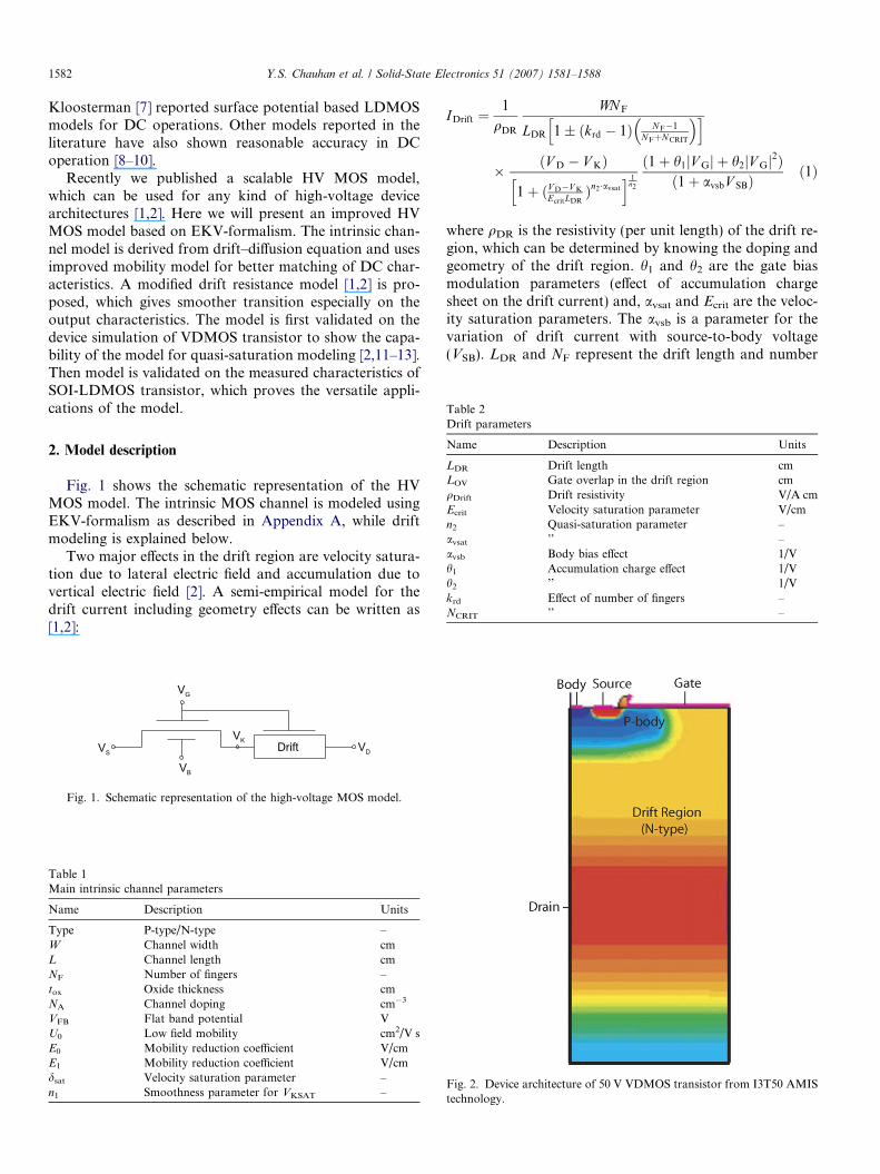
Table 2
1582 Y.S. Chauhan et al. / Solid-State Electronics 51 (2007) 1581–1588
Kloosterman [7] reported surface potential based LDMOSmodels for DC operations. Other models reported in theliterature have also shown reasonable accuracy in DCoperation [8–10].
Recently we published a scalable HV MOS model,which can be used for any kind of high-voltage devicearchitectures [1,2]. Here we will present an improved HVMOS model based on EKV-formalism. The intrinsic chan-nel model is derived from drift–diffusion equation and usesimproved mobility model for better matching of DC char-acteristics. A modified drift resistance model [1,2] is pro-posed, which gives smoother transition especially on theoutput characteristics. The model is first validated on thedevice simulation of VDMOS transistor to show the capa-bility of the model for quasi-saturation modeling [2,11–13].Then model is validated on the measured characteristics ofSOI-LDMOS transistor, which proves the versatile appli-cations of the model.
Drift parameters
Name Description Units
LDR Drift length cmLOV Gate overlap in the drift region cmqDrift Drift resistivity V/A cmEcrit Velocity saturation parameter V/cmn2 Quasi-saturation parameter –avsat ’’ –avsb Body bias effect 1/Vh1 Accumulation charge effect 1/Vh2 ’’ 1/Vkrd Effect of number of fingers –NCRIT ’’ –
2. Model description
Fig. 1 shows the schematic representation of the HVMOS model. The intrinsic MOS channel is modeled usingEKV-formalism as described in Appendix A, while driftmodeling is explained below.
Two major effects in the drift region are velocity satura-tion due to lateral electric field and accumulation due tovertical electric field [2]. A semi-empirical model for thedrift current including geometry effects can be written as[1,2]:
Drift
VG
VB
VS VD
VK
Fig. 1. Schematic representation of the high-voltage MOS model.
Table 1Main intrinsic channel parameters
Name Description Units
Type P-type/N-type –W Channel width cmL Channel length cmNF Number of fingers –tox Oxide thickness cmNA Channel doping cm�3
VFB Flat band potential VU0 Low field mobility cm2/V sE0 Mobility reduction coefficient V/cmE1 Mobility reduction coefficient V/cmdsat Velocity saturation parameter –n1 Smoothness parameter for VKSAT –
IDrift ¼1
qDR
WN F
LDR 1� ðkrd � 1Þ NF�1NFþNCRIT
� �h i
� ðV D � V KÞ
1þ ðV D�V K
EcritLDRÞn2�avsat
h i 1n2
ð1þ h1jV Gj þ h2jV Gj2Þð1þ avsbV SBÞ
ð1Þ
where qDR is the resistivity (per unit length) of the drift re-gion, which can be determined by knowing the doping andgeometry of the drift region. h1 and h2 are the gate biasmodulation parameters (effect of accumulation chargesheet on the drift current) and, avsat and Ecrit are the veloc-ity saturation parameters. The avsb is a parameter for thevariation of drift current with source-to-body voltage(VSB). LDR and NF represent the drift length and number
Fig. 2. Device architecture of 50 V VDMOS transistor from I3T50 AMIStechnology.

Y.S. Chauhan et al. / Solid-State Electronics 51 (2007) 1581–1588 1583
of fingers, respectively. NCRIT and krd are the parametersfor drift scaling with number of fingers. The ‘‘+’’ sign isused for drain-on-side devices while ‘‘�’’ sign is used fordrain-all-around devices.
Fig. 3. Device architecture of 40 V SOI-LDMO
b
a
Fig. 4. Transfer characteristics of 50 V VDMOS using device simulation (L
The accumulation charge in the drift region is obtainedby integrating the drift charge density over the gate overlaplength, assuming surface potential varies linearly in the driftregion also validated from numerical device simulation.
S transistor from I2T100 AMIS technology.
= 0.6 lm): (a) ID–VG and (b) gm–VG for VD = 1–5 V in steps of 1 V.
1584 Y.S. Chauhan et al. / Solid-State Electronics 51 (2007) 1581–1588
3. Results
The major advantage of this model is the simplicity andfew number of parameters. Most of the parameters used inthe model are physical. Tables 1 and 2 shows the list ofparameters used in the model. Fig. 2 and Fig. 3 show thedevice architectures of VDMOS and SOI-LDMOS transis-tors, respectively, on AMIS (AMI Semiconductor, Bel-gium) technologies.
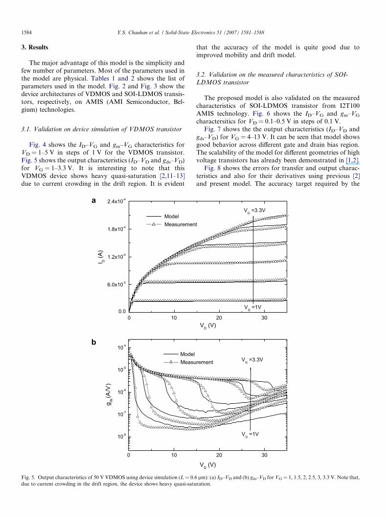
3.1. Validation on device simulation of VDMOS transistor
Fig. 4 shows the ID–VG and gm–VG characteristics forVD = 1–5 V in steps of 1 V for the VDMOS transistor.Fig. 5 shows the output characteristics (ID–VD and gds–VD)for VG = 1–3.3 V. It is interesting to note that thisVDMOS device shows heavy quasi-saturation [2,11–13]due to current crowding in the drift region. It is evident
a
b
Fig. 5. Output characteristics of 50 V VDMOS using device simulation (L = 0.6due to current crowding in the drift region, the device shows heavy quasi-satu
that the accuracy of the model is quite good due toimproved mobility and drift model.
3.2. Validation on the measured characteristics of SOI-LDMOS transistor
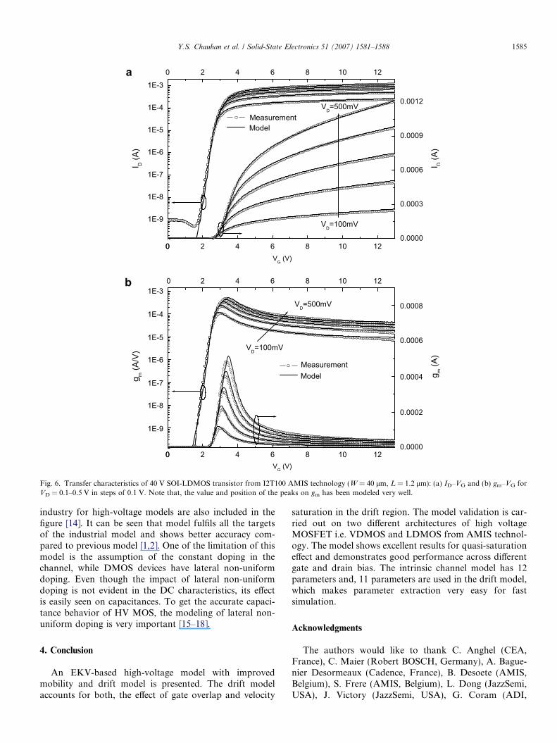
The proposed model is also validated on the measuredcharacteristics of SOI-LDMOS transistor from I2T100AMIS technology. Fig. 6 shows the ID–VG and gm–VG
charactersitics for VD = 0.1–0.5 V in steps of 0.1 V.Fig. 7 shows the the output characteristics (ID–VD and
gds–VD) for VG = 4–13 V. It can be seen that model showsgood behavior across different gate and drain bias region.The scalability of the model for different geometries of highvoltage transistors has already been demonstrated in [1,2].
Fig. 8 shows the errors for transfer and output charac-teristics and also for their derivatives using previous [2]and present model. The accuracy target required by the
lm): (a) ID–VD and (b) gds–VD for VG = 1, 1.5, 2, 2.5, 3, 3.3 V. Note that,ration.
0
0
a
b
Fig. 6. Transfer characteristics of 40 V SOI-LDMOS transistor from I2T100 AMIS technology (W = 40 lm, L = 1.2 lm): (a) ID–VG and (b) gm–VG forVD = 0.1–0.5 V in steps of 0.1 V. Note that, the value and position of the peaks on gm has been modeled very well.
Y.S. Chauhan et al. / Solid-State Electronics 51 (2007) 1581–1588 1585
industry for high-voltage models are also included in thefigure [14]. It can be seen that model fulfils all the targetsof the industrial model and shows better accuracy com-pared to previous model [1,2]. One of the limitation of thismodel is the assumption of the constant doping in thechannel, while DMOS devices have lateral non-uniformdoping. Even though the impact of lateral non-uniformdoping is not evident in the DC characteristics, its effectis easily seen on capacitances. To get the accurate capaci-tance behavior of HV MOS, the modeling of lateral non-uniform doping is very important [15–18].
4. Conclusion
An EKV-based high-voltage model with improvedmobility and drift model is presented. The drift modelaccounts for both, the effect of gate overlap and velocity
saturation in the drift region. The model validation is car-ried out on two different architectures of high voltageMOSFET i.e. VDMOS and LDMOS from AMIS technol-ogy. The model shows excellent results for quasi-saturationeffect and demonstrates good performance across differentgate and drain bias. The intrinsic channel model has 12parameters and, 11 parameters are used in the drift model,which makes parameter extraction very easy for fastsimulation.
Acknowledgments
The authors would like to thank C. Anghel (CEA,France), C. Maier (Robert BOSCH, Germany), A. Bague-nier Desormeaux (Cadence, France), B. Desoete (AMIS,Belgium), S. Frere (AMIS, Belgium), L. Dong (JazzSemi,USA), J. Victory (JazzSemi, USA), G. Coram (ADI,

a
b
Fig. 7. Output characteristics of 40 V SOI-LDMOS transistor on I2T100 AMIS technology (W = 40 lm, L = 1.2 lm): (a) ID–VD and (b) gds–VD forVG = 4–13 V in steps of 1 V.
Fig. 8. Plot of RMS errors for transfer and output characteristics.
1586 Y.S. Chauhan et al. / Solid-State Electronics 51 (2007) 1581–1588
USA), M. Lee (Atmel, USA) for interesting discussionsand suggestions to improve the model performance. Thiswork was supported by the IST-507653’ROBUSPIC’ ECproject and the Swiss OFES No. 03-491.
Appendix A. Modeling of intrinsic MOS using EKV-
formalism
The well-known drift–diffusion current expression isgiven by
IKS ¼ IDrift þ IDiff ¼ lW �Qi
dWS
dxþ U T
dQi
dx
� �; ðA:1Þ
where, l, W, Qi, and WS are the mobility, width, inversioncharge, and surface potential, respectively, at any position

Y.S. Chauhan et al. / Solid-State Electronics 51 (2007) 1581–1588 1587
x in the channel. The thermal voltage has been denoted byUT. The doping is assumed constant along the channel. Theinversion charge linearization relation between Qi and WS
using EKV formalism [19–21] can be expressed as
�Qi ¼ nqCoxðWP �WSÞ; ðA:2Þ
where slope factor nq and pinch-off surface potential WP aredefined as [19,20]
nq ¼ 1þ CffiffiffiffiWp
P þffiffiffiffiffiffiffiffiffiffiffiffiffiffiffiffiffiffiffiffiffiffiffiffiffiffiffiffiffiffiffiffiffiffiffiffiWP þ U Tðqs þ qkÞ
p ; ðA:3Þ
V G � V FB ¼ WP þ signðWPÞCffiffiffiffiffiffiffiffiffiffiffiffiffiffiffiffiffiffiffiffiffiffiffiffiffiffiffiffiffiffiffiffiffiffiffiffiffiffiffiU Te�
WPUT þWP � U T
q; ðA:4Þ
where Cox and C are the oxide capacitance and body effectcoefficient, respectively. The qk and qs are the normalizedcharge densities at intrinsic drain and source, respectively,described later in this section. The mobility model can bederived as follows [22]:
l ¼ vdrift
Ex
¼ lv
1þ Ex
Ec
��� ��� ¼lv
1þ dWS=dxvsat=lv
��� ��� ; ðA:5Þ
where
lv ¼ qvl0: ðA:6Þ
Here vdrift, vsat, Ex and Ec are the drift velocity, saturationvelocity, longitudinal electric field and critical electric field,respectively. The mobility lv is a function of the verticalelectric field only, through qv, where qv is a function of biascondition and doping level defined as follows:
qv ¼1
1þ Eeff
E0þ Eeff
E1
� �2; ðA:7Þ
where E0 and E1 are the parameters. The effective verticalelectric field Eeff [22] is given by
Eeff ¼Qb þ gQi
�Si
�������� ¼ �Qb þ gð�QiÞ
�Si
¼Qg � ð1� gÞð�QiÞ
�Si; ðA:8Þ
where g is the weighing parameter between Qb and Qi.From (A.1) and (A.5), IKS can be written as
IKS ¼lv
1þ lv
vsat
dWs
dx
�� ��W �Qi
dWs
dxþ U T
dQi
dx
� �: ðA:9Þ
Using (A.2) and (A.6) for dWs
dx > 0, (A.9) can be rewritten as
dqdn¼ � iks
qv 1þ 2q� dsatiksð Þ ; ðA:10Þ
where variables and constants are normalized from EKVformalism [19,20] as follows:
q ¼ �Qi
2nqCoxU T
; iks ¼IKS
2nqWL l0CoxU 2
T
;
dsat ¼2l0UT
vsatL; n ¼ x
L: ðA:11Þ
Notice that q, iks, dsat and, qv are all dimensionlessquantities.
Integrating (A.10) along the channel from n = 0 ton = 1, the intrinsic drain to source current iks and total nor-malized inversion charge density qc in the channel areobtained as
iks ¼qv
1þ qvdsatðqs � qkÞq2
s þ qs
� � q2
k þ qk
� �; ðA:12Þ
qc ¼Z 1
0
qn
¼ 1
2qs þ qk þ
1
3
ðqs � qkÞ2
ð1þ qs þ qkÞ½1þ qvdsatðqs � qkÞ�
( ):
ðA:13Þ
The normalized charge densities at intrinsic drain (qk) andsource (qs) are obtained from following transcendentalequations [19].
2qk þ lnðqkÞ ¼ vp � vk; ðA:14Þand,
2qs þ lnðqsÞ ¼ vp � vs: ðA:15Þwhere vk ¼ V K
UT, vs ¼ V S
UTare the normalized bias voltages; vp
is the normalized pinch off voltage and defined as [19]
vp ¼ wp � w0; ðA:16Þ
where wp ¼ WP
UTis the normalized pinch-off surface potential
while w0 is the normalized inversion surface potential givenby [19]
w0 ¼ 2/f þ m; ðA:17Þwhere m is an adjustable parameter, typically ranging be-tween 1–4 [19]. /f ¼ lnðNA
niÞ is the normalized bulk fermi po-
tential. The normalized drain-to-source current iks
including velocity saturation from (A.12) can be written as,
iks ¼qv
1þ qvdsatðqs � qkvÞq2
s þ qs
� � q2
kv þ qkv
� �; ðA:18Þ
where qkv is expressed as
qkv ¼ gqk
vk � vs
1þ vk�vs
jvqksatj
� �n1h i 1
n1
þ qk0; ðA:19Þ
qk0 ¼ qkjvks¼0; ðA:20Þ
gqk¼ @qk
@vk
����vks¼0
¼ � 1
2þ 1qk0
; ðA:21Þ
vqksat¼ qksat � qk0
gqk
: ðA:22Þ
The n1 is a parameter, which gives smoother transitionfrom qk to qksat (or VK to VKSAT). The minimum normal-ized inversion charge density (qksat) at the drain end of thechannel during velocity saturation is given as,
qksat ¼1
2þ qsþ
1
qvdsat
� ��
ffiffiffiffiffiffiffiffiffiffiffiffiffiffiffiffiffiffiffiffiffiffiffiffiffiffiffiffiffiffiffiffiffiffiffiffiffiffiffiffiffiffiffiffiffiffiffiffiffiffiffiffiffiffiffiffiffiffiffiffiffiffi1
2þ 1
qvdsat
� �2
þ 1
qvdsat
2qsþ 1ð Þ
s:
ðA:23Þ

1588 Y.S. Chauhan et al. / Solid-State Electronics 51 (2007) 1581–1588
The charge densities related to gate (Qg), intrinsic drain(Qk), source (Qs) for intrinsic MOS can be calculated fromfollowing equations:
Qg ¼QG
WLCoxU T
¼Z 1
0
V G � V FB �WS
U T
dn
¼Z 1
0
ðvg � vfb � wp þ 2qÞdn; ðA:24Þ
Qk ¼Z 1
0
n � qdn; ðA:25Þ
Qs ¼Z 1
0
ð1� nÞ � qdn; ðA:26Þ
where vg ¼ V G
UT, vfb ¼ V FB
UTare the normalized gate and flat-
band voltage, respectively. The final expressions for intrin-sic drain to source current (IKS) can be written as,
IKS ¼ 2nq
WL
l0CoxU 2T
� �iks: ðA:27Þ
Similarly, final expressions for total intrinsic drain, source,gate and, bulk charge ignoring mobility degradation can bewritten as,
QD ¼ �WLCoxUT
nq
3qs þ 2qd þ
1
21þ 6
5qs þ
4
5qd
� ��
� qs � qdð Þ2
1þ qs þ qdð Þ2
#; ðA:28Þ
QS ¼ �WLCoxUT
nq
32qs þ qd þ
1
21þ 4
5qs þ
6
5qd
� ��
� qs � qdð Þ2
1þ qs þ qdð Þ2
#; ðA:29Þ
QG ¼ WLCoxU T vg � vfb � wp
þ qs þ qd þ
1
3
ðqs � qdÞ2
ð1þ qs þ qdÞ
!#; ðA:30Þ
QB ¼ �WLCoxUT vg � vfb � wp � nq � 1�
� qs þ qd þ1
3
ðqs � qdÞ2
ð1þ qs þ qdÞ
!#: ðA:31Þ
References
[1] Chauhan YS, Anghel C, Krummenacher F, Ionescu AM, DeclercqM, Gillon R, et al. A highly scalable high voltage MOSFET model.In IEEE European solid-state device research conference (ESSD-ERC), September 2006. p. 270–3.
[2] Chauhan YS, Anghel C, Krummenacher F, Maier C, Gillon R,Bakeroot B, et al. Scalable general high voltage MOSFET modelincluding quasi-saturation and self-heating effect. Solid State Electron2006;50(11–12):1801–13.
[3] van der Pol JA, Ludikhuize A, Huizing H, van Velzen B, Hueting R,Mom J, et al. A-BCD: an economic 100 V RESURF silicon-on-insulator BCD technology for consumer and automotive applica-
tions. In IEEE international symposium on power semiconductordevices and ICs, June 2000. p. 327330.
[4] Frere S, Moens P, Desoete B, Wojciechowski D, Walton A. Animproved LDMOS transistor model that accurately predicts capac-itance for all bias conditions. In Proceedings of the 2005 internationalconference on microelectronic test structures (ICMTS), April 2005. p.75–9.
[5] D’Halleweyn N, Benson J, Redman-White W, Mistry K, SwanenbergM. MOOSE: a physically based compact DC model of SOI LDMOSFETs for analogue circuit simulation. IEEE Trans Comput-AidDes Integr Circ Syst 2004;23(10):1399–410.
[6] Aarts A, D’Halleweyn N, van Langevelde R. A surface-potential-based high-voltage compact LDMOS transistor model. IEEE TransElectron Dev 2005;52(5):999–1007.
[7] Aarts A, Kloosterman W. Compact modeling of high-voltageLDMOS devices including quasi-saturation. IEEE Trans ElectronDev 2006;53(4):897–902.
[8] Victory J, Sanchez J, DeMassa T, Welfert B. A static, physicalVDMOS model based on the charge-sheet model. IEEE TransElectron Dev 1996;43(1):157–64.
[9] Tsai C-Y, Burk DE, Ngo KDT. Physical modeling of the powerVDMOST for computer-aided design of integrated circuit. IEEETrans Electron Dev 1997;44(3):472–80.
[10] Hefyene N, Anghel C, Ionescu A, Frere S, Gillon R, Vermandel M,et al. An experimental approach for bias-dependent drain seriesresistances evaluation in asymmetric HV MOSFETs. In IEEEEuropean solid-state device research conference (ESSDERC), Sep-tember 2001. p. 403–6.
[11] Darwish MN. Study of the quasi-saturation effect in VDMOStransistors. IEEE Trans Electron Dev 1986;33(11):1710–6.
[12] Park C-K, Lee K. Experiments and 2D-simulations for quasi-saturation effect in power VDMOS transistors. In IEEE internationalsymposium on power semiconductor devices and ICs, June 1990. p.219–24.
[13] Rebollo J, Figueras E, Milln J, Lora-Tamayo E, Serra-Mestres F.Analysis of the quasi-saturation region of high voltage VDMOSdevices. Solid-State Electron 1987;30(2):77–180.
[14] Robuspic (robust mixed signal design methodologies for smart powerics). http://www-g.eng.cam.ac.uk/robuspic, 2004–2006.
[15] Aarts A, van der Hout R, Paasschens J, Scholten A, Willemsen M,Klaassen D. Capacitance modeling of laterally non-uniform MOSdevices. In IEEE international electron devices meeting, December2004. p. 751–4.
[16] Roy AS, Chauhan YS, Enz C, Sallesse J-M, Ionescu AM, DeclercqM. Partitioning scheme in lateral asymmetric MOST. In IEEEEuropean solid-state device research conference, September 2006. p.307–10.
[17] Roy AS, Enz CC, Sallesse J-M. Source–drain partitioning inMOSFET. IEEE Trans Electron Dev 2007;54(6):1384–93.
[18] Chauhan YS, Krummenacher F, Anghel C, Gillon R, Bakeroot B,Declercq M. Analysis and modeling of lateral non-uniform doping inhigh-voltage MOSFETs. In IEEE international electron devicesmeeting, December 2006. p. 831–4.
[19] Sallese J-M, Bucher M, Krummenacher F, Fazan P. Inversion chargelineariazation in MOSFET modeling and rigorous derivation of theEKV compact model. Solid-State Electron 2003;46(11):677–83.
[20] Enz C, Krummenacher F, Vittoz E. An analytical MOS transistormodel valid in all regions of operation and dedicated to low-voltageand low-current applications. J Analog Integr Circ Signal Process1995;8(1):3–114.
[21] Enz CC, Vittoz EA. MOS transistor modeling for low-voltage andlow-power analog IC design. Microelectron Eng 1997;39(1–4):59–76.
[22] Bucher M. Analytical MOS transistor modelling for analog circuitsimulation. Ph.D. dissertation, EPFL, 1999, thesis No. 2114.