Feedback Linearization and High Order Sliding Mode Observer For A Quadrotor UAV
566 IEEE TRANSACTIONS ON INDUSTRIAL ELECTRONICS, VOL. 52, NO. 2, APRIL 2005
Sliding-Mode Control of Quantum Series-ParallelResonant Converters via Input–Output Linearization
Miguel Castilla, Luis García de Vicuña, Josep María Guerrero, José Matas, and Jaume Miret, Member, IEEE
Abstract—The purpose of this paper is to explore the problem ofdesigning proper sliding-mode controllers to regulate the outputvoltage of the dc-to-dc quantum series-parallel resonant converter.A control-oriented dynamic model, which appropriately describesthe large-signal behavior of the power circuit by average state vari-ables, is first developed. Using input–output feedback lineariza-tion, a control design methodology is then presented, which leadsto a family of sliding surfaces that make the output voltage behavefollowing a particular large-signal linear dynamics. Among thesesurfaces, the final configuration is selected taking into account con-trol circuit simplicity as the basic premise. Besides exhibiting theabsence of output-voltage errors in steady state, the control solu-tion leads to robust operation with respect to parameter variationsand external disturbances. Simulations and experimental resultsare reported to validate the expected features of the proposed con-trol solution.
Index Terms—Feedback linearization, quantum modulation,resonant converter, sliding-mode control.
I. INTRODUCTION
THE control of resonant power converters has been widelyinvestigated in the literature [1]–[8]. Although the most
popular are frequency and phase control, switching losses andelectromagnetic interference (EMI) noise are strongly reducedusing amplitude modulation by means of a new time-domainoperation scheme named quantum-mode control [5]–[8]. To im-plement this switching technique, sliding-mode control seems tobe a good choice due to its excellent properties, such as robust-ness against both system parameter variations and large-signalexternal disturbances [9], [10]. The application of this controltechnique to quantum resonant converters, however, has onlybeen examined in a small number of studies that basically in-volve the control design of the series-loaded and parallel-loadedtopologies [11], [12].
The purpose of this paper is to explore the problem of de-signing proper sliding-mode controllers to regulate the outputvoltage of the dc-to-dc quantum series-parallel resonant con-verter (QSPRC). Besides the good steady-state accuracy thesystem exhibits, we are especially interested in the synthesis ofsliding surfaces that makes the output voltage of the QSPRCbehave following a particularly large-signal linear dynamics.This control objective allows the designer to use traditional
Manuscript received November 19, 2002; revised Decembr 16, 2003. Ab-stract published on the Internet January 13, 2005. This work was supported bythe Ministerio de Ciencia y Tecnología (Spain) under Grant DPI2003-06508-C02-01.
The authors are with the Departamento de Ingeniería Electrónica, Uni-versidad Politécnica de Cataluña, 08800 Vilanova i la Geltrú, Spain (e-mail:[email protected]).
Digital Object Identifier 10.1109/TIE.2005.844256
(linear) control techniques to establish suitable linear dynamicsthat meets the time-domain converter specifications (maximumsettling time, overshoot, etc.).
The control design begins with the development of a con-trol-oriented dynamic model for the open-loop QSPRC. Theaveraging method reported in [13], among other similar existingtechniques [14], [15], is selected to derive the model becausethe time-varying average variables include the amplitudes andphase angles of resonant state variables, which results in asimpler and easy-to-use dynamic model. Although practicalconsiderations are used in the model derivation (such as thefact that resonant waveforms evolve quickly when comparedwith output filter variables), the large-signal operation of theQSPRC is preserved as no small-signal approximations areconsidered. In addition, no assumptions are made to reducethe order of the nonlinear dynamic model; consequently, theperformance of the closed-loop power system can be correctlytested.
Next, we consider the use of feedback linearization to designthe sliding-mode controller for the QSPRC. Feedback lineariza-tion techniques have been successfully used in the control de-sign of conventional (hard switching) dc-to-dc conversion cells[16]–[19]. The main goal of these approaches is to transformthe converter bilinear model into a fully linear system, usingexact state transformations and feedback (again no small-signalapproximations are considered) [20]. However, the applicationof these interesting techniques has not been widely expandednowadays, probably because full linearizing control loops re-quire a complex and expensive practical implementation.
As an alternative, and starting from input–output feedbacklinearization (a partial linearizing approach) [20], this paperpresents a design methodology leading to a family of slidingsurfaces that force the output voltage of the QSPRC to followdesired linear dynamics. Among these surfaces, the finalconfiguration is selected taking into account control circuitsimplicity as the basic premise. Besides exhibiting the absenceof output-voltage errors in steady state, the control solutionleads to robust operation with respect to parameter variationsand external disturbances (in the input voltage and/or in theload). All these features will be evidenced in the followingsections.
The effectiveness of the control solution is established bythe stability analysis of the closed-loop system dynamics.The analysis yields a set of design restrictions in terms ofthe converter components and the parameters of the desiredoutput-voltage dynamics. In addition, numerical simulations andexperimental results are reported, confirming the validity of thetheoretical contributions: 1) the control-oriented dynamic model
0278-0046/$20.00 © 2005 IEEE
CASTILLA et al.: SLIDING-MODE CONTROL OF QSPRCs VIA INPUT–OUTPUT LINEARIZATION 567
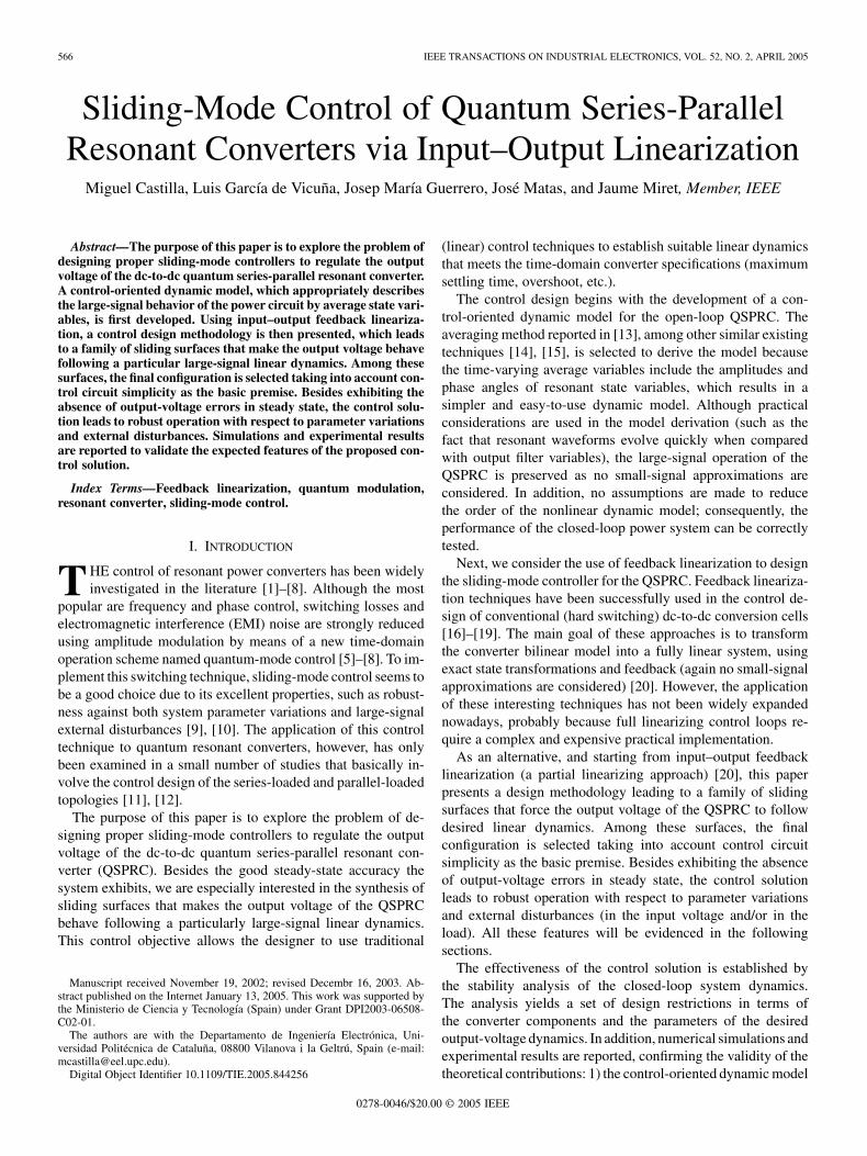
Fig. 1. Basic topology of the QSPRC.
TABLE ICHARACTERISTICS OF OPERATIONAL MODES
Fig. 2. Typical quantum waveforms. (a) Resonant inductor current (2 A/div). (b) Transformer voltage v (50 V/div). Bottom: control signal u(kT ) (10 V/div).
of the QSPRC; 2) the design methodology of sliding-modecontrol schemes; and 3) the proposed control solution.
II. OPERATION PRINCIPLE OF THE QSPRC
The power circuit of the QSPRC is shown in Fig. 1. It consistsof a third-order resonant network that includes a high-frequencytransformer, excited by a full-bridge inverter and loaded by arectifier and a low-pass filter.
In the QSPRC, the energy flow between the input source andthe load is controlled by two different modes of operation. In theenergizing mode (EM), the pair of switches S1-S4 and S2-S3are switching on and off at resonant frequency, thus transferringenergy toward the resonant tank at a maximum rate (the inputpower to the resonant circuit is always positive;see Table I). In the de-energizing mode (DM), switches S2 andS4 are constantly in the on state, forcing the input power flowing
toward the resonant circuit to be zero. In both modes of opera-tion, the output power of the resonant tank isalways positive, thus continuously supplying part of its energyto the load (see also Table I).
This principle of operation results in sinusoidal resonantwaveforms with amplitude modulation. The peak values ofthese waveforms are increased in EM and decreased in DM.Typical waveforms for a nonperiodic sequence of controlmodes are shown in Fig. 2. Note how the operational modespresent discrete time duration, which coincides with an integernumber of half resonant periods.
III. CONTROL-ORIENTED DYNAMIC MODEL
The first problem addressed in this paper is the developmentof an appropriate dynamic description of the isolated QSPRCconverter valid for the design of a nonlinear variable-structurecontroller.
568 IEEE TRANSACTIONS ON INDUSTRIAL ELECTRONICS, VOL. 52, NO. 2, APRIL 2005
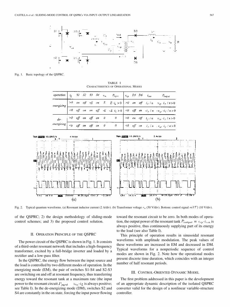
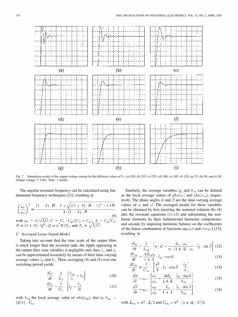
Fig. 3. Waveform comparison of the QSPRC converter with its averaged model.
A. State-Space Model
The power stage of the QSPRC, shown in Fig. 1, can be rep-resented by the following set of differential state equations:
(1)
(2)
(3)
(4)
(5)
where , , and are the resonant state variables (denotinginductor current, series capacitor voltage, and parallel capacitorvoltage) and , the output filter state variables (being in-ductor current and capacitor voltage). The control input is adiscrete-time variable which shows the selected mode of opera-tion: corresponds to EM and to DM.
CASTILLA et al.: SLIDING-MODE CONTROL OF QSPRCs VIA INPUT–OUTPUT LINEARIZATION 569
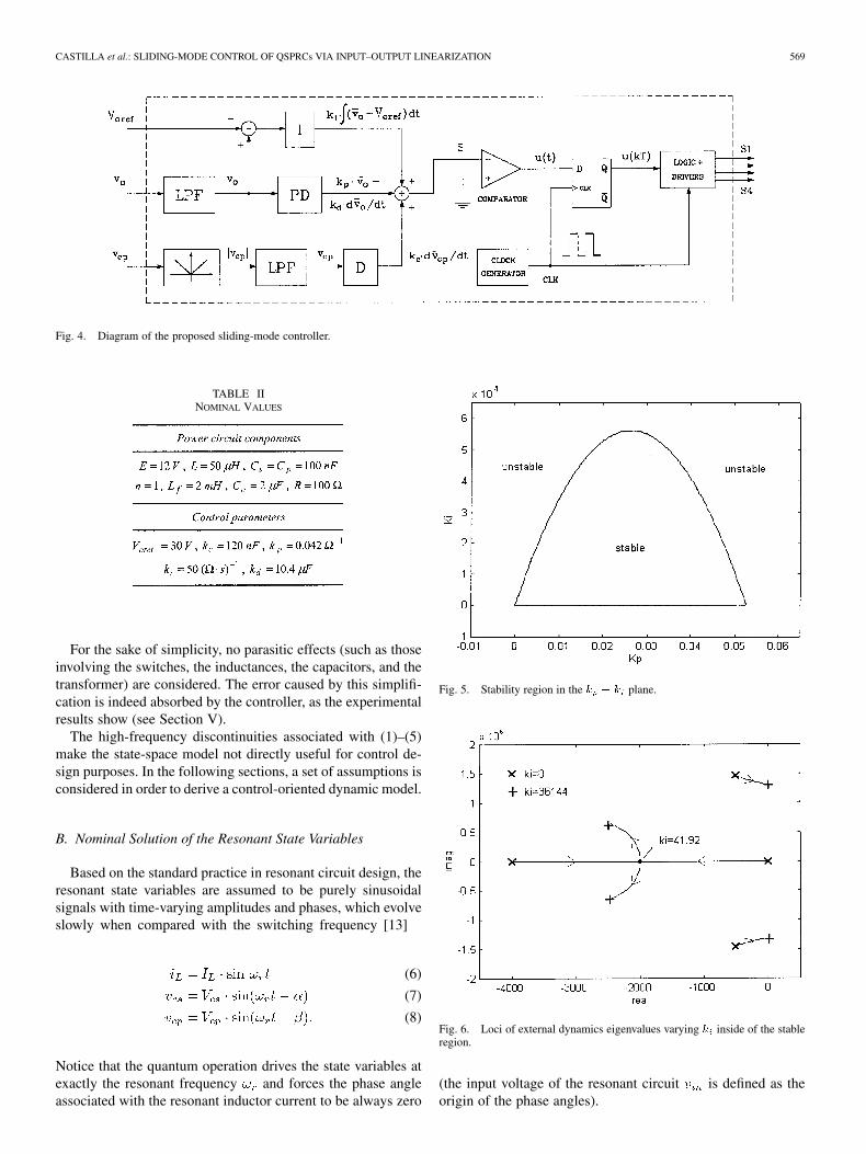
Fig. 4. Diagram of the proposed sliding-mode controller.
TABLE IINOMINAL VALUES
For the sake of simplicity, no parasitic effects (such as thoseinvolving the switches, the inductances, the capacitors, and thetransformer) are considered. The error caused by this simplifi-cation is indeed absorbed by the controller, as the experimentalresults show (see Section V).
The high-frequency discontinuities associated with (1)–(5)make the state-space model not directly useful for control de-sign purposes. In the following sections, a set of assumptions isconsidered in order to derive a control-oriented dynamic model.
B. Nominal Solution of the Resonant State Variables
Based on the standard practice in resonant circuit design, theresonant state variables are assumed to be purely sinusoidalsignals with time-varying amplitudes and phases, which evolveslowly when compared with the switching frequency [13]
(6)
(7)
(8)
Notice that the quantum operation drives the state variables atexactly the resonant frequency and forces the phase angleassociated with the resonant inductor current to be always zero
Fig. 5. Stability region in the k � k plane.
Fig. 6. Loci of external dynamics eigenvalues varying k inside of the stableregion.
(the input voltage of the resonant circuit is defined as theorigin of the phase angles).
570 IEEE TRANSACTIONS ON INDUSTRIAL ELECTRONICS, VOL. 52, NO. 2, APRIL 2005
Fig. 7. Simulation results of the output-voltage startup for the different values of k : (a) 920, (b) 535, (c) 325, (d) 200, (e) 145, (f) 120, (g) 75, (h) 50, and (i) 30.Output voltage: 5 V/div. Time: 1 ms/div.
The angular resonant frequency can be calculated using fun-damental frequency techniques [21], resulting in
(9)with , , ,
, , and .
C. Averaged Large-Signal Model
Taking into account that the time scale of the output filteris much longer than the resonant tank, the ripple appearing inthe output filter state variables is negligible and, thus, andcan be approximated accurately by means of their time-varyingaverage values and . Then, averaging (4) and (5) over oneswitching period yields
(10)
(11)
with the local average value of , that is,.
Similarly, the average variables and can be definedas the local average values of and , respec-tively. The phase angles and are the time-varying averagevalues of and . The averaged model for these variablescan be obtained by first inserting the nominal solution (6)–(8)into the resonant equations (1)–(3) and substituting the non-linear elements by their fundamental harmonic components;and second, by imposing harmonic balance on the coefficientsof the linear combination of functions and [13],resulting in
(12)
(13)
(14)
(15)
(16)
with and .
CASTILLA et al.: SLIDING-MODE CONTROL OF QSPRCs VIA INPUT–OUTPUT LINEARIZATION 571
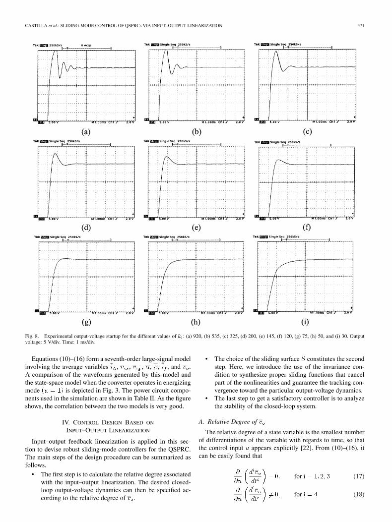
Fig. 8. Experimental output-voltage startup for the different values of k : (a) 920, (b) 535, (c) 325, (d) 200, (e) 145, (f) 120, (g) 75, (h) 50, and (i) 30. Outputvoltage: 5 V/div. Time: 1 ms/div.
Equations (10)–(16) form a seventh-order large-signal modelinvolving the average variables , , , , , , and .A comparison of the waveforms generated by this model andthe state-space model when the converter operates in energizingmode is depicted in Fig. 3. The power circuit compo-nents used in the simulation are shown in Table II. As the figureshows, the correlation between the two models is very good.
IV. CONTROL DESIGN BASED ON
INPUT–OUTPUT LINEARIZATION
Input–output feedback linearization is applied in this sec-tion to devise robust sliding-mode controllers for the QSPRC.The main steps of the design procedure can be summarized asfollows.
• The first step is to calculate the relative degree associatedwith the input–output linearization. The desired closed-loop output-voltage dynamics can then be specified ac-cording to the relative degree of .
• The choice of the sliding surface constitutes the secondstep. Here, we introduce the use of the invariance con-dition to synthesize proper sliding functions that cancelpart of the nonlinearities and guarantee the tracking con-vergence toward the particular output-voltage dynamics.
• The last step to get a satisfactory controller is to analyzethe stability of the closed-loop system.
A. Relative Degree of
The relative degree of a state variable is the smallest numberof differentiations of the variable with regards to time, so thatthe control input appears explicitly [22]. From (10)–(16), itcan be easily found that
for (17)
for (18)
572 IEEE TRANSACTIONS ON INDUSTRIAL ELECTRONICS, VOL. 52, NO. 2, APRIL 2005
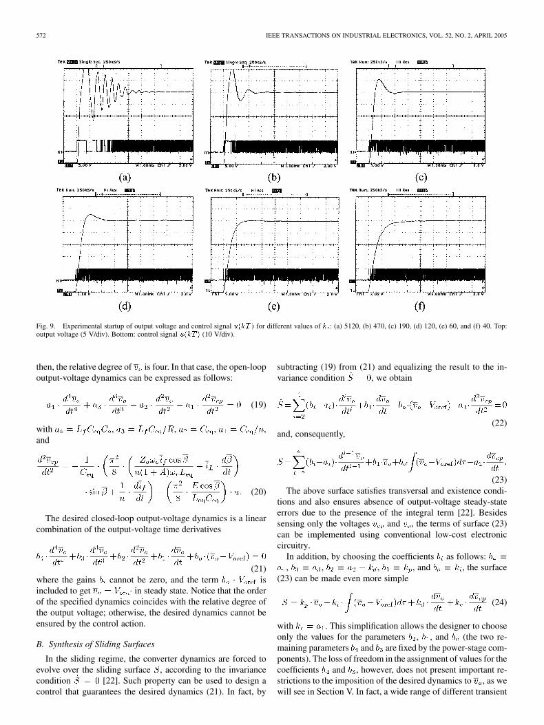
Fig. 9. Experimental startup of output voltage and control signal u(kT ) for different values of k : (a) 5120, (b) 470, (c) 190, (d) 120, (e) 60, and (f) 40. Top:output voltage (5 V/div). Bottom: control signal u(kT ) (10 V/div).
then, the relative degree of is four. In that case, the open-loopoutput-voltage dynamics can be expressed as follows:
(19)
with , , , ,and
(20)
The desired closed-loop output-voltage dynamics is a linearcombination of the output-voltage time derivatives
(21)where the gains cannot be zero, and the term isincluded to get in steady state. Notice that the orderof the specified dynamics coincides with the relative degree ofthe output voltage; otherwise, the desired dynamics cannot beensured by the control action.
B. Synthesis of Sliding Surfaces
In the sliding regime, the converter dynamics are forced toevolve over the sliding surface , according to the invariancecondition [22]. Such property can be used to design acontrol that guarantees the desired dynamics (21). In fact, by
subtracting (19) from (21) and equalizing the result to the in-variance condition , we obtain
(22)and, consequently,
(23)The above surface satisfies transversal and existence condi-
tions and also ensures absence of output-voltage steady-stateerrors due to the presence of the integral term [22]. Besidessensing only the voltages and , the terms of surface (23)can be implemented using conventional low-cost electroniccircuitry.
In addition, by choosing the coefficients as follows:, , , , and , the surface
(23) can be made even more simple
(24)
with . This simplification allows the designer to chooseonly the values for the parameters , , and (the two re-maining parameters and are fixed by the power-stage com-ponents). The loss of freedom in the assignment of values for thecoefficients and , however, does not present important re-strictions to the imposition of the desired dynamics to , as wewill see in Section V. In fact, a wide range of different transient
CASTILLA et al.: SLIDING-MODE CONTROL OF QSPRCs VIA INPUT–OUTPUT LINEARIZATION 573
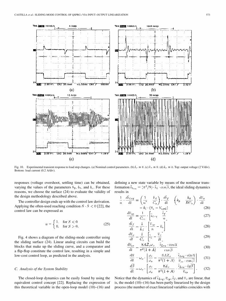
Fig. 10. Experimental transient response to load step changes. (a) Nominal control parameters. (b) k = 0. (c) k = 0. (d) k = 0. Top: output voltage (2 V/div).Bottom: load current (0.2 A/div).
responses (voltage overshoot, settling time) can be obtained,varying the values of the parameters , , and . For thesereasons, we choose the surface (24) to evaluate the validity ofthe design methodology described above.
The controller design ends up with the control law derivation.Applying the often-used reaching condition [22], thecontrol law can be expressed as
forfor
(25)
Fig. 4 shows a diagram of the sliding-mode controller usingthe sliding surface (24). Linear analog circuits can build theblocks that make up the sliding curve, and a comparator anda flip-flop constitute the control law, resulting in a simple andlow-cost control loop, as predicted in the analysis.
C. Analysis of the System Stability
The closed-loop dynamics can be easily found by using theequivalent control concept [22]. Replacing the expression ofthis theoretical variable in the open-loop model (10)–(16) and
defining a new state variable by means of the nonlinear trans-formation , the ideal sliding dynamicsresults in
(26)
(27)
(28)
(29)
(30)
(31)
(32)
Notice that the dynamics of , , , and are linear, thatis, the model (10)–(16) has been partly linearized by the designprocess (the number of exact linearized variables coincides with
574 IEEE TRANSACTIONS ON INDUSTRIAL ELECTRONICS, VOL. 52, NO. 2, APRIL 2005
the relative degree of ). Moreover, these external dynamicsare uncoupled to the internal variables ( , , ), so the sta-bility of this subsystem can be tested using well-known lineartechniques. In doing so, the following design restrictions can bededuced in terms of the converter components and the controlparameters:
(33)
(34)
(35)
On the other hand, a simple way of demonstrating the sta-bility of the internal dynamics expressed in (30)–(32) is usingthe zero-dynamics approach [20]. The zero dynamics are de-fined as the internal dynamics of the system when the output iskept at its equilibrium value and, then, all of its time derivativesare zero. By means of small-signal linearization, it can be easilyfound that the zero dynamics of (30)–(32) present local asymp-totic stability. Moreover, the zero dynamics are independent ofthe control parameters, so no design conditions are derived fromthis analysis.
Fig. 5 shows the stability region in the plane, usingthe nominal values listed in Table II. Fixing ,the minimum and maximum values of for stable operationare 0 and 36144, respectively. For this range of , the loci ofthe external dynamics eigenvalues are depicted in Fig. 6.
Finally, Fig. 7 shows some simulation results of theclosed-loop QSPRC during the output-voltage startup fordifferent values of . Notice that a wide range of transientresponses is obtained varying the gain of only one sliding sur-face parameter (the coefficient of the desired output-voltagedynamics).
V. EXPERIMENTAL RESULTS
A high-frequency QSPRC prototype with the sliding-modecontroller diagrammed in Fig. 4 was built and tested. The nom-inal values of the power-stage components and control parame-ters are listed in Table II.
Fig. 8 shows the output-voltage startup of the prototype forthe same values of used in the simulations (see Fig. 7). Onlyslight differences can be observed when comparing these sim-ulation and experimental results. However, when control entersinto the saturation region (high values of gain), the transientresponses are not exactly linear as expected. Fig. 9 depicts someexamples of such saturation events.
Fig. 10 shows the transient responses of the output voltageand the load current when the resistive load is abruptly changed.Four different situations were considered. First, nominal con-trol parameters were used, showing good transient and steady-state characteristics. The next experiments eliminate some termsof the sliding surface (with the remaining gains unchanged),proving that all terms are necessary. Although not shown infigures, a slightly better behavior was obtained in the second
and third cases modifying appropriately thesurface gain parameters. In the last case , however, noimprovements were observed when changing the surface gains.
In fact, this situation corresponds to an unstable behavior, aspredicted in (33).
VI. CONCLUSION
In this paper, we have addressed the problem of designingproper sliding-mode control schemes to regulate the outputvoltage of the QSPRC. First, we established an averagedlarge-signal model, which constitutes the appropriate descrip-tion of the power circuit for control design purposes. Second,a promising control design approach based on input–outputfeedback linearization was proposed. The application of thedesign procedure to the averaged model leads to a family ofsliding surfaces that make the output voltage of the QSPRC be-have following a desired large-signal linear dynamics. Amongthese surfaces, the final configuration was selected takinginto account a simple and low-cost practical implementation.The features of the proposed control solution include linearoutput-voltage transient responses, absence of steady-stateoutput-voltage errors, and robust operation with respect to pa-rameter variation and external disturbances (both in the voltagesource and in the load).
Finally, a set of design restrictions arising from the stabilityanalysis was established. Such conditions were expressed interms of the power circuit components and the parametersof the desired output-voltage dynamics, thus facilitating thesubsequent design procedure. The validity of the theoreticalpredictions has been confirmed by means of simulations andexperimental results.
REFERENCES
[1] P. R. Chetty, “Resonant power supplies: Their history and status,” IEEEAerosp. Electron. Syst. Mag., vol. 7, no. 4, pp. 23–29, Apr. 1992.
[2] R. Oruganti and F. C. Lee, “Resonant power processors, PartII—Methods of control,” IEEE Trans. Ind. Appl., vol. 21, no. 6,pp. 1461–1471, Nov./Dec. 1985.
[3] M. G. Kim and M. J. Youn, “An energy feedback control of seriesresonant converters,” IEEE Trans. Power Electron., vol. 6, no. 4, pp.338–345, Jul. 1991.
[4] J. M. Carrasco, E. Galván, G. E. Valderrama, R. Ortega, and A.Stankovic, “Analysis and experimentation of nonlinear adaptative con-trollers for the series resonant converter,” IEEE Trans. Power Electron.,vol. 15, no. 3, pp. 536–544, May 2000.
[5] G. B. Joung, C. T. Rim, and G. H. Cho, “An integral cycle mode con-trol of series resonant converter,” in Proc. IEEE PESC’88, 1988, pp.575–582.
[6] G. B. Joung and G. H. Cho, “Modeling of quantum parallel resonantconverters controlled by integral cycle mode,” in Proc. IEEE PESC’89,1989, pp. 744–751.
[7] W. H. Kwon and G. H. Cho, “Optimum quantum sequence control ofquantum series resonant converter for minimum output voltage ripple,”IEEE Trans. Power Electron., vol. 9, no. 1, pp. 74–84, Jan. 1994.
[8] J. H. Ko, S. S. Hong, M. G. Kim, and M. J. Youn, “Modeling and im-proved current control of series resonant converter with nonperiodicintegral cycle mode,” IEEE Trans. Power Electron., vol. 7, no. 2, pp.280–288, Apr. 1992.
[9] F. Boudjema and J. L. Abatut, “Sliding mode. A new way to controlseries resonant converters,” in Proc. IEEE IECON’90, 1990, pp.938–943.
[10] P. Bidan, M. Valentin, and L. Martinez, “Modeling and current-modecontrol of a zero-current switching resonant converter used for AC-sinevoltage generation,” in Proc. IEEE PESC’93, 1993, pp. 636–640.
[11] B. R. Jo, H. W. Ahn, G. W. Moon, H. C. Choi, and M. J. Youn, “De-coupled output voltage control of quantum series resonant converter forimproved Buck-Boost operation,” IEEE Trans. Power Electron., vol. 11,no. 1, pp. 146–161, Jan. 1996.
CASTILLA et al.: SLIDING-MODE CONTROL OF QSPRCs VIA INPUT–OUTPUT LINEARIZATION 575
[12] M. Castilla, L. García de Vicuña, M. López, O. López, and J. Matas,“On the design of sliding mode control schemes for quantum resonantconverters,” IEEE Trans. Power Electron., vol. 15, no. 6, pp. 960–973,Nov. 2000.
[13] M. Castilla, L. García de Vicuña, M. López, and V. Barcons, “An av-eraged large-signal modeling method for resonant converters,” in Proc.IEEE IECON’97, 1997, pp. 447–452.
[14] S. R. Sanders, J. Noworolski, X. Liu, and G. C. Verghese, “Generalizedaveraging method for power conversion systems,” IEEE Trans. PowerElectron., vol. 6, no. 5, pp. 251–259, Sep. 1991.
[15] E. X. Yang, F. C. Lee, and M. M. Jovanovic, “Extended describing func-tion technique applied to the modeling of resonant converters,” in Proc.VPEC PES, 1991, pp. 179–191.
[16] H. Sira-Ramirez and M. Ilic, “Exact linearization in switch modedc-to-dc power converters,” Int. J. Control, vol. 50, pp. 511–524, Aug.1989.
[17] H. Sira-Ramirez, “Switched control of bilinear converters via pseudo-linearization,” IEEE Trans. Circuits Syst., vol. 36, no. 6, pp. 858–865,Jun. 1989.
[18] H. Sira-Ramirez and M. Rios-Bolívar, “Sliding mode control of dc-to-dcpower converters via extended linearization,” IEEE Trans. Circuits Syst.I, Fundam. Theory Appl., vol. 41, no. 10, pp. 652–661, Oct. 1994.
[19] O. López, “Imposición de dinámica en los sistemas electrónicos de po-tencia. Una nueva perspectiva en el diseño de controladores,” Ph.D. dis-sertation, Dept. Electron. Eng., Univ. Politécnica Cataluña, Vilanova í laGeltrú, Spain, 2000.
[20] J. J. Slotine and W. Li, Applied Nonlinear Control. Englewood Cliffs,NJ: Prentice-Hall, 1991.
[21] M. Kazimierczuk, N. Thirunarayan, and S. Wang, “Analysis of series-parallel resonant converter,” IEEE Trans. Aerosp. Electron. Syst., vol.29, no. 1, pp. 88–99, Jan. 1993.
[22] J. Y. Hung, W. Gao, and J. C. Hung, “Variable structure control: Asurvey,” IEEE Trans. Ind. Electron., vol. 40, no. 1, pp. 2–22, Feb. 1993.
Miguel Castilla received the M.S. and Ph.D. degreesin telecommunications engineering from the Univer-sidad Politécnica de Cataluña, Barcelona, Spain, in1995 and 1998, respectively.
Since 2002, he has been an Associate Professorin the Departamento de Ingeniería Electrónica, Uni-versidad Politécnica de Cataluña, where he teachesanalog circuits and power electronics. His researchinterests are in the areas of modeling, simulation, andcontrol of dc-to-dc power converters and high-power-factor rectifiers.
Luis García de Vicuña received the Ingeniero deTelecomunicación and Dr.Ing. Telecomunicación de-grees from the Universidad Politécnica de Cataluña,Barcelona, Spain, in 1980 and 1990, respectively, andthe Dr.Sci. degree from the Université Paul Sabatier,Toulouse, France, in 1992.
From 1980 to 1982, he was an Engineer withthe Control Applications Company. He is currentlyan Associate Professor in the Departamento deIngeniería Electrónica, Universidad Politécnica deCataluña, where he teaches power electronics. His
research interests include power electronics modeling, simulation and control,active power filtering, and high-power-factor ac/dc conversion.
Josep María Guerrero received the B.S. degree intelecommunication engineering, the M.S. degree inelectronic engineering, and the Ph.D. degree fromthe Universidad Politécnica de Cataluña, Barcelona,Spain, in 1997, 2000, and 2003, respectively.
Since 1998, he has been an Assistant Professorin the Department of Automatic Control Systemsand Computer Engineering, Universidad Politécnicade Cataluña, where he teaches control theory andmicroprocessors. His research interests includeDSP-based control, uninterruptible power supplies,
and distributed power systems.
José Matas received the B.S., M.S., and Ph.D.degrees in telecommunications engineering fromthe Universidad Politécnica de Cataluña, Barcelona,Spain, in 1988, 1996, and 2003, respectively.
Since 1997, he has been an Assistant Professor inthe Departamento de Ingeniería Electrónica, Univer-sidad Politécnica de Cataluña. His research interestsinclude power-factor-correction circuits, distributedpower systems, and nonlinear control.
Jaume Miret (M’98) received the B.S. (Telecom-munications) and M.S. (Electronics) degrees in1992 and 1999, respectively, from the UniversidadPolitécnica de Cataluña, Barcelona, Spain, where heis currently working toward the Ph.D. degree in theDepartamento de Ingeniería Electrónica.
Since 1993, he has been an Assistant Professor atthe Universidad Politécnica de Cataluña. His researchinterests include dc-to-ac converters, active power fil-ters, and digital control.
Copyright © 2022 FDOKUMEN