Optimizing the design of nanostructures for improved thermal conduction within confined spaces
8
NANO IDEA Open Access Optimizing the design of nanostructures for improved thermal conduction within confined spaces Jianlong Kou 1,2 , Huiguo Qian 1 , Hangjun Lu 1 , Yang Liu 3 , Yousheng Xu 1 , Fengmin Wu 1* and Jintu Fan 2* Abstract Maintaining constant temperature is of particular importance to the normal operation of electronic devices. Aiming at the question, this paper proposes an optimum design of nanostructures made of high thermal conductive nanomaterials to provide outstanding heat dissipation from the confined interior (possibly nanosized) to the micro- spaces of electronic devices. The design incorporates a carbon nanocone for conducting heat from the interior to the exterior of a miniature electronic device, with the optimum diameter, D 0 , of the nanocone satisfying the relationship: D 0 2 (x) ∝ x 1/2 where x is the position along the length direction of the carbon nanocone. Branched structure made of single-walled carbon nanotubes (CNTs) are shown to be particularly suitable for the purpose. It was found that the total thermal resistance of a branched structure reaches a minimum when the diameter ratio, b* satisfies the relationship: b* = g -0.25b N -1/k* , where g is ratio of length, b = 0.3 to approximately 0.4 on the single- walled CNTs, b = 0.6 to approximately 0.8 on the multiwalled CNTs, k* = 2 and N is the bifurcation number (N = 2, 3, 4 ...). The findings of this research provide a blueprint in designing miniaturized electronic devices with outstanding heat dissipation. PACS numbers: 44.10.+i, 44.05.+e, 66.70.-f, 61.48.De Introduction With the miniaturization of electronic devices and the increased integration density, the effective dissipation of heat becomes an important requirement for ensuring trouble-free operation [1,2]. The limited space available for heat dissipation, the high energy densities and the dynamically changing, and often unknown, locations of heat sources in micro- and nano-devices [3], make it difficult to apply conventional thermal management strategies and techniques of heat transmission, such as convection-driven heat fins, fluids, heat pastes, and metal wiring [3]. It is a challenge to find the best mate- rial and structure for providing excellent heat transfer within the severe space constraints. Nanomaterials have been widely researched and found to possess novel properties [4-10], for example, single-walled CNTs exhibit extraordinary strength [4], high electrical conductivity (4 × 10 9 Acm -2 ) [5] and ultra-high thermal conductivity (3,000 to 6,600 Wm -2 K -1 ) [6,7], which make them potentially useful in many applications in nano-technology, electronics and other fields of material science [11-16]. It therefore follows that nanomaterial should be uniquely suitable for applications requiring exceptional heat transfer proper- ties. Nevertheless, nanomaterials cannot be used directly due to area and volume constraints [17]; parti- cularly in the case of the very small interior of electro- nic devices which is much smaller than their outside. It is also important to consider the transition from nano- to micro-structure or ‘ point ’ to bulk, which occurs from the interior to the exterior of electronic devices. Thus, for example, it is not possible to use single-walled CNTs because of severe space constraints at the interior ‘point’ level. Therefore, it is necessary to design structures to satisfy space constraints, and, furthermore, to optimize the design to also satisfy the heat conduction requirements. * Correspondence: [email protected]; [email protected] 1 College of Mathematics, Physics and Information Engineering, Zhejiang Normal University, Jinhua 321004, PR China 2 Institute of Textiles and Clothing, The Hong Kong Polytechnic University, Kowloon, Hong Kong, PR China Full list of author information is available at the end of the article Kou et al. Nanoscale Research Letters 2011, 6:422 http://www.nanoscalereslett.com/content/6/1/422 © 2011 Kou et al; licensee Springer. This is an Open Access article distributed under the terms of the Creative Commons Attribution License (http://creativecommons.org/licenses/by/2.0), which permits unrestricted use, distribution, and reproduction in any medium, provided the original work is properly cited.
-
Upload
independent -
Category
Documents
-
view
0 -
download
0
Transcript of Optimizing the design of nanostructures for improved thermal conduction within confined spaces
NANO IDEA Open Access
Optimizing the design of nanostructures forimproved thermal conduction within confinedspacesJianlong Kou1,2, Huiguo Qian1, Hangjun Lu1, Yang Liu3, Yousheng Xu1, Fengmin Wu1* and Jintu Fan2*
Abstract
Maintaining constant temperature is of particular importance to the normal operation of electronic devices. Aimingat the question, this paper proposes an optimum design of nanostructures made of high thermal conductivenanomaterials to provide outstanding heat dissipation from the confined interior (possibly nanosized) to the micro-spaces of electronic devices. The design incorporates a carbon nanocone for conducting heat from the interior tothe exterior of a miniature electronic device, with the optimum diameter, D0, of the nanocone satisfying therelationship: D0
2(x) ∝ x1/2 where x is the position along the length direction of the carbon nanocone. Branchedstructure made of single-walled carbon nanotubes (CNTs) are shown to be particularly suitable for the purpose. Itwas found that the total thermal resistance of a branched structure reaches a minimum when the diameter ratio,b* satisfies the relationship: b* = g-0.25bN-1/k*, where g is ratio of length, b = 0.3 to approximately 0.4 on the single-walled CNTs, b = 0.6 to approximately 0.8 on the multiwalled CNTs, k* = 2 and N is the bifurcation number (N = 2,3, 4 ...). The findings of this research provide a blueprint in designing miniaturized electronic devices withoutstanding heat dissipation.PACS numbers: 44.10.+i, 44.05.+e, 66.70.-f, 61.48.De
IntroductionWith the miniaturization of electronic devices and theincreased integration density, the effective dissipation ofheat becomes an important requirement for ensuringtrouble-free operation [1,2]. The limited space availablefor heat dissipation, the high energy densities and thedynamically changing, and often unknown, locations ofheat sources in micro- and nano-devices [3], make itdifficult to apply conventional thermal managementstrategies and techniques of heat transmission, such asconvection-driven heat fins, fluids, heat pastes, andmetal wiring [3]. It is a challenge to find the best mate-rial and structure for providing excellent heat transferwithin the severe space constraints.Nanomaterials have been widely researched and
found to possess novel properties [4-10], for example,
single-walled CNTs exhibit extraordinary strength [4],high electrical conductivity (4 × 10⁹ Acm-2) [5] andultra-high thermal conductivity (3,000 to 6,600 Wm-2
K-1) [6,7], which make them potentially useful in manyapplications in nano-technology, electronics and otherfields of material science [11-16]. It therefore followsthat nanomaterial should be uniquely suitable forapplications requiring exceptional heat transfer proper-ties. Nevertheless, nanomaterials cannot be useddirectly due to area and volume constraints [17]; parti-cularly in the case of the very small interior of electro-nic devices which is much smaller than their outside.It is also important to consider the transition fromnano- to micro-structure or ‘point’ to bulk, whichoccurs from the interior to the exterior of electronicdevices. Thus, for example, it is not possible to usesingle-walled CNTs because of severe space constraintsat the interior ‘point’ level. Therefore, it is necessary todesign structures to satisfy space constraints, and,furthermore, to optimize the design to also satisfy theheat conduction requirements.
* Correspondence: [email protected]; [email protected] of Mathematics, Physics and Information Engineering, ZhejiangNormal University, Jinhua 321004, PR China2Institute of Textiles and Clothing, The Hong Kong Polytechnic University,Kowloon, Hong Kong, PR ChinaFull list of author information is available at the end of the article
Kou et al. Nanoscale Research Letters 2011, 6:422http://www.nanoscalereslett.com/content/6/1/422
© 2011 Kou et al; licensee Springer. This is an Open Access article distributed under the terms of the Creative Commons AttributionLicense (http://creativecommons.org/licenses/by/2.0), which permits unrestricted use, distribution, and reproduction in any medium,provided the original work is properly cited.
The use of branched nanostructures has been identi-fied as an effective way to form functional elements thatbridge nano- to macro- scale [18-22], for example, actin,cytoskeleton, bone, and collagen fiber networks in biolo-gical structures. Recently, Xu and Buehler [22] presenteda novel concept involving the use of hierarchical struc-tures as an effective means to create a bridge from thenano- to the macro-scale. Either from the confinedinterior to the exterior of electronic devices or fromnano- to micro-spaces, the space are limited. So, to findthe proper structure is necessary. Nevertheless, no workappears to have been done on the optimum design ofthe heat conduction structures from the confined inter-ior to the exterior of electronic devices and from nano-to micro-spaces.The objective of the present work is to propose such
an optimum design based on the use of carbon nano-cones and carbon nanotubes in the form of a conicaland branched structure. In the Description of structuresection, we give the detailed description of the heat con-duction structure, from the interior of an electronicdevice to micro space, and in the Optimum design
section, we present optimum design for heat conductionfrom the interior to the exterior and nano- to micro-spaces of electronic devices. Lastly, some concludingremarks are given in the Conclusions section.
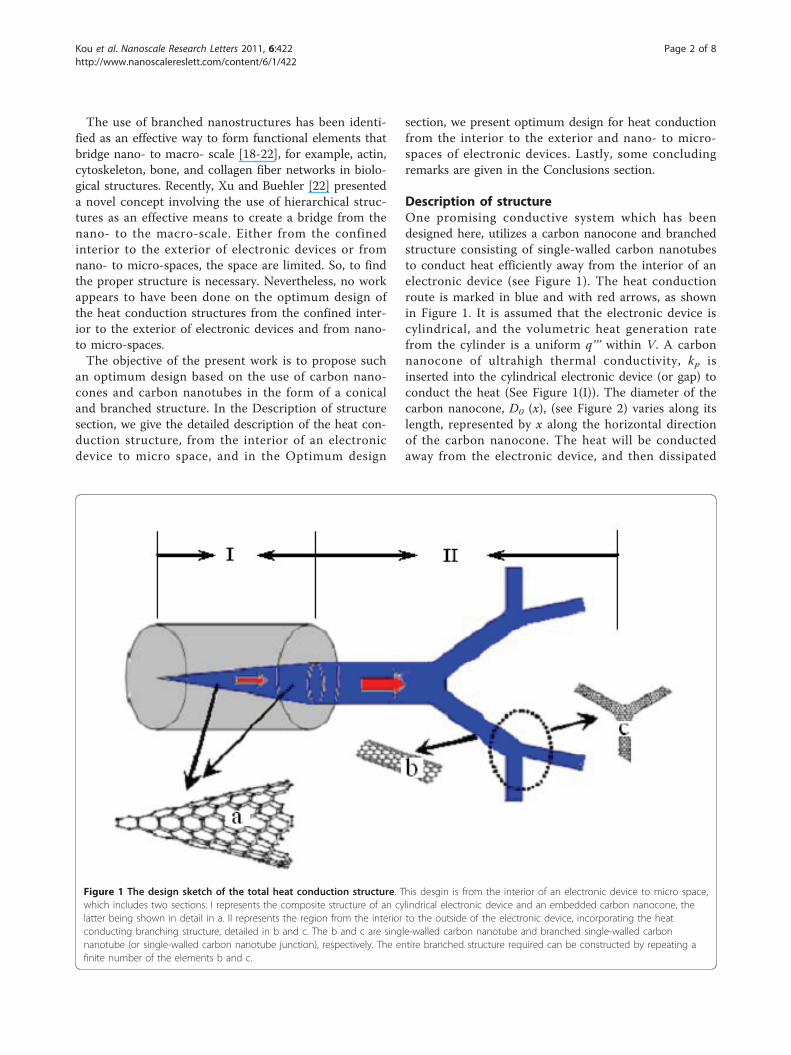
Description of structureOne promising conductive system which has beendesigned here, utilizes a carbon nanocone and branchedstructure consisting of single-walled carbon nanotubesto conduct heat efficiently away from the interior of anelectronic device (see Figure 1). The heat conductionroute is marked in blue and with red arrows, as shownin Figure 1. It is assumed that the electronic device iscylindrical, and the volumetric heat generation ratefrom the cylinder is a uniform q’’’ within V. A carbonnanocone of ultrahigh thermal conductivity, kp isinserted into the cylindrical electronic device (or gap) toconduct the heat (See Figure 1(I)). The diameter of thecarbon nanocone, D0 (x), (see Figure 2) varies along itslength, represented by x along the horizontal directionof the carbon nanocone. The heat will be conductedaway from the electronic device, and then dissipated
Figure 1 The design sketch of the total heat conduction structure. This desgin is from the interior of an electronic device to micro space,which includes two sections: I represents the composite structure of an cylindrical electronic device and an embedded carbon nanocone, thelatter being shown in detail in a. II represents the region from the interior to the outside of the electronic device, incorporating the heatconducting branching structure, detailed in b and c. The b and c are single-walled carbon nanotube and branched single-walled carbonnanotube (or single-walled carbon nanotube junction), respectively. The entire branched structure required can be constructed by repeating afinite number of the elements b and c.
Kou et al. Nanoscale Research Letters 2011, 6:422http://www.nanoscalereslett.com/content/6/1/422
Page 2 of 8

into the space through the branches (see Figure 1(II)).The structure is characterized according to each branchas follows: Let the length and diameter of a typicalbranch at some intermediate level k (k = 0, 1, 2, 3...m,where m is total level) be lk and dk, respectively, andintroduce two scaling factors: b = dk+1/dk and g = lk+1/lk, respectively. The elements of the structural designare shown in Figure 1.
Optimum designInterior to the exterior of electronic devicesBecause carbon nanocones are so thin and have anultra-high thermal conductivity, they may be consideredas ‘one-dimensional’, with the heat channeled practicallyalong the x direction (i.e., along the axis of the tube).The temperature distribution in the carbon nanocone isshown qualitatively by the red arrows in Figure 1. Thestructural parameters are detailed in Figure 2(a). Theheat generated by the electronic device and entered thecarbon nanocone having an ultra-high thermal conduc-tivity kp is given by q′′′πH2
0/4, where H0 is diameter ofcylindrical electronic device. The unidirectional heatconduction through the carbon nanocone is given bythe following equation [23]
ddx
(π
4kpD2
0dT0
dx) + q′′′ πH2
0
4= 0 (1)
The boundary conditions are:
dT0
dx= 0 (2)
T0 = T0 (L0) , at x = L0 (3)
where L0 is length of cylindrical electronic device orlength of embedded nanocone. Applying the boundarycondition (2) to Eq. 1 gives:
dT0
dx= −q′′′H2
0
kpD20
x (4)
Integrating Eq. 4 with respect to x, the temperaturedrop from the thin taper end to the thick end of thenanocone can be derived as follows:
T0(0) − T0(L0) =∫ L0
0
q′′′H20
kpD20
xdx (5)
In order to achieve maximum heat conduction, T0 (0)- T0(L0) should be minimized. Since the volume of the
Figure 2 Sketch of a cylindrical electronic device. (a) a three dimensional sketch of a cylindrical electronic device. The conical sectionrepresents the heat conduction medium, the cone showing one of the heat transfer paths from the interior heat source (red) to the edge (blue)of the electronic device, and (b) is the cross section optimal designs of the embedded nanocone. Three curves represent the three shapes ofthe nanocone corresponding to three different volumes of the nanocone (viz. Vp).
Kou et al. Nanoscale Research Letters 2011, 6:422http://www.nanoscalereslett.com/content/6/1/422
Page 3 of 8
nanocone:
Vp =
L0∫
0
π
4D2
0(x)dx (6)
is confined within a miniaturized device, to minimizeT0 (0) - T0(L0) within the given constraints (6), the fol-lowing integral should be minimized [24]:
ϕ =
L0∫
0
(x
D20
+ λD20)dx (7)
where, l is the Lagrange multiplier. The solution ofEq. 7 is the optimal diameter given by D2
0 = (x/λ)1/2. lcan be obtained by substituting D0
2 into Eq. 6. Wetherefore have:
D20 =
6VP
πL0(
xL0
)
12 (8)
Defining the porosity φ = Vp/V = 4Vp
/πH2
0L0 and com-
bining Eqs. 8 and 5, gives:
T0(0) − T0(L0) =4q′′′L0
2
9kpφ(9)
The question now arises as to how good the D02
design is relative to that using a uniform path havingthe thermal conductivity kp. For the path with a uni-formly cylindrical dimension, and porosity
φ = Vp/V = D2
0/H2
0, the minimized T0 (0) - T0(L0) can be
expressed as follows:
T0(0) − T0(L0) =∫ L0
0
q′′′H20
kpD20
xdx =q′′′L2
0
2kpφ(10)
By comparing Eqs. 9 and 10, it can be seen that taper-ing as represented by Eq. 9, produces a 5.6% lower valuefor T0 (0) - T0 (L0) than the uniform path design repre-sented by Eq. 10. The optimal designs are illustrated inFigure 2(b). Three curves represent the three shapes ofthe nanocone corresponding to three different volumesof the nanocone (viz. Vp).
Nano- to micro-spacesMethodAs discussed above, optimum heat conduction path-ways made of carbon nanocones can be optimallydesigned to transfer heat efficiently from the interiorto the exterior of a miniaturized electronic device;however, heat may still not be rapidly dissipated intothe surrounding space as exterior surface of the minia-turized electronic device is small (possibly in nano-
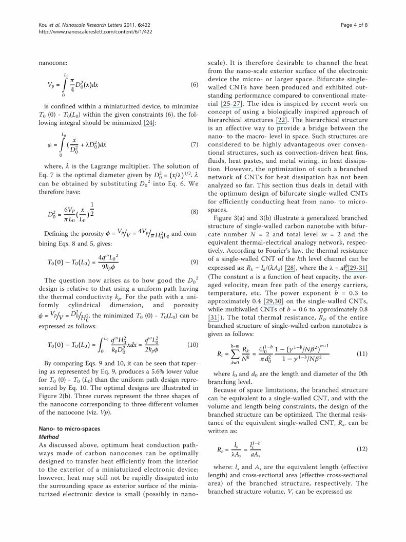
scale). It is therefore desirable to channel the heatfrom the nano-scale exterior surface of the electronicdevice the micro- or larger space. Bifurcate single-walled CNTs have been produced and exhibited out-standing performance compared to conventional mate-rial [25-27]. The idea is inspired by recent work onconcept of using a biologically inspired approach ofhierarchical structures [22]. The hierarchical structureis an effective way to provide a bridge between thenano- to the macro- level in space. Such structures areconsidered to be highly advantageous over conven-tional structures, such as convection-driven heat fins,fluids, heat pastes, and metal wiring, in heat dissipa-tion. However, the optimization of such a branchednetwork of CNTs for heat dissipation has not beenanalyzed so far. This section thus deals in detail withthe optimum design of bifurcate single-walled CNTsfor efficiently conducting heat from nano- to micro-spaces.Figure 3(a) and 3(b) illustrate a generalized branched
structure of single-walled carbon nanotube with bifur-cate number N = 2 and total level m = 2 and theequivalent thermal-electrical analogy network, respec-tively. According to Fourier’s law, the thermal resistanceof a single-walled CNT of the kth level channel can beexpressed as: Rk = lk/(lAk) [28], where the λ = albk[29-31](The constant a is a function of heat capacity, the aver-aged velocity, mean free path of the energy carriers,temperature, etc. The power exponent b = 0.3 toapproximately 0.4 [29,30] on the single-walled CNTs,while multiwalled CNTs of b = 0.6 to approximately 0.8[31]). The total thermal resistance, Rt, of the entirebranched structure of single-walled carbon nanotubes isgiven as follows:
Rt =k=m∑k=0
Rk
Nk=
4l1−b0
πd20
1 − (γ 1−b/Nβ2)m+1
1 − γ 1−b/Nβ2(11)
where l0 and d0 are the length and diameter of the 0thbranching level.Because of space limitations, the branched structure
can be equivalent to a single-walled CNT, and with thevolume and length being constraints, the design of thebranched structure can be optimized. The thermal resis-tance of the equivalent single-walled CNT, Rs, can bewritten as:
Rs =ls
λAs=
l1−bs
aAs(12)
where: ls and As are the equivalent length (effectivelength) and cross-sectional area (effective cross-sectionalarea) of the branched structure, respectively. Thebranched structure volume, V, can be expressed as:
Kou et al. Nanoscale Research Letters 2011, 6:422http://www.nanoscalereslett.com/content/6/1/422
Page 4 of 8
V =k=m∑k=0
Nkπ(d2
k
2)lk =
πd20l0
41 − (Nβ2γ )m+1
1 − Nβ2γ(13)
The equivalent length of the branched structure, ls, isequal to that of the branched structure, L, and is givenby:
ls = L =m∑0
lk =l0(1 − γ m+1)
1 − γ(14)
For given an electronic device, the space may be lim-ited by the design. So the length (L) of the branchedstructure may be a limiting factor. With (L) being fixed,Eq. (14) implies that, the branched level number m, thelength (l0) of the 0th branched single-walled carbonnanotube and the length ratio (g) can be optimized tomaximize heat conduction.According to the relationship between total volume
and effective length, i.e., V = AsL, the effective cross-sec-tional area, As, can be derived as follows:
As =V
L=
πd20
41 − γ
1 − γ m+1
1 − (Nγ β2)m+1
1 − Nγ β2(15)
By substituting Eqs. 14 and 15, into Eq. 12, the ther-mal resistance, Rs, of the equivalent single-walled carbonnanotube of the same volume as those of the branchedstructure can be derived as follows:
Rs =4l1−b
0
aπd20
[1 − γ m+1
1 − γ]2−b 1 − Nβ2γ
1 − (Nβ2γ )m+1 (16)
Combining Eqs. 11 and 16, the dimensionless effectivethermal resistance, R+, of a branched structure isobtained as follows:
R+ =Rt
Rs= [
1 − γ m+1
1 − γ]b−2 1 − (Nβ2γ )m+1
1 − Nβ2γ
1 − (γ 1−b/
Nβ2)m+1
1 − γ 1−b/
Nβ2(17)
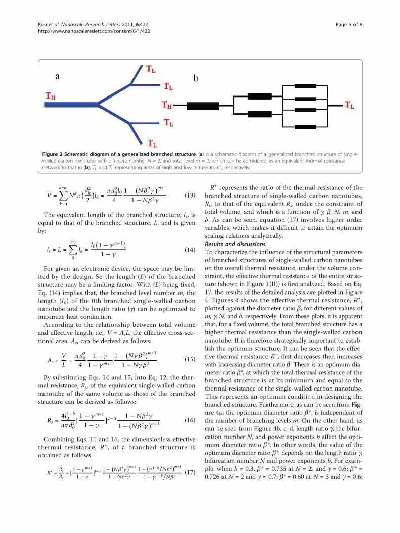
R+ represents the ratio of the thermal resistance of thebranched structure of single-walled carbon nanotubes,Rt, to that of the equivalent Rs, under the constraint oftotal volume, and which is a function of g, b, N, m, andb. As can be seen, equation (17) involves higher ordervariables, which makes it difficult to attain the optimumscaling relations analytically.Results and discussionsTo characterize the influence of the structural parametersof branched structures of single-walled carbon nanotubeson the overall thermal resistance, under the volume con-straint, the effective thermal resistance of the entire struc-ture (shown in Figure 1(II)) is first analyzed. Based on Eq.17, the results of the detailed analysis are plotted in Figure4. Figures 4 shows the effective thermal resistance, R+,plotted against the diameter ratio b, for different values ofm, g, N, and b, respectively. From these plots, it is apparentthat, for a fixed volume, the total branched structure has ahigher thermal resistance than the single-walled carbonnanotube. It is therefore strategically important to estab-lish the optimum structure. It can be seen that the effec-tive thermal resistance R+, first decreases then increaseswith increasing diameter ratio b. There is an optimum dia-meter ratio b*, at which the total thermal resistance of thebranched structure is at its minimum and equal to thethermal resistance of the single-walled carbon nanotube.This represents an optimum condition in designing thebranched structure. Furthermore, as can be seen from Fig-ure 4a, the optimum diameter ratio b*, is independent ofthe number of branching levels m. On the other hand, ascan be seen from Figure 4b, c, d, length ratio g, the bifur-cation number N, and power exponents b affect the opti-mum diameter ratio b*. In other words, the value of theoptimum diameter ratio b*, depends on the length ratio g,bifurcation number N and power exponents b. For exam-ple, when b = 0.3, b* = 0.735 at N = 2, and g = 0.6; b* =0.726 at N = 2 and g = 0.7; b* = 0.60 at N = 3 and g = 0.6;
Figure 3 Schematic diagram of a generalized branched structure. (a) is a schematic diagram of a generalized branched structure of single-walled carbon nanotube with bifurcate number N = 2, and total level m = 2, which can be considered as an equivalent thermal resistancenetwork to that in (b), TH and TL representing areas of high and low temperatures, respectively.
Kou et al. Nanoscale Research Letters 2011, 6:422http://www.nanoscalereslett.com/content/6/1/422
Page 5 of 8
and b* = 0.593 at N = 3 and g = 0.7. In addition, from Fig-ure 4a, it can be seen that the effective thermal resistanceR+ increases with increase of the number of the branchinglevels m. This is because when the branching levels mincreases, the network becomes densely filled with muchslenderer branches. Figure 4b also denotes that the effec-tive thermal resistance R+ increases with the increase ofthe length ratio g. This is because a higher length ratio gimplies longer branches. From Figure 4c, it also can beseen that when the diameter ratio is smaller than optimumdiameter ratio (viz., b <b*), the effective thermal resistanceR+ decreases with increase of bifurcation number N, whilethe diameter ratio is bigger than optimum diameter ratio(viz., b >b*), the trends is just opposite. The reason is thatwhen b <b*, the increase of the parallel channels in everylevel leads to lower total thermal resistance; but when b>b*, the increase of the parallel channels in every level will
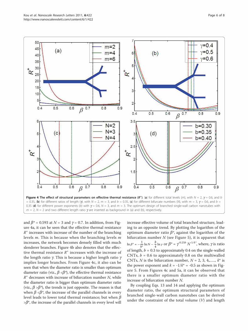
increase effective volume of total branched structure, lead-ing to an opposite trend. By plotting the logarithm of theoptimum diameter ratio b*, against the logarithm of thebifurcation number N (see Figure 5), it is apparent that
ln β∗ = − 1k∗ ln N − b
4ln γ or b* = g-0.25b N-1/k*, where, g is ratio
of length, b = 0.3 to approximately 0.4 on the single-walledCNTs, b = 0.6 to approximately 0.8 on the multiwalledCNTs, N is the bifurcation number, N = 2, 3, 4,......, k* isthe power exponent and k = -1/k* = -0.5 as shown in Fig-ure 5. From Figures 4c and 5a, it can be observed thatthere is a smaller optimum diameter ratio with theincrease of bifurcation number N.By coupling Eqs. 13 and 14 and applying the optimum
diameter ratio, the optimum structural parameters ofbranched single-wall carbon nanotubes can be derivedunder the constraint of the total volume (V) and length
Figure 4 The effect of structural parameters on effective thermal resistance (R+). (a) for different total levels (m), with N = 2, g = 0.6, and b= 0.35, (b) for different ratios of length (g), with N = 2, m = 3, and b = 0.35, (c) for different bifurcate numbers (N), with m = 3, g = 0.6, and b =0.35 (d) for different power exponents (b) with g = 0.6, N = 3, and m = 3. The optimum design of branched single-wall carbon nanotubes withm = 2, N = 2 and two different length ratio g are inserted as background in (a) and (b), respectively.
Kou et al. Nanoscale Research Letters 2011, 6:422http://www.nanoscalereslett.com/content/6/1/422
Page 6 of 8

(L). The backgrounds of Figure 4a, b show two optimumdesigns of the branched single-wall carbon nanotubeswith b = 0.3, m = 2, N = 2 and different length ratio g.The design in the background of Figure 4a has a smallervalue of g, while that of Figure 4b has a greater value ofg. To achieve optimum heat conduction and dissipationunder the constraints of the total volume (V) and length(L) of the branched carbon nanotubes structure, the big-ger g, the smaller the length (l0) of the 0th branch.
ConclusionsIn this paper, the optimum design of carbon nanostruc-ture for most efficiently dissipating heat from the con-fined interior of electronic devices to the micro space isanalyzed. It is found that the optimum diameter, D0, ofcarbon nanocones satisfies the relationship,D2
0(x) ∝ x1/2. For transmitting heat from the nano-scaled surface of electronic devices to the micro-space,the total thermal resistance of a branched structurereaches a minimum when the diameter ratio, b*, satisfiesb* = g-0.25b N-1/k*, where, g is ratio of length, b = 0.3 toapproximately 0.4 on the single-walled CNTS, b = 0.6 toapproximately 0.8 on the multiwalled CNTS, k* = 2 andN = the bifurcation number (N = 2, 3, 4,......) under thevolume constraints. If space is the only limitation, theoptimum diameter remains applicable. These findingshelp optimize the design of heat conducting media fromnano- to micro-structures. It must be noted that thepresent work is an improvement from the Ref. [22],which showed hierarchical structure is effective in pro-viding a bridge between the nano- to the macro- levelfor heat transfer. The present work provides a
theoretical prediction of how such heat dissipater can beoptimally designed.Despite recent progress in synthesizing and manipulat-
ing nanocones and branched single-walled CNTs[25-27,32-34], further work is necessary to perfect tech-niques and systems for the fabrication of nanostructuresand creation of seamless links between the individualsingle-walled CNT elements of the branched structures,thereby reducing the interfacial thermal resistance[35-37], as well as to precisely control the scale ofnanostructures.
AbbreviationsCNTs: carbon nanotubes.
AcknowledgmentsThis work was partially supported by the Research Grant Council of HKSAR(Project No. PolyU 5158/10E), the National Natural Science Foundation ofChina under Grant No’s 10932010, 10972199, 11005093, 11072220 and11079029, and the Zhejiang Provincial Natural Science under Grant Nos.Z6090556 and Y6100384.
Author details1College of Mathematics, Physics and Information Engineering, ZhejiangNormal University, Jinhua 321004, PR China 2Institute of Textiles andClothing, The Hong Kong Polytechnic University, Kowloon, Hong Kong, PRChina 3Department of Mechanical Engineering, The Hong Kong PolytechnicUniversity, Kowloon, Hong Kong, PR China
Authors’ contributionsJLK performed all the research and drafted the manuscript. HGQ, HJL, YL,and YSX helped to analyze data and contributed equally; WFM and JTFdesigned the research and supervised all of the studies. All the authorsdiscussed the results and approved the final manuscript.
Competing interestsThe authors declare that they have no competing interests.
Figure 5 Scaling relationship of diameter ratio to bifurcate number and rations of length. Scaling relationship between optimumdiameter ratio (b) and, (a) bifurcate number (N) for different ratios of length (g) with b = 0.3; (b) ratios of length (g) for different bifurcatenumbers (N) with b = 0.35.
Kou et al. Nanoscale Research Letters 2011, 6:422http://www.nanoscalereslett.com/content/6/1/422
Page 7 of 8

Received: 23 March 2011 Accepted: 14 June 2011Published: 14 June 2011
References1. Chen G: Nanoscale energy transport and conversion. New York: Oxford
University Press; 2005.2. Tien CL: Microscale energy transfer, chemical and mechanical
engineering. Boca RAton: CRC; 1997.3. Simons RE, Antonetti VW, Nakayama W, Oktay S: Heat transfer in electronic
packages. Microelectronics Packaging Handbook New York: Chapman andHall; 1997.
4. Hong SH, Myung S: Nanotube electronics: a flexible approach tomobility. Nat Nanotechnol 2007, 2:207-208.
5. Berber S, Kwon YK, Tománek D: Unusually high thermal conductivity ofcarbon nanotubes. Phys Rev Lett 2000, 84:4613.
6. Pop E, Mann D, Wang Q, Goodson K, Dai HJ: Thermal conductance of anindividual single-wall carbon nanotube above room temperature. NanoLett 2006, 6:96-100.
7. Helgesen G, Knudsen KD, Pinheiro JP, Skjeltorp AT, Svåsand E, Heiberg-Andersen H, Elgsaeter A, Garberg T, Naess SN, Raaen S, Tverdal MF, Yu X,Mel TB: Carbon nanocones: a variety of non-crystalline graphite. MaterRes Soc Symp Proc 2007, 1057:24-29.
8. Brinkmann G, Fowler PW, Manolopoulos DE, Palser AHR: A census ofnanotube caps. Chem Phys Lett 1999, 315:335347.
9. Shenderova OA, Lawson BL, Areshkin D, Brenner DW: Predicted structureand electronic properties of individual carbon nanocones andnanostructures assembled from nanocones and nanostructuresassembled from nanocones. Nanotechnolo 2001, 12:191-197.
10. Reich S, Li L, Robertson J: Structure and formation energy of carbonnanotube caps. Phys Rev B 2005, 72:165423.
11. Gong XJ, Li JY, Lu HJ, Wan RZ, Li JC, Hu J, Fang HP: A charge-drivenmolecular water pump. Nat Nanotechnol 2007, 2:709-712.
12. Yang N, Zhang G, Li BW: Carbon nanocone: a promising thermal rectifier.Appl Phys Lett 2008, 93:243111.
13. Tu YS, Xiu P, Wan RZ, Hu J, Zhou RH, Fang HP: Water-mediated signalmultiplication with Y-shaped carbon nanotubes. Proc Natl Acad Sci USA2009, 106:18120-18124.
14. Song J, Whang D, McAlpine MC, Friedman RS, Wu Y, Lieber CM: Scalableinterconnection and integration of nanowire devices withoutregistration. Nano Lett 2004, 4:915-919.
15. Kordas K, Tóth G, Moilanen P, Kumpumäki M, Vähäkangas J, Uusimäki A,Vajtai R, Ajayan PM: Chip cooling with integrated carbon nanotubemicrofin architectures. Appl Phys Lett 2007, 90:123105.
16. Gannon CJ, Cherukuri P, Yakobson BI, Cognet L, Kanzius JS, Kittrell C,Weisman RB, Pasquali M, Schmidt HK, Smalley RE, Curley SA: Carbonnanotube-enhanced thermal destruction of cancer cells in a noninvasiveradiofrequency field. Cancer 2007, 110:2654-2665.
17. Prasher R: Predicting the thermal resistance of nanosized constrictions.Nano Lett 2005, 5:2155-2159.
18. Dong H, Paramonov SE, Hartgerink JD: Self-assembly of α-helical coiledcoil nanofibers. J Am Chem Soc 2008, 130:13691-13695.
19. Fratzl P, Weinkamer R: Nature’s hierarchical materials. Prog Mater Sci 2007,52:1263-1334.
20. Alberts B, Johnson A, Lewis J, Raff M, Roberts K, Walter P: Molecularbiology of the cell. New York: Garland Sciences, Taylor and Francis; 2002.
21. Keten S, Buehler MJ: Geometric confinement governs the rupturestrength of H-bond assemblies at a critical length scale. Nano Lett 2008,8:743-748.
22. Xu Z, Buehler MJ: Hierarchical nanostructures are crucial to mitigateultrasmall thermal point loads. Nano Lett 2009, 9:2065-2072.
23. Bejan A: Heat transfer. New York: Wiley; 1993.24. Ledezma GA, Bejan A, Errera MR: Constructal tree networks for heat
transfer. J Appl Phys 1997, 82:89100.25. Li J, Papadopoulos C, Xu J: Growing Y-junction carbon nanotubes. Nature
2000, 402:253-254.26. Wei DC, Liu YQ: Review-The intramolecular junctions of carbon
nanotubes. Adv Mater 2008, 20:2815-2841.27. Li N, Chen XX, Stoica L, Xia W, Qian J, Aßmann J, Schuhmann W: The
catalytic synthesis of three-dimensional hierarchical carbon nanotubecomposites with high electrical conductivity based on electrochemicaliron deposition. Adv Mater 2007, 19:2957-2960.
28. Xu P, Yu BM, Yun MJ, Zou MQ: Heat conduction in fractal tree-likebranched networks. Int J Heat Mass Transfer 2006, 49:3746-3751.
29. Maruyama S: A molecular dynamics simulation of heat conduction infinite length SWNTs. Phys B 2002, 323:193-195.
30. Zhang G, Li BW: Thermal conductivity of nanotubes revisited: effects ofchirality, isotope impurity, tube length, and temperature. J Chem Phys2005, 123:014705.
31. Chang CW, Okawa D, Garcia H, Majumdar A, Zettl A: Breakdown ofFourier’s Law in Nanotube Thermal Conductors. Phys Rev Lett 2008,101:075903.
32. Krishnan A, Dujardin E, Treacy MMJ, Hugdahl J, Lynum S, Ebbesen TW:Graphitic cones and the nucleation of curved carbon surfaces. Nature1997, 388:451-454.
33. Naess SN, Elgsaeter A, Helgesen G, Knudsen KD: Carbon nanocones: wallstructure and morphology. Sci Technol Adv Mater 2009, 10:065002.
34. Hu JQ, Bando Y, Zhan JH, Zhi CY, Xu FF, Golberg D: Tapered carbonnanotubes from activated carbon powders. Adv Mater 2006, 18:197-200.
35. Meng GW, Han FM, Zhao XL, Chen BS, Yang DC, Liu JX, Xu QL, Kong MG,Zhu XG, Jung YJ, Yang YJ, Chu ZQ, Ye M, Kar S, Vajtai R, Ajayan PM: Ageneral synthetic approach to interconnected nanowire/nanotube andnanotube/nanowire/nanotube heterojunctions with branched topology.Angew Chem Int Ed 2009, 48:7166-7306.
36. Hobbie EK, Fagan JA, Becker ML, Hudson SD, Fakhri N, Pasquali M: Self-assembly of ordered nanowires in biological suspensions of single-wallcarbon nanotubes. ACS Nano 2009, 3:189-196.
37. Xu ZP, Buehler MJ: Nanoengineering heat transfer performance at carbonnanotube interfaces. ACS Nano 2009, 3:2767-2775.
doi:10.1186/1556-276X-6-422Cite this article as: Kou et al.: Optimizing the design of nanostructuresfor improved thermal conduction within confined spaces. NanoscaleResearch Letters 2011 6:422.
Submit your manuscript to a journal and benefi t from:
7 Convenient online submission
7 Rigorous peer review
7 Immediate publication on acceptance
7 Open access: articles freely available online
7 High visibility within the fi eld
7 Retaining the copyright to your article
Submit your next manuscript at 7 springeropen.com
Kou et al. Nanoscale Research Letters 2011, 6:422http://www.nanoscalereslett.com/content/6/1/422
Page 8 of 8