Electronics in Motion and Conversion June 2018 - Bodo's ...
124
Electronics in Motion and Conversion June 2018 ISSN: 1863-5598 ZKZ 64717 06-18
-
Upload
khangminh22 -
Category
Documents
-
view
2 -
download
0
Transcript of Electronics in Motion and Conversion June 2018 - Bodo's ...

Electronics in Motion and Conversion June 2018
ISSN: 1863-5598 ZKZ 6471706-18
C
M
Y
CM
MY
CY
CMY
K
Cover_06-18.pdf 1 09.05.18 13:16

WELCOME TO THE HOUSE OF COMPETENCE
PRODUCTIONENGINEERING GvA SOLUTIONS DISTRIBUTION
GvA Leistungselektronik GmbH
Boehringer Straße 10 - 12
D-68307 Mannheim
Phone +49 (0) 621/7 89 92-0
www.gva-leistungselektronik.de
POWER IS IN OUR NATURE!
Power is in our nature. Everyday we deliver full power for your success.
ENGINEERING: Quick design-to-product using state-of-the-art technologies
PRODUCTION: Extensive production experience with maximum flexibility
GvA SOLUTIONS: Short time-to-market with innovative plug&play system solutions
DISTRIBUTION: Vast product knowledge and consulting expertise
VISIT US AT PCIM EUROPE
5 - 7 JUNE 2018 IN NUREMBERG
HALL 9 · STAND 209
180177GvA_Anzeige Image_engl_mit Storer_RZ_180301.indd 1 01.03.18 10:52
— Thyristors Low losses for efficient transmission.
ABB Semiconductors’ new generation of thyristors enable HVDC transmission lines of up to 12 GW in a single installation, with a conversion efficiency beyond 99.6 %. Each de-vice has the capacity to conduct in the range of 5000 A to 6250 A, has blocking capabili-ty of up to 8500 V and offers power savings up to 1 kW per device at rated current. abb.com/semiconductors

Electronics in Motion and Conversion June 2018
ISSN: 1863-5598 ZKZ 6471706-18
Bodo‘s PowerBodo‘s Power
Systems ®Systems ®

Cost-effective and accurate, miniature isolated current sensor GO speeds your drives applications. A unique sensor with an integrated primary conductor achieves optimum temperature accuracy, measuring from -40 to +125 °C in a surface mounted SO8 or SO16 package.
• 10-30 A nominal current • Better than 1.3 % accuracy @ +25°C • Differential Hall principle measurement: Very
robust against external fields • 2 μs response time • Up to 3 kV RMS isolation • Double Over-Current Detection outputs for short
circuit and over-load protection (SO16 version)
www.lem.com
At the heart of power electronics.
GO, where you have never been before.
LEM_GO_poster_2_A4.indd 1 08.05.2018 16:19:47

The Suijin Series by Hitachi
Power. Performance. Proven.
Electronics in Motion and Conversion June 2018
ISSN: 1863-5598 ZKZ 6471706-18
Bodo‘s PowerBodo‘s Power
Systems ®Systems ®


www.bodospower.com June 2018 Bodo´s Power Systems® 1
CONTENT
Viewpoint & Events ......................................................................................... 4 Showtime in Nuremberg!
News .............................................................................................................6-14Product of the Month .....................................................................................16 A Complete Set of Tools for MMC Studies
Green Product of the Month ......................................................................... 18 PowerForge: A Game-Changing Tool for Power Converter Design
Blue Product of the Month ............................................................................ 20 Win a Microchip Curiosity HPC Development Board
Guest Editorial .......................................................................................... 22-23 Semiconductors Bring Robots Closer to Humans By Dr. Peter Wawer, Division President Industrial Power Control at Infineon
VIP Interview .............................................................................................. 24-28 ROHM Focusses on WBG for Automotive and Industrial Markets By Roland R. Ackermann, Correspondent Editor Bodo’s Power Systems
Guest Editorial .......................................................................................... 30-32 15 Years Anniversary of the European Center for Power Electronics ECPE By Dipl.-Phys. Thomas Harder, ECPE European Center for Power Electronics e.V.
Guest Editorial ............................................................................................... 34 Indian IT Expert Got a Job in Nuremberg with the Blue Card By Martina Frimberger, Bundesamt für Migration und Flüchtlinge
Design and Simulation .................................................................................. 36 GaN Systems Unveils an Online Circuit Simulation Tool for Evaluating Gallium Nitride Power Transistor Circuits By Kristofer Eberle, Plexim and Paul Wiener, GaN Systems
Cover Story ............................................................................................... 38-43 Maximise Your Power: With New Chips and New Topologies to the Next Level of Power Density By Stefan Häuser, Bernhard Eichler, Thomas Hürtgen and Werner Obermaier, SEMIKRON Elektronik
Design and Simulation ..............................................................................44-46 Designing Custom Inductors with ONE Design Equation By Dr. Ray Ridley, Ridley Engineering Inc.
Power Modules ......................................................................................... 48-49 Hitachi Suijin Series Power Modules for Electric Vehicles By Chris White, Hitachi Europe Limited
Power Supply ............................................................................................ 50-52 Integrated Circuits Offer Enhanced Protection & Improved Safety Features for High Reliability Power Supplies By Steve Munns, Mil-Aero Marketing Manager, Analog Devices
Renewable Energy .................................................................................... 54-61 Making Single-Phase Solar Inverters Smaller, Cheaper & Safer By Thomas Hargé, Global Product Manager for the Renewable Energy Busi-ness at LEM and David Jobling, ASIC Development Group Manager at LEM
Intelligent Power ........................................................................................62-64 New Transfer Molded SMD Type IPM By Narender Lakshmanan and Muzaffer Albayrak from Mitsubishi Electric Europe B.V, Germany; Teruaki Nagahara, Mitsubishi Electric Power Device Works, Japan
Capacitors ..................................................................................................66-67 Aluminum Sealed Film Capacitors for Harsh Humid Environments By Dr. Thomas Ebel, Managing Director, FTCAP GmbH
IGBTs ......................................................................................................... 68-70 Making the Most of Three-Level NPC Topology By Guillem Gargallo Pallardó, Product Marketing Manager, Vincotech GmbH
Technology ................................................................................................ 72-75 eGaN® FET-Based Synchronous Rectification By David Reusch, Executive Director Applications Engineering and John Glaser, Director Engineering, Efficient Power Conversion Corporation
Design and Simulation ............................................................................. 76-78 Handling Late Changes in Power System Designs By Lev Slutskiy, Business Development Manager, Central/Eastern Europe, Vicor
Technology ................................................................................................ 80-82 DCM™ 1000X - Designed to Meet the Future SiC Demand of Electric Vehicle Drive Trains By Omid Shajarati, Alexander Streibel and Norbert Apfel, Danfoss Silicon Power
Thermal Management ............................................................................... 84-87 Temperature and Overload Protected Triac – TOPTriac™ By Nick Ham, Matjaz Rozman, Ed Huang and Stephen Wood, WeEn Semiconductors
Transistors ................................................................................................ 88-89 Benefiting from the Evolution in Power Transistors By Christopher Rocneanu, Business Development Manager, UnitedSiC
Driver ICs ................................................................................................... 90-91 Optimisation of dV/dt – Losses Trade Off Using Switchable Gate Resistance By Dr Angus Bryant, Amantys Power Electronics Limited
Driver ICs ................................................................................................... 94-95 Dynamically Configurable Off-Line Switcher IC for Higher Application Flexibility By Jason Yan, Senior Technology Training Manager at Power Integrations
Transistors ................................................................................................ 96-99 A Novel Circuit Topology for Turning a ‘Normally On’ GaN Transistor into ‘Normally Off’ that Can be Driven by Popular Drivers By Prof. Shmuel (Sam) Ben-Yaakov, Ben-Gurion University, and Luc Van de Perre, Sr. Director of Sales and Marketing, VisIC Technologies
Capacitors ............................................................................................. 100-101 Class 2 MLCC Dielectrics and the Case of the Missing Capacitance By Steve Hopwood, Senior Applications Engineer at Knowles Precision Devices
Thermal Management ........................................................................... 102-103 New Advances in Friction Stir Welding for Cold Plate Manufacture By Andreas Engelhardt, Technical Director, Columbia-Staver Ltd
New Products ........................................................................................ 104-112

June 2018 www.bodospower.com2
The Gallery

Allinclusive.
© e
iSos
#MAGICPOWERMODULES
MagI³C Power Modules are easy-to-use DC/DC converters with integrated regulator IC,
power inductor and capacitors. Design and layout reviews as well as support with EMI fi lter
design are offered as a service service for all customers. Datasheets contain detailed specifi -
cations and application information.
For more information please visit:
www.we-online.com/powermodules
Simple design-in process Design and layout support EMI filter design for EN55022
class B compliance Evaluation Boards for all products
LGA-6 LGA-16 QFN TO263 SIP-3 SIP-4 SIP-7

Bodo´s Power Systems® June 2018 www.bodospower.com4
CONTENTVIEWPOINT
On Tuesday, the 5th June, PCIM Europe and SMT will be open for visitors – always exciting to meet again in Nuremberg for these two events ! At my home, Ingrid has already served delicious asparagus (I help with the prep) and we hope that the season extends into June. So far PCIM Europe has been always in May – so no problems for the asparagus. I’ve been an advisory board member since the late 80’s - time does fly by, but asparagus remains the special treat. I look forward to the local asparagus of Nuremberg.
IGBT switches have been a most important innovation in the last century. Now wide band gap technologies are the driving factors to more efficient designs. Both silicon carbide (SiC) and gallium nitride (GaN) have shown reliability and serve their particular areas of best expertise. GaN is most successful in the lower voltage range, while SiC serves predominantly at higher voltages, and some overlap is showing up. A future player could be gallium arsenide (GaAs) for upcoming new power semiconductors. At PCIM, all the well positioned players will be presenting their latest and showing applications of wide band gap devices in the mainstream now.
Showtime in Nuremberg! A Media
Katzbek 17a D-24235 Laboe, Germany Phone: +49 4343 42 17 90 Fax: +49 4343 42 17 89 [email protected] www.bodospower.com
Publishing Editor Bodo Arlt, Dipl.-Ing.
[email protected] Editor
Holger Moscheik Phone + 49 4343 428 5017 [email protected] Editor China Min Xu Phone: +86 156 18860853 [email protected] Support June Hulme
Phone: +44 1270 872315 [email protected]
US Support Cody Miller Phone +1 208 429 6533 [email protected]
Creative Direction & Production Repro Studio Peschke
[email protected] Subscription to qualified readersBodo´s Power Systems is available for the following subscription charges:Annual charge (12 issues)
is 150 € world wideSingle issue is 18 €[email protected]
circulation
print run 24 000
Printing by: Brühlsche Universitätsdruckerei GmbH
& Co KG; 35396 Gießen, GermanyA Media and Bodos Power Systems
assume and hereby disclaim any liability to any person for any loss or damage by errors or omissions in the material contained herein regardless of whether such errors result from negligence accident or any other cause whatsoever.
EventsPCIM 2018
Nuremberg, Germany, June 5-7 www.mesago.de/en/PCIM/
The_conference/Welcome/index.htmSMT Hybrid Packaging 2018
Nuremberg, Germany, June 5-7 www.mesago.de/en/SMT/
SCAPE 2018 Stockholm, Sweden, June 10-12
www.acreo.se/projects/sic-power-centerCWIEME 2018
Berlin, Germany, June 19-21 www.coilwindingexpo.com/berlin
Intersolar Europe 2018 Munich, Germany, June20-22
www.intersolar.de/enSpeedam 2018
Amalfi Coast, Italy, June 20-22 www.speedam.org
3D PEIM 2018 Maryland MD, USA, June25-27
www.3d-peim.orgSensor & Test 2018
Nuremberg, Germany, June 26-28 www.sensor-test.de
In a tradition of nearly two decades, I have invited experts from industry leaders to pres-ent their latest achievements in wide band gap development. Come to the podium at PCIM Europe on
Wednesday, 6th of June, at Hall 6, Booth 155
From 13:30 to 14:30 we have: “SIC – Devices for the Future Design”
From 14:30 to 15:30 we have: “GaN – Devices for the Future Design”
Mark up your calendar and we will see you in Nuremberg. PCIM is the big family event for Power Electronics in Europe.
A second conference on wide band gap power applications, organized by ICC media and my magazine, will emphasize getting started with these devices and making the design process easier. Last year the pre-sentations were well received, so we repeat the event in Munich, on December 4th, at the Airport Hilton.
My magazine is delivered by postal service to all places in the world. It is the only maga-zine that globally serves the need of techni-cal information on power electronics.
Bodo’s Power Systems reaches readers around the world. We have EE tech as a partner to serve North America more ef-ficiently. If you are using any kind of tablet or smart phone, you will find all of our content on the website www.eepower.com. If you speak the language, or just want to have a look, don’t miss our Chinese version: www.bodospowerchina.com
My Green Power Tip for June: Travel in groups by car to Nuremberg. Fill the seats with your colleagues and save energy.
See you in Nuremberg, and at my podium Wednesday the 6th.
Best Regards

Cost effective miniature and accurate isolated current sensor GO speeds your drives applications. A unique sensor with an integrated primary conductor achieves optimum temperature accuracy, measuring from -40 to +125 °C in a surface mounted SO8 or SO16 package.
• 10-30 A nominal current • Better than 1.3 % accuracy @ +25°C • Differential Hall principle measurement: Very
robust against external fields • 2 μs response time • Up to 3 kV RMS isolation • Double Overcurrent detection outputs for short
circuit and over-load protection (SO16 version)
www.lem.com
At the heart of power electronics.
GO. A breath of fresh air in power electronics.
PCIMEurope 2018
Stand 9-204

Bodo´s Power Systems® June 2018 www.bodospower.com6
CONTENTNEWS
LTEC Corporation and Anagenesis Inc. announce that they have agreed to partner to create the most advanced market reports for emerging power electronics and power semiconductor products. Ana-genesis is a technical marketing consultancy working in collaboration with Ada Cheng of AdaClock has successfully provided Power Supply in a Package (PSiP) and Power Supply on a Chip (PwrSoC) market reports to the power supply and power semiconductor players since 2011. These reports have provided a unique contribution to power supply and semiconductor business and technology managers by complimenting traditional market forecasting with technical trend anal-yses. LTEC offers teardowns, deep analysis of competing products and technologies for product development, patents’ enforcement and defense with headquarters in Osaka, Japan, and local offices in the USA and the Asia-Pacific region.
Arnold Alderman, Anagenesis’ Founder and President, explains, “Today’s competitive environment demands accelerated business planning and execution processes. Therefore, we are raising the bar for our market reports by teaming with LTEC to include their product benchmarking that permits insight into the micro-construction of present integrated power supplies. We provide a single off-the-shelf report to the entire customer planning team. Looking to the future, we are excited to have the input from LTEC’s broad range of analyses to serve customers contemplating other emerging product targets.“
www.ltecusa.com
www.anagenesis-inc.com
LTEC Corporation and Anagenesis Inc. Announce Cooperative Partnering
IEEE International Power Electronics and Application Conference and Exposition (PEAC) is an international conference for presentation and discussion of the state-of-the art in power electronics, energy conver-sion and its applications. The IEEE PEAC’2018 is the second meeting of PEAC, which will be held in Shenzhen, China, during November 4-7, 2018. The worldwide power electronic industry, research, and academia are cordially invited to participate in an array of presenta-tions, tutorials, exhibitions and social activities for the advancement of science, technology, engineering education, and fellowship.Technical interests of the conference included, but are not limited to: * Switching Power Supply: DC/DC converter, Power Factor
Correction converter * Inverter and control: DC/AC Inverter, Modulation and Control * Power Devices and applications: Si, SiC, and GaN devices * Magnetics, Passive Integration, Magnetics for Wireless and EMI * Control, Modeling, Simulation, System Stability and Reliability * Conversion Technologies for Renewable Energy and Energy
Saving * Power Electronics for Transmission and Distribution
* Power Electronics for Electric Vehicles, Railway, Marine, Airplane etc.
* Power Electronics for Lighting and Consumer Electronics * Power Electronics for Data center and Telecom Paper SubmissionThe working language of the conference is English. Prospective authors are invited to electronically submit digests of their work in English (Maximum 6 pages in double space, in pdf format) through PEAC User Central following this link http://www.peac-conf.org/User-Central/Index/CreateAccount
Important DeadlinesSubmission of digests May 30th, 2018 Submission of tutorial proposals June 30th, 2018Notification of paper acceptance July 15th, 2018Submission of final papers Aug 30th, 2018
www.peac-con.org/Home/Menu/126
PEAC’2018 Call for Papers
Purdue University researchers have demonstrated the ability of a thin film to conduct heat on just its surfaces, identifying a potential solution to overheating in electronic devices such as phones and computers.“When you try to make an electronic device, the heat dissipation is always a problem,” said Xianfan Xu, Purdue’s Professor of Mechani-cal Engineering. “So we are trying to provide an understanding of how heat can be dissipated in these future devices.”This thin film material is a topological insulator, which supports the flow of electrons on its surface but not in its interior. No study had yet tested whether the same were true for heat, until confirmed by research published in „ACS Nano“. Past research has speculated that topological insulators could be use-
ful for the development of spintronic devices, which encode informa-tion through the spins of electrons as opposed to electrical charge in today’s electronics.The researchers found that the thinner the film is, the higher the heat conductivity. They also discovered that the ratio of thermal conductiv-ity to electrical conductivity at the surface of the topological insulator materials can be more than 10 times higher than the Sommerfeld value, which is the value known for most metals and semiconductors determined by the Weidemann-Franz law. By conducting heat on just its surfaces rather than across the entire film, this material could prevent parts of a device from heating up or redirect heat.Now, having identified this characteristic of heat transfer in topological insulators, the next step is to figure out how to use them for manipu-lating heat flow.“There are not many ways to control heat. It’s not electricity, where you can turn it on and off,” Xu said. “But now there might be a chance to do that.”The work is a collaborative effort among the research groups led by Xu, Yong Chen, a professor in Purdue’s Department of Physics and Astronomy, and Jesse Maassen, a physics professor at Dalhousie University in Canada.
www.purdue.edu
Thin Film Manages Heat Flow in Future Devices

SMALLER STRONGER FASTER
The Formula E Venturi team has adopted the latest range of ROHM power modules in full SiC technology for its electric-powered racing cars. ROHM has enabled the broad implementation of e-mobility by delivering the next generation of power semiconductor devices. Our modules are produced in-house using a vertically integrated manufacturing system, guaranteeing high quality and a consistent supply to the market.
www.rohm.com
SMALLERSiC technology enables a SMALLER inverter design in terms of volume and weight.
STRONGERWith SiC, a higher power density for a STRONGER performance can be achieved.
FASTERSiC helps vehicles to cross the finish line FASTER and supports fast-charging solutions.
ROHM_Brand_PCIM2018_210x297+3mm_EN_V02.indd 1 10.04.18 14:35

8
CONTENTNEWS
Power plants not larger than a sugar cube that can be used for both domestic and industry purposes: Thermoelectric generators (TEG) convert even small ambient temperature differences into electrical en-ergy. otego GmbH, a spinoff of Karlsruhe Institute of Technology (KIT), has now commercialized the first electronic component of its kind.The team of otego makes thermoelectdric generators (TEG) fit for the mass market by using novel materials and large-scale produc-tion processes. Production of a prototype series is about to start this year. The “oTEG” innovative energy converter is suited for a large range of applications in the areas of Industry 4.0 and Smart Homes. Similar to solar cells that convert light into electrical energy, TEGs can extract electrical power from the ambient heat and, in this way, ensure continuous supply. “Various sensors, evaluation electronics, and wireless systems can be operated without a battery: From simple products, such as a wireless data tracker, to distributed sensor nodes of industrial facilities to future electronic thermostats of radiators,” says Frederick Lessmann, one of the founders of the company. TEGs not only are an ideal energy source for comfort applications in the domestic environment, they can also be used for the power supply of a number of autonomous industry sensors in larger facilities. Polymer materials make the oTEG mechanical flexible and insensitive to impacts and vibrations. It can be operated for a longer term without any maintenance being required. Heavy metals are not needed at all, consumption of natural resources is reduced.Conversion of energy from ambient heat is based on the Seebeck effect: The temperature gradient in the thermoelectric semiconductor
material induces an electric voltage. When combined with another semiconductor material generating a complementary voltage, if possible, the potential of this “thermocouple” can be used as a source of voltage for small consumers. In oTEG, thousands of these thermocouples are connected in series. The generated voltage in the
single-digit volt range is sufficient to operate microelectronic circuits. The difference of the oTEGs lies in the self-developed production process: “We print the electronic conducting paths onto extremely thin plastic foils – the time needed corresponds to about the time needed for printing a newspaper. Then, we use our special automated origami folding method to bring these printed foils into a compact form. In the past years, we intensively worked on implementing this method on the industrial scale for rapid production at low costs,” Lessmann says.
www.energy.kit.edu
www.otego.de/en
Microenergy Supply without Battery and Cable
“Infineon continues to grow profitably,” stated Dr. Reinhard Ploss, CEO of Infineon. “Our growth is broadly based: Solutions for the entire range of drivetrain systems for all types of electric vehicles, including 48-volt systems, high-speed trains and renewable power genera-tion. In addition, we are seeing growing demand for data center power supplies for artificial intelligence. Our order books are bulging. We therefore are very
confident that we will achieve our revenue targets for the 2018 fiscal year. Compared to the previous year’s March quarter, the average US dollar exchange rate against the euro fell by around 16 percent in the three-month period to 31 March 2018. Despite headwinds from the US dollar and rising material prices, we expect to achieve our targeted Segment Result Margin of 17 percent again in the 2018 fiscal year. This demonstrates the robustness of our business model,” continued Dr. Reinhard Ploss.
www.infineon.com
Infineon Reported Results for the Second Quarter of the 2018 Fiscal Year
ZH Wielain Electronic (Hangzhou Co.,LTD)Hangzhou, China
E-mail: [email protected]://www.zhwielain.com
+86 571 28898137
Power Module Product and Packaging & Interconnect Power Module Products Press Fit Solderless Connection Solution
Connect teminals
DBC connectors
IGBT body


Bodo´s Power Systems® June 2018 www.bodospower.com10
CONTENTNEWS
The date, the last week of June, is new, but one thing is for sure: The SENSOR+TEST 2018 will be held from 26 to 28 June in Nürnberg
and will once again be the worldwide leading platform for sensor, measuring, and testing technology. Visitors will have the opportunity to obtain comprehensive information on the state of the art in sensors and measurement not only at the stands of the 580 exhibitors from all over the globe, but also at the numerous parallel technical conferenc-es and action programs. The SENSOR+TEST will be complemented again this year by two first-rate technical conferences: The 19. ITG/GMA-Fachtagung “Sensoren und Messsysteme” is the most important congress dealing with sensors and measuring technology in German speaking countries. It is supported jointly by the VDI/VDE’s GMA and organized by the ITG. For the third time, after 2014 and 2016, the European Society of Telemetry will hold the European Test and Telem-etry Conference – ettc2018 in cooperation with the SENSOR+TEST in Nürnberg. The ettc2018 – including the conference and its accompa-nying exhibition in Hall 2 – is the European platform for telemetry, test instrumentation, and telecontrol.l
www.sensor-test.com/direct/voucher
SENSOR+TEST 2018: Two First-Rate Conferences, Highly-Qualified Exhibitor Forums, Dynamic Action Program
UnitySC announced that its board of directors has appointed Kamel Ait-Mahiout as chief executive officer. He has also been elected to serve on UnitySC’s board. Following the company’s recent announcement of the acquisition of HSEB Dresden, GmbH, this appointment marks the next step of the company’s aggressive growth strategy for its process control solutions. Ait-Mahiout joins UnitySC after serving seven years as senior vice president
and general manager at Amkor Europe. During that time, he success-fully restructured Amkor Europe, strategically positioning the company as a dynamic, customer-oriented, and commercially strong organiza-
tion. Under his watch, Amkor Europe’s revenue grew by more than 60%, despite the region’s challenging competitive environment. “We are pleased to welcome Kamel as Unity’s new CEO,” said Patrick Leteurtre, chairman of the board, UnitySC. “He has demonstrated his leadership experience, operational excellence, and strategic vision in the semiconductor industry for over 20 years. Kamel’s experience managing growth businesses makes him exceptionally well-suited to lead us through our next growth phase, and position Unity as the next market leader in advanced inspection and metrology equipment.” “It is a pivotal time to be joining UnitySC. The company has built a strong reputation for technology and market leadership, particularly in new semiconductor applications, and has significant growth potential driven by its ambitious strategy,” said Ait-Mahiout.
www.unity-sc.com
Ait-Mahiout Brings Strong Track Record of Growth and Significant Operational Experience
A unique public-private partnership was created last summer when Danfoss, Linak, the Bitten and Mads Clausen’s Foundation, the Region of Southern Denmark, Sønderborg Municipality and SDU joined forces and established the Centre for Industrial Electronics (CIE) as part of the section SDU Electrical Engineering. Altogether,
the six partners invest more than 30 million € in order to address the shortage of engineers which enterprises of the region are facing. A completely new building will be erected, connected to the existing university building with a glass bridge and accommodating laborato-ries and test facilities for the new centre. CIE will provide enterprises of Southern Denmark and Northern Germany with access to state-of-the-art- knowledge, the best facilities and the brightest brains. As a lighthouse in electronics, CIE will boost the development of new products and solutions within industrial electronics, supporting exist-ing companies as well as establishing new businesses. The vision is a strong and committed collaboration between industry and university, spanning education and development based on excel-lent. Dr. Thomas Ebel from FTCAP will head SDU Electrical Engineer-ing and the Centre for Industrial Electronics. He brings along solid experience from both industry and academia.
www.sdu.dk/cie
CIE - Lighthouse in Electronics at the Danish/German Border


Bodo´s Power Systems® June 2018 www.bodospower.com12
CONTENTNEWS
Prospects for continuing strong growth in the SiC industry are high, fuelled predominantly by increasing sales of hybrid and electric vehicles. Market penetration is also growing, particularly in China, with Schottky barrier diodes, MOSFETs, junction gate field-effect transistors (JFETs) and other SiC discretes already appearing in mass-produced automotive DC-DC converters and on-board battery chargers. It looks increasingly likely that powertrain main inverters — using SiC MOSFETs, instead of Si insulated-gate bipolar transistors (IGBTs) — will start to appear on the market in three to five years. As there are many more devices used in main inverters, than in DC-DC converters and on-board chargers, the required quantity will also rapidly rise. There might come a time when inverter manufacturers eventually choose custom full SiC power modules over SiC discretes. Integration, control and package optimization are the major strengths of module assemblers. Not only will the number of per-vehicle SiC devices increase, but new, global registration demand for both battery electric vehicles (BEVs) and plug-in hybrid electric vehicles (PHEVs) will also increase 10-fold between 2017 and 2027, as many global governments aim to reduce air pollution and lower dependence on vehicles burning fossil fuels. China, India, France, Great Britain and Norway have already announced plans to ban cars with internal combustion engines in the coming decades, replacing them with cleaner vehicles. The prospects
for electrified vehicles generally, and for wide band-gap semiconduc-tors specifically, are therefore very good. The biggest inhibitor to mas-sive growth for SiC components could be GaN components. The first automotive AEC-Q101 qualified GaN transistor was launched in 2017
by Transphorm, and GaN devices manufactured on GaN-on-Si epiwa-fers boast considerably lower costs. They are also easier to manufac-ture than anything produced on SiC wafers. For these reasons, GaN transistors could become the preferred choice in inverters in the late 2020s, ahead of more expensive SiC MOSFETs.
https://technology.ihs.com/601312/sic-gan-power-semiconductors-report-2018
Market for GaN and SiC Power Semiconductors to Top $10 billion in 2027
The Power Sources Manufacturers Association (PSMA) is pleased to announce that a new slate of officers has been elected to lead its board of directors for the 2018-2020 term. The new officers are: Chairman Stephen Oliver (Navitas Semiconductor), President Mike Hayes (Tyndall National Institute), Vice President Fred Weber (Future Technology Worldwide) and Secretary/Treasurer Michel Grenon (Gaia Converter Inc.). “PSMA continues to drive the promotion of the tremendous techni-cal advances being made in power conversion systems, products and component technologies,” said Stephen Oliver, PSMA’s new chairman. “The Association’s critical work in producing its Technology Roadmap—plus the influential work from the PSMA committees on Packaging, Energy Management, Energy Harvesting, and many oth-ers—relies on the active participation of our members. We welcome and encourage all companies in our industry to become part of the organization.”
The twelve members of the board are elected by the member com-pany representatives to serve three-year terms, with four members rotating off each year. In addition to the new officers, the following members complete the PSMA’s strong board of directors for 2018-2019:
• Alain Chapius, Bel Power Solutions• Dhaval Dalal, ON Semiconductor• Alexander Gerfer, Würth Elektronik• Tim McDonald, Infineon Technologies• Brian Narveson, Narveson Innovative Consulting• Kevin Parmenter, Excelsys Technologies• Conor Quinn, Artesyn Embedded Technologies• Brian Zahnstecher, PowerRox
www.psma.com
PSMA Announces New Officers and Board of Directors
Proton-Electrotex is making final prepara-tions for the largest exhibition in the industry of power electronics, PCIM Europe 2018, taking place on June 5-7th in Nuremberg, Germany. This year our company is proud to announce two important additions to our portfolio that will be presented at the expo.
• IGBT Driver DI28-17-E-1 is a dual chan-nel IGBT plug&play driver designed spe-cifically for 34 & 62 mm IGBT modules with voltage class up to 1.7 kV.
• Press-pack IGBT Module (MCDA) is a full-SiC 1200V 500A low inductance half-bridge / phase-leg module in industry-
standard housing. Its compact design ensures flexibility, small size and cost reduction on the system level.
Meet us in Hall 9, Booth 115 on June 5-7th in Nuremberg Exhibition Center for more detailed information about these and many other brand new products to be launched in 2018. To plan a more detailed meeting please let us know by email: [email protected].
www.proton-electrotex.com
Presenting Press-Pack IGBT and IGBT Drivers at PCIM Europe 2018
cde.com/HHT
Takes the Heat.Shakes off the G’s.
Our HHT capacitor goes where others can’t. At 175 ºC, it’s rated for 2,000 hours and withstands vibrations up to 20G’s. And at 150 ºC, the HHT is rated at an industry-best 5,000 hours. That’s 3,000 hours longer than the competition. For extreme aerospace applications, the HHT capacitor is the obvious choice.
175 ºC for 2,000 hours at rated voltage
High performance, high temperature capacitor
Withstands vibrations up to 20G’s

Bodo´s Power Systems® June 2018 www.bodospower.com14
CONTENTNEWS
X-FAB Silicon Foundries SE announced the availability of a new galvanic isola-tion process technology that enables the fabrication of robust and reliable high voltage signal isolation solutions. The new process achieves best-in-class isolation performance. By leveraging it, X-FAB’s customers will be able to design their own capacitive or induc-tive couplers for a wide range of applications. Galvanic isolation electrically separates two circuits in order to improve noise immunity, remove ground loops, increase common mode voltage and safely isolate high volt-ages. Traditionally, optocoupler technology has been used to provide single-package signal isolation between two circuits in a system. However, for high temperature, high
speed, high reliability or multi-channel sys-tems, chip-level galvanic isolation based on capacitive or inductive coupling is more ap-propriate and cost-efficient compared to an optocouplerapproach. The 12 VDC auxiliary systems in electric vehicles require galvanic isolation from the hundreds of volts power-
ing the vehicle’s traction systems in order to protect against ground loops, signal noise and the risk of dangerous electric shocks. Another common application is medical diagnostic equipment, where it is important to safely isolate the electronic circuitry – which is plugged into the AC mains – from the low voltage sensor element that is in contact with the patient’s skin. Power supplies such as DC/DC converters and switched-mode con-verters also need cost-effective high voltage isolation to ensure proper voltage regula-tion and reliability is maintained, as well as operator safety.
www.xfab.com
X-FAB Introduces New Galvanic Isolation Technology
Vincotech has joined Charging Interface Initiative e. V., an association set up by Ger-many’s automotive luminaries to entrench the Combined Charging System (CCS) as the definitive technology for battery-powered electric vehicles (EVs). Vincotech and Cha-rIN’s founding members, which include Audi, BMW, Daimler, Porsche, Volkswagen and a host of other illustrious enterprises, are natu-ral allies. The market leader in power mod-ules (PMs) for solar applications, Vincotech already offers cutting-edge PMs for compa-nies that build innovative stationary chargers for EVs. The enterprise is keen to contribute to CharIN’s efforts to develop charging stan-
dards and a certification system for the CCS. CharIN affords Vincotech excellent opportu-nities to connect with the EV industry leaders and move forward in a joint effort towards a
sustainable future. Vincotech is confident that its ultra-reliable standard solutions and cus-tomization capabilities can help further the cause of renewable energy in the automotive field. The principle of reliable partnership is embedded in the company’s DNA, and it looks forward to putting its considerable engineering and electronics integration skills to work for a worthy cause that will benefit not only the industry, but all of society.
www.vincotech.com/products/by-application/charging-stations.html
www.vincotech.com
Vincotech Joins the Charging Interface Initiative
In support of worldwide innovation in the power electronics indus-try, GaN Systems is once again sponsoring the distinguished China Power Supply Society (CPSS) design competition, which is currently underway with many top engineering teams participating from lead-ing universities throughout China. The fourth annual “GaN Systems Cup,” continues to promote and build excitement in the advance-ment of power electronic systems leveraging the benefits of GaN transistors. GaN Systems has supported this annual competition for several years, helping to accelerate and proliferate the learning of and development of high performing system designs with GaN transistors to address the applications needs of the most demanding industries,
including data centers, renewable energy systems, automotive, and consumer electronics. “We’re experiencing a revolution in power elec-tronics driven by growing requirements for smaller, lighter, lower cost, and more efficient power systems,” said Jim Witham, CEO of GaN Systems. “It’s an exciting time to be a power engineer challenged by the opportunities to create new or to improve on existing design ap-proaches with GaN transistors. We wish the participating teams best of luck and look forward to seeing their design creativity in Novem-ber!”
www.gansystems.com
Compete for the 2018 “GAN Systems CUP”
The ECPE Guideline AQG 324 ´Qualification of Power Modules for Use in Power Electronics Converter Units (PCUs) in Motor Vehicles´ has been released by the responsible ECPE Working Group ´Automo-tive Power Module Qualification´ comprising more than 30 ECPE member companies from the automotive market. This guideline is based on the supply specification LV 324 which has been devel-oped a few years ago by German automotive OEMs together with
representatives from the power electronics supplier industry in a joint working group of ECPE and the German ZVEI association. The qualification guideline defines a common procedure for characterizing module testing as well as for environmental and lifetime testing of power electronic modules for automotive application.
www.ecpe.org
Automotive Power Module Qualification Guideline AQG 324 Released by the European ECPE Network

apexanalog.com/BodosPA194© 2018 Apex Microtechnology, Inc. All rights reserved. Product information is subject to change without notice. The Apex Microtechnology logo is a trademark of Apex Microtechnology, Inc. BPS0618
The PA194 Raises the Bar for Precision Power Analog Applications Requiring High Speed, High Voltage and Low NoiseNoise in an electrical circuit can create issues in overall system performance, especially in applications needing to apply high voltages at very precise levels. The PA194 supports such applications, like electron beam focusing and particle deflection by combining very low noise of ≈5 nV/√Hz @ 1 kHz with fast rise and fall times of 1700 V/µs and a voltage supply of up to 900 V. The amplifier also provides 100 mA of continuous output current, and an integrated standby mode with a low 4 mA of quiescent current for increased efficiency, all within a very small footprint. The PA194 is housed in a 8-pin power SIP package with metal heat tab that can continuously dissipate up to 30 W of internally generated power.
Target Applications: • Electrostatic Deflection • SEM Analysis Tools • Dynamic Focusing • High Voltage Instrumentation
DYNAMIC FOCUSING
8-PIN, POWER SIP, STYLE GN
Footprint 57.3 mm x 24.6 mm
Turn Down the Noise!
≈5 nV/√Hz @ 1 kHz
FR
CCINR
CONTROLLOGIC
S–V
S+V
OUTV
COMPUTERFOCUS
COMMANDVOLTAGE
CLR
PA194
Power up at apexanalog.com/BodosPA194

Bodo´s Power Systems® June 2018 www.bodospower.com16
CONTENT
Imagine having a complete set of tools to study Modular Multilevel Converters (MMC) for various applications, such as HVDC links, Flexible AC transmission systems (FACTS), Static Synchronous Compensators (STATCOM), Multilevel Matrix Converters, complex Drives, etc.
OPAL-RT solutions allow not only the software simulation of such complex systems based on MMC technologies, as well as their controls, but also the capability to prototype such systems and per-form HIL validation of real replicas of MMC controllers.
Software solutionThe MMC blockset developed by OPAL-RT simulates the MMC of various submodule topologies with very high fidelity and unbeatable efficiency. The MMC blockset is directly accessible by the user from MATLAB/Simulink®/SimPowerSystems. User can further edit the model and produce their own power systems circuits and control algorithms.
User can define his own circuit topology, composed of various MMCs. Up to 6000 MMC submodules can be simulated on one single FPGA in OPAL-RT hardware !
These simulated MMCs can be either controlled by a simulated control algorithm designed with MATLAB/Simulink®, or by a real control replica using Aurora communication protocol.
Hardware solutionThe OP1200 Modular Multilevel Converter is the ideal turnkey test bench dedicated to the verification and prototyping of new control algorithms and for developing future HVDC interconnections. It allows researchers to focus on cutting-edge work and gain time by not ha-ving to design and build a hardware test platform.
Each OP1210 box represents an MMC arm with 10, 20 or 30 submo-dules (HB or FB). Integrating multiple OP1210 together allows, for instance, the set up of a complete AC/DC 6-arm converter, or a 3-arm STATCOM.
The OP1200 Test bench is designed with quality components and high-level protection for conducting research-grade experiments in a safe laboratory environment. Onboard low-level protection isolates key components to keep the bench in operation and maintenance free.
Number of levels 11, 21, 31
DC voltage 400 V, 700 V
Frequency 50 Hz, 60 Hz
Output power 6 kW, 10 kW, 20 kW
www.opal-rt.com
PRODUCT OF THE MONTH
A Complete Set of Tools for MMC Studies

www.fujielectric-europe.com
Improved switching performance
Reduced on-state voltage
Enhanced power cycling capability
Increased output power
Tj(op), max = 175 °C
Expanded current ratings
High performance DCB substrates
Visit us: Hall 9Booth 210
The 7th Generation ModulesMade for very compact & reliable inverter designs
MAIN FEATURES

Bodo´s Power Systems® June 2018 www.bodospower.com18
CONTENT
Power Design Technologies has introduced a new generation of design tool to better help companies seize opportunities in a market where global competition pushes for shorter time-to-market and higher performance.
CAUGHT BETWEEN THE HAMMER AND THE ANVILDesigning performing power converters has become increasingly challenging in the last years and this trend is not slowing down. On the one hand, power designers need to master a wide set of skills: to-pologies, component selection, inductor sizing and thermal evaluation among others. On the other hand, competition at international level drives the entire industry toward product differentiation and shorter development cycles. For design teams, finding the product-price-market fit has never been so challenging!
DESCRIPTIONPowerForge is a powerful platform for designing, exploring and comparing power converter designs. Centered around the engineer’s workflow, it offers a seamless experience from product specification stages to trade-off of most advanced multilevel topologies and sizing of passive and active components.
Thanks to multidisciplinary integration of electric, magnetic and thermal aspects early in the design process, PowerForge empowers development teams with a unique tool for designing lighter, smaller and more efficient converters in record time.
“Power Design Technologies has concentrated years of research and know-how in a single tool to allow direct comparison of standard and multilevel designs”, says Dr. Thierry Meynard, scientific advisor and co-founder.
The combination of deep power electronics knowledge with propri-etary fast steady-state calculation algorithms built into PowerForge enables the exploration of cutting-edge multilevel conversion stages in unprecedented short time.
Key features of PowerForge include:• Automated design of bidirectional non-isolated DC/DC and DC/AC
conversion stages in the kW to MW range,• Effortless transition and comparison between well-known 2-level
and advanced multilevel topologies thanks to native support for NPC, flying-capacitor and interleaved parallel cells,
• Device and material libraries including IGBT & MOSFET (Si & SiC), capacitors and magnetic materials,
• Instant mass, volume and loss estimates for active and passive components,
• Ready-to-use file exports for industry-standard software,• Real-time, collaborative multi-user project sharing thanks to cloud
access.
INDUSTRY EVOLUTIONDemand for more efficient power converters keeps driving the entire industry toward fast-paced evolutions in all domains of power elec-tronics. Designers need to maintain a deep expertise in an increas-ingly number of subjects. Power Design Technologies made the same observation and developed PowerForge, the reference platform for engineers to explore cutting-edge designs in record time and develop winning products!
www.powerdesign.tech
PowerForge: A Game-Changing Tool for Power Converter DesignExplore a Wider Range of Solutions with an Automated Design Tool
GREEN PRODUCT OF THE MONTH
Broadcom OptocouplersA Superior Technology for High Voltage Protection!
Optocouplers are the only isolation devices that meet or exceed the IEC 60747-5-5 International Safety Standard for insulation and isolation.
IEC 60747-5-5 Certifi ed
Broadcom, the pulse logo, connecting everything are among the trademarks of Broadcom. Copyright © 2017 Broadcom. All Rights Reserved. The term “Broadcom” refers to Broadcom Limited and/or its subsidiaries. For more information, please visit www.broadcom.com.BC-0472EN 02.06.17
Stringent evaluation tests show Broadcom optocouplers deliver outstanding performance on essential safety and deliver exceptional High Voltage protection for your equipment. Alternative isolation technologies such as magnetic or capacitive isolators do not deliver anywhere near the high voltage insulation protection or noise isolation capabilities that optocouplers deliver.

Bodo´s Power Systems® June 2018 www.bodospower.com20
CONTENT
Win a Microchip Curiosity HPC Development Board (DM164136) from Bodo’s Power. Curiosity HPC is the perfect platform to harness the power of modern 8-bit PIC® Microcontrollers. Its layout and external connections offer unparalleled access to the Core Independent Peripherals (CIPs) avail-able on many newer 8-bit PIC MCUs. These CIPs enable the user to integrate various system functions onto a single MCU, simplifying the design and keeping system power consumption and BOM cost low. This board provides flexibility for experimentation through an applica-tion header with ground (GND) and supply voltage (VDD) connec-tions. It also includes a set of indication LEDs, push button switches, and a variable potentiometer. Additionally, it features two mikroBUS™ headers to accommodate a variety of plug-in Click™ Boards that can be used in application development. All connections to the mikro-BUS headers, LEDs, switches and potentiometer are labelled with the microcontroller port name for ease of programming. The full pin breakout of the microcontroller is provided to expand the flexibility of the Curiosity HPC Development Board.
Curiosity HPC is fully compatible with MPLAB® Code Configurator and MPLAB® X v3.05 or later.
The Curiosity HPC Development Board accommodates 40- and 28-pin 8-bit microcontrollers. The PIC16F18875 is initially connected to the following components: • Push Button (S1) • Push Button (S2) • Potentiometer • Reset Button • LEDs (D2 – D5)• mikroBUS™ Header 1• mikroBUS™ Header 2
For your chance to win a Microchip Curiosity HPC Development Board, visit http://page.microchip.com/Bodo-HPC.html and enter your details in the online entry form.
www.microchip.com
BLUE PRODUCT OF THE MONTH
Win a Microchip Curiosity HPC Development Board

Digital Power Designs Made EasierProducts, Tools, Software and Reference Designs
Microchip’s digital power design suite includes the Digital Compensation Design Tool (DCDT), MPLAB® Code Configurator (MCC), Microchip compensator libraries and design examples.
These four components of the digital power design suite provide the tools and required guidance for developing complete digital power designs. Once the initial simulation model of your design is ready, the DCDT can be used to analyze the design and the feedback transfer function, and to generate compensator coefficients. Device initialization code can be generated with the help of MCC; and the final firmware can be created with some help from the code examples and the code generated from MCC and the DCDT.
Key Features Digital Compensation Design Tool to analyze your design Libraries and design examples to jump start your development Feature-rich dsPIC33EP “GS” family of DSCs
The Microchip name and logo, the Microchip logo and MPLAB are registered trademarks of Microchip Technology Incorporated in the U.S.A. and other countries. All other trademarks are the property of their registered owners. © 2017 Microchip Technology Inc. All rights reserved. DS00002536A. MEC2199Eng12/17
www.microchip.com/DDSMCU16

Bodo´s Power Systems® June 2018 www.bodospower.com22
CONTENT
Robots have long been workhorses in the production lines of modern factories. Manufac-turers worldwide benefit from them in terms of increased productivity and cost optimization. Against the background of Industry 4.0 and the Smart Factory, the latest generation of industrial robots is revolutionizing traditional production processes. This generation is used as collabora-tive robots, otherwise known as cobots. They work alongside people, support them in the re-spective manufacturing processes and enhance the quality of finished products thanks to their highly precise and safe working methods.
New robot type: compact, agile and safeTechnological advances in the fields of sensor technology, the rapid analysis of vast amounts of data, artificial intelligence and power electron-ics have made the new generation of robots possible. And the robotics market is undergoing radical change. In addition to the well-known “top dogs”, many relatively small start-up companies have appeared on the market, and the trend continues. Their focus is to develop special algorithms as a basis for new robot concepts. They do not want to spend so much time with the mechani-cal design and required electronics hardware.
Within a few weeks, these specialized start-up robotics companies are able for example to set up development platforms, on the basis of which robots are developed for use in a wide range of fields. Unlike the earlier robot generations, these do not require complex program-ming for the respective target application. Instead, they can be easily and flexibly reprogrammed and can adapt their motion sequences – sometimes even independently – to new conditions.
The new generation of robots provides a broad application field for modern semiconductor products. The spectrum ranges from motor control, high-performance position and object detection, efficient and compact drives, power supplies and chargers. It also includes the implementation of virtual safety gates to security functions with secure authentication and calibration. Without security, functional safety is not possible in networked production environments. In addition, IP protection, especially for start-up companies whose know-how is based on the algorithms, is essential.
Out of the cageIf you want to liberate robots from their cages, you have to ensure that people do not come within a critical range of a robot that is working at high speed and high precision. This could result in people being injured either through their own fault or by malfunctions. Designing
robots with the corresponding degree of sensitiv-ity is only possible with sophisticated sensor technology.
Basically, it is important to make the area between the person and robot safer, and also between the robots themselves. This is about making the protection zones more flexible, i.e. having much smaller protection zones move along dynamically with a moving robot arm, for example. A zone concept is used when imple-menting the virtual fences. By way of example, only a warning signal is triggered when someone approaches the first warning level, whilst the robot continues to operate at full speed. On ap-proaching further, the speed is then reduced with the corresponding warning. Only in the immedi-ate danger area does the robot stop.
Appropriate protection mechanisms require extremely precise object recognition. Redundant sampling ensures maximum functional safety. It is also helpful to capture the direction of movement, for example whether a person approaches and then moves away again, or whether they enter the danger area. Intelligent detection of the actual danger situation prevents unnecessary downtime or slowing down of the robot’s work, and accordingly, production losses and costs.
No safety without securityOnly in terms of security (data security) are secure systems also func-tionally safe – an aspect that is increasingly important in the context of Industry 4.0 and IoT. Cryptographic encryption can be used to avoid modification of the robot’s software-code by non-authorized users and therefore ensures that the robot only performs the functions that it is supposed to. In particular, robots used as part of manufacturing pro-cesses are to be secured against manipulation, but on the other hand should permit wired or remote software updates. This also requires secure authentication of users and newly added components.
Calibration is necessary for the correct functioning of the robot. If, for example, a hacker manipulates the calibrations, the robot could then exceed the specified limits of movement. This is where security and safety converge – without efficient security protection, there is no functional safety. This is an important requirement for future systems, which is addressed by dedicated security controllers or microcon-trollers with features such as the HSM (Hardware Security Module). Since the security functions are implemented in the hardware, users require little detailed knowledge of encryption technologies. In addi-tion, the impact on existing software implementations is extremely low!
GUEST EDITORIAL
Semiconductors Bring Robots Closer to Humans
By Dr. Peter Wawer, Division President Industrial Power Control at Infineon

www.bodospower.com
Mobile for longerEfficient and compact power supplies and charging functions play an essential role in mobile robots. On the basis of the latest Cool-MOS, SiC and GaN technologies, Infineon expects an increase in power density by a factor of 2 to 5 compared to conventional battery chargers, with a shorter charging time for mobile robots. Wireless charging is also possible. The energy can be used even more ef-ficiently if the batteries are recharged via the braking process.
This is made possible by modern power semiconductors and the improved use of batteries in uninterruptible power supplies, for example for buffering energy. Due to the increasing use of battery-powered AGVs in Industry 4.0 factories, the automated guided ve-hicles could dramatically reduce the outlay and cost of the additional UPS batteries needed in manufacturing. Because the batteries of an AGV located at the charging station, if networked, could be used to some extent for the emergency power supply of the factory’s internal supply network.
Simplified wiringA conventional industrial robot is usually based on a central motor-control and numerous drives in the axes. This requires a considerable amount of wiring for a typical robot arm with thick motor cables (3 or more phases) per motor, plus an additional communication bus for control purposes and reading out sensor data.
Thanks to modern semiconductors and the integration of powerline-like modulation, together with motor-control electronics, this outlay can be significantly reduced, thus also weight and costs. In labora-tory experiments, Infineon has succeeded in reducing the number of cables in a robot arm from almost 30 down to only 2 or 3. At the same time, transmission speeds for signal communication of well over 100 Mbps have been achieved. Less wiring also means fewer interfaces in harsh manufacturing environments, which in turn increases reliability. An initial prototype of such a motor control, for which Infineon integrates the necessary components, is in prepara-tion.
From controllers and power electronics to sensors and chips for safety and security functions: Infineon offers a comprehensive range of components that can be used to implement efficient electronics for the new generation of robots. Additionally, we not only manufac-ture a comprehensive semiconductor portfolio for robots but also use various generations of robots in our production lines. Many concepts that are currently being discussed in connection with Industry 4.0 are already in use here. It is only logical that the knowledge acquired in robotics will then be incorporated into the further development of our semiconductor offering.
www.infineon.com
Rethinkingconverters!converters!
• Design according to customer speci cations
• Extremely low inductance
• 10 percent higher capacity volume
• No corrosion of contacts
• Easy to assemble
• Very long service life
FischerLink
DC-Link capacitors
in a robust and low-
inductive module
• Very long service life
CapacitorsMade in Germany
www.ftcap.deHall 9 Stand 513Nuremberg, 5 - 7 June, 2018

Bodo´s Power Systems® June 2018 www.bodospower.com24
CONTENT
Gentlemen, how is ROHM’s business going at the moment? In which industries are your business results satisfactory, where is there a backlog? Where do you see significant opportunities for future expansion in technology and sales?
Christian André: We ended up our revenue in the last fiscal year with a growth rate of 13% and 397.1 Billion Japanese Yen (BJPY). Automotive and Industrial are the main contributors with a share of respectively 14% and 22%. The revenues in these segments come from in-vehicle infotainment, powertrain and body electronics as well as factory automation and home appliance.
Further opportunities will come from ADAS, Energy and Infrastructure as the demand for semiconductors in these areas will grow.
We are particularly interested in your focus market segments “Automotive and Industrial”. What share of the consolidated turnover of the company as a whole do these have, and what does the European organisation contribute? What is the global distribution of sales in the other areas?
In our last fiscal term, which ended in March 2018, Automotive and Industrial sectors realized 43% of the turnover of ROHM Group. Our guidance for this new fiscal year is to achieve 48% of our total rev-enue in these areas. By March 2021 we target to generate 50% of our sales in Automotive and Industrial segments. The European Region will have a larger contribution of the growth revenue in the upcom-ing years. The company target is, 50% of its revenue should come from overseas customers. Currently 62% are gained from Japanese customers while overseas markets represent 38%.
How do you see your position in the competitive environment of the industrial market? Where do you focus on, where have you already been particularly innovative (can you give examples?), and where do you want to go in the future? What measures have you taken?
Dr. Andreas Bauknecht: ROHM’s vertical integration and the large products portfolio from Passives, small, middle and high power dis-crete devices and IC’s power management and gate drivers make us unique. We are a one stop shop company for our industrial custom-ers. We particularly focus on factory automation, energy management fields such as building energy management system (BEMS), home energy management system (HEMS) and infrastructure. Our market share is still modest with 12% of our consolidated revenue but we are
steadily growing. We target a marketshare of 15% of sales by March 2021 with 13% compound annual growth rate (CAGR). In order to assist and secure time to market of our customers’ projects we have established a Powerlab with several test benches and TÜV’s certifica-tion. We are able to support our customers at their system level for several applications.
What further plans do you have to achieve these goals?
On top of our lineup for analog power devices, including system power management ICs, and we will enhance our product offering for complex motor driver for motor control application which requires sensors, wireless communication and CPUs. We will notably increase the efficiency of our power management IC in response to the market needs in high efficiency and high accuracy. For example, “Nano En-ergy” is a DC/DC converter that achieves the lowest current consump-tion in the industry, making it ideal for compact battery-driven devices that deliver an unprecedented current consumption of just 180nA making possible to increase the battery drive time by 1.4 time over conventional products contributing to longer battery life. Our SiC devices get a great traction thanks to its superior characteris-tics as on-resistance, faster switching speeds and higher temperature operation. This allows achieving a compact system design. Additional advantages include high voltage and high temperature operation mak-ing SiC a preferable solution in the field of auxiliary power supplies, uninterruptible power supplies (UPS), auxiliary traction power supplies and drives and other applications like medical, welding equipment, white-goods and fast growing off-board EV charging.
What share do automotive sales have in your considerations, which are of eminent importance for the European and especially also for the German economy? Where do you see your main focus here (power semiconductors)? In which direction does the further development in this sector go? How, for example, does the trend to 48V systems influence your work and your develop-ments.
Heiko Metzger: Automotive sales have the largest share in our development plan, it is currently representing 32% of our revenue. We target 35% by March 2021 with 11% CAGR. In the large scope of application, our major focus globally but also in Europe is the Infotain-ment where we have transferred our experience from the consumer market to develop products for clusters for instance LCD drivers, timing controller, ADAS for which our strategic cooperation on system power management with SoC manufacturers are key to introduce our
ROHM Focusses on WBG for Automotive and Industrial Markets
Vertical Integration and a One-Stop OfferBodo´s Power Systems interviewed the management of ROHM Europe and ROHM
Semiconductor GmbH in Willich about actual and future economic and technological plans as well as developments of the company especially in Europe.
By Roland R. Ackermann, Correspondent Editor Bodo’s Power Systems
VIP INTERVIEW

AZ_DinA4_final_pfade.indd 1 11.04.13 13:04
AMB and DAB Substrates
AMB Substrates with lowest thermal resistance and superior bending strength. DAB Substrates with excellent reliability and PD properties.
High innovative substrates, embedded in Al-baseplate or Al-heatsink, enabling >25% improved heat-transfer and > 50% reduction in weight.
Integrated Substrate
Cu Baseplates
Balanced material combination for high thermal conductivity and minimized warpage for high reliability in comparison to conventional Cu baseplates.
PCIM Europe
Hall 9,
Booth 529
Solutions for your Power Modules from One Source
Cu-Graphite Composite Baseplates Co-Development with The Goodsystem Corp.
Effective material combination of higher thermal conductivity and lower thermal expandability (CTE-adjusted to Al2O3) for excellent reliability, smaller size and lighter weight.
Find out more details:www.dowa-europe.com / [email protected]

Bodo´s Power Systems® June 2018 www.bodospower.com26
CONTENTVIP INTERVIEW
knowhow and technology to the next generation of the cars, body electronics where we are successful with LED drivers and developing products in the communication IC.
We also offer a discrete IC based solution with a complete power tree with high performing DC/DC “Nano Pulse Control” enabling low voltage 2.5V output from 60V at 2MHz for the 48V mild hybrids market. Powertrain has an important place in our growth plan where Europe could play an important role with the EV market, the applica-tion that our SiC gets traction are DC/DC, inverter, e. compressor and on-board charger (OBC). SiC Diode is mainly used in OBC but the technology is recognized and adopted in several new applications DC/DC, E. compressor and Inverter We are expanding our product of-fering with IGBT line up for which we are very successful, it is boosted by the tight market supply in Automotive and Industrial applications.
Where do your shares, your solutions and your development goals lie in the rapidly growing ADAS sector? Or in connectiv-ity? Or in lighting? Within these areas, do you concentrate on specific subsegments or do you cover the entire spectrum?
Our growth expectation for the ADAS field is very high with 20% CAGR by 2021. Our developments are on low-power power manage-ment ICs for camera, radar and high-precision signal processing ICs for sonar. It is necessary to achieve the utmost safety at the semicon-ductor level. ROHM recently received certification (for the develop-ment process) under the ISO 26262 functional safety standard for automotive products.
ROHM is known for its large vertical range of manufacture; almost all products are manufactured in its own factories. What is the philosophy behind this (high quality assurance? High flexibility and faster response to changing market and demand situations?
Christian André: Our company philosophy was created by our founder, it is written in the Mission Statement of the company which did not change since its establishment.
Quality is our top priority at all times. Our objective is to contribute to the advancement and progress of our culture through a consistent supply, under all circumstances, of high quality products in large volumes to the global market.
It speaks for itself. It is about quality, our ability to supply our custom-ers globally and under the rapid change of the market.
What further plans do you have for the industrial market to achieve these goals?
Dr. Andreas Bauknecht: In addition, ROHM establishes ROHM Product System (RPS). By improving the production efficiency through RPS activities through capital investment to build smart lines. We believe that these activities are important for the automotive and industrial market to keep high quality level, stable supply and also long term supply which are the key requirements of the industrial market.
Where do you want to go in the future (regarding the industrial sector)?
We are expanding our power solution with Digital Power IC, IGBT line up and IPM.
We will continuously develop new SiC trench MOSFETs, and intro-duce 6-inch SiC wafers for diodes, including the new 4th generation of SiC MOSFETs. Furthermore we will also develop SiC MOSFETs for high voltages such as 3.3 kV, new 650V & 1200V IGBT generations. In addition the product line up with more efficient packages for 650V and 1200V will be extended.
In power electronics, the possibilities of silicon are mature and almost exhausted. The alternatives are wide band gap (WBG) semiconductors, where you are known to be one of the pioneers (examples SiC diodes and SiC MOSFETs). What other forward-looking activities are you pursuing in this sector? And where do you see your next goals in this area? Also with GaN? What part does the European organisation play in these?
Aly Mashaly: Since ROHM mass-produced SiC MOSFETs for the first time in the world in 2010, the company has led the market for SiC power devices. SiC has conquered diverse markets, such as photo-voltaic power generation and xEV. Its demand will expand drastically with the accelerating trend of energy saving. ROHM continues to invest in the wafer production capacity at SiCrystal in Germany and will build a new facility in Japan. The total invests will be about 60 billion yen until 2025. We will increase the current share of 20% to 30% in 2025, and aim for the world’s top position by further expanding production capacity.
For GaN devices, we believe that application benefits can be obtained in the high frequency range. ROHM already started development and we will propose powere devices for each application separately.
With the newly established European “Power Lab”, ROHM demon-strates the deployment of its global strategy on the power semicon-ductor market in Europe which is one of the very potential regions for power devices. The Power Lab is located in the European Head-quarter in Willich-Münchheide location near Dusseldorf. The project took several months and ended with the TÜV’s approval in 2017. The 300m² lab’s purpose is the analysis of power components and systems to provide the customers with the best support at application level. To that end, the test lab is equipped with several test benches and a separate high voltage area.
In your opinion, will SiC MOSFETs play an important role in elec-tro mobility and replace conventional solutions such as IGBTs?
The demand of PHEV and EV chargers is growing and the number of companies that stated to adopt SiC devices is growing with it. On the other hand, we also believe that the adoption of SiC MOSFETs will rapidly increase to applications such as in-vehicle inverters in the future. SiC enables to increase the efficiency of inverters while reduc-ing the battery size.
Although the SiC market is still small compared to the whole IGBT ap-plications, we see a gradual replacement from IGBT to SiC progress-ing.
In this context, what contribution do you make to improve the ecological and environmental aspects? (e.g. your technology partnership with the Venturi Formula E Team)
Christian André: The society is evolving and concerned about eco-logical and environmental issues. The shift to EV is one of the results and it is proceeding with the worldwide initiatives and regulations. In 2016, ROHM decided to become the sponsor and the official partner

Main benefi ts/ Superior thermal performance for increased lifetime, higher power and improved reliability
/ Real multiple source down to chip level for enhanced supply chain security
/ Latest generation IGBT M7 chip technology for improved effi ciency
www.vincotech.com/flow-E1+E2
fl owPIM & fl owPACK E1/E2 The new benchmark for low-powerpackagesVincotech has added the industry standard 12 mm fl ow E1 and fl ow E2 packages to further enhance its family of modules for motion control applications. Featuring superior thermal performance and latest generation IGBT M7 chip technology, these new modules provide customers with enhanced efficiency and increased supply chain security.
Discover the new PIM (CIB) and sixpack configurations with power ranges extending up to 100 A.
REACH THE NEXT LEVEL
fl ow E1 and fl ow E1 and fl ow E2 packages to further enhance its family of modules for
Featuring superior thermal performance and latest generation IGBT M7 chip technology, these new modules provide customers with enhanced efficiency and increased supply
NEXT
provide customers with enhanced efficiency and increased supply
E1 and E2 packages to further enhance its family of modules for
Featuring superior thermal performance and latest generation IGBT M7 chip technology, these new modules provide customers with enhanced efficiency and increased supply
NEXT NEXT R
th (
J–s)
(K/
W)
in (
%)
0,00
10,00
20,00
30,00
40,00
50,00
60,00
70,00
80,00
90,00
100,00
Competitor fl ow E2
–20%
Rth Benchmark Benchmark
RELY ON US

Bodo´s Power Systems® June 2018 www.bodospower.com28
CONTENT
of the Venturi Formula E team. We provide their development team with our latest SiC technology. In season four, they integrated our Full SiC power modules into their inverter. These embedded modules improved the size of the inverter drastically - making it 43% smaller and 6 kg lighter than the previous inverter. This progress proves both, the robustness of the device and the reliability of the technology. We believe to be the leading company in SiC technology with our exper-tise and high quality standard.
In addition, the need for energy saving at device level increases. As well as the need for lower power consumption of the automobiles it-self. We will contribute to energy saving with our generation of analog power IC’s such as ultra-low dark current or highly efficient power supply IC.
What other trends do you expect in power electronics in general, both in terms of technology and applications?
Aly Mashaly: Power electronics is a key technology for automotive and industrial field. And it is expected to increase the sales ratio of ROHM in EU. From the technical point of view, ROHM is developing new devices of both existing Si- and SiC devices, which are expected to accelerate adoption. In modules, we focus especially on intelligent power modules (IPM) as well as SiC and LSI, and others.
In addition, in applications, we expect that adoption will also increase demand for servers, as data centers grow, as well as power condition-ers and xEVs.
Beyond the large vertical range of manufacture, you distinguish yourself through your image as a broadliner who offers every-thing from a single source. Is this philosophy recognized and appreciated by the market, is it being pursued and expanded?
Christian André: ROHM supplies a one-stop product portfolio with a wide range of line-ups from resistors to discrete products, vari-ous type of sensors , wireless IC, analog IC and modules making us unique in the semiconductor’s world which our customers value greatly. We will continue to expand our product offer to respond to the market needs.
Are you involved in development projects by your existing and potential customers already at an early stage? Does it happen that as a Japanese company of German and European compa-nies, for fear of Japanese competition (especially in the automo-tive sector, for example), you sometimes find it harder than your competitors?
ROHM is in Europe since 1971, we have established long-term co-operation with our customers, several automotive tier one companies and OEMS. We are regularly awarded for our performance regarding the quality of our products and being a reliable supplier.
On the other hand, Japanese technology is highly valued in this country for its innovative power, reliability and quality. What specific strengths does ROHM offer as a Japanese company in cooperation with the European market? Where are the typical dif-ferences and distinguishing features of your company?
To meet our customers’ expectations, we built several facilities in Europe, which include our IC design center, power lab and quality center. Above this the production of our latest innovative technology is taking place in Nuremberg, Germany.
We will continue our investment to increase our production capac-ity in order to keep a stable supply and satisfy the increasing global demand in semiconductor devices and passives.
What are your plans for the current year?
Our guidance for this fiscal year is 420BJPY, which implies +9% growth vs last FY. The plan for power solutions is +37% and analog solutions are expected to grow by 11%. We will start the construction of a new building to increase the production capacity of SiC devices notably.
Thank you, gentlemen, for this interview.
www.rohm.com/eu
VIP INTERVIEW
Christian André, President ROHM Europe
Aly Mashaly, Manager Power Systems
Dr. Andreas Bauknecht, Director Industrial Sales
Heiko Metzger, Director Automotive Sales

Find out more at unitedsic.com/sic | [email protected]
How breakthrough 650V SiC FET technology cuts power losses in hard switched systems
• Simple Silicon Substitution™ technology
that works with standard silicon gate drive
• Lowest RDS
(on), down to 27 mOhms in TO-220
• Lowest Qrr < 80 nC (UJC06505K)
If your power system will benefit from
higher frequency operation and higher
efficiency, the simplest solution is to
replace Si Superjunction transistors with
new silicon carbide devices from UnitedSiC.
To learn more about how “SiC cascodes
outperform in practical applications”,
download the white paper at
www.unitedsic.com/SiCcascodes1
Visit us at PCIM
Conference, Nuremberg,
Germany, June 5th – 7th,
Hall 7 Booth 406
Electric Vehicles Power Supplies Industrial Drives Renewable Energy
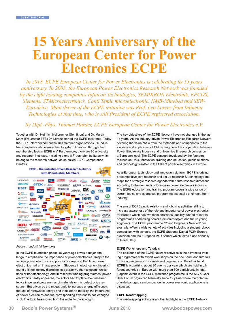
Bodo´s Power Systems® June 2018 www.bodospower.com30
CONTENT
Together with Dr. Heinrich Heilbronner (Semikron) and Dr. Martin März (Fraunhofer IISB) Dr. Lorenz started the ECPE task force. Today the ECPE Network comprises 180 member organisations, 85 indus-trial companies who ensure their long-term financing through their membership fees in ECPE e.V. Furthermore, there are 95 university and research institutes, including alone 8 Fraunhofer institutes which belong to the research network as so-called ECPE Competence Centres.
In the ECPE foundation phase 15 years ago it was a major chal-lenge to emphasize the importance of power electronics. Despite the various power electronics applications already at that time, power electronics had an image problem. Students in electrical engineering found this technology discipline less attractive than telecommunica-tions or nanotechnology. And in research funding programmes, power electronics hardly appeared, the actors had to place their research topics in general programmes of materials or microelectronics re-search. But driven by the megatrends to increase energy efficiency, the use of renewable energy and then later e-mobility, the importance of power electronics and the corresponding awareness has changed a lot. The topic has moved from the niche to the spotlight.
The key objectives of the ECPE Network have not changed in the last 15 years. As the industry-driven Power Electronics Research Network covering the value chain from the materials and components to the systems and applications ECPE strengthens the cooperation between Power Electronics industry and universities & research centres on a European level. The ECPE concept developed by the founders focuses on R&D, innovation, training and education, public relations and technology transfer in the field of power electronics in Europe.
As a European technology and innovation platform, ECPE is driving precompetitive joint research and set up research & technology road-maps for a strategic research agenda with future research directions according to the demands of European power electronics industry. The ECPE education and training program covers a wide range of current topics and addresses programme especially engineers from industry.
The aim of ECPE public relations and lobbying activities still is to increase awareness of the role and importance of power electronics for Europe which has two main directions, publicly funded research programmes addressing power electronics topics and future young engineers. The ECPE programme “Young Engineers Needed”, for example, offers a wide variety of activities including a student robotic competition with schools, the ECPE Students Day at PCIM Europe exhibition and the European PhD School which takes place annually in Gaeta, Italy.
ECPE Workshops and TutorialsThe backbone of the ECPE Network activities is the advanced train-ing programme with expert workshops on the one hand, and tutorials for young engineers in industry and beginners on the other hand. ECPE is organizing about 20 events per year which are held in dif-ferent countries in Europe with more than 800 participants in total. Flagship event in the ECPE workshop programme is the SiC & GaN User Forum organized biennially since 12 years where the potential of wide bandgap semiconductors in power electronic applications is discussed.
ECPE RoadmappingThe roadmapping activity is another highlight in the ECPE Network
15 Years Anniversary of the European Center for Power
Electronics ECPEIn 2018, ECPE European Center for Power Electronics is celebrating its 15 years
anniversary. In 2003, the European Power Electronics Research Network was founded by the eight leading companies Infineon Technologies, SEMIKRON Elektronik, EPCOS,
Siemens, STMicroelectronics, Conti Temic microelectronic, NMB-Minebea and SEW-Eurodrive. Main driver of the ECPE initiative was Prof. Leo Lorenz from Infineon Technologies at that time, who is still President of ECPE registered association.
By Dipl.-Phys. Thomas Harder, ECPE European Center for Power Electronics e.V.
GUEST EDITORIAL
Figure 1: Industrial Members

electrical engineering software
THE SIMULATION SOFTWARE PREFERRED BY POWER ELECTRONICS ENGINEERS
MODELING DOMAINS ElectricalControlThermalMagneticMechanical
KEY FEATURES Fast simulation of complex systemsCode generationFrequency analysisAvailable as standalone program or Simulink blockset
Get a free test license
www.plexim.com/trial
cara
binb
ackh
aus.
com

Bodo´s Power Systems® June 2018 www.bodospower.com32
CONTENT
with several programmes to develop power electronics roadmaps from the system and application perspectives e.g. the ECPE Road-map ´Power Electronics 2025´, see an example from automotive and aerospace power electronics. Presently, ECPE is working on a roadmapping programme identifying promising lead applications for the wide-bandgap power semiconductors SiC and GaN in cooperation with partners in Japan.
ECPE Guideline AQG 324 „Automotive Qualification Guideline“Another recent highlight is the transfer of the German automotive qualification standard LV 324 to the European level as ECPE Guide-line AQG 324 by an ECPE working group with more than 30 industry representatives from the automotive supply chain. The qualification guideline defines a common procedure for characterizing module testing as well as for environmental and lifetime testing of power electronic modules for automotive application. The ECPE Guideline AQG 324 ´Qualification of Power Modules for Use in Power Electron-ics Converter Units in Motor Vehicles´ has been released by the re-sponsible ECPE Industrial Working Group comprising ECPE member companies from the automotive market. The present version dated 12 April 2018 focuses on Si-based power modules where future versions to be released by the ECPE Working Group will also cover the new wide bandgap power semiconductors.
ECPE Lighthouse Programme on modular and scalable Power Electronic Building Blocks (msPEBB)In the frame of the its Joint Research Programme ECPE has started the msPEBB Lighthouse Programme in 2017 defining a heteroge-neous system integration especially when fast switching SiC and GaN power devices are involved. Approaches like switching cell-in-package and power system-in-packages are developed to master the parasitic inductances in fast switching. The critical part of the circuit is integrated in a package and therewith, a more EMI robust msPEBB module can be supplied to the end users.
ECPE organizes the „Semikron Innovation Award“ The Semikron Innovation Award and the Young Engineer Award were initiated 2012 by the Semikron Foundation in cooperation with ECPE. These awards given for outstanding innovations in projects, proto-types, services or novel concepts in the field of power electronics in Europe, combined with notable societal benefits in form of supporting environmental protection and sustainability by improving energy ef-ficiency and conservation of resources.
ECPE Outlook and Future Mega TopicsA key topic will be the future energy system and especially the role of power electronics in the energy transition towards an electricity grid dominated by power electronics on the generation side as well as on the load side. The stabilization and control of such grids without 50Hz backbone provided by conventional generation is a major chal-lenge. Furthermore, the fusion of power electronics and information & commu-nication technologies (ICT) will lead to a digitalization in energy systems e.g. with the smart grids. This will raise the problem of cybersecurity of energy sys-tems. These topics will be discussed in an ECPE Network Meeting on 12 September 2018 in Brussels.
ECPE Joint Stand at PCIM EuropeECPE and the Power Electronics Clus-ter once again organize a joint stand at PCIM Europe 2018 with 20 exhibit-ing companies and institutes (Hall 7, Booth 237). Take the chance and meet
experts from the largest power electronics network in Europe! ECPE celebrates its 15th anniversary on the joint stand. Highlights from the last 15 years as well as future research topics, will be presented on Wednesday, June 6, 2018 at 11:30 am at the industry forum in hall 6 by ECPE.
www.ecpe.org
GUEST EDITORIAL
Figure 2: Roadmap 2015 – 2025
Figure 3: PCIM Booth

The first platform for design, exploration and comparison of advanced power converter designs
Booth 6 - 335
PCIM 2018
Design cutting-edgeconverters
Reduce time-to-market
Streamline your design workflow
POWER DESIGNT E C H N O L O G I E S
[email protected] +33 5 82 95 70 80

Bodo´s Power Systems® June 2018 www.bodospower.com34
CONTENT
Sankara is in demand in Germany as an IT expert with a recognised University degree. The Blue Card has crucial advantages for him in comparison to other residence titles: He can be given an indefinite settlement per-mit after only 33 months, and this entitlement comes earlier if his German is better. If he had a family, they would be able to live with him in Germany as well without them having to prove command of the German language. “This means for me that I have security and prospects, an outlook which made it much easier for me to choose Germany as my principal place of residence.”
The Blue Card, which has been in existence since 2012, offers to small and medium-sized enterprises and their employees simplified ways of planning staffing and residence with legal certainty. The Blue Card can be applied for by University graduates from non-Eu-ropean countries who can prove that they have received a binding job offer in Ger-many. There is a legal entitlement to a Blue
Card from an annual income of 52,000 Euro upwards. This already applies to scientists, mathematicians, engineers, IT experts and physicians from 40,560 Euro upwards. These income thresholds are adjusted every year.
In addition to the higher level of legal certain-ty, it is above all the considerable easing up of the preconditions for indefinite residence in Germany that is attractive for future workers. If an employee has held a Blue Card for 33 months, he or she is given an indefinite right of residence in Germany. This applies after only 21 months if an individual has achieved B1 level in German. Roughly 20,000 former Blue Card holders already have an indefinite right of residence in Germany. This is impor-tant for companies’ advance planning: They can place their human resources planning on a secure footing without needing to take other residence-related aspects into account. The Blue Card is therefore the ideal tool for planning the long-term immigration of high-ly-qualified experts from third countries.
Simplification thanks to the ICT arrange-mentWhilst the Blue Card supports the acquisi-tion of foreign experts in the long term, the ICT (Intra Corporate Transfer) arrangement, which was established in 2017, makes personnel deployment more flexible: Work-ers who are already deployed at locations outside Europe can also come to work in the European locations of the same company. Managers, specialists and trainees only need a residence title in one single EU Member State, and can then be deployed flexibly at locations in other EU Member States.
An entirely electronic procedure has been established for this which can already be initiated from abroad. It is generally no longer necessary to attend in person, and there is no longer any need to apply for a separate residence title in each Member State. This makes companies’ staff rotation more trans-parent and certain, since a legal entitlement to this immigration method has been created. Example: A company which has locations in Germany, France and Pakistan is entitled to also deploy its Pakistani specialists in Germany and France. If the longest stay is planned to take place in France, for instance, the “ICT Card” residence title is issued there. This title enables the specialist to also be deployed in Germany flexibly and at short notice, thus promoting in particular the exchange of specific expertise within the company.
Political scientist Dr. Andreas Müller, deputy Head of Division for Migration policy at the Federal Office for Migration and Refugees (BAMF), said on this topic: “The simplification for intra-corporate transfers and the possibil-ities offered by the Blue Card offer Germany tools under the law on residence which are already offering global enterprises legal se-curity when it comes to recruiting, appointing and rotating highly-qualified experts from third countries.”
BAMF hotline “Working and Living in Germany”:
Tel. +49 (0)30 1815-1111www.make-it-in-germany.com
www.bamf.de
GUEST EDITORIAL
Indian IT Expert Got a Job in Nuremberg with the Blue Card The Blue Card and the ICT Arrangement Make it Easier to Deploy
Highly-Qualified Experts from non-EU Countries.Sankara R. is a 33-year-old computer expert from India who recently came to live and
work in Nuremberg. He is one of now more than 77.000 people who ever received a Blue Card in Germany. “The Blue Card is a great thing. I was working and living in the United
Kingdom until last year. Then I moved to Nuremberg to work here”, says Sankara. “A good friend of mine works at the Federal Office for Migration and Refugees, and he
told me about the Blue Card. I was off like a shot, and I like my work here a lot.
By Martina Frimberger, Bundesamt für Migration und Flüchtlinge

www.fujielectric-europe.com
Visit us: Hall 9Booth 210
7G IGBT & FWD
New internal layout
Higher reliability
Improved silicone gel
SolderorMinipress-fitpins
More power, lower losses
7G IGBT & FWD
Advanced bond wire design
High thermal conductive ceramic substrate
Package material with CTI > 600
Vww = 4 kV
Improved silicone gel
Solderorminipress-fitpins
High power density
MAIN FEATURES MAIN FEATURESDual XT Premium Dual XT
The 7th Generation ModulesDual XT & Premium Dual XT

Bodo´s Power Systems® June 2018 www.bodospower.com36
CONTENT
GaN Systems has unveiled a free simulation tool on its website that provides power conversion designers valuable insight into the perfor-mance of GaN transistors in a specific application. The Circuit Simula-tion Tool is the first online platform in the industry fully dedicated to GaN semiconductor products.
Within moments, engineers can evaluate the benefits of using GaN HEMTs and select the appropriate devices for their design. Users can customize a simulation to include the precise parameters of interest and view key device and system metrics, including power level, con-duction and switching losses, efficiency, and junction temperatures.
In addition to selecting one or more transistors, you can choose various source and load parameters, device switching frequency, the number of devices to parallel, heat sink parameters, and more. Further, GaN-specific details, such as deadtime effects and gate-resistance loss dependencies during device turn-on and turn-off, are supported.
The simulator initially includes unique topologies for a totem-pole PFC converter, 2- and 3-level single-phase inverters, and isolated LLC and phase-shift full bridge converter models. New circuit applications for DC-DC and single-and three-phase designs will soon be added.
GaN Systems will be showcasing the Circuit Simulation Tool at their exhibition booth (#9-511) at PCIM in Nuremburg, Germany, June 5-7.
GaN Systems’ Circuit Simulation Tool is available at www.gansys-tems.com and uses the PLECS® web-based simulation (WBS) tool developed by Plexim. Files containing the loss models and thermal impedance information for GaN Systems’ product portfolio are avail-able for offline use in PLECS, so existing PLECS users can directly include models for GaN Systems’ parts in their custom designs. Free trial licenses for PLECS can be requested on Plexim’s website at www.plexim.com. Further, PLECS Standalone has a free demo mode allowing access to a collection of prebuilt designs. PLECS® is a regis-tered trademark of Plexim GmbH.
www.gansystems.com
www.plexim.com
DESIGN AND SIMULATION
GaN Systems Unveils an Online Circuit Simulation Tool for Evaluating Gallium Nitride Power Transistor Circuits
The Circuit Simulation Tool allows you to virtually test Gallium Nitride (GaN) transistor circuits before you even have hardware built by comparing application conditions. With a simple and intuitive interface, engineers can quickly and easily tune parameters to suit their design goals, explore merits of alternative designs, and see the results in real time.
Live simulated device and system waveforms, as well as data tables showing calculations for loss and junction temperature, are generated, allowing you to compare the effects of
parameter variations or the operation of different parts directly.
By Kristofer Eberle, Plexim and Paul Wiener, GaN Systems
Figure 1: GaN Systems’ Circuit Simulation Tool

Want to see clip Ag-sintering?
a mature solution for mass-production
Development - Samples - Production
Email: [email protected] Telephone: +31 26 3194900 Web: www.boschman.nl
Visit us at PCIM at booth 7-518

Bodo´s Power Systems® June 2018 www.bodospower.com38
CONTENT
With two decades of field experience and 40 million modules in the field, the MiniSKiiP platform has become THE standard for low- and medium-power motor drives. With new versions that are perfect for multi-axis or four-quadrant drives, the drive portfolio is being continu-ously expanded.
In 2017, the MiniSKiiP celebrated its 20th birthday. In 2018, SEMIK-RON is demonstrating its innovation potential once again. With the introduction of the latest IGBT chip generation, the MiniSKiiP is once more setting a new standard in power density and performance for low- and medium-power motor drives. Combined with the well-known advantages of the MiniSKiiP SPRiNG technology and its easy assem-bly process, a new performance benchmark is being set.
MiniSKiiP is also a perfect power module for silicon carbide, hybrid and full SiC solutions. Equipped with the latest chips from Rohm and Infineon, the MiniSKiiP SiC portfolio gives benchmark performance results while still offering all the benefits of MiniSKiiP. Let’s have a look at all these aspects in detail.
The outstanding mounting concept not only impresses in drive ap-plications but is also a perfect fit for the high-volume manufacturing process required for solar string inverters.
SEMIKRON offers a broad portfolio of three-level MiniSKiiP modules. The latest addition is the MiniSKiiP Dual Split MLI, with a nominal current of 400A and 1200V devices. As an option it is available with SiC Schottky diodes in the neutral path for maximum efficiency. This new module allows baseplate-less PCB-mounted inverter designs with a power of up to 180kW for 1500VDC photovoltaic systems and sets a new benchmark in this class. The layout of the MiniSKiiP Dual’s SPRiNG contacts allows for a low-inductance DC-link connection, easy driver integration and paralleled AC power connections.
This elegant solution overcomes the challenges associated with paralleling three level NPC inverters. The approach is suitable for buil-ding scalable and modular phase legs. SEMIKRON’s concept takes advantage of the symmetry in the NPC topology and uses two half
COVER STORY
Maximise Your Power: With New Chips and New Topologies to the
Next Level of Power Density Thanks to its easy assembly concept, MiniSKiiP knows no bounds when it comes to
new applications and markets. The MiniSKiiP Dual Split MLI offers the most powerful baseplate-less string inverter design available and is ready for 1500V DC bus voltage and
up to 180kW output power. In a second version optimised for 1000V DC bus, the same design pushes the power density of medium-power standalone and modular UPS designs
to 150kW.
By Stefan Häuser, Bernhard Eichler, Thomas Hürtgen and Werner Obermaier, SEMIKRON Elektronik
Figure 1: MiniSKiiP Package Family: One concept from 4 to 400A nominal current
TOP BOT
DC+ DC-AC
N
TS
DC+
TS
DC-
AC AC
Driver
N
ACAC
Figure 2: MiniSKiiP Dual Split MLI topology

C
M
Y
CM
MY
CY
CMY
K
696984-FORTE | The Intelligent BOM Tool A4 copy.pdf 1 23.02.18 12:43

Bodo´s Power Systems® June 2018 www.bodospower.com40
CONTENT
NPC topologies referred as MLI TOP and MLI BOT. Each half NPC to-pology is implemented in its own module as shown in Fig 2. Following SEMITOP E2 and SEMITRANS 10, the MiniSKiiP Dual is the third product line to use this innovative and highly efficient approach.
For maximum efficiency, we have optimised the internal 3-level NPC chipset: the fast switching devices (T1, T4) are equipped with high-speed IGBT 4 (12F4) in combination with SEMIKRON CAL4F diodes to reduce switching losses. The slow switching devices (T2, T3) use low-power IGBT 4 (12T4) in combination with rectifier diodes to achie-ve minimal conduction losses.
The neutral clamping path (D5 & D6) has also been optimised: here you can choose between the standard version with SEMIKRON CAL4F diodes or a high-efficiency solution with SiC Schottky diodes that can reach an efficiency of up to 99.3%.
In addition to the single modules, SEMIKRON has developed an application sample that demonstrates a simple way to design a three-phase inverter stage for DC voltages up to 1500V (Figure 3)
Additionally to the modules based on 1200V IGBT, the MiniSKiiP Dual Split MLI modules will also be available with 650V IGBTs. Here, the chipset is also optimised: for the output stage a combination of fast but soft switching S5 IGBT for the outer switches T1 and T4 in combi-nation with L5 IGBT that exhibit a low saturation voltage VCE,sat for T2 and T3. The diodes are fast switching silicon or standard free-whee-ling diodes for the slower switching components.
These modules are a perfect fit for high-efficiency systems running on a maximum of 1000V DC bus and 400VAC output voltage, such as UPS and solar systems. Thanks to the optimised chipset selection, this solution can reach up to 150kVA output power within a single 19-inch rack. Including the 99% single conversion efficiency at full load, this solution sets a new benchmark in power density for modular UPS systems. With the optional silicon carbide diodes for clamping part (D5, D6), the efficiency will even exceed 99%.
Talking about silicon carbide brings us to the general question of whether MiniSKiiP is the right power module for SiC devices. Whene-ver we talk about full SiC power modules, the major requirement is a
low inductance module package. But, especially for power modules with lower current ratings, this is not necessarily required. Introducing an evaluation factor of module stray inductance and nominal current rating (Lstray x Inom) enables us to evaluate the SiC power module performance easily. The smaller the factor, the better the usability. While the stray inductance is fixed by the spring design and layout to approx. 20 to 25nH with MiniSKiiP 6-packs, the current rating varies with the chipset. The 6-pack with the highest available current rating is 90A, resulting in an evaluation factor value of 2.25x10⁻⁶, which is an acceptable value: no limitation in performance is expected. For full SiC MiniSKiiPs with lower current ratings such as 30A, the evaluation factor is as low as 0.75x10⁻⁶, resulting in a full speed application of the SiC MOSFET.
In the current product line-up of full SiC power modules, 6-packs of 1200V with nominal currents from 25A to 90A are available. The latest addition to the portfolio will be a 6-pack in MiniSKiiP housing size 1 with an Rds,on of 45mΩ, equipped with the latest SiC MOSFET chip from Infineon. Fig. 4 shows a direct comparison of power losses for a 4kW motor drive. In this case, the dv/dt of the SiC MOSFET has been limited to 10kV/µs to limit the stress on the motor windings as well as the effort to comply with EMI requirements. With the SiC power module the power losses at 15kHz are reduced by 75%. At the same time the efficiency rises from 97.8% to more than 99%. This makes SiC the perfect solution for high-efficiency or motor-integrated drives where the inverter is directly built on or into the motor housing. In this case the capability of dissipating power losses is limited and the losses must be minimized.
Furthermore, under the given conditions, the silicon-based motor drive could not be used at switching frequencies higher than 18 kHz without exceeding the recommended operation junction tempera-ture of 150°C. The silicon carbide module can be run at 40kHz and generates the same power losses as the silicon version at approx. 8kHz. For high-speed motor drives supporting output frequencies up to several thousand Hz, silicon carbide is therefore the only solution.
Also in the silicon world, new chip technologies help to innovate MiniSKiiP and its application in motor drives. MiniSKiiP is the first product group within SEMIKRON to be equipped with the new IGBT 7 from Infineon. This next generation IGBT uses an advanced Micro Pattern Trench cell structure and the latest thin wafer technology. As a result, this new IGBT series provides a saturation voltage of only 1.75V at nominal current and at the maximum junction temperature (Tj=175°C) and 1.70V at the recommended operation temperature of 150°C. This compares to 2.1V at Tj=150°C for the previous genera-tion (IGBT 4). This means a reduction of more than 20% is achieved while at the same time allowing the chip size to be reduced by almost 25%.
COVER STORY
Figure 3: 3-phase solar inverter application sample for 1500V and 99.3% efficiency
120
100
80
60
40
20
00 5 10 15 20 25 30 35 40 45
Switching Frequency in kHz
Pow
er L
osse
s in
W
Silicon CarbideSKiiP15ACM12V20
SiliconSKiiP13AC12T4V1
Vin = 600VVout = 400VPout = 4kW200% Overload / 10sRth(s-a) = 0.3K/W
Figure 4: Power loss comparison between silicon and silicon carbide MiniSKiiP housing size 1 in a typical motor drive application.

210x297 mm
Visit us at PCIM 2018Hall 9, Booth No. 341 www.semikron.com
In the world of electronics today, the way to guarantee maximum supply chain safety is to use industry stan-dard power modules. The portfolio at SEMIKRON covers all the standard packages, fully compatible but with added value in the form of optimisations, thanks to our technology portfolio. And by continually expanding our SEMiX and MiniSKiiP production capacities, we are in a position to meet your growing needs. What’s more, our application experts worldwide are at your service – delivering professional support for your system design and configuration.
One-Stop Innovation & Service.
Your Ultimate Partner for Power Electronics

Bodo´s Power Systems® June 2018 www.bodospower.com42
CONTENT
Thanks to this reduction in die size, the power level for MiniSKiiP products has been able to be significantly increased. For example, with the new technology the maximum current rating for MiniSKiiP CIB (converter-inverter-brake) modules will be increased from 35A to 50A in a size 2 housing, and for MiniSKiiP 6-pack modules from 150A to 200A in a size 3 housing. Assuming a heatsink temperature of 80°C, a switching frequency of 4kHz and an overload factor of 150%, this results in an increase in output power of more than 20%.
This increase could be further extended by using our High Perfor-mance Thermal Paste (HPTP), which greatly reduces the thermal resistance from junction to the heatsink. For the new 200A IGBT 7 de-vice, a Rth reduction of more than 30% has been achieved. Combin-ing these improvements – using 200A IGBT 7 instead of 150A IGBT 4 and High Performance Thermal Paste instead of standard paste – increases the available output power by more than 65%.
The reduced saturation voltage not only enables the die size to shrink but also results in lower total losses at a given output power, thus pro-viding better overall efficiency and cutting the effort for the heatsink. Fig. 5 shows a comparison of the estimated total losses at overload for the different devices. The simulations show that a 55kW inverter based on an IGBT 7 150A module will reduce the total losses in overload condition by about 12% compared to a 150A IGBT 4 based solution. A design rated 67kW using a 200A IGBT 7 will have only slightly higher maximum losses than a 55kW system utilising a 150A IGBT 4 based module. This means, IGBT 7 extends the maximum output power range, resulting in a scalable power module platform ad-dressing from 1 to 110kW. Furthermore, this means a direct upgrade of power density in existing MiniSKiiP designs.
IGBT 7 was designed with a full focus on use in motor drives, which is reflected in several features: IGBT 7 has a short circuit withstand time of 8us at high chip temperature. It supports a high peak current capability of three times the nominal current. Motor windings are treated with care thanks to fully controllable dv/dt at IGBT turn-on and a low dv/dt at turn-off of less than 4kV/µs. This also reduces the effort needed to meet the system’s EMI requirements.
The first step will see the IGBT 7 rolled out for all MiniSKiiP CIB and 6-pack standard types with a focus on power modules fully populated with chip area. These provide simple and direct benefits in terms of power density.
Besides the latest IGBT technologies, the MiniSKiiP portfolio is also being enriched by innovative new topologies that help to save energy. The use of regenerative drives is becoming more and more popular in elevator applications. This is because typical inverters allow the energy to flow only in one direction, from the power supply to the load (usually a motor). With the rising demand for energy-efficient motor drives, modern inverters are increasingly being equipped with bidirec-tional energy flow capability.
In non-regenerative inverters, the regenerative energy of the motor is converted into heat using the inverter’s brake chopper, which is connected to a braking resistor. The kinetic energy of the motor is essentially lost, which pushes up costs due to the increase in energy consumption. What’s more, energy efficiency demands might not be met with this design.
This is why regenerative or four-quadrant drives are playing a more and more important role in new inverter designs. Here, the energy is not wasted in braking resistors but fed back into the grid, effectively lowering the energy consumption. The setup of regenerative drives typically requires a solution with two power modules – one module for the active converter and one for the inverter part.
MiniSKiiP ACC twin 6-pack modules combine two independent 6-packs in a single power module as shown in Fig. 6. Available in 1200V with a nominal current of up to 50A, these modules are the perfect solution for low-power and ultra-compact elevator or crane drives.
A second important area of application for MiniSKiiP ACC modules is multi-axis inverters like servo drives for robotics. Each axis requires an independent 6-pack to control the motion of the robot. The integra-tion of two 6-packs in one module package reduces the number of modules by 50%. This results in inverter cost and size reduction, lead-ing to a simpler and effective inverter integration into the robot itself.
With conquering new markets, the latest chip technologies and the continuous addition of new topologies, MiniSKiiP shows a very pro-mising outlook and continuously increasing demand. To prepare for the future, the MiniSKiiP production capacity is going to be expanded by 50% starting from Q1 2019. This investment shows and confirms the future importance of MiniSKiiP in the low- and medium-power segment.
As well as the capacity increase, the MiniSKiiP housing material is being upgraded to achieve a higher CTI (Comparative Tracking Index). The CTI is a figure that specifies the electrical breakdown on an insulating material. The higher the value, the smaller the distance between two points of different voltage potential can be. The new material’s CTI of 600 allows for greater freedom in the insulation coordination of new system designs. In addition, the new package
COVER STORY
100
%
IGBT 7, 6-pack150A/1200V
IGBT 7, 6-pack200A/1200V
IGBT 7, 6-pack200A/1200V withHigh Performance
Thermal Interface Material
Max. Output Power and Total Loss Comparison
IGBT 4, 6-pack150A/1200V
SKiiP 39AC12T4V1
100
%
100
%
88 %
121
%
103
%
166
%
159
%
Maximum Output Power Total losses in Overload Condition (150% / 1min)
Figure 5: Motor drive maximum output power and loss comparison (fsw=4kHz, fout=50Hz, Tsink=80°C, Tj,max=150°C)
Figure 6: MiniSKiiP Twin 6-pack (ACC) topology

www.bodospower.com
material exhibits a higher temperature of deflection under load, which will prepare the MiniSKiiP housing for potentially higher maximum chip temperatures in the future. By switching to this new material, SEMIKRON is also ensuring the long-term supply reliability of the raw material, which is an important piece of the overall supply chain.
MiniSKiiP Dual 1 and 2 are the first MiniSKiiP housings to have been introduced with the new housing material. All other MiniSKiiP packages will be transferred to the new package material by the end of 2018.
MiniSKiiP is fit for the future: Not only with the latest chip technologies in silicon and silicon carbide, but also with new topologies it conquers new markets. Maximum power density and easiest mounting proces-ses designed for high volume productions convince in solar and UPS systems, too. With the investments in new housing materials and production lines SEMIKRON makes sure to stay your first choice for current and future product developments.
www.semikron.com
a Knowles Precision Devices brand
TM
a Knowles Precision Devices brand
TM
Zoom, Zoom. Beep, Beep
Drive towards all electric
AEC-Q200l Standard and large size MLCCsl Safety Certified MLCCsl 3 terminal EMI filters
l X2Y integrated passive componentsl StackiCap™ high CV capacitorsl Open Mode & Tandem capacitorsl X8R high temperature MLCCs
automotive application
s
capacitors and emi Filters For

Bodo´s Power Systems® June 2018 www.bodospower.com44
CONTENT
The design equation that matters is as follows:
We have arranged this equation with the magnetics variables of core saturation level, number of turns, and core cross-sectional area (minimum) on the left. The electrical engineering variables are on the right, and these are usually determined by the circuit designer through simulation, experience, and personal preferences. We will talk more about this in a future article, since the choices of inductance can vary widely from one designer to another, and from one application to another.
Defining the BEST InductorDesign engineers think they want the best inductor for an application. But, what does this mean? To the purchasing department, “best” typi-cally means cheapest, and they will work hard to drive the price down. To the electrical engineer, “best” may mean the most efficient for the application. For the packaging engineer, “best” will mean a smaller size. And for the EMI engineer, “best” may mean small capacitance, and minimal stray electromagnetic fields from the part.
Satisfying all these definitions simultaneously is not possible. For every design, there will be a tradeoff between allowable size, heat dissipation, impact on the rest of the circuit design, and cost. This tradeoff will be different for every application, and that is why you will find a very wide range of inductor designs from one power supply to another.
Starting with Arbitrary ChoicesNow we come to the heart of the problem – how to start a design? At many companies I work with, there is an almost pathological obses-sion with finding the equations to be programmed into Mathcad that will provide the “RIGHT” solution to the problem. Which core should you choose? What material? What is the right answer? Many manag-ers feel that if they can see an equation, their engineers must have chosen the proper solution.
But, there is NO single right answer. There are an infinite number of solutions, and the choice of which way to go is arbitrary. I am delib-erately being extreme in saying this to make a point – if you want an optimized inductor, stop looking for nonexistent sets of equations and begin exploring engineering options with an unconstrained mind.
There is an important consequence with the ONE design equation above. Let us assume that we have chosen the inductance and the subsequent peak current that results. (more about this will be dis-cussed in future articles – it is not necessarily a simple choice.) The equation implies that you can use a core of ANY size, and if you put enough turns on the core, the inductor will not saturate. That means you can start the design anywhere you wish!
If you are doing this for the first time, just pick a number for the core area. Plug it into the design equation and see how many turns you are going to need to make sure the inductor doesn’t saturate. From that result, it won’t take long to ascertain whether the design is sensible or not. Choosing a number that is too small, for example, will help build our experience base by seeing the impact on losses in the windings or the core. There is usually more to be learned from making a wrong initial choice that starting with a design that will work comfortably. This is the process we encourage in our design workshops – iterate quickly with several different options and you learn quickly.
If you are working with a company that already does custom inductor designs, you may choose just pick a core already being used. This will provide purchasing power that can drive a lower price than a smaller core. It may also fit better with your company’s tooling. There
DESIGN AND SIMULATION
Designing Custom Inductors with ONE Design Equation
In the last article of this series, I introduced one equation that matters for inductor design. This is the equation that you will use when you are creating a custom design from scratch. Please note that we are talking about the design of an inductor, NOT the analysis process. Mathematical structure analysis can be quite involved and is a popular subject for PhD
dissertations. You can also read many articles on this topic in our Design Center [1].
By Dr. Ray Ridley, Ridley Engineering Inc.
Figure 1: The Basic Parts of a Custom-Designed Inductor

www.bodospower.com
are many factors that will drive the decision, but a single optimizing equation is not one of them.
We will explore the idea of exploiting the design freedom that exists by starting with any size core with examples in later articles. This is also the process that we demonstrate in our design workshops [3].
But now let’s consider how design guidelines that you find in text books or databooks have the unfortunate consequence of remov-ing design freedom and iteration to arrive at a single solution. This is counter-productive to the creative process.
Wire Current-Density EquationMost data books, text books, and magnetics guides take the same fundamental step in overcomplicating the design process. They search for a single solution that cannot possibly exist for every ap-plication. The view is presented that there must be a starting point for the design, and design freedom should not be considered.
For many publications [2], the size of the wire can immediately be locked down according to the arbitrary (but common) current-density equation:
500 /CuA circular mils A=
Please note that the number 500 is arbitrary. In some books it will be 350, and in others 750. We have deliberately left this expression in one of the absurd units that you will find in many magnetics texts and handbooks (apologies to non-US engineers). A circular mil is the
Dean Technology oers a wide range of power electronics in all common packages, with ratings to cover most applications. As with everything we oer custom specications, packages, and full assemblies are a specialty - we pride ourselves on helping customers get exactly what they need for their success.
Contact us today for a catalog, quote, or to begin a new design!
POWERELECTRONICS
www.deantechnology.com
COMPONENTS, ASSEMBLIES, & CUSTOM SOLUTIONS
Visit us in Booth #9-164

Bodo´s Power Systems® June 2018 www.bodospower.com46
CONTENT
area of a piece of wire that is 1 mil in diameter, that is 0.001” or 25 microns. I don’t like to choose a more sensible unit since I don’t want to encourage people to use this guideline. For all of the magnetics I have worked with, I have never known the current density, but I do know the temperature rise after it has been built and tested.
The equation gives the recommended cross-section of the wire for the rms current in the inductor windings. It seems initially like a reasonable starting point. However, we must ask, where does this equation come from? It is hard to trace the first usage, but ultimately it is derived from the early days of line-frequency magnetics work. Transformers and inductors had hundreds or thousands of turns, and they were massive thermal structures with the windings and cores inti-mately thermally connected. The recommended current density made sense when the frequency was preselected and the thermal situation was known and well charaterized.
However, with high frequency magnetics, we have many compound-ing factors. Firstly, there may be just a few turns of wire or foil. The thermal situation is profoundly different from multiple layers of wire in a conventional line-frequency inductor. The windings can be in a sin-gle layer, multiple layers, on a bobbin, or part of a PCB. The thermal variations are tremendous. So why apply the same design guideline?
And, for most high frequency inductors, there are multiple frequency components to the current waveforms. This leads to uneven current distribution in the wire which is usually considerably thicker than a single skin depth. The current density rule no longer applies, and it is not a good starting point.
Design Tip: Wire Current Density – calculate it if you like, but don’t use it to drive a design. I may never know the current density of the final design. I do, however, want to know how hot it gets.
Window-Area Product EquationSome texts take a further step in trying to pin down a single “correct” solution by defining a window-area product. This is the product of the area of the core, multiplied by the area of the window available for the winding. This quantity is then used in a design equation based on the power level of the application [2].
Equations like this give the appearance of providing a unique solution and design path. But no two applications can be the same. One of the primary drivers of a design is the cooling of the part. This is never the same from one application to another. Some designs have forced air cooling, and at the other extreme, some magnetics must work in a vacuum with zero air flow. The design process should not be the same for these examples.
Design Tip: Window Area Product – Without full thermal informa-tion, it can never be a good guide to design direction.
Gap Length EquationSome design engineers like to start with a gap length. We ran into this on our LinkedIn group recently with questions asked by new designers in the field [4]. Why? I don’t really know. Perhaps they have a pre-gapped core on hand and don’t want to order another. Regard-less, the gap length is not the way to start your design.
However, when you are DONE with a design, you can use an equa-tion to estimate the gap as follows:
never the same from one application to another. Some designs have forced air cooling, and at the other extreme, some magnetics must work in a vacuum with zero air flow. The design process should not be the same for these examples.Design Tip: Window Area Product – Without full thermal information, it can never be a good guide to design direction.
Gap Length EquationSome design engineers like to start with a gap length. We ran into this on our LinkedIn group recently with questions asked by new designers in the field [4]. Why? I don’t really know. Perhaps they have a pre-gapped core on hand and don’t want to order another. Regardless, the gap length is not the way to start your design. However, when you are DONE with a design, you can use an equation to estimate the gap as follows:
20 e
gn AlL
µ=
<<Figure 2: The Simplest Equation Assumes All Energy is Stored in the Gap>>
Is this a good and accurate equation? No, not at all! The accuracy will depend on the size of the gap relative to the core total path length, the permeability of the core, and the gap length compared to the dimensions of the core cross section. You can read many papers about fringing fields, and how to find a better equation for the gap. But, in the end, it doesn’t matter. All equations for gap length will be empirically inaccurate. Don’t worry about this, just gap a finished design until you get the desired value of inductance. That is how inductor manufacturing works. The gap is adjusted to get the inductor with the specified tolerance required.There are two things that are important about the gap length – one, it should not be too small, or you will be relying on the permeability of the core material, a quantity that can be very variable. And two, it must not be too large, or excessive fringing and EMI will result. In between these two extremes, the actual value of gap is determined empirically. Design Tip: Gap length equation– Use it to establish upper and lower bounds, but ultimately the gap will be adjusted empirically for the desired result.
SummaryWe encourage engineers to experience the freedom in working with just ONE design equation. Try many alternatives, and you will learn quickly through iteration. Most design books constrain designs simply to arrive at a single solution. This discourages creative thought leading to designs that are suboptimal for most applications.
References[1] Magnetics Design Videos and Articles, Ridley Engineering Design Center.[2] Mag Inc Design Guide: https://www.mag-inc.com/Design/Design-Guides/Transformer-Design-with-
Magnetics-Ferrite-Cores[3] Learn about proximity losses and magnetics design in our hands-on workshops for power supply
design www.ridleyengineering.com/workshops.html (The only hands-on magnetics seminar in the world.
[4] Join our LinkedIn group titled Power Supply Design Center. Noncommercial site with over 8000experienced and helpful industry experts.
[5] Join our new Facebook group titled Power Supply Design Center. Advanced in-depth discussion group for all topics related to power supply design.
www.ridleyengineering.com
Is this a good and accurate equation? No, not at all! The accuracy will depend on the size of the gap relative to the core total path length, the permeability of the core, and the gap length compared to the di-mensions of the core cross section. You can read many papers about fringing fields, and how to find a better equation for the gap.
But, in the end, it doesn’t matter. All equations for gap length will be empirically inaccurate. Don’t worry about this, just gap a finished design until you get the desired value of inductance. That is how inductor manufacturing works. The gap is adjusted to get the inductor with the specified tolerance required.
There are two things that are important about the gap length – one, it should not be too small, or you will be relying on the permeability of the core material, a quantity that can be very variable. And two, it must not be too large, or excessive fringing and EMI will result. In between these two extremes, the actual value of gap is determined empirically.
Design Tip: Gap length equation– Use it to establish upper and lower bounds, but ultimately the gap will be adjusted empirically for the desired result.
SummaryWe encourage engineers to experience the freedom in working with just ONE design equation. Try many alternatives, and you will learn quickly through iteration. Most design books constrain designs simply to arrive at a single solution. This discourages creative thought lead-ing to designs that are suboptimal for most applications.
References1. Magnetics Design Videos and Articles, Ridley Engineering Design
Center. 2. Mag Inc Design Guide: https://www.mag-inc.com/Design/Design-
Guides/Transformer-Design-with-Magnetics-Ferrite-Cores 3. Learn about proximity losses and magnetics design in our hands-
on workshops for power supply design www.ridleyengineering.com/workshops.html (The only hands-on magnetics seminar in the world.
4. Join our LinkedIn group titled Power Supply Design Center. Non-commercial site with over 8000 experienced and helpful industry experts.
5. Join our new Facebook group titled Power Supply Design Center. Advanced in-depth discussion group for all topics related to power supply design.
www.ridleyengineering.com
Figure 2: The Simplest Equation Assumes All Energy is Stored in the Gap
DESIGN AND SIMULATION

u Isolated USBu Full Frequency u 0.01 Hz to 30 MHzu Source 1 mV to 20 V u RF Power Amplifier u Graphic Control u Multi-Sweep Storage u Full Range Accessories u Maximum Productivity u Fully-Automated Loop Designu Support from Industry Experts u Easy to Useu One-Button Setup
RIDLEY ENGINEERING601 E Daily Drive, Suite 112 Camarillo CA 93010 [email protected] +1 805 504 2212 POWER SUPPLY DESIGN CENTER GROUP on Linkedin
AP310 is the industry’s only full-featured frequency response analyzer designed specifically for power supplies. Enhance the experience with RidleyWorks® software for seamless integration between power supply design and measurement. Made in California since 1995.
RIDLEYENGINEERING.COM
Education Software Hardware Design Ideas
AP310 from AP Instruments Inc.
RidleyWorks®
Automation Software

Bodo´s Power Systems® June 2018 www.bodospower.com48
CONTENT
IntroductionElectric Vehicles are receiving ever-greater attention from vehicle manufacturers, governments, regulators and consumers and the pres-sure is increasing on vehicle designers to deliver on the technology’s promise.
Hitachi’s Suijin series of automotive power modules are here to help. Building on Hitachi’s long history in producing power modules for Electric and Hybrid-Electric vehicles the Suijin series provides a range of high power, high performance power modules to meet the most demanding automotive applications from 600V to 1200V.
The Suijin Series PackageThe Suijin Series provides high function 6in1 power modules incor-porating direct water-cooling for maximum cooling efficiency, power cycle life and output power and temperature sensing for optimum design performance.
The series offers a single package outline for the full range of voltage and current ratings allowing for a common mechanical design and high level of design re-use for converters with different ratings. The compact form factor, high power density facilitate and robust con-struction enables the designer to realise industry leading converter designs.
Product Line upThe Suijin Series product line up covers from 650V, 750V and 1200V rated modules with current ratings up to 1000A. All products are avail-able now as samples or in mass production.650V, 600A – MBB600TV6A650V, 800A – MBB800TW6A750V, 1000A – MBB1000UW1A1200V, 400A – MBB400TX12A
Evaluation KitsTo assist with initial evaluation and design activities Hitachi can supply a comprehensive evaluation kit to support each module. The Evalua-tion kit includes:
• Gate Drive with all key IGBT drive and protection features and temperature sensing for each arm.
• DC Link Capacitor designed to connect directly to the DC connec-tions of the module and provide a low inductance DC link
• Water cooling jacket for connection to a cooling system during test.
Latest TechnologyHitachi continues to apply the latest technology breakthroughs to the Suijin series to continue extending the performance envelope. The application of latest generation Side Gate IGBT, on chip temperature sensing and Copper Sintering for improved die attach ensure the best output power, energy losses, control and lifetime.
POWER MODULES
Hitachi Suijin Series Power Modules for Electric Vehicles
Hitachi’s Suijin series of automotive power modules provide a range of high power, high performance power modules to meet the most demanding automotive applications.
By Chris White, Hitachi Europe Limited
Figure 1: Suijin Series Direct Water Cooled Module
Figure 2: Side Gate IGBT performancea. (top) Vce – Eff tradeoff b. (bottom) Eon+Err – reverse recover dV/dt
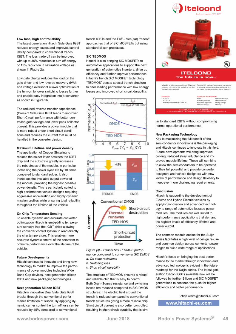
www.bodospower.com June 2018 Bodo´s Power Systems® 49
CONTENT
Low loss, high controllabilityThe latest generation Hitachi Side Gate IGBT reduces energy losses and improves control-lability compared to conventional trench IGBT. The loss trade off can be improved with up to 35% reduction in turn off energy or 15% reduction in saturation voltage as shown in Figure 2a.
Low gate charge reduces the load on the gate driver and low reverse recovery dV/dt and voltage overshoot allows optimization of the turn-on to lower switching losses further and enable easy integration into a converter as shown in Figure 2b.
The reduced reverse transfer capacitance (Cres) of Side Gate IGBT leads to improved Short Circuit performance with better-con-trolled gate voltage and lower peak collector current. This provides a power module that is more robust under short circuit condi-tions and reduces the current that must be handled in the converter design.
Maximum Lifetime and power densityThe application of Copper Sintering to replace the solder layer between the IGBT chip and the substrate greatly increases the robustness of the module, in particular increasing the power cycle life by 10 times compared to standard solder. It also increases the available output power of the module, providing the highest possible power density. This is particularly suited to high performance vehicle designs requiring aggressive acceleration and highly dynamic mission profiles while ensuring total reliability throughout the lifetime of the vehicle.
On Chip Temperature SensingTo enable dynamic and accurate converter optimization Hitachi is embedding tempera-ture sensors into the IGBT chips allowing the converter control system to read directly the chip temperature. This enables more accurate dynamic control of the converter to optimize performance over the lifetime of the vehicle.
Future DevelopmentsHitachi continue to innovate and bring new technology to market to improve the perfor-mance of power modules including Wide Band Gap devices, next generation silicon IGBT and new packaging technologies.
Next generation Silicon IGBTHitachi’s innovative Dual Side Gate IGBT breaks through the conventional perfor-mance limitation of silicon. By applying dy-namic carrier control the turn off loss can be reduced by 45% compared to conventional
trench IGBTs and the Eoff – Vce(sat) tradeoff approaches that of SiC MOSFETs but using standard silicon processes.
SiC TEDMOSHitachi is also bringing SiC MOSFETs to automotive applications to support the next generation of automotive inverters, drive up efficiency and further improve performance. Hitachi’s trench SiC MOSFET technology “TEDMOS” uses a special trench structure to offer leading performance with low energy losses and improved short circuit durability.
The structure of TEDMOS ensures a robust and reliable chip that is easy to control. Both Drain-Source resistance and switching losses are reduced compared to SiC DMOS structures. The electric field around the trench is reduced compared to conventional trench structures giving a more reliable chip. Short circuit current is also better controlled, resulting in short circuit durability that is simi-
lar to standard IGBTs without compromising normal operational performance.
New Packaging TechnologyKey to maximizing the full benefit of the semiconductor innovations is the packaging and Hitachi continues to innovate in this field. Future developments will bring improved cooling, reduced stray inductance and im-proved module lifetime. These will combine to allow the semiconductors to be operated to their full potential and provide converter designers and vehicle designers with new levels of performance and design flexibility to meet ever more challenging requirements.
ConclusionHitachi is supporting the development of Electric and Hybrid Electric vehicles by applying innovation and advanced technol-ogy to range of automotive focused power modules. The modules are well suited to high performance applications that demand the highest levels of efficiency, lifetime and power output.
The common module outline for the Suijin series facilitates a high level of design re-use and common design across converter power ranges to suit a wide range of applications.
Hitachi’s focus on bringing the best perfor-mance to the market through innovation and advanced technology is evident in the future roadmap for the Suijin series. The latest gen-eration Silicon IGBTs available now will be followed by further Silicon and SiC MOSFET generations to continue the push for higher efficiency and better performance.
www.hitachi-eu.com
Figure [3] – Hitachi SiC TEDMOS perfor-mance compared to conventional SiC DMOSa. On state resistanceb. Switching lossc. Short circuit durability
ITELCOND the future is now…
Excellence in capacitors 1976 - 2017
Itelcond SRL Viale de Gasperi,36 20010 BareggioT: +39 02 90362995 F: +39 02 90360740 www.itelcond.it Email: [email protected]
Itelcond is an Italian company with over 40 years of experience in the field of high quality large can alumi-nium electrolytic capacitors.
Flexibility, high quality and a continuous improvement in technology and automation, gave us a leading role in the market of screw terminal and snap-in capacitors.
Certification• ISO 9001• ISO 14001• International standard CECC, DIN, IEC
Applications and technologies:• UPS• Welding Machines• Industrial Application• Electric Vehicles
• Renewable Energy• Medical Devices• Energy Storage• Railways
ADV_Itelcond.indd 1 06/09/17 16:38

Bodo´s Power Systems® June 2018 www.bodospower.com50
CONTENT
Requirements of High Reliability Power SystemsIn a perfect world a high reliability system should be designed to avoid single point failures and provide a means of isolating faults in such a way that operation may continue perhaps at a reduced performance level. It should also be able to contain faults to avoid propagation to downstream or upstream electronics.Built-in redundancy, either in the form of parallel circuits that share the load actively or that wait in a standby until a failure occurs, is one solution. In each case, fault detection and management requires additional overhead circuitry contributing to the overall complexity and cost. Some systems also create dissimilar parallel circuits to add diversity and avoid the risk of a common failure mechanism; this is the case for some aircraft flight control systems. Increasing system complexity places a greater burden on the power supply performance so high conversion efficiency and good thermal management are critical as for every 10°C rise in junction temperature the IC lifetime is approximately halved. As we shall see, new feature rich power supply ICs and dedicated power management functions now provide increased protection to the IC itself and the surrounding system.
Power Regulator Safety FeaturesVoltage regulators have seen increasingly more accurate and sophis-ticated forms of current limiting to avoid excessive output currents damaging the device itself or downstream components. It is also fairly common to find internal protection circuitry including reverse battery protection, current limiting, thermal limiting and reverse current protection. One product that provides an example of improvements in both process technology and in safety features is the LTC7801 DC/DC Switching Controller, it can safely sustain input voltages up to 150V and implements a protection feature that inhibits switching when the input voltage rises above a programmable operating range. This functionality simplifies the input supply transient protection circuitry reducing component count and solution size. The output is also well
protected with an overvoltage comparator that guards against voltage overshoots while a foldback current limiter controls power dissipation during overcurrent and short-circuit fault conditions. The physical packaging aspects of safety are also addressed by offering package options with widely spaced pins to avoid the danger of arcing between adjacent high voltage and low voltage pins. The breakdown voltage reduces with lower air pressure so unpressurized aircraft applications can select the LTC3895 that offers the same func-tions and performance as the LTC7801 but with a 0.68mm double pin spacing package option.Some products such as the fault tolerant LT3007 linear regulator are also available with so called FMEA (Failure Mode and Effects Analy-sis) compliant pinout where the output stays at or below the regulation voltage if adjacent pins are shorted together or if a pin is left floating.
Controlling Multiple Input Sources Power supply systems that contain a main supply and a redundant backup with perhaps an external auxiliary supply need a system to arbitrate which supply has priority and to monitor their status. Furthermore, it must protect the system from cross-conducting and back-feeding during source switching. Single chip ICs such as the LTC4417, provide one solution automatically selecting the source based on validation of user defined supply thresholds for each input.
POWER SUPPLY
Integrated Circuits Offer Enhanced Protection & Improved Safety
Features for High Reliability Power Supplies
The design of high reliability systems encompasses the use of fault tolerant design techniques, the selection of suitable components to meet the anticipated environmental
conditions and compliance to standards. This article focuses on semiconductor solutions for the implementation of high reliability power supplies including redundancy, circuit
protection and remote systems management. It will highlight how improvements in semiconductor technology and new safety features can simplify design and enhance
component reliability.
By Steve Munns, Mil-Aero Marketing Manager, Analog Devices
Figure 1: LTC7801 High Voltage Step Down DC/DC Controller

www.bodospower.com
An alternative approach is to share the load between two input sources that operate simultaneously, increasing reliability by reducing the burden on each source and at the same time providing protection against failure of one source if they are each suitably sized to support the full load requirement. In the past, a simple but inefficient diode-OR arrangement might have been adopted but that required each supply to have active control to balance the loading. Figure 2 shows how this can now be accomplished with a single chip solution. The LTC4370 is a current sharing controller with reverse blocking that prevents a fault in one supply, bringing down the power system.
Transient and Circuit ProtectionMilitary and aircraft electronics must conform to transient protection specifications such as MIL-STD-1275 (vehicles) and MIL-STD-704 / DO-160 (aircraft). However, protection from voltage surges, spikes and ripple is desirable in any high reliability system and there are products that are dedicated to that function such at LT4364.
There are also a wide variety of circuit protection functions available including products such as the LTC4368, a 100V Bidirectional Circuit Breaker that includes protection from power supply voltages that may be too high, too low, or even negative and from overcurrent faults in both forward and reverse directions.
POWER SUPPLY
Figure 2: LTC4370 Dual Redundant Power Source Sharing
Figure 3: LTC4368 Bidirectional Circuit Breaker with Protection
Visit us: Nuremberg,June 5 – 7, 2018Hall 9 Booth 406
POWERFUL PRODUCTSFOR POWER ELECTRONICS
Best in class efficiency, performanceand thermal management fornext generation power conversionmodules and devices
www.rogerscorp.com/pes
www.curamik.com
www.rolinx.com
1/2 Page Ad Vertical / BODO, 180 x 130 mm

Bodo´s Power Systems® June 2018 www.bodospower.com52
CONTENT
In these examples we can observe how new products with increas-ingly sophisticated protection and safety feature sets can simplify the application circuit design and reduce solution size.
Digital Power System ManagementNew products are combining the advantages of analogue power regulation with digital control over an I2C-based PMBus interface to enable remote management of power supply systems. Telemetry and diagnostics data can be used to monitor load conditions, read die temperature and provide access for trimming and margining to very high accuracy, maximizing system stability, efficiency and reliability. One concern with digital power supply management is the complexity of software, however LTC3815 implements a simplified PMBus “Lite” command set, with no on-chip non-volatile memory or microcontroller it simplifies design while providing the benefits of digital control and monitoring.
As previously mentioned good thermal control is essential for reli-ability and the LTC3815 has two levels of thermal thresholds and two levels of responses. When the internal die temperature exceeds 150°C, the overtemperature condition is flagged to the PMBus and the ALERT pin pulls low to alert the PMBus master. If the temperature continues to rise and exceeds 170°C, the LTC3815 shuts down all cir-cuitry, including output regulation until the overtemperature condition has cleared. Such systems that can report their status offer the opportunity to move from time based maintenance schedules to condition based maintenance and can potentially highlight performance degradation prior to system fault conditions taking hold.
Isolated SystemsHigh reliability power supply systems often include an isolation barrier to protect the power buses from faults in downstream line replace-able units. Increasing numbers of sensors and actuators are also driving demand for smaller, locally isolated power supplies and data interfaces to reduce noise induced problems from ground loops and common mode interference. There are now complete galvanic iso-lated BGA module solutions to simplify design and increase reliability. The LTM9100 Isolated Switch Controller is an all-in-one solution for controlling, protecting, and monitoring high voltage power supplies up to 1000VDC. A 5kVRMS galvanic isolation barrier separates the digital interface from the switch controller, driving an external N-channel MOSFET or IGBT switch. Isolated digital measurements of load current, bus voltage, and temperature are accessed via the I2C/ SMBus interface, enabling power and energy monitoring of the high voltage bus.
Component SelectionMost of this article has been dedicated to new functions that simplify designing high reliability power supplies or product features that protect the device from fault conditions or mistreatment. However it is critical not to overlook the importance of component quality and of selecting the correct grade of component for the anticipated environ-mental conditions. For example Analog Devices Military Plastic grade provides 100% tested and guaranteed performance over -55°C to +125°C, avoiding the need for costly rescreening or characterization of the component in the application circuit where very harsh condi-tions are anticipated.
ConclusionsDesign of high reliability power supplies have been simplified by user programmable features, more sophisticated on-chip protection mechanisms and improved integration that reduce the overall solution footprint. Digital Power System Management provides the means to remotely monitor and control power systems and to further improve efficiency and reliability. Finally, selecting the correct grade of compo-nent from a reputable supplier will reduce the chance of quality and reliability issues.
www.analog.com
POWER SUPPLY
Figure 4: LTM9100 Isolated Switch Controller with Telemetry
ABB’s LoPak design features excellent internal current sharing for optimal chip usage and 175 °C operation temperature, giving a healthy margin to cope with overload situations. Addi-tionally the module features copper bond-wire in-terconnects that reduce resistive losses compared to the classical approach with aluminium wires. The LoPak1 phase leg IGBT module is available in 1700 V with current ratings of 2 x 225 A, 2 x 300 A and 2 x 450 A, respectively.abb.com/semiconductors
— LoPak The rock-solid alternative.
LoPak_210x99mm.indd 1 2017-11-06 11:49:54
Order easy-to-use evaluation boards based on these regulators:STEVAL-ISA156V1, STEVAL-ISA190V1, STEVAL-ISA187V1
ST’s new L6986, L6986F and L6985F step-down monolithic switching regulators help your design achieve the highest efficiency at all loads. The adjustable switching frequency of up to 2 MHz allows for the best trade-off between application size and efficiency and makes them ideal for a wide range of applications such as factory automation and smart buildings
KEY FEATURES • Synchronous rectification for high efficiency at full load in a compact form factor• Very low quiescent current: 30 µA in low consumption mode for high efficiency at light loads• High switching frequency to reduce size and cost of passive components • Wide input voltage range : up to 38 V with current capabilities from 0.5 to 2A allowing pin-to-pin compatibility for different output currents• Thermally efficient, 16-pin HTSSOP package
The Power to be FlexibleDC-DC switching regulators with synchronous rectification
For more information, visit us at : http://www.st.com/DCDC

Bodo´s Power Systems® June 2018 www.bodospower.com54
CONTENT
Typically PV installations use current transducers in three places. One is on the DC side, for the maximum power point tracking (MPPT) sys-tem. Two are on the AC side: first to define the parameters of the out-put current waveform, and secondly for safety reasons: for Residual Current Measurement (RCM) in the output caused by earth leakages, so the system may be closed down if necessary. This article shows how recently introduced LEM transducers can be used for MPPT and for AC waveform management, and then presents a new compact transducer specifically designed for RCM.
IntroductionFigure 1 shows main components around an inverter in a PV system typically used in residential installations of up to approximately 20kW.
Several such inverters may be combined to make the complete instal-lation which is connected to the grid via metering apparatus.
During the last decade new silicon MOSFETs have been introduced in inverters, and in future MOSFETs based on SiC and GaN will begin to replace those using silicon. This is allowing higher frequency switching which in turn means that reactive components (inductors, capacitors) of lower value, and hence smaller physical dimensions, can be used. A 2kW inverter available in 2010 and weighing over 20 kg according to the manufacturer’s datasheet has been replaced in 2016 by a model weighing less than 10 kg. In order that the current
transducers used as measurement devices in a PV system continue to use a negligible part of the overall space and weight budget, their size must also reduce without any performance degradation. Similarly their cost must reduce to follow the downwards cost trend of the complete inverter system.
There are 3 LEM current transducers in figure 1, all containing custom proprietary CMOS ASICs with fully integrated Hall cells. On the DC side of the inverter there is an open-loop GO; on the AC side a closed loop LPSR for the inverter control system and at the output an LDSR, a new differential transducer for RCM also with a closed loop architec-ture. (For a detailed explanation of Hall effect open and closed loop transducers see Reference (1)
Figure 2 shows the voltage waveforms on the DC and AC sides of the inverter. Note that in a transformer-less system, the “DC side” does in-deed have a DC voltage corresponding to the output of the photovol-taic cells between the PV+ and PV- nodes (this may be increased by a DC-DC converter) but each of the PV nodes also has an AC voltage whose peak value is similar to the peak output voltage of the AC side. If not considered at the system level this represents a serious safety hazard.
Current Transducers in the PV InverterThe DC side.Depending on the illumination intensity of the PV cells the load which maximizes the power transferred from them varies, and so the control system uses a real-time MPPT algorithm to load the cells for maxi-mum power transfer. In the case of motorized PV panels the MPPT algorithm can also be used to obtain the optimum orientation. Since the target of the algorithm is simply to find the peak in the power
RENEWABLE ENERGY
Making Single-Phase Solar Inverters Smaller, Cheaper & Safer
New technologies allow photo-voltaic (PV) inverters to switch at ever higher frequencies and consequently they are becoming much smaller and lighter. International competition and the move away from subsidies for new installations mean that there is strong pressure on their cost. The current transducers used in PV inverters must follow these trends: they must have a reduced footprint while having equivalent or improved performance at lower
cost, compared to the transducers they replace.
By Thomas Hargé, Global Product Manager for the Renewable Energy Business at LEM and David Jobling, ASIC Development Group Manager at LEM
Figure 1: An inverter system for Photo-Voltaic installations.
Figure 2: Voltages and residual currents in the PV installation.
Figure 3: GO-SMS transducer in an SOIC-16 package.
Wide Band Gap SemiconductorsWide Band Gap semiconductors have become mature during the last decade. We are facing a change of semiconductor power switches away from Silicon to SiC and GaN. It is important that systems design engineers get involved in the advanced design work using wide band gap devices for their next project. The experts from the semiconductor manufactures and the early users are important to teach the field their experience and take the barrier down using new technology.
Contact for Speaking Opportunities: Bodo Arlt – [email protected]
Contact for Sponsoring/Exhibiting Opportunities: Manfred Blumoser – [email protected]
4. DECEMBERMUNICH-AIRPORT
Power-Conference.com
2018

E-M
obili
tyA
rea
/ New
com
er P
avili
on
to
6-20
6
6-15
5
6-42
16-
417
6-41
9
6-21
0
6-30
3
6-10
86-
106
6-20
8
6-42
96-
435
6-44
2
6-43
7 6-33
9
6-32
0
6-13
66-
138
6-40
8
6-13
4
6-20
46-
214
6-36
5
6-24
5
6-12
9
6-24
3
6-34
0
6-21
76-
211
6-11
86-
120
6-42
6
6-35
3
6-12
66-
122
6-12
4
6-34
8
6-20
2
6-35
1
6-33
66-
350
6-24
1
6-33
8
6-36
1
6-41
36-
409
6-42
7
6-35
6
6-42
3
6-35
8
6-24
4
6-35
4
6-35
76-
359
6-34
9
6-34
66-
352
6-46
2
6-33
7
6-13
3
6-23
8
6-30
8
6-45
26-
454
6-12
36-
117
6-31
7
6-44
76-
445
6-45
16-
449
6-41
4
6-31
3
6-41
6
6-40
76-
405
6-30
76-
311
6-41
2
6-34
2
6-36
4
6-46
46-
432
6-46
16-
459
6-45
7
6-32
56-
331
6-42
46-
347
6-11
46-
112
6-10
3
6-34
4
6-20
3
6-32
2
6-22
16-
233
6-22
7
6-33
26-
334
6-25
7
6-15
6
6-22
86-
232
6-23
46-
236
6-25
2
6-11
16-
153
6-45
36-
455
6-34
5
6-24
6
6-44
8
6-11
56-
141
6-24
7
6-10
7
6-23
7
6-401
6-4026-403
6-300
6-200
6-31
4
Hal
le 6
/ ha
ll 6
OMIC
RON
Fach
foru
m/
Indu
stry
For
um
Net
wor
king
Are
aE
-Mob
ility
Foru
m
E-M
obili
tyA
rea
W
6-12
7
New
com
er P
avili
on
Podi
ums-
Dis
cuss
ion
Wed
nesd
ay, 6
th o
f Jun
e, a
t Hal
l 6,
Boo
th 1
55
From
13:
30 to
14:
30:
“SIC
– D
evic
es fo
r the
Fut
ure
Des
ign”
Fr
om 1
4:30
to 1
5:30
: “G
aN –
Dev
ices
for t
he F
utur
e D
esig
n”

7-129
7-135
7-123
7-320
7-362
7-165
7-212
7-163
7-511
7-358
7-546
7-118
7-303
7-450
7-535
7-459
7-451
7-203
7-455
7-543
7-315
7-306
7-311
7-302
7-355
7-448
7-444
7-403
7-128
7-114
7-109
7-531
7-144
7-502
7-132
7-158
7-517
7-519
7-134
7-525
7-406
7-148
7-508
7-411
7-514
7-252
7-512
7-419
7-415
7-431
7-414
7-524
7-520
7-435
7-532
7-159
7-356
7-439
7-505
7-503
7-426
7-321
7-507
7-542
7-329
7-427
7-536
7-538
7-240
7-509
7-147
7-434
7-246
7-155
7-250
7-345
7-151
7-146
7-330
7-338
7-225
7-233
7-221
7-317
7-416
7-441
7-420
7-506
7-548
7-139
7-449
7-447
7-326
7-239
7-237
7-526 7-4
30
7-455
7-457
7-456
7-457
ZEZ S
ILKO
Mesag
o Mess
e Fran
kfurt G
mbH
.Ka
rrier
eplat
tform
/Ca
reer
platf
orm
Fachp
resse/
Trade
press
7-452
Hal
le 7
/ ha
ll 7
Resta
urant
Ausst
ellerfo
rum /
Exhib
itor Fo
rum
Bodo
‘s Po
wer
Bodo
‘s Po
wer
Syste
ms®
Syste
ms®

www.bodospower.com
Hal
le 9
/ ha
ll 9
9-33
2
9-146
9-35
0
9-22
0
9-15
5
9-25
4
9-35
3
9-55
0
9-354
9-15
3
9-15
69-447
9-11
6
9-55
4
9-10
69-
112
9-22
4
9-11
0
9-13
5
9-41
5
9-11
9
9-43
1
9-44
19-
429
9-42
59-4
05
9-31
39-4
12
9-23
7
9-45
1
9-32
7
9-24
29-
248
9-147
9-50
3
9-55
6
9-51
7
9-43
4
9-34
1
9-535 9-
342
9-559
9-62
09-
626
9-60
09-
609
9-52
5
9-34
3
9-625
9-61
1
9-62
8
9-435
9-60
4
9-542
9-15
49-346
9-63
8
STS
9-6
27

www.bodospower.com June 2018 Bodo´s Power Systems® 59
CONTENTRENEWABLE ENERGY
transfer the accuracy requirement on the current transducer used is not demanding, and an open-loop transducer is ideal for this purpose. LEM has recently introduced the GO family of transducers (Reference (2)) which have the primary conductor integrated into a standard IC package. This gives a 70% PCB footprint reduction compared with a small transducer including a magnetic circuit. The SOIC-16 transduc-er is shown in figure 3. The principal specification parameters of the GO-SMS transducer in its SOIC-16 packaging are shown in Table 1.
Parameter GO-SMS trans-ducers
Nominal current range (A) 10 – 30 External field immunity Yes: gradient
sensorInsulation test, 50 Hz, 1 min (kV) 3 Impulse test voltage, 50 us (kV) 4 Creepage, clearance distances
(mm)7.5
Accuracy over 25 - 105°C (%) 3.25Primary resistance (mΩ) 0.75 Out-of-range detection Yes, 10 µs
response timeShort-circuit detection Yes, 2.1 µs
response timeResponse time µs <2
Offset drift (10 A model) (mA/K) 0.94 Sensitivity drift (ppm/K) 150
Magnetic offset 0Footprint (mm2) 100
Table 1: Main performances of the GO-SMS transducer.
The AC side.The transducer shown after the inverter in figure 1 is a key element of the control loop which drives the inverter switches and so governs the accuracy of the current output waveform. It must have a fast response time, low noise and good linearity, and in particular the offset and its drift with temperature must be low so that the DC component of the current injected into the grid meets regulatory requirements. Closed-loop transducers have an architecture which, due to the transformer effect, give good speed, noise and linearity performance. Historically the low offset requirements have been met using a fluxgate as the magnetically sensitive element. However low offset (and low offset drift) are now achieved by design innovations in the CMOS ASIC used in, for example, the LPSR family of transducers. The ASIC includes Hall cells and low offset amplifiers merged in a new patented architecture which allows the input related offset drift of the sensor
to be around 4ppm/°C (25 A model). The result is a sensor whose construction is simpler than that of the fluxgate families with similar performance. Table 2 summarizes the key performance parameters. The LPSR family of transducers has been described in detail in Refer-ence (3).
Parameter LPSR 25-NPSensitivity error (%) +/-0.2
Temperature coefficient of sensitiv-ity (ppm/°C)
+/- 40
Electrical offset voltage (mV) +/- 1Magnetic offset current (mA) after overload 10 x IPN (Referred to pri-
mary)
+/- 60
Reference Voltage VREF @ IP = 0 2.485 – 2.515Temperature coefficient of VREF @
IP = 0 (ppm/°C of 2.5 V)+/- 70
Temperature coefficient of VOUT @ IP = 0 (ppm/°C of 2.5 V)
+/- 4
Linearity (%) +/- 0.1Response time @ 90 % of IPN step
(ns)400
Overall accuracy (% of IPN) @ 25°C
0.8
Overall accuracy @ TA=85°C (% of IPN)
0.85
Overall accuracy @ TA=105°C (% of IPN)
0.9
Table 2: Main performances of LPSR 25-NP.
Residual Current Measurement for Safety.The nodes PV+ and PV- of figure 1 are physically large in a typical PV system. The average voltage on each node, relative to ground, is half of the voltage from the PV cells but on this is added an AC voltage whose peak-peak value is similar to that of the cells. In the event of a person touching the PV+ or PV- nodes (or, in general, any node on the DC side of the inverter) a leakage current will flow out of the sys-tem through the person to ground. Since there is only one node in the system whose potential is maintained at ground level, the N node at the output, this leakage must flow back into the system through the N node, and this will cause a DC current imbalance, or residual current, between the L and N outputs. This residual current must be detected, permitting the system to take very fast action to protect the person who has caused the residual current to flow. Among the challenges in RCM are:i) The absolute value of the current to be detected is low, some 10’s
of mA, and so the transducer offsets must be low enough for this level of current to be detected;
ii) The AC current at the output is between zero and 10’s of A, and the residual current must be detected in the presence of this;
iii) Capacitance between the PV panels and ground mean that there is always some current flowing to ground, and the system objec-tive is to distinguish these from an extra current caused by danger-ous human contact.
Figure 2 shows the leakage current path in a simplified inverter sys-tem with the new LEM LDSR transducer used for RCM.
Figure 4: LPSR current transducer with an ASIC using the Hall effect Closed Loop technology

Bodo´s Power Systems® June 2018 www.bodospower.com60
CONTENT
Of the three challenges listed, (i) and (ii) have been achieved in the LDSR by a special transducer design dedicated to RCM, while (iii) is achieved by applying a signal processing algorithm to the transducer output.
Figure 5 shows the principal of RCM: a Hall cell ASIC similar to that used in the LPSR example presented above is the heart of a closed-loop transducer. The AC currents I1 and I2 cancel, and the low residual current is detected by the Hall cell ASIC and compensated by a secondary winding having far fewer turns than in the case of the LPSR, since the current to be detected is much lower.
Detailed analyses of the effect of the position of the primary conduc-tors in figure 5 shows that the cancellation of I1 and I2 is not perfect and the residual magnetic field in the air gap depends on their posi-tion. Therefore it was decided to define the primary positions exactly by placing them on a multi-layer PCB inside the transducer. Further-more, for RCM only a few dozen turns are required for the secondary coil, which means they can also be written on a PCB. In this way an innovative sensor has been designed whose construction is far simpler than that of earlier sensors. Having the primary conductors on a PCB limits the maximum primary current, but the allowed value of 35 A in each conductor is more than enough for domestic installations.
With primary currents of this value the design of the PCB on which the LDSR is mounted is important. Simulations have shown that with an optimized design the temperature rise in the transducer due to a 35 A primary current is limited to 13 °C.
Figure 6 shows a simplified drawing of the LDSR transducer with its package removed. For test purposes an additional coil is wound on the ASIC PCB concentrically with the secondary circuit. This is useful for a system test: a current passed through it will give a transducer output in the same way as the current difference between the prima-ries.
Figure 6 shows a transducer with a single primary phase, it is also available with three phases.
As with the LPSR transducer the ASIC is designed for minimum offset, and the offset referred back to the input current is reduced by placing a hole in the PCB under the ASIC, allowing the smallest pos-sible air gap in the magnetic circuit.
Because of the high sensitivity of the LDSR a magnetic shield (not shown in figure 6, for clarity) is placed around the ASIC and air gap.
Figure 7 shows a photograph of the LDSR transducer.
Parameter LDSR 0.3-TP
Sensitivity error (%) +/-2
Temperature coefficient of sensitivity (ppm/°C) +/- 250
Accuracy (mA) without initial offset @ from -40 to +105°C
+/-40
Accuracy (mA) without initial offset @ 30 mA for +/-30 mA instantaneous DC jump
+/- 8
Accuracy (mA) without initial offset @ 60 mA for +/-60 mA instantaneous DC jump
+/- 12
Accuracy (mA) without initial offset @ 150 mA for +/-150 mA instantaneous DC jump
+/- 20
Reference Voltage VREF @ IPRN = 0 2.485 – 2.515
Response time @ 90 % of IPRN step (us) 300
Table 3: Main performances of LDSR 0.3-TP.
In general the leakage currents detected by the LDSR will have an AC and a DC component and each user will use a specific algorithm on the transducer output to determine when a leakage is ‘excessive’ and take appropriate action. A particularly challenging case occurs when there is a large natural and variable AC leakage component (depend-ing on ambient humidity, for example) through parasitic capacitances and the extra leakage caused by a person touching the DC side must
RENEWABLE ENERGY
Figure 5: RCM operation principle based on the Hall effect closed loop technology
Figure 7: LDSR in single and three phase versions.
Figure 6: The LDSR transducer with planar primary conductors and magnetic core.
Figure 8: The effect of adding a resistive path to the leakage.

be detected. The impedance presented by a person is largely resis-tive, and so, as shown in Figure 8, the extra current flowing makes almost no difference to the RMS value of the leakage current; the main effect is a change of phase.
In general of course there is also noise which adds to the real and imaginary currents of figure 8. In a case where only one known frequency must be analysed in a sampled waveform the Goertzel algorithm is particularly efficient. In figure 9 a 30mA rms ‘person leakage’ current is added to a 300mA rms ‘capacitive leakage’ current
with 7.5mArms of noise at time = 0.1 s. The visible effect on the total leakage current is quite invisible, but after treatment with the Goertzel algorithm the 30mA current step is easily recovered and if this value exceeds a predefined threshold value appropriate action can be taken at the system level.
ConclusionThis article has used the example of photovoltaic installations to show the advances in recent LEM current transducers. Their size and cost are reducing while performance is maintained or improved. Transducers are now designed without the magnetic circuit or fluxgate component previously needed. This innovation is enabled by moving the complexity of transducer design into the custom Hall effect ASICs they use.
Reference (1): https://www.lem.com/en/file/3139/downloadReference (2): Bodo’s Power Systems April 2017 issue “A New Family of Miniature, Fast and Accurate Transducers for Isolated Current Measurement”Reference (3): Bodo’s Power Systems May 2017 issue “Closed Loop Current Transducers with Excellent Performance are also Cost-Effective”
www.lem.comFigure 9: Simulation of residual current during fault and output of the Goertzel algorithm.
RENEWABLE ENERGY
Power SolutionsQuick Charge
www.aosmd.com or call +1 (408) 830-9742 Powering a Greener Future™
Product Solutions aMOS5™ (600 ‒ 700V) • Super Junction Technology • Superior EMI Performance
AlphaSGT2 (100V) • Best in Class RDS(ON) x Qg FOM • Low dV/dt • Low EMI
Load Switches • Extended SOA Performance • Linear Mode Robustness
Contoller • High Integration • Super Transient
TVS • Dataline Protection (D+/D-, CC1/2) • High Surge Current • Low Clamping Voltage
85
85.5
86
86.5
87
87.5
0.5 1 1.5 2 2.5 3 3.5
Effi
cien
cy
Output Current (A)
90Vac
Competitor
AlphaSGT2
VIN VOUT
Controller IC
SR Controller ICHV MOSFET
αMOS5™
MV MOSFETAlphaSGT2
ALPHA & OMEGAS EM ICONDUCTOR
Booth 9-615
AOS_QC Sol_Bodo_Ad_May18.indd 1 4/11/2018 2:15:47 PM

Bodo´s Power Systems® June 2018 www.bodospower.com62
CONTENT
IntroductionApplications such as small drives (in the range of 100W output power) have certain special requirements with regards to the design of the power supply unit. The power supply unit encompasses the power semiconductor module and the associated peripheries (such as gate-drive, control, protection and heatsink) which are assembled using a single PCB. This unit must be able to deliver the highest possible efficiency and must offer a high degree of compactness. Addition-ally, it is expected that the modules must be mounted with minimum effort on the PCB. Considering the special requirements presented by such applications, the MISOP™ (Mitsubishi Electric Intelligent Small Outline Power Module) are being developed in the 1A/600V range and the 3A/600V range. The MISOP™ is SMD type Intelligent Power Module (IPM) which consists of integrated gate-driver components and bootstrap diodes. This product is a new addition in the Mitsubishi DIPIPM™ family of products which consist of transfer molded power semiconductors optimized for applications requiring a high degree of compactness and high operational efficiency.
Highly Optimized SMD type Power module:The MISOP™ is based on the Mitsubishi 7th generation Reverse Conduction (RC) IGBT chip technology. The 7th generation chip technology is a low loss thin wafer IGBT technology which allows
an optimization of the balance between performance and IGBT chip size. In addition to the inherent benefits of the 7th generation chip technology, the RC technology enables a significant level of optimiza-tion of the power module’s surface area requirement since the IGBT and the diode are effectively integrated into a single die. As a result, the chip surface which is normally used for the placement of diode dies are not required in this approach and therefore the IGBTs and the diodes necessary for a 3 phase inverter are effectively packed into a single package corresponding to the SOP footprint. Figure 1 indicates the size of the package and Figure 2 indicates the internal circuit topology of the power module. The pin assignment is similar to that of Mitsubishi’s SLIMDIP™ module from the DIPIPM™ series and the isolation standard has been designed under the consideration of market requirements of creepage and clearance distances. Pin design is also in accordance with the norm IEC60335-1. This product has been developed in the SMD package. It does not have through-hole pins and it can be soldered to the PCB using the reflow soldering technique which is intended to optimize efforts required in the as-sembly process. Continuing with the concept of the DIPIPMTM series, the MISOP™ is also equipped with integrated gate drive components.
New Transfer Molded SMD Type IPM
Mitsubishi Electric has added a new transfer molded SMD type Intelligent Power Module to its line-up – the MISOP™. The MISOP™ is an ideal solution for high performance
inverters in the range of 100W which require a high degree of compactness, high efficiency and easy assembly.
By Narender Lakshmanan and Muzaffer Albayrak from Mitsubishi Electric Europe B.V, Germany
Teruaki Nagahara, Mitsubishi Electric Power Device Works, Japan
INTELLIGENT POWER
Figure 1 : Package dimensions of the MISOP™ and the pin layout indicating the compliance to the IEC60335-1
Figure 2 : The internal topology of the MISOP™

www.bodospower.com June 2018 Bodo´s Power Systems® 63
CONTENTINTELLIGENT POWER
The module is equipped with embedded driver ICs: a Low Voltage IC (LVIC) which is responsible for driving the low side switches and a High Voltage IC (HVIC) which utilizes the bootstrap topology to drive the high side switches (with bootstrap diodes and current limiting resistors). The full integration of driver and protection functionality are guaranteed under Mitsubishi quality standards and allows to reduce the failure rate of whole inverter. Also, through the full integration, the number of peripheral components will be optimized and this would help the stock management. The embedded gate drive ICs also sup-port several important protection functionalities. Figure 3 indicates the wiring pattern which has to be established in an application utilizing the MISOP™. The approach adopted by the MISOP™ avoids the needs for several undesirable cross points in the PCB tracks and even enables to use a single-side board. As a result, the PCB board design required for utilizing the MISOP™ is significantly simplified.
Performance AnalysisThe increasing global awareness for carbon footprint reduction com-bined with the commercial benefit of reducing power consumption in appliances has motivated manufacturers of inverters (for applications such as small fans or pumps) in the range of 100W output power to adopt power semiconductors which deliver the highest possible efficiency during operation. Therefore, along with the advantage of offering compactness and easy design, the MISOP™ must be able to perform well under the required operating conditions. Figure 4 indicates simulation results of the power loss performance with the 1A device MISOP™ for different RMS inverter current Iout(rms) and the corresponding increase in the ∆Tj-c(average) for the given values
of the Iout(rms). Considering an inverter with the following nominal working conditions: Iout = 0.283 Arms, Vcc = 300V, fc = 20 kHz, pf = 0.8, modulation index = 1; the 3 phase output power is approximately 72W by using the 1A devices (SP1SK) from MISOP™ family. Using the data from Figure 4, we understand that the total power loss is around 2.76W. This performance indicates a power module efficiency of around 96%. Although the MISOP™ is highly compact in volume, it can be observed that this module is capable of delivering excellent thermal performance. With regards to the thermal performance, it is evident that the ∆Tj-c(average) for this operating point is around 7 K for each RC-IGBT. Under these operating conditions, (considered an air cooled heatsink with effective Rthc-s =16 K/W for the entire module and ambient temperature of around 40°C) the temperature of the case re-mains at around 85°C and the average junction temperature remains at around 92°C. Figure 5 indicates the thermal performance of the module captured via a thermal camera (this analysis was performed without any external heatsink). A combination of high operational effi-ciency and good thermal performance enables the inverter to achieve maximum output power from this MISOP module.
Integrated Protection FunctionsAlong with the requirement for high efficiency, it also necessary to ensure that the inverter is designed using a high performance power module with regards to protection against irregular operation modes. The MISOP™ is provided with several integrated protection functions (please refer to Table 1). The device offers the possibility to implement a short circuit protection via external shunt resistances which can be
Unit 54 | Springfi eld Commercial CentreBagley Lane | Farsley | Leeds | LS28 5LY UK
+44 (0)113 257 7333 | [email protected] www.smar tpowerso lut ions .com
smartpowersolutionsPower Electronics R&D, M/F and Test
Manufacture & Test We provide a fl exible, high quality service for lower volume power electronics. SPS is able to supply fully-tested products from PCB level, through sub-assembly / power stacks to full systems. We are versatile enough to o er both prototype and production quantities. SPS works closely witha well-established network of suppliers for both standard and custom components in order to meet our customers’ requirements.
Research & Development We have a team of focused power electronics professionals with many years of experience in new product development and introduction for a wide range of markets. They are backed up by very well-equipped development facilities with many specialist pieces of equipment. All aspects of design are carried out in house including modelling and simulation, mechanical design,PCB layout, hardware and software development.
Custom Engineered Power ElectronicsNOW HIRING
visit our websitefor more details…
/careers
Technologies
Grid-tied Inverters/AFE
Custom/Digital PowerSupplies
Multi-Level/ResonantConverters
Brushless Motor Drives
Integrated Motor Drives
Embedded Control
Applications
Smart Grid
EV Charging
Combined Heat & Power
Hybrid & Fully Electric Vehicles
Automotive & TractionAuxiliaries
Voltage Optimisation& Power Conditioning
Test
EMC & Safety Pre-compliance
EMC & Safety Debug & Fix
Temperature & HumidityCycling
High Current Loading
100kW+ Power Capability
PCB Level Full System
Manufacture
Power Electronics Oriented
1kW 1MW+
Low-Med Volume/Prototyping
Full Procure or Free Issue
Sub Assembly or CompleteSystemIn-House Design orBuild to Print
1395 SMA Bodospower advert v2.indd 1 29/03/2018 9:46 am

Bodo´s Power Systems® June 2018 www.bodospower.com64
CONTENT
connected to each of the open emitter pins. To avoid the risk of over-heating during operation, there is a built-in overtemperature protection function (OT) and there is a possibility of monitoring the module tem-perature with an accurate linear analog voltage output signals (VOT), which could help to define the derating points to use the module with high power density. The availability of the “interlock-protection” is an important implementation, this protection function prevents the simultaneous turn-on of both high side and low side switches (such a turn-on would lead to an arm-shot through short circuit). In addition, there is a system to detect and indicate a failure in the control supply voltage. An unstable input to the control power supply can lead to undefined switching states and subsequently thermal run-away of power chips. A failure event in any of the low side switches would be indicated via the Fo signal (except for interlock function).
# Functions available in the MISOPTM
1 Under voltage protection (UV)
2 Short circuit Protection (SC)
3 Over temperature protection (OT)
4 Temperature information output (VOT)
5 Arm short circuit protection à Interlock (IL)
6 Failure output (Fo)
7 Bootstrap diode (BSD)
8 Open emitter N side :Three shunts can be connected
Table 1 : List of internal functionalities available in the MISOP™
SummaryIndices such as the APF (Annual Performance Factor) pertaining to efficiency have gained significance in recent years and have moti-vated the manufacturers of appliances such as small fans, pumps and various other such appliances which require an output power in the range of 100W to consider power semiconductor devices which offer high operational efficiencies. Simultaneously, the demand for inverter size optimization has led to the demand for highly optimized power modules. On the other hand, such a compact power module must also be robust and offer high reliability. The MISOP™ is designed to address the requirements of this sector. In addition to the avail-ability of integrated functionalities (such as protection functions), the MISOP™ package allows for easy and efficient assembly process. In addition, it must also be noted that the wiring scheme required for the MISOP™ facilitates an easy PCB design thanks to similar pin layout with Mitsubishi’s SLIMDIP™ module and the secured pin to pin isola-tion distance in accordance with isolation standard IEC60335-1.
MISOP, SLIMDIP, and DIPIPM are trademarks of Mitsubishi Electric Corporation
References[1] The DIPIPM™ family concept http://www.mitsubishielectric.com/
semiconductors/products/powermod/dipipm/index.html[2] Datasheet – SLIMDIP Module: http://www.mitsubishielectric.com/
semiconductors/content/product/powermodule/dipipm/slimdip/slimdip-s_e.pdf
[3] Press release: Mitsubishi Electric to Launch MISOP Surface-mount Package IPM http://de.mitsubishielectric.com/de/news-events/releases/global/2018/0416-a/index.page
www.mitsubishielectric.com
Figure 3: An example of the application circuit required for MISOP™ indicating the connections to the shunt resistors, Bootstrap-Capaci-tors, control input, control power supply and power terminals.
Figure 4: Tentative data pertaining to the thermal and electrical loss performance of a single RC-IGBT device (MISOP™). Conditions: Vcc = 300V, fc = 20 kHz, pf = 0.8, M = 1, Three Phase Modulation, Rth(j-c) maximum, Tj = 125°C, heatsink connected.
Figure 5: Heatsink-less operation captured using a thermal cam-era- Vcc=270V, VD=15V, Io=0.12 and 0.28Arms, fc=16kHz, Modula-tion=1, Three phase sine wave, Natural convection (no forced air), Ta=20.9~21.6ºC, Evaluation board, typical data.
INTELLIGENT POWER

Automotive Home Appliances Industrial Power Transmission Renewables Railway
Home appliances are becoming more and more demanding regarding function- ality, reliability and efficiency. In the field of Power Semiconductors Mitsubishi Electric had created the necessary basis already 20 years ago as the pioneer of the DIPIPM™ Transfer molded package intelligent power modules, followed by the continuous development and expansion of this series. Consequently, with the new MISOP™ a surface-mount package Intelligent Power Module has been added to the line-up to realise compactness and easy assembling in small power inverters for pumps and fans. Also low power servos in industrial appli- cations can be covered. The versatile integrated features are designed to give the benefit of reduced development time for the complete inverter system.
Scan and learn more about our Power Semiconductors on YouTube.
Power Devices from Mitsubishi Electric.
More Information: [email protected]
One of our key products:Trust.
New surface-mount package type IPM with latest RC-IGBT Chip technology
The MISOPTM Surface-mount Package IPM – Optimized terminal layout enabling simple and compact PCB design – Integrated driver ICs (HVIC and LVIC) – Integrated bootstrap diodes and capacitors – Short circuit protection through external shunt resistor – Power supply under-voltage protection: Fo output on N-side – Over temperature protection – Analog temperature voltage signal output – Interlock function
Conference presentation, 7 June, 10:25 – 10:50 hrs. Room München 2 “New Transfer Mold SMD Type IPM with Integrated RC-IGBT, Bootstrap Diode and Capacitor”
Nuremberg 5 – 7 June 2018 hall 9 booth 343
ME_SC_PowerDevices_HomeAppliances_AZ_A4_QR_E_PCIM18_RZ.indd 1 14.05.18 11:18

Bodo´s Power Systems® June 2018 www.bodospower.com66
CONTENT
DC link foil capacitors in industrial power electronics equipment are increasingly exposed to harsh environmental conditions. Especially in offshore wind-energy conversion systems, converters are exposed to conditions like moisture, salty air and extreme temperatures. These conditions cause additional stress to the DC link capacitors that are used: Moisture severely affects the electrical properties of metallised foil capacitors. The moisture exposure leads to a resulting corrosion of the vacuum metallisation. Other disadvantages are an increased loss factor, lower insulation resistance and a higher thermal load. According to studies, the average humidity at the locations of wind-energy conversion systems is between 70% and 95%. With the use of standard capacitors, such conditions quickly lead to damage from corrosion, which significantly shortens the life cycle – because sooner or later the result will be complete failure.
Special aluminum encapsulation for optimal sealTo solve this problem, FTCAP has developed type GP film capaci-tors. Standard GT type capacitors have a housing made of polyamide PA66, the film capacitor winding is simply potted with capacitor resin. Capacitors with improved moisture-proof properties (type GP) on the other hand have an aluminum deck and sealing ring. The special en-capsulation of these capacitors provides excellent protection against moisture. The axial design additionally provides anti-vibration protec-tion in order to minimise stress from torque at the sensitive terminal winding interconnection.
Endurance tests passedAn endurance test lasting 26 days confirmed the effectiveness of the moisture-proof design: Eight foil capacitors of type GT (225µF/1000 V) with Steiner metallisation foil were potted in a PA6 container with Wevo PU resin (capacitor type A). Another eight foil capacitors of type GP (225µF/1000 V) with Steiner metallisation foil were potted with Wevo PU resin in an aluminum container and sealed with an alumi-num cover (capacitor type B).
All 16 samples were stored for 26 days in a climatic chamber of type Weiss WKL 100_40 at 93% relative humidity and a temperature of 70 °C. Before and after the treatment the weight (core balance) and ca-pacities (WayneKerr4300_EMP) of the A and B types were measured.
The result: no significant changes in capacity for the two capacitor models after the 26-day treatment. No drop in capacity was noted, as in the case of other tests. A 26-day treatment is probably too short to observe damage to the metallisation of the electrodes. FTCAP therefore continues to test the ageing process. However, a significant positive change in the weight of the two capacitor types can be ob-served. That is interesting because a positive change in weight under these circumstances is ascribed to the entry of water. The analysis of the weight gain of the capacitors shows that capacitors of type A have an average weight of 3 g after the test period, while type B capaci-tors weigh only 0.3 g. Although both models increased in weight, the increase for the standard version was ten times more than that of the new solution. The special encapsulation of the capacitors therefore ef-fectively reduces the penetration of moisture, which results in a longer life and improved reliability, even under extreme conditions of use.
CAPACITORS
Aluminum Sealed Film Capacitors for Harsh Humid Environments
FTCAP has developed new Aluminum sealed film capacitors that are perfectly suited for the use in offshore wind-energy conversion systems. The capacitors are equipped with a
special encapsulation and an aluminum deck, and perform with a longer life under harsh humid conditions. Long-term tests confirm with use of the innovative capacitors sealing
show a ten times less water adsorption rate than with a conventional sealing.
By Dr. Thomas Ebel, Managing Director, FTCAP GmbH
Figure 1: FTCAP has developed moisture-proof capacitors with a special encapsulation that are ideal for use in offshore wind-energy conversion systems.
Figure 2: Capacitors used in wind-energy conversion systems are ex-posed to adverse conditions such as moisture, salty air and extreme temperatures.

www.bodospower.com
Additional capacitors for wind powerIn addition to the new moisture-proof film capacitors, FTCAP also of-fers numerous other solutions that are suitable for use in wind-energy conversion systems. For example, the long life electrolytic capaci-tor banks: in these solutions, several capacitors are connected on a single bus bar. The closed system makes it practically impossible for moisture to penetrate, which significantly extends the service life even in harsh conditions, such as offshore. Users of the electrolytic capacitor banks also benefit from a variety of additional advantages: The pre-assembled modules have an extremely low inductance and provide long life time endurance due to the low height tolerances of the used single capacitors.
With slight modifications, high-performance PowerStacks developed by FTCAP in cooperation with Mersen and AgileSwitch could also be used in wind-energy converters. These systems combine power modules, bus bars, capacitors, cooling devices and gate drivers in a single unit with high power density. For example, a model for energy storage was developed that can easily be adapted for the use in custom applications due to the versatile overall concept. In general, development is an ongoing process at FTCAP: Within the framework of the “Innovation Cluster Power Electronics for Renewable Energy”, the Husum-based company is also currently researching film capaci-tors with a high-temperature dielectric for an extended life cycle.
www.ftcap.de
Figure 3: FTCAP offers a series of additional solutions that are suit-able for use in wind-energy conversion systems – such as time-prov-en electrolytic capacitor banks.
Figure 4: The high-performance PowerStacks developed by FTCAP in cooperation with partners Mersen and AgileSwitch could also be used in wind-energy conversion systems
norwe.de | norwe.eu
norwe.com
NORWE-Anz_90x270.indd 1 15.05.18 09:09
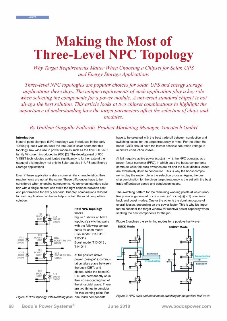
Bodo´s Power Systems® June 2018 www.bodospower.com68
CONTENT
IntroductionNeutral-point-clamped (NPC) topology was introduced in the early 1980s [1], but it was not until the late 2000s’ solar boom that this topology saw wide use in power modules such as the flowSOL0-NPI family Vincotech introduced in 2008 [2]. The development of 650 V IGBT technologies contributed significantly to further extend the usage of this topology not only in Solar but also in UPS and Energy Storage applications
Even if these applications share some similar characteristics, their requirements are not all the same. These differences have to be considered when choosing components. No universal standard solu-tion with a single chipset can strike the right balance between cost and performance for every scenario. But chip combinations tailored for each application can better help to obtain the most competitive solution.
How NPC topology worksFigure 1 shows an NPC topology’s switching pairs with the following compo-nents for each mode:Buck mode: T11-D11 ; T12-D12Boost mode: T13-D13 ; T14-D14
At full positive active power (cos(ϕ)=1), commu-tation takes place between the buck IGBTs and diodes, while the boost IG-BTS are permanently on in their corresponding half of the sinusoidal wave. There are two things to consider for this working point: For one, buck components
have to be selected with the best trade-off between conduction and switching losses for the target frequency in mind. For the other, the boost IGBTs should have the lowest possible saturation voltage to minimize conduction losses.
At full negative active power (cos(ϕ) = −1), the NPC operates as a power-factor corrector (PFC), in which case the boost components commute while the buck switches are off and the buck diode’s losses are exclusively down to conduction. This is why the boost compo-nents play the major role in the selection process. Again, the best chip combination for the given target frequency is the set with the best trade-off between speed and conduction losses.
The switching pattern for the remaining working points at which reac-tive power is generated or consumed (−1 < cos(ϕ)) < 1) combines buck and boost modes. One or the other is the dominant cause of overall losses, depending on the power factor. This is why it’s impor-tant to consider the target window for reactive power capability when seeking the best components for the job.
Figure 2 outlines the switching modes for a positive half-wave.
Making the Most of Three-Level NPC TopologyWhy Target Requirements Matter When Choosing a Chipset for Solar, UPS
and Energy Storage Applications
Three-level NPC topologies are popular choices for solar, UPS and energy storage applications these days. The unique requirements of each application play a key role
when selecting the components for a power module. A universal standard chipset is not always the best solution. This article looks at two chipset combinations to highlight the importance of understanding how the target parameters affect the selection of chips and
modules.
By Guillem Gargallo Pallardó, Product Marketing Manager, Vincotech GmbH
IGBTS
Figure 1: NPC topology with switching pairs Figure 2: NPC buck and boost mode switching for the positive half-wave
Kool Mµ® MAX Powder Core
IMPROVE INDUCTOREFFICIENCY
AT A FRACTIONOF THE COST OF HIGH FLUX
VISIT US AT PCIM 9H 531
USA:+1 412 696 1333
ASIA:+852 3102 9337
www.mag-inc.com
Kool Mu MAX Bodos Ad 4_18.indd 1 4/26/18 3:46 PM

www.bodospower.com June 2018 Bodo´s Power Systems® 69
CONTENT
Comparing and selecting chipsetsVarious suppliers have developed new 650 V IGBT families. Very low Vce_sat IGBTs, medium speed IGBTs (up to 50 kHz approximately), and ultrafast IGBTs (up to 100 kHz) are available to target a wide range of frequencies, so there are plenty of options out there.The frequencies of most applications that are a good fit for NPC topologies range from 16 to 32 kHz. Low Vce_sat IGBTs and me-diumspeed IGBTs are usually the components of choice for these performance requirements.
The options are even more numerous when it comes to diodes. Any-thing goes from rectifier diodes with low forward voltages to ultrafast diodes with low recovery losses.
Although this article compares just two chipsets in a 100 A power module with a flow 0 housing, Vincotech offers several more combina-tions. This wide selection of standard modules goes to meet each customer’s and application’s requirements. Table 1 shows the compo-nents selected for the modules compared here:
The P927F58 module has fully rated fast components in all positions. This combination enables four quadrant operation at almost constant efficiency. Losses fluctuate from one switching pair to the other de-pending on the phase angle. The P927F53 module’s boost components have been modified to achieve maximum efficiency at full positive active power and to reduce costs. At this working point, the boost IGBTs are permanently on and generate conduction losses only, so that a low Vce_sat switch will achieve the best possible performance. This component provides some reactive power, but the switching losses soon dominate, which limits the range of the phase angle. The anti-parallel diodes (D13-D16) have half of the current rating at all positions to allow for some reactive power. These diodes recover fast enough to rule out very high losses and voltage spikes.
One’s choice of module will depend on the application’s target parameters such as switching frequency or reactive power capability. Figures 3 and 4 shows efficiency versus output phase angle for 16 kHz and 32 kHz, respectively. The P927F53’s efficiency decreases significantly as the phase angle increases, while the P927F58 delivers nearly constant performance at all working points.
IGBTS
Module name
Components P927F58 P927F53
Buck IGBTs (T11 & T12)
100 A Mid-speed
100 A Mid-speed
Buck Diodes (D11 & D12)
100 A Fast
100 A Fast
Boost IGBTs (T13 & T14)
100 A Mid-speed
75 A Low-speed
Boost Diodes (D13 & D14)
100 A Fast
50 A Fast
Boost inv. diodes (D15 & D16)
100 A Fast
50 A Fast
Table 1: flowNPC 0 chipsets in 100 A modules
Kool Mµ® MAX Powder Core
IMPROVE INDUCTOREFFICIENCY
AT A FRACTIONOF THE COST OF HIGH FLUX
VISIT US AT PCIM 9H 531
USA:+1 412 696 1333
ASIA:+852 3102 9337
www.mag-inc.com
Kool Mu MAX Bodos Ad 4_18.indd 1 4/26/18 3:46 PM

Bodo´s Power Systems® June 2018 www.bodospower.com70
CONTENT
At 16 kHz, the P927F53—that is, the module that has been optimized for active power— achieves nearly 0.1% higher efficiency at full active power. It delivers better performance until the phase angle is at 60° power (cos(ϕ) = 0,5), at which point the low Vce_sat IGBTs’ increased switching losses begin to dominate. At higher phase angles (lower cos(ϕ)), the IGBT junction temperature rise to a level that might compromise the component’s lifetime. Moreover, the anti-parallel diodes have half of the IGBT’s current rating, so they will also limit the reactive power capability.
When switching at 32 kHz, the boost IGBTs’ losses dominate at a low-er angle, decreasing the cross-over point between the two modules to 45° (cos(ϕ) ≈ 0,7). At full active power, the P927F53’s efficiency is still better by almost 0.1%. However, the temperature difference between the IGBT junction and heat sink (ΔTj-hs) already reaches to 40°C at a phase angle of 45°. The viability of this option also depends on the selected package’s or heat sink’s ability to dissipate the losses.
The results vary slightly at low load and near the current’s zero cross-ing when the IGBTs can go to zero voltage switching (ZVS) mode. At this working point, the boost IGBTs contribute with additional switch-ing losses even at full active power. Efficiency drops further in the P927F53 module with slow boost IGBTs, shifting the cross-over point to a lower phase angle. However, this module still delivers the best performance at full active power.
Another important aspect to consider is cost. Figure 5 shows a nor-malized cost comparison for the two modules. The optimized module clearly has a significant cost advantage.
Choosing a moduleOnce the performance and cost are compared, the final decision will depend on application’s requirements and the specific target param-eters of each customers.
The P927F58 provides a good balance between efficiency and cost for applications where the device needs to have full reactive power capability or the ability to work in all four quadrants with high ef-ficiency. This might be the case of Energy Storage Systems or UPS with a wide reactive power range.
On the other hand, the P927F53 delivers the bigger benefits in terms of cost and performance when the primary goal is to achieve the high-est efficiency at active power and the device doesn’t need full reactive power capability. This could well be the case with solar PV inverters and UPS for modern data centers.
ConclusionThe market offers a wide variety of components that can be combined in multiple ways in an NPC topology achieving different outcomes. Understanding the target requirements of each application and customer is essential to finding the most competitive solution for each case. A universal standard chipset does not always provide the most optimal result. This is why application-specific solutions and design flexibility in the power module can bring customers an added value to their final product.
[1] Mikami, W., Nagataje, K. & Ono, T. (1981). A New Neutral-Point-Clamped PWM Inverter. IEEE Transaction on Industry Applications, IA-17, 518-523
[2] Frisch, M., Temesi, E. (2008). High Efficient Topologies for Next Generation Solar Inverter
www.vincotech.com
SCW18 Bodos_210x297mm_PQ.pdf 1 4/12/18 6:15 PM
IGBTS
Figure 5: Normalized cost comparison for the P927F53 & P927F58
Figure 3: Efficiency vs. phase angle; conditions: 700 VDC; 16 kHz; 230 VAC; 48 A (rms)
Figure 4: Efficiency vs. phase angle; conditions: 700 VDC; 32 kHz; 230 VAC; 48 A (rms)

SCW18 Bodos_210x297mm_PQ.pdf 1 4/12/18 6:15 PM

Bodo´s Power Systems® June 2018 www.bodospower.com72
CONTENT
Typical data sheet reverse conduction characteristics of eGaN FETs and Si MOSFETs are shown in figure 1. For the eGaN FETs, the source-drain forward voltage is three to four times larger than that of a Si MOSFET, but there is no reverse recovery charge, Qrr. For Si MOSFETs, Qrr is significant, although it decreases as voltage rating is reduced. For source-drain forward voltage, the values have little dependence on voltage rating.
The major effects of reverse recovery can be discussed in the context of the typical buck converter, shown in figure 2. While SR reverse volt-age drop VSD2 remains relatively consistent versus dead-time, td,on, which is the interval between switching transitions when both Q1 and Q2 are commanded to be off, the reverse recovery charge, QRR, is strongly affected by dead-time [1], [2].
Dead-time is necessary in practical converters to prevent cross-conduction of Q1 and Q2 due to the non-zero switching time, since cross-conduction results in shoot-through currents and corresponding high losses. However, dead-time also results in losses and the design of a high-efficiency converter will be improved by understanding the underlying mechanisms, of which two are dominant; reverse voltage drop and reverse recovery.
Reverse Voltage Drop And Dead-Time LossesThere are two dead-times to consider. The turn-on dead-time, td,on, is the interval between the time Q2 responds to its turn-off command and the time its current iQ2 decreases to zero. The turn-off dead-time, td,off, is the interval beginning when Q1 responds to its turn-off command and the time when Q2 responds to its turn-on command. Figure 3 shows the key turn-on dead-time waveforms, and the turn-off dead-time is similar. During td,on and td,off the channel of Q2 is off, and inductor current IL flows through the body diode for a MOSFET and body diode like mechanism [3] for a GaN transistor.
TECHNOLOGY
eGaN® FET-Based Synchronous Rectification
As GaN-on-Si becomes more common in DC-DC converter designs, questions often arise from experienced designers about the impact of the unique characteristics of GaN transistors when used as synchronous rectifiers (SRs). In particular, the third quadrant
off-state characteristics, better known as “body diode” conduction in Si MOSFETs, which is activated during converter dead-time, is of interest. For this article, the focus will be on the similarities and differences of Si MOSFETs and eGaN FETs when operated as a “body
diode” and outline their relative advantages and disadvantages.
By David Reusch, Executive Director Applications Engineering and John Glaser, Director Applications Engineering, Efficient Power Conversion Corporation
Figure 1: Typical source-to-drain forward drop vs. source-to-drain cur-rent and temperature for eGaN FETs and Si MOSFETs
Figure 2: Buck converter schematic with synchronous rectifier
Figure 3: Idealized buck converter deivce Q1 turn-on waveforms, including reverse recovery of a Si MOSFET body diode

www.bodospower.com June 2018 Bodo´s Power Systems® 73
CONTENTTECHNOLOGY
In silicon MOSFETs this body diode is comprised of the PN junction formed between the drain epitaxial layer and the source wells. This diode has a forward voltage drop VSD2 of 0.6 - 0.8 V. The effective body diode in an eGaN FET arises when the gate and source are tied together with VSD2 ≈ 2.5-3 V at nominal currents. The body diode conduction loss is easily computed by equation (1):
PSR,VSD=IL•VSD2•fsw•(td,on+td,off) (1)
The higher VSD2 for eGaN FETs means that dead-time conduction losses are larger than those for silicon MOSFETs. This can be mitigat-ed via an external Schottky diode or by good dead-time management [4], [5]. The faster switching of eGaN FETs compared to Si MOSFETs means that smaller dead-times are practical with GaN.
Reverse Recovery and Indirect Dead-Time LossesReverse recovery is a major source of switching loss, sometimes dominating all other switching loss mechanisms. However, it is frequently underestimated or even ignored, due to the lack of good data and challenging analysis, particularly for lower voltage FETs. As power density and efficiency demands continue to increase, reverse recovery losses merit closer inspection. Dead-time has a strong effect on reverse recovery [2]. This can result in much higher losses than body diode conduction in silicon MOSFETs, and these losses can far exceed the body diode conduction losses of eGaN FETs [1].
Reverse recovery is a phenomenon of PN junction diodes. When such a diode conducts a current iD = IL in the forward direction, a population of minority carriers is injected into the junction depletion region. The final size of this carrier population corresponds to the magnitude of IL. A portion of this population lags changes in iD, with a time constant dependent on diffusion time, mobility, and recombina-tion time of the minority carriers [6]. This portion of the carrier popula-tion is often referred to as stored junction charge. It is often confused with the capacitive depletion charge, but differs in that it is primarily a function of the diode current waveform, not the voltage waveform. As long as the stored charge remains in the junction, the diode can be considered to be in the conducting state regardless of the current value or direction. For the eGaN FET, reverse conductionis based on majority carrier devices with no PN junction, hence they do not exhibit reverse recovery.
Reverse recovery occurs when reverse voltage is applied to a PN diode that is conducting in the forward direction. It thus occurs dur-ing turn-on of Q1. Figure 3 shows typical turn-on waveforms. At the beginning of the turn-on dead-time interval, the channel of Q2 is turned off, forcing inductor current – IL through the body diode. Then Q1 is turned on and begins to carry an increasing portion of IL. When the control FET current reaches IL, iQ2 = 0, an ideal diode would stop conducting. However, in a real PN junction diode, the stored charge in the junction region lags the current. Thus, the diode remains on, and since Q1 is also on, the voltage VBUS forces the current to continue to increase. This additional current flows strictly through the power loop, and is known as the reverse recovery current, where it acts as a shoot-through current and significantly increases losses. The stored charge begins to decay when the current reverses, and eventually reaches the point that it is just enough to support IRRM, the peak negative iQ2 current, after which the current magnitude decreases exponentially with time constant tRR until the iQ2 = 0, iQ1 = IL, and the diode is off. The extra current that flows results in an extra charge termed reverse recovery charge (QRR) flowing through the power loop, and the resultant losses are given by:
PSR,VSD=QRR•VBUS•fsw (2)
Unfortunately, an accurate QRR value is difficult to obtain. Silicon MOSFET data sheets normally supply numbers for body diode QRR and tRR under unrealistic conditions. QRR values may or may not include Qoss, and this is rarely specified. Measurement of reverse recovery parameters under realistic conditions is challenging and error-prone, and accurate modeling of reverse recovery in typical de-vice models is rare. This leads to poor estimates of reverse recovery losses.
Comparison of eGaN FETs and Si MOSFETs in VIN=48 V Synchronous RectificationNow let’s look at the impact of the dead-time period on in-circuit performance for eGaN FET and Si MOSFET based SR designs. We will look at a VIN = 48 V to VOUT = 12 V synchronous buck converter operating in the frequency range of fsw = 300 kHz to fsw = 1 MHz. The experimental evaluation boards are shown in figures 4 (a) and (b) for the eGaN FET (EPC2045) and Si MOSFET equivalent, respectively. Each board is designed with a similar layout based on [7], use four-layer two by two inch two-ounce copper PCBs, and use gate drivers designed for their respective technologies.
To evaluate the impact of dead-time on performance for the two sys-tems, the dead-time was tuned for each of the measurement points using no-load timing for consistency. Since the impact of QRR is seen during device Q1 turn-on, only the rising edge dead-time, tDead_Rise, was varied, with the falling dead-times minimized to 10 ns and 15 ns, for the GaN transistor and Si MOSFET, respectively.
The minimum dead-time case is used as a baseline and subtracted from all other loss measurements. This enables quantification of the losses due to dead-time effects. For the faster eGaN FET, a mini-mum dead-time of 5 ns was selected, for the slower Si MOSFET, a minimum dead-time of 10 ns was selected. Figure 5 shows the impact of the duration of the “body-diode” conduction during dead-time on performance for output currents of 6 A, 10 A, and 14 A for switch-ing frequencies of 500 kHz (figure 5(a)) and 1 MHz (figure (5b)). As dead-time is increased, Si MOSFETs show a large initial increase in loss due to QRR, which then approaches an asymptote of constant slope due to VSD2,diode, as expected. It can be seen from figure 5 that the Si MOSFET QRR has a strong dependence on the forward biasing duration of the body diode and the current magnitude conducted by the diode. For the Si MOSFET, the ΔQRR can be estimated from equa-tion 2, and ΔQRR was measured to be approximately 40 nC for 6 A, 80nC for 10 A, and 135 nC for 14 A for a 50 ns increase in body diode conduction time. From figure 5 (b) it can be seen that the dead-time losses scale proportional to frequency, as predicted in equation 2. The loss increased by more than a factor of two (~2.5) when increasing
Figure 4: VIN = 48 V demonstration systems (a) eGaN FET based de-sign EPC9078 with EPC2045 eGaN FETs and LMG5113 GaN FET 5 V gate driver and (b) Si MOSFET based design with BSZ097N10NS5 Si MOSFETs and ISL2111 MOSFET 10 V gate driver

Bodo´s Power Systems® June 2018 www.bodospower.com74
CONTENT
the switching frequency from 500 kHz to 1 MHz. This indicates that the QRR value (nC) has a dependence on fsw, but to a lesser extent than IOUT and tDead_Rise. In figure 5 (c), a wider range of frequencies, fsw=300 kHz, 500 kHz, and 1 MHz are shown for a load current, IOUT, of 10 A, confirming the eGaN FET was a superior SR over a wide frequency range.
For the eGaN FET with no reverse recovery, losses are proportional to dead-time source-to-drain conduction, as predicted by equation 1. One would expect that the slope of the eGaN FET loss curve would be higher due to the larger VSD2 of reverse conduction. Although the slope is higher, the initial high loss from reverse recovery of the Si MOSFETs means that even for large dead-time, the reverse recovery loss of the Si MOSFETs far exceeds losses from the reverse voltage drop of the eGaN FETs. This shows that for SR applications where the body-diode conducts, the GaN transistor is superior to the Si MOSFET as a result of the elimination of QRR.
The impact of dead-time on system efficiency and power loss was tested and shown in figures 6 (a) and (b), respectively. The eGaN FET
based design showed superior performance in all conditions, with the total system losses decreasing by 35% and 40%, and efficiency increasing by 2% and 2.5% for respective rising edge dead-times of 30 ns and 60 ns. The improved switching performance of the eGaN FET based design enables higher power density when the system is optimized, which is discussed in detail in [8].
Up to this point, the impact of dead-time on power loss and efficiency was considered exclusively. But the third quadrant “body diode” conduction also has a significant impact on the switching wave-forms, which impacts design criteria such as the minimum allowable dead-time, maximum negative switch node voltage of the gate driver/controller, and the peak voltage rating of the device. Shown in figure 7 (a) is the switch node waveform of the eGaN FET for rising edge dead-times of 5 ns, 20 ns, and 40 ns. The eGaN FET, with no reverse recovery, has almost identical switching transitions and peak voltage spikes, allowing a designer to more simply select a minimum dead-time and peak device blocking voltage required. For the eGaN FET based design, the transistor also has a higher third quadrant off-state forward voltage, resulting in a more negative switch node, which impacts driver/controller selection.
For the Si MOSFET based design, the switch node waveforms are shown in figure 7 (b) for dead-times of 5 ns, 20 ns, and 40 ns. The third quadrant body diode voltage is significantly lower than the eGaN FET, but the transitions and peak voltage spikes vary significantly with dead-time, an effect of the reverse recovery charge (QRR) current. Current will have a similar impact, making it much more challenging for a designer to minimize the dead-time and select a proper device voltage rating.
ConclusionsTo summarize the design considerations for effective use of eGaN FETs in synchronous rectification: 1) eGaN FETs have two to three
TECHNOLOGY
Figure 5: Impact of rising edge dead-time duration on power loss for converters shown in figure 4 with various output currents and a switching frequency of (a) fsw=500 kHz, (b) fsw=1 MHz; and (c) vari-ous switching frequencies and an output current of IOUT=10 A
Figure 6: Impact of rising edge dead-time duration on total system (a) efficiency and (b) power loss for experimental converters shown in figure 4 for switching frequency of fsw=500 kHz (IHLP-5050-FD-01)

www.bodospower.com June 2018 Bodo´s Power Systems® 75
CONTENTTECHNOLOGY
times higher “body diode” forward voltage drop when compared to Si MOSFETs and the related forward diode conduction losses will increase accordingly and, 2) eGaN FETs completely eliminate reverse recovery QRR and the related losses are reduced to zero.
For higher voltage applications (VIN = 48 V), there is a large impact of QRR on SR loss for Si MOSFETs, and the increase in eGaN FET forward diode conduction loss is very small in comparison, yielding far superior performance for eGaN FET as SRs in most applications. As the voltage increases, the larger the relative advantage will be for eGaN FETs, since Si MOSFET QRR and related losses both increase with voltage. The dependence of Si MOSFET QRR on conduction cur-rent level was also demonstrated, with higher current levels showing larger advantages for eGaN FETs.
References[1] J. Glaser and D. Reusch, “Comparison of deadtime effects on
the performance of DC-DC converters with GaN FETs and silicon MOSFETs,” Energy Conversion Congress and Exposition (ECCE) 2016.
[2] C. Mößlacher and O. Guillemant, “Improving Efficiency of Syn-chronous Rectification by Analysis of the MOSFET Power Loss Mechanism,” Infineon Technologies, Mar. 2012.
[3] A. Lidow, J. Strydom, M. de Rooij, D. Reusch, GaN Transistors for Efficient Power Conversion, Second Edition, Wiley, 2014.
[4] J. Strydom and D. Reusch, “eGaN® FET-Silicon Power Shoot Out Volume 12: Optimizing Dead Time,” Power Electronics - Penton Electronics Group, Jan. 2013.
[5] D. Reusch and J. Glaser, DC-DC Converter Handbook - A Supplement to GaN Transistors for Efficient Power Conversion, 1st ed. Power Conversion Publications, 2015.
[6] C. L. Ma and P. O. Lauritzen, “A simple power diode model with forward and reverse recovery,” Power Electronics, IEEE Transac-tions on, vol. 8, no. 4, pp. 342–346, Oct. 1993.
[7] D. Reusch and J. Strydom, “Understanding the Effect of PCB Lay-out on Circuit Performance in a High-Frequency Gallium-Nitride-Based Point of Load Converter,” in IEEE Transactions on Power Electronics, vol. 29, no. 4, pp. 2008-2015, April 2014.
[8] D. Reusch and S. Biswas, “ System Optimization of a High Power Density Non-Isolated Intermediate Bus Converter for 48 V Server Applications,” Applied Power Electronics Conference and Exposi-tion (APEC), 2018.
www.epc-co.comFigure 7: Impact of rising edge dead-time duration on switch node waveforms for (a) GaN transistor based and (b) Si MOSFET based experimental converters shown in figure 4
THE MOST POWERFUL REAL-TIME SIMULATOR
FOR TOMORROW’S SMART GRIDS
Meet our experts at PCIM in Hall 6 - booth #128

Bodo´s Power Systems® June 2018 www.bodospower.com76
CONTENT
Not every application area will have the same set of challenges, but it is inescapable that power supply design has become a key expertise, no matter what the end-product.
Seeking real-world opinionsAgainst this background, Vicor commissioned a survey of power system engineers to sound out their concerns and priorities. It was conducted “blind”, to an audience independent of the company’s own customer records, to ensure an authentic result. High on the list of issues was meeting performance targets (75% of respondents said so) and as many as 80% said they struggle to meet the allocated timescales for completion of a design.
Perhaps coming as no surprise to those working in the field is that the very notion of the “power system specialist” is somewhat flawed, and that those who describe themselves so, are rather rare; 70% of those surveyed said they spend less than half their time with power design. The survey also indicated that those responsible for recruiting power system engineers are finding it difficult to fill positions.
Very little in the survey indicates that designing a power system in the “conventional” way has become impossible. There is certainly no shortage of components on the market, all promising high levels
of performance. This only adds to the dilemma of how to allocate scarce resources; should a project manager (for example) pursue an additional percentage point in efficiency by having an engineer get up to speed with the latest technology: or stay with known techniques? “Keeping up with best practices/new technologies in power design” was listed as a concern by 65% of respondents.
Change notices; a major concernHowever, sitting at the top of the list of issues faced by the power system designers, is that of specification changes during, and even late, in the design process; almost 87% of those who replied, said that they struggled to cope with such design changes, which make it even harder to deliver a project on time and on budget.
Changes are most often requested or driven by technical issues, especially when the exact power budget is not known at the start of the project, loads are changed, or restrictions are placed on thermal management due to space restrictions. It is desirable to start the power design as early as possible: the days of it being the last task in the project lie in the past. However, this makes the process vulnerable to changes. External market or competitive forces can also cause revisions to specifications.
Handling Late Changes in Power System Designs
Providing power to today’s electronic systems designs has become a complex and challenging exercise. Stable power, efficiently delivered at the correct levels, is the bedrock on which all other performance parameters rest. The pursuit of ever-more
demanding specifications and ever-lower power losses has come to be seen as requiring more specialised expertise. Those working in the power area see some serious problems ahead, and anticipate a need for more engineering resources, for better-qualified and
more-experienced power system engineers – and for new approaches to architecting, and implementing the power system design.
By Lev Slutskiy, Business Development Manager, Central/Eastern Europe, Vicor
DESIGN AND SIMULATION
Figure 1: Initial Power System for Robot

www.bodospower.com June 2018 Bodo´s Power Systems® 77
CONTENT
A power system that has been designed from the “ground-up” can lack flexibility when its designers are challenged to accommodate changes late in the evolution of the end product. The revision may call for new power semiconductors, or controller ICs: even if the major components remain unchanged, the power system will be operating at possibly different voltage, current and power points, and every aspect of its performance will require verification.
Power design with modular function-level componentsA way forward is offered by Vicor using its Power Component Design Methodology (PCDM). This power system design method-ology, can provide engineers with a means of not only simplifying the power systems design in the first instance, but also with a route to accommodating changing specifica-tions without incurring significant delays.
PCDM uses dense, easily interchangeable power components, that perform a range of power-system functions at various power levels; come with guaranteed performance figures; and allow changes to be accommo-dated quickly and easily, either by altering the operating point of a given module, or exchanging it for another.
The Power System Designer (PSD) The entire methodology is supported by VICOR’s Power System Designer (PSD), a powerful, easy to use on line tool, that allows engineers to enter their key power system specifications with the tool offering various architectures and power component selection based on lowest density, high-est efficiency, lowest component count and lowest cost. Engineers can then select which of these system designs meets their needs and then go on to simulate their design using additional online tools. A designer embarking on a new power system design needs only to enter the power system’s key input and output parameters into the Power System Designer to generate a complete power system design.
Using proven power components with on line tools, increases power system design certainty; it also becomes much easier to accurately forecast the size and perfor-mance of power systems developed using this approach and to automatically change the design if new performance parameters are to be met. The following are real world examples of engineers utilizing the PCDM.
Robotics One design challenge concerned a spe-cialised robot: one that is employed by law enforcement and bomb disposal agencies to remotely inspect and defuse suspicious objects. For a unit that must be transported easily to where it is required, and that can make its way into possibly confined spaces, the smaller and lighter the robot can be made, the better it can perform. To this requirements list, was added the need to operate from AC mains power (universal) if available, or from either internal or external batteries. That is to say, from 115 or 230 VAC, or from 12 or 24V DC. In this case the development team were specialists in various aspects of design of the robotic system, but lacked in-depth experience in implementing a power system design. Their initial solution is shown in Figure 1.
When AC input is in use, the AIM/PFM combination – forms an isolated, AC/DC converter with power factor correction (PFC) providing a 24 VDC output. Alternatively, the 24 VDC supply is derived from batteries – via a filter block. Noise filtering is an important feature; the robot could be operating in an electrically-noisy environment, and it is es-sential that any such noise, that might disrupt operation, be kept out of the microcontroller and control circuitry. When AC power is in use, the AIM/PFM modules provide this fil-tering. The DCM module down-converts 24V to 12VDC, that directly powers the robot’s motors; two ZVS (Zero Voltage Switching) regulator modules efficiently generate 3.3 and 5V rails to power the robot’s control circuits.
This design not only provides a robust and flexible power system architecture: it also dramatically reduces the size and weight of the power system. The solution occupied an area of 66.8 cm², and the use of proven modular components selected by the PSD tool, greatly reduced the design effort., The additional online simulation tools provided confidence that the entire system would operate within design parameters, with good end to end efficiency (80%).
Scientific instrumentationIn another recent project, a design team developing scientific instrumentation found that using the Power Component Design Methodology not only provided an optimized power system, but also helped to quickly accommodate changing specifications. The product under development used two sensors to make measurements for DNA analysis, and had previously been powered by a fan-cooled discrete based power sys-
PRECISION AND POWER RESISTORS
YOU CAN’T COPY
EXPERIENCE
Isabellenhütte Heusler GmbH & Co. KGEibacher Weg 3 – 5 · 35683 Dillenburg, Germany
Phone +49 (0) 2771 934-0 · Fax +49 (0) 2771 [email protected] · www.isabellenhuette.de
Innovation by Tradition
We invented the MANGANIN® resistance alloy 125 years ago. To this day, we produce the MANGANIN® used in our resistors by ourselves.
More than 20 years ago, we patented the use of electron-beam welding for the production of resistors, laying the foundation for the ISA-WELD® manufacturing technology (composite material of Cu-MANGANIN®-Cu). We were the first to use this method to manufacture resistors. And for a long time, we were the only ones, too.
Today, we have a wealth of expertise based on countless projects on behalf of our customers. The automotive industry’s high standards were the driving force behind the continuous advancement of our BVx resistors. For years, we have also been leveraging this experience to develop successful industrial applications.
The result: resistors that provide unbeatable excellent performance, outstanding thermal characteristics and impressive value for money.
PCIM Europe 2018
Messe Nürnberg // June 5 - 7 Hall 7 // Booth 119

Bodo´s Power Systems® June 2018 www.bodospower.com78
CONTENT
tem, which needed to provide 12V, 2.5V and 3.3V rails for the sensors as well as a 2.5V and two 3.3V rails for housekeeping functions. The total power requirement was around 200W.
Initial studies had envisaged a design using discrete devices. Re-casting the design in the Power Component paradigm using the online PSD tool, produced an immediate benefit; the size of the power system was reduced from 161 cm² to 64 cm², a saving of 60%. This was achieved, as set out in figure A, using an AIM, PFM and ZVS buck regulator Power Modules, that allow power system attributes such as level conversion, isolation and regulation. In this example, the AIM Component is providing off-line AC/DC rectification; the PFM block is providing an isolated, regulated voltage of 24V; the ZVS (zero-voltage switching), regulators further step-down to the point of load power rails.
Extra power demandedDuring development, however, it became clear that an increase in throughput was required if the product was to remain competitive, and therefore it was decided to increase the number of sensors from two to four. This meant that the current demanded on all three sensor power rails doubled and the total power requirement increased from 200W to 350W, yet the size of the power system had to remain more or less the same.
Fortunately, the engineers at this company were able to use the Power Component Design Methodology to meet this late change in specification. By simply entering the new requirement into the PSD, the tool selected two additional ZVS Buck regulators used for each power rail, as depicted in Figure 3. The sensor power rails are the three outputs shown on the right of the diagram - each regulator for those rails is now a paralleled array-of-two. This increased the size of the power solution by just 6%, to 67 cm². An equivalent discrete solu-tion would have needed 346 cm²: an increase that simply could not be accommodated by the system.
Flexibility: A key element of power system designThe market for electronic equipment, such as the examples in this article, changes rapidly. This means that power system designers can no longer be sure that the specification they receive at the start of the
project will not change: in fact, it’s likely that changes will be need-ed. Flexibility to adapt to these changing requirements is now a key element of effective power system design, and something that can be enabled by modern approaches such as the Power Component Design Methodology.
www.vicorpower.com
DESIGN AND SIMULATION
Figure 2: Design solution for the Scientific Instrumentation
RSG and P-DUKE Present:New 15 Watt and 30 Watt Industrial AC/DC ModulesTxC15/TxD30 Series Very compact modules
for industry/automation Integral Class B EMI filter Constant Current Mode 5000m altitude 4 cases: encapsulated or
open, terminal or DIP Meets EN/UL62368-1
TAC15/TSC15: open PCB or encapsulated with terminal
DIP case version available for all models (here: TSD30)
For more information visit www.rsg-electronic.de or www.pduke.comOr contact us via email [email protected] or phone +49.69.984047-0
we energize electronics!

We deliver big results with small things at Wolfspeed
> Our compact components deliver high efficiency and performance
> Our compressed system layouts yield extensive savings
> Our focused, innovative team has more than 30 years of experience and 2,245 patents
Visit us in PCIM Booth 9-242 to see live demos and talk with our engineers, or attend one of our presentations during the show.
We’re driving the discussions about the latest in SiC innovations. Here is our list of presentations at PCIM Europe 2018 — come join the conversation!
Wolfspeed SiC: Powering the path to an electric future
SUNDAY 3 JUNE
TUESDAY 5 JUNE
WEDNESDAY 6 JUNE
> Seminar 3: Wide Band Gap (WBG) Power Devices, Characterisation, Simulation and Testing
> Exhibitor Presentation: Wolfspeed Introduces the Industry’s Lowest On-Resistance and Lowest SwitchingLosses at 1200V
> Oral Presentation: New SiC 1200V Power MOSFET & Compact 3.25 mOhm, 41mm Power Module forIndustrial Applications
> Podium Discussion: SiC – Devices for the Future Design: Featuring John Palmour, Wolfspeed – A Cree Company> Poster/Dialogue Sessions: Current Sharing During Unipolar and Bipolar Operation of SiC JBS Diodes> Poster/Dialogue Sessions: Analog Based High Efficiency 2KW Totem Pole PFC Converter Using Surface Mount
SiC MOSFETs
> Poster/Dialogue Sessions: Reliability Testing of SiC JBS Diodes for Harsh Environment Operation> Poster/Dialogue Sessions: 650 V Silicon Carbide MOSFETs in Bridgeless Totem-Pole PFC Design Achieves
High Efficiency (80+ Titanium) Whilst Simplifying Design Complexity and Reducing Cost
For details, visit Wolfspeed.com/PCIM-Europe-2018

Bodo´s Power Systems® June 2018 www.bodospower.com80
CONTENT
Global warming and pollution as well as international carbon emission targets initiated a process to reduce car emissions. The automotive industry pushes to improve fuel efficiency and reduce emissions, also by increasing the vehicle electrification. Increasing global demand for BHEV, BEV vehicles and new drive train designs causes automotive manufacturers to evaluate suitable power electronic technology in their current and future designs. Automotive manufacturers constant-ly seek improved overall performance: higher conversion efficiency, reduced cost, lower weight, higher power density.
Enhancement of energy efficiency reduces the energy expense and battery capacity required to travel a given distance.
Compared to silicon (Si) IGBTs or MOSFETs, silicon carbide (SiC) MOSFETs offer several advantages, i.e. faster switching capabilities, reducing the losses in the motor and improving the acoustic charac-teristics of the drive train. By increasing switching frequency, a more sinusoidal motor current can be achieved and thereby reduce motor losses, lower on-state and switching losses, higher thermal conductiv-ity and higher dielectric strength. Contributing to higher power density and substantially reducing the weight & volume of the inverter.
Utilization of SiC devices to their full capability needs to be evaluated from a system level, since these might introduce challenges for other components in the drive train. For instance, utilizing high switching frequencies without output filters can result in high voltage slope rates (dV/dt), resulting in motor insulation breakdown. Furthermore, higher switching frequencies can cause undesired capacitive couplings and EMI issues.
Perceived high SiC device costs present one of the most obvious arguments against SiC technology adoption. Pricing for SiC chipsets are presently several times higher than Si chip sets. Following the development of previous semiconductor technologies, it is assumed that SiC chipset prices will decrease as increased adoption drives higher fab production capacities and technology advances increase wafer diameters.
Hybrid electric vehicles (HEVs), plug-in hybrid electrical vehicles (PHEVs) and battery electrical vehicles (BEVs) all contain several critical systems that will benefit from SiC power devices, enhancing both the energy efficiency and performance of electric vehicles.
DCM™ 1000XDanfoss extends the DCM™ 1000 technology platform for traction ap-plications in hybrid electric and battery electric vehicles by introducing the DCM™ 1000X. The DCM™ 1000X uses 1200V semiconductors, either in Si or SiC. SiC based DCM™ 1000X modules with 1200V blocking voltage are designed for drive trains operating with a DC-link up to 950V with a current rating ranging from 200A-800A. The 1200V
platform fulfills all commonly applied insulation requirements, e.g. LV123, IEC 60664-1 or other safety margins for 950V DC-link voltage.
Just like the DCM™ 1000 (750V), the DCM™ 1000X is designed to operate under harshest conditions; high temperature cycles (up to 135K), high humidity, mechanical shock and vibration. The shock and vibration requirements are addressed using a specific transfer mold package material (Epoxy-Raisin Coating) of the power module, as shown in Figure 1.
To reach maximum power cycle performance and lifetime, the DCM™ 1000X platform module uses Danfoss Bond Buffer technology (DBB®), as does DCM™ 1000. DBB® enables operation at higher junction temperatures. Sintered semiconductor to substrate combined with DBB® and copper wire bonding offer higher power and tempera-ture cycling capabilities and up to 15 times higher lifetime than any other standard bonding and joining technology.
Figure 1 also shows that the DCM™ 1000X uses ShowerPower® 3D, a direct-liquid cooling technology which helps to achieve outstand-ing thermal performance. The SP3D concept offers several benefits compared to other liquid cooling technologies e.g. pin fin coolers.
The parallel cooling principle eliminates temperature gradients associ-ated with the serial cooled pin fin concept. It also allows for tailoring the cooling channels to focus cooling at local hot spots; a feature that is not possible for the pin fin concept due to “shadowing” effects (1).
The DCM™ 1000X is designed and optimized to leverage chip inde-pendency. Danfoss Silicon Power can provide DCM™ 1000X designs based on different semiconductors and thereby ensure attractive cost base, optimized design and secure supply.
Electrical Performance DCM™ 1000XDCM™ 1000X fulfils the EV market’s requirement to nearly double DC-link voltage from 450V to 950V, enabling higher output power and faster charging capabilities. Efficient 200kW inverter designs or above
TECHNOLOGY
DCM™ 1000X - Designed to Meet the Future SiC Demand of
Electric Vehicle Drive TrainsBy Omid Shajarati, Alexander Streibel and Norbert Apfel, Danfoss Silicon Power
Figure 1: DCM™ 1000X.

www.bodospower.com
can be realized by making use of 1200V semiconductors using Si IGBTs or SiC MOSFETs. With higher DC-link voltages, the phase cur-rents can be reduced by 50%, maintain the same output power as an inverter at a lower DC-link voltage, and achieve fast charging times of less than 10 minutes. Since this relation is nonlinear, even higher out-put power can be achieved using 1200V IGBTs in the DCM™ 1000X package as compared to the classic 650V/750V power modules with the same footprint. The benefits of SiC MOSFETs, as introduced above, gives optimal partial load benefits due to the MOSFETs on-state behavior and low switching losses and therefore great overall benefits if higher switching frequencies are utilized by the inverter.
Figure 2 illustrates a comparison between the phase currents of 1200V Si IGBTs/FWDs (1000mm² silicon) and SiC MOSFETs (400 mm² silicon carbide, without external diodes). It is assumed that the coolant boundary conditions for both inverters, 10 liters/minute minimum flow rate and 65°C maximum coolant temperature remain unchanged.
Typical automotive inverter design rules state maximum operating IGBT junction temperature of 165°C for 175°C rated devices, while for SiC MOSFETs, the maximum design operating junction temperature is 190°C for a rated SOA of 200°C. Please note that these tempera-tures can only be achieved by utilizing DBB®, including a safety mar-gin that is below the maximum operating chip junction temperature.
Furthermore, the ShowerPower® 3D cooler enables an unreachable Rth of 0,1K/W at coolant conditions as stated above; this is true for 200mm² total SiC MOSFET area and 300mm² total IGBT area per
switch due to the difference in chip size.
This Rth implies, that for a SiC junction temperature of 190°C and a resulting temperature delta of 125K, the total module losses are limited to 2,5kW and the DCM™1000X has the ability to dissipate more than 625W/cm² un-der peak load and cooling conditions mentioned above (IGBT module losses of 2kW and dissipation of 325W/cm² for the IGBT functions).
In Figure 2, SiC MOSFETs only show a slight decrease of the maximum phase current over switching frequen-cy, demonstrating the great benefit of SiC at high switching frequency. In other words, the highest IGBT perfor-mance without derating is achieved at low switching frequencies. Thus, higher inverter efficiency for the same output power and reasonable switch-ing frequencies can be achieved with SiC MOSFET’s. Comparative efficien-cy can only be reached by increasing Si area, but the disadvantages will be increased space and increased system cost. In addition, for partial load illustrated at Tjunction = 100°C in Figure 2, the difference between Si and SiC becomes more severe.
Automotive 1200V IGBT traction pow-er modules will remain cost-attractive. Looking deeper at the performance of the DCM™1000X, doubling the DC link voltage and reducing the current by less than 50% point out that the cost driver for SiC is the performance of 1200V IGBT technology as an alter-native already enabling a performance step from the 475V towards the 950V DC-link voltage before utilizing SiC MOSFETs.
As shown in Figure 3, the maximum output current of DCM™ 1000X utiliz-ing latest generation Si 1200V IGBT is up to 600Arms at 6kHz.
Increasing the switching frequency to 10kHz would reduce phase current by 150Arms due to significant ad-ditional switching losses. Due to the well-known on-state characteristic of IGBTs, the partial load efficiency is not optimal.
SiC MOSFETs have been introduced earlier with reduced switching losses and excellent partial load performance.
Figure 2: Maximum phase current vs. switching frequency at constant junction temperatures (10K margin to maximum allowable junction temperatures 175°C and 200°C), 850VDC, m=cos(φ)=1, 10l/min. per inverter, 65°C coolant temperature.
prod
uct fi
nde
r:pewatron.com
Experts on Design-In for sensors and power solutions
Visit usHall 1 – Booth 333
MunichZurich
Figure 3: Electrical Performance of the DCM™ 1000X utilizing latest generation Si 1200V IGBT, 850VDC, m=cos(φ)=1, flow rate given per inverter, 65°C coolant temperature.

Bodo´s Power Systems® June 2018 www.bodospower.com82
CONTENT
Conduction losses become dominant only at peak loads, requiring an even temperature distribution between the individual chips and a reduction of the Rds(on) temperature gradient.
Figure 4 illustrates the electrical performance of DCM™ 1000X utiliz-ing the newest generation SiC MOSFETs. The DCM™ 1000X is cur-rently under development, and customers are testing prototypes.
The performance comparison is carried out at 20kHz and 30kHz at different flow rates. Due to low influence of the switching frequency and the related losses, the increase from 20kHz to 30kHz leads to a current derating of only 80Arms. The DCM™ 1000X enables inverter designs up to 600Arms and more, enabling 300kW inverters.
Danfoss is developing an optimized application kit for the DCM™ 1000X including DC capacitors, busbar connections, a heatsink suit-able for 3 half-bridges and gate drivers. Thus; enabling customers to evaluate the performance of the DCM™ 1000X and to support and verify their inverter design.
SummaryThe DCM™ technology platform has been extended to 950V applica-tions, using both Si or SiC chip technology. Future high-performance traction applications will benefit from using this scalable power mod-ule platform, offering a full scale performance and latest Si and SiC semiconductor technology for the best fit to requirements and use.
Danfoss will make available an application kit, offering customers an easy path to start testing and verification of drive train designs utilizing the DCM™ 1000X.
The introduction of DCM™ 1000X has further strengthened Danfoss Silicon Power’s range of customized power module offering. The DCM™ 1000X and its application kit will be on display at PCIM. Visit the Danfoss Silicon Power at Hall 9, Booth 327 for a first impression.
References:Omid Shajarati, Klaus Olesen, Norbert Apfel, Matthias Beck; DCM™ 1000 Designed to meet the future demand of Electric Vehicle Drive Trains. Bodo’s Power Systems, March 2018.
www.danfoss.com
TECHNOLOGY
Figure 4: Electrical Performance of the DCM™ 1000X utilizing latest generation SiC MOSFETs, 850VDC, m=cos(φ)=1, flow rate given per inverter, 65°C coolant temperature.

Exceed Standardswith our NEW scalable DCM™ 1000X technology platform
Visit us at PCIM EuropeNuremberg
5th-7th June, 2018Booth 9-327
www.siliconpower.danfoss.com
DCM™ 1000X – Designed to meet the future SiC demandof Electric Vehicle Drive Trains
with our NEW scalable DCM™ 1000X technology platformtechnology platform
DCM™ 1000X – Designed to meet the future SiC demandDCM™ 1000X – Designed to meet the future SiC demandof Electric Vehicle Drive Trainsof Electric Vehicle Drive Trains
technology platformtechnology platform
Danfoss extends the DCM™ 1000 power module technology platform for traction applications in hybrid electric and battery electric vehicles by introducing the DCM™ 1000X. The DCM™ 1000X uses 1200V semiconductors, either in Si or SiC. Just like the DCM™ 1000 (750V), the DCM™ 1000X is designed to operate under the harshest conditions; high temperature cycles (up to 135K), high humidity, mechanical shock and vibration. To reach maximum power cycle performance and lifetime, the DCM™ 1000X technology platform utilizes Danfoss Bond Buff er® technology (DBB®) and ShowerPower® 3D (SP®3D), as does DCM™ 1000. Danfoss can provide DCM™ 1000X customer-specifi c semiconductor designs and thereby ensures attractive cost base, optimized design and security of supply.

Bodo´s Power Systems® June 2018 www.bodospower.com84
CONTENT
Introduction Triacs are the most widely used solid state AC power switches for controlling AC mains loads of 50/60Hz or even 400Hz. They are widely used in home appliances, commercial andindustrial equipment. They are designed to withstand highblocking voltage while conducting very low leakage current, or latch into the on-state to con-duct load current in response to a low level current pulse on the gate.
As with all power semiconductors, triacs are available at many differ-ent current levels from <1A upwards. At higher currents, a heatsink will be required to remove the heat.
[Due to the fixed voltage drop inherent with their technology, triacs will dissipate typically around 1 Watt per Ampere ofload current.]
If the triac should become too hot for any reason (Tj > Tj(max)), it may lose control, i.e. be unable to commutate (turn itself off at the end of a half-cycle) and continue to conduct even without trigger commands applied to the gate. This may lead to thermal runaway and destruc-tive failure of the triac andpossibly the load. To avoid such danger, the application must be over-designed to allow for all possible fault or overloadconditions. Over-design strategies may include: • A larger triac than necessary to allow for fault conditions; • A larger heatsink than necessary to allow for fault conditions; • A larger enclosure than necessary to allow for fault condition cooling; • Additional thermal protection;• Additional overcurrent protection;• Artificial limitation of duty cycle on intermittent loads.
Temperature and Overload Protected Triac (TOPTriac™) does not require any such over-design because it protectsitself against over-heating, turning itself off well below thetemperature at which it would lose control. This allows the application to be designed exclusively for normal operation only, in the safe knowledge that TOPTriac will take care of its own thermal overload conditions.
In addition to over-temperature protection with indefinite latchoff until reset, TOPTriac can communicate its status back to the system microcontroller via gate feedback. The system canreport when it is conducting or blocking normally or whetherit is in over-temperature
trip state, with or without gate trigger commands applied. Its capability to communicate its status tothe microcontroller gives the designer a unique opportunity toimplement a smart overload monitoring function, with manual orautomatic reset applied according to the needs of the application.
The over-temperature protection and smart monitoringfeatures of TOPTriac improve the overall safety of the endproduct, remove the need to over-design for fault conditions,remove the need for additional protection components and reduce the chance of field failures.
How it works TOPTriac is based on WeEn’s planar-passivated three-quadrant Hi-Com Triac technology. It is a solid-state AC power switch with semiconductor-based on-chip thermal protection. The protection disables the Triac element, preventing conduction before excessive die temperature causes loss of control and damage to the device or the circuit. Protection is activated at a junctiontemperature between 125°C and 150°C.
As a two-quadrant device, TOPTriac is triggered exclusively by nega-tive gate current.
TOPTriac is triggered like a standard Triac by applying current to its gate. Trigger current can be DC (for continuous conduction) or pulsed (for any phase angle). Pulsed triggering requires an additional low level continuous DC bleed current to be applied to the gate. Bleed current is in the range 0.5mA – 2mA.
When TOPTriac goes into the over-temperature protection condi-tion, “tripped”, it will remain latched-off indefinitely even after cooling, thanks to the continuous DC gate trigger current or bleed current.
THERMAL MANAGEMENT
Temperature and Overload Protected Triac – TOPTriac™
For decades, triacs have been used as solid-state AC power switches. The emergence of smart appliances and greater emphasis on safety has suggested a need for triacs with
self-protection features and smart monitoring capability. This need can be met by TOPTriacTM.
By Nick Ham, Matjaz Rozman, Ed Huang and Stephen Wood, WeEn Semiconductors
Figure 1: Triac and TOPTriacTM symbols.
Table 1: Three-quadrant Hi-com triac and TOPTriac compared.
WeEn Hi-Com triac WeEn TOPTriacTM
High dVD/dt High dVD/dt
High dIcom/dt High dIcom/dt
High dVcom/dt High dVcom/dt
High Tj(max) High Tj(max)
No need for snubbers No need for snubbers
Voltage-rugged Voltage-rugged
Planar passivated Planar passivated
Thermal self-protection
Status feedback

www.bodospower.com
Reset is achieved by removing and re-applying the DC gatedrive. Normal conduction will be restored, provided by then Tjis below the trip temperature.
Application circuitsTOPTriac triggering and gate monitoring circuits can be assimple or as complicated as the application requires. A simple discrete circuit (open loop, no monitoring or feedback, manual reset) can be applied to low cost designs and simple systems, while for higher end applica-tions with microcontroller, fullstatus monitoring and any combination of manual or automaticreset become possible.
Discrete phase control with manual resetTOPTriac is a two-quadrant device with IGT of 5mA min to 35mA max. Negative gate current pulses of at least 35mA amplitude and adjustable phase angle are applied for variable power control. A bleed current of ~0.8mA is applied via R7 to ensure continued latch-off after over-temperature trip. Reset is achieved by opening the switch momentarily in series with the gate.
Figure 2: Discrete phase control circuit.
Table 2: Bill of materials for discrete phase control circuit.
Name Value
C1, C4 220n 275V AC Class X2, MKP 338 2 seriesC2 33n 400V, MKT 372 seriesC3 10n 400V, MKT 372 series,
C5 220µ 63V axial, 021 ASM seriesD1 - D4 1N4007D5 1N4148Diac DB3F1 10A AntisurgeOpto1 TCET1100G opto transistor (4 pin DIL) *R1 22k 0.6W, MRS25 seriesR3 1k 0.6W, MRS25 seriesR4 100R 2W, ROX2SR5 470k 0.6W, MRS25 seriesR6 100R 0.6W, MRS25 seriesR7 12k 0.6W, MRS25 seriesSW1 Push switch SPNCTOPT1 TOPT12-800C0TR1 BC547*VR1 1MZD1 BZX79-C5V6ZD2 BZX79-C12V
* Opto1 and TR1 can be replaced by an opto-coupler with Darlington output - e.g. Vishay SFH655A.
Application circuits TOPTriac triggering and gate monitoring circuits can be as simple or as complicated as the application requires. A simple discrete circuit (open loop, no monitoring or feedback, manual reset) can be applied to low cost designs and simple systems, while for higher end applications with microcontroller, full status monitoring and any combination of manual or automatic reset become possible.
Discrete phase control with manual resetTOPTriac is a two-quadrant device with IGT of 5mA min to 35mA max. Negative gate current pulses of at least 35mA amplitude and adjustable phase angle are applied for variable power control. A bleed current of ~0.8mA is applied via R7 to ensure continued latch-off after over-temperature trip. Reset is achieved by opening the switch momentarily in series with the gate.
Figure 2: Discrete phase control circuit
Table 2: Bill of materials for discrete phase control circuit.

Bodo´s Power Systems® June 2018 www.bodospower.com86
CONTENT
Microcontroller controlled Combining TOPTriac with a microcontroller allows fullfunctional-ity. Triggering can be continuous DC or pulsed with bleed current (minimum pulse duration 10.s). Gate voltage feedback indicates TOPTriac’s status: - Presence of mains frequency square wave means load current is
flowing; - Low level continuous DC offset and no AC signal meansover-tem-
perature tripped.
Gate feedback also allows detection of load current zerocrossing because the gate voltage AC signal reflects loadcurrent. This is critical for Triacs, which commutate at current (not voltage) zero-crossing, so pulse triggering needs to be synchronized to current zero-crossing for continuousconduction.
When the TOPTriac has gone into an over-temperature tripcondition, the microcontroller will spontaneously detect its statusand automati-cally send an alert signal after a programmedtime delay. For instance, it could be hazardous to allow cyclingthrough an over-temperature trip (e.g. it may be unsafe to have an unexpected start-up of the ma-chine). In such a scenario, the system can be programmed to send an early warning signal that the user could self-evaluate and intervene in the process allowingthe circuit to be manually reset.
TOPTriac vs conventional Hi-Com triac The performance of TOPTriac was evaluated and comparedwith a conventional Hi-Com triac. The test board used was designed to function well for both TOPTriac and conventional triacs. Hi-Com triac BTA312-600CT was compared withTOPTriac TOPT12-800C0. The devices were controlled by a microcontroller and triggered at a phase angle of 90degrees with a 230V 1,200W heating element used as the-load. Functionality was evaluated under general environment working
conditions and an extreme temperature environmentwhich exceeded Tj(max).
Figure 4 shows normal operation of conventional triacand TOPTriac with Tj below Tj(max). Gate pulse and loadcurrent waveforms are identical and the devices are in full control, operating within normal parameters.
Figure 5 shows the benefit of TOPTriac. Junctiontemperature has been allowed to rise to the point where the Hi-Com triac has lost control (Tj exceeding Tj(max) by aconsiderable margin). It is failing to commutate at current zero-crossings and is now conducting continu-ously. It is in a thermal runaway condition and will be destroyedif the power is not turned off very soon. By contrast,the TOPTriac has detected high junction temperature exceeding 125°C and has turned itself off. Gate pulses are still being applied but it is tripped and now cooling down to ambient temperature. It will remain safely trippeduntil it is reset manually by the user or automatically themicrocontroller.
Figure 3: DC and pulse trigger using 3.3V microcontroller.
Figure 4: Hi-Com triac BTA312-600CT (top) and TOPTriacTOPT12-800C0 (bottom), phase control at 90 degrees phase angle, 230V 1.2kW load, Tj below Tj(max).
THERMAL MANAGEMENT

www.bodospower.com June 2018 Bodo´s Power Systems® 87
CONTENT
Conclusion In this article, TOPTriac with its Temperature and OverloadProtection functionality has been compared with aconventional Hi-Com triac up to and beyond normal operating temperature conditions. TOPTriac operates as a standardtriac with the additional unique capability to protect itselfagainst overheating and overload scenarios, so prevent-ingloss of control of power supplied to the load. In this way,TOPTriac provides an enhanced safety and reliabilityoption for ap-pliance designers. This eliminates the need for overdesign and extra protection strategies and can reduce the risk of field failures. Total cost of ownership can be reduced, while the reliability of the appliance and the reputation of itsmanufacturer can be enhanced.
www.ween-semi.com
Figure 5: Hi-Com triac BTA312-600CT (top) has lost control with Tj >> Tj(max) and is in thermal runaway condition. TOPTriac TOPT12-800C0 (bottom), has detected Tj > 125°C and has gone into over-tem-perature trip mode. Gate pulses are still being applied at 90 degrees phase angle butboth devices are ignoring them. Only TOPTriac is safely off (non-conducting).

Bodo´s Power Systems® June 2018 www.bodospower.com88
CONTENT
The design of an auxiliary power supply provides the perfect example of how innovation and evolution work together. The PSU is designed to deliver between 300V and 1200V; delivering a voltage range as wide as this can be achieved using a Flyback topology using a high voltage power transistor capable of handling up to 1700V. The initial design was conceived around 2010 and at that time the choices were limited; the most viable option was a power MOSFET.
After designing the PSU it was clear that the main losses were as a result of the Miller Effect associated with the power MOSFET; the output capacitance of the device was causing losses that could be attributed to around a third of the total losses seen. These losses limited the operating frequency of the Flyback circuit to 80kHz, further contributing to the losses. However, with no other options available at the time, these losses had to be endured.
The advent of Silicon Carbide (SiC) MOSFET transistor technology allowed the design to be revised. This had many benefits, primarily the operating frequency could be increased from 80kHz to 135kHz and, with that, the number of ferrite core components required could
be reduced by half, providing both a cost and space saving. This provided some benefits, but the starting resistance of the MOSFET meant losses were still experienced. Also, the gate voltage for SiC MOSFETs can vary, with gate-source voltages ranging from 25V/-10V to 19V/-6V and 20V/-4V; standard switching power supply controllers are only able to supply 15V and so it was necessary to add a voltage level shifter to the drive circuit.
The more recent move to normally ON SiC JFET technology repre-sents the latest evolutionary stage of the PSU (See Figure 2) and brings with it benefits in terms of a simplified design, faster start times, lower losses, lower BoM cost and reduced volume. This is in addition to being able to act as a second source to any silicon or SiC MOSFET.
The PSU design path from MOSFET to SiC MOSFET to SiC JFET over the course of seven years has delivered an overall reduction in losses of around 20%; moving from 90% efficiency to 92% efficiency. SEW-Eurodrive’s lead designer on the project, Klaus Marahrens, explained that a fundamental impact of moving to the JFET was removing the need for a start-up resistor. In a typical Flyback power supply that needs a start-up resistor, even a relatively high ohmic re-sistor will continue to dissipate power when the circuit is running. With a normally ON SiC JFET the start-up resistor isn’t needed, delivering an instant efficiency gain. A second benefit was that the level shifter required to drive the SiC MOSFET was no longer needed, and so it could be removed from the circuit completely, further lowering the BoM cost and overall size of the PSU.
TRANSISTORS
Benefiting from the Evolution in Power Transistors
Evolution is an important part of any company enabled by technology. As a company with over 85 years’ experience in drive technology, with 77 drive technology centers in 50 countries around the world and sales of over €3 billion in 2017/18, SEW-Eurodrive
is recognized for its expertise in supplying key industries including Automotive, Airport Baggage Handling, Transport & Logistics, and Beverages & Liquids. As such,
it understands how adopting the latest technological innovations is fundamental to remaining a leader in its field. As demand for higher efficiency has increased, SEW-
Eurodrive also recognizes how the evolution of power transistors has helped it continue to deliver customer benefits.
By Christopher Rocneanu, Business Development Manager, UnitedSiC
Figure 1: Example of the Miller Effect on a MOSFET
Figure 2: SEW-Eurodrive’s auxiliary power supply unit SiMosFet -> SiCJFet

www.bodospower.com June 2018 Bodo´s Power Systems® 89
CONTENT
The main functional block of the circuit (see Figure 3) uses a normally ON SiC JFET paired with a silicon MOSFET in a cascode configura-tion. Using a standard MOSFET means it can be driven from a low (0V to 10V) control signal, rather than a higher (around 18V) signal required by a SiC MOSFET. The cascode design also simplifies the start-up circuit; at start-up the MOSFET drain voltage will reach steady-state at a level around the inverse of the JFET threshold volt-age. This can power the circuit until the auxiliary winding is regulating. The application note uses a resistor and diode to join the MOSFET to the control circuitry.
In the SEW-Eurodrive circuit, the MOSFET replaces the level shifter, as described earlier. The application note also describes a direct connection between the JFET’s gate and ground, however in the case of SEW-Eurodrive, this is replaced with a resistor and diode combina-tion.
The reason for this variation is to allow the switching characteristics of the JFET to be controlled directly, rather than using the MOSFET. This allows the switch-on and switch-off times of the JFET to be different, which in this case helped with EMC. For SEW-Eurodrive, the switch-on time could be very slow, by implementing a soft-switch design it was possible to avoid unnecessary EMC issues associated with fast switching signals. Conversely, in a Flyback converter the current is high during switch-off, for this reason it was advantageous to have a very fast switch-off time. Thanks to the capacitance in the winding, however, the voltage rise is slower, which results in lower switching losses in the JFET. In addition, the beneficial effects of having a gate voltage higher than 0V are an increased forward bias of the JFET and reduced on-resistance, further lowering losses.
The cascode circuit based on the normally ON SiC JFET supports higher switching frequencies; up to 400kHz potentially. For EMC purposes, however, the SEW-Eurodrive implementation operates at 135kHz. In fact, there were very few design changes needed to move from a SiC MOSFET to a SiC JFET, but the benefits are numerous, as described in this case study. This includes a faster start-up time; 20ms as opposed to 500ms for a design based on a SiC MOSFET.
As the primary power converters operate at higher power levels driving motor loads, using a SiC JFET is not currently viable. This is partly because the motor loads are not suited to the high dv/dt characteristics of the JFETs, which could potentially damage the mo-tor windings, particularly if the type of motor connected is unknown. It should be noted that the turn-on and turn-off times, dv/dt, of the JFET can be controlled by varying its gate resistance, which in a cascode configuration is a function of the MOSFET. If the gate resistance is relatively high the dv/dt can be controlled by the rate of change of the MOSFET drain-source voltage, which effectively slows down the turn-on voltage of the JFET (for more details about how to control the dv/dt in a cascode configuration, refer to http://unitedsic.com/wp-content/uploads/2016/02/bp_2015_06-Switching-Behavior-of-USCi’s-SiC-Cascodes.pdf).
By moving to a cascode design based on a SiC JFET, SEW-Eurodrive has successfully reduced the losses in the auxiliary power supply con-verter by 20%. As a result, the heat generated by the design has also been reduced, allowing the overall power density to be increased and, therefore, the size of the PSU to be reduced.
In addition to lower losses and reduced size, the other main benefits of moving to the UnitedSiC SiC JFET include reduced cost, thanks partly to the fact that the device is surface-mounted, meaning the entire design is now SMD, removing the need to use PTH devices completely. With a comparable BoM cost and lower assembly cost, the overall saving is as much as 20%.
Christopher Rocneanu Dipl. Wirt. Ing received his Master’s degree at the University of Kiel and did further gradu-ate studies at the University of California in Santa Barbara. Christopher began his career as a Field Ap-plication Engineer at MEV Elektronik Service GmbH where he developed an interest in SiC devices.
He then moved to Rohm Semiconductor where he did business development for the SiC device product line.He then moved to Rohm Semiconductor where he did business development for the SiC device product line, before joining United-SiC as the Business Development Manager and Director of Sales EMEA & NA.
www.unitedsic.com
TRANSISTORS
Figure 3: A multi-output Flyback converter using the UJN171K0K

Bodo´s Power Systems® June 2018 www.bodospower.com90
CONTENT
IntroductionThe rate of change of voltage, dV/dt, generated by the power semiconductors in an inverter bridge has a significant impact on any wound components connected to its output. In a motor drive, the inter-action of cable impedance and motor winding capacitance causes over-voltages in the windings depending on the dV/dt generated in the inverter. Limiting the dV/dt is often a key requirement in power converter and motor drive design, which results in bulky and lossy dV/dt filters at the converter output or excessive demands on wound component insulation.In order to mitigate this effect on converter design, the source of the excessive dV/dt – the power semiconductors, typically IGBTs and diodes – should be controlled to reduce the dV/dt generated. How-ever, this increases the switching losses significantly, reducing the converter current rating because of thermal limitations.This article explores a unique feature of Amantys gate drives, which have selectable (switchable) gate resistances. These may be used dynamically during converter operation to optimise the trade-off between dV/dt and switching loss. This results in a significant improvement in losses for a given dV/dt, making possible for the first a realistic alternative to passive dV/dt filters to reduce the stress on machine windings.
Switchable Gate Resistances on Amantys Gate DrivesAmantys gate drives feature Power Insight, which is a two way com-munications protocol between the converter controller and the gate drive. Data is superimposed on top of the PWM switching command and feedback / acknowledge signal. This allows online configurabil-ity of the gate drive; for example, the converter designer can modify gate resistor vales (Rg_on, Rg_off and Rg_soft_off) and gate-emitter capacitances (Cge) without removing the gate drives from the inverter stack or interrupting device switching. This opens the door to selec-tion of gate resistances appropriate to different converter operating conditions while the converter is switching.
Switching Test ResultsTo assess the opportunity presented by selecting gate resistances during operation, a candidate IGBT module was subjected to double pulse switching tests. An industry-standard IGBT, rated at
4500 V/1200 A in a 190 x 140 mm package, was switched at room temperature. Switching energy losses and voltage rise/fall times were recorded, with the latter used to calculate dV/dt. The tests were repeated at different off-state voltages and on-state currents, and with different gate resistances.
Figure 1 shows the effect of on-state current on dV/dt for different turn-on gate resistances (Rg_on). As expected, the dV/dt decreases at higher currents; the zero-current dV/dt is at least double that at rated current. The corresponding turn-on energy losses are also shown, with a near-linear relationship between loss (E_on) and on-state current. With a larger gate resistance, the trend is for reduced dV/dt but increased IGBT switching loss; the effect on the diode is to reduce both its reverse recovery loss and its switching stress (peak power dissipation, the limit of which is defined in the reverse recovery safe operating area). Corresponding data was also gathered for the dV/dt at IGBT turn-off, although the dV/dt is largely current-inde-pendent. However, given that the turn-on switching loss is typically greater than or equal to the turn-off energy loss, the potential to make substantial improvements lies with improving the trade-off at IGBT turn-on.
Closer examination of Figure 1 reveals the advantages to be gained from selecting Rg_on based on the current. Using the example dV/dt constraint of 1.5 kV/μs (as shown by the red curve) below an on-state current of about 70 A the largest gate resistance (3.41 Ω) is used. While this restricts the dV/dt to less than 1.5 kV/μs, it results in very little extra turn-on loss because of the small load current. Above this current, the gate resistance would reduce to 1.97 Ω, resulting in a lower-loss trajectory for E_on vs current. Similar changes in Rg occur at about 350 A and 720 A, with the effect that Rg_on is selected to give the lowest energy loss while maintaining a dV/dt less than or equal to the constraint. A similar pattern is shown with a constraint of 1.0 kV/μs (black curve), albeit with larger Rg_on required to achieve this. Clearly, as the constraint increases in value, the smaller the resistance can be at a given current, thus minimising the impact on turn-on energy loss of a constrained dV/dt.
DRIVER ICS
Optimisation of dV/dt – Losses Trade Off Using Switchable
Gate ResistanceSystem-level effects in power converters are often caused or constrained by behaviour of the power semiconductor devices, for example high dV/dt from modern IGBTs. Bulky and lossy dV/dt filters are often required in high-power converters to limit the voltage
stress on insulation of wound components, e.g. motors. By taking advantage of real-time bi-directional communication over the fibre-optic link, Amantys gate drives reduce the
need for dV/dt filtering through intelligent selection of gate resistance, thus enhancing the overall system performance and power density.
By Dr. Angus Bryant, Amantys Power Electronics Limited

www.bodospower.com June 2018 Bodo´s Power Systems® 91
CONTENT
Resistance Selection StrategyThe strategy used to select the gate resistance value Rg_on is there-fore set in the converter controller:• Current measured in the controller.• Rg_on value selected based on the current.• Rg_on value sent to the gate drive ready for the next turn-on event.• Controller commands the gate drive to turn on.• Process repeats for next switching cycle.
Figure 2 shows an example pattern of Rg_on selection for two ampli-tudes of AC current in a phase leg. The Rg_on value selected (A to D) depends on the instantaneous current measured by the controller.
Effect on LossesWhile the curves in Figure 1 show the effect of the technique on switching losses, the effect on converter losses is more important to assess the system impact. Simple average loss calculations, following a similar method to the equations in [1,2], were carried out for the following conditions:• DC link voltage: 3000 V• AC output current: 849 A rms• AC output voltage: 1653 V rms line-line• Power factor: ±0.866 pu (30°/150° lagging, i.e. inverting/rectifying
respectively)• Switching frequency: 400 Hz
On-state curves were taken from the manufacturers’ datasheets, with switching losses taken from the dV/dt-constrained measured data (as shown in Figure 1).
The resulting inverter stack losses (3 phases, i.e. 6 IGBTs and 6 di-odes) are shown alongside constrained dV/dt in Figure 3. Four cases are shown: switchable Rg and constant Rg, each for inverting (pf = +0.866 pu) and rectifying (pf = -0.866 pu) operation.
In the constant Rg case, the resistance value is chosen for all currents to limit the worst-case dV/dt at zero current. Clearly this is a poor strategy; the loss increase is significant as the dV/dt is constrained to smaller values, with almost 50% loss increase at 1.0 kV/μs.
By using switchable Rg, the impact on inverter losses is reduced, espe-cially at 1.5 kV/μs and above. For example, restricting the dV/dt to 1.5 kV/μs may allow a significant improvement in machine efficiency (or reduction in dV/dt filter losses, cost or size) for a modest 8% increase in inverter losses. Using constant Rg to restrict the dV/dt would in contrast increase losses by 36% which is clearly undesirable.
Integration into a ConverterThe mechanism to select Rg_on and Rg_off is to use Power Insight communications over the fibre optic link to the gate drive. This avoids an extra fibre channel being used to select the resistance, or the need for the gate drive to sense the current.
In most Amantys Gate Drives, there are 63 values for each of Rg_on and Rg_off to choose from. In practice, there are extra values between the four shown in Figure 1, so the converter designer may decide to change resistance value at more points in between, giving smoother profiles of dV/dt and losses against current.
Figure 1: dV/dt (upper) and turn-on energy loss (lower) dependence on on-state current. Red curves: dV/dt constrained to 1.5 kV/μs; black curves: 1.0 kV/μs. Gate resistance Rg_on is given in ohms.
Figure 2: Examples of how Rg_on is selected using the on-state current.
Figure 3: Trade-off curves of inverter stack losses vs constrained dV/dt. The “>3 kV/μs” case is unconstrained (i.e. the base case). The percentages are loss increases relative to the base case.
DRIVER ICS

The 29th European Symposium on Reliability of Electron Devices, Failure Physics and Analysis
October 1-5, [email protected]
Early-bird registration until June 30th
The first European forum on Reliability of electronics:• + 400 Participants• + 30 Countries• 50% participation from industry• + 30 Exhibiting companies• + 250 technical papers (ESREF record ever)
Sponsored by

www.bodospower.com June 2018 Bodo´s Power Systems® 93
CONTENT
The 29th European Symposium on Reliability of Electron Devices, Failure Physics and Analysis
October 1-5, [email protected]
Early-bird registration until June 30th
The first European forum on Reliability of electronics:• + 400 Participants• + 30 Countries• 50% participation from industry• + 30 Exhibiting companies• + 250 technical papers (ESREF record ever)
Sponsored by
While Power Insight functionality is already built into Amantys Gate Drives, the converter controller would need such functionality adding to send the resistance commands to the gate drives. The functionality required can be licensed from Amantys as an IP block for integration into the customers’ controller, as shown in Figure 4.
Further Switching Trade-Off ImprovementsIt is not only the trade-off of dV/dt against switching losses that can be improved by dynamic selection of gate resistance. At high DC link voltages, the voltage overshoot at IGBT turn-off must be limited, which is only feasible for continuous operation by increasing Rg_off. (The extent to which this is feasible is IGBT-dependent.) This is not usually possible using constant Rg, because of the large increases in switching losses (and resulting restriction of current rating) for nominal DC link voltages.
However, increasing Rg_off only when the DC link voltage exceeds a certain threshold is a feature available on most Amantys Gate Drives and this does not require communication with the converter control-ler. It is useful in applications where an increase in voltage must be tolerated for short periods (or at low current) without affecting nominal rating, e.g.:• Solar inverters at low loads• DC-fed rail traction inverters• Wind converters (high voltage ride-through)
ConclusionsThis article has explored the application of selectable (switchable) gate resistances to optimise the trade-off between dV/dt and switch-ing loss, using real-time bi-directional communication over the fibre-optic link. The need for dV/dt filtering is reduced, thus enhancing the overall system performance and power density, and reducing stress on the electrical machine.
References[1] K. Berringer, J. Marvin and P. Perruchoud, “Semiconductor Power
Losses in AC Inverters,” in IAS Conf. Rec., p. 882, Orlando, Oct 1995.
[2] A. Wintrich, U. Nicolai, W. Tursky and T. Reimann, “Applica-tion Manual Power Semiconductors,” SEMIKRON International GmbH, 2015.
Email: [email protected]
www.amantys.com
Figure 4: Integration of Amantys Power Insight into a converter controller (e.g. FPGA handling PWM generation and I/O) using an IP block.
Tj estimation technology ready Customer confi gurable for optimal power stack performance Performance monitoring for operational validation IGBT module support from 1200V to 6500V
Next Generation Power Stack TechnologyPower Stack Technology
See us at PCIM Europe Hall 9 Stand 241t. +44 (0)1223 652530 e. [email protected]
DRIVER ICS

Bodo´s Power Systems® June 2018 www.bodospower.com94
CONTENTDRIVER ICS
Programmable, Configurable and Power Adjustable SolutionInnoSwitch ICs previously released by PI are mainly dedicated to high efficiency and integration. In addition to these features, the new InnoSwitch3-Pro IC family offers significant advantages of program-mability, configurability, and adjustability.
The newly-released InnoSwitch3-Pro enables programmable power conversion, featuring an advanced control engine of the digital interface (I2C). The device realizes accurate dynamic step control (in 10 mV voltage and 50 mA current) over the output voltage and current through a simple dual-line I2C interface, providing constant voltage (CV), constant current (CC), and constant power (CP) output features. Its protection function is also configurable, supporting enabling, disabling, shutdown, auto-restart, and threshold triggering operations. For example, generally, there are two protection response mechanisms for short circuits. One is a complete turn-off and the other is hiccups (repeated restarts). These two protection response mechanisms can be configured externally via InnoSwitch3-Pro. Once a fault occurs, the device enters a specified protection mode based
on the configuration, while a traditional power supply cannot realize it, because the protection response mechanism is fixed once the power supply is manufactured. In this way, InnoSwitch3-Pro offers flexibility in a great extent.
The new devices may be paired with a microcontroller or take inputs from the system CPU to control and monitor the off-line power supply. Applications include virtually any rapid-charging protocol, includ-ing USB Power Delivery (PD) 3.0 + PPS, Quick Charge 4/4+, AFC, VOOC, SCP, FCP and other industrial and consumer battery char-gers, dimmable LED ballast drivers and field-configurable industrial power supplies. The new InnoSwitch3-Pro IC adopts both primary and secondary controllers, as well as the I2C interface. In addition, it uses FluxLink™, a high-speed digital communication technology developed by PI, to bridge the isolation barrier. Certified by CQC, UL, and TUV, this new IC can safely bridge across the primary power isolation barri-er. It also provides synchronous rectification, quasi-resonant switching and a precise secondary-side feedback sensing and control circuit. Its InSOP-24D package provides a slim solution that features high heat dissipation efficiency and extended creepage (>11.5 mm) and clearance between primary and secondary sides for high reliability, surge protection and ESD robustness. The enhanced flexibility of I2C is also significant. The AC-DC power conversion market is undergo-ing rapid transition with system designers needing a programmable solution that can adapt to various fast-charging protocols, including the recently-completed USB PD 3.0 + PPS specifications. The ability to precisely control the output voltage and current of a power supply over a wide range is also useful for designers of specialized applica-tions with smaller production runs, as they can easily configure a single board design for multiple product SKUs using software either at manufacture or during installation. It addresses a wide range of applications, supporting almost all rapid-charging protocols, covering smartphones, notebooks/laptop, tablets, smart speakers and so on.
Transforming the Traditional Mode of Power Supply productionTraditional power supplies are designed and manufactured based on the output specifications and features by SKU. For example, some power supplies require a 5V CV/CC output, some a 12V CV output, and still others CC output for LED lighting. Different output specifica-tions require different designs and dedicated certification. In this case, the production line needs to adjust the processing and material for each SKU. With InnoSwitch3-Pro power supply solution, only one production line is needed. The power supply output specifications and
Dynamically Configurable Off-Line Switcher IC for Higher
Application FlexibilityInnoSwitch3-Pro integrated switcher ICs enable digital micro-stepping of voltage and current for precise battery charge control and elimination of DC-DC post-regulators, and provide 65 W power output at efficiency levels of up to 94% across line and load
conditions.
By Jason Yan, Senior Technology Training Manager at Power Integrations
Figure 1: InnoSwitch3-Pro: Digitally Programmable Power Conversion
Figure 2: Programming Interface

www.bodospower.com June 2018 Bodo´s Power Systems® 95
CONTENT
features can be adjusted through programmable control. For different customer requirements, only configuration is involved. This greatly improves production efficiency and speeds up customer requirement response. Importantly, safety certification needs only to be done for once.
Thanks to this programmability, InnoSwitch 3-Pro can be easily used for ballast applications requiring multiple output voltage levels and satisfy the power supply protection and safety requirements of differ-ent regions. For example, output latching protection mode required by Japanese customers. For non-charging applications, its output pro-grammability enables the implementation of different output require-ments using only one power supply design, which greatly shortens the design period and reduces the cost of production, certification and warehousing. To be specific, InnoSwitch3-Pro can implement different power supply specifications of customers with one design.
The configurability of InnoSwitch3-Pro will facilitate the produc-tion of high-performance power supplies in high efficiency and low component counts. With its configurability implemented through I2C communication and low-cost microcontrollers, InnoSwitch3-Pro can deliver programmable output based on load requirements, suitable for rapid-charging applications. The specifications can be configured during manufacture in the production line. The specifications and protection features are adjustable by the client even in the field.
PI also provides a comprehensive set of design supporting tools, reference design (DER-641), design guide and manual, program-ming support, and PI Expert design software for this new IC family to help users complete design more easily and quickly. By using InnoSwitch3-Pro off-line switcher IC, BOM count of a power supplies is significantly reduced and design complexity is dramatically simpli-fied. A comprehensive API library for object-based programming is also available.
Jason Yan is Senior Technology Training Manager at Power Integrations, a leading company with innovative semiconductor technologies for high-voltage power con-version. The company’s products are key building blocks in the clean-power ecosys-tem, enabling the generation of renewable energy as well as the efficient transmission and consumption of power in applications ranging from milliwatts to megawatts.
www.power.com
DRIVER ICS
Figure 3: Disrupts the Power Supply Manufacturing Model Multiple Custom Power Supplies from One Design

Bodo´s Power Systems® June 2018 www.bodospower.com96
CONTENT
Si MOSFETs have been improved for de-cades but have started to reach physical limi-tations in terms of density and efficiency, pre-venting additional significant improvements. The increase in input and output capacitance as Rds(on) is reduced, hampers high switch-ing frequency operation due to the increase in switching losses. GaN transistors on the other hand, which are characterized by sig-nificant lower capacitances, are only at the beginning of a long road of improvements and breakthroughs, made possible with the superior material and physical properties such as high conductivity, high energy gap and high electric field – as compared to Si.
There are two major versions of GaN-on-Si power transistors, Enhancement mode (E-mode) and Depletion mode (D-mode) transistors. In their natural state, an E-mode transistor is a ‘normally off’ (device is ‘off’ at Vgs=0V) and requires a positive Vgs to turn ‘on’. A D-mode transistor is ‘normally on’ (device is ON at Vgs=0V) and requires a negative Vgs to turn ‘off’.
E-mode GaN transistors available in the mar-ket today all make use of gate doping to in-crease the threshold voltage and to improve dynamic Rds(on). It remains a challenge to find the optimal trade-off between perfor-
mance (such as Vth drift) and reliability (life-time) with high voltage E-mode technology. On the other hand, the lack of doping makes D-mode devices inherently more robust and
reliable compared to E-mode devices. The doping activation efficiency in GaN is only 12-20%. In addition, for every dopant there are 5 to 7 crystal defects created. As a result, undoped GaN has 2 to 3 orders of magnitude less crystal defects than doped GaN. High voltage D-mode devices are therefore a better fit to qualify for the stringent standards such as the automotive AEC-Q101.
D-mode transistors have been turned into Normally ‘off’ devices using a cascode topol-ogy, or in the case of VisIC with a proprietary ‘normally off’ (NOFF) circuit and driving scheme. This will be explained in more detail further down in this article.
When GaN is grown naturally on a Silicon substrate, the resulting device layers and structure are that of a D-mode GaN transis-tor, as shown in Figure 1.
VisIC’s GaN transistor assemblies have a maximum gate drive of 15V and a gate volt-age threshold or noise immunity of 5V (typ), making them easy to use and robust. The combination of its low switching energy and excellent thermal performance, makes it pos-sible to get more power out of the V22N65A (22mOhm typ) devices than any other GaN device on the market. Furthermore, since
TRANSISTORS
A Novel Circuit Topology for Turning a ‘Normally On’ GaN
Transistor into ‘Normally Off’ that Can be Driven by Popular Drivers
In the past year, it has become clear that Gallium Nitride (GaN) power transistors have been successfully launched in end user’s products, as has been reported by the various GaN device
manufacturers. Examples include Transphorm products in Corsair’s AX1600i Power Supply Unit (PSU) and Bel Power Solution’s TET3000-12-069RA power supply, and Infineon products in
Eltek’s Flatpack2 SHE power conversion module. The system performance and cost benefits in, for instance, a Totem Pole Power Factor Correction (PFC) in high-end AC/DC power supplies
(such as is the case in the Corsair and Bel Power Solutions’ products) are so significant that GaN transistors are clearly destined to replace the incumbent Si MOSFET transistors. Increased volume will lead to reduced GaN transistor pricing and in turn to accelerated adoption in PFC,
DC/DC and inverter applications.
By Prof. Shmuel (Sam) Ben-Yaakov, Ben-Gurion University, and Luc Van de Perre, Sr. Director of Sales and Marketing, VisIC Technologies
Figure 1. VisIC D-mode GaN Transistor Structure (a), and Native I=f(Vgs) character-istics (b).

www.bodospower.com June 2018 Bodo´s Power Systems® 97
CONTENTTRANSISTORS
the VisIC GaN devices do not include a body or attached diode, they are void of the reverse recovery problems and hence offer additional design flexibility.
The VisIC ‘Normally Off’ Configuration and Level ShiftingThe drive voltage shifter or reversal circuit and build-in ‘normally off’ state circuit around the GaN transistor Q1 (Fig. 2) has three functions: to assure ‘normally off’ operation, to shift or reverse the gate drive voltage signal such that a conventional (0V - 15V) driver can be used, and to enable operation with one power supply. The latter provides considerable savings especially when the transistor is used on the high side. Fig. 2 shows the GaN MCM (Multi-Chip Module) driven by a common MOSFET gate driver which is powered by a single power supply Vdd.
a. ‘Normally off’ configurationThe ‘normally off’ configuration is implemented by Q2, Q3 and associ-ated passive elements. Without a Vdd power supply, the assembly is not conducting because the series, P channel MOSFET transistor Q2, is ‘off’ due to the fact that its gate to source voltage is zero. This tran-sistor is a low voltage MOSFET, chosen to have a very low Rds(on) when conducting - in the order of 1mΩ. This adds little to the total resistance of the GaN assembly (between 22 mΩ and 80 mΩ depend-ing on the model) when the module is ‘on’.
Once the auxiliary supply starts to rise, the Vdd line is clamped to the source of Q1 by virtue of the body diode of Q3. Nothing happens until Vdd reaches the breakdown voltage of the Zener diode D2. This turns on Q4 which, in turn, pulls down the voltage of R to the AuxGnd potential. This potential is negative with respect to the sources of Q1, Q3 and Q3 by virtue of the fact that the source of Q1 is at Vdd poten-tial (initially via the body diode of Q3). Once the voltage of the gate’s resistor R1 becomes negative with respect to the sources of Q3 and
Figure 2: The VisIC V22N65A and typical drive arrangement. The broken red line is the path of gate ‘turn on’ current while the dotted blue line is the ‘turn off’ gate current path. Figure 3: Experimental measurements of the GaN (VisIC V22N65A).
(a) Driver signal (Green) and VDS (yellow) at current ‘turn off’. (b) Driver signal (Green) and ID (red) of GaN at current ‘turn on’.

THE WORLD’S LEADING EXHIBITION FOR COIL WINDING, ELECTRICMOTOR AND TRANSFORMER
MANUFACTURING TECHNOLOGIES
www.coilwindingexpo.com/berlin/BPS
BRINGING THE INDUSTRY TOGETHER, SAVING YOU TIME.

www.bodospower.com June 2018 Bodo´s Power Systems® 99
CONTENT
Q2, these P channel MOSFETS turn ‘on’ - putting the assembly into the ‘ready’ state.
b. Voltage level shifterAs pointed out above, once the assembly is in the ready position, the Vdd line is connect-ed to the source of the GaN MOSFET Q1 and therefore the Gnd potential is negative with respect to the source of the GaN. This assures an ‘off’ state of the GaN when the output of the driver is low with respect to its supply. When the output of the driver is high, the gate of the GaN is effectively shorted by the high side of the driver as shown by the dashed red line in Figure 2.
Diode D1 protects the system against harm-ful overvoltage due to gate path inductance as well as against noise coupling via the gate-to-drain capacitance of the GaN. Another pivotal function of diode D1 is the protection of the GaN transistor in the absence of Vdd, if power is turned and thus a high voltage is imposed on the GaN’s drain. In this case, without the diode, the static gate potential may cause the GaN to conduct which, in turn will subject the low voltage Si MOSFET Q2, to a high voltage which will cause a breakdown of the device. This is remedied by D1 which clamps the gate of the GaN to Gnd. If, upon the onset of a high voltage on the drain of the GaN it will partially conduct, the source will become positive with respect to the gate until the threshold, Vth, is reached and the GaN will shut down. Hence the maximum voltage on Q2 in the off state is about Vth.
When the output of the driver goes ‘low’ again, the driver feeds a negative current to the gate of the GaN, as shown by the dotted blue line. This clamps the gate to the Gnd potential which is negative with respect to the source of the GaN.
PerformanceTypical performance of the GaN assembly (VisIC V22N65A) is depicted in Fig 3a. The unit was loaded by a 15Ω resistor connected to a voltage source of 400V and hence the current was 28A. The unit was driven by a Si82394AD-IS driver. The fall time of the driver signal was measured to be about 12ns and the rise time of VDS was 6.4ns (Figure 3a).
The current switching details of the GaN transistor at ‘turn on’ and ‘turn off’ are shown in Fig. 3b. The rise time of the drive signal in this case is about 10ns. The current starts to rise as soon as Vgs hits the threshold voltage. The somewhat exponential shape of the turn on current is due to the stray induc-tance of the circuit which is calculated to be approximately 800nH. This stray inductance causes the disturbance at the ‘turn off’ of the transistor seen also in Figure 3a. It should be noted that while the driver signals are in the 0-12V range, the voltage reversal circuit of the VisIC V22N65A will deliver a -12V to 0V to the gate of the GaN.
ConclusionsThe improved material as well as physical and electrical characteristics of the D-mode GaN transistors makes them excellent build-ing blocks for the next generation power conversion systems that need to address stringent requirements of efficiency and size without compromising reliability. Although the native D-mode GaN is a ‘normally on’ device, the VisIC GaN devices, such as the V22N65A, are ‘normally off’ assemblies that are directly compatible with common, 0 to 15V MOSFET gate drivers powered by a single power supply. This transparency is made possible by a ‘normally off’ circuitry and a drive level shifter discussed in this article.
Based in Nes Ziona, Israel, VisIC Tech-nologies, Ltd. was established in 2010 by experts in Gallium Nitride (GaN) technol-ogy to develop and sell advanced GaN-based power conversion products. VisIC has successfully developed, and is bring-ing to market, high power GaN-based transistors and modules. (GaN is expect-ed to replace most of the Silicon-based (Si) products currently used in power con-version systems.) VisIC has been granted keystone patents for GaN technology and has additional patents pending.
www.visic-tech.com
WE POWER YOUR PRODUCTSwww.recom-power.com/IoT
Low Cost Miniature
AC/DC Power Supplies
RAC series with built-in EMC lter
1, 2, 3, 4, 5 & 10 Watt
Universal input: 85 up to 305VAC
Operating temperature range -40 up to +85°C
Industry standard pin-out
Excellent light load ef ciency
Fully protected (SCP, OCP, OVP)
Suitable for IoT, building automation and household applications
UL/IEC/EN certi ed 60950, 62368, and 60335*
25.4 mm 25.4 mm
16.5 mm
There is no better solution! 5W AC/DC
*(60335 for 1-4W & 10W only)
Operating temperature range

Bodo´s Power Systems® June 2018 www.bodospower.com100
CONTENT
Ceramic dielectrics are split into 2 classes depending on their basic characteristics – class 1 & class 2. These characteristics are reflected in the 3 figure dielectric codes issued by the EIA – examples below.
• C0G (0±30ppm/ºC) is the most common followed by U2J (-750±120ppm/ºC)
• C0G is the same as NP0 (negative positive zero)• P90 (positive 90) is also sometimes seen
• X7R (-55ºC / +125ºC / ±15%) and X8R (-55ºC / +150ºC / ±15%) are the most common
• X7S (-55ºC / +125ºC / ±22%) and X7T (-55ºC / +125ºC / +22%/-56%) are also sometimes encountered
These codes enable us to predict the maximum change of capaci-tance over the temperature range, but here there is the first possibility of confusion – what do the figures actually mean?
Class 2 are the easiest to deal with – taking an X7R capacitor as an example, the capacitance change due to temperature will lie within the boundary of +/-15% from -55ºC to 125ºC. Note, this is not +/-15% of the nominal capacitance value, but +/-15% change from the ambi-ent temperature starting capacitance value. For example, we have an X7R capacitor with a +/-10% stated tolerance. The capacitance value at ambient could be -10%. Over the operating temperature range, the capacitance value could change -15% from this value, so down to a potential 76.5% of the nominal capacitance value.
Class 1 are harder to calculate. Take a C0G MLCC with a change of 30ppm/ºC. Assuming the nominal value is measured at 25ºC, then we have a potential worst-case temperature change of 100ºC, so the capacitance can change by (30x100 =) 3000ppm/ºC or a maximum of 0.3%. This may seem very small, but these capacitors can some-times be purchased with a minimal tolerance of +/-0.1%, so it should be considered.
Note that dielectric classifications X7R / C0G etc are not types of dielectric material themselves. Each manufacturer may use several types of dielectrics across their range, each with its own TC curve, so there is likely to be natural variation within the components.
POWER MANAGEMENT
Class 2 MLCC Dielectrics and the Case of the Missing Capacitance
Most designers selecting an MLCC for their application will be familiar with the dielectrics being described as class 1 or 2, but may not be totally familiar with what
this actually means, or what impact it can have. MLCC’s are often advertised with their temperature co-efficient of ceramic (TCC) figure, but their voltage co-efficient (VCC) is often overlooked or ignored. In practise, even the TCC figure can be misleading and the
VCC figure can have a much larger impact on the actual effective capacitance of the part. Here Knowles Precision Devices consider what the 2 different characteristics actually
mean, and what impact they can have.
By Steve Hopwood, Senior Applications Engineer at Knowles Precision Devices
Table 1: Class 1 dielectrics are the most stable, but have the lowest K (dielectric constant) value, so cannot achieve the highest capacitance values.
Table 2: Class 2 dielectrics have much higher K (40 to 50 times that of C0G) meaning much higher capacitance is obtainable, but is less stable with a greater variation with changing temperature or applied voltage.
Figure 1: Typical VC curve for a X7R (Type 2) MLCC

www.bodospower.com June 2018 Bodo´s Power Systems® 101
CONTENT
These figures only give the figures for change with temperature. Class 1 devices suffer minimal change with voltage - so low they’re assumed to have no change. However, the change with voltage can be shocking for class 2 devices as much as 85% to 90% drop with full rated voltage applied.
Why is this a shock? It’s a figure that tends to be ignored, but why? Has it always been like this?
Consider the factors that affect the VCC alongside those that define the actual capacitance of an MLCC. VCC is controlled by the charac-teristics of the dielectric material and the electrical stress applied to that material expressed in Volts per micron.Design capacitance is calculated using Where: C = total capacitance n = number of active electrode pairs (individual single layer capacitors) K = dielectric constant of the ceramic material d = dielectric thickness between layers
New dielectrics have been developed over the years, but these have concentrated on environmental issues (e.g. lead free dielectrics) or improved reliability. There have been no real improvements in K or VCC performance of the materials. Dielectric constant ‘K’ has remained relatively the same, but dielectric thickness ‘d’ has got significantly less as improvements in manufacturing have resulted in reliable thin layers.When MLCC’s were first developed the manufacturing technology of the time couldn’t achieve very thin dielectric thickness and consistent reliability, so the VCC performance wasn’t as bad – thick layers re-sulted in Low V/micron stress levels. As manufacturing improvements over the years have enabled thinner and thinner layers to be realised, manufacturers have either reduced the electrode count (reduced cost) or used the improvement to offer higher capacitance in smaller case sizes for the same voltage rating. These manufacturing improve-ments have yielded the high reliability components that we take for granted today, but have also been used by the supplier to maximise the capacitance per unit volume. The extreme headline figures each manufacturer strives for mean much higher voltage stress on the part – more volts per micron on the dielectric, meaning the actual capacitance / voltage curve drops off much more significantly under applied voltage.
ConclusionHeadline capacitance values are not always what you’ll have under full operating voltage. Take time to understand how your components will perform and discuss what the actual performance is with the sup-plier.
www.knowlescapacitors.com
POWER MANAGEMENT
Figure 2: Chip Capacitance Graphic

Bodo´s Power Systems® June 2018 www.bodospower.com102
CONTENT
Thermal management of these devices with increased power and decreased space requires innovative solutions. To help fulfil the demands of the consumer electronics market for compact, complex-shaped cold plates, Columbia-Staver has successfully developed FSW (friction stir welding) of dissimilar grades of aluminium including die cast alloys. An efficient cold plate design capable of being inte-grated into these devices would almost certainly require a combina-tion of complex external geometry and maximum internal surface area. What’s more, traditional manufacturing techniques capable of achieving these two desires would be prohibitively expensive.
In order to meet the thermal requirements and achieve the complex internal structure, cold forging was chosen as the manufacturing technology for the base. This allowed the production of an AL1070 part with high density surface enhancements within a high-volume production/low cost environment.
To offer the complex geometry features of the upper half of the cold plate, diecasting was selected. ADC12, an aluminium alloy widely used for diecasting, enables the bespoke complex geometry to be produced in high volume and at low cost.
The new innovation comes in the joining together of the AL1070 base and the ADC12 upper body. Columbia-Staver have been offering FSW (friction stir welding) cold plates for some time. This technology allows the fusion of two aluminium components by locally melting and mixing the materials. The joining of the different materials AL1070 and ADC12 required a back to the drawing board approach. Columbia-Staver used their extensive experience to develop design rules for the interface geometry between the two halves, and spent consider-able effort optimising the critical FSW tool shape and the tool feed speed. The combination of joint geometry, tool shape and feed speed
enabled Columbia-Staver to achieve a high enough temperature to mix/weld both materials successfully without over-heating or melting the die cast alloy.
In order to speed up development, Columbia-Staver designed a simplified cold plate that used a machined aluminium top section and a flat ADC12 bottom plate. These simplified cold plates could easily be pressure-tested and cross-sectioned in order to establish the joint strength and the joint diffusion.
Once successful, the process was transferred on to the complex parts with their diecast ADC12 top section and cold forged AL1070 bot-tom. Columbia-Staver can now confirm that the technology is totally successful and production ready. In tests it can be shown that it is possible to achieve leak tight cavities with only minimal fallout rates, which are linked to non-welding issues.
Initial prototypes and pre-production parts have been subjected to rigorous leak tightness and proof pressure tests and in all cases they exceeded expectations. Further, a helium leak test with stringent limits was applied, and all tested parts achieved leak rates smaller than the 10-6mbar l/s limits when tested in the outside-in method.
The parts were intended to withstand proof pressures in the region of 10bar. However, during practical experimentation, it was found that multiple parts reached 25bar. At this pressure the test was stopped due to part distortion and the fact that the pressure was reaching the maximum capability of the test system. Overall this is seen as a very positive result. The next step will be the full life cycle qualification of these parts to ensure that there will be no fatigue failures over the pre-empted product life.
THERMAL MANAGEMENT
New Advances in Friction Stir Welding for Cold plate Manufacture
The electronics world is ever evolving, and today the trend towards wearable products, VR and the connected world decreases the size of many products. Reliability is directly linked to cost and design engineers are under increasing pressure to reduce component volume,
mass and cost.
By Andreas Engelhardt, Technical Director, Columbia-Staver Ltd.
Figure 1: Leak Rate Requirements
Figure 2: Machined aluminium top section and a flat ADC12 bottom plate

www.bodospower.com June 2018 Bodo´s Power Systems® 103
CONTENT
The major benefit of FSW as the manufacturing technology for high volume cold plates is the possibility of having a joining process which is CNC controlled. This eliminates operator error in more manual types of welding. Furthermore FSW does not use any additional con-sumables in the form of filler materials or jointing foils. This reduces
the amount of material used in processes, and makes the risk of intro-ducing additional contaminants into the cooling system less likely. The lack of additional material also eliminates the risk that deficiencies in
these materials might lead to an incomplete joint. The FSW process only melts the material local to the joint, so this means that the bulk of the material maintains its hardness therefore eliminating the need for complex heat treatment processes after the joining. This is a major benefit over competing processes such as vacuum brazing.
Another benefit is the relative cost of the manufacturing equipment being significantly lower than vacuum brazing, and production can be continuous rather than batch-based, with long run and cool down times.
In summary, this process offers extremely repeatable mechanically strong diffusion joints, and the ability to offer complex shaped be-spoke designs with super-enhanced inner structures at an attractive cost. Because of the inherent capability of diecasting to offer the vast majority of required features, this virtually eliminates the need for secondary machining processes.
Columbia-Staver offers a full range of thermal design services, includ-ing CFD, thermal design, mechanical design and design for manufac-ture for a range of bespoke thermal products such as heat sinks, heat pipe assemblies, conduction cards and liquid cold plates as well as cooling systems.
Please contact Columbia-Staver at [email protected] with your thermal management requirements.
www.columbia-staver.co.uk
THERMAL MANAGEMENT
Figure 3: Withstand proof pressures in the region of 10bar
Testing Static and Dynamic Power BehaviourMotor Drive Analyzer 8 Ch, 12-bit, up to 1 GHzComplete Test Capabilities for Power and Embedded Control Debug
teledynelecroy.com/static-dynamic-complete
FREE Power Poster
Learn more new Power Basics Poster:
Anz. MDA800_210x148 ENG.indd 1 16.04.18 11:46

Bodo´s Power Systems® June 2018 www.bodospower.com104
CONTENTNEW PRODUCTS
Leading Chinese control cabinet manufacturer Ruiju Machinery se-lects DBL distribution block for improved operational efficiency. ABB’s new DBL distribution terminal block is helping a Chinese company
transform the design of its specialist control cabinets used in plastic extrusion production throughout China. The compact DBL module requires 50 percent less installation space and cuts assembly time by 80 percent. Ruiju Machinery Co Ltd of Nanjing is a key supplier of control cabinets for plastic extruders across China. The energy
intensity of extrusion processes means that efficient, reliable power distribution is essential. Ruiju Machinery’s electrical cabinets help make extrusion processes safer and more stable for a wide range of industries. David Lin, product marketing director, Electrification Prod-ucts division from ABB China commented: “ABB’s new DBL distribu-tion terminal block is a compact module that replaces bulky, traditional copper bars and their related accessories. The innovative solution provides simplified connections and increased safety.”ABB’s new DBL distribution terminal block enabled Ruiju Machinery to replace the copper bar solution the company had been using, resulting in improved performance and greater cabinet space for new functionalities and configurations. Ruiju Machinery’s general manager, Li Zumin, said: “To make our electrical distribution more reliable and convenient, we were looking for a way to maximize space and productivity, while reducing costs and installation times. ABB’s DBL distribution block was the ideal solution.
www.abb.com
ABB’s DBL Distribution Block
Teledyne LeCroy announced the WaveSurfer 3000z oscilloscopes, which expand the existing WaveSurfer 3000 bandwidth range above and below that of earlier models, while also bolstering functionality for power-electronics testing. In addition, the new models provide more processing power and memory. All WaveSurfer 3000z oscilloscopes feature a large 10.1” capacitive touch screen, a vast set of debug and
analysis tools, multi-instrument capabilities, feature/option upgrades, and support for a wider probe range. The WaveSurfer 3000z comes in five models with bandwidths from 100 MHz to 1 GHz and sample rates up to 4 GS/s. The WaveSurfer 3000z adds a 100-MHz ver-sion that brings the powerful features of the WaveSurfer 3000 to an entry-level price, and a highly affordable, yet equally feature-loaded 1-GHz model. The 100-MHz version addresses the requirements of general-purpose debugging and validation tasks, while the 1-GHz model serves users looking for the bandwidth to tackle sophisticated applications such as high-speed serial communications test and RF signal analysis. The WaveSurfer 3000z combines an entirely new CPU engine, an improved internal-communications bus, and up to 20 Mpoints of acquisition memory, twice that of the WaveSurfer 3000, to facilitate rapid and responsive oscilloscope operation. Meanwhile, the 10.1” capacitive touch screen combines with Teledyne LeCroy’s MAUI user interface to give users a better look at waveforms and deeper insight into signal abnormalities.
www.teledynelecroy.com
WaveSurfer 3000z Oscilloscopes
Sintering technology
Patented sintering system SIN 200+For reliable, highly thermally conductive bonds
System features•• Modular•design•with•flexible•expandability•
• (e.g.•preheating•and•/•or•cooling•unit)•• Dynamic•controlled•and•monitored•pressure•ramps•
• with•pressing•force:•up•to•2.000•kN•(200•t)•• Press•tool•exchangeable•• Programmable•and•monitored•temperature•profiles•• Exact•control•of•inherent•gas•atmosphere•• Integrated•interface•to•MES•(e.g.•SECS/GEM)•optional•• Customized•automation•options•(e.g.•robot•handling)
PINK•GmbH•Thermosysteme•·•Am•Kessler•6•·•97877•Wertheim•·•T•+49•(0)•93•42-919-0•·•[email protected]•·•www.pink.de
Please visit us: hall 4, booth 335

www.bodospower.com June 2018 Bodo´s Power Systems® 105
CONTENT
TDK Corporation presents the completely re-vised data book for EPCOS NTC thermistors. Product highlights include NTC elements
for measuring temperatures of up to 650 °C. They are suitable for use in combustion engines, for example, where they help to improve the combustion control for minimal environmental impact. They can be used in applications such as self-cleaning pyrolytic ovens as well. Also featured is the S860 se-ries of bondable NTC chip thermistors, which can be embedded in IGBT modules and other power semiconductors for temperature-
monitoring purposes. Other highlights include SMD NTC thermistors with very tight-toler-ance R and B values.
In addition, the data book presents a wide range of leaded NTC thermistors for automo-tive and industrial electronics, as well as specially assembled types for household ap-pliances. Detailed technical descriptions and circuit examples complete the reference tool.
www.epcos.com/ntc
New Data Book for NTC Thermistors
CAPACITORS
• -55 ... +125°C
• LONG LIFE
• HIGH CURRENT
• VIBRATION 20…45 G
SNAPSIC 125
• 8000 h, 125°C• 16 …100V• as SNAPSIC HV up to 500V available• 25 FIT
FELSIC 125 • 3500 h, 125°C• 16 …350V• EN45545-2• 3500V Insulation• 10 FIT
• 8000 h, 125°C• 10…450V• as VACSIC 45 g Vibration• 5 FIT
PRORELSIC 145
Vicor Corporation has announced a 12V to 48V non-isolated up converter to support 48V high-performance GPUs in data centers that are still relying on legacy 12V power distribution.
The 2317 NBM converts 12V to 48V with over 98% peak efficiency, 750W continuous and 1kW peak power in a 23 x 17 x 7.4mm surface-mount SM-ChiP package. The
NBM (NBM2317S14B5415T00) provides a complete solution with no external input filter or bulk capacitors required. By switching at 2MHz with ZVS and ZCS, the NBM provides low output impedance and MHz fast transient
response to dynamic loads. The NBM incor-porates hot-swap and inrush current limiting. The NBM supports state-of-the-art 48V input GPUs using Power-on-Package (“PoP”) Modular Current Multipliers (“MCMs”) driven from a 48V node sourcing a small fraction (1/48) of the GPU current. Current multiplication overcomes the power delivery boundaries imposed by traditional 12V systems standing
in the way of higher bandwidth and connec-tivity.
www.vicorpower.com
12V to 48V NBM Module

Bodo´s Power Systems® June 2018 www.bodospower.com106
CONTENTNEW PRODUCTS
Vincotech announced the launch of the flowSOL 1 BI (TL) high effi-ciency H6.5 inverter with dual booster designed to ease the develop-
ment of single-phase solar applications up to 10 kW. Efficient, reliable and robust, this module is perfect for higher power multi-PV installa-tions. The flowSOL 1 BI (TL) is an innovative module which features a dual booster and three-level H6.5 inverter in a single housing. This smart alternative to conventional solutions reduces power losses by up to 20%. Its three-level topology reduces filtering effort compared to two-level solutions and its high integration drastically cuts design time compared to discrete or multiple module solutions. The compact flowSOL 1 BI (TL) module’s high power density also helps reduce system weight and is rated for 650 V / 50 A or 75 A. The flowSOL 1 BI (TL) is packaged in the low-inductive 82 x 38 x 12 mm flow 1 housing and is available now.
www.vincotech.com/flowSOL-1-BI-TL
Booster + H6.5 Inverter for Single-Phase Solar Applications
Efficient Power Conversion (EPC) announces the EPC2050, a 350 V GaN transistor with a maximum RDS(on) of 65 mΩ and a 26 A pulsed output current. Applications include EV charging, solar power invert-
ers, motor drives, and multi-level converter configurations, such as a 3-level, 400 V input to 48 V output LLC converter for telecom or serv-er power supplies. The EPC2050 is just 1.95 mm x 1.95 mm (3.72 mm2). Designers no longer have to choose between size and per-formance – they can have both! Given the tiny size of the EPC2050, a highly efficient half bridge with gate driver occupies five times less area than a comparable silicon solution. Despite the small size of the chip-scale packaging, EPC2050 handles thermal conditions more ef-ficiently than plastic packaged MOSFETs. “The performance and cost gap of silicon with eGaN technology widens with the 350 V, EPC2050, that is almost 20 times smaller than the closest silicon MOSFET.” said Alex Lidow, EPC’s CEO. Development Board The EPC9084 develop-ment board is a 350 V maximum device voltage, half bridge featuring the EPC2050, and the Silicon Labs Si8274GB1-IM gate driver. This 2” x 1.5” (51 mm x 38 mm) board is designed for optimal switching performance and contains all critical components for easy evaluation of the 350 V EPC2050 eGaN FET.
www.epc-co.com
350 V eGaN® Power Transistor
DC link capacitors AC filter capacitors Snubber capacitors Energy storage capacitors
PCIM Europe, Hall 7, Stand 202 5. 6. – 7. 6. 2018 www.zez-silko.com
Power Electronics Capacitors

www.bodospower.com
With the MagI³C-VDMM (Variable Step Down MicroModule), Würth Elektronik eiSos expands its product series of power modules with high power density, very few external components and outstanding electromag-netic compatibility. The step-down converter with variable output voltage is a particularly compact solution in a LGA-6EP package (dimensions 3.2 × 2.5 × 1.6 mm).The input voltage range VIN for the new step-down converters from Würth Elektronik eiSos extends from 2.75 to 5.5 VDC. So the new DC-DC converter can be operated on a 5 V or 3.3 V bus. VOUT of the power module with integrated inductor and capacitors ranges from 0.6 to 5.5 V. The highly efficient module delivers an output current up to 600 mA. MagI³C-VDMM can replace linear controllers. The power module is suitable for powering interfaces, microcontrollers, micro-processors, DSPs and FPGAs. Because of
its small package size and high efficiency, it is especially recommended for use in mobile and battery-operated devices. The MagI³C-VDMM is now available from stock. Free samples can be requested.
www.we-online.com
Step Down Converter, Inductor and Capacitors in a Compact Package
Jianghai is known for on-site technical sup-port of their customers, providing optimal support to European customers when selecting the appropriate technology for a given application. Additional to the field sales engineers, an engineering team at the head office gives advice already at the start of a new design.
Extended range of DC-Link film capaci-tors series CBB_131_DLIn the voltage range of 600 to 2000 V, Jianghai Europe is presenting dry, cylindri-cal polypropylene film capacitors for use in intermediate circuits from –55 to +85 °C. The IEC 61071 compliant capacitors have aluminum cans measuring up to D x L = 136 mm x 252 mm and are available in a variety of terminal and cover disc configurations. The applications of CBB_131_DL series ca-pacitors include renewable energy, vehicles,
elevators, motor controls, welders and large industrial drives.DC-Link capacitors CBB_132_DH for PCB mounting in cylindrical plastic caseThe CBB_132_DH series with cylindrical DC-Link capacitors for PCB mounting offers a wide temperature range of –40 to +105 °C with dimensions up to D x L = 63.5 mm x
51.4 mm. The operating voltage of the flame-retardant molded ca-pacitors ranges from 600 to 1200 V and the capacitance values extend from 25 to 145 μF. The capacitors are found in smaller converters and professional power supplies.DC-link film capacitor modules CBB_135_DVThe CBB_135_DV self-healing film capacitor modules offer a wide operating temperature range of –40 to +105 °C. Their rated voltages extend from 450 to 3000 V and capacitance
values from 100 to 10,000 μF are available. The module housings of the capacitors are molded with resin and have customer-specific terminations for direct connection to power semiconductors or busbars. The long-lasting modules have low series inductances of typically 15 nH and are suitable for use in electric and hybrid vehicles as well as in converters with high output power.
www.jianghai-europe.com
Various Capacitor Series on Display

Bodo´s Power Systems® June 2018 www.bodospower.com108
CONTENT
With the BVF, Isabellenhütte Heusler GmbH and Co. KG has developed a precision resistor that not only impresses with its unique overall size 1213 (3.1 mm x 3.3 mm), but also with its extremely high load capacity and precision in use. Smaller electrically-operated applications in particular benefit from the properties of the high-performance component that Isabellenhütte has now included in its series reper-toire. With its small overall size, the BVF is currently unique on the market. The temperature coefficient of the BVF precision resis-tor is just under 70 ppm/K. The thermal resistance is also extremely low at 10 K/W. This results in the high load capacity of the BVF of 3 watts at up to a temperature of 145°C at the contact point. Due to the sturdy design in the proven ISA-WELD® technology, the component is suitable for a temperature range from -65°C to +175°C and is therefore above the current required limits for typical automotive applications. The application of the ISA-WELD® procedure de-veloped by Isabellenhütte in conjunction with the material NOVENTIN® allows for maximum
design flexibility, resulting in the small overall size and the stepped shape of the BVF.The resistance alloy NOVENTIN® newly developed by Isabellenhütte ensures that the sophisticated BVF is stable on the one hand
and still delivers accurate measurement re-sults on the other hand, even after 2,000 hours with only slight deviations of less than 1.0% at a contact point temperature of 145°C.
www.isabellenhuette.com
The Smallest of its Kind in Composite Technology
Mornsun launched SIP8 6W wide input voltage isolated regulated R3 DC/DC Converters, URB_S-6WR3 and VRB_S-6WR3 series. By increasing the power density of converters in international SIP8 package, the power is increased from 1W and 3W to 6W. The 6W R3 DC/DC Converters provide 4:1 and 2:1 wide input voltage range, single output of 3.3, 5, 9, 12, 15, 24 V and multiple protections, meeting EN62368 certification. Applications include
industrial control, grid power, instrumentation, communication, etc. Subsequent DC/DC Converters in DIP pack-ages (DIP24, 1 * 1, 2 * 1) will be coming soon, providing higher power density on the basis of upgrading the product performance, to meet the demands for space and high power density in different applications.Features: • Ultra wide input voltage range: 9-36V• No-load power consumption as low as
0.12W• Operating temperature range: -40° to
+105°• Input under-voltage protection, output
short circuit, over-current protection• High power density, SIP package• International standard pin-out
www.mornsun-power.com
6W SIP8 Wide Input Voltage R3 DC/DC Converters
www.bodospower.com June 2018 Bodo´s Power Systems® 109
CONTENT
Microchip announces technological ad-vancements and the increased adoption of complex electronics systems in modern ve-hicles requires superior timing performance and reliability. Timing precision, accuracy and tolerance to harsh environments are essential to ensuring precise operation in today’s highly-advanced automotive systems. Mi-crochip Technology has unveiled the new DSA family of automotive grade Micro-Electro-Mechanical Systems (MEMS) oscilla-tors that provide 20 times better reliability, 500 times better tolerance to shock and five times better vibra-tion resistance than tradi-tional quartz-based crystal devices. The DSA family also includes the industry’s first multiple output MEMS oscillator, offering customers a solution that can replace mul-tiple crystals or oscillators with one device. Timing solutions with tight frequency stability over a wide temperature range are critical for applications such as Advanced Driver Assistance Systems (ADAS), Light Detection
and Ranging (LiDAR), in-vehicle Ethernet and autonomous driving. Available in small package sizes, Microchip’s new DSA1001, DSA11x1, DSA11x5 and DSA2311 offer the highest tolerance to mechanical shock, jar-ring and stability in harsh environments over a frequency range of 2.3 MHz to 170 MHz.
The devices are Automotive Electronics Council Q100 (AEC-Q100) qualified with +/-20 ppm stability over temperatures ranging from -40 to +125 degrees Celsius.
www.microchip.com
Automotive MEMS Oscillators
www.cefem-group.com
P A S S I V E C O M P O N E N T S S P E C I A L I S T
Chokes & TransformersMedium frequency power Up to 300 kW
Custom-made film capacitorsUp to 100 kV - Up to 700 J/l
Visit us Hall 9 - Booth 344 5-7 june 2018, Nuremberg
Infineon Technologies Bipolar GmbH & Co. KG launches a new diode family especially designed for modern IGBT applications: Infineon ® Prime Soft. This diode features an improved turn-off capability which now rates at 5 kA/µs. Prime Soft builds on the well-re-
ceived IGCT freewheeling diode family which is based on a monolithic silicon design. Typi-cal applications for the diodes are HVDC/FACTs and medium voltage drives using volt-age source converters. These applications are marked by demanding requirements on power losses. Customers implementing the new Prime Soft diode profit from an industry
leading low on-state loss. This is enabled by the monolithic silicon design creating an active silicon area increased by more than 25 percent compared to multichip diodes. This new design improves the switching power up to 6 to 10 MW at a maximum junction temperature of 140°C. Compared to a free-floating contact without solid metallurgical connection between silicon and molybdenum carrier, the thermal resistance of the new, bonded device is about 20 percent lower.In addition to the high standards on reliability and good thermal properties, Infineon Prime Soft diodes feature minimum switching loss-es. Its soft reverse-recovery behavior shows no improper oscillations under all relevant operating conditions. Further to the electric parameters, the new mechanical concept simplifies the stack construction with series stacking of press-pack IGBTs and freewheel-ing diodes. This reduces the time needed for stack design by about 50 percent.
www.infineon.com/primesoft
Ultra-Soft IGBT Freewheeling Diodes

Bodo´s Power Systems® June 2018 www.bodospower.com110
CONTENT
Texas Instruments introduced a 5.5-V step-down power module that delivers true, continuous 6-A output current with up to 95 percent efficiency. The easy-to-use TPSM82480 DC/DC module integrates power metal-oxide semiconductor field-effect transistors (MOSFETs) and shielded inductors into a tiny, low-profile footprint for space- and height-constrained applications such as point-of-load telecommunica-tions, networking, and test and measurement power supplies. For more informa-tion, samples and an evalu-ation module, see www.ti.com/tpsm82480-pr. TI’s highly integrated TPSM82480 maintains the required 6-A output current over the full tem-perature range without additional airflow. This is accomplished using a two-phase control topology that shares the load between the phases to ensure high efficiency and balanced operation. Additional features include adjustable soft start, voltage select (VSEL) to support multiple processor stages, and a power-good indicator.
www.ti.com
5.5-V DC/DC Step-Down Power Module

Alpha and Omega Semiconductor Limited introduced and new family of EZBuck™ regulators featuring I2C control. The first two members of the family are the 4A AOZ2231CQI-01 and the 8A AOZ2233CQI-02. The new devices provide a compact, efficient power converter solu-tion for next-generation chipsets and FPGAs used in high-end TVs, set-top boxes, data storage systems, servers and other embedded systems. Next generation microprocessors and SoCs often use dynamic voltage scaling to reduce power dissipation and improve system performance. Implementing dynamic voltage scaling in a DC/DC converter often requires several external components. The 4A, AOZ2231CQI-01 and the 8A AOZ2233CQI-02 make the design of such converters simple by allowing the system designer to control the output voltage from 0.6V to 1.79V using an I2C interface with 9.375mV steps.
The new devices have all the integration advantages of the EZBuck family of products. Combining AOS’ benchmark MOSFET technology with advanced packaging technology enables high-performance DC/
DC regulators in a compact footprint. AOS’ performance MOSFETs enable high efficiency over the entire load range, and light load ef-ficiency gets a further boost with an optional pulse frequency mode (PFM). Both the 4A and the 8A devices are available in footprint com-patible QFN 4 x 4mm package allowing designers an easy upgrade path as power requirements increase. The devices operate over a wide input voltage range of 6.5V to 28V and have a built-in 5.3V regu-lator making single supply operation possible.
www.aosmd.com
I2C Controllable EZBuck™ Regulator
SIRIO ELETTRONICA s.r.l.Via Selve, 2 - 35037 TEOLO (PD) - ITALYPhone: 0039 049 9901090Fax: 0039 049 9901868E-mail: [email protected] COMPONENTS
FOR HF INDUSTRIAL APPLICATIONS
For standard components visit our websitewww.sirio-ic.com
MORE THAN 40 YEARS OF EXPERIENCE
AUTOMATIC PRODUCTION MADE IN EUROPE
AUTOMATION MEANS QUALITY
NEW PRODUCTS

Bodo´s Power Systems® June 2018 www.bodospower.com112
CONTENT
ABB Semi ..................C3 & 52Alpha and Omega ..............61Amantys ..............................93Apex Microtechnology ........15Asahi Kasei .......................101Boschmann .........................37Broadcom ...........................19Cefem Power ....................109Columbia Staver .................87Cornell Dubilier ...................13CPS .................................. 111CWIEME Berlin ...................98Danfoss ...............................83Dean Technology ................45DOWA .................................25Electronic Concepts ..............1ESREF ................................92
FTCAP ................................23Fuji Electric Europe .... 17 & 35GvA .................................... C2Heraeus ..............................45Hioki .................................. 112Hitachi ...................................9Infineon .............................. C4Isabellenhütte .....................77Itelcond ...............................49IXYS .................................. 110Kendeil ................................97Knowles ..............................43LEM ......................................5Magnetics ...........................69Microchip ............................21Mitsubishi Electric ...............65Mornsun ............................107
Mouser ................................39MueCap ............................105NORWE ..............................67Opal-RT ..............................75Payton Planar .....................87PEM UK ..............................43Pewatron .............................81Pink ...................................104Plexim ................................31Power Conference ..............55Power Design Technologies 33Proton .................................95Recom ................................99Ridley ..................................47Rogers ................................51Rohm ....................................7RSG Electronic ...................78
Semicon West .....................71Semikron .............................41Sirio Elettronica ................. 111Smart Power Solutions .......63ST Microelectronics ............53Teledyne Lecroy ................103Texas Instruments ............... 11Thermal Management .........82UnitedSiC ............................29Vincotech ............................27VMI ................................... 110WeEn Semi .........................85WIMA ................................108Wolfspeed ...........................79Würth Elektronik eiSos .........3ZEZ Silko ..........................106ZH Wielain ........................... 8
Advertising Index
Changing the Worldof Current Measurement
AC/DC CURRENT SENSOR CT6904Waveform via new CT6904
Waveform via legacy sensor
・500 A (rms) Rated For Measurement Of Large Currents・4 MHz (±3 dB) Wide Measurement Frequency Range・±10 ppm Excellent Linearity・±0.02% rdg. (±0.007% f.s.) Superior Basic Measurement Accuracy・120 dB (100 kHz) High Common-Mode Rejection Ratio (CMRR)
HIOKI EUROPE GmbH Stand 11585-7 Jun 2018 MESSE STUTTGART,GERMANY
MORNSUN continued to enrich and expand existing packages (DIP24, 1*1 and 2*1) of DC/DC Converters and developed new ultra-thin 6W and 10W DC/DC Converters, to meet customers’ differential needs for packages in practical applications. The dimension of 6W converter is 31.60*18.10*6.10mm (about 1.24*0.71*0.24 inch) and 10W is 39.20*20.80*6.10mm (about 1.54*0.82*0.24 inch). Packages are available in SMD, DIP, open frame and metal case.When it comes to performance, the new SMD 6W and 10W DC/DC Converters feature R3 DC/DC Converters’ advantages, providing isolation of 500VAC, efficiency up to 88%, no-load power consump-tion as low as 0.096W, multiple protections including SCP, OCP, OVP and input UVP.
Features:a) Ultra-thin DC/DC Converters in DIP/SMD packageb) Ultra-wide input voltage range: 4:1, 2:1c) Efficiency high up to 88%d) No-load power consumption as low as 0.096We) Isolation voltage: 500VACf) Operating temperature range: -40° to +85°g) Protections: SCP, OCP, OVP and input UVP
www.mornsun-power.com
6W and 10W SMD/DIP DC/DC Converters


www.lem.com At the heart of power electronics.
Accuratelyeverywhere
LXS, LXSR, LES, LESR, LKSR, LPSR seriesNew closed-loop current transducers, based on a custom Hall Effect LEM ASIC, perform at the level of fluxgate transducers, achieving the highest levels of quality and traceability using advanced manufacturing techniques. Offset drift is over four times lower than the previous generation of closed-loop transducers based on Hall cells and very similar to those using fluxgate.There are 6 families and 22 models available with various options, such as an integrated reference (VREF), footprint (3 or 4 primary pins with different layouts), with an aperture and/or with integrated primary conductors and overcurrent detection.
• 1.5 to 50 A nominal current• PCB mounting• Low offset drift (4 – 14 ppm/°C)• Overcurrent detection output (LPSR models)• -40 to +105°C operation• 100 % compatible with previous LEM generation• Multi-range configuration
LXSR_Poster_A4_e_2018.indd 1 08.05.2018 16:10:01

Made for Digital by LEM
www.lem.com At the heart of power electronics.
Sigma-delta modulated-outputcurrent transducers• CMOS (single-ended): data & clock out or clock in • RS422 (2-wire differential): Manchester-coded • LVDS & RS422 (4-wire differential) outputs• Compact HO & HLSR Open Loop Hall effect current transducers • 12 bits effective resolution with a 20 kHz bandwidth
digital_A4_2018.indd 1 08.05.2018 16:32:57

— Thyristors Low losses for efficient transmission.
ABB Semiconductors’ new generation of thyristors enable HVDC transmission lines of up to 12 GW in a single installation, with a conversion efficiency beyond 99.6 %. Each de-vice has the capacity to conduct in the range of 5000 A to 6250 A, has blocking capabili-ty of up to 8500 V and offers power savings up to 1 kW per device at rated current. abb.com/semiconductors

www.infineon.com/robotics
Advance your robots with technology and insightReady-to-use solutions for the latest robotics trends
The robotics sector is booming. Today’s robots are able to identify and navigate their surroundings, work alongside humans and teach themselves the skills required to complete a new task. This enables them to serve as farmhands, surgical assistants and domestic everyday helpers.
All this wouldn’t be possible without semiconductor solutions. Whether in an industrial robot, a cobot or an automated guided vehicle (AGV), intelligent semiconductors are the key enabler for all major robotic functions, from sensing and motion control to functional safety to security.
Our experience, your benefits:No matter the precise robotics application, at Infineon you’ll find ready-to-use semiconductor solutions that cover all major robotic trends. This includes power management, motor control, security, communication, environmental sensing, and position and condition sensing.
› Unique application insight: As a user and an enabler, our unique application insight adds value to every robotic system.
› Real functional safety: Certified safety products combined with advanced security solutions ensure your robotics system is actually functionally safe.
› Broadest product portfolio: Our portfolio features leading products with proven track record, for the entire control loop, and accelerate your time to market.
Collaborate with us to benefit from our unique capabilities, outstanding robotics expertise and dedicated application support. At our manufacturing sites, we produce flexibly to your specifications while always upholding the highest quality standards.