BASIC ELECTRICAL & ELECTRONICS
205
M r R A V I R A J S R I K R I S H N A A P S O A SCHOOL OF AERONAUTICS NEEMRANA FACULTY NAME RAVIRAJ SRIK RISHNA B Tech A E R O N A U TICA L SUBJE CT COD E E E SE M E STE R II S U BJ E CT N A M E BASIC E L E CTRICAL E L E CTR O N ICS
-
Upload
khangminh22 -
Category
Documents
-
view
4 -
download
0
Transcript of BASIC ELECTRICAL & ELECTRONICS

Mr. RAVIRAJ SRIKRISHNA AP/SOA 1
SCHOOL OF AERONAUTICS (NEEMRANA)
FACULTY NAME : RAVIRAJ SRIKRISHNA
B.Tech AERONAUTICAL
SUBJECT CODE : EE101
SEMESTER : II
SUBJECT NAME: BASIC ELECTRICAL & ELECTRONICS

Mr. RAVIRAJ SRIKRISHNA AP/SOA 2
UNIT - 1

Mr. RAVIRAJ SRIKRISHNA AP/SOA 3
..

Mr. RAVIRAJ SRIKRISHNA AP/SOA 4
CHAPTER - 1BASIC CONCEPTS OF ELECTRICAL
ENGINEERING
NATURE OF ELECTRICITYAccording to Modern electron theory of matter, all matter whether solid, liquid or gas is composed of very smallparticles called molecules. A molecule is in turn made up of atoms. An atom consists of a central part callednucleus and around the nucleus (called extra-nucleus), there are a number of electrons revolving in differentpaths or orbits. The size of the nucleus is very small as compared to the size of the atom. The nucleuscontains protons and neutrons. A proton is a positively charged particle having mass 1837 times that of anelectron. A neutron has the same mass as proton but no charge. Clearly, the nucleus of an atom bears apositive charge. An electron is a negatively charged particle having negative charge equal to the positive chargeon a proton. Under normal conditions, the number of electrons is equal to the number of protons in an atom.Therefore, an atom is neutral as whole, the negative charge on electrons cancelling the positive charge onprotons.
The above discussion shows that matter is electrical in nature i.e. it contains particles of electricity vizprotons and electrons. Wheter a given body exhibits electricity (i.e. chare) or nto depends upon the relativenumber of these particles of electricity.i. If the number of protons is equal to the number of electrons in a body, the resultant charge is zero and the
body will be electrically neutral. Thus the paper of this book is electrically neutral (i.e. paper exhibits nocharge) because it has the same number of protons and electrons.
ii. If from a neutral body, some electrons are removed, there occurs a deficit of electrons in the body.Consequently, the body attains a positive charge. Hence a positively charged body has deficit of electronsfrom the normal due share.
iii. If a neutral body is supplied with electrons, there occurs an excess of electrons. Consequently, the bodyattains a negative charge. Hence a negatively charged body has an excess of electrons from the normaldue share.
Unit of ChargeThe charge on an electron is so small that it is not convenient to select it as the unit of charge. In practice,coulomb is used as the unit of charge. One coulomb of charge is equal to the charge on 625 x 1016 electronsi.e.
1 Coulomb = Charge on 625 x 1016 electronsThus when we say that a body has a positive charge of 1 coulomb (1 C), it mans that it has a deficit of
625 x 1016 electrons from the normal due share.
Free ElectronsWe know electrons move round the nucleus of an atom in different orbits. The electrons in the last orbit arecalled valence electrons. In certain substances, especially metals (e.g. copper, aluminium etc), the valenceelectrons are so weakly attached to their nuclei that they can be easily removed or detached. Such electronsare called free electrons. It may be noted here that all valence electrons in a metal are not free electrons. It hasbeen found that one atom of metal can provide at the msot one of free electrons in metals. For example, 1 cm 3
of copper has about 8.5 x 10²² free electrons at room temperature.
ELECTRIC CURRENTThe flow of free electrons (or charge) in a definite directions is called electric current. The flow of electric currentis shown in Fig. 1.1. The copper strip has a large number of free electrons. For simplicity, only the valenceorbits are shown because only the valence electrons can take apart in the flow of current. When electricpressure or voltage is applied, the free electrons being negatively charged start moving towards the positiveterminal round the circuit as shown in Fig. 1.1. This directed flow of electrons is called electric current.
Conventionally, the direction of electric current is taken along the direction of motion of positive charges.When current is caused by electrons (e.g. in metals), the direction of current is opposite to the direction ofelectron flow.
Mr. RAVIRAJ SRIKRISHNA AP/SOA 5
Fig. 1.1
Note: It is important to note that none of the practical consequences nor any of the results of computationsperformed in the study of electricity and electronics are in any way affected by the direction of current flow thatone assumes. In this book, the direction of conventional current will be assumed.
Fig. 1.2
Measurement of CurrentThe flow of charge in a definite direction is called electric current. It is measured by the time rate of flow ofcharge through the conductor. If q is the charge flowing through any cross-section of the conductor in time t,then,
Electric current,tqI
If the rate of flow of charge varies with time, then current at any time (instantaneous current) is given by;
dtdqi
where dq is the small charge passing through any cross-section of the conductor in small time dt. The SI unitof electric current is ampere. If q = 1 C and t = 1s, then I = 1/1 = 1 ampere.
One Ampere of current is said to flow through a wire if at any section one coulomb of charge flows in onesecond.
If n electrons are passing through any cross-section of the wire in time t, then,
tne
tqI where e = 1.6 x 10⁻¹⁹C
Electric PotentialJust as a body raised above the ground has gravitational potential energy, similarly, a charged body haselectric potential energy. When a body is charged, work is done in charging the body. This work done is storedin the body in the form of electric potential energy. The charged body has the capacity to do work by movingother charges either by attraction or repulsion. Quantitatively, electric potential is defined as under :
The electric potential at a point is the electric potential energy per unit charge.
Electric potential,QW
ChargeenergypotentialElectricV
The SI unit of energy or work is 1 J and that of charge is 1 C so that SI unit of electric potential is 1 J/Cwhich is also called 1 volt.

Mr. RAVIRAJ SRIKRISHNA AP/SOA 6
Thus when we say that electric potential at a point is 10V, it means that if we place a charge of 1C at thatpoint, the charge will have electric potential energy of 10J. Similarly, if we place a charge of 2C at that point, thecharge will have electric potential energy of 20J. Note that potential energy per unit charge (i.e. electric potential)is 10V.
Potential DifferenceThe difference in the potentials of two charged bodies is called potential difference (p.d.). Consider two bodiesA and B having potentials of +5V and +3V respectively as shown in Fig. 1.3 (i). Each coulomb of charge onbody A has an energy of 5 Joules while each coulomb of charge on body B has an energy of 3 Joules. Clearly,the body A is at higher potential than body B.
Fig. 1.3
If the two bodies are joined through a conductor [See Fig. 1.3 (ii)], then electrons will flow from body B tobody A. When the two bodies attain the same potential, the flow of current stops. Therefore, we arrive at a veryimportant conclusion that current will flow in a circuit if potential difference exists. No potential difference, nocurrent flow. It may be noted that potential difference is sometime called voltage.
EMF, Voltage, Potential DifferenceAbsolute potential of a point is the work done in moving a unit positive test charge from infinity to that point. Thepotential difference between two points is the work done in moving a unit positive test charge from one point tothe other. If we have two points A and B and it requires work to move a unti positive charge from B to A than Ais said to be at higher potential with respect to B or the potential difference between points A and B is positive.When we move from point B to point A, we experience a rise in potential. Conversely, from point A to B there isa fall or potential.
The SI unit of potential difference is volt (symbol V). It is defined as the potential difference across aresistance of 1 ohm when a current of 1A is flowign in the resistance.
Since the potential difference between two points A and B may be positive or negative, it is more appropriateto write is as, say VAB which means potential of point A with respect to that of point B. If A is at higher potentialthan B, VAB is positive. Then VBA (i.e. potential of point B with respect to that of A) is negative. Thus VBA = – VAB.The terms potential difference and voltage are synonymous.
The term emf (electromotive force) is also used instead of voltage. Strictly speaking emf is the total voltageof a source (e.g. a battery or a generarator). There would always be some voltage drop in the source itself andthe voltage at the terminals of the source would be a bit less than the source emf. The voltage at the terminalsis known as output voltage or terminal voltage.
Electric Potential or VoltageA continuous path is needed before a continuous flow of electrons will occur. There is a need for some meansto push these electrons around the circuit. With electrons, the force for movement is produced by an imbalanceof electric charge. In order to move electrons along a conductor, some amount of work is required.
When electrons are present in the static condition, the energy stored is called "potential energy". Thispotential energy, stored in the form of an electric charge is imbalanced and capable of providing electrons toflow through a conductor, is expressed as "Voltage", which is a measure of potential energy per unit charge onelectron. Voltage is the measure of work required to move a unit charge from one location to another, againstthe force which tries to keep electric charge balanced.
Why Current Flows in the CircuitLet potential difference exists between two terminals of the resistance.
Fig. 1.4. Resistance and Potential
Mr. RAVIRAJ SRIKRISHNA AP/SOA 7
Due to this potential difference, one terminal is positive and other terminal is negative. Now due to positiveand negative charges threre is the production of free electrons. Due to poitive and negative charges, electronsstart to flow from negative side to positive side because the charge on electron is negative and negativecharges repels and negative-positive charges attract each other.
Fig. 1.5. Flow of electrons on application of voltage
As the electric current is due to the flow of electrons, the current to flow in the circuits as shown in Fig. 1.5.The direction of current is opposite to flow of electrons i.e. from positive side to negative side.
Fig. 1.6. Current through resistance
In other words, if the conductor is connected across positive and negative terminals, due to the potentialdifference between the terminals, the current starts to flow in conductor and direction of current is from positiveterminal to negative terminal.
ELECTROMAGNETIC FORCEThe force exerted by one particle on another by virtue of electric charge on the particle is known as electromagneticforce. An electromagnetic force is a physics concept that refers to a particular force or influence, that effectcharged particles. These particles may be positively or negatively charged. The electromagnetic force of interactionthat exists between certain elementary particles is regarded as a force between electric charges. Electromagneticforce acts between two electrically charged particles e.g. a negatively charged electron and a positively chargedproroton attracts each other with a force which is poroportional to electric charge and inversely proportional tothe square of distance between them. The presence of charged particle produces an electric field and whenmoving it produces a magnetic field. This field manifests itself in a force between chared particles. The differencebetween these forces is that for a magnetic force to act the charge must be moving, but the electric force isindependent of the motion.
Fig. 1.7 shows a charged particle in an electric field. If the charged q is at point 'a' where the electric fieldis E, the electric force Fe1on the charge 1 is
Fe1 = q.E
The direction of the electrid field is parallel to the electric field if charge q is positive and antiparallel if it isnegative.
Fig. 1.7. Electric force Fe1 on charge q in electric field

Mr. RAVIRAJ SRIKRISHNA AP/SOA 8
The magnetic force Fmag on charge q moving with speed v due to magnetic field B isFmag = qv x B
The total electromagnetic force on charge 1, arising from the combined electric and magnetic force is:F = Fe1 + Fmag = q (E + v x B)
ELECTRIC POWERThe power of an electric applicance is the rate at which electrical energy is converted into other forms of energy(e.g. heat, etc.). For example, a 60 W bulb converts 60J of electrical energy into heat light each second.
Thus referring to Fig. 1.8, as the charge q (= I t) moves from point A to B, it loses electric potential energy= qV. In other words, qV joules of electrical energy is converted into heat in t seconds.
Fig. 1.8
wattsorJ/sVItVt)(I
tVqPowerElectric
Electric Power = V I watts ...(i)= I2 R watts ...(ii)= V2/R watts ...(iii)
Any one of the three formulas can be used to calculate electric power, depending upon the problem inhand.
Unit of Electric Power P = V I
The SI unit of p.d. is 1 V and that of current is 1 A so that SI unit of power = 1 V x 1 A = 1 V A or 1 watt (1W).Hence electric power of a circuit or device is one watt if a current of 1A flows through it when a p.d. of 1V
is maintained across it.The bigger units of electric power are kilowatt (kW) and megawatt (MW).
1 kW = 1000 W ; 1 MW = 103 kW = 106 W.Note. Electric appliances are rated in terms of electric power. The faster the appliances converts electrical
energy into some other from of energy, the greater the electric` power it has. Thus, in 1 second, a 100 W bulbcoverts more electrical energy into heat and light than a 60 W bulb.
ELECTRICAL ENERGYThe loss of electrical potential energy in maintaining current in a circuit is called electrical energy consumed inthe circuit.
Thus in Fig. 1.8 above, as the charge q (= I t) moves from point A to B, it loses electric potential energy =q V = V I t joules. This loss of electric potential is converted into heat.
We say that electrical energy consumed in t second is VIt joules.
Electrical energy consumed, tRVtRItIVW
22 joules
Unit of Electrical EnergyW = V I t = power x time
The SI unit of power is 1W and that of time is 1s so that SI unit of electrical energy = 1W x 1s = 1Wsor 1J.
I J (or 1Ws) energy is consumed when a device (e.g., bulb, heater, etc.) converts electrical energy to otherforms at a rate of 1W for a time of 1 second.
Commercial Unit. In practice, electrical energy is measured in kilowatt-hour (kWh).1 kWh energy is consumed when a device converts electrical energy to other forms at a rate of 1 kW for
a time of 1 hour.Electrical energy in kWh = Power in kW x Time in hours.The electricity bills are made on the basis of total electrical energy consumed by the consumer. The unit
for billing of electrical energy is 1k Wh. Thus when we say that a consumer has consumed 100 units, it meansthat electrical energy consumption is 100 kWh.

Mr. RAVIRAJ SRIKRISHNA AP/SOA 9
Use of Power and Energy FormulasIt has already been discussed that electric power as well as electrical energy consumed can be expressed bythree formulas. While using these formulas, the following points may be kept in mind :
i. Electric Power, wattsRVRIP
22
Electrical energy consumed, joulestRVtRIW
22
The above formulas apply only to resistors and to devices (e.g.,. electric bulb, heater, electric kettle etc.)where all electrical energy, consumed is converted into heat.
ii. Electric power, P = V I wattsElectrical energy consumed, W = V I t joules
Electrical MaterialsThe materials used in electricity and electronics can be broadly divided into three major types viz
1. Conductors 2. Semiconductors 3. InsulatorsConductors (e.g. copper, aluminium etc.) conduct current very easily while insulators (e.g. glass, mica,
paper) practically conduct no current. In other words, conductors have small resistivity and insulators have highvalue of resistivity. The resistivity of semiconductors (e.g. germanium, silicon etc.) lies between conductorsand insulators.
Conductorsi. Conductors are formed by metallic bonds. These bonds are based on a structure of positive metal ions
surrounded by a cloud of electrons.ii. Conductors have positive termperature coefficient of resistance i.e. their resistance increases with the rise
in temperature and vice-versa [see Fig. 1.9].
Fig. 1.9
iii. Conductors are used to carry current in electric circuits.
Power and Energy in ResistanceThe resistor is an element, which dissipate the energy in the form of heat.
Fig. 1.10. Resistive circuit
Mr. RAVIRAJ SRIKRISHNA AP/SOA 10
By Ohm's law V = IR
Power at any instant p = VI = I2 R watt
Energy at any instane e = joulesRtIdtp 2
At steady state p = VI = I2 Rt joules
E = I2 Rt joules
Power and Energy in InductorThe indicator is an element, which stores the energy by virtue of current flowing through it.
Fig. 1.11. Inductive circuit
The voltage across the capacitor is qC1V
The current through the capacitor is dtdVCi
Power in capacitor
dtdVV.C.iVp
dtdVCVp
Energy in capacitance
dcVC.dtdtdVVCE
joulesCV21E 2
The energy is stored in the form of electrostatic field of capacitor and capacitor also does not dissipate anypower.
Table 1.1 : Properties of Circuit Elements
Mr. RAVIRAJ SRIKRISHNA AP/SOA 11
OHM'S LAWThis law applies to electric to electric conduction through good conductros and may be state as follows :
The ratio of potential difference (V) between any two points on a conductor to the current (I) flowingbetween them, is constant, provided the temperature of the conductors does not change.
In other words, RIVorconstant
IV
where R is the resistance of the ocnductor between the two points considered.Put in another way, it simply means that provided R is kept constant, current is directly proportional to the
potential difference across the ends of the conductor. However, this linear relationship between V and I doesnot apply to all non-metallic conductors. for example, for silicon carbide, the relationship is given by V = KImwhere K and m are constants and m is less than unity. It also does not apply to non-linear devices such asZener diodes and voltage-regulator (VR) tubes.
ResistanceIt may be defined as the property of a substance due to which it opposes (or restricts) the flow of electricity(i.e., electrons) through it.
Metals (as a class), acids and salts solutins are good conductors of electricity. Amongst pure metals,silver, copper and aluminium are very good conductors in the given order. This, as discussed earliear, is due tothe presence of a large number of free or loosely-attached electrons in their atoms. These vagrant electronsassume a directed motion on the application of an electric potential difference. These electrons while flowingpass through the molecules or the atoms of the conductor, collide and other atoms and electrons, therebyproducing heat.
Those substances which offer relatively greater difficulty or hindrance to the passage of these electronsare said to be relatively poor conductors of electricity like bakelite, mica, glass, rubber, p.v.c. (polyvinylechloride) and dry wood etc. Amongst good insulators can be included fibrous sunstances such as paper andcotton when dry, mineral oils free from acids and water, ceramics like hard porcelain and asbestos and manyother plastics besides p.v.c. It is helpful to remember that electric friction is similar to friction in Mechanics.
The Units of ResistanceThe practical unit of resitance is ohm. A conductor is said to have a resistance of one ohm if it permits oneampere current to flow through it when one volt is impressed across its terminals.
For insulators whose resistances are very high, a much bigger unit is used i.e., mega-ohm = 106 ohm(the prefix 'mega' or mego meaning a million) or kilo-ohm = 103 ohm (kilo means thousand). In the case of verysmall resistances, smaller units like milli-ohm = 10–3 ohm or micro-ohm = 10–6 ohm are used. The symbol forohm is .
Table 1.2. Multiples and Sub-multiples of Ohm
Prefix Its meaning Abbreviation Equal to
Mega- One million M 106
Koli- One thousand k 103
Centi- One hundredth – –
Milli- One thousandth m 10–3
Micro- One millionth 10–6
Laws of ResistanceThe resistance R offered by a conductor depends on the following factors:
i. It varies directly as its length, l
ii. It varies inversely as the cross-section A of the conductor.
iii. It depends on the nature of the material.
iv. It also depends on the temperature of the conductor.
Mr. RAVIRAJ SRIKRISHNA AP/SOA 12
Fig. 1.12 Fig. 1.13
Neglecting the last factor for the time being, we an say that
AlρRor
AlR
wehre is a constant depending on the nature of the material of the conductor and is known as its specificresistance or resistivity.
If in Eq. (i), we put l = 1 metre and A = 1 metre2, then R = (Fig. 1.13)
Hence, specific resistance of a material may be defined as the resistance between the opposite faces ofa metre cube of that material.
Units of Resistivity
From Eq. (i), we havel
ARρ
metreohml
ARmetrel
ohmRxmetreAρ2
Hence, the unit of resistivity is ohm-metre (-m).
InductanceThe inductance is the property of a circuit element by virtue of which it opposes the change of current throughit and is capable to store electric energy in the form of magentic field. Inductance has no meaning unless thecurrent through it changes with respect to time.
Inductors react against change in current by dropping voltage in the polarity necessary to oppose thechange. When an inductor is faced with an increasing current, it have drop in voltage (load) as it absorbsenergy. When an inductor is faced with a decreasing current, it acts as a source, which creates voltage as itrelease stored energy.
Fig. 1.14
The inductance parameter depends upon the geometry, physical dimension and property of magneticmedium. The unit of inductance is Henry (H). The ability of an inductor is to store energy in the form of magneticfield, is called inductance.
lμANL
2
When N is number of turns, l is mean length of the core, A is cross-sectional area of the acore and ispermeability of the material of core. The inductor has no resistance. The energy is stored by the inductor in itsmagenetic field. Resistance parameter dissipate electrical energy but the inductance parameter does notdissipate energy but it stores the same.

Mr. RAVIRAJ SRIKRISHNA AP/SOA 13
CapacitanceThe capacitance is the propterty of circuit element which appears only when time varying potential is appliedacross its terminals. A capacitor consists of two conducting surfaces separated by a layer of an insulatingmedium called dielectric. The use of capacitor is to store electric energy by means of electrostatic stress indielectric.
Capacitors react against changes in voltage by supplying current in the direction necessary to oppose thechange. When capacitor is faced with an increasing voltage, it acts as a load and draw current as it absorbsenergy. When capacitor is faced with decreasing voltage, it acts as a source and supply current as it releasesstored energy.
The capacitance is the amount of charge required to create a unit potential difference between its plates.
Fig. 1.15. Capacitor and its symbol
Let Q coulomb is the charge on one of two plates of capacitor and if potential difference of V volt's betweenthe plates, then capacitance is given as
platestwobetweendifferencePotentialplateoneonCharge
VQC
The ability of a capacitor is to store energy in the form of an electric field, is called capacitance. The unitof capacitance is Farad (F). One Farad is defined as the capacitance which requires a charge of one coulombto establish a potential difference of one volt between its plates.
The capacitane depends on the area, distance between the two plates and permitivity of the mediumbetween the plates.
FaraddAC
Where is permittivity of the medium between the plates, A is area of plates and d is the distance betweentwo plates. The capacitance is the property which delay any change of voltage across it i.e. oppose the changeof voltage.
Classification of Circuit ElementsThe resistor, inductor, capacitor, etc. are called circuit elements. The circuit elements are classified as follows:
Active ElementsThe elements which are source of energy and always supply energy to the network are called active elements.The energy source can be supplying voltage or current. An element which can increase the power level of thecircuit, is known as active element. A transistor is an active element as it can amplify the power level in thecircuit. Transformer is not an active element as it can not modify the power level.
Examples : Batteries, cell, alternators, etc.
Passive ElementsThe elements which either dissipate or store the energy are called passive elements. These elements have theproperty of absorbing/dissipating or storing energy. These are able to return the energy previously stored inthem. These elements are not able to return energy more than that stored in them.
Examples : Resistance, inductance, capacitance, etc.
Linear ElementsLinear elements are elements, whose output is directly proportional to the input. Consider an element A. Let forX1 input, output is Y1, for X2 input, output is Y2. Then if the element is linear and X1 + X2 is input, then output mustbe Y1 + Y2. This is known as the superposition principle and the elements which follow superposition principleare called linear elements. In electrical term, the elements whose value do not change with the change incurrent or voltage are called linear elements.

Mr. RAVIRAJ SRIKRISHNA AP/SOA 14
Fig. 1.16. Characteristics of Linear Parameter
Examples : Pure R, L, C, etc.
Non-linear ElementsThe elements which do not follow superposition principle are non-linear elements. In the non-linear elementsthe output is not directly proportional to the input.
Examples : Diodes, choke, etc.
Fig. 1.17. Characteristics of Non-Linear System
Lumped ParametersIf any parameter can be concentrated (lumped) at one point irrespective of their physical size and properties,without affecting the electrical properties ofthe parameter, then it is called as lumped parameter.
Examples : Resistance, inductance, capacitance, etc.
Distributed ParameterIf the parameter cannot be assumed to be lumped at one point and it is distributed all over the circuit, is called'Distributed Parameter'. Sometimes when we are interested in the intermediate values or point to point valuesof the electrical signal, then the element is said to be distributed.
Examples : Transmission line, etc.
Bilateral ElementsThe elements are assumed to be bilateral, in which voltage and current relationship are same irrespective of thedirection of flow of current i.e. properties of elements does not depend on direction of flow of current. Thebehaviour of the element is equal in either direction. The V-I curve will be same in both the direction for bilateralelement.

Mr. RAVIRAJ SRIKRISHNA AP/SOA 15
Fig. 1.18. V-I Characteristic of Bilateral Elements
Examples : Resistance (because the V/I ratio is alway R irrespective of direction of flow of current), etc.
Unilateral ElementsThe elements are assumed to be unilateral, in which voltage and current relationship are not same if thedirection of current is changed i.e. the voltage and current are different for two possible directions of flow ofcurrent. The behaviour of the element is unequal in either directions. The V-I curve will be different in bothdirections for unilateral elements (I and III quadrant).
Fig. 1.19. V-I Characteristic of Unilateral Elements
Examples : Diode, etc.
Time-Invariant ElementsThe elements which do not change their values with respect to tiem are called time-invariant elements. In theseelements, the response with remain same to certain input irrespective of time of application of input i.e. thevalue of that element is same (constant) at all time.
Example : Inductance, etc.
Time-Varying ElementsThe elements whose value change with respect to time are called time-varying elements. In these the responseto certain input depend on time of application of input. The value of the element is different at different time.
Example : Resistance, etc.
ELECTRICAL POWER AND ENERGYWhen a potential difference (V volts) is applied across a resistance, a current (I amperes) flows through it for aparticular time period (t seconds). A work is said to be done for moving electrons and this work done is calledelectrical energy.

Mr. RAVIRAJ SRIKRISHNA AP/SOA 16
The total amount of work done in an electric circuit is called electrical energy.
QdoneWorkV
i.e. work done or electrical energy = V.Q
as tQI
so work done = tRVV.I.t
2
Fig. 1.20. Electrical Energy
The basic unit of electrical energy is joule or watt-second.If V = 1 volt, I = 1 amp and t = 1 secelectrical energy = 1 joule
The energy is said to be joule if one ampere current flows through the circuit for one second when apotential difference of 1 volt is applied across it. The other unit of electrical energy is kilowatt-hour (kW-h).
1kWh = 1000 x 60 x watt-second = 36 x 105 Watt-sec or joules.
DIRECT CURRENTThe current that always flows in one direction is called direct current (d.c.). The current supplied by a cell/battery or d.c. generator is direct current. Thus in Fig. 1.21, the battery supplies direct current to the bulb. Thedirection of current is along ABCDA and always flows in this direction. Note that direct current means steadydirect current unless stated otherwise.
D.C. CircuitThe closed path followed by direct current is called a D.C. circuit. A D.C. circuit essentially consists of asource of direct voltage (e.g. battery), the conductors used to carry current and the load. Fig. 1.21 shows atorch bulb (i.e. load) connected to a battey through conducting wires. The direct current starts from the po;sitiveterminal of the battery and comes back to the starting point via the load. The direct current follows the closedpath ABCDA and hence ABCDA is a D.C. circuit. The load for a D.C. circuit is usually a resistance. In a D.C.circuit, loads (i.e. resistances) may be connected in series or parallel or series-parallel.
Fig. 1.21

Mr. RAVIRAJ SRIKRISHNA AP/SOA 17
Resistors in SeriesA number of resistors are said to be connected in series if the same current flows through each resistor andthere is only one path for the current flow throughout. Consider three resistors of resistances R1, R2 and R3connected in series across a battery of E volts as shown in Fig. 1.22 (i). Then total resistance RT is given by,
RT = R1 + R2 + R3
Fig. 1.22
Hence when a number of resistances are connected in series, the total or equivalent resistance is equal tothe sum of the individual resistances. Thus we can replace the series connected resistors shown in Fig. 1.22(i) by a single resistor RT (= R1 + R2 + R3) as shown in Fig. 1.22 (ii). This wil enable us to calculate the circuitcurrent easily (I = E/RT).
i. When resistors are connected in series, the total circuit resistance increases.ii. RT = R1 + R2 + R3
or 23
22
21
2T
VR
VR
VR
VR
or321T P1
P1
P1
P1
where PT is the total power dissipated by the series circuit and P1, P2 and P3 are the powers dissipated byindividual resistors.
Resistors in ParallelA number of resistors are said to be connected in parallel if voltage across each resistor is the same and thereare as many paths for current as the number of resistors. Consider three resistors of resistances R1, R2 and R3connected in parallel across a battery of E volts as shown in Fig. 1.23 (i). Then total resistance RT is given by;
321T R1
R1
R1
R1
Fig. 1.23

Mr. RAVIRAJ SRIKRISHNA AP/SOA 18
Hence when a number of resistnaces are connected in parallel, the reciporocal of the total resistance isequal to the sum of reciprocals of individual resistances. Again, we can replace the parallel connected resistorsshown in Fig. 1.23 (i) by a single resistor RT shown in Fig. 1.23 (ii).i. When resistors are connected in parallel, the total circuit resistance decreases.ii. The total resistance of a parallel circuit is always less than the smallest of the resistances. For example,
if three resistors of 1, 3 and 4 are connected in parallel, the total resistance will be less than 1 .iii. If n resistors, each or resistance R, are connected in parallel, then total resistance RT = R/n.
iv.321T R
1R1
R1
R1
or3
2
2
2
1
2
T
2
RV
RV
RV
RV
or RT = R1 + R2 + R3
where PT is the total power dissipated by the parallel circuit and P1, P2 and P3 are the powers dissipated byindividual resistors.
Two Resistors in ParallelA frequent special case of parallel resistors is a circuit that contains two resistors in parallel as shown inFig. 1.24. The total circuit current I divides into two parts; I1 flowing through R1 and I2 flowing through R2.
Fig. 1.24
i. Total Resistance:21
12
21T RRRR
R1
R1
R1
orSum
Producti.e.,RR
RRR21
21T
Thus, if two resistances of 3 and 6 are connected in parallel, then their total or equivalent resistanceR is
2Ω9
18636x3R
ii. Branch Currents :21
21T RR
RRIRIE
Now21
2
121
21
11 RR
RIR1
RRRRI
REI
21
21 RR
RxII
Similarly,21
12 RR
RxII
Mr. RAVIRAJ SRIKRISHNA AP/SOA 19
i.e., current in any of the two branches = Total current x sresistancetwotheofSum
resistanceOther
Fig. 1.25
Thus referring to Fig. 1.25, the currents in the two branches are :
A663
6x9I1
A363
3x9I2
Advantages of Parallel CircuitsThe most useful property of a parallel circuit is the fact that potential differences has the same value betweenthe terminals of each branch of parallel circuit. This feature of the parallel circuit offers the following advantages:
i. The appliances rated for the same voltage but different powers can be connected in parallel withoutdisturbing each other's performance. Thus a 230V, 230W TV receiver can be operated independentlyin parallel with a 230V, 40W lamp.
ii. If a break occurs in any one of the branch circuits, it will have no effect on other branch cirucits.Due to above advantages, electrical appliances in homes are connected in parallel. We can switch on or
off any light or appliances without affecting other lights or appliances.
Maxwell,,s Loop Current MethodThis method which is particularly well-suited to coupled circuit solutions employs a system of loop or meshcurrents instead of branch currents (as in Kirchhoff's laws). Here, the currents in different meshes are assignedcontinuous paths so that they do not split at a junction into branch currents. This method eliminates a greatdeal of tedious work involved in the branch-current method and is best suited when energy sources are voltagesources rather than current sources. Basically, this method consists of writing loop voltage eqautions byKirchhoff's voltage law in terms of unknown loop currents. As will be seen later, the number of independentequations to be solved reduces from b by Kirchhoff's laws to b– (j – 1) for the loop current method where b is thenumber of branches and j is the number of junctions in a given network.
Fig. 1.26
Fig. 1.26 shows two batteries E1 and E2 connected in a network consisting of five resistors. Let the loopcurrents for the three meshes be I1, I2 and I3. It is obvious that current through R4 (when considered as a part of
Mr. RAVIRAJ SRIKRISHNA AP/SOA 20
the first loop) is (I1 – I2) and that through RS is (I2 – I3). However, when R4 is considered part of the second loop,current through it is (I2 – I1). Similarly, when R5 is considered part of the third loop, current through it is (I3 – I2).Applying Kirchhoff's voltage law to the three loops, we get,
E1 – I1R1 – R4 (I1 – I2) = 0 or I1 (R1 + R4) – I2 R2 – E1 = 0 ...loop 1
Similarly, – I2R2 – R5 )I2 – I3) – I2 – I1) = 0
or I2R4 – I2 (R2 + R4 + R5) + I3R5 = 0 ... loop 2
Also – I3R3 – E2 – R5 (I3 – I2) = 0 or I2R5 – I3 (R3 + R5) – E2 = 0 ... loop 3
The above three equations can be solved not only to find loop currents but branch currents as well.
Mesh Analysis Using Matrix FormConsider the network of Fig. 1.27, which contains resistances and independent voltage sources and has threemeshes. Let the three mesh currents be designated as I1, I2 and I3 and all the three may be assumed to flow inthe clockwise direction for obtaining symmetry in mesh equations.
Fig. 1.27
Applying KVL to mesh (i), we have
E1 – I1R1 – R3 (I1– R2I2 – R3I3 = E1
or (R1 + R2 + R3) I1 – R2I2 – R3I3 = E1
Similarly, from mesh (ii) we have
E2 – R2 (I2 + I1) – R5 (I2 – I3) – I2R4 = 0
or R2I1 + (R2 + R4 + R5) I2 – R5I3 = E2
Applying KVL to mesh (iii), we have
E3 – I3R7 – R5 (I3 – I2) – R3 (I3 – I1) – I3 R6 = 0
or R3I1 – R5I2 + (R3 + R5 + R6 + R7) I3 = E3
It should be noted that signs of different items in the above three equations have been so changed as tomake the items containing self resistances positive (please see further).
The matrix equivalent of the above three equations is
)RRR(RRRR)RR(RRRRRR(R
765353
55422
32321 )
3
2
1
III
3
2
1
EEE
It would be seen that the first item is the firs row i.e. (R1 + R2 + R3) represents the self resistance of mesh(i) which equals the sum of all resistance in mesh (i). Similarly, the second item in the first row represents the
Mr. RAVIRAJ SRIKRISHNA AP/SOA 21
mutual resistance between meshes (i) and (ii) i.e. the sum of the resistance common to mesh (i) and (ii).Similarly, the third item in the first row represents the mutual-resistance of the mesh (i) and mesh (ii).
The item E1, in general, represents the algebraic sum of the voltage of all the above sources acting aroundmesh (i). Similar is the case with E2 and E3. The sign of the e.m.f.'s is the same as discussed in Art. 2.3 i.e.while going along the current, if we pass from negative to the positive terminal of a battery, then its e.m.f. istaken positive. If it is the other way around, then battery e.m.f. is taken negative.
In general, letR11 = self-resistance of mesh (i)R22 = self-resistance of mesh (ii) i.e. sum of all resistance in mesh (ii)R33 = Self-resistance of mesh (iii) i.e. sum of all resistance in mesh (iii)R12 = R21 = – [Sum of all the resistances common to meshes (i) and (ii)]R23 = R32 = – [Sum of all the resistances common to meshes (ii) and (iii)]
R31 = R13 = – [Sum of all the resistances common to meshes (i) and (iii)Using these symbols, the generalized form of the above matrix equivalent can be written as
333131
232221
131211
RRRRRRRRR
3
2
1
III
3
2
1
EEE
If there are m independent meshes in any liner network, then the mesh equations can be written in thematrix form as under :
3m333131
2m232221
1m131211
R...RRR..............................R...RRRR...RRR
m
2
2
I......II
=
m
2
1
E......EE
The above equations can be written in a more compact form as [Rm] [Im] = [Em]. It is known as Ohm's lawin matrix form.
In the end, it may be pointed out that the directions of mesh currents can be selected arbitrarily. If weassume each mesh current to flow in the clockwise direction, then
i. All self-resistances will always be positive and (ii) all mutual resistance will always be negative. Wewill adapt this sign convention in the solved examples to follow.
The abovemain advantage of the generalized form of all mesh equations is that they can be easilyremembered because of their symmetry. Moreover, for any given network, these can be written byinspectionand then solved by the use of determinants. It eliminates the tedium of deriving simultaneous equations.
NODAL ANALYSIS WITH SOURCESThe node-equation method is based directly on Kirchhoff's current law unlike loop-current method which isbased on Kirchhoff's voltage law. However, like loop current method, nodal method also has the advantagethat a minimum number of equations need be written to determine the unknown quantities. Moreover, it isparticularly suited for networks having many parallel circuits with common ground connected such as electroniccircuits.
Fig. 1.28
Mr. RAVIRAJ SRIKRISHNA AP/SOA 22
For the application of this method, every junction in the network where three or more branches meet isregarded a node. One of these is regarded as the reference node or datum node or zero-potential node. Hencethe number of simultaneous equations to be solved becomes (n – 1) where n is the number of independentnodes. These node equations often become simplified if all voltage sources are converted into current sources.
First CaseConsider the circuit of Fig. 1.28 which has three nodes. One of these i.e. node 3 has been taken in as thereference node. VA represents the potential of node 1 with reference to the datum node 3. Similarly, VB is thepotential difference between node 2 and node 3. Let the current directions which have been chosen arbitrary beas shown.
For node 1, the following current equation can be written with the help of KCL.I1 = I4 + I2
Now I1R1 = E1 – VA I1 = (E1 – VA)/R1 ...(i)Obviously, I4 = VA/R4 Also, I2R2 = VA – VB (VA > VB)
I2 = (VA – VB)/R2
Substituting these values in Eq. (i) above, we get,
2
BA
4
A
1
A
RVV
RV
RV-E1
Simplifying the above, we have
0RE
RV
R1
R1
R1V
1
1
2
B
421A
...(ii)
The current equation for node 2 is I5 = I2 + I3
or3
B2
2
BA
5
B
RVE
RVV
RV
...(iii)
or 0RE
RV
R1
R1
R1V
3
2
2
A
532B
...(iv)
Though the above nodal equations (ii) and (iii) seem to be complicated, they employ a very simple andsystematic arrangement of terms which can be written simply by inspection. Eq. (ii) at node 1 is representedby1. The product of node potential VA and (1/R1 + 1/R4) i.e. the sum of the reciprocals of the branch resistance
connected to this node.2. Minus the ratio of adjacent potential VB and the interconnecting resistance R2.3. Minus ratio of adjacent battery (or generator) voltage E1 and interconnecting resistance R1.4. All the above set to zero.
Same is the case with Eq. (iii) which applies to node 2.
Fig. 1.29

Mr. RAVIRAJ SRIKRISHNA AP/SOA 23
Using conductances instead of resistances, the above two equations may be written asVA (G1 + G2 + G4) – VBG2 – E1G1 = 0VB (G2 + G3 + G5) – VAG2 – E2G3 = 0
To emphasize the procedure given above, consider the circuit of Fig. 1.29.
The three node equations are 0RE
RV
RV
R1
R1
R1
R1V
1
1
8
B
2
C
8521A
(nodel 1)
0RV
RV
R1
R1
R1V
3
B
2
A
631C
(nodel 2)
0RE
RV
RV
R1
R1
R1
R1V
4
4
8
A
3
C
8743B
(nodel 3)
After finding different node voltages, various currents can be calculated by using Ohm's law.
Second CaseNow, consider the case when a third battery of e.m.f. E3 is connected between nodes 1 and 2 as shown inFig. 1.30.
Fig. 1.30
It must be noted that as we travel from node 1 to node 2, we go from the –ve terminal of E3 to its +veterminal. Hence, according to the sign convention given in Art.2.3, E3 must be taken as positive. However, if wetravel from node 2 to node 1, we go from the +ve to the –ve terminal of E3. Hence, when viewed from node 2, E3is taken negative.
For Node 1I1 – I4 – I2 = 0 or I1 = I4 + I1 – as per KCL
Now,4
A4
2
B3A2
1
A11 R
VI;R
VEVI;R
VEI
2
B3A
4
A
1
A1
RVEV
RV
RVE
or 0RE
RV
RE
R1
R1
R1V
2
2
2
B
1
1
321A
It is exactly the same expression as given under the First Case discussed above except for the additionalterm involving E3. This additional term is taken as +E3/R2 (and not as –E3/R2) because this third battery is soconnected that when viewed from mode1, it represents a rise in voltage. Had it been connected the other wayaround, the additional term would have been taken as –E3/R2.

Mr. RAVIRAJ SRIKRISHNA AP/SOA 24
For Node 2 I2 + I3 – I5 = 0 or I2 + I3 = I5 – as per KCL
Now, as before,5
B
3
B23
2
B3A2 R
VR
VEI,R
VEVI
5
B
3
B2
2
B3A
RV
RVE
RVEV
On simplifying, we get 0RE
RV
RE
R1
R1
R1V
2
3
2
A
3
2
532B
As seen, the additional terms is –E3/R2 (and not + E3/R2) because as viewed from this node, E3 representsa fall in potential.
It is worth repeating that the additional term in the above Eq. (i) and (ii) can be either +E3/R2 or –E3/R2depending on whether it represents a rise or fall of potential when viewed from the node under consideration.
SOURCE CONVERSIONA given voltage with a series resistnace can be converted into (or replaced by) an equivalent current source witha parallel resistance. Conversely, a current source with a parallel resistance can be converted into a voltagesource with a series resistance. Suppose, we want to covnert the voltage source of Fig. 1.31 (a) into anequivalent current source. First, we will find the value of current supplied by the source when a 'short' is putacross in terminals A and B as shown in Fig. 1.31 (b). This current is l = V/R.
Fig. 1.31
A current source supplying this current I and having the same resistance R connected in parallel with itrepresents the equivalent source. It is shown in Fig. 1.31 (c). Similarly, a current source of I and a parallelresistance R can be converted into a voltage source of voltage V = IR and a resistance R in series with it. Itshould be kept in mind that a voltage source-series resistance combination is equivalent to (or replaceable by)a current source-parallel resistance combination if, and only if their
1. respetive open-circuit voltages are equal, and2. respective short-circuit currents are equal.For example, in Fig. 1.31(a), voltage across terminals A and B when they are open (i.e. open-circuit
voltage VOC) is V itself because there is no drop across R. Short-circuit current across AB = I = V/R.Now, take the circuit of Fig. 1.31(c). the open-circuit voltage across AB = drop across R = IR = V. If a short
is placed across AB, whole of I passes through it because R is completely shorted out.
Ideal Constant-Current SourceIt is that voltage whose internal resistance is infinity. In practice, it is approachaed by a source which possesvery high resistance as compared to that of the external load resistance. Let the 6-V battery or voltage sourcehave an internal resisance of 1M and let the load resistance vary from 20K to 200K. The current supplied bythe source varies from 6.1/1.02 = 5.7 A to 6/1.2 = 5 A. As seen, even when load resistance increases 10times current decreases by 0.9 A. Hence, the source can be considered, for all practical purposes, to be aconstant-current source.

Mr. RAVIRAJ SRIKRISHNA AP/SOA 25
Superposition Theorem
Fig. 1.32
According to this theorem if there are a number of e.m.fs. acting simultaneously in any linear bilateralnetwork, then each e.m.f. acts independently of the others i.e. as if the other e.m.fs. did not exist. The value ofcurrent in any conductor is the algebraic sum of the currents due to each e.m.f. Similarly, voltage across anyconductor isthe algebraic sum of the voltages which each e.m.f. would have produce while acting singly. Inother words, current in or voltage across, any conductor of the network is obtained by sumperimposing thecurrents and voltages due to each e.m.f. in the network. It is important to keep in mind that this theorem isapplicable only to linear networks where current is linearly related to voltage as per Ohm's law.
Fig. 1.33
Hence, this theorem may be stated as follows:In a network of linear resistances containing more than one generator (or source of e.m.f.), the current
which flow at any point is the sum of all the currents which would flow at that point if each generator whereconsidered separately and all the other generators replaced for the time being byresistances equal to theirinternal resistances.
ExplanationIn Fig. 1.32 (a) I1, I2 and I3 represent the values of currents which are due to the simultaneous action of the twosources of e.m.f. in the network. In Fig. 1.32 (b) are shown the current values which would have been obtainedif left-hand side battery had acted alone. Similarly, Fig. 1.33 represents conditions obtained when right-handside battery acts alone. By combining the current values of Fig. 1.32 (b) and 1.33 the actual values of Fig. 1.32(a) can be ontained.
Obviously, I1 = I1´ – I1´´, I2 = I2´´ – I2´, I = I´ + I´´

Mr. RAVIRAJ SRIKRISHNA AP/SOA 26
THEVENIN THEOREM
Fig. 1.34
It provides a mathematical technique for replacing a given network, as viewed from two output terminals,by a single voltage source with a series resistance. It makes the solution of complicated networks (particularly,electronic networks) quite quick and easy. The application of this extremely useful theorem will be explainedwith the help of the following simple example.
Fig. 1.35
Suppose, it is required to find current flowing through load resistance R L, as shown in Fig. 1.35 (a). We willproceed as under :
1. Remove RL from the circuit terminals A and B and redraw the circuit as shown in Fig. 1.35(b). Obviously,the terminals have become open-circuited.
2. Calculate the open-circuit voltage VOC which appears across terminals A and B when they are openi.e. when RL is removed.As seen, VOC = drop across R2 = IR2 where I is the circuit current when A and B are open.
rRRERIRV
rRREI
21
22oc
21
[r is the terminal resitance or battery]
It is also called 'Thevenin voltage ' Vth.3. Now, imaging the battery to be removed from the circuit, leaving its internal resistance r behind and
redraw the circuit, as shown in Fig. 1.35 (c). When viewed inwards from terminals A and B, the circuitconsists of two parallel paths : one containing R2 and the other containing (R1 + r). The equivalentresistance of the network, as viewed from these terminals is given as
r)(RRr)(RRr)(R||RR
12
1212
This resistance is also called,* Thevenin resistance Rsh (though, it is also sometimes written asRi or R0).Consequently, as viewed from terminals A and B, the whole network (excluding R1) can be reduced toa single source (called Thevenin's source) whose e.m.f. equals V (or Vsh) and whose internal resistanceequals Rsh (or Ri) as shown in Fig. 1.36.

Mr. RAVIRAJ SRIKRISHNA AP/SOA 27
Fig. 1.36
4. RL is now connected back across terminals A and B from where it was temporarily removed earlier.Current flowing through RL is given by
Lth
th
RRVI
It is clear from above that any network of resistors and voltage sources (and current sources as well) whenviewed from any points A and B in the network, can be replaced by a single voltage source and a singleresistance** in series with the voltage source.
After this replacement of the network by a single voltage source with a series resistance has beenaccomplished, it is easy to find current in any load resistance joined across terminals A and B. This theoremis valid even for those linear networks which have a nonlinear load.
Hence, Thevenin's theorem, as applied to d.c. circuits, may be stated as under :The current flowing through a load resitance RL connected across any two terminals A and B of a linear,
avtive bilateral network is given by VOC || (Ri + RL) where VOC is the open-circuit voltage (i.e. voltage across thetwo terminals when RL is removed) and Ri is the internal resistance of the network as viewed back into theopen-circuited network from terminals A and B with all voltage source replaced by their internal resistance (ifany) and current sources by infinite resistance.
How to Thevenize a Given Circuit1. Temporarily remove the resistance (called load resistance RL) whose current is required.2. Find the open-circuit voltage VOC which appears across the two terminals from where resistance has been
removed. It is also called Thevenin voltage Vth.3. Compute the resistance of the whose network as looked into from these two terminals after all voltage
sources have been removed leaving behind their internal resistances (if any) and current sources havebeen replaced by open-circuit i.e. infinite resisance. It is also called Thevenin resistance Rth or Ti.
4. Replace the entire network by a single Thevenin source, whose voltage is Vth or VOC and whose internalresistance is Rth or Ri.
5. Connect RL back to its terminals from where it was previously removed.6. Finally, calculate the current flowing through RL by using the equation,
I = Vth/(Rth + RL) or I = VOC/(Ri + RL)
NORTON'S THEOREMThis theorem is an alternative to the Thevenin's theorem. In fact, it is the dual of Thevenin's theorem. WhereasThevenin's theorem reduces a two-terminal active network of linear resistances and generators to an equivalentconstant-voltage source and series resistance, Norton's theorem replaces the network by an equivalent constant-current source and a parallel resistance.
This theorem may be stated as follows:i. Any two-terminal active network containing voltage sources and resistance when viewed from its
output terminals, is equivalent to a constant-current source and a parallel resistance. The constant current isequal to the current which would flow in tha short-circuit placed acrossthe terminals and parallel resistance isthe resistance of the network when viewed from these open-circuited terminals after all voltage and currentsources have been removed and replaced by their internal resistances.

Mr. RAVIRAJ SRIKRISHNA AP/SOA 28
Fig. 1.37
ExaplanationAs seen from Fig. 1.37(a), a short is placed across the terminals A and B of the network with all its energysources present. The short-circuit current ISC gives the value of constant-current source.
For finding Ri, all sources have been removed as shown in Fig. 1.37(b). The resistance of the network whenlooked into from terminals A and B gives Ri.
The Norton's equivalent circuit is shown in Fig. 1.37(c). It consists of an ideal constant-current source ofinfinite internal resistance having a resistance of Ri connected in parallel with it.
ii. Another useful generalized form of this theorem is as follows :The voltage between any two points in a network is equal to ISC. Ri where ISC isthe short-circuit current
between the two points and Ri is the resistance of the network as viewed from these points will all voltagesources being replaced by their internal resistances (if any) and current sources replaced by open-circuits.
Suppose, it is required to findthe voltage across resistance R3 and hence current through it [Fig. 1.37(d)].If short-circuit is placed between A and B, then current in it due to battery of e.m.f. E1 is E1/R1 and due to theother battery is E2/R2.
22112
2
1
1SC GEGE
RE
REI
where G1 and G2 are branch conductances.Now, the internal resistnace of the network as viewed from A and B simply consists of three resistances
R1, R2 and R3 connected in parallel between A and B. Please note that here load resistance R 3 has not beenremoved. In the first method given above, it has to be removed.
321321i
GGGR1
R1
R1
R1
321
2211iSCAB
321i GGG
GEGE.RIVGGG
1R
Current through R2 is I3 = VAB/R3.Solved example No. 2.96 illustrates this approach.
How To Nortonize a Given Circuit?This procedure is based on the first statement of the theorem given above.1. Remove the resistance (if any) across the two given terminals and put a short-circuit across them.2. Compute the short-circuit current ISC.3. Remove all voltage sources but retain their internal resisances, if any. Similarly, remove all current sources
and replace them by open-circuits i.e. by infinite resistance.4. Next, find the resistance R1 (also called RN) of the network as looked into from the given terminals. It is
exactly the same as Rth.5. The current source (ISC) joined in parallel across Ri between the two terminals gives Norton's equivalent
circuit.
Maximum Power Transfer TheoremAlthough applicable to all branches of electrical engineering , this theorem is particularly useful for analysingcommunication networks. The overall efficiency of a network supplying maximum power to any branch is 50per cent. For this reason, the application of this theorem to power transmission and distribution networks islimited because, in their case, the goal is high efficiency and not maximum power transfer.

Mr. RAVIRAJ SRIKRISHNA AP/SOA 29
However, in the case of electronic and communication networks, very often, the goal is either to receive ortransmit maximum power (through at reduced efficiency) specially when power involved is only a few milliwattsor microwatts. Frequently, the problem of maximum power transfer is of crucial significance in the operation oftransmission lines and antennas.
Fig. 1.38
As applied to d.c. networks, this theorem may be stated as follows:A resistive load will abstract maximum power from a network when the load resistance is equal to the
resistance of the network as viewed from the output terminals, with all energy source removed leaving behindtheir internal resistances.
In Fig. 1.38, a load resistance of RL is connected across the terminals A and B of a network which consitsof a generator of e.m.f. E and internal resistance Rg and a serias resistance R which, in fact, represents thelumped resistance ofthe connecting wires. Let Ri = Rg + R = internal resistance of the network as viewed froma and B.
According to this theorem, RL will abstract maximum power from the network when RL = Ri.
Proof. Circuit currentiL RR
EI
Power consumed by the load is
2iL
L2
L2
L )R(RRERIP
For PL to be maximum, 0.dRdP
L
L
Differentiating Eq. (i) above, we have
3iL
L2
iL
23
iLL2
iL
2
L
L
)R(R2R
)R(R1E
)R(R2R
)R(R1E
dRdP
iLiLL3iL
L2
iL
2 RRorRR2Ror)R(R
2R)R(R
1E0
It is worth noting that under these conditins, the voltage across the load is hold the open-circuit voltage atthe terminals A and B.
Max power is i
2
L
2
2L
L2
Lmax R4E
R4E
R4REP
Let us consider an a.c. source of internal impedance (R1 + j X1) supplying power to a load impedance(RL + j XL). It can be proved that maximum powr transfer will take place when the modules of the load impedanceis equal to the modulus of the source impedance i.e. | ZL | = | Z1|.
Where there is a completely free choice about the load, the maximum power transfer is obtained whenload impedance is the complex conjugate of the source impedance. For example, if source impedance is(R1 + jX1), then maximum transfer power occurs, when load impedance is (R1 – jX1). It can be shown that underthis condition, the load power is = E2/4R1.

Mr. RAVIRAJ SRIKRISHNA AP/SOA 30
UNIT - 2

Mr. RAVIRAJ SRIKRISHNA AP/SOA 31

Mr. RAVIRAJ SRIKRISHNA AP/SOA 32
CHAPTER - 2Alternating Currents
ALTERNATING VOLTAGE AND CURRENTIf the polarity of voltage change with time, it is know as an alternating voltage. The current that such a voltagecauses to flow repeatedly changes its direction and is called alternating current.
i. Sinusoidal alternating voltage: The most commonly encountered type of alternating voltage variessinusoidally with time. A sinusoidal alternating voltage can be produced by rotating a coil with constantangular velocity (sayrad/sec) in a uniform magnetic field. The sinusoidal alternating voltage can beexpressed by the equation:
= Vm sin twhere = value of alternating voltage at time t (called
instantaneous value)Vm = maximum value of alternating voltage = angular velocity of the coil
Fig. 12.1(i) shows the waveform of sinusoidal alternating voltage. Note that voltage varies from zero to apositive peak (+Vm), then back via zero to a negative peak (–Vm) and so on. In time period T, the wavecompletes one cycle.
Fig. 2.1
ii. Sinusoidal Alternating current : A sinusoidal alternating voltage applied in a circuit results in a sinusoidalalternating current. Therefore a sinusoidal alternating current can be represented in the same way asvoltage i.e.,
i = Im sintwhere i = value of alternating current at time t (called instantaneous
value)Im = maximum value of alternating current.
Fig. 2.1(ii) shows the waveform of sinusoidal alternating current. Note that sinusoidal voltage or currentnot only changes direction at regular intervals but the magnitude is also changing continuously.Note: Alternating voltage and current mean sinusoidal alternating voltage and current unless stated otherwise.
Therefore, we shall omit the word ‘sinusoidal’ in our further discussion.
FLOW OF ALTERNATING CURRENTFig. 2.2 (i) shows an alternating voltage source connected to a resistor R. In Fig. 2.2(i), the upper terminal ofalternating voltage source is positive and the lower terminal negative so that current flows in the circuit asshown. After time equal to T/2 (where T is the time period of alternating voltage), the polarities of the voltagesource are reversed [See Fig. 2.2(ii)] so that current now flows in the opposite direction. This is calledalternating current because the current flows in alternate directions in the circuit.
Mr. RAVIRAJ SRIKRISHNA AP/SOA 33
Fig. 2.2
Note that alternating current has the same frequency ( = 2f) as the alternating voltage that produces it.Therefore, when an alternating voltage is applied in a circuit, the resulting current has the same frequency asthat of applied voltage.
IMPORTANT A.C. TERMINOLOGYThe important a.c. terminology is defined below:i. Waveform: The shape of the curve obtained by plotting the instantaneous values of voltage or current as
ordinate against time as abcissa is called its waveform or waveshape. Fig.11.3 shows the waveform of analternating voltage varying sinusoidally.
ii. Instantaneous value: The value of an alternating quantity at any instant is called its instantaneousvalue. The instantaneous values of alternating voltage and current are represented by and i respectively..As example, the instantaneous values of voltage (See Fig. 2.3) at 0°, 90° and 270° are 0, + Vm and –Vmrespectively.
Fig. 2.3
iii. Cycle : One complete set of positive and negative values of an alternating quantity is known as a cycleFig. 2.3 shows one cycle of an alternating voltage.
A cycle can also be defined in terms of angular measure. One cycle corresponds to 360° electrical or2radians. The voltage or current generated in a conductor will span 360°electrical (or complete onecycle) when the conductor moves past a north and south pole.
iv. Alternation. one-half cycle of an alternating quantity is called an alternation. An alternation spans 180°electrical. Thus in Fig. 2.3, the positive or negative half of alternating voltage is the alternation.
v. Time period. The time taken in seconds to complete one cycle of an alternating quantity is called itstime period. It is generally represented by T.
vi. Frequency. The number of cycles that occur in one second is called the frequency (f) of the alternatingquantity. It is measured in cycles/sec (C/s) or Hertz (Hz). One Hertz is equal to 1C/s.
The frequency of power system is low; the most common being 50 C/s or 50 hz. It means thatalternating voltage or current completes 50 cycles in one second. The 50 Hz frequency is the mostpopular because it gives the best results when used for operating both lights and machinery.
vii. Amplitude. The maximum value (positive or negative) attained by an alternating quantity is called itsamplitude or peak value. The amplitude of an alternating voltage or current is designed by m m mV or E or I .
Mr. RAVIRAJ SRIKRISHNA AP/SOA 34
IMPORTANT RELATIONSHaving become familiar with a.c. terminology, we shall now establish some important relations.i. Time period and frequency :Consider an attenuating quantity having a frequency of f C/s and time
period T second.Time taken to complete f cycles = 1 secondTime taken to compete 1 cycle = 1/f secondBut the time taken to complete one cycle is the time period T (by definition).
T = 1f or f =
1T
ii. Angular velocity and frequency : Suppose the coil is rotating with an angular velocity of rad/sec ina uniform magnetic field. In one revolution of the coil, the angle turned is 2 radians and the voltage wavecompletes 1 cycle. The time taken to complete one cycle is the time period T of the alternating voltage.
Angular velocity, = Angle turnedTime taken =
2T
or = 2 f ( f = 1/T)
iii. Frequency and speed. Consider a coil rotating at a speed of N r.p.m. in the field of p poles. As the coilmoves past a north and south pole, one complete cycle is generated. Obviously, in one revolution of thecoil, P/2 cycles will be generated.Now, Frequency, f = No of cycles/sec
= (No. of cycles/revolution) × (No. of revolutions/sec)
= 2 60 120P N PN
f = 120NP
For example, an a.c. generator having 10 poles and running at 600 r.p.m. will generate alternating voltagewhose frequency is:
f = 120NP
= 10 600 50
120Hz
.
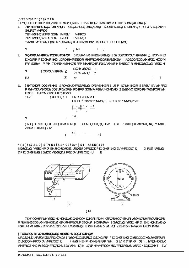
GENERATION OF ALTERNATING VOLTAGE AND CURRENTSAlternating voltage may be generated by rotating a coil in a magnetic field, as shown in Fig.2.4(a) or by rotatinga magnetic field within a stationary coil, as shown in Fig.2.4(b).
Fig. 2.4
The value of the voltage generated depends, in each case, upon the number of turns in the coil, strengthof the field and the speed at which the coil or magnetic field rotates. Alternating voltage may be generated ineither of the two ways shown above, but rotating-field method is the one which is mostly used in practice.
Equations of the Alternating Voltages and currentsConsider a rectangular coil, having N turns and rotating in a uniform magnetic field, with an angular velocity ofradian/second, as shown in Fig.2.5. Let time be measured from the X-axis. Maximum flux m is linked withthe coil, when its plane coincides with the X-axis. In time t seconds, this coil rotates through an angle = t.
Mr. RAVIRAJ SRIKRISHNA AP/SOA 35
In this deflected position, the component of the flux which isperpendicular to the plane of the coil, is = m cos t. Hence, fluxlinkages of the coil at any time are N= Nm cos t.
According to Faraday’s Laws of Electromagnetic Induction, thee.m.f. induced in the coil if given by the rate of change of flux-linkagesof the coil. Hence, the value of the induced e.m.f. at this instant (i.e.when = t) or the instantaneous value of the induced e.m.f. is
de Ndt
volt = – . cosm
dN tdt
volt = – (– sin )mN t volt
= sinmN t volt = sinmN volt ...(i)
When the coil has turned through 90° i.e. when = 90°, then sin = 1, hence e has maximum value, says Em. Therefore, from Eq.(i)we get
mE = m mn NB A = 2 mfNB A volt ...(ii)where mB = maximum flux density in Wb/m2; A = area of the coil in m2
f = frequency of rotation of the coil in rev/secondSubstituting this value of Em in Eq. (i), we get e = Em sin = Em sin t ...(iii)Similarly, the equation of induced alternating current is i = Im sin t ...(iv)provided the coil circuit has been closed through a resistive load.
Since = 2f, where if is the frequency of rotation of the coil, the above equations if the voltage andcurrent can be written as
e = 2sin2 sinm mE ft E tT
and
2sin2 sinm mi I ft I tT
where T = time-period of the alternating voltage or current = 1/f
It is seen that the induced e.m.f. varies as sine function of the time angle t and when e.m.f. is plottedagainst time, a curve similar to the one shown in Fig.2.6 is obtained. This curve is known as sine curve and thee.m.f. which varies in this manner is known as sinusoidal e.m.f. Such a sine curve can be conveniently drawn,as shown in Fig.2.7. A vector, equal in length to Em is drawn. It rotates in the counter-clockwise direction witha velocity of radian/second, making one revolution while the generated e.m.f. makes two loops or one cycle.The projection of this vector on Y-axis gives the instantaneous value e of the induced e.m.f. i.e. Em sin t.
Fig. 2.6 Fig. 2.7
To construct curve, lay off along X-axis equal angular distance oa, ab, bc, cd etc. corresponding tosuitable angular displacement of the rotating vector. Now, erect coordinates at the points a, b, c and d etc.(Fig.2.7) and then project the free ends of the vector Em at the corresponding position a', b', c', etc to meet theseordinates. Next draw a curve passing through these intersecting points. The curve so obtained is the graphicrepresentation of equation (iii) above.
Alternate Method for the Equations of Alternating Voltages and CurrentsIn Fig.2.8 is shown a rectangular coil AC having N turns and rotating in a magnetic field of flux density BWb/m2. Let the length of each of its sides A and C be/meters and their peripheral velocity v metre/second. Letangle be measured from the horizontal position i.e. from the X-axis. When in horizontal position, the two sidesA and C move parallel to the lines of the magnetic flux. Hence, no flux is cut and so no e.m.f. is generated inthe coil.
Fig. 2.5

Mr. RAVIRAJ SRIKRISHNA AP/SOA 36
Fig. 2.8
When the coil has turned through angle , its velocity can be resolved into two mutually perpendicularcomponents (i) v cos component-parallel to the direction of the magnetic flux and (ii) v sin component-perpendicular to the direction of the magnetic flux. The e.m.f. is generated due entirely to the perpendicularcomponent i.e. v sin.
Hence, the e.m.f. generated in one side of the coil which contains N conductors, is given by,e = N × Bl v sin .
Root-Mean-Square (R.M.S) ValueThe r.m.s value of an alternating current is given by that steady (d.c.) current which when flowing through agiven circuit for a given time produces the same heat as produced by the alternating current when flowingthrough the same circuit for the same time.
It is also known as the effective or virtual value of the alternating current, the former term being used moreextensively. For computing the r.m.s. value of symmetrical sinusoidal alternating currents, either mid-ordinatemethod or analytical method may be used, although for symmetrical but non-sinusoidal waves, the mid-ordinate method would be found more convenient.
Fig. 2.9
A simple experimental arrangement for measuring the equivalent d.c. value of a sinusoidal current isshown in Fig.2.9. The two circuits have identical resistance but one is connected to battery and the other to asinusoidal generator. Wattmeters are used to measure heat power in each circuit. The voltage applied to eachcircuit is so adjusted that heat power production in each circuit is the same. In that case, the direct current willequal / 2mI which is called r.m.s. value of the sinusoidal current.
Mid-ordinate MethodIn Fig.2.10 are shown the positive half cycles for both symmetrical sinusoidal and non-sinusoidal alternatingcurrent. Divide time base ‘t’ into n equal intervals of time each of duration t/n seconds. Let the average valuesof instantaneous currents during these intervals be respectively i1, i2, i3, ....in (i.e. mid-ordinates in Fig.2.10).Suppose that this alternating current is passed through a circuit of resistance R ohms. Then,

Mr. RAVIRAJ SRIKRISHNA AP/SOA 37
Fig. 2.10
Heat produced in 1st interval = 0.24 ×10⁻³ 21i Rt/n kcal (1/J = 1/4200 = 0.24 × 10⁻³)
Heat produced in 2nd interval = 0.24 × 10⁻³ 22i Rt/n kcal
: : : : : :: : : : : :: : : : : :
Heat produced in nth interval = 0.24 × 10⁻³ 2ni Rt/n kcal
Total heat produced in t seconds is = 0.24 × 10⁻³² 2 21 2 .... ni i iRt kcal
n
Now, suppose that a direct current of value I produces the same heat through the same resistance duringthe same time t. Heat produced by it is = 0.24 ×10⁻³ I2Rt kcal. By definition, the two amounts of heat producedshould be equal.
0.24 × 3 210 I Rt = 0.24 × 3102 2 21 2 ... ni i iRt
n
2I = 2 2 21 2 ... ni i i
n
I = 2 2 21 2 ... ni i i
n
= squire root of the mean of the square of the instantaneous currentsSimilarly, the r.m.s. value of alternating voltage is given by the expression
V = 2 2 21 2 .... nv v v
n
Analytical MethodThe standard form of a sinusoidal alternating current is i = Im sin t = Im sin .
The mean of the squares of the instantaneous values of current over one complete cycle is (even the valueover half a cycle will do).
= 22
0 2 0i d
The square root of this value is = 22
0 2i d
Hence, the r.m.s. value of the alternating current is
I = 2 2
2 2 2
0 0sin
2 2mi d I d
(put i = sinmI )
Now, cos 2 = 1 – 2sin2 2 1 cos 2sin2
I = 2 2
24 2
m mI I
I = 2mI = 0.707 mI
Hence, we find that for a symmetrical sinusoidal current

Mr. RAVIRAJ SRIKRISHNA AP/SOA 38
r.m.s value of current = 0.707 × max. value of currentThe r.m.s. value of an alternating current is of considerable importance in practice, because the ammeters
and voltmeters record the r.m.s. value of alternating current and voltage respectively. In electrical engineeringwork, unless indicated otherwise, the values of the given current and voltage are always the r.m.s. values.
It should be noted that the average heating effect produced during one cycle is
= 2I R = 2 21/ 22m mI R I R
R.M.S. Value of a Complex WaveIn their case also, either the mid-ordinate method (when equation of the wave is not known) or analyticalmethod (when equation of the wave is known) may be used. Suppose a current having the equation i = 12 sint + 6 sin (3t – /6) + 4 sin (5t – /3) flows through a resistor of R ohm. Then, in the time period T secondof the wave, the effect due to each component is as follows:
Fundamental ................. 2(12 / 2) RT watt
3rd harmonic.................. 2(6 / 2) RT watt
5th harmonic ................. 24 / 2 RT watt
Total heating effect = RT 2 2 2
12 / 2 6 / 2 4 / 2
If I is the r.m.s. value of the complex wave, then equivalent heating effect is 2I RT
2 2 22 12 / 2 6 / 2 4 / 2I RT RT
I = 2 2 2
12 / 2 6 / 2 4 / 2 9.74A Had there been a direct current of (say) 5 amperes flowing in the circuit also*, then the r.m.s. value would
have been
= 2 2 2212 / 2 6 / 2 4 / 2 5 10.93A
Hence, for complex waves the rule is as follows: The r.m.s value of a complex current wave is equal to thesquare root of the sum of the squares of the r.m.s. values of its individual components.
Average ValueThe average value Ia of an alternating current is expressed by that steady current which transfers across anycircuit the same charge as is transferred by that alternating current during the same time.
In the case of a symmetrical alternating current (i.e. one whose two half-cycle are exactly similar, whethersinusoidal or non-sinusoidal), the average value over a complete cycle is zero. Hence, in their case, theaverage value is obtained by adding or integrating the instantaneous values of current over one half-cycle only.But in the case of an unsymmetrical alternating current (like half-wave rectified current) the average value mustalways be taken over the whole cycle.i. Mid-ordinate Method
With reference to Fig.2.16, 1 2 .... nav
i i iIn
This method may be used both for sinusoidal and non-sinusoidal waves, although it is specially convenientfor the latter.
ii. Analytical MethodThe standard equation of an alternating current is, i = Im sin
0 0sin
0m
av
id II d
(putting value of i)
= 0
2– cos 1 1/ 2
m m m mI I I I
=
twice the maximum current
avI = 1/ 0.6372m mI I average value of current = 0.637 × maximum value
Note: R.m.S. value is always greater than average value except in the case of a rectangular wave whenboth are equal.
Mr. RAVIRAJ SRIKRISHNA AP/SOA 39
Form Factor
It is defined as the ratio, fK = . . . 0.707 1.1
0.637m
m
r m s value Iaveragevalue I
(for sinusoidal alternating currents only).
In the case of sinusoidal alternating voltage also, 0.707 1.110.637
mf
m
EKE
As is clear, the knowledge of form factor will enable the r.m.s value to be found from the arithmetic meanvalue and vice-versa.
Crest or Peak or Amplitude Factor
It is defined as the ratio maximum value 2 1.414r.m.s value / 2
ma
m
IKI
(for sinusoidal a.c. only)
For sinusoidal alternating voltage also, aK = 1.414/ 2m
m
EE
Knowledge of this factor is of importance in dielectric insulation testing, because the dielectric stress towhich the insulation is subjected, is proportional to the maximum or peak value of the applied voltage. Theknowledge is also necessary when measuring iron losses, because the iron loss depends on the value ofmaximum flux.
A.C. Through Resistance, Inductance and CapacitanceWe will now consider the phase angle introduced between an alternating voltage and current when the circuitcontains resistance only, inductance only and capacitance only. In each case, we will assume that we aregiven the alternating voltage of equation e = Em sin t and will proceed to find the equation and the phase of thealternating current produced in each case.
A.C. Through Pure Ohmic Resistance AloneThe circuit is shown in Fig.2.56 Let the applied voltage be given by the equation
v = Vmsin = Vmsin t ...(i)Let R = ohmic resistance; i = instantaneous currentObviously, the applied voltage has to supply ohmic voltage drop only. Hence for equilibrium
v = iR;
Putting the value of ‘v’ from above, we get Vm sin t = ; mViR iR
sin t ...(ii)
Current ‘i’ is maximum when sin t is unity mI = /mV R Hence, equation (ii) becomes, sinmi I t
Comparing (i) and (ii), we find that the alternating voltage and current are in phase with each other asshown in Fig.2.12. It is also shown vectrorially by vectors VR and I in Fig. 2.11.
Power: Instantaneous power, p = vi = VmIm sin2t ... (Fig.2.11)
= 1 cos2 cos 22 2 2m m m m m mV I V I V It t
Fig. 2.11 Fig. 2.12

Mr. RAVIRAJ SRIKRISHNA AP/SOA 40
Power consists of a constant part 2m mV I
and a fluctuating part 2m mV I
cos 2t of frequency double that of
voltage and current waves. For a complete cycle. The average value of 2m mV I
cos 2 t is zero.
Hence, power for the whole cycle is
P = 2 2 2m m m mV I V I
or P = V × I wattwhere V = r.m.s. value of applied voltage.
I = r.m.s. value of the current .
Fig. 2.13
It is seen from Fig.2.13 that no part of the power cycle becomes negative at any time. In other words, ina purely resistive circuit, power is never zero. This is so because the instantaneous values of voltage andcurrent are always either both positive or negative and hence the product is always positive.
A.C. Through Pure Inductance AloneWhenever an alternating voltage is applied to a purely inductive coil, a back e.m.f. is produced due to the self-inductance of the coil. The back e.m.f., at every step, opposes the rise of fall of current through the coil. Asthere is no ohmic voltage drop, the applied voltage has to overcome this self-induced e.m.f. only. So at everystep
Fig. 2.14
v = diLdt
Now v = sinmV t
sinmV t = sinmdi VL di t dtdt L
Mr. RAVIRAJ SRIKRISHNA AP/SOA 41
Integrating both sides, we get i = sinmV t dtL
= cosmV tL
... (constant of integration=0)
sin sin / 22
m m
L
V Vt tL X
Max, value of i is mI = mVL when sin 2
t
is unity..
Hence, the equation of the current becomes i = mI sin / 2t .So, we find that if applied voltage is represented by v = Vm sint, then current flowing in a purely inductive
circuit is given by sin2mi I t
Fig. 2.15
Clearly, the current lags behind the applied voltage by a quarter cycle (Fig.2.15) or the phase differencebetween the two is /2 with voltage leading. Vectors are shown in Fig. 2.14 where voltage has been takenalong the reference axis. We have seen that Im = Vm/L = Vm/XL. Here ‘L’ plays the part of ‘resistance’. It iscalled the (inductive) reactance XL of the coil and is given in ohms if L is in henry and is in radian/second.
Now, XL = L = 2fL ohm. It is seen that XL depends directly on frequency of the voltage. Higher the valueof f, greater the reactance offered and vice-versa.
Power
Instantaneous power = vi = VmIm sin t sin 2t
= – VmImsin t .cos t = sin2
2m mV I t
Power for whole cycle is P = 2
0sin 2 0
2m mV I t dt
It is also clear from Fig.2.15(b) that the average demand of power from the supply for a complete cycle iszero. Here again it is seen that power wave is a sine wave of frequency double that of the voltage and currentwaves. The maximum value of the instantaneous power is VmIm/2.
A.C. Through Pure Capacitance AloneWhen an alternating voltage is applied to the plates of a capacitor, the capacitor is charged first in one directionand then in the opposite direction. When reference to Fig.2.16, let
v = p.d. developed between plates at any instantq = Charge on plates at that instant.
Then q = Cv ...where C is the capacitance= C Vm sin t ...putting the value of v,

Mr. RAVIRAJ SRIKRISHNA AP/SOA 42
Fig. 2.16 Fig. 2.17
Now, current i is given by the rate of flow of charge.
i = ( sin ) cosm m
dq d CV t CV tdt dt or i = cos cos sin
/ 1/ 1/ 2m m mV V Vt t t
I C C C
Obviously, sin1/ 2
m mm m
C
V VI i I tC X
The denominator XC = 1/C is known as capacitive reactance and is in ohms if C is in farad and in
radian/second. It is seen that if the applied voltage is given by v = Vm sin t, then the current is given byi = Im sin (t + /2).
Hence, we find that the current in a pure capacitor leads its voltage by a quarter cycle as shown infig.11.17 or phase difference between its voltage and current is /2 with the current leading. Vector representationis given in Fig.2.17. Note that Vc is taken along the reference axis.
Power. Instantaneous power
p = vi = Vm sin t. mI sin (t + 90°)
= 1sin cos sin22m m m mV I t t V I t
Power for the whole cycle
= 2
0
1 sin2 02 m mV I t dt
Fig. 2.18
The fact is graphically illustrated in Fig.2.18. We find that in a purely capacitive circuit, the average demand ofpower from supply is zero (as in a purely inductive circuit). Again, it is seen that power wave is a sine wave offrequency double that of the voltage and current waves. The maximum value of the instantaneous power isVmIm/2.
Mr. RAVIRAJ SRIKRISHNA AP/SOA 43
A.C. Through Resistance and InductanceA pure resistance R and a pure inductive coil of inductance L are shown connected in series in Fig.2.19.
Fig. 2.19 Fig. 2.20
Let V = r.m.s. value of the applied voltage, I = r.m.s. value of the resultant current VR = IR – voltage dropacross R (in phase with I), VL = I.XL –voltage drop across coil (ahead of I by 90°)
These voltage drops are shown in voltage triangle OAB in Fig.2.20. Vector OA represents ohmic drop V Rand AB represents inductive drop VL. The applied voltage V is the vector sum of the two i.e. OB.
V = 2 22 2 2 2.R L L LV V IR I X I R X , 2 2L
V IR X
The quantity 2 2LR X is known as the impedance (Z) of the circuit. As seen from the impedance
triangle ABC (Fig.2.20) 2 2 2LZ R X .
i.e. (Impedance)2 = (resistance)2+(reactance)2.From Fig.11.20 it is clear that the applied voltage V leads the current I by an angle such that
tan= ..
L L L
R
V I X X LV I R R R
=
tantan
reac cereac ce = 1tan Lx
R
The same fact is illustrated graphically in Fig.2.22.In other words, current I lags behind the applied voltage V by an angle .Hence, if applied voltage is given by v = Vm sin t, then current equation is
i = Im sin (t – ) where Im = Vm/Z
Fig. 2.21 Fig. 2.22
In Fig. 2.23. It has been resolved into its two mutually perpendicular components, I cos along the appliedvoltage V and I sin in quadrature (i.e. perpendicular) with V.
Fig. 2.23 Fig. 2.24

Mr. RAVIRAJ SRIKRISHNA AP/SOA 44
The mean power consumed by the circuit is given by the product of V and that a component of the currenti which is in phase with V.
So P = V × I cos = r.m.s. voltage × r.m.s. current × cosThe term ‘cos’ is called the power factor of the circuit.Remember that in an a.c. circuit, the product of r.m.s. volts and r.m.s. amperes gives volt amperes (VA)
and not true power in watts. True power (W) = volt-amperes (V.A) × power factor.or Watts = VA × cosIt should be noted that power consumed is due to ohmic resistance only because pure inductance does
not consume any power.Now P = VI cos = VI × (R/Z) = (V/Z) × I.R = I2 R ( cos = R/Zzz) or P = I2R wattGraphical representing of the power consumed is shown in Fig.11.24.let us calculate power in terms of instantaneous values.Instantaneous power is = i = Vm sin t x Im sin (t – ) = VmIm sin t sin (t – )
= 1 [cos cos(2 )]2 m mV I t
Obviously, this power consists of two parts (Fig.2.25)
Fig. 2.25
i. a constant part 1 cos2 m mV I which contributes to real power..
ii. a pulsating component 1 cos 22 m mV I t which has a frequency twice that of the voltage and current. It
does not contribute to actual power since its average value over a complete cycle is zero.
Hence, average power consumed = 1 cos . cos cos2 2 2
m mm m
V IV I VI , where V and i represent the
r.m.s. values.
Symbolic Notation, Z = R + jXL
Impedance vector has numerical value of 2 2LR X
It is phase angle with the reference axis is = 1tan /LX R
it may also be expressed in the polar form as Z = Z
i. Assuming V = V 0 ;
0 –V V VIZ Z Z (Fig.2.26)

Mr. RAVIRAJ SRIKRISHNA AP/SOA 45
It shows that current vector is lagging behind the voltage vector by . The numerical value of current is V/Z.
Fig. 2.26 Fig. 2.27
ii. However, if we assumed that 0,I I then
V = 0IZ I Z = IZ
It shows that voltage vector is ahead of current vector in ccw direction as shown in Fig.2.27.
A.C. Through Resistance and CapacitanceThe circuit is shown in Fig.2.28(a). Here VR = IR = drop across R in phase with I.
VC = IXC = drop across capacitor-lagging I by /2.As capacitive reactance XC is taken negative, VC is shown along negative direction of Y-axis in the voltage
triangle [Fig.2.28(b)]
Now V = 2 2 22 2 2– –R C C CV V IR IX I R X or
2 2C
V VIZR X
The denominator is called the impedance of the circuit, So, Z = 2 2CR X
From Fig.2.28(b) it is found that I leads V by angle such that tan = –XC/R
Fig. 2.28
Hence, it means that if the equation of the applied alternating voltage is v = Vm sin t, the equation of theresultant current in the R-C circuit is i = Im sin (t + ) so that current leads the applied voltage by an angle .This fact is shown graphically in Fig.2.29.
Fig. 2.29

Mr. RAVIRAJ SRIKRISHNA AP/SOA 46
Resistance, Inductance and Capacitance in SeriesThe three are shown in Fig.2.30(a) joined in series across an ac supply of r.m.s. voltage V.
Fig. 2.30
Let VR = IR = voltage drop across R – in phase with iVL = I.XL = voltage drop across L – leading I by /2VC = I.XC = voltage drop across C – lagging I by /2
In voltage triangle of Fig.2.33(b), OA represents VR, AB and AC represent the inductive and capacitivedrops respectively. It will be seen that VL and VC are 180° out of phase with each other i.e. they are in directopposition to each other.
Subtracting BD (=AC) from AB, we get the net reactive drop AD = I(XL – XC)The applied voltage V is represented by OD and is the vector sum of OA and AD.
OD = 2 2OA AD or 2 2 22
L C L CV IR IX IX I R X X
or I =
2 2 22
L C
V V VZR XR X X
The term 22
L CR X X is known as the impedance of the circuit. Obviously,,(impedance)2 = (resistance)2 + (net reactance)2
or 22 2 2 2
L CZ R X X R Xwhere X is the net reactance (Fig.2.30 and 2.31).
Fig. 2.31 Fig. 2.32
Phase angle is given by tan = (XL – XC)/R = X/R = net reactance/resistance.
Power factor is cos = RZ =
2 2 2 2( )L C
R RR X X R X
Hence, it is seen that if the equation of the applied voltage is v = Vm sin t, then equation of the resultingcurrent in an R-L-C circuit is given by i = Im sin (t + ) ( )t
The +ve sign is to be used when current leads i.e. XC > XL.The –ve sign is to be used when current lags i.e. when XL > XC.In general, the current lags or leads the supply voltage by an angle such that tan = X/R.Using symbolic notation, we have (Fig.2.35), Z = R + j (XL – XC)

Mr. RAVIRAJ SRIKRISHNA AP/SOA 47
Numerical value of impedance Z = 22
L CR X X
Its phase angle is = tan–1 [XL – XC/R]
Z = 1 1tan / tan /L CZ X X R Z X R
If V = V 0, then I = V/Z.
Summary of Results of Series AC Circuits
Type of impedance Value of Impedance Phase angle for current power factor
Resistance only R 0° 1Inductance only L 90° lag 0Capacitance only 1/ C 90° lead 0
Resistance and 22R L 0< < 90° lag 1 > p.f. > 0 lag
Inductance
Resistance and 22 1/R C 0<< 90° lead 1 > p.f > 0 lead
Capacitance
R-L-C 2 2( ~ 1/ )R L C between 0° and 90° between 0 and
lag or lead unity lag or lead
Resonance in R-L-C CircuitsWe have seen from Art.13.9 that net reactance in an R-L circuit of Fig.2.40(a) is
X = L CX X and Z = 222 2
L CR X X R X
Let such a circuit be connected across an a.c. source of constant voltage V but of frequency varying fromzero to infinity. There would be a certain frequency of the applied voltage which would make XL equal to XC inmagnitude. In that case, X = 0 and Z = R as shown in Fig.2.40(c). Under this condition, the circuit is said tobe in electrical resonance.
As shown in fig.2.40(c), VL = I. XL and VC = I. XC and the two are equal in magnitude but opposite inphase. Hence, they cancel each other out. The two reactances taken together act as a short-circuit since novoltage develops across them. Whole of the applied voltage drops across R so that V = XC. The circuitimpedance Z = R. The phasor diagram for series resonance is shown in Fig.2.40(d).
Calculation of Resonant FrequencyThe frequency at which the reactance of the series circuit is zero is called the resonant frequency f0. Its valuecan be found as under : XL – XC = 0 or XL = XC or 0L = 1/0C.
or 20 =
1LC or
2
0
12 fLC or 0f =
12 LC
If L is in henry and C in farad, then f0 is given in Hz.When a series R-L-C circuit is in resonance, it possesses minimum impedance z = R. Hence, circuit
current is maximum, it being limited by value of R alone. The current I0 = V/r and is in phase with V.
Fig. 2.33

Mr. RAVIRAJ SRIKRISHNA AP/SOA 48
Since circuit current is maximum, it produces large voltage drops across L and C. but these drops beingequal and opposite, cancel each other out. Taken together, L and C from part of a circuit across which novoltage develops, however, large the current following. if it were not for the presence of R, such a resonantcircuit would act like short-circuit to currents of the frequency to which it resonates. Hence, a series resonantcircuit is sometimes called acceptor circuit and the series resonance is often referred to as voltage resonance.
In fact, at resonance the series RLC circuit is reduced to a purely resistive circuit, as shown in Fig.2.33.Incidentally, it may be noted that if XL and XC are shown at any frequency f, that the value of the resonant
frequency of such a circuit can be found by the relation 0f = /C Lf X X .When an R-L-C circuit is in resonance1. net reactance of the circuit is zero i.e. (XL – XC) = 0 or X = 0.2. circuit impedance is minimum i.e. Z=R. Consequently, circuit admittance is maximum.3. circuit current is maximum and is given by I0 = V/Z0 = V/R.4. power dissipated is maximum i.e. 2 2
0 0 /P I R V R .5. circuit power factor angle = 0 . Hence, power factor cos = 1.6. although VL = VC yet VC is greater than VC because of its resistance.7. at resonance, LC = 1.8. Q = tan = tan0° = 0°.
Graphical Representation of ResonanceSuppose an alternating voltage of constant magnitude, but of varying frequency is applied to an R-L-C circuit.The variations of resistance, inductive reactance XL and capacitive reactance XC with frequency are shown inFig.2.45(a).
i. Resistance : It is independent of f, hence, it is represented by a straight line.ii. Inductive Reactance : It is given by XL = L = 2fL. As seen, XL is directly proportional to f i.e. XL
increases linearly with f. Hence, its graph is a straight line passing through the origin.iii. Capacitive Reactance: It is given by XC = 1/C = 1/2fC. Obviously, it is inversely proportional to
f. Its graph is a rectangular hyperbola which is drawn in the fourth quadrant because XC is regardednegative. It is asymptotic to the horizontal axis at high frequencies and to the vertical axis at lowfrequencies.
iv. Net Reactance: It is given by X = XL ~ XC. Its graph is a hyperbola (not rectangular) and crosses theX-axis at point A which represents resonant frequency f0.
v. Circuit Impedance: It is given by 22 2 2~L CZ R X X R X
At low frequencies Z is large because XC is large. Since XC > XL, the net circuit reactance X is capacitiveand the p.f. is leading [Fig.2.34(b)]. At high frequencies. Z is again large (because X L is large) but is inductivebecause XL > XC. Circuit impedance has minimum values at f0 iven by Z = R because X = 0.
Fig. 2.34
vi. Current I0 : It is the reciprocal of the circuit impedance. When Z is low. I0 is high and vice versa. Asseen, I0 has low value on both sides of f0 (because Z is large there) but has maximum value of I0 =V/R at resonance. Hence, maximum power is dissipated by the series circuit under resonantconditions. At frequencies below and above resonance, current decreases as shown in Fig.11.34
(b). Now, 0I = V/R and I = V/Z = 2 2VI R X . Hence 0/I I = R/Z = 2 2VI R X where X is the netcircuit reactance at any frequency f.

Mr. RAVIRAJ SRIKRISHNA AP/SOA 49
vii. Power FactorAs pointed out earlier, X is capacitive below f0. Hence, current leads the applied voltage. However,at frequencies above f0. X is inductive. Hence, the current lags the applied voltage as shown inFig. 2.34. The power factor has maximum value of unity at f0.
Resonance CurveThe curve, between circuit current and frequency of the applied voltage, is known as resonance curve. Theshapes of such a curve, for different values of R are shown in Fig.2.35. For smaller values of R, the resonancecurve is sharply peaked and such a circuit is said to be sharply resonant or highly selective. However, for largervalues of R, resonance curve is flat and is said to have poor selectivity. The ability of a resonant circuit todiscriminate between one particular frequency and all others is called its selectivity. The selectivities ofdifferent resonant circuits are compared in terms of their half-power bandwidths.
Fig. 2.35
Solving Parallel CircuitsWhen impedances are joined in parallel, there are three methods available to solve such circuits.(a) Vector or phasor Method (b) Admittance Method and (c) Vector Algebra
Vector or Phasor MethodConsider the circuits shown in Fig.2.36. Here, two reactors A and B have been joined in parallel across andr.m.s. supply of V volts. The voltage across two parallel branches A and B is the same, but currents throughthen are different.
Fig. 2.36 Fig. 2.37
For Branch A, Z1 = 2 21 LR X ; 1I =V/ 1Z ; cos 1= 1 1/R Z or 1 = 1cos (
1 1/R Z )Current I1 lags behind the applied voltage by 1 (Fig.14.2).
For Branch B, 2Z = 2 22 cR X ; 2I = 2/V Z ; cos 2 = ( 2 2/R Z )
Current I2 leads V by 2 (Fig.2.2).

Mr. RAVIRAJ SRIKRISHNA AP/SOA 50
Resultant current IThe resultant circuit current I is the vector sum of the branch currents I1 and I2 and can be found by (i) usingparallelogram law of vectors, as shown in Fig.2.37. or (ii) resolving I2 into their X-and y-components (or activeand reactive components respectively) and then by combining these components, as shown in Fig.2.38.Method (ii) is preferable, as it is quick and convenient.
With reference to Fig.2.38(a) we haveSum of the active components of I1 and I2
= I1 cos 1 + I2 cos 2Sum of the reactive components of I1 and I2 sin 2 – I1 sin 1If I si the resultant current and , its phase, then its active and reactive components must be equal to
these X-and Y-components respectively [Fig.2.38(b)].I cos = I1 cos1 + I2 cos2 and I sin = I2 sin2 – I1 sin1
I = 22
1 1 2 2 2 2 1 1(I cos I cos ) I sing I sin
and tan =
2 2 1 1
1 1 2 2
I sin I sin Y componentI cos I cos X component
If tan is positive, then current leads and if tan is negative, then current lags behind the applied voltageV. Power factor for the whole circuit is given by
cos = 1 1 2 2I cos I cos X comp.
I I
Fig. 2.38
Admittance MethodAdmittance of a circuit is defined as the reciprocal of its impedance. It symbol is Y.
Y = 1 1Z V or
r.m.s.amperesYr.m.s volts
Its unit is Sciemens (S). A circuit having an impedance of one ohm has an admittance of one Siemens.The old unit was mho (ohm spelled backwards).
As the impedance Z of a circuit has two components X and R (Fig. 2.39), similarly, admittance Y also hastwo components as shown in Fig. 2.40. The X-component is known as conductance and Y-component assusceptance.
Obviously, conductance g = Y cos
or g = 1 R.Z Z (from Fig. 2.39)
g = 2 2 2
R RZ R X
Similarly, susceptance b = Y sin = 1 X,2 Z
b = X/Z2 = X/(R2+X2) (from Fig. 2.40)
The admittance 2 2Y g b just as Z = 2 2R X
The unit of g, b and Y is Siemens. We will regard the capacitive suscepance as positive and inductivesusceptance as negative.

Mr. RAVIRAJ SRIKRISHNA AP/SOA 51
Fig. 2.39 Fig. 2.40
Application of Admittance MethodConsider the 3-branched circuit of Fig.2.41. Total conductance is found by merely adding the conductances ofthree branches. Similarly, total susceptance is found by algebraically adding the individual susceptances ofdifferent branches.
Fig. 2.41
Total conductance G = g1 + g2 + g3 .......Total susceptance B = (–b1) + (–b2) + b3 ........ (algebraic sum)
total admittance Y = 2 2G B
Total current I = VY; Power factor cos = G/Y.
Complex or Phasor AlgebraConsider the parallel circuit shown in Fig.2.42. The two impedances, Z1 and Z2, being in parallel, have thesame p.d. across them.
Fig. 2.42 Fig. 2.43
Now 1I = 1
VZ and 2I =
2
VZ
Total current I = 1I + 2I =
1 2
1 2 1 2
V V 1 1V V Y Y VYZ Z Z Z
where Y = total admittance = 1 2Y Y

Mr. RAVIRAJ SRIKRISHNA AP/SOA 52
It should be noted that admittances are added for parallel branches. Whereas for branches in series, it isthe impedances which are added. However, it is important to remember that since both admittances andimpedances are complex quantities, all additions must be in complex form. Simple arithmetic additions mustnot be attempted.
Considering the two parallel branches of Fig.2.43, we have
1Y =
1 L
1 1 L 1 L 1 L
R jX1 1Z R jX R jX R jX
=
1 L 1 L1 12 2 2 2 2 2
1 L 1 L 1 L
R jX R Xj g jbR X R X R X
where 1g = 1
2 21 L
RR X – conductance of upper branch
1b = L
2 21 L
X–R X – susceptance of upper branch
Similarly, 2Y = 2 2 C
1 1Z R jX .
=
2 C 2 C 2 C2 22 2 2 2 2 2
2 C 2 C 2 C 2 c 2 C
R jX R jX R Xj g jbR jX R jX R X R X R X
Total admittance Y = 1 2 1 1 2 2 1 2 1 2Y Y g jb g jb g g j b b G jB
Y =
2 2 1 1 21 2 1 2
1 2
b bg g b b ; tnag g
The polar form for admittance is Y = Y where is as given above.
Y = 2 2G B 1tan B / G
Total current I = VY; 1I = VY1 and 2I = 2VYIf V = V 0 and Y = Y then I = VY = V 0 × Y = VY In general, if V = V and Y = Y , then I = VY = V Y VYHence, it should be noted that when vector voltage is multiplied by admittance either in complex (rectangular)
or polar form, the result is vector current in its proper phase relationship with respect to the voltage, regardlessof the axis to which the voltage may have been referred to.
Generation of Polyphase VoltageThe kind of alternating currents and voltages discussed in chapter 12 to 15 are known as single-phase voltageand current, because they consist of a single alternating current and voltage wave. A single-phase alternatorwas diagrammatically depicted in Fig.2.1(b) and it was shown to have one armature winding only. But if thenumber of armature windings is increased, then it becomes polyphase alternator and it produces as manyindependent voltage waves as the number of windings or phases. These windings are displaced from oneanother by equal angles, the values of these angles being determined by the number of phases or windings. Infact, the word ‘polyphase’ mean poly (i.e. many or numerous) and phases (i.e. winding or circuit).
In a two-phase alternator, the armature windings are displaced 90 electrical degrees apart. A 3-phasealternator, as the name shows, has three independent armature windings which are 120 electrical degreesapart. Hence, the voltages induced in the three windings are 120° apart in time-phase. With the exception oftwo-phase windings, it can be stated that, in general, the electrical displacement between different phases is360/n where n is the number of phases or windings.
The rotary Phase Converter
Mr. RAVIRAJ SRIKRISHNA AP/SOA 53
Three-phase systems are the most common, although, for certain special jobs, greater number of phasesis also used. For example almost all mercury-arc rectifiers for power purposes are either six-phase or twelve-phase and most of the rotary converters in use are six-phase. All modern generators are practically three-phase. For transmitting large amounts of power, three-phase is invariably used. The reasons for the immensepopularity of three-phase apparatus are that (i) it is more efficient (ii) it uses less material for a given capacityand (iii) it costs less than single-phase apparatus etc.
In Fig.2.44 is shown a two-pole, stationary-armature, rotating-field type three-phase alternator. It hasthree armature coils aa', bb' and cc' displaced 120° apart from one another. With the position and clockwiserotation of the poles as indicated in Fig.2.44, it is found that the e.m.f. induced in conductor ‘a’ for coil aa' ismaximum and its direction is away from the reader. The e.m.f. in conductor ‘b’ of coil bb' would be maximumand away from the reader when the N-pole has turned through 120° i.e. when N-S axis lies along bb'. it is clearthat the induced e.m.f. in conductor ‘b’ reaches its maximum value 120° later than the maximum value inconductor ‘a’. In the like manner, the maximum e.m.f. induced (in the direction away from the reader) inconductor ‘c’ would occur 120° later than that in ‘b’ or 240° later than that in ‘a’.
Thus the three coils have three e.m.fs. induced in them which are similar in all respects except that theyare 120° out of time phase with one another as pictured in Fig.2.46. Each voltage wave is assumed to besinusoidal and having maximum value of Em.
In practice, the space on the armature is completely covered and there are many slots per phase perpole.
Fig. 2.44 Fig. 2.45
Fig.2.45 illustrates the relative positions of the windings of a 3-phase, 4-pole alternator and Fig.2.47shows the developed diagram of its armature windings. Assuming full-pitched winding and the direction ofrotation as shown, phase ‘a’ occupies the position under the centres of N and S-poles. It starts and Sa andends or finishes at Fa.
The second phase ‘b’ start at Sb which is 120 electrical degrees apart from the start of phase ‘a’, progressesround the armature clockwise (as does ‘a’) and finishes at Fb. Similarly, phase ‘c’ starts at SC, which is 120electrical degrees away from Sb, progresses round the armature and finishes at FC. As the three circuits areexactly similar but are 120 electrical degrees apart, the e.m.f. waves generated in them (when the field rotates)are displaced from each other by 120°. Assuming these waves to be sinusoidal and counting the time from theinstant when the e.m.f. in phase ‘a’ is zero, the instantaneous values of the three e.m.fs. will be given by curvesof Fig.193.
Their equations are :
ea = Em sin t ....(i)
eb = Em sin(t – 120°) ....(ii)
ec = Em sin(t – 240°) ....(iii)
As shown, alternating voltages may be represented by revolving vectors which indicate their maximumvalues (or r.m.s. values if desired). The actual values of these voltages vary from peak positive to zero and topeak negative values in one revolution of the vectors. In Fig. 2.48 are shown the three vectors representing ther.m.s. voltages of the three phases Eo, Eb, and Ec (in the present case Ea = Eb = Ec = E, say)
It can be shown that the sum of the three phase e.m.fs. is zero in the following three ways:i. The sum of the above three equations (i), (ii) and (iii) is zero as shown below:

Mr. RAVIRAJ SRIKRISHNA AP/SOA 54
Fig. 2.46
Resultant instantaneous e.m.f. = a b ce e e
= m m mE sin t E sin t 120 E t 240
= mE sin t 2sin t 180 cos60
= mE sin t 2sin t cos60 0
ii. The sum of ordinates of three e.m.f. curves of Fig.2.46 is zero. For example, taking ordinates ABand AC as positive and AD as negative, it can be shown by actual measurement that
AB + AC + (–AD) = 0iii. If we add the three vectors of Fig.11.48 either vectorially or by calculation, the result is zero.
Fig. 2.47Vector AdditionAs shown in Fig.2.49, the resultant of Ea and Eb is Er and its magnitude is 2E cos 60° = E where Ea = Eb = Ec = E.
This resultant Er is equal and opposite to Ec. Hence, their resultant is zero.
By CalculationLet us take Ea as reference voltage and assuming clockwise phase sequence
aE = E 0 E j0
bE = E – 240 E 120 E –0.05 j0.866
cE = E – 240 E 120 E 0.05 j0.866

Mr. RAVIRAJ SRIKRISHNA AP/SOA 55
a b cE E E E j0 E 0.5 0.866 E 0.05 j0.866 0
Fig. 2.48 Fig. 2.49
Fig. 2.50
Phase SequenceBy phase sequence is meant the order in which the three phases attain their peak or maximum values. In thedevelopment of the three-phase e.m.fs in Fig. 2.50, clockwise rotation of the field system in Fig. 2.44 wasassumed. This assumption made the e.m.fs. of phase ‘b’ lag behind that of ‘a’ by 120° and in a similar way,made that of ‘c’ lag behind that of ‘b’ by 120° (or that of ‘a’ by 240°). hence, the order in which the e.m.fs. ofphases a, b and c attain their maximum values is abc. It is called the phase order or phase sequenceabc as illustrated in Fig. 2.50(a).
If, now, the rotation of the field structure of Fig. 2.50 is reversed i.e. made anticlockwise, then the order inwhich the three phases would attain their corresponding maximum voltages would also be reversed. Thephase sequence would become abc. This means that e.m.f. of phase ‘c’ would now lag behind that ofphase ‘a’ by 120° instead of 240° as in the previous case as shown in Fig. 2.50(b). By repeating the letters,this phase sequence can be written as acbacba which is the same thing as cba. Obviously, a three-phasesystem has only two possible sequences : abc and cba (i.e. abc read in the reverse direction).

Mr. RAVIRAJ SRIKRISHNA AP/SOA 56
UNIT - 3

Mr. RAVIRAJ SRIKRISHNA AP/SOA 57

Mr. RAVIRAJ SRIKRISHNA AP/SOA 58
CHAPTER - 3Rotating Electrical Machines
WorkingImagine the coil to be rotating in clock-wise direction (Fig. 3.1). As the coil assumes successive positions inthe field, the flux linked with it changes. Hence, an e.m.f. is induced in it which is proportional to the rate ofchange of flux linkages (e = Nddt). When the plane of the coil is at right angles to lines of flux i.e. when it isin position, 1, then flux linked with the coil is maximum but rate of change of flux linkages is minimum.
It is so because in this position, the coil sides AB and CD do not cut or shear the flux, rather they slidealong them i.e. they move parallel to them. Hence, there is no induced e.m.f. in the coil. Let us take this no-e.m.f. or vertical position of the coil as the starting position. The angle of rotation or time will be measured fromthis position.
Fig. 3.1 Fig. 3.2
As the coil continues rotating further, the rate of change of flux linkages (and hence induced e.m.f. in it)increases, till position 3 is reached where = 90°. Here, the coil plane is horizontal i.e. parallel to the lines offlux. As seen, the flux linked with the coil is minimum but rate of change of flux linkages is maximum. Hence,maximum e.m.f. is induced in the coil when in this position (Fig. 3.2).
In the next quarter revolution i.e. from 90° to 180°, the flux linked with the coil gradually increases but therate of change of flux linkages decreases. Hence, the induced e.m.f. decreases gradually till in position 5 ofthe coil, it is reduced to zero value.
So, we find that in the first half revolution of the coil, no (or minimum) e.m.f. is induced in it when inposition I, maximum when in position 3 and no e.m.f. when in position 5. The direction of this induced e.m.f.can be found by applying Flaming’s Right-hand rule which gives its direction from A to B and C to D. The currentthrough the load resistance R flows from M to L during the first half revolution of the coil.
In the next half revolution i.e. from 180° to 360°, the variations in the magnitude of e.m.f. are similar tothose in the first half revolution. Its value is maximum when coil is in position 7 and minimum when in position1. Hence, the path of current flow is along DCLMBA which is just the reverse of the previous direction of flow.
Therefore, we find that the current which we obtain from such a simple generator reverse its direction afterevery half revolution. Such a current undergoing periodic reversals is known as alternating current. It is, obviously,different from a direct current which continuously flows in one and the same direction. It should be noted thatalternating current not only reverses its direction, it does not even keep its magnitude constant while flowing inany one direction. The two half-cycles may be called positive and negative half-cycles respectively (Fig. 3.2).
For making the flow of current unidirectional in the external circuit, the slip-rings are replaced by split-rings (Fig. 3.3). The split-rings are made out of a conducting cylinder which is cut into two halves or segmentsinsulated from each other by a thin sheet of mica or some other insulating material (Fig. 3.4).
As before, the coil ends are joined to these segments on which rest the carbon or copper brushes. It isseen [Fig. 3.5a)] that in the first half revolution current flows along (ABMNLCD) i.e. the brush No.1 in contactwith segment ‘n’ acts as the positive end of the supply and ‘b’ as the negative end. In the next half revolution[Fig. 3.5(b)], the direction of the induced current in the coil has reversed. But at the same time, the

Mr. RAVIRAJ SRIKRISHNA AP/SOA 59
Fig. 3.3 Fig. 3.4
positions of segments ‘a’ and ‘b’ have also reversed with the result that brush no.1 comes in touch with thesegment which is positive i.e. segment ‘b’ in this case. hence, current tin the load resistance again flows fromM to L. The waveform of the current through the external circuit is as shown in Fig.3.6. The current isunidirectional but not continuous like pure direct current.
Fig. 3.5 Fig. 3.6
It should be noted that the position of brushes is so arranged that the change over of segments ‘a’ and ‘b’from one brush to the other takes place when the plane of the rotating coil is at right angles to the plane of thelines of flux. It is so because in that position, the induced e.m.f. in the coil is zero.
Another important point worth remembering is that even now the current induced in the coil sides isalternating as before. It is only due to the rectifying action of the split-rings (also called commutator) that itbecomes unidirectional in the external circuit. Hence, it should be clearly understood that even in the armatureof a d.c. generator, the induced voltage is alternating.
Motor PrincipleAn Electric motor is a machine which converts electric energy into mechanical energy. Its action is based onthe principle that when a current-carrying conductor is placed in a magnetic field is experiences a mechanicalforce whose direction is given by Fleming’s Left-hand Rule and whose magnitude is given by F = Bll Newton.
Principle of Motor
Mr. RAVIRAJ SRIKRISHNA AP/SOA 60
Constructionally, there is no basic difference between a d.c. generator and a d.c. motor. In fact, the samed.c. machine can be used interchangeably as a generator or as a motor. D.C. motors are also like generators,shunt-wound or series-wound or compound-wound.
Fig. 3.7
In Fig.3.7 a part of multipolar d.c. motor is shown. When its field magnet are excited and its armatureconduction are supplied with current from the supply mains, they experience a force tending to rotate thearmature. Armature conductors under N-pole are assumed to carry current downwards (crosses) and thoseunder S-poles, to carry current upwards (dots). By applying fleming’s Left-hand Rule, the direction of the forceon each conductor can be found. It is shown by small arrows placed above each conductor. It will be seen thateach conductor can be found. It will be seen that each conductor experiences a force F which tends to rotatethe armature in anticlockwise direction. These forces collectively produce & driving torque which sets thearmature rotating.
It should be noted that the function of a commutator in the motor is the same as in a generator. Byreversing current in each conductor as it passes from one pole to another, it helps to develop a continuous andunidirectional torque.
Comparison of Generator and Motor ActionAs said above, the same d.c. machine can be used, at least theoretically, interchangeably as a generator or asa motor. When operating as a generator, it si driven by a mechanical machine and it develops, voltage whichin turn produces current flow in an electric circuit. When operating as a motor, it is supplied by electric currentand it develops torque which in turn produces mechanical rotation.
Let us first consider its operation as a generator and see how exactly and through which agency, mechanicalpower is converted into electric power.
Significance of the Back e.m.f.As explained when the motor armature rotates, the conductors also rotate and hence cut the flux. In accordancewith the laws of electromagnetic induction, e.m.f. is induced in them whose direction, as found by Fleming’sRight-hand Rule, is in opposition to the applied voltage (Fig.3.9). Because of its opposing direction, it isreferred to as counter e.m.f. or back e.m.f. Eb. The equivalent circuit of a motor is shown in Fig.3.10. Therotating armature generating the back e.m.f. Eb is like a battery of e.m.f. Eb put across a supply mains of Vvolts. Obviously, V has to drive Ia against the opposition of Eb. The power required to overcome this oppositionis EbIa.
In the case of a cell, this power over an interval of time is converted into chemical energy, but in the presentcase, it is converted into mechanical energy.
It will be seen that aI = b
a
Net voltage V VResis tance R
where Ra is the resistance of the armature circuit. As pointed out above.
bE ZN (P / A) volt where N is in r.p.s.

Mr. RAVIRAJ SRIKRISHNA AP/SOA 61
Fig. 3.9 Fig. 3.10
Back e.m.f. depends, among other factors, upon the armature speed. If speed is high, Eb is large hencearmature current Ia, seen from the above equation, is small. If the speed is less, then Eb is less, hence morecurrent flows which develops motor torque. So, we find that Eb acts like a governor i.e., it makes a motor self-regulating so that it draws as much current as is just necessary.
Voltage Equation of a MotorThe voltage V applied across the motor armature has to
i. overcome the back e.m.f. Eb andii. supply the armature ohmic drop IaRa.
V = Eb + IaRa
This is known as voltage equation of a motor. Now, multiplying both sides by Ia, we get
aVI = 2b a a aE I I R
As shown in Fig. 3.10,
aVI = Electrical input to the armature.
b aE I = Electrical equivalent of mechanical power developed in the armature
2a aI R = Cu loss in the armature.
Hence, out of the armature input, some is wasted in I2 R loss and the rest is converted into mechanicalpower within the armature.
It may also be noted that motor efficiency is given by the ratio of power developed by the armature to itsinput i.e., EbIa/VIa = Eb/V. Obviously, higher the value of Eb as compared to V, higher the motor efficiency.
Condition for Maximum PowerThe gross mechanical power developed by a motor is mP = 2
a a aV I I R .Differentiating both sides with respect to Ia and equating the result to zero, we get
m a a adP / dI V 2I R 0 a aI R V / 2
As b a aV E I R and a aI R V / 2 a aI R V / 22vEb
Thus gross mechanical power developed by a motor is maximum when back e.m.f. is equal to half theapplied voltage. This condition is, however, not realized in practice, because in that case current would bemuch beyond the normal current of the motor. Moreover, half the input would be wasted in the form of heat andtaking other losses (mechanical and magnetic) into consideration, the motor efficiency will be well below 50percent.
Classification of A.C. MotorsWith the almost universal adoption of a.c. system of distribution of electric energy for light and power, the fieldof application of a.c. motors has widened considerably during recent years. As a result, motor manufactureshave tried, over the last few decades, to perfect various types of a.c. motors suitable for all classes of industrialdrives and for both single and three-phase a.c. supply. This has given rise to bewildering multiplicity of typeswhose proper classification often offers considerable difficulty. Different a.c. motors may, however, be classifiedand divided into various groups from the following different points of view:

Mr. RAVIRAJ SRIKRISHNA AP/SOA 62
Three phase high voltage asynchronous motors.
1. As Regards their principle of operation(a) Synchronous motors
i. plain and ii. super(b) Asynchronous motors
a. Induction motorsi. Squirrel cage single doubleii. Slip-ring (external resistance)
b. Commutator motorsi. Series { single phase universal}ii. Compensated [conductively inductivelyiii. shunt { simple compensatediv. repulsion { straight compensatedv. repulsion-start inductionvi. repulsion induction
2. As Regards the Type of Currenti. single phase ii. three phase
3. As Regards Their Speedi. constant speed ii. variable speed iii. adjustable speed
4. As Regards Their Structural Featuresi. open ii. enclosed iii. semi-enclosediv. ventilated v. pipe-ventilated vi. reverted frame eye etc.
Induction Motor : General PrincipleAs a general rule, conversion of electrical power into mechanical power takes place in the rotating part of anelectric motor. In d.c. motors, the electric power is conducted directly to the armature (i.e rotating part)through brushes and commutator. Hence, in this sense, a d.c. motor can be called a conduction motor.However, in a.c. motors, the rotor does not receive electric power by conduction but by induction in exactly thesame way as the secondary of a 2-winding transformer receives its power from the primary. That is why motorsare known as induction motors. In fact, an induction motor can be treated as a rotating transformer i.e. one inwhich primary winding is stationary but the secondary is free to rotate.
Squirrel cage AC induction motor opened to show the stator and rotor construction,the shaft with bearings, and the cooling fan.

Mr. RAVIRAJ SRIKRISHNA AP/SOA 63
Of all the a.c. motors, the polyphase induction motor is the one which is extensively used for various kindsof industrial drives. It has the following main advantages and also some dis-advantages:
Advantages;1. It has very simple and extremely rugged, almost unbreakable construction (especially squirrel-cage type).2. Its cost is low and it is very reliable.3. It has sufficiently high efficiency. In normal running condition, no brushes are needed, hence frictional
losses are reduced. It has a reasonably good power factor.4. It requires minimum of maintenance.5. It starts up from rest and needs no extra starting motor and has not to be synchronized. Its starting
arrangement is simple-especially for squirrel-cage type motor.
Disadvantages1. Its speed cannot be varied without sacrificing some of its efficiency.2. Just like a d.c. shunt motor, its speed decreases with increase in load.3. Its starting torque is somewhat inferior to that of a d.c. shunt motor.
ConstructionAn induction motor consists essentially of two main parts:a. a stator and b. a rotor.
a. StatorThe stator of an induction motor is, in principle, the same as that of a synchronous motor or generator. It ismade up of a number of stamping, which are slotted to receive the windings [Fig. 3.11(a)]. The stator carriesa 3-phase winding [Fig.3.11(b)] and is fed from a 3-phase supply. It is wound for a definite number if poles, theexact number of poles being determined by the requirements of speed. Greater the number of poles, lesser thespeed and vice versa. It will be shown in Art.34.6 that the stator windings, when supplied with 3-phasecurrents, produce a magnetic flux, which is of constant magnitude but which revolves (or rotates) at synchronousspeed (given by Ns=120 f/P). This revolving magnetic flux induces an e.em.f. in the motor by mutual induction.
3.11. a. Unwound stator with semi-closed 3.11. b. Completely wound stator for slots. laminations are of high-quality an induction motor. low-loss silicon steel
b. Rotori. Squirrel-cage rotor: Motors employing this type of rotor are known as squirrel-cage induction motors.ii. Phase-wound or wound rotor: Motor employing this type of rotor are variously known in ‘phase-
wound’ motors or ‘wound’ motors or as ‘slip-ring’ motors.
Squirrel-cage RotorAlmost 90 per cent of induction motors are squirrel-cage type, because this type of rotor has the simplest andmost rugged construction imaginable and is almost indestructible. The rotor consists of a cylindrical laminatedcore with parallel slots for carrying the rotor conductors which, it should be noted clearly, are not wires butconsist of heavy bars of copper, aluminium or alloys. One bar is placed in each slot, rather the bars areinserted from the end when semi-closed slots are used. The rotor bars are brazed or electrically welded orbolted to two heavy and stout short-circuiting end-rings, thus giving us, what is so picturesquely called, asquirrel-case construction (Fig. 3.12).
It should be noted that the rotor bars are permanently short-circuited on themselves, hence it is notpossible to add any external resistance in series with the rotor circuit for starting purposes.
Mr. RAVIRAJ SRIKRISHNA AP/SOA 64
The rotor slots are usually not quite parallel to the shaft but are purposely given a slight skew(Fig. 3.13). This is useful in two ways:
Fig. 3.12a. Squirrel-cage rotor with copper Fig. 3.12b. Rotor with shaft and brings bars and alloy brazed end-rings
i. it helps to make the motor run quietly by reducing the magnetic hum andii. it helps in reducing the locking tendency of the rotor i.e. tendency of the rotor teeth to remain under the
stator teeth due to direct magnetic attraction between the two.
Fig. 3.13
In small motors, another method of construction is used. It consists of placing the entire rotor core in amould and casting all the bars and end-rings in one piece. The meal commonly used is an aluminium alloy.
Another form of rotor consists of a solid cylinder of steel without any conductors or slots at all. The motoroperation depends upon the production of eddy currents in the steel rotor.
This type of rotor is provided with 3-phase, double-layer, distributed winding consisting of coils as used inalternators. The rotor is wound for as many poles as the number of stator poles and is always wound 3-phaseeven when the stator is wound two-phase.
(a) (b) (c)
Fig. 3.14b. Slip-ring motor with slip-rings brushed and short-circuiting devices
The three phases are starred internally. The other three winding terminals are brought out and connectedto three insulated slip-rings on them [Fig. 3.14(b)]. These three brushes are further externally connected to a3-phase star-connected the rheostat [Fig. 3.14(c)]. This makes possible the introduction of additional resistance

Mr. RAVIRAJ SRIKRISHNA AP/SOA 65
in the rotor circuit during the starting period for increasing the starting torque of the motor, as shown in Fig.3.14(a)(Ex.34.7 and 34.10 and for changing is speed-torque/current characteristics. When running under normalconditions, the slip-rings are automatically short-circuited by means of a metal collar, which is pushed alongthe shaft and connects all the rings together. Next, the brushes are automatically lifted from the slip-rings toreduce the frictional losses and the wear and tear. Hence, it is seen that under normal running conditions, thewound rotor is short-circuited on itself just like the squirrel-case rotor.
Fig. 3.15(b) shows the longitudinal section of a slip-ring motor, whose structural details are as under:
Fig. 3.16(a) Fig. 3.16 (b) longitudinal section of a Jyotisplash-proof slip-ring motor
1. Frame. Made of close-grained alloy cast iron.
2. Stator and Rotor Core. Built from high-quality low-loss silicon steel laminations and flash enamelled onboth sides.
3. Stator and Rotor windings. Have moisture proof tropical insulation embodying mica and high qualityvarnishes. Are carefully spaced for most effective air circulation and are rigidly braced to withstandcentrifugal forces and any short-circuit stresses.
4. Air-gap. The stator rabbets and bore are machined carefully to ensure uniformity of air-gap.
5. Shafts and bearings. Ball and roller bearings are used to suit heavy duty, trouble-free running and forenhanced service life.
6. Fans. Light aluminium fans are used for adequate circulation of cooling air and are securely keyed ontothe rotor shaft.
7. Slip-rings and Slip-ring Enclosures. Slip-rings are made of high quality phosphor-bronze and are ofmoulded construction.
Why Does the Rotor RotateThe reason why the rotor of an induction motoris set into rotation is as follow:
When the 3-phase stator windings, are fedby a 3-phase magnitude, but rotating atsynchronous speed, is set up. The flux passesthrough the air-gap, sweeps past the rotorsurface and so cuts the rotor conductors which,as yet, are stationary. Due to the relative speedbetween the rotating flux and the stationaryconductors, an e.m.f. is induced in the latter,according to Faraday’s laws of electro-magneticinduction. The frequency of the induced e.m.f.is the same as the supply frequency. Itsmagnitude is proportional to the relative velocitybetween the flux and the conductors and itsdirection si given by Fleming’s Right-hand rule. Winding of induction electric motor
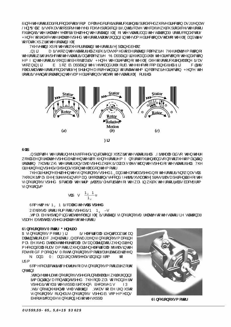
Mr. RAVIRAJ SRIKRISHNA AP/SOA 66
Since the rotor bars or conductors form a closed circuit, rotor current is produced whose direction, as given atLenz’s law, is such as to oppose the very cause producing it. In this case, the cause which produces the rotorcurrent is the relative velocity between the rotating flux of the stator and the stationary rotor conductors.Hence, to reduce the relative speed, the rotor starts running in the same direction as that of the flux and triesto catch up with the rotating flux.
The setting up of the torque for rotating the rotor is explained below:In Fig.3.16(a) is shown the stator field which is assumed to be rotating clockwise. The relative motion of
the rotor with respect to the stator is anticlockwise. By applying right-hand rule, the direction of the inductione.m.f. in the rotor is found to be outwards. Hence, the direction of the flux due to rotor current alone, is asshown in Fig.3.16(b). Now, by applying the Left-hand rule, or by the effect of combined field [Fig.3.16(c)] it isclear that the rotor conductors experience a force tending to rotate them in clockwise direction. Hence, therotor is set into rotation in the same direction as that of the stator flux (or field).
Fig. 3.16
SlipIn practice, the rotor never succeeds in ‘catching up’ with the stator field. If it really did so, then there
would be no relative speed between the two, hence rotor e.m.f., no roto current and so no torque to maintainrotation. That is why the rotor runs at a speed which is always less than the speed of the stator field. Thedifference in speeds depends upon the load on the motor.
The difference between the synchronous speed Ns and the actual speed n of the rotor is known as slip.Though it may be expressed in so many revolutions/second, yet it is usual to express it as a percentage of thesynchronous speed. Actually, the term ‘slip’ is descriptive of the way in which the rotor ‘slips back’ fromsynchronism.
% slip s = s
s
N N 100N
Sometimes, sN N is called the slip speed.Obviously, rotor (or motor) speed is N = NS (1–s)It may be kept in mind that revolving flux is rotating synchronously, relative to the stator (i.e. stationary
space) but at slip speed relative to the rotor.
Synchronous Motor - GeneralA synchronous motor (Fig.3.17) is electrically identical with analternator or a.c. generator. In fact, a given synchronous machinemay be used, at least theoretically, as an alternator, when drivenmechanically or as a motor, when driven electrically, just as in thecase of d.c. machines. Most synchronous motors are rated between150 kW and 15 MW and run at speeds ranging from 150 to 1800r.p.m.
Some characteristic features of a synchronous motor are worthnothing:1. It runs either at synchronous speed or not at all i.e. while running
it maintains a constant speed. The only way to change itsspeed is to vary the supply frequency (because Ns=120f/P).
2. It is not inherently self-starting. It has to be run uptosynchronous (or near synchronous) speed by some means,before it can be synchronized to the supply. Synchronous motor

Mr. RAVIRAJ SRIKRISHNA AP/SOA 67
3. It is capable of being operated under a wide range of power factors, both lagging and leading. Hence, itcan be used for power correction purposes, in addition to supplying torque to drive loads.
Principle of OperationAs shown, when a 3- winding is fed by a 3- supply, then a magnetic flux of constant magnitude but rotatingat synchronous speed, is produced. Consider a two-pole stator of Fig.3.18, in which are shown two statorpoles (marked Ns and Ss) rotating at synchronous speed, say, in clockwise direction. With the rotor positionas shown, suppose the stator poles are at that instant situated at points A and B. The two similar poles, N (ofrotor) and Ns (or stator) as well as S and Ss will repel each other, with the result that the rotor tends to rotate inthe anticlockwise direction.
Fig. 3.17
But half a period later, stator poles, having rotated around, interchange their positions i.e. Ns is at point Band Ss at point A. Under these conditions, Ns attracts S and Ss attracts N. Hence, rotor tends to rotateclockwise (which is just the reverse of the first direction). Hence, we find that due to continuous and rapidrotation of stator poles, the rotor is subjected to a torque which is rapidly reversing i.e., in quick succession,the rotor si subjected to torque which tends to move it first in one direction and then in the opposite direction.owing to its large inertia, the rotor cannot instantaneously respond to such quickly-reversing torque, with theresult that it remains stationary.
Fig. 3.19 Fig. 3.19 Fig. 3.19
Now, consider the condition shown in Fig.3.19(a). The stator and rotor poles are attracting each other.Suppose that the rotor is not stationary, but is rotating clockwise, with such a speed that it turns through onepole-pitch by the time the stator poles interchange their positions, as shown in Fig.3.19(b). Here , again thestator and rotor poles attract each other. It means that if the rotor poles also shift their positions along with thestator poles, then they will continuously experience a unidirectional torque i.e., clockwise torque, as shown inFig. 3.19.

Mr. RAVIRAJ SRIKRISHNA AP/SOA 68
Method of StartingThe rotor (which is as yet unexcited) is speeded up to synchronous/near synchronous speed by somearrangement and then excited by the d.c. source. The moment this (near) synchronously rotating rotor isexcited, it is magnetically locked into position with the stator i.e., the rotor poles are engaged with the statorpoles and both run synchronously in the same direction. It is because of this interlocking of stator and rotorpoles that the motor has either to run synchronously or not at all. The synchronous speed is given by theusual relation Ns = 120 f/p.
The rotor and the stator parts of motor
However, it is important to understand that the arrangement between the stator and rotor poles is not anabsolutely rigid one. As the load on the motor is increased, the rotor progressively tends to fall back in phase(but not in speed as in d.c. motors) by some angle (Fig. 3.20) but it still continues to run synchronously. Thevalue of this load angle or coupling angle (as it is called) depends on the amount of load to be met by the motor.In other words, the torque developed by the motor depends on this angle, say, .
Fig. 3.20 Fig. 3.21
The working of a synchronous motor is, in many ways, similar to the transmission of mechanical power bya shaft. In Fig. 3.21 are shown two pulleys P and Q transmitting power from the driver to the load. The twopulleys are assumed to be keyed together (just as stator and rotor poles are interlocked) hence they run atexactly the same (average) speed. When Q is loaded, it slightly falls behind owing to the twist in the shaft(twist angle corresponds to in motor), the angle of twist, in fact, being a measure of the torque transmitted.It is clear that unless Q is so heavily loaded as to break the coupling, both pulleys must run at exactly thesame (average) speed.

Mr. RAVIRAJ SRIKRISHNA AP/SOA 69

Mr. RAVIRAJ SRIKRISHNA AP/SOA 70
UNIT - 4

Mr. RAVIRAJ SRIKRISHNA AP/SOA 71
..
Mr. RAVIRAJ SRIKRISHNA AP/SOA 72
CHAPTER - 4CONDUCTION IN SEMINCONDUCTORS
DEFINITION OF SEMICONDUCTOR
Semiconductors6HPLFRQGXFWRUV��H�J��JHUPDQLXP��VLOLFRQ�HWF���DUH�WKRVH�VXEVWDQFHV�ZKRVH�HOHFWULFDO�FRQGXFWLYLW\�OLHV�LQ�EHWZHHQ�FRQGXFWRUV�DQG�LQVXODWRUV��,Q�WHUPV�RI�HQHUJ\�EDQG��WKH�YDOHQFH�EDQG�LV�DOPRVW�HPSW\��)XUWKHU��WKHHQHUJ\�JDS�EHWZHHQ�YDOHQFH�DQG�FRQGXFWLRQ�EDQGV�LV�YHU\�VPDOO�DV�VKRZV�LQ�)LJ�������7KHUHIRUH��FRPSDUDWLYHO\VPDOOHU�HOHFWULF�ILHOG��VPDOOHU�WKDQ�LQVXODWRUV�EXW�PXFK�JUHDWHU�WKDQ�FRQGXFWRUV��LV�UHTXLUHG�WR�SXVK�WKH�HOHFWURQVIURP�WKH�YDOHQFH�EDQG�WR�WKH�FRQGXFWLRQ�EDQG��,Q�VKRUW��D�VHPLFRQGXFWRU�KDV�
�D� DOPRVW�IXOO�YDOHQFH�EDQG�E� DOPRVW�HPSW\�FRQGXFWLRQ�EDQG�F� 6PDOO�HQHUJ\�JDS��a���H9��EHWZHHQ�YDOHQFH�EDQG�DQG�FRQGXFWLRQ�EDQGV�
Fig. 4.1
Energy Band Description of Semiconductors,W�KDV�DOUHDG\�EHHQ�GLVFXVVHG�WKDW�D�VHPLQFRQGXFWRU�LV�D�VXEVWDQFH�ZKRVH�UHVLVWLYLW\�OLHV�EHWZHHQ�FRQGXFWRUVDQG�LQVXOWRUV��7KH�UHVLVWLYLW\�LV�RI�WKH�RUGHU�RI���±���WR�����RKP�PHWUH��+RZHYHU��D�VHPLFRQGXFWRU�FDQ�EH�GHILQHGPXFK�PRUH�FRPSUHKHQVLYHO\�RQ�WKH�EDVLV�RI�HQHUJ\�EDQGV�DV�XQGHU�
Fig. 4.2 Fig. 4.3
$�VHPLFRQGXFWRU�LV�D�VXEVWDQFH�ZKLFK�KDV�DOPRVW�ILOOHG�YDOHQFH�EDQG�DQG�QHDUO\�HPSW\�FRQGXFWLRQ�EDQGZLWK�D�YHU\�VPDOO�HQHUJ\�JDS��a���H9��VHSDUDWLQJ�WKH�WZR�
)LJ������DQG�����VKRZV�WKH�HQHUJ\�EDQG�GLDJUDPV�RI�JHUPDQLXP�DQG�VLOLFRQ�UHVSHFWLYHO\��,W�PD\�EH�VHHQWKDW�IRUELGGHQ�HQHUJ\�JDS�LV�YHU\�VPDOO��EHLQJ�����H9�IRU�VLOLFRQ�DQG�����H9�IRU�JHUPDQLXP��7KHUHIRUH��UHODWLYHO\VPDOO�HQHUJ\� LV�QHHGHG�E\� WKULH�FDOZQFH�HOHFWURQV� WR� FURVV�RYHU� WR� WKH�FRQGXFWLRQ�EDQG��(YHQ�DW� URRPWHPSHUDWXUH��VRPH�RI�WKH�YDOHQFH�HOHFWURQV�PD\�DFTXLUH�VXIILFLHQW�HQHUJ\�WR�HQWHU�LQWR�WKH�FRQGXFWLRQ�EDQG

Mr. RAVIRAJ SRIKRISHNA AP/SOA 73
DQG�WKXV�EHFRPH�IUHH�HOHFWURQV��+RZHYHU��DW�WKLV�WHPSHUDWXUH��WKH�QXPEHU�RI�IUHH�HOHFWURQV�DYDLODEOH�LV�YHU\VPDOO��7KHUHIRUH��DW�URRP�WHPSHUDWXUH��D�SLHFH�RI�JHUPDQLXP�RU�VLOLFRQ�LQ�QHLWKHU�D�JRRG�FRQGXFWRU�QRU�DQLQVXODWRU��)RU�WKLV�UHDVRQ��VXFK�VXEVWDQFHV�DUH�FDOOHG�VHPLFRQGXFWRUV�
7KH�HQHUJ\�EDQG�GHVFULSWLRQ�LV�H[WUHPHO\�KHOSIXO�LQ�XQGUVWDQGLQJ�WKH�FXUUHQW�IORZ�WKURXJK�D�VHPLFRQGXFWRU�7KHUHIRUH��ZH�VKDOO�IUHTXHQWO\�XVH�WKLV�FRQFHSW�LQ�RXU�IXUWKHU�GLVFXVVLRQ�
Majority and Minority Carriers,W�KDV�DOUHDG\�EHHQ�GLVFXVVHG�WKDW�GXH�WR�WKH�HIIHFW�RI�LPSXULW\��Q�W\SH�PDWHULDO�KDV�D�ODUJH�QXPEHU�RI�IUHHHOHFWURQV�ZKHUHDV�S�W\SH�PDWHULDO�KDV�D�ODUJH�QXPEHU�RI�KROHV��+RZHYHU��LW�PD\�EH�UHFDOOHG�WKDW�HYHQ�DW�URRPWHPSHUDWXUH��VRPH�RI�WKH�FR�YDOHQW�ERQGV�EUHDN��WKXV�UHOHDVLQJ�DQ�HTXDO�QXPEHU�RI�IUHH�HOHFWURQV�DQG�KROHV�$Q�Q�W\SH�PDWHULDO�KDV�LWV�VKDUH�RI�HOHFWURQ�KROH�SDLUV��UHOHDVHG�GXH�WR�EUHDNLQJ�RI�ERQGV�DW�URRP�WHPSHUDWXUH�EXW�LQ�DGGLWLRQ�KDV�D�PXFK�ODUJHU�TXDQWLW\�RI�IUHH�HOHFWURQV�GXH�WR�WKH�HIIHFW�RI�LPSXULW\��7KHVH�LPSXULW\�FDXVHGIUHH�HOHFWURQV�DUH�QRW�DVVRFLDWHG�ZLWK�KROHV��&RQVHTXHQWO\��DQ�Q�W\SH�PDWHULDO�KDV�D�ODUJH�QXPEHU�RI�IUHHHOHFWURQV�DQG�D�VPDOO�QXPEHU�RI�KROHV�DV�VKRZQ�LQ�)LJ�������L���7KH�IUHH�HOHFWURQV�LQ�WKLV�FDVH�DUH�FRQVLGHUHGPDMRULW\�FDUULHUV�±�VLQFH�WKH�PDMRULW\�SRUWLRQ�RI�FXUUHQW�LQ�Q�W\SH�PDWHULDO�LV�E\�WKH�IORZ�RI�IUHH�HOHFWURQV�±�DQGWKH�KROHV�DUH�WKH�PLQRULW\�FDUULHUV�
6LPLODUO\��LQ�D�S�W\SH�PDWHULDO��KROHV�RXWQXPEHU�WKH�IUHH�HOHFWURQV�DV�VKRZQ�LQ�)LJ�������LL���7KHUHIRUH�KROHV�DUH�WKH�PDMRULW\�FDUULHUV�DQG�IUHH�HOHFWURQV�DUH�WKH�PLQRULW\�FDUULHUV�
Fig. 4.4
CONDUCTION PROPERTIES OF SEMICONDUCTORS
TYEPS OF SEMICONDUCTORS
Instrinc Semiconductor$�VHPLFRQGXFWRU�LQ�DQ�H[WUHPHO\�SXUH�IRUP�LV�NQRZQ�DV�DQ�LQVWULFW�VHPLFRQGXFWRU�,Q�DQ�LQWULQVLF��VHPLFRQGXFWRU��HYHQ�DW�URRP�WHPSHUDWXUH��KROH�HOHFWURQ�SDLUV�DUH�FUHDWHG��:KHQ�HOHFWULF�ILHOG�LVDSSOLHG�DFURVV�DQ�LQWULQVLF�VHPLFRQGXFWRU��WKH�FXUUHQW�FRQGXFWLRQ�WDNHV�SODFH�E\�WZR�SURFHVV��QDPHO\��E\�IUHHHOHFWURQV�DQG�KROHV�DV�VKRZQ�LQ�)LJ�������7KH�IUHH�HOHFWURQV�DUH�SURGXFHG�GXH�WR�WKH�EUHDNLQJ�XS�RI�VRPHFRYDOHQW�ERQGV�E\�WKHUPDO�HQHUJ\��$W�WKH�VDPH�WLPH��KROHV�DUH�FUHDWHG�LQ�WKH�FRYDOHQW�ERQGV��8QGHU�WKHLQIOXHFQFH�RI�HOHFWULF�ILHOG��FRQGXFWLRQ�WKURXJK�WKH�VHPLFRQGXFWRU�LV�E\�ERWK�IUHH�HOHFWURQV�DQG�KROHV��7KHUHIRUH�WKH�WRWDO�FXUUHQW�LQVLGH�WKH�VHPLFRQGXFWRU�LV�WKH�VXP�RI�FXUUHQWV�GXH�WR�IUHH�HOHFWURQV�DQG�KROHV�
,W�PD\�EH�QRWHG�WKDW�FXUUHQW�LQ�WKH�H[WHUQDO�ZLUHV�LV�IXOO\�HOHFWURQLF�L�H��E\�HOHFWURQV��:KDW�DERXW�WKHKROHV"�5HIHUULQJ�WR�)LJ�������KROHV�EHLQJ�SRVLWLYHO\�FKDUJHG�PRYH�WRZDUGV�WKH�QHJDWLYH�WHUPLQDO�RI�VXSSO\��$VWKH�KROHV�UHDFK�WKH�QHJDWLYH�WHUPLQDO�%��HOHFWURQV�HQWHU�WKH�VHPLFRQGXFWRU�FU\VWDO�QHDU��WKH�WHUPLQDO�DQGFRPELQH�ZLWK�KROHV�� WKXV�FDQFHOOLQJ�WKHP��$W�WKH�VDPH�WLPH��WKH� ORRVHO\�KHOG�HOHFWURQV�QHDU�WKH�SRVLWLYHWHUPLQDO�$�DUH�DWWUDFWHG�DZD\�IURP�WKHLU�DWRPV�LQWR�WKH�SRVLWLYH�WHUPLQDO��7KLV�FUHDWHV�QHZ�KROHV�QHDU�WKHSRVLWLYH�WHUPLQDO�ZKLFK�DJDLQ�GULIW�WRZDUGV�WKH�QHJDWLYH�WHUPLQDO�
Fig. 4.5

Mr. RAVIRAJ SRIKRISHNA AP/SOA 74
Extrinsic Semiconductor7KH�LQWULQVLF�VHPLFRQGXFWRU�KDV�OLWWOH�FXUUHQW�FRQGXFWLRQ�FDSDELOLW\�DW�URRP�WHPSHUDWXUH��7R�EH�XVHIXO�LQ�HOHFWURQLFGHYLFHV��WKH�SXUH�VHPLFRQGXFWRU�PXVW�EH�DOWHUHG�VR�DV�WR�VLJQLILFDQWO\�LQFUHDVH�LWV�FRQGXFWLQJ�SURSHUWLHV��7KLVLV�DFKLHYHG�E\�DGGLQJ�D�VPDOO�DPRXQW�RI�VXLWDEOH�LPSXULW\�WR�D�VHPLFRQGXFWRU��,W�LV�WKHQ�FDOOHG�LPSXULW\�RUH[WULQVLF�VHPLFRQGXFWRU��7KH�SURFHVV�RI�DGGLQJ�LPSXULWLHV�WR�D�VHPLFRQGXFWRU�LV�NQRZQ�DV�GRSLQJ��7KH�DPRXQWDQG�W\SH�RI�VXFK�LPSXULWLHV�KDYH�WR�EH�FORVHO\�FRQWUROOHG�GXULQJ�WKH�SUHSDUDWLRQ�RI�H[WULQVLF�VHPLFRQGXFWRU�*HQHUDOO\��IRU�����DWRPV�RI�VHPLFRQGXFWRU��RQH�LPSXULW\�DWRP�LV�DGGHG�
7KH�SXUSRVH�RI�DGGLQJ�LPSXULW\�LV�WR�LQFUHDVH�HLWKHU�WKH�QXPEHU�RI�IUHH�HOHFWURQV�RU�KROHV�LQ�WKH�VHPLFRQGXFWRUFU\VWDO��$V�ZH�VKDOO�VHH��LI�D�SHQWDYDOHQW�LPSXULW\��KDYLQJ���YDOHQFH�HOHFWURQV��LV�DGGHG�WR�WKH�VHPLFRQGXFWRU�D�ODUJH�QXPEHU�RI�IUHH�HOHFWURQV�DUH�SURGXFHG�LQ�WKH�VHPLFRQGXFWRU��2Q�WKH�RWKHU�KDQG��DGGLWLRQ�RI�WULYDOHQWLPSXULW\��KDYLQJ���YDOHQFH�HOHFWURQV��FUHDWHV�D�ODUJH�QXPEHU�RI�KROHV�LQ�WKH�VHPLFRQGXFWRU�FU\VWDO��'HSHQGLQJXSRQ�WKH�W\SH�RI�LPSXULW\�DGGHG��H[WULQVLF�VHPLFRQGXFWRUV�DUH�FODVVLILHG�LQWR�
L��Q�W\SH�VHPLFRQGXFWRU�����������������LL��S�W\SH�VHPLFRQGXFWRU
n-type Semiconductor:KHQ�D�VPDOO�DPRXQW�RI�SHQWDYDOHQW� LPSXULW\�LV�DGGHG�WR�D�SXUH�VHPLQFRQGXFWRU�� LW� LV�NQRZQ�DV� n-typesemiconductor.
7KH�DGGLWLRQ�RI�SHQWDYDOHQW�LPSXULW\�SURYLGHV�D�ODUJH�QXPEHU�RI�IUHH�HOHFWURQV�LQ�WKH�VHPLFRQGXFWRU�FU\VWDO�7\SLFDO�H[DPSOHV�RI�SHWDYDOHQW�LPSXULWLHV�DUH�DUVHQLF��$W��1R������DQG�DQWLPRQ\��$W��1R�������6XFK�LPSXULWLHVZKLFK�SURGXFH�Q�W\SH�VHPLFRQGXFWRU�DUH�NQRZQ�DV�GRQRU�LPSXULWLHV�EHFDXVH�WKH\�GRQDWH�RU�SURYLGH�IUHHHOHFWURQV�WR�WKH�VHPLFRQGXFWRU�FU\VWDO�
Fig. 4.6
7R�H[SODLQ�WKH�IRUPDWLRQ�RI�Q�W\SH�VHPLFRQGXFWRU��FRQVLGHU�D�SXUH�JHUPDQLXP�FU\VWDO��:H�NQRZ�WKDWJHUPDQLXP�DWRP�KDV�IRXU�YDOHQFH�HOHFWURQV��:KHQ�D�VPDOO�DPRXQW�RI�SHQWDYDOHQW�LPSXULW\�OLNH�DUVHQLF�LVDGGHG�WR�JHUPDQLXP�FU\VWDO��D�ODUJH�QXPEHU�RI�IUHH�HOHFWURQV�EHFRPH�DYDLODEOH�LQ�WKH�FU\VWDO��7KH�UHDVRQ�LVVLPSOH��$UVHQLF�LV�SHQWDYDOHQW�L�H��LWV�DWRP�KDV�ILYH�YDOHQFH�HOHFWURQV��DQ�DUVHQLF�DWRP�ILWV�LQ�WKH�JHUPDQLXPFU\VWDO�LQ�VXFK�D�ZD\�WKDW�LWV�IRXU�YDOHQFH�HOHFWURQV�IRUP�FRYDOHQW�ERQGV�ZLWK�IRXU�JHUPDQLXP�DWRPV��7KH�ILIWKYDOHQFH�HOHFWURQ�RI�DUVHQLF�DWRP�ILQGV�QR�SODFH�LQ�FR�YDOHQW�ERQGV�DQG�LV�WKXV�IUHH�DV�VKRZQ�LQ�)LJ������7KHUHIRUH��IRU�HDFK�DUVHQLF�DWRP�DGGHG��RQH�IUHH�HOHFWURQ�ZLOO�EH�DYDLODEOH�LQ�WKH�JHUPDQLXP�FU\VWDO��7KRXJKHDFK�DUVHQLF�DWRP�SURYLGHV�RQH�IUHH�HOHFWURQ��\HW�DQ�H[WUHPHO\�VPDOO�DPRXQW�RI�DUVHQLF�LPSXULW\�SURYLGHVHQRXJK�DWRPV�WR�VXSSO\�PLOOLRQV�RI�IUHH�HOHFWURQV�
)LJ������VKRZV�WKH�HQHUJ\�EDQG�GHVFULSWLRQ�RI�Q�W\SH�VHPLFRQGXFWRU��7KH�DGGLWLRQ�RI�SHQWDYDOHQW�LPSXULW\KDV�SURGXFHG�D�QXPEHU�RI�FRQGXFWLRQ�EDQG�HOHFWURQV�L�H���IUHH�HOHFWURQV��7KH�IRXU�YDOHQFH�HOHFWURQV�RI�SHQWDYDOHQWDWRP�IRUP�FRYDOHQW�ERQGV�ZLWK�IRXU�QHLJKERXULQJ�JHUPDQLXP�DWRPV��7KH�ILIWK�OHIW�RYHU�YDOHQFH�HOHFWURQ�RI�WKHSHQWDYDOHQW�DWRP�FDQQRW�EH�DFFRPPRGDWHG�LQ�WKH�YDOHQFH�EDQG�WUDYHOV�WR�WKH�FRQGXFWLRQ�EDQG��7KH�IROORZLQJSRLQWV�PD\�EH�QRWHG�FDUHIXOO\�
Fig. 4.7

Mr. RAVIRAJ SRIKRISHNA AP/SOA 75
L� 0DQ\�QHZ�IUHH�HOHFWURQV�DUH�SURGXFHG�E\�WKH�DGGLWLRQ�RI�SHQWDYDOHQW�LPSXULW\�LL� 7KHUPDO�HQHUJ\�RI�URRP�WHPSHUDWXUH�VWLOO�JHQHUDWHV�D�IHZ�KROH�HOHFWURQ�SDLUV��+RZHYHU��WKH�QXPEHU�RI
IUHH�HOHFWURQV�SURYLGHG�E\�WKH�SHQWDYDOHQW�LPSXULW\�IDU�H[FHHGV�WKH�QXPEHU�RI�KROHV��,W�LV�GXH�WR�WKLV�SUHGRPLQDQFHRI�HOHFWURQV�RYHU�KROHV�WKDW�LW�LV�FDOOHG�Q�W\SH�VHPLFRQGXFWRU��Q�VWDQGV�IRU�QHJDWLYH��
n-type conductivity. �7KH�FXUUHQW�FRQGXFWLRQ�LQ�DQ�Q�W\SH�VHPLFRQGXFWRU�LV�SUHGRPLQDWO\�E\�IUHH�HOHFWURQV�L�H�QHJDWLYH�FKDUJHV�DQG�LV�FDOOHG�Q�W\SH�RU�HOHFWURQ�W\SH�FRQGXFWLYLW\��7R�XQGHUVWDQG�Q�W\SH�FRQGXFWLYLW\��UHIHU�WR)LJ�������:KHQ�S�G��LV�DSSOLHG�DFURVV�WKH�Q�W\SH�VHPLFRQGXFWRU��WKH�IUHH�HOHFWURQV��GRQDWHG�E\�LPSXULW\��LQ�WKHFU\VWDO�ZLOO�EH�GLUHFWHG�WRZDUGV�WKH�SRVLWLYH�WHUPLQDO��FRQVWLWXWLQJ�HOHFWULF�FXUUHQW��$V�WKH�FXUUHQW�IORZ�WKURXJKWKH�FU\VWDO�LV�E\�IUHH�HOHFWURQV�ZKLFK�DUH�FDUULHUV�RI�QHJDWLYH�FKDUJH��WKHUHIRUH��WKLV�W\SH�RI�FRQGXFWLYLW\�LVFDOOHG�QHJDWLYH�RU�Q�W\SH�FRQGXFWLYLW\��,W�PD\�EH�QRWHG�WKDW�FRQGXFWLRQ�LV�MXVW�DV�LQ�RUGLQDU\�PHWDOV�OLNH�FRSSHU�
Fig. 4.8
p-type Semiconductor:KHQ�D�VPDOO�DPRXQW�RI�WULYDOHQW�LPSXULW\�LV�DGGHG�WR�D�SXUH�VHPLFRQGXFWRU��LW�LV�FDOOHG�S�W\SH�VHPLFRQGXFWRU�
7KH�DGGLWLRQ�RI�WULYDOHQW�LPSXULW\�SURYLGHV�D�ODUJH�QXPEHU�RI�KROHV�LQ�WKH�VHPLFRQGXFWRU��7\SLFDO�H[DPSOHVRU�WULYDOHQW�LPSXULWLHV�DUH�JDOOLXP��$W��1R������DQG�LQGLXP��$W��1R�������6XFK�LPSXULWLHV�ZKLFK�SURGXFH�S�W\SHVHPLFRQGXFWRU�DUH�NQRZQ�DV�DFFHSWRU�LPSXULWLHV�EHFDXVH�WKH�KROHV�FUHDWHG�FDQ�DFFHSW�WKH�HOHFWURQV�
Fig. 4.9
7R�H[SODLQ�WKH�IRUPDWLRQ�RI�S�W\SH�VHPLFRQGXFWRU��FRQVLGHU�D�SXUH�JHUPDQLXP�FU\VWDO��:KHQ�D�VPDOODPRXQW�RI�WULYDOHQW�LPSXULW\�OLNH�JDOOLXP�LV�DGGHG�WR�JHUPDQLXP�FU\VWDO��WKHUH�H[LVWV�D�ODUJH�QXPEHU�RI�KROHV�LQWKH�FU\VWDO��7KH�UHDVRQ�LV�VLPSOH��*DOOLXP�LV�WULYDOHQW�L�H��LWV�DWRP�KDV�KUHH�YDOHQFH�HOHFWURQV��(DFK�DWRP�RIJDOOLXP�ILWV�LQWR�WKH�JHUPDQLXP�FU\VWDO�EXW�QRZ�RQO\�WKUHH�FR�YDOHQW�ERQGV�FDQ�EH�IRUPHG��,W�LV�EHFDXVH�WKUHHYDOHQFH�HOHFWURQV�RI�JDOOLXP�DWRP�FDQ�IRUP�RQO\�WKUHH�VLQJOH�FR�YDOHQW�ERQGV�ZLWK�WKUHH�JHUPDQLXP�DWRPV�DVVKRZQ�LQ�)LJ�������,Q�WKH�IRXUWK�FR�YDOHQW�ERQG��RQO\�JHUPDQLXP�DWRP�JDOOLXP�KDV�QR�YDOHQFH�HOHWURQ�WR�FRQWULEXWH

Mr. RAVIRAJ SRIKRISHNA AP/SOA 76
DV�DOO�LWV�WKUHH�YDOHQFH�HOHFWURQV�DUH�DOUHDG\�HQJDJHG�LQ�WKH�FR�YDOHQW�ERQGV�ZLWK�QHLJKERXULQJ�JHUPDQLXPDWRPV��,Q�RWKHU�ZRUGV��IRXUWK�ERQG�LV�LQFRPSOHWH��EHLQJ�VKRUW�RI�RQH�HOHFWURQ��7KLV�PLVVLQJ�HOHFWURQ�LV�FDOOHG�DKROH��7KHUHIRUH��IRU�HDFK�JDOOLXP�DWRP�DGGHG��RQH�KROH�LV�FUHDWHG��$�VPDOO�DPRXQW�RI�JDOOLXP�SURYLGHV�PLOOLRQVRI�KROHV�
)LJ�������VKRZV�WKH�HQHUJ\�EDQG�GHVFULSWLRQ�RI�WKH�S�W\SH�VHPLFRQGXFWRU��7KH�DGGLWLRQ�RI�WULYDOHQW�LPSXULW\KDV�SURGXFHG�D�ODUJH�QXPEHU�RI�KROHV��+RZHYHU��WKHUH�DUH�D�IHZ�FRQGXFWLRQ�EDQG�HOHFWURQV�GXH�WR�WKHUPDOHQHUJ\�DVVRFLDWHG�ZLWK�URRP�WHPSHUDWXUH��%XW�WKH�KROHV�IDU�RXWQXPEHU�WKH�FRQGXFWLRQ�EDQG�HOHFWURQV��,W�LV�GXHWR�WKH�SUHGRPLQDQFH�RI�KROHV�RYHU�IUHH�HOHFWURQV�WKDW�LW�LV�FDOOHG�S�W\SH�VHPLFRQGXFWRU��S�VWDQGV�IRU�SURVLWLYH��
Fig. 4.10 Fig. 4.11
S�W\SH�FRQGXFWLYLW\���7KH�FXUUHQW�FRQGXFWLRQ�LQ�S�W\SH�VHPLFRQGXFWRU�LV�SUHGRPLQDQWO\�E\�KROHV�L�H��SRVLWLYHFKDUJHV�DQG�LV�FDOOHG�S�W\SH�RU�KROH�W\SH�FRQGXFWLYLW\��7R�XQGHUVWDQG�S�W\SH�FRQGXFWLYLW\��UHIHU�WR�)LJ�������:KHQ�S�G��LV�DSSOLHG�WR�WKH�S�W\SH�VHPLFRQGXFWRU��WKH�KROHV��GRQDWHG�E\�WKH�LPSXULW\��DUH�VKLIWHG�IURP�RQH�FR�YDOHQW�ERQG�WR�DQRWKHU��FRQVWLWXWLQJ�ZKDW�LV�NQRZQ�DV�KROH�FXUUHQW��,W�PD\�EH�QRWHG�WKDW�LQ�S�W\SH�FRQGXFWLYLW\�WKH�YDOHQFH�HOHFWURQV�PRYH�IURP�RQH�FR�YDOHQW�ERQG�WR�DQRWKHU�XQOLNH�WKH�Q�W\SH�ZKHUH�FXUUHQW�FRQGXFWLRQ�LV�E\IUHH�HOHFWURQV�
Properties of SemiconductorsL� 7KH�UHVLVWLYLW\�RI�D�VHPLFRQGXFWRU�LV�OHVV�WKDQ�DQ�LQGXODWRU�EXW�PRUH�WKDQ�D�FRQGXFWRU�LL� 6HPLFRQGXFWRUV�KDYH�QHJDWLYH�WHPSHUDWXUH�FR�HIILFLHQW�RI�UHVLVWDQFH�L�H��WKH�UHVLVWDQFH�RI�D�VHPLFRQGXFWRU
GHFUHDVHV�ZLWK�WKH�LQFUHDVH�LQ�WHPSHUDWXUH�DQG�YLFH�YHUVD��)RU�H[DPSOH��JHUPDQLXP�LV�DFWXDOO\�DQ�LQVXODWRUDW�ORZ�WHPSHUDWXUHV�EXW�LW�EHFRPHV�D�JRRG�FRQGXFWRU�DW�KLJK�WHPSHUDWXUHV�
LLL� :KHQ�VXLWDEOH�PHWDOOLF� LPSXULW\� �H�J�� DUVHQLF��JDOOLXP�HWF��� LV�DGGHG� WR�D� VHPLFRQGXFWRU�� LWV� FXUUHQWFRQGXFWLQJ�SURSHUWLHV�FKDQJH�DSSUHFLDEO\��7KLV�SURSHUW\�LV�PRVW�LPSRUWDQW�DQG�LV�GLVFXVVHG�ODWHU�GHWDLO�
Effect of Temperature on Semiconductors7KH�HOHFWULFDO�FRQGXFWLYLW\�RI�D�VHPLFRQGXFWRU�FKDQJHV�DSSUHFLDEO\�ZLWK�WHPSHUDWXUH�YDULDWLRQV��7KLV�LV�D�YHU\LPSRUWDQW�SRLQW�WR�NHHS�LQ�PLQG�L� $W�DEVROXWH�]HUR���$W�DEVROXWH�]HUR�WHPSHUDWXUH��DOO�WKH�HOHFWURQV�DUH�WLJKWO\�KHOG�E\�WKH�VHPLFRQGXFWRU
DWRPV��7KH�LQQHU�RUELW�HOHFWRUQV�DUH�ERXQG�ZKHUHDV�WKH�YDOHQFH�HOHFWURQV�DUH�HQJDJHG�LQ�FR�YDOHQW�ERQGLQJ�$W�WKLV�WHPSHUDWXUH��WKH�FR�YDOHQW�ERQGV�DUH�YHU\�VWURQJ�DQG�WKHUH�DUH�QR�IUHH�HOHFWURQV��7KHUHIRUH��WKHVHPLFRQGXFWRU�FU\VWDO�EHKDYHV�DV�D�SHUIHFW�LQVXODWRU�>6HH�)LJ��������L�@�,Q�WHUPV�RI�HQHUJ\�EDQG�GHVFULSWLRQ��WKH�YDOHQFH�EDQG�LV�ILOOHG�DQG�WKHUH�LV�D�ODUJH�HQHUJ\�JDS�EHWZHHQYDOHQFH�EDQG�DQG�FRQGXFWLRQ�EDQG��7KHUHIRUH��QR�YDOHQFH�HOHFWURQ�FDQ�UHDFK�WKH�FRQGXFWLRQ�EDQG�WREHFRPH�IUHH�HOHFWURQ��,W�LV�GXH�WR�WKH�QRQ�DYDLODELOLW\�RI�IUHH�HOHFWURQV�WKDW�D�VHPLFRQGXFWRU�EHKDYHV�DV�DQLQVXODWRU�
LL� $ERYH�DEVROXWH�]HUR���:KHQ�WKH�WHPSHUDWXUH�LV�UDLVHG��VRPH�RI�WKH�FRYDOHQW�ERQGV�LQ�WKH�VHPLFRQGXFWRUEUHDN�GXH�WR�WKH�WKHUPDO�HQHUJ\�VXSSOLHG��7KH�EUHDNLQJ�RI�ERQGV�VHWV�WKRVH�HOHFWURQV�IUHH�ZKLFK�DUHHQJDJHG�LQ�WKH�IRUPDWLRQ�RI�WKHVH�ERQGV��7KH�UHVXOW�LV�WKDW�D�IHZ�IUHH�HOHFWURQV�H[LVW�LQ�WKH�VHPLFRQGXFWRU�7KHVH�IUHH�HOHFWURQV�FDQ�FRQVWLWXWH�D�WLQ\�HOHFWULF�FXUUHQW�LI�SRWHQWLDO�GLIIHUHQFH�LV�DSSOLHG�DFURVV�WKHVHPLFRQGXFWRU�FU\VWDO�>6HH�)LJ��������L�@��7KLV�VKRZV�WKDW�WKH�UHVLVWDQFH�RI�D�VHPLFRQGXFWRU�GHFUHDVHVZLWK�WKH�ULVH�LQ�WHPSHUDWXUH�L�H��LW�KDV�QHJDWLYH�WHPSHUDWXUH�FRHIILFLHQW�RI�UHVLVWDQFH��,W�PD\�EH�DGGHG�WKDWDW�URRP�WHPSHUDWXUH��FXUUHQW�WKURXJK�D�VHPLFRQGXFWRU�LV�WRR�VPDOO�WR�EH�RI�DQ\�SUDFWLFDO�YDOXH�

Mr. RAVIRAJ SRIKRISHNA AP/SOA 77
Fig. 4.12
Fig. 4.13
)LJ��������LL��VKRZV�WKH�HQHUJ\�EDQG�GLDJUDP��$V�WKH�WHPSHUDWXUH�LV�UDLVHG��VRPH�RI�WKH�YDOHQFH�HOHFWURQVDFTXLUH�VXIILFLHQW�HQHUJ\�WR�HQWHU�LQWR�WKH�FRQGXFWLRQ�EDQG�DQG�WKXV�EHFRPH�IUHH�HOHFWURQV��8QGHU�WKH�LQIOXHQFHRI�HOHFWULF�ILHOG��WKHVH�IUHH�HOHFWURQV�ZLOO�FRQVWLWXWH�HOHFWULF�FXUUHQW��,W�PD\�EH�QRWHG�WKDW�HDFK�WLPH�D�YDOHQFHHOHFWURQ�HQWHUV�LQWR�WKH�FRQGXFWLRQ�EDQG��D�KROH�LV�FUHDWHG�LQWKH�YDOHQFH�EDQG��$V�ZH�VKDOO�VHH�LQ�WKH�QH[WDUWLFOH��KROHV�DOVR�FRQWULEXWH�WR�FXUUHQW��,Q�IDFW��KROH�FXUUHQW�LVWKH�PRVW�VLJQLILFDQW�FRQFHSW�LQ�VHPLFRQGXFWRUV�
PN JUNCTION DIODE
Definition:KHQ�D�S�W\SH�VHPLFRQGXFWRU�LV�VXLWDEO\�MRLQHG�WR�Q�W\SH�VHPLFRQGXFWRU��WKH�FRQWDFW�VXUIDFH�LV�FDOOHG�SQMXQFWLRQ�
0RVW�VHPLFRQGXFWRU�GHYLFHV�FRQWDLQ�RQH�RU�PRUH�SQ�MXQFWLRQV��7KH�SQ�MXQFWLRQ�LV�RI�JUHDW�LPSRUWDQFHEHFDXVH�LW�LV�LQ�HIIHFW��WKH�FRQWURO�HOHPHQW�IRU�VHPLFRQGXFWRU�GHYLFHV��$�WKRURXJK�NQRZOHGJH�RI�WKH�IRUPDWLRQDQG�SURSHUWLHV�RI�SQ�MXQFWLRQ�FDQ�HQDEOH�WKH�UHDGHU�WR�XQGHUVWDQG�WKH�VHPLFRQGXFWRU�GHYLFHV�
Formation of pn junction,Q�DFWXDO�SUDFWLFH��WKH�FKDUDFWHULVWLF�SURSHUWLHV�RI�SQ�MXQFWLRQ�ZLOO�QRW�EH�DSSDUHQW�LI�D�S�W\SH�EORFN�LV�MXVWEURXJKW�LQ�FRQWDFW�ZLWK�Q�W\SH�EORFN��,Q�IDFW��SQ�MXQFWLRQ�LV�IDEULFDWHG�E\�VSHFLDO�WHFKQLTXHV��2QH�FRPPRQPHWKRG�RI�PDNLQJ�SQ�MXQFWLRQ�LV�FDOOHG�DOOR\LQJ��,Q�WKLV�PHWKRG��D�VPDOO�EORFN�RI�LQGLXP��WULYDOHQW�LPSXULW\��LVSODFHG�RQ�DQ�Q�W\SH�JHUPDQLXP�VODE�DV�VKRZQ�LQ�)LJ�������L� 7KH�V\VWHP�LV�WKHQ�KHDWHG�WR�D�WHPSHUDWXUH�RI�DERXW����&��7KH�LQGLXP�DQG�VRPH�RI�WKH�JHUPDQLXP�PHOW
WR�IURP�D�VPDOO�SXGGOH�RI�PROWHQ�JHUPDQLXP�LQGLXP�PL[WXUH�DV�VKRZQ�LQ�)LJ�������LL� 7KH�WHPSHUDWXUH�LV�WKDQ�ORZHUHG�DQG�SXGGOH�EHJLQV�WR�VROLGLI\��8QGHU�SURSHU�FRQGLWLRQV��WKH�DWRPV�RI
LQGLXP�LPSXULW\�ZLOO�EH�VXLWDEO\�DGMXVWHG�LQ�WKH�JHUPDQLXP�VODE�WR�IRUP�D�VLQJOH�FU\VWDO��7KH�DGGLWLRQ�RI

Mr. RAVIRAJ SRIKRISHNA AP/SOA 78
LQGLXP�RYHUFRPHV�WKH�H[FHVV�RI�HOHFWURQV�LQ�WKH�Q�W\SH�JHUPDQLXP�WR�VXFKDQ�H[WHQW�WKDW�LW�FUHDWHV�D�S�W\SH�UHJLRQ�$V�WKH�SURFHV�JRHV�RQ��WKH�UHPDLQLQJ�PROWHQ�PL[WXUH�EHFRPV�LQFUHDVLQJO\ULFK�LQ�LQGLXP��:KHQ�DOO�JHUPDQLXP�KDV�EHHQ�UHGHSRVLWHG��WKH�UHPDLQLQJPDWHULDO�DSSHDUV�DV�LQGLXP�EXWWRQ�ZKLFK�LV�IUR]HQ�RQ�WKH�RXWHU�VXUIDFH�RI�WKHFU\VWDOLVHG�SRUWLRQ�DV�VKRZQ�LQ�)LJ�������LLL�����7KLV�EXWWRQ�VHUYHV�DV�D�VXLWDEOH�EDVH�IRU�VROGHULQJ�RQ�OHDGV�
Fig. 4.14
Properties of pn Junction$W�WKH�LQVWDQW�RI�SQ�MXQFWLRQ�IRUPDWLRQ��WKH�IUHH�HOHFWURQV�QHDU�WKH�MXQFWLRQ�LQ�WKH�Q�UHJLRQ���EHJLQ�WR�GLIIXVH
DFURVV�WKH�MXQFWLRQ�LQWR�WKH�S�UHJLRQ�ZKHUH�WKH\�FRPELQH�ZLWK�KROHV�QHDU�WKH�MXQFWLRQ��7KH�UHVXOW�LV�WKDW�QUHJLRQ�ORVHV�IUHH�HOHFWURQV�DV�WKH\�GLIIXVH�LQWR�WKH�MXQFWLRQ��7KLV�FUHDWHV�D�OD\HU�RI�SRVLWLYH�FKDUJHV��SHQWDYDOHQWLRQV��QHDU�WKH�MXQFWLRQ��$V�WKH�HOHFWURQV�PRYH�DFURVV�WKH�MXQFWLRQ��WKH�S�UHJLRQ�ORVHV�KROHV�DV�WKH�HOHFWURQVDQG�KROHV�FRPELQH��7KH�UHVXOW�LV�WKDW�WKHUH�LV�D�OD\HU�RI�QHJDWLYH�FKDUJHV��WULYDOHQW�LRQV��QHDU�WKH�MXQFWLRQ�7KHVH�WZR�OD\HUV�RI�SRVLWLYH�DQG�QHJDWLYH�FKDUJHV�IURP�WKH�GHSOHWLRQ�UHJLRQ��RU�GHSOHWLRQ�OD\HU���7KH�WHUPGHSOHWLRQ�LV�GXH�WR�WKH�IDFW�WKDW�QHDU�WKH�MXQFWLRQ��WKH�UHJLRQ�LV�GHSOHWHG��L�H��HPSWLHG��RI�FKDUJH�FDUULHV��IUHHHOHFWURQV�DQG�KROHV��GXH�WR�GLIIXVLRQ�DFURVV�WKH�MXQFWLRQ��,W�PD\�EH�QRWHG�WKDW�GHSOHWLRQ�OD\HU�LV�IRUPHG�YHU\TXLFNO\�DQG�LV�YHU\�WKLQ�FRPSDUHG�WR�WKH�Q�UHJLRQ�DQG�WKH�S�UHJLRQ�DQG�WKH�S�UHJLRQ��)RU�FODULW\��WKH�ZLGWK�RI�WKHGHSOHWLRQ�OD\HU�LV�VKRZQ�H[DJJHUDWHG�
Fig. 4.15 Fig. 4.16
Mr. RAVIRAJ SRIKRISHNA AP/SOA 79
2QFH�SQ�MXQFWLRQ�LV�IRUPHG�DQG�GHSOHWLRQ�OD\HU�FUHDWHG��WKH�GLIIXVLRQ�RI�IUHH�HOHFWURQV�VWRSV��,Q�RWKHUZRUGV��WKH�GHSOHWLRQ�UHJLRQ�DFWV�DV�D�EDUULHU�WR�WKH�IXUWKHU�PRYHPHQW�RI�IUHH�HOHFWURQV�DFURVV�WKH�MXQFWLRQ��7KHSRVLWLYH�DQG�QHJDWLYH�FKDUJHV�VHW�XS�DQ�HOHFWULF�ILHOG��7KLV�LV�VKRZQ�E\�D�EODFN�DUURZ�LQ�)LJ��������L���7KHHOHFWULF�ILHOG�LV�D�EDUULHU�WR�WKH�IUHH�HOHFWURQV�LQ�WKH�Q�UHJLRQ��7KHUH�H[LVWV�D�SRWHQWLDO�GLIIHUHQFH�DFURVV�WKHGHSOHWLRQ�OD\HU�DQG�LV�FDOOHG�EDUULHU�SRWHQWLDO��9����7KH�EDUULHU�SRWHQWLDO�RI�D�SQ�MXQFWLRQ�GHSHQGV�XSRQ�VHYHUDOIDFWRUV�LQFOXGLQJ�WKH�W\SH�RI�VHPLFRQGXFWRU�PDWHULDO��WKH�DPRXQW�RI�GRSLQJ�DQG�WHPSHUDWXUH��7KH�W\SLFDO�EDUULHUSRWHQWLDO�LV�DSSUR[LPDWHO\�
)RU�VLOLFRQ��9�� �����9��)RU�JHUPDQLXP��9�� �����9)LJ�������VKRZV�WKH�SRWHQWLDO��9���GLVWULEXWLRQ�FXUYH�
BEHAVIOUR OF PN JUNCTIONApplying D.C.Voltage Across pn Junction or Biasing a pn Junction,Q�HOHFWURQLFV��WKH�WHUP�ELDV�UHIHUV�WR�WKH�XVH�RI�G�F��YROWDJH�WR�HVWDEOLVK�FHUWDLQ�RSHUDWLQJ�FRQGLWLRQV�IRU�DQHOHFWURQLF�GHYLFH��,Q�UHODWLRQ�WR�D�SQ�MXQFWLRQ��WKHUH�DUH�IROORZLQJ�WZR�ELDV�FRQGLWLRQV
1. Forward biasing 2. Reverse biasing
Forward biasing:KHQ�H[WHUQDO�G�F��YROWDJH�DSSOLHG�WR�WKH�MXQFWLRQ�LV�LQ�VXFK�D�GLUHFWLRQ�WKDW�LW�FDQFHOV�WKH�SRWHQWLDO�EDUULHU��WKXVSHUPLWWLQJ�FXUUHQW�IORZ��LW�LV�FDOOHG�IRUZDUG�ELDVLQJ�
7R�DSSO\�IRUZDUG�ELDV��FRQQHFW�SRVLWLYH�WHUPLQDO�RI�WKH�EDWWHU\�WR�WKH�EDWWHU\�WR�S�W\SH�DQG�QHJDWLYH�WHUPLQDOWR�Q�W\SH�DV�VKRZQ�LQ�)LJ��������7KH�DSSOLHG�IRUZDUG�SRWHQWLDO�HVWDEOLVKHV�DQ�HOHFWULF�ILHOG�ZKLFK�DFWV�DJDLQVWWKH�ILHOG�GXH�WR�SRWHQWLDO�EDUULHU��7KHUHIRUH��WKH�UHVXOWDQW�ILHOG�LV�ZHDNHQHG�DQG�WKH�EDUULHU�KHLJKW�LV�UHGXFHG�DWWKH�MXQFWLRQ�DV�VKRZQ�LQ�)LJ��������$V�SRWHQWLDO�EDUULHU�YROWDJH�LV�YHU\�VPDOO������WR�����9���WKHUHIRUH��D�VPDOOIRUZDUG�YROWDJH�LV�VXIILFLHQW�WR�FRPSOHWHO\�HOLPLQDWH�WKH�EDUULHU��2QFH�WKH�SRWHQWLDO�EDUULHU�LV�HOLPLQDWHG�E\�WKHIRUZDUG�YROWDJH��MXQFWLRQ�UHVLVWDQFH�EHFRPHV�DOPRVW�]HUR�DQG�D�ORZ�UHVLVWDQFH�SDWK�LV�HVWDEOLVKHG�IRU�WKHHQWLUH�FLUFXLW��7KHUHIRUH��FXUUHQW�IORZV�LQ�WKH�FLUFXLW��7KLV�LV�FDOOHG�IRUZDUG�FXUUHQW��:LWK�IRUZDUG�ELDV�WR�SQMXQFWLRQ��WKH�IROORZLQJ�SRLQWV�DUH�ZRUWK�QRWLQJ�L� 7KH�SRWHQWLDO�EDUULHU�LV�UHGXFHG�DQG�DW�VRPH�IRUZDUG�YROWDJH��R���WR�������LW�LV�HOLPLQDWHG�DOWRJHWKHU�LL� 7KH�MXQFWLRQ�RIIHUV�ORZ�UHVLVWDQFH��FDOOHG�IRUZDUG�UHVLVWDQFH��5I��WR�FXUUHQW�IORZ�LLL� &XUUHQW�IORZV�LQ�WKH�FLUFXLW�GXH�WR�WKH�HVWDEOLVKPHQW�RI�ORZ�UHVLVWDQFH�SDWK��7KH�PDJQLWXGH�RI�FXUUHQW
GHSHQGV�XSRQ�WKH�DSSOLHG�IRUZDUG�YROWDJH�
Fig. 4.17 Fig. 4.18
Reverse Biasing:KHQ�WKH�H[WHUQDO�G�F��YROWDJH�DSSOLHG�WR�WKH�MXQFWLRQ�LV�LQ�VXFK�GLUHFWLRQ�WKDW�SRWHQWLDO�EDUULHU�LV�LQFUHDVHG��LWLV�FDOOHG�UHYHUVH�ELDVLQJ�
7R�DSSO\�UHYHUVH�ELDV��FRQQHFW�QHJDWLYH�WHUPLQDO�RI�WKH�EDWWHU\�WR�S�W\SH�DQG�SRVLWLYH�WHUPLQDOV�Q�W\SH�DVVKRZQ�LQ�)LJ��������,W�LV�FOHDU�WKDW�DSSOLHG�UHYHUVH�YROWDJH�HVWDEOLVKHV�DQ�HOHFWULF�ILHOG�ZKLFK�DFWV�LQ�WKH�VDPHGLUHFWLRQ�DV�WKH�ILOHG�GXH�WR�SRWHQWLDO�EDUULHU��7HUHIRUH��WKH�UHVXOWDQW�ILHOG�DW�WKH�MXQFWLRQ�LV�VWUHQJWKHQHG�DQG�WKHEDUULHU�KHLJKW�LV�LQFUHDVHG�DV�VKRZQ�LQ�)LJ��������7KH�LQFUHDVHV�SRWHQWLDO�EDUULHU�SUHYHQWV�WKH�IORZ�RI�FKDUJH

Mr. RAVIRAJ SRIKRISHNA AP/SOA 80
FDUULHUV�DFURVV�WKH�MXQFWLRQ��7KXV��D�KLJK�UHVLVWDQFH�SDUW�LV�HVWDEOLVKHG�IRU�WKH�HQWLUH�FLUFXLW�DQG�KHQFH�WKHFXUUHQW�GRHV�QRW�IORZ��:LWK�UHYHUVH�ELDV�WR�MXQFWLRQ��WKH�IROORZLQJ�SRLQWV�DUH�ZRUWK�QRWLQJ�L� 7KH�SRWHQWLDO�EDUULHU�LV�LQFUHDVHG�LL� 7KH�MXQFWLRQ�RIIHUV�YHU\�KLJK�UHVLVWDQFH��FDOOHG�UHYHUVH�UHVLVWDQFH��5U��WR�FXUUHQW�IORZ�LLL� 1R�FXUUHQW�IORZV�LQ�WKH�FLUFXLW�GXH�WR�WKH�HVWDEOLVKPHQW�RI�KLJK�UHVLVWDQFH�SDWK�
Conclusion. )URP�WKH�DERYH�GLVFXVVLRQ��LW�IROORZ�WKDW�ZLWK�UHYHUVH�ELDVWR�WKH�MXQFWLRQ��D�KLJK�UHVLVWDQFH�SDWKLG�HVWDEOLVKHG�DQG�KHQFH�QR�FXUUHQW�IORZ�RFFXUV��2Q�WKH�RWKHU�KDQG��ZLWK�IRUZDUG�ELDV�WR�WKH�MXQFWLRQ��D�ORZUHVLVWDQFH�SDWK�LV�VHW�XS�DQG�KHQFH�FXUUHQW�IORZV�LQ�WKH�FLUFXLW�
V.I. CHARACTERISTICS OF ZENER DIODE,W�KDV�DOUHDG\�GLVFXVVHG�WKDW�ZKHQ�WKH�UHYHUVH�ELDV�DV�D�FU\VWDO�GLRGH�LV�LQFUHDVHG��D�FULWLFDO�YROWDJH��FDOOHGEUHDNGRZQ�YROWDJH�LV�UHDFKHG�ZKHUH�WKH�UHYHUVH�FXUUHQW�LQFUHDVHV�VKDUSO\�WR�D�KLJK�YDOXH��7KH�EUHDNGRZQUHJLRQ�LV�WKH�NQHH�RI�WKH�UHYHUVH�FKDUDFWHULVWLF�DV�VKRZQ�LQ�)LJ���������7KH�VDWLVIDFWRU\�H[SODQDWLRQ�RIWKLVEUHDNGRZQ�RI�WKH�MXQFWLRQ�ZDV�ILUVW�JLYHQ�E\�WKH�$PHULFDQ�VFLHQWLVW�&��=HQHU��7KHUHIRUH��WKH�EUHDNGRZQ�YROWDJHLV�VRPHWLPHV�FDOOHG�]HQHU�YROWDJH�DQG�WKH�VXGGHQ�LQFUHDVH�LQ�FXUUHQW�LV�NQRZQ�DV�]HQHU�FXUUHQW�
7KH�EUHDNGRZQ�RU�]HQHU�YROWDJH�GHSHQGV�XSRQ�WKH�DPRXQW�RI�GRSLQJ��,I�WKH�GLRGH�LV�KHDYLO\�GRSHG��GHSOHWLRQOD\HU�ZLOO�EH�WKLQ�DQG�FRQVHTXHQWO\�WKH�EUHDNGRZQ�RI�WKH�MXQFWLRQ�ZLOO�RFFXU�DW�D�ORZHU�UHYHUVH�YROWDJH��2Q�WKHRWKHU�KDQG��D�OLJKWO\�GRSHG�GLRGH�KDV�KLJKHU�EUHDNGRZQ�YROWDJH��:KHQ�DQ�RUGLQDU\�FU\VWDO�GLRGH�LV�SURSHUO\GRSHG�VR�WKDW�LW�KDV�D�VKDUS�EUHDNGRZQ�YROWDJH��LV�FDOOHG�D�]HQHU�GLRGH�
$�SURSHUO\�GRSHG�FU\VWDO�GLRGH�ZKLFK�KDV�D�VKDUS�EUHDNGRZQ�YROWDJH�LV�NQRZQ�DV�D�]HQHU�GLRGH�)LJ�������VKRZV�WKH�V\PERO�RI�D�]HQHU�GLRGH��,W�PD\�EH�VHHQ�WKDW�LW�LV�MXVW�OLNH�DQ�RUGLQDU\�GLRGH�H[FHSW
WKDW�WKH�EDU�LV�WXUQHG�LQWR�]�VKDSH��7KH�IROORZLQJ�SRLQWV�PD\�EH�QRWHG�DERXW�WKH�]HQHU�GLRGH�
Fig. 4.19
L� $�]HQHU�GLRGH�LV�OLNH�DQ�RUGLQDU\�GLRGH�H[FHSW�WKDW�LW�LV�SURSHUO\�GRSHG�VR�DV�WR�KDYH�D�VKDUS�EUHDNGRZQYROWDJH�
LL� $�]HQHU�GLRGH�LV�DOZD\V�UHYHUVH�FRQQHFWHG�L�H��LW�LV�DOZD\V�UHYHUVH�ELDVHG�LLL� $�]HQHU�GLRGH�KDV�VKDUS�EUHDNGRZQ�YROWDJH��FDOOHG�]HQHU�YROWDJH�9]�

Mr. RAVIRAJ SRIKRISHNA AP/SOA 81
LY� :KHQ�IRUZDUG�ELDVHG��LWV�FKDUDFWHULVWLFV�DUH�MXVW�WKRVH�RI�RUGLQDU\�GLRGH�Y� 7KH�]HQHU�GLRGH�LV�QRW�LPPHGLDWHO\�EXUQW�MXVW�EHFDXVH�LW�KDV�HQWHUHG�WKH�EUHDNGRZQ�UHJLRQ��$V�ORQJ�DV�WKH
H[WHUQDO�FLUFXLW�FRQQHFWHG�WR�WKH�GLRGH�OLPLWV�WKH�GLRGH�FXUUHQW�WR�OHVV�WKDQ�EXUQ�RXW�YDOXH��WKH�GLRGH�ZLOOQRW�EXUQ�RXW�
Equivalent Circuit of Zener Diode7KH�DQDO\VLV�RI�FLUFXLWV�XVLQJ�]HQHU�GLRGHV�FDQ�EH�PDGH�TXLWH�E\�UHSODFLQJ�WKH�]HQHU�GLRGH�E\�LWV�HTXLYDOHQWFLUFXLW�
L� "ON" state.�:KHQ�UHYHUVH�YROWDJH�DFURVV�D�]HQHU�GLRGH�LV�HTXDO�WR�RU�PRUH�WKDQ�EUHDN�GRZQ�YROWDJH9=��WKH�FXUUHQW�LQFUHDVHV�YHU\�VKDUSO\��,Q�WKLV�UHJLRQ��WKH�FXUYH�LV�DOPRVW�YHUWLFDO��,W�PHDQV�WKDW�YROWDJH�DFURVV]HQHU�GLRGH�LV�FRQVWDQW�DW�9=�HYHQ�WKRXJK�WKH�FXUUHQW�WKURXJK�LW�FKDQJHV��7KHUHIRUH��LQ�WKH�EUHDNGRZQ�UHJLRQ�DQ�LGHDO�]HQHU�GLRGH�FDQ�EH�UHSUHVHQWHG�E\�D�EDWWHU\�RI�YROWDJH�9=�DV�VKRZQ�LQ�)LJ��������LL���8QGHU�VXFKFRQGLWLRQV��WKH�]HQHU�GLRGH�LV�VDLG�WR�EH�LQ�WKH��21��VWDWH�
Fig. 4.20
LL� "OFF" state.�:KHQ�WKH�UHYHUVH�YROWDJH�DFURVV�WKH�]HQHU�GLRGH�LV�OHVV�WKDQ�9=��EXW�JUHDWHU�WKDQ��9��WKH]HQHU�GLRGH�LV�LQ��2))��VWDWH��8QGHU�VXFK�FRQGLWLRQV��WKH�]HQHU�GLRGH�FDQ�EH�UHSUHVHQWHG�E\�DQ�RSHQ�FLUFXLWDV�VKRZQ�LQ�)LJ��������LL��
Fig. 4.21
Zener Diode as Voltage Stabiliser$�]HQHU�GLRGH�FDQ�EH�XVHG�DV�D�YROWDJH�UHJXODWRU�WR�SURYLGH�D�FRQVWDQW�YROWDJH�IURP�D�VRXUFH�ZKRVH�YROWDJHPD\�YDU\�RYHU�VXIILFLHQW�UDQJH��7KH�FLUFXLW�DUUDQJHPHQW�LV�VKRZQ�LQ�)LJ��������L���7KH�]HQHU�GLRGH�RI�]HQHU�GLRGHRI�]HQHU�YROWDJH�9=�LV�UHYHUVH�FRQQHFWHG�DFURVV�WKH�ORDG�5/�DFURVV�ZKLFK�FRQVWDQW�RXWSXW�LV�GHVLUHG��7KHVHULHV�UHVLVWDQFH�5�DEVRUEV�WKH�RXWSXW��YROWDJH�IOXFWXDWLRQV�VR�DV�WR�PDLQWDLQ�FRQVWDQW�YROWDJH�DFURVV�WKHORDG��,W�PD\�EH�QRWHG�WKDW�WKH�]HQHU�ZLOO�PDLQWDLQ�D�FRQVWDQW�YROWDJH�9=�� �(���DFURVV�WKH�ORDG�VR�ORQJ�DV�WKHLQSXW�YROWDJH�GRHV�QRW�IDOO�EHORZ�9=�
Fig. 4.22

Mr. RAVIRAJ SRIKRISHNA AP/SOA 82
:KHQ��WKH�FLUFXLW�LV�SURSHUO\�GHVLJQHG��WKH�ORDG�YROWDJH�(��UHPDLQV�HVVHQWLDOO\�FRQVWDQW��HTXDO�WR�9=��HYHQWKRXJK�WKH�LQSXW�YROWDJH�(L�DQG�ORDG�UHVLVWDQFH�5/�PD\�YDU\�RYHU�D�ZLGH�UDQJH�
L� 6XSSRVH�WKH�LQSXW�YROWDJH�LQFUHDVHV��6LQFH�WKH�]HQHU�LV�LQ�WKH�EUHDNGRZQ�UHJLRQ��WKH�]HQHU�GLRGH�LVHTXLYDOHQW�WR�D�EDWWHU\�9=�DV�VKRZQ�LQ�)LJ��������LL���,W�LV�FOHDU�WKDW�RXWSXW�YROWDJH�UHPDLQV�FRQVWDQW�DW�9=� �(���7KH�H[FHVV��YROWDJH�LV�GURSSHG�DFURVV�WKH�VHULHV�UHVLVWDQFH�5��7KLV�ZLOO�FDXVH�DQ�LQFUHDVH�LQ�WKH�YDOXH�RI�WRWDOFXUUHQW�,��7KH�]HQHU�ZLOO�FRQGXFW�WKH�LQFUHDVH�RI�FXUUHQW�LQ�,�ZKLOH�WKH�ORDG�FXUUHQW�UHPDLQV�FRQVWDQW��+HQFH�RXWSXW�YROWDJH�(��UHPDLQV�FRQVWDQW�LUUHVSHFWLYH�RI�WKH�FKDQJHV�LQ�WKH�LQSXW�YROWDJH�(L�
LL� 1RZ�VXSSRVH�WKDW�LQSXW�YROWDJH�LV�FRQVWDQW�EXW�WKH�ORDG�UHVLVWDQFH�5/�GHFUHDVHV��7KLV�ZLOO�FDXVH�DQLQFUHDVH�LQ�ORDG�FXUUHQW��7KH�H[WUD�FXUUHQW�FRPH�IURP�WKH�VRXUFH�EHFDXVH�GURS�LQ�5��DQG�KHQFH�VRXUFHFXUUHQW�,��ZLOO�QRW�FKDQJH�DV�WKH�]HQHU�LV�ZLWKLQ�LWV�UHJXODWLQJ�UDQJH��7KH�DGGLWLRQDO�ORDG�FXUUHQW�ZLOO�FRPH�IURPD�GHFUHDVH�LQ�]HQHU�FXUUHQW�,=��&RQVHTXHQWO\��WKH�RXWSXW�YROWDJH�VWD\V�DW�FRQVWDQW�YDOXH�
9ROWDJH�GURS�DFURVV�5� �(L�±�(�&XUUHQW�WKURXJK�5��,� �,=���,/
$SSO\LQJ�2KPV�ODZ��ZH�KDYH�
/=
�L
,,((5
Solving Zener Diode Circuits7KH�DQDO\VLV�RI�]HQHU�GLRGH�FLUFXLWV�LV�TXLWH�VLPLODU�WR�WKDW�DSSOLHG�WR�WKH�DQDO\VLV�RI�VHPLFRQGXFWRU�GLRGHV��7KHILUVW�VWHS�LV�WR�GHWHUPLQH�WKH�VWDWH�RI�]HQHU�GLRGH�L�H���ZKHWKHU�WKH�]HQHU�LV�LQ�WKH��RQ��VWDWH�RI��RII��VWDWH��1H[W�WKH�]HQHU�LV�UHSODFHG�E\�LWV�DSSURSULDWH�PRGHO��)LQDOO\��WKH�XQNQRZQ�TXDQWLWLHV�DUH�GHWHUPLQHG�IURP�WKH�UHVXOWLQJFLUFXLW�
Ei and RL fixed. �7KLV�LV�WKH�VLPSHOVW�FDVH�DQG�LV�VKRZQ�LQ�)LJ��������L���+HUH�WKH�DSSOLHG�YROWDJH�(L�DV�ZHOO�DVORDG�5/�LV�IL[HG��7KH�ILUVW�VWHS�LV�WR�ILQG�WKH�VWDWH�RI�]HQHU�GLRGH��7KLV�FDQ�EH�GHWHUPLQHG�E\�UHPRYLQJ�WKH�]HQHUIURP�WKH�FLUFXLW�DQ�FDOFXODWLQJ�WKH�YROWDJH�9�DFURVV�WKH�UHVXOWLQJ�RSHQ�FLUFXLW�DV�VKRZQ�LQ�)LJ��������LL��
,I�9�!�9=��WKH�]HQHU�GLRGH�LV�LQ�WKH��RQ��VWDWH�DQG�LWV�HTXLYDOHQW�PRGHO�FDQ�EH�VXEVWLWXWHG�DV�VKRZQ�LQ�)LJ�������L���,I�9���9=��WKH�GLRGH�LV�LQ�WKH��RII��VWDWH�DV�VKRZQ�LQ�)LJ��������LL��
L
iL
RREREV
0
Fig. 4.23
,I�9�!�9=��WKH�]HQHU�GLRGH�LV�LQ�WKH��RQ��VWDWH�DQG�LWV�HTXLYDOHQW�PRGHO�FDQ�EH�VXEVWLWXWHG�DV�VKRZQ�LQ�)LJ�������L����,I�9���9=��WKH�GLRGH�LV�LQ�WKH��RII��VWDWH�DV�VKRZQ�LQ�)LJ��������LL��
L� On State. 5HIHUULQJ�WR�FLUFXLW�VKRZQ�LQ�)LJ��������L��(�� �9=
Fig. 4.24

Mr. RAVIRAJ SRIKRISHNA AP/SOA 83
5
((,DQG
5
(,ZKHUH,,, �L
/
�//=
3RZHU�GLVVLSDWHG�LQ�]HQHU��3=�� ��9=,=LL� Off state. 5HIHUULQJ�WR�WKH�FLUFXLW�VKRZQ�LQ�)RJ��������LL�
,����� ��,/��DQG��,=� ��95�� ��(L�±�(���DQG��9�� ��(������9���9=�
3=�� ��9�,=�� ��9���� ��
Fig. 4.25
Fixed Ei and Variable RL. ��7KLV�FDVH�LV�VKRZQ�LQ�)LJ��������+HUH�WKH�DSSOLHG�YROWDJH��(L��LV�IL[HG�ZKLOHORDG�UHVLVWDQFH�5/��DQG�KHQFH�ORDG�FXUUHQW�,/��FKDQJHV��1RWH�WKDW�WKHUH�LV�D�GHILQLWH�UDQJH�RI�5/�YDOXHV��DQGKHQFH�,/�YDOXHV��ZKLFK�ZLOO�HQVXUH�WKH�]HQHU�GLRGH�WR�EH�LQ��RQ��VWDWH��/HW�XV�FDOFXODWH�WKDW�UDQJH�RI�YDOXHV�
L� RLmin and ILmax.��2QFH�WKH�]HQHU�LV�LQ�WKH��RQ��VWDWH��ORDG�YROWDJH�(��� �9=��LV�FRQVWDQW��$V�D�UHVXOW�ZKHQ�ORDG�UHVLVWDQFH�LV�PLQLPXP��L�H���5/PLQ���ORDG�FXUUHQW�ZLOO�EH�PD[LPXP��,/� �(��5/���,Q�RUGHU�WR�ILQG�WKHPLQLPXP�ORDG�UHVLVWDQFH�WKDW�ZLOO�WXUQ�WKH�]HQHU�RQ��ZH�VLPSO\�FDOFXODWH�WKH�YDOXH�RI�5/�WKDW�ZLOO�UHVXOW�LQ�(�� 9=� L�H��
L
iLZ RR
ERVE
0
Zi
ZL VE
VRR
min
7KLV�LV�WKH�PLQLPXP�YDOXH�RI�ORDG�UHVLVWDQFH�WKDW�ZLOO�HQVXUH�WKDW�]HQHU�LV�LQ�WKH��RQ��VWDWH��$Q\�YDOXH�RIORDG�UHVLVWDQFH�OHVV�WKDQ�WKLV�YDOXH�ZLOO�UHVXOW�LQ�D�YROWDJH�(��DFURVV�WKH�ORDG�OHVV�WKDQ�9=�DQG�WKH�]HQHU�ZLOO�EHLQ�WKH��RII��VWDWH�
&OHDUO\��minmin
0max
L
Z
LL R
VREI
LL� ILmin and RLmax.���,W�LV�HDV\�WR�VHH�WKDW�ZKHQ�ORDG�UHVLVWDQFH�LV�PD[LPXP��ORDG�FXUUHQW�LV�PLQLPXP�1RZ� =HQHU�FXUUHQW��,=�� ��,��±��,/:KHQ��WKH�]HQHU�LV�LQ�WKH��RQ��VWDWH��,�UHPDLQV�IL[HG���7KLV�PHDQV�WKDW�ZKHQ�,/�LV�PD[LPXP��,=�ZLOO�EH
PLQLPXP��2Q�WKH�RWKHU�KDQG��ZKHQ�,/�LV�PLQLPXP��,=�LV�PD[LPXP��,I�WKH�PD[LPXP�FXUUHQW�WKDW�D�]HQHU�FDQFDUU\�LV�,=0��WKHQ�
DQG
minmin
0max
min
L
Z
LL
ZML
IV
IEI
III
,I�WKH�ORDG�UHVLVWDQFH�H[FHHGV�WKLV�OLPLWLQJ�YDOXH��WKH�FXUUHQW�WKURXJK�]HQHU�ZLOO�H[FHHG�,=0�DQG�WKH�GHYLFHPD\�EXUQ�RXW�
Fixed RL and Variable Ei. 7KLV�FDVH�LV�VKRZQ�LQ�)LJ��������+HUH�WKH�ORDG�UHVLVWDQFH�5/�LV�IL[HG�ZKLOH�WKHDSSOLHG�YROWDJH��(L��FKDQJHV��1RWH�WKDW�WKHUH�LV�D�GHILQLWH�UDQJH�RI�(L�YDOXHV�WKDW�ZLOO�HQVXUH�WKDW�]HQHU�GLRGH�LVLQ�WKH��RQ��VWDWH��/HW�XV�FDOFXODWH�WKDW�UDQJH�RI�YDOXHV�

Mr. RAVIRAJ SRIKRISHNA AP/SOA 84
Fig. 4.26
L� Ei (min). 7R�GWHUPLQH�WKH�PLQLPXP�DSSOLHG�YROWDJH�WKDW�ZLOO�WXUQ�WKH�]HQHU�RQ��VLPSO\�FDOFXODWH�WKHYDOXH�RI�(L�WKDW�ZLOO�UHVXOW�LQ�ORDG�YROWDJH�(�� �9=�L�H��
/
=/L�PLQ�
/
L/=�
59�5�5(
55(59(
LL� Ei (max)1RZ��FXUUHQW�WKURXJK�5��,�� ��,=���,/6LQFH�,/�� �(��5/� �9=�5/��LV�IL[HG��WKH�YDOXH�RI�,�ZLOO�EH�PD[LPXP�ZKHQ�]HQHU�FXUUHQW�LV�PD[LPXP�L�H��
,PD[�� ��,=0���,/1RZ (L ��,�5���(�6LQFH�(��� �9=��LV�FRQVWDQW��WKH�LQSXW�YROWDJH�ZLOO�EH�PD[LPXP�ZKHQ�,�LV�PD[LPXP�
(L�PD[��� ��,PD[�5���9=
Example 1. )RU�WKH�FLUFXLW�VKRZQ�LQ�)LJ��������L���ILQG��L� WKH�RXWSXW�YROWDJH LL����WKH�YROWDJH�GURS�DFURVV�VHULHV�UHVLVWDQFHLLL� WKH�FXUUHQW�WKURXJK�]HQHU�GLRGH�
Fig. 4.27
Solution. ,I�\RX�UHPRYH�WKH�]HQHU�GLRGH�LQ�)LJ�������L���WKH�YROWDJH�9�DFURVV�WKH�RSHQ�FLUFXLW�LV�JLYHQ�E\�
9��������[��
55(59
/
L/
6LQFH�YROWDJH�DFURVV�]HQHU�GLRGH�LV�JUHDWHU�WKDQ�9=�� ����9���WKH�]HQHU�LV�LQ�WKH��RQ��VWDWH��,W�FDQ�WKHUHIRUH�EH�UHSUHVHQWHG�E\�D�EDWWHU\�RI���9�DV�VKRZQ�LQ�)LJ��������LL��
L� 5HIHUULQJ�WR�)LJ��������LL��2XWSXW�YROWDJH��������� ����9=� ����9
LL� 9ROWDJH�GURS�DFURVV 5�� � ����,QSXW�YROWDJH�±�9=� �����±���� �70 VLLL� /RDG�FXUUHQW� ,/���� ����9=�5/� ����9���N� ���P$
&XUUHQW�WKURXJK �����������5��,� ��� P$��Nȍ�9��
$SSO\LQJ�.ULFKKRIIV�ILUVW�ODZ� ��,� ����,/���,=
=HQHU�FXUUHQW� ,=��� ��� ,�±�,/�� �����±���� ��9 mA

Mr. RAVIRAJ SRIKRISHNA AP/SOA 85
Example 2. )RU�WKH�FLUFXLW�VKRZQ�LQ�)LJ��������L���ILQG�WKH�PD[LPXP�DQG�PLQLQPXP�YDOXHV�RI�]HQHU�GLRGHFXUUHQW�
Solution. 7KH�ILUVW�VWHS�WR�GHWHUPLQH�WKH�VWDWH�RI�WKH�]HQHU�GLRGH��,W�LV�HDV\�WR�VHH�WKDW�IRU�WKH�JLYHQ�UDQJHRI�YROWDJHV�����±����9���WKH�YROWDJH�DFURVV�WKH�]HQHU�LV�JUHDWHU�WKDQ�9=�� ����9���+HQFH�WKH�]HQHU�GLRGH�ZLOO�EHLQ�WKH��RQ��VWDWH�IRU�WKLV�UDQJH�RI�DSSOLHG�YROWDJHV��&RQVHTXHQWO\��LW�FDQ�EH�UHSODFHG�E\�D�EDWWHU\�RI����9�DVVKRZQ�LQ�)LJ��������LL��
Fig. 4.28
Maximum zener current.��7KH�]HQHU�ZLOO�FRQGXFW�PD[LPXP�FXUUHQW�ZKHQ�WKH�LQSXW�YROWDJH�LV�PD[LPXPL�H�����9��8QGHU�VXFK�FRQGLWLRQV��
����2XWSXW�YROWDJH��������N���� ��������±���� ����9
9ROWDJH�WKURXJK���N� �,�� � ���� mAkV 14
570
/RDG�FXUUHQW� ,/���� ���� mAkV 5
1050
$SSO\LQJ�.ULFKKRIIV�ILUVW�ODZ� �,� ����,/���,=
=HQHU�FXUUHQW� ,= � ��� ,�±�,/�� �����±���� ��9 mA
Minimum Zener current. 7KH�]HQHU�ZLOO�FRQGXFW�PLQLPXP�FXUUHQW�ZKHQ�WKH�LQSXW�YROWDJH�LV�PLQLPXPL�H�����9��8QGHU�VXFK�FRQGLWLRQV��ZH�KDYH�
9ROWDJH�DFURVV���N �����±����� �����9
��&XUUHQW�WKURXJK���N��, �� mAkV 6
530
/RDG�FXUUHQW��,/ �����P$
=HQHU�FXUUHQW��,=� ���,�±�,/�� ����±���� ��1mA
Example 3. $�����9�]HQHU�LV�XVHG�LQ�WKH�FLUFXLW�VKRZQ�LQ�)LJ�������DQG�WKH�ORDG�FXUUHQW�LV�WR�YDU\�IURP����WR����P$���)LQG�WKH�YDOXH�RI�VHULHV�UHVLVWDQFH�5�WR�PDLQWDLQ�D�YROWDJH�RI�����9�DFURVV�WKH�ORDG���7KH�LQSXW�YROWDJHLV�FRQVWDQW�DW���9�DQG�WKH�PLQLPXP�]HQHU�FXUUHQW�LV����P$�
Fig. 4.29
Mr. RAVIRAJ SRIKRISHNA AP/SOA 86
Solution. (L�� �����9�����9=�� ������9
LZ
i
IIEER
0
7KH�YROWDJH�DFURVV�5�LV�WR�UHPDLQ�FRQVWDQW�DW����±����� �����9�DV�WKH�ORDG�FXUUHQW�FKDQHV�IURP����WR����P$���7KH�PLQLPXP�
5.43110
8.4)10010(2.712
)()( maxmin
0
mAmAVV
IIEER
LZ
i
,I�5� ������LV�LQVHUWHG�LQ�WKH�FLUFXLW��WKH�RXWSXW�YROWDJH�ZLOO�UHPDLQ�FRQVWDQW�RYHU�WKH�UHJXODWLQJ�UDQJH��$VWKH�ORDG�FXUUHQW�,/�GHFUHDVHV��WKH�]HQHU�FXUUHQW�,=�ZLOO�LQFUHDVH�WR�VXFK�D�YDOXH�WKDW�,=���,/� �����P$���1RWH�WKDWLI�ORDG�UHVLVWDQFH�LV�RSHQ�FLUFXLWHG��WKHQ�,/� ���DQG�]HQHU�FXUUHQW�EHFRPHV�����P$�
Example 4. 7KH�]HQHU�GLRGH�VKRZQ�LQ�)LJ�������KDV�9=� ���9��7KH�YROWDJH�DFURVV�WKH�ORDG�VWD\V�DW����9�DVORQJ�DV�,=�LV�PDLQWDLQHG�EHWZHHQ�����P$�DQG���$��)LQG�WKH�YDOXH�RI�VHULHV�UHVLVWDQFH�5�VR�WKDW�(��UHPDLQV���9�ZKLOH�LQSXW�YROWDJH�(L�LV�IUHH�WR�YDU\�EHWZHHQ���9�WR���9�
Fig. 4.30
Solution. 7KH�]HQHU�FXUUHQW�ZLOO�EH�PLQLPXP��L�H������P$��ZKHQ�WKH�LQSXW�YROWDJH�LV�PLQLPXP��L�H�����9��7KH�ORDG�FXUUHQW�VWD\V�DW�FRQVWDQW�YDOXH�,/� �9=�5/� ����9���� ���$� ������P$�
33.312004
)1000200()1822(
)()( maxmin
0
mAV
mAV
IIEER
LZ
i
Example 5.���$����9�]HQHU�GLRGH�LV�XVHG�WR�UHJXODWH�WKH�YROWDJH�DFURVV�D�YDULDEOH�ORDG�UHVLVWRU��7KH�LQSXWYROWDJH�YDULHV�EHWZHHQ���9�DQG���9�DQG�WKH�ORDG�FXUUHQW�YDULHV�EHWZHHQ����P$�DQG����P$��7KH�PLQLPXP]HQHU�FXUUHQW�LV����P$��&DOFXODWH�WKH�YDOXH�RI�VHULHV�UHVLVWDQFH�5�
Fig. 1.1
Solution. 7KH�]HQHU�ZLOO�FRQGXFW�PLQLPXP�FXUUHQW��L�H�����P$��ZKHQ�LQSXW�YROWDJH�PLQLPXP��L�H����9��
301003
)8515()1013(
)()( maxmin
0
mAV
mAV
IIEER
LZ
i
Example 6. 7KH�FLUFXLW�RI�)LJ�������XVHV�WZR�]HQHU�GLRGHV��HDFK�UDWHG�DW����9������P$��,I�WKH�FLUXFLW��LVFRQHQFWHG�WR�D����YROW�XQUHJXODWHG�VXSSO\��GHWHUPLQH��
L� 7KH�UHJXODWHG�RXWSXW�YROWDJH� LL����7KH�YDOXH�RI�VHULHV�UHVLVWDQFH�5
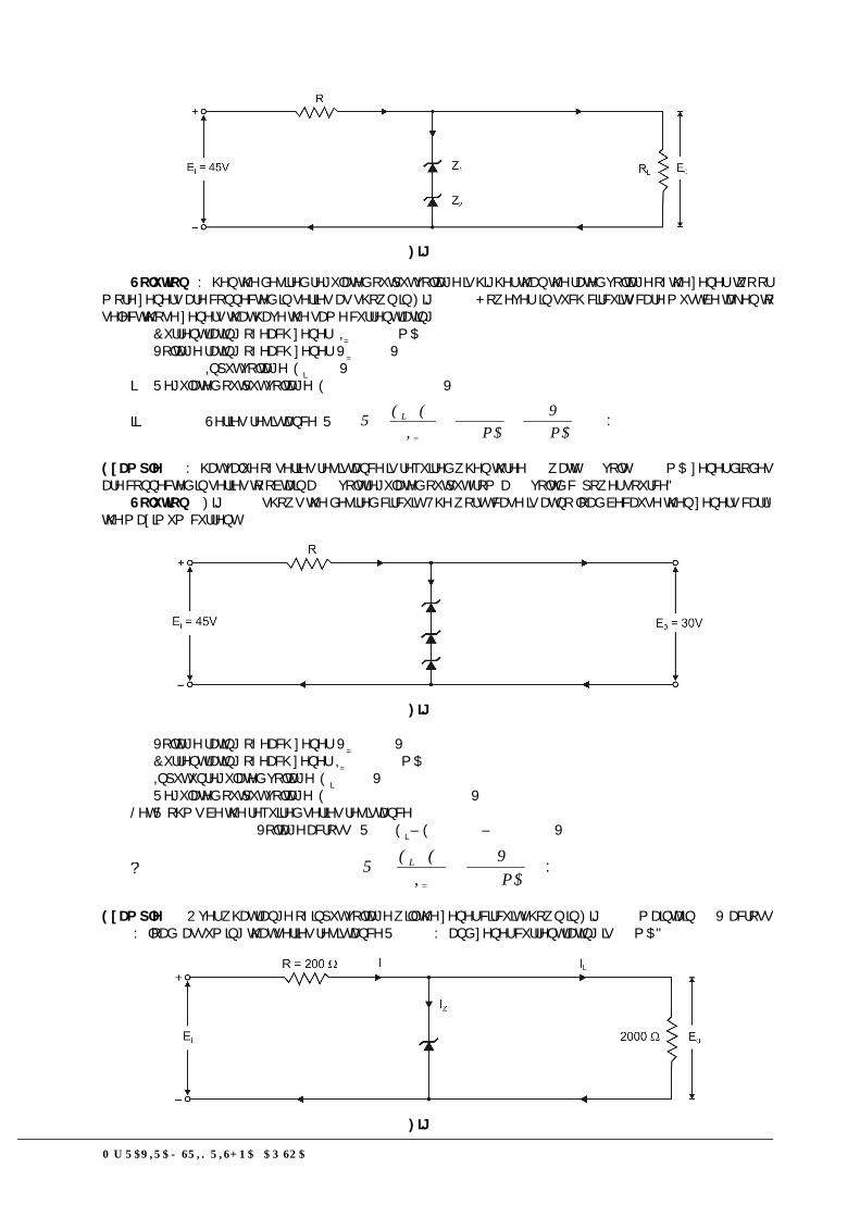
Mr. RAVIRAJ SRIKRISHNA AP/SOA 87
Fig. 4.31
Solution. :KHQ�WKH�GHVLUHG�UHJXODWHG�RXWSXW�YROWDJH�LV�KLJKHU�WKDQ�WKH�UDWHG�YROWDJH�RI�WKH�]HQHU��WZR�RUPRUH�]HQHUV�DUH�FRQQHFWHG�LQ�VHULHV�DV�VKRZQ�LQ�)LJ��������+RZHYHU��LQ�VXFK�FLUFXLWV�FDUH�PXVW�EH�WDNHQ�WRVHOHFW�WKRVH�]HQHUV�WKDW�KDYH�WKH�VDPH�FXUUHQW�UDWLQJ�
&XUUHQW�UDWLQJ�RI�HDFK�]HQHU���,=�� ������P$9ROWDJH�UDWLQJ�RI�HDFK�]HQHU��9=� �����9
,QSXW�YROWDJH��(L� ����9L� 5HJXODWHG�RXWSXW�YROWDJH��(��� ����������� ����9
LL� 6HULHV�UHVLVWDQFH��5�� ��
7520015
20030450
mAV
mAIEER
Z
i
Example 7. :KDW�YDOXH�RI�VHULHV�UHVLVWDQFH�LV�UHTXLUHG�ZKHQ�WKUHH����ZDWW�����YROW�������P$�]HQHU�GLRGHVDUH�FRQQHFWHG�LQ�VHULHV�WR�REWDLQ�D����YROW�UHJXODWHG�RXWSXW�IURP�D����YROW�G�F��SRZHU�VRXUFH"
Solution. )LJ�������VKRZV�WKH�GHVLUHG�FLUFXLW��7KH�ZRUVW�FDVH�LV�DW�QR�ORDG�EHFDXVH�WKHQ�]HQHUV�FDUU\WKH�PD[LPXP�FXUUHQW�
Fig. 4.32
9ROWDJH�UDWLQJ�RI�HDFK�]HQHU��9=�� �����9&XUUHQW�UDWLQJ�RI�HDFK�]HQHU��,=�� �������P$,QSXW�XQUHJXODWHG�YROWDJH��(L�� �����95HJXODWHG�RXWSXW�YROWDJH��(��� ��������������� ����9
/HW�5�RKPV�EH�WKH�UHTXLUHG�VHULHV�UHVLVWDQFH�9ROWDJH�DFURVV 5�� ��(L�±�(��� �����±����� �����9
151000150
mAV
IEER
Z
i
Example 8. 2YHU�ZKDW�UDQJH�RI�LQSXW�YROWDJH�ZLOO�WKH�]HQHU�FLUFXLW�VKRZQ�LQ�)LJ�������PDLQWDLQ����9�DFURVV�����ORDG��DVVXPLQJ�WKDW�VHULHV�UHVLVWDQFH�5� �����DQG�]HQHU�FXUUHQW�UDWLQJ�LV����P$"
Fig. 4.33

Mr. RAVIRAJ SRIKRISHNA AP/SOA 88
Solution. 7KH�PLQLPXP�LQSXW�YROWDJH�UHTXLUHG�ZLOO�EH�ZKHQ�,=� ����8QGHU�WKLV�FRQGLWLRQ�
mAVIIL 15200030
0LQLPXP�LQSXW�YROWDJH��� �������,�5�� ����������P$�[���������������� ���������� ��33 V
7KH�PD[LPXP��LQSXW�YROWDJH�UHTXLUHG�ZLOO�EH�ZKHQ�,=� ����P$���8QGHU�WKLV�FRQGLWLRQ���������,�� ��,/���,=�� ����������� �����P$
0D[��LQSXW�YROWDJH�� �������,�5����������� ����������P$�[������
���������� �38 V7KHUHIRUH��WKH�LQSXW�YROWDJH�UDQJH�RYHU�ZKLFK�WKH�FLUFXLW�ZLOO�PDLQWDLQ����9�DFURVV�WKH�ORDG�LV����9�WR���9�
Example 9. ,Q�WKH�FLUFXLW�VKRZQ�LQ�)LJ��������WKH�YROWDJH�DFURVV�WKH�ORDG�LV�WR�EH�PDLQWDLQHG�DW����9�DV�ORDGFXUUHQW�YDULHV�IURP���WR�����P$��'HVLQJ�WKH�UHJXODWRU���$OVR�ILQG�WKH�PD[LPXP�YROWDJH�UDWLQJ�RI�]HQHU�GLRGH�
Fig. 4.34
Solution. %\�GHVLJQLQJ�WKH�UHJXODWRU�KHUH�PHDQV�WR�ILQG�WKH�YDOXHV�RI�9=�DQG�5���6LQFH�WKH�ORDGYROWDJH�LV�WR�EH�PDLQWDLQHG�DW����9��ZH�ZLOO�XVH�D�]HQHU�GLRGH�RI�]HQHU�YROWDJH����9�L�H��
9=�� ��12 V7KH�YROWDJH�DFURVV�5�LV�WR�UHPDLQ�FRQVWDQW�DW����±���� ���9�DV�WKH�ORDG�FXUUHQW�FKDQJHV�IURP���WR����
P$��7KH�PLQLPXP�]HQHU�FXUUHQW�ZLOO�ZKHQ�WKH�ORDG�FXUUHQW�LV�PD[LPXP�
202004
)2000(1216
)()( maxmin
0
mAV
mAIIEER
LZ
i
0D[LPXP�SRZHU�UDWLQJ�RI�]HQHU�LV3=0�� ��9=,=0�� ������9�������P$��� ������:
Example. 10. )LJ�������VKRZV�WKH�EDVLF�]HQHU�GLRGH�FLUFXLWV��:KDW�ZLOO�EH�WKH�FLUFXLW�EHKDYLRXU�LI�WKH�]HQHU�LV�L��ZRUNLQJ�SURSHUW\��LL��VKRUWHG��LLL��RSHQ�FLUFXLWHG"
Fig. 4.35
Mr. RAVIRAJ SRIKRISHNA AP/SOA 89
Solution. =HQHU�GLRGHV�FDQQRW�EH�WHVWHG�LQGLYLGXDOO\�ZLWK�D�PXOWLPHWHU��,W�LV�EHFDXVH�PXOWLPHWHU�XVXDOO\GR�QRW�KDYH�HQRXJK�LQSXW�YROWDJH�WR�SXW�WKH�]HQHU�LQWR�EUHDNGRZQ�UHJLRQ�
L� ,I�WKH�]HQHU�GLRGH�LV�ZRUNLQJ�SURSHUO\��WKH�YROWDJH�9��DFURVV�WKH�ORDG�� ��N��ZLOO�EH�QHDUO\��9�LL� ,I�WKH�]HQHU�GLRGH�LV�VKRUW�>6HH�)LJ��������LL�@��\RX�ZLOO�PHDVXUH�9��DV��9��7KH�VDPH�SUREOHP�FRXOG�DOVR
EH�FDXVHG�E\�D�VKRUWHG�ORDG�UHVLVWRU�� �N��RU�DQ�RSHQHG�VRXUFH�UHVLVWRU�� ��N���7KH�RQO\�ZD\�WR�WHOO�ZKLFKGHYLFH�KDV�IDLOHG�LV�WR�UHPRYH�WKH�UHVLVWRUV�DQG�FKHNF�WKHP�ZLWK�DQ�RKPPHWHU��,I�WKH�UHVLVWRUV�DUH�JRRG��WKHQ]HQHU�GLRGH�LV�EDG�
LLL� ,I�WKH�]HQHU�GLRGH�LV�VKRUW�>6HH�)LJ��������LL�@��\RXU�ZLOO�PHDVXUH�9��DV��9��7KH�VDPH�SUREOHP�FRXOG�DOVREH�FDXVHG�E\�D�VKRUWHG�ORDG�UHVLVWRU�� ��N��RU�DQ�RSHQHG�VRXUFH�UHVLVWRU�� ���N���7KH�RQO\�ZD\�WR�WHOO�ZKLFKGHYLFH�KDV�IDLOHG�LV�WR�UHPRYH�WKH�UHVLVWRUV�DQG�FKHFN�WKHP�ZLWK�DQ�RKPPHWHU��,I�WKH�UHVLVWRUV�DUH�JRRG��WKHQ]HQHU�GLRGH�LV�EDG�
LLL� ,I�WKH�]HQHU�GLRGH�LV�RSHQ�FLUFXLWHG��WKH�YROWDJH�9��DFURVV�WKH�ORDG�� ��N��ZLOO�EH���9�
Example. 11. )LJ�������VKRZV�UHJXODWHG�SRZHU�VXSSO\�XVLQJ�D�]HQHU�GLRGH��:KDW�ZLOO�EH�WKH�FLUFXLW�EHKDYLRXULI��L��ILOWHU�FDSDFLWRU�VKRUWV��LL��ILOWHU�FDSDFLWRU�RSHQV"
Fig. 4.36
Solutions. 7KH�FRPPRQ�IDXOWV�LQ�D�]HQHU�YROWDJH�UHJXODWRU�DUH�VKRUWHG�ILOWHU�FDSDFLWRU�RU�RSHQV�ILOWHUFDSDFLWRU�
L� When filter capacitor shorts.��:KHQ�WKH�ILOWHU�FDSDFLWRU�VKRUWV��WKH�SULPDU\�IXVH�ZLOO�EORZ��7KH�UHDVRQIRU�WKLV�LV�LOOXVWUDWHG�LQ�)LJ��������:KHQ�WKH�ILOWHU�FDSDFLWRU�VKRUWV��LW�VKRUWV�RXW�WKH�ORDG�UHVLVWDQFH�5/��7KLV�KDVWKH�VDPH�HIIHFW�DV�ZLULQJ�WKH�WZR�VLGHV�RI�WKH�EULGJH�WRJHWKHU�
PHOTO VOLTAIC (SOLAR) CELL7KH�SKRWR�YROWDLF�FHOO�JHQHUDWHV�D�YROWDJH�ZKHQ�LW�LV�VXEMHFWHG�WR�RSWLFDO�UDGLDWLRQ��7KH�JHQHUDWHG�HOHFWULF
SRWHQWLDO�FDOOHG�Photo Voltaic Potential�LV�SURSRUWLRQDO�WR�LQFLGHQW�OLJKW�LQWHQVLW\��6LQFH�WKLV�GHYLFH�LV�XVHG�WRJHQHUDWH�HOHFWULFLW\�IURP�VXQOLJKW��LW�LV�SRSXODULW\�NQRZQ�DV�VRODU�FHOO���7KH�FLFXLW�V\PERO�JHQHUDOO\�XVHG�IRUVRODU�LV�VKRZQ�LQ�)LJ�������
Fig. 4.37. Symbol of Solar Cell
Mr. RAVIRAJ SRIKRISHNA AP/SOA 90
Construction and Operating Principle of Solar Cell
Fig. 4.38. Structure of Solar Cell
)LJ�������VKRZV�VWUXFWXUH�RI�VRODU�FHOO��,W�VKRZV�WKDW�FHOO�LV�DFWXDOO\�D�3�1�MXQFWLRQ�GLRGH�ZLWK�DSSURSULDWHO\GRSHG�VHPLFRQGXFWRUV��7KH�WRS�3�W\SH�VHPLFRQGXFWRU�OD\HU�LV�PDGH�YHU\�WKLQ�VR�DV�WR�SHUPLW�VRODU�UDGLDWLRQ�WRIDOO�RQWR�MXQFWLRQ��'RSLQJ�OHYHO�LV�YHU\�KLJK��VR�WKH�UHVXOWLQJ�MXQFWLRQ�ZLOO�EH�H[WUHPHO\�QDUURZ�
Fig. 1.1. A Solar Cell Array
7R�SHUPLW�ODUJH�DPRXQW�RI�OLJKW�LQSXW�LQWR�WKH�GHYLFH��VRODU�FHOOV�DUH�GHVLJQHG�WR�KDYH�ODUJH�VXUIDFH�DUHD�:KHQ�SKRWRQV�VWULNH�RQ�WKH�WKLQ�3�GRSHG�XSSHU�OD\HU��WKH\�DUH�DEVRUEHG�E\�WKH�HOHFWURQV�LQ�WKH�1�OD\HU��ZKLFKFDXVHG�IRUPDWLRQ�RI�FRQGXFWLRQ�HOHFWURQV�DQG�KROHV��7KHVH�FRQGXFWLRQ�HOHFWURQV�DQG�KROHV�DUH�VHSDUDWHG�E\GHSOHWLRQ�DFURVV�WKH�FHOO��WKH�GHSOHWLRQ�UHJLRQ�SRWHQWLDO�FDXVHV�WKH�SKRWR�FXUUHQW�WR�IORZ�WKURXJK�WKH�ORDG�
7\SLFDO�VRODU�FHOOV�JHQHUDWHV�����9�RU�OHVV�ZLWK�FXUUHQWV�UDQJLQJ�IURP�WKH�X$�UDQJH�WR�P$�UDQJH��GHSHQGLQJRQ�WKH�H[WHUQDO�ORDG��8VXDOO\�D�ODUJH�QXPEHU�RI�VRODU�FHOOV�DUH�DUUDQJHG�LQ�DQ�DUUD\�LQ�RUGHU�WR�DFKLHYH�KLJKHUYROWDJH�DQG�FXUUHQWV�DV�VKRZQ�LQ�)LJ�������
,Q�RUGHU�WR�HIILFLHQWO\�XWLOL]H�WKH�VXQ�DV�D�VRXUFH�RI�SRZHU��VRODU�FHOO�LV�DQ�LPSRUWDQW�GHYLFH��,W�KDV�EHFRPHDQ�LPSRUWDQW�FRPSRQHQW�IRU�SURGXFLQJ�VSDFH�FUDIW�SRZHU�
ADVANTAGES AND DISADVANTAGES
AdvantagesL� 6RODU�FHOO�GR�QRW�IXHO�LL� 2QFH�LQVWDOOHG��WKH\�FDQ�ZRUN�IRU�\HDUV�ZLWKRXW�DQ\�H[SHQGLWXUH�RQ�PDLQWHQDQFH�LLL� 7KH\�GR�QRW�SROOXWH�DWPRVSKHUH�LY� 6RODU�FHOO�GR�QRW�SURGXFH�QRLVH�Y� 7KH\�FDQ�SURGXFH�HQRXJK�YROWDJH�DQG�FXUUHQW�UHTXLUHG�IRU�RSHUDWLRQ�RI�HTXLSPHQWV�LQ�URFNHW�DQG�VDWHOOLWHV�

Mr. RAVIRAJ SRIKRISHNA AP/SOA 91
DisadvanteageL� 6ORZ�UHVSRQVH�FRPSDUHG�WR�SKRWRGLRGH�LL� 7R�JHW�ODUJH�RXWSXW�YROWDJH��VRODU�SDQHO�UHTXLUH�ODUJH�VSDFH�LLL� 6RODU�SDQHOV�DUH�QHHGHG�WR�EH�FOHDQHG�UHJXODUO\�WR�JHW�EHWWHU�UHVXOW�LY� 0XVW�EH�VXSSRUWHG�E\�VWRUDJH�EDWWHULHV�WR�JHW�FRQWLQRXV�RSHUDWLRQ�LQ�QLJKW�
HALF-WAVE RECTIFIER,Q�KDOI�ZDYH�UHFWLILFDWLRQ��WKH�UHFWLILHU�FRQGXFWV�FXUUHQW�RQO\�GXULQJ�WKH�SRVLWLYH�KDOI�F\FOHV�RI�LQSXW�D�F��VXSSO\�7KH�QHJDWLYH�KDOI�F\FOHV�RI�D�F��VXSSO\�DUH�VXSSUHVVHG�L�H��GXULQJ�QHJDWLYH�KDOI�F\FOHV��QR�FXUUHQW�LV�FRQGXFWHGDQG�KHQFH�QR�YROWDJH�DSSHDUV�DFURVV�WKH�ORDG��7KHUHIRUH��FXUUHQW�DOZD\V�IORZV�LQ�RQH�GLUHFWLRQ��L�H��G�F��WKURXJK�WKH�ORDG�WKRXJK�DIWHU�HYHU\�KDOI�F\FOH�
Fig. 2.23
Circuit Details.���)LJ�������VKRZV�WKH�FLUFXLW�ZKHUH�D�VLQJOH�FU\VWDO�GLRGH�DFWV�DV�D�KDOI�ZDYH�UHFWLILHU��7KH�D�F�VXSSO\�WR�EH�UHFWLILHG�LV�DSSOLHG�LQ�VHULHV�ZLWK�WKH�GLRGH�DQG�ORDG�UHVLVWDQFH�5/��*HQHUDOO\��D�F��VXSSO\�LV�JLYHQWKURXJK�D�WUDQVIRUPHU��7KH�XVH�RI�WUDQVIRUPHU�SHUPLWV�WZR�DGYDQWDJHV��)LUVWO\��LW�DOORZV�XV�WR�VWHS�XS�RU�VWHSGRZQ�WKH�D�F��LQSXW�YROWDJH�DV�WKH�VLWXDWLRQ�GHPDQGV��6HFRQGO\��WKH�WUDQVIRUPHU�LVRODWHV�WKH�UHFWLILHU�FLUFXLWIURP�SRZHU�OLQH�DQG�WKXV�UHGXFHV�WKH�ULVN�RI�HOHFWULF�VKRFN�
Operation.���7KH�D�F��YROWDJH�DFURVV�WKH�VHFRQGDU\�ZLQGLQJV�$%�FKDQJHV�SRODULWLHV�DIWHU�HYHU\�KDOI�F\FOH�'XULQJ�WKH�SRVLWLYH�KDOI�F\FOH�RI�LQSXW�D�F��YROWDJH��HQG�$�EHFRPHV�SRVLWLYH�Z�U�W��HQG�%��7KLV�PDNHV�WKH�GLRGHIRUZDUG�ELDVHG�DQG�KHQFH�LW�FRQGXFWV�FXUUHQW��'XULQJ�WKH�QHJDWLYH�KDOI�F\FOH��HQG�$�LV�QHJDWLYH�Z�U�W��HQG�%�8QGHU�WKLV�FRQGLWLRQ��WKH�GLRGH�LV�UHYHUVH�ELDVHG�DQG�LW�FRQGXFWV�QR�FXUUHQW��7KHUHIRUH��FXUUHQW�IORZV�WKURXJKWKH�GLRGH�GXULQJ�SRVLWLYH�KDOI�F\FOHV�RI�LQSXW�D�F��YROWDJH�RQO\��LW�LV�EORFNHG�GXULQJ�WKH�QHJDWLYH�KDOI�F\FOHV�>6HH)LJ��������LL�@��,Q�WKLV�ZD\��FXUUHQW�IORZV�WKURXJK�ORDG�5/�DOZD\V�LQ�WKH�VDPH�GLUHFWLRQ��+HQGH�G�F��RXWSXW�LVREWDLQHG�DFURVV�5/��,W�PD\�EH�QRWHG�WKDW�RXWSXW�DFURVV�WKH�ORDG�LV�SXOVDWLQJ�G�F��7KHVH�SXOVDWLRQV�LQ�WKH�RXWSXWDUH�IXUWKHU�VPRRWKHQHG�ZLWK�WKH�KHOS�RI�ILOWHU�FLUFXLWV�GLVFXVVHG�ODWHU�
Disadvantages :�7KH�PDLQ�GLVDGYDQWDJHV�RI�D�KDOI�ZDYH�UHFWLILHU�DUH��L� 7KH�SXOVDWLQJ�FXUUHQW�LQ�WKH�ORDG�FRQWDLQV�DOWHUQDWLQJ�FRPSRQHQW�ZKRVH�EDVLF�IUHTXHQF\�LV�HTXDO�WR�WKH
VXSSO\�IUHTXHQF\��7KHUHIRUH��DQ�HODERUDWH�ILOWHULQJ�LV�UHTXLUHG�WR�SURGXFH�VWHDG\�GLUHFW�FXUUHQW�LL� 7KH�D�F��VXSSO\�GHOLYHUV�SRZHU�RQO\�KDOI�WKH�WLPH��7KHUHIRUH��WKH�RXWSXW�LV�ORZ�
OUTPUT FREQUENCY OF HALF-WAVE RECTIFIER7KH�RXWSXW�IUHTXHQF\�RI�D�KDOI�ZDYH�UHFWLILHU�LV�HTXDO�WR�WKH�LQSXW�IUHTXHQF\�����+]���5HFDOO�KRZ�D�FRPSROHWHF\FOH�LV�GHILQHG��D�ZDYHIRUP�KDV�D�FRPSOHWH�F\FOH�LV�GHILQHG��$�ZDYHIRUP�KDV�FRPSOHWH�F\FOH�ZKHQ�LW�UHSHDWVWKH�VDPH�ZDYH�SDWWHUQ�RYHU�D�JLYHQ�WLPH��7KXV�LQ�)LJ��������WKH�D�F��LQSXW�YROWDJH�UHSHDWV�WKH�VDPH�ZDYHSDWWHUQ�RYHU����±������������±������DQG�VR�RQ��7KLV�PHDQV�WKDW�ZKHQ�LQSXW�D�F��FRPSOHWHV�RQH�F\FOH��WKH�RXWSXWKDOI�ZDYH�UHFWLILHG�ZDYH�DOVR�FRPSOHWHV�RQH�F\FOH��,Q�RWKHU�ZRUGV��WKH�RXWSXW�IUHTXHQF\�LV�HTXDO�WR�WKH�LQSXWIUHTXHQF\�L�H�
IRXW� �ILQ)RU�H[DPSOH��LI�WKH�LQSXW�IUHTXHQF\�RI�VLQH�ZDYH�DSSOLHG�WR�D�KDOI�ZDYH�UHFWLILHU�LV�����+]��WKHQ�IUHTXHQF\
RI�WKH�RXWSXW�ZDYH�ZLOO�DOVR�EH�����+]�

Mr. RAVIRAJ SRIKRISHNA AP/SOA 92
Fig. 2.24
EFFICIENCY OF HALF-WAVE RECTIFIER
7KH�UDWLR�RI�G�F��SRZHU�RXWSXW�WR�WKH�DSSOLHG�LQSXW�D�F��SRZHU�LV�NQRZQ�DV�UHFWLILHU�HIILFLHQF\�L�H�
powercaInputoutputpowercdefficinecyctifier
....,Re
Fig. 1.1
&RQVLGHU�D�KDOI�ZDYH�UHFWLILHU�VKRZQ�LQ�)LJ��������/HW�Y� �9P�VLQ�EH��WKH�DOWHUQDWLQJ�YROWDJH�WKDW�DSSHDUVDFURVV�WKH�VHFRQGDU\�ZLQGLQJ���/HW�UI�DQG�5/�EH�WKH�GLRGH�UHVLVWDQFH�DQG�ORDG�UHVLVWDQFH�DQG�ORDG�UHVLVWDQFHUHVSHFWLYHO\��7KH�GLRGH�FRQGXFWV�GXULQJ�SRVLWLYH�KDOI�F\FOH�RI�D�F��VXSSO\�ZKLOH�QR�FXUUHQW�FRQGXFWLRQ�WDNHVSODFH�GXULQJ�QHJDWLYH�KDOI�F\FOHV�
D.C. Power.��7KH�RXWSXW�FXUUHQW�LV�SXOVDWLQJ�GLUHFW�FXUUHQW��7KHUHIRUH��LQ�RUGHU�WR�ILQG�G�F��SRZHU��DYHUDJHFXUUHQW�KDV�WR�EH�IRXQG�RXW�
�5�U9,
ʌ,
ʌ�[
�5�U9�[
�5�U�ʌ9
ș@FRV>�5�ʌʌ�
9GșșVLQ�5�U�ʌ
9
Gș5U
șVLQ9�ʌ�GșL
�ʌ�,,
/I
PP
P
/I
P
/I
P
ʌ�
ʌ
� /I
P
/I
P
ʌ
� /I
Pʌ
�GFDY
/P
/�GFGF 5[
ʌ,5[,3SRZHU�G�F�
����L�

Mr. RAVIRAJ SRIKRISHNA AP/SOA 93
A.C. Power Input : 7KH�D�F��SRZHU�LQSXW�LV�JLYHQ�E\���5�U,3 /I
�UPVDF
)RU�D�KDOI�ZDYH�UHFWLILHG�ZDYH��,UPV� �,P��
�5�U�,3 /I
�P
DF
����LL�
�5�U����,5[ʌ���,
SRZHULQSXWD�F�SRZHURXWSXWG�F�HIILFLHQF\5HFWLILHU
/I�
P
/�
P
/
I/I
/
5U�
�����5U
5�����
7KH�HIILFLHQF\�ZLOO�EH�PD[LPXP�LI�UI�LV�QHJOLJLEOH�DV�FRPSDUHG�WR�5/� ���0D[��UHFWLILHU�HIILFLHQF\� ������7KLV�VKRZV�WKDW�LQ�KDOI�ZDYH�UHFWLILFDWLRQ��D�PD[LPXP�RI�������RI�D�F��SRZHU�LV�FRQYHUWHG�LQWR�G�F��SRZHU�
Example 12. 7KH�DSSOLHG�LQSXW�D�F��SRZHU�WR�KDOI�ZDYH�UHFWLILHU�LV�����ZDWWV��7KH�G�F��RXWSXW�SRZHU�REWDLQHGLV����ZDWWV�
L� :KDW�LV�WKH�UHFWLILFDWLRQ�HIILFLHQF\"LL� :KDW�KDSSHQV�WR�UHPDLQLQJ����ZDWWV"Solution.
L� 40% ��������
SRZHULQSXWD�F�SRZHURXWSXWG�F�HIILFLHQF\LRQ5HFWLILFDW
LL� ����HIILFLHQF\�RI�UHFWLILFDWLRQ�GRHV�QRW�PHDQ�WKDW�����RI�SRZHU�LV�ORVW�LQ�WKH�UHFWLILHU�FLUFXLW��,Q�IDFW��DFU\VWDO�GLRGH�FRQVXPHV�OLWWOH�SRZHU�GXH�WR�VPDOO�LQWHUQDO�UHVLVWDQFH��7KH�����:�D�F��SRZHU�LV�FRQWDLQHG�DV���ZDWWV�LQ�SRVLWLYH�KDOI�F\FOHV�DQG����ZDWWV�LQ�QHJDWLYH�KDOI�F\FOHV��7KH����ZDWWV�LQ�WKH�QHJDWLYH�KDOI�F\FOHV�QRWVXSSOLHG�DW�DOO��2QO\����ZDWWV�LQ�WKH�SRVLWLYH�KDOI�F\FOHV�DUH�FRQYHUWHG�LQWR����ZDWWV�
������[����HIILFLHQF\3RZHU
$OWKRXJK�����ZDWWV�RI�D�F��SRZHU�ZDV�RI�D�F��SRZHU�ZDV�VXSSOLHG��WKH�KDOI�ZDYH�UHFWLILHU�DFFHSWHG�RQO\���ZDWWV�DQG�FRQYHUWHG�LW�LQWR����ZDWWV�G�F��SRZHU��7KHUHIRUH��LW�LV�DSSURSULDWH�WR�VD\�WKDW�HIILFLHQF\�RI�UHFWLILFDWLRQLV�����DQG�QRW�����ZKLFK�LV�SRZHU�HIILFLHQF\�
Example 13. $Q�D�F��VXSSO\�RI�����9�LV�DSSOLHG�WR�D�KDOI�ZDYH�UHFWLILHU�FLUFXLW�WKURXJK�D�WUDQVIRUPHU�RI�WXUQ�UDWLR��������)LQG��L��WKH�RXWSXW�G�F��YROWDJH�DQG��LL��WKH�SHDN�LQYHUVH�YROWDJH�$VVXPH�WKH�GLRGH�WR�EH�LGHDO�
Fig. 1.1Solution.3ULPDU\�WR�VHFRQGDU\�WXUQV�LV
��11
�
�
5�0�6��SULPDU\�YROWDJH������������������ �����9
�����0D[��SULPDU\�YROWDJH�LV
Mr. RAVIRAJ SRIKRISHNA AP/SOA 94
9��������[�
YROWDJHSULPDU\U�P�V�[�9SP
0D[��VHFRQGDU\�YROWDJH�LV
9��������[�����
11[99
�
�SPVP
L�P
GF,
I
V10.36ʌ
�����ʌ
95[ʌ,9 VP
/P
GF
LL� 'XULQJ�WKH�QHJDWLYH�KDOI�F\FOH�RI�D�F��VXSSO\��WKH�GLRGH�LV�UHYHUVH�ELDVHG�DQG�KHQFH�FRQGXFWV�QRFXUUHQW��7KHUHIRUH��WKH�PD[LPXP�VHFRQGDU\�YROWDJH�DSSHDUV�DFURVV�WKH�GLRGH�
3HDN�LQYHUVH�YROWDJH� �32.53 V
Example 14. $�FU\VWDO�GLRGH�KDYLQJ�LQWHUQDO�UHVLVWDQFH�U I� ����LV�XVHG�IRU�KDOI�ZDYH�UHFWLILFDWLRQ��,I�WKH�DSSOLHGYROWDJH�Y� ����VLQ�W�DQG�ORDG�UHVLVWDQFH�5/� ������ILQG�
L� ,P��,GF��,UPV LL����D�F��SRZHU�LQSXW�DQG�G�F��SRZHU�RXWSXWLLL� G�F��RXWSXW�YROWDJH LY����HIILFLHQF\�RI�UHFWLILFDWLRQSolution.
Y�� �����VLQ�Z�W0D[LPXP�YROWDJH��9P �����9
L� mA61
$����������
��5U
9,/I
PP
����������,GF�� ��,P�� ����� �19.4 mA���������,UPV�� ��,P��� ������ �30.5 mA
LL� watt0.763
�������[���������5�U[��,LQSXWSRZHUD�F�
�
/I�
UPV
39.5%
volt15.52
watt0.31
���[����������LRQUHFWLILFDWRI(IILFLHQF\LY�
���[P$����5,YROWDJHRXWSXWG�F�LLL�
���[��������5[,RXWSXWSRZHUG�F�
/GF
�
/GF�
Example 15. $�KDOI�ZDYH�UHFWLILHU�LV�XVHG�WR�VXSSO\���9�G�F��WR�D�UHVLVWLYH�ORDG�RI�������7KH�GLRGH�KDV�DUHVLVWDQFH�RI������&DOFXODWH�D�F��YROWDJH�UHTXLUHG�
Solution.2XWSXW�G�F��YROWDJH��9GF�� �����9
'LRGH�UHVLVWDQFH��UI�� �����/RDG�UHVLVWDQFH��5/�� ������
/HW�9P�EH�WKH�PD[LPXP�YODXH�RI�D�F��YROWDJH�UHTXLUHG�
9������
��[���[ʌ9
���[�������ʌ
9��RU
5U9,5[
�5�Uʌ95[
ʌ,
5[,9
P
P
/I
PP/
/I
P/
P
/GFGF
+HQFH�D�F��YROWDJH�RI�PD[LPXP�YDOXH�����LV�UHTXLUHG�

Mr. RAVIRAJ SRIKRISHNA AP/SOA 95
FULL-WAVE RECTIFIER,Q�IXOO�ZDYH�UHFWLILFDWLRQ��FXUUHQW�IORZV�WKURXJK�WKH�ORDG�LQ�WKH�VDPH�GLUHFWLRQ�IRU�ERWK�KDOI�F\FOHV�RI�LQSXW�D�F�YROWDJH��7KLV�FDQ�EH�DFKLHYHG�ZLWK�WZR�GLRGHV�ZRUNLQJ�DOWHUQDWHO\��)RU�WKH�SRVLWLYH�KDOI�F\FOH�RI�LQSXW�YROWDJH�RQH�GLRGH�VXSSOLHV�FXUUHQW�WR�WKH�ORDG�DQG�IRU�WKH�QHJDWLYH�KDOI�F\FOH��WKH�RWKHU�GLRGH�GRHV�VR��FXUUHQW�EHLQJDOZD\V�LQ�WKH�VDPH�GLUHFWLRQ�WKURXJK�WKH�ORDG��7KHUHIRUH��D�IXOO�ZDYH�UHFWLILHU�XWLOLVHV�ERWK�KDOI�F\FOHV�RI�LQSXWD�F��YROWDJH�WR�SURGXFH�WKH�G�F��RXWSXW��7KH�IROORZLQJ�WZR�FLUFXLWV�DUH�FRPPRQO\�XVHG�IRU�IXOO�ZDYH�UHFWLILFDWLRQ�
L�����&HQWUH�WDS�IXOO�ZDYH�UHFWLILHU�����������������LL�����)XOO�ZDYH�EULGJH�UHFWLILHU
CENTRE-TAP FULL-WAVE RECTIFIER7KH�FLUFXLW�HPSOR\HV�WZR�GLRGHV�'��DQG�'��DV�VKRZQ�LQ�)LJ��������$�FHQWUH�WDSSHG�VHFRQGDU\�ZLQGLQJ�$%�LVXVHG�ZLWK�WZR�GLRGHV�FRQQHFWHG�VR�WKDW�HDFK�XVHV�RQH�KDOI�F\FOH�RI�LQSXW�D�F��YROWDJH��,Q�RWKHU�ZRUGV��GLRGH�' �XWLOLVHV�WKH�D�F��YROWDJH�DSSHDULQJ�DFURVV�WKH�XSSHU�KDOI��2$��RI�VHFRQGDU\�ZLQGLQJ�IRU�UHFWLILFDWLRQ�ZKLOH�GLRGH'��XVHV�WKH�ORZHU�KDOI�ZLQGLQJ�2%�
Operation.���'XULQJ�WKH�SRVLWLYH�KDOI�F\FOH�RI�VHFRQGDU\�YROWDJH��WKH�HQG�$�RI�WKH�VHFRQGDU\�ZLQGLQJ�EHFRPHVSRVLWLYH�DQG�HQG�%�QHJDLWYH��7KLV�PDNHV�WKH�GLRGH�'��IRUZDUG�ELDVHG�DQG�GLRGH�'��UHYHUVH�ELDVHG��7KHUHIRUH�GLRGH�'��FRQGXFWV�ZKLOH�GLRGH�'��GRHV�QRW��7KH�FRQYHQWLQDO�FXUUHQW�IORZ�LV�WKURXJK�GLRGH�'���ORDG�UHVLVWRU�5/DQG�WKH�XSSHU�KDOI�RI�VHFRQGDU\�ZLQGLQJ�DV�VKRZQ�E\�WKH�GRWWHG�DUURZ��'XULQJ�WKH�QHJDWLYH�KDOI�F\FOH��HQG�$�RIWKH�VHFRQGDU\�ZLQGLQJ�EHFRPHV�QHJDWLYH�DQG�HQG�%�SRVLWLYH��7KHUHIRUH��GLRGH�' ��FRQGXFWV�ZKLOH�GLRGH�'��GRHVQRW��7KH�FRQYHQWLRQDO�FXUUHQW�IORZ�WKURXJK�GLRGH�'���ORDG�5/�DQG�ORZHU�KDOI�ZLQGLQJ�DV�VKRZQ�E\�VROLG�DUURZV�5HIHUULQJ�WR�)LJ��������LW�PD\�EH�VHHQ�WKDW�FXUUHQW�LQ�WKH�ORDG�5/�LV�LQ�WKH�VDPH�GLUHFWLRQ�IRU�ERWK�KDOI�F\FOHV�RILQSXW�D�F��YROWDJH��7KHUHIRUH��G�F��LV�REWDLQHG�DFURVV�WKH�ORDG�5/��$OVR�WKH�SRODULWLHV�RI�WKH�G�F��RXWSXW�DFURVVWKH�ORDG�VKRXOG�EH�QRWHG�
Fig. 2.25
Peak inverse voltage.���6XSSRVH�9P�LV�WKH�PD[LPXP�YROWDJH�DFURVV�WKH�KDOI�VHFRQGDU\�ZLQGLQJ��)LJ������VKRZV�WKH�FLUFXLW�DW�WKH�LQVWDQW�VHFRQGDU\�YROWDJH�UHDFKHV�LW�PD[LPXP�YDOXH�LQ�WKH�SRVLWLYH�GLUHFWLRQ��$W�KLVLQVWDQW��GLRGH�'��LV�FRQGXFWLQJ�ZKLOH�GLRGH�'��LV�QRQ�FRQGXFWLQJ��7KHUHIRUH��ZKROH�RI�WKH�VHFRQGDU\�YROWDJHDSSHDUV�DFURVV�WKH�QRQ�FRQGXFWLQJ�GLRGH��&RQVHTXHQWO\��WKH�SHDN�LQYHUVH�YROWDJH�LV�WZLFH�WKH�PD[LPXPYROWDJH�DFURVV�WKH�KDOI�VHFRQGDU\�ZLQGLQJ�L�H�
3,9�� ����9P
Fig. 2.26DisadvantagesL� ,W�LV�GLIILFXOW�WR�ORFDWH�WKH�FHQWUH�WDS�RQ�WKH�VHFRQGDU\�ZLQGLQJ�LL� 7KH�G�F��RXWSXW�LV�VPDOO�DV�HDFK�GLRGH�XWLOLVHV�RQO\�RQH�KDOI�RI�WKH�WUDQVIRUPHU�VHFRQGDU\�YROWDJH�LLL� 7KH�GLRGHV�XVHG�PXVW�KDYH�KLJK�SHDN�LQYHUVH�YROWDJH�
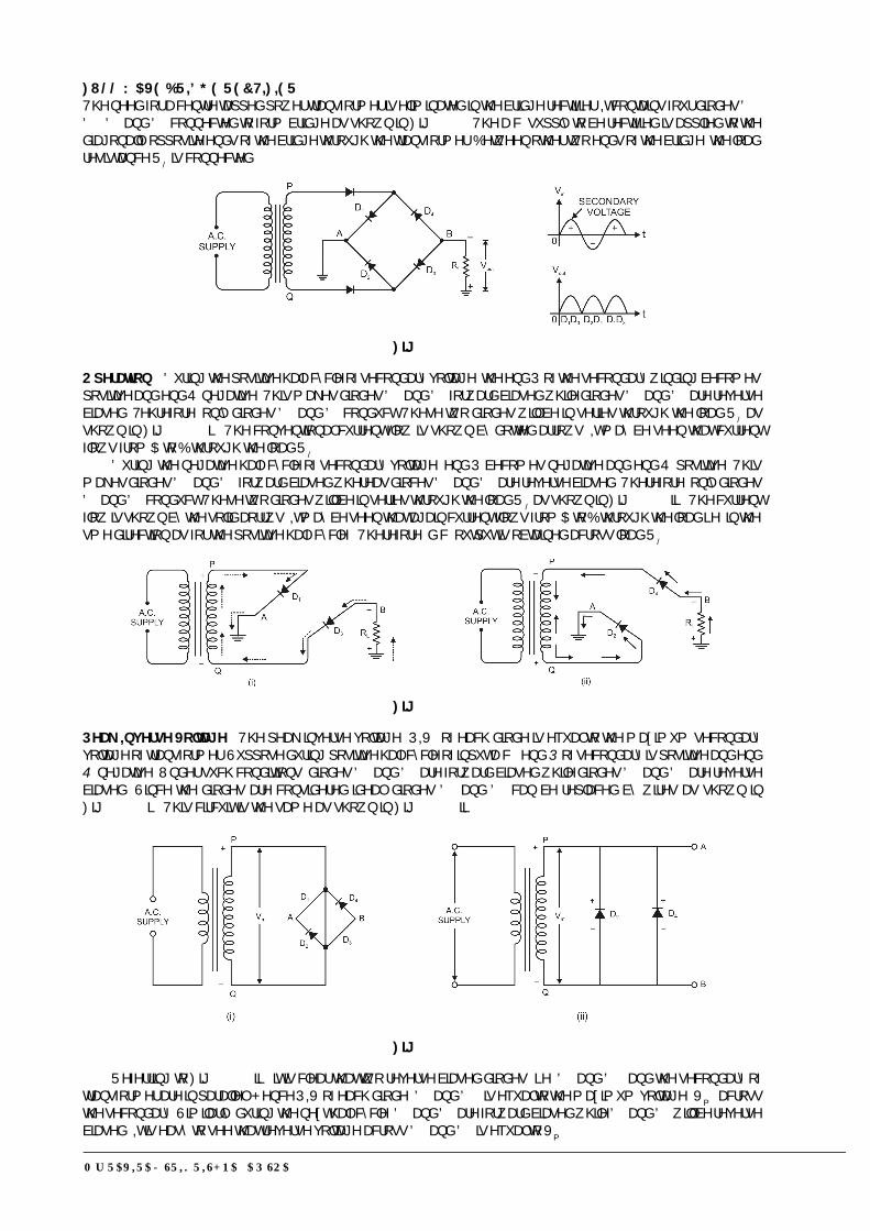
Mr. RAVIRAJ SRIKRISHNA AP/SOA 96
FULL-WAVE BRIDGE RECTIFIER7KH�QHHG�IRU�D�FHQWUH�WDSSHG�SRZHU�WUDQVIRUPHU�LV�HOLPLQDWHG�LQ�WKH�EULGJH�UHFWLILHU��,W�FRQWDLQV�IRXU�GLRGHV�' ��'���'��DQG�'��FRQQHFWHG�WR�IRUP�EULGJH�DV�VKRZQ�LQ�)LJ��������7KH�D�F��VXSSO\�WR�EH�UHFWLILHG�LV�DSSOLHG�WR�WKHGLDJRQDOO\�RSSRVLWH�HQGV�RI�WKH�EULGJH�WKURXJK�WKH�WUDQVIRUPHU��%HWZHHQ�RWKHU�WZR�HQGV�RI�WKH�EULGJH��WKH�ORDGUHVLVWDQFH�5/�LV�FRQQHFWHG�
Fig. 2.23
Operation.���'XULQJ�WKH�SRVLWLYH�KDOI�F\FOH�RI�VHFRQGDU\�YROWDJH��WKH�HQG�3�RI�WKH�VHFRQGDU\�ZLQGLQJ�EHFRPHVSRVLWLYH�DQG�HQG�4�QHJDWLYH��7KLV�PDNHV�GLRGHV�'��DQG�'��IRUZDUG�ELDVHG�ZKLOH�GLRGHV�'��DQG�'��DUH�UHYHUVHELDVHG��7HKUHIRUH��RQO\�GLRGHV�'��DQG�'��FRQGXFW��7KHVH�WZR�GLRGHV�ZLOO�EH�LQ�VHULHV�WKURXJK�WKH�ORDG�5/�DVVKRZQ�LQ�)LJ��������L���7KH�FRQYHQWLRQDO�FXUUHQW�IORZ�LV�VKRZQ�E\�GRWWHG�DUURZV��,W�PD\�EH�VHHQ�WKDW�FXUUHQWIORZV�IURP�$�WR�%�WKURXJK�WKH�ORDG�5/�
'XULQJ�WKH�QHJDWLYH�KDOI�F\FOH�RI�VHFRQGDU\�YROWDJH��HQG�3�EHFRPHV�QHJDWLYH�DQG�HQG�4�SRVLWLYH��7KLVPDNHV�GLRGHV�'���DQG�'��IRUZDUG�ELDVHG�ZKHUHDV�GLRFHV�'��DQG�'��DUH�UHYHUVH�ELDVHG��7KHUHIRUH��RQO\�GLRGHV'��DQG�'��FRQGXFW��7KHVH�WZR�GLRGHV�ZLOO�EH�LQ�VHULHV�WKURXJK�WKH�ORDG�5/�DV�VKRZQ�LQ�)LJ��������LL���7KH�FXUUHQWIORZ�LV�VKRZQ�E\�WKH�VROLG�DRUUZV��,W�PD\�EH�VHHQ�WKDW�DJDLQ�FXUUHQW�IORZV�IURP�$�WR�%�WKURXJK�WKH�ORDG�L�H��LQ�WKHVPH�GLUHFWLRQ�DV�IRU�WKH�SRVLWLYH�KDOI�F\FOH���7KHUHIRUH��G�F��RXWSXW�LV�REWDLQHG�DFURVV�ORDG�5/�
Fig. 2.24
Peak Inverse Voltage.��7KH�SHDN�LQYHUVH�YROWDJH��3,9��RI�HDFK�GLRGH�LV�HTXDO�WR�WKH�PD[LPXP�VHFRQGDU\YROWDJH�RI�WUDQVIRUPHU��6XSSRVH�GXULQJ�SRVLWLYH�KDOI�F\FOH�RI�LQSXW�D�F���HQG�P�RI�VHFRQGDU\�LV�SRVLWLYH�DQG�HQGQ�QHJDWLYH��8QGHU�VXFK�FRQGLWLRQV��GLRGHV�'��DQG�'��DUH�IRUZDUG�ELDVHG�ZKLOH�GLRGHV�'��DQG�'��DUH�UHYHUVHELDVHG��6LQFH�WKH�GLRGHV�DUH�FRQVLGHUHG�LGHDO��GLRGHV�'��DQG�'��FDQ�EH� UHSODFHG�E\�ZLUHV�DV�VKRZQ� LQ)LJ��������L���7KLV�FLUFXLW�LV�WKH�VDPH�DV�VKRZQ�LQ�)LJ��������LL��
Fig. 2.25
5HIHUULQJ�WR�)LJ��������LL���LW�LV�FOHDU�WKDW�WZR�UHYHUVH�ELDVHG�GLRGHV��L�H��'��DQG�'���DQG�WKH�VHFRQGDU\�RIWUDQVIRUPHU�DUH�LQ�SDUDOOHO��+HQFH�3,9�RI�HDFK�GLRGH��'��DQG�'���LV�HTXDO�WR�WKH�PD[LPXP�YROWDJH��9P��DFURVVWKH�VHFRQGDU\��6LPLODUO\��GXULQJ�WKH�QH[W�KDOI�F\FOH��'��DQG�'��DUH�IRUZDUG�ELDVHG�ZKLOH�'��DQG�'��ZLOO�EH�UHYHUVHELDVHG��,W�LV�HDV\�WR�VHH�WKDW�UHYHUVH�YROWDJH�DFURVV�'��DQG�'��LV�HTXDO�WR�9P�
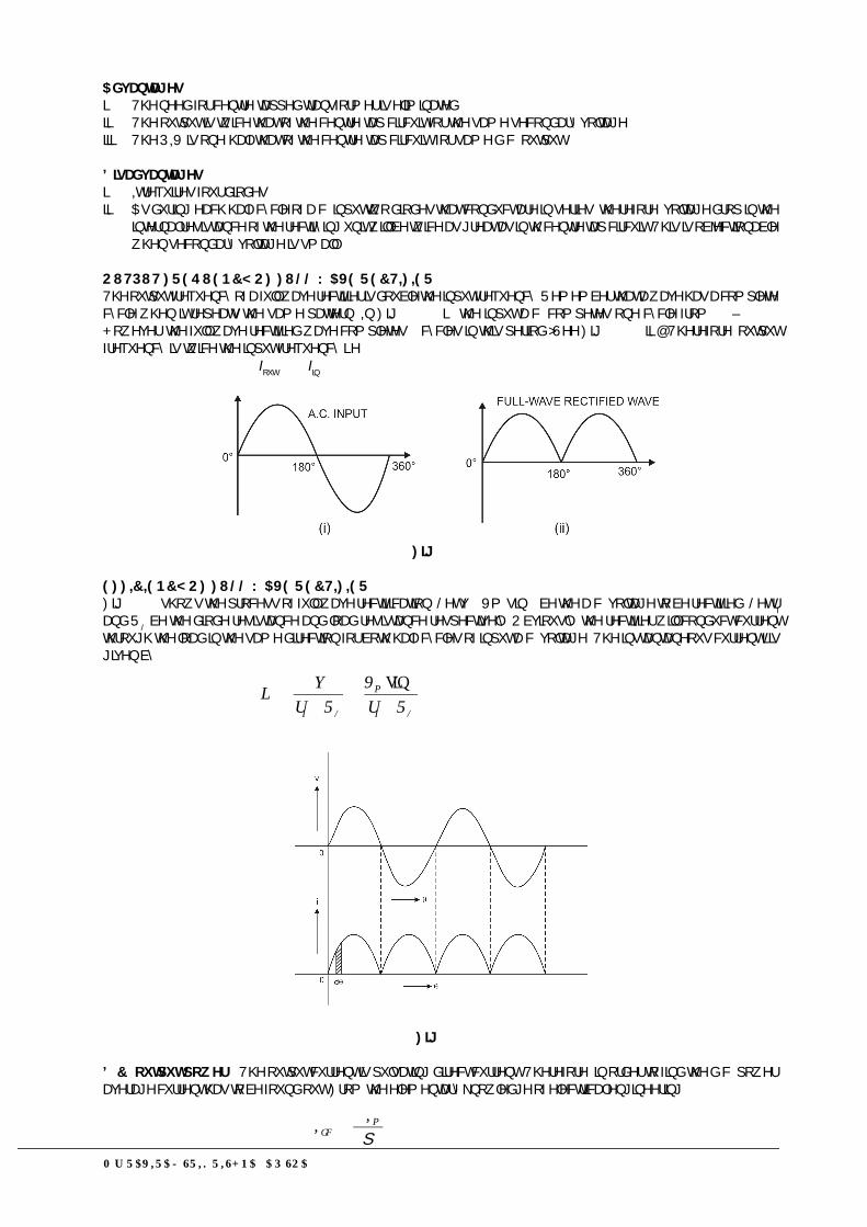
Mr. RAVIRAJ SRIKRISHNA AP/SOA 97
AdvantagesL� 7KH�QHHG�IRU�FHQWUH�WDSSHG�WUDQVIRUPHU�LV�HOLPLQDWHG�LL� 7KH�RXWSXW�LV�WZLFH�WKDW�RI�WKH�FHQWUH�WDS�FLUFXLW�IRU�WKH�VDPH�VHFRQGDU\�YROWDJH�LLL� 7KH�3,9�LV�RQH�KDOI�WKDW�RI�WKH�FHQWUH�WDS�FLUFXLW��IRU�VDPH�G�F��RXWSXW��
DisadvantagesL� ,W�UHTXLUHV�IRXU�GLRGHV�LL� $V�GXULQJ�HDFK�KDOI�F\FOH�RI�D�F��LQSXW�WZR�GLRGHV�WKDW�FRQGXFW�DUH�LQ�VHULHV��WKHUHIRUH��YROWDJH�GURS�LQ�WKH
LQWHUQDO�UHVLVWDQFH�RI�WKH�UHFWLI\LQJ�XQLW�ZLOO�EH�WZLFH�DV�JUHDW�DV�LQ�WK�FHQWUH�WDS�FLUFXLW��7KLV�LV�REMHFWLRQDEOHZKHQ�VHFRQGDU\�YROWDJH�LV�VPDOO�
OUTPUT FREQUENCY OF FULL-WAVE RECTIFIER7KH�RXWSXW�IUHTXHQF\�RI�D�IXOO�ZDYH�UHFWLILHU�LV�GRXEOH�WKH�LQSXW�IUHTXHQF\��5HPHPEHU�WKDW�D�ZDYH�KDV�D�FRPSOHWHF\FOH�ZKHQ�LW�UHSHDWV�WKH�VDPH�SDWWHUQ��,Q�)LJ��������L���WKH�LQSXW�D�F��FRPSHWHV�RQH�F\FOH�IURP����±������+RZHYHU��WKH�IXOO�ZDYH�UHFWLILHG�ZDYH�FRPSOHWHV���F\FOHV�LQ�WKLV�SHULRG�>6HH�)LJ��������LL�@��7KHUHIRUH��RXWSXWIUHTXHQF\�LV�WZLFH�WKH�LQSXW�IUHTXHQF\�L�H�
fRXW�� ���fLQ
Fig. 2.26
EFFICIENCY OF FULL-WAVE RECTIFIER)LJ�������VKRZV�WKH�SURFHVV�RI�IXOO�ZDYH�UHFWLILFDWLRQ��/HW�Y� �9P�VLQ���EH�WKH�D�F��YROWDJH�WR�EH�UHFWLILHG��/HW�UIDQG�5/�EH�WKH�GLRGH�UHVLVWDQFH�DQG�ORDG�UHVLVWDQFH�UHVSHFWLYHO\��2EYLRXVO\��WKH�UHFWLILHU�ZLOO�FRQGXFW�FXUUHQWWKURXJK�WKH�ORDG�LQ�WKH�VDPH�GLUHFWLRQ�IRU�ERWK�KDOI�F\FOHV�RI�LQSXW�D�F��YROWDJH��7KH�LQVWDQWDQHRXV�FXUUHQW�L�LVJLYHQ�E\��
Lf
m
Lf RrV
Rrvi
θsin
Fig. 1.1
D.C. output power. ��7KH�RXWSXW�FXUUHQW�LV�SXOVDWLQJ�GLUHFW�FXUUHQW��7KHUHIRUH��LQ�RUGHU�WR�ILQG�WKH�G�F��SRZHU�DYHUDJH�FXUUHQW�KDV�WR�EH�IRXQG�RXW��)URP�WKH�HOHPHQWDU\�NQRZOHGJH�RI�HOHFWULFDO�HQJLQHHULQJ�
m
dcII 2

Mr. RAVIRAJ SRIKRISHNA AP/SOA 98
Lm
Ldcdc RxIRxIP2
2 2ut,d.c.powero
A.C. input power. ��7KH�D�F��LQSXW�SRZHU�LV�JLYHQ�E\��
)(2Lfrmsac RrIP
)RU�D�IXOO�ZDYH�UHFWLILHG�ZDYH��ZH�KDYH�
2/mrms II
)(2
2
Lfm
ac RrIP
���)XOO�ZDYH�UHFWLILFDWLRQ�HIILFLHQF\�LV
L
fLf
L
Lf
L
Lfm
Lm
ac
dc
RrRr
RRr
Rx
RrIRI
PP
1
812.0812.0)(
8
)(2
)/2(
2
2
2
7KH�HIILFLHQF\�ZLOO�EH�PD[LPXP�LI�UI�LV�QHJOLJLEOH�DV�FRPSDUHG�WR�5/� ��0D[LPXP�HIILFLHQF\� ������
7KLV�LV�GRXEOH�WKH�HIILFLHQF\�GXH�WR�KDOI�ZDYH�UHFWLILHU��7KHUHIRUH��D�IXOO�UHFWLILHU�LV�WZLFH�DV�HIIHFWLYH�DV�DKDOI�ZDYH�UHFWLILHU�
Example 16.��$�IXOO�ZDYH�UHFWLILHU�XVHV�WZR�GLRGHV��WKH�LQWHUQDO�UHVLVWDQFH�RI�HDFK�GLRGH�PD\�EH�DVVXPHGFRQVWDQW�DW�����7KH�WUDQVIRUPHU�U�P�V��VHFRQGDU\�YROWDJH�IURP�FHQWUH�WDS�WR�HDFK�HQG�RI�VHFRQGDU\�LV���9DQG�ORDG�UHVLVWDQFH�LV������)LQG�
L����WKH�PHDQ�DQG�FXUUHQW LL����WKH�U�P�V��YDOXH�RI�ORDG�FXUUHQW
Solution 980,20 Lf Rr
0D[��D�F��YROWDJH���������� V7.70250 xVm
0D[��ORDG�FXUUHQW���������� mA7.70)98020(
V7.70
Lf
mm Rr
VI
L�����0HDQ�ORDG�FXUUHQW�� mA457.7022
xII m
dc
LL����5�0�6��YDOXH�RI�ORDG�FXUUHQW�LV
mA5027.70
2 m
rmsII
Example 17. ,Q�WKH�FHQWUH�WDS�FLUFXLW�VKRZQ�LQ�)LJ��������WKH�GLRGHV�DUH�DVVXPHG�WR�EH�LGHDO�L�H��KDYLQJ�]HURLQWHUQDO�UHVLVWDQFH��)LQG��
L���G�F��RXWSXW�YROWDJH���������LL���SHDN�LQYHUVH�YROWDJH��������LLL���UHFWLILFDWLRQ�HIILFLHQF\�
Solution.3ULPDU\�WR�VHFRQGDU\�WXUQV��1����1�� ��5�0�6��SULPDU\�YROWDJH� �����9 �5�0�6��VHFRQGDU\�YROWDJH
�����[������� ����90D[LPXP�YROWDJH�DFURVV�VHFRQGDU\
��9�[��

Mr. RAVIRAJ SRIKRISHNA AP/SOA 99
0D[LPXP�YROWDJH�DFURVV�KDOI�VHFRQGDU\�ZLQGLQJ�LV9P� ������� �������9
L� $YHUDJH�FXUUHQW��,GF�
$��������[
����[�
/5P�9
ππ
��G�F��RXWSXW�YROWDJH��9GF�� �,GF�� ��5/� �������[����� ������9LL� 7KH�SHDN�LQYHUVH�YROWDJH�LV�HTXDO�WR�WKH�PD[LPXP�VHFRQGDU\�YROWDJH��L�H�
3,9� ����9
LLL� 5HFWLILFDWLRQ�HIILFLHQF\� �LRfr
1
812.0
6LQFH�UI� ��
��5HFWLILFDWLRQ�HIILFLHQF\�� �������
Example 18. �,Q�WKH�EULGJH�W\SH�FLUFXLW�VKRZQ�LQ�)LJ��������WKH�GLRGHV�DUH�DVVXPHG�WR�EH�LGHDO��)LQG��L���G�F�RXWSXW�YROWDJH���LL��SHDN�LQYHUVH�YROWDJH��LLL��RXWSXW�IUHTXHQF\��$VVXPH�SULPDU\�WR�VHFRQGDU\�WXUQV�WR�EH���
Fig. 1.1
Solution.3ULPDU\�VHFRQGDU\�WXUQV��1��1�� ��
�������5�0�6��SULPDU\�YROWDJH�� ����9
5�0�6��VHFRQGDU\�YROWDJH� ������1��1��� �����[������� ������90D[LPXP�YROWDJH�DFURVV�VHFRQGDU\�LV
V.x.mV 3812557
L� �����������$YHUDJH�FXUUHQW�� Axx
LRπmV
dcI 26.0
2003.8122
��������G�F��RXWSXW�YROWDJH�� 5220026.0 xL
RxdcI
dcV 9
LL� 7KH�SHDN�LQYHUVH�YROWDJH�LV�HTXDO�WR�WKH�PD[LPXP�VHFRQGDU\�YROWDJH�L�H�3,9�� � 81.3 V
LLL� ,Q�IXOO�ZDYH�UHFWLILFDWLRQ��WKHUH�DUH�WZR�RXWSXW�SXOVHV�IRU�HDFK�FRPSOHWH�F\FOH�RI�WKH�LQSXW�D�F��YROWDJH�7KHUHIRUH��WKH�RXWSXW�IUHTXHQF\�LV�WZLFH�WKDW�RI�WKH�D�F��VXSSO\�IUHTXHQF\�L�H�
IRXW�� ����[�ILQ�� ����[����� ��100 Hz

Mr. RAVIRAJ SRIKRISHNA AP/SOA 100
Example 19.��)LJ��������L��DQG�)LJ��������LL��VKRZ�WKH�FHQWUH�WDS�DQG�EULGJH�W\SH�FLUFXLWV�KDYLQJ�WKH�VDPH�ORDGUHVLVWDQFH�DQG�WUDQVIRUPHU�WXUQ�UDWLR��7KH�SULPDU\�RI�HDFK�LV�FRQQHFWHG�WR����9����+]�VXSSO\�
L� )LQG�WKH�G�F��YROWDJH�LQ�HDFK�FDVH�LL� 3,9�IRU�HDFK�FDVH�IRU�WKH�VDPH�G�F��RXWSXW��$VVXPH�WKH�GLRGHV�WR�EH�LGHDO�
Fig. 1.1
Solution.L� D.C. output voltageCentre-tap circuit
5�0�6��VHFRQGDU\�YROWDJH�� ������[����� ����9
�����0D[��YROWDJH�DFURVV�VHFRQGDU\� V652x46 0D[��YROWDJH�DSSHDULQJ�DFURVV�KDOI�VHFRQGDU\�ZLQGLQJ�LV
����������9P�� ������� ������9
����������$YHUDJH�FXUUHQW��,GF�L
m
RV
2
'�&��RXWSXW�YROWDJH�� LL
mLdcdc Rx
RVRxIV
2
V20.7
5.3222 xVm
Bridge Circuit����0D[��YROWDJH�DFURVV�VHFRQGDU\��9P�� �����9
��������������������'�&��RXWSXW�YROWDJH�� V41.465222 xVRx
RVRIV m
LL
mLdcdc
7KLV�VKRZV�WKDW�IRU�WKH�VDPH�VHFRGDU\��WKH�G�F��RXWSXW�YROWDJH�RI�EULGJH�FLUFXLW�LV�WZLFH�WKDW�RI�WKH�FHQWUH�WDS�FLUFXLW�
LL� PIV for same d.c. output voltage7KH�G�F��RXWSXW�YROWDJH�RI�WKH�WZR�FLUFXLWV�ZLOO�EH�WKH�VDPH�LI�9P��L�H��PD[��YROWDJH�XWLOLVHG�E\�HDFK�FLUFXLW
IRU�FRQYHUVLRQ�LQWR�G�F���LV�WKH�VDPH��)RU�WKLV�WR�KDSSHU��WKH�WXUQ�UDWLR�RI�WKH�WUDQVIRUPHUV�VKRXOG�EH�DV�VKRZQLQ�)LJ�������
Centre-tap circuit5�0�6��VHFRQGDU\�YROWDJH� �����[����� ����9
0D[��YROWDJH�DFURVV�VHFRQGDU\� � Vx 65246 0D[��YROWDJH�DFURVV�KDOI�VHFRQGDU\�ZLQGLQJ�LV
9P� ������ ������9
Fig. 1.1

Mr. RAVIRAJ SRIKRISHNA AP/SOA 101
�������3,9�� ���9P� ���[������ �65 V%ULGJH�W\SH�FLUFXLW����������������5�0�6��VHFRQGDU\�YROWDJH�� ������[������ ����9
���0D[��YROWDJH�DFURVV�VHFRQGDU\�� VxVm 5.32223 3,9�� ��9P� �32.5 V7KLV�VKRZV�WKDW�IRU�WKH�VDPH�G�F��RXWSXW�YROWDJH��3,9�RI�EULGJH�FLUFXLW�LV�KDOI�WKDW�RI�FHQWUH�WDS�FLUFXLW��7KLV
LV�D�GLVWLQFW�DGYDQWDJH�RI�EULGJH�FLUFXLW�
Example 20. �7KH�IRXU�GLRGHV�XVHG�LQ�D�EULGJH�UHFWLILHU�KDYH�IRUZDUG�UHVLVWDQFHV�ZKLFK�PD\�EH�FRQVLGHUHGFRQVWDQW�DW���DQG�LQILQLWH�UHYHUVH�UHVLVWDQFH��7KH�DOWHUQDWLQJ�VXSSO\�YROWDJH�LV�����9�U�P�V��DQG�ORDG�UHVLVWDQFHLV������&DOFXODWH��L��PHDQ�ORDG�FXUUHQW�DQG��LL��SRZHU�GLVVLSDWHG�LQ�HDFK�GLRGH�
Solution.�������0D[��D�F��YROWDJH�� VxVm 2240
L� $W�DQ\� LQVWDQW� LQ� WKH�EULGJH� UHFWLILHU�� WZR�GLRGHV� LQ�VHULHV�DUH�FRQGXFWLQJ��7KHUHIRUH�� WRWDO� FLUFXLWUHVLVWDQFH� ���UI���5/�
0D[��ORDG�FXUUHQW�� Ax
xRr
VILf
mm 7.0
480122240
2
�����0HDQ�ORDG�FXUUHQW�� A45.07.022
xII m
dc
LL� 6LQFH�HDFK�GLRGH�FRQGXFWV�RQO\�KDOI�D�F\FOH��GLRGH�U�P�V��FXUUHQW�LV��,r.m.s.�� ��,m��� ������� ������$
���3RZHU�GLVVLSDWHG�LQ�HDFK�GLRGH�� ��,�U.m.s��[�Uf� ���������[��� �0.123 W
Example 21.��7KH�EULGJH�UHFWLILHU�VKRZQ�LQ�)LJ�������XVHV�VLOLFRQ�GLRGHV��)LQG��L��RXWSXW�YROWDJH��LL��G�F��RXWSXWFXUUHQW��8VH�VLPSOLILHG�PRGHO�IRU�WKH�GLRGHV�
Fig. 2.30
Solution.��7KH�FRQGLWLRQV�RI�WKH�SUREOHP�VXJJHVW�WKDW�WKH�D�F��YROWDJH�DFURVV�WUDQVIRUPHU�VHFRQGDU\�LV��9�U�P�V�
�3HDN�VHFRQGDU\�YROWDJH�LV
V97.16212)( xV pks
L� $W�DQ\�LQVWDQW�LQ�WKH�EULGJH�UHFWLILHU��WZR�GLRGHV�LQ�VHULHV�DUH�FRQGXFWLQJ� �3HDN�RXWSXW�YROWDJH�LV
�����������9out (pk)� �������±��������� �������9 �$YHUDJH��RU�G�F���RXWSXW�YROWDJH�LV
V91.957.1522 )(
xVVV pkoutdcav
LL� $YHUDJH��RU�G�F���RXWSXW�FXUUHQW�LV
μA825.8
kV
RVI
L
avav 12
91.9

Mr. RAVIRAJ SRIKRISHNA AP/SOA 102
RIPPLE FACTOR7KH�RXWSXW�RI�D�UHFWLILHU�FRQVLVWV�RI�D�G�F��FRPSRQHQW�DQG�DQ�D�F��FRPSRQHQW��DOVR�NQRZQ�DV�ULSSOH���7KH��D�F�FRPSRQHQW�LV�XQGHVLUDEOH�DQG�DFFRXQWV�IRU�WKH�SXOVDWLRQV�LQ�WKH�UHFWLILHU�RXWSXW��7KH�HIIHFWLYHQHVV�RI�D�UHFWLILHUGHSHQGV�XSRQ�WKH�PDJQLWXGH�RI�D�F��FRPSRQHQW�LQ�WKH�RXWSXW��WKH�VPDOOHU�WKLV�FRPSRQHQW��WKH�PRUH�HIIHFWLYHLVWKH�UHFWLILHU�
7KH�UDWLR�RI�U�P�V��YDOXH�RI�D�F��FRPSRQHQW�WR�WKH�G�F��FRPSRQHQW�LQ�WKH�UHFWLILHU�RXWSXW�LV�NQRZQ�DV�ripplefactor L�H�
GF
DF
,,
FRPSRQHQWG�F�RIYDOXHFRPSRQHQWD�F�RIYDOXHU�P�VIDFWRU5LSSOH
7KHUHIRUH��ULSSOH�IDFWRU�LV�YHU\�LPSRUWDQW�LQ�GHFLGLQJ�WKH�HIIHFWLYHQHVV�RI�D�UHFWLILHU��7KH�VPDOOHU�WKH�ULSSOHIDFWRU��WKH�OHVVHU�WKH�HIIHFWLYH�D�F��FRPSRQHQW�DQG�KHQFH�PRUH�HIIHFWLYH�LV�WKH�UHFWLILHU�
Fig. 1.1
Mathematical Analysis. 7KH�RXWSXW�FXUUHQW�RI�D� UHFWLILHU�FRQWDLQV�G�F��DV�ZHOO�DV�D�F��FRPSRQHQW��7KHXQGHVLUHG�D�F��FRPSRQHQW�KDV�D�IUHTXHQF\�RI����+]��L�H��GRXEOH�WKH�VXSSO\�IUHTXHQF\����+]��DQG�LV�FDOOHG�WKHULSSOH��6HH�)LJ���������,W�LV�D�IOXFWXDWLRQ�VXSHULPSRVHG�RQ�WKH�G�F��FRPSRQHQW�
%\�GHILQLWLRQ��WKH�HIIHFWLYH��L�H��U�P�V���YDOXH�RI�WRWDO�ORDG�FXUUHQW�LV�JLYHQ�E\��
�DF
�GFUPV ,,,
RU �GF
�UPVDF ,,,
'LYLGLQJ�WKURXJKRXW�E\�,GF��ZH�JHW�
�GF
�UPV
GFGF
DF ,,,�
,,
%XW�,DF�,GF�LV�WKH�ULSSOH�IDFWRU�
�,,,,
,�IDFWRU5LSSOH
�
GF
UPV�GF
�UPV
GF
L� For half-wave rectification. ,Q�KDOI�ZDYH�UHFWLILFDWLRQ������������,UPV�� ��,P�����������������,GF�� ��,P�
�����ʌ�,��,IDFWRU5LSSOH
�
P
P
,W�LV�FOHDU�WKDW�D�F��FRPSRQHQW�H[FHHGV�WKH�G�F��FRPSRQHQW�LQ�WKH�RXWSXW�RI�D�KDOI�ZDYH�UHFWLILHU��7KLV�UHVXOWLQ�JUHDWHU�SXOVDWLRQV�LQ�WKH�RXWSXW��7KHUHIRUH��KDOI�ZDYH�UHFWLILHU�LV�LQHIIHFWLYH�IRU�FRQYHUVLRQ�RI�D�F��LQWR�G�F�
LL� For full-wave rectification. ,Q�IXOO�ZDYH�UHFWLILFDWLRQ�
ʌ,�,�
�,, P
GFP
UPV
������ʌ,���,IDFWRU5LSSOH
�
P
P
L�H� ����FRPSRQHQWG�F�
FRPSRQHQWD�F�HIIHFWLYH

Mr. RAVIRAJ SRIKRISHNA AP/SOA 103
7KLV�VKRZV�WKDW�LQ�WKH�RXWSXW�RI�D�IXOO�ZDYH�UHFWLILHU��WKH�G�F��FRPSRQHQW�LV�PRUH�WKDQ�WKH�D�F��FRPSRQHQW�&RQVHTXHQWO\��WKH�SXOVDWLRQV�LQ�WKH�RXWSXW�ZLOO�EH�OHVV�WKDQ�LQ�KDOI�ZDYH�UHFWLILHU��)RU�WKLV�UHDVRQ��IXOO�ZDYHUHFWLILFDWLRQ�LV�LQYDULDEO\�XVHG�IRU�FRQYHUVLRQ�RI�D�F��LQWR�G�F�
Example 22. $�SRZHU�VXSSO\�$�GHOLYHUV���9�GF�ZLWK�D�ULSSOH�RI�����9�U�P�V��ZKLOH�WKH�SRZHU�VXSSO\��%�GHOLYHUV��9�GF�ZLWK�D�ULSSOH�RI���P9�U�P�V���:KLFK�LV�EHWWHU�SRZHU�VXSSO\"
Splution. 7KH�ORZHU�WKH�ULSSOH�IDFWRU�RI�D�SRZHU�VXSSO\��WKH�EHWWHU�LW�LV�For power supply A
�����[�����
99
IDFWRU5LSSOHGF
DF�U�P�V��
For power supply B
���������[��
�����9
9IDFWRU5LSSOH
GF
DF�U�P�V��
&OHDUO\��SRZHU�VXSSO\�%�LV�EHWWHU�
COMPARISON OF RECTIFIERS
��6�1R� 3DUWLFXODUV +DOI�ZDYH &HQWUH�WDS %ULGJH�W\SH
� 1R��RI�GLRGHV � � �
� 7UDQVIRUPHU�QHFHVVDU\ QR \HV QR
� 0D[��HIILFLHQF\ ����� ����� �����
� 5LSSOH�IDFWRU ���� ���� ����
� 2XWSXW�IUHTXHQF\ ILQ ��ILQ ��ILQ
� 3HDN�LQYHUVH�YROWDJH 9P ��9P 9P
$�FRPSDULVRQ�DPRQJ�WKH�WKUHH�UHFWLILHU�FLUFXLWV�PXVW�EH�PDGH�YHU\�MXGLFLRXVO\��$OWKRXJK�EULGJH�FLUFXLW�KDVVRPH�GLVDGYDQWDJHV��LW�LV�WKH�EHVW�FLUFXLW�IURP�WKH�YLHZSRLQW�RI�RYHUDOO�SHUIRUPDQFH��:KHQ�FRVW�RI�WKH�WUDQVIRUPHULV�WKH�PDLQ�FRQVLGHUDWLRQ�LQ�D�UHFWLILHU�DVVHPEO\��ZH�LQYDULDEO\�XVH�WKH�EULGJH�FLUFXLW��7KLV�LV�SDUWLFXODUO\�WUXH�IRUODUJH�UHFWLILHUV�ZKLFK�KDYH�D�ORZ�YROWDJH�DQG�D�KLJK�FXUUHQW�UDWLQJ�
FILTER CIRCUITS*HQHUDOO\��D�UHFWLILHU�LV�UHTXLUHG�WR�SURGXFH�SXUH�G�F��VXSSO\�IRU�XVLQJ�DW�YDULRXV�SODFHV�LQ�WKH�HOHFWURQLF�FLUFXLWV�+RZHYHU��WKH�RXWSXW�RI�D�UHFWLILHU�KDV�SXOVDWLQJ�FKDUDFWHU�L�H��LW�FRQWDLQV�D�F��DQG�G�F��FRPSRQHQWV��7KH�D�F�FRPSRQHQW�LV�XQGHVLUDEOH�DQG�PXVW�EH�NHSW�IURP�WKH�ORDG��7R�GR�VR��D�ILOWHU�FLUFXLW�LV�XVHG�ZKLFK�UHPRYHV��RUILOWHUV�RXW��WKH�D�F��FRPSRQHQW�DQG�DOORZV�RQO\�WKH�G�F��FRPSRQHQW�UHDFK�WKH�ORDG�
Fig. 1.1
$� filter circuit� LV�D�GHYLFH�ZKLFK� UHPRYHV� WKH�D�F��FRPSRQHQW�RI� UHFWLILHU�RXWSXW�EXW�DOORZV� WKH�G�F�FRPSRQHQW�WR�UHDFK�WKH�ORDG�
2EYLRXVO\��D�ILOWHU�FLUFXLW�VKRXOG�EH�LQVWDOOHG�EHWZHHQ�WKH�UHFWLILHU�DQG�WKH�ORDG�DV�VKRZQ�LQ�)LJ��������$�ILOWHUFLUFXLW�LV�JHQHUDOO\D�FRPELQDWLRQ�RI�LQGXFWRUV��/��DQG�FDSDFLWRUV��&���7KH�ILOWHULQJ�DFWLRQ�RI�/�DQG�&�GHSHQGV
Mr. RAVIRAJ SRIKRISHNA AP/SOA 104
XSRQ�WKH�EDVLF�HOHFWULFDO�SULQFLSOHV��$�FDSDFLWRU�SDVVHV�D�F��UHDGLO\�EXW�GRHV�QRW�SDVV�G�F��DW�DOO��2Q�WKH�RWKHUKDQG��DQ�LQGXFWRU�RSSRVHV�D�F��EXW�DOORZV�G�F��WR�SDVV�WKURXJK�LW��,W�WKHQ�EHFRPHV�FOHDU�WKDW�VXLWDEOH�QHWZRUNRI�/�DQG�&�FDQ�HIIHFWLYHO\�UHPRYH�WKH�D�F��FRPSRQHQW��DOORZLQJ�WKH�G�F��FRPSRQHQW�WR�UHDFK�WKH�ORDG�
Types of Filter Circuits7KH�PRVW�FRPPRQO\�XVHG�ILOWHU�FLUFXLWV�DUH�FDSDFLWRU�ILOWHU��FKRNH�LQSXW�ILOWHU�DQG�FDSDFLWRU�LQSXW�ILOWHU�RQ��ILOWHU�:H�VKDOO�GLVFXVV�WKHVH�ILOWHUV�LQ�WXUQ�
L� Capacitor filter. )LJ��������LL��VKRZV�D�W\SLFDO�FDSDFLWRU� ILOWHU�FLUFXLW�� ,W�FRQVLVWV�RI�D�FDSDFLWRU�&SODFHG�DFURVV�WKH�UHFWLILHU�RXWSXW�LQ�SDUDOOHO�ZLWK�ORDG�5/��7KH�SXOVDWLQJ�GLUHFW�YROWDJH�RI�WKH�UHFWLILHU�LV�DSSOLHGDFURVV�WKH�FDSDFLWRU��$V�WKH�UHFWLILHU�YROWDJH�LQFUHDVHV��LW�FKDUJHV�WKH�FDSDFLWRU�DQG�DOVR�VXSSOLHV�FXUUHQW�WRWKH�ORDG��$W�WKH�HQG�RI�TXDUWHU�F\FOH�>3RLQW�$�LQ�)LJ��������LLL�@��WKH�FDSDFLWRU�LV�FKDUJHG�WR�WKH�SHDN�YDOXH�9P�RIWKH�UHFWLILHU�YROWDJH��1RZ��WKH�UHFWLILHU�YROWDJH�VWDUWV�WR�GHFUHDVH��$V�WKLV�RFFXUV��WKH�FDSDFLWRU�GLVFKDUJHVWKURXJK�WKH�ORDG�QDG�YROWDJH�DFURVV�LW��L�H��DFURVV�SDUDOOHO�FRPELQDWLRQ�RI�5�&��GHFUHDVHV�DV�VKRZQ�E\�WKH�OLQH$%�LQ�)LJ��������LLL���7KH�YROWDJH�DFURVV�ORDG�ZLOO�GHFUHDVH�RQO\�VOLJKWO\�EHFDXVH�LPPHGLDWHO\�WKH�QH[W�YROWDJHSHDN�FRPHV�DQG�UHDFKDUJHV�WKH�FDSDFLWRU��7KLV�SURFHVV�LV�UHSHDWHG�DJDLQ�DQG�DJDLQ�DQG�KH�RXWSXW�YROWDJHZDYHIRUP�EHFRPHV�$%&'()*��,W�PD\�EH�VHHQ�WKDW�YHU\�OLWWOH�ULSSOH�LV�OHIW�LQ�WKH�RXWSXW��0RUHRYHU��RXWSXWYROWDJH�LV�KLJKHU�DV�LW�UHPDLQV�VXEVWDQWLDOO\�QHDU�WKH�SHDN�YDOXH�RI�UHFWLILHU�RXWSXW�YROWDJH�
Fig. 1.1
7KH�FDSDFLWRU�ILOWHU�FLUFXLW�LV�H[WUHPHO\�SRSXODU�EHFDXVH�RI�LWV�ORZ�FRVW��VPDOO�VL]H��OLWWOH�ZHLJKW�DQG�JRRGFKDUDFWHULVWLFV��)RU�VPDOO�ORDG�FXUUHQWV��VD\�XSWR����P$���WKLV�W\SH�RI�ILOWHU�LV�SUHIHUUHG��,W�LV�FRPPRQO\�XVHG�LQWUDQVLVWRU�UDGLR�EDWWHU\�HOLPLQDWRUV�
LL� Choke input filter. )LJ�������VKRZV�D� W\SLFDO� FKRNH� LQSXW� ILOWHU� FLUFXLW�� ,W� FRQVLVWV�RI�D� FKRNH�/FRQQHFWHG�LQ�VHULHV�ZLWK�WKH�UHFWLILHU�RXWSXW�DQG�D�ILOWHU�FDSDFLWRU�&�DFURVV�WKH�ORDG��2QO\�D�VLJQOH�ILOWHU�VHFWLRQLV�VKRZQ��EXW�VHYHUDO�LGHQWLFDO�VHFWLRQV�DUH�RIWHQ�XVHG�WR�UHGXFH�WKH�SXOVDWLRQV�DV�HIIHFWLYHO\�DV�SRVVLEOH�
7KH�SXOVDWLQJ�RXWSXW�RI�WKH�UHFWLILHU�LV�DSSOLHG�DFURVV�WHUPLQDOV���DQG���RI�WKH�ILOWHU�FLUFXLW��$V�GLVFXVVHGEHIRUH��WKH�SXOVDWLQJ�RXWSXW�RI�UHFWLILHU�FRQWDLQV�D�F��DQG�G�F��FRPSRQHQWV��7KH�FKRNH�RIIHUV�KLJK�RSSRVLWLRQ�WRWKH�SDVVDJH�RI�D�F��FRPSRQHQW�EXW�QHJOLJLEOH�RSSRVLWLRQ�WR�WKH�G�F��FRPSRQHQW��7KH�UHVXOW�LV�WKDW�PRVW�RI�WKHD�F��FRPSRQHQW�DSSHDUV�DFURVV�WKH�FKRNH�ZKLOH�ZKROH�RI�G�F��FRPSRQHQW�SDVVHV�WKURXJK�WKH�FKRNH�RQ�LWV�ZD\WR�ORDG��7KLV�UHVXOW�LQ�WKH�UHGXFHG�SXOVDWLRQV�DW�WHUPLQDO���
Fig. 1.1
$�WHUPLQDO����WKH�UHFWLILHU�RXWSXW�FRQWDLQV�G�F��FRPSRQHQW�DQG�WKH�UHPDLQLQJ�SDUW�RI�D�F��FRPSRQHQW�ZKLFKKDV�PDQDJHG�WR�SDVV�WKURXJK�WKH�FKRNH��1RZ��WKH�ORZ�UHDFWDQFH�RI�ILOWHU�FDSDFLWRU�E\�SDVVHV�WKH�D�F��FRPSRQHQWEXW�SUHYHQWV�WKH�G�F��FRPSRQHQW�WR�IORZ�WKURXJK�LW��7KHUHIRUH��RQO\�G�F��FRPSRQHQW�UHDFKHV�WKH�ORDG��,Q�WKLVZD\��WKH�ILOWHU�FLUFXLW�KDV�ILOWHUHG�RXW�WKH�D�F��FRPSRQHQW�IURP�WKH�UHFWLILHU�RXWSXW��DOORZLQJ�G�F��FRPSRQHQW�WRUHDFK�WKH�ORDG�
LLL� Capacitor input filter or -filter. )LJ�������VKRZV�D�W\SLFDO�FDSDFLWRU�LQSXW�ILOWHU�RU��ILOWHU��,W�FRQVLVWVRI�D�ILOWHU�FDSDFLWRU�&��FRQQHFWHG�DFURVV�WKH�UHFWLILHU�RXWSXW��D�FKRNH�/�LQ�VHULHV�DQG�DQRWKHU�ILOWHU�FDSDFLWRU�&�FRQQHFWHG�DFURVV�WKH�ORDG��2QO\�RQH�ILOWHU�VHFWLRQ�LV�VKRZQ�EXW�VHYHUDO�LGHQWLFDO�VHFWLRQV�DUH�RIWHQ�XVHG�WRLPSURYH�WKH�VPRRWKLQJ�DFWLRQ�

Mr. RAVIRAJ SRIKRISHNA AP/SOA 105
Fig. 1.1
7KH�SXOVDWLQJ�RXWSXW�IURP�WKH�UHFWLILHU�LV�DSSOLHG�DFURVV�WKH�LQSXW�WHUPLQDOV��L�H��WHUPLQDOV���DQG����RI�WKHILOWHU��7KH�ILOWHULQJ�DFWLRQ�RI�WKH�WKUHH�FRPSRQHQWV�YL]�&���/�DQG�&��RI�WKLV�ILOWHU�LV�GHVFULEHG�EHORZ�
D� 7KH�filter capacitor C1�RIIHUV�ORZ�UHFWDJQFH�WR�D�F��FRPSRQHQW�RI�UHFWLILHU�RXWSXW�ZKLOH�LW�RIIHUV�LQILQLWHUHDFWDQFH�WR�WKH�G�F��FRPSRQHQW��7KHUHIRUH��FDSDFLWRU�&��E\SDVVHV�DQ�DSSUHFLDEOH�DPRXQW�RI�D�F��FRPSRQHQWZKLOH�WKH�G�F��FRPSRQHQW�FRQWLQXHV�LWV�MRXUQH\�WR�WKH�FKRNH�/�
E� 7KH�choke L�RIIHUV�KLJK�UHDFWDQFH�WR�WKH�D�F��FRPSRQHQW�EXW�LW�RIIHUV�DOPRVW�]HUR�UHDFWDQFH�WR�WKH�G�F�FRPSRQHQW��7KHUHIRUH��LW�DOORZV�WKH�G�F��FRPSRQHQW�WR�IORZ�WKURXJK�LW��ZKLOH�WKH�XQE\SDVVHG�D�F��FRPSRQHQW�LVEORFNHG�
F� 7KH�filter capacitor C2�E\SDVVHG�WKH�D�F��FRPSRQHQW�ZKLFK�WKH�FKRNH�KDV�IDLOHG�WR�EORFN��7KHUHIRUH�RQO\�G�F��FRPSRQHQW�DSSHDUV�DFURVV�WKH�ORDG�DQG�WKDW�LV�ZKDW�ZH�GHVLUH�
Example 23. )RU�WKH�FLUFXLW�VKRZQ�LQ�)LJ��������ILQG�WKH�RXWSXW�G�F��YROWDJH�
Fig. 1.1
Solution. ,W�FDQ�EH�SURYHG�WKDW�RXWSXW�G�F��YROWDJH�LV�JLYHQ�E\��
&5�I��99
/S�LQ�GF
+HUH �������9S�LQ��� ��3HDN�UHFWLILHG�IXOO�ZDYH�YROWDJH�DSSOLHG�WR�WKH�ILOWHUI�� ��2XWSXW�IUHTXHQF\
3HDN�SULPDU\�YROWDJH�� 9������[�9S�SULP�
3HDN�VHFRQGDU\�YROWDJH�� �������[���9S�VHF�
3HDN�IXOO�ZDYH�UHFWLILHG�YROWDJH�DW�WKH�ILOWHU�LQSXW�LV������9S�LQ��� ��9S�VHF��±����[����� ������±����� �����9
)RU�IXOO�ZDYH�UHFWLILFDWLRQ���I�� ���ILQ� ���[���� �����+]
1RZ ��������[���[���[����[���[�
�&5�I
���
/
����9������������&5�I
��99/
S�LQ�GF

Mr. RAVIRAJ SRIKRISHNA AP/SOA 106
Example 24. 7KH�FKRNH�RI�)LJ�������KDV�D�G�F��UHVLVWDQFH�RI�����:KDW�LV�WKH�G�F��YROWDJH�LI�WKH�IXOO�ZDYHVLJQDO�LQWR�WKH�FKRNH�KDV�D�SHDN�YDOXH�RI�����9"
Fig. 1.1Solution. 7KH�RXWSXW�RI�D�IXOO�ZDYH�UHFWLILHU�KDV�D�G�F��FRPSRQHQW�DQG�DQ�D�F��FRPSRQHQW��'XH�WR�WKH
SUHVHQFH�RI�D�F��FRPSRQHQW��WKH�UHFWLILHU�RXWSXW�KDV�D�SXOVDWLQJ�FKDUDFWHU�DV�VKRZQ�LQ�)LJ��������7KH�PD[LPXPYDOXH�RI�WKH�SXOVDWLQJ�RXWSXW�LV�9P�DQG�G�F��FRPSRQHQW�LV�9GF� ���9P��
Fig. 1.1
)RU�G�F��FRPSRQHQW�9GF��WKH�FKRNH�UHVLVWDQFH�LV�LQ�VHULHV�ZLWK�WKH�ORDG�DV�VKRZQ�LQ�)LJ�������
9ROWDJH�DFURVV�ORDG�� //
GFGF 5[
5599
��������,Q�RXU�H[DPSOH� 9����ʌ����[�
ʌ9�9 P
GF
9ROWDJH�DFURVV�ORDG�� V15.9
���[�����
����5[55
99 //
GFGF
7KH�YROWDJH�DFURVV�WKH�ORDG�LV�����9�G�F��SOXV�D�VPDOO�ULSSOH�
BIPOLAR JUNCTION TRANSISTOR
Introduction to BJT:KHQ�D�WKLUG�GRSHG�HOHPHQW�LV�DGGHG�WR�D�FU\VWDO�GLRGH�LQ�VXFK�D�ZD\�WKDW�WZR�SQ�MXQFWLRQV�DUH�IRUPHG��WKHUHVXOWLQJ�GHYLFH�LV�NQRZQ�DV�D�WUDQVLVWRU��7KH�WUDQVLVWRU�±�DQ�HQWLUHO\�QHZ�W\SH�RI�HOHFWURQLF�GHYLFH�±�LV�FDSDEOHRI�DFKLHYLQJ�DPSOLILFDWLRQ�RI�ZHDN�VLJQDOV�LQ�D�IDVKLRQ�FRPSDUDEOH�DQG�RIWHQ�VXSHULRU�WR�WKDW�UHDOLVHG�E\�YDFXXPWXEHV��7UDQVLVWRUV�DUH�IDU�VPDOOHU�WKDQ�YDFXXP�WXEHV��KDYH�QR�KHDWLQJ�SRZHU�DQG�PD\�EH�RSHUDWHG�LQ�DQ\SRVLWLRQ��7KH\�DUH�PHFKDQLFDOO\�VWURQJ��KDYH�SUDFWLFDOO\�XQOLPLWHG� OLIH�DQG�FDQ�GR�VRPH�MREV�EHWWHU� WKDQYDFXXP�WXEHV�
,QYHQWHG�LQ������E\�-��%DUGHHQ�DQG�:�+��%UDWWDLQ�RI�%HOO�7HOHSKRQH�/DERUDWRULHV��8�6�$��WUDQVLVWRU�KDVQRZ�EHFRPH�WKH�KHDUW�RI�PRVW�HOHFWURQLF�DSSOLFDWLRQV��7KRXJK�WUDQVLVWRU�LV�RQO\�VOLJKWO\�PRUH�WKDQ����\HDUVROG��\HW�LW�LV�IDVW�UHSODFLQJ�YDFXXP�WXEHV�LQ�DOPRVW�DOO�DSSOLFDWLRQV��,Q�WKLV�FKDSWHU��ZH�VKDOO�IRFXV�RXU�DWWHQWLRQRQ�WKH�YDULRXV�DVSHFWV�RI�WUDQVLVWRUV�DQG�WKHLU�LQFUHDVLQJ�DSSOLFDWLRQV�LQ�WKH�IDVW�GHYHORSLQJ�HOHFWURQLFV�LQGXVWU\�
Types of BJT$�WUDQVLVWRU�FRQVLVWV�RI�WZR�SQ�MXQFWLRQ�IRUPHG�E\�VDQGZLFKLQJ�HLWKHU�S�W\SH�RU�Q�W\SH�VHPLFRQGXFWRU�EHWZHHQD�SDLU�RI�RSSRVLWH�W\SHV��$FFRUGLQJO\��WKHUH�DUH�WZR�W\SHV�RI�WUDQVLVWRUV��QDPHO\�
Mr. RAVIRAJ SRIKRISHNA AP/SOA 107
L��Q�S�Q�WUDQVLVWRU LL��S�Q�S�WUDQVLVWRU$Q�Q�S�Q�WUDQVLVWRU�LV�FRPSRVHG�RI�WZR�Q�W\SH�VHPLFRQGXFWRUV�VHSDUDWHG�E\�D�WKLQ�VHFWLRQ�RI�S�W\SH�DV
VKRZQ�LQ�)LJ�������L���+RZHYHU��D�S�Q�S�WUDQVLVWRU�LV�IRUPHG�E\�WZR�S�VHFWLRQV�VHSDUDWHG�E\�D�WKLQ�VHFWLRQ�RIQ�W\SH�DV�VKRZQ�LQ�)LJ������
Fig. 1.1.
,Q�WKH�W\SH�RI�WUDQVLVWRU��WKH�IROORZLQJ�SRLQWV�PD\�EH�QRWHG�L� 7KHVH�DUH�WZR�SQ�MXQFWLRQV��7KHUHIRUH��D�WUDQVLVWRU�PD\�EH�UHJDUGHG�DV�D�FRPELQDWLRQ�RI�WZR�GLRGHV
FRQQHFWHG�EDFN�WR�EDFN�LL� 7KHUH�DUH�WKUHH�WHUPLQDOV��RQH�WDNHQ�IURP�HDFK�W\SH�RI�VHPLFRQGXFWRU�LLL� 7KH�PLGGOH�VHFWLRQ�LV�D�YHU\�WKLQ�OD\HU��7KLV�LV�WKH�PRVW�LPSRUWDQW�IDFWRU�LQ�WKH�IXQFWLRQ�RI�D�WUDQVLVWRU�
Origin of the name "Transistor". :KHQ�QHZ�GHYLFHV�DUH�LQYHQWHG��VFLHQWLVWV�RIWHQ�WU\�WR�GHYLVH�D�QDPH�WKDWZLOO�DSSURSULDWHO\�GHVFULEH�WKH�GHYLFH��$�WUDQVLVWRU�KDV�WZR�SQ�MXQFWLRQV��$V�GLVFXVVHG�ODWHU��RQH�MXQFWLRQ�LVIRUZDUG�ELDVHG�DQG�WKH�RWKHU�LV�UHYHUVH�ELDVHG��7KH�IRUZDUG�ELDVHG�MXQFWLRQ�KDV�D�ORZ�UHVLVWDQFH�SDWK�ZKHUHDVD�UHYHUVH�ELDVHG�MXQFWLRQ�KDV�D�KLJK�UHVLVWDQFH�SDWK��7KH�ZHDN�VLJQDO�LV�LQWURGXFHG�LQ�WKH�ORZ�UHVLVWDQFH�FLUFXLWDQG�RXWSXW�LV�WDNHQ�IURP�WKH�KLJK�UHVLVWDQFH�FLUFXLW��7KHUHIRUH��D�WUDQVLVWRU�WUDQVIHUV�D�VLJQDO�IURP�D�ORZUHVLVWDQFH�WR�KLJK�UHVLVWDQFH��7KH�SUHIL[�WUDQV�PHDQV�WKH�VLJQDO�WUDQVIHU�SURSHUW\�RI�WKH�GHYLFH�ZKLOH�LVWRUFODVVLILHV�LW�DV�D�VROLG�HOHPHQW�LQ�WKH�VDPH�JHQHUDO�IDPLO\�ZLWK�UHVLVWRUV�
Naming the Transistor Terminals$�WUDQVLVWRU��SQS�RU�QSQ��KDV�WKUHH�VHFWLRQV�RI�GRSHG�VHPLFRQGXFWRUV��7KH�VHFWLRQ�RQ�RQH�VLGH�LV�WKH�HPLWWHUDQG�WKH�VHFWLRQ�RQ�WKH�RSSRVLWH�VLGH�LV�WKH�FROOHFWRU��7KH�PLGGOH�VHFWLRQ�LV�FDOOHG�WKH�EDV�DQG�IRUPV�WZRMXQFWLRQV�EHWZHHQ�WKH�HPLWWHU�DQG�FROOHFWRU�
L� Emitter. 7KH�VHFWLRQ�RQ�RQH�VLGH�WKDW�VXSSOLHV�FKDUJH�FDUULHV��HOHFWURQV�RU�KROHV�� LV�FDOOHG� WKHHPLWWHU��7KH�HPLWWHU�LV�DOZD\V�IRUZDUG�ELDVHG�Z�U�W��EDVH�VR�WKDW�LW�FDQ�VXSSO\�D�ODUJH�QXPEHU�RI�PDMRULW\FDUULHUV��,Q�)LJ�������L���WKH�HPLWWHU��S�W\SH��RU�SQS�WUDQVLVWRU�LV�IRUZDUG�ELDVHG�DQG�VXSSOLHV�KROH�FKDUJHV�WR�WLVMXQFWLRQ�ZLWK�WKH�EDVH��6LPLODUO\��LQ�)LJ�������LL���WKH�HPLWWHU��Q�W\SH��RI�QSQ�WUDQVLVWRU�KDV�D�IRUZDUG�ELDV�DQGVXSSOLHV�IUHH�HOHFWURQV�WR�LWV�MXQFWLRQ�ZLWK�WKH�EDVH�
LL� Collector. 7KH�VHFWLRQ�RQ�WKH�RWKHU�VLGH�WKDW�FROOHFWV�WKH�FKDUJHV�LV�FDOOHG�FROOHFWRU��7KH�FROOHFWRU�LVDOZD\V�UHYHUVH�ELDVHG��,WV�IXQFWLRQ�LV�WR�UHPRYH�FKDUJHV�IURP�LWV�MXQFWLRQ�ZLWK�WKH�EDVH��,Q�)LJ�������L���WKHFROOHFWRU��S�W\SH��RI�SQS�WUDQVLVWRU�KDV�D�UHYHUVH�ELDV�DQG�UHFHLYHV�KROH�FKDUJHV�WKDW�IORZ�LQ�WKH�RXWSXW�FLUFXLW�6LPLODUO\��LQ�)LJ�������LL���WKH�FROOHFWRU��Q�W\SH��RI�QSQ�WUDQVLVWRU�KDV�UHYHUVH�ELDVH�DQG�UHFHLYHV�HOHFWURQV�
Fig. 1.1.
LLL� Base.��7KH�PLGGOH�VHFWLRQ�ZKLFK�IRUPV�WZR�SQ�MXQFWLRQ�EHWZHHQ�WKH�HPLWWHU�DQG�FROOHFWRU�LV�FDOOHG�WKHEDVH��7KH�EDVH�HPLWWHU�MXQFWLRQ�LV�IRUZDUG�ELDVHG��DOORZLQJ�ORZ�UHVLVWDQFH�IRU�WKH�HPLWWHU�FLUFXLW��7KH�EDV�FROOHFWRU�MXQFWLRQ�LV�UHYHUVH�ELDVHG�DQG�SURYLGHV�KLJK�UHVLVWDQFH�LQ�WKH�FROOHFWRU�FLUFXLW�
Some Facts about the Transistor%HIRUH�GLVFXVVLQJ�WUDQVLVWRU�DFWLRQ��LW�LV�LPSRUWDQW�WKDW�WKH�UHDGHU�PD\�NHHS�LQ�PLQG�WKH�IROORZLQJ�IDFWV�DERXWWKH�WUDQVLVWRU�

Mr. RAVIRAJ SRIKRISHNA AP/SOA 108
L� 7KH�WUDQVLVWRU�KDV�WKUHH�UHJLRQV��QDPHO\��HPLWWHU��EDVH�DQG�FROOHFWRU��7KH�EDVH�LV�PXFK�WKLQQHU�WKDQ�WKHHPLWWHU�ZKLOH�FROOHFWRU�LV�ZLGHU�WKDQ�ERWK�DV�VKRZQ�LQ�)LJ�������+RZHYHU��IRU�WKH�VDNH�RI�FRQYHQLHQFH��LW�LVFXVWRPDU\�WR�VKRZ�HPLWWHU�DQG�FROOHFWRU�WR�EH�RI�HTXDO�VL]H�
LL� 7KH�HPLWWHU�LV�KHDYLO\�GURSHG�VR�WKDW�LW�FDQ�LQMHFW�D�ODUJH�QXPEHU�RI�FKDUJH�FDUULHUV��HOHFWURQV�RU�KROHV��LQWRWKH�EDVH��LV�OLJKWO\�GRSHG�DQG�YHU\�WKLQ�� LW�SDVVHV�PRVW�RI�WKH�HPLWWHU�XQMHFWHG�FKDUJH�FDUULHUV�WR�EHFROOHFWRU��7KH�FROOHFWRU�LV�PRGHUDWHO\�GRSHG�
LLL� 7KH�WUDQVLVWRU�KDVWZR�SQ�MXQFLWRQV�L�H��LW�LWV�OLNH�WZR�GLRGHV��7KH�MXQFWLRQ�EHWZHHQ�HPLWWHU�DQG�EDVH�PD\EH�FDOOHG�HPLWWHU�EDVH�GLRGH�RU�VLPSO\�WKH�HPLWWHU�GLRGH��7KH�MXQFWLRQ�EHWZHHQ�WKH�EDVH�DQG�FROOHFWRU�PD\EH�FDOOHG�FROOHFWRU�EDVH�GLRGH�RU�VLPSO\�FROOHFWRU�GLRGH�
LY� 7KH�HPLWWHU�GLRGH�LV�DOZD\V�IRUZDUG�ELDVHG�ZKHUHDV�FROHOFWRU�GLRGH�LV�DOZD\V�UHYHUVH�ELDVHG�Y� 7KH�UHVLVWDQFH�RI�HPLWWHU�GLRGH��IRUZDUG�ELDVHG��LV�YHU\�VPDOO�DV�FRPSDUHG�WR�FROOHFWRU�GLRGH��UHYHUVH
ELDVHG���7KHUHIRUH��IRUZDUG�ELDV�DSSOLHG�WR�WKH�HPLWWHU�GLRGH�LV�JHQHUDOO\�YHU\�VPDOO�ZKHUHDV�UHYHUVH�ELDVRQ�WKH�FROOHFWRU�GLRGH�PXFK�KLJKHU�
Transistor Action7KH�HPLWWHU�EDVH�MXQFWLRQ�RI�D�WUDQVLVWRU�LV�IRUZDUG�ELDVHG�ZKHUHDV�FROOHFWRU�EDVH�MXQFWLRQ�LV�UHYHUVH�ELDVHG��,IIRU�D�PRPHQW��ZH�LJQRUH�WKH�SUHVHQFH�RI�HPLWWHU�EDVH�MXQFWLRQ��WKH�SUDFWLFDOO\�QR�FXUUHQW�ZRXOG�IORZ�LQ�WKHFROOHFWRU�FLUFXLW�EHFDXVH�RI�WKH�UHYHUVH�ELDV��+RZHYHU��LI�WKH�HPLWWHU�EDVH�MXQFWLRQ�LV�DOVR�SUHVHQW��WKHQ�IRUZDUGELDV�RQ�LW�FDXVHV�WKH�HPLWWHU�FXUUHQW�WR�IORZ��,W�LV�VHHQ�WKDW�WKLV�HPLWWHU�FXUUHQW�DOPRVW�HQWLUHO\�IORZV�LQ�WKHFROOHFWRU�FLUFXLW��7KHUHIRUH��WKH�FXUUHQW�LQ�WKH�FROOHFWRU�FLUFXLW�GHSHQGV�XSRQ�WKH�HPLWWHU�FXUUHQW��,I�WKH�HPLWWHUFXUUHQW�LV�]HUR��WKHQ�FROOHFWRU�FXUUHQW�LV�QHDUO\�]HUR��+RZHYHU��LI�WKH�HPLWWHU�FXUUHQW�LV��P$��WKHQ�FROOHFWRUFXUUHQW�LV�DOVR�DERXW�P$��7KLV�LV�SUHFLVHO\�ZKDW�KDSSHQV�LQ�D�WUDQVLVWRU��:H�VKDOO�QRZ�GLVFXVV�WKLV�WUDQVLVWRUDFWLRQ�IRU�QSQ�DQG�SQS�WUDQVLVWRUV�
Working of npn Transistor)LJ������VKRZV�WKH�QSQ�WUDQVLVWRU�ZLWK�IRUZDUG�ELDV�WR�HPLWWHU�EDVH�MXQFWLRQ�DQG�UHYHUVH�ELDV�WR�FROOHFWRU�EDVHMXQFWLRQ��7KH�IRUZDUG�ELDV�FDXVHV�WKH�HOHFWURQV�LQ�WKH�Q�W\SH�HPLWWHU�WR�IORZ�WRZDUGV�WKH�EDVH��7KLV�FRQVWLWXWHVWKH�HPLWWHU�FXUUHQW�,(��$V�WKHVH�HOHFWURQV�IORZ�WKURXJK�WKH�S�W\SH�EDVH��WKH\�WHQG�WR�FRPELQH�ZLWK�KROHV��$V�WKHEDVH�LV�OLJKWO\�GRSHG�DQG�YHU\�WKLQ��WKHUHIRUH��RQO\�D�IHZ�HOHFWURQV��OHVV�WKDQ�����FRPELQH�ZLWK�KROHV�WRFRQVWLWXWH�EDVH�FXUUHQW�,%��7KH�UHPDLQGHU��PRUH�WKDQ������FURVV�RYHU�LQWR�WKH�FROOHFWRU�UHJLRQ�WR�FRQVWLWXWHFROOHFWRU�FXUUHQW�,&��,Q�WKLV�ZD\��DOPRVW�WKH�HQWLUH�HPLWWHU�FXUUHQW�IORZV�LQ�WKH�FROOHFWRU�FLUFXLW��,W�LV�FOHDU�WKDWHPLWWHU�FXUUHQW�LV�WKH�VXP�RI�FROOHFWRU�DQG�EDVH�FXUUHQWV�L�H�
,(� �,%���,&
Fig. 2.30. Basic connection of npn transistor
Working of pnp transistor)LJ�����VKRZV�WKH�EDVLF�FRQQHFWLRQ�RI�D�SQS�WUDQVLVWRU��7KH�IRUZDUG�ELDV�FDXVHV�WKH�KROHV�LQ�WKH�S�W\SH�HPLWWHUWR�IORZ�WRZDUGV�WKH�EDVH��7KLV�FRQVWLWXWHV�WKH�HPLWWHU�FXUUHQW�,(���$V�WKHVH�KROHV�FURVV�LQWR�Q�W\SH�EDVH��WKH\WHQG�WR�FRPELQH�ZLWK�WKH�HOHFWURQV��$V�WKH�EDVH�LV�OLJKWO\�GRSHG�DQG�YHU\�WKLQ��WKHUHIRUH��RQO\�D�IHZ�KROHV��OHVVWKDQ�����FRPELQH�ZLWK�WKH�HOHFWURQV��7KH�UHPDLQGHU��PRUH�WKDQ������FURVV�LQWR�WKH�FROOHFWRU�UHJLRQ�WR�FRQVWLWXWHFROOHFWRU�FXUUHQW�,&��,Q�WKLV�ZD\��DOPRVW�WKH�HQWLUH�HPLWWHU�FXUUHQW�IORZV�LQ�WKH�FROOHFWRU�FLUFXLW��,W�PD\�EH�QRWHGWKDW�FXUUHQW�FRQGXFWLRQ�ZLWKLQ�SQS�WUDQVLVWRU�LV�E\�KROHV��+RZHYHU��LQ�WKH�H[WHUQDO�FRQQHFWLQJ�ZLUHV��WKH�FXUUHQWLV�VWLOO�E\�HOHFWURQV�

Mr. RAVIRAJ SRIKRISHNA AP/SOA 109
Fig. 2.30. Basic connection of pnp transistor
Importance of Transistor Action. 7KH�LQSXW�FLUFXLW��L�H��HPLWWHU�EDVH�MXQFWLRQ��KDV�ORZ�UHVLVWDQFH�EHFDXVHRI�IRUZDUG�ELDV�ZKHUHDV�RXWSXW�FLUFXLW��L�H��FROOHFWRU�EDVH�MXQFWLRQ��KDV�KLJK�UHVLVWDQFH�GXH�WR�UHYHUVH�ELDV��$VZH�KDYH�VHHQ��WKH�LQSXW�HPLWWHU�FXUUHQW�DOPRVW�HQWLUHO\�IORZV�LQ�WKH�FROOHFWRU�FLUFXLW��7KHUHIRUH��D�WUDQVLVWRUWUDQVIHUV�WKH�LQSXW�VLJQDO�FXUUHQW�IURP�D�ORZ�UHVLVWDQFH�FLUFXLW�WR�D�KLJK�UHVLVWDQFH�FLUFXLW��7KLV�LV�WKH�NH\�IDFWRUUHVSRQVLEOH�IRU�WKH�DPSOLI\LQJ�FDSDELOLW\�RI�WKH�WUDQVLVWRU��:H�VKDOO�GLVFXVV�WKH�DPSOLI\LQJ�SURSHUW\�RI�WUDQVLVWRUODWHU�LQ�WKLV�FKDSWHU�
Fig. Conventional Current
Note. 7KHUH�DUH�WZR�EDVLF�WUDQVLVWRU�W\SHV���WKH�bipolar junction transistor �%-7��DQG�field effect transistor�)(7���$V�ZH�VKDOO�VHH��WKHVH�WZR�WUDQVLVWRU�W\SHV�GLIIHU�LQ�ERWK�WKHLU�RSHUDWLQJ�FKDUDFWHULVWLFV�DQG�WKHLU�LQWHUQDOFRQVWUXFWLRQ��Note that when we use term transistor, it means bipolar junction transistor �%-7���7KHWHUP�FRPHV�IURP�WKH�IDFW�WKDW�LQ�D�ELSRODU�WUDQVLVWRU��WKHUH�DUH�WZR�W\SHV�RI�FKDUJH�FDUULHUV��YL]��HOHFWURQV�DQGKROHV��WKDW�SOD\�SDUW� LQ�FRQGXFWLRQV��1RWH�WKDW�ELPHDQV�WZR�DQG�SRODU�UHIHUV�WR�SLODULWLHV��7KH�ILHOG�HIIHFWWUDQVLVWRU�LV�VLPSO\�UHIHUUHG�WR�DV�)(7�
Transistor Symbols,Q�WKH�HDUOLHU�GLDJUDPV��WKH�WUDQVLVWRUV�KDYH�EHHQ�VKRZQ�LQ�GLDJUDPPDWLF�IRUP��+RZHYHU��IRU�WKH�VDNH�RIFRQYHQLHQFH��WKH�WUDQVLVWRUV�DUH�UHSUHVHQWHG�E\�VFKHPDWLF�GLDJUDPV��7KH�V\PEROV�XVHG�IRU�QSQ�DQG�SQSWUDQVLVWRUV�DUH�VKRZQ�LQ�)LJ������
Fig. 1.1.

Mr. RAVIRAJ SRIKRISHNA AP/SOA 110
1RWH�WKDW�HPLWWHU�LV�VKRZQ�E\�DQ�DUURZ�ZKLFK�LQGLFDWHV�WKH�GLUHFWLRQ�RI�FRQYHQWLRQDO�FXUUHQW�IORZ�ZLWKIRUZDUG�ELDV��)RU�QSQ�FRQQHFWLRQ��LW�LV�FOHDU�WKDW�FRQYHQWLRQDO�FXUUHQW�IORZV�RXW�RI�WKH�HPLWWHU�DV�LQGLFDWHG�E\WKH�RXWJRLQJ�DUURZ�LQ�)LJ�������L���6LPLODUO\��IRU�SQS�FRQQHFWLRQ��WKH�FRQYHQWLRQDO�FXUUHQW�IORZV�LQWR�WKH�HPLWWHU�DVLQGLFDWHG�E\�LQZDUG�DUURZ�LQ�)LJ�������LL��
Transistor Circuit as an Amplifier$�WUDQVLVWRU�UDLVHV�WKH�VWUHQJWK�RI�D�ZHDN�VLJQDO�DQG�WKXV�DFWV�DV�DQ�DPSOLILHU��)LJ������VKRZV�WKH�EDVLF�FLUFXLWRI�D�WUDQVLVWRU�DPSOLILHU��7KH�ZHDN�VLJQDO�LV�DSSOLHG�EHWZHHQ�HPLWWHU�EDVH�MXQFWLRQ�DQG�RXWSXW�LV�WDNHQ�DFURVVWKH�ORDG�5&�FRQQHFWHG�LQ�WKH�FROOHFWRU�FLUFXLW��,Q�RUGHU�WR�DFKLHYH�IDLWKIXO�DPSOLILFDWLRQ��WKH�LQSXW�FLUFXLW�VKRXOGDOZD\V�UHPDLQ�IRUZDUG�ELDVHG��7R�GR�VR��D�G�F��YROWDJH�9((�DSSOLHG�LQ�WKH�LQSXW�FLUFXLW�LQ�DGGLWLRQ�WR�WKH�VLJQDODV�VKRZQ��7KLV�G�F��YROWDJH�LV�NQRZQ�DV�ELDV�YROWDJH�DQG�LWV�PDJQLWXGH�LV�VXFK�WKDW�LW�DOZD\V�NHHSV�WKH�LQSXWFLUFXLW�IRUZDUG�ELDVHG�UHJDUGOHVV�RI�WKH�SRODULW\�RI�WKH�VLJQDO�
Fig. 1.1
$V�WKH�LQSXW�FLUFXLW�KDV�ORZ�UHVLVWDQFH��WKHUHIRUH��D�VPDOO�FKDQJH�LQ�VLJQDO�YROWDJH�FDXVHV�DQ�DSSUHFLDEOHFKDQJH�LQ�HPLWWHU�FXUUHQW���7KLV�FDXVHV�DOPRVW�WKH�VDPH�FKDQJH�LQ�FROOHFWRU�FXUUHQW�GXH�WR�WUDQVLVWRU�DFWLRQ�7KH�FROOHFWRU�FXUUHQW�IORZLQJ�WKURXJK�D�KLJK�ORDG�UHVLVWDQFH�5&�SURGXFHV�D�ODUJH�YROWDJH�DFURVV�LW��7KXV��D�ZHDNVLJQDO�DSSOLHG�LQ�WKH�LQSXW�FLUFXLW�DSSHDUV�LQ�WKH�DPSOLILHU�IRUP�LQ�WKH�FROOHFWRU�FLUFXLW��,W�LV�LQ�WKLV�ZD\�WKDW�DWUDQVLVWRU�DFWV�DV�DQ�DPSOLILHU�
Illustration. 7KH�DFWLRQ�RI�D�WUDQVLVWRU�DV�DQ�DPSOLILHU�FDQ�EH�PDGH�PRUH�LOOXVWUDWLYH�LI�ZH�FRQVLGHU�W\SLFDOFLUFXLW�YDOXHV��6XSSRVH�FROOHFWRU�ORDG�UHVLVWDQFH�5&� ���N��/HW�XV�IXUWKHU�DVVXHP�WKDW�D�FKDQJH�RI����9�LQVLJQDO�YROWDJH�DSURGXFHV�D�FKDQJH�RI���P$�LQ�HPLWWHU�FXUUHQW��2EYLRXVO\��WKH�FKDQJH�LQ�FROOHFWRU�FXUUHQW�ZRXOGDOVR�EH�DSSUR[LPDWHO\���P$��7KLV�FROOHFWRU�FXUUHQW�IORZLQJ�WKURXJK�FROOHFWRU�ORDG�5 &�ZRXOG�SURGXFH�D�YROWDJH� ��N�[��P$� ��9��7KXV��D�FKDQJH�RI����9�LQ�WKH�VLJQDO�KDV�FDXVHG�D�FKDQJH�RI��9�LQ�WKH�RXWSXW�FLUFXLW��,Q�RWKHUZRUGV��WKH�WUDQVLVWRU�KDV�EHHQ�DEOH�WR�UDLVH�WKH�YROWDJH�OHYHO�RI�WKH�VLJQDO�IURP����9�WR��9�L�H��YROWDJH�DPSOLILFDWLRQLV����

Mr. RAVIRAJ SRIKRISHNA AP/SOA 111
Example 25. $�FRPPRQ�EDVH�WUDQVLVWRU�DPSOLILHU�KDV�DQ�LQSXW�UHVLVWDQFH�RI����DQG�RXWSXW�UHVLVWDQFH�RI���N��7KH�FROHOFWRU�ORDG�LV��N��,I�D�VLJQDO�RI�����P9�LV�DSSOLHG�EHWZHHQ�HPLWWHU�DQG�EDVH��ILQG�WKH�YROWDJHDPSOLILFDWLRQ��$VVXPH�DF�WR�EH�QHDUO\�RQH�
Solution. )LJ������VKRZV�WKH�FRQGLWLRQV�RI�WKH�SUREOHP��1RWH�WKDW�RXWSXW�UHVLVWDQFH�LV�YHU\�KLJK�DVFRPSDUHG�WR�LQSXW�UHVLVWDQFH��7KLV�LV�QRW�VXUSULVLQJ�EHFDXVH�LQSXW�MXQFWLRQ��EDVH�WR�HPLWWHU��RI�WKH�WUDQVLVWRU�LVIRUZDUG�ELDVHG�ZKLOH�WKH�RXWSXW�MXQFWLRQ��EDVH�WR�FROOHFWRU��LV�UHYHUVH�ELDVHG�
Fig. 8.8
P$���,,FXUUHQ�RXWSXW��QHDUO\LVĮ6LQFHP$���ȍ��P9���
56LJQDO,FXUUHQW�,QSXW (&DF
LQ(
�����2XWSXW�YROWDJH���9RXW� �,&5&� ����P$�[���N� ����9
9ROWDJH�DPSOLILFDWLRQ�� 50P9���9��
VLJQDO9$ RXW
Y
Comments.��7KH�UHDGHU�PD\�QRWH�WKDW�EDVLF�DPSOLI\LQJ�DFWLRQ�LV�SURGXFHG�E\�WUDQVIHUULQJ�FXUUHQW�IURP�DORZ�UHVLVWDQFH�WR�D�KLJK�UHVLVWDQFH�FLUFXLW��&RQVHTXHQWO\��WKH�QDPH�WUDQVLVWRU�LV�JLYHQ�WR�WKH�GHYLFH�E\�FRPELQLQJWKH�WZR�WHUPV�JLYHQ�LQ�EHORZ�
Transfer + Resistor Transistor
Transistor Connections7KHUH�DUH�WKUHH�OHDGV�LQ�D�WUDQVLVWRU�YL]���HPLWWHU��EDVH�DQG�FROOHFWRU�WHUPLQDOV��+RZHYHU��ZKHQ�D�WUDQVLVWRU�LV�WREH�FRQQHFWHG�LQ�D�FLUFXLW��ZH�UHTXLUH�IRXU�WHUPLQDOV��WZR�IRU�WKH�RXWSXW��7KLV�GLIILFXOW\�LV�RYHUFRPH�E\�PDNLQJRQH� WHUPLQDO�RI� WKH�WUDQVLVWRU�FRPPRQ� WR�ERWK� LQSXW�DQG�RXWSXW�WHUPLQDOV��7KH� LQSXW� LV� IHG�EHWZHHQ� WKLVFRPPRQ�WHUPLQDO�DQG�RQH�RI�WKH�RWKHU�WZR�WHUPLQDOV��7KH�RXWSXW�LV�REWDLQHG�EHWZHHQ�WKH�FRPPRQ�WHUPLQDO�DQGWKH�UHPDLQLQJ�WHUPLQDO��$FFRUGLQJO\��D�WUDQVLVWRU�FDQ�EH�FRQQHFWHG�LQ�D�FLUFXLW�LQ�WKH�IROORZLQJ�WKUHH�ZD\V�
L� FRPPRQ�EDVH�FRQQHFWLRQ LL����FRPPRQ�HPLWWHU�FRQQHFWLRQLLL� FRPPRQ�FROOHFWRU�FRQQHFWLRQ
Common Base Connection,Q�WKLV�FLUFXLW�DUUDQJHPHQW��LQSXW�LV�DSSOLHG�EHWZHHQ�HPLWWHU�DQG�EDVH�DQG�RXWSXW�LV�WDNHQ�IURP�FROOHFWRU�DQGEDVH��+HUH��EDVH�RI�WKH�WUDQVLVWRU�LV�FRPPRQ�WR�ERWK�LQSXW�DQG�RXWSXW�FLUFXLWV�DQG�KHQFH�WKH�QDPH�FRPPRQEDVH�FRQQHFWLRQ��,Q�)LJ�������L���D�FRPPRQ�EDVH�QSQ�WUDQVLVWRU�FLUFXLW�LV�VKRZQ�ZKHUHDV�)LJ�������LL��VKRZV�WKHFRPPRQ�EDVH�SQS�WUDQVLVWRU�FLUFXLW�
Fig. 1.1. Fig. 1.1.
Current amplification factor (). ,W�LV�WKH�UDWLR�RI�RXWSXW�FXUUHQW�WR�LQSXW�FXUUHQW��,Q�D�FRPPRQ�EDVH�FRQQHFWLRQ�WKH�LQSXW�FXUUHQW�LVWKH�HPLWWHU�FXUUHQW�,(�DQG�RXWSXW�FXUUHQW�LV�WKH�FROOHFWRU�FXUUHQW�,&�
7KH�UDWLR�RI�FKDQJH�LQ�FROOHFWRU�FXUUHQW�WR�WKH�FKDQJH�LQ�HPLWWHU�FXUUHQW�DW�FRQVWDQW�FROOHFWRU�EDVH�YROWDJH9&%�LV�NQRZQ�DV�FXUUHQW�DPSOLILFDWLRQ�IDFWRU��L�H�
,W�LV�FOHDU�WKDW�FXUUHQW�DPSOLILFDWLRQ�IDFWRU�LV�OHVV�WKDQ�XQLWU\��7KLV�YDOXH�FDQ�EH�LQFUHDVHG��EXW�QRW�PRUHWKDQ�XQLWU\��E\�GHFUHDVLQJ�WKH�EDVH�FXUUHQW��7KLV�LV�DFKLHYHG�E\�PDNLQJ�WKH�EDVH�WKLQ�DQG�GRSLQJ�LW�OLJKWO\�3UDFWLFDO�YDOXHV�RI�LQ�FRPPHUFLDO�WUDQVLVWRUV�UDQJH�IURP�����WR������
Mr. RAVIRAJ SRIKRISHNA AP/SOA 112
Expression for Collector Current. 7KH�ZKROH�RI�HPLWWHU�FXUUHQW�GRHV�QRW�UHDFK�WKH�FROOHFWRU��,W�LV�EHFDXVH�DVPDOO�SHUFHQWDJH�RI�LW��DV�D�UHVXOW�RI�HOHFWURQ�KROH�FRPELQDWLRQV�RFFXUULQJ�LQ�EDVH�DUHD��JLYHV�ULVH�WR�EDVHFXUUHQW��0RUHRYHU��DV�WKH�FROOHFWRU�EDVH�MXQFWLRQ�LV�UHYHUVH�ELDVHG��WKHUHIRUH��VRPH�OHDNDJH�FXUUHQW�IORZV�GXHWR�PLQRULW\�FDUULHUV��,W�IROORZV��WKHUHIRUH��WKDW�WRWDO�FROOHFWRU�FXUUHQW�FRQVLVWV�RI��
L� 7KDW�SDUW�RI�HPLWWHU�FXUUHQW�ZKLFK�UHDFKHV�WKH�FROOHFWRU�FXUUHQW�WHUPLQDO�L�H��,(�LL� 7KH�OHDNDJH�FXUUHQW�,OHDNDJH��7KLV�FXUUHQW�LV�GXH�WR�WKH�PRYHPHQW�RI�PLQRULW\�FDUULHUV�DFURVV�EDVH�
FROOHFWRU�MXQFWLRQ�RQ�DFFRXQW�RI�LW�EHLQJ�UHYHUVH�ELDVHG��7KLV�LV�JHQHUDOO\�PXFK�VPDOOHU�WKDQ�,(� ���7RWDO�FROOHFWRU�FXUUHQW���,&� �,(���,OHDNDJH,W�LV�FOHDU�WKDW�LI�,(� ����L�H���HPLWWHU�FLUFXLW�LV�RSHQ���D�VPDOO�OHDNDJH�FXUUHQW�VWLOO�IORZV�LQ�WKH�FROOHFWRU�FLUFXLW�
7KLV�,OHDNDJH�LV�DEEUHYLDWHG�DV�,&%2��PHDQLQJ�FROOHFWRU�EDVH�FXUUHQW�ZLWK�HPLWWHU�RSHQ��7KH�,&%2�LV�LQGLFDWHG�LQ)LJ�������
,&�� ��,(���,&%21RZ ,(�� ��,&���,%
,&�� ���,&���,%����,&%2RU ,&����±���� ��,%���,&%2
RU ,&�� � Į�,,
Į�Į &%2
%
5HODWLRQ��L��RU��LL��FDQ�EH�WR�ILQG�,&��,W�LV�IXUWKHU�FOHDU�IURP�UHODWLRQV�WKDW�WKH�FROOHFWRU�FXUUHQW�RI�D�WUDQVLVWRUFDQ�EH�FRQWUROOHG�E\�HLWKHU�WKH�HPLWWHU�RU�EDVH�FXUUHQW�
)LJ�������VKRZV�WKH�FRQFHSW�RI�,&%2��,Q�&%�FRQILJXUDWLRQ��D�VPDOO�FROOHFWRU�FXUUHQW�IORZV�HYHQ�ZKHQ�WKH�HPLWWHUFXUUHQW�LV�]HUR��7KLV�LV�WKH�OHDNDJH�FROOHFWRU�FXUUHQW��L�H�� WKH�FROOHFWRU�FXUUHQW�ZKHQ�HPLWWHU� LV�RSHQ��DQG�LVGHQRWHG�E\�,&%2��:KHQ�WKH�HPLWWHU�YROWDJH�9((�LV�DOVR�DSSOLHG��WKH�YDULRXV�FXUUHQWV�DUH�DV�VKRZQ�LQ�)LJ��������LL��
Fig. 8.11
Note. 2ZLQJ�WR�LPSURYHG�FRQVWUXFWLRQ�WHFKQLTXHV��WKH�PDJQLWXGH�RI�,&%2�IRU�JHQHUDO�SXUSRVH�DQG�ORZ�SRZHUHG�WUDQVLVWRUV��HVSHFLDOO\�VLOLFRQ�WUDQVLVWRUV��LV�XVXDOO\�YHU\�VPDOO�DQG�PD\�EH�QHJOHFWHG�LQ�FDOFXODWLRQV�+RZHYHU��IRU�KLJK�SRZHU�DSSOLFDWLRQV��LW�ZLOO�DSSHDU�LQ�PLFURDPSHUH�UDQJH��)XUWKHU��,&%2�LV�YHU\�PXFK�WHPSHUDWXUHGHSHQGHQW��LW�LQFUHDVHV�UDSLGO\�ZLWK�WKH�LQFUHDVH�LQ�WHPSHUDWXUH��7KHUHIRUH��DW�KLJKHU�WHPSHUDWXUH��,&%2�SOD\VDQ�LPSRUWDQW�UROH�DQG�PXVW�EH�WDNHQ�FDUH�RI�LQ�FDOFXODWLRQV�
Example 26. ,Q�D�FRPPRQ�EDVH�FRQQHFWLRQ��,(� ��P$��,&� �����P$��&DOFXODWH�WKH�YDOXH�RI�,%�
Solution. 8VLQJ�WKH�UHODWLRQ� ,(�� ��,%���,&RU �� ��,%������� ,%�� ����±������ �0.05 mA
Example 27. ,Q�D�FRPPRQ�EDVH�FRQQHFWLRQ��FXUUHQW�DPSOLILFDWLRQ�IDFWRU�LV�������,I�WKH�HPLWWHU�FXUUHQW�LV��P$�GHWHUPLQH�WKH�YDOXH�RI�EDVH�FXUUHQW�
Solution. +HUH����� ����������,(�� ����P$
1RZ �� ��(
&
,,
RU ,&�� ���,(� �����[��� �����P$$OVR ,(�� ��,%���,&
%DVH�FXUUHQW��,%�� ��,(�±�,&� ���±����� �0.1 mA
Mr. RAVIRAJ SRIKRISHNA AP/SOA 113
Example 28.��,Q�D�FRPPRQ�EDVH�FRQQHFWLRQ��,&� ������P$�DQG�,%� ������P$��)LQG�WKH�YDOXH�RI��
Solution. :H�NQRZ�,(�� ��,%���,&� �������������� ����P$
��&XUUHQW�DPSOLILFDWLRQ�IDFWRU����
����,,Į(
& �0.95
Example 29. ,Q�D�FRPPRQ�EDVH�FRQQHFWLRQ��WKH�HPLWWHU�FXUUHQW�LV��P$��,I�WKH�HPLWWHU�FLUFXLW�LV�RSHQ��WKHFROOHFWRU�FXUUHQW�LV����$��)LQG�WKH�WRWDO�FROOHFWRU�FXUUHQW���*LYHQ�WKDW�� �����
Solution. +HUH���,(�� ����P$���� ������������,&%2� ����$ 7RWDO�FROOHFWRU�FXUUHQW���,& ���,(���,&%2�� �������[��������[���±�
�� ��������������� ��0.97 mA
Example 30. ,Q�D�FRPPRQ�EDVH�FRQQHFWLRQ��� �������7KH�YROWDJH�GURS�DFURVV��N�UHVLVWDQFH�ZKLFK�LVFRQQHFWHG�LQ�WKH�FROOHFWRU�LV��9���)LQG�WKH�EDVH�FXUUHQW�
Solution. )LJ�������VKRZV�WKH�UHTXLUHG�FRPPRQ�EDVH�FRQQHFWLRQ��7KH�YROWDJH�GURS�DFURVV�5&�� ��N�LV��9�
,&�� ����9���N� ���P$1RZ �� ��,&�,(
,(�� �� P$��������
�Į,&
��8VLQJ�WKH�UHODWLRQ��,(�� ��,%���,&,%�� ��,(�±�,&�� �������±��
��0.05 mA
Fig. 1.12
Example 31. )RU�WKH�FRPPRQ�EDVH�FLUFXLW�VKRZQ�LQ�)LJ��������GHWHUPLQH�,&�DQG�9&%��$VVXPH�WKH�WUDQVLVWRUWR�EH�RI�VLOLFRQ�
Solution. 6LQFH�WKH�WUDQVLVWRU�LV�RI�VLOLFRQ��9%(� ����9��$SSO\LQJ�.LUFKKRIIV�YROWDJH�ODZ�WR�WKH�HPLWWHU�VLGH�ORRS��ZH�JHW�
9((�� ��,(5(���9%(
RU(
%(((( 5
99,
P$����Nȍ������9�9
mA4.87 (& ,, ~
$SSO\LQJ�.LUFKRIIV�YROWDJH�ODZ�WR�WKH�FROOHFWRU�VLGH�ORRS��ZH�KDYH�
9&&�� ��,&5&���9&%
9&%�� ��9&&�±��,&5&������� �����9�±������P$�[�����N� �12.16 V Fig. 1.13

Mr. RAVIRAJ SRIKRISHNA AP/SOA 114
Characteristics of Common Base Connection7KH�FRPSOHWH�HOHFWULFDO�EHKDYLRXU�RI�D�WUDQVLVWRU�FDQ�EH�GHVFULEHG�E\�VWDWLQJ�WKH�LQWHUUHODWLRQ�RI�WKH�YDULRXVFXUUHQWV�DQG�YROWDJHV��7KHVH�UHODWLRQVKLSV�FDQ�EH�FRQYHQLHQWO\�GLVSOD\HG�JUDSKLFDOO\�DQG�WKH�FXUYHV�WKXVREWDLQHG�DUH�NQRZQ�DV�WKH�FKDUDFWHULVWLFV�RI�WUDQVLVWRU��7KH�PRVW�LPSRUWDQW�FKDUDFWHULVWLFV�RI�FRPPRQ�EDVHFRQQHFWLRQ�DUH�LQSXW�FKDUDFWHULVWLFV�DQG�RXWSXW�FKDUDFWHULVWLFV�
Input Characteristics. ,W�LV�WKH�FXUYH�EHWZHHQ�HPLWWHU�FXUUHQW�,(�DQG�HPLWWHU�EDVH�YROWDJH�9(%�DW�FRQVWDQWFROOHFWRU�EDVH�YROWDJH�9&%��7KH�HPLWWHU�FXUUHQW�LV�JHQHUDOO\�WDNHQ�DORQJ�\�D[LV�DQG�HPLWWHU�EDVH�YROWDJH�DORQJ[�D[LV��)LJ�������VKRZV�WKH�LQSXW�FKDUDFWHULVWLFV�RI�D�W\SLFDO�WUDQVLVWRU�LQ�&%�DUUDQJHPHQW��7KH�IROORZLQJ�SRLQWVPD\�EH�QRWHG�IURP�WKHVH�FKDUDFWHULVWLFV��
Fig. 1.1.
L� 7KH�HPLWWHU�FXUUHQW�,(�LQFUHDVHV�UHDSLGO\�ZLWK�VPDOO�LQFUHDVH�LQ�HPLWWHU�EDVH�YROWDJH�9(%��,W�PHDQV�WKDWLQSXW�UHVLVWDQFH�LV�YHU\�VPDOO�
LL� 7KH�HPLWWHU�FXUUHQW�LV�DOPRVW�LQGHSHQGHQW�RI�FROOHFWRU�EDVH�YROWDJH�9&%��7KLV�OHDGV�WR�WKH�FRQFOXVLRQ�WKDWHPLWWHU�FXUUHQW��DQG�KHQFH�FROOHFWRU�FXUUHQW��LV�DOPRVW�LQGHSHQGHQW�RI�FROOHFWRU�YROWDJH�
Input resistance. ,W�LV�WKH�UDWLR�RI�FKDQJH�LQ�HPLWWHU�EDVH�YROWDJH��9(%��WR�WKH�UHVXOWLQJ�FKDQJH�LQ�HPLWWHUFXUUHQW��,(��DW�FRQVWDQW�FROOHFWRU�EDVH�YROWDJH��9&%��L�H�
,QSXW�UHVLVWDQFH��UL�(
%(
,9
�DW�FRQVWQDW�9&%
,Q�IDFW��LQSXW�UHVLVWDQFH�LV�WKH�RSSRVLWLRQ�RIIHUHG�WR�WKH�VLJQDO�FXUUHQW��$V�D�YHU\�VPDOO�9((�VXIILFLHQW�WRSURGXFH�D�ODUJH�IORZ�RI�HPLWWHU�FXUUHQW�,(��WKHUHIRUH��LQSXW�UHVLVWDQFH�LV�TXLWH�VPDOO�RI�WKH�RUGHU�RI�D�IHZ�RKPV�
Output characteristic. ,W�LVWKH�FXUYH�EHWZHHQ�FROOHFWRU�FXUUHQW�,&�DQG�FROOHFWRU�EDVH�YROWDJH�9&%�DW�FRQVWDQWHPLWWHU�FXUUHQW�,(��*HQHUDOO\��FROOHFWRU�FXUUHQW�LV�WDNHQ�DORQJ�\�D[LV�DQG�FROOHFWRU�EDVH�YROWDJH�DORQJ�[�D[LV�)LJ�������VKRZV�WKH�RXWSXW�FKDUDFWHULVWLFV�RI�D�W\SLFDO�WUDQVLVWRU�LQ�&%�DUUDQJPHQW�
7KH�IROORZLQJ�SRLQWV�PD\�EH�QRWHG�IURP�WKH�FKDUDFWHULVWLFV��
Fig. 1.1.
Mr. RAVIRAJ SRIKRISHNA AP/SOA 115
L� 7KH�FROOHFWRU�FXUUHQW�,&�YDULHV�ZLWK�9&%�RQO\�DW�YHU\�ORZ�YROWDJH����9���7KH�WUDQVLVWRU�LV�QHYHU�RSHUDWHG�LQWKLV�UHJLRQ�
LL� :KHQ�WKH�YDOXH�RI�9&%�LV�UDLVHG�DERYH���±��9��WKH�FROOHFWRU�FXUUHQW�EHFRPHV�FRQVWDQW�DV�LQGLFDWHG�E\VWUDLJKW�KRUL]RQWDO�FXUYHV��,W�PHDQV�WKDW�QRZ�,&�LV�LQGHSHQGHQW�RI�9&%�DQG�GHSHQGV�XSRQ�,(�RQO\��7KLV�LVFRQVLVWHQW�ZLWK�WKH�WKHRU\�WKDW�WKH�HPLWWHU�FXUUHQW�IORZV�DOPRVW�HQWLUHO\�WR�WKH�FROOHFWRU�WHUPLQDO��7KHWUDQVLVWRU�LV�DOZD\V�RSHUDWHG�LQ�WKLV�UHJLRQ�
LLL� $�YHU\�ODUJH�FKDQJH�LQ�FROOHFWRU�EDVH�YROWDJH�SURGXFHV�RQO\�D�WLQ\�FKDQJH�LQ�FROOHFWRU�FXUUHQW��7KLV�PHDQVWKDW�RXWSXW�UHVLVWDQFH�LV�YHU\�KLJK�
Output resistance. ,W�LV�WKH�UDWLR�RI�FKDQJH�LQ�FROOHFWRU�EDVH�YROWDJH��9&%��WR�WKH�UHVXOWLQJ�FKDQJH�LQ�FROOHFWRUFXUUHQW��,&��DW�FRQVWDQW�HPLWWHU�FXUUHQW�L�H�
2XWSXW�UHVLVWDQFH��UR�� ��B
BE
IV
��DW�FRQVWQDW�,(
7KH�RXWSXW�UHVLVWDQFH�RI�&%�FLUFXLW�LV�YHU\�KLJK��RI�WKH�RUGHU�RI�VHYHUDO�WHQV�RI�NLOR�RKPV��7KLV�LV�QRWVXUSULVLQJ�EHFDXVH�WKH�FROOHFWRU�FXUUHQW�FKDQJHV�YHU\�VOLJKWO\�ZLWK�WKH�FKDQJH�LQ�9&%�
Common Emitter Connection,Q�WKLV�FLUFXLW�DUUDQJHPHQW��LQSXW�LV�DSSOLHG�EHWZHHQ�EDVH�DQG�HPLWWHU�DQG�RXWSXW�LV�WDNHQ�IURP�WKH�FROOHFWRUDQG�HPLWWHU��+HUH��HPLWWHU�RI�WKH�WUDQVLVWRU�LV�FRPPRQ�WR�ERWK�LQSXW�DQG�RXWSXW�FLUFXLWV�DQG�KHQFH�WKH�QDPHFRPPRQ�HPLWWHU�FRQQHFWLRQ��)LJ��������L��VKRZV�FRPPRQ�HPLWWHU�QSQ�WUDQVLVWRU�FLUFXLW�ZKHUHDV�)LJ��������LL�VKRZV�FRPPRQ�HPLWWHU�SQS�WUDQVLVWRU�FLUFXLW�
Fig. 1.1.
Base current amplification factor (),Q�FRPPRQ�HPLWWHU�FRQQHFWLRQ��LQSXW�FXUUHQW�LV�,%�DQG�RXWSXW�FXUUHQW�LV�,&�
7KH�UDWLR�RI�FKDQJH�LQ�FROOHFWRU�FXUUHQW��,&��WR�WKH�FKDQJH�LQ�EDVH�FXUUHQW��,%��LV�NQRZQ�DV�EDVH�FXUUHQWDPSOLILFDWLRQ�IDFWRU��L�H�
%
&
ǻ,ǻ,ȕ
,Q�DOPRVW�DQ\�WUDQVLVWRU��OHVV�WKDQ����RI�HPLWWHU�FXUUHQW�IORZV�DV�WKH�EDVH�FXUUHQW��7KHUHIRUH��WKH�YDOXH�RI�LV�JHQHUDOOD\�JUHDWHU�WKDQ�����8VXDOO\��LWV�YDOXH�UDQJHV�IURP����WR������7KLV�W\SH�RI�FRQQHFWLRQ�LV�IUHTXHQWO\XVHG�DV�LW�JLYHV�DSSUHFLDEOH�FXUUHQW�JDLQ�DV�ZHOO�DV�YROWDJH�JDLQ�
Relation between and $�VLPSOH�UHODWLRQ�H[LVWV�EHWZHHQ��DQG���7KLV�FDQ�EH�GHULYHG�DV�IROORZV�
B
C
II
����L�
E
C
II
����LL�
1RZ ,(�� ��,%����,&RU ,(�� ��,%����,&RU ,%�� ��,(��±�,&

Mr. RAVIRAJ SRIKRISHNA AP/SOA 116
6XEVWLWXWLQJ�WKH�YDOXH�RI�,%�LQ�H[S���L���ZH�JHW�
CE
C
III
����LLL�
'LYLGLQJ�WKH�QXPHUDWRU�DQG�GHQRPLQDWRU�RI�5�+�6��RI�H[S���LLL��E\�,(��ZH�JHW�
E
C
E
C
E
E
EC
II
II
II
II
1/
1
,W�LV�FOHDU�WKDW�DV��DSSURDFKHV�XQLW\���DSSURDFKHV�LQILQLW\��,Q�RWKHU�ZRUGV��WKH�FXUUHQW�JDLQ�LQ�FRPPRQHPLWWHU�FRQQHFWLRQ�LV�YHU\�KLJK��,W�LV�GXH�WR�WKLV�UHDVRQ�WKDW�WKLV�FLUFXLW�DUUDQJHPHQW�LV�XVHG�LQ�DERXW����WR���SHUFHQW�RI�DOO�WUDQVLVWRU�DSSOLFDWLRQV�
Expression for collector current. ,Q�FRPPRQ�HPLWWHU�FLUFXLW�,%�LV�WKH�LQSXW�FXUUHQW�DQG�LV�WKH�RXWSXW�FXUUHQW�:H�NQRZ�����,(�� ��,%���,&
DQG ,& ��,(���,&%2
)URP�H[S���LL���ZH�JHW� ,& ��,(���,&%2�� ���,%���,&����,&%2
RU �,&����±���� ���,%���,&%2
RU ,&�� �� &%2% ,Į�
�,Į�
Į
)URP�H[S���LLL���LW�LV�DSSDUHQW�WKDW�LI�,%� ����L�H��EDVH�FLUFXLW�LV�RSHQ���WKH�FROOHFWRU�FXUUHQW�ZLOO�EH�WKH�FXUUHQWWR�WKH�HPLWWHU��7KLV�LV�DEEUHYLDWHG�DV�,&(2��PHDQLQJ�FROOHFWRU�HPLWWHU�FXUUHQW�ZLWK�EDVH�RSHQ�
&(2&(2 ,Į�
�,
6XEVWLWXGH�WKH�YDOXH�RI� JHW�ZH�LLL�H[S�LQ,,Į�
�&(2&(2
&(2%& ,,Į�
Į,
&(2%& ,,ȕ,
Į�
Įȕ
Concept of ICEO. ,Q�&(�FRQILJXUDWLRQ��D�VPDOO�FROOHFWRU�FXUUHQW�IORZV�HYHQ�ZKHQ�WKH�EDVH�FXUUHQW�LV�]HUR>6HH�)LJ��������L�@��7KLV�LV�WKH�FROOHFWRU�FXW�RII�FXUUHQW��L�H��WKH�FROOHFWRU�FXUUHQW�WKDW�IORZV�ZKHQ�EDVH�LV�RSHQ�DQG�LV�GHQRWHG�E\�,&(2���7KH�YDOXH�RI�,&(2�LV�PXFK�ODUJHU�WKDQ�,&%2�
Fig. 1.17
Mr. RAVIRAJ SRIKRISHNA AP/SOA 117
:KHQ�WKH�EDVH�YROWDJH�LV�DSSOLHG�DV�VKRZQ�LQ�)LJ��������LL���WKHQ�WKH�YDULRXV�FXUUHQWV�DUH��%DVH�FXUUHQW�� ��,%
&ROOHFWRU�FXUUHQW�� ��,%���,&(2���������(PLWWHU�FXUUHQW�� ��&ROOHFWRU�FXUUHQW���%DVH�FXUUHQW
���,%���,&(2����,%�� ���������,%���,&(2,W�PD\�EH�QRWHG�KHUH�WKDW��
�,&(2�� ��
�ȕ
Į��,���ȕ,
Į�,
&%2&%2
Measurement fo Leakage Current$�YHU\�VPDOO�OHDNDJH�FXUUHQW�IORZV�LQ�DOO�WUDQVLVWRU�FLUFXLWV��+RZHYHU��LQ�PRVW�FDVHV��LW�LV�TXLWH�VPDOO�DQG�FDQ�EHQHJOHFWHG�
L� Circuit for ICEO test. )LJ�������VKRZV�WKH�FLUFXLW�IRU�PHDVXULQJ�,&(2���6LQFH�EDVH�LV�RSHQ��,%� �����WKHWUDQVLVWRU�LV�LQ�FXW�RII��,GHDOO\��,&� ���EXW�DFWXDOO\�WKHUH�LV�D�VPDOO�FXUUHQW�IURP�FROOHFWRU�WR�HPLWWHU�GXH�WR�PLQRULW\FDUULHUV��,W�LV�FDOOHG�,&(2��FROOHFWRU�WR�HPLWWHU�FXUUHQW�ZLWK�EDVH�RSHQ���7KLV�FXUUHQW�LV�XVXDOO\�LQ�WKH�Q$�UDQJH�IRUVLOLFRQ��$�IDXOW\�WUDQVLVWRU�ZLOO�RIWHQ�KDYH�H[FHVVLYH�OHDNDJH�FXUUHQW�
Fig. 1.18 Fig. 1.19
LL� Circuit for ICBO test. )LJ�������VKRZV�WKH�FLUFXLW�IRU�PHDVXULQJ�,&%2���6LQFH�WKH�HPLWWHU�LV�RSHQ��,(� ����WKHUH�LV�D�VPDOO�FXUUHQW�IURP�FROOHFWRU�WR�EDVH��7KLV�LV�FDOOHG�,&%2��FROOHFWRU�WR�EDVH�FXUUHQW�ZLWK�HPLWWHU�RSHQ��7KLV�FXUUHQW�LV�GXH�WR�WKH�PRYHPHQW�RI�PLQRULW\�FDUULHUV�DFURVV�EDVH�FROOHFWRU�MXQFWLRQ��7KH�YDOXH�RI�,&%2�LV�DOVRVPDOO��,I�LQ�PHDVXUHPHQW��,&%2�LV�H[FHVVLYH��WKHQ�WKHUH�LV�D�SRVVLELOLW\�WKDW�FROOHFWRU�EDVH�LV�VKRUWHG�
Example 8.8. )LQG�WKH�YDOXH�RI��LI��L��� ������LL�� �������LLL�� ������
Solution. L� 9
����
���Į�
Įȕ
LL� 49
�����
����Į�
Įȕ
������������LLL� 99
�����
����Į�
Įȕ
Example 8.9. &DOFXODWH�,(�LQ�D�WUDQVLVWRU�IRU�ZKLFK�� ����DQG�,%� ����$�Solution. ���+HUH���� �������,%� ���$�� �������P$
1RZ%
&
,,ȕ
�����������,&�� ���,%�� �����[������� ����P$�������8VLQJ�WKH�UHODWLRQ���,(�� ��,%���,&�� ������������ �������mA
Example 8.10. )LQG�WKH��UDWLQJ�RI�WKH�WUDQVLVWRU�VKRZQ�LQ�)LJ�������+HUH�GHWHUPLQH�WKH�YDOXH�RI�,&�XVLQJ�ERWK��DQG��UDWLQJ�RI�WKH�WUDQVLVWRU�
Solution. )LJ�������VKRZV�WKH�FRQGLWLRQV�RI�WKH�SUREOHP�
0.98
���
��ȕ�
ȕĮ
7KH�YDOXH�RI�,&�FDQ�EH�IRXQG�E\�XVLQJ�HLWKHU��RU��UDWLQJ�DV�XQGHU�Fig. 8.20
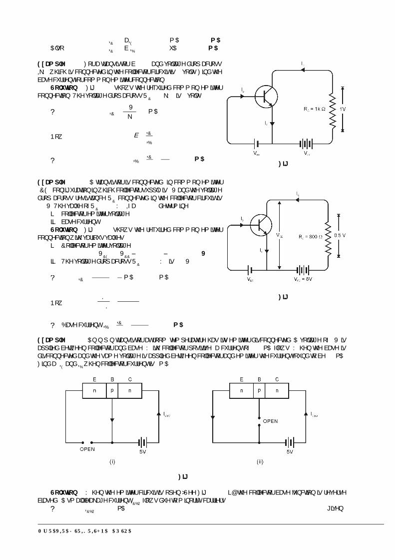
Mr. RAVIRAJ SRIKRISHNA AP/SOA 118
,&�� ��,(�� �����������P$��� ��11.76 mA$OVR ,&�� ���,%�� ����������X$��� ��11.76 mA
Example 8.11. )RU�D�WUDQVLVWRU��� ����DQG�YROWDJH�GURS�DFURVV,N�ZKLFK�LV�FRQQHFWHG�LQ�WKH�FROOHFWRU�FLUFXLW�LV���YROW���)LQG�WKHEDVH�FXUUHQW�IRU�FRPPRQ�HPLWWHU�FRQQHFWLRQ�
Solution. )LJ�������VKRZV�WKH�UHTXLUHG�FRPPRQ�HPLWWHUFRQQHFWLRQ��7KH�YROWDJH�GURS�DFURVV�5&�� ��N��LV���YROW�
P$�Nȍ�9�,&
1RZ%
&
,,
mA0.022���
ȕ,, &
%
Example 8.12. $�WUDQVLVWRU�LV�FRQQHFWHG��LQ�FRPPRQ�HPLWWHU�&(��FRQILJXUDWLRQ�LQ�ZKLFK�FROOHFWRU�VXSSO\�LV��9�DQG�WKH�YROWDJHGURS�DFURVV� UHVLVWDQFH�5&�FRQQHFWHG� LQ� WKH�FROOHFWRU�FLUFXLW� LV���9��7KH�YDOXH�RI�5&� �������,I�� �������GHWHUPLQH��
L� FROOHFWRU�HPLWWHU�YROWDJHLL� EDVH�FXUUHQWSolution. )LJ������� VKRZV� WKH� UHTXLUHG�FRPPRQ� HPLWWHU
FRQQHFWLRQ�ZLWK�YDULRXV�YDOXHV�L� &ROOHFWRU�HPLWWHU�YROWDJH�
�������9&(�� ��9&&�±������ ����±������ ��7.5 VLL� 7KH�YROWDJH�GURS�DFURVV�5&�� ������LV�����9�
P$�����P$��
ȍ������,&
1RZ �������
����Į�
Įȕ
��%DVH�FXUUHQW�� mA0.026��
�����ȕ,, &
%
Example 8.13. $Q�Q�S�Q�WUDQVLVWRU�DW�URRP�WHPSHUDWXUH�KDV�LWV�HPLWWHU�GLVFRQQHFWHG��$�YROWDJH�RI��9�LVDSSOLHG�EHWZHHQ�FROOHFWRU�DQG�EDVH��:LWK�FROOHFWRU�SRVLWLYH��D�FXUUHQW�RI�����$�IORZV��:KHQ�WKH�EDVH�LVGLVFRQQHFWHG�DQG�WKH�VDPH�YROWDJH�LV�DSSOLHG�EHWZHHQ�FROOHFWRU�DQG�HPLWWHU��WKH�FXUUHQW�IRXQG�WR�EH����$�)LQG���,(�DQG�,%�ZKHQ�FROOHFWRU�FXUUHQW�LV��P$�
Fig. 1.23
Solution. :KHQ�WKH�HPLWWHU�FLUFXLW�LV�RSHQ�>6HH�)LJ��������L�@��WKH�FROOHFWRU�EDVH�MXQFWLRQ�LV�UHYHUVHELDVHG���$�VPDOO�OHDNDJH�FXUUHQW�,&%2�IORZV�GXH�WR�PLQRULW\�FDUULHUV�
,&%2�� ������$ ���JLYHQ
Fig. 1.21
Fig. 1.22
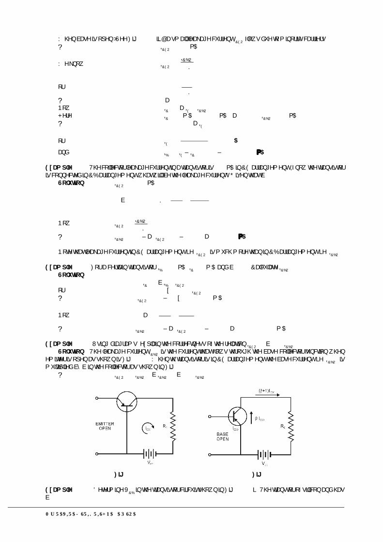
Mr. RAVIRAJ SRIKRISHNA AP/SOA 119
:KHQ�EDVH�LV�RSHQ�>6HH�)LJ��������LL�@��D�VPDOO�OHDNDJH�FXUUHQW�,&(2�IORZV�GXH�WR�PLQRULW\�FDUULHUV� ,&(2�� �����$
:H�NQRZ ,&(2�� � Į��,&%2
RU ����� ��Į��
���
�� ������1RZ ��,&�� ���,(���,&%2+HUH ��,&�� ���P$�� �������$���� ��������,&%2� �����$ ��������������� ��������,(������
RU ��,(�� �� μA1010����
��������
DQG ��,%�� ��,(�±�,&� ������±������� ��10 A
Example 8.14. 7KH�FROOHFWRU�OHDNDJH�FXUUHQW�LQ�D�WUDQVLVWRU�LV�����$�LQ�&(�DUUDQJHPHQW��,I�QRZ�WKH�WUDQVLVWRULV�FRQQHFWHG�LQ�&%�DUUDQJHPHQW��ZKDW�ZLOO�EH�WKH�OHDNDJH�FXUUHQW"�*LYHQ�WKDW�� �����
Solution. ,&(2�� ������$
�� ������������ ���������
����ȕ
ȕĮ
1RZ� ,&(2�� �Į��
,&%2
,&%2�� �����±���,&(2� ����±������������� �2.4 A
1RWH�WKDW�OHDNDJH�FXUUHQW�LQ�&(�DUUDQJHPHQW��L�H��,&(2��LV�PXFK�PRUH�WKDQ�LQ�&%�DUUDQJHPHQW��L�H��,&%2��
Example 8.15. )RU�D�FHUWDLQ�WUDQVLVWRU��,%� ����$��,&� ���P$�DQG�� �����&DOFXODWH�,&%2�Solution.
���,&�� ��,%���,&(2RU ��� �����[��������,&(2
,&(2�� ����±����[������ �����P$
1RZ �� �� ��������
���ȕ
ȕ
,&%2�� �����±���,&(2�� �����±�������������� ���������P$
Example 8.16. 8VLQJ�GLDJUDPV��H[SODLQ�WKH�FRUUHFWQHVV�RI�WKH�UHODWLRQ�,&(2� ��������,&%2�Solution. 7KH�OHDNDJH�FXUUHQW�,&%2�LV�WKH�FXUUHQW�WKDW�IORZV�WKURXJK�WKH�EDVH�FROOHFWRU�MXQFWLRQ�ZKHQ
HPLWWHU�LV�RSHQ�DV�VKRZQ�LV�)LJ���������:KHQ�WK�WUDQVLVWRU�LV�LQ�&(�DUUDQJHPHQW��WKH�EDVH�FXUUHQW��L�H��,&%2��LVPXOWLSOLHG�E\��LQ�WKH�FROOHFWRU�DV�VKRZQ�LQ�)LJ�������
,&(2�� ��,&%2����,&%2� ��������,&%2
Fig. 1.24 Fig. 1.25
Example 8.17. 'HWHUPLQH�9&%�LQ�WKH�WUDQVLVWRU�FLUFXLW�VKRZQ�LQ�)LJ��������L���7KH�WUDQVWRU�RI�VLOLFRQ�DQG�KDV� �����

Mr. RAVIRAJ SRIKRISHNA AP/SOA 120
Fig. 1.26
Solution. )LJ��������L��VKRZV�WKH�WUDQVLVWRU�FLUFXLW�ZKLOH�)LJ��������LL��VKRZV�WKH�YDULRXV�FXUUHQWV�DQGYROWDJHV�DORQJ�ZLWK�SRODULWLHV�
$SSO\LQJ�.LUFKKRIIV�YROWDJH�ODZ�WR�EDVH�HPLWWHU�ORRS��ZH�KDYH�9%%�� ��,%5%�±�9%(�� ���
RU ,%�� �� ȝ$���Nȍ�����9�9
599
%
%(%%
��,&�� ��,%� �����������$�� ������P$1RZ �����������9&(�� ��9&&�±�,&5&
������ ����9�������P$��������� ���9�±�����9� �����9:H�NQRZ�WKDW�� �����������9&(�� ��9&%���9%(
�����������9&%�� ��9&(�±�9%(�� �������±������ � 2.85V
Example 8.18. ,Q�D�WUDQVLVWRU��,%� ����$��,(� ����P$�DQG�� ������'HWHUPLQH�WKH��UDWLQJ�RI�WKH�WUDQVLVWRU�7KHQ�GHWHUPLQH�WKH�YDOXH�RI�,&�XVLQJ�ERWK�WKH��UDWLQJ�DQG��UDWLQJ�RI�WKH�WUDQVLVWRU�
Solution.
0.9977
����
����ȕ
ȕĮ
��,&�� ���,(�� ����������������P$��� ��29.93 mA$OVR ��������������,&�� ��%�,%�� �������������$��� ��29.93 mA
Example 8.19.� � �$�WUDQVLVWRU�KDV� WKH�IROORZLQJ� UDWLQJ��� ,&��PD[�� � � �����P$�DQG�PD[� ������'HWHUPLQH� WKHPD[LPXP�DOORZDEOH�YDOXH�RI�,%�IRU�WKH�GHYLFH�
Solution.
mA1.67���
P$���ȕ
,,
PD[
�PD[�&�PD[�%
)RU�WKLV�WUDQVLVWRU��LI�WKH�EDVH�FXUUHQW�LV�DOORZHG�WR�H[FHHG������P$��WKH�FROOHFWRU�FXUUHQW�ZLOO�H[FHHG�LWVPD[LPXP�UDWLQJ�RI�����P$�DQG�WKH�WUDQVLVWRU�ZLOO�SUREDEO\�EH�GHVWUR\HG�
Example 8.20. )LJ�������VKRZV�WKH�RSHQ�FLUFXLW�IDLOXUHV�LQ�D�WUDQVLVWRU��:KDW�ZLOO�EH�WKH�FLUFXLW�EHKDYLRXU�LQHDFK�FDVH"
Fig. 1.27
Mr. RAVIRAJ SRIKRISHNA AP/SOA 121
Solution. )LJ�������VKRZV�WKH�RSHQ�FLUFXLW�IDLOXUHV�LQ�D�WUDQVLVWRU��:H�VKDOO�GLVFXVV�WKH�FLUFXLW�EHKDYLRXULQ�HDFK�FDVH�
L� Open emitter. )LJ��������L��VKRZV�DQ�RSHQ�HPLWWHU�IDLOXUH�LQ�D�WUDQVLVWRU��6LQFH�WKH�FROOHFWRU�GLRGH�LVQRW�IRUZDUG�EDLVHG��LW�LV�2))�DQG�WKHUH�FDQ�EH�QHLWKHU�FROOHFWRU�FXUUHQW�QRU�EDVH�FXUUHQW��7KHUHIRUH��WKHUH�ZLOO�EHQR�YROWDJH�GURSV�DFURVV�HLWKHU�UHVLVWRU�DQG�WKH�YROWDJH�DW�WKH�EDVH�DQG�DW�WKH�FROOHFWRU�OHDGV�RI�WKH�WUDQVLVWRUZLOO�EH���9�
LL� Open-base. )LJ��������LL��VKRZV�DQ�RHSQ�EDVH�IDLOXUH�LQ�D�WUDQVLVWRU��6LQFH�WKH�EDVH�LV�RSHQ��WKHUHFDQ�EH�QR�EDVH�FXUUHQW�VR�WKDW�WKH�WUDQVLVWRU�LV�LQ�FXW�RII��7KHUHIRUH��DOO�WKH�WUDQVLVWRU�FXUUHQWV�DUH��$��,Q�WKLVFDVH��WKH�EDVH�DQG�FROOHFWRU�YROWDJHV�ZLOO�ERWK�EH�DW���9�
Note. ,W�PD\�EH�QRWHG�WKDW�DQ�RSHQ�IDLOXUH�DW�HLWKHU�WKH�EDVH�RU�HPLWWHU�ZLOO�SURGXFH�VLPLODU�UHVXOWV�LLL� Open collector. )LJ��������LLL��VKRZV�DQ�RSHQ�FROOHFWRU�IDLOXUH�LQ�D�WUDQVLVWRU��,Q�WKLV�FDVH��WKH�HPLWWHU
GLRGH�LV�VWLOO�21��VR�ZH�H[SHFW�WR�VHH����9�DW�WKH�EDVH��+RZHYHU��ZH�ZLOO�VHH���9�DW�WKH�FROOHFWRU�EHFDXVHWKHUH�LV�QR�FROOHFWRU�FXUUHQW�
Example 8.21. )LJ�������VKRZV�WKH�VKRUW�FLUFXLW�IDLOXUHV�LQ�D�WUDQVLVWRU��:KDW�ZLOO�EH�WKH�FLUFXLW�EHKDYLRXU�LQHDFK�FDVH"
Fig. 1.22
Solution. )LJ�������VKRZV�WKH�VKRU�FLUFXLW�IDLOXUHV�LQ�D�WUDQVLVWRU��:H�VKDOO�GLVFXVV�WKH�FLUFXLW�EHKDYLRXULQ�HDFK�FDVH�
L� Collector-emitter short. )LJ��������L��VKRZV�D�VKRUW�EHWZHHQ�FROOHFWRU�DQG�HPLWWHU��7KH�HPLWWHU�GLRGHLV�VWLOO�IRUZDUG�ELDVHG��VR�ZH�H[SHFW�WR�VHH����9�DW�WKH�EDVH��6LQFH�WKH�FROOHFWRU�LV�VKRUWHG�WR�WKH�HPLWWHU��9& �9(� ��9�
LL� Base-emitter short. )LJ��������LL��VKRZV�D�VKRUW�EHWZHHQ�EDVH�DQG�HPLWWHU��6LQFH�WKH�EDVH�LV�QRZGLUHFWO\�FRQQHFWHG�WR�JURXQG��9%� ����7KHUHIRUH��WKH�FXUUHQW�WKURXJK�5%�ZLOO�EH�GLYHUWHG�WR�JURXQG�DQG�WKHUH�LV�QRFXUUHQW�WR�IRUZDUG�ELDV�WKH�HPLWWHU�GLRGH��$V�D�UHVXOW��WKH�WUDQVLVWRU�ZLOO�EH�FXW�RII�DQG�WKHUH�LV�QR�FROOHFWRUFXUUHQW��6R�ZH�ZLOO�H[SHFW�WKH�FROOHFWRU�YROWDJH�WR�EH���9�
LLL� Collector-base short. )LJ��������LLL��VKRZV�D�VKRUW�EHWZHHQ�WKH�FROOHFWRU�DQG�WKH�EDVH��,Q�WKLV�FDVH�WKH�HPLWWHU�GLRGH�LV�VWLOO�IRUZDUG�ELDVHG�VR�9%� ����9��1RZ��KRZHYHU��EHFDXVH�WKH�FROOHFWRU�LV�VKRUWHG�WR�WKHEDVH��9&� �9%� ����9�
Note. 7KH�FROOHFWRU�HPLWWHU�VKRUW�LV�SUREDEO\�WKH�PRVW�FRPPRQ�W\SH�RI�IDXOW�LQ�D�WUDQVLVWRU��,W�LV�EHFDXVHWKH�FROOHFWRU�FXUUHQW��,&��DQG�FROOHFWRU�HPLWWHU�YROWDJH��9&(��DUH�UHVSRQVLEOH�IRU�WKH�PDMRU�SDUW�RI�WKH�SRZHUGLVVLSDWLRQ�LQ�WKH�WUDQVLVWRU��$V�ZH�VKDOO�VHH��6HH�$UW���������WKH�SRZHU�GLVVLSDWLRQ�LQ�D�WUDQVLVWRU�LV�PDLQO\�GXUWR�,&�DQG�9&(��L�H��3'� �9&(�,&���7KHUHIRUH��WKH�WUDQVLVWRU�FKLS�EHWZHHQ�WKH�FROOHFWRU�DQG�WKH�HPLWWHU�LV�PRVW�OLNHO\WR�PHOW�ILUVW�

Mr. RAVIRAJ SRIKRISHNA AP/SOA 122
Characteristics of Common Emitter Connection7KH�LPSRUWDQW�FKDUDFWHULVWLFV�RI�WKLV�FLUFXLW�DUUDQJHPHQW�DUH�WKH�LQSXW�FKDUDFWHULVWLFV�DQG�RXWSXW�FKDUDFWHULVWLFV�
Fig. 8.29
Input Characteristic. ,W� LV� WKH�FXUYH�EHWZHHQ�EDVH�FXUUHQW�,%�DQG�EDVH�HPLWWHU�YROWDJH�9%(�DW�FRQVWDQWFROOHFWRU�HPLWWHU�YROWDJH�9&(�
7KH�LQSXW�FKDUDFWHULVWLFV�RI�D�&(�FRQQHFWLRQ�FDQ�EH�GHWHUPLQHG�E\�WKH�FLUFXLW�VKRZQ�LQ�)LJ��������.HHSLQJ9&(�FRQVWDQW��VD\�DW���9���QRWH�WKH�EDVH�FXUUHQW�,%�IRU�YDULRXV�YDOXHV�RI�9%(��7KHQ�SORW�WKH�UHDGLQJV�REWDLQHG�RQWKH�JUDSK��WDNLQJ�,%�DORQJ�\�D[LV�DQG�9%(�DORQJ�[�D[LV��7KLV�JLYHV�WKH�LQSXW�FKDUDFWHULVWLF�DW�9&(� ���9�DVVKRZQ�LQ�)LJ��������)ROORZLQJ�D�VLPLODU�SURFHGXUH��D�IDPLO\�RI�LQSXW�FKDUDFWHULVWLFV�FDQ�EH�GUDZQ��7KH�IROORZLQJSRLQWV�PD\�EH�QRWHG�IURP�WKH�FKDUDFWHULVWLFV��
Fig. 1.1.
L� 7KH�FKDUDFWHULVWLF�UHVHPEOHV�WKDW�RI�D�IRUZDUG�ELDVHG�GLRGH�FXUYH��7KLV�LV�H[SHFWHG�VLQFH�WKH�EDVH�HPLWWHU�VHFWLRQ�RI�WUDQVLVWRU�LV�D�GLRGH�DQG�LW�LV�IRUZDUG�ELDVHG�
LL� $V�FRPSDUHG�WR�&%�DUUDQJHPHQW��,%�LQFUHDVHV�OHVV�UHSLGO\�ZLWK�9%(��7KHUHIRUH��LQSXW�UHVLVWDQFH�RI�D&(�FLUFXLW�LV�KLJKHU�WKDQ�WKDW�RI�&%�FLUFXLW�
Input resistance. ,W�LV�WKH�UDWLR�RI�FKDQJH�LQ�EDVH�HPLWWHU�YROWDJH��9%(��WR�WKH�FKDQJH�LQ�EDVH�FXUUHQW�,%��DW�FRQVWDQW�9&(�L�H�
,QSXW�UHVLVWDQFH����UL�� ��B
BE
IV
�DW�FRQVWDQW�9&(
7KH�YDOXH�RI�LQSXW�UHVLVWDQFH�IRU�D�&(�FLUFXLW�LV�RI�WKH�RUGHU�RI�D�IHZ�KXQGUHG�RKPV�
Output Characteristic. ,W�LV�WKH�FXUYH�EHWZHHQ�FROOHFWRU�FXUUHQW�,&�DQG�FROOHFWRU�HPLWWHU�YROWDJH�9&(�DW�FRQVWDQWEDVH�FXUUHQW�,%�
7KH�RXWSXW�FKDUDFWHULVWLFV�RI�D�&(�FLUFXLW�FDQ�EH�GUDZQ�ZLWK�WKH�KHOS�RI�WKH�FLUFXLW�VKRZQ�LQ�)LJ�������.HHSLQJ�WKH�EDVH�FXUUHQW�,%�IL[HG�DW�VRPH�YDOXH�VD\����X$��QRWH�WKH�FROOHFWRU�FXUUHQW�,&�IRU�YDULRXV�YDOXHV�RI9&(��7KHQ�SORW�WKH�UHDVLQJV�RQ�D�JUDSK��WDNLQJ�,&�DORQJ�\�D[LV�DQG�9&(�DORQJ�[�D[LV��7KLV�JLYHV�WKH�RXWSXWFKDUDFWHULVWLFV�DW�,%� ���X$�DV�VKRZQ�)LJ��������L���7KH�WHVW�FDQ�EH�UHSHDWHG�IRU�,%� ����X$�WR�REWDLQ�WKH�QHZRXWSXW�FKDUDFWHULVWLF�DV�VKRZQ�LQ�)LJ��������LL���)ROORZLQJ�VLPLODU�SURFHGXUH��D�IDPLO\�RI�RXWSXW�FKDUDFWHULVWLFVFDQ�EH�GUDZQ�DV�VKRZQ�LQ�)LJ��������LLL��

Mr. RAVIRAJ SRIKRISHNA AP/SOA 123
Fig. 1.1.
7KH�IROORZLQJ�SRLQWV�PD\�EH�QRWHG�IURP�WKH�FKDUDFWHULVWLFV�L� 7KH�FROOHFWRU�FXUUHQW�,&�YDULHV�ZLWK�9&(�IRU�9&(�EHWZHHQ���DQG��9�RQO\��$IWHU�WKLV��FROOHFWRU�FXUUHQW
EHFRPHV�DOPRVW�FRQVWDQW�DQG�LQGHSHQGHQW�RI�9&(��7KLV�YDOXH�RI�9&(�XSWR�ZKLFK�FROOHFWRU�FXUUHQW�,&�FKDQJHVZLWK�9&(�LV�FDOOHG�WKH�NQHH�YROWDJH��9NQHH����7KH�WUDQVLVWRUV�DUH�DOZD\V�RSHUDWHG�LQ�WKH�UHJLRQ�DERYH�NQHHYROWDJH�
LL� $ERYH�NQHH�YROWDJH��,&�LV�DOPRVW�FRQVWDQW��+RZHYHU��D�VPDOO�LQFUHDVH�LQ�,&�ZLWK�LQFUHDVLQJ�9&(�LVFDXVHG�E\�WKH�FROOHFWRU�GHSOHWLRQ�OD\HU�JHWWLQJ�ZLGHU�DQG�FDSWXULQJ�D�IHZ�PRUH�PDMRULW\�FDUULHUV�EHIRUH�HOHFWURQ�KROH�FRPELQDWLRQV�RFFXU�LQ�WKH�EDVH�DUHD�
LLL� )RU�DQ\�YDOXH�RI�9&(�DERYH�NQHH�YROWDJH��WKH�FROOHFWRU�FXUUHQW�,&�LV�DSSUR[LPDWHO\�HTXDO�WR�[�,%�
Output resistance. ,W�LV�WKH�UDWLR�RI�FKDQJH�LQ�FROOHFWRU�HPLWWHU�YROWDJH��9&(��WR�WKH�FKDQJH�LQ�FROOHFWRU�FXUUHQW�,&��DW�FRQVWDQW�,%�L�H�
2XWSXW�UHVLVWDQFH��UR�� ��C
CE
IV
�DW�FRQVWQDW�,%
,W�PD\�EH�QRWHG�WKDW�ZKHUHDV�WKH�RXWSXW�FKDUDFWHULVWLFV�RI�&%�FLUFXLW�DUH�KRUL]RQWDO��WKH\�KDYH�PRWLFHDEOHVORSH�IRU�WKH�&(�FLUFXLW��7KHUHIRUH��WKH�RXWSXW�UHVLVWDQFH�RI�D�&(�FLUFXLW�LV�OHVV�WKDQ�WKDW�RI�&%�FLUFXLW��,WV�YDOXHLV�WKH�RUGHU�RI����N�
Common Collector Connection,Q�WKLV�FLUFXLW�DUUDQJHPHQW��LQSXW�LV�DSSOLHG�EHWZHHQ�EDVH�DQG�FROOHFWRU�ZKLOH�RXWSXW�LV�WDNHQ�EHWZHHQ�WKHHPLWWHU�DQG�FROOHFWRU��+HUH��FROOHFWRU�RI�WKH�WUDQVLVWRU�LV�FRPPRQ�WR�ERWK�LQSXW�DQG�RXWSXW�FLUFXLWV�DQG�KHQFHWKH�QDPH�FRPPRQ�FROOHFWRU�FRQQHFWLRQ��)LJ��������L��VKRZV�FRPPRQ�FROOHFWRU�QSQ�WUDQVLVWRU�FLUFXLW�ZKHUHDV)LJ�������VKRZV�FRPPRQ�FROOHFWRU�SQS�FLUFXLW�
Fig. 1.1.
Current amplification factor ,Q�FRPPRQ�FROOHFWRU�FLUFXLW��LQSXW�FXUUHQW�LV�WKH�EDVH�FXUUHQW�,%�DQG�RXWSXW�FXUUHQW�LV�WKH�HPLWWHU�FXUUHQW�,(�7KHUHIRUH��FXUUHQW�DPSOLILFDWLRQ�LQ�WKLV�FLUFXLW�DUUDQJHPHQW�FDQ�EH�GHILQHG�DV�XQGHU��
7KH�UDWLR�RI�FKDQJH�LQ�HPLWWHU�FXUUHQW��,(��WR�WKH�FKDQJH�LQ�EDVH�FXUUHQW��,%��LV�NQRZQ�DV�FXUUHQW�DPSOLILFDWLRQIDFWRU�LQ�FRPPRQ�FROOHFWRU��&&��DUUDQJHPHQW�L�H�
Mr. RAVIRAJ SRIKRISHNA AP/SOA 124
B
E
II
7KLV�FLUFXLW�SURYLGHV�DERXW�WKH�VDPH�FXUUHQW�JDLQ�DV�WKH�FRPPRQ�HPLWWHU�DV� CE II ~ ��+RZHYHU��LWVVYROWDJH�JDLQ�LV�DOZD\V�OHVV�WKDQ���
Relation between and
B
E
II
E
C
II
1RZ ,(�� ��,%���,&RU ,(�� ��,%���,&RU ,%�� ��,(�±�,&6XEVWLWXWLQJ�WKH�YDOXH�RI�,%�LQ�H[S���L���ZH�JHW�
CE
E
III
'LYLGLQJ�WKH�QXPEHUDWRU�DQG�GHQRPLQDWRU�RI�5�+�6��E\�,(��ZH�JHW�
E
C
E
C
E
E
E
E
II
II
II
II
11
11
Expression for collector current:H�NQRZ �����������,&�� ��,(���,&%2$OVR ,(�� ��,%���,&� �,%����,(���,&%2� ,(����±���� ��,%���,&%2
RU
11CBOB
EIII
RU ,&�� ��,(�� ���������,%����������,&%2LLL� Applications. 7KH�FRPPRQ�FROOHFWRU�FLUFXLW�KDV�YHU\�KLJK�LQSXW�UHVLVWDQFH��DERXW�����N��DQG�YHU\
ORZ�RXWSXW�UHVLVWDQFH��DERXW������'XH�WR�WKLV�UHDVRQ��WKH�YROWDJH�JDLQ�SURYLGHG�E\�WKLV�FLUFXLW�LV�DOZD\V�OHVVWKDQ����7KHUHIRUH��WKLV�FLUFXLW�DUUDQJHPHQW�LV�VHOGRP�XVHG�IRU�DPSOLILFDWLRQ��+RZHYHU��GXH�WR�UHODWLYHO\�KLJKLQSXW�UHVLVWDQFH�DQG�ORZ�RXWSXW�UHVLWDQFH��WKLV�FLUFXLW�LV�SULPDULO\�XVHG�IRU�LPSHGDQFH�PDWFKLQJ�L�H��IRU�GULYLQJD�ORZ�LPSHGDQFH�ORDG�IURP�D�KLJK�LPSHGDQFH�VRXUFH�
Comparison of Transistor Connections7KH�FRPSDULVRQ�RI�YDULRXV�FKDUDFWHULVWLFV�RI�WKH�WKUHH�FRQQHFWLRQV�LV�JLYHQ�EHORZ�LQ�WKH�WDEXODU�IRUP�
S.No. Characteristic Common Base Common Emitter Collector Collector
�� ,QSXW�UHVLVWDQFH /RZ��DERXW����� /RZ��DERXW������ 9HU\�KLJK��DERXW�����N�
�� 2XWSXW�UHVLVWDQFH 9HU\�KLJK��DERXW +LJK��DERXW����N� /RZ��DERXW���������N2�
�� 9ROWDJH�JDLQ $ERXW���� $ERXW���� /HVV�WKDQ��
�� $SSOLFDWLRQV )RU�KLJK�IUHTXHQF\ )RU�DXGLR�IUHTXHQF\ )RU�LPSHGDQFHDSSOLFDWLRQV DSSOLFDWLRQ PDWFKLQJ
�� &XUUHQW�JDLQ 1R��OHVV�WKDQ��� +LJK��%� $SSUHFLDEOH
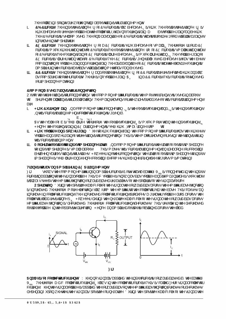
Mr. RAVIRAJ SRIKRISHNA AP/SOA 125
7KH�IROORZLQJ�SRLQWV�DUH�ZRUWK�QRWLQJ�DERXW�WUDQVLVWRU�DUUDQJHPHQWV��L� CB Circuit. 7KH�LQSXW�UHVLVWDQFH��UL��RI�&%�FLUFXLW�LV�ORZ�EHFDXVH�,(�LV�KLJK��7KH�RXWSXW�UHVLVWDQFH��UR��LV
KLJK�EHFDXVH�RI�UHYHUVH�YROWDJH�DW�WKH�FROOHFWRU��,W�KDV�QR�FXUUHQW�JDLQ��������EXW�YROWDJH�JDLQ�FDQ�EH�KLJK�7KH�&%�FLUFXLW�LV�VHOGRP�XVHG��7KH�RQO\�DGYDQWDJH�RI�&%�FLUFXLW�LV�WKDW�LW�SURYLGHV�JRRG�VWDELOLW\�DJDLQVWLQFUHDVH�LQ�WHPSHUDWXUH�
LL� CE Circuit. 7KH�LQSXW�UHVLVWDQFH��UL��RI�D�&(�FLUFXLW�LV�KLJK�EHFDXVH�RI�VPDOO�,%��7KHUHIRUH��UL�IRU�D�&(FLUFXLW�LV�PXFK�KLJKHU�WKDQ�WKDW�RI�&%�FLUFXLW��7KH�RXWSXW�UHVLVWDQFH��UR��RI�&(�FLUFXLW�LV�VPDOOHU�WKDQ�WKDWRI�&%�FLUFXLW��7KH�FXUUHQW�JDLQ�RI�&(�FLUFXLW�LV�ODUJH�EHFDXVH�,&�LV�PXFK�ODUJHU�WKDQ�,%��7KH�YROWDJH�JDLQ�RI&(�FLUFXLW� LV�ODUJHU�WKDQ�WKDW�RI�&%�FLUFXLW��7KH�&(�FLUFXLW� LV�JHQHUDOO\�XVHG�EHFDXVH�LW�KDV�WKH�EHVWFRPELQDWLRQ�RI�YROWDJH�JDLQ�DQG�FXUUHQW�JDLQ��7KH�GLVDGYDQWDJH�RI�&(�FLUFXLW�LV�WKDW�WKH�OHDNDJH�FXUUHQW�LVDPSOLILHU�LQ�WKH�FLUFXLW��EXW�ELDV�VWDELOLVDWLRQ�PHWKRGV�FDQ�EH�XVHG�
LLL� CC Circuit. 7KH�LQSXW�UHVLVWDQFH��UL��DQG�RXWSXW�UHVLVWDQFH��UR��RI�&&�FLUFXLW�DUH�UHVSHFWLYHO\�KLJK�DQG�ORZDV�FRPSDUHG�WR�RWKHU�FLUFXLWV��7KHUH�LV�QR�YROWDJH�JDLQ��$Y������LQ�D�&&�FLUFXLW��7KLV�FLUFXLW�LV�RIWHQ�XVHGIRU�LPSHGDQFH�PDWFKLQJ�
Commonly Used Transistor Connection2XW�RI�WKH�WKUHH�WUDQVLVWRU�FRQQHFWLRQV��WKH�FRPPRQ�HPLWWHU�FLUFXLW�LV�WKH�PRVW�HIILFLHQW��,W�LV�XVHG�LQ�DERXW���WR����SHU�FHQW�RI�DOO�WUDQVLVWRU�DSSOLFDWLRQV��7KH�PDLQ�UHDVRQV�IRU�WKH�ZLGHVSUHDG�XVH�RI�WKLV�FLUFXLW�DUUDQJHPHQWDUH��L� High Current Gain. ,Q�D�FRPPRQ�HPLWWHU�FRQQHFWLRQ��,&�LV�WKH�RXWSXW�FXUUHQW�DQG�,%�LV�WKH�LQSXW�FXUUHQW�
,Q�WKLV�FLUFXLW�DUUDQJHPHQW��FROOHFWRU�FXUUHQW�LV�JLYHQ�E\��,&�� ���,%���,&(2
$V�WKH�YDOXH�RI��LV�YHU\�ODUJH��WKHUHIRUH��WKH�RXWSXW�FXUUHQW�,&�LV�PXFK�PRUH�WKDQ�WKH�LQSXW�FXUUHQW�,%�+HQFH��WKH�FXUUHQW�JDLQ�LQ�&(�DUUDQJHPHQW�LV�YHU\�KLJK��,W�PD\�UDQJH�IURP����WR�����
LL� High voltage and power gain. 'XH�WR�KLJK�FXUUHQW�JDLQ��WKH�FRPPRQ�HPLWWHU�FLUFXLW�KDV�WKH�KLJKHVWYROWDJH�DQG�SRZHU�JDLQ�RI�WKUHH�WUDQVLVWRU�FRQQHFWLRQV��7KLV�LV�WKH�PDMRU�UHDVRQ�IRU�XVLQJ�WKH�WUDQVLVWRU�LQWKLV�FLUFXLW�DUUDQJPHQW�
LLL� Moderate output to input impedance ratio. ,Q�D�FRPPRQ�HPLWWHU�FLUFXLW��WKH�UDWLR�RI�RXWSXW�LPSHGDQFHWR�LQSXW�LPSHUDQFH�LV�VPDOO��DERXW������7KLV�PDNHV�WKLV�FLUFXLW�DUUDQJHPHQW�DQ�LGHDO�RQH�IRU�FRXSOLQJEHWZHHQ�YDULRXV�WUDQVLVWRU�VWDJHV��+RZHYHU��LQ�RWKHU�FRQQHFWLRQV��WKH�UDWLR�RI�RXWSXW�LPSHGDQFH�WR�LQSXWLPSHGDQFH�LV�YHU\�ODUJH�DQG�KHQFH�FRXSOLQJ�EHFRPHV�KLJKO\�LQHIILFLHQW�GXH�WR�JURVV�PLVPDWFKLQJ�
Transistor as an Amplifier in CE Arrangement)LJ�������VKRZV�WKH�FRPPRQ�HPLWWHU�QSQ�DPSOLILHU�FLUFXLW��1RWH�WKDW�D�EDWWHU\�9%%�LV�FRQQHFWHG�LQ�WKH�LQSXWFLUFXLW�LQ�DGGLWLRQ�WR�WKH�VLJQDO�YROWDJH��7KLV�D�F��YROWDJH�LV�NQRZQ�DV�ELDV�YROWDJH�DQG�LWV�PDJQLWXGH�LV�VXFK�WKDWLW�DOZD\V�NHHSV�WKH�HPLWWHU�MXQFWLRQ�IRUZDUG�ELDVHG�UHJDUGOHVV�RI�WKH�SRODULW\�RI�WKH�VLJQDO�VRXUFH�
Operation. 'XULQJ�WKH�SRVLWLYH�KDOI�F\FOH�RI�WKH�VLJQDO��WKH�IRUZDUG�ELDV�DFURVV�WKH�HPLWWHU�EDVH�MXQFWLRQLV�LQFUHDVHG��7KHUHIRUH��PRUH�HOHFWURQV�IORZ�IURP�WKH�HPLWWHU�WR�WKH�FROOHFWRU�YLD�WKH�EDVH��7KLV�FDXVHV�DQLQFUHDVH�LQ�FROOHFWRU�FXUUHQW��7KH�LQFUHDVHG�FROOHFWRU�FXUUHQW�SURGXFHV�D�JUHDWHU�YROWDJH�GURS�DFURVV�WKHFROOHFWRU�ORDG�UHVLVWDQFH�5&���+RZHYHU��GXULQJ�WKH�QHJDWLYH�KDOI�F\FOH�RI�WKH�VLJQDO��WKH�IRUZDUG�ELDV�DFURVVHPLWWHU�EDVH�MXQFWLRQ�LV�GHFUHDVHG��7KHUHIRUH��FROOHFWRU�FXUUHQW�GHFUHDVHV��7KLV�UHVXOWV�LQ�WKH�GHFUHDVHGRXWSXW�YROWDJH��LQ�WKH�RSSRVLWH�GLUHFWLRQ���+HQFH��DQ�DPSOLILHG�RXWSXW�LV�REWDLQHG�DFURVV�WKH�ORDG�
Fig. 1.1
Analysis of collector currents. :KHQ�QR�VLJQDO�LV�DSSOLHG��WKH�LQSXW�FLUFXLW�LV�IRUZDUG�ELDVHG�E\�WKH�EDWWHU\9%%���7KHUHIRUH��D�G�F��FROOHFWRU�FXUUHQW�,&�IORZV�LQ�WKH�FROOHFWRU�FLUFXLW��7KLV�LV�FDOOHG�]HUR�VLJQDO�FROOHFWRUFXUUHQW��:KHQ�WKH�VLJQDO�YROWDJH�LV�DSSOLHG��WKH�IRUZDUG�ELDV�RQ�WKH�HPLWWHU�ELDV�MXQFWLRQ�LFUHDVHV�RU�GHFUHDVHVGHSHQGLQJ�XSRQ�ZKHWKHU�WKH�VLJQDO�LV�SRVLWLYH�RU�QHJDWLYH��'XULQJ�WKH�SRVLWLYH�KDOI�F\FOH�RI�WKH�VLJQDO��WKH
Mr. RAVIRAJ SRIKRISHNA AP/SOA 126
IRUZDUG�ELDV�RQ�HPLWWHU�EDVH�MXQFWLRQ�LV�LQFUHDVHG��FDXVLQJ�WRWDO�FROOHFWRU�FXUUHQW�L&�WR�LQFUHDVH��5HYHUVH�ZLOOKDSSHQ�IRU�WKH�QHJDWLYH�KDOI�F\FOH�RI�WKH�VLJQDO�
)LJ�������VKRZV�WKH�JUDSK�RI�WRWDO�FROOHFWRU�FXUUHQW�L&�YHUVXV�WLPH��)URP�WKH�JUDSK��LW�LV�FOHDU�WKDW�WRWDOFROOHFWRU�FXUUHQW�FRQVLVWV�RI�WZR�FRPSRQHQWV��QDPHO\��
L� 7KH�G�F��FROOHFWRU�FXUUHQW�,&��]HUR�VLJQDO�FROOHFWRU�FXUUHQW��GXH�WR�ELDV�EDWWHU\�9%%���7KLV�LV�WKH�FXUUHQWWKDW�IORZV�LQ�WKH�FROOHFWRU�LQ�WKH�DEVHQFH�RI�VLJQDO�
LL� WKH�D�F��FROOHFWRU�FXUUHQW�L&�GXH�WR�VLJQDO� ����7RWDO�FROOHFWRU�FXUUHQW��L&� �L&���,&7KH�XVHIXO�RXWSXW�LV�WKH�YROWDJH�GURS�DFURVV�FROOHFWRU�ORDG�5&�GXH�WR�WKH�D�F��FRPSRQHQW�L&��7KH�SXUSRVH
RI�]HUR�VLJQDO�FROOHFWRU�FXUUHQW�LV�WR�HQVXUH�WKDW�WKH�HPLWWHU�EDVH�MXQFWLRQ�LV�IRUZDUG�ELDVHG�DW�DOO�WLPHV��7KHWDEOH�EHORZ�JLYHV�WKH�V\PEROV�XVXDOO\�HPSOR\HG�IRU�FXUUHQWV�DQG�YROWDJHV�LQ�WUDQVLVWRU�DSSOLFDWLRQV�
S.No. Particular Instantaneous a.c. d.c. Total
�� (PLWWHU�FXUUHQW LH ,( L(�� &ROOHFWRU�FXUUHQW LF ,& L&�� %DVH�FXUUHQW LE ,% L%�� &ROOHFWRU�HPLWWHU�YROWDJH YFH 9&( Y&(
�� (PLWWHU�EDVH�YROWDJH YHE 9(% Y(%
Transistor Load Line Analysis,Q�WKH�WUDQVLVWRU�FLUFXLW�DQDO\VLV��LW�LV�JHQHUDOO\�UHTXLUHG�WR�GHWHUPLQH�WKH�FROOHFWRU�FXUUHQW�IRU�YDULRXV�FROOHFWRU�HPLWWHU�YROWDJHV��2QH�RI�WKH�PHWKRGV�FDQ�EH�XVHG�WR�SORW�WKH�RXWSXW�FKDUDFWHULVWLFV�DQG�GHWHUPLQH�WKH�FROOHFWRUFXUUHQW�DW�DQ\�GHVLUHG�FROOHFWRU�HPLWWHU�YROWDJH��+RZHYHU��D�PRUH�FRQYHQLHQW�PHWKRG��NQRZQ�DV�ORDG�OLQHPHWKRG�FDQ�EH�XVHG�WR�VROYH�VXFK�SUREOHPV��$V�H[SODLQHG�ODWHU�LQ�WKLV�VHFWLRQ��WKLV�PHWKRG�LV�TXLWH�HDV\�DQGLV�IUHTXHQWO\�XVHG�LQ�WKH�DQDO\VLV�RI�WUDQVLVWRU�DSSOLFDWLRQV�
D.C. load line. &RQVLGHU�D�FRPPRQ�HPLWWHU�QSQ�WUDQVLVWRU�FLUFXLW�VKRZQ�LQ�)LJ��������L��ZKHQ�QR�VLJQDO�LVDSSOLHG��7KHUHIRUH��G�F��FRQGLWLRQV�SUHYDLO�LQ�WKH�FLUFXLW��7KH�RXWSXW�FKDUDFWHULVWLFV�WR�WKLV�FLUFXLW�DUH�VKRZQ�LQ)LJ��������LL��
7KH�YODXH�RI�FROOHFWRU�HPLWWHU�YROWDJH�9&(�DW�DQ\�WLPH�LV�JLYHQ�E\��9&(�� ��9&&�±�,&5&
Fig. 8.35
$V�9&&�DQG�5&�DUH�IL[HG�YDOXHV��WKHUHIRUH��LW�LV�D�ILUVW�GHJUHH�HTXDWLRQ�DQG�FDQ�EH�UHSUHVHQWHG�E\�D�VWUDLJKWOLQH�RQ�WKH�RXWSXW�FKDUDFWHULVWLFV��7KLV�LV�NQRZQ�DV�G�F��ORDG�OLQH�DQG�GHWHUPLQHV�WKH�ORFXV�RI�9&(�±�,&�SRLQWV�IRUDQ\�JLYHQ�YDOXH�RI�5&��7R�DGG�ORDG�OLQH��ZH�QHHG�WZR�HQG�SRLQWV�RI�WKH�VWUDLJKW�OLQH��7KHVH�WZR�SRLQWV�FDQ�EHORDFWHG�DV�XQGHU��
L� :KHQ�WKH�FROOHFWRU�FXUUHQW�,&� ����WKHQ�FROOHFWRU�HPLWWHU�YROWDJH�LV�PD[LPXP�DQG�LV�HTXDO�WR�9&&�L�H�0D[���9&(�� ��9&&�±�,&5&
��9&& � �,&� ���

Mr. RAVIRAJ SRIKRISHNA AP/SOA 127
7KLV�JLYHV�WKH�ILUVW�SRLQW�%��2%� �9&&��RQ�WKH�FROOHFWRU�HPLWWHU�YROWDJH�D[LV�DV�VKRZQ�LQ�)LJ��������LL��LL� :KHQ�FROOHFWRU�HPLWWHU�YROWDJH�9&(�±����WKH�FROOHFWRU�FXUUHQW�LV�PD[LPXP�DQG�LV�HTXDO�WR�9&&�5&�L�H�
9&(�� ��9&&�±�,&5&RU ������ ��9&&�±�,&5&
����0D[����,&�� ��9&&�5&
7KLV�JLYHV�WKH�VHFRQG�SRLQW�$��2$� �9&&�5&��RQ�WKH�FROOHFWRU�FXUUHQW�D[LV�DV�VKRZQ�LQ�)LJ��������LL���%\MRLQLQJ�WKHVH�WZR�SRLQWV��G�F��ORDG�OLQH�$%�LV�FRQVWUXFWHG�
Fig. 8.36
Importance. 7KH�FXUUHQW��,&��DQG�YROWDJH��9&(��FRQGLWLRQV�LQ�WKH�WUDQVLVWRU�FLUFXLW�DUH�UHSUHVHQWHG�E\�VRPHSRLQW�RQ�WKH�RXWSXW�FKDUDFWHULVWLFV���7KH�VDPH�LQIRUPDWLRQ�FDQ�EH�REWDLQHG�IURP�WKH�ORDG�OLQH��7KXV�ZKHQ�,&�LVPD[LPXP�� �9&&�5&���WKHQ�9&(� ���DV�VKRZQ�LQ�)LJ���������,I�,&� ����WKHQ�9&(�LV�PD[LPXP�DQG�LV�HTXDO�WR�9&&�)RU�DQ\�RWKHU�YDOXH�RI�FROOHFWRU�FXUUHQW�VD\�2&��WKH�FROOHFWRU�HPLWWHU�YROWDJH�9&(� �2'��,W�IROORZV��WKHUHIRUH��WKDWORDG�OLQH�JLYHV�D�IDU�PRUH�FRQYHQLHQW�DQG�GLUHFW�VROXWLRQ�WR�WKH�SUREOHP�
Operating Point7KH�]HUR�VLJQDO�YDOXHV�RI�,&�DQG�9&(�DUH�NQRZQ�DV�WKH�operating point.
,W�LV�FDOOHG�RSHUDWLQJ�SRLQW�EHFDXVH�WKH�YDULDWLRQV�RI�,&�DQG�9&(�WDNH�SODFH�DERXW�WKLV�SRLQW�ZKHQ�VLJQDO�LVDSSOLHG��,W�LV�DOVR�FDOOHG�TXLHVFHQW��VLOHQW��SRLQW�RU�4�SRLQW�EHFDXVH�LW�LV�WKH�SRLQW�RQ�,&�±�9&(�FKDUDFWHULVWLFZKHQ�WKH�WUDQVLVWRU�LV�VLOHQW�L�H��LQ�WKH�DEVHQFH�RI�WKH�VLJQDO�
Fig. 8.37
6XSSRVH�LQ�WKH�DEVHQFH�RI�VLJQDO��WKH�EDVH�FXUUHQW�LV���$��7KHQ�,&�DQG�9&(�FRQGLWLRQV�LQ�WKH�FLUFXLW�PXVWEH�UHSUHVHQWHG�E\�VRPH�SRLQW�RQ�,%� ���$�FKDUDFWHULVWLF��%XW�,&�DQG�9&(�FRQGLWLRQV�LQ�WKH�FLUFXLW�VKRXOG�DOVREH�UHSUHVHQWHG�E\�VRPH�SRLQW�RQ�WKH�G�F��ORDG�OLQH�$%���7KH�SRLQW�4�ZKHUH�WKH�ORDG�OLQH�DQG�WKH�FKDUDFWHULVWLFLQWHUVHFW�LV�WKH�RQO\�SRLQW�ZKLFK�VDWLVILHV�ERWK�WKHVH�FRQGLWLRQV��7KHUHIRUH��WKH�SRLQW�4�GHVFULEHV�WKH�DFWXDOVWDWH�RI�DIIDLUV�LQ�WKH�FLUFXLW�LQ�WKH�]HUR�VLJQDO�FRQGLWLRQV�DQG�LV�FDOOHG�WKH�RSHUDWLQJ�SRLQW��5HIHUULQJ�WR�)LJ�������IRU�,%� ���$��WKH�]HUR�VLJQDO�YDOXHV�DUH��

Mr. RAVIRAJ SRIKRISHNA AP/SOA 128
9&(�� ��2&��YROWV���,&�� ��2'��P$
,W�IROORZV��WKHUHIRUH��WKDW�WKH�]HUR�VLJQDO�YDOXHV�RI�,&�DQG�9&(��L�H��RSHUDWLQJ�SRLQW��DUH�GHWHUPLQHG�E\�WKHSRLQW�ZKHUH�G�F��ORDG�OLQH�LQWHUVHFWV�WKH�SURSHU�EDVH�FXUUHQW�FXUYH�
Example 8.22. )RU�WKH�FLUFXLW�VKRZQ�LQ�)LJ��������L���GUDZ�WKH�G�F��ORDG�OLQH�Solution. 7KH�FROOHFWRU�HPLWWHU�YROWDJH�9&(�LV�JLYHQ�E\�
9&(�� ��9&&�±�,&5&��:KHQ����,&�� �����WKHQ�
9&(�� ��9&&�� �������97KLV�ORFDWHV�WKH�SRLQW�%�RI�WKH�ORDG�OLQH�RQ�WKH�FROOHFWRU�HPLWWHU�YROWDJH�D[LV�
Fig. 8.38
:KHQ���9&(�� �����WKHQ���,&�� ��9&&�5&� ������9�����N� �5 mA
7KLV�ORFDWHV�WKH�SRLQW�$�RI�WKH�ORDG�OLQH�RQ�WKH�FROOHFWRU�FXUUHQW�D[LV��%\�MRLQLQJ�WKHVH�WZR�SRLQWV��ZH�JHWWKH�G�F��ORDG�OLQH�$%�DV�VKRZQ�LQ�)LJ��������LL��
Example 8.23. ,Q�WKH�FLUFXLW�GLDJUDP�VKRZQ�LQ�)LJ��������L���,I�9&&� ���9�DQG�5&� ���N��GUDZ�WKH�G�F��ORDGOLQH���:KDW�ZLOO�EH�WKH�4�SRLQW�LI�]HUR�VLJQDO�EDVH�FXUUHQW�LV����$�DQG�%� ���"
Solution. 7KH�FROOHFWRU�HPLWWHU�YROWDJH�9&(�LV�JLYHQ�E\��9&(�� ��9&&�±�,&5&
:KHQ�,&� ����9&(� �9&&� ���9���7KLV�ORFDWHV�WKH�SRLQW�%�RI�WKH�ORDG�OLQH��:KHQ�9&(� ����,&� �9&&�5&� ���9��N� ���P$���7KLV�ORFDWHV�WKH�SRLQW�$�RI�WKH�ORDG�OLQH���%\�MRLQLQJ�WKHVH�WZR�SRLQWV��ORDG�OLQH�$%�LV�FRQVWUXFWHGDV�VKRZQ�LQ�)LJ��������LL��
=HUR�VLJQDO�EDVH�FXUUHQW��,%�� �����$�� �������P$&XUUHQW�DPSOLILFDWLRQ�IDFWRU���� ���� ����=HUR�VLJQDO�FROOHFWRU�FXUUHQW���,&�� ���,%�� �����[������� ���P$
Fig. 8.39

Mr. RAVIRAJ SRIKRISHNA AP/SOA 129
=HUR�VLJQDO�FROOHFWRU�HPLWWHU�YROWDJH�LV9&(�� ��9&&�±�,&5&�� �����±���P$�[��N�� ���9
��2SHUDWLQJ�SRLQW�LV��9����P$�)LJ��������LL��VKRZV�WKH�4�SRLQW���,WV�FR�RUGLQDWHV�DUH�,&� ���P$�DQG�9&(� ���9�
Example 8.24. ,Q�D�WUDQVLVWRU�FLUFXLW��FROOHFWRU�ORDG�LV���N�ZKHUHDV�TXLHVFHQW�FXUUHQW��]HUR�VLJQDO�FROOHFWRUFXUUHQW��LV��P$�
L� :KDW�LV�WKH�RSHUDWLQJ�SRLQW�LI�9&&� ���9"LL� :KDW�ZLOO�EH�WKH�RSHUDWLQJ�SRLQW�LI�5&� ���N"Solution. 9&&�� ����9��,&�� ���P$
L� :KHQ�FROOHFWRU�ORDG �5&�� ����N��WKHQ�
9&(�� ��9&&�±�,&5&� ����±���P$�[���N� ����±��� ��9
���2SHUDWLQJ�SRLQW�LV�6 V, 1 mA�
LL� :KHQ�FROOHFWRU�ORDG��������5&�� ����N��WKHQ�
9&(�� ��9&&�±�,&5&� ����±��P$�[���N�� �����±��� ��9 ���2SHUDWLQJ�SRLQW�LV��5 V, 1 mA.
Example 8.25. 'HWHUPLQH�WKH�4�SRLQW�RI�WKH�WUDQVLVWRU�FLUFXLW�VKRZQ�LQ�)LJ��������$OVR�GUDZ�WKH�G�F��ORDG�OLQH�*LYHQ�� �����DQG�9%(� ����9�
Fig. 8.40 Fig. 8.41
Solution. 7KH�SUHVHQFH�RI�UHVLVWRU�5%�LQ�WKH�EDVH�FLUFXLW�VKRXOG�QRW�GLVWXUE�\RX�EHFDXVH�ZH�FDQ�DSSO\.LUFKKRIIV�YROWDJH�ODZ�WR�ILQG�WKH�YDOXH�RI�,%�DQG�KHQFH�,&�� ,%���5HIHUULQJ�WR�)LJ�������DQG�DSSO\LQJ�.LUFKKRIIVYROWDJH�ODZ�WR�EDVH�HPLWWHU�ORRS��ZH�KDYH�
9%%�±�,%5%�±�9%(� ��
,%�� �� ȝ$���Nȍ�����9��9
599
%
%(%%
1RZ ,&�� ��,%� ������������$�� ������P$
$OVR ����������9&(�� ��9&&�±�,&5&�� ����9�±�������P$��������� ���Y�±������9� �����9
7KHUHIRUH��WKH�4�SRLQW�LV�,&� �39.6 mA�DQG�9&(� �6.93V.
D.C. Load Line.���,Q�RUGHU�WR�GUDZ�WKH�G�F��ORDG�OLQH��ZH�QHHG�WZR�HQG�SRLQWV���������9&(�� ��9&&�±�,&5&
:KHQ�,&� ����9&(� �9&&� ���9��7KLV�ORFDWHV�WKH�SRLQW�%�RI�WKH�ORDG�OLQH�RQ�WKH�FROOHFWRU�HPLWWHU�YROWDJH�D[LVDV�VKRZQ�LQ�)LJ��������:KHQ�9&(� ����,&� �9&&�5&� ���9����� ������P$���7KLV�ORFDWHV�WKH�SRLQW�$�RI�WKH�ORDGOLQH�RQ�WKH�FROOHFWRU�FXUUHQW�H[LV��%\�MRLQLQJ�WKHVH�WZR�SRLQWV��G�F��ORDG�OLQH�$%�LV�FRQVWUXFWHG�DV�VKRZQ�LQ�)LJ������
Example 8.26. 'HWHUPLQH�WKH�4�SRLQW�RI�WKH�WUDQVLVWRU�FLUFXLW�VKRZQ�LQ�)LJ��������$OVR�GUDZ�WKH�G�F��ORDG�OLQH�*LYHQ�� �����DQG�9%(� ����9�

Mr. RAVIRAJ SRIKRISHNA AP/SOA 130
Fig. 8.42 Fig. 8.43
CUT OFF AND SATURATION POINTS)LJ��������L��VKRZV�&(�WUDQVLVWRU�FLUFXLW�ZKLOH�)LJ��������LL��VKRZV�WKH�RXWSXW�FKDUDFWHULVWLFV�DORQJ�ZLWK�WKH�G�F�ORDG�OLQH�
L� Cut Off. 7KH�SRLQW�ZKHUH�WKH�ORDG�OLQH�LQWHUVHFW�WKH�,%� ���FXUYH�LV�NQRZQ�DV�FXW�RII���$W�WKLV�SRLQW��,%� ��DQG�RQO\�VPDOO� FROOHFWRU�FXUUHQW� �L�H�� FROOHFWRU� OHDNDJH�FXUUHQW� ,&(2��H[LVWV��$W� FXW�RII�� WKH�EDVH�HPLWWHUMXQFWLRQ�QR�ORQJHU�UHPDLQV�IRUZDUG�ELDVHG�DQG�QRUPDO�WUDQVLVWRU�DFWLRQ�LV�ORVW��7KH�FROOHFWRU�HPLWWHU�YROWDJH�LVQHDUO\�HTXDO�WR�9&&��L�H�
9&(�FXW�RII�� �9&&
Fig. 8.49
LL� Saturation. 7KH�SRLQW�ZKHUH�WKH�ORDG�OLQH�LQWHUVHFW�WKH�,%� �,%�VDW��FXUYH�LV�FDOOHG�VDWXUDWLRQ��$W�WKLVSRLQW��WKH�EDVH�FXUUHQW�LV�PD[LPXP�DQG�VR�LV�WKH�FROOHFWRU�FXUUHQW��$W�VDWXUDWLRQ��FROOHFWRU�EDVH�MXQFWLRQ�QRORQJHU�UHPDLQV�UHYHUVH�ELDVHG�DQG�QRUPDO�WUDQVLVWRU�DFWLRQ�LV�ORVW�
,&�VDW��� �� NQHH&(�VDW�&(&
&& 999�59
,I�EDVH�FXUUHQW�LV�JUHDWHU�WKDQ�,%�VDW���WKHQ�FROOHFWRU�FXUUHQW�FDQQRW�LQFUHDVH�EHFDXVH�FROOHFWRU�EDVH�MXQFWLRQLV�QR�ORQJHU�UHYHUVH�ELDVHG�
LLL� Active reagion. 7KH�UHJLRQ�EHWZHHQ�FXW�RII�DQG�VDWXUDWLRQ�LV�NQRZQ�DV�DFWLYH�UHJLRQ���,Q�WKH�DFWLYHUHJLRQ��FROOHFWRU�EDVH�MXQFWLRQ�UHPDLQV�UHYHUVH�ELDVHG�ZKLOH�EDVH�HPLWWHU�MXQFWLRQ�UHPDLQV�IRUZDUG�ELDVHG�&RQVHTXHWQO\��WKH�WUDQVLVWRU�ZLOO�IXQFWLRQ�QRUPDOO\�LQ�WKLV�UHJLRQ�
Note. :H�SURYLGH�ELDVLQJ�WR�WKH�WUDQVLVWRU�WR�HQVXUH�WKDW�LW�RSHUDWHV�LQ�WKH�DFWLYH�UHJLRQ��7KH�UHDGHU�PD\ILQG�WKH�GHWDLOHG�GLVFXVVLRQ�RQ�WUDQVLVWRU�ELDVLQJ�LQ�WKH�QH[W�FKDSWHU�
Summary. $�WUDQVLVWRU�KDV�WZR�SQ�MXQFWLRQV�L�H���LW�LV�OLNH�WZR�GLRGHV��7KH�MXQFWLRQ�EHWZHHQ�EDVH�DQGHPLWWHU�PD\�EH�FDOOHG�HPLWWHU�GLRGH��7KH�MXQFWLRQ�EHWZHHQ�EDVH�DQG�FROOHFWRU�PD\�EH�FDOOHG�FROOHFWRU�GLRGH�

Mr. RAVIRAJ SRIKRISHNA AP/SOA 131
:H�KDYH�VHHQ�DERYH�WKDW�WUDQVLVWRU�FDQ�DFW�LQ�RQH�RI�WKH�WKUHH�VWDWHV���cut-off, saturated and actived. 7KHVWDWH�RI�D�WUDQVLVWRU�LV�HQWLUHO\�GHWHUPLQHG�E\�WKH�VWDWHV�RI�WKH�HPLWWHU�GLRGH�DQG�FROOHFWRU�GLRGH�>6HH�)LJ������@�7KH�UHODWLRQV�EHWZHHQ�WKH�GLRGH�VWDWHV�DQG�WKH�WUDQVLVWRU�VWDWHV�DUH��
CUT-OFF : (PLWWHU�GLRGH�DQG�FROOHFWRU�GLRGH�DUH�OFF.ACTIVE : (PLWWHU�GLRGH�LV�ON DQG�FROOHFWRU�GLRGH�LV�OFF.SATURATED : (PLWWHU�GLRGH�DQG�FROOHFWRU�GLRGH�DUH�ON.
,Q�WKH�active state,�FROOHFWRU�FXUUHQW� >6HH� ILJ�������L�@� LV�� WLPHV�WLPHV� WKH�EDVHFXUUHQW��L�H��,&� �,%���,I�WKH�WUDQVLVWRU�LV�cut-off, WKHUH�LV�QR�EDVH�FXUUHQW��VR�WKHUH�LV�QRFROOHFWRU�RU�HPLWWHU�FXUUHQW��7KDW�LV�FROOHFWRU�HPLWWHU�SDWKZD\�LV�RSHQ�>6HH�)LJ��������LL�@�,Q�saturation,�WKH�FROOHFWRU�DQG�HPLWWHU�DUH��LQ�HIIHFW��VKRUWHG�WRJHWKHU��7KDW�LV�WKH�WUDQVLVWRUEHKDYHV�DV�WKRXJK�D�VZLWFK�KDV�EHHQ�FORVHG�EHWZHHQ�WKH�FROOHFWRU�DQG�HPLWWHU�>6HH�)LJ�������LLL�@�
Fig. 8.51
Note. :KHQ�WKH�WUDQVLVWRU�LV�LQ�WKH�DFWLYH�VWDWH��,&� �,%��7KHUHIRUH��D�WUDQVLVWRU�DFWV�DV�DQ�DPSOLILHU�ZKHQRSHUDWLQJ�LQ�WKH�DFWLYH�VWDWH��$PSOLILFDWLRQ�PHDQV�OLQHDU�DPSOLILFDWLRQ��,Q�IDFW��VPDOO�VLJQDO�DPSOLILHUV�DUH�WKHPRVW�FRPPRQ�OLQHDU�GHYLFHV�
Example 8.31. )LQG�,&�VDW��DQG�9&(�FXW�RII��IRU�WKH�FLUFXLW�VKRZQ�LQ�)LJ��������L��Solution. $V�ZH�GHFUHDVHV�5%��EDVH�FXUUHQW�DQG�KHQFH�FROOHFWRU�FXUUHQW�LQFUHDVHV��7KH�LQFUHDVHG
FROOHFWRU�FXUUHQW�FDXVHV�D�JUHDWHU�YROWDJH�GURS�DFURVV�5&��WKLV�GHFUHDVHV�WKH�FROOHFWRU�HPLWWHU�YROWDJH��(YHQWXDOO\DW�VRPH�YDOXH�RI�5%���9&(�GHFUHDVHV�WR�9NQHH��$W�WKLV�SRLQW��FROOHFWRU�EDVH�MXQFWLRQ�LV�QR�ORQJHU�UHYHUVH�ELDVHGDQG�WUDQVLVWRU�DFWLRQ�LV�ORVW��&RQVHTXHQWO\��IXUWKHU�LQFUHDVH�LQ�FROOHFWRU�FXUUHQW�LV�QRW�SRVVLEOH��7KH�WUDQVLVWRUFRQGXFWV�PD[LPXP�FROOHFWRU�FXUUHQW��ZH�VD\�WKH�WUDQVLVWRU�LV�VDWXUDWHG�
mA20
Nȍ�
9��59
599,
&
&&
&
NQHH&&&�VDW�
$V�ZH�LQFUHDVH�5%��EDVH�FXUUHQW�DQG�KHQFH�FROOHFWRU�FXUUHQW�GHFUHDVHV��7KLV�GHFUHDVHV�WKH�DJH�GURSDFURVV�5&��7KLV�LQFUHDVHV�WKH�FROOHFWRU�HPLWWHU�YROWDJH��(YHQWXDOO\��ZKHQ�,%� ����WKH�HPLWWHU�EDVH�MXQFWLRQ�LV�QRORQJHU�IRUZDUG�ELDVHG�DQG�WUDQVLVWRU�DFWLRQ�LV�ORVW��&RQVHTXHQWO\��IXUWKHU�LQFUHDVH�LQ�9 &(�LV�QRW�SRVVLEOH��,Q�IDFW�9&(�QRZ�HTXDOV�WR�9&&�
9&(�FXW�RII��� ��9&&�� ����9
Fig. 8.52
Fig. 8.50

Mr. RAVIRAJ SRIKRISHNA AP/SOA 132
)LJ��������LL��VKRZVWKH�VDWXUDWLRQ�DQG�FXW�RII�SRLQWV��,QFLGHQWDOO\��WKH\�DUH�HQG�SRLQWV�RI�WKH�G�F��ORDG�OLQH�Note.��7KH�H[DFW�YDOXH�RI�9&(�FXW�RII�� �9&&�±�,&(2�5&���6LQFH�WKH�FROOHFWRU�OHDNDJH�FXUUHQW�,&(2�LV�YHU\�VPDOO�
ZH�FDQ�QHJOHFW�,&(2�5&�DV�FRPSDUHG�WR�9&&�
Example 8.32. GHWHUPLQH�WKH�YDOXHV�RI�9&(�RII��DQG�,&�VDW��IRU�WKH�FLUFXLW�VKRZQ�LQ�)LJ�������
Fig. 8.53
Solution. $SSO\LQJ�.LUFKKRIIV�YROWDJH�ODZ�WR�WKH�FROOHFWRU�VLGH�RI�WKH�FLUFXLW�LQ�)LJ��������ZH�KDYH�9&&�±�,&5&�±�9&(�±�,&5(���9((� ��
RU �����9&(�� ��9&&���9((�±�,&��5&���5(�
:H�KDYH�9&(�RII��ZKHQ�,&� ����7KHUHIRUH��SXWWLQJ�,&� ���LQ�HT���L���ZH�KDYH�
9&(�RII��� ��9&&���9((� ��������� �24V
:H�KDYH�,&�VDW��ZKHQ�9&(� ���
,&�VDW��� � mA10.67
ȍ���������9������
5599
(&
((&&
Example 8.33. 'HWHUPLQH�ZKHWKHU�RU�QRW�WKH�WUDQVLVWRU�LQ�)LJ�������LV�LQ�VWDXUDWLRQ��$VVXPH�9NQHH� ����9�
Fig. 8.54
Solution.
P$���Nȍ�
9���Nȍ�
9���9��5
99,&
NQHH&&&�VDW�
1RZ�ZH�VKDOO�VHH�LI�,%�LV�ODUJH�HQRXJK�WR�SURGXFH�,&�VDW��
Mr. RAVIRAJ SRIKRISHNA AP/SOA 133
1RZ P$����Nȍ��9���
Nȍ��9����9
599,
%
%(%%%
,&�� ��,%� ����[������ ������P$7KLV�VKRZV�WKDW�ZLWK�VSHFLILHG���WKLV�EDVH�FXUUHQW�� ������P$��LV�FDSDEOH�RI�SURGXFLQJ�,&�JUHDWHU�WKDQ
,&�VDW���7KHUHIRUH��WKH�WUDQVLVWRU�LV�saturated.�,Q�IDFW��WKH�FROOHFWRU�FXUUHQW�YDOXH�RI������P$�LV�QHYHU�UHDFKHG��,IWKH�EDVH�FXUUHQW�YDOXH�FRUUHVSRQGLQJ�WR�,&�VDW��LV�LQFUHDVHG��WKH�FROOHFWRU�FXUUHQW�UHPDLQV�DW�WKH�VDWXUDWHG�YDOXH� �����P$��
Example 8.34. ,V�WKH�WUDQVLVWRU�LQ�)LJ�������RSHUDWLQJ�LQ�VDWXUDWHG�VWDWH"
Fig. 8.55
Solution.���,&�� ��,%� ������������$�� ����P$9&(�� ��9&&�±�,&5&������� ����9�±�����P$�������� ����9
/HW�XV�UHODWH�WKH�YDOXHV�IRXQG�WR�WKH�WUDQVLVWRU�VKRZQ�LQ�)LJ��������$V\RX�FDQ�VHH��WKH�YDOXH�RI�9%(�LV�����9�DQG�WKH�YDOXH�RI�9&(� ����9��7KLVOHDYHV�9&%�RI�����9��1RWH�WKDW�9&(� �9&%���9%(���,Q�WKLV�FDVH��FROOHFWRU�EDVHMXQFWLRQ��L�H��FROOHFWRU�GLRGH��LV�IRUZDUG�ELDVHG�DV�LV�WKH�HPLWWHU�EDVH�MXQFWLRQ�L�H��HPLWWHU�GLRGH���7KHUHIRUH��WKH�WUDQVLVWRU�LV�RSHUDWLQJ�LQ�WKH�saturationregion.
Note. :KHQ�WKH�WUDQVLVWRU�LV�LQ�WKH�VDWXUDWHG�VWDWH��WKH�EDVH�FXUUHQWDQG�FROOHFWRU�FXUUHQW�DUH�LQGHSHQGHQW�RI�HDFK�RWKHU��7KH�EDVH�FXUUHQW�LV�VWLOO�DQG�DOZD\V�LV��IRXQG�RQO\�IURP�WKH�EDVH�FLUFXLW��7KH�FROOHFWRU�FXUUHQW�LVIRXQG�DSSUR[LPDWHO\�E\�FORVLQJ�WKH�LPDJLQDU\�VZLWFK�EHWZHHQ�WKH�FROOHFWRUDQG�WKH�HPLWWHU�LQ�WKH�FROOHFWRU�FLUFXLW�
Fig. 8.56
Mr. RAVIRAJ SRIKRISHNA AP/SOA 134
CHAPTER - 5FIELD EFFECT TRANSISTOR
INTRODUCTION,Q�WKH�SUHYLRXV�FKDSWHUV��ZH�KDYH�GLVFXVVHG�WKH�FLUFXLW�DSSOLFDWLRQV�RI�DQ�RUGLQDU\�WUDQVLVWRU��,Q�WKLV�W\SH�RIWUDQVLVWRU��ERWK�KROHV�DQG�HOHFWURQV�SOD\�SDUW�LQ�WKH�FRQGXFWLRQ�SURFHVV��)RU�WKLV�UHDVRQ��LW�LV�VRPHWLPHV�FDOOHGD�ELSRODU�WUDQVLVWRU��7KH�RUGLQDU\�RU�ELSRODU�WUDQVLVWRU�KDV�WZR�SULQFLSDO�GLVDGYDQWDJHV��)LUVW��LW�KDV�D�ORZ�LQSXWLPSHGDQFH�EHFDXVH�RI�IRUZDUG�ELDVHG�HPLWWHU�MXQFWLRQ��6HFRQGO\��LW�KDV�FRQVLGHUDEOH�QRLVH�OHYHO���$OWKRXJK�ORZLQSXW�LPSHGDQFH�SUREOHP�PD\�EH�LPSURYHG�E\�FDUHIXO�GHVLJQ�DQG�XVH�RI�PRUH�WKDQ�RQH�WUDQVLVWRU��\HW�LW�LVGLIILFXOW�WR�DFKLHYH�LQSXW�LPSHGDQFH�PRUH�WKDQ�D�IHZ�PHJDRKPV��7KH�ILHOG�HIIHFW�WUDQVLVWRU��)(7��KDV��E\�YLUWXURI�LWV�FRQVWUXFWLRQ�DQG�ELDVLQJ��ODUJHU�LQSXW�LPSHGDQFH�ZKLFK�PD\�EH�PRUH�WKDQ�����PHJDRKPV��7KH�)(7�LVJHQHUDOO\�PXFK�OHVV�QRLV\�WKDQ�WKH�RUGLQDU\�RU�ELSRODU�WUDQVLVWRU��7KH�UDSLGO\�H[SDQGLQJ�)(7�PDUNHW�KDV�OHGPDQ\�VHPLFRQGXFWRU�PDUNHWLQJ�PDQDJHUV�WR�EHOLHYH�WKDW�WKLV�GHYLFH�ZLOO�VRRQ�EHFRPH�WKH�PRVW�LPSRUWDQWHOHFWURQLF�GHYLFH��SULPDULO\�EHFDXVH�RI�LWV�LQWHJUDWHG�FLUFXLW�DSSOLFDWLRQV��,Q�WKLV�FKDSWHU��ZH�VKDOO�IRFXV�RXUDWWHQWLRQ�RQ�WKH�FRQVWUXFWLRQ��ZRUNLQJ�DQG�FLUFXLW�DSSOLFDWLRQV�RI�ILHOG�HIIHFW�WUDQVLVWRUV�
Types of Field Effect Transistor$�ELSRODU�MXQFWLRQ�WUDQVLVWRU��%-7��LV�D�FXUUHQW�FRQWUROOHG�GHYLFH�L�H���RXWSXW�FKDUDFWHULVWLFV�RI�WKH�GHYLFH�DUHFRQWUROOHG�E\�EDVH�FXUUHQW�DQG�QRW�E\�EDVH�YROWDJH��+RZHYHU��LQ�D�ILHOG�HIIHFW�WUDQVLVWRU��)(7���WKH�RXWSXWFKDUDFWHULVWLFV�DUH�FRQWUROOHG�E\�LQSXW�YROWDJH��L�H��HOHFWULF�ILHOG��DQG�QRW�E\�LQSXW�FXUUHQW��7KLV�LV�SUREDEO\�WKHELJJHVW�GLIIHUHQFH�EHWZHHQ�%-7�DQG�)(7��7KHUH�DUH�WZR�EDVLF�W\SHV�RI�ILHOG�HIIHFW�WUDQVLVWRUV�L� -XQFWLRQ�ILHOG�HIIHFW�WUDQVLVWRU��-)(7�LL� 0HWDO�R[LGH�VHPLFRQGXFWRU�ILHOG�HIIHFW�WUDQVLVWRU��026)(7�
7R�EHJLQ�ZLWK��ZH�VKDOO�VWXG\�DERXW�-)(7�DQG�WKHQ�LPSURYHG�IRUP�RI�-)(7��QDPHO\��026)(7�
JUNCTION FIELD EFFECT TRANSISTOR (JFET)-XQFWLRQ�ILHOG�HIIHFW�WUDQVLVWRU�LV�D�WKUHH�WHUPLQDO�VHPLFRQGXFWRU�GHYLFH�LQ�ZKLFK�FXUUHQW�FRQGXFWLRQ�LV�E\�RQHW\SH�RI�FDUULHU�L�H���HOHFWURQV�RU�KROHV�
7KH�-)(7�ZDV�GHYHORSHG�DERXW�WKH�VDPH�WLPH�DV�WKH�WUDQVLVWRU�EXW�LW�FDPH�LQWR�JHQHUDO�XVH�RQO\�LQ�WKHODWH�����V��,Q�D�-)(7��WKH�FXUUHQW�FRQGXFWLRQ�LV�HLWKHU�E\�HOHFWURQV�RU�KROHV�DQG�LV�FRQWUROOHG�E\�PHDQV�RI�DQHOHFWULF�ILHOG�EHWZHHQ�WKH�JDWH�HOHFWURGH�DQG�WKH�FRQGXFWLQJ�FKDQQHO�RI�WKH�GHYLFH��7KH�-)(7�KDV�KLJK�LQSXWLPSHGDQFH�DQG�ORZ�QRLVH�OHYHO�
Constructional Details$�-)(7�FRQVLVWV�RI�D�S�W\SH�RU�Q�W\SH�VLOLFRQ�EDU�FRQWDLQLQJ�WZR�SQ�MXQFWLRQV�DW�WKH�VLGHV�DV�VKRZQ�LQ�)LJ�������7KH�EDU�IRUPV�WKH�FRQGXFWLQJ�FKDQQHO�IRU�WKH�FKDUJH�FDUULHUV��,I�WKH�EDU�LV�RI�Q�W\SH��LW�LV�FDOOHG�Q�FKDQQHO�-)(7DV�VKRZQ�LQ�)LJ��������L��DQG�LI�WKH�EDU�LV�RI�S�W\SH��LW�LV�FDOOHG�D�S�FKDQQHO�-)(7�DV�VKRZQ�LQ�)LJ��������LL���7KHWZR�SQ�MXQFWLRQV�IRUPLQJ�GLRGHV�DUH�FRQQHFWHG�LQWHUQDOO\�DQG�D�FRPPRQ�WHUPLQDO�FDOOHG�JDWH�LV�WDNHQ�RXW�2WKHU�WHUPLQDOV�DUH�VRXUFH�DQG�GUDLQ�WDNHQ�RXW�IURP�WKH�EDU�DV�VKRZQ��7KXV�D�-)(7�KDV�HVVHQWLDOO\�WKUHHWHUPLQDOV�YL]���JDWH��*���VRXUFH��6��DQG�GUDLQ��'��
Fig. 5.1

Mr. RAVIRAJ SRIKRISHNA AP/SOA 135
JFET Polarities)LJ��������L��VKRZV�Q�FKDQQHO�-)(7�SRODULWLHV�ZKHUHDV�)LJ��������LL��VKRZV�WKH�S�FKDQQHO�-)(7�SRODULWLHV��1RWHWKDW�LQ�HDFK�FDVH��WKH�YROWDJH�EHWZHHQ�WKH�JDWH�DQG�VRXUFH�LV�VXFK�WKDW�WKH�JDWH�LV�UHYHUVH�ELDVHG��7KLV�LV�WKHQRUPDO�ZD\�RI�-)(7�FRQQHFWLRQ��7KH�GUDLQ�DQG�VRXUFH�WHUPLQDOV�DUH�LQWHUFKDQJHDEOH�L�H���HLWKHU�HQG�FDQ�EHXVHG�DV�VRXUFH�DQG�WKH�RWKHU�HQG�DV�GUDLQ�
Fig. 5.2
7KH�IROORZLQJ�SRLQWV�PD\�EH�QRWHG��L� 7KH�LQSXW�FLUFXLW��L�H��JDWH�WR�VRXUFH��RI�D�-)(7�LV�UHYHUVH�ELDVHG��7KLV�PHDQV�WKDW�WKH�GHYLFH�KDV�KLJK�LQSXW
LPSHGDQFH�LL� 7KH�GUDLQ�LV�VR�ELDVHG�Z�U�W��VRXUFH�WKDW�GUDLQ�FXUUHQW�,'�IORZV�IURP�WKH�VRXUFH�WR�GUDLQ�LLL� ,Q�DOO�-)(7V��VRXUFH�FXUUHQW�,6�LV�HTXDO�WR�WKH�GUDLQ�FXUUHQW�L�H��,6� �,'�
Principle and Working Of JFET)LJ�������VKRZV�WKH�FLUFXLW�RI�Q�FKDQQHO�-)(7�ZLWK�QRUPDO�SRODULWLHV��1RWH�WKDW�WKH�JDWH�LV�UHYHUVH�ELDVHG�
Principle7KH�WZR�SQ�MXQFWLRQV�DW�WKH�VLGHV�IRUP�WZR�GHSOHWLRQ�OD\HUV��7KH�FXUUHQW�FRQGXFWLRQ�E\�FKDUJH�FDUULHUV��L�H��IUHHHOHFWURQV�LQ�WKLV�FDVH��LV�WKURXJK�WK�FKDQQHO�EHWZHHQ�WKH�WZR�GHSOHWLRQ�OD\HUV�DQG�RXW�RI�WKH�GUDLQ��7KH�ZLGWKDQG�KHQFH�UHVLVWDQFH�RI�WKLV�FKDQQHO�FDQ�EH�FRQWUROOHG�E\�FKDQJLQJ�WKH�LQSXW�YROWDJH�9 *6��7KH�JUHDWHU�WKHUHYHUVH�YROWDJH�9*6��WKH�ZLGHU�ZLOO�EH�WKH�GHSOHWLRQ�OD\HUV�DQG�QDUURZHU�ZLOO�EH�WKH�FRQGXFWLQJ�FKDQQHO��7KHQDUURZHU�FKDQQHO�PHDQV�JUHDWHU�UHVLVWDQFH�DQG�KHQFH�VRXUFH�WR�GUDLQ�FXUUHQW�GHFUHDVHV��5HYHUVH�ZLOO�KDSSHQVKRXOG�9*6�GHFUHDVH��7KXV�-)(7�RSHUDWHV�RQ�WKH�SULQFLSOH�WKDW�ZLGWK�DQG�KHQFH�UHVLVWDQFH�RI�WKH�FRQGXFWLQJFKDQQHO�FDQ�EH�YDULHG�E\�FKDQJLQJ�WKH�UHYHUVH�YROWDJH�9*6��,Q�RWKHU�ZRUGV��WKH�PDJQLWXGH�RI�GUDLQ�FXUUHQW��,'�FDQ�EH�FKDQJHG�E\�DOWHULQJ�9*6�
Working7KH�ZRUNLQJ�RI�-)(7�LV�DV�XQGHU��L� :KHQ�D�YROWDJH�9'6�LV�DSSOLHG�EHWZHHQ�GUDLQ�DQG�VRXUFH�WHUPLQDOV�DQG�YROWDJH�RQ�WKH�JDWH�LV�]HUR��6HH
)LJ�������L���WKH�WZR�SQ�MXQFWLRQV�DW�WKH�VLGHV�RI�WKH�EDU�HVWDEOLVK�GHSOHWLRQ�OD\HUV��7KH�HOHFWURQV�ZLOO�IORZIURP�VRXUFH�WR�GUDLQ�WKURXJK�D�FKDQQHO�EHWZHHQ�WKH�GHSOHWLRQ�OD\HUV��7HK�VL]H�RI�WKHVH�OD\HUV�GHWHUPLQHVWKH�ZLGWK�RI�WKH�FKDQQHO�DQG�KHQFH�WKH�FXUUHQW�FRQGXFWLRQ�WKURXJK�WKH�EDU�
LL� :KHQ�D�UHYHUVH�YROWDJH�9*6�LV�DSSOLHG�EHWZHHQ�WKH�JDWH�DQG�VRXUFH�>6HH�)LJ�������LL@��WKH�ZLGWK�RI�WKHGHSOHWLRQ�OD\HUV�LV�LQFUHDVHG��7KLV�UHGXFHV�WKH�ZLGWK�RI�FRQGXFWLQJ�FKDQQHO��WKHUHE\�LQFUHDVLQJ�WKH�UHVLVWDQFHRI�Q�W\SH�EDU��&RQVHTXHQWO\��WKH�FXUUHQW�IURP�VRXUFH�WR�GUDLQ�LV�GHFUHDVHG��2Q�WKH�RWKHU�KDQG��LI�WKHUHYHUVH�YROWDJH�RQ�WKH�JDWH�LV�GHFUHDVHG�WKH�ZLGWK�RI�WKH�GHSOLHWLRQ�OD\HUV�DOVR�GHFUHDVHV��7KLV�LQFHUDVHVWKH�ZLGWK�RI�WKH�FRQGXFWLQJ�FKDQQHO�DQG�KHQFH�VRXUFH�WR�GUDLQ�FXUUHQW�
Fig. 5.3
Mr. RAVIRAJ SRIKRISHNA AP/SOA 136
,W�LV�FOHDU�IURP�WKH�DERYH�GLVFXVVLRQ�WKDW�FXUUHQW�IURP�VRXUFH�WR�GUDLQ�FDQ�EH�FRQWUROOHG�E\�WKH�DSSOLFDWLRQRI�SRWHQWLDO��L�H��HOHFWULF�ILHOG��RQ�WKH�JDWH��)RU�WKLV�UHDVRQ��WKH�GHYLFH�LV�FDOOHG�ILHOG�HIIHFW�WUDQVLVWRU��,W�PD\�EHQRWHG�WKDW�D�S�FKDQQHO�-)(7�RSHUDWHV�LQ�WKH�VDPH�PDQQHU�DV�DQ�Q�FKDQQHO�-)(7�H[FHSW�WKDW�FKDQQHO�FXUUHQWFDUULHUV�ZLOO�EH�WKH�KROHV�LQVWHDG�RI�HOHFWURQV�DQG�WKH�SRODULWLHV�RI�9*6�DQG�9'6�DUH�UHYHUVHG�
Fig. 5.4
Note.��,I�WKH�UHYHUVH�YROWDJH�9*6�RQ�WKH�JDWH�LV�FRQWLQXRXVO\�LQFUHDVHG��D�VWDWH�LV�UHDFKHG�ZKHQ�WKH�WZRGHSOHWLRQ�OD\HUV�WRXFK�HDFK�RWKHU�DQG�WKH�FKDQQHO�LV�FXW�RII��8QGHU�VXFK�FRQGLWLRQV��WKH�FKDQQHO�EHFRPHV�DQRQ�FRQGXFWRU�
Schematic Symbol of JFET)LJ�������VKRZV�WKH�VFKHPDWLF�V\PERO�RI�-)(7��7KH�YHUWLFDO�OLQH�LQ�WKH�V\PERO�PD\�EH�WKRXJKW�DV�FKDQQHO�DQGVRXUFH��6��DQG�GUDLQ��'��FRQQHFWHG�WR�WKLV�OLQH��,I�WKH�FKDQQHO�LV�Q�W\SH��WKH�DUURZ�RQ�WKH�JDWH�SRLQWV�WRZDUGVWKH�FKDQQHO�DV�VKRZQ�LQ�)LJ��������L���+RZHYHU��IRU�S�W\SH�FKDQQHO��WKH�DUURZ�RQ�WKH�JDWH�SRLQWV�IURP�FKDQQHO�WRJDWH�>6HH�)LJ��������LL�@�
Fig. 5.5
Importance of JFET$�-)(7�DFWV�OLNH�D�YROWDJH�FRQWUROOHG�GHYLFH�L�H��LQSXW�YROWDJH��9*6��FRQWUROV�WKH�RXWSXW�FXUUHQW��7KLV�LV�GLIIHUHQWIURP�RUGLQDU\�WUDQVLVWRU��RU�ELSRODU�WUDQVLVWRU��ZKHUH�LQSXW�FXUUHQW�FRQWUROV�WKH�RXWSXW�FXUUHQW��7KXV�-)(7�LV�DVHPLFRQGXFWRU�GHYLFH�DFWLQJ�OLNH�D�YDFXXP�WXEH��7KH�QHHG�IRU�-)(7�DURVH�EHFDXVH�DV�PRGHUQ�HOHFWURQLFHTXLSPHQW�EHFDPH�LQFUHDVLQJO\�ZHUH�WUDQVLVWRULVHG��LW�EHFDPH�DSSDUHQW�WKDW�WKHUH�ZHUH�PDQ\�IXQFWLRQV�LQZKLFK�ELSRODU�WUDQVLVWRU�ZHUH�XQDEOH�WR�UHSODFH�YDFXXP�WXEHV��2ZLQJ�WR�WKHLU�H[WUHPHO\�KLJK�LQSXW�LPSHGDQFH�-)(7�GHYLFHV�DUH�PRUH�OLNH�YDFXXP�WXEHV�WKDQ�DUH�WKH�ELSRODU�WUDQVLVWRUV�DQG�KHQFH�DUH�DEOH�WR�WDNH�RYHU�PDQ\YDFXXP�WXEH�IXQFWLRQV��7KXV��EHFDXVH�RI�-)(7��HOHFWURQLF�HTXLSPHQW�LV�FORVHU�WRGD\�WR�EHLQJ�FRPSOHWHO\�VROLGVWDWH�
7KH�-)(7�GHYLFHV�KDYH�QRW�RQO\�WDNHQ�RYHU�WKH�IXQFWLRQV�RI�YDFXXP�WXEHV�EXW�WKH\�QRZ�DOVR�WKUHDWHQ�WRGHSRVH�WKH�ELSRODU�WUDQVLVWRUV�DV�WKH�PRVW�ZLGHO\�XVHG�VHPLFRQGXFWRU�GHYLFHV��$V�DQ�DPSOLILHU��WKH�-)(7�KDVKLJKHU�LQSXW�LPSHGDQFH�WKDQ�WKDW�RI�D�FRQYHQWLRQDO�WUDQVLVWRU��JHQHUDWHV�OHVV�QRLVH�DQG�KDV�JUHDWHU�UHVLVWDQFHWR�QXFOHDU�UDGLDWLRQV�
Difference Between JFET and Bipolar Transistor7KH�-)(7�GLIIHUV�IURP�DQ�RUGLQDU\�RU�ELSRODU�WUDQVLVWRU�LQ�WKH�IROORZLQJ�ZD\V�L� ,Q�D�-)(7��WKHUH�LV�RQO\�RQH�W\SH�RI�FDUULHU��KROHV�LQ�S�W\SH�FKDQQHO�DQG�HOHFWURQLV�LQ�Q�W\SH�FKDQQHO��)RU
WKLV�UHDVRQ�� LW� LV�DOVR�FDOOHG�D�XQLSRODU� WUDQVLVWRU��+RZHYHU�� LQ�DQ�RUGLQDU\�WUDQVLVWRU��ERWK�KROHV�DQG

Mr. RAVIRAJ SRIKRISHNA AP/SOA 137
HOHFWURQV�SOD\�SDUW�LQ�FRQGXFWLRQ��7KHUHIRUH��DQ�RUGLQDU\�WUDQVLVWRU�LV�FRPHWLPHV�FDOOHG�D�ELSRODU�WUDQVLVWRU�LL� $V�WKH�LQSXW�FLUFXLW��L�H���JDWH�WR�VRXUFH��RI�D�-)(7�LV�UHYHUVH�ELDVHG��WKHUHIRUH��WKH�GHYLFH�KDV�KLJK�LQSXW
LPSHGDQFH��+RZHYHU��WKH�LQSXW�FLUFXLW�RI�DQ�RUGLQDU\�WUDQVLVWRU�LV�IRUZDUG�ELDVHG�DQG�KHQFH�KDV�ORZ�LQSXWLPSHGDQFH�
LLL� 7KH�SULPDU\�IXQFWLRQDO�GLIIHUHQW�EHWZHHQ�WKH�-)(7�DQG�WKH�%-7�LV�WKDW�QR�FXUUHQW��DFWXDOO\��D�YHU\��YHU\VPDOO�FXUUHQW��HQWHUV�WKH�JDWH�RI�-)(7��L�H��,*� ��$���+RZHYHU��W\SLFDO�%-7�EDVH�FXUUHQW�PLJKW�EH�D�IHZ�$ZKLOH�-)(7�JDWH�FXUUHQW�D�WKRXVDQG�WLPHV�VPDOOHU��6HH�)LJ������@�
Fig. 5.6
LY� $�ELSRODU�WUDQVLVWRU�XVHV�D�FXUUHQW�LQWR�LWV�EDVH�WR�FRQWURO�D�ODUJH�FXUUHQW�EHWZHHQ�FROOHFWRU�DQG�HPLWWHUZKHUHDV�D�-)(7�XVHV�YROWDJH�RQ�WKH�JDWH��� �EDVH��WHUPLQDO�WR�FRQWURO�WKH�FXUUHQW�EHWZHHQ�GUDLQ�� FROOHFWRU��DQG�VRXUFH��� �HPLWWHU���7KXV�D�ELSRODU�WUDQVLVWRU�JDLQ�LV�FKDUDFWHULVHG�E\�FXUUHQW�JDLQ�ZKHUHDVWKH�-)(7�JDLQ�LV�FKDUDFWHULVHG�DV�D�WUDQVFRQGXFWDQFH�L�H���WKH�UDWLR�RI�FKDQJH�LQ�RXWSXW�FXUUHQW��GUDLQFXUUHQW��WR�WKH�LQSXW��JDWH��YROWDJH�
Y� ,Q�-)(7��WKHUH�DUH�QR�MXQFWLRQV�DV�LQ�DQ�RUGLQDU\�WUDQVLVWRU��7KH�FRQGXFWLRQ�LV�WKURXJK�DQ�Q�W\SH�RU�S�W\SHVHPL�FRQGXFWRU�PDWHULDO��)RU�WKLV�UHDVRQ��QRLVH�OHYHO�LQ�-)(7�LV�YHU\�VPDOO�
JFET as an Amplifier)LJ�������VKRZV�-)(7�DPSOLILHU�FLUFXLW��7KH�ZHDN�VLJQDO�LV�DSSOLHG�EHWZHHQ�JDWH�DQG�VRXUFH�DQG�DPSOLILHGRXWSXW�LV�REWDLQHG�LQ�WKH�GUDLQ�VRXUFH�FLUFXLW��)RU�WKH�SURSHU�RSHUDWLRQ�RI�-)(7��WKH�JDWH�PXVW�EH�QHJDWLYH�Z�U�W�VRXUFH�L�H���LQSXW�FLUFXLW�VKRXOG�DOZD\V�EH�UHYHUVH�ELDVHG��7KLV�LV�DFKLHYHG�HLWKHU�E\�LQVHUWLQJ�D�EDWWHU\�9**�LQWKH�JDWH�FLUFXLW�RU�E\�D�FLUFXLW�NQRZQ�DV�ELDVLQJ�FLUFXLW��,Q�WKH�SUHVHQW�FDVH��ZH�DUH�SURYLGLQJ�ELDVLQJ�E\�WKHEDWWHU\�9**�
Fig. 5.7

Mr. RAVIRAJ SRIKRISHNA AP/SOA 138
$�VPDOO�FKDQJH�LQ�WKH�UHYHUVH�ELDV�RQ�WKH�JDWH�SURGXFHV�D�ODUJH�FKDQJH�LQ�GUDLQ�FXUUHQW��7KLV�IDFW�PDNHV-)(7�FDSDEOH�RI�UDLVLQJ�WKH�VWUHQJWK�RI�D�ZHDN�VLJQDO��'XULQJ�WKH�SRVLWLYH�KDOI�RI�VLJQDO��WKH�UHYHUVH�ELDV�RQ�WKHJDWH�GHFUHDVHV��7KLV�LQFUHDVHV�WKH�FKDQQHO�ZLGWK�DQG�KHQFH�WKH�GUDLQ�FXUUHQW��'XULQJ�WKH�QHJDWLYH�KDOI�F\FOHRI�WKH�VLJQDO��WKH�UHYHUVH�YROWDJH�RQ�WKH�JDWH�LQFUHDVHV��&RQVHTXHQWO\��WKH�GUDLQ�FXUUHQW�GHFUHDVHV��7KH�UHVXOWLV�WKDW�D�VPDOO�FKDQJH�LQ�YROWDJH�DW�WKH�JDWH�SURGXFHV�D�ODUJH�FKDQJH�LQ�GUDLQ�FXUUHQW��7KHVH�ODUJH�YDULDWLRQV�LQGUDLQ�FXUUHQW�SURGXFH�ODUJH�RXWSXW�DFURVV�WKH�ORDG�5/��,Q�WKLV�ZD\��-)(7�DFWV�DV�DQ�DPSOLILHU�
Output Characteristics of JFET7KH�FXUYH�EHWZHHQ�GUDLQ�FXUUHQW��,'��DQG�GUDLQ�VRXUFH�YROWDJH��9'6��RI�D�-)(7�DW�FRQVWDQW�JDWH�VRXUFH
YROWDJH��9*6��LV�NQRZQ�DV�RXWSXW�FKDUDFWHULVWLFV�RI�-)(7��)LJ�������VKRZV�WKH�FLUFXLW�IRU�GHWHUPLQLQJ�WKH�RXWSXWFKDUDFWHULVWLFV�RI�-)(7��.HHSLQJ�9*6�IL[HG�DW�VRPH�YDOXH��VD\��9��WKH�GUDLQ�VRXUFH�YROWDJH�LV�FKDQJHG�LQ�VWHSV�&RUUHVSRQGLQJ�WR�HDFK�YDOXH�RI�9'6��WKH�GUDLQ�FXUUHQW�,'�LV�QRWHG��$�SORW�RI�WKHVH�YDOXHV�JLYHV�WKH�RXWSXWFKDUDFWHULVWLF�RI�-)(7�DW�9*6� ��9��5HSHDWLQJ�VLPLODU�SURFHGXUH��RXWSXW�FKDUDFWHULVWLFV�DW�RWKHU�JDWH�VRXUFHYROWDJHV�FDQ�EH�GUDZQ��)LJ�������VKRZV�D�IDPLO\�RI�RXWSXW�FKDUDFWHULVWLFV�
Fig. 5.8 Fig. 5.9
7KH�IROORZLQJ�SRLQWV�PD\�EH�QRWHG�IURP�WKH�FKDUDFWHULVWLFV�L� $W�ILUVW��WKH�GUDLQ�FXUUHQW�,'�ULVHV�UDSLGO\�ZLWK�GUDLQ�VRXUFH�YROWDJH�9'6�EXW�WKHQ�EHFRPHV�FRQVWDQW��7KH
GUDLQ�VRXUFH�YROWDJH�DERYH�ZKLFK�GUDLQ�FXUUHQW�EHFRPHV�FRQVWDQW�LV�NQRZQ�DV�SLQFK�RII�YROWDJH��7KXV�LQ)LJ�������2$�LV�WKH�SLQFK�RII�YROWDJH�93�
LL� $IWHU�SLQFK�RII�YROWDJH��WKH�FKDQQHO�ZLGWK�EHFRPH�VR�QDUURZ�WKDW�GHSOHWLRQ�OD\HUV�DOPRVW�WRXFK�HDFK�RWKHU�7KH�GUDLQ�FXUUHQW�SDVVHV�WKURXJK�WKH�VPDOO�SDVVDJH�EHWZHHQ�WKHVH�OD\HUV��7KHUHIRUH��LQFUHDVH�LQ�GUDLQFXUUHQW�LVYHU\�VPDOO�ZLWK�9'6�DERYH�SLQFK�RII�YROWDJH��&RQVHTXHQWO\��GUDLQ�FXUUHQW�UHPDLQV�FRQVWDQW�
LLL� 7KH�FKDUDFWHULVWLFV�UHVHPEOH�WKDW�RI�D�SHQWRGH�YDOYH�
Salient Features of JFET7KH�IROORZLQJ�DUH�VRPH�VDOLHQW�IHDWXUHV�RI�-)(7�
L� $�-)(7�LV�D�WKUHH�WHUPLQDO�YROWDJH�FRQWUROOHG�VHPLFRQGXFWRU�GHYLFH�L�H��LQSXW�YROWDJH�FRQWUROV�WKH�RXWSXWFKDUDFWHULVWLFV�RI�-)(7�
LL� 7KH�-)(7�LV�DOZD\V�RSHUDWHG�ZLWK�JDWH�VRXUFH�SQ�MXQFWLRQ�UHYHUVH�ELDVHG�LLL� ,Q�D�-)(7��WKH�JDWH�FXUUHQW�LV�]HUR�L�H��,*� ��$�LY� 6LQFH�WKHUH�LV�QR�JDWH�FXUUHQW�,'� �,6�Y� 7KH�-)(7�PXVW�EH�RSHUDWHG�EHWZHHQ�9*6� ��9�DQG�9*6�RII���)RU�WKLV�UDQJH�RI�JDWH�VRXUFH�YRWDJHV��,'�ZLOO
YDU\�IURP�D�PD[LPXP�RI�,'66�WR�D�PLQLPXP�RI�DOPRVW�]HUR��>6HH�)LJ�������@�YL� %HFDXVH�WKH�WZR�JDWHV�DUH�DW�WKH�VDPH�SRWHQWLDO��ERWK�GHSOHWLRQ�OD\HUV�ZLGHQ�RU�QDUURZ�GRZQ�E\�DQ�HTXDO
DPRXQW�YLL� 7KH�-)(7�LV�QRW�VXEMHFWHG�WR�WKHUPDO�UXQZD\�ZKHQ�WKH�WHPSHUDWXUH�RI�WKH�GHYLFH�LQFUHDVHV�YLLL� 7KH�GUDLQ�FXUUHQW�,'�LV�FRQWUROOHG�E\�FDQJLQJ�WKH�FKDQQHO�ZLGWK�L[� 6LQFH�-)(7�KDV�QR�JDWH�FXUUHQW��WKHUH�LV�QR��UDWLQJ�RI�WKH�GHYLFH��:H�FDQ�ILQG�GUDLQ�FXUUHQW�,'�E\�XVLQJ�WKH
HT��PHQWLRQHG�LQ�$UW��������
Important Terms,Q�WKH�DQDO\VLV�RI�D�-)(7�FLUFXLW��WKH�IROORZLQJ�LPSRUWDQW�WHUPV�DUH�RIWHQ�XVHG��� 6KRUWHG�JDWH�GUDLQ�FXUUHQW��,'66��� 3LQFK�RII�YROWDJH��93��� *DWH�VRXUFH�FXW�RII�YROWDJH�>9*6�RII@
Mr. RAVIRAJ SRIKRISHNA AP/SOA 139
Shorted-gate Drain Current (IDSS),W�LV�WKH�GUDLQ�FXUUHQW�ZLWK�VRXUFH�VKRUW�FLUFXLWHG�WR�JDWH��L�H��9*6� ����DQG�GUDLQ�YROWDJH��9'6��HTXDO�WR�SLQFK�RIIYROWDJH��,W�LV�VRPHWLPHV�FDOOHG�]HUR�ELDV�FXUUHQW�
)LJ�������VKRZV�WKH�-)(7�FLUFXLW�ZLWK�9*6� ���L�H���VRXUFH�VKRUWHG�FLUFXLWHG�WR�JDWH��7KLV�LV�QRUPDOO\�FDOOHGVKRUWHG�JDWH�FRQGLWLRQ��)LJ��������VKRZV�WKH�JUDSK�EHWZHHQ�,'�DQG�9'6�IRU�WKH�VKRUWHG�JDWH�FRQGLWLRQ��7KH�GUDLQFXUUHQW�ULVHV�UDSLGO\�DW�ILUVW�DQG�WKHQ�OHYHOV�RII�DW�SLQFK�RII�YROWDJH�93��7KH�GUDLQ�FXUUHQW�KDV�QRZ�UHDFKHG�WKHPD[LPXP�YDOXH�,'66��:KHQ�9'6�LV�LQFUHDVHG�EH\RQG�93��WKH�GHSOHWLRQ�OD\HUV�H[SDQG�DW�WKH�WRS�RI�WKH�FKDQQHO�7KH�FKDQQHO�QRZ�DFWV�DV�D�FXUUHQW�OLPLWHU�DQG�KROGV�GUDLQ�FXUUHQW�FRQWDQW�DW�,'66�
Fig. 5.10 Fig. 5.11
7KH�IROORZLQJ�SRLQWV�PD\�EH�QRWHG�FDUHIXOO\�L� 6LQFH�,'66�LV�PHDVXUHG�XQGHU�VKRUWHG�JDWH�FRQGLWLRQV��LW�LV�WKH�PD[LPXP�GUDLQ�FXUUHQW�WKDW�\RX�FDQ�JHW
ZLWK�QRUPDO�RSHUDWLRQ�RI�-)(7�LL� 7KHUH�LV�D�PD[LPXP�GUDLQ�YROWDJH�>9'6��PD[�@�WKDW�FDQ�EH�DSSOLHG�WR�D�-)(7��,I�WKH�GUDLQ�YROWDJH�H[FHHGV
9'6��PD[���-)(7�ZRXOG�EUHDNGRZQ�DV�VKRZQ�LQ�)LJ��������LLL� 7KH�UHJLRQ�EHWZHHQ�93�DQG�9'6��PD[���EUHDNGRZQ�YROWDJH��LV�FDOOHG�FRQVWDQW�FXUUHQW�UHJLRQ�RU�DFWLYH
UHJLRQ��$V�ORQJ�DV�9'6�LV�NHSW�ZLWKLQ�WKLV�UDQJH��,'�ZLOO�UHPDLQ�FRQVWDQW�IRU�D�FRQVWDQW�YDOXH�RI�9*6��,QRWKHU�ZRUGV��LQ�WKH�DFWLYH�UHJLRQ��-)(7�EHKDYHV�DV�D�FRQVWDQW�FXUUHQW�GHYLFH��)RU�SURSHU�ZRUNLQJ�RI�-)(7�LW�PXVW�EH�RSHUDWHG�LQ�WKH�DFWLYH�UHJLRQ�
Pinch off Voltage (VP),W�LV�WKH�PLQLPXP�GUDLQ�VRXUFH�YROWDJH�DW�ZKLFK�WKH�GUDLQ�FXUUHQW�HVVHQWLDOO\�EHFRPHV�FRQVWDQW�
)LJ��������VKRZV�WKH�GUDLQ�FXUYHV�RI�D�-)(7��1RWH�WKDW�SLQFK�RII�YROWDJH�LV�93��7KH�KLJKHVW�FXUYH�LV�IRU�9*6 ��9��WKH�VKRUWHG�JDWH�FRQGLWLRQ��)RU�YDOXHV�RI�9'6�JUHDWHU�WKDQ�93��WKH�GUDLQ�FXUUHQW�LV�DOPRVW�FRQVWDQW��,W�LVEHFDXVH�ZKHQ�9'6�HTXDOV�93��WKH�FKDQQHO�LV�HIIHFWLYHO\�FORVHG�DQG�GRHV�QRW�DOORZ�IXUWKHU�LQFUHDVH�LQ�GUDLQFXUUHQW��,W�PD\�EH�QRWHG�WKDW�IRU�SURSHU�IXQFWLRQ�RI�-)(7��LW�LV�DOZD\V�RSHUDWHG�IRU�9'6�!�93��+RZHYHU��9'6�VKRXOGQRW�H[FHHG�9'6��PD[��RWKHUZLVH�-)(7�PD\�EUHDNGRZQ�
Fig. 5.12 Fig. 5.13

Mr. RAVIRAJ SRIKRISHNA AP/SOA 140
Gate-source cut off Voltage VGS (off),W�LV�WKH�JDWH�VRXUFH�YROWDJH�ZKHUH�WKH�FKDQQHO�LV�FRPSOHWHO\�FXW�RII�DQG�WKH�GUDLQ�EHFRPHV�]HUR�
7KH�LGHD�RI�JDWH�VRXUFH�FXW�RII�YROWDJH�FDQ�EH�HDVLO\�XQGHUVWRRG�LI�ZH�UHIHU�WR�WKH�WUDQVIHU�FKDUDFWHULVWLF�RID�-)(7�VKRZQ�LQ�)LJ���������$V�WKH�UHYHUVH�JDWH�VRXUFH�YROWDJH�LV�LQFUHDVHG��WKH�FURVV�VHFWLRQDO�DUHD�RI�WKHFKDQQHO�GHFUHDVHV��7KLV�LQ�WXUQ�GHFUHDVHV�WKH�GUDLQ�FXUUHQW��$W�VRPH�UHYHUVH�JDWH�VRXUFH�YROWDJH��WKH�GHSOHWLRQOD\HUV�H[WHQG�FRPSOHWHO\�DFURVV�WKH�FKDQQHO��,Q�WKLV�FRQGLWLRQ��WKH�FKDQQHO�LV�FXW�RII�DQG�WKH�GUDLQ�FXUUHQWUHGXFHV�WR�]HUR��7KH�JDWH�YROWDJH�DW�ZKLFK�WKH�FKDQQHO�LV�FXW�RII��L�H��FKDQQHO�EHFRPHV�QRQ�FRQGXFWLQJ��LVFDOOHG�JDWH�VRXUFH�FXW�RII�YROWDJH�9*6��RII��
Notes����L� ,W�LV�LQWHUHVWLQJ�WR�QRWH�WKDW�9*6�RII��ZLOO�DOZD\V�KDYH�WKH�VDPH�PDJQLWXGH�YDOXH�D�93��)RU��H[DPSOHLI�93� ��9��WKHQ�9*6��RII�� �±��9��6LQFH�WKHVH�WZR�YDOXHV�DUH�DOZD\V�HTXDO�DQG�RSSRVLWH��RQO\�RQH�LV�OLVWHG�RQ�WKHVSHFLILFDWLRQ�VKHHW�IRU�D�JLYHQ�-)(7�
LL� 7KHUH�LV�D�GLVWLQFW�GLIIHUHQFH�EHWZHHQ�93�DQG�9*6��RII���1RWH�WKDW�93�LV�WKH�YDOXH�RI�9'6�WKDW�FDXVHV�WKH-)(7�WR�EHFRPH�D�FRQVWDQW�FXUUHQW�GHYLFH��,W�LV�PHDVXUHG�DW�9*6� ��9�DQG�ZLOO�KDYH�D�FRQVWDQW�GUDLQ�FXUUHQW� ,'66��+RZHYHU��9*6��RII��LV�WKH�YDOXH�RI�9*6�WKDW�FDXVHV�,'�WR�GURS�WR�QHDUO\�]HUR�
Expression for Drain Current (ID)7KH�UHODWLRQ�EHWZHHQ�,'66�DQG�93�LV�VKRZQ�LQ�)LJ���������:H�QRWH�WKDW�JDWH�VRXUFH�FXW�RII�YROWDJH�>L�H��9*6�RII�@�RQWKH�WUDQVIHU�FKDUDFWHULVWLF�LV�HTXDO�WR�SLQFK�RII�YROWDJH�93�RQ�WKH�GUDLQ�FKDUDFWHULVWLF�L�H�
)(offGSP VV )RU�H[DPSOH��LI�D�-)(7�KDV�9*6��RII�� �±��9��WKHQ�93� ��9�7KH�WUDQVIHU�FKDUDFWHULVWLF�RI�-)(7�VKRZQ�LQ�)LJ��������LV�SDUW�RI�D�SDUDEROD��$�UDWKHU�FRPSOH[�PDWKHPDWLFDO
DQDO\VLV�\LHOGV�WKH�IROORZLQJ�H[SUHVVLRQ�IRU�GUDLQ�FXUUHQW��2
1
GS
GSDDSD V
VII
ZKHUH ,' ��GUDLQ�FXUUHQW�DW�JLYHQ�9*6,'66 VKRUWHG�±�JDWH�GUDLQ�FXUUHQW9*6 ��JDWH±VRXUFH�YROWDJH
9*6�RII� ��JDWH±VRXUFH�FXW�RII�YROWDJH
Fig. 5.14
Example 1.��)LJ��������VKRZV�WKH�WUDQVIHU�FKDUDFWHULVWLF�FXUYH�RI�D�-)(7��:ULWH�WKH�HTXDWLRQ�IRU�GUDLQ�FXUUHQW�Solution. 5HIHUULQJ�WR�WKH�WUDQVIHU�FKDUDFWHULVWLF�FXUYH�LQ�)LJ���������ZH�KDYH�,'66�� �����P$9*6�RII��� ���9
2
)(
1
offGS
GSDDSD V
VII
RU2
5112
GS
DVI P$����Ans.
Fig. 5.15
Mr. RAVIRAJ SRIKRISHNA AP/SOA 141
Example 2. $�-)(7�KDV�WKH�IROORZLQJ�SDUDPHWHUV��,'66�� �����P$���9*6�RII��� ��±��9����9*6� �±�����9���)LQGWKH�YDOXH�RI�GUDLQ�FXUUHQW�
Solution.2
)(
1
offGS
GSDSSD V
VII
2
8)5.4(132
���P$
������ �6.12 mA
Example 3.��$�-)(7�KDV�D�GUDLQ�FXUUHQW�RI���P$��,I�,'66� ����P$�DQG�9*6�RII�� �±��9��ILQG�WKH�YDOXH�RI��L��9*6�DQG�LL��93�
Solution.2
)(
1
offGS
GSDSSD V
VII
RU2
61105
GSV
RU 707.010/56
1 GSV
L� �����������9*6�� ��1.76 VLL� DQG 93�� ��±9*6�RII��� ��6 V
Example 4. )RU�WKH�-)(7�LQ�)LJ���������9*6�RII�� �±�9�,'66� ����P$��'HWHUPLQH�WKH�PLQLPXP�YDOXH�RI�9''UHTXLUHG�WR�SXW�WKH�GHYLFH�LQ�WKH�FRQVWDQW�FXUUHQW�UHJLRQ�RI�RSHUDWLRQ�
Solution. 6LQFH�9*6�RII�� �±��9��93� ��9��7KH�PLQLPXP�YDOXH�RI�9'6�IRU�WKH�-)(7�WR�EH�LQ�FRQVWDQW�FXUUHQWUHJLRQ�LV
9'6 ��93�� ���9,Q�WKH�FRQVWDQW�FXUUHQW�UHJLRQ�ZLWK�9*6� ��9�
,'����� ��,'66�� �����P$$SSO\LQJ�.LUFKKRIIV�YROWDJH�ODZ�DURXQG�WKH�GUDLQ�FLUFXLW��ZH�KDYH�
9''�� ��9'6���95'� �9'6���,'5'
������� ���9�������P$�������� ��9�������9� �10.72V7KLV�LV�WKH�YDOXH�RI�9''�WR�PDNH�9'6� �93�DQG�SXW�WKH�GHYLFH�LQ�WKH�FRQVWDQW�FXUUHQW�UHJLRQ�
Fig. 5.16 Fig. 5.17

Mr. RAVIRAJ SRIKRISHNA AP/SOA 142
Example 5. 'HWHUPLQH�WKH�YDOXH�RI�GUDLQ�FXUUHQW�IRU�WKH�FLUFXLW�VKRZQ�LQ�)LJ��������
Solution . ,W�LV�FOHDU�IURP�)LJ��������WKDW�9*6� �±��9��7KH�GUDLQ�FXUUHQW�IRU�WKH�FLUFXLW�LV�JLYHQ�E\�2
)(
1
offGS
GSDSSD V
VII
2
6213
VVmA
������ ����P$���������� ������P$
Example 6. $�SDUWLFXODU�S�FKDQQHO�-)(7�KDV�D�9*6�RII�� ����9��:KDW�LV�,'�ZKHQ�9*6� ����9"
Solution. 7KH�S�FKDQQHO�-)(7�UHTXLUHV�D�SRVLWLYH�JDWH�WR�VRXUFH�YROWDJH�WR�SDVV�GUDLQ�FXUUHQW�,'��7KHPRUH�WKH�SRVLWLYH�YROWDJH��WKH�OHVV�WKH�GUDLQ�FXUUHQW��:KHQ�9*6� ��9��,'� ���DQG�-)(7�LV�FXW�RII��$Q\�IXUWKHULQFUHDVH�LQ�9*6�NHHSV�WKH�-)(7�FXW�RII��7KHUHIRUH��DW�9*6� ���9��,'� �0A.
Advantages of JFET$�-)(7�LV�D�YROWDJH�FRQWUROOHG��FRQVWDQW�FXUUHQW�GHYLFH��VLPLODU�WR�D�YDFXXP�SHQWRGH��LQ�ZKLFK�YDULDWLRQV�LQ
LQSXW�YROWDJH�FRQWURO�WKH�RXWSXW�FXUUHQW��,W�FRPELQHV�WKH�PDQ\�DGYDQWDJHV�RI�ERWK�ELSRODU�WUDQVLVWRU�DQG�YDFXXPSHQWRGH��6RPH�RI�WKH�DGYDQWDJHV�RI�-)(7�DUH�L� ,W�KDV�D�YHU\�KLJK�LQSXW�LPSHGDQFH��RI�WKH�RUGHU�RI�����0���7KLV�SHUPLWV�KLJK�GHJUHH�RI�LVRODWLRQ�EHWZHHQ
WKH�LQSXW�DQG�RXWSXW�FLUFXLWV�LL� 7KH�RSHUDWLRQ�RI�D�-)(7�GHSHQGV�XSRQ�WKH�EXON�PDWHULDO�FXUUHQW�FDUULHUV�WKDW�GR�QRW�FURVV�MXQFWLRQV�
7KHUHIRUH��WKH�LQKHUHQW�QRLVH�RI�WXEHV��GXH�WR�KLJK�WHPSHUDWXUH�RSHUDWLRQ��DQG�WKRVH�RI�WUDQVLVWRUV��GXH�WRMXQFWLRQ�WUDQVLWLRQV��DUH�QRW�SUHVHQW�LQ�D�-)(7�
LLL� $�-)(7�KDV�D�QHJDWLYH�WHPSHUDWXUH�FR�HIILFLHQW�RI�UHVLVWDQFH��7KLV�DYRLGV�WKH�ULVN�RI�WKHUPDO�UXQDZD\�LY� $�-)(7�KDV�D�YHU\�KLJK�SRZHU�JDLQ��7KLV�HOLPLQDWHV�WKH�QHFHVVLW\�RI�XVLQJ�GULYHU�VWDJHV�Y� $�-)(7�KDV�D�VPDOOHU�VL]H��ORQJHU�OLIH�DQG�KLJK�HIILFLHQF\�
Parameters of JFET/LNH�YDFXXP�WXEHV��D�-)(7�KDV�FHUWDLQ�SDUDPHWHUV�ZKLFK�GHWHUPLQH�LWV�SHUIRUPDQFH�LQ�D�FLUFXLW��7KH�PDLQ
SDUDPHWHUV�RI�D�-)(7�DUH��L��D�F��GUDLQ�UHVLVWDQFH��LL��WUDQVFRQGXFWDQFH��LLL��DPSOLILFDWLRQ�IDFWRU�L� a.c. drain resistance (rd).���&RUUHVSRQGLQJ�WR�WKH�D�F��SODWH�UHVLVWDQFH��ZH�KDYH�D�F��GUDLQ�UHVLVWDQFH�LQ
D�-)(7��,W�PD\�EH�GHILQHG�DV�IROORZV�,W�LV�WKH�UDWLR�RI�FKDQJH�LQ�GUDLQ�VRXUFH�YROWDJH��9'6��WR�WKH�FKDQJH�LQ�GUDLQ�FXUUHQW��,'��DW�FRQVWDQW�JDWH�
VRXUFH�YROWDJH�L�H�
D�F��GUDLQ�UHVLVWDQFH����D
DSd I
Vr
��DW�FRQVWDQW�9*6
)RU�LQVWDQFH��LI�D�FKDQJH�LQ�GUDLQ�YROWDJH�RI���9�SURGXFHV�D�FKDQJH�LQ�GUDLQ�FXUUHQW�RI������P$��WKHQ�
D�F��GUDLQ�UHVLVWDQFH���mAVrd 02.02
� �����N
5HIHUULQJ�WR�WKH�RXWSXW�FKDUDFWHULVWLF�RI�D�-)(7�LQ�)LJ��������LW�LV�FOHDU�WKDW�DERYH�WKH�SLQFK�RII�YRWDJH��WKHFKDQJH�LQ�,'�LV�VPDOO�IRU�D�FKDQJH�LQ�9'6�EHFDXVH�WKH�FXUYH�LV�DOPRVW�IODW��7KHUHIRUH��GUDLQ�UHVLVWDQFH�RI�D�-)(7KDV�D�ODUJH�YDOXH��UDQJLQJ�IURP����N�WR��0�LL� Transconductance (gfs).��7KH�FRQWURO�WKDW�WKH�JDWH�YROWDJH�KDV�RYHU�WKH�GUDLQ�FXUUHQW�LV�PHDVXUHG�E\
WUDQVFRQGXFWDQFH�JIV�DQG�LV�VLPLODU�WR�WKH�WUDQVFRQGXFWDQFH�JP�RI�WKH�WXEH��,W�PD\�EH�GHILQHG�DV�IROORZV�,W�LV�WKH�UDWLR�RI�FKDQJH�LQ�GUDLQ�FXUUHQW��,'��WR�WKH�FKDQJH�LQ�JDWH�VRXUFH�YROWDJH��9*6��DW�FRQVWDQW�GUDLQ�
VRXUFH�YROWDJH�L�H�
7UDQVFRQGXFWDQFH���GS
Dfs V
Ig
�DW�FRQVWDQW�9'6
7KH�WUDQVFRQGXFWDQFH�RI�D�-)(7�LV�XVXDOO\�H[SUHVVHG�HLWKHU�LQ�P$�YROW�RU�PLFURPKR��$V�DQ�H[DPSOH��LI�DFKDQJH�LQ�JDWH�YROWDJH�RI�����9�FDXVHV�D�FKDQJH�LQ�GUDLQ�FXUUHQW�RI�����P$��WKHQ�
7UDQVFRQGXFWDQFH���VmAg fs 1.0
3.0 �� ���P$�9� ���[���±��$�9�RU�PKR�RU�6��VLHPHQV�
� ���[���±��[������PKR� �������PKR��RU�6�

Mr. RAVIRAJ SRIKRISHNA AP/SOA 143
LLL� $PSOLILFDWLRQ�IDFWRU������,W�LV�WKH�UDWLR�RI�FKDQJH�LQ�GUDLQ�VRXUFH�YROWDJH��9'6��WR�WKH�FKDQJH�LQ�JDWH�VRXUFHYROWDJH��9*6��DW�FRQVWDQW�GUDLQ�FXUUHQW�L�H�
$PSOLILFDWLRQ�IDFWRU���GS
DS
VV
��DW�FRQVWDQW�,'
$PSOLILFDWLRQ�IDFWRU�RI�D�-)(7�LQGLFDWHV�KRZ�PXFK�PRUH�FRQWURO�WKH�JDWH�YROWDJH�KDV�RYHU�GUDLQ�FXUUHQWWKDQ�KDV�WKH�GUDLQ�YROWDJH��)RU�LQVWDQFH��LI�WKH�DPSOLILFDWLRQ�IDFWRU�RI�D�-)(7�LV�����LW�PHDQV�WKDW�JDWH�YROWDJHLV����WLPHV�DV�HIIHFWLYH�DV�WKH�GUDLQ�YROWDJH�LQ�FRQWUROOLQJ�WKH�GUDLQ�FXUUHQW�
Relation Among JFET Parameters7KH�UHODWLRQVKLS�DPRQJ�-)(7�SDUDPHWHUV�FDQ�EH�HVWDEOLVKHG�DV�XQGHU�
:H�NQRZ*6
'6
9ǻ9ǻȝ
0XOWLSO\LQJ�WKH�QXPHUDWRU�DQG�GHQRPLQDWRU�RQ�5�+�6��E\�,'��ZH�JHW�
*6
'
'
'6
'
'
*6
'6
9ǻ,ǻ[
,ǻ9ǻ
,ǻ,ǻ[
9ǻ9ǻȝ
�� ��UG�[�JIV
L�H� �����������DPSOLILFDWLRQ�IDFWRU�� ��D�F��GUDLQ�UHVLVWDQFH�[�WUDQVFRQGXFWDQFH
Example 19.7. :KHQ�D�UHYHUVH�JDWH�YROWDJH�RI���9�LV�DSSOLHG�WR�D�-)(7��WKH�JDWH�FXUUHQW�LV��� ±� $���)LQG�WKHUHVLVWDQFH�EHWZHHQ�JDWH�DQG�VRXUFH�
Solution. 9*6�� ����9���,*�� ����±� $�� ����±��$
����*DWH�WR�VRXUFH�UHVLVWDQFH�� �� MΩ15,000
ȍ��[��$��
9��,
9 ��
*
*6
7KLV�H[DPSOH�VKRZV�WKH�PDMRU�GLIIHUHQFH�EHWZHHQ�D�-)(7�DQG�D�ELSRODU�WUDQVLVWRU���:KHUHDV�WKH�LQSXWLPSHGDQFH�RI�D�-)(7�LV�VHYHUDO�KXQGUHG�0��WKH�LQSXW�LPSHGDQFH�RI�D�ELSRODU�WUDQVLVWRU�LV�RQO\�KXQGUHGV�RUWKRXVDQGV�RI�RKPV��7KH�ODUJH�LQSXW�LPSHGDQFH�RI�D�-)(7�SHUPLWV�KLJK�GHJUHH�RI�LVRODWLRQ�EHWZHHQ�WKH�LQSXWDQG�RXWSXW�
Example 19.8. :KHQ�9*6�RI�D�-)(7�FKDQJHV�IURP�±�9��WKH�GUDLQ�FXUUHQW�FKDQJHV�IURP���P$�WR�����P$�:KDW�LV�WKH�YDOXH�RI�WUDQVFRQGXFWDQFH"
Solution. 9*6�� ������±���� ������9 ���PDJQLWXGH
,'�� ������±��� �����P$
�����������7UDQVFRQGXFWDQFH���JIV�� �� mhoμ3000 P$�9�9���
P$���9ǻ,ǻ
*6
'
Example 19.9. 7KH�IROORZLQJ�UHDGLQJV�ZHUH�REWDLQHG�H[SHULPHQWDOO\�IURP�D�-)(7��
9*6 ��9 ��9 ±�����9
9'6 ��9 ���9 ���9
,' ���P$ ������P$ �����P$
'HWHUPLQH��L��D�F��GUDLQ�UHVLVWDQFH��LL��WUDQVFRQGFWDQFH�DQG��LLL��DPSOLILFDWLRQ�IDFWRU�
Solution. L���:LWK�9*6�FRQVWDQW�DW��9��WKH�LQFUHDVH�LQ�9'6�IURP��9�WR���9�LQFUHDVHV�WKH�GUDLQ�FXUUHQW�IURP���P$�WR�������P$�L�H�

Mr. RAVIRAJ SRIKRISHNA AP/SOA 144
&KDQJH�LQ�GUDLQ�VRXUFH�YROWDJH� 9'6�� �����±���� ���9
��������&KDQJH�LQ�GUDLQ�FXUUHQW��,'�� ��������±����� �������P$
��D�F��GUDLQ�UHVLVWDQFH���UG�� �� kΩ32P$����9�
,ǻ9ǻ
'
'6
LL� :LWK�9'6�FRQVWDQW�DW���9��GUDLQ�FXUUHQW�FKDQJHV�IURP�������P$�WR������P$�DV�9*6�LV�FKDQJHG�IURP��9�WR�±�����9�
�������9*6�� ������±���� ������9
����������,'�� ��������±������� ������P$
7UDQVFRQGXFWDQFH��JIV�� �� mhoμ3000 P$�9�9���
P$���9ǻ,ǻ
*6
'
LLL� �$PSOLILFDWLRQ�IDFWRU����� ��UG�[�JIV�� ������[������[�������[���±��� �96
Variation of Transconductance (gm or gfs) of JFET:H�KDYH�VHHQ�WKDW�WUDQVFRQGXFWDQFH�JP�RI�D�MIHW�LV�WKH�UDWLR�RI�D�FKDQJH�LQ�GUDLQ�FXUUHQW��,'��WR�D�FKDQJH�LQJDWH�VRXUFH�YROWDJH��9*6��DW�FRQVWDQW�9'6�L�H�
PJ � '
*6
,9
7KH�WUDQVFRQGXFWDQFH�JP�RI�D�-)(7�LV�DQ�LPSRUWDQW�SDUDPHWHU�EHFDXVH�LW�LV�D�PDMRU�IDFWRU�LQ�GHWHUPLQLQJWKH�YROWDJH�JDLQ�RI�-)(7�DPSOLILHUV���+RZHYHU��WKH�WUDQVIHU�FKDUDFWHULVWLF�FXUYH�IRU�D�-)(7�LV�QRQOLQHDU�VR�WKDWWKH�YDOXH�RI�JP�GHSHQGV�XSRQ�WKH�ORFDWLRQ�RQ�WKH�FXUYH���7KXV�WKH�YDOXH�RI�JP�DW�SRLQW�$�LQ�)LJ�������ZLOO�EHGLIIHUHQW�IURP�WKDW�DW�SRLQW�%���/XFNLO\�WKHUH�LV�IROORZLQJ�HTXDWLRQ�WR�GHWHUPLQH�WKH�YDOXH�RI�J P�DW�D�VSHFLILHG�YDOXHRI�9*6�
Fig. 5.18
PJ � *6PQ
*6�RII �
9J �9
ZKHUH JP��� ��YDOXH�RI�WUDQVFRQGXFWDQFH�DW�DQ\�SRLQW�RQ�WKH�WUDQVIHU�FKDUDFWHULVWLF�FXUYH
JPR�� ��YDOXH�RI�WUDQVFRQGXFWDQFH��PD[LPXP��DW�9*6� ��
1RUPDOO\�� WKH�GDWD�VKHHW�SURYLGHV� WKH�YDOXH�RI�JPR��:KHQ� WKH�YDOXH�RI�JPR� LV�QRW�DYDLODEOH��\RX�FDQDSSUR[LPDWHO\�FDOFXODWH�JPR�XVLQJ�WKH�IROORZLQJ�UHODWLRQ�
PRJ �'66
*6�RII �
�,9
Mr. RAVIRAJ SRIKRISHNA AP/SOA 145
Example 19.10. $�-)(7�KDV�D�YDOXH�RI�JPR� ������6����'HWHUPLQH�WKH�YDOXH�RI�JP�DW�9*6� �±�9���*LYHQ�WKDW9*6�RII�� �±�9�
Solution�
PJ �
*6PR
*6 RII
9J �9
����� ��������96 ��9
����� ������6��������� ������6
Example 19.11. 7KH� GDWD� VKHHW� RI� D� -)(7� JLYHV� WKH� IROORZLQJ� LQIRUPDWLRQ� �� ,'66� � �P$�9*6�RII�� �±�9�DQG�JP�PD[�� ������6���'HWHUPLQH�WKH�WUDQVFRQGXFWDQFH�IRU�9*6� �±�9�DQG�ILQG�GUDLQ�FXUUHQW�,'�DWWKLV�SRLQW�
Solution. $W�9*6� ����WKH�YDOXH�RI�JP�LV�PD[LPXP�L�H��JPR�
PRJ ����� 6
1RZ PJ � *6PD
*6�RII �
9J �9
�������±�96 �±�9
������6������� ������6
$OVR ', ��
*6'66
*6�RII �
9, �9
���P$����
�
����� $
Types of MOSFETs
7KHUH�DUH�WZR�EDVLF�W\SHV�RI�026)(7V�YL]�
�� 'HSOHWLRQ�W\SH�026)(7�RU�'�026)(7�FDQ�EH�RSHUDWHG�LQ�ERWK�WKH�GHSOHWLRQ�PRGH�DQG�WKH�HQKDQFHPHQW�PRGH���)RU�WKLV�UHDVRQ��D�'�026)(7�LV�VRPHWLPHV�FDOOHG�GHSOHWLRQ�HQKDQFHPHQW�026)(7�
�� (QKDQFHPHQW�W\SH�026)(7�RU�(�026)(7���7KH�(�026)(7�FDQ�EH�RSHUDWHG�RQO\�LQ�HQKDQFHPHQW�PRGH�
7KH�PDQQHU�LQ�ZKLFK�D�026)(7�LV�FRQVWUXFWHG�GHWHUPLQHV�ZKHWKHU�LW�LV�'�026)(7�RU�(�026)(7�
�� D-MOSFET.��)LJ�������VKRZV�WKH�FRQVWUXFWLRQDO�GHWDLOV�RI�Q�FKDQQHO�'�026)(7����,W�LV�VLPLODU�WR�Q�FKDQQHO�-)(7�H[FHSW�ZLWK�WKH�IROORZLQJ�PRGLILFDWLRQV�UHPDUNV�
L� 7KH�Q�FKDQQHO�'�026)(7�LV�D�SLHFH�RI�Q�W\SH�PDWHULDO�ZLWK�D�S�W\SH�UHJLRQ��FDOOHG�VXEVWUDWH��RQWKH�ULJKW�DQG�DQ�LQVXODWHG�JDWH�RQ�WKH�OHIW�DV�VKRZQ�LQ�)LJ���������7KH�IUHH�HOHFWURQV�� �LW�LV�Q�FKDQQHO��IORZLQJ�IURP�VRXUFH�WR�GUDLQ�PXVW�SDVV�WKURXJK�WKH�QDUURZ�FKDQQHO�EHWZHHQ�WKH�JDWHDQG�WKH�S�W\SH�UHJLRQ��L�H��VXEVWUDWH��
LL� 1RWH�FDUHIXOO\�WKH�JDWH�FRQVWUXFWLRQ�RI�'�026)(7���$�WKLQ�OD\HU�RI�PHWDO�R[LGH��XVXDOO\�VLOLFRQGLR[LGH��6L2��LV�DQ�LQVXODWRU��WKHUHIRUH��JDWH�LV�LQVXODWHG�IURP�WKH�FKDQQHO���1RWH�WKDW�WKH�DUUDQJHPHQWIRUPV�D�FDSDFLWRU���2QH�SODWH�RI�WKLV�FDSDFLWRU�LV�WKH�JDWH�DQG�WKH�RWKHU�SODWH�LV�WKH�FKDQQHO�ZLWK6L2��DV�WKH�GLHOHFWULF���5HFDOO�WKDW�ZH�KDYH�D�JDWH�GLRGH�LQ�D�-)(7�
LLL� ,W�LV�D�XVXDO�SUDFWLFH�WR�FRQQHFW�WKH�VXEVWUDWH�WR�WKH�VRXUFH��6��LQWHUQDOO\�VR�WKDW�D�026)(7�KDVWKUHH�WHUPLQDOV�YL]�VRXUFH��6���JDWH��*��DQG�GUDLQ��'��
LY� 6LQFH�WKH�JDWH�LV�LQVXODWHG�IURP�WKH�FKDQQHO��ZH�FDQ�DSSO\�HLWKHU�QHJDWLYH�RU�SRVLWLYH�YROWDJH�WRWKH�JDWH���7KHUHIRUH��'�026)(7�FDQ�EH�RSHUDWHG�LQ�ERWK�GHSOHWLRQ�PRGH�DQG�HQKDQFHPHQW�PRGH���+RZHYHU��-)(7�FDQ�EH�RSHUDWHG�RQO\�LQ�GHSOHWLRQ�PRGH�

Mr. RAVIRAJ SRIKRISHNA AP/SOA 146
Fig. 5.19 Fig. 5.20
�� E-MOSFET. )LJ��������VKRZV�WKH�FRQVWUXFWLRQDO�GHWDLOV�RI�Q�FKDQQHO�(�026)(7��,WV�JDWH�FRQVWUXFWLRQLV�VLPLODU�WR�WKDW�RI�'�026)(7��7KH�(�026)(7�KDV�QR�FKDQQHO�EHWZHHQ�VRXUFH�DQG�GUDLQ�XQOLNH�WKH'�026)(7��1RWH�WKDW�WKH�VXEVWUDWH�H[WHQGV�FRPSOHWHO\�WR�WKH�6L2��OD\HU�VR�WKDW�QR�FKDQQHO�H[LVWV�7KH�(�026)(7�UHTXLUHV�D�SURSHU�JDWH�YROWDJH�WR�IRUP�D�FKDQQHO��FDOOHG�LQGXFHG�FKDQQHO���,W�LVUHPLQGHG�WKDW�(�026)(7�FDQ�EH�RSHUDWHG�RQO\�LQ�HQKDQFHPHQW�PRGH��,Q�VKRUW��WKH�FRQVWUXFWLRQ�RI(�026)(7�LV�TXLWH�VLPLODU�WR�WKDW�RI�WKH�'�026)(7�H[FHSW�IRU�WKH�DEVHQFH�RI�D�FKDQQHO�EHWZHHQ�WKHGUDLQ�DQG�VRXUFH�WHUPLQDOV�
Why the name MOSFET? 7KH�UHDGHU�PD\�ZRQGHU�ZK\�LV�WKH�GHYLFH�FDOOHG�026)(7"�7KH�DQVZHU�LV�VLPSOH�7KH�6L2��OD\HU�LV�DQ�LQVXODWRU��7KH�JDWH�WHUPLQDO�LV�PDGH�RI�D�PHWDO�FRQGXFWRU��7KXV��JRLQJ�IURP�JDWH�WRVXEVWUDWH��\RX�KDYH�D�PHWDO�R[LGH�VHPLFRQGXFWRU�DQG�KHQFH�WKH�QDPH�026)(7��6LQFH�WKH�JDWH�LV�LQVXODWHGIURP�WKH�FKDQQHO��WKH�026)(7�LV�VRPHWLPHV�FDOOHG�LQVXODWHG�JDWH�)(7��,*)(7���+RZHYHU��WKLV�WHUP�LV�UDUHO\XVHG�LQ�SODFH�RI�WKH�WHUP�026)(7�
Symbol for D-MOSFET7KHUH�DUH�WZR�W\SHV�RI�'�026)(7V�YL]��L��Q�FKDQQHO�'�026)(7�DQG��LL��S�FKDQQHO�'�026)(7�L� n-channel D-MOSFET. )LJ���������L��VKRZ�WKH�YDULRXV�SDUWV�Q�FKDQQHO�'�026)(7��7KH�S�W\SH�VXEVWUDWH
FRQVWULFWV�WKH�FKDQQHO�EHWZHHQ�WKH�VRXUFH�DQG�GUDLQ�VR�WKDW�RQO\�D�VPDOO�SDVVDJH�UHPDLQV�DW�WKH�OHIW�VLGH�
Fig. 5.21

Mr. RAVIRAJ SRIKRISHNA AP/SOA 147
(OHFWURQV�IORZLQJ�IURP�VRXUFH��ZKHQ�GUDLQ�LV�SRVLWLYH�Z�U�W��VRXUFH��PXVW�SDVV�WKURXJK�WKLV�QDUURZ�FKDQQHO�7KH�V\PERO�IRU�Q�FKDQQHO�'�026)(7�LV�VKRZQ�LQ�)LJ���������LL���7KH�JDWH�DSSHDUV�OLNH�D�FDSDFLWRU�SODWH�-XVW�WR�WKH�ULJKW�RI�WKH�JDWH�LV�D�WKLFN�YHUWLFDO�OLQH�UHSUHVHQWLQJ�WKH�FKDQQHO��7KH�GUDLQ�OHDG�FRPHV�RXW�RI�WKHWRS�RI�WKH�FKDQQHO�DQG�WKH�VRXUFH�OHDG�FRQQHFWV�WR�WKH�ERWWRP��7KH�DUURZ�LV�RQ�WKH�VXEVWUDWH�DQG�SRLQWVWR�WKH�Q�PDWHULDO��WKHUHIRUH�ZH�KDYH�Q�FKDQQOH�'�026)(7��,W�LV�D�XVXDO�SUDFWLFH�WR�FRQQHFW�WKH�VXEVWUDWHWR�VRXUFH�LQWHUQDOO\�DV�VKRZQ�LQ�)LJ���������LLL���7KLV�JLYHV�ULVH�WR�D�WKUHH�WHUPLQDO�GHYLFH�
LL� p-channel D-MOSFET. )LJ��������L��VKRZV�WKH�YDULRXV�SDUWV�RI�S�FKDQQHO�'�026)(7��7KH�Q�W\SH�VXEVWUDWHFRQVWULFWV�WKH�FKDQQHO�EHWZHHQ�WKH�VRXUFH�DQG�GUDLQ�VR�WKDW�RQO\�D�VPDOO�SDVVDJH�UHPDLQV�DW�WKH�OHIW�VLGH�7KH�FRQGXFWLRQ�WDNHV�SODFH�E\�WKH�IORZ�RI�KROHV�IURP�VRXUFH�WR�GUDLQ�WKURXJK�WKLV�QDUURZ�FKDQQHO��7KHV\PERO�IRU�S�FKDQQHO�'�026)(7�LV�VKRZQ�LQ�)LJ��������LL���,W�LV�D�XVXDO�SUDFWLFH�WR�FRQQHFW�WKH�VXEVWUDWHWR�VRXUFH�LQWHUQDOO\��7KLV�UHVXOWV�LQ�D�WKUHH�WHUPLQDO�GHYLFH�ZKRVH�VFKHPDWLF�V\PERO�LV�VKRZQ�LQ�)LJ�������LLL��
Fig. 5.22
Circuit Operation of D-MOSFET)LJ��������L��VKRZV�WKDW�FLUFXLW�RI�Q�FKDQQHO�'�026)(7���7KH�JDWH�IRUPV�D�VPDOO�FDSDFLWRU���2QH�SODWH�RI�WKLVFDSDFLWRU�LV�WKH�JDWH�DQG�WKH�RWKHU�SODWH�LV�WKH�FKDQQHO�ZLWK�PHWDO�R[LGH�OD\HU�DV�WKH�GLHOHFWULF���:KHQ�JDWHYROWDJH�LV�FKDQJHG��WKH�HOHFWULF�ILHOG�RI�WKH�FDSDFLWRU�FKDQJHV�ZKLFK�LQ�WXUQ�FKDQJHV�WKH�UHVLVWDQFH�RI�WKHQ�FKDQQHO���6LQFH�WKH�JDWH�LV�LQVXODWHG�IURP�WKH�FKDQQHO��ZH�FDQ�DSSO\�HLWKHU�QHJDWLYH�RU�SRVLWLYH�YROWDJH�WR�WKHJDWH���7KH�QHJDWLYH�JDWH�RSHUDWLRQ�LV�FDOOHG�GHSOHWLRQ�PRGH�ZKHUHDV�SRVLWLYH�JDWH�RSHUDWLRQ�LV�NQRZQ�DVHQKDQFHPHQW�PRGH�
L� Depletion mode���)LJ��������L��VKRZV�GHSOHWLRQ�PRGH�RSHUDWLRQ�RI�Q�FKDQQHO�'�026)(7���6LQFH�JDWH�LVQHJDWLYH��LW�PHDQV�HOHFWURQV�DUH�RQ�WKH�JDWH�DV�VKRZQ�LQ�)LJ��������LL����7KHVH�HOHFWURQV�UHSHO�WKH�IUHHHOHFWURQV�LQ�WKH�Q�FKDQQHO��OHDYLQJ�D�OD\HU�RI�SRVLWLYH�LRQV�LQ�D�SDUW�RI�WKH�FKDQQHO�DV�VKRZQ�LQ�ILJ�������LL��,Q�RWKHU�ZRUGV��ZH�KDYH�GHSOHWHG��L�H��HPSWLHG��WKH�Q�FKDQQHO�RI�VRPH�RI�LWV�IUHH�HOHFWURQV���7KHUHIRUH�OHVVHU�QXPEHU�RI�IUHH�HOHFWURQV�DUH�PDGH�DYDLODEOH�IRU�FXUUHQW�FRQGXFWLRQ�WKURXJK�WKH�Q�FKDQQHO���7KLV�LVWKH�VDPH�WKLQJ�DV�LI�WKH�UHVLVWDQFH�RI�WKH�FKDQQHO�LV�LQFUHDVHG���7KH�JUHDWHU�WKH�QHJDWLYH�YROWDJH�RQ�WKHJDWH��WKH�OHVVHU�LV�WKH�FXUUHQW�IURP�VRXUFH�RI�GUDLQ�7KXV�E\�FKDQJLQJ�WKH�QHJDWLYH�YROWDJH�RQ�WKH�JDWH��ZH�FDQ�YDU\�WKH�UHVLVWDQFH�RI�WKH�Q�FKDQQHO�DQG�KHQFHWKH�FXUUHQW�IURP�VRXUFH�GR�GUDLQ���1RWH�WKDW�ZLWK�QHJDWLYH�YROWDJH�WR�WKH�JDWH��WKH�DFWLRQ�RI�'�026)(7�LVVLPLODU�WR�-)(7���%HFDXVH�WKH�DFWLRQ�ZLWK�QHJDWLYH�JDWH�GHSHQGV�XSRQ�GHSOHWLQJ��L�H��HPSW\LQJ�WKH�FKDQQHORI�IUHH�HOHFWURQV��WKH�QHJDWLYH�JDWH�RSHUDWLRQ�LV�FDOOHG�GHSOHWLRQ�PRGH�

Mr. RAVIRAJ SRIKRISHNA AP/SOA 148
Fig. 5.23
LL� Enhancement mode. )LJ�������L��VKRZV�HQKDQFHPHQW�PRGH�RSHUDWLRQ�RI�Q�FKDQQHO�'�026)(7���$JDLQ�WKH�JDWH�DFWV�OLNH�D�FDSDFLWRU���6LQFH�WKH�JDWH�LV�SRVLWLYH��LW�LQGXFHV�QHJDWLYH�FKDUJHV�LQ�WKH�Q�FKDQQHO�DVVKRZQ�LQ�)LJ�������LL����7KHVH�QHJDWLYH�FKDUJHV�DUH�WKH�IUHH�HOHFWURQV�GUDZQ�WKH�FKDQQHO����%HFDXVH�WKHVHIUHH�HOHFWURQV�DUH�DGGHG�WR�WKRVH�DOUHDG\�LQ�WKH�FKDQQHO��WKH�WRWDO�QXPEHU�RI�IUHH�HOHFWURQV�LQ�WKH�FKDQQHOLV�LQFUHDVHG���7KXV�D�SRVLWLYH�JDWH�YROWDJH�HQKDQFHV�RU�LQFUHDVHV�FRQGXFWLYLW\�RI�WKH�FKDQQHO���7KH�JUHDWHUWKH�SRVLWLYH�YROWDJH�RQ�WKH�JDWH��JUHDWHU�WKH�FRQGXFWLRQ�VRXUFH�WR�GUDLQ�
7KXV�E\�FKDQJLQJ�WKH�SRVLWLYH�YROWDJH�RQ�WKH�JDWH��ZH�FDQ�FKDQJH�WKH�FRQGXFWLYLW\�RI�WKH�QHO���7KHPDLQ�GLIIHUHQFH�EHWZHHQ�'�026)(7�DQG�-)(7�LV�WKDW�ZH�FDQ�DSSO\�SRVLWLYH�JDWH�YROWDJH�'�026)(7�DQGVWLOO�KDYH�HVVHQWLDOO\�]HUR�FXUUHQW���%HFDXVH�WKH�DFWLRQ�ZLWK�D�SRVLWLYH�JDWH�GHSHQGV�XSRQ�HQKDQFLQJ�WKHFRQGXFWLYLW\�RI�WKH�FKDQQHO��WKH�SRVLWLYH�JDWH�RSHUDWLRQ�LV�FDOOHG�HQKDQFHPHQW�PRGH�
Fig. 5.24
7KH�IROORZLQJ�SRLQWV�PD\�EH�QRWHG�DERXW�'�026)(7�RSHUDWLRQ�L� ,Q�D�'�026)(7��WKH�VRXUFH�WR�GUDLQ�FXUUHQW�LV�FRQWUROOHG�E\�WKH�HOHFWULF�ILHOG�RI�FDSDFLWRU�IRUPHG�DW�WKH
JDWH�LL� 7KH�JDWH�RI�-)(7�EHKDYHV�DV�D�UHYHUVH�ELDVHG�GLRGH�ZKHUHDV�WKH�JDWH�RI�D�'�026)(7�OLNH�D�FDSDFLWRU�
)RU�WKLV�UHDVRQ��LW�LV�SRVVLEOH�WR�RSHUDWH�'�026)(7�ZLWK�SRVLWLYH�RU�QHJDWLYH�JDWH�YROWDJH�LLL� $V�WKH�JDWH�RI�'�026)(7�IRUPV�D�FDSDFLWRU��WKHUHIRUH��QHJOLJLEOH�JDWH�FXUUHQW�IORZV�ZKHWKHU�SRVLWLYH�RU
QHJDWLYH�YROWDJH�LV�DSSOLHG�WR�WKH�JDWH���)RU�WKLV�UHDVRQ��WKH�LQSXW�LPSHGDQFH�RI�'�026)(7�LV�YHU\�KLJK�UDQJLQJ�IURP��������0�WR�����������0�
Mr. RAVIRAJ SRIKRISHNA AP/SOA 149
LY� 7KH�H[WHUQDOO\�VPDOO�GLPHQVLRQV�RI�WKH�R[LGH�OD\HU�XQGHU�WKH�JDWH�WHUPLQDO�UHVXOW�LQ�D�YHU\�ORZ�FDSDFLWDQFHDQG�WKH�'�026)(7�KDV��WKHUHIRUH��D�YHU\� ORZ�LQSXW�FDSDFLWDQFH���7KLV�FKDUDFWHULVWLF�PDNHV�WKH�'�026)(7�XVHIXO�LQ�KLJK�IUHTXHQF\�DSSOLFDWLRQV�
D-MOSFET Transfer Characteristic)LJ�������VKRZV�WKH�WUDQVIHU�FKDUDFWHULVWLF�FXUYH��RU�WUDQVFRQGXFWDQFH�FXUYH��IRU�Q�FKDQQHO�'�PRVIHW���7KHEHKDYLRXU�RI�WKLV�GHYLFH�FDQ�EH�EHDXWLIXOO\�H[SODLQHG�ZLWK�WKH�KHOS�RI�WKLV�FXUYH�DV�XQGHU�L� 7KH�SRLQW�RQ�WKH�FXUYH�ZKHUH�9*6� ����,'� �,'66���,W�LV�H[SHFWHG�EHFDXVH�,'66�LV�WKH�YDOXH�RI�,'�ZKHQ�JDWH�DQG
VRXUFH�WHUPLQDOV�DUH�VKRUWHG�L�H��9*6� ���LL� $V�9*6�JRHV�QHJDWLYH��,'�GHFUHDVHV�EHORZ�WKH�YDOXH�RI�,'66�WLOO�,'�UHDFKHV�]HUR�ZKHQ�9*6� �9*6�RII���MXVW�DV
ZLWK�-)(7�LLL� :KHQ�9*6�LV�SRVLWLYH��,'�LQFUHDVHV�DERYH�WKH�YDOXH�RI�,'66���7KH�PD[LPXP�DOORZDEOH�YDOXH�RI�,'�LV�JLYHQ�RQ
WKH�GDWD�VKHHW�RI�'�026)(7�
Fig. 5.25
1RWH�WKDW�WKH�WUDQVFRQGXFWDQFH��FXUYH�IRU�WKH�'�026)(7�LV�YHU\�VLPLODU�WR�WKH�FXUYH�IRU�D�-)(7���%HFDXVH��RIWKLV�VLPLODULW\��WKH�-)(7�DQG�WKH�'�026)(7�KDYH�WKH�VDPH�WUDQVFRQGXFWDQFH�HTXDWLRQ�YL]�
', ��
*6'66
*6�RII �
9, ,9
Example 19.30.��)RU�D�FHUWDLQ�'�026)(7��,'66� ����P$�DQG�9*6�RII�� �±�9�L� ,V�WKLV�DQ�Q�FKDQQHO�RU�D�S�FKDQQHO"LL� &DOFXODWH�,'�DW�9*6� �±�9�LLL� &DOFXODWH�,'�DW�9*6� ����9�
Solution.L� 7KH�GHYLFH�KDV�D�QHJDWLYH�9*6�RII���7KHUHIRUH��LW�LV�Q�FKDQQHO�'�026)(7�
LL� ', �
*6'66
*6�RII �
9, �9
���P$����
�
�����P$
LLL� ', �
*6'66
*6�RII �
9, �9
���P$���Y�
�9
������P$

Mr. RAVIRAJ SRIKRISHNA AP/SOA 150
Example 19.31. $��'�026)(7�KDV�SDUDPHWHUV�RI�9*6�RII�� ±�9�DQG�,'66� ���P$���+RZ�ZLOO�\RX�SORW� WKHWUDQVFRQGXFWDQFH�FXUYH�IRU�WKH�GHYLFH"
Solution. :KHQ�9*6� ���9��,'� �,'66� ���P$�DQG�ZKHQ�9*6� �9*6�RII���,'� ��$���7KLV�ORFDWHV�WZR�SRLQWV�YL],'66�DQG�9*6�RII��RQ�WKH�WUDQVFRQGXFWDQFH�FXUYH���:H�FDQ�ORFDWH�PRUH�SRLQWV�RI�WKH�FXUYH�FKDQJLQJ�9*6�YDOXHV�
:KHQ��9*6 ��±�9 ��,'� ���P$���9�
�9
������P$
:KHQ�9*6 ��±�9 ��,'� ���P$��±�9� �����P$
±�9
:KHQ�9*6 ����9 ��,'� ���P$���9�
�9
������P$
:KHQ�9*6 ����9 ��,'� ���P$���9�
�9
������P$
7KXV�ZH�KDYH�D�QXPEHU�RI�9*6�±�,'�UHDGLQJV�VR�WKDW�WUDQVFRQGXFWDQFH�FXUYH�IRU�WKH�GHYLFH�FDQ�EH�UHDGLO\SORWWHG�
Transconductance and Input Impedance of D-MOSFET7KHUH�DUH�LPSRUWDQW�SDUDPHWHUV�RI�D�'�026)(7�DQG�D�EULHI�GLVFXVVLRQ�RQ�WKHP�LV�GHVLUDEOH�L� '�026)(7�7UDQVFRQGXFWDQFH��JP���7KH�YDOXH�RI�JP�LV�IRXQG�IRU�D�'�026)(7�LQ�WKH�VDPH�ZD\�WKDW�LW�LV�IRU
WKH�-)(7�L�H�
PJ � *6PR
*6�RII �
9J �9
LL� '�026)(7�,QSXW�,PSHGDQFH���7KH�JDWH�LPSHGDQFH�RI�D�'�026)(7�LV�H[WUHPHO\�KLJK���)RU�H[DPSOH��D
W\SLFDO�'�026)(7�PD\�KDYH�D�PD[LPXP�JDWH�FXUUHQW�RI����S$�ZKHQ�9*6� ���9
�,QSXW�LPSHGDQFH� �� ��9��S$
� ����9
�� �� $ ���������
:LWK�DQ�LQSXW�LPSHGDQFH�LQ�WKLV�UDQJH��'�026)(7�ZRXOG�SUHVHQW�YLUWXDOO\�QR�ORDG�WR�D�VRXUFH�FLUFXLW�
D-MOSFET Biasing7KH�IROORZLQJ�PHWKRGV�PD\�EH�XVHG�IRU�'�026)(7�ELDVLQJ�L� *DWH�ELDV LL� 6HOI�ELDVLLL� 9ROWDJH�GLYLGHU�ELDV LY� =HUR�ELDV
7KH�ILUVW�WKUHH�PHWKRGV�DUH�H[DFWO\�WKH�VDPH�DV�WKRVH�XVHG�IRU�MIHWV�DQG�DUH�QRW�GLVFXVVHG�KHUH���+RZHYHU�WKH�ODVW�PHWKRG�RI�]HUR�ELDV�LV�ZLGHO\�XVHG�LQ�'�026)(7�FLUFXLWV�
Zero bias.��6LQFH�D�'�026)(7�FDQ�EH�RSHUDWHG�ZLWK�HLWKHU�SRVLWLYH�RU�QHJDWLYH��YDOXHV�RI�9 *6��ZH�FDQ�VHWLWV�4�SRLQW�DW�9*6� ��9�DV�VKRZQ�LQ�ILJ���������7KHQ�DQ�LQSXW�D�F��VLJQDO�WR�WKH�JDWH�FDQ�SURGXFH�YDULDWLRQVDERYH�DQG�EHORZ�WKH�4�SRLQW�
Fig. 5.26 Fig. 5.27

Mr. RAVIRAJ SRIKRISHNA AP/SOA 151
:H�FDQ�XVH�WKH�VLPSOH�FLUFXLW�RI�)LJ�������WR�SURYLGH�]HUR�ELDV���7KLV�FLUFXLW�KDV�9*6� ��9�DQG�,'� �,'66�:H�FDQ�ILQG�9'6�DV�XQGHU�
'69 � � '' '66 '9 ± , 51RWH�WKDW�IRU�WKH�'�026)(7�]HUR�ELDV�FLUFXLW��WKH�VRXUFH�UHVLVWRU��56��LV�QRW�QHFHVVDU\���:LWK�QR�VRXUFH
UHVLVWRU��WKH�YDOXH�RI�96�LV��9���7KLV�JLYHV�XV�D�YDOXH�RI�9*6� ��9���7KLV�ELDVHV�WKH�FLUFXLW�DW�,'� �,'66�DQG�9*6� �9���)RU�PLG�SRLQW�ELDVLQJ��WKH�YDOXH�RI�5'�LV�VR�VHOHFWHG�WKDW�9'6� �9''���
Example 19.32 'HWHUPLQH� WKH�GUDLQ�WR�VRXUFH� YROWDJH� � �9'6�� LQ� WKH� FLUFXLW� VKRZQ� LQ� ILJ�������DERYH� LI9''� ����9�DQG�5'� �������7KH�026)(7�GDWD�VKHHW�JLYHV�9*6�RII�� �±�9�DQG�,'66� ����P$�
Solution. 6LQFH�,'� �,'66� ����P$��WKH�9'6�LV�JLYHQ�E\�
��9'6� �9''�±�,'66�5'
��������� ���9�±����P$�������N�� �����9
Common-Source D-MOSFET Amplifier)LJ�������VKRZV�D�FRPPRQ�VRXUFH�DPSOLILHU�XVLQJ�Q�FKDQQHO�'�026)(7���6LQFH�WKH�VRXUFH�WHUPLQDO�LV�FRPPRQWR�WKH�LQSXW�DQG�RXWSXW�WHUPLQDOV��WKH�FLUFXLW�LV�FDOOHG�FRPPRQ�VRXUFH�DPSOLILHU���7KH�FLUFXLW�LV�]HUR�ELDVHG�ZLWKDQ�D�F��VRXUFH�FRXSOHG�WR�WKH�JDWH�WKURXJK�WKH�FRXSOLQJ�FDSDFLWRU�&����7KH�JDWH�LV�DW�DSSUR[LPDWHO\��9�G�F��DQGWKH�VRXUFH�WHUPLQDO�LV�JURXQGHG��WKXV�PDNLQJ�9*6� ��9�
Fig. 5.28 Fig. 5.29
Operation.��7KH�LQSXW�VLJQDO��9LQ��LV�FDSDFLWLYHO\�FRXSOHG�WR�WKH�JDWH�WHUPLQDO���,Q�WKH�DEVHQFH�RI�WKH�VLJQDOG�F���YDOXH�RI�9*6� ��9���:KHQ�VLJQDO��9LQ��LV�DSSOLHG��9*6�VZLQJV�DERYH�DQG�EHORZ�YDOXH�� �G�F��YDOXH�RI�9*6� �9���SURGXFLQJ�D�VZLQJ�LQ�GUDLQ�FXUUHQW�,G�
L� $�VPDOO�FKDQJH�LQ�JDWH�YROWDJH�SURGXFHV�D�ODUJH�FKDQJH�LQ�GUDLQ�FXUUHQW�DV�LQ�D�-)(7���7KLV�IDFW�PDNHV026)(7�FDSDEOH�RI�UDLVLQJ�WKH�VWUHQJWK�RI�D�ZHDN�VLJQDO��WKXV�DFWLQJ�DV�DQ�DPSOLILHU�
LL� 'XULQJ� WKH�SRVLWLYH�KDOI�F\FOH�RI� WKH�VLJQDO�� WKH�SRVLWLYH�YROWDJH�RQ� WKH�JDWH� LQFUHDVHV�SURGXFHV� WKHHQKDQFHPHQW�PRGH���7KLV�LQFUHDVHV�WKH�FKDQQHO�FRQGXFWLYLW\�DQG�KHQFH�WKH�GUDLQ�UHQW�
LLL� 'XULQJ�WKH�QHJDWLYH�KDOI�F\FOH�RI�WKH�VLJQDO��WKH�SRVLWLYH�YROWDJH�RQ�WKH�JDWH�GHFUHDVHV�SURGXFHV�GHSOHWLRQ�PRGH���7KLV�GHFUHDVHV�WKH�FRQGXFWLYLW\�DQG�KHQFH�WKH�GUDLQ�FXUUHQW�
7KH�UHVXOW�RI�DERYH�DFWLRQ�LV�WKDW�D�VPDOO�FKDQJH�LQ�JDWH�YROWDJH�SURGXFHV�D�ODUJH�FKDQJH�LQ�WKH�GUDLQFXUUHQW����7KLV�ODUJH�YDULDWLRQ�LQ�GUDLQ�FXUUHQW�SURGXFHV�D�ODUJH�D�F��RXWSXW�YROWDJH�DFURVV�GUDLQ�UHVLVWDQFH�5'�,Q� WKLV� ZD\�� '�026)(7�DFWV� DV� DQ� DPSOLILHU�� � )LJ������� VKRZV� WKH� DPSOLI\LQJ� DFWLRQV� '�026)(7� RQWUDQVFRQGXFWDQFH�FXUYH�
Voltage gain.��7KH�D�F��DQDO\VLV�RI�'�026)(7�LV�VLPLODU�WR�WKDW�RI�WKH�-)(7���7KHUHIRUH��YROWDJH�JDLQ�H[SUHVVLRQVGHULYHG�IRU�-)(7�DUH�DOVR�DSSOLFDEOH�WR�'�026)(7�
9ROWDJH�JDLQ��$Y� �JP5' �����IRU�XQORDGHG�'�026)(7�DPSOLILHU
�JP5$& �����IRU�ORDGHG�'�026)(7�DPSOLILHU�
1RWH�WKH�WRWDO�D�F��GUDLQ�UHVLVWDQFH�5$&� �5'�__5'�

Mr. RAVIRAJ SRIKRISHNA AP/SOA 152
Example 19.33.��7KH��'�026)(7�XVHG�LQ�WKH�DPSOLILHU�RI�)LJ�������KDV�DQ�,'66� ���P$��DQG�JP� �����P6�'HWHUPLQH��L��G�F��GUDLQ�WR�VRXUFH�YROWDJH�9'6�DQG��LL��D�F��RXWSXW�YROWDJH���*LYHQ�9LQ� �����P9�
Fig. 5.30Solution.L� 6LQFH�WKH�DPSOLILHU�LV�]HUR�ELDVHG��,'� �,'66� ����P$� '69 � '' '66 '9 , 5
���9�±�����P$��������N� �����9LL� �7RWDO�D�F��GUDLQ�UHVLVWDQFH�5$&�RI�WKH�FLUFXLW�LV
$&5 � ' /5 5 ��� ���N ���
��9RX �$Y�[�9LQ� ��JP5$&���9LQ� ������[���±�6�[����������P9�� ����P9
D-MOSFETs Versus JFETs7DEOH�EHORZ�VXPPDULVHV�PDQ\�RI�WKH�FKDUDFWHULVWLFV�RI�-)(7V�DQG�'�026)(7V�
Devices JFETs D-MOSFETs
6FKHPDWLF6\PERO�
7UDQVFRQGXFWDQFHFXUYH
0RGHV�RI�RSHUDWLRQ 'HSOHWLRQ�RQO\ 'HSOHWLRQ�DQG�HQKDQFHPHQW
&RPPRQO\�XVHG *DWH�ELDV *DWH�ELDVELDV�FLUFXLWV 6HOI�ELDV 6HOI�ELDV
9ROWDJH�GLYLGHU�ELDV 9ROWDJH�GLYLGHU�ELDV=HUR�ELDV
$GYDQWDJHV ([WUHPHO\�KLJK�LQSXW +LJKHU�LQSXW�LPSHGDQFHLPSHGDQFH� WKDQ�D�FRPSDUDEOH�-)(7�
&DQ�RSHUDWH�LQ�ERWK�PRGHV�GHSOHWLRQ�DQG�HQKDQFHPHQW�
'LVDGYDQWDJHV %LDV� LQVWDELOLW\� %LDV� LQVWDELOLW\�
&DQ�RSHUDWH�RQO\�LQ�WKH 0RUH�VHQVLWLYH�WR�FKDQJHV�LQGHSOHWLRQ�PRGH� WHPSHUDWXUH�WKDQ�WKH�-)(7�
Mr. RAVIRAJ SRIKRISHNA AP/SOA 153
E-MOSFET7ZR�WKLQJV�DUH�ZRUWK�QRWLQJ�DERXW�(�026)(7���)LUVW�(�026)(7�RSHUDWHV�RQO\�LQ�WKH�HQKDQFHPHQW�PRGH�DQGKDV�QR�GHSOHWLRQ�� �6HFRQGO\�� WKH�(�026)(7�KDV�QR�SK\VLFDO�FKDQQHO� IURP�VRXUFH�WR�GUDLQ�EHFDXVH�WKHVXEVWUDWH�H[WHQGV�FRPSOHWHO\�WR�WKH�6L2��OD\HU�>6HH�)LJ�������L�@���,W�LV�RQO\�E\�WKH�DSSOLFDWLRQ�RI�9*6��JDWH�WR�VRXUFH�YROWDJH��RI�SURSHU�PDJQLWXGH�DQG�SRODULW\�WKDW�WKH�GHYLFH�VWDUWV�FRQGXFWLQJ���7KH�PLQLPXP��YDOXH�RI�9 *6RI�SURSHU�SRODULW\�WKDW�WXUQV�RQ�WKH�(�026)(7�LV�FDOOHG�7KUHVKROG�YROWDJH�>9*6�WK�@���7KH�Q�FKDQQHO�GHYLFHUHTXLUHV�SRVLWLYH�9*6���9*6�WK���DQG�WKH�S�FKDQQHO�GHYLFH�UHTXLUHV�QHJDWLYH�9*6����9*6�WK���DQG�WKH�S�FKDQQHOGHYLFH�UHTXLUHV�QHJDWLYH��9*6�WK���
2SHUDWLRQ���)LJ�������L��VKRZV�WKH�FLUFXLW�RI�Q�FKDQQHO�(�026)(7���7KH�FLUFXLW�DFWLRQ�LV�DV�XQGHU�L� :KHQ�9*6� ��9�>6HH�)LJ��������L�@���WKHUH�LV�QR�FKDQQHO�FRQQHFWLQJ�WKH�VRXUFH�DQG�GUDLQ���7KH�S�VXEVWUDWH
KDV�RQO\�D�IHZ�WKHUPDOO\�SURGXFHG�IUHH�HOHFWURQV��PLQRULW\�FDUULHUV��VR�WKDW�GUDLQ�FXUUHQW�LV�HVVHQWLDOO\]HUR�� � )RU� WKLV� UHDVRQ�� (�026)(7� LV� QRUPDOO\� 2))�ZKHQ� 9*6� � �9�� � 1RWH� WKDW� WKLV� EHKDYLRXU� RI(�026)(7�LV�TXLWH�GLIIHUHQW�IURP�-)(7�RU�'�026)(7�
Fig. 5.31
LL� :KHQ�JDWH�LV�PDGH�SRVLWLYH��L�H��9*6�LV�SRVLWLYH��DV�VKRZQ�LQ�)LJ�������LL���LW�DWWUDFWV�IUHH�HOHFWURQV�LQWR�WKHS�UHJLRQ���7KH�IUHH�HOHFWURQV�FRPELQH�ZLWK�WKH�KROHV�QH[W�WR�WKH�6L2��OD\HU���,I�9*6�LV�SRVLWLYH�HQRXJK��DOO�WKHKROHV�WRXFKLQJ�WKH�6L2��OD\HU�DUH�ILOOHG�DQG�IUHH�HOHFWURQV�EHJLQ�WR�IORZ�IURP�WKH�VRXUFH�WR�GUDLQ���7KH�HIIHFWLV�WKH�VDPH�DV�FUHDWLQJ�D�WKLQ�OD\HU�RI�Q�W\SH�PDWHULDO��L�H��LQGXFLQJ�D�WKLQ�Q�FKDQQHO���DGMDFHQW�WR�WKH��6L2 �OD\HU���7KXV�WKH�(�026)(7�LV�WXUQHG�21�DQG�GUDLQ�FXUUHQW�,'�VWDUWV�IORZLQJ�IRUP�WKH�VRXUFH�WR�WKH�GUDLQ�7KH�PLQLPXP�YDOXH�RI�9*6�WKDW�WXUQV�WKH�(�026)(7��21�LV�FDOOHG�WKUHVKROG�YROWDJH�>9*6�WK�@�
LLL� :KHQ�9*6�LV�OHVV�WKDQ�9*6�WK���WKHUH�LV�QR�LQGXFHG�FKDQQHO�DQG�WKH�GUDLQ�FXUUHQW�,'�LV�]HUR���:KHQ�9*6�LVHTXDO�WR�9*6�WK���WKH�(�026)(7�LV�WXUQHG�21�DQG�WKH�LQGXFHG�FKDQQHO�FRQGXFWV�GUDLQ�FXUUHQW�IURP�WKHVRXUFH�RI�WKH�GUDLQ���%H\RQG�9*6�WK���LI�WKH�YDOXH�RI�9*6�LV�LQFUHDVHG��WKH�QHZO\�IRUPHG�FKDQQHO�EHFRPHVZLGHU��FDXVLQJ�,'�WR�LQFUHDVH���,I�WKH�YDOXH�RI�9*6�GHFUHDVHV�>QRW�OHVV�WKDQ�9*6�WK�@��WKH�FKDQQHO�EHFRPHVQDUURZHU�DQG�,'�ZLOO�GHFUHDVH���7KLV�IDFW�LV�UHYHDOHG�E\�WKH�WUDQVFRQGXFWDQFH�FXUYH�RI�Q�FKDQQHO�(�026)(7VKRZQ�LQ�)LJ���������$V�\RX�FDQ�VHH��,'� ���ZKHQ�9*6� �����7KHUHIRUH�WKH�YDOXH�RI�,'66�RI�WKH�(�026)(7�LV]HUR���1RWH�DOVR�WKDW�WKHUH�LV�QR�GUDLQ�FXUUHQW�XQWLO�9*6�UHDFKHV�9*6�WK��
Fig. 5.32 Fig. 5.33

Mr. RAVIRAJ SRIKRISHNA AP/SOA 154
Schematic Symbols.��)LJ�������L��VKRZV�WKH�VFKHPDWLF�V\PEROV�IRU�Q�FKDQQHO�(�026)(7�ZKHUHDV�)LJ�������LL��VKRZV�WKH�VFKHPDWLF�V\PERO�IRU�S�FKDQQHO�(�026)(7���:KHQ�9*6� ����WKH�(�026)(7�LV�2))�EHFDXVHWKHUH�LV�QR�FRQGXFWLQJ�FKDQQHO�EHWZHHQ�VRXUFH�DQG�GUDLQ���7KH�EURNHQ�FKDQQHO�OLQH�LQ�WKH�V\PEROV�LQGLFDWHVWKH�QRUPDOO\�2))�FRQGLWLRQ�Equation for Transconductance Curve.� � )LJ������� VKRZV� WKH� WUDQVFRQGXFWDQFH� FXUYH� IRU� Q�FKDQQHO(�026)(7��QRWH�WKDW�WKLV�FXUYH�LV�GLIIHUHQW�IURP�WKH�WUDQVFRQGXFWDQFH�FXUYH�IRU�Q�FKDQQHO�-)(7�RU�Q�FKDQQHO'�026)(7���,W�LV�EHFDXVH�LW�VWDUWV�DW�9*6�WK��UDWKHU�WKDQ�9*6�RII��RQ�WKH�KRUL]RQWDO�D[LV�DQG�QHYHU�LQWHUVHFWV�WKHYHUWLFDO�D[LV���7KH�HTXDWLRQ�IRU�WKH�(�026)(7�WUDQVFRQGXFWDQFH�FXUYH�IRU��9*6�!9*6�WK���LV
', �� �*6 *6�WK�. 9 9
7KH�FRQVWDQW�.�GHSHQGV�RQ�WKH�SDUWLFXODU�(�026)(7�DQG�LWV�YDOXH�LV�GHWHUPLQHG�IURP�WKH�IROORZLQJHTXDWLRQ�
����. �'�RQ�
�*6�RQ� *6�WK�
,�9 9 �
Fig. 5.34
$Q\�GDWD�VKHHW�IRU�DQ�(�PRVIHW�ZLOO�LQFOXGH�WKH�FXUUHQW�,'�RQ��DQG�WKH�YROWDJH�9*6�RQ��IRU�RQH�SRLQW�ZHOO�DERYHWKH�WKUHVKROG�YROWDJH�DV�VKRZQ�LQ�)LJ�������
Example 19.34. 7KH�GDWD� VKHHW� IRU�DQ�(�026)(7�JLYHV� ,'�RQ�� �����P$� DW�9*6� ���9�DQG�9*6�WK�� � �9�'HWHUPLQH�WKH�GUDLQ�FXUUHQW�IRU�9*6� ��9�
Solution. +HUH�9*6�RQ� ���9�
', �� �*6 *6�WK�. 9 9
+HUH .� �� '�RQ� �
� �*6�RQ� *6�WK�
, ���P$ ����P$ � 9���9 �9�9 9
3XWWLQJ�WKH�YDULRXV�YDOXHV�LQ�HT��L���ZH�KDYH�,'� ���������9±�9��� ������P$
Example 19.35. 7KH�GDWD�VKHHW�IRU�DQ�(�026)(7�JLYHV�,'�RQ�� ���P$�DW�9*6� ���9�DQG�9*6�WK�� ��9���'HWHUPLQHWKH�UHVXOWLQJ�YDOXH�RI�.�IRU�WKH�GHYLFH���+RZ�ZLOO�\RX�SORW�WKH�WUDQVFRQGXFWDQFH�FXUYH�IRU�WKLV�026)(7"
Solution. 7KH�YDOXH�RI�.�FDQ�EH�GHWHUPLQH�IURP�WKH�IROORZLQJ�HTXDWLRQ�
.� � '�RQ�
�*6�RQ� *6�WK�
,
9 9
+HUH '�RQ�, ��� ����P$��� *6�RQ� *6� WK�9 ��9 �9 �9
���������. ���� � � �
� ��P$ �P$ ����� �� $ � 9
��9 �9 �9
1RZ ', ��� �� �*6 *6�WK�. 9 9

Mr. RAVIRAJ SRIKRISHNA AP/SOA 155
,Q�RUGHU�WR�SORW�WKH�WUDQVFRQGXFWDQFH�FXUYH�IRU�WKH�GHYLFH��ZH�VKDOO�GHWHUPLQH�D�IHZ�SRLQWV�IRU�WKH�FXUYH�E\FKDQJLQJ�WKH�YDOXH�RI�9*6�DQG�QRWLQJ�WKH�FRUUHVSRQGLQJ�YDOXHV�RI�,'�
)RU�9*6� ��9 ��,'� �������î���±����9�±��9��� �������P$)RU�9*6� ��9 ��,'� �������î���±����9�±��9��� �������P$)RU�9*6� ���9 ��,'� �������î���±�����9±�9��� ���P$)RU�9*6� ���9 ��,'� �������î���±�����9±�9��� ������P$7KXV�ZH�FDQ�SORW�WKH�WUDQVFRQGXFWDQFH�FXUYH�IRU�WKH�(�026)(7�IURP�WKHVH�9*6�,'�SRLQWV�
Boolean Algebra0DWKHPDWLFLDQ�*HRUJH�%RROH�LQYHQWHG�D�QHZ�NLQG�RI�DOJHEUD�±�WKH�DOJHEUD�RI�ORJLF�LQ�WKH�\HDU�������SRSXODUO\NQRZQ�DV�Boolean algebra RU�6ZLWFKLQJ�DOJHEUD���+H�VWDWHV�WKDW�V\PEROV�FDQ�EH�XVHG�WR�UHSUHVHQW�WKHVWUXFWXUH�RI�ORJLFDO�WKRXJKW����%RROHDQ�DOJHEUD�GLIIHUV�VLJQLILFDQWO\�IURP�FRQYHQWLRQDO�DOJHEUD���7KLV�DOJHEUD�GHDOVZLWK�WKH�UXOHV�E\�ZKLFK�WKH�ORJLFDO�RSHUDWLRQV�DUH�FDUULHG�RXW���+HUH�D�GLJLWDO�FLUFXLW�LV�UHSUHVHQWHG�E\�D�VHW�RILQSXW�DQG�RXWSXW�V\PEROV�DQG�WKH�FLUFXLW�IXQFWLRQ�H[SUHVVHG�DV�D�VHW�RI�%RROHDQ�UHODWLRQVKLSV�EHWZHHQ�WKHV\PEROV
%RROHDQ�DOJHEUD�LV�DQ�DOJHEUD�IRU�WKH�PDQLSXODWLRQ�RI�ELQDU\�YDULDEOHV�WKDW�FDQ�WDNH�RQ�RQO\�WZR�YDOXHV��RU���
Basic Laws of Boolean Algebra/RJLF�RSHUDWLRQ�FDQ�EH�H[SUHVVHG�DQG�PLQLPL]HG�PDWKHPDWLFDOO\�XVLQJ�WKH�UXOHV��ODZV�DQG�WKHRUHPV�RI�%RROHDQDOJHEUD���,W�LV�D�FRQYHQLHQW�DQG�V\VWHPDWLF�PHWKRG�RI�H[SUHVVLQJ�DQG�DQDO\]LQJ�WKH�RSHUDWLRQ�RI�GLJLWDO�FLUFXLWVDQG�V\VWHPV�
Boolean Addition and Multiplication$GGLWLRQ�DQG�PXOWLSOLFDWLRQ�E\�WKH�%RROHDQ�PHWKRGV�LQYROYHV�YDULDEOHV�KDYLQJ�YDOXHV�RI�HLWKHU�D�ELQDU\���RU�D���7KH�EDVLF�UXOHV�RI�%RROHDQ�DGGLWLRQ�DQG�PXOWLSOLFDWLRQ�DUH�JLYHQ�EHORZ�
Boolean Addition Boolean Multiplication
������ �� ��±��� ��
������ �� ��±��� ��
������ �� ��±��� ��
������ �� ��±��� ��
Table 6.11 : Rules for Boolean addition and Boolean Multiplication
%RROHDQ�DGGLWLRQ�LV�VDPH�DV�WKH�ORJLFDO�25�RSHUDWLRQ��ZKLOH�ERROHDQ�PXOWLSOLFDWLRQ�LV�VDPH�DV�WKH�ORJLFDO$1'�RSHUDWLRQ�
Boolean Algebraic TheoremsELQDU\�YDULDEOHV�FDQ�EH�UHSUHVHQWHG�E\�D�OHWWHU�V\PERO�VXFK�DV�$��%��;��<������7KH�YDULDEOH�FDQ�KDYH�RQO\�RQH�RIWKH�WZR�SRVVLEOH�YDOXHV�DW�DQ\�WLPH���YL]����RU�����7KH�ERROHDQ�DOJHEUDLF�WKHRUHPV�DUH�JLYHQ�LQ�WKH�IROORZLQJWDEOH�
Theorem No. Theorem
� $����� �$
� $�±��� �$
� $����� �$
� $����� ��
� $���$� �$
� $�±�$� �$
� $��� $ � ��
� $��� $ � ��
Mr. RAVIRAJ SRIKRISHNA AP/SOA 156
Theorem No. Theorem
� $����%���&�� �$��%���$��&
�� $���%&� ��$���%���$���&�
�� $���$%� �$
�� $���$���%�� �$
�� $��� $% � �$���%
�� $�� $ % �� �$%
�� $%��� $% � �$$
�� �$���%���$�% �� �$$
�� $%��� $& � ��$���&��� $ ���%�
�� �$���%��� $ ���&�� �$&��� $ %
�� $%��� $& ���%&� �$%��� $&
�� �$���%��� $ & ���%�&�� ��$�%��� $ & �
Table 6.12 Boolean Algebraic Theorems
)URP�WKHVH�WKHRUHPV�ZH�REVHUYH�WKDW�WKH�HYHQ�QXPEHUHG�WKHRUHPV�FDQ�EH�REWDLQHG�IURP�WKHLU�SURFHHGLQJRGG�QXPEHUHG�WKHRUHPV�E\�LQWHUFKDQJLQJ�����DQG�����DQG�E\�LQWHUFKDQJLQJ���DQG����E\�Duality concept�
7KH�WKHRUHP�FDQ�EH�SURYHG�E\�PDNLQJ�D�WUXWK�WDEOH���)RU�H[DPSOH�
Theorem 10; A + BC = (A + B) (A + C)
$ % & %�& $���%& $���% $���& �$�%���$�&�
� � � � � � � �
� � � � � � � �
� � � � � � � �
� � � � � � � �
� � � � � � � �
� � � � � � � �
� � � � � � � �
� � � � � � � �
&ROXPQ���DQG���SURYHV�WKH�WKHRUHP�WUXH�%RROHDQ�DOJHEUD�KDV�WKH�FRPPXWDWLYH��DVVRFLDWLYH��GLVWULEXWLYH��DEVRUSWLRQ��FRQVHQVXV�DQG�LGHPSRWHQF\
SURSHUW\�ZKLFK�DUH�GHVFULEHG�DV�IROORZLQJ�L� Commutative property:
$���%� �%���$ �������D�
$���%� �%���$ �������E�
$FFRUGLQJ�WR�FRPPXWDWLYH�SURSHUW\��RI�ERROHDQ�DOJHEUD�WKH�RUGHU�RI�WKH�$1'�DQG�25�RSHUDWLRQ�FRQGXFWHGRQ�WKH�YDULDEOHV�PDNHV�QR�GLIIHUHQFH�

Mr. RAVIRAJ SRIKRISHNA AP/SOA 157
LL� Associative property :
$����%��&�� ��$���%����& ��������D�
$�ā��%�ā�&��� ��$�ā�%��ā�& ��������E�
$FFRUGLQJ�WR�WKLV�ODZ��LW�PDNHV�QR�GLIIHUHQFH�LQ�ZKDW�RUGHU�WKH�YDULDEOHV�DUH�JURXSHG�GXULQJ�WKH�$1'�DQG25�RSHUDWLRQ�RI�VHYHUDO�YDULDEOHV�
LLL� Distributive property :
$���%&� ��$���%���$���&� ��������D�
7KH�$1'�RSHUDWLRQ�RI�VHYHUDO�YDULDEOHV�DQG�WKHQ�WKH�25�RSHUDWLRQ�RI�WKH�UHVXOW�ZLWK�D�VLQJOH�YDULDEOH�LVHTXLYDOHQW�WR�WKH�25�RSHUDWLRQ�RI�WKH�VLQJOH�YDULDEOH�ZLWK�HDFK�RI�WKH�VHYHUDO�YDULDEOHV�DQG�WKHQ�WKH�$1'RSHUDWLRQ�RI�WKH�VXPV�
6LPLODUO\� $�ā��%���&�� �$�ā�%���$�ā�& ��������E�
7KH�25�RSHUDWLRQ�RI�VHYHUDO�YDULDEOHV�DQG�WKHQ�WKH�$1'�RSHUDWLRQ�RI�WKH�UHVXOW�ZLWK�VLQJOH�YDULDEOH�LVHTXLYDOHQW�WR�WKH�$1'�RSHUDWLRQ�RI�WKH�VLQJOH�YDULDEOH�ZLWK�HDFK�RI�WKH�VHYHUDO�YDULDEOH�DQG�WKHQ�WKH�25�RSHUDWLRQRI�WKH�SURGXFWV�
LY� Absorption property :
1. $���$%� �$ ��������D�
Proof� $���$%� �$�ā�����$% �$�������%� �$�ā��� �$ >� ���25�%� ��@
$���$%� �$
2. $�ā��$���%�� �$ �������E�
Proof $�ā��$���%�� �$�ā�$���$�ā�% �$���$% �$��,���%� �$�ā�,� �$
$��$���%�� �$
3. �$���$±%� ���$���% ��������D�
Proof �$���$±%� ���$���$
±���$���%�
����ā��$���%� ���$���%�
�$���$±%� ��$���%
4. $�ā��$±���%�� �$�% ��������E�
Proof $�ā��$±���%�� ��$$
±���$%
������$% �$%
��������$�ā��$±���%�� �$%
Y� Consensus Law :
�� ��$%���$±&���%&� �$%���$
±& ��������D�
Proof $%���$±&���%&� �$%���$
±&���%&�ā��
�$%���$±&���%&��$���$
±� � �$��$
±� ���
�$%���$±&���$%&���$
±%&
�$%����&����$±&����%�
�$%�ā�����$±&�ā�� � �����&� ��� �����%�
�$%���$±&
$%���$±&���%&� �$%���$
±&

Mr. RAVIRAJ SRIKRISHNA AP/SOA 158
�� ���$���%���$±���&���%���&�� ��$���%���$
±���&� ��������E�
Proof �$���%���$±���&���%���&�� ��$��%���$
±���&���%���&�����
��$���%���$±���&���%���&���$$
±�
��$���%���$±���&���%���&���$���%���&���$
±�
��> �$���%&� ��$���%���$���&�@ ��$���%���$���%���&���$
±�&���$
±��&���%�
��$���%���$±
��&� > �$��$���%�� �$@�$���%���$
±��&���%���&�� ���$���%���$
±��&�
vi. Principle of Duality7KH�DERYH�SURSHUWLHV�DQG�ODZV�RI�ERROHDQ�DOJHEUD�DUH�JURXSHG�LQ�SDLUV�DV��D��DQG��E����2QH�H[SUHVVLRQ�FDQ
EH�REWDLQHG�IURP�RWKHU�LQ�HDFK�SDLU�E\�UHSODFLQJ�HYHU\���DQG����HYHU���ZLWK����HYHU\�����ZLWK�����DQG�HYHU\�����ZLWK������$Q\�SDLU�RI�H[SUHVVLRQ�VDWLVI\LQJ�WKLV�UXOH�DUH�FDOOHG�GXDO�H[SUHVVLRQ�DQG�WKH�UXOH�LV�FDOOHG�SULQFLSOH�RIGXDOLW\�
De-Morgan’s Theorem7ZR�WKHRUHPV�WKDW�DUH�DQ�LPSRUWDQW�SDUW�RI�%RROHDQ�DOJHEUD�ZHUH�SURSRVHG�E\�'H�0RUJDQ���7KH�ILUVW�WKHRUHPVWDWHV�WKDW�WKH�FRPSOHPHQW�RI�D�SURGXFW�LV�HTXDO�WR�WKH�VXP�RI�WKH�FRPSOHPHQW��L�H���LI�WKH�YDULDEOH�DUH�$�DQG%��WKHQ��
$% � � $ ��� %
7KH�VHFRQG�WKHRUHP�VWDWHV�WKDW��WKH�FRPSOHPHQW�RI�D�VXP�LV�HTXDO�WR�WKH�SURGXFW�RI�WKH�FRPSOHPHQWV���,QHTXDWLRQ�IRUP��WKLV�FDQ�EH�ZULWWHQ�DV�±
$ % $�%
Proof of De- Morgan’s Theorem :
�� By Truth Table (Perfect Induction Method)
� � � � � � � � � ��
$ % $ % $���% $ % $�% $�ā�% $ % $ %
� � � � � � � � � �
� � � � � � � � � �
� � � � � � � � � �
� � � � � � � � � �
Table 6.13. Prof for DE-Morgan’s Theorem
7R�FRQVWUXFW�WKH�DERYH�WDEOH�� ILUVWO\��WDNH�DOO�SRVVLEOH�FRPELQDWLRQV�RI� LQSXWV�$�DQG�%�LQ�WKH�ILUVW� WZRFROXPQ���7DNH�FRPSOHPHQWV�RI�$�DQG�%�WR�JHQHUDWH�FROXPQV���DQG���UHVSHFWLYHO\���'XULQJ�$�DQG�%�JLYHV�XV��WKFROXPQ�ZKRVH�FRPSOHPHQW�LV�WKH��WK�FROXPQ���7KH��WK�DQG��WK��FROXPQ�VKRZ�ORJLFDO�$1'�RI�FRPSOHPHQWHGDQG�WUXH�LQSXWV�UHVSHFWLYHO\���&ROXPQ����LV�WKH�FRPSOHPHQW��RI�FROXPQ���DQG�FROXPQ����JLYHV�ORJLFDO�25�RI�WKHFRPSOHPHQWHG�LQSXWV�
)URP�WKH�DERYH�WUXWK�WDEOH��ZH�REVHUYH�WKDW�FROXPQ���DQG���DUH�HTXDO���7KHUHIRUH�
$ % � � $ %
6LPLODUO\��FROXPQ���DQG����DUH�HTXDO���7KHUHIRUH�
$ � % � � $ %
Mr. RAVIRAJ SRIKRISHNA AP/SOA 159
2. Algebraic method ;$FFRUGLQJ� WR� WKH� ILUVW� WKHRUHP�� �$
±�� %
±±�� LV� WKH� FRPSOHPHQW�RI�$%�DQG� ZH� NQRZ� WKDW�$���$
±� ��� DQG
$�ā�$±� �����6R�6XEVWLWXWLQJ�$%�IRU�$�DQG��$
±��%
±±��IRU�$
±�LQ�WKH�DERYH�H[SUHVVLRQ
$%���$±���%
±±� �� DQG $%��$
±��%
±±�� ��
$±���%���%
±±� �� DQG $
±%$���$%%
±±� ��
$±����� �� DQG ������ ��
��� �� DQG �� ��
7KXV��'H�0RUJDQ¶V�ILUVW�WKHRUHP�LV�SURYHG�DOJHEUDLFDOO\���6LPLODUO\�DFFRUGLQJ�WR�'H�0RUJDQ¶V�VHFRQGWKHRUHP��$
±ā�%
±±�LV�WKH�FRPSOHPHQW�RI��$���%����6R
$���%���$±�ā�%
±±� �� DQG �$���%���$
±ā�%
±±�� ��
$���%���%±±
� �� DQG �����$$±%±±
���%$±%±±
� ��
$����� �� DQG ������ ��
����� �� DQG �� ��
7KXV��'H�0RUJDQ¶V�VHFRQG�WKHRUHP�LV�SURYHG�DOJHEUDLFDOO\�
Minimization (Simplification) of Boolean Expression using Algebraic Method7KH�VZLWFKLQJ�RU�%RROHDQ�H[SUHVVLRQV�FDQ�EH�VLPSOLILHG�E\�DSSO\LQJ�SURSHUWLHV��ODZV�DQG�WKHRUHPV�RI�%RROHDQDOJHEUD���7KH�VLPSOLILFDWLRQ�RI�GLIIHUHQW��%RROHDQ�H[SUHVVLRQV�DUH�GHPRQVWUDWHG�LQ�WKH�IROORZLQJ�H[DPSOHV�
Example 12 : 3URYH�WKDW�$%���%&���%±±
&� �$%���&�Solution. $%���%&���%
±±& �$%���&�%���%
±±�
�$%���&���� > �%���%±±
� �����7KHRUHP��@ �$%���& > �&����� �&���7KHRUHP��@
Example 13 : 6LPSOLI\�WKH�H[SUHVVLRQ� $ % $ % $ % �Solution : $ % $ % $ % � �%�� $ $ ���� $ %
�%������� $ % >� $ $ � ���7KHRUHP��@ �%��� $ % >� % � % � �7KHRUHP��@ �%��� $ >� $ $% $ % ��7KHRUHP���@
Example 14 : 6LPSOLI\�WKH�H[SUHVVLRQ�$���$�ā�%��� $ �ā�%Solution. �������������$��� $ % $ % � �$������% ���� $ %
�$�ā����� $% >����$� �����7KHRUHP��@ �$��� $% �$���% > $ $% $ % � 7KHRUHP���@
Example 15 : &RPSOHPHQW�RI�WKH�H[SUHVVLRQ� $% &' �
Solution. $% &' � � �$%� �&'� >�IURP�'H�0RUJDQ¶V�WKHRUHP@
� $ % & '
� $ % & ' >� $ $ @
Example 16 : 6LPSOLI\�WKH�IROORZLQJ�ERROHDQ�H[SUHVVLRQ�L� <= : ;= :;<= :<=
LL� $ %&
Mr. RAVIRAJ SRIKRISHNA AP/SOA 160
Solution:L� <= : ;= :;<= :<=
� <= :;= :;<= :<=
� <= :;= <=�:; :� > $ $% $ % @
� <= :;= <=�; :�
� <= :;= ;<= :<=
� <= ;<= :;= :<=
� =�< ;<� : ;= :<= > $ $% $ % @
� = �< ;� :;= :<=
� <= ;= :;= :<=
� <= :<= ;= :;=
� = < :< = ; :; > $ $% $ % @
� = < : = ; :
� =�< : ; :�
� =�< ; �� > $ $ � @
� =���
�� =
LL� $ %&8VLQJ�'H�0RUJDQ¶V�ODZ
$ %& � � $ %&
� $ % &
� $ % &
� $% $&
Example 17 : 6LPSOLI\�WKH�H[SUHVVLRQ�$%��� $& �� $%& �$%���&�Solution. $%��� $& �� $%& ��$%���&�
���$%��� $& $%&$% $%& &
�� $% $& $ $ & % % $ %& > & & & @
�� $% $& � $ % & > % % � @
���$%��� $& $%&
�� $�% %&� $ & > $& $ & @
��$��%���&���� $ & > $ $% $ %
�� $% $& $ &
�� $ $% & $&
�� $ % & $ > $ $% $ % @
�����%��� & > $ $ � @
������� & > $ � � @ ����

Mr. RAVIRAJ SRIKRISHNA AP/SOA 161
Example 18 : 6LPSOLI\�WKH�H[SUHVVLRQ�<� � $ % $ %
Solution : ���������<� � $ % $ % $ % $ %
�� $ $ $ % $ % % % �� � $ % $ % % > $ $ � @ �� $ % %>$ �@ �� $ % % � > $ � � @ �� $ % % �� %�$ �� ��% � ��%
Example 19 : ,I�$% &' �� �WKHQ�SURYH�WKDW
$% &�$ '� $% %' $&'
Solution. : /+6��� $% &�$ '� � � $% &�$ '� �
�� $% $& &' $% &' > �JLYHQ�WKDW� $% &' � @
� $% $% &' &' $&
� %�$ $� '�& &� $&
� %�'�$&�
RHS : $%���%'���%' �� $&'��� �$%���%'���%'�$&'�$%�&'> �JLYHQ�WKDW� $% &' � @
�� $% $% %' %' $&' &'
��%�$ $� %' %' $&' &'
��%�� '� %' $&' &'
��% %' $&' &'
��% ' $&' &' > $ $% $ % @ �� % '�� &� $&'
�% ' '$&
�% ' $& > $ $% $ % @+HQFH /+6�� �5+6
Example 20 : 6LPSOLI\��� � $% �$ %�&
Solution. <� � $% �$ %�&
� $% �$%�& > $% $ % @
� $% �$%�& > $ $% $ %� �+HUH�$� � $%� % & @
�� $% &
Example 21 : 6LPSOLI\�<� �$��� $% $%& $%&'
Solution. <� ��$��� $% $%& $%&'
� $ % $%�& &'�
� $ % $%�& '� > [ [\ [ \ @
� $ $%�& '� %
�� $ %�& '� %
� $ % %�& '� ��$���%���&���'

Mr. RAVIRAJ SRIKRISHNA AP/SOA 162
Example 22 : ,I� $% $% & �VKRZ�WKDW� $& $& %
Solution: <� � $& $&
� $�$% $%� $�$% $%�
� $>�$%���$%�@ $�$% $%� > $$ � @
�� $�$ %��$ %� $$% $$%
�� �$$ $%��$ %� $% > $$ � @
�� $%�$ %� $%
�� $$% $%% $%
� $% $% > %% � @
��%�$ $�
��%�ā��
��%
Example 23 : 6LPSOLI\�WKH�IROORZLQJ�DV�PXFK�DV�SRVVLEOH� $>% &�$% $&�@
Solution. 8VLQJ�'H�0RUJDQV�ODZ�RQ�LQQHU�EUDFNHWV��ZH�JHW
$>% &�$% $&�@ � �� $>% &�$% $&�@
�� $>% &^�$ %� �$ &�`@ >8VLQJ�'H�0RUJDQ¶V�ODZ@
�� $>% &^�$ $ $& $% %&`@
�� $>% &^$�� & %� %&@
�� $>% &^$ %&`@ > , $ � @
�� $>% $& &%&@
�� $>% $&@ > $$ � @
�� $% $$&
��$% > $$ � @
Example 24 : 8VLQJ�ERROHDQ�DOJHEUD�VLPSO\�
�$ %� �$ %� �$%��$%�
Solution. 8VLQJ�'H�PRUJDQ¶V�WKHRUHP
� �$ %� �$ %� �$%��$%�
�� �$ %��$ %� $% $%
�� $$ $% $% %% $% $%
�� $% $% $% $% > $$ � @
�� $�% %� $�% %�
�� $ $ > % % � @
��� > % % � @

Mr. RAVIRAJ SRIKRISHNA AP/SOA 163
Binary Number System$�QXPEHU�V\VWHP�LV�D�FRGH�WKDW�XVHV�V\PEROV�WR�FRXQW�WKH�QXPEHU�RI�LWHPV���7KH�PRVW�FRPPRQ�DQG�IDPLOLDUQXPEHU�V\VWHP�LV�WKH�GHFLPDO�QXPEHU�V\VWHP���7KH�GHFLPDO�QXPEHU�V\VWHP�XVHV�WKH�V\PEROV��������������������������DQG�����7KXV��WKH�GHFLPDO�V\VWHP�XVHV����GLJLWV�IRU�FRXQWLQJ�WKH�LWHPV���$�ELQDU\�V\VWHP�XVHV�RQO\WZR�GLJLWV����DQG����IRU�FRXQWLQJ�WKH�LWHPV���7KH�UHDGHU�PD\�ZRQGHU�KRZ�WR�FRXQW�WKH�LWHPV�LQ�D�ELQDU\�V\VWHP�/HW�XV�VHH�KRZ�LW�LV�GRQH�
&RXQWLQJ�LQ�'HFLPDO�DQG�%LQDU\�V\VWHPV���)LJXUHV������VKRZV�WKH�FRXQWLQJ�RI�VWRQHV�LQ�GHFLPDO�DV�ZHOODV�ELQDU\�V\VWHP���$V�\RX�ZLOO�VHH��WKH�FRXQWLQJ�LQ�WKH�ELQDU\�QXPEHU�V\VWHP�LV�SHUIRUPHG�PXFK�WKH�VDPH�ZD\DV�LQ�WKH�GHFLPDO�QXPEHU�V\VWHP�
Stones Decimal Binary � � � � � �� � �� � ��� � ��� � ��� � ��� � ���� � ����
Fig. 5.35
L� /HW�XV�ILUVW�VHH�KRZ�LWHPV�DUH�FRXQWHG�LQ�GHFLPDO�V\VWHP���,Q�WKLV�V\VWHP��WKH�FRXQW�VWDUWV�DV�����������������$IWHU����ZH�DUH�WR�ZULWH�WKH�QH[W�QXPEHU���7R�GR�VR��ZH�XVH�WKH�VHFRQG�GLJLW�RI�WKH�GHFLPDO�V\VWHP��L�H�����IROORZHG�E\�WKH�ILUVW�GLJLW��L�H������6R�DIWHU����WKH�QH[W�QXPEHU�LV������7KH�FRXQW�DJDLQ�FRQWLQXHV�DV������������������������$IWHU�����ZH�XVH�WKH�WKLUG�GLJLW�RI�WKH�V\VWHP��L�H�����IROORZHG�E\�WKH�ILUVW�GLJLW��L�H�����DQG�WKHFRXQW�FRQWLQXHV�DV���������������HWF���,Q�WKLV�ZD\��ZH�JHW�WKH�QXPEHU�XSWR������,Q�RUGHU�WR�UHSUHVHQW�DQXPEHU�QH[W�WR�����ZH�XVH�WKUHH�GHFLPDO�GLJLWV���������7KDW�LV�WR�VD\�VHFRQG�GLJLW�RI�WKH�GHFLPDO�V\VWHP�L�H�����IROORZHG�E\�WZR�ILUVW�GLJLWV��L�H��WZR�]HURV��
LL� /HW�XV�QRZ�WXUQ�WR�ELQDU\�V\VWHP���1RWH�WKDW���DQG���FRXQW�LQ�WKH�ELQDU\�V\VWHP�LV�WKH�VDPH�DV�LQ�WKHGHFLPDO�FRXQWLQJ���7R�UHSUHVHQW���VWRQHV��ZH�XVH�WKH�VHFRQG�ELQDU\�GLJLW��L�H�����IROORZHG�E\�WKH�ILUVW��L�H�������7KLV�JLYHV�ELQDU\�QXPEHU�����UHDG�DV�RQH�]HUR�DQG�QRW�WHQ��DV�DQ�HTXLYDOHQW�RI���LQ�WKH�GHFLPDOV\VWHP���/LNHZLVH����LQ�WKH�GHFLPDO�V\VWHP�FDQ�EH�UHSUHVHQWHG�E\�WKH�ELQDU\�QXPEHU�����UHDG�DV�RQH�RQHDQG�QRW�HOHYHQ����$IWHU�WKLV��WKH�WZR�ELQDU\�GLJLWV�DUH�H[KDXVWHG���:H�VKDOO�XVH�WKUHH�GLJLWV�WR�UHSUHVHQW�WKHQH[W�ELQDU\�QXPEHU���7KXV��WR�UHSUHVHQW����IRXU���ZH�XVH�WKH�VHFRQG�ELQDU\�GLJLW�IROORZHG�E\�WZR�ILUVW�ELQDU\GLJLWV���7KLV�JLYHV�WKH�ELQDU\������UHDG�DV�RQH�]HUR�]HUR��DV�HTXLYDOHQW�WR���LQ�WKH�GHFLPDO�V\VWHP���+HUHLV�D�VLPSOH�ZD\�WR�ILQG�ELQDU\�HTXLYDOHQWV���(DFK�WLPH�WKH�WZR�GLJLWV���DQG���LQ�RQH�SRVLWLRQ�DUH�H[KDXVWHG�FRXQWHG�DV�KLJK�DV�WKH\�ZLOO�JR���D���LV�DGGHG�DW�WKH�OHIW��DOO�GLJLWV�WR�WKH�ULJKW�DUH�PDGH����DQG�WKH�FRXQWFRQWLQXHV���7KH�UHDGHU�PD\�DSSO\�WKLV�VLPSOH�UXOH�WR�ILQG�QH[W�ELQDU\�QXPEHUV�Notes :L� (DFK�ELQDU\�GLJLW����RU����LV�UHIHUUHG�WR�DV�D�ELW���$�VWULQJ�RI�IRXU�ELWV�LV�FDOOHG�DV�D�QLEEOH�DQG�HLJKW�ELWV
PDNH�D�E\WH���7KXV�������LV�D�QLEEOH�DQG����������LV�D�ELQDU\�E\WH�LL� 7KH�ELQDU\�QXPEHU�V\VWHP�LV�WKH�PRVW�XVHIXO�LQ�GLJLWDO�FLUFXLWV�EHFDXVH�WKHUH�DUH�RQO\�WZR�GLJLWV
���DQG����
Place Value&RQVLGHU�WKH�GHFLPDO�QXPEHU�������7KLV�FDQ�EH�H[SUHVVHG�DV�
�������� �������������1RWH�WKDW�LQ�D�PXOWL�GLJLW�GHFLPDO�QXPEHU��L�H�������LQ�WKH�SUHVHQW�FDVH����HDFK�SRVLWLRQ�KDV�D�YDOXH�WKDW�LV
���WLPHV�WKH�YDOXH�RI�WKH�QH[W�SRVLWLRQ�WR�LWV�LPPHGLDWH�ULJKW���,Q�RWKHU�ZRUGV��HYHU\�SRVLWLRQ�FDQ�EH�H[SUHVVHGDV�
���� ����������������������
7KXV��ZH�ILQG�WKDW�YDOXHV�RI�YDULRXV�SRVLWLRQV�LQ�D�GHFLPDO�QXPEHU�V\VWHP�DUH�SRZHUV�RI����L�H���HTXDO�WRWKH�QXPEHU�RI�GLJLWV�XVHG�LQ�WKH�V\VWHP���7KLV�QXPEHU�LV�FDOOHG�EDVH�RU�UDGL[��RI�WKH�V\VWHP���7KXV��WKH�GHFLPDOV\VWHP�KDV�EDVH�RI�����WHQ��
Mr. RAVIRAJ SRIKRISHNA AP/SOA 164
)RU�WKH�GHFLPDOV��WKH�GLJLW�WR�WKH�H[WUHPH�ULJKW�LV�UHIHUUHG�WR�DV�WKH�OHDVW�VLJQLILFDQW�GLJLW��/6'��EHFDXVH�LWVSRVLWLRQDO�YDOXH�RU�ZHLJKW�LV�WKH�ORZHVW���)RU�WKH�GHFLPDO�QXPEHU������LV�WKH�/6'���7KH�OHIW�PRVW�GLJLW�LQ�WKHGHFLPDO�QXPEHU�LV�WKH�PRVW�VLJQLILFDQW�GLJLW��06'��EHFDXVH�LWV�SRVLWLRQDO�YDOXH�RU�ZHLJKW�LV�WKH�KLJKHVW���)RUWKH�GHFLPDO�QXPEHU��������LV�WKH�06'�ZLWK�D�YDOXH�RI�����
%LQDU\�QXPEHU�V\VWHP���,Q�WKH�ELQDU\�QXPEHU�V\VWHP��RQO\�WZR�GLJLWV����DQG����DUH�XVHG���7KHUHIRUH��WKHEDVH�RI�WKLV�V\VWHP�LV�����,Q�WKH�ELQDU\�QXPEHU���HDFK�SRVLWLRQ�KDV�D�YDOXH�WKDW�LV���WLPHV�WKH���UDLVHG�WR�VRPHSRZHU���:H�NQRZ�WKDW�ELQDU\�QXPEHU������LV�HTXDO�WR�WKH�GHFLPDO�QXPEHU�����7KLV�FDQ�EH�UHDGLO\�VKRZQ�DVXQGHU�
����� � � � � �� � � � � � � � � )RU�ELQDU\�QXPEHUV��WKH�GLJLW�DW�WKH�H[WUHPH�ULJKW�LV�UHIHUUHG�WR�DV�OHDVW�VLJQLILFDQW�ELW��/6%����,Q�WKH�ELQDU\
QXPEHU�������WKH���DW�WKH�ULJKW�LV�WKH�/6%���7KH�OHIW�PRVW�GLJLW�LV�FDOOHG�WKH�PRVW�VLJQLILFDQW�ELW��06%����,Q�WKHELQDU\�QXPEHU�������WKH���DW�WKH�ULJKW�LV�WKH�/6%���7KH�OHIW�PRVW�GLJLW�LV�FDOOHG�WKH�PRVW�VLJQLILFDQW�ELW��06%��,Q�WKH�ELQDU\�QXPEHU�������DW�WKH�OHIW�LV�WKH�06%�ZLWK�WKH�YDOXH�RI���LQ�GHFLPDO�WHUPV�
Decimal to Binary Conversion7KHUH�DUH�PDQ\�PHWKRGV�WR�SHUIRUP�WKLV�FRQYHUVLRQ���7KH�PHWKRG�GHVFULEHG�KHUH�LV�FDOOHG�GRXEOH��GDEEOHEHFDXVH�LW�UHTXLUHV�VXFFHVVLYH�GLYLVLRQV�E\�����7KLV�PHWKRG�FDQ�EH�VXPPDULVHG�DV�XQGHU�
'LYLGH�SURJUHVVLYHO\�WKH�GHFLPDO�QXPEHU�E\���DQG�ZULWH�GRZQ�WKH�UHPDLQGHU�DIWHU�HDFK�GLYLVLRQ���&RQWLQXHWKLV�SURFHVV�WLOO�\RX�JHW�D�TXRWLHQW�RI���DQG�UHPDLQGHU�RI����WKH�FRQYHUVLRQ�LV�QRZ�FRPSOHWH���7KH�UHPDLQGHUV�WDNHQ�LQ�UHYHUVH�RUGHU��IRUP�WKH�ELQDU\�QXPEHU�>6HH�)LJ�����@�
1RWH�WKDW����LV�ILUVW�GLYLGHG�E\����JLYLQJ�D�TXRWLHQW�RI���ZLWK�D�UHPDLQGHU�RI�����7KLV�UHPDLQGHU�EHFRPHV�WKH2��SRVLWLRQ�LQ�WKH�ELQDU\�QXPEHU���7KH���LV�WKHQ�GLYLGHG�E\����JLYLQJ�D�TXRWLHQW�RI���ZLWK�D�UHPDLQGHU�RI�����7KLVUHPDLQGHU�EHFRPHV�WKH���SRVLWLRQ�LQ�WKH�ELQDU\�QXPEHU�
&RQWLQXLQJ�WKLV�SURFHGXUH��WKH�HTXLYDOHQW�ELQDU\�QXPEHU�LV������'HFLPDO�QXPEHU
Fig. 5.36
Example 26.1. &RQYHUW�WKH�GHFLPDO�QXPEHU����WR�LWV�HTXLYDOHQW�ELQDU\�QXPEHU�
Solution. 8VLQJ�GRXEOH�GDEEOH�PHWKRG��ZH�ILQG�WKDW�WKH�HTXLYDOHQW�ELQDU\�QXPEHU�LV��������,W�LV�D�XVXDO�SUDFWLFH�WR�PHQWLRQ�WKH�EDVH�RI�WKH�QXPEHU�V\VWHP�
7KH�GHFLPDO�V\VWHP�KDV�D�EDVH�RI����ZKLOH�ELQDU\�V\VWHP�KDV�D�EDVH�RI��� ������� �����������Note.��7KLV�QRWDWLRQ�DYRLGV�WKH�FRQIXVLRQ�WKDW�PD\�DULVH�EHFDXVH�GHFLPDO�QXPEHU�DOVR
LQYROYHV�WKH�GLJLWV���DQG�����7KXV����������GHQRWHV�WKH�GHFLPDO�QXPEHU�KXQGUHG�RQH�ZKLOH�WKHELQDU\�QXPEHU���������LV�HTXLYDOHQW�WR�GHFLPDO�QXPEHU���
Example 26.2. &RQYHUW�WKH�GHFLPDO�QXPEHU����WR�LWV�HTXLYDOHQW�ELQDU\�QXPEHU�Solution. 8VLQJ�GRXEOH�GDEEOH�PHWKRG��ZH�ILQG�WKDW�WKH�HTXLYDOHQW�ELQDU\�QXPEHU�LV������� ������ ���������1RWH�WKDW�ELQDU\�QXPEHU�������KDV�ILYH�ELWV�
Binary to Decimal Conversion%LQDU\��QXPEHUV�FDQ�EH�FRQYHUWHG�WR�HTXLYDOHQW�GHFLPDO�QXPEHUV�TXLWH�HDVLO\���6XSSRVH�\RX�DUH�JLYHQ�WKHELQDU\�QXPEHU����������,WV�FRQYHUVLRQ�WR�HTXLYDOHQW�GHFLPDO�QXPEHU�LQYROYHV�WKH�IROORZLQJ�WZR�VWHSV�L� 3ODFH�WKH�GHFLPDO�YDOXH�RI�HDFK�SRVLWLRQ�RI�WKH�ELQDU\�QXPEHU�LL� $GG�DOO�WKH�GHFLPDO�YDOXHV�WR�JHW�WKH�GHFLPDO�QXPEHU�
7KXV� ��������� �� � � � � � �� � � � � � � � � � � � ��������������������������� ���
��������� �� ������
� � � � � ��� �� �� �� �� ��

Mr. RAVIRAJ SRIKRISHNA AP/SOA 165
Note.��,Q�ELQDU\�WR�GHFLPDO�FRQYHUVLRQ��DOO�SRVLWLRQV�FRQWDLQLQJ���FDQ�EH�LJQRUHG���2QO\�DGG�WKH�GHFLPDOYDOXHV�RI�WKH�SRVLWLRQV�ZKHUH���DSSHDUV���7KXV��LQ�FDVH�RI�WKH�DERYH�ELQDU\�QXPEHU�
��������� �� � � � �� � � � � � � �
������������������ ���
Example 26.3. &RQYHUW�WKH�ELQDU\�QXPEHU��������WR�LWV�HTXLYDOHQW�GHFLPDO�QXPEHU�Solution. 7KH�ELQDU\�QXPEHU�DORQJ�ZLWK�LWV�GHFLPDO�YDOXHV�RI�YDULRXV�SRVLWLRQV�LV�VKRZQ�
��������� �� � � �� � � � � � � � � � � �
�������������� ��� �� �� �� �� �� ��
RU ��������� ��������
Octal Number System7KH�RFWDO�QXPEHU�V\VWHP�KDV�D�UDGL[�RI�HLJKW�VR�WKDW�LW�XVHV�HLJKW�GLJLWV�����������������������DQG�����7KH�SRVLWLRQZHLJKWV�LQ�WKH�V\VWHP�DUH�SRZHUV�RI�HLJKW���7KH�GLJLW�SRVLWLRQV�RI�ILUVW�VL[�SRZHUV�RI�HLJKW�DUH��
�� � � �� � � �� ��
�� ��� � �� ���� � �� �����
7KH�RFWDO�QXPEHU�V\VWHP�LV�IUHTXHQWO\�XVHG�LQ�GLJLWDO�FLUFXLWV�GXH�WR�WZR�SULQFLSDO�UHDVRQV���)LUVW��LW�FDQ�EHHDVLO\�FRQYHUWHG�WR�ELQDU\���6HFRQGO\��WKHUH�DUH�VLJQLILFDQWO\�IHZHU�GLJLWV�LQ�DQ\�JLYHQ�RFWDO�QXPEHU�WKDQ�LQ�WKHFRUUHVSRQGLQJ�ELQDU\�QXPEHU�VR�WKDW�LW�LV�PXFK�HDVLHU�WR�ZRUN�ZLWK�VKRUWHU�RFWDO�QXPEHUV�
1. Decimal-to-Octal Conversion. �7R�FRQYHUW�D�GHFLPDO�QXPEHU�WR�RFWDO��ZH�HPSOR\�WKH�VDPH�UHSHDWHG�GLYLVLRQ�PHWKRG�WKDW�ZH�XVHG�LQ�GHFLPDO�WR�ELQDU\�FRQYHUVLRQ���+RZHYHU��KHUH�WKH�GLYLVLRQ�IDFWRU�LV���LQVWHDG�RIWZR���7KH�IROORZLQJ�H[DPSOHV�LOOXVWUDWH�GHFLPDO�WR�RFWDO�FRQYHUVLRQ�
L� 7R�FRQYHUW�GHFLPDO�QXPEHU����WR�RFWDO�QXPEHU��WKH�SURFHGXUH�LV�DV�XQGHU�
Division Remainder�� �� �� � �/6%���� �� � ��� �� � � �06%�
������ �� � ������LL� $V�DQRWKHU�H[DPSOH��FRQVLGHU�WKH�FRQYHUVLRQ�RI�GHFLPDO�QXPEHU�����WR�RFWDO�QXPEHU�
Division Remainder���� ���� ��� � �/6%�
�� ���� �� � �06%� ������� ��
2. Octal-to-Decimal Conversion.��$Q�RFWDO�WR�GHFLPDO�FRQYHUVLRQ�FDQ�EH�GRQH�LQ�WKH�VDPH�PDQQHU�DV�DELQDU\�WR�GHFLPDO�FRQYHUVLRQ� L�H��VLPSO\�DGG�XS�WKH�SRVLWLRQ�ZHLJKWV�WR�REWDLQ� WKH�GHFLPDO�QXPEHU�� �7KHIROORZLQJ�H[DPSOHV�LOOXVWUDWH�RFWDO�WR�GHFLPDO�FRQYHUVLRQ�
L��7R�FRQYHUW�RFWDO�QXPEHU��������WR�GHFLPDO�QXPEHU��WKH�SURFHGXUH�LV�DV�XQGHU�3RVLWLRQ�ZHLJKWV �� �� ��
2FWDO�QXPEHU � � � ������ � � � ��� �� �� �� �� ��
������������� ��� ������ � ������
LL� $V�DQRWKHU�H[DPSOH��FRQVLGHU�WKH�FRQYHUVLRQ�RI�RFWDO�QXPEHU��������WR�GHFLPDO�QXPEHU�3RVLWLRQ�ZHLJKWV �� �� ��
2FWDO�QXPEHU � � � ������ � � � ��� �� �� �� �� ��
�������������� ���� ������ � �������

Mr. RAVIRAJ SRIKRISHNA AP/SOA 166
3. Octal-to-Binary Conversion. 7KH�DGYDQWDJH�RI�RFWDO�QXPEHU�V\VWHPLV�WKH�FDVH�ZLWK�ZKLFK�DQ�RFWDO�QXPEHU�FDQ�EH�FRQYHUWHG�WR�D�ELQDU\QXPEHU�DQG�YLFH�YHUVD���,W�LV�EHFDXVH�HLJKW�LV�WKH�WKLUG�SRZHU�RI�WZR�SURYLGLQJ�D�GLUHFW�FRUUHODWLRQ�EHWZHHQ�WKUHH�ELW�JURXSV�LQ�D�ELQDU\�QXPEHUDQG� WKH� RFWDO� GLJLWV� L�H�� HDFK� WKUHH�ELW� JURXS� RI� ELQDU\� ELWV� FDQ� EHUHSUHVHQWHG�E\�RQH�RFWDO�GLJLW���7KHUHIRUH��FRQYHUVLRQ�IURP�RFWDO�WR�ELQDU\LV�SHUIRUPHG�E\�FRQYHUWLQJ�HDFK�RFWDO�GLJLW�WR�LWV���ELW�ELQDU\�HTXLYDOHQW�7KH�HLJKW�GLJLWV�DUH�FRQYHUWHG�DV�VKRZQ�LQ�WKH�DGMRLQLQJ�WDEOH�L� 7KH�FRQYHUVLRQ�RI�RFWDO�QXPEHU��������WR�ELQDU\�QXPEHU�LV�GRQH�DVXQGHU�
� � �
��� ��� ���
7KHUHIRUH��RFWDO�����LV�HTXLYDOHQW�WR�ELQDU\�����������L�H�
������ � ��������������
LL� $V�DQRWKHU�H[DPSOH��FRQVLGHU�WKH�FRQYHUVLRQ�RI�RFWDO�QXPEHU������� ��WR�ELQDU\�QXPEHU�� � � �
��� ��� ��� ���7KHUHIRUH��RFWDO������LV�HTXLYDOHQW�WR�ELQDU\��������������L�H�
������� � ����������������
4. Binary-to-Octal Conversion. 7KH�FRQYHUVLRQ�RI�ELQDU\�QXPEHU�WR�RFWDO�QXPEHU�LV�VLPSO\�WKH�UHYHUVH�RIWKH�DERYH�SURFHVV���7KH�ELWV�RI�WKH�ELQDU\�QXPEHU�DUH�JURXSHG�LQWR�JURXSV�RI�WKUHH�ELWV�VWDUWLQJ�DW�WKH�/6%�7KHQ�HDFK�JURXS�LV�FRQYHUWHG�WR�LWV�RFWDO�HTXLYDOHQW���7R�LOOXVWUDWH�WKLV�PHWKRG��FRQVLGHU�WKH�FRQYHUVLRQ�RIELQDU\�QXPEHU��������������WR�RFWDO�QXPEHU���7KH�SURFHGXUH�LV�DV�XQGHU�
��� ��� ���
� � � ������������� �������
1RWH�WKDW�WKHUH�DUH�IHZHU�GLJLWV�LQ�WKH�RFWDO�QXPEHU�WKDQ�LQ�WKH�FRUUHVSRQGLQJ�ELQDU\�QXPEHU���7KHUHIRUH��LWLV�PXFK�HDVLHU�WR�ZRUN�ZLWK�VKRUWHU�RFWDO�QXPEHUV�
6RPHWLPHV�WKH�ELQDU\�QXPEHU�ZLOO�QRW�KDYH�HYHQ�JURXSV�RI���ELWV���,Q�WKDW�FDVH��ZH�FDQ�DGG�RQH�RU�WZR��VWR�WKH�OHIW�RI�WKH�06%�RI�WKH�ELQDU\�QXPEHU�WR�ILOO�WKH�ODVW�JURXS���7KLV�SRLQW�LV�LOOXVWUDWHG�EHORZ�IRU�WKH�ELQDU\QXPEHU����������
��� ��� ���
� � �
1RWH�WKDW�D���LV�SODFHG�WR�WKH�OHIW�RI�WKH�06%�WR�SURGXFH�HYHQ�JURXSV�RI���ELWV�
Example 26.4. &RQYHUW�WKH�IROORZLQJ�GHFLPDO�QXPEHUV�WR�RFWDO�HTXLYDOHQW�
L����� LL������ LLL������
Solution.L� 'LYLVLRQ 5HPDLQGHU
�� ��� �� � ����/6%��� ��� �� ��� ��� �� � ����06%�
������������������������������������������������ ��������
} }}
} }}
Mr. RAVIRAJ SRIKRISHNA AP/SOA 167
LL� 'LYLVLRQ 5HPDLQGHU���� ��� ��� � ����/6%���� ��� �� ����� ��� �� � ����06%�
������������������������������������������������ ��������
LLL� 'LYLVLRQ 5HPDLQGHU���� ��� ��� � ����/6%���� ��� �� ��� ��� �� � ����06%�
����������������������������������������������� ��������
Example 26.5. &RQYHUWHG�RFWDO�QXPEHU���������WR�WKH�HTXLYDOHQW�GHFLPDO�QXPEHU�
Solution.���������������� �����[����������[����������[��±��
���������������� ������ ��������������� �����������
Example 26.6. &RQYHUW���������WR�LWV���ELW�ELQDU\�HTXLYDOHQW�E\�ILUVW�FRQYHUWLQJ�WR�RFWDO�
Solution. :H�VKDOO�ILUVW�FRQYHUW���������WR�LWV�HTXLYDOHQW�RFWDO�QXPEHU�DV�XQGHU�
Division Remainder���� ��� ��� � ���/6%���� ��� �� ����� ��� �� � �06%�
��������������������������������������� ��������� � �
��� ��� ���
7KHUHIRUH��WKH�ELQDU\�HTXLYDOHQW�LV�������������:H�UHPRYH�WKH�OHDGLQJ�]HUR�WR�H[SUHVV�WKH�UHVXOW�DV���ELWV� ���������� �������������
Hexadecimal Number System7KH�KH[DGHFLPDO�V\VWHP�XVHV�D�UHGL[�RI������7KHUHIRUH��LW�KDV����SRVVLEOHGLJLW� V\PEROV�� � 7KH� ILUVW� WHQ� GLJLWV� LQ� WKH� KH[DGHFLPDO� V\VWHP� DUHUHSUHVHQWHG�E\�WKH�QXPEHUV���WKURXJK������������������������������DQG���DQG�WKH�OHWWHUV�$�WKRXJK�)�DUH�XVHG�WR�UHSUHVHQW�WKH�QXPEHUV�������������������DQG����UHVSHFWLYHO\���7KH�DGMRLQLQJ�WDEOH�VKRZV�WKH�UHODWLRQVKLSVDPRQJ�KH[DGHFLPDO��GHFLPDO�DQG�ELQDU\���1RWH�WKDW�HDFK�KH[DGHFLPDOGLJLW�UHSUHVHQWV�D�JURXS�RI�IRXU�ELQDU\�GLJLWV�
$V� LV� WUXH� IRU� ELQDU\� DQG� GHFLPDO� QXPEHUV�� HDFK� GLJLW� LQ� WKHKH[DGHFLPDO�V\VWHP�KDV�D�SRVLWLRQDO�YDOXH�RU�ZHLJKW���)RU�WKH�ULJKWPRVW�GLJLW�RI�D�KH[��DEEUHYLDWLRQ�IRU�KH[DGHFLPDO��QXPEHU��WKH�SRVLWLRQDOZHLJKW�LV������� ����WKH�QH[W�GLJLW�WR�WKH�OHIW�KDV�D�SRVLWLRQDO�ZHLJKW�RI����
� ����DQG�VR�RQ���7KH�SRVLWLRQDO�ZHLJKW�GLVWULEXWLRQ�RI�D�KH[�QXPEHUV\VWHP�LV�JLYHQ�EHORZ�
��� ��� ��� ���
.HWF ���� ��� �� �
�� 'HFLPDO�WR�+H[�&RQYHUVLRQ���7R�FRQYHUW�D�GHFLPDO�QXPEHU�WR�KH[�QXPEHU��WKH�WHFKQLTXH�LV�WKH�VDPH�DVXVHG�IRU�GHFLPDO�WR�ELQDU\�FRQYHUVLRQ�RU�GHFLPDO�WR�RFWDO�FRQYHUVLRQ���5HFDOO�WKDW�ZH�GLG�GHFLPDO�WR�ELQDU\FRQYHUVLRQ�XVLQJ�UHSHDWHG�GLYLVLRQ�E\���DQG�GHFLPDO�WR�RFWDO�FRQYHUVLRQ�XVLQJ�UHSHDWHG�GLYLVLRQ�E\�����/LQNHZLVH�

Mr. RAVIRAJ SRIKRISHNA AP/SOA 168
GHFLPDO�WR�KH[�FRQYHUVLRQ�LV�GRQH�XVLQJ�UHSHDWHG�GLYLVLRQ�E\�������/HW�XV�LOOXVWUDWH�WKH�GHFLPDO�WR�KH[��FRQYHUVLRQSURFHGXUH���6XSSRVH�ZH�DUH�WR�FRQYHUW�WKH�GHFLPDO�QXPEHU�����WR�KH[�QXPEHU�
Division Remainder���� ���� ��� � �/6%���� ���� �� ������ ���� �� � �06%�
��������� ����$����
1RWH�WKDW����LV�UHSUHVHQWHG�E\�WKH�OHWWHU�$�
�� +H[�WR�'HFLPDO�&RQYHUVLRQ���,Q�RUGHU�WR�FRQYHUW�D�KH[�QXPEHU�WR�LWV�GHFLPDO�HTXLYDOHQW���VLPSO\�DQG�XS�WKHSRVLWLRQ�ZHLJKW�RI�HDFK�GLJLW�LQ�WKH�KH[�QXPEHU���7KH�IROORZLQJ�H[DPSOH�LOOXVWUDWHV�WKLV�FRQYHUVLRQ�
������� ������������������ �������������� ����
������� ���������
�� +H[�WR�%LQDU\�&RQYHUVLRQ���7KH�FRQYHUVLRQ�IURP�KH[�WR�ELQDU\�LV�SHUIRUPHG�E\��&RQYHUWLQJ�HDFK�KH[�GLJLWWR�LWV���ELW�ELQDU\�HTXLYDOHQW��6HH�DERYH�WDEOH����7KH�IROORZLQJ�H[DPSOH�LOOXVWUDWHV�WKLV�SRLQW���+HQFH�ZH�VKDOOFRQYHUW�KH[�QXPEHU����)�����WR�LWV�ELQDU\�HTXLYDOHQW�
� ) �
���� ���� ����
��)������� ����������������
�� %LQDU\�WR�+H[�&RQYHUVLRQ���7KH�FRQYHUVLRQ�IURP�ELQDU\�WR�KH[�LV�MXVW�WKH�UHYHUVH�RI�WKH�DERYH�SURFHVV���7KHELQDU\�QXPEHU�LV�JURXSHG�LQWR�JURXSV�RI�IRXU�ELWV�DQG�HDFK�JURXS�LV�FRQYHUWHG�WR�LWV�HTXLYDOHQW�KH[�GLJLW���7KHIROORZLQJ�H[DPSOH�LOOXVWUDWHV�WKLV�SRLQW���+HUH��ZH�VKDOO�FRQYHUW�ELQDU\�QXPEHU���������������WR�LWV�HTXLYDOHQWKH[�QXPEHU�
���� ���� ����
��� ���$ ���
��������������� �����$����
Example 26.7. &RQYHUW�GHFLPDO�QXPEHU�����WR�KH[DGHFLPDO�Solution.
Division Remainder���� ���� ��� ������� ����/6%���� ���� �� �������� ���� �� ������ ����06%�
��������� �����'���
Example 26.8. &RQYHUW�GHFLPDO�QXPEHU�����WR�D����ELW�QXPEHU�E\�ILUVW�FRQYHUWLQJ�WR�KH[D�GHFLPDO�Solution.
Division Remainder���� ���� ��� ������ �/6%������ ���� �� �����
�� ���� �� ����� �06%�
7KXV��������� ����$������:H�FDQ�HDVLO\�FRQYHUW�WKLV�KH[�QXPEHU�WR�ELQDU\����������������7KHUHIRUH��ZH�FDQH[SUHVV���������DV�D����ELW�ELQDU\�QXPEHU�E\�DGGLQJ�IRXU�OHDGLQJ��V�
��������� ��������������������
Example 26.9. &RQYHUW��%�)����WR�RFWDO�Solution. ,W�LV�HDVLHU�WR�ILUVW�FRQYHUW�KH[�WR�ELQDU\�DQG�WKHQ�WR�RFWDO�
�%�)��� ���� ���� ���� �����FRQYHUVLRQ�WR�ELQDU\ ��� ��� ��� ��� ������ELW�JURXSLQJV � � � �
�%�)��� �������
} } }

Mr. RAVIRAJ SRIKRISHNA AP/SOA 169
Binary-Coded Decimal Code (BCD Code)&LUFXLW�DQG�PDFKLQHV�FDQ�GHDO�UHDGLO\�ZLWK�ELQDU\�QXPEHUV��EXW�SHRSOH��DUH�XVHGWR�ZRUNLQJ�ZLWK�GHFLPDO�QXPEHUV���0RUHRYHU��WKHUH�DUH�FRQVLGHUDEO\�IHZHU�GHFLPDOGLJLWV�UHTXLUHG�WR�UHSUHVHQW�D�QXPEHU�WKDQ�WKHUH�DUH�ELQDU\���,W�LV�PXFK�HDVLHU�WRUHPHPEHU�MXVW�D�IHZ�GLJLWV�WKDQ�LW�LV�WR�UHPHPEHU�PDQ\���7KXV�ZKHQHYHU�WKHUH�LVDQ�LQWHUIDFH�EHWZHHQ�GLJLWDO�FLUFXLWV�DQG�SHRSOH��WKH�LQWHUIDFH�GDWD�XVXDOO\�WDNHVWKH�GHFLPDO�IURP���$V�D�UHVXOW��WKH�GLJLWDO�FLUFXLW�PXVW�XWLOLVH�VRPH�ELQDU\�FRGH�WRFRQYHQLHQWO\�UHSUHVHQW�WKH�GHFLPDO�QXPEHUV���7KH�FRGH�XVHG�IRU�WKLV�SXUSRVH�LVFDOOHG�%&'�FRGH���,Q�D�%&'�FRGH�
��� ���� ������� ���� ����
1RWH�WKDW�WKH�KLJKHVW�%&'�YDOXH�WKDW�D���ELW�ELQDU\�QXPEHU�FRXOG�UHSUHVHQW�LV��ZKLFK�ZRXOG�EH���������LQ�ELQDU\���&OHDUO\��RQO\�WKH���ELW�ELQDU\�QXPEHUV�IURP�����WKURXJK������DUH�XVHG�
7KH�DGMRLQLQJ�WDEOH�VKRZV�WKH�%&'�FRGH���(DFK�RI�WKH�GHFLPDO�GLJLWV����WKURXJK���LV�UHSUHVHQWHG�E\�LWV�ELQDU\�HTXLYDOHQW���6LQFH�D�GHFLPDO�GLJLW�FDQ�EH�DV�ODUJH�DV����IRXU�ELWV�DUH�UHTXLUHG�WRFRGH�HDFK�GHFLPDO�GLJLW��WKH�ELDQU\�FRGH�IRU���LV�������
1RWH�WKDW�HDFK�GHFLPDO�GLJLW�LV�DVVLJQHG�D���ELW�ELQDU\�QXPEHU�HYHQ�WKRXJK�WKH�ELQDU\�HTXLYDOHQW�ELQDU\UHTXLUH�IHZHU�WKDQ�IRXU�ELQDU\�SODFHV���7KLV�ZD\��FLUFXLWV�ZKLFK�XVH�%&'�DOZD\V�KDQGOH�WKH�VWULQJ�RI�ELQDU\�ELWVLQ�IRXU��SODFH�JURXSV���:KHQ�XVLQJ�%&'�FRGH��UHPHPEHU�WKDW�DOO�]HURV�PXVW�EH�UHWDLQHG��XQOLNH�ZKHQ�LW�LVQHFHVVDU\�WR�WUDQVIHU�GHFLPDO�LQIRUPDWLRQ�LQWR�DQG�RXW�RI�D�GLJLWDO�PDFKLQH���([DPSOH�RI�GLJLWDO�PDFKLQHVLQFOXGH�WKH�GLJLWDO�FORFNV��FDOFXODWRUV��GLJLWDO�YROWPHWHUV�DQG�IUHTXHQF\�FRXQWHUV�
Example 26.10. :KDW�GHFLPDO�QXPEHU�LV�UHSUHVHQWHG�E\�WKH�%&'�VWULQJ�JLYHQ�EHORZ"
���� ���� ����
Solution. 'LYLGH�WKH�%&'�QXPEHU�LQWR���ELW�JURXSV�DQG�FRQYHUW�HDFK�WR�GHFLPDO�
���� ���� �������� ���� ����
7KHUHIRUH��WKH�HTXLYDOHQW�GHFLPDO�QXPEHU�LV���������Note. �7R�DYRLG�FRQIXVLRQ�EHWZHHQ�%&'�DQG�WUXH�ELQDU\��D�%&'�VWULQJ�LV�RIWHQ�VHSDUDWHG�LQWR�JURXSV�RI��
ELQDU\�ELWV�RU�D�VXEVFULSW�%&'�LV�VRPHWLPHV�DWWDFKHG�WR�WKH�VWULQJ�DV�LOOXVWUDWHGXQGHU�
���� ���� ���� RU �������������%&'
Logic Gates$�GLJLWDO�FLUFXLW�ZLWK�RQH�RU�PRUH�LQSXW�VLJQDOV�EXW�RQO\�RQH�RXWSXW�VLJQDO�LV�FDOOHG�D�ORJLF�JDWH�
6LQFH�D�ORJLF�JDWH�LV�D�VZLWFKLQJ�FLUFXLW��L�H��D�GLJLWDO�FLUFXLW��� LWV�RXWSXW�FDQ�KDYH�RQO\�RQH�RI�WKH�WZRSRVVLEOH�VWDWHV�YL]���HLWKHU�D�KLJK�YROWDJH�����RU�D�ORZ�YROWDJH�����±�LW�LV�HLWKHU�21�RU�2))���:KHWKHU�WKH�RXWSXWYROWDJH�RI�D�ORJLF�JDWH�LV�KLJK�����RU�ORZ�����ZLOO�GHSHQG�XSRQ�WKH�FRQGLWLRQV�DW�LWV�LQSXW���)LJ������VKRZV�WKHEDVLF�LGHD�RI��D�ORJLF�JDWH�XVLQJ�VZLWFKHV�
Fig. 5.37
L� :KHQ�6��DQG�6��DUH�RSHQ��WKH�EXOE�LV�2))�LL� :KHQ�6��LV�RSHQ�DQG�6��FORVHG��WKH�EXOE�LV�2))�LLL� :KHQ�6��LV�RSHQ�DQG�6��FORVHG��WKH�EXOE�LV�2))�LY� :KHQ�ERWK�6��DQG�6��DUH�FORVHG��WKH�EXOE�LV�21�
Mr. RAVIRAJ SRIKRISHNA AP/SOA 170
1RWH�WKDW�RXWSXW��2))�RU�21��GHSHQGV�XSRQ�WKH�FRQGLWLRQV�DW�WKH�LQSXW�7KH�IRXU�SRVVLEOH��FRPELQDWLRQV�RI�VZLWFKHV�6��DQG�6��DUH�VKRZQ�LQ�WKH�WDEOH�RQ�WKH�SUHYLRXV�SDJH���,W�LV
FOHDU�WKDW�ZKHQ�HLWKHU�RI�WKH�VZLWFKHV��6��RU�6���RU�ERWK�DUH�RSHQ��WKH�EXOE�LV�2))���,Q�ELQDU\�ODQJXDJH��ZKHQHLWKHU�RI�WKH�LQSXWV�RU�ERWK�WKH�LQSXWV�DUH�ORZ������WKH�RXWSXW�LV�ORZ���:KHQ�ERWK�VZLWFKHV�DUH�FORVHG��WKH�EXOELV�21���,Q�WHUPV�RI�ELQDU\�ODQJXDJH��ZKHQ�ERWK�WKH�LQSXWV�DUH�KLJK������WKH�RXWSXW�LV�KLJK���,W�LV�XVXDO�SUDFWLFHWR�VKRZ�WKH�FRQGLWLRQV�DW�WKH�LQSXW�DQG�RXWSXW�RI�D�ORJLF�JDWH�LQ�WKH�ELQDU\�IRUP�DV�VKRZQ�LQ�WKH�WDEOH�RQ�WKHSUHYLRXV�SDJH���6XFK�D�WDEOH�LV�FDOOHG�WUXWK�WDEOH�
7KH�WHUP�³ORJLF´�LV�XVXDOO\�XVHG�WR�UHIHU�WR�D�GHFLVLRQ�PDNLQJ�SURFHVV���$�ORJLF�JDWH�PDNHV�ORJLFDO�GHFLVLRQVUHJDUGLQJ�WKH�H[LVWHQFH�RI�RXWSXW�GHSHQGLQJ�XSRQ�WKH�QDWXUH�RI�WKH�LQSXW����+HQFH��VXFK�FLUFXLWV�DUH�FDOOHG�ORJLFFLUFXLWV�
Three Basic Logic Gates$�ORJLF�JDWH�LV�D�FLUFXLW�WKDW�KDV�RQH�RU�PRUH�LQSXW�VLJQDOV�EXW�RQO\�RQH�RXWSXW�VLJQDO���$OO�ORJLF�JDWHV�FDQ�EHDQDO\VHG�E\�FRQVWUXFWLQJ�D�WUXWK�WDEOH���$�WUXWK�WDEOH�OLVWV�DOO�LQSXW�SRVVLELOLWLHV�DQG�WKH�FRUUHVSRQGLQJ�RXWSXW�IRUHDFK�LQSXW���7KH�WKUHH�EDVLF�ORJLF�JDWHV�WKDW�PDNH�XS�DOO�GLJLWDO�FLUFXLWV�DUH��L��25�JDWH��LL��$1'�JDWH�DQG��LLL�127�JDWH���:H�VKDOO�ILUVW�GLVFXVV�WKHVH�WKUHH�EDVLF�ORJLF�JDWHV�DQG�WKHQ�WKH�FRPELQDWLRQ�RI�WKHVH�JDWHV���7KHIROORZLQJ�SRLQWV�PD\�EH�QRWHG�DERXW�ORJLF�JDWHV´
L� $�ELQDU\���UHSUHVHQWV����9�DQG�ELQDU\���UHSUHVHQWV���9���,W�LV�FRPPRQ�WR�UHIHU�WR�ELQDU\���DV�/2:�LQSXWRU�RXWSXW�DQG�ELQDU\���DV�+,*+�LQSXW�RU�RXWSXW�
LL� $�ORJLF�JDWH�KDV�RQO\�RQH�RXWSXW�VLJQDO���7KH�RXWSXW�ZLOO�XSRQ�WKH�LQSXW�VLJQDO�VLJQDOV�DQG�WKH�W\SH�RI�JDWH�
LLL� 7KH�RSHUDWLRQ�RI�D�ORJLF�JDWH�PD\�EH�GHVFULEHG�HLWKHU�E\�WUXWK�WDEOH�RU�%RROHDQ�DOJHEUD�
OR Gate$Q�25�JDWH�LV�D�ORJLF�JDWH�WKDW�KDV�WZR�RU�PRUH�LQSXWV�EXW�RQO\�RQH�RXWSXW���+RZHYHU��WKH�RXWSXW�\�RI�DQ�25JDWH�LV�/2:�ZKHQ�DOO�LQSXWV�DUH�/2:���7KH�RXSXW�<�RI�DQ�25�JDWH�LV�+,*+�LI��DQ\�RU�DOO�WKH�LQSXWV�DUH�+,*+�,W�LV�FDOOHG�25�JDWH�EHFDXVH�WKH�RXSXW�LV�KLJK�LI�DQ\�RU�DOO�WKH�LQSXWV�DUH�KLJK���)RU�WKH�VDPH�UHDVRQ��DQ�25�JDWHLV�VRPHWLPHV�FDOOHG�³DQ\�RU�DOO�JDWH´���)RU�H[DPSOH��FRQVLGHU�D���LQSXW�25�JDWH���7KH�RXWSXW�<�ZLOO�EH�KLJK�LIHLWKHU�RU�ERWK�LQSXWV�DUH�KLJK�
25�JDWH�RSHUDWLRQ��)LJ�������L��VKRZV�RQH�ZD\�WR�EXLOG�D���LQSXW�25�JDWH�ZKLOH�)LJ�������LL��VKRZV�LWVVLPSOLILHG�VFKHPDWLF�GLDJUDP���7KH�LQSXW�YROWDJHV�DUH�ODEHOHG�DV�$�DQG�%�ZKLOH�WKH�RXSXW�YROWDJH�LV�<���1RWH�WKDWQHJDWLYH�WHUPLQDO�RI�WKH�EDWWHU\�LV�JURXQGHG�DQG�FRUUHVSRQGV�WR���VWDWH��/2:�OHYHO����7KH�SRVLWLYH�WHUPLQDO�RIWKH�EDWWHU\����9��FRUUHVSRQGV�WR���VWDWH��+,*+�OHYHO����7KHUH�DUH�RQO\�IRXU�LQSXW�RXWSXW�SRVVLELOLWLHV�
Fig. 5.38
L� :KHQ�ERWK�$�DQG�%�DUH�FRQQHFWHG�WR�JURXQG��ERWK�GLRGHV�DUH�QRQ�FRQGXFWLQJ���+HQFH��WKH�RXSXW�YROWDJHLV�LGHDOO\�]HUR��ORZ�YROWDJH����,Q�WHUPV�RI�ELQDU\��ZKHQ�$� ���DQG�%� ����WKHQ�<� ���DV�VKRZQ�LQ�WKH�WUXWKWDEOH�LQ�ILJ�������LLL��
LL� :KHQ�$�LV�FRQQHFWHG�WR�JURXQG�DQG�E�FRQQHFWHG�WR�WKH�SRVLWLYH�WHUPLQDO�RI�WKH�EDWWHU\��GLRGH�' ��LV�IRUZDUGELDVHG�DQG�GLRGH�'��LV�QRQ�FRQGXFWLQJ���7KHUHIRUH��GLRGH�'��FRQGXFWV�DQG�WKH�RXWSXW�YROWDJH�LV�LGHDOO\��9���,Q�WHUPV�RI�ELQDU\��ZKHQ�$� ���DQG�%� ����WKHQ�<� ���>6HH�)LJ�������LLL�@�
LLL� :KHQ�$�LV�FRQQHFWHG�WR�WKH�SRVLWLYH�WHUPLQDO�RI�WKH�EDWWHU\�DQG�%�WR�WKH�JURXQG��GLRGH�'��LV�RQ�DQG�GLRGH'��LV�RII���$�JDLQ�WKH�RXSXW�YROWDJH�LV���9���,Q�ELQDU\�WHUPV��ZKHQ�$� ���DQG�%� ����WKHQ�<� ���>6HH)L�J�����LLL�@�
LY� :KHQ�ERWK�$�DQG�%�DUH�FRQQHFWHG�WR�WKH�SRVLWLYH�WHUPLQDO�RI�WKH�EDWWHU\��ERWK�GLRGHV�DUH�RQ���6LQFH�WKHGLRGHV�DUH�LQ�SDUDOOHO��WKH�RXWSXW�YROWDJH�LV���9���,Q�ELQDU\�WHUPV��ZKHQ�$� ���DQG�%� ����WKHQ�<� ���>6HH)LJ������LLL�@�

Mr. RAVIRAJ SRIKRISHNA AP/SOA 171
,W�LV�FOHDU�IURP�WKH�WUXWK�WDEOH�WKDW�IRU�25�JDWH��WKH�RXWSXW�LV�KLJK�LI�DQ\�RU�DOO�RI�WKH�LQSXWV�DUH�KLJK���7KH�RQO\ZD\�WR�JHW�D�ORZ�RXWSXW�LV�E\�KDYLQJ�DOO�LQSXWV�ORZ���)LJ������VKRZV�WKH�ORJLF�V\PERO�RI�25�JDWH���1RWH�WKDW�WKHV\PERO�KDV�FXUYHG�OLQH�DW�WKH�LQSXW�
Fig. 5.39
%RROHDQ�H[SUHVVLRQ���7KH�DOJHEUD�XVHG�WR�V\PEROLFDOO\�GHVFULEH�ORJLF�IXQFWLRQV�LV�FDOOHG�%RROHDQ�DOJHEUD�7KH�³�´�VLJQ�LQ�%RROHDQ�DOJHEUD�UHIHUV�WR�WKH�ORJLFDO�25�IXQFWLRQ���7KH�%RROHDQ�H[SUHVVLRQ�IRU�25�IXQFWLRQ�LV
$���%� �<
25�V\PERO
7KH�DGMRLQLQJ�WDEOH�VKRZV�SRVVLELOLWLHV�IRU�WKH�LQSXWV���$FFRUGLQJ�WR�WKLV�WDEOH��ZKHQ���LV�25HG��ZLWK����WKHUHVXOW�HTXDOV�����$OVR�DQ\�YDULDEOH�25HG�ZLWK���HTXDOV�����7KH�25�IXQFWLRQ�FDQ�EH�VXPPHG�XS�DV�XQGHU
� 25HG�ZLWK���HTXDOV �
� 25HG�ZLWK���HTXDOV �
� 25HG�ZLWK���HTXDOV �
AND Gate7KH�$1'�JDWH�LV�D�ORJLF�JDWH�WKDW�KDV�WZR�RU�PRUH�LQSXWV�EXW�RQO\�RQH�RXWSXW���7KH�RXWSXW�<�RI�$1'�JDWH�LV+,*+�ZKHQ�DOO�LQSXWV�DUH�+,*+���+RZHYHU��WKH�RXWSXW�<�RI�$1'�JDWH�LV�/2:�LI�DQ\�RU�DOO�LQSXWV�DUH�/2:�
,W�LV�FDOOHG�$1'�JDWH�EHFDXVH�RXWSXW�LV�+,*+�RQO\�ZKHQ�DOO�WKH�LQSXWV�DUH�+,*+���)RU�WKLV�UHDVRQ��WKH�$1'JDWH�LV�VRPHWLPHV�FDOOHG�³DOO�RU�QRWKLQJ�JDWH´���)RU�H[DPSOH��FRQVLGHU�D���LQSXW�$1'�JDWH���7KH�RXWSXW�ZLOO�EH+,*+�ZKHQ�ERWK�WKH�LQSXWV�DUH�+,*+�
$1'�JDWH�RSHUDWLRQ���)LJ������L��VKRZV�RQH�ZD\�WR�EXLOG�D���LQSXW�$1'�JDWH�ZKLOH�)LJ�������LL��VKRZV�LWVVLPSOLILHG�VFKHPDWLF�GLDJUDP���7KHUH�DUH�RQO\�IRXU�LQSXW�RXWSXW�SRVVLELOLWLHV�
Fig. 5.40
L� :KHQ�ERWK�$�DQG�%�DUH�FRQQHFWHG�WR�JURXQG��ERWK�WKH�GLRGHV��'��DQG�'����DUH�IRUZDUG�ELDVHG�DQG�KHQFHWKH\�FRQGXFW�FXUUHQW���&RQVHTXHQWO\��WKH�WZR�GLRGHV�DUH�JURXQGHG�DQG�RXWSXW�YROWDJH�LV�]HUR���,Q�WHUPV�RIELQDU\��ZKHQ�$� ���DQG�%� ����WKHQ�\� ���DV�VKRZQ�LQ�WUXWK�WDEOH�LQ�)LJ�������LLL��
LL� :KHQ�$�LV�FRQQHFWHG�WR�WKH�JURXQG�DQG�%�FRQQHFWHG�WR�WKH�SRVLWLYH�WHUPLQDO�RI�WKH�EDWWHU\��GLRGH�'��LVIRUZDUG�ELDVHG�ZKLOH�GLRGH�'��ZLOO�QRW�FRQGXFW���7KHUHIRUH��GLRGH�'��FRQGXFWV�DQG�LV�JURXQGHG����$JDLQRXWSXW�YROWDJH�ZLOO�EH�]HUR���,Q�ELQDU\�WHUPV��ZKHQ�$� ���DQG�%� ����WKHQ�<� �����7KLV�IDFW�LV�VKRZQ�LQ�WKHWUXWK�WDEOH�
LLL� :KHQ�%�LV�FRQQHFWHG�WR�WKH�JURXQG�DQG�$�FRQQHFWHG�WR�WKH�SRVLWLYH�WHUPLQDO�RI�WKH�EDWWHU\��WKH�UROHV��RIGLRGHV�DUH�LQWHUFKDQJHG���1RZ�GLRGH�'��ZLOO�FRQGXFW�ZKLOH�GLRGH�'��GRHV�QRW�FRQGXFW���%� ����WKHQ�<� ���7KLV�IDFW�LV�LQGLFDWHG�LQ�WKH�WUXWK�WDEOH�
LY� :KHQ�ERWK�$�DQG�%�DUH�FRQQHFWHG�WR�WKH�SRVLWLYH�WHUPLQDO�RI�WKH�EDWWHU\��ERWK�WKH�GLRGHV�GR�QRW�FRQGXFW�1RZ��WKH�RXWSXW�YROWDJH�LV���9�EHFDXVH�WKHUH�LV�QR�FXUUHQW�WKRXJK�5/�
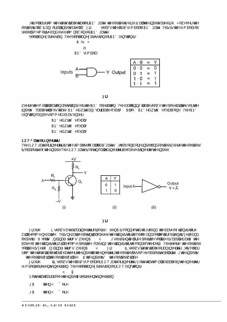
Mr. RAVIRAJ SRIKRISHNA AP/SOA 172
,W�LV�FOHDU�IURP�WKH�WUXWK�WDEOH�WKDW�IRU�$1'�JDWH��WKH�RXWSXW�LV�KLJK�LI�DOO�WKH�LQSXWV�DUH�KLJK���+RZHYHU��WKHRXWSXW�LV�ORZ�LI�DQ\�RU�DOO�LQSXWV�DUH�ORZ���)LJ������VKRZV�WKH�ORJLF�V\PERO�RI�$1'�JDWH���7KLV�LV�WKH�V\PERO�\RXVKRXOG�PHPRULVH�DQG�XVH�IURP�QRZ�RQ�IRU�$1'�JDWHV�
%RROHDQ�H[SUHVVLRQ���7KH�%RROHDQ�H[SUHVVLRQ�IRU�$1'�IXQFWLRQ�LV$ % <
�����������$1'�V\PERO
Fig. 5.41
ZKHUH�WKH�PXOWLSOLFDWLRQ�GRW�VWDQGV�IRU�WKH�$1'�RSHUDWLRQ���7KH�DGMRLQLQJ�WDEOH�VKRZV�WKH�SRVVLELOLWLHV�IRU�WKHLQSXWV����7DEOH�WHOOV�XV�WKDW���$1'HG�ZLWK�DQ\�YDULDEOH�HTXDOV�����$OVR����$1'HG�ZLWK���HTXDOV�RQH���7KH�$1'IXQFWLRQ�FDQ�EH�VXPPHG�XS�DV�XQGHU�
��$1'HG�ZLWK���HTXDOV����$1'HG�ZLWK���HTXDOV����$1'HG�ZLWK���HTXDOV��
NOT Gate or Inverter7KH�127�JDWH�RU�LQYHUWHU�LV�WKH�VLPSOHVW�RI�DOO�ORJLF�JDWHV���,W�KDV�RQO\�RQH�LQSXW�DQG�RXWSXW��ZKHUH�WKH�RXWSXWLV�RSSRVLWH�RI�WKH�LQSXW���7KH�127�JDWH�LV�RIWHQ�FDOOHG�LQYHUWHU�EHFDXVH�LW�LQYHUWV�WKH�LQSXW�
Fig. 5.42
)LJXUH�������L��VKRZV�D�W\SLFDO�LQYHUWHU�FLUFXLW���:KHQ�$�LV�FRQQHFWHG�WR�JURXQG��WKH�EDVH�RI�WUDQVLVWRU�4�ZLOO�EHFRPH�QHJDWLYH����7KLV�QHJDWLYH�SRWHQWLDO�FDXVHV�WKH�WUDQVLVWRU�WR�FXW�RII�DQG�FROOHFWRU�FXUUHQW�LV�]HUR�DQGRXSXW�LV��9�YROWV���,Q�ELQDU\�WHUPV��ZKHQ�$� ����<� �����,I�VXIILFLHQWO\�ODUJH�SRVLWLYH�YROWDJH�LV�DSSOLHG�DW�$��WKHEDVH�RI�WKH�WUDQVLVWRU�ZLOO�EHFRPH�SRVLWLYH��FDXVLQJ�WKH�WUDQVLVWRU�WR�FRQGXFW�KHDYLO\���7KHUHIRUH��WKH�RXWSXWYROWDJH�LV�]HUR���,Q��ELQDU\�WHUPV��ZKHQ�$� ����<� �����)LJ��������LL��VKRZV�WUXWK�WDEOH�IRU�DQ�LQYHUWHU���,W�LV�FOHDUIURP�WKH�WUXWK�WDEOH�WKDW�ZKDWHYHU�WKH�LQSXW�WR�WKH�LQYHUWHU��WKH�RXWSXW�DVVXPHV�RSSRVLWH�SRODULW\���,I�WKH�LQSXW�LV���WKH�RXWSXW�ZLOO�WKH�RXWSXW�ZLOO�EH����LI�WKH�LQSXW�LV����WKH�RXWSXW�ZLOO�EH���
)LJXUH��������LLL��VKRZV�WKH�ORJLF�V\PERO�IRU�127�JDWH�RU�LQYHUWHU��1RWH�WKDW�VPDOO�EXEEOH�RQ�WKH�LQYHUWHUV\PERO�UHSUHVHQWV�LQYHUVLRQ���7KH�%RROHDQ�H[SUHVVLRQ�IRU�127�IXQFWLRQ�LV
<�� � $1RWH�WKDW�EDU�DERYH�WKH�LQSXW�$�UHSUHVHQWV�LQYHUVLRQ�
,I�$� ����WKHQ�<� � � �RU�<� ��
,I�$� ����WKHQ�<� � ��RU�<� ���

Mr. RAVIRAJ SRIKRISHNA AP/SOA 173
Combination of Basic Logic Gates7KH�25��$1'�DQG�127�JDWHV�DUH�WKH�WKUHH�EDVLF�FLUFXLWV�WKDW�PDNH�XS�DOO�GLJLWDO�GHWDLOV�FLUFXLWV���:H�VKDOOGLVFXVV�D�IHZ�FRPELQDWLRQV�RI�WKHVH�EDVLF�FLUFXLWV�
L� NAND gate���,W� LV�D�FRPELQDWLRQ�RI�$1'�JDWH�DQG�127�JDWH���,Q�RWKHU�ZRUGV��RXSXW�RI�$1'�JDWH�LVFRQQHFWHG�WR�WKH�LQSXW�RI�D�QRW�JDWH�DV�VKRZQ�LQ�)LJ�������L����&OHDUO\��WKH�RXSXW�RI�D�1$1'�JDWH�LVRSSRVLWH�WR�WKH�$1'�JDWH���7KLV�LV�LOOXVWUDWHG�LQ�WKH�WUXWK�WDEOH�IRU�1$1'�JDWH���1RWH�WKDW�WUXWK�WDEOH�IRU1$1'�JDWH�LV�GHYHORSHG�E\�LQYHUWLQJ�WKH�RXWSXWV�RI�WKH�$1'�JDWH�7KH�%RROHDQ�H[SUHVVLRQ�IRU�1$1'�IXQFWLRQ�LV
<��� � $ %
7KLV�%RROHDQ�H[SUHVVLRQ�FDQ�EH�UHDG�DV�<� �QRW�$�%���7R�SHUIRUP�WKH�%RROHDQ�DOJHEUD�RSHUDWLRQ��ILUVW�WKHLQSXWV�PXVW�EH�$1'HG�DQG�WKHQ�WKH�LQYHUVLRQ�LV�SHUIRUPHG���1RWH�WKDW�RXWSXW�IURP�D�1$1'�JDWH�LV�DOZD\V,�H[FHSW�ZKHQ�DOO�RI�WKH�LQSXWV�DUH�����)LJ�������LLL��VKRZV�WKH�ORJLF�V\PEROV�IRU�D�1$1'�JDWH���7KH�WLWOHEXEEOH��VPDOO�FLUFOH��RQ�WKH�ULJKW�HQG�RI�WKH�V\PERO�PHDQV�WR�LQYHUW�WKH�$1'�
Fig. 5.43
LL� NOR gate���,W�LV�D�FRPELQDWLRQ�RI�25�JDWH�DQG�127�JDWH����,Q�RWKHU�ZRUGV��RXSXW�RI�25�JDWH�LV�FRQQHFWHGWR�WKH�LQSXW�RI�D�127�JDWH�DV�VKRZQ�LQ�)LJ�������L����1RWH�WKDW�RXSXW�RI�25�JDWH�LV�LQYHUWHG�WR�IRUP�127JDWH���7KLV�LV�LOOXVWUDWHG�LQ�WKH�WUXWK�WDEOH�IRU�125�JDWH���,W�LV�FOHDU�WKDW�WUXWK�WDEOH�IRU�125�JDWH�LV�GHYHORSHGE\�LQYHUWLQJ�WKH�RXWSXWV�RI�WKH�25�JDWH�
Fig. 5.44
7KH�%RROHDQ�H[SUHVVLRQ�IRU�125�IXQFWLRQ�LV
<�� � $ %
7KLV�%RROHDQ�H[SUHVVLRQ�FDQ�EH�UHDG�DV�<� �QRW�$�RU�%���7R�SHUIRUP�WKH�%RROHDQ�DOJHEUD�RSHUDWLRQ��ILUVW�WKHLQSXWV�PXVW�EH�25HG�DQG�WKHQ�WKH�LQYHUVLRQ�LV�SHUIRUPHG���1RWH�WKDW�RXWSXW�IURP�D�125�JDWH�LV�KLJK�����RQO\ZKHQ�DOO�WKH�LQSXWV�DUH�ORZ�������,I�DQ\�RI�WKH�LQSXWV�LV�KLJK������WKH�RXWSXW�LV�ORZ�������)LJ��������LLL��VKRZV�WKHORJLF�V\PEROV�IRU�D�125�JDWH���7KH�EXEEOH��VPDOO�FLUFOH�DW�WKH�<�RXWSXW�LQGLFDWH�LQYHUVLRQ�
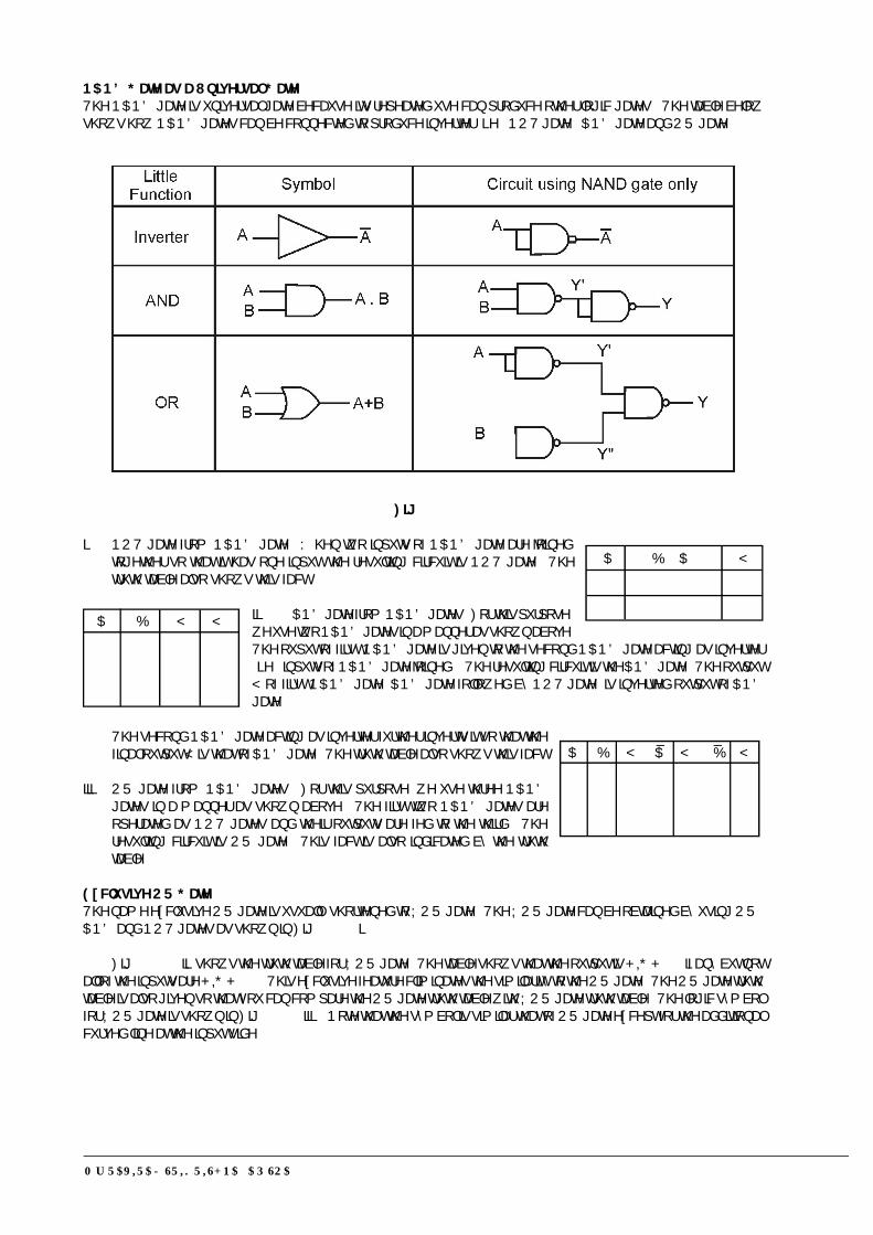
Mr. RAVIRAJ SRIKRISHNA AP/SOA 174
NAND Gate as a Universal Gate7KH�1$1'�JDWH�LV�XQLYHUVDO�JDWH�EHFDXVH�LWV�UHSHDWHG�XVH�FDQ�SURGXFH�RWKHU�ORJLF�JDWHV���7KH�WDEOH�EHORZVKRZV�KRZ�1$1'�JDWHV�FDQ�EH�FRQQHFWHG�WR�SURGXFH�LQYHUWHU��L�H���127�JDWH���$1'�JDWH�DQG�25�JDWH�
Fig. 5.45
L� 127�JDWH�IURP�1$1'�JDWH���:KHQ�WZR�LQSXWV�RI�1$1'�JDWH�DUH�MRLQHGWRJHWKHU�VR�WKDW�LW�KDV�RQH�LQSXW��WKH�UHVXOWLQJ�FLUFXLW�LV�127�JDWH���7KHWUXWK�WDEOH�DOVR�VKRZV�WKLV�IDFW�
LL� $1'�JDWH�IURP�1$1'�JDWHV���)RU�WKLV�SXUSRVH�ZH�XVH�WZR�1$1'�JDWHV�LQ�D�PDQQHU�DV�VKRZQ�DERYH�7KH�RXSXW�RI�ILUVW�1$1'�JDWH�LV�JLYHQ�WR�WKH�VHFRQG�1$1'�JDWH�DFWLQJ�DV�LQYHUWHU�L�H���LQSXWV�RI�1$1'�JDWH�MRLQHG����7KH�UHVXOWLQJ�FLUFXLW�LV�WKH�$1'�JDWH���7KH�RXWSXW<�RI�ILUVW�1$1'�JDWH��$1'�JDWH�IROORZHG�E\�127�JDWH��LV�LQYHUWHG�RXWSXW�RI�$1'JDWH�
7KH�VHFRQG�1$1'�JDWH�DFWLQJ�DV�LQYHUWHU�IXUWKHU�LQYHUWV�LW�VR�WKDW�WKHILQDO�RXWSXW�<�LV�WKDW�RI�$1'�JDWH���7KH�WUXWK�WDEOH�DOVR�VKRZV�WKLV�IDFW�
LLL� 25�JDWH�IURP�1$1'�JDWHV���)RU�WKLV�SXUSRVH��ZH�XVH�WKUHH�1$1'JDWHV�LQ�D�PDQQHU�DV�VKRZQ�DERYH���7KH�ILUVW�WZR�1$1'�JDWHV�DUHRSHUDWHG�DV�127�JDWHV�DQG�WKHLU�RXWSXWV�DUH�IHG�WR�WKH�WKLUG���7KHUHVXOWLQJ�FLUFXLW� LV�25�JDWH���7KLV�IDFW�LV�DOVR� LQGLFDWHG�E\�WKH�WUXWKWDEOH�
Exclusive OR Gate7KH�QDPH�H[FOXVLYH�25�JDWH�LV�XVXDOO\�VKRUWHQHG�WR�;25�JDWH���7KH�;25�JDWH�FDQ�EH�REWDLQHG�E\�XVLQJ�25�$1'�DQG�127�JDWHV�DV�VKRZQ�LQ�)LJ�������L��
)LJ���������LL��VKRZV�WKH�WUXWK�WDEOH�IRU�;25�JDWH���7KH�WDEOH�VKRZV�WKDW�WKH�RXWSXW�LV�+,*+�����LI�DQ\�EXW�QRWDOO�RI�WKH�LQSXWV�DUH�+,*+�������7KLV�H[FOXVLYH�IHDWXUH�FOLPLQDWHV�WKH�VLPLODULW\�WR�WKH�25�JDWH���7KH�25�JDWH�WUXWKWDEOH�LV�DOVR�JLYHQ�VR�WKDW�\RX�FDQ�FRPSDUH�WKH�25�JDWH�WUXWK�WDEOH�ZLWK�;25�JDWH�WUXWK�WDEOH���7KH�ORJLF�V\PEROIRU�;25�JDWH�LV�VKRZQ�LQ�)LJ�������LLL����1RWH�WKDW�WKH�V\PERO�LV�VLPLODU�WKDW�RI�25�JDWH�H[FHSW�IRU�WKH�DGGLWLRQDOFXUYHG�OLQH�DW�WKH�LQSXW�VLGH�
$ %�� $� <
� � �
� � �$ % < <� � � �� � � �� � � �� � � �
$ % <� �$± <�� �%± <� � � � �� � � � �� � � � �� � � � �

Mr. RAVIRAJ SRIKRISHNA AP/SOA 175
Fig. 5.46
7KH�ORJLF�RSHUDWLRQV�LQ�WKH�FLUFXLW�DUH�DV�XQGHU�
$ % $ % $ % < $ % < < < <
� � � � � � �
� � � � � � �
� � � � � � �
� � � � � � �
1RWH�WKDW���$1'HG�ZLWK���LV���DQG���$1'HG�ZLWK���LV���
Example 26.11. 2EWDLQ�WKH�WUXWK�WDEOH�IRU�WKH�FLUFXLW�VKRZQ�LQ�ILJ��������L��
Solution. )LJXUH�������LL��VKRZV�WKH�WUXWK�WDEOH�IRU�WKH�FLUFXLW���7KH�WUXWK�WDEOH�FDQ�EH�REWDLQHG�YHU\�HDVLO\LI�WKH�UHDGHU�UHPHPEHUV�WKH�IROORZLQJ�VLPSOH�%RROHDQ�RSHUDWLRQV�
Fig. 5.47
L� ��25HG��ZLWK��� ������25HG�ZLWK��� �������25HG�ZLWK��� ��LL� ��$1'HG�ZLWK��� �������$1'HG�ZLWK��� ��������$1'HG�ZLWK��� ��
7KXV��ZKHQ�$� ���DQG�%� ����WKHQ�$�25HG�ZLWK�%� ���L�H���<¶� �����:KHQ�<¶�� ���LV�$1'HG�ZLWK�$�� ����WKHUHVXOW�LV�����$JDLQ�ZKHQ�$� ���DQG�%� ����WKHQ�$�25HG�ZLWK�%�LV���L�H���<¶� �����1RZ�<¶�� ���$1'HG�ZLWK�$�� ���WKH�UHVXOW�LV���
Example 26.12. �2EWDLQ�WKH�WUXWK�WDEOH�IRU�WKH�FLUFXLW�VKRZQ�LQ�)LJ�������
Fig. 26.16

Mr. RAVIRAJ SRIKRISHNA AP/SOA 176
Solution. 7KH�WUXWK�WDEOH�IRU�WKH�FLUFXLW�LV�VKRZQ�EHORZ�
$ % $ < $ % % < < %
� � � � � �
� � � � � �
� � � � � �
� � � � � �
L� :KHQ�$� ���DQG�%� ����WKHQ� $ ����1RZ�<�LV�HTXDO�WR� $ �� ���$1'HG�ZLWK�%�� �����7KH�UHVXOW�LV�����7KHQ<�� ���25HG�ZLWK�% �� ���LV���L�H��<� ���
LL� :KHQ�$� ���DQG�%� ����WKHQ� $ � �����1RZ�<�LV�HTXDO�WR� $ �� ���$1'HG�ZLWK�%�� ���DQG�WKH�UHVXOW�LV���L�H�<�� ���25HG�ZLWK�% �� ���LV���L�H���<� ���
7KH�UHDGHU�FDQ�SURFHHG�LQ�D�VLPLODU�ZD\�WR�ILQG�WKH�RWKHU�RXWSXW�YDOXHV�

Mr. RAVIRAJ SRIKRISHNA AP/SOA 177

Mr. RAVIRAJ SRIKRISHNA AP/SOA 178
UNIT - 5

Mr. RAVIRAJ SRIKRISHNA AP/SOA 179
..
Mr. RAVIRAJ SRIKRISHNA AP/SOA 180
CHAPTER - 6COMMUNICATION SYSTEMS
BLOCK DIAGRAM OF COMMUNICATION SYSTEMA communication system may be described by the block diagram as shown in Fig. 6.1. The basic elementsof a communication system are information source, input transducer, transmitter, transmission channel, receiverand destination.
Informationsource
Inputtransducer Transmitter ReceiverTransmission
channel
Informationdestination
Outputtransducer
Fig. 6.1. Block Diagram of a Communication System.
Information SourceOriginates the messages or information in the form of audio, image, text, data, codes etc. However out ofthese messages, only the desired message is selected and communicated through the transmission.
Input Transducerconverts source information into electrical signal (incase if the information source is not in the form of electricalsignal). It may use microphone, camera, keyboard etc.
TransmitterIt processes the incoming information so as to make it suitable for onward transmission and subsequentreception. The transmitter consists of a number of electronic components e.g. oscillator modulator, amplifier,antenna etc.
Transmission ChannelIt is the electrical medium through which the information (message) travels from the transmitter to the receiver.It provides a path (physical connection) or free space for modulated wave to travel between transmitter andreceiver. The transmission can be point-to-point or in a broadcast mode. The medium can be one of thefollowing types:• Wired Lines (twisted pair, co-axial cable, waveguide, fibre optic cable, LASER beam etc.) type• Wireless / Radio (Microwave, satellite, etc.) type
‘Notice’ is an unwanted but unavoidable electrical signal which may introduce at any point in thecommunication system. It should be kept at minimum. It is most noticeable when it occurs in the channel orat the input of the receiver. When the level of noise is too high it makes the information useless and reducesthe quality of the system. A good system should have a high signal to noise ratio.
ReceiverIt receives the transmitted signal and performs a process which is reverse of transmitter stage. The transmittedsignal is received through antenna and then processed to get the original signal. The electronic componentsof receiver are antenna, filter, amplifier, demodulator etc.
Output TransducerIt converts the electrical signal at its input into the form desired by the system user. It may use loud speaker,personal computer (PC), tape recorder etc.
Information DestinationAt last the original information is received at this destination without any noise or distortion.
Figure 6.1 represents one-way (simplex) transmission. Two way communication of course requires atransmitter and receiver at each end. A full duplex system has a channel that allows simultaneous transmissionin both directions. A half-duplex system allows transmission in either direction but not at the same time.

Mr. RAVIRAJ SRIKRISHNA AP/SOA 181
IEEE SPECTRUM FOR COMMUNICATION SYSTEMSRadio waves are a type of Electromagnetic (EM) radiation with wavelengths in the electromagnetic spectrumlonger than infrared light. Radio waves have frequencies from 3 KHz to 300 GHz, which corresponds to thewavelength from 100 km to 1 mm. Like all other electromagnetic waves, they travel at the speed of light.Radio waves are used for mobile radio communication, broadcasting, RADAR and other navigational systems,satellite communication, computer network and many other applications. Different frequencies of radio waveshave different propagation characteristic in the earth’s atmosphere. Radio spectrum is typically governmentregulated in developed countries and in some cases sold or licensed to operators of private radio transmissionsystems for example mobile phones and broadcast television stations.
A frequency band is a small section of the spectrum of radio communication frequencies, in which channelsare usually used or set aside for the same purpose. Above 300 GHz the absorption of EM radiation by earth’satmosphere is so great that the atmosphere is effectively opaque. To convert from frequency (f) to wavelength() & vice versa, recall that f = c/ or = c/f, where c = speed of light.
8 5
meterHz KHz MHz GHz
3 10 3 10 300 0.3f f f f
or8 5
Hz KHz MHz GHzmeter meter meter meter
3 10 3 10 300 0.3f , f , f ,f
For example : at 10 GHz, the wavelength = 30/10 = 3 cm.Military RADAR band nomenclature (L, S, C, X, Ku, K and Ka bands) originated during word war-II as a
secret code so scientists and engineers could talk about frequencies without divulging them. After the war thecodes were declassified, millimeter (mm) was added and the designation were eventually were eventuallyadopted by the IEEE. (Institute of Electrical and Electronic Engineers).
The IEEE adopted nomenclature for various bands is shown in table 6.1. The same is used in militaryRADAR, satellite and terrestrial communications.
Table 6.1 : IEEE RADAR Band Designations
Band Frequency Range Origin of Name
HF 3 to 30 MHz High Frequency
VHF 30 to 300 MHz Very High Frequency
UHF 300 to 1000 MHz Ultra High Frequency
L 1 to 2 GHz Long wave
S 2 to 4 GHz Short wave
C 4 to 8 GHz Compromise between S and X
X 8 to 12 GHz X for cross (used in world war-II for fire control)
Ku 12 to 18 GHz Kurz - under
K 18 to 27 GHz German Kurz (short)
Ka 27 to 40 GHz Kurz - above
V 40 to 75 GHz -
W 75 to 110 GHz W follows V in the alphabet
mm 110 to 300 GHz -
The IEEE system in widely used, but lacks some fine granularity. In that it covers maximum of RADARfrequencies bands i.e. starting from 1 GHz. The designations below for the lower frequencies come from ITU(International Telecommunication Union) frequency bands which are more useful for radio applications. Theseare shown in Table 6.2.
Mr. RAVIRAJ SRIKRISHNA AP/SOA 182
Table 6.2 : ITU Radio Band Designations
Band Frequency Range Origin of Name
VLF 3 to 30 KHz Very Low Frequency
LF 30 to 300 KHz Low Frequency
MF 300 to 3000 KHz Medium Frequency
TYPES OF COMMUNICATIONBased on the type of modulation scheme and the nature of the output of the information sources, thecommunication systems are divided into two categories :1. Analog communication, and2. Digital communication
Other ways of categorizing communication systems include the classification based on the frequency ofthe carrier and the nature of the communication channel.
Analog CommunicationAnalog communication systems are designed to transmit analog information using analog modulation methods.The block diagram of an analog communication system is shown in Fig. 6.2.
Modulator Transmitter Communicationchannel DemodulatorReceiver
Noise
Message Message
Fig. 6.2. Block Diagram of Analog Communication System.
These include the modulator which produces a signal that is transmitted over the communication channelthrough the transmitter and on the other side the receiver receives the signal and the demodulator reconstructsthe original analog signal. The noise is an unavoidable random signal, which is entirely undesirable in nature.This electrical energy invariably enters any communication system through the electronic components presentin the transmitter and receiver circuit. They are also present in the medium itself. Noise is one of the mostserious problems to be handled by any communication system and is very crucial in designing the system.Methods are devised to minimize noise but it can not be eliminated fully.
Advantages of Analog Communications1. Transmitter and receivers are simple2. Requires smaller bandwidth3. Frequency Division Multiplexing (FDM) can be used4. Synchronization problem is relatively easier.
Disadvantages of Analog Communications1. Repeaters can not be used between transmitters and receivers2. Not suitable for secret informations3. Coding is not possible4. Noise affects the quality of signal5. No error correction capability6. Noise and signals are inseparable
Applications1. Radio broadcasting (AM, FM)2. T.V. broadcasting3. Telephones
Digital CommunicationDigital communication systems are designed to transmit digital information using digital modulation schemes.Figure 6.3 shows the block diagram of a digital communication system.
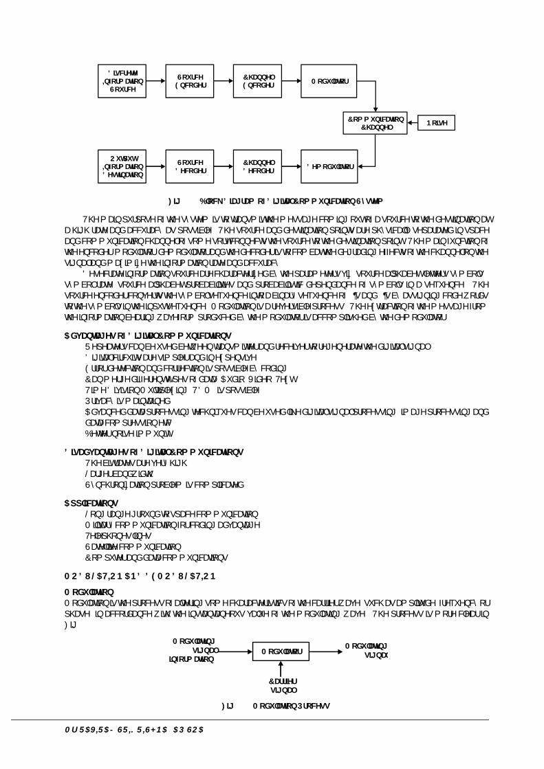
Mr. RAVIRAJ SRIKRISHNA AP/SOA 183
DiscreteInformation
Source
Noise
SourceEncoder
ChannelEncoder Modulator
OutputInformationDestination
SourceDecoder
ChannelDecoder Demodulator
CommunicationChannel
Fig. 6.3. Block Diagram of Digital Communication System
The main purpose of the system is to transmit the message coming out of a source to the destination ata high rate and accuracy as possible. The source and destination points are physically separated in spaceand communication channel of some sort connects the source to the destination point. The main function ofthe encoder, modulator, demodulator and the decoder is to combat the degrading effects of the channel on thesignal and maximize the information rate and accuracy.
Desecrate information source are characterized by the parameters viz. source alphabet (letters/symbols),symbol rate, source alphabet probabilities and probabilistic dependance of symbols in a sequence. Thesource encoder converts the symbol sequence into a binary sequence of 0’s and 1’s by assigning code wordsto the symbols in the input sequence. Modulation is a reversible process. The extraction of the message fromthe information bearing waveform produced by the modulator is accomplished by the demodulator.
Advantages of Digital Communications1. Repeaters can be used between transmitter and receiver to regenerate the digital signal.2. Digital circuits are simpler and in expensive.3. Error detection and correction is possible by coding.4. Can merge different types of data (Audio, Video, Text).5. Time Division Multiplexing (TDM) is possible.6. Privacy is maintained.7. Advanced data processing techniques can be used like digital signal processing, image processing and
data compression etc.8. Better noise immunity.
Disadvantages of Digital Communications1. The bit rates are very high.2. Larger bandwidth.3. Synchronization problem is complicated.
Applications1. Long range ground to space communication2. Military communication for coding advantage.3. Telephones lines4. Satellite communication5. Computer and data communications
MODULATION AND DEMODULATION
ModulationModulation is the process of altering some characteristics of the carrier wave (such as amplitude, frequency orphase) in accordance with the instantaneous value of the modulating wave. The process is more clear inFig. 6.4.
ModulatorModulating
signal(information)
Modulatingsignal
Carriersignal
Fig. 6.4. Modulation Process.

Mr. RAVIRAJ SRIKRISHNA AP/SOA 184
In the modulation process two signals are used namely the modulating signal and the carrier signal. Themodulating signal is the based and signal which contains the information or intelligence, while the carrier is ahigh frequency, constant amplitude, constant frequency and non-interrupted wave generated by radio-frequencyoscillators. The carrier wave infect acts as a carrier which carries the information signal (modulated signal)from transmitter to the receiver. The modulator combines the two signals to from the modulated signal.
DemodulationDemodulation or detection is the process of extracting the original information signal from the modulatedcarrier wave. This is a reverse process of modulations. It is carried out for the following reasons1. The transmitted modulated wave consists of RF component mixed with AF signal. If it is fed directly to
the loud speaker it will not produce any sound as the RF consists of vary high frequency and the loudspeaker can not respond to such frequencies due to large inertia of their vibrating discs etc.
2. Such RF wave will also not produce any effect on human ears as its frequency is much higher than theaudible range of human ears i.e., 20 Hz to 20 KHz.Therefore it is essential to separate the AF signal from RF modulated carrier wave.
NEED FOR MODULATIONLow frequency signals can not be transmitted over a long range directly without modulation. The main factorsresponsible for the need of modulation are :1. Small Operating Range
The energy of any wave depends on its frequency, the larger the frequency, the greater the energy containedby it. An audio signal having small frequency and hence a small power can not travel a long distance ifradiated directly into the space. Therefore a modulated wave is needed to send the signal over a longerrange.
2. Huge Antenna sizeThe size of the antenna required for an efficient transmission (or reception) is at least /4 i.e., one quarterwavelength.
i.e.1 (c)
4 4 (f )
where c = 3 x 10⁸ m/sec. and f = Frequency in Hz
Let the frequency of transmitted signal is 15 KHz, then an antenna of length 15 km will be required whichis practically not possible. On the other hand if the transmitted signal is of frequency 15 MHz then thesize of the antenna required will only be about 15 meters, which is quite easily constructed.
3. Poor Radiation EfficiencyThe radiation efficiency at audio frequencies is very poor and the transmission is not practicable. But athigh frequencies (above 20 KHz) the energy can be radiated efficiently thus is the need of modulation.
4. Mutual InterferenceThe audio frequency range is from 20 Hz to 20 KHz. If this signal is transmitted directly from differentsources then all of these will mix up and will not serve the purpose. Therefore different signals can betransmitted at different carrier frequency through modulation to get the transmission without interference.Hence, the only solution is to transmit the low-frequency signal with the help of a high frequency carrier
wave using modulation, to avoid the factors mentioned above.
TYPES OF MODULATIONModulation is a process of mixing a signal with a sinusoid (sine wave) to produce a new signal. This new signalhas many advantages over un-modulated signal during transmission. A general function for a sinusoid :
f(t) A sin( t ) Here we can see that this sinusoid has 3 parameters, that can be altered to affect the shape of the graph.
These parameters are :• A, the amplitude or magnitude of the sinusoid• the angular frequency (in radian per second)• the phase angle
Depending upon these three parameters we have three types of modulations i.e., Amplitude Modulation(AM), Frequency Modulation (FM) and Phase Modulation (PM).i. In Amplitude Modulation the amplitude of the carrier signal changed (modulated) in proportion to the
message signal while the frequency and phase are kept constant.ii. In Frequency Modulation the frequency of the carrier signal is changed (modulated) in proportion to the
message signal while the amplitude and phase are kept constant.iii. In Phase Modulation the phase of the carrier signal is varied in accordance to the low frequency of the
message signal keeping the amplitude and frequency unchanged.In India radio broadcasting using AM as well as FM while for TV transmission AM is used for video signal
and FM is used for audio signals. Therefore our discussion in this chapter will be limited to AM and FM only.
Mr. RAVIRAJ SRIKRISHNA AP/SOA 185
Another way of classification of modulation is according to the nature of carrier wave used. As per this itcan be either continuous wave modulation, and pulse modulation.i. Continuous Wave Modulation
When the carrier wave is continuous in nature then this modulation is called continuous wave modulationor analog modulation. AM, FM, PM fall under this category.
ii. Pulse ModulationWhen the carrier wave is a pulse type waveform then this modulation is called pulse modulation. Here thecarrier wave is a periodic sequence of rectangular or square pulses. Pulse modulation can be of two typesanalog and digital.• In analog pulse modulation the amplitudes, duration or position of the pulse varies in accordance with
the message signal. Here it is of three types, i.e., Pulse Amplitude Modulation (PAM), Pulse DurationModulation (PDM) and Pulse Position Modulation (PPM).
• In digital type of pulse modulation we have Pulse Code Modulation (PCM).
AMPLITUDE MODULATION (AM)
Amplitude ModulationAmplitude Modulation is the process of changing amplitude of the high frequency carrier wave in accordancewith the instantaneous value of modulating signal, keeping the frequency and phase unchanged. In thisprocess the modulating signal (information) is superimposed upon the RF carrier waves with the help of modulator.Fig. 6.5 shows the AM waveform for sine wave and Fig. 6.6 shows the details of amplitude modulated carrierwave. Here the amplitudes of both positive and negative half cycles are varied according to the informationsignal. The RF carrier wave consists of sine wave where amplitudes follow the amplitude variations of themodulating wave. The carrier is contained in an envelope formed by the modulating wave. Thus the amplitudevariations of the carrier wave are at the signal frequency and the frequency of AM is equal to the frequency ofcarrier wave.
Fig. 6.5. AM waveform for sine wave.
Fig. 6.6. Amplitude modulated carrier wave.

Mr. RAVIRAJ SRIKRISHNA AP/SOA 186
Analysis and Frequency Spectrum of Amplitude Modulated Carrier WaveLet the carrier and modulating wave be represented by
c cc(t) V cos t ...(i)
and m mx(t) V cos t ...(ii)We know that general expression for AM signal is
c cs(t) [V x(t)] cos t
c c cV cos t x(t) cos t ...(iii)By putting the value of x(t) from equation (ii) we get
c c m m cs(t) V cos t V cos t cos t
c c m c mV cos t 0V cos t cos t
mc c m
c
VV cos t 1 cos tV
...(iv)
We know that the modulation index for AM is given by
maxa
c
x(t)m
V ...(v)
Where max
x(t) is the maximum amplitude of modulating signal and Vc is the maximum amplitude of carriersignal.
Hence mmaxx(t) V
ma
c
VmV
Putting this value in equation (4) we get
c c a ms(t) V cos t [1 m cos t] ...(vi)
c c c a c mV cos t + V m cos t cos t
c ac c c m
V mV cos t + [2 cos t cos t]2
c ac c c m c m
V mV cos t + [cos( )t cos( )t]2
c a c ac c c m c m
V m V mV cos t + cos( )t cos( )t]2 2
...(vii)
Equation (vii) reveals that the AM signal has three frequency components as given below:i. Carrier frequency c having amplitude cV .
ii. Upper sideband c m( ) having amplitude a cm V2 .
iii. Lower side band c m( ) having amplitude a cm V2 .
The frequency spectrum of AM is shown in Fig. 6.7.
Fig. 6.7. Frequency Spectrum of AM.
Mr. RAVIRAJ SRIKRISHNA AP/SOA 187
Modulation IndexModulation index is defined as the ratio of change in amplitude of carrier wave to the amplitude of normal carrierwave. Hence
ma
c
V (amplitude change of carrier wave)mV (amplitude of normal, unmodulated carrier wave)
The modulation index is a number between 0 and 0.8. It can also be represented in percentage bymultiplying by 100 :
m
c
V% modulation 100V
It may also be defined in terms of values referred to the modulated carrier wave (refer Fig. 6.6).
max min
max min
V VmV V
Where maxV and minV are the maximum and minimum values of the modulated carrier wave.
The Various Cases ForAmplitude modulated wave for different values of ‘m’ are discussed as: (Assuming in Vm as the amplitude ofsignal).
Case 1. When Vm = 0, it means m = 0This is the case of unmodulated carrier wave.
Case 2. When cm
VV2
In this case m = 0.5 or 50%The carrier wave is said to be 50% modulated.
Case 3. When Vm = VcThen m = 1 or 100%The carrier wave is 100% modulated.
Case 4. When Vm > VcThen m >> 1The modulation is called over-modulation.
Advantages and Disadvantages of AM
AdvantagesAmplitude Modulation has the following advantages :i. Simple to implementii. Inexpensiveiii. Can be demodulated using only a few components
Disadvantagesi. Low efficiency in terms of power usageii. Limited range of operationiii. Noisy receptioniv. Poor recovery of original signalv. Lower band width
Applications of AMi. Radio Broadcastingii. Inexpensiveiii. Personal (Walkie-Talkie)iv. Military : to control weaponsv. Business : Conference calls
FREQUENCY MODULATION (FM)
Frequency ModulationFrequency modulation is the process in which the frequency of carrier wave is varied instantaneously in proportionwith the amplitude of the modulating signal, keeping amplitude and phase constant. Thus the information isconveyed via frequency change. Fig. 6.8 shows the FM waveform for sine wave.

Mr. RAVIRAJ SRIKRISHNA AP/SOA 188
Fig. 6.8. FM waveform for sine wave.
In an FM receiver, it is the amount of frequency shift that is produced in the modulated waveform thatdetermines the volume (audio intensity) heard on the speaker of the receiver. Thus we can say ; as theamplitude of the modulating signal increases or decreases, the frequency of the carrier wave also increases ordecreases. However the amplitude of the FM modulated carrier remains constant and it does not change. Theproblem associated in AM are overcome in FM.
Analysis and Frequency Modulated Carrier WaveLet the carrier and modulating wave be represented by
c c cV Cos ( t ) ...(i)
and m m mV cos t ...(ii)
Where c , cV , c and are instantaneous values, peak value, angular velocity and the initial phase angle
of the carrier ; and m , mV and m are the instantaneous value, peak value and the angular velocity of themodulating wave.
Let c c(t) t ...(iii)
Where c(t) is the total instantaneous phase angle of the carrier wave at time t. Hence from equation (i),we get
c c cV cos (t) ...(iv)
The c is defined as the instantaneous rate of increase of instantaneous phase (or angular displacement),
is related to phase angle c as below :
cc
ddt
...(v)
In FM, cf (frequency of carrier wave) varies with time according to the instantaneous value of the modulatingvoltage. Thus the frequency of the carrier after FM is given by.
c f m c f m mK v K V cos t ...(vi)Where Kf is a constant of probability and represents the frequency conversion factor, whose value
depends on the modulation system. The total instantaneous phase of the FM wave is obtained by integratingequation (vi).

Mr. RAVIRAJ SRIKRISHNA AP/SOA 189
c f m m(t) dt ( K V cos t dt
c f m m lm
1t K V sin t
Where t is the constant of integration and represents the initial phase. It may be neglected as it isinsignificant in the modulation process. Thus:
mc f m
m
V(t) t K sin t
Hence the equation of FM wave is given by
FM cV sin (t)
or mFM c c f m
m
VV sin t K sin t
...(vii)
The instantaneous frequency of FM wave can be drawn from equation (vi). Thus
c mf m
Vf K cos t2 2 2
or mc f m
Vf f K cos t2
...(viii)
From this equation the maximum and minimum value of frequency are given as:
mmax c f
Vf f K2
and mmin c f
Vf f K2
(as cos 180 = -1)
Hence the frequency deviation, which is defined as the maximum change in frequency from mean value f c, isgiven by
md max c c min f
Vf f f f f K2
...(ix)
Also the carrier swing, which is the total variation in frequency from minimum to maximum value i.e.,(fmax – fmin) is :
md f
VCS 2f K
...(x)
and the frequency modulation index (mf) which is defined as the ratio of frequency deviation to modulationfrequency is given by:
d d f mf
m m m
f K Vmf
...(xi)
Thus the equation for the FM wave equation (vii) in terms of mf becomes :
FM c c f mV sin t m sin t
or FM c c f m m f mV sin t cos(m sin t) cos t sin(m sin t) ...(xii)
Modulation IndexIn FM, the modulation index is normally used instead of percentage of modulation. It is defined fined as theratio of the frequency deviation to the frequency of the modulating signal. It is expressed in decimal and doesnot have any unit. For a constant frequency deviation the modulation index drops as the frequency of themodulating signal increases. It varies during the transmission of FM signal as the modulation frequencychanges. This term is required for the calculation of bandwidth of an FM signal.
f mf
m m
f K Vmf
[From equation (x)]
Here we can say that for a given frequency (f) deviation or for a constant amplitude modulating voltage, variesinversely to the fm.

Mr. RAVIRAJ SRIKRISHNA AP/SOA 190
Advantages and Disadvantages of FM
Advantagesi. Improved signal to noise ratioii. Better immune to noise (Less distortion)iii. Less interference from adjacent channelsiv. Less radiated powerv. Greater efficiency
Disadvantagesi. Suffer more attenuation than AM signalii. Larger band widthiii. More complicated receiver and transmitter
Applications of FMi. Radio Broadcastingii. TV Transmission (For Audio)iii. Mobile Communication (Earlier)iv. Police, Fire Department etc.v. Point to point microwave links used by telecom companies
DIFFERENCE BETWEEN AM AND FMTable 6.3 gives the main highlights of the difference between AM and FM
Table 6.3 : Difference between AM and FM
S.No. Parameter AM FM
1. Principle of operation By changing amplitude By changing frequency ofof carrier wave carrier wave
2. Amplitude Depends on Constantmodulating index
3. Transmitter Simple Complex
4. Transmitted power Fully utilized A fraction is utilized
5. Area of reception Large Small
6. Band width required Small Large
7. Cost Low High
8. Modulating index Maximum value = 1 No restriction
9. Prone to noise More Less
10. Broadcast type Can only transmit Can transmit stereo(Radio) mono for talk only suitable for music
SOLVED EXAMPLESExample 6.1. A 1 MHz carrier is amplitude modulated by a 40 KHz modulated signal to a depth of 50%. Theunmodulated carrier is having a power of 1kW. Calculate the power of amplitude modulated signal and sideband frequencies.
Solution : Given, carrier power,Pc = 1 kW
Modulation index, m = 50% = 0.5
Power of AM signal,2 2
total carrier
m 0.5P P 1 1 1 1.125 kW2 2
Ans.

Mr. RAVIRAJ SRIKRISHNA AP/SOA 191
Lower side band frequency, LSB c mf f f 1000 40 960 KHz Ans.Upper side band frequency, USB c mf f f 1000 40 1,040 KHz Ans.
Example 6.2. A certain transmitter radiates 9 kW with the carrier unmodulated and 10.125 kW, when thecarrier is sinusoidal modulated. Calculate the modulation index. If another sinewave corresponding to 40%modulation is transmitted simultaneously, determine the total radiated power.
Solution : Given, carrier power,Pcarrier = 9 kW
Total power of modulated wave, Ptotal = 10.125 kW
Modulation index, total
carrier
Pm 2 1P
2
total carrier
m P P 12
10.1252 1 0.5 50%9
Ans.
Example 6.3. An AM broadcast radio radiates 10 kW of power if modulation percentage is 60. Calculate howmuch of this is the carrier power.
Solution : We know2
total carrier
mP P 12
ortotal
carrier 2 2
P 10Pm (0.6)1 12 2
10 8.47 kW1.18
Ans.
Example 6.4. The r.m.s. antenna current of a radio transmitter is 10A, when unmodulated and rising to 12 Awhen the carrier is sinusoidally modulated. Calculate the modulation index.
Solution : Given, carrier current Ic = 10 A
Total modulated current Itotal = 12 A
We know, modulation index, 2
total
carrier
Im 1 2I
212 1 210
= 0.938 Ans.
Example 6.5. Determine the modulation index of an FM carrie having a frequency deviation of 25 KHz andmodulation signal of 5 KHz. Also determine the carrier swing.
Solution : Given, frequency deviationf = 25 KHz
Frequency of modulation signal, fm = 5 KHz
Modulated index fm
f 25m 5f 5
Ans.
Carrier swing 2 f 2 25 KHz 50 KHz Ans.
Mr. RAVIRAJ SRIKRISHNA AP/SOA 192
Example 7.6. An FM transmission has a frequency deviation of 18.75 KHz. Calculate percent modulation ifit is broadcasted (i) in the 88 - 108 MHz band (ii) as a portion of a TV broadcast.
Solution : Given frequency deviation,f 18.75 KHz
A maximum frequency deviation of 75 KHz is allowed for commercial FM broadcast :i.e., max( f ) 75 KHz
max
f% modulation, m 100( f )
18.75 100 25%75
Ans.
A maximum frequency deviation of 25 KHz is allowed for sound portion of the TV broadcast.i.e. max( f ) 25 KHz
18.75% modulation, m 100
25
= 75% Ans.
SUMMARY1. Communication: Means the process of exchanging information. Radio communication can be used for
long range such as from one country to other or from earth to space.
2. Modulation: In this process some parameter of the carrier wave such as amplitude, frequency or phaseis varied in accordance with the modulating signal.
3. Demodulation: or detection is the process of recovering the original modulated signal (information) fromthe modulated carrier wave.
4. Modulation index: or modulation depth is described by how much the modulated variable of the carrierwave signal varies around its unmodulated level. It is defined differently in each modulation scheme i.e.AM, FM and PM.
5. Spectrum: A spectrum represents the relative amount of different frequency components in any signal.
6. Efficiency: Power in all the side bandsefficiencyTotal transmitted power
7. Frequency Deviation: The change of shift above or below the mean or centre frequency is calledfrequency deviation.
8. FM Index: The ratio of frequency deviation to modulation frequency is called the FM index.
9. Bandwidth of AM Wave: The difference between the two extreme frequencies is equal to the bandwidthof AM wave.
c m c mB.W. ( ) ( )
or mB.W. 2

Mr. RAVIRAJ SRIKRISHNA AP/SOA 193
IMPORTANT FORMULAE1. Size of quarter wave antenna
83 10l4 4 f
meter
where f is frequency in Hz.
2. General equation of sinusoid signalf(t) A sin( t )
3. Modulation index for AM
ma
c
V (Amplitude change of carrier wave)mV (Amplitude of normal, unmodulated carroer wave)
or m
c
V% Modulation 100V
4. Modulation index for FM :
fm
fmf
5. Power of AM signal :2
total carrier
mP P 12
6. Efficiency :Power in all the side bands
Total transmitted power
REVIEW QUESTIONSQ.1. What is communication system. Explain with block diagram.
Q.2. Write short note on analog and digital communications.
Q.3. What do you mean by modulation index.
Q.4. Derive an expression for the AM index.
Q.5. What is modulation and why it is necessary.
Q.6. Compare AM and FM.
Q.7. Define AM and FM, use sketches to explain these definitions. Where are theseemployed.
Q.8. What is frequency modulation? Give the mathematical representation of FM.
Q.9. What is the modulation index of an frequency modulated (FM) carrier having carrierswing of 200 KHz and a modulating signal of 10 KHz.

Mr. RAVIRAJ SRIKRISHNA AP/SOA 194
TRANSDUCERThe words ‘sensor’ and ‘transducer’ are both widely used in the description of measurement systems. Theformer is popular in the USA whereas the latter has been used in Europe. A ‘sensor’ is a device that detectsa change in physical stimulus and turns it into a signal which can be measured or recorded, a correspondingdefinition of ‘transducer’ is a device that transfers power from one system to another in the same or in thedifferent form. The block diagram of a transducer is shown in Fig. 8.2.
TransducerInput Energy(or Signal)
Output Energy(or Signal)
Fig. 6.9. Block diagram of transducer.
The transducer receives energy from the process variable under measurement and transmits a proportionalelectrical energy to the output. This output energy can be further processed through liner operations likeamplification, attenuation, differentiation, integration, addition, subtraction etc. so that it can be acceptable bythe output unit for record or display. The processing of signal is called signal conductioning.
Qualities of a Good Transducer• Ruggedness • Linearity• Repeatability • High output signal quality• Good dynamic response • High reliability and stability• No hysteresis
TYPES OF TRANSDUCERThere are various types of transducers depending upon the change in property or the energy they bring aboutto measure specified physical quantities. The input given to a transducer can be in the form of the displacement,strain, velocity, temperature, flow etc. and the output obtained fro, them can be in the form of voltage, current,change in resistance, inductance and capacitance etc. The output can be measured easily and it is calibratedagainst the input, thus enabling the measurement of the value of the input. The widely used transducer inmeasuring instruments are of following types.
Thermoelectric Transducers• Thermocouple • Resistance Temperature Detector (RTD)• Thermistor • Peltier Cooler
Electromechanical Transducers• Strain Gauge • Load Cell• Potentiometer • Galvanometer• Accelerometer
Mechanical Transducer• Bimetallic Strib • Bellows• Bourdon Tube • Spring
Photoelectric Transducer• Laser diodes • Light Emitting Diodes (LEDs)• Photo diode, photo resistor, photo transistor
Electro Acoustic Transducer• Microphone • Loudspeaker, earphone• Piezo electric Crystal • Hydrophone
Electrochemical Transducer• pH Probes • Hydrogen Sensors• Electro-Galvanic Fuel Cell
Electromagnetic Transducers• Antenna • Cathode Ray Tube (CRT)• Hall-Effect Sensor • Magnetic Disk Reader/Writer
THERMOCOUPLEThermocouple is a transducer for the measurement of high temperature. It is a thermoelectric device, whichworks on the principle of seeback effect by converting thermal energy into electrical energy.

Mr. RAVIRAJ SRIKRISHNA AP/SOA 195
It consists of two wires of dissimilar metals joined together to form two junctions in a close circuit formation.If the two junctions are at different temperature, an electric current will flow in the circuit. This phenomenon isknown as seebeck effect and was first observed by Thomas Johnn seebeck in 1981. He arranged 35 metals inorder of their thermoelectric properties. The current flows through the hot junction from the former to the lattermetal of the following series :
Bi-Ni-Co-Pd-Pt-U-Cu-Mn-Ti-Hg-Pb-Sn-Cr-Mo-Ph-Ir-Au-Ag-Zn-W-Cd-Fe-As-Sb-Te
If the two metals used are copper (Cu) and Iron (Fe), then the current flows from copper to Iron at the hotjunction (Jh) and from Iron to copper at the cold (reference) junction (Jc) which can be detected by galvanometer.This is explained in Fig 6.10.
Fig. 6.10. Basic Thermocouple Phenomenon.
The amount of current (emf) produced depends on the difference in the temperature between the twojunctions and on the characteristics of the two metals. The instrument that records the variations in currentflow is calibrated in terms of temperature and is known as thermocouple pyrometer. When the junction, Jh isheated it produces voltage greater than the voltage across the cold junction (Jc). The difference between twovoltage is measured and the voltmeter reading is converted into its corresponding temperatures. The conversiontable is provided by thermo-couple manufacturer.
The emf produced in thermocouple is given by2
1
T
1 2T
emf (S S )dt
Where T1 and T2 are the temperature of reference and measuring end respectively and S1 and S2 are theSeebeck coefficients of two thermoelements. The temperature-emf characteristics of some of the metals isshown in Fig. 6.11 where Jc is kept at 0oC and Jh is at variable temperature.
Fig. 6.11. Temperature-emf characteristics of some Thermocouples.
Advantagesi. Inexpensiveii. Rugged constructioniii. High temperature range (200 to 2600oC)iv. Fast response to change in temperaturev. Good accuracy

Mr. RAVIRAJ SRIKRISHNA AP/SOA 196
Disadvantagesi. Vulnerable to corrosionii. Calibration is difficult and tediousiii. Complexity and prone to erroriv. Produces low volt output (mV)v. None linear devicevi. Requires two temperature measurements
RESISTANCE TEMPERATURE DETECTOR (RTD)Resistance temperature detector (or Resistance Thermometer) is basically a temperature sensitive resistor. Itis a positive temperature coefficient device which means the resistance increases with temperature. Thecommonly used metals elements for RTD are platinum, nickel, copper and tungsten. The platinum has a lineartemperature-resistance characteristics and is reproductable over wide range of temperatures. It is available inpure form and is relatively unaffected by environmental conditions, hence is used for precision thermometry.Nickel has a high temperature coefficient. The common forms of RTD elements are shown in Fig. 6.12.
Fig. 6.12. Common Forms of RTD Elements.
The materials used for RTD have temperature coefficients of resistivity much higher than the coefficient ofthermal expansion. The temperature coefficient of resistance, , is given by :
0 0
1 1 RT T R
where T = change in temperature (oC)
0/ = fractional change in resistivity
0R /R = fractional change in resistance
0 0,R = resistivity and resistance respectively (oC)The resistance RT at any other temperature is given as :
T 0R R (1 T)
or T 0R R (1 T) But in case of non-linearly, the equation is modified as :
2 nT 0 1 2 nR R (1 T T ............ T )
Where 1 2 n, ,... are constants applicable for each metal.
Advantagesi. High Accuracyii. Linearity over wide range of temperatureiii. High temperature operationiv. Fast responsev. Better stability at high temperaturevi. Easily replaceablevii. More suitable for remote indicatorsviii. Immune to electrical noise

Mr. RAVIRAJ SRIKRISHNA AP/SOA 197
Disadvantagesi. High costii. Requires no point sensingiii. Possibility of self heatingiv. Requires external DC power supplyv. Low sensitivityvi. Affected by shock and vibration
Applicationsi. Heating ovens/food processingii. Compression mouldingsiii. Plastics processingiv. Air, gas and liquid temperature measurementv. Textile production
STRAIN GAUGEA strain gauge is a transducer which is used to measure the strain of an object. When an electrical conductoris stretched, it will become narrower and longer, both increases its electrical resistance end-to-end. Conversely,when a conductor is compressed (without buckling), it will broaden and shorten both decreases its electricalresistance end to end. If these stresses are kept within the elastic limit of the metal conductor (So that it doesnot deform permanently), the strip can be used as a measuring element for physical force, the amount ofapplied force inferred from measuring its resistance.
The most commonly used types of strain gauge are wire-type strain gauge, foil strain gauge andsemiconductor strain gauge.
Fig. 6.13. Some Common Type of Strain Gauges.
Derivation for Gauge FactorThe fundamental formula for the resistance of a wire (conductor) of length, l, diameter d, cross section area Aand resistivity , can be expressed as :
22
l l lRdA d
44
.... (i)
Let a tensile stress, S be applied to the wire, thereby a positive strain is produced which causes the lengthto increase by I and area to decrease by A as shown in Fig. 6.14. This will also reduce the diameter by andthus resistance changes by R.
Fig. 6.14. Change in dimension of strain gauge wire when subjected to a tensile force.

Mr. RAVIRAJ SRIKRISHNA AP/SOA 198
The strain changes two important parameters of the wire i.e., R and I. The measurement of sensitivityof a material to strain is known as gauge factor. It is defined as the ratio of change in resistance R/R tochange in length I/I.
Hence, Gauge factor R /R(G)l / l
.... (ii)
Since strain is defined as change in length divided by original length i.e l / l . Hence equation (ii) canwritten as :
R /RG
...(iii)
Due to strain the length of wire increases by I and simultaneously the diameter decreases by d. Hencethe new value of resistance is given by [Using equation (i)]
s2 2 2
(l l) (l l)R(d d) (d 2d d 2d )
4 4
Neglecting d2 as d is very small. We get
s2 2
ll 1(l l) lR
2 d(d 2d d) d 14 4 d
We know that Poisson’s ratio, is defined as the ratio of strain in lateral direction to strain in axialdirection. Thus
d / dl / l
ord ld l
Substituting the value of d
d
in equation (iv), we get
s2
l ll 1 1 2l lR
l ld 1 2 1 24 l l
2
2
222
2
l l l1 2 2l l e ll1 4d
l4
Neglecting higher power of l , as l in very small.
s2
l l lR 1 2l ld
4
2
l l1 (2 1)ld
4
2 2
l l l (1 2 )ld d
4 4
or sR R R from Equation (i)
where2
lRd
4
and

Mr. RAVIRAJ SRIKRISHNA AP/SOA 199
2
l lR (1 2 )ld
4
Gauge factor
l (1 2 )R /R lG ll / l
l
or G = 1+ 2
Advantagesi. No moving Partii. Small in sixiii. Inexpensive
Disadvantagesi. They are non-linearii. Need to be calibratediii. Usually they are placed where it is really hard to install
LOAD CELLLoad cells are elastic devices that can be used for the measurement of force through indirect method i.e.through use of secondary transducer. Load cells utilize an elastic member as a primary transducer and straingauge as secondary transducer. When the combination of the strain gauge-elastic member is used for weighing,it is called a “load cell”. It converts force into a measurable electrical output. Although there are manyvarieties of load calls, strain gauge based load cells are the most commonly used type.
Construction and WorkingThe strain gauge load cells shown in Fig. 8.15 utilizes four identical strain gauges attached to a steel cylinder.The gauges Rg1 and Rg4 are along the direction of applied load and the gauges Rg2 and Rg3 are attachedcircumferentially to gauge Rg1 and Rg4. All the four gauges are connected into the bridge circuitry in such amanner as to make use of poisson’s ratio.
Fig. 6.15. Load cell Strain Gauge.
When there is no load on the cell, all the four gauges have the same resistance i.e. Rg1 = Rg2= Rg3= Rg4.Hence the terminals B and D are at same potential, the bridge is balanced and the output voltage, V 0= 0.
i.e. AB AD
VV V2
also AB AB 0V V V 0
Now when the load is applied the vertical gauges (Rg1, Rg4) undergo compression i.e. negative strain andthus decrease in resistance. Simultaneously the circumferential gauges (R g2, Rg3) undergo tension i.e. positivestrain which leads to increase in resistance. The two strain are not equal and are related to a factor , thePoisson’s ratio. In this condition various resistance of the gauges are :
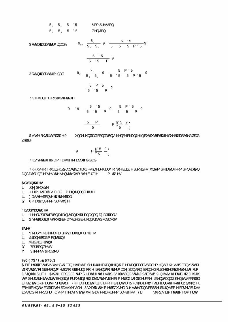
Mr. RAVIRAJ SRIKRISHNA AP/SOA 200
g1 g4
g2 g3
R R R R (Compression)R R R R (Tension)
Potential at terminal B,g1
ABg1 g3
R R RV V VR R (R R) (R R)
R R V2R R(1 )
Potential at terminal D,g2
ADg2 g4
R R RV V VR R (R R) (R R)
R R V2R R(1 )
The changed output voltage
0 0
R R R RV V V V2R R(1 ) 2R R(1 )
R(1 ) R V2(1 )2R R 4
As the output voltage V0 = 0 under unload conditions, hence change in output voltage due to applied loadwill be
0
R VV 2(1 )R 4
This voltage is a measure of applied load.
The use of four identical strain gauges in each arm of the bridge provides full temperature compensationand also increases the sensitivity of the bridge 2 (1+) times.
Advantagesi. Inexpensiveii. Hermetically sealed & maintenance freeiii. Fast response to the loadiv. Small and compact size
Disadvantagesi. Needs protection against angular and non-axial loads.ii. Overloading should be avoided beyond rated capacity.
Usesi. Road vehicle or Aircraft weighing devices.ii. Crane load monitoringiii. Bridging liftingiv. Torsion Testv. Process Control
BIMETALLIC STRIPA bimetallic strip is used to confert a temperature change into mechanical displacement. The strip consists oftwo strips of different metals of differing co-efficients of thermal expansion, bonded or welded together to forma single piece. At the bonding temperature the strip is flat and straight but when it is heated to a hightemperature it starts bending or curling towards the side of metal with lower coefficients and when it is cooledbelow its normal temperature. The layer with higher coefficients , is called active side and the other with lowercoefficient is called the passive side. Usually the metals used are steel and copper or in some cases brassinstead of copper. In some cases it is used as coil for compactness. Fig. 6.16 shows bimetallic elements.

Mr. RAVIRAJ SRIKRISHNA AP/SOA 201
Fig. 6.16. Bimetallic Strip.
The strip is fixed at one end and the other end kept open in the environment whose temperature is to bemeasured. A rise in temperature by ToC causes the element to bend into an arc of a circle. The angle between the original plate axis and the tangent drawn from the tip to the deflection line is given by :
1 2 1 2 1 2 1 22 2 2
1 2 1 2 1 2 1 1 2 2
6 E E t t (t t )( ) L T4 E E t t (t t ) (E t E t )
or Tk L T radians
where E1, E2 = young’s moduli of the materials of layer 1 and 2 respectively.t1, t2 = Thickness of layer 1 and 21, 2 = Coefficients of thermal expansion of the materials of layer 1 and 2 respectively.L = Length of original elementT = Rise in temperaturekT = Bimetallic element sensitivity in radians per m/oC
The sensitivity will be maximum when the term 2 21 1 2 2(E t E t ) becomes zero, thus
1 2
2 1
t Et E
Under this condition KT is given by :
1 2T
3 ( )K2 t
The deflection (d) of the tip of the element from its original position is :2
T
Ld K T2
For circular strip T TK L T
Advantagesi. No moving part to avoid wear outs.ii. Saving of expansive metals and alloys.iii. Portabilityiv. Independence from power supply.
Mr. RAVIRAJ SRIKRISHNA AP/SOA 202
Disadvantagesi. Railway track and roadway construction.ii. Pipes carrying hot water.iii. Inaccurate
Applicationsi. Thermostatsii. Mechanical clocksiii. Heat enginesiv. Circuit breakers (restores when cooled down)
INTRODUCTION OF INTEGRATED CIRCUITS (ICS)Until 1960 the technology of discrete components were used to design electronic circuits. It uses diodes,transistors in conjunction with other circuit elements like resistors, inductors, capacitors etc. which are joinedwith wires or plated conductors on printed circuit boards (PCBs). These discrete circuits have two maindisadvantages. Firstly in a large circuit (like TV circuit, computer circuit) where there are hundred of components,the discrete assembly would occupy a large space. Secondly there will be hundred of soldered points whichwill cause a poor reliability. To avoid these problems researchers started a drive to miniaturize the circuits.One type of such circuit is the integrated circuits, generally abbreviated as IC.
The first commercially available IC came in 1961 from Fairchild Semiconductor Corporation. An IC hasvarious components such as resistor, capacitors, diodes, transistors etc. fabricated on the same smallsemiconductor chip. ICs are now a days used in electronic industry, instrumentation, control system,computer industry, automobile industry and many other applications. This has now fulfilled the demand ofindustries for electronic equipment of smaller size, lighter weight, low power requirement and high reliability ascompared with discrete components. The IC possesses the following advantages and disadvantages overdiscrete circuits :
Advantagesi. Low cost due to simultaneous production of a large number of components.ii. Extremely small size due to fabrication of various circuit elements on the same chip of semiconductor
material. Hence also light weight.iii. High Reliability as components are fabricated sequentially without using soldering.iv. Low Power Consumption due to smaller size components (capacitance, resistance etc.)v. High Temperature handling capacity at extreme values.vi. Easy Replacement as it is more economical to replace them than to repair them.vii. Increased Operating Speed due to absence of parasitic capacitance effect.viii. Close matching of components and temperature coefficients because of bull production in batches.ix. Improved functional performance as more complex circuits can be fabricated for achieving better
characteristics.x. Suitable for small signal operation because of no change of stray electrical pickup as various components
of an IC are located very close to each other on a silicon water.
Disadvantagesi. If a single component goes bad in an IC, it can bot be removed instead the whole IC is to be replaced.ii. Limited power dissipation (< 10 watts).iii. Inductors and transformers can not be integrated into it, instead they are connected exterier to the chip.iv. High value of capacitance (> 30 pF) not convenient or economical to integrate, hence it is to be connected
as discrete component exterior to IC Chip.v. High grade p-n-p assembly is not easily possible.vi. Low temperature coefficient is difficult to be achieved.vii. Difficult to achieve low noise and high voltage operations.viii. Large value of saturation resistance of transistors.ix. Voltage dependence of resistors and capacitors.x. Parameter modification not possible.xi. Quite delicate in handling as these cannot withstand rough handling or excessive heat.
Mr. RAVIRAJ SRIKRISHNA AP/SOA 203
CLASSIFICATION OF IC’SThe integrated circuits may be classified according to a number of ways as shown in Figure 6.17.
Fig. 6.17. Block Diagram of IC Classification.
A. On the basis of fabrication techniques used, the ICs can be divided into following four classes.
Monolithic ICsThe word ‘monolithic’ is derived from the greek ‘monos’ means single and ‘lithos’ means stone. Thus it is madeinto a single stone or single crystal. In monolithic ICs all circuit components both active components (transistoretc.) and passive components (diodes, resistor, capacitors etc.) and their interconnections are formed into asingle chip of silicon. This technology is useful for manufacturing identical ICs in large quantities and thereforeprovides lowest per unit cost and greater reliability. These type of ICs are most commonly used. Figure 6.18shows the monolithic IC in plastic and can type package.
Fig. 6.18. Monolithic IC Packages.
Commercially available ICs of this types are used as amplifiers, voltage regulators, crowbars, AM receivers,TV circuits and computer circuits. However these ICs have following limitations. Low power rating (< 1 watt) Poorer isolation between components. Fabrication of inductors not possible. Passive components of only low values are possible. Lack of flexity in circuit design i.e. modification is not possible.
Thin and Thick Film ICsThese devices are larger than monolithic ICs but smaller than discrete circuits. These ICs can be used forcomparatively higher power requirement. With a thin-or thick-film IC, the passive components like resistorsand capacitors are integrated, but the transistors and diodes are connected as discrete components to formcomplete circuit. Therefore, commercially available thin-and thick-film circuits are combination of integratedand discrete components. The main difference between these is not their relative thickness but the method ofdeposition of film. Both have similar look, characteristic and features. Figure 6.19 shows the enlarged view ofthick film IC.

Mr. RAVIRAJ SRIKRISHNA AP/SOA 204
Fig. 6.19. Enlarged view of thick film IC.
Hybrid ICsIn Hybrid ICs the circuit is fabricated by interconnecting a number of individual chips. The active elements arediffused transistors or diodes. The passive components may be group of diffused resistors or capacitors on asingle chip, or they may be thin-film components. Wiring provides interconnection between chips. These ICsare used for high power audio amplifiers applications from 5W to 50 Watts. The structure of a hybrid (multi chipICs) is shown in Figure 6.20.
Fig. 6.20. Structure of Hybrid IC.
Like thin-and thick-film ICs, hybrid ICs usually have better performance than monolithic ICs. However theprocess is too expensive for mass production, multi chip techniques are quite economical for small quantityproduction and are more offen used as prototype for monolithic ICs.b. On the basis of application ICs are of two types i.e. linear ICs and digital ICs. When the input/output
relationship of a circuit is linear, linear ICs are used for example operational amplifiers (OP-Amps) whichwas originally designed for performing mathematical operations like addition, subtraction, multiplication,differentiation, integration, inversion etc.When the circuit is either in on-state or off-state and not in between the two, the circuit is called the digitalcircuit. ICs used in such circuits are called digital ICs. They find their wide applications in computers andlogic circuits.
c. Based upon the active devices used the ICs can be further classified as bipolar ICs using bipolar activedevices (BJT) and unipolar ICs using unipolar active devices like (FET).
d. The ICs can also be classified on the basis of their chip size i.e. the number of components contains in it.
Small Scale Integration (SSI) - 1 to 20 components/chip. Medium Scale Integration (MSI) - 20 to 100 components/chip. Large Scale Integration (LSI) - 100 to 1000 components/chip. Very Large Scale Integration (VLSI) - 1000 to 10,000 components/chip. Super Large Scale Integration (SLSI) - 10,000 to 1,00,000 components/chip.
Mr. RAVIRAJ SRIKRISHNA AP/SOA 205
SOLVED EXAMPLESExample 8.1. A resistive wire strain gauge uses a soft iron wire of small diameter. The gauge factor is +4.2.Neglecting the piezoresistive effects, calculates the Poisson’s ratio.
Solution : Given G = + 4.2
We know thats / sG 1 2l / l
But as piezoresistive effect is zero, hence
G = 1 + 2
or 4.2 = 1 + 2
or4.2 1 3.2
2 2
= 1.6 Ans.
Example 8.2. A platinum thermometer has a resistance of 100 W at 25oC.i. Find its resistance at 65oC, if the platinum has a resistance temp. coefficient of 0.003921oC.ii. If the thermometer has a resistance of 150 W, calculate the temperature.
Solution : Using linear approximation, the resistances at any temperature oC.is given by
i. R = R0 (1+ 0)
At 65oC R65 = 100 [1 + 0.003921 (65-25)]
or R65 = 115.68 Ans.
ii. Suppose is the unknown temperature then
150 = 100 [1 + 0.003921 (-25)]
= 152.55oC Ans.