Electrical Engineering Department Electronics Lab Manual
108
Electrical Engineering Department Electronics Lab Manual 2013 Revised by:Haneen Al-'Out Nasim zayed 000001 000001 Page 1 / 108
-
Upload
khangminh22 -
Category
Documents
-
view
0 -
download
0
Transcript of Electrical Engineering Department Electronics Lab Manual

Electrical Engineering Department
Electronics Lab Manual
2013
Revised by:Haneen Al-'Out
Nasim zayed
000001000001
Page 1 / 108

An-Najah National University
Faculty of Engineering
Issue number: AD3-3
Department Name : Course Name:Electronic circuit lab Course # :63314
Report Grading Sheet
Instructor Name: Experiment name: Academic Year: Experiment #:
Students:1- 2-3- 4-
Report’s OutcomesILO A,B=( 50 ) % ILO D =( 20 ) % ILO A =( 20 ) % ILO K =( 10 ) %
Evaluation Criterion Grade PointsIntroductionSufficient,Clear and complete statement of objectives. Apparatus/ ProcedureApparatus sufficiently described to enable another experimenter to identify the equipment needed to conduct the experiment. Procedure sufficiently described.Experimental Results and CalculationsResults analyzed correctly. Experimental findings adequately and specifically summarized, in graphical, tabular, and/or written form.Conclusions Conclusions summarize the major findings from the experimental results with adequate specificity. ReferencesComplete and consistent bibliographic information that would enable the reader to find the reference of interest.Total
Total
000002000002
Page 2 / 108

1Key 1: Report structure: Abstract, Introduction, results ….etc 2: References: Complete and consistent bibliographic information that would enable the reader to find the reference of interest. 3: Time keeping: Sticking to the allowed time for each student 4: Presentation skills: Personality, attention to audience, body language and gestures.
An-Najah National University
Faculty of Engineering
Issue number : AD4-1
Department Name:
Course name : Electronic Circuit Course # :63314
Mini- Project Evaluation Form
Project name : Semester : Instructor name : Project ILOs (with percentages) :
Final grade
Presentation evaluation Report evaluation
Students names Grade Answered questions
Presentation skills 4
Time keeping 3
GradeReferences
2 Addressing problems
Data analysis
Report structure 1
Points Points Points Points Points Points Points Points
000003000003
Page 3 / 108

2Key 1: Report structure: Abstract, Introduction, results ….etc 2: References: Complete and consistent bibliographic information that would enable the reader to find the reference of interest. 3: Time keeping: Sticking to the allowed time for each student 4: Presentation skills: Personality, attention to audience, body language and gestures.
An-Najah National University
Faculty of Engineering
Issue number : AD4-1
Final grade
Presentation evaluation Report evaluation
Students names Grade Answered questions
Presentation skills 4
Time keeping 3
GradeReferences
2 Addressing problems
Data analysis
Report structure 1
Points Points Points Points Points Points Points Points
000004000004
Page 4 / 108

63314 Electronic Circuits Lab - Department: Electrical Engineering
Semester Teaching Methods Credits
4Lecture Rec. Lab.
Project Work
HR Other Total
0 0 36 28 36 0 1001
Language English
Compulsory / Elective
major compulsory
Prerequisites
P1 : Electronic Circuits I (63260) OR Electronic Circuits I (63214)
Instructors
Eng Haneen Al-Out, [email protected]
Course Contents
Electronics lab has been prepared to equip the students with the necessary practical and theoretical knowledge of electronic principles. During the lab the students become very familiar with , Types of Diodes, Rectifier diode, Half wave rectifier, Bridge rectifier, On state and off state characteristic of zener diode, Testing the layering and rectifying of bipolar transistor, Characteristic of the transistor, Depletion layer Fets, Characteristic of the Fets, Multistage amplifier, Differential amplifier, Push pull output amplifier, Operational amplifier
Learning Outcomes and Competences
1 Basic Knowledge of Principles of Electrical circuits and analysis Knowledge and also to take measurements deferent type of Electronic circuits
A B 50 %
2 2) An ability To function and work the experiments as team D 20 %
3 An ability to identify, formulate, and solve electronics circuits problems A 20 %
4 An ability ORCAD methods to solve electronics circuits engineering analyses and designee
K 10 %
Textbook and / or Refrences
Electronic circuits lab
Assessment Criteria
Percent (%)
Projects 10 %
Laboratory Work 60 %
Final Exam 30 %
Week Subject
2 EXPERIMENT # 2: Junction diodes and applications
3 EXPERIMENT # 3: Zener diodes and applications
4 EXPERIMENT # 4 Bipolar Junction transistors
5 EXPERIMENT # 5: Soldering and Desoldering skills
6 EXPERIMENT # 6: Junction field effect Transistors
7 EXPERIMENT # 7: Amplifiers
8 EXPERIMENT # 8: Multistage amplifiers
9 EXPERIMENT # 9: DIFFERENTIAL AMPLIFIER
10 EXPERIMENT # 10: [10] Push Pull amplifiers
000005000005
1 Introduction -Pspice (ORCAD ) 1 I
Page 5 / 108

13 EXPERIMENT # 13: Dynamic Behavior of an Op-Amp
11 EXPERIMENT # 11 Operational amplifiers study
12 EXPERIMENT # 12: Op-amp circuits NON-INVERTING AMPLIFIER
13 EXPERIMENT # 13: Dynamic Behavior of Op-amps
14 EXPERIMENT # 14: Mini Project Discussion
15 Practical Exam
000006000006
16 Theoretical Exam
Page 6 / 108
An-Najah National University Electrical Engineering Department
Electronics Laboratory Safety Rules
Acquaint yourself with the location of the following safety items
within the laboratory:
a. Fire extinguisher
b. First aid kit
c. Telephone and emergency numbers:
The following Regulations and Safety Rules must be observed:
1. Avoid bulky, loose or trailing clothes. Avoid long loose hair. Remove metal bracelets,
rings or watchstraps when working in the laboratories.
2. Smoking, food, beverages and other substances are strictly prohibited in the laboratory at
all times. Avoid working with wet hands and clothing.
3. You may enter the laboratory only when authorized to do so and only during authorized
hours of operation.
4. Do not open, remove the cover, or attempt to repair any broken equipment or defective
parts.
5. When the lab exercise is over, all instruments must be turned off.
6. Concerning experiments, electrical equipments, materials and devices:
o Before equipment is energized ensure:
a. circuit connections and layout have been checked by a Teaching
Assistant (TA) and
b. all colleagues in your group give their assent.
o Experiments left unattended should be isolated from the power supplies. If for a special reason, it must be left on, a barrier and a warning notice are required.
o Make sure the power is off when wiring or making changes to circuit.
o Make sure instrumentation is set on proper range for the desired type of
measurement, BEFORE ENERGIZING CIRCUIT.
o Make sure components used are of a rating that will withstand applied current
and voltage.
7. It is the duty of all concerned (who use electronics laboratory and visitors) to take all
reasonable steps to safeguard the HEALTH and SAFETY of themselves.
Note: If any safety questions arise, consult the lab instructor or staff for guidance and
instructions. 000007000007
Page 7 / 108

[14] Mini Project Discussion
[15] Practical Exam
[16] Theoretical Exam
000008000008
Page 8 / 108
[1] Introduction -Pspice (ORCAD )
[5] Soldering and Desoldering skills
[13] Dynamic Behavior of Op-amps 104
[7] Amplifiers 71
[10] Push Pull amplifiers 84
Schedule Lab: page
[2] Junction diodes and applications 16
[3] Zener diodes and applications 26
[9] Differential amplifiers 80
[8] Multistage amplifiers 76
[11] Operational amplifiers 88
[12] Op-amp circuits 95
[4] Bipolar Junction transistors 40
[6] Junction field effect Transistors 58

General Report Guidelines: The lab report reinforces the material that was learned in the lab and helps you develop effective technical communication skills. Development of both oral and written technical communication skills is one of the most important things you can learn as an undergraduate student. A technical report is expected to contain the following items or subsections:
• Cover page,
• Introduction,
• Experimental procedure and methodology
• experimental results,
• Conclusion or summary,
• References. Introduction:
It should contain a brief statement in which you state the objectives, or goals of the experiment.
The Procedure:
measurements were made.
Results/Questions:
This section of the report should be used to answer any
questions presented in the lab handout. Any tables and/or
circuit diagrams representing results of the experiment should
A brief conclusion summarizing the work done, theory
applied, and the results of the completed work should be
included here. Data and analyses are not appropriate for the
000009000009
be referred to and discussed/explained with detail.
It describes the experimental setup and how the
Conclusion:
conclusion.
References:Complete and consistent bibliographic information that wouldenable the reader to find the reference of interest.
Page 9 / 108

1) Opening PSpice
1. Find PSpice. Open Schematics and then click on the schematic icon .
2. You will see the window as shown in Figure 1.
Figure 1
2) Drawing the circuit
I. Getting the Parts
1. Clicking on the 'get new parts' button , or Pressing "Control+G".
2. Select a part that you want in your circuit. This can be done by typing in the name (part name) or scrolling down the list until you find it.
000011000011
Experiment # 1 Introduction –Pspice tutorial
Page 10 / 108

Figure 2
3. Upon selecting your part, click on the place button then click where you want it placed , if you need multiple instances of this part click again
4. If you want to take a part and close then you just select the part and click onplace& close.
II. Placing the Parts
1. Just select the part (It will become Red) and drag it where you want it.2. To rotate parts so that they will fit in you circuit nicely, click on the part and
press3. "Ctrl+R" (or Edit "Rotate"). To flip them, press "Ctrl+F" (or Edit
"Flip").If you have any parts left over, just select them and press "Delete".
III. Connecting the Circuit
1. You'll have to attach them with wires,go up to the tool bar andselect "Draw
Wire" or"Ctrl+W" .
2. With the pencil looking pointer, click on one end of a part, when you moveyour mouse around, you should see dotted lines appear. Attach the other end of your wire to the next part in the circuit.
000012000012
Page 11 / 108

3. Repeat this until your circuit is completely wired.
IV. Changing the Name of the Part
1. To change the name, double click on the present name (C1, or R1 orwhatever your part is), t he top window, you can type in the name you want the part to have.
Figure 3
V. Changing the Value of the Part
• If you only want to change the value of the part, you can double click on the present value and type in the new value and press OK.
Figure 4
000013000013
Page 12 / 108

VI. Making Sure You Have a GND
This is very important. You cannot do any simulation on the circuit if you don't have a ground. If you aren't sure where to put it, place it near the negative side of your voltage source.
VII. Voltage and Current Bubbles
These are important if you want to measure the voltage at a point or the current going through that point.To add voltage or current bubbles, go to the right side
of the top tool bar and select "Voltage/Level Marker" (Ctrl+M) or
"Current Marker" . To get either of these, go to "Markers" and either"Voltage/Level Marker" or "Current Marker".
3) Analysis Menu
Figure 5
To open the analysis menu click on the button.
A. DC Sweep
The DC sweep allows you to do various different sweeps of your circuit to see how it responds to various conditions.
• You need to specify a start value, an end value, and the number of points you wish to calculate.
• Another excellent feature of the DC sweep in PSpice, is the ability to do a nested sweep.A nested sweep allows you to run two simultaneous sweeps to see how changes in two different DC sources will affect your circuit.Once you've filled inthe main sweep menu, click on the nested sweep button and choose the second type of source to sweep and name it, also specifying the start and end values.(Note: In some versions of PSpice you need to click on enable nested sweep).
B. Bias Point Detail 000014000014
Page 13 / 108

• This is a simple, but incredibly useful sweep. It will not launch Probe and so give you nothing to plot. But by clicking on enable bias current display or enable bias voltage display, this will indicate the voltage and current at certain points within the circuit.
C. Transient
The transient analysis is probably the most important analysis you can run in PSpice, and it computes various values of your circuit over time
• Choose Analysis…Setup from the menu bar, or click on the Setup Analysis
button in the toolbar. The Analysis Setup dialog box opens.
• Click on the Transient button in the Analysis Setup dialog box. The Transient dialog box opens.
• Two very important parameters in the transient analysis are (see Figure6):
print step final time.
Figure 6
• The ratio of final time: print step (Keep print step atleast 1/100th of the final time) determines how many calculations PSpice must make to plot a wave form. However play with step time to see what works best for your circuit.
• You can set a step ceiling which will limit the size of each interval, thus increasing calculation speed.
000015000015
Page 14 / 108

4) Graphing:
If you don't have any errors, you should get a window with a black background to pop up.
5) Finding Points:
There are Cursor buttons that allow you to find the maximum or minimum or just a point on the line. These are located on the toolbar (to the right).Select which curve
you want to look at and then select "Toggle Cursor" .Then you can
find the max, min, the slope, or the relative max or min ( is find relative max).
000016000016
Page 15 / 108

1 Junction Diodes and applications 1.1 Effects of the p-n-junction of diodes 1.1.1 Basics
Diodes are two poles semiconductors. The semiconductor diode consists
of a semiconductor crystal (silicon, germanium), one side is n-doped, the
other one is p-doped. At the p-n-junction there is a barrier layer. The different
doped layers are equipped with ohm contacts and could be connected to
other components.
When voltage is applied, the barrier effect could be increased or nullified.
The semiconductor diode allows current flow in one direction and blocks the
other one.
The diode has following the circuit symbol in pic. 1.1.
1.1.2 Tests Test
Examine the effect of the rectifier diode’s p-n-junction on the current flow in relation to the applied
voltage and its polarity.
~-
+
Polarität1
Polarität2
RV=680Ω
U0 = 0...30 V V1 V1
IF
UF
V1 = Si-Diode 1A
pic. 1.2 Test proceeding:
• One by one apply following voltages UF according to chart 1.1 to the diode’s polarity 1 (pic. 1.2)
and measure the respective conducting current IF. Fill the values in chart 1.1. Use the current
error circuit.
pic. 1.1
P N
Electrical Engineering Department Electronics Lab Manual
1
Experiment #2
000017000017
Page 16 / 108

• Then change the polarity of the diode (polarity 2) and repeat same test with the voltage
values of chart 1.2., remove the series resistor. (680 Ω) and set the voltage directly at the
power supply. Use the voltage error circuit for this measurement. An exact measurement of
the reverse current IR requires a highly sensible multimeter (100 nA).
• For construction of the diode characteristic curve use the values of both charts and fill in the
diagram pic. 1.3. chart 1.1 chart 1.2 chart 1.3 Test: What is the name of the voltage, when the diode gets conductive? Answer:
UF [V] 0 0,1 0,2 0,3 0,4 0,5 0,6 0,65 0,7 0,75
IF [mA]
UR [V] 0 2,5 5 10 15 20 25 30
IR [nA]
IF [mA]
25
20
15
10
5
30
U R [V]
20 10 0
20
0,1 0,2 0,3 0,4 0,5 0,6 0,7 0,8
U F [V]
40
60
I R [nA]
80
Electrical Engineering Department Electronics Lab Manual
2
000018000018
Page 17 / 108

1.2 Characteristics of Diodes with Various Semiconducting Materials 1.2.1 Basics
If AC voltage, with periodically changing instantaneous value between zero and the maximum value, is
applied to a diode, the diode characteristic could be presented completely at the display of the
oscilloscope. Therefore the diode voltage is applied to the X-amplifier. The diode current could be
measured at a series resistor as a proportional voltage. That voltage is applied to the inverted Y-
amplifier. 1.2.2 Tests Test
Store the characteristics of a silicon diode, a geranium diode and a gallium-arsenide diode (LED)
with your oscilloscope. Test proceeding:
• Set-up the circuit in pic. 1.4 and one by one present the voltage curve for the silicon diode, the
germanium diode and the gallium-arsenide diode (LED red) at the oscilloscope (X/Y
presentation).
G
R=330ΩY
X
uss = 6V Sinusf = 50 Hz
V1
0 V
pic.1.2.2.1
Note:
Due to the reversed polarity of the voltages, the Y-amplifier has to be inverted.
A mirror image is presented, when using an oscilloscope without inverting function.
Caution:
To avoid short-circuit of the measuring voltage across mutual earth, the generator output and the
oscilloscope inputs must be potential-free.
• Draw the curves of all three diodes into the diagram (pic. 1.4).
Electrical Engineering Department Electronics Lab Manual
3
000019000019
Page 18 / 108
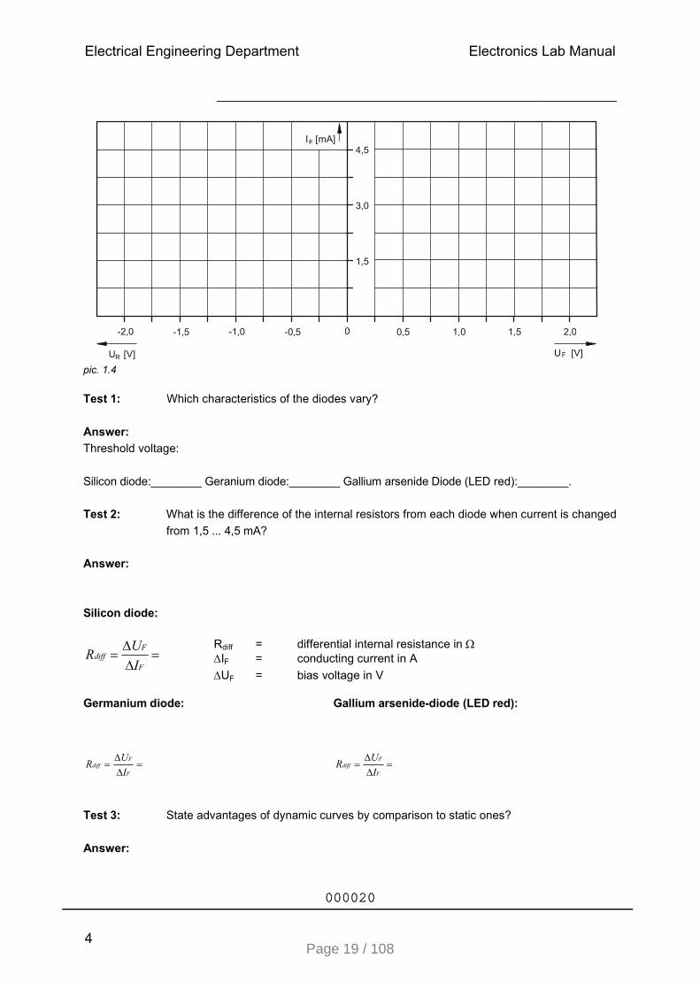
pic. 1.4 Test 1: Which characteristics of the diodes vary?
Answer:
Threshold voltage:
Silicon diode:________ Geranium diode:________ Gallium arsenide Diode (LED red):________. Test 2: What is the difference of the internal resistors from each diode when current is changed
from 1,5 ... 4,5 mA? Answer:
Silicon diode:
Rdiff = differential internal resistance in Ω ∆IF = conducting current in A
∆UF = bias voltage in V Germanium diode: Gallium arsenide-diode (LED red):
=∆∆
=F
F
diff
I
UR =
∆∆
=F
F
diff
I
UR
Test 3: State advantages of dynamic curves by comparison to static ones?
Answer:
I F [mA] 4,5
3,0
1,5
-2,0 UR [V]
-1,5 -1,0 -0,5 0 0,5 1,0 1,5 2,0
U F [V]
=∆∆
=F
Fdiff
I
UR
Electrical Engineering Department Electronics Lab Manual
4
000020000020
Page 19 / 108

1.3 Half Wave Rectifier 1.3.1 Basics
If a semiconductor diode is integrated to a
circuit, current flow is only possible at one polarity of the applied voltage (bias direction).
When polarity is reversed the blocking function
is effective and no current will flow. If AC voltage is applied to such a circuit, it is only
conductive at the half wave with the respective
polarity. The other half wave is blocked. Current within the circuit will flow only in one
direction.
pic. 1.5 M1 single pulse center tapped circuit 1.3.2 Tests Test
Examine the rectifying effect of a semiconductor diode within a single pulse center tapped circuit M1
with a multimeter and an oscilloscope.
Test proceeding
• Set-up the circuit in pic. 1.6 without smoothing capacitor.
• Measure the input voltage UE and the DC voltage Ud with the multimeter and calculate the ratio
d E
G~
+1 2
Si 1AUeff = 5Vf = 50 Hz
Sinus
UERL=
10kΩ CG
Ud
pic. 1.6
Electrical Engineering Department Electronics Lab Manual
5
000021000021
Y Y
between U and U .
Page 20 / 108

• Measure the input voltage UE and the DC voltage Ud with the oscilloscope and draw the curve in pic. 1.7.
Settings: Y1 = 5 V / part Y2 = 5 V / part X = 5 ms / part Determine by help of the oscilloscope picture in pic. 18.7 the peak-peak-value and the frequency of the ripple UBr . Note: Ripple is the AC portion of a pulsating DC voltage Ud. .
pic. 1.7 Then connect the smoothing - capacitor CG according to chart 1.3 in parallel to load resistance and repeat your measurements.
Please regard the polarity when
connecting the electrolytic capacitors! Fill
all determined values in chart 1.3.
chart 1.3
Settings:
Y1 = 5 V / part
Y2 = 5 V / part
X = 5 ms / part Draw the curve for the input voltage UE and the DC voltage Ud, with smoothing capacitor 10 µF into the chart in pic. 1.8.
pic. 1.8
Electrical Engineering Department Electronics Lab Manual
6
000022000022
Page 21 / 108

• Reverse the diode within the circuit in pic. 1.4, measure the voltages UE and Ud without smoothing capacitor.
• Draw the curves for both voltages into the chart 1.9
Settings: Y1 = 5 V / part Y2 = 5 V / part X = 5 ms / part
pic. 1.9 Test 1: What is the frequency of the ripple UBr? Answer: Test 2: What happens if the diode in circuit pic.1.6 is reversed in polarity? Answer: Test 3: At which connector of the diode is the plus pole of the obtained DC voltage Ud? Answer: Test 4: State the value of blocking voltage affecting the diode with smoothing capacitor CG? Answer: Test 5: What influence does the smoothing capacitor have on the peak-peak-value of the
ripple? Answer:
- 0 (Y2 ) = U d
Electrical Engineering Department Electronics Lab Manual
7
000023000023
Page 22 / 108

1.4 Full Wave Refctifier 1.4.1 Basics
At the single pulse center-tapped circuit M1 only a half-wave of the AC voltage is used. Disadvantage is the small portion of DC voltage with high ripple.
This disadvantage is avoided in the two-pulse bridge B2, as polarity of the opposed half-wave is changed and added to the DC voltage.
pic. 1.10 B2 Two-pulse Bridge Circuit 1.4.2 Tests Test Examine by help of the oscilloscope and multimeter the characteristics of two-pulse bridge B2.
V1 V2
a
G~
UE
RL
10 k
+CG
Ud
Y
X
b
V3 V4
V1 - V4 = Si Diode 1A
Ueff = 5Vf = 50 Hz
Sinus
pic. 1.11 Test proceeding:
• Set-up the circuit in pic. 1.11 without smoothing capacitor. Measure input voltage UE and DC voltage Ud with your multimeter and determine the ratio Ud to UE.
• Measure with the oscilloscope all the input voltages UE and DC voltages Ud and draw the curve
into pic. 1.12.
UE
UE
t
Ud
Ud
t
Electrical Engineering Department Electronics Lab Manual
8
000024000024
Page 23 / 108

• Determine by help of the oscilloscope curve in pic. 1.12 the peak-peak-value and the frequency of ripple voltage UBr. Note: Ripple voltage is the portion of AC voltage within pulsating DC voltage Ud.
Setting:
Y = 5 V / part
X = 5 ms / part - 0 (Y1 ) = U E
- 0 (Y2 ) = U d
pic. 1.12
• Then one by one connect the smoothing capacitors CG in parallel to
the load resistor RL according to chart
1.5 and repeat your measurements. Please regard the polarity when
connecting the electrolytic capacitor! • Fill the determined values in chart 1.5.
chart 1.5
Settings:
Y = 5 V / Teil
X = 5 ms / Teil
- 0 (Y1 ) = U E
Draw the curve for the input voltage UE
and the DC voltage Ud with smoothing
capacitor 10 µF in chart 1.13.
- 0 (Y2 ) = U d
pic. 1.13
Electrical Engineering Department Electronics Lab Manual
9
000025000025
Page 24 / 108

Test 1: What is the ratio between DC voltage Ud and the applied effective input voltage UE
(without smoothing capacitor)? Answer: Test 2: What is the frequency of the ripple voltage UBr? Answer:
Electrical Engineering Department Electronics Lab Manual
10
000026000026
Page 25 / 108

2 Zener Diodes and appliactions 2.1.1 Basics Z-Diodes are silicon-semiconductor diodes, with conduction curve similar to rectifier diodes. In
comparison to rectifier diodes, the Z-diode has a lower breakdown voltage within stop – or reverse band
(Z-Voltage). When exceeding the breakdown voltage, current increases steeply in reversed direction (Zener effect). In opposite to the rectifier diodes, Z-diodes are utilized in reversed direction.
To protect from overload, a resistor is connected in series to the Z-diode, its value is calculated as follows:
Ub = applied operating voltage UZ = Zener-voltage of the utilized diode-type IZ = average acceptable Z-current IL = current affecting the load resistance RL in parallel to the Z-diode
Circuit Symbol pic. 2.1 Due to its characteristics the Z-diodes are used for voltage stabilization and voltage limitation. 2.1.2 Tests Test
Present the curve of a Z-diode with your oscilloscope and determine the Z-voltage. Test proceeding:
• Set-up the circuit in pic. 2.2. Switch the oscilloscope to X/Y presentation.
Note: As both voltages are reversed poled to the reference point, the Y-amplifier has to invert.
Oscilloscopes without inverting function show a mirror like presentation.
G~
-Y
X
Zener-Diode 10 V / 40 mA
RV 1kΩ
Ueff = 24 Vf = 50 Hz
Sinus
pic. 2.2
LZ
ZbV
II
UUR
+−
=
Electrical Engineering Department Electronics Lab Manual
11
Experiment # 3
000027000027
Page 26 / 108

Note: The output of the power supply or the inputs of the oscilloscope have to be potential-free to avoid
short-circuit due to mutual earth. Draw the presented oscilloscope display into the chart 2.3.
Settings: Y = 10 V / part X = 2 V / part
- 0 (Y)
0 (X)
pic. 2.3 Test 1: Determine the Z-voltage UZ. Answer: UZ = Test 2: What is the value of the maximum current IZ? Answer:
R
UIz
R
=max
Test 3: What is the value of the threshold voltage US? Answer: US =
Electrical Engineering Department Electronics Lab Manual
12
000028000028
Page 27 / 108

2.2 DC Voltage regulation using Z-Diodes 2.2.1 Basics Because of the steep increasing current in the reverse band of a Z-diode, it is used for regulating DC
voltage.
Therefore a resistor, at which the difference between the unstable input voltage and the limited output voltage drops, is connected in series to the Z-diode.
Limited output voltage is equal to the Z-voltage and is depending on the Z-diode type. 2.2.2 Tests Test 1 Examine the relationship between output voltage and input voltage at a limiter circuit with Z-diodes. Test proceeding:
• Set-up the circuit in pic. 2.4. One by one set to DC voltages UE according to chart 2.1.auf.
Measure the respective output voltages with the multimeter and fill in chart 2.1.
• Graphically present the relation between output voltage and input voltage within the diagram
2.5.
~-
10 V40 mA
RV 330Ω
U=0...15V UE UA
pic. 2.4
Electrical Engineering Department Electronics Lab Manual
13
000029000029
Page 28 / 108

chart 2.1 pic. 2.5
UE [V] 0 1 2 3 4 5 6 7 8 9 10 11 12 13 14 15
UA [V]
Electrical Engineering Department Electronics Lab Manual
14
000030000030
Page 29 / 108

Test 2
Examine the relationship between Zener current IZ and input voltage
Test proceeding: • Set-up the circuit in pic. 2.6. One by one set the DC voltages UE according to chart 2.6. • Measure the respective Z-currents IZ with the multimeter and fill the current values in chart 2.2.
• Graphically present the relation of Z-current IZ and input voltage UE in the diagram pic. 2.7.
~-
RV 330 Ω
10 V40 mA
Ugl = 0...15V
UE UA
IZ
pic. 2.6
Electrical Engineering Department Electronics Lab Manual
15
000031000031
Page 30 / 108

chart 2.2 IL [mA] pic. 2.7
UE [V] 0 1 2 3 4 5 6 7 8 9 10 11 12 13 14 15
IZ [V]
Electrical Engineering Department Electronics Lab Manual
16
000032000032
Page 31 / 108

Test 3 Relationship between zener current Iz and load current I load Test proceeding:
• Set-up the circuit in pic. 2.8. Adjust the potentiometer to the load currents IL according to chart 2.3.
Note:
Increase the resistor R1 to 1 kΩ, 2,2 kΩ, 4,7 kΩ and 10 kΩ , use low load current.
~-
U = 15 V
RV 330 Ω R1 680 Ω
R 1 kΩ
ILIZ
UE 10 V40 mA
pic. 2.8
• Graphically present the relation between Z-current IZ and load current IL within the diagram pic. 2.9.
Electrical Engineering Department Electronics Lab Manual
17
000033000033
Page 32 / 108

chart 2.3 pic. 2.9 Test 1: What condition is needed that the output voltage remains constant in a limiter circuit
with Z-diode? Answer: Test 2: When does Z-current IZ flow? Answer: Test 3: Under which condition is the limiting effect maintained although under load? Answer:
IL [V] 0 1 2 3 4 5 6 7 8 9 10 11 12 13 14 15
IZ [V]
Electrical Engineering Department Electronics Lab Manual
18
000034000034
Page 33 / 108

2.4 AC Voltage Limiting and Overvoltage Protection with Z-Diodes 2.4.1 Basics
If the voltage applied to a Z-diode is less than Z voltage, no current is flowing. Current only flows if the
value of Z voltage is reached or exceeded. Therefore this component could be used to protect other
parts (e. g. MOS-components) from over voltage.
To avoid a rectifying effect due to low threshold voltage, two Z-diodes are connected in opposite,
thus a polarity independent voltage limitation is received.
2.4.2 Tests
Test 1
Statically record the curve UA = f (UE) of two in opposite directed Z-diodes.
Test proceeding:
• Set-up the circuit in pic. 2.11. One by one set to DC voltages UE according to chart 2.6. Measure the respective output voltage UA with your multimeter and fill in chart 2.6.
• Then reverse the poles of input voltage UE and go on with your measurements. Note the respective output voltages UA in chart 2.7.
V1 = Z-Diode, 10 V / 40 mA V2 = Z-Diode 3,3 V / 130 mA
pic. 2.11
Electrical Engineering Department Electronics Lab Manual
21
000035000035
Page 34 / 108

• Graphically present the relation between output voltage UA and input voltage UE in chart 2.7. chart 2.6 chart 2.7 pic. 2.12
UE [V] 0 1 2 3 4 5 6 7 8 9 10 11 12 13 14 15
UA [V]
-UE [V] 0 1 2 3 4 5 6 7 8 9 10 11 12 13 14 15
-UA [V]
UA [V] 10
8
6
4
2
-16 -UE [V]
-14 -12 -10 -8 -6 -4 -2 -2
-4
2 4 6 8 10 12 14 16
UE [V]
-6
-8
-UA [V] -10
Electrical Engineering Department Electronics Lab Manual
22
000036000036
Page 35 / 108

Test 2 Examine with your oscilloscope the voltage limiting effect of two opposite directed Z-diodes. Test proceeding:
• Apply a sine-wave AC voltage Ueff = 10 V; f = 50 Hz to the circuit in pic. 2.14 and set the input voltage to UE eff = 2 V at the potentiometer.
V1=Z-Diode 10V/40mA V2=Z-Diode 3,3 V/130mA
pic. 2.14
• Measure the input voltage UE and output voltage UA with your oscilloscope and draw the curve into diagram pic. 2.15.
• Then increase input voltage to UE eff = 10 V.
• Repeat your measurements and fill the values into pic. 2.16.
Notes: Y1 = input voltage UE
Y2 = output voltage UA
- 0 (Y1 )
Settings: X = 5 ms / part
Y1 = 2 V / part Y2 = 2 V / part
- 0 (Y2 ) pic. 2.15
Electrical Engineering Department Electronics Lab Manual
23
000037000037
Page 36 / 108

Notes: Y1 = Input voltage UE
Y2 = Output voltage UA
- 0 (Y1 )
Settings: X = 5 ms / part Y1 = 10 V / part Y2 = 5 V / part
- 0 (Y2 ) pic. 2.16 Test 1: Do you know the application possibilities for a Z-diode? Answer: Test 2: State the advantage of two opposed directed Z-diodes? Answer:
Electrical Engineering Department Electronics Lab Manual
24
000038000038
Page 37 / 108
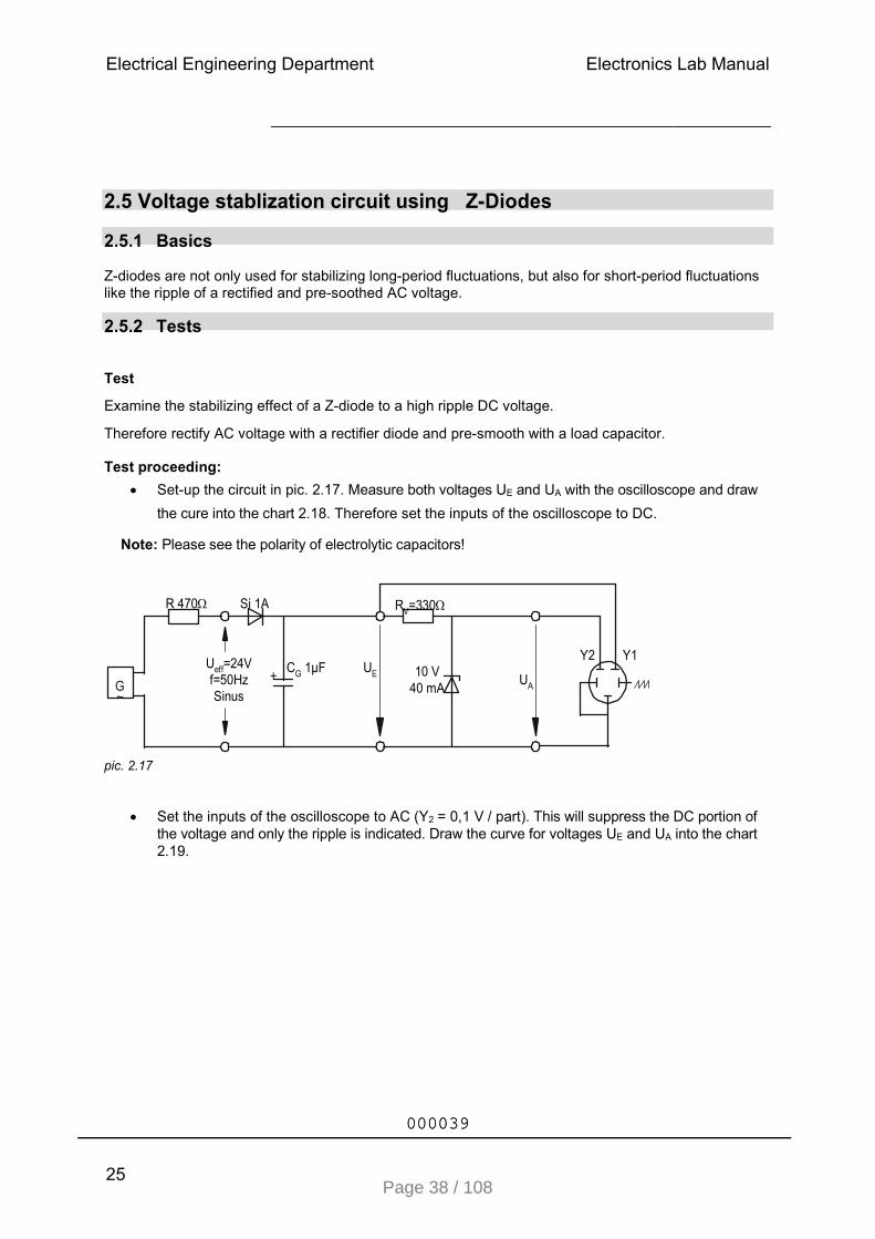
2.5 Voltage stablization circuit using Z-Diodes 2.5.1 Basics Z-diodes are not only used for stabilizing long-period fluctuations, but also for short-period fluctuations like the ripple of a rectified and pre-soothed AC voltage. 2.5.2 Tests Test
Examine the stabilizing effect of a Z-diode to a high ripple DC voltage.
Therefore rectify AC voltage with a rectifier diode and pre-smooth with a load capacitor. Test proceeding:
• Set-up the circuit in pic. 2.17. Measure both voltages UE and UA with the oscilloscope and draw
the cure into the chart 2.18. Therefore set the inputs of the oscilloscope to DC.
Note: Please see the polarity of electrolytic capacitors!
G~
+
R 470Ω
Ueff=24Vf=50HzSinus
CG 1µF UE
Si 1A RV=330Ω
10 V40 mA
UA
Y2 Y1
pic. 2.17
• Set the inputs of the oscilloscope to AC (Y2 = 0,1 V / part). This will suppress the DC portion of the voltage and only the ripple is indicated. Draw the curve for voltages UE and UA into the chart 2.19.
Electrical Engineering Department Electronics Lab Manual
25
000039000039
Page 38 / 108

- 0 (Y2) pic. 2.18 pic. 2.19 Settings: Notes:
X = 5 ms / part Y1 = voltage
UE Y1 = 5 V / part Y2 = voltage
UA Y2 = 5 V / part
Set inputs to DC
Settings: Notes: X = 5 ms / part Y1 = voltage UE
Y1 = 5 V / part without DC portion
Y2 = 0,1 V / part Y2 = voltage UA
without DC portion set inputs to DC
Test 1: Measure in pic. 2.18 ripple voltage ∆UE at the smoothing capacitor CG. Answer:
∆UE = ∆UE = peak-peak-value input voltage UE
Test 2: Measure in pic. 2.19 ripple voltage ∆UA at the Z-diode. Answer:
∆UA = ∆UA = -peak-value output voltage UA
Test 3: Determine the smoothing factor G (absolute stabilizing factor)? Answer:
=∆∆
=A
E
U
UG
Test 4: Determine the relative stabilizing factor S? Answer:
=•=•∆•∆
=E
A
EA
AE
U
UG
UU
UUS
S = relative stabilizing factor
Measure voltages UE and UA with a multimeter.
- 0 (Y1)
- 0 (Y1)
- 0 (Y2)
Electrical Engineering Department Electronics Lab Manual
26
000040000040
Page 39 / 108

4 Bipolar Junction Transistors
4.1 The Rectifying Function of Bipolar Transistors 4.1.1 Basics
Transistors are 3-layers semiconductor
components with two p-n-junctions each. The n-p-n transistors have a thin p-conductive layer
between the two n-conductive layers. The p-n-p
transistors have a thin n-conductive layer embedded between two p-conductive layers.
The p-n-junction between the mid-layer (base) and the two outer layers (emitter and
collector) have rectifying effect, this could be
examined likewise to any other rectifier diode.
4.1.2 Tests
Examine the effect of the p-n-junctions of a n-p-n transistor on the conductivity in dependence of the
supply voltage and its polarity. Repeat same the test with a p-n-p transistor. Note the basic differences
to the n-p-n transistor.
Test proceeding
• Set-up the circuit in pic. 4.2. One by one adjust the potentiometer with help of a multimeter
to the voltages UF in chart 4.1. Measure each respective current IF and fill in chart 4.1.
Graphically present the relation between current IF and voltage UF within the diagram
• pic. 4.2.
Note: Make sure to apply correct type of
measurement: voltage error or current error
circuit
pic. 4.2
pic. 4.1
Electrical Engineering Department Electronics Lab Manual
30
Experiment #4
000041000041
Page 40 / 108

• Set-up the circuit in pic. 4.2 (picture 2). One by one adjust to the voltages UF according to chart
4.3. Measure the respective current IF and fill the values in chart 4.3. Graphically represent the
relation between current IF and voltage UF within the diagram pic.4.4.
• For following measurements according to pic. 4.2 remove your multimeter and adjust the
voltages directly at the power supply. For protective measures do not remove the series resistor RV.
• Set-up the circuit in pic. 4.2 (picture 3). One by one adjust to the voltages UR according to chart 4.2. Measure the respective current IR and fill the values in chart 4.3. Graphically represent the
relation between current IF and voltage UF within the diagram pic. 4.3.
• Set-up the circuit in pic. 21.2 (picture 4). One by one adjust to the voltages UR according to
chart 4.5. Measure the respective current IR and fill the values in chart 4.5 (multimeter with 0,1-
µA measuring range required). Graphically present the relation between current IF and voltage UF
within the diagram pic.4.4.
UF [V] 0 0,1 0,2 0,3 0,4 0,5 0,6 0,65 0,7 0,75 0,76
IF [mA chart 4.1 pic.1 (base/ emitter junction)
* Due to tolerances within the capacitors, the voltage UF for the threshold needs to be adjusted. UR [V] 0 2 4 6 8 8,1 8,2 8,3
IR [mA chart 4.2 pic. 3 (base/ emitter junction) pic. 4.3
I F [mA]
2,0
1,5
1,0
0,5
14 U R [V]
12 10 8 6 4 20
10,1 0,2 0,3 0,4 0,5 0,6 0,7 0,8
UF [V]
2
3
I R [mA] 4
Electrical Engineering Department Electronics Lab Manual
31
000042000042
Page 41 / 108

UF [V] 0 0,1 0,2 0,3 0,4 0,5 0,6 0,65 0,7 0,75 0,8
IF [mA chart 4.3 pic. 2 (collector/ base junction)
* Due to tolerances within the capacitors, the voltage UF for the threshold needs to be adjusted. UR [V] 0 5 10 15 20 25 30
IR [mA chart 4.5 pic. 4 (collector/ base junction) pic. 4.4
I F [mA]
2,0
1,5
1,0
0,5
35 U R [V]
30 25 20 15 10 50
20
0,1 0,2 0,3 0,4 0,5 0,6 0,7 0,8
U F [V]
40
60
I R [nA]
80
Electrical Engineering Department Electronics Lab Manual
32
000043000043
Page 42 / 108

• Then repeat the measurements with a p-n-p transistor (Art no. 503.130.004) and give your statement for the base/ emitter path and the collector/base path at what polarity the junctions of p-n-p transistors and n-p-n transistors are conductive or blocked. Fill your results in chart 4.6.
Polarity NPN-Type PNP-Type
base/ emitter junction (conductive or blocked)
base + / emitter -
base - / emitter +
collector/ base junction conductive or blocked)
collector - / base +
collector + / base -
chart 4.6 Test 1: Name the basic characteristics of the two p-n-junctions of a transistor. Answer: Test 2: What characteristic of the p-n-junction from base and emitter is different from base and
collector? Answer: Test 3: What needs to be regarded when changing a circuit from n-p-n transistors to p-n-p
transistors?
Answer:
Electrical Engineering Department Electronics Lab Manual
33
000044000044
Page 43 / 108

4.2 Current Distribution within a Transistor and Control Function of Base Current
4.2.1 Basics Due to the conductive p-n-junction load carriers from the emitter will be accelerated into the extreme thin basis layer, they will break down the opposing blocked p-n-junction between collector and base, and are biased towards the collector. Base current IB is less than emitter current IE.by the value of this collector current IC. Base current influences the value of the collector current. The relation between those both currents is called the current amplifier ratio B.
CE IIB −= B
C
I
IB =
Low signal current amplification β is: B
C
I
I
∆∆
=β
The terminal connection of the transistor with negative or positive polarity is given by its layering. With n-p-n transistors base and collector are positive in reference to the emitter, with the p-n-p transistor it is negative. 4.2.2 Tests Test 1
Examine statically the influence of the collector current in reference to the base current. Repeat same test for the n-p-n transistor. Test proceeding
• Apply DC voltage of Ugl = 20 V on the circuit in pic. 4.5. Measure the base current IB with
interrupted collector conductance (remove potentiometer) and fill the value in chart 4.7.
• Add potentiometer to the circuit and adjust the collector currents according to chart 4.7. Add
the values for the base current into chart 4.7.
~-
U = 20V
0V
R14,7kΩ
R21kΩ
RV
R 1kΩ IC
IB
R310Ω
NPN, 20 V100 mA
Basis links
pic. 4.5
Electrical Engineering Department Electronics Lab Manual
34
000045000045
Page 44 / 108
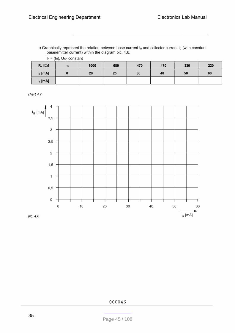
• Graphically represent the relation between base current IB and collector current IC (with constant base/emitter current) within the diagram pic. 4.6.
IB = (IC), UBE constant chart 4.7 pic. 4.6
RV [Ω] ∞ 1000 680 470 470 330 220
IC [mA] 0 20 25 30 40 50 60
IB [mA]
I B [mA]
4 3,5
3
2,5
2
1,5
1
0,5
0
0 10 20 30 40 50 60
I C [mA]
Electrical Engineering Department Electronics Lab Manual
35
000046000046
Page 45 / 108

Test 2
Examine statically the influence of base current to the collector current. Use n-p-n transistors for this
test. Test proceeding:
• Set-up the circuit in pic. 4.7. Adjust the base current according to the values in chart 4.8.
Measure the respective collector current IC and fill the values in chart 4.8.
~-
U = 20V
R2 100Ω
R14,7 kΩ
R 1 kΩR3
10 Ω
0 V
IB
IC
NPN 20 V100 mA
Basis links
pic. 4.7
• Graphically present the relation between collector current and base current within the diagram pic. 4.8.
IC = f (IB)
Electrical Engineering Department Electronics Lab Manual
36
000047000047
Page 46 / 108

chart 4.8 pic. 4.8 Test 1: What do we learn from the curve in pic. 4.8? Answer: Test 2: What is the current amplification factor B at IC = 55 mA (see pic. 4.8)?
Answer: ==B
C
I
IB
Test 3: What is the small signal current amplification β (see pic. 4.8)?
Answer: small signal current amplification at ∆IC = 40 mA - 20 mA =∆∆
=B
C
I
Iβ
small signal current amplification at ∆IC = 80 mA - 70 mA =∆∆
=B
C
I
Iβ
IB [mA] 0 0,05 0,1 0,15 0,2 0,25 0,3 0,35 0,4 0,45 0,5
IC [mA]
IC [mA]
110
100
90
80
70
60
50
40
30
20
10
0
0 0,1 0,2 0,3 0,4 0,5 0,6
IB [mA]
Electrical Engineering Department Electronics Lab Manual
37
000048000048
Page 47 / 108

4.3 Characteristics of a BJT Transistor 4.3.1 Basics Characteristics of the transistor could be presented in 4 curves. Input characteristic
The input characteristic show the relation between base current IB and base/ emitter voltage UBE
(at short-circuit output). Output characteristic
The output characteristic shows the relation between collector current IC and collector/ emitter
voltage UCE with different constant base currents. Control characteristic
The control characteristic shows the relation between collector current IC and base current IB. Reverse voltage transfer characteristic
Reverse voltage transfer characteristic show the relation between different constant base currents UBE
and respective base/ emitter voltages UCE. 4.3.2 Tests Test
Measure the electric characteristics of a transistor and draw the 4 curves of the transistor (4 quadrants
presentation).
Test proceeding: • Set-up the circuit in pic. 4.9. One by one adjust the potentiometer to the base currents IB
according to chart 4.9. Measure the respective collector currents IC and fill in chart 4.9.
Graphically present the relation between collector current and base currents IC = f (IB) in the 2nd
quadrant of the diagram pic. 4.13.
~-
U = 10V
0 V
R14,7 kΩ
R 1kΩ
IB
IC
R210Ω
NPN20 V 100 mA Basis links
pic. 4.9
Electrical Engineering Department Electronics Lab Manual
38
000049000049
Page 48 / 108

Note: At this and following measurements there are high tolerances in the measured values due to component heating. Temperature stabilizing measures are not practicable, as they would basically
falsify the characteristic curves. Therefore we recommend reducing the current to zero for about 30 s
after each measurement and short action for reading the measured values when current is applied. When drawing the curve the variations within the measurements have to be compensated by interpolating. Modify the circuit according to pic. 4.10, then one by one adjust the potentiometer to base/ emitter UBE
currents according to chart 4.10.
Measure the respective base currents IB and fill the values in chart 4.1. Graphically present the relation
between the base current and the base/ emitter voltage IB = f (UBE) in the 3rd quadrant of the diagram
4.13.
~-
U = 10 V
R14,7 kΩ
R 1 kΩR2 10 Ω
UBE
IB NPN 20 V 100 mA
Basis links
0 V pic. 4.10
• Then modify the circuit according to pic. 4.11, then measure the collector current IC for different base currents IB and collector/ emitter voltages UC according to chart 4.11 and fill the values
into chart 4.11. Graphically present the relation between collector current and collector/ emitter current IC = f (UCE) for different base currents in the 1st quadrant of diagram 4.13.
~+
~
+
U = 15 V
U = 0...30 V
R14,7 kΩ
R 1 kΩ
R3 10 kΩ
R210 Ω
IC
UCE
NPN 20 V 100 mA
Basis links
pic. 4.11
Electrical Engineering Department Electronics Lab Manual
39
000050000050
Page 49 / 108

• Modify the circuit according to pic. 4.12, then measure the base/ emitter voltage UBE for
different base currents IB and different collector/ emitter voltages UCE according to chart 4.12
and fill the values in chart 4..12. Graphically present the relation between base/ emitter voltage and collector/ emitter voltage UBE = f (UCE) for different base currents in the 4th
quadrant of the diagram 4.13.
• Last examine the influence of the resistor R2. Therefore adjust the circuit according to pic. 4.9 to
a collector current of IC = 3 mA bridge the resistor for about 2-3 s and regard the behavior of both
ammeters.
~+
~
+
U = 15 V
U = 0...20 V
R14,7 kΩ
R1 kΩ
R3 10 kΩ
R210 Ω
UCE
UBE
IBNPN
20 V 100 mABasis links
pic. 4.12 Test 1: What is the duty of resistor R2 within the emitter line? Answer: Test 2: Which parameter can control the collector current IC? Answer:
Electrical Engineering Department Electronics Lab Manual
40
000051000051
Page 50 / 108

chart 4.9 chart 4.10 chart 4.11 chart 4.12
UCE = 10 V IB [∝A] 0 20 40 60 80 100 120 140 160
IC [mA]
UCE = 10 V
UBE [V] 0 0,5 0,6 0,65 0,7 ca. 0,71 ca. 0,71 ca. 0,71 ca. 0,71 ca. 0,71 IB [µA]
UCE [V] 0 0,2 0,5 2 4 6 8 10 12 14
IC [mA] at IB = 20 µA
IC [mA] at IB = 40 µA
IC [mA] at IB = 60 µA
IC [mA] at IB = 80 µA
UCE [V] 2 4 6 8 10 12 14
UBE [V] at IB = 20 µA
UBE [V] at IB = 40 µA
UBE [V] at IB = 60 µA
Electrical Engineering Department Electronics Lab Manual
41
000052000052
Page 51 / 108

pic. 4.13
Electrical Engineering Department Electronics Lab Manual
42
000053000053
Page 52 / 108

4.4 Effect of the Working Resistor on Transistor Characteristics 4.4.1 Basics A transistors variation of collector current IC due to base current IB is converted into voltage variation UCE by a series connected working resistor Ra.
Variation in base current IB is caused by base/ emitter voltage UBE.
Voltage amplification of a transistor is given by the ratio of both voltage variations. As the working resistor Ra affects the collector/ emitter voltage variations, it also controls the voltage amplification.
BE
CE
U
U
Uv
∆∆
=
4.4.2 Tests Test
By doing tests, examine the effect of the working resistor on voltage amplification and on frequency of a
transistor amplifier. Test proceeding:
• Set-up the circuit in pic. 4.14. f = 1 kHz / Ra = 100 Ω. Utilize the transistor for an AC voltage amplifier. The capacitors C1 and C2 will avoid DC voltage portions at input and output side.
G
~+U = 10V
U = 0...1Vf = 10Hz...50kHz
R3 10 kΩ
R41kΩ
R14,7 kΩ
Ra
Y1Y2
C20,22µF
R210Ω
R 1kΩ
C11µF
∆UBEUE
∆UCEUA
NPN links20V
100mA
A
pic. 4.14 Note: Before measurement, adjust the quiescent collector current with a potentiometer, so the display of
the oscilloscope shows the biggest possible sine-wave amplitude.
(operating point adjustment).
• Apply to the input (point A) AC voltages UE (f = 1 kHz) according to chart 4.13 with different
working resistors Ra and measure with the oscilloscope the respective output voltages UA.
Electrical Engineering Department Electronics Lab Manual
43
000054000054
Page 53 / 108

• Calculate the amplification ratio with bellow equation:
• Fill the calculated values in chart 21.13.
• Draw the curve for input voltage UE and output voltage UA (at Ra = 4,7 kΩ) in pic. 4.15.
• Graphically present the relation between amplification ratio and working resistor in diagram
4.16.
E
A
U
U
Uv =
- 0 (Y1)
- 0 (Y2) pic. 4.15 Settings: Notes:
X = 0,1 ms / part Y1 = input voltage UE
Y1 = 20 mV / part Y2 = output voltage UA
Y2 = 2 V / part
Electrical Engineering Department Electronics Lab Manual
44
000055000055
Page 54 / 108

chart 4.13 * depending on the transformer type voltage values have to be decreased pic. 4.16
Ra [kΩ] 0,1 0,47 1 4,7 10 22
UE ss [mV]* 400 200 100 40 20 20
UA ss [V]
vU
v U
300 200
100
20
10
2
1
0,1 0,2 1 2 10 20 R [ kΩ]
30
Electrical Engineering Department Electronics Lab Manual
45
000056000056
Page 55 / 108

chart 4.14 * for the test you will need a function generator with frequency 100 kHz ... 5 MHz pic. 4.17
• In another test measure the influence of the working resistor on the limiting frequency. Therefore
adjust the output voltage at f = 1 kHz to a fixed value, which is considered 100%. Now increase
frequency until output voltage is 70,7% of its original value. The respective frequency is called the upper limiting frequency. Determine the upper limiting frequency for each working resistor in chart 4.14 and fill the values in chart 4.14. Please see the adjusted input voltage UE does not overload the
transistor.
• Graphically present the relation between upper limiting frequency and working resistor in diagram
4.17.
Ra [kΩ] 0,1 0,47 1 4,7 10 22
f0 [kHz]*
f [MHz]
10
5
2
1
0,5
0,2
0,1 0,2 1 2 10 20 Ra [ kΩ]
30
Electrical Engineering Department Electronics Lab Manual
46
000057000057
Page 56 / 108

Test 1: State the influence of the working resistor on the amplification factor. Answer: Test 2: State the influence of the working resistor on the upper limiting frequency. Answer: Test 3: What is the phase shift angle between input and output voltage? Answer:
Electrical Engineering Department Electronics Lab Manual
47
000058000058
Page 57 / 108

5 Unipolar Transistors (Junction Field-Effect Transistor) 5.1 Layering Check and Rectifying Characteristics of FETs 5.1.1 Basics
At field-effect transistors (FET), the current
carriers do not pass the PN junction between
the different conductive layers, but flow within the same conductive channel. Therefore we
call them unipolar transistors. There are
electrodes (gates) to control the current carriers, which are isolated from the channel
either by p-n-junction (barrier FET) or by quartz
layer (MOS-FET).
5.1.2 Tests Test Examine the characteristics of the p-n-junction between gate-electrode and the main electrodes (source
and drain) of a n-channel-FET.
Measure the relation between current and applied voltage with your multimeter. Repeat this test for a p-channel-FET. Test proceeding
• Set-up the circuit in pic. 5.2 auf (pic. 1) and determine with your multimeter if the p-n-junction is conductive or blocked. Repeat your measurements for pic. 2,3 and 4. Fill your results (conductive/
blocked) into chart 5.1.
~-
AB
BA
B
A
A
B
Typ N-Kanal Art. 503.130.015
Bild 1 Bild 2 Bild 3 Bild 4
U = 2V
0 V
R 1 kΩ
R 1kΩ
IF(IR)
A
B
UF(UR)
Gate/Source-Strecke
Gate/Source-Strecke
Drain/Gate-Strecke
Drain/Gate-Strecke
pic. 5.2
N-channel-FET P-channel-FET
D D
N P P
P N N
G G
S S
Circuit Symbol Circuit Symbol
pic. 5.1
Electrical Engineering Department Electronics Lab Manual
48
Experiment #6
000059000059
Page 58 / 108

Picture 1 2 3 4
n-channel-type
p-channel-type chart 5.1
• Substitude the n-channel-FET with a p-channel-FET (pic. 5.3). Determine the states of the p-n-
junction with current measurements (pic. 1...4) and fill the results in chart 5.1.
~-
A
BA
B
B
AB
A
U = 2 V
0 V
R 1kΩ
R 1kΩ
IF(IR)
UF(UR)
A
B
Typ P-Kanal 503.130.016
Bild 1 Bild 2 Bild 3 Bild 4
Gate/Source-Strecke
Gate/Source-Strecke
Drain/Gate-Strecke
Drain/Gate-Strecke
pic. 5.3 Test 1: When is the p-n-junction of a n-channel-FET blocked? Answer: Test 2: When is the p-n-junction of a p-channel-FET blocked? Answer:
Electrical Engineering Department Electronics Lab Manual
49
000060000060
Page 59 / 108

5.2 Current Curve of the PN-Junction of the FETs-Gates 5.2.1 Basics The junction-FET has a rectifying effect between gate and channel. Although practically it is not relevant, you have to know its current characteristic to understand the control behaviour of the FET. 5.2.2 Tests Test 1 By measurement examine by the current curve of the p-n-junction between gate and channel electrodes of a junction field-effect transistor.
Do this test only with the n-channel-FET. These results are also valid for p-channel-types except of the polarity. Test proceeding: • Set-up the circuit in pic. 5.4 (with gate/ source path). One by one adjust the voltage UF according to
chart 5.2. Measure the respective currents IF with your multimeter and fill in chart 5.2.
• Repeat your measurements with the drain/ gate path and fill the current values IF in chart 5.3. • Graphically present the current curve of the p-n-junction IF = f (UF) in diagram 5.5.
~-
A
B
B
A
U = 0...30V
O V
R1 kΩ
R1 kΩ
IF
UF
Art. 503.130.015
Gate/Source-Strecke
Drain/Gate-Strecke
pic. 5.4
Electrical Engineering Department Electronics Lab Manual
50
000061000061
Page 60 / 108

Gate/Source Path
UF [V 0 0,2 0,4 0,6 0,7 0,75 0,8 0,85 0,9 1,0
IF [mA] chart 5.2
Gate/Drain Path
UF [V 0 0,2 0,4 0,6 0,7 0,75 0,8 0,85 0,9 1,0
IF [mA] chart 5.3 pic. 5.5 Test: What is the meaning of the distortion between both current curves? Answer:
IF [mA]
20 18
16
14
12
10
8
6
4
2
0
0 0,2 0,4 0,6 0,8 1
UF [V]
Electrical Engineering Department Electronics Lab Manual
51
000062000062
Page 61 / 108

5.3 Control Function of the N-Channel-FET 5.3.1 Basics Current flow through the channel of a field-effect transistor (Source/ Drain) is controlled by the gate
potential. Unlike bipolar transistors, no voltage is required, as long s the p-n-junction between gate and
channel is blocked. Input characteristic or control characteristic of a FET shows the relation between gate/ source voltage UGS and drain current ID.
With the characteristic curve steepness S could be determined, which shows the exact voltage amplification:
S = Steepness in mA/V ∆ID = Change of Drain Current in mA
∆UGS = Change of Gate/Source Voltage in mA
GS
D
U
IS
∆∆
=
5.3.2 Tests Test
Examine the influence of the gate/ source voltage on the gate current and drain current. Draw the
control curve: IG = f (UGS); ID = f (UGS) Test proceeding:
• Set-up the circuit in pic. 5.6 and change the gate/ source voltage UGS in steps shown in chart
5.4.Measure each gate current IG and drain current ID with your multimeter and fill the values in
chart. 5.4 and 5.5.
~+
~
+
U = + 15V
U = - 15V
R1 1kΩ
R 1kΩ
R2 1kΩ
ID
IG
UGS
503.130.015 25 V10 mA
N-Kanal Gate links
pic. 5.6
Electrical Engineering Department Electronics Lab Manual
52
000063000063
Page 62 / 108

• Graphically present the relation between gate IG current and gate/ source voltage UGS in diagram 5.7.
IG = f (UGS) chart 5.4 UDS = 15 V pic. 5.7
UGS [V] -4 -3 -2 -1 0 +0,5 +0,6 +0,7 +0,75
IG [mA]
IG [mA]
0,8
0,6
0,4
0,2
-4 -3 -2 -1 0 1 2 UGS [V]
Electrical Engineering Department Electronics Lab Manual
53
000064000064
Page 63 / 108

• Graphically present the relation between drain current ID and gate/ source voltage UGS in diagram 5.8.
ID = f (UGS) chart 5.5 UDS = 15 V pic. 5.8 Test 1: What is the steepness S of a FETs when change of gate/ source voltage is
∆UGS = 1,0 V and a respective change of drain current ∆ID = 3,8 mA? Answer: Test 2: When is the field-effect-transistor controlled without voltage? Answer:
UGS [V] -4 -3 -2 -1 0 +0,5 +0,6 +0,7 +0,75
ID [mA]
ID [mA] 22
20
18
16
14
12
10
8
6
4
2
-4 -3 -2 -1 0 1 2 UGS [V]
Electrical Engineering Department Electronics Lab Manual
54
000065000065
Page 64 / 108

5.4 Output Characteristics of FETs 5.4.1 Basics Semiconductor-manufacturers not only state control characteristics of field-effect-transistors, but also output characteristics, showing the relation between drain current and a variety of constant drain/ source voltages. Output characteristics are stated without working resistance (static values). The practically used working resistance is drawn into the characteristic curve, the graph shows the voltage amplification. 5.4.2 Tests Test 1
Statically measure the relation between drain current and drain/ source voltage for different gate/
source voltages. ID = f (UDS) Test proceeding:
• Set-up the circuit in pic. 5.9, then measure with your multimeter the drain current ID for each
gate/ source voltage UGS and drain/ source voltage UDS according to chart 5.6.
Fill the values for drain current ID into chart 5.6.
~+
~+
~
+
U = 0...20 V
U = +15V
U = -15V
R2,2 kΩ
R2,2 kΩ
R1 kΩ
ID
UDS
UGS
503.130.01525 V 10 mA
N-Kanal, Gate links
pic. 5.9
Electrical Engineering Department Electronics Lab Manual
55
000066000066
Page 65 / 108

chart 5.6
• Graphically present the relation between drain current ID and drain/ source voltage UDS for different gate/ source voltages UGS.
UDS [V] 0 0,5 1 1,5 2 3 4 6 8 10 12 14 16 18 20
ID [mA] at UGS = -1,5 V
ID [mA] at UGS = -0,5 V
ID [mA] at UGS = 0 V
ID [mA] at UGS = 0,5 V
Electrical Engineering Department Electronics Lab Manual
56
000067000067
Page 66 / 108

16 14 12 10 8 6 4 2 0 ID [mA] pic. 5.10
20
18
16
14
12
10
8
6
4
2
0
UDS
[V]
Electrical Engineering Department Electronics Lab Manual
57
000068000068
Page 67 / 108

Test 2
Examine the influence of working resistance to the field-effect-transistor. Test proceeding:
• Set-up the circuit in pic. 5.11 and measure with your multimeter the output voltage UA for all
working resistances Ra and input voltages UE of chart 5.7.
• Fill your determined values into chart 5.7.
• Calculate the amplification v for different working resistances Ra with following equation:
∆UA = UA1 – UA2
E
A
U
Uv
∆∆
=
∆UE = UE1 – UE2
~
+
~+
U = +15V
U = -15V
R2 1kΩR 1kΩ
Ra
ID
UGS = UE
UDS = UA
503.130.01525 V 10 mA
N-Kanal Gate links
pic.5.11
Electrical Engineering Department Electronics Lab Manual
58
000069000069
Page 68 / 108

chart 5.7
• Graphically present in chart 5.12 the relation between voltage amplification v and working
resistance Ra. in chart 5.12
• Draw the graph for the working resistance with Ra = 2 kΩ into the diagram 5.10. pic. 5.12
Ra [kΩ] 1 2 kΩΩΩΩ 4,7
-UE 1 [V] 0,5 1,0 1,5
-UE 2 [V] 1,0 1,5 2,0
UA 1 [V]
UA 2 [V]
∆UE [V]
∆UA [V] v = ∆UA / ∆UE
20
v 18
16
14
12
10
8
6
4
2
0
0 2 4 6 8 10
Ra [kΩ]
Electrical Engineering Department Electronics Lab Manual
59
000070000070
Page 69 / 108

Test 1: How does the amplification factor v react, when working resistance Ra increases? Answer: Test 2: What is the amplification factor v at UE = -0,5 V - (-1,5 V)? Diagram in pic. 5.7 may help
to find the answer. Answer: Test 3: What do the negative results for UA indicate? Answer:
Electrical Engineering Department Electronics Lab Manual
60
000071000071
Page 70 / 108

6 Amplifiers 6.1 Basic Amplifier Circuits using BJT 6.1.1 Introduction
Transistors are operated in different basic amplifier circuits. Those circuits are named according to the
electrode, which is the common reference point for in- and output signal voltage. Most amplifier circuits
are operated by NPN-transistors. Operation with PNP-transistors is also possible, but polarity of the supply voltage has to be reversed.
According to that we distinguish between:
1. emitter circuit 2. collector circuit
3. base circuit 6.1.2 Tests
Determine by measurement the electric characteristics of the three basic amplifier circuits: - Voltage amplification factor vU - input resistance RE
- upper limiting frequency fo - output resistance RA
- phase shift angle ϕ
Operate the basic amplifier circuit as pure AC voltage amplifier, for isolation of supply voltage from signal voltage use capacitor C1, C2 and additionally for the base circuit C3. Test proceeding:
• Apply sine-wave voltage to the input A of emitter circuit in pic. 6.1.: f = 1 kHz, uss = 30 mV
Note: For more convenient measurement of the low input voltage, select a voltage divider (RT 1 / RT 2)
at the generator output. Thus, input voltage UE‘ at the measuring point B is 11 x UE = 0,33 V.
Adjust the operation point of the thyristor with the potentiometer, until undistorted voltage is applied to
measuring point C.
• Measure input – and output voltage with the oscilloscope and draw the curve into diagram pic. 6.4 .Determine the phase shifting between UE and UA and calculate the voltage amplification
factor with following equation:
vU = voltage amplification factor UA = output voltage UE = input voltage
==E
A
U
U
Uv
Electrical Engineering Department Electronics Lab Manual
61
Experiment #7
000072000072
Page 71 / 108

G
~+
U = 10 V
f = 1 kHz
RT1 1kΩ
UE` =11x UE
RT2100Ω
UEUSS
30mV
R110 kΩ
Ra4,7 kΩ
R1 kΩ
R2470Ω
R310Ω
C20,22µF
UA
Y1Y2NPN20V
100 mAB A
C
pi. 6.1 Emitter circuit
• Determine the upper limiting frequency. It is the frequency, when output voltage drops to
70,7% of its maximum value if frequency is increased.
• Determine the input resistance RE. According to pic. 6.1 connect resistor RV with 470 Ω in series to the input (A). This will affect, that output voltage of value U1 drops to value U2. From both
voltages and the familiar series resistor, you can calculate the input resistance RE:
==
ss
ss
V
E
U
U
RR
2
1
RE = input resistance in Ω RV = series resistance in Ω U1ss = output voltage without series resistance U2 ss = output voltage with series resistance
• Then determine the output resistance RA. Therefore connect the load resistor RL in parallel to
output (C to earth), thus output voltage with value U1 drops to value of U2. From both voltages
and the familiar load resistor, you can calculate the output resistance with following equation:
• =
−•= 1
2
1
U
URR LA
RA = output resistance in Ω RL = load resistance in Ω U1 = output voltage without load resistance U2 = output voltage with load resistance
• Note the determined values in chart 61. • Then set-up the collector circuit in pic. 6.2. Repeat your measurements in the same way. Draw
the curve into diagram 6.4 and note your values in chart 6.1.
Note: For determination of the upper limiting frequency the function generator should have
a frequency range of 5 MHz.
Electrical Engineering Department Electronics Lab Manual
62
000073000073
Page 72 / 108

G
~+
U = 10 V
f = 1kHz
R110 kΩ
C10,22µF
UEUSS= 1V RT2
100Ω
C20,22µF
UA
Y2Y1
NPN20 V
100 mA
pic. 6.2 collector circuit
• Set-up the base circuit in pic. 6.3 and repeat your measurements. Draw the curves in diagram 6.6. and note your values in chart 6.1.
Note: Use the measuring frequency of 10 kHz, as otherwise the reactance of the input coupling
capacitor is not low enough in respect to input resistance.
G
~+
U = 10 VR1
10 kΩRa
4,7 kΩ
RT11 kΩ
R 1kΩ
f =10kHz
U´E=11xUE
RT2100Ω
UEUSS=
30mV
R3470Ω
R2680Ω
C20,22µF
UA
Y2 Y1
C30,47µF
C11µF
B A C
NPN20V
100mA
pic. 6.3 Base circuit
Electrical Engineering Department Electronics Lab Manual
63
000074000074
Page 73 / 108

chart 6.1
Settings: Y1 = 0,1 V / part Y2 = 1 V / part
X = 0,1 ms / part pic.6.4
Settings: Y1 = 0,5 V / part Y2 = 0,5 V / part X = 0,1 ms / part
pic. 6.5
Emitter Circuit Collector Circuit Base Circuit
UE 30 mV / 1 kHz 1 V / 1 kHz 30 mV / 10 kHz
UA
vU
fo ϕ
RE (RV = 470 Ω) (RV = 4,7 kΩ) (RV = 220 Ω) RA (RL = 4,7 kΩ) (RL = 1kΩ) (RL = 4,7 kΩ)
- 0 (Y1)
= U E’
- 0 (Y2)
= U A
- 0 (Y1)
= U E’
- 0 (Y2)
= U A
Electrical Engineering Department Electronics Lab Manual
64
000075000075
Page 74 / 108

Settings: Y1 = 0,1 V / part Y2 = 0,2 V / part X = 10 µs / part
pic. 6.6 Test 1: Which one of the three circuits does have inverting effects? Answer: Test 2: For what task do we use the collector circuit due to its characteristics? Answer: Test 3: What are the both significant differences between base circuit and emitter circuit? Answer:
- 0 (Y1)
= U ’E
- 0 (Y2)
= U A
Electrical Engineering Department Electronics Lab Manual
65
000076000076
Page 75 / 108

7 Multistage Amplifiers 7.1 IntroductionIf the amplification factor of one transistor is not enough, then more could be connected, thus amplification is multiplied. An exception is the distributed amplifier, used for ultra-high-frequency, here all partial amplification factors are added.
When connecting the single transistors, they have to be coupled in a way that the operation values (collector – and basic-closed-currents, base -/ emitter-pre-load) will not influence one another. For AC voltage amplifiers it is affected by coupling across RC-elements or transformers. At composite amplifiers (for amplification of DC- and AC voltages) all stages are potential-matched and then coupled together. 7.2 Two-Stage AC Voltage Amplifier 7.2.1 The Basics Voltage gain of both transistors in an emitter circuit is fully utilizable. Resistor R4 and R6 are for stabilizing the operation point. As input- and output stages are coupled by RC elements, no DC voltage could be transferred. Only AC voltages over a certain frequency will be transferred. 7.2.2 Tests Measure the curves for input – and output voltages, the partial voltage amplification factors, total voltage amplification factor and the limiting frequencies for a two-stage AC voltage amplifier Test proceeding:
• Apply to the input A of the circuit in Fig. 7.1 a sine-wave voltage with a frequency of f = 1
kHz. Set the voltage to 1 mV.
Note: For better adjustment of the low input voltage with the oscilloscope, select a voltage divider (RT 1 / RT 2) at the generator output. Input voltage UE‘ at measuring point B is 1001 x UE = 1 V.
• Adjust the operating point of the transistors at the potentiometers 1 kΩ and 10 kΩ, so the maximum and undistorted output voltage is given.
Electrical Engineering Department Electronics Lab Manual
66
Experiment #8
000077000077
Page 76 / 108

• Measure with your oscilloscope the curve for the output voltage at the collector of transistor V1
(UA 1) and the curve for the output voltage at the collector of transistor V2 (UA 2).
• Trigger the oscilloscope with input voltage UE‘. • Then measure the amplification factor v1 and v2, as well as the total amplification factor vges of
both transistors.
• At least measure with constant input voltage the output voltage for different frequencies and note the values in chart 7.4.
• In pic. 7.15 graphically present the dependency of amplification factor vges from frequency.
Maximum amplification factor vges = 100 %.
• Determine then the upper and lower limiting frequency. It is the frequency, when output voltage drops to 70,7% of its maximum value if frequency is increased or decreased.
• Note: Multistage amplifiers are susceptible for noise from the 50-Hz-power supply (so called
ripple voltage) due to the high amplification factor. For keeping this a minimum, all reference
potentials of the circuit have to be connected to a single point ( see point E pic. 7.13) (negative pole of the operating voltage, reference point of the function generator and the oscilloscope, base point of RT 2, potentiometer 1 kΩ and 10 kΩ, R4, and R6).
If necessary (ripple of power supply > 1 mV), please increase the output voltage of the power supply to 20V and smooth with R7 and Z-diode ZPD 10.
G
~+
20V mit Z-Diode
R7 330Ω
U = 10V R24,7kΩ
R310kΩ
10Hz...5MHz
RT1 10kΩ
B
UE´=1001*UE
RT210Ω
UEUSS=1mV
C11µF
R1kΩ
R122kΩ
R422Ω
C21µF
UA1
R522kΩR
10kΩ R622Ω
C30,47µF
Y2 Y1
UA2
NPN, links20V, 100mA
NPN, links40V, 1A
Punkt E
Fig 7.1
Electrical Engineering Department Electronics Lab Manual
67
000078000078
Page 77 / 108

Settings:
Y1 = 0,5 V / part
Y2 = 20 mV / part Y2 = 5 V / part
X = 0,2 ms / part pic.7.14 chart 7.3 chart 7.4
- 0 (Y1)
= U E
- 0 (Y2)
= U A
v1 v2 vges
f [kHz] 0,01 0,02 0,05 0,1 0,2 0,5 1 2 5 10 20 50
UE [mV] 1 1 1 1 1 1 1 1 1 1 1 1
UA [V]
v = U A
U E
vges [%]
Electrical Engineering Department Electronics Lab Manual
68
000079000079
Page 78 / 108

pic.7.15 Test 1: What is the phase shift between UE and UA 1? Answer: Test 2: What is the phase shift between UE and UA 2? Answer: Test 3: What is the interrelation between the single amplification factor and the total
amplification factor? Answer: Test 4: What is the lower limiting frequency? Answer: Test 5: What is the upper limiting frequency? Answer:
Vges [%] 100
90
80
70
60
50
40
30
20
10
0 10 20 50 100 200 500 Hz 1 2 5 10 20 50 100 kHz
f
Electrical Engineering Department Electronics Lab Manual
69
000080000080
Page 79 / 108

9. Differential Amplifiers 9.1 The Basics
Differential amplifiers increase the difference between two input voltages. Same voltages at both inputs
cause no output voltage. Basically the differential amplifier is similar to an emitter-coupled phase inverter. Instead of an emitter resistor, another transistor is utilized for constant voltage supply. It
provides that the sum of the both emitter currents within the emitter-coupled circuit remains constant.
Thus, emitter current of one transistor drops the same rate than emitter current at the other increases. than increases at the other. 9.2 Tests Test
Examine the characteristics of a differential amplifier first for DC voltage and second for superimposed
AC voltage. Test proceeding:
• Apply to circuit 9.26 DC voltage of Ugl = 20 V. Adjust the voltage UE2 by potentiometer (10 kΩ)
to 5,5 V and keep this constant.
• Then step by step change the voltage UE 1. Note the respective values of the output voltage in
chart 9.8.
~+
U = 20 V
R12,2 kΩ
R1 kΩ
R21 kΩ
R31 kΩ
R62,2 kΩ
R710kΩ
UA
R4 100Ω R5 100ΩR8
10 kΩ
R10 kΩ
UE2
R10470 Ω
R91 kΩ
20 V
UE1
NPN, links40 V1 A
NPN, rechts40 V1 A
NPV, links20 V
100 mA
Z-Diode3,3 V
pic. 9.26
Electrical Engineering Department Electronics Lab Manual
77
Experiment #9
000081000081
Page 80 / 108

• Calculate the input voltage differentials UE Diff = UE 1 - UE 2 and note the values in chart 9.8.
• Then set the voltage UE 1 to 5,5 V and keep it constant. Step by step change the voltage UE 2 and
note the respective output voltages in chart 9.9.
• Again calculate the input voltage differentials and note the results in chart 9.9.
• Graphically present in diagram 9.27 the dependency of output voltage from the difference of the input voltages, first for constant voltage UE 2, then for constant voltage UE 1.
chart 9.8 UE 2 = 5,5 V (constant) chart 9.9 UE 1 = 5,5 V (constant) pic. 9.27
UE 1 [V] 4,6 4,8 5 5,2 5,5 5,8 6 6,2
UA [V]
UE Diff [V]
UE 2 [V] 4,6 4,8 5 5,2 5,5 5,8 6 6,2
UA [V]
UE Diff [V]
UA [V]
8 6
4
2
-1,0 -0,8 -0,6 -0,4 -0,2 0,2 0,4 0,6 0,8 1,0
-2 U Diff [V]
-4
-6
-8
Electrical Engineering Department Electronics Lab Manual
78
000082000082
Page 81 / 108

G
~+
U = 20 V
R12,2 kΩ
C11µF
R1 kΩ
UE1
R21 kΩ
R31 kΩ
R62,2 kΩ
R710 kΩ
UA1
C30,47 µF
UA
UA2
C40,47 µF
R4 100Ω R5 100Ω
R810 kΩ
C21 µF
R10 kΩ
Y2 Y1
UE2C
R91 kΩ
R10470 Ω
Z-Diode3,3 V
130 mA
NPN, links40 V1 A
NPN, rechts40 V1 A
NPN, links20 V
100 mA
20 V
B A
pic. 9.28
• In another test examine the dynamic characteristics of the circuit in pic. 9.28. Therefore adjust both DC input voltages UE 1 and UE 2 to 5,5 V (UA = 0 V). First superpose input voltage UE 1 with
AC voltage UE ss = 0,6 V; f = 1 kHz. Draw the respective curves for output voltages UA 1 and UA 2
in diagram 9.29.
Note: To allocate the input voltages, the oscilloscope has to be triggered with the input
voltage UE at the external trigger input. Set the trigger source to “extern“.
Settings:
Y1 = 1 V / part
Y2 = 1 V / part
X = 0,2 ms / part UE 1 = trigger signal
pic. 9.29
- 0 (Y1)
= U A 1
- U E 1
- 0 (Y2)
= U A 2
Electrical Engineering Department Electronics Lab Manual
79
000083000083
Page 82 / 108

• Then superimpose the AC voltage of the output voltage UE 2 (C) and draw the curves of the
output voltages UA 1 and UA 2 in diagram 9.30.
• Then superpose the AC voltage of both input voltages (UE 1 and UE 2) (B and C) and draw the curve of the output voltages UA 1 and UA 2 into diagram 9.31.
Settings: Y1 = 1 V / part Y2 = 1 V / part
X = 0,2 ms / part UE 2 = trigger signal
pic.9.30
Settings: Y1 = 1 V / part Y2 = 1 V / part
X = 0,2 ms / part
UE 1 = UE 2 = trigger signal pic. 9.31 Test 1: What is the output voltage when both inputs are controlled the same? Answer: Test 2: In which integrated circuit is the differential amplifier the base circuit? Answer:
- 0 (Y1)
= U A 1
- U E 2
- 0 (Y2)
= U A 2
- 0 (Y1)
- 0 (Y2)
80
000084000084
Page 83 / 108

10. Push-Pull-Amplifier 10.1 Basics
Amplifiers have the task to apply a certain signal to a load resistor. For load resistors there are actuators, which transfer
electrical signals into meachnical power (i.e. loud speakers,
actuator motors, valves). In todays amplifier technology mostly complementary collector stages are used. In pic. 10.37 you see a its circuit diagram. During the positive half-wave V1 is conductive
and V2 is blocked, at the negative half-wave it is vice versa. Therefore one after the other half-wave is applied to the load RL.
Without signal both transistors are blocked, its closed-circuit current is IC = 0.
10.2 Tests Test Examine by measurement the characteristics of a push-pull-amplifier with complementary transistors. Test proceeding:
• Apply a sine-wave voltage of Uss = 2 V; f = 4 kHz to the input (A) of the push-pull-amplifier
according to pic. 10.38 and display the dependency of output voltage to input voltage on the oscilloscope (X/Y-presentation). Adjust the operating point of the transistor V1 at the
potentiometer, so undistorted output voltage is at measuring point C.
+
G
~+
U = 30 V
R11 kΩ
R1 kΩ
R222 kΩ
R31 kΩ
R4100 Ω
C10,47 µF
UE
C2470 µF
UA
RL22 Ω
Y1Y2
NPN, links20 V
100 mA
NPN, links40 V1 A
PNP, links- 40 V- 1 A
pic. 10.38
pic. 10.37
G
+Ub
- Ub
RL
V1
V2
81
Experiment #10
000085000085
Page 84 / 108

Caution: Regard the polarity of the electrolytic capacitor!
Note: This open circuit set-up holds the possibility that the circuit energizes itself and starts with high-
frequent oscillation. If this occurs you have to twist the input signal wire with the ground wire or use an
isolated cable. Do not double-ground your measuring devices.
Settings:
Y = 2 V / part
X = 0,2 V / part
• Draw the screen shot into diagram 10.39.
• Calculate by help of the measured voltage the voltage applied to the load resistor RL. Note those values
together with the values for the effective load current in chart 10.12.
pic. 10.39 chart 10.12
Settings:
Y = 0,5 V / part
X = 50 mV / part
• Calculate the efficiency and note the values in chart 10.12.
• Reduce step by step the input voltage
to Uss = 0,5 V and draw the curve (X / • Y-presentation) in pic. 10.40.
pic. 10.40
- 0
0
uA ss UA eff P Ieff ϕ RA η
0
- 0
Electrical Engineering Department Electronics Lab Manual
82
000086000086
Page 85 / 108

• Select the two-channel mode with time dependant presentation for the oscilloscope, draw the curve for input- and output voltage in diagram10.41.
Settings:
Y1 = 0,2 V / part
Y2 = 1 V / part
X = 50 ms / part pic. 10.41
• Then increase the input voltage to Uss = 2 V and draw the Oscilloscope-presented curve in
diagram 10.42.
Settings:
Y1 = 1 V / part
Y2 = 5 V / part
X = 50 ms / part pic. 10.42
• Measure the open circuit voltage UA and draw into diagram 10.43.
• Determine the phase shift between UA and UE. Note the values in chart 10.12. • Use following equation for the calculation of the internal resistance at the output side.
=
−•= 1
2
1
U
URR LA
RA = output resistance in Ω RL = load resistor in Ω U1 = output voltage without load resistor U2 = output voltage with load resistor
- 0 (Y1)
- 0 (Y2)
- 0 (Y1)
- 0 (Y2)
Electrical Engineering Department Electronics Lab Manual
83
000087000087
Page 86 / 108

Settings:
Y1 = 1 V / part
Y2 = 10 V / part
X = 50 ms / part pic. 10.43 Test 1: How big is in this circuit the effective output voltage and output power? Answer: Ueff = P = Test 2: Determine the effective load current across the load resistor. Answer: Ieff = Test 3: On which parameter depends the operating current that the amplifier consumes from the
power supply? Answer: Test 4: Determine the input power of the circuit at hand. What is the efficiency of this? Answer: PV = Test 5: What is the internal resistance at output side? Answer:
==Pzu
Pabη
Test 6: What is the difference in the curve for low control in respect to high control? Answer:
=
−•= 1
2
1
U
URR LA
Test 7: How is the curve for open circuit output voltage? Answer:
- 0 (Y1)
- 0 (Y2)
Electrical Engineering Department Electronics Lab Manual
84
000088000088
Page 87 / 108

1. Operational Amplifiers Introduction
Operational Amplifiers (op-amp) are ideal DC voltage amplifiers with high ohmic differential input and very high amplification factor. Op-amps are offered as integrated standard components (e.g. A 741). In principal all circuit set-ups with single transistors could also be done with op-amps. Following tests are for examination of the basic characteristics of this kind
of components.
Circuit Symbol
pic. 15.1
15.1 Op-Amp serving as inverting Amplifier 15.1.1 Basics The inverting amplifier is a circuit that inverts the input voltage at the output. With AC voltage there is a phase shifting of 180° between in- and output voltage. With an inverting amplifier we can either get a gain or loss at the input signal, depending on the resistance of RR and RE.
Amplification factor:
or
pic.11.2 Circuit of the op-amp as inverting amplifier
Calculation could be simplified as follows: - Within the dynamic range is the difference of both inputs 0. - Input current IE within the amplifier is 0. Amplification factor is v = -1 (at RR = RE), means the amplitude at input and output are the same.
v = − U A
U E v = −
RR
RE
R R
R E -E
U E +E
U A
8-
+
Electrical Engineering Department Electronics Lab Manual
85
Experiment #11
000089000089
Page 88 / 108
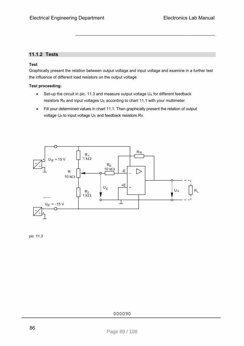
11.1.2 Tests Test
Graphically present the relation between output voltage and input voltage and examine in a further test
the influence of different load resistors on the output voltage. Test proceeding:
• Set-up the circuit in pic. 11.3 and measure output voltage UA for different feedback
resistors RR and input voltages UE according to chart 11.1 with your multimeter.
• Fill your determined values in chart 11.1. Then graphically present the relation of output
voltage UA to input voltage UE and feedback resistors RR.
pic. 11.3
~
-
U gl = 15 V
R
R 1 1 k Ω
RE
10 kΩ -E
R R
10 kΩ
R2 1 k Ω
UE+E
U A R L
~- Ugl = -15 V
Electrical Engineering Department Electronics Lab Manual
86
000090000090
Page 89 / 108

chart 11.1 *To get a linear curve, you have to insert an additional measuring point UE, at the
limiting point of the op-amp.
pic. 11.4
UE [V]* -10 -8 -6 -4 -2 0 2 4 6 8 10 UA [V] at RR = 10 kΩ UA [V] at RR = 22 kΩ
UA [V] 14
12
10
8
6
4
2
-10
-U E [V]
-8 -6 -4 -2
-2
-4
2 4 6 8 10
U E [V]
-6
-8
-10
-12
-UA [V] -14
Electrical Engineering Department Electronics Lab Manual
87
000091000091
Page 90 / 108

• For another test adjust input voltage UE to -5 V. RR and RE = 10 kΩ. Connect different loads according to chart 11.2. Now measure the respective output voltages UA.
• Fill the determined values in chart 11.2. Then graphically present the relation of output voltage UA to load resistance RL in diagram 11.5.
chart 11.2 pic. 11.5 Test 1: What is the polarity of the input voltage UE in reference to the output voltage UA at an
inverting amplifier? Answer: Test 2: What components specify the amplification factor v at the inverting amplifier? Answer: Test 3: What is the amplification factor at RR = 10 kΩ and RE = 1 kΩ? Answer: Test 4: What statement could be given to the characteristic curve pic. 11.5? Answer:
RL [Ω] 1000 680 470 330 220 100
UA [V]
UA [V]
7
6
5
4
3
2
1
0
0 200 400 600 800 1000
R L
1200 [Ω ]
Electrical Engineering Department Electronics Lab Manual
88
000092000092
Page 91 / 108

1.2 Op-Amp serving as non-inverting Amplifier 1.2.1 Basics At the non-inverting amplifier input – and output voltages are of same polarity, with AC voltages phase shifting is 0°. Like shown in pic. 11.6 input voltage at the not inverted amplifier is applied to input +E. As within the dynamic range the difference between both inputs is 0, also the input –E is voltage supplied. Use following equation for the amplification factor :
pic. 11.6
11.2.2 Tests Test Graphically present the relation of output voltage to input voltage with different feedback resistors. Test proceeding
• Set-up the circuit in pic. 11.7 and measure with your multimeter the output voltages UA for different feedback resistors RR and input voltages UE according to chart 11.3.
• Fill the determined values in chart 11.3, then graphically present the relation between output voltage UA and input voltage UE as well as the feedback resistors RR within the diagram 1.8
pic. 11.7
R E
∆U = 0
-E +E
R R
U A
U E U E
v = 1 + RR
RE
v = U A
U E
~
-
U 15 V
R 3
1 k Ω
R 10 k Ω
R E
10 kΩ
R 1
10 kΩ
U E
-E +E
R R
U A
~ -
U -15 V R 4
1 k Ω
Electrical Engineering Department Electronics Lab Manual
89
000093000093
Page 92 / 108

chart 11.3 * To get a linear curve, you have to insert an additional measuring point UE, at the limiting point of the op-amp. pic. 11.8
UE [V]* -10 -8 -6 -4 -2 0 2 4 6 8 10 UA [V] at RR = 10 kΩ UA [V] at RR = 22 kΩ
UA [V] 14
12
10
8
6
4
2
-10
-U E [V]
-8 -6 -4 -2
-2
-4
2 4 6 8 10
U E [V]
-6
-8
-10
-12
-UA [V] -14
Electrical Engineering Department Electronics Lab Manual
90
000094000094
Page 93 / 108

Test 1: What components define the amplification factor? Answer: Test 2: What is the output voltage UA when RR = 47 Ω, RE = 10 kΩ, UE = 2 V? Answer: Test 3: What is the polarity of input voltage UE with respect to output voltage UA? Answer:
Electrical Engineering Department Electronics Lab Manual
91
000095000095
Page 94 / 108

12. Op- amp circuits 12.1 The Adder
With an adder multiple analog voltages could be summed up with respect to their algebraic sign. Basically adder also could be set-up with resistors. However, a disadvantage would be that the input resistors could not be decoupled. Pic. 12.9 shows a circuit that could sum up two voltages UE 1 and UE 2. If only input E1 is connected to the input voltage, we will have an inverter gain.
pic. 12.9
If input E2 is connected to earth, nothing will change at the characteristic of the inverter. As –E has
ground potential, the voltage drop at the input resistor is 0. Hence, input current is I E 2 = 0. At the
voltages E1 = 1 V and E2 = 3 V, for each input resistor is the voltage respective to its input voltage.
Hence, is IE 1 = 0,1 mA IE 2 = 0,3mA.
Both input currents have to flow across the feedback resistor R R. Hence, voltage at the output has to
be UA =- (IE 1 + IE 2) . RR = - (0,1 mA + 0,3 mA) . 10 k_ = - 4 V.
Due to the sum of the input currents, also the input voltages are summed-up. Please consider the
change of the algebraic sign due to the inverting effects of the amplifier.
This can be corrected by a downstream connected inverter.
If one of the input voltages is negative, the input current reverses its direction. One input current is
subtracted from the other one. Hence, only the difference between the input currents flows across the
feedback resistor, and at the output there is also only the difference of the input voltages.
Multiple inputs could be added to the circuit and you will receive the sum of all input voltages at the
output. Following is true for output voltages:
at RE 1 = RE 2 = ... RE n = RE is true: ( )EnEE
E
R
A UUUR
RU +++−= ...21
at RR = RE is true: UA = - ( UE 1 + UE 2 + ... + UE n )
+++−=
En
En
E
E
E
E
RA
R
U
R
U
R
URU ......
2
2
1
1
E1 I E1
I E2
E2
U E1
U E2
R E1
10 k Ω R E2
10 k Ω
I E
I E1 + I E2
-E
+E
R R 10 k Ω
UA
v = − RR
RE1
= − 1
Electrical Engineering Department Electronics Lab Manual
92
Experiment #12
000096000096
Page 95 / 108

12.2 Tests Test
Examine an adder by measurement.
Test proceeding
• Set-up the circuit in pic. 12.10 and adjust the input voltage to UE 2 = 2 V the input voltage UE 1
is according to chart 12.4 then measure with the multimeter each output voltage UA.
Repeat those measurements with input voltage of UE = -2 V.
• Fill the determined values into chart 12.4 and graphically present the relation of UA and input voltage UE 1 [UA = f (UE 1)] in diagram 12.11.
• Then repeat all measurements for an input resistance of RE 1 = 4,7 kΩ, fill the values for the output kΩ, voltages UA in chart 12.5, then draw the curve into the diagram 12.12.
pic. 12.10
~ ~
-
-
Ugl = 15 V Ugl = 0 ... 10 V
U E1
R1
1 kΩ
R 1 k Ω
R2
1 k Ω
RE1
10 kΩ
RE2
10 k Ω U E2
-E +E
RR
10 k Ω
UA
~-U -15 V
Electrical Engineering Department Electronics Lab Manual
93
000097000097
Page 96 / 108

chart 12.4 pic. 12.11
RE 2 = 10 kΩ
UE 1 [V] 0 2 4 6 8 10
UA [V] at UE 2 = 2 V
UA [V] at UE 2 = -2 V
UA [V] 4
2
0 -2
2 4 6 8 10
UE1 [V]
-4
-6
-8
-10
-12
-14
Electrical Engineering Department Electronics Lab Manual
94
000098000098
Page 97 / 108

chart 12.5 * To get a linear curve, you have to insert an additional measuring point UE, at the limiting point of the . op-amp. pic. 12.12
RE 1 = 4,7 kΩ
UE 1 [V]* 0 2 4 6 8 10
UA [V] at UE 2 = 2 V
UA [V] at UE 2 = -2 V
UA [V] 4
2
0 -2
2 4 6 8 10
UE1 [V]
-4
-6
-8
-10
-12
-14
Electrical Engineering Department Electronics Lab Manual
95
000099000099
Page 98 / 108

Test 1: Input currents IE 1 and IE 2 have to flow across which resistor? Answer: Test 2: What kind of circuit is obtained if only one input is connected? Answer: Test 3: What is the output voltage if one input current is positive and the other one negative? Answer:
Electrical Engineering Department Electronics Lab Manual
96
000100000100
Page 99 / 108

12.3 Op-Amp serving as Differential Amplifier 12.3 Basics The differential amplifier is considered to be a subtraction element with amplification. Both input voltages gain with the same amplification factor. For a good common mode rejection the amplification factors for both inputs have to be equal. Following equation is for the common mode rejection G: At the non-connected amplifier it is µA 741 approx. 90 dB. With subtraction element is RE 1 = RE 2 = RE and R3 = RR output voltage UA is:
E
R
E
E
RE
RE
R
EA
R
RU
R
RR
RR
RUU •−
+•
+•= 12 ( )
E
R
EEA
R
RUUU •−= 12
If resistance RR and both input resistances RE are totally equal, then only the difference between the two inputs gain by amplification ratio RR to RE. Op-amps in differential amplifier circuits are e.g. used for measuring amplifiers. pic. 12.13
G = 20 log v
vcommon mode
/ dB
RR
RE1 -E
UE1
UE2
RE2 +E RR
UA
Electrical Engineering Department Electronics Lab Manual
97
000101000101
Page 100 / 108

12.3.1 Tests Test
Examine the differential amplifier for common mode rejection by measurement. Test proceeding
• Set-up the circuit in pic. 12.14, then measure for different input voltages UE 1 and UE 2
according to chart 12.6 the output voltage UA. Fill the values for voltage in chart 12.6 and graphically present the relation of output voltage UA to input voltages UE 1 and UE 2
in diagram. 12.15. pic. 12.14
~
- Ugl = 15 V
R 1
1 k Ω R 3
470 Ω R 5
10 k Ω -E
R 7
10 k Ω
R
U E1
R R 6
22 kΩ +E
~- U -15 V
10 k Ω
R 2
1 k Ω
1 k Ω R 4
470 Ω U E2 R8
22 k Ω
U A
Electrical Engineering Department Electronics Lab Manual
98
000102000102
Page 101 / 108

UE 1 [V]* -10 -6 -2 +2 +6 +10
UA [V] at UE 2 = -4 V
UA [V] at UE 2 = 0 V
UA [V] at UE 2 = 4 V
chart 12.6 * To get a linear curve, you have to insert an additional measuring point UE, at the limiting
point of the op-amp. pic.12.15
UA [V] 14
12
10
8
6
4
2
-16 -14 -UE1 [V]
-12 -10 -8 -6 -4 -2 -2 -4
2 4 6 8 10 12 14 16
UE1 [V]
-6
-8
-10
-12
-UA [V] -14
Electrical Engineering Department Electronics Lab Manual
99
000103000103
Page 102 / 108

Test 1: When do we obtain a common mode rejection? Answer: Test 2: What circuit is considered to be a differential amplifier? Answer: Test 3: What output voltage is obtained when both inputs are supplied? Answer:
Electrical Engineering Department Electronics Lab Manual
100
000104000104
Page 103 / 108

13. Dynamic Behavior of an Op-Amp 13.1 Basics Op-amps are broadband DC voltage amplifiers, not only amplifying DC voltages but also AC voltages in some frequency ranges. Negative feedback caused by external circuitry does not only define the amplification factor but also the bandwidth and the input resistance. 13.2 Tests Test
Examine my measuring the behavior of an op-amp when applying sinus voltage.
Test proceeding: • Apply sinus voltage Uss = 1 V, f = 1 kHz to the input of circuit in pic. 13.16. Measure
with the oscilloscope the input voltage UE and the output voltage UA, and draw the respective curve into pic. 13.18.
• Determine the amplification factor v by following equation:
E
A
U
U
Uv =
pic. 13.16
~
-Ugl = 15 V
R 2
1 k Ω
R 1
10 k Ω
G~ UE
+
UA
~-
U -15 V
Electrical Engineering Department Electronics Lab Manual
101
Experiment #13
000105000105
Page 104 / 108

• Then determine the upper limiting frequency. It is the frequency, when output voltage drops to 70,7% of its maximum value, if frequency is increases.
• Determine the input resistance RE. Therefore connect a resistor RV in series to the input. This will affect a receding of the output voltage from value U1 to value U2.. Calculate the input resistance RE with both voltage values and the given series resistor with following equation:
−=
12
1
U
U
RR
V
E
RE = input resistance in Ω RV = series resistor in Ω U1 = output voltage with no series resistor U2 = output voltage with series resistor
• Then determine the output resistance RA, by connecting load resistance RL to earth at the
output. This affects a drop of output voltage from value U1to value U2. • Calculate the output resistance with both voltage values and the given load resistance with
following equation:
−= 12
1
U
URR LA
RA = output resistance in Ω RL = series resistance in Ω U1 = output voltage with no resistor U2 = output voltage with resistor
• Fill the determined values in chart 13.7.
• Then set-up the circuit in pic. 13.17, apply sinus voltage of uss = 1 V; f = 1 kHz to the input UE.
Repeat all measurements and calculations, draw the curves of input- and output voltages into diagram 13.19 and fill your values in chart 13.7.
pic.13.17
~
-
Ugl = 15 V
A
R 2
R 1
G
B
10 k Ω
- R2 1 kΩ
+
~ U E R 4 R 3 UA 1 k Ω 10 k Ω
~-
U -15 V
Electrical Engineering Department Electronics Lab Manual
102
000106000106
Page 105 / 108

Inverting Input
(R1 = 10 kΩ, R2 = 1 kΩ) Non-inverting Input
(R1 = R3 =10 kΩ, R2 = R4= 1 kΩ) UE 1 V 1 V
UA
vU
fo
RE (RV = 100 Ω) (RV = 10 kΩ)
RA (RL = 100 Ω) (RL = 100 Ω)
Tab. 13.7
Settings: Y1 = 5 V / part Y2 = 0,5 V / part X = 0,2 ms / part
pic. 13.18
Settings: Y1 = 5 V / part Y2 = 0,5 V / part X = 0,2 ms / part
pic. 13.19
• Now disconnect point A in the circuit of pic. 13.17 from reference potential () and connect to point B. Hence, both inputs are fed by same voltage. Measure the output voltage with your oscilloscope.
- 0 (Y1)
= U A
- 0 (Y2)
= U E
- 0 (Y1)
= U A
- 0 (Y2)
= U E
Electrical Engineering Department Electronics Lab Manual
103
000107000107
Page 106 / 108

Test 1: What is the phase shift angle between input and output voltage? Answer:
a) When inverting input is used:
b) When non-inverting input is used: Test 2: The input resistance RE is similar to what resistance value at the inverting input? Answer: Test 3: The input resistance RE is similar to what resistance value at the non-inverting input? Answer: Test 4: Does output resistance RA is in any relation to the feeding input RE? Answer: Test 5: What is the value of the output voltage RA if both inputs of the op-amp are fed by
same voltage?
Answer:
Electrical Engineering Department Electronics Lab Manual
104
000108000108
Page 107 / 108

Required voltage supply and measuring instruments Function generator
functions: Sinus
- reactive voltage: Uss = 20 mV ... 7 V
- frequency: f = 10 Hz ... 5 MHz
- impedance: Ri = 50 Ω
Voltage supply
- mains supply: 230 V AC; 50 ... 60 Hz
- DC voltage: 0 ... 30 V; 0,3 A (adjustable); +/-15 V; 0,3 A (fix) - AC voltage (Sinus): 0 ... 24 V (effective); 50 Hz; 0,1 A (adjustable) AC Generator
- Line voltage: 7 V
- Conductor voltage: 12 V - Conductor Current: 50 mA Multimeter
- DC voltage
range: 0,1 V ... 30 V input
resistance: RE > 100 kΩ - AC voltage (Sinus)
range: 1 V ... 15 V (effective) input
resistance: RE > 100 kΩ frequency:
f < 50 Hz - DC voltage*
range: 0,1 µA ... 300 mA
voltage drop : < 250 mV - tolerances +/- 3%
* For some test with lower currents you will need a measuring range of < 1µA. Oscilloscope (with X/Y-operation) - channels: 2 (one of it invert)
- range: f ε 10 MHz - distortion coefficient Y: 0,02 - 0,5 - 1 - 2 - 5 - 10 - 20 V / part
X: 0,1 - 1 - 2 - 5 - 10 ms / part
X: 0,1 - 1 - 2 - 5 - 10 ms / part Those technical data are minimum requirements to do all the tests within this manual.
Electrical Engineering Department Electronics Lab Manual
105
000109000109
Page 108 / 108