
Basic Electronics Engineering
74
-
Upload
khangminh22 -
Category
Documents
-
view
0 -
download
0
Transcript of Basic Electronics Engineering

Course syllabus:
Unit I:Diodes Circuits 6L
Half wave rectifier, Full wave rectifier, Power supply Filters and Capacitor filters, Diode
limiting Circuits (Clippers) and clamping circuits, Voltage Multipliers, Zener diode & its
application, LEDs and Photodiodes.
Unit II: Bipolar Junction Transistor (BJT) Circuits 8L
BJT structure & its operation with normal biasing, Transistor characteristics and parameters,
DC operating point, transistor as an amplifier, Transistor as a switch, Enhancement type
MOSFET
Unit III: Linear Integrated Circuits 5L
Introduction to operational amplifiers, Op-amp input modes and parameters, Negative feedback,
Comparators, Summing amplifiers, integrators and differentiators, IC 555 timer as an oscillator,
Voltage regulator (3 Pin).
Unit IV: Digital Electronics : 5L
Introduction, digital signals, basic digital circuits –AND, OR, NOT, NAND, NOR, EX-OR,
Boolean algebra, Examples of IC gates, Standard representation for logic functions, Half adder,
Full adder, Multiplexers, De-multiplexers, Flip-Flop, 1-bit memory cell, D-Flip-Flop,
Shift register, Counters, block diagram of microprocessor and microcontroller and
their application.

Course syllabus contd….
Unit V:Power Devices & Transducers 5L
Power devices: Basics of 4 layer devices: Silicon controlled rectifier (SCR), Diac and Triac.
Transducers: Introduction, electrical transducer, Selecting a transducer, resistive transducer,
Thermister, Inductive transducer, LVDT, Load cell, Phototransistor, Temperature transducer,
Flow measurement (Mechanical Transducers).
Application of transducers : Digital Thermometer, Weighing machine (Block diagram).
Unit VI: Electronic Communication 6L
Importance of communication system, the elements of communication system, bandwidth
requirement, IEEE frequency spectrum, transmission media : wired(twisted pair, co-axial and
optical fiber cables) and wireless, need for modulation, analog modulation schemes – AM and
FM, mobile communication system : cellular concept, simple block diagram of GSM system
Text books:
1. Floyd, ”Electronic Devices & Circuits”, Pearson Education India(For Unit I,II,III).
2. R. P. Jain, ”Modern Digital Electronics”,3rd edition,12th reprint TMH Publication, 2007.
(For Unit IV)
3. H.S. Kalasi ”Electronic Intrumentation”, Tata McGraw Hill.(For Unit V)
4. Frenzel, ”Communication Electronics-Principles & Application”, TATA McGraw Hill.
(For Unit VI)

C104012. BASIC ELECTRONICS ENGINEERING COURSE OUTCOMES:
The student shall be able to:
C104012.1 Study PN junction diode and Analyze its circuits (Rectifier, voltage Regulator circuits, wave
shaping circuit using clipper and clamper circuits).
C104012.2 Summarize transistor theory and Analyze BJT Characteristics; Recognize the need of DC
load line analysis .Compare different type of BJT configurations (e.g. CE, CB, and CC).
C104012.3 Use of BJT in Amplification and switching applications.
C104012.4 Use OP-Amp characteristics to design various circuits (Such as Comparators Adder, Subtractor,
Integrator, and Differentiator). Study various Linear integrated circuits (IC 555,78XX, 79XX and LM317).
C104012.5 Categorize & employ logic gates to designing different combinational and sequentional
circuits (e.g. Adder, Multiplexer, Flip flops, Counter, Shift register).
C104012.6 Classify and recognize the use of power devices(SCR, DIAC, and TRIAC) and Transducer
(such as LVDT, Load cell, Phototransistor).
C104012.7 Identify the need of communication, Study of Modulation techniques and Mobile
communication technology, Summarize the IEEE spectrum and various communication media.

Pre-requisites: pg. 15&16
P-N junction diode and its characteristics: The p-type and n-type materials are combined to form a P-N junction, called as Diode.
The p region is called the anode and the n region is called the cathode.
The basic diode structure and schematic symbol are shown below.
Si (14) +
B(5) Si (14) +
P(15)
The maximum no. of electrons in any shell is 2n2.

Pre-requisites contd….
In P-N junction, large no. of electrons are present on N-side.
In P-N junction, large no. of holes are present on P-side.
P-region pn junction N-region P-region depletion region N-region
barrier potential a) pn junction before the formation
of depletion region. b) pn junction after the formation
of depletion region.
Free electrons near the pn junction starts to move / diffuse thr‟ the junction and combines with the
hole.
This creates a positive charge on n-side and negative charge on p-side forming the barrier
potential.
This process continues till the barrier potential opposes the further diffusion.
The potential that prevents the electrons to cross the junction, is barrier potential.
(0.7V-Si, 0.3V-Ge).
The arrows in the depletion region represents the electric field.

a) At the instant of junction formation
b) At equilibrium

The cathode is usually marked by a band, a tab, or some other feature.
On those packages where one lead is connected to the case, the case is the cathode.
Pre-requisites contd….

Forward bias:
Used to
limit the
current
Should be greater than
barrier potential.

Working of Forward bias:
When we apply dc voltage, -ve terminal provides enough energy to free electrons
to cross the pn junction.
Once the electrons cross pn junction, they loses energy (equivalent to barrier
potential) and combine with holes in the p-region.
The +ve terminal of bias attracts these electrons and finally out of the p-region.
As more electrons flows from n-region to p-region and more no. of holes flows from
p-region to n-region, there occurs reduction in –ve ions in p-region and +ve ions in
n-regions.
Thus depletion region becomes narrow.

V-I characteristic for forward bias:
a) Small forward bias voltage (VF<0.7V) a) VF reaches 0.7V and remains nearly const.
but IF continues to increase.

a) V-I characteristic curve for
forward bias b) Expanded view to understand dynamic resistance
When 0V is applied across diode, there is no current.
When applied bias VBIAS is gradually increased upto 0.7V, then VF increases while IF increases
with a very small amount. A portion of VBIAS is dropped across RLIMIT.
When VBIAS increases upto a value, where VF becomes 0.7V, IF starts increasing rapidly.
If we still increase VBIAS, VF increases with a small amount above 0.7V due to dynamic internal
resistance of semiconductor material.
As we can see rd1=∆VF1
∆IF1 > rd2=
∆VF2
∆IF2
Dynamic resistance begins to decrease in the knee region and become smallest above the knee
region.

Reverse bias:
RLIMIT

Only for reference of next slide

Working of Reverse bias:
The +ve bias terminal pulls free electrons out of n-region, leaving more +ve ions in
n-region.
The –ve bias terminal provides electrons which move from hole to hole in p-region,
forming another column at depletion region, thus widening the depletion region.
This movement of electrons continues till VBarrier Potential =VBIAS.

Reverse current:
Minority electrons in p-region are pushed by –ve terminal of bias towards the
depletion region.
When these electrons cross depletion region, combines with minority holes in n-region
and flows towards +ve terminal, creating Reverse current.

Reverse breakdown:
When the applied reverse bias voltage is increased, free minority electrons gets
enough energy to speed up thr‟ the p-region.
While speeding up thr‟ p-region, these minority electrons colloids with conduction
electrons and then conduction electrons gets enough energy and
those conduction electrons will move and colloid with another conduction electrons
and the process continues.
This multiplication of electrons is referred as avalanche effect.
Now, these high energy electrons has enough energy to go thr‟ n-region as conduction
electrons, rather than combining with holes.
Thus, reverse current increases drastically.
When reverse current is not controlled / limited, diode may get damaged due to heating.

V-I characteristic in reverse bias:
When 0V is applied across diode, there is no current.
When we gradually reverse bias the voltage, there is a small reverse current due to
minority carriers and voltage across diode increases.
When we further increase reverse bias voltage to a value VBR i.e. breakdown voltage., the
reverse current begins to increase rapidly.
The typical rectifier diode has a breakdown voltage of greater than 50V.

The complete V-I characteristic curve:

Temperature effects:
Forward bias:
Temp. ↑ ,
IF ↑ for given VF ,
VF ↓ for given IF.
Reverse bias:
Temp. ↑ ,
IR ↑ for given VR ,
VR ↓ for given IR.

Diode current equation:
The relation between applied voltage across diode „VD‟ and current flowing thr‟ diode
„ID‟ can be given as,
ID = Io [𝒆VD/η VT -1]
where,
ID => current flowing thr‟ diode
Io => reverse saturation current flowing thr‟ diode
VD => applied voltage across diode
η => ideality factor, generally in between 1 and 2,
2 for silicon P-N junction diode and 1 for germanium P-N junction diode
VT => k × Tk
q;
where, k => Boltzman‟s const.= 1.38×10⁻²³ J/˚k and
Tk => temp. in ˚k.
q => electronic charge = 1.6 ×10⁻¹⁹ C

UNIT ONE : DIODE CIRCUITS THE BASIC DC POWER SUPPLY :
The dc power supply converts the standard 230 V, 50 Hz ac voltage available at wall outlets
into a constant dc voltage.
A basic block diagram of the complete power supply is shown in Figure below,
TRANSFORMER RECTIFIER FILTER REGULATOR
LOAD
Steps down
the ac input
line voltage
to a lower ac
voltage
Converts
the ac input
voltage to a
pulsating dc
voltage
Eliminates the
fluctuations in
rectified voltage,
produces a
relatively smooth
dc voltage.
maintains a
constant dc
voltage for
variations in the
input line voltage

Types of Diode rectifiers: A device which converts ac vtg. to pulsating DC vtg. using P-N junction diodes, is
called a rectifier.
1. Half-Wave Rectifier: A diode is connected to an ac source and to a load resistor, RL, forming a half-wave rectifier.
For ideal model of diode:
(a) For positive half cycle,
- When the sinusoidal input voltage (Vin) goes positive, the diode is forward-biased and
conducts current through the load resistor, as shown in fig.(1.1).
- The current produces an output voltage across the load RL , which has the same shape as the
positive half-cycle of the input voltage.
Fig.(1.1)
I

Half-Wave Rectifier contd….
For ideal model of diode:
(b) For negative half cycle,
The diode is reverse-biased. There is no current, so the voltage across the load resistor is
0V, as shown in Figure (1.2).
Fig.(1.2)
The net result is that only the positive half-cycles of the ac input voltage appear across the load.
Output is a pulsating dc voltage as shown in fig.(1.3)
Fig.(1.3)
I=0

A) Average Value of the Output/Load current (IL DC / Iavg) :
The average value of the half-wave rectified output current is determined by finding the area
under the curve over a full cycle, and then dividing by its period ‘2𝝅’ the number of radians
in a full cycle.
i.e. IL DC or IAVG = Ip𝝅 = I𝒎
𝝅
Proof: Let, i=Imsin𝑤𝑡 IL DC or IAVG = 𝑎𝑟𝑒𝑎
2𝜋
= 1
2𝜋 Imsin 𝑤𝑡 𝑑𝑤𝑡𝜋
0
= Im2𝜋 [-cos(𝑤𝑡)] for 𝑤𝑡=>“0 to 𝜋”.
= Im2𝜋
· 2
IL DC or IAVG = Ip𝝅
= I𝒎
𝝅
where,
Ip = Im = max. peak current = Vp
Rs+RF+RL =
Vm
Rs+RF+RL
where,
Vm= max. peak sec. vtg.
Rs= DC resistance of transformer sec. wdg.
RF = Fwd resistance of diode
RL= Load resistance
Detail analysis of HWR:

B) Average Value of the Output/Load Voltage(VAVG or VL DC ) :
The average value of the half-wave rectified output voltage is the value you would measure on
a dc voltmeter.
Mathematically, it is determined by finding the area under the curve over a full cycle,
and then dividing by 2𝝅 the number of radians in a full cycle.
i.e. VAVG or VL DC = Vp
𝝅 =
Vm
𝝅
Proof: Let, v=Vpsin 𝑤𝑡=Vmsin 𝑤𝑡
VAVG or VL DC = 𝑎𝑟𝑒𝑎2𝜋
or VAVG or VL DC = IL DC × RL
= 1
2𝜋 Vpsin 𝑤𝑡 𝑑𝑤𝑡𝜋
0
= Vp
2𝜋 [-cos(𝑤𝑡)] for wt => “0 to 𝜋”.
= Vp
2𝜋 · 2
VAVG or VL DC = Vp
𝝅 =
Vm
𝝅
Fig.(1.2)
Detail analysis of HWR contd….
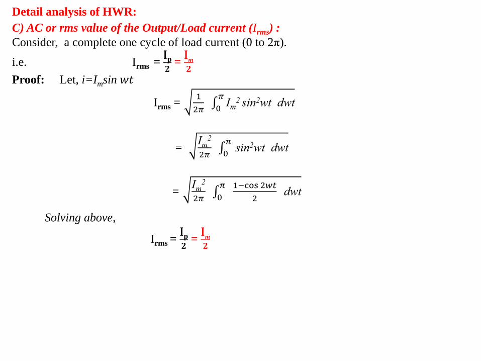
C) AC or rms value of the Output/Load current (Irms) :
Consider, a complete one cycle of load current (0 to 2π).
i.e. Irms = Ip𝟐 = I𝒎
𝟐
Proof: Let, i=Imsin 𝑤𝑡
Irms = 1
2𝜋 Im
2 sin2wt dwt
𝜋
0
= Im
2
2𝜋 sin2wt dwt
𝜋
0
= Im
2
2𝜋
1−cos 2𝑤𝑡
2 dwt
𝜋
0
Solving above,
Irms = Ip𝟐
= I𝒎
𝟐
Detail analysis of HWR:
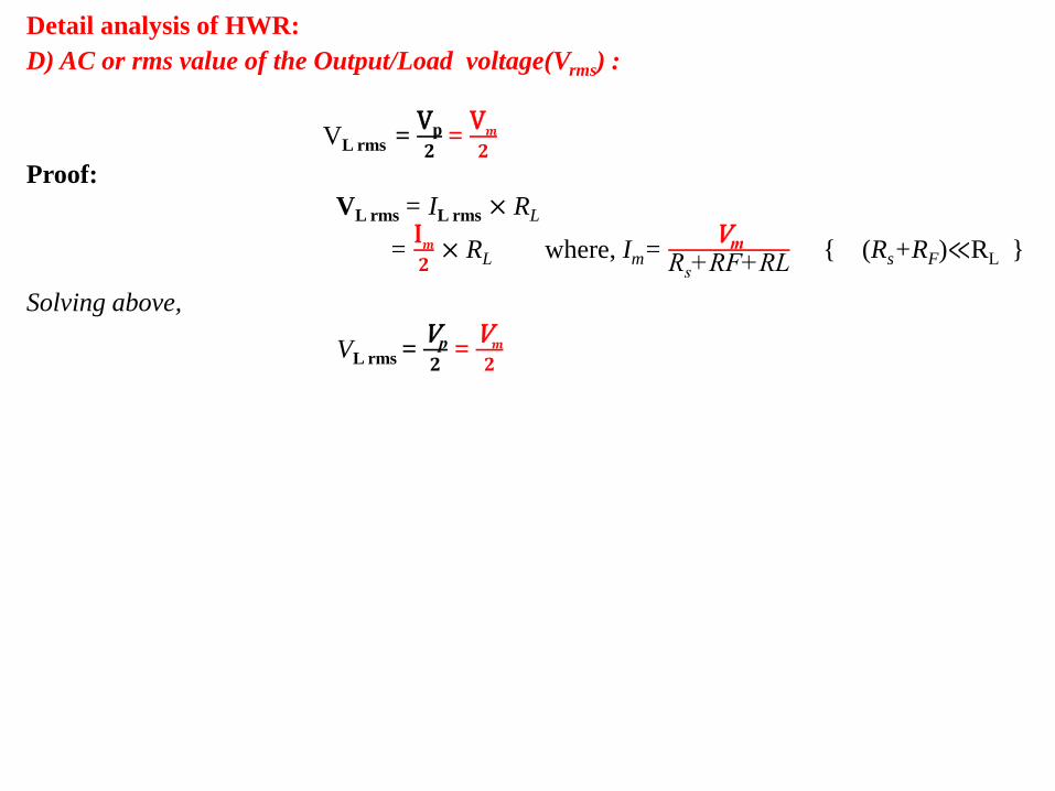
D) AC or rms value of the Output/Load voltage(Vrms) :
VL rms = Vp
𝟐 = V
𝒎
𝟐
Proof:
VL rms = IL rms × RL
= I𝒎
𝟐 × RL where, Im=
Vm
Rs+RF+RL { (Rs+RF)≪RL }
Solving above, VL rms =
Vp
𝟐 = V
𝒎
𝟐
Detail analysis of HWR:

E) Ripple factor (r) :
Percentage of ac component in the output.
Ideally, it should be zero, practically it should be very small.
Ripple factor ‘r’ = Vac pure
VL DC
= Iac pure
IL DC
Ripple factor ‘r’ = Vac pure
VL DC
= 𝑹𝑴𝑺 𝒗𝒂𝒍𝒖𝒆 𝒐𝒇 𝒂𝒄 𝒄𝒐𝒎𝒑𝒐𝒏𝒆𝒏𝒕 𝒊𝒏 𝒐/𝒑
𝑫𝑪 𝒐𝒓 𝒂𝒗𝒈 𝒗𝒂𝒍𝒖𝒆 𝒐𝒇 𝒐/𝒑
= Vrms
2−Vdc2
Vdc
Substituting, Vrms= Vm
2 and Vdc=
Vm
π
and
solving,
‘r’ = 1.21 or ‘r’ = 121%
Note:
Ripple factor in o/p vtg. of HWR is 1.21 times the dc component in o/p vtg.
It can be reduced by using filter at the rectifier o/p to get pure dc o/p.
Detail analysis of HWR:

F) Voltage regulation :
Measure of change in dc o/p vtg. from no load to full load condn.
Ideally, avg. o/p vtg. of rectifier should be const., but practically, it varies with the load
current.
% Voltage regulation = VNL−VFL
VFL × 100 - - - - eqn (1)
For HWR,
VFL= Vm
π
RL
Rs+RF+RL and
VNL= Vm
π
Putting above substitutions in eqn(1),
% Voltage regulation = VNL−VFL
VFL × 100
% Voltage regulation = Rs+RF
RL
× 100
Note:
Ideally, load regulation should be 0%.
As, IL ↑, Voltage drop across RF and Rs increases, thus decreasing o/p dc vtg. VL DC.
Detail analysis of HWR:

G) DC o/p power (PL DC) :
PL DC= IL DC2 × RL
= (Im/π)2 × RL
As, Im = Vm
Rs+RF+RL
we can write,
PL DC= Vm
2
π2 (Rs+RF+RL )2 × RL
As, (Rs+RF) ≪ RL
= Vm
2
π2RL
As, VL DC = Vm
𝜋
PL DC = VL DC
2
RL
Detail analysis of HWR:

H) AC i/p power (Pac) :
Power supplied by sec. wdg. of transformer.
Pac= Is rms2 × (Rs+RF+RL)
For HWR,
Is rms= IL rms = (Im/2)
Pac= (Im/2)2 × (Rs+RF+RL)
Pac= Im
2
𝟒 × (Rs+RF+RL)
Detail analysis of HWR:

I) Rectification efficiency (η) :
Ratio of DC o/p power to ac i/p power.
η= PL DC
Pac
= IL DC
2 RL
Is rms2 × (Rs+RF+RL
)
= (Im/π)2
RL
(Im/2)2× (Rs+RF+RL )
= 4
π2
RL
(Rs+RF+RL )
as, (Rs+RF) ≪ RL
ηmax = 4
π2 =0.405
% ηmax= 40.5 %
Note:
Ideally, η should be 100%.
Practically, it should be as high as possible.
Detail analysis of HWR:

J) Transformer utilization factor (TUF) :
Ratio of DC o/p power to ac power rating of transformer.
TUF indicates how well the input transformer is utilized.
Mathematically,
TUF = 𝑫𝑪 𝒐𝒖𝒕𝒑𝒖𝒕 𝒑𝒐𝒘𝒆𝒓PL DC
𝑨𝑪 𝒑𝒐𝒘𝒆𝒓 𝒓𝒂𝒕𝒊𝒏𝒈 𝒐𝒇 𝒕𝒓𝒂𝒏𝒔𝒇𝒐𝒓𝒎𝒆𝒓
= PL DC
IL DC
VS rms IS rms
If, (Rs+RF) ≪ RL
Then,
TUF =
Vmπ Im
π
Vm𝟐 Im
2
= 2 𝟐
π2
= 0.287
% TUF = 28.7 % Note:
Ideally, TUF should be 100%.
Practically, it should be as high as possible.
Detail analysis of HWR:

K) Peak Inverse Voltage (PIV):
The amount of reverse voltage, which the diode should withstand. The peak inverse voltage (PIV) equals the peak value of the input voltage.
The diode must be capable of withstanding this amount of repetitive reverse voltage.
A diode should be rated at least 20% higher than the PIV.
PIV = VP(in)
Fig.(1.2)
Detail analysis of HWR:
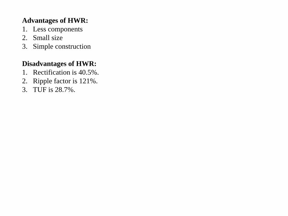
Advantages of HWR:
1. Less components
2. Small size
3. Simple construction
Disadvantages of HWR:
1. Rectification is 40.5%.
2. Ripple factor is 121%.
3. TUF is 28.7%.

2. Full-Wave Rectifier:
A) Center-tapped:
- During +ve half cycle, terminal a is +ve wrt b, thus current flows only thr’ D1,
then thr‟ load.
- D1 is forward biased, acts as closed switch; while D2 is reverse biased,
acts as open switch.
-During -ve half cycle, terminal b is +ve wrt a, thus current flows only thr’ D2,
then thr‟ load.
- D2 is forward biased, acts as closed switch; while D1 is reverse biased,
acts as open switch.
a
b

During +ve half cycle
During -ve half cycle

A) Average Value of the Output/Load current (IL DC / Iavg) :
IL DC or IAVG = 2Ip𝝅 = 2I
𝒎
𝝅
Proof: Let, i=Imsin𝑤𝑡 IL DC or IAVG = 𝑎𝑟𝑒𝑎
2𝜋
= 1
𝜋 Imsin 𝑤𝑡 𝑑𝑤𝑡𝜋
0
= Im𝜋 [-cos(𝑤𝑡)] for 𝑤𝑡=>“0 to 𝜋”.
= Im𝜋
· 2
IL DC or IAVG = 2Ip𝝅
= 2I
𝒎
𝝅
where,
Ip = Im = max. peak current = Vp
Rs+RF+RL =
Vm
Rs+RF+RL
where,
Vm= max. peak sec. vtg.
Rs= DC resistance of transformer sec. wdg.
RF = Fwd resistance of diode
RL= Load resistance
Detail analysis of center-tapped FWR:

B) Average Value of the Output/Load Voltage(VAVG or VL DC ) :
For purely resistive load, DC voltage is,
VAVG or VL DC = 2Vp
𝝅 = 2Vm
𝝅
Proof: Let, v=Vpsin 𝑤𝑡=Vmsin 𝑤𝑡
VAVG or VL DC = 𝑎𝑟𝑒𝑎2𝜋
or VAVG or VL DC = IL DC × RL
= 1
𝜋 Vpsin 𝑤𝑡 𝑑𝑤𝑡𝜋
0
= Vp
𝜋 [-cos(𝑤𝑡)] for wt => “0 to 𝜋”.
= Vp
𝜋 · 2
VAVG or VL DC = 2Vp
𝝅 = 2Vm
𝝅
Detail analysis of CT-FWR contd….

C) AC or rms value of the Output/Load current (Irms) :
Irms = Ip2 = I𝒎
2
Proof:
Consider, a complete one cycle of load current (0 to π).
Let, i=Imsin 𝑤𝑡
Irms = 1
𝜋 Im
2 sin2wt dwt
𝜋
0
= Im
2
𝜋 sin2wt dwt
𝜋
0
= Im
2
𝜋
1−cos 2𝑤𝑡
2 dwt
𝜋
0
Solving above,
Irms = Ip2 = I𝒎
2
Detail analysis of CT-FWR:

D) AC or rms value of the Output/Load voltage(Vrms) :
VL rms = Vp
2 = V
𝒎
2
Proof:
VL rms = IL rms × RL
= I𝒎
2 × RL where, Im=
Vm
Rs+RF+RL { (Rs+RF)≪RL }
Solving above, VL rms =
Vp
2 = V
𝒎
2
Detail analysis of CT-FWR:
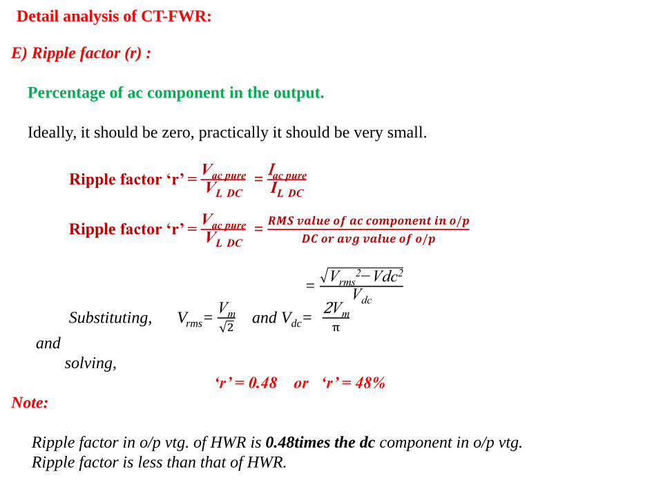
E) Ripple factor (r) :
Percentage of ac component in the output.
Ideally, it should be zero, practically it should be very small.
Ripple factor ‘r’ = Vac pure
VL DC
= Iac pure
IL DC
Ripple factor ‘r’ = Vac pure
VL DC
= 𝑹𝑴𝑺 𝒗𝒂𝒍𝒖𝒆 𝒐𝒇 𝒂𝒄 𝒄𝒐𝒎𝒑𝒐𝒏𝒆𝒏𝒕 𝒊𝒏 𝒐/𝒑
𝑫𝑪 𝒐𝒓 𝒂𝒗𝒈 𝒗𝒂𝒍𝒖𝒆 𝒐𝒇 𝒐/𝒑
= Vrms
2−Vdc2
Vdc
Substituting, Vrms= Vm
2 and Vdc=
2Vm
π
and
solving,
‘r’ = 0.48 or ‘r’ = 48%
Note:
Ripple factor in o/p vtg. of HWR is 0.48times the dc component in o/p vtg.
Ripple factor is less than that of HWR.
Detail analysis of CT-FWR:

F) Voltage regulation :
Measure of change in dc o/p vtg. from no load to full load condn.
Ideally, avg. o/p vtg. of rectifier should be const., but practically, it varies with the load
current.
% Voltage regulation = VNL−VFL
VFL × 100 - - - - eqn (1)
For CT-FWR,
VFL= 2Vm
π
RL
Rs+RF+RL
and
VNL= 2Vm
π
Putting above substitutions in eqn(1),
% Voltage regulation = Rs+RF
RL
× 100
Note:
Ideally, load regulation should be 0%.
As, IL ↑, Voltage drop across RF and Rs increases, thus decreasing o/p dc vtg. VL DC.
Detail analysis of CT-FWR :

G) DC o/p power (PL DC) :
PL DC= IL DC2 × RL
= (2Im/π)2 × RL
As, Im = Vm
Rs+RF+RL
we can write,
PL DC= 4Vm
2
π2 (Rs+RF+RL )2 × RL
As, (Rs+RF) ≪ RL
= 4Vm
2
π2RL
As, VL DC = 2Vm
𝜋
PL DC = VL DC
2
RL
Detail analysis of CT-FWR :

H) AC i/p power (Pac) :
Power supplied by sec. wdg. of transformer.
Pac= Is rms2 × (Rs+RF+RL)
For CT-FWR,
Is rms= IL rms = (Im/ 2)
Pac= (Im/ 2)2 × (Rs+RF+RL)
Pac= Im
2
𝟐 × (Rs+RF+RL) ; where, Im=
Vm
Rs+RF+RL
Pac= Vm
2
𝟐(Rs+RF+RL )
Detail analysis of CT-FWR :

I) Rectification efficiency (η) :
Ratio of DC o/p power to ac i/p power.
η= PL DC
Pac
= IL DC
2 RL
Is rms2 × (Rs+RF+RL)
= (2Im/π)2
RL
(Im/ 2)2× (Rs+RF+RL )
= 8
π2
RL
(Rs+RF+RL ) as, (Rs+RF) ≪ RL
ηmax = 8
π2 =0.812
% ηmax= 81.2 %
Note:
Ideally, η should be 100%.
Practically, it should be as high as possible.
η is more than that of HWR.
Detail analysis of CT-FWR :

J) Transformer utilization factor (TUF) :
- Ratio of DC o/p power to ac power rating of transformer.
- TUF indicates how well the input transformer is utilized.
As center-tapped connection is used, secondary current flows thr‟ each half separately, whereas
primary current flows continuously.
Therefore, TUF of each winding is calculated separately and then average TUF is calculated.
Mathematically,
TUF of sec. wdg. = 𝑫𝑪 𝒐𝒖𝒕𝒑𝒖𝒕 𝒑𝒐𝒘𝒆𝒓PL DC
𝒑𝒐𝒘𝒆𝒓 𝒓𝒂𝒕𝒊𝒏𝒈 𝒐𝒇 𝒔𝒆𝒄𝒐𝒏𝒅𝒂𝒓𝒚
= PL DC
IL DC
VS rms IS rms
If, (Rs+RF) ≪ RL
Then, TUF =
2Vmπ 2Im
π
Vm𝟐 Im
𝟐
= 𝟖
π2 = 0.812
TUF of prim. wdg. = 2 × TUF of HWR = 2 × 0.287 = 0.574
Avg. TUF = TUFsec. +
TUFprim.
2 =
0.812+0.574
2
Avg. TUF = 0.693 and % Avg. TUF = 69.3% Note:
Ideally, TUF should be 100%.
Practically, it should be as high as possible.
Detail analysis of CT-FWR :
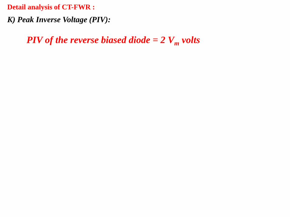
K) Peak Inverse Voltage (PIV):
PIV of the reverse biased diode = 2 Vm volts
Detail analysis of CT-FWR :

Advantages of CT-FWR:
1. Better rectification efficiency 81.2%
2. Better ripple factor 48%
3. Increased IL DC and VL DC values.
4. Better TUF 69.3%
Disadvantages of CT-FWR :
1. Cost increases due to diode of high PIV
2. Center-tapped transformer is costly and makes design complicated.
Applications of CT-FWR :
1. Used in battery chargers.
2. Used in power supplies in laboratories.
3. Used in high current power supplies.

2. Full-Wave Rectifier:
B) Bridge Rectifier:
- During +ve half cycle, diodes D1 and D2 conducts, while D3 and D4 are open.
During +ve half cycle

During -ve half cycle
- During -ve half cycle, diodes D3 and D4 conducts, while D1 and D2 are open.

A) Average Value of the Load current (IL DC / Iavg) :
IL DC or IAVG = 2Ip𝝅 = 2I
𝒎
𝝅
B) Average Value of the Output/Load Voltage(VAVG or VL DC ) :
For purely resistive load, DC voltage is,
VAVG or VL DC = 2Vp
𝝅 = 2Vm
𝝅 where, Rs+2RF ≪ RL
C) AC or rms value of the Output/Load current (Irms) :
Irms = Ip2 = I𝒎
2
D) AC or rms value of the Output/Load voltage(Vrms) :
VL rms = Vp
2 = V
𝒎
2 where, Rs+2RF ≪ RL
Detail analysis of Bridge type FWR:
The bridge rectifier is basically a FWR, therefore its analysis remains same as that of CT-FWR.
Only here, instead of one diode, two diodes are conducting simultaneously, so RF is replaced
with 2RF.

E) Ripple factor (r) :
‘r’ = 0.48 or ‘r’ = 48%
G) DC o/p power (PL DC) :
PL DC= IL DC2 × RL = (2Im/π)2 × RL =
4Im2RL
π2 = 4Vm
2
π2RL
H) AC i/p power (Pac) :
Pac= Vm
2
𝟐(Rs+RF+RL)
I) Rectification efficiency (η) :
ηmax = 8
π2 =0.812 and % ηmax= 81.2 %
J) Transformer utilization factor (TUF) :
Avg. TUF = TUFsec. +
TUFprim.
2 =
0.812+0.812
2 = 0.812 and % TUF = 81.2%
K) Peak Inverse Voltage (PIV):
PIV of the reverse biased diode = Vm volts
Detail analysis of Bridge type FWR:

Advantages of Bridge type FWR:
1. Center-tapped transformer is not required, hence cost is less
2. TUF is increased as Center-tapped transformer is not used
3. High rectification efficiency
4. Cost reduces as diode required are of low PIV ratings.
5. Both o/p vtg and o/p current are higher.
Disadvantages of Bridge type FWR :
1. Due to four diodes, additional vtg. drop across them reduces o/p vtg.
Applications of Bridge type FWR :
1. Used to convert AC to DC in power circuits.
2. Used in power supplies.

Zener diode:
A major application for zener diodes is to provide stable reference voltages.
A zener diode is a silicon pn junction device that is designed to operate in the reverse-
breakdown region.
The breakdown voltage of a zener diode is set by carefully controlling the doping level during
manufacture.
The symbol for a zener diode is shown in figure below.
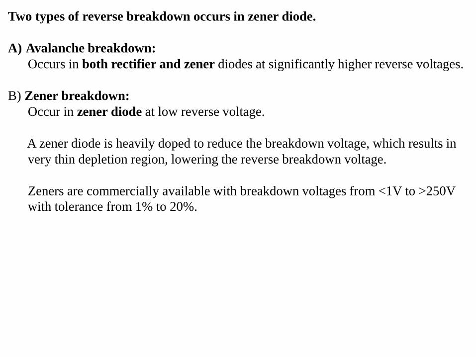
Two types of reverse breakdown occurs in zener diode.
A) Avalanche breakdown:
Occurs in both rectifier and zener diodes at significantly higher reverse voltages.
B) Zener breakdown:
Occur in zener diode at low reverse voltage.
A zener diode is heavily doped to reduce the breakdown voltage, which results in
very thin depletion region, lowering the reverse breakdown voltage.
Zeners are commercially available with breakdown voltages from <1V to >250V
with tolerance from 1% to 20%.
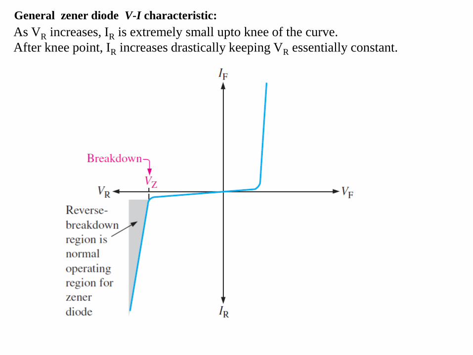
General zener diode V-I characteristic:
As VR increases, IR is extremely small upto knee of the curve.
After knee point, IR increases drastically keeping VR essentially constant.

The reverse current IR is also referred as zener current IZ.
The zener impedance ZZ is given at IZ i.e. zener test current as,
ZZ = ∆VZ
∆IZ
It is best to avoid operating a zener diode near the knee of the curve because the impedance
changes dramatically in that area.

Zener regulation with variable input voltage:
Let us consider voltage at IZK as VZK and voltage at IZM as VZM and voltage at IZT as
VZT.
If the applied voltage is in between VZT and VZM, then IZ is increasing and Vout will be
VZ+∆VZ.
As the input voltage increases, the output voltage remains nearly constant (IZK < IZ < IZM)

If the applied voltage is in between VZT and VZK, then IZ is decreasing and Vout will be
VZ - ∆VZ.
As the input voltage decreases, the output voltage remains nearly constant (IZK < IZ < IZM)

Zener regulation with a variable load:
Following is the zener voltage regulator with variable load across zener.
The zener diode maintains a nearly constant voltage across RL as long as IZ is in between IZK
and IZM.
When there is no load i.e. RL=∞, all the current passes thr‟ zener. This is no-load condition.
When load RL is connected, current will flow thr‟ zener as well as load.
The total current through R remains essentially constant as long as the zener is regulating.
If we decrease the RL, more current will pass thr‟ RL and less current will pass thr‟ zener till the
value IZK. This is full load condition.
If we increase the RL, less current will pass thr‟ RL and more current will pass thr‟ zener till the
value IZM.

LED (Light emitting diode):
An LED is an optical device, which emits light if forward biased.
When free electrons combines with holes, they fall from conduction band to valence band,
releasing the energy in the form of photons, which emits the light energy.
This process is referred as Electroluminescence.
The efficiency of the device in converting electrical power to visible light is called
“luminous performance” and is measured in lumens/watt.
LED device structure
LED symbol

Electroluminescence:

LED (Light emitting diode):
The color of the emitted light is decided by its wavelength, which is decided by forbidden
energy gap. Forbidden energy gap depends on semiconductor material.

LED (Light emitting diode):
When LED is forward biased as shown below, its current increases rapidly.
To prevent this rapid rise in current, a resistor is connected in series with the LED.
As shown in graph, Light output is almost linearly proportional to the forward current.
Light output can be precisely modulated to send an undistorted signal thr‟ a fiber optic
cable.

Advantages of LEDs: 1. Light in weight, small in size.
2. Longer life.
3. Available in various colors.
4. Can be turned OFF and ON with high speed.
5. Brightness can be controlled with current passing thr‟ them.
6. Can be interfaced with electronic ckts easily.
Disadvantages of LEDs: 1. Operating environment temp. dependent.
2. Must be operated above threshold voltage and below current rating specified
in datasheet.
3. Luminous efficiency is low.
4. Large power is needed as compared with normal diodes.
Applications of LEDs: 1. Used in visual display applications e.g. alphabetical display on railway
stations.
2. Used in opto-isolators.
3. Used in fiber optic data transmission.

Seven segment display:
LED displays are the packages of many LEDs arranged in a specific pattern.
The most familiar pattern is seven segment displays for showing numbers (0 to 9).
The arrangement and labeling is as shown below.

Seven segment display:
Two types of seven segment displays are :
1. Common Anode type
In this, all anodes are connected to +VCC and a current limiting resistor is
connected in between cathode and ground.
To activate the particular segment, the particular segment must go low.
1. Common Anode type

Seven segment display:
2. Common Cathode type
In this, all cathodes are connected to ground and a current limiting resistor is
connected in between anode and +VCC.
To activate the particular segment, the particular segment must go high.
2. Common Cathode type

1. Common Anode type
2. Common Cathode type

Various digits can be displayed by illuminating individual segments as shown in the table
below.
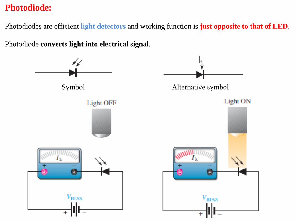
Photodiode:
Photodiodes are efficient light detectors and working function is just opposite to that of LED.
Photodiode converts light into electrical signal.
Symbol Alternative symbol

Photodiode contd….
Photodiode operates in reverse bias.
Reverse leakage current flows in rev. biased condn.
The rev. current is produced by thermally generated electron-hole pairs in depletion region
which are swept across P-N junction by applied rev. bias vtg.
When there is no incident light, reverse current is very small, which can be neglected, such
current is called as dark current.
Increase in light intensity (irradiance) produces increase in reverse current as shown below.