বেসিক ইলেকট্রনিক্স-১ (Basic electronics-1)
30
Aqua Robotics Week-2 Basic Electronics Shadman Sakib (Siam) 1012009 Naval Architecture & Marine Engineering BUET ।
Transcript of বেসিক ইলেকট্রনিক্স-১ (Basic electronics-1)
Aqua Robotics
Week-2
Basic Electronics
Shadman Sakib (Siam)
1012009
Naval Architecture & Marine Engineering
BUET
।

Resistor values - the resistor colour code:
Resistance is measured in ohms, the symbol for ohm is an omega Ω.
1 Ω is quite small so resistor values are often given in k Ω and M Ω.
1 k Ω = 1000 Ω 1 M Ω = 1000000 Ω.
Resistor values are normally shown using coloured bands.
Each colour represents a number as shown in the table.
Most resistors have 4 bands:
The first band gives the first digit.
The second band gives the second digit.
The third band indicates the number of zeros.
The fourth band is used to shows the tolerance (precision) of the resistor, this may be ignored for
almost all circuits but further details are given below.
This resistor has red (2), violet (7), yellow (4 zeros) and gold bands.
So its value is 270000 Ω = 270 k Ω.
On circuit diagrams the Ω is usually omitted and the value is written 270K.

।

।

। ।

Reading a table of technical data for LEDs
Suppliers' websites and catalogues usually provide tables of technical data for components
such as LEDs. These tables contain a good deal of useful information in a compact form but
they can be difficult to understand if you are not familiar with the abbreviations used.
The table below shows typical technical data for some 5mm diameter round LEDs with
diffused packages (plastic bodies). Only three columns are important and these are shown in
bold. Please see below for explanations of the quantities.

Calculating an LED resistor value
An LED must have a resistor connected in series to limit the current through the LED, otherwise it will burn out
almost instantly.
The resistor value, R is given by:
R = (VS - VL) / I
VS = supply voltage
VL = LED voltage (usually 2V, but 4V for blue and white LEDs)
I = LED current (e.g. 10mA = 0.01A, or 20mA = 0.02A)
Make sure the LED current you choose is less than the maximum permitted and convert the current to
amps (A) so the calculation will give the resistor value in ohms (Ω).
To convert mA to A divide the current in mA by 1000 because 1mA = 0.001A.
If the calculated value is not available choose the nearest standard resistor value which is greater, so that the
current will be a little less than you chose. In fact you may wish to choose a greater resistor value to reduce
the current (to increase battery life for example) but this will make the LED less bright.
For example If the supply voltage VS = 9V, and you have a red LED (VL = 2V), requiring a current I = 20mA = 0.020A,
R = (9V - 2V) / 0.02A = 350 Ω, so choose 390 Ω (the nearest standard value which is greater).
Working out the LED resistor formula using Ohm's law
Ohm's law says that the resistance of the resistor, R = V/I, where:
V = voltage across the resistor (= VS - VL in this case)
I = the current through the resistor
So R = (VS - VL) / I


BE
CE IB
IC IC = β × IB β
DATASHEET

( www.Ikalogic.com )
The Bipolar Junction Transistors (BJT), is one of the oldest but most famous transistors, that still find their
place in modern electronics. They come in many classes and sizes to match your application, and with some
basic knowledge and some simple mathematical relations, you can build very efficient while very simple
switch circuits. Using a transistor in the ‘switching’ configuration is indispensable in many situation, where
it is required to drive a relatively important load, providing important currents, that most controllers are not
able to provide.
Introduction to the BJT
Before going on with the tutorial, let us agree that we are going to discuss one among many other
configurations of Bipolar Junction Transistors. The same BJT can be used in an audio amplifier or and FM
receiver, however, usually each model of BJTs is manufactured with specific characteristics to make it more
adequate to a certain application.
Configuring a transistor, means connecting to it a number of external components and power sources in a
very specific way to make if function in a very specific and controllable way.
The BJT has 3 pins. The Base, the Collector, and the Emitter (see figure 1). According to the configuration
of the transistor, it can be difficult to precisely say which one of those pins is input, and which one is output,
as they are all related, and all affect each others somehow. However, in a switch configuration, this is clearly
defined: The Base current controls the flow of current from the collector to the Emitter or vice-versa,
depending on the type of BJT.
figure 1
There are two main types of BJTs: NPN and PNP. To make this as simple as possible, we can say that the
main difference between those two types is the directions of the electric currents. This can be seen in figure
1, where the direction of the arrow points towards the direction of the current; In the NPN transistor, one
current flow from the base to ‘inside’ the transistor, and another current flow from the collector to the
Emitter, while in a PNP transistor, all the directions are reversed, one current flows from the ‘inside’ of the
transistor to the base, and another one flows from the emitter to the collector. From a functional point of
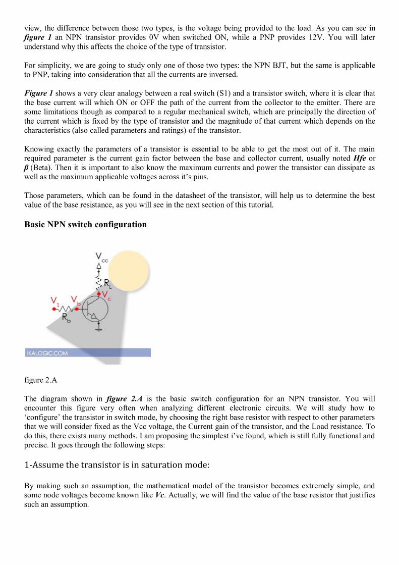
view, the difference between those two types, is the voltage being provided to the load. As you can see in
figure 1 an NPN transistor provides 0V when switched ON, while a PNP provides 12V. You will later
understand why this affects the choice of the type of transistor.
For simplicity, we are going to study only one of those two types: the NPN BJT, but the same is applicable
to PNP, taking into consideration that all the currents are inversed.
Figure 1 shows a very clear analogy between a real switch (S1) and a transistor switch, where it is clear that
the base current will which ON or OFF the path of the current from the collector to the emitter. There are
some limitations though as compared to a regular mechanical switch, which are principally the direction of
the current which is fixed by the type of transistor and the magnitude of that current which depends on the
characteristics (also called parameters and ratings) of the transistor.
Knowing exactly the parameters of a transistor is essential to be able to get the most out of it. The main
required parameter is the current gain factor between the base and collector current, usually noted Hfe or
β (Beta). Then it is important to also know the maximum currents and power the transistor can dissipate as
well as the maximum applicable voltages across it’s pins.
Those parameters, which can be found in the datasheet of the transistor, will help us to determine the best
value of the base resistance, as you will see in the next section of this tutorial.
Basic NPN switch configuration
figure 2.A
The diagram shown in figure 2.A is the basic switch configuration for an NPN transistor. You will
encounter this figure very often when analyzing different electronic circuits. We will study how to
‘configure’ the transistor in switch mode, by choosing the right base resistor with respect to other parameters
that we will consider fixed as the Vcc voltage, the Current gain of the transistor, and the Load resistance. To
do this, there exists many methods. I am proposing the simplest i’ve found, which is still fully functional and
precise. It goes through the following steps:
1-Assume the transistor is in saturation mode:
By making such an assumption, the mathematical model of the transistor becomes extremely simple, and
some node voltages become known like Vc. Actually, we will find the value of the base resistor that justifies
such an assumption.
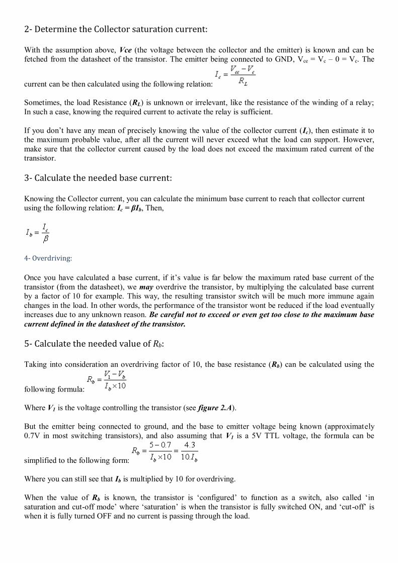
2- Determine the Collector saturation current:
With the assumption above, Vce (the voltage between the collector and the emitter) is known and can be
fetched from the datasheet of the transistor. The emitter being connected to GND, Vce = Vc – 0 = Vc. The
current can be then calculated using the following relation:
Sometimes, the load Resistance (RL) is unknown or irrelevant, like the resistance of the winding of a relay;
In such a case, knowing the required current to activate the relay is sufficient.
If you don’t have any mean of precisely knowing the value of the collector current (Ic), then estimate it to
the maximum probable value, after all the current will never exceed what the load can support. However,
make sure that the collector current caused by the load does not exceed the maximum rated current of the
transistor.
3- Calculate the needed base current:
Knowing the Collector current, you can calculate the minimum base current to reach that collector current
using the following relation: Ic = βIb, Then,
4- Overdriving:
Once you have calculated a base current, if it’s value is far below the maximum rated base current of the
transistor (from the datasheet), we may overdrive the transistor, by multiplying the calculated base current
by a factor of 10 for example. This way, the resulting transistor switch will be much more immune again
changes in the load. In other words, the performance of the transistor wont be reduced if the load eventually
increases due to any unknown reason. Be careful not to exceed or even get too close to the maximum base
current defined in the datasheet of the transistor.
5- Calculate the needed value of Rb:
Taking into consideration an overdriving factor of 10, the base resistance (Rb) can be calculated using the
following formula:
Where V1 is the voltage controlling the transistor (see figure 2.A).
But the emitter being connected to ground, and the base to emitter voltage being known (approximately
0.7V in most switching transistors), and also assuming that V1 is a 5V TTL voltage, the formula can be
simplified to the following form:
Where you can still see that Ib is multiplied by 10 for overdriving.
When the value of Rb is known, the transistor is ‘configured’ to function as a switch, also called ‘in
saturation and cut-off mode’ where ‘saturation’ is when the transistor is fully switched ON, and ‘cut-off’ is
when it is fully turned OFF and no current is passing through the load.

Some common sense about the electric currents in a transistor: When we say that Ic = βIb, that does mean
that the collector current has to be equal to ‘βIb‘, neither that it is forced to be equal to that value. It simply
means that the collector of the transistor can sink or source this amount of current. The actual value of the
current will follow Ohm’s laws, like any electrical current.
Calculation precautions:
When we assumed that the transistor was is saturation mode, we also assumed some of its parameters were
constant. This was not exactly true. Actually those parameters change, mainly due to increasing the collector
current, and that’s why it is safer to overdrive. Each datasheet will present those variation of the parameters
as a table or as a graph. Anyway, you have to consider those parameters into your calculations. For example,
the table in figure 2.B shows two parameters (among others) that considerably change:
Hfe (β) changes according to the collector current, and the voltage VCEsat. But VCEsat itself changes according
to the collector current and the base current.
Another part of the table is highlighted: the VBEsat, which varies depending on collector and base current.
figure 2.B
Calculation can become extremely complicated, as all the parameters are tightly and complexly related, so
the solution is to assume the worst values. In other words, assume the smallest Hfe, the biggest VCEsat and
VBEsat, and at last, don’t forget to overdrive the transistor, but increasing the base current.
Typical Transistor switch applications
It’s a habit in Ikalogic to always tightly bond theory and practice, so here are a couple of example
applications using the very standard 2N2222 switching transistor.

1. Controlling a relay:
A very classic use of transistor in modern electronics is to
control ‘electro-magnetic’ relays, that incorporates a coil,
that sinks important amount of current (up to 200 mA),
and generate feed-back voltages when switched OFF. If
you want a logic gate or a microcontroller to control a
relay, it is indispensable to use a transistor.
In figure 3.A, the base resistance is to be calculated
according to the required current to activate the coil of the
relay.
The Diode D1 is very important, it protects the transistor
from the current surges generated by the coil when
switching OFF. It is called a freewheeling diode, and it is a
regular rectifier diode like the 1N4007.
You can connect any 220V or 110V appliance to the
output of the relay.
figure 3.A
2. Connecting a transistor to an open-collector output:
figure 3.B
Many devices like the 8051 family of microcontrollers
have open-collector output ports. Such output
configuration is unable to ‘source’ any current, it can only
sink current. When connecting a switching transistor to
such a device, the position of the base resistance changes,
to sink current from the 5V power supply instead of the
device that is unable to do so.This way you can calculate
the base resistance normally as described in this tutorial.
Note that the representation of the output device is just for
clarifying the concept of open collector output, but in
general, output ports are more complicated, and often use
FET transistors instead of BJTs, and is called ‘open drain’
output, but the mechanism remains exactly the same and is
fully compatible with the configuration given in figure
3.B.

3. Building NOR Logic gates:
Sometimes, on a circuit, you need a single NOR logic gate,
but you don’t want to use a 14 pin IC containing 4 gates,
and only use one of them.
Either due to the cost or due to the foot print (space taken
on the PCB), building a gate using a couple transistors can
be interesting. However, note that the frequency response
of such a gate depends on the characteristics and type of
the transistor, but below 100 Khz, you probably wont
notice any difference of behavior.
This method also allows you to build transistor with
controllable Input and output resistance given in figure
3.C. Decreasing the output resistance (Ro) in this case
would increase the power consumption of the gate, but
increase the output current.
It’s up to you to find the compromise between the different
parameters.
figure 3.C
figure 3.D
Figure 3.D shows a NOR logic gate constructed using two 2N2222 BJT
transistors. You can see the full schematic of this H-bridge here. You can
notice the assembled gate takes relatively less space that a DIP14 logic IC
(DIP stands for Dual Inline Package)
Note that you can also build a NAND logic gate using the same two
transistors by connecting them in series (not in parallel as in figure 3.C).
All those applications can be built on the complementary PNP transistor
2N2907, with minor modifications. You just have to consider that all the
electric currents flow in the opposite direction.
The H-Bridge is a very famous example application to switching transistors,
where two PNP and two NPN transistors are used, as in the
following schematic, or in our 5A H-Brigde tutorial.
Debugging transistor switch circuits.
When a problem occurs in circuits containing many transistors, is can be very problematic to know which
one is defective, specially when they are all soldered. I propose a bunch of tips to help you find the problem
in such a circuit in minimum time:
1- Temperature:
If a transistor is getting hot, this probably men there is a problem somewhere. But don’t be too confident
saying that the problem is coming from the transistor getting hot. Usually a defective transistor don’t even
get warm any more. This rise of temperature can be caused by another transistor connected to it. Bottom
line: The temperature is an indication of the region where things are going wrong.
2- Measure the VCE of the transistors:
If they are all of the same type, and all turned ON, they should approximately have the same collector to
emitter voltage. Finding the transistor having a different VCE is a quick way of detecting a dead transistor.

3- Measure the voltage across the base resistance:
The voltage across a base resistance should be relatively important (if the transistor is switched ON). For a
TTL (5V) device controlling a NPN transistor, the voltage drop across the resistor should be more than 3V.
If there no remarkable voltage drop across the base resistor, then either the transistor is dead, either the
device controlling the transistor has a problem. In both case, the base current is equal to 0.
β
(DARLINGTON PAIR)
PAIR DARLINGTON PAIR …
DARLINGTON PAIR

ULN2003 .
ULN2003 DARLINGTON PAIR IC
। hfe
http://sound.westhost.com/trans.htm


BJT Bipolar
Junction Transistors (MOSFET) ।

।
।

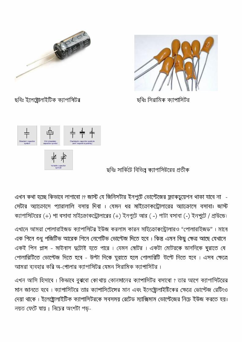
Polarised capacitors (large values, 1µF +)
Electrolytic Capacitors Electrolytic capacitors are polarized and they must be connected the correct way round, at least one of their leads
will be marked + or -. They are not damaged by heat when soldering.
There are two designs of electrolytic capacitors; axial where the leads are attached to each end (220µF in
picture) and radial where both leads are at the same end (10µF in picture). Radial capacitors tend to be a
little smaller and they stand upright on the circuit board.
It is easy to find the value of electrolytic capacitors because they are clearly printed with their capacitance
and voltage rating. The voltage rating can be quite low (6V for example) and it should always be checked
when selecting an electrolytic capacitor. If the project parts list does not specify a voltage, choose a
capacitor with a rating which is greater than the project's power supply voltage. 25V is a sensible minimum
for most battery circuits.
Unpolarised capacitors (small values, up to 1µF)

https://learn.sparkfun.com/tutorials/capacitors/capacitor-theory
http://www.schoolphysics.co.uk/age16-
19/Electricity%20and%20magnetism/Electrostatics/text/Capacitor_charge_and_discharge_mathematics/in
dex.html
Mathematical treatment of charging and discharging a
capacitor:
Discharging
The area under the current-time discharge graph gives the charge held by the
capacitor. The gradient of the charge-time graph gives the current flowing from the
capacitor at that moment.
Discharge of a capacitor through a resistor
In Figure 1 let the charge on a capacitor of capacitance C at any instant be q, and let V be the potential
difference across it at that instant.
The current (I) in the discharge at that instant is therefore:
I = - dq/dt
But V = IR and q = CV so dq/dt = d(CV)/dt = C dV/dt
Therefore we have V = -CR dV/dt Rearranging and integrating gives:
Capacitor discharge (voltage decay): V = Voe-(t/RC)
where Vo is the initial voltage applied to the capacitor. A graph of this exponential discharge is shown below
in Figure 2.

Since Q = CV the equation for the charge (Q) on the capacitor after a time t is therefore:
Capacitor discharge (charge decay): Q = Qoe-(t/RC)
V = Voe-(t/RC)
and also I = Ioe-(t/RC)
Q = Qoe-(t/RC)
You should realise that the term RC governs the rate at which the charge on the capacitor decays.
When t = RC, V = Vo/e = 0.37 Vo and the product RC is known as the time constant for the circuit. The
bigger the value of RC the slower the rate at which the capacitor discharges.
The value of C can be found from this discharge curve if R is known.
Example problems:
1. A capacitor of 1000 μF is with a potential difference of 12 V across it is discharged through a 500 Ω
resistor.
Calculate the voltage across the capacitor after 1.5 s
V = Voe-(t/RC)
so V = 12e-1.5/[500 x 0.001]
= 0.6 V
2. A capacitor is discharged through a 10 MΩ resistor and it is found that the time constant is 200 s.
Calculate the value of the capacitor.
RC= 200
Therefore C = 200/10 x 106 = 20 μF.
3. Calculate the time for the potential across a 100 ΨF capacitor to fall to 80 per cent of its original value if
it is discharged through a 20 kΩ resistor.
V = 0.8 Vo. Therefore 0.8 = e–t/20000x0.0001
Therefore:
ln(1/0.8) = 20 000 x 0.0001
This gives t= 2xln(1/0.8) = 0.45 s.

Charging a capacitor
When a capacitor (C) is being charged through a resistance (R) to a final potential Vo the equation giving the
voltage (V) across the capacitor at any time t is given by:
Capacitor charging (potential difference): V = Vo[1-e-(t/RC)
]
and the variation of potential with time is shown in Figure 2.
As the capacitor charges the charging current decreases since the potential across the resistance decreases as
the potential across the capacitor increases.
Figure 4 shows how both the potential difference across the capacitor and the charge on the plates vary with
time during charging.
The charging current would be given by the gradient of the curve in Figure 2 at any time and the graph of
charging current against time is shown in Figure 3.
The area below the current-time curve in both charging and discharging represents the total charge held by
the capacitor.