AUIR3330S - Mouser Electronics
32
Automotive Grade AUIR3330S w w w .irf.com 1 Ifbk pin. The over-current shutdown is programmable from 5A to 50A. Over-current, over-temperature latch OFF the pow er sw itch, providing a digital diagnostic status on the input pin. In sleep mode, the device consumes typically less then 1uA. Further integrated protections such as ESD and GND disconnect protection guarantee safe operation in harsh conditions of the automotive environment. PROTECTED HIGH FREQUENCY HIGH SIDE SWITCH FOR AUTOMOTIVE DC MOTOR DRIVE Features Up to 30Khz PWM switching capability Charge pump for DC operation Active di/dt control to reduce EMI Load current feedback Short-circuit protection Programmable over current shutdown Over temperature shutdown Diagnostic feedback Under voltage shutdown Gnd, IN and bootstrap pin loss protection E.S.D protection Low power mode Lead-free, RoHS compliant Product Summary Rds(on)@25°C 3.5m max. Max current 65A Operating voltage 6 -18V Application Fan engine cooling Air conditioning blower Pumps (oil, fuel, water…) Compressor Packages AUIR3330S D2Pak - 7 leads Typical connection with reverse battery protection Description The AUIR3330s is a 7 terminals high side sw itch for variable speed DC motor. It features simplify the design of the DC motor drive w ith a microcontroller. The Mosfet sw itches the pow er load proportionally to the input signal duty cycle at the same frequency and provides a current feedback on the D1 Ifb Boot IN Vcc Gnd AUIR3330 IN Gnd Input f ilter R2 D2 - Mot GND + Mot Vbat Cboot 100nF T1 Output Current shutdown programming resistor Diag Ifb Micro-processor I/O I/O A/D Gnd Rifb Rin Rp Ifb Rp diag Cd1 100nF* Cd2 2.2μF* *ceramic capacitor Cifb 1nF*
-
Upload
khangminh22 -
Category
Documents
-
view
1 -
download
0
Transcript of AUIR3330S - Mouser Electronics
Automotive Grade
AUIR3330S
w w w .irf.com 1
Ifbk pin. The over-current shutdown is programmable from 5A to 50A. Over-current, over-temperature latch OFF the pow er sw itch, providing a digital diagnostic status on the input pin. In sleep mode, the device consumes typically less then 1uA.
Further integrated protections such as ESD and GND disconnect protection guarantee safe operation in harsh conditions of the automotive environment.
PROTECTED HIGH FREQUENCY HIGH SIDE SWITCH FOR AUTOMOTIVE DC MOTOR DRIVE
Features Up to 30Khz PWM switching capability
Charge pump for DC operation Active di/dt control to reduce EMI
Load current feedback
Short-circuit protection Programmable over current shutdown
Over temperature shutdown
Diagnostic feedback Under voltage shutdown
Gnd, IN and bootstrap pin loss protection E.S.D protection
Low power mode
Lead-free, RoHS compliant
Product Summary
Rds(on)@25°C 3.5m max. Max current 65A
Operating voltage 6 -18V
Application
Fan engine cooling
Air conditioning blower Pumps (oil, fuel, water…)
Compressor
Packages
AUIR3330S D2Pak - 7 leads
Typical connection with reverse battery protection
Description The AUIR3330s is a 7 terminals high side sw itch for variable
speed DC motor. It features simplify the design of the DC motor drive w ith a microcontroller. The Mosfet sw itches the pow er load proportionally to the input signal duty cycle at the same frequency and provides a current feedback on the
D1 Ifb
Boot IN
Vcc
Gnd
AUIR3330
IN
Gnd
Input f ilter
R2
D2
- Mot GND
+ Mot Vbat
Cboot
100nF
T1
Output
Current shutdown programming resistor
Diag
Ifb
Mic
ro-p
roc
es
so
r I/O
I/O
A/D
Gnd
Rifb
Rin
Rp Ifb
Rp diag
Cd1
100nF*
Cd2
2.2µF*
*ceramic capacitor
Cifb
1nF*

AUIR3330S
w w w .irf.com 2
Qualification Information†
Qualification Level
Automotive
(per AEC-Q100††
)
Comments: This family of ICs has passed an Automotive qualif ication. IR’s Industrial and Consumer qualif ication level is granted by extension of the higher Automotive level.
Moisture Sensitivity Level MSL1 260°C
(per IPC/JEDEC J-STD-020)
ESD
Machine Model Class M3 (+/-350V)
(per AEC-Q100-003)
Human Body Model Class H4 (+/-4000V) (per AEC-Q100-002)
Charged Device Model Class C4 (Pass +/-1000V)
(per AEC-Q100-011)
IC Latch-Up Test Class II Level A
(per AEC-Q100-004)
RoHS Compliant Yes
† Qualif ication standards can be found at International Rectif ier’s w eb site http://w w w .irf .com/
†† Exceptions to AEC-Q100 requirements are noted in the qualif ication report.
AUIR3330S
w w w .irf.com 3
Absolute Maximum Ratings Absolute maximum ratings indicate sustained limits beyond which damage to the device may occur. (Tj= -40°C..150°C, Vcc=6..18V unless otherwise specified).
Symbol Parameter Min. Max. Units Vout Maximum drain to source voltage GND-5V Vcc+0.3 V
Vin Maximum input voltage -0.3 5.5 V
Vcc max. Maximum Vcc voltage 36 V
Vcc cont Maximum continuous Vcc voltage 28 V
Iin max. Maximum input current -0.3 10 mA
Ifb max Maximum Ifb current -50 10 mA
Pd Maximum pow er dissipation Rth=60°C/W Tambient=25°C, Tj=150°C Rth=40°C/W D²Pack 6cm² footprint 2.5 W
Tj max. Max. storage & operating temperature junction temperature -40 150 °C
Thermal Characteristics Symbol Parameter Typ. Max. Units Rth1 Thermal resistance junction to ambient D²Pak Std footprint 60
°C/W Rth2 Thermal resistance junction to ambient D²pak 6cm² footprint 40
Rth3 Thermal resistance junction to case D²pak 0.65
Recommended Operating Conditions These values are given for a quick design.
Symbol Parameter Min. Max. Units Vcc op. Operating voltage range 6 18 V
Iout DC output current Tj=145°C, Tamb=85°C, Rth=5°C/W 45 A
Cboot Bootstrap capacitor 100 220 nF
Cd1 Decoupling ceramic capacitor 100 nF
Cd2 Decoupling ceramic capacitor 2.2 µF
R In Recommended resistor in series w ith In pin 1 5 k
Rp diag Recommended resistor in series w ith In pin to read the diagnostic 10 50 k
CIfb Recommended Ifb f ilter capacitor 1 2.2 nF
RIfb Recommended resistor to program over current shutdown 0.6 5 k
Rp Ifb Recommended resistor in series w ith RIfb pin to read the current feedback
10 25 k
F max. Maximum recommended input frequency, duty cycle=10% to 90% 30 kHz

AUIR3330S
w w w .irf.com 4
Static Electrical Characteristics -40°C < Tj < 150°C, 6V < Vcc < 18V, (unless otherw ise specif ied)
Symbol Parameter Min. Typ. Max. Units Test Conditions
Rds on ON state resistance Tj=25°C 3 3.5
m Iout=30A
ON state resistance Tj=150°C1 5.5 6.2 Iout=30A
Rds on Lv ON state resistance low voltage Tj=25°C 3 3.5 m Iout=15A Vcc=6V
Vf Mos Forw ard voltage of the Mosfet body
diode 0.6 1.1 V Iout = -50A
Vbrk out Breakdow n voltage between Vcc and
Vout (MOSFET body diode) 39 40 V
I Vcc Slp Supply current in sleep mode (IC + MOSFET leakage)
1 2 µA Vin=0V Vcc = 14V Tj = 25°C
I bias Boot Bootstrap regulator biasing current (f low s through the output)
5.5 14 mA Vout = 0V
I Vcc Wke Vcc current when the device is w oken up (IC + Ibias Boot) 14 20 mA I_boot = 0A Vout = 0V
V In Wke Input threshold voltage to w ake up
the device 0.35 0.75 1 V
V In Off In voltage threshold to turn off 1.9 2.2 V
V In On In voltage threshold to turn on 2.8 3.2 V
V In Hyst Input threshold hysteresis 0.4 0.7 V
C In Input pin capacitor - 10 - pF
I In on On state input current 10 20 30 µA Vin = 5V
I Bt Chrge Bootstrap current charge 0.4 1.5 A Vout = 0V Cboot =500nF
V Bt Chrge Bootstrap voltage 4.9 5.5 6.3 V Cboot =500nF
Guaranteed by design.
AUIR3330S
w w w .irf.com 5
Switching Electrical Characteristics -40°C < Tj < 150°C, 6V < Vcc < 18V, Rin = 5k (unless otherw ise specif ied)
Symbol Parameter Min. Typ. Max. Units Conditions
Td Vout on Turn-on output voltage delay time 0.7 1 1.4 µs betw een 50% of IN and 30% of Vout, Iout = 14A
Tr Vout Ouput voltage rise time 500 800 1300 ns Betw een 15% and 85%; Vcc = 14v, Iout=14A
Tr Iout Ouput current rise time 0.7 1.2 1.85 µs Betw een 5A and 40A;
Vcc = 14v, Iout=45A
dv/dt on Turn on dv/dt 10 20 28 V/µs Betw een 25% and 70%; Vcc = 14v
di/dt on Turn on di/dt 21 40 51 A/µs Betw een Iout 15A and 35A; Vcc = 14v
Td Vout off Turn-off delay time 0.9 1.2 1.7 µs betw een 50% of IN and 90% of Vout, Iout = 14A
Tf Vout Output voltage fall time 250 430 650 ns Betw een 90% and 10%; Vcc = 14v, Iout=14A
Tf Iout Output current fall time 0.55 1 1.45 µs Betw een 40A and 5A; Vcc = 14v, Iout=45A
dv/dt off Turn off dv/dt 28 50 67 V/µs Betw een 30% and 70%;
Vcc = 14v
di/dt off Turn off di/dt 30 40 51 A/µs Betw een Iout 35A and 15A;
Vcc = 14v
T Trfct Ld Input output transfer function for low duty cycle
8.5 10 11.5 µs Iout = 1A; In pulse time =10µS
T Trfct Hd Input output transfer function for high duty cycle
38.5 39.5 40.5 µs Iout = 1A; In pulse time =40µS
T Off Min Minimum off time to recharge the bootstrap capacitor
2 µs Cboot = 100nF
AUIR3330S
w w w .irf.com 6
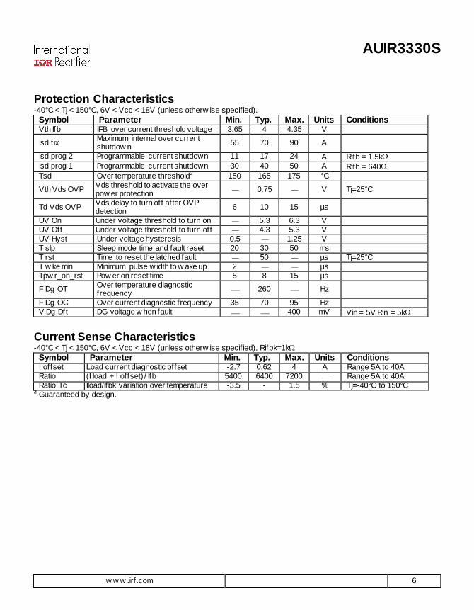
Protection Characteristics -40°C < Tj < 150°C, 6V < Vcc < 18V (unless otherw ise specif ied).
Symbol Parameter Min. Typ. Max. Units Conditions Vth Ifb IFB over current threshold voltage 3.65 4 4.35 V
Isd f ix Maximum internal over current shutdow n
55 70 90 A
Isd prog 2 Programmable current shutdown 11 17 24 A Rifb = 1.5k
Isd prog 1 Programmable current shutdown 30 40 50 A Rifb = 640
Tsd Over temperature threshold2 150 165 175 °C
Vth Vds OVP Vds threshold to activate the over pow er protection
0.75 V Tj=25°C
Td Vds OVP Vds delay to turn off after OVP detection
6 10 15 µs
UV On Under voltage threshold to turn on 5.3 6.3 V
UV Off Under voltage threshold to turn off 4.3 5.3 V
UV Hyst Under voltage hysteresis 0.5 1.25 V
T slp Sleep mode time and fault reset 20 30 50 ms
T rst Time to reset the latched fault 50 µs Tj=25°C
T w ke min Minimum pulse w idth to w ake up 2 µs
Tpw r_on_rst Pow er on reset time 5 8 15 µs
F Dg OT Over temperature diagnostic frequency 260 Hz
F Dg OC Over current diagnostic frequency 35 70 95 Hz
V Dg Dft DG voltage w hen fault 400 mV Vin = 5V Rin = 5k
Current Sense Characteristics -40°C < Tj < 150°C, 6V < Vcc < 18V (unless otherw ise specif ied), Rifbk=1k
Symbol Parameter Min. Typ. Max. Units Conditions I offset Load current diagnostic offset -2.7 0.62 4 A Range 5A to 40A
Ratio (I load + I offset) / Ifb 5400 6400 7200 Range 5A to 40A
Ratio Tc Iload/Ifbk variation over temperature -3.5 - 1.5 % Tj=-40°C to 150°C 2 Guaranteed by design.

AUIR3330S
w w w .irf.com 7
Leads Assignment
PART NUMBER AUIR3330S
1 : Ifb 2 : In
3 : Gnd 4 : Vcc (Tab) 5 : Boot
6 : Out 7 : Out
D2Pak 7 leads

AUIR3330S
w w w .irf.com 8
Functional Block Diagram All values are typical
Internal diode schematic All values are typical
Isd f ixed
Tj > 165°C
+
- 6V
Gnd
IN
Ifb Out
Level
Shifter Di/dt
Driver control
Charge Pump
R
S Q
75V
43V
Vcc
Boot
Internal pow er
supply
Vss
On/Off
Boot strap
regulator
Uvlo
Dia
gnostic
+
-
Vcc + -
4V
Logic input
Treset
Over
pow er
Pw r on rst
Boot
AUIR3330S
w w w .irf.com 9
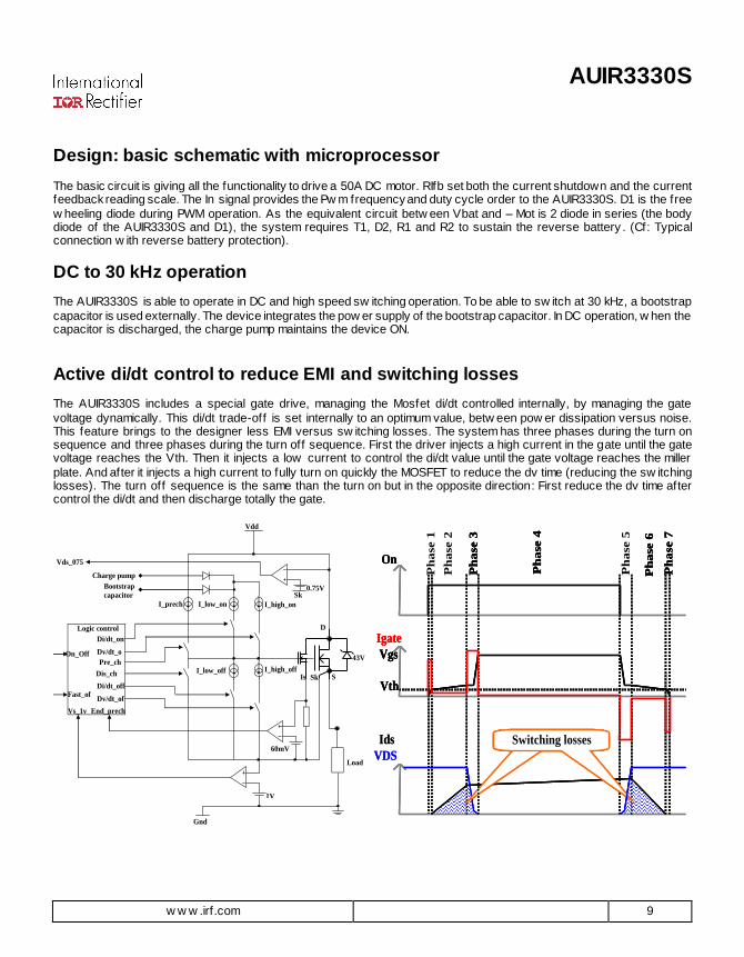
Design: basic schematic with microprocessor The basic circuit is giving all the functionality to drive a 50A DC motor. RIfb set both the current shutdown and the current feedback reading scale. The In signal provides the Pw m frequency and duty cycle order to the AUIR3330S. D1 is the free
w heeling diode during PWM operation. As the equivalent circuit betw een Vbat and – Mot is 2 diode in series (the body diode of the AUIR3330S and D1), the system requires T1, D2, R1 and R2 to sustain the reverse battery . (Cf: Typical connection w ith reverse battery protection).
DC to 30 kHz operation The AUIR3330S is able to operate in DC and high speed sw itching operation. To be able to sw itch at 30 kHz, a bootstrap
capacitor is used externally. The device integrates the pow er supply of the bootstrap capacitor. In DC operation, w hen the capacitor is discharged, the charge pump maintains the device ON.
Active di/dt control to reduce EMI and switching losses The AUIR3330S includes a special gate drive, managing the Mosfet di/dt controlled internally, by managing the gate
voltage dynamically. This di/dt trade-off is set internally to an optimum value, betw een pow er dissipation versus noise. This feature brings to the designer less EMI versus sw itching losses. The system has three phases during the turn on sequence and three phases during the turn off sequence. First the driver injects a high current in the gate until the gate voltage reaches the Vth. Then it injects a low current to control the di/dt value until the gate voltage reaches the miller
plate. And after it injects a high current to fully turn on quickly the MOSFET to reduce the dv time (reducing the sw itching losses). The turn off sequence is the same than the turn on but in the opposite direction: First reduce the dv time after control the di/dt and then discharge totally the gate.
43V
Vdd
Charge pump
Bootstrap
capacitor
Logic control
Gnd
1V
On_Off
Fast_of
f Vs_1v
Di/dt_on
Dv/dt_o
n Pre_ch
Di/dt_off
Dv/dt_of
f
I_low_on I_high_on
I_high_off I_low_off
Load
S
D
I_prech
Is Sk
60mV
End_prech
0.75V Sk
Vds_075
v
Dis_ch
Ids
VDS
Ph
ase 1
Ph
ase 2
Ph
ase 3
Ph
ase 4
Ph
ase 5
Ph
ase 6
Ph
ase 7
Vth
On
Switching lossesSwitching losses
Igate
Vgs
Ids
VDS
Ph
ase 1
Ph
ase 2
Ph
ase 3
Ph
ase 4
Ph
ase 5
Ph
ase 6
Ph
ase 7
Vth
On
Switching lossesSwitching losses
Igate
Vgs
Ph
ase 1
Ph
ase 2
Ph
ase 3
Ph
ase 4
Ph
ase 5
Ph
ase 6
Ph
ase 7
Vth
On
Switching lossesSwitching losses
Igate
Vgs

AUIR3330S
w w w .irf.com 10
Sense Load current feedback and programmable current shutdown The Ifb pin allow s an analog measurement of the load current and w ith an external resistor allow s to program the over
current shutdown level from 10A to 50A. The voltage threshold level of the Ifb pin is internally set to 4v (See the formulas below ). It is also possible to dynamically adjust the current shutdow n protection versus time by adding some external components. This protection is latched and turns off the output MOSFET w ithout di/dt sequence to reduce the device and the application stress. The operating mode is recovered after resetting by the sleep mode.
minmin_
min_Ratio
IoffsetappliImax
gndVifbRifb
CIshtdIshdCIshdMAXIshd 150max@;25max@;40max@max
CTIoffsetCTRatiocalculatedRifb
gndVifbCTIshd
max@max@
)(
max_max@
Where: Imax appli is the maximum application current
Ishtd max is the maximum output shutdown current
RifbCTRatio
CTIoffsetIloadCTVifb
max@
max@min@
RifbCTRatio
CTIoffsetIloadCTVifb
min@
min@max@
Internal over current shutdown The maximum current shutdown threshold value is internally f ixed to 65A typ. This protection is latched and turns off the
output MOSFET w ithout di/dt sequence to reduce the device and the application stress. The operating mode is recovered after resetting by the sleep mode.
Under voltage lock-out The AUIR3330S remains operational from UV off threshold. Under this continuous voltage, the device w ill be locked until
the voltage recovers the operating range, according to an internal hysteresis f ixed to 0,5V min. The maximum rating voltage is given by the Trench VDMOS technology w here the avalanche voltage is up to 43V typically.
Sleep mode and reset fault: The sleep mode is enabled if the IN pin stay low (Vin < V In Slp) more than T Slp time. The consumption in sleep mode is Icc off. The AUIR3330S w akes up at f irst rise edge on the IN pin (Vin > V In Slp). This mode allow s resetting all the
latched faults after Trst time (Cf. Figure 1: Wake sequence, sleep mode and reset latched fault protocol). This f ilter time allow s memorizing and maintaining the fault latched even if the pow er supply is removed (ISO pulses latch protection).

AUIR3330S
w w w .irf.com 11
Over-power protection The AUIR3330S have an internal over-pow er protection. This feature allow s protecting the silicon device and the application against several critical issues:
The bootstrap capacitor missing.
Abnormal leakage on the bootstrap capacitor. Abnormal leakage on the pow er MOSFET gate.
Very low impedance output short circuit.
• The time constant Ign1 + C represent the thermal
silicon time constant
• The time constant Ign2 + C represent the thermal package time constant (T(ign2 + C) < T Slp)
• Igen1 is on if the gate voltage (of the output MOSFET) is higher than its Vth
• Ign2 is alw ays sw itching on.
• Sw 1 is close if the Vbat – out voltage (Vds) is low er than 0.75V
When the Output MOSFET gate voltage reaches its output MOSFET V th value, the current generator Igen1 start to charge the capacitor C. Then three scenarios are possible: 1. The device turn on properly (Vds < 0.75v) and the capacitor C is discharged by the sw itch sw 1. The device is ready
for the next pulse. It is the normal case.
2. The device can not turn on properly (Vds
stay > 0.75v no capacitor reset) and the on time duration (duty cycle) is enough
long to charge completely the capacitor C. The comparator detects the fault, stop the device and latch it. This fault could be reset by a sleep mode
C
Igen1
Igen2
+
-
R1
R2
Time to charge the capacitor and latch a fault (Igen1 + C) = 9µs
Time to discharge the capacitor (Igen2 + C) = 11ms
ED_pch signal
Actif if Vgs > Vth
Sw 1Vds_075 signal
Actif if Vds < 0.75 V
OVP_Flt signal
Go to the latch block
In input
Vgs voltage
Normal value
Vbat – Voutput voltage
(Vds)
Ed_pch signal
C capacitor
voltage
OVP_Flt
signal
In input
Vgs voltage
Normal value
Vbat – Voutput voltage
(Vds)
Ed_pch signal
C capacitor
voltage
OVP_Flt
signal

AUIR3330S
w w w .irf.com 12
3. The device can not turn on properly (Vds stay > 0.75v no capacitor reset) but the ON time duration (duty cycle) is not enough long to charge completely the capacitor C.
So the fault is not detected by the comparator and it is not latched. But the picture of energy value dissipated by the
MOSFET during the almost turn on value is stored in the capacitor C. And at the next pulse the current generator Igen1 resume to charge the capacitor until it reach the
comparator value and latch the fault (this sequence could be on several pulse). It could be reset by a sleep mode.
Wake up sequence: The AUIR3330S has an internal pow er on reset. After waking it up by the IN signal, the device w aits for Tpwron_rst before activating the output pow er mosfet. This time is required to charge properly the bootstrap capacitor and to stabilize the internal pow er supply (Cf. Figure 1: Wake sequence, sleep mode and reset latched fault protocol).
In input
Vgs voltage
Normal value
Vbat – Voutput voltage
(Vds)
Ed_pch signal
C capacitor
voltage
OVP_Flt
signal
In input
Vgs voltage
Normal value
Vbat – Voutput voltage
(Vds)
Ed_pch signal
C capacitor
voltage
OVP_Flt
signal

AUIR3330S
w w w .irf.com 13
In pin and digital diagnostic The IN has tw o functions. In normal w orking condition, the output follow s the IN pin digital level. In latched fault condition (over current and over temperature shutdow n), the IN pin provides a digital feedback to the µ-processor. This digital
diagnostic gives a different frequency signal according to the fault type.
Vpwm
Input pin
Diag
5V
Tpwron_rst
Fault
Tslp
Reset
fault
5V
VdiagL
Vout
Vcc
Trst
Sleep
mode
DiagF
1
Figure 1: Wake sequence, sleep mode and reset latched fault protocol
AUIR3330S
w w w .irf.com 14
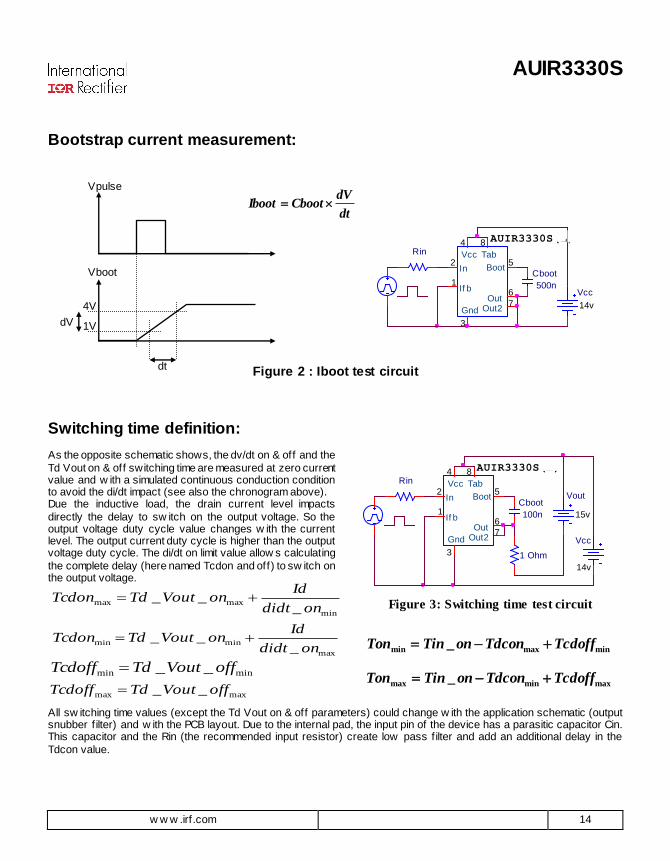
Bootstrap current measurement:
Switching time definition: As the opposite schematic shows, the dv/dt on & off and the
Td Vout on & off switching time are measured at zero current value and w ith a simulated continuous conduction condition to avoid the di/dt impact (see also the chronogram above). Due the inductive load, the drain current level impacts
directly the delay to sw itch on the output voltage. So the output voltage duty cycle value changes w ith the current level. The output current duty cycle is higher than the output voltage duty cycle. The di/dt on limit value allow s calculating
the complete delay (here named Tcdon and off) to sw itch on the output voltage.
All sw itching time values (except the Td Vout on & off parameters) could change w ith the application schematic (output snubber f ilter) and w ith the PCB layout. Due to the internal pad, the input pin of the device has a parasitic capacitor Cin. This capacitor and the Rin (the recommended input resistor) create low pass f ilter and add an additional delay in the
Tdcon value.
max
minmin_
__ondidt
IdonVoutTdTcdon
min
maxmax_
__ondidt
IdonVoutTdTcdon
minmin __ offVoutTdTcdoff
maxmax __ offVoutTdTcdoff
minmaxmin _ TcdoffTdcononTinTon
maxminmax _ TcdoffTdcononTinTon
Vpulse
Vboot
4V
1V dV
dt
dt
dVCbootIboot
Figure 2 : Iboot test circuit
If b1
In2
Gnd
3
Vcc
4
Boot5
Out6
Out27
Tab
8Rin
Vcc
14v
Cboot
500n
AUIR3330S(L)
Figure 3: Switching time test circuit
If b1
In2
Gnd
3
Vcc
4
Boot5
Out6
Out27
Tab
8Rin
Vcc
14v
Cboot
100n
AUIR3330S(L)
Vout
15v
1 Ohm

AUIR3330S
w w w .irf.com 15
The minimum off time is the time to charge the bootstrap capacitor (recover the value before turn on the MOSFET) during
the high duty cycle operation. In the high duty cycle value condition, due to the di/dt driver, the internal gate continues to move w hereas the output voltage doesn’t go dow n under 6v (from vbat). So the device still need energy from the bootstrap capacitor but it can not charge it. When the bootstrap capacitor is discharged the circuit goes in linear mode and it is stopped by the over pow er protection. To avoid this situation, the micro-processor must turn fully on the device after
the minimum off time is reached as it is describe in the Figure 5: High duty cycle operation recommendation. The minimum off time is the minimum time to charge properly the bootstrap capacitor.
Pwm input
5v
Input duty cycle increase
Min off time
Period
The minimum off time to recharge properly the bootstrap
capacitor is reached so the
device must be turned fully on.
Figure 5: High duty cycle operation recommendation
Figure 4 : Switching time chronogram
Vin
Vout
10%
Td Vout on on
90%
Tr Td Vout off Tf
Dt off Dt on
Dv off Dv on 20%
Drain current
t
t
t
80%
20%
Di on
Dt on
80%
20%
Di off
Dt on
Tin_on
Ton
80%
AUIR3330S
w w w .irf.com 16
Notes:
Decoupling capacitors: During the turn on and off phase, a high current (about a hundred mA) f low s through the Vcc, the gnd and the boot. So the bootstrap capacitor and the decoupling
must be as closer as possible. And it is forbidden to implement a resistor in series w ith the Gnd pin.
Bootstrap capacitor charge: The pow er on reset is necessary to charge the
bootstrap capacitor before turns on the pow er mosfet. The bootstrap capacitor gets its charge through the load. So the time to charge it depends of the load.
But the pow er on reset doesn’t monitor the bootstrap capacitor voltage. Its time is set internally to allow starting the most of load w ithout implement a special sequence:
If the inductance of the load is low er than 500µH, the pow er on reset is
enough long to charge the bootstrap capacitor before turns on the pow er
mosfet.
D1 MBR 3045CT
Boot Vcc
+Bat
- Mot
Gnd
+ Mot
Vbat C2 100nF
Rev erse battery
protection
Mot L
6V 6V Out
In
Ifb
Gnd
D1 MBR 3045CT
Vcc
+Bat
- Mot
Gnd
+ Mot
Vbat C2 100nF
Rev erse battery
protection
Mot L
6V 6V 6V 6V Out
In
Ifb
Gnd
Vcboot
charged
Vin
Vg
Power on reset
time
Time to charge the
bootstrap capacitor
Vcboot
charged
Vin
Vg
Power on reset
time
Time to charge the
bootstrap capacitor
Vboot
D1
MBR
3045CT
Ifbk
CBoot
IN/Diag
Vcc
Gnd
+Bat
IR3330
IN
Gnd
10k
+C3
+C4
10k
D3
12V
- Mot
GND
+ Mot
Vbat
C2
100nF
T1
IRF1404
Output
Current shutdown
programming
resistor
Diag
Ifbk50k
Micro-
processor
I/O
I/O
A/D
Gnd
50k
+
Cd1 Cd2 onicI _
officI _
Decoupling
capacitor
Cboot
D1
MBR
3045CT
Ifbk
CBoot
IN/Diag
Vcc
Gnd
+Bat
IR3330
IN
Gnd
10k
+C3
+C4
10k
D3
12V
- Mot
GND
+ Mot
Vbat
C2
100nF
T1
IRF1404
Output
Current shutdown
programming
resistor
Diag
Ifbk50k
Micro-
processor
I/O
I/O
A/D
Gnd
50k
+
Cd1 Cd2 onicI _
officI _
Decoupling
capacitor
Cboot
Ifb
Boot
IR3330S
AUIR3330S
w w w .irf.com 17
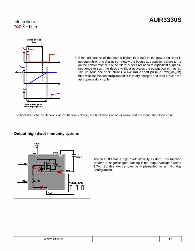
If the inductance of the load is higher than 500µH, the pow er on reset is
not enough long to charge completely the bootstrap capacitor before turns on the pow er mosfet. So the micro-processor need to implement a special sequence to start the device w ithout activates the output pow er mosfet. The µp send one short pulse (Tw ake min < short pulse < Tpw r_on_rst)
then w ait for the bootstrap capacitor is totally charged and after provide the appropriate duty cycle.
The bootstrap charge depends of the battery voltage, the bootstrap capacitor value and the inductance load value.
Output high dv/dt immunity system:
The IR3330S has a high dv/dt immunity system. This function
creates a negative gate biasing if the output voltage exceed 1.7V. So this device can be implemented in an H-bridge configuration.
charged
V boot
V in
V g
Power on reset time
Time to charge the bootstrap capacitor
charged
V
V in
V g
Power on reset time
Time to charge the bootstrap capacitor
Twakemin
Ifb
CBootVcc
+Bat
Out
In
Ifbk
Gnd
43V
Vs high dv/dtOff
0.6V
C2
100nF
CBootVcc
+Bat
Out
In
Ifbk
Gnd
43V
Vs high dv/dtOff
0.6V
C2
100nF
Boot

AUIR3330S
w w w .irf.com 18
Open load detection function: The bootstrap regulator bias provides a current on device output. If the impedance betw een the Output and ground is too high, after the turn off of the output mosfet,
the output never reaches the ground. So it becomes possible to detect easily an open load condition w hen the device sw itches. In fully on condition the open load
condition w ill detect by the current feedback (easy thanks to a high current condition). In the schematic below the component R7, Q1, R8, D2
create the detection open load and provide a logic level diagnostic (open diag line) even if the battery in low voltage condition.
D1
MBR
3045CT
CBootVcc
+Bat
- Mot
Gnd
+ Mot
Vbat
C2
100nF
Reverse
battery
protection
6V6V6V6V
Out
In
Ifbk
Gnd
8mA
Ifb
Boot
Open load
detector
If b1
In2
Gnd
3
Vcc
4
Boot5
Out6
Out27
Tab
8
Vcc
14v
Cboot
500n
AUIR3330S(L)
D1
MBR3045CT
1 3
2 4
-
+
12
10k
3.3k
Q15v 1
Open Diag line
Input signal
Open diag
line 5v/Div Output voltage
5V/Div
Load current 1A/div
Vbat = 6V; Duty cycle =10% Load = 0.95 + 150µH
Open load
condition
AUIR3330S
w w w .irf.com 19
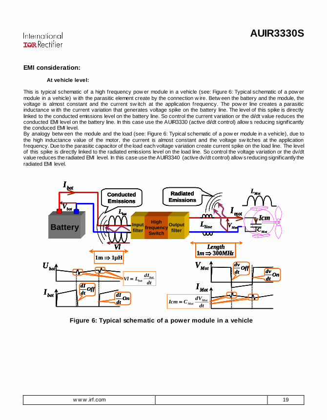
EMI consideration: At vehicle level: This is typical schematic of a high frequency pow er module in a vehicle (see: Figure 6: Typical schematic of a pow er
module in a vehicle) w ith the parasitic element create by the connection w ire. Betw een the battery and the module, the voltage is almost constant and the current sw itch at the application frequency. The pow er line creates a parasitic inductance w ith the current variation that generates voltage spike on the battery line. The level of this spike is directly
linked to the conducted emissions level on the battery line. So control the current variation or the di/dt value reduces the conducted EMI level on the battery line. In this case use the AUIR3330 (active di/dt control) allow s reducing signif icantly the conduced EMI level. By analogy betw een the module and the load (see: Figure 6: Typical schematic of a pow er module in a vehicle), due to
the high inductance value of the motor, the current is almost constant and the voltage sw itches at the application frequency. Due to the parasitic capacitor of the load each voltage variation create current spike on the load line. The level of this spike is directly linked to the radiated emissions level on the load line. So control the voltage variation or the dv/dt value reduces the radiated EMI level. In this case use the AUIR3340 (active dv/dt control) allow s reducing signif icantly the
radiated EMI level.
Battery Input
filter
High
frequency
Switch
Output
filterBattery Input
filter
High
frequency
Switch
Output
filterBattery Input
filter
High
frequency
Switch
Output
filterBatteryBattery Input
filter
High
frequency
Switch
Output
filter
Radiated
EmissionsConducted
Emissions
batIMotL
Vl
batL
lineLIcm
MotV
batV
MotC
motI
Radiated
EmissionsConducted
Emissions
batIMotL
Vl
batL
lineLIcm
MotV
batV
MotC
motI
Radiated
Emissions
Radiated
EmissionsConducted
Emissions
Conducted
Emissions
batIbatIMotLMotL
Vl
batL
Vl
batL
lineLlineLIcm
MotV
batV
MotC
motImotI
batU
batIOff
dt
dI
Ondt
dI
dt
dILVl bat
bat
1m 1µH
batU
batIOff
dt
dI
Ondt
dI
dt
dILVl bat
bat
batU
batIOff
dt
dIOff
dt
dI
Ondt
dIOn
dt
dI
dt
dILVl bat
bat
1m 1µH
MotI
MotV Offdt
dv
Ondt
dv
dt
dVCIcm Mot
Mot
MHzmLength
3001
MotI
MotV Offdt
dv
Ondt
dv
dt
dVCIcm Mot
Mot
MotIMotI
MotV Offdt
dvOff
dt
dv
Ondt
dvOn
dt
dv
dt
dVCIcm Mot
Mot
MHzmLength
3001 MHzmLength
3001
Figure 6: Typical schematic of a power module in a vehicle

AUIR3330S
w w w .irf.com 20
At module level: This typical schematic takes into account the parasitic elements created by the PCB tracks. Its impedance
is jLRZtrace .
F 2
Due to the jL element, the current variation in each
line must be smooth to avoid the over voltage spikes.
Dt
DiLU l
The impedance value of the parasitic element Z3 and Z6
are negligible compare to the motor impedance. So they don’t have an important influence on the EMI perturbation level.
The parasitic component evaluation for DC and low frequency conditions are:
S
lR
)(22.05.0)
2ln(102.0 6
l
ed
ed
llL
Where:
: material resistivity Cu = 1.7x10⁻⁸m
l : track length in m
S : track section in m² (d x e)
d : track w idth in m
e : track thickness in m
e
Figure 7: typical schematic of a power
module

AUIR3330S
w w w .irf.com 21
Example:
If the copper track characteristic betw een the MOSFET pin and the free w heeling diode (parasitic element Z2) is:
l = 2 cm
d = 1mm
e = 35µm
So
R = 0.9m L = 8nH
If the MOSFET sw itches w ithout any slope control, the di/dt can reach 100A/µs. The overvoltage spike created by the current variation in the parasitic inductance is then
Ul = 8n * (100/1E-6) = 800mv
Now , if the MOSFET slope is controlled and limited to 40A/µs. Then, the overvoltage spike created by the current variation in the parasitic inductance is:
Ul = 8n * (40/1E-6) = 320mV
Even if the PCB tracks are short, their parasitic impedances are not negligible in 20 kHz application. Limiting the current variation in these parasitic impedances reduces the overvoltage spikes so the noise level. For further information about the PCB impedance effect see the application note named “Using the AUIR3330/40: PCB layout recommendation” on the
IR w eb site (w w w .irf.com).
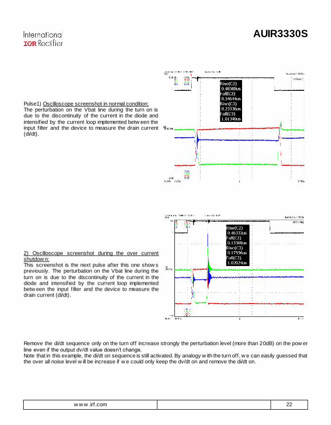
Measured impact of the di/dt control: If the device detects an over current condition, it turns off the output MOSFET w ithout di/dt sequence to reduce application stress. So a simple test, consists to look at the w aveform before (pulse1) and during the over current protection shutdow n (pulse 2) to see the di/dt impact w ith the same condition (even if the dv/dt stay constant).
Black (Ch1) = In_pw m 5V/div
Red (Ch2) = drain current 10A/div
Green (Ch3) = Vds (drain source
voltage) 5V/div
Blue (Ch4) = Vbat (battery voltage)
in AC mode 1V/div
Pulse1 Pulse2
AUIR3330S
w w w .irf.com 22
Pulse1) Oscilloscope screenshot in normal condition: The perturbation on the Vbat line during the turn on is due to the discontinuity of the current in the diode and
intensif ied by the current loop implemented betw een the input f ilter and the device to measure the drain current (di/dt).
2) Oscilloscope screenshot during the over current shutdow n: This screenshot is the next pulse after this one show s previously. The perturbation on the Vbat line during the
turn on is due to the discontinuity of the current in the diode and intensif ied by the current loop implemented betw een the input f ilter and the device to measure the drain current (di/dt).
Remove the di/dt sequence only on the turn off increase strongly the perturbation level (more than 20dB) on the pow er
line even if the output dv/dt value doesn’t change. Note that in this example, the di/dt on sequence is still activated. By analogy w ith the turn off, w e can easily guessed that the over all noise level w ill be increase if w e could only keep the dv/dt on and remove the di/dt on.
AUIR3330S
w w w .irf.com 23
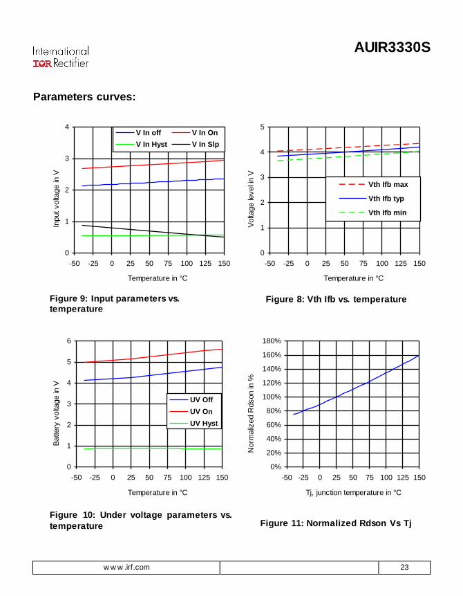
0
1
2
3
4
5
6
-50 -25 0 25 50 75 100 125 150
UV Off
UV On
UV Hyst
0
1
2
3
4
5
-50 -25 0 25 50 75 100 125 150
Vth Ifb max
Vth Ifb typ
Vth Ifb min
0%
20%
40%
60%
80%
100%
120%
140%
160%
180%
-50 -25 0 25 50 75 100 125 150
Tj, junction temperature in °C
Norm
aliz
ed R
dson in
%
Figure 11: Normalized Rdson Vs Tj
Temperature in °C
Figure 9: Input parameters vs. temperature
Temperature in °C
Battery
volta
ge in
V
Temperature in °C
Volta
ge le
vel i
n V
Figure 10: Under voltage parameters vs.
temperature
Figure 8: Vth Ifb vs. temperature
0
1
2
3
4
-50 -25 0 25 50 75 100 125 150
V In off V In On
V In Hyst V In Slp
Input volta
ge in
V
Parameters curves:
AUIR3330S
w w w .irf.com 24
0
0.2
0.4
0.6
0.8
1
1.2
1.4
1.6
-50 -25 0 25 50 75 100 125 150
Tr IoutTr VoutTf IoutTf Vout
Temperature in °C
0
5
10
15
20
25
30
35
40
-50 -25 0 25 50 75 100 125 150
Tpwr_on_rst
Tslp
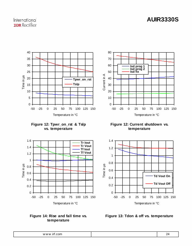
Figure 12: Tpwr_on_rst & Tslp vs. temperature
Tim
e in
µs
Temperature in °C
Tim
e in
µs
Figure 14: Rise and fall time vs. temperature
0
0.2
0.4
0.6
0.8
1
1.2
1.4
-50 -25 0 25 50 75 100 125 150
Td Vout On
Td Vout Off
Figure 13: Tdon & off vs. temperature
Temperature in °C
Tim
e in
µs
0
10
20
30
40
50
60
70
80
-50 -25 0 25 50 75 100 125 150
Isd prog 1Isd prog 2Isd fix
Temperature in °C
Figure 12: Current shutdown vs. temperature
Curr
ent in
A
AUIR3330S
w w w .irf.com 25
0
5
10
15
20
25
30
35
40
45
-50 -25 0 25 50 75 100 125 150
DiDtOn
DiDtOff
0
1
2
3
4
5
6
-50 -25 0 25 50 75 100 125 150
Vboot
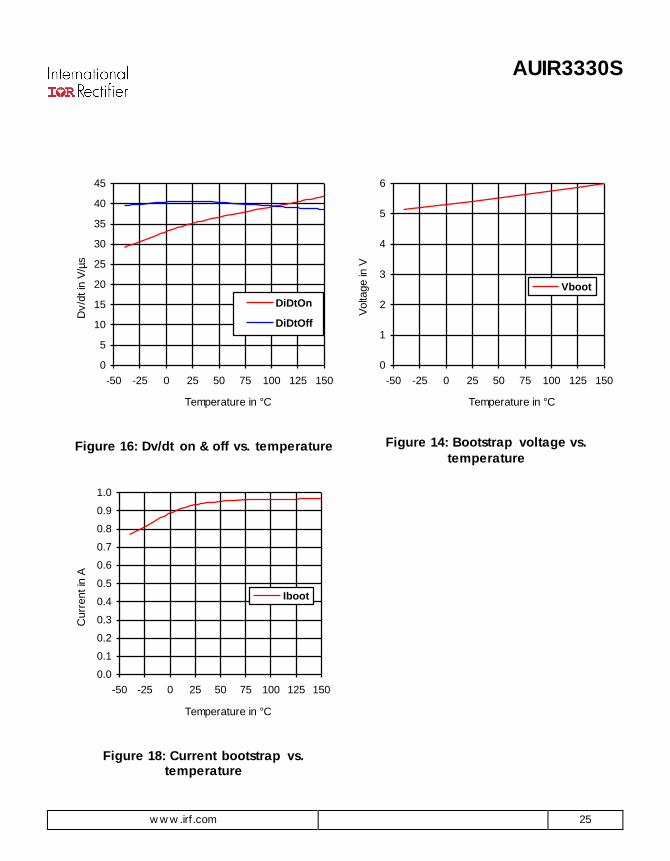
Figure 16: Dv/dt on & off vs. temperature Figure 14: Bootstrap voltage vs.
temperature
0.0
0.1
0.2
0.3
0.4
0.5
0.6
0.7
0.8
0.9
1.0
-50 -25 0 25 50 75 100 125 150
Iboot
Figure 18: Current bootstrap vs. temperature
Temperature in °C
Dv/d
t in
V/µ
s
Temperature in °C
Volta
ge in
V
Temperature in °C
Curr
ent in
A

AUIR3330S
w w w .irf.com 26
Figure 15: Transient thermal impedance and model vs. time

AUIR3330S
w w w .irf.com 27
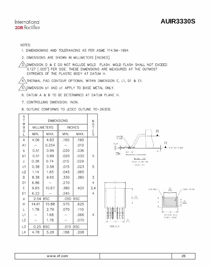
Case Outline 7L D2PAK
AUIR3330S
w w w .irf.com 28
AUIR3330S
w w w .irf.com 29
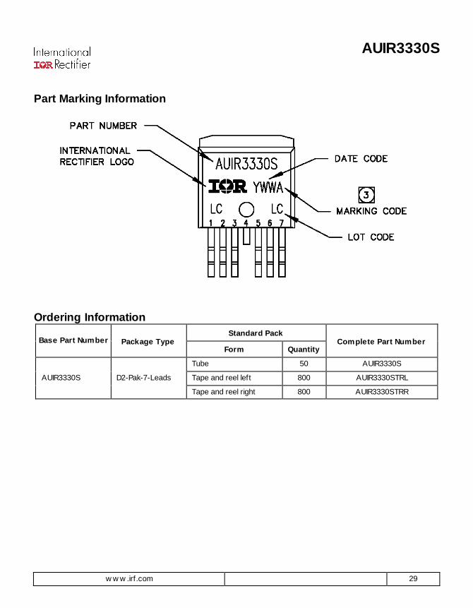
Part Marking Information
Ordering Information
Base Part Number Package Type Standard Pack
Complete Part Number Form Quantity
AUIR3330S D2-Pak-7-Leads
Tube 50 AUIR3330S
Tape and reel left 800 AUIR3330STRL
Tape and reel right 800 AUIR3330STRR
AUIR3330S
w w w .irf.com 30
IMPORTANT NOTICE
Unless specif ically designated for the automotive market, International Rectif ier Corporation and its subsidiaries (IR) reserve the right to make corrections, modif ications, enhancements, improvements, and other changes to its products and services at any time and to discontinue any product or services w ithout notice. Part numbers designated w ith the “AU”
prefix follow automotive industry and / or customer specif ic requirements w ith regards to product discontinuance and process change notif ication. All products are sold subject to IR’s terms and conditions of sale supplied at the time of order acknow ledgment.
IR w arrants performance of its hardw are products to the specif ications applicable at the time of sale in accordance w ith IR’s standard w arranty. Testing and other quality control techniques are used to the extent IR deems necessary to support this w arranty. Except where mandated by government requirements, testing of all parameters of each product is
not necessarily performed. IR assumes no liability for applications assistance or customer product design. Customers are responsible for their products and applications using IR components. To minimize the risks w ith customer products and applications,
customers should provide adequate design and operating safeguards. Reproduction of IR information in IR data books or data sheets is permissible only if reproduction is w ithout alteration and is accompanied by all associated w arranties, conditions, limitations, and notices. Reproduction of this information w ith
alterations is an unfair and deceptive business practice. IR is not responsible or liable for such altered documentation. Information of third parties may be subject to additional restrictions. Resale of IR products or serviced with statements different from or beyond the parameters stated by IR for that product or
service voids all express and any implied w arranties for the associated IR product or service and is an unfair and deceptive business practice. IR is not responsible or liable for any such statements.
IR products are not designed, intended, or authorized for use as components in systems intended for surgical implant into the body, or in other applications intended to support or sustain life, or in any other application in w hich the failure of the IR product could create a situation w here personal injury or death may occur. Should Buyer purchase or use IR products for any such unintended or unauthorized application, Buyer shall indemnify and hold International Rectif ier and its off icers,
employees, subsidiaries, aff iliates, and distributors harmless against all claims, costs, damages, and expenses, and reasonable attorney fees arising out of, directly or indirectly, any claim of personal injury or death associated w ith such unintended or unauthorized use, even if such claim alleges that IR w as negligent regarding the design or manufacture of the product.
Only products certif ied as military grade by the Defense Logistics Agency (DLA) of the US Department of Defense, are designed and manufactured to meet DLA military specif ications required by certain military, aerospace or other applications. Buyers acknow ledge and agree that any use of IR products not certif ied by DLA as military-grade, in
applications requiring military grade products, is solely at the Buyer’s ow n risk and that they are solely responsible for compliance w ith all legal and regulatory requirements in connection w ith such use. IR products are neither designed nor intended for use in automotive applications or environments unless the specif ic IR
products are designated by IR as compliant w ith ISO/TS 16949 requirements and bear a part number including the designation “AU”. Buyers acknow ledge and agree that, if they use any non-designated products in automotive applications, IR w ill not be responsible for any failure to meet such requirements.
For technical support, please contact IR’s Technical Assistance Center
http://w w w .irf.com/technical-info/
WORLD HEADQUARTERS: 101 N. Sepulveda Blvd., El Segundo, California 90245
Tel: (310) 252-7105
AUIR3330S
w w w .irf.com 31
Revision History
Revision Date Notes/Changes A 29/01/10 First release
B 28-Jul-11 Update the MSL qualification level p2
C 15-Feb-12 Correct the ratio formula page 6

Mouser Electronics
Authorized Distributor
Click to View Pricing, Inventory, Delivery & Lifecycle Information: International Rectifier:
AUIR3330S