
Power and sensing - Mouser Electronics
390
Power and sensing Selection guide 2020 IoT-Security Charger www.infineon.com/powerandsensing-selectionguide
-
Upload
khangminh22 -
Category
Documents
-
view
1 -
download
0
Transcript of Power and sensing - Mouser Electronics

Power and sensingSelection guide 2020
IoT-Security
Charger
www.infineon.com/powerandsensing-selectionguide


Dear reader,
The era of convergence is here. The trends of the past – such as energy efficiency and security – are now global challenges: how do we sustainably feed our needs in mobility, IoT and big data? Together, these questions transform life as we know it, intertwining technology with humanity.
From the cloud and the edge, personal vehicles and power tools, to drones and satellites, thousands of systems we use every day rely on efficient and intelligent power. Our next generation of silicon solutions and our wide-bandgap portfolio, including CoolSiC™ and CoolGaN™ devices, provide unparalleled performance and reliability for 5G, big data and renewable energy applications. The cooler, smaller and lighter MERUS™ audio amplifiers enable customers to achieve better-sounding systems and deliver exceptional audio performance in smart speakers and other audio home, portable and professional audio products.
Collectively, we are building towards a new age of interaction with multiple devices. These need to perceive and respond to events while steadily extending and enhancing their performance to further ease our lives. We meet this challenge with intuitive sensing - by giving things human-like senses for a greater contextual awareness. Founded on Infineon’s 40 years of experience in the development of sensor products, our XENSIV™ products deliver exceptional accuracy and best-in-class measurement performance. Spanning magnetic, pressure, acoustic, 3D image (REAL3™) and radar sensor MMICs (RASIC™ for automotive), our broad XENSIV™ portfolio ensures the perfect fit for all performance and integration needs – regardless of the industry.
Building on the company’s in-depth system understanding, the 2020 edition of the Power and Sensing Selection Guide offers a comprehensive selection of power and sensors system solutions for your future success.
尊敬的读者:
“大融合”时代已然到来。以往的一些发展趋势(诸如能源效率和安全性等)现已成为全球性挑战:我们如何才能秉承可持续性发展理念来满足我们在移动交通、物联网和大数据方面的需求?这些问题的演进为我们的生活带来了巨大变革,将科技与人类生活交织在一起。
从云端和先进的私家车和动力工具,到无人机和卫星,我们每天使用的无数系统都离不开高效、智能的电源。我们下一代硅解决方案和我们宽带隙产品组合(包括 CoolSiC™ 和 CoolGaN™ 设备)为 5G、大数据和可再生能源应用提供了无与伦比的性能和可靠性。利用更酷、更小和更轻的 MERUS™ 音频放大器,客户可以实现音质更佳的系统,在智能扬声器和其他音频家电、便携和专业音频产品中提供卓越的音频性能。
总而言之,我们正在迈向一个与多个设备交互的新时代。这些设备需要感知和响应事件,同时稳定地扩展和增强其性能,让我们的生活变得更加轻松惬意。我们赋予事物类似于人类的感知、通过直观感知来应对此项挑战,从而获得更佳的情境意识。 依托英飞凌在传感器产品开发领域长达 40 年的经验,我们的 XENSIV™ 产品提供卓越的精确性和一流的测量性能。我们丰富的 XENSIV™ 产品组合涵盖磁性、压力、声学、三维图像 (REAL3™) 和雷达传感器 MMIC(用于汽车行业的 RASIC™)。无论何种行业,这些产品均可确保完美满足所有性能和集成需求。
《2020 电源与传感选型指南》以公司对系统的深厚了解为基础,提供综合全面的电源和传感器系统解决方案,助力您走向成功的未来。
Andreas Urschitz, Division President of Power and Sensor Systems
电源和传感系统事业部总裁
Connectivity and linking the real to the digital world is no longer a dream – it is a lived reality. Future is something we create together to make life easier, safer, and greener.
连接真实世界和数字世界不再是一个梦想, 而是活生生的现实。未来由我们共同创造, 让生活更轻松、更安全、更环保。Andreas Urschitz, Division President of Power and Sensor Systems
电源和传感系统事业部总裁

4
Applications 6
Advanced system solutions for consumer applications 6
Class D audio amplifiers 8
Major home appliances 10
Smart speaker 14
Robotics 18
SMPS - TV power supply 21
SMPS - mobile charger 24
Wireless charging 25
Wearables and healthtech 30
SMPS and digital power management solutions for data processing applications 32
DC-DC enterprise power solution for data processing applications 34
SMPS - laptop adapters 37
SMPS - PC power supply 39
SMPS - server power supply 40
SMPS - telecom power supply 42
Advanced system solutions for industrial applications 46
Smart building 48
Power over Ethernet 50
LED lighting 52
Power and gardening tools 54
Battery formation 56
Energy storage systems 58
Solar 60
Uninterruptible power supply 64
SMPS - embedded power supply 69
SMPS - industrial SMPS 70
Advanced system solutions for transportation and infrastructure 72
Fast EV charging 74
E-mobility 78
Light electric vehicles and forklift 82
Multicopter 84
Contents
20-300 V MOSFETs 86
500-950 V MOSFETs 122
Wide bandgap semiconductors 152
Discrete IGBTs 178
Power management ICs 200
Intelligent power switches and modules 276
Gate driver ICs 286
Microcontrollers 318
XENSIV™ sensors 344
Packages 382

5
For more details on the product, click on the part number.
We make life easier, safer and greener – with technology that achieves more, consumes less and is accessible to everyone.
From product thinking to system understanding Infineon enables eff icient generation, transmission and conversion of electrical energy
www.infineon.com/power
Appl
icat
ions
Pack
ages
20-3
00 V
MO
SFET
s50
0-95
0 V
MO
SFET
sW
BG se
mic
ondu
ctor
sDi
scre
te IG
BTs
Pow
er IC
sIn
telli
gent
switc
hes
and
inpu
t ICs
Gate
driv
er IC
sM
icro
cont
rolle
rsXE
NSIV
™ se
nsor
s

6
For more details on the product, click on the part number.
› Class D audio amplifiers › Major home appliances - air conditioning and induction cooking › Smart speaker › Service robots › SMPS – TV power supply › SMPS – mobile charger › Wireless charging › Wearables and healthtech
Advanced system solutions for consumer applications
Applications

7
For more details on the product, click on the part number.
Appl
icat
ions
Pack
ages
20-3
00 V
MO
SFET
s50
0-95
0 V
MO
SFET
sW
BG se
mic
ondu
ctor
sDi
scre
te IG
BTs
Pow
er IC
sIn
telli
gent
switc
hes
and
inpu
t ICs
Gate
driv
er IC
sM
icro
cont
rolle
rsXE
NSIV
™ se
nsor
s

8
For more details on the product, click on the part number.
Class D audio amplifiersNo compromise on quality – products for exceptional audio performance
Class D audio
www.infineon.com/merus www.infineon.com/audio
At Infineon, we manufacture power-efficient class D audio amplifier solutions that maintain best-in-class audio quality, without heating up the surroundings. We believe smaller and lighter is better, and that the amplifier embedded in your product should be heard, but not seen. Our amplifier solutions help you design robust, flexible products that meet the needs of your customers and the market. Choose from our high-performance class D audio amplifier solutions for all power ranges and application requirements, from the smallest fully integrated single-chip solutions to highly scalable driver and power MOSFET combinations (for full portfolio of audio amplifier ICs, see pages 236-240).
Home audio Modern home audio products vary in shapes, sizes and configurations, but common requirement is great sound in combination with outstanding industrial and acoustic design. In addition to producing exceptional sound quality, MERUS™ amplifiers from Infineon can completely eliminate the need for bulky and expensive LC output filters and heatsinks. This allows design of new innovative and great sounding home audio products in form factors and shapes that were previously unthinkable.
Solution example: 2.1 configuration (2xBTL + 1xPBTL) 4.1 configuration (4xBTL + 1xPBTL)
Design with Infineon’s solutions to benefit from:
Exceptional audio performance
Maximized power efficiency
Maximized output power
Design freedom
Fast time to market
Battery powered speakers: › On-the-go Bluetooth speakers › Docking speakers › Boom boxes › Wearable speakers
› Multiroom systems › Audio hub › TVs › Sound bars › Home theater systems › Smart speakers
› Power-over-ethernet (PoE) audio systems
› Touring amplifiers › Active speakers › Public announcement 70-100 V systems › Music instrument amplifiers
Portable/battery powered audio applications
Home audio applications
Professional audio applications
Solution specificationNumber of audio channels: 2 bridge-tied load (BTL) and 1 parallel BTL channelsPeak power output: 2x80 W @ 4 Ω, 10% THD and 160 W @ 2 Ω, 10% THDFeatured audio ICs: 2x MA12070
Solution specificationNumber of audio channels: 4 bridge-tied load (BTL) and 1 parallel BTL channelsPeak power output: 2x80 W @ 4 Ω, 10% THD and 160 W @ 2 Ω, 10% THDFeatured audio ICs:MA12040, MA12070 and IR4302M
MA12070 MERUS™
integrated audio
amplifier IC
MA12070 MERUS™
integrated audio
amplifier IC
Wireless connectione.g., WiFi
Power supply unit
MA12040 MERUS™integrated audio
amplifier IC
MA12070 MERUS™integrated audio
amplifier IC
IR4302M MERUS™ integrated
audio amplifier IC
Wireless connectione.g. WiFI
Power supply unit

9
For more details on the product, click on the part number.
Portable audioWhen designing portable/battery powered audio devices, it is essential to maximize battery playback time, and at the same time, maintain an excellent audio performance. Infineon’s MERUS™ amplifiers provide up to twice as long battery playback time in combination with the best-in-class audio performance and unsurpassed sound quality.
Solution example: 2.1 configuration (2xSE + 1xBTL) Solution example: 2.1 configuration (2xBTL + 1xPBTL)
Professional audioProfessional audio equipment is all about maximizing output power and power density. With the conception of Infineon’s MERUS™ multilevel class D technology and GaN-based CoolGaN™ e-mode HEMTs, it is now possible to conceive both amplifiers and power supply units with great audio performance and high efficiency in a very compact design. For engineers developing amplifiers, Infineon offers both monolithic and chip-set solutions with versatile MOSFET combinations for the scaling of output power.
Solution specificationNumber of audio channels: 2 single-ended (SE) and 1 bridge-tied load (BTL) channelsPeak power output: 2x10 W and 40 W @ 4 Ω, 10% THDFeatured audio IC: MA12040P including volume control and limiter
Solution specificationNumber of audio channels: 2 bridge-tied load (BTL) and 1 parallel BTL channelsPeak power output: 2x40 W @ 4 Ω, 10% THD and 160 W @ 2 Ω, 10% THDFeatured audio ICs: MA12040P and MA12070P including volume control and limiter
Bluetooth
Battery power unit
MA12040P MERUS™ integrated audio
amplifier IC
MA12040P MERUS™
integrated audio
amplifier IC
MA12070P MERUS™
integrated audio
amplifier IC
Bluetooth
Battery power unit
Solution example: active speakers
Solution example: public announcement 70-100 V system
Solution specificationNumber of audio channels: 2 half-bridge channelsPeak power output: 500 W @ 4 Ω, 1% THDFeatured audio ICs: IRS2092S, IRS20957S
Solution specificationNumber of channels: 2 half bridge channelsPeak power output: 500 W, 70 Vrms/100 Vrms, 1% THDFeatured audio IC: IRS2452AM
For full product portfolio, see 234-238.
IRS2092S/IRS20957S
and MOSFETin parallel
MixerLevel
adjustment
IRS2452AMand
MOSFET
HPF&
ATT
Analoginput
70 V/100 VStep-down
transformer
Speaker (4/8 Ω)
www.infineon.com/audiosolutions
Class D audio
Appl
icat
ions
Pack
ages
20-3
00 V
MO
SFET
s50
0-95
0 V
MO
SFET
sW
BG se
mic
ondu
ctor
sDi
scre
te IG
BTs
Pow
er IC
sIn
telli
gent
switc
hes
and
inpu
t ICs
Gate
driv
er IC
sM
icro
cont
rolle
rsXE
NSIV
™ se
nsor
s

10
For more details on the product, click on the part number.
Major home appliances
Product designers are facing the daunting challenge of developing smaller, smarter, more powerful, and more energy-efficient appliances. Based on industry-leading technology and manufacturing expertise, Infineon’s line of innovative components for household appliances meets and exceeds even the most rigorous requirements for reliability and quality. The block diagram of an air conditioning system shown below, together with the product selection table, provides an effective recommendation for engineers to select the right component for each power management stage inside major home appliances.
In addition to efficiency gain through power solutions, Infineon’s XENSIV™ sensor portfolio also enhances the operation of major home appliances through advanced sensor-enabled use cases such as condition monitoring and predictive maintenance to detect potential device failures before they occur. Furthermore, integration of voice control or presence detection in those appliances increases user convenience and results in even more efficient devices.
Major home appliancesInnovative approach for air conditioning
Rect
ifica
tion
Power management
DCsupply
User interface&
communication
Central control unit
Gate driver ICs
MCU
AF discretes Sense and monitor Rotor position detection
Driver stage
M
IGBT
Plug
www.infineon.com/homeappliance
Product category Product family BenefitsSensors XENSIV™ MEMS microphones IM69D130 High performance microphone with low self-noise (high SNR) and low distortions enables noise
monitoring for advanced predictive maintenance analytics
XENSIV™ digital barometric pressure sensors DPSxxx Advanced predictive maintenance analytics are enabled based on highest precision and relative accuracy over a wide temperature range to detect anomalies in air flow
XENSIV™ TLV493D-A1B6 3D magnetic sensor Accurate three-dimensional sensing with extremely low power consumption in a small 6-pin package to enable vibration and position monitoring of the compressor
XENSIV™ TLI4970 current sensor Fully digital solution featuring high precision and ease of use, significantly reduces overall imple-mentation efforts as well as PCB space to enable cost fan and compressor current measurement
Radar sensor XENSIV™ 60 GHz radar sensor Accurate presence detection and vibration detection based on ability to track sub-millimeter motion at high speed and accuracy, in both stand-alone chip as well as system solution available

11
For more details on the product, click on the part number.
Recommended products
Functional block Topology Voltage class Technology/product family Selection/benefitPFC AC-DC IGBT – PFC CCM (high frequency – SC) 600 V HighSpeed 3 Recommendation
IGBT – PFC CCM (low frequency – SC) 600 V TRENCHSTOP™ Performance Recommendation
IGBT – PFC CCM (cost competitive – no SC) 650 V TRENCHSTOP™ 5 – H5 Recommendation
IGBT – PFC CCM (low losses - SC) 650 V TRENCHSTOP™ IGBT6 Recommendation
IGBT – PFC 600 V TRENCHSTOP™ Advanced Isolation Recommendation
IGBT – PFC (cost competitive - no SC) 650 V TRENCHSTOP™ 5 WR5 Recommendation
MOSFET – PFC CCM 600 V CoolMOS™ P7 Reference
Diode – PFC CCM 650 V Rapid 1 and Rapid 2 diodes Recommendation
Controller – PFC CCM – ICE2PCS0xG, ICE3PCS0xG Recommendation
IPM – PFC CCM 650 V CIPOS™ Mini PFC interleaved IPM series, CIPOS™ PFC integrated IPM series
Recommendation
Low-side gate driver IC – PFC 25 V Single low-side driver EiceDRIVER™ 1ED44176N01F, 1ED44175N01B, 1ED44173N01B *
OCP, fault and enable function in DSO-8/SOT23-6
Dual low-side driver IRS4427S Rugged and reliable in DSO-8
Single low-side driver IRS44273L Rugged and reliable in SOT23-5
Half-bridge gate driver – totem pole PFC 650 V EiceDRIVER™ 2ED2304S06F, 2ED2106S06F, 2ED2182S06F
SOI with integrated bootstrap diode
DC-AC IGBT – B6-VSI 650 V TRENCHSTOP™ IGBT6 Efficiency
IGBT – B6-VSI 600 V RC-Drives Fast, RC-D2 * Recommendation
MOSFET - B6-VSI 600 V CoolMOS™ PFD7 Cost/performance
IPM – B6-VSI 600 V CIPOS™ Mini Recommendation
Half-bridge gate driver ICs 650 V EiceDRIVER™ 2ED2304S06F, 2ED2106S06F, 2ED2182S06F
SOI with integrated bootstrap diode
Half-bridge gate driver ICs 600 V EiceDRIVER™ 2EDL05I06PF, 2EDL23I06PJ, IRS2890DS, 2ED28073J06F *
Integrated bootstrap diode/FET
Three-phase gate driver ICs 600 V 6EDL04I06PT, IR2136S, 6ED003L06-F2 OCP, fault and enable function
AUX Flyback fixed frequency 700 V CoolSET™ F5 * Recommendation
Microcontroller/motor control IC 32-bit Arm® Cortex®-M4 - XMC4100/XMC4200 Recommendation
iMOTION™ - IRMCxx motor control IC (incl. motion control algorithm)
Recommendation
Microcontroller supply Linear voltage regulator Up to 20 V IFX1763, IFX54441, IFX54211, IFX3008 Efficiency
Communication CAN transceiver - IFX1050, IFX1051, IFX1040 Robustness
Position sensing Angle sensor - TLE5009, TLI5012B Recommendation
Hall switch - TLI496x Recommendation
www.infineon.com/homeappliance * For more information on the product, contact our product support
Appl
icat
ions
Pack
ages
20-3
00 V
MO
SFET
s50
0-95
0 V
MO
SFET
sW
BG se
mic
ondu
ctor
sDi
scre
te IG
BTs
Pow
er IC
sIn
telli
gent
switc
hes
and
inpu
t ICs
Gate
driv
er IC
sM
icro
cont
rolle
rsXE
NSIV
™ se
nsor
s

12
For more details on the product, click on the part number.
Resonant-switching applications such as induction cooktops and inverterized microwave ovens have unique system requirements. The consumer marketplace demands them to be cost-effective, energy efficient, and reliable. To achieve the named goals, designers need solutions that are developed specifically for these applications.
Infineon’s reverse conducting (RC) discrete IGBTs were developed for resonant switching with a monolithically integrated reverse conducting diode. With technology leadership and a broad portfolio of devices with voltage classes ranging from 650 to 1600 V, Infineon provides the industry benchmark performance in terms of switching and conduction losses.
The latest RC-H5 family, previously offered with blocking voltages of 1200 V and 1350 V in a wide current range from 20 A to 40 A, is now with the addition of a new 1350 V, 20 A IGBT completed.
The Integrated Power Device Protect (IPD Protect), IEWS20R5135IPB, is a new device in Infineon’s portfolio for induction cooking applications, which adds new functionalities to standard discrete IGBTs. The innovative IPD Protect combines a 1350 V, 20 A IGBT in RC-H5 technology with a unique protecting gate driver IC in a TO-247 6-pin package.
The RC-E family is cost- and feature-optimized specifically for low- to mid-range induction cookers and other resonant applications. This new family offers Infineon’s proven quality in RC IGBTs with the best price-performance ratio and ease of use. Infineon also offers a range of complementary products, such as low-side gate drivers and high-voltage level-shift gate drivers which can be used with the IGBTs, as well as in the central control and power supply subsystems of induction cooking appliances.
Induction heating inverter (current resonance) Induction heating inverter (voltage resonance)
Major home appliancesHighest performance and efficiency for induction cooking
Single switchHalf-bridge
AUX
MCU
Lres
Lf
RC-IGBT
Cbus
CK2
CK1
VAC
Cres
2
Cres
2
Lf
CbusVAC
AUX
MCU
RC-IGBT
Lres
Cres
RC-IGBT
Gate
driv
er IC
s
Gate
driv
er IC
s
AUX
MCU
Lres
Lf
RC-IGBT
Cbus
CK2
CK1
VAC
Cres
2
Cres
2
Lf
CbusVAC
AUX
MCU
RC-IGBT
Lres
Cres
RC-IGBT
Gate
driv
er IC
s
Gate
driv
er IC
s
www.infineon.com/homeappliancewww.infineon.com/homeappliance
Major home appliances

13
For more details on the product, click on the part number.
Induction heating Topology Voltage class Technology/product family Selection/benefitDC-AC Series-resonant half-bridge 650 V RC-H5 Recommendation
Quasi-resonant single switch 1100 V RC-H3 RecommendationQuasi-resonant single switch 1200 V RC-H5, RC-E RecommendationQuasi-resonant single switch 1350 V RC-H5 Recommendation Quasi-resonant single switch 1600 V RC-H2 RecommendationQuasi-resonant single switch and protective driver 1350 V RC-H5/IPD Protect Integrated power device
Gate driver ICs Low-side gate driver 25 V EiceDRIVER™ 1ED44176N01F, 1ED44175N01B, 1ED44173N01B, IRS44273L
1ED integrated with OPC, fault and enable functions
Half-bridge gate driver 650 V/600 V EiceDRIVER™ 2ED2304S06F, 2ED2106S06F, 2ED2182S06F, 2EDL23I06PJ
SOI with integrated bootstrap diode
Isolated gate driver 1200 V EiceDRIVER™ 1EDI20I12AF, 1EDI20I12MF, 2ED020I12-F2
Galvanic isolation, separate sink/source output, DESAT, Miller clamp
Microcontroller 32-bit Arm® Cortex®-M0 - XMC1302 Recommendation Microcontroller supply Linear voltage regulator Up to 20 V IFX54211 EfficiencyAUX Fixed-frequency flyback 700 V CoolSET™ F5 * Recommendation
www.infineon.com/homeappliance
Recommended products
* For more information on the product, contact our product support
Appl
icat
ions
Pack
ages
20-3
00 V
MO
SFET
s50
0-95
0 V
MO
SFET
sW
BG se
mic
ondu
ctor
sDi
scre
te IG
BTs
Pow
er IC
sIn
telli
gent
switc
hes
and
inpu
t ICs
Gate
driv
er IC
sM
icro
cont
rolle
rsXE
NSIV
™ se
nsor
s

14
For more details on the product, click on the part number.
Once a novelty in households, speakers are more and more becoming a norm. With this rapid adaptation, user expectations are rising and the frustration with devices that are not understanding or hearing commands leads to lower usage rates and growth below its full potential. Components such as MEMS microphones and new technologies such as radar are key to improving the user experience in the smart speaker segment.
Infineon has a long-standing expertise in both sensor and power solutions that fulfill the consumer market requirements in terms of outstanding performance as well as reliable customer service and operations.
Application diagram
Smart speakerDesign speakers for an intuitive and outstanding user experience
Smart speaker
Features and benefitsKey features
Low self-noise (high SNR) and distortion, a wide dynamic range, plus a high acoustic overload-point microphone
Infineon’s proprietary multilevel switching technology at fully rated power in a wide range of audio products
Ultrahigh power efficiency and cool operation of the audio amplifiers
Highly efficient and power-dense SMPS solutions
Key benefits
Improved audio input and thus command recognition, especially in extended use cases such as whispering or longer distances to the speaker for better user experience
Enables very low power loss under all operating conditions and enables the class D audio amplifier to be used in filterless configurations
Extended battery playback time or the reduction of battery size without com-promising on battery playback time to save cost
Highly efficient charger in small form factor
www.infineon.com/voiceinterface
Application processor
Charger or internal power supply
Temperaturesensor
Light sensor
Touchcontroller
RAMmemory
DSPMicrophone Amplifiers
LED driver
60 GHz radar
RF switch
WiFi/BT
Flashmemory
Power outputDC
Main stageACVin Vout
SwitchRectification
SR and protocol controlPrimary side PWM control

15
For more details on the product, click on the part number.
www.infineon.com/voiceinterface
Recommended products
Functional block Product family Topology Product BenefitsAudio input Microphones - XENSIV™ MEMS microphones
IM69D130 › High performance microphone with low self-noise (high
SNR) and low distortions represents a new benchmark in performance enabling superior user experience
Audio output Class D amplifier - MERUS™ class D audio amplifiers MA120xx
› Cooler, smaller and lighter amplifiers designed to maximize power efficiency and dynamic range while providing best-in-class audio performance in product form factors for great sounding audio products
Presence detection Radar sensor - XENSIV™ 60 GHz radar sensor › Accurate presence detection and vibration detection based on ability to track sub-millimeter motion at high speed and accuracy, both stand-alone chip as well as system solution available
SMPS - Flyback converter
High voltage MOSFETs Flyback 700 V CoolMOS™ P7 (standard grade)
› Best price-competitive CoolMOS™ SJ MOSFET family › Lower switching losses than a standard MOSFET
ACF, FMCI 600 V CoolMOS™ PFD7 › Lower Qrr, lower hysteresis loss, low RDS(on)
Control ICs QR flyback ICs ICE5QSAG › High efficiency and low standby powerFFR flyback IC XDPS21071 › High power density and ideal for USB-PD
SMPS - Synchronous rectification
Low voltage MOSFETs Synchronous rectification OptiMOS™ PD › Low conduction losses and reduced overshoot › Logic level switching/S308/PQFN 3.3x3.3 packages
availableControl ICs Synchronous rectification IR1161LTRPBF › High efficiency / simple external circuitry
SMPS - Load switch
Low voltage MOSFETs Load switch OptiMOS™ 30 V › Low conduction losses › S308/PQFN 3.3x3.3 packages available
Appl
icat
ions
Pack
ages
20-3
00 V
MO
SFET
s50
0-95
0 V
MO
SFET
sW
BG se
mic
ondu
ctor
sDi
scre
te IG
BTs
Pow
er IC
sIn
telli
gent
switc
hes
and
inpu
t ICs
Gate
driv
er IC
sM
icro
cont
rolle
rsXE
NSIV
™ se
nsor
s
16
For more details on the product, click on the part number.
Smart home
Smart homeSmartifying homes the secured way
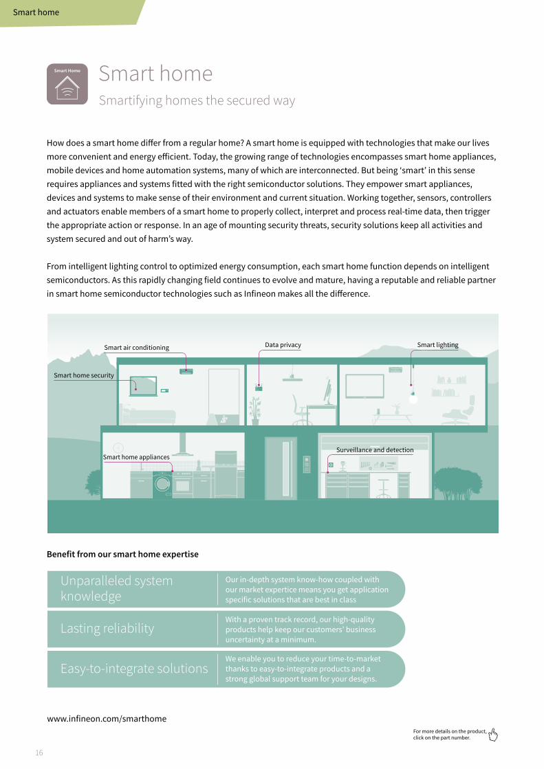
How does a smart home differ from a regular home? A smart home is equipped with technologies that make our lives more convenient and energy efficient. Today, the growing range of technologies encompasses smart home appliances, mobile devices and home automation systems, many of which are interconnected. But being ‘smart’ in this sense requires appliances and systems fitted with the right semiconductor solutions. They empower smart appliances, devices and systems to make sense of their environment and current situation. Working together, sensors, controllers and actuators enable members of a smart home to properly collect, interpret and process real-time data, then trigger the appropriate action or response. In an age of mounting security threats, security solutions keep all activities and system secured and out of harm’s way.
From intelligent lighting control to optimized energy consumption, each smart home function depends on intelligent semiconductors. As this rapidly changing field continues to evolve and mature, having a reputable and reliable partner in smart home semiconductor technologies such as Infineon makes all the difference.
Benefit from our smart home expertise
Smart home security
Smart home appliancesSurveillance and detection
Smart air conditioning Data privacy Smart lighting
www.infineon.com/smarthome
Our in-depth system know-how coupled withour market expertice means you get applicationspecific solutions that are best in class
Unparalleled system knowledge
Lasting reliability
Easy-to-integrate solutionsWe enable you to reduce your time-to-marketthanks to easy-to-integrate products and astrong global support team for your designs.
With a proven track record, our high-qualityproducts help keep our customers’ businessuncertainty at a minimum.

17
For more details on the product, click on the part number.
Infineon’s leading portfolio of best-fit, ready-to-use semiconductor solutions empowers you to create innovative smart home applications that meet both current and future demands. You can count on our components to be smart, secured and energy efficient. In our one-stop shop, you will find all components and solutions required for your project. Furthermore, our products are easy to integrate into your designs.
As you forge new, unexplored territory in the smart home realm, our in-depth know-how of our components and their potential in smart homes and home automation systems enable us to support you through and through. At the cutting-edge of key smart home technologies, we are in the position to guide you through this exciting new market while you explore new opportunities and business models. Especially those new to smart homes will appreciate our easy-to-use smart home demo and our basic offering of solutions.
How Infineon’s offering enhances your project
www.infineon.com/smarthome
Contextual sensitivity withmarket-leading accuracy andreliability. For more natural,seamless interaction betweenhumans, machines and the surroundings.
Advancedsensing
Ensure optimized systemperformance thanks to our deep system understanding and strong processing and steering know-how. The result: an excellent user experience.
Cross-applicationcontrol
Our innovative power electronics technologies allowusers to save energy and run applications at a market-leadinglow energy level. It’s the basis for real green smart homes.
Efficientpowermanagement
The right, easy to implementsecurity solutions for smart, always secured homes. We meetyour design’s evolving securityneeds without compromising onconvenience.
Trustedsecurity
Appl
icat
ions
Pack
ages
20-3
00 V
MO
SFET
s50
0-95
0 V
MO
SFET
sW
BG se
mic
ondu
ctor
sDi
scre
te IG
BTs
Pow
er IC
sIn
telli
gent
switc
hes
and
inpu
t ICs
Gate
driv
er IC
sM
icro
cont
rolle
rsXE
NSIV
™ se
nsor
s

18
For more details on the product, click on the part number.
Disruptive technologies have significantly changed our lifestyle in the past few decades. Now a new era is on the horizon – the age of robots. Robots are joining the ranks of innovative and disruptive technologies by revolutionizing traditional habits and processes. Today’s robots are able to identify and navigate through surroundings, work alongside and even interact with humans. Moreover, they teach themselves the skills required to complete a new task.
All this would not be possible without semiconductor solutions. Whether in an industrial robot, a cobot, an automated guided vehicle (AGV) or a service robot, intelligent semiconductors are the key enabler for all major robotic functions. Drawing on our insight into all facets of the robotics field, and with a comprehensive portfolio of power products and sensors on offer, we are able to provide reliable system solutions that address the latest trends in robotics like artificial intelligence, the Internet of Things, smart home, cloud based services, human machine interface etc., and add value to nearly every robot design.
RoboticsSuperior solutions for industrial and service robotics
www.infineon.com/service-robotics
Robotics
The latest generation of domestic robots is ushering in a new level of assistance and simplicity in homes and professional environments.They directly interact with humans, which introduces unique challenges from a designperspective, especially in domestic environments. Energy efficiency, long battery life as well as security aspects and sensing capabilities are key to user-friendly and safe designs.By choosing Infineon, you get aone-stop semiconductor shop for all your service-robot design needs.
Structural system overview: domestic robots
Motorsensing
Motorsensing
Motorsensing
Othermotors
Blower/blade motor
Wheelmotor
Motordrive
Motordrive
Motordrive
Humanmachineinterface
WLAN/BT/GPSWLAN/BT/GPS
Maincontroller
Securitycontroller
Power DC-supply (24 V/36 V/48 V/54 V) AUX DC-supply (12 V, 5 V, 3.3 V, …) Central COM bus (Ethernet, CAN, I2C, SPI, …)
Drives
110/230 V~ AC grid
Remote controlmonitoring
Smartphone/tablet/computer
AUX supplies› 12 V› 5 V, 3.3 V› Others
Service robot Charger(can be on board)
Domestic robots - simplifying everyday life and work
Features and benefitsKey features
Fast time to market
Complete solutions – broad portfolio
Extended battery lifetime and product life spans
Overall system size and cost reduction
Security, quality, and safety
Authentication
Key benefits
A complete eco-system of simulations, documentation, and demonstration boards enable a faster time to market
Whatever design specification, Infineon has the answer thanks to its comprehensive portfolio of products and solutions which you can easily tailor to your needs
High reliability of Infineon components results in prolonged product life spans
Reduction of overall system size and cost thanks to small form factor and compact design of components, both of which are required for highest power density BOM savings thanks to lowest RDS(on)
Trustworthy hardware-based security
As a security market leader with a proven track record and outstanding partner network for embedded security, Infineon provides highest quality standards and a safety-certified development process
OPTIGA™ Trust enables authentication of components connected to the system (e.g., battery pack recognition to avoid second-party batteries)
19
For more details on the product, click on the part number.
Robotics
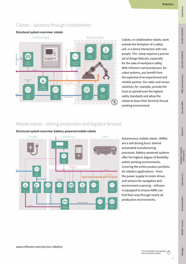
Cobots, or collaborative robots, work outside the limitation of a safety cell, in a direct interaction with real people. This setup requires a precise set of design features, especially for the sake of workplace safety. With Infineon’s semiconductors for cobot systems, you benefit from the expertise of an experienced and reliable partner. Our radar and sensor solutions, for example, provide the tools to uphold even the highest safety standards and allow the robots to leave their formerly fenced working environment.
Structural system overview: cobots
Cobots – advance through collaboration
Mobile robots – driving production and logistics forward
www.infineon.com/service-robotics
Autonomous mobile robots (AMRs) are a self-driving force behind automated manufacturingprocesses. Battery-powered systems offer the highest degree of flexibility within working environments.Covering the entire product portfolio for robotics applications – fromthe power supply to motor drives and sensors for navigation and environment scanning – Infineon is equipped to ensure AMRs can find their way through nearly all production environments.
Structural system overview: battery-powered mobile robots
Appl
icat
ions
Pack
ages
20-3
00 V
MO
SFET
s50
0-95
0 V
MO
SFET
sW
BG se
mic
ondu
ctor
sDi
scre
te IG
BTs
Pow
er IC
sIn
telli
gent
switc
hes
and
inpu
t ICs
Gate
driv
er IC
sM
icro
cont
rolle
rsXE
NSIV
™ se
nsor
s

20
For more details on the product, click on the part number.
Robotics
www.infineon.com/service-robotics
Functional block Purpose Characteristics Component Type or FamilyPower:-Power supply-Power factor correction (PFC)-Charger-Battery management
Power switches (0.4-6 kW output power)
25-150 V OptiMOS™20-75 V StrongIRFET™P-/N-channel - 60 to 20 V Small signal MOSFETs600-800 V CoolMOS™ P7600 V CoolMOS™ C7600 V CoolMOS™ CFD7600 V CoolGaN™600 V IGBT HighSpeed 5
PFC power diodes 650 V Schottky diode CoolSiC™Integrated power stage 800 V CoolSET™Gate driver ICs 200 V/650 V, half-bridge IRS2005M, IRS2007M, IRS2008M,
2ED2106S06F, 2ED2182S06F20 V, non-isolated, low-side EiceDRIVER™ 1EDN/2EDN, 1ED44175, 2ED24427 *650 V/1200 V, galvanic isolation EiceDRIVER™ 1ED Compact/1EDF2/
2EDF/2EDS650 V/1200 V, three-phase EiceDRIVER™ 6EDL04, 6ED2230
Microcontroller Arm® Cortex®-M0 microcontroller XMC1100/XMC1300Arm® Cortex®-M4 microcontroller XMC4200
Voltage regulators LDO and DC-DC switching regulators e.g., IFX1763, IFX90121Battery authentication Hardware-based, embedded security OPTIGA™ Trust B
Motor control Motor inverter power switches <12 V, <400 W PROFET™20-60 V StrongIRFET™
60 V SIPMOS™ *25-100 V, <1 kW OptiMOS™P-/N-channel MOSFETs ranging from -60 V to 20 V Small signal MOSFETs600 V, <500 W CoolMOS™ CFD7650 V, <500 W CoolMOS™ CFD2600 V/1200 V, <10 kW TRENCHSTOP™1200 V, 10-20 kW CoolSiC™Fully integrated, 600 V, 0.5-5 kW CIPOS™Fully integrated, 600 V, <20 kW EasyPIM™Fully integrated, 1200 V, 10-20 kW CoolSiC™ Easy1B *
Gate driver ICs 200 V/650 V, half-bridge IRS2005M, IRS2007M, IRS2008M, 2ED2106S06F, 2ED2182S06F
20 V, non-isolated, low-side EiceDRIVER™ 1EDN/2EDN, 1ED44175, 2ED24427 *650 V/1200 V, galvanic isolation EiceDRIVER™ 1ED Compact/1EDF2/2EDF/2EDS650 V/1200 V, three-phase EiceDRIVER™ 6EDL04, 6ED2230Integrated gate driver ICs NovalithIC™Automotive embedded power ICs TLE986x, TLE987x
Microcontroller Arm® Cortex®-M0 microcontroller XMC1000 microcontroller familyArm® Cortex®-M4 microcontroller XMC4000 microcontroller familyTriCore™ Safety certified security on-chip AURIX™Fully integrated motor control ICs iMOTION™
Position and condition sensing XENSIV™ magnetic Hall switches TLx496xXENSIV™ angle sensor, digital I/F TLE/TLI5012B, TLE5014SPXENSIV™ angle sensor, analog I/F TLE5009/5109/5309/5501
Sensing:-Robot sensing-Environment sensing-Human machine interface
XENSIV™ 3D magnetic sensor, digital I/F TLV/TLE/TLI493DXENSIV™ current sensor, digital I/F TLI 4970XENSIV™ current sensor, analog I/F TLI4971
Object and condition sensing XENSIV™ pressure/temperature sensor, digital I/F DPS310XENSIV™ 24 GHz radar sensor BGT24MTR11/12, BGT24MR2XENSIV™ MEMS microphones, digital I/F IM69D120/IM69D130XENSIV™ ToF 3D imaging @ 38-100 k pixel REAL3™ IRS1125C */IRS1645C/IRS2381C
Peripherals:-WLAN/BT/GPS-Human machine interface
Audio Class D audio amplifier IR43x1M, IR43x2MInterface CAN, CAN FD, CAN PD @ 1-5 MBit/s Industrial CAN transceiver
Industrial interface ICs ISOFACE™LED drivers Driving currents from 10-250 mA Linear driver ICs BCR3xx, BCR4xx
Support currents from 150 mA to 3A DC-DC switch mode ILD4xxx, ILD6xxxSecurity and safety-Motion controller (incl. safety)-Security controller
Controller TriCore™ Safety certified with security on-chip AURIX™Sensors Safe angle sensing - dual die structure e.g., TLE5009xxxDVoltage regulators DC-DC voltage regulator 12 V/5 V or 3.3 V; watchdog,
error monitoring, safe state control, BIST etc.e.g., TLF35584
Security Hardware-based, embedded security solutions, mutual authentication, secure communication, key protection, data signing etc.
OPTIGA™ TPM/Trust B/Trust X
Recommended products

21
For more details on the product, click on the part number.
TV power supply
www.infineon.com/smps
In addition to their outstanding image quality, new generation TVs gain attention for their user interface, low power consumption, and slim design. This requires the power supply unit (PSU) to either keep a low profile to maintain the slim appearance of a TV and a low thermal dissipation image or to have an external adapter. In addition, a growing number of TV manufacturers will use external adapters to deliver DC power to the TV. Infineon introduced two products based on digital power technology, designed to meet challenging efficiency and standby power requirements for the IoT-enabled TVs (both embedded PSU and adapter).
Thanks to digital power, our customers can reduce the number of TV power supplies by adapting the digital IC parameters to different TV and screen models by flexible and easy parameter setting. Infineon’s recently introduced digital-based flyback controllers are ideal to implement in low-power adapters for TVs and monitors. With the digital soft switching, the adapter power density can be improved significantly. The 600 V CoolMOS™ P7 series has been developed to cover a broad spectrum of different applications where the excellent performance and perfect ease of use are required. The rugged body diode enables not only the use in hard-switching topologies, such as power factor correction, boost, and two transistor forward, but also in resonant topologies such as LLC where the technologies lead to high efficiency in both hard-switching and resonant circuits.
For higher on-state resistance (RDS(on)) classes, there is a new feature of an integrated ESD diode that helps improve the quality in manufacturing. At the same time, the low RDS(on) and gate charge (QG) enable high efficiency in the various topologies. The 600 V CoolMOS™ P7 comes with a wide variety of RDS(on)s and packages on consumer grade to make it best suitable for TV power by balancing the cost and performance. Infineon developed specifically for TV power supplies a family of packages, characterized by short lead, SOT-223 mold stopper, and wide creepage distance, which enable our customers’ low-cost and reliable manufacturing.
Non-AUX digital solution for large screen size
High power solution for larger screen size
SMPSDiversify TV power supply with cost, performance, and ease of use
Activebridge
PFC + LLC combo
EMIfilter
LED
driv
er ICAudio
Mainboard
2EDN gate driver 2EDN gate driver
Main board
OLED
Activebridge
EMIfilter
Interleave PFC controller LLC controller
AUX power
SMPS - TV power supply
Appl
icat
ions
Pack
ages
20-3
00 V
MO
SFET
s50
0-95
0 V
MO
SFET
sW
BG se
mic
ondu
ctor
sDi
scre
te IG
BTs
Pow
er IC
sIn
telli
gent
switc
hes
and
inpu
t ICs
Gate
driv
er IC
sM
icro
cont
rolle
rsXE
NSIV
™ se
nsor
s

22
For more details on the product, click on the part number.
DC outputAC inputRectificationHV MOS
PWM
Flyback solution for small screen size
Recommended products
Functional block Product category Topology Product family BenefitsMain stage/PFC combo non-AUX
High voltage MOSFETs
Active bridge 600 V CoolMOS™ S7 › Body diode robustness at AC line commutation › Improved thermal resistance › Absolute lowest RDS(on) in the market › Enables top-side cooling with DDPAK and QDPAK › Ideal fit for solid state and hybrid relays and circuit breakers
600 V CoolMOS™ P7 › Fast-switching speed for improved efficiency › Low gate charge for enhanced light-load efficiency and low power
consumption at no-load condition › Optimized VGS threshold for lower turn-off losses › Rugged body diode for HB LLC application
DCM PFC, HB LLC 600 V CoolMOS™ PFD7 › Robustness and reliability with integrated robust, fast body diode and up to 2 kV ESD protection in gate
› Reduced gate charge for enhanced light-load efficiency, and lower hysteresis loss
Control ICs IDP2308 PFC-LLC non-AUX digital IC for TV embedded PSU
› Low BOM count/system cost due to high integration › Low standby power › High system reliability › Shorter development cycles and higher design and production flexibility
IDP2303A PFC-LLC non-AUX digital IC for TV adapter
› Low BOM count/system cost due to high integration › Low standby power › Small form factor designs › High system reliability
Synchronous rectification Low voltage MOSFETs
Synchronous rectification
OptiMOS™ 5 100-150 V › Low conduction losses, reduced overshoot › FullPAK package available
PFC Boost diodes DCM PFC 650 V Rapid diode › Low conduction losses
Control ICs CCM PFC ICs ICE3PCS0xG › High PFC and low THDMain stage Control ICs HB LLC ICs ICE1HS01G-1/ICE2HS01G › High efficiency and low EMIAuxiliary power supply Control ICs QR/FF flyback
CoolSET™700 V/800 V – ICE5QRxx70/80A(Z)(G) › Low standby power, high efficiency, and robustness
Flyback Control ICs Digital ZVS flyback IDP2105 * › Forced resonant ZVS control reduces the switching loss › Multilevel protection enables the robust design › Flexible firmware provides more differentiation for OEMs
High voltage MOSFETs
Flyback 700 V CoolMOS™ P7 › Optimized for flyback topologies › Best price competitive CoolMOS™ SJ MOSFET family › Lower switching losses versus standard MOSFET › Controlled dV/dt and di/dt for better EMI
www.infineon.com/smps
TV power supply
*For more information on the product, contact our product support

23
For more details on the product, click on the part number.
OLED LLCcontroller IC
OLED LLCstage
Main LLCstage
Rectifier+ PFCstage
VBUS
VCC
Supply for standby mode
Supply for OLED display
On/o control
Supply for system
Supply for system
Power on control
Status information
Vin
PFC not active instandby mode
startup
Main LLC/PFCcombo-controller IC
OLEDmodule and TV systemAC
OLED TV power block diagram
Benefiting from several advantages of organic light emitting diodes (OLED), various TV manufacturers are developing OLED TVs to level up the user experience of their consumers. Comparing with LCD/LED TV panels, the OLED can be thinner, lighter, and more flexible, also the power consumption is lower. With the excellent performance of Infineon’s GaN e-mode HEMTs (for full portfolio see pages 156-160), the OLED TV becomes even thinner and more reliable.
www.infineon.com/smps
Appl
icat
ions
Pack
ages
20-3
00 V
MO
SFET
s50
0-95
0 V
MO
SFET
sW
BG se
mic
ondu
ctor
sDi
scre
te IG
BTs
Pow
er IC
sIn
telli
gent
switc
hes
and
inpu
t ICs
Gate
driv
er IC
sM
icro
cont
rolle
rsXE
NSIV
™ se
nsor
s

24
For more details on the product, click on the part number.
Mobile charger
Modern mobile devices require a charger that provides faster charging but comes in a small size. High power density and cost-effective power supplies can be designed by operating the converter at a higher switching frequency to avoid a considerable increase in the transformer and the output capacitor size. In achieving the required thermal performance and EMI behavior, power devices with lower losses and controlled switching behavior enable effective and fast product development.
Infineon’s state-of-the-art digital-based controller, XDPS2107, enables the forced frequency resonant flyback (zero voltage switching) operation, ideal to be implemented in high power density adapters and well-supporting USB-PD requirements.
To address these requirements, Infineon offers its CoolMOS™ P7 SJ MOSFET family for adapters and chargers. Special care has been taken to ensure very good thermal behavior, increased efficiency, and fulfillment of all EMI requirements, enabling our customers to easily design products based on this new family. In addition, power devices in IPAK/SMD packages enable optimal PCB layout through minimal footprint. SMD packages offer additional benefits for automatized large volume production. Specifically, high power density at low manufacturing cost can be delivered using Infineon’s SOT-223 cost-effective package, which enables SMT manufacturing to maintain very good thermal performances.
The digital soft-switching controller, CoolMOS™ high-voltage MOSFETs, OptiMOS™ low-voltage MOSFETs and synchronous rectification IC portfolios, enable high power density designs whilst meeting the thermal requirements.
Functional block Product category Topology Product family BenefitsFlyback converter High voltage MOSFETs Flyback 700 V CoolMOS™ P7 (standard grade) › Best price competitive CoolMOS™ SJ MOSFET family
› Lower switching losses versus standard MOSFET
ACF, FMCI 600 V CoolMOS™ PFD7 (standard grade) › Robustness and reliability with integrated robust fast body diode and up to 2 kV ESD protection
› Reduced gate charge for enhanced light-load efficiency
› Lower hysteresis loss
Control IC FFR flyback IC XDPS21071 › High power density and ideal for USB-PD
Synchronous rectification Low voltage MOSFETs Synchronous rectification
OptiMOS™ PD 25 V – 150 V › Low conduction losses and reduced overshoot › Logic level switching › S308/PQFN 3.3 x 3.3 package available
Control IC Synchronous rectification
IR1161LTRPBF › High efficiency › Simple external circuitry
Load switch Low voltage MOSFETs Load switch OptiMOS™ PD 25 V/30 V › Low conduction losses › S308/PQFN 3.3 x 3.3 package available
Charger SMPSBest solutions for mobile charger
www.infineon.com/smps
Type-C connectorDC
Main stageACVin Vout
SwitchRectification
SR and protocol controlPrimary-side PWM control
SMPS - mobile charger

25
For more details on the product, click on the part number.
Wireless charging solutions Cost-effective and secure offerings for consumer, industrial and automotive applications
Over the last years, wireless charging has gained more and more traction in the market and is expected to heavily influence our daily lives in future. Infineon offers a broad portfolio of efficient, high-quality products and solutions to serve the key requirements of the dominant market standards: inductive (Qi (WPC)) and resonant (AirFuel). Whether you charge a smartphone (e.g. at home or in the car), a handful of wearables, a power tool, a laptop or a service robot, Infineon’s components and solutions help you overcome a wide range of common wireless power transfer challenges for consumer, industrial, and automotive wireless charging designs.
Wireless charging standards
www.infineon.com/wirelesscharging
Many end markets for wireless charging or wireless power transfer
Infineon’s key enabling products for consumer, industrial, and automotive solutions › Low and medium voltage power MOSFETs – OptiMOS™ and StrongIRFET™ › Gate driver ICs – EiceDRIVER™ or DC-DC low voltage gate driver › 32-bit microcontrollers – XMC™ and AURIX™ › Wireless power controller (including software IP) – XMC™-SC and AURIX™ › P-channel and N-channel small signal power MOSFETs › High-voltage power MOSFETs – CoolMOS™ Superjunction MOSFETs › PWM/flyback controllers and integrated power stage ICs – CoolSET™ › Gallium nitride (GaN) – CoolGaN™ e-mode HEMTs › Dedicated automotive power products – MOSFETs, DC-DC, LDO, PMIC with ASIL qualification › Voltage and buck regulators for component and bridge supply › Authentication – OPTIGA™ Trust Qi * › Reverse conducting IGBTs – 650V TRENCHSTOP™ 5
Inductive multi-coil
Number of devices charged Charges only one device Charges one device but with better user experience Charges multiple devices
Positioning of receiver application Exact positioning Positioning more flexible (X and Y direction)
Free positioning(up to >30 mm vertical freedom)
Rx-Tx communication In-band communication Bluetooth low energy or in-band communication
Magnetic resonanceInductive single-coil
Standard Qi inductive110-205 kHz
Resonant AirFuel6.78 MHz
Wireless charging
* Available when WPC Qi specification is released
Appl
icat
ions
Pack
ages
20-3
00 V
MO
SFET
s50
0-95
0 V
MO
SFET
sW
BG se
mic
ondu
ctor
sDi
scre
te IG
BTs
Pow
er IC
sIn
telli
gent
switc
hes
and
inpu
t ICs
Gate
driv
er IC
sM
icro
cont
rolle
rsXE
NSIV
™ se
nsor
s
26
For more details on the product, click on the part number.
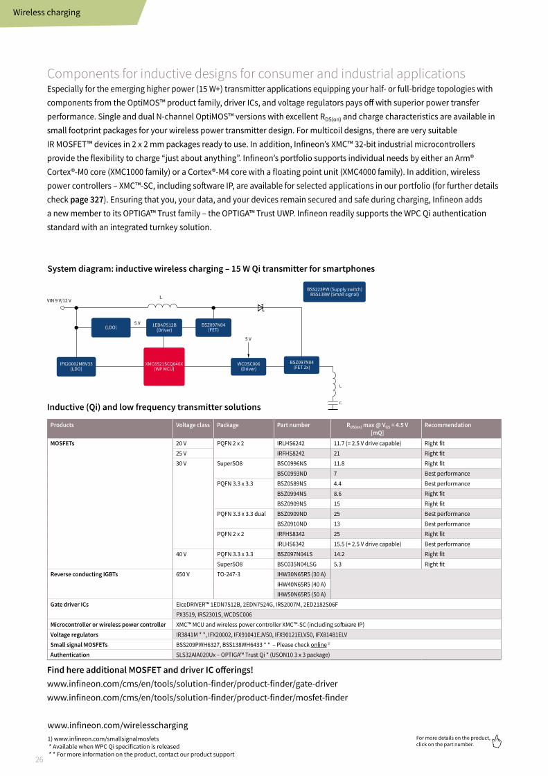
Components for inductive designs for consumer and industrial applications Especially for the emerging higher power (15 W+) transmitter applications equipping your half- or full-bridge topologies with components from the OptiMOS™ product family, driver ICs, and voltage regulators pays off with superior power transfer performance. Single and dual N-channel OptiMOS™ versions with excellent RDS(on) and charge characteristics are available in small footprint packages for your wireless power transmitter design. For multicoil designs, there are very suitable IR MOSFET™ devices in 2 x 2 mm packages ready to use. In addition, Infineon’s XMC™ 32-bit industrial microcontrollers provide the flexibility to charge “just about anything”. Infineon’s portfolio supports individual needs by either an Arm® Cortex®-M0 core (XMC1000 family) or a Cortex®-M4 core with a floating point unit (XMC4000 family). In addition, wireless power controllers – XMC™-SC, including software IP, are available for selected applications in our portfolio (for further details check page 327). Ensuring that you, your data, and your devices remain secured and safe during charging, Infineon adds a new member to its OPTIGA™ Trust family – the OPTIGA™ Trust UWP. Infineon readily supports the WPC Qi authentication standard with an integrated turnkey solution.
Find here additional MOSFET and driver IC offerings! www.infineon.com/cms/en/tools/solution-finder/product-finder/gate-driverwww.infineon.com/cms/en/tools/solution-finder/product-finder/mosfet-finder
Inductive (Qi) and low frequency transmitter solutions
www.infineon.com/wirelesscharging1) www.infineon.com/smallsignalmosfets * Available when WPC Qi specification is released * * For more information on the product, contact our product support
Products Voltage class Package Part number RDS(on) max @ VGS = 4.5 V [mQ]
Recommendation
MOSFETs 20 V PQFN 2 x 2 IRLHS6242 11.7 (= 2.5 V drive capable) Right fit25 V IRFHS8242 21 Right fit30 V SuperSO8 BSC0996NS 11.8 Right fit
BSC0993ND 7 Best performancePQFN 3.3 x 3.3 BSZ0589NS 4.4 Best performance
BSZ0994NS 8.6 Right fitBSZ0909NS 15 Right fit
PQFN 3.3 x 3.3 dual BSZ0909ND 25 Best performanceBSZ0910ND 13 Best performance
PQFN 2 x 2 IRFHS8342 25 Right fitIRLHS6342 15.5 (= 2.5 V drive capable) Best performance
40 V PQFN 3.3 x 3.3 BSZ097N04LS 14.2 Right fitSuperSO8 BSC035N04LSG 5.3 Right fit
Reverse conducting IGBTs 650 V TO-247-3 IHW30N65R5 (30 A)IHW40N65R5 (40 A)IHW50N65R5 (50 A)
Gate driver ICs EiceDRIVER™ 1EDN7512B, 2EDN7524G, IRS2007M, 2ED2182S06FPX3519, IRS2301S, WCDSC006
Microcontroller or wireless power controller XMC™ MCU and wireless power controller XMC™-SC (including software IP)Voltage regulators IR3841M * *, IFX20002, IFX91041EJV50, IFX90121ELV50, IFX81481ELVSmall signal MOSFETs BSS209PWH6327, BSS138WH6433 * * – Please check online 1)
Authentication SLS32AIA020Ux – OPTIGA™ Trust Qi * (USON10 3 x 3 package)
System diagram: inductive wireless charging – 15 W Qi transmitter for smartphones
BSS223PW (Supply switch)BSS138W (Small signal)
WCDSC006(Driver)
BSZ097N04(FET 2x)
L
VIN 9 V/12 V
C
L
5 V
5 V
IFX20002MBV33(LDO)
(LDO)
XMC6521SCQ040X(WP MCU)
1EDN7512B(Driver)
BSZ097N04(FET)
Wireless charging

27
For more details on the product, click on the part number.
IFX78M05(LDO)
Buck
BSZ0909ND (Dual FET)
VIN
VOUT
Optional:XMC8201SC-Q024X
Wireless power controller
L
C
XMC8511SC-Q040XWireless
power controller
2EDN7524R(Driver)
IRL80HS120(FET 2x)
PX3519 (Driver)
Wireless charging
Components for resonant (AirFuel) and high frequency solutions
www.infineon.com/wirelesscharging
Components for resonant designs for consumer and industrial Infineon offers superior power MOSFET technologies especially in the 30-100 V classes for class D inverter designs and in the 150-250 V voltage classes for class E inverters to address MHz switching implementations. We provide industry leading products when it comes to fast switching and have the best figure of merit for gate charge times RDS(on) and for Coss thus enabling our customer to achieve 6.78 MHz inverter designs using robust silicon MOSFET technology. CoolGaN™ 600 V with low and highly linear COSS, as well as low QC, enables high efficiency at higher power levels, especially in higher power class E designs. The CoolGaN™ portfolio qualifying for the use in wireless charging applications will be extended by adding 100 V and 200 V products over the next years. Infineon offers the “coolest” driver ICs in the industry, already available as low-side drivers for class E implementations and very soon as level shifted half-bridge driver for class D topologies. If your transmitter design uses a pre-regulator (buck or buck/boost) to control the input voltage of your amplifier you can find OptiMOS™ solutions in the 20-300 V MOSFETs section. Here again, the XMC™ industrial mircocontroller and the XMC™-SC wireless power controller, including software IP, are a great fit to charge “just about anything”.
Products Voltage class Package Part number RDS(on) max @ VGS = 4.5[mQ]
QG typical[nC]
Coss typical[pF]
Topology
MOSFETs 30 V PQFN 2 x 2 dual IRLHS6376PBF * * * 48 2.8 32 Class DPQFN 3.3 x 3.3 dual
BSZ0909ND 25 1.8 120 Class DBSZ0910ND 13 5.6 230 Class D
SOT-23 IRLML0030PBF 33 2.75 84 Class D40 V SOT-23 IRLML0040 62 2.8 49 Class D60 V SOT-23 IRLML0060 98 2.6 37 Class D80 V PQFN 2 x 2 IRL80HS120 32 3.5 68 Class D/E100 V PQFN 2 x 2 IRL100HS121 42 2.7 62 Class D/E150 V PQFN 3.3 x 3.3 BSZ900N15NS3 75 * * 4.1 * * 46 Class E
BSZ520N15NS3 42 * * 7.2 * * 80 Class E200 V BSZ900N20NS3 78 * * 7.2 * * 52 Class E
BSZ22DN20NS3 200 * * 3.5 * * 24 Class EBSZ12DN20NS3 111 * * 5.4 * * 39 Class E
250 V BSZ42DN25NS3 375 * * 3.6 * * 21 Class EGaN e-mode HEMT CoolGaN™ 600 V e-mode GaN HEMT IGT60R190D1S (HSOF-8-3)Gate driver ICs EiceDRIVER™ 2EDL71 *, 1EDN7512, 2EDN7524, 2ED2182S06F, 2ED24427N01F * * *, 1EDI60N12AF
GaN EiceDRIVER™ gate driver ICs 1EDS5663H, 1EDF5673F, 1EDF5673KMicrocontroller or wireless power controller XMC™ MCU and wireless power controller XMC™-SC * (including software IP)Voltage regulators IR3841M * * *, IFX20002, IFX91041EJV50, IFX90121ELV50, IFX81481ELVSmall signal MOSFETs Please check online 1)
Find here additional MOSFET and driver IC offerings! www.infineon.com/cms/en/tools/solution-finder/product-finder/gate-driverwww.infineon.com/cms/en/tools/solution-finder/product-finder/mosfet-finder
System diagram: resonant wireless charging – 2.5 W transmitter and recevier – 6.78 MHz - proprietary solution
* On demand * * VGS = 8 V * * *For more information on the product, contact our product support
Appl
icat
ions
Pack
ages
20-3
00 V
MO
SFET
s50
0-95
0 V
MO
SFET
sW
BG se
mic
ondu
ctor
sDi
scre
te IG
BTs
Pow
er IC
sIn
telli
gent
switc
hes
and
inpu
t ICs
Gate
driv
er IC
sM
icro
cont
rolle
rsXE
NSIV
™ se
nsor
s

28
For more details on the product, click on the part number.
Wireless in-car charging (automotive)The next generation of in-cabin wireless charging systems have to meet strict automotive safety, security, environmental, and regulatory requirements while still enabling industry-leading charging performance and efficiency. Infineon’s AURIX™ microcontroller, voltage regulators, power MOSFET technologies, and network ICs will easily support these requirements with a complete charging solution. With 15 W charging that meets existing standards, including fast-charging smartphones, the solution easily supports future changes with a software update. Infineon’s new innovative foreign object detection (FOD) system or our unique improved power drive architecture that provides unparalleled EMI performance are just two benefits out of many to address the design challenges in the automotive wireless charging market. Discover our complete offerings for in-cabin charging on a system level on Infineon’s wireless charging webpage – something you will not find just anywhere.
www.infineon.com/wirelesscharging
System diagram: AURIX™-based wireless charger – three-coil
Automotive products for wireless charging Voltage class Package Part number RDS(on) max @ VGS = 4.5 V[mQ]
QG typical[nC]
Inverter automotive grade MOSFETs 40 V SuperSO8 5 x 6 dual IPG20N04S4-12A 15.5 9
S3O8 3.3 x 3.3 IPZ40N04S5L-4R8 6.7 11
IPZ40N04S5L-7R4 10.7 6.5
Automotive products for wireless charging Voltage class Package Part number RDS(on) max @ VGS = 4.5 V [mQ]
RDS(on) max @ VGS = 10 V [mQ]
Coil selection switch 60 V TDSON-8 IPG20N06S4L-11A 15.8 11.2
100 V SuperSO8 5 x 6 dual IPG20N10S4L-22A 28 22
IPG20N10S4L-35A 45 35
IPG16N10S4L-61A 78 61
Microcontroller and wireless power controller AURIX™ SAK-TC212S-4F100N *, SAK-TC212S-8F133SC
Power supply TLD5190 – buck-boost controller/TLE8366, TLS4120x, TLS203x/TLF35584 – safety MCU supply + CAN supply
CAN TLE7250SJ – high performance CAN transceiver
Gate driver ICs AUIRS2301S
TLD5190QV
(Buck/Boost)
TLE8366
Pre-regulator
TLS203B0
(LDO)
TLE7250VSJ
(CAN)
AUIRS2301S
(Driver)
IPG20N04S4L-11A
(Dual FET)
AUIRS2301S
(Driver)
IPG20N04S4L-11A
(Dual FET)
IPG16N10S4L-61A
(2x Dual FET)VBAT
5-40V
5 V gate DRV
3.3 V
NFC radio
CAN interface
Coil 1 Coil 2 Coil 3
IPG20N10S4L-22 (100 V)
(coil switches)
AURIX ™
SAK-TC212S-8F133SC
Wireless
power
controller
Wireless charging
*For more information on the product, contact our product support

29
For more details on the product, click on the part number.
www.infineon.com/wirelesscharging
Wireless charging
System solutions for wireless charging Master your design challenges with Infineon. With our broad range of designs, customers have the possibility to make wireless charging available for different kinds of applications. For more information on the availability of our boards, please visit www.infineon.com/wirelesscharging or get in contact with us via www.infineon.com/support.
Reference design Valkyrie – the 15W Qi transmitter (Tx) for charging smartphones REF_10WTx_QI_4102 *
Board specification
Find the right solutions for your wireless charging designs in four stepsInfineon’s selection tool for wireless charging allows you to find the right solutions for your designs in just four steps: select the application, power range, standard, and the topology you want to apply and get an overview of Infineon’s most recommended offerings.
Spark Connected Inc. is our official partner for wireless charging.The software IP is provided by our partner.For details visit: www.sparkconnected.com
Try now!
15 W inductive
Consumer/industrialAutomotive
1-15 W inductive 2.5 W resonant60-200 W inductive 16/20 W resonant >20 W resonant
Resonant solutionsInductive solutions
Dedicated for automotive in-cabin wireless charging
Board number REF_10WTx_QI-4102
Solution max. power capability [W] 7.5 W / 10 W
Frequency fixed 127.8 kHz (Apple iOS), variable (Android)
Input power supply USB QC 3.0 (9 V / 12 V)
Topology boost topology (half-bridge solution)
Power regulation method Variable voltage boost (added frequency control for Android)
Rx-Tx communication In-band communication (bi-directional)
Supports WPC 1.2.4 EPP
Charging rates Rx Up to 15 W
FOD measurements calculated Tx power Direct AC measurement at coil
DC-DC efficiency 83%
Dimensions L: 85 mm, W: 50 mm, H: 6.4 mm / Active area: L: 45 mm, W: 40 mm
Coil type MP-A11
*On demand
Appl
icat
ions
Pack
ages
20-3
00 V
MO
SFET
s50
0-95
0 V
MO
SFET
sW
BG se
mic
ondu
ctor
sDi
scre
te IG
BTs
Pow
er IC
sIn
telli
gent
switc
hes
and
inpu
t ICs
Gate
driv
er IC
sM
icro
cont
rolle
rsXE
NSIV
™ se
nsor
s

30
For more details on the product, click on the part number.
Wearables and healthtech
Wearables and healthtech Next level of wearable devices with Infineon‘s sensing, RF, power, and security solutions
Smart wearable devices have become an essential part of our lives and are expected to gain more popularity in the future. Wearables are devices that can be comfortably worn on the body and that are used for multiple purposes depending on the application. With Infineon‘s product offerings, customers can solve design challenges such as data security, sensor accuracy, longer battery lifetime, small form factor of the components, device protection, and differentiation between everyday movements and a fall.
www.infineon.com/wearables
Key enabling products: › XENSIV™ barometric pressure sensors › OPTIGA™ Trust B › Broad RF switch portfolio › GPS LNA › 4G/5G LTE LNAs › eSim › XENSIV™ MEMS microphone › Wireless charging solutions › 3D Image Sensor REAL3™ › 32Mb NVM ultralow power flash memory › ESD protection › SECORA™ Connect › XENSIV™ 60 GHz radar
Achieve robust and accurate altitude measurement, location tracking, precise single step or body motion detection
Highest accuracy
Easy implementation of smart payment, ticketing or access control with Infineon’s NFC solution
Fast and secure transactions
Decrease your time to market. Thanks to our broad product portfolio and solution offerings such as wireless charging, eSim, ESD protection or authentication
Easy tointegratesolutions
Infineon’s products with smallest form factors and low energy consumptions provide high functional integration and long-lasting battery
Increased batterylifetime
Smartwatch and sport watch
Wristband
AR/VR glasses Smart clothing Healthtech
Hearables
Wearable applications addressed by Infineon

31
For more details on the product, click on the part number.
www.infineon.com/wearables * Available on request
Solution tree for smartwatch, sport watch, and wristband
Functional blocks of smartwatch, sports watch, and wristband
Functional block Product family Functional block Recommended parts and familiesSecurity › OPTIGA™ Trust B SLE 95250
› SECORA™ Connect * › eSim: NC1025 *
Interface › Broad ESD protection product portfolio › XENSIV™ MEMS microphone
Wireless charging › 2 W inductive * › 2.5 W resonant *
Memory › 32Mb NVM flash memory
Sensing › XENSIV™ pressure sensor DPS310/DPS368
Connectivity › Broad 4G/5G LNA product portfolio › GNSS LNA: BGA123L4, BGA123N6, BGA524N6, BGA125N6 › Broad RF switches portfolio
Microcontroller
BT/WiFi Cellular
MicrocontrollerMicrophone
Haptic feedback Speaker
Screen
Vital sensing Environmentalsensing
Sports/activity sensing
Touch interface
Interface
Sensing
Charging Internal power stage Output power stage
Connectivity Memory
Security
ESD protection
Wireless charging
USB charging
Batterymanagement
Internal powermanagement
RAM
eSIM Secure element+ NFC
Authentication
FlashGNSS
(GPS, GLONASS,BEIDOU, GALILEO
Appl
icat
ions
Pack
ages
20-3
00 V
MO
SFET
s50
0-95
0 V
MO
SFET
sW
BG se
mic
ondu
ctor
sDi
scre
te IG
BTs
Pow
er IC
sIn
telli
gent
switc
hes
and
inpu
t ICs
Gate
driv
er IC
sM
icro
cont
rolle
rsXE
NSIV
™ se
nsor
s

32
For more details on the product, click on the part number.
› DC-DC enterprise solutions for data processing applications › SMPS – laptop adapters › SMPS – PC power supply › SMPS – server power supply › SMPS – telecom power supply
SMPS and digital power management solutions for data processing applications

33
For more details on the product, click on the part number.
Appl
icat
ions
Pack
ages
20-3
00 V
MO
SFET
s50
0-95
0 V
MO
SFET
sW
BG se
mic
ondu
ctor
sDi
scre
te IG
BTs
Pow
er IC
sIn
telli
gent
switc
hes
and
inpu
t ICs
Gate
driv
er IC
sM
icro
cont
rolle
rsXE
NSIV
™ se
nsor
s

34
For more details on the product, click on the part number.
DC-DC
DC-DC enterprise power solution for data processing applicationsMultiphase and point-of-load DC-DC solution
As an industry leader in digital power management, Infineon delivers solutions for the next-generation server, communication, storage and client computing applications. Infineon offers a complete portfolio including digital PWM controllers, integrated power stages, integrated point-of-load (POL) voltage regulators, MOSFET drivers, power blocks and discrete MOSFETs. These proven technologies offer full flexibility to our customers to optimize a complete system solution for space, performance, ease of design and cost to meet critical design goals. In addition, our latest software tools help simplify design, shorten design cycles and improve time-to-market.
CPU, GPU, DDR
AC adapters
Batterycharger
Chipset, I/O,other peripheral loads
OptiMOS™
OptiMOS™
OptiMOS™
DC-DCPWM
controller
www.infineon.com/dataprocessing
Features and benefitsKey features
Best-in-class efficiency
Multi-protocol support
Complete system solution
Digital controller flexibility
Ease of design
Smallest solution size
Key benefits
Digital controller and power stage provide industry‘s highest efficiency of more than 95 percent
Intel SVID, AMD SVI2, NVIDIA PWM VID, parallel VID (up to 8 bits) , PMBus™ Rev1.3, AVS Bus (PMBus™ Rev1.3)
A broad portfolio of fully integrated point-of-load, integrated power stage and digital controller solutions in addition to discrete drivers and MOSFETs offers full flexibility to optimize complete system solutions ranging from 1 A to 1000+ A.
Industry‘s benchmark for feature richness and low quiescent power with up to 16-phases
Intuitive GUI enables faster optimization, thereby reduces design cycle time
Best-in-class OptiMOS™ MOSFETs combined with advanced packaging technologies enable high power density at high efficiency, and the superior control engine with digital controllers helps minimize output capacitance significantly

35
For more details on the product, click on the part number.
Multiphase DC-DC system solution
Server/storage
Server-Intel/IBM/AMD/ARMWorkstation
Storage
High-end consumer
High-end desktopNotebookGaming
GraphicIndustrial PC
Comms
DatacomComms coreSOHO SANEdge access
TelecomBase station(macro + distributed)
Powered ICs
Server chipset
Voltage
VCCIO
VMCP
Vcore
Vmem
ASICASSPFPGA
FPGAs (~0.5–3.3 V) Networking SoCs and ASICs, FPGAs
Multi-core processors
Ethernet switch ICs
PC chipset
Vcore
Graphics
ASICs (~1.0 V)
ASSPs (~1.0 V)
10-30 Asingle-phase (multi-rail)
>30 Amultiphase/rail
www.infineon.com/dataprocessing
Appl
icat
ions
Pack
ages
20-3
00 V
MO
SFET
s50
0-95
0 V
MO
SFET
sW
BG se
mic
ondu
ctor
sDi
scre
te IG
BTs
Pow
er IC
sIn
telli
gent
switc
hes
and
inpu
t ICs
Gate
driv
er IC
sM
icro
cont
rolle
rsXE
NSIV
™ se
nsor
s

36
For more details on the product, click on the part number.
DC-DC enterprise power solution for data processing applicationsIntegrated point-of-load (IPOL) converters
Infineon’s IPOL converters integrate a PWM controller, a driver and MOSFETs into a small PQFN package for ease of use. The patented PWM modulation scheme allows greater than 1 MHz switching frequencies to deliver ultracompact layouts and and the smallest bill of materials (BOM). A PMBus™ interface is available for monitoring and control in systems that use advanced CPUs, ASICs and FPGAs.
DC-DC IPOL portfolioDigital interface IPOL
*Coming soon
Analog IPOL
Block diagram
POLIR38XXX
POLIR38XXX
POLIR38XXX
I/O I/O
Core
Memory
+
+
+
+
0.9 V
1.5 V
1.8 V
12 V
PMBus™
CPU/ASIC/FPGA/DSP
Key features › Input voltage range
4.5-21 V › Output current 1-35 A › Operating temperature
range of -40 to 125°C
Key benefits › Integrated controller,
driver, MOSFETs for small footprint
› High-efficiency MOSFETs and thermally enhanced packages for operation without heat sinks
www.infineon.com/dataprocessing
I²C PMBus™, telemetry, margin, faults, SVID PVIDDigital control/configuration, telemetry and diagnostic
Part number Max. current
[A]
Package size [mm]
Max. Vin Max. fsw Distinctive features
IR38064MTRPBF 35 5 x 7 21 V 1500 KHz PMBus™
IR38063M 25 5 x 7 21 V 1500 KHz
IR38062M 15 5 x 7 21 V 1500 KHz
IR38060M 6 5 x 6 16 V 1500 KHz
IR38163M 30 5 x 7 16 V 1500 KHz OptiMOS™ 5, SVID + PMBus™
IR38165M 30 5 x 7 16 V 1500 KHz OptiMOS™ 5, SVID
IR38363M 15 5 x 7 16 V 1500 KHz OptiMOS™ 5, SVID + PMBus™
IR38365M 15 5 x 7 16 V 1500 KHz OptiMOS™ 5, SVID
IR38263M 30 5 x 7 16 V 1500 KHz OptiMOS™ 5,PVID + PMBus™
IR38265M 30 5 x 7 16 V 1500 KHz OptiMOS™ 5, PVID
IR38164M 30 5 x 7 16 V 1500 KHz OptiMOS™ 5, SVID + PMBus™, enhanced Imon
IRPS5401M 4+4+2+2+0.5
7 x 7 14 V 1500 KHz 5 output PMIC, PMBus™
„Performace“ voltage-mode PWMUltralow jitter and noise, high accuracy and low ripple
Part number Max. current [A]
Package size [mm]
Max. Vin Max. fsw Distinctive features
IR3883MTRPBF 3 3 x 3 14 V 800 KHz Constant-on-timeIR3888MTRPBF 25 5 x 6 17 V 2000 KHzIR3887MTRPBF * 30 4 x 5 17 V 2000 KHzIR3889MTRPBF 30 5 x 6 17 V 2000 KHz
DC-DC

37
SMPS - laptop adapters
For more details on the product, click on the part number.
www.infineon.com/smps
Manufacturing slimmer and lighter adapters requires ICs that enable high efficiency with good electromagnetic interference (EMI) performance and low standby power. There is also a need for cost-effective MOSFETs in small packages that feature good EMI and excellent thermal performance. Infineon offers a wide range of products specifically designed for adapters including high-voltage MOSFETs and control ICs for PFC and PWM stages, as well as low-voltage MOSFETs for synchronous rectification. With these products, Infineon supports the trend towards a significantly higher efficiency level, especially in partial load conditions, as well as the miniaturization of the adapter.
Extremely versatile are the CoolMOS™ P7 SJ MOSFET series and the latest body-diode performance-enhanced CoolMOS™ PFD7 series which combine high efficiency and optimized cost with the ease of use. Infineon developed a family of packages, characterized by having a short lead, IPAK short lead with ISO-standoff and wide creepage that enable our customers’ low-cost and reliable manufacturing, specifically for adapters. High power density at low manufacturing cost can be achieved by using Infineon’s SOT-223 cost-effective package and ThinPAK 5x6 and 8x8 high-density SMD packages which enable SMT manufacturing while maintaining very good thermal performances. For synchronous rectification, Infineon’s OptiMOS™ PD logic-level power MOSFET series offer extremely low on-state resistance and low capacitances.
The new control ICs such as the digital-based XDP™ controller enable forced-frequency-resonant zero-voltage-switching (FFR ZVS) operation, ideal in high-power-density adapter designs and supporting USB-PD requirements.
Multiple and often clunky chargers and adapters for phones, tablets, and laptops pose a nuisance for many users due to the additional weight and added space. That created a need and a trend towards higher power density and consequently smaller devices. Today, flyback power conversion topology is typically used in such systems and the form factor is limited by the efficiency achievable at 90 VAC input voltage and full load. The highest-power-density systems available today reach ~12 W/in3 (for 65 W maximum output power). Infineon’s CoolGaN™ e-mode HEMTs enable a breakthrough with respect to power density for adapter and charger systems enabling ~20 W/in3 power density systems (for 65 W maximum output power). This advantage can be realized by implementing Infineon’s CoolGaN™ in a half-bridge topology that allows simultaneous increase of switching frequency and efficiency.
SMPSRight-fit portfolio for competitive design of laptop adapters
Type-C connectorDC
Main stageACVin Vout
SwitchRectification
SR and protocol controlPrimary-side PWM control
Infineon’s 20 W/in3 adapter (cased) - 24 W/in3 (uncased) with 65 W output power capability (LxWxH: 74.2 mm x 36.5 mm x 16.5 mm)
Laptop adapter
Appl
icat
ions
Pack
ages
20-3
00 V
MO
SFET
s50
0-95
0 V
MO
SFET
sW
BG se
mic
ondu
ctor
sDi
scre
te IG
BTs
Pow
er IC
sIn
telli
gent
switc
hes
and
inpu
t ICs
Gate
driv
er IC
sM
icro
cont
rolle
rsXE
NSIV
™ se
nsor
s

38
For more details on the product, click on the part number.
Functional block Product category Topology Product family BenefitsFlyback converter High voltage MOSFETs
and HEMTsFlyback 600 V/700 V/800 V CoolMOS™ P7
SJ MOSFETs › Fast switching speed for improved efficiency and thermals › Reduced gate charge for enhanced light load efficiency › Optimized gate-to-source voltage (VGS) threshold for lower turn-off losses
ACF, FMCI 600 V CoolMOS™ PFD7 SJ MOSFETs
› Robustness and reliability with integrated robust fast body diode and up to 2 kV ESD protection
› Reduced gate charge for enhanced light load efficiency › Lower hysteresis loss
Flyback (ACF, FFR, etc.) CoolGaN™ 600 V e-mode HEMTs › Highest efficiency › Highest power density
Low voltage MOSFETs Flyback/auxiliary synchronous rectification
OptiMOS™ 100-150 V › Low conduction losses and reduced overshoot › Logic level can support low voltage gate drive to achieve
high efficiency
Control ICs QR flyback IC ICE2QS03G, ICE5QSAG › High efficiency and low standby power
FFR flyback IC XDPS21071 › High power density and digital control › Suitable for USB-PD design
PFC High voltage MOSFETs, HEMTs, and diodes
DCM PFC 600 V CoolMOS™ P7 SJ MOSFETs
› Fast switching speed for improved efficiency › Reduced gate charge for enhanced light load efficiency › Optimized gate-to-source voltage (VGS) threshold for lower turn-off losses
DCM/CCM PFC CoolGaN™ 600 V e-mode HEMTs › Highest efficiency contribution via less parasitic parameter › Space saving with SMD smaller package
Boost diode DCM/PFC 650 V Rapid 1 diodes › Low conduction losses
Control ICs DCM PFC ICs TDA4863G, IRS2505LTRPBF
› Simple external circuitry › High PFC and low THD
Main stage High voltage MOSFETs and HEMTs
HB LLC 600 V CoolMOS™ P7 SJ MOSFETs
› Fast switching speed for improved efficiency and thermals › Reduced gate charge for enhanced light load efficiency › Optimized gate-to-source voltage (VGS) threshold for lower turn-off losses
CoolGaN™ 600 V e-mode HEMTs › Highest efficiency › Highest power density
Synchronous rectification
Low voltage MOSFETs Synchronous rectification OptiMOS™ PD 100-150 V › Low conduction losses, reduced overshoot › Adapter-oriented synchronous rectification MOSFETs
Control ICs Synchronous rectification IR1161LTRPBF › High efficiency › Simple external circuitry
www.infineon.com/smps
Recommended products

39
SMPS - PC power supply
For more details on the product, click on the part number.
PC power supply
The PC power market is divided into high-end gaming PC and better cost-performance sectors to achieve a better price/performance for desktop SMPS. The PC OEMs are implementing the desktop SMPS by removing the AUX power block to save the cost of having a flyback circuit.
Due to new structure of the CPU and GPU, more and more higher peak power is needed ( 1.5 to 2 times higher than normal power). In addition to the needed CCM PFC, Infineon 600 V CoolMOS™ P7 and 40 V / 60 V OptiMOS™ offer the best price/performance and reliability to meet the design requirements, as well as to achieve the highest efficiency enabled by semiconductors available in the market.
For those CPU and GPU power hungry gaming PCs, the ICE3PCS0xG CCM PFC IC provides high efficiency over the whole load range and low count of external components, in addition, the ICE3PCS0xG CCM PFC IC offers fast output dynamic response during load jump. In additions to PGFC IC, Infineon’s LLC ICs ICE1HS01G/ICE2HS01G support customers to minimize the external component count.
SMPSMore efficient PC power supply
DCACVin Vout
PFC-PWM with AUX and ICs
RectificationPFC Main stageVbus
www.infineon.com/smps
Functional block Product category Topology Technology BenefitsPFC/main stage High voltage MOSFETs CrCM/DCM PFC 600 V CoolMOS™ P7 › Best thermal performance
› Rugged body diode › ESD enhancement for production line › Wide RDS(on) portfolio including both THD and SMD packages
600 V CoolMOS™ P6 › Fast switching speed for improved efficiency and thermals › Low gate charge for enhanced light-load efficiency and low
power consumption at no load condition › Optimized VGS threshold for low turn-off losses
500 V CoolMOS™ CE › Optimized cost/performance › Lower transition losses versus standard MOSFET
Boost diodes DCM PFC 650 V Rapid 1 › Low conduction losses
CCM PFC 650 V Rapid 2 › Low reverse-recovery losses and PFC switch turn-on losses
Control ICs CCM PFC ICs ICE3PCS0xG › High PFC and low THD
Main stage Control ICs HB LLC ICs 650 V – ICE1HS01G-1/ ICE2HS01G
› High efficiency and low EMI
Synchronous rectification
Medium voltage diodes HB LLC + center-tap OptiMOS™ 40 V › Optimized cost/performance and low thermals
OptiMOS™ 60 V › Layout tolerance and low thermals
Recommended products
Appl
icat
ions
Pack
ages
20-3
00 V
MO
SFET
s50
0-95
0 V
MO
SFET
sW
BG se
mic
ondu
ctor
sDi
scre
te IG
BTs
Pow
er IC
sIn
telli
gent
switc
hes
and
inpu
t ICs
Gate
driv
er IC
sM
icro
cont
rolle
rsXE
NSIV
™ se
nsor
s

40
SMPS - server power supply
For more details on the product, click on the part number.
Server power supply
The trend in the field of data center and enterprise servers is to deliver more power per rack. Meanwhile, the rising cost of energy and environmental concerns make SMPS-efficiency optimization a key requirement across the entire load range for server and data center designs. This challenging task is combined with the requirement for higher power and higher power, higher power density and cost-effectiveness.
In the PFC stage and generally in hard-switching topologies used in server applications, Infineon recommends its 600 V CoolMOS™ C7 and G7 families offering the lowest FOM RDS(on) *QG and RDS(on) *Eoss. These MOSFET series provide the lowest switching losses, which is necessary in fast-switching-frequency operations in high-end server SMPS. With Infineon’s C7 and G7 series, the efficiency is optimized already from a very light-load operation. 600 V CoolMOS™ C7 and G7 products are used with Infineon’s industry-benchmark non-isolated 2EDN752x gate driver IC family. Available in compact SMD packages such as ThinPAK, DDPAK and TOLL, these SJ MOSFETs offer benefits in space usage and power density.
Complementary to the 600 V CoolMOS™ C7 in high efficiency PFC is the CoolSiC™ Schottky diodes. The 600 V CoolMOS™ P7 family offers a good compromise between price and performance. This is valuable in both PFC and HV DC-DC stages where low QG and turn-off losses are important benefits, especially in case of high-switching-frequency operation and high light-load efficiency requirements.
As high power (2-6 kW and above) require ultrahigh efficiency (96-98 percent peak) and high power density, Infineon’s CoolGaN™ 600 V e-mode HEMTs family with totem-pole PFC controls deliver the highest efficiency and power density in the world. Using the 600 V CoolMOS™ S7 devices with active bridge circuit fulfills the Titanium® requirement at the lowest cost. Operating expenses (OPEX) and capital expenditures (CAPEX) are both reduced through simplified topologies and the power density in the server PSU is doubled.
In applications with low output voltage and high output current, further efficiency improvements are enabled by the continuous reduction of on-resistance. This can be achieved by using Infineon’s low-voltage OptiMOS™ MOSFET series in the synchronous rectification stage. Infineon’s low-voltage products are complemented by StrongIRFET™ devices that are optimized for lower switching frequencies and highest system robustness.
SMPSHighly efficient server power supply
DC
Auxiliary power
Control and housekeeping
ACVin Vout
DCVaux
PFC-PWM with AUX and ICs
RectificationPFC Main stageVbus
www.infineon.com/smps

41
For more details on the product, click on the part number.
www.infineon.com/smps
Functional block Product category Topology Product family BenefitsPFC High voltage MOSFETs CCM/interleaved PFC; TTF 600 V/650 V CoolMOS™ C7
650 V CoolMOS™ G7600 V CoolMOS™ S7
› Best FOM RDS(on) *QG and RDS(on) *Eoss › Lowest RDS(on) per package › Low dependency of switching losses form Rg,ext
High voltage GaN Totem-pole PFC CoolGaN™ 600 V › Enable the highest efficiency and highest power density
SiC diodes CCM/interleaved PFC CoolSiC™ Schottky diode 650 V G5
› Low FOM VF *QG
Control ICs CCM PFC ICs ICE3PCS0xG › Ease of use
Main stage High voltage MOSFETs ITTF 600 V CoolMOS™ C7/P6 › Fast switching speed for improved efficiency and thermals › Low gate charge for enhanced light load efficiency and low
power consumption at no load condition › Optimized VGS threshold for lower turn-off losses › Rugged body diode which prevents device failure during hard
commutation
LLC, half-bridge below 1 kW
600 V CoolMOS™ P7, CFD7 › Low turn-off losses › Low Qoss › Low QG
LLC, phase shift full-bridge below 1 kW
600 V CoolMOS™ CFD7, 650 V CoolMOS™ CFD2
› Fast and rugged body diode › Optimized low QG and soft commutation behavior to reach
highest effciency › Highest reliability for 650 V VDS
ZVS PS FB, LLC, TTF TRENCHSTOP™ IGBT 650 V F5 › Improved ruggedness and high efficiency in low inductance designs
Control ICs HB LLC ICs ICE1HS01G-1ICE2HS01G
› High efficiency and low EMI
Sychronous rectification
Low voltage MOSFETs
HB LLC and center tap OptiMOS™ 40 V › High efficiency over whole load range, layout tolerance
ITTF OptiMOS™ 60 V › High efficiency, low thermals, low VDS overshoot
ZVS PS FB and center tap OptiMOS™ 80 V › High efficiency over whole load range, low VDS overshoot and oscillations
Auxiliary power supply Control ICs QR/FF flyback CoolSET™ 800 V – ICE2QRxx80(Z)(G) ICE3xRxx80J(Z)(G) 700 V ICE5QRxx70A(Z)(G) 800 V ICE5QRxx80A(Z)(G)
› Low standby power, high efficiency and robustness › An integrated 700 V/800 V superjunction power MOSFET with
avalanche capability › Burst mode entry/exit to optimize standby power at different
low load conditions
Housekeeping Microcontrollers - XMC1xxx › Flexibility, HR PWM, digital communication › Arm®-based standard MCU family and wide family
Conversion Microcontrollers - XMC4xxx › Flexibility, HR PWM and digital communication
PFC, PWM/resonant converter, synchronous rectification
Gate driver ICs - EiceDRIVER™ 1EDix › 100 ns typical propagation delay time › Functional isolation › Separate source
- EiceDRIVER™ 2EDNx › 8 V UVLO option › -10 V input robustness › Output robust against reverse current
Recommended products
Appl
icat
ions
Pack
ages
20-3
00 V
MO
SFET
s50
0-95
0 V
MO
SFET
sW
BG se
mic
ondu
ctor
sDi
scre
te IG
BTs
Pow
er IC
sIn
telli
gent
switc
hes
and
inpu
t ICs
Gate
driv
er IC
sM
icro
cont
rolle
rsXE
NSIV
™ se
nsor
s

42
SMPS - telecom power supply
For more details on the product, click on the part number.
www.infineon.com/smps * in development
The ever increasing data consumption, coupled with new levels of virtualization and complexity of the 5G telecom infrastructure, is bringing its demanding requirements into the telecom power arena. The outstanding improvements made in telecom SMPS performance in the past decade have been primarily brought by the dramatic reduction of the on resistance achieved in high voltage MOSFETs, using the revolutionary superjunction principle. This principle was introduced by Infineon at the end of the nineties with the CoolMOS™ series.
To achieve the current demanding, flat energy efficiency targets, it has been increasingly popular to employ synchronous rectification utilizing the unique performance of medium-voltage OptiMOS™ power MOSFETs. OptiMOS™power MOSFET family, which has gained terrific popularity in DC-DC brick solutions, coupled with gate-driver ICs and microcontrollers efficiently powers the BBUs, RRUs and AAUs of the macro and the small cells.
Infineon’s wide bandgap technologies, such as CoolGaN™ 600 V (gallium-nitride-based) and CoolSiC™ 650 V (silicon-carbide-based) for primary side and upcoming CoolGaN™ 100V/200V * for synchronous rectification, complement the wide portfolio of silicon-based switches, enabling highest electrical conversion efficiency and robustness at attractive system costs. Infineon’s EiceDRIVER™ gate driver IC family perfectly matches the CoolGaN™ and CoolSiC™ products.
SMPSFull system solution for telecom power supply
Telecom power supply
niPOL, buck
Load
LoadPower
distribution Hot swapPrimary side
PWMSynchronousrectification
Battery protection
DC
Isolated DC-DC Non-isolated POL
AUX
Analog and digital control ICs
ACVin
DCVout
DCVaux
AC-DC rectifier
SynchronousrectificationPFC
DC-DC main stage
Vbulk
Or-ing
Analog and digital control ICs

43
For more details on the product, click on the part number.
Telecom power supply
www.infineon.com/smps
Functional block Product category Topology Product family BenefitsPFC High voltage
MOSFETsCCM/interleaved Dual-boost PFC
600 V/650 V CoolMOS™ C7 › Best FOM RDS(on) *QG and RDS(on) *Eoss › Lowest RDS(on) per package › Low dependency of switching losses form Rg,ext
600 V CoolMOS™ P7 › Low turn-off losses › Low Qoss › Low QG
TRENCHSTOP™ 5 IGBT 650 V H5TRENCHSTOP™ 5 IGBT 650 V S5
› Best trade-off between switching and conduction losses › Low gate charge QG › High current density
High voltage GaN CCM totem pole CoolGaN™ 600 V › Switching at high frequencies (> Si) › Enables high power density
SiC diodes CCM/interleaved PFC Dual-boost PFC
CoolSiC™ Schottky diode 650 V G6
› Low FOM VF *QC
Control ICs CCM PFC ICs 800 V – ICE3PCS0xG › High PFC and low THDGate driver ICs Totem-pole PFC EiceDRIVER™ 1EDF5673F
and 1EDF5673K › Low driving impedance (on-resistance 0.85 Ω source, 0.35 Ω sink) › Input-output propagation delay accuracy: ±5 ns › Functional and reinforced isolation available
GaN gate driver ICs
Totem-pole PFC Half-bridge: EiceDRIVER™ 2ED2106S06F, 2EDL23N06PJ, 2ED2182S06F
› Integrated bootstrap diode › Low level-shift loss › Excellent ruggedness against negative transient voltages on VS pin
Interleaved PFC Low side: EiceDRIVER™ 2ED4427N01F *, 1ED44176N01F, 1ED44175N01B
› OCP, fault and enable function in DSO-8/SOT23-6 › 2ED – 10 A, dual low side driver
DC-DC main stage
High voltage MOSFETs
TTF, ITTF 600 V CoolMOS™ C7/P7 › Fast-switching speed for improved efficiency and thermals › Low gate charge for enhanced light load efficiency › Optimized VGS threshold for lower turn-off losses › Rugged body diode which prevents device failure during hard commutation
HB/FB LLC 600 V CoolMOS™ P7 › Low turn-off losses › Low Qoss › Low QG
HB/FB LLC, ZVS PSFB
600 V CoolMOS™ CFD7 › Best-in-class Qrr and trr level › Significantly reduced QG › Improved efficiency over previous CoolMOS™ fast-body-diode series
Gate driver ICs HB LLC, ZVS phase-shift full-bridge
Half-bridge: EiceDRIVER™ 2ED2106S06F, 2ED2182S06F, 2EDL23N06PJ
› Integrated bootstrap diode › Low level-shift loss › Excellent ruggedness against negative transient voltages on VS pin
High side: 1EDI60N12AF, 1ED3122MU12H *, 1ED020I12-F2
› Isolated gate driver, up to 10 A, 100 ns propagation delay › Miller clamp and DESAT protection, UL certified
Control ICs HB LLC ICE1HS01G-1, ICE2HS01G › High efficiency and low EMIGaN gate driver ICs
LLC, ZVS phase-shift full-bridge
EiceDRIVER™ 1EDS5663H › Low driving impedance (on-resistance 0.85 Ω source, 0.35 Ω sink) › Input-output propagation delay accuracy: +/- 5 ns › Functional and reinforced isolation available
GaN e-mode HEMTs
LLC, ZVS phase-shift full-bridge
CoolGaN™ 600 V › Enables the highest efficiency and highest power density
Synchronous rectification
Low voltage MOSFETs
Synchronous rectification MOSFET
OptiMOS™ 80-200 V › Industry’s lowest FOM (RDS(on) *QG) leading to high efficiency at good price/performance
› Low voltage overshoots enabling easy design-in › Industry’s lowest RDS(on) › Highest system efficiency and power density › Outstanding quality and reliability › Reduces the need for a snubber circuit
Gate driver ICs Synchronous rectification
Half-bridge: EiceDRIVER™ IRS2010S *, 2ED2182S06F, 2EDL23N06PJ
› Integrated bootstrap diode › Low level-shift loss › Excellent ruggedness against negative transient voltages on VS pin
Low side: EiceDRIVER™ 2ED4427N01F, IRS4427S, 1ED44175N01B
› OCP, fault and enable function in SOT23-6 › 2ED – 10 A, dual low-side driver, DSO-8 with power pad
Auxiliary power supply
Control ICs 5th generation QR/FF flyback CoolSET™
QR 800 V - ICE5QRxx80AxFF 800 V - ICE5xRxx80AG
› Quasi-resonant-switching operation for high efficiency and low EMI signature › Fixed-frequency-switching operation for ease of design – 100 KHz and 125 KHz › Fast and robust start-up with cascode configuration › Robust protection with adjustable line input overvoltage protection,
VCC and CS pin short-to-ground protection › Optimized light-load efficiency with selectable burst mode entry/exit profile › Frequency reduction for mid- and light-load condition to reduce switching losses and
increase efficiency › Direct feedback and regulation with integrated error amplifier for non-isolated output › High power delivery of up to 42 W with 800 V CoolSET™ in heatsink-free SMD package
Housekeeping Microcontrollers - XMC1xxx › Flexibility, HR PWM, digital communication › Arm®-based standard MCU family and wide family
Conversion Microcontrollers - XMC4xxx › Flexibility, HR PWM, digital communication › Arm®-based standard MCU family and wide family
Isolated DC-DC Microcontrollers - XDPP1100 › Optimized for 48 V telecom isolated conversion › Highly flexible digital core › State-of-the-art dedicated AFE › State-machine based fast loop control › Pre-programmed peripherals in ROM › Negligible internal power consumption › Industry smallest digital power controller
Recommended products
*For more information on the product, contact our product support
Appl
icat
ions
Pack
ages
20-3
00 V
MO
SFET
s50
0-95
0 V
MO
SFET
sW
BG se
mic
ondu
ctor
sDi
scre
te IG
BTs
Pow
er IC
sIn
telli
gent
switc
hes
and
inpu
t ICs
Gate
driv
er IC
sM
icro
cont
rolle
rsXE
NSIV
™ se
nsor
s

44
For more details on the product, click on the part number.
Functional block Product category Topology Product family BenefitsPFC, PWM/ resonant converter, synchronous rectification
Gate driver ICs Single-channel non-isolated
EiceDRIVER™ 1EDN751x / 1EDN851x
› 4 V and 8 V UVLO option › 8 A sink and 4 A source driver capability › 19 nS propagation delay precision for fast MOSFET and GaN switching › (-)10 V input robustness
Single-channel non-isolated
EiceDRIVER™ 1EDN7550 / 1EDN8550
› 4 V and 8V UVLO option › 8 A sink and 4 A source driver capability › True differential inputs for ground shift robustness ( CMR up to +/-150 V )
Dual-channel non-isolated
EiceDRIVER™ 2EDN75xx / 2EDN85xx
› 4 V and 8 V UVLO option › 5 A Source and Sink driver capability › 17 nS propagation delay precision for fast Mosfet and GaN switching › (-)10 V input robustness
Dual-channel junction isolated
EiceDRIVER™ 2EDL811x / 2EDL801x
› 2 A/3 A/4 A source ( high and low side ) and 6 A sink ( low side ) and 5 A sink ( high side ) driver capability
› 2 control input version: independent and differential ( shoot-through protection with -8 V/ +15 V GND shift robustness )
› 120 V on-chip bootstrap diode › Support operating frequency up to 1 MHz
Single-channel isolated EiceDRIVER™ 1EDi Compact
› 100 ns typical propagation delay time › Functional isolation 1.2 kV separate source and sync outputs
Dual-channel isolated EiceDRIVER™ 2EDFx › 35 ns typical propagation delay time › Functional isolation 1.5 kVCMTI > 150 V/ns
Dual-channel isolated EiceDRIVER™ 2EDSx › 35 ns typical propagation delay time › Reinforced (safe) isolation 6 kV CMTI > 150 V/ns
Or-ing Low voltage MOSFETs
Or-ing MOSFET OptiMOS™ 60-200 V › Industry’s lowest FOM (RDS(on) *QG) leading to high efficiency at good price/performance › Low-voltage overshoots enabling easy design-in
Battery protection
Low voltage MOSFETs
MOSFET OptiMOS™ 60-150 V
Isolated DC-DC Low voltage MOSFETs
Primary-side PWM MOSFET
OptiMOS™ 60-200 V › Industry’s lowest RDS(on) › Highest system efficiency and power density › Outstanding quality and reliability › Reduces the need for a snubber circuit
StrongIRFET™ 60-200 VSmall signal MOSFETs 60-200 V
Synchronous- rectification MOSFET
OptiMOS™ 40-100 VStrongIRFET™ 40-100 V
Or-ing MOSFET OptiMOS™ 25-30 VStrongIRFET™ 25-30 V
Active snubber OptiMOS™ Power MOSFET 60 V/100 V/150 V
www.infineon.com/smps
Recommended products

45
For more details on the product, click on the part number.
Wide bandgap semiconductorsA new era in power electronics
From operating expense and capital expenditure reduction, through higher power
density enabling smaller and lighter designs, to overall system cost reduction, the
benefits are compelling.
Interested? Learn more at:
www.infineon.com/wbg
Appl
icat
ions
Pack
ages
20-3
00 V
MO
SFET
s50
0-95
0 V
MO
SFET
sW
BG se
mic
ondu
ctor
sDi
scre
te IG
BTs
Pow
er IC
sIn
telli
gent
switc
hes
and
inpu
t ICs
Gate
driv
er IC
sM
icro
cont
rolle
rsXE
NSIV
™ se
nsor
s

46
For more details on the product, click on the part number.
› Smart building › Power over Ethernet (PoE) › LED lighting › Power and gardening tools › Battery formation
› Energy storage systems › Solar › UPS › SMPS - embedded power supply › SMPS - industrial SMPS
Advanced system solutions for industrial applications

47
For more details on the product, click on the part number.
Appl
icat
ions
Pack
ages
20-3
00 V
MO
SFET
s50
0-95
0 V
MO
SFET
sW
BG se
mic
ondu
ctor
sDi
scre
te IG
BTs
Pow
er IC
sIn
telli
gent
switc
hes
and
inpu
t ICs
Gate
driv
er IC
sM
icro
cont
rolle
rsXE
NSIV
™ se
nsor
s

48
For more details on the product, click on the part number.
Smart building Make connected buildings smart with Infineon’s full-spectrum portfolio
With the rise of IoT and big data in building automation, commercial buildings are now on the verge of becoming smart. Thanks to a myriad of smart devices placed inside a building, intelligent buildings can collect and process a variety of data and take data-based decisions to optimize their operations. This does not only result in significant savings in energy costs but also increases the overall comfort for people inside the building. There are several steps to reach a fully integrated smart building. Across all smart building domains, manufacturers and integrators alike are struggling to climb the ladder of smartification by slowly adding more and more functionalities to smart building devices.
A starting point can be first-level data collection thanks to accurate sensors, combined with increased energy efficiency. The goal is to eventually reach a level of smartness in which advanced building analytics can be conducted so that the building reacts in an intuitive way to its tenants. At the same time, the different domains of a building should be integrated to increase the use of the collected data.
Infineon provides the right solutions for smart buildings as well as the system expertise and the partnership ecosystem needed to make buildings smart.
www.infineon.com/smartbuilding
Levels of intelligence in smart building
Domains of a building
Entry level of integration: Connectivity to building management
system platform.
Next level of integration:Comprehensive command & control over several domains
Extensive level of integration:Extensive command &
control over all domains
Building management system
Lighting Access control
Heating, ventilation air, conditioning (HVAC)
Security and surveillance
Shutter Valves andpipes
Information & communications technology (ICT)
Public address system
Intelligent lighting solutions powered and connected through Power over Ethernet (PoE) to collect data from connected sensors and gain more insights
Triggered fire alarm activates lighting and door systems to adjust themselves in order to guide people outside in most eective and eicient manner
Entering employee triggers access control to inform all domains to adjust to employee’s personal preferences
Level of intelligence
Smart building

49
For more details on the product, click on the part number.
Infineon offers a broad portfolio of products to transform ordinary buildings into smart buildings, ranging from sensors and power management ICs to microcontrollers and security ICs. › Best in class XENSIV™ sensor portfolio enabling accurate data collection in a building environment › Leading MOSFETs, drivers and other power semiconductor solutions for power-efficient devices › Microcontrollers for data processing and analyses at the edge › Security ICs, developed with proven expertise, for strong protection of IoT devices against security threats
Additionally, Infineon has a long-standing expertise in common building automation domains, such as lighting and HVAC.
www.infineon.com/smartbuilding
Sensors
Microcontrollers
Connectivity and RF
Hardware security
Control unit, gateway, safety control application, edge node
Voice user interface, predictive maintenance, position sensing, presence detection, authentication
5G backhaul enablement,wireless connectivity, Ethernet, DALI
Power supply, power conversion, motor control, LED driver
Trusted platform module, accesscontrol, secure elements
Power semiconductors
Appl
icat
ions
Pack
ages
20-3
00 V
MO
SFET
s50
0-95
0 V
MO
SFET
sW
BG se
mic
ondu
ctor
sDi
scre
te IG
BTs
Pow
er IC
sIn
telli
gent
switc
hes
and
inpu
t ICs
Gate
driv
er IC
sM
icro
cont
rolle
rsXE
NSIV
™ se
nsor
s

50
For more details on the product, click on the part number.
Power over Ethernet (PoE) Design reliable and power efficient PoE power supplies
Power over Ethernet (PoE) has been around for years, but it is only with the new standard IEEE 802.3bt that the maximum power that can be delivered via a twisted pair Ethernet cable has been significantly increased. Power sourcing equipment (PSE) now provides up to 100 W per port whereas powered devices (PD) will have up to71 W available. The adoption of this new PoE standard also depends largely on the capability of being able to increase the power density on the PSE side while maintaining the same form factor. Infineon has a long-standing expertise in switched mode power supply (SMPS) designs and offers a highly reliable, rugged and efficient high-quality MOSFET portfolio for your PoE PSE and PD designs.
www.infineon.com/poe
Powered devicesPowered devices (PD) include devices powered by PoE such as wireless access points, 5G small-cell radio units, IP cameras, conference systems, thin clients or public address systems. DC-DC SMPS designs need to be power efficient to maximize the available power for the PD itself with the simultaneous increase of power density. Moreover, PDs need to function reliably in the field even under potentially rough conditions for a long time.
Power sourcing equipmentPower sourcing equipment (PSE) is any equipment that is able to provide and source power on the twisted pair Ethernet cable, such as PoE switches, PoE extenders and PoE injectors. PSE needs to be highly reliable to prevent device failure and ensure uninterruptible operations of connected power devices. With IEEE 802.3bt PoE, the power demand for PoE switches significantly increases with highest efficiency over broad-load condition. For example, to fully enable a switch with six 802.3bt compliant PoE ports, up to 600 W of available PoE power budget is required. This will make modifications in AC-DC SMPS designs necessary to fulfill these requirements.
Power over Ethernet (PoE)
Main power supply for Power Sourcing Equipment PoE port
AC-DC rectifier
Main power supply for power devices
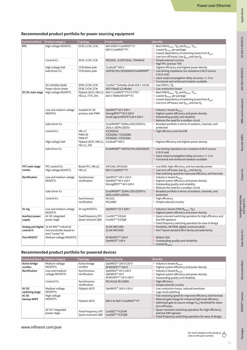
51
For more details on the product, click on the part number.
Recommended product portfolio for power sourcing equipment
Recommended product portfolio for powered devices
Recommended products powered device
www.infineon.com/poe
Functional block Product category Topology Product family BenefitsPFC High voltage MOSFETs DCM, CrCM, CCM, 600 V/650 V CoolMOS™ C7
600 V CoolMOS™ P7 › Best FOM RDS(on) *QG and RDS(on) *Eoss › Lowest RDS(on) per package › Lowest dependency of switching losses from Rg,ext › Low turn-off losses, low Qoss, and low QG
Control ICs DCM, CrCM, CCM IRS2505L, ICE3PCS0xG, TDA4863G › Simple external circuitry › High PFC and low THD
High voltage GaN CCM totem pole CoolGaN™ 600 V › Highest efficiency and highest power densityGaN driver ICs CCM totem pole 1EDF5673Fx/1EDS5663H EiceDRIVER™ › Low driving impedance (on-resistance 0.85 Ω source,
0.35 Ω sink) › Input-output propagation delay accuracy: +/- 5 ns › Functional and reinforced isolation available
SiC schottky diode DCM, CrCM, CCM CoolSiC™ Schottky diode 650 V G5/G6 › Low FOM VF *QC
Power silicon diode DCM, CrCM, CCM 650 V Rapid 1/2 diodes › Low conduction lossesDC-DC main stage High voltage MOSFETs Flyback (ACF), HB LLC,
FB LLC, ITTF, ZVS600 V CoolMOS™ P7/C7/CFD7650 V TRENCHSTOP™ F5
› Best FOM RDS(on) *QG and RDS(on) *Eoss › Lowest RDS(on) per package › Lowest dependency of switching losses from Rg,ext › Low turn-off losses, low Qoss, and low QG
Low and medium voltage MOSFETs
Isolated DC-DC primary-side PWM
OptiMOS™ 60 V-200 VStrongIRFET™ 60 V-200 VSmall signal MOSFETs 60 V-200 V
› Industry’s lowest RDS(on) › Highest system efficiency and power density › Outstanding quality and reliability › Reduces the need for a snubber circuit
Gate driver ICs - EiceDRIVER™ 1EDNx/1EDi/2EDN7x/2EDLx/ 2EDFx/2EDSx
› Broadest portfolio in terms of isolation, channels, and protection
Control ICs HB LLCPWM-QFPWM-FF
ICE2HS01GICE5QSAG / ICE5QSBGICE5ASAG / ICE5GSAG
› High efficiency and low EMI
High voltage GaN Flyback (ACF), HB LLC, FB LLC, ZVS
CoolGaN™ 600 V › Highest efficiency and highest power density
GaN driver ICs - EiceDRIVER™ 1EDF5673Fx/1EDS5663H › Low driving impedance (on-resistance 0.85 Ω source, 0.35 Ω sink)
› Input-output propagation delay accuracy: +/- 5 ns › Functional and reinforced isolation available
PFC-main stage combo
PFC control ICs Boost PFC, HB LLC IDP2308, IDP2303A › Low BOM, high efficiency, and low standby powerHigh voltage MOSFETs HB LLC 600 V CoolMOS™ P7 › Low turn-off losses, low Qoss, and low QG
› Fast-switching speed for improved efficiency and thermalsRectification Low and medium voltage
MOSFETsSynchronous rectification
OptiMOS™ 100 V-150 VOptiMOS™ 40 V-120 VStrongIRFET™ 40 V-100 V
› Industry’s lowest RDS(on) › Highest system efficiency and power density › Outstanding quality and reliability › Reduces the need for a snubber circuit
Gate driver ICs - EiceDRIVER™ 1EDNx/1EDi/2EDN7x/2EDLx/2EDFx/2EDSx
› Broadest portfolio in terms of isolation, channels, and protection
Control ICs Synchronous rectification
IR1161LIR11688S
› High efficiency › Simple external circuitry
Or-ing Low and medium voltage MOSFETs
Or-ing MOSFETs OptiMOS™ 25 V-200 V › Industry’s lowest FOM (RDS(on) *QG) › Highest system efficiency and power density
Auxiliary power supply
AC-DC integrated power stage
Fixed frequency (FF) Quasi resonant (QR)
CoolSET™ ICE5xRCoolSET™ ICE5QR
› Quasi-resonant switching operation for high efficiency and low EMI signature
› Fixed frequency switching operation for ease of designAnalog and digital control IC
32-bit XMC™ industrial microcontroller based on Arm® Cortex®-M
- 32-bit XMC100032-bit XMC4000
› Flexibility, HR PWM, digital communication › Arm® based standard MCU family and wide family
Port MOSFET Medium voltage MOSFETs - IR MOSFET™ 100 VOptiMOS™ 100 V
› Widest SOA › Outstanding quality and reliability › Lowest RDS(on)
Functional block Product category Topology Product family BenefitsActive bridge rectifier
Medium voltage MOSFETs
Active bridgerectifier
OptiMOS™ 100 V-150 V › Industry’s lowest RDS(on) › Highest system efficiency and power densityIR MOSFET™ 100 V
Rectification Low and medium voltage MOSFETs
Synchronous rectification
OptiMOS™ 25 V-100 VOptiMOS™ 40 VIR MOSFET™ 20 V-100 V
› Industry’s lowest RDS(on) › Highest system efficiency and power density › Outstanding quality and reliability
Control ICs Synchronous rectification
IR1161L& IR11688S › High efficiency › Simple external circuitry
DC-DC switching stage
Medium voltage MOSFETs
Flyback (ACF) OptiMOS™ 100 V-150 V › Low conduction losses, reduced overshoot › Logic level switching
AC-DC backup SMPS
High voltage MOSFETs
Flyback (ACF) 600 V to 950 V CoolMOS™ P7
› Fast-switching speed for improved efficiency and thermals › Reduced gate charge for enhanced light load efficiency › Optimized gate-to-source voltage (VGS) threshold for lower
turn-off lossesAC-DC integrated power stage Fixed frequency (FF)
Quasi resonant (QR)CoolSET™ ICE5xRCoolSET™ ICE5QR
› Quasi-resonant switching operation for high efficiency and low EMI signatur
› Fixed frequency switching operation for ease of design
Power over Ethernet
Appl
icat
ions
Pack
ages
20-3
00 V
MO
SFET
s50
0-95
0 V
MO
SFET
sW
BG se
mic
ondu
ctor
sDi
scre
te IG
BTs
Pow
er IC
sIn
telli
gent
switc
hes
and
inpu
t ICs
Gate
driv
er IC
sM
icro
cont
rolle
rsXE
NSIV
™ se
nsor
s

52
For more details on the product, click on the part number.
LED lightingSolutions for cost sensitive applications as well as for smart lighting
At Infineon, we focus on supplying tailored products for LED drivers, LED strips, horticultural, and smart lighting. Our broad portfolio of tailored products and solutions for LED lighting comprises LED driver ICs, MOSFETs, and microcontrollers suited for LED drivers as well sensors and dedicated ICs for secure communication. In addition to offering products of proven quality, a competent global lighting team supports our lighting customers in designing LED lighting products and systems in collaboration with our channel partners.
Key trends and challenges in LED lighting and our offering: › Human-centric lighting (HCL)
– The lowest cost implementation of tunable white with single-stage flyback constant voltage and smart linear regulators with advanced headroom control ensuring high efficiency – BCR601
› Configuration of output current and some further parameters – Our NFC controller allows the configuration of the output current without the need of an
additional microcontroller – Our XDPL lighting IC family allows, besides output current, also adjustment of other features
like protection, dimming curves, etc. › Cost reduction combined with efficiency increase
– Integration of resonance inductor for PFC + resonant topology enables highest efficiency at low cost. Integration is enabled by the coreless transformer technology that enables high switching frequencies
LED drivers
AC-lineinput
MCUcommunication
intellegent control
Hardware-basedsecurity
Wired/wirelesscommunication
0-10 Vdimming interface
Sensorshub
LED module
Dimmer
PFC stage Main stage
Combo IC
LED lighting
www.infineon.com/lighting

53
For more details on the product, click on the part number.
Recommended LED driver products
www.infineon.com/lighting
Functional block Product type Product family MOSFET technology Voltage classPFC stage PFC IRS2505 CoolMOS™ P7 600/700/800/950 V 1)
Main stage PFC + LCC (constant current)PFC + LLC (constant current)
ICL5102 2) CoolMOS™ P7 (up to 600 mΩ) 600 V/650 V
CoolMOS™ CE (above to 600 mΩ) 600 V
PFC + flyback (dual stage) XDPL8220 3) / XDPL8221 2) CoolMOS™ P7 800 V/950 V
PFC/flyback (single-stage constant voltage) XDPL8105 CoolMOS™ P7 800 V/950 V
PFC/flyback (single-stage constant voltage) XDPL8218 CoolMOS™ P7 800 V/950 V
Buck / linear solutions Secondary buck (single-channel) Secondary buck (multichannel)
ILD6150 / ILD8150 Integrated 60 V/80 V
Secondary linear BCR601 Small signal MOSFETs 75 V/100 V
Synchronous rectification Synchronous rectification controller IR1161 / IR11688 OptiMOS™ 100 V/150 V/200 V
Dimming 0-10 V dimming interface IC CDM10 V - -
CDM10 VD - -
NFC NFC controller NLM0010 / NLM0011 * - -
Hardware based security OPTIGA™ OPTIGA™ Trust - -
Microcontroller XMC™ microcontroller XMC1100 - -
Sensors XENSIV™ radar sensor IC BGT24LTR11 - -
LED driver with constant voltage output and linear/switch mode LED driver ICs
Linear LED driver IC product portfolio
For additional portfolio of lighting ICs, take a look at pages 242-257.
Functional block Topology IC product family MOSFET technologyLowest cost LED driver IC Linear BCR400W series Integrated
Low voltage drop LED driver IC BCR430 / BCR431 * *
Robust LED driver IC BCR40xU / BCR42xU
1) 700 V, 800 V and 950 V CoolMOS™ P7 are optimized for PFC and flyback topologies. 600 V CoolMOS™ P7 is suitable for hard as well as soft switching topologies (flyback, PFC and LLC)
2) PFC and resonant combo controllers 3) PFC and flyback combo controllers *Contains besides current configuration also Constant Lumen Output (CLO) feature
* * For more information on the product, contact our product support
AC-lineinput Synchronous
rectificationMainstage
PFC stage Linear LEDdriver IC
Appl
icat
ions
Pack
ages
20-3
00 V
MO
SFET
s50
0-95
0 V
MO
SFET
sW
BG se
mic
ondu
ctor
sDi
scre
te IG
BTs
Pow
er IC
sIn
telli
gent
switc
hes
and
inpu
t ICs
Gate
driv
er IC
sM
icro
cont
rolle
rsXE
NSIV
™ se
nsor
s

54
For more details on the product, click on the part number.
Infineon is bringing reliability and safety to consumer projects. Millions of households worldwide rely on power tools to complete daily tasks or creative projects around the home. Consumers want robust, reliable and portable power tools that are easy-to-use with low price and long battery life as key selection options. Battery-powered tools must also be equipped with diagnostic and safety features to ensure confidence with high quality.
Infineon’s broad portfolio offers best-fit, innovative solutions for all power tools applications. We help you meet each consumer need and reduce your overall costs. Also, our wireless-charging reference designs deliver high performance and are easily optimized in our DAVE™ development platform. Configure your BOM and exceed expectations with Infineon components in your cordless power tool designs.
www.infineon.com/powertools
Power and gardening toolsBattery-powered home and professional applications
Features and benefits
Key features
Comprehensive portfolio of products and solutions, easy to tailor to design specification
Infineon offers complete solutions for power supplies, chargers and motor drives
Best-in-class MOSFETs e.g. OptiMOS™ and HEXFET™/StrongIRFET™ extend battery lifetime and reduce chances for control failure
High reliability of Infineon components
Offering LV FETs with SMD packaging improves the productive capability by automatic production, improves reliability and reduces assembly cost
Components featuring small form factor and compact design offering highest power density and BOM savings thanks to lowest RDS(on)
Trustworthy hardware-based security
Highest quality standards and a safety-certified development process
Proven track record and outstanding partner network for embedded security
OPTIGA™ Trust enables authentication of components connected to the system (e.g., battery pack recognition to avoid second-party batteries etc.)
Evaluation and demonstration boards for fast prototyping
Available simulations, documentation, and system support to reduce develop-ment time and cost
Key benefits
Convenient selection of the right fit products thanks to broad portfolio and complete solutions
Extended battery lifetime and product life span
Productive capability
Overall system size and cost reduction
Security, quality, and safety
Authentication
Short time to market
Power and gardening tools

55
For more details on the product, click on the part number.
www.infineon.com/powertools
Current sensing
MOSFET temperature sensing
Position sensing
Gate driver
3-phaseinverter
USB,serialCOM
XMC1000microcontroller
Userinterface
DC-DC Battery18-36 V
Motor temperature sensing
M Hallsensors
Application block diagram example: cordless power tools
Infineon product offering Home and professional applicationsSupply voltage 10.8-56 V
OptiMOS™ and HEXFET™/StrongIRFET™power MOSFETs
Voltage 20-100 V
Package SuperSO8, PQFN 3x3, DirectFET™ S/M/L-Can, TOLL, TO-220, TO-247, DPAK, D²PAK, D²PAK 7-pin
CoolMOS™ P7 SJ MOSFET * Voltage 600-700 V
Gate driver ICs EiceDRIVER™ 1EDN/2EDN/6EDL04N02PR, 6ED003L02- F2, 2EDL05N06PF, 2ED2304S06F, IRS2005S/M, IRS2007S, IRS2008S, IRS2301 *, IRS21867, IRS2304Integrated: IFX9201SG/ BTN8982
IPM – CIPOS™ Nano IRSM005-800MH, IRSM005-301MH
Authentication IC, security OPTIGA™ Trust B
XMC™ microcontrollersiMotion™ePower
XMC1300, XMC4400/XMC4500, iMOTION™ IRMCK099MePower: TLE987X (BLDC)
Microcontroller and driver supply:linear voltage and DC-DC switching regulators
IFX1763/IFX54441/IFX54211/IFX30081/IFX90121/IFX91041
CAN transceivers IFX1050, IFX1051
XENSIV™ sensors Hall switches (TLE496X *), Angle sensor (TLI5012B), 3D magnetic sensor (TLV493D)
*For more information on the product, contact our product support
Appl
icat
ions
Pack
ages
20-3
00 V
MO
SFET
s50
0-95
0 V
MO
SFET
sW
BG se
mic
ondu
ctor
sDi
scre
te IG
BTs
Pow
er IC
sIn
telli
gent
switc
hes
and
inpu
t ICs
Gate
driv
er IC
sM
icro
cont
rolle
rsXE
NSIV
™ se
nsor
s

56
For more details on the product, click on the part number.
Everyday routine is being increasingly pervaded by a growing number of wireless and battery powered devices – electric vehicles (EVs) among them. This trend further drives a steadily rising demand for the production of batteries with different charging capacities. Consequently, battery manufacturers find themselves confronted with the challenge to increase efficiency throughout their production and meet the required volume.
The essential stage every battery needs to undergo in the manufacturing process is battery formation. In it, the newly assembled batteries are initially charged and discharged with high voltage and current accuracy with the aim to activate the battery material. Formation cycling has great impact on battery lifetime, quality and cost, but is currently the bottleneck in the production process as it is expensive and time-consuming.
With its comprehensive product portfolio of cost- and efficiency-optimized products Infineon offers full-spectrum power system solutions, and adequately addresses the application requirements of high accuracy, efficiency and power density.
Application diagram
Battery formationSolutions that make battery formation equipment more accurate and efficient
Features and benefits
Key features
High voltage and current accuracy (up to 0.01%) during charge and discharge cycles
High power density
High efficiency
Optimal thermal management during operation
High system reliability due to 24/7 operation cycles
Key benefits
Highly efficient, innovative and cost-attractive solutions leading to overall BOM savings enabling size reduction
High power density semiconductors
Fast time to market due to the complete ecosystem: › Simulations › Documentation › Demonstration boards
Increased lifetime and reliability due to Infineon’s quality
One-stop-shop portfolio
Control unit
Bidirectional AC-DC
Totem pole PFC boost converter
AC grid
Bidirectional DC-DC Non-isolated Bidirectional DC-DC
Dual active bridge resonance converter
V_PFC V_Bus
V_Bat
Buck/boost converter
CIN CIN
N
Gate driver
XMC™ microcontroller
Auxiliary power supplyCoolSET™ 5
COUT
COUT
Rsense
L1L2L3 Eice
DRIVER™
www.infineon.com/batteryformation
Battery formation

57
For more details on the product, click on the part number.
www.infineon.com/batteryformation
Highlight/ recommended product portfolio
Functional block Product category Topology Product family BenefitsBi-directionalAC-DC – PFC
CoolMOS™ MOSFET 600 V & 650 V TO-247 › Best-in-class Qrr and trr level › Significantly reduced QG › Improved efficiency over previous CoolMOS™ fast body diode series
CoolSiC™ MOSFET 650 V & 1200 V TO-247 › Input neededTRENCHSTOP™ 5 IGBT 650 V TO-247 › Best-in-class efficiency, resulting in lower junction and case temperature
leading to higher device reliability › Higher power density designs
TRENCHSTOP™ 6 IGBT 1200 V TO-247 › Low conduction losses with 1.85 V, VCE(sat) for S6 series › Full rated, robust freewheeling diode
Gate driver 650 or 1200 V EiceDRIVER™ PG-DSO-16 › Integrated bootstrap diode › Low level shift loss › Excellent ruggedness against negative transient voltages on VS pin
Bi-directionalisolatedDC-DC
CoolMOS™ MOSFET 600 V and 650 V TO-247, D2PAK › Best-in-class Qrr and trr level › Significantly reduced QG › Improved efficiency over previous CoolMOS™ fast body diode series
CoolSiC™ MOSFET 650 V and 1200 V TO-247 › Combination of high performance, high reliability and ease of useTRENCHSTOP™ 5 IGBT 650 V TO-247 › Best-in-class efficiency, resulting in lower junction and case temperature
leading to higher device reliability › Higher power density designs
OptiMOS™ MOSFET 60 V – 150 V Shrink SuperSO8SuperSO8TOLLD2PAK
› Lowest RDS(on) › Ideal for high switching frequency › Increased power density › Reduced system cost › Less parallelingBi-directional
non-isolatedDC-DC
OptiMOS™ MOSFET 25 V – 60 V Shrink SuperSO8SuperSO8TOLLD2PAK
OptiMOS™ Power block 25 V and 30 V Power stage 5x6 › Integrated solution with low side and high side MOSFET › Space reduction › Minimized loop inductance › Higher efficiency
Gate driver ICs Low-side with truly differential input
1EDNx550 in PG-SOT23-6
› Control inputs independent from gate driver GND › Fast Miller plateau transition › Robust against false MOSFET triggering › Increased power density and BOM savings
Functional level shift 2EDL in QFN package › Level-shift high and low side dual channel driver › Strong source and sink current capability › 120 V on-chip bootstrap diode › Fast propagation delay
Appl
icat
ions
Pack
ages
20-3
00 V
MO
SFET
s50
0-95
0 V
MO
SFET
sW
BG se
mic
ondu
ctor
sDi
scre
te IG
BTs
Pow
er IC
sIn
telli
gent
switc
hes
and
inpu
t ICs
Gate
driv
er IC
sM
icro
cont
rolle
rsXE
NSIV
™ se
nsor
s

58
For more details on the product, click on the part number.
Facing diminishing fossil reserves, the world nonetheless needs to manage rising demand for electrical energy while meeting the growing call for urgent climate action. The transition to renewable energies has become inevitable.
Energy storage systems are a vital part to successfully manage this transition. Our system solutions help to make energy storage the backbone of the new energy era. Our unique application expertise and comprehensive offering makes us the natural choice to advance energy storage solutions in terms of efficiency, performance, optimal cost, and Energy storage systems are a vital part to successfully manage this transition. Our system solutions help to make energy storage the backbone of the new energy era. Our unique application expertise and comprehensive offering makes us the natural choice to advance energy storage solutions in terms of efficiency, performance, optimal cost, and innovation.
www.infineon.com/energy-storage-systems
Application diagram
Energy storage systemsMake energy storage systems the backbone of the new energy era with our semiconductor system solutions
Features and benefits
Key features
Eficcient power convertion in DC-DC and AC-DC stage
Power dense design
Bi- direcitonal power flow
Safe operation of Lithium-ion battery
Long battery life time
Key benefits
Improvement of system performance with industry leading semiconductor offering such as OptiMOS™, CoolMOS™, CoolSiC™ MOSFETs but also best-in-class modules
Reduction of design efforts and faster time to market
Trust in a true partnership during the whole system lifetime
Full system provider form power conversion stage (PCS) to the battery management system (BMS)
Energy storage systems
Grid
AC load
Gate driver
...
SensingSensing/
MontioringProtection
BMS
Security
XMC™ Microcontroller
DC-DCBattery
conversionDC-AC
conversion
Gate driver Sensing
Auxiliary powersupply
Gate driver
...
...

59
For more details on the product, click on the part number.
www.infineon.com/energy-storage-systems
Highlight/ recommended product portfolio
Functional block Power/battery voltage
Voltage class
[VDS max]
Product family Package Benefits
Power conversion systems (PCS)
< 10 kW 150 V OptiMOS™ Super S08, TOLL › High power density and system cost reduction
600 V/650 V CoolMOS™ CFD7 / S7 TO-220/247, ThinPAK 8x8, TOLL
› Highest efficiency, enabling increased power density / more compact and easier design
600 V CoolSiC™ Schottky diode G6 TO-220 › Improved system efficiency and extremely fast switching
650 V CoolSiC™ MOSFET TO-247 › Combination of high performance, high reliability and ease of use
10-100 kW 150 V OptiMOS™ TO-263 › High power density and system cost reduction
600 V CoolMOS™ C7/P7 TO-247 › Ease of use and fast design-in
650 V CoolSiC™ MOSFET TO-247 › Combination of high performance, high reliability and ease of use
650 V TRENCHSTOP™ 5 H5 TO-247 › Benefit increase at high current conditions
650 V CoolSiC™ Schottky diode C6 TO-220 › Higher frequency and increased power density
1200 V CoolSiC™ MOSFET TO-247 › Highest efficiency and increased power density
1200 V TRENCHSTOP™ 5/6 or S6 TO-247 › High device reliability and lifetime expectancy
101-250 kW 150 V OptiMOS™ D2PAK › Enables and simplifies the setup of 2nd life batteries › Lower switching voltage enables higher inverter efficiency
200 V OptiMOS™ D2PAK › Enables and simplifies the setup of 2nd life batteries › Lower switching voltage enables higher inverter efficiency
1200 V EasyPACK™ 2B Modules › Highest efficiency for reduced cooling effort
1700 V PrimePACK™/ EconoDUAL™ Modules › High power density › Easy and most reliable assembly> 0.25 MW 1200 V PrimePACK™ / EconoDUAL™ Modules
1700 V PrimePACK™/ EconoDUAL™ Modules
Gate driver EiceDRIVER™ 2EDS PG-DSO-16-NB › Dual-channel functional isolated › Dual-channel reinforced (safe) isolated › Single-channel non-isolatedEiceDRIVER™ 2EDF PG-DSO-16-NB
EiceDRIVER™ 1EDN PG-SOT23-6
BMS – battery protection
40-60 V 100 V OptiMOS™/OptiMOS™ LinearFET TOLL, D2PAK › Highest system efficiency › Minimize parallelization of MOSFETs › Market leading MOSFETS with lowest RDSon enabling low
conduction losses › Widest SOA area with LinearFET™
60-100 V 150 V OptiMOS™/OptiMOS™ LinearFET TOLL, D2PAK
100-150 V 200-300 V OptiMOS™/OptiMOS™ LinearFET D2PAK
150-400 V 600 V CoolMOS™ S7 TO-247 › Lowest RDS(on) MOSFET
Appl
icat
ions
Pack
ages
20-3
00 V
MO
SFET
s50
0-95
0 V
MO
SFET
sW
BG se
mic
ondu
ctor
sDi
scre
te IG
BTs
Pow
er IC
sIn
telli
gent
switc
hes
and
inpu
t ICs
Gate
driv
er IC
sM
icro
cont
rolle
rsXE
NSIV
™ se
nsor
s

60
Solar
For more details on the product, click on the part number.
Infineon provides a comprehensive portfolio to deliver the best efficiency and reliability for solar applications. Infineon’s cutting edge technologies such as CoolMOS™ SJ MOSFETs, HighSpeed3 IGBT and TRENCHSTOP™ 5, CoolSiC™ Schottky diodes, CoolSiC™ MOSFETs, coreless transformer, driver, etc. combined with the rich experience and highest quality ensure the company’s leader position in solar applications. The newly added Arm® Cortex™-M4 based MCU enables easy and high efficiency design.
Infineon’s products for complete solar system
Solar
High efficiency designs for solar power systems
Optimizer250-750 W
Single and multiple panel micro inverter250 -1500 W
String inverter1-200 kW
BAT165 Schottky diode
Auxiliary power supply CoolSET™800 V
MOSFETsOptiMOS™
SuperSO8/DirectFET™ | 60-150 V
CoolMOS™ TOLL/D2PAK | 600-800 V
CoolMOS™ TO-247-3/TO-247-4 | 600/650 V
OptiMOS™ 150-300 V
Microcontrollers
XMC1xxx Arm® Cortex®-M0 XMC1xxx Arm® Cortex®-M0XMC1xxx Arm® Cortex®-M0
XMC45xx Arm® Cortex®-M4 XMC45xx Arm® Cortex®-M4XMC45xx Arm® Cortex®-M4
SiC MOSFETs
SiC diodes
Easy 1B/2B
650 V TRENCHSTOP™ 5 / 1200 V HighSpeed 3TO-247-3/TO-247-4/TO-247PLUS | 600 V/650 V/1200 V
Gate driver ICs EiceDRIVER™2EDi/1ED Compact/SOI/ ED-F2/X3Compact/1EDB
Central inverter 500-5000 kW
XMC1xxx Arm® Cortex®-M0
XMC45xx Arm® Cortex®-M4
PrimePACK™ / EconoDUAL™ 3 / 62 mm
EiceDRIVER™1ED Compact/1ED-F2/X3Compact/X3A/X3D/1EDB
EiceDRIVER™ 2EDi/1EDB/1EDCompact/SOI/1ED-F2/1EDB
EiceDRIVER™ 2EDi/1EDCompact/SOI/1EDB
OptiMOS™SuperSO8 | DirectFET™ 60-200V
CoolSiC™ MOSFETTO-247-3/TO-247-4 | 1200 V
IGBTs
CoolSiC™ Schottky diodesDPAK/TO-220 | 600 V/1200 V
D2PAK | 650 V
CoolSiC™ Schottky diodes TO-220/TO-247/TO-247-2/DPAK/D2PAK| 650 V/1200 V
www.infineon.com/solar
Solar
GridPhotovoltaicpanels
EiceDRIVER™...
Sensing
MPPTcalculation
PWMgeneration ADC
MCU with ARM® Cortex®-M4
MPP trackerDC-DC conversion
DC-ACconversion
EiceDRIVER™Sensing
Auxiliary powersupply
Energy storage(optional)
EiceDRIVER™Sensing
Battery management
...
...

61
For more details on the product, click on the part number.
Optimizer
Microinverter
Micro inverter can either be used per › single (~300 W) PV panel or › multiple PV panels (600 – 1500 W)
www.infineon.com/solar
DC 20 to 150 V45 V (typ.)
~ DC 80 V (typ.)
MPPTcalculation
PWMgeneration ADC
XMC1000
Opt
iMO
S™O
ptiM
OS™
Opt
iMO
S™O
ptiM
OS™
PV
Microcontrollerpower supply
Gate driver ICs
Functional block
Product family
Input voltage
Voltage class [VDS max]
Package * Part number *
RDS(on)
Buck boostMPPT
OptiMOS™ ≤ 48 V 60 V SuperSO8 BSC012N06NS 1.2 mΩ
DirectFET™ BSB028N06NN3 G 2.8 mΩ
≤ 64 V 80 V SuperSO8 BSC021N08NS5 2.1 mΩ
DirectFET™ BSB044N08NN3 G 4.4 mΩ
≤ 80 V 100 V SuperSO8 BSC027N10NS5 2.7 mΩ
DirectFET™ BSB056N10NN3 G 5.6 mΩ
≤ 125 V 150 V SuperSO8 BSC220N20NSFD 9.3 mΩ
Gate driver ICs Single channel PG-SOT23-6 1EDN8550
Dual channel VDSON 2EDL81xx
Microcontroller XMC1000
Functional block Product family Voltage class [VDS max] Package * Part number * RDS(on)
MPPT – Boost stage OptiMOS™ 60 V SuperSO8 BSC028N06NS 2.8 mΩ
80 V BSC026N08NS5 2.6 mΩ
120 V BSC190N12NS3 19.0 mΩ
150 V BSC093N15NS5 9.3 mΩ
BSC160N15NS5 16.0 mΩ
CoolSiCTM Schottky diode 1200 V DPAK IDM02G120C5 2.0 A
IDM05G120C5 5.0 A
IDM08G120C5 8.0 A
Gate driver: EiceDRIVER™ VDSON-8 2EDL81xx
PG-DSO-8-60/PG-TSSOP-8-1 2EDN7524F
Inverter stage CoolMOS™ 600 V TO-Leadless IPT60R102G7 102.0 mΩ
D2PAK IPB60R145CDF7 * 145.0 mΩ
TO-247 IPW60R145CFD7 145.0 mΩ
650 V D2PAK IPB65R150CFD 150.0 mΩ
TO-247 IPW65R150CFD 150.0 mΩ
Gate driver: EiceDRIVER™ PG-DSO-16 2EDS8165H
2EDS8265H
Microcontroller XMC1000, XMC4000
Solar
*For more information on the product, contact our product support
Appl
icat
ions
Pack
ages
20-3
00 V
MO
SFET
s50
0-95
0 V
MO
SFET
sW
BG se
mic
ondu
ctor
sDi
scre
te IG
BTs
Pow
er IC
sIn
telli
gent
switc
hes
and
inpu
t ICs
Gate
driv
er IC
sM
icro
cont
rolle
rsXE
NSIV
™ se
nsor
s

62
For more details on the product, click on the part number.
Solar
PV
PV
EiceDRIVER™ EiceDRIVER™Sensors
MPPTcalculation
PWMgeneration
ADC
XMC4000MPPT
PWM
Boost
TREN
CHST
OP™
5
Opt
iMO
S™ 5 OptiMOS™ 5
OptiMOS™ 5 OptiMOS™ 5Opt
iMO
S™ 5
Opt
iMO
S™ 5
Opt
iMO
S™ 5
PV
Grid
Multilevel inverter
Microcontrollerpower supply
SiC diode /Rapid diode
OptiMOS™ 5
Single-phase string inverter – multilevel topology
In multilevel inverter, four high voltage MOSFETs/IGBTs in H-bridge topology are replaced with a higher number of lower voltage MOSFETs. Compared to a conventional H-bridge inverter, a multilevel inverter, composed of lower voltage MOSFETs, offers several advantages: › With much lower RDS(on) and switching loss parameters it significantly reduces conduction and switching losses › Higher effective output frequency (smaller magnetics) is possible with lower switching losses › Improved EMC due to reduced switching voltages › Significant reduction in cooling system, size and weight
Discrete power devices for multilevel string inverter
Functional block Product family Voltage class [VDS max] Package Part number RDS(on)
Boost CoolMOS™ 600 V TO-247 IPW60R017C7 17 mΩ
TO-247 IPW60R024P7 24 mΩ
D2PAK IPB60R045P7 45 mΩ
IGBT TRENCHSTOP™ 5 650 V TO-247 IKW40N65EH5, IKW40N65ES5
40 A
D2PAK IKB40N65EH5, IKB40N65ES5 40 A
CoolSiC™ Schottky diode 650 V TO-247 IDW20G65C5 20 A
EiceDRIVER™ 1EDN PG-SOT23-6 1EDN8511B 4 A / 8 A
Flying-capacitor-based active neutral-point-clamp (NPC)
OptiMOS™ 150 V SuperSO8 BSC093N15NS5 9.3 mΩ
SuperSO8 BSC110N15NS5 11 mΩ
DirectFET™ IRF150DM115 * 11.3 mΩ
D2PAK IPB044N15N5 4.4 mΩ
D2PAK IPB048N15N5 4.8 mΩ
Gate driver ICs EiceDRIVER™ 2EDi NB-DSO16 2EDF7275F 4 A / 8 A
Microcontroller XMC4000
www.infineon.com/solar *For more information on the product, contact our product support

63
For more details on the product, click on the part number.
Solar
Single-phase string inverter
Three-phase string inverter
www.infineon.com/solar
H4 topology
Discrete power devices for string inverter
H6 topology
Inverter
PV
PV
EiceDRIVER™
...
EiceDRIVER™
...
Sensors
MPPTcalculation
PWMgeneration ADC
XMC4000MPPT
PWM
Boost
Cool
MO
S™
CoolSiC™Schottky
diode
Cool
MO
S™/T
REN
CHST
OP™
< 600 DC(typ.)
Grid
Cool
MO
S™/
TREN
CHST
OP™
Microcontrollerpower supply
Inverter
PV
PV
EiceDRIVER™
...
EiceDRIVER™
...
Sensors
MPPTcalculation
PWMgeneration ADC
XMC4000MPPT
PWM
Boost
Cool
MO
S™
CoolSiC™Schottky
diode
400 DC(typ.)
Grid
Microcontrollerpower supply
CircuitBreaking
Cool
MO
S™/T
REN
CHST
OP™
Inverter type
Functional block
Product category
Product technology
Voltage Package Part number RDS(on) Ampere
Single phase MPPT – Boost stage
Si MOSFET CoolMOS™ P7 600 V TO-247-3 IPW60R037P7 37 mΩ -
TO-247-4 IPZA60R037P7 37 mΩ -
SiC MOSFET CoolSiC™ MOSFET 650 V TO-247-4 IMZA65R027M1H 27 mΩ -TO-247-3 IMW65R048M1H 48 mΩ -
1200 V TO-247-3 IMW120R045M1 45 mΩ -IGBT TRENCHSTOP™ 5
S5/H5650 V TO-247-3 IKW40N65ES5, IKW40N65EH5 - 40 A
TO-247-4 IKZ50N65ES5, IKZ50N65EH5 - 50 ADiode CoolSiC™ diode 650 V TO-247 IDW20G65C5 - 20 A
Inverter Si MOSFET CoolMOS™ C7 650 V TO-247-3 IPW65R65C7 * 65 mΩ -CoolMOS™ S7 600 V TO-Leadless IPT60R022S7 22 mΩ -
IPT60R040S7 40 mΩ -CoolMOS™ CFD 7 600 V TO-247-3 IPW60R018CFD7 18 -
600 V TO-247-3 IPW60R031CFD7 31 -SiC MOSFET CoolSiC™ MOSFET 650 V TO-247-4 IMZA65R027M1H 27 mΩ -
TO-247-3 IMW65R048M1H 48 mΩ -1200 V TO-247-3 IMW120R045M1 45 mΩ -
IGBT TRENCHSTOP™ 5 S5/H5
650 V TO-247-4 IKZ50N65ES5, IKZ50N65EH5 - 50 ATO-247-3 IKW40N65ES5, IKW40N65EH5 * - 40 A
Gate driver ICs EiceDRIVER™ 1ED Compact, EiceDRIVER™ 2EDN FamilyThree phase MPPT
– Boost stage
IGBT HighSpeed 3 1200 V TO-247-3 IKW40N120H3 - 40 ATO-247PLUS-3 IKQ75N120CH3 - 75 A
SiC MOSFET CoolSiC™ MOSFET 1200 V TO-247-3/-4 IMW120R030M1H, IMZ120R030M1H 30 mΩ -IMW120R045M1, IMZ120R045M1 45 mΩ -IMW120R060M1H, IMZ120R060M1H 60 mΩ -
Inverter IGBT HighSpeed 3 1200 V TO-247-3 IKW40N120H3 - 40 ATO-247PLUS-3 IKQ750N120CH3 * - 75 A
SiC MOSFET CoolSiC™ MOSFET 1200 V TO-247-3/-4 IMW120R030M1H, IMZ120R030M1H 30 mΩ -IMW120R045M1, IMZ120R045M1 45 mΩ -IMW120R060M1H, IMZ120R060M1H 60 mΩ -
Gate driver ICs EiceDRIVER™ 1ED Compact, EiceDRIVER™ 2EDN family, EiceDRIVER™ 1EDBMicrocontroller XMC4000
Inverter
PV
PV
EiceDRIVER™
...
Sensors
MPPTcalculation
PWMgeneration ADC
XMC4000MPPT
PWM
Boost
1200
V H
ighS
peed
3/
Cool
SiC™
MO
SFET
<1000 V(typ.) 3~
Grid
650 VTRENCHSTOP™ 5
Grid
Microcontrollerpower supply
EiceDRIVER™
...
Phase A
Phase B
Phase C
1200 VCoolSiC™Schottky diode
1200 VCoolSiC™MOSFET
1200
V H
ighS
peed
3 /
Cool
SiC™
MO
SFET
*For more information on the product, contact our product support
Appl
icat
ions
Pack
ages
20-3
00 V
MO
SFET
s50
0-95
0 V
MO
SFET
sW
BG se
mic
ondu
ctor
sDi
scre
te IG
BTs
Pow
er IC
sIn
telli
gent
switc
hes
and
inpu
t ICs
Gate
driv
er IC
sM
icro
cont
rolle
rsXE
NSIV
™ se
nsor
s

64
Uninterruptible power supply
For more details on the product, click on the part number.
UPS
Uninterruptible power supply (UPS)Attractive solutions for highest efficiency and power density
Today’s uninterruptible power supply systems introduce a wide range of challenges. Overcoming them requires anincrease in output power, energy efficiency and power density. We offer complete system-level solutions and highquality products for diverse uninterruptible power supply applications. Equipped with our semiconductors, UPSapplications can achieve best-possible power-conversion efficiency and cutting-edge power density. The benefits arecost reduction and fewer passive components – regardless of the topology used.
Our solutions and products for UPS applications fulfill the latest market requirements. This includes the trend ofmodularization of UPS brick units due to scalable power demand from data centers, as well as the topology shiftfrom two-level to three-level to achieve higher efficiency. Our products are suitable for any kind of uninterruptiblepower supplies in telecom, data center, server or industrial automation environments.
www.infineon.com/ups
Offline UPS
CoolMOS™ SJ MOSFETs500-950 V
OptiMOS™ and StrongIRFET™ 20-300 V
Online UPS
MOSFETs
IGBTs
Auxiliary power supply
TRENCHSTOP™ IGBT6TRENCHSTOP™ 5 H5
CoolSET™650-800 V
SiC diodes
Driver ICs EiceDRIVER™ 1EDi EiceDRIVER™ 2EDi
XMC1300 series
CoolSiC™ Schottky diode
EiceDRIVER™ 1ED Compact
Power module and stack
Microcontrollers
EasyPACK™

65
For more details on the product, click on the part number.
UPS
Offline UPS
Bidirectional UPS power stage
Full-bridge bidirectional power stage Push-pull bidirectional power stage
Bidirectionalcharger / inverter
Battery12 V / 24 V
GridLoad
Sensing
www.infineon.com/ups
Battery voltage Topology MOSFET breakdown voltage
TO-220 TO-247 D2PAK and D2PAK-7 Gate drivers
Inverter/charger MOSFETs
12 V Push-pull 60 V IRFB7530IRFB7534IRFB7540IRFB7545
IRFP3006IRFP7530IRFP7537
IRFS7530IRFS7530-7P
IRS44273IRS4427 1EDN751x 2EDN851x *
Full-bridge 30 V40 V
IRLB3813IRLB8314IRLB8743IRFB7430 (40 V)
IRFP7430 IRFS7430 (40 V)IRFS7430-7P (40 V)
IRS211X *IRS21862EDL811X1EDN7550B
24 V Push-pull 75 V100 V
IRFB3077IRFB3207IRFB7730IRFB7734
IRFP7718 IRFS7430IRFS7734IRF3610S (100 V)IRFS4010 (100 V)
IRS44273IRS44271EDN851X2EDN852X
Full-bridge 40 V60 V
IRFB7430IRFB7434IRFB7545 (60 V)IRF60B217 (60 V)
IRFP7530IRFP3006IRFP7537
IRFS7430IRFS7430-7PIRF7430*IRFS7530-7P
IRS211X * IRS21862EDL811X1EDN7550B
48 V Push-pull 150 V IRFB4115IRFB4321IPP046N15N5 *IRFB4228IRFB4019
IRFP4568IRFP4321IRF150P220IRF150P221
IRFS4321IRFS4115IRB048N15N5*IRFS4615
IRS44273IRS44271EDN851X2EDN852X
Full-bridge 100 V IPP030N10NIRFB4110IPP086N10N3GIRFB4510IPP180N10N3G
IRFP4468IRFP4110IRF100P218IRF100P219
IRFS3610 *IRF3710SIRF8010SIRFS4510IRFS4010
IRS211X *IRS21862EDL811X1EDN8550B
72 V Push-pull 200 V IPP110N20N3IRFB4127IRFB4227IPP320N20N3IRFB4320 *
IRF200P222IRFP4668IRF200P223IRFP4127IRFP4227
IPB110N20N3LFIRFS4127IRFS4227IRFB117N20NFD *IRF200S234
IRS44273IRS44271EDN851X2EDN852X
Full-bridge 150 V IRFB4321IPP046N15N5 *
IRFP4568IRF150P220
IRFS4321IRB048N15N5 *
IRS211X *IRS21862EDL811X
Full-bridge 200 V IPP110N20N3IRFB4227
IRF200P222IRFP4668
IPB110N20N3LFIRFS4127
IRS211X *IRS21862EDL811X
Microcontrollers 12-72 V XMC1300 series
Battery +
XMC1300
PWMgeneration
ADC
Displaydrive
Battery -
LF transformer
StrongIRFET™
HB driver
Grid
HB driver
Battery +
XMC1300
PWMgeneration
ADC
Displaydrive
Battery -
LSgate driver
LSgate driver
LF transformer
StrongIRFET™
GridTap select
*For more information on the product, contact our product support
Appl
icat
ions
Pack
ages
20-3
00 V
MO
SFET
s50
0-95
0 V
MO
SFET
sW
BG se
mic
ondu
ctor
sDi
scre
te IG
BTs
Pow
er IC
sIn
telli
gent
switc
hes
and
inpu
t ICs
Gate
driv
er IC
sM
icro
cont
rolle
rsXE
NSIV
™ se
nsor
s

66
For more details on the product, click on the part number.
Unidirectional
Unidirectional power stage (output stage)
Battery12 V / 24 V
AC-DCcharger
DC-DCstep up
Inverter + filter
Multistage
GridLoad
Sensing
Unidirectional DC-DC stageBattery voltage Topology MOSFET breakdown voltage TO-220 TO-247 D2PAK and D2PAK-7 Gate drivers
12 V Push-pull 40 V IRFB7430IRFB7434
IRFP7718 IRFS7430IRFS7430-7PIRF7430 *
IRS44273IRS44271EDN851X2EDN852X60 V IRFB7540
IRFB7545IRF60B217
IRFS7530-7P
75 V IRFP7718
24 V Push-pull 75 V IRFB3077IRFB3207IRFB7730IRFB7734
IRFP7718 IRFS7730IRFS7734
100 V IRF100P218IRFP4468
IRFS4010IRF3610S
150 V IRFB4115IRFB4321IPP046N15N5*IRFB4228IRFB4019
IRF150P220IRFS4321IRFS4115IRB048N15N5 *IRFS4615
Microcontrollers XMC1300 series
www.infineon.com/ups
UPS
Battery +
XMC1300
HBdriver
PWMgeneration
ADC
Displaydrive
HBdriver
Battery -
LSgate driver
LSgate driver
HF transformer
Grid
DC-DC stageInverter stage
CoolMOS™
StrongIRFET™
*For more information on the product, contact our product support

67
For more details on the product, click on the part number.
Unidirectional inverter stage
Unidirectional charger
Battery voltage Topology MOSFET breakdown voltage TO-220 TO-247 Gate drivers
200 V Full-bridge inverter 120 VAC
300 V IPP410N30N IRFB4137
IRF300P226 IRF300P227 IRFP4868 IRFP4137
IRS211X * IRS2186
400 V Full-bridge inverter 220 VAC
500 V IPP50R280CE IPP50R380CE IPP50R190CE
IPW50R190CE IRS211X * IRS2186
Microcontrollers XMC1300 series
Battery voltage Topology MOSFET breakdown voltage TO-220 TO-247 PG-DIP-7
12-72 V Flyback 650 V CoolSET™ ICE3RBR1765JZ ICE3RBR0665JZ
12-72 V Flyback 800 V CoolMOS™ P7 IPP80R750P7 IPP80R600P7 IPP80R450P7 IPP80R360P7 IPP80R280P7
Microcontrollers Integrated, ICE3AS03LJG, ICE3BS03LJG
www.infineon.com/ups *For more information on the product, contact our product support
Appl
icat
ions
Pack
ages
20-3
00 V
MO
SFET
s50
0-95
0 V
MO
SFET
sW
BG se
mic
ondu
ctor
sDi
scre
te IG
BTs
Pow
er IC
sIn
telli
gent
switc
hes
and
inpu
t ICs
Gate
driv
er IC
sM
icro
cont
rolle
rsXE
NSIV
™ se
nsor
s

68
For more details on the product, click on the part number.
Activefront end
orrectifier
Inverter
Microcontroller
Auxiliary powersupplyvoltage
regulation
Gate driver+
isolation
Gate driver+
isolation
Grid Load
Communicationinterface
Battery charger
Online UPS
Online UPS power stage
Stage Topology Voltage class Technology Part numberRectifier Three-phase 800 V/1600 V EasyBRIDGE, EconoBRIDGE™
PFC Boost PFC / Vienna “T-type” 1200 V TRENCHSTOP™ IGBT6 IKW40N120CS6 IKQ75N120CS6
Boost PFC / Vienna rectifier 1200 V CoolSiC™ MOSFET F3L15MR12W2M1_B69
Boost PFC / Vienna “T-type” 650 V TRENCHSTOP™ 5 H5 IKW50N65EH5 IKW75N65EH5
Boost PFC 600 V/1200 V EasyPACK™
Boost PFC 1200 V CoolSiC ™ Schottky diode
PFC 600 V CoolMOS™ P7 IPP60R060P7IPB60R060P7
PFC 600 V CoolMOS™ C7 IPP60R040C7IPB60R040C7
Inverter NPC 1 650 V TRENCHSTOP™ 5 H5 IKW50N65EH5 IKW75N65EH5 IKZ50N65EH5 IKZ75N65EH5
NPC 1 650 V TRENCHSTOP™ 5 S5 IKW50N65ES5 IKW75N65ES5
NPC 1 650 V TRENCHSTOP™ HighSpeed3 IGBT Rapid diode
FS3L50R07W2H3F_B11
NPC 2 1200 V TRENCHSTOP™ IGBT6 IKW40N120CS6 IKQ75N120CS6
NPC 2 1200 V CoolSiC ™ Schottky diode
NPC 2 1200 V TRENCHSTOP™ HighSpeed3 IGBT Rapid diode
FS3L25R12W2H3_B11F3L200R12W2H3_B11F3L200R12W2H3_B47 *
NPC 2 650 V TRENCHSTOP™ 5 S5 IKW50N65ES5 IKW75N65ES5
Two-level 1200 V EconoPACK™ , EasyPACK™ FS75R12W2T4_B11FS200R12KT4R_B11
Two-level 1200 V EconoDUAL™ FF600R12ME4_B11
Three-level NPC1 600 V/1200 V EconoPACK™ F3L300R07PE4
Battery charger Half-bridge 1200 V TRENCHSTOP™ IGBT6 IKW40N120CS6 IKQ75N120CS6
1200 V CoolSiC™ MOSFET FF6MR12W2M1_B11
650 V TRENCHSTOP™ 5 H5 IKW50N65EH5 IKW75N65EH5
Gate driver ICs Single-channel 1200 V EiceDRIVER™ 1ED Compact
AUX - 650-800 V CoolSET™
www.infineon.com/ups
UPS
*For more information on the product, contact our product support

69
SMPS - embedded power supply
For more details on the product, click on the part number.
Embedded power supply
Customers who design or manufacture a product that needs embedded intelligence typically want to focus on the system design of their product, be it white goods, a vending machine, an automatic door opener or any other product. They do not want to spend valuable efforts and time in designing the power supply systems. They just want to use them, having a trouble-free, EMI friendly, and reliable power supply.
Along with a wide range of products, we developed flexible and easy to reuse reference designs with the intention to provide our customers with best fitting solutions tailored for their different needs.
Depending on these needs, our customers can select very low-cost power supply reference designs featuring high integration or using a platform approach to reuse the same power designs for different products that need different power supplies. If high efficiency is needed, for example to meet ENERGY STAR label requirements or to improve overall thermal performance, we offer power supply reference designs with the outstanding efficiency levels.
Our comprehensive reference design offering coupled with application notes help our customers to drasticallyimprove the efficiency of their power supply by using secondary-side synchronous rectification instead of a rectifierdiode. Benefits of synchronous rectification are greater efficiency and improved thermal performance of the power supply.
SMPSFull system solutions for embedded power supplies
www.infineon.com/smps
Functional block Product category Topology Technology BenefitsAuxiliary power supply Control ICs QR/FF flyback CoolSET™ 700 V/800 V
ICE5QRxx70/80A(Z)(G) › Low standby power, high efficiency and
robustness
Flyback Control ICs QR flyback ICE5QSAG › High efficiency and low standby power
High voltage MOSFET Flyback 700 V/800 V CoolMOS™ P7 › Best price competitive CoolMOS™ family › Lower switching losses versus standard
MOSFET › Controlled dV/dt and di/dt for better EMI
DCFlybackACVin Vout
Flyback
Rectification
DCACVin Vout
Flyback non-AUX
RectificationPFC Main stageVbus
Appl
icat
ions
Pack
ages
20-3
00 V
MO
SFET
s50
0-95
0 V
MO
SFET
sW
BG se
mic
ondu
ctor
sDi
scre
te IG
BTs
Pow
er IC
sIn
telli
gent
switc
hes
and
inpu
t ICs
Gate
driv
er IC
sM
icro
cont
rolle
rsXE
NSIV
™ se
nsor
s

70
SMPS - industrial SMPS
For more details on the product, click on the part number.
Industrial SMPS powers a wide range of devices from industrial automation robots to medical equipment and vending machines. With the expansion of the Internet of Things (IoT) and the adoption of Industry 4.0, the demand for industrial SMPS is on the rise. Industrial switch-mode power supplies (SMPS) are mostly operated in environments such as outdoor without air conditioning, or systems without fans. Such operating conditions make reliability and robustness the key requirements for the industrial SMPS, especially when it comes to high temperature operations, outdoor use, line surges, load jumps, short circuit ,etc.
In addition to quality, reliable supply and long-term product availability are also some of the key customer concerns. Industrial SMPS life cycle goes over 10 years and it takes 3 to 5 years to ramp. Hence, not only do customers need a high quality products, but also a stabile and reliable supply over the industrial SMPS lifecycle (10 to 20 years). Infineon offers this with its CoolMOS™, OptiMOS™ and StrongIRFET™ product families, which thanks to the high robustness and reliable performance have been meeting customer and market requirements for more than 20 years. Infineon’s products offer the best price/performance ratio along with highest efficiency and reliability. For new designs, we highlight our CoolMOS™ P7 600 V/800 V/950 V parts, as well as the latest generation of OptiMOS™ 30 V/40 V/60 V/80 V/ 100 V/150 V and 250 V products. For designs with convection-cooled, high power supplies, our CoolMOS™ S7 in active bridge will reduce the power losses to enable the operation without fans.
Industrial SMPSReliable and robust
www.infineon.com/smps
Functional block Product category Topology Technology BenefitsPFC/Main stage High voltage MOSFETs CrCM/DCM PFC 600 V / 800 V / 950 V CoolMOS™ P7 › Best thermal performance
› Rugged body diode › ESD enhancement for production line › Wide RDS(on) portfolio including both THD
and SMD packages
600 V CoolMOS™ P6 › Fast-switching speed for improved efficiency and thermals
› Low gate charge for enhanced light-load efficiency and low power consumption at no load condition
› Optimized VGS threshold for low turn-off losses
600 V CoolMOS™ S7 › PFC Efficiency boost ~1% › Lowest RDS(on) in SMD packages
Boost diodes DCM PFC 650 V Rapid 1 › Low conduction losses
CCM PFC 650 V Rapid 2 › Low reverse recovery losses and PFC switch turn-on losses
Control ICs CCM PFC ICs ICE3PCS0xG › High PFC and low THD
Main stage Control ICs HB LLC ICs 650 V – ICE1HS01G-1/ ICE2HS01G › High efficiency and low EMI
Synchronous rectification Medium voltage diodes HB LLC + center-tap OptiMOS™ 30 V/40 V/60 V/80 V/150 V/250 V › Optimized cost/performance and low thermals
Industrial SMPS
DCACVin Vout
PFC-PWM with AUX and ICs
RectificationPFC Main stageVbus

71
For more details on the product, click on the part number.
Appl
icat
ions
Pack
ages
20-3
00 V
MO
SFET
s50
0-95
0 V
MO
SFET
sW
BG se
mic
ondu
ctor
sDi
scre
te IG
BTs
Pow
er IC
sIn
telli
gent
switc
hes
and
inpu
t ICs
Gate
driv
er IC
sM
icro
cont
rolle
rsXE
NSIV
™ se
nsor
s

72
For more details on the product, click on the part number.
› Fast EV charging › E-mobility › Light electric vehicles and forklifts › Multicopter
Advanced system solutions for transportation and infrastructure

73
For more details on the product, click on the part number.
Appl
icat
ions
Pack
ages
20-3
00 V
MO
SFET
s50
0-95
0 V
MO
SFET
sW
BG se
mic
ondu
ctor
sDi
scre
te IG
BTs
Pow
er IC
sIn
telli
gent
switc
hes
and
inpu
t ICs
Gate
driv
er IC
sM
icro
cont
rolle
rsXE
NSIV
™ se
nsor
s

74
For more details on the product, click on the part number.
Fast EV charging
www.infineon.com/ev-charging
As e-mobility increasingly becomes part of daily life, there is a growing need for more efficient charging solutions. Fast electric vehicle (EV) charging stations equipped with powerful DC chargers are the answer. DC EV chargers are an attractive choice because they allow much faster charging than the standard AC EV ones that many EV owners have at home. Today, a DC charger with 150 kW can put a 200 km charge on an EV in around 15 minutes. As fast charging and battery technologies continue to evolve and improve in the near future, experts anticipate the charging time to drop even further.
As a market leader and the global front-runner in power electronics, Infineon enables you to bring energy-efficient DC EV charger designs to life, with our highly efficient components and in-depth technical support. We cover power ranges from kilowatts to megawatts in our broad portfolio of high-quality power semiconductors, microcontrollers, gate drivers and security, safety, and authentication solutions. Our CoolMOS™ and CoolSiC™ MOSFETs, for example, are ideal in a wide range of DC EV charging designs. Their matchless advantages include high frequency operation, high power density and reduced switching losses, allowing you to reach high levels of efficiency in any battery charging system.
Fast EV chargingAdvanced solutions for DC EV charging
Application diagram
AC-DCincluding
PFC
Gate driver and galvanic isolation
Internal power supply
MicrocontrollerAURIX™ / XMC™
DC-DCstage
DC power to batteries
Communicationto car - end user
Communicationto user
Human-machineinterface
(HMI)Authentication/encryption
and communication
AC power in
Currentsensor
Currentsensor
Infineon offering and customer benefitsInfineon offering
CoolMOS™ and CoolSiC™ discrete and power module semiconductor solutions
EiceDRIVER™ and XMC™ microcontroller
XENSIV™ magnetic current sensor
OPTIGA™
Power supply ICs (LDO, DC-DC)Communication (CAN transceiver)
Customer benefits
Highly efficient power conversion for reducing system size by up to 50 % and reduced cooling effortsScalability across various platforms for upgrading system power charger levels on demand
Safe drive and ease of control
Bidirectional high precision current sensing
Identity protection against fake devices and protection against the manipulation of the data
Robust quality and easy to use implementation shorten time to marketand guarantee long operation

75
For more details on the product, click on the part number.
www.infineon.com/ev-charging
Infineon’s solution recommendation for DC EV charging system blocks Our solutions are designed for harsh environmental conditions and long lifetime as we have an excellent understanding of quality requirements. Take the next step by exploring our product portfolio for DC EV charging systems.
Product category Product family Product Additional informationHigh voltage MOSFET / SiC MOSFET / IGBT
650 V CoolMOS™ C7 IPW65R019C7 650 V, 19 mΩ, TO-247
600 V CoolMOS™ C7 IPW60R017C7 600 V, 17 mΩ, TO-247
600 V CoolMOS™ P7 IPW60R024P7 600 V, 24 mΩ, TO-247
IPW60R037P7 600 V, 37 mΩ, TO-247
IPW60R060P7 600 V, 60 mΩ, TO-247
650 V TRENCHSTOP™ 5 H5 IKW50N65EH5/IKZ50N65EH5 650 V, 50 A, TO-247-3/4
IKW75N65EH5/IKZ75N65EH5 650 V, 75 A, TO-247-3/4
1200 V CoolSiC™ MOSFETs IMW120R045M1/IMZ120R045M1 1200 V, 45 mΩ, TO-247-3/4
1200 V CoolSiC™ Easy modules F3L15MR12W2M1_B69 1200 V, 15 mΩ, Easy 2B, Vienna rectifier phase leg
FS45MR12W1M1_B11 1200 V, 45 mΩ, Easy 1B, six-pack
SiC diodes 1200 V CoolSiC™ Schottky diodes generation 5 IDW15G120C5B/IDWD15G120C5 1200 V, 15 A, TO-247-3/2
IDW20G120C5B/IDWD20G120C5 1200 V, 20 A, TO-247-3/2
IDW30G120C5B/IDWD30G120C5 1200 V, 30 A, TO-247-3/2
PFC stage (three-phase input)
Appl
icat
ions
Pack
ages
20-3
00 V
MO
SFET
s50
0-95
0 V
MO
SFET
sW
BG se
mic
ondu
ctor
sDi
scre
te IG
BTs
Pow
er IC
sIn
telli
gent
switc
hes
and
inpu
t ICs
Gate
driv
er IC
sM
icro
cont
rolle
rsXE
NSIV
™ se
nsor
s

76
For more details on the product, click on the part number.
www.infineon.com/ev-charging
Product category Product family Product Additional informationGate driver ICs EiceDRIVER™ (non-isolated) 1EDN family, 2EDN family Single-channel/dual-channel, non-isolated low-side gate driver ICs
2ED24427N01F * 10 A dual-channel low-side gate driver with DSO-8 power pad package
EiceDRIVER™ level shift gate driver
IR2214SS, 2ED2184S06F, 2ED2110S06M*
1200 V / 650 V half-bridge gate driver for IGBTs and MOSFETs with level-shift technology
EiceDRIVER™ (galvanic isolation)
2EDF7175F, 2EDF7275F Dual-channel functional isolated (1,5 kV)
2EDS8265H, 2EDS8165H Dual-channel reinforced (safe) isolated (6 kV)
1EDI40I12AF/H, 1EDI60I12AF, 1EDI60I12AH, 1EDC40I12AH, 1EDC60I12AH, 1ED3124MU12H/F*
1200 V single-channel, galvanic isolated driver with separate source and sink outputs to drive CoolMOS™ SJ MOSFETs in floating mode as in Vienna rectifier variants
1EDC20H12AH, 1EDC60H12AH, 1ED020I12-F2, 2ED020I12-F21ED3491MU12M*
1200 V, single-channel/dual-channel, galvanic-isolated driver recommended to drive CoolSiC™ MOSFETs and CoolSiC™ EasyPack™ power modules
1EDI30I12MF/H, 1EDC30I12H*,1EDI10I12MF/H, 1EDC10I12MH1ED3122MU12H *
1200 V, single-channel, galvanic-isolated driver with integrated Miller clamp to drive TRENCHSTOP™ 5 IGBTs H5
Gate driver and galvanic isolation
Fast EV charging
Product category Product family Product Additional informationHigh voltage MOSFET / SiC MOSFET
600 V CoolMOS™ CFD7 / CSFD IPW60R018CFD7 600 V, 18 mΩ, TO-247IPW60R024CFD7 600 V, 24 mΩ, TO-247IPW60R037CSFD 600 V, 37 mΩ, TO-247IPW60R040CFD7 600 V, 40 mΩ, TO-247IPW60R055CFD7 600 V, 55 mΩ, TO-247IPW60R070CFD7 600 V, 70 mΩ, TO-247
600 V CoolMOS™ C7 IPW65R045C7 650 V, 45 mΩ, TO-247600 V CoolMOS™ P7 IPW60R080P7 600 V, 80 mΩ, TO-247650 V CoolMOS™ CFD7 IPW65R029CFD7 * Coming soon ,650 V, 29 mΩ, TO-247
IPW65R029CFD7 * Coming soon , 650 V, 29 mΩ, TO-247-41200 V CoolSiC™ SiC MOSFET IMW120R045M1/IMZ120R045M1 1200 V, 45 mΩ, TO-247-3/41200 V CoolSiC™ Easy module FF6MR12W2M1(P)_B11 * 1200 V, 6 mΩ, Easy 2B, half-bridge
FF8MR12W2M1(P)_B11 * 1200 V, 8 mΩ, Easy 2B, half-bridgeFF11MR12W1M1_B11 1200 V, 11 mΩ, Easy 1B, half-bridgeFF23MR12W1M1(P)_B11 * 1200 V, 23 mΩ, Easy 1B, half-bridgeF4-23MR12W1M1(P)_B11 * 1200 V, 23 mΩ, Easy 1B, fourpackFS45MR12W1M1_B11 1200 V, 45 mΩ, Easy 1B, sixpack
SiC DiodesOutput rectification diodes
1200 V CoolSiC™ Schottky diode generation 5 IDW15G120C5B/IDWD15G120C5 1200 V, 15 A, TO-247-3/2IDW20G120C5B/IDWD20G120C5 1200 V, 20 A, TO-247-3/2IDW30G120C5B/IDWD30G120C5 1200 V, 30 A, TO-247-3/2
650 V CoolSiC™ Schottky diode generation 5 IDW12G65C5 650 V, 12 A, TO-247IDW16G65C5 650 V, 16 A, TO-247IDW20G65C5 650 V, 20 A, TO-247IDW20G65C5B 650 V, 10 A, TO-247IDW24G65C5B 650 V, 24 A, TO-247IDW30G65C5 650 V, 30 A, TO-247IDW32G65C5B 650 V, 32 A, TO-247IDW40G65C5 650 V, 40 A, TO-247IDW40G65C5B 650 V, 40 A, TO-247
650 V CoolSiC™ Schottky diode generation 6 IDH20G65C6 650 V, 20 A, TO-220IDH16G65C6 650 V, 16 A, TO-220 real 2-pinIDH12G65C6 650 V, 12 A, TO-220 real 2-pinIDH10G65C6 650 V, 10 A, TO-220 real 2-pinIDH08G65C6 650 V, 8 A, TO-220 real 2-pinIDH06G65C6 650 V, 6 A, TO-220 real 2-pinIDH04G65C6 650 V, 4 A, TO-220 real 2-pinIDDD20G65C6 650 V, 20 A, Double DPAKIDDD16G65C6 650 V, 16 A, Double DPAKIDDD12G65C6* 650 V, 12 A, Double DPAKIDDD10G65C6 650 V, 10 A, Double DPAKIDDD08G65C6 650 V, 8 A, Double DPAKIDDD06G65C6 650 V, 6 A, Double DPAKIDDD04G65C6 650 V, 4 A, Double DPAK
HV DC-DC main stage
(P): Module with pre-applied thermal interface material (TIM)
* For more information on the product, contact our product support

77
For more details on the product, click on the part number.
* For more information on the product, contact our product support
www.infineon.com/ev-charging
Product category Product family Product Additional informationSecurity OPTIGA™ Trust B SLE952500000XTSA1 Assymetric ECC authentication with individual certificate key pair and
an extended temperature range of -40 to 110°C
OPTIGA™ Trust TPM SLB9670XQ2.0 * Fully TCG TPM 2.0 standard compliant module with the SPI interface
SLC37 SLC37ESA2M0, SLI97CSIFX1M00PE *
New class of performance and security cryptocontroller adhering to CC EAL6+ high targeted and EMVCo targeted certifications for payment and eSIM applications
Product category Product family Product Additional informationAC-DC power conversion CoolSET™ 5 QR/FF flyback ICE5QR0680AG 800 V, 42 W, 710 mΩ, PG-DSO-12
ICE5AR0680AG 800 V, 42 W, 710 mΩ, PG-DSO-12
5th generation PWM controllers and CoolMOS™ P7
ICE5QSAG and IPP80R360P7 800 V, 360 mΩ, TO-220
ICE5QSAG and IPA95R450P7 950 V, 450 mΩ , TO-220 FP
CoolMOS™ HV SJ MOSFETs IPN95R1K2P7 950 V, 450 mΩ, SOT-223
IPN80R1K4P7 800 V, 1.4 Ω, SOT-223
DC-DC power conversion Low power LDOs IFX30081 50 mA ultralow quiescent current linear voltage regulator with wideinput voltage range
IFX54211 150 mA LDO in tiny package
IFX54441 300 mA low noise LDO
IFX25001 400 mA wide input voltage LDO
Buck converter IFX91041 1.9 A DC-DC buck converter
Safety PMIC for AURIX™ MCU TLF35584 Multichannel power supply IC, optimized for AURIX™ MCU,up to ASIL-D rated
Product category Product family Product Additional informationCAN transceiver Industrial grade transceiver IFX1050G High speed CAN with 1Mbps, certified to ISO11898-2
IFX1051G * High speed CAN with 2Mbps, certified to ISO11898-2
Automotive transceiver TLE9250SJ Automotive grade high speed CAN FD transceiver with 5 Mbps, certified to ISO11898-5
TLE9250LE Automotive grade high speed CAN FD transceiver with 5 Mbps, certified to ISO1189- 5 in tiny SMD package
Authentication and encryptionAs embedded systems are increasingly becoming targets of attackers, Infineon offers OPTIGA™ - a turnkey security solution.
Internal power supply
Communication
Product category Product family Product Additional informationMicrocontroller XMC™ XMC1400 family (PFC stage) Arm® Cortex® M0 based microcontroller
XMC4500/XMC4700 (HV DC-DC/PWM stage)
Arm® Cortex® M4F based microcontroller
AURIX™ TC26X/TC27X TC36X/TC37X
TriCore™ AURIX™ 32-bit microcontroller HSM (hardware secure module) full EVITA compliance
Product category Product family Product Additional informationMagnetic current sensor XENSIV™ TLI4971-A120T5-E0001
TLI4971-A120T5-U-E0001 UL certified
Microcontroller
Current sensor
E-mobility
Appl
icat
ions
Pack
ages
20-3
00 V
MO
SFET
s50
0-95
0 V
MO
SFET
sW
BG se
mic
ondu
ctor
sDi
scre
te IG
BTs
Pow
er IC
sIn
telli
gent
switc
hes
and
inpu
t ICs
Gate
driv
er IC
sM
icro
cont
rolle
rsXE
NSIV
™ se
nsor
s

78
For more details on the product, click on the part number.
E-mobility
To recharge the battery of an electric or hybrid car, a charger is needed. Chargers can be implemented onboard or off-board the vehicle. Electric energy is transferred to the vehicle by wire or by wireless methods like resonant inductive power transfer. Power units onboard the vehicle require automotive-grade components, while the wider product selection of industrial-grade components can be used for off-board units.
Onboard chargersIn cars with onboard chargers the batteries can be recharged from any standard AC power outlet, which provides maximum power of 6.6 kW best case (single-phase 230 V/32 A) or 22 kW (three-phase input grid). System designers face the challenge of supporting the varied voltage and current levels while increasing the power density. When it comes to on-board charging, the key success factors involve efficiency and a high power density for a small form factor. The long-term trend is moving towards bi-directional charging, where the charger also feeds power from the car to the smart grid.
Off-board chargersThe off-board chargers ensure the proper energy flow from AC grid and HV battery charging electronics. While AC charger delivers only limited power of up to 22kW and thus longer charging time, DC charger will enable much faster battery fill with higher power levels. Infineon provides various solutions that reduce power losses, maximizing power savings and boosting performance.Ultrafast chargers with power ratings of 50 kW and above are usually build with power stack of 20-30 kW for modularity. Often, bidirectional operation of power conversion stage is a requirement for enabling the charger for V2G operation.
AC-DC battery chargers: functional blocks
E-mobilityBest solutions for battery chargers, wireless charging and battery management
*For off-board chargers only
RFIfilter
PFCDC-DC
converter
RFIfilter
PFCDC-DC
converter
RFIfilter
PFCDC-DC
converter
Power(grid)
Auxiliarypowersupply
Control + display
Isolation
Batterymanagement
L1
L2
L3
N
L1L2L3
I/V
mea
sure
men
t
Single-phase charger
Microcontrollerpower supply
32-bitmicrocontroller
TC23xLTC26xD
XMC1000*XMC4000*
Isolated currentsensor
Transceiver
Gate driver ICs
Microcontroller
Input
Protection
EMI Filter
AC input PFC stage PFC output
Driver ICs
Driver ICs
Driver ICs
Microcontroller
Driv
er
Input Protection
and EMI Filter
High Voltage Battery
Driv
er
Driv
er
Digital Isolation
Microcontroller
Driv
er
Input Protection
and EMI Filter
High Voltage Battery
Driv
er
Driv
er
Digital IsolationMicrocontrollerwww.infineon.com/emobility
Driver ICsHigh
voltage
battery
Digital isolation
Driver ICs
Microcontroller
PFC stage output Full-bridge converter PWM stage – secondary rectification
Driver ICs

79
For more details on the product, click on the part number.
E-mobility
Product portfolio for onboard and off-board charger applications Infineon’s comprehensive portfolio of semiconductors (sensors, microcontrollers, power semiconductors, etc.) lends itself perfectly to designs of compact units for onboard, off-board, and wireless charging. Our products in this sector support high switching frequencies at lowest possible on-state resistance (RDS(on)) to enable compact and efficient designs: MOSFETs such as CoolMOS™, IGBTs such as TRENCHSTOP™ 5 and SiC Schottky diodes, such as 650 V CoolSiC™ diode. In addition, integrated MOSFET and IGBT drivers, controller ICs for active CCM PFC high-performance microcontroller solutions and highly accurate current sensors complete our product portfolio. For more information about off-board chargers, refer to page 74 - Fast EV charging.
Part number Product family DescriptionIPx65RxxxCFDA CoolMOS™ 650 V 650 V MOSFET with integrated fast body diodeAIKW50N, AIKW40N, AIGW40 TRENCHSTOP™ 5 AUTO IGBT IGBT discrete dedicated to automotive applicationsAIMW120Rx * CoolSiC™ 1200 V Automotive 1200 V discrete SiC MOSFETAUIRS2191S, AUIRS2113S Level shifter Automotive high and low side driver2ED020I12FA Automotive EiceDRIVER™ Dual-channel isolated driver for 650 V/1200 V IGBTs and MOSFETsTC23xL,TC26xD AURIX™ microcontroller 32-bit lockstep microcontrollerTLF35584 OPTIREG™ PMIC ISO26262 – system-supply optimized for AURIX™TLE9250 , TLE9251 CAN FD transceiver High-speed automotive CAN transceiver with 5MbpsTLE9461, TLE9471 Automotive system basic chips High integrated solution for microcontroller supply and communicationTLS810, TLS850, TLS105 OPTIREG™ Linear Automotive linear voltage regulatorsTLI4971 XENSIV™ current sensor Coreless magnetic current sensors
Part number Product family DescriptionIKWxxN65F5/H5/EH5, IKZxxN65EH5 TRENCHSTOP™ 5 IGBTs 650 V ultrafast/fast IGBT with Rapid 1 diode
IGWxxN65F5/H5, IGZxxN65H5 TRENCHSTOP™ 5 IGBTs 650 V ultrafast/fast IGBTIDWxxG65/120C5(B 3)) CoolSiC™ diodes 650 V/1200 V SiC Schottky diode generation 5
IDWDxxG120C5 CoolSiC™ diodes 1200 V SiC Schottky diode generation 5 TO-247 2-pinIMW/Z120RxxxM1H CoolSiC™ MOSFETs 1200 V SiC MOSFETsIPW65RxxxC7 CoolMOS™ SJ MOSFETs 650 V MOSFET, CoolMOS™ C7 series for hard switching topologiesIPW60RxxxP7 CoolMOS™ SJ MOSFETs 600 V MOSFET, CoolMOS™ P7 series for hard switching topologiesIPW65RxxxCFD CoolMOS™ SJ MOSFETs 650 V MOSFET, CoolMOS™ CFD2 series for soft switching topologiesIPW60RxxxCFD7 CoolMOS™ SJ MOSFETs 600 V MOSFET, CoolMOS™ CFD7 series for soft switching topologiesHybridPACK™1 Power module 1200 V/200 A for fast and ultrafast charging (>10 kW/phase)XMC1000 2), XMC4000 2) XMC™ microcontrollers 32-bit Arm® Cortex® M0/M4F microcontrollers, up to 125ºC ambient temperature (XMC4000)IFX1763, IFX54441, IFX54211 Linear voltage regulators Linear voltage regulator family with output current capability of 500 mA/300 mA/150 mA respectivelyIFX1050, IFX1021 * Transceivers High-speed CAN transceiver/LIN transceiverTLI4970 Current sensor 600 V functional isolation, ± 50 A2EDNxxxxF/R EiceDRIVER™ 2EDN gate driver ICs Dual-channel, low-side, non-isolated1EDxxxI12AF/MF, 1ED31xxMU12H EiceDRIVER™ 1ED Compact gate driver 1200 V, single-channel, isolated driver with Miller clamp or separate output1ED-F2, 2ED-F2, 1ED34x1MU12M EiceDRIVER™ Enhanced 1200 V, single-channel, galvanic isolated driver with DESAT, Miller clamp, Soft-off2ED24427N01F * EiceDRIVER™ low side gate driver 10 A dual low side gate driver with DSO-8 thermal pad packageIR2214SS, 2ED21xxS06F EiceDRIVER™ level shift gate driver 1200 V/650 V half-bridge gate driver for IGBTs and MOSFETs
1) in development2) for external chargers3) „B“ in product name refers to common-cathode configuration * For more information on the product, contact our product support
Wireless chargingWireless methods for power transfer to charge the batteries of electric vehicles are gaining attention. Several concepts for wireless power transfer systems have been proposed, which in general seek to compensate the significant stray inductances on primary and secondary sides of the magnetic couplers by adaptive resonant methods. At the end of 2013, SAE announced a new standard for inductive charging which defined three power levels at 85 kHz. Infineon’s CoolMOS ™ CFD7, C7, and P7 series along with TRENCHSTOP™ 5 IGBTs, CoolSiC™ diodes, and EiceDRIVER™ gate driver ICs are perfectly suited for driving inductive power transfer systems on the road side which operate inside the 80 to 90 kHz band.
Power
(grid)
50/60 Hz
High voltage
battery~
+
-
+
-
+
-
Road side Car side
M
~ ~
Inverter
Resonance
loops
PFC
AC-DC
Receiver
Resonance
loops
Rectifier
Battery
management85 kHz
High
voltage
switch
Microcontroller
High
voltage
switch
Gate driver ICs Gate driver ICs
Microcontroller
www.infineon.com/emobility
Automotive products for on-board units
Industrial products for off-board units
Appl
icat
ions
Pack
ages
20-3
00 V
MO
SFET
s50
0-95
0 V
MO
SFET
sW
BG se
mic
ondu
ctor
sDi
scre
te IG
BTs
Pow
er IC
sIn
telli
gent
switc
hes
and
inpu
t ICs
Gate
driv
er IC
sM
icro
cont
rolle
rsXE
NSIV
™ se
nsor
s

80
For more details on the product, click on the part number.
E-mobility
Charger concepts without galvanic isolation of the power stagesTransformerless designs, without galvanic isolation inside the power stages, are economic and efficient. But enhanced safety measures may be required to operate such designs from standard AC-grid power outlets. Type-B RCD (GFCI) safety switches are needed on the grid side to immediately break the circuit in case an unintended feedback ofDC-voltage from the HV-battery into the AC-grid occurs under worst-case failure conditions, but type-B safety switches on the grid side are not standard by today. The main reason why non-isolated designs are currently not accepted for onboard chargers is because the level of safety measures on the grid side of the charging spot is uncertain. However, inside an off-board charger installation with an integrated type-B safety switch, the use of non-isolated concepts may be indicated. To highlight their opportunities, Infineon has investigated non-isolated concepts, built and evaluated laboratory demonstrators of single-phase 3 kW chargers without galvanic isolation inside the power stages.
Part number Product family DescriptionICE3PCS01G Integrated controller For active CCM PFC, DSO 14-pin
IPW65R019C7 CoolMOS™ C7 SJ MOSFET 650 V MOSFET, 19 mΩ, TO-247
IKW40N65H5 TRENCHSTOP™ 5 IGBT 650 V fast IGBT with Rapid 1 diode, 40 A, TO-247
IKW50N65EH5 TRENCHSTOP™ 5 IGBT 650 V fast IGBT with Rapid 1 diode, 50 A, TO-247
IDW30G65C5 CoolSiC™ diode 650 V SiC Schottky diode generation 5, 30 A, TO-247
TLI4970 Current sensor 600 V functional isolation, ± 50 A
1EDxxxI12AF/MF, 1ED31xxMU12H EiceDRIVER™ 1ED Compact gate driver 1200 V, single-channel, isolated driver with Miller clamp or separate output
2ED24427N01F * EiceDRIVER™ low side gate driver 10 A dual low-side gate driver with DSO-8 thermal pad package
Part number Product family Description1ED020I12FA2 Automotive EiceDRIVER™ Single-channel isolated driver for 650 V/1200 V IGBTs and MOSFETs
1ED020I12FTA Automotive EiceDRIVER™ Single-channel isolated driver, two-level turn-off for 650 V/1200 V IGBTs 2ED020I12FA Automotive EiceDRIVER™ Dual-channel isolated driver for 650 V/1200 V IGBTs and MOSFETs IPx65RxxxCFDA CoolMOS™ 650 V MOSFET with integrated fast body diodeTC23xL, TC26xD AURIX™ 32-bit lockstep microcontrollerTLF35584 1) OPTIREG™ PMIC ISO26262 – system-supply optimized for AURIX™TLE9250, TLE9251 CAN FD transceiver High-speed automotive CAN transceiver with 5 MbpsTLE9461, TLE9471 Automotive system basic chips High integrated solution for microcontroller supply and communicationTLS810, TLS850, TLS105 OPTIREG™ Linear Automotive linear voltage regulators
RCD
(GFCI)
type B
AC-DC
PFC w/o
galvanic
isolation
DC-DC
buck
Power
(grid)~
+
-N
+
-
L1
To EV‘s DC
charging socket
High
voltage
switch
Gate driver ICs
Microcontroller
1) In development2) Automotive version under consideration3) More detailed information about this demonstrator
is available upon request
* For more information on the product, contact our product support * * Available in different current ratings
Concept demonstrator 3) of lean and efficient off-board DC-charger without galvanic isolation › Input 230 V/50 Hz single-phase AC › Output 220 V-390 VDC, max. power 3.3 kW at 350 V with
96.2 percent efficiency
Part number Product family DescriptionIPW60R031CFD7 CoolMOS™ CFD7 SJ MOSFET 600 V MOSFET, 31 mΩ, TO-247
IPW60R040C7 CoolMOS™ C7 SJ MOSFET 600 V MOSFET, 40 mΩ, TO-247
IPW60R037P7 CoolMOS™ P7 SJ MOSFET 600 V MOSFET, 37 mΩ, TO-247
IKW40N65F5 TRENCHSTOP™ 5 IGBTs Fast IGBT with Rapid 1 diode, 40 A, TO-247
IGW40N65F5 TRENCHSTOP™ 5 IGBTs Fast IGBT, single, 40 A, TO-247IDW40G65C5 CoolSiC™ diode 650 V SiC Schottky diode generation 5, 40 A, TO-247 2)
XMC4000 XMC™ microcontroller 32-bit Arm® Cortex® -M4F microcontrollers, up to 125 ºC ambient temperature
IFX1763, IFX54441 Linear voltage regulators Linear voltage regulator family with output current capability of 500 mA or 300 mA respectively
TLI4970 Current sensor 600 V functional isolation, ± 50 A2ED21xxS06F EiceDRIVER™ SOI gate driver 650 V half-bridge gate driver for IGBTs and MOSFETs1EDxxxI12AF/MF, 1ED31xxMU12H EiceDRIVER™ 1ED Compact gate driver IC 1200 V, single-channel, isolated driver with Miller clamp or separate output
www.infineon.com/emobility
Automotive products for the car side * *
Industrial products for the road side * *
Industrial products for the road side

81
For more details on the product, click on the part number.
E-mobility
Best solution for battery management An intelligent battery management system (BMS) is necessary to sustain battery performance throughout its entire lifetime – the challenge there is to tune the utilization of each battery cell individually. Passive cell balancing is the default approach where the weakest of the cells sets the limits for battery lifetime and cruising range. Infineon’s microcontrollers and sensors, in combination with our power devices, enable active cell balancing while charging and discharging. An active cell balancing system helps to increase the effective cruising range and the battery lifetime by 5 to 10 percent, compared to passive balancing. In this context, highlights are our 8-bit XC886CM microcontroller family for the slave blocks and the new 32-bit AURIX™ microcontroller family for the master block, OptiMOS™ low voltage MOSFETs, automotive CAN transceivers TLE9250, TLE9251, as well as brand new OPTIREG™ PMIC TLF35584 to enable safety level up-to ASIL-D.
Part number DescriptionTC23xL, TC26xD 32-bit AURIX™ lockstep microcontrollers
TLF35584 ISO26262 – system-supply optimized for AURIX™TLE9250, TLE9251 High-speed automotive CAN transceiver with 5 MbpsTLE9461, TLE9471 High integrated Solution for Microcontroller supply and communication
Part number DescriptionXC886CM 8051-compatible 8-bit automotive microcontroller
TLF35584 ISO26262 – system-supply optimized for AURIX™TLE9250, TLE9251 High-speed automotive CAN transceiver with 5 MbpsTLE9461, TLE9471 High integrated Solution for Microcontroller supply and communicationIPG20N04S4L OptiMOS™-T2 power transistor, logic level, dual, 40 V/8.2 mWIPD70N03S4L OptiMOS™-T2 power transistor, logic level, 30 V/4.3 mWIPD70N10S3L OptiMOS™-T2 power transistor, logic level, 100 V/11.5 mW
Part number Product family DescriptionIPx65RxxxCFDA CoolMOS™ CFDA 650 V SJ MOSFET with integrated fast body diode
Main switch
650 V CoolMOS™
Battery master
32-bit microcontrollerTC23xL/TC26xD
TLF35584
HS-CAN transceiverTLE7250G
Private CAN
Public CAN
150 V-400 V
+
-
Battery block slave
8-bit µC XC 886CM6x IPG20N04S4L-08
IPD70N03S4LIPD70N10S3L
TLE7250G
TLE6389-2GV
Battery block slave
8-bit uC XC 886CM6x IPG20N04S4L-08
IPD70N03S4LIPD70N10S3L
TLE7250G
TLE6389-2GV
Battery block slave
8-bit µC XC 886CM6x IPG20N04S4L-08
IPD70N03S4LIPD70N10S3L
TLE7250G
TLE6389-2GV
High voltageswitch
Gate driver ICs
Microcontroller
www.infineon.com/emobility
Main switch
Battery master
Battery slave
Appl
icat
ions
Pack
ages
20-3
00 V
MO
SFET
s50
0-95
0 V
MO
SFET
sW
BG se
mic
ondu
ctor
sDi
scre
te IG
BTs
Pow
er IC
sIn
telli
gent
switc
hes
and
inpu
t ICs
Gate
driv
er IC
sM
icro
cont
rolle
rsXE
NSIV
™ se
nsor
s

82
For more details on the product, click on the part number.
Light electric vehicles and forklifte-Bike, e-Scooter, e-Rickshaw, LSEV, e-forklift
Light electric vehicles (LEV) are viable options for daily commute. Started with Asia, now moving towards Europe and Americas, the increasingly wide spread of e-kick scooter, e-bike, e-scooter, e-motorcycle, e-rickshaw, as well as low speed electric vehicles, also referred to as neighborhood EV (NEV) are spotted all around the world. Electrification with lithium batteries gives hardware overhaul to some of the existing designs built with lead-acid batteries. With the state-of-art battery technology, LEV manufacturers are launching premium vehicles requiring technologies that enable longer distance per charge, fast charge in various speed class up to 100 km/hr.
On the other hand, electric forklifts (class I, II, and III) lift loads up to 10 tones while maintaining 4.83 kilometers per hour on 20° incline for 2 minutes. The faster the LEV and the higher load a LSEV or forklift has to carry, the stronger the motor and the motor controller has to be. This requires multiple best-in-class, MOSFETs with lowest on-resistance gathering together in parallel to generate sufficient power.
Infineon’s industrial grade OptiMOS™ and StrongIRFET™ MOSFETs product families consider light electric vehicles mission profile within its qualification process. They provide industry-leading on-resistance as well as robustness against critical conditions (short circuit conditions, hard commutation ruggedness, and instantaneous peak power tolerance). Both product families come with a broad range of voltage classes spreading from 25 V to 300 V with multiple RDS(on) classes to choose from. OptiMOS™ devices are designed for best performance in paralleling operation while StrongIRFET™ devices have great mix between performance and robustness.
Application diagram
Infineon offering and customer benefitsInfineon offering
Lowest on-resistance RDS(on)
Lowest power consumption during operation
Track record of reliability and quality
Complete portfolio
Complete design support with simulations, documentation and demonstration boards for high end solution available
Customer benefits
Highest power density and BOM cost reduction
Increased battery operating time
Prolonged lifetime
Enabled scalability
Shortened development cycle
Interface
I/O f(x)
Driver Sensor
Power management
M
Safety & security
Micro-controller
www.infineon.com/lev
Light electric vehicle and forklift

83
For more details on the product, click on the part number.
Highlight/ recommended product portfolio – electric bike and electric kick scooter
Highlight/ recommended product portfolio – electric scooter, LSEV and forklift
www.infineon.com/lev
Functional block Product category Product family Part numberMotor control MOSFETs OptiMOS™ power MOSFET 60 V IPT007N06N
BSC039N06NSHEXFET™ power MOSFET 60 V IRFS3006TRL7PP
IRFH7545TRPBF
HEXFET™ power MOSFET 75 V IRFB3607PBF
OptiMOS™ 5 power MOSFET 80 V IPT029N08N5IPP052N08N5
OptiMOS™ 5 power MOSFET 100 V IPT015N10N5IPB017N10N5
OptiMOS™ 3 power MOSFET 100 V IPB042N10N3OptiMOS™ 5 power MOSFET 150 V IPB048N15N5HEXFET™ power MOSFET 200 V IRFP4668PBF
Gate driver ICs EiceDRIVER™ 650 V half-bridge SOI gate driver IC with integrated bootstrap diode 2ED2106S06F2ED2182S06F
EiceDRIVER™ 200 V three-phase SOI driver IC with integrated bootstrap diode 6EDL04N02PREiceDRIVER™ 200 V half-bridge gate driver IC IRS2005/7/8M, IRS2011SEiceDRIVER™ single-channel gate driver IC 1EDN7550
Voltage regulator Monolithic integrated voltage regulator IFX21004TNSensors XENSIV™ integrated Hall effect switch TLE4964-1M
XENSIV™ 3D magnetic sensor TLE493DW2B6AxMotor control IC iMOTION™ digital motor controller IMC101T-F064Microcontrollers 3-Phase Bridge Driver IC with Integrated Arm® Cortex® M3 TLE9877QXW40
XMC1400 series XMC1404-F064X0200Battery management MOSFETs OptiMOS™ 5 100 V IPT015N10N5
OptiMOS™ 3 100 V IPT020N10N3Safety and security Security chip OPTIGA™ Trust B SLE 95250
Functional block Product category Product family Part numberMotor control MOSFETs OptiMOS™ 5 power MOSFET 80 V IPT012N08N5
OptiMOS™ 3 power MOSFET 80 V IPB019N08N3 GOptiMOS™ 5 power MOSFET 100 V IPT015N10N5
IPB027N10N5IPP051N15N5
HEXFET™ power MOSFET 100 V IRFB4110
OptiMOS™ 5 power MOSFET 150 V IPB044N15N5
OptiMOS™ Fast Diode (FD) power MOSFET 200 V IPB156N22NFDOptiMOS™ 3 power MOSFET 200 V IPB107N20N3 GStrongIRFET™ power MOSFET 200 V IRF200S234
Gate driver ICs EiceDRIVER™ 1ED Compact 1200 V isolated gate driver 1EDI20N12AF1ED3122MU12H *
EiceDRIVER™ 650 V/600 V, half-bridge/high-side 2ED2106S06F2ED2182S06FIRS2127S
EiceDRIVER™ single-channel gate driver IC 1EDN7550EiceDRIVER™ reinforced isolated gate driver IC 2EDS8265H
2EDS8165H600V MOSFETs and IGBTs
600 V CoolMOS™ CFD7 power MOSFET IPW60R018CFD7600 V DuoPack IGBT (TRENCHSTOP™ Performance) with RAPID 1 fast anti-parallel diode IKW30N60DTP600 V DuoPack IGBT with RAPID 1 fast anti-parallel diode IKW50N60DTP
Voltage regulators Monolithically integrated w/ dual output: 5 V and 15 V IFX21004TN V51OPTIREG™ Tracker TLS115D0EJ
Sensor XENSIV™ integrated Hall effect switch TLE4964-1MMicrocontrollers XC2000 family SAK-XC2365B-40F80LR AB
XMC4300 XMC4300-F100K256Battery Management MOSFET OptiMOS™ 5 150 V IPB044N15N5
OptiMOS™ 3 150 V IPB059N15N3 *Safety & Security Security chip OPTIGA™ Trust B SLE 95250Air-conditioning MOSFETs HEXFET™ power MOSFET 200 V IRFP4668PBF
StrongIRFET™ power MOSFET 200 V IRF200P222Gate driver IC 600 V three phase gate driver IC for IGBTs and MOSFETs 6EDL04I06PT
Light electric vehicle and forklift
* For more information on the product, contact our product support
Appl
icat
ions
Pack
ages
20-3
00 V
MO
SFET
s50
0-95
0 V
MO
SFET
sW
BG se
mic
ondu
ctor
sDi
scre
te IG
BTs
Pow
er IC
sIn
telli
gent
switc
hes
and
inpu
t ICs
Gate
driv
er IC
sM
icro
cont
rolle
rsXE
NSIV
™ se
nsor
s

84
Multicopter
For more details on the product, click on the part number.
Multicopter Reliable and cost-effective solutions to support future design trends
Infineon’s comprehensive portfolio of high quality products allows designers to rapidly design, develop, and deploy systems that address the ever more demanding needs of today’s customers. We offer a near system solution – everything from XMC™ microcontrollers, to iMOTION™ motor control ICs, to magnetic sensors and many other cutting-edge technologies – with the exception of one commodity, an IMU (inertial measurement unit) for existing solutions. In the very fast growing multicopter market, energy efficiency and reliability are becoming more important. Camera applications, autonomous flying and sophisticated onboard equipment are pushing the limits of power management and reliability. With increased adoption comes increased regulation and the multicopter itself needs to be capable of being piloted in a safe and well-controlled manner. Being a recognized leader in automotive and industrial power electronic systems, Infineon offers high quality system solutions for the next generation of multicopters and enables customers to achieve a higher degree of innovation and differentiation.
Overview of the main electronic subsystems of a typical multicopter design
Multicopter
Key featursDevelopment effort and cost reduction
Authentication
Ease-of-precision control for flight and data
Longer flight times
Collision avoidance
Altitude stabilization
Broader portfolio
Fast time-to-market
Key benefits With no or little experience in motor control, customers can implement the iMOTION™ motor control IC and take flight
Project development can be reduced up to 30 percent by using reference designs and the DAVE™ platform for microcontroller programmingInfineon’s solutions enable authentication of components connected to the system
Guaranteed safety and protection of the product, avoiding liability
Through the benefits of multifunction sensors, the user can experience an easy, stable, smooth and accurate control of the multicopterClosed loop control of gimbal motor, sensors enhanced camera stability and data transmission when recording videoThe highly efficient components and effective flight control can make the multicopter lighter, which results in longer flight timeXENSIV™ 24 GHz radar sensors have the capability of detecting the proximity of objects such as trees, buildings, etc.The miniaturized digital barometric air pressure sensors based on capacitive technology guarantee high precision during temperature changesInfineon can provide all the necessary critical semiconductor components for multicopters
A complete eco-system of simulations, documentation and demoboard solutions enables a faster time-to-market
www.infineon.com/multicopter
Current sensing
Gate driver
3-phase
inverter
XMC4000microcontroller
and
digital control ICs
M
Power management
Batterymanagement
Authentication
LED
Gimbal
XMC1400
microcontroller
Video camera
Silicon microphones
CAN
USB
ESD
2.4/5.0 GHz
Wireless
LTE/GPS
24 GHz
Radar sensor
Pressure Sensor
Authentication& remote control
M
Security
Inertial measurement unit(IMU)
3-axis gyroscope3-axis accelerometer3-axis magnetometer
DC-DC
LDO
Electronic speedcontroller
IRMCK099 / XMC1300microcontroller
YawMotor controlM
I2C/SPI
Position sensor
Position sensor
Rollmotor control
Pitchmotor control
Position sensor
M
Application processorand wireless Interfacee.g. Raspberry PI Zero
I2C/SPI
Features and benefits

85
For more details on the product, click on the part number.
www.infineon.com/multicopter
Flight control ESC
Microcontroller Sensor DC-DC module LDO Low noise amplifer(LNA) SensorMicrocontroller Intelligent power
module
› XMC4000 family › XMC1000 family › AURIX™
› XENSIV™ pressure sensor: DPS310
› XENSIV™ 24 GHz radar sensor: BGT24MR
› Current sensor: TLI4970
› IFX90121ELV50 › IFX91041EJV33 › IFX91041EJV50
› IFX1117ME › IFX54441EJV › IFX1763XEJV33
› LTE: BGA7H, BGA7M, BGA7L
› GPS: BGA524N6, BGA824N6
› Wi-Fi: BFP842ESD, BFR840L3RHESD, BFR843L3 * *, etc.
› Hall sensor: TLI4961, TLV4961
› Angle sensor: TLI5012B, TLE5009
Security Accessoryauthentication Joystick Interface
protection diode LED driver Dual n-channel
power MOSFETs MOSFET gate
driverLow voltage
MOSFETs
› OPTIGA™ Trust E SLS 32AIA
› OPTIGA™ Trust P SLJ 52ACA * *
› OPTIGA™ TPM SLB 96XX
› OPTIGA™ Trust SLS 10ERE * *
› OPTIGA™ Trust B SLE 95250
› OPTIGA™ Trust X SLS 32AIA
› 3D magnetic sensor: TLV493D
› ESD102 series › BCR450 › BCR321U › BCR421U
› IR3742 * *, etc. › BSC0925ND, etc.
› XMC1300 family › iMOTION™
IRMCK099 › ePOWER: TLE987x
› IRSM005-800MH › IRSM836-084MA
› IRS2301S › 6EDL04N02P › IRS23365 › PX3517
› OptiMOS™ 5 series › StrongIRFET™ series
Gimbal control
Microcontrollers Angle sensor LDO CAN transceiver Low voltage MOSFETs
Dual n-channel power MOSFETs MOSFET gate driver
› XMC1400 family › TLI5012B › TLE5009
› IFX1117ME › IFX54441EJV › IFX1763XEJV33
› HS CAN IFX1050G * * › IFX1050GVIO
› OptiMOS™ 5 25-30 V › StrongIRFET™ 25-30 V
› IRFHM8363TRPBF, etc. › IR2101STRPBF, etc.
Charger Battery management
High voltage MOSFETs Low voltage MOSFETs Stand alone PWM controller Authentication ICs Cell balancing Low voltage MOSFETs
› 600 V CoolMOS™ P7 * › OptiMOS™ 5 40-80 V in TO-220, SuperSO8
› StrongIRFET™ 40-75 V
› ICE2QS03G › OptiMOS™ 30 V in SSO8, S308, DirectFET™
› StrongIRFET™ 30 V
› OPTIGA™ Trust B SLE 95250 › OptiMOS™ 5 in SuperSO8, S3O8, DirectFET™
› StrongIRFET™ 40-80 V
Solution tree for multicopters
* If the necessary package/RDS(on) combination is not available in the new CoolMOS™ P7 series yet, the previous CoolMOS™ CE and P6 series are the preferred series
* *For more information on the product, contact our product suppor
Appl
icat
ions
Pack
ages
20-3
00 V
MO
SFET
s50
0-95
0 V
MO
SFET
sW
BG se
mic
ondu
ctor
sDi
scre
te IG
BTs
Pow
er IC
sIn
telli
gent
switc
hes
and
inpu
t ICs
Gate
driv
er IC
sM
icro
cont
rolle
rsXE
NSIV
™ se
nsor
s

86
20-300 V MOSFETs
For more details on the product, click on the part number.
› 20-300 V MOSFETs N-channel power MOSFETs technology development and product family positioning
› Guidance for applications and voltage classes › Space-saving and high performance packages › Discrete and integrated packages
› OptiMOS™ Source-Down power MOSFETs 25-150 V › OptiMOS™ Linear FET › OptiMOS™ 6 power MOSFETs 40 V › Small signal/small power MOSFETs 250-600 V › Product portfolio › Nomenclature
20-300 V MOSFETs

87
For more details on the product, click on the part number.
Appl
icat
ions
Pa
cka
ges
20
-30
0 V
MO
SF
ETs
50
0-9
50
V M
OS
FE
TsW
BG
se
mic
on
du
cto
rsD
iscr
ete
IGB
TsP
ow
er
ICs
Inte
llig
en
t sw
itch
es
an
d in
pu
t IC
sG
ate
dri
ver
ICs
Mic
roco
ntr
oll
ers
XE
NS
IV™
se
nso
rs

88
For more details on the product, click on the part number.
OptiMOS™ and StrongIRFET™20-300 V N-channel power MOSFETs
Infineon’s semiconductors are designed to bring greater efficiency, power density and cost-effectiveness. The full range of OptiMOS™ and StrongIRFET™ power MOSFETs enables innovation and performance in applications such as switch mode power supplies (SMPS), battery powered applications, motor control and drives, inverters, and computing.
Infineon’s highly innovative OptiMOS™ and StrongIRFET™ families consistently meet the highest quality and performance demands in key specifications for power system designs such as on-state resistance (RDS(on)) and figure of merit (FOM).
OptiMOS™ power MOSFETs provide best-in-class performance. Features include ultralow RDS(on), as well as low charge for high switching frequency applications. StrongIRFET™ power MOSFETs are designed for drives applications and are ideal for designs with a low switching frequency, as well as those that require a high current carrying capability.
OptiMOS™ and StrongIRFET™
www.infineon.com/powermosfet-12V-300V
Technology development and product family positioning
IR MOSFET
20-300 V
StrongIRFET™ Gen. 1
20-300 V
IR MOSFET
100-300 V
OptiMOS™
25/30/40/60 V
OptiMOS™ 3
80/100/150 V
OptiMOS™ 6
40 V
OptiMOS™ 5
25/30/40/60 V
OptiMOS™ 3
75/120 V
OptiMOS™ 5
80/100/150 V
OptiMOS™ 3
200/250/300 V
Active
(Price/performance optimized) (High performance optimized)
Active and preferred Active
(Price/performance optimized) (High performance optimized)
Active and preferred
StrongIRFET™ OptiMOS™
Robust and excellent price/performance ratio › Optimized for switching frequency < 100 kHz › Designed for industrial applications › High current carrying capability › Rugged silicon
Best-in-class technology › Optimized for broad switching frequency › Designed for high performance applications › Industry's best figure of merit › High efficiency and power density
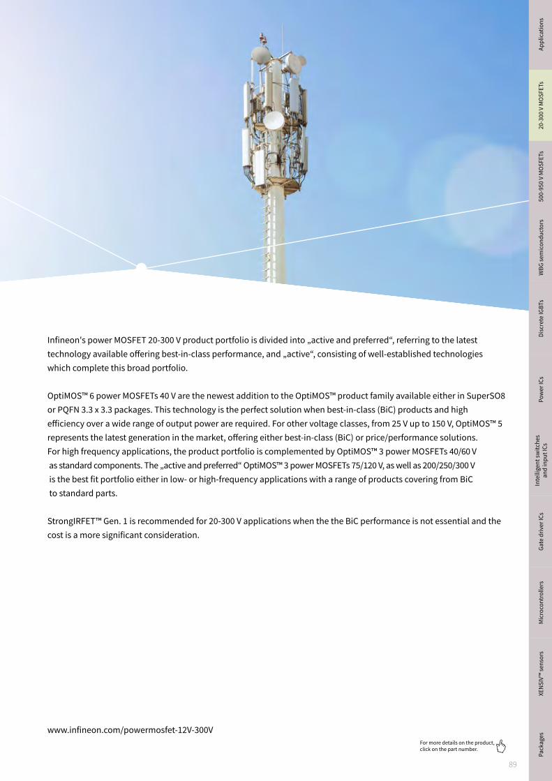
89
For more details on the product, click on the part number.
www.infineon.com/powermosfet-12V-300V
Infineon's power MOSFET 20-300 V product portfolio is divided into „active and preferred“, referring to the latest technology available offering best-in-class performance, and „active“, consisting of well-established technologies which complete this broad portfolio.
OptiMOS™ 6 power MOSFETs 40 V are the newest addition to the OptiMOS™ product family available either in SuperSO8 or PQFN 3.3 x 3.3 packages. This technology is the perfect solution when best-in-class (BiC) products and high efficiency over a wide range of output power are required. For other voltage classes, from 25 V up to 150 V, OptiMOS™ 5 represents the latest generation in the market, offering either best-in-class (BiC) or price/performance solutions. For high frequency applications, the product portfolio is complemented by OptiMOS™ 3 power MOSFETs 40/60 V as standard components. The „active and preferred“ OptiMOS™ 3 power MOSFETs 75/120 V, as well as 200/250/300 V is the best fit portfolio either in low- or high-frequency applications with a range of products covering from BiC to standard parts.
StrongIRFET™ Gen. 1 is recommended for 20-300 V applications when the the BiC performance is not essential and the cost is a more significant consideration.
Appl
icat
ions
Pa
cka
ges
20
-30
0 V
MO
SF
ETs
50
0-9
50
V M
OS
FE
TsW
BG
se
mic
on
du
cto
rsD
iscr
ete
IGB
TsP
ow
er
ICs
Inte
llig
en
t sw
itch
es
an
d in
pu
t IC
sG
ate
dri
ver
ICs
Mic
roco
ntr
oll
ers
XE
NS
IV™
se
nso
rs

90
For more details on the product, click on the part number.
OptiMOS™ and StrongIRFET™
Guidance for applications and voltage classes
OptiMOS™ and StrongIRFET™ portfolio, covering 20 up to 300 V MOSFETs, can address a broad range of needs fromlow- to high-switching frequencies. The tables below provide a guidance on the recommended OptiMOS™ or StrongIRFET™ products for each major sub-application and voltage class.
StrongIRFET™ available
OptiMOS™ recommended
OptiMOS™ available
StrongIRFET™ recommended
www.infineon.com/powermosfet-12V-300V
Low powerPower tools, Mul-ticopter, Battery, Industrial Drives
OptiMOS™
OptiMOS™
StrongIRFET™
StrongIRFET™
High power (LEV, LSEV)Ba
tter
y po
wer
ed
Solar
Offline UPS
slow switching
fast switching
OptiMOS™
OptiMOS™
OptiMOS™
OptiMOS™
StrongIRFET™
StrongIRFET™
StrongIRFET™
StrongIRFET™
Online UPS
Inve
rter
s
Adapter /Charger
PC Power
LCD TV
Server
AC-DC
Telecom
OptiMOS™
OptiMOS™
OptiMOS™
OptiMOS™
OptiMOS™
OptiMOS™
StrongIRFET™
StrongIRFET™
StrongIRFET™
StrongIRFET™
StrongIRFET™
StrongIRFET™
SMPS
Recommended voltage 20 V to 30 V 40 V 60 V 75 V
to 80 V 100 V 135 V to 150 V 200 V 250 V 300 V

91
For more details on the product, click on the part number.
OptiMOS™ and StrongIRFET™
www.infineon.com/powermosfet-12V-300V
Space-saving and high performance packages
TO-247 TO-220 TO-220 FullPAK D2PAK D2PAK 7-pin TO-Leadless
Optimized for high power applications and high current capability
Height [mm] 5.0 4.4 4.5 4.4 4.4 2.3
Outline [mm] 40.15 x 15.9 29.5 x 10.0 29.5 x 10.0 15.0 x 10.0 15.0 x 10.0 11.68 x 9.9
Thermal resistance RthJC [K/W] 2.0 0.5 2.5 0.5 0.5 0.4
SuperSO8 Power Block PQFN 3.3 x 3.3 Source-Down
PQFN 3.3 x 3.3 PQFN 2 x 2 DirectFET™
For highest efficiency and power
management
Significant design shrink
High power density and performance
For highest efficiency and power
management
Enables significant space saving
Best thermal behavior in a tiny
footprint
Height [mm]1.0 1.0 1.0 1.0 0.9 Small: 0.65
Medium: 0.65 Large: 0.71
Outline [mm]5.15 x 6.15 5.0 x 6.0 3.3 x 3.3 3.3 x 3.3 2.0 x 2.0 Small: 4.8 x 3.8
Medium: 6.3 x 4.9 Large: 9.1 x 6.98
Thermal resistance RthJC [K/W] 0.8 1.5 1.4 3.2 11.1 0.5
Appl
icat
ions
Pa
cka
ges
20
-30
0 V
MO
SF
ETs
50
0-9
50
V M
OS
FE
TsW
BG
se
mic
on
du
cto
rsD
iscr
ete
IGB
TsP
ow
er
ICs
Inte
llig
en
t sw
itch
es
an
d in
pu
t IC
sG
ate
dri
ver
ICs
Mic
roco
ntr
oll
ers
XE
NS
IV™
se
nso
rs

92
For more details on the product, click on the part number.
OptiMOS™ and StrongIRFET™
Discrete and integrated packages
OptiMOS™ and StrongIRFET™ technologies are available in different packages to address demands for higher current carrying capability and significant space saving. The broad portfolio enables footprint reduction, boosted current rating and optimized thermal performance. While the surface mound leadless devices are enabled for footprint reduction, through-hole packages are characterized by a high power rating. Furthermore, Infineon offers innovative packages such as DirectFET™ and TO-Leadless. DirectFET™ is designed for high frequency applications by offering the lowest parasitic resistance. This package is available in three different sizes: small, medium and large. TO-Leadless is optimized to dissipate power up to 375 W, increasing power density with a substantial reduction in footprint.
10000
1000
100
0
0 100 200 300 400 500 600
Power Dissipation [W]
Ou
tlin
e [
mm
2]
PQFN 2x2
PQFN 3.3x3.3 PQFN 3.3x3.3 Source Down
DirectFET™ S-Can
DirectFET™ M-Can
DirectFET™ L-Can
SuperSO8
sTOLL
TOLLI2PAK
TO-220 TO-220 FullPAK
TO-247
D2PAK D2PAK 7-pin
DPAK
SuperCool
www.infineon.com/powermosfet-12V-300V

93
For more details on the product, click on the part number.
Source-Down PQFN 3.3 x 3.3
In the Source-Down concept, the heat is dissipated directly into the PCB through a thermal pad instead of over the bond wire or the copper clip (Figure 3). › Significantly improves the thermal resistance (RthJC) of
this product family › In most cases, thermal vias cannot be used on the thermal
pad if it is connected to the noisy switch node potential › With Source-Down, the thermal pad of the low-side MOSFET
is now on the ground potential enabling the use of thermal vias right underneath the device
› Considerably improves the thermal performance and the power density in the end application
Drain-DownPQFN 3.3 x 3.3 mm
Source-DownPQFN 3.3 x 3.3 mm
www.infineon.com/PQFN-3-source-down
OptiMOS™ Source-Down power MOSFETs 25-150 VAn innovative PQFN 3.3x3.3 mm product family
Features and benefits
Optimized thermal management
Once again Infineon sets the standard in MOSFET performance with the new Source-Down package supporting the requirement for high power density and optimized system level efficiency. In contrast to a Drain-Down device, in Source-Down technology, we connect the source potential to the thermal pad (Figure 1). We go even further with the Source-Down Center-Gate footprint. Here the gate-pin is moved to the center supporting easy parallel configuration of multiple MOSFETs. With the larger drain-to-source creepage distance, the gates of multiple devices can be connected on a single PCB layer (Figure 2).
Key benefits
High current capability
More efficient use of real estate
High power density and performance
Optimized footprint for MOSFET parallelization with center gate
System cost reduction
Key features
Major reduction in RDS(ON) , up to 30% due to larger silicon die in same package outline
Superior thermal performance in RthJC
Optimized layout possibilities
Standard-Gate and Center-Gate footprint
MSL1 rated
Standard Drain-Down New Source-Down
PQFN 3.3 x 3.3 mm standard Drain-Down footprint
PQFN 3.3 x 3.3 mm Standard-Gate
Source-Down footprint
PQFN 3.3 x 3.3 mm Center-Gate
Source-Down footprint
RthJC [C/W] 1.8 1.4 1.4
Thermal vias
Thermal vias
Thermal vias
Thermal vias
Drain
0.7
5 m
m
Source
Gate Gate
Source
Drain
Appl
icat
ions
Pa
cka
ges
20
-30
0 V
MO
SF
ETs
50
0-9
50
V M
OS
FE
TsW
BG
se
mic
on
du
cto
rsD
iscr
ete
IGB
TsP
ow
er
ICs
Inte
llig
en
t sw
itch
es
an
d in
pu
t IC
sG
ate
dri
ver
ICs
Mic
roco
ntr
oll
ers
XE
NS
IV™
se
nso
rs

94
For more details on the product, click on the part number.
OptiMOS™ Linear FET
www.infineon.com/optimos-linearfet
OptiMOS™ Linear FET Combining low on-state resistance (RDS(on)) with wide safe operating area (SOA)
OptiMOS™ Linear FET is a revolutionary approach to avoid the trade-off between on-state resistance (RDS(on)) and linear mode capability operation in the saturation region of an enhanced mode MOSFET. It offers the state-of-the-art RDS(on) of a trench MOSFET, as well as the wide SOA of a classic planar MOSFET.
This product is the perfect fit for hot swap and e-fuse applications commonly found in telecom and battery management systems. OptiMOS™ Linear FET prevents damage at the load in case of a short circuit by limiting high inrush currents.
OptiMOS™ Linear FET is currently available in three voltage classes – 100 V, 150 V, and 200 V – in either D2PAK or D2PAK 7-pin packages.
SOA comparison
While the OptiMOS™ 5 power MOSFET 100 V, 1.7 mΩ has an SOA of 0.5 A, the OptiMOS™ Linear FET version at the same RDS(on) offers a much wider SOA of 11.5 A (@ 54 V, 10 ms).
103
102
101
100
10-1
103
102
101
100
10-1
10-1 100 101 102 103 10-1 100 101 102 103
VDS [V]
I D [A
]
VDS [V]
I D [A
]
1 µs 1 µs
10 µs10 µs
100 µs 100 µs
1 ms
1 ms
10 ms
10 ms
DC
DC
OptiMOS™ 5
RDS(on) = 1.7 mΩOptiMOS™ Linear FET
RDS(on) = 1.7 mΩ
0.5 A @ 54 Vtpulse= 10 ms
11.5 A @ 54 Vtpulse= 10 ms

95
For more details on the product, click on the part number.
OptiMOS™ 6
In SMPS applications, OptiMOS™ 6 is the perfect solution for high efficiency over a wide range of output power, avoiding the trade-off between low and high load conditions.
At the low output power range, where switching losses due to parasitic capacitance in the MOSFET are dominating, OptiMOS™ 6 power MOSFET BSC010N04LS6 achieves the same efficiency as the OptiMOS™ 5 power MOSFET BSC014N04LS at 40% lower RDS(on).
Moreover, compared to the OptiMOS™ 5 power MOSFET 40 V 1.0 mΩ , the OptiMOS™ 6 generation achieves lower switching losses at high load with the same RDS(on). This combination leads to an overall efficiency optimization in low and high load operating points.
0
OptiMOS™ 6 power MOSFET BSC010N04LS6
OptiMOS™ 5 power MOSFET BSC010N04LS
OptiMOS™ 5 power MOSFET BSC014N04LS
99.8
99.7
99.6
99.5
99.4
99.3
99.2
99.1
99.0
100 200 300 400 500 600 700 800 900 1000 1100 1200
Output power [W]
Eic
ienc
y [%
]
www.infineon.com/optimos6
OptiMOS™ 6 power MOSFETs 40 VNext generation of cutting edge MOSFETs
Infineon’s OptiMOS™ 6 power MOSFET 40 V family offers an optimized solution for synchronous rectification in switched mode power supplies (SMPS) in servers, desktop PCs, wireless and quick chargers. The improved performance in on-state resistance (RDS(on)) and figure of merits (FOM - RDS(on) x Qg and Qgd) yields an efficiency improvement, allowing easier thermal design and less paralleling, leading to system cost reduction. In addition, the best-in-class RDS(on) makes these devices suitable for ORing circuits.
Infineon’s market-leading OptiMOS™ 6 power MOSFETs 40 V are available in two different packages: › SuperSO8 – 5 x 6 mm with RDS(on) ranging from 5.9 mΩ down to 0.7 mΩ › PQFN 3x3 – 3.3 x 3.3 mm with RDS(on) ranging from 6.3 mΩ down to 1.8 mΩ
Features and benefits
OptiMOS™ 6 40 V combines the best-in-class RDS(on)with the superior switching performance
Key benefits
Highest system efficiency and power density
Less paralleling required
Very low voltage overshoot
Reduced need for snubber circuit
System cost reduction
Key features
Compared to alternative products: › RDS(on) reduced by 30% › Improved FOM Qg x RDS(on) by 29% › Improved FOM Qgd x RDS(on) by 46%
Optimized for synchronous rectification
Suited for ORing circuits
RoHS compliant - halogen free
MSL1 rated
Gate drive
Controller
Gate drive
fsw
UT
UGS UGS
Charger
Appl
icat
ions
Pa
cka
ges
20
-30
0 V
MO
SF
ETs
50
0-9
50
V M
OS
FE
TsW
BG
se
mic
on
du
cto
rsD
iscr
ete
IGB
TsP
ow
er
ICs
Inte
llig
en
t sw
itch
es
an
d in
pu
t IC
sG
ate
dri
ver
ICs
Mic
roco
ntr
oll
ers
XE
NS
IV™
se
nso
rs

96
For more details on the product, click on the part number.
Small signal/ small power MOSFETs
Small signal/small power MOSFETs 250-600 V Combining latest high-performance silicon technology with small and innovative packaging
Small signal/small power products are ideally suited for space-constrained automotive or non-automotive applications. By combining the latest high-performance silicon technology with small and innovative packaging, Infineon’s small signal/small power family offers designers more flexibility when it comes to making their power MOSFET selection. The products can be found in almost all applications e.g. battery protection, battery charging, LED lighting, load switches, DC-DC converters, level shifters, low voltage drives and many more.
The entire family includes different packages:SOT-223, SOT-23, SOT-323, SOT-363, SOT-89, TSOP-6 and SC59
The product portfolio covers N-channel and P-channel enhancement mode MOSFETs as well as N-channel depletion mode products: › 20-250 V P-channel enhancement mode (available in single and dual configurations) › 20-600 V N-channel enhancement mode (available in single and dual configurations) › -20/20 V and -30/30 V complementary (P + N channel) enhancement mode › 60-600 V N-channel depletion mode
Key benefits
Suitable for automotive and high quality demanding applications
Easy interface to MCU
Reduction of design complexity
Wide selection of products availableIndustry standard small outline packages
Environmentally friendly
Key features
Most products qualified to AEC Q101
Four VGS(th) classes available for 1.8 V, 2.5 V, 4.5 V, and 10 V gate drives
ESD protected p-channel parts
VDS range from -250 V to 600 V
RoHS compliant and halogen free
www.infineon.com/smallsignal
Small signal/small power MOSFETs are available in seven industry-standard package types ranging from the largest SOT-223 to the smallest SOT-363.
Products are offered in single, dual and complementary configurations and are suitable for a wide rangeof applications, including battery protection, LED lighting, low voltage drives and DC-DC converters.
600400250240200150100
7560554030252012
10 mΩ 100 mΩ 1 Ω 10 Ω 100 Ω 1000 Ω
RDS(on) max. @VGS = 4.5 V [mΩ/Ω]
Volta
ge cl
ass [
V] ±
50 mΩ
21 mΩ 3 Ω
3 Ω
20 Ω
15 Ω
600 Ω
1 Ω
90 Ω
10 Ω
41 mΩ
19 mΩ
56 mΩ 112 mΩ
825 mΩ
60 mΩ
180 mΩ
235 mΩ
1.2 Ω
2.2 Ω
7.5 Ω
22 Ω
45 Ω
5 Ω
SOT-363 SOT-323 SOT-23 TSOP-6 SC59 SOT-89 SOT-223
Package outline [mm2] 4.2 4.2 6.96 7.25 8.4 18 45.5

97
For more details on the product, click on the part number.
Appl
icat
ions
Pa
cka
ges
20
-30
0 V
MO
SF
ETs
50
0-9
50
V M
OS
FE
TsW
BG
se
mic
on
du
cto
rsD
iscr
ete
IGB
TsP
ow
er
ICs
Inte
llig
en
t sw
itch
es
an
d in
pu
t IC
sG
ate
dri
ver
ICs
Mic
roco
ntr
oll
ers
XE
NS
IV™
se
nso
rs

98
For more details on the product, click on the part number.
Product portfolio
* Optimized for resonant applications (e.g. LLC converter) * * Monolithically integrated Schottky-like diode * * * RDS(on) max @ VGS=4.5 V * * * *For more information on the product, contact our product support
1) 2.5 VGS capable2) Coming soon3) Source-Down Center-Gate
OptiMOS™ and StrongIRFET™ 20 V (super) logic level RDS(on) max @ VGS=10 V
[mΩ]
TO-252(DPAK)
DirectFET™ PQFN 2 x 2 PQFN 3.3 x 3.3 SuperSO8 SO-8
< 1 IRL6283MTRPBFRDS(on)=0.65 mΩ
IRFH6200TRPBFRDS(on)=0.99 mΩ
2-4
IRLHM620TRPBF * * * 1)RDS(on)=2.5 mΩ
BSC026N02KS GRDS(on)=2.6 mΩ
IRF6201TRPBFRDS(on)=2.45 mΩ
IRLR6225TRPBFRDS(on)=4.0 mΩ
IRL6297SDTRPBF * *RDS(on)=3.8 mΩ; dual
IRLH6224TRPBFRDS(on)=3.0 mΩ
4-10 BSC046N02KS GRDS(on)=4.6 mΩ
IRF3717RDS(on)=4.4 mΩ
> 10
IRLHS6242TRPBFRDS(on)=11.7 mΩIRLHS6276TRPBF * *RDS(on)=45.0 mΩ; dual
www.infineon.com/powermosfet-12V-300V
OptiMOS™ and StrongIRFET™ 25 V logic level RDS(on) max @ VGS=10 V
[mΩ]
DirectFET™ PQFN 2 x 2 PQFN 3.3 x 3.3 SuperSO8 SO-8
< 1
IRF6718L2TRPBFRDS(on)=0.7 mΩ
IQE006NE2LM5 3)
RDS(on)=0.6 mΩBSC004NE2LS5 2)
RDS(on)=0.9 mΩBSB008NE2LXRDS(on)=0.8 mΩ
IQE006NE2LM5CG 3)
RDS(on)=0.6 mΩBSC009NE2LS5RDS(on)=0.9 mΩ
BSZ009NE2LS5RDS(on)=0.9 mΩ
BSC009NE2LS5I * *RDS(on)=0.95 mΩ
1-2
IRF6898MTRPBF * *RDS(on)=1.1 mΩ
BSZ010NE2LS5RDS(on)=1.0 mΩ
BSC010NE2LSRDS(on)=1.0 mΩ
BSB012NE2LXI * *RDS(on)=1.2 mΩ
BSZ011NE2LS5****RDS(on)=1.1 mΩ
BSC010NE2LSI * *RDS(on)=1.05 mΩ
IRF6717MTRPBFRDS(on)=1.25 mΩ
BSZ011NE2LS5I RDS(on)=1.1 mΩ
BSC014NE2LSI * *RDS(on)=1.4 mΩ
IRF6894MTRPBF * *RDS(on)=1.3 mΩ
BSZ013NE2LS5I * *RDS(on)=1.3 mΩ
IRFH5250DRDS(on)=1.4 mΩ
BSB013NE2LXI * *RDS(on)=1.3 mΩ
BSZ014NE2LS5IF * * *RDS(on)=1.45 mΩ
BSC015NE2LS5I * *RDS(on)=1.5 mΩ
IRF6797MTRPBF * *RDS(on)=1.4 mΩ
BSZ017NE2LS5I * *RDS(on)=1.7 mΩ
BSC018NE2LSRDS(on)=1.8 mΩ
IRF6716MRDS(on)=1.6 mΩ
BSZ018NE2LSRDS(on)=1.8 mΩ
BSC018NE2LSI * *RDS(on)=1.8 mΩ
IRF6715MTRPBFRDS(on)=1.6 mΩ
BSZ018NE2LSI * *RDS(on)=1.8 mΩ
IRF6893MTRPBF * *RDS(on)=1.6 mΩIRF6892STRPBF * *RDS(on)=1.7 mΩIRF6795MTRPBF * *RDS(on)=1.8 mΩ
2-4
IRF6714MTRPBFRDS(on)=2.1 mΩ
ISK024NE2LM5 * * * *RDS(on)=2.4 mΩ
BSZ031NE2LS5RDS(on)=3.1 mΩ
BSC024NE2LSRDS(on)=2.4 mΩ
BSF030NE2LQRDS(on)=3.0 mΩ
BSZ033NE2LS5RDS(on)=3.3 mΩ
BSC026NE2LS5RDS(on)=2.6 mΩ
IRF8252RDS(on)=2.7 mΩ
BSF035NE2LQRDS(on)=3.5 mΩ
BSZ036NE2LSRDS(on)=3.6 mΩ
BSC032NE2LSRDS(on)=3.2 mΩ
IRF6811STRPBF * *RDS(on)=3.7 mΩ
BSZ037NE2LS5 * * * *RDS(on)= 3.7mΩBSZ039NE2LS5 * * * *RDS(on) = 3.9 mΩ
4-10
IRF6802SDRDS(on)=4.2 mΩIRF6710S2TRPBFRDS(on)=4.5 mΩ
IRFHM8228TRPBFRDS(on)=5.2 mΩ
BSC050NE2LSRDS(on)=5.0 mΩ
IRF6712STRPBFRDS(on)=4.9 mΩ
BSZ060NE2LSRDS(on)=6.0 mΩ
IRF6810STRPBF * *RDS(on)=5.2 mΩ
IRFHM8235TRPBF RDS(on)=7.7 mΩ
> 10 IRFHS8242RDS(on)=13 mΩ

99
For more details on the product, click on the part number.
OptiMOS™ and StrongIRFET™ 25/30 V in Power Stage 3x3 and 5x6 Part number Package Monolithically
integrated Schottky like diode
BVDSS [V] RDS(on), max. [ mΩ] @ VGS=4.5 V max. Qg [nC] @ VGS=4.5 V typ.
High-side Low-side High-side Low-side
BSZ0910ND TISON 3 x 3 – 30 13 13 4.0 4.0
BSZ0909ND TISON 3 x 3 – 30 25 25 1.8 1.8
BSC0910NDI TISON 5 x 6 ü 25 5.9 1.6 7.7 25.0
BSC0911ND TISON 5 x 6 – 25 4.8 1.7 7.7 25.0
BSC0921NDI TISON 5 x 6 ü 30 7.0 2.1 5.8 21.0
BSC0923NDI TISON 5 x 6 ü 30 7.0 3.7 5.2 12.2
BSC0924NDI TISON 5 x 6 ü 30 7.0 5.2 5.2 8.6
BSC0925ND TISON 5 x 6 – 30 6.4 6.4 5.2 6.7BSC0993ND TISON 5 x 6 – 30 7.0 7.0 5.4 6.7
OptiMOS™ and StrongIRFET™ 25/30 V in Power Block 5x6 and 5x4 Part number Package Monolithically
integrated Schottky like diode
BVDSS [V] RDS(on), max. [ mΩ] @ VGS=4.5 V max. Qg [nC] @ VGS=4.5 V typ.
High-side Low-side High-side Low-side
BSG0810NDI TISON 5 x 6 ü 25 4.0 1.2 5.6 16.0BSG0811ND TISON 5 x 6 – 25 4.0 1.1 5.6 20.0
BSG0813NDI TISON 5 x 6 ü 25 4.0 1.7 5.6 12.0
www.infineon.com/powermosfet-12V-300V
Appl
icat
ions
Pa
cka
ges
20
-30
0 V
MO
SF
ETs
50
0-9
50
V M
OS
FE
TsW
BG
se
mic
on
du
cto
rsD
iscr
ete
IGB
TsP
ow
er
ICs
Inte
llig
en
t sw
itch
es
an
d in
pu
t IC
sG
ate
dri
ver
ICs
Mic
roco
ntr
oll
ers
XE
NS
IV™
se
nso
rs

100
For more details on the product, click on the part number.
Product portfolio
OptiMOS™ and StrongIRFET™ 30 V logic level RDS(on), max.
@ VGS=10 V [mΩ]
TO-252(DPAK)
TO-263(D²PAK)
TO-263(D²PAK 7-pin)
TO-220
<1 IPB009N03L GRDS(on)=0.95 mΩ
1-2 IRLS3813TRLPBFRDS(on)=1.95 mΩ
IRLB3813PBFRDS(on)=1.95 mΩ
2-4
IRLR8743TRPBFRDS(on)=3.1 mΩ
IRFR8314TRPBFRDS(on)=2.2 mΩ
IRLB8314PBFRDS(on)=2.4 mΩ
IPD031N03L GRDS(on)=3.1 mΩ
IRL3713PBFRDS(on)=3.0 mΩ
IPB034N03L GRDS(on)=3.4 mΩ
IRLB8743PBFRDS(on)=3.2 mΩ
IPD040N03L GRDS(on)=4.0 mΩ
IPP034N03L GRDS(on)=3.4 mΩ
4-10
IPD050N03L GRDS(on)=5.0 mΩ
IPB042N03L GRDS(on)=4.2 mΩ
IPP042N03L GRDS(on)=4.2 mΩ
IRLR8726TRPBFRDS(on)=5.8 mΩ
IPB055N03L GRDS(on)=5.5 mΩ
IRLB8748PBFRDS(on)=4.8 mΩ
IPD060N03L GRDS(on)=6.0 mΩ
IPB065N03L GRDS(on)=6.5 mΩ
IPP055N03L GRDS(on)=5.5 mΩ
IPD075N03L GRDS(on)=7.5 mΩ
IPB080N03L GRDS(on)=8.0 mΩ
IRL8113PBFRDS(on)=6.0 mΩ
IRLR8729TRPBFRDS(on)=8.9 mΩ
IRLB8721PBFRDS(on)=8.7 mΩ
IPD090N03L G RDS(on)=9.0 mΩ
10-25 IPD135N03L GRDS(on)=13.5 mΩIRLR3103RDS(on)=19.0 mΩ
OptiMOS™ and StrongIRFET™ 30 V logic level
RDS(on), max. @ VGS=10 V
[mΩ]
DirectFET™ PQFN 3.3 x 3.3 SuperSO8 TO-Leadless
<1
BSC005N03LS5 *RDS(on)=0.5 mΩ
IPT004N03LRDS(on)=0.4 mΩ
BSC005N03LS5I *RDS(on)=0.5 mΩ
1-2 ISC011N03L5SRDS(on)=1.1 mΩIRFH8303TRPBFRDS(on)=1.1 mΩ BSC011N03LSRDS(on)=1.1 mΩBSC011N03LSI * *RDS(on)=1.1 mΩBSC011N03LST * * *RDS(on)=1.1 mΩ
IRF8301MTRPBFRDS(on)=1.5 mΩ
IRFH8307TRPBFRDS(on)=1.3 mΩ
IRF6726MTRPBFRDS(on)=1.7 mΩ
BSZ0500NSI * *RDS(on)=1.5 mΩ
BSC0500NSI * *RDS(on)=1.3 mΩ
IRF6727MTRPBFRDS(on)=1.7 mΩ
BSZ019N03LSRDS(on)=1.9 mΩ
BSC014N03LS GRDS(on)=1.4 mΩ
IRF8302MTRPBF * *RDS(on)=1.8 mΩ
ISZ019N03L5SRDS(on)=1.9 mΩ
IRFH5301TRPBFRDS(on)=1.85 mΩ
BSZ0901NSRDS(on)=2.0 mΩ
ISC019N03L5SRDS(on)=1.9 mΩ
BSZ0501NSI * *RDS(on)=2.0 mΩ
BSC0901NSRDS(on)=1.9 mΩBSC0501NSI * *RDS(on)=1.9 mΩBSC0901NSI * *RDS(on)=2.0 mΩ
2-4 ISC026N03L5SRDS(on)=2.6 mΩISC037N03L5ISRDS(on)=3.7 mΩ
ISZ040N03L5ISRDS(on)=4.0 mΩ
ISC045N03L5SRDS(on)=4.5 mΩ
4-10 ISZ065N03L5SRDS(on)=6.5 mΩ
* Coming soon * * Monolithically integrated Schottky-like diode * * *For more information on the product, contact our product support
www.infineon.com/powermosfet-12V-300Vwww.infineon.com/baredie

101
For more details on the product, click on the part number.
Product portfolio
OptiMOS™ and StrongIRFET™ 30 V logic level RDS(on), max. @VGS=10 V
[mΩ]
DirectFET™ PQFN 3.3 x 3.3 SuperSO8 SO-8 SO-8Dual
PQFN 2 x 2
2-4
IRF8304MTRPBFRDS(on)=2.2 mΩ
BSZ0901NSI * *RDS(on)=2.1 mΩ
BSC020N03LS GRDS(on)=2.0 mΩ
ISK036N03LM5 2)
RDS(on)=3.6 mΩIRFH5302TRPBFRDS(on)=2.1 mΩ
IRF6724MTRPBFRDS(on)=2.5 mΩ
IRLHM620TRPBFRDS(on)=2.5 mΩ
BSC0502NSI * *RDS(on)=2.4 mΩ
IRF8306MTRPBF * *RDS(on)=2.5 mΩ
BSZ0902NSRDS(on)=2.6 mΩ
BSC025N03LS GRDS(on)=2.5 mΩIRFH5302DTRPBF * *RDS(on)=2.5 mΩBSC0902NSRDS(on)=2.6 mΩIRF8252TRPBFRDS(on)=2.7 mΩ
BSZ0902NSI * *RDS(on)=2.8 mΩ
BSC0902NSI * *RDS(on)=2.8 mΩ
IRF8788TRPBFRDS(on)=2.8 mΩ
BSZ0502NSI * *RDS(on)=2.8 mΩ
IRFH8316TRPBFRDS(on)=2.95 mΩBSC030N03LS GRDS(on)= 3.0 mΩ
BSZ0503NSI * *RDS(on)=3.4 mΩ
IRFH8318TRPBFRDS(on)=3.1 mΩ
IRLHM630 * * *RDS(on)= 3.5 mΩ
BSC0503NSI * *RDS(on)=3.2 mΩ
IRF7862TRPBFRDS(on)=3.3 mΩ
BSZ035N03LS GRDS(on)=3.5 mΩ
BSC034N03LS GRDS(on)=3.4 mΩ
IRF8734TRPBFRDS(on)=3.5 mΩ
IRFHM830RDS(on)= 3.8 mΩ
BSC0504NSI * *RDS(on)=3.7 mΩ
BSZ0904NSI * *RDS(on)=4.0 mΩ
BSC0904NSI * *RDS(on)=3.7 mΩ
4-10
IRF6722MTRPBFRDS(on)= 7.7 mΩ
IRFHM830DRDS(on)= 4.3 mΩ
IRFH8324TRPBFRDS(on)=4.1 mΩ
BSZ0506NSRDS(on)=4.4 mΩ
BSC042N03LS GRDS(on)=4.2 mΩ
IRFHM8326TRPBFRDS(on)=4.7 mΩ
BSC0906NSRDS(on)=4.5 mΩIRFH5304TRPBFRDS(on)=4.5 mΩIRFH8321TRPBFRDS(on)=4.9 mΩ
BSZ050N03LS GRDS(on)=5.0 mΩ
IRFH8325TRPBFRDS(on)=5.0 mΩ
IRF8736TRPBFRDS(on)=4.8 mΩ
BSZ058N03LS GRDS(on)=5.8 mΩ
BSC050N03LS GRDS(on)=5.0 mΩ
IRFHM8329TRPBFRDS(on)=6.1 mΩ
BSC052N03LSRDS(on)=5.2 mΩ
BSZ065N03LSRDS(on)=6.5 mΩ
BSC057N03LS GRDS(on)=5.7 mΩ
IRF8327S2 * * * *RDS(on)= 7.3 mΩ
IRFHM8330TRPBFRDS(on)=6.6 mΩ
IRFH8330TRPBFRDS(on)=6.6 mΩ
BSZ0994NSRDS(on)= 7.0 mΩ
BSC080N03LS GRDS(on)=8.0 mΩ
IRFHM831RDS(on)= 7.8 mΩ
IRFH8334TRPBFRDS(on)=9.0 mΩ
IRF8721TRPBFRDS(on)=8.5 mΩ
BSZ088N03LS GRDS(on)=8.8 mΩ
BSC090N03LS GRDS(on)=9.0 mΩ
IRF8714TRPBFRDS(on)=8.7 mΩ
IRFHM8334TRPBFRDS(on)=9.0 mΩ
BSC0909NSRDS(on)=9.2 mΩ
BSZ100N03LS GRDS(on)=10.0 mΩ
10-63
BSZ0909NSRDS(on)=12.0 mΩ
BSC120N03LS GRDS(on)=12.0 mΩ
IRF8707TRPBFRDS(on)=11.9 mΩ
IRF7907TRPBFRDS(on)=11.8 mΩ+16.4 mΩ
IRLHS6342 * * *RDS(on)= 16 mΩ
IRFHM8337TRPBFRDS(on)=12.4 mΩ
IRFH8337TRPBFRDS(on)=12.8 mΩ
IRL6342 1) * * *RDS(on) = 14.6 mΩ
IRF8513TRPBF * * * *RDS(on)=2.7 mΩ+15.5 mΩ
IRFHS8342RDS(on)= 16 mΩ
BSZ130N03LS GRDS(on)=13.0 mΩ
IRL6372 1) * * *RDS(on) = 18 mΩ; dual
IRF8313TRPBFRDS(on)=15.5 mΩ+15.5 mΩ
IRLHS6376 * * *RDS(on)= 63 mΩ; dual
IRFHM8363TRPBFRDS(on)=14.9 mΩ
IRF7905TRPBFRDS(on)=17.1 mΩ+21.8 mΩ
2 x 7.2BSC072N03LD GRDS(on)=7.2 mΩ
2 x 15 BSC150N03LD GRDS(on)=15.0 mΩ
* * Monolithically integrated Schottky-like diode * * * RDS(on) max @VGS=4.5 V * * * *For more information on the product, contact our product support
1) 2.5 VGS capable2) Coming soon
www.infineon.com/powermosfet-12V-300V
Appl
icat
ions
Pa
cka
ges
20
-30
0 V
MO
SF
ETs
50
0-9
50
V M
OS
FE
TsW
BG
se
mic
on
du
cto
rsD
iscr
ete
IGB
TsP
ow
er
ICs
Inte
llig
en
t sw
itch
es
an
d in
pu
t IC
sG
ate
dri
ver
ICs
Mic
roco
ntr
oll
ers
XE
NS
IV™
se
nso
rs

102
For more details on the product, click on the part number.
Product portfolio
OptiMOS™ and StrongIRFET™ 30 V logic level 5 V optimized RDS(on), max.@VGS=10 V
[mΩ]
PQFN 3.3 x 3.3 SuperSO8 SO-8 SO-8Dual
1-2
BSC016N03MS GRDS(on) =1.6 mΩBSC020N03MS GRDS(on) =2.0 mΩ
2-4
BSC025N03MS GRDS(on) =2.5 mΩ
BSO033N03MS GRDS(on) =3.3 mΩ
BSZ035N03MS GRDS(on) =3.5 mΩ
BSC030N03MS GRDS(on) =3.0 mΩ
BSO040N03MS GRDS(on) =4.0 mΩ
4-10
BSC042N03MS GRDS(on) =4.2 mΩ
BSZ050N03MS GRDS(on) =5.0 mΩ
BSC057N03MS GRDS(on) =5.7 mΩBSC080N03MS GRDS(on) =8.0 mΩ
BSZ058N03MS GRDS(on) =5.8 mΩ
BSC090N03MS GRDS(on) =9.0 mΩ
BSZ088N03MS GRDS(on) =8.8 mΩ
BSC100N03MS GRDS(on) =10.0 mΩ
BSZ100N03MS GRDS(on) =10.0 mΩ
>10
BSZ130N03MS GRDS(on) =13.0 mΩ
BSC120N03MS GRDS(on) =12.0 mΩ
BSO110N03MS GRDS(on) =11.0 mΩ
BSO150N03MD GRDS(on) =15.0 mΩBSO220N03MD GRDS(on) =22.0 mΩ
OptiMOS™ and StrongIRFET™ 40 V normal level
RDS(on), max. @VGS=10 V
[mΩ]
TO-252(DPAK)
TO-263(D2PAK)
TO-263(D2PAK 7-pin)
TO-220 TO-247 DirectFET™ PQFN 3.3 x 3.3 SuperSO8 TO-220 FullPAK
<1
IRF40SC240RDS(on)=0.65 mΩIRFS7430TRL7PPRDS(on) =0.75 mΩ
1-2
IRFS7430TRLPBFRDS(on) =1.3 mΩ
IRFS7434TRL7PPRDS(on) =1.0 mΩ
IRFB7430PBFRDS(on) =1.3 mΩ
IRFP7430PBFRDS(on) =1.3 mΩ
IRL40DM247 2)
RDS(on) =1.0 mΩIRFH7084TRPBFRDS(on) =1.25 mΩ
IPB015N04N GRDS(on) =1.5 mΩ
IPB011N04N GRDS(on) =1.1 mΩ
IPP015N04N GRDS(on) =1.5 mΩ
IRF7739L1TRPBFRDS(on) =1.0 mΩ
IRFH7004TRPBFRDS(on) =1.4 mΩ
IRFS3004RDS(on) =1.75 mΩ
IRFS3004-7PRDS(on) =1.25 mΩ
IRFB7434PBFRDS(on) =1.6 mΩ
IRF7480MTRPBFRDS(on) =1.2 mΩ
BSC017N04NS GRDS(on) =1.7 mΩ
IRFS7434TRLPBFRDS(on) =1.6 mΩ
IRFS7437TRL7PPRDS(on) =1.4 mΩ
IRFB3004PBF RDS(on) =1.75 mΩ
IRF7946TRPBFRDS(on) =1.4 mΩ
IRF40H210RDS(on) =1.7 mΩ
IRFS7437TRLPBFRDS(on) =1.8 mΩ
IPB020N04N GRDS(on) =2.0 mΩ
IRFB7437PBFRDS(on) =2.0 mΩ
BSB015N04NX3 GRDS(on) =1.5 mΩ
BSC019N04NS GRDS(on) =1.9 mΩ
IRF40DM229RDS(on)=1.85 mΩ
2-4
IRFR7440TRPBFRDS(on) =2.4 mΩ
IRFS7440TRLPBFRDS(on) =2.5 mΩ
IPP023N04N GRDS(on) =2.3 mΩ
IRF7483MTRPBFRDS(on) =2.3 mΩ
IRFH7440TRPBFRDS(on) =2.4 mΩ
IPA028N04NM3SRDS(on) =2.8 mΩ
IRFR7446TRPBFRDS(on) =3.9 mΩ
IRF1404SRDS(on) =4.0 mΩ
IRFB7440PBFRDS(on) =2.5 mΩ
IRFH5004TRPBFRDS(on)=2.6 mΩ
IRFB7446PBFRDS(on) =3.3 mΩ
BSC030N04NS GRDS(on) =3.0 mΩIRFH7446TRPBFRDS(on) =3.3 mΩ
4-10
IPP041N04N GRDS(on) =4.1 mΩ
BSC054N04NS GRDS(on)=5.4 mΩ
IPA041N04N G *RDS(on)=4.1 mΩ
IRF40R207RDS(on) =5.1 mΩ
IRF40B207RDS(on) =4.5 mΩ
IRF40H233RDS(on)=5.9 mΩ, dual
IPP048N04N GRDS(on)=4.8 mΩ
BSC076N04NDRDS(on) =7.6 mΩ, dual
>10
BSZ105N04NS GRDS(on) =10.5 mΩBSZ165N04NS GRDS(on) =16.5 mΩ
w
www.infineon.com/powermosfet-12V-300V 2) Coming soon * For more information on the product, contact our product support

103
For more details on the product, click on the part number.
OptiMOS™ and StrongIRFET™ 40 V logic level
RDS(on), max. @VGS=10 V
[mΩ]
TO-252(DPAK)
TO-263(D2PAK)
TO-263(D2PAK 7-pin)
TO-220 TO-247 DirectFET™ PQFN 3.3 x 3.3 SuperSO8 TO-Leadless
<1
IRL40SC228RDS(on) =0.65 mΩ
IRL7472L1TRPBFRDS(on) =0.45 mΩ
BSC007N04LS6RDS(on)=0.7 mΩ
IRL40T209 RDS(on)= 0.8 mΩ
IRL40SC209RDS(on) =0.8 mΩ
1-2
IPB015N04L G RDS(on) =1.5 mΩ
IPB011N04L G RDS(on) =1.1 mΩ
IRL40B209RDS(on) =1.25 mΩ
IRLP3034PBFRDS(on) =1.7 mΩ
BSB014N04LX3 GRDS(on) =1.4 mΩ
BSC010N04LSRDS(on) =1.0 mΩ
IRLS3034TRLPBFRDS(on) =1.7 mΩ
IRLS3034TRL7PRDS(on) =1.4 mΩ
IRLB3034PBFRDS(on) =1.7 mΩ
IRL7486MTRPBFRDS(on) =1.4 mΩ
BSC010N04LS6RDS(on) =1.0 mΩ
IRL40S212RDS(on) =1.9 mΩ
IRL40B212RDS(on) =1.9 mΩ
BSC010N04LST RDS(on)=1.0 mΩBSC010N04LSIRDS(on) =1.05 mΩBSC010N04LSC * RDS(on)= 1.05 mΩBSC014N04LST RDS(on) =1.4 mΩBSC014N04LSRDS(on) =1.4 mΩBSC014N04LSIRDS(on) =1.45 mΩBSC016N04LS GRDS(on) =1.6 mΩ
BSZ018N04LS6RDS(on)=1.8 mΩ
BSC018N04LS GRDS(on) =1.8 mΩBSC019N04LSRDS(on) =1.9 mΩBSC019N04LSTRDS(on) =1.9 mΩ
2-4
IRL40B215RDS(on) =2.7 mΩ
IRF6613TRPBFRDS(on)=3.4 mΩ
BSZ021N04LS6RDS(on) =2.1 mΩ
BSC022N04LSRDS(on) =2.2 mΩ
BSZ024N04LS6RDS(on) =2.4 mΩ
BSC022N04LS6RDS(on) =2.2 mΩIRLH5034TRPBFRDS(on)=2.4 mΩ
IPP039N04L GRDS(on) =3.9 mΩ
BSZ025N04LSRDS(on) =2.5 mΩ
BSC026N04LSRDS(on) =2.6 mΩ
BSZ028N04LSRDS(on) =2.8 mΩ
BSC027N04LS GRDS(on) =2.7 mΩBSC032N04LSRDS(on) =3.2 mΩ
IPD036N04L G RDS(on)=3.6 mΩ
IRL1404SRDS(on) =4.0 mΩ
BSZ034N04LSRDS(on) =3.4 mΩ
BSC035N04LS GRDS(on) =3.5 mΩ
4-10
IRLR31142TRPBF * *RDS(on) =4.5 mΩ
IRF6616TRPBFRDS(on) =5.0 mΩ
BSZ040N04LS GRDS(on) =4.0 mΩ
BSC050N04LS GRDS(on) =5.0 mΩ
IRF6614TRPBFRDS(on)=8.3 mΩ
BSZ063N04LS6RDS(on) =6.3 mΩ
BSC059N04LS GRDS(on) =5.9 mΩBSC059N04LS6
RDS(on) =5.9 mΩ BSC072N04LDRDS(on)=7.2 mΩ, dual
BSZ097N04LS GRDS(on) =9.7 mΩ
BSC093N04LS GRDS(on) =9.3 mΩ
w
www.infineon.com/powermosfet-12V-300V * Increased creepage distance * * For more information on the product, contact our product support
Appl
icat
ions
Pa
cka
ges
20
-30
0 V
MO
SF
ETs
50
0-9
50
V M
OS
FE
TsW
BG
se
mic
on
du
cto
rsD
iscr
ete
IGB
TsP
ow
er
ICs
Inte
llig
en
t sw
itch
es
an
d in
pu
t IC
sG
ate
dri
ver
ICs
Mic
roco
ntr
oll
ers
XE
NS
IV™
se
nso
rs

104
For more details on the product, click on the part number.
Product portfolio
2) 6 V rated (RDS(on) also specified @ VGS=6 V) * For more information on the product, contact our product support
OptiMOS™ and StrongIRFET™ 60 V normal level
RDS(on), max. @VGS=10 V
[mΩ]
TO-252(DPAK)
TO-263(D2PAK)
TO-263(D2PAK 7-pin)
TO-262(I2PAK)
TO-220 TO-220FullPAK
TO-247
1-2
IPB010N06N 2) RDS(on) =1.0 mΩIRF60C241 *RDS(on)=1.3 mΩIRFS7530TRL7PPRDS(on) =1.4 mΩIPB014N06N 2)
RDS(on) =1.4 mΩIPB017N06N3 GRDS(on) =1.7 mΩ
IRFS7530TRLPBFRDS(on) =2.0 mΩ
IRFS7534TRL7PP * *RDS(on) =1.95 mΩ
IPI020N06N 2)
RDS(on) =2.0 mΩIRFB7530PBFRDS(on) =2.0 mΩ
IRFP7530PBFRDS(on) =2.0 mΩ
2-4
IPD025N06N 2)
RDS(on) =2.5 mΩIRFS7534TRLPBFRDS(on) =2.4 mΩ
IRFS3006TRL7PPRDS(on) =2.1 mΩ
IPP020N06N 2)
RDS(on) =2.0 mΩIRFS3006RDS(on) =2.5 mΩ
IPI024N06N3 GRDS(on) =2.4 mΩ
IRFB7534PBFRDS(on) =2.4 mΩ IPP024N06N3 G 2)
RDS(on) =2.4 mΩIPB026N06N 2)
RDS(on) =2.6 mΩIRFB3006PBFRDS(on) =2.5 mΩ
IRFP3006PBFRDS(on) =2.5 mΩ
IPB029N06N3 GRDS(on) =2.9 mΩ
IPI029N06N 2)
RDS(on) =2.9 mΩIPP029N06N 2)
RDS(on) =2.9 mΩIPA029N06N 2)
RDS(on) =2.9 mΩIRFP3206PBFRDS(on) =3.0 mΩ
IRFB3206BFRDS(on) =3.0 mΩ
IPA029N06NM5SRDS(on) =2.9 mΩ
IPD033N06N 2)
RDS(on)=3.3 mΩIRFS3206RDS(on)=3.0 mΩ
IPI032N06N3 GRDS(on) =3.2 mΩ
IPP032N06N3 GRDS(on) =3.2 mΩ
IPA032N06N3 GRDS(on) =3.2 mΩ
IPD034N06N3 GRDS(on) =3.4 mΩ
IRFS7537TRLPBFRDS(on) =3.3 mΩ
IRFB7537PBFRDS(on) =3.3 mΩ
IRFP7537PBFRDS(on) =3.3 mΩ
IRFB3256PBFRDS(on) =3.4 mΩ
IPD038N06N3 GRDS(on) =3.8 mΩ
IPB037N06N3 GRDS(on) =3.7 mΩ
IPP040N06N3 G
RDS(on) =4.0 mΩIPA040N06N 2)
RDS(on) =4.0 mΩIRFS3306RDS(on) =4.2 mΩ
IPI040N06N3 GRDS(on) =4.0 mΩ
IPP040N06N 2)
RDS(on) =4.0 mΩIPA040N06N M5SRDS(on) =4.0 mΩ
IRFB3306PBFRDS(on) =4.2 mΩ
IRFP3306PBFRDS(on) =4.2 mΩ
4-10
IRFR7540TRPBFRDS(on) =4.8 mΩ
IRFS7540TRLPBFRDS(on) =5.1 mΩ
IRFB7540PBFRDS(on) =5.1 mΩ
IPA057N06N3 GRDS(on) =5.7 mΩ
IPD053N06N 2)
RDS(on) =5.3 mΩIPB054N06N3 G RDS(on)=5.4 mΩ
IPP057N06N3 G 2)
RDS(on) =5.7 mΩIPB057N06N 2)
RDS(on) =5.7 mΩIRFB7545PBFRDS(on) =5.9 mΩ
IRFR7546TRPBFRDS(on) =7.9 mΩ
IRF1018ESRDS(on)=8.4 mΩ
IPP060N06N 2)
RDS(on) =6.0 mΩIPA060N06N 2)
RDS(on) =6.0 mΩIRFR1018ES *RDS(on)=8.4 mΩ
IRFB7546PBFRDS(on) =7.3 mΩIRF1018EPBFRDS(on) =8.4 mΩ
IPA060N06NM5SRDS(on) =6.0 mΩ
IPD088N06N3 G RDS(on)=8.8 mΩ
IRF60B217RDS(on) =9.0 mΩ
IPA093N06N3 GRDS(on) =9.3 mΩ
IRF60R217RDS(on) =9.9 mΩ
IPB090N06N3 GRDS(on) =9.0 mΩ
IPP093N06N3 GRDS(on) =9.3 mΩ
>10 IRFR3806RDS(on) =15.8 mΩ
IRFS3806RDS(on) =15.8 mΩ
IRFB3806PBFRDS(on) =15.8 mΩ
www.infineon.com/powermosfet-12V-300V

105
For more details on the product, click on the part number.
Product portfolio
2) 6 V rated (RDS(on) also specified @ VGS = 6 V)
OptiMOS™ and StrongIRFET™ 60 V normal level
RDS(on), max. @VGS=10 V
[mΩ]
DirectFET™ PQFN 3.3 x 3.3 SO-8 SuperSO8 TO-Leadless
<1 IPT007N06N 2)
RDS(on) =0.7 mΩ
1-2
IRF7749L1TRPBFRDS(on) =1.5 mΩ
BSC012N06NSRDS(on) =1.2 mΩ
IPT012N06N 2)
RDS(on) =1.2 mΩ BSC014N06NS 2)
RDS(on) =1.4 mΩBSC014N06NST 2)
RDS(on) =1.45 mΩ BSC016N06NST 2)
RDS(on) =1.6 mΩBSC016N06NS 2)
RDS(on) =1.6 mΩBSC019N06NS 2)
RDS(on) =1.9 mΩ
2-4
IRF7748L1TRPBFRDS(on) =2.2 mΩ
BSZ039N06NSRDS(on)=3.9 mΩ
BSC028N06NS 2)
RDS(on) =2.8 mΩBSC028N06NST 2)
RDS(on) =2.8 mΩBSB028N06NN3 GRDS(on) =2.8 mΩ
BSC031N06NS3 GRDS(on) =3.1 mΩ
IRF60DM206RDS(on) =2.9 mΩ
IRFH7085TRPBFRDS(on) =3.2 mΩ BSC034N06NS 2)
RDS(on) =3.4 mΩIRF7580MTRPBFRDS(on) =3.6 mΩ
BSC039N06NS 2)
RDS(on) =3.9 mΩ
4-10
IRFH5006TRPBFRDS(on) =4.1 mΩ
IRF6648RDS(on) =7.0 mΩ
BSZ042N06NS 2)
RDS(on) =4.2 mΩIRF7855TRPBFRDS(on)=9.4 mΩ
IRLH5036TRPBFRDS(on) =4.4 mΩ
IRF6674RDS(on) =11.0 mΩ
IRFH7545TRPBFRDS(on) =5.2 mΩ
BSZ068N06NS 2)
RDS(on) =6.8 mΩBSC066N06NS 2)
RDS(on) =6.6 mΩBSC076N06NS3 GRDS(on) =7.6 mΩ
BSZ100N06NS 2)
RDS(on) =10.0 mΩIRF7351TRPBFRDS(on)=17.8 mΩ, dual
BSC097N06NS 2)
RDS(on) =9.7 mΩBSC097N06NST 2)
RDS(on)=9.7 mΩ
>10
BSZ110N06NS3 GRDS(on) =11.0 mΩ
BSC110N06NS3 GRDS(on) =11.0 mΩIRFH5406TRPBFRDS(on)=14.4 mΩBSC155N06NDRDS(on)=15.5 mΩ, dual
OptiMOS™ and StrongIRFET™ 60 V logic level
RDS(on), max. @VGS=10 V
[mΩ]
TO-252(DPAK)
TO-263(D2PAK)
TO-263(D2PAK 7-pin)
TO-262(I2PAK)
TO-220 PQFN 2 x 2 PQFN 3.3 x 3.3 SuperSO8
1-2
IRL60SC216RDS(on) =1.5 mΩ
IPB019N06L3 GRDS(on) =1.9 mΩ
IPB016N06L3 GRDS(on) =1.6 mΩ
IRL60S216RDS(on) =1.95 mΩ
IRLS3036TRL7PPRDS(on) =1.9 mΩ
IRL60SL216RDS(on) =1.95 mΩ
IRL60B216RDS(on) =1.9 mΩ
2-4
IRLS3036TRLPBFRDS(on) =2.4 mΩ
IRLB3036PBFRDS(on) =2.4 mΩ
BSZ037N06LS5RDS(on) =3.7 mΩ
BSC027N06LS5RDS(on) =2.7 mΩ
IPD031N06L3 GRDS(on) =3.1 mΩ
IPB034N06L3 GRDS(on) =3.4 mΩ
IPP037N06L3 G
RDS(on) =3.7 mΩBSC028N06LS3 GRDS(on) =2.8 mΩ
4-10
IPD048N06L3 GRDS(on) =4.8 mΩ
IPP052N06L3 GRDS(on) =5.2 mΩ
BSZ040N06LS5 RDS(on) =4.0 mΩ
IRLH5036TRPBFRDS(on) =4.4 mΩ
IRLR3636TRPBFRDS(on) =6.8 mΩ
BSZ065N06LS5 RDS(on) =6.5 mΩ
BSC065N06LS5 RDS(on)=6.5 mΩ
IPD079N06L3 GRDS(on) =7.9 mΩ
IPB081N06L3 GRDS(on) =8.1 mΩ
IPI084N06L3 GRDS(on) =8.4 mΩ
IPP084N06L3 GRDS(on) =8.4 mΩ
BSZ067N06LS3 GRDS(on) =6.7 mΩ
BSC067N06LS3 GRDS(on) =6.7 mΩ
BSZ099N06LS5RDS(on) =9.9 mΩ
BSC094N06LS5 RDS(on) =9.4 mΩ
BSZ100N06LS3 GRDS(on) =10.0 mΩ
BSC100N06LS3 GRDS(on) =10.0 mΩ
>10 IPD220N06L3 GRDS(on) =22.0 mΩ
IRL60HS118RDS(on)=17.0 mΩ
BSC112N06LDRDS(on)=11.2 mΩ, dual
IPD350N06L GRDS(on) =35.0 mΩ
www.infineon.com/powermosfet-12V-300V
Appl
icat
ions
Pa
cka
ges
20
-30
0 V
MO
SF
ETs
50
0-9
50
V M
OS
FE
TsW
BG
se
mic
on
du
cto
rsD
iscr
ete
IGB
TsP
ow
er
ICs
Inte
llig
en
t sw
itch
es
an
d in
pu
t IC
sG
ate
dri
ver
ICs
Mic
roco
ntr
oll
ers
XE
NS
IV™
se
nso
rs

106
For more details on the product, click on the part number.
Product portfolio
OptiMOS™ and StrongIRFET™ 75 V normal level
RDS(on), max. @VGS=10 V
[mΩ]
TO-252(DPAK)
TO-263(D²PAK)
TO-263(D²PAK 7-pin)
TO-220 TO-247 DirectFET™ SuperSO8
1-2
IPB020NE7N3 GRDS(on) =2.0 mΩ
IRFS7730TRL7PPRDS(on) =2.0 mΩ
IRFP7718PBFRDS(on) =1.8 mΩ IRFP4368PBFRDS(on) =1.85 mΩ
2-4
IRFS7730TRLPBFRDS(on) =2.6 mΩ
IRFS3107TRL7PPRDS(on) =2.6 mΩ
IPP023NE7N3 GRDS(on) =2.3 mΩ
IRFP3077PBFRDS(on) =3.3 mΩ
IRF7759L2TRPBFRDS(on) =2.3 mΩ
IRFS3107TRLPBFRDS(on) =3.0 mΩ
IRFB7730PBFRDS(on) =2.6 mΩ
IPB031NE7N3 GRDS(on) =3.1 mΩ
IRFS7734TRL7PPRDS(on) =3.05 mΩ
IRFB3077PBFRDS(on) =3.3 mΩ
BSC036NE7NS3 GRDS(on) =3.6 mΩ
IRFS7734TRLPBFRDS(on) =3.5 mΩ
IPP034NE7N3 GRDS(on) =3.4 mΩ IRFB7734PBFRDS(on) =3.5 mΩ
4-10
IRFS3207ZTRLPBFRDS(on) =4.1 mΩ
IRFB3207ZPBFRDS(on) =4.5 mΩ
IPB049NE7N3 GRDS(on) =4.9 mΩ
IPP052NE7N3 GRDS(on) =5.2 mΩ
BSC042NE7NS3 GRDS(on) =4.2 mΩ
IRFS3307ZTRLPBFRDS(on) =5.8 mΩ
IRFB3307ZPBFRDS(on) =5.8 mΩ
IRFS7762TRLPBFRDS(on) =6.7 mΩ
IPP062NE7N3 GRDS(on) =6.2 mΩ
IRF7780MTRPBFRDS(on) =5.7 mΩ
IRFH5007TRPBFRDS(on) =5.9 mΩ
IRFR7740TRPBFRDS(on) =7.2 mΩ
IRFB7740PBFRDS(on) =7.3 mΩ
IRFS7787TRLPBFRDS(on) =8.4 mΩ
IRFB7787PBFRDS(on) =8.4 mΩ
IRFH7787TRPBFRDS(on) =8.0 mΩ
IRFR3607PBFRDS(on) =9.0 mΩ
IRFS3607TRLPBFRDS(on)=9.0 mΩ
IRFB3607PBFRDS(on) =9.0 mΩ
>10 IRFR7746TRPBFRDS(on) =11.2 mΩ
IRFB7746PBFRDS(on) =10.6 mΩ
BSF450NE7NH3 1)
RDS(on) =45.0 mΩ
1) DirectFET™ S * For more information on the product, contact our product support
OptiMOS™ and StrongIRFET™ 80 V normal level – logic level
RDS(on), max. @VGS=10 V
[mΩ]
TO-252(DPAK)
TO-263(D²PAK)
TO-263(D²PAK 7-pin)
TO-262(I2PAK)
TO-220 TO-220FullPAK
DirectFET™ PQFN 2 x 2 PQFN 3.3 x 3.3 SuperSO8 TO-Leadless
1-2
IPB017N08N5RDS(on) =1.7 mΩ
IPB015N08N5RDS(on) =1.5 mΩ
IPT012N08N5RDS(on) =1.2 mΩ
IPB020N08N5RDS(on) =2.0 mΩ
IPB019N08N3 GRDS(on) =1.9 mΩ
IPP020N08N5RDS(on) =2.0 mΩ
BSC021N08NS5 RDS(on) =2.1 mΩ
IPT019N08N5RDS(on) =1.9 mΩ
IPB019N08N5RDS(on) =1.95 mΩ
2-4
IPB024N08N5RDS(on) =2.4 mΩ
IPP023N08N5RDS(on) =2.3 mΩ
BSC025N08LS5RDS(on) =2.5 mΩ
IPB025N08N3 GRDS(on) =2.5 mΩ
IPB030N08N3 GRDS(on) =3.0 mΩ
IPP027N08N5RDS(on) =2.7 mΩ
BSC026N08NS5RDS(on) =2.6 mΩ
IPP028N08N3 GRDS(on) =2.8 mΩ
IPA028N08N3 GRDS(on) =2.8 mΩ
BSC030N08NS5RDS(on) =3.0 mΩ
IPT029N08N5RDS(on) =2.9 mΩ
IPB031N08N5RDS(on) =3.1 mΩ
IPP034N08N5RDS(on) =3.4 mΩ
BSC037N08NS5RDS(on) =3.7 mΩBSC037N08NS5TRDS(on)= 3.7 mΩ
IPB035N08N3 GRDS(on) =3.5 mΩ
IPI037N08N3 GRDS(on) =3.7 mΩ
IPP037N08N3 GRDS(on) =3.7 mΩ
IPA037N08N3 GRDS(on) =3.7 mΩ
BSC040N08NS5RDS(on) =4.0 mΩ
4-10
IPD046N08N5RDS(on)=4.6 mΩ
IPB049N08N5RDS(on) =4.9 mΩ
IPP052N08N5RDS(on) =5.2 mΩ
IPA040N08NM5SRDS(on) =4.0 mΩ
BSB044N08NN3 GRDS(on) =4.4 mΩ
BSC047N08NS3 GRDS(on) =4.7 mΩ
IPD053N08N3 GRDS(on) =5.3 mΩ
IPB054N08N3 GRDS(on) =5.4 mΩ
IPP057N08N3 GRDS(on) =5.7 mΩ
IPA052N08NM5SRDS(on) =5.2 mΩ
BSC052N08NS5RDS(on) =5.2 mΩ
IPB067N08N3 GRDS(on) =6.7 mΩ
IPA057N08N3 GRDS(on) =5.7 mΩ
BSZ070N08LS5RDS(on) =7.0 mΩ
BSC057N08NS3 GRDS(on) =5.7 mΩ
IRF6646TRPBFRDS(on) =9.5 mΩ
BSZ075N08NS5RDS(on) =7.5 mΩ
BSC061N08NS5RDS(on) =6.1 mΩ
IPD096N08N3 GRDS(on) =9.6 mΩ
IPP100N08N3 GRDS(on) =9.7 mΩ
IRF7854TRPBFRDS(on) =9.5 mΩ
BSZ084N08NS5RDS(on) =8.4 mΩ
BSC072N08NS5RDS(on) =7.2 mΩ
>10
BSB104N08NP3 *RDS(on) =10.4 mΩ
IRL80HS120RDS(on)=32.0 mΩ
BSZ110N08NS5RDS(on) =11.0 mΩ
BSC117N08NS5RDS(on) =11.7 mΩ
IPD135N08N3 GRDS(on) =13.5 mΩ
BSZ123N08NS3 GRDS(on) =12.3 mΩ
BSC123N08NS3 *RDS(on) =12.3 mΩ
BSZ340N08NS3 GRDS(on) =34.0 mΩ
BSC340N08NS3 GRDS(on) =34.0 mΩ
www.infineon.com/powermosfet-12V-300V

107
For more details on the product, click on the part number.
1) HB = Half-bridge * For more information on the product, contact our product support
Product portfolio
OptiMOS™ and StrongIRFET™ 100 V normal level RDS(on), max. @VGS=10 V
[mΩ]
TO-252(DPAK)
TO-263(D²PAK)
TO-263(D²PAK 7-pin)
TO-262(I2PAK)
TO-220 TO-220FullPAK
TO-247
1-2
IPB020N10N5RDS(on) =2.0 mΩ
IPB017N10N5RDS(on) =1.7 mΩ
IRF100P218RDS(on)=1.1 mΩ
IPB020N10N5LFRDS(on)=2.0 mΩ
IPB017N10N5LFRDS(on)=1.7 mΩ
IRF100P219RDS(on)=2.1 mΩ
2-4
IPB027N10N3 GRDS(on) =2.7 mΩ
IPB024N10N5RDS(on) =2.4 mΩ
IPP023N10N5RDS(on) =2.3 mΩ
IRFP4468PBFRDS(on) =2.6 mΩ
IPB027N10N5RDS(on) =2.7 mΩ
IPB025N10N3 GRDS(on) =2.5 mΩ
IPI030N10N3 GRDS(on) =3.0 mΩ
IPP030N10N3 GRDS(on) =3.0 mΩ
IPA030N10N3 GRDS(on) =3.0 mΩ
IPB033N10N5LFRDS(on) =3.3 mΩ
IPB032N10N5RDS(on) =3.2 mΩ
IPP030N10N5RDS(on)=3.0 mΩ
IPB039N10N3 GRDS(on) =3.9 mΩ
IPP039N10N5RDS(on)=3.9 mΩ
4-10
IPD050N10N5
RDS(on)=5.0 mΩIPB042N10N3 GRDS(on) =4.2 mΩ
IRFS4010TRL7PPRDS(on) =4.0 mΩ
IPI045N10N3 GRDS(on) =4.5 mΩ
IRF100B201RDS(on) =4.2 mΩ
IPA045N10N3 GRDS(on) =4.5 mΩ
IRFP4110PBFRDS(on) =4.5 mΩ
IPD068N10N3 GRDS(on) =6.8 mΩ
IRF100S201RDS(on) =4.2 mΩ
IRFB4110PBFRDS(on) =4.5 mΩ
IPA050N10NM5SRDS(on) =5.0 mΩ
IRFP4310ZPBFRDS(on) =6.0 mΩ
IRFS4010TRLPBFRDS(on) =4.7 mΩ
IPP045N10N3 GRDS(on) =4.5 mΩ
IPB065N10N3 GRDS(on)=6.5 mΩ
IRFB4310ZPBFRDS(on) =6.0 mΩ
IRFS4310ZTRLPBFRDS(on) =7.0 mΩ
IPI072N10N3 GRDS(on) =7.2 mΩ
IPP072N10N3 GRDS(on) =7.2 mΩ
IPA083N10N5RDS(on) =8.3 mΩ
IPD082N10N3 GRDS(on) =8.2 mΩ
IPP083N10N5RDS(on) =8.3 mΩ
IPA083N10NM5SRDS(on) =8.3 mΩ
IPB083N10N3 GRDS(on) =8.3 mΩ
IPI086N10N3 GRDS(on) =8.6 mΩ
IPP086N10N3 GRDS(on) =8.6 mΩ
IPA086N10N3 GRDS(on) =8.6 mΩ
IRF100B202RDS(on) =8.6 mΩ
IRFS4410ZTRLPBFRDS(on) =9.0 mΩ
IRFS4410ZTRLPBFRDS(on) =9.0 mΩ
IRFP4410ZPBF *RDS(on) =9.0 mΩ
IRFB4410ZPBFRDS(on) =9.0 mΩ
10-25
IPD122N10N3 G RDS(on) =12.2 mΩ IPD12CN10N G RDS(on)=12.4 mΩ
IPB123N10N3 GRDS(on) =12.3 mΩ
IRFR4510TRPBF *RDS(on) =13.9 mΩ
IRFS4510TRLPBFRDS(on) =13.9 mΩ
IRFB4510PBFRDS(on) =13.5 mΩ
IPA126N10NM3SRDS(on) =12.6 mΩ
IPD180N10N3 G *RDS(on) =18.0 mΩ
IPI180N10N3 GRDS(on) =18.0 mΩ
IPD25CN10N GRDS(on) =25.0 mΩ
>25
IPD33CN10N G
RDS(on) =33.0 mΩIRFI4212H-117PRDS(on) =72.5 mΩ, HB 1)
IPD78CN10N G
RDS(on) =78.0 mΩ
www.infineon.com/powermosfet-12V-300V
Appl
icat
ions
Pa
cka
ges
20
-30
0 V
MO
SF
ETs
50
0-9
50
V M
OS
FE
TsW
BG
se
mic
on
du
cto
rsD
iscr
ete
IGB
TsP
ow
er
ICs
Inte
llig
en
t sw
itch
es
an
d in
pu
t IC
sG
ate
dri
ver
ICs
Mic
roco
ntr
oll
ers
XE
NS
IV™
se
nso
rs

108
For more details on the product, click on the part number.
Product portfolio
1) DirectFET™ S * For more information on the product, contact our product support
OptiMOS™ and StrongIRFET™ 100 V normal level
RDS(on), max. @VGS=10 V
[mΩ]
DirectFET™ PQFN 3.3 x 3.3 SuperSO8 SuperSO8 dual cool SO-8 TO-Leadless
1-2
IPT015N10N5 RDS(on) =1.5 mΩ
BSC027N10NS5 RDS(on) =2.7 mΩ
IPT020N10N3 RDS(on) =2.0 mΩIPT020N10N5 RDS(on) =2.0 mΩ
2-4
IRF7769L1TRPBF RDS(on) =3.5 mΩ
BSC035N10NS5 RDS(on) =3.5 mΩ
BSC040N10NS5SC *RDS(on) =4.0 mΩ
IPT026N10N5 RDS(on) =2.6 mΩ
BSC040N10NS5 RDS(on) =4.0 mΩ
4-10
BSC050N10N5 * RDS(on) =5.0 mΩ
BSB056N10NN3 G RDS(on) =5.6 mΩ
BSC060N10NS3 G RDS(on) =6.0 mΩBSC070N10NS3 G RDS(on) =7.0 mΩ
BSC070N10NS5SC *RDS(on) =7.0 mΩ
BSC070N10NS5 RDS(on) =7.0 mΩIRFH5010TRPBF RDS(on) =9.0 mΩ
BSZ097N10NS5 RDS(on) =9.7 mΩ
BSC098N10NS5 RDS(on) =9.8 mΩ
10-25
BSC100N10NSF G RDS(on) =10.0 mΩ
IRF6644TRPBF RDS(on) =13.0 mΩ
BSC109N10NS3 G RDS(on) =10.9 mΩBSC118N10NS G RDS(on) =11.8 mΩIRFH5110TRPBF RDS(on) =12.4 mΩ
BSF134N10NJ3 G 1) RDS(on) =13.4 mΩ
IRFH7110TRPBF RDS(on) =13.5 mΩIRFH5210TRPBF RDS(on) =14.9 mΩ
BSZ160N10NS3 G RDS(on) =16.0 mΩ
BSC160N10NS3 G RDS(on) =16.0 mΩ
IRF6662TRPBF RDS(on) =22.0 mΩ
BSC196N10NS G RDS(on) =19.6 mΩ
IRF7853TRPBF RDS(on) =18.0 mΩ
>25
IRF6645TRPBF RDS(on) =35.0 mΩ
BSZ440N10NS3 G RDS(on) =44.0 mΩ
BSC252N10NSF G RDS(on)=25.2 mΩ
IRF7665S2TRPBF RDS(on) =62.0 mΩ
BSC440N10NS3 G RDS(on) =44.0 mΩ
2 x 75 IRF6665TRPBF RDS(on) =63.0 mΩ
BSC750N10ND G RDS(on) =75.0 mΩ; dual
2 x 195 IRFHM792TRPBF RDS(on) =195.0 mΩ, dual
OptiMOS™ and StrongIRFET™ 100 V logic level RDS(on), max. @VGS=10 V
[mΩ]
TO-252(DPAK)
TO-263(D2PAK)
TO-263(D²PAK 7-pin)
TO-220 PQFN 2 x 2 PQFN 3.3 x 3.3 SuperSO8
2-4 IRLS4030TRL7PPRDS(on) =3.9 mΩ
BSC034N10LS5RDS(on) =3.4 mΩ
4-10 IRLS4030TRLPBFRDS(on) =4.3 mΩ
IRLB4030PBFRDS(on) =4.3 mΩ
BSZ096N10LS5RDS(on) =9.6 mΩ
BSC070N10LS5RDS(on)=7.0 mΩIRLH5030TRPBFRDS(on)=9.0 mΩBSC096N10LS5RDS(on)=9.6 mΩ
10-25
IPP12CN10L GRDS(on) =12.0 mΩ
BSZ146N10LS5 RDS(on) =14.6 mΩ
BSC123N10LS GRDS(on) =12.3 mΩ
IRLR3110ZTRPBFRDS(on) =14.0 mΩ
BSZ150N10LS3 *RDS(on) =15.0 mΩ
BSC146N10LS5RDS(on) =14.6 mΩ
>25 IRL100HS121RDS(on)=42.0 mΩ
BSC265N10LSF GRDS(on) =26.5 mΩ
www.infineon.com/powermosfet-12V-300V

109
For more details on the product, click on the part number.
* For more information on the product, contact our product support
OptiMOS™ and StrongIRFET™ 120 V normal level
RDS(on), max. @VGS=10 V
[mΩ]
TO-252(DPAK)
TO-263(D2PAK)
TO-263(D²PAK 7-pin)
TO-262(I2PAK)
TO-220 PQFN 3.3 x 3.3 SuperSO8
2-4 IPB038N12N3 GRDS(on) =3.8 mΩ
IPB036N12N3 GRDS(on) =3.6 mΩ
4-10
IPI041N12N3 GRDS(on) =4.1 mΩ
IPP041N12N3 GRDS(on) =4.1 mΩ
BSC077N12NS3 GRDS(on) =7.7 mΩ
IPP048N12N3 GRDS(on) =4.8 mΩ
BSC080N12LS *RDS(on) =8.0 mΩ
IPI076N12N3 GRDS(on) =7.6 mΩ
IPP076N12N3 GRDS(on) =7.6 mΩ
10-25
IPD110N12N3 GRDS(on) =11.0 mΩ
IPP114N12N3 GRDS(on) =11.4 mΩ
BSC120N12LS *RDS(on) =12.0 mΩ
IPB144N12N3 GRDS(on) =14.4 mΩ
IPI147N12N3 GRDS(on) =14.7 mΩ
IPP147N12N3 GRDS(on) =14.7 mΩ
BSZ240N12NS3 GRDS(on) =24.0 mΩ
BSC190N12NS3 GRDS(on) =19.0 mΩ
www.infineon.com/powermosfet-12V-300V
Appl
icat
ions
Pa
cka
ges
20
-30
0 V
MO
SF
ETs
50
0-9
50
V M
OS
FE
TsW
BG
se
mic
on
du
cto
rsD
iscr
ete
IGB
TsP
ow
er
ICs
Inte
llig
en
t sw
itch
es
an
d in
pu
t IC
sG
ate
dri
ver
ICs
Mic
roco
ntr
oll
ers
XE
NS
IV™
se
nso
rs
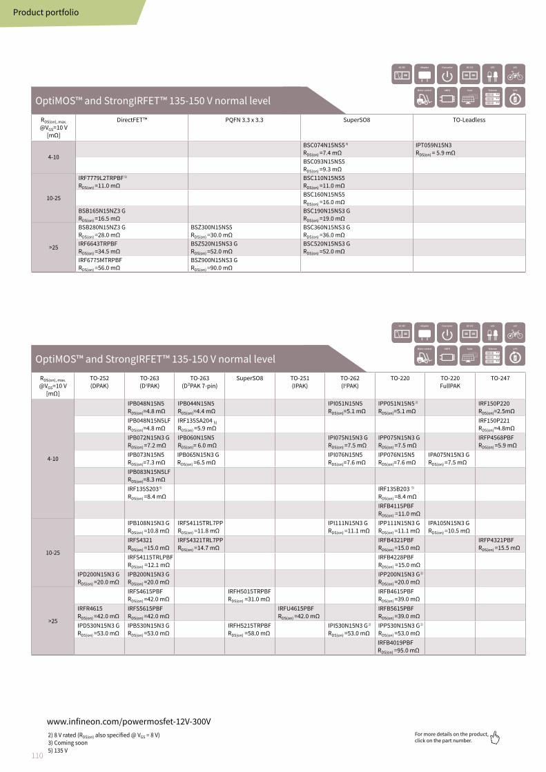
110
For more details on the product, click on the part number.
2) 8 V rated (RDS(on) also specified @ VGS = 8 V) 3) Coming soon 5) 135 V
OptiMOS™ and StrongIRFET™ 135-150 V normal level
RDS(on), max. @VGS=10 V
[mΩ]
TO-252(DPAK)
TO-263(D2PAK)
TO-263(D²PAK 7-pin)
SuperSO8 TO-251(IPAK)
TO-262(I2PAK)
TO-220 TO-220FullPAK
TO-247
4-10
IPB048N15N5
RDS(on)=4.8 mΩIPB044N15N5RDS(on)=4.4 mΩ
IPI051N15N5
RDS(on)=5.1 mΩIPP051N15N5 2)
RDS(on)=5.1 mΩIRF150P220RDS(on)=2.5mΩ
IPB048N15N5LFRDS(on)=4.8 mΩ
IRF135SA204 5)RDS(on) =5.9 mΩ
IRF150P221 RDS(on)=4.8mΩ
IPB072N15N3 G
RDS(on) =7.2 mΩIPB060N15N5RDS(on)= 6.0 mΩ
IPI075N15N3 G
RDS(on) =7.5 mΩIPP075N15N3 GRDS(on) =7.5 mΩ
IRFP4568PBFRDS(on) =5.9 mΩ
IPB073N15N5RDS(on)=7.3 mΩ
IPB065N15N3 GRDS(on) =6.5 mΩ
IPI076N15N5
RDS(on)=7.6 mΩIPP076N15N5
RDS(on)=7.6 mΩIPA075N15N3 GRDS(on) =7.5 mΩ
IPB083N15N5LFRDS(on)=8.3 mΩIRF135S203 5)
RDS(on) =8.4 mΩIRF135B203 5)
RDS(on) =8.4 mΩIRFB4115PBFRDS(on) =11.0 mΩ
10-25
IPB108N15N3 GRDS(on) =10.8 mΩ
IRFS4115TRL7PPRDS(on) =11.8 mΩ
IPI111N15N3 GRDS(on) =11.1 mΩ
IPP111N15N3 GRDS(on) =11.1 mΩ
IPA105N15N3 GRDS(on) =10.5 mΩ
IRFS4321RDS(on) =15.0 mΩ
IRFS4321TRL7PPRDS(on) =14.7 mΩ
IRFB4321PBFRDS(on) =15.0 mΩ
IRFP4321PBFRDS(on) =15.5 mΩ
IRFS4115TRLPBFRDS(on) =12.1 mΩ
IRFB4228PBFRDS(on) =15.0 mΩ
IPD200N15N3 GRDS(on) =20.0 mΩ
IPB200N15N3 GRDS(on) =20.0 mΩ
IPP200N15N3 G 2)
RDS(on) =20.0 mΩ
>25
IRFS4615PBFRDS(on) =42.0 mΩ
IRFH5015TRPBFRDS(on) =31.0 mΩ
IRFB4615PBFRDS(on) =39.0 mΩ
IRFR4615RDS(on) =42.0 mΩ
IRFS5615PBFRDS(on) =42.0 mΩ
IRFU4615PBFRDS(on) =42.0 mΩ
IRFB5615PBFRDS(on) =39.0 mΩ
IPD530N15N3 GRDS(on) =53.0 mΩ
IPB530N15N3 GRDS(on) =53.0 mΩ
IRFH5215TRPBFRDS(on) =58.0 mΩ
IPI530N15N3 G 2)
RDS(on) =53.0 mΩIPP530N15N3 G 2)
RDS(on) =53.0 mΩIRFB4019PBFRDS(on) =95.0 mΩ
Product portfolio
www.infineon.com/powermosfet-12V-300V
OptiMOS™ and StrongIRFET™ 135-150 V normal level
RDS(on), max. @VGS=10 V
[mΩ]
DirectFET™ PQFN 3.3 x 3.3 SuperSO8 TO-Leadless
4-10
BSC074N15NS5 3)
RDS(on) =7.4 mΩIPT059N15N3RDS(on) = 5.9 mΩ
BSC093N15NS5RDS(on) =9.3 mΩ
10-25
IRF7779L2TRPBF 5)
RDS(on) =11.0 mΩBSC110N15NS5RDS(on) =11.0 mΩBSC160N15NS5RDS(on) =16.0 mΩ
BSB165N15NZ3 GRDS(on) =16.5 mΩ
BSC190N15NS3 GRDS(on) =19.0 mΩ
>25
BSB280N15NZ3 GRDS(on) =28.0 mΩ
BSZ300N15NS5RDS(on) =30.0 mΩ
BSC360N15NS3 GRDS(on) =36.0 mΩ
IRF6643TRPBFRDS(on) =34.5 mΩ
BSZ520N15NS3 GRDS(on) =52.0 mΩ
BSC520N15NS3 GRDS(on) =52.0 mΩ
IRF6775MTRPBFRDS(on) =56.0 mΩ
BSZ900N15NS3 GRDS(on) =90.0 mΩ
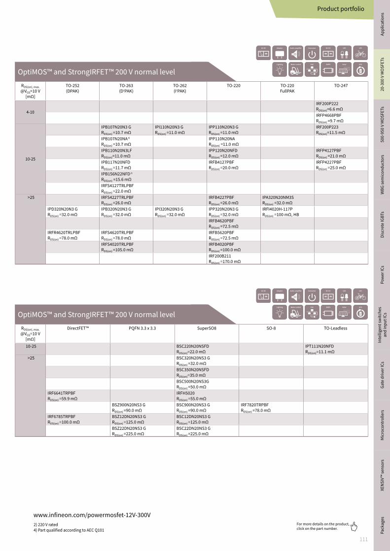
111
For more details on the product, click on the part number.
2) 220 V rated4) Part qualified according to AEC Q101
OptiMOS™ and StrongIRFET™ 200 V normal level
RDS(on), max. @VGS=10 V
[mΩ]
TO-252(DPAK)
TO-263(D2PAK)
TO-262(I2PAK)
TO-220 TO-220FullPAK
TO-247
4-10
IRF200P222RDS(on)=6.6 mΩIRFP4668PBFRDS(on) =9.7 mΩ
10-25
IPB107N20N3 GRDS(on) =10.7 mΩ
IPI110N20N3 GRDS(on) =11.0 mΩ
IPP110N20N3 GRDS(on) =11.0 mΩ
IRF200P223RDS(on)=11.5 mΩ
IPB107N20NA 4)
RDS(on) =10.7 mΩIPP110N20NARDS(on) =11.0 mΩ
IPB110N20N3LFRDS(on)=11.0 mΩ
IPP120N20NFDRDS(on) =12.0 mΩ
IRFP4127PBFRDS(on) =21.0 mΩ
IPB117N20NFDRDS(on) =11.7 mΩ
IRFB4127PBFRDS(on) =20.0 mΩ
IRFP4227PBFRDS(on) =25.0 mΩ
IPB156N22NFD 2)
RDS(on) =15.6 mΩ IRFS4127TRLPBFRDS(on) =22.0 mΩ
>25 IRFS4227TRLPBFRDS(on) =26.0 mΩ
IRFB4227PBFRDS(on) =26.0 mΩ
IPA320N20NM3SRDS(on) =32.0 mΩ
IPD320N20N3 GRDS(on) =32.0 mΩ
IPB320N20N3 GRDS(on) =32.0 mΩ
IPI320N20N3 GRDS(on) =32.0 mΩ
IPP320N20N3 GRDS(on) =32.0 mΩ
IRFI4020H-117PRDS(on) =100 mΩ, HB
IRFB4620PBFRDS(on) =72.5 mΩ
IRFR4620TRLPBFRDS(on) =78.0 mΩ
IRFS4620TRLPBFRDS(on) =78.0 mΩ
IRFB5620PBFRDS(on) =72.5 mΩ
IRFS4020TRLPBFRDS(on) =105.0 mΩ
IRFB4020PBFRDS(on) =100.0 mΩIRF200B211RDS(on) =170.0 mΩ
Product portfolio
www.infineon.com/powermosfet-12V-300V
OptiMOS™ and StrongIRFET™ 200 V normal level
RDS(on), max. @VGS=10 V
[mΩ]
DirectFET™ PQFN 3.3 x 3.3 SuperSO8 SO-8 TO-Leadless
10-25 BSC220N20NSFDRDS(on)=22.0 mΩ
IPT111N20NFDRDS(on)=11.1 mΩ
>25 BSC320N20NS3 GRDS(on) =32.0 mΩBSC350N20NSFDRDS(on)=35.0 mΩBSC500N20NS3GRDS(on) =50.0 mΩ
IRF6641TRPBFRDS(on) =59.9 mΩ
IRFH5020RDS(on) =55.0 mΩ
BSZ900N20NS3 GRDS(on) =90.0 mΩ
BSC900N20NS3 GRDS(on) =90.0 mΩ
IRF7820TRPBFRDS(on) =78.0 mΩ
IRF6785TRPBFRDS(on) =100.0 mΩ
BSZ12DN20NS3 GRDS(on) =125.0 mΩ
BSC12DN20NS3 GRDS(on) =125.0 mΩ
BSZ22DN20NS3 GRDS(on) =225.0 mΩ
BSC22DN20NS3 GRDS(on) =225.0 mΩ
Appl
icat
ions
Pa
cka
ges
20
-30
0 V
MO
SF
ETs
50
0-9
50
V M
OS
FE
TsW
BG
se
mic
on
du
cto
rsD
iscr
ete
IGB
TsP
ow
er
ICs
Inte
llig
en
t sw
itch
es
an
d in
pu
t IC
sG
ate
dri
ver
ICs
Mic
roco
ntr
oll
ers
XE
NS
IV™
se
nso
rs

112
For more details on the product, click on the part number.
OptiMOS™ and StrongIRFET™ 250 V normal level
RDS(on), max. @VGS=10 V
[mΩ]
TO-252(DPAK)
TO-263(D2PAK)
TO-262(I2PAK)
TO-220 TO-220FullPAK
TO-247 PQFN 3.3 x 3.3 SuperSO8 TO-Leadless
10-25
IPB200N25N3 GRDS(on) =20.0 mΩ
IPI200N25N3 GRDS(on) =20.0 mΩ
IPP200N25N3 GRDS(on) =20.0 mΩ
IRF250P224RDS(on)=12.0 mΩ
IPP220N25NFDRDS(on) =22.0 mΩ
IRFP4768PBFRDS(on) =17.5 mΩ
IPT210N25NFDRDS(on)=21.0 mΩ
IRF250P225RDS(on)=22.0 mΩ
>25
BSC430N25NSFD RDS(on)=43.0 mΩ
IRFS4229TRLPBFRDS(on) =48.0 mΩ
IRFB4332PBFRDS(on) =33.0 mΩ
IRFP4332PBFRDS(on) =33.0 mΩ
BSC600N25NS3 GRDS(on) =60.0 mΩ
IPD600N25N3 GRDS(on) =60.0 mΩ
IPB600N25N3 GRDS(on) =60.0 mΩ
IPI600N25N3 GRDS(on) =60.0 mΩ
IRFB4229PBFRDS(on) =46.0 mΩ
BSC670N25NSFDRDS(on)=67.0 mΩ
IPP600N25N3 GRDS(on) =60.0 mΩ
IPA600N25NM3SRDS(on)=60.0 mΩ
IRFP4229PBFRDS(on) =46.0 mΩ
BSZ16DN25NS3 GRDS(on) =165.0 mΩ
IRFH5025RDS(on) =100.0 mΩ
BSZ42DN25NS3 GRDS(on) =425.0 mΩ
BSC16DN25NS3 GRDS(on) =165.0 mΩ
OptiMOS™ and StrongIRFET™ 300 V normal level RDS(on), max.
@VGS=10 V
[mΩ]
TO-263(D2PAK)
TO-220 TO-247 SuperSO8
0-25 IRF300P226RDS(on)=19.0 mΩ
>25
IPB407N30NRDS(on) =40.7 mΩ
IPP410N30NRDS(on) =41.0 mΩ
IRFP4868PBFRDS(on) =32.0 mΩIRF300P227RDS(on)=40.0 mΩ
IRFB4137PBFRDS(on) =69.0 mΩ
IRFP4137PBFRDS(on) =69.0 mΩ
BSC13DN30NSFDRDS(on)=130.0 mΩ
www.infineon.com/powermosfet-12V-300V
Product portfolio

113
For more details on the product, click on the part number.
Power MOSFETs complementary Voltage
[V]PQFN 3.3 x 3.3 SO-8
Com
plem
enta
ry -20/20 >50 mΩ
BSZ15DC02KD H */ * *N: 55 mΩ, 5.1 AP: 150 mΩ, -3.2 ABSZ215C H */ * *N: 55 mΩ, 5.1 AP: 150 mΩ, -3.2 A
-60/60 11-30 Ω
BSO612CV G * N: 0.12 Ω, 3.0 AP: 0.30 Ω, -2.0 ABSO615C G *N: 0.11 Ω, 3.1 AP: 0.30 Ω, -2.0 A
*Products are qualified to Automotive AEC Q101 * *RDS(on) specified at 4.5 V
www.infineon.com/complementary
Appl
icat
ions
Pa
cka
ges
20
-30
0 V
MO
SF
ETs
50
0-9
50
V M
OS
FE
TsW
BG
se
mic
on
du
cto
rsD
iscr
ete
IGB
TsP
ow
er
ICs
Inte
llig
en
t sw
itch
es
an
d in
pu
t IC
sG
ate
dri
ver
ICs
Mic
roco
ntr
oll
ers
XE
NS
IV™
se
nso
rs

114
For more details on the product, click on the part number.
Product portfolio
* Products are qualified to Automotive AEC Q101 * *RDS(on) specified at 4.5 V * * * For more information on the product, contact our product support
1) 5-leg2) 2.5 VGS capable
Power P-channel MOSFETs Voltage
[V]TO-252(DPAK)
TO-263(D2PAK)
TO-220 DirectFET™ PQFN 3.3 x 3.3 SuperSO8 SO-8 PQFN 2 x 2
P-ch
anne
l MO
SFET
s
-20
BSO201SP HRDS(on) =7.0 mΩBSO203SP HRDS(on) =21.0 mΩBSO203P HRDS(on) =21.0 mΩ
IRLHS2242TRPBF * *RDS(on) =31.0 mΩ
BSO207P HRDS(on) =45.0 mΩBSO211P HRDS(on) =67.0 mΩ
-30
BSC030P03NS3 GRDS(on) =3.0 mΩ
IRF9310RDS(on)=4.6 mΩ
IPD042P03L3 GRDS(on) =4.2 mΩ
BSC060P03NS3E GRDS(on) =6.0 mΩ; ESD
IRF9317RDS(on)=6.6 mΩ
BSZ086P03NS3 GRDS(on) =8.6 mΩ
IRF9321RDS(on)=7.2 mΩ
SPD50P03L G 1) *RDS(on) =7.0 mΩ
IRF9395MRDS(on)=7.0 mΩ; dual
BSZ086P03NS3E GRDS(on) =8.6 mΩ
BSO080P03NS 3 GRDS(on) =8.0 mΩ
BSC084P03NS3 GRDS(on) =8.4 mΩ
BSO080P03NS3E GRDS(on) =8.0 mΩ; ESD
BSC084P03NS3E GRDS(on) =8.4 mΩ; ESD
BSO080P03S HRDS(on) =8.0 mΩ
BSZ120P03NS3 GRDS(on) =12.0 mΩ
BSO301SP HRDS(on) =8.0 mΩ
BSZ120P03NS3E GRDS(on) =12.0 mΩ; ESD
IRF9328RDS(on)=11.9 mΩIRF9388TRPBFRDS(on)=11.9 mΩ BSO130P03S HRDS(on) =13.0 mΩIRF9358RDS(on)=16 mΩ; dual
IRFHM9331 2)
RDS(on)=15 mΩIRF9332RDS(on)=17.5 mΩIRF9392TRPBF * * *RDS(on)= 17.5 mΩ
BSZ180P03NS3 GRDS(on) =18.0 mΩ
IRF9333RDS(on)=19.4 mΩ
BSZ180P03NS3E GRDS(on) =18.0 mΩ; ESD
BSO200P03S HRDS(on) =20.0 mΩBSO303SP HRDS(on) =21.0 mΩ
IRFH9301TRPBF * * *RDS(on) =37.0 mΩ
BSO303P HRDS(on) =21.0 mΩ; dualIRF9362RDS(on)=21 mΩ; dual
IRFHS9351TRPBFRDS(on) =170.0 mΩ; dual
IRF9335RDS(on)=59 mΩ
-60
IPD380P06NMRDS(on)= 38 mΩ
IPB110P06LMRDS(on)= 11 mΩ
SPP80P06P H *RDS(on) =23.0 mΩ
IPD650P06NMRDS(on)= 65 mΩ
SPB80P06P G *RDS(on) =23.0 mΩ
SPD30P06P G *RDS(on) =75.0 mΩIPD900P06NMRDS(on) = 90 mΩSPD18P06P G *RDS(on) =130.0 mΩ
SPB18P06P G *RDS(on) =130.0 mΩ
SPP18P06P H *RDS(on) =130.0 mΩ
BSO613SPV G *RDS(on) =130.0 mΩ
SPD09P06PL G *RDS(on) =250.0 mΩIPD25DP06LMRDS(on) = 250 mΩIPD25DP06NMRDS(on) = 250 mΩSPD08P06P G *RDS(on) =300.0 mΩ
SPB08P06P G */ * * *RDS(on) =300.0 mΩ
SPP08P06P H * RDS(on) =300.0 mΩ
IPD40DP06NMRDS(on) = 400 mΩ
-100
SPD15P10PL G *RDS(on) =200.0 mΩ
SPP15P10PL H *RDS(on) =200.0 mΩ
SPD15P10P G *RDS(on) =240.0 mΩ
SPP15P10P H *RDS(on) =240.0 mΩ
SPD04P10PL G *RDS(on) =850.0 mΩSPD04P10P G *RDS(on) =1000.0 mΩ
www.infineon.com/pchannel

115
For more details on the product, click on the part number.
Product portfolio
Small signal/small power N-channel
Voltage[V]
SOT-223 TSOP-6 SOT-89 SC59 SOT-23 SOT-323 SOT-363
N-ch
anne
l
20
BSR802N23 mΩ, 3.7 A, ULL
IRLML6244 * 1)
21 mΩ, 6.3 A, LLBSL202SN22 mΩ, 7.5 A, SLL
BSR202N21 mΩ, 3.8 A, SLL
IRLML2502 * 1)
45 mΩ, 4.2 A, SLLIRLMS2002 * 1)
30 mΩ, 6.5 A, SLLIRLML6246 * 1)
46 mΩ, 4.1 A, LLBSS205N50 mΩ, 2.5 A, SLL
BSD214SN140 mΩ, 1.5 A, SLL
BSS806NE57 mΩ, 2.3 A, ULL, ESD
BSL806N **82 mΩ, 2.3 A, ULL
BSS806N57 mΩ, 2.3 A, ULL
BSS214NW140 mΩ, 1.5 A, SLL
BSD235N350 mΩ, 0.95 A, SLL, dual
IRLMS1902 * 1)
100 mΩ, 3.2 A, SLLBSS214N140 mΩ, 1.5 A, SLL
BSS816NW160 mΩ, 1.4 A, ULL
BSD840N400 mΩ, 0.88 A, ULL, dual
IRLML2402 * 1)
250 mΩ, 1.2 A, SLL
25 IRFML8244 *24 mΩ, 5.8 A, NL
30
IRLTS6342 * 1)
17.5 mΩ, 8.3 A, LLIRLML0030 *27 mΩ, 5.3 A, LL
BSD316SN160 mΩ, 1.4A, LL
IRFTS8342 *19 mΩ. 8.2 A, NL
IRLML6344 * 1)
29 mΩ, 5.0 A, LLBSS306N57 mΩ, 2.3 A, LLIRLML6346 * 1)
63 mΩ, 3.4 A, LLIRLMS1503 *100 mΩ, 3.2 A, LL
IRLML2030 *100 mΩ, 1.4 A, LLBSS316N160 mΩ, 1.4 A, LLIRLML2803 *250 mΩ, 1.2 A, LL
55
IRLML0040TRPBF *56 mΩ,3.6 A, LLBSS670S2L650 mΩ, 0.54 A, LL
BSS340NW400 mΩ, 0.88 A, LL
60
BSP318S90 mΩ, 2.6 A, LL
BSL606SN60 mΩ, 4.5 A, LL
BSS606N60 mΩ, 3.2 A, LL
IRLML0060 *92 mΩ, 2.7 A, LL
BSS138W3.5 Ω, 0.28 A, LL
2N7002DW3 Ω, 0.3 A, LL, dual
BSP320S120 mΩ, 2.9 A, NL
IRLML2060 *480 mΩ, 1.2 A, LL
SN7002W5 Ω, 0.23 A, LL
BSP295300 mΩ, 1.8 A, LL
BSS138N3.5 Ω, 0.23 A, LLBSS7728N5 Ω, 0.2 A, LLSN7002N5 Ω, 0.2 A, LL2N70023 Ω, 0.3 A, LLBSS159N8 Ω, 0.13 A, depl.
75 BSP716N160 mΩ, 2.3 A, LL
100
BSP372N 230 mΩ, 1.8 A, LL
IRLML0100 *220 mΩ, 1.6 A, LL
BSP373N 240 mΩ, 1.8 A, NL
BSS119N 6 Ω, 0.19 A, LLVGS(th) 1.8 V to 2.3 V
BSP296N600 mΩ, 1.2 A, LL
BSS123N 6 Ω, 0.19 A, LL VGS(th) 0.8 V to 1.8 V BSS169 12 Ω, 0.09 A, depl.
150 IRF5802 *1.2 mΩ, 0.9 A, NL
200
BSP2971.8 Ω, 0.66 A, LL
IRF5801 *2.2 mΩ, 0.6 A, NL
BSP1493.5 Ω,0.14 A, depl.
240
BSP886 Ω, 0.35 A, 2.8 V rated
BSS876 Ω, 0.26 A, LL
BSS13114 Ω, 0.1 A, LL
BSP896 Ω, 0.35 A, LLBSP1296 Ω, 0.05 A, depl.
250 BSS13930 Ω, 0.03 A, depl.
400 BSP32425 Ω, 0.17 A, LL
500
600
BSP12545 Ω, 0.12 A, LL
BSS22545 Ω, 0.09 A, LL
BSS127500 Ω, 0.023 A, LL
BSP13560 Ω, 0.02 A, depl.
BSS126700 Ω, 0.007 A, depl.
800
All products are qualified to Automotive AEC Q101 (except 2N7002) (except the parts marked with *) 1) RDS(on) specified at 4.5 V ** For more information on the product, contact our product support
www.infineon.com/smallsignal
Appl
icat
ions
Pa
cka
ges
20
-30
0 V
MO
SF
ETs
50
0-9
50
V M
OS
FE
TsW
BG
se
mic
on
du
cto
rsD
iscr
ete
IGB
TsP
ow
er
ICs
Inte
llig
en
t sw
itch
es
an
d in
pu
t IC
sG
ate
dri
ver
ICs
Mic
roco
ntr
oll
ers
XE
NS
IV™
se
nso
rs

116
For more details on the product, click on the part number.
All products are qualified to Automotive AEC Q101 (except the parts marked with *) 1) RDS(on) 4.5 V rated
Small signal/small power P-channel Voltage
[V]SOT-223 TSOP-6 SOT-89 SC59 SOT-23 SOT-323 SOT-363
P-ch
anne
l MO
SFET
s
-250
BSP317P 4 Ω, -0.43 A, LL
BSS192P 12 Ω, -0.19 A, LL
BSR92P 11 Ω, -0.14 A, LL
BSP92P 12 Ω, -0.26 A, LL
-100
BSP321P 900 mΩ, -0.98 A, NLBSP322P 800 mΩ, -1.0 A, LLBSP316P 1.8 Ω, -0.68 A, LL
BSR316P 1.8 Ω, -0.36 A, LL
-60
ISP650P06NM 65 mΩ, -3.7 A, NL
ISS17EP06LM 1.7Ω, -0.3 A, LL
ISP12DP06NM 125 mΩ, -2.8 A, NL
BSS83P 2 Ω, -0.33 A, LL
BSS84PW 8 Ω, -0.15 A, LL
ISP13DP06NMS 125 mΩ, -2.8 A, NL
ISS55EP06LM 5.5 Ω, -0.18 A, NL
BSP613P 130 mΩ, 2.9 A, NLISP25DP06LM 250 mΩ, -1.9 A, LL
BSS84P 8 Ω, -0.17 A, LL
ISP25DP06NM 250 mΩ, -1.9 A, NLISP25DP06LMS 250 mΩ, -1.9 A, LL
BSR315P 800 mΩ, -0.62 A, LL
ISP26DP06NMS 260 mΩ, -1.9 A, NLBSP171P 300 mΩ, -1.9 A, LLBSP170P 300 mΩ, -1.9 A, NLISP75DP06LM 750 mΩ, -1.1 A, LLBSP315P 800 mΩ, -1.17 A, LL
-40 IRF5803TRPBF * 112 mΩ, -3.4 A, LL
-30
IRFTS9342TRPBF * 40 mΩ, -5.8 A, LL
IRLML9301TRPBF * 64 mΩ, -3.6 A, LL
BSD314SPE 140 mΩ, -1.5 A, LL, ESD
BSL307SP 43 mΩ, -5.5 A, LL
BSS308PE 80 mΩ, -2.1 A, LL, ESD
BSL308PE 80 mΩ, -2.1 A, LL,dual, ESD
IRLML5203TRPBF * 98 mΩ, -3.0 A, LL
BSS314PE 140 mΩ, -1.5 A, LL, ESDBSS315P 150 mΩ, -1.5 A, LLIRLML9303TRPBF * 165 mΩ, -2.3 A, LLIRLML5103TRPBF * 600 mΩ, -0.76 A, LL
-20
IRLTS2242 * 1) 32 mΩ, -6.9 A, SLLBSL207SP 1) 41 mΩ, -6 A, SLL
IRLML2244 * 1) 54 mΩ, 4.3 A, LL
IRLMS6802 * 1) 50 mΩ, -5.6 A, SLL
IRLML6402 * 1) 65 mΩ, -3.7 A, SLL
BSS209PW 1) 550 mΩ, -0.58 A, SLL
BSV236SP 1) 175 mΩ, -1.5 A, SLL
BSL211SP 1) 67 mΩ, -4.7 A, SLL
IRLML2246 * 1) 135 mΩ, 2.6 A, LL
BSS223PW 1) 1.2 Ω, -0.39 A, SLL
BSD223P 1) 1.2 Ω, -0.39 A, SLL, dual
IRLMS6702 * 1) 200 mΩ, -2.4 A, SLL
BSS215P 1) 150 mΩ, -1.5 A, SLLIRLML6302 * 1) 600 mΩ, -0.78 A, SLL
-12 IRLML6401 * 1) 50 mΩ, -4.3 A, SLL
Small signal/small power complementary Voltage
[V]TSOP-6 SOT-363
Com
plem
enta
ry
-20/20BSL215CN: 140 mΩ, 1.5 A, SLL P: 150 mΩ, 1.5 A, SLL
BSD235CN: 350 mΩ, 0.95 A, SLL P: 1.2 Ω, 0.53 A, SLL
-30/30
BSL308C N: 57 mΩ, 2.3 A, LL P: 80 mΩ, -2.0 A, LL BSL316C N: 160 mΩ, 1.4 A, LL P: 150 mΩ, -1.5 A, LL
www.infineon.com/smallsignal
Product portfolio

117
For more details on the product, click on the part number.
*RDS(on) typ. @VGS=4.5 V
www.infineon.com/baredie
Product portfolio
Bare Die
V(BR)DSS Part number RDS(on) typ. @ VGS=10 V Die Size X Die Size Y Die Size Area
30 V
IPC042N03L3 * 0.83 mΩ 2.78 mm 1.53 mm 4.25 mm²
IPC055N03L3 * 2.7 mΩ 3.28 mm 1.68 mm 5.51 mm²
IPC028N03L3 * 5 mΩ 1.24 mm 2.26 mm 2.80 mm²
IPC022N03L3 * 5.3 mΩ 1.05 mm 2.1 mm 2.2 mm²
IPC014N03L3 * 10.3 mΩ 1.64 mm 0.84 mm 1.37 mm²
40 V IPC218N04N3 0.9 mΩ 5.9 mm 3.7 mm 21.83 mm²
60 V IPC218N06N3 1.3 mΩ 5.9 mm 3.7 mm 21.83 mm²
75 V IPC302NE7N3 1.2 mΩ 6.7 mm 4.5 mm 30.15 mm²
80 V IPC302N08N3 1.2 mΩ 6.7 mm 4.5 mm 30.15 mm²
100 V
IPC302N10N3 1.7 mΩ 6.7 mm 4.5 mm 30.15 mm²
IPC313N10N3R 1.9 mΩ 6 mm 5.2 mm 31.26 mm²
IPC26N10NR 3.2 mΩ 6 mm 4.36 mm 26.16 mm²
IPC173N10N3 3.6 mΩ 5.76 mm 3 mm 17.28 mm²
IPC045N10N3 15.2 mΩ 2.5 mm 1.8 mm 4.5 mm²
IPC045N10L3 * 16 mΩ 2.5 mm 1.8 mm 4.5 mm²
IPC020N10L3 * 42 mΩ 2.12 mm 0.96 mm 2.04 mm²
120 V
IPC302N12N3 2.5 mΩ 6.7 mm 4.5 mm 30.15 mm²
IPC26N12N 3 mΩ 6.6 mm 3.96 mm 26.13 mm²
IPC26N12NR 3.2 mΩ 6 mm 4.36 mm 26.16 mm²
150 V
IPC331N15NM5R 2.9 mΩ 7.05 mm 4.7 mm 33.14 mm²
IPC302N15N3 4.9 mΩ 6.7 mm 4.5 mm 30.15 mm²
IPC300N15N3R 4.9 mΩ 6 mm 5 mm 30 mm²
200 V
IPC300N20N3 9.2 mΩ 6 mm 5 mm 30 mm²
IPC302N20N3 9.2 mΩ 6.7 mm 4.5 mm 30.15 mm²
IPC302N20NFD 9.4 mΩ 6.7 mm 4.5 mm 30.15 mm²
250 V IPC302N25N3 16 mΩ 6.7 mm 4.5 mm 30.15 mm²
Appl
icat
ions
Pa
cka
ges
20
-30
0 V
MO
SF
ETs
50
0-9
50
V M
OS
FE
TsW
BG
se
mic
on
du
cto
rsD
iscr
ete
IGB
TsP
ow
er
ICs
Inte
llig
en
t sw
itch
es
an
d in
pu
t IC
sG
ate
dri
ver
ICs
Mic
roco
ntr
oll
ers
XE
NS
IV™
se
nso
rs

118
For more details on the product, click on the part number.
StrongIRFET™ nomenclature
Nomenclature
OptiMOS™
LBSC 014 N GS03
RDS(on) [mΩ] Divide by 10 to get RDS(on)
value e.g. 014 = 1.4 mΩ
However, if the sixth character is a C, the fourth and the fifth character indicate the RDS(on) e.g. 12C = 12 mΩFor chip products chip area in mm2 multiplied by 10
Breakdown voltage [V]Multiply by 10 to get voltage class e.g. 03 = 30 VE = Extended, +5 V, e.g. E2 = 25 V
N = N-channelP = P-channelC = Complementary
RoHS compliant
LevelN = Normal level (NL) 10.0M = Logic level 5 V opt. (LL) 4.5 L = Logic level (ELL) 4.5K = Super logic level (SLL) 2.5J = Ultra logic level (ULL) 1.8
Package optionsSO-8/SuperSO8/PQFN 3.3 x 3.3/PQFN 2 x 2 S = Single chipD = Dual chip
DirectFET™X = MX footprintN = MN footprintZ = MZ footprintQ = SQ footprint T = ST footprintH = SH footprintJ = SJ footprint
3 = Technology generationI = Monolithically integrated Schottky-like diodeFD = Fast diodeLF = Linear mode capability
X E
FeaturesF = Fast switchingR = Integrated gate resistorE = ESD protectionA = Qualified according to AEC Q101
to be used from VGS
Package typeBSB = DirectFET™ (M Can)BSC = SuperSO8BSF = DirectFET™ (S Can)BSK = PQFN 2 x 2BSO = SO-8BSZ = PQFN 3.3 x 3.3 IPA = FullPAKSPB/IPB = D2PAKIPC = Chip productSPD/IPD = DPAKIPI = I2PAKSPP/IPP = TO-220IPS = IPAK Short LeadsIPT = TO-Leadless
OptiMOS™ 30 V
Package type
Consecutive numberwithout any correlation to product specification
ChannelsN = N-channelP = P-channel
D = DualE = ESDS = Single
I = Monolithically integrated Schottky-like diode
BSC 0901 N X I

119
For more details on the product, click on the part number.
StrongIRFET™ (from May 2015 to 2019)
Drive voltageF = 4.5 VGS capable for BV ≤ 30 VL = 2.5 VGS capable for BV ≤ 30 V, 4.5 VGS capable for BV ≥ 40 V
2 to 3 digit voltageFor example:25 = 25 V135 = 135 V
Package1 or 2 lettersB = TO-220BA = Super220C = Bare die or waferDL = DirectFET™ 1.5 Large CanDM = DirectFET™ 1.5 Medium CanCan DS = DirectFET™ 1.5 Small CanCan FF = TO-220 FullPAKH = PQFN 5 x 6HB = Power Block 5 x 6HM = PQFN 3.0 x 3.0 or 3.3 x 3.3HS = PQFN 2 x 2I = TO-220 FullPAKK = SO-8L = SOT-223ML = SOT-23P = TO-247PS = Super247R = DPAKS = D2PAKSL = TO-262SA = D2 7-pin with pin 2 voidSN = D2 7-pin with pins voidSC = D2 7-pin with pin 4 voidT = TollFETTS = TSOP-6U = IPAK
3 sequential digits3 digits issued sequentially
IR F 135 SA 204
Small signal
“X” indicates the packageD = SOT-363P = SOT-223R = SC59S = SOT-89, SOT-23, SOT-323L = TSOP-6
3 digits product identifiermeaning dependent onproduct generation
Only present in following caseS = Single (only for packages which are also used for multichip products)
PolarityN = N-channelP = P-channelC = Complementary (N-ch + P-ch)
Only present in following caseW = to distinguish SOT-323 from SOT-23
Additional featuresE = ESD protected MOSFET
BSX J1 Y J2 Z
OptiMOS™ nomenclature
Appl
icat
ions
Pa
cka
ges
20
-30
0 V
MO
SF
ETs
50
0-9
50
V M
OS
FE
TsW
BG
se
mic
on
du
cto
rsD
iscr
ete
IGB
TsP
ow
er
ICs
Inte
llig
en
t sw
itch
es
an
d in
pu
t IC
sG
ate
dri
ver
ICs
Mic
roco
ntr
oll
ers
XE
NS
IV™
se
nso
rs

120
For more details on the product, click on the part number.
New Nomenclature 2019 onward
New nomenclature for OptiMOS™ and StrongIRFET™ MOSFETs (2019 onward)
I LSC IN010 25
Package typeSC = SuperSO8 SD = SOT-363SL = TSOP-6SK = PQFN 2x2SO = SO-8SP = SOT-223SQ = CE2SR = SC59SS = SOT-89, SOT-23, SOT-323ST = sTOLLSZ = PQFN 3.3 x 3.3PA = TO-220 FullPAKPB = D²PAKPC = Chip ProductPD = DPAKPF = D2PAK-7PinPI = I²PAKPP = TO-220PS = IPAK Short LeadsPT = TO-LeadlessPW = TO-247 QA = PQFN 4.5x4QB = PQFN 3x2QC = PQFN 3x5QD = PQFN 5x6 Source-DownQE = PQFN 3.3 x 3.3 Source-DownWS = DirectFET™ (S)WM = DirectFET™ (M)WL = DirectFET™ (L)
Breakdown voltage [V]Divide by 10e.g. E2 = 25 V 10 = 100 V 25 = 250 V
Level To be used for VGS
N = Normal level (NL) 10.0 VL = Logic level (LL) 4.5 VM = Logic level 5 V opt. (ELL) 4.5 VK = Super logic level (SLL) 2.5 VJ = Ultra logic level (ULL) 1.8 V
FeaturesD = Dual H = Halfbridge
M|F… Product brand – family (M.. OptiMOS™, F…StrongIRFET™)
3 = Marketing generation with branding strategy
CG = Center gateE = ESD protection F = Fast switchingFD = Fast diodeSC = Super CoolI = Monolithically integrated
Schottky like diodeLF = Linear modeR = Integrated gate resistor
Last letter: requirement category: A = Qualified according to AECQ 101S = StandardNone = Industrial
Infineon
RDS(on) [mΩ]Divide by 10 to get RDS(on) value e.g. 012 = 1.2 mΩ
However, if the sixth character is D or E the fourth and the fifth characters indicate the RDS(on) e.g. 12D = 120 mΩ12E = 1200 mΩFor chip products chip area in mm2 multiplied by 10
VersionN = N-channelP = P-channelC = ComplementaryG = GaN

121
For more details on the product, click on the part number.
Further information, data sheets and documentswww.infineon.com/powermosfet-12V-300Vwww.infineon.com/smallsignal www.infineon.com/pchannelwww.infineon.com/depletionwww.infineon.com/complementary www.infineon.com/baredie
Evaluation boards and simulation modelswww.infineon.com/to-leadless-evaluationboardwww.infineon.com/powermosfet-simulationmodels
Infineon support for low voltage MOSFETsUseful links and helpful information
Simulation
Appl
icat
ions
Pa
cka
ges
20
-30
0 V
MO
SF
ETs
50
0-9
50
V M
OS
FE
TsW
BG
se
mic
on
du
cto
rsD
iscr
ete
IGB
TsP
ow
er
ICs
Inte
llig
en
t sw
itch
es
an
d in
pu
t IC
sG
ate
dri
ver
ICs
Mic
roco
ntr
oll
ers
XE
NS
IV™
se
nso
rs

122
500-950 V MOSFETs
For more details on the product, click on the part number.
› CoolMOS™ SJ MOSFETs › 950 V CoolMOS™ P7 SJ MOSFETs › 800 V CoolMOS™ P7 SJ MOSFETs › 700 V CoolMOS™ P7 SJ MOSFETs › 600 V CoolMOS™ P7 SJ MOSFETs › 600 V CoolMOS™ PFD7 SJ MOSFETs › 600 V and 650 V CoolMOS™ C7 and
C7 Gold (G7) SJ MOSFETs
500-950 V MOSFETs › 600 V CoolMOS™ S7 SJ MOSFETs › 600 V CoolMOS™ CFD7 SJ MOSFETs › CoolMOS™ CE SJ MOSFETs › CoolMOS™ SJ MOSFETs – package innovations › CoolMOS™ SJ MOSFETs for automotive › CoolMOS™ product portfolio

123
For more details on the product, click on the part number.
› 600 V CoolMOS™ S7 SJ MOSFETs › 600 V CoolMOS™ CFD7 SJ MOSFETs › CoolMOS™ CE SJ MOSFETs › CoolMOS™ SJ MOSFETs – package innovations › CoolMOS™ SJ MOSFETs for automotive › CoolMOS™ product portfolio
Appl
icat
ions
Pa
cka
ges
20
-30
0 V
MO
SF
ETs
50
0-9
50
V M
OS
FE
TsW
BG
se
mic
on
du
cto
rsD
iscr
ete
IGB
TsP
ow
er
ICs
Inte
llig
en
t sw
itch
es
an
d in
pu
t IC
sG
ate
dri
ver
ICs
Mic
roco
ntr
oll
ers
XE
NS
IV™
se
nso
rs

124
For more details on the product, click on the part number.
CoolMOS™ SJ MOSFETs Trusted leader in high voltage MOSFETs
High voltage superjunction MOSFETs address consumer applications, such as smartphone/tablet chargers, notebook adapters, LED lighting, PC power, as well as audio and TV power supplies. Customers are increasingly replacing standard MOSFETs with superjunction MOSFETs to benefit from higher efficiency and lower power consumption for end users. CoolMOS™ P7 sets a new benchmark by offering high performance and competitive price all at once. CoolMOS™ PFD7 as brand new series shifts the state-of-the-art for high density chargers/adapters as well as low-power motor drives.
Also for industrial applications such as server, telecom, PC power, solar, UPS, EV-charging and others, Infineon’s latest CoolMOS™ 7 superjunction MOSFETs with C7, G7, CFD7 and P7 product families offer what you need - from highest efficiency to best price performance. Complementary to the silicon CoolMOS™ portfolio, Infineon offers a broad wide bandgap (WBG) portfolio of CoolGaN™ e-mode HEMTs and CoolSiC™ MOSFETs to further optimize efficiency and system cost (see pages 154-172).
Infineon’s industrial- and consumer-qualified CoolMOS™ superjunction MOSFET offering is complemented by the automotive qualified series 600 V CPA, 650 V CFDA, 800 V C3A and our latest 650 V CFD7A. Gain your momentum in the rapidly growing on-board charger and DC-DC converter markets with our excellent performing automotive series with proven outstanding quality standards that go well beyond AEC Q101.
The revolutionary CoolMOS™ power MOSFET sets new standards in the field of energy efficiency. Our CoolMOS™ products offer a significant reduction of conduction, switching and driving losses, and enable high power density as well as efficiency for superior power conversion systems.
www.infineon.com/coolmos
600 V P6
600 V CE
650/700 V CE
800 V C3
800 V CE
900 V C3
500 V CE
600 V P7
700 V P7 1)
800 V P7 1)
950 V P7 1)
650 V CFD2
600 V P6
650 V CFDA
600 V CPA
800 V C3A
600 V CFD7A
600 V CFD7
600 V P7
600/650 V C7
600/650 V G7
600 V S7
600 V PFD7
1) Optimized for flyback topologies Price-performance Highest performance Fast recovery diode Automotive Slow switching
TimeTime
CoolMOS™ superjunction MOSFETs for industrial applications (>250 W) and automotiveCoolMOS™ superjunction MOSFETs for consumer applications (<400 W)
Active Active and preferred Active Active and preferred
CoolMOS™ SJ MOSFETs
CoolMOS™ low power package innovationsClick to learn more
CoolMOS™ high power package innovationsClick to learn more

125
For more details on the product, click on the part number.
950 V CoolMOS™ P7 SJ MOSFETsPerfect fit for PFC and flyback topologies
Designed to meet the growing consumer needs in the high voltage MOSFETs arena, the latest 950 V CoolMOS™ P7 technology focuses on the low-power SMPS market. The P7 family addresses applications ranging from lighting, smart meter, mobile phone charger, notebook adapter, to AUX power supply and industrial SMPS. Offering 50 V more blocking voltage than its predecessor 900 V CoolMOS™ C3, the 950 V CoolMOS™ P7 series delivers outstanding performance in terms of efficiency, thermal behavior and ease of use. As all other P7 family members, the 950 V CoolMOS™ P7 series comes with an integrated Zener diode ESD protection. The integrated diode considerably improves ESD robustness, thus reducing ESD-related yield loss and reaching exceptional ease-of-use levels. CoolMOS™ P7 is developed with best-in-class threshold voltage (VGS(th)) of 3 V and a narrow tolerance of only ± 0.5 V, which makes it easy to drive and design-in.
Compared to competition, the 950 V CoolMOS™ P7 delivers best-in-class efficiency and thermal performance. Plug-and-play at 90 VAC in a 40 W adapter reference design, featuring the snubberless concept, demonstrates excellent efficiency gains of up to 0.2 % and lower MOSFET temperature of up to 5.2°C compared to similar competitor technology. With over 20 years of experience in superjunction technology, Infineon introduces 950 V CoolMOS™ P7 with best-in-class DPAK on-resistance (RDS(on)). This SMD device comes with the RDS(on) of 450 mΩ - more than 60% lower RDS(on) compared to the nearest competitor. Such low RDS(on) value enables higher density designs while decreasing BOM and assembly cost.
www.infineon.com/950v-p7
Charger
Best-in-class DPAK RDS(on)
Customer benefits: › Possible change from leaded to SMD packages › High power density › Lower BOM cost › Lower production cost
1400
1200
1000
800
600
400
200
0
1250 mΩ 1200 mΩ
450 mΩ
Competitor CoolMOS™ C3 CoolMOS™ P7
R DS(o
n) [m
Ω]
-65%
0.2
0.0
-0.2
-0.4
-0.6
-0.8
-1.0
Pout [W]
Relative eiciency @ 90 VAC (ref: IPA95R450P7)
E
icie
ncy
[%
]
65
60
55
50
45
40
35
30
255 10 15 20 25 30 35 40
5 10 15 20 25 30 35 40
Pout [W]
Temperature @ 90 VAC
Te
mp
era
ture
[°C
]
Δ 5.2°C
Δ 0.2%
IPA95R450P7 IPA90R500C3 Competitor IPA95R450P7 IPA90R500C3 Competitor
950 V CoolMOS™ P7 SJ MOSFETs
Appl
icat
ions
Pa
cka
ges
20
-30
0 V
MO
SF
ETs
50
0-9
50
V M
OS
FE
TsW
BG
se
mic
on
du
cto
rsD
iscr
ete
IGB
TsP
ow
er
ICs
Inte
llig
en
t sw
itch
es
an
d in
pu
t IC
sG
ate
dri
ver
ICs
Mic
roco
ntr
oll
ers
XE
NS
IV™
se
nso
rs

126
For more details on the product, click on the part number.
800 V CoolMOS™ P7 SJ MOSFETsA benchmark in efficiency and thermal performance
With the 800 V CoolMOS™ P7 series, Infineon sets a benchmark in 800 V superjunction technologies and combines best-in-class performance with the remarkable ease of use. This product family is a perfect fit for flyback-based consumer and industrial SMPS applications. In addition, it is also suitable for PFC stages within consumer, as well as solar applications, fully covering the market needs in terms of its price/performance ratio.
The technology offers fully optimized key parameters to deliver best-in-class efficiency as well as thermal performance. As demonstrated on an 80 W LED driver, bought on the market, the >45 percent reduction in switching losses (Eoss) and output capacitance (Coss) as well as the significant improvement in input capacitance (Ciss) and gate charge (QG), compared to competitor technologies, lead to 0.5 percent higher efficiency at light load which helps to reduce standby power in the end application. At full load, the observed improvement is up to 0.3 percent higher efficiency and 6°C lower device temperature.
EMI is a system level topic, and the optimization needs to be done on the system level only. Nevertheless, a pure plug-and-play measurement on Infineon's 45 W adapter reveals that 800 V CoolMOS™ P7 shows similar EMI performance to Infineon’s previous technologies as well as to competitors’ technologies.
Compared to competition, the 800 V CoolMOS™ P7 technology allows to integrate much lower RDS(on) values into small packages, such as a DPAK. This finally enables high power density designs at highly competitive price levels.
The complete P7 platform has been developed with an integrated Zener diode that is used as an electrostatic discharge (ESD) protection mechanism, which increases the overall device ruggedness up to Human body model (HBM) class 2 level.
www.infineon.com/800V-p7
0.6
0.5
0.4
0.3
0.2
0.1
0
0 10 20 30 40 50 60 70 80 90
Plug and play in an 80 W LED driver from market
Pout [W]
Rela
tive e
ici
ency
[%]
CoolMOS™ P7
0.5%
0.3%
CoolMOS™ C3 Competitor 1 Competitor 2
60
50
40
30
20
10
0
30
CoolMOS™ C3
300Frequency [MHz]
800 V CoolMOS™ exceptional EMI performance
CoolMOS™ P7 Competitor 1 Competitor 2
CoolMOS™ P7 sets a new benchmark in best-in-class DPAK RDS(on)
Customer benefits: › High power density › Lower BOM cost › Lower production cost
850 mΩ
Competitor 2
630 mΩ
Competitor 1
280 mΩ
CoolMOS™ P7
360 mΩ
CoolMOS™ P7
450 mΩ
CoolMOS™ P7
-56%
Overview of lowest DPAK RDS(on) for 800 V superjunction MOSFET
800 V CoolMOS™ P7 SJ MOSFETs
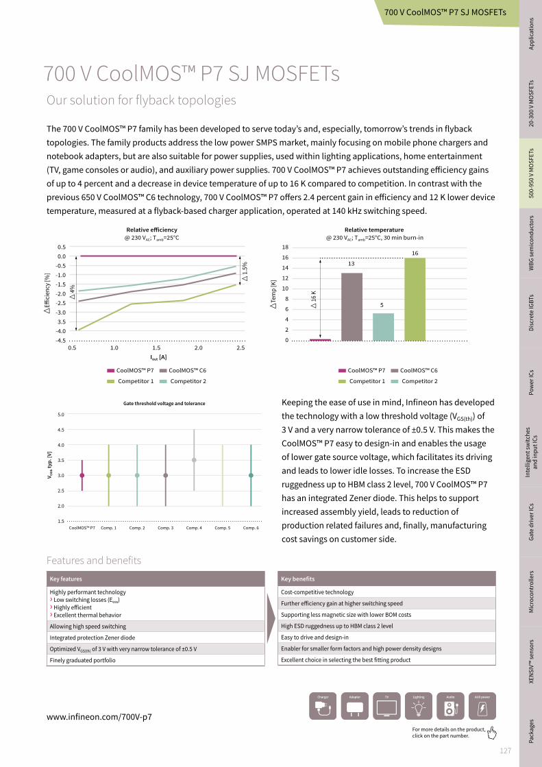
127
For more details on the product, click on the part number.
700 V CoolMOS™ P7 SJ MOSFETsOur solution for flyback topologies
The 700 V CoolMOS™ P7 family has been developed to serve today’s and, especially, tomorrow’s trends in flyback topologies. The family products address the low power SMPS market, mainly focusing on mobile phone chargers and notebook adapters, but are also suitable for power supplies, used within lighting applications, home entertainment (TV, game consoles or audio), and auxiliary power supplies. 700 V CoolMOS™ P7 achieves outstanding efficiency gains of up to 4 percent and a decrease in device temperature of up to 16 K compared to competition. In contrast with the previous 650 V CoolMOS™ C6 technology, 700 V CoolMOS™ P7 offers 2.4 percent gain in efficiency and 12 K lower device temperature, measured at a flyback-based charger application, operated at 140 kHz switching speed.
Keeping the ease of use in mind, Infineon has developed the technology with a low threshold voltage (VGS(th)) of 3 V and a very narrow tolerance of ±0.5 V. This makes the CoolMOS™ P7 easy to design-in and enables the usage of lower gate source voltage, which facilitates its driving and leads to lower idle losses. To increase the ESD ruggedness up to HBM class 2 level, 700 V CoolMOS™ P7 has an integrated Zener diode. This helps to support increased assembly yield, leads to reduction of production related failures and, finally, manufacturing cost savings on customer side.
www.infineon.com/700V-p7
Charger
0.50.0
-0.5-1.0-1.5-2.0-2.5-3.03.5
-4.0-4.5
0.5 1.0 1.5 2.0 2.5Iout [A]
CoolMOS™ P7
Relative eiciency@ 230 VAC; Tamb=25°C
4
%
Relative temperature @ 230 VAC; Tamb=25°C, 30 min burn-in
E
icie
ncy [
%]
Te
mp
[K]
13
16
5
18
16
14
12
10
8
6
4
2
0
CoolMOS™ C6
Competitor 1 Competitor 2
CoolMOS™ P7 CoolMOS™ C6
Competitor 1 Competitor 2
1
.5%
1
6 K
5.0
4.5
4.0
3.5
3.0
2.5
2.0
1.5
CoolMOS™ P7 Comp. 1
Gate threshold voltage and tolerance
VG
Sth t
yp
. [V
]
Comp. 2 Comp. 3 Comp. 4 Comp. 5 Comp. 6
Features and benefits
Key benefits
Cost-competitive technology
Further efficiency gain at higher switching speed
Supporting less magnetic size with lower BOM costs
High ESD ruggedness up to HBM class 2 level
Easy to drive and design-in
Enabler for smaller form factors and high power density designs
Excellent choice in selecting the best fitting product
Key features
Highly performant technology › Low switching losses (Eoss) › Highly efficient › Excellent thermal behavior
Allowing high speed switching
Integrated protection Zener diode
Optimized VGS(th) of 3 V with very narrow tolerance of ±0.5 V
Finely graduated portfolio
700 V CoolMOS™ P7 SJ MOSFETs
Appl
icat
ions
Pa
cka
ges
20
-30
0 V
MO
SF
ETs
50
0-9
50
V M
OS
FE
TsW
BG
se
mic
on
du
cto
rsD
iscr
ete
IGB
TsP
ow
er
ICs
Inte
llig
en
t sw
itch
es
an
d in
pu
t IC
sG
ate
dri
ver
ICs
Mic
roco
ntr
oll
ers
XE
NS
IV™
se
nso
rs

128
For more details on the product, click on the part number.
600 V CoolMOS™ P7 SJ MOSFETs Perfect combination between high efficiency and ease of use
The 600 V CoolMOS™ P7 is a general purpose series, targeting a broad variety of applications, ranging from low power SMPS up to the highest power levels. In the low power arena, it is the successor of the 600 V CoolMOS™ CE, and for high power SPMS applications, it is the replacement for the 600 V CoolMOS™ P6, which makes it the perfect choice for applications such as chargers, adapters, lighting, TV power supply, PC power supply, solar, small light electric vehicles, server power supply, telecom power supply, and electric vehicle (EV) charging.
The 600 V CoolMOS™ P7 is Infineon’s most well-balanced CoolMOS™ technology in terms of combining the ease of use and excellent efficiency performance. Compared to its predecessors, it offers higher efficiency and improved power density due to the significantly reduced gate charge (QG) and switching losses (EOSS) levels, as well as optimized on-state resistance (RDS(on)). The carefully selected integrated gate resistors enable very low ringing tendency and, thanks to its outstanding robustness of body diode against hard commutation, it is suitable for hard as well as soft switching topologies, such as LLC. In addition, an excellent ESD capabilty helps to improve the quality in manufacturing. The 600 V CoolMOS™ P7 familiy offers a wide range of on-resistance (RDS(on))/package combinations, including THD, as well as SMD devices, at an RDS(on) granularity from 24 to 600 mΩ and comes along with the most competitive price/performance ratio of all 600 V CoolMOS™ offerings.
Portfolio
Eiciency
CoolMOS™ P7 CoolMOS™ P6 CoolMOS™ C7 CoolMOS™ CE
Low ringing
Commutationruggedness
Price competitiveness
ESD
www.infineon.com/600V-p7
Charger
Features and benefits
Key benefits
Ease of use and fast design-in through low ringing tendency and usage across PFC and PWM stages
Improved efficiency and simplified thermal management due to low switching and conduction losses
Higher manufacturing quality due to >2 kV ESD protection
Increased power density solutions enabled by using products with smaller footprint
Suitable for a wide variety of applications and power ranges
Key features
Suitable for hard and soft switching (PFC and LLC) due to an outstanding commutation ruggedness
Optimized balance between efficiency and ease of use
Significant reduction of switching and conduction losses leading to low MOSFET temperature
Excellent ESD robustness >2 kV (HBM) for all products
Better RDS(on)/package products compared to competition
Large portfolio with granular RDS(on) selection qualified for a variety of industrial and consumer applications
600 V CoolMOS™ P7 SJ MOSFETs

129
For more details on the product, click on the part number.
600 V CoolMOS™ PFD7 SJ MOSFETsThe next level for ultrahigh power density designs
The 600 V CoolMOS™ PFD7 MOSFET series sets a new benchmark in 600 V Superjunction (SJ) technologies, suitable for ultrahigh power density designs as well as low power motor drives. It combines best-in-class performance with ease of use, built on Infineon’s superjunction technology innovation and more than 20 years of experience. The products come with an integrated fast body diode ensuring a robust device and reduced bill-of-material (BOM).
This product family offers up to 1.17 % efficiency increase compared to the CoolMOS™ P7 technologies, which leads to a power density increase of 1.8 W. This outstanding improvement is achieved by lower conduction and charge/discharge losses, as well as reduced turn-off and gate-driving losses, enabled by pushing the cutting-edge CoolMOS™ technology to new limits.
A broad range of RDS(on) values in combination with a variety of packages, helps in selecting the right part to optimize designs. Furthermore, an integrated ESD protection of up to 2kV eliminates ESD related yield loss. At the same time, especially our industry-leading SMD package offering contributes to BOM and PCB space savings and simplifies manufacturing. This unique set of product features and their resulting benefits, position the CoolMOS™ PFD7 Superjunction MOSFET family exceptionally well for ultrahigh density applications like chargers and adapters, but also for low-power drives and specific lighting applications.
600 V CoolMOS™ PFD7 increases efficiency in light- and full-load conditions. This results in a power density increase of 1.8 W for ultrahigh power chargers and adapters.
600 V CoolMOS™ PFD7 provides up to 2% higher efficiency at 100 W, which results in an 18°C thermal improvement. Considering its excellent commutation ruggedness as well as its low EMI, it is the perfect solution for low-power drives.
www.infineon.com/600V-PFD7
Features and benefits
Key benefits
+1.8 W / inch3 power density improvement compared to latest CoolMOS™ technologies used in charger applications
Supports smaller form factors and thinner designs
Up to 2% efficiency increase and 18°C improved thermal behavior compared to CoolMOS™ CE for low-power drives applications
BOM cost reduction and easy manufacturing
Robustness and reliability
Easy to select right parts for design fine-tuning
Key features
Very low FOM RDS(on) x Eoss
Extremely low switching losses
Integrated robust fast body diode
Up to 2 kV ESD protection
Wide range of RDS(on) values and broad package portfolio
Excellent communication ruggedness
Low EMI
Case
tem
pera
ture
[°C]
Low-side MOSFET temperature100 W motor drive at high line 230 VAC
"#$%!
70
80
60
50
CE
PFD7
= 18°C
IPD60R2K0PFD7S IPD50R2K0CE
= 1.17%
65 W delta eiciency @ 90 VAC input voltagewith IPAN60R125PFD7S as reference
P7
PFD7
Output current [A]
Eic
ienc
y in
crea
se [%
]
0,5
0
- 0,5
- 1
- 1,50,5 1 1,5 2 2,5 3 3,5
IPAN60R125PFD7SIPA60R120P7
= 0.35%
Charger
600 V CoolMOS™ PFD7
Appl
icat
ions
Pa
cka
ges
20
-30
0 V
MO
SF
ETs
50
0-9
50
V M
OS
FE
TsW
BG
se
mic
on
du
cto
rsD
iscr
ete
IGB
TsP
ow
er
ICs
Inte
llig
en
t sw
itch
es
an
d in
pu
t IC
sG
ate
dri
ver
ICs
Mic
roco
ntr
oll
ers
XE
NS
IV™
se
nso
rs

130
For more details on the product, click on the part number.
www.infineon.com/c7
600 V and 650 V CoolMOS™ C7 and C7 Gold (G7) SJ MOSFETs Infineon’s Superjunction MOSFET series for highest efficiency
The 600 V and 650 V CoolMOS™ C7 and C7 Gold (G7) Superjunction MOSFET series are designed to achieve record level efficiency performance – they offer substantial efficiency benefits over the whole load range in hard switching applications compared to previous series and competition. This is achieved by minimizing switching losses via ultralow levels of switching losses (EOSS) (approximately 50 percent reduction compared to the CoolMOS™ CP), reduced gate charge (QG) and a careful balance of other relevant product key parameters. The low Eoss and QG also enable operation at higher switching frequency and related size reduction of the circuit magnetics.
The outstanding figures of merit (FOM) and the best-in-class on-state resistance (RDS(on)) offerings make the CoolMOS™ C7 and C7 Gold series key enablers for highest efficiency and power density. While the 650 V CoolMOS™ C7 and G7 (C7 Gold) superjunction MOSFETs are solely designed for hard switching applications such as PFC, the 600 V version is also well suited for high-end LLC stages due to its rugged body diode that withstands slew rates up to 20 V/ns. The product portfolio contains TO-247 4-pin, ThinPAK 8x8, TO-Leadless and top-side cooled Double DPAK (DDPAK) packages which come with additional Kelvin source contacts enabling further efficiency advantages over the classical 3-pin approach.
–50%
7
6
5
4
3
2
1
0
0 100 200 300 400
Drain source voltage VDS [V]
Reduction of EOSS
Stor
ed e
nerg
y EOS
S [µJ
]
GaN HEMTIPP60R180C7 IPP60R199CP
0.8
0.7
0.6
0.5
0.4
0.3
0.2
0.1
0.0
IPZ60R040C7
0 200 400 600 800 1.000 1.200
PFC CCM 1200 W eiciency dierence for 90 VAC (PFC CCM, 1.150 W @ 65 kHz)
Pout [W]
∆ E
ic
ien
cy [
%]
IPW60R040C7 IPW60R045CP
Average
0.7% 0.4%
CoolMOS™ CP CoolMOS™ C7 CoolMOS™ CP CoolMOS™ C7
65 kHz 130 kHz
1.9 2.8 2.1 2.9
2.1
3.0
0.1
0.1
0.1
0.2
7.1
4.7
6.6
12.4
0.8
6.0
1.5
2.11.0 4.1
CoolMOS™ CP
CoolMOS™ C7
Gate charge Turn-o Turn-on Conduction
MOSFET losses [W]
IPW60R045CP vs. IPZ60R060C7, highline 2.5 kW
Features and benefits
Key benefits
Increased efficiency in hard switching topologies such as PFC and TTF
Reduced size and cost of magnetic components by increased switching frequency (e.g. 65 -130 kHz)
Increased power density by smaller packages for the same RDS(on)
Key features
Reduced switching loss parameters such as QG and Coss, enabling higher switching frequency
50 percent Eoss reduction compared to older CoolMOS™ CP
Suitable for hard switching topologies (650 V and 600 V)
Suitable for high-end resonant (600 V only) topologies
600/650 V CoolMOS™ C7/G7 SJ MOSFETs
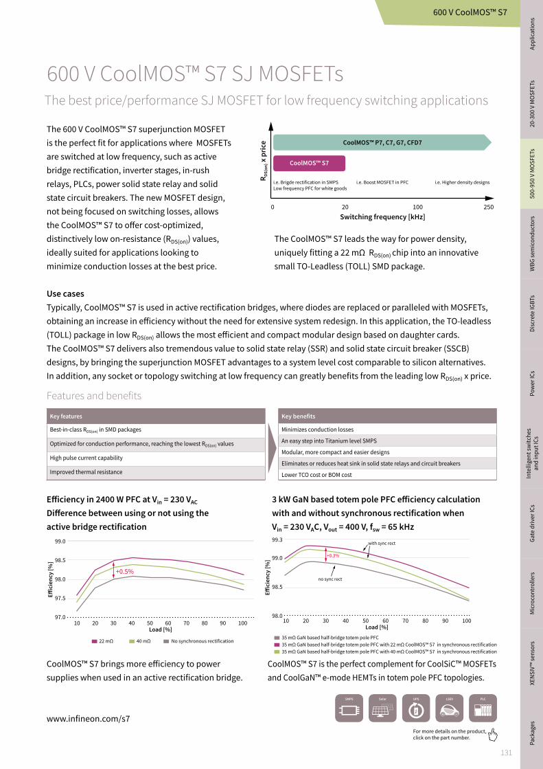
131
For more details on the product, click on the part number.
www.infineon.com/s7
Features and benefits
Key benefits
Minimizes conduction losses
An easy step into Titanium level SMPS
Modular, more compact and easier designs
Eliminates or reduces heat sink in solid state relays and circuit breakers
Lower TCO cost or BOM cost
Key features
Best-in-class RDS(on) in SMD packages
Optimized for conduction performance, reaching the lowest RDS(on) values
High pulse current capability
Improved thermal resistance
600 V CoolMOS™ S7 SJ MOSFETsThe best price/performance SJ MOSFET for low frequency switching applications
The 600 V CoolMOS™ S7 superjunction MOSFET is the perfect fit for applications where MOSFETs are switched at low frequency, such as active bridge rectification, inverter stages, in-rush relays, PLCs, power solid state relay and solid state circuit breakers. The new MOSFET design, not being focused on switching losses, allows the CoolMOS™ S7 to offer cost-optimized, distinctively low on-resistance (RDS(on)) values, ideally suited for applications looking to minimize conduction losses at the best price.
The CoolMOS™ S7 leads the way for power density, uniquely fitting a 22 mΩ RDS(on) chip into an innovative small TO-Leadless (TOLL) SMD package.
Use casesTypically, CoolMOS™ S7 is used in active rectification bridges, where diodes are replaced or paralleled with MOSFETs, obtaining an increase in efficiency without the need for extensive system redesign. In this application, the TO-leadless (TOLL) package in low RDS(on) allows the most efficient and compact modular design based on daughter cards. The CoolMOS™ S7 delivers also tremendous value to solid state relay (SSR) and solid state circuit breaker (SSCB) designs, by bringing the superjunction MOSFET advantages to a system level cost comparable to silicon alternatives. In addition, any socket or topology switching at low frequency can greatly benefits from the leading low RDS(on) x price.
Efficiency in 2400 W PFC at Vin = 230 VAC
Difference between using or not using the active bridge rectification
CoolMOS™ S7 brings more efficiency to power supplies when used in an active rectification bridge.
CoolMOS™ S7 is the perfect complement for CoolSiC™ MOSFETs and CoolGaN™ e-mode HEMTs in totem pole PFC topologies.
3 kW GaN based totem pole PFC efficiency calculation with and without synchronous rectification when Vin = 230 VAC, Vout = 400 V, fsw = 65 kHz
0 20 100 250
i.e. Brigde rectification in SMPS
Low frequency PFC for white goods
CoolMOS™ S7
CoolMOS™ P7, C7, G7, CFD7
i.e. Boost MOSFET in PFC
Switching frequency [kHz]
RD
S(o
n) x
pric
e
i.e. Higher density designs
99.0
98.5
98.0
97.5
97.010 20 30 40 50 60 70 80 90 100
Load [%]
E
icie
ncy
[%
]
No synchronous rectification22 mΩ 40 mΩ
+0.5%
99.0
98.5
98.0
99.3
10 20 30 40 50 60 70 80 90 100Load [%]
Eic
ienc
y [%
]
no sync rect
with sync rect
+0.3%
35 mΩ GaN based half-bridge totem pole PFC35 mΩ GaN based half-bridge totem pole PFC with 22 mΩ CoolMOS™ S7 in synchronous rectification35 mΩ GaN based half-bridge totem pole PFC with 40 mΩ CoolMOS™ S7 in synchronous rectification
600 V CoolMOS™ S7
Appl
icat
ions
Pa
cka
ges
20
-30
0 V
MO
SF
ETs
50
0-9
50
V M
OS
FE
TsW
BG
se
mic
on
du
cto
rsD
iscr
ete
IGB
TsP
ow
er
ICs
Inte
llig
en
t sw
itch
es
an
d in
pu
t IC
sG
ate
dri
ver
ICs
Mic
roco
ntr
oll
ers
XE
NS
IV™
se
nso
rs

132
For more details on the product, click on the part number.
600 V CoolMOS™ CFD7 SJ MOSFETsInfineon's solution for resonant switching high power applications
The 600 V CoolMOS™ CFD7 is one of Infineon’s latest high voltage superjunction MOSFET series with an integrated fast body diode. It is the ideal choice for resonant topologies, such as LLC and ZVS PSFB, and targets the high SMPS market.
As a result of significantly reduced gate charge (QG), improved turn-off behavior, a reverse recovery charge (Qrr) of up to 69 percent lower compared to the competition, as well as the lowest reverse recovery time (trr) in the market, it combines the highest efficiency and best-in-class reliability in soft switching applications, without sacrificing the easy implementation in the design-in process.
In addition, the 600 V CoolMOS™ CFD7 enables higher power density solutions by offering the best-in-class on-state resistance (RDS(on)) package combinations in through-hole devices, as well as in surface mount devices. In ThinPAK 8x8 and TO-220 with CoolMOS™ CFD7, a RDS(on) of around 30 percent below the next best competitor offering can be achieved. All this together makes CoolMOS™ CFD7 the perfect fit for server and telecom applications, and it is also suitable for EV-charging stations.
www.infineon.com/cfd7
1200
1000
800
600
400
200
0Comp. C Comp. A Comp. D
Qrr [
nC
]
Comp. B
-69 %
-32 %
CFD2 CFD7
World‘s best Qrr got even better!
Qrr
comparison of 170 mΩ CFD vs. 190 mΩ range competition*
*Comparison based on datasheet values
Δ E
ic
ien
cy
[%
]
Load current [A]
1
0.8
0.6
0.4
0.2
0
-0.2
-0.4
-0.6
-0.80 10 20 30 40
IPW60R070CFD7 IPW65R080CFD Competitor A
Competitor B Competitor C Competitor D
Eiciency comparison of CFD7 vs. CFD2 and competition in 2 kW ZVS
Δ 1.45% Δ 0.17%
Features and benefits
Key benefits
Best-in-class hard commutation ruggedness
Highest reliability for resonant topologies
Highest efficiency with outstanding ease of use/performance trade-off
Enabling increased power density solutions
Key features
Ultrafast body diode
Best-in-class reverse recovery charge (Qrr)
Improved reverse diode dv/dt and dif/dt ruggedness
Lowest figure of merit (RDS(on) x QG x Eoss)
Best-in-class RDS(on)/package combinations
600 V CoolMOS™ CFD7 SJ MOSFETs
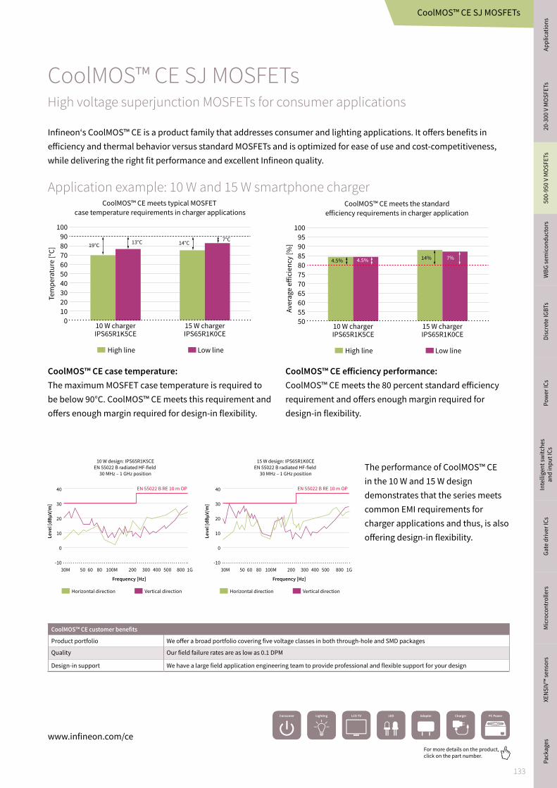
133
For more details on the product, click on the part number.
CoolMOS™ CE SJ MOSFETsHigh voltage superjunction MOSFETs for consumer applications
Infineon‘s CoolMOS™ CE is a product family that addresses consumer and lighting applications. It offers benefits in efficiency and thermal behavior versus standard MOSFETs and is optimized for ease of use and cost-competitiveness, while delivering the right fit performance and excellent Infineon quality.
CoolMOS™ CE customer benefits
Product portfolio We offer a broad portfolio covering five voltage classes in both through-hole and SMD packages
Quality Our field failure rates are as low as 0.1 DPM
Design-in support We have a large field application engineering team to provide professional and flexible support for your design
www.infineon.com/ce
Application example: 10 W and 15 W smartphone charger
10 W chargerIPS65R1K5CE
100
90
80
70
60
50
40
30
20
10
0
Tem
pe
ratu
re [
°C]
CoolMOS™ CE meets typical MOSFET
case temperature requirements in charger applications
19°C13°C 14°C
7°C
15 W chargerIPS65R1K0CE
High line Low line
CoolMOS™ CE case temperature:The maximum MOSFET case temperature is required to be below 90°C. CoolMOS™ CE meets this requirement and offers enough margin required for design-in flexibility.
10 W chargerIPS65R1K5CE
10095908580757065605550
Aver
age
eic
ienc
y [%
]
CoolMOS™ CE meets the standard eiciency requirements in charger application
4.5% 4.5% 14% 7%
15 W chargerIPS65R1K0CE
High line Low line
CoolMOS™ CE efficiency performance:CoolMOS™ CE meets the 80 percent standard efficiency requirement and offers enough margin required for design-in flexibility.
The performance of CoolMOS™ CE in the 10 W and 15 W design demonstrates that the series meets common EMI requirements for charger applications and thus, is also offering design-in flexibility.
40
30
20
10
0
-10
30M 50 60 80 100M
Frequency [Hz]
10 W design: IPS65R1K5CE
EN 55022 B radiated HF-field
30 MHz – 1 GHz position
15 W design: IPS65R1K0CE
EN 55022 B radiated HF-field
30 MHz – 1 GHz position
Leve
l [dB
µV/m
]
Leve
l [dB
µV/m
]
200 300 400 500 800 1G
40
30
20
10
0
-10
Frequency [Hz]
30M 50 60 80 100M 200 300 400 500 800 1G
EN 55022 B RE 10 m OP EN 55022 B RE 10 m OP
Horizontal direction Vertical direction Horizontal direction Vertical direction
Charger
CoolMOS™ CE SJ MOSFETs
Appl
icat
ions
Pa
cka
ges
20
-30
0 V
MO
SF
ETs
50
0-9
50
V M
OS
FE
TsW
BG
se
mic
on
du
cto
rsD
iscr
ete
IGB
TsP
ow
er
ICs
Inte
llig
en
t sw
itch
es
an
d in
pu
t IC
sG
ate
dri
ver
ICs
Mic
roco
ntr
oll
ers
XE
NS
IV™
se
nso
rs

134
For more details on the product, click on the part number.
CoolMOS™ SJ MOSFET high power package innovationsSpace-saving and high performance packages
TO-247 4-pin with asymmetric leadsThe TO-247 4-pin package with asymmetric leads is an optimized version of the standard
TO-247 4-pin and enables highest efficiency and controllability in the high power SMPS
market. The fourth pin acts as a Kelvin source. The main current of the switch is placed
outside of the gate loop and the feedback is eliminated. This leads to less switching losses,
especially at high currents. Secondly, the EMI will be reduced due to cleaner waveforms.
In addition, the asymmetric leads further improve the ease of use in the design-in process.
Compared to the standard TO-247 4-pin the distance between the critical pins has been
increased to enable simplified wave soldering and reduced board yield loss.
Top-side cooled Double DPAK (DDPAK)This is the first top-side cooled surface mount device (SMD) package
addressing high power SMPS applications such as PC power, solar, server and telecom.
SMD-based SMPS designs support fast switching and help to reduce the parasitic induc-
tance associated with long leaded packages such as the common TO-220 package. In
today’s SMD-based designs, the output power is restricted by the thermal limit of the PCB
material because the heat must be dissipated through the board. Thanks to the top-side
cooling concept of DDPAK, the thermal decoupling of board and semiconductor is pos-
sible, enabling higher power density or improved system lifetime.
TO-263-7 (D2PAK-7-pin)The TO-263-7-pin package is an SMD package addressing automotive-specific requirements
including high efficiency and controllability. The Kelvin source pin leads to reduced
switching losses. Furthermore the new 7-pin design increases the creepage distance at
the PCB and therefore helps to improve the manufacturability.
ThinPAK 8x8With very small footprint of only 64 mm² (vs. 150 mm² for the D²PAK) and a very low profile
with only 1 mm height (vs. 4.4 mm for the D²PAK) the ThinPAK 8x8 leadless SMD package
for high voltage MOSFETs is a first choice to decrease system size in power-density driven de-
signs. Low parasitic inductance and a separate 4-pin Kelvin source connection offer best ef-
ficiency and ease of use. The package is RoHS compliant with halogen-free mold compound.
TO-Leadless Combined with the latest CoolMOS™ C7 Gold (G7) technology, the TO-Leadless (TOLL)
package is Infineon’s flagship SMD package for high power/high current SMD solutions.
Compared to D2PAK 7-pin, TO-Leadless shows a 30 percent reduction in footprint, yet of-
fers improved thermal performance. This and the 50 percent height reduction result in a
significant advantage whenever highest power density is demanded. Equipped with 4-pin
Kelvin source connection and low parasitic inductances the package offers best efficiency
and ease of use. The package is MSL1 compliant and reflow solderable.
For highest efficiency and controllability in high power SMPS markets
Enabling significant space savings
Optimized for high power applications
www.infineon.com/coolmos-latest-packages
Innovative top-side cooled SMD solu-tion for high power applications
An SMD package for high efficiency and controllability in automotive applications
CoolMOS™ high power packages

135
For more details on the product, click on the part number.
CoolMOS™ SJ MOSFET low power package innovationsAddressing today’s consumer needs
SOT-223The SOT-223 package without middle pin is a cost-effective alternative to DPAK, ad-
dressing the need for cost reductions in price sensitive applications. It offers a smaller
footprint, while still being pin-to-pin compatible with DPAK, thus, allowing a drop-in
replacement for DPAK and second sourcing. Moreover, SOT-223 achieves comparable
thermal performance to DPAK and enables customers to achieve improved form fac-
tors or space savings in designs with low power dissipation.
ThinPAK 5x6ThinPAK 5x6 reduces the PCB area by 52 percent and height by 54 percent when com-
pared to the DPAK package which is widely used in chargers and adapters. ThinPAK
5x6 is the right device to replace DPAK and meet the market demands of slimmer and
smaller designs. Also ThinPAK 5x6 enables a reduced charger and adapter case hot
spot temperature by increasing the space between the MOSFET and the charger and
adapter case.
TO-220 FullPAK Narrow LeadInfineon’s TO-220 FullPAK Narrow Lead addresses customer needs with regards to
height reduction requirements in adapter and charger applications. By offering an
optimized standoff width and height and improved creepage distance, the package
can be fully inserted into the PCB without any production concerns and, therefore, is
especially suitable for slim and
semi-slim adapter solutions.
TO-220 FullPAK Wide CreepageThis package solution has an increased creepage distance between the pins to 4.25 mm
compared to 2.54 mm of a TO-220 FullPAK package. It targets open frame power sup-
plies such as TV sets and PC power, where dust can enter the case through air vents.
Dust particles can reduce the effective creepage between pins over time, which may
lead to high voltage arcing. The package meets the requirements of open frame power
supplies without any additional measures. Thus, it reduces system cost by offering an
alternative to frequently used approaches to increase creepage distance.
Cost-effective drop-in replacement for DPAK
Solution for slim and small adapters and chargers
Solution for height reduction in adapters and chargers
Improved creepage distance for open frame power supplies
www.infineon.com/coolmos-latest-packages
CoolMOS™ low power packages
Appl
icat
ions
Pa
cka
ges
20
-30
0 V
MO
SF
ETs
50
0-9
50
V M
OS
FE
TsW
BG
se
mic
on
du
cto
rsD
iscr
ete
IGB
TsP
ow
er
ICs
Inte
llig
en
t sw
itch
es
an
d in
pu
t IC
sG
ate
dri
ver
ICs
Mic
roco
ntr
oll
ers
XE
NS
IV™
se
nso
rs

136
For more details on the product, click on the part number.
CoolMOS™ SJ MOSFETs for automotive 600 V CoolMOS™ CPA, 650 V CoolMOS™ CFDA, 800 V CoolMOS™ C3A and new 650 V CoolMOS™ CFD7A – on the fast lane in automotive applications
Highest system performance in a size and weight constrained environment, outstanding and proven product quality and reliability, as well as 100 percent reliable delivery are the needs of our automotive customers. With the high voltage automotive MOSFET series 600 V CoolMOS™ CPA and 650 V CoolMOS™ CFDA, 800 V CoolMOS™ C3A and the new 650 V CoolMOS™ CFD7A, Infineon is perfectly prepared to take the challenges in the strongly growing automotive market.
CoolMOS™ SJ MOSFET automotive – benchmark in quality and reliability Focus on top-notch quality and reliability without any compromise – that is the principle Infineon applies during development and qualification of all CoolMOS™ superjunction technologies. For our automotive grade derivatives, the great quality levels of the industrial base technologies are further boosted by special screening measures in front- and back-end, as well as by extended qualification procedures. The Infineon robustness validation approach with extended stress-test procedures, doubling the real application requirements, is one of our key measures to ensure a quality level well beyond the formal requirements of the AEC Q101 standard. Aside from extended stress times on standard qualification tests, it comprises test procedures, specially developed by Infineon to ensure highest quality of e.g., the power metallization of our devices. Usage of robust package technologies, 100 percent gate oxide screening, and top-notch production monitoring, including yield screening measures, part average testing (PAT), statistical bin alarm (SBA), and pattern recognition procedures, complete our package to guarantee highest automotive quality. This holistic approach results in an unrivalled quality position of our 600 V CoolMOS™ CPA and 650 V CoolMOS™ CFDA, 800 V CoolMOS™ C3A and the new 650 V CoolMOS™ CFD7A.
AEC Q101
Robustness validation – example for thermal cycling test
1.000 cycles1.270 cycles
+254%
2.540 cycles
Customer mission
profile
Infineon automotive
robustness validation
www.infineon.com/cfda www.infineon.com/coolmos-automotive
Product series Key features Applications Quality600 V CoolMOS™ CPA Best choice for demanding hard
switching applications › Lowest RDS(on) per package › Lowest gate charge value QG
› Hard switching topologies (with SiC diode) › PFC boost stages in on-board charger
Quality level well beyond the formal requirements of the AEC Q101 standard through › Special screening measures in front end, back end › Mission-profile based qualification procedures
650 V CoolMOS™ CFDA Easy implementation of layout and design › Integrated fast body diode › Limited voltage overshoot during hard commutation – self-limiting dI/dt and dV/dt › Low Qrr at repetitive commutation on body diode and low Qoss
› Resonant switching topologies › DC-DC stage of OBC › LLC or full-bridge phase shift (ZVS) in DC-DC converter › HID lamp › Active DC link dis-charche › Pre-charge
800 V CoolMOS™ C3A › Outstanding performance in terms of efficiency, thermal behavior and ease-of-use › High blocking voltage
› Auxiliary Supplies for low-power applications in Traction Inverters › On-Board Charger › HV-LV DC-DC converters › DC-link pre-charge › DC-Link active discharge › Isolation Supervision
NEW 650 V CoolMOS™ CFD7A › Improved 650 V CoolMOS™ CFDA › Higher application voltage possible (at the same proven reliability level) › New D2PAK 7-pin with increased creepage distance and Kelvin source › Considerable improvement in key parameters (higher efficiency)
› Hard switching topologies (with SiC diode) › PFC boost stages in on-board charger › Resonant switching topologies › DC-DC stage of OBC › LLC or full-bridge phase shift (ZVS) in DC-DC converter › HID lamp › Active DC link discharge › Pre-charge
CoolMOS™ automotive

137
For more details on the product, click on the part number.
CoolMOS™ SJ MOSFET automotive – ready to support future application trends Driven by the carbon dioxide (CO2) reduction initiatives, the market of plug-in hybrid PHEV and pure EV is strongly growing. Higher ranges of the electric vehicles are realized by increasing the battery capacity and the energy efficiency of the used electric components. The used battery voltage classes tend to become standardized at approximately 450 V with a trend towards the higher voltages, as this supports faster charging times and enables lighter cabling within the vehicle. Discrete high voltage components are widely used for on board charger (OBC) and DC-DC converter (LDC) applications, as price pressure increasingly displaces module-based solutions. The trend towards fast charging impacts on the power range demanded from OBC topologies. Presently, as well as in the past, a vast majority of OBC topologies have been found in the range up to 7.2 kW, whereas the future tends to stir the trend towards 11 kW or even up to 22 kW. This development, paired with a demand for high efficiency and power density at low system cost, is a strong driver for the usage of three-phase solutions.
While for the lower power OBC solutions classic PFC approaches are the well-established approaches in the market, the Vienna rectifier is the optimal solution for the higher power levels. As a true three-phase topology, it delivers full power if attached to a three-phase input but is flexible enough to run on a single-phase if required. The three-level topology minimizes the filter effort compared to other solutions. By using the doubled frequency on the magnetic components, it also helps to significantly reduce the size of the passives. As a three-level topology, the Vienna rectifier, followed by two paralleled DC-DC stages, furthermore leads to a relaxed voltage stress level on the power MOSFETs. This way, it enables to handle upcoming higher battery voltage levels. The RDS(on), required to yield a desired efficiency level in a Vienna Rectifier, is a function of applied switching frequency and demanded power level. With our 600 V CoolMOS™ CPA and 650 V CoolMOS™ CFDA portfolio, covering an RDS(on) range from 45 to 660 mΩ, we are well prepared to support your next generation three-phase Vienna rectifier design. With CoolMOS™ you are ready to seize your share in the emerging high-power onboard-charger markets.
www.infineon.com/coolmos-automotive
Classic PFC stage for OBC OBC Vienna rectifier for three-phase PFC in OBC
Appl
icat
ions
Pa
cka
ges
20
-30
0 V
MO
SF
ETs
50
0-9
50
V M
OS
FE
TsW
BG
se
mic
on
du
cto
rsD
iscr
ete
IGB
TsP
ow
er
ICs
Inte
llig
en
t sw
itch
es
an
d in
pu
t IC
sG
ate
dri
ver
ICs
Mic
roco
ntr
oll
ers
XE
NS
IV™
se
nso
rs

138
For more details on the product, click on the part number.
900 V CoolMOS™ C3 ACTIVE RDS(on)[mΩ]
TO-220 TO-262(I2PAK)
TO-263(D2PAK)
TO-220 FullPAK TO-247 TO-252(DPAK)
120 IPW90R120C3
340 IPP90R340C3 IPI90R340C3 IPB90R340C3 IPA90R340C3 IPW90R340C3
500 IPI90R500C3 IPA90R500C3 IPW90R500C3
800 IPP90R800C3 IPA90R800C3
1000 IPP90R1K0C3 IPA90R1K0C3
1200 IPP90R1K2C3 IPI90R1K2C3 IPA90R1K2C3 IPD90R1K2C3
950 V CoolMOS™ P7 ACTIVE & PREFERRED Charger
RDS(on)[mΩ]
TO-220 TO-220 FullPAK
SOT-223 TO-251Long lead
TO-252(DPAK)
TO-220Wide creepage
ThinPAK 8x8 D2PAK
450 IPA95R450P7 IPU95R450P7 IPD95R450P7
750 IPA95R750P7 IPU95R750P7 IPD95R750P7
1200 IPA95R1K2P7 IPN95R1K2P7 IPU95R1K2P7 IPD95R1K2P7
2000 IPN95R2K0P7 IPU95R2K0P7 IPD95R2K0P7
3700 IPN95R3K7P7 IPU95R3K7P7
800 V CoolMOS™ P7 ACTIVE & PREFERRED RDS(on)[mΩ]
TO -220 TO-220 FullPAK TO-247 TO-252(DPAK)
TO-251(IPAK)
TO-251(IPAK Short Lead)
SOT-223 TO-220 FullPAK narrow lead
280 IPP80R280P7 IPA80R280P7 IPW80R280P7 IPD80R280P7 IPAN80R280P7
360 IPP80R360P7 IPA80R360P7 IPW80R360P7 IPD80R360P7 IPAN80R360P7
450 IPP80R450P7 IPA80R450P7 IPD80R450P7 IPAN80R450P7
600 IPP80R600P7 IPA80R600P7 IPD80R600P7 IPU80R600P7 IPS80R600P7 IPN80R600P7
750 IPP80R750P7 IPA80R750P7 IPD80R750P7 IPU80R750P7 IPS80R750P7 IPN80R750P7
900 IPP80R900P7 IPA80R900P7 IPD80R900P7 IPU80R900P7 IPS80R900P7 IPN80R900P7
1200 IPP80R1K2P7 IPA80R1K2P7 IPD80R1K2P7 IPU80R1K2P7 IPS80R1K2P7 IPN80R1K2P7
1400 IPP80R1K4P7 IPA80R1K4P7 IPD80R1K4P7 IPU80R1K4P7 IPS80R1K4P7 IPN80R1K4P7
2000 IPD80R2K0P7 IPU80R2K0P7 IPS80R2K0P7 IPN80R2K0P7
2400 IPD80R2K4P7 IPU80R2K4P7 IPS80R2K4P7 IPN80R2K4P7
3300 IPD80R3K3P7 IPU80R3K3P7 IPN80R3K3P7
4500 IPD80R4K5P7 IPU80R4K5P7 IPN80R4K5P7
www.infineon.com/coolmoswww.infineon.com/c3
www.infineon.com/800v-p7www.infineon.com/950v-p7
CoolMOS™ product portfolio

139
For more details on the product, click on the part number.
www.infineon.com/coolmoswww.infineon.com/c3
www.infineon.com/cewww.infineon.com/700v-p7
800 V CoolMOS™ CE ACTIVE RDS(on)[mΩ]
TO-220 TO-220 FullPAK TO-247 TO-252(DPAK)
TO-251(IPAK)
310 IPA80R310CE
460 IPA80R460CE
650 IPA80R650CE
1000 IPA80R1K0CE IPD80R1K0CE IPU80R1K0CE
1400 IPA80R1K4CE IPD80R1K4CE
2800 IPD80R2K8CE
700 V CoolMOS™ P7 ACTIVE & PREFERRED Charger
RDS(on)[mΩ]
TO-251 (IPAK Short Lead)
TO-220 FullPAK TO-252 (DPAK)
TO-220 FullPAK narrow lead
TO-251(IPAK Short Leadw/ ISO Standoff)
SOT-223
360 IPS70R360P7S IPA70R360P7S IPD70R360P7S IPAN70R360P7S IPSA70R360P7S IPN70R360P7S
450 IPA70R450P7S IPAN70R450P7S IPSA70R450P7S IPN70R450P7S
600 IPS70R600P7S IPA70R600P7S IPD70R600P7S IPAN70R600P7S IPSA70R600P7S IPN70R600P7S
750 IPA70R750P7S IPAN70R750P7S IPSA70R750P7S IPN70R750P7S
900 IPS70R900P7S IPA70R900P7S IPD70R900P7S IPAN70R900P7S IPSA70R900P7S IPN70R900P7S
1200 IPSA70R1K2P7S IPN70R1K2P7S
1400 IPS70R1K4P7S IPD70R1K4P7S IPSA70R1K4P7S IPN70R1K4P7S
2000 IPSA70R2K0P7S IPN70R2K0P7S
800 V CoolMOS™ C3 ACTIVE RDS(on)[mΩ]
TO-220 TO-263(D2PAK)
TO-220 FullPAK TO-247 TO-252(DPAK)
85 SPW55N80C3
290 SPP17N80C3 SPB17N80C3 SPA17N80C3 SPW17N80C3
450 SPP11N80C3 SPA11N80C3 SPW11N80C3
650 SPP08N80C3 SPA08N80C3
900 SPP06N80C3 SPA06N80C3 SPD06N80C3
1300 SPP04N80C3 SPA04N80C3 SPD04N80C3
2700 SPA02N80C3 SPD02N80C3
700 V CoolMOS™ CE ACTIVE Charger
RDS(on)[mΩ]
TO-220 FullPAK Wide Creepage
TO-262(I2PAK)
TO-251(IPAK Short Lead with ISO
Standoff)
TO-252(DPAK)
TO-251(IPAK Short Lead)
SOT-223
600 IPAW70R600CE IPSA70R600CE IPD70R600CE
950 IPAW70R950CE IPI70R950CE IPSA70R950CE IPD70R950CE IPS70R950CE
1000 IPN70R1K0CE
1400 IPSA70R1K4CE IPD70R1K4CE IPS70R1K4CE
1500 IPN70R1K5CE
2000 IPSA70R2K0CE IPD70R2K0CE IPS70R2K0CE
2100 IPN70R2K1CE
CoolMOS™ product portfolio
Appl
icat
ions
Pa
cka
ges
20
-30
0 V
MO
SF
ETs
50
0-9
50
V M
OS
FE
TsW
BG
se
mic
on
du
cto
rsD
iscr
ete
IGB
TsP
ow
er
ICs
Inte
llig
en
t sw
itch
es
an
d in
pu
t IC
sG
ate
dri
ver
ICs
Mic
roco
ntr
oll
ers
XE
NS
IV™
se
nso
rs

140
For more details on the product, click on the part number.
650 V CoolMOS™ CFD2 ACTIVE RDS(on)[mΩ]
TO-220 TO-262(I2PAK)
TO-263(D2PAK)
TO-220 FullPAK TO-247 TO-252(DPAK)
ThinPAK 8x8
41 IPW65R041CFD80 IPW65R080CFD
110 IPP65R110CFD IPB65R110CFD IPA65R110CFD IPW65R110CFD150 IPP65R150CFD IPB65R150CFD IPA65R150CFD IPW65R150CFD165 IPL65R165CFD190 IPP65R190CFD IPI65R190CFD IPB65R190CFD IPA65R190CFD IPW65R190CFD210 IPL65R210CFD310 IPP65R310CFD IPB65R310CFD IPA65R310CFD340 IPL65R340CFD420 IPP65R420CFD IPA65R420CFD IPW65R420CFD IPD65R420CFD660 IPA65R660CFD IPD65R660CFD950 IPD65R950CFD
1400 IPD65R1K4CFD
www.infineon.com/coolmoswww.infineon.com/g7www.infineon.com/c7
www.infineon.com/cfd2www.infineon.com/ce
650 V CoolMOS™ CE ACTIVE Charger
RDS(on)[mΩ]
TO-220 TO-220 FullPAK TO-247 TO-252(DPAK)
TO-251(IPAK)
TO-251(IPAK Short Lead)
SOT-223 TO-220 FullPAKNarrow Lead
400 IPA65R400CE IPD65R400CE IPS65R400CE650 IPA65R650CE IPD65R650CE IPS65R650CE IPAN65R650CE
1000 IPA65R1K0CE IPD65R1K0CE IPS65R1K0CE1500 IPA65R1K5CE IPD65R1K5CE IPN65R1K5CE
650 V CoolMOS™ C7 ACTIVE & PREFERRED RDS(on)[mΩ]
TO-220 TO-263(D2PAK)
TO-220 FullPAK TO-247 TO-247 4-pin TO-252(DPAK)
ThinPAK 8x8
19 IPW65R019C7 IPZ65R019C745 IPP65R045C7 IPB65R045C7 IPA65R045C7 IPW65R045C7 IPZ65R045C765 IPP65R065C7 IPB65R065C7 IPA65R065C7 IPW65R065C7 IPZ65R065C770 IPL65R070C795 IPP65R095C7 IPB65R095C7 IPA65R095C7 IPW65R095C7 IPZ65R095C799 IPL65R099C7
125 IPP65R125C7 IPB65R125C7 IPA65R125C7 IPW65R125C7 130 IPL65R130C7190 IPP65R190C7 IPB65R190C7 IPA65R190C7 IPW65R190C7 IPD65R190C7195 IPL65R195C7225 IPP65R225C7 IPB65R225C7 IPA65R225C7 IPD65R225C7230 IPL65R230C7
650 V CoolMOS™ C7 Gold (G-series) ACTIVE & PREFERRED RDS(on)[mΩ]
TO -220 TO-Leadless (TOLL)
TO-263 (D2PAK)
TO-220 FullPAK
TO-247 TO -252 (DPAK)
33 IPT65R033G7105 IPT65R105G7195 IPT65R195G7
CoolMOS™ product portfolio

141
For more details on the product, click on the part number.
www.infineon.com/coolmos www.infineon.com/600v-p7 www.infineon.com/600v-PFD7 www.infineon.com/CFD7
600 V CoolMOS™ P7 ACTIVE & PREFERRED
Standard grade
Charger
RDS(on)[mΩ]
TO -220 TO-220 FullPAK TO-220 FullPAK Narrow lead
TO-247 4-pin TO-252(DPAK)
TO-220 FullPAKWide Creepage
ThinPAK 8x8 SOT-223
180 IPA60R180P7S IPAN60R180P7S IPD60R180P7S IPAW60R180P7S280 IPA60R280P7S IPAN60R280P7S IPD60R280P7S IPAW60R280P7S360 IPA60R360P7S IPAN60R360P7S IPD60R360P7S IPAW60R360P7S IPN60R360P7S600 IPA60R600P7S IPAN60R600P7S IPD60R600P7S IPAW60R600P7S IPN60R600P7S
*Coming soon
600 V CoolMOS™ P7 ACTIVE & PREFERRED
Industrial grade
RDS(on)[mΩ]
TO -220 TO-220 FullPAK TO-247 TO-247 4-pin asymmetric leads
TO-252(DPAK)
TO-220 FullPAKWide Creepage
ThinPAK 8x8 D2PAK
24 IPW60R024P7 IPZA60R024P737 IPW60R037P7 IPZA60R037P745 IPW60R045P7 IPZA60R045P7 IPB60R045P760 IPP60R060P7 IPA60R060P7 IPW60R060P7 IPZA60R060P7 IPB60R060P765 IPL60R065P780 IPP60R080P7 IPA60R080P7 IPW60R080P7 IPZA60R080P7 IPL60R085P7 IPB60R080P799 IPP60R099P7 IPA60R099P7 IPW60R099P7 IPZA60R099P7 IPB60R099P7
105 IPL60R105P7120 IPP60R120P7 IPA60R120P7 IPW60R120P7 IPZA60R120P7 IPB60R120P7125 IPL60R125P7160 IPP60R160P7 IPA60R160P7180 IPP60R180P7 IPA60R180P7 IPW60R180P7 IPZA60R180P7 IPD60R180P7 IPB60R180P7185 IPL60R185P7280 IPP60R280P7 IPA60R280P7 IPD60R280P7 IPB60R280P7285 IPL60R285P7360 IPP60R360P7 IPA60R360P7 IPD60R360P7 IPB60R360P7365 IPL60R365P7600 IPP60R600P7 IPA60R600P7 IPD60R600P7
Charger
600 V CoolMOS™ PFD7 ACTIVE & PREFERRED Charger
RDS(on)[mΩ]
TO-220 FullPAK Narrow Leads
TO-251(IPAK Short Lead)
TO-252(DPAK)
SOT-223 ThinPAK 5x6
125 IPAN60R125PFD7S210 IPAN60R210PFD7S IPS60R210PFD7S IPD60R210PFD7S280 IPAN60R280PFD7S IPS60R280PFD7S IPD60R280PFD7S360 IPAN60R360PFD7S IPS60R360PFD7S IPD60R360PFD7S IPN60R360PFD7S IPLK60R360PFD7 *600 IPS60R600PFD7S IPD60R600PFD7S IPN60R600PFD7S IPLK60R600PFD7 *
1000 IPS60R1K0PFD7S IPD60R1K0PFD7S IPN60R1K0PFD7S IPLK60R1K0PFD7 *1500 IPD60R1K5PFD7S IPN60R1K5PFD7S IPLK60R1K5PFD7 *2000 IPD60R2K0PFD7S IPN60R2K0PFD7S
600 V CoolMOS™ CFD7 ACTIVE & PREFERRED RDS(on)[mΩ]
TO-220 TO-263(D2PAK)
TO-220 FullPAK TO-247 TO-252(DPAK)
ThinPAK 8x8 DDPAK TO-Leadless (TOLL)
18 IPW60R018CFD7
24 IPW60R024CFD7
31/35 IPW60R031CFD7 IPT60R035CFD7 *
40/45 IPB60R040CFD7 IPW60R040CFD7 IPDD60R045CFD7 * IPT60R045CFD7 *
55 IPB60R055CFD7 IPW60R055CFD7 IPDD60R055CFD7 * IPT60R055CFD7 *
60 IPL60R060CFD7
70 IPP60R070CFD7 IPB60R070CFD7 IPW60R070CFD7
75 IPL60R075CFD7 IPDD60R075CFD7 * IPT60R075CFD7 *
90/95 IPP60R090CFD7 IPB60R090CFD7 IPW60R090CFD7 IPL60R095CFD7 IPDD60R090CFD7 * IPT60R090CFD7 *
105/115 IPP60R105CFD7 IPB60R105CFD7 IPW60R105CFD7 IPL60R115CFD7 IPDD60R105CFD7 * IPT60R105CFD7 *
125/140 IPP60R125CFD7 IPB60R125CFD7 IPA60R125CFD7 IPW60R125CFD7 IPL60R140CFD7 IPDD60R125CFD7 * IPT60R125CFD7 *
145/160 IPP60R145CFD7 IPB60R145CFD7 IPA60R145CFD7 IPW60R145CFD7 IPD60R145CFD7 IPL60R160CFD7 IPDD60R145CFD7 * IPT60R145CFD7 *
170 IPP60R170CFD7 IPB60R170CFD7 IPA60R170CFD7 IPW60R170CFD7 IPD60R170CFD7 IPDD60R170CFD7 *
185 IPL60R185CFD7
210/225 IPP60R210CFD7 IPB60R210CFD7 IPA60R210CFD7 IPD60R210CFD7 IPL60R225CFD7
280 IPP60R280CFD7 IPB60R280CFD7 IPA60R280CFD7 IPD60R280CFD7
360 IPP60R360CFD7 * IPB60R360CFD7 IPA60R360CFD7 IPD60R360CFD7
CoolMOS™ product portfolio
Appl
icat
ions
Pa
cka
ges
20
-30
0 V
MO
SF
ETs
50
0-9
50
V M
OS
FE
TsW
BG
se
mic
on
du
cto
rsD
iscr
ete
IGB
TsP
ow
er
ICs
Inte
llig
en
t sw
itch
es
an
d in
pu
t IC
sG
ate
dri
ver
ICs
Mic
roco
ntr
oll
ers
XE
NS
IV™
se
nso
rs

142
For more details on the product, click on the part number.
600 V CoolMOS™ P6 ACTIVE RDS(on)[mΩ]
TO-220 TO-220 FullPAK TO-247 TO-247 4-pin TO-252(DPAK)
ThinPAK 5x6 ThinPAK 8x8
41 IPW60R041P6
70 IPW60R070P6 IPZ60R070P6
99 IPP60R099P6 IPA60R099P6 IPW60R099P6 IPZ60R099P6
125 IPP60R125P6 IPA60R125P6 IPW60R125P6
160 IPP60R160P6 IPA60R160P6 IPW60R160P6
180 IPL60R180P6
190 IPP60R190P6 IPA60R190P6 IPW60R190P6
210 IPL60R210P6
230 IPA60R230P6
255
280 IPP60R280P6 IPA60R280P6 IPW60R280P6
330/360 IPL60R360P6S
380 IPA60R380P6 IPD60R380P6
600 IPA60R600P6 IPD60R600P6
650 IPL60R650P6S
www.infineon.com/coolmoswww.infineon.com/c7
www.infineon.com/p6www.infineon.com/g7 www.infineon.com/s7
600 V CoolMOS™ C7 ACTIVE & PREFERRED RDS(on)[mΩ]
TO-220 TO-263(D2PAK)
TO-220 FullPAK TO-247 TO-247 4-pin TO-252(DPAK)
ThinPAK 8x8
17 IPW60R017C7 IPZ60R017C7
40 IPP60R040C7 IPB60R040C7 IPW60R040C7 IPZ60R040C7
60 IPP60R060C7 IPB60R060C7 IPA60R060C7 IPW60R060C7 IPZ60R060C7
65 IPL60R065C7
99 IPP60R099C7 IPB60R099C7 IPA60R099C7 IPW60R099C7 IPZ60R099C7
104 IPL60R104C7
120 IPP60R120C7 IPB60R120C7 IPA60R120C7 IPW60R120C7
125 IPL60R125C7
180 IPP60R180C7 IPB60R180C7 IPA60R180C7 IPW60R180C7 IPD60R180C7
185 IPL60R185C7
600 V CoolMOS™ C7 Gold (G-series) ACTIVE & PREFERRED RDS(on)[mΩ]
TO -220 TO-Leadless(TOLL)
TO-220 FullPAK TO-247 TO-247 4-pin TO-252(Double DPAK)
ThinPAK 8x8
28 IPT60R028G750 IPT60R050G7 IPDD60R050G780 IPT60R080G7 IPDD60R080G7
102 IPT60R102G7 IPDD60R102G7125 IPT60R125G7 IPDD60R125G7150 IPT60R150G7 IPDD60R150G7190 IPDD60R190G7
600 V CoolMOS™ S7 ACTIVE & PREFERRED RDS(on)[mΩ]
TO -220 QDPAK TO-Leadless (TOLL)
10 IPDQ60R010S7 *22 IPP60R022S7 IPT60R022S740 IPT60R040S765 IPT60R065S7
* Coming soon
CoolMOS™ product portfolio

143
For more details on the product, click on the part number.
600 V CoolMOS™ CE ACTIVE Charger
RDS(on)[mΩ]
TO-220 FullPAK TO-220 FullPAKWide Creepage
TO-247 TO-252(DPAK)
TO-251(IPAK)
TO-251(IPAK Short Lead)
SOT-223 TO-220 FullPAKNarrow Lead
190 IPAW60R190CE
280 IPAW60R280CE
380 IPAW60R380CE
400 IPA60R400CE IPD60R400CE IPS60R400CE
460 IPA60R460CE IPD60R460CE IPS60R460CE
600 IPAW60R600CE
650 IPA60R650CE IPD60R650CE IPS60R650CE IPAN60R650CE
800 IPD60R800CE IPS60R800CE IPAN60R800CE
1000 IPA60R1K0CE IPD60R1K0CE IPU60R1K0CE IPS60R1K0CE IPN60R1K0CE
1500 IPA60R1K5CE IPD60R1K5CE IPU60R1K5CE IPS60R1K5CE IPN60R1K5CE
2100 IPD60R2K1CE IPU60R2K1CE IPS60R2K1CE IPN60R2K1CE
3400 IPD60R3K4CE IPS60R3K4CE IPN60R3K4CE
500 V CoolMOS™ CE ACTIVE & PREFERRED RDS(on)[mΩ]
TO-220 TO-220 FullPAK TO-247 TO-252(DPAK)
TO-251(IPAK)
TO-251(IPAK Short Lead)
SOT-223 TO-220 FullPAKNarrow Lead
190 IPP50R190CE IPA50R190CE
280 IPP50R280CE IPA50R280CE IPD50R280CE
380 IPP50R380CE IPA50R380CE IPD50R380CE
500 IPA50R500CE IPD50R500CE IPAN50R500CE
650 IPD50R650CE IPN50R650CE
800 IPA50R800CE IPD50R800CE IPN50R800CE
950 IPA50R950CE IPD50R950CE IPN50R950CE
1400 IPD50R1K4CE IPN50R1K4CE
2000 IPD50R2K0CE IPN50R2K0CE
3000 IPD50R3K0CE IPN50R3K0CE
www.infineon.com/coolmoswww.infineon.com/ce www.infineon.com/500v-ce
CoolMOS™ product portfolio
Appl
icat
ions
Pa
cka
ges
20
-30
0 V
MO
SF
ETs
50
0-9
50
V M
OS
FE
TsW
BG
se
mic
on
du
cto
rsD
iscr
ete
IGB
TsP
ow
er
ICs
Inte
llig
en
t sw
itch
es
an
d in
pu
t IC
sG
ate
dri
ver
ICs
Mic
roco
ntr
oll
ers
XE
NS
IV™
se
nso
rs

144
For more details on the product, click on the part number.
www.infineon.com/coolmoswww.infineon.com/coolmos-automotive
CoolMOS™ SJ MOSFET automotive
600 V CoolMOS™ CPA ACTIVE & PREFERRED Product type RDS(on) @ TJ = 25°C
VGS = 10 V[mΩ]
ID,max. @ TJ = 25°C[A]
ID_puls,max.[A]
VGS(th),min.-max. [V]
QG,typ.[nC]
RthJC,max.[K/W]
Package
IPB60R099CPA 99 31 93 2.5 … 3.5 60 0.5 TO-263
IPB60R199CPA 199 16 51 2.5 … 3.5 32 0.9 TO-263
IPB60R299CPA 299 11 34 2.5 … 3.5 22 1.3 TO-263
IPP60R099CPA 99 31 93 2.5 … 3.5 60 0.5 TO-220
IPW60R045CPA 45 60 230 2.5 … 3.5 150 0.29 TO-247
IPW60R075CPA 75 39 130 2.5 … 3.5 87 0.4 TO-247
IPW60R099CPA 99 31 93 2.5 … 3.5 60 0.5 TO-247
IPI60R099CPA 99 31 93 2.5 … 3.5 60 0.5 TO-262
800 V CoolMOS™ C3A ACTIVE & PREFERRED Product type RDS(on) @ TJ = 25°C
VGS = 10 V[mΩ]
ID,max. @ TJ = 25°C[A]
ID_puls,max.[A]
VGS(th),min.-max. [V]
QG,typ.[nC]
RthJC,max.[K/W]
Package
IPD80R2K7C3A 2700 2 6 2.1 … 3.9 12 3 TO-252
IPB80R290C3A 290 17 51 2.1 … 3.9 91 0.55 TO-263
IPW80R290C3A 290 17 51 2.1 … 3.9 91 0.55 TO-247
650 V CoolMOS™ CFDA ACTIVE & PREFERRED Product type RDS(on) @ TJ = 25°C
VGS = 10 V[mΩ]
ID,max. @ TJ = 25°C[A]
ID_puls,max.[A]
VGS(th),min.-max. [V]
QG,typ.[nC]
RthJC,max.[K/W]
Package
IPD65R420CFDA 420 8.7 27 3.5...4.5 32 1.5 TO-252
IPD65R660CFDA 660 6 17 3.5...4.5 20 2 TO-252
IPB65R110CFDA 110 31.2 99.6 3.5...4.5 11 0.45 TO-263
IPB65R150CFDA 150 22.4 72 3.5...4.5 86 0.64 TO-263
IPB65R190CFDA 190 17.5 57.2 3.5...4.5 68 0.83 TO-263
IPB65R310CFDA 310 11.4 34.4 3.5...4.5 41 1.2 TO-263
IPB65R660CFDA 660 6 17 3.5...4.5 20 2 TO-263
IPP65R110CFDA 110 31.2 99.6 3.5...4.5 11 0.45 TO-220
IPP65R150CFDA 150 22.4 72 3.5...4.5 86 0.64 TO-220
IPP65R190CFDA 190 17.5 57.2 3.5...4.5 68 0.83 TO-220
IPP65R310CFDA 310 11.4 34.4 3.5...4.5 41 1.2 TO-220
IPW65R048CFDA 48 63.3 228 3.5...4.5 27 0.25 TO-247
IPW65R080CFDA 80 43.3 127 3.5...4.5 16 0.32 TO-247
IPW65R110CFDA 110 31.2 99.6 3.5...4.5 11 0.45 TO-247IPW65R150CFDA 150 22.4 72 3.5...4.5 86 0.64 TO-247IPW65R190CFDA 190 17.5 57.2 3.5...4.5 68 0.83 TO-247
CoolMOS™ product portfolio

145
For more details on the product, click on the part number.
650V CoolMOS™ CFD7A ACTIVE & PREFERRED RDS(on)[mΩ]
TO-263D²PAK
TO-263-7D²PAK 7 pin
TO-220 TO-247
230 IPB65R230CFD7A * IPBE65R230CFD7A *
115 IPB65R115CFD7A * * IPBE65R115CFD7A * * IPP65R0115CFD7A * IPW65R115CFD7A *
99 IPB65R099CFD7A * IPBE65R099CFD7A * IPP65R099CFD7A * IPW65R099CFD7A *
75 IPBE65R075CFD7A * IPW65R075CFD7A *
50 IPB65R050CFD7A * IPBE65R050CFD7A * IPP65R050CFD7A * IPW65R050CFD7A *
35 IPW65R035CFD7A *
22 IPW65R022CFD7A *
* ES available, SOP second half 2020 * * Coming soon
CoolMOS™ product portfolio
Appl
icat
ions
Pa
cka
ges
20
-30
0 V
MO
SF
ETs
50
0-9
50
V M
OS
FE
TsW
BG
se
mic
on
du
cto
rsD
iscr
ete
IGB
TsP
ow
er
ICs
Inte
llig
en
t sw
itch
es
an
d in
pu
t IC
sG
ate
dri
ver
ICs
Mic
roco
ntr
oll
ers
XE
NS
IV™
se
nso
rs

146
For more details on the product, click on the part number.
www.infineon.com/coolmos-latest-packages
CoolMOS™ SJ MOSFETs – packages
TO-247RDS(on) [mΩ]
Voltage [V] Series 0-59 60-89 90-149 150-199 200-299 300-400 401-600 601-899 900-1500 >1500
600
P7 24/37/45 60/80 99/120 180C7 17/40 60 99/120 180P6 41 70 99/125 160/190 280
CFD7 18/24/31/40/55 70 90/125/145 170CPA 45 75 99
650
C7 19/45 65 95/125 190CFD2 41 80 110 150/190 420CFDA 48 80 110 150/190
CFD7A 22 */35 */50 * 75 * 99 */115 *
800 P7 280 360C3 85 290 450
900 C3 120 340 500
SOT-223RDS(on) [mΩ]
Voltage [V] Series 0-59 60-89 90-149 150-199 200-299 300-400 401-600 601-899 900-1500 >1500500 CE 650/800 950/1400 2000/3000
600P7 360 600CE 1000/1500 2100/3400
PFD7 360 600 1000/1500 2000650 CE 2000
700 P7 360 450/600 700 900/1200/1400 2000CE 1000/1500/2100
800 P7 650/750 900/1200/1400 2000/2400/ 3300/4500
950 P7 1200 2000/3700
TO-247 4-pinRDS(on) [mΩ]
Voltage [V] Series 0-59 60-89 90-149 150-199 200-299 300-400 401-600 601-899 900-1500 >1500
600C7 17/40 60 99
P6 70 99
650 C7 19/45 65 95
TO-247 4-pin asymmetric leadsRDS(on) [mΩ]
Voltage [V] Series 0-59 60-89 90-149 150-199 200-299 300-400 401-600 601-899 900-1500 >1500
600 P7 24/37/45 60/80 99/120 180
IPAKRDS(on) [mΩ]
Voltage [V] Series 0-59 60-89 90-149 150-199 200-299 300-400 401-600 601-899 900-1500 >1500
600 CE 1000/1500 2100
800P7 600 750 900/1200/1400 2000/2400
3300/4500
CE 1000
950 P7 450 750 1200 2000/3700
ACTIVE & PREFERRED
CoolMOS™ product portfolio
* ES available, SOP second half 2020

147
For more details on the product, click on the part number.
IPAK Short LeadRDS(on) [mΩ]
Voltage [V] Series 0-59 60-89 90-149 150-199 200-299 300-400 401-600 601-899 900-1500 >1500
600CE 400 460 650/800 1000/1500 2100/3400
PFD7 210/280 360 600 1000
650 CE 400 650 1000
700P7 360/600 900/1400
CE 950/1400 2000
800 P7 600 750 900/1200/1400 2000/2400
IPAK Short Lead with ISO StandoffRDS(on) [mΩ]
Voltage [V] Series 0-59 60-89 90-149 150-199 200-299 300-400 401-600 601-899 900-1500 >1500
700P7 360 450/600 750 900/1200/1400 2000
CE 600 950/1400 2000
DPAKRDS(on) [mΩ]
Voltage [V] Series 0-59 60-89 90-149 150-199 200-299 300-400 401-600 601-899 900-1500 >1500
500 CE 280 380 500 650/800 950/1400 2000/3000
600
P7 180 280 360 600
C7 180
CE 400 460 650/800 1000/1500 2100/3400
P6 380 600
CFD7 170 280 360 *
PFD7 210/280 360 600 1000/1500 2000
650
C7 190 225
CE 400 650 1000/1500
CFD2 420 660 950/1400
CFDA 420 660
700P7 360 600 900/1400
CE 600 950/1400 2000
800
P7 280 360 450/600 750 900/1200/1400 2000/24003300/4500
C3 900/1300 2700
CE 1000/1400 2800
900 C3 1200
950 P7 450 750 1200 2000
I²PAKRDS(on) [mΩ]
Voltage [V] Series 0-59 60-89 90-149 150-199 200-299 300-400 401-600 601-899 900-1500 >1500
600 CPA 99
650 CFD2 199
700 CE 950
900 C3 340 500 1200
www.infineon.com/coolmos-latest-packages *Coming soon
ACTIVE & PREFERRED
CoolMOS™ product portfolio
Appl
icat
ions
Pa
cka
ges
20
-30
0 V
MO
SF
ETs
50
0-9
50
V M
OS
FE
TsW
BG
se
mic
on
du
cto
rsD
iscr
ete
IGB
TsP
ow
er
ICs
Inte
llig
en
t sw
itch
es
an
d in
pu
t IC
sG
ate
dri
ver
ICs
Mic
roco
ntr
oll
ers
XE
NS
IV™
se
nso
rs
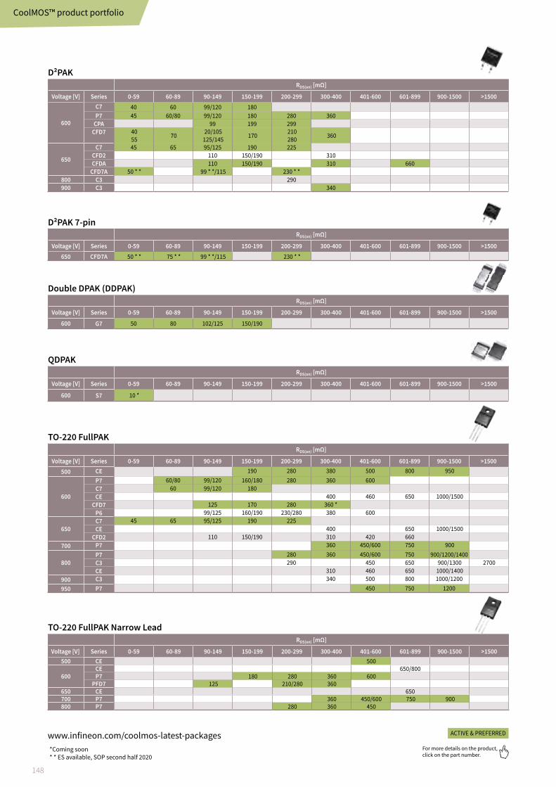
148
For more details on the product, click on the part number.
TO-220 FullPAKRDS(on) [mΩ]
Voltage [V] Series 0-59 60-89 90-149 150-199 200-299 300-400 401-600 601-899 900-1500 >1500500 CE 190 280 380 500 800 950
600
P7 60/80 99/120 160/180 280 360 600C7 60 99/120 180CE 400 460 650 1000/1500
CFD7 125 170 280 360 *P6 99/125 160/190 230/280 380 600
650C7 45 65 95/125 190 225CE 400 650 1000/1500
CFD2 110 150/190 310 420 660700 P7 360 450/600 750 900
800P7 280 360 450/600 750 900/1200/1400C3 290 450 650 900/1300 2700CE 310 460 650 1000/1400
900 C3 340 500 800 1000/1200950 P7 450 750 1200
TO-220 FullPAK Narrow Lead RDS(on) [mΩ]
Voltage [V] Series 0-59 60-89 90-149 150-199 200-299 300-400 401-600 601-899 900-1500 >1500500 CE 500
600CE 650/800P7 180 280 360 600
PFD7 125 210/280 360650 CE 650 700 P7 360 450/600 750 900800 P7 280 360 450
Double DPAK (DDPAK)RDS(on) [mΩ]
Voltage [V] Series 0-59 60-89 90-149 150-199 200-299 300-400 401-600 601-899 900-1500 >1500600 G7 50 80 102/125 150/190
QDPAKRDS(on) [mΩ]
Voltage [V] Series 0-59 60-89 90-149 150-199 200-299 300-400 401-600 601-899 900-1500 >1500
600 S7 10 *
D²PAKRDS(on) [mΩ]
Voltage [V] Series 0-59 60-89 90-149 150-199 200-299 300-400 401-600 601-899 900-1500 >1500
600
C7 40 60 99/120 180P7 45 60/80 99/120 180 280 360
CPA 99 199 299CFD7 40
55 70 20/105125/145 170 210
280 360
650
C7 45 65 95/125 190 225CFD2 110 150/190 310CFDA 110 150/190 310 660
CFD7A 50 * * 99 * */115 230 * *800 C3 290900 C3 340
D²PAK 7-pinRDS(on) [mΩ]
Voltage [V] Series 0-59 60-89 90-149 150-199 200-299 300-400 401-600 601-899 900-1500 >1500650 CFD7A 50 * * 75 * * 99 * */115 230 * *
www.infineon.com/coolmos-latest-packages ACTIVE & PREFERRED
*Coming soon * * ES available, SOP second half 2020
CoolMOS™ product portfolio

149
For more details on the product, click on the part number.
*Coming soon * * ES available, SOP second half 2020
TO-Leadless RDS(on) group [mΩ]
Voltage [V] Series 0-59 60-89 90-149 150-199 200-299 300-400 401-600 601-899 900-1500 >1500
600 G7 28/50 80 102/125 150 S7 22/40 65
650 G7 33 105 195
TO-220RDS(on) [mΩ]
Voltage [V] Series 0-59 60-89 90-149 150-199 200-299 300-400 401-600 601-899 900-1500 >1500
500 CE 190 280 380
600
P7 60/80 99/120 160/180 280 360 600
C7 40 60 99/120 180
P6 99/125 160/190 280
CFD7 70 90/125 170 280 360
CPA 99
S7 22
650
C7 45 65 95/125 190 225
CFD2 110 150/190 310 420
CFDA 50 99/110/115 150/190 310 660
CFD7A 50 * * 99 * */115 * *
800P7 280 360 450/600 750 900/1200/1400
C3 290 450 650 900/1300
900 C3 340 800 1000/1200
ThinPAK 8x8RDS(on) [mΩ]
Voltage [V] Series 0-59 60-89 90-149 150-199 200-299 300-400 401-600 601-899 900-1500 >1500
600
P7 65/85 105/125 185 285 365
C7 65 104/125 185
CFD7 75 185 225
P6 180 210
650C7 70 99/130 195 230
CFD2 165 210 340
ThinPAK 5x6RDS(on) [mΩ]
Voltage [V] Series 0-59 60-89 90-149 150-199 200-299 300-400 401-600 601-899 900-1500 >1500
600P6 360 650
PFD7 360 600 1000/1500
TO-220 FullPAK Wide CreepageRDS(on) [mΩ]
Voltage [V] Series 0-59 60-89 90-149 150-199 200-299 300-400 401-600 601-899 900-1500 >1500
600P7 180 280 360 600
CE 190 280 380 600
700 CE 600 950
www.infineon.com/coolmos-latest-packages ACTIVE & PREFERRED
CoolMOS™ product portfolio
Appl
icat
ions
Pa
cka
ges
20
-30
0 V
MO
SF
ETs
50
0-9
50
V M
OS
FE
TsW
BG
se
mic
on
du
cto
rsD
iscr
ete
IGB
TsP
ow
er
ICs
Inte
llig
en
t sw
itch
es
an
d in
pu
t IC
sG
ate
dri
ver
ICs
Mic
roco
ntr
oll
ers
XE
NS
IV™
se
nso
rs

150
For more details on the product, click on the part number.
Power MOSFETs (from October 2015 onwards)
Power MOSFETs (until 2005)
Nomenclature
S P P 20 N 60 C 3
Company
S = Formerly Siemens
Device
P = Power MOSFET
Continuous drain current
(@ TC = 25°C) [A]
Package type
A = TO-220 FullPAK
B = TO-263 (D2PAK)
D = TO-252 (DPAK)
I = TO-262 (I2PAK)
N = SOT-223
P = TO-220
U = TO-251 (IPAK)
W = TO-247
Z = TO-247 4-pin
Breakdown voltage
Divided by 10 (60x10 = 600 V)
Specifications
C3 = CoolMOSTM C3
S5 = CoolMOSTM S5
Technology
N = N-channel transistors
I P DD 80 R 190 P7
CompanyI = Infineon
DeviceP = Power MOSFET
Breakdown voltageDivided by 10 (80x10 = 800 V)
Package type (max. 2 digits)A = TO-220 FullPAKB = TO-263 (D2PAK)C = Bare dieD = TO-252 (DPAK)I = TO-262 (I2PAK)L = ThinPAK 8x8N = SOT-223P = TO-220S = TO-251 (IPAK Short Lead)U = TO-251 (IPAK Long Lead)W = TO-247Z = TO-247 4-pinT = TO-LeadlessDD = TO-252 (Double DPAK)AW = TO-220 (Wide Creepage)AN = TO-220 (Narrow Lead)LS = ThinPAK 5x6LK = ThinPAK 5x6 Kelvin sourceDQ = TO-252 (Quadruple DPAK)SA = TO-251 (IPAK Short Lead with ISO Stando)ZA = TO-247 4-pin asymmetric
Series name (2-4 digits)In this case CoolMOS™ P7(max. digits e.g. CFD7)
Reliability gradeblank = IndustrialA = AutomotiveS = Standard
R = RDS(on)
As a seperator between voltage und RDS(on)
RDS(on) [mΩ]
Automotive MOSFETsI P P 60 R 099 C P A
Package type
B = TO-263 (D2PAK)
I = TO-262 (I2PAK)
D = TO-252 (DPAK)
P = TO-220
W = TO-247
BE = TO-263 (D2PAK 7-pin)
Automotive
Series name
CoolMOS™ CP, CoolMOS™ CFD, CoolMOS™ C3, CoolMOS™ CFD7
Company
I = Infineon
Device
P = Power MOSFET
Breakdown voltage
Divided by 10 (60x10 = 600 V)
RDS(on)
[mΩ]
R = RDS(on)
CoolMOS™ nomenclature

151
For more details on the product, click on the part number.
Further information, datasheets and documentswww.infineon.com/coolmoswww.infineon.com/coolmos-latest-packageswww.infineon.com/coolmos-automotive www.infineon.com/gan
Evaluationboards and simulation modelswww.infineon.com/coolmos-boardswww.infineon.com/powermosfet-simulationmodels
Infineon support for high voltage MOSFETsUseful links and helpful information
Simulation
Appl
icat
ions
Pa
cka
ges
20
-30
0 V
MO
SF
ETs
50
0-9
50
V M
OS
FE
TsW
BG
se
mic
on
du
cto
rsD
iscr
ete
IGB
TsP
ow
er
ICs
Inte
llig
en
t sw
itch
es
an
d in
pu
t IC
sG
ate
dri
ver
ICs
Mic
roco
ntr
oll
ers
XE
NS
IV™
se
nso
rs

152
For more details on the product, click on the part number.
› CoolGaN™ e-mode HEMTs › CoolGaN™ 400 V e-mode GaN HEMTs › CoolGaN™ 600 V e-mode GaN HEMTs › CoolGaN™ product portfolio › Silicon carbide › CoolSiC™ silicon carbide MOSFETs 650 V › CoolSiC™ silicon carbide MOSFETs 1200 V
Wide bandgap semiconductors › CoolSiC™ product portfolio › CoolSiC™ Schottky diodes › CoolSiC™ Schottky diodes 650 V › CoolSiC™ Schottky diodes 1200 V › SiC diodes product portfolio › Silicon power diodes

153
For more details on the product, click on the part number.
Appl
icat
ions
Pa
cka
ges
20
-30
0 V
MO
SF
ETs
50
0-9
50
V M
OS
FE
TsW
BG
se
mic
on
du
cto
rsD
iscr
ete
IGB
TsP
ow
er
ICs
Inte
llig
en
t sw
itch
es
an
d in
pu
t IC
sG
ate
dri
ver
ICs
Mic
roco
ntr
oll
ers
XE
NS
IV™
se
nso
rs

154
For more details on the product, click on the part number.
Wide bandgap semiconductors
Wide bandgap semiconductorsGallium nitride (GaN) and silicon carbide (SiC)
The key to the next essential step towards an energy-efficient world is to use new materials, such as wide bandgap semiconductors that allow for greater power efficiency, smaller size, lighter weight, lower overall cost – or all of these together. Infineon, with its unique market position of being currently the only company offering silicon (Si), silicon carbide (SiC) and gallium nitride (GaN) devices, is the customer’s first choice in all segments.
CoolGaN™ – ultimate efficiency and reliabilityCompared to silicon (Si), the breakdown field of Infineon’s CoolGaN™ enhancement mode (e-mode) HEMTs is ten times higher and the electron mobility is double. Both the output charge and gate charge are ten times lower than with Si and the reverse recovery charge is almost zero which is key to high-frequency operations. GaN is the best-suited technology in hard-switching as well as resonant topologies, and is enabling new approaches in current modulation. Infineon’s GaN solution is based on the most robust and performing concept in the market – the enhancement-mode concept - offering fast turn-on and turn-off speed. CoolGaN™ products focus on high performance and robustness, and add significant value to a broad variety of systems across many applications such as server, telecom, hyperscale data centers, wireless charging, adapter/charger, and audio. CoolGaN™ switches are easy to design-in with the matching GaN EiceDRIVER™ gate driver ICs from Infineon.
CoolSiC™ - revolution to rely onSilicon carbide (SiC) has a wide bandgap of 3 electronvolts (eV) and a much higher thermal conductivity compared to silicon. SiC-based MOSFETs are best-suited for high-breakdown, high-power applications that operate at higher frequencies compared to traditional IGBTs. CoolSiC™ MOSFETs come along with a fast internal freewheeling diode, thus making hard commutation without additional diode chips possible. Due to its unipolar character, the MOSFETs show very low, temperature-independent switching and low conduction losses, especially under partial load conditions. Based on proven, high-quality volume manufacturing, Infineon’s silicon carbide solutions combine revolutionary technology with benchmark reliability – for our customers’ success today and tomorrow. The offering is completed by EiceDRIVER™ SiC MOSFET gate driver ICs based on Infineon’s successful coreless transformer technology.
www.infineon.com/wbg

155
For more details on the product, click on the part number.
Appl
icat
ions
Pa
cka
ges
20
-30
0 V
MO
SF
ETs
50
0-9
50
V M
OS
FE
TsW
BG
se
mic
on
du
cto
rsD
iscr
ete
IGB
TsP
ow
er
ICs
Inte
llig
en
t sw
itch
es
an
d in
pu
t IC
sG
ate
dri
ver
ICs
Mic
roco
ntr
oll
ers
XE
NS
IV™
se
nso
rs

156
For more details on the product, click on the part number.
CoolGaN™
CoolGaN™ e-mode HEMTs Tailor-made for the highest efficiency and power density in switch mode power supplies
In comparison to the next best silicon alternative, CoolGaN™ enables higher power density and the highest efficiency, especially in the partial load range, through novel topologies such as the CCM totem-pole PFC stage. GaN e-mode HEMT performance features a low reverse recovery charge and excellent dynamic performance in reverse conduction compared to silicon FET solutions. This enables more efficient operation at established frequencies, and much higher frequency operation which can improve power density by shrinking the size of passive components. CoolGaN™ enables doubled output power in a given energy storage slot size, freeing up space and realizing higher efficiency at the same time. Infineon’s CoolGaN™ comes with industry-leading reliability. During the quality management process, it is not only the device which is thoroughly tested but also its behavior in the application environment. The performance of CoolGaN™ goes beyond other GaN products in the market.
Infineon leverages its unique portfolio of high- and low-voltage MOSFETs, driver ICs and digital controllers to complement its CoolGaN™ product line, thus enabling full exploit for GaN benefits.
CoolGaN™ e-mode HEMTs overview
Features › Low output charge and
gate charge › No reverse recovery charge
Design benefits › High power density, small and
light design › High efficiency in resonant circuits › New topologies and current
modulation › Fast and (near-)lossless switching
Advantages › Operational expenses (OPEX)
and capital expenditure (CAPEX) reduction
› BOM and overall cost savings
CoolGaN™ 600 V e-mode HEMTs
1EDF5673K
CoolGaN™ 400 V e-mode HEMTs
1EDF5673F 1EDS5663H
CoolGaN™ e-mode HEMTs
Perfect fit for enhancement-mode GaN HEMTs
Single-channel functional and reinforced isolated gate-driver ICs for enhancement-mode GaN HEMTs
www.infineon.com/gan
The highest qualityThe qualification of GaN switches requires a dedicated approach, well above existing silicon standards › Infineon qualifies GaN devices well beyond
industry standards › Application profiles are an integral part of
the qualification process › Failure models, based on accelerated test condi-
tions, ensure target lifetime and quality are met › Infineon sets the next level of wide bandgap quality
Application
profile
Degradation
models
Qualification plan
Rel. investigation at
development phase
QRP – quality
requirement profile
Released
product

157
For more details on the product, click on the part number.
CoolGaN™
CoolGaN™ 400 V and 600 V e-mode GaN HEMTs – bringing GaN technology to the next level
Infineon’s CoolGaN™ 400 V and 600 V e-mode HEMTs enable more than 98 percent system efficiency and help customers to make their end products smaller and lighter. Driving enhancement-mode devices requires some additional features when choosing the correct gate driver IC, however, CoolGaN™ technology does not require customized ICs. Infineon offers three new members of a single-channel galvanically isolated gate driver IC family. The new components are a perfect fit for e-mode GaN HEMTs with non-isolated gate (diode input characteristic) and low threshold voltage, such as CoolGaN™. Complete support of all requirements specific to e-mode GaN HEMTs operation: › Low driving impedance (on-resistance 0.85 Ω source, 0.35 Ω sink) › Resistor programmable gate current for steady on-state (typically 10 mA) › Programmable negative gate voltage to completely avoid spurious turn-on in half-bridges
Block diagram: high-efficiency GaN switched mode power supply (SMPS)
www.infineon.com/gan
CoolMOS™
CoolMOS™
OptiMOS™
OptiMOS™
OptiMOS™
OptiMOS™
AC
LINEEMIfilter
EiceDRIVER™
2EDF7275
LLC
controller
Totem pole
Full-bridge PFC Resonant LLC
Synchronous
rectifier
High voltage
CoolGaN™
High voltage
CoolGaN™
High voltage
CoolGaN™
High voltage
CoolGaN™
High voltage
CoolGaN™
High voltage
CoolGaN™
*GaN EiceDRIVER™ ICs are single-channel products
2 x EiceDRIVER™
2EDF7275
2 x GaN EiceDRIVER™
1EDF5673*4 x
GaN EiceDRIVER™1EDS5663H*
PFC
controller
Appl
icat
ions
Pa
cka
ges
20
-30
0 V
MO
SF
ETs
50
0-9
50
V M
OS
FE
TsW
BG
se
mic
on
du
cto
rsD
iscr
ete
IGB
TsP
ow
er
ICs
Inte
llig
en
t sw
itch
es
an
d in
pu
t IC
sG
ate
dri
ver
ICs
Mic
roco
ntr
oll
ers
XE
NS
IV™
se
nso
rs

158
For more details on the product, click on the part number.
CoolGaN™ 400 V
CoolGaN™ 400 V e-mode GaN HEMTs Class D output stage offering the best audio experience
CoolGaN™ 400 V enables smoother switching and more linear class D output stage by offering low/linear Coss, zero Qrr, and normally-off switch. Ideal class D audio amplifiers offer 0 percent distortion and 100 percent efficiency. What impairs the linearity and power loss is highly dependent on switching characteristics of the switching device. Infineon’s CoolGaN™ 400 V breaks through the technology barrier by introducing zero reverse recovery charge in the body diode and very small, linear input and output capacitances.
In addition, the e-mode concept offers fast turn-on and turn-off speed. This feature also simplifies pairing CoolGaN™ with the IRS20957SPBF class D controller and therefore enables faster go-to-market.
CoolGaN™ for class D audio solutionsCoolGaN™ 400 V is tailored for premium HiFi home audio, professional, and aftermarket car audio systems where end users demand every detail of their high resolution soundtracks. These have been conventionally addressed by bulky linear amplifiers or tube amplifiers. With CoolGaN™ 400 V as the class D output stage, audio designers will be able to deliver the best audio experience to their prospective audio fans.
CoolGaN™ 400 V devices in DSO-20-87 and HSOF-8-3 (TOLL-leadless) package have been tested in class D audio amplifier applications on 200 W + 200 W dual-channel system designs.
The CoolGaN™ 400 V devices benefit from the engineering expertise Infineon has made towards challenging applications, such as telecom rectifiers and SMPS servers, where CoolGaN™ technology proved to be highly reliable. It is the most robust and performing concept in the market. The CoolGaN™ 400 V portfolio is built around class D audio requirements, with high-performing SMD packages to fully exploit the benefits of GaN technology.
Key features › Ultralow and linear Coss 400 V power devices › Zero Qrr
› E-mode transistor – normally-off switch
Key benefits › Clean switching performance › Narrow dead time for better THD › Easy to use: compatible with the IRS20957SPBF class D
audio control IC
www.infineon.com/gan

159
For more details on the product, click on the part number.
CoolGaN™ 600 V
www.infineon.com/gan
CoolGaN™ 600 V e-mode GaN HEMTs The highest efficiency and power density with reduced system costs
The e-mode concept offers fast turn-on and turn-off speed, as well as a better path towards integration. CoolGaN™ 600 V e-mode HEMTs enable simpler and more cost-effective half-bridge topologies. As e-mode based products reach maturity, CoolGaN™ 600 V HEMTs are gaining growing prominence thanks to their potential. The CoolGaN™ 600 V series is manufactured according to a specific, GaN-tailored qualification process which goes far beyond the standards for silicon power devices. CoolGaN™ 600 V is designed for datacom and server SMPS, telecom rectifiers, as well as mobile chargers and adapters, and can be used as a general switch in many other industrial and consumer applications. It is the most rugged and reliable solution in the market. The CoolGaN™ portfolio is built around high performing SMD packages to fully exploit the benefits of GaN.
CoolGaN™ for PFCCoolGaN™ enables the adoption of simpler half-bridge topologies (including the elimination of the lossy input bridge rectifier). The result is record efficiency (>99%) with a potential for BOM savings.
CoolGaN™ for resonant topologies › In resonant applications, ten times lower Qoss and QG enables
high-frequency operations (>1 MHz) at the highest efficiency levels
› Linear output capacitance leads to 8 to 10 times lower dead time
› Devices can be easily paralleled › Power density can be pushed even further by optimizing
the thermal performance › CoolGaN™ enables to push the efficiency forward, thus
enabling high power density e.g., in low-power chargers/adapters
Full-bridge totem pole Demonstration board2.5 kW totem pole PFC board: EVAL_2500W_PFC_GAN_A
250 500 750 1000 1250 1500 1750 2000 2250 2500
99.1899.33 99.33 99.31 99.25 99.17
99.07 99.0098.90
98.75
Eiciency versus load (fsw = 65 kHz)*
Output power [W]
E
icie
nc
y [
%]
100
99
98
97
96
Flat eiciency
> 99 % over wide load range
Measured values
All available boards within +/- 0.1%
IGO60R070D1
* No external power supplies – everything included.
Vin = 230 VAC, Vout = 390 VDC, tambient = 25 °C
Q3
400 V
AC IN
Q4
L1
Q1
Q2
› 2 x 70 mΩ CoolGaN™ in DSO-20-85 › 2 x 33 mΩ CoolMOS™
Applications › Telecom › Server › Datacom › Adapter and charger › Wireless charging › SMPS
Appl
icat
ions
Pa
cka
ges
20
-30
0 V
MO
SF
ETs
50
0-9
50
V M
OS
FE
TsW
BG
se
mic
on
du
cto
rsD
iscr
ete
IGB
TsP
ow
er
ICs
Inte
llig
en
t sw
itch
es
an
d in
pu
t IC
sG
ate
dri
ver
ICs
Mic
roco
ntr
oll
ers
XE
NS
IV™
se
nso
rs
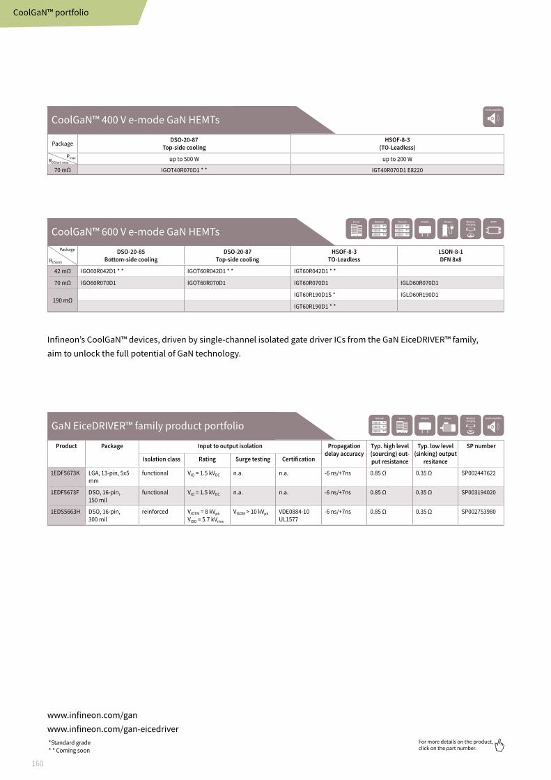
160
For more details on the product, click on the part number.
CoolGaN™ portfolio
CoolGaN™ 400 V e-mode GaN HEMTs
Package DSO-20-87Top-side cooling
HSOF-8-3(TO-Leadless)
up to 500 W up to 200 W
70 mΩ IGOT40R070D1 * * IGT40R070D1 E8220
*Standard grade * * Coming soon
GaN EiceDRIVER™ family product portfolio
Product Package Input to output isolation Propagation delay accuracy
Typ. high level (sourcing) out-put resistance
Typ. low level (sinking) output
resitance
SP number
Isolation class Rating Surge testing Certification
1EDF5673K LGA, 13-pin, 5x5 mm
functional VIO = 1.5 kVDC n.a. n.a. -6 ns/+7ns 0.85 Ω 0.35 Ω SP002447622
1EDF5673F DSO, 16-pin, 150 mil
functional VIO = 1.5 kVDC n.a. n.a. -6 ns/+7ns 0.85 Ω 0.35 Ω SP003194020
1EDS5663H DSO, 16-pin, 300 mil
reinforced VIOTM = 8 kVpkVISO = 5.7 kVrms
VISOM > 10 kVpk VDE0884-10 UL1577
-6 ns/+7ns 0.85 Ω 0.35 Ω SP002753980
Infineon’s CoolGaN™ devices, driven by single-channel isolated gate driver ICs from the GaN EiceDRIVER™ family, aim to unlock the full potential of GaN technology.
www.infineon.com/ganwww.infineon.com/gan-eicedriver
CoolGaN™ 600 V e-mode GaN HEMTs DSO-20-85
Bottom-side coolingDSO-20-87
Top-side coolingHSOF-8-3
TO-LeadlessLSON-8-1 DFN 8x8
42 mΩ IGO60R042D1 * * IGOT60R042D1 * * IGT60R042D1 * *
70 mΩ IGO60R070D1 IGOT60R070D1 IGT60R070D1 IGLD60R070D1
190 mΩIGT60R190D1S * IGLD60R190D1
IGT60R190D1 * *
PmaxRDS(on) max.
RDS(on)
Package

161
For more details on the product, click on the part number.
I G T 60 R 070 D 1
Package typeLD = DFN 8 x 8-LSONT = TOLLO = DSO20-BSCOT = DSO20-TSC
Generation1 = 1st generation
Product typeD = DiscreteS = System
CompanyI = Infineon
TechnologyG = GaN
Voltage Divided by 10 (60x10 = 600 V)
RDS(on) [mΩ]
R = RDS(on)
Reliability gradeblank = IndustrialA = AutomotiveS = Standard
CoolGaN™
www.infineon.com/gan
Nomenclature
Appl
icat
ions
Pa
cka
ges
20
-30
0 V
MO
SF
ETs
50
0-9
50
V M
OS
FE
TsW
BG
se
mic
on
du
cto
rsD
iscr
ete
IGB
TsP
ow
er
ICs
Inte
llig
en
t sw
itch
es
an
d in
pu
t IC
sG
ate
dri
ver
ICs
Mic
roco
ntr
oll
ers
XE
NS
IV™
se
nso
rs

162
For more details on the product, click on the part number.
Silicon carbideRevolution to rely on
Silicon carbide (SiC) devices belong to the so-called wide bandgap semiconductor group, which offers a number of attractive characteristics for high voltage power semiconductors when compared to commonly used silicon (Si). In particular, the much higher breakdown field strength and thermal conductivity of silicon carbide allow developing devices which by far outperform the corresponding silicon-based ones, and enable efficiency levels unattainable otherwise. Infineon’s portfolio of SiC devices covers 650 V to 1200 V Schottky diodes as well as the revolutionary CoolSiC™ MOSFETs.
EiceDRIVER™ SiC MOSFET gate driver ICs are well-suited to drive SiC MOSFETs, especially Infineon’s ultra-fast switching CoolSiC™ SiC MOSFETs. These gate drivers incorporate most important key features and parameters for SiC driving such as tight propagation delay matching, precise input filters, wide output-side supply range, negative gate voltage capability, active Miller clamp, DESAT protection, and extended CMTI capability.
www.infineon.com/coolsic-mosfetwww.infineon.com/SiCgd

163
For more details on the product, click on the part number.
CoolSiC™ silicon carbide MOSFETs 650 VDelivering reliable and cost effective top performanceSilicon carbide physical characteristics, from wide bandgap to electron mobility and thermal conductivity, provide the basis to engineer high performance semiconductor technologies and products. The CoolSiC™ MOSFETs from Infineon maximize the advantages of silicon carbide, offering a high performance product that also meets power electronics design requirements, like reliability and ease of use. As per performance, the CoolSiC™ MOSFETs show low RDS(on) dependency with temperature and low switching losses. The reliability is built on technological strengths and on flawless quality processes. Some aspects of Infineon’s SiC technology, like a superior gate oxide reliability, excellent thermal behavior, advanced avalanche ruggedness and short circuit capabilities contribute to the robustness of the device. Infineon’s benchmark quality was further improved for silicon carbide, with an application-focused qualification scope exceeding standards, complemented by SiC-specific screening measures. Additional unique features, like 0 V turn-off VGS, wide VGS range, and the use of silicon MOSFET drivers and driving schemas make CoolSiC™ MOSFETs 650 V easy to integrate and use.
CoolSiC™ MOSFETs can enable streamlined and cost-optimized system designs with less components, weight and size, reaching high energy efficiency and power density. For instance, the CoolSiC™ MOSFETs boast a low level of Qrr, roughly 80% less of the best CoolMOS™ reference in the market, the CoolMOS™ CFD7. This ensures the robustness of the body diode, making the CoolSiC™ MOSFETs suitable for topologies with continuous hard commutation, like, the high efficiency Totem Pole PFC, a topology that enables > 99% of efficiency.
High efficiency CoolSiC™ totem-pole PFC in server SMPS (switched mode power supply)
Leveraging SiC’s material properties
Pe
rfo
rma
nce
Static behavior
Dynamic behavior
Re
lia
bil
ity
Quality
Ease of use
Robustness
Robustness for continuous hard commutation topologies
R DS(
on)*Q
rr [m
Ω * µ
C]
R DS(
on)*Q
oss [
mΩ
* µC]
35
30
25
20
15
10
5
0
CoolMOS™ CFD7*
* Best CoolMOS™ SJ MOSFET reference in the market
CoolSiC™ 650 V CoolMOS™ CFD7* CoolSiC™ 650 V
35
30
25
20
15
10
5
0
CoolSiC™ / Silicon carbide devices
www.infineon.com/coolsic-mosfetwww.infineon.com/SiCgd
OptiMOS™
OptiMOS™
OptiMOS™
OptiMOS™
AC
LINEEMIfilter
PFC
controller
EiceDRIVER™
2EDF9275F
EiceDRIVER™
2EDF7275F
2x EiceDRIVER™
2EDF7275
LLC
controller 2x EiceDRIVER™
2EDS9265H
Totem pole
Full-bridge PFC Resonant LLC
Synchronous
rectifier
CoolSiC™ 650 V
CoolSiC™ 650 V
CoolSiC™ 650 V
CoolSiC™ 650 V
CoolSiC™ 650 V
CoolSiC™ 650 V
600 V CoolMOS™ S7
600 V CoolMOS™ S7
Appl
icat
ions
Pa
cka
ges
20
-30
0 V
MO
SF
ETs
50
0-9
50
V M
OS
FE
TsW
BG
se
mic
on
du
cto
rsD
iscr
ete
IGB
TsP
ow
er
ICs
Inte
llig
en
t sw
itch
es
an
d in
pu
t IC
sG
ate
dri
ver
ICs
Mic
roco
ntr
oll
ers
XE
NS
IV™
se
nso
rs
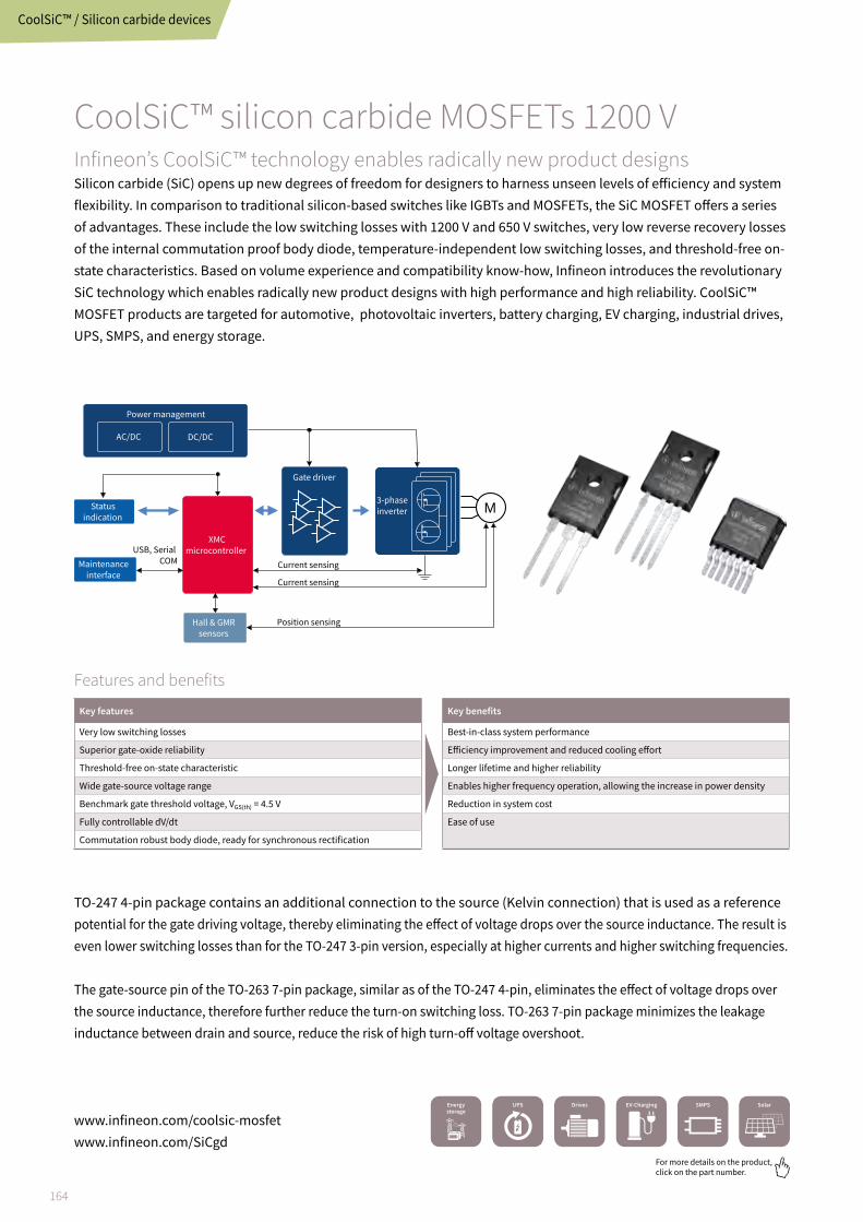
164
For more details on the product, click on the part number.
www.infineon.com/coolsic-mosfetwww.infineon.com/SiCgd
CoolSiC™ silicon carbide MOSFETs 1200 VInfineon’s CoolSiC™ technology enables radically new product designsSilicon carbide (SiC) opens up new degrees of freedom for designers to harness unseen levels of efficiency and system flexibility. In comparison to traditional silicon-based switches like IGBTs and MOSFETs, the SiC MOSFET offers a series of advantages. These include the low switching losses with 1200 V and 650 V switches, very low reverse recovery losses of the internal commutation proof body diode, temperature-independent low switching losses, and threshold-free on-state characteristics. Based on volume experience and compatibility know-how, Infineon introduces the revolutionary SiC technology which enables radically new product designs with high performance and high reliability. CoolSiC™ MOSFET products are targeted for automotive, photovoltaic inverters, battery charging, EV charging, industrial drives, UPS, SMPS, and energy storage.
TO-247 4-pin package contains an additional connection to the source (Kelvin connection) that is used as a referencepotential for the gate driving voltage, thereby eliminating the effect of voltage drops over the source inductance. The result is even lower switching losses than for the TO-247 3-pin version, especially at higher currents and higher switching frequencies.
The gate-source pin of the TO-263 7-pin package, similar as of the TO-247 4-pin, eliminates the effect of voltage drops over the source inductance, therefore further reduce the turn-on switching loss. TO-263 7-pin package minimizes the leakage inductance between drain and source, reduce the risk of high turn-off voltage overshoot.
Features and benefits
Key benefits
Best-in-class system performance
Efficiency improvement and reduced cooling effort
Longer lifetime and higher reliability
Enables higher frequency operation, allowing the increase in power density
Reduction in system cost
Ease of use
Key features
Very low switching losses
Superior gate-oxide reliability
Threshold-free on-state characteristic
Wide gate-source voltage range
Benchmark gate threshold voltage, VGS(th) = 4.5 V
Fully controllable dV/dt
Commutation robust body diode, ready for synchronous rectification
USB, Serial
COM
Current sensing
Current sensing
Position sensing
Power management
AC/DC DC/DC
Gate driver
3-phase
inverter
XMC
microcontroller
Hall & GMR
sensors
MStatus
indication
Maintenance
interface
CoolSiC™ / Silicon carbide devices

165
For more details on the product, click on the part number.
CoolSiC™ MOSFET nomenclature
Breakdown voltage Divided by 10120 = 1200 V
I M W 120 R HM145
CompanyI = Infineon
H = High gate voltage rangeDeviceM = MOSFET
Package TypeW = TO-247Z = TO-247 4-pinBG = D2PAK 7-pin
Series nameM1 = Generation 1
RDS(on) [mΩ]
R = RDS(on)
As a separator betweenvoltage und RDS(on)
www.infineon.com/coolsic-mosfetwww.infineon.com/SiCgd
CoolSiC™ MOSFET 1200 V ACTIVE & PREFERRED TO-247 TO-247-4 D2PAK 7-pin Gate Driver for CoolSiC™
30 mΩ IMW120R030M1H IMZ120R030M1H IMBG120R030M1H * 1EDC60H12AH
45 mΩ IMW120R045M1 – lead product IMZ120R045M1– lead product IMBG120R045M1H * 1EDC20I12MH
60 mΩ IMW120R060M1H IMZ120R060M1H IMBG120R060M1H * 1ED020I12-F2
90 mΩ IMW120R090M1H IMZ120R090M1H IMBG120R090M1H * 2ED020I12-F2
140 mΩ IMW120R140M1H IMZ120R140M1H IMBG120R140M1H * 1ED3124MU12H *
220 mΩ IMW120R220M1H IMZ120R220M1H IMBG120R220M1H * 1ED3491MU12M *
350 mΩ IMW120R350M1H IMZ120R350M1H IMBG120R350M1H * 1ED3890MU12M *
* Coming soon
RDS(on)
Package
Appl
icat
ions
Pa
cka
ges
20
-30
0 V
MO
SF
ETs
50
0-9
50
V M
OS
FE
TsW
BG
se
mic
on
du
cto
rsD
iscr
ete
IGB
TsP
ow
er
ICs
Inte
llig
en
t sw
itch
es
an
d in
pu
t IC
sG
ate
dri
ver
ICs
Mic
roco
ntr
oll
ers
XE
NS
IV™
se
nso
rs

166
For more details on the product, click on the part number.
CoolSiC™ Schottky diodes
CoolSiC™ Schottky diodes
The differences in material properties between silicon carbide and silicon limit the fabrication of practical silicon unipolar diodes (Schottky diodes) to a range up to 100-150 V, with a relatively high on-state resistance and leakage current. In SiC, Schottky diodes can reach a much higher breakdown voltage. Infineon is the world’s first SiC discrete power supplier. Infineon offers products up to 1200 V in discrete packages and up to 1700 V in modules.
The long market presence and experience enable Infineon to deliver highly reliable, industry-leading SiC performance. With over 10 years of pioneering experience in developing and manufacturing SiC diodes, Infineon’s latest CoolSiC™ Schottky diode generation 6 family sets benchmark in quality, efficiency and reliability.
Features
› No reverse recovery charge
› Purely capacitive switching
› High operating temperature (Tj, max 175°C)
Advantages
› Low turn-off losses › Reduction of CoolMOS™
or IGBT turn-on loss › Switching losses
independent from load current, switching speed and temperature
Benefits
› System efficiency improvement compared to Si diodes
› Reduced cooling requirements
› Enabling higher frequency/increased power density
› Higher system reliability due to lower operating temperature
› Reduced EMI
Applications
› Server › Telecom › Solar › UPS › EV charging › Energy storage › PC power › Motor drives › Lighting › CAV
Reverse recovery charge of SiC Schottky diodes versus Si-pin diodesThe majority of carrier characteristics imply no reverse recovery charge and the only contribution to the switching losses comes from the tiny displacement charge of capacitive nature. In the same voltage range, silicon devices have a bipolar component resulting in much higher switching losses. The graph shows the comparison between various 600 V devices.
Improved system efficiency (PFC in CCM mode operation, full load, low line)The fast switching characteristics of the SiC diodes provide clear efficiency improvements at system level. The performance gap between SiC and high-end silicon devices increases with the operating frequency.
10
8
6
4
2
0
-2
-4
-6
-8
-100.07 0.1 0.13 0.16 0.19 0.22 0.25
T=125°C, VDC= 400 V, IF=6 A, di/dt=200 A/µs
SiC Schottky diodeSi-pin double diode (2*300 V)
Ultrafast Si-pin diode
I [A
]
Time [µs]
95.0
94.5
94.0
93.5
93.0
92.5
92.0
91.5
91.060 120 180 240
Switchting frequency [kHz]
Eic
ienc
y [%
]
Infineon SiC 6 A Comp. 1 6 A Comp. 2 6 A
www.infineon.com/sic

167
For more details on the product, click on the part number.
CoolSiC™ Schottky diodes
CoolSiC™ Schottky diodes 650 VCoolSiC™ Schottky diodes 650 V G6 and G5
The new CoolSiC™ Schottky diode 650 V G6 product family is built over the strong characteristics of theprevious generation G5, fully leveraging technology and process innovation to propose the best efficiency and zero price/performance products to date.
Foundation technology – CoolSiC™ Schottky diodes 650 V G5The established CoolSiC™ Schottky diodes G5 product family has been optimized after all key aspects including junction structure, substrate and die attach. It represents a well-balanced product family which offers state-of-the-art performance and high surge current capability at a competitive cost level.
Innovation: optimized junction, substrate and die attachInfineon’s SiC Schottky diode generation 5 is optimized with regard to all key aspects relevant for high-power and high-efficiency SMPS applications.
Junction: merged PN structureOn the junction level, it has an optimized merged PN structure. Compared to competitors, Infineon’s SiC diode has an additional P-doped area, which, together with the N-doped EPI layer, forms a PN junction diode. Thus, it is a combination of Schottky diode and PN junction diode. Under normal conditions it works like a standard Schottky diode. Under abnormal conditions such as lighting, AC line drop-out, it works like a PN junction diode. At high current level, the PN junction diode has a significantly lower forward voltage (VF) than the Schottky diode, which leads to less power dissipation, thus significantly improving the surge current capability.
Substrate: thin wafer technology On the substrate level, Infineon introduced the thin wafer technology. At the later stage of our SiC diode production, the thin wafer process is used to reduce the wafer thickness by about two-thirds, which significantly reduces the substrate resistance contribution, thus, improving both forward voltage (VF) and thermal performance.
Backside and
packaging
SiC substrate
Field stop layer
EPI
layer
Al
Al wire bond
Ti
110 µm
p+ p+p+ p+p+
60
50
40
30
20
10
00 2 4 6 8
VF [V]
I F [
A/m
m2]
Generation 5 Generation 2, 3
0
5
10
15
20
25
30
35
40
0.00 2.00 4.00 8.00 10.00 12.00 14.00
I F (
A)
VF (V)
Bipolar PN diode
forward characteristic
Schottky diode
forward characteristic
Combined
characteristic
surg
e cu
rren
t
RthJC=2.0 K/W RthJC=1.5 K/W
Diffusion soldering
Die attach: diffusion solderingOn the backside, package level diffusion soldering is introduced, which significantly improves the thermal path between lead frame and the diode, enhancing the thermal performance. With the same chip size and power dissipation, the junction temperature is reduced by 30°C.
www.infineon.com/sic
Appl
icat
ions
Pa
cka
ges
20
-30
0 V
MO
SF
ETs
50
0-9
50
V M
OS
FE
TsW
BG
se
mic
on
du
cto
rsD
iscr
ete
IGB
TsP
ow
er
ICs
Inte
llig
en
t sw
itch
es
an
d in
pu
t IC
sG
ate
dri
ver
ICs
Mic
roco
ntr
oll
ers
XE
NS
IV™
se
nso
rs

168
For more details on the product, click on the part number.
G2*
G3
G5
G6
Performance (eiciency, density)
Price
* G2 is discontinued
CoolSiC™ Schottky diodes
In terms of efficiency, the 8 A G6 device has been tested in CCM PFC. The maximum output power is 3.5 kW. The leftfigure shows the relative efficiency at 65 kHz, while the right figure shows the relative efficiency at 130 kHz. This shows that Infineon’s CoolSiC™ Schottky diode G6 delivers better efficiency over the full load range, keeping this advantage even at 130 kHz, therefore meeting the needs of designers who want to increase the switching frequencies in their designs to attain more power density.
Latest development - CoolSiC™ Schottky diodes 650 V G6The CoolSiC™ Schottky diodes G6 product family introduces a novel and proprietary Schottky metal system. This contributes to the reduction of the forward voltage (VF) to levels which are difficult, determining a measurable decrease of conduction losses. Infineon’s CoolSiC™ Schottky diodes enable optimum efficiency and ruggedness. Lower forward voltage (VF) means lower conduction loss, and lower capacitive charge (Qc) means lower switching loss. Qc x VF is the figure of merit for efficiency, and comparison indicates that the latest generation 6 products have the lowest Qc x VF on the market. Infineon’s CoolSiC™ Schottky diodes offer a surge current robustness far better than the one offered by the most efficient products. Thus, under abnormal conditions, this surge current capability offers excellent device robustness.
Efficiency comparison
www.infineon.com/coolsic-g6
0.02
0.00
-0.02
-0.04
-0.06
-0.08
-1.00
-1.02
0.02
0.00
-0.02
-0.04
-0.06
-0.08
-1.00
-1.02
E
icie
ncy
di
ere
nce
[%
]
Output power [% of nominal]
Relative eiciency @ 65 kHz Relative eiciency @ 130 kHz
10 20 30 40 50 60 70 80 90 100
E
icie
ncy
di
ere
nce
[%
]
Output power [% of nominal]
10 20 30 40 50 60 70 80 90 100
G6 Competitor 1 Competitor 2 Competitor 3
The best price performanceCoolSiC™ Schottky diodes G6 are the outcome of Infineon’s continuoustechnological and process improvements which enable the design anddevelopment of SiC-based products, making them more price-competitive and increasing performance across generations. As a result, G6 is Infineon’s best price/performance CoolSiC™ Schottky diode generation, offering the highest cost-efficiency. In addition, Infineon offers the reliability of collaborating with the industry leader. Customers can leverage Infineon’s proven quality and supply chain reliability. They can benefit from “one-stop-shop” advantages and maximize system performance, combining CoolSiC™ Schottky diodes with the SJ MOSFETs of the CoolMOS™ 7 family, such as 600 V C7, 650 V C7, 600 V G7, 650 V G7 and 600 V P7.
A comprehensive portfolioThe combined G6 and G5 CoolSiC™ Schottky diode 650 V diode portfolio offers a wide choice of packages and ampere class granularity to allow the best fit to application. G6 comes in double DPAK, the first top-side cooled surface mount package, which allows thermal decoupling of PCB to chip junction and enables higher power dissipation and improved system lifetime thanks to the reduced board temperature.
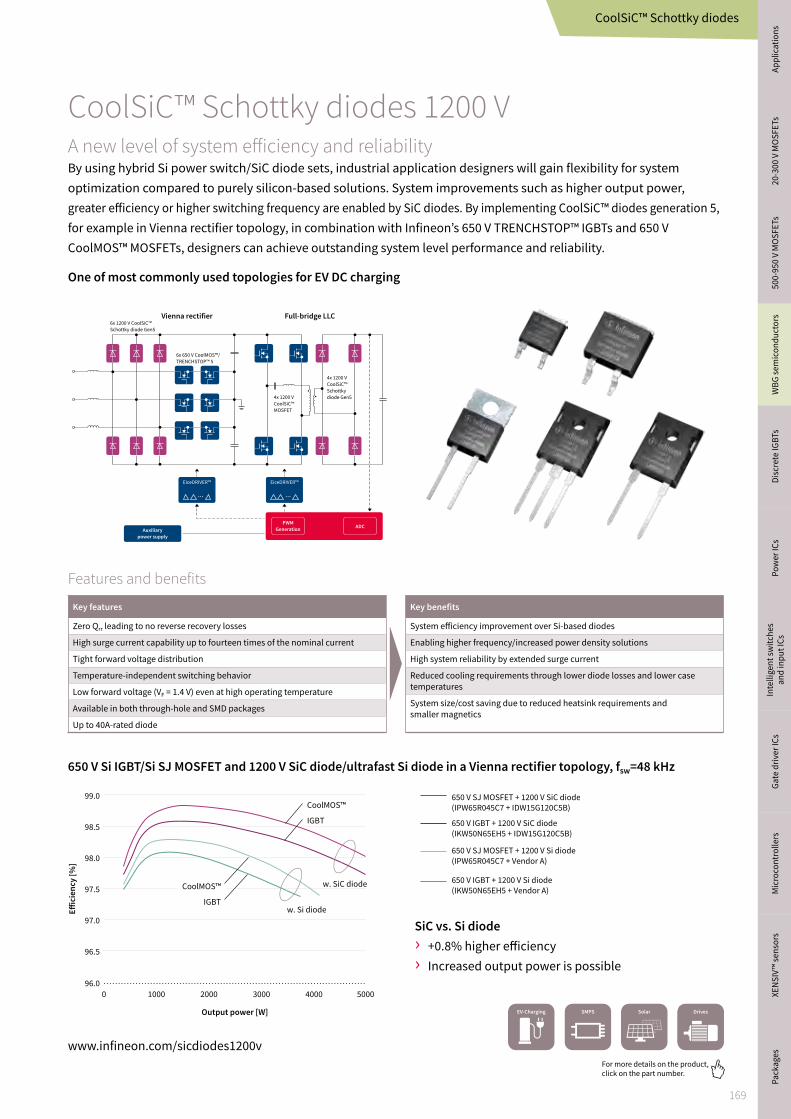
169
For more details on the product, click on the part number.
CoolSiC™ Schottky diodes
www.infineon.com/sicdiodes1200v
CoolSiC™ Schottky diodes 1200 VA new level of system efficiency and reliabilityBy using hybrid Si power switch/SiC diode sets, industrial application designers will gain flexibility for system optimization compared to purely silicon-based solutions. System improvements such as higher output power, greater efficiency or higher switching frequency are enabled by SiC diodes. By implementing CoolSiC™ diodes generation 5, for example in Vienna rectifier topology, in combination with Infineon’s 650 V TRENCHSTOP™ IGBTs and 650 V CoolMOS™ MOSFETs, designers can achieve outstanding system level performance and reliability.
One of most commonly used topologies for EV DC charging
650 V Si IGBT/Si SJ MOSFET and 1200 V SiC diode/ultrafast Si diode in a Vienna rectifier topology, fsw=48 kHz
96.0
96.5
97.0
97.5
98.0
98.5
99.0
0 1000
CoolMOS™
w. SiC diode
w. Si diode
IGBT
CoolMOS™
IGBT
2000 3000 4000 5000
Output power [W]
650 V SJ MOSFET + 1200 V SiC diode
(IPW65R045C7 + IDW15G120C5B)
Eic
ienc
y [%
]
650 V IGBT + 1200 V SiC diode
(IKW50N65EH5 + IDW15G120C5B)
650 V SJ MOSFET + 1200 V Si diode
(IPW65R045C7 + Vendor A)
650 V IGBT + 1200 V Si diode
(IKW50N65EH5 + Vendor A)
Features and benefits
Key benefits
System efficiency improvement over Si-based diodes
Enabling higher frequency/increased power density solutions
High system reliability by extended surge current
Reduced cooling requirements through lower diode losses and lower case temperatures
System size/cost saving due to reduced heatsink requirements and smaller magnetics
Key features
Zero Qrr leading to no reverse recovery losses
High surge current capability up to fourteen times of the nominal current
Tight forward voltage distribution
Temperature-independent switching behavior
Low forward voltage (VF = 1.4 V) even at high operating temperature
Available in both through-hole and SMD packages
Up to 40A-rated diode
Auxiliary
power supply
PWM
GenerationADC
EiceDRIVER™ EiceDRIVER™
6x 650 V CoolMOS™/
TRENCHSTOP™ 5
4x 1200 V
CoolSiC™
MOSFET
4x 1200 V
CoolSiC™
Schottky
diode Gen5
6x 1200 V CoolSiC™
Schottky diode Gen5
Vienna rectifier Full-bridge LLC
SiC vs. Si diode› +0.8% higher efficiency› Increased output power is possible
Appl
icat
ions
Pa
cka
ges
20
-30
0 V
MO
SF
ETs
50
0-9
50
V M
OS
FE
TsW
BG
se
mic
on
du
cto
rsD
iscr
ete
IGB
TsP
ow
er
ICs
Inte
llig
en
t sw
itch
es
an
d in
pu
t IC
sG
ate
dri
ver
ICs
Mic
roco
ntr
oll
ers
XE
NS
IV™
se
nso
rs

170
For more details on the product, click on the part number.
SiC diodes product portfolio
www.infineon.com/sic
CoolSiC™ Schottky diodes 650 V G5 ACTIVE
IF [A]
TO-220 R2L TO-247Dual Die
TO-247 D2PAK R2L ThinPAK 8x8
2 IDH02G65C5 IDK02G65C5 IDL02G65C5
3 IDH03G65C5 IDK03G65C5
4 IDH04G65C5 IDK04G65C5 IDL04G65C5
5 IDH05G65C5 IDK05G65C5
6 IDH06G65C5 IDK06G65C5 IDL06G65C5
8 IDH08G65C5 IDK08G65C5 IDL08G65C5
9 IDH09G65C5 IDK09G65C5
10 IDH10G65C5 IDW10G65C5 IDK10G65C5 IDL10G65C5
12 IDH12G65C5 IDW12G65C5 IDK12G65C5 IDL12G65C5
16 IDH16G65C5 IDW16G65C5
20 IDH20G65C5 IDW20G65C5B IDW20G65C5
24 IDW24G65C5B
30/32 IDW32G65C5B IDW30G65C5
40 IDW40G65C5B IDW40G65C5
CoolSiC™ Schottky diodes 650 V G6 ACTIVE & PREFERRED
IF [A]
TO-220 R2L TO-247Dual Die
TO-247 Double DPAK D2PAK R2L ThinPAK 8x8
4 IDH04G65C6 IDDD04G65C6
6 IDH06G65C6 IDDD06G65C6
8 IDH08G65C6 IDDD08G65C6
10 IDH10G65C6 IDDD10G65C6
12 IDH12G65C6 IDDD12G65C6 *
16 IDH16G65C6 IDDD16G65C6
20 IDH20G65C6 IDDD20G65C6
*For more information on the product, contact our product support

171
For more details on the product, click on the part number.
CoolSiC™ Schottky diodes 650 V G6 ACTIVE & PREFERRED
IF[A]
TO-220 R2L TO-247Dual Die
TO-247 Double DPAK D2PAK R2L ThinPAK 8x8
4 IDH04G65C6 IDDD04G65C6
6 IDH06G65C6 IDDD06G65C6
8 IDH08G65C6 IDDD08G65C6
10 IDH10G65C6 IDDD10G65C6
12 IDH12G65C6 IDDD12G65C6 *
16 IDH16G65C6 IDDD16G65C6
20 IDH20G65C6 IDDD20G65C6
www.infineon.com/sic
„B“ in product name refers to common-cathode configuration
CoolSiC™ Schottky diodes 1200 V G5 ACTIVE & PREFERRED
IF [A]
TO-220 R2L TO-247Dual Die
TO-247 R2L DPAK R2L D2PAK R2L
2 IDH02G120C5 IDM02G120C5 IDK02G120C5
5 IDH05G120C5 IDM05G120C5 IDK05G120C5
8 IDH08G120C5 IDM08G120C5 IDK08G120C5
10 IDH10G120C5 IDW10G120C5B IDWD10G120C5 IDM10G120C5 IDK10G120C5
15/16 IDH16G120C5 IDW15G120C5B IDWD15G120C5 IDK16G120C5
20 IDH20G120C5 IDW20G120C5B IDWD20G120C5 IDK20G120C5
30 IDW30G120C5B IDWD30G120C5
40 IDW40G120C5B IDWD40G120C5
CoolSiC™ Schottky diodes 600 V G3 ACTIVE
IF [A]
TO-220 R2L TO-247Dual Die
TO-247 DPAK R2L D2PAK ThinPAK 8x8
3 IDH03SG60C IDD03SG60C
4 IDH04SG60C IDD04SG60C
5 IDH05SG60C IDD05SG60C
6 IDH06SG60C IDD06SG60C
8 IDH08SG60C IDD08SG60C
9 IDH09SG60C IDD09SG60C
10 IDH10SG60C IDD10SG60C
12 IDH12SG60C IDD12SG60C *
*For more information on the product, contact our product support
Appl
icat
ions
Pa
cka
ges
20
-30
0 V
MO
SF
ETs
50
0-9
50
V M
OS
FE
TsW
BG
se
mic
on
du
cto
rsD
iscr
ete
IGB
TsP
ow
er
ICs
Inte
llig
en
t sw
itch
es
an
d in
pu
t IC
sG
ate
dri
ver
ICs
Mic
roco
ntr
oll
ers
XE
NS
IV™
se
nso
rs

172
For more details on the product, click on the part number.
Nomenclature
CoolSiC™ Schottky diodes G2 and G3
Continuous forward current
[A]
I D H X S XG C
Company
I = Infineon
Specifications
C = Surge current stable
Device
D = Diode
Package Type
D = DPAK
H = TO-220 R2L
B = D2PAK
D = DPAK = TO-220
V = TO-220 FullPAK
W = TO-247
Breakdown voltage
60 = 600 V
G = Low thermal resistance
(diffusion soldering)
Technology
S = SiC diode
CoolSiC™ Schottky diodes G5 and G6
Continuous forward current
[A]
I D K X G CX 5 B
Company
I = Infineon
Series name
5 = Generation 5
6 = Generation 6
B = Common-cathode configuration
Device
D = Diode
Package type
H = TO-220 R2L
W = TO-247
K = D2PAK R2L
L = ThinPAK 8x8
M = DPAK R2L
WD = TO-247 R2L
Specifications
C = Surge current stable*
Breakdown voltage
65 = 650 V
120 = 1200 V
G = Low thermal resistance
*Generation
SiC diodes nomenclature
www.infineon.com/sic

173
For more details on the product, click on the part number.
Silicon power diodes
Silicon power diodesFilling the gap between SiC diodes and emitter controlled diodes
The Rapid diode family complements Infineon’s existing high-power 600 V/650 V diode portfolio by filling the gap between SiC diodes and previously released emitter controlled diodes. They offer a perfect cost/performance balance and target high-efficiency applications switching between 18 and 100 kHz. Rapid 1 and Rapid 2 diodes are optimized to have excellent compatibility with CoolMOS™ and high speed IGBTs (insulated gate bipolar transistor) such as the TRENCHSTOP™ 5 and HighSpeed 3.
The Rapid 1 diode familyRapid 1 is forward voltage drop (VF) optimized to address low switching frequency applications between 18 kHz and 40 kHz, for example, air conditioner and welder PFC stages.
› 1.35 V temperature-stable forward voltage (VF) › Lowest peak reverse recovery current (Irrm) › Reverse recovery time (trr) < 100 ns › High softness factor
The Rapid 2 diode familyRapid 2 is Qrr/trr optimized hyperfast diode to address high-speed switching applications between 40 kHz and 100 kHz, typically found in PFCs in high efficiency switch mode power supplies (SMPS) and welding machines.
› Lowest reverse recovery charge (Qrr): VF ratio for best-in-class performance › Lowest peak reverse recovery current (Irrm) › Reverse recovery trr < 50 ns › High softness factor
Emitter controlled diodes Rapid 2 SiCRapid 1
0 Hz 18 kHz 40 kHz 100 kHz >100 kHz
1000
900
800
700
600
500
400
300
200
100
0
1.3 1.4 1.5 1.6 1.7 1.8 1.9 2.0 2.1 2.2 2.3
30 A competitor A
IDW30E65D1
IDP08E65D28 A competitor C
8 A competitor D
30 A competitor B
Qrr
[n
C]
VF [V]
VF - Qrr trade-o, Rapid 1 diF/dt = 1000 A/us, Rapid 2 diF/dt = 300 A/us
97.6
97.4
97.2
97.0
96.8
96.6
96.4
96.2
96.0
95.8
95.6
0 100 200 300 400 500 600 700 800
E
icie
ncy
[%
]
Output Power [W]
IDP08E65D2
Competitor S
Competitor F
PFC Eiciency @ 60 kHz – Vin = 230 V
98.2
98.0
97.8
97.6
97.4
97.2
97.0
96.8
96.6
96.4
96.2
0 200 400 600 800 1000 1200 1400 1600
E
icie
ncy
[%
]
Output Power [W]
PFC Eiciency @ 70 kHz – Vin = 230 V
Rapid 2
SiC
www.infineon.com/rapiddiodeswww.infineon.com/ultrasoftdiodes
Appl
icat
ions
Pa
cka
ges
20
-30
0 V
MO
SF
ETs
50
0-9
50
V M
OS
FE
TsW
BG
se
mic
on
du
cto
rsD
iscr
ete
IGB
TsP
ow
er
ICs
Inte
llig
en
t sw
itch
es
an
d in
pu
t IC
sG
ate
dri
ver
ICs
Mic
roco
ntr
oll
ers
XE
NS
IV™
se
nso
rs

174
For more details on the product, click on the part number.
Silicon power diodes
Rapid 2 diodes650 V product family Continuous
current Ic@TC=100°C
[A]
TO-220 TO-220 FullPAK
TO-220 common cathode
TO-247 TO-247 common cathode
8 IDP08E65D2 IDV08E65D2
15 IDP15E65D2 IDV15E65D2 IDW15E65D2
20 IDP20E65D2 IDP20C65D2 IDW20C65D2
30 IDP30E65D2 IDV30E65D2 IDP30C65D2 IDW30C65D2
40 IDP40E65D2 IDW40E65D2
80 IDW80C65D2
www.infineon.com/rapiddiodes
Rapid 1 diodes650 V product family Continuous
current Ic@TC=100°C
[A]
TO-220 TO-220FullPAK
TO-247 TO-247 common cathode
TO-247advanced isolation
8 IDP08E65D1
15 IDP15E65D1
20 IDV20E65D1
30 IDP30E65D1 IDW30E65D1 IDW30C65D1
40 IDW40E65D1 IDFW40E65D1E
60 IDW60C65D1 IDFW60C65D1
75 IDW75D65D1
80 IDW80C65D1

175
For more details on the product, click on the part number.
www.infineon.com/ultrasoftdiodes
Emitter controlled diodes600 V and 1200 V product families Continuous
current Ic@TC=100°C
[A]
TO-263(D2PAK)
TO-220 Real 2-pin
TO-247
600
V
30 IDW30E60
50 IDW50E60
75 IDW75E60
100 IDW100E60
1200
V
12 IDP12E120
18 IDP18E120
30 IDB30E120 IDP30E120
Appl
icat
ions
Pa
cka
ges
20
-30
0 V
MO
SF
ETs
50
0-9
50
V M
OS
FE
TsW
BG
se
mic
on
du
cto
rsD
iscr
ete
IGB
TsP
ow
er
ICs
Inte
llig
en
t sw
itch
es
an
d in
pu
t IC
sG
ate
dri
ver
ICs
Mic
roco
ntr
oll
ers
XE
NS
IV™
se
nso
rs

176
For more details on the product, click on the part number.
Nomenclature
Silicon power diodes
CompanyI = Infineon
I D
DeviceD = Diode
Package typeP = TO-220V = TO-220 FullPAKW = TO-247B = TO-263 (D2PAK)FW = TO-247 Advanced Isolation
D1 = Rapid 1D2 = Rapid 2
W 75 E 65 D1
Nominal current (@ 100°C) [A]
Nominal voltageDivided by 10 (650 V/10 = 65)
TechnologyE = Std. diode configuration – replacement for FullPAK packages or TO-247 + medium performance insulator C = Common cathodeD = Dual anode
www.infineon.com/rapiddiodes
Silicon power diodes

177
For more details on the product, click on the part number.
Infineon support for wide bandgap semiconductorsUseful links and helpful information
Further information, datasheets and documentswww.infineon.com/wbgwww.infineon.com/sic www.infineon.com/rapiddiodes
www.infineon.com/ultrasoftdiodeswww.infineon.com/ganwww.infineon.com/gan-eicedriver
Simulation
Appl
icat
ions
Pa
cka
ges
20
-30
0 V
MO
SF
ETs
50
0-9
50
V M
OS
FE
TsW
BG
se
mic
on
du
cto
rsD
iscr
ete
IGB
TsP
ow
er
ICs
Inte
llig
en
t sw
itch
es
an
d in
pu
t IC
sG
ate
dri
ver
ICs
Mic
roco
ntr
oll
ers
XE
NS
IV™
se
nso
rs

178
For more details on the product, click on the part number.
› 650 V TRENCHSTOP™ 5 IGBT › 1200 V IGBT families › Lower power drive IGBT portfolio › TRENCHSTOP™ IGBT6 › TRENCHSTOP™ advanced isolation
Discrete IGBTs › Integrated Power Device – IPD protect › TRENCHSTOP™ 5 selection tree › IGBT selection tree › Discrete IGBTs product portfolio › IGBT nomenclature

179
For more details on the product, click on the part number.
Appl
icat
ions
Pa
cka
ges
20
-30
0 V
MO
SF
ETs
50
0-9
50
V M
OS
FE
TsW
BG
se
mic
on
du
cto
rsD
iscr
ete
IGB
TsP
ow
er
ICs
Inte
llig
en
t sw
itch
es
an
d in
pu
t IC
sG
ate
dri
ver
ICs
Mic
roco
ntr
oll
ers
XE
NS
IV™
se
nso
rs

180
For more details on the product, click on the part number.
Discrete IGBTs
Discrete IGBTs Market leadership through groundbreaking innovation and application focus
Resolute to achieve the highest standards in performance and quality, Infineon offers a comprehensive portfolio of application-specific discrete IGBTs.
Discrete IGBT overview
New best-in-class technologies and applicationsTechnology Application Gate Driver Family
TRENCHSTOP™ 5 H5/F5 650 V
EiceDRIVER™ isolated gate driver (1EDC60H12AH)EiceDRIVER™ 650 V SOI gate driver (2ED2184S06F)EiceDRIVER™ low side gate driver (1ED44175N01B)
TRENCHSTOP™ 5 L5 650 V
EiceDRIVER™ isolated gate driver (1EDC20I12MH)
Rapid diode 650 V
N/A
RC-H5650 V/1200 V/1350 V
EiceDRIVER™ isolated gate driver (1EDC20I12MH)EiceDRIVER™ low side gate driver (1ED44175N01B)
RC-E1200 V
EiceDRIVER™ isolated gate driver (1EDC20I12MH)EiceDRIVER™ low side gate driver (1ED44175N01B)
WR5650 V
EiceDRIVER™ low side gate driver (1ED44175N01B)
RC-drives RC-drives fast600 V
EiceDRIVER™ 650 V SOI gate driver (2ED2184S06F)EiceDRIVER™ 650 V SOI gate driver (6EDL04I06PT)
RC-D2600 V
EiceDRIVER™ 650 V SOI gate driver (2ED2184S06F)EiceDRIVER™ 650 V SOI gate driver (6EDL04I06PT)
TRENCHSTOP™ 5S5 650 V
EiceDRIVER™ isolated gate driver (1EDC20I12MH)EiceDRIVER™ 650 V SOI gate driver (2ED2184S06F)
TRENCHSTOP™ IGBT6 650 V
EiceDRIVER™ 650 V SOI gate driver (2ED2106S06F)EiceDRIVER™ 650 V SOI gate driver (6EDL04I06PT)
TRENCHSTOP™ IGBT6 1200 V
EiceDRIVER™ isolated gate driver (1ED020I12-F2)EiceDRIVER™ 1200 V level shift gate driver (6ED2230S12T)
www.infineon.com/igbtdiscreteswww.infineon.com/gatedriver
P-SOT-223-4 SMD SMD,
single transistor, small signal
TO-252 (DPAK)
TO-263(D2PAK)
TO-220 TO-220FullPAK
TO-247 TO-247 4-pin
TO-247PLUS
TO-247PLUS
4-pin
TRENCHSTOP™ advanced
isolation TO-247
Package options
Voltage class 600 V, 650 V, 1100 V, 1200 V, 1350 V, 1600 V 600 V, 650 V
ConfigurationDuoPack (with diode), single IGBTs Duopack IGBTs
(with diode) and single diodes
Continuous collector current TC = 100°C
3-120 A 40-90 A

181
For more details on the product, click on the part number.
TRENCHSTOP™ 5 L5
Best-in-class IGBT low VCE(sat) IGBTVCE(sat) IGBT – 1.05 VBest trade-off VCE(sat) Vss Ets for frequencies below 20 kHz
Solar, UPS, welding › Ultralow frequency converters › Three-level inverter type I NPC 1 and NPC 2 › Modified HERIC inverter › AC output (aluminum/magnesium welding)
TRENCHSTOP™ 5 S5
Best-in-class ease-of-use IGBT Elimination of: › Collector-emitter snubber capacitor and gate capacitor in low induc-
tance designs (<100 nH) › Softer switching than TRENCHSTOP™ 5 H5
UPS, battery charger, solar, welding › Medium frequency converters › Multilevel inverter stages › Output stages › PFC
TRENCHSTOP™ 5 H5/F5
Best-in-class high frequency IGBT › Bridge to SJ MOSFET performance › Highest efficiency, especially under light load conditions
UPS, solar, welding › High frequency converters › Multilevel inverter stages › Output stages › PFC
TRENCHSTOP™ 5 R5Price/performance optimizedapplication specific IGBT
Induction cooking – RC-H5Half-bridge topologies in induction cooking appliances and other resonant switching applications
TRENCHSTOP™ 5 WR5
Price optimized application specific IGBT for zero current switching (ZCS) › Optimized full rated hard switching turn-off typically found in welding › Excellent RG controllability › Soft recovery plus low reverse recovery charge (Qrr) for diode
Air conditioning, welding › Medium frequency converters › Zero-voltage switching › PFC
650 V TRENCHSTOP™ 5
650 V TRENCHSTOP™ 5 IGBTIn terms of switching and conduction losses, there is no other IGBT on the market that can match the performance of the TRENCHSTOP™ 5. Wafer thickness has been reduced by more than 25 percent, which enables a dramatic improvement in both switching and conduction losses, while providing an increased breakthrough voltage of 650 V. Based on TRENCHSTOP™ 5 IGBT technology, Infineon has developed six different product families optimized for specific applications, allowing designers to optimize for high efficiency, system cost or reliability demands of the market. The quantum leap of efficiency improvement provided by the TRENCHSTOP™ 5 IGBT families opens up new opportunities for designers to explore. EiceDRIVER™ isolated gate driver like 1ED compact family 650 V IGBT in solar and UPS applications. EiceDRIVER™ low side gate driver with over current protection is widely used in induction cooking application and PFC stage.
Highest power density in D2PAK footprintInfineon’s ultrathin TRENCHSTOP™ 5 IGBT technology allows higher power density in a smaller chip size. Infineon is the first on the market able to fit a 40 A 650 V IGBT with 40 A diode in D2PAK – 25 percent higher than any other competitors that are offering maximum 30 A DuoPack IGBT in D2PAK. Now it is possible to upgrade the available SMD designs for higher power output Pout.
Features and benefits
0 10 20 30 40 50 60 70 80 90 100 110 120 130 140 150 kHz
TRENCHSTOP™ 5 L5 (hard switching)
TRENCHSTOP™ 5 S5 (hard switching)
TRENCHSTOP™ 5 WR5 (resonant switching)
RC-H5 (resonant switching)
TRENCHSTOP™ 5 H5 (hard switching)
TRENCHSTOP™ 5 F5 (hard switching)
www.infineon.com/trenchstop5www.infineon.com/gatedriver
Key benefits
Higher power design with D2PAK package
Upgrade of the available designs for higher
Less paralleling for improved system reliability and less complexity
Smaller PCB, more compact system design, lighter
Key features
The highest power density – 40 A IGBT co-packed with a 40 A diode in D2PAK
25 percent higher current than any other competitor
Superior efficiency of leading TRENCHSTOP™ 5 technology
Appl
icat
ions
Pa
cka
ges
20
-30
0 V
MO
SF
ETs
50
0-9
50
V M
OS
FE
TsW
BG
se
mic
on
du
cto
rsD
iscr
ete
IGB
TsP
ow
er
ICs
Inte
llig
en
t sw
itch
es
an
d in
pu
t IC
sG
ate
dri
ver
ICs
Mic
roco
ntr
oll
ers
XE
NS
IV™
se
nso
rs

182
For more details on the product, click on the part number.
1200 V discrete IGBTs
1200 V IGBT families
The 1200 V TRENCHSTOP™ 2 IGBT is optimized for low conduction losses with the lowest saturation voltage VCE(sat) of 1.75 V. A soft fast recovery emitter controlled diode further minimizes the turn-on losses.
The 1200 V HighSpeed 3 discrete IGBTs provides the lowest losses and the highest reliability for switching above 20 kHz. Transition to fast switching high speed devices allows reduction in the size of the active components (25-70 kHz).
The new 1200 V IGBT generation, TRENCHSTOP™ IGBT6, is designed to meet requirements of high efficiency, lowest conduction and switching losses in hard switching and resonant topologies, operating at switching frequencies above 15 kHz. The IGBT6 devices can be used as direct replacement for the Highspeed 3 H3 series, without any changes of the design. Such plug-and-play replacement of H3 with new S6 IGBT may benefit up to 0.2 percent efficiency improvement.
The RC-H5 family is the latest generation in the RC-H series of reverse conducting IGBT. With a monolithically integrated diode, they offer optimized performance for resonant switching applications such as induction cooking. R5 devices are also available in 1350 V and 1600 V blocking voltage.
EiceDRIVER™ isolated gate driver like 1ED Compact family and EiceDRIVER™ 1200 V level shift gate driver family are perfect match for the 1200 V IGBT in motor control, general purpose inverter, solar, and UPS applications. EiceDRIVER™ low side gate driver with over current protection is widely used in induction cooking application.
RC-H5
World-class TRENCHSTOP™ RC-H productsHigh performance and low losses
Induction cookingResonant switching Medium to high frequency converters
RC-E
Competitive TRENCHSTOP™ RC-EPrice versus performance leader
Induction cookingResonant switching Low to medium power cookers
TRENCHSTOP™ 2
Best-in-class 1200 V IGBT › Outstanding efficiency › Lowest conduction and switching losses › Market proven and recognized quality leader
Motor control, general purpose inverter, solar, UPS Low frequency converters
HighSpeed 3 H3
High speed/high power IGBT › First tailless/low loss IGBT on market › Market proven and recognized quality leader
Solar, UPS, welding Medium frequency converters
TRENCHSTOP™ IGBT6
New low switching losses and high power IGBTs › Optimized for operation at 15 – 40 kHz › Best combination of low VCE(sat) of 1.85 V and low switching losses
UPS, solar, weldingMedium frequency converters
0 5 10 15 20 25 30 35 40 45 50 55 60 kHz
TRENCHSTOP™ R3/R5 (resonant switching)
HighSpeed 3 H3 (hard switching)
TRENCHSTOP™ 2 (hard switching)
TRENCHSTOP™ IGBT6 S6, H6 (hard switching)
TRENCHSTOP™ RC-E (resonant switching)
www.infineon.com/rch5www.infineon.com/rc-ewww.infineon.com/igbt6-1200vwww.infineon.com/gatedriver

183
For more details on the product, click on the part number.
Lower power drive IGBT portfolio 650 V TRENCSTOP™ IGBT6 and 600 V RC-D2
Motor drives up to 1 kW are used in a wide variety of applications from home appliance fans and compressors to pumps. The market for these products demands design flexibility, EMI performance and easy controllability. Therefore, these compact motors require power electronics with the lowest losses and best thermal performance. The TRENCHSTOP™ IGBT6 family of discrete devices has been designed for the lowest switching losses, which is particularly important in systems with higher switching frequencies up to 30 kHz. Additionally, the IGBTs are co-packed with the soft, fast recovery Rapid 1 anti-parallel diodes for the lowest total losses. With a higher blocking voltage at 650 V, and short circuit rating, TRENCHSTOP™ IGBT6 is a key contributor to robust motor designs. Together with EiceDRIVER™ 650 V SOI gate driver 2ED210x and 2ED218x family, Infineon provides the whole solution for motor drives and home appliances.
The new RC-D2 family of discrete devices has been cost optimized in surface mounted packages. The device contains a monolithically integrated diode and has HV-H3TRB ruggedness capability. With a blocking voltage at 600 V, and short circuit rating, the RC-D2 is a key contributor to cost-effective motor designs. The RC-H5 family is the latest generation in the RC-H series of reverse conducting IGBT. With a monolithically integrated diode, they offer optimized performance for resonant switching applications such as induction cooking. R5 devices are also available in 1350 V and 1600 V blocking voltage.
EMI performance
Features and benefits
› Rg(on) and Rg(off) is selected to meet dv/dt of 2 V/ns at 500 mA and Tj of 100°C
› IGBTs (IKD04N60RC2) are easily controllable by optimizing Rg values
› CoolMOS™ (IPS60R1K0PFD7S) EMI performance can be enhanced with additional passive components
www.infineon.com/IGBT6www.infineon.com/gatedriver
Low power IGBT portfolio
Example
application:
refrigerator
compressor
Design
flexibility
and
customization
TRENCHSTOP™
IGBT6
and RC-D2
Full load
operation
and
EMI
performance
Discretes
IPM
High
integration
and
reduced
footprint
Light load
eiciency
and
ESD
immunity
CoolMOS™
PFD7
Key benefits
Enable space limited application
Performance improvement
Cost optimized solution
SC protection
No need for additional components on PCB
Key features
Available in surface mounted packages
IGBT6 co-packed with and without diodes (DPAK)
RC-D2 monolithically integrated diode (SOT, DPAK)
SC rating between 3 µs and 5 µs
Low EMI due to easy controllability
5.04.54.03.53.02.52.01.51.00.50.0
Rg(on)=404 Ω Rg(on)=0 ΩRg(on)=2200 Ω Rg(o)=520 Ω
10 20 30 40 50Eon [µJ]
dv/d
t (on)
[V/n
s]
5.04.54.03.53.02.52.01.51.00.50.0
10 20 30 40 50 60Eon [µJ]
dv/d
t (on)
[V/n
s]
Appl
icat
ions
Pa
cka
ges
20
-30
0 V
MO
SF
ETs
50
0-9
50
V M
OS
FE
TsW
BG
se
mic
on
du
cto
rsD
iscr
ete
IGB
TsP
ow
er
ICs
Inte
llig
en
t sw
itch
es
an
d in
pu
t IC
sG
ate
dri
ver
ICs
Mic
roco
ntr
oll
ers
XE
NS
IV™
se
nso
rs

184
For more details on the product, click on the part number.
TRENCHSTOP™ advanced isolation
www.infineon.com/igbt6-1200V www.infineon.com/gatedriver
TRENCHSTOP™ IGBT6New generation 1200 V fast speed IGBT
The new 1200 V IGBT generation TRENCHSTOP™ IGBT6 is designed to meet requirements of high efficiency, lowest conduction and switching losses in hard switching and resonant topologies operating at switching frequencies above 15 kHz.
The TRENCHSTOP™ IGBT 6 is released in two product families – low conduction losses optimized S6 series and improved switching losses H6 series. The TRENCHSTOP™ IGBT6 S6 series features low conduction losses of 1.85 V collector-emitter saturation voltage VCE(sat) combined with low switching losses of the HighSpeed 3 H3 series. TRENCHSTOP™ IGBT6 H6 series is optimized for low switching losses, provides ~15 percent lower total switching losses when compared to predecessor generation H3.
Very soft, fast recovery anti-parallel emitter controlled diode is optimized for fast recovery while still maintaining a high level of softness complementing to an excellent EMI behaviour.
Positive temperature coefficient allows easy and reliable device paralleling. Very good RG controllability allows adjustment of IGBT switching speed to the requirements of application.
EiceDRIVER™ isolated gate driver like 1ED Compact family and EiceDRIVER™ 1200 V level shift gate driver family are perfect match for the 1200 V IGBT6 in motor control, general purpose inverter, solar, and UPS applications.
300
250
200
150
100
50
0
Switc
hing
loss
es E
tot/I
Cnom
[μJ/
A]
Forward voltage VCE(sat) [V]
Datasheet specifications @ 175°C
TRENCHSTOP™ 2
HighSpeed 3
10 20 30 40 50 60 70 80 90 100
CT2
CS6BH6
CH3H3
Lower VCE(sat)
Lower Esw
Features and benefits
Key benefits
Best combination of switching and conduction losses for switching frequency 15–40 kHz
Low conduction losses with 1.85 VCE(sat) for S6 series
High RG controllability
Low EM
Full rated, robust freewheeling diode
Key features
Easy, plug and play replacement of predecessor HighSpeed 3 H3 IGBT
0.15 percent system efficiency improvement when changing from H3 to S6 in TO-247-3
0.2 percent system efficiency improvement when changing from H3 to S6 in TO-247 PLUS 4-pin

185
For more details on the product, click on the part number.
TRENCHSTOP™ advanced isolation
www.infineon.com/advanced-isolationwww.infineon.com/gatedriver
TRENCHSTOP™ advanced isolationFully isolated TO-247 package with industry leading IGBTs
TRENCHSTOP™ advanced isolation solution breaks the limits reached by traditional packaging and isolation techniques. This new isolated package enables the highest power density, the best performance and the lowest cooling effort thanks to an effective and reliable thermal path from the IGBT die to the heatsink.
In addition to providing 100 percent electrical isolation, TRENCHSTOP™ advanced isolation also eliminates the need for thermal grease or thermal interface sheets. The new package delivers at least 35 percent lower thermal resistivity, helping designers to increase power density, as well as lower system complexity and assembling costs.This new package solution allows industrial and home appliance designs to fully utilize the high performance of TRENCHSTOP™ IGBTs without compromises for isolation and cooling.
Features and benefits
Rth(j-h)
TO-247
FullPAK
50% lower
35% lower
TO-247 with
isolation film1)
Advanced
isolation
1) Isolation material: standard polyimide based reinforced carrier
insulator film with 152 µm thickness, 1.3 W/mK thermal conductivity
Thermal resistivity of package and isolation types
Key benefits
Up to 35 percent reduction in assembly time reduces manufacturing cost
Increased power density
Improved reliability from higher yield and no isolation film misalignment
Less EMI filter design effort
Decreased heatsink size
Key features
2500 VRMS electrical isolation, 50/60 Hz, t = 1 min
100 percent tested isolated mounting surface
Lowest Rth(j-h)
Low coupling capacitance, 38 pF
No need for isolation film or thermal interface material
0 5 10 15 20 25 30 35 40 45 50 55 60 kHz
TRENCHSTOP™
HighSpeed 3 H3
Fast H5Medium-speed S5
Reverse-conducting RS5No SC rating
0 µsec
SC rating
5 µsec
Appl
icat
ions
Pa
cka
ges
20
-30
0 V
MO
SF
ETs
50
0-9
50
V M
OS
FE
TsW
BG
se
mic
on
du
cto
rsD
iscr
ete
IGB
TsP
ow
er
ICs
Inte
llig
en
t sw
itch
es
an
d in
pu
t IC
sG
ate
dri
ver
ICs
Mic
roco
ntr
oll
ers
XE
NS
IV™
se
nso
rs

186
For more details on the product, click on the part number.
Integrated Power Device
Integrated Power Device – IPD protectIEWS20R5135IPB - 20 A 1350 V TRENCHSTOP™ IGBT with integrated protective functions
Infineon’s IEWS20R5135IPB is a best-in-class IGBT in RC-H5 technology with a unique protective gate driver IC co-packed in a TO-247 6-pin package for induction heating applications. IPD protect has, not only the industry’s best IGBT performance considering blocking voltage, static losses and conduction losses in induction cooktop applications and other soft switching application, but also integrated protection functions. Its original concept provides protection against overvoltage, overcurrent, and overtemperature and additional features as a unique active clamp control, fault condition notification, and a special two level turn-on gate driving current that reduces significantly the typical high start-up peak current. These integrated protection functions provide a simple and robust solution for increased overall system reliability.
Features and benefits
Key benefits
Increased overall reliability, reducing costs for replacement / rework
Reduced board complexity and design-in effort
Simplified BOM and reduced cost for total solution
Best-in-class performance IGBT
Key features
Reverse conducting IGBT with monolithic body diode designed for soft switching
Integrated Driver with › Overvoltage and overcurrent protection › Active clamp control circuit › Programmable overvoltage threshold › Programmable cycle-by-cycle overcurrent threshold › Integrated gate drive with 2 level turn-on current › Temperature warning › Over-temperature protection › VCC UVLO › Integrated ESD protection and latch immunity on all pins
TO-247 6-pin package
www.infineon.com/IPD-Protect
VAC
Lres
Cres
CBUSIEWS20R5135IPB
AUX
Mic
roco
ntr
oll
er
Dri
ver
an
d p
rote
ctio
n
RC-IGBT

187
For more details on the product, click on the part number.
Appl
icat
ions
Pa
cka
ges
20
-30
0 V
MO
SF
ETs
50
0-9
50
V M
OS
FE
TsW
BG
se
mic
on
du
cto
rsD
iscr
ete
IGB
TsP
ow
er
ICs
Inte
llig
en
t sw
itch
es
an
d in
pu
t IC
sG
ate
dri
ver
ICs
Mic
roco
ntr
oll
ers
XE
NS
IV™
se
nso
rs

188
TRENCHSTOP™ 5 selection tree
TRENCHSTOP™ 5 selection tree
www.infineon.com/trenchstop5www.infineon.com/gatedriver
650 V
Free wheeling diode (FWD)
50 Hz-20 kHz
low speed
Low VCE(sat)
TRENCHSTOP™ 5 (L5)
IGW30N65L5 IGP20N65H5/F5
IGP30N65H5/F5
IGP40N65H5/F5
IGW30N65H5/F5
IGW40N65H5/F5
IGW50N65H5/F5
IGZ50N65H5
IGZ75N65H5
IGZ100N65H5
IGB15N65S5
IGB20N65S5
IGB50N65S5
IGB50N65H5
IKW30N65EL5
IKW30N65NL5
IKW75N65EL5
IKZ75N65EL5
Corresponding best fit IGBT Corresponding best fit IGBT
TRENCHSTOP™ 5
(H5/F5/S5)
Low VCE(sat)
TRENCHSTOP™ 5 (L5)
30 kHz-120 kHz
high speed
50 Hz-20 kHz
low speed
IKW30N65WR5
IKW40N65WR5
IKW50N65WR5
RC TRENCHSTOP™ 5
(WR5)
> 20 kHz-60 kHz
high speed
No Yes
IKP08N65H5
IKP15N65H5
IKP20N65H5
IKP30N65H5
IKP40N65H5
IKA08N65H5
IKA15N65H5
IKW30N65H5
IKW40N65H5
IKW50N65H5
IKW50N65EH5
IKW75N65EH5
IKZ50N65EH5
IKZ50N65NH5
IKZ75N65EH5
IKZ75N65NH5
IKB15N65EH5
IKB20N65EH5
IKB30N65EH5
IKB40N65EH5
TRENCHSTOP™ 5
(H5)
30 kHz-100 kHz
high speed
IKB40N65EF5
IKP08N65F5
IKP15N65F5
IKP20N65F5
IKP30N65F5
IKP40N65F5
IKA08N65F5
IKA15N65F5
IKW30N65F5
IKW40N65F5
IKW50N65F5
TRENCHSTOP™ 5
(F5)
60 kHz-120 kHz
ultra-high speed
IKW30N65ES5
IKW40N65ES5
IKW50N65ES5
IKW75N65ES5
IKZ50N65ES5
IKZ75N65ES5
IKB30N65ES5
IKB40N65ES5
„So“
TRENCHSTOP™ 5 (S5)
10 kHz-40 kHz
high speed

189
TRENCHSTOP™ 5 selection tree
650 V
Free wheeling diode (FWD)
50 Hz-20 kHz
low speed
Low VCE(sat)
TRENCHSTOP™ 5 (L5)
IGW30N65L5 IGP20N65H5/F5
IGP30N65H5/F5
IGP40N65H5/F5
IGW30N65H5/F5
IGW40N65H5/F5
IGW50N65H5/F5
IGZ50N65H5
IGZ75N65H5
IGZ100N65H5
IGB15N65S5
IGB20N65S5
IGB50N65S5
IGB50N65H5
IKW30N65EL5
IKW30N65NL5
IKW75N65EL5
IKZ75N65EL5
Corresponding best fit IGBT Corresponding best fit IGBT
TRENCHSTOP™ 5
(H5/F5/S5)
Low VCE(sat)
TRENCHSTOP™ 5 (L5)
30 kHz-120 kHz
high speed
50 Hz-20 kHz
low speed
IKW30N65WR5
IKW40N65WR5
IKW50N65WR5
RC TRENCHSTOP™ 5
(WR5)
> 20 kHz-60 kHz
high speed
No Yes
IKP08N65H5
IKP15N65H5
IKP20N65H5
IKP30N65H5
IKP40N65H5
IKA08N65H5
IKA15N65H5
IKW30N65H5
IKW40N65H5
IKW50N65H5
IKW50N65EH5
IKW75N65EH5
IKZ50N65EH5
IKZ50N65NH5
IKZ75N65EH5
IKZ75N65NH5
IKB15N65EH5
IKB20N65EH5
IKB30N65EH5
IKB40N65EH5
TRENCHSTOP™ 5
(H5)
30 kHz-100 kHz
high speed
IKB40N65EF5
IKP08N65F5
IKP15N65F5
IKP20N65F5
IKP30N65F5
IKP40N65F5
IKA08N65F5
IKA15N65F5
IKW30N65F5
IKW40N65F5
IKW50N65F5
TRENCHSTOP™ 5
(F5)
60 kHz-120 kHz
ultra-high speed
IKW30N65ES5
IKW40N65ES5
IKW50N65ES5
IKW75N65ES5
IKZ50N65ES5
IKZ75N65ES5
IKB30N65ES5
IKB40N65ES5
„So“
TRENCHSTOP™ 5 (S5)
10 kHz-40 kHz
high speed
Appl
icat
ions
Pa
cka
ges
20
-30
0 V
MO
SF
ETs
50
0-9
50
V M
OS
FE
TsW
BG
se
mic
on
du
cto
rsD
iscr
ete
IGB
TsP
ow
er
ICs
Inte
llig
en
t sw
itch
es
an
d in
pu
t IC
sG
ate
dri
ver
ICs
Mic
roco
ntr
oll
ers
XE
NS
IV™
se
nso
rs

190
Discrete IGBTs selection tree
IGBT selection tree
www.infineon.com/igbtdiscreteswww.infineon.com/gatedriver *Coming soon * *For more information on the product, contact our product support
Diode commutation
IGBT
Frequency range
Voltage range
Part number
Applications
Induction cooking
Microwave
Multifunction printers
Half-bridge resonant
(Current resonance < 650 V)
Single switch
(Voltage resonance > 650 V)
Conduction loss optimized
Solar inverter
Asymmetrical bridge
Symmetrical full-bridge
Three-level type I or three-level type II converter
Motor control
Three-phase inverter
Full-bridge inverter
Single-phase inverter
Uninterruptable power supply
UPS bridge
Three-level type II converter
Major and small home appliances
Symmetrical full-bridge
Single-phase inverter
PFC
Battery charger
Welding
UPS
Solar
Energy storage
SMPS
Air conditioning
HVDC (telecom/data centers)
Totem pole PFC
PFC
Welding inverter
Full-brigde
Half-bridge
Two transistor forward
UPS
Three-level NPC1 and
NPC2 topology,
inner switches
Solar
Three-level NPC1 and
NPC2 topology,
inner switches
Welding
AC output
(Al/Mag welding)
UPS
Energy storage
Battery charger
Welding
Solar inverter
IHpccNvvvR3**
IHpccNvvvR5**
IHpccNvvvE1**
IHFW40N65R5S**
IEWS20R5135IPB**
IKpccN60R**
IKpccN60RF**
IKpccN60RC2*/**
IKpccN60T**
IKpccN60dTP**
IKpccT120…**
IGpccN60T**
IGpccN60TP**
IGpccT120**
IGpccN120T2**
IKpccN60H3**
IKpccN120H3**
IGpccN60H3**
IGpccN120H3**
IKpccN65H5**
IKpccN65F5**
IGpccN65H5**
IGpccN65F5**
IKpccN65dR5** IKpccN65dL5**
IGpccN65L5**
IKpccN65dS5**
650 V, 1100 V, 1200 V,
1350 V, 1600 V600 V 600 V, 1200 V
IKpccN65dT6**
IKpccN120dS6**
IKpccN120dH6**
650 V, 1200 V 650 V 650 V 650 V 650 V600 V, 1200 V
8 kHz – 60 kHz
RC series (monolythic) 2 kHz – 30 kHz
So Hard/no diode for IG** parts
RC-drives (monolythic) TRENCHSTOP™ performance TRENCHSTOP™ IGBT6So turn-o
TRENCHSTOP™ 5 (S5)
HighSpeed 3
(H3)
TRENCHSTOP™ 5
H5/F5
RC TRENCHSTOP™ 5
(WR5)
Low VCE(sat)
TRENCHSTOP™ 5 (L5)
10 kHz – 40 kHz
medium speed
> 18 kHz – 60 kHz
high speed
10 kHz – 100 kHz
high speed
> 18 kHz – 60 kHz
high speed
50 Hz – 20 kHz
low speed

191
Diode commutation
IGBT
Frequency range
Voltage range
Part number
Applications
Induction cooking
Microwave
Multifunction printers
Half-bridge resonant
(Current resonance < 650 V)
Single switch
(Voltage resonance > 650 V)
Conduction loss optimized
Solar inverter
Asymmetrical bridge
Symmetrical full-bridge
Three-level type I or three-level type II converter
Motor control
Three-phase inverter
Full-bridge inverter
Single-phase inverter
Uninterruptable power supply
UPS bridge
Three-level type II converter
Major and small home appliances
Symmetrical full-bridge
Single-phase inverter
PFC
Battery charger
Welding
UPS
Solar
Energy storage
SMPS
Air conditioning
HVDC (telecom/data centers)
Totem pole PFC
PFC
Welding inverter
Full-brigde
Half-bridge
Two transistor forward
UPS
Three-level NPC1 and
NPC2 topology,
inner switches
Solar
Three-level NPC1 and
NPC2 topology,
inner switches
Welding
AC output
(Al/Mag welding)
UPS
Energy storage
Battery charger
Welding
Solar inverter
IHpccNvvvR3**
IHpccNvvvR5**
IHpccNvvvE1**
IHFW40N65R5S**
IEWS20R5135IPB**
IKpccN60R**
IKpccN60RF**
IKpccN60RC2*/**
IKpccN60T**
IKpccN60dTP**
IKpccT120…**
IGpccN60T**
IGpccN60TP**
IGpccT120**
IGpccN120T2**
IKpccN60H3**
IKpccN120H3**
IGpccN60H3**
IGpccN120H3**
IKpccN65H5**
IKpccN65F5**
IGpccN65H5**
IGpccN65F5**
IKpccN65dR5** IKpccN65dL5**
IGpccN65L5**
IKpccN65dS5**
650 V, 1100 V, 1200 V,
1350 V, 1600 V600 V 600 V, 1200 V
IKpccN65dT6**
IKpccN120dS6**
IKpccN120dH6**
650 V, 1200 V 650 V 650 V 650 V 650 V600 V, 1200 V
8 kHz – 60 kHz
RC series (monolythic) 2 kHz – 30 kHz
So Hard/no diode for IG** parts
RC-drives (monolythic) TRENCHSTOP™ performance TRENCHSTOP™ IGBT6So turn-o
TRENCHSTOP™ 5 (S5)
HighSpeed 3
(H3)
TRENCHSTOP™ 5
H5/F5
RC TRENCHSTOP™ 5
(WR5)
Low VCE(sat)
TRENCHSTOP™ 5 (L5)
10 kHz – 40 kHz
medium speed
> 18 kHz – 60 kHz
high speed
10 kHz – 100 kHz
high speed
> 18 kHz – 60 kHz
high speed
50 Hz – 20 kHz
low speed
Discrete IGBTs selection tree
Appl
icat
ions
Pa
cka
ges
20
-30
0 V
MO
SF
ETs
50
0-9
50
V M
OS
FE
TsW
BG
se
mic
on
du
cto
rsD
iscr
ete
IGB
TsP
ow
er
ICs
Inte
llig
en
t sw
itch
es
an
d in
pu
t IC
sG
ate
dri
ver
ICs
Mic
roco
ntr
oll
ers
XE
NS
IV™
se
nso
rs

192
For more details on the product, click on the part number.
TRENCHSTOP™ and RC-drives600 V/650 V product family together with 650 V SOI gate driver family
Continuous collector current
@ Tc=100°C[A]
TO-251(IPAK)
TO-252(DPAK)
TO-263(D2PAK)
TO-220 TO-247advanced isolation
TO-220FullPAK
TO-247 TO-247PLUS/ Super 247
(TO-247AA)
Sing
le IG
BT
4 IGU04N60T
6IGD06N60TIGD06N65T6 * IGP06N60T
10 IGD10N65T6 * IGB10N60T IGP10N60T
15 IGD15N65T6 * IGB15N60T IGP15N60T
30 IGB30N60T IGW30N60TIGW30N60TP
40 IGW40N60TP
50 IGB50N60T IGP50N60T IGW50N60TIGW50N60TP
75 IGW75N60T
IGBT
and
dio
de
3 IKD03N60RF
4IKD04N60RF IKD04N60R IKP04N60T
6IKD06N60RFIKD06N60RIKD06N65ET6 *
IKB06N60T IKP06N60T IKA06N60T
8 IKD08N65ET6 *
10IKD10N60RFIKD10N60R IKB10N60T IKP10N60T IKA10N60T
15IKD15N60RFIKD15N60R IKB15N60T IKP15N60T IKA15N60T
20 IKB20N60T IKP20N60T IKW20N60T
30IKW30N60TIKW30N60DTP
40 IKW40N60DTP
50 IKFW50N60ET IKW50N60TIKW50N60DTP
75 IKFW75N60ET IKW75N60T
100 IKQ100N60T
120 IKQ120N60T
Discrete IGBTs product portfolio
www.infineon.com/600V-1200V-trenchstop *For more information on the product, contact our product support

193
For more details on the product, click on the part number.
TRENCHSTOP™ IGBT61200 V fast speed IGBT product family together with isolated gate driver family
Continuous collector current
@ Tc=100°C[A]
TO-247 TO-247PLUS 3-pin
TO-247PLUS4-pin
DuoP
ack 15 IKW15N120BH6
40 IKW40N120CS6 IKY40N120CS6
75 IKQ75N120CS6 IKY75N120CS6
NEW!
TRENCHSTOP™1200 V product family together with isolated driver and 1200 V level shift driver family
Continuous collector current
@ Tc=100°C[A]
TO-247 TO-247PLUS 3-pin
TRENCHSTOP™ TRENCHSTOP™ 2 TRENCHSTOP™ 2
Sing
le IG
BT
8 IGW08T12015 IGW15T12025 IGW25T12040 IGW40T12060 IGW60T120
DuoP
ack
8 IKW08T12015 IKW15T120 IKW15N120T225 IKW25T120 IKW25N120T2
40 IKW40T120 IKW40N120T2 IKQ40N120CT250 IKQ50N120CT275 IKQ75N120CT2
TRENCHSTOP™ IGBT6650 V product family together with 650 V SOI gate driver family
Continuous collector current
@ Tc=100°C[A]
TO-252(DPAK)
TO-220FullPAK
6 IKD06N65ET6 * *IGD06N65T6 * *
8 IKD08N65ET6 * * IKA08N65ET6 *
10 IGD10N65T6 * * IKA10N65ET6 *
15 IGD15N65T6 * * IKA15N65ET6 *
www.infineon.com/igbt6 * Limited by maximum junction temperature. Applicable for TO-220 standard package. * *For more information on the product, contact our product support
Appl
icat
ions
Pa
cka
ges
20
-30
0 V
MO
SF
ETs
50
0-9
50
V M
OS
FE
TsW
BG
se
mic
on
du
cto
rsD
iscr
ete
IGB
TsP
ow
er
ICs
Inte
llig
en
t sw
itch
es
an
d in
pu
t IC
sG
ate
dri
ver
ICs
Mic
roco
ntr
oll
ers
XE
NS
IV™
se
nso
rs
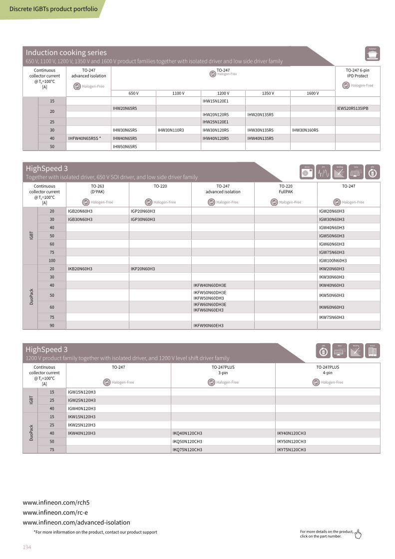
194
For more details on the product, click on the part number.
Induction cooking series 650 V, 1100 V, 1200 V, 1350 V and 1600 V product families together with isolated driver and low side driver family
Continuous collector current
@ Tc=100°C[A]
TO-247advanced isolation
TO-247 TO-247 6-pinIPD Protect
650 V 1100 V 1200 V 1350 V 1600 V
15 IHW15N120E1
20IHW20N65R5 IEWS20R5135IPB
IHW20N120R5 IHW20N135R525 IHW25N120E1
30 IHW30N65R5 IHW30N110R3 IHW30N120R5 IHW30N135R5 IHW30N160R5
40 IHFW40N65R5S * IHW40N65R5 IHW40N120R5 IHW40N135R5
50 IHW50N65R5
Discrete IGBTs product portfolio
HighSpeed 3 Together with isolated driver, 650 V SOI driver, and low side driver family
Continuous collector current
@ Tc=100°C[A]
TO-263(D2PAK)
TO-220 TO-247advanced isolation
TO-220 FullPAK
TO-247
IGBT
20 IGB20N60H3 IGP20N60H3 IGW20N60H3
30 IGB30N60H3 IGP30N60H3 IGW30N60H3
40 IGW40N60H3
50 IGW50N60H3
60 IGW60N60H3
75 IGW75N60H3
100 IGW100N60H3
DuoP
ack
20 IKB20N60H3 IKP20N60H3 IKW20N60H3
30 IKW30N60H3
40 IKFW40N60DH3E IKW40N60H3
50 IKFW50N60DH3EIKFW50N60DH3 IKW50N60H3
60 IKFW60N60DH3EIKFW60N60EH3 IKW60N60H3
75 IKW75N60H3
90 IKFW90N60EH3
HighSpeed 3 1200 V product family together with isolated driver, and 1200 V level shift driver family
Continuous collector current
@ Tc=100°C[A]
TO-247 TO-247PLUS 3-pin
TO-247PLUS 4-pin
IGBT
15 IGW15N120H3
25 IGW25N120H3
40 IGW40N120H3
DuoP
ack
15 IKW15N120H3
25 IKW25N120H3
40 IKW40N120H3 IKQ40N120CH3 IKY40N120CH3
50 IKQ50N120CH3 IKY50N120CH3
75 IKQ75N120CH3 IKY75N120CH3
www.infineon.com/rch5www.infineon.com/rc-ewww.infineon.com/advanced-isolation
*For more information on the product, contact our product support

195
For more details on the product, click on the part number.
TRENCHSTOP™ 5 F5, H5 and S5 Together with isolated driver, 650 V SOI driver, and low side driver family
Continuous collector current
@ Tc=100°C[A]
TO-263(D2PAK)
TO-220 TO-247advanced isolation
TO-220 FullPAK
TO-247 TO-2474-pin
IGBT
20 IGB20N65S5 IGP20N65F5/IGP20N65H5
30 IGB30N65S5 * IGP30N65F5/IGP30N65H5
40 IGP40N65F5/IGP40N65H5 IGW40N65F5/IGW40N65H5
50IGB50N60H5 * IGW50N65F5/IGW50N65H5 IGZ50N65H5
IGB50N60S5 *
75 IGW75N65H5 IGZ75N65H5
100 IGZ100N65H5
DuoP
ack
8 IKP08N65F5/IKP08N65H5 IKA08N65F5/IKA08N65H5
15 IKB15N65EH5 IKP15N65F5/IKP15N65H5 IKA15N65F5/IKA15N65H5
20 IKB20N65EH5 IKP20N65H5/IKP20N65F5
28 IKP28N65ES5
30IKB30N65EH5 IKP30N65H5/IKP30N65F5 IKW30N65H5
IKB30N65ES5
39 IKP39N65ES5
40
IKB40N65ES5 IKP40N65F5/IKP40N65H5 IKFW40N65DH5 * IKW40N65F5/IKW40N65H5
IKB40N65EH5
IKB40N65EF5
50IKFW50N65ES5* IKW50N65F5/IKW50N65H5 IKZ50N65EH5
IKFW50N65DH5IKFW50N65EH5* IKW50N65EH5
60 IKFW60N65ES5 *
75IKFW75N65ES5 * IKW75N65EH5
IKFW75N65EH5 * IKZ75N65EH5
90 IKFW90N65ES5
Discrete IGBTs product portfolio
TRENCHSTOP™ 5 L5 low VCE(sat) 650 V product family together with low side driver family
Continuous collector current
@ Tc=100°C[A]
TO-251(IPAK)
TO-252(DPAK)
TO-263(D2PAK)
TO-220 TO-262(I²PAK)
TO-220 FullPAK
TO-247 TO-247 4-pin
IGBT 30 lGW30N65L5 *
DuoP
ack 30 IKW30N65EL5
75 IKW75N65EL5 IKZ75N75EL5 *
TRENCHSTOP™ 5 WR5 650 V product family together with low side driver family
Continuous collector current
@ Tc=100°C[A]
TO-247
DuoP
ack 30 IKW30N65WR5
40 IKW40N65WR5
50 IKW50N65WR5
TRENCHSTOP™ 5 S5Together with isolated driver, 650 V SOI driver, and low side driver family
Continuous collector current
@ Tc=100°C[A]
TO-247 TO-247 4-pin
DuoP
ack
30 IKW30N65ES5
40 IKW40N65ES5
50 IKW50N65ES5 IKZ50N65ES5
75 IKW75N65ES5 IKZ50N65ES5
www.infineon.com/trenchstop5 *For more information on the product, contact our product support
Appl
icat
ions
Pa
cka
ges
20
-30
0 V
MO
SF
ETs
50
0-9
50
V M
OS
FE
TsW
BG
se
mic
on
du
cto
rsD
iscr
ete
IGB
TsP
ow
er
ICs
Inte
llig
en
t sw
itch
es
an
d in
pu
t IC
sG
ate
dri
ver
ICs
Mic
roco
ntr
oll
ers
XE
NS
IV™
se
nso
rs

196
For more details on the product, click on the part number.
IGBT nomenclature
Nomenclature
IGBT (after 03/2013)
Company I = InfineonS = Formerly Siemens
I K
DeviceG = Single IGBTH = Reverse conductingK = Duo pack
Package typeA = TO-220-3 FullPAKB = TO-263-3 (D2PAK)D = TO-252-3 (DPAK)P = TO-220-3U = TO-251-3 (IPAK)W = TO-247-3Y = TO-247PLUS 4-pinFW = TO-247-3 advanced isolationQ = TO-247PLUS/Super 247 (TO247AA)Z = TO-247-4
F5 = Ultra fast IGBT
H5 = High speed IGBT
L5 = Low VCE(sat) IGBT
R5 = Reverse conducting IGBT
E1 = Reverse conducting IGBT
S5 = “Soft” high speed IGBTT6 = TRENCHSTOP™ IGBT6TP = TRENCHSTOP™ PerformanceWR5 = RC TRENCHSTOP™ 5S6 = 1200 V TRENCHSTOP™ IGBT6H6 = 1200 V TRENCHSTOP™ IGBT6 fast
Diode (for duo pack only)B = Emitter controlled half ratedC = Emitter controlled full ratedD = Rapid 1 half ratedE = Rapid 1 full ratedN = Rapid 2 full ratedW = Full rated hard switching
W 75 N 65 L5E
Nominal current [A] @ 100°C Nominal voltage
Divided by 10 (650 V/10 = 65)
TechnologyN = N-channelP = P-channel
www.infineon.com/igbtdiscretes

197
For more details on the product, click on the part number.
IGBT (before 03/2013)
Company
I = Infineon
S = Formerly Siemens
I K
Device
K = IGBT + diode (normal drives)
H = Optimized for so
switching applications
(e.g. induction heating)
G = Single IGBT
D = Diode
Package type
A = TO-220 FullPAK
B = TO-263 (D2PAK)
D = TO-252 (DPAK)
P = TO-220
U = TO-251 (IPAK)
W = TO-247
– = Fast IGBT (~20 kHz)
Hχ = HighSpeed generation
(600 V - 1200 V)
Tχ = TRENCHSTOP™ generation
(600 V IGBT 3) (1200 V IGBT 4)
Rχ = Reverse conducting
RF = Reverse conducting fast
F = HighSpeed FAST 5
Rχ = Rapid diode generation
W 40 N 120 H 3
Generation
Nominal current
(@ 100°C) [A]
Nominal voltage
Divided by 10 (1200 V/10 = 120)
Technology
N = N-channel
T = TRENCHSTOPTM
E = Emitter-controlled diodes
(for diode only)
www.infineon.com/igbtdiscretes
IGBT nomenclature
Appl
icat
ions
Pa
cka
ges
20
-30
0 V
MO
SF
ETs
50
0-9
50
V M
OS
FE
TsW
BG
se
mic
on
du
cto
rsD
iscr
ete
IGB
TsP
ow
er
ICs
Inte
llig
en
t sw
itch
es
an
d in
pu
t IC
sG
ate
dri
ver
ICs
Mic
roco
ntr
oll
ers
XE
NS
IV™
se
nso
rs

198
For more details on the product, click on the part number.
IPD protect
I –E 135 IPB20WS R5
Product type G = Single IGBTH = Reverse conductingK = DuoPackE = Enhanced IGBT
OptimizationR5: RC 5th generation
Diode (for DuoPack only)Note: not used for RC device = blank
Nominal voltageDivided by 10 (1350 V/10 = 135)
IC/Co-Pack functionalityIPB = Induction cooking protection IC version B General format:1st: I = Induction cooking2nd : Added funcionality (P = protection)3rd : version
Infineon
Package W = TO-247 3pinZ = TO-247 4pinWS = TO-247 6pin
Nominal current [A] @ 100°C
Nomenclature
www.infineon.com/igbtdiscretes
IGBT nomenclature

199
For more details on the product, click on the part number.
Infineon support for discrete IGBTsUseful links and helpful information
Further information, datasheets and documentswww.infineon.com/igbt www.infineon.com/igbtdiscretes
www.infineon.com/discrete-automotive-igbtwww.infineon.com/latest-discrete-packages
Evaluationboards and simulation models www.infineon.com/eval-TO-247-4pin www.infineon.com/igbtdiscrete-simulationmodels
Simulation
Appl
icat
ions
Pa
cka
ges
20
-30
0 V
MO
SF
ETs
50
0-9
50
V M
OS
FE
TsW
BG
se
mic
on
du
cto
rsD
iscr
ete
IGB
TsP
ow
er
ICs
Inte
llig
en
t sw
itch
es
an
d in
pu
t IC
sG
ate
dri
ver
ICs
Mic
roco
ntr
oll
ers
XE
NS
IV™
se
nso
rs

200
For more details on the product, click on the part number.
Power management ICs › XDP™ SMPS controllers › DC-DC digital multiphase controllers › PFC controllers › PWM controllers › Resonant LLC half-bridge controller ICs › Integrated power stages
› Switching regulators › Voltage regulators › Audio amplifier ICs › Lighting ICs › Intelligent power modules (IPMs) › Motor control ICs

201
For more details on the product, click on the part number.
Appl
icat
ions
Pa
cka
ges
20
-30
0 V
MO
SF
ETs
50
0-9
50
V M
OS
FE
TsW
BG
se
mic
on
du
cto
rsD
iscr
ete
IGB
TsP
ow
er
ICs
Inte
llig
en
t sw
itch
es
an
d in
pu
t IC
sG
ate
dri
ver
ICs
Mic
roco
ntr
oll
ers
XE
NS
IV™
se
nso
rs

202
For more details on the product, click on the part number.
XDP™ SMPSIDP2308 and IDP2303A – digital multi-mode PFC+LLC combo controller
The IDP2308 and IDP2303A are high performance digital combo controllers with integrated drivers and 600 V depletion cell designed for boost PFC and half-bridge LLC targeting switched mode power supplies (SMPS) from 75 W to 300 W.
› Support non-AUX operation with the lowest standby performance and start-up cell › Support multi-mode PFC operation for optimized efficiency curve › Configurable frequency setting for LLC soft-start and normal operation › Synchronous PFC and LLC burst mode control with soft-start to prevent acoustic noise › Excellent dynamic response by adaptive LLC burst mode › Configurable and comprehensive protections for PFC/LLC/IC temp › IEC62368-1 certified active X-cap discharge function › Flexible IC parameter setting with digital UART interface supports
PSU platform approach Key benefits › Low BOM count due to high integration of digital control › No auxiliary power supply needed › Easy design of system schematic and PCB layout › Small form factor design › Higher system reliability › Shorter development cycles and higher design and production flexibility
www.infineon.com/xdp-smps
IDP2303A – power adapter
GDO
ZCD
CSOVS
VAC
HV
HBFB
GND
VCC
CS1GD1HSGNDHSVCCHSGD
IDP2303A
VCC
UART
SR IC
Vout
Product Target application Major difference PackageIDP2308 TV embedded PSU 2nd redundant PFC output
overvoltage protectionDSO-14 (with enhanced HV creepage distance)
IDP2303A Adapter, general SMPS Constant output voltage DSO-16
XDP™ SMPS controllers

203
For more details on the product, click on the part number.
www.infineon.com/xdp-smps
GDO
ZCD
CSOVS
VAC
HV
HBFB
GND
VCC
CS1GD1HSGNDHSVCCHSGD
IDP2308
UART
Vout_1
Vout_2
Power_on/
standby
Vbulk
Target applications › LCD TV power supply › General SMPS › Power adapter
IDP2308 – embedded PSU
Appl
icat
ions
Pa
cka
ges
20
-30
0 V
MO
SF
ETs
50
0-9
50
V M
OS
FE
TsW
BG
se
mic
on
du
cto
rsD
iscr
ete
IGB
TsP
ow
er
ICs
Inte
llig
en
t sw
itch
es
an
d in
pu
t IC
sG
ate
dri
ver
ICs
Mic
roco
ntr
oll
ers
XE
NS
IV™
se
nso
rs

204
For more details on the product, click on the part number.
XDP™ SMPSXDPS21071 – digital FFR flyback controller
XDPS21071 is the first flyback controller in the industry to introduce ZVS (Zero Voltage Switching) on the primary side to achieve high efficiency with simplified circuitry and economical switches. By driving an external low voltage switch to induce a negative current to discharge the main high voltage MOSFET, switching losses can be reduce further than traditional valley switching type of switching scheme. To achieve high efficiency with synchronous rectification, DCM operation is ensured via valley detection for a safe and robust operation.
45W USB-PD Type-C reference design in a small form factor based on XDPS21071. › 45W USB-PD Type-C charger › Universal input range 90~264 VAC
› Supported output: 5 V/3 A, 9 V/3 A, 12 V/3 A, 15 V/3 A and 20 V/2.25 A › Peak efficiency > 90% › Low no-load standby input power < 30 mW
Ordering code: REFXDPS2107145W1TOBO1
REF_XDPS21071_45W1
www.infineon/xdps21071
Features and benefits
Key benefits
Reduce switching loss and achieve high efficiency
Optimize efficiency across various line/load condition
Optimize light and no load efficiency
Save BOM count and cost with no messy external driver
Easy to drive, low cost and widely available off the shelf 60V MOSFET
Fail safe mechanism to limit output power in the event of PD controller failure
Avoid CCM operation and no potential of shoot-through with SR MOSFET
Key features
Zero voltage switching
Frequency law optimization
Active burst mode operation with multi entry/exit threshold
Integrated dual MOSFET gate driver
Easy ZVS implementation with an external 60V MOSFET
Multiple peak current threshold offset for different output
CrCM operation with valley detection
IPD70R360P7S
BSL606SN
XDPS21071
BSC0805LS
LF1
LCM RxCx
DB
RHV CBUS
CFVCVCC
CZC RZC2
RZC1
RG1
RCS
QM
U2
U3
RB1 RF1
RF2
RC2
CC3
CC1
CC2
RC1
RB2
CY
RG0
RFC
CFC
CFM
DVCC
RCP2
RCP1
CCP
DCP
WP
WAUX
WZVS
QZVS
60 V,
WS
QSR
CFS
Qload
Cout
U1
VCC ZCD
GD1
GD0
CS
MFIO
GND
GPIO
HV
N
85 ... 264 VAC
ISZ0901NLS
SR + protocol control
Type-C
XDP™ SMPS controllers

205
For more details on the product, click on the part number.
DC-DC digital multiphase controllersPoint-of-load power management
Infineon’s digital multiphase and multirail controllers provide power for today’s medium and high current POL applications used in telecom/datacom, server, and storage environments. Infineon’s digital controller family enables OEMs and ODMs to improve efficiency and total cost of ownership, while increasing power density and optimizing the total system footprint of the voltage regulator. The products highlighted in the table below represent our fifth generation digital controller family and support up to two rails with 1-6 phases on individual rails. The I2C/PMBus™ interface connects the digital controllers to the application system and provides real time telemetry information, monitoring and control capabilities. The digital controllers are fully configurable through our PowerCode™ and PowerClient™ graphical user interfaces that allows for easy to use and simplified design optimization.
Multi-phase configurations are supported for best power optimization
Advantages of a digital controllerProtection features include a set of sophisticated overvoltage, undervoltage, overtemperature, and overcurrent protections. Each of the controllers in the table above also detect and protect against an open circuit on the remote sensing inputs. These attributes provide a complete and advanced protection feature set for microprocessor, DSP, FPGA or ASIC power sys-tems. Accurate current sense telemetry is achieved through internal calibration that measures and corrects current sense offset error sources upon start-up. Programmable temperature compensation provides accurate current sense information even when using DCR current sense.
Feature Controller family
Configurable output rails Dual rail Dual rail Dual/single rail Dual/single rail Dual rail Dual/single rail Dual/single rail Dual rail
Part number PMBus™ PXE1610C * IR35212 XDPE10280B * XDPE10281B * IR35204MTRPBF IR35201MTRPBF IR35223 * XDPE132G5C *
Phase configuration
Main 7 ph 7 ph 8 ph 8 ph 4 ph 8 ph 10 ph 16 ph
Subconfigurations 6 + 1 6+1 8+0, 6+2, 4+4 8+0, 6+2, 4+4 3+1 8+0, 7+1, 6+2 10+0, 5+5 8+8
Vout_max 2.5 V 3.3 V 3.04 V 3.04 V 3.3 V 3.3 V 3.3 V 3.3 V
Switching frequency Up to 2 MHz Up to 2 MHz Up to 2 MHz Up to 2 MHz Up to 2 MHz Up to 2 MHz Up to 2 MHz Up to 2 MHz
Operating temperature range - 5°C to 85°C - 40°C to 85°C - 40°C to 85°C - 40°C to 85°C - 40°C to 85°C - 40°C to 85°C - 40°C to 85°C - 40°C to 120°C
VQFN package 48-lead(6x6)
0.4 mm pitch
48-lead(6x6)
0.4 mm pitch
56-lead(7x7)
0.4 mm pitch
56-lead(7x7)
0.4 mm pitch
40-lead(5x5)
0.4 mm pitch
56-lead(7x7)
0.4 mm pitch
48-lead(6x6)
0.4 mm pitch
56-lead(7x7)
0.4 mm pitch
Typical application Intel server,high end desktop
Intel server, workstation,
high end desktop
Intel server, workstation,
high end desktop
AMD server, workstation,
high end desktop
AMD server,memory and
SOC
AMD server, CPU
Phase redundant
based server systems
AMD server,GPU, ASIC, networking
ASSP
www.infineon.com/digital-controller *For more information on the product, contact our product support
Digital multiphase controllers
Appl
icat
ions
Pa
cka
ges
20
-30
0 V
MO
SF
ETs
50
0-9
50
V M
OS
FE
TsW
BG
se
mic
on
du
cto
rsD
iscr
ete
IGB
TsP
ow
er
ICs
Inte
llig
en
t sw
itch
es
an
d in
pu
t IC
sG
ate
dri
ver
ICs
Mic
roco
ntr
oll
ers
XE
NS
IV™
se
nso
rs

206
For more details on the product, click on the part number.
Typical multiphase application circuit
CVIN1Cboost1
L1
12 V
CVCC1VGD
CVIN2Cboost2
L2
12 V
CVIN3
L3
12 V
CVIN4
L4
12 V
V_CPU_L2
LOAD
CCSRS2
1uF
3.3 V
10nF1K
13K12V
10nF13K13K
1uF
VIN_1RVIN1_1
Rseries
RVIN1_2
10nF1K
13K12VVIN_2
RVIN2_1
RVIN2_2
I2C BusIf pin is configured
for SM_ALERT
VV
CPU SerialBus3.3V
1K
VV
From System
VV Bus
CCSRS2Rseries
V_CPU_L1
LOAD
CVIN_L2
L4
12 V
10nF1K
PWM
REFIN
ZCD_EN#
BOOST
SW
PGND
GATEL
TDA21472
LGND
CVDRV1
CVCC2VGD
PWM
ZCD_EN#
BOOST
SW
PGND
GATEL
LGND
CVDRV2
Cboost3
CVCC3VGD
TDA21472PWM
ZCD_EN#
BOOST
SW
PGND
GATEL
LGND
CVDRV3
Cboost4
CVCC4VGD
CVDRV4
Cboost5
CVCC5VGD
TDA21472PWM
ZCD_EN#
BOOST
SW
PGND
GATEL
LGND
CVDRV5
PWM
ZCD_EN#
BOOST
SW
PGND
GATEL
LGND
RCSP
RCSMVCC
VSENVRTN
TSEN
CFILT
VINSEN
SM_ALERT#/VINSEN2/PSI#1
SV_ALERT#SV_DIOSV_CLK
VRHOT_ICRIT#
ENEN_L2/INMODE/CAT_FLT
SV_ADDR
SM_DIOSM_CLK
RCSP_L2
RCSM_L2
VSEN_L2
VRTN_L2
GND
PWM1
ISEN1
IRTN1
PWM2
ISEN2
IRTN2
PWM3
ISEN3
IRTN3
PWM4
ISEN4
IRTN4
PWM1_L2
ISEN1_L2
IRTN1_L2
VRDY1VRDY2
ADDR_PROT
IR3584
I2C
TDA21472
TDA21472
IOUT
V DRV
V IN
TOUT /FLT
IOUT
V DRV
V IN
TOUT /FLT
IOUT
V DRV
V IN
TOUT /FLT
REFINREFIN
IOUT
V DRV
V IN
TOUT /FLT
REFIN
IOUT
V DRV
V IN
TOUT /FLT
REFIN
IOUT
V DRV
V IN
TOUT /FLT
REFIN
V CC
V CC
V CC
V CC
V CC
Digital multiphase controllers

207
For more details on the product, click on the part number.
AC-DC power management ICsTechnology leadership in power supply
AC-DC power management ICs
PFC controller
Continuous conduction mode
(CCM) PFC
Critical conduction mode
(CrCM) PFCCombi (PFC+PWM)
Stand-alone PWM Fixed frequency (FF) CoolSET™
PWM controller
Quasi-resonant (QR) CoolSET™
www.infineon.com/acdc
By offering a wide variety of highly efficient control ICs we enable our customer to meet new demands like PFC regulations and ultra low standby power requirements in a very cost effective way. A comprehensive array of safety features helps to minimize the number of external components, reduces design in time and improves the reliability of the SMPS.
AC-DC power management ICs
*For more information on the product, contact our product support
Fixed frequencyICE5GSAG (125 kHz)ICE5ASAG (100 kHz)ICE3AS03LJG (100 kHz)ICE3BS03LJG (65 kHz)XDPS21071 (140 kHz)
Quasi-resonantICE5QSBG*ICE2QS02GICE2QS03G
Half-bridge LLC resonantICE1HS01G-1ICE2HS01G
650 V F3/F3R CoolSET™ICE3Axx65ELJICE3RBRxx65JZ ICE3RBRxx65JG
700 V Gen5 CoolSET™ICE5AR4770AGICE5AR4770BZS
800 V F3R CoolSET™ICE5A/GRxx80AGICE5ARxx80BZSICE3A/BRxx80JZICE3ARxx80CJZICE3ARxx80VJZICE3ARxx80JG
Fixed frequencyICE2PCS02G (65 kHz)ICE2PCS03G* (100 kHz)
Adjustable frequencyICE2PCS01G (50 - 250 kHz)ICE2PCS05G (20 - 250 kHz)ICE3PCS01G (OVP+brown-out)ICE3PCS02G (OVP)ICE3PCS03G (Brown-out)
TDA4862GTDA4863GTDA4863-2GIRS2505L
CrCM + LLCXDP™ SMPS IDP2308 (DSO-14)XDP™ SMPS IDP2303A (DSO-16)
650 V CoolSET™ICE2QRxx65(Z)/(G)
700 V CoolSET™ICE5QRxx70AZ/G
800 V CoolSET™ICE2QRxx80Z/GICE5QRxx80AZ/GICE5QRxx80BG
Appl
icat
ions
Pa
cka
ges
20
-30
0 V
MO
SF
ETs
50
0-9
50
V M
OS
FE
TsW
BG
se
mic
on
du
cto
rsD
iscr
ete
IGB
TsP
ow
er
ICs
Inte
llig
en
t sw
itch
es
an
d in
pu
t IC
sG
ate
dri
ver
ICs
Mic
roco
ntr
oll
ers
XE
NS
IV™
se
nso
rs

208
For more details on the product, click on the part number.
ICE2PCS0xG
ICE3PCS0xG
Continuous conduction mode (CCM) PFC ICsHigh efficiency and very low system cost
2nd generation continuous conduction mode PFC IC features
› Fulfills class D requirements of IEC 61000-3-2 › Lowest count of external components › Adjustable and fixed switching frequencies › Frequency range from 20 to 250 kHz › Versions with brown-out protection available › Wide input range supported › Enhanced dynamic response during load jumps › Cycle by cycle peak current limiting › Integrated protections OVP, OCP › DIP-8 and DSO-8 › Lead-free, RoHS compliant
3rd generation continuous conduction mode PFC IC features
› Fulfills class D requirements of IEC 61000-3-2 › Integrated digital voltage loop compensation › Boost follower function › Bulk voltage monitoring signals, brown-out › Multi protections such as double OVP › Fast output dynamic response during load jump › External synchronization › Extra-low peak current limitation threshold › SO-8 and SO-14 › Lead-free, RoHS compliant
Compared to the first generation of ICE1PCS01/02, the second generation of CCM PFC controller ICs, ICE2PCS01/02, have lower internal reference trimmed at 3V. They also have other advantages such as wider VCC operating range, improved internal oscillator and additional direct bulk capacitor overvoltage protection. Compared to the first and second generation of ICE1PCS0x and ICE2PCS0x, the third generation CCM PFC have the lowest internal reference trimmed at 2.5 V and integrated digital control voltage loop. They also feature low peak current limit at 0.2 V, adjustable gate switching frequency range from 21 kHz to 100 kHz and able to synchronize with external frequency range from 50 kHz to 100 kHz. They are now able to achieve 95% efficiency at full load for all input voltage range.
Application diagram
www.infineon.com/acdc
PFC CCM IC by feature ICE2PCS01GICE2PCS05G
ICE2PCS02GICE2PCS03G *
ICE3PCS03G ICE3PCS02G ICE3PCS01G
Digital control voltage loop –
Variable frequency –
Synchronous frequency –
Open loop protection
Low peak current limit -1 V -1 V -0.4 V -0.4 V -0.2 V
Brown-out protection – –
Overvoltage protection
Second overvoltage protection –
PFC enable function –
Boost follower mode –
5 V regulator –
PFC controllers
*For more information on the product, contact our product support

209
For more details on the product, click on the part number.
Critical conduction mode (CrCM) PFCEasy design and lowest system cost
Application diagram
Fully compatible with the world standard, these devices are optimized to offer extremely compact and cost effective PFC solutions for electronic ballast and off-line SMPS. By using a zero current detector for discontinuous operation mode a near unity power factor and an excellent THD are achieved. The latest addition are the TDA4863G and TDA4863-2G which are the improved versions of the active power factor controller TDA4862G. Products are available in DSO-8 (TDAxxG parts) and SOT23 (IRS2505L) packages.
www.infineon.com/acdc
TDA4862GPower factor controller (PFC) IC for high-power factor and active harmonic filter › IC for sinusoidal line current consumption › Power factor approaching 1 › Controls boost converter as an active
harmonics filter › Internal start-up with low current consumption › Zero current detector for discontinuous
operation mode › High current totem pole gate driver › Trimmed ±1.4% internal reference › Undervoltage lockout with hysteresis › Very low start-up current consumption › Pin compatible with world standard › Output overvoltage protection › Current sense input with internal low pass filter › Totem pole output with active shutdown
during UVLO › Junction temperature range -40°C to +150°C › Available in DIP-8 and SO-8 packages
TDA4863G/TDA4863-2GPower factor controller IC for high-powerfactor and low THD additional features to TDA4862 › Reduced tolerance of signal levels › Improved light load behavior › Open loop protection › Current sense input with leading edge blanking LEB › Undervoltage protection › SO-8 package
IRS2505LPBF › Crticial conduction mode PFC control › High power factor and ultralow THD › Wide load and line range › Regulated and programmable DC bus voltage › No secondary winding required › MOSFET cycle-by-cycle overcurrent protection › DC bus overvoltage protection › Low EMI gate drive › Ultralow start-up current › 20.8 V internal Zener clamp on VCC
› Excellent ESD and latch immunity › RoHS compliant › 5-pin SOT-23 package
TDA4862G
TDA4863G
TDA4863-2G
IRS2505LPBF
PFC controllers
Appl
icat
ions
Pa
cka
ges
20
-30
0 V
MO
SF
ETs
50
0-9
50
V M
OS
FE
TsW
BG
se
mic
on
du
cto
rsD
iscr
ete
IGB
TsP
ow
er
ICs
Inte
llig
en
t sw
itch
es
an
d in
pu
t IC
sG
ate
dri
ver
ICs
Mic
roco
ntr
oll
ers
XE
NS
IV™
se
nso
rs

210
For more details on the product, click on the part number.
PFC controller portfolio
Critical conduction mode (CrCM) PFC IC portfolio
Continuous conduction mode PFC ICs
www.infineon.com/acdc
Product Frequency – fSW Current drives PackageICE2PCS01G 50-250 kHz 2.0 A DSO-8ICE2PCS02G 65 kHz 2.0 A
ICE2PCS03G* 100 kHz 2.0 AICE2PCS05G 20-250 kHz 2.0 A
Product VCC min. VCC max. PackageTDA4862G 11 V 19 V DSO-8TDA4863G 10 V 20 V DSO-8
TDA4863-2G 10 V 20 V DSO-8IRS2505L 9 V 20.8 V SOT23
2nd generation continuous conduction mode PFC IC product portfolio
3rd generation continuous conduction mode PFC IC product portfolio
Product Frequency – fSW Current drives Features PackageICE3PCS01G Adjustable 0.75 A OVP+brown-out SO-14
ICE3PCS02G 0.75 A OVP SO-8ICE3PCS03G 0.75 A Brown-out SO-8
www.infineon.com/acdc
PFC controllers
*For more information on the product, contact our product support

211
For more details on the product, click on the part number.
Appl
icat
ions
Pa
cka
ges
20
-30
0 V
MO
SF
ETs
50
0-9
50
V M
OS
FE
TsW
BG
se
mic
on
du
cto
rsD
iscr
ete
IGB
TsP
ow
er
ICs
Inte
llig
en
t sw
itch
es
an
d in
pu
t IC
sG
ate
dri
ver
ICs
Mic
roco
ntr
oll
ers
XE
NS
IV™
se
nso
rs
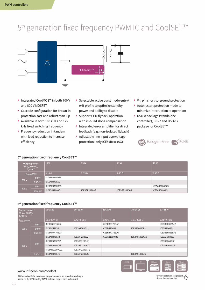
212
For more details on the product, click on the part number.
5th generation fixed frequency CoolSET™ Output power 1)
85 VAC~300 VAC Ta=50°C
15 W 23 W 27 W 40 W
RDS(on) max 5.18 Ω 2.35 Ω 1.75 Ω 0.80 Ω
700 VDIP-7 ICE5AR4770BZS
DSO-12 ICE5AR4770AG
800 VDIP-7 ICE5AR4780BZS ICE5AR0680BZS
DSO-12 ICE5GR4780AG ICE5GR2280AG ICE5GR1680AG ICE5AR0680AG
3rd generation fixed frequency CoolSET™ Output power 1) 85 VAC~300 VAC Ta=50°C
10~15 W 19~21 W 23~26 W 30~34 W 37~41 W
RDS(on) max 11.1~5.44 Ω 3.42~2.62 Ω 1.96~1.71 Ω 1.11~1.05 Ω 0.75~0.71 Ω
650 V
DIP-7 ICE3RBR4765JZ ICE3RBR1765JZ ICE3RBR0665JZ
DIP-8 ICE3BR4765J ICE3A1065ELJ ICE3BR1765J ICE3A2065ELJ ICE3BR0665J
DSO-12 ICE3RBR4765JG ICE3RBR1765JG ICE3RBR0665JG
800 VDIP-7
ICE3AR4780JZ ICE3AR2280JZ ICE3AR1580VJZ ICE3AR1080VJZ ICE3AR0680JZ
ICE3AR4780VJZ ICE3BR2280JZ ICE3BR0680JZ
ICE3AR4780CJZ ICE3AR2280VJZ ICE3AR0680VJZ
ICE3AR10080CJZ ICE3AR2280CJZ
DSO-12 ICE3AR4780JG ICE3AR2280JG ICE3AR1080JG
1) Calculated DCM maximum output power in an open-frame design based on Ta=50° C and Tj=125°C without copper area as heatsink
5th generation fixed frequency PWM IC and CoolSET™
› Integrated CoolMOS™ in both 700 V and 800 V MOSFET
› Cascode configuration for brown-in protection, fast and robust start-up
› Available in both 100 kHz and 125 kHz fixed switching frequency
› Frequency reduction in tandem with load reduction to increase efficiency
› Selectable active burst mode entry/exit profile to optimize standby power and ability to disable
› Support CCM flyback operation with in-build slope compensation
› Integrated error amplifier for direct feedback (e.g. non-isolated flyback)
› Adjustable line input overvoltage protection (only ICE5xRxxxxAG)
› VCC pin short-to-ground protection › Auto restart protection mode to
minimize interruption to operation › DSO-8 package (standalone
controller), DIP-7 and DSO-12 package for CoolSET™
FF CoolSETTM
www.infineon.com/coolset
PWM controllers

213
For more details on the product, click on the part number.
www.infineon.com/coolset
5th generation 3rd generation
FF PWM IC ICE5ASAG ICE5GSAG ICE3AS03LJG ICE3BS03LJGPackage DSO–8 DSO–8
Switching frequency 100 kHz 125 kHz 100 kHz 65 kHz
Operating temperature -40°C~129°C -25°C~130°C
Start-up cell Cascode
VCC on/off threshold 16 V/10 V 18 V/10.5 V
Soft start time 12 ms 10 ms 20 ms
Frequency jittering
Modulated gate drive
Active burst mode (3 level selectable)
Slope compensation for CCM –
Frequency reduction –
Integrated error amplifier for direct feedback –
Adjustable line Input overvoltage protection with auto restart –
Adjustable brown-in protection with auto restart –
VCC pin short-to-ground protection (no start–up) –
VCC undervoltage protection with auto restart with auto restart
VCC overvoltage protection with auto restart with latch–up
Overload /open loop protection with auto restart with auto restart
Overtemperature protection with auto restart and hysteresis with latch–up
External blanking time extension – with auto restart
External protection enable pin – with latch–up
Fixed frequency PWM IC
Appl
icat
ions
Pa
cka
ges
20
-30
0 V
MO
SF
ETs
50
0-9
50
V M
OS
FE
TsW
BG
se
mic
on
du
cto
rsD
iscr
ete
IGB
TsP
ow
er
ICs
Inte
llig
en
t sw
itch
es
an
d in
pu
t IC
sG
ate
dri
ver
ICs
Mic
roco
ntr
oll
ers
XE
NS
IV™
se
nso
rs

214
For more details on the product, click on the part number.
Fixed frequency CoolSET™
1) Calculated 85 VAC~300 VAC DCM maximum output power in an open-frame design based on Ta=50°C and Tj=125°C without copper area as heatsink
700 V CoolSET™ 650 V CoolSET™ 800 V CoolSET™
Gen5ICE5ARxx70AG(BZS)
Gen3 ICE3Axx65ELJ
Gen3RICE3BRxx65J
Gen3RICE3RBRxx65JZ(G)
Gen3R ICE3A(B)Rxx80JZ
Gen3RICE3ARxx80CJZ
Gen3RICE3ARxx80JG
Gen3RICE3ARxx80VJZ
Gen5ICE5ARxx80AG(BZS)
Gen5ICE5GRxx80AG
Package DIP-7, DSO-12 DIP-8 DIP-7, DSO-12 DIP–7 DSO–12 DIP–7 DIP–7, DSO–12 DSO–12
Output power range 15 W 19 W~34 W 15 W~41 W 14 W~39 W 10 W~40 W 11 W~23 W 14 W~30 W 15 W~39 W 15 W~40 W 15 W~27 W
Operating temperature range -40°C~129°C -25°C~130°C -40°C~130°C –25°C~130°C –40°C~130°C –40°C~129°C
Switching frequency 100 kHz 100 kHz 65 kHz 65 kHz 100 kHz/65 kHz 100 kHz 100 kHz 100 kHz 125 kHz
Frequency reduction – –
Integrated error amplifier – –
Slope compensation for CCM mode – – –
VCC on/off threshold 16 V/10 V 18 V/10.5 V 17 V/10.5 V 16 V/10 V
Soft start time 12 ms 20 ms 10 ms 12 ms
Active burst mode selection 3 level 1 level 4 level 3 level 4 level 3 level
VCC pin short-to-ground protection No start-up – – No start–up
VCC overvoltage protection Auto restart Latch Auto restart Auto restart
Overtemperature protection Auto restart with hysteresis Latch Auto restart Auto restart with hysteresis
External protection enable pin - Latch Auto restart Auto restart Latch Auto restart –
Adjustable brown-in/-out protection Brown-in only – Auto restart – Brown-in only
Adjustable line input overvoltage protection
Only ICE5ARxx70AG – – Auto restart Only ICE5ARxx80AG Auto restart
Fast AC reset – – –
Product available
ICE5AR4770AGICE5AR4770BZS
ICE3A1065ELJICE3A2065ELJ
ICE3BR4765JICE3BR1765JICE3BR0665J
ICE3RBR4765JZICE3RBR1765JZICE3RBR0665JZICE3RBR4765JGICE3RBR1765JGICE3RBR0665JG
ICE3AR10080JZICE3AR4780JZICE3AR2280JZICE3AR0680JZICE3BR2280JZICE3BR0680JZ
ICE3AR10080CJZICE3AR4780CJZICE3AR2280CJZ
ICE3AR4780JGICE3AR2280JGICE3AR1080JG
ICE3AR4780VJZICE3AR2280VJZICE3AR1580VJZICE3AR1080VJZICE3AR0680VJZ
ICE5AR0680AGICE5AR4780BZSICE5AR0680BZS
ICE5GR4780AGICE5GR2280AGICE5GR1680AG
www.infineon.com/coolset
PWM controllers

215
For more details on the product, click on the part number.
700 V CoolSET™ 650 V CoolSET™ 800 V CoolSET™
Gen5ICE5ARxx70AG(BZS)
Gen3 ICE3Axx65ELJ
Gen3RICE3BRxx65J
Gen3RICE3RBRxx65JZ(G)
Gen3R ICE3A(B)Rxx80JZ
Gen3RICE3ARxx80CJZ
Gen3RICE3ARxx80JG
Gen3RICE3ARxx80VJZ
Gen5ICE5ARxx80AG(BZS)
Gen5ICE5GRxx80AG
Package DIP-7, DSO-12 DIP-8 DIP-7, DSO-12 DIP–7 DSO–12 DIP–7 DIP–7, DSO–12 DSO–12
Output power range 15 W 19 W~34 W 15 W~41 W 14 W~39 W 10 W~40 W 11 W~23 W 14 W~30 W 15 W~39 W 15 W~40 W 15 W~27 W
Operating temperature range -40°C~129°C -25°C~130°C -40°C~130°C –25°C~130°C –40°C~130°C –40°C~129°C
Switching frequency 100 kHz 100 kHz 65 kHz 65 kHz 100 kHz/65 kHz 100 kHz 100 kHz 100 kHz 125 kHz
Frequency reduction – –
Integrated error amplifier – –
Slope compensation for CCM mode – – –
VCC on/off threshold 16 V/10 V 18 V/10.5 V 17 V/10.5 V 16 V/10 V
Soft start time 12 ms 20 ms 10 ms 12 ms
Active burst mode selection 3 level 1 level 4 level 3 level 4 level 3 level
VCC pin short-to-ground protection No start-up – – No start–up
VCC overvoltage protection Auto restart Latch Auto restart Auto restart
Overtemperature protection Auto restart with hysteresis Latch Auto restart Auto restart with hysteresis
External protection enable pin - Latch Auto restart Auto restart Latch Auto restart –
Adjustable brown-in/-out protection Brown-in only – Auto restart – Brown-in only
Adjustable line input overvoltage protection
Only ICE5ARxx70AG – – Auto restart Only ICE5ARxx80AG Auto restart
Fast AC reset – – –
Product available
ICE5AR4770AGICE5AR4770BZS
ICE3A1065ELJICE3A2065ELJ
ICE3BR4765JICE3BR1765JICE3BR0665J
ICE3RBR4765JZICE3RBR1765JZICE3RBR0665JZICE3RBR4765JGICE3RBR1765JGICE3RBR0665JG
ICE3AR10080JZICE3AR4780JZICE3AR2280JZICE3AR0680JZICE3BR2280JZICE3BR0680JZ
ICE3AR10080CJZICE3AR4780CJZICE3AR2280CJZ
ICE3AR4780JGICE3AR2280JGICE3AR1080JG
ICE3AR4780VJZICE3AR2280VJZICE3AR1580VJZICE3AR1080VJZICE3AR0680VJZ
ICE5AR0680AGICE5AR4780BZSICE5AR0680BZS
ICE5GR4780AGICE5GR2280AGICE5GR1680AG
Appl
icat
ions
Pa
cka
ges
20
-30
0 V
MO
SF
ETs
50
0-9
50
V M
OS
FE
TsW
BG
se
mic
on
du
cto
rsD
iscr
ete
IGB
TsP
ow
er
ICs
Inte
llig
en
t sw
itch
es
an
d in
pu
t IC
sG
ate
dri
ver
ICs
Mic
roco
ntr
oll
ers
XE
NS
IV™
se
nso
rs

216
For more details on the product, click on the part number.
Climate saver 80 PLUS® and 80 PLUS® Bronze
Climate saver systems
Climate saver 80 PLUS® Silver
FF CoolSETTM
5 VPFC
DC-DC
12 V
5 V
3.3 VDC-DC
PWM
FF CoolSETTM
PFC/PWM
12 V
5 V
3.3 V
5 V
PFC block
ICE3PCS01G
ICE3PCS02G
ICE3PCS03G
PWM block ICE2HS01G
Standby blockFF CoolSET™
ICE5GR4780AG
ICE5GR2280AG
ICE5GR1680AGICE3AR1080JGICE5AR0680AG
PFC blockICE2PCS01G
ICE2PCS02G
PWM block ICE1HS01G-1
Standby blockFF CoolSET™
ICE5GR4780AG
ICE5GR2280AG
ICE5GR1680AG
ICE3AR1080JG
ICE5AR0680AG
80 PLUS® Silver
80 PLUS® and 80 PLUS® Bronze
www.infineon.com/pcpowerwww.infineon.com/acdcwww.infineon.com/coolset
Climate saver systems

217
For more details on the product, click on the part number.
www.infineon.com/pcpowerwww.infineon.com/acdcwww.infineon.com/coolset
FF CoolSETTM
DC-DC
PFC PWM
DC-DC
5 V
3.3 V
12 V
5 V
Climate saver 80 PLUS® Gold Climate saver 80 PLUS® PlatinumCertification for Infineon's PC power reference design
PFC block
ICE3PCS01G
ICE3PCS02G
ICE3PCS03G
PWM block ICE2HS01G
Standby blockFF CoolSET™
ICE5GR4780AG
ICE5GR2280AG
ICE5GR1680AG
ICE3AR1080JG
ICE5AR0680AG
PFC block
ICE3PCS01G
ICE3PCS02G
ICE3PCS03G
PWM block ICE2HS01G
Standby blockQR CoolSET™
ICE5QR4780BG *
ICE5QR2280BG *
ICE5QR1680BG *
ICE2QR1080G
ICE5QR0680BG *
80 PLUS® Gold80 PLUS® Platinum Certification for Infineon's PC power reference design
Climate saver systems
*For more information on the product, contact our product support
Appl
icat
ions
Pa
cka
ges
20
-30
0 V
MO
SF
ETs
50
0-9
50
V M
OS
FE
TsW
BG
se
mic
on
du
cto
rsD
iscr
ete
IGB
TsP
ow
er
ICs
Inte
llig
en
t sw
itch
es
an
d in
pu
t IC
sG
ate
dri
ver
ICs
Mic
roco
ntr
oll
ers
XE
NS
IV™
se
nso
rs

218
For more details on the product, click on the part number.
5th generation quasi-resonant PWM IC and CoolSET™
› Integrated CoolMOS™ in both 700 V and 800 V MOSFET with cascode configuration
› Digital frequency reduction with reducing load
› Novel quasi-resonant to minimize the spread of switching frequency between low and high line AC input
› Selectable active burst mode entry/exit profile
› Auto restart mode for line overvoltage protection
› Auto restart mode for brown-out protection
› Auto restart mode for VCC under-/overvoltage protection
› Auto restart mode for open-loop and output overload protection
› Auto restart mode for overtemperature protection with hysteresis
› Auto restart mode for output overvoltage
› Limited charging current during VCC pin short-to-ground protection
› Peak power limitation with input voltage compensation
› Minimum switching frequency limitation (no audible noise on power units on/off)
› DSO package (controller) and DIP-7/DSO-12 (CoolSET™ )
5th generation quasi-resonant CoolSET™ Output power 1)
85 VAC~300 VAC Ta=50°C
15 W 22 W 27 W 32 W 41 W~42 W
RDS(on) max 5.18 Ω 2.35 Ω 1.75 Ω 1.25 Ω 0.80 Ω
700 VDIP-7 ICE5QR4770AZ ICE5QR2270AZ ICE5QR1070AZ
DSO-12 ICE5QR4770AG
800 VDIP-7 ICE5QR4780AZ ICE5QR2280AZ ICE5QR0680AZ
DSO-12 ICE5QR4780BG * ICE5QR2280BG * ICE5QR1680AGICE5QR1680BG *
ICE5QR0680AGICE5QR0680BG *
2nd generation quasi-resonant CoolSET™Output power 1) 85 VAC~300 VAC Ta=50°C
14 W~15 W 20 W~21 W 23 W~26 W 31 W 38 W~42 W
RDS(on) max 5.44 Ω ~ 5.18 Ω 2.62 Ω 1.96 Ω 1.11 Ω 0.75 Ω~0.71 Ω
650 V
DIP-7 ICE2QR4765Z ICE2QR1765Z ICE2QR0665Z
DIP-8 ICE2QR4765 ICE2QR1765 ICE2QR0665
DSO-12 ICE2QR4765G ICE2QR1765G ICE2QR0665G
800 VDIP-7 ICE2QR2280Z ICE2QR0680Z
DSO-12 ICE2QR4780G ICE2QR2280GICE2QR2280G-1
ICE2QR1080G
1) Calculated maximum output power in an open frame design at Ta=50°C, Tj=125°C and without copper area as heat sink *For more information on the product, contact our product support
QR CoolSETTM
zero crossingdetector
www.infineon.com/coolset
PWM controllers

219
For more details on the product, click on the part number.
PWM controllers
Feature ICE5QSAG and ICE5QSBG ICE2QS02G ICE2QS03GPackage DSO-8 DSO-8 DSO-8Switching scheme Novel QR with 10 zero crossing
countersQR with 7 zero crossing counters QR with 7 zero crossing counters
Operating temperature -40°C~129°C -25°C~130°C -25°C~130°CStartup cell Cascode – VCC on/off 16 V/10 V 12 V/11 V 18 V/10.5 V
Power saving during standby active burst mode in QR switching 2-level selectable burst mode
entry/exit level
– active burst mode 52 kHz
Digital frequency reduction for high average efficiency
OLP blanking time Fixed Adjustable Fixed
Auto restart timer Through VCC charging/discharging Setting with external components Through VCC charging/discharging
Maximum input power limitation Vin pin voltage dependent Adjustable through ZC resistor Adjustable through ZC resistor
VCC undervoltage protection with auto restart with latch with auto restart
Adjustable output overvoltage protection with auto restart with latch with latch
Adjustable line input overvoltage protection
– –
Brown-out feature –
Vcc pin short-to-ground protection – –
Target application Home appliances, set-top-box, AUX SMPS
AUX power supply to VCC eg. LCD TV multi/main, audio main,
PDP TV multi/address
Self-power supply to VCC eg. smart meter, industrial applications
Quasi-resonant PWM IC
2nd generationICE2QRxxxxZ/G
2nd generationICE2QRxx80G-1
5th generation ICE5QRxxxxA/B/Z/G
Switching scheme QR with 7 zero crossing counters Novel QR with 10 zero crossing counters
Integrated MOSFET 650 V and 800 V 800 V 700 V and 800 V
High voltage start-up cell Cascode
Power saving during standby Active burst mode fSW @ 52 kHz 2 level selectable active burst mode quasi-resonant
VCC on/off threshold (typ.) 18 V/10.5 V 18 V/9.85 V 16 V/10 V
Adjustable output overvoltage protection with latch with auto restart
VCC over/undervoltage protection with auto restart with auto restart
Overload/open loop protection with auto restart with auto restart
Overtemperature protection with auto restart (Auto restart with hysteresis)Adjustable line input overvoltage protection – with auto restartBrown-out – with auto restart
VCC pin short to ground – (No start-up)
Package DIP-7DIP-8
DSO-12
DIP-7DSO-12
DIP-7DSO-12
Quasi-resonant CoolSET™
www.infineon.com/coolset
Appl
icat
ions
Pa
cka
ges
20
-30
0 V
MO
SF
ETs
50
0-9
50
V M
OS
FE
TsW
BG
se
mic
on
du
cto
rsD
iscr
ete
IGB
TsP
ow
er
ICs
Inte
llig
en
t sw
itch
es
an
d in
pu
t IC
sG
ate
dri
ver
ICs
Mic
roco
ntr
oll
ers
XE
NS
IV™
se
nso
rs

220
For more details on the product, click on the part number.
www.infineon.com/acdc
Resonant LLC half-bridge controller ICBest-in-class converters and controllers to support LLC HB resonant mode topology
Resonant mode power supplies are a variation over SMPS circuits where the switching losses are significantly reduced by adapting zero-voltage or zero-current switching techniques, also known as soft-switching technique. In non-resonant mode SMPS circuits, the switches are subjected to hard switching. LLC HB resonant operates under the ZVS mode, whereby switching loss is reduced to operate converter at a higher switching frequency. In addition, the converter can be further optimized at a high input voltage. This topology allows to eliminate the secondary filter inductor, adopt better rectifier diodes and reduce secondary conduction loss. The converter utilizes leakage and magnetizing inductance of a transformer. With magnetic integration concept, all the magnetic components can be built in one magnetic core.
› Novel and simple design (12 components + HB driver) › Minimum operating frequency is adjustable externally › Burst mode operation for output voltage regulation during
no load and/or bus overvoltage › Multiple protections in case of fault › Input voltage sense for brown-out protection › Open loop/overload fault detection by FB pin with
auto restart and adjustable blanking/restart time › Frequency shift for overcurrent protection › Lead-free, RoHS compliant package › DSO-8 package
Application diagram – LLC resonant (no SR)
ICE1HS01G-1
LLC resonant (no SR)
Resonant LLC half-bridge controller IC with integrated synchronized rectifier control
› Novel LLC/SR operation mode and controlled by primary side controller
› Multiple protections for SR operation › Tight tolerance control › Accurate setting of switching frequency and dead time › Simple system design › Optimized system efficiency › Multiple converter protections: OTP, OLP, OCP, latch-off enable › External disable for either SR switching or HB switching › Lead-free, RoHS compliant package › DSO-20 package
LLC resonant + SR
ICE2HSO1G
HB LLC resonant
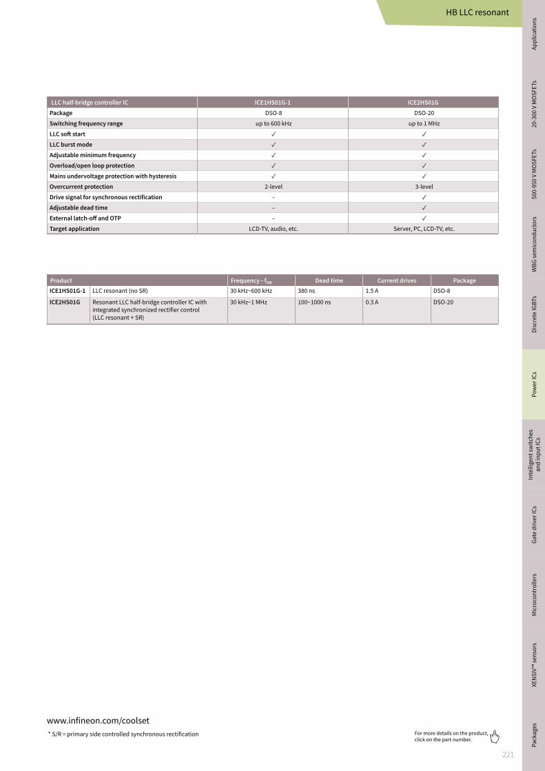
221
For more details on the product, click on the part number.
Product Frequency – fSW Dead time Current drives PackageICE1HS01G-1 LLC resonant (no SR) 30 kHz~600 kHz 380 ns 1.5 A DSO-8
ICE2HS01G Resonant LLC half-bridge controller IC with integrated synchronized rectifier control (LLC resonant + SR)
30 kHz~1 MHz 100~1000 ns 0.3 A DSO-20
www.infineon.com/coolset * S/R = primary side controlled synchronous rectification
HB LLC resonant
LLC half-bridge controller IC ICE1HS01G-1 ICE2HS01GPackage DSO-8 DSO-20
Switching frequency range up to 600 kHz up to 1 MHz
LLC soft start
LLC burst mode
Adjustable minimum frequency
Overload/open loop protection
Mains undervoltage protection with hysteresis
Overcurrent protection 2-level 3-level
Drive signal for synchronous rectification –
Adjustable dead time –
External latch-off and OTP –
Target application LCD-TV, audio, etc. Server, PC, LCD-TV, etc.
Appl
icat
ions
Pa
cka
ges
20
-30
0 V
MO
SF
ETs
50
0-9
50
V M
OS
FE
TsW
BG
se
mic
on
du
cto
rsD
iscr
ete
IGB
TsP
ow
er
ICs
Inte
llig
en
t sw
itch
es
an
d in
pu
t IC
sG
ate
dri
ver
ICs
Mic
roco
ntr
oll
ers
XE
NS
IV™
se
nso
rs

222
For more details on the product, click on the part number.
DC-DC convertersHighest density end-to-end power management solutions
www.infineon.com/power-stages
As the innovation leader for power semiconductor and energy efficiency technologies, we are continually developing and working on the best solutions for your applications. Our DC-DC converter portfolio includes integrated power stages, switching regulators, integrated POL converters and integrated POL voltage regulators, as well as digital multiphase controllers (see page 205)

223
For more details on the product, click on the part number.
OptiMOS™ Powerstage 60 A and 70 A integrated power stages with integrated current and temperature telemetry
Infineon’s integrated OptiMOS™ Powerstage family contains a synchronous buck gate driver IC which is co-packed with control and synchronous MOSFETs and a Schottky diode to further improve efficiency. The package is optimized for PCB layout, heat transfer, driver/MOSFET control timing and minimal switch node ringing when layout guidelines are followed. The paired gate driver and MOSFET combination enables higher efficiency at lower output voltages required by cutting edge CPU, GPU, ASIC and DDR memory designs. The TDA21472 integrated power stages internal MOSFET current sense algorithm, with integrated temperature compensation, achieves superior current sense accuracy versus best-in-class controller based inductor DCR sense methods. Up to 1.0 MHz switching frequency enables high performance transient response, allowing miniaturization of output inductors, as well as input and output capacitors, while maintaining industry-leading efficiency. The TDA21472 is optimized for CPU core power delivery in server applications. The ability to meet the stringent requirements of the server market also makes the TDA21472 ideally suited for powering GPU, ASIC, DDR memory, and other high current designs.
Features › Integrated driver, Schottky diode, control MOSFET and
synchronous MOSFET › 5 mV/A on-chip MOSFET current sensing with temperature
compensated reporting › Input voltage (Vin) range of 4.5 to 15 V › VCC and VDRV supply of 4.5 to 7 V › Output voltage range from 0.25 up to 5.5 V › Output current capability of 70 A › Operation up to 1.0 MHz › VCC undervoltage lockout (UVLO) › 8 mV/°C temperature analog output and thermal flag
pull-up to 3.3 V › Overtemperature protection (OTP) › Cycle-by-cycle self-preservation overcurrent protection (OCP) › MOSFET phase fault detection and flag › Preliminary overvoltage protection (pre-OVP) › Compatible with 3.3 V tri-state PWM input › Body-Braking™ load transient support through PWM tri-state › Diode emulation mode (DEM) for improved light load efficiency › Efficient dual-sided cooling › Small 5.0 x 6.0 x 0.9 mm PQFN package
Applications › High frequency, high current, low profile DC-DC converters › Voltage regulators for CPUs, GPUs, ASICs, and DDR memory arrays
Part type Package Iout[A]
Vin [V]
Vout [V]
Switching frequency [MHz]
TDA21472 5 x 6 x 0.9 mm PQFN 70 4.5 to 15 0.25 to 5.5 1.0
TDA21462 * 5 x 6 x 0.9 mm PQFN 60 4.5 to 15 0.25 to 5.5 1.0
www.infineon.com/integrated-powerstages *For more information on the product, contact our product support
CVIN1
L1
12V
CVIN2
L2
12V
CVIN6
L6
12V
CVIN1_L2
L_L2
12V
V_CPU_L2L
O
A
D
1uF
3.3V
10nF1K
13K12V
VCC
VSEN1
VRTN1
TSEN2
CFILT1uF
VIN_1R VIN 1_1
R VIN 1_2
SV_ALERT#
SV_DAT
SV_CLK
CPU Serial
Bus
VR_HOT#
1K
From
System
VR_EN1
VR_EN2
PROG
SM_DAT
SM_CLKI2C Bus
VSEN_L2
VRTN_L2
GND
L
O
A
D
PWM1
ISEN1
PWM2
ISEN2
PWM6
ISEN6
PWM1_L2
ISEN1_L2
VRDY1
VRDY2
IR35215
VINSEN1
V_CPU_L1
VCCIO
IINSEN
.
.
.
.
.
.
TSEN1
PWR_IN_ALERT#
SM_ALERT#
Cboot1
+5V
TOUT/FLT
PWM
IOUT
REFIN
OC
SE
T
VD
RV
VIN
BO
OT
SW
PGND
GA
TE
L
TDA21472
PHASE
VC
C
EN
VOS
NC
CVCC1 CVDRV1
LGN
D
Cboot2
+5V
TOUT/FLT
PWM
IOUT
REFIN
OC
SE
T
VD
RV
VIN
BO
OT
SW
PGND
GA
TE
L
TDA21472
PHASE
VC
C
EN
VOS
NC
CVCC2 CVDRV2
LGN
D
Cboot6
+5V
TOUT/FLT
PWM
IOUT
REFIN
OC
SE
T
VD
RV
VIN
BO
OT
SW
PGND
GA
TE
L
TDA21472
PHASE
VC
C
EN
VOS
NC
CVCC6 CVDRV6
LGN
D
Cboot1_L2
+5V
TOUT/FLT
PWM
IOUT
REFIN
OC
SE
T
VD
RV
VIN
BO
OT
SW
PGND
GA
TE
L
TDA21472
PHASE
VC
C
EN
VOS
NC
CVCC1_L2 CVDRV1_L2
LGN
D
Rboot1
Rboot2
Rboot6
Rboot1_L2
Integrated power stages
Appl
icat
ions
Pa
cka
ges
20
-30
0 V
MO
SF
ETs
50
0-9
50
V M
OS
FE
TsW
BG
se
mic
on
du
cto
rsD
iscr
ete
IGB
TsP
ow
er
ICs
Inte
llig
en
t sw
itch
es
an
d in
pu
t IC
sG
ate
dri
ver
ICs
Mic
roco
ntr
oll
ers
XE
NS
IV™
se
nso
rs

224
For more details on the product, click on the part number.
OptiMOS™ Powerstage 70 A power stage with exposed top for improved thermal performance
Infineon’s TDA21475 exposed-top power stage contains a low quiescent-current synchronous buck gate driver IC co-packaged with high-side and low-side MOSFETs. The package is optimized for PCB layout, heat transfer, driver/MOSFET control timing, and minimal switch node ringing when layout guidelines are followed. The gate driver and MOSFET combination enables higher efficiency at the lower output voltages required by cutting edge CPU, GPU and DDR memory designs. The TDA21475 internal MOSFET current sense algorithm with temperature compensation achieves superior current sense accuracy versus best-in-class controller-based inductor DCR sense methods. Protection includes cycle-by-cycle over current protection with programmable threshold, VCC/VDRV UVLO protection, bootstrap capacitor un-dervoltage protection, phase fault detection, IC temperature reporting and thermal shutdown. The TDA21475 also features auto replenishment of the bootstrap capacitor to prevent overdischarge. The TDA21475 features a deep-sleep power saving mode, which greatly reduces the power consumption when the multiphase system enters PS3/PS4 mode. Operation at switching frequency as high as 1.5 MHz enables high performance transient response, allowing reduction of output inductance and output capacitance while maintaining industry-leading efficiency. The TDA21475 is optimized for CPU core power delivery in server applications. The ability to meet the stringent requirements of the server market also makes the TDA21475 ideally suited for powering GPU and DDR memory designs.
Features › Co-packaged driver, high-side and low-side MOSFETs › 5 mV/A on-chip MOSFET current sensing with temperature
compensated reporting Input voltage (VIN) range of 4.25 to 16 V › VCC and VDRV supply of 4.25 to 5.5 V › Output voltage range from 0.25 up to 5.5 V output current
capability of 70 A operation up to 1.5 MHz › VCC/VDRV undervoltage lockout (UVLO) Bootstrap capacitor
undervoltage protection 8 mV/°C temperature analog output › Thermal shutdown and fault flag › Cycle-by-cycle over current protection with programmable
threshold and fault flag MOSFET phase fault detection and flag › Auto replenishment of bootstrap capacitor Deep-sleep
mode for power saving Compatible with 3.3 V tri-state PWM input Body-Braking™ load transient support Small 5 x 6 x 0.65 mm PQFN package
› Lead-free RoHS compliant package › Integrated driver, Schottky diode, control MOSFET and
synchronous MOSFET
Applications › High frequency, high current, low profile DC-DC converters › Voltage regulators for CPUs, GPUs, ASICs, and DDR memory arrays
Part type Package Iout[A]
Vin [V]
Vout [V]
Switching frequency [MHz]
TDA21475 * 5 x 6 x 0.9 mm PQFN 70 4.25 to 16 0.25 to 5.5 1.5
www.infineon.com/integrated-powerstages
CVIN1
L1
12V
CVIN2
L2
12V
CVIN6
L6
12V
CVIN1_L2
L_L2
12V
V_CPU_L2L
O
A
D
1uF
3.3V
10nF1K
13K12V
VCC
VSEN1
VRTN1
TSEN2
CFILT1uF
VIN_1R VIN 1_1
R VIN 1_2
SV_ALERT#
SV_DAT
SV_CLK
CPU Serial
Bus
VR_HOT#
1K
From
System
VR_EN1
VR_EN2
PROG
SM_DAT
SM_CLKI2C Bus
VSEN_L2
VRTN_L2
GND
L
O
A
D
PWM1
ISEN1
PWM2
ISEN2
PWM6
ISEN6
PWM1_L2
ISEN1_L2
VRDY1
VRDY2
IR35215
VINSEN1
V_CPU_L1
VCCIO
IINSEN
.
.
.
.
.
.
TSEN1
PWR_IN_ALERT#
SM_ALERT#
Cboot1
+5V
TOUT/FLT
PWM
IOUT
REFIN
OC
SE
T
VD
RV
VIN
BO
OT
SW
PGND
GA
TE
L
TDA21475
PHASE
VC
C
EN
VOS
NC
CVCC1 CVDRV1
LGN
D
Cboot2
+5V
TOUT/FLT
PWM
IOUT
REFIN
OC
SE
T
VD
RV
VIN
BO
OT
SW
PGND
GA
TE
L
TDA21475
PHASE
VC
C
EN
VOS
NC
CVCC2 CVDRV2
LGN
D
Cboot6
+5V
TOUT/FLT
PWM
IOUT
REFIN
OC
SE
T
VD
RV
VIN
BO
OT
SW
PGND
GA
TE
L
TDA21475
PHASE
VC
C
EN
VOS
NC
CVCC6 CVDRV6
LGN
D
Cboot1_L2
+5V
TOUT/FLT
PWM
IOUT
REFIN
OC
SE
T
VD
RV
VIN
BO
OT
SW
PGND
GA
TE
L
TDA21475
PHASE
VC
C
EN
VOS
NC
CVCC1_L2 CVDRV1_L2
LGN
D
Rboot1
Rboot2
Rboot6
Rboot1_L2
Integrated power stages
*For more information on the product, contact our product support

225
For more details on the product, click on the part number.
OptiMOS™ Powerstage 20 A power stage with integrated current sense
Infineon’s IR35401 integrated power stage contains a synchronous buck gate driver IC, which is co-packaged with control and synchronous MOSFETs and Schottky diode to further improve efficiency. The package is optimized for PCB layout, heat transfer, driver/MOSFET control timing, and minimal switch node ringing when layout guidelines are followed. The paired gatedriver and MOSFET combination enables higher efficiency at lower output voltages required by cutting edge CPU, GPU and DDR memory designs. The IR35401 power stage features an integrated current sense amplifier to achieve superior current-sense accuracy against best-in-class controller-based inductor DCR sense methods while delivering the clean and accurate current report information. The protection features inside IR35401 include VCC UVLO and thermal flag. IR35401 also features an auto replenishment of bootstrap capacitor to prevent the bootstrap capacitor from overdischarging. The IR35401 supports deep-sleep mode and consumes <100 µA VCC bias current when the EN pin is pulled low. Up to 1.5 MHz switching frequency enables high performance transient response, allowing miniaturization of output inductors, as well as input and output capacitors while maintaining industry-leading efficiency. When combined with Infineon’s digital controllers, the IR35401 incorporates the Body-Braking™ feature through PWM tri-state which enables reduction of output capacitors. The IR35401 is optimized for low current CPU rails in server applications. The ability to meet the stringent requirements of the server market also makes the IR35401 ideally suited for powering GPU and DDR memory rails.
Features › Integrated driver, control MOSFET and synchronous MOSFET › Integrated bootstrap synchronous PFET › Inductor DCR current sensing with temperature compensation › Input voltage (VIN) range from 4.25 to 16 V › VCC supply of 4.25 to 5.5 V › Output voltage range from 0.5 to 3 V or up to 5.5 V if the
internal current sense amplifier is not used › Local lossless inductor current sensing with improved noise
immunity and accuracy › Single reference based current reporting output › Output current capability of 20 A › Operation up to 1.5 MHz › VCC undervoltage lockout › Over-temperature and VCC UVLO fault communication to
controller via TOUT pin › Compatible with 3.3 V tri-state PWM Input › Body-Braking™ load transient support through PWM tri-state › Auto-replenishment on BOOST pin › Low operating quiescent current and <100 µA when disabled › Small 4 x 5 x 0.9 mm PQFN package › Lead-free RoHS compliant package
Applications › General purpose POL DC-DC converters › Voltage regulators for CPUs, GPUs, ASICs, and DDR
memory arrays
Part type Package Iout[A]
Vin [V]
Vout [V]
Switching frequency [MHz]
IR35401 * 4 x 5 x 0.9 mm PQFN 20 4.25 to 16 0.5 to 5.5 1.5
www.infineon.com/integrated-powerstages
CVIN1Cboost1
L1
12V
+5V
CVIN3Cboost3
L3
12V
CVIN1_L2
L1_L2
12V
V_CPU_L2L
O
A
D
1uF
3.3V
10nF1K
13K12V
VCC
VSEN1
VRTN1
CFILT1uF
VIN_1R VIN 1_1
R VIN 1_2
SV_ALERT#
SV_DIO
SV_CLK
CPU Serial
Bus
VRHOT_ICRIT#
1K
VSEN2
VRTN2GND
L
O
A
D
PWM1
ISEN1
PWM3
ISEN3
PWM1_L2
ISEN1_L2
VRDY1
VRDY2
CVDRV1
+5V
CVDRV3
Cboost1_L2
+5V
CVDRV1_L2
VIN
BO
OS
T
SW
PGND
GATEL
IR35411
LGND
PHASE
VIN
BO
OS
T
SW
PGND
GATEL
IR35411
LGND
PHASETOUT/FLT
PWM
IOUT
REFIN
VOS
TOUT/FLT
PWM
IOUT
REFIN
VOS
.
.
.
VINSEN1
V_CPU_L1
VCCIO
ADDR_PROT
/PROGh 1K
10nF
TSEN1
r13K
TSEN2
IOUT
VCC
PWM
REFIN
VIN
BO
OS
T
SW
PGNDIR35401
LGND
PHASE
CSIN+
CSIN-
VC
C
EN
OC
SE
T
VD
RV
VC
C
EN
OC
SE
T
VD
RV
From
System
VR_EN1
VR_EN2
SM_DAT
SM_CLKI2C Bus
SM_ALERT
10nF1K1K
EN
TOUT/FLTRboost1_L2
Rboost3
Rboost1
IR352XX
Integrated power stages
*For more information on the product, contact our product support
Appl
icat
ions
Pa
cka
ges
20
-30
0 V
MO
SF
ETs
50
0-9
50
V M
OS
FE
TsW
BG
se
mic
on
du
cto
rsD
iscr
ete
IGB
TsP
ow
er
ICs
Inte
llig
en
t sw
itch
es
an
d in
pu
t IC
sG
ate
dri
ver
ICs
Mic
roco
ntr
oll
ers
XE
NS
IV™
se
nso
rs

226
For more details on the product, click on the part number.
OptiMOS™ Powerstage 25 A, 35 A, 40 A integrated power stages with highest efficiency on smallest form factor
Infineon’s TDA21240 powerstage is a multichip module that incorporates Infineon’s premier MOSFET technology for a single high-side and a single low-side MOSFET coupled with a robust, high performance, high switching frequency gate driver in a single PG-IQFN-30-2 package. The optimized gate timing allows for significant light load efficiency improvements over discrete solutions. When combined with Infineon’s family of digital multi-phase controllers, the TDA21240 forms a complete core voltage regulator solution for advanced micro and graphics processors as well as point-of-load applications.
Features › For synchronous buck converter step
down voltage applications › Maximum average current of 40 A › Input voltage range +4.5 V to +16 V › Power MOSFETs rated 25 V › Fast switching technology for improved
performance at high switching frequencies (> 500 kHz)
› Remote driver disable function › Includes bootstrap diode › Undervoltage lockout › Shoot through protection › +5 V high side and low side MOSFETs
driving voltage › Compatible to standard +3.3 V PWM
controller integrated circuits › Tri-state PWM input functionality › Small package: PG-IQFN-30-2 (4 x 4 x 1 mm) › RoHS compliant › Thermal warningApplications
› Desktop and server VR buck converter › Single-phase and multiphase POL › CPU/GPU regulation in notebook, desktop graphics cards,
DDR memory, graphic memory › High power density voltage regulator modules (VRM) › Qualified for DC-DC industrial applications based on JEDEC
(JESD47, JESD22, J-STD20) › General purpose POL DC-DC converters
www.infineon.com/integrated-powerstages
Part type Package Iout[A]
Vin [V]
Switching frequency [MHz]
TDA21242 4 x 4 x 1 mm PQFN 25 4.5 to 16 1.0
TDA21241 4 x 4 x 1 mm PQFN 35 4.5 to 16 1.0TDA21240 4 x 4 x 1 mm PQFN 40 4.5 to 16 1.0
PXE1210J
Power Stage
Power Stage
Power Stage
Integrated
Integrated
Integrated
Integrated power stages

227
For more details on the product, click on the part number.
DC-DC converters Robust range of controllers and regulators for the widest application spectrum
Our high-efficiency switching regulators and controllers help to reduce energy consumption. In addition to extending the operating time of battery powered systems, they also significantly improve the thermal budget of the application. Overall, this translates into minimal operating costs. For your design flexibility, they are available as adjustable voltage variants as well as with dedicated fixed output voltage values.
Soft-start rampgenerator
Charge pump
Bandgapreference
Overtemperatureshutdown
Enable
Buckconverter
Oscillator
Feed forward
7EN
IFX91041
VS
3
BUO
BDS
FB1
2
8
5
COMP
SYNC
GND
6
4
45 V
≤1 A≥2 A
>1 A
> 45 V … 60 VMaximum input voltage
Output current
IFX901215 V
2.2 MHz
500 mA
IFX91041Adj., 5 V, 3.3 V
370 kHz
1.8 A
IFX80471Adj., 5 V
60 V, 360 kHz
2.3 A
IFX81481Adj.
Synchronouscontroller
10 A
Output current
IFX91041 block diagram Industrial DC-DC buck regulators (selection tree)
Part number VQ (multiple) Output current type
Output current[A]
Product features Package
IFX81481ELV Adjustable Buck controller 10.0 10 A synchronous DC-DC adjustable step down controller; f = 100 kHz-700 kHz, N
PG-SSOP-14
IFX90121EL V50 5.0 V Buck converter 0.5 Vin up to 45 V, 2.2 MHz step-down regulator with low quiescewnt current PG-SSOP-14
IFX80471SK V Adjustable Buck controller 2.3 Vin up to 60 V; VQ adjustable from 1.25 V up to 15 V; external MOSFET PG-DSO-14
IFX80471SK V50 5.0 V Buck controller 2.3 Vin up to 60 V; external MOSFET PG-DSO-14
IFX91041EJV Adjustable Buck converter 1.8 VQ adjustable from 0.6 V up to 16 V; tolerance 2% up to 1000 mA PG-DSO-8
IFX91041EJ V33 3.3 V Buck converter 1.8 VQ fixed to 3.3 V; tolerance 2% up to 1000 mA PG-DSO-8
IFX91041EJ V50 5.0 V Buck converter 1.8 VQ fixed to 5.0 V; tolerance 2% up to 1000 mA PG-DSO-8
DC-DC converters
www.infineon.com/industrial-dcdc-converters
Features and benefits
Key benefits
High-efficiency regulation
Only a few external components needed for stable regulation
Perfectly suited for regulation in pre-/post-regulation power supply architectures
Key features
Input voltage up to 60 V
Output currents going from 500 mA up to 10 A
Switching frequencies ranging from 100 kHz to 2.2 MHz
Shutdown quiescent current down to below 2 µA
Current limitation and overtemperature protection
Enable feature
Switching regulators
Appl
icat
ions
Pa
cka
ges
20
-30
0 V
MO
SF
ETs
50
0-9
50
V M
OS
FE
TsW
BG
se
mic
on
du
cto
rsD
iscr
ete
IGB
TsP
ow
er
ICs
Inte
llig
en
t sw
itch
es
an
d in
pu
t IC
sG
ate
dri
ver
ICs
Mic
roco
ntr
oll
ers
XE
NS
IV™
se
nso
rs

228
For more details on the product, click on the part number.
Integrated POL voltage regulators Highest density high efficiency integrated POL (IPOL) for smart enterprise systems
Infineon’s integrated POL switching converters deliver benchmark efficiency and dramatically reduce system size. Solutions up to 35 A are available in compact PQFN packages. Target applications include server, storage, routers and switches, telecom base stations, digital home media, mobile computing and embedded data processing. Solutions with and without PMBus digital communication are available in single output and multi-rail format.
Ready-to-go reference designs and the on-line PowerDesk simulator simplify the task of designing regulated voltage rails. Different control topologies are available to meet an application’s specific requirements.
*Coming soon
www.infineon.com/ipolwww.infineon.com/analog-ipol
DC-DC products 1 to 35 A
› Telemetry › Margining › Intel SVID Support › Parallel VID › IR3806x: 6-35 A with PMBus™ › IR3816x: 15 A, 30 A with PMBus™ and Intel SVID › IR38263: 30 A with PVID and PMBus™
IPOL with digital interface
PMBus™ digital IPOL Constant on-time IPOL
Easy/light-load efficiencyIR3883MTRPBF (3 A), IR3888MTRPBF (25 A),
IR3889MTRPBF (30 A), IR3887MTRPBF * (30 A)
VIN
PGOOD
SC
LS
DA
SA
lert
RS+RS–
PVIN Boot
SWVOPower
good
Vin
Inventory
Configuration
Control
Telemetry
Status
Device ID
On/o configuration
fault/warnings
Sequencing delay/ramp
fault response
Vout, Iout, power
temperature, peak values
Comms, data, temps
Digital mode: I2C/PMBus™ interface
Dierential remote sense for
optimum output accuracy
PMBus™ IC capabilities
Point-of-load products – how to choose
Switching regulators
PGood
4.3 V < Vin< 17V
Enable
Vo
IR3887MTRPBF*
Boot
Vcc/LDO
Fb
AGnd PGnd
SW
PGood
Enable PVinVin
SS/Latch
Ton/Mode
VSENMILIM
Phase
GATEL
PGood
4.3 V < Vin< 14V
(optional)
IR3883MTRPBF
Boot
Vcc
Vo
Fb
Gnd PGnd OCset
SW
PGood
En/FCCM PVinVin
PGND

229
For more details on the product, click on the part number.
Integrated point-of-load converters IR3806x series (6 A /15 A / 25 A / 35 A) Digital interface IPOL voltage regulators
The digital interface IPOL devices are easy-to-use, fully integrated and highly efficient DC-DC regulator offering I2C/PMBus™, parallel VID, Intel SVID. The on-board PWM controller and MOSFETs make the family a space-efficient solution, providing accurate power delivery for low output voltage and high current applications.
The IR3806x family of PMBus™ enabled IR MOSFET™ IPOL based IR MOSFET IPOL voltage regulators offers: › Compactness of integrated controller, driver and MOSFETs › High performance analog voltage mode engine › Flexibility of a rich PMBus™ interface
The IR381(2/3)6x family features OptiMOS™ 5 for the highest efficiency and adds Intel SVID support (IR381(/3)6x) for Intel based systems or parallel VID (IR3826x) for voltage scaling or 8 programmable output voltages booting options to avoid programming at start up. Pin compatible options with and without PMBus™ are available to allow the flexibility of using PMBus™ only during evaluation or easily upgrade a system to PMBus™ without re-layout.
www.infineon.com/ipol
Part number Max. current [A]
Package size [mm]
Max. Vin Max. fsw Distinctive features
IR38064MTRPBF 35 5 x 7 21 V 1500 KHz
PMBus™IR38063M 25 5 x 7 21 V 1500 KHz
IR38062M 15 5 x 7 21 V 1500 KHz
IR38060M 6 5 x 6 16 V 1500 KHz
IR38163M 30 5 x 7 16 V 1500 KHz OptiMOS™ 5, SVID + PMBus™
IR38165M 30 5 x 7 16 V 1500 KHz OptiMOS™ 5, SVID
IR38363M 15 5 x 7 16 V 1500 KHz OptiMOS™ 5, SVID + PMBus™
IR38365M 15 5 x 7 16 V 1500 KHz OptiMOS™ 5, SVID
IR38263M 30 5 x 7 16 V 1500 KHz OptiMOS™ 5, PVID + PMBus™
IR38265M 30 5 x 7 16 V 1500 KHz OptiMOS™ 5, PVID
IR38164M 30 5 x 7 16 V 1500 KHz OptiMOS™ 5, SVID + PMBus™, enhanced Imon
IRPS5401M 4+4+2+2+0.5 7 x 7 14 V 1500 KHz 5 output PMIC, PMBus™
Digital interface IPOL
Features and benefits
Key features
PMBus™ revision 1.2 compliant
≥ 66 PMBus™ commands
Wide input voltage range and single 5 V – 16 V input operations
Differential remote sense
Ultralow jitter voltage mode eingine
Operation temp: -40° to 125° C
Key benefits
Only single chip solution with extensive PMBus™, parallel VID, Intel SVID support allows 50 percent space saving versus external power competition
Intel SVID support for Intel-based systems
Parallel VID or PMBus™ for voltage setting and margining
Telemetry status via digital bus
Remote monitoring and update
Parameter changes by register
Flexible sequencing
High accuracy low ripple
Integrated sequencing, margin, current and voltage monitoring
Switching regulators
Appl
icat
ions
Pa
cka
ges
20
-30
0 V
MO
SF
ETs
50
0-9
50
V M
OS
FE
TsW
BG
se
mic
on
du
cto
rsD
iscr
ete
IGB
TsP
ow
er
ICs
Inte
llig
en
t sw
itch
es
an
d in
pu
t IC
sG
ate
dri
ver
ICs
Mic
roco
ntr
oll
ers
XE
NS
IV™
se
nso
rs

230
For more details on the product, click on the part number.
www.infineon.com/ipol
OptiMOS™ IPOL voltage regulators with COTEasy to use with no external compensation and smallest BOM
OptiMOS™ IR3883MTRPBF, IR3887MTRPBF *, IR3889MTRPBF, and IR3888MTRPBF integrated point-of-load DC-DC devices are easy-to-use, fully integrated and highly efficient DC-DC regulators that operate from a wide input voltage range and provide up to 30 A continuous current. The devices increase efficiency and power density and simplify design for POL applications in server, enterprise storage, netcom router and switches, datacom and telecom base stations.
Block diagram IR3883M Block diagram IR3887M (30 A)
Analog interface IPOL
Part number Max. current [A]
Package size [mm]
Max. Vin Max. fsw Distinctive features
IR3883MTRPBF 3 3 x 3 14 V 800 KHz Constant-on-time (COT)
IR3888MTRPBF 25 5 x 6 17 V 2000 KHz
IR3887MTRPBF * 30 4 x 5 17 V 2000 KHz
IR3889MTRPBF 30 5 x 6 17 V 2000 KHz
Switching regulators
PGood
4.3 V < Vin< 14V
(optional)
IR3883MTRPBF
Boot
Vcc
Vo
Fb
Gnd PGnd OCset
SW
PGood
En/FCCM PVinVin
PGND
PGood
4.3 V < Vin< 17V
Enable
Vo
IR3887MTRPBF*
Boot
Vcc/LDO
Fb
AGnd PGnd
SW
PGood
Enable PVinVin
SS/Latch
Ton/Mode
VSENMILIM
Phase
GATEL
Main benefits
Main benefits
Enhanced Voltage Mode PWM devices offer high accuracy, ultralow ripple and noise, and higher control bandwidth for less capacitors.
Scalable solution from 3A up to 35A.
For designs requiring high density, low cost and easy design, the family includes a 3A device with Enhanced Stability Constant-on-Time (CoT) engine that does not require external compensation enabling easy designs and fast time to market.
Quiescent current down to 5 µA
Overload, overtemperature, short circuit and reverse-polarity protection
Low current consumption
Extended temperature range -40°C ... +125°C
*Coming soon

231
For more details on the product, click on the part number.
Voltage regulators Energy-efficient voltage regulators and trackers
Our linear voltage regulators and trackers help to reduce energy consumption, extending operating time and minimizing operating costs across all kinds of systems. The wide supply voltage range, low quiescent current, rich protective feature set and choice of packages make our devices the perfect fit across a broad application spectrum, apart from automation systems as well for heath care, traffic, power tools, lighting and many other multi-market systems. Our trackers are ideal as additional supplies for off-board loads to increase system reliability
20 V
≤500 mA ≥500 mA<500 mA>500 mA
> 20 V ... 60 V
2 3
3
3
4
5
72
Maximum input voltage
Output current
IFX54441EJ V
Adj., 3.3 V, 5 V
EN, rev. pol, 2%
300 mA
IFX1117
Adj., 3.3 V
2% accuracy
800 mA
IFX1763
Adj., 3.3 V, 5 V
EN, rev. pol, 2.5%
500 mA
1
Output current
Low quiescent current
2 Low noise behavior
3 Small package
4 Tracker! High accuracy
5 Ultra low quiescent current
7 Very low dropout
IFX1963
Adj.
EN, rev. pol, 1.5%
1500 mA
IFX20001
3.3 V, 5 V
EN, rev. pol, 4%
30 mA
IFX20002
3.3 V, 5 V
EN, rev. pol, 4%
30 mA
IFX54211
3.3 V
EN
150 mA
IFX24401
5 V
EN, 2%
300 mA
IFX25001
3.3 V, 5 V
45 V, rev. pol, 4%
400 mA
IFX21401
0.5%
50 mA
Output current
IFX27001
Adj.,
3.3 V, 5 V
40 V, 3%
1000 mA
IFX25401
Adj., 5 V
EN, rev. pol, 2%
400 mA
IFX4949
RST, 1%
100 mA
IFX2931
5 V
100 mA
IFX30081
Adj., 3.3 V
50 mA
Industrial linear voltage regulator (selection tree)
www.infineon.com/industrial-voltage-regulators
Features and benefits
Key features
Input voltage up to 60 V
Output current up to 1.5 A
Output voltage adjustable or fixed to specific values
Quiescent current down to 5 µA
Overload, overtemperature, short circuit and reverse-polarity protection
Low current consumption
Extended temperature range -40°C ... +125°C
Key benefits
Pin-to-pin compatibility with industry-standard parts
Very low dropout voltageTrackers for optimized heat distribution and external protection
Trackers for maximum system cost reduction
Small robust packages
Voltage regulators
Infineon's microcontroller families and industrial voltage regulatorsMicrocontroller family Input voltage [V] Input current (max.) [mA] Voltage regulator
XMC1000 family 1.8 to 5.5 <100 IFX54211/IFX2931/IFX4949/IFX25001/IFX544xx */ IFX30081
XMC4000 family 3.3 <500/300 IFX1763/IFX544xx */IFX1117/IFX30081
XC8xx 3.3 to 5.0 200 IFX20001/IFX30081/IFX21401/IFX4949/IFX544xx *
XE166/XC2000 1.5 and 3.3 or 5.0 100 IFX25401/IFX24401/IFX2931/IFX4949/IFX1763/IFX54441
TriCore™ 1.5 to 3.3 >400 IFX27001/IFX91041/IFX80471/IFX25001/IFX1117
* For more information on the product, contact our product support
Appl
icat
ions
Pa
cka
ges
20
-30
0 V
MO
SF
ETs
50
0-9
50
V M
OS
FE
TsW
BG
se
mic
on
du
cto
rsD
iscr
ete
IGB
TsP
ow
er
ICs
Inte
llig
en
t sw
itch
es
an
d in
pu
t IC
sG
ate
dri
ver
ICs
Mic
roco
ntr
oll
ers
XE
NS
IV™
se
nso
rs

232
For more details on the product, click on the part number.
Integrated class D audio amplifier ICs Cooler, smaller and lighter class D audio amplifiers for great sounding products
Infineon’s MERUS™ audio solutions enable audio designers to improve the performance of their products, while increasing efficiency and reducing solution size. Advances in semiconductor processes in combination with new innovative architectures are behind a portfolio of class D technologies that allow professional, commercial/home and portable audio applications to benefit from unparalleled performance, power density and reliability. The broad portfolio covers power ranges from 20W to 2kW per channel from the smallest single-chip devices and multi-chip module (MCMs) to highly scalable discrete audio amplifier solutions consisting of powerful MOSFET/CoolGaN™ enhancement mode (e-mode) HEMT and driver ICs combinations.
By combining our core principles, competencies, and leadership in groundbreaking power semiconductors with revolutionary audio amplifier technologies, such as MERUS™, we provide solutions that are smaller, lighter, more robust and flexible, running with less heat dissipation. In addition to outstanding quality and reliability, Infineon’s amplifier solutions are designed to maximize power efficiency and dynamic range while providing best-in-class performance in product form factors that make them an optimal fit for any high-end application. These include portable/battery powered applications, voice controlled active speakers, television sets, stereo HiFi, soundbars, monitors, power-over-ethernet (PoE) and multichannel systems.
www.infineon.com/merus
Exceptional audio performance
Maximized power efficiency
Maximized output power
Design freedom
Fast time to market
Design with Infineon’s solutions to benefit from:
Output power [W/Channel]
Scalable in output power Best audio performanceHighest power w/o heatsinkLowest idle power
No heatsink
20
Digi
tal i
nput
Anal
og in
put
100 1000 2000
w/gate buffer
IRS209X (1 ch) + CoolGaN™ 400 V e-mode HEMTs
IRS2092 (1 ch) + MOSFETs
IRS2052 (2 ch) + MOSFETs
IRS2093 (4 ch) + MOSFETs
IR43x1 (1 ch)
IR43x2 (2 ch)
MA12040 (1– 4 ch)
MA12070 (1– 4 ch)
MA12040P (1– 4 ch)
MA12070P (1– 4 ch)
Inte
grat
edIC
sIC
s + M
OSF
ETs/
e-m
ode
GaN
Audio amplifier ICs

233
For more details on the product, click on the part number.
Integrated MERUS™ multilevel amplifier ICs for class D audio solutions High power efficiency and density in small packages
With its revolutionary MERUS™ integrated multilevel class D audio amplifier ICs, Infineon is leading in efficiency and power density. Compared to traditional class D amplifier ICs, which produce only two voltage output levels, multilevel amplifier ICs use additional on-chip MOSFETs and capacitors to produce outputs with a higher signal granularity i.e. higher switching frequencies and/or multiple output signal levels - typically up to five voltage levels
www.infineon.com/merus
Wireless audio
Features and benefits
Key features
Multilevel switching technology
Scalable signal “granularity”
Proprietary circuits architecture
Key benefits
Highest efficiency and power density
Potential LC filter removal
Low THD+N
Cooler operation
Low power loss
Virtually no switching loss measurable in idle mode
Filterless topology with “flying capacitor” of an integrated class D IC
PWMmodulator
Protection
Multilevel amplifiers
PVDO
Efficiency where it matters for audio reproduction
For MERUS™ integrated multilevel audio amplifier ICs, amplifier efficiency at average output power is key. As the graph on the left shows, MERUS™ multilevel amplifier is much more effective than the traditional class D ampli-fier, which translates into less power consumption in AC input and in battery powered audio applications.
Audio amplifier ICs
Appl
icat
ions
Pa
cka
ges
20
-30
0 V
MO
SF
ETs
50
0-9
50
V M
OS
FE
TsW
BG
se
mic
on
du
cto
rsD
iscr
ete
IGB
TsP
ow
er
ICs
Inte
llig
en
t sw
itch
es
an
d in
pu
t IC
sG
ate
dri
ver
ICs
Mic
roco
ntr
oll
ers
XE
NS
IV™
se
nso
rs

234
For more details on the product, click on the part number.
MERUS™ integrated audio amplifier multi-chip modules (MCM) Integrated components for scalable output power and superb audio performance
Multi-chip modules integrate PWM controller and power MOSFETs in a single package to offer a highly efficient, compact solution that reduces component count, shrinks PCB size up to 70 percent, and simplifies class D amplifier design.
www.infineon.com/merus
Wireless audio
Features and benefits
Key features
Single package with integrated PWM controller and audio-performance- optimized power MOSFET
Overcurrent protection
Thermal shutdown
Floating differential input
Clip detection
Best-in-class power efficiency and audio performance
Lower component count, leading to design simplification
Compatible with single supply or split rail configuration
Click noise reduction
Key benefits
Extended battery playback time
Unrivalled audio performance
Smaller solution size (BOM reduction, system level cost savings)
Eliminated need for heatsink
High noise immunity
Reliable operation
Thermal efficiency
Multi-chip audio amplifier module
PWMmodulator
Analog input class D driver family
Protection
PowerMOSFETs
LPF
Gate driver
Multi-chip audio amplifier module
PWM input class D driver family
Audio amplifier ICs

235
For more details on the product, click on the part number.
Discrete MERUS™ audio amplifier driver ICs with MOSFET and gallium nitride CoolGaN™ 400V e-mode HEMTsScalable output power with a unified design platform
Infineon’s discrete audio solutions are scalable to various output power levels, simply by replacing the external MOSFETs or CoolGaN™ e-mode HEMTs of the driver-transistor combinations. Key parameters for the transistors used in discrete class D audio applications include on-state resistance (RDS(on)), gate charge (QG), and reverse recovery charge (Qrr). Our products are specifically suitable for class D audio applications and optimized for these parameters to achieve maximized efficiency, THD and EMI amplifier performance. The CoolGaN™ 400V e-mode HEMTs portfolio is specifically built for class D audio requirements, with high performing SMD packages to fully utilize the benefits of gallium nitride.
Audio solution overview
Wireless audio
www.infineon.com/merus
Features and benefits
Key benefits
Unified design platform
Scalable output power up to over 2 kW per channel
Simple yet effective - exchange of external MOSFET triggers alteration in output power level
Best-in-class power efficiency
Key advantages
Superior audio performance
Increased reliability
Unique audio experience
PWM
modulator
PWM Input class D driver family
Analog input class D driver family
Protection
Gate driver
Digital audio
MOSFET
Integrated PowIRAudio class D driver family
MERUS™ Audio IC, MCM,Multi-level IC
StrongIRFET™OptiMOS™, CoolMOS™
40~600 V
Switch mode power supplies – Energy efficiency on it's next level!Dedicated Class D SMPS from 100~500 W
Audio amplifier ICs
Appl
icat
ions
Pa
cka
ges
20
-30
0 V
MO
SF
ETs
50
0-9
50
V M
OS
FE
TsW
BG
se
mic
on
du
cto
rsD
iscr
ete
IGB
TsP
ow
er
ICs
Inte
llig
en
t sw
itch
es
an
d in
pu
t IC
sG
ate
dri
ver
ICs
Mic
roco
ntr
oll
ers
XE
NS
IV™
se
nso
rs

236
For more details on the product, click on the part number.
www.infineon.com/merus
*All ICs carry a full protection scheme comprising undervoltage lockout, overtemperature warning/error, short circuit/overload protection, power stage pin-to-pin short circuit, error reporting through serial interface (I2C), and DC protection
MERUS™ integrated multilevel audio amplifier IC product portfolio
Integrated class D audio amplifier IC portfolio
MA12040 MA12040P MA12070 MA12070P
Specifications
Number of audio channels 2xBTL 2xBTL 2xBTL 2xBTL
Max. peak power @ 4 ohm 10% THD 2x40 W 2x40 W 2x80 W 2x80 W
Supply voltage 4-18 V 4-18 V 4-26 V 4-26 V
3-level and 5-level modulation
Max. PWM frequency 726 kHz
Audio input Analog Digital Analog Digital
HiRes audio compliant
Volume and dynamic range control
Idle power dissipationMax. output and all channels switching <100 mW <110 mW <160 mW <160 mW
Audio performance (PMP2)>107dB DNR
55 µV output noise0.003% THD+N
>98dB DNR135 µV output noise
0.006% THD+N
>110dB SNR 45 µV output integrated
0.004% THD+N
101dB SNR140 µV output noise
0.007% THD+N
Features
Comprehensive protection scheme *
Configurable for SE or PBTL operation
I2C communication
Filterless implementation
Package type64-pin QFN package with
exposed thermal pad
64-pin QFN package with exposed
thermal pad
64-pin QFN package with exposed
thermal pad
64-pin QFN package with exposed
thermal pad
Evaluation boards EVAL_AUDIO_MA12040 EVAL_AUDIO_MA12040P EVAL_AUDIO_MA12070 EVAL_AUDIO_MA12070P
MERUS™ integrated audio amplifier multi-chip modules (MCMs)
IR4301M IR4321M IR4311M IR4302M IR4322M IR4312M
Specifications
Number of audio channels 1 1 1 2 2 2
Max. power per channel 160 W 90 W 45 W 130 W 100 W 40 W
Supply voltage ~ ± 31 V or 62 V ~ ± 25 V or 50 V ~ ± 15 V or 30 V ~ ± 31 V or 62 V ~ ± 25 V or 50 V ~ ± 16 V or 32 V
Max. PWM frequency 500 kHz 500 kHz 500 kHz 500 kHz 500 kHz 500 kHz
Features
Differential audio input
Over-current protection
Integrated power MOSFET
Voltage 80 V 60 V 40 V 80 V 60 V 40 V
PWM controller
Thermal shutdown
Click noise reduction
Clip detection
Package type 5 x 6 mm QFN 5 x 6 mm QFN 5 x 6 mm QFN 7 x 7 mm QFN 7 x 7 mm QFN 7 x 7 mm QFN
Evaluation boards IRAUDAMP12 IRAUDAMP19 IRAUDAMP21 IRAUDAMP15 IRAUDAMP16
IRAUDAMP17 IRAUDAMP22 IRAUDAMP18
Audio amplifier ICs
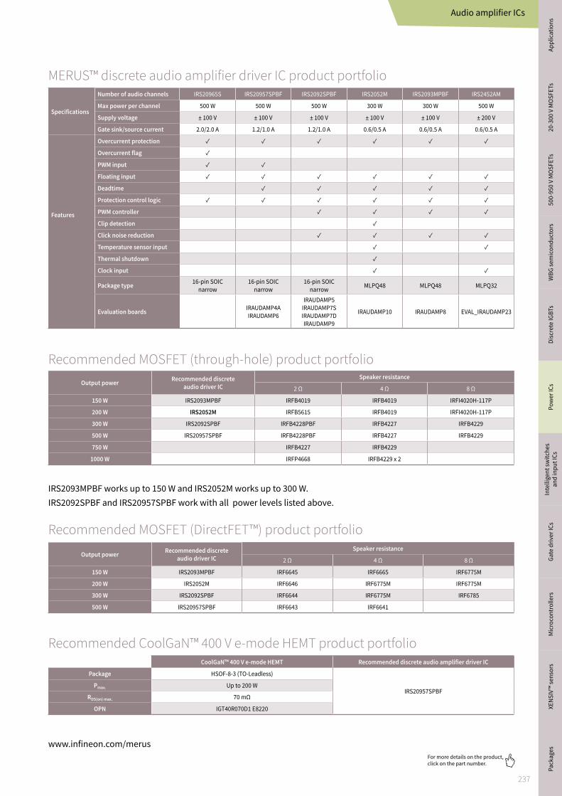
237
For more details on the product, click on the part number.
www.infineon.com/merus
IRS2093MPBF works up to 150 W and IRS2052M works up to 300 W. IRS2092SPBF and IRS20957SPBF work with all power levels listed above.
Recommended MOSFET (through-hole) product portfolio
Recommended MOSFET (DirectFET™) product portfolio
Recommended CoolGaN™ 400 V e-mode HEMT product portfolio
Specifications
Number of audio channels IRS20965S IRS20957SPBF IRS2092SPBF IRS2052M IRS2093MPBF IRS2452AM
Max power per channel 500 W 500 W 500 W 300 W 300 W 500 W
Supply voltage ± 100 V ± 100 V ± 100 V ± 100 V ± 100 V ± 200 V
Gate sink/source current 2.0/2.0 A 1.2/1.0 A 1.2/1.0 A 0.6/0.5 A 0.6/0.5 A 0.6/0.5 A
Features
Overcurrent protection
Overcurrent flag
PWM input
Floating input
Deadtime
Protection control logic
PWM controller
Clip detection
Click noise reduction
Temperature sensor input
Thermal shutdown
Clock input
Package type 16-pin SOIC narrow
16-pin SOIC narrow
16-pin SOIC narrow MLPQ48 MLPQ48 MLPQ32
Evaluation boards IRAUDAMP4AIRAUDAMP6
IRAUDAMP5IRAUDAMP7SIRAUDAMP7DIRAUDAMP9
IRAUDAMP10 IRAUDAMP8 EVAL_IRAUDAMP23
MERUS™ discrete audio amplifier driver IC product portfolio
Output power Recommended discrete audio driver IC
Speaker resistance
2 Ω 4 Ω 8 Ω
150 W IRS2093MPBF IRFB4019 IRFB4019 IRFI4020H-117P
200 W IRS2052M IRFB5615 IRFB4019 IRFI4020H-117P
300 W IRS2092SPBF IRFB4228PBF IRFB4227 IRFB4229
500 W IRS20957SPBF IRFB4228PBF IRFB4227 IRFB4229
750 W IRFB4227 IRFB4229
1000 W IRFP4668 IRFB4229 x 2
Output power Recommended discrete audio driver IC
Speaker resistance
2 Ω 4 Ω 8 Ω
150 W IRS2093MPBF IRF6645 IRF6665 IRF6775M
200 W IRS2052M IRF6646 IRF6775M IRF6775M
300 W IRS2092SPBF IRF6644 IRF6775M IRF6785
500 W IRS20957SPBF IRF6643 IRF6641
CoolGaN™ 400 V e-mode HEMT Recommended discrete audio amplifier driver IC
Package HSOF-8-3 (TO-Leadless)
IRS20957SPBF Pmax. Up to 200 W
RDS(on) max. 70 mΩ
OPN IGT40R070D1 E8220
Audio amplifier ICs
Appl
icat
ions
Pa
cka
ges
20
-30
0 V
MO
SF
ETs
50
0-9
50
V M
OS
FE
TsW
BG
se
mic
on
du
cto
rsD
iscr
ete
IGB
TsP
ow
er
ICs
Inte
llig
en
t sw
itch
es
an
d in
pu
t IC
sG
ate
dri
ver
ICs
Mic
roco
ntr
oll
ers
XE
NS
IV™
se
nso
rs

238
For more details on the product, click on the part number.
www.infineon.com/merus
IRAUDAMP17Number of audio channels: 2Output power per channel [RMS]: 100 WFeatured class D IC: IR4302MInput: AnalogOPN: IRAUDAMP17
IRAUDAMP19Number of audio channels: 2Output power per channel [RMS]: 100 WFeatured class D IC: IR4301MInput: AnalogOPN: IRAUDAMP19
IRAUDAMP21Number of audio channels: 2Output power per channel [RMS]: 135 WFeatured class D IC: IR4321MInput: AnalogOPN: IRAUDAMP21
IRAUDAMP22Number of audio channels: 2Output power per channel [RMS]: 100 WFeatured class D IC: IR4322MInput: AnalogOPN: IRAUDAMP22
IRAUDAMP12Number of audio channels: 2Output power per channel [RMS]: 130 WFeatured class D IC: IR4301MInput: AnalogOPN: IRAUDAMP12
MERUS™ integrated audio amplifier multi-chip module (MCM) evaluation boards
Recommended audio evaluation boardsEnabling fast time to market and device performance evaluation
EVAL_AUDIO_MA12070 Number of audio channels:2 channels BTL or 1 channel PBTL or2 channels SE + 1 BTL or 4 channels SEOutput power per channel (2xBTL, Peak, 10% THD, 4 Ω): 2x 80 WFeatured module IC: MA12070Input: AnalogOPN: EVALAUDIOMA12070TOBO1
EVAL_AUDIO_MA12070P Number of audio channels:2 channels BTL or 1 channel PBTL or2 channels SE + 1 BTL or 4 channels SEOutput power per channel (2xBTL, Peak, 10% THD, 4 Ω): 2x 80 WFeatured module IC: MA12070PInput: DigitalOPN: EVALAUDIOMA12070PTOBO1
MERUS™ integrated multilevel audio amplifier IC evaluation boards
Audio amplifier ICs

239
For more details on the product, click on the part number.
www.infineon.com/merus
Discrete MERUS™ audio amplifier driver IC and MOSFET evaluation boards
IRAUDAMP4ANumber of audio channels: 2Output power per channel [RMS]: 120 WFeatured driver IC: IRS20957SFeatured MOSFET: IRF6645TRPbFOPN: IRAUDAMP4A
IRAUDAMP5Number of audio channels: 2Output power per channel [RMS]: 120 WFeatured driver IC: IRS2092SFeatured MOSFET: IRF6645TRPbFOPN: IRAUDAMP5
IRAUDAMP9Number of audio channels: 1Output power per channel [RMS]: 1700 WFeatured driver IC: IRS2092SFeatured MOSFET: IRFB4227PbFOPN: IRAUDAMP9
IRAUDAMP6Number of audio channels: 2Output power per channel [RMS]: 250 WFeatured driver IC: IRS20957SFeatured MOSFET: IRF6785MTRPbFOPN: IRAUDAMP6
IRAUDAMP10Number of audio channels: 2Output power per channel [RMS]: 370 WFeatured driver IC: IRS2052MFeatured MOSFET: IRF6775MTRPbFOPN: IRAUDAMP10
IRAUDAMP7SNumber of audio channels: 2Output power per channel [RMS]: 500 WFeatured driver IC: IR-S2452AMFeatured MOSFET: IRFI4019H-117POPN: IRAUDAMP7S
IRAUDAMP23Number of audio channels: 2Output power per channel [RMS]: 500 WFeatured driver IC: IR-S2452AMFeatured MOSFET: IPP60R180C7OPN: IRAUDAMP23
Audio amplifier ICs
Appl
icat
ions
Pa
cka
ges
20
-30
0 V
MO
SF
ETs
50
0-9
50
V M
OS
FE
TsW
BG
se
mic
on
du
cto
rsD
iscr
ete
IGB
TsP
ow
er
ICs
Inte
llig
en
t sw
itch
es
an
d in
pu
t IC
sG
ate
dri
ver
ICs
Mic
roco
ntr
oll
ers
XE
NS
IV™
se
nso
rs

240
For more details on the product, click on the part number.
Discrete audio amplifier driver IC and CoolGaN™ 400 V evaluation board
Power supply units for audio evaluation boards
IRAUDPS1Input voltage: 12 VDC
Output voltage: ± 35 VOutput power per channel [RMS]: 100 WFeatured driver IC: IR2085Description: 250-1000 W scalable audio power supplyOPN: IRAUDPS1
IRAUDPS3Input voltage: 110/220 VAC
Output voltage: ± 30 VOutput power per channel [RMS]: 200 WFeatured driver IC: IRS27952SDescription: Power supply for class D audio amplifierOPN: IRAUDPS3
EVAL_AUDAMP24Number of audiochannels: 2Output power per channel [RMS]: 300 W @ 1%Featured driver IC: IRS20957SFeatured HEMTIGOT40R070D1IGT40R070D1OPN: EVAL_AUDAMP24
www.infineon.com/meruswww.infineon.com/gan
Audio amplifier ICs

241
For more details on the product, click on the part number.
Appl
icat
ions
Pa
cka
ges
20
-30
0 V
MO
SF
ETs
50
0-9
50
V M
OS
FE
TsW
BG
se
mic
on
du
cto
rsD
iscr
ete
IGB
TsP
ow
er
ICs
Inte
llig
en
t sw
itch
es
an
d in
pu
t IC
sG
ate
dri
ver
ICs
Mic
roco
ntr
oll
ers
XE
NS
IV™
se
nso
rs

242
For more details on the product, click on the part number.
CDM10V and CDM10VD – most flexible dimming interface ICs for 0-10 V inputInfineon’s fully integrated dimming solutions
Infineon’s CDM10V and CDM10VD are the industry’s first single-chip lighting interface ICs. They are capable of transforming an analog 0–10 V input into a PWM or dimming input signal, required by a lighting controller IC. CDM10V and CDM10VD devices are dedicated for commercial and industrial LED lighting applications. The compact and highly integrated devices allow designers to replace up to 25 discrete components, used in conventional 0–10 V dimming schemes, with a single device. Supplied in an ultra-miniature 6-pin SOT package, the CDM10Vx and CDM10VDx perfectly match small PCBs with high component densities.
www.infineon.com/cdm10V
› 0–10 V interface› Resistor/potentiometer› PWM-generator
ICL8105
CDM10V
VCC supply11–25 V
LDOVCC
Iout
GND
Rdim+
RxD
VFSS
OSC
Bandgap
UVLO
FSM eFuses8-bit
PWM_gen
DigitalAnalog
UART
Currentsource
DIM
ADC8-bit
Currentsource
PWM_out
85–305 V AC Linefilter
Typical application schematic using CDM10V
Product type Iout [mA]
Min. duty cycle [%] PWM output frequency [kHz]
Dimmer/resistor bias current [μA]
Dimm-to-Off Ordering code
CDM10V 5 1/2/5/10 0.2/0.5/1/2 50/100/200/500 Disabled/enabled CDM10VXTSA1
CDM10V-2 5 n.a. 1 200 Enabled CDM10V2XTSA1
CDM10V-3 5 1 1 200 Disabled CDM10V3XTSA1
CDM10V-4 5 n.a. 2 100 Enabled CDM10V4XTSA1
CDM10VD 5 5 1 120 Enabled CDM10VDXTSA1
CDM10VD-2 5 10 1 120 Enabled CDM10V2DXTSA1
CDM10VD-3 1 5 1 120 Enabled CDM10V3DXTSA1
CDM10VD-4 1 10 1 120 Enabled CDM10V4DXTSA1
Board name Description Ordering codeCOOLDIM_PRG_BOARD Configuration board for CDM10V only COOLDIMPRGBOARDTOBO1
REF-XDPL8220-U30W 30 W two stage PFC FB digital power, efficient and flicker free reference design with CDM10V REFXDPL8220U30WTOBO1
REF-XDPL8105-CDM10V 40 W single stage PFC FB digital power reference design with CDM10V REFXDPL8105CDM10VTOBO1
Features and benefits
Key benefits
Active dimming (0–10 V) and passive dimming (resistor)
Embedded digital signal processing which maintains minimum variations from device to device
PWM input
One-time configurable device: CDM10V and preconfigured devices with various feature sets
Key advantages
Single-device solution leading to low BOM and PCB savings
Dimming ICs in small SOT-23 package for high power density designs
Granular portfolio for highest flexibility and easy design-in
Wide input VCC range 11–25 V, extended range down to 6 V for CDM10V
Attractive pricing and faster time to market
Lighting ICs

243
For more details on the product, click on the part number.
DC-DC switch mode LED driver ICs ILD8150/ILD8150E – 80 V DC-DC buck LED driver IC for high-power LEDs and high-performance hybrid dimming
The ILD8150 is 80 V DC-DC converter IC, designed to be used in LED applications to drive high power LEDs. For applications operating close to safe extra low voltage (SELV) limits, it provides a high safety voltage margin. The buck LED driver IC is tailored for LEDs in general lighting applications with average currents up to 1.5 A using a high-side integrated switch. Several performance and protection features provide the right fit for professional LED lighting.
The hysteretic current control provides an extremely fast regulation and stable LED current combined with good EMI performance. The efficiency of the LED driver IC is remarkably high, reaching more than 95 percent efficiency over a wide range. A PWM input signal between 250 Hz and 20 kHz controls dimming of the LEDs current in analog mode from 100 to 12.5 percent and 12.5 to 0.5 percent in PWM mode with flicker-free modulation frequency of 3.4 kHz.
Digital PWM dimming detection with high resolution makes ILD8150/E the perfect LED driver IC for the use together with microcontrollers. Precise output current accuracy from device to device under all loads and input voltages conditions makes it perfect for tunable white and flat panel designs where current must be identical string to string.
BOOT
DIM SW
CS
VCC
GND
ILD8150/ILD8150E
SD
VIN
80 V
www.infineon.com/ild8150
Type Description Package Ordering codeILD8150 80 V DC-DC buck LED driver IC DSO-8 ILD8150XUMA1
ILD8150E 80 V DC-DC buck LED driver IC DSO-8 exposed pad ILD8150EXUMA1
REF_ILD8150_DC_1.5A Reference design board 1.5 A Board with ILD8150E REFILD8150DC15ATOBO1
REF_ILD8150_DC_1.5A_SMD Reference design board 1 A with SMD inductor Board with ILD8150E REFILD8150DC15ASMDTOBO1
Features and benefits
Key benefits
Wide input voltage ranging from 8–80 VDC
Up to 1.5 A average output current, adjustable via shunt resistor
Efficiency > 95 percent
Up to 2 MHz switching frequency
Soft-start
PWM dimming input, with 250 Hz to 20 kHz PWM dimming frequency
Key advantages
Hybrid dimming for flicker free light down to 0.5 percent › Analog dimming 100 percent – 12.5 percent › PWM dimming 12.5 percent – 0.5 percent with 3.4 kHz flicker-free
modulation, dim-to-off
Typical 3 percent output current accuracy
Overtemperature protection
Pull-down transistor to avoid LED glowing in dim-to-off
DSO-8 package to enable wave soldering
DSO-8 with exposed pad for higher thermal performance (ILD8150E)
Lighting ICs
Appl
icat
ions
Pa
cka
ges
20
-30
0 V
MO
SF
ETs
50
0-9
50
V M
OS
FE
TsW
BG
se
mic
on
du
cto
rsD
iscr
ete
IGB
TsP
ow
er
ICs
Inte
llig
en
t sw
itch
es
an
d in
pu
t IC
sG
ate
dri
ver
ICs
Mic
roco
ntr
oll
ers
XE
NS
IV™
se
nso
rs

244
For more details on the product, click on the part number.
DC-DC switch mode LED driver ICsILD series DC-DC switch mode LED driver ICs
The ILD series are switch mode LED driver ICs for high power LEDs. They combine protection features that contribute to the lifetime of LEDs with the flexibility in output current range up to multiple amperes. The new ILD series include LED driver ICs with integrated power stage, as well as with external MOSFET achieving up to 98 percent driver efficiency across a wide range of general lighting applications.
Type Vs (min.)
[V]
Vs (max).
[V]
Iout (typ.)[mA]
Iout (max.)[mA]
Package Dimming Topology fsw Features Ordering code
ILD1151 4.5 45 90 3.000 SSOP-14 Analog/digital Boost,buckboost SEPIC
Adjustable100-500 kHz
Multi topology controller, constant current or constant voltage mode, overvoltage, overcurrent, short on GND protection
ILD1151XUMA1
ILD6070 4.5 60 Selec-table by resistor
700 DSO-8 exposed pad
Digital output Hysteretic buck 1 MHz Integrated switch rated up to 700 mA, PWM or analog dimming input, ad-justable overtemperature protection, overcurrent protection
ILD6070XUMA1
ILD6150 4.5 60 Selec-table by resistor
1.500 DSO-8exposed pad
Digital output Hysteretic buck 1 MHz Integrated switch rated up to 1.500 mA, PWM or analog dimming input, adjustable overtemperature protec-tion, overcurrent protection
ILD6150XUMA1
ILD8150 8 80 Selec-table by resistor
1.500 DSO-8 Hybrid (analog down to 12% and PWM down to 0,5%)dim-ming output
Hysteretic buck 2 MHz Integrated 80 V switch rated up to 1.500 mA with low RDS(on), hybrid dimming down to 0.5%, UVLO, thermal protection, digital soft-start, flicker-free operation
ILD8150XUMA1
ILD8150E 8 80 Selec-table by resistor
1.500 DSO-8exposed pad
Hybrid (analog down to 12% and PWM down to 0,5%) dim-ming output
Hysteretic buck 2 MHz Integrated 80 V switch rated up to 1.500 mA with low RDS(on), hybrid dimming down to 0.5%, UVLO, thermal protection, digital soft-start, flicker-free operation
ILD8150EXUMA1
(optional for so start)
www.infineon.com/ild
Features and benefits
Key benefits
Wide input voltage range up to 80 V
Scalability in output current from 90 mA up to multiple amperes
Alternative dimming concepts: digital or analog
Hybrid dimming: analog and digital output combined for flicker free light down to 0.5 percent realized with ILD8150
Key advantages
Superior adjustable overtemperature protection for ILD6150 and ILD6070 contributing to longer LED lifetime
Overvoltage and overcurrent protection
ILD1151 supports boost, buck-boost and SEPIC topologies
Lighting ICs

245
For more details on the product, click on the part number.
Lighting ICs
A unique feature of BCR601 is to provide feedback to the primary side via an optocoupler to control the output voltage of the primary side converter, e.g. XDPL8218. The integrated control loop minimizes the voltage overhead and power dissipation of the external driver transistor. This capability, coupled with the adjustment of voltage overhead by external configuration according to application needs, leads to power- and cost-efficient LED systems.AC line ripple suppression, analog dimming option and various protection features round up this device for LED drivers allowing for flicker-free light and longevity of LEDs.
Type Description Ordering codeBCR601 60 V linear LED controller IC with voltage feedback to primary side BCR601XUMA1
DEMO_BCR601_60V_IVCTRL Demonstration board BCR601 current and voltage control, 500 mA DEMOBCR60160VIVCTRLTOBO1
Order information for BCR601
Typical application schematic
N-channel MOSFETse.g. OptiMOS™ BSP716N
BCR601
Controller IC
e.g. XDPL8218
VS
OPTO
MFIO
DRV
OVP VDROP
GND
VSENSE
Cin
COVPROVP2
ROVP1
Rsense
RDROP
DAC/MCU
e.g. XMC1200
CDROP
Rset
RPICPI
ROPTO
COPTO ZD1
RZENER
www.infineon.com/bcr601
Linear current regulators60V linear LED controller IC with active headroom control for power- and cost-efficient linear regulation on DC-DC side
Features and benefits
Key features and benefits
Active headroom control (supports an optocoupler feedback loop to primary side minimizing power losses)
Dimming in pure analog mode down to 3%
Suppresses the voltage ripple of the power supply driving a constant LED current for high light quality
The embedded hot plug protection allows plug in and plug out of any LED load during operation without damaging the LEDs
Supports wide current range depending on external driver transistor
Supply voltage range up to 60 V
Gate driver current 10 mA
LED current can be adjusted by Rset functionality
Overtemperature protection and adjustable overvoltage protection
Appl
icat
ions
Pa
cka
ges
20
-30
0 V
MO
SF
ETs
50
0-9
50
V M
OS
FE
TsW
BG
se
mic
on
du
cto
rsD
iscr
ete
IGB
TsP
ow
er
ICs
Inte
llig
en
t sw
itch
es
an
d in
pu
t IC
sG
ate
dri
ver
ICs
Mic
roco
ntr
oll
ers
XE
NS
IV™
se
nso
rs

246
For more details on the product, click on the part number.
Lighting ICs
www.infineon.com/bcr602
60 V linear LED controller IC for dimmable LED applicationsThe BCR602 is a perfect fit for 48V LED applications by combining small form factor with low cost. Through its higher integration, BOM savings and ensuring long lifetime of LEDs, this controller has many advantages compared to discrete solutions. BCR602 is a linear LED controller IC regulating the LED current with an external driver transistor. It supports either NPN bipolar transistors or N-channel MOSFETs to cover a wide LED current and power range. AC line ripple suppression, flexible dimming options and protection features make it a perfect fit for LED modules allowing for dimmable, flicker-free light and longevity of LEDs.
Type Description Ordering codeBCR602 60 V linear LED controller IC BCR602XTSA1
DEMO_BCR602_60V_ICTRL Demonstration board BCR602U current control, 200 mA DEMOBCR60260VICTRLTOBO1
Order information for BCR602
Typical application schematic
N-channel MOSFETse.g. OptiMOS™ BSP716N
Rpred
BCR602
DRV
GND
VSENSE
VS
MFIO
R1 Rset
DAC
PWM
Controller IC
e.g. XDPL8218
Microcontroller
e.g. XMC1200
V
Features and benefits
Key features and benefits
Suppresses the voltage ripple of the power supply dring a constant LED current for high light quality
Deep dimming down to 1% (PWM), pure analog dimming down to 3%
The embedded hot plug protection allows plug in and plug out of any LED load during operation without damaging the LEDs
Supports wide current range depending on external driver transistor
Supply voltage range up to 60 V makes it ideal for 48 V designs
Gate driver current 10 mA
LED current can be adjusted by Rset functionality
Overtemperature protection

247
For more details on the product, click on the part number.
BCR40x and BCR43x linear LED driver ICs for low power LEDs
The BCR40x family is the smallest size and lowest cost series of LED drivers. These products are perfectly suited for driving low power LEDs in general lighting applications. Thanks to AEC-Q101 qualification, it may also be used in automotive applications such as brake lights or interior.
The advantage over resistor biasing is: › Long lifetime of LEDs due to constant current in each LED string › Homogenous LED light output independent of LED forward
voltage binning, temperature increase and supply voltage variations
The advantage versus discrete semiconductors is: › Reduced part count and assembly effort › Pretested output current › Defined negative temperature co-efficient protection
www.infineon.com/bcr
* Ultralow voltage drop version BCR430U with only 135 mV at 50 mA * * Coming soon
Needing more details on replacing resistors?
Download now the application note "Driving low power LEDs from 10 to 65 mA LED driver ICs with BCR401W and BCR402W family"
Low-power LED driver ICs (5-100 mA)Type Group Topology Vs (min.)
[V]Vs (max.)
[V]Iout (typ.)
[mA]Iout (max.)
[mA]Dimming Package Ptot (max.)
[ mW]Ordering code
BCR401U LED drivers for low-power LEDs Linear 1.4 40 10.0 65
PWM by external
transistor
SC74 750 BCR401UE6327HTSA1
BCR401W LED drivers for low-power LEDs Linear 1.2 18 10.0 60 SOT343 500 BCR401WH6327XTSA1
BCR402U LED drivers for low-power LEDs Linear 1.4 40 20.0 65 SC74 750 BCR402UE6327HTSA1
BCR402W LED drivers for low-power LEDs Linear 1.4 18 20.0 60 SOT343 500 BCR402WH6327XTSA1
BCR405U LED drivers for low-power LEDs Linear 1.4 40 50.0 65 SC74 750 BCR405UE6327HTSA1
BCR430U * LED drivers for low-power LEDs Linear 6 42 Defined by Rset 100 SOT23 600 BCR430UXTSA1
BCR431U * * LED drivers for low-power LEDs Linear 6 42 - - - SOT23-6 600 BCR431UXTSA1
I LE
D [
mA
]
Vdrop [mV]
Rset = 9.1 kΩRset = 6.2 kΩ
40
30
50
60
70
80
90
100
110
100 150 200 250 300 350 400
The voltage drop at the integrated LED driver stage can go down to 135 mV at 50 mA and less improving the overall system efficiency and providing extra voltage headroom to compensate fortolerances of LED forward voltage or supply voltage. With the BCR430U and BCR431U, additional LEDs can be added to lighting designs or longer LED strips can be created without changing the supply voltage.
LED current versus voltage drop (VS = 24 V)
Features and benefits
Key features and benefits
Output current from 10 to 100 mA (adjustable by external resistor)
Supply voltage up to 18 V (BCR401W, BCR402W) and up to 40 V (BCR401U, BCR402U, BCR405U, BCR430U, BCR431U *)
Reduction of output current at high temperature, contributing to long lifetime LED systems
Extra low voltage drop for more voltage headroom and flexibility in designs (BCR430U, BCR431U)
Excellent ESD perfomance on device and system level for BCR431U
Very small form factor packages with up to 750 mW max. power handling capability
Lighting ICs
Appl
icat
ions
Pa
cka
ges
20
-30
0 V
MO
SF
ETs
50
0-9
50
V M
OS
FE
TsW
BG
se
mic
on
du
cto
rsD
iscr
ete
IGB
TsP
ow
er
ICs
Inte
llig
en
t sw
itch
es
an
d in
pu
t IC
sG
ate
dri
ver
ICs
Mic
roco
ntr
oll
ers
XE
NS
IV™
se
nso
rs

248
For more details on the product, click on the part number.
Lighting ICs
www.infineon.com/bcr1) See page 245 for detailed description 2) See page 246 for detailed description
Type Group Topology Vs (min.)[V]
Vs (max.)[V]
Iout (typ.)[mA]
Iout (max.)[mA]
Dimming Package Ptot (max.)[ mW]
Ordering code
BCR320U LED drivers for mid-power LEDs
Linear 1.4 24 250 300 No SC74 1000 BCR320UE6327HTSA1
BCR321U Linear 1.4 24 250 300 Digital input SC74 1000 BCR321UE6327HTSA1
BCR420U Linear 1.4 40 150 200 No SC74 1000 BCR420UE6327HTSA1
BCR421U Linear 1.4 40 150 200 Digital input SC74 1000 BCR421UE6327HTSA1
BCR450 LED controller Linear 3.0 27 70 Ext. switch Digital input SC74 500 BCR450E6327HTSA1
BCR601 1) LED controller Linear 8.0 60 Ext. switch Ext. switch Analog PG-DSO-8 360 BCR601XUMA1
BCR602 2) LED controller Linear 8.0 60 Ext. switch Ext. switch Analog/PWM PG-SOT23-6 360 BCR602XTSA1
BCR32x/BCR42x/BCR450/BCR601/BCR602 linear LED driver and controller ICs for medium and high power LEDs
The BCR32x and BCR42x LED drivers are dedicated linear regulators for 0.5 W LEDs with a maximum output current of 250 mA. They are optimized in terms of cost, size and feature set for medium power LEDs in general lighting applications. Thanks to AEC-Q101 qualification, it may also be used in automotive applications such as brake lights or interior.
RSENSE
(optional)
VS
Von:
BCR320BCR420
Von:
BCR321BCR421
+–
Microcontroller
Typical application schematic
Medium- and high-power LED driver ICs
Features and benefits
Key features and benefits
Output current from 10 mA up to 300 mA for BCR32x (200 mA for BCR42xU), adjustable by external resistor
Supply voltage up to 40 V for BCR42x (24 V for BCR32x)
Direct microcontroller interface for PWM dimming with BCR321U/BCR421U
Reduction of output current at high temperature, contributing to long lifetime LED systems
Dedicated 60 V devices targeting 48 V systems BCR601 for LED Driver/ BCR602 for LED Module
Very small form factor packages with up to 1000 mW max. power handling capability

249
For more details on the product, click on the part number.
www.infineon.com/offline-led-driver
XDP™ digital power – digital single- and dual-stage flyback combo controllersThe XDP™ portfolio of high performance digital power control ICs addresses today’s challenges such as smart or connected lighting, meeting demanding LED driver requirements with a unique set of features.
Mixed-signal control ICs for solid-state lighting luminaires Infineon's mixed-signal control ICs for LED drivers deliver excellent power quality and high efficiency for LED lighting applications supporting dimming levels down to 1%. The integration of advanced functions saves external components and minimizes system cost. The wide variety of features and functions gives the option to choose the best fitting part for the application.
AC-DC LED driver ICDigital and mixed signal, single- and dual-stage high voltage control ICs for LED drivers
Appl
icat
ions
Pa
cka
ges
20
-30
0 V
MO
SF
ETs
50
0-9
50
V M
OS
FE
TsW
BG
se
mic
on
du
cto
rsD
iscr
ete
IGB
TsP
ow
er
ICs
Inte
llig
en
t sw
itch
es
an
d in
pu
t IC
sG
ate
dri
ver
ICs
Mic
roco
ntr
oll
ers
XE
NS
IV™
se
nso
rs

250
For more details on the product, click on the part number.
XDP™ LEDThe IC family XDP™ is the first all-in-one package solutions combining a digital controller with key powerperipherals. Such integration provides exceptional flexibility and performance. The XDP™ family addressesessential features for advanced LED driver.
XDPL8105 – digital flyback controller IC for LED driverThe XDPL8105 is a digital, single-stage flyback controller with high power factor for constant current LED driver. The device offers versatile functions for different indoor and outdoor lighting applications. The IC is available in a DSO-8 package and it provides a wide feature set, requiring a minimum of external components. The advanced control algorithms in the digital core of the XDPL8105 provide multimode operation for high efficiency. Configurable parameters allow last minute changes, shorten the product development and reduce hardware variants. The extensive set of configurable standard and sophisticated protection mechanisms ensure safe, reliable and robust LED driver device for diverse use cases.
www.infineon.com/xdpl8105
Typical application schematic
Type Description Ordering codeXDPL8105 Digital flyback controller IC XDPL8105XUMA1
REF-XDPL8105-CDM10V 40 W reference design with CDM10V isolated 0 V-10 V dimming interface REFXDPL8105CDM10VTOBO1
Order information for XDPL8105
85 … 305 VAC
VCC
CS
GD
GND
ZCD
XDPL8105
Output
HV
R_CS
Iout
Co
olM
OS
™
Optional VCC
regulator
Features and benefits
Key features and benefits
Constant current with primary side regulation
Supports AC and DC input
Nominal input voltage range 90-305 VAC or 120-350 VDC
Integrated 600 V start-up cell
Power factor > 0.9 and THD < 15 percent over wide load range
Highly accurate primary side control output current typ. ± 3 percent
Reference board efficiency > 90 percent
Internal temperature guard with adaptive thermal management
Multimode operation › QRM (quasi-resonant mode) › DCM (discontinuous conduction mode) › ABM (active burst mode)
Digital parameters
Relevant error conditions are monitored and protected › Undervoltage › Overvoltage › Open load › Output shorted
Lighting ICs

251
For more details on the product, click on the part number.
XDPL8210 – digital flyback constant current controller IC for LED driver with 1 percent dimming
The XDPL8210 is a digital, single-stage, quasi-resonant flyback controller with high power factor and high precisionprimary side controlled constant current output. The IC is available in a DSO-8 package and it provides a wide feature set, which requires only a small number of external components. Sophisticated algorithms provide flicker-free dimming below one percent. The driver fully supports IEC61000-3-2 class C designs. The limited power mode improvesfunctional safety, while configurable parameters allow last minute changes, shorten the product development and reduce hardware variants. The extensive set of configurable standard and sophisticated protection mechanisms ensure safe, reliable and robust LED driver for a large set of use cases.
www.infineon.com/xdpl8210
Typical application schematic
Type Description Ordering codeXDPL8210 Digital flyback constant current controller IC XDPL8210XUMA1
REF-XDPL8210-U35W 35 W reference design with CDM10V isolated 0 V-10 V dimming interface REFXDPL8210U35WTOBO1
Order information for XDPL8210
XDPL8210
PWM
90 … 305 VAC
VCC
CS
GD
GND
ZCD
Output
HV
RCS
CVCC
Iout
Optional VCC
regulator
Co
olM
OS
™
Features and benefits
Key features and benefits
Constant current with primary side regulation
Supports AC and DC input
Nominal input voltage range 90-305 VAC or 90-430 VDC
Reference board efficiency > 90 percent
Power factor > 0.9 and THD < 15 percent over wide load range
Standby power < 100 mW
Internal temperature guard with adaptive thermal management
Multimode operation › QRM (quasi-resonant mode) › DCM (discontinuous conduction mode) › ABM (active burst mode)
Digital parameters
Relevant error conditions are monitored and protected › Undervoltage › Overvoltage › Open load › Output shorted
Lighting ICs
Appl
icat
ions
Pa
cka
ges
20
-30
0 V
MO
SF
ETs
50
0-9
50
V M
OS
FE
TsW
BG
se
mic
on
du
cto
rsD
iscr
ete
IGB
TsP
ow
er
ICs
Inte
llig
en
t sw
itch
es
an
d in
pu
t IC
sG
ate
dri
ver
ICs
Mic
roco
ntr
oll
ers
XE
NS
IV™
se
nso
rs

252
For more details on the product, click on the part number.
Lighting ICs
XDPL8218 – high power factor constant voltage flyback IC with secondary side regulation
The XDPL8218 is a digital, highly integrated, future-proof device combining a constant voltage quasi-resonant flybackcontroller with algorithms for high power factor and low THD. The main application field for XDPL8218 are dual stagedesigns with a DC-DC stage at secondary side and XDPL8218 as primary side. The device manages wide load ranges and reacts fast and stable to dynamic load changes. The digital core of the XDPL8218 enables high efficiency over full output power range, multimode operation with quasi-resonant switching at high power, discontinuous conduction mode fre-quency reduction at medium power and active burst mode at low power. The XDPL8218 is available in a DSO-8 package.
www.infineon.com/xdpl8218
Type Description Ordering codeXDPL8218 Digital flyback CV-output controller IC XDPL8218XUMA1
REF-XDPL8218-U40W 40 W reference board with replaceable feedback circuit REFXDPL8218U40WTOBO1
Order information for XDPL8218
Feedback circuit
Input
VCC
CS
GD
ZCD
Output
HV
FBGND
CVCC
RCS
XDPL8218
Co
olM
OS
™
Typical application schematic
Features and benefits
Key features and benefits
Constant voltage with secondary side regulation
Supports AC and DC input
Nominal input voltage range 100-305 VAC or 90-430 VDC
Reference board efficiency > 90 percent
Power factor > 0.9 and THD < 15 percent over wide load range
Standby power < 100 mW
Internal temperature guard with adaptive thermal management
Brown-out and brown-in protections
Embedded digital filters
Multimode operation › QRM (quasi-resonant mode) › DCM (discontinuous conduction mode) › ABM (active burst mode)
Digital parameters
Relevant error conditions are monitored and protected › Undervoltage › Overvoltage › Open load › Output shorted

253
For more details on the product, click on the part number.
Features and benefits
Key features and benefits
Features and benefits
Constant current, constant voltage, limited power with primary side regulation
PWM dimming input controls respective analog output current
Reference board efficiency > 90 percent
Power factor > 0.9 and THD < 15 percent over wide load range
Nominal input voltage range 100-305 VAC or 90-430 VDC
Standby power < 100 mW
Internal temperature guard with adaptive thermal management
Multimode operation › QRM (quasi-resonant mode) › DCM (discontinuous conduction mode) › ABM (active burst mode)
Digital parameters
Relevant error conditions are monitored and protected › Undervoltage › Overvoltage › Open load
XDPL8220 - digital dual stage multi-mode flyback controller for CC, CV, LP with primary side regulation
The XDPL8220 simplifies for the lighting industry to realize essential features for smart lighting and increases the benefits to the end user and the luminaire manufacturers. The XDPL8220 is a digital, highly integrated, future-proof device combining a quasi-resonant PFC plus a quasi-resonant flyback digital controller with primary side regulation. The multi control features - constant voltage, constant current, and limited power - enable a highly versatile LED driver (e.g. window LED driver). The main application field of the XDPL8220 is advanced dual stage LED driver for indoor or outdoor lighting. The IC is available in a DSO-16 package.
www.infineon.com/xdpl8220
Type Description Ordering codeXDPL8220 Digital dual stage multimode flyback Controller for CC, CV, LP XDPL8220XUMA1
REF-XDPL8220-U30W 30 W reference board with CDM10V isolated 0 V-10 V dimming interface REFXDPL8220U30WTOBO1
REF-XDPL8220-U50W 50 W reference board with CDM10V isolated 0 V-10 V dimming interface REFXDPL8220U50WTOBO1
REF-XDPL8220-U100W 100 W reference board with CDM10V isolated 0 V-10 V dimming interface REFXDPL8220U100WTOBO1
Order information for XDPL8220
Input
voltage
L
N
GDF
CSF
XDPL8220
GN
PW M
UART GND
V VC
ZC
ART
Vsupply
SPFC
DPFC
S
LED-
LED+
PW M
EM P
R_NTC
Co
olM
OS
™Co
olM
OS
™
Typical application schematic
Lighting ICs
Appl
icat
ions
Pa
cka
ges
20
-30
0 V
MO
SF
ETs
50
0-9
50
V M
OS
FE
TsW
BG
se
mic
on
du
cto
rsD
iscr
ete
IGB
TsP
ow
er
ICs
Inte
llig
en
t sw
itch
es
an
d in
pu
t IC
sG
ate
dri
ver
ICs
Mic
roco
ntr
oll
ers
XE
NS
IV™
se
nso
rs

254
For more details on the product, click on the part number.
Lighting ICs
XDPL8221 - digital dual stage multi-mode flyback controller for CC, CV, LP with 1 percent dimming and serial interface
The XDPL8221 is a digital, highly integrated, future-proof device combining a quasi-resonant PFC with a quasi-resonant flyback controller with primary side regulation. A serial communication interface supports direct communication with an external microcontroller unit (MCU). The XDPL8221 is especially designed for advanced LED driver in smart lightingor IoT applications, featuring flicker-free dimming down to 1 percent of nominal current. The device enables customiz-able LED driver and simplifies the generation and maintenance of different variants without increasing the number of stock keeping units. The IC is available in a DSO-16 package.
www.infineon.com/xdpl8221
Type Description Ordering codeXDPL8221 Digital dual stage multimode flyback Controller for CC, CV, LP with 1 percent dimming XDPL8221XUMA1
REF-XDPL8221-U50W 50 W reference board with CDM10V isolated 0 V-10 V dimming interface REFXDPL8221U50WTOBO1
REF-XDPL8221-U100W 100 W reference board with CDM10V isolated 0 V-10 V dimming interface REFXDPL8221U100WTOBO1
Order information for XDPL8221
Typical application schematic
Input
voltage
XDPL8221
GDPFC
CSPFC
TEMP
HV
VS
UART PWM PWM
GND
ZCD
VCC
CSFB
GDFB
R_NTC
N
L
LED-
LED+
UART Vsupply GNDFeatures and benefits
Key features and benefits
Nominal input voltage range 100-305 VAC or 90-430 VDC
Reference board efficiency > 90 percent
Power factor > 0.9 and THD < 15 percent over wide load range
UART Interface for control and real-time monitoring
Constant current, constant voltage, limited power with primary side regulation
1 percent dimming
Dim-to-off with low standby power < 100 mW
Internal temperature guard with adaptive thermal management
The UART interface and the command set enable to control the function of the XDPL8221 or inquire status information
Multimode operation › QRM (quasi-resonant mode) › DCM (discontinuous conduction mode) › ABM (active burst mode)
Digital parameters
Relevant error conditions are monitored and protected › Undervoltage › Overvoltage › Open load › Output shorted

255
For more details on the product, click on the part number.
Typical application schematic
Order information for ICL5102
ICL5102High performance PFC + resonant controller for LCC and LLCWith ICL5102 Infineon offers a highly integrated combo controller IC with a universal input of 70V to 325V, which allows manufactures to realize global designs, keeping cost for product variety and stock low. Highest efficiency of up to 94 percent by resonant topology, a THD factor less than 3.5 percent and a high power factor of more than 0.95 allow for more lumen output and less thermal load, enabling cost effective designs and keeping cost for LEDs and heat sink low. Thanks to the high integration, there is no need for additional expensive components in PFC and LLC stage, reducing the overall BOM cost. In addition integrated protection features complement the ICL5102 features.
www.infineon.com/icl5102
Type Description Ordering codeICL5102 PFC and resonant controller for LCC and LLC ICL5102XUMA2
REF-ICL5102-U130W-CC PFC/LLC-CC constant current evaluation board 130 W LED driver REFICL5102U130WCCTOBO1
Features and benefits
Key features and benefits
Small form factor LED driver and low BOMThe high level of integration assures a low count of external components, enabling small form factor designs and making them ideal for compact and slimline power supplies for lighting, such as LED driver for indoor and outdoor applications
High performance, digital PFC and advanced HB driverThe high performance digital PFC stage achieves power factor of 99 percent, through operation in CrCM and DCM mode, in a frequency range of 22 to 500 kHz. This supports stable operation even at low-load conditions down to 0.1 percent of the nominal power without audible noise
Fast time-to-light and low standbyWith start-up current of less than 100 µA the controller provides very fast time-to-light within less than 300 ms, while standby the controller changes into active burst mode which reduces power consumption to less than 300 mW
Safety firstThe controller has a comprehensive set of protection features built in to increase the system safety. It moni-tors in the run mode the complete system regarding bus over- and undervoltage, open loop, overcurrent of PFC and/or inverter, output overvoltage, overtemperature and capacitive load operation
Lighting ICs
Appl
icat
ions
Pa
cka
ges
20
-30
0 V
MO
SF
ETs
50
0-9
50
V M
OS
FE
TsW
BG
se
mic
on
du
cto
rsD
iscr
ete
IGB
TsP
ow
er
ICs
Inte
llig
en
t sw
itch
es
an
d in
pu
t IC
sG
ate
dri
ver
ICs
Mic
roco
ntr
oll
ers
XE
NS
IV™
se
nso
rs

256
For more details on the product, click on the part number.
Lighting ICs
VACIN
ROVP_1
Rf_
min
RF
BO
BM
VC
C
PFCZCD
PFCGD
PFCVS
PFCCS
HSGD
HSVCC
HSGND
LSGD
LSCS
OV
P
GN
D
ICL5102HV
OT
PN
TC
CVCCR RBM
BO2
ROVP_2
DBO2
RBO1
DBO1
Lr
Lm
Cr1
Cr2
L4_3
L4
_4
VOUT +
VOUT -
Cr3
LPFC
RBM_DA SFH617-A3
CV
& C
C R
eg
ula
tor
Typical application schematic
ICL5102HVHigh performance PFC + resonant controller for LCC and LLC, supporting 980 V high side
ICL5102HV control IC for LED drivers offers a unique one-package solution for lighting applications up to 350 W, supporting LLC/LCC topology. It is particularly designed to deliver best performance of total harmonic distortions (THD) and power factor (PF). Compared to level-shifter technology, the integrated coreless transformer not only further reduces the loss at high operation frequency, but also enhances the capability of handling huge negative voltage (-600 V on HSGND). Reduce the number of external components to optimize form factor and reduce bill of material (BOM) with the integrated two-stage combination controller (PFC + LLC/LCC) for lighting applications. Simplify your design and shorten time-to-market.
Order information for ICL5102HV
www.infineon.com/icl5102hv
Type Description Ordering codeICL5102HV PFC and resonant controller for LCC and LLC ICL5102HVXUMA1
REF-ICL5102HV-U150W PFC/LCC evaluation board 150 W, CC LED driver REFICL5102HVU150WTOBO1
Features and benefits
Key features and benefits
Small form factor LED driver and low BOMThe high level of integration assures a low count of external components, enabling small form factor designs and making them ideal for compact and slimline power supplies for lighting, such as LED driver for indoor and outdoor applications
High performance, digital PFC and advanced HB driverThe high performance digital PFC stage achieves power factor of 99 percent, through operation in CrCM and DCM mode, in a frequency range of 22 to 500 kHz. This supports stable operation even at low-load conditions down to 0.1 percent of the nominal power without audible noise
Fast time-to-light and low standbyWith start-up current of less than 100 µA the controller provides very fast time-to-light within less than 300 ms, while standby the controller changes into active burst mode which reduces power consumption to less than 300 mW
Safety firstThe controller has a comprehensive set of protection features built in to increase the system safety. It moni-tors in the run mode the complete system regarding bus over- and undervoltage, open loop, overcurrent of PFC and/or inverter, output overvoltage, overtemperature and capacitive load operation

257
For more details on the product, click on the part number.
Typical example of NFC lighting application
EVAL_NLM0011_DC – evaluation board demo kit
NFC-PWM configuration ICsDual-mode NFC wireless configuration ICs with CLO function and pulse width modulation (PWM) output for lighting applications
The NLM0011 is a dual-mode NFC wireless configuration IC with PWM output. It is compatible with existing analog LED-driver designs and with the NFC-programming specification from the Module-Driver Interface Special Interest Group (MD-SIG). This device is primarily designed for LED applications to enable NFC programming. In addition, advanced features such as the constant lumen output (CLO) as well as the on/off counting are integrated, and there is no need for an additional microcontroller. Since the NLM0011 is designed to work together with mainstream analog driver ICs, there are no firmware development efforts needed. It can be easily adapted into existing designs to replace the “plug-in resistor” current configuration concept. The NLM0010 is a light version without CLO function.
This evaluation board not only enables fast demonstration of NFC-PWM configuration ICs with NLM0011 through the NFC-PWM mobile app, but also accelerates the development of the NFC-reader software. EVAL_NLM0011_DC does not require a full system, but allows NFC configuration for existing LED driver boards.Ordering code: EVALNLM0011DCTOBO1
www.infineon.com/NFC-PWM
Type Description Package Ordering codeNLM0011 Dual mode NFC configuration IC with PWM output and CLO function SOT23-5 NLM0011XTSA1
NLM0010 Dual mode NFC configuration IC with PWM output, without CLO function SOT23-5 NLM0010XTSA1
Current adjustable
LED driver IC
NLM0011
NLM0010
IADJ
ISET
ADIMM
R1
C1
VCC
CVCC
PWM
GND
VCC LA
LB
GND
Features and benefits
Key benefits
Configurable pulse width modulation (PWM) output
NFC contactless interface compliant to ISO/IEC 18000-3 mode 1 (ISO/IEC 15963)
Constant light output (CLO) with 8 configurable points
Integrated operation-time counter (OTC) and on/off counter
Non-volatile memory (NVM) including UID and 20 bytes free memory for user data
Key advantages
Fast and cost effective implementation of NFC programming and CLO without the need of an additional microcontroller
Compatible with most analog LED driver designs using “plug-in resistor” method
Stable PWM output with fixed 2.8 V amplitude and +/-0.1% duty cycle accuracy
Internal voltage regulator (LDO) to avoid influence of instable external supply voltage
Lighting ICs
Appl
icat
ions
Pa
cka
ges
20
-30
0 V
MO
SF
ETs
50
0-9
50
V M
OS
FE
TsW
BG
se
mic
on
du
cto
rsD
iscr
ete
IGB
TsP
ow
er
ICs
Inte
llig
en
t sw
itch
es
an
d in
pu
t IC
sG
ate
dri
ver
ICs
Mic
roco
ntr
oll
ers
XE
NS
IV™
se
nso
rs

258
For more details on the product, click on the part number.
Lighting ICs

259
For more details on the product, click on the part number.
Performance IPM
CIPOS™ IPM familyControl integrated power system (CIPOS™) intelligent power modules (IPM)
Key benefits › Shorter time-to-market › Increased reliability › Reduced system design complexity › Improved manufacturability
CIPOS™ product overview
Depending on the level of integration and power to be handled, Infineon offers a variety of IPMs, with different semiconductors in different packages and different voltage and current classes. CIPOS™ IPMs are families of highly integrated, compact power modules designed to drive motors in applications ranging from home appliances to fans, pumps, and general purpose drives.
Infineon’s energy-efficient IPMs integrate the latest power semiconductor and control IC technology leveraging Infineon’s advanced IGBTs, MOSFETs, next-generation gate driver ICs and state-of-the-art thermo-mechanical technology.
CIPOS™ Nano CIPOS™ Micro CIPOS™ Mini CIPOS™ Maxi
All MOSFET40/100/250/500 V
250/500 V
MOSFET: 250/500 V IGBT: 600 V, 3/4/6 A
IGBT: 600 V, 4-30 AMOSFET: 600 V
IGBT: 1200 V, 5-10 A
7 x 8 x 0.9 mm8 x 9 x 0.9 mm
12 x 12 x 0.9 mm 29 x 12 x 2.9 mm 36 x 21 x 3.1 mm 36 x 23 x 3.1 mm
Standard IPMCompact IPM
Motor current0.1 Arms 20 Arms
www.infineon.com/ipm
Intelligent power modules
Appl
icat
ions
Pa
cka
ges
20
-30
0 V
MO
SF
ETs
50
0-9
50
V M
OS
FE
TsW
BG
se
mic
on
du
cto
rsD
iscr
ete
IGB
TsP
ow
er
ICs
Inte
llig
en
t sw
itch
es
an
d in
pu
t IC
sG
ate
dri
ver
ICs
Mic
roco
ntr
oll
ers
XE
NS
IV™
se
nso
rs

260
For more details on the product, click on the part number.
Package overviewQFN 12x12
12 x 12 x 0.9 mmQFN 8x9
8 x 9 x 0.9 mmQFN 7x8
7 x 8 x 0.9 mm
www.infineon.com/ipm
CIPOS™ Nano is a family of highly integrated, ultracompact IPMs for high efficiency appliance and light industrial applications including rectifiers, converters, inverters in power management circuits and motor drives for hair dryers, air purifiers, ceiling fans, circulation pumps and ventilators. By utilizing an innovative packaging solution, these IPMs delivers a new benchmark in device size, offering up to a 60 percent smaller footprint than existing three-phase motor control power IPMs.
The family is comprised of a series of fully integrated three-phase or half-bridge surface-mount motor control circuit solutions. The new alternative approach utilizes PCB copper traces to dissipate heat from the module, providing cost savings through a smaller package design and even eliminating the need for an external heat sink.
CIPOS™ NanoThree-phase or half-bridge driver with MOSFETs
Key applications › Small home appliances › Hair driers › Air purifiers › Fans › Motor drives › Battery management › Water pumps › CPAP
Features and benefits
Key benefits
Motor drive-optimized fast recovery FETs
Heat sink-less operation
Smallest modules on the market
Wide range of footprint compatible parts
Integrated bootstrap functionality
Untervoltage lockout for all channels
Key advantages
Cost savings from smaller footprint and reduced PCB space
Easy implementation of two or three-phase motor drives with half-bridge IPMs
IPMs distribute heat dissipation and enable elimination of heat sink
Same PCB footprint to address multiple application markets (100-230 VAC)
Intelligent power modules
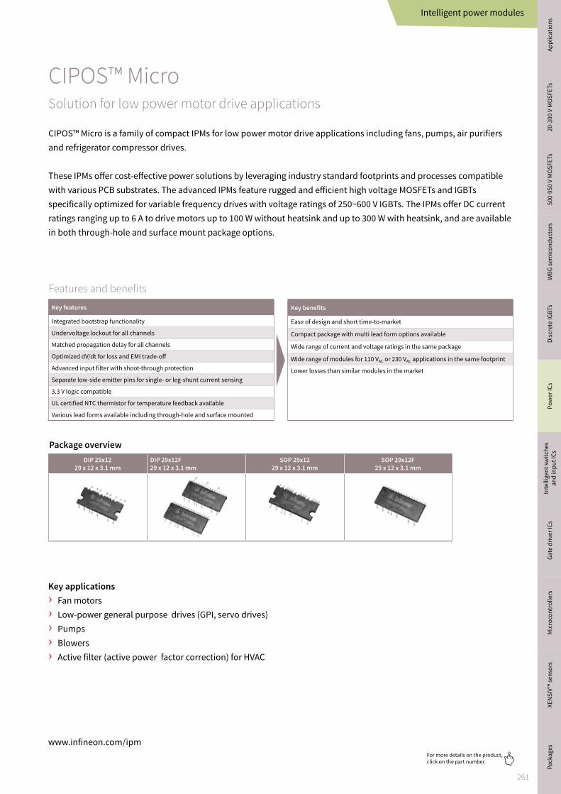
261
For more details on the product, click on the part number.
CIPOS™ Micro is a family of compact IPMs for low power motor drive applications including fans, pumps, air purifiers and refrigerator compressor drives.
These IPMs offer cost-effective power solutions by leveraging industry standard footprints and processes compatible with various PCB substrates. The advanced IPMs feature rugged and efficient high voltage MOSFETs and IGBTs specifically optimized for variable frequency drives with voltage ratings of 250~600 V IGBTs. The IPMs offer DC current ratings ranging up to 6 A to drive motors up to 100 W without heatsink and up to 300 W with heatsink, and are available in both through-hole and surface mount package options.
CIPOS™ MicroSolution for low power motor drive applications
Key applications › Fan motors › Low-power general purpose drives (GPI, servo drives) › Pumps › Blowers › Active filter (active power factor correction) for HVAC
www.infineon.com/ipm
Features and benefits
Key features
Integrated bootstrap functionality
Undervoltage lockout for all channels
Matched propagation delay for all channels
Optimized dV/dt for loss and EMI trade-off
Advanced input filter with shoot-through protection
Separate low-side emitter pins for single- or leg-shunt current sensing
3.3 V logic compatible
UL certified NTC thermistor for temperature feedback available
Various lead forms available including through-hole and surface mounted
Key benefits
Ease of design and short time-to-market
Compact package with multi lead form options available
Wide range of current and voltage ratings in the same package
Wide range of modules for 110 VAC or 230 VAC applications in the same footprint
Lower losses than similar modules in the market
DIP 29x1229 x 12 x 3.1 mm
DIP 29x12F29 x 12 x 3.1 mm
SOP 29x1229 x 12 x 3.1 mm
SOP 29x12F29 x 12 x 3.1 mm
Package overview
Intelligent power modules
Appl
icat
ions
Pa
cka
ges
20
-30
0 V
MO
SF
ETs
50
0-9
50
V M
OS
FE
TsW
BG
se
mic
on
du
cto
rsD
iscr
ete
IGB
TsP
ow
er
ICs
Inte
llig
en
t sw
itch
es
an
d in
pu
t IC
sG
ate
dri
ver
ICs
Mic
roco
ntr
oll
ers
XE
NS
IV™
se
nso
rs

262
For more details on the product, click on the part number.
DIP 36x2136 x 21 x 3.1 mm
DIP 36x21D36 x 21 x 3.1 mm
Key applications › Home appliances › Room air conditioners › Motor control and drives › Fan motors, pumps
www.infineon.com/ipm
CIPOS™ Mini is a family of high efficient intelligent power modules that has the highest power density with 4 A to 30 A rated product built into single package platform. It integrates various power and control components to increase reliability, and optimize PCB size and system costs. Utilizing multiple configurations, CIPOS™ Mini IPMs are applicable to the wide applications to control variable speed drives, such as air conditioners, washing machines, refrigerators, vacuum cleaners, compressors, and industrial drives up to 3 kW. The configurations offered within the CIPOS™ Mini family are 2-phase MOSFET, 3-phase MOSFET and IGBT, integrated PFC, and 2-phase and 3-phase interleaved PFC. All options include an integrated gate driver and built-in temperature sensor. CIPOS™ Mini provides optimized performance for power applications, which need good thermal conduction and electrical isolation, but also EMI-safe control, innovative fault indication, and overload protection. The feature of Infineon’s reverse conducting IGBTs or TRENCHSTOP™ IGBTs are used with a new optimized Infineon SOI gate driver IC for excellent electrical performance.
CIPOS™ MiniBroad range of configurations from PFC to inverter
Package overview
Features and benefits
Key features
Dual-in-line transfer molded package
Current rating from 4 A to 30 A, power rating up to 3 kW
Optimized for home appliances and motor drives
Rugged SOI gate driver IC technology
Advanced protection features
UL-certified
Key benefits
High integration (bootstrap circuit, thermistor) for easy design and system space saving
Easy and fast platform design from small to large power
Enhanced robustness of the advanced IGBT and gate driver IC technology
High power density with compact form factor
Two kinds of substrates provide cost efficient solution for home appliances
Intelligent power modules

263
For more details on the product, click on the part number.
DIP36x23D36 x 22.7 x 3.1mm
CIPOS™ Maxi IPMs integrate various power and control components to increase reliability, optimize PCB size and system costs. It is designed to control three-phase AC motors and permanent magnet motors in variable speed drives applications, such as low-power motor drives, pumps, fan drives and active filters for HVAC (heating, ventilation, and air conditioning). The existing portfolio offers 5 A and 10 A in 1200 V class up to 1.8 kW power rating. The smallest package in 1200 V IPM class offers highest power density and best performance in its class.
IM818 is the first 1200 V IPM that integrated an optimized 6-channel SOI gate driver to provide built-in dead time that prevents damage from transients. The product concept is especially adapted to power applications, which require excellent thermal performance and electrical isolation as well as meeting EMI requirements and overload protection.
CIPOS™ MaxiSolutions for high reliability and performance application
Package overview
www.infineon.com/ipm
Key applications › Fan motors › Low-power general purpose drives (GPI, servo drives) › Pumps › Active filter (active power factor correction) for HVAC › HVAC outdoor fan
Features and benefits
Key benefits
Fully isolated dual in-line molded module with DCB
1200 V TRENCHSTOP™ IGBT 4
Rugged 1200 V SOI gate driver technology
Integrated booststrap functionality
Overcurrent shutdown
Undervoltage lockout at all channels
All of six switches turn-off during protection
Cross-conduction prevention
Programmable fault clear timing
Allowable negative VS potential up to -11 V for signal transmission at VBS of 15 V
Low side emitter pins accessible for all phase current monitoring (open emitter)
Key advantages
The smallest package size in 1200 V IPM class with high power density and best performance
Enhanced robustness of gate driver technology for excellent protection
Adapted to high switching application with lower power loss
Simplified design and manufacturing
Intelligent power modules
Appl
icat
ions
Pa
cka
ges
20
-30
0 V
MO
SF
ETs
50
0-9
50
V M
OS
FE
TsW
BG
se
mic
on
du
cto
rsD
iscr
ete
IGB
TsP
ow
er
ICs
Inte
llig
en
t sw
itch
es
an
d in
pu
t IC
sG
ate
dri
ver
ICs
Mic
roco
ntr
oll
ers
XE
NS
IV™
se
nso
rs

264
For more details on the product, click on the part number.
Intelligent power modules
CIPOS™ IPM product portfolio
www.infineon.com/ipm
MOSFET based CIPOS™ IPMs
Product family Voltage [V] Configuration RDS(on) max. [Ω]
Package Product name
CIPOS™ Nano 40 Half-bridge 0.05 QFN 7x8 IRSM005-800MH
100 Half-bridge 0.02 QFN 7x8 IRSM005-301MH
250 Half-bridge 0.15 QFN 8x9 IRSM808-204MH
3-phase inverter 0.45. ~ 2.20 QFN 12x12 IRSM836-084MA/IRSM836-044MA IRSM836-024MA
500 Half-bridge 0.80/1.70 QFN 8x9 IRSM807-105MH/IRSM808-105MHIRSM807-045MH
3-phase inverter 1.70 ~ 6.00 QFN 12x12 IRSM836-045MA/IRSM836-035MA/IRSM836-035MBIRSM836-025MA/IRSM836-015MA
CIPOS™ Micro 250 3-phase inverter 2.40 DIP 29x12F IRSM5y5-024DA 1) *
2.40 SOP 29x12F IRSM5y5-024PA 1) *
500 1.30 ~ 6.00 DIP 29x12F IRSM5y5-065DA */IRSM5y5-055DA 1) *IRSM5y5-035DA */IRSM5y5-025DA 1) *IRSM5y5-015DA 1) *
1.30 ~ 6.00 SOP 29x12F IRSM5y5-065PA/IRSM5y5-055PA 1) *IRSM5y5-035PA/IRSM5y5-025PA 1) *IRSM5y5-015PA 1) *
CIPOS™ Mini 600 2/3-phase inverter 0.33 DIP 36x21 IM512-L6A/IM513-L6A
IGBT based CIPOS™ IPMs
Product family Voltage [V] Configuration Rated current [A]
Package Product name
CIPOS™ Micro 600 3-phase inverter 3.0/4.0 DIP 29x12F IM240-S6Y1B/IM240-S6Y2BIM240-M6Y1B/IM240-M6Y2B
4.0/6.0 DIP 29x12 IM231-M6T2B/IM231-L6T2B
3.0/4.0 SOP 29x12F IM240-S6Z1B IM240-M6Z1B
4.0/6.0 SOP 29x12 IM231-M6S1B/IM231-L6S1B
CIPOS™ Mini 600 PFC integrated 10.0~20.0 DIP 36x21D IFCM10S60GD/IFCM10P60GDIFCM15S60GD/IFCM15P60GDIM564-X6D
3-phase inverter 4.0 ~ 30.0 DIP 36x21 IGCM04F60GA/IGCM04G60GAIGCM06F60GA/IGCM06G60GAIGCM10F60GA/IKCM10H60GA/IKCM10L60GAIGCM15F60GA/ICM15L60GA */IKCM15F60GA/IKCM15H60GAIGCM20F60GA/IKCM20L60GAIKCM30F60GA
15.0 ~ 30.0 DIP 36x21D IKCM15L60YD */IKCM20L60YD */IKCM30F60YA 2) *
650 3-phase interleaved PFC 20 DIP 36x21D IFCM20T65GD/IFCM20U65GD
2-phase interleaved PFC 30 DIP 36x21D IFC30T65GD */IFCM30U65GDCIPOS™ Maxi 1200 3-phase inverter 5.0/10.0 DIP 36x23D IM818-SCC/IM818-MCC
1) y = 0 (with NTC), y = 1 (without NTC)2) y = G (with NTC), y = H (without NTC)
*For more information on the product, contact our product support

265
For more details on the product, click on the part number.
www.infineon.com/motor-control-ics
iMOTION™ products for industrial and consumer motor control applicationsiMOTION™ products are offered in several integration levels on both hardware as well as software. The hardware integration ranges from stand-alone motor controllers up to fully integrated inverters in the SmartIPMs. On software offering, Infineon is providing full turnkey solutions as well as freely programmable modules. Using the turnkey products that are based on the patented and field proven motor control engine (MCE) and assisted by powerful tools like MCEwizard and MCEdesigner the implementation of a variable speed drive is reduced to configuring the respective motor. Infineon provides complete solution for motor control with its combined offering of iMOTION™ together with EiceDRIVER™ gate drivers, TRENCHSTOP™ IGBTs, CoolMOS™ MOSFETs and CIPOS™ IPMs.
Intelligent motor control ICsPower bridges for all kind of motors in automotive and industrial applications from 100 mA up to 70 A with different feature sets scaled to your needs. Choose from our single and multi half-bridge ICs, integrated full-bridge drivers, servo and stepper motor drivers or multi-MOSFET driver.
Automotive embedded power ICs (system-on-chip)Infineon's embedded power ICs are specifically designed to enable mechatronic motor control solutions for a range of motor control applications, where a small package form factor and a minimum number of external components are essential, including but not limited to: window lift, sunroof, wiper, fuel pump, HVAC fans, engine cooling fan, water pumps. See more on embedded power solutions in Microcontroller section, pages 320-343.
Motor control ICsSolutions for motor control systems in automotive, consumer and industrial applications
Appl
icat
ions
Pa
cka
ges
20
-30
0 V
MO
SF
ETs
50
0-9
50
V M
OS
FE
TsW
BG
se
mic
on
du
cto
rsD
iscr
ete
IGB
TsP
ow
er
ICs
Inte
llig
en
t sw
itch
es
an
d in
pu
t IC
sG
ate
dri
ver
ICs
Mic
roco
ntr
oll
ers
XE
NS
IV™
se
nso
rs

266
For more details on the product, click on the part number.
iMOTION™Flexible and scalable platform for motor control solutions
iMOTION™ products integrate all required hardware and software functions for the control of a variable speed drive (VSD). Infineon’s field proven motion control engine (MCE) eliminates software coding from the motor control development process reducing the research and development efforts to the configuration for the respective motor. The MCE implements highly efficient control of the motor and an optional power factor correction (PFC) and integrates all necessary protections and a flexible scripting engine. Configuration options allow the use of single or leg shunt current measurement as well as sensorless or hall-based field oriented control (FOC). Assisted by powerful tools like MCEWizard and MCEDesigner it is possible to have the motor up and running in less than an hour. Integrated support for functional safety for home appliances paves the way to meet regulations in the global market.
www.infineon.com/iMOTIONwww.infineon.com/iMOTION-software
M
IMC100T
Scripting
iMOTION™ motor controller iMOTION™ SmartIPM
IMC300A
Full 3-phase inverter system controller, gate driver and MOSFETs
in compact 12x12 mm2 package up to ~80 W
IMM100A/IMM100T
Gate driverIMC300 IMC100 3-phase inverterARM®
Cortex®-M0(IMC300)
› MCE supervision› Sensors› Communication› Custom functions
› Motor control› PFC control› Protection› Safety functions
Motion controlengine(MCE)
iMOTION™
M
Gate driver 3-phase inverter
› Motor control› PFC control› Protection› Safety function
Motion controlengine(MCE)
Motion control engine (MCE)motor + PFC control,
protection, integrated scripting engine
MCE + additional MCU additional MCU available for
system/application code
Scripting
PC tools and evaluation kits are available to configure, test and fine-tune the drive inverter.
MCEWizardSW tool to generate initial drive control parametersMCEDesignerSW tool to test, monitor and fine-tune the motor drive – including trace features for live monitoringiMOTION™ LinkIsolated debug interface to iMOTION™ devices
Features and benefits
Key features
Ready-to-use and field-proven motor control solution
Multiple integrated protection features
Functional safety acc. IEC/UL 60730 supported
Scalable - from motor to scripting, PFC and additional MCU
Various integration levels - from motor controller to SmartIPM
iMOTION™ controller – run with any gate driver and power stage
iMOTION™ SmartIPM – highest integration level
Key benefits
Fastest time to market
Easy to use – no motor control coding required
High performance and energy-optimized solution
Reduced cost of ownership due to R&D savings
Easy adaptation to differing application requirements
Highest flexibility for low or high voltage drives
Reduced system cost due to minimum BOM count and PCB size
Motor control ICs

267
For more details on the product, click on the part number.
M1
M3
iMOTION™ Modular Application Design KitInfineon‘s motor control evaluation platform
Get a motor running in less than 1 hour!
The iMOTION™ Modular Application Design Kit (MADK) evaluation platform targets variable speed-drive applications up to 2 kW. The platform offers a modular and scalable system solution with different control board options and a wide range of power boards. While the M1 platform provides control of a permanent magnet synchronous motor (PMSM), the M3 platform additionally includes the power factor correction (PFC) implemented as a CCM boost PFC.
Using the iMOTION™ MADK standardized platform interfaces, different control and power boards can be combined in a system that perfectly meets the requirements of the application. This modular approach allows developers maximum flexibility and scalability during evaluation and development phase at affordable costs.
Further information, datasheets and documents www.infineon.com/MADK
For technical assistancewww.infineon.com/support
Motor control boards
Motor + PFC control boards
Wide range of power boards
Power boards with PFC
EVAL-M1-101TIMC101T-T038Control card
EVAL-M3-102TIMC102T-F064Control card
EVAL-M1-36-84ACIPOS™ Nano-power boardIRSM836-084MA ~110V/80W
EVAL-M3-CM615PNCIPOS ™ mini with boost PFCIFCM15S60GD ~220V/650W
EVAL-M1-CM610N3CIPOS™ Mini-power boardIKCM10H60GA ~220V/750W
EVAL-M3-IM564CIPOS ™ mini with boost PFCIM564-X6D ~220V/2000W
EVAL-M1-IM818-ACIPOS™-Maxi power board IM818-MCC ~380V/1500W
EVAL-M1-099M-CIRMCK099Control card
EVAL-M3-302FIMC302A-F064Control card
EVAL-M1-101TFIMC101T-F048Control card
Motor control ICs
Appl
icat
ions
Pa
cka
ges
20
-30
0 V
MO
SF
ETs
50
0-9
50
V M
OS
FE
TsW
BG
se
mic
on
du
cto
rsD
iscr
ete
IGB
TsP
ow
er
ICs
Inte
llig
en
t sw
itch
es
an
d in
pu
t IC
sG
ate
dri
ver
ICs
Mic
roco
ntr
oll
ers
XE
NS
IV™
se
nso
rs
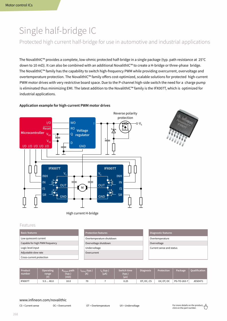
268
For more details on the product, click on the part number.
Motor control ICs
Single half-bridge ICProtected high current half-bridge for use in automotive and industrial applications
The NovalithIC™ provides a complete, low-ohmic protected half-bridge in a single package (typ. path resistance at 25°C down to 10 mΩ). It can also be combined with an additional NovalithIC™ to create a H-bridge or three-phase bridge. The NovalithIC™ family has the capability to switch high-frequency PWM while providing overcurrent, overvoltage and overtemperature protection. The NovalithIC™ family offers cost-optimized, scalable solutions for protected high-current PWM motor drives with very restrictive board space. Due to the P-channel high-side switch the need for a charge pump is eliminated thus minimizing EMI. The latest addition to the NovalithIC™ family is the IFX007T, which is optimized for industrial applications.
Features
Basic features
Low quiescent current
Capable for high PWM frequency
Logic level input
Adjustable slew rate
Cross-current protection
Protection features
Overtemperature shutdown
Overvoltage shutdown
Undervoltage
Overcurrent
Diagnostic features
Overtemperature
Overvoltage
Current sense and status
Application example for high-current PWM motor drives
IFX007T
VS VS
GND
OUT
GND
OUT
SR
IS
IN
INH
SR
IS
IN
INH
I/OI/O I/OI/O I/O
Reset
I/O I
VDD
VSS
WO
RO
Q
DGND
MicrocontrollerVoltage
regulator
Reverse polarity
protection
IFX007T
M
VS
High current H-bridge
Product number
Operating range
[V]
RDS(on) path (typ.)[mΩ]
ID(lim) (typ.)[A]
Iq (typ.)[µA]
Switch time (typ.)[µs]
Diagnosis Protection Package Qualification
IFX007T 5.5 ... 40.0 10.0 70 7 0.25 OT, OC, CS UV, OT, OC PG-TO-263-7 JESD471
CS = Current sense OC = Overcurrent OT = Overtemperature UV = Undervoltage
www.infineon.com/novalithic

269
For more details on the product, click on the part number.
Features
Key features
Capable of high frequency PWM, e.g. 30 kHz
Adjustable slew rates for optimized EMI by changing external resistor
Driver circuit with logic level inputs
Diagnosis with current sense
www.infineon.com/shields-for-arduinowww.infineon.com/makerswww.infineon.com/novalithIC
DC motor control shield with IFX007T for Arduino
The BLDC motor control shield is a high current motor control board compatible with Arduino and Infineon’s XMC4700 Boot Kit. It is equipped with three smart IFX007T half-bridges. The BLDC motor control shield is capable to drive one BLDC motor. Alternatively, it can be used to drive one or two bidirectional DC motors (H-Bridge configuration, cascaded to support second motor) or up to three unidirectional DC motors (half-bridge configuration). The implemented inte-grated NovalithIC™ IFX007T half-bridges can be controlled by a PWM via the IN-pin.
BLDC-SHIELD_IFX007TDC motor control with half-bridge IFX007T Infineon's shields for Arduino are compatible with microcontroller boards using the Arduino-compatible form factor, e.g. Infineon's XMC™ microcontroller kits.Ordering code: BLDCSHIELDIFX007TTOBO1
Target applications › Brushed DC motor control up to 250 W continuous load › 24 V nominal input voltage (max. 6 V–40 V) › Average motor current 30 A restricted due to PCB (IFX007T current limitation @ 55 A min.)
Motor control ICs
Appl
icat
ions
Pa
cka
ges
20
-30
0 V
MO
SF
ETs
50
0-9
50
V M
OS
FE
TsW
BG
se
mic
on
du
cto
rsD
iscr
ete
IGB
TsP
ow
er
ICs
Inte
llig
en
t sw
itch
es
an
d in
pu
t IC
sG
ate
dri
ver
ICs
Mic
roco
ntr
oll
ers
XE
NS
IV™
se
nso
rs

270
For more details on the product, click on the part number.
Motor control ICs
Multi half-bridge ICsExtensive offering ranging from two-fold half-bridge ICs to twelve-fold half-bridge ICs
The TLE94xyz are protected half-bridge drivers designed for 12 V motion control applications such as small DC motors for heating, ventilation and air conditioning (HVAC), as well as automotive mirror adjustment and fold. The family offers three-, four-, six-, eight-, ten-, and twelve-fold integrated half-bridge driver. All devices can drive DC motor loads up to 0.9 A per output or the outputs can be used stand-alone or combined to increase driving capability up to 3.6 A. They provide diagnosis of short circuit, open load, power supply failure and overtemperature for each half-bridge to ensure safe operation in HVAC or other systems. The TLE94xyz offers enhanced EMC performance, which in combination with the low quiescent current and a small package makes the product attractive for a wide range of 12 V automotive and industrial applications.
Overloaddetection
Overtemp.detection
Open-loaddetection
PWMgenerator
Charge pumpUndervoltage andovervoltage monitor
Overloaddetection
Overtemp.detection
Open-loaddetection
Temperaturesensor
Logic control andlatch SPI interface
Errordetection
VDD VS1 VS2
CSN
GND GND GND GND
EN
12-foldhalf-bridge driverSPI interface
SCLK
SDI
SDO
Power driver
OUT3OUT2OUT1
12x driver stage
High-sidedriver
Low-sidedriver
OUT4OUT5OUT6
OUT9OUT8OUT7
OUT10OUT11OUT12
Bias andmonitor
Block diagram TLE94112ELInfineon's portfolio of multi half-bridge ICs
www.infineon.com/multihalfbridges
Key applications › 12 V automotive and industrial applications › Flap motors in HVAC systems › Mirror adjustment and fold › Small DC motors (≤ 0.9 A/output) › Bistable relays › Bipolar stepper motors in full-step and
half-step mode
Features and benefits
Microcontroller
InterfaceDirect
interfaceSPI
Number of motors
1 Motor
TLE4207G
DSO-14
TLE94003EP
TSDSO-14
TLE94004EP
TSDSO-14
TLE94104EP
TSDSO-14
TLE8444SL
SSOP-24
TLE94103EP
TSDSO-14
TLE94106ES
TSDSO-14
TLE94108EL
SSOP-24
TLE94110EL
SSOP-24
TLE94112EL
SSOP-24
2 Motors 2 Motors 3 Motors 4 Motors 5 Motors 6 Motors
Number of motors
Key features and benefits
Three-, four-, six-, eight-, ten-, and twelve-fold half-bridges with integrated output stages and PWM
16-bit SPI or direct inputs for control and diagnosis
Voltage supply range: 5.5– 20 V
Adjustable open load threshold for two outputs
Variable driving schemes for up to

271
For more details on the product, click on the part number.
Product name
Config. IL(NOM)[A]
IL(lim)[A]
Iq[μA]
VS(OP)[V]
Protection Diagnosticinterface
Highlights VCE(sat)/RDS(on)[mΩ]
Package
TLE94003EP 3 x half-bridge 3 x 0.30 3 x 0.90 0.6 5.5 to 20 OC, OT, VS, UV/OV Error flag TLE94xyz family concept + small package
850/switch
TSDSO-14-EP
TLE94103EP 3 x half-bridge 3 x 0.30 3 x 0.90 0.6 5.5 to 20 OC, OT, OL, VS, UV/OV 16-bit SPI TLE94xyz family concept + small package TSDSO-14-EP
TLE94004EP 4 x half-bridge 4 x 0.30 4 x 0.90 0.6 5.5 to 20 OC, OT, VS, UV/OV Error flag TLE94xyz family concept + small package TSDSO-14-EP
TLE94104EP 4 x half-bridge 4 x 0.30 4 x 0.90 0.6 5.5 to 20 OC, OT, OL, VS, UV/OV 16-bit SPI TLE94xyz family concept + small package TSDSO-14-EP
TLE94106ES 6 x half-bridge 6 x 0.30 6 x 0.90 0.6 5.5 to 20 OC, OT, OL, VS, UV/OV 16-bit SPI TLE94xyz family concept + backwards compatible to TLE84106EL TSDSO-24
TLE94108EL 8 x half-bridge 8 x 0.30 8 x 0.90 0.6 5.5 to 20 OC, OT, OL, VS, UV/OV 16-bit SPI TLE94xyz family concept SSOP-24
TLE94110EL 10 x half-bridge 10 x 0.30 10 x 0.90 0.6 5.5 to 20 OC, OT, OL, VS, UV/OV 16-bit SPI TLE94xyz family concept + backwards compatible to TLE84110 SSOP-24
TLE94112EL 12 x half-bridge 12 x 0.30 12 x 0.90 0.6 5.5 to 20 OC, OT, OL, VS, UV/OV 16-bit SPI TLE94xyz family concept + 12 outputs in one package SSOP-24
TLE4207G 2 x half-bridge 2 x 0.80 2 x 1.50 20 8 to 18 OC, OT, VS, UV/OV Status flag Error detection DSO-14
TLE8444SL 4 x half-bridge 4 x 0.50 4 x 0.90 1 8 to 18 OC, OT, OL, VS, UV/OV Status flag Open-load detection in ON-state SSOP-24
OC = Overcurrent OT = Overtemperature OL = Openload UV = Undervoltage OV = Overvoltage
www.infineon.com/shields-for-arduinowww.infineon.com/makers
DC motor shield with TLE94112EL for Arduino
The DC motor shield is a small evaluation board equipped with TLE94112EL for use with Arduino. The TLE94112EL is capable to drive up to 6 small DC motors in parallel mode or up to 11 DC motors in cascaded mode. All outputs can drive up to 0.9 A. The outputs can be used stand-alone or combined to increase driving capability up to 3.6 A.
Features
Key features
Driver with 12 half-bridge outputs to drive DC motors, resistive or inductive loads
Driver is protected against overtemperature, overcurrent, overvoltage, undervoltage and enables diagnosis of overcurrent, overvoltage, undervoltage
SPI interface with zero clock diagnosis
Enhanced EMC performance
Integrated PWM generator with three different frequencies (80 Hz, 100 Hz, 200 Hz)
Target applications › Multi-motor applications › DC motors and voltage controlled bipolar stepper motors › Toys › HVAC systems
Motor control ICs
Appl
icat
ions
Pa
cka
ges
20
-30
0 V
MO
SF
ETs
50
0-9
50
V M
OS
FE
TsW
BG
se
mic
on
du
cto
rsD
iscr
ete
IGB
TsP
ow
er
ICs
Inte
llig
en
t sw
itch
es
an
d in
pu
t IC
sG
ate
dri
ver
ICs
Mic
roco
ntr
oll
ers
XE
NS
IV™
se
nso
rs

272
For more details on the product, click on the part number.
Motor control ICs
Integrated full-bridge driverGeneral purpose 6 A H-bridges
IFX9201SG and IFX9202ED are general purpose 6 A H-bridges designed for the control of small DC motors and inductive loads. The outputs can be pulse width modulated at frequencies up to 20 kHz, which enables operation above the human sonic range by means of PWM/DIR control. While the signal at the DIR input defines the direction of the DC motor, the PWM signal controls the duty cycle. For load currents above the current limitation threshold (8 A typically), the H-bridges switch into chopper current limitation mode.
Application example H-bridge with error flag
SOGND
Microcontroller
IFX9201SG
SISCKCSNDIRPWMDIS
VSO
VS
OUT1
OUT2
3.3 or 5 VDigital supply
VBat
< 33 nF
100 nF100 µFVS < 40 V
< 33 nF
M
+–
+–
+–
+–
PWM_2
XMC1300
PWM_1
Step
2-phase
stepper motor
Direction (DIR)
Disable (DIS)IFX9202ED
PWM_1
PWM_2 OUT2_2
OUT2_1
OUT1_2
OUT1_1
GND GND
Application example H-bridge with SPI interface
SOGND
Microcontroller
SISCKCSNDIRPWMDIS
VSO
VS
OUT1
OUT2
VBat
M
< 33 nF
100 nF100 µFVS < 40 V
< 33 nF
3.3 or 5 VDigital supply IFX9201SG
+–
+–
+–
+–
PWM_2
IFX9201XMC1300
IFX9201
PWM_1
Step
2-phase
stepper motor
Direction (DIR)
Disable (DIS)
Applications examples
www.infineon.com/dc-motor-bridges *For more information on the product, contact our product support
Product number Operating voltage
Current limit (min.) [A]
Quiescent current (typ.) [µA]
Operating range[V]
RDS(on) (typ./switch)[mΩ]
Package RthJC (max.)[K/W]
IFX9201SG 4.5 to 36 V 6.0 10.0 70 7 PG-DSO-12 (power) 2.0
IFX9202SG * 4.5 to 36 V 2 x 6.0 A 19.0 5 to 36 2 x 100 DSO-36 2 x 0.5
Features
Key features
Up to nominal 36 V supply voltage
Short circuit, overtemperature protection and undervoltage shutdown
Detailed SPI diagnosis or simple error flag
Simple design with few external components
Small and robust DSO-12-17 (IFX9201SG) and DSO-36-72 (IFX9202ED) packages

273
For more details on the product, click on the part number.
www.infineon.com/dc-motor-bridges
H-BRIDGE KIT 2GO with IFX9201SG
Build your own DC motor control with the H-bridge Kit 2GO, a ready-to-use evaluation kit. It is fully populated with all electronic components equipped with the H-bridge IFX9201 combined with XMC1100 microcontroller based on Arm® Cortex®-M0 CPU. It is designed for the control of DC motors or other inductive loads up to 6 A or up to 36 V of supply.
Target applications › DC motor control for industrial applications › Home and building automation › Power tools battery management › Industrial robotic applications › Electric toys applications
Ordering code: HBRIDGEKIT2GOTOBO1
KIT_XMC1300_IFX9201 Stepper motor control shield with IFX9201SG and XMC1300 for Arduino
The stepper motor control shield from Infineon is one of the first high current stepper motor control boards being compatible to Arduino as well as to Infineon’s XMC1100 boot kit. The stepper motor control shield is capable to drive the two coils in a stepper motors featuring dual-half bridge configuration. The implemented integrated IFX9201 half-bridges can be controlled by a STEP-signal via the STEP pin. Interfacing to a microcontroller is made easy by the integrated XMC1300 microcontroller that holds the peripherals to allow high-speed current control. Microstepping of the stepper motor can be achieved using the internal comparators, while operational amplifiers are installed to adapt the motor current sense signal to the microcontroller’s input levels.
Target applications › Stepper motors up to 5 A phase current › 24 V nominal input voltage for the power stage › Average motor current 3 A without additional
cooling effort, 5 A possible with proper coolingOrdering code: KITXMC1300IFX9201TOBO1
Features and benefits
Key features
Compatible with microcontroller boards using the Arduino form factor, e.g. Infineon's XMC™ microcontroller kits
Capable of high frequency PWM, e.g. 30 kHz
Adjustable slew rates for optimized EMI by changing external resistor
Driver circuit with logic level inputs
Diagnosis with current sense
Key benefits
Fast and inexpensive prototyping of stepper motor control
Simple testing of microstepping algorithms
Diagnose pin to allow hardware feedback during development
Overtemperature shutdown with latch behavior and undervoltage shutdown of the power section
Motor control ICs
Appl
icat
ions
Pa
cka
ges
20
-30
0 V
MO
SF
ETs
50
0-9
50
V M
OS
FE
TsW
BG
se
mic
on
du
cto
rsD
iscr
ete
IGB
TsP
ow
er
ICs
Inte
llig
en
t sw
itch
es
an
d in
pu
t IC
sG
ate
dri
ver
ICs
Mic
roco
ntr
oll
ers
XE
NS
IV™
se
nso
rs

274
For more details on the product, click on the part number.
Motor control ICs
www.infineon.com/dc-motor-bridges
Stepper motor driver Cost-efficient, durable and reliable
The TLE8444SL is a protected quad-half-bridge IC targeted towards automotive and industrial motion control applica-tions. It is a monolithic die based on Infineon’s smart mixed technology SPT which combines bipolar and CMOS control circuitry with DMOS power devices. DC Motors can be driven in forward (cw), reverse (ccw), brake and high impedance modes where as stepper motors can be driven in no-current, negative/positive output current modes. These various modes can easily be achieved via standard parallel interface of the device to a microcontroller. The PG-SSOP-24-7 pack-age is advantageous as it saves PCB board space and costs. The integrated short circuit and overtemperature protection as well as its built-in diagnosis features such as over- and undervoltage lockout and open load detection improve system reliability and performance.
Applications › Unipolar or bipolar loads › Stepper motors in automotive and industrial
applications (e.g. idle speed control for small cars or motor bike)
Product number
IL(NOM) IL(lim) Iq[µA]
VS(op) Stepoperations
Protection Diagnosticinterface
Highlights Package
TLE8444SL 4x0.50 4x0.90 1 1–18 Full to half-step SC, OT, OV, UV, OL Status flag Open-load detection in on-state
SSOP-24-7
CS = Current sense OC = Overcurrent OT = Overtemperature SC = Short circuit UV = Undervoltage OL = Open-load
Features
Benefits
Suited for fast switching applications (PWM capability up to 10kHz)
Easy failure detection
Low impact on battery lifetime
Implementation of thermal shutdown extends IC lifetime
Allows motor peak currents up to 0.9a
Broken wire connections easily detected
Designed for automotive and industrial applications

275
For more details on the product, click on the part number.
Further information, datasheets and documentswww.infineon.com/acdcwww.infineon.com/coolsetwww.infineon.com/integrated-powerstageswww.infineon.com/digital-controllerwww.infineon.com/lighting-icswww.infineon.com/isofacewww.infineon.com/eicedriverwww.infineon.com/industrial-transceiverswww.infineon.com/industrial-voltage-regulatorswww.infineon.com/industrial-DC-DC-converters
www.infineon.com/industrial-profetwww.infineon.com/novalithicwww.infineon.com/dc-motor-bridgeswww.infineon.com/shields-for-arduinowww.infineon.com/ipolwww.infineon.com/analog-ipolwww.infineon.com/xdpwww.infineon.com/ipmwww.infineon.com/madk
Infineon support for power ICsUseful links and helpful information
Simulation
Appl
icat
ions
Pa
cka
ges
20
-30
0 V
MO
SF
ETs
50
0-9
50
V M
OS
FE
TsW
BG
se
mic
on
du
cto
rsD
iscr
ete
IGB
TsP
ow
er
ICs
Inte
llig
en
t sw
itch
es
an
d in
pu
t IC
sG
ate
dri
ver
ICs
Mic
roco
ntr
oll
ers
XE
NS
IV™
se
nso
rs

276
For more details on the product, click on the part number.
› ISOFACE™ isolated industrial interface › HITFET™ protected low-side switches › Industrial PROFET™ protected high-side switches › Infineon support for intelligent switches and input ICs
Intelligent power switches and modules

277
For more details on the product, click on the part number.
Intelligent power switches and modules
Appl
icat
ions
Pa
cka
ges
20
-30
0 V
MO
SF
ETs
50
0-9
50
V M
OS
FE
TsW
BG
se
mic
on
du
cto
rsD
iscr
ete
IGB
TsP
ow
er
ICs
Inte
llig
en
t sw
itch
es
an
d in
pu
t IC
sG
ate
dri
ver
ICs
Mic
roco
ntr
oll
ers
XE
NS
IV™
se
nso
rs

278
For more details on the product, click on the part number.
ISOFACE™ isolated industrial interface Output switches and digital input ICs offering unmatched system uptime, reliability and shortened product launch time by 50%
ISOFACE™ galvanic-isolated 8-channel output switches
Our ISOFACE™ product family provides robust and intelligent galvanic isolation for industrial control applications such as programmable logic controllers, sensor input modules, control panels and general control equipment. The output switches are compact in design, enabling robust and reliable operation at low system cost. Ideal for high-speed applications, digital input ICs are equally robust, reliable and compact – also offering superior EMI robustness and setting a new standard in diagnostics.
The ISO1H81xG product family integrates: › Robust galvanic isolation (UL508 and EN 61131-2 certified) to protect the 3.3 V/5 V control domain of an industrial
control system from the harsh 24 V process side › 8-channel high-side power-switching capabilities of up to 1.2 A per channel › Active current limitation and overtemperature protection › Common diagnostic feedback for overtemperature and for Vbb undervoltage
Isolated output switch block diagram
Control
and
protection
unit
Control
unit
Microcontroller
i.e.
XMC1xxx
XMC4xxx
Logic
Tra
nsm
issi
on
Tra
nsm
issi
on
Parallel or
serial
interface
VbbVCC
VCC
DIAG
GND
VbbVCC
OUT0
DIS
CS
WR
D0
D7
DIAG
GNDCC GNDBB
OUT1
OUT7
ISO1H81xG
www.infineon.com/isoface
Isolated output switches
Key benefits
Robust and reliable
Compact system solution
Lower system cost
System status feedback
Directly interfacing with all MPUs and MCUs
Key features
Integrated galvanic isolation (500 V)
Eight channels (0.6 or 1.2 A, each)
Inductive load switching
Diagnostic feedback (overtemperature, overload)
Serial and parallel MCU interface
Features and benefits
ISOFACE™

279
For more details on the product, click on the part number.
ISOFACE™ galvanic-isolated digital input ICs
The ISO1I81xT digital input IC family is an intelligent system solution offering robust galvanic isolation between the microcontroller on the “control side” and the 24 V factory floor environment, frequently referred to as the process side.
Digital input switch block diagram
Featured products › XMC4800-E196K2048 -Arm® Cortex®-M4 microcontroller › ISO2H823V2.5- 24 V 8-channel isolated output › ISO1I813T - 24 V 8-channel isolated input › SLS 32AIA020A4 USON10 - OPTIGA™ Trust E – embedded security solution › TLE6250GV33 - Infineon CAN transceiver › IFX54441LDV - Infineon voltage regulator
Key features › Complete automation kit gateway › Combined MCU with EtherCAT® slave application › Isolated interfaces w/ diagnose › Ethernet connectivity with software examples available › Full software DAVE™ examples
Digitalfilter
Digitalfilter
Seria
lize
Logi
c
Dese
rializ
e Micro-controller
e.g.XE166
Parallelor serialinterface
VFI
IN7
8 se
nsor
s
IN0 2 kΩ
330 nF
12 kΩ
GNDFI
I0H ERR
CS
Sync
GND
DCENA
I0L
TS
SW1 S W2Vbb VCC
WB
I7HI7L
GNDBBISO1I813T
2 kΩ
12 kΩ
www.infineon.com/isoface
XMC4800 automation board V2
Orderable part number:KITXMC48AUTBASEV2TOBO1
Galvanic-isolated digital input ICs
Key benefits
Robust and reliable
Compact system solution
High-speed applications
Superior EMI robustness
System status feedback
Valuable maintenance support
Key features
Integrated galvanic isolation (500 V)
Eight channels (IEC type 1/2/3)
Up to 500 kHz sampling speed
Programmable input filters
Channel-specific diagnostics (wire-break, undervoltage)
Features and benefits
ISOFACE™
Appl
icat
ions
Pa
cka
ges
20
-30
0 V
MO
SF
ETs
50
0-9
50
V M
OS
FE
TsW
BG
se
mic
on
du
cto
rsD
iscr
ete
IGB
TsP
ow
er
ICs
Inte
llig
en
t sw
itch
es
an
d in
pu
t IC
sG
ate
dri
ver
ICs
Mic
roco
ntr
oll
ers
XE
NS
IV™
se
nso
rs

280
For more details on the product, click on the part number.
Product overview ISO1H801G ISO1H811G ISO1H812G ISO1H815G ISO1H816G
Switch
Vbb operational range: 11 V to 35 V
Max. continuous load current per channel 0.6 A 0.6 A 0.6 A 1.2 A 1.2 A
Load current increase by using outputs in parallel
Inductive clamping energy per channel: 1 Joule
Microcontroller interface
Type Parallel Parallel Serial Parallel Serial
Nominal voltages 5 V 3.3 V/5 V 3.3 V/5 V 3.3 V/5 V 3.3 V/5 V
Safety features
Isolation voltage: VISO = 500 VUL508 and EN 61131-2 certified
Active current limitation
Thermal shutdown
Common output disable pin
Diagnosticsfeedback
Overtemperature
Vbb undervoltage
Package DSO-36 (16x14 mm)
Ordering code ISO1H801GAUMA1 ISO1H811GAUMA1 ISO1H812GAUMA1 ISO1H815GAUMA1 ISO1H816GAUMA1
Product overview ISO1I811T ISO1I813T
Input characteristics IEC type: I, II, III
Input status LED
Max. sampling frequency 125 kHz 500 kHz
Deglitching filter setting Hard wired Software, individual per channel
Synchronous data acquisition –
µC interface 3.3 V/5 V
Serial and parallel
Safety features 500 V isolation voltage
Wire break, channel-specific –
Vbb undervoltage –
Support for external Vbb supply –
Package TSSOP-48 (8x12.5 mm)
Ordering code ISO1I811TXUMA1 ISO1I813TXUMA1
ISOFACE™ output switches
ISOFACE™ digital input IC
www.infineon.com/isoface
ISOFACE™ product portfolio
ISOFACE™ product portfolio

281
For more details on the product, click on the part number.
HITFET™ Protected low-side switches
HITFET™ stands for highly-integrated temperature-protected MOSFET. These well-established low-side switches offer a compelling feature set with protection against overtemperature, short circuit and overload conditions as well as ESD robustness. The HITFET™+ family is the new generation based on a new technology, enabling a significant shrink compared to the existing HITFET™ portfolio (up to 50 percent shrink). This novel generation consists of standard and fully-featured protected low-side switches (11 to 125 mΩ) in the TO-252-3 DPAK/TO-252-5 DPAK and TDSO-8 packages. HITFET™ and HITFET™+ devices address a wide range of applications including resistive, inductive and resistive loads.
Key applications › Industrial automation * › Programmable logic controller (PLC) * * › Digital I/O modules › Building and home management › All kind of solenoid or valve driving › Power modules › Solar power inverters
Application diagramm example for HITFET™
www.infineon.com/hitfet www.infineon.com/shields-for-arduino *See block diagram on page 278 * * See block diagram on page 279
OUT
GND
STATUS
SRP
IN
ENABLEVDD
Load
OUTPUT (PWM)
INPUT (feedback)/
OUTPUT (reset)
OUTPUT
OUT
Mic
ro
co
ntro
lle
r
BTF3xxxEJ
GND
VDD
VBatt
IN
RSTATUS
RSRP
CVDD2)
CSRP1)
Voltage
regulator
5 V
1) CSRP-GND < 100 pF – maximum permittet parasitic capacitance at the SRP-pin
2) Filter capacitor on supply, recommended 100 nF
Vehicle
CAN bus
Key benefits
High design flexibility with scalable RDS(on) and package
Driving applications with high switching speed requirements up to 25 kHz (e.g. valve, solenoid)
Easy to design-in
Choice of packages to match individual application needs
Key features
Low-side switches with integrated protection features
Scalable in RDS(on) ranges from 490 mΩ down to 11 mΩ
Adjustable slew rate control (BTFxxx)
Thermal shutdown with auto restart or latch behavior
Status feedback via › Increased input current (HITFET™ 2nd gen.) › Digital readout via SRP (BTF3050TE) › Via status pin (BTF3xxxEJ)
Features and benefits
Featured products: Three BTF3050TE low-side switches of the HITFET™+ family Combatible with: Microcontroller boards using the Arduino form factor and the corresponding Infineon’s kits with Arm® powered XMC™ microcontrollerOrderable part number: SHIELDBTF3050TETOBO1
Featured products: One single-channel low-side switch of BTT3018EJ Combatible with: Can be used as single stand and is also pin-compatible with microcontroller boards using the Arduino form factor (e.g. XMC1100 Boot Kit, Arduino Uno)Orderable part number: BTT3018EJDEMOBOARDTOBO1
Low-side switch shield with BTF3050TE for Arduino
BTT3018EJ DEMOBOARD
Low-side switches
Appl
icat
ions
Pa
cka
ges
20
-30
0 V
MO
SF
ETs
50
0-9
50
V M
OS
FE
TsW
BG
se
mic
on
du
cto
rsD
iscr
ete
IGB
TsP
ow
er
ICs
Inte
llig
en
t sw
itch
es
an
d in
pu
t IC
sG
ate
dri
ver
ICs
Mic
roco
ntr
oll
ers
XE
NS
IV™
se
nso
rs

282
For more details on the product, click on the part number.
Industrial PROFET™Protected high-side switches
The well-established high-side switch Industrial PROFET™ products were designed for targeting a variety of industrial applications which include all types of resistive, inductive and capacitive loads. Due to their outstanding energy robustness, they are perfectly suitable for switching even higher inductive loads and driving relays. Their main application areas include high-voltage applications (VBAT up to 60 V), high-speed PWM applications (up to 1 kHz) and they are most notably capable of switching higher inductances smoothly. Industrial PROFET™ can be applied to drive any kind of sensor units, indicators, displays, LEDs, relays, valves and magnetic actuators or replace electromechanical relays, fuses and discrete circuits. Industrial PROFET™ products are also the perfect match for applications with long wiring or any other kind of inductive loads or applications with space constraints.
www.infineon.com/industrial-profet
PLC – programmable logic controller digital output modules
Protectiondiagnosis
Isolation
Protectiondiagnosis
Multichannelswitch
Switch
Switch
Load 1
Load 2Microcontrolleror
bus ASIC
Industrial PROFET™ Protected high-sideswitches
Load 3
Load 4
Field levelControl level
Key applications › Industrial automation › Programmable logic controller (PLC) › Digital I/O modules › Robotics › Building and home automation › Solar applications › Wind energy systems › Smart grid › Motor control and drives › Power supplies
PROFET™ as actuators typically address I/O modules supplying nominal currents of 2 A or 0.5 A. However PROFET ™ portfolio as well provides devices also for lower and higher currents. PROFET ™ parts are suitable for switching resistive, capacitive and, by featuring high EAS, inductive loads.Corresponding PROFET™ evaluation boards are available on request.
PROFET™ typical block diagram
Key benefits
Small system form factor
No/little downtime of system in operation
Low heating up of a system
System cost saving by built-in protection and tailored featureset
Reduced system maintenance efforts by providing optimized diagnostics
Key features
Right fit for digital output switches, motor or robot control, protected switching of decentralized loads like sensors or auxiliary supply
Outstanding robustness and reliability as required by industrial mission profiles
Thermally optimized products with low RDS(on) to deal with the high ambient temperatures and limited or even no cooling
Diagnosis and protection for safe system operation
Small and compact design for higher integration and applications with space constraints
Features and benefits
GND
IN
Biassupervision
ESDprotection
Logic
Overvoltageprotection
Currentlimiter
Gatecontrolcircuit
Temperaturesensore
ST
OUT
VS
High-side switches

283
For more details on the product, click on the part number.
www.infineon.com/industrial-profet
Load current Typical, per channel
1-channel 2-channel 4-channel 8-channel
7 A ITS428L2 7 A, 60 mΩ, TO-252-5
3 A ITS4060S-SJ-N, ISP772T3.1 A, 60 mΩDSO-8
2 A … 3 A ITS4100S-SJ-N, ISP762T 2.4 A, 100 mΩ, DSO-8
1 A … 2 A ITS4200S-ME-P, ITS4142N1.4 A, 200 mΩ, SOT223
ITS4040D-EP-D 2.6 A, 40 mΩ, TSDSO14
ITS4075Q-EP-D 2.6 A, 75 mΩ, TSDSO14
ISP752T1.3 A, 200 mΩ, DSO-8
ITS5215L 2 A, 90 mΩ, DSO-12
ITS724G 2 A, 90 mΩ, DSO-20
ITS4200S-SJ-D, ISP752R 1.2 A, 200 mΩ, DSO-8
ITS716G 1 A, 140 mΩ, DSO-20
ITS711L1 1 A, 200 mΩ, DSO-20
0.5 A … 1 A ITS4200S-ME-N, ISP4520.7 A, 200 mΩ, SOT223
ITS4090Q-EP-D 0.7 A, 90 mΩ, TSDSO14
ITS42008-SB-D, ITS4880R 0.6 A, 200 mΩ, DSO-36
ITS4200S-ME-O, ITS4141N0.7 A, 200 mΩ, SOT223
ITS4130Q-EP-D 0.65 A, 130 mΩ, TSDSO14
ITS4141D0.5 A, 200 mΩ, TO-252-5
< 0.5 A ITS4300S-SJ-D, ISP742RI 0.4 A, 300 mΩ, DSO-8
ITS42K5D-LD-F 0.25 A, 2.5Ω, TSON-10
ITS41k0S-ME-N, ITS4140N0.2 A, 1Ω, SOT223
= With diagnosis
Appl
icat
ions
Pa
cka
ges
20
-30
0 V
MO
SF
ETs
50
0-9
50
V M
OS
FE
TsW
BG
se
mic
on
du
cto
rsD
iscr
ete
IGB
TsP
ow
er
ICs
Inte
llig
en
t sw
itch
es
an
d in
pu
t IC
sG
ate
dri
ver
ICs
Mic
roco
ntr
oll
ers
XE
NS
IV™
se
nso
rs

284
For more details on the product, click on the part number.
HITFET™ and PROFET™ portfolio
Product type Product family
Channels RDS(on) @ 25°C [mW]
Nominal load current
[A]
EAS [mJ]
Operating voltage range
[V]
IL(SD) (typ)
[A]
IL(lim)(typ)
[A]
IL(lim)_TRIG-
GER (typ)
[A]
Diagnosis Package
BTS3011TE HITFET™+ 1 10.7 10 300 @ 5 A up to 28 – 35 70 Status pin TO-252-5 (DPAK 5-leg) BTT3018EJ HITFET™+ 1 16 7.0 150 up to 36 – 45 – Status pin TDSO-8BTS3035EJ HITFET™+ 1 28 5.00 105 @ 5 A up to 31 – 20.00 – Status pin TDSO-8BTS3035TF HITFET™+ 1 30 5.00 106 @ 5 A up to 31 – 20.00 – – TO-252-3 (DPAK 3-leg)BTF3035EJ HITFET™+ 1 28 5.00 95 @ 5 A up to 32 – 14.00 41.00 Status pin TDSO-8BTF3050TE HITFET™+ 1 40 3.00 120 @ 3 A up to 28 – 8.00 30.00 Through SRP pin TO-252-5 (DPAK 5-leg)BTS3050EJ HITFET™+ 1 40 4.00 62 @ 3 A up to 31 – 15.00 – Status pin TDSO-8BTS3050TF HITFET™+ 1 44 4.00 64 @ 4 A up to 31 – 15.00 – – TO-252-3 (DPAK 3-leg)BTF3050EJ HITFET™+ 1 40 4.00 62 @ 4 A up to 32 – 10.00 29.00 Status pin TDSO-8BTS3060TF HITFET™+ 1 50 3.00 55 @ 3 A up to 35 – 10.50 – – TO-252-3 (DPAK 3-leg)BTS3080EJ HITFET™+ 1 64 3.00 35 @ 3 A up to 31 – 10.00 – Status pin TDSO-8BTS3080TF HITFET™+ 1 69 3.00 38 @ 3 A up to 31 – 10.00 – – TO-252-3 (DPAK 3-leg)BTF3080EJ HITFET™+ 1 64 3.00 33 @ 3 A up to 32 – 7.00 18.00 Status pin TDSO-8BTS3125EJ HITFET™+ 1 100 2.00 30 @ 2 A up to 31 – 7.00 – Status pin TDSO-8BTS3125TF HITFET™+ 1 108 2.00 24 @ 2 A up to 31 – 7.00 – – TO-252-3 (DPAK 3-leg)BTF3125EJ HITFET™+ 1 100 2.00 23 @ 2 A up to 32 – 5.00 12.00 Status pin TDSO-8BTS3018TC HITFET™ 1 14 6.00 1900 up to 36 – 30.00 – Through input pin TO-263-3-2 (TO-220-3 (SMD))BTS141TC HITFET™ 1 25 5.10 4000 up to 36 – 25.00 – Through input pin TO-263-3-2 (TO-220-3 (SMD))BTS3028SDL HITFET™ 1 28 5.00 350 up to 36 – 18.00 – Through input pin TO-252-3 (DPAK 3-leg)BTS3028SDR HITFET™ 1 28 5.00 350 up to 36 – 18.00 – Through input pin TO-252-3 (DPAK 3-leg)BTS133TC HITFET™ 1 40 3.80 2000 up to 36 – 21.00 – Through input pin TO-263-3-2 (TO-220-3 (SMD))BTS3046SDL HITFET™ 1 46 3.60 140 up to 36 – 10.00 – Through input pin TO-252-3 (DPAK 3-leg)BTS3046SDR HITFET™ 1 46 3.60 140 up to 36 – 10.00 – Through input pin TO-252-3 (DPAK 3-leg)BTS117TC HITFET™ 1 80 3.50 1000 up to 36 – 7.00 – Through input pin TO-263-3-2 (TO-220-3 (SMD))BTS3104SDL HITFET™ 1 104 2.00 50 up to 36 – 6.00 – Through input pin TO-252-3 (DPAK 3-leg)BTS3104SDR HITFET™ 1 104 2.00 50 up to 36 – 6.00 – Through input pin TO-252-3 (DPAK 3-leg)AUIPS2041L HITFET™ 1 100 1.40 - up to 35 5.00 – – – SOT-223AUIPS2051L HITFET™ 1 250 0.90 - up to 35 1.80 – – – SOT-223AUIPS2052G HITFET™ 2 250 0.90 - up to 35 1.80 – – – SO-8 (DSO-8)BTS3408G HITFET™ 2 480 0.55 800 up to 36 – 1.00 – Through input pin DSO-8BSP75N HITFET™ 1 490 0.70 550 up to 36 – 1.00 – Through input pin SOT-223
www.infineon.com/hitfetwww.infineon.com/industrial-profet
Product Number of channels
RDS(on) (typ)[mΩ]
Nominal load current
[A]
EAS[mJ]
Recommended operating voltage range
[V]
IL(SC) (typ)[A]
Diagnosis Package
ITS4060S-SJ-N 1 50 3.10 900 @ 1.50 A 5.00 … 34.00 17.0 n/a DSO-8ISP772T 1 50 2.60 900 @ 1.50 A 5.00 … 34.00 17.0 n/a DSO-8ITS428L2 1 60 7.00 190 @ 7.00 A 4.75 … 41.00 22.0 Digital TO252-5ITS4100S-SJ-N 1 70 2.40 870 @ 1.00 A 5.00 … 34.00 10.0 n/a PG-DSO-8ISP762T 1 70 2.00 870 @ 1.00 A 5.00 … 34.00 10.0 n/a DSO-8ITS4200S-ME-O 1 150 1.10 700 @ 0.50 A 11.00 … 45.00 1.4 n/a SOT-223-4ITS4141N 1 150 1.10 700 @ 0.50 A 12.00 … 45.00 1.4 n/a SOT-223-4ITS4141D 1 150 1.10 12,000 @ 0.50 A 12.00 … 45.00 1.4 n/a TO-252-5ITS4200S-ME-P 1 150 2.20 160 @ 1.00 A 11.00 … 45.00 3.0 n/a SOT-223-4ITS4142N 1 150 2.20 160 @ 1.00 A 12.00 … 45.00 3.0 n/a SOT-223-4ITS4200S-ME-N 1 160 1.20 500 @ 0.50 A 5.00 … 34.00 1.5 n/a DSO-8ISP452 1 160 1.20 500 @ 0.50 A 5.00 … 34.00 1.5 n/a SOT-223-4ITS4200S-SJ-D 1 150 1.70 125 @ 1.00 A 6.00 … 52.00 6.5 Digital DSO-8ISP752R 1 200 1.70 125 @ 1.00 A 6.00 … 52.00 6.5 Digital DSO-8ISP752T 1 200 1.70 125 @ 1.00 A 6.00 … 52.00 6.5 n/a DSO-8ITS4300S-SJ-D 1 250 0.80 800 @ 0.30 A 5.00 … 34.00 1.2 Digital DSO-8ISP742RI 1 350 0.80 800 @ 0.30 A 5.00 … 34.00 1.2 Digital, inverted DSO-8ITS41K0S-ME-N 1 1000 0.55 1000 @ 0.15 A 4.90 … 60.00 0.9 n/a SOT-223-4ITS4140N 1 1000 0.55 1000 @ 0.15 A 4.90 … 60.00 0.9 n/a SOT-223-4ITS4040D-EP-D 2 40 2 x 2.00 185 * 5.00 … 45.00 4.1 Digital TSDSO-14ITS5215L 2 90 2 x 2.00 178 @ 3.50 A 5.50 … 40.00 15.0 Digital DSO-12ITS42K5D-LD-F 2 2500 2 x 0.25 Freewheeling 4.50 … 45.00 0.6 Digital TSON-10ITS4075Q-EP-D 4 75 4 x 2.00 60 * 5.00 … 45.00 4.1 Digital TSDSO-14ITS4090Q-EP-D 4 100 4 x 0.50 410 * 5.00 … 45.00 1.5 Digital TSDSO-14ITS724G 4 90 4 x 2.00 120 @ 3.30 A 5.50 … 40.00 15.0 Digital DSO-20ITS4130Q-EP-D 4 130 4 x 0.50 380 * 5.00 … 45.00 1.25 Digital TSDSO-14ITS716G 4 140 4 x 1.00 76 @ 2.30 A 5.50 … 40.00 9.0 Digital DSO-20ITS711L1 4 200 4 x 1.00 150 @ 1.90 A 5.00 … 35.00 7.5 Digital DSO-20ITS42008-SB-D 8 200 8 x 0.60 10,000 @ 625 mA 11.00 … 45.00 3.0 Digital DSO-36ITS4880R 8 200 8 x 0.60 10,000 @ 625 mA 11.00 … 45.00 3.0 Digital DSO-36
HITFET™ product portfolio
Industrial PROFET™ product portfolio

285
For more details on the product, click on the part number.
Further information, datasheets and documentswww.infineon.com/isofacewww.infineon.com/hitfetwww.infineon.com/industrial-profetwww.infineon.com/shields-for-arduino
Infineon support for intelligent switches and input ICsUseful links and helpful information
Appl
icat
ions
Pa
cka
ges
20
-30
0 V
MO
SF
ETs
50
0-9
50
V M
OS
FE
TsW
BG
se
mic
on
du
cto
rsD
iscr
ete
IGB
TsP
ow
er
ICs
Inte
llig
en
t sw
itch
es
an
d in
pu
t IC
sG
ate
dri
ver
ICs
Mic
roco
ntr
oll
ers
XE
NS
IV™
se
nso
rs

286
For more details on the product, click on the part number.
› EiceDRIVER™ 1EDN › EiceDRIVER™ 2EDN › EiceDRIVER™ 2EDi product › GaN EiceDRIVER™ › 650 V level shift SOI and JI gate driver
for IGBTs and MOSFETs › 200 V level shift SOI and JI gate driver for MOSFET › Non-isolated low-side gate driver ICs › EiceDRIVER™ Enhanced 1ED-F2 and 2ED-F2
› EiceDRIVER™ 1ED Compact › EiceDRIVER™ Enhanced 1ED34xx (X3 analog)
and 1ED38xx (X3 digital) › EiceDRIVER™ 1EDS-SRC › Industrial and general purpose gate driver ICs › Product portfolio › Nomenclature › Gate driver selection tool
Gate driver ICs

287
For more details on the product, click on the part number.
Appl
icat
ions
Pa
cka
ges
20
-30
0 V
MO
SF
ETs
50
0-9
50
V M
OS
FE
TsW
BG
se
mic
on
du
cto
rsD
iscr
ete
IGB
TsP
ow
er
ICs
Inte
llig
en
t sw
itch
es
an
d in
pu
t IC
sG
ate
dri
ver
ICs
Mic
roco
ntr
oll
ers
XE
NS
IV™
se
nso
rs

288
For more details on the product, click on the part number.
EiceDRIVER™ overview
Gate driver ICsEiceDRIVER™ gate driver ICs for MOSFETs, IGBTs, SiC MOSFETs and GaN HEMTs
Every switch needs a driver – the right driver makes a difference. Power electronics applications employ power device switches. And power device switches require optimum gate driver solutions. That is why we offer more than 500 EiceDRIVER™ gate driver IC solutions suitable for any power switch, and for any application.
EiceDRIVER™ gate driver ICs provide a wide range of typical output current options, from 0.1-A up to 10-A. Robust gate drive protection features such as fast short-circuit protection (DESAT), active Miller clamp, shoot-through protection, fault, shutdown, and overcurrent protection make them well-suited for both silicon and wide bandgap power devices, including CoolGaN™ and CoolSiC™.
Right configuration for any power dicrete and moduleOur portfolio spans a variety of configurations, voltage classes, isolation levels, protection features, and package options. We offer excellent product families of galvanic isolated gate drivers, automotive qualifies gate drivers, 200 V, 500-700 V, 1200 V level shift gate drivers, and non-isolated low-side drivers.
Advanced features for different applicationsOur EiceDRIVER™ gate drivers provide advanced features such as integrated bootstrap diode(BSD), overcurrent protection, shutdown, fault reporting, enable, input filter, OPAMP, DESAT, programmable deadtime, shoot through protection, active miller clamp, active shutdown, separate sink and source outputs, short circuit clamping, soft shutdown, two level turn off, galvanic isolation(functional, basic and reinforced), etc.
EiceDRIVER™ Gate Driver Selection
By switch device
By configuration By applicationBy isolation
Automotive qualifiedGate driver forumGate driver
selection guideGate driver
finder
CoolGaN™HEMTs
gate drivers
CoolSiC™ MOSFET
gate drivers
MOSFETgate drivers
IGBTgate drivers
Non isolatedIsolatedLevel shi
Synchr.buck
Gatedriver
support ICs
Driverboards
Threephase
Fullbridge
High andlow side
Halfbridge
High sideLow side
www.infineon.com/gatedriver
Gate driver configuration 5 V 25 V 100 V 200 V 500 V 600 V 650 V 1200 V
Gate driv-ers
1-Channel High-side Low-side
2-Channel
High-side Low-side High- and low-side
Half-bridge 4-Channel Full-bridge6-Channel Three-phase
System building blocks
Current sense Start-up
Non-isolated (N-ISO) Junction isolation (JI) Silicon on insulator (SOI) Coreless transformer (CT)
Industrialrobotics
Level-shifting technology(SOI&JI)
Coreless transformer(CT) technology
Non-Isolated(N-ISO) technology

289
For more details on the product, click on the part number.
EiceDRIVER™ overview
www.infineon.com/gatedriver
Single-channel low-side driver Single-channel high-side driver
Dual-channel low-side driver Dual-channel high-side driver
High and low-side driver Half-bridge driver
Current sense
Three-phase bridge
Allows low offset of the voltage between input and output
Allows high voltage offset between input and output
Both channels allow individual low voltage offsets, no interlock
Both channels allow individual high voltage offsets, no interlock
Two non-interlocked channels, one for high, one for low voltage offsets
Two interlocked channels where one of the channel allows a high voltage offset
Current sensing across a high-voltage offset between sense input and data output
Six channels in a package with three independent half bridges
Synchronous-buck driver
High speed drivers for dual high-side and low-side MOSFETs in synchronous rectified buck converters
Full-bridge driver
Four channels in a package with two independent half bridges
Appl
icat
ions
Pa
cka
ges
20
-30
0 V
MO
SF
ETs
50
0-9
50
V M
OS
FE
TsW
BG
se
mic
on
du
cto
rsD
iscr
ete
IGB
TsP
ow
er
ICs
Inte
llig
en
t sw
itch
es
an
d in
pu
t IC
sG
ate
dri
ver
ICs
Mic
roco
ntr
oll
ers
XE
NS
IV™
se
nso
rs

290
For more details on the product, click on the part number.
EiceDRIVER™ 1EDNRugged, cool and fast, single-channel low-side 4 A/8 A gate driver ICs
Single-channel MOSFET gate driver ICs are the crucial link between control ICs and powerful MOSFET switching devices. EiceDRIVER™ 1EDN family is fast, precise, strong and compatible. In SMPS designs, for fast MOSFET switching, high efficiency is enabled by 5 ns short slew rates and ±5 ns propagation delay precision. Separate source and sink outputs simplify the application design, while industry standard packages and pinout ease system design upgrades. EiceDRIVER™ 1EDN family brings about the new reference in ruggedness and low power dissipation. A -10 V robustness of control and enable inputs provide crucial safety margin when driving pulse transformers. 5 A reverse output current robustness eliminates the need for Schottky switching diodes when driving MOSFETs in TO-220 and TO-247 packages. True rail-to-rail low impedance output stages ensure the cool operation of driver ICs, while 4 V and 8 V UVLO (undervoltage lockout) options for instant MOSFET offer protection during start-up and under abnormal conditions.
Product features
› 4 A source/8 A sink current › 6 ns rise/5 ns fall times › ± 5 ns propagation delay precision
› True rail-to-rail low impedance output stages
› 4 V and 8 V UVLO options › 19 ns propagation delay
› -10 V robustness of inputs
› 5 A reverse output current robustness
› Industry standard pinout and packages
Product benefits
› Fast Miller plateau transition › Precise timing
› Low power dissipation in driver IC
› Fast and reliable MOSFET turn-off, independent of control IC
› Increased GND-bounce robustness
› Saving switching diodes
› Straight forward design upgrades
Application benefits
› High power efficiency – in hard switching PFC with SiC diode – in half-bridges and synchronous rectifications
› Cooler driver IC operation › Higher MOSFET drive capability › Instant MOSFET protection during start-up and
under abnormal operation › Crucial safety margin to drive pulse transformer › Increases power density › BOM savings › Short time-to-market
PFC controller
L
GND
N
+12 V
Isolation
1EDN
gate driver
1EDN
gate driver
2EDN
gate
driver
Pulse
transformer
PWM controller
1EDN
gate driver
Synchronous rectificationLLCPFC
CoolSiC™
Schottky diode G6
OptiMOS™ 5 OptiMOS™ 5
CoolMOS™
CFD7 or P7
CoolMOS™
CFD7 or P7
CoolMOS™
C7 or P7
Application overview: 800 W switched mode power supply
Package UVLO Product name Orderable part number Pinout
SOT-23 6-pin
4 V 1EDN7511B 1EDN7511BXUSA1 1
1EDN
VDD
2
3
IN+
GND
6
IN-5
4OUT_SNK
OUT_SRC
8 V 1EDN8511B 1EDN8511BXUSA1
SOT-23 5-pin 4 V 1EDN7512B 1EDN7512BXTSA1
1
1EDN
VDD
2
3
OUT
IN-
5
4IN+
GND
WSON 6-pin 4 V 1EDN7512G 1EDN7512GXTMA11
1EDN
IN-
2
3
IN+
OUT
VDD
6
5
4GND
GND
www.infineon.com/1edn
Features and benefits
EiceDRIVER™ highlight products

291
For more details on the product, click on the part number.
Single-channel MOSFET gate driver ICs are the crucial link between control ICs and powerful MOSFETs. The input signal levels of conventional low-side gate driver ICs are referenced to the ground potential of the gate driver IC. If in the application the ground potential of the gate driver IC shifts excessively, false triggering of the gate driver IC can occur. Gate driver ground-shifts have two main causes: the parasitic ground inductance between where the gate driver IC is placed and where the control-IC resides, and parasitic source inductances between the gate driver IC and the MOSFET driven by it. Overcome ground-shift challenges in your design with Infineon’s single-channel, low-side, EiceDRIVER™ gate driver ICs with truly differential inputs. The 1EDN7550/1EDN8550 gate driver ICs feature control signal inputs which are largely independent from the ground potential. Only the voltage difference between its input contacts is relevant, which prevents false triggering of power MOSFETs.
www.infineon.com/1EDN-TDI
Features and benefits
EiceDRIVER™ 1EDN7550 and 1EDN8550 Single-channel low-side gate driver family with truly differential inputs prevents false triggering of power MOSFETs
1EDN7550 driving CoolMOS™ SJ MOSFET on single-layer PCB
in +
VDD
in - OUT sink
Cbulk
CoolSiC™
CoolMOS™ P7
Rbias
RG1
RG2
12 V
Cbias
PWM controller
GND
PWM
Parasitic source inductance
1EDN
7550
OUT source
RCM2
RCM1
CS
Parasitic GND
Inductance
1EDN8550 driving Kelvin source CoolMOS™ SJ MOSFET in boost PFC
in +
VDD
in - OUT sink
Cbulk
CoolSiC™
Rbias
RG1
RG2
12 V
CbiasKelvin-source contact
PFC controller
CS
GND
Rcurrent sense
Parasitic source inductance
OUT source
RCM2
RCM1
CoolMOS™ P7, C7 or G7
CS IN -
IN + OUT1EDN
8550
Pinout
1
1EDN7511B1EDN8511B
VDD
2
3IN+
GND
6IN-
5
4
OUT_SNK
OUT_SRC
OUT_SNK
OUT_SRC
VDDIN+
GND
IN-
TypeGround shift robustness
UVLO Package Orderable part numberdynamic static
1EDN7550B +/- 150 V +/- 70 V 4 V SOT-23 6-pin 1EDN7550BXTSA11EDN8550B +/- 150 V +/- 70 V 8 V SOT-23 6-pin 1EDN8550BXTSA1
Product features
› Truly differential inputs
› 4 A source current › 8 A sink current › Separate source/sink outputs › Low-ohmic output stage
› 29 ns input minimum pulse width › 7 ns propagation delay accuracy
› 5 A reverse current robustness of the outputs
› 4 V and 8 V UVLO versions
› SOT-23 package, 6 pins
Product benefits
› Control inputs independent from gate driver GND
› Fast Miller plateau transition › Fast shut-off › No diode voltage drop → near zero
gate voltage at turn-off › Low power dissipation within gate driver IC
› Up to 15 MHz switching speed › Precise
› No Schottky clamping diodes required › Fast and reliable MOSFET turn-off
› Small
Application benefits
› Robust against ground shifts from power MOSFET switching
› Low MOSFET switching losses › Robust against false
MOSFET triggering › Highest effective MOSFET
driving power
› Efficiency gains
› Increased power density and BOM savings › Instant MOSFET protection under abnormal
operation
› High power density
EiceDRIVER™ highlight products
Appl
icat
ions
Pa
cka
ges
20
-30
0 V
MO
SF
ETs
50
0-9
50
V M
OS
FE
TsW
BG
se
mic
on
du
cto
rsD
iscr
ete
IGB
TsP
ow
er
ICs
Inte
llig
en
t sw
itch
es
an
d in
pu
t IC
sG
ate
dri
ver
ICs
Mic
roco
ntr
oll
ers
XE
NS
IV™
se
nso
rs

292
For more details on the product, click on the part number.
EiceDRIVER™ 2EDNRugged, cool and fast, dual-channel low-side 4 A/5 A driver IC
Dual-channel driver ICs are the crucial link between digital control ICs and powerful MOSFET and GaN switching devices. EiceDRIV-ER™ 2EDN family is fast, precise, strong and compatible. In SMPS designs, high efficiency is enabled by 5 ns short slew rates and 10 ns propagation delay precision for fast MOSFET and GaN switching. The family offers numerous deployment options thanks to two 4 A/5 A channels. The channel-to-channel accuracy of 1 ns allows using two channels in parallel, while industry standard packages and pinout ease system design upgrades. EiceDRIVER™ 2EDN family offers the new reference in ruggedness and low power dissipa-tion. A 5 A reverse output current robustness eliminates the need for Schottky switching diodes and reduces bill-of-material.
Product features
› 5 A souce/sink current › 5 ns rise/fall times › <10 ns propagation delay precision
› True rail-to-rail low impedance output stages
› 4 V and 8 V UVLO options › 19 ns propagation delay for both control and enable
inputs
› -10 V robustness of control and enable inputs
› 5 A reverse output current robustness
› 2 independent channels › Excellent 1 ns channel-to-channel accuracy
› Industry standard pinout and packages
Product benefits
› Fast Miller plateau transition › Precise timing
› Low power dissipation in driver IC
› Fast and reliable MOSFET turn-off, independent of control IC
› Increased GND-bounce robustness
› Saves switching diodes
› Option to increase drive current by truly concurrent switching of 2 channels
› Straight forward design upgrades
Application benefits
› High power efficiency – in hard-switching PFC with SiC diode – in half-bridges and synchronous rectifications
› Cooler driver IC operation › Higher MOSFET drive capability
› Instant MOSFET protection under abnormal operation
› Crucial safety margin to drive pulse transformer
› Increases power density › BOM savings
› One IC covering many applications
› Short time to market
www.infineon.com/2edn
Application overview 800 W 130 kHz switched mode power supply
110 VAC
- 240 VAC
2EDN
Gate driver
PFC controller
Isolation
PWM controller
2EDN
Gate driver2EDN
Gate
driver
Pulse
transformer
GND
GND
+12 V
CoolMOS™
CFD7 or P7
CoolSiC™
Schottky diode G6
CoolMOS™
C7 or P7
LLC Sync. rec.PFC
CoolMOS™
CFD7 or P7
ICE3PCS01G
ICE2HS01G
or
XMC4000
OptiMOS™ 5
OptiMOS™ 5
Package UVLO Inputs Product name Orderable part number Current
DSO 8-pin4 V
Direct 2EDN7524F 2EDN7524FXTMA15 A
Inverted 2EDN7523F 2EDN7523FXTMA1Direct 2EDN7424F 2EDN7424FXTMA1 4 A
8 VDirect 2EDN8524F 2EDN8524FXTMA1
5 AInverted 2EDN8523F 2EDN8523FXTMA1
TSSOP 8-pin4 V
Direct 2EDN7524R 2EDN7524RXUMA1Inverted 2EDN7523R 2EDN7523RXUMA1Direct 2EDN7424R 2EDN7424RXUMA1 4 A
8 VDirect 2EDN8524R 2EDN8524RXUMA1
5 AInverted 2EDN8523R 2EDN8523RXUMA1
WSON 8-pin 4 VDirect 2EDN7524G 2EDN7524GXTMA1
Inverted 2EDN7523G 2EDN7523GXTMA1
Industry standard pinout configuration
1
2EDN7524
ENA
2INA
3GND
4
ENB
OUTA
VDD
OUTB
8
7
6
5INB
Features and benefits
EiceDRIVER™ highlight products

293
For more details on the product, click on the part number.
The EiceDRIVER™ 2EDi product family is designed for use in high-performance power conversion applications. Very strong 4 A/8 A source/sink dual-channel gate drivers increase efficiency in CoolMOS™ and OptiMOS™ MOSFET half-bridges. The low propagation delay of 37 ns, combined with highly accurate and stable timing overtemperature and production, enables further efficiency gains within and across galvanically isolated power stages or in multiphase/multilevel topologies. The availability of functional and reinforced isolated drivers in different packages makes them the perfect fit for both primary-side and (safe) secondary-side control. Gate driver outputs come with a high 5 A reverse current capability and 150 V/ns CMTI robustness for high dv/dt power loops. For slower switching or driving smaller MOSFETs, 1 A/2 A peak current product variants are available as well.
Features and benefits
EiceDRIVER™ 2EDiFast, robust, dual-channel, functional and reinforced isolated MOSFET gate drivers with accurate and stable timing
System application diagram
DSO 16-pinNarrow body1.27 mm lead pitch
Functional isolation
LGA 13-pin 5x5 mm0.65 mm lead pitch
Functional isolation
DSO 16-pinWide body1.27 mm lead pitch
Reinforced isolation
4 mm 8 mm
PFCEMIFilter
Primarystage
SyncRec
IsolatedDC-DC
Non-isolatedDC-DC Brick
2EDF7275F 4 A/8 A2EDF7175F 1 A/2 A
2EDS8265H 4 A/8 A2EDS8165H 1 A/2 A
2EDF7275K 4 A/8 A2EDF7235K 4 A/8 A w. DTC
TCOM supplies
TCOM PDU
CPU (VRM)POL power
Product key features Product benefits System benefits Fast power switching with accurate timing › Available with 4 A/8 A and 1 A/2 A source/sink currents › Propagation delay typ. 37 ns with 3 ns channel-to-channel mismatch
› Max. delay variation ~14 ns
Efficiency gain and lower losses › Lower switching losses in half-bridges due to fast and accurate turn on/off
› Perfect for new digital, fast high resolution PWM control including light load optimization
Enabling higher system efficiency and higher power density designs
Optimized for area and system BOM › Isolation and driver in one package › Low power dissipation due to low on-resistance › Output stages with 5A reverse current capability
Improved thermal behavior at smaller form factor › LGA with 1 mm, DSO with 2.3 mm package height versus volume > 1 cm3 for pulse transformers
› Eliminates two costly protection diodes on the gate driver outputs
Improving long term competitive cost position, integration and mass manufacturability
Robust design against switching noise › Floating drivers are able to handle large inductive voltage over- and undershoots
› Very good common mode transient immunity CMTI >150 V/ns
› Undervoltage lockout function for switch protection
Protection and safe operation › Ideal for use in high power designs with fast switching transients
› Reliable CT coreless transformer PWM signal chain to turn-on high-side MOSFETs
Extending end-product lifetime by improving safe operation of power switches in normal and abnormal field (grid) conditions
Output- to -output channel isolation › Functional level galvanic isolation
Flexible configurations › HS+LS, HS+HS, LS+LS or 2x Imax on 1xHS
Lower EMI by ground isolation, driver proximity to MOSFETs or the use of 4-pin Kelvin source MOSFETs
Input- to output channel isolation › Functional and reinforced galvanic isolation
Regulatory safety › Functional for primary-side control › Reinforced for secondary-side control
Simplified safety approval through component (VDE884-x, UL1577) and system (IEC60950, IEC62386) certificates
Part number Orderable part number (OPN) Package PWM
input type
Driversource/
sinkcurrent
GatedriverUVLO
Input to output isolation Dead-time
control Isolation class Rating Surge testing Safety certification
2EDF7275F 2EDF7275FXUMA1 NB-DSO1610 x 6 mm
Dual mode(IN_A, IN_B)
4 A/8 A
4 V Functional VIO =1.5 kVDC n.a. n.a.
no
2EDF7175F 2EDF7175FXUMA1 1 A/2 A2EDF7275K 2EDF7275KXUMA1 LGA13
5.0 x 5.0 mm 4 A/8 A
2EDF7235K 2EDF7235KXUMA1 yes 2EDS8265H 2EDS8265HXUMA1
WB-DSO1610.3 x 10.3 mm
4 A/8 A
8 V Reinforced
VIOTM = 8 kVpeak (VDE0884-1x)
VISO = 5.7 kVrms (UL1577)
VIOSM = 10 kVpeak (IEC60065)
VDE0884-10UL1577
IEC60950 IEC62368
CQC
no 2EDS8165H 2EDS8165HXUMA1
1 A/2 A
www.infineon.com/2edi
EiceDRIVER™ highlight products
Appl
icat
ions
Pa
cka
ges
20
-30
0 V
MO
SF
ETs
50
0-9
50
V M
OS
FE
TsW
BG
se
mic
on
du
cto
rsD
iscr
ete
IGB
TsP
ow
er
ICs
Inte
llig
en
t sw
itch
es
an
d in
pu
t IC
sG
ate
dri
ver
ICs
Mic
roco
ntr
oll
ers
XE
NS
IV™
se
nso
rs

294
For more details on the product, click on the part number.
EiceDRIVER™ highlight products
GaN EiceDRIVER™ Single-channel isolated gate driver ICs for high voltage GaN switches
GaN EiceDRIVER™ ICs evaluation environmentHigh-frequency (1 MHz) half-bridge evaluation board EVAL_1EDF_G1_HB_GANKey components:GaN switches: 2x CoolGaN™ 600 V e-mode HEMTs (IGOT60R070D1)GaN drivers: 2x GaN EiceDRIVER™ (1EDF5673K)Order code: EVAL1EDFG1HBGANTOBO1
CoolGaN™ e-mode HEMTs are best driven by Infineon’s GaN EiceDRIVER™ ICs, the 1EDF5673K, 1EDF5673F and 1EDS5663H. They ensure robust and highly efficient high voltage GaN switch operation whilst concurrently minimizing R&D efforts and shortening time-to-market.
High power SMPS application example Key use cases › Totem pole PFCs › Vienna rectifiers › Multilevel topologies › Resonant LLC
www.infineon.com/gan-eicedriver
CoolMOS™
CoolMOS™
OptiMOS™
OptiMOS™
OptiMOS™
OptiMOS™
AC
LINEEMIfilter
EiceDRIVER™
2EDF7275
LLC
controller
Totem pole
Full-bridge PFC Resonant LLC
Synchronous
rectifier
High voltage
CoolGaN™
High voltage
CoolGaN™
High voltage
CoolGaN™
High voltage
CoolGaN™
High voltage
CoolGaN™
High voltage
CoolGaN™
*GaN EiceDRIVER™ ICs are single-channel products
2 x EiceDRIVER™
2EDF7275
2 x GaN EiceDRIVER™
1EDF5673*4 x
GaN EiceDRIVER™1EDS5663H*
PFC
controller
Package
LGA 13-pin 5x5 mm DSO 16-pin 150 mil DSO 16-pin 300 mil
Product 1EDF5673K 1EDF5673F 1EDS5663H
OPN 1EDF5673KXUMA1 1EDF5673FXUMA1 1EDS5663HXUMA1
Isolation (input to output) VIO = 1500 VDC VIO = 1500 VDC VIOTM = 8000 Vpk (VDE0884-10 pending)
Source/sink output resistance 0.85 Ω/0.35 Ω 0.85 Ω/0.35 Ω 0.85 Ω/0.35 Ω
UVLO 4.5 V / 5.0 V 4.5 V / 5.0 V 4.5 V / 5.0 V
Charger
Features and benefits
Key benefits
Positive and negative gate drive currents: › Fast turn-on/turn-off GaN switch slew-rates
Firmly hold gate voltage at zero, during off-phase: › Avoids spurious GaN switch turn-on › Up to 50% lower dead time losses
Configurable and constant GaN switching slew-rates, across wide range of switching frequency and duty-cycle: › Robust and energy efficient SMPS designs › Short time to market
Integrated galvanic isolation: › Robust operation in hard-switching applications › Safe isolation where needed
Key features
Low ohmic outputs: › Source: 0.85 Ω › Sink: 0.35 Ω
Single-channel galvanic isolation:Functional: › VIO= 1500 VDC › VIOWM = 510 Vrms (DSO 16-pin) › VIOWM = 460 Vrms (LGA 5x5)
Reinforced: › VIOTM = 8000 Vpk (VDE 0884-10 pending) › VIOWM = 1420 VDC › CMTI min: 200 V/ns
Timing: › Minimum output pulse width: 18 ns › Propagation delay accuracy: 13 ns

295
For more details on the product, click on the part number.
EiceDRIVER™ highlight products
650 V level shift SOI and JI gate driver for IGBTs and MOSFETsEiceDRIVER™ 2ED210xS06 and 2ED218xS06 - 650 V half-bridge, high and low-side gate drivers with integrated bootstrap diode
Evaluation board : EVAL-M1-2ED2106SKey components: › 650 V high- and low-side gate driver with integrated
bootstrap diode (2ED2106S06F) › 650 V IGBT6 (IKB10N65ET6)
Order code: EVALM12ED2106STOBO1www.infineon.com/SOI
Features and benefits
The 2ED2106/08/09/091S06 gate driver family and 2ED2181/83/84S06 high-current gate driver family are high-voltage power MOSFET and IGBT driver families with half-bridge and high and low-side configuration. Based on SOI-technolo-gy, this device has excellent robustness and noise immunity with the capability to maintain operational logic at nega-tive voltages of up to -11 VDC on the VS pin (VCC=15 V) on transient voltages. With no parasitic structures, the device is immune to parasitic latch-up at all temperature and voltage conditions.
Power dissipation of Infineon SOI
DC = 300 V; CoolMOS™ P7 in D-Pak; 300 kHz switching frequency
120.3°
20.4°
Infineon SOI HS+LS driverMax. temperature 66.6°
Standard HS+LS driverMax. temperature 122.2°
Part Output current Input Logic Configuration Deadtime Package
2ED2106S07F *
+0.29 A/-0.7 A
HIN, LINHide side + Low side
noneDSO-8
2ED21064S07J * DSO-14
2ED2108S07F *HIN, /LIN
Half-bridge
540 ns DSO-8
2ED21084S07J * Programmable DSO-14
2ED2109S07F * IN, /SD 540 ns DSO-8
2ED21094S07J *IN, DT/SD Programmable
DSO-14
2ED21091S07F * DSO-8
2ED2181S07F *
+2.5 A/-2.5 A
HIN, LIN
Hide side + Low side
NoneDSO-8
2ED21814S07J * DSO-14
2ED2182S07F *
Half-bridge
400 ns DSO-8
2ED21824S07J * Programmable DSO-14
2ED2183S07F *HIN, /LIN
400 ns DSO-8
2ED21834S07J * Programmable DSO-14
2ED2184S07F *IN, /SD
400 ns DSO-8
2ED21844S07J * Programmable DSO-14
Simplified application diagrams
Key benefits
› Infineon 650 V thin-film SOI-technology
› Integrated ultrafast, low resistance bootstrap diode
› Negative VS transient immunity of 100 V
› Logic operational up to –11 V on VS pin
› Separate logic and power ground (DSO-14)
Key benefits
› Low level shift losses, suitable for high-frequency application
› Quick time to market, reduced BOM cost
› High reliability and robustness
› SOI technology eliminates the parasitic bipolar transistors that are causing latch-up
› Integrated input filters enhance noise immunity
IN2ED2184S06J
VSS
RDT
VCC
SD SD
IN
VS
HO
VB
VSS
COM
LO
VCC
DT
1
2
3
4
5
6
7
14 Up to 650 V
TO
LOAD
13
12
11
10
9
8
VCC
Up to 650 V2ED2106S06F
TO LOAD
HIN
VCC VB
HO
VS
LO
HIN
LIN
COM
LIN
1
2
3
4
8
7
6
5
*For more information on the product, contact our product support
Appl
icat
ions
Pa
cka
ges
20
-30
0 V
MO
SF
ETs
50
0-9
50
V M
OS
FE
TsW
BG
se
mic
on
du
cto
rsD
iscr
ete
IGB
TsP
ow
er
ICs
Inte
llig
en
t sw
itch
es
an
d in
pu
t IC
sG
ate
dri
ver
ICs
Mic
roco
ntr
oll
ers
XE
NS
IV™
se
nso
rs

296
For more details on the product, click on the part number.
EiceDRIVER™ highlight products
650 V level shift SOI and JI gate drivers for IGBTs and MOSFETsEiceDRIVER™ 2ED28073J06F - 600 V half-bridge junction isolated gate driver with integrated bootstrap FET
The 2ED28073J06F is a high voltage, high-speed power MOSFET and IGBT drivers with dependent high and low-side referenced output channels. It is optimized to drive CoolMOS™ PFD7 in motor drive applications. Proprietary HVIC and latch immune CMOS technologies enable ruggedized monolithic construction. The output drivers feature a high-pulse current buffer stage designed for minimum driver cross-conduction. The floating channel can be used to drive N-chan-nel power MOSFETs or IGBTs in the high side configuration which operates up to 600 V.
EVAL_DRIVE_3PH_PFD7 is a three-phase motor drive evaluation board with sensorless field oriented control (FOC), which demonstrates Infineon’s latest SJ technology tuned specially for motor drives by introducing a complete system-level solution using discrete inverters to control and drive three-phase motors. The evaluation board EVAL_DRIVE_3PH_PFD7 was developed to support customers in the first steps of designing a three-phase inverter stage for the target applications
www.infineon.com/700VHVIC
Typical application diagram Up to 200 V
to load
VCC VCC VB
VS
HIN HO
COM LO
LIN
HIN
LIN
Features and benefits
Evaluation board EVAL_DRIVE_3PH_PFD7Key components: › CoolMOS™ PFD7 gate driver suitable for low power drives (2ED28073J06F *) › 600 V CoolMOS™ PFD7 MOSFET (IPN60R1K5PFD7S)
Order code: EVALDRIVE3PHPFD7TOBO1
Key features
Source current / sink current: + 20 mA/ - 80 mA
Negative VS transient immunity of 70 V, dV/dt immune
Lower di/dt gate driver
Integrated bootstrap FET
Integrated short pulse/noise rejection filter
Key benefits
Smaller current for low power drive application with CoolMOS™ PFD7, reduced system cost of high voltage capacitor (CDS).
High reliability and robustnexss
Better noise immunity
Quick time to market, reduced BOM cost
An improvement in the input/output pulse symmetry of the driver and helps to reject noise spikes and short pulses
*For more information on the product, contact our product support

297
For more details on the product, click on the part number.
6ED2230S12T - 1200 V three-phase gate driver with overcurrent protection and integrated bootstrap diode (BSD)
The 6ED2230S12T is a 1200 V three-phase SOI gate driver with an integrated bootstrap diode and overcurrent protection, with typical 0.35 A source and 0.65 A sink currents in a DSO-24 package (DSO-28 with 4 pins removed) for driving IGBTs. Proprietary HVIC and latch-immune CMOS technologies enable a robust monolithic design. A current-trip function which terminates all six outputs can also be derived from this resistor. An open-drain FAULT signal is provided to indicate that an overcurrent or undervoltage shutdown has occurred. Fault conditions are cleared automatically after a delay programmed externally via an RC network. The output drivers feature a high-pulse current buffer stage designed for minimum driver cross conduction. Propagation delays are matched to simplify the HVIC’s use in high-frequency applications.
Typical application diagram
Negative VS transient robustness of Infineon SOI
DC BUS+
To load
DC BUS–
VCCHIN 1, 2, 3
FLT/EN/RCIN
ITRIP
VSS COM
LO 1, 2, 3
VS 1, 2, 3
HO 1, 2, 3
VB 1, 2, 3
LIN 1, 2, 3
Negative VS transient SOA characterization @ VBS=15 V of 6ED2230S12T
-20
-100
-120
-40
-60
-80
0
PW (ns)
Min
us V
s (V)
0 200 400 600 800 1000
SOAEvaluation board available: EVAL-M1-6ED2230-B1Key components: › 1200 V three-phase gate driver with integrated bootstrap diode (6ED2230S12T)
› 1200 V, 15 A three-phase PIM IGBT module (FP15R12W1T4)Order code: EVALM16ED2230B1TOBO1
Features and benefits
www.infineon.com/SOI
Key benefits
› Infineon thin-film SOI technology
› Output source/sink current capability +0.35 A/-0.65 A
› Integrated ultrafast, low RDS(on) bootstrap diode
› Overcurrent protection (ITRIP ±5% reference)
› Fault reporting, automatic fault clear and enable function on the same pin (RFE)
Key benefits
› Tolerant to negative transient voltage up to -100 V (pulse width is up 700 ns) given by SOI technology, high reliability and robustness
› Drive 1200 V IGBT and SiC MOSFET
› Quick time to market, reduced BOM cost
› Advanced protection
EiceDRIVER™ highlight products
Appl
icat
ions
Pa
cka
ges
20
-30
0 V
MO
SF
ETs
50
0-9
50
V M
OS
FE
TsW
BG
se
mic
on
du
cto
rsD
iscr
ete
IGB
TsP
ow
er
ICs
Inte
llig
en
t sw
itch
es
an
d in
pu
t IC
sG
ate
dri
ver
ICs
Mic
roco
ntr
oll
ers
XE
NS
IV™
se
nso
rs

298
For more details on the product, click on the part number.
200 V level shift SOI and JI gate drivers for MOSFETHalf-bridge, high and low-side, three-phase gate driver family for low voltage motor drives
Infineon offers 200 V ICs tailored for low-voltage (24 V, 36 V, and 48 V) and mid-voltage (60 V, 80 V, and 100 V) motor drive applications. These MOSFET drivers provide full driver capability with extremely fast switching speeds, designed-in ruggedness and low power dissipation. The 200 V driver ICs are offered in standard packages and pinout configura-tions with various logic input options for high design flexibility and fast time to market. Low side supply voltage (VCC) and floating channel supply (VBS) undervoltage lockout (UVLO) ensures reliable start-up operation. The three-phase product family utilizes Infineon’s unique Silicon-on-Insulator(SOI) level shift technology to provide functional isolation with industry leading negative VS robustness and reduced level shift losses. The family provides integrated Bootstrap Diodes(BSD) to reduce BOM cost, simplify layout, and reduce PCB size.
www.infineon.com/200VHVIC
Features and benefits
Simplified application diagramIRS2008S Up to 200 V
to load
VCC
VCC VB
VS
IN IN HO
COM LO
SD SD
6EDL04N02PR
Evaluation board EVAL-PS-IRS200X for stepper motor Key components: › 200 V high-side and low-side
level-shift gate driver (IRS2005S) › OptiMOS™ 3 power MOSFET 100 V (IPP180N10N3 G)
Order code: EVALPSIRS200XTOBO1
Evaluation board EVAL-6EDL04N02PR for battery powered applicationKey components: › 200 V three-phase gate driver with integrated
bootstrap diode (6EDL04N02PR) › OptiMOS™ power MOSFET 80 V (BSB044N08NN3 G)
Order code: EVAL6EDL04N02PRTOBO1
Part number Voltage class
[V]Configuration Channels
Source/sink current typ.
[mA]
Deadtime typ. [ns]
Typ. propagation delay [ns]Control inputs
UVLO typ. [V]
Package MSLon off
IRS2008S, IRS2008M 200 Half-bridge 2 290/600 520 680 150 IN, SD +8.9/-8.2 DSO-8, MLPQ-14L 2
IRS2007S, IRS2007M 200 Half-bridge 2 290/600 520 160 150 HIN, LIN +8.9/-8.2 DSO-8, MLPQ-14L 2
IRS2005S, IRS2005M 200 High- and low-side 2 290/600 – 160 150 HIN, LIN +8.9/-8.2 DSO-8, MLPQ-14L 2
6EDL04N02PR 200 Three-phase 6 165/375 310 530 530 HIN, LIN +9/-8.1 TSSOP-28 3
Key features
VCC UVLO protection with VBS UVLO for IRS2005/7/8
Deadtime and cross-conduction prevention logic
Three-phase solution with silicon-on-insulator (SOI) technology with integrated bootstrap diodes (BSD)
Deadtime and cross-conduction prevention logic
Fully operational to +200 V off set voltage
Tolerate to negative transient voltage, dV/dt immune
Low quiescent current
Various input options , standard pin-out and packages
Key benefits
Fast and reliable switching
Protection under abnormal operation, Ensure reliable start-up operation
Reduced BOM cost, smaller PCB at lower cost with simpler design
Increased negative VS robustness for increased reliability
Increased device reliability, operational headroom
Low-cost bootstrap power supply
Easy-to-use, straight-forward design
Fast time to market
VCC
FAULT
LIN 1,2,3
E N
RCIN
ITRIP
VSS
VB 1,2,3
HO 1,2,3
VS 1,2,3
LO 1,2,3
COM
To Load
VSS
EN
R RCIN
C RCIN
HIN 1,2,3HIN 1,2,3
LIN 1,2,3
FAULT
VCC
DC -Bus
R Sh
5 V
EiceDRIVER™ highlight products

299
For more details on the product, click on the part number.
Appl
icat
ions
Pa
cka
ges
20
-30
0 V
MO
SF
ETs
50
0-9
50
V M
OS
FE
TsW
BG
se
mic
on
du
cto
rsD
iscr
ete
IGB
TsP
ow
er
ICs
Inte
llig
en
t sw
itch
es
an
d in
pu
t IC
sG
ate
dri
ver
ICs
Mic
roco
ntr
oll
ers
XE
NS
IV™
se
nso
rs

300
For more details on the product, click on the part number.
Non-isolated low-side gate driver ICs1ED44173/5/6 - 25 V low-side gate driver with integrated overcurrent protection and fault/enable function
The 1ED44173N01B, 1ED44175N01B, and 1ED44176NO1F are low-voltage, non-inverting gate drivers designed for ground-referenced applications such as digitally controlled power-factor correction (PFC) circuits requiring overcurrent protection (OCP). OCP is typically implemented by using a current measurement circuit with a comparator such as LM293 and a network of resistors and capacitors. 1ED44173N01B, 1ED44175N01B, and 1ED44176NO1F also integrate up to 20% cost and 50% space savings by integrating the OCP comparator, which features an accurate current-sensing threshold tolerance of ±5%. 1ED44173N01B, 1ED44175N01B, and 1ED44176NO1F also integrate fault-output reporting to the controller and driver enable functionality on the same pin. These driver ICs also have separate logic and power ground pins for operational robustness.
Simplified application diagram
Product features
Integrated overcurrent protection comparator with accurate OCP threshold
Single pin for fault output and enable function
Programmable fault clear time
Low quiescent supply current
Separate logic ground and gate driver return
Undervoltage lockout (UVLO) protection
Product benefits
› 0.5 V overcurrent threshold with accurate ±5 percent tolerance
› Internal Schmitt trigger comparator for the enable function
› External capacitor (CFLTC) sets the length of the fault clear time
› Max IQCC: 750 µA
› VSS and COM pins
› Specific UVLO level for IGBTs (typ. on/off = 11.9 V / 11.4 V)
Application benefits
Potential space savings up to 50 percent and cost savings up to 20 percent compared to the discrete solution
Flexible fault clear time setup for different micro-controller processing speeds
Minimizes power consumption
Avoids noise coupling from output to input which improves noise immunity
Eliminates switching loss at low VCC supply voltage
Features and benefits
www.Infineon.com/1ED44176www.Infineon.com/1ED44175 *Coming soon
Part Number Package IO+/- [A] UVLO [V] VOCTH [mV] ton/off [ns] Ground pins Feature
1ED44176N01F DSO-8 +0.8 /-1.75 11.9 / 11.4 500 50 VSS / COM OCP (positive current sensing), Enable, Fault, Programmable fault clear time
1ED44175N01B SOT23-6 ±2.6 11.9 / 11.4 -250 50 COM OCP (negative current sensing), Enable, Fault1ED44173N01B * SOT23-6 ±2.6 8 / 7 -250 34 COM
1ED44175N01B
VCC
Vin-
Vin+
RCS
VCC
OUT
COM
OCP
EN/FLT
IN
VDD
RFLTC
CFLTC
Microcontroller
I/O2
I/O1
Gnd
EiceDRIVER™ highlight products
Evaluation board EVAL-1ED44176N01FEVAL-1ED44175N01B *EVAL-1ED44173N01B *
Key components: › 25 V low-side gate driver with
integrated OCP (1ED4417x) › Single N-Channel HEXFET™
power MOSFET 30 V (IRLML2803)
Order code: EVAL1ED44176N01FTOBO1EVAL1ED44175N01BTOBO1EVAL1ED44173N01BTOBO1

301
For more details on the product, click on the part number.
*Coming soon * * For more information on the product, contact our product support
2ED24427N01F * – 24 V, 10 A dual low-side gate driver with enable-function in DSO-8 package with thermal pad
The 2ED24427N01F is a low-voltage, power MOSFET and IGBT non-inverting gate driver. Proprietary latch immune CMOS technologies enable rugged monolithic construction. The logic input is compatible with standard CMOS or LSTTL output. The output drivers feature a high pulse current buffer stage designed for minimum driver cross-conduction. Propagation delays between two channels are matched. Internal circuitry on VCC pin provides an undervoltage lockout protection that holds output low until Vcc supply voltage is within operating range.
In half-bridge LLC or full-bridge ZVS power topologies, 2ED24427N01F can easily drive low RDS(on) high voltage MOSFETs in a half-bridge at high-switching frequencies in. In synchronous rectification, more than two MOSFETs can be paralleled and driven from a single channel of the driver. One 2ED24427 can easily drive both synchronous rectification legs. When higher current needed, 2ED24427N01F can boost the current from regular gate driver and drive high current IGBTs or MOSFETs or EasyPACK™ or EconoPACK™ power modules. 2ED24427 outputs can be paralleled to increase the drive current to drive power modules such as PrimePACK™.
Simplified application diagram
www.infineon.com/gdlowside
EN
Logic level
input
RgTo load
RgVbatt
+
–
NC
OUTA
OUTB
VCC
INA
INB
COM
Features and benefits
Evaluation board EVAL-2ED24427N01F *
Key components: › 24 V, 10 A dual low-side gate driver with
Enable in DSO-8 package with thermal pad (2ED24427N01F * *)
› OptiMOS™ 5 power MOSFET 80 V (BSC026N08NS5 )
Order code:EVAL2ED24427N01FTOBO1
EiceDRIVER™ highlight products
Key features
10 A sink and 10 A source driver capability
11.5 V undervoltage lockout
24 V maximum supply voltage
Enable function
DSO-8 package with thermal pad
Key benefits
Suitable for IGBT/MOSFET paralleling, transformer driver, easily drive low RDS(on) MOSFETs at high switching frequencies
Can be used as external booster
Robustness in noisy environment
Dedicated pin to terminates all outputs
Smaller thermal resistor, bigger Power dissipation
Appl
icat
ions
Pa
cka
ges
20
-30
0 V
MO
SF
ETs
50
0-9
50
V M
OS
FE
TsW
BG
se
mic
on
du
cto
rsD
iscr
ete
IGB
TsP
ow
er
ICs
Inte
llig
en
t sw
itch
es
an
d in
pu
t IC
sG
ate
dri
ver
ICs
Mic
roco
ntr
oll
ers
XE
NS
IV™
se
nso
rs

302
For more details on the product, click on the part number.
EiceDRIVER™ Enhanced 1ED-F2 and 2ED-F2 1200 V single and dual-channel, isolated driver family with DESAT and two level turn off
The EiceDRIVER™ 1ED Enhanced gate driver ICs are galvanic isolated single-channel IGBT and SiC MOSFET drivers in DSO-16 package that provide output current capabilities of typically 2 A. The precision DESAT function for IGBT is also an excellent solution for SiC MOSFET short-circuit protection. All logic pins are 5 V CMOS compatible. 2ED020I12-F2 is the dual-channel version of 1ED020I12-F2 in DSO-36 package. 2ED020I12-FI is a high voltage, high-speed power MOS-FET and IGBT driver with interlocking high and low-side referenced outputs.
Features and benefits
+15 V+5 V
RDY
FLT
RST
SGND
10k
10k 100n
1ED020I12-F2
VCC11μ
10R
220p
1k
VEE2
VCC2
GND2
NC
OUT
CLAMP
DESATGND1
IN+
RDY
/FLT
/RST
IN-
IN
Simplified application diagram
Evaluation board: EVAL-1ED020I12-B2
EVAL-1ED020I12-BT
EVAL-2ED020I12-F2
Key components: › 1ED-B2 with EasyPACK™ 1B IGBT module (FS25R12W1T4_B11)
› 1ED-BT with TRENCHSTOP™ IGBT 4 (IKW25N120H3)
› 2ED-F2 with TRENCHSTOP™ IGBT 3 (IKP20N60H3)
Order code: EVAL1ED020I12B2TOBO1
EVAL1ED020I12BTTOBO1
EVAL2ED020I12F2TOBO1
EiceDRIVER™ Enhanced 1ED020I12-F2 2ED020I12-F2 1ED020I12-FT 1ED020I12-B2 1ED020I12-BT 2ED020I12-FI
Configuration Single Dual Single Single Single Half-bridge
Package (all 300mil) DSO-16 DSO-36 DSO-16 DSO-16 DSO-16 DSO-18
Galvanic Isolation Functional Functional Functional UL 1577; VDE 0884-10
UL 1577; VDE 0884-10
Functional on high-side
Protection function DESAT, UVLO DESAT, UVLO DESAT, UVLO, Two-level turn-off
DESAT, UVLO DESAT, UVLO, Two-level turn-off
UVLO, OPAMP, comparator
Input 4.1 V/3.8 V 4.1 V/3.8 V 4.1 V/3.8 V 4.1 V/3.8 V 4.1 V/3.8 V 12 V/11 V
Output 12 V/11 V 12 V/11 V 12 V/11 V 12 V/11 V 12 V/11 V 12 V/11 V
DESAT charge current 500 µA 500 µA 500 µA 500 µA 500 µA No
Typical propagation delay 170 ns 170 ns 170 ns + TLTOff 170 ns 170 ns + TLTOff 85 ns
www.infineon.com/gdisolated
EiceDRIVER™ highlight products
Key features
Desaturation detection
Active Miller clamp
100 kV/μs CMTI
Short circuit clamping and active shutdown
Combinable Enable/Shutdown and Fault Feedback signals
Bipolar output supply
Inverting and non-inverting inputs
Key benefits
Protect the power switch from damage during short circuit condition
Small space-saving package with large creepage distance (>8 mm)
Avoids wrong switching patterns in rugged environments
No external filter needed, cost saving and robustness
Higher dynamic range in PWM modulation and shorter deadtime
Suitable for operation at high ambient temperature
Higher robustness in rugged environments

303
For more details on the product, click on the part number.
Infineon’s EiceDRIVER™ 1ED Compact family now includes the 1ED-X3 Compact family, which is recognized under UL 1577 (pending) with an insulation test voltage of VISO = 5000 V(rms) for 1 min. 1EDC Compact 300 mil family is recognized under UL 1577 with an insulation test voltage of VISO = 2500 V(rms) for 1 min. The functional isolated EiceDRIVER™ 1EDI Compact 150 mil and 300 mil families are also available. The EiceDRIVER™ 1ED Compact family is the perfect driver for superjunction MOSFETs such as CoolMOS™, IGBTs, silicon carbide (SiC) MOSFETs such as CoolSiC™, and IGBT modules.
Features and benefits
Evaluation board EVAL-1EDC20H12AH-SICEVAL-1EDI60I12AFEVAL-1ED3121MX12H *EVAL-1ED3122MX12H *EVAL-1ED3124MX12H *
Key components: › CoolSiC™ 1200 V IMZ120R045M1 › TRENCHSTOP™ 5 IGBT IKW50N65F5 › 1ED31xx with IGBT Highspeed 3 1200 V
IKQ75N120CH3
Key components:EVAL1EDC20H12AHSICTOBO1EVAL1EDI60I12AFTOBO1EVAL1ED3121MX12HTOBO1EVAL1ED3122MX12HTOBO1EVAL1ED3124MX12HTOBO1
www.infineon.com/1EDcompact
EiceDRIVER™ 1ED Compact 1200 V single-channel, isolated driver family with active Miller clamp or separate output
Simplified application diagramSeparate sink/source outputs Active Miller clamp
+5 V
+15 V
SGND
100nVCC1
OUT+10R
1μ
3R3OUT-
VCC2
GND2
GND1
IN+
IN-
IN
+5 V
+15 V
SGND
100nVCC1
OUT+10R
1μ
CLAMP
VCC2
GND2
GND1
IN+
IN-
IN
1ED Compact, 1200 V, DSO-8, Separate sink/source outputs
150 mil 1EDI60I12AF 1EDI40I12AF 1EDI20I12AF 1EDI05I12AF 1EDI60N12AF 1EDI20N12AF150 mil Certified 1ED3124MU12F *300 mil 1EDI60I12AH 1EDI40I12AH 1EDI20I12AH 1EDI05I12AH 1EDI60H12AH 1EDI20H12AH300 mil Certified 1EDC60I12AH 1EDC40I12AH 1EDC20I12AH 1EDC05I12AH 1ED3131MU12H * 1ED3123MU12H *
1ED3124MU12H *1ED3120MU12H *1ED3121MU12H *
1EDC60H12AH 1EDC20H12AH
Typ. output current [A] ±10 ±7.5 ±4 ±1.3 ±3 ±9 ±3 ±10 ±4
Prop. delay [ns] 300 300 300 300 280 100 100 125 125
Recommendation 1) All 650 V and 1200 V IGBT discrete and modules 2) All 650 V and 1200 V IGBT discrete and modules, SiC MOSFETs
1ED Compact, 1200 V, DSO-8, Combined output with active Miller clamp
150 mil 1EDI30I12MF 1EDI20I12MF 1EDI10I12MF150 mil Certified 1ED3125MU12F *300 mil 1EDI30I12MH 1EDI20I12MH 1EDI10I12MH300 mil Certified 1ED3122MU12H * 1EDC30I12MH 1EDC20I12MH 1EDC10I12MHMin. output current [A] ±6 ±6 ±4 ±2.2
Prop. delay [ns] 100 300 300 300
Recommendation 2) All 650 V and 1200 V IGBT discrete and modules, SiC MOSFETs
1) All 650 V and 1200 V IGBT modules
EiceDRIVER™ highlight products
* Coming soon
Perfect for driving SiC MOSFET
Key features
DSO-8 300 mil wide body package with 8 mm creepage distance
Up to 10 A typical peak rail-to-rail output
200 kV/μs CMTI
Active Miller clamp or separate output
15 ns propagation delay matching
Short circuit clamping and active shutdown
UL 1577 pending (VISO = 5 kV (rms))
Key benefits
Small space-saving package with large creepage distance (>8 mm)
No external filter needed, cost saving and robustness
Avoids wrong switching patterns in rugged environments
Optimized pinout for low inductance power supply
Higher dynamic range in PWM modulation and shorter deadtime
Higher robustness in rugged environments
Suitable for operation at high ambient temperature
Appl
icat
ions
Pa
cka
ges
20
-30
0 V
MO
SF
ETs
50
0-9
50
V M
OS
FE
TsW
BG
se
mic
on
du
cto
rsD
iscr
ete
IGB
TsP
ow
er
ICs
Inte
llig
en
t sw
itch
es
an
d in
pu
t IC
sG
ate
dri
ver
ICs
Mic
roco
ntr
oll
ers
XE
NS
IV™
se
nso
rs

304
For more details on the product, click on the part number.
EiceDRIVER™ Enhanced 1ED34xx (X3 analog) and 1ED38xx (X3 digital) * 1200 V single-channel, isolated driver family with DESAT and soft-off and I2C configurability
The X3 Analog (1ED34x1Mx12M) family and X3 Digital (1ED38x0Mx12M) include galvanic-isolated single-channel gate driver ICs in a small DSO-16 fine pitch package with a large creepage and clearance of 8 mm. The gate driver ICs provide a typical peak output current of 3 A, 6 A and 9 A. The precision DESAT function for IGBT is also an excellent solution for SiC MOSFET short-circuit protection. Both X3 analog and digital families provide active Miller clamp, soft-off, separate sink and source output. The 1ED34x1Mx12M analog family provides adjustable DESAT filter time and adjustable Soft-off current level functionality. The 1ED38x0Mx12M digital family provide I2C configurability for multiple parameters including DESAT, soft-off, UVLO, active Miller clamp, overtemperature shutdown, two-level turn-off through software.
Protection › Reliable short-circuit detection via accurate desaturation
(DESAT) detection circuits (current source and comparator) protects the power switches from damage during short-circuit condition
› Two-level turn-off (TLTO) for short-circuit current protection to lower collector-emitter voltage overshoot
› Active Miller clamping option protects against parasitic turn-on due to high dV/dt
› Built-in short-circuit clamping limits the gate voltage during short circuitEvaluation board available: EVAL-1ED3491Mx12M *
Simplified application diagram
Features and benefits
+15 V+3V3
RDYC
FLT_N
SGND
10k
10k 100n
Analog
VCC11μ
1R
1k
VEE2
VCC2
GND2
CLAMP
OFF
ON
DESATGND1
RDYC
IN
FLT_N
ADJA
ADJB
IN
1R
+15 V+3V3
RDYC
FLT_N
SCL
SDA
SGND10
k
10k 100n
Digital
VCC11μ
1R
1k
VEE2
VCC2
GND2
CLAMP
OFF
ON
DESATGND1
RDYC
IN
FLT_N
SCL
SDA
IN
1R
www.infineon.com/gdisolated
+15 V
9 V
VD
ID
CDESAT
RDESAT DDESAT
VCE
VCC2
DESAT
Logic
DESAT protection
OUT
GND2
EiceDRIVER™ highlight products
*Coming soon
Key features
Adjustable DESAT and Adjustable Soft-off
High number of configuration capabilities through I2C interface
100 kV/μs CMTI
Active Miller clamp or clamp driver
Separate source/sink output pins
Short circuit clamping and active shutdown
VDE 0884-11 planned (VIORM = 1.4 kV)
UL 1577 pending (VISO = 5 kV (rms))
Key benefits
Optimized short circuit control for 3-level inverters
Flexible design
Avoids wrong switching patterns in rugged environments
Small space-saving package with large creepage distance (>8 mm)
No external filter needed, cost saving and robustness
Higher dynamic range in PWM modulation and shorter deadtime
Suitable for operation at high ambient temperature
Higher robustness in rugged environments

305
For more details on the product, click on the part number.
EiceDRIVER™ Enhanced 1ED34xx (X3 analog) and 1ED38xx (X3 digital) * 1200 V single-channel, isolated driver family with DESAT and soft-off and I2C configurability
EiceDRIVER™ 1EDS-SRC1200 V single-channel, isolated driver family with slew-rate control
The new EiceDRIVER™ slew-rate control (SRC) family serves the latest generation of highly efficient low-EMI electric drive systems with improved efficiency. This is the first high-voltage isolated gate driver on the market with dynamic slew-rate control (SRC) which allows on-the-fly dV/dt control of electric drives through precise gate current control, providing the best trade-off between minimum power dissipation and minimum EMI depending on operating conditions.
Features and benefits
www.infineon.com/SRC
Simplified application diagram
RSOFF
ROFF
VCC2
T1
Co
ntr
ol u
nit
5V5V
GND
RS
RPRB2
T2
RDESAT
DDESAT
RF
CDESAT
CF
C3 C2
VCC2
RD
CD
C1
DESAT
RDY2
RDY1
CS
/FLT
GATE
ON
GND2
VZ
VCC2
OFF
CZ
RSENSE
VEE2
SOFF
OCOFF
INP
SPEED
SIGI
SIGO
VCC1
INN
PADP
EN
PADN
GND1
PRB
RPRB1
Feature – real-time gate current control Effect – gate turn-on tunable across a very large dV/dt range:
Time
I GA
TE [
A]
Ad
just
ab
le g
ate
cu
rre
nt
Preboost phase
SRC controlled
gate current in 11 levels
-1.5
-1
-0.5
-3.5
0
-2
-2.5
-3
-42000
IC [A]
dV/d
t [k
V/µs
]
400 600 800 1000
dV/dt = f(IC, 25°C, VSPEED)
Adjustable
dV/dt rangeMinimum speed
Maximum speed
Part Number Isolation rating
1EDS20I12SV Isolation according VDE 0884-10 (VIORM = 1420 V) and UL 1577 certified with VISO = 5 kV (rms) for 1 min
1EDU20I12SV UL 1577 certified with VISO = 5 kV (rms) for 1 min
1EDI20I12SV Functional isolation
Evaluation board EVAL-1EDS20I12SV
Key components: › Isolated gate driver with slew rate control
(1EDS20I12SV) › Suitable for EconoDUAL™3 module FF600R12ME4
(module is not delivered with board)
Order code:EVAL1EDS20I12SVTOBO2
EiceDRIVER™ highlight products
Key features
Real-time adjustable gate current control
Desaturation detection
Overcurrent protection for sense IGBTs and conventional IGBTs
Soft turn-off shutdown: 1 A pull down to rail
Two-level turn-off
Key benefits
Low EMI during low load conditions and high efficiency during high load conditions
Reduction or elimination of dV/dt filter
Drive power modules up to 900 A
Drive 1200 V single-channel IGBT driver
Unique: NPC1 short circuit protection for three-level inverters
Appl
icat
ions
Pa
cka
ges
20
-30
0 V
MO
SF
ETs
50
0-9
50
V M
OS
FE
TsW
BG
se
mic
on
du
cto
rsD
iscr
ete
IGB
TsP
ow
er
ICs
Inte
llig
en
t sw
itch
es
an
d in
pu
t IC
sG
ate
dri
ver
ICs
Mic
roco
ntr
oll
ers
XE
NS
IV™
se
nso
rs

306
For more details on the product, click on the part number.
Gate driver ICs portfolio
www.infineon.com/gatedriverwww.infineon.com/gdfinder
Industrial and general purpose gate driver ICsInfineon's gate driver IC solutions are the expert's choice. With more than 500 reliable and efficient gate driver solutions, we provide a comprehensive portfolio for virtually any application. Addressing various application requirements, Infineon delivers solutions with an assortment of gate driver topologies, voltage classes, drive capability, features and package options to optimize performance, minimize size and reduce cost. Some discrete gate driver ICs are also available in bare die. The table below shows additional gate driver IC features available in the current portfolio.
Infineon's industrial and general purpose gate driver ICs utilize the following technologies: › (1) Coreless transformer technology (CT) › (2) Level-shifting silicon-on-insulator technology (SOI)
› (3) Level-shifting junction-isolation technology (JI) › (4) Non-isolated technology (N-ISO)
Features Abbreviation BenefitsActive Miller clamp M-CLAMP Protection against inadvertent dynamic turn-on because of parasitic Miller effectsActive shutdown SD-ACT Ensures a safe IGBT off-state in case the output chip is not connected to the power supply or an undervoltage lockout is in effectBrake chopper BRAKE Integrated brake IGBT driver with protectionComparator CMP General purpose comparator includedCurrent sense CS Senses the motor phase current through an external shunt resistor, converts from analog to digital signal, and transfers the signal to the low sideDedicated JFET control JFETDRIVE Optimized to drive SiC JFETDesaturation protection DESAT Protects the IGBT at short circuitEnable EN Dedicated pin terminates all outputsFault reporting FAULT-RPT Indicates an overcurrent or undervoltage shutdown has occurredFault reset FAULT-RST Dedicated pin resets the DESAT-FAULT-state of the chipHigh-voltage start-up HVSTART Provides easy and fast circuit start-up while enabling low circuit standby lossesIntegrated bootstrap diode BSD Integrated bootstrap reduces BOMOperational amplifier OPAMP An independent op-amp for current measurement or overcurrent detectionSelf-oscillating (oscillator) OSC Integrated front end oscillatorOvercurrent protection (ITRIP) OCP Ensures safe application operation in case of overcurrentOvertemperature shutdown SD-OT Internal overtemperature protection circuit protects the IC against excessive power loss and overheatingProgrammable dead time DT-PROG Dead time is programmable with external resistor for flexible designProgrammable fault clear time FLTC The length of the fault clear time period (tFLTC) is programmed by external capacitor which connected between FLTC and VSS (CFLTC). Programmable shutdown SD-PROG A shutdown feature has been designed into a pinSeparate pin for logic ground SEP-GND Dedicated pin or logic ground for improved noise immunitySeparate sink/source outputs SEP-OUT Simplifies gate resistor selection, reduces BOM, and improves dV/dt controlShoot-through protection STP Additional shoot-through protection logic such as interlockShort-circuit clamping SC-CLAMP During short circuit the IGBT’s gate voltage tends to rise because of the feedback via the Miller capacitance. An additional protection circuit connec-
ted to OUT+ limits this voltage to a value slightly higher than the supply voltage.Shutdown SD Dedicated pin disables the IC outputsSoft overcurrent shutdown SD-SOFT Dedicated pin turns off the desaturated transistor, preventing overvoltagesTruly differential inputs TDI ±70 VDC and ±150 VAC ground-shift robustness of low-side gate driver ICsTwo-level turn-off TLTO Lowers VCE overshoots at turn-off during short circuits or overcurrent eventsUL 1577 UL Double galvanic isolation certificationUndervoltage lockout UVLO Ensures safe application operation by avoiding unexpected driver behavior at low voltagesVDE 0884-10 or VDE 0884-11 VDE Reinforced galvanic isolation certifications for non-optical couplers
Infineon gate driver IC technologies
Non-isolated Level-shift Galvanic isolation
Low voltage Junction isolation Silicon on insulator Coreless transformer
› Comprehensive families of single- and dual-low-side drivers with flexible output current, logic configurations, and UVLOs
› Rugged technology of the high-voltage gate drivers, and the state-of-the-art 130-nm process
› 20 years proven technology
› Largest portfolio of 200 V, 600 V, 700 V and 1200 V industry stan-dard gate drivers using rugged proprietary HVIC process
› Infineon SOI technology for high-voltage applications with inherent integrated bootstrap diode capability and lower level-shift losses
› Industry best-in-class robustness against negative VS transient spikes
› Magnetically-coupled isolation technology provides galvanic isolation (functional, basic and reinforced)
› Strongest gate-drive output currents (up to 10 A) reducing need for external booster circuits

307
For more details on the product, click on the part number.
Gate driver ICs portfolio
www.infineon.com/gatedriver www.infineon.com/gdfinder
Product overviewTo ease the selection process, this overview is structured along the configurations of the gate driver ICs, as opposed to by application topology.
* Coming soon * * For more information on the product, contact our product support
Half-bridge gate driver ICs
Tech
nolo
gy
Com
para
tor
Ope
ratio
nal a
mpl
ifier
Desa
tura
tion
prot
ectio
nEn
able
Faul
t rep
ortin
gIn
tegr
ated
boo
tstra
p di
ode
Ove
r-cur
rent
pro
tect
ion
Prog
ram
mab
le d
ead
time
Prog
ram
mab
le sh
utdo
wn
Self-
osci
llatin
g (o
scill
ator
)Se
para
te p
in fo
r log
ic g
roun
dSh
oot-t
hrou
gh p
rote
ctio
nSh
utdo
wn
Soft
over
-cur
rent
shut
dow
nDS
O-8
DSO
-14
DSO
-16
DSO
-16
WB
DSO
-18
DIP-
8DI
P-14
SSO
P-24
VDSO
N-8
VQFN
-14
CHIP
1
Voltage class [V]
IO+/IO- typ. [mA]
UVLO on/off typ. [V]
Prop delay off/on typ. [ns] Base PN Features Packag
1200 1500/2500 12.2/11.2 85/85 2ED020I12-FI CT 2000/3000 10.2/9.3 440/440 IR2214SS JI
650
2500/2500
9.1/8.2 200/200
2ED2182S06F NEW SOI 2ED21824S06J NEW SOI 2ED2183S06F NEW SOI 2ED21834S06J NEW SOI 2ED2184S06F NEW SOI 2ED21844S06J NEW SOI
290/700
2ED2108S06F NEW SOI 2ED21084S06J NEW SOI 2ED2109S06F NEW SOI 2ED21094S06J NEW SOI 2ED21091S06F NEW SOI
360 / 700 9.1 / 8.3 300/310 2ED2304S06F NEW SOI 1500/2500 12.2/11.2 85/85 2ED020I06-FI CT
20/80 8.9/7.7 530/530 2ED28073J06 * * NEW JI 290/600 8.9/8 90/90 2ED2103S06F * * SOI
2ED2104S06F * * SOI
600
78/169 8.9/8.2 220/220 IR2304 JI 8.9/8.2 IR25601S JI
180/260
9/8
N.A.
IR21531 JI 9/8 IR21531D JI 9/8 IR25603 JI
11/9 IRS2153D ,IRS21531D JI
200/350 8.9/8.2200/220
IR2108 JI IR21084 JI IR2308 JI IR25606S JI
200/750IR2109 JI IR21091 JI IR21094 JI
4.1/3.8 IR2302 JI
210/3608.9/8.2
150/680IR2103 JI
8.9/8.2 IR2104 JI 8.9/8.2 IR25602S JI
220/480 8.9/7.7 500/500 IRS2890DS NEW JI 250/500 8.6/8.2 150/750 IR2111 JI
290/600
8.9/8.2 150/150 IRS2304 JI 8.9/8.2 150/680 IRS2103 JI 8.9/8.2 IRS2104 JI 8.6/8.2 150/750 IRS2111 JI 8.9/8.2 200/220
IRS2108IRS2308 JI
8.9/8.2 IRS21084 JI 8.9/8.2
200/750IRS2109 JI
8.9/8.2 IRS21091 JI 8.9/8.2 IRS21094 JI
360/7009.1/8.3 300/310 2EDL05N06PF ,
2EDL05N06PJ SOI
12.5/11.6 400/420 2EDL05I06PF ,2EDL05I06PJ SOI
1900/2300
8.9/8.2220/180
IRS2183 JI 8.9/8.2 IR2183 JI 8.9/8.2 IRS21834
IR21834 JI 8.9/8.2
270/680IRS2184 JI
8.9/8.2 IR2184 JI 8.9/8.2 IR21844 JI 8.9/8.2 IRS21844 JI
2000/3000 10.2/9.3 440/440 IR2114SS JI 2300/2800 9.1/8.3 300/310 2EDL23N06PJ SOI
12.5/11.6 400/420 2EDL23I06P SOI
200 290/600 8.9/8.2150/160 IRS2007M ,
IRS2007S NEW JI
150/680 IRS2008M ,IRS2008S NEW JI
1202000/6000
7/6.5 47/472EDL8112G * JI
3000/6000 2EDL8113G * JI 4000/6000 2EDL8114G * JI
VCC VB
IN HO
VS
Up to 1200 V
SD
VCC
COM LO
IN
To loadSD
Typical connection
Appl
icat
ions
Pa
cka
ges
20
-30
0 V
MO
SF
ETs
50
0-9
50
V M
OS
FE
TsW
BG
se
mic
on
du
cto
rsD
iscr
ete
IGB
TsP
ow
er
ICs
Inte
llig
en
t sw
itch
es
an
d in
pu
t IC
sG
ate
dri
ver
ICs
Mic
roco
ntr
oll
ers
XE
NS
IV™
se
nso
rs

308
For more details on the product, click on the part number.
High-side and low-side gate driver ICs
Tech
nolo
gy
Inte
grat
ed b
oots
trap
diod
e
Sepa
rate
pin
for l
ogic
gro
und
Shut
dow
n
DSO
-8
DSO
-14
DSO
-16
WB
DIP-
8
DIP-
14
VQFN
-14
CHIP
1
Voltage class [V]
IO+/IO- typ. [mA]
UVLO on/off typ. [V]
Prop delay off/on typ. [ns] Base PN Features Package
1200 2000/2500 10.2/9.3 225/280 IR2213 JI
650
290/700
9.1/8.2 200/200
2ED2106S06F NEW SOI
2ED21064S06J NEW SOI
2500/25002ED2181S06 NEW SOI
2ED21814S06J NEW SOI
290/6008.9/8 90/90
2ED2101S06 * SOI
2500/25002ED2110S06 * SOI
2ED2113S06 * SOI
600
200/350
8.9/8.2
200/220
IR2106 JI
8.9/8.2 IR21064 JI
4.1/3.8 IR2301 JI
8.9/8.2 IR25604S JI
4.1/3.8 IR25607S JI
210/360 8.9/8.2 150/160IR2101 JI
IR2102 JI
250/500 8.6/8.2 105/125 IR2112 JI
290/600
8.6/8.2 130/135 IRS2112 JI
8.9/8.2 150/160 IRS2101 JI
8.9/8.2200/220
IRS2106 JI
8.9/8.2 IRS21064 JI
360/700 12.5/11.6 400/420 2EDL05I06BF SOI
1900/2300
8.9/8.2
220/180
IRS2181 JI
8.9/8.2 IR2181 JI
8.9/8.2 IR21814 JI
8.9/8.2 IRS21814 JI
2500/2500
8.6/8.294/120
IR2113 JI
8.6/8.2 IR25607S JI
8.5/8.2 120/130 IRS2113 JI
4000/4000
8.9/8.2
170/170
IRS2186 JI
8.9/8.2 IRS21864 JI
6/5.5 IRS21867S JI
500 2500/25008.6/8.2 94/120 IR2110 JI
8.5/8.2 120/130 IRS2110 JI
200
290/600 8.9/8.2 150/160 IRS2005S , IRS2005M JI
1000/10009/8.2 60/60 IRS2011 JI
9/8.2 75/80 IR2011 JI
3000/3000 8.6/8.2 65/95 IR2010 JI
Gate driver ICs portfolio
www.infineon.com/gatedriverwww.infineon.com/gdfinder
*Coming soon * *For more information on the product, contact our product support
Typical connection
LIN VS
COM LO
VCC VB
HIN HO
To loadLIN
HIN
VCC Up to 1200 V

309
For more details on the product, click on the part number.
Gate driver ICs portfolio
www.infineon.com/gatedriverwww.infineon.com/gdfinder
* *For more information on the product, contact our product support
Three-phase gate driver ICs
Base PN
Tech
nolo
gy
Brak
e ch
oppe
rO
pera
ltion
al a
mpl
ifier
Desa
tura
tion
prot
ectio
nEn
able
Faul
t rep
ortin
gIn
tegr
ated
boo
tstra
p di
ode
Ove
r-cur
rent
pro
tect
ion
Prog
ram
mab
le d
ead
time
Sepa
rate
pin
for l
ogic
gro
und
Shoo
t-thr
ough
pro
tect
ion
Shut
dow
nDS
O-2
0 W
BDS
O-2
4DS
O-2
8 W
BDI
P-28
LCC-
32M
QFP
-64
TSSO
P-28
VQFN
-28
VQFN
-34
CHIP
1
Voltage class [V]
IO+/IO- typ. [mA]
UVLO on/off typ. [V]
Prop delay off/on typ. [ns] Base PN Features Package
1200
350/650 11.4/10.4 600/600 6ED2230S12T NEW SOI
250/5008.6/8.2
700/750IR2233 JI
10.4/9.4 IR2235 JI
350/540 11.2/10.2 550/550 IR2238Q JI
600
165/375
11.7/9.8490/530
6ED003L06-F2 SOI
11.7/9.8 6EDL04I06NT , 6EDL04I06PT SOI
9/8.1 530/530 6EDL04N06PT SOI
200/350
8.9/8.2
400/425
IR2136 JI
11.1/10.9 IR21363J , IR21363S JI
11.1/10.9 IR21365S JI
8.9/8.2 IR21368S JI
10.4/9.4 530/500 IR21364S JI
11.1/10.9
530/530
IRS2334M , IRS2334S JI
8.9/8.2 IRS2336S JI
8.9/8.2IRS2336DJ ,IRS2336DM , IRS2336DS
JI
8.9/8.2 IRS23364DJ , IRS23364DS JI
8.9/8.2 IRS23365DM JI
250/500
9/8.7 425/675 IR2130, IR2132 JI
8.7/8.3 600/1300 IR2131 JI
8.6/8.2700/750
IR2133 JI
10.4/9.4 IR2135J , IR2135S JI
200 165/37511.7/9.8 490/530 6ED003L02-F2 SOI
9/8.1 530/530 6EDL04N02PR SOI
EN
FAULT
RCIN
VCC
HIN
LIN
ITRIP
VB (x3)
HO (x3)
VS (x3)
LO (x3)
VSS COM
Toload
DC+ bus
DC- bus
Typical connection
Appl
icat
ions
Pa
cka
ges
20
-30
0 V
MO
SF
ETs
50
0-9
50
V M
OS
FE
TsW
BG
se
mic
on
du
cto
rsD
iscr
ete
IGB
TsP
ow
er
ICs
Inte
llig
en
t sw
itch
es
an
d in
pu
t IC
sG
ate
dri
ver
ICs
Mic
roco
ntr
oll
ers
XE
NS
IV™
se
nso
rs

310
For more details on the product, click on the part number.
Gate driver ICs portfolio
www.infineon.com/gatedriverwww.infineon.com/gdfinder SRC=Turn on slew rate control * Coming soon * * For more information on the product, contact our product support
Single high-side gate driver ICs
Typical Connection
Tech
nolo
gy Activ
e M
iller
clam
pAn
alog
conf
igur
abili
ty(D
esat
, soft
-off)
Digi
tal I
2C co
nfig
urab
ility
(16
para
met
ers)
Dedi
cate
d co
ntro
l for
JFE
TDe
satu
ratio
n pr
otec
tion
Enab
leFa
ult r
epor
ting
Faul
t res
etO
ver-c
urre
nt p
rote
ctio
nSe
para
te p
in fo
r log
ic g
roun
dSe
para
te si
nk/s
ourc
e ou
tput
sSo
ft ov
er-c
urre
nt sh
utdo
wn
Two-
leve
l tur
n-off
UL 1
577
VDE
0884
-10
DSO
-8DS
O-8
300
mil
DSO
-16
fine
pitc
h 30
0 m
ilDS
O-1
6DS
O-1
6 W
BDS
O-1
9DS
O-3
6DI
P-8
SOT2
3-6
TFLG
A-13
CHIP
1
Voltage class [V]
IO+/IO- typ. [mA]
UVLO on/off typ. [V]
Prop delay off/on typ. [ns] Base PN Features Digital I2C configurability
(16 parameters)
1200
1300/900 12/11.1 300/3001EDI05I12AF , 1EDI05I12AH CT 1EDC05I12AH CT
2000/2000 12/11165/170 1ED020I12-F2 CT
1ED020I12-B2 CT
1750/1750 1ED020I12-FT CT 1ED020I12-BT CT
2200/2300 12/11.1 300/3001EDI10I12MF , 1EDI10I12MH CT 1EDC10I12MH CT
3000/3000
10/8 100/100 1ED3120MU12 * CT
12.5/10.51ED3121MU12 * CT
280/280 1ED3131MU12 * CT 232/232 1ED3431MU12 * * NEW CT
1ED3830MU12 * * NEW CT
4000/3500
9.1/8.5 120/115 1EDI20N12AF CT
12/11.1
125/120 1EDI20H12AH CT 1EDC20H12AH CT
300/300
1EDI20I12AF ,1EDI20I12AH CT 1EDC20I12AH CT
4400/41001EDI20I12MH , 1EDI20I12MF CT 1EDC20I12MH CT
4000/4000 16.9/16.4 80/80 1EDI30J12CP CT
6000/600010/8 100/100 1ED3122MU12 * CT
12.5/10.5 1ED3125MU12 * CT 232/232 1ED3461MU12 * * NEW CT
1ED3860MU12 * * NEW CT
5900/620012/11.1 300/300
1EDI30I12MF , 1EDI30I12MH CT 1EDC30I12MH CT
7500/68001EDI40I12AH , 1EDI40I12AF CT 1EDC40I12AH CT
SRC/2000 11.9/11 460/460 1EDI20I12SV NEW CT SRC/2000 11.9/11 460/460 1EDU20I12SV NEW CT SRC/2000 11.9/11 460/460 1EDS20I12SV NEW CT
9000/9000
10/8 100/100 1ED3123MU12 * CT
12.5/10.5 1ED3124MU12 * CT 232/232 1ED3491MU12 * * NEW CT
1ED3890MU12 * * NEW CT
10000/9400 12/11.1125/120 1EDI60H12AH CT
1EDC60H12AH CT
300/3001EDI60I12AF , 1EDI60I12AH CT 1EDC60I12AH CT
600
160/240 9/8 215/140 IRS25752L JI
250/5008.6/8.2 105/125 IR2117 JI
IR2118 JI 10.3/9 150/200 IR2127 , IR2128 JI 7.2/6.8 IR21271 JI
290/6008.6/8.2 105/125 IRS2117 , IRS2118 JI 10.3/9 150/150 IRS2127 JI 7.2/6.8 IRS21271 JI
500 1600/3300 9.2/8.3 200/170 IR2125 JI 200 160/240 9/8 215/140 IRS20752L JI 100 IRS10752L JI
650 4000/8000 4.5/5.0 41/37 1EDS5663H CT 4000/8000 4.5/5.0 41/37 1EDF5673F CT
250 4000/8000 4.5/5.0 41/37 1EDF5673K CT
to load
Up to 200 V VCC
VCC
COM
IN
VB
HO
VSIN
Typical connection

311
For more details on the product, click on the part number.
Gate driver ICs portfolio
www.infineon.com/gatedriverwww.infineon.com/gdfinder
* Coming soon * * For more information on the product, contact our product support
Dual high-side/half-bridge a
Tech
nolo
gy
Activ
e M
iller
clam
p
Dead
time
cont
rol
Desa
tura
tion
prot
ectio
n
Disa
ble
Faul
t rep
ortin
g
Faul
t res
et
Sepa
rate
pin
for l
ogic
gro
und
UL 1
577
VDE
0884
-10
DSO
-16
DSO
-16
WB
DSO
-36
(w/o
4 p
ins)
TFLG
A-13
Voltage class [V]
IO+/IO- typ. [mA]
UVLO on/off typ. [V]
Prop delay off/on typ. [ns] Base PN Features Package
1200 2000/2000 12/11 165/170 2ED020I12-F2 CT
650
4000/80004.2/3.9
37 / 37
2EDF7275F CT 1000/2000 2EDF7175F CT 4000/8000
8/72EDS8265H CT
1000/2000 2EDS8165H CT
250 4000/8000 4.2/3.92EDF7235K CT 2EDF7275K CT
Typical connection
VSS
VB 2
NC
HO 2
NC
VS 2
Up to 1200 V
Up to 1200 V
To loadIN 2
VDD
HIN 1
HIN 2
VCC
COM
NC
NC
VB 1
HO 1
VS 1To load
15 V
IN 1
5 V
Single low-side gate driver ICs
Tech
nolo
gy
Auto
mat
ic m
inim
um o
n tim
e pr
otec
tion
Enab
leFa
ult r
epor
ting
Ove
r-cur
rent
pro
tect
ion
Prog
ram
mab
le fa
ult c
lear
tim
ePr
ogra
mm
able
min
imum
on
time
Sepa
rate
sink
/sou
rce
outp
uts
Sync
hron
ous r
ectif
icat
ion
Trul
y di
ffere
ntia
l inp
uts
DSO
-8DI
P-8
SOT2
3-5
SOT2
3-6
WSO
N-6
Voltage class [V]
IO+/IO- typ. [mA]
UVLO on/off typ. [V]
Prop delay off/on typ. [ns] Base PN Features Package
2001000/4000 10.55/9 50/60 IR11662 N-ISO 2000/7000 10.55/9 50/60 IR11672A N-ISO 1000/2500 4.5/4.4 50/50 IR1161L N-ISO
80 4000/80004.2/3.9 45 / 45 1EDN7550 NEW N-ISO
8/7 45 / 45 1EDN8550 NEW N-ISO
252600/2600
8/7.3 34/34 1ED44173N01 * * NEW N-ISO 11.9/11.4 50/50 1ED44175N01 NEW N-ISO
800/1750 11.9/11.4 50/50 1ED44176N01F NEW N-ISO 1500/1500 10.2/9.2 50/50 IRS44273L N-ISO
20
300/550 5/4.15 50/50 IR44252L N-ISO
1700/15005/4.15
50/50IR44272L N-ISO
5/4.15 IR44273L N-ISO
4000/80004.2/3.9
19/191EDN7511B N-ISO
8/7 1EDN8511 N-ISO 4.2/3.9 1EDN7512B , 1EDN7512G N-ISO
5 1600/3300 8.9/8 200/150 IR2121 N-ISO
Typical connection
To load
VCC
COM
IN
OUT
IN
Appl
icat
ions
Pa
cka
ges
20
-30
0 V
MO
SF
ETs
50
0-9
50
V M
OS
FE
TsW
BG
se
mic
on
du
cto
rsD
iscr
ete
IGB
TsP
ow
er
ICs
Inte
llig
en
t sw
itch
es
an
d in
pu
t IC
sG
ate
dri
ver
ICs
Mic
roco
ntr
oll
ers
XE
NS
IV™
se
nso
rs

312
For more details on the product, click on the part number.
Gate driver ICs portfolio
www.infineon.com/gatedriverwww.infineon.com/gdfinder
Dual low-side gate driver ICs
Tech
nolo
gy
Auto
mat
ic m
inim
um o
n tim
e pr
otec
tion
Enab
le
Prog
ram
mab
le m
inim
um o
n tim
e
Sync
hron
ous r
ectif
icat
ion
DSO
-8
DIP-
8
WSO
N-8
TSSO
P-8
Voltage class [V]
IO+/IO- typ. [mA]
UVLO on/off typ. [V]
Prop delay off/on typ. [ns] Base PN Features Package
200
1000/4000 8.1/7.6 70/60 IR1168 N-ISO
1000/4000 8.1/7.6 80/100 IR11682 N-ISO
1000/4000 4.55/4.35 60/250 IR11688S N-ISO
25
1000/1000 11.5/10 55/55 2ED24427N01 * N-ISO
2300/3300
10.2/9.2
50/50
IRS44262S N-ISO
N.A.
IRS4426S N-ISO
IRS4427 N-ISO
65/85IR25600 N-ISO
IR4426 , IR4427 N-ISO
205000/5000
4.2/3.919/19
2EDN7523 , 2EDN7524 N-ISO
8/7 2EDN8523F , 2EDN8523R , 2EDN8524F , 2EDN8524R N-ISO
4000/4000 4.2/3.9 19/19 2EDN7424R , 2EDN7424F N-ISO
COM VCC
INB OUTB
NC NC
INA OUTA
To load
INB
INA
To load
Typical connection
Full-bridge gate driver ICs
Tech
nolo
gy
Inte
grat
ed b
oots
trap
diod
e
Shoo
t-thr
ough
pro
tect
ion
Shut
dow
n
Ove
rcur
rent
pro
tect
ion
Prog
ram
mab
le d
ead
time
Self-
osci
llatin
g (o
scill
ator
)
DSO
-14
DSO
-16
DIP-
14
Voltage class [V]
IO+/IO- typ. [mA]
UVLO on/off typ. [V]
Prop delay off/on typ. [ns] Base PN Features Package
100 1200/1200 7.25/6.8 40/60 IR2086S JI
600 180/260 11/9 N.A.IRS24531DS JI
IRS2453D JI
Typical connection
RSENSE
IR2086S
CD**
LO1
HO1VB1
COM2*
VS1
VB2
HO2
VS2
VCC
LO2
*COM2 must be shorted to COM1 for proper operation**CD is optional
VBUSS (100 VDC MAX.)
DELAY
CS
COM1
CT
RT
CT
VCC (9 ~15 V)
*Coming soon

313
For more details on the product, click on the part number.
Gate driver ICs portfolio
www.infineon.com/gatedriverwww.infineon.com/gdfinder
Complementary: current sense ICs
Tech
nolo
gy
Curr
ent s
ense
Ove
rcur
rent
pro
tect
ion
DSO
-8
DSO
-16
WB
DIP-
8
SOT2
3-5
Voltage class [V] Base PN Features Package
600IR2175 JI IR25750 JI
Complementary: high-voltage start-up IC
Tech
nolo
gy
Enab
le
High
volta
ge st
art-u
p
Ove
rtem
pera
ture
shut
dow
n
SOT2
3-5
Voltage class [V] Base PN Features Package
480 IRS25751 N-ISO
Typical connection
OC VS
COM
VCC V+
PO VB
To motor phaseOvercurrent
COM
PWM out
VCC
Typical connection
DC bus (+)
DC bus (-)
5
4
1
3
VIN
VTH
VOUT
ENN
2COM
VCC (+)
VCC (-)R1
R2
CVCC
From AUX supply
Appl
icat
ions
Pa
cka
ges
20
-30
0 V
MO
SF
ETs
50
0-9
50
V M
OS
FE
TsW
BG
se
mic
on
du
cto
rsD
iscr
ete
IGB
TsP
ow
er
ICs
Inte
llig
en
t sw
itch
es
an
d in
pu
t IC
sG
ate
dri
ver
ICs
Mic
roco
ntr
oll
ers
XE
NS
IV™
se
nso
rs

314
For more details on the product, click on the part number.
Gate driver ICs nomenclature
1ED I 12 A F60I
Isolation technology
S = reinforced galvanic isolation
B = basic galvanic isolation
I = functional galvanic isolation
C = UL certified functional galvanic isolation
L = level-shifting (SOI)
N = non-isolated driver
Minimum drive strength
in hundreds of milliamps
Optimal switch Type
H = high-speed IGBT
I = IGBT
J= JFET
N = MOSFET
Package type
F = DSO8-150 mil
H = DSO8-300 mil
Key features
A = separate sink/source
B = Bootstrap diode
D = DESAT
M = active Miller clamp
S = Slew rate control
T = two-level turn-o
Voltage class
06 = 600 V
12 = 1200 V
Number of channels
1 = 1-ch EiceDRIVER™
2 = 2-ch (half-bridge) EiceDRIVER™
6 = 6-ch (3-phase) EiceDRIVER™
AU IR 10 D S21
Technology generationIR = Gen2 high-voltage driver ICIRS = Gen5 high-voltage driver IC
Voltage class20 = 200 V21 = 600 V22 = 1200 V23 = 600 V26 = 600 V feature adder44 = low-side driver
Driver type3 = 3-phase driver7 = current-sense ICOther: half-bridge, high-side/low-side, etc.
Package typeS = SOICJ = PLCC44M = MLPQQ = MFQPL = SOT-23B/F = die partBlank: PDIP
Additional featuresD = bootstrapBlank = without bootstrap
Automotive rating
Naming convention for existing families of gate driver ICs
Nomenclature

315
For more details on the product, click on the part number.
Gate driver ICs nomenclature
ED 7 52 4 FN2
ED = EiceDRIVERTM
Isolation class
N = non-isolated
F = functional isolation
B = basic isolation
S = reinforced isolation
UVLO threshold
6 = reserved
7 = ~ 4.2 V
8 = ~ 8 V
9 = reserved
“i” used to
designate any type
of galvanic isolation
Package
F = DSO 150 mil, 1.27 mm
H = DSO 300 mil, 1.27 mm
B = SOT-23
G = VDSON
R = TSSOP (“mini DSO-8”)
K = LGA
Control Inputs
3 = inverted
4 = non-inverted
5 = mixed
6 = dierential
Family ID
xx = 2 digits
Number of channels
ED S[x]2304 06 F2
Product number/voltage
Flexible
Technology indicator
M = Coreless transformer (inductive)
N = Non-isolated driver (low-side drivers)
J = Junction level shifting (non-SOI)
S = Infineon SOI[x] Optional
C = Isolation-certified
S = Reinforced isolation
B = Basic Isolation
U/C = UL 1577-certified
Package type
F = DSO8-150 mil
H = DSO8-300 mil
C = Bare die single chip
J = SO14-150 mil
M = SO16-300 mil
P = SO20-300 mil
R = TSSOP28-140 mil
T = SO28-300 mil
V = SO36-300 mil
Voltage class
01 = <200 V
02 = 200 V
06 = 600 V/650 V
07 = 700 V
12 = 1200 V
16 = 1600 V
17 = 1700 V
Number of channels
1 = 1-ch
2 = 2-ch
(half-bridge, hi/low)
6 = 6-ch (3-phase)
ED = EiceDRIVER™
Naming convention for existing and upcoming families of gate driver ICs
Appl
icat
ions
Pa
cka
ges
20
-30
0 V
MO
SF
ETs
50
0-9
50
V M
OS
FE
TsW
BG
se
mic
on
du
cto
rsD
iscr
ete
IGB
TsP
ow
er
ICs
Inte
llig
en
t sw
itch
es
an
d in
pu
t IC
sG
ate
dri
ver
ICs
Mic
roco
ntr
oll
ers
XE
NS
IV™
se
nso
rs

316
For more details on the product, click on the part number.
Gate driver ICs support
www.infineon.com/gatedriverwww.infineon.com/gdfinder
Gate driver selection toolTo simplify the gate driver selection process, Infineon offers an online easy-to-use gate driver selection tool. By selecting a few key parameters, the tool quickly guides you in finding the right driver for your application.
Click to access the gate driver selection tool
www.infineon.com/gdfinder
For recommended gate drivers by application, visit www.infineon.com/gdapplication to download the PDF version of the gate driver application matrix.
Home Appliances
General Air Conditioner (Residential)
Commercial Lighting
Electric Tools (Battery)
Hood Fan/Ceiling Fan/Freezer Fan
Power Tools (AC)
Refrigerator/Washer/
Dryer
Vacuum Cleaner
PFC IRS4427S IRS44273L 2EDN8524F
IRS44273L 2EDN8524F 1EDN8511B
IRS4427S IRS44273L 2EDN8524F
SMPS ICE5QR4770AZ (CoolSET™)
2EDN8524F IRS4427S IRS2153(1)D
DC-DC 1EDI20N12AF
Inverter (<1 kW)
6EDL04I06PT IR2136S IRS2890DS 2ED2304S06F
6EDL04N02PR IRS2007S IRS2301S
6EDL04I06PT IR2136S 2ED2304S06F
6EDL04I06PT IR2136S 2EDL05I06PF
6EDL04I06PT IRS2890DS 2ED2304S06F
Inverter (<3 kW)
IR2235 2EDL23I06PJ IR2214SS
SR Motor Inverter
2EDL05I06PF IRS2181(4) IRS2890DS
Half-bridge Topology
2EDL05N06PF 2ED2304S06F IRS2153(1)D
HS-Buck IRS2117 IRS25752L IRS20752L
Sync-Buck 2EDL05N06PF 2ED2304S06F
Recommended Gate Drivers
Home AppliancesDiscover the next level of power and efficiency
Infineon’s gate driver ICs utilize level-shift silicon-on-insulator technology (SOI), and level-shift junction isolation
technology (JI) to meet the high performance requirements in home appliance applications.
Charger
Mobility & Battery Driven
Drones/ E-Bike/ E-Scooter
EV Charger/ Battery Charger
General Traction Light Electric Vehicle (LEV)
Lawn Mower/ Vacuum/ Service Robotics
Inverter 6EDL04N02PR IRS2334 IRS2007S
IRS2186S 1EDI60I12AF IR2214SS IR2213
6EDL04N02PR IR2136S 2EDL05N06PF IRS2183
6EDL04N02PR
DC-DC 1EDI20I12AF 1EDI40I12AF IR2214SS
PFC IRS4427S IRS44273L 2EDN7524F
HB (LLC) 1EDI60I12AF 1EDU20I12SV
Sync-Buck IR2010S
BLDC 6EDL04N02PR IR2136S IRS2007S
Recommended Gate Drivers
Mobility & Battery DrivenFull range of best-in-class components
From EV charger and light electric vehicle (LEV) to service robotics and drones, Infineon’s family of configurable
half-bridge and three-phase gate driver ICs can be combined with powerful Infineon MOSFETs to provide the
required power and efficiency. Automotive-specific gate drivers qualified according to AEC-Q100 are also available.
For battery-driven applications, saving battery power is the key. Infineon offers an excellent selection of gate
driver ICs providing the highest-possible energy efficiency and top precision.
Charger
Industrial Air Conditioner (Commercial)
Automatic Door Opening Systems
Building Fans & Pumps
Commercial Sewing Machine
Drives Forklift Truck/ CAV
UPS
Compressor/ Fan/CAC
1ED020I12-F2 1EDI10I12MF 2ED020I12-F2
Inverter (<5 kW)
6EDL04I06PT IR2136S IRS2103
6EDL04(I,N)06PT 2EDL23I06PJ IR2214SS
6EDL04I06PT IR2136S IRS2334
6EDL04I06PT IR2133 2EDL23I06PJ
1EDI60I12AF 2EDL23I06PJ IR7106S
Inverter (<30 kW)
1EDI30I12MF 1EDI60I12AF 1EDU20I12SV
1EDI40I12AF 1ED020I12-BT 2ED020I12-FI
1EDI60N12AF 2EDL23I06PJ IRS2127(1)
Inverter (<200 kW)
1EDI60I12AF 1ED020I12-B2 1EDU20I12SV
1EDU20I12SV 1ED020I12-B2 1EDI60I12AF
1EDI60I12AF 1ED020I12-F2 1EDU20I12SV
PFC IRS4427S IRS44273L 2EDN8524F
IRS4427S IRS44273L 2EDN8524F
DC-DC (1 kW - 100 kW)
2EDL05N06PJ 2EDL23N06PJ 1EDI20N12AF 1EDI60N12AF
SMPS 2EDN8524F IR7106S IRS2186(4)
IRS4427S IRS44273L 2EDN7524F
Brake Chopper 1EDI05I12AF 1EDI10I12MF IRS44273L
Active Bridge Rectifier
2ED020I12-F2 1ED020I12-F2 1ED020I12-FT
Recommended Gate Drivers
IndustrialReliable, high quality solutions for the most rugged situations
Infineon’s gate driver ICs are the expert’s choice. With the breadth and depth of the portfolio, customers can quickly
design and build efficient and robust systems for every industrial application.
Automatic
opening system
Renewable Energy Heat Pump Solar Inverter
Inverter (<2 kW) 6EDL04I06PT IR2136S 2ED2304S06F
Inverter (>2 kW) IR2214SS IR2213 IR2235 1EDI20I12AF
µInverter Boost IRS4427S 2EDN7524F IRS44273L
µInverter DC-AC 2ED2304S06F IR2114SS 2EDL05N06PJ
String Boost 2EDN8524F IRS4427S 1EDI20N12AF
String Inverter 1ED020I12-F2 IR7106S 1EDI60N12AF
Central Boost/SMPS 2EDN8524F 1EDI60I12AF
Central Inverter 1EDI60I12AF 1ED020I12-F2 IR2214SS
Recommended Gate Drivers
Renewable EnergyPowering an energy-smart world
Improving efficiency is the number one objective in the field of photovoltaics. Efficiency gains of as little as one percent
can still yield enormous returns in renewable energy segment.
Infineon provides a comprehensive portfolio of high-performance gate driver ICs for photovoltaic inverters. By combining
EiceDRIVER™ with super-junction MOSFETs such as CoolMOS™, IGBTs, Silicon Carbide (SiC) MOSFET such as CoolSiC™,
as well as IGBT and SiC modules, Infineon enables solutions that maximizing uptime and energy production.

317
For more details on the product, click on the part number.
Gate driver ICs support
Further information, datasheets and documentswww.infineon.com/gatedriverwww.infineon.com/gdapplicationwww.infineon.com/gdisowww.infineon.com/ifxdesignerwww.infineon.com/crswww.infineon.com/eicedriver
www.infineon.com/1ednwww.infineon.com/2ednwww.infineon.com/gdbrochurewww.infineon.com/gdfinderwww.infineon.com/SiC-GDwww.infineon.com/TDI
www.infineon.com/200vhvicwww.infineon.com/1EDcompactwww.infineon.com/700vhvicwww.infineon.com/microhvicwww.infineon.com/gan-eicedriverwww.infineon.com/2edi
Infineon support for gate driver ICsUseful links and helpful information
Appl
icat
ions
Pa
cka
ges
20
-30
0 V
MO
SF
ETs
50
0-9
50
V M
OS
FE
TsW
BG
se
mic
on
du
cto
rsD
iscr
ete
IGB
TsP
ow
er
ICs
Inte
llig
en
t sw
itch
es
an
d in
pu
t IC
sG
ate
dri
ver
ICs
Mic
roco
ntr
oll
ers
XE
NS
IV™
se
nso
rs

318
For more details on the product, click on the part number.
› XMC™ micricontrollers › XMC™ ecosystem, enablement and partners › XMC™ digital power conversion kits › XMC™ starter kits › XMC™ peripherals › AURIX™ – 32-bit microcontrollers
› AURIX™ TC2xx family system architecture › AURIX™ TC3xx family system architecture › AURIX™ starter and application kits › AURIX™ and XMC™ PDH partners › Embedded power ICs › BLDC Motor Control Shield for Arduino
Microcontrollers

319
For more details on the product, click on the part number.
Appl
icat
ions
Pa
cka
ges
20
-30
0 V
MO
SF
ETs
50
0-9
50
V M
OS
FE
TsW
BG
se
mic
on
du
cto
rsD
iscr
ete
IGB
TsP
ow
er
ICs
Inte
llig
en
t sw
itch
es
an
d in
pu
t IC
sG
ate
dri
ver
ICs
Mic
roco
ntr
oll
ers
XE
NS
IV™
se
nso
rs

320
For more details on the product, click on the part number.
XMC™ microcontrollers
XMC™One microcontroller platform – countless solutions
Infineon’s XMC™ 32-bit industrial microcontroller portfolio is designed for efficiency and demanding industrial applications.
XMC™ MCU portfolio › RAM: 8 kB up to 352 kB › Flash: 16 kB up to 2 MB › Accurate analog mixed-signal
peripherals › Fast timer/PWM peripherals › Rich communication interfaces › 16-pin to 196-pin count packages
XMC1000 family › Arm® Cortex®-M0 up to 48 MHz › Peripherals up to 96 MHz › One-time event request unit (ERU) › VDD: 1.8 to 5.5 V › TAmbient: -40°C to 105°C
XMC4000 family › Arm® Cortex®-M4 up to 144 MHz › Built-in DSP, SFPU › Peripherals up to 144 MHz › Event request unit (ERU) › TAmbient: -40°C to 125°C
www.infineon.com/xmc
XMC1000Arm® Cortex®-M0
up to 48 MHz core/ 96 MHz peripheral
8-200 KB flash up to 105°C
1.8-5.5 V
XMC4000Arm® Cortex®-M4F up to 144 MHz core
64 kB-2 MB Flash up to 125°C
XMC1100Basic control and
connectivity TSSOP-16/38 VQFN-24/40
XMC4100Basic control and
connectivity VQFN-48 LQFP-64
XMC™ entry
XMC1200, XMC1300Flicker-free,
4-Ch LED, SMPS, connectivity
TSSOP-16/28/38 VQFN-24, -40
XMC1400Flicker-free,
4-Ch LED, SMPS, connectivity VQFN-40/64
LQFP-64
LED lighting
XMC1300SMPS control, connectivity, TSSOP-16/38 VQFN-24/40
XMC1400SMPS control, connectivity VQFN-40/64
LQFP-64
XMC4200Server power
150 ps HRPWM LQFP-64/100
Digital power
XMC1300Hall and encoder I/F, MATH co-processor,
TSSOP-16/38 VQFN-24/40
XMC1400Hall and encoder I/F, MATH co-processor,
CAN VQFN-40/64
LQFP-64
XMC4100/XMC4400Industrial drives,
Hall and encoder I/F, ΔΣ demodulator, LQFP-64/100/144
LFBGA-144
XMC4700/4800Industrial drives,
Hall and encoder I/F, ΔΣ demodulator,
LQFP-100/144 LFBGA-196
Motor control
XMC1400Multi CAN - 2 nodes
VQFN-48/64 LQFP-64
XMC4500MultiCAN - 3 nodes,
Ethernet, +drives ext. memory, SD/MMC
LQFP-100/144 LFBGA-144
XMC4800, XMC4300EtherCAT, +drives
MultiCAN - 6 nodes LQFP-100/144 LFGBGA-196
Industrial I/O
XMC1000
Arm® Cortex®-M0
CPU up to 48 MHz
Flash: 8–200 kB
Package: 16–64 pins
XMC4000
Arm® Cortex®-M4F
CPU up to 144 MHz
Flash: 64 kB–2 MB
Package: 48–196 pins
AURIX™ TC2x1)
TriCore™
Up to 3x multicore
CPU up to 300 MHz
Flash: 0.5–8 MB
Package: 80–516 pins
AURIX™ TC3x1)
TriCore™
Up to 6x multicore
CPU up to 300 MHz
Flash: 1–16 MB
Package: 100–516 pins
AURIX™ 2nd generation
AURIX™ 1st generation
XMC4000
XMC1000
Embedded Power ICs
Arm® Cortex® M TriCore™
1) AURIX™ devices add safety and CAN FD
XMC1000
Embedded power ICs
XMC4000AURIX™
1st generation
AURIX™
2nd generation
Integration
Pe
rfo
rma
nce
Co
nsu
me
r a
nd
ind
ust
ria
l
Embedded
Power ICs
(System-on-Chip)
Arm® Cortex®-M
CPU up to 40 MHz
Flash: 36–128 kB
Package: 48 pins

321
For more details on the product, click on the part number.
XMC™ ecosystem, enablement and partners
Infineon enablement for XMC™ MCUs › DAVE™ – www.infineon.com/dave
Professional and free-of-charge development platform › XMC™ library for Embedded Coder® – www.infineon.com/matlab
Model-based design from MATLAB® and Simulink® environment, download free of charge
› IEC60730 class B library for XMC™ – www.infineon.com/iec60730 Available for XMC™ industrial microcontrollers free of charge
› Microcontroller/Probe™ XMC™ – www.infineon.com/ucprobexmc Free-of-charge version of microcontroller/Probe™ for XMC™ MCUs to build user interfaces for visualizing, observing, and control of the internals of XMC™ MCUs
› XMC™ link – www.infineon.com/xmclink Functional isolated debug probe, based on SEGGER J-Link technology
In addition to a rich third party ecosystem and enablement landscape, which support the entire development cycle from evaluation to production.For more www.infineon.com/xmc-ecosystem
From evaluation to production
Third partiesHand-in-hand with third party tools
DAVE™ Apps
Graphical-configurable application-oriented soware components
XMC™ Lib
Low-level driver library/APIs for peripherals
Idea Product
DAVE™Professional free-of-charge IDE
XMC™ 32-bit industrial microcontroller portfolio
Examples
XMC™ Lib and DAVE™ Apps composed to create more complex applications
A comprehensive set of tools, products, components, and services are available for fast and efficient design with XMC™ microcontrollers.
Appl
icat
ions
Pa
cka
ges
20
-30
0 V
MO
SF
ETs
50
0-9
50
V M
OS
FE
TsW
BG
se
mic
on
du
cto
rsD
iscr
ete
IGB
TsP
ow
er
ICs
Inte
llig
en
t sw
itch
es
an
d in
pu
t IC
sG
ate
dri
ver
ICs
Mic
roco
ntr
oll
ers
XE
NS
IV™
se
nso
rs

322
For more details on the product, click on the part number.
XMC™ microcontrollers
Infineon’s XMC™ 32-bit industrial microcontroller portfolio is designed for system cost and efficiency for demanding industrial applications. It comes with the most advanced peripheral set in the industry. Fast and largely autonomous peripherals can be configured to support individual needs.
Highlights include analog mixed-signal, timer/PWM and communication peripherals powered by either an Arm® Cortex®-M0 core (XMC1000 family) or an Arm® Cortex®-M4 core with a floating point unit (XMC4000 family).
Memory Analog Timer/PWM Connectivity Package
Arm® Cortex®-M0 Fr
eque
ncy [
MHz
]
ADC1
2-bi
t/S&H
Num
ber o
f cha
nnel
s
DAC1
2-bi
t
CCU4
(4 ch
)
CCU8
(4 ch
)
HRPW
M (1
50 p
s)
POSI
F
∑ Dem
odul
ator
US IC
CAN
2.0B
USB
Ethe
rnet
Ethe
rCAT
®
SDIO
/SD/
MM
C
Exte
rnal
BUS
Uni
t (EB
U)
XMC41x80
Flash 64-128 kB2/2 Up to 9 2 ch 2x 1x - 4x Up
to 2 - - - - VQFN 48TQFP 64RAM 20 kB
XMC42x80
Flash 256 kB2/2 Up to 9 2 ch 2x 1x - 4x 2x - - - - VQFN 48
TQFP 64RAM 40 kB
XMC43x144
Flash 256 kB2/2 14 2 ch 2x 1x - - - 4x 2x - LQFP 100
RAM 128 kB
XMC44x120
Flash 256-512 kB4/4 Up to 18 2 ch 4x 2x 2x 4ch 4x 2x - - - TQFP 64
LQFP 100RAM 80 kB
XMC45x120
Flash 512 kB-1 MB 4/4 Up to 26 2 ch 4x 2x - 2x 4 ch 4x Up
to 3 - LQFP 100/144LFBGA 144
RAM 128-160 kB
XMC47x144
Flash 1.5-2 MB4/4 Up to 26 2 ch 4x 2x - 2x 4 ch 6x 6x - LQFP 100/144
LFBGA 196RAM 276-352 kB
XMC48x144
Flash 1-2 MB4/4 Up to 26 2 ch 4x 2x - 2x 4 ch 6x 6x LQFP 100/144
LFBGA 196RAM 276-352 kB
Supply voltage range 3.1-3.6 V
Temperature range -40°C … 85°C/125°C
Clocks Memory Analog Timer/PWM Connectivity Package
Arm® Cortex®-M0 Co
-pro
cess
or
Freq
uenc
y
Perip
hera
ls
ADC1
2-bi
t/S&H
Num
ber o
f cha
nnel
s
Anal
og co
mpa
rato
rs
CCU4
(4 ch
)
CCU8
(4 ch
)
POS
IF
BCCU
US IC
CAN
2.0B
XMC11x- 32 64
Flash 8-64 kB1/1 Up to
12 - 1x - - - 2x - VQFN 24/40TSSOP 16/38RAM 16 kB
XMC12x- 32 64
Flash 16-200 kB1/2 Up to
12 Up to 3 1x - - 2x - VQFN 24/40TSSOP 16/28/38RAM 16 kB
XMC13x 32 64
Flash 8-200 kB1/2 Up to
12 Up to 3 1x 1x 2x - VQFN 24/40TSSOP 16/38RAM 16 kB
XMC14x 48 96
Flash 32-200 kB1/2 Up to
12 Up to 4 2x 2x 4x VQFN 40/48/64LQFP 64RAM 16 kB
Supply voltage range 1.8-5.5 V
Temperature range -40°C … 85°C/105°C
www.infineon.com/xmcwww.infineon.com/dave

323
For more details on the product, click on the part number.
XMC™ digital power explorer kitThe new digital power explorer kit is designed with the particular goal of making it easy for engineers to take the first steps into digital power control with XMC™ microcontrollers. It showcases both XMC™ families Arm® Cortex-M microcontrollers: XMC4000 and XMC1000, 30 V dual n-channel OptiMOS™ MOSFETs and IRS2011S gate drivers. The kit includes two different control card options, XMC1300 control card (Arm® Cortex®-M0) and XMC4200 control card (Arm® Cortex®-M4F), which allow designers to evaluate both XMC™ microcontroller families and make the right price/performance choice for their application.
Features and benefits
Key featuresSynchronous buck converter evaluation kit controlled with XMC4200 or XMC1300 Arm® Cortex®-M MCUs
Onboard resistive load banks
Featuring BSC0924NDI dual n-channel OptiMOS™ MOSFET and IRS2011S high- and low-side gate driver
Different control schemes possible › Voltage mode control › Peak current mode control (with slope compensation)
Key benefitsEasy entry in digital power control applications
Understand the details of voltage/peak current control and how to extract the maximum of XMC™ devices
DAVE™ v4 APPs for buck converter and many more example
www.infineon.com/xmc
Appl
icat
ions
Pa
cka
ges
20
-30
0 V
MO
SF
ETs
50
0-9
50
V M
OS
FE
TsW
BG
se
mic
on
du
cto
rsD
iscr
ete
IGB
TsP
ow
er
ICs
Inte
llig
en
t sw
itch
es
an
d in
pu
t IC
sG
ate
dri
ver
ICs
Mic
roco
ntr
oll
ers
XE
NS
IV™
se
nso
rs

324
For more details on the product, click on the part number.
XMC™ power conversion kits
600 W half-bridge LLC evaluation board with 600 V CoolMOS™ C7 SJ MOSFET with digital controlThe 600 W LLC digital control evaluation board shows how to design the half-bridge LLC stage of a server SMPS with the target to meet 80+ Titanium standard efficiency requirements. For this purpose, the latest CoolMOS™ technologies, 600 V CoolMOS™ C7 or P6 superjunction MOSFETs have been used on the primary side, and OptiMOS™ low voltage power MOSFET in SuperSO8, BSC010N04LS, in the synchronous rectification secondary stage in combination with QR CoolSET™ ICE2QR2280Z, high- and low-side driver 2EDL05N06PF, low-side gate driver 2EDN7524F and a XMC4200 microcontroller.
600 W LLC digital control Specification Infineon components
Vin 350-410 VDC MCU XMC4200 (VQFN48)
Vout_nom 12 VDC MOSFET SR BSC010N04LS
Iout 50 A HB driver 2EDL05N06PF
Pout 600 W LLC HB MOSFET CoolMOS™ IPP60R190P6
fres 157 kHz Auxiliary PSU ICE2QR2280Z
www.infineon.com/xmc www.infineon.com/800w-pfc-eval www.infineon.com/600w-llc-eval
High power density 800 W 130 kHz platinum server design with XMC1300 The 800 W PFC CCM evaluation board demonstrates design and practical results of an 800 W 130 kHz platinum server PFC evaluation board based on Infineon devices, in terms of power semiconductors, non-isolated gate drivers, analog and digital controllers for the PFC converter, as well as flyback controller for the auxiliary supply. This evaluation board verifies the performance of the latest 600 V CoolMOS™ C7 superjunction MOSFET technology working at 130 kHz in a PFC CCM boost converter along with EiceDRIVER™ ICs and CoolSiC™ Schottky diode 650 V G5 using digital control.
800 W PFC CCM with XMC1300 Specification Infineon components
Vin 90-265 VAC MCU XMC1302 (TSSOP38)
Vout_nom 380 VDC MOSFET 600 V CoolMOS™ C7
Iout 2 A MOSFET driver EiceDRIVER™ 2EDN7524F non-isolated
PWM frequency 130 kHz Diode CoolSiC™ Schottky diode 650 V G5
THD <10% Auxiliary PSU ICE2QR4780Z
Power factor >0.9 from 20% load
Efficiency 97% (peak)
Features and benefits
Features and benefits
Key featuresClassic PFC boost stage digitally controlled with XMC1302 including voltage and current loops
Protections, including cycle-by-cycle current protection
Run time debug with isolated UART to PC interface and PC software
Key features600 W LLC half-bridge stage with synchronous rectification (SR)
All controlled with XMC4200 including: › Start up (PWM to PFM) and burst-mode algorithms › Adaptive dead time and capacitive-mode detection › No hard commutation at any condition
Customer benefitsHigh efficient PFC stage with a complete systemsolution from Infineon
HW and SW available
Higher switching frequency permits higher power density
Customer benefitsLearn LLC topology with a complete system solution from Infineon › HW and SW available
Close to customer solution › High efficiency → 97.8% › Reliability and power density

325
For more details on the product, click on the part number.
XMC™ power conversion kits
3 kW dual-phase LLC converter using XMC4400The 3 kW dual-phase LLC demonstration board is an example of a high efficiency isolated DC-DC converter using the state-of-the-art Infineon components, both power devices and controller/driver ICs. The use of an advanced digital control using the XMC4400 microcontroller, together with the latest generation of CoolMOS™ and OptiMOS™ devices, allows achieving a very flat efficiency curve in the entire load range. The demonstration board is targeting the high voltage DC-DC stage of high-end telecom rectifiers.
3 kW dual-phase LLC converter using XMC4400 Specification Infineon components
Vin 350-410 VDC MCU XMC4400 (LQFP64)
Vout_nom 54.3 VDC SR MOSFET OptiMOS™BSC093N15NS5
Iout_max 55 A Drivers 1EDI60N12AF2EDN7524R
Pout 3000 W LLC Half-bridge MOSFET
CoolMOS™ P6IPW60R041P6
frange 90-200 kHz Auxiliary PSU ICE2QR2280Z
Peak efficiency >98.4%
RGB LED lighting shield with XMC1202 for ArduinoThe RGB LED lighting shield with XMC1202 for Arduino uses a DC-DC buck topology and is able to drive up to three LED channels with constant current. The shield itself is powered by a programmable XMC™ 32-bit Arm® MCU with embedded brightness color control unit (BCCU, XMC1200 MCU series), for flicker-free LED dimming and color control.
Features › Compatible with Arduino Uno R3 and XMC1100
boot kit from Infineon › Easily configurable for various light engines and
any input voltage (within operating conditions) › Wide DC input voltage range › Simple I2C interface
Operating conditions › Nominal: 12-48 V input voltage (max. 6-60 V) › Average LED current up to 700 mA (max. peak current 1 A)
The Infineon shields mentioned above are hardware compatible with Arduino and Infineon’s XMC™ boot and relax kits.
www.infineon.com/shields-for-arduino www.infineon.com/3kw-llc-eval-p7-to247
Features and benefits
Key featuresFull digital control by XMC4400 on the secondary side
Digital current sharing with phase shedding
Accurate algorithm able to prevent hard commutation and capacitive load mode in LLC operation
Customer benefitsFull digital control by XMC4400 on the secondary side
Efficiency peak 98.5% and more than 97.2% in the entire load range
Easy monitoring and parameter setting via a graphic user interface
Appl
icat
ions
Pa
cka
ges
20
-30
0 V
MO
SF
ETs
50
0-9
50
V M
OS
FE
TsW
BG
se
mic
on
du
cto
rsD
iscr
ete
IGB
TsP
ow
er
ICs
Inte
llig
en
t sw
itch
es
an
d in
pu
t IC
sG
ate
dri
ver
ICs
Mic
roco
ntr
oll
ers
XE
NS
IV™
se
nso
rs

326
For more details on the product, click on the part number.
XMC™ power conversion kits
www.infineon.com/automationkit
3 kW dual-phase LLC converterXMC4800 automation board V2 – explore XMC4800 microcontroller based on Arm® Cortex®-M4
The XMC4800 automation board V2 uses Infineon’s industry leading XMC™ Arm® Cortex®-M4 microcontroller in combination with Infineon's supply, interface, communication and safety products. The XMC4800 automation board V2 is designed to evaluate the capabilities of the XMC4800 microcontroller especially in EtherCAT® slave applications and can be used with a wide range of development tools including Infineon’s free-of-charge Eclipse based IDE, DAVE™.
XMC4800 automation board V2 Type Description OPNKIT_XMC48_AUT_BASE_V2 The XMC4800 automation board V2 utilizes Infineon’s industry leading
XMC Arm® Cortex®-M4 microcontroller in combination with Infineon's supply, interface/communication and safety products.
KITXMC48AUTBASEV2TOBO1
XMC4800-E196K2048 Arm® Cortex®-M4 microcontroller XMC4800E196K2048AAXQMA1
ISO2H823V2.5 24 V 8-channel isolated output ISO2H823V25XUMA1
ISO1I813T 24 V 8-channel isolated input ISO1I813TXUMA1
SLS 32AIA020A4 USON10 OPTIGA™ Trust E – embedded security solution SLS32AIA020A4USON10XTMA2
TLE6250GV33 Infineon CAN transceiver TLE6250GV33XUMA1
IFX54441LDV Infineon voltage regulator IFX54441LDVXUMA1
Features and benefits
Key featuresXMC4800-E196 MCU based on Arm® Cortex®-M4 at 144 MHz
EtherCAT® slave controller, 2 MB flash and 352 kB RAM
OPTIGA™ Trust E embedded security solution (CC EAL6+)
Real time clock crystal
SPI FRAM (64 kB non-volatile memory)
EtherCAT® slave node (2 EtherCAT® PHY and RJ45 Jacks)
24 V ISOFACE™ 8-channel inputs and 8-channel outputs CAN transceiver
CAN transceiver
Customer benefitsComplete automation kit gateway
Combined MCU with EtherCAT slave application
Isolated interfaces with diagnose
Ethernet connectivity with software examples available
24 V supply
CAN connectivity
Full software DAVE™ examples

327
For more details on the product, click on the part number.
XMC™ power conversion kits
www.infineon.com/wirelesscharging
XMC™ wireless power controller – enabling wireless charging transmitter applications
Infineon's XMC™ wireless power controller, based on the Arm® Cortex®-M0 core, provides a powerful and cost-effective platform for high performance, smart and safe wireless charging applications. The XMC™ wireless power controller helps the next-generation wireless charging systems to meet strict safety, environmental and regulatory requirements, while still enabling industry-leading charging performance and efficiency. This controller works seamlessly with Infineon's power devices in a scalable architecture to provide a complete charging solution for everything from a fast-charge smartphone, to a 20 W robot, or a 60 W drone and beyond.
For a detailed overview of Infineon's wireless charging solutions, check pages 25-29.
Features and benefits
Key featuresSupports inductive and resonant charging methods
Power levels up to 60 W
Multiple industry standard and custom charging profiles using the same hardware architecture
Single- and multi-coil transmitters
Half- and full-bridge support
Variable and fixed frequency transmitter types
Buck and boost topologies
Integrated flash for parameter storage
Voltage supply 1.8-5.5 V
Space saving VQFN-40 package
Customer benefitsSupports 15 W charging and existing standards, including fast charging of smartphones
Full power 15 W without exotic thermal management
Achieves charging rates equivalent to wired charging
Supports custom-charging profiles and industry standards on the same hardware
Foreign object detection (FOD) with improved accuracy quality-factor monitoring
Foreign object detection capability can be extended beyond existing standards to improve detection
Supports custom coils, and greater than three coils
Appl
icat
ions
Pa
cka
ges
20
-30
0 V
MO
SF
ETs
50
0-9
50
V M
OS
FE
TsW
BG
se
mic
on
du
cto
rsD
iscr
ete
IGB
TsP
ow
er
ICs
Inte
llig
en
t sw
itch
es
an
d in
pu
t IC
sG
ate
dri
ver
ICs
Mic
roco
ntr
oll
ers
XE
NS
IV™
se
nso
rs

328
For more details on the product, click on the part number.
XMC™ starter kits
XMC™ starter kitsKits and evaluation boards
Xtreme2goOrder number: KIT_XMC_2GO_XTR_ XMC1400
› XMC1400 family kit with ADAFRUIT, MikroE and Shields2Go connectivity. Extension for IoT and other cloud applications.
› The XMC1400 series devices are optimized for motor control, power conversion and LED Lighting applications and Human-Machine Interface (HMI)
Click on the following to find/purchase the kit:www.infineon.com/Xtreme2go
XMC1400 ArduinoOrder number: KIT_XMC1400_ARDUINO
› This kit utilizes Infineon’s industry leading Arm® Cortex® M0 microcontroller in combination with Arduino form factor.
› It can be used with a wide range of development tools including Infineon’s free of charge Eclipse based IDE, DAVE™ and much more.
Click on the following to find/purchase the kit:www.infineon.com/xmc1400_ARDUINO
Platform2go XMC4400Order number: KIT_XMC_PLT_2GO_XMC4400
› Equipped with an Arm® Cortex®-M4 based XMC™ microcontroller, the XMC4400 Platform2Go is designed to evaluate the capabilities of Infineon’s XMC4400 microcontroller. It can be used with a wide range of development tools including Infineon’s free of charge Eclipse based IDE DAVE™
› This kit has the XMC4400 device with debugger plus Ethernet, CAN, Arduino, MikroBUS and Shields2Go form factor.
Click on the following to find/purchase the kit:www.infineon.com/XMC4400patform2go

329
For more details on the product, click on the part number.
XMC™ starter kits
Platform2go XMC4200Order number: KIT_XMC_PLT 2GO_XMC 4200
› Equipped with an Arm® Cortex®-M4 based XMC™ microcontroller from Infineon Technologies AG, the XMC4200 Platform2Go is designed to evaluate the capabilities of Infineon’s XMC4200 microcontroller.
› It can be used with a wide range of development tools including Infineon’s free of charge Eclipse based IDE DAVE™
› This kit has the XMC4200 device with debugger plus CAN, Arduino, MikroBUS and Shields2Go form factor.
Click on the following to find/purchase the kit: www.infineon.com/XMC4200patform2go
RGB LED lighting shieldOrder number: KIT_XMC_LED_DALI_20_RGB
› One of the first intelligent evaluation boards compatible with Arduino as well as Infineon’s XMC1100 BOOT KIT.
› Designed to be easily configurable and combinable for different LED light engines and lamps, for fast prototyping and in-expensive evaluation of LED lighting applications.
› The RGB LED lighting shield with XMC1302 uses a DC-DC buck topology.
Click on the following to find/purchase the kit:www.infineon.com/cms/en/product/evaluation-boards/kit_xmc_led_dali_20_rgb/
Appl
icat
ions
Pa
cka
ges
20
-30
0 V
MO
SF
ETs
50
0-9
50
V M
OS
FE
TsW
BG
se
mic
on
du
cto
rsD
iscr
ete
IGB
TsP
ow
er
ICs
Inte
llig
en
t sw
itch
es
an
d in
pu
t IC
sG
ate
dri
ver
ICs
Mic
roco
ntr
oll
ers
XE
NS
IV™
se
nso
rs

330
For more details on the product, click on the part number.
XMC™ peripherals
www.infineon.com/xmc
Supporting the XMC1xxx and XMC4xxx familiesIn collaboration with the consultancy Hitex, Infineon developed the IEC60730 – class B software library for XMC™ industrial microcontrollers for household electrical appliances. This is a dedicated software library for XMC™ MCUs with routines for internal supervisory functions and for self-diagnostics.
Extended documentation and pre-certified software libraries to XMC™ Cortex® Arm® based controllers are free of charge. For more information, please check: www.hitex.com/classb
Documentation Consultancy
› Safety application note› Failure mode report› FMEDA tool
by Infineon, revised in workshops by TÜV Süd
Implementation support by Hitex
Embedded security for XMC™ MCUs
Infineon and its partners provide solutions which support with data protection, allowing authentication and encryption and securing firmware file updates to prevent cloning and downtimes.
Security solutionsSoftware Hardware
Secure bootloaderby Infineon, XMC1000
OPTIGA™ family by Infineon Hardware-based security solutions
CodeMeter µEmbeddedby WIBU, XMC4000 exclusive
OPTIGA™ Trust family
Turnkey and programmable security solutions
OPTIGA™ TPM family
Standardized certified turnkey solution
KMS/CycurKEYSby ESCRYPT, XMC4000
emSecureby SEGGER
XMC™ peripheralsIEC60730 class B library for XMC™

331
For more details on the product, click on the part number.
AURIX™ microcontroller
AURIX™ – 32-bit microcontrollers32-bit multicore TriCore™ – safety joins performance
AURIX™ is Infineon’s family of microcontrollers serving the needs of industrial applications in terms of performance and safety. Its innovative multicore architecture, based on up to six independent 32-bit TriCore™ CPUs at 300 MHz, has been designed to meet the highest safety standards while increasing the performance at the same time. Using the AURIX™ scalable platform, developers will be able to implement applications such as motor control and drives, PLC or any other automa tion application. Developments using AURIX™ require less effort to achieve the SIL/ IEC61508 standard based on its innovative safety concept and multiple HW safety features. Furthermore, AURIX™ has enhanced communication capabilities to support communication between CAN, LIN, FlexRay and Ethernet buses.
www.infineon.com/aurix
Features and benefits
Key featuresTriCore™ with DSP functionality
Best-in-class real-time performance: up to six TriCore™ with up to 300 MHz per core
Supporting floating point and fix point with all cores
Up to 6.9 MB of internal RAM, up to 16 MB of flash
Innovative single supply 5 V or 3.3 V
IEC61508 conformance to support safety requirements up to SIL 3
Embedded EEPROM
Advanced communication peripherals: CAN FD, LIN, SPI, FlexRay, Ethernet
Customer benefitsHigh scalability gives the best cost-performance fit
High integration leads to significant cost savings
High integration leads to reduced complexity
Innovative supply concept leads to best-in-class power consumption
Appl
icat
ions
Pa
cka
ges
20
-30
0 V
MO
SF
ETs
50
0-9
50
V M
OS
FE
TsW
BG
se
mic
on
du
cto
rsD
iscr
ete
IGB
TsP
ow
er
ICs
Inte
llig
en
t sw
itch
es
an
d in
pu
t IC
sG
ate
dri
ver
ICs
Mic
roco
ntr
oll
ers
XE
NS
IV™
se
nso
rs
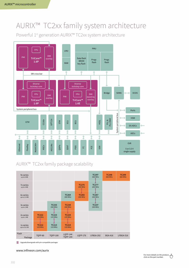
332
For more details on the product, click on the part number.
AURIX™ microcontroller
www.infineon.com/aurix
AURIX™ TC2xx family system architecturePowerful 1st generation AURIX™ TC2xx system architecture
AURIX™ TC2xx family package scalability
FPU PMU
PMI DMIoverlay Data flash
BROMkey flash
Progr.flash
Progr.flash
LMU
Ethe
rnet
GTM
EVR
5 or 3.3 Vsingle supplyFl
exRa
y
Mul
tiCAN
+
MSC
x
ASCL
INx
QSP
Ix
SEN
T
PSI5
I2 C
FCE
IOM
HSS
L
PLL
&PL
L ER
AYPorts
HSM
DS-ADCx
ADCx
CCU
6x
GPT1
2x
STM
SCU
BCU
SDMABridge OCDS
RAM
SRI cross bar
Syst
em p
erip
hera
l bus
System peripheral bus
TriCore™1.6P
FPU
Diverselockstep core
Diverselockstep core
PMI DMIoverlay
TriCore™1.6P
FPUPMI
DMIstand-byoverlayTriCore™
1.6E
9x seriesup to 8 MB
TQFP-80LQFP-144TQFP-144
TQFP-100 LQFP-176 LFBGA-292 BGA-416 LFBGA-516
TC297
300 MHzTC298
300 MHzTC299
300 MHz
7x seriesup to 4 MB
TC275
200 MHzTC277
200 MHz
TC267
200 MHz
TC237
200 MHz
6x seriesup to 2.5 MB
TC264
200 MHzTC265
200 MHz
3x seriesup to 2 MB
TC233
200 MHzTC234
200 MHz
2x seriesup to 1 MB
TC223
133 MHzTC224
133 MHz
TC214
133 MHz1x seriesup to 512 KB
Flash
Package
TC213
133 MHz
TC222
133 MHz
TC212
133 MHz
Upgrade/downgrade with pin-compatible packages

333
For more details on the product, click on the part number.
www.infineon.com/aurix
AURIX™ microcontroller
AURIX™ TC2xx portfolio
Prod
uct t
ype
Max
. clo
ck fr
eque
ncy [
MHz
]
Prog
ram
mem
ory [
kB]
SRAM
(inc
l. ca
che)
[kB]
Co-p
roce
ssor
1)
Core
s/lo
ckst
ep
Tim
ed I/
O
Num
ber o
f ADC
chan
nels
Exte
rnal
bus
inte
rface
CAN
node
s
Com
mun
icatio
n in
terfa
ces 2)
Tem
pera
ture
rang
es 3)
Pa
ckag
es
Addi
tiona
l fea
ture
s/re
mar
ks 4)
TC299TX 300 8000 2728 FPU 3/1 263 84/10 DS yes 6 4xASCLIN, 6xQSPI, 3xMSC, 2xI2C, 15xSENT, HSSL, 5xPSI5, 2xFlexRay, Ethernet, CAN FD K LFBGA-516 EVR, STBU, HSM
TC299TP 300 8000 728 FPU 3/1 263 84/10 DS yes 6 4xASCLIN, 6xQSPI, 3xMSC, 2xI2C, 15xSENT, HSSL, 5xPSI5, 2xFlexRay, Ethernet, CAN FD K LFBGA-516 EVR, STBU, HSM
TC298TP 300 8000 728 FPU 3/1 232 60/10 DS yes 6 4xASCLIN, 6xQSPI, 3xMSC, 2xI2C, 15xSENT, HSSL, 5xPSI5, 2xFlexRay, Ethernet, CAN FD K LBGA-416 EVR, STBU, HSM
TC297TA 300 8000 2728 FPU, FFT, CIF 3/1 169 60/10 DS no 6 4xASCLIN, 4xQSPI, 3xMSC, 2xI2C, 15xSENT, HSSL, 5xPSI5, 2xFlexRay, Ethernet, CAN FD K LFBGA-292 EVR, STBU, HSM
TC297TX 300 8000 2728 FPU 3/1 263 60/10 DS no 6 4xASCLIN, 4xQSPI, 3xMSC, 2xI2C, 15xSENT, HSSL, 5xPSI5, 2xFlexRay, Ethernet, CAN FD K LFBGA-292 EVR, STBU, HSM
TC297TP 300 8000 728 FPU 3/1 169 60/10 DS no 6 4xASCLIN, 4xQSPI, 3xMSC, 2xI2C, 15xSENT, HSSL, 5xPSI5, 2xFlexRay, Ethernet, CAN FD K LFBGA-292 EVR, STBU, HSM
TC277TP 200 4000 472 FPU 3/2 169 60/6 DS no 4 4xASCLIN, 4xQSPI, 2xMSC, HSSL, 2xI2C, 10xSENT, 3xPSI5, FlexRay, Ethernet, CAN FD K LFBGA-292 EVR, WUT, HSM
TC275TP 200 4000 472 FPU 3/2 112 60/6 DS no 4 4xASCLIN, 4xQSPI, 2xMSC, HSSL, 2xI2C, 10xSENT, 3xPSI5, FlexRay, Ethernet, CAN FD K LQFP-176 EVR, WUT, HSM
TC267D 200 2500 240 FPU 2/1 169 50/3 DS no 5 4xASCLIN, 4xQSPI, 2xMSC, 2xI2C, 10xSENT, 3xPSI5, HSSL, FlexRay, Ethernet, CAN FD K LFBGA-292 EVR, STBU
TC265D 200 2500 240 FPU 2/1 112 50/3 DS no 5 4xASCLIN, 4xQSPI, 2xMSC, 2xI2C, 10xSENT, HSSL, 3xPSI5, FlexRay, Ethernet, CAN FD K LQFP-176 EVR, STBU
TC264DA 200 2500 752 FPU, FFT, CIF 2/1 88 40/3 DS no 5 4xASCLIN, 4xQSPI, 2xMSC, 2xI2C, 10xSENT, HSSL, 3xPSI5, FlexRay, Ethernet, CAN FD K LQFP-144 EVR, STBU
TC264D 200 2500 240 FPU 2/1 88 40/3 DS no 5 4xASCLIN, 4xQSPI, 2xMSC, 2xI2C, 10xSENT, HSSL, 3xPSI5, FlexRay, Ethernet, CAN FD K LQFP-144 EVR, STBU
TC237LP 200 2000 192 FPU 1/1 120 24 no 6 2xASCLIN, 4xQSPI, 4xSENT, FlexRay, CAN FD K LFBGA-292 EVR, WUT, HSM
TC234LA 200 2000 704 FPU, FFT 1/1 120 24 no 6 2xASCLIN, 4xQSPI, 4xSENT, FlexRay, Ethernet K TQFP-144 EVR, WUT, HSM
TC234LX 200 2000 704 FPU 1/1 120 24 no 6 2xASCLIN, 4xQSPI, 4xSENT, FlexRay, Ethernet K TQFP-144 EVR, WUT, HSM
TC234LP 200 2000 192 FPU 1/1 120 24 no 6 2xASCLIN, 4xQSPI, 4xSENT, FlexRay, CAN FD K TQFP-144 EVR, WUT, HSM
TC233LP 200 2000 192 FPU 1/1 78 24 no 6 2xASCLIN, 4xQSPI, 4xSENT, FlexRay, CAN FD K TQFP-100 EVR, WUT, HSM
TC224L 133 1000 96 FPU 1/1 120 24 no 3 2xASCLIN, 4xQSPI, 4xSENT, CAN FD K TQFP-144 EVR, WUT
TC223L 133 1000 96 FPU 1/1 78 24 no 3 2xASCLIN, 4xQSPI, 4xSENT, CAN FD K TQFP-100 EVR, WUT
TC222L 133 1000 96 FPU 1/1 59 24 no 3 2xASCLIN, 4xQSPI, 4xSENT, CAN FD K TQFP-80 EVR, WUT
TC214L 133 500 96 FPU 1/1 120 14 no 3 2xASCLIN, 4xQSPI, 4xSENT, CAN FD K TQFP-144 EVR, WUT
TC213L 133 500 96 FPU 1/1 78 24 no 3 2xASCLIN, 4xQSPI, 4xSENT, CAN FD K TQFP-100 EVR, WUT
TC212L 133 500 96 FPU 1/1 59 24 no 3 2xASCLIN, 4xQSPI, 4xSENT, CAN FD K TQFP-80 EVR, WUT
1) CIF = camera and external ADC Interface, FFT = fast fourier transform accelerator, FPU = floating point unit, PCP = peripheral control processor2) ASC = asynchronous serial channel, ASCLIN = asyn/synchronous local interconnect network, HSSL= high-speed serial link, I2C = inter-integrated circuit,
LIN = local interconnect network, MLI = micro link interface, MSC = micro second channel, PSI5 = peripheral sensor interface 5, QSPI = queued serial peripheral interface, SENT = single edge nibble transmission, SSC = synchronous serial channel, CAN FD ISO11898-1:2015
3) Ambient temperature range: A = -40°C ... 140°C, B = 0°C ... 70°C, F = -40°C ... 85°C, H = -40°C ... 110°C, K = -40°C ... 125°C, L = -40°C ... 150°C, X = -40°C ... 105°C4) EVR = embedded voltage regulator, HSM = hardware security module, STBU = stand-by control unit, WUT = wake-up timer
Evolution from TC2xx to TC3xx - Easy migration with focus on reuse
› Fast conversion of existing AURIX™ TC2xx designs – Backwards compatibility – High AURIX™ TC3xx compatibility to pinout of existing QFP100/144/176 and BGA packages
› Flexibility - scalability within the AURIX™ TC3xx family – Up-/Downgrade paths for devices in identical packages – Compatible pin-out of QFP/BGA package options enabling combination designs
› Pin-to-pin compatibility between the devices of AURIX™ TC2xx/TC3xx and from generation to generation › A high scalability with a very large portfolio for both AURIX™ TC2xx and TC3xx
Appl
icat
ions
Pa
cka
ges
20
-30
0 V
MO
SF
ETs
50
0-9
50
V M
OS
FE
TsW
BG
se
mic
on
du
cto
rsD
iscr
ete
IGB
TsP
ow
er
ICs
Inte
llig
en
t sw
itch
es
an
d in
pu
t IC
sG
ate
dri
ver
ICs
Mic
roco
ntr
oll
ers
XE
NS
IV™
se
nso
rs

334
For more details on the product, click on the part number.
AURIX™ TC3xx family system architectureAURIX™ TC3xx – scalable family - from low-cost to high-performance applications
AURIX™ TC3xx provides an upgrade on key parameters with focus on SW & HW reuse
www.infineon.com/aurix
AURIX™ microcontroller
EVADC
FC
OM
P
Se
con
da
ry A
DC
Pri
ma
ry A
DC
ED
S A
DC
GT
M
CC
U6
GP
T
ST
M
ER
AY
CA
N F
D
AS
C L
IN
QS
PI/
I2S
(e
mu
lati
on
)
I2C
PS
I5
PS
I5S
SE
NT
LMU DAMLarge
MEM
Mini
MCDS
SPU
RIFCIF
SPU
RIF
DflashPflash
0 … 5
ETH
MACDMA
SFI
bridge
HSSL
HSCT
eM
MC
/SD
IO
Std
By
ctrl
HS
M
FC
E
MS
C
HS
DP
M
SC
U
IOM
Po
rt
System resource interconnect
System
peripheral
bus
Memories
› Larger SRAM
› SRAM/flash ratio increased
› Enhanced MPU
› A/B swap support
Stand-by control unit
› Low-power modes
ADAS
› LVDS IF
› Signal processing unit
ADC
› Improvement of existing ADC
› Reduction of capacitive load
Delta-sigma
› Enhanced concept
Performance
› New TriCore™ 162 generation
› New instructions
› Up to 6 CPUs at 300 MHz
› New direct flash access path
IO pads
all 5 V/3.3 V
Ethernet
› 1 Gbit/s ETH
› QoS services
› Remote DMA
HSM: Full EVITA compliance
› New accelerators ECC256/SHA256
› Available on all devices
Safety
› LBIST
› MBIST upgrade
eMMC/SDIO
› External NAND flash IF
Checker coreChecker core
Checker core
CP
U5
CP
U4
CP
U3
CP
U2
CP
U1
Checker core
TC 1.6P
CPU0
FPU
PSPR, PCACHE
DSPR, DCACHE
Increased from 3 to 6 cores
Developed in 40 nm for power consumption reduction
Fully compatible devices with focus on HW & SW reuse
IEC61508 compliant enabling SiL-3 level
Upgraded to Full EVITA support
Richer peripheral set
Full support of SOTA A/B swap
Performance increase and reduction of power
Scalable & backwards compatible to TC2xx
Functional safety
Enhanced security
Improved networking
SOTA

335
For more details on the product, click on the part number.
www.infineon.com/aurix
AURIX™ microcontroller
› Advanced package technologies deliver the best price/performance ratio › Customers can choose between different devices in the same pin-compatible package
AURIX™ TC3xx package scalability
L – Single lockstep core
1) An option of 300 MHz is also available
D – Dual core T – Triple core Q – Quadruple core X – Sextuple core Control and actuate Sense and compute
TQFP-100TQFP-80Package
FlashBGA-180 BGA-233T/LQFP-144 LQFP-176 LFBGA-292 LFBGA-516
TC397x300 MHz
TC397XA300 MHz
TC387Qx300 MHz
TC387Q300 MHz
TC399x300 MHz
TC389Q300 MHz
TC377TX300 MHz
TC377T300 MHz
TC367D300 MHz
TC375T300 MHz
TC357TA300 MHz
TC356TA300 MHz
TC337DA1)
200 MHz
TC337L1)
200 MHz
TC366D300 MHz
TC336DA1)
200 MHz
TC336L1)
200 MHz
TC327L160 MHz
TC364D300 MHz
TC334L1)
200 MHz
TC324L160 MHz
TC333L1)
200 MHz
TC332L1)
200 MHz
TC323L160 MHz
TC322L160 MHz
8x series10 MB
7x X series6 MB
7x series6 MB
6x series4 MB
5x A series4 MB
Ax series4 MB
3x A series2 MB
3x series2 MB
2x series1 MB
9x series16 MB
9x A series16 MB
6x 300 MHz
6x 300 MHz
4x 300 MHz
4x 300 MHz
3x 300 MHz
3x 300 MHz
2x 300 MHz
4x 300 MHz
3x 300 MHz
2x 300 MHz
1x 300 MHz
1x 300 MHz
Ex series12 MB
TC365D300 MHz
TC3A8Q300 MHz
TC3A7Q300 MHz
MCU scalability Safety/security concept
AURIX™ TC3xx
› Performance and flash
› Pin compatibility
› Binary-compatible cores
Power consumption
› On-chip SC DC-DC high-eiciency power supply
› Integrated standby controller
› ISO 26262 compliance
› IEC61508 compliant
Connectivity
› Ethernet: up to 2x1 GB
› CAN FD: up to 12 channels
› eMMC IF
Appl
icat
ions
Pa
cka
ges
20
-30
0 V
MO
SF
ETs
50
0-9
50
V M
OS
FE
TsW
BG
se
mic
on
du
cto
rsD
iscr
ete
IGB
TsP
ow
er
ICs
Inte
llig
en
t sw
itch
es
an
d in
pu
t IC
sG
ate
dri
ver
ICs
Mic
roco
ntr
oll
ers
XE
NS
IV™
se
nso
rs

336
For more details on the product, click on the part number.
AURIX™ microcontroller
www.infineon.com/aurix
AURIX™ TC3xx portfolio
Prod
uct t
ype
Core
s/lo
ckst
ep
Max
cloc
k
frequ
ency
[MHz
]
Prog
ram
m
emor
y [k
B]
SRAM
(inc
l. ca
che)
[kB]
Rada
r ac
cele
rato
r/ ra
dar i
nter
face
1)
CAN/
CAN
FD
node
s
Ethe
rnet
10
0/10
00 M
bit
Exte
rnal
bus
in
terfa
ce 2
)
Com
mun
icat
ion
inte
rface
s
HSM
Tem
pera
ture
ra
nges
Pack
ages
Addi
tiona
l fe
atur
es/
rem
arks
3)
AURIX™ TC3xx family
TC399XX 6/4 300 16000 6912 no 12 1 EBU, eMMC, 2x HSSL
6x SPI, 2x FlexRay, 12x LIN, 25x SENT, 4x PSI5, 2x I2C, 4x MSC
EVITA full
K, L LFBGA-516 5 V/3.3 V EVR, 8-bit SCR
TC399XP 6/4 300 16000 2816 no 12 1 EBU, eMMC, 2x HSSL
6x SPI, 2x FlexRay, 12x LIN, 25x SENT, 4x PSI5, 2x I2C, 4x MSC
EVITA full
K, L LFBGA-516 5 V/3.3 V EVR, 8-bit SCR
TC397XX 6/4 300 16000 6912 no 12 1 eMMC, 2x HSSL
6x SPI, 2x FlexRay, 12x LIN, 25x SENT, 4x PSI5, 2x I2C, 4x MSC
EVITA full
K, L LFBGA-292 5 V/3.3 V EVR, 8-bit SCR
TC397XP 6/4 300 16000 2816 no 12 1 eMMC, 2x HSSL
6x SPI, 2x FlexRay, 12x LIN, 25x SENT, 4x PSI5, 2x I2C, 4x MSC
EVITA full
K, L LFBGA-292 5 V/3.3 V EVR, 8-bit SCR
TC397XA 6/4 300 16000 6912 2x SPU/ 8x 400 Mbit/s LVDS
12 1 2x HSSL 6x SPI, 2x FlexRay, 12x LIN, 25x SENT, 4x PSI5, 2x I2C, 4x MSC
EVITA full
K, L LFBGA-292 5 V/3.3 V EVR, 8-bit SCR
TC389QP 4/2 300 10000 1568 no 12 1 HSSL 5x SPI, 2x FlexRay, 24x LIN, 25x SENT, 4x PSI5, 2x I2C, 3x MSC
EVITA full
K, L LFBGA-516 5 V/3.3 V EVR, 8-bit SCR
TC387QP 4/2 300 10000 1568 no 12 1 HSSL 5x SPI, 2x FlexRay, 24x LIN, 25x SENT, 4x PSI5, 2x I2C, 3x MSC
EVITA full
K, L LFBGA-292 5 V/3.3 V EVR, 8-bit SCR
TC377TX 3/3 300 6000 4208 no 12 2 eMMC, HSSL 5x SPI, 1x FlexRay, 12x LIN, 15x SENT, 2x PSI5, 1x I2C, 2x MSC
EVITA full
K, L LFBGA-292 5 V/3.3 V EVR, 8-bit SCR
TC377TP 3/2 300 6000 1136 no 8 1 HSSL 5x SPI, 1x FlexRay, 12x LIN, 15x SENT, 2x PSI5, 1x I2C, 2x MSC
EVITA full
K, L LFBGA-292 5 V/3.3 V EVR, 8-bit SCR
TC375TP 3/2 300 6000 1136 no 8 1 HSSL 5x SPI, 1x FlexRay, 12x LIN, 15x SENT, 2x PSI5, 1x I2C, 2x MSC
EVITA full
K, L LQFP-176 5 V/3.3 V EVR, 8-bit SCR
TC367DP 2/2 300 4000 672 no 8 1 HSSL 4x SPI, 1x FlexRay, 12x LIN, 10x SENT, 2x PSI5, 1x I2C, 1x MSC
EVITA full
K, L LFBGA-292 5 V/3.3 V EVR, 8-bit SCR
TC366DP 2/2 300 4000 672 no 8 1 HSSL 4x SPI, 1x FlexRay, 12x LIN, 10x SENT, 2x PSI5, 1x I2C, 1x MSC
EVITA full
K, L LFBGA-196 5 V/3.3 V EVR, 8-bit SCR
TC365DP 2/2 300 4000 672 no 8 1 HSSL 4x SPI, 1x FlexRay, 12x LIN, 10x SENT, 2x PSI5, 1x I2C, 1x MSC
EVITA full
K, L LQFP-176 5 V/3.3 V EVR, 8-bit SCR
TC364DP 2/2 300 4000 672 no 8 1 HSSL 4x SPI, 1x FlexRay, 12x LIN, 10x SENT, 2x PSI5, 1x I2C, 1x MSC
EVITA full
K, L TQFP-144 5 V/3.3 V EVR, 8-bit SCR
TC364DP 2/2 300 4000 672 no 8 1 HSSL 4x SPI, 1x FlexRay, 12x LIN, 10x SENT, 2x PSI5, 1x I2C, 1x MSC
EVITA full
K, L LQFP-144 5 V/3.3 V EVR, 8-bit SCR
TC357TA 3/2 300 4000 3664 2x SPU/ 8x 400 Mbit/s LVDS
8 1 no 4x SPI, 1x FlexRay, 4x LIN EVITA full
K, L LFBGA-292 5 V/3.3 V EVR, 8-bit SCR
TC356TA 3/2 300 4000 3664 2x SPU/ 8x 400 Mbit/s LVDS
8 1 no 4x SPI, 1x FlexRay, 4x LIN EVITA full
K, L LFBGA-196 5 V/3.3 V EVR, 8-bit SCR
TC337DA 2/1 200 2000 1568 1x SPU/ 4x 400 Mbit/s LVDS
8 1 eMMC 4x SPI, 1x FlexRay, 12x LIN, 6x SENT EVITA full
K, L LFBGA-292 5 V/3.3 V EVR, 8-bit SCR
TC336DA 2/1 200 2000 1568 1x SPU/ 4x 400 Mbit/s LVDS
8 1 eMMC 4x SPI, 1x FlexRay, 12x LIN, 6x SENT EVITA full
K, L LFBGA-196 5 V/3.3 V EVR, 8-bit SCR
TC337LP 1/1 200 2000 248 no 8 no no 4x SPI, 1x FlexRay, 12x LIN, 6x SENT EVITA full
K, L LFBGA-292 5 V/3.3 V EVR, 8-bit SCR
TC336LP 1/1 200 2000 248 no 8 no no 4x SPI, 1x FlexRay, 12x LIN, 6x SENT EVITA full
K, L LFBGA-196 5 V/3.3 V EVR, 8-bit SCR
TC334LP 1/1 200 2000 248 no 8 no no 4x SPI, 1x FlexRay, 12x LIN, 6x SENT EVITA full
K, L TQFP-144 5 V/3.3 V EVR, 8-bit SCR
TC333LP 1/1 200 2000 248 no 8 no no 4x SPI, 1x FlexRay, 12x LIN, 6x SENT EVITA full
K, L TQFP-100 5 V/3.3 V EVR, 8-bit SCR
TC332LP 1/1 200 2000 248 no 8 no no 4x SPI, 1x FlexRay, 12x LIN, 6x SENT EVITA full
K, L TQFP-80 5 V/3.3 V EVR, 8-bit SCR
TC327LP 1/1 160 1000 96 no 8 no no 4x SPI, 6x SENT, 6x LIN EVITA full
K, L LFBGA-292 5 V/3.3 V EVR, 8-bit SCR
TC324LP 1/1 160 1000 96 no 8 no no 4x SPI, 6x SENT, 6x LIN EVITA full
K, L TQFP-144 5 V/3.3 V EVR, 8-bit SCR
TC323LP 1/1 160 1000 96 no 8 no no 4x SPI, 6x SENT, 6x LIN EVITA full
K, L TQFP-100 5 V/3.3 V EVR, 8-bit SCR
TC322LP 1/1 160 1000 96 no 8 no no 4x SPI, 6x SENT, 6x LIN EVITA full
K, L TQFP-80 5 V/3.3 V EVR, 8-bit SCR
1) SPU – Signal processing unit2) HSSL – High-speed serial link3) 8-bit SCR – Standby controller for low power modes4) EVR – Embedded voltage regulator

337
For more details on the product, click on the part number.
AURIX™ microcontroller
www.infineon.com/aurix-kits
AURIX™ starter and application kitsInfineon starter kits – 32-bit microcontrollers
AURIX™ Triboards Kits
› Full evaluation board for development to write and debug your 1st programs
› Includes getting started advice, free TriCore™ entry tool chain, technical documentation, compiler and debugger
› TriBoard available for all productive silicon
AURIX™ TFT Kits
› Low cost board for early evaluation with limited access to signals
› Additional touchscreen display for convenient handling › TFT board available for every silicon
Click on the following to find/purchase the kit: www.infineon.com/aurix-kits
Arduino ShieldBuddy KitsOrder number: KIT_AURIX_TC275_ARD_SB
› The Hitex TC275/TC375 ShieldBuddy follows the Arduino standard › Compatible with 100’s of Arduino application shields › Evaluation licenses available › Ideal for getting started on a high-end real time embedded industrial
or automotive application as well as students and hobbyists
AURIX™ TC275 Lite kit
› AURIX™ TC275/TC375 device in LQFP-176 package › FTDI based debugger with micro USB › Use of Arduino Uno/compatible platform › Coming soon
Appl
icat
ions
Pa
cka
ges
20
-30
0 V
MO
SF
ETs
50
0-9
50
V M
OS
FE
TsW
BG
se
mic
on
du
cto
rsD
iscr
ete
IGB
TsP
ow
er
ICs
Inte
llig
en
t sw
itch
es
an
d in
pu
t IC
sG
ate
dri
ver
ICs
Mic
roco
ntr
oll
ers
XE
NS
IV™
se
nso
rs
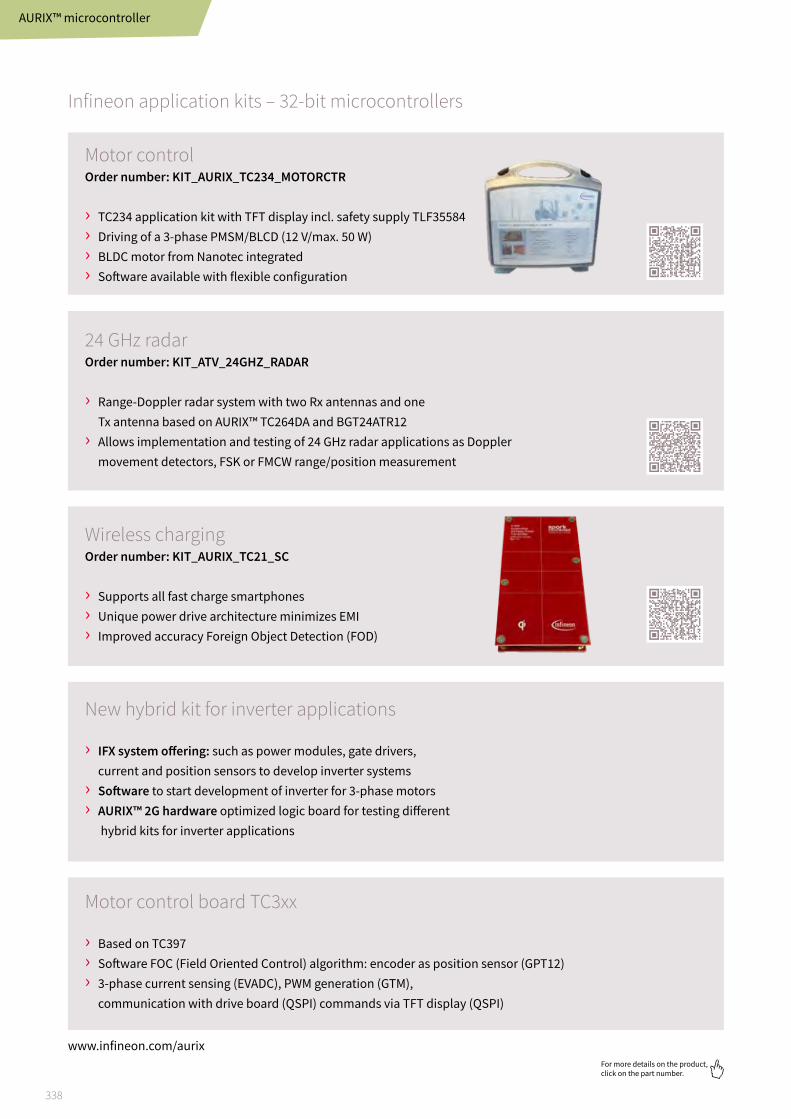
338
For more details on the product, click on the part number.
Infineon application kits – 32-bit microcontrollers
www.infineon.com/aurix
AURIX™ microcontroller
New hybrid kit for inverter applications
› IFX system offering: such as power modules, gate drivers, current and position sensors to develop inverter systems
› Software to start development of inverter for 3-phase motors › AURIX™ 2G hardware optimized logic board for testing different
hybrid kits for inverter applications
Motor control board TC3xx
› Based on TC397 › Software FOC (Field Oriented Control) algorithm: encoder as position sensor (GPT12) › 3-phase current sensing (EVADC), PWM generation (GTM),
communication with drive board (QSPI) commands via TFT display (QSPI)
Motor controlOrder number: KIT_AURIX_TC234_MOTORCTR
› TC234 application kit with TFT display incl. safety supply TLF35584 › Driving of a 3-phase PMSM/BLCD (12 V/max. 50 W) › BLDC motor from Nanotec integrated › Software available with flexible configuration
24 GHz radarOrder number: KIT_ATV_24GHZ_RADAR
› Range-Doppler radar system with two Rx antennas and one Tx antenna based on AURIX™ TC264DA and BGT24ATR12
› Allows implementation and testing of 24 GHz radar applications as Doppler movement detectors, FSK or FMCW range/position measurement
Wireless chargingOrder number: KIT_AURIX_TC21_SC
› Supports all fast charge smartphones › Unique power drive architecture minimizes EMI › Improved accuracy Foreign Object Detection (FOD)

339
For more details on the product, click on the part number.
Industrial roboticsApplication example
Application features › High computing performances › High level of accuracy, integration and efficiency › Safety management in line with current norms › Various topologies for axes, joints and motors › Security features that protect intellectual property
from counterfeiting
Suggested products › TC23x › TC33x › TC36x › TC37x
› TC38x › TC39x › XMC4xxx
System benefits › High computing performance: up to 6x 300 MHz › High flexibility thanks to tailored peripherals › Integrated safety support
(EN ISO 10218 and ISO/TS15066) › Integrated security with hardware security module › Robust 3 V-, 5 V-, LVDS – PortPins › Large portfolio with long-term availability
www.infineon.com/aurix
Current sensing
Position sensing
Actuators
Gate driver
Hall latches
Sensor interface
XMC4xxx
3-phase
inverterM
Power management
SMPS
LDO
DC-DC
Angle sensor
LEDs
Authentication
Security
Wireless
CAN
USB
Communications
Sensing
Human-device
interface
EtherCAT
Gyro
Pushbutton
Accelerometer
Output signal
Pressure sensor
Light/optical sensor
3D image sensor
Radar sensor
32-bit MCU
AURIX™
AURIX™ microcontroller
Appl
icat
ions
Pa
cka
ges
20
-30
0 V
MO
SF
ETs
50
0-9
50
V M
OS
FE
TsW
BG
se
mic
on
du
cto
rsD
iscr
ete
IGB
TsP
ow
er
ICs
Inte
llig
en
t sw
itch
es
an
d in
pu
t IC
sG
ate
dri
ver
ICs
Mic
roco
ntr
oll
ers
XE
NS
IV™
se
nso
rs

340
For more details on the product, click on the part number.
AURIX™ microcontroller
www.infineon.com/aurix
Preferred Design Houses (PDH) and software resellers
The preferred design house extends the support force by specifying and customizing the know-how. Furthermore, it brings an additional value for customer service. The preferred design house supports the set up for systems using AURIX™ and XMC™ , including software and other Infineon products. Our partners are trained to use AURIX™ and XMC™.
› 1st level customer support covering Infineon products/solutions
› Technical interface and support to the customer
› Driving design at customer › Basic training for design teams
at customer › 24 h response time to the customer
› Project management and project-specific application support
› Specification of general software architec-ture, defining required layers, control and data flow structure etc.
› Specification and implementation of custom device drivers
› Optimization of software components with regard to speed/code size
Classic(Free of charge)
Premium(Consultancy mode)
To be agreed between customers and PDH
› Software testing › Support for project-specific
functional safety engineering › Project-specific support for
security solution › Safety support › Security support › Multicore support
AURIX™ and XMC™ PDH partners
Basic ••Essential principles and elementary know-how to support
a customer; provision of basic training for design teams
Advanced ••High-level project-specific
application support/consulting
Expert ••Extensive knowledge and ability
to fully support development

341
For more details on the product, click on the part number.
www.infineon.com/embeddedpower
Criteria TLE984x TLE9845 TLE9850/1 TLE985x TLE986x TLE987xController Arm® Cortex®-M0 Arm® Cortex®-M3
Core frequency 25-40MHz 40 MHz 24-40MHz
Flash size 36KB – 64KB 48KB 48/64KB 48KB – 96KB 36KB – 128KB (Extension to 256KB in development)
Driver stage Relay Half-bridge H-bridge B6-bridge
Relay PN FET half-bridge * NN FET falf-Bridge N FET H-bridge N FET B6-bridge
HV monitor inputs 4-5 5 4 0-1
Junction temperature levels
150°C 150°C 150°C and 175°C 150°C and 175°C 150°C and 175°C
Packages VQFN-48-31 VQFN-48-31VQFN-48-29
VQFN-48-31VQFN-48-29
VQFN-48-29 and VQFN-48-31(TQFP-48 planned)
Features and benefits
Key featuresExtensive diagnostics and protections embedded within the system-on-chip
Minimum number of external components needed
Platform based approach with compatible software between the product families
Data processing, actuation and sensing integrated into the product with 32-bit Arm® Cortex®-M
Leadless VQFN package with 7x7 mm footprint
Intelligent power saving modes including stop and sleep mode and energy management for external sensors (on demand)
Customer benefitsHigh levels of system reliability
Reduced cost
Support multiple and flexible designs with minimal effort
Space saving
Energy saving
Embedded power ICs
System-on-chip solution for motor control applications
Infineon‘s Embedded power ICs include a 32-bit Arm® Cortex®-M microcontroller, a voltage regulator, the communication interfaces, along with the driving stages for motor control applications. These system-on-chip solutions offer an unmatched level of integration of all functions required to sense, control and actuate a motor. They save space and energy, improve the overall system reliability through advanced diagnosis features and reduce the overall cost due to a minimum number of external components. They perfectly fit with a range of motor control applications where a small package form factor and a minimum number of external components are essential.
› Embedded power ICs enable mechatronic motor control solutions for either relay, half-bridge or fullbridge DC and BLDC motor applications
› They are supported by a complete development tool chain provided by Infineon and third party vendors. The tool chain includes compilers, debuggers, evaluation boards, LIN low level drivers and configuration tools as well as variety of example software code.
Embedded power ICs
Powersupply
Interface
Supporting Functionality
Position measurement
Switch panel inputs
Output driver
Discrete control
or
Microcontroller
Bridge driver
or
Relay driver
MOSFET
of
RelayM
M
M
PWM
LIN
Input
signals
Uni-direction
(DC brush motor)
+12 V from
battery
Embedded power IC
2-phase
(DC brush motor)
3-phase
(Brushless DC motor)
-BLDC-
or
or
Appl
icat
ions
Pa
cka
ges
20
-30
0 V
MO
SF
ETs
50
0-9
50
V M
OS
FE
TsW
BG
se
mic
on
du
cto
rsD
iscr
ete
IGB
TsP
ow
er
ICs
Inte
llig
en
t sw
itch
es
an
d in
pu
t IC
sG
ate
dri
ver
ICs
Mic
roco
ntr
oll
ers
XE
NS
IV™
se
nso
rs

342
For more details on the product, click on the part number.
Features and benefits
Key featuresImplemented motor control algorithms (FOC, BEMF, Hall)
Controlled over Arduino via SPI
Compatible with the Arduino Uno or the Infineon XMC™ baseboard
Up to four Shields can be used simultaneously
Each Shield can be controlled independently
Motor parameters can be set for each Shield individually
Customer benefitsEasy to use API, allowing the user to quickly setup an application
High performance BLDC motor control in form of the TLE987x chip
www.infineon.com/bldcmotorshieldwww.infineon.com/shields-for-arduino
Embedded power ICs
3-phase motor control shield with TLE9879QXA40
The BLDC Shield for Arduino uses the TLE9879QXA40 chip, which is a part of the TLE987x family of the Infineon Embedded power IC portfolio. It enables the shield to drive 3-phase BLDC motors with a variety of different features.One Arduino base board can control up to four BLDC shields via SPI. The BLDC Shield firmware provides an autoaddressing functionality. Every shield in the stack can be controlled independently and run completely differentmotor control algorithms if desired.
The shield implements three different advanced motor control algorithms: › Sensorless field-oriented control (FOC), › Block commutation with back EMF (BEMF) › Hall based block commutation (HALL)
The firmware can be changed using the SWD InterfaceAdditional connectors for voltage supply, motor-phasesand hall sensors speed up the evaluation.
Our BLDC Shield for Arduino comes with a librarywhich includes a collection of code that makes it easyfor you to run your project. The Arduino library offersan intuitive API to quickly setup and configure anapplication.
BLDC Motor Control Shield for Arduino

343
For more details on the product, click on the part number.
Microcontroller support
Further information, datasheets and documentswww.infineon.com/xmcwww.infineon.com/xmc1000www.infineon.com/xmc4000www.infineon.com/aurixwww.infineon.com/makers
XMC SC Wireless power controller:www.infineon.com/xmcscwirelesspowercontrollers
Infineon support for industrial microcontrollersOne platform, countless solutions
XMC™ MCUs ecosystem and enablement – kits, board, tools and software
Boards and kits: www.infineon.com/xmc-devwww.infineon.com/connectivitykitwww.infineon.com/ethercat
Ecosystem and tools:www.infineon.com/xmc-ecosystem
DAVE™ IDE:www.infineon.com/dave
Appl
icat
ions
Pa
cka
ges
20
-30
0 V
MO
SF
ETs
50
0-9
50
V M
OS
FE
TsW
BG
se
mic
on
du
cto
rsD
iscr
ete
IGB
TsP
ow
er
ICs
Inte
llig
en
t sw
itch
es
an
d in
pu
t IC
sG
ate
dri
ver
ICs
Mic
roco
ntr
oll
ers
XE
NS
IV™
se
nso
rs

344
XENSIV™ sensors
For more details on the product, click on the part number.
› XENSIV™ pressure sensors › XENSIV™ current sensors › XENSIV™ magnetic position sensors › Intuitive sensing › XENSIV™ MEMS microphone
› XENSIV™ pressure sensor › XENSIV™ 24 GHz radar sensor ICs › XENSIV™ 60 GHz radar sensor IC › Shield2Go › Sensor 2GO kits
Sensors

345
For more details on the product, click on the part number.
Appl
icat
ions
Pa
cka
ges
20
-30
0 V
MO
SF
ETs
50
0-9
50
V M
OS
FE
TsW
BG
se
mic
on
du
cto
rsD
iscr
ete
IGB
TsP
ow
er
ICs
Inte
llig
en
t sw
itch
es
an
d in
pu
t IC
sG
ate
dri
ver
ICs
Mic
roco
ntr
oll
ers
XE
NS
IV™
se
nso
rs

346
For more details on the product, click on the part number.
XENSIV™

347
For more details on the product, click on the part number.
XENSIV™
Infineon XENSIV™ – sensing the world
Infineon XENSIV™ sensors are exceptionally precise thanks to industry-leading technologies. They are the perfect fit for various customer applications in automotive, industrial and consumer markets.
From the world leader in sensing technology, XENSIV™ sensors simplify lives by enabling “things” to “see”, “hear”, “feel” and intuitively “understand” their environment. As a result of proven quality and outstanding reliability, customers can rely on XENSIV™ for system stability, durability and integrity. Providing high accuracy and best-in-class measurement performance, XENSIV™ sensors add great value to customer applications. More than 40 years of experience in sensing solutions and a deep-rooted system understanding result in the broadest portfolio of ready-to-use sensor solutions on the market. Ecosystem partners and our customers partner with us for leading technologies, perfect-fit solutions and continuous innovation.
With a proven track record in IoT innovation, we continue to seamlessly and securely connect people and machines. Many IoT trends, such as smart devices and wearables, electromobility and connected cars, smart factories and homes, and energy intelligence are being driven by technologies that develop with XENSIV™ sensors families as one of their key elements. Today, we are already inspiring the next generation of smart environments, capable of understanding and responding to human communication. Infineon's semiconductors are at the very heart of machine-to-machine (M2M), human-machine interface (HMI), mobile and wireless infrastructure technologies. As the technological boundary between humans and machines gradually disappears, these devices need even more advanced intelligence, enriched with voice assistance capabilities and the latest sensor fusion innovations, not to mention robust security technologies to protect personal data. Infineon’s sensors and microphones are already delivering this intelligent functionality and inspiring the next step in mobile connectivity.
www.infineon.com/xensiv
Appl
icat
ions
Pa
cka
ges
20
-30
0 V
MO
SF
ETs
50
0-9
50
V M
OS
FE
TsW
BG
se
mic
on
du
cto
rsD
iscr
ete
IGB
TsP
ow
er
ICs
Inte
llig
en
t sw
itch
es
an
d in
pu
t IC
sG
ate
dri
ver
ICs
Mic
roco
ntr
oll
ers
XE
NS
IV™
se
nso
rs

348
For more details on the product, click on the part number.
XENSIV™ pressure sensors
Absolute pressure sensors (MAP and BAP)
KP21x/KP22x – Analog manifold air pressure sensor IC family (MAP + turbo MAP)
KP23x – Analog barometric air pressure (BAP) sensor IC family
KP25x/KP264 – Digital barometric air pressure (BAP) sensor IC family
Infineon's pressure sensors are ideal for a wide range of applications in automotive and industrial sectors. Typical applications in automotive include side airbag, engine control and seat comfort with high quality, highly accurate products adhering to ISO26262 standard. Infineon offers the ideal portfolio for these systems.
The analog and digital interfaces of Infineon's pressure sensors provide customers with a high degree of design flexibility and enable manufacturers to meet evolving market demands.
Features › Manifold air pressure measurement –
MAP and turbo MAP › Excellent accuracy of up to 1.0 kPa over a large
temperature range › Ratiometric analog voltage output proportional
to the applied pressure › Output signal fully compensated over pressure and
temperature
› Pressure range from 10 to 400 kPa › Temperature range from -40 to +140°C › Output clamping (optional) › Complete product family available with multiple
transfer function › Reverse polarity protection › Green SMD package
Features › Absolute air pressure measurement › Excellent accuracy of 1.0 kPa over a large temperature
range › Ratiometric analog voltage output proportional
to the applied pressure › Output signal fully compensated across pressure and
temperature range
› Pressure range from 40 to 165 kPa › Temperature range from -40 to +125°C › Serial service interface › Open bond detection (OBD) for supply and GND › Inverse polarity protection › Green SMD package
Features › Absolute air pressure measurement › Excellent accuracy of 1.0 kPa over a large temperature range › Real 10-bit pressure resolution › Integrated temperature sensor › Real 10-bit temperature resolution › Power-down mode for reduced power consumption › Self diagnosis features
› Output signal fully compensated across pressure and temperature range
› Pressure range from 40 to 165 kPa › Temperature range from -40 to +125°C › Green SMD package
www.infineon.com/pressure

349
For more details on the product, click on the part number.
XENSIV™ pressure sensors
KP276 Media robust MAP sensor with digital interface
Features › Media robustness for current automotive requirements › Digital single edge nibble transmission (SENT) interface (282 clock ticks) › Excellent accuracy of ±0.77 percent FSS › Green SMD package › Temperature range -40 to +170°C › Integrated NTC temperature sensor functionality with fast start up time (typ. 10ms)
Block diagram
Integrated pressure sensor ICs for manifold and barometric air pressure
Pressure
cells
Voltage
regulator
Analog
Normal mode/
Digital
diagnosis mode
E2PROM
interfaceE2PROM
Temperature
compensationROM
Reset
VDDA
MUX
Digital
signal
processing
(interface driver)
Buer amplifier
NTC conditioning
ADC
Digital
core
(iSM)
SPI
interface
VDD
NCS
NTCIN
CLK
SDI
SDO
GND
SENTOUT
VDDD
Product Pressure range [kPa] Max. accuracy [kPa] Max. operating temperature [°C] Automotive Industrial
KP21x * 10 ... 150 1.0 140
KP22x * 10 ... 400 2.5 140
KP23x * 15 ... 115 1.0 125
KP236N6165 60 ... 165 1.0 125
KP253 60 ... 165 1.0 125
KP254 40 ... 115 1.5 125
KP255 * 10 ... 125 1.4 140
KP256 60 ... 165 1.0 125
KP264 40...115 1.5 125
KP276 * 10 ... 400 3.0 170
www.infineon.com/pressure *For more information on the product, contact our product support
Appl
icat
ions
Pa
cka
ges
20
-30
0 V
MO
SF
ETs
50
0-9
50
V M
OS
FE
TsW
BG
se
mic
on
du
cto
rsD
iscr
ete
IGB
TsP
ow
er
ICs
Inte
llig
en
t sw
itch
es
an
d in
pu
t IC
sG
ate
dri
ver
ICs
Mic
roco
ntr
oll
ers
XE
NS
IV™
se
nso
rs

350
For more details on the product, click on the part number.
XENSIV™ current sensors
High-precision coreless current sensors for industrial applications
Infineon's current sensors provide accurate and stable current measurement up to 120 A. The products are intended for use in high-voltage industrial applications such as electric drives, photovoltaic inverters, power supplies or battery management systems. The coreless open-loop sensors are based on Infineon’s precise and stable Hall technology. Thus, the output signal is highly linear over temperature and lifetime. Due to a lack of an iron core, the sensor signal doesn’t show hysteresis and it doesn’t suffer from saturation. Thanks to the integrated current rail there is no need for external calibration. The differential measurement with two Hall cells ensures high accuracy even in a noisy environment with cross-talk from adjacent current lines or magnetic stray fields. Highlights of the XENSIV™ TLI4971 include best-in-class thermal performance for high currents as a result of its innovative TISON-8 package as well as isolation against high voltages. The two output pins for fast overcurrent signals can be used for pre-warning and system shut-down. Designers can program the threshold levels of the overcurrent signals and thus adapt them to individual requirements without any external components. The sensor also provides a signal in case of an over or undervoltage condition for the supply voltage. The well-established Infineon's TLI4970 combines superior accuracy with one output pin for overcurrent detection signal. The measurement signal is provided through a 3-pin serial peripheral interface (SPI) using a standard unidirectional 16-bit SPI protocol is used. Several sensors can be connected to a parallel SPI bus.
www.infineon.com/current-sensor
Product Accuracy 1) Current range [A] Bandwidth [kHz] Sensitivity [mV/A] Certification Industrial Package
TLI4971-A120T5-U-E0001 3.45% 120.0 120 kHz min. 10 UL PG-TISON-8
TLI4971-A120T5-E0001 3.45% 120.0 120 kHz min. 10 – PG-TISON-8
1) Total error over lifetime and temperature
Features › Integrated current rail with typical 225 µΩ insertion resistance enables ultralow power loss › Smallest form factor, 8x8 mm SMD, for easy integration and board area saving › Single supply voltage, 3.1 to 3.5 V › Highly accurate, scalable, DC and AC current sensing › Bandwidth greater than 120 kHz enables wide range of applications › Very low sensitivity error over temperature (max. 2.5%) › Excellent stability of offset over temperature and lifetime › High robustness to voltage slew rates up to 10 V/ns › Galvanic functional isolation up to 1150 V peak VIORM;
partial discharge capability of at least 1200 V; 4 mm clearance and creepage › Differential sensor principle ensures superior magnetic stray field suppression › Two independent fast over-current detection (OCD) pins with configurable
thresholds enable protection mechanisms for power circuitry (typical < 1.5 µs) › Precalibrated sensor
Applications › Electrical drives (up to 690 V) › Photovoltaic inverter › General purpose inverters › Overload and overcurrent detection › Current monitoring › Chargers Power supplies
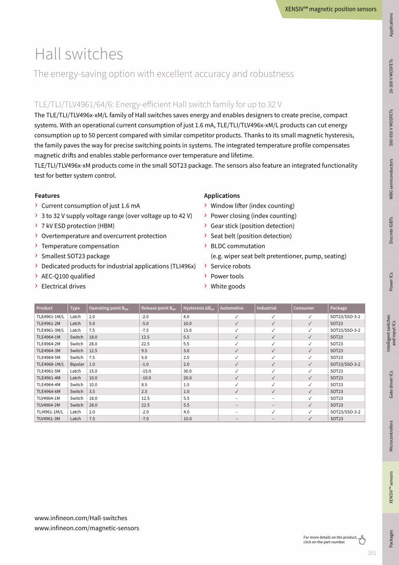
351
For more details on the product, click on the part number.
Product Type Operating point BOP Release point BRP Hysteresis ΔBHY Automotive Industrial Consumer Package
TLE4961-1M/L Latch 2.0 -2.0 4.0 SOT23/SSO-3-2TLE4961-2M Latch 5.0 -5.0 10.0 SOT23TLE4961-3M/L Latch 7.5 -7.5 15.0 SOT23/SSO-3-2TLE4964-1M Switch 18.0 12.5 5.5 SOT23TLE4964-2M Switch 28.0 22.5 5.5 SOT23TLE4964-3M Switch 12.5 9.5 3.0 SOT23TLE4964-5M Switch 7.5 5.0 2.5 SOT23TLE4968-1M/L Bipolar 1.0 -1.0 2.0 SOT23/SSO-3-2TLE4961-5M Latch 15.0 -15.0 30.0 SOT23TLE4961-4M Latch 10.0 -10.0 20.0 SOT23TLE4964-4M Switch 10.0 8.5 1.5 SOT23TLE4964-6M Switch 3.5 2.5 1.0 SOT23TLV4964-1M Switch 18.0 12.5 5.5 – – SOT23TLV4964-2M Switch 28.0 22.5 5.5 – – SOT23TLI4961-1M/L Latch 2.0 -2.0 4.0 – SOT23/SSO-3-2TLV4961-3M Latch 7.5 -7.0 15.0 – – SOT23
XENSIV™ magnetic position sensors
Hall switchesThe energy-saving option with excellent accuracy and robustness
TLE/TLI/TLV4961/64/6: Energy-efficient Hall switch family for up to 32 VThe TLE/TLI/TLV496x-xM/L family of Hall switches saves energy and enables designers to create precise, compact systems. With an operational current consumption of just 1.6 mA, TLE/TLI/TLV496x-xM/L products can cut energy consumption up to 50 percent compared with similar competitor products. Thanks to its small magnetic hysteresis, the family paves the way for precise switching points in systems. The integrated temperature profile compensates magnetic drifts and enables stable performance over temperature and lifetime. TLE/TLI/TLV496x-xM products come in the small SOT23 package. The sensors also feature an integrated functionality test for better system control.
Features › Current consumption of just 1.6 mA › 3 to 32 V supply voltage range (over voltage up to 42 V) › 7 kV ESD protection (HBM) › Overtemperature and overcurrent protection › Temperature compensation › Smallest SOT23 package › Dedicated products for industrial applications (TLI496x) › AEC-Q100 qualified › Electrical drives
Applications › Window lifter (index counting) › Power closing (index counting) › Gear stick (position detection) › Seat belt (position detection) › BLDC commutation
(e.g. wiper seat belt pretentioner, pump, seating) › Service robots › Power tools › White goods
www.infineon.com/Hall-switcheswww.infineon.com/magnetic-sensors
Appl
icat
ions
Pa
cka
ges
20
-30
0 V
MO
SF
ETs
50
0-9
50
V M
OS
FE
TsW
BG
se
mic
on
du
cto
rsD
iscr
ete
IGB
TsP
ow
er
ICs
Inte
llig
en
t sw
itch
es
an
d in
pu
t IC
sG
ate
dri
ver
ICs
Mic
roco
ntr
oll
ers
XE
NS
IV™
se
nso
rs

352
For more details on the product, click on the part number.
XENSIV™ magnetic position sensors
TLE/TLI4963/65-xM 5 V high-precision automotive/industrial Hall-effect sensors
By offering an excellent magnetic behavior Infineon’s switches are ideally suited for: › Index counting application with a pole wheel › Rotor position detection (BLDC motors) › Open/close detection
TLV496x-xTA/B Precision Hall-effect sensor for consumer applications in leaded package
Features › 3.0 to 5.5 V operating supply voltage › Low current consumption 1.4 mA › ESD protection 4 kV HBM › Active error compensation (chopped) › High stability of magnetic thresholds › Low jitter (typ. 0.35 μs)
› Operating temperature range: – from -40 to +170°C (TLE496x-xM) – from -40 to +125°C (TLI496x-xM)
› Small SMD package SOT23 › TLE: AEC-Q100 qualified › TLI: JESD47 qualified
Features › 3.0 to 26 V operating supply voltage › Low current consumption 1.6 mA › ESD protection 4 kV HBM › Operating temperature range from -40 to +125 °C › Leaded package TO92S
Applications › BLDC motor commutation for consumer
devices (e.g. e-bikes, fans, aircons) › Position detection e.g. flaps and
control buttons
Product Type Operating point BOP Release point BRP Hysteresis ΔBHY Automotive Industrial Package
TLE4963-1M Latch 2.0 -2.0 4.0 – SOT23
TLE4963-2M Latch 5.0 -5.0 10.0 – SOT23
TLE4965-5M Unipolar switch 7.5 5.0 2.5 – SOT23
TLI4963-1M Latch 2.0 -2.0 4.0 – SOT23
TLI4963-2M Latch 5.0 -5.0 10.0 – SOT23
TLI4965-5M Unipolar switch 7.5 5.0 2.5 – SOT23
Product Type Operating point BOP Release point BRP Hysteresis ΔBHY Consumer Industrial Package
TLV4961-1TA Latch 2.0 -2.0 4.0 TO92S-3-1 TO92S-3-1
TLV4961-1TB Latch 2.0 -2.0 4.0 TO92S-3-2 TO92S-3-2
TLV4961-3TA Latch 7.5 -7.5 15.0 TO92S-3-1 TO92S-3-1
TLV4961-3TB Latch 7.5 -7.5 15.0 TO92S-3-2 TO92S-3-2
TLV4964-4TA Unipolar switch 10.0 8.5 1.5 TO92S-3-1 TO92S-3-1
TLV4964-4TB Unipolar switch 10.0 8.5 1.5 TO92S-3-2 TO92S-3-2
TLV4964-5TA Unipolar switch 7.5 5.0 2.5 TO92S-3-1 TO92S-3-1
TLV4964-5TB Unipolar switch 7.5 5.0 2.5 TO92S-3-2 TO92S-3-2
TLV4968-1TA Latch 1.0 -1.0 2.0 TO92S-3-1 TO92S-3-1
TLV4968-1TB Latch 1.0 -1.0 2.0 TO92S-3-2 TO92S-3-2
www.infineon.com/Hall-switcheswww.infineon.com/magnetic-sensors
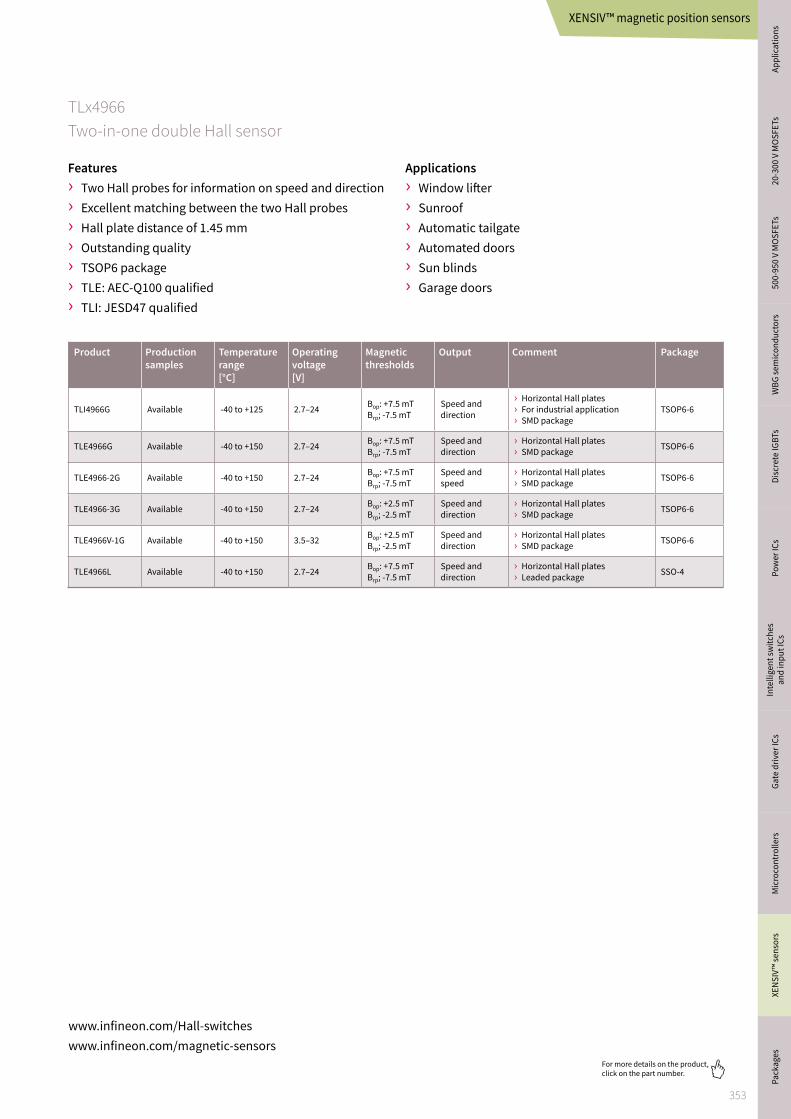
353
For more details on the product, click on the part number.
XENSIV™ magnetic position sensors
TLx4966 Two-in-one double Hall sensor
Features › Two Hall probes for information on speed and direction › Excellent matching between the two Hall probes › Hall plate distance of 1.45 mm › Outstanding quality › TSOP6 package › TLE: AEC-Q100 qualified › TLI: JESD47 qualified
Applications › Window lifter › Sunroof › Automatic tailgate › Automated doors › Sun blinds › Garage doors
www.infineon.com/Hall-switcheswww.infineon.com/magnetic-sensors
Product Production samples
Temperature range [°C]
Operating voltage[V]
Magnetic thresholds
Output Comment Package
TLI4966G Available -40 to +125 2.7–24 Bop: +7.5 mT Brp; -7.5 mT
Speed and direction
› Horizontal Hall plates › For industrial application › SMD package
TSOP6-6
TLE4966G Available -40 to +150 2.7–24 Bop: +7.5 mT Brp; -7.5 mT
Speed and direction
› Horizontal Hall plates › SMD package TSOP6-6
TLE4966-2G Available -40 to +150 2.7–24 Bop: +7.5 mT Brp; -7.5 mT
Speed and speed
› Horizontal Hall plates › SMD package TSOP6-6
TLE4966-3G Available -40 to +150 2.7–24 Bop: +2.5 mT Brp; -2.5 mT
Speed and direction
› Horizontal Hall plates › SMD package TSOP6-6
TLE4966V-1G Available -40 to +150 3.5–32 Bop: +2.5 mT Brp; -2.5 mT
Speed and direction
› Horizontal Hall plates › SMD package TSOP6-6
TLE4966L Available -40 to +150 2.7–24 Bop: +7.5 mT Brp; -7.5 mT
Speed and direction
› Horizontal Hall plates › Leaded package SSO-4
Appl
icat
ions
Pa
cka
ges
20
-30
0 V
MO
SF
ETs
50
0-9
50
V M
OS
FE
TsW
BG
se
mic
on
du
cto
rsD
iscr
ete
IGB
TsP
ow
er
ICs
Inte
llig
en
t sw
itch
es
an
d in
pu
t IC
sG
ate
dri
ver
ICs
Mic
roco
ntr
oll
ers
XE
NS
IV™
se
nso
rs
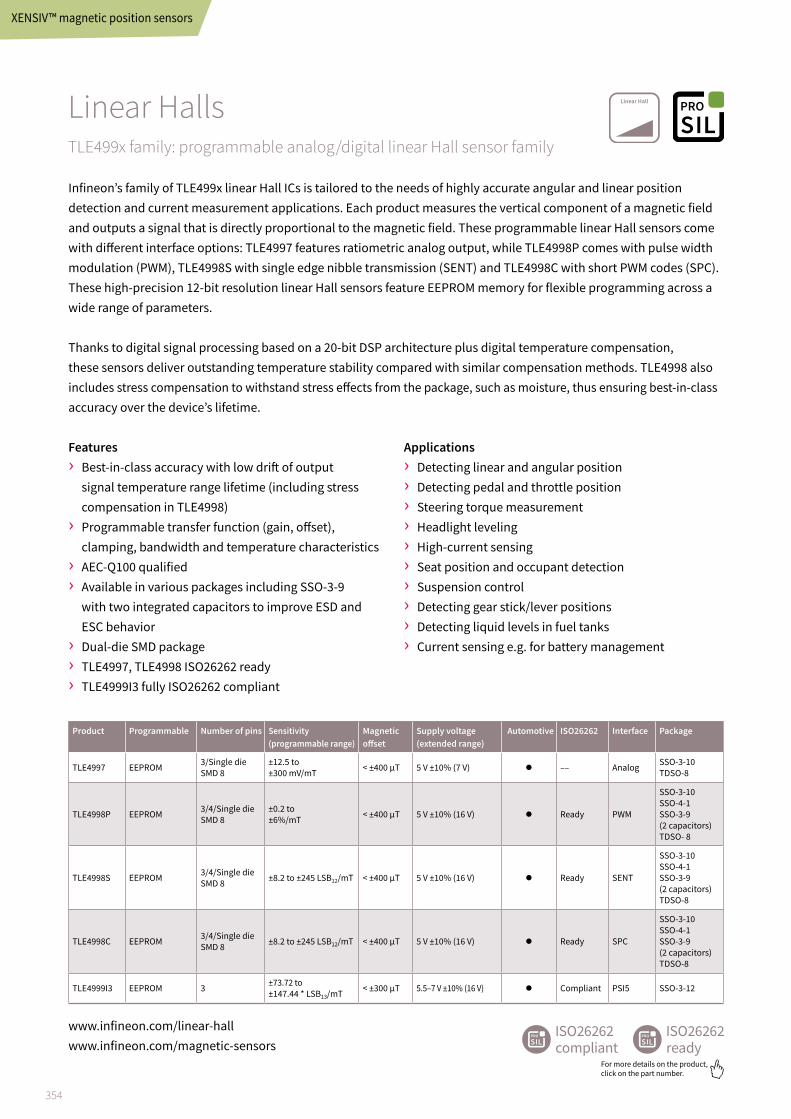
354
For more details on the product, click on the part number.
XENSIV™ magnetic position sensors
Linear HallsTLE499x family: programmable analog/digital linear Hall sensor family
Features › Best-in-class accuracy with low drift of output
signal temperature range lifetime (including stress compensation in TLE4998)
› Programmable transfer function (gain, offset), clamping, bandwidth and temperature characteristics
› AEC-Q100 qualified › Available in various packages including SSO-3-9
with two integrated capacitors to improve ESD and ESC behavior
› Dual-die SMD package › TLE4997, TLE4998 ISO26262 ready › TLE4999I3 fully ISO26262 compliant
Applications › Detecting linear and angular position › Detecting pedal and throttle position › Steering torque measurement › Headlight leveling › High-current sensing › Seat position and occupant detection › Suspension control › Detecting gear stick/lever positions › Detecting liquid levels in fuel tanks › Current sensing e.g. for battery management
Infineon’s family of TLE499x linear Hall ICs is tailored to the needs of highly accurate angular and linear position detection and current measurement applications. Each product measures the vertical component of a magnetic field and outputs a signal that is directly proportional to the magnetic field. These programmable linear Hall sensors come with different interface options: TLE4997 features ratiometric analog output, while TLE4998P comes with pulse width modulation (PWM), TLE4998S with single edge nibble transmission (SENT) and TLE4998C with short PWM codes (SPC). These high-precision 12-bit resolution linear Hall sensors feature EEPROM memory for flexible programming across a wide range of parameters. Thanks to digital signal processing based on a 20-bit DSP architecture plus digital temperature compensation, these sensors deliver outstanding temperature stability compared with similar compensation methods. TLE4998 also includes stress compensation to withstand stress effects from the package, such as moisture, thus ensuring best-in-class accuracy over the device’s lifetime.
Product Programmable Number of pins Sensitivity(programmable range)
Magnetic offset
Supply voltage (extended range)
Automotive ISO26262 Interface Package
TLE4997 EEPROM 3/Single die SMD 8
±12.5 to ±300 mV/mT < ±400 µT 5 V ±10% (7 V) l –– Analog SSO-3-10
TDSO-8
TLE4998P EEPROM 3/4/Single die SMD 8
±0.2 to ±6%/mT < ±400 µT 5 V ±10% (16 V) l Ready PWM
SSO-3-10 SSO-4-1 SSO-3-9 (2 capacitors) TDSO- 8
TLE4998S EEPROM 3/4/Single die SMD 8 ±8.2 to ±245 LSB12/mT < ±400 µT 5 V ±10% (16 V) l Ready SENT
SSO-3-10 SSO-4-1 SSO-3-9 (2 capacitors) TDSO-8
TLE4998C EEPROM 3/4/Single die SMD 8 ±8.2 to ±245 LSB12/mT < ±400 µT 5 V ±10% (16 V) l Ready SPC
SSO-3-10 SSO-4-1 SSO-3-9 (2 capacitors) TDSO-8
TLE4999I3 EEPROM 3 ±73.72 to ±147.44 * LSB13/mT < ±300 µT 5.5–7 V ±10% (16 V) l Compliant PSI5 SSO-3-12
www.infineon.com/linear-hallwww.infineon.com/magnetic-sensors

355
For more details on the product, click on the part number.
XENSIV™ magnetic position sensors
Dual linear Halls Two sensors in one SMD package
The SMD package (TDSO) includes two independent sensors with separate power supply and separate signal outputs. Due to special mounting technology, Infineon is able to keep dual-sensor package size very small to enable compact PCB layouts and small magnet sizes. Infineon offers a wide range of Hall sensors in the TDSO package. The combination of two sensors in one package offers sensors redundancy, a feature which is especially interesting for new generation EPS steering systems with increased ISO26262 requirements and other safety critical applications. All sensors are automotive qualified.
Most products are also available as single-sensor solution with only one sensor. The newest member of the TLE499x family, the TLE4999I3, is a fully ISO26262 compliant linear Hall sensor that includes 2 sensor channels on one chip. The SSO-3 package allows PCB-less application flexibility and the PSI5 interface enables low EMI at high speed communication with minimum wiring.
Features › Two sensors in one package › Separate power supply and signal output › AEC-Q100 qualified › Temperature range from -40 to +125°C › Outstanding quality › Single-sensor versions available › 16-pin and 8-pin versions available › ISO26262 ready › TLE4999I3 ISO26262 compliant
Automotive applications › Steering torque systems › Pedal position › Any other safety critical application
Product Interface Dual-/ single-sensor available
ISO26262 Package
TLE4997A8D Analog yes/yes Ready TDSO-8
TLE4998P8D PWM yes/yes Ready TDSO-8
TLE4998S8D SENT yes/yes Ready TDSO-8
TLE4998C8D SPC yes/yes Ready TDSO-8
TLE4999I3 PSI5 monolithic * Compliant SSO-3
* 2 sensor channels on one chip
www.infineon.com/linear-hallwww.infineon.com/magnetic-sensors
Appl
icat
ions
Pa
cka
ges
20
-30
0 V
MO
SF
ETs
50
0-9
50
V M
OS
FE
TsW
BG
se
mic
on
du
cto
rsD
iscr
ete
IGB
TsP
ow
er
ICs
Inte
llig
en
t sw
itch
es
an
d in
pu
t IC
sG
ate
dri
ver
ICs
Mic
roco
ntr
oll
ers
XE
NS
IV™
se
nso
rs

356
For more details on the product, click on the part number.
Angle sensorsCompact designs in small outline packages
Highest variety - low end to high end, standardized and specialized in all four magnetic technologies: Hall, GMR, AMR and TMR
Infineon's magnetic sensor products TLE5501, are fast analogue TMR-based angle sensors dedicated to automotive applications. Their fields of use range from steering angle applications, with the highest functional safety requirements, to motors for wipers, pumps and actuators and electric motors in general. They are also ready to be used in industrial and consumer applications like robotics or gimbal. Angle sensors detect the orientation of an applied magnetic field by measuring sine and cosine angle components with monolithically integrated magneto resistive elements.
Infineon's iGMR sensors are ideal for applications with a wide angle range, such as BLDC motors or steering sensors. They are pre-calibrated and ready to use. Different levels of signal processing integration enable designers to optimize system partitioning. The XENSIV™ iAMR sensors also perfectly fit applications with the highest accuracy requirements, as they offer best performance over temperature, lifetime and magnetic field range.
SPI = Serial peripheral interfaceIIF = Incremental interfacePWM = Pulse width modulation *For more information on the product, contact our product support
Product Technology Die configuration ISO26262 Sin/cos output Angle output Second interface Accuracy Package
TLE5009 GMR Single die Ready Analog sin/cos – – 0.9° DSO-8
TLE5009A16(D) * GMR Dual die Ready Analog sin/cos – – 1.0° TDSO-16
TLE5011 GMR Single die Ready SSC (SPI) – – 1.6° DSO-8
TLI5012B GMR Single die Ready SSC (SPI) SSC (SPI) PWM/IIF/SPC/HSM 1.9° DSO-8
TLE5012B(D) GMR Single and dual die Ready SSC (SPI) SSC (SPI) PWM/IIF/SPC/HSM 1.0° DSO-8/ TDSO-16
TLE5014C16(D) GMR Single and dual die Compliant – SPC – 1.0° TDSO-16
TLE5014P16(D) GMR Single and dual die Compliant – PWM – 1.0° TDSO-16
TLE5014S16(D) GMR Single and dual die Compliant – SENT – 1.0° TDSO-16
TLE5014SP16(D) * GMR Single and dual die Compliant – SPI – 1.0° TDSO-16
TLE5109A16(D) * AMR Single and dual die Ready Analog sin/cos – – 0.5° TDSO-16
TLE5309D AMR + GMR Dual die Ready Analog sin/cos SSC (SPI) – AMR 0.5°, GMR 1.0° TDSO-16
TLE5501 TMR Single die Compliant Analog sin/cos – – 1.0° DSO-8
iGMR, iAMR and iTMR based angle sensorsDiverse redundant sensor with analog and digital interface
XENSIV™ magnetic position sensors
www.infineon.com/angle-sensorswww.infineon.com/magnetic-sensors

357
For more details on the product, click on the part number.
iTMR based angle sensorsTunneling Magneto Resisitive (iTMR) technology is offering high sensing sensitivity with a high output voltage, reducing the need for an internal amplifier. Thus, the sensor can be connected directly to the microcontroller without any further amplification. In addition, iTMR technology shows a very low temperature drift, reducing external calibration and compensation efforts. The iTMR technology is also well known for its low current consumption.
TLE5501With the TLE5501 products, Infineon is currently launching the first angle sensor products based on iTMR technology. TLE5501 is available in two versions.
TLE5501 - product versions with different pin out: › TLE5501 E0001: pin-compatible to TLE5009
automotive qualified acc. AEC-Q100 › TLE5001 E0002: decoupled bridges for redundant external
angle calculation and highest diagnostic coverage, realizing ISO26262-compliant development ASIL D
Features › Large output signals of up to 0.37 V/V for direct microcontroller connection › Discrete bridge with differential sine and cosine output › Very low supply current: ~2 mA › Magnetic field range (20-100 mT) › Typ. angle error ~ 1.0 ° (overtemperature and lifetime) › DSO-8 package › AEC-Q100, grade 0: TA = -40°C to 150°C (ambient temperature) › For TLE5501 E0002:
– Reaching ASIL D with just one single sensor chip – ISO26262-compliant development ASIL D
Applications › Steering angle sensor › BLDC motor commutation (e.g. wipers, pumps and actuators) › Angular position sensing for e.g. robotics or gimbal › Electric motors › Industrial automation › Safety applications
XENSIV™ magnetic position sensors
www.infineon.com/angle-sensorswww.infineon.com/magnetic-sensors
Appl
icat
ions
Pa
cka
ges
20
-30
0 V
MO
SF
ETs
50
0-9
50
V M
OS
FE
TsW
BG
se
mic
on
du
cto
rsD
iscr
ete
IGB
TsP
ow
er
ICs
Inte
llig
en
t sw
itch
es
an
d in
pu
t IC
sG
ate
dri
ver
ICs
Mic
roco
ntr
oll
ers
XE
NS
IV™
se
nso
rs

358
For more details on the product, click on the part number.
TLE5014(D)Digital iGMR sensor with an easy-to-use plug-and-play concept for highest functional safety applications
All XENSIV™ TLE5014 angle sensors are available as single and dual die products. The products come pre-configured and pre-calibrated as plug-and-play sensors and are easy to use. Customers can choose between the interfaces SENT, PWM, SPC an SPI. On top of those protocol options, the sensors can be adapted to any kind of application setup via their programmable E²PROM interfaces. TLE5014 magnetic angle sensors meet ISO26262 ASIL C for the single die and ISO26262 ASIL D for the dual die versions. All products are ready for applications with the highest functional safety requirements. The sensors show an extremely small angle error of less than 1° across the entire temperature profile and lifetime. This is particularly helpful in applications with the need for very accurate position sensing such as steering angle sensing or motor commutation. Further application areas range from rotor position measurement, electric power steering (EPS), pedal position to any other kind of position measurement.
Features › Easy-to-use, plug-and-play sensors, pre-configured and pre-calibrated › Offering high flexibility:
– Available as single and dual die products – 12bit digital interface with protocol options PWM, SENT, SPC and SPI – E2 PROM and look-up table for customer configuration and calibration
› High angle accuracy: max. 1.0° over temperature and lifetime › High voltage capability up to 26 V › Development fully compliant with ISO26262
– Developed acc. ASIL D level – Dual die sensors reaching ASIL D, single die sensors ASIL C metrics
› Safety manual and safety analysis summary report available on request
Applications › Steering angle sensing (SAS) › Motor commutation › Rotor position measurement › Pedal position › Safety applications › Any other kind of high-accuracy position measurement
TLE5109A16(D)Analog iAMR sensor with temperature compensation
Features › Features a differential or single-ended analog interface for sine and cosine values › Internal temperature drift compensation for gain and offset › Also available as a dual-sensor package › ISO26262 ready › Typical 0.1” angle error over lifetime and temperature range after compensation (max 0.5”) › Available as single and dual die product
S
N
X SPI
Y
CO
RD
IC
A/D
A/D
cos
sin
X
Y
S
N
XENSIV™ magnetic position sensors
www.infineon.com/angle-sensorswww.infineon.com/magnetic-sensors *Giant Magneto resistance

359
For more details on the product, click on the part number.
The TLV493D-A1B6 sensor realizes an accurate three-dimensional sensing with extremely low power consumption in a small 6-pin package. Capable of detecting the magnetic field in the x, y, and z-direction, the sensor is ideally suited for the measurement of linear, rotation or 3 dimensional movements. Thanks to its small package and low power consumption, the TLx493D-AxB6 can be used in new applications, replacing potentiometer and optical solutions. Featuring contactless position sensing and high temperature stability of the magnetic threshold, the sensor allows systems getting smaller, more accurate and more robust.
While the TLV493D-A1B6 just supports a typical value for the linear magnetic range of ±130 mT, the TLI493D-A2B6 specification includes also a minimum value of ±160 mT.
With the TLI493D-A2B6, a broader microcontroller compatibility as well an enhanced feature set is included.
1) Half range mode
Features › 3D magnetic sensing › Integrated temperature sensing › Low current consumption
– 7 nA in power-down mode – 10 μA in ultralow power mode
› 2.8 to 3.5 V operating supply voltage
› Digital output via a 2-wire standard I2C interface › Bx, By and Bz linear field measurement up to ±160 mT › JESD47 qualified › 12-bit data resolution for each measurement direction › Various resolution options from 65 μT/LSB to 130 μT › Operating temperature range from -40 to +125°C
New features › Sensor address read back › Short mode range setting, focusing on the half of the
magnetic range, ensuring higher accuracy › Higher update frequency allows for an application
field that requires faster update speed › Angular mode (for x and y read-out only)
Applications › Anti tempering protection in smart meters › Joysticks e.g. for medical equipment, cranes,
CCTV-control, game consoles › Control elements e.g. white goods multifunction knobs
XENSIV™ magnetic position sensors
3D magnetic sensors TLV493D-A1B6/TLI493D-A2B6 for consumer and industrial market
www.infineon.com/3dmagneticwww.infineon.com/magnetic-sensors
Rotation movement 3D movement Linear movement
Product Temperaturerange
Qualification Linear magneticrange
Resolution IDD Update rate Package Ordering code
TLV493D-A1B6 -40 … 125°C JESD47 ±130 mT (typ) 98 μT/LSB 7 nA – 3.7 mA 10 Hz – 3.3 kHz TSOP6 SP001286056
TLI493D-A2B6 -40 … 105°C JESD47 ±160 mT (min)±100 mT (min)
130 μT/LSB(65 μT/LSB) 1)
7 nA – 3.3 mA 10 Hz – 8.4 kHz TSOP6 SP001689844
Appl
icat
ions
Pa
cka
ges
20
-30
0 V
MO
SF
ETs
50
0-9
50
V M
OS
FE
TsW
BG
se
mic
on
du
cto
rsD
iscr
ete
IGB
TsP
ow
er
ICs
Inte
llig
en
t sw
itch
es
an
d in
pu
t IC
sG
ate
dri
ver
ICs
Mic
roco
ntr
oll
ers
XE
NS
IV™
se
nso
rs

360
For more details on the product, click on the part number.
3D magnetic sensors
25
Product Temperature range
Qualification Linear magnetic range
Resolution IDD Update rate Wake- up
Package Ordering code
TLE493D-A2B6 -40 … 125°C AEC-Q100 ±160 mT (min) 130 µT/LSB (65 µT/LSB)1)
7 nA – 3.3 mA 10 Hz – 8.4 kHz No TSOP6 SP001689848
TLE493D-W2B6 A0TLE493D-W2B6 A1TLE493D-W2B6 A2TLE493D-W2B6 A3
-40 … 125°C AEC-Q100 ±160 mT (min) ±100 mT (min)
130 µT/LSB (65 µT/LSB)1) 7 nA – 3.3 mA 0.05 Hz – 8.4 kHz Yes TSOP6
SP001655334 SP001655340 SP001655344 SP001655348
1) Half range mode
TLE493D-A2B6/W2B63D magnetic sensors for automotive low-power applications
The TLE493D-x2B6 enables for all kind of automotive control element applications within the passenger compartment or under the hood with a temperature range of -40 to +125°C with linear magnetic range requirements up to ±160 mT.
www.infineon.com/3Dmagnetic
Features › 3D magnetic sensing
› Integrated temperature sensing
› 2.8 to 3.5 V operating supply voltage
› Low current consumption – 0.007 µA in power-down mode – 10 µA in ultra-low power mode – Up to 10 power modes
› Digital output via a 2-wire standard I2C interface
› Bx, By and Bz linear field measurement ±160 mT
› AEC-Q100 qualified
› 12-bit data resolution for each measurement direction
› Various resolution options from 67 µT/LSB to 134 µT
› Operating temperature range up to -40 to +125°C
The TLE493D-A2B6 features include a sensor address read back feature for additional communication verification, a half range mode focusing to half of the magnetic range ensuring higher accuracy and an angular mode (for x and y read out only).
With the TLE493D-W2B6 A0-A3, a 3D sensor has been developed, which includes an enhanced dynamic wake up feature. Four pre-programmed address options (A0-A3) will be available, enabling for a fast start up initialization, when used in I2C bus configurations. It also includes enhanced test options and a safety documentation is available to enable the usage of this sensor in the context of ASIL B systems.
Applications › Control elements for infotainment/navigation systems, air conditions, multifunctional steering wheels, seat controls
› Top column modules e.g. direction indicator, wiper control
› Gear stick position sensing
Sensor_Solutions_BR-2018.indb 25 23.07.2018 15:55:49
The XENSIV™ sensor TLE493D-A2B6 features include a sensor address read-back feature for additional communication verification, a half range mode focusing to half of the magnetic range, ensuring higher accuracy and an angular mode (for x and y readout only).
With the TLE493D-W2B6 A0-A3, a 3D sensor has been developed, which includes an enhanced dynamic wake up feature. Four pre-programmed address options (A0-A3) will be available, enabling for a fast start-up initialization, when used in I2C bus configurations. It also includes enhanced test options, and a safety documentation is available to enable the usage of this sensor in the context of ASIL B systems.
Applications› Control elements for infotainment/navigation systems, air conditions, multifunctional steering wheels, seat controls› Top column modules e.g. direction indicator, wiper control› Gear stick position sensing
www.infineon.com/3dmagneticwww.infineon.com/magnetic-sensors
3D magnetic sensors TLE493D-A2B6/W2B6 for automotive low power applications
Infineon's TLE493D-x2B6 enables for all kind of automotive controlelement applications within the passenger compartmentor under the hood with a temperature range of -40 to +125°C,with linear magnetic range requirements up to ±160 mT.
XENSIV™ magnetic position sensors
Features › 3D magnetic sensing › Integrated temperature sensing › 2.8 to 3.5 V operating supply voltage › Low current consumption
– 0.007 μA in power-down mode – 10 μA in ultralow power mode – Up to 10 power modes
› Digital output via a 2-wire standard I2C interface › Bx, By and Bz linear field measurement ±160 mT › AEC-Q100 qualified › 12-bit data resolution for each measurement direction › Various resolution options from 67 μT/LSB to 134 μT › Operating temperature range from -40 to +125°C

361
For more details on the product, click on the part number.
www.infineon.com/speed-sensorswww.infineon.com/magnetic-sensors
Magnetic speed sensorsEasy to use, robust and cost-effective sensors for speed measurement
Infineon's Hall- and GMR-based magnetic speed sensors are designed to measure speed in safety and powertrain applications such as speedometers, ABS, camshafts/crankshafts and automatic transmissions. They are also used in similar applications in the industrial sector. The sensors use a ferromagnetic gear tooth or encoder structure to measure linear or rotational speed and position. Hall sensor measuring rotational speed with a gear tooth and a magnetic encoder wheel. The majority of sensors also feature additional benefits such as integrated capacitors (C- types) for high EMC robustness and the highest levels of ESD protection.Modern powertrain systems rely on magnetic speed sensors, along with automotive pressure sensors, to achieve the required CO2 targets and smart powertrain solutions. Infineon offers a broad variety of magnetic speed sensors for camshaft, crankshaft and transmission applications.
This sensor is specially designed to provide an easy-to-use, robust and cost-effective solution for vehicle or industrial speed sensing applications. The TLE4922 can, therefore, be back-biased using a simple, low-cost bulk magnet, while providing a good air gap performance and switching accuracy. Its hidden adaptive hysteresis and calibration algorithm enable good accuracy over air gap jumps and immunity to vibration and run-out events.
TLE4922 Highly robust, easy-to-use mono-Hall speed sensor with twist-independent mounting
Features › Large operating air gap capability › Twist-independent mounting › Hidden adaptive hysteresis › Low current consumption › Reverse magnetic polarity capability › Advanced protection technology
– Reverse voltage protection at VS-pin – Short-circuit protection – Overtemperature protection
› Wide operating temperature ranges of -40°C ≤ Tj ≤ ±150°C › High ESD robustness up to ±4 kV HBM › 3-wire PWM voltage interface
Applications › Two-wheeler › Automotive vehicle speed
XENSIV™ magnetic speed sensors
Appl
icat
ions
Pa
cka
ges
20
-30
0 V
MO
SF
ETs
50
0-9
50
V M
OS
FE
TsW
BG
se
mic
on
du
cto
rsD
iscr
ete
IGB
TsP
ow
er
ICs
Inte
llig
en
t sw
itch
es
an
d in
pu
t IC
sG
ate
dri
ver
ICs
Mic
roco
ntr
oll
ers
XE
NS
IV™
se
nso
rs

362
For more details on the product, click on the part number.
The TLE4929 is an active Hall sensor ideally suited for crankshaft applications and similar industrial applications, such as speedometer or any speed sensor with high accuracy and low jitter capabilities.
TLE4929 Fully programmable crankshaft sensor
Features › Differential Hall speed sensor to measure speed and position of
tooth/pole wheels › Switching point in the middle of the tooth enables backward compatibility › Robustness over magnetic stray-field due to differential sensing principle › Digital output signal with programmable output-protocol including
diagnosis interface › Direction detection and stop-start-algorithm › High accuracy and low jitter › High sensitivity enable large air gap › End-of-line programmable to adapt engine parameters › Can be used as a differential camshaft sensor › Automotive operating temperature range
Product Automotive Industrial Sensor technology AEC-Q100 qualified RoHS HAL free Product status
TLE4922 Mono-Hall In production
TLE4929 Differential Hall In production
XENSIV™ magnetic speed sensors
www.infineon.com/speed-sensorswww.infineon.com/magnetic-sensors

363
For more details on the product, click on the part number.
Appl
icat
ions
Pa
cka
ges
20
-30
0 V
MO
SF
ETs
50
0-9
50
V M
OS
FE
TsW
BG
se
mic
on
du
cto
rsD
iscr
ete
IGB
TsP
ow
er
ICs
Inte
llig
en
t sw
itch
es
an
d in
pu
t IC
sG
ate
dri
ver
ICs
Mic
roco
ntr
oll
ers
XE
NS
IV™
se
nso
rs

364
For more details on the product, click on the part number.

365
For more details on the product, click on the part number.
Intuitive sensing
Intuitive sensingGiving things human-like senses for a better contextual awareness
Imagine a world where technology is unobtrusive and seamlessly integrated into our lives. Where intentional/deliberate communication between people and devices is no longer necessary. In this world, there is no need to push buttons or issue commands in order to activate devices, because technology is capable of interpreting implicit intentions and context. This enhances the user experience and makes it more natural – it almost seems like the devices around us intuitively understand what we want them to do. At Infineon, this future is already becoming reality. We develop sensor solutions that enable simple and effortless user interactions with all kinds of smart devices. Bridging the gap between the real and digital worlds, our technology is developed to make
life easier, safer, greener and more efficient. Our intuitive sensing solutions are at the very core of this mission. Reflecting our belief that the essential value of sensor technology lies in making our lives more convenient through seamless, natural interactions between people and sensing devices, our aim is to leave you free to focus on what really matters in life.
Choose your type of senseThanks to industry-leading technologies Infineon XENSIV™ sensors are exceptionally precise. They are the perfect fit for various customer applications in automotive, industrial and consumer markets.
This interaction often depends on the interpretation and merging of information from different sources. Machines cannot yet read our minds and do not always have the information necessary to correctly evaluate a given situation. So, we sometimes have to explicitly tell devices what we want them to do. This can be inconvenient and time-consuming. Inspired by human nature, Infineon intuitive sensing solutions are designed to take the complexity out of our interaction with devices.
Reflecting a holistic approach, we combine different sensors with state-of-the-art software to create a comprehensive picture of the world around us. By fusing several smart sensors into one coherent intelligent system, our intuitive sensing solutions simplify complex technical processes and enable people to effortlessly interact with devices. These smart devices intuitively sense the world around them, determining what is expected and needed from them.
Today, sensors already enable interactions between people and devices
Pressure sensors
Our digital barometric pressure sensors give designers the best choice when it comes small form factors, highest precision and accuracy over a wide temperature range, fast read-out speeds and low power consumption.
Radar sensors
Radar supports existing applications while providing features that enable completely new use cases. It measures velocity, range and angle, both horizontal and vertical, for precise position mapping and 3D tracking.
MEMS microphones
Digital MEMS microphones overcome existing audio chain limitations and are designed for applications where low self-noise (high SNR), wide dynamic range, low distortions and a high acoustic overload point are required.
PAS CO2 sensor
Leveraging photoacoustic spectroscopy (PAS), Infineon has developed an exceptionally small CO₂ sensor that overcomes existing size, cost and performance challenges.
Appl
icat
ions
Pa
cka
ges
20
-30
0 V
MO
SF
ETs
50
0-9
50
V M
OS
FE
TsW
BG
se
mic
on
du
cto
rsD
iscr
ete
IGB
TsP
ow
er
ICs
Inte
llig
en
t sw
itch
es
an
d in
pu
t IC
sG
ate
dri
ver
ICs
Mic
roco
ntr
oll
ers
XE
NS
IV™
se
nso
rs

366
For more details on the product, click on the part number.
XENSIV™ MEMS microphone
XENSIV™ MEMS microphoneTime to debottleneck your audio chain
The popularity of voice user interfaces and the usage of audio recording to share information and experiences are increasing dramatically. However, the performance of microphones often limits the potential of today’s cutting-edge devices. Not anymore!
Infineon's XENSIV™ MEMS microphones introduce a new performance class for digital MEMS microphones that overcome existing audio chain limitations. IM69D130 is designed for applications where low self-noise (high SNR), wide dynamic range, low distortions and a high acoustic overload point are required.
Features › 69 dB(A) signal-to-noise ratio (SNR) › Below 1 percent distortions at 128 dBSPL (130 dBSPL AOP) › Digital (PDM) interface with 6 µs group delay at 1 kHz › Tight sensitivity (-36 ±1 dB) and phase (± 2 deg) tolerances › 28 Hz low frequency roll-off › 4.0 x 3.0 x 1.2 mm package
Benefits › High fidelity and far field audio recording › Matched, noise and distortion free audio signals for
advanced audio processing › Ultralow group delay for latency-critical applications › No analog components required
Don’t miss a single thing!With XENSIV™ MEMS microphones, you can create a new user experience benchmark in audio recording.
Talk to tomorrow and be heard!With XENSIV™ MEMS microphones, you can define the benchmark in speech recognition for a new user experience.
Hear nothing but your favorite beats!With XENSIV™ MEMS microphones, you can create headsets offering users a benchmark noise cancellation experience.
www.infineon.com/microphones
Typical applications › High quality audio capturing: e.g. cameras, camcorders, conference systems › Voice user interface: e.g. smart speaker, home automation and IoT devices › Active noise cancellation: headphones and earphones › Audio pattern detection: predictive maintenance, security or safety applications

367
For more details on the product, click on the part number.
XENSIV™ MEMS microphone
Infineon's dual backplate MEMS technology is based on a miniaturized symmetrical microphone design, similar as utilized in studio condenser microphones, and results in high linearity of the output signal within a dynamic range of 105 dB. The microphone noise floor is at 25 dB[A] (69 dB[A] SNR) and distortion does not exceed 1 percent even at sound pressure levels of 128 dB SPL (AOP 130 dB SPL). The flat frequency response (28 Hz low-frequency roll-off) and tight manufacturing tolerance result in close phase matching of the microphones, which is important for multi-microphone (array) applications.
Devices with voice user interface
TV, laptop and set top box
+ Highest beam-forming precision + Best speech recognition
+ Sensitive to softest audio signals
+ Extended voice pickup distance
+ Best noise attenuation + Smallest pattern deviation detection
+ Best audio quality
Audio
Digital voice assistance and robots
Security
Smart home appliances
Headsets Industry 4.0
+ Ultraclear voice pickup
Conference
www.infineon.com/microphones
Product portfolio
Maximum noise rejection
Ultra precise corner frequency
28 Hz
Ultralow distorsion
(<1% THD)
IM69D130: 128dBSPL
IM69D120: 118dBSPL
AIN(+)
AIN(-)
Class leading
dynamic range
IM69D130: 105dB
IM69D120: 95dB
Phase matched microphones
+/- 2deg @1kHz
Product OPN Package Current consumption Sensitivity Signal to noise Supply voltage
IM69D130 IM69D130V01XTSA1 LLGA-5-1 980 µA -36 dBFS 69 dB 1.62-3.6 V
IM69D120 IM69D120V01XTSA1 LLGA-5-1 980 µA -26 dBFS 69 dB 1.62-3.6 V
Appl
icat
ions
Pa
cka
ges
20
-30
0 V
MO
SF
ETs
50
0-9
50
V M
OS
FE
TsW
BG
se
mic
on
du
cto
rsD
iscr
ete
IGB
TsP
ow
er
ICs
Inte
llig
en
t sw
itch
es
an
d in
pu
t IC
sG
ate
dri
ver
ICs
Mic
roco
ntr
oll
ers
XE
NS
IV™
se
nso
rs

368
For more details on the product, click on the part number.
XENSIV™ pressure sensors
XENSIV™ digital barometric pressure sensorFor mobile and wearable devices
Infineon’s digital barometric pressure sensor family is the best choice for mobile and wearable devices due to its small form factor, high precision and low power consumption. Pressure sensing is based on capacitive technology which guarantees ultrahigh precision (±2/±5 cm) and relative accuracy (±0.6 hPa) over a wide temperature range. The sensor’s internal signal processor converts the output from the pressure and temperature sensor elements to 24-bit results. Each pressure sensor has been calibrated individually and contains calibration coefficients. The coefficients are used in the application to convert the measurement results to true pressure and temperature values. All sensors have a FIFO that can store the latest 32 measurements. Since the host processor can remain in a sleep mode for a longer period between readouts, a FIFO can reduce the system power consumption. Sensor measurements and calibration coefficients are available via the serial I2C/SPI interface.
DPS310Barometric pressure sensor with very low power consumption, recommended for applications where power consumption is critical and the highest precision in pressure metering is required.
DPS422Monolithic chip solution that has an ultrasmall critical area and a very thin package (0.73 mm typ.). Beneath high precision pressure metering, DPS422 offers also highly accurate absolute temperature sensing (±0.4ºC), which is required in applications like weather stations, thermostats, etc. It can be used in applications such as weather stations/smart thermostats and offers additional features by pressure sensing (e.g. intruder detection, weather forecast).
DPS368DPS368 offers the best-in-class resolution (±2 cm), a very fast read-out speed and a low current consumption. The sensor can be used in harsh environment, as it is robust against water (IPx8 - 50 m under water for 1 hour), dust and humidity. The small package size saves up to 80 percent of the space and makes the DPS368 ideal for mobile applications and wearable devices.
Typical applications › Drones: altitude detection and height stability › Health and fitness: accurate elevation gain and step counting (e.g. for smart watches) › Outdoor navigation: GPS start-up time/accuracy improvement; dead reckoning (e.g. in tunnels) › Indoor navigation: floor detection e.g. in shopping malls and parking garages › Smart home: micro weather forecasting; room temperature control; intruder detection › Air flow control: Smart filter replacement alarm (e.g. in home appliances); predictive maintenance › Health care: fall detection; respiratory devices; smart inhalers
Key product features DPS310 DPS422 DPS368Package size LGA 8-pin: 2.0 x 2.5 x 1.0 mm LGA 8-pin: 2.0 x 2.5 x 0.73 mm LGA 8-pin: 2.0 x 2.5 x 1.1 mmOperating pressure range 300 … 1200 hPaOperating temperature range -40 … 85°CPressure level precision ± 0.005 hPa (or ±0.05 m) ± 0.002 hPa (or ±0.02 m)Relative accuracy ± 0.06 hPa (or ±0.5 m)Absolute accuracy ± 1 hPa (or ±8 m)Temperature accuracy 0.5°C < 0.4°C 0.5°CPressure temperature sensitivity 0.5 Pa/KMeasurement time 3.6 ms (low precision); 27.6 ms (standard mode) Average current consumption @ 1 Hz sampling rate
1.7 μA pressure measurement, 1.5 μA temp. measurement, standby 0.5 μA
1.7 μA pressure measurement, 2.0 μA temp. measurement, standby < 1 μA
1.7 μA pressure measurement, 1.5 μA temp. measurement, standby 0.5 μA
Supply voltage VDDIO: 1.2 – 3.6 V; VDD: 1.7 – 3.6 VOperating modes Command (manual), background (automatic), standbyInterface I2C and SPI, both with optional interrupt
www.infineon.com/pressuresensor

369
For more details on the product, click on the part number.
XENSIV™ pressure sensors
Functional block diagram
Application circuit example (in I2C configuration)
Pin configuration (top view)
DPS422 package drawingDPS310 package drawing DPS368 package drawing
www.infineon.com/pressuresensor
SCK
INT
SDA
I2C serial interface
C
SDO
SCK
SDI
CSB
GND
GND
VDD
VDDIO
Pressure sensor
Processor
VDDIO
1.7 … 3.6 V
1.2 … 3.6 V
C
R
VDDIO
R
N.C.
Interrupt (optional)
I2C/SPI
VDDIO
VDD
Temperaturesensor
Digital signalprocessing
Calibrationcoefficients
FIFO
Capacitivepressure sensor
Digital core
Memoryinterface
Voltageregulators
Digital interfaceMUX ADC
4
3
2
1
5
6
7
8 GND
CSB
SDI
SCK
VDD
GND
VDDIO
SDO
Vent hole
Pin Name Function
1 GND Ground
2 CSB Chip select
3 SDI Serial data in/out
4 SCK Serial clock
5 SDO Serial data out
6 VDDIO Digital interface supply
7 GND Ground
8 VDD Analog supplyAp
plic
atio
nsP
ack
age
s2
0-3
00
V M
OS
FE
Ts5
00
-95
0 V
MO
SF
ETs
WB
G s
em
ico
nd
uct
ors
Dis
cret
e IG
BTs
Po
we
r IC
sIn
tell
ige
nt
swit
che
sa
nd
inp
ut
ICs
Gat
e d
rive
r IC
sM
icro
con
tro
lle
rsX
EN
SIV
™ s
en
sors

370
For more details on the product, click on the part number.
24 GHz radar sensor ICs
www.infineon.com/24GHz
XENSIV™ 24 GHz radar sensor ICs
Infineon offers a wide portfolio of mmWave radar sensors to address different customer requirements. The BGT24M/L family is the largest and highest integrated 24 GHz radar transceiver family currently on the market, saving ~30 percent board space compared to discrete lineups. Infineon provides a total of five 24 GHz industrial radar chips, providing a range of different transmitter and receiver channel configurations, supporting different application requirements.
In addition to the BGT24M/L family of MMIC chips, Infineon provides a continuously expanding range of evaluation and demonstration boards to support the testing and development of radar in multiple applications. All boards are provided with base level software to support the ease of use and faster time-to-market integration.
Utilizing our strong network of partners, the radar portfolio is extended to include a range of easy-to-integrate modules. Each of them contains Infineon's 24 GHz MMIC.
Applications › Building and smart home (IoT) › Indoor/outdoor lighting › Security › UAV/multicopters › Robotics › Smart street lighting
Key benefits › Direction, proximity and speed detection › Hidden mounting capability › Maintains operation through harsh weather conditions › Motion tracking › Sensitive enough to capture breathing and heartbeat › Target positioning › Adaptable to different application requirements
Intrusion detection
Air flight control
Streetlighting
Collision avoidance in
multicopters and robotics
People tracking and occupancy
detection in IoT/smart home
Gesture control on TV
Indoor and outdoor
lighting systems
Collision
avoidance
proximity sensor to
activate appliances BSD (blind spot detection) in the car
Intruder alarm/presence
detection in surveillance

371
For more details on the product, click on the part number.
24 GHz radar sensor ICs
www.infineon.com/24GHz
Infineon BGT24M/L family of MMIC chips
Infineon's range of 24 GHz industrial radar chips provides five configurations of transmit and receiver channels, ensuring that there is a chip to support your specific application. From basic applications such as motion detection in security systems, which only requires one transmit and one receive channel, to more complex applications like 3D positioning, which requires two or more receive channels, our range of radar chips supports all of your requirements.
Features Infineon MMIC Benefits
› 24 GHz ISM band operation for motion, speed, direction movement and distance measurements
› 5 MMIC chips available › Highly integrated
› Long range distance detection of moving objects up to 30 m
› Wide range speed detection up to ±100 km/h
› Lower BOM costs
2.4 m
m
2.4 mm5.5 mm
4.5 m
m
The BGT24LTR22N16 key features › 24 GHz transceiver MMIC › Fully integrated low phase noise VCO › Integrated analog base band stage with
programmable gain and filter settings › Bi-directional pin for synchronization › Built in temperature compensation
circuit for VCO stabilization, no PLL needed
› Low power consumption › Fully ESD protected device › Single ended RF and IF terminals › Single supply voltage 1.5 V
Product Configuration Features
BGT24MTR11 1Tx + 1Rx › Measures not just motion, but also speed, direction, and distance › Small form factor › Resistance to moisture, dirt and temperature › Increased area coverage › Discrete design › Energy savings › Privacy protection › Adaptable to different application requirements › Highly integrated chips eliminating costly external components
BGT24MR2 2Rx
BGT24MTR12 1Tx + 2Rx
BGT24LTR11 1Tx + 1Rx
BGT24LTR22 2Tx + 2Rx
SPISensor
ADCBG/PTAT
DAC
Sync 1
Sync 1
PPF
HPF LPF
LPF
LPF
LPF
Trafo
Trafo
HPF
HPF
HPF
PS
PSPPF
DAC
f-Div/tbd
Power
Det.
Power
Det.
Trafo
Trafo
Trafo
Power
splitter
Appl
icat
ions
Pa
cka
ges
20
-30
0 V
MO
SF
ETs
50
0-9
50
V M
OS
FE
TsW
BG
se
mic
on
du
cto
rsD
iscr
ete
IGB
TsP
ow
er
ICs
Inte
llig
en
t sw
itch
es
an
d in
pu
t IC
sG
ate
dri
ver
ICs
Mic
roco
ntr
oll
ers
XE
NS
IV™
se
nso
rs

372
For more details on the product, click on the part number.
24 GHz radar sensor
www.infineon.com/24GHz
24 GHz evaluation and demonstration boards
Infineon's range of 24 GHz evaluation and demo boards continues to expand to support the needs of our customers and the increasing number of innovative ways radar is being incorporated into new applications.
Learn radar with Infineon on www.infineon.com/MakeRadar For the first time we bring radar to makers and developers. Here you can test, develop, and learn radar and its applications. At www.infineon.com/makeradar, you will see how simple it has become to work with ultrasmall radar sensors. The board and data will flow to your browser for testing, and this is not all, if you want to take the next step just take the available Arduino code examples and start your own project.
› Three system boards available › All include 24 GHz radar and XMC™
microcontroller › Kit contains user manual, GUI,
MATLAB compiler and Gerber files › Software available via
Infineon Toolbox
› Capability to detect motion, speed and direction of movement (approaching or retreating) distance and angle of arrival based on hardware
› Fast prototyping with available software
Features Infineon development kit Benefits
Sense2GOL Pulse (BGT24LTR11 + XMC4700) Distance2Go (BGT24MTR11 + XMC4200) Position2Go (BGT24MTR12 + XMC4700)
› Capability to detect motion, speed and direction of movement (approaching or retreating) › Detection range of 18 m for human target at a power consumption < 5 mW › High sensitivity of detection in comparison to PIR › Arduino compatible microcontroller board (Arduino standard connectors) › Modulation parameters can be changed to suit the application requirements › Multiple current sensors for current consumption monitoring and optimization › Integrated multiple element patch antennas
› Capability to detect distance of multiple targets › Capability to detect motion, speed and direction of movement (approaching or retreating) › Operates in harsh environments and detects through non-metallic materials › BGT24MTR11 – 24 GHz highly integrated RF MMIC › XMC4200 Arm® Cortex®-M4 –32-bit industrial microcontroller › Debug over Cortex 10 pin debug connector › Integrated multiple element patch antennas
› Capability to detect and track position of multiple targets › Capability to detect distance of multiple targets › Capability to detect motion, speed and direction of movement (approaching or retreating) › Operates in harsh environments and detects through non-metallic materials › BGT24MTR12 – 24 GHz highly integrated RF MMIC › XMC4700 Arm® Cortex®-M4 –32-bit industrial microcontroller › Debug over Cortex 10 pin debug connector › Integrated multiple element patch antennas
Main applications › Security › Indoor and outdoor lighting › Smart home › Automatic door opener › Intelligent switches › Speed measurement
Main applications › Drone: soft landing/obstacle avoidance › Smart toilets › Tank level sensing › Intelligent switches
Main applications › Drone/robots: obstacle avoidance › Security › People tracking (IoT, smart home) › Vital sensing
Board dimensions › Board 55 mm x 85 mm › Shield: 55 mm x 66 mm
Board dimensions › Board 36 mm x 45 mm
Board dimensions › Board 50 mm x 45 mm
Kit contents › RF radar shield: SHIELD_BGT24LTR11 › Programmed controller board: RADAR BB XMC4700 › Micro USB cable › Corner reflector › SW GUI to operate kit › Doppler FW and SW 1)
› Schematic and bill-of-materials of module
Kit contents › User's manual › Demonstration board › Corner reflector › SW GUI to operate kit › FMCW FW and SW 1)
› Doppler FW and SW 1)
› Schematic and bill-of-materials of module
Kit contents › User's manual › Demonstration board › Corner reflector › SW GUI to operate kit › FMCW FW and SW › Doppler FW and SW › Schematic and bill-of-materials of module
Demokit with SW, reference design
1) Usage of the FMCW and/or Doppler FW and SW requires agreeing to Infineon’s user’s agreement and licensing terms.

373
For more details on the product, click on the part number.
24 GHz radar sensor
24 GHz modules
Partnering with the leading radar solution providers enables Infineon to connect our customers looking for turnkey solutions and design support for a complete range of applications.
By integrating Infineon's 24GHz MMIC chip into the partners easy-to-use and simple-to-integrate modules the complexity and time to market for a range of applications such as home automation, multicopter, robotics and street lighting, are reduced.
Lighting
Security
Touch free switches
Door automation
New application or simple PIR replacement? Radar has it covered.Radar, used in motion detection applications, increases accuracy when compared to passive infrared (PIR) technology, allowing a more precise measurement of object detection, and providing new capabilities such as the detection of speed and the direction of moving objects. Radar is also superior to camera-based systems by allowing detection of the objects while keeping identities anonymous.
Visit the link below to view our network of partners who provide modules and design support for all 24GHz industrial applications: www.infineon.com/24GHzpartners
› Complete module, including radar MMIC, antenna options, MCU signal processing options, and SW options (Doppler, FSK and FMCW versions available)
› Ease of design › Turnkey solution, no need for
test and certification
Features Partner modules using Infineon chips Benefits
www.infineon.com/24GHz
Module (RF module; RF module + MCU including SW)
Appl
icat
ions
Pa
cka
ges
20
-30
0 V
MO
SF
ETs
50
0-9
50
V M
OS
FE
TsW
BG
se
mic
on
du
cto
rsD
iscr
ete
IGB
TsP
ow
er
ICs
Inte
llig
en
t sw
itch
es
an
d in
pu
t IC
sG
ate
dri
ver
ICs
Mic
roco
ntr
oll
ers
XE
NS
IV™
se
nso
rs

374
For more details on the product, click on the part number.
XENSIV™ 60 GHz radar sensor IC
Infineon’s innovative XENSIV™ 60 GHz radar chip enables things to see and revolutionizes the human-machine interface.
BGT60LTR11AIP * for consumer and IoT applicationsWith their small form factor and low power consumption, Infineon’s highly integrated radar sensor solutions bring innovative, intuitive sensing capabilities to many applications. Radar has been demonstrated to be a powerful sen-sor for short-range localization in surveillance, lighting and smart home appliances. And also for vital sign tracking in consumer electronics, healthcare, driver assistance and industrial applications. The BGT60LTR11AIP * is the smallest motion sensor in the market, featuring integrated antennas and integrated detectors. The device supports multiple operating modes including fully autonomous motion sensing that does not require any SW or HW design in effort.
Block diagram
Product portfolioProduct Package
BGT60LTR11AIP * UF2BGA-42-1
*available Q3/2020
www.infineon.com/60GHz
60 GHz radar sensor
SPI
Trafo Trafo
Power
Del.
f-Div
PLLFSM/
Controller
Clock
gen.BIST
Target
direct
Target
direct
LPFADC S&HPulse
gen. LPF
LPFS&H
PPF
Ext
. Qu
arz
VT
UN
E
LNAMPA TX_DRV
PS
Automatic
opening system
Key benefits
Macro motions without microcontroller
No antenna design necessary
Can also measure micromotion, speed and distance when using a microcontroller
Key features
1 Transmit, 1 Receive
Integrated detectors
Small footprint: 6,7mm x 3,3mm
Radiated power = 8 dBm
Supports Doppler and FMCW modes of operation
Antenna in package
Low cost and high integration
Features and benefits

375
For more details on the product, click on the part number.
Shield2Go
Shield2GoInfineon’s Shield2Go boards offer a unique customer and evaluation experience – the boards are equipped with one Infineon IC and come with a ready-to-use Arduino library. Customers can now develop their own system solutions by combining 2GO boards together with Infineon MyIoT adapters. MyIoT adapters are gateways to external hardware solutions like Arduino and Raspberry PI, which are popular IoT hardware platforms. All this enables the fastest evaluation and development of the IoT system.
Security
Sensors
OPTIGA™ Trust X Security Shield2GoProduct name: S2GO SECURITY OPTIGA XSP: SP002349576
OPTIGA™ Trust E Security Shield2GoProduct name: S2GO_Security_OPTIGA_ESP: SP001820138
S2GO Pressure Sensor DPS310Product name: S2GO_PRESSURE_DPS310SP: SP001777630
S2GO Pressure Sensor DPS422Product name: S2GO PRESSURE DPS422Featured product: XENSIV™ pressure sensor DPS422OPN: S2GOPRESSUREDPS422TOBO1
TLI4970 Current Sense Shield2GoProduct name: S2GO_CUR-SENSE_TLI4970SP: SP001823682
www.infineon.com/sensors2go www.infineon.com/s2go-myiot
S2GO Pressure Sensor DPS368Product name: S2GO PRESSURE DPS368Featured product: XENSIV™ pressure sensor DPS368OPN: S2GOPRESSUREDPS368TOBO1
IM69D130 Microphone Shield2GoProduct name: S2GO MEMSMIC IM69DSP: SP002851544
Appl
icat
ions
Pa
cka
ges
20
-30
0 V
MO
SF
ETs
50
0-9
50
V M
OS
FE
TsW
BG
se
mic
on
du
cto
rsD
iscr
ete
IGB
TsP
ow
er
ICs
Inte
llig
en
t sw
itch
es
an
d in
pu
t IC
sG
ate
dri
ver
ICs
Mic
roco
ntr
oll
ers
XE
NS
IV™
se
nso
rs

376
For more details on the product, click on the part number.
Microcontroller
Sensors
MyIoT – Adapter
XMC 2Go Kit Product name: KIT_XMC_2GO_XMC1100_V1SP: SP001199544
MyIoT AdapterSales name: MYIOTADAPTERTOBO1SP: SP002434972
Infineon’s 2Go boards offer a unique customer and evaluation experience – the boards are equipped with one Infineon IC and come with a ready-to-use Arduino library. Customers can now develop their own system solutions by combining 2Go boards together with Infineon MyIoT adapters. MyIoT adapters are gateways to external hardware solutions like Arduino and Raspberry PI, which are popular IoT hardware platforms. All this enables the fastest evaluation and development of IoT system.
Shield2Go
TLE4964-3M Hall Sense Shield2GoProduct name: S2GO_HALL_TLE4964-3MSP: SP004308590
TLE493DW2B6 3DSense Shield2GoProduct name: S2GO_3D_TLE493DW2B6-A0SP: SP004308594
TLE4966K Double Hall Shield2GoProduct name: S2GO_2_HALL_TLE4966KSP: SP004308598
www.infineon.com/s2go-myiot
TLV493D 3DSense Shield2GoProduct name: S2GO_3D-SENSE_TLV493DSP: SP001823678
TLI4971 Current Sense Shield2GoProduct name: S2GO_CUR-SENSE_TLI4971SP: SP005345472
Shield2Go

377
For more details on the product, click on the part number.
Sensor 2GO kits
Sensor 2GO kits
Infineon’s XENSIV™ sensor 2GO kits are budget-priced evaluation boards that are already equipped with a sensor combined with an Arm® Cortex®-M0 CPU. The sensor 2GO kits provide a complete set of on-board
devices, including an on-board debugger. Build your own application and gadget with the sensor 2GO kits. Our 2GO kits are ready-to-use plug-and-play boards.
3D Magnetic Sensor 2GO kitProduct name: TLE493D-A2B6 MS2GO/TLE493D-W2B6 MS2GO/ TLV493D-A1B6 MS2GOSP: SP001707582/SP001707578/ SP001707574Features › We offer three different derivatives
– TLE493D-A2B6 (three dimensional magnetic sensor) – TLE493D-W2B6 (three dimensional magnetic sensor) – TLV493D-A1B6 (three dimensional magnetic sensor)
› XMC1100 (Arm® Cortex™-M0 based) › On-board J-Link Lite Debugger (Realized with XMC4200 Microcontroller) › Power over USB (Micro USB), ESD and reverse current protection › GUI for free download
TLI4970 current sensor 2GO kitProduct name: TLI4970050 MS2GOSP: SP003119148Features › TLI4970-D050T4 (current sensor with digital interface) › XMC1100 (Arm® Cortex®-M0 based) › On-board J-link lite debugger (realized with XMC4200 microcontroller) › Power over USB (micro USB), ESD and reverse current protection › GUI for free download
TLI4971 Current Sensor 2GO kitProduct name: TLI4971_MS2GOSP: SP00534547Features › XENSIV™ magnetic current sensor TLI4971-A120T › Sensor board for high current capability (≤20 A) › Complete evaluation set including control and debug › First measurements possible within minutes
Speed Sensor 2GO kit Product name: TLE4922 Speed-2-Go-KitSP: SP001624692Features › Budget-priced evaluation board for speed sensing › Complete speed sensor incl. back-bias magnet, fixing and cable › TLE4922 (active mono cell Hall sensor) › XMC1100 (Arm® Cortex™-M0 based) › On-board J-Link Lite Debugger (realized with XMC4200 microcontroller) › Power over USB (Micro USB), ESD and reverse current protection › GUI based tool for real in-application evaluation for free download
www.infineon.com/sensors2go
Appl
icat
ions
Pa
cka
ges
20
-30
0 V
MO
SF
ETs
50
0-9
50
V M
OS
FE
TsW
BG
se
mic
on
du
cto
rsD
iscr
ete
IGB
TsP
ow
er
ICs
Inte
llig
en
t sw
itch
es
an
d in
pu
t IC
sG
ate
dri
ver
ICs
Mic
roco
ntr
oll
ers
XE
NS
IV™
se
nso
rs

378
For more details on the product, click on the part number.
Sensor 2GO kits
Sensor 2GO kits
Angle Sensor 2GO kit
Product name: TLE5012B_E1000_MS2GO/TLI5012B_E1000_MS2GO/
TLE5012B_E5000_MS2GO/TLE5012B_E9000_MS2GO
SP: SP002133956/SP002133960/SP002133964/SP002133968Features › Budget-priced evaluation board for angle and position sensing › We offer three four derivatives:
– TLE5012B E1000 version: automotive predefined variant with SSC and IIF communication protocols
– TLE5012B E5000 version: automotive predefined variant with SSC and PWM communication protocols
– TLE5012B E9000 version: automotive predefined variant with SSC and SPC communication protocols
– TLI5012B E1000 version: industrial predefined variant with SSC and IIF communication protocols
› TLE5012B/TLI5012B GMR digital angle sensor › XMC1100 (Arm® Cortex™-M0 based) › On-board J-Link Lite Debugger (realized with XMC4200 microcontroller) › The kit is compatible with the angle rotate knob for fast evaluation › GUI based tool for real in-application evaluation for free download
www.infineon.com/sensors2go
MEMS 2Go
Product name: EVAL_IM69D130_FLEXKIT
SP: SP002153022The flex evaluation kit allows simple and easy evaluation of XENSIV™ MEMS microphone IM69D130. The flex board can be easily connected to audio testing setup. The evaluation kit includes five IM69D130 mounted on flex board and one adapter board.Features › Quick and easy evaluation of XENSIV™ MEMS microphones › Flex dimensions: 25 x 4.5 mm › Adapter dimensions: 20 x 15 mm

379
For more details on the product, click on the part number.
Sensor 2GO kits
Linear slider for all 3D magnetic sensor 2GO kits and Shield2Go
Product name: LINEAR-SLIDER 2GO
SP: SP002043034Features › Easy mounting on all 3D magnetic sensor 2GO kits and Shield2Go › First magnetic linear evaluations within minutes › Use case: linear movements › Linear slider with magnet – flexible setup: adaptable air-gaps, two different
magnetic strengths/materials and distance limiters
Out of shaft adapter for all 3D magnetic sensor 2GO kits and Shield2Go
Product name: OUT OF SHAFT FOR 3D 2 GO
SP: SP003475178Features › Easy mounting on all 3D magnetic sensor 2GO kits and Shield2Go › Use case: angle measurement in out of shaft configuration with 3D Hall
sensor › Three different out of shaft configurations possible (x-z, y-z and x-y axis) › Magnetic rotation bar with ring magnet included
Add ons for Sensor 2GO kits and Shield2Go
www.infineon.com/sensors2go
Joystick for all 3D magnetic sensor 2GO kits and Shield2GoProduct name: JOYSTICK FOR 3D 2 GO KIT
SP: SP001491834Features › Easy mounting on all 3D magnetic sensor 2GO kits and Shield2Go › First magnetic joystick measurements within minute
Rotate knob for all 3D magnetic sensor 2GO kits, angle sensor 2GO kits and 3D magnetic sensor Shield2Go
Product name: ROTATE KNOB 3D 2 GO KIT
SP: SP001504602Features › Easy mounting on all 3D magnetic and angle sensor 2GO kits as well as 3D
magnetic sensor Shield2Go › Rotate knob with magnet as used in control elements and push buttons › Use cases 3D magnetic sensors: rotational and vertical movements of
control elements and push buttons › Use cases angle sensors: simulates rotational movements for angle
measurements
Appl
icat
ions
Pa
cka
ges
20
-30
0 V
MO
SF
ETs
50
0-9
50
V M
OS
FE
TsW
BG
se
mic
on
du
cto
rsD
iscr
ete
IGB
TsP
ow
er
ICs
Inte
llig
en
t sw
itch
es
an
d in
pu
t IC
sG
ate
dri
ver
ICs
Mic
roco
ntr
oll
ers
XE
NS
IV™
se
nso
rs

380
For more details on the product, click on the part number.
Sensor 2GO kits
www.infineon.com/sensors2go
HMI mini control with 4 directions and 360° rotation for all 3D magnetic sensor 2GO Kits and Shield2Go
Product name: MINI_CONTROL2GOFeatures › Easy mounting on all 3D magnetic sensor 2GO Kits and Shield2Go › Use case: left/rigth/forwad and backward including 360° rotation at all positions › Control element includes magnet
Linear control trigger for all 3D magnetic sensor 2GO Kits and Shield2GoProduct name: POWER_DRILL2GOFeatures › Easy mounting on all 3D magnetic sensor 2GO Kits and Shield2Go › Use case: control trigger for e.g. power drill (linear position measurements
with 3D Hall sensor) › Magnetic slider with magnet included
Human machine interface (HMI) direction indicator for all 3D magnetic sensor 2GO Kits and Shield2GoProduct name: DIR_INDICATOR2GOFeatures › Easy mountig on all 3D magnetic sensor 2GO Kits and Shield2Go › Use case: human-machine interface (3x3 position matrix) for e.g.
automotive direction indicator › Magnetic direction indicator with magnet included in handle bar
Add ons for Sensor 2GO kits and Shield2Go

381
For more details on the product, click on the part number.
Infineon support for sensorsUseful links and helpful information
Further information, datasheets and documentswww.infineon.com/sensorswww.infineon.com/microphoneswww.infineon.com/magnetic-sensorswww.infineon.com/current-sensor www.infineon.com/hall-switches
www.infineon.com/angle-sensorswww.infineon.com/3dmagneticwww.infineon.com/pressuresensorwww.infineon.com/24GHzwww.infineon.com/pressure
2GO evaluation kitswww.infineon.com/sensors2go
Online simulation toolswww.infineon.com/cms/en/product/sensor/#!simulation
Appl
icat
ions
Pa
cka
ges
20
-30
0 V
MO
SF
ETs
50
0-9
50
V M
OS
FE
TsW
BG
se
mic
on
du
cto
rsD
iscr
ete
IGB
TsP
ow
er
ICs
Inte
llig
en
t sw
itch
es
an
d in
pu
t IC
sG
ate
dri
ver
ICs
Mic
roco
ntr
oll
ers
XE
NS
IV™
se
nso
rs

382
Packages
For more details on the product, click on the part number.
› Surface mount device (SMD) technology › Through-hole device (THD) technology
Packages

383
For more details on the product, click on the part number.
Appl
icat
ions
Pa
cka
ges
20
-30
0 V
MO
SF
ETs
50
0-9
50
V M
OS
FE
TsW
BG
se
mic
on
du
cto
rsD
iscr
ete
IGB
TsP
ow
er
ICs
Inte
llig
en
t sw
itch
es
an
d in
pu
t IC
sG
ate
dri
ver
ICs
Mic
roco
ntr
oll
ers
XE
NS
IV™
se
nso
rs

384
For more details on the product, click on the part number.
Package overview
Packages
All products are RoHS Compliant.
DPAK (TO-252-2) DPAK (TO-252) DPAK 5-pin (TO-252) HDSOP-10-1 HDSOP-22-1 D2PAK (TO-263)2 9.9 x 6.5 x 2.3 3 9.9 x 6.5 x 2.3 5 9.9 x 6.5 x 2.3 10 20.96 x 6.5 x 2.3 22 20.96 x 15.0 x 2.3 3 15.0 x 10.0 x 4.4
D2PAK (TO-263-2) TO263-7-11 TO263-7-12 TO263-7-13 D2PAK 7-pin (TO-263) TO-Leadless (TOLL)2 15.0 x 10.0 x 4.4 7 15.0 x 10.0 x 4.4 7 15.0 x 10.0 x 4.4 7 15.0 x 10.0 x 4.4 7 15.0 x 10.0 x 4.4 8 11.68 x 9.9 x 2.3
SC59 SOT-23 SOT-23-5 SOT-23-6 SOT-89 SOT-2233 3.0 x 2.8 x 1.1 3 2.9 x 2.4 x 1.0 5 2.9 x 1.6 x 1.3 6 2.9 x 1.6 x 1.3 3 4.5 x 4.0 x 1.5 4 6.5 x 7.0 x 1.6
SOT223-3-1 SOT-323 SOT-363 TSOP6 PQFN 2x2 PQFN 2x2 dual3 6.5 x 7.0 x 1.6 3 2.0 x 2.1 x 0.9 6 2.0 x 2.1 x 0.9 6 2.9 x 2.5 x 1.1 6 2.0 x 2.0 x 0.9 6 2.0 x 2.0 x 0.9
PQFN 3.3x3.3 SuperSO8 SuperSO8 dual SuperSO8 fused leads TDSON-8-47 TDSON-10-28 3.3 x 3.3 x 1.0 8 5.15 x 6.15 x 1.0 8 5.15 x 6.15 x 1.0 8 5.15 x 6.15 x 1.0 8 5.15 x 6.15 x 1.0 10 3.0 x 3.0 x 0.9
TDSON-10-7 TSDSON-8-25 fused leads TISON-8 TISON-8 (power stage 5x6) TISON-8-4 (Power Block) TSON-8-110 3.0 x 3.0 x 0.9 8 3.3 x 3.3 x 1.0 8 7.0 x 7.0 x 1.0 8 5.0 x 6.0 x 1.0 8 5.0 x 6.0 x 1.0 8 3.0 x 3.0 x 1.0
TSON-8-3 ThinPAK 5x6 (TSON-8) TSON-10 TSNP-6-13 ThinPAK 8x8 (VSON-4) VDSON-88 5.0 x 6.0 x 1.0 8 5.0 x 5.0 x 1.0 10 3.3 x 3.3 x 1.0 6 1.5 x 1 x 0.375 4 8.0 x 8.0 x 1.0 8 4.0 x 4.0 x 0.9
WSON-6-1 WSON-8-3 WSON-10 DirectFET™ Small Can DirectFET™ Medium Can DirectFET™ Large Can6 3 x 3 x 0.75 8 3 x 3 x 0.75 10 4.0 x 4.0 x 0.8 V 4.8 x 3.8 x 0.65 V 6.3 x 4.9 x 0.65 V 9.1 x 6.98 x 0.71
Package (JEITA-code)X L x W x H
pin-count V = Variable number of pins
All dimensions in mm
Surface mount device (SMD) technology
www.infineon.com/packages

385
For more details on the product, click on the part number.
All products are RoHS Compliant.
IQFN-27-2 IQFN-30 (DrMOS 4x4) IQFN-31 (DrMOS 5x5) IQFN-36 IQFN-39 IQFN-4027 3.3 x 6.0 x 0.9 30 4.0 x 4.0 x 1.0 31 5.0 x 5.0 x 0.8 36 7.5 x 6.0 x 0.9 39 5.0 x 6.0 x 0.9 40 6.0 x 6.0 x 0.8
SO-8/SO-8 dual SO-16/12 SO-14 SO-16 SO-18 DSO-128 5.0 x 6.0 x 1.75 12 10.0 x 6.0 x 1.75 14 8.75 x 6.0 x 1.75 16 10.0 x 6.0 x 1.75 18 12.8 x 10.3 x 2.65 12 10.3 x 7.8 x 2.6 (max)
DSO-16-30 (300 mil) DSO-24 SSOP-24 TDSO-16 SO-19 SO-2016 10.3 x 7.5 x 2.35 24 10.5 x 15.6 x 2.65 (max) 24 6 x 8.65 x 1.75 (max) 16 5.0 x 6.0 x 1.2 19 12.8 x 10.3 x 2.65 20 12.8 x 10.3 x 2.65
DSO-28 SO-36 TSSOP-28 TSSOP-48 LFBGA-516-5 LFBGA-292-628 18.1 x 10.3 x 2.65 36 15.9 x 11.0 x 3.5 28 9.7 x 6.4 x 1.2 48 12.5 x 6.1 x 1.1 516 25.3 x 25.3 x 2.8 292 17.3 x 17.3 x 2.35
BGA-416-26 TFLGA-13-1 LQFP-176-22 LQFP-144-22 TQFP-144-27 TQFP-100-23 416 27.3 x 27.3 x 3.2 13 5 x 5 x 0.96 176 26.7 x 26.7 x 2.1 144 22.4 x 22.4 x 2.2 144 18.7 x 18.7 x 1.6 100 14.5 x 14.5 x 1.5
TQFP-80-7 VQFN-40-13 VQFN-48-60 VQFN-48-78 (LTI) VQFN-56-5/-6 Package (JEITA-code)80 12.6 x 12.6 x 1.5 40 5 x 5 x 0.85 48 6 x 6 x 0.85 48 7 x 7 x 0.85 56 7 x 7 x 0.9 X L x W x H
pin-count V = Variable number of pins
All dimensions in mm
Package overview
www.infineon.com/packages
Appl
icat
ions
Pa
cka
ges
20
-30
0 V
MO
SF
ETs
50
0-9
50
V M
OS
FE
TsW
BG
se
mic
on
du
cto
rsD
iscr
ete
IGB
TsP
ow
er
ICs
Inte
llig
en
t sw
itch
es
an
d in
pu
t IC
sG
ate
dri
ver
ICs
Mic
roco
ntr
oll
ers
XE
NS
IV™
se
nso
rs
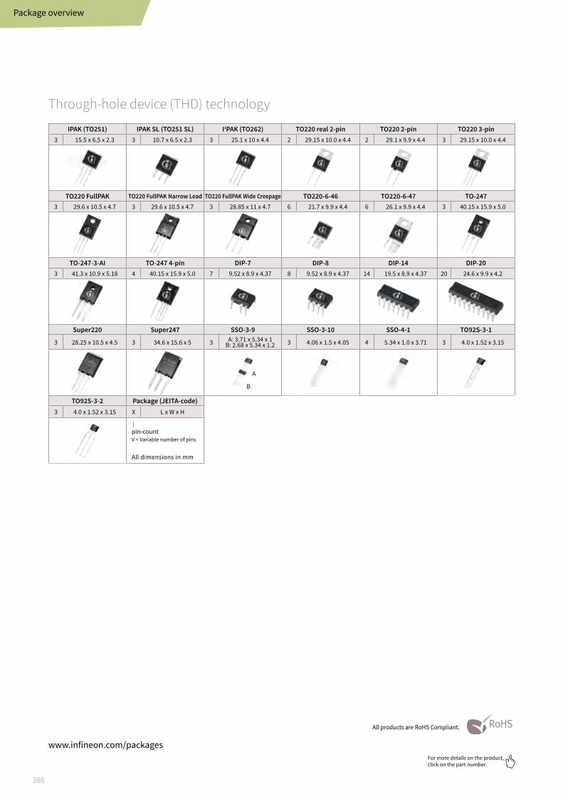
386
For more details on the product, click on the part number.
Package overview
www.infineon.com/packages
IPAK (TO251) IPAK SL (TO251 SL) I2PAK (TO262) TO220 real 2-pin TO220 2-pin TO220 3-pin3 15.5 x 6.5 x 2.3 3 10.7 x 6.5 x 2.3 3 25.1 x 10 x 4.4 2 29.15 x 10.0 x 4.4 2 29.1 x 9.9 x 4.4 3 29.15 x 10.0 x 4.4
TO220 FullPAK TO220 FullPAK Narrow Lead TO220 FullPAK Wide Creepage TO220-6-46 TO220-6-47 TO-2473 29.6 x 10.5 x 4.7 3 29.6 x 10.5 x 4.7 3 28.85 x 11 x 4.7 6 21.7 x 9.9 x 4.4 6 26.1 x 9.9 x 4.4 3 40.15 x 15.9 x 5.0
TO-247-3-AI TO-247 4-pin DIP-7 DIP-8 DIP-14 DIP-203 41.3 x 10.9 x 5.18 4 40.15 x 15.9 x 5.0 7 9.52 x 8.9 x 4.37 8 9.52 x 8.9 x 4.37 14 19.5 x 8.9 x 4.37 20 24.6 x 9.9 x 4.2
Super220 Super247 SSO-3-9 SSO-3-10 SSO-4-1 TO92S-3-1
3 28.25 x 10.5 x 4.5 3 34.6 x 15.6 x 5 3 A: 3.71 x 5.34 x 1B: 2.68 x 5.34 x 1.2 3 4.06 x 1.5 x 4.05 4 5.34 x 1.0 x 3.71 3 4.0 x 1.52 x 3.15
TO92S-3-2 Package (JEITA-code)3 4.0 x 1.52 x 3.15 X L x W x H
pin-count V = Variable number of pins
All dimensions in mm
Through-hole device (THD) technology
A
B
All products are RoHS Compliant.

387
For more details on the product, click on the part number.
Infineon support for packagesUseful links and helpful information
Further information, datasheets and documentswww.infineon.com/packages
Appl
icat
ions
Pa
cka
ges
20
-30
0 V
MO
SF
ETs
50
0-9
50
V M
OS
FE
TsW
BG
se
mic
on
du
cto
rsD
iscr
ete
IGB
TsP
ow
er
ICs
Inte
llig
en
t sw
itch
es
an
d in
pu
t IC
sG
ate
dri
ver
ICs
Mic
roco
ntr
oll
ers
XE
NS
IV™
se
nso
rs

388
For more details on the product, click on the part number.
General supportwww.infineon.com/supportwww.infineon.com/wheretobuywww.infineon.com/qualitywww.infineon.com/packageswww.infineon.com/greenwww.infineon.com/opn
Request reliability (FIT) datahttp://infineon-community.com/FIT_1
Infineon powerful supportUseful links and helpful information
Tools, desks and morewww.infineon.com/solutionfinderwww.infineon.com/lightdeskwww.infineon.com/evaluationboards www.infineon.com/webinars
Register for the Newsletter4Engineershttp://infineon-community.com/Newsletter4Engineers

389
For more details on the product, click on the part number.
Part of your life. Part of tomorrow.
A world leader in semiconductor solutions
Our missionWe make life easier, safer and greener.
Our valuesWe commitWe partnerWe innovateWe perform
Our visionWe are the link between the real and the digital world.
Appl
icat
ions
Pa
cka
ges
20
-30
0 V
MO
SF
ETs
50
0-9
50
V M
OS
FE
TsW
BG
se
mic
on
du
cto
rsD
iscr
ete
IGB
TsP
ow
er
ICs
Inte
llig
en
t sw
itch
es
an
d in
pu
t IC
sG
ate
dri
ver
ICs
Mic
roco
ntr
oll
ers
XE
NS
IV™
se
nso
rs

Service hotline
Infineon offers its toll-free 0800/4001 service hotline as one central number, available 24/7 in English, Mandarin and German.
› Germany .................... 0800 951 951 951 (German/English) › China, mainland ....... 4001 200 951 (Mandarin/English) › India .......................... 000 800 4402 951 (English) › USA ............................ 1-866 951 9519 (English/German) › Other countries ......... 00 * 800 951 951 951 (English/German) › Direct access ............. +49 89 234-0 (interconnection fee, German/English)
* Please note: Some countries may require you to dial a code other than “00” to access this international number. Please visit www.infineon.com/service for your country!
Where to buy
Infineon distribution partners and sales offices: www.infineon.com/wheretobuy
Published by Infineon Technologies Austria AG9500 Villach, Austria
© 2020 Infineon Technologies AG. All Rights Reserved.
Document number: B131-I0773-V1-7600-EU-EC-PDate: 04 / 2020
Please note!THIS DOCUMENT IS FOR INFORMATION PURPOSES ONLY AND ANY INFORMATION GIVEN HEREIN SHALL IN NO EVENT BE REGARDED AS A WARRANTY, GUARANTEE OR DESCRIPTION OF ANY FUNCTIONALITY, CONDITIONS AND/OR QUALITY OF OUR PRODUCTS OR ANY SUITABILITY FOR A PARTICULAR PURPOSE. WITH REGARD TO THE TECHNICAL SPECIFICATIONS OF OUR PRODUCTS, WE KINDLY ASK YOU TO REFER TO THE RELEVANT PRODUCT DATA SHEETS PROVIDED BY US. OUR CUSTOMERS AND THEIR TECHNICAL DEPARTMENTS ARE REQUIRED TO EVALUATE THE SUITABILITY OF OUR PRODUCTS FOR THE INTENDED APPLICATION.
WE RESERVE THE RIGHT TO CHANGE THIS DOCUMENT AND/OR THE INFORMATION GIVEN HEREIN AT ANY TIME.
Additional informationFor further information on technologies, our products, the application of our products, delivery terms and conditions and/or prices, please contact your nearest Infineon Technologies office (www.infineon.com).
WarningsDue to technical requirements, our products may contain dangerous substances. For information on the types in question, please contact your nearest Infineon Technologies office.
Except as otherwise explicitly approved by us in a written document signed by authorized representatives of Infineon Technologies, our products may not be used in any life- endangering applications, including but not limited to medical, nuclear, military, life-critical or any other applications where a failure of the product or any consequences of the use thereof can result in personal injury.
Mobile product catalogMobile app for iOS and Android.
www.infineon.com