ATA 10W Series - Mouser Electronics
28
Rev.09.25.18_#1.0 ATA 10W Series Page 1 Technical Reference Note ATA 10W Series 10 Watts DC/DC Converter Total Power: 10 Watts Input Voltage: 9 to 36Vdc 18 to 75Vdc # of Outputs: Single, dual Special Features • Ultra compact DIP Package 23.8*13.7*8.0 mm(0.94*0.54*0.31 Inches) • Ultra-wide 4:1 input voltage range • Efficiency up to 86% • I/O Isolation 1500Vdc • Operating Temp. Range –40 O C to +80 O C • Input filter meets EN55022, Class A and FCC, Level A • No minimum load requirement • Overload voltage and short circuit protection • Shielded Metal Case with Insulated Baseplate • Conducted EMI meets EN55032/22 Class A & FCC Level A Safety UL/cUL/IEC/EN62368-1 (60950-1) Product Descriptions The ATA 10W series is the latest generation of high performance DC-DC converter modules setting a new standard concerning power density 65W/in 3 . The product offers a full 10W isolated DC-DC converter within an small encapsulated DIP-16 package which occupies only 0.5 in 2 of PCB space. There are 16 models available for 24, 48Vdc with wide 4:1 input voltage range. Further features include under-voltage protection over current protection, short circuit protection, very low no load power consumption, and no minimum load requirement as well. An high efficiency allows operating temperatures range of - 40 O C to +80 O C. These DC-DC converters offer an economical solution for many critical applications in battery-powered equipment, instrumentation, distributed power architectures in communication, industrial electronics, energy facilities where PCB space is limited and offer designers the opportunity to reduce overall PCB layout area.
-
Upload
khangminh22 -
Category
Documents
-
view
3 -
download
0
Transcript of ATA 10W Series - Mouser Electronics
Rev.09.25.18_#1.0ATA 10W Series
Page 1
Technical Reference Note
ATA 10W Series10 Watts DC/DC Converter
Total Power: 10 WattsInput Voltage: 9 to 36Vdc
18 to 75Vdc# of Outputs: Single, dual
Special Features• Ultra compact DIP Package
23.8*13.7*8.0 mm(0.94*0.54*0.31 Inches)
• Ultra-wide 4:1 input voltage range• Efficiency up to 86%• I/O Isolation 1500Vdc• Operating Temp. Range –40 OC to
+80OC • Input filter meets EN55022, Class
A and FCC, Level A• No minimum load requirement• Overload voltage and short circuit
protection• Shielded Metal Case with Insulated
Baseplate• Conducted EMI meets
EN55032/22 Class A & FCC Level A
Safety UL/cUL/IEC/EN62368-1 (60950-1)
Product DescriptionsThe ATA 10W series is the latest generation of high performance DC-DC converter modules setting a new standard concerning power density 65W/in3. The product offers a full 10W isolated DC-DC converter within an small encapsulated DIP-16 package which occupies only 0.5 in2 of PCB space. There are 16 models available for 24, 48Vdc with wide 4:1 input voltage range. Further features include under-voltage protection over current protection, short circuit protection, very low no load power consumption, and no minimum load requirement as well. An high efficiency allows operating temperatures range of -40 OC to +80OC.
These DC-DC converters offer an economical solution for many critical applications in battery-powered equipment, instrumentation, distributed power architectures in communication, industrial electronics, energy facilities where PCB space is limited and offer designers the opportunity to reduce overall PCB layout area.

Technical Reference Note
Rev.09.25.18_#1.0ATA 10W Series
Page 2
Technical Reference Note
Artesyn Embedded Technologies
Model Numbers
Options
None
Model Input Voltage Output Voltage Maximum Load Efficiency Output power
ATA03F18-L 9-36Vdc 3.3Vdc 2.7A 80% 8.9W
ATA03A18-L 9-36Vdc 5Vdc 2.0A 83% 10W
ATA03B18-L 9-36Vdc 12Vdc 0.833A 87% 10W
ATA03C18-L 9-36Vdc 15Vdc 0.666A 88% 10W
ATA03H18-L 9-36Vdc 24Vdc 0.416A 88% 10W
ATA03BB18-L 9-36Vdc ±12Vdc ±0.416A 87% 10W
ATA03CC18-L 9-36Vdc ±15Vdc ±0.333A 87% 10W
ATA03F36-L 18-75Vdc 3.3Vdc 2.7A 80% 8.9W
ATA03A36-L 18-75Vdc 5Vdc 2.0A 83% 10W
ATA03B36-L 18-75Vdc 12Vdc 0.833A 87% 10W
ATA03C36-L 18-75Vdc 15Vdc 0.666A 88% 10W
ATA03H36-L 18-75Vdc 24Vdc 0.416A 88% 10W
ATA03BB36-L 18-75Vdc ±12Vdc ±0.416A 87% 10W
ATA03CC36-L 18-75Vdc ±15Vdc ±0.333A 87% 10W

Technical Reference Note
Rev.09.25.18_#1.0ATA 10W Series
Page 3
Technical Reference Note
Artesyn Embedded Technologies
Table 1. Absolute Maximum Ratings:
Parameter Model Symbol Min Typ Max Unit
Input Surge Voltage1 Sec.max
24V Input Models48V Input Models
VIN,DC-0.7-0.7
--
50100
VdcVdc
Maximum Output Power All models PO,max - - 10 W
Isolation Voltage Input to output (60 seconds)
(1 seconds) All modelsAll models
15001800
--
--
VdcVdc
Isolation Resistance All models 1000 - - Mohm
Isolation Capacitance All models - - 1500 pF
Operating Ambient Temperature Range Convection Cooling -40 +80 OC
Operating Case Temperature All models TCASE - - +105 OC
Storage Temperature All models TSTG -50 +125 OC
Humidity (non-condensing)Operating
Non-operatingAll modelsAll models
--
--
9595
%%
MTBFMIL-HDBK-
217F@25OC, Ground Benign
2538785 - - Hours
Electrical Specifications
Absolute Maximum Ratings
Stress in excess of those listed in the “Absolute Maximum Ratings” may cause permanent damage to the power supply. These are stress ratings only and functional operation of the unit is not implied at these or any other conditions above those given in the operational sections of this TRN. Exposure to any absolute maximum rated condition for extended periods may adversely affect the power supply’s reliability.

Technical Reference Note
Rev.09.25.18_#1.0ATA 10W Series
Page 4
Technical Reference Note
Artesyn Embedded Technologies
Input Specifications
Table 2. Input Specifications:
Parameter Condition Symbol Min Typ Max Unit
Operating Input Voltage, DC
24V Input Models48V Input Models
All VIN,DC9
182448
3675
VdcVdc
Start-Up Threshold Voltage
24V Input Models48V Input Models
All VIN,ON--
--
918
VdcVdc
Under Voltage Shutdown
24V Input Models48V Input Models
All VIN,OFF--
816
--
VdcVdc
Input Current
ATA03F18-LATA03A18-LATA03B18-LATA03C18-LATA03H18-L
ATA03BB18-LATA03CC18-LATA03F36-LATA03A36-LATA03B36-LATA03C36-LATA03H36-L
ATA03BB36-LATA03CC36-L
VIN,DC=VIN,nom IIN,full load
--------------
464502479473473478478232256239237236239239
--------------
mAmAmAmAmAmAmAmAmAmAmAmAmAmA
No Load Input Current(VO On, IO = 0A)
24V Input Models48V Input Models
VIN,DC=VIN,nom IIN,no_load--
107
--
mAmA
Efficiency @Max. Load
ATA03F18-LATA03A18-LATA03B18-LATA03C18-LATA03H18-L
ATA03BB18-LATA03CC18-LATA03F36-LATA03A36-LATA03B36-LATA03C36-LATA03H36-L
ATA03BB36-LATA03CC36-L
VIN,DC=VIN,nomIO=IO,max
TA =25 OC
--------------
8083878888878780838788888787
--------------
%%%%%%%%%%%%%%
Input Filter All Internal Pi Type

Technical Reference Note
Rev.09.25.18_#1.0ATA 10W Series
Page 5
Technical Reference Note
Artesyn Embedded Technologies
Table 3: Output Specifications
Parameter Condition Symbol Min Typ Max Unit
Output Voltage Set-PointVIN,DC=VIN,nom
IO=IO,max
TA =25 OC±VO - - 1.0 %
Output Current
ATA03F18-LATA03A18-LATA03B18-LATA03C18-LATA03H18-L
ATA03BB18-LATA03CC18-LATA03F36-LATA03A36-LATA03B36-LATA03C36-LATA03H36-L
ATA03BB36-LATA03CC36-L
Convection Cooling IO
--------------
--------------
2.72.0
0.8330.6660.416
±0.416±0.333
2.72.0
0.8330.6660.416
±0.416±0.333
AAAAAAAAAAAAAA
Load Capacitance
ATA03F18-LATA03A18-LATA03B18-LATA03C18-LATA03H18-L
ATA03BB18-LATA03CC18-LATA03F36-LATA03A36-LATA03B36-LATA03C36-LATA03H36-L
ATA03BB36-LATA03CC36-L
All CO
--------------
--------------
26001300560560200
390#200#26001300560560200
390#200#
uFuFuFuFuFuFuFuFuFuFuFuFuFuF
Line Regulation VIN,DC=VIN,min to VIN,max %VO - 0.2 0.8 %
Load Regulation IO=IO,min to IO,max %VO - - 1.0 %
Switching Frequency All fSW - 420 - KHz
Temperature Coefficient All %/OC - 0.01 0.02 %
Output Over Current Protection1 All %IO,max - 160 - %
Output Short Circuit Protection AllHiccup Mode 0.5Hz type, Automatic
Recovery
Output Ripple, pk-pk
Measure with a 4.7uF ceramic capacitor in parallel with a 10uF
tantalum capacitor, 0 to 20MHz bandwidth
VO - - 80 mV
Output Specifications

Technical Reference Note
Rev.09.25.18_#1.0ATA 10W Series
Page 6
Technical Reference Note
Artesyn Embedded Technologies
ATA03F18-L Performance Curves
Figure 4: ATA03F18-L Transient ResponseVin = 24Vdc Load: Io = 100% to 75% load change
Ch 1: Vo
Figure 1: ATA03F18-L Efficiency Versus Output Current CurveVin = 9 to 36Vdc Load: Io = 0 to 2.7A
Figure 2: ATA03F18-L Efficiency Versus Input Voltage CurveVin = 9 to 36Vdc Load: Io = 2.7A
Figure 3 ATA03F18-L Ripple and Noise MeasurementVin = 24Vdc Load: Io = 2.7A
Ch 1: Vo
Figure 5: ATA03F18-L Output Voltage Startup Characteristic by VinVin = 24Vdc Load: Io = 2.7A
Ch1: Vo Ch3: Vin
Figure 6: ATA03F18-L Derating Output Current vs Ambient Temperature Vin = 24Vdc Load: Io = 2.7A

Technical Reference Note
Rev.09.25.18_#1.0ATA 10W Series
Page 7
Technical Reference Note
Artesyn Embedded Technologies
ATA03A18-L Performance Curves
Figure 10: ATA03A18-L Transient ResponseVin = 24Vdc Load: Io = 100% to 75% load change
Ch 1: Vo
Figure 7: ATA03A18-L Efficiency Versus Output Current CurveVin = 9 to 36Vdc Load: Io = 0 to 2.0A
Figure 8: ATA03A18-L Efficiency Versus Input Voltage CurveVin = 9 to 36Vdc Load: Io = 2.0A
Figure 9: ATA03A18-L Ripple and Noise MeasurementVin = 24Vdc Load: Io = 2.0A
Ch 1: Vo
Figure 11: ATA03A18-L Output Voltage Startup Characteristic by VinVin = 24Vdc Load: Io = 2.0A
Ch1: Vo Ch3: Vin
Figure 12: ATA03A18-L Derating Output Current vs Ambient Temperature Vin = 24Vdc Load: Io = 2.0A

Technical Reference Note
Rev.09.25.18_#1.0ATA 10W Series
Page 8
Technical Reference Note
Artesyn Embedded Technologies
ATA03B18-L Performance Curves
Figure 16: ATA03B18-L Transient ResponseVin = 24Vdc Load: Io = 100% to 75% load change
Ch 1: Vo
Figure 13: ATA03B18-L Efficiency Versus Output Current CurveVin = 9 to 36Vdc Load: Io = 0 to 0.833A
Figure 14: ATA03B18-L Efficiency Versus Input Voltage CurveVin = 9 to 36Vdc Load: Io = 0.833A
Figure 15: ATA03B18-L Ripple and Noise MeasurementVin = 24Vdc Load: Io = 0.833A
Ch 1: Vo
Figure 17: ATA03B18-L Output Voltage Startup Characteristic by VinVin = 24Vdc Load: Io = 0.833A
Ch1: Vo Ch3: Vin
Figure 18: ATA03B18-L Derating Output Current vs Ambient Temperature Vin = 24Vdc Load: Io = 0.833A

Technical Reference Note
Rev.09.25.18_#1.0ATA 10W Series
Page 9
Technical Reference Note
Artesyn Embedded Technologies
ATA03C18-L Performance Curves
Figure 22: ATA03C18-L Transient ResponseVin = 24Vdc Load: Io = 100% to 75% load change
Ch 1: Vo
Figure 19: ATA03C18-L Efficiency Versus Output Current CurveVin = 9 to 36Vdc Load: Io = 0 to 0.666A
Figure 20: ATA03C18-L Efficiency Versus Input Voltage CurveVin = 9 to 36Vdc Load: Io = 0.666A
Figure 21: ATA03C18-L Ripple and Noise MeasurementVin = 24Vdc Load: Io = 0.666A
Ch 1: Vo
Figure 23: ATA03C18-L Output Voltage Startup Characteristic by VinVin = 24Vdc Load: Io = 0.666A
Ch1: Vo Ch3: Vin
Figure 24: ATA03C18-L Derating Output Current vs Ambient Temperature Vin = 24Vdc Load: Io = 0.4A

Technical Reference Note
Rev.09.25.18_#1.0ATA 10W Series
Page 10
Technical Reference Note
Artesyn Embedded Technologies
ATA03H18-L Performance Curves
ATA01H18-L Performance Curves
Figure 28: ATA03H18-L Transient ResponseVin = 24Vdc Load: Io = 100% to 75% load change
Ch 1: Vo
Figure 25: ATA03H18-L Efficiency Versus Output Current CurveVin = 9 to 36Vdc Load: Io = 0 to 0.416A
Figure 26: ATA03H18-L Efficiency Versus Input Voltage CurveVin = 9 to 36Vdc Load: Io = 0.416A
Figure 27: ATA03H18-L Ripple and Noise MeasurementVin = 24Vdc Load: Io = 0.416A
Ch 1: Vo
Figure 29: ATA03H18-L Output Voltage Startup Characteristic by VinVin = 24Vdc Load: Io = 0.416A
Ch1: Vo Ch3: Vin
Figure 30: ATA03H18-L Derating Output Current vs Ambient Temperature Vin = 24Vdc Load: Io = 0.416A
Technical Reference Note
Rev.09.25.18_#1.0ATA 10W Series
Page 11
Technical Reference Note
Artesyn Embedded Technologies
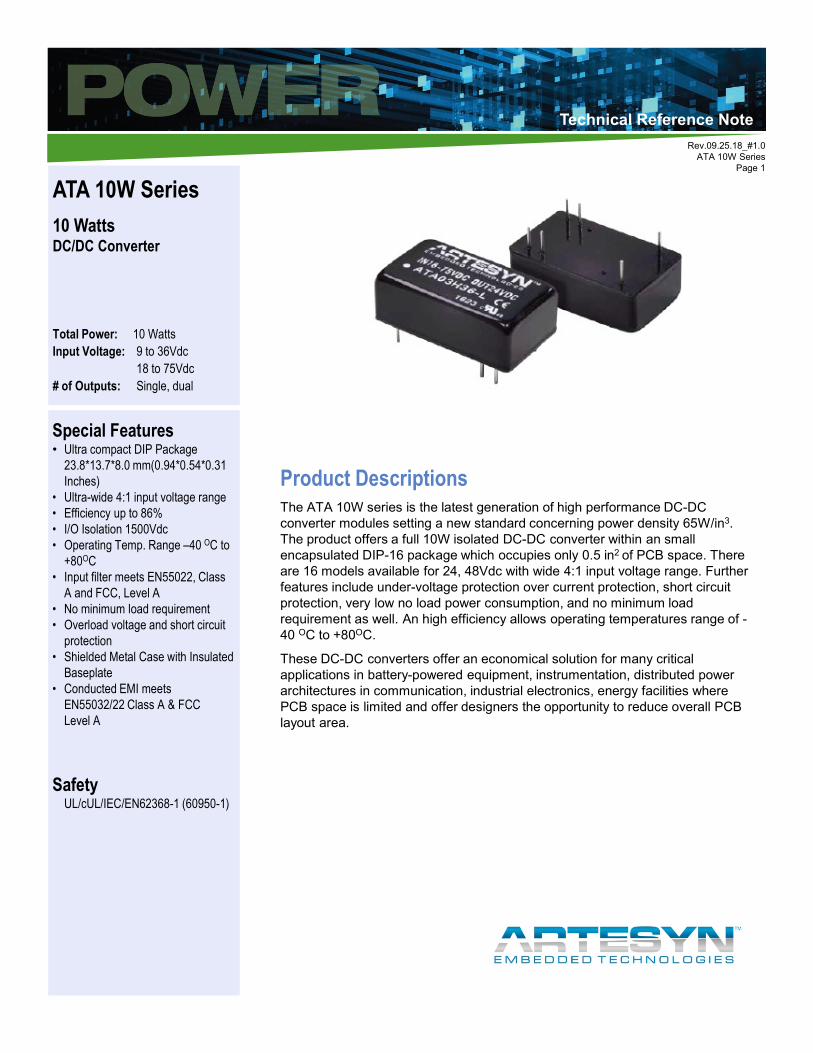
ATA03BB18-L Performance Curves
ATA01H18-L Performance Curves
Figure 34: ATA03BB18-L Transient ResponseVin = 24Vdc Load: Io = 100% to 75% load change
Ch 1: Vo1 Ch 2: Vo2
Figure 31: ATA03BB18-L Efficiency Versus Output Current CurveVin = 9 to 36Vdc Load: Io = 0 to ±0.416A
Figure 32: ATA03BB18-L Efficiency Versus Input Voltage CurveVin = 9 to 36Vdc Load: Io = ±0.416A
Figure 33: ATA03BB18-L Ripple and Noise MeasurementVin = 24Vdc Load: Io = ±0.416A
Ch 1: Vo1 Ch 2: Vo2
Figure 35: ATA03BB18-L Output Voltage Startup Characteristic by VinVin = 24Vdc Load: Io = ±0.416A
Ch1: Vo1 Ch2:Vo2 Ch3: Vin
Figure 36: ATA03BB18-L Derating Output Current vs Ambient Temperature Vin = 24Vdc Load: Io = ± 0.416A

Technical Reference Note
Rev.09.25.18_#1.0ATA 10W Series
Page 12
Technical Reference Note
Artesyn Embedded Technologies
ATA03CC18-L Performance Curves
ATA01H18-L Performance Curves
Figure 40: ATA03CC18-L Transient ResponseVin = 24Vdc Load: Io = 100% to 75% load change
Ch 1: Vo1 Ch 2: Vo2
Figure 37: ATA03CC18-L Efficiency Versus Output Current CurveVin = 9 to 36Vdc Load: Io = 0 to ±0.333A
Figure 38: ATA03CC18-L Efficiency Versus Input Voltage CurveVin = 9 to 36Vdc Load: Io = ±0.333A
Figure 39: ATA03CC18-L Ripple and Noise MeasurementVin = 24Vdc Load: Io = ±0.333A
Ch 1: Vo1 Ch 2: Vo2
Figure 41: ATA03CC18-L Output Voltage Startup Characteristic by VinVin = 24Vdc Load: Io = ±0.333A
Ch1: Vo1 Ch2:Vo2 Ch3: Vin
Figure 42: ATA03CC18-L Derating Output Current vs Ambient Temperature Vin = 24Vdc Load: Io = ± 0.333A

Technical Reference Note
Rev.09.25.18_#1.0ATA 10W Series
Page 13
Technical Reference Note
Artesyn Embedded Technologies
ATA03F36-L Performance Curves
Figure 46: ATA03F36-L Transient ResponseVin = 48Vdc Load: Io = 100% to 75% load change
Ch 1: Vo
Figure 43: ATA03F36-L Efficiency Versus Output Current CurveVin = 18 to 75Vdc Load: Io = 0 to 2.7A
Figure 44: ATA03F36-L Efficiency Versus Input Voltage CurveVin = 18 to 75Vdc Load: Io = 2.7A
Figure 45: ATA03F36-L Ripple and Noise MeasurementVin = 48Vdc Load: Io = 2.7A
Ch 1: Vo
Figure 47: ATA03F36-L Output Voltage Startup Characteristic by VinVin = 48Vdc Load: Io = 2.7A
Ch1: Vo Ch3: Vin
Figure 48: ATA03F36-L Derating Output Current vs Ambient Temperature Vin = 48Vdc Load: Io = 2.7A
~
Ambient Temperature
Ou
tpu
tPow
er(%
)
0
20
40
60
80
100
-40 0 20 60 100 1108040
NaturalConvection
20LFM
C

Technical Reference Note
Rev.09.25.18_#1.0ATA 10W Series
Page 14
Technical Reference Note
Artesyn Embedded Technologies
ATA03A36-L Performance Curves
Figure 52: ATA03A36-L Transient ResponseVin = 48Vdc Load: Io = 100% to 75% load change
Ch 1: Vo
Figure 49: ATA03A36-L Efficiency Versus Output Current CurveVin = 18 to 75Vdc Load: Io = 0 to 2.0A
Figure 50: ATA03A36-L Efficiency Versus Input Voltage CurveVin = 18 to 75Vdc Load: Io = 2.0A
Figure 51: ATA03A36-L Ripple and Noise MeasurementVin = 48Vdc Load: Io = 2.0A
Ch 1: Vo
Figure 53: ATA03A36-L Output Voltage Startup Characteristic by VinVin = 48Vdc Load: Io = 2.0A
Ch1: Vo Ch3: Vin
Figure 54: ATA03A36-L Derating Output Current vs Ambient Temperature Vin = 48Vdc Load: Io = 2.0A

Technical Reference Note
Rev.09.25.18_#1.0ATA 10W Series
Page 15
Technical Reference Note
Artesyn Embedded Technologies
ATA03B36-L Performance Curves
Figure 58: ATA03B36-L Transient ResponseVin = 48Vdc Load: Io = 100% to 75% load change
Ch 1: Vo
Figure 55: ATA03B36-L Efficiency Versus Output Current CurveVin = 18 to 75Vdc Load: Io = 0 to 0.833A
Figure 56: ATA03B36-L Efficiency Versus Input Voltage CurveVin = 18 to 75Vdc Load: Io = 0.833A
Figure 57: ATA03B36-L Ripple and Noise MeasurementVin = 48Vdc Load: Io = 0.833A
Ch 1: Vo
Figure 59: ATA03B36-L Output Voltage Startup Characteristic by VinVin = 48Vdc Load: Io = 0.833A
Ch1: Vo Ch3: Vin
Figure 60: ATA03B36-L Derating Output Current vs Ambient Temperature Vin = 48Vdc Load: Io = 0.833A

Technical Reference Note
Rev.09.25.18_#1.0ATA 10W Series
Page 16
Technical Reference Note
Artesyn Embedded Technologies
ATA03C36-L Performance Curves
Figure 64: ATA03C36-L Transient ResponseVin = 48Vdc Load: Io = 100% to 75% load change
Ch 1: Vo
Figure 61: ATA03C36-L Efficiency Versus Output Current CurveVin = 18 to 75Vdc Load: Io = 0 to 0.666A
Figure 62: ATA03C36-L Efficiency Versus Input Voltage CurveVin = 9 to 36Vdc Load: Io = 0.666A
Figure 63: ATA03C36-L Ripple and Noise MeasurementVin = 48Vdc Load: Io = 0.666A
Ch 1: Vo
Figure 65: ATA03C36-L Output Voltage Startup Characteristic by VinVin = 48Vdc Load: Io = 0.666A
Ch1: Vo Ch3: Vin
Figure 66: ATA03C36-L Derating Output Current vs Ambient Temperature Vin = 48Vdc Load: Io = 0.666A
Technical Reference Note
Rev.09.25.18_#1.0ATA 10W Series
Page 17
Technical Reference Note
Artesyn Embedded Technologies
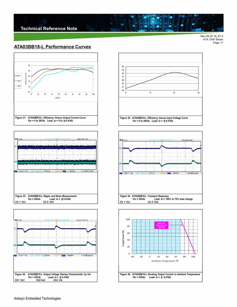
ATA03H36-L Performance Curves
ATA01H18-L Performance Curves
Figure 70: ATA03H36-L Transient ResponseVin = 48Vdc Load: Io = 100% to 75% load change
Ch 1: Vo
Figure 67: ATA03H36-L Efficiency Versus Output Current CurveVin = 18 to 75Vdc Load: Io = 0 to 0.416A
Figure 68: ATA03H36-L Efficiency Versus Input Voltage CurveVin = 18 to 75Vdc Load: Io = 0.416A
Figure 69: ATA03H36-L Ripple and Noise MeasurementVin = 48Vdc Load: Io = 0.416A
Ch 1: Vo
Figure 71: ATA03H36-L Output Voltage Startup Characteristic by VinVin = 48Vdc Load: Io = 0.416A
Ch1: Vo Ch3: Vin
Figure 72: ATA03H36-L Derating Output Current vs Ambient Temperature Vin = 48Vdc Load: Io = 0.416A
Technical Reference Note
Rev.09.25.18_#1.0ATA 10W Series
Page 18
Technical Reference Note
Artesyn Embedded Technologies
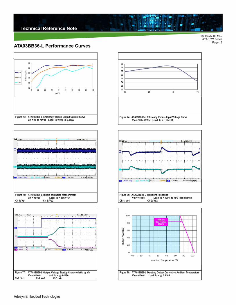
ATA03BB36-L Performance Curves
ATA01H18-L Performance Curves
Figure 76: ATA03BB36-L Transient ResponseVin = 48Vdc Load: Io = 100% to 75% load change
Ch 1: Vo1 Ch 2: Vo2
Figure 73: ATA03BB36-L Efficiency Versus Output Current CurveVin = 18 to 75Vdc Load: Io = 0 to ±0.416A
Figure 74: ATA03BB36-L Efficiency Versus Input Voltage CurveVin = 18 to 75Vdc Load: Io = ±0.416A
Figure 75: ATA03BB36-L Ripple and Noise MeasurementVin = 48Vdc Load: Io = ±0.416A
Ch 1: Vo1 Ch 2: Vo2
Figure 77: ATA03BB36-L Output Voltage Startup Characteristic by VinVin = 48Vdc Load: Io = ±0.416A
Ch1: Vo1 Ch2:Vo2 Ch3: Vin
Figure 78: ATA03BB36-L Derating Output Current vs Ambient Temperature Vin = 48Vdc Load: Io = ± 0.416A

Technical Reference Note
Rev.09.25.18_#1.0ATA 10W Series
Page 19
Technical Reference Note
Artesyn Embedded Technologies
ATA03CC36-L Performance Curves
ATA01H18-L Performance Curves
Figure 82: ATA03CC36-L Transient ResponseVin = 48Vdc Load: Io = 100% to 75% load change
Ch 1: Vo1 Ch 2: Vo2
Figure 79: ATA03CC36-L Efficiency Versus Output Current CurveVin = 18 to 75Vdc Load: Io = 0 to ±0.333A
Figure 80: ATA03CC36-L Efficiency Versus Input Voltage CurveVin = 18 to 75Vdc Load: Io = ±0.333A
Figure 81: ATA03CC18-L Ripple and Noise MeasurementVin = 48Vdc Load: Io = ±0.333A
Ch 1: Vo1 Ch 2: Vo2
Figure 83: ATA03CC36-L Output Voltage Startup Characteristic by VinVin = 48Vdc Load: Io = ±0.333A
Ch1: Vo1 Ch2:Vo2 Ch3: Vin
Figure 84: ATA03CC36-L Derating Output Current vs Ambient Temperature Vin = 48Vdc Load: Io = ± 0.333A

Technical Reference Note
Rev.09.25.18_#1.0ATA 10W Series
Page 20
Technical Reference Note
Artesyn Embedded Technologies
Mechanical Specifications
Mechanical Outlines
Note:1.All dimensions in mm (inches)2.Tolerance: X.X±0.5 (X.XX±0.02)
X.XX±0.25 ( X.XXX±0.01)3.Pin diameter 0.5 ±0.05 (0.02±0.002)
Pin Connections
Single output
Pin 1 – -Vin
Pin 7 – NC
Pin 8 – NC
Pin 9 – +Vout
Pin 10 – -Vout
Pin 16 – +Vin
Dual Output
Pin 1 – -Vin
Pin 7 – NC
Pin 8 – Common
Pin 9 – +Vout
Pin 10 – -Vout
Pin 16 – +Vin
Physical Characteristics
Case Size 23.8x13.7x8.0mm (0.94x0.54x0.31 inches)
Case Material Aluminium Alloy, Black Anodized Coating
Pin Material Tinned Copper
Weight 6.5g
10
.16
[0.4
0]
13
.7 [0
.54
]8.
0 [
0.3
1]
0.5 [0.02]
3.8
[0.1
5]
1 7 8
16 10 9
2.54 [0.10]
23.8 [0.94]
Bottom View
15.24[0.60]
3.0 [0.12]
1.7
7 [
0.0
7]

Technical Reference Note
Rev.09.25.18_#1.0ATA 10W Series
Page 21
Technical Reference Note
Artesyn Embedded Technologies
Recommended Pad Layout for Single & Dual Output Converter
15.24 2.54
[0.10][0.60]
10.
16
[0.4
0]
13.
70
[0.5
4]16 10 9
871
TOP VIEW
23.8 [0.94] 1.77
[0.0
7]
6X 1.30 0.1(PAD)[6X 0.05 0.004]6X 0.80 0.1(HOLE)[6X 0.03 0.004]

Technical Reference Note
Rev.09.25.18_#1.0ATA 10W Series
Page 22
Technical Reference Note
Artesyn Embedded Technologies
Environmental Specifications
EMC Immunity
ATA 10W series power supply is designed to meet the following EMC immunity specifications.
Table 4. EMC Specifications:
Parameter Standards & Level Performance
EMI Conduction EN55032, FCC part15 Class A
EMS
EN55024
ESD EN61000-4-2 Air ±8kV, Contact ±6kVPerf. Criteria A
Radiated immunity EN61000-4-3 20V/m
Fast transient1 EN61000-4-4 ±2KV Perf. Criteria A
Surge1 EN61000-4-5 ±2KV Perf. Criteria A
Conducted immunity EN61000-4-6 10Vrms Perf. Criteria A
PFMF EN61000-4-8 100A/M Perf. Criteria A
Note 1 - To meet EN61000-4-4 & EN61000-4-5 an external filter requested, please contact Artesyn

Technical Reference Note
Rev.09.25.18_#1.0ATA 10W Series
Page 23
Technical Reference Note
Artesyn Embedded Technologies
Safety Certifications
The ATA 10W series power supply is intended for inclusion in other equipment and the installer must ensure that it is in compliance with all the requirements of the end application. This product is only for inclusion by professional installers within other equipment and must not be operated as a stand alone product.
Table 5. Safety Certifications for ATA 10W series power supply system
Document Description
cUL/UL 60950-1(UL certificate) US and Canada Requirements
IEC/EN 60950-1(CB-scheme) European Requirements(All CENELEC Countries)
cUL/UL 62368-1(UL certificate) US Requirements
IEC/EN 62368-1(CB-scheme) European Requirements(All CENELEC Countries)
CE Mark

Technical Reference Note
Rev.09.25.18_#1.0ATA 10W Series
Page 24
Technical Reference Note
Artesyn Embedded Technologies
MTBF and Reliability
The MTBF of ATA 10W series of DC/DC converters has been calculated using MIL-HDBK 217F NOTICE2, Operating Temperature 25 OC, Ground Benign.
Model MTBF Unit
ATA03F18-L 2562483
Hours
ATA03A18-L 2555111
ATA03B18-L 3534977
ATA03C18-L 3704681
ATA03H18-L 3776036
ATA03BB18-L 3526032
ATA03CC18-L 3499799
ATA03F36-L 2606925
ATA03A36-L 2587419
ATA03B36-L 3604906
ATA03C36-L 3735662
ATA03H36-L 3792554
ATA03BB36-L 3533217
ATA03CC36-L 3519995

Technical Reference Note
Rev.09.25.18_#1.0ATA 10W Series
Page 25
Technical Reference Note
Artesyn Embedded Technologies
Application Notes
Peak-to-Peak Output Noise Measurement Test
Refer to the output specifications or add 4.7μF capacitor if the output specifications undefine Cout. Scope measurement should be made by using a BNC socket, measurement bandwidth is 0-20 MHz. Position the load between 50 mm and 75 mm from the DC-DC Converter.
Output Ripple Reduction
A good quality low ESR capacitor placed as close as practicable across the load will give the best ripple and noise performance. To reduce output ripple, it is recommended to use 3.3μF capacitors at the output.
Input Source Impedance
The power module should be connected to a low ac-impedance input source. Highly inductive source impedances can affect the stability of the power module. In applications where power is supplied over long lines and output loading is high,it may be necessary to use a capacitor at the input to ensure startup. Capacitor mounted close to the power module helps ensure stability of the unit, it is recommended to use a good quality low Equivalent Series Resistance (ESR < 1.0Ω at 100KHz) capacitor of a 2.2μF for the 24V and 48V devices.
+Out
-Out
+Vin
-Vin
Dual OutputDC / DC
Converter
ResistiveLoad
Scope
Copper Strip
Cout
Com.
ScopeCout
Copper Strip
Copper Strip
+Out
-Out
+Vin
-Vin
Single OutputDC / DC
Converter
ResistiveLoad
Scope
Copper Strip
Cout
Copper Strip
+
+Out
-Out
+Vin
-Vin
DC / DCConverter Load
DC PowerSource
+
-
Cin
+Out
-Out
+Vin
-Vin
LoadDC Power
Source
+
-
CoutCom.
Dual OutputDC / DC
Converter LoadCout
+Out
-Out
+Vin
-Vin
LoadDC Power
Source
+
-
CoutCom.
Dual OutputDC / DC
Converter LoadCout

Technical Reference Note
Rev.09.25.18_#1.0ATA 10W Series
Page 26
Technical Reference Note
Artesyn Embedded Technologies
Output Over Current Protection
To provide hiccup mode protection in a fault (output overload) condition, the unit is equipped with internal current limitingcircuitry and can endure overload for an unlimited duration.
Thermal Considerations
Many conditions affect the thermal performance of the power module, such as orientation, airflow over the module and board spacing. To avoid exceeding the maximum temperature rating of the components inside the power module, the case temperature must be kept below 105 OC. The derating curves are determined from measurements obtained in a test setup.
Maximum Capacitive Load
The ATA 10W series has limitation of maximum connected capacitance at the output. The power module may operate in current limiting mode during start-up, affecting the ramp-up and the startup time. The maximum capacitance can be found in the datasheet.
DUT
Position of air velocityprobe and thermocouple
50mm / 2inAir Flow
15mm / 0.6in
Technical Reference Note
Rev.09.25.18_#1.0ATA 10W Series
Page 27
Technical Reference Note
Artesyn Embedded Technologies
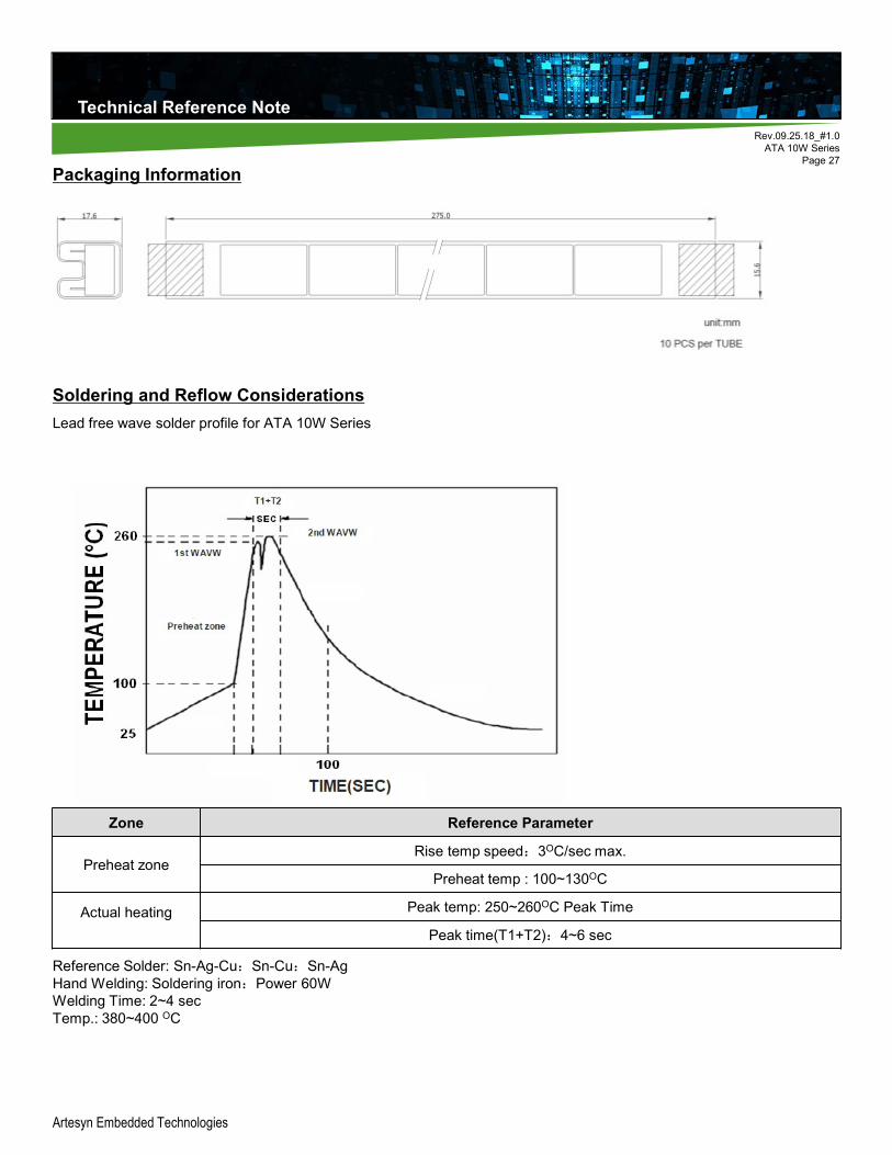
Packaging Information
Soldering and Reflow Considerations
Lead free wave solder profile for ATA 10W Series
Reference Solder: Sn-Ag-Cu:Sn-Cu:Sn-AgHand Welding: Soldering iron:Power 60WWelding Time: 2~4 sec Temp.: 380~400 OC
Zone Reference Parameter
Preheat zoneRise temp speed:3OC/sec max.
Preheat temp : 100~130OC
Actual heating Peak temp: 250~260OC Peak Time
Peak time(T1+T2):4~6 sec

Technical Reference Note
Rev.09.25.18_#1.0ATA 10W Series
Page 28
Technical Reference Note
For more information: www.artesyn.com/powerFor support: [email protected]
Record of Revision and Changes
Issue Date Description Originators
1.0 09.25.2018 First Issue K. Wang