TC78B027FTG - Mouser Electronics
46
TC78B027FTG © 2019 Toshiba Electronic Devices & Storage Corporation 1 2019-09-27 TOSHIBA CDMOS Integrated Circuit Silicon Monolithic TC78B027FTG 1-Hall sine-wave PWM pre-driver for 3-phase brushless DC motors 1. Outline The TC78B027FTG is a 1-Hall sine-wave PWM controller for 3- phase brushless DC motors. N-ch MOSFET can be used as external FET’s. A non-volatile memory (NVM) and a closed loop speed control function are incorporated. Cost can be suppressed without using microcontrollers. 2. Applications Fan motors (e.g. Server) 3. Features ● 1-Hall sine-wave PWM drive ● Pre-driver for external N-ch MOSFET. ● Closed loop speed control, configurable speed curve ● Adjustable driving current for the gate of external MOSFET. ● Operating voltage range : 5 to 16V (Electrical characteristics are not guaranteed from 5 to 9V) ● Serial interface ● Standby mode ● Soft start ● Output RPM information ● Protection features: Thermal ShutDown (TSD)、Under Voltage LockOut (UVLO)、Over Voltage Protection (OVP)、 Under voltage protection for the charge pump、Over Current limit Protection (OCP)、Over current protection (ISD)、Lock detection Start of commercial production 2019-08 QFN24
-
Upload
khangminh22 -
Category
Documents
-
view
1 -
download
0
Transcript of TC78B027FTG - Mouser Electronics

TC78B027FTG
© 2019 Toshiba Electronic Devices & Storage Corporation 1 2019-09-27
TOSHIBA CDMOS Integrated Circuit Silicon Monolithic
TC78B027FTG
1-Hall sine-wave PWM pre-driver for 3-phase brushless DC motors
1. Outline The TC78B027FTG is a 1-Hall sine-wave PWM controller for 3-phase brushless DC motors. N-ch MOSFET can be used as external FET’s. A non-volatile memory (NVM) and a closed loop speed control function are incorporated. Cost can be suppressed without using microcontrollers.
2. Applications Fan motors (e.g. Server)
3. Features ● 1-Hall sine-wave PWM drive ● Pre-driver for external N-ch MOSFET. ● Closed loop speed control, configurable speed curve ● Adjustable driving current for the gate of external MOSFET. ● Operating voltage range : 5 to 16V (Electrical characteristics are not guaranteed from 5 to 9V) ● Serial interface ● Standby mode ● Soft start ● Output RPM information ● Protection features:
Thermal ShutDown (TSD)、Under Voltage LockOut (UVLO)、Over Voltage Protection (OVP)、 Under voltage protection for the charge pump、Over Current limit Protection (OCP)、Over current protection (ISD)、Lock detection
Start of commercial production 2019-08
QFN24

TC78B027FTG
© 2019 Toshiba Electronic Devices & Storage Corporation 2 2019-09-27
Contents 1. Outline ................................................................................................................................................ 1 2. Applications ........................................................................................................................................ 1 3. Features ............................................................................................................................................. 1 4. Block Diagram .................................................................................................................................... 4 5. Absolute Maximum Ratings (Ta = 25°C) ............................................................................................. 5 6. Operating range ................................................................................................................................. 6 7. Pin Assignment (Top view) ................................................................................................................. 6 8. Pin Description ................................................................................................................................... 7 9. I/O Equivalent Circuit .......................................................................................................................... 8 10. Electrical Characteristics ................................................................................................................ 11 11. Functional Description .................................................................................................................... 14
11.1. Basic Operation ................................................................................................................................... 14 11.1.1. The IC status in each mode ..................................................................................................................15 11.1.2. 1-Hall commutation ...............................................................................................................................15 11.1.3. PWM frequency .....................................................................................................................................16 11.1.4. Lead angle control .................................................................................................................................17 11.1.5. Soft Start ...............................................................................................................................................18 11.1.6. Acceleration and deceleration control ...................................................................................................19 11.1.7. Output current for the gate of external MOSFET ..................................................................................19 11.1.8. Limitation of step of reducing rotation speed ........................................................................................20
11.2. Input / Output Signals .......................................................................................................................... 21 11.2.1. SPD .......................................................................................................................................................21 11.2.2. DIR ........................................................................................................................................................21 11.2.3. ALERT ...................................................................................................................................................22 11.2.4. HP, HM ..................................................................................................................................................23 11.2.5. FG .........................................................................................................................................................25 11.2.6. BRAKE ..................................................................................................................................................26
11.3. Speed Control ...................................................................................................................................... 27 11.3.1. Closed loop ...........................................................................................................................................27 11.3.2. Open loop ..............................................................................................................................................30
11.4. Serial I/F and NVM .............................................................................................................................. 33 11.4.1. Serial commands ..................................................................................................................................33 11.4.2. Status register .......................................................................................................................................34 11.4.3. Normal register ......................................................................................................................................35 11.4.4. Flowchart of writing Non-Volatile Memory (NVM) .................................................................................37
11.5. Protection Function.............................................................................................................................. 38 11.5.1. Fault and detection table .......................................................................................................................38 11.5.2. Lock detection .......................................................................................................................................38

TC78B027FTG
© 2019 Toshiba Electronic Devices & Storage Corporation 3 2019-09-27
11.5.3. Output current limit protection (OCP) ....................................................................................................39 11.5.4. Over current protection (ISD) ................................................................................................................40 11.5.5. Over voltage protection (OVP) ..............................................................................................................40 11.5.6. Under voltage lockout (UVLO) ..............................................................................................................40 11.5.7. Charge pump under voltage .................................................................................................................40 11.5.8. Thermal shutdown (TSD) ......................................................................................................................40
12. Reference circuit............................................................................................................................. 41 13. Reference board layout .................................................................................................................. 42 14. Package ......................................................................................................................................... 43
14.1. Package dimension ............................................................................................................................. 43 15. IC Usage Considerations ................................................................................................................ 44
15.1. Notes on handling IC ........................................................................................................................... 44 15.2. Points to remember on handling of ICs ............................................................................................... 44
RESTRICTIONS ON PRODUCT USE .................................................................................................. 45
TC78B027FTG
© 2019 Toshiba Electronic Devices & Storage Corporation 4 2019-09-27
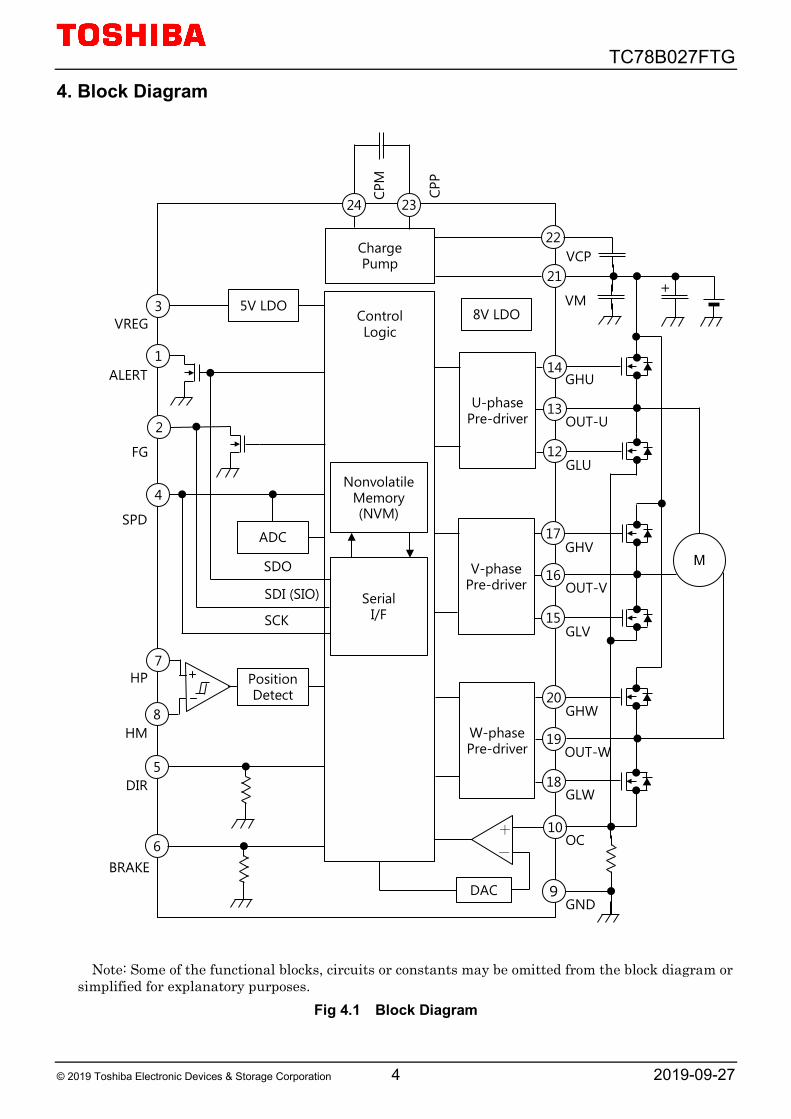
4. Block Diagram
Note: Some of the functional blocks, circuits or constants may be omitted from the block diagram or
simplified for explanatory purposes. Fig 4.1 Block Diagram
M
3 5V LDO VREG
1 ALERT
2
FG
4
SPD ADC
Control Logic
Nonvolatile Memory (NVM)
Serial I/F
SDO
SDI (SIO) SCK
7 HP
8 HM
Position Detect
5 DIR
6 BRAKE
Charge Pump
23 24
CPP
CPM
22 VCP
21
VM +
U-phase Pre-driver
14
13
12
V-phase Pre-driver
17
16
15
W-phase Pre-driver
20
19
18
10
9
8V LDO
DAC
GHU
OUT-U
GLU
GHV
OUT-V
GLV
GHW
OUT-W
GLW
OC
GND
+ -

TC78B027FTG
© 2019 Toshiba Electronic Devices & Storage Corporation 5 2019-09-27
5. Absolute Maximum Ratings (Ta = 25°C)
Table 5.1 Absolute Maximum Ratings (Unless otherwise specified, Ta = 25°C)
Characteristics Symbol Rating Unit
Power supply voltage of the motor VM 18 V
5V reference voltage VREG 6 (Note 1) V
Charge pump voltage VCP VM+10 (Note 1) V
Input voltage
HP, HM, DIR, BRAKE, OC VIN
-0.3 to 6 V
SPD -0.3 to 6(18) (Note2) V
Output voltage
ALERT, FG, GLU, OUT-U, GLV, OUT-V, GLW, OUT-W, VOUT
18 V
GHU, GHV, GHW VM+10 V
Output current
ALERT, FG, VREG
IOUT
10 mA
GLU, GHU, GLV, GHV, GLW, GHW FET gate source current
100 mA
GLU, GHU, GLV, GHV, GLW, GHW FET gate sink current
200 mA
Power dissipation PD 1.7 (Note3) W
Operating temperature Topr -40 to 105 °C
Storage temperature Tstg -55 to 150 °C
Junction temperature Tj(MAX) 150 °C
Note 1: VREG and VCP pin voltage are generated in the IC. Do not apply voltage externally. Note 2: This terminal should be used within operating range. However up to 18V can be applied, it
does NOT mention that IC will not deteriorate in such a case. Note 3: When mounted on a board, (JEDEC 2-layer board, Rθja=73.5°C/W) Note: Output current is limited depend on the ambient temperature and the device
implementation. The maximum junction temperature (Tj(MAX)) should not exceed 150°C.
Note: The absolute maximum ratings of a semiconductor device are a set of ratings that must not be exceeded, even for a moment. Do not exceed any of these ratings. Exceeding the ratings may cause the device breakdown, damage or deterioration, and may result injury by explosion or combustion. Please use the IC within the specified operating ranges.

TC78B027FTG
© 2019 Toshiba Electronic Devices & Storage Corporation 6 2019-09-27
6. Operating range
Table 6.1 Operating range (Unless otherwise specified, Ta=-40 to 105°C)
Characteristics Symbol Min. Typ. Max. Unit
VM pin power supply voltage1 VM(opr1) 9 12 16 V
VM pin power supply voltage2 (Note1) VM(opr2) 5.0 — 9 V
VM pin power supply voltage3 (Note2) VM(opr3) 10.8 12 16 V
Input PWM frequency fTSP 1 — 100 kHz
Input SPI CLK frequency fSCK 15 — 500 kHz
Input voltage
HP, HM VIN
0.1 — VREG – 2.0 V
DIR,SPD, BRAKE, OC -0.3 — 5.5 V
Note 1: Electrical characteristics are only for reference because the variation of electrical characteristics becomes large.
Note 2: For NVM writing.
Table 6.2 NVM Characteristics
Characteristics Conditions Min. Max. Unit
Program/Erase cycle Tj = 0 to 90 °C 10 — Cycle
7. Pin Assignment (Top view)
Figure 7.1 Pin assignment (Top view)
1 18
2 17
3 16
4 15
5 14
6 13
7 8 9 10 11 12
24 23 22 21 20 19
HP
GN
D
OC
TES
T
GLU
ALERT
FG
VREG
SPD
DIR
BRAKE
HM
OUT-U
GHU
GLV
OUT-V
GHV
GLW
OU
T-W
GH
W
VM
VC
P
CPP
CPM

TC78B027FTG
© 2019 Toshiba Electronic Devices & Storage Corporation 7 2019-09-27
8. Pin Description
Table 8.1 Pin description
Pin No. Pin Name Input / Output Description
1 ALERT OUT Output pin for alert signal, serial I/F data output pin
2 FG IO Output pin for rotation number signal, serial I/F data I/O pin
3 VREG — 5V reference voltage output pin
4 SPD (Note1) IN Input pin for speed command, serial I/F clock input pin
5 DIR IN Input pin for rotation direction signal (50 kΩ pull-down)
6 BRAKE IN Input pin for brake command (50kΩ pull-down)
7 HP IN Hall signal input (+) pin
8 HM IN Hall signal input (-) pin
9 GND — GND pin
10 OC IN Input pin for the current sense resistor.
11 TEST (Note 2) — TEST pin
12 GLU OUT U-phase low-side MOSFET gate driver output.
13 OUT-U IN Input pin for U-phase signal of the motor
14 GHU OUT U-phase high-side MOSFET gate driver output.
15 GLV OUT V-phase low-side MOSFET gate driver output.
16 OUT-V IN Input pin for V-phase signal of the motor
17 GHV OUT V-phase high-side MOSFET gate driver output.
18 GLW OUT W-phase low-side MOSFET gate driver output.
19 OUT-W IN Input pin for W-phase signal of the motor
20 GHW OUT W-phase high-side MOSFET gate driver output.
21 VM — Power supply pin
22 VCP — Connect pin for accumulation capacitor of charge pump
23 CPP — Connect pin for pumping capacitor of charge pump
24 CPM — Connect pin for pumping capacitor of charge pump
Note1: SPD pin should not be left open state. Note2: TEST pin must be connected to GND.

TC78B027FTG
© 2019 Toshiba Electronic Devices & Storage Corporation 8 2019-09-27
9. I/O Equivalent Circuit
Pin Name Description Equivalent Circuit
ALERT
Output pin for alert signal Open drain
Serial I/F data output pin
FG
Output pin for rotation number signal Open drain
Serial I/F data I/O pin
VREG 5V reference voltage output pin
HP HM
Hall signal input pin
SPD Input pin for speed command
Serial I/F clock input pin
DIR Input pin for rotation direction signal
50 kΩ pull-down
BRAKE Input pin for brake command
50kΩ pull-down
ALERT
HP
HM
DIR
SPD
STBY
ADC
TSP
VSP
VM VM
VREG
DIRBRAKE
FG
SDI (SIO)

TC78B027FTG
© 2019 Toshiba Electronic Devices & Storage Corporation 9 2019-09-27
Pin Name Description Equivalent Circuit
OC Input pin for the current sense resistor
TEST TEST pin
50kΩ pull-down
GHU GHV GHW
OUT-U OUT-V OUT-W
GHx: High-side MOSFET gate driver
output.
OUT-x: Input pin for the motor
GLU GLV GLW
Low-side MOSFET gate driver output.
TEST1TEST2
TEST
OC
VREG
+ -
ISD OCP
GHU GHV GHW
VCP
OUT-U OUT-V OUT-W
8V
GLU GLV GLW
VM

TC78B027FTG
© 2019 Toshiba Electronic Devices & Storage Corporation 10 2019-09-27
Pin Name Description Equivalent Circuit
VCP CPP CPM
Pins for the charge pump
CPP
VCP
VM
CPM
TC78B027FTG
© 2019 Toshiba Electronic Devices & Storage Corporation 11 2019-09-27
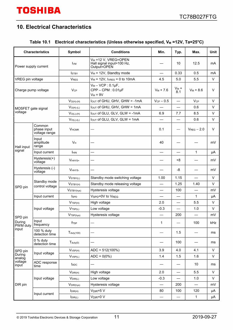
10. Electrical Characteristics
Table 10.1 Electrical characteristics (Unless otherwise specified, VM =12V, Ta=25°C)
Characteristics Symbol Conditions Min. Typ. Max. Unit
Power supply current IVM
VM =12 V, VREG=OPEN Hall signal input=100 Hz, Output=OPEN
— 10 12.5 mA
ISTBY VM = 12V, Standby mode — 0.33 0.5 mA
VREG pin voltage VREG VM = 12V, IVREG = 0 to 10mA 4.5 5.0 5.5 V
Charge pump voltage VCP VM – VCP : 0.1µF, CPP – CPM : 0.01µF VM = 9V
VM + 7.6 VM + 8.1 VM + 8.6 V
MOSFET gate signal voltage
VO(H)-(H) IOUT of GHU, GHV, GHW = -1mA VCP – 0.5 — VCP V
VO(H)-(L) IOUT of GHU, GHV, GHW = 1mA — — 0.6 V
VO(L)-(H) IOUT of GLU, GLV, GLW = -1mA 6.9 7.7 8.5 V
VO(L)-(L) IOUT of GLU, GLV, GLW = 1mA — — 0.6 V
Hall input signal
Common phase input voltage range
VHCMR — 0.1 — VREG – 2.0 V
Input amplitude range
VH — 40 — — mV
Input current IHIN — — — 1 µA
Hysteresis(+) voltage VHHYS+ — — +8 — mV
Hysteresis (-) voltage VHHYS- — — -8 — mV
SPD pin Standby mode control voltage
VSTBY(L) Standby mode switching voltage 1.00 1.15 — V
VSTBY(H) Standby mode releasing voltage — 1.25 1.40 V
VSTBY(hys) Hysteresis voltage — 100 — mV
Input current ISPD VSPD=0V to VREG — — 1 µA
SPD pin During PWM duty input
Input voltage
VTSP(H) High voltage 2.0 — 5.5 V
VTSP(L) Low voltage -0.3 — 1.0 V
VTSP(hys) Hysteresis voltage — 200 — mV
Input frequency fTSP — 1 — 100 kHz
100 % duty detection time Tduty(100) — — 1.5 — ms
0 % duty detection time Tduty(0) — — 100 — ms
SPD pin During analog voltage input
Input voltage VVSP(H) ADC = 512(100%) 3.9 4.0 4.1 V
VVSP(L) ADC = 0(0%) 1.4 1.5 1.6 V
ADC response time tADC — — — 10 ms
DIR pin
Input voltage
VDIR(H) High voltage 2.0 — 5.5 V
VDIR(L) Low voltage -0.3 — 1.0 V
VDIR(hys) Hysteresis voltage — 200 — mV
Input current IDIR(H) VDIR=5 V 80 100 120 µA
IDIR(L) VDIR=0 V — — 1 µA
TC78B027FTG
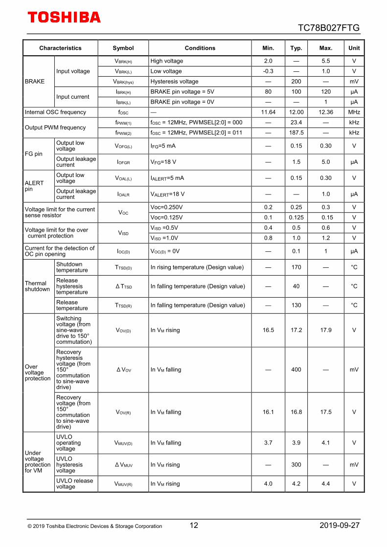
© 2019 Toshiba Electronic Devices & Storage Corporation 12 2019-09-27
Characteristics Symbol Conditions Min. Typ. Max. Unit
BRAKE
Input voltage
VBRK(H) High voltage 2.0 — 5.5 V
VBRK(L) Low voltage -0.3 — 1.0 V
VBRK(hys) Hysteresis voltage — 200 — mV
Input current IBRK(H) BRAKE pin voltage = 5V 80 100 120 µA
IBRK(L) BRAKE pin voltage = 0V — — 1 µA
Internal OSC frequency fOSC — 11.64 12.00 12.36 MHz
Output PWM frequency fPWM(1) fOSC = 12MHz, PWMSEL[2:0] = 000 — 23.4 — kHz
fPWM(2) fOSC = 12MHz, PWMSEL[2:0] = 011 — 187.5 — kHz
FG pin
Output low voltage VOFG(L) IFG=5 mA — 0.15 0.30 V
Output leakage current IOFGR VFG=18 V — 1.5 5.0 µA
ALERT pin
Output low voltage VOAL(L) IALERT=5 mA — 0.15 0.30 V
Output leakage current IOALR VALERT=18 V — — 1.0 µA
Voltage limit for the current sense resistor VOC
Voc=0.250V 0.2 0.25 0.3 V
Voc=0.125V 0.1 0.125 0.15 V
Voltage limit for the over current protection VISD
VISD =0.5V 0.4 0.5 0.6 V
VISD =1.0V 0.8 1.0 1.2 V
Current for the detection of OC pin opening IOC(D) VOC(D) = 0V — 0.1 1 µA
Thermal shutdown
Shutdown temperature TTSD(D) In rising temperature (Design value) — 170 — °C
Release hysteresis temperature
ΔTTSD In falling temperature (Design value) — 40 — °C
Release temperature TTSD(R) In falling temperature (Design value) — 130 — °C
Over voltage protection
Switching voltage (from sine-wave drive to 150° commutation)
VOV(D) In VM rising 16.5 17.2 17.9 V
Recovery hysteresis voltage (from 150° commutation to sine-wave drive)
ΔVOV In VM falling — 400 — mV
Recovery voltage (from 150° commutation to sine-wave drive)
VOV(R) In VM falling 16.1 16.8 17.5 V
Under voltage protection for VM
UVLO operating voltage
VMUV(D) In VM falling 3.7 3.9 4.1 V
UVLO hysteresis voltage
ΔVMUV In VM rising — 300 — mV
UVLO release voltage VMUV(R) In VM rising 4.0 4.2 4.4 V

TC78B027FTG
© 2019 Toshiba Electronic Devices & Storage Corporation 13 2019-09-27
Characteristics Symbol Conditions Min. Typ. Max. Unit
Under voltage protection for VREG
UVLO operating voltage
VRUV(D) In VREG falling — 3.7 — V
UVLO hysteresis voltage
ΔVRUV In VREG rising — 300 — mV
UVLO release voltage VRUV(R) In VREG rising — 4.0 — V
Under voltage protection for charge pump
Under voltage protection operating voltage
VCUV(D) In the voltage between VCP pin and VM pin falling VM ≥ 5.5V
— 3.7 — V
Under voltage protection hysteresis voltage
ΔVCUV In the voltage between VCP pin and VM pin rising VM ≥ 5.5V
— 300 — mV
Under voltage protection release voltage
VCUV(R) In the voltage between VCP pin and VM pin rising VM ≥ 5.5V
— 4.0 — V
Table 10.2 Serial I / F (Unless otherwise specified, VM = 12 V and Ta = 25°C)
Characteristics Symbol Conditions Min. Typ. Max. Unit
SCK
Input voltage
VSCK(H) High voltage 2.0 — 5.5 V
VSCK(L) Low voltage -0.3 — 1.0 V
VSCK(hys) Hysteresis voltage — 100 — mV
Input frequency fSCK — 15 — 500 kHz
High period tWH — 1 — — µs
Low period tWL — 1 — — µs
SDI(SIO) Setup period tSDIS — 1 — — µs
Hold period tSDIH — 500 — — ns
SDO(SIO) Setup period — — — 500 ns
Figure 10.1 Serial I / F timing chart
tWH tWL
tSDIS tSDIH
SCK
SDI
SDO
tSDOS
SDI(SIO)
SDO(SIO)

TC78B027FTG
© 2019 Toshiba Electronic Devices & Storage Corporation 14 2019-09-27
11. Functional Description 11.1. Basic Operation
The TC78B027FTG can be operated by 1-Hall sine-wave commutation and 1-Hall 150° commutation. Also, a closed loop speed control function is implemented without using an external microcontroller. Motor rotation speed can be controlled by inputting PWM signal or applying analog voltage to the SPD pin. The operation moves to the standby mode when a zero cross of the Hall signal is not detected for a lock detection period after the voltage of VSTBY(L) or less is applied to the SPD pin. In the standby mode, the IC power consumption is reduced by powering off its internal 5-V regulator. In case that the Hall element is power supplied by the IC's 5-V regulator, the power consumption of the whole motor system can be reduced. In case that motor is configured as not stop when the voltage of SPD pin is VSTBY(L) or less, standby mode is disabled.
Figure 11.1 Basic operation flow chart
Power ON
Read NVM
Brake sequence
Idle mode Standby mode
Rotation detection
Free run?
Soft start
Closed loop (Open loop)
OFF mode (1)
Brake Rev
start? Reversed
? OFF mode
(2)
VSPD > VSTBY(H)
VSPD < VSTBY(L) and
Hall not change for TON
SPD > 0
Auto restart
Yes
No
Abnormal released
Lock
ISD
SPD=0
Yes
No
Yes
No
TSD / VCP low

TC78B027FTG
© 2019 Toshiba Electronic Devices & Storage Corporation 15 2019-09-27
11.1.1. The IC status in each mode
Note 1 : ALERT=L when TSD / VCP is dropped. ALERT is released when the cause of fault is released. Note 2 : Fault means ISD / TSD / VCP dropping and lock. Note 3:When ALERTINV=0. ALERT outputs H level when ALERTINV=1. 11.1.2. 1-Hall commutation
The TC78B027FTG can be operated by 1-Hall sine-wave commutation and 1-Hall 150° commutation. The way of commutation can be switched by register. Rotation direction is defined by DIR and register setting.
CW lead angle=0
CCW angle=0 Figure 11.2 Timing chart of Hall input signal and sine-wave commutation signal
Read NVM
Stop mode
OFF mode (1)
OFF mode (2)
Standby mode
Normal mode
VREG 5V 5V 5V 5V OFF 5V
Charge pump Active Active Active Active Inactive Active
FG function
FG In reading:L After reading:
Hi-Z
Hall output (Hi-Z under
1Hz) Hi-Z Hall output
(Hi-Z under 1Hz) Hi-Z Hall output (Hi-Z under 1Hz)
RDO State sustaining
State sustaining State sustaining Hi-Z
Lock is detected:L Lock is released:Hi-Z
ALERT Hi-Z State
sustaining (Note 1)
L(Note 3) L(Note 3) Hi-Z
Fault(Note 2)is detected:L(Note 3) Fault is released:Hi-Z
GLx(x:U,V,W) GHx(x:U,V,W)
L L L L Hi-Z Active
Hall
HP
HM
OutputU
V
W
Hall
HP
HM
OutputU
V
W

TC78B027FTG
© 2019 Toshiba Electronic Devices & Storage Corporation 16 2019-09-27
CW lead angle=0
CCW lead angle=0 Figure 11.3 Timing chart of Hall input and 150° commutation signal
11.1.3. PWM frequency
PWM is generated from internal oscillator. Table 11.1 Division ratio vs PWM frequency
Division ratio PWM frequency 512 23.4kHz 256 46.9kHz 128 93.7kHz 64 187.5kHz
Table 11.2 The setting of PWM frequency
PWMSEL[2:0] fhall
0 to 250 150 to 0
250 to 500 400 to 150
500 to 1000 900 to 400
1000 to 1500 1400 to 900
1500 to 2000 1900 to 1400
Over 2000 Under 1900
0 0 0 23.4kHz
0 0 1 46.9kHz
0 1 0 93.7kHz
0 1 1 187.5kHz
1 0 0 23.4kHz 23.4kHz 46.9kHz 46.9kHz 93.7kHz 93.7kHz
1 0 1 23.4kHz 46.9kHz 46.9kHz 93.7kHz 93.7kHz 187.5kHz
1 1 0 23.4kHz 46.9kHz 93.7kHz 93.7kHz 187.5kHz 187.5kHz
1 1 1 46.9kHz 93.7kHz 93.7kHz 187.5kHz 187.5kHz 187.5kHz
There is a 100Hz hysteresis when the motor decreases its speed.
Hall
HP
HM
OutputU
V
W
Hall
HP
HM
OutputU
V
W

TC78B027FTG
© 2019 Toshiba Electronic Devices & Storage Corporation 17 2019-09-27
11.1.4. Lead angle control TC78B027 contains the function of lead angle control. This function requires a Hall signal to compensate the lead angle with the setting of LATABLE.
Table 11.3 Table of LATABLE
LATABLE[4:0] The value of lead angle
0 0 0 0 0 LATABLE = 0 to 27 Lead angle(deg) = 1.875(deg) x Speed(RPM) / 4096 x LATABLE Maximum lead angle is 58.125°
・・・・・・
1 1 0 1 1
1 1 1 0 0 7.5° fixed
1 1 1 0 1 15° fixed
1 1 1 1 0 22.5° fixed
1 1 1 1 1 30° fixed
Figure 11.4 Example of the setting of lead angle LATABLE = 14 (1b01110)
Figure 11.5 Example of the setting of lead angle LATABLE = 4 (1b00100)

TC78B027FTG
© 2019 Toshiba Electronic Devices & Storage Corporation 18 2019-09-27
This IC contains the function of automatic optimizing lead angle, InPAC, from “Zero cross of Hall signal” and “Zero cross of motor current”
Table 11.4 The setting of controlling lead angle
LASEL Auto
0 InPAC enable
1 InPAC disable • InPAC is enabled when LASEL=0.
Lead angle=Optimized lead angle by InPAC + lead angle set in LATABLE Since a low motor current in low speed makes a difficulty of detecting zero cross, InPAC regards an optimized lead angle is zero when the motor speed becomes under startup frequency. When LASEL=1, InPAC is disabled and an optimized lead angle is zero.
11.1.5. Soft Start
Soft start operates when the motor starts from the stop state to prevent rush current.
Figure 11.6 Timing chart of soft start
• Soft start increases the output duty gradually from 0 % until the output current reaches the startup current.
• The rotation frequency increases from 1 Hz. Soft start is finished and switches to the closed loop speed control or the open loop speed control when the rotation frequency reaches the switching frequency (startup frequency).
• The way of commutation is defined by register setting.
The time for lock detecting in soft start can be selected by register setting so that slow start motor can be used.
Table 11.5 The setting of the time for lock detecting in soft start
SS_LOCK The time for lock detecting (s)
0 TON x 1 1 TON x 5
Power supplyCurrent
Rotation Speed 1Hz
Soft start
start upfrequency
Closed loop(or Open loop)
Coil current
0A
start up current
Time

TC78B027FTG
© 2019 Toshiba Electronic Devices & Storage Corporation 19 2019-09-27
11.1.6. Acceleration and deceleration control Acceleration and deceleration rate of motor can be controlled by limiting of PWM duty.
Table 11.6
Duty change limit ( DUTYCHGLIMIT )
Variation amount of duty every 2.7ms (Δ/512)
Time (sec) 0% to 100%
0 N/A (64/8) 0.17 1 2/8 5.53 2 (default) 3/8 3.69 3 4/8 2.76 4 6/8 1.84 5 10/8 1.11 6 20/8 0.55 7 56/8 0.20
Example: The case of DUTYCHGLIMIT = 2 Figure 11.7 Table 11.7
Item Soft start Closed-loop
Open-loop Mild brake Reverse brake Acceleration Steady Deceleration
Period of changing duty 2.7ms 10.8ms/2.7ms 2.7ms 10.8ms/2.7ms 10.8ms/2.7ms 10.8ms/2.7ms
Variation amount of duty
Duty chg limit for soft start Duty chg limit
Determined by PI (Maximum variation amount is Duty chg
limit)
Duty chg limit Duty chg limit Duty chg limit
11.1.7. Output current for the gate of external MOSFET
TC78B027FTG drives external MOSFETs. This IC contains six half bridge pre-drivers and drives high-side and low-side Nch-MOSFETs. The voltage for high-side gate of MOSFET is VM + 8V(typ.). The voltage for low-side gate of MOSFET is 8V(typ.). The register, ISOURCE_SEL、ISINK_SEL set a driving current to the gate.
Target output duty 100/512
102/512
Output duty
Output duty: 100/512(Internal duty: 100/512)
100/512(100.375/512)
2.7ms
Internal triangle wave
2.7ms
100/512(100.75/512)
2.7ms
101/512(101.125/512)
2.7ms
101/512(101.5/512)
2.7ms
101/512(101.875)/512
102/512(102/512)
TC78B027FTG
© 2019 Toshiba Electronic Devices & Storage Corporation 20 2019-09-27
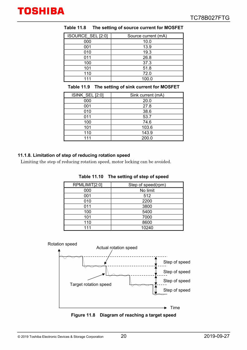
Table 11.8 The setting of source current for MOSFET
ISOURCE_SEL [2:0] Source current (mA) 000 10.0 001 13.9 010 19.3 011 26.8 100 37.3 101 51.8 110 72.0 111 100.0
Table 11.9 The setting of sink current for MOSFET
ISINK_SEL [2:0] Sink current (mA) 000 20.0 001 27.8 010 38.6 011 53.7 100 74.6 101 103.6 110 143.9 111 200.0
11.1.8. Limitation of step of reducing rotation speed
Limiting the step of reducing rotation speed, motor locking can be avoided.
Table 11.10 The setting of step of speed
RPMLIMIT[2:0] Step of speed(rpm) 000 No limit 001 512 010 2200 011 3800 100 5400 101 7000 110 8600 111 10240
Figure 11.8 Diagram of reaching a target speed
Rotation speed
Time
Actual rotation speed
Target rotation speed
Step of speed
Step of speed Step of speed Step of speed

TC78B027FTG
© 2019 Toshiba Electronic Devices & Storage Corporation 21 2019-09-27
11.2. Input / Output Signals 11.2.1. SPD
SPD pin controls the motor start, the motor stop, and the rotation speed. PWM duty signal input or analog voltage signal input can be configured by the register. Also, the polarity of the signal can be configured by the register.
Table 11.11 Polarity of SPD
Positive logic(Default) Negative logic
Analog voltage input VVSP(L) : SPD command = 0 (0%) VVSP(H) : SPD command = 512(100%)
VVSP(L) : SPD command = 512 (100%) VVSP(H) : SPD command = 0 (0%)
PWM duty input H active L active(Note1)
Note1: The polarity of the input signal is inverted inside the IC, and the inverted signal is used as the positive logic SPD.
In case of analog voltage input, the resolution is 9 bit in the voltage range of VVSP(L) to VVSP(H). In case of PWM duty input, its frequency range is from 1 kHz to 100 kHz. When the frequency range is from 1 kHz to 20 kHz, the resolution is 9 bit. And when it is 20 kHz or more, the resolution decreases. For example, in case of 40 kHz, the resolution is 8 bit, and in case of 100 kHz, it becomes 7 bit. In addition, the SPD pin can be also used as the clock input pin for the serial interface (for SCK signal).
11.2.2. DIR
DIR pin controls the motor rotation direction; forward rotation (CW) and reverse rotation (CCW). Relation of DIR pin polarity and the rotation direction is configured by the register.
Table 11.12 The relation of register and DIR
Register (DIR) DIR pin Rotation direction
0 L CW H CCW
1 L CCW H CW
TC78B027FTG
© 2019 Toshiba Electronic Devices & Storage Corporation 22 2019-09-27
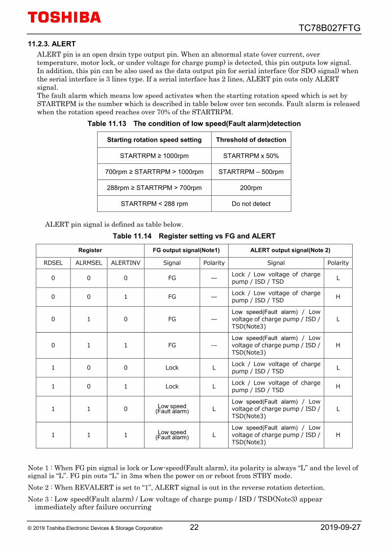
11.2.3. ALERT ALERT pin is an open drain type output pin. When an abnormal state (over current, over temperature, motor lock, or under voltage for charge pump) is detected, this pin outputs low signal. In addition, this pin can be also used as the data output pin for serial interface (for SDO signal) when the serial interface is 3 lines type. If a serial interface has 2 lines, ALERT pin outs only ALERT signal. The fault alarm which means low speed activates when the starting rotation speed which is set by STARTRPM is the number which is described in table below over ten seconds. Fault alarm is released when the rotation speed reaches over 70% of the STARTRPM.
Table 11.13 The condition of low speed(Fault alarm)detection
Starting rotation speed setting Threshold of detection
STARTRPM ≥ 1000rpm STARTRPM x 50%
700rpm ≥ STARTRPM > 1000rpm STARTRPM – 500rpm
288rpm ≥ STARTRPM > 700rpm 200rpm
STARTRPM < 288 rpm Do not detect
ALERT pin signal is defined as table below.
Table 11.14 Register setting vs FG and ALERT
Register FG output signal(Note1) ALERT output signal(Note 2)
RDSEL ALRMSEL ALERTINV Signal Polarity Signal Polarity
0 0 0 FG — Lock / Low voltage of charge pump / ISD / TSD L
0 0 1 FG — Lock / Low voltage of charge pump / ISD / TSD H
0 1 0 FG — Low speed(Fault alarm) / Low voltage of charge pump / ISD / TSD(Note3)
L
0 1 1 FG — Low speed(Fault alarm) / Low voltage of charge pump / ISD / TSD(Note3)
H
1 0 0 Lock L Lock / Low voltage of charge pump / ISD / TSD L
1 0 1 Lock L Lock / Low voltage of charge pump / ISD / TSD H
1 1 0 Low speed (Fault alarm) L
Low speed(Fault alarm) / Low voltage of charge pump / ISD / TSD(Note3)
L
1 1 1 Low speed (Fault alarm) L
Low speed(Fault alarm) / Low voltage of charge pump / ISD / TSD(Note3)
H
Note 1 : When FG pin signal is lock or Low-speed(Fault alarm), its polarity is always “L” and the level of signal is “L”. FG pin outs “L” in 3ms when the power on or reboot from STBY mode. Note 2 : When REVALERT is set to “1”, ALERT signal is out in the reverse rotation detection. Note 3 : Low speed(Fault alarm) / Low voltage of charge pump / ISD / TSD(Note3) appear
immediately after failure occurring

TC78B027FTG
© 2019 Toshiba Electronic Devices & Storage Corporation 23 2019-09-27
11.2.4. HP, HM
Pins of HP and HM are input pins for Hall signals. In case of using Hall element, please input signals whose characteristics are shown below.
Figure 11.9 Hall signal waveform
Table 11.10 Hall and FG signal waveform
Note : In case of using Hall IC, the Hall signal must be input to HP pin. Voltage of HM pin should be fixed.
VREG
GND
HP
HM
HP
HM
VH
CM
R
Common phase input voltage range
HP
HM
Hall signal
FG (1ppr)
VHHYS-
VHHYS+
VH

TC78B027FTG
© 2019 Toshiba Electronic Devices & Storage Corporation 24 2019-09-27
As default, please align the Hall sensor so that the relationship between Hall signals and induced voltage is as charts below.
Figure 11.11 The waveform of Hall signal and induced voltage in CW
Figure 11.12 The waveform of Hall signal and induced voltage in CCW Figure below is the example of the default Hall position.
Figure 11.13 Example of the default position of Hall element
Forward rotation (CW)
Reverse rotation (CCW)
BEMFU phase
V phase
W phase
HallHP
HM
150º
BEMFU phase
V phase
W phase
HallHP
HM
30º

TC78B027FTG
© 2019 Toshiba Electronic Devices & Storage Corporation 25 2019-09-27
11.2.5. FG
FG pin is an open drain type output pin. It outputs the rotation speed signal that is obtained from the Hall signal. According to the register setting, FG pin can also output RDO signal when motor lock is detected. RDO signal is low level in motor lock detection. In addition, FG pin can be also used as the data input or input/output pin for serial interface (for SDI or SIO signal).
1ppr(pulse per revolution)、3ppr、2.4ppr、0.5ppr can be selected as FG signal. Below table show the number of FG pulse per 1 rotation of motor.
Table 11.15 Relation of FG signal setting and the number of output pulses per one motor cycle
FGSEL[2:0] FG signal setting Number of motor poles
2poles 4poles 6poles 8poles 10poles
000 1ppr 1 2 3 4 5
001 2/3 ppr 2/3 4/3 2 8/3 10/3
010 1/2 ppr 0.5 1 1.5 2 2.5
011 2 ppr 2 4 6 8 10
100 3ppr 3 6 9 12 15
101 2.4 ppr 2.4 4.8 7.2 9.6 12
110 1/3 ppr 1/3 2/3 1 4/3 5/3
111 Don’t use
Note: FG pin outputs the signal when the frequency of the Hall signal is 1Hz or more.
When the frequency of the Hall signal is less than 1Hz, FG signal is fixed to Hi-Z. Note: When FG signal is set to 1ppr, a signal synchronized with the Hall signal is output.
When FG signal is set to the others, internal processed result is output.
FG pin can be also used as the data input pin for serial interface (for SDI signal) when the serial interface is 3 lines type. If a serial interface has 2 lines, FG pin can be also used as the data input/output pin for serial interface (for SIO).

TC78B027FTG
© 2019 Toshiba Electronic Devices & Storage Corporation 26 2019-09-27
11.2.6. BRAKE BRAKE pin is for controlling the motor braking function. TC78B027FTG has several braking functions, motor
off, short brake, reverse brake, mild brake.
Table 11.16
BRAKE pin Register
Motor status BRK_INV BRK_MODE[1:0]
L 0:Positive polarity Don’t care No brake L 1:Negative polarity 00 No brake L 1:Negative polarity 01 Short brake L 1:Negative polarity 10 Reverse brake L 1:Negative polarity 11 Mild brake H 0:Positive polarity 00 No brake H 0:Positive polarity 01 Short brake H 0:Positive polarity 10 Reverse brake H 0:Positive polarity 11 Mild brake H 1:Negative polarity Don’t care No brake
Table 11.17
Driving status right after power on
BRAKEALT ALARMSEL Status of ALERT pin
Short brake Don’t care Don’t care Low voltage of charge pump / ISD / TSD
Reverse brake 0 0 Low voltage of charge pump / ISD / TSD
Reverse brake 1 0 Low voltage of charge pump / ISD / TSD
Reverse brake Don’t care 1 Lock / Low voltage of charge pump / ISD / TSD
Mild brake Don’t care Don’t care Low voltage of charge pump / ISD / TSD

TC78B027FTG
© 2019 Toshiba Electronic Devices & Storage Corporation 27 2019-09-27
11.3. Speed Control 11.3.1. Closed loop
The basic speed curve (relation between SPD signal value and rotation speed) of closed loop speed control is as follows;
Figure 11.14 Speed slope example in closed loop control (1) Startup point:
Output is enabled when SPD signal value exceeds the startup threshold. The threshold range is from 0 (0 %) to 255 (49.8 %) with a 0.2 % resolution. It is set by the 8-bit register STARTDUTY.
SPD duty to enable output (%) = 100 x STARTDUTY / 512
(2) Stop point: Output is disabled when SPD signal value decreases to the stop threshold. The threshold range is from 0 (0 %) to 254 (49.6 %) with a 0.4 % resolution. It is set by the 7-bit register STOPDUTY.
SPD duty to disable output (%) = 200 x STOPDUTY / 512
(3) Output clamping point and (7) MAXOPEN hysteresis: In case MAXDUTY = 0: When SPD signal value exceeds the output clamping threshold, the rotation speed is fixed. The threshold range is from 257 (50.2 %) to 512 (100 %) with a 0.2 % resolution. It is set by the 8-bit register MAXDUTY.
SPD duty to clamp output (%) = 100 x (257 + MAXDUTY) / 512 In case MAXOPEN = 1: When SPD signal value exceeds the output clamping threshold, the control switches to open loop speed control. The output duty during open loop speed control corresponds to SPD signal value. The hysteresis of SPD signal value to let the control switch back to closed loop speed control range is from 2 (0.4 %) to 32 (6.25 %) with a 0.4 % resolution. It is set by the 4-bit register MAXDUTYHYS.
SPD duty hys (%) = 200 x (MAXDUTYHYS + 1) / 512
(4) Startup speed: The minimum rotation speed in startup is set by the 12-bit register STARTRPM. Setting range is from 0 to 4095 RPM with 1 RPM resolution.
Startup speed (RPM) = STARTRPM
(5) Maximum speed and (6) Speed slope: Maximum speed depends on the speed slope, which is set by the register SPEEDSLOP. It is a 14-bit register.
SPEEDSLOP = 64 x (Maximum speed – Startup speed) / (MAXDUTY + 257 – STARTDUTY)
(1) Startup point (2) Stop point (3) Output clamping point (4) Startup speed (5) Maximum speed (depending on speed
slope) (6) Speed slope (7) MAXOPEN hysteresis
Please set as follows; (3) > (1) ≥ (2)
SPD signal value 512 ( 100 %)
(5)
0 ( 0 %)
100 % output speed
Spe
ed
(RP
M)
(4)
(2) (1) (3)
(6)
(7)

TC78B027FTG
© 2019 Toshiba Electronic Devices & Storage Corporation 28 2019-09-27
Configurations of MAXOPEN, NOSTOP, and MAXOFF registers determine the behavior when SPD signal value is equivalent to the startup (output enabling) point or less.
Table 11.18 Rotation Behavior (SPD signal value ≤ Startup point)
MAXOPEN NOSTOP MAXOFF Target speed
SPD =0 % 0 % < SPD
≤ Startup point Stop point < SPD
≤ Startup point
0
0 0 0 0 Duty up: 0
Duty down: Startup speed
0 1 Maximum Speed 0 Duty up: 0
Duty down: Startup speed
1 0 Startup speed Startup speed Startup speed
1 1 Maximum Speed Maximum Speed Startup speed
1
0 0 0 0 Duty up: 0
Duty down: Startup speed
0 1 100 % Output 0 Duty up: 0
Duty down: Startup speed
1 0 Startup speed Startup speed Startup speed
1 1 100 % Output 100 % Output Startup speed
Adding a speed change point to the speed curve is possible.
Figure 11.15 Speed Slope Example in Closed loop speed control (in case of adding speed change point)
(8) Speed change point:
The SPD signal value range of the speed change point is from 0 (0.4 %) to 510 (99.6 %) with a 0.4 % resolution. It is set by the 8-bit register CHANGEDUTY.
SPD duty of change point (%) = 200 x CHANGEDUTY / 512
In case of un-using the speed change point, set CHANGEDUTY to 0.
(9) Second speed slope: After passing the speed change point, the register SPEEDSLOP2 sets the speed slope.
(1) Startup point (2) Stop point (3) Output clamping point (4) Startup speed (5) Maximum speed (depending on
speed slope) (6) First speed slope (8) Speed change point (9) Second speed slope
Please set as follows; (3) > (8) > (1) ≥ (2)
(1) (2)
SPD signal value 512 ( 100 %)
0 ( 0 %)
Spe
ed
(RP
M)
(6)
(3)
(9)
(4)
(5)

TC78B027FTG
© 2019 Toshiba Electronic Devices & Storage Corporation 29 2019-09-27
In case of DIR50=1, rotation direction of motor is controlled by the duty of SPD signal. Motor rotates forward direction when SPD duty is 50% or more. Motor rotates reverse direction when
SPD duty is under 50%.
Figure 11.16 Speed Slope Example in Closed loop speed control (in case of DIR50=1)
50% 100% 0% SPD input duty(%)
Spe
ed (R
PM
)
(2) (1)
(5)‘
(1)‘ (2)‘
(4)
(4)‘
(3)
(3)‘
(6)
(6)‘
Reverse direction Forward direction
SPD’ = (256 – SPD) x 2
SPD = 0 to 255
SPD = 256 to 512
SPD’ = (SPD – 256) x 2
100% 100% 0%
Register value
(5)

TC78B027FTG
© 2019 Toshiba Electronic Devices & Storage Corporation 30 2019-09-27
11.3.2. Open loop The basic speed curve (relation between SPD signal value and output duty) of open loop speed control is as follows ;
Figure 11.17 Speed slope example in Open loop speed control
(1) Startup point: Output is enabled when SPD signal value exceeds the startup threshold. The threshold range is from 0 (0 %) to 255 (49.8 %) with a 0.2 % resolution. It is set by the 8-bit register STARTDUTY.
SPD duty to enable output (%) = 100 x STARTDUTY / 512
(2) Stop point: Output is disabled when SPD signal value decreases to the stop threshold. The threshold range is from 0 (0 %) to 254 (49.6 %) with a 0.4 % resolution. It is set by the 7-bit register STOPDUTY.
SPD duty to disable output (%) = 200 x STOPDUTY / 512
(3) Output clamping point and (7) MAXOPEN hysteresis: In case MAXDUTY = 0: When SPD signal value exceeds the output clamping threshold, the output duty is fixed. The threshold range is from 257 (50.2 %) to 512 (100 %) with a 0.2 % resolution. It is set by the 8-bit register MAXDUTY.
SPD duty clamp output (%) = 100 x (257 + MAXDUTY) / 512 In case MAXOPEN = 1: When SPD signal value exceeds the output clamping threshold, the output duty becomes corresponding to SPD signal value. The hysteresis range of SPD signal value to let the output return to original speed curve is from 2 (0.4 %) to 32 (6.25 %) with a 0.4 % resolution. It is set by the 4-bit register MAXDUTYHYS.
SPD duty hys (%) = 200 x (MAXDUTYHYS + 1) / 512
(4) Startup output duty: The minimum output duty in startup is set by an upper 8-bit of the 12-bit register STARTRPM. Setting range is from 0 (0 %) to 255 (49.8 %) with a 0.2 % resolution.
Startup output duty (%) = 100 x STARTRPM[11:4] / 512
(5) Maximum output duty and (6) Speed slope: Maximum output duty depends on the speed slope, which is set by the register SPEEDSLOP. It is a 14-bit register.
SPEEDSLOP =219 x (Maximum output duty(%) – Startup output duty(%) ) / (MAXDUTY + 257 – STARTDUTY) / 100
(1) Startup point (2) Stop point (3) Output clamping point (4) Startup output duty (5) Maximum output duty (depending on speed slope) (6) Speed slope (7) MAXOPEN hysteresis
Please set as follows; (3) > (1) ≥ (2)
100 %
SPD signal value 512 ( 100 %)
(2) 0 ( 0 %)
(4)
(5)
(1) (3)
(6)
(7)
Outp
ut
Peak
Duty
(%)

TC78B027FTG
© 2019 Toshiba Electronic Devices & Storage Corporation 31 2019-09-27
Configurations of MAXOPEN, NOSTOP, and MAXOFF registers determine the behavior when SPD signal value is equivalent to the startup (output enabling) point or less.
Table 11.19 Rotation Behavior (SPD signal value ≤ Startup point)
MAXOPEN NOSTOP MAXOFF Output Duty
SPD =0 % 0 % < SPD
≤ Startup point Stop point < SPD
≤ Startup point
0
0 0 0 0 Duty up: 0
Duty down: Startup Output
0 1 Maximum Output 0 Duty up: 0
Duty down: Startup Output
1 0 Startup Output Startup Output Startup Output
1 1 Maximum Output Maximum Output Startup Output
1
0 0 0 0 Duty up: 0
Duty down: Startup Output
0 1 100 % Output 0 Duty up: 0
Duty down: Startup Output
1 0 Startup Output Startup Output Startup Output
1 1 100 % Output 100 % Output Startup Output
Adding a speed change point to the speed curve is possible.
Figure 11.18 Speed Slope Example in Open loop speed control (in case of adding speed change point)
(8) Speed change point:
The SPD signal value range of the speed change point is from 0 (0.4 %) to 510 (99.6 %) with a 0.4 % resolution. It is set by the 8-bit register CHANGEDUTY.
SPD duty of change point (%) = 200 x CHANGEDUTY / 512 In case of unusing the speed change point, set CHANGEDUTY to 0.
(9) Second speed slope:
After passing the speed change point, the register SPEEDSLOP2 sets the speed slope.
(1) Startup point (2) Stop point (3) Output clamping point (4) Startup output duty (5) Maximum output duty (depending on
speed slope) (6) First speed slope (8) Speed change point (9) Second speed slope
Please set as follows; (3) > (8) > (1) ≥ (2)
SPD input duty (%) 100 % (2) 0 %
(4)
(5)
(1) (8) (3)
(9)
(6)
Outp
ut
Peak
Duty
(%)
TC78B027FTG
© 2019 Toshiba Electronic Devices & Storage Corporation 32 2019-09-27
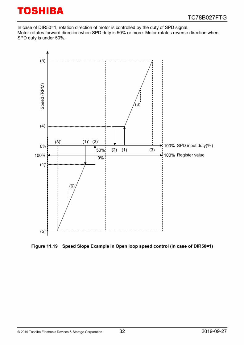
In case of DIR50=1, rotation direction of motor is controlled by the duty of SPD signal. Motor rotates forward direction when SPD duty is 50% or more. Motor rotates reverse direction when SPD duty is under 50%.
Figure 11.19 Speed Slope Example in Open loop speed control (in case of DIR50=1)
50% 100% 0% SPD input duty(%)
Spe
ed (R
PM
)
(2)
(5)
(5)‘
(1)‘ (2)‘
(4)
(4)‘
(3)‘
(6)
(6)‘
100% Register value 100% 0%
(1) (3)

TC78B027FTG
© 2019 Toshiba Electronic Devices & Storage Corporation 33 2019-09-27
11.4. Serial I/F and NVM Data of internal registers and non-volatile memory (NVM) can be configured via serial interface. When FG pin is Hi-Z, receiving serial commands is possible.
Figure 11.20 Timing chart After receiving command code, IC enters into serial mode. Motor stops if IC enters into serial mode. FG pin is fixed Hi-Z.
After inputting command code and following data (if needed),
If ENB of Status Register is “0”, IC returns to normal mode. If ENB of Status Register is “1”, IC stays in serial mode.
11.4.1. Serial commands
Table 11.20 Serial commands (Instruction Code)
Command Code Description Following Data
SR_READ 010 01 001 Read status register 8-bit data out SR_WRITE 010 01 010 Write status register 8-bit data in
REG_READ 010 10 001 Read normal register 8-bit addr in + 16-bit data out REG_WRITE 010 10 010 Write normal register 8-bit addr in + 16-bit data in
NVM_LOAD 010 11 001 Load NVM data to normal register None NVM_SAVE 010 11 010 Store data of normal register to NVM None
NVM_ABORT 010 11 100 Terminate NVM writing process forcedly None
SCK (SPD)
SDI (FG) Hi-Z 0 1 0 1
Ready to receiveserial data
IC mode Normal mode Serial mode
Instruction code Following instructions if needeFollowing instructions if needed
SDI/SIO(FG)
TC78B027FTG
© 2019 Toshiba Electronic Devices & Storage Corporation 34 2019-09-27
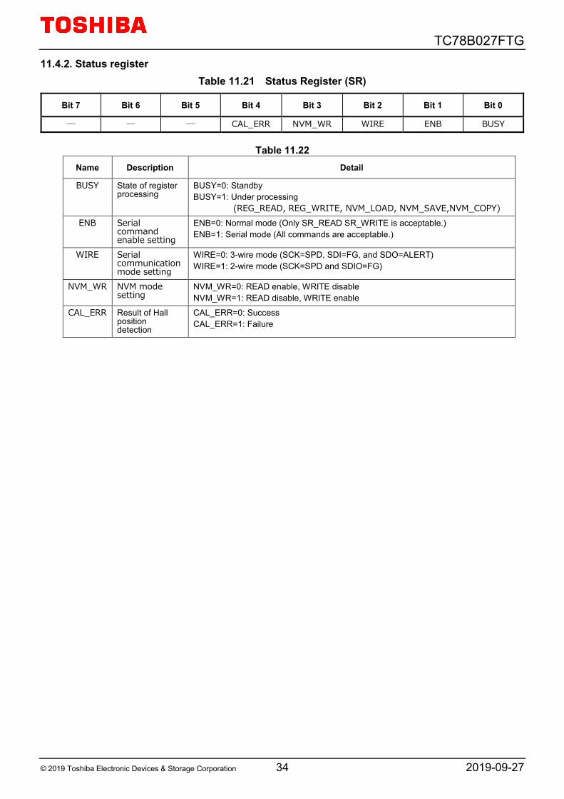
11.4.2. Status register Table 11.21 Status Register (SR)
Bit 7 Bit 6 Bit 5 Bit 4 Bit 3 Bit 2 Bit 1 Bit 0
― ― ― CAL_ERR NVM_WR WIRE ENB BUSY
Table 11.22 Name Description Detail
BUSY State of register processing
BUSY=0: Standby BUSY=1: Under processing
(REG_READ, REG_WRITE, NVM_LOAD, NVM_SAVE,NVM_COPY) ENB Serial
command enable setting
ENB=0: Normal mode (Only SR_READ SR_WRITE is acceptable.) ENB=1: Serial mode (All commands are acceptable.)
WIRE Serial communication mode setting
WIRE=0: 3-wire mode (SCK=SPD, SDI=FG, and SDO=ALERT) WIRE=1: 2-wire mode (SCK=SPD and SDIO=FG)
NVM_WR NVM mode setting
NVM_WR=0: READ enable, WRITE disable NVM_WR=1: READ disable, WRITE enable
CAL_ERR Result of Hall position detection
CAL_ERR=0: Success CAL_ERR=1: Failure

TC78B027FTG
© 2019 Toshiba Electronic Devices & Storage Corporation 35 2019-09-27
11.4.3. Normal register Table 11.23 Register map
ADDR Bit Name Description Default
0 15:0 USERID[15:0] - 0 1 15 NOSTOP Non-stop mode (0: disable, 1: enable) 0
1 14:8 STOPDUTY[6:0] Stop duty 0
1 7:0 STARTDUTY[7:0] Startup duty 0
2 15:8 CHANGEDUTY[7:0] Speed change point duty 0
2 7:0 MAXDUTY[7:0] Maximum duty 0
3 15:4 STARTRPM[11:0] Rotation speed in startup 0
3 3:0 MAXDUTYHYS[3:0] Recovery hysteresis from open loop to closed loop speed control 0
4 15:2 SPEEDSLOPE[13:0] Speed slope 0
4 1 MAXOPEN Switching to open loop speed control when SPD signal value exceeds the threshold (0: disable, 1: enable) 0
4 0 MAXOFF Rotating with full speed when SPD signal value corresponds to the startup point or less. (0: disable, 1: enable) 0
5 15:2 SPEEDSLOPE2[13:0] Speed slope after passing speed change point 0
5 1 REVALERT ALERT output in reverse detection 0 5 0 OPENLOOP OPEN LOOP/CLOSEDLOOP (0: closed loop, 1: open loop) 0 6 15 KiX To eight times the KI (0: x1, 1: x8) 0 6 14:8 Ki[6:0] KP (0 to 127) 0 6 7 KpX To eight times the KI (0: x1, 1: x8) 0 6 6:0 Kp[6:0] KI (0 to 127) 0 7 15 STBY Standby mode (0: disable, 1: enable) 0
7 14 DIR Relation of DIR pin polarity and rotation direction (0: positive, 1: negative) 0
7 13:11 POLEPAIR[2:0] Pair of motor poles 0
7 10:9 MAXSPEED[1:0] Maximum rotation speed 0
7 8 HALLINV Hall signal polarity conversion (0: positive, 1: negative) 0
7 7:6 HALLPOS[1:0] Hall alignment sector 0
7 5:0 HALLOFFSET[5:0] Hall position offset 0
8 15 RDSEL The signal selection to output FG pin (0: FG signal, 1: RDO signal or ALARM signal) 0
8 14:12 FGSEL[2:0] FG signal type setting 0
8 11 SPDSEL SPD command type setting (0: Analog voltage input , 1: PWM duty input) 0
8 10 SPDINV SPD signal polarity conversion (0: positive, 1: negative) 0
8 9 REVBRAKE Reverse startup (0: disable, 1: enable) 0
8 8 150DRV 150° commutation (0: sine-wave drive, 1:150° commutation) 0
8 7 ISDLATCH ISD latch (0: disable, 1:enable) 0
8 6:5 OCPMASK[1:0] Masking period for current limit 0 8 4:3 OCPHYS[1:0] Current limit setting 0 8 2:0 PWMSEL[2:0] Output PWM frequency setting 0 9 15 TON Lock detection ON period 0 9 14 TOFF Lock detection OFF period 0

TC78B027FTG
© 2019 Toshiba Electronic Devices & Storage Corporation 36 2019-09-27
ADDR Bit Name Description Default
9 13 LOCKDIS Disable lock detection 0 9 12:10 DUTYCHGLIMIT[2:0] Duty changing limit 0 9 9:8 STARTFREQ[1:0] Startup switching frequency 0 9 7:5 STARTCURRENT[2:0] Startup current limit 0 9 4:0 LATABLE[4:0] Lead angle table 0
10 15 LASEL Lead angle selection 0
10 14 BRK_360_SEL 0: 180° reset during mild brake 1: 360° reset during mild brake 0
10 13 OCPDIS Disable current limit (0: OCP enable, 1: OCP disable) 0 10 12:11 SS_ADD_SEL[1:0] Soft start current (OCP * 0%, 30%, 40%, 50%) 0
10 10:9 SS_UP_SEL[1:0] Increasing amount of the current in soft start (OCP * +1%, +2%, +5%, +10%) 0
10 8:6 SS_DUTYCHGLIMIT[2:0] Duty change limit in soft start phase (equivalent to DUTYCHGLIMIT) 0
10 5 OC_LEVEL Reference voltage for OCP (0: 0.25V, 1: 0.125V) 0
10 4 DUTY_UP_TIME Changing period of PWM duty (0: each 2.7ms, 1: each 10.9ms) 0
10 3 ISD_LEVEL Reference voltage for ISD (0: 1.0V, 1: 0.5V) 0
10 2:0 RPMLIMIT[2:0] Limit of step of changing rotation speed (No limit, 512rpm, 2200rpm, 3800rpm, 5400rpm, 7000rpm, 8600rpm, 10240rpm)
0
11 15:14 BRK_MODE[1:0] The setting of brake(No brake, Short brake, Reverse brake, Mild brake) 0
11 13 BRK_INV Polarity of BRAKE pin (0: positive, 1: negative) 0
11 12:10 WAIT_TIME[2:0] Wait time after power on(0s, 1s, 2s, 3s, 4s, 5s, 6s, 7s) 0
11 9:8 WAIT_MODE[1:0] Output status at power on(No brake, Short brake, Reverse brake, Mild brake) 0
11 7 WAIT_CON Output status after a certain time from power on (0: Brake off after WAIT_TIME from power on, 1: Sustain the brake status which is set by WAIT_MODE after WAIT_TIME from power on)
0
11 6 LOCK_BRK Short brake setting when locking protection (0: OFF, 1: Short brake) 0
11 5 ALRMSEL The output setting for ALERT (FG/Lock/Low speed(Fault alarm)) 0
11 4 ALERTINV Polarity of ALERT pin (0: Fault when L, 1: Fault when H) 0 11 3 IND_SEL DC excitation ON/OFF (0: disable, 1: enable) 0 11 2 SS_LOCK Lock detection when soft start 0
11 1 ALARM_LAT_SEL 0: Release ALARM when no torque command / brake setting, 1: Sustain ALARM however no torque command / brake setting 0
11 0 ISD_MASK ISD mask setting (0: enable, 1: disable) 0 12 15:13 ISOURCE_SEL[2:0] High side / Low side Source current 0 12 12:10 ISINK_SEL[2:0] High side / Low side Sink current 0 12 9:8 DEADTIME[1:0] Dead time(200ns 500ns 1µs 1.5µs) 0
12 7 DIR50 DIR50 signal (0: disable, 1: enable) 0
12 6:5 RS_SEL[1:0] Input filter of OC pin (None, 200kHz, 100kHz, 50kHz) 0 12 4 ANTITHROUGH Dead time auto tuning (0: Auto, 1: Manual) 0 12 3:2 INPACEDGE - 0
TC78B027FTG
© 2019 Toshiba Electronic Devices & Storage Corporation 37 2019-09-27
ADDR Bit Name Description Default
12 1 INPACAPPLY - 0 12 0 BRAKEALT The setting of lock detection when in reverse brake 0 13 15:6 Trq_duty[9:0] SPD command 0 13 5 UNUSED Don’t care 0 13 4:3 Hall_off_Freq[1:0] Hall position detection, frequency of forced rotation 0
13 2:1 Hall_cal_Freq[1:0] Hall position detection, Frequency of detection when starting 0
13 0 Hall_cal Hall position detection enable 0
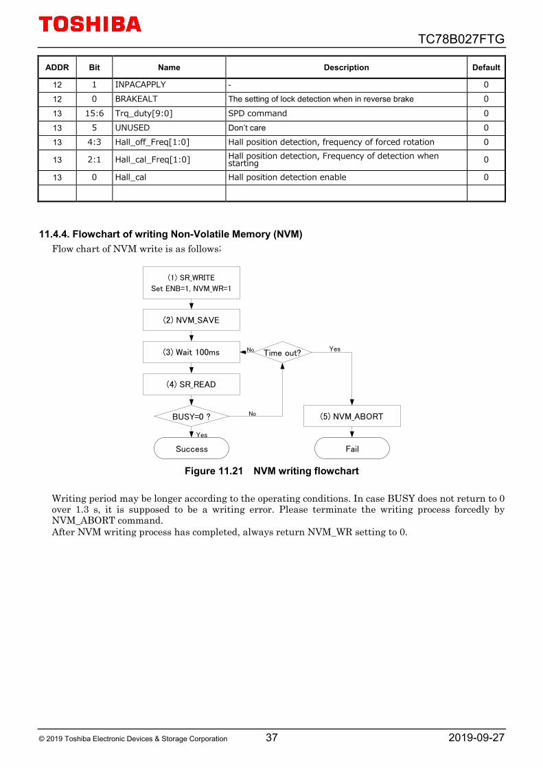
11.4.4. Flowchart of writing Non-Volatile Memory (NVM)
Flow chart of NVM write is as follows;
Figure 11.21 NVM writing flowchart
Writing period may be longer according to the operating conditions. In case BUSY does not return to 0 over 1.3 s, it is supposed to be a writing error. Please terminate the writing process forcedly by NVM_ABORT command. After NVM writing process has completed, always return NVM_WR setting to 0.
(1) SR_WRITE
Set ENB=1, NVM_WR=1
(2) NVM_SAVE
(3) Wait 100ms
BUSY = 0 ?
(4) SR_READ
Success Yes
(5) NVM_ABORT No
Fail
Time out ? No Yes

TC78B027FTG
© 2019 Toshiba Electronic Devices & Storage Corporation 38 2019-09-27
11.5. Protection Function 11.5.1. Fault and detection table
Fault Detect condition Release conditions Behavior in faults ALERT output
Lock Zero cross of Hall signal does not appear over TON
Detect rotation two times ・Output OFF ・Automatic recover after TOFF
Yes
OCP Current>OCP threshold
SPD=0 or <Sine-wave>
rotation two times under condition of current < OCP
<150°> PWM release
・Output OFF ・Switch from sine-wave to 150°
No
ISD Current>ISD threshold
Rotation two times under the condition of “current<ISD threshold”
・Output OFF ・Automatic recover after TOFF
Yes
OVP VM>17.2V SPD = 0 or rotation two times under the condition of “VM<16.8V”, “150°”
Switch from sine-wave to 150° No
Charge pump under voltage
VCP-VM <3.7V VCP-VM >4.0V Output OFF Yes
UVLO VM<3.9V VM>4.2 IC off No
TSD Tj>170°C (When IC starts up, over 130℃)
Tj<130°C Output OFF Yes
11.5.2. Lock detection
It is recognized as a lock state if the zero cross of the Hall signal is not detected for a certain period (tON). In this case, the output is turned off for a certain period (tOFF). Then, the IC output is recovered automatically. During output OFF period, the FG pin is Hi-Z. Lock detection period and output OFF period can be configured by registers
Table 11.24 Lock detecting period
TON Lock detecting period (TON)
0 0.3 s 1 0.6 s
Table 11.25 Output off period
TOFF Output off period (TOFF)
0 TON x 10 s 1 TON x 5 s
Table 11.26 Lock detecting function setting
LOCKDIS Lock detecting function
0 Enable 1 Disable
TC78B027FTG
© 2019 Toshiba Electronic Devices & Storage Corporation 39 2019-09-27
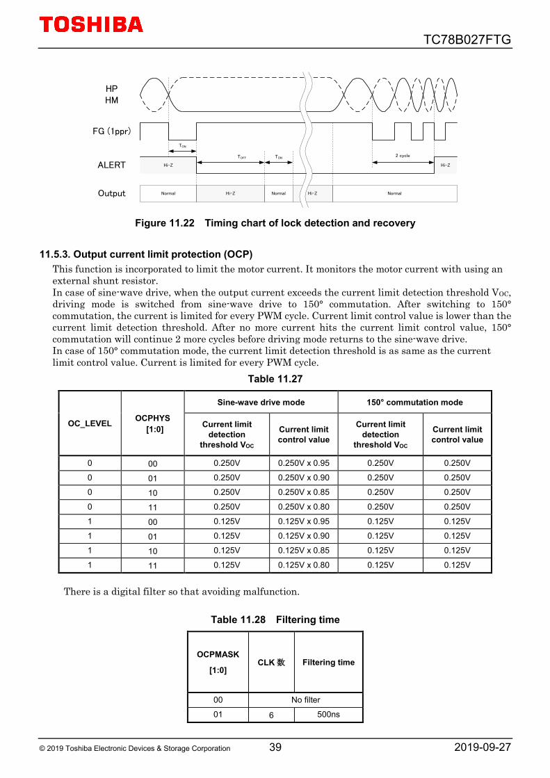
Figure 11.22 Timing chart of lock detection and recovery 11.5.3. Output current limit protection (OCP)
This function is incorporated to limit the motor current. It monitors the motor current with using an external shunt resistor. In case of sine-wave drive, when the output current exceeds the current limit detection threshold VOC, driving mode is switched from sine-wave drive to 150° commutation. After switching to 150° commutation, the current is limited for every PWM cycle. Current limit control value is lower than the current limit detection threshold. After no more current hits the current limit control value, 150° commutation will continue 2 more cycles before driving mode returns to the sine-wave drive. In case of 150° commutation mode, the current limit detection threshold is as same as the current limit control value. Current is limited for every PWM cycle.
Table 11.27
OC_LEVEL OCPHYS [1:0]
Sine-wave drive mode 150° commutation mode
Current limit detection
threshold VOC
Current limit control value
Current limit detection
threshold VOC
Current limit control value
0 00 0.250V 0.250V x 0.95 0.250V 0.250V
0 01 0.250V 0.250V x 0.90 0.250V 0.250V
0 10 0.250V 0.250V x 0.85 0.250V 0.250V
0 11 0.250V 0.250V x 0.80 0.250V 0.250V
1 00 0.125V 0.125V x 0.95 0.125V 0.125V
1 01 0.125V 0.125V x 0.90 0.125V 0.125V
1 10 0.125V 0.125V x 0.85 0.125V 0.125V
1 11 0.125V 0.125V x 0.80 0.125V 0.125V
There is a digital filter so that avoiding malfunction.
Table 11.28 Filtering time
OCPMASK
[1:0] CLK 数 Filtering time
00 No filter
01 6 500ns
Hi-Z
HPHM
FG (1ppr)
ALERT Hi-Z
Output Hi-ZNormal Normal Hi-Z
TON
TOFF TON
Normal
2 cycle

TC78B027FTG
© 2019 Toshiba Electronic Devices & Storage Corporation 40 2019-09-27
10 7 666ns
11 8 750ns
There is a filter on the OC pin to avoid malfunction.
Table 11.29 Filter setting on OC pin
RS_SEL[1:0] Cut off frequency
00 None
01 200kHz
10 100kHz
11 50kHz
11.5.4. Over current protection (ISD) This function monitors the current of the output power transistor by shunt resistor and turns off all output stages when the current value exceeds the detection threshold. It prevents the external MOSFET from flowing over current continuously. While this function is activated, ALERT pin outputs a low level signal. Automatic recovery or latch can be selected by using the register. In the case of automatic recovery, output resumes automatically after the output OFF period (tOFF) has passed. If the over current condition continues, the protection cycle repeats. If it repeats 8 times in a row, output will not recover, and all output power transistors will keep in off-state. This state is released by re-applying SPD signal or turning on the power again. In the case of the latch method, output power transistors keep in the off-state after the over current is detected. This state is released by re-applying SPD signal or turning on the power again. Detection voltage level can be set 1.0V or 0.5V by the setting of NVM. Default level is 1.0V. Filtering time is longer one clock than OCP’s time to prevent a malfunction due to pulse current.
11.5.5. Over voltage protection (OVP) This function is incorporated to prevent VM voltage from rising during motor deceleration. In case of sine-wave drive, driving mode is switched from sine-wave drive to 150° commutation when the VM voltage becomes 17.2 V (typ.) or more. After VM voltage falls to 16.8 V (typ.) or less, 150° commutation continues 2 more cycles before driving mode is switched back to the sine-wave drive. In case of 150° commutation mode, the over voltage protection is invalid.
11.5.6. Under voltage lockout (UVLO)
When the power supply voltage is less than the IC operation voltage, this function turns off the IC operation to avoid malfunction. It monitors both VM voltage and VREG voltage. When VM voltage is 3.9 V (typ.) or less, or VREG voltage is 3.7 V (typ.) or less, this function is activated. It has a hysteresis of 0.3 V (typ.). Normal operation resumes when VM voltage is over 4.2 V (typ.), and VREG voltage is over 4.0 V (typ.).
11.5.7. Charge pump under voltage
When the voltage between VCP pin and VM pin is 3.7V(typ.) or less, this function is activated and motor output is fixed Hi-Z. It has a hysteresis of 0.3V(typ.). IC is resumed to normal operation when the voltage is over 4.0V (typ.).
11.5.8. Thermal shutdown (TSD)
Thermal shutdown (TSD) is incorporated. It operates when IC’s junction temperature (Tj) exceeds 170°C (typ.). All outputs are turned off. It has a hysteresis of 40°C (typ.). When IC's junction temperature becomes 130°C (typ.) or less, the operation returns automatically.

TC78B027FTG
© 2019 Toshiba Electronic Devices & Storage Corporation 41 2019-09-27
12. Reference circuit
Figure 12.1 Reference circuit
TC78B027FTG
© 2019 Toshiba Electronic Devices & Storage Corporation 42 2019-09-27
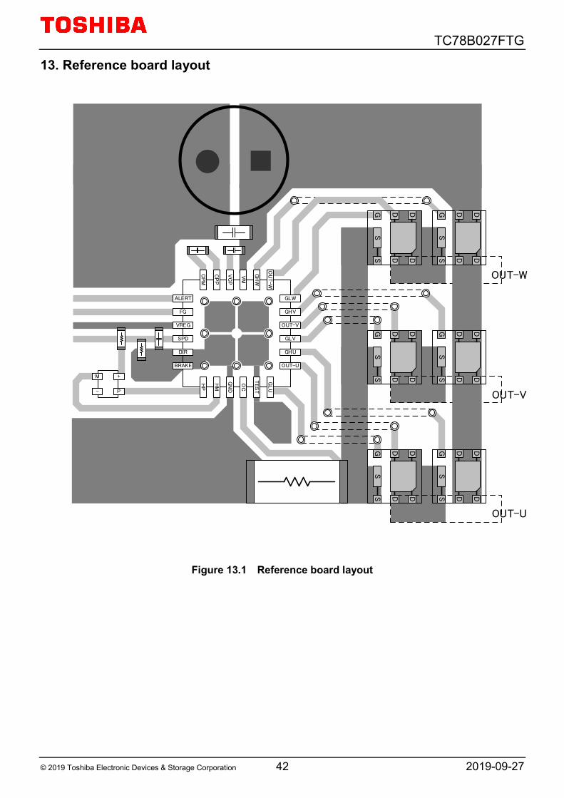
13. Reference board layout
DD
DDG
SS
DD
DDG
SS
DD
DDG
SS
DD
DDG
SS
DD
DDG
SS
DD
DDG
SS
OU
T-W
OUT-U
OUT-V
GLV
GLW
OC
TES
T
GL
U
CP
M
CP
P
ALERT
VM
GH
W
HP
HM
GN
DV
CP
GHU
GHV
DIR
VREG
SPD
FG
BRAKE
OUT-W
OUT-V
OUT-U
Figure 13.1 Reference board layout

TC78B027FTG
© 2019 Toshiba Electronic Devices & Storage Corporation 43 2019-09-27
14. Package 14.1. Package dimension
P-VQFN24-0404-0.50-003 Unit: mm
Figure 14.1 Package dimension
Weight: 0.04 g (typ.)

TC78B027FTG
© 2019 Toshiba Electronic Devices & Storage Corporation 44 2019-09-27
15. IC Usage Considerations 15.1. Notes on handling IC
[1] The absolute maximum ratings of a semiconductor device are a set of ratings that must not be exceeded, even for a moment. Do not exceed any of these ratings. Exceeding the rating(s) may cause the device breakdown, damage or deterioration, and may result injury by explosion or combustion.
[2] Use an appropriate power supply fuse to ensure that a large current does not continuously flow in
case of over current and/or IC failure. The IC will fully break down when used under conditions that exceed its absolute maximum ratings, when the wiring is routed improperly or when an abnormal pulse noise occurs from the wiring or load, causing a large current to continuously flow and the breakdown can lead smoke or ignition. To minimize the effects of the flow of a large current in case of breakdown, appropriate settings, such as fuse capacity, fusing time and insertion circuit location, are required.
[3] If your design includes an inductive load such as a motor coil, incorporate a protection circuit into
the design to prevent device malfunction or breakdown caused by the current resulting from the inrush current at power ON or the negative current resulting from the back electromotive force at power OFF. IC breakdown may cause injury, smoke or ignition. Use a stable power supply with ICs with built-in protection functions. If the power supply is unstable, the protection function may not operate, causing IC breakdown. IC breakdown may cause injury, smoke or ignition.
[4] Do not insert devices in the wrong orientation or incorrectly.
Make sure that the positive and negative terminals of power supplies are connected properly. Otherwise, the current or power consumption may exceed the absolute maximum rating, and exceeding the rating(s) may cause the device breakdown, damage or deterioration, and may result injury by explosion or combustion. In addition, do not use any device that is applied the current with inserting in the wrong orientation or incorrectly even just one time.
15.2. Points to remember on handling of ICs
(1) Over current Protection Circuit Over current protection circuits (referred to as current limiter circuits) do not necessarily protect ICs under all circumstances. If the over current protection circuits operate against the over current, clear the over current status immediately. Depending on the method of use and usage conditions, such as exceeding absolute maximum ratings can cause the over current protection circuit to not operate properly or IC breakdown before operation. In addition, depending on the method of use and usage conditions, if over current continues to flow for a long time after operation, the IC may generate heat resulting in breakdown.
(2) Thermal Shutdown Circuit
Thermal shutdown circuits do not necessarily protect ICs under all circumstances. If the thermal shutdown circuits operate against the over temperature, clear the heat generation status immediately. Depending on the method of use and usage conditions, such as exceeding absolute maximum ratings can cause the thermal shutdown circuit to not operate properly or IC breakdown before operation.
(3) Others
Utmost care is necessary in the design of power supply line, GND line, and output line since the IC may be destroyed and occur smoke and fire in some cases by short-circuiting between outputs, to the power supply or ground, or between contiguous pins.

TC78B027FTG
© 2019 Toshiba Electronic Devices & Storage Corporation 45 2019-09-27
RESTRICTIONS ON PRODUCT USE Toshiba Corporation and its subsidiaries and affiliates are collectively referred to as “TOSHIBA”. Hardware, software and systems described in this document are collectively referred to as “Product”.
• TOSHIBA reserves the right to make changes to the information in this document and related Product without notice.
• This document and any information herein may not be reproduced without prior written permission from TOSHIBA. Even with TOSHIBA's written permission, reproduction is permissible only if reproduction is without alteration/omission.
• Though TOSHIBA works continually to improve Product's quality and reliability, Product can malfunction or fail. Customers are responsible for complying with safety standards and for providing adequate designs and safeguards for their hardware, software and systems which minimize risk and avoid situations in which a malfunction or failure of Product could cause loss of human life, bodily injury or damage to property, including data loss or corruption. Before customers use the Product, create designs including the Product, or incorporate the Product into their own applications, customers must also refer to and comply with (a) the latest versions of all relevant TOSHIBA information, including without limitation, this document, the specifications, the data sheets and application notes for Product and the precautions and conditions set forth in the "TOSHIBA Semiconductor Reliability Handbook" and (b) the instructions for the application with which the Product will be used with or for. Customers are solely responsible for all aspects of their own product design or applications, including but not limited to (a) determining the appropriateness of the use of this Product in such design or applications; (b) evaluating and determining the applicability of any information contained in this document, or in charts, diagrams, programs, algorithms, sample application circuits, or any other referenced documents; and (c) validating all operating parameters for such designs and applications. TOSHIBA ASSUMES NO LIABILITY FOR CUSTOMERS' PRODUCT DESIGN OR APPLICATIONS.
• PRODUCT IS NEITHER INTENDED NOR WARRANTED FOR USE IN EQUIPMENTS OR SYSTEMS THAT REQUIRE EXTRAORDINARILY HIGH LEVELS OF QUALITY AND/OR RELIABILITY, AND/OR A MALFUNCTION OR FAILURE OF WHICH MAY CAUSE LOSS OF HUMAN LIFE, BODILY INJURY, SERIOUS PROPERTY DAMAGE AND/OR SERIOUS PUBLIC IMPACT ("UNINTENDED USE"). Except for specific applications as expressly stated in this document, Unintended Use includes, without limitation, equipment used in nuclear facilities, equipment used in the aerospace industry, lifesaving and/or life supporting medical equipment, equipment used for automobiles, trains, ships and other transportation, traffic signaling equipment, equipment used to control combustions or explosions, safety devices, elevators and escalators, and devices related to power plant. IF YOU USE PRODUCT FOR UNINTENDED USE, TOSHIBA ASSUMES NO LIABILITY FOR PRODUCT. For details, please contact your TOSHIBA sales representative or contact us via our website.
• Do not disassemble, analyze, reverse-engineer, alter, modify, translate or copy Product, whether in whole or in part.
• Product shall not be used for or incorporated into any products or systems whose manufacture, use, or sale is prohibited under any applicable laws or regulations.
• The information contained herein is presented only as guidance for Product use. No responsibility is assumed by TOSHIBA for any infringement of patents or any other intellectual property rights of third parties that may result from the use of Product. No license to any intellectual property right is granted by this document, whether express or implied, by estoppel or otherwise.
• ABSENT A WRITTEN SIGNED AGREEMENT, EXCEPT AS PROVIDED IN THE RELEVANT TERMS AND CONDITIONS OF SALE FOR PRODUCT, AND TO THE MAXIMUM EXTENT ALLOWABLE BY LAW, TOSHIBA (1) ASSUMES NO LIABILITY WHATSOEVER, INCLUDING WITHOUT LIMITATION, INDIRECT, CONSEQUENTIAL, SPECIAL, OR INCIDENTAL DAMAGES OR LOSS, INCLUDING WITHOUT LIMITATION, LOSS OF PROFITS, LOSS OF OPPORTUNITIES, BUSINESS INTERRUPTION AND LOSS OF DATA, AND (2) DISCLAIMS ANY AND ALL EXPRESS OR IMPLIED WARRANTIES AND CONDITIONS RELATED TO SALE, USE OF PRODUCT, OR INFORMATION, INCLUDING WARRANTIES OR CONDITIONS OF MERCHANTABILITY, FITNESS FOR A PARTICULAR PURPOSE, ACCURACY OF INFORMATION, OR NONINFRINGEMENT.
• Do not use or otherwise make available Product or related software or technology for any military purposes, including without limitation, for the design, development, use, stockpiling or manufacturing of nuclear, chemical, or biological weapons or missile technology products (mass destruction weapons). Product and related software and technology may be controlled under the applicable export laws and regulations including, without limitation, the Japanese Foreign Exchange and Foreign Trade Law and the U.S. Export Administration Regulations. Export and re-export of Product or related software or technology are strictly prohibited except in compliance with all applicable export laws and regulations.
• Please contact your TOSHIBA sales representative for details as to environmental matters such as the RoHS compatibility of Product. Please use Product in compliance with all applicable laws and regulations that regulate the inclusion or use of controlled substances, including without limitation, the EU RoHS Directive. TOSHIBA ASSUMES NO LIABILITY FOR DAMAGES OR LOSSES OCCURRING AS A RESULT OF NONCOMPLIANCE WITH APPLICABLE LAWS AND REGULATIONS.
https://toshiba.semicon-storage.com/

Mouser Electronics
Authorized Distributor
Click to View Pricing, Inventory, Delivery & Lifecycle Information: Toshiba:
TC78B027FTG,EL