BD16939AEFV-C : Motor / Actuator Drivers - Mouser Electronics
28
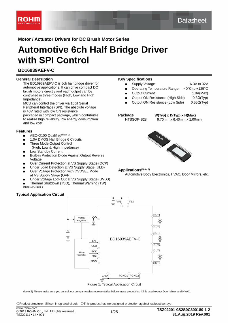
〇Product structure : Silicon integrated circuit 〇This product has no designed protection against radioactive rays 1/25 TSZ02201-0S2S0C300180-1-2 31.Aug.2019 Rev.001 www.rohm.com © 2019 ROHM Co., Ltd. All rights reserved. TSZ22111 • 14 • 001 Motor / Actuator Drivers for DC Brush Motor Series Automotive 6ch Half Bridge Driver with SPI Control BD16939AEFV-C General Description The BD16939AEFV-C is 6ch half bridge driver for automotive applications. It can drive compact DC brush motors directly and each output can be controlled in three modes (High, Low and High Impedance). MCU can control the driver via 16bit Serial Peripheral Interface (SPI). The absolute voltage is 40V rated with low ON resistance packaged in compact package, which contributes to realize high reliability, low energy consumption and low cost. Features ■ AEC-Q100 Qualified (Note 1) ■ 1.0A DMOS Half Bridge 6 Circuits ■ Three Mode Output Control (High, Low & High Impedance) ■ Low Standby Current ■ Built-in Protection Diode Against Output Reverse Voltage ■ Over Current Protection at VS Supply Stage (OCP) ■ Under Load Detection at VS Supply Stage (ULD) ■ Over Voltage Protection with OVDSEL Mode at VS Supply Stage (OVP) ■ Under Voltage Lock Out at VS Supply Stage (UVLO) ■ Thermal Shutdown (TSD), Thermal Warning (TW) (Note 1) Grade 1 Key Specifications ■ Supply Voltage 6.3V to 32V ■ Operating Temperature Range -40°C to +125°C ■ Output Current 1.0A(Max) ■ Output ON Resistance (High Side) 0.8Ω(Typ) ■ Output ON Resistance (Low Side) 0.55Ω(Typ) Package W(Typ) x D(Typ) x H(Max) HTSSOP-B28 9.70mm x 6.40mm x 1.00mm Applications (Note 2) Automotive Body Electronics, HVAC, Door Mirrors, etc. Typical Application Circuit EN CSB SCK SDI SDO VCC VS1 VS2 OUT1 OUT2 OUT3 GND PGND1 PGND2 Voltage Regulator Micro Contoller M M OUT4 BD16939AEFV-C OUT5 M OUT6 (Note 2) Please make sure you consult our company sales representative before mass production, if it is used except Door Mirror and HVAC. Figure 1. Typical Application Circuit Datasheet
-
Upload
khangminh22 -
Category
Documents
-
view
0 -
download
0
Transcript of BD16939AEFV-C : Motor / Actuator Drivers - Mouser Electronics
〇Product structure : Silicon integrated circuit 〇This product has no designed protection against radioactive rays
1/25
TSZ02201-0S2S0C300180-1-2
31.Aug.2019 Rev.001
www.rohm.com © 2019 ROHM Co., Ltd. All rights reserved. TSZ22111 • 14 • 001
Motor / Actuator Drivers for DC Brush Motor Series
Automotive 6ch Half Bridge Driver with SPI Control BD16939AEFV-C
General Description The BD16939AEFV-C is 6ch half bridge driver for automotive applications. It can drive compact DC brush motors directly and each output can be controlled in three modes (High, Low and High Impedance). MCU can control the driver via 16bit Serial Peripheral Interface (SPI). The absolute voltage is 40V rated with low ON resistance packaged in compact package, which contributes to realize high reliability, low energy consumption and low cost.
Features ■ AEC-Q100 Qualified(Note 1)
■ 1.0A DMOS Half Bridge 6 Circuits■ Three Mode Output Control
(High, Low & High Impedance) ■ Low Standby Current■ Built-in Protection Diode Against Output Reverse
Voltage■ Over Current Protection at VS Supply Stage (OCP)■ Under Load Detection at VS Supply Stage (ULD)■ Over Voltage Protection with OVDSEL Mode
at VS Supply Stage (OVP)■ Under Voltage Lock Out at VS Supply Stage (UVLO)■ Thermal Shutdown (TSD), Thermal Warning (TW)(Note 1) Grade 1
Key Specifications
■ Supply Voltage 6.3V to 32V
■ Operating Temperature Range -40°C to +125°C
■ Output Current 1.0A(Max)
■ Output ON Resistance (High Side) 0.8Ω(Typ)
■ Output ON Resistance (Low Side) 0.55Ω(Typ)
Package W(Typ) x D(Typ) x H(Max) HTSSOP-B28 9.70mm x 6.40mm x 1.00mm
Applications(Note 2) Automotive Body Electronics, HVAC, Door Mirrors, etc.
Typical Application Circuit
EN
CSB
SCK
SDI
SDO
VCC
VS1 VS2
OUT1
OUT2
OUT3
GND PGND1 PGND2
Voltage
Regulator
Micro
Contoller
M
M
OUT4
BD16939AEFV-C
OUT5
M
OUT6
(Note 2) Please make sure you consult our company sales representative before mass production, if it is used except Door Mirror and HVAC.
Figure 1. Typical Application Circuit
Datasheet
2/25
TSZ02201-0S2S0C300180-1-2 © 2019 ROHM Co., Ltd. All rights reserved. 31.Aug.2019 Rev.001
www.rohm.com
TSZ22111 • 15 • 001
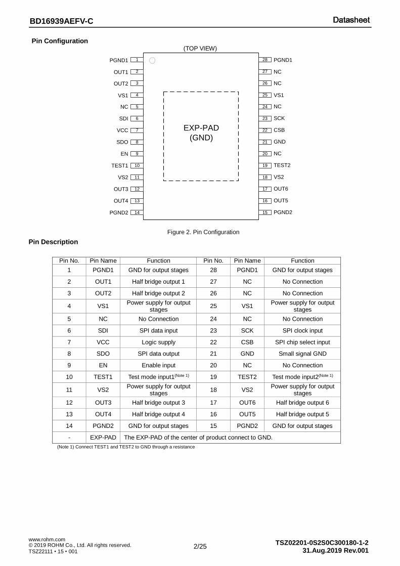
BD16939AEFV-C
Pin Configuration (TOP VIEW)
PGND1 1
2OUT1
OUT2 3
VS1 4
NC
VCC
5
SDO
7
EN
8
TEST1
9
10
SDI 6
11
12
13
14
28
27
26
25
24
22
21
20
19
23
18
17
16
15
VS2
OUT3
OUT4
PGND2
PGND1
NC
NC
VS1
NC
CSB
GND
NC
TEST2
SCK
VS2
OUT6
OUT5
PGND2
EXP-PAD
(GND)
Pin Description
Pin No. Pin Name Function Pin No. Pin Name Function
1 PGND1 GND for output stages 28 PGND1 GND for output stages
2 OUT1 Half bridge output 1 27 NC No Connection
3 OUT2 Half bridge output 2 26 NC No Connection
4 VS1 Power supply for output
stages 25 VS1
Power supply for output stages
5 NC No Connection 24 NC No Connection
6 SDI SPI data input 23 SCK SPI clock input
7 VCC Logic supply 22 CSB SPI chip select input
8 SDO SPI data output 21 GND Small signal GND
9 EN Enable input 20 NC No Connection
10 TEST1 Test mode input1(Note 1) 19 TEST2 Test mode input2(Note 1)
11 VS2 Power supply for output
stages 18 VS2
Power supply for output stages
12 OUT3 Half bridge output 3 17 OUT6 Half bridge output 6
13 OUT4 Half bridge output 4 16 OUT5 Half bridge output 5
14 PGND2 GND for output stages 15 PGND2 GND for output stages
- EXP-PAD The EXP-PAD of the center of product connect to GND.
(Note 1) Connect TEST1 and TEST2 to GND through a resistance
Figure 2. Pin Configuration
3/25
TSZ02201-0S2S0C300180-1-2 © 2019 ROHM Co., Ltd. All rights reserved. 31.Aug.2019 Rev.001
www.rohm.com
TSZ22111 • 15 • 001
BD16939AEFV-C
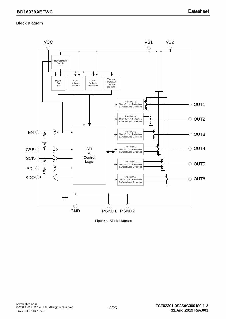
Block Diagram
EN
CSB
SCK
SDI
SDO
VCC
Power
On
Reset
Under
Voltage
Lock Out
Over
Voltage
Protection
Thermal
Shutdown
Thermal
Warning
Predriver &
Over Current Protection
& Under Load Detection
SPI
&
Control
Logic
VS1 VS2
OUT1
OUT2
OUT3
GND PGND1 PGND2
Predriver &
Over Current Protection
& Under Load Detection
Predriver &
Over Current Protection
& Under Load Detection
Predriver &
Over Current Protection
& Under Load Detection
Predriver &
Over Current Protection
& Under Load Detection
Predriver &
Over Current Protection
& Under Load Detection
OUT4
OUT5
OUT6
VCC
Internal Power
Supply
Figure 3. Block Diagram
4/25
TSZ02201-0S2S0C300180-1-2 © 2019 ROHM Co., Ltd. All rights reserved. 31.Aug.2019 Rev.001
www.rohm.com
TSZ22111 • 15 • 001
BD16939AEFV-C
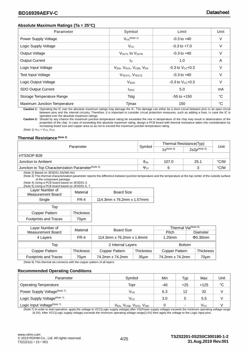
Absolute Maximum Ratings (Ta = 25°C)
Parameter Symbol Limit Unit
Power Supply Voltage VVS(Note 1) -0.3 to +40 V
Logic Supply Voltage VCC -0.3 to +7.0 V
Output Voltage VOUT1 to VOUT6 -0.3 to +40 V
Output Current IO 1.0 A
Logic Input Voltage VSDI, VSCK, VCSB, VEN -0.3 to VCC+0.3 V
Test Input Voltage VTEST1, VTEST2 -0.3 to +40 V
Logic Output Voltage VSDO -0.3 to VCC+0.3 V
SDO Output Current ISDO 5.0 mA
Storage Temperature Range Tstg -55 to +150 °C
Maximum Junction Temperature Tjmax 150 °C
Caution 1: Operating the IC over the absolute maximum ratings may damage the IC. The damage can either be a short circuit between pins or an open circuit between pins and the internal circuitry. Therefore, it is important to consider circuit protection measures, such as adding a fuse, in case the IC is operated over the absolute maximum ratings.
Caution 2: Should by any chance the maximum junction temperature rating be exceeded the rise in temperature of the chip may result in deterioration of the properties of the chip. In case of exceeding this absolute maximum rating, design a PCB board with thermal resistance taken into consideration by increasing board size and copper area so as not to exceed the maximum junction temperature rating.
(Note 1) VVS = VVS1, VVS2
Thermal Resistance (Note 2)
Parameter Symbol Thermal Resistance(Typ)
Unit 1s(Note 4) 2s2p(Note 5)
HTSSOP-B28
Junction to Ambient θJA 107.0 25.1 °C/W
Junction to Top Characterization Parameter(Note 3) ΨJT 6 3 °C/W
(Note 2) Based on JESD51-2A(Still-Air) (Note 3) This thermal characterization parameter reports the difference between junction temperature and the temperature at the top center of the outside surface
of the component package. (Note 4) Using a PCB board based on JESD51-3. (Note 5) Using a PCB board based on JESD51-5, 7.
Layer Number of Measurement Board
Material Board Size
Single FR-4 114.3mm x 76.2mm x 1.57mmt
Top
Copper Pattern Thickness
Footprints and Traces 70μm
Layer Number of Measurement Board
Material Board Size Thermal Via(Note 6)
Pitch Diameter
4 Layers FR-4 114.3mm x 76.2mm x 1.6mmt 1.20mm Φ0.30mm
Top 2 Internal Layers Bottom
Copper Pattern Thickness Copper Pattern Thickness Copper Pattern Thickness
Footprints and Traces 70μm 74.2mm x 74.2mm 35μm 74.2mm x 74.2mm 70μm
(Note 6) This thermal via connects with the copper pattern of all layers
Recommended Operating Conditions
Parameter Symbol Min Typ Max Unit
Operating Temperature Topr -40 +25 +125 °C
Power Supply Voltage(Note 7) VVS 6.3 12 32 V
Logic Supply Voltage(Note 7) VCC 3.0 5 5.5 V
Logic Input Voltage(Note 7) VEN, VCSB, VSCK, VSDI 0 - VCC V (Note 7) In order to start operation, apply the voltage to VCC(Logic supply voltage) after VS(Power supply voltage) exceeds the minimum operating voltage range
(6.3V). After VCC(Logic supply voltage) exceeds the minimum operating voltage range(3.0V) then apply the voltage to the Logic input pins.
5/25
TSZ02201-0S2S0C300180-1-2 © 2019 ROHM Co., Ltd. All rights reserved. 31.Aug.2019 Rev.001
www.rohm.com
TSZ22111 • 15 • 001
BD16939AEFV-C
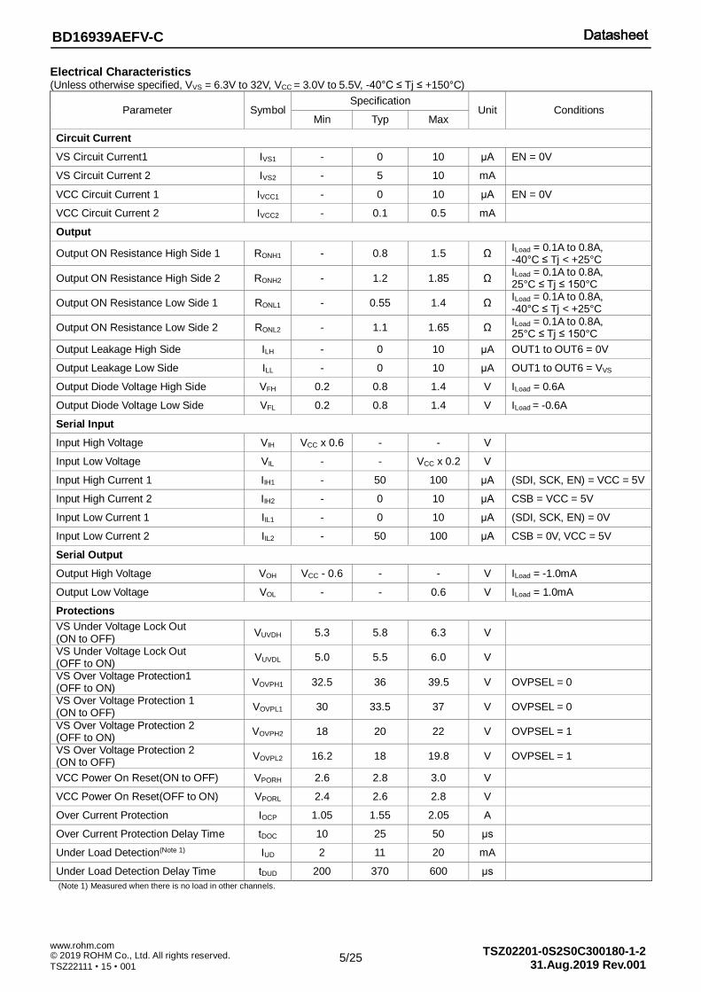
Electrical Characteristics (Unless otherwise specified, VVS = 6.3V to 32V, VCC = 3.0V to 5.5V, -40°C ≤ Tj ≤ +150°C)
Parameter Symbol Specification
Unit Conditions Min Typ Max
Circuit Current
VS Circuit Current1 IVS1 - 0 10 μA EN = 0V
VS Circuit Current 2 IVS2 - 5 10 mA
VCC Circuit Current 1 IVCC1 - 0 10 μA EN = 0V
VCC Circuit Current 2 IVCC2 - 0.1 0.5 mA
Output
Output ON Resistance High Side 1 RONH1 - 0.8 1.5 Ω ILoad = 0.1A to 0.8A, -40°C ≤ Tj < +25°C
Output ON Resistance High Side 2 RONH2 - 1.2 1.85 Ω ILoad = 0.1A to 0.8A, 25°C ≤ Tj ≤ 150°C
Output ON Resistance Low Side 1 RONL1 - 0.55 1.4 Ω ILoad = 0.1A to 0.8A, -40°C ≤ Tj < +25°C
Output ON Resistance Low Side 2 RONL2 - 1.1 1.65 Ω ILoad = 0.1A to 0.8A, 25°C ≤ Tj ≤ 150°C
Output Leakage High Side ILH - 0 10 μA OUT1 to OUT6 = 0V
Output Leakage Low Side ILL - 0 10 μA OUT1 to OUT6 = VVS
Output Diode Voltage High Side VFH 0.2 0.8 1.4 V ILoad = 0.6A
Output Diode Voltage Low Side VFL 0.2 0.8 1.4 V ILoad = -0.6A
Serial Input
Input High Voltage VIH VCC x 0.6 - - V
Input Low Voltage VIL - - VCC x 0.2 V
Input High Current 1 IIH1 - 50 100 μA (SDI, SCK, EN) = VCC = 5V
Input High Current 2 IIH2 - 0 10 μA CSB = VCC = 5V
Input Low Current 1 IIL1 - 0 10 μA (SDI, SCK, EN) = 0V
Input Low Current 2 IIL2 - 50 100 μA CSB = 0V, VCC = 5V
Serial Output
Output High Voltage VOH VCC - 0.6 - - V ILoad = -1.0mA
Output Low Voltage VOL - - 0.6 V ILoad = 1.0mA
Protections
VS Under Voltage Lock Out (ON to OFF)
VUVDH 5.3 5.8 6.3 V
VS Under Voltage Lock Out (OFF to ON)
VUVDL 5.0 5.5 6.0 V
VS Over Voltage Protection1 (OFF to ON)
VOVPH1 32.5 36 39.5 V OVPSEL = 0
VS Over Voltage Protection 1 (ON to OFF)
VOVPL1 30 33.5 37 V OVPSEL = 0
VS Over Voltage Protection 2 (OFF to ON)
VOVPH2 18 20 22 V OVPSEL = 1
VS Over Voltage Protection 2 (ON to OFF)
VOVPL2 16.2 18 19.8 V OVPSEL = 1
VCC Power On Reset(ON to OFF) VPORH 2.6 2.8 3.0 V
VCC Power On Reset(OFF to ON) VPORL 2.4 2.6 2.8 V
Over Current Protection IOCP 1.05 1.55 2.05 A
Over Current Protection Delay Time tDOC 10 25 50 μs
Under Load Detection(Note 1) IUD 2 11 20 mA
Under Load Detection Delay Time tDUD 200 370 600 μs
(Note 1) Measured when there is no load in other channels.
6/25
TSZ02201-0S2S0C300180-1-2 © 2019 ROHM Co., Ltd. All rights reserved. 31.Aug.2019 Rev.001
www.rohm.com
TSZ22111 • 15 • 001
BD16939AEFV-C
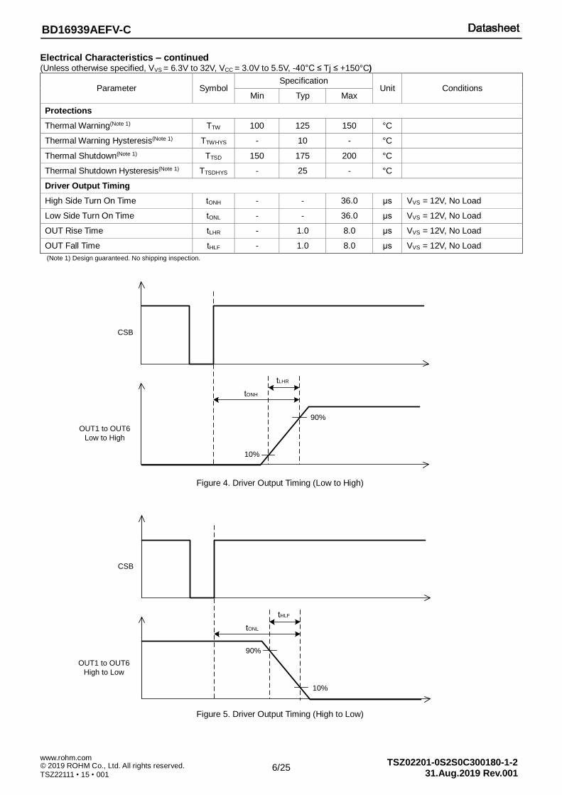
Electrical Characteristics – continued (Unless otherwise specified, VVS = 6.3V to 32V, VCC = 3.0V to 5.5V, -40°C ≤ Tj ≤ +150°C)
Parameter Symbol Specification
Unit Conditions Min Typ Max
Protections
Thermal Warning(Note 1) TTW 100 125 150 °C
Thermal Warning Hysteresis(Note 1) TTWHYS - 10 - °C
Thermal Shutdown(Note 1) TTSD 150 175 200 °C
Thermal Shutdown Hysteresis(Note 1) TTSDHYS - 25 - °C
Driver Output Timing
High Side Turn On Time tONH - - 36.0 μs VVS = 12V, No Load
Low Side Turn On Time tONL - - 36.0 μs VVS = 12V, No Load
OUT Rise Time tLHR - 1.0 8.0 μs VVS = 12V, No Load
OUT Fall Time tHLF - 1.0 8.0 μs VVS = 12V, No Load
(Note 1) Design guaranteed. No shipping inspection.
Figure 4. Driver Output Timing (Low to High)
Figure 5. Driver Output Timing (High to Low)
CSB
OUT1 to OUT6
High to Low
tONL
tHLF
90%
10%
CSB
OUT1 to OUT6
Low to High
tONH
tLHR
90%
10%
7/25
BD16939AEFV-C
TSZ02201-0S2S0C300180-1-2 © 2019 ROHM Co., Ltd. All rights reserved. 31.Aug.2019 Rev.001
www.rohm.com
TSZ22111 • 15 • 001
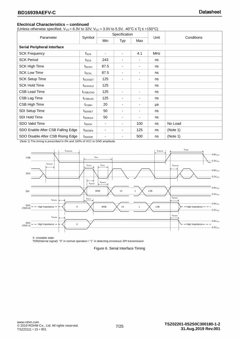
Electrical Characteristics – continued (Unless otherwise specified, VVS = 6.3V to 32V, VCC = 3.0V to 5.5V, -40°C ≤ Tj ≤ +150°C)
Parameter Symbol Specification
Unit Conditions Min Typ Max
Serial Peripheral Interface
SCK Frequency fSCK - - 4.1 MHz
SCK Period tSCK 243 - - ns
SCK High Time tSCKH 87.5 - - ns
SCK Low Time tSCKL 87.5 - - ns
SCK Setup Time tSCKSET 125 - - ns
SCK Hold Time tSCKHLD 125 ns
CSB Lead Time tCSBLEAD 125 - - ns
CSB Lag Time tCSBLAG 125 - - ns
CSB High Time tCSBH 20 - - μs
SDI Setup Time tSDISET 50 - - ns
SDI Hold Time tSDIHLD 50 - - ns
SDO Valid Time tSDOV - - 100 ns No Load
SDO Enable After CSB Falling Edge tSDOEN - - 125 ns (Note 1)
SDO Disable After CSB Rising Edge tSDODE - - 500 ns (Note 1)
(Note 1) The timing is prescribed in 0% and 100% of VCC to GND amplitude.
SDO
(TER=0)
SDI
CSB
SCK
MSB 14 1 LSB
MSB 14 1 LSB
tSCKSET
tCSBLEAD
tSCK
tCSBLAGtCSBH
tSCKH tSCKL tSCKHLD
tSDISETtSDIHLD
tSDOVtSDOEN
tSDODE
0.6VVCC
0.2VVCC
0.6VVCC
0.2VVCC
0.6VVCC
0.2VVCC
0.6VVCC
0.2VVCC
X
SDO
(TER=1)
tSDOEN
tSDODE
X
0.6VVCC
0.2VVCC
High ImpedanceHigh Impedance
High Impedance High Impedance
X: Unstable state TER(Internal signal): “0” in normal operation / “1” in detecting erroneous SPI transmission
Figure 6. Serial Interface Timing
8/25
BD16939AEFV-C
TSZ02201-0S2S0C300180-1-2 © 2019 ROHM Co., Ltd. All rights reserved. 31.Aug.2019 Rev.001
www.rohm.com
TSZ22111 • 15 • 001
0
0.3
0.6
0.9
1.2
1.5
0 0.2 0.4 0.6 0.8 1
Hig
h S
ide
Outp
ut O
n R
esis
tan
ce
[Ω
]
Output Current [A]
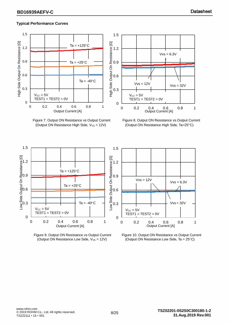
Typical Performance Curves
Figure 7. Output ON Resistance vs Output Current Figure 8. Output ON Resistance vs Output Current
(Output ON Resistance High Side, VVS = 12V) (Output ON Resistance High Side, Ta=25C)
Figure 9. Output ON Resistance vs Output Current Figure 10. Output ON Resistance vs Output Current
(Output ON Resistance Low Side, VVS = 12V) (Output ON Resistance Low Side, Ta = 25C)
0
0.3
0.6
0.9
1.2
1.5
0 0.2 0.4 0.6 0.8 1
Lo
w S
ide
Ou
tpu
t O
n R
esis
tan
ce
[Ω
]
Output Current [A]
0
0.3
0.6
0.9
1.2
1.5
0 0.2 0.4 0.6 0.8 1
Lo
w S
ide
Outp
ut O
n R
esis
tance [Ω
]
Output Current [A]
Ta = +125C
Ta = +25C
Ta = -40C
VCC = 5V TEST1 = TEST2 = 0V
Vvs = 12V Vvs = 32V
Vvs = 6.3V
Vvs = 6.3V Vvs = 12V
VCC = 5V TEST1 = TEST2 = 0V
VCC = 5V TEST1 = TEST2 = 0V 0
0.3
0.6
0.9
1.2
1.5
0 0.2 0.4 0.6 0.8 1H
igh
Sid
e O
utp
ut O
n R
esis
tan
ce
[Ω
]Output Current [A]
VCC = 5V TEST1 = TEST2 = 0V
Ta = +125C
Ta = +25C
Ta = -40C Vvs = 12V
Vvs = 6.3V
VCC = 5V TEST1 = TEST2 = 0V
Vvs = 32V
Vvs = 6.3V Vvs = 12V
Vvs = 32V
9/25
BD16939AEFV-C
TSZ02201-0S2S0C300180-1-2 © 2019 ROHM Co., Ltd. All rights reserved. 31.Aug.2019 Rev.001
www.rohm.com
TSZ22111 • 15 • 001
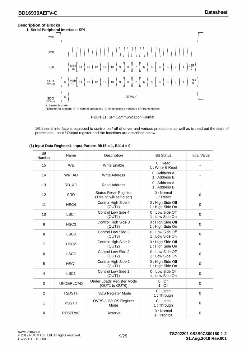
Description of Blocks 1. Serial Peripheral Interface: SPI
CSB
SDI
SCK
SDO( TER=0 )
MSB15
14 13 12 11 10 9 8 7 6 5 4 3 2 1LSB
0
MSB
1514 13 12 11 10 9 8 7 6 5 4 3 2 1
LSB0
SDO( TER=1 )
All "High"
X
X
X: Unstable state
TER(Internal signal): “0” in normal operation / “1” in detecting erroneous SPI transmission
16bit serial interface is equipped to control on / off of driver and various protections as well as to read out the state of protections. Input / Output register and the functions are described below.
(1) Input Data Register1- Input Pattern Bit15 = 1, Bit14 = 0
Bit Number
Name Description Bit Status Initial Value
15 WE Write Enable 0 : Read
1 : Write & Read -
14 WR_AD Write Address 0 : Address A 1 : Address B
-
13 RD_AD Read Address 0 : Address A 1 : Address B
-
12 SRR Status Reset Register (This bit will self-clear)
0 : Normal 1 : Reset
0
11 HSC4 Control High Side 4
(OUT4) 0 : High Side Off 1 : High Side On
0
10 LSC4 Control Low Side 4
(OUT4) 0 : Low Side Off 1 : Low Side On
0
9 HSC3 Control High Side 3
(OUT3) 0 : High Side Off 1 : High Side On
0
8 LSC3 Control Low Side 3
(OUT3) 0 : Low Side Off 1 : Low Side On
0
7 HSC2 Control High Side 2
(OUT2) 0 : High Side Off 1 : High Side On
0
6 LSC2 Control Low Side 2
(OUT2) 0 : Low Side Off 1 : Low Side On
0
5 HSC1 Control High Side 1
(OUT1) 0 : High Side Off 1 : High Side On
0
4 LSC1 Control Low Side 1
(OUT1) 0 : Low Side Off 1 : Low Side On
0
3 UNDERLOAD Under Loads Register Mode
(OUT1 to OUT6) 0 : On 1 : Off
0
2 TSDSTH TSDS Register Mode 0 : Latch
1 : Through 0
1 PSSTH OVPS / UVLOS Register
Mode 0 : Latch
1 : Through 0
0 RESERVE Reserve 0 : Normal 1 : Prohibit
0
Figure 11. SPI Communication Format
10/25
BD16939AEFV-C
TSZ02201-0S2S0C300180-1-2 © 2019 ROHM Co., Ltd. All rights reserved. 31.Aug.2019 Rev.001
www.rohm.com
TSZ22111 • 15 • 001
Description of Blocks – continued
(2) Input Data Register2- Input Pattern Bit15 = 1, Bit14 = 1
Bit Number
Name Description Bit Status Initial Value
15 WE Write Enable 0 : Read
1 : Write & Read -
14 WR_AD Write Address 0 : Address A 1 : Address B
-
13 RD_AD Read Address 0 : Address A 1 : Address B
-
12 SRR Status Reset Register (This bit will self-clear)
0 : Normal 1 : Reset
0
11 RESERVE Reserve - -
10 RESERVE Reserve - -
9 RESERVE Reserve - -
8 RESERVE Reserve - -
7 HSC6 Control High Side 6
(OUT6) 0 : High Side Off 1 : High Side On
0
6 LSC6 Control Low Side 6
(OUT6) 0 : Low Side Off 1 : Low Side On
0
5 HSC5 Control High Side 5
(OUT5) 0 : High Side Off 1 : High Side On
0
4 LSC5 Control Low Side 5
(OUT5) 0 : Low Side Off 1 : Low Side On
0
3 OVPSEL OVP Threshold Select 0 : VOVPH1, VOVPL1 1 : VOVPH2, VOVPL2
0
2 RESERVE Reserve - -
1 RESERVE Reserve - -
0 RESERVE Reserve 0 : Normal 1 : Prohibit
0
Input of High Side On and Low Side On is prohibited. The input of High Side On and Low Side On results in High Side Off and Low Side Off state.
If WE(Bit15: Write Enable) is set to ‘1’, then Input Data Registers will be written and output will be Read Data as well depending on the previous SPI command.
It can select the Write Registers by setting WR_AD(Bit14: Write Address) bit. Read Data can be selected from the table of Read register by setting WR_AD(Bit14: Write Address) and RD_AD(Bit13: Read Address). For Read Data information, please refer below from Output Data Register1 to Output Data Register4.
If WE(Bit15: Write Enable) is set to ‘0’, then Input Data Registers will not be written (the transferred write data Bits 12 to 0 in this case will be ignored) and output will be only Read Data depending on the previous SPI command setting of WR_AD(Bit14: Write Address) and RD_AD(Bit13: Read Address).
Daisy Chain input is not supported.
11/25
BD16939AEFV-C
TSZ02201-0S2S0C300180-1-2 © 2019 ROHM Co., Ltd. All rights reserved. 31.Aug.2019 Rev.001
www.rohm.com
TSZ22111 • 15 • 001
Description of Blocks – continued
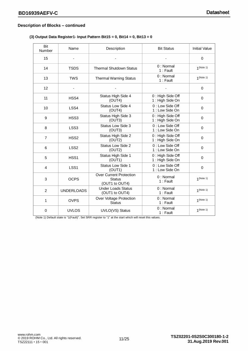
(3) Output Data Register1- Input Pattern Bit15 = 0, Bit14 = 0, Bit13 = 0
Bit Number
Name Description Bit Status Initial Value
15 - - - 0
14 TSDS Thermal Shutdown Status 0 : Normal 1 : Fault
1(Note 1)
13 TWS Thermal Warning Status 0 : Normal 1 : Fault
1(Note 1)
12 - - - 0
11 HSS4 Status High Side 4
(OUT4) 0 : High Side Off 1 : High Side On
0
10 LSS4 Status Low Side 4
(OUT4) 0 : Low Side Off 1 : Low Side On
0
9 HSS3 Status High Side 3
(OUT3) 0 : High Side Off 1 : High Side On
0
8 LSS3 Status Low Side 3
(OUT3) 0 : Low Side Off 1 : Low Side On
0
7 HSS2 Status High Side 2
(OUT2) 0 : High Side Off 1 : High Side On
0
6 LSS2 Status Low Side 2
(OUT2) 0 : Low Side Off 1 : Low Side On
0
5 HSS1 Status High Side 1
(OUT1) 0 : High Side Off 1 : High Side On
0
4 LSS1 Status Low Side 1
(OUT1) 0 : Low Side Off 1 : Low Side On
0
3 OCPS Over Current Protection
Status (OUT1 to OUT4)
0 : Normal 1 : Fault
1(Note 1)
2 UNDERLOADS Under Loads Status
(OUT1 to OUT4) 0 : Normal 1 : Fault
1(Note 1)
1 OVPS Over Voltage Protection
Status 0 : Normal 1 : Fault
1(Note 1)
0 UVLOS UVLO(VS) Status 0 : Normal 1 : Fault
1(Note 1)
(Note 1) Default state is “1(Fault)”. Set SRR register to “1” at the start which will reset this values.
12/25
BD16939AEFV-C
TSZ02201-0S2S0C300180-1-2 © 2019 ROHM Co., Ltd. All rights reserved. 31.Aug.2019 Rev.001
www.rohm.com
TSZ22111 • 15 • 001
Description of Blocks – continued
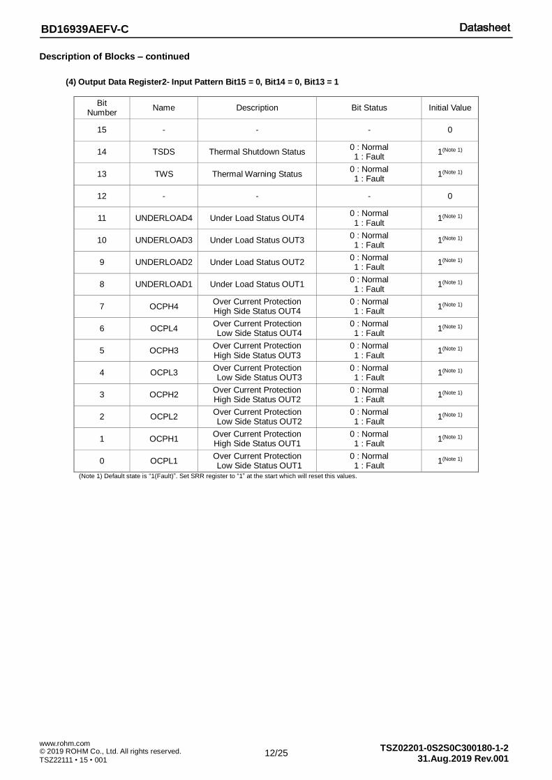
(4) Output Data Register2- Input Pattern Bit15 = 0, Bit14 = 0, Bit13 = 1
Bit Number
Name Description Bit Status Initial Value
15 - - - 0
14 TSDS Thermal Shutdown Status 0 : Normal 1 : Fault
1(Note 1)
13 TWS Thermal Warning Status 0 : Normal 1 : Fault
1(Note 1)
12 - - - 0
11 UNDERLOAD4 Under Load Status OUT4 0 : Normal 1 : Fault
1(Note 1)
10 UNDERLOAD3 Under Load Status OUT3 0 : Normal 1 : Fault
1(Note 1)
9 UNDERLOAD2 Under Load Status OUT2 0 : Normal 1 : Fault
1(Note 1)
8 UNDERLOAD1 Under Load Status OUT1 0 : Normal 1 : Fault
1(Note 1)
7 OCPH4 Over Current Protection High Side Status OUT4
0 : Normal 1 : Fault
1(Note 1)
6 OCPL4 Over Current Protection Low Side Status OUT4
0 : Normal 1 : Fault
1(Note 1)
5 OCPH3 Over Current Protection High Side Status OUT3
0 : Normal 1 : Fault
1(Note 1)
4 OCPL3 Over Current Protection Low Side Status OUT3
0 : Normal 1 : Fault
1(Note 1)
3 OCPH2 Over Current Protection High Side Status OUT2
0 : Normal 1 : Fault
1(Note 1)
2 OCPL2 Over Current Protection Low Side Status OUT2
0 : Normal 1 : Fault
1(Note 1)
1 OCPH1 Over Current Protection High Side Status OUT1
0 : Normal 1 : Fault
1(Note 1)
0 OCPL1 Over Current Protection Low Side Status OUT1
0 : Normal 1 : Fault
1(Note 1)
(Note 1) Default state is “1(Fault)”. Set SRR register to “1” at the start which will reset this values.
13/25
BD16939AEFV-C
TSZ02201-0S2S0C300180-1-2 © 2019 ROHM Co., Ltd. All rights reserved. 31.Aug.2019 Rev.001
www.rohm.com
TSZ22111 • 15 • 001
Description of Blocks – continued
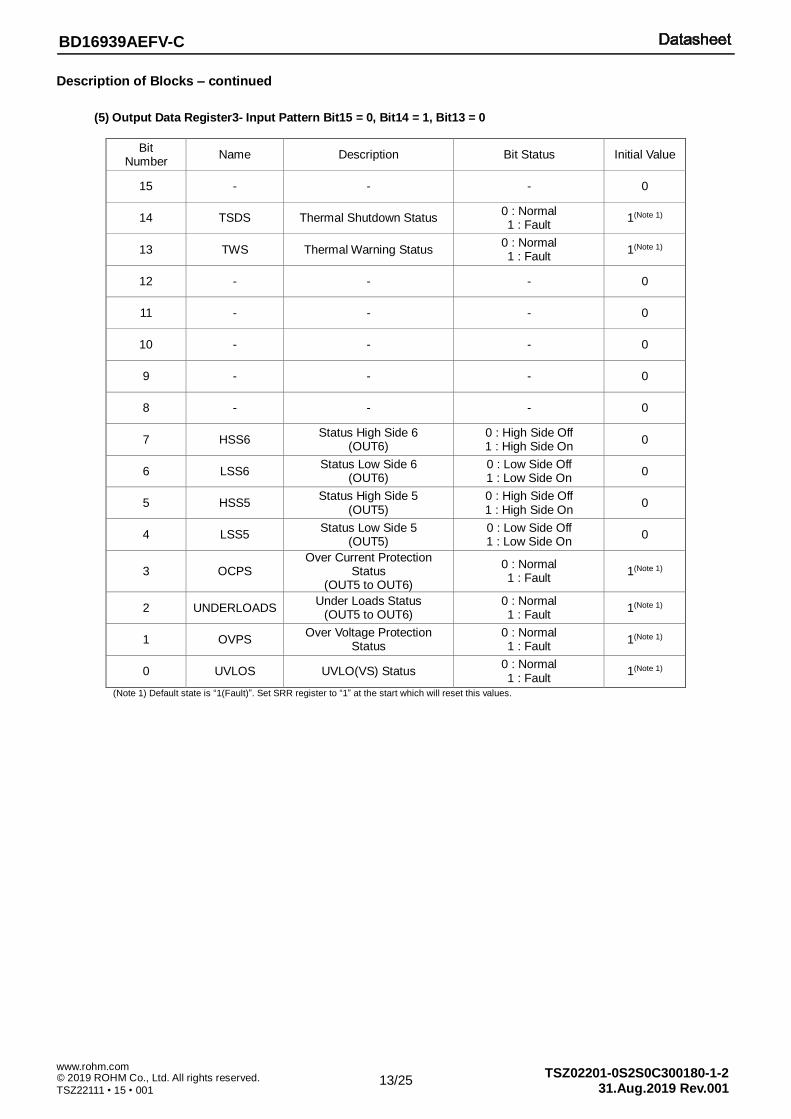
(5) Output Data Register3- Input Pattern Bit15 = 0, Bit14 = 1, Bit13 = 0
Bit Number
Name Description Bit Status Initial Value
15 - - - 0
14 TSDS Thermal Shutdown Status 0 : Normal 1 : Fault
1(Note 1)
13 TWS Thermal Warning Status 0 : Normal 1 : Fault
1(Note 1)
12 - - - 0
11 - - - 0
10 - - - 0
9 - - - 0
8 - - - 0
7 HSS6 Status High Side 6
(OUT6) 0 : High Side Off 1 : High Side On
0
6 LSS6 Status Low Side 6
(OUT6) 0 : Low Side Off 1 : Low Side On
0
5 HSS5 Status High Side 5
(OUT5) 0 : High Side Off 1 : High Side On
0
4 LSS5 Status Low Side 5
(OUT5) 0 : Low Side Off 1 : Low Side On
0
3 OCPS Over Current Protection
Status (OUT5 to OUT6)
0 : Normal 1 : Fault
1(Note 1)
2 UNDERLOADS Under Loads Status
(OUT5 to OUT6) 0 : Normal 1 : Fault
1(Note 1)
1 OVPS Over Voltage Protection
Status 0 : Normal 1 : Fault
1(Note 1)
0 UVLOS UVLO(VS) Status 0 : Normal 1 : Fault
1(Note 1)
(Note 1) Default state is “1(Fault)”. Set SRR register to “1” at the start which will reset this values.
14/25
BD16939AEFV-C
TSZ02201-0S2S0C300180-1-2 © 2019 ROHM Co., Ltd. All rights reserved. 31.Aug.2019 Rev.001
www.rohm.com
TSZ22111 • 15 • 001
Description of Blocks – continued
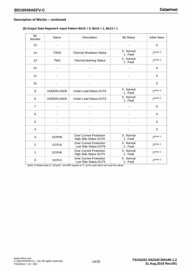
(6) Output Data Register4- Input Pattern Bit15 = 0, Bit14 = 1, Bit13 = 1
Bit Number
Name Description Bit Status Initial Value
15 - - - 0
14 TSDS Thermal Shutdown Status 0 : Normal 1 : Fault
1(Note 1)
13 TWS Thermal Warning Status 0 : Normal 1 : Fault
1(Note 1)
12 - - - 0
11 - - - 0
10 - - - 0
9 UNDERLOAD6 Under Load Status OUT6 0 : Normal 1 : Fault
1(Note 1)
8 UNDERLOAD5 Under Load Status OUT5 0 : Normal 1 : Fault
1(Note 1)
7 - - - 0
6 - - - 0
5 - - - 0
4 - - - 0
3 OCPH6 Over Current Protection High Side Status OUT6
0 : Normal 1 : Fault
1(Note 1)
2 OCPL6 Over Current Protection Low Side Status OUT6
0 : Normal 1 : Fault
1(Note 1)
1 OCPH5 Over Current Protection High Side Status OUT5
0 : Normal 1 : Fault
1(Note 1)
0 OCPL5 Over Current Protection Low Side Status OUT5
0 : Normal 1 : Fault
1(Note 1)
(Note 1) Default state is “1(Fault)”. Set SRR register to “1” at the start which will reset this values.
15/25
BD16939AEFV-C
TSZ02201-0S2S0C300180-1-2 © 2019 ROHM Co., Ltd. All rights reserved. 31.Aug.2019 Rev.001
www.rohm.com
TSZ22111 • 15 • 001
Description of Blocks – continued
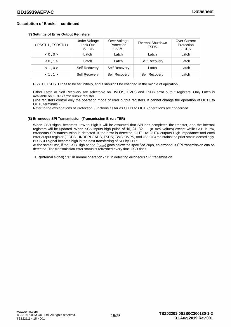
(7) Settings of Error Output Registers
< PSSTH , TSDSTH > Under Voltage
Lock Out UVLOS
Over Voltage Protection
OVPS
Thermal Shutdown TSDS
Over Current Protection
OCPS
< 0 , 0 > Latch Latch Latch Latch
< 0 , 1 > Latch Latch Self Recovery Latch
< 1 , 0 > Self Recovery Self Recovery Latch Latch
< 1 , 1 > Self Recovery Self Recovery Self Recovery Latch
PSSTH, TSDSTH has to be set initially, and it shouldn’t be changed in the middle of operation.
Either Latch or Self Recovery are selectable on UVLOS, OVPS and TSDS error output registers. Only Latch is available on OCPS error output register. (The registers control only the operation mode of error output registers. It cannot change the operation of OUT1 to OUT6 terminals.) Refer to the explanations of Protection Functions as far as OUT1 to OUT6 operations are concerned.
(8) Erroneous SPI Transmission (Transmission Error: TER)
When CSB signal becomes Low to High it will be assumed that SPI has completed the transfer, and the internal registers will be updated. When SCK inputs high pulse of 16, 24, 32, … (8+8xN values) except while CSB is low, erroneous SPI transmission is detected. If the error is detected, OUT1 to OUT6 outputs High Impedance and each error output register (OCPS, UNDERLOADS, TSDS, TWS, OVPS, and UVLOS) maintains the prior status accordingly. But SDO signal become high in the next transferring of SPI by TER. At the same time, if the CSB High period (tCSBH) goes below the specified 20μs, an erroneous SPI transmission can be detected. The transmission error status is refreshed every time CSB rises.
TER(Internal signal) : “0” in normal operation / “1” in detecting erroneous SPI transmission
16/25
BD16939AEFV-C
TSZ02201-0S2S0C300180-1-2 © 2019 ROHM Co., Ltd. All rights reserved. 31.Aug.2019 Rev.001
www.rohm.com
TSZ22111 • 15 • 001
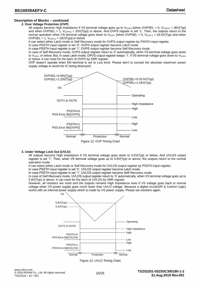
Description of Blocks – continued 2. Over Voltage Protection (OVP)
All outputs become High impedance if VS terminal voltage goes up to VOVPH [when OVPSEL = 0, VOVPH1 = 36V(Typ) and when OVPSEL = 1, VOVPH2 = 20V(Typ)] or above. And OVPS register is set ‘1’. Then, the outputs return to the normal operation when VS terminal voltage goes down to VOVPL [when OVPSEL = 0, VOVPL1 = 33.5V(Typ) and when OVPSEL = 1, VOVPL2 = 18V(Typ)] or below. It can select either Latch mode or Self-Recovery mode for OVPS output register by PSSTH input register. In case PSSTH input register is set ‘0’, OVPS output register become Latch mode. In case PSSTH input register is set ‘1’, OVPS output register become Self-Recovery mode. In case of Self-Recovery mode, OVPS output register return to ‘0’ automatically, when VS terminal voltage goes down to VOVPL or below. But, in case Latch mode, OPVS output register keeps ‘1’, if VS terminal voltage goes down to VOVPL or below. It can reset for the latch of OVPS by SRR register. OVP doesn’t operate when EN terminal is set to Low level. Please don’t to exceed the absolute maximum power supply voltage to avoid the IC being destroyed.
OVPSEL=0:36V(Typ)
OVPSEL=1:20V(Typ)
OUT1 to OUT6High Impedance
Operating
Normal Protection Normal
VS
PSS Error Bit(OVPS)
Low
HighPSSTH=0
PSS Error Bit(OVPS)PSSTH=1
Low
High
OVPSEL=0:33.5V(Typ)
OVPSEL=1:18V(Typ)
3. Under Voltage Lock Out (UVLO)
All outputs become High impedance if VS terminal voltage goes down to 5.5V(Typ) or below. And UVLOS output register is set ‘1’. Then, when VS terminal voltage goes up to 5.8V(Typ) or above, the outputs return to the normal operation mode. It can select either Latch mode or Self-Recovery mode for UVLOS output register by PSSTH input register. In case PSSTH input register is set ‘0’, UVLOS output register become Latch mode. In case PSSTH input register is set ‘1’, UVLOS output register become Self-Recovery mode. In case of Self-Recovery mode, UVLOS output register return to ‘0’ automatically, when VS terminal voltage goes up to 5.8V(Typ) or above. It can reset for the latch of UVLOS by SRR register. However, all resisters are reset and the outputs remains High impedance even if VS voltage goes back to normal voltage when VS power supply goes much lower than UVLO voltage. Because a digital circuit(SPI & Control Logic) works with an internal power supply which is made by VS power supply. Please set resisters again.
5.8V(Typ)
5.5V(Typ)
OUT1 to OUT6High Impedance
Operating
Normal Protection Normal
VS
PSS Error Bit(UVLOS)
Low
HighPSSTH=0
PSS Error Bit(UVLOS)
PSSTH=1
Low
High
Figure 12. OVP Timing Chart
Figure 13. UVLO Timing Chart
17/25
BD16939AEFV-C
TSZ02201-0S2S0C300180-1-2 © 2019 ROHM Co., Ltd. All rights reserved. 31.Aug.2019 Rev.001
www.rohm.com
TSZ22111 • 15 • 001
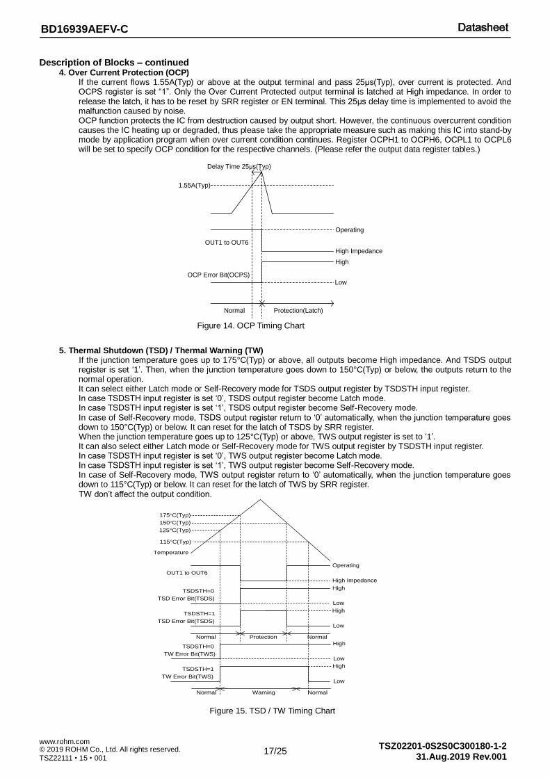
Description of Blocks – continued 4. Over Current Protection (OCP)
If the current flows 1.55A(Typ) or above at the output terminal and pass 25μs(Typ), over current is protected. And OCPS register is set “1”. Only the Over Current Protected output terminal is latched at High impedance. In order to release the latch, it has to be reset by SRR register or EN terminal. This 25μs delay time is implemented to avoid the malfunction caused by noise. OCP function protects the IC from destruction caused by output short. However, the continuous overcurrent condition causes the IC heating up or degraded, thus please take the appropriate measure such as making this IC into stand-by mode by application program when over current condition continues. Register OCPH1 to OCPH6, OCPL1 to OCPL6 will be set to specify OCP condition for the respective channels. (Please refer the output data register tables.)
1.55A(Typ)
OUT1 to OUT6
OCP Error Bit(OCPS)
Normal Protection(Latch)
High Impedance
Operating
High
Low
Delay Time 25μs(Typ)
5. Thermal Shutdown (TSD) / Thermal Warning (TW) If the junction temperature goes up to 175°C(Typ) or above, all outputs become High impedance. And TSDS output register is set ‘1’. Then, when the junction temperature goes down to 150°C(Typ) or below, the outputs return to the normal operation. It can select either Latch mode or Self-Recovery mode for TSDS output register by TSDSTH input register. In case TSDSTH input register is set ‘0’, TSDS output register become Latch mode. In case TSDSTH input register is set ‘1’, TSDS output register become Self-Recovery mode. In case of Self-Recovery mode, TSDS output register return to ‘0’ automatically, when the junction temperature goes down to 150°C(Typ) or below. It can reset for the latch of TSDS by SRR register. When the junction temperature goes up to 125°C(Typ) or above, TWS output register is set to ‘1’. It can also select either Latch mode or Self-Recovery mode for TWS output register by TSDSTH input register. In case TSDSTH input register is set ‘0’, TWS output register become Latch mode. In case TSDSTH input register is set ‘1’, TWS output register become Self-Recovery mode. In case of Self-Recovery mode, TWS output register return to ‘0’ automatically, when the junction temperature goes down to 115°C(Typ) or below. It can reset for the latch of TWS by SRR register. TW don’t affect the output condition.
175°C(Typ)
150°C(Typ)
OUT1 to OUT6
TSD Error Bit(TSDS)
High Impedance
Operating
High
Low
Normal Protection Normal
Temperature
TSDSTH=0
TSD Error Bit(TSDS)
TSDSTH=1
Low
High
125°C(Typ)
TW Error Bit(TWS)
High
Low
Normal Warning Normal
TW Error Bit(TWS)
TSDSTH=1
Low
High
TSDSTH=0
115°C(Typ)
Figure 14. OCP Timing Chart
Figure 15. TSD / TW Timing Chart
18/25
BD16939AEFV-C
TSZ02201-0S2S0C300180-1-2 © 2019 ROHM Co., Ltd. All rights reserved. 31.Aug.2019 Rev.001
www.rohm.com
TSZ22111 • 15 • 001
Description of Blocks – continued
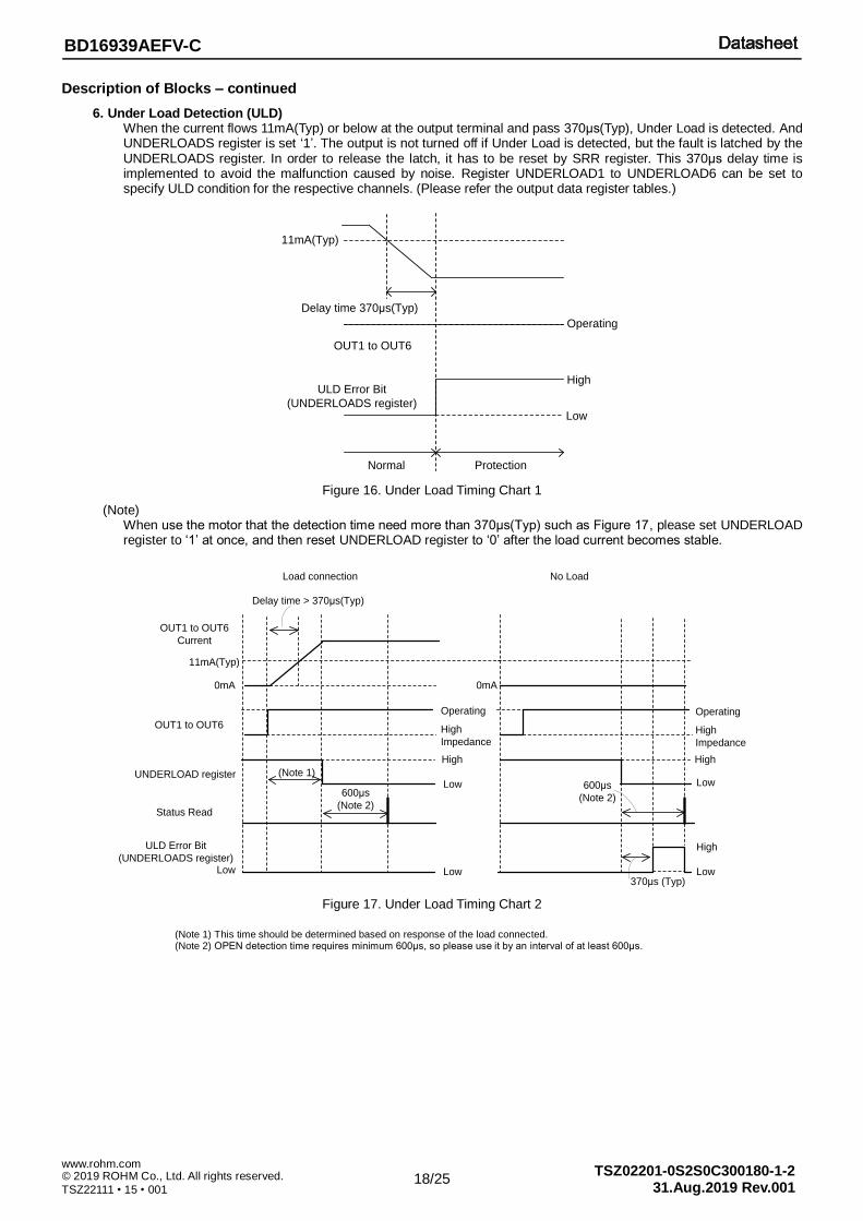
6. Under Load Detection (ULD) When the current flows 11mA(Typ) or below at the output terminal and pass 370μs(Typ), Under Load is detected. And UNDERLOADS register is set ‘1’. The output is not turned off if Under Load is detected, but the fault is latched by the UNDERLOADS register. In order to release the latch, it has to be reset by SRR register. This 370μs delay time is implemented to avoid the malfunction caused by noise. Register UNDERLOAD1 to UNDERLOAD6 can be set to specify ULD condition for the respective channels. (Please refer the output data register tables.)
11mA(Typ)
OUT1 to OUT6
ULD Error Bit
(UNDERLOADS register)
Normal Protection
Operating
High
Low
Delay time 370μs(Typ)
(Note)
When use the motor that the detection time need more than 370μs(Typ) such as Figure 17, please set UNDERLOAD register to ‘1’ at once, and then reset UNDERLOAD register to ‘0’ after the load current becomes stable.
High
Low
Low
0mA
Delay time > 370μs(Typ)
High
Low
Low
High
370μs (Typ)
600μs
(Note 2)
(Note 1)
Operating
High
Impedance
Operating
High
Impedance
Load connection No Load
OUT1 to OUT6
Current
UNDERLOAD register
ULD Error Bit
(UNDERLOADS register)
OUT1 to OUT6
Low
0mA
11mA(Typ)
Status Read
600μs
(Note 2)
Figure 17. Under Load Timing Chart 2
(Note 1) This time should be determined based on response of the load connected. (Note 2) OPEN detection time requires minimum 600μs, so please use it by an interval of at least 600μs.
Figure 16. Under Load Timing Chart 1
19/25
BD16939AEFV-C
TSZ02201-0S2S0C300180-1-2 © 2019 ROHM Co., Ltd. All rights reserved. 31.Aug.2019 Rev.001
www.rohm.com
TSZ22111 • 15 • 001
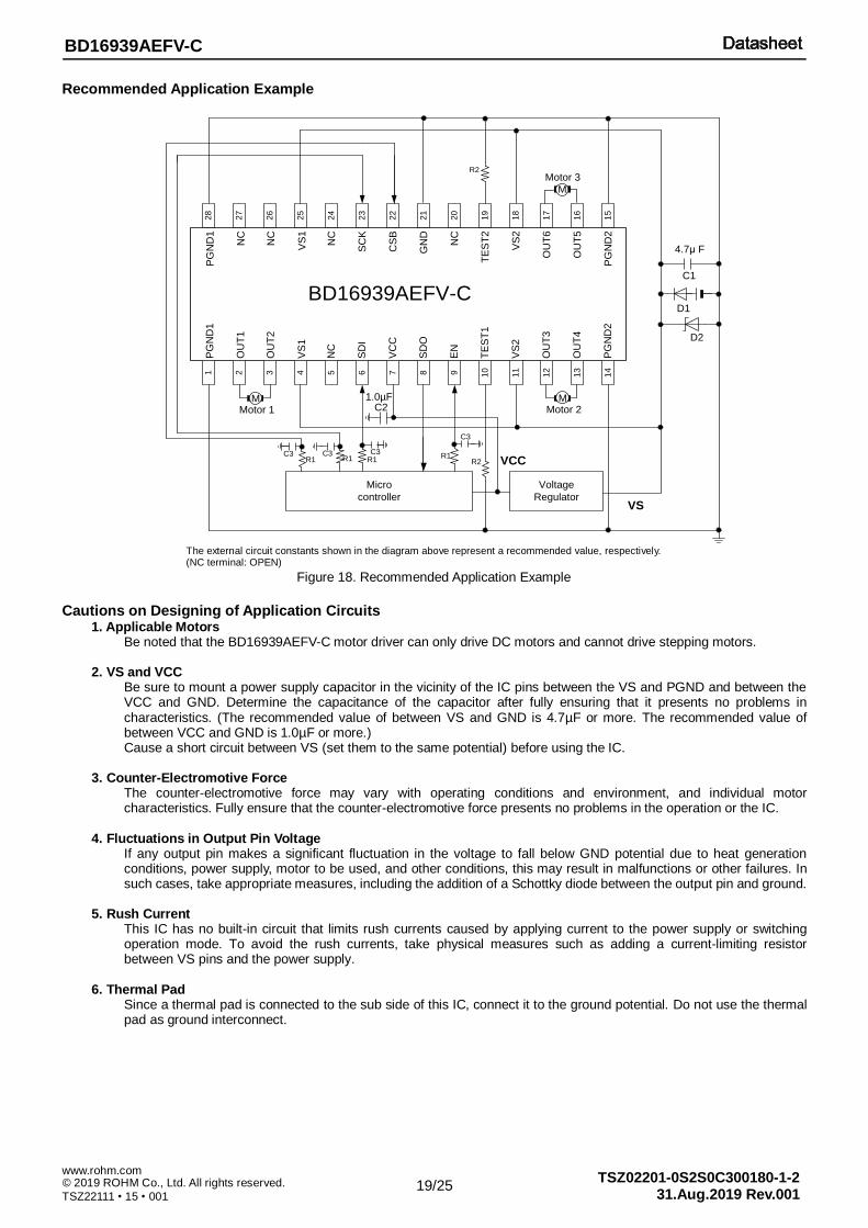
Recommended Application Example
PG
ND
11 2
OU
T1
OU
T2
3
VS
14
NC
VC
C
5
SD
O
7
EN
8
TE
ST
1
9 10
BD16939AEFV-C
4.7μ F
SD
I6
Micro
controller
Voltage
Regulator
1.0µF
11
12
13
14
28
27
26
25
24
22
21
20
19
23
18
17
16
15
VS
2
OU
T3
OU
T4
PG
ND
2
PG
ND
1
NC
NC
VS
1
NC
CS
B
GN
D
NC
TE
ST
2
SC
K
VS
2
OU
T6
OU
T5
PG
ND
2
Motor 1M
Motor 3
M
VS
VCC
C1
C2
C3R1
C3R1
C3R1
R1
C3
D1
D2
Motor 2M
R2
R2
The external circuit constants shown in the diagram above represent a recommended value, respectively. (NC terminal: OPEN)
Cautions on Designing of Application Circuits 1. Applicable Motors
Be noted that the BD16939AEFV-C motor driver can only drive DC motors and cannot drive stepping motors.
2. VS and VCC Be sure to mount a power supply capacitor in the vicinity of the IC pins between the VS and PGND and between the VCC and GND. Determine the capacitance of the capacitor after fully ensuring that it presents no problems in characteristics. (The recommended value of between VS and GND is 4.7µF or more. The recommended value of between VCC and GND is 1.0µF or more.) Cause a short circuit between VS (set them to the same potential) before using the IC.
3. Counter-Electromotive Force
The counter-electromotive force may vary with operating conditions and environment, and individual motor characteristics. Fully ensure that the counter-electromotive force presents no problems in the operation or the IC.
4. Fluctuations in Output Pin Voltage
If any output pin makes a significant fluctuation in the voltage to fall below GND potential due to heat generation conditions, power supply, motor to be used, and other conditions, this may result in malfunctions or other failures. In such cases, take appropriate measures, including the addition of a Schottky diode between the output pin and ground.
5. Rush Current
This IC has no built-in circuit that limits rush currents caused by applying current to the power supply or switching operation mode. To avoid the rush currents, take physical measures such as adding a current-limiting resistor between VS pins and the power supply.
6. Thermal Pad
Since a thermal pad is connected to the sub side of this IC, connect it to the ground potential. Do not use the thermal pad as ground interconnect.
Figure 18. Recommended Application Example
20/25
BD16939AEFV-C
TSZ02201-0S2S0C300180-1-2 © 2019 ROHM Co., Ltd. All rights reserved. 31.Aug.2019 Rev.001
www.rohm.com
TSZ22111 • 15 • 001
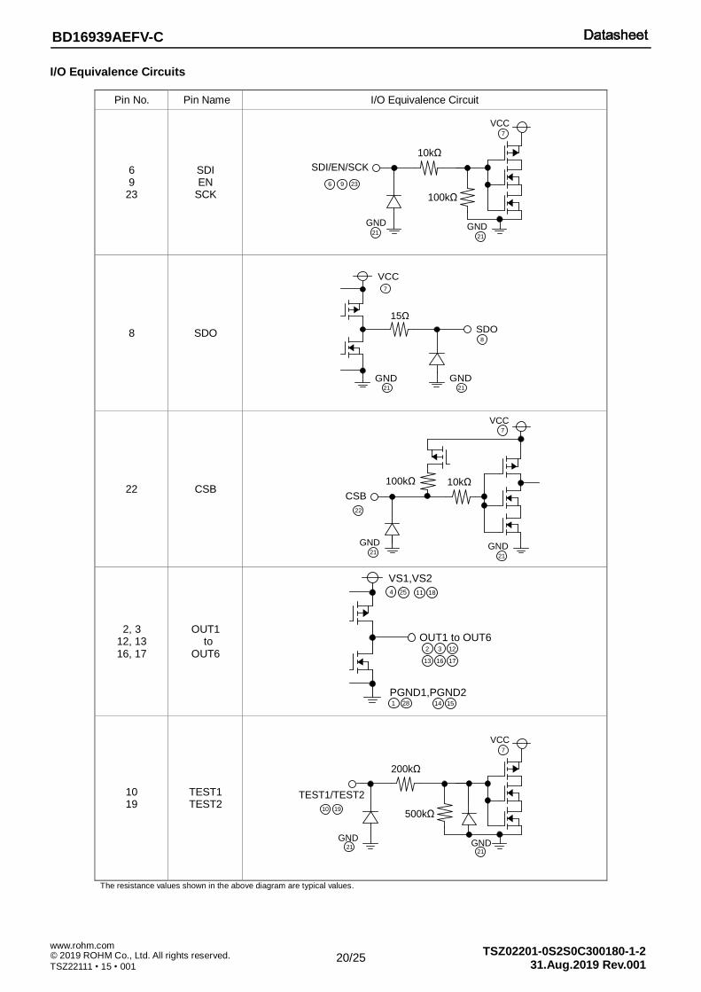
I/O Equivalence Circuits
Pin No. Pin Name I/O Equivalence Circuit
6 9
23
SDI EN
SCK
SDI/EN/SCK
10kΩ
100kΩ
6 9 23
GND21
GND21
VCC7
8 SDO
VCC
SDO
GND
7
8
21
GND21
15Ω
22 CSB CSB
10kΩ100kΩ
22
GND21
GND21
VCC7
2, 3 12, 13 16, 17
OUT1 to
OUT6
VS1,VS2
OUT1 to OUT6
PGND1,PGND2
4 25
2 3 12
1 28
11 18
13 16 17
14 15
10 19
TEST1 TEST2
TEST1/TEST2
200kΩ
500kΩ10 19
GND21
GND21
VCC7
The resistance values shown in the above diagram are typical values.
21/25
BD16939AEFV-C
TSZ02201-0S2S0C300180-1-2 © 2019 ROHM Co., Ltd. All rights reserved. 31.Aug.2019 Rev.001
www.rohm.com
TSZ22111 • 15 • 001
Operational Notes
1. Reverse Connection of Power Supply Connecting the power supply in reverse polarity can damage the IC. Take precautions against reverse polarity when connecting the power supply, such as mounting an external diode between the power supply and the IC’s power supply pins.
2. Power Supply Lines Design the PCB layout pattern to provide low impedance supply lines. Separate the ground and supply lines of the digital and analog blocks to prevent noise in the ground and supply lines of the digital block from affecting the analog block. Furthermore, connect a capacitor to ground at all power supply pins. Consider the effect of temperature and aging on the capacitance value when using electrolytic capacitors.
3. Ground Voltage Ensure that no pins are at a voltage below that of the ground pin at any time, even during transient condition. However, pins that drive inductive loads (e.g. motor driver outputs, DC-DC converter outputs) may inevitably go below ground due to back EMF or electromotive force. In such cases, the user should make sure that such voltages going below ground will not cause the IC and the system to malfunction by examining carefully all relevant factors and conditions such as motor characteristics, supply voltage, operating frequency and PCB wiring to name a few.
4. Ground Wiring Pattern
When using both small-signal and large-current ground traces, the two ground traces should be routed separately but connected to a single ground at the reference point of the application board to avoid fluctuations in the small-signal ground caused by large currents. Also ensure that the ground traces of external components do not cause variations on the ground voltage. The ground lines must be as short and thick as possible to reduce line impedance.
5. Recommended Operating Conditions
The function and operation of the IC are guaranteed within the range specified by the recommended operating conditions. The characteristic values are guaranteed only under the conditions of each item specified by the electrical characteristics.
6. Inrush Current When power is first supplied to the IC, it is possible that the internal logic may be unstable and inrush current may flow instantaneously due to the internal powering sequence and delays, especially if the IC has more than one power supply. Therefore, give special consideration to power coupling capacitance, power wiring, width of ground wiring, and routing of connections.
7. Testing on Application Boards When testing the IC on an application board, connecting a capacitor directly to a low-impedance output pin may subject the IC to stress. Always discharge capacitors completely after each process or step. The IC’s power supply should always be turned off completely before connecting or removing it from the test setup during the inspection process. To prevent damage from static discharge, ground the IC during assembly and use similar precautions during transport and storage.
8. Inter-pin Short and Mounting Errors Ensure that the direction and position are correct when mounting the IC on the PCB. Incorrect mounting may result in damaging the IC. Avoid nearby pins being shorted to each other especially to ground, power supply and output pin. Inter-pin shorts could be due to many reasons such as metal particles, water droplets (in very humid environment) and unintentional solder bridge deposited in between pins during assembly to name a few.
9. Unused Input Pins Input pins of an IC are often connected to the gate of a MOS transistor. The gate has extremely high impedance and extremely low capacitance. If left unconnected, the electric field from the outside can easily charge it. The small charge acquired in this way is enough to produce a significant effect on the conduction through the transistor and cause unexpected operation of the IC. So unless otherwise specified, unused input pins should be connected to the power supply or ground line.
22/25
BD16939AEFV-C
TSZ02201-0S2S0C300180-1-2 © 2019 ROHM Co., Ltd. All rights reserved. 31.Aug.2019 Rev.001
www.rohm.com
TSZ22111 • 15 • 001
Operational Notes – continued
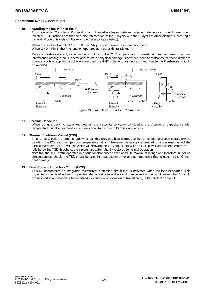
10. Regarding the Input Pin of the IC This monolithic IC contains P+ isolation and P substrate layers between adjacent elements in order to keep them isolated. P-N junctions are formed at the intersection of the P layers with the N layers of other elements, creating a parasitic diode or transistor. For example (refer to figure below):
When GND > Pin A and GND > Pin B, the P-N junction operates as a parasitic diode. When GND > Pin B, the P-N junction operates as a parasitic transistor.
Parasitic diodes inevitably occur in the structure of the IC. The operation of parasitic diodes can result in mutual interference among circuits, operational faults, or physical damage. Therefore, conditions that cause these diodes to operate, such as applying a voltage lower than the GND voltage to an input pin (and thus to the P substrate) should be avoided.
Figure 19. Example of monolithic IC structure
11. Ceramic Capacitor
When using a ceramic capacitor, determine a capacitance value considering the change of capacitance with temperature and the decrease in nominal capacitance due to DC bias and others.
12. Thermal Shutdown Circuit (TSD) This IC has a built-in thermal shutdown circuit that prevents heat damage to the IC. Normal operation should always be within the IC’s maximum junction temperature rating. If however the rating is exceeded for a continued period, the junction temperature (Tj) will rise which will activate the TSD circuit that will turn OFF power output pins. When the Tj falls below the TSD threshold, the circuits are automatically restored to normal operation. Note that the TSD circuit operates in a situation that exceeds the absolute maximum ratings and therefore, under no circumstances, should the TSD circuit be used in a set design or for any purpose other than protecting the IC from heat damage.
13. Over Current Protection Circuit (OCP)
This IC incorporates an integrated overcurrent protection circuit that is activated when the load is shorted. This protection circuit is effective in preventing damage due to sudden and unexpected incidents. However, the IC should not be used in applications characterized by continuous operation or transitioning of the protection circuit.
N NP
+ P
N NP
+
P Substrate
GND
NP
+
N NP
+N P
P Substrate
GND GND
Parasitic
Elements
Pin A
Pin A
Pin B Pin B
B C
E
Parasitic
Elements
GNDParasitic
Elements
CB
E
Transistor (NPN)Resistor
N Region
close-by
Parasitic
Elements
23/25
BD16939AEFV-C
TSZ02201-0S2S0C300180-1-2 © 2019 ROHM Co., Ltd. All rights reserved. 31.Aug.2019 Rev.001
www.rohm.com
TSZ22111 • 15 • 001
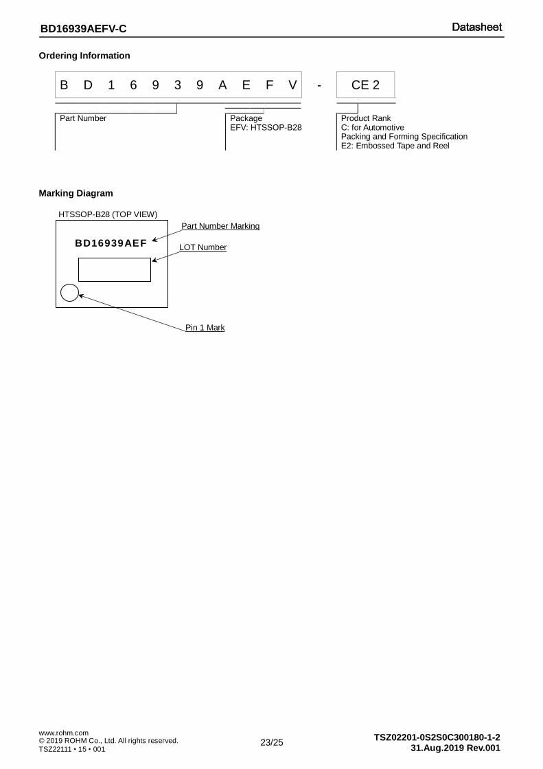
Ordering Information
B D 1 6 9 3 9 A E F V - CE 2
Part Number
Package EFV: HTSSOP-B28
Product Rank C: for Automotive Packing and Forming Specification E2: Embossed Tape and Reel
Marking Diagram
HTSSOP-B28 (TOP VIEW)
Part Number Marking
LOT Number
Pin 1 Mark
BD16939AEF
24/25
TSZ02201-0S2S0C300180-1-2 © 2019 ROHM Co., Ltd. All rights reserved. 31.Aug.2019 Rev.001
BD16939AEFV-C
www.rohm.com
TSZ22111 • 15 • 001
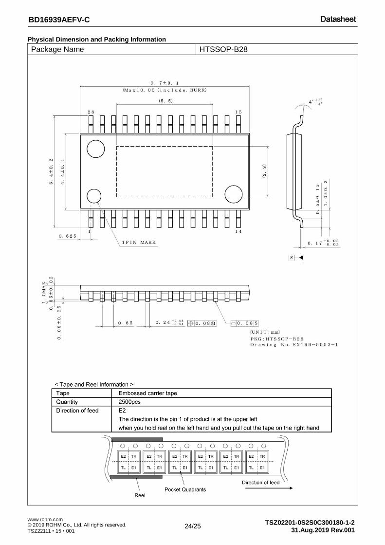
Physical Dimension and Packing Information
Package Name HTSSOP-B28
25/25
TSZ02201-0S2S0C300180-1-2 © 2019 ROHM Co., Ltd. All rights reserved. 31.Aug.2019 Rev.001
BD16939AEFV-C
www.rohm.com
TSZ22111 • 15 • 001
Revision History
Date Revision Changes
31.Aug.2019 001 New Release
Notice-PAA-E Rev.004
© 2015 ROHM Co., Ltd. All rights reserved.
Notice
Precaution on using ROHM Products 1. If you intend to use our Products in devices requiring extremely high reliability (such as medical equipment (Note 1),
aircraft/spacecraft, nuclear power controllers, etc.) and whose malfunction or failure may cause loss of human life,bodily injury or serious damage to property (“Specific Applications”), please consult with the ROHM salesrepresentative in advance. Unless otherwise agreed in writing by ROHM in advance, ROHM shall not be in any wayresponsible or liable for any damages, expenses or losses incurred by you or third parties arising from the use of anyROHM’s Products for Specific Applications.
(Note1) Medical Equipment Classification of the Specific Applications
JAPAN USA EU CHINA
CLASSⅢ CLASSⅢ
CLASSⅡb CLASSⅢ
CLASSⅣ CLASSⅢ
2. ROHM designs and manufactures its Products subject to strict quality control system. However, semiconductorproducts can fail or malfunction at a certain rate. Please be sure to implement, at your own responsibilities, adequatesafety measures including but not limited to fail-safe design against the physical injury, damage to any property, whicha failure or malfunction of our Products may cause. The following are examples of safety measures:
[a] Installation of protection circuits or other protective devices to improve system safety [b] Installation of redundant circuits to reduce the impact of single or multiple circuit failure
3. Our Products are not designed under any special or extraordinary environments or conditions, as exemplified below.Accordingly, ROHM shall not be in any way responsible or liable for any damages, expenses or losses arising from theuse of any ROHM’s Products under any special or extraordinary environments or conditions. If you intend to use ourProducts under any special or extraordinary environments or conditions (as exemplified below), your independentverification and confirmation of product performance, reliability, etc, prior to use, must be necessary:
[a] Use of our Products in any types of liquid, including water, oils, chemicals, and organic solvents [b] Use of our Products outdoors or in places where the Products are exposed to direct sunlight or dust [c] Use of our Products in places where the Products are exposed to sea wind or corrosive gases, including Cl2,
H2S, NH3, SO2, and NO2
[d] Use of our Products in places where the Products are exposed to static electricity or electromagnetic waves [e] Use of our Products in proximity to heat-producing components, plastic cords, or other flammable items [f] Sealing or coating our Products with resin or other coating materials [g] Use of our Products without cleaning residue of flux (Exclude cases where no-clean type fluxes is used.
However, recommend sufficiently about the residue.); or Washing our Products by using water or water-soluble cleaning agents for cleaning residue after soldering
[h] Use of the Products in places subject to dew condensation
4. The Products are not subject to radiation-proof design.
5. Please verify and confirm characteristics of the final or mounted products in using the Products.
6. In particular, if a transient load (a large amount of load applied in a short period of time, such as pulse, is applied, confirmation of performance characteristics after on-board mounting is strongly recommended. Avoid applying power exceeding normal rated power; exceeding the power rating under steady-state loading condition may negatively affect product performance and reliability.
7. De-rate Power Dissipation depending on ambient temperature. When used in sealed area, confirm that it is the use inthe range that does not exceed the maximum junction temperature.
8. Confirm that operation temperature is within the specified range described in the product specification.
9. ROHM shall not be in any way responsible or liable for failure induced under deviant condition from what is defined inthis document.
Precaution for Mounting / Circuit board design 1. When a highly active halogenous (chlorine, bromine, etc.) flux is used, the residue of flux may negatively affect product
performance and reliability.
2. In principle, the reflow soldering method must be used on a surface-mount products, the flow soldering method mustbe used on a through hole mount products. If the flow soldering method is preferred on a surface-mount products,please consult with the ROHM representative in advance.
For details, please refer to ROHM Mounting specification

Notice-PAA-E Rev.004
© 2015 ROHM Co., Ltd. All rights reserved.
Precautions Regarding Application Examples and External Circuits 1. If change is made to the constant of an external circuit, please allow a sufficient margin considering variations of the
characteristics of the Products and external components, including transient characteristics, as well as static characteristics.
2. You agree that application notes, reference designs, and associated data and information contained in this document
are presented only as guidance for Products use. Therefore, in case you use such information, you are solely responsible for it and you must exercise your own independent verification and judgment in the use of such information contained in this document. ROHM shall not be in any way responsible or liable for any damages, expenses or losses incurred by you or third parties arising from the use of such information.
Precaution for Electrostatic This Product is electrostatic sensitive product, which may be damaged due to electrostatic discharge. Please take proper caution in your manufacturing process and storage so that voltage exceeding the Products maximum rating will not be applied to Products. Please take special care under dry condition (e.g. Grounding of human body / equipment / solder iron, isolation from charged objects, setting of Ionizer, friction prevention and temperature / humidity control).
Precaution for Storage / Transportation 1. Product performance and soldered connections may deteriorate if the Products are stored in the places where:
[a] the Products are exposed to sea winds or corrosive gases, including Cl2, H2S, NH3, SO2, and NO2 [b] the temperature or humidity exceeds those recommended by ROHM [c] the Products are exposed to direct sunshine or condensation [d] the Products are exposed to high Electrostatic
2. Even under ROHM recommended storage condition, solderability of products out of recommended storage time period may be degraded. It is strongly recommended to confirm solderability before using Products of which storage time is exceeding the recommended storage time period.
3. Store / transport cartons in the correct direction, which is indicated on a carton with a symbol. Otherwise bent leads
may occur due to excessive stress applied when dropping of a carton. 4. Use Products within the specified time after opening a humidity barrier bag. Baking is required before using Products of
which storage time is exceeding the recommended storage time period.
Precaution for Product Label A two-dimensional barcode printed on ROHM Products label is for ROHM’s internal use only.
Precaution for Disposition When disposing Products please dispose them properly using an authorized industry waste company.
Precaution for Foreign Exchange and Foreign Trade act Since concerned goods might be fallen under listed items of export control prescribed by Foreign exchange and Foreign trade act, please consult with ROHM in case of export.
Precaution Regarding Intellectual Property Rights 1. All information and data including but not limited to application example contained in this document is for reference
only. ROHM does not warrant that foregoing information or data will not infringe any intellectual property rights or any other rights of any third party regarding such information or data.
2. ROHM shall not have any obligations where the claims, actions or demands arising from the combination of the Products with other articles such as components, circuits, systems or external equipment (including software).
3. No license, expressly or implied, is granted hereby under any intellectual property rights or other rights of ROHM or any third parties with respect to the Products or the information contained in this document. Provided, however, that ROHM will not assert its intellectual property rights or other rights against you or your customers to the extent necessary to manufacture or sell products containing the Products, subject to the terms and conditions herein.
Other Precaution 1. This document may not be reprinted or reproduced, in whole or in part, without prior written consent of ROHM.
2. The Products may not be disassembled, converted, modified, reproduced or otherwise changed without prior written consent of ROHM.
3. In no event shall you use in any way whatsoever the Products and the related technical information contained in the Products or this document for any military purposes, including but not limited to, the development of mass-destruction weapons.
4. The proper names of companies or products described in this document are trademarks or registered trademarks of ROHM, its affiliated companies or third parties.
DatasheetDatasheet
Notice – WE Rev.001© 2015 ROHM Co., Ltd. All rights reserved.
General Precaution 1. Before you use our Products, you are requested to carefully read this document and fully understand its contents.
ROHM shall not be in any way responsible or liable for failure, malfunction or accident arising from the use of any ROHM’s Products against warning, caution or note contained in this document.
2. All information contained in this document is current as of the issuing date and subject to change without any prior
notice. Before purchasing or using ROHM’s Products, please confirm the latest information with a ROHM sales representative.
3. The information contained in this document is provided on an “as is” basis and ROHM does not warrant that all
information contained in this document is accurate and/or error-free. ROHM shall not be in any way responsible or liable for any damages, expenses or losses incurred by you or third parties resulting from inaccuracy or errors of or concerning such information.