Table of Contents - Mouser
488
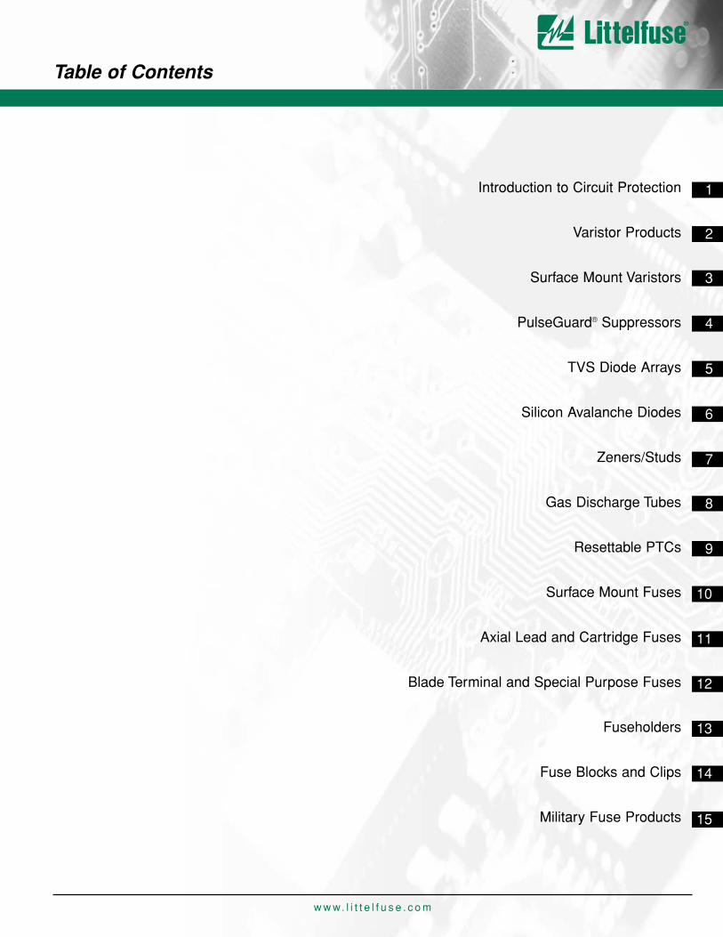
www.littelfuse.com Table of Contents 1 2 3 4 5 6 7 8 9 10 11 12 Introduction to Circuit Protection Varistor Products Surface Mount Varistors PulseGuard ® Suppressors TVS Diode Arrays Silicon Avalanche Diodes Zeners/Studs Gas Discharge Tubes Resettable PTCs Surface Mount Fuses Axial Lead and Cartridge Fuses Blade Terminal and Special Purpose Fuses Fuseholders Fuse Blocks and Clips Military Fuse Products 13 14 15
-
Upload
khangminh22 -
Category
Documents
-
view
1 -
download
0
Transcript of Table of Contents - Mouser
w w w. l i t t e l f u s e . c o m
Table of Contents
1
2
3
4
5
6
7
8
9
10
11
12
Introduction to Circuit Protection
Varistor Products
Surface Mount Varistors
PulseGuard® Suppressors
TVS Diode Arrays
Silicon Avalanche Diodes
Zeners/Studs
Gas Discharge Tubes
Resettable PTCs
Surface Mount Fuses
Axial Lead and Cartridge Fuses
Blade Terminal and Special Purpose Fuses
Fuseholders
Fuse Blocks and Clips
Military Fuse Products
13
14
15

Table of Contents
w w w. l i t t e l f u s e . c o m
INTRODUCTION TO CIRCUIT PROTECTION Fuseology . . . . . . . . . . . . . . . . . . . . . . . . . . . . . . . . . . . . . . . . . . . . . . . . . . . . . . . . . . . . . . . . . . .2-8PTC Facts . . . . . . . . . . . . . . . . . . . . . . . . . . . . . . . . . . . . . . . . . . . . . . . . . . . . . . . . . . . . . . . . . . . .9Overcurrent Selection Worksheet . . . . . . . . . . . . . . . . . . . . . . . . . . . . . . . . . . . . . . . . . . . . . . . .10-11Overvoltage Suppression Facts . . . . . . . . . . . . . . . . . . . . . . . . . . . . . . . . . . . . . . . . . . . . . . . . .12-23Overvoltage Selection Guide . . . . . . . . . . . . . . . . . . . . . . . . . . . . . . . . . . . . . . . . . . . . . . . . . . .24-25ESD Suppressor Selection Guide . . . . . . . . . . . . . . . . . . . . . . . . . . . . . . . . . . . . . . . . . . . . . . . .26-27
VARISTOR PRODUCTS Varistor Products Overview . . . . . . . . . . . . . . . . . . . . . . . . . . . . . . . . . . . . . . . . . . . . . . . . . . . .29-30TMOV® and iTMOV® High Surge Current Radial Lead,
Thermally Protected Metal Oxide Varistor . . . . . . . . . . . . . . . . . . . . . . . . . . . . . . . . . . . . . . .31-39UltraMOV™ High Surge Current Radial Lead Metal Oxide Varistors . . . . . . . . . . . . . . . . . . . . . . .40-51C-III Series High Energy Radial Lead Varistors . . . . . . . . . . . . . . . . . . . . . . . . . . . . . . . . . . . . . .52-59LA Series Radial Lead Metal-Oxide Varistors for Line Voltage Operation . . . . . . . . . . . . . . . . . . .60-70ZA Series Radial Lead Metal-Oxide Varistors for Low to Medium Voltage Operation . . . . . . . . . .71-84BA/BB Series Industrial High Energy Metal-Oxide Varistors . . . . . . . . . . . . . . . . . . . . . . . . . . . .85-89DA/DB Series Industrial High Energy Metal-Oxide Varistors . . . . . . . . . . . . . . . . . . . . . . . . . . . .90-93HA Series Industrial High Energy Metal-Oxide Varistors . . . . . . . . . . . . . . . . . . . . . . . . . . . . . . .94-97HB34, HF34 and HG34 Series Industrial High Energy Metal-Oxide Varistors . . . . . . . . . . . . . .98-104DHB34 Series Industrial High Energy Metal-Oxide Varistors . . . . . . . . . . . . . . . . . . . . . . . . . .105-108CA Series Industrial High Energy Metal-Oxide Disc Varistors . . . . . . . . . . . . . . . . . . . . . . . . .109-116NA Series Industrial High Energy Metal-Oxide Square Disc Varistors . . . . . . . . . . . . . . . . . . .117-121MA Series Axial Lead Metal-Oxide Varistors . . . . . . . . . . . . . . . . . . . . . . . . . . . . . . . . . . . . . .122-126PA Series Base Mount Metal-Oxide Varistors . . . . . . . . . . . . . . . . . . . . . . . . . . . . . . . . . . . . .127-131RA Series Low Profile Metal-Oxide Varistors . . . . . . . . . . . . . . . . . . . . . . . . . . . . . . . . . . . . .132-139High Reliability Varistors . . . . . . . . . . . . . . . . . . . . . . . . . . . . . . . . . . . . . . . . . . . . . . . . . . . . .140-149
SURFACE MOUNT VARISTORS Surface Mount Varistors Overview . . . . . . . . . . . . . . . . . . . . . . . . . . . . . . . . . . . . . . . . . . . . . . . . .151MHS Series Multilayer High-Speed Surface Mount ESD Voltage Suppressor . . . . . . . . . . . . .152-155MLE Series Multilayer Surface Mount ESD Suppressor/Filter . . . . . . . . . . . . . . . . . . . . . . . . .156-162ML Series Multilayer Surface Mount Transient Voltage Surge Suppressor . . . . . . . . . . . . . . . .163-173MLN SurgeArray™ Four Line Multilayer Transient Voltage Suppressor . . . . . . . . . . . . . . . . . . .174-180AUML Series Multilayer Surface Mount Automotive Transient Surge Suppressor . . . . . . . . . . .181-189CH Series Monolithic Chip Transient Voltage Suppressor . . . . . . . . . . . . . . . . . . . . . . . . . . . .190-194
PULSEGUARD® SUPPRESSORS PGB Series 0603, Single Line ESD Suppressor . . . . . . . . . . . . . . . . . . . . . . . . . . . . . . . . . . .197-198PGB1 Series Lead-Free 0603, Single Line ESD Suppressor . . . . . . . . . . . . . . . . . . . . . . . . . .199-200PGB Series SOT23, Two Line ESD Suppressor . . . . . . . . . . . . . . . . . . . . . . . . . . . . . . . . . . .201-202PGB Series 0805, Four Line ESD Suppressor . . . . . . . . . . . . . . . . . . . . . . . . . . . . . . . . . . . .203-204PGD Series Connector Array, ESD Suppressor. . . . . . . . . . . . . . . . . . . . . . . . . . . . . . . . . . . . . . .205
TVS DIODE ARRAYS SPUSB1 Series, TVS Protection with Filter and Termination . . . . . . . . . . . . . . . . . . . . . . . . . .208-210SP05x Series Avalanche Diode Arrays . . . . . . . . . . . . . . . . . . . . . . . . . . . . . . . . . . . . . . . . . .211-218SP0501 Series 0402 Chip Scale Package Avalanche Diodes . . . . . . . . . . . . . . . . . . . . . . . . .219-221SP05x Series Unipolar Chip Scale Package Avalanche Diode Arrays . . . . . . . . . . . . . . . . . . .222-227SP05x Series Bipolar Chip Scale Package Avalanche Diode Arrays . . . . . . . . . . . . . . . . . . . .228-233SP05x Series Low Voltage Rail Clamp Arrays . . . . . . . . . . . . . . . . . . . . . . . . . . . . . . . . . . . . .234-237SP720 Series High Voltage Rail Clamp SCR/Diode Arrays . . . . . . . . . . . . . . . . . . . . . . . . . . .238-243SP721 Series High Voltage Rail Clamp SCR/Diode Arrays . . . . . . . . . . . . . . . . . . . . . . . . . . .244-249SP723 Series High Voltage Rail Clamp SCR/Diode Arrays . . . . . . . . . . . . . . . . . . . . . . . . . . .250-255SP724 Series High Voltage Rail Clamp SCR/Diode Arrays . . . . . . . . . . . . . . . . . . . . . . . . . . .256-261
SILICON AVALANCHE DIODES AK6 Series . . . . . . . . . . . . . . . . . . . . . . . . . . . . . . . . . . . . . . . . . . . . . . . . . . . . . . . . . . . . . . . . . .264AK10 Series . . . . . . . . . . . . . . . . . . . . . . . . . . . . . . . . . . . . . . . . . . . . . . . . . . . . . . . . . . . . . .265-266SMBJ Series . . . . . . . . . . . . . . . . . . . . . . . . . . . . . . . . . . . . . . . . . . . . . . . . . . . . . . . . . . . . .267-271P6SMBJ Series . . . . . . . . . . . . . . . . . . . . . . . . . . . . . . . . . . . . . . . . . . . . . . . . . . . . . . . . . . .272-2761KSMBJ Series . . . . . . . . . . . . . . . . . . . . . . . . . . . . . . . . . . . . . . . . . . . . . . . . . . . . . . . . . . .277-279SA Series . . . . . . . . . . . . . . . . . . . . . . . . . . . . . . . . . . . . . . . . . . . . . . . . . . . . . . . . . . . . . . .280-284P6KE Series . . . . . . . . . . . . . . . . . . . . . . . . . . . . . . . . . . . . . . . . . . . . . . . . . . . . . . . . . . . . .285-2891.5KE Series . . . . . . . . . . . . . . . . . . . . . . . . . . . . . . . . . . . . . . . . . . . . . . . . . . . . . . . . . . . . .290-2945KP Series . . . . . . . . . . . . . . . . . . . . . . . . . . . . . . . . . . . . . . . . . . . . . . . . . . . . . . . . . . . . . . .295-29915KP Series . . . . . . . . . . . . . . . . . . . . . . . . . . . . . . . . . . . . . . . . . . . . . . . . . . . . . . . . . . . . . .300-303Foldback™ Series . . . . . . . . . . . . . . . . . . . . . . . . . . . . . . . . . . . . . . . . . . . . . . . . . . . . . . . . . . . . .304SLD™ Series . . . . . . . . . . . . . . . . . . . . . . . . . . . . . . . . . . . . . . . . . . . . . . . . . . . . . . . . . . . . . . . .30515KP Cells . . . . . . . . . . . . . . . . . . . . . . . . . . . . . . . . . . . . . . . . . . . . . . . . . . . . . . . . . . . . . . . . . .306ICTE/MPTE Series . . . . . . . . . . . . . . . . . . . . . . . . . . . . . . . . . . . . . . . . . . . . . . . . . . . . . . . . .307-308LCE Series . . . . . . . . . . . . . . . . . . . . . . . . . . . . . . . . . . . . . . . . . . . . . . . . . . . . . . . . . . . . . .309-3121N56 Series . . . . . . . . . . . . . . . . . . . . . . . . . . . . . . . . . . . . . . . . . . . . . . . . . . . . . . . . . . . . . .313-3161N60 Series . . . . . . . . . . . . . . . . . . . . . . . . . . . . . . . . . . . . . . . . . . . . . . . . . . . . . . . . . . . . . .317-320
PAGE
Pb
Pb
Pb
Pb
Pb
Pb
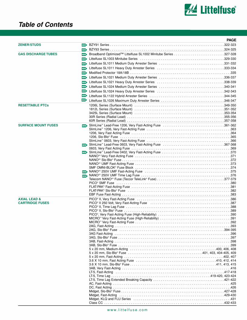
ZENER/STUDS BZY91 Series . . . . . . . . . . . . . . . . . . . . . . . . . . . . . . . . . . . . . . . . . . . . . . . . . . . . . . . . . . . . .322-323BZY93 Series . . . . . . . . . . . . . . . . . . . . . . . . . . . . . . . . . . . . . . . . . . . . . . . . . . . . . . . . . . . . .324-325
GAS DISCHARGE TUBES Broadband Optimized™ Littelfuse SL1002 Minitube Series . . . . . . . . . . . . . . . . . . . . . . . . . . .327-328Littelfuse SL1003 Minitube Series . . . . . . . . . . . . . . . . . . . . . . . . . . . . . . . . . . . . . . . . . . . . .329-330Littelfuse SL1011 Medium Duty Arrester Series . . . . . . . . . . . . . . . . . . . . . . . . . . . . . . . . . . .331-332Littelfuse SL1011 Heavy Duty Arrester Series . . . . . . . . . . . . . . . . . . . . . . . . . . . . . . . . . . . .333-334Modified Protector 18A/18B . . . . . . . . . . . . . . . . . . . . . . . . . . . . . . . . . . . . . . . . . . . . . . . . . . . . . .335Littelfuse SL1021 Medium Duty Arrester Series . . . . . . . . . . . . . . . . . . . . . . . . . . . . . . . . . . .336-337Littelfuse SL1021 Heavy Duty Arrester Series . . . . . . . . . . . . . . . . . . . . . . . . . . . . . . . . . . . .338-339Littelfuse SL1024 Medium Duty Arrester Series . . . . . . . . . . . . . . . . . . . . . . . . . . . . . . . . . . .340-341Littelfuse SL1024 Heavy Duty Arrester Series . . . . . . . . . . . . . . . . . . . . . . . . . . . . . . . . . . . .342-343Littelfuse SL1122 Hybrid Arrester Series . . . . . . . . . . . . . . . . . . . . . . . . . . . . . . . . . . . . . . . .344-345Littelfuse SL1026 Maximum Duty Arrester Series . . . . . . . . . . . . . . . . . . . . . . . . . . . . . . . . . .346-347
RESETTABLE PTCs 1206L Series (Surface Mount) . . . . . . . . . . . . . . . . . . . . . . . . . . . . . . . . . . . . . . . . . . . . . . . .349-3501812L Series (Surface Mount) . . . . . . . . . . . . . . . . . . . . . . . . . . . . . . . . . . . . . . . . . . . . . . . .351-3523425L Series (Surface Mount) . . . . . . . . . . . . . . . . . . . . . . . . . . . . . . . . . . . . . . . . . . . . . . . .353-35430R Series (Radial Lead) . . . . . . . . . . . . . . . . . . . . . . . . . . . . . . . . . . . . . . . . . . . . . . . . . . . .355-35660R Series (Radial Lead) . . . . . . . . . . . . . . . . . . . . . . . . . . . . . . . . . . . . . . . . . . . . . . . . . . . .357-358
SURFACE MOUNT FUSES SlimLine™ Lead-Free 1206, Very Fast-Acting Fuse . . . . . . . . . . . . . . . . . . . . . . . . . . . . . . . . .361-362SlimLine™ 1206, Very Fast-Acting Fuse . . . . . . . . . . . . . . . . . . . . . . . . . . . . . . . . . . . . . . . . . . . . .3631206, Very Fast Acting Fuse . . . . . . . . . . . . . . . . . . . . . . . . . . . . . . . . . . . . . . . . . . . . . . . . . . . . .3641206, Slo-Blo® Fuse . . . . . . . . . . . . . . . . . . . . . . . . . . . . . . . . . . . . . . . . . . . . . . . . . . . . . . . . . . .365SlimLine™ 0603, Very Fast-Acting Fuse . . . . . . . . . . . . . . . . . . . . . . . . . . . . . . . . . . . . . . . . . . . . .366SlimLine™ Lead-Free 0603, Very Fast-Acting Fuse . . . . . . . . . . . . . . . . . . . . . . . . . . . . . . . . .367-3680603, Very Fast Acting Fuse . . . . . . . . . . . . . . . . . . . . . . . . . . . . . . . . . . . . . . . . . . . . . . . . . . . . .369SlimLine™ Lead-Free 0402, Very Fast-Acting Fuse . . . . . . . . . . . . . . . . . . . . . . . . . . . . . . . . . . . . .370NANO2® Very Fast-Acting Fuse . . . . . . . . . . . . . . . . . . . . . . . . . . . . . . . . . . . . . . . . . . . . . . . . . . .371NANO2® Slo-Blo® Fuse . . . . . . . . . . . . . . . . . . . . . . . . . . . . . . . . . . . . . . . . . . . . . . . . . . . . . . . . . .372NANO2® UMF Fast-Acting Fuse . . . . . . . . . . . . . . . . . . . . . . . . . . . . . . . . . . . . . . . . . . . . . . . . . . .373SMF OMNI-BLOK® Fuse Block . . . . . . . . . . . . . . . . . . . . . . . . . . . . . . . . . . . . . . . . . . . . . . . . . . .374NANO2® 250V UMF Fast-Acting Fuse . . . . . . . . . . . . . . . . . . . . . . . . . . . . . . . . . . . . . . . . . . . . . .375NANO2® 250V UMF Time Lag Fuse . . . . . . . . . . . . . . . . . . . . . . . . . . . . . . . . . . . . . . . . . . . . . . . .376Telecom NANO2® Fuse (Teccor TeleLink® Fuse) . . . . . . . . . . . . . . . . . . . . . . . . . . . . . . . . . . . .377-379PICO® SMF Fuse . . . . . . . . . . . . . . . . . . . . . . . . . . . . . . . . . . . . . . . . . . . . . . . . . . . . . . . . . . . . .380FLAT-PAK® Fast-Acting Fuse . . . . . . . . . . . . . . . . . . . . . . . . . . . . . . . . . . . . . . . . . . . . . . . . . . . . .381FLAT-PAK® Slo-Blo® Fuse . . . . . . . . . . . . . . . . . . . . . . . . . . . . . . . . . . . . . . . . . . . . . . . . . . . . . . .382EBF Fuse Fast-Acting . . . . . . . . . . . . . . . . . . . . . . . . . . . . . . . . . . . . . . . . . . . . . . . . . . . . . . . . . .383
AXIAL LEAD & PICO® II, Very Fast-Acting Fuse . . . . . . . . . . . . . . . . . . . . . . . . . . . . . . . . . . . . . . . . . . . . . . . . . .386CARTRIDGE FUSES PICO® II 250 Volt, Very Fast-Acting Fuse . . . . . . . . . . . . . . . . . . . . . . . . . . . . . . . . . . . . . . . . . . .387
PICO® II, Time Lag Fuse . . . . . . . . . . . . . . . . . . . . . . . . . . . . . . . . . . . . . . . . . . . . . . . . . . . . . . . .388PICO® II, Slo-Blo® Fuse . . . . . . . . . . . . . . . . . . . . . . . . . . . . . . . . . . . . . . . . . . . . . . . . . . . . . . . . .389PICO®, Very Fast-Acting Fuse (High-Reliability) . . . . . . . . . . . . . . . . . . . . . . . . . . . . . . . . . . . . . . .390MICRO™ Very Fast-Acting Fuse (High-Reliability) . . . . . . . . . . . . . . . . . . . . . . . . . . . . . . . . . . . . . .391MICRO™ Very Fast-Acting Fuse . . . . . . . . . . . . . . . . . . . . . . . . . . . . . . . . . . . . . . . . . . . . . . . . . . .3922AG, Fast-Acting . . . . . . . . . . . . . . . . . . . . . . . . . . . . . . . . . . . . . . . . . . . . . . . . . . . . . . . . . . . . . .3932AG, Slo-Blo® Fuse . . . . . . . . . . . . . . . . . . . . . . . . . . . . . . . . . . . . . . . . . . . . . . . . . . . . . . . .394-3953AG Fast-Acting . . . . . . . . . . . . . . . . . . . . . . . . . . . . . . . . . . . . . . . . . . . . . . . . . . . . . . . . . . . . . .3963AG, Slo-Blo® Fuse . . . . . . . . . . . . . . . . . . . . . . . . . . . . . . . . . . . . . . . . . . . . . . . . . . . . . . . . . . . .3973AB, Fast-Acting . . . . . . . . . . . . . . . . . . . . . . . . . . . . . . . . . . . . . . . . . . . . . . . . . . . . . . . . . . . . . .3983AB, Slo-Blo® Fuse . . . . . . . . . . . . . . . . . . . . . . . . . . . . . . . . . . . . . . . . . . . . . . . . . . . . . . . . . . . .3995 x 20 mm, Medium-Acting . . . . . . . . . . . . . . . . . . . . . . . . . . . . . . . . . . . . . . . . . . . . . .400, 406, 4085 x 20 mm, Slo-Blo® Fuse . . . . . . . . . . . . . . . . . . . . . . . . . . . . . . . . . . . . . . . .401, 403, 404-405, 4095 x 20 mm, Fast-Acting . . . . . . . . . . . . . . . . . . . . . . . . . . . . . . . . . . . . . . . . . . . . . . . . . . . . .402, 4073.6 X 10 mm, Fast Acting Fuse . . . . . . . . . . . . . . . . . . . . . . . . . . . . . . . . . . . . . . . . . . .410, 412, 4143.6 X 10 mm, Slo-Blo® Fuse . . . . . . . . . . . . . . . . . . . . . . . . . . . . . . . . . . . . . . . . . . . . . .411, 413, 4153AB, Very Fast-Acting . . . . . . . . . . . . . . . . . . . . . . . . . . . . . . . . . . . . . . . . . . . . . . . . . . . . . . . . . .416LT-5, Fast-Acting . . . . . . . . . . . . . . . . . . . . . . . . . . . . . . . . . . . . . . . . . . . . . . . . . . . . . . . . . .417-418LT-5, Time Lag . . . . . . . . . . . . . . . . . . . . . . . . . . . . . . . . . . . . . . . . . . . . . . . . . . . . .419-420, 423-424LT-5, Time Lag Extended Breaking Capacity . . . . . . . . . . . . . . . . . . . . . . . . . . . . . . . . . . . . . .421-422AC, Fast-Acting . . . . . . . . . . . . . . . . . . . . . . . . . . . . . . . . . . . . . . . . . . . . . . . . . . . . . . . . . . . . . . .425DC, Fast Acting . . . . . . . . . . . . . . . . . . . . . . . . . . . . . . . . . . . . . . . . . . . . . . . . . . . . . . . . . . . . . . .426Midget, Slo-Blo® Fuse . . . . . . . . . . . . . . . . . . . . . . . . . . . . . . . . . . . . . . . . . . . . . . . . . . . . . . .427-428Midget, Fast-Acting . . . . . . . . . . . . . . . . . . . . . . . . . . . . . . . . . . . . . . . . . . . . . . . . . . . . . . . .429-430Midget, KLQ and FLU Series . . . . . . . . . . . . . . . . . . . . . . . . . . . . . . . . . . . . . . . . . . . . . . . . . . . .431Class CC . . . . . . . . . . . . . . . . . . . . . . . . . . . . . . . . . . . . . . . . . . . . . . . . . . . . . . . . . . . . . . . .432-433
Table of Contents
w w w. l i t t e l f u s e . c o m
PAGE
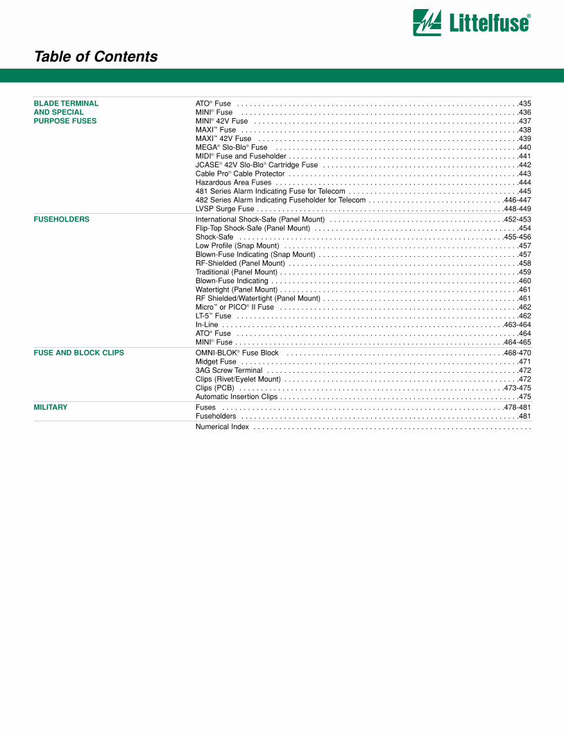
BLADE TERMINAL ATO® Fuse . . . . . . . . . . . . . . . . . . . . . . . . . . . . . . . . . . . . . . . . . . . . . . . . . . . . . . . . . . . . . . . . . .435AND SPECIAL MINI® Fuse . . . . . . . . . . . . . . . . . . . . . . . . . . . . . . . . . . . . . . . . . . . . . . . . . . . . . . . . . . . . . . . . .436PURPOSE FUSES MINI® 42V Fuse . . . . . . . . . . . . . . . . . . . . . . . . . . . . . . . . . . . . . . . . . . . . . . . . . . . . . . . . . . . . . .437
MAXI™ Fuse . . . . . . . . . . . . . . . . . . . . . . . . . . . . . . . . . . . . . . . . . . . . . . . . . . . . . . . . . . . . . . . . .438MAXI™ 42V Fuse . . . . . . . . . . . . . . . . . . . . . . . . . . . . . . . . . . . . . . . . . . . . . . . . . . . . . . . . . . . . .439MEGA® Slo-Blo® Fuse . . . . . . . . . . . . . . . . . . . . . . . . . . . . . . . . . . . . . . . . . . . . . . . . . . . . . . . . .440MIDI® Fuse and Fuseholder . . . . . . . . . . . . . . . . . . . . . . . . . . . . . . . . . . . . . . . . . . . . . . . . . . . . . .441JCASE® 42V Slo-Blo® Cartridge Fuse . . . . . . . . . . . . . . . . . . . . . . . . . . . . . . . . . . . . . . . . . . . . . .442Cable Pro® Cable Protector . . . . . . . . . . . . . . . . . . . . . . . . . . . . . . . . . . . . . . . . . . . . . . . . . . . . . .443Hazardous Area Fuses . . . . . . . . . . . . . . . . . . . . . . . . . . . . . . . . . . . . . . . . . . . . . . . . . . . . . . . . .444481 Series Alarm Indicating Fuse for Telecom . . . . . . . . . . . . . . . . . . . . . . . . . . . . . . . . . . . . . . . .445482 Series Alarm Indicating Fuseholder for Telecom . . . . . . . . . . . . . . . . . . . . . . . . . . . . . . . .446-447LVSP Surge Fuse . . . . . . . . . . . . . . . . . . . . . . . . . . . . . . . . . . . . . . . . . . . . . . . . . . . . . . . . . .448-449
FUSEHOLDERS International Shock-Safe (Panel Mount) . . . . . . . . . . . . . . . . . . . . . . . . . . . . . . . . . . . . . . . . .452-453Flip-Top Shock-Safe (Panel Mount) . . . . . . . . . . . . . . . . . . . . . . . . . . . . . . . . . . . . . . . . . . . . . . . .454Shock-Safe . . . . . . . . . . . . . . . . . . . . . . . . . . . . . . . . . . . . . . . . . . . . . . . . . . . . . . . . . . . . . .455-456Low Profile (Snap Mount) . . . . . . . . . . . . . . . . . . . . . . . . . . . . . . . . . . . . . . . . . . . . . . . . . . . . . . .457Blown-Fuse Indicating (Snap Mount) . . . . . . . . . . . . . . . . . . . . . . . . . . . . . . . . . . . . . . . . . . . . . . .457RF-Shielded (Panel Mount) . . . . . . . . . . . . . . . . . . . . . . . . . . . . . . . . . . . . . . . . . . . . . . . . . . . . . .458Traditional (Panel Mount) . . . . . . . . . . . . . . . . . . . . . . . . . . . . . . . . . . . . . . . . . . . . . . . . . . . . . . . .459Blown-Fuse Indicating . . . . . . . . . . . . . . . . . . . . . . . . . . . . . . . . . . . . . . . . . . . . . . . . . . . . . . . . . .460Watertight (Panel Mount) . . . . . . . . . . . . . . . . . . . . . . . . . . . . . . . . . . . . . . . . . . . . . . . . . . . . . . . .461RF Shielded/Watertight (Panel Mount) . . . . . . . . . . . . . . . . . . . . . . . . . . . . . . . . . . . . . . . . . . . . . .461Micro™ or PICO® II Fuse . . . . . . . . . . . . . . . . . . . . . . . . . . . . . . . . . . . . . . . . . . . . . . . . . . . . . . . .462LT-5™ Fuse . . . . . . . . . . . . . . . . . . . . . . . . . . . . . . . . . . . . . . . . . . . . . . . . . . . . . . . . . . . . . . . . . .462In-Line . . . . . . . . . . . . . . . . . . . . . . . . . . . . . . . . . . . . . . . . . . . . . . . . . . . . . . . . . . . . . . . . . .463-464ATO® Fuse . . . . . . . . . . . . . . . . . . . . . . . . . . . . . . . . . . . . . . . . . . . . . . . . . . . . . . . . . . . . . . . . . .464MINI® Fuse . . . . . . . . . . . . . . . . . . . . . . . . . . . . . . . . . . . . . . . . . . . . . . . . . . . . . . . . . . . . . . .464-465
FUSE AND BLOCK CLIPS OMNI-BLOK® Fuse Block . . . . . . . . . . . . . . . . . . . . . . . . . . . . . . . . . . . . . . . . . . . . . . . . . . .468-470Midget Fuse . . . . . . . . . . . . . . . . . . . . . . . . . . . . . . . . . . . . . . . . . . . . . . . . . . . . . . . . . . . . . . . . .4713AG Screw Terminal . . . . . . . . . . . . . . . . . . . . . . . . . . . . . . . . . . . . . . . . . . . . . . . . . . . . . . . . . . .472Clips (Rivet/Eyelet Mount) . . . . . . . . . . . . . . . . . . . . . . . . . . . . . . . . . . . . . . . . . . . . . . . . . . . . . . .472Clips (PCB) . . . . . . . . . . . . . . . . . . . . . . . . . . . . . . . . . . . . . . . . . . . . . . . . . . . . . . . . . . . . . .473-475Automatic Insertion Clips . . . . . . . . . . . . . . . . . . . . . . . . . . . . . . . . . . . . . . . . . . . . . . . . . . . . . . . .475
MILITARY Fuses . . . . . . . . . . . . . . . . . . . . . . . . . . . . . . . . . . . . . . . . . . . . . . . . . . . . . . . . . . . . . . . . . .478-481Fuseholders . . . . . . . . . . . . . . . . . . . . . . . . . . . . . . . . . . . . . . . . . . . . . . . . . . . . . . . . . . . . . . . . .481Numerical Index . . . . . . . . . . . . . . . . . . . . . . . . . . . . . . . . . . . . . . . . . . . . . . . . . . . . . . . . . . . . . . . . .
Table of Contents

Introduction To Circuit Protection
1
1w w w. l i t t e l f u s e . c o m
Fuseology . . . . . . . . . . . . . . . . . . . . . . . . . . . . . . . . . . . . . . . . . . . . . . . . . . . . . . . . . . . . . . . . . . . . . . . . . . . . . . . . . . . . . . . . . . . . . . . . . . . . . . . 2-8
PTC Facts. . . . . . . . . . . . . . . . . . . . . . . . . . . . . . . . . . . . . . . . . . . . . . . . . . . . . . . . . . . . . . . . . . . . . . . . . . . . . . . . . . . . . . . . . . . . . . . . . . . . . . . . . 9
Overcurrent Selection Worksheet . . . . . . . . . . . . . . . . . . . . . . . . . . . . . . . . . . . . . . . . . . . . . . . . . . . . . . . . . . . . . . . . . . . . . . . . . . . . . . . . 10-11
Overvoltage Suppression Facts . . . . . . . . . . . . . . . . . . . . . . . . . . . . . . . . . . . . . . . . . . . . . . . . . . . . . . . . . . . . . . . . . . . . . . . . . . . . . . . . . . 12-23
Overvoltage Selection Guide . . . . . . . . . . . . . . . . . . . . . . . . . . . . . . . . . . . . . . . . . . . . . . . . . . . . . . . . . . . . . . . . . . . . . . . . . . . . . . . . . . . . 24-25
ESD Suppressor Selection Guide . . . . . . . . . . . . . . . . . . . . . . . . . . . . . . . . . . . . . . . . . . . . . . . . . . . . . . . . . . . . . . . . . . . . . . . . . . . . . . . . 26-27
PAGE
Fuse Facts
Introduction to Circuit Protection
2w w w. l i t t e l f u s e . c o m
The application guidelines and product data in this guide are intended to provide technical information that will help with application design. Since these are only a few of the contributing parameters, application testing is strongly recommended and should be used to verify performance in the circuit/application. In the absence of special requirements, Littelfuse reserves the right to make appropriate changes in design, process, andmanufacturing location without notice.
The purpose of the Fuseology Section is to promote a better understanding of both fuses and common application details. The fuses to be consideredare current sensitive devices which are designed as the intentional weak link in the electrical circuit. The function of the fuse is to provide protection ofdiscrete components, or of complete circuits, by reliably melting under current overload conditions. This fuseology section will cover some importantfacts about fuses, selection considerations, and standards.
The following fuse parameters or application concepts should be wellunderstood in order to properly select a fuse for a given application.
AMBIENT TEMPERATURE: Refers to the temperature of the air immediately surrounding the fuse and is not to be confused with “roomtemperature.” The fuse ambient temperature is appreciably higher inmany cases, because it is enclosed (as in a panel mount fuseholder) or mounted near other heat producing components, such as resistors,transformers, etc.
BREAKING CAPACITY: See Interrupting Rating.
CURRENT RATING: The nominal amperage value of the fuse.It is established by the manufacturer as a value of current which the fuse cancarry, based on a controlled set of test conditions (See RERATING).
Catalog Fuse part numbers include series identification and amperageratings. Refer to the FUSE SELECTION GUIDE section for guidance onmaking the proper choice.
RERATING: For 25°C ambient temperatures, it is recommended thatfuses be operated at no more than 75% of the nominal current ratingestablished using the controlled test conditions. These test conditions arepart of UL/CSA/ANCE (Mexico) 248-14 “Fuses for SupplementaryOvercurrent Protection,” whose primary objective is to specify commontest standards necessary for the continued control of manufactured itemsintended for protection against fire, etc. Some common variations ofthese standards include: fully enclosed fuseholders, high contact resist-ances, air movement, transient spikes, and changes in connecting cablesize (diameter and length). Fuses are essentially temperature-sensitivedevices. Even small variations from the controlled test conditions cangreatly affect the predicted life of a fuse when it is loaded to its nominalvalue, usually expressed as 100% of rating.
The circuit design engineer should clearly understand that the purpose ofthese controlled test conditions is to enable fuse manufacturers to main-tain unified performance standards for their products, and he mustaccount for the variable conditions of his application. To compensate for these variables, the circuit design engineer who is designing fortrouble-free, long-life fuse protection in his equipment generally loads hisfuse not more than 75% of the nominal rating listed by the manufacturer,keeping in mind that overload and short circuit protection must be adequately provided for.
The fuses under discussion are temperature-sensitive devices whoseratings have been established in a 25°C ambient. The fuse temperaturegenerated by the current passing through the fuse increases ordecreases with ambient temperature change.
The ambient temperature chart in the FUSE SELECTION GUIDE sectionillustrates the effect that ambient temperature has on the nominal currentrating of a fuse. Most traditional Slo-Blo® Fuse designs use lower meltingtemperature materials and are, therefore, more sensitive to ambienttemperature changes.
DIMENSIONS: Unless otherwise specified, dimensions are in inches.
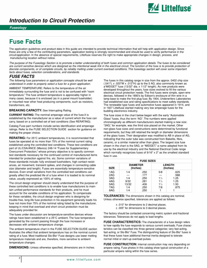
The fuses in this catalog range in size from the approx. 0402 chip size(.041"L x .020"W x .012"H) up to the 5 AG, also commonly known asa“MIDGET” fuse (13/32" dia. x 11/2" length). As new products weredeveloped throughout the years, fuse sizes evolved to fill the variouselectrical circuit protection needs. The first fuses were simple, open-wiredevices, followed in the 1890’s by Edison’s enclosure of thin wire in alamp base to make the first plug fuse. By 1904, Underwriters Laboratorieshad established size and rating specifications to meet safety standards.The renewable type fuses and automotive fuses appeared in 1914, andin 1927 Littelfuse started making very low amperage fuses for thebudding electronics industry.
The fuse sizes in the chart below began with the early “AutomobileGlass” fuses, thus the term “AG”. The numbers were appliedchronologically as different manufacturers started making a new size:“3AG,” for example, was the third size placed on the market. Othernon-glass fuse sizes and constructions were determined by functionalrequirements, but they still retained the length or diameter dimensionsof the glass fuses. Their designation was modified to AB in place of AG,indicating that the outer tube was constructed from Bakelite, fibre,ceramic, or a similar material other than glass. The largest size fuseshown in the chart is the 5AG, or “MIDGET,” a name adopted from itsuse by the electrical industry and the National Electrical Code rangewhich normally recognizes fuses of 9/16" x 2" as the smallest standardfuse in use.
FUSE SIZES
DIAMETER LENGTHSIZE (Inches) (Inches)
1AG 1/4 .250 5/8 .6252AG — .177 — .5883AG 1/4 .250 11/4 1.254AG 9/32 .281 11/4 1.255AG 13/32 .406 11/2 1.507AG 1/4 .250 7/8 .8758AG 1/4 .250 1 1
TOLERANCES: The dimensions shown in this catalog are nominal.Unless otherwise specified, tolerances are applied as follows:
± .010" for dimensions to 2 decimal places.± .005" for dimensions to 3 decimal places.
The factory should be contacted concerning metric system and fractional tolerances. Tolerances do not apply to lead lengths.
FUSE CHARACTERISTICS: The characteristic of a fuse design refersto how rapidly the fuse responds to various current overloads. Fuse charac-teristics can be classified into three general categories: very fast-acting,fast-acting, or Slo-Blo® Fuse. The distinguishing feature of Slo-Blo® fuses isthat these fuses have additional thermal inertia designed to toleratenormal initial or start-up overload pulses.
FUSE CONSTRUCTION: Internal construction may vary depending onampere rating. Fuse photos in this catalog show typical construction of aparticular ampere rating within the fuse series.
FUSE FACTS
Fuseology

Fuse Facts
Introduction to Circuit Protection
3w w w. l i t t e l f u s e . c o m
1
INTR
OD
UC
TIO
N T
OC
IRC
UIT
PR
OTE
CTI
ON
FUSEHOLDERS: In many applications, fuses are installed in fuse-holders. These fuses and their associated fuseholders are not intended for operation as a “switch” for turning power “on” and “off ”.
INTERRUPTING RATING: Also known as breaking capacity or shortcircuit rating, the interrupting rating is the maximum approved currentwhich the fuse can safely interrupt at rated voltage. During a fault orshort circuit condition, a fuse may receive an instantaneous overload current many times greater than its normal operating current. Safe operation requires that the fuse remain intact (no explosion or body rupture) and clear the circuit.
Interrupting ratings may vary with fuse design and range from 35amperes AC for some 250V metric size (5 x 20mm) fuses up to 200,000amperes AC for the 600V KLK series. Information on other fuse seriescan be obtained from the factory.
Fuses listed in accordance with UL/CSA/ANCE 248 are required to have an interrupting rating of 10,000 amperes, with some exceptions(See STANDARDS section) which, in many applications, provides a safety factor far in excess of the short circuit currents available.
NUISANCE OPENING: Nuisance opening is most often caused by an incomplete analysis of the circuit under consideration. Of all the“Selection Factors” listed in the FUSE SELECTION GUIDE, specialattention must be given to items 1, 3, and 6, namely, normal operatingcurrent, ambient temperature, and pulses. For example, one prevalentcause of nuisance opening in conventional power supplies is the failureto adequately consider the fuse’s nominal melting I2t rating. The fuse cannot be selected solely on the basis of normal operating current andambient temperature. In this application, the fuse’s nominal melting I2trating must also meet the inrush current requirements created by theinput capacitor of the power supply’s smoothing filter. The procedure forconverting various waveforms into I2t circuit demand is given in the FUSESELECTION GUIDE. For trouble-free, long-life fuse protection, it is gooddesign practice to select a fuse such that the I2t of the waveform is nomore than 20% of the nominal melting I2t rating of the fuse. Refer to thesection on PULSES in the FUSE SELECTION GUIDE.
RESISTANCE: The resistance of a fuse is usually an insignificant partof the total circuit resistance. Since the resistance of fractional amperagefuses can be several ohms, this fact should be considered when usingthem in low-voltage circuits. Actual values can be obtained from the factory. Most fuses are manufactured from materials which have positivetemperature coefficients, and, therefore, it is common to refer to coldresistance and hot resistance (voltage drop at rated current), with actualoperation being somewhere in between. Cold resistance is the resistanceobtained using a measuring current of no more than 10% of the fuse’snominal rated current. Values shown in this publication for cold resistanceare nominal and representative. The factory should be consulted if thisparameter is critical to the design analysis. Hot resistance is the resist-ance calculated from the stabilized voltage drop across the fuse, withcurrent equal to the nominal rated current flowing through it. Resistancedata on all Littelfuse products are available on request. Fuses can besupplied to specified controlled resistance tolerances at additional cost.
SOLDERING RECOMMENDATIONS: Since most fuse construc-tions incorporate soldered connections, caution should be used wheninstalling those fuses intended to be soldered in place. The application of excessive heat can reflow the solder within the fuse and change itsrating. Fuses are heat-sensitive components similar to semi-conductors,and the use of heat sinks during soldering is often recommended.
TEST SAMPLING PLAN: Because compliance with certain specifica-tions requires destructive testing, these tests are selected on a statisticalbasis for each lot manufactured.
TIME-CURRENT CURVE: The graphical presentation of the fusingcharacteristic, time-current curves are generally average curves whichare presented as a design aid but are not generally considered part ofthe fuse specification. Time-current curves are extremely useful in defin-ing a fuse, since fuses with the same current rating can be representedby considerably different time-current curves. The fuse specification typically will include a life requirement at 100% of rating and maximumopening times at overload points (usually 135% and 200% of rating).A time-current curve represents average data for the design; however,there may be some differences in the values for any one given production lot. Samples should be tested to verify performance, once the fuse has been selected.
UNDERWRITERS LABORATORIES: Reference to “Listed byUnderwriters Laboratories” signifies that the fuses meet the requirements of UL/CSA/ANCE 248-14 “Fuses for Supplementary OvercurrentProtection”. Some 32 volt fuses (automotive) in this catalog are listedunder UL Standard 275. Reference to “Recognized under theComponent Program of Underwriters Laboratories” signifies that the item is recognized under the component program of UnderwritersLaboratories and application approval is required.
VOLTAGE RATING: The voltage rating, as marked on a fuse, indicates that the fuse can be relied upon to safely interrupt its ratedshort circuit current in a circuit where the voltage is equal to, or lessthan, its rated voltage. This system of voltage rating is covered by N.E.C. regulations and is a requirement of Underwriters Laboratories as a protection against fire risk. The standard voltage ratings used byfuse manufacturers for most small-dimension and midget fuses are 32,63, 125, 250 and 600.
In electronic equipment with relatively low output power supplies, with circuit impedance limiting short circuit currents to values of less than ten times the current rating of the fuse, it is common practice to specifyfuses with 125 or 250 volt ratings for secondary circuit protection of 500volts or higher.
As mentioned previously (See RERATING), fuses are sensitive tochanges in current, not voltage, maintaining their “status quo” at any voltage from zero to the maximum rating of the fuse. It is not until thefuse element melts and arcing occurs that the circuit voltage and avail-able power become an issue. The safe interruption of the circuit, as itrelates to circuit voltage and available power, is discussed in the sectionon INTERRUPTING RATING.
To summarize, a fuse may be used at any voltage that is less than itsvoltage rating without detriment to its fusing characteristics. Please contact the factory for applications at voltages greater than the voltage rating.
Fuseology

Fuse Facts and Fuse Selection Guide
Introduction to Circuit Protection
4w w w. l i t t e l f u s e . c o m
FUSE SELECTION GUIDE
Many of the factors involved with fuse selection are listed below:
Selection Factors1. Normal operating current2. Application voltage (AC or DC)3. Ambient temperature4. Overload current and length of time in which the fuse must open.5. Maximum available fault current6. Pulses, Surge Currents, Inrush Currents, Start-up Currents, and
Circuit Transients7. Physical size limitations, such as length, diameter, or height8. Agency Approvals required, such as UL, CSA, VDE, METI, MITI
or Military9. Considerations: mounting type/form factor, ease of removal, axial
leads, visual indication, etc.10. Fuseholder features: clips, mounting block, panel mount, p.c. board
mount, R.F.I. shielded, etc.
NORMAL OPERATING CURRENT: The current rating of a fuse is typically derated 25% for operation at 25°C to avoid nuisance blowing.For example, a fuse with a current rating of 10A is not usually recom-mended for operation at more than 7.5A in a 25°C ambient. For additional details, see RERATING in the previous section and AMBIENT TEMPERATURE below.
VOLTAGE: The voltage rating of the fuse must be equal to, or greater than, the available circuit voltage. For exceptions, see VOLTAGE RATING.
AMBIENT TEMPERATURE: The current carrying capacity tests offuses are performed at 25°C and will be affected by changes in ambienttemperature. The higher the ambient temperature, the hotter the fuse willoperate, and the shorter its life will be. Conversely, operating at a lowertemperature will prolong fuse life. A fuse also runs hotter as the normaloperating current approaches or exceeds the rating of the selected fuse.Practical experience indicates fuses at room temperature should lastindefinitely, if operated at no more than 75% of catalog fuse rating.
CHART SHOWING EFFECT OF AMBIENT TEMPERATURE ONCURRENT-CARRYING CAPACITY (TYPICAL)
KEY TO CHART:Curve A: Thin-Film Fuses and 313 Series (.010 to .150A)Curve B: Very Fast-Acting, Fast-Acting, and Spiral Wound Slo-Blo® FusesCurve C: Resettable PTC’s
*Ambient temperature effects are in addition to the normal rerating, see example.
Example: Given a normal operating current of 2.25 amperes in an application using a Very Fast Acting fuse at room temperature, then:
Catalog Fuse Rating = Normal Operating Current
0.75or
= 3 Amp Fuse (at 25°C)
B
A
B
C
C
A
25°C
PE
RC
EN
T O
F R
AT
ING
*
AMBIENT TEMPERATURE248°F212°F176°F140°F104°F68°F32°F-4°F-40°F-76°F120°C100°C80°C60°C40°C20°C0°C-20°C-40°C-60°C
80
60
40
20
100
120
140
2.25 Amperes0.75
The application guidelines and product data in this guide are intended to provide technical information that will help with application design. Since these are only a few of the contributing parameters, application testing is strongly recommended and should be used to verify performance in the circuit/application.
procedure is to assure that the heat created has insufficient time to thermally conduct away from the fuse element. That is, all of the heatenergy (I2t) is used, to cause melting. Once the measurements of current(I) and time (t) are determined, it is a simple matter to calculate meltingI2t. When the melting phase reaches completion, an electrical arc occursimmediately prior to the “opening” of the fuse element. Clearing I2t = Melting I2t + arcing I2t. The nominal I2t values given in this publicationpertain to the melting phase portion of the “clearing” or “opening”.
DERIVATION OF NOMINAL MELTING I2t: Laboratory tests areconducted on each fuse design to determine the amount of energyrequired to melt the fusing element. This energy is described as nominalmelting I2t and is expressed as “Ampere Squared Seconds” (A2 Sec.). Apulse of current is applied to the fuse, and a time measurement is takenfor melting to occur. If melting does not occur within a short duration ofabout 8 milliseconds (0.008 seconds) or less, the level of pulse current isincreased. This test procedure is repeated until melting of the fuse element is confined to within about 8 milliseconds. The purpose of this
Fuseology
Fuse Selection Guide
Introduction to Circuit Protection
5w w w. l i t t e l f u s e . c o m
1
INTR
OD
UC
TIO
N T
OC
IRC
UIT
PR
OTE
CTI
ON
Similarly, if that same fuse were operated at a very high ambient temperature of 80°C, additional derating would be necessary. Curve “B” (Spiral Wound Slo-Blo® Fuse) of the ambient temperature chartshows the maximum operating “Percent of Rating” at 80°C to be 95%, in which case;
Catalog Fuse Rating =
or
= 3.15 Amp Fuse (at 80°C)
OVERLOAD CURRENT CONDITION: The current level for whichprotection is required. Fault conditions may be specified, either in termsof current or, in terms of both current and maximum time the fault can be tolerated before damage occurs. Time-current curves should be consulted to try to match the fuse characteristic to the circuit needs,while keeping in mind that the curves are based on average data.
MAXIMUM FAULT CURRENT: The Interrupting Rating of a fusemust meet or exceed the Maximum Fault Current of the circuit.
PULSES: The general term “pulses” is used in this context to describethe broad category of wave shapes referred to as “surge currents”, “start-up currents”, “inrush currents”, and “transients”. Electrical pulseconditions can vary considerably from one application to another.Different fuse constructions may not all react the same to a given pulsecondition. Electrical pulses produce thermal cycling and possiblemechanical fatigue that could affect the life of the fuse. Initial or start-uppulses are normal for some applications and require the characteristic ofa Slo-Blo® fuse. Slo-Blo® fuses incorporate a thermal delay design toenable them to survive normal start-up pulses and still provide protectionagainst prolonged overloads. The start-up pulse should be defined andthen compared to the time-current curve and I2t rating for the fuse.Application testing is recommended to establish the ability of the fusedesign to withstand the pulse conditions.
Nominal melting I2t is a measure of the energy required to melt the fusingelement and is expressed as “Ampere Squared Seconds” (A2 Sec.). Thisnominal melting I2t, and the energy it represents (within a time durationof 8 milliseconds [0.008 second] or less and 1 millisecond [0.001 second]or less for thin film fuses), is a value that is constant for each differentfusing element. Because every fuse type and rating, as well as its corre-sponding part number, has a different fusing element, it is necessary todetermine the I2t for each. This I2t value is a parameter of the fuse itselfand is controlled by the element material and the configuration of thefuse element. In addition to selecting fuses on the basis of “NormalOperating Currents”, “Rerating”, and “Ambient Temperature” as dis-cussed earlier, it is also necessary to apply the I2t design approach.This nominal melting I2t is not only a constant value for each fuse ele-ment design, but it is also independent of temperature and voltage.Most often, the nominal melting I2t method of fuse selection is applied tothose applications in which the fuse must sustain large current pulses ofa short duration. These high-energy currents are common in many appli-cations and are described by a variety of terms, such as “surge current”,“start-up current”, “inrush current”, and other similar circuit “transients”that can be classified in the general category of “pulses.” Laboratorytests are conducted on each fuse design to determine its nominal melting I2t rating. The values for I2t given in this publication are nominaland representative. The factory should be consulted if this parameter is
Nominal Operating Current
0.75 x Percent of Rating
2.25 Amperes0.75 x 0.95
critical to the design analysis.The following example should assist in providing a better understandingof the application of I2t.
EXAMPLE: Select a 125V, very fast-acting PICO® fuse that is capable of withstanding 100,000 pulses of current (I) of the pulse waveformshown in Figure 1. The normal operating current is 0.75 ampere at anambient temperature of 25°C.
Step 1 — Refer to Chart I (page #6) and select the appropriate pulsewaveform, which is waveform (E) in this example. Place the applicablevalue for peak pulse current (ip) and time (t) into the corresponding formula for waveshape (E), and calculate the result, as shown:
I2t= (ip)
x 82 x .004 = 0.0512 A2 Sec.
This value is referred to as the “Pulse I2t”.
Step 2 — Determine the required value of Nominal Melting I2t by referring to Chart II (page 6). A figure of 22% is shown in Chart II for100,000 occurrences of the Pulse I2t calculated in Step 1. This Pulse I2tis converted to its required value of Nominal Melting I2t as follows:
Nom. Melt I2t = Pulse I2t/.22
= 0.0512/.22 = 0.2327 A2 Sec.
.001 .002 .003 .004 .005 .006Time (Seconds)
Cur
rent
(A
mpe
res)
Figure 1
2
4
6
8
10
Normal Operating Currentl t
PulseEnergy
2
1
5
1
5
Fuseology

6w w w. l i t t e l f u s e . c o m
Introduction to Circuit Protection
t
t t
1
ip
ip
ip
ip
ip
ib
ip
F
E
D
C
B
A
OR
t
t
t
t
CHART I
WAVESHAPES FORMULAS
i = kI2t = ip2 t
i = ip-ktI2t = (1/3)(ip2 + ipib + ib2) t
i = ip sin tI2t = (1/2) ip2 t
I2t = (1/3) ip2 t
i = kt2 OR i = ip(1-kt)2
I2t = (1/5) ip2 t
i = ipe–kt)I2t ≅ (1/2) ip2 t1
RERATING: For 25°C ambient temperatures, it is recommended thatfuseholders be operated at no more than 60% of the nominal currentrating established using the controlled test conditions specified byUnderwriters Laboratories. The primary objective of these UL testconditions is to specify common test standards necessary for thecontinued control of manufactured items intended for protection againstfire, etc. A copper dummy fuse is inserted in the fuseholder byUnderwriters Laboratories, and then the current is increased until acertain temperature rise occurs. The majority of the heat is produced bythe contact resistance of the fuseholder clips. This value of current isconsidered to be the rated current of the fuseholder, expressed as 100%
of rating. Some of the more common, everyday applications may differfrom these UL test conditions as follows: fully enclosed fuseholders, high contact resistance,air movement, transient spikes, and changes inconnecting cable size (diameter and length). Even small variations fromthe controlled test conditions can greatly affect the ratings of the fuse-holder. For this reason, it is recommended that fuseholders be deratedby 40% (operated at no more than 60% of the nominal current ratingestablished using the Underwriter Laboratories test conditions, as stated above).
FUSEHOLDER SELECTION GUIDE
Step 3 — Examine the I2t rating data for the PICO® II, 125V, very fast-acting fuse. The part number 251001, 1 ampere design is rated at 0.256A2 Sec., which is the minimum fuse rating that will accommodate the0.2327 A2 Sec. value calculated in Step 2. This 1 ampere fuse will alsoaccommodate the specified 0.75 ampere normal operating current, when a 25% derating factor is applied to the 1 ampere rating, as previously described.
TESTING: The above factors should be considered in selecting a fuse for a given application. The next step is to verify the selection byrequesting samples for testing in the actual circuit. Before evaluating thesamples, make sure the fuse is properly mounted with good electricalconnections, using adequately sized wires or traces. The testing shouldinclude life tests under normal conditions and overload tests under faultconditions, to ensure that the fuse will operate properly in the circuit.
CHART II
PULSE CYCLE WITHSTAND CAPABILITY100,000 Pulses Pulse I2t = 22% of Nominal Melting I2t10,000 Pulses Pulse I2t = 29% of Nominal Melting I2t1,000 Pulses Pulse I2t = 38% of Nominal Melting I2t
100 Pulses Pulse I2t = 48% of Nominal Melting I2t
100000
10000
1000
10010% 100%
Num
ber
of P
ulse
s
Pulse I t / Average Melting I t2 2
Note: Adequate time (10 seconds) must exist between pulse eventsto allow heat from the previous event to dissipate.
Fuse Selection Guide
Fuseology

Standards
Introduction to Circuit Protection
7w w w. l i t t e l f u s e . c o m
1
INTR
OD
UC
TIO
N T
OC
IRC
UIT
PR
OTE
CTI
ON
Fuse ratings and other performance criteria are evaluated under labora-tory conditions and acceptance criteria, as defined in one or more ofthe various fuse standards. It is important to understand these standardsso that the fuse can be properly applied to circuit protection applications.
UL/CSA/ANCE (Mexico) 248-14 FUSES FOR SUPPLEMENTARYOVERCURRENT PROTECTION (600 Volts, Maximum) (Previously UL198G and CSA C22.2, No. 59)
UL LISTEDA UL Listed fuse meets all the requirements of the UL/CSA 248-14Standard. Following are some of the requirements.UL ampere ratingtests are conducted at 100%, 135%, and 200% of rated current. The fusemust carry 100% of its ampere rating and must stabilize at a temperaturethat does not exceed a 75°C rise.
The fuse must open at 135% of rated current within one hour. It alsomust open at 200% of rated current within 2 minutes for 0-30 ampere ratings and 4 minutes for 35-60 ampere ratings.
The interrupting rating of a UL Listed fuse is 10,000 amperes ACminimum at 125 volts. Fuses rated at 250 volts may be listed as interrupting 10,000 amperes at 125 volts and, at least, the minimum values shown below at 250 volts.
Ampere Rating Interrupting Rating Voltage of Fuse In Amperes Rating0 to 1 35 250 VAC
1.1 to 3.5 100 250 VAC3.6 to 10 200 250 VAC10.1 to 15 750 250 VAC15.1 to 30 1500 250 VAC
Recognized Under the Component Program of Underwriters Laboratories
The Recognized Components Program of UL is different from UL Listing.UL will test a fuse to a specification requested by the manufacturer. Thetest points can be different from the UL Listed requirements if the fuse hasbeen designed for a specific application. Application approval is requiredby UL for fuses recognized under the Component Program.
UL 275 AUTOMOTIVE GLASS TUBE FUSES (32 Volts)
UL Listed
UL ampere ratings tests are conducted at 110%, 135%, and 200%.Interrupting rating tests are not required.
CSA Certification
CSA Certification in Canada is equivalent to UL Listing in the United States.
The Component Acceptance Program of CSA is equivalent to the Recognition Program at UL.
METI APPROVAL
METI approval in Japan is similar to UL Recognition in the United States.METI has its own design standard and characteristics.
MITI APPROVAL
MITI approval in Japan is similar to UL Recognition in the United States.MITI has its own design standard and characteristics.B
B
INTERNATIONAL ELECTROTECHNICAL COMMISSION (IEC)Publication 60127, Parts 1, 2, 3, 4, 6
The IEC organization is different from UL and CSA, since IEC only writes specifications and does not certify. UL and CSA write the specifications, and are responsible for testing and certification.
Certification to IEC specifications are given by such organizations asSEMKO (Swedish Institute of Testing and Approvals of ElectricalEquipment) and BSI (British Standards Institute , as well as ULand CSA.
IEC Publication 60127 defines three breaking capacity levels (interruptingrating). Low breaking capacity fuses must pass a test of 35 amperes orten times rated current, whichever is greater, while enhanced breakingcapacity fuses must pass a test of 150 amperes and finally high breakingcapacity fuses must pass a test of 1500 amperes.
60127 Part 2Sheet 1 – Type F Quick Acting, High Breaking CapacitySheet 2 – Type F Quick Acting, Low Breaking CapacitySheet 3 – Type T Time Lag, Low Breaking CapacitySheet 4 – Style Fuses 1/4 x 1 1/4Sheet 5 – Type T Time Lag, High Breaking CapacitySheet 6 – Type T Time Lag, Enhanced Breaking Capacity
The letters ‘F’ and ‘T’ represent the time-current characteristic of the fast-acting and time delay fuses. One of these letters will be marked on the end cap of the fuse.
UL/CSA/ANCE (Mexico) 248-14 vs. IEC 60127 Part 2 FUSEOPENING TIMES (UL/CSA/ANCE (Mexico) 248-14 WasPreviously UL 198G and CSA 22.2, No. 59) vs. METI , METI
Percent UL & CSA IEC TYPE F IEC Type F IEC Type T IEC Type T METI/MITIof Rating STD 248-14 Sheet 1 (*) Sheet 2 (*) Sheet 3 (*) Sheet 5 (*)
110 4 Hr. Min. — — — —
130 — — — — — 1Hr. Min.
60 Minutes135 Max. — — — —
150 — 60 Minutes 60 Minutes 60 Minutes 60 MinutesMin. Min. Min. Min.
160 — — — — — 1 Hr. Max.
200 2 Minutes — — — — 2 MinutesMax. Max.
210 — 30 Minutes 30 Minutes 2 Minutes 30 MinutesMax. Max. Max. Max.
(*) Note: The IEC Specification is only written up to 6.3A (8 and 10A willbe added soon), any components above these ratings are not recog-nized by the IEC (although the fuses may have those opening charac-teristics).
IEC also has requirements at 275%, 400% and 1000%; however, thechart is used to show that fuses with the same ampere rating made todifferent specifications are not interchangeable. According to the IEC60127 Standard, a one ampere-rated fuse can be operated at oneampere. A one ampere-rated fuse made to UL/CSA/ANCE 248-14should not be operated at more than .75 ampere (25% derated — See RERATING section of FUSEOLOGY).
METI covers only one characteristic i.e. there are no ‘delay’ definitionson other performance variants.
B
B
BB
®UL
®
®
®
Littelfuse is at your service to help solve your electrical protection problems. When contacting Littelfuse sales engineers, please have all the requirements of your applications available. Requests for quotes or assistance in designing or selecting special types of circuit protection componentsfor your particular applications are also welcome. In the absence of special requirements, Littelfuse reserves the right to make appropriate changes indesign, process, and manufacturing location without prior notice.
Fuseology

Standards and Packaging Information
Introduction to Circuit Protection
8w w w. l i t t e l f u s e . c o m
Publication IEC 60127-4 (Universal Modular Fuse-Links [UMF])
This part of IEC 60127 covers both PCB through-hole and surface mountfuses. This standard covers fuses rated 32, 63, 125, and 250 volts. This standard will be accepted by UL/CSA making it the first global fusestandard. This specification uses different fusing gates than IEC 60127-2;the gates used here are 125%, 200%, and 1000%.
The fuses must not open in less than one hour at 125% of rated currentand open within two minutes at 200% of rated current. The 1000% overload is used to determine the fuse characteristic. The time for eachrating is listed below.
Type FF: Less than 0.001 sec.
Type F: From 0.001 - 0.01 sec.
Type T: From 0.01 - 0.1 sec.
Type TT: From 0.1 - 1.00 sec.
These characteristics correlate to the terminology used in IEC 60127-1.
Breaking capacity (interrupting rating) varies based on voltage rating.Parts rated at 32 & 63 volts must pass a test of 35 amperes or ten timesrated current, whichever is greater.Parts rated at 125 volts must pass atest of 50 amperes or ten times rated current, whichever is greater. Partsrated at 250 volts are further defined as either low, intermediate or highbreaking. The low breaking capacity fuses must pass a test of 100amperes or ten times rated current, while intermediate breaking capacityfuses must pass a test of 500 amperes and, finally, high breaking capacity fuses must pass a test of 1500 amperes.
Packaging Suffixes
R = Taped & reeled fusesA/X = 1 unit per bag
V = 5 units per boxT = 10 units per boxH = 100 units per boxU = 500 units per boxM = 1000 units per boxD = 1500 units per boxP = 2000 units per boxE = 2500 units per boxW = 3000 units per boxY = 4,000 units per boxN = 5000 units per boxK = 10,000 units per box
RT1 = Taped & reeled. Spacing (x) = 2.062 inches (52.4 mm)
RT2 = Taped & reeled. Spacing (x) = 2.50 inches (63.5 mm)
RT3 = Taped & reeled. Spacing (x) = 2.874 inches (73 mm)
Tape and Reel packaging per EIA-296:
• Tape spacing is defined as the width of the tape and reeled fuse(x) as measured from inside tape to inside tape.
• Pitch is defined as the space between two tape and reeled fuses(y) as measured from lead to lead.
MILITARY/FEDERAL STANDARDSSee Table of Contents for Military Product Section.Fuses and holders approved to the following Military specifications areon the Qualified Products List (QPL) for that specification.
MIL-PRF-15160 and MIL-PRF-23419
These specifications govern the construction and performance of fusessuitable primarily for military electronic applications.
MIL-PRF-19207
This specification governs the construction and performance of fuseholders suitable for military applications.
DSSC Drawing #87108
This drawing governs the construction and performance of .177" x .570"(2AG size) cartridge fuses and axial lead versions suitable for militaryapplications. DSSC #87108 designation is included in the fuse end cap marking.
FEDERAL SPECIFICATION W-F-1814
This specification governs the construction and performance of fuseswith high interrupting ratings that are approved for federal applications.Fuses approved to these specifications are on the Federal QualifiedProducts List.
Write to the following agencies for additional information on standards,approvals, or copies of the specifications.
Underwriters Laboratories Inc. (UL)333 Pfingsten RoadNorthbrook, IL 60062
Att: Publications Stock
Canadian Standards Association (CSA)178 Rexdale BoulevardRexdale, Ontario, Canada M9W 1R3
Att: Standard Sales
International Electrotechnical Commission (IEC)3, Rue de Varembe1211 Geneva 20Switzerland
Att: Sales Department
Naval Publications and Military StandardsForm Center (for Military and Federal Standards)5801 Tabor AvenuePhiladelphia, PA 19120
Att: Commanding Officer
Defense Supply Center Columbus (DSCC)3990 East Broad StreetColumbus, OH 43216-5000
Ministry of Economy Trade and Industry (METI)KasumigasekiChi-Youda-KuTokyo 100, Japan
y
x
Fuseology

PTC Facts
Introduction to Circuit Protection
9w w w. l i t t e l f u s e . c o m
1
INTR
OD
UC
TIO
N T
OC
IRC
UIT
PR
OTE
CTI
ON
Overcurrent circuit protection can be accomplished with the use of eithera traditional fuse or the more recently developed resettable PTC. Bothdevices function by reacting to the heat generated by the excessive current flow in the circuit. The fuse melts open, interrupting the currentflow, and the PTC changes from low resistance to high resistance to limitcurrent flow. Understanding the differences in performance between thetwo types of devices will make the best circuit protection choice easier.
The most obvious difference is that the PTC is resettable. The generalprocedure for resetting after an overload has occurred is to removepower and allow the device to cool down. There are several other operating characteristics that differentiate the two types of products.The terminology used for PTCs is often similar but not the same as forfuses. Two parameters that fall into this category are leakage current and interrupting rating.
LEAKAGE CURRENT: The PTC is said to have “tripped” when it hastransitioned from the low resistance state to the high resistance state dueto an overload.
Protection is accomplished by limiting the current flow to some low leak-age level. Leakage current can range from less than a hundred milliampsat rated voltage up to a few hundred milliamps at lower voltages. Thefuse on the other hand completely interrupts the current flow and thisopen circuit results in “0” leakage current when subjected to an overload.
INTERRUPTING RATING: The PTC is rated for a maximum short circuit current at rated voltage. This fault current level is the maximumcurrent that the device can withstand but the PTC will not actually interrupt the current flow (see LEAKAGE CURRENT above). A typicalPTC short circuit rating is 40A. Fuses do in fact interrupt the current flowin response to the overload and the range of interrupting ratings goesfrom hundreds of amperes up to 10,000 amperes at rated voltage.
The circuit parameters may dictate the component choice based on typical device rating differences.
OPERATING VOLTAGE RATING: General use PTCs are not ratedabove 60V while fuses are rated up to 600V.
CURRENT RATING: The operating current rating for PTCs can be upto 11A while the maximum level for fuses can exceed 20A.
TEMPERATURE RATING: The useful upper limit for a PTC is gener-ally 85°C while the maximum operating temperature for fuses is 125°C.
The following temperature rerating curves that compare PTCs to fusesillustrate that more rerating is required for a PTC at a given temperature.
Additional operating characteristics can be reviewed by the circuitdesigner in making the decision to choose a PTC or a fuse for overcurrent protection.
AGENCY APPROVALS: PTCs are Recognized under the ComponentProgram of Underwriters Laboratories to UL Standard 1434 forThermistors. The devices have also been certified under the CSAComponent Acceptance Program. Approvals for fuses includeRecognition under the Component Program of Underwriters Laboratoriesand the CSA Component Acceptance Program. In addition, many fusesare available with full “Listing” in accordance with the new SupplementaryFuse Standard UL/CSA/ANCE (Mexico) 248-14.
RESISTANCE: Reviewing product specifications indicates that similarlyrated PTCs have about twice (sometimes more) the resistance of fuses.
TIME-CURRENT CHARACTERISTIC: Comparing the time-currentcurves of PTCs to time-current curves of fuses show that the speed ofresponse for a PTC is similar to the time delay of a Slo-Blo® fuse.
SUMMARY: Many of the issues discussed become a matter of preference, but there is an important area of application where the use of resettable PTCs is becoming a requirement. Much of the design workfor personal computers and peripheral devices is strongly influenced byMicrosoft and Intel System Design Guide which states that “Using a fusethat must be replaced each time an overcurrent condition occurs is unacceptable.” And the Plug and Play SCSI (Small Computer SystemsInterface) Specification for this large market includes a statement that“. . .must provide a self-resetting device to limit the maximum amount ofcurrent sourced”.
The PTC / fuse discussion provides some insight as to when PTCs maybe the appropriate choice for providing overcurrent circuit protection. Aselection guide worksheet appears on the following page as an aid inchoosing the best circuit protection component.
Lo
g r
esis
tan
ce (
oh
ms)
Temperature (°C)
Trip Point
B
A
B
C
C
A
25°C
PE
RC
EN
T O
F R
AT
ING
*
AMBIENT TEMPERATURE248°F212°F176°F140°F104°F68°F32°F-4°F-40°F-76°F120°C100°C80°C60°C40°C20°C0°C-20°C-40°C-60°C
80
60
40
20
100
120
140
Curve A: Thin-Film Fuses and 313 Series (.010 to .150A)Curve B: Very Fast-Acting, and Spiral Wound FusesCurve C: Resettable PTCs
• Ambient temperature effects are in addition to the normal derating.
Key to chart:
Fuseology

Overcurrent Selection Guide Worksheet
Introduction to Circuit Protection
10w w w. l i t t e l f u s e . c o m
1. Define the circuit operating parameters.
Complete the following form:Normal operating current in amperes:Normal operating voltage in volts:Maximum interrupt current: (see page 3)Ambient Temperature/Rerating: (see page 4)Typical overload current:Required opening time at specified overload:Transient pulses expected: (see page 5)Resettable or one-time:Agency Approvals:Mounting type/form factor:Typical resistance (in circuit):
2. Select the proper circuit protection component.
1206 PTC 1812 PTC 3425 PTC 30V PTC 60V PTC 0402 SMF 0603 SMF 1206 SMFLead-Free AvailableOperating Current Range Maximum Voltage (*)MaximumInterrupting Rating (**)
Temperature Range
Thermal ReratingOpening time at200% IN (***)
Transient Withstand
Resistance
Agency Approvals
Operational UsesMounting/FormFactor
LITTELFUSE CIRCUIT PROTECTION COMPARISON TABLE:
(*) Maximum operating voltage in the series, parts may be used at voltages equal to or less than this value.(**) Maximum interrupting rating at specified voltage which may be less than maximum operating voltage.(***) Opening time is in relation to other forms of protection. A fast device will typically operate within three seconds at 200% of
rated current.
0.20 -1.50A6-15V
40A
-40°C to85°CHigh
Slow
Low
Medium
UL, CSA,TUV
MultipleSurfaceMount
0.5 -2.60A15V
40A
-40°C to85°CHigh
Slow
Low
Medium
UL, CSA,TUV
MultipleSurfaceMount
1.5 -3.0A
6-15V
40A
-40°C to85°CHigh
Slow
Low
Medium
UL, CSA,TUV
Multiple
SurfaceMount
0.100 -3.75A60V
40A
-40°C to85°CHigh
Slow
Low
Medium
UL, CSA,TUV
Multiple
Leaded
0.250 -2A24V
35A
-55°C to90°C
Medium
Fast
Low
Low
UL, CSA,
One TimeSurfaceMount
0.900 -9.0A30V
40A
-40°C to85°CHigh
Slow
Low
Medium
UL, CSA,TUV
Multiple
Leaded
0.250 -5A32V
50A
-55°C to90°CLow
Fast
Low
Low
UL, CSA,
One TimeSurfaceMount
0.125 -7A
125V
50A
-55°C to90°CLow
Fast toMedium
Low
Low
UL, CSA,
One TimeSurfaceMount
Fuseology
yes yes no no no yes yes yesPb

1
INTR
OD
UC
TIO
N T
OC
IRC
UIT
PR
OTE
CTI
ON
11w w w. l i t t e l f u s e . c o m
Overcurrent Selection Guide Worksheet
Introduction to Circuit ProtectionFuseology
3. Determine the opening time at fault.Consult the Time-Current (T-C) Curve to determine if the selected part will operate within the constraints of your application. If the deviceopens too soon, the application may experience nuisance operation. If the device does not open soon enough, the overcurrent may damagedownstream components.
To determine the opening time for the chosen device, locate the overload current on the X-axis of the appropriate T-C Curve and follow its lineup to its intersection with the curve. At this point read the time listed on the Y-axis. This is the average opening time for that device. If youroverload current falls to the right of the curve the device will open. If the overload current is to the left of the curve the device will not operate.
4. Verify ambient operating parameters.Ensure that the application voltage is less than or equal to the device’s rated voltage and that the operating temperature limits are withinthose specified by the device.
5. Verify the device’s dimensions.Using the information from the Designer’s Guide page, compare the maximum dimensions of the device to the space available inthe application.
6. Test the selected product in an actual application.
Nano2® SMF Fuse PICO® II Fuse 2AGs 5x20mm 3AGs/3ABs Midgets
Lead-Free AvailableOperating Current Range Maximum Voltage (*)MaximumInterrupting Rating (**)
Temperature Range
Thermal ReratingOpening time at200% IN (***)
Transient Withstand
Resistance
Agency Approvals
Operational UsesMounting/FormFactor
LITTELFUSE CIRCUIT PROTECTION COMPARISON TABLE:
(*) Maximum operating voltage in the series, parts may be used at voltages equal to or less than this value.(**) Maximum interrupting rating at specified voltage which may be less than maximum operating voltage.(***) Opening time is in relation to other forms of protection. A fast device will typically operate within three seconds at 200% of
rated current.(****) RoHS compliant version available.
Samples Available0.062 -
15A250V
60A
-55oC to125oCLow
Fast to Slow
Low to Medium
Low
UL, CSA,METI, UMF
One TimeSurfaceMount
yes0.062 -
15A250V
50A
-55oC to125oCLow
Fast to Medium
Low to Medium
Low
UL, CSA,METI
One Time
Leaded
no0.100-10A250V
10,000A
-55oC to125oCLow
Fast to Medium
Low to High
Low
UL, CSA,METI
One TimeLeaded or Cartridge
no0.010 -
35A250V
10,000A
-55oC to125oCLow
Fast to Slow
Low to High
Low
UL, CSA,METI
One TimeLeaded or Cartridge
no0.100 -
30A600V
200,000A
-55oC to125oCLow
Fast to Slow
Low to High
Low
UL, CSA,
One Time
Cartridge
no0.032 -
15A250V
10,000A
-55oC to125oCLow
Fast to Slow
Low to High
Low
CSA, BSI, VDE,METI, SEMKO, UL
One TimeLeaded or Cartridge
****Pb

Introduction to Circuit Protection
12w w w. l i t t e l f u s e . c o m
Transientology
Overvoltage Suppression Facts
t1
t2
Vp
Vp/2
t
Figure 1. Lightning Transient Waveform
Table 1. Examples of transient sources and magnitude
10090%
I
I
30n
60n
tr = 0.7 to 1.0ns
Cur
rent
(I)
% 30
60
Figure 2. ESD Test Waveform
Device Type Vulnerability (volts)
VMOS 30-1800MOSFET 100-200GaAsFET 100-300EPROM 100
JFET 140-7000CMOS 250-3000
Schottky Diodes 300-2500Bipolar Transistors 380-7000
SCR 680-1000
Table 2. Range of device vulnerability.
Transient Threats – What Are Transients?Voltage Transients are defined as short duration surges of electricalenergy and are the result of the sudden release of energy that was previ-ously stored, or induced by other means, such as heavy inductive loadsor lightning strikes. In electrical or electronic circuits, this energy can bereleased in a predictable manner via controlled switching actions, or ran-domly induced into a circuit from external sources.
Repeatable transients are frequently caused by the operation of motors,generators, or the switching of reactive circuit components. Random tran-sients, on the other hand, are often caused by Lightning (Figure 1) andElectrostatic Discharge (ESD) (Figure 2). Lightning and ESD generallyoccur unpredictably, and may require elaborate monitoring to be accu-rately measured, especially if induced at the circuit board level.Numerous electronics standards groups have analyzed transient voltageoccurrences using accepted monitoring or testing methods. The keycharacteristics of several transients are shown below in Table 1.
Why are Transients of Increasing Concern?
Component miniaturization has resulted in increased sensitivity;microprocessors for example, have conductive paths which areunable to handle high currents from ESD transients. Such compo-nents operate at very low voltages, so voltage disturbances mustbe controlled to prevent device interruption and latent or cata-strophic failures. Sensitive devices such as microprocessors arebeing adopted at an exponential rate. Microprocessors are begin-ning to perform transparent operations never before imagined.Everything from home appliances, such as dishwashers, to indus-trial controls and even toys, have increased the use of micro-processors to improve functionality and efficiency.
Vehicles now employ many electronics systems to control theengine, climate, braking and, in some cases, steering systems.Some of the innovations are designed to improve efficiency,but many are safety related, such as ABS brakes and tractioncontrol systems. Many of the features in appliances and auto-mobiles employ items which present transient threats (such aselectric motors). Not only is the general environment hostile,but the equipment or appliance is also a source of threats. Forthis reason, careful circuit design and the correct use of over-voltage protection technology will greatly improve the reliabilityand safety of the end application. Table 2 shows the vulnerabil-ity of various component technologies.
VOLTAGE CURRENT RISE-TIME DURATION
Lighting 25kV 20kA 10µs 1msSwitching 600V 500A 50µs 500msEMP 1kV 10A 20ns 1msESD 15kV 30A 1-5ns 100ns
Characteristics of Transient Voltage Spikes
Transient voltage spikes generally exhibit a "double exponential" waveform, shown in Figure 1 for lightning and figure 2 for ESD. The exponen-tial rise time of lightning is in the range 1.2µsec to 10µsec (essentially10% to 90%) and the duration is in the range of 50µsec to 1000µsec(50% of peak values). ESD on the other hand, is a much shorter durationevent. The rise time has been characterized at less than 1.0ns. The over-all duration is approximately 100ns.

Introduction to Circuit Protection
13w w w. l i t t e l f u s e . c o m
1
INTR
OD
UC
TIO
N T
OC
IRC
UIT
PR
OTE
CTI
ON
Transientology
Overvoltage Suppression FactsTransient Voltage ScenariosESD (Electrostatic Discharge)Electrostatic discharge is characterised by very fast rise times and veryhigh peak voltages and currents. This energy is the result of an imbal-ance of positive and negative charges between objects.
Below are some examples of the voltages which can be generated,depending on the relative humidity (RH):
• Walking across a carpet:35kV @ RH = 20%; 1.5kV @ RH = 65%
• Walking acrss a vinyl floor:12kV @ RH = 20%; 250V @ RH = 65%
• Worker at a bench:6kV @ RH = 20%; 100V @ RH = 65%
• Vinyl envelopes:7kV @ RH = 20%; 600V @ RH = 65%
• Poly bag picked up from desk:20kV @ RH = 20%; 1.2kV @ RH = 65%
Referring to Table 2 on the previous page, it can be seen how much of ahazard ESD presents. Figure 2 shows the ESD waveform as defined inthe IEC 61000-4-2 test specification.
Inductive Load SwitchingThe switching of inductive loads generates high energy transients whichincrease in magnitude with increasingly heavy loads. When the inductiveload is switched off, the collapsing magnetic field is converted into elec-trical energy which takes the form of a double exponential transient.Depending on the source, these transients can be as large as hundredsof volts and hundreds of Amps, with duration times of 400 milliseconds.
Typical sources of inductive transients are:
• Generator• Motor• Relay• Transformer
These examples are extremely common in electrical andelectronic systems. Because the sizes of the loads varyaccording to the application, the wave shape, duration, peakcurrent and peak voltage are all variables which exist in realworld transients. Once these variables can be approximated,a suitable suppressor technology can be selected.
Figure 3, bottom left, shows a transient which is the result ofstored energy within the alternator of an automobile charg-ing system. A similar transient can also occur as a result oftransients caused by other DC motors in a vehicle. ForExample, DC motors power amenities such as power locks,seats and windows. These various applications of a DCmotor can produce transients that are just as harmful to thesensitive electronic components as transients created in theexternal environment.
Lightning Induced TransientsEven though a direct strike is clearly destructive, transientsinduced by lightning are not the result of direct a directstrike. When a lightning strike occurs, the event creates amagnetic field which can induce transients of large magni-tude in nearby electrical cables.
Figure 4, below shows how a cloud-to-cloud strike will effectnot only overhead cables, but also buried cables. Even astrike 1 mile distant (1.6km) will generate 70 volts in electri-cal cables.
Figure 5, on the following page shows the effect of a cloud-to-ground strike: the transient generating effect is far greater.
Buried Line
Transient Generated:• 70 V at 1.6km (1 mile)• 10 kV at 150m (160 yards)
T
T1
VB VB = 25V to 125VVB = 14V T= 40ms to 400ms
VS
90%
10%
t
V
T1 = 5ms to 10ms R = 0.5Ω to 4Ω
Figure 3. Automotive Load Dump Figure 4. Cloud-to-Cloud Lightning Strike

TERMSRated AC Voltage (VM(AC)RMS)This is the maximum continuous sinusoidal voltage which may be appliedto the MOV. This voltage may be applied at any temperature up to themaximum operating temperature of 85°C.
PE
RC
EN
T O
F P
EA
K V
ALU
E 100
90
50
10
O1 tt1
t2
TIME
Figure 4. Peak Pulse Current Test Waveform
Technological Solutions for Transient ThreatsBecause of the various types of transients and applications, it is neces-sary to employ protection devices with different applications. Littelfuseoffers the broadest range of circuit protection technologies to ensure thatyou get the proper solution for your application. Our overvoltage protec-tion portfolio includes:
Varisitors and Multilayer VaristorLittelfuse Varistors are voltage dependent, nonlinear devices which haveelectrical characteristics similar to back to back zener diodes. They arecomposed primarily of zinc oxide with small additions of other metaloxides. The metal oxide Varistor or “MOV” is sintered during themanufacturing operation. This forms a ceramic and results in a crystallinemicrostructure across the entire bulk of the device. It is this attribute thatallows MOVs to dissipate very high levels of transient energy. Therefore,Varistors are typically used for the suppression of lightning and otherhigh level transients found in industrial or AC line applications.Additionally, Varistors are used in DC circuits such as low voltage powersupplies and automobile applications. Their manufacturing processpermits many different form factors with the radial leaded disc being themost common.
Multilayer Varistors are constructed of zinc oxide material similar tostandard MOVs, however, they are fabricated with interleaved layers ofmetal electrodes and supplied in leadless ceramic packages. As withstandard MOVs, Multilayers transition from a high impedance to aconduction state when subjected to voltages that exceed their nominalvoltage rating. MLVs are constructed in various chip form sizes and arecapable of significant surge energy for their physical size. Thus, data lineand power supply suppression are achieved with one technology.
The following parameters apply to Varistors and/or Multilayer Varistors andshould be understood by the circuit designer to properly select a devicefor a given application.
Introduction to Circuit Protection
14w w w. l i t t e l f u s e . c o m
Overvoltage Suppression Facts
Figure 6, shows a typical current waveform for inducedLightning disturbances.
Transientology
100m1km
10km
11kV
1100 V
110 V
Figure 5. Cloud-to-Ground Lightning Strike
PE
RC
EN
T O
F P
EA
K V
ALU
E 100
90
50
10
O1 tt1
t2
TIME
Figure 6. 5kA 8/20µS pulse

Introduction to Circuit Protection
15w w w. l i t t e l f u s e . c o m
1
INTR
OD
UC
TIO
N T
OC
IRC
UIT
PR
OTE
CTI
ON
Transientology
Power Dissipation RatingsWhen transients occur in rapid succession the average power dissipationis the energy (watt-seconds) per pulse times the number of pulses persecond. The power so developed must be within the specifications shownon the Device Ratings and Characteristics table for the specific device.Certain parameter ratings must be derated at high temperatures asshown in Figure 5.
Voltage Clamping DeviceA clamping device, such as an MOV, refers to a characteristic in whichthe effective resistance changes from a high to low state as a function of applied voltage. In its conductive state, a voltage divider action isestablished between the clamping device and the source impedance of the circuit. Clamping devices are generally “dissipative” devices,converting much of the transient electrical energy to heat.
PulseGuard® SuppressorsPulseGuard devices are designed for ESD transients. This technologyis manufactured utilizing a polymer-over- gap procedure resulting inextremely low capacitance. Likewise, leakage current is essentiallynon-existent, an important factor for certain portable products.PulseGuard Suppressors, therefore, do not skew fast edge rates orattenuate high speed data signals due to capacitive loading. They aresuited to data rate applications ranging beyond 5GHz. The PulseGuardfamily of devices are fabricated in various surface mount package formas well as a D-Sub connector insert film. Like Multilayer Varistors, thesedevices are not applicable for existing safety agency standards listing.PulseGuard devices are intended for the suppression of Human BodyModel ESD transients, such as defined in IEC 61000-4-2.
TERMSCapacitanceThe capacitance measured between input pins and the commonterminal, at 1 MHz.
Leakage CurrentUntil the PulseGuard suppressor transitions to the “on” state, it iselectrically transparent to the circuit. Leakage current passing throughthe device is less than 1 nA.
Voltage RatingPulseGuard suppressors are rated for use in operating environments upto 24 VDC.
Temperature RatingThe operating temperature range is –65°C to +125°C. Unlike thepolymer PTCs, these devices do not operate as a result of thermalaction; therefore, there is no rerating necessary.
Agency ApprovalsAt this time, there are no applicable standards for ESD suppressorcomponents. Nonetheless, PulseGuard suppressors have beensubjected to all levels of severity of the IEC 61000-4-2 test specificationusing both the Contact Discharge and Air Discharge injection methods.In all cases, clamping of the ESD transient is provided and the devicessurvived the multiple ESD events.
ResistanceWhile in the “off” state, the suppressors remain electrically transparentto the circuit. The measured resistance of the suppressors is 10 MΩ,or greater.
-55 50 60 70 80 90 100 110 120 130 140 150AMBIENT TEMPERATURE (ºC)
100
90
80
70
60
50
40
30
20
10
0
PE
RC
EN
T O
F R
ATE
D V
ALU
E
ML, MLE, MHS, MLNCH, CP, CS, RA SERIES
BA/BB, CA, DA/DB,LA, "C"III, HA, NA, MA,
UltraMOV, PA, ZA SERIES
Figure 5. Current, Energy, Power Derating v/s Temperature.
Maximum Non-Repetitive Surge Current (ITM)This is the maximum peak current which may be applied for an 8/20µsimpulse, with rated line voltage also applied, without causing greater than10% shift in nominal voltage.
Maximum Non-Repetitive Surge Energy (WTM)This is the maximum rated transient energy which may be dissipated fora single current pulse at a specified impulse and duration (2µs), with therated VRMS applied, without causing device failure.
Nominal Voltage (VN(DC))This is the voltage at which the device changes from the off state to the on state and enters its conduction mode of operation. This voltage is characterized at the 1mA point and has specified minimum and maximum voltage ratings.
Clamping Voltage (VC)This is the peak voltage appearing across the MOV when measured atconditions of specified pulse current amplitude and specified waveform(8/20µs).
Operating Temperature RangeThe minimum and maximum ambient operating temperature of the circuit in which the Varistor will be applied, allowing for other adjacentcomponents which could effect the surrounding temperature.
Overvoltage Suppression Facts

Introduction to Circuit Protection
16w w w. l i t t e l f u s e . c o m
Transientology
Overvoltage Suppression FactsTime-Voltage CharacteristicBecause the magnitude of the voltage and the time duration vary withthe individual ESD event, a general form of this curve is shown below.
Silicon Protection (SP) Introduction:Silicon Transient Voltage Suppression (TVS) technology offers a highlevel of protection (up to 30kV per IEC 61000-4-2 Direct Discharge) withvery low capacitance, leakage current and clamp voltage. In addition to asingle line 0402 device, high-density arrays are available for up to 18lines including power rail protection. The next generation of productsavailable offers TVS protection plus filtering and termination. For morerobust applications, silicon devices are available for EFT and Lightningthreats per IEC-61000-4-4/5. The SP family consists of three main tech-nology types. This includes a single line or array TVS Avalanche diodes,Rail Clamp Diode arrays and filter/protection.
TVS Avalanche DiodeThe Surface Mount families of TVS Avalanche Diode arrays are specifi-cally designed to protect circuits from Electrostatic Discharge (ESD). Thisfamily is rated per the International Electromagnetic Compatibility (IEC)transient immunity standards IEC 61000-4-2 for level 4 (20kV DirectDischarge). The devices are typically connected between the sensitivesignal line and ground. When a transient event occurs, the device turnson and directs the transient into the ground plane. These space savingarrays protect multiple data lines in ultra small package sizes includingthe SC70, SOT23, TSSOP, and MSOP package. The arrays are config-ured to protect 2,3,4,5 or 6 sensitive digital or analog input circuits ondata, signal, or control lines with voltage levels up to 5VDC. The devicesare ideal for high-speed signal lines due to their low capacitance (30pF),low clamping voltage, leakage current and very fast response time.
The TVS Avalanche Diodes are also offered in an ultra small Chip ScalePackage (CSP) size with outstanding ESD protection. The single line0402 or high-density arrays are ideal for hand held and computer appli-cation where board space is at a premium. The CSP families of TVSAvalanche Diode arrays are specifically designed to protect circuits fromElectrostatic Discharge (ESD). This family is rated per the internationalElectromagnetic Compatibility (EMC) transient immunity standards IEC61000-4-2 for level 4. These space saving arrays protect multiple datalines in an ultra small CSP package. The arrays are configured to protect
4, 8 and 16 sensitive digital or analog input circuits on data, signal, orcontrol lines with voltage levels up to 5VDC. The devices are ideal forhigh-speed signal lines due to their low capacitance (39pF), low clamp-ing voltage, and leakage current and very fast response time. Both unipo-lar and bipolar versions are available.
Rail Clamp TVS Diode ArraysThe Rail clamp arrays are low capacitance (3pf), low leakage (10nA) andhigh-energy structures designed for transient protection. The rail clampdevices are connected to the sensitive signal line and to the power sup-ply rails. When a transient voltage exceeds either supply rail by a diodedrop (0.7V), the SCR /diode action directs the transient away from thesensitive line to the power supply. After the transient subsides, the railclamp device returns to its off state. There are two main product typeswithin the rail clamp technology. This includes a high voltage (35v) SP72xfamily and lower voltage (5V) SP05x family.
USB Port Terminator with EMI Filter and TVS protectionThe newest family of devices offer a highly integrated solution for protect-ing USB1.1 ports on peripheral (upstream) products such as DigitalCameras, MP3 players, printers or scanners.
The design integrates passive components including resistors, capacitorsand TVS Avalanche diodes into a monolithic device. To save boardspace, the device is packaged in an ultra small SC70-6 lead plastic package. The end result of this design is the recommended terminationresistance and filter (EMI) characteristic of the USB1.1 specification.The device offers very robust 15kV(IEC 61000-4-2 direct discharge) bi-directional protection of the data and Vbus lines
TERMSOperating Voltage Range (Vsupply)
The range limits of the power supply voltage that may be across the V+and V- terminals. The SCR/ Diode arrays do not a have a fixed breakoveror operating voltage. These devices “float” between the input and powersupply rails and thus the same device can operate at any potentialwithin its range.
Forward Voltage DropThe maximum forward voltage drop between an input pin and respectivepower supply pin for a specific forward current.
Input Leakage CurrentThe DC input current that is measured at maximum Vsupply with1/2 Vsupply applied to the input.
Quiescent Supply CurrentThe maximum DC current into V+ / V- pins with Vsupply at itsmaximum voltage.
Input CapacitanceThe capacitance measured between the input pin and either supply pinat 1MHz / 1VRMS applied.
Comparing the TechnologiesThe differences between the families offer the designer specific optionsto best suit the circuit application. Basic comparisons are listed in thetables on page 23 which highlight the fundamental attributes of each.
Figure 6. ESD Event.

Introduction to Circuit Protection
17w w w. l i t t e l f u s e . c o m
1
INTR
OD
UC
TIO
N T
OC
IRC
UIT
PR
OTE
CTI
ON
Overvoltage Suppression Facts
Transientology
The considerations below restate how the product attributes/offeringscan differ as an aid in determining which device family may bemost appropriate.
When to choose the Silicon Protection• The device being protected requires the lowest possible clamp voltage
(9.2), low capacitance (3 to 40pF) and low leakage (5nA to 10uA).
• Board space is at a premium and high density single line (0402) ormulti-line protection is needed.
• Additional features such as EMI and termination are required.
• Transients are ESD or beyond such as EFT or Lightning.
When to choose the PulseGuard® Suppressors • The application cannot tolerate added capacitance (high speed
data lines)
• ESD is the primary transient threat
• On data, signal, and control lines (not power supply lines)
• The suppression function must be within a Dsub connector(PGD types)
When to choose the ML, MLE or MLN Series• Surge currents or energy beyond ESD is expected in the application
(EFT, Lightning remnants).
• Replacing high wattage TVS Zeners (300-1500W).
• Added capacitance is desirable for EMI filtering (3pF - 6000pF).
• Power supply line or low/medium speed data, signal lines are tobe protected.
• Single, leadless SM package is required in EIA sizes. (MLN is 4-line)
• The operating voltage is above the SP or PulseGuard®
Suppressor ratings.
SiBOD™Thyristor Breakover TechnologyAvailable in surface mount, axial leaded and TO-220 through hole pack-age options. Offers protection from medium to hight energy transients.SiBOD thyristors are specifically designed for transient suppression intelecom and data transmission systems.
Silicon Avalanche Diodes (SADs)
The Transient Voltage Suppressor diode (T.V.S.) is specifically designedto protect electronic circuits against transients and over voltages. It is asilicon avalanche device available in both uni-directional or bi-directionalconfigurations. With a uni-directional, the specified clamping characteris-tic is only apparent in one direction, the other direction exhibiting a VFnormally experienced with conventional rectifier diodes. All electricalcharacteristics are specified at 25 degrees C.
When selecting a T.V.S. device there are some important parameters tobe considered, these are; Reverse Standoff Voltage (VR), Peak PulseCurrent (IPP) and Maximum Clamping Voltage (VC max).
The most important is VR, this is the parameter that is the key to select-ing a T.V.S. diode. The VR of the device should be equal to, or greaterthan, the peak operating level of the circuit (or part of the circuit) to beprotected. This will ensure that the T.V.S. does not clip the circuit drive voltage.
The Peak Pulse Current (IPP) is the maximum current the T.V.S. can with-stand without damage. The required IPP can only be determined by divid-ing the peak transient voltage by the source impedance. Of course, inmany cases, the very nature of transient occurance makes this parame-ter difficult to determine. The T.V.S. failure mechanism is a short circuit,therefore if the device fails due to a transient, the circuit will still be pro-tected.
In secondary protection applications, any series impedances due toresistors, transformers and inductors will have a limiting effect on thepeak pulse current. In some cases these may be due to long lengths ofinterconnecting wire.
The Maximum Clamping Voltage (VC max) is the peak voltage that willappear across the T.V.S. device when subjected to the Peak PulseCurrent (IPP), based on a 1ms exponential waveform. This waveform is a10 /1000 microsecond waveform as shown in Figure 1.
This pulse is a standard test waveform used for protection devices.
Test Severity Level
Test Voltage Test VoltageLevel Contact Discharge Air Discharge
1 2kV 2kV
2 4kV 4kV
3 6kV 8kV
4 8kV 15kVX Special Special
Notes:1. X is an open level.
2. The test severity levels shall be selected in accordance with the mostrealistic installation and environmental conditions.
PEAK VALUEIPP
0.9 IPP
0.5 IPP
0.1 IPP
CU
RR
EN
T
TIMET1 x 1.25 = 10µS
1000µS
FIGURE 1
Conclusion
Choosing the most appropriate suppressor depends upon a balancebetween the application, its operation, voltage transient threats expectedand sensitivity levels of the components requiring protection. Formfactor/package style also must be considered.
The three Littelfuse technologies described offer a comprehensive choicefor the designer. Reviewing the attributes of each can result in a suitableESD suppression solution for most applications. See the individual datasheets for specific electrical and mechanical information.
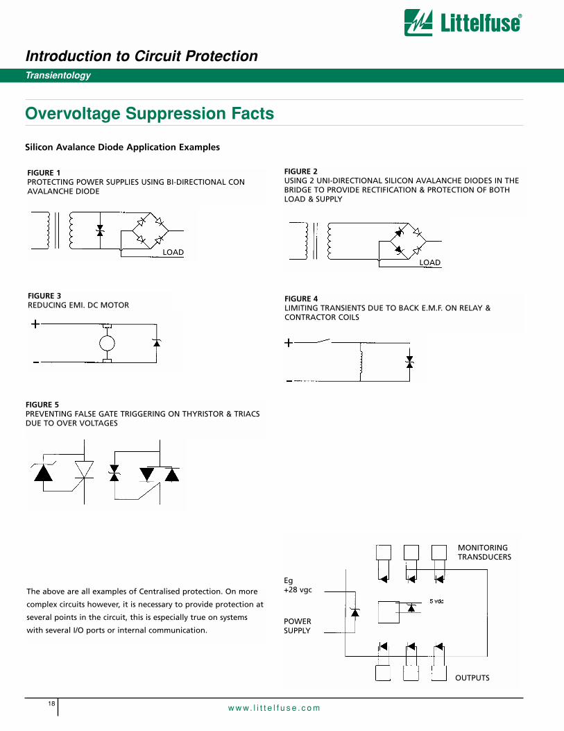
Introduction to Circuit Protection
18w w w. l i t t e l f u s e . c o m
Overvoltage Suppression Facts
Transientology
FIGURE 1PROTECTING POWER SUPPLIES USING BI-DIRECTIONAL CONAVALANCHE DIODE
FIGURE 2USING 2 UNI-DIRECTIONAL SILICON AVALANCHE DIODES IN THEBRIDGE TO PROVIDE RECTIFICATION & PROTECTION OF BOTHLOAD & SUPPLY
FIGURE 3REDUCING EMI. DC MOTOR
FIGURE 4LIMITING TRANSIENTS DUE TO BACK E.M.F. ON RELAY &CONTRACTOR COILS
FIGURE 5PREVENTING FALSE GATE TRIGGERING ON THYRISTOR & TRIACSDUE TO OVER VOLTAGES
The above are all examples of Centralised protection. On more
complex circuits however, it is necessary to provide protection at
several points in the circuit, this is especially true on systems
with several I/O ports or internal communication.
MONITORING TRANSDUCERS
OUTPUTS
POWERSUPPLY
Eg+28 vgc
LOADLOAD
Silicon Avalance Diode Application Examples
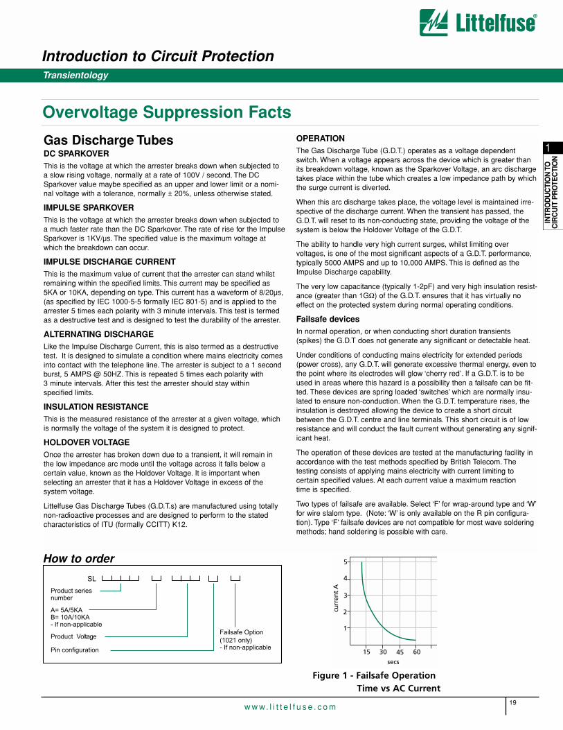
Introduction to Circuit Protection
19w w w. l i t t e l f u s e . c o m
1
INTR
OD
UC
TIO
N T
OC
IRC
UIT
PR
OTE
CTI
ON
15 30 45 60
secs
1
2
3
4
5
curr
ent
A
Figure 1 - Failsafe OperationTime vs AC Current
Transientology
Overvoltage Suppression Facts
Gas Discharge TubesDC SPARKOVERThis is the voltage at which the arrester breaks down when subjected toa slow rising voltage, normally at a rate of 100V / second. The DCSparkover value maybe specified as an upper and lower limit or a nomi-nal voltage with a tolerance, normally ± 20%, unless otherwise stated.
IMPULSE SPARKOVERThis is the voltage at which the arrester breaks down when subjected toa much faster rate than the DC Sparkover. The rate of rise for the ImpulseSparkover is 1KV/µs. The specified value is the maximum voltage atwhich the breakdown can occur.
IMPULSE DISCHARGE CURRENTThis is the maximum value of current that the arrester can stand whilstremaining within the specified limits. This current may be specified as5KA or 10KA, depending on type. This current has a waveform of 8/20µs,(as specified by IEC 1000-5-5 formally IEC 801-5) and is applied to thearrester 5 times each polarity with 3 minute intervals. This test is termedas a destructive test and is designed to test the durability of the arrester.
ALTERNATING DISCHARGELike the Impulse Discharge Current, this is also termed as a destructivetest. It is designed to simulate a condition where mains electricity comesinto contact with the telephone line. The arrester is subject to a 1 secondburst, 5 AMPS @ 50HZ. This is repeated 5 times each polarity with 3 minute intervals. After this test the arrester should stay within specified limits.
INSULATION RESISTANCEThis is the measured resistance of the arrester at a given voltage, whichis normally the voltage of the system it is designed to protect.
HOLDOVER VOLTAGEOnce the arrester has broken down due to a transient, it will remain inthe low impedance arc mode until the voltage across it falls below a certain value, known as the Holdover Voltage. It is important when selecting an arrester that it has a Holdover Voltage in excess of the system voltage.
Littelfuse Gas Discharge Tubes (G.D.T.s) are manufactured using totallynon-radioactive processes and are designed to perform to the statedcharacteristics of ITU (formally CCITT) K12.
OPERATIONThe Gas Discharge Tube (G.D.T.) operates as a voltage dependentswitch. When a voltage appears across the device which is greater thanits breakdown voltage, known as the Sparkover Voltage, an arc dischargetakes place within the tube which creates a low impedance path by whichthe surge current is diverted.
When this arc discharge takes place, the voltage level is maintained irre-spective of the discharge current. When the transient has passed, theG.D.T. will reset to its non-conducting state, providing the voltage of thesystem is below the Holdover Voltage of the G.D.T.
The ability to handle very high current surges, whilst limiting over voltages, is one of the most significant aspects of a G.D.T. performance,typically 5000 AMPS and up to 10,000 AMPS. This is defined as theImpulse Discharge capability.
The very low capacitance (typically 1-2pF) and very high insulation resist-ance (greater than 1GΩ) of the G.D.T. ensures that it has virtually noeffect on the protected system during normal operating conditions.
Failsafe devicesIn normal operation, or when conducting short duration transients(spikes) the G.D.T does not generate any significant or detectable heat.
Under conditions of conducting mains electricity for extended periods(power cross), any G.D.T. will generate excessive thermal energy, even tothe point where its electrodes will glow ‘cherry red’. If a G.D.T. is to beused in areas where this hazard is a possibility then a failsafe can be fit-ted. These devices are spring loaded ‘switches’ which are normally insu-lated to ensure non-conduction. When the G.D.T. temperature rises, theinsulation is destroyed allowing the device to create a short circuitbetween the G.D.T. centre and line terminals. This short circuit is of lowresistance and will conduct the fault current without generating any signif-icant heat.
The operation of these devices are tested at the manufacturing facility inaccordance with the test methods specified by British Telecom. The testing consists of applying mains electricity with current limiting to certain specified values. At each current value a maximum reaction time is specified.
Two types of failsafe are available. Select ‘F’ for wrap-around type and ‘W’for wire slalom type. (Note: ‘W’ is only available on the R pin configura-tion). Type ‘F’ failsafe devices are not compatible for most wave solderingmethods; hand soldering is possible with care.
Product seriesnumber
A= 5A/5KAB= 10A/10KA- If non-applicable
Product Voltage
Pin configuration
Failsafe Option(1021 only)- If non-applicable
SL
How to order

Introduction to Circuit Protection
20w w w. l i t t e l f u s e . c o m
Overvoltage Suppression Facts
Transientology
Low capacitance High capacitance
LINE
EQUIPMENT
Low Capacitance Protection
HDSL:
Telephone System:
Telephone System:
MDF Protection PABX NTE
Low capacitance Fast response
LINE
T.V.S DIODES
GREENTUBE™
T.V.S DIODES
Littelfuse Hybrid ArrestorsThe Littelfuse Hybrid is an over-voltage surge protectiondevice utilizing both gas tube and semiconductor technolo-gies, resulting in a package that delivers the high currenthandling capability of the G.D.T. with the speed of a silicondevice.
Compatible with standard gas tube arrester outlines it canbe easily fitted or exchanged into most board or magazineconnection systems, eg Krone™ LSA - plus 5B and Quante79126-506 00 magazines.
As electronic equipment becomes evermore complex, it hasalso now become more sensitive, and therefore prone todamage due to transients at lower voltage levels.
The hybrid series provides protection for sensitive electronicequipment where a standard G.D.T. installation proves inef-fective by allowing too much let through voltage against ultrafast transients.The precision matching of the G.D.T. and the semiconductorTVS eliminates the dv/dt switching delay normally associat-ed with G.D.T.s giving lower clamping levels and better pro-tection whilst maintaining its ability to divert high energypulses, i.e. 5KA 8/20µ sec.
Already approved and trialed by BT, the hybrid provides theultimate in over-voltage circuit protection.
FEATURES• Fast response, i.e. no dv/dt switching delay
• High current handling capability, 5KA 8/20µs defined byIEC 1000-4-5
• High insulation resistance
• Typ capacitance <100pF @ 1MHz
• No series resistive element for switching co-ordination
• Compatible with most G.D.T. connection systems
• Approved for BT systems failsafe
BENEFITS• Increased level of protection for sensitive electronic
equipment
• No need for separate primary and secondary protectors
• Low leakage current
• Can be used on most telecom and electronic applica-tions
• No extra component cost
• No modifications of existing hardware
• Proven performance to the highest of standards
• Prevents hazardous temperature conditions

Introduction to Circuit Protection
21w w w. l i t t e l f u s e . c o m
1
INTR
OD
UC
TIO
N T
OC
IRC
UIT
PR
OTE
CTI
ON
Transientology
Overvoltage Suppression Facts
30
Time (µs)
100
50
Per
cent
age
peak
vol
tage
20
90
td = 50 µs
tr
tr = 1.67 x (t 2 - t1) =1.2 µst2
t1
4010 30
VRSM
VRSM
50 60 70
10
Time (µs)
100
50
Per
cent
age
peak
vol
tage
90
td =50µs
tr
tr = 1.25 x (t 2 - t1) =8 µs
t2
t1
10 20
1RSM or 1SM
VRSM
30 40 50
1RSM
Figure 2 - 1.2/50µS Impulse Discharge Voltage Waveshape
Figure 3 - 8/20µS Impulse
Discharge Current Waveshape
102 104 106 108
100V / s
0
100
200
300
400
500
600
700
800
900
Bre
akdo
wn
volta
ge
STATIC VOLTAGE DYNAMIC RANGE
Figure 4 - Dynamic Impulse Characteristic OF 230/260/350/450 Volt G.D.T.s
INTERNATIONAL EMMISSIONS STANDARDIEC 1000-4-5

Introduction to Circuit Protection
22w w w. l i t t e l f u s e . c o m
Transientology
Overvoltage Suppression FactsUL (Underwriters Laboratories)UL writes “standards” to which products are investigated. Upon comple-tion of the tests, a “Listing” or “Recognition” to the standard with condi-tions of acceptability is given under a unique file number. All of Littelfuseapplicable Varistors are in the “Recognized Components” category to oneor more of the following standards:
• UL1449 Transient Voltage Suppressors.
• UL1414 Across the Line Capacitors, Antenna Coupling and Line By-Pass Capacitors for Radio and Television Type Appliances.
• UL497B Protectors for Data and Communication and Fire AlarmCircuits.
(Note that the terms “Approved” or “Certified” are not correct in referringto devices listed or recognized by UL.)
VDE (Verband Deutscher Electrotechniker)Based in Germany, this is the Association of German Engineers whodevelop specific safety standards and test requirements. VDE tests andcertifies devices or products, assigning a license number.
Littelfuse Radial Varistors are currently certified under license number104846 E having successfully met CECC standard 42 201-006(issue 1/1996).
ESD StandardsSeveral industry standards and specifications exist that are used toqualify and quantify ESD events. Since many circuits or systems mustdemonstrate immunity to ESD, these standards are often incorporated inthe testing of ESD capability. Of particular concern is the immunity levelfor semiconductors. The “standards” include Human Body Model (HBM)to MIL-STD-883 or IEC 61000-4-2, Machine Model (MM) such as EIAJIC121, and Charged Device Model (CDM) such as US ESD DS 5.3. TheHuman Body Model, Machine Model and Charged Device Modelprimarily relate to manufacturing and testing process of an IC.
One of the most severe is IEC 61000-4-2 from the InternationalElectrotechnical Commission and referenced in the EMC directive.Level 4 of this test method is the highest level, subjecting the deviceunder test to 8kV contact discharge method (preferred) and/or 15kV airdischarge. Each Littelfuse technology is designed for this level. Therecommended types are the silicon based SP05x, SP723 and SP724SCR/Diode Arrays, the polymeric VVM based PulseGuard® Suppressor,and the V18ML, MLE, MHS or MLN Multilayers.
The designer should be aware of the ESD ratings of the semiconductorsused in the circuit. For example, semiconductor manufacturers that ratetheir devices to MIL-STD-883 to 2kV may not pass 2kV when subjectedto the more difficult IEC test method (150pF / 330Ω instead of 100pF /1500Ω ). Additionally, even if semicon-ductors do meet some level ofESD immunity to IEC standards, that does not imply that additional ESDsuppression is not required. Real world ESD transients can exceed thepeak currents and voltages as defined by the standards and can havemuch faster rise times.
IEC 61000-4-2 consists of four test severity levels of ESD immunityusing both a Contact Discharge and Air Discharge test method. TheEUT or DUT may be subjected to increasing levels of severity untilfailure. Or, a particular level of immunity may be prescribed for EM
compatibility of an end product.
For more information about the IEC 61000-4-2 test method, seeApplication Note AN9734, “IEC Electromagnetic CompatibilityStandards for Industrial Process Measurement and ControlEquipment.”
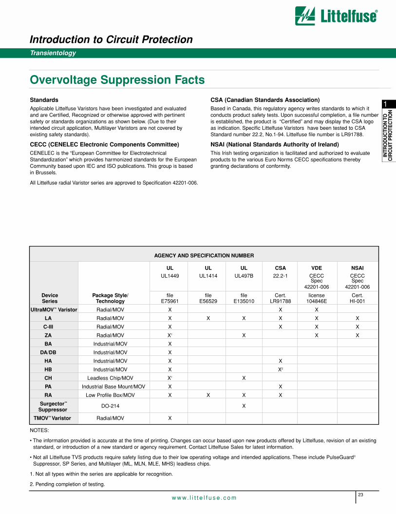
Introduction to Circuit Protection
23w w w. l i t t e l f u s e . c o m
1
INTR
OD
UC
TIO
N T
OC
IRC
UIT
PR
OTE
CTI
ON
Overvoltage Suppression Facts
Transientology
StandardsApplicable Littelfuse Varistors have been investigated and evaluated and are Certified, Recognized or otherwise approved with pertinent safety or standards organizations as shown below. (Due to their intended circuit application, Multilayer Varistors are not covered by existing safety standards).
CECC (CENELEC Electronic Components Committee)CENELEC is the “European Committee for ElectrotechnicalStandardization” which provides harmonized standards for the EuropeanCommunity based upon IEC and ISO publications. This group is based in Brussels.
All Littelfuse radial Varistor series are approved to Specification 42201-006.
CSA (Canadian Standards Association)Based in Canada, this regulatory agency writes standards to which itconducts product safety tests. Upon successful completion, a file numberis established, the product is “Certified” and may display the CSA logoas indication. Specific Littelfuse Varistors have been tested to CSAStandard number 22.2, No.1-94. Littelfuse file number is LR91788.
NSAI (National Standards Authority of Ireland)This Irish testing organization is facilitated and authorized to evaluateproducts to the various Euro Norms CECC specifications therebygranting declarations of conformity.
NOTES:
• The information provided is accurate at the time of printing. Changes can occur based upon new products offered by Littelfuse, revision of an existingstandard, or introduction of a new standard or agency requirement. Contact Littelfuse Sales for latest information.
• Not all Littelfuse TVS products require safety listing due to their low operating voltage and intended applications. These include PulseGuard®
Suppressor, SP Series, and Multilayer (ML, MLN, MLE, MHS) leadless chips.
1. Not all types within the series are applicable for recognition.
2. Pending completion of testing.
AGENCY AND SPECIFICATION NUMBER
UL UL UL CSA VDE NSAI
UL1449 UL1414 UL497B 22.2-1 CECC CECCSpec Spec
42201-006 42201-006
Device Package Style/ file file file Cert. license Cert.Series Technology E75961 E56529 E135010 LR91788 104846E HI-001
UltraMOV™ Varistor Radial/MOV X X X
LA Radial/MOV X X X X X X
C-III Radial/MOV X X X X
ZA Radial/MOV X1 X X X
BA Industrial/MOV X
DA/DB Industrial/MOV X
HA Industrial/MOV X X
HB Industrial/MOV X X2
CH Leadless Chip/MOV X1 X
PA Industrial Base Mount/MOV X X
RA Low Profile Box/MOV X X X X
Surgector™
DO-214 XSuppressor
TMOV™ Varistor Radial/MOV X
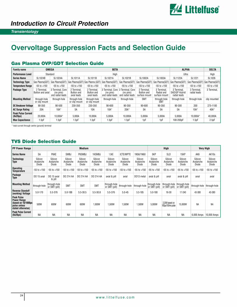
Introduction to Circuit Protection
24w w w. l i t t e l f u s e . c o m
Transientology
Overvoltage Suppression Facts and Selection Guide
PP Power Range Medium High Very High
Series Name SA P6KE SMBJ P6SMBJ 1KSMBJ 1.5KE ICTE/MPTE 1N56/1N60 5KP SLD 15KP AK6 AK10s
Technology Silicon Silicon Silicon Silicon Silicon Silicon Silicon Silicon Silicon Silicon Silicon Silicon SiliconType Avalanche Avalanche Avalanche Avalanche Avalanche Avalanche Avalanche Avalanche Avalanche Avalanche Avalanche Avalanche Avalanche
Diode Diode Diode Diode Diode Diode Diode Diode Diode Diode Diode Diode DiodeOperating Temperature -55 to +150 -55 to +150 -55 to +150 -55 to +150 -55 to +150 -55 to +150 -55 to +150 -55 to +150 -55 to +150 -55 to +150 -55 to +150 -55 to +150 -55 to +150
PackageType DO 15 axial DO 15 axial DO 214 AA DO 214 AA DO 214 AA axial & pill axial DO13 metal axial & pill axial axial & pill axial axial
& pill
Mounting Method through-hole through-hole through-hole through-hole through-holethrough-hole or SMT (pill) SMT SMT SMT or SMT (pill) through-hole through-hole or SMT (pill) or SMT (pill) or SMT (pill) through-hole through-hole
Reverse Standoff(working) Voltage 5.0-170 5.5-376 5.0-188 5.5-30.5 5.5-30.8 5.5-376 5.0-45 5.5-185 5.0-180 16-30 17-240 43-380 43-380
Peak Pulse Power Range (based on 10/1000µs 2,200 based onpulse unless 500W 600W 600W 600W 1,000W 1,500W 1,500W 1,500W 5,000W 100µs/150ms pulse 15,000W NA NAstated otherwise)Peak Pulse Current(8x20µs) NA NA NA NA NA NA NA NA NA NA NA 6,000 Amps 10,000 Amps
TVS Diode Selection Guide
* total current through centre (ground) terminal
Family name OMEGA BETA ALPHA DELTA
Performance Level Standard High Ultra HighSeries Name SL1024B SL1024A SL1011A SL1011B SL1021A SL1021B SL1002A SL1003A SL1122A SL1221 SL1026Technology Type Gas Plasma(GDT) Gas Plasma(GDT) Gas Plasma(GDT) Gas Plasma (GDT) Gas Plasma(GDT) Gas Plasma(GDT) Gas Plasma(GDT) Gas Plasma(GDT) Gas Plasma(GDT) Gas Plasma(GDT) Gas Plasma(GDT)Temperature Range -55 to +150 -55 to +150 -55 to +150 -55 to +150 -55 to +150 -55 to +150 -55 to +150 -55 to +150 -55 to +150 -55 to +150 -55 to +150Package Type 2 Terminal, 3 Terminal, Core 2 Terminal, 2 Terminal, 3 Terminal, Core 3 Terminal, Core 2 Terminal, 3 Terminal, 3 Terminal, 3 Terminal, 3 Terminal,
Button and axial (no pins) Button and Button and (no pins) (no pins) Button and Radial and SAD/GP Hybrid radial leadsand radial leads axial leads axial leads and radial leads and radial leads surface mount surface mount radial leads
Mounting Method through-hole through-hole through-hole through-hole through-hole through-hole SMT through-hole through-hole through-hole clip mountedor clip mount or clip mount or clip mount SMT
DC Breakover Voltage 90-350 90-500 230-350 230-350 90-600 90-350 90-600 90-350 90-300 200 275-1100AC Surge Rating 20A 10A* 5A 10A 10A* 20A* 5A 5A 5A 10A* 40A*Peak Pulse Current (8x20µs) 20,000A 10,000A* 5,000A 10,000A 5,000A 10,000A 5,000A 5,000A 5,000A 10,000A* 40,000AMax Capacitance 1.5pF 1.5pF 1.5pF 1.5pF 1.5pF 1.5pF 1pF 1pF 100-200pF 1.5pF 2.5pF
Gas Plasma OVP/GDT Selection Guide
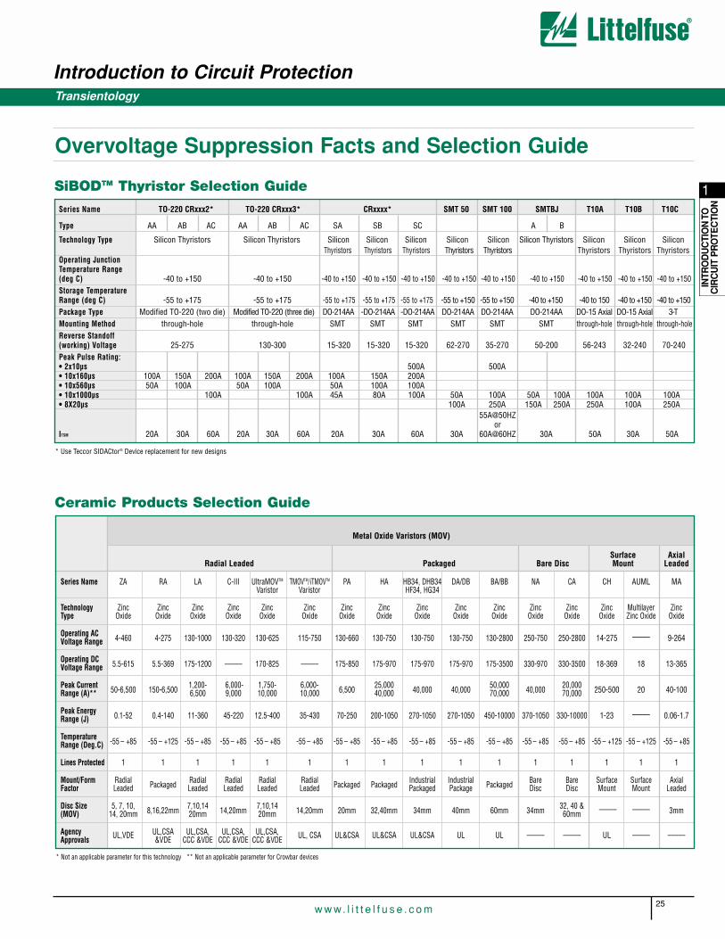
Introduction to Circuit Protection
25w w w. l i t t e l f u s e . c o m
1
INTR
OD
UC
TIO
N T
OC
IRC
UIT
PR
OTE
CTI
ON
Overvoltage Suppression Facts and Selection Guide
SiBODTM Thyristor Selection Guide
Series Name TO-220 CRxxx2* TO-220 CRxxx3* CRxxxx* SMT 50 SMT 100 SMTBJ T10A T10B T10C
Type AA AB AC AA AB AC SA SB SC A B
Technology Type Silicon Thyristors Silicon Thyristors Silicon Silicon Silicon Silicon Silicon Silicon Thyristors Silicon Silicon SiliconThyristors Thyristors Thyristors Thyristors Thyristors Thyristors Thyristors Thyristors
Operating Junction Temperature Range (deg C) -40 to +150 -40 to +150 -40 to +150 -40 to +150 -40 to +150 -40 to +150 -40 to +150 -40 to +150 -40 to +150 -40 to +150 -40 to +150Storage Temperature Range (deg C) -55 to +175 -55 to +175 -55 to +175 -55 to +175 -55 to +175 -55 to +150 -55 to +150 -40 to +150 -40 to 150 -40 to +150 -40 to +150Package Type Modified TO-220 (two die) Modified TO-220 (three die) DO-214AA -DO-214AA -DO-214AA DO-214AA DO-214AA DO-214AA DO-15 Axial DO-15 Axial 3-TMounting Method through-hole through-hole SMT SMT SMT SMT SMT SMT through-hole through-hole through-holeReverse Standoff (working) Voltage 25-275 130-300 15-320 15-320 15-320 62-270 35-270 50-200 56-243 32-240 70-240Peak Pulse Rating:• 2x10µs 500A 500A• 10x160µs 100A 150A 200A 100A 150A 200A 100A 150A 200A• 10x560µs 50A 100A 50A 100A 50A 100A 100A• 10x1000µs 100A 100A 45A 80A 100A 50A 100A 50A 100A 100A 100A 100A• 8X20µs 100A 250A 150A 250A 250A 100A 250A
55A@50HZor
ITSM 20A 30A 60A 20A 30A 60A 20A 30A 60A 30A 60A@60HZ 30A 50A 30A 50A
* Not an applicable parameter for this technology ** Not an applicable parameter for Crowbar devices
Ceramic Products Selection Guide
Metal Oxide Varistors (MOV)
Surface AxialRadial Leaded Packaged Bare Disc Mount Leaded
Series Name ZA RA LA C-III UltraMOVTM TMOVTM/iTMOVTM PA HA HB34, DHB34 DA/DB BA/BB NA CA CH AUML MAVaristor Varistor HF34, HG34
Technology Zinc Zinc Zinc Zinc Zinc Zinc Zinc Zinc Zinc Zinc Zinc Zinc Zinc Zinc Multilayer ZincType Oxide Oxide Oxide Oxide Oxide Oxide Oxide Oxide Oxide Oxide Oxide Oxide Oxide Oxide Zinc Oxide Oxide
Operating AC –––––Voltage Range 4-460 4-275 130-1000 130-320 130-625 115-750 130-660 130-750 130-750 130-750 130-2800 250-750 250-2800 14-275 9-264
Operating DCVoltage Range 5.5-615 5.5-369 175-1200 ––––– 170-825 ––––– 175-850 175-970 175-970 175-970 175-3500 330-970 330-3500 18-369 18 13-365
Peak Current 1,200- 6,000- 1,750- 6,000- 25,000 50,000 20,000Range (A)** 50-6,500 150-6,500 6,500 9,000 10,000 10,000 6,500 40,000 40,000 40,000 70,000 40,000 70,000 250-500 20 40-100
Peak Energy –––––Range (J) 0.1-52 0.4-140 11-360 45-220 12.5-400 35-430 70-250 200-1050 270-1050 270-1050 450-10000 370-1050 330-10000 1-23 0.06-1.7
TemperatureRange (Deg.C) -55 – +85 -55 – +125 -55 – +85 -55 – +85 -55 – +85 -55 – +85 -55 – +85 -55 – +85 -55 – +85 -55 – +85 -55 – +85 -55 – +85 -55 – +85 -55 – +125 -55 – +125 -55 – +85
Lines Protected 1 1 1 1 1 1 1 1 1 1 1 1 1 1 1 1
Mount/Form Radial Radial Radial Radial Radial Industrial Industrial Bare Bare Surface Surface AxialFactor Leaded Packaged Leaded Leaded Leaded Leaded Packaged Packaged Packaged Package Packaged Disc Disc Mount Mount Leaded
Disc Size 5, 7, 10, 7,10,14 7,10,14 32, 40 & ––––– –––––(MOV) 14, 20mm 8,16,22mm 20mm 14,20mm 20mm 14,20mm 20mm 32,40mm 34mm 40mm 60mm 34mm 60mm 3mm
Agency UL,VDE UL,CSA UL,CSA, UL,CSA, UL,CSA, UL, CSA UL&CSA UL&CSA UL&CSA UL UL ––––– ––––– UL ––––– –––––Approvals &VDE CCC &VDE CCC &VDE CCC &VDE
Transientology
* Use Teccor SIDACtor® Device replacement for new designs

Introduction to Circuit Protection
26w w w. l i t t e l f u s e . c o m
Transientology
ESD Suppressor Selection GuideLittelfuse manufacturers three different surface mount product families for ESD suppression. Each technology provides distinct attributes forcompatibility to specific circuit requirements.
1. Review the circuit requirements or parameters from the left hand column and compare them to the Littelfuse product offerings shown.
2. Refer to Littelfuse data sheets and application notes for complete technical information
PulseGuard®
Suppressors Silicon Protection Arrays Multilayer Varistors
Surface Chip ScaleMount Package (CSP) Surface Mount Surface Mount
Series Name PGB SP05X SP72X SP05X SP05X SPUSB1 ML MLE MLN MHS
TVS Silicon TVS Rail MLV MLV MLV MLVTechnology Type VVM Avalanche SCR/Diode Avalanche Clamp ZnO ZnO ZnO ZnODiode Diode
Working Voltage 0-24VDC 0-5.5VDC 0-30VDC 0-5.5VDC 0-5.5VDC 0-5.5VDC 0-120VDC 0-18VDC 0-18VDC 0-42VDCrange by type
DIP, SOIC SC70 (2,4,5), S0T143 (2),SC70-6
Array Package SOT23 (2), CSP (6, 14) SOT23 (2,4,5), MSOP-8 (6),(3)
(No. of Lines) (4, 8, 16) SOT23 SOT143 (3), SOIC-8 (6), No No 1206 No0805 (4) (4) TSSOP-8 (4), QSOP-24(18) (4)MSOP-8 (6)
Single Line Package 0402, 0603 No No No No No 0402-1210 0402-1206 ––––– 0402, 0603
Typical Device Capacitance 0.05pF 39pF 3-5pF 30pF 3-7pF 47pF 40-6000pF 40-1700pF 45-430pF 3-22pF
Leakage Current <1nA <10µA <20µA <10µA <.1µA <100nA <25µA <25µA <2µA <5µA
Rated Immunity to Yes Yes Yes Yes Yes Yes Yes Yes Yes YesIEC 61000-4-2 level 4
Also Rated for EFT or No TBD Yes TBD TBD TBD Yes Yes Yes YesLightning Wave
Bidirectional (transients Yes Yes Yes Yes Yes Yes Yes Yes Yes Yesof either polarity)
Performs Low Pass Filtering – – – – – Yes Yes Yes Yes Yes
USB Port Terminator(w/ESD Suppression
and EMI Filter)
Application Examples Circuit Examples Transient Threat Device Family Technology
Computers High-speed Interfaces:- desktop, laptop, notebook USB 2.0, IEEE 1394, InfiniBand, ESD PGB PulseGuard®
Peripherals RF antenna circuits, Gigabit Ethernet, DVI Polymer- scanner, printer, monitor, disk drive sSP05x TVS diode
External Broadband hardware Medium-speed Interfaces: SP72x SCR/Rail clamp- modem, set top box USB 1.1, RS 485, Ethernet, video ESD, EMI, EFT MHS, ML, MLE, MLN MLV
Network hardware 10 Baset, 100Baset, T1/E1 SPUSB1 TVS/filter- switch, router, hub, repeater Lightning PxxxxMC SIDACtor® Devices
Digital camera/camcorderHandheld portables Low-speed Interfaces:- PDA, cell phone, cordless phone, GPS Audio, RS 232, IEEE 1284, push buttons, Lightning LCE, SA SAD
Video equipment key pads, switches Pxxxxx SIDACtor® Devices- HDTV, DVD, VCR, set top box
Alarm systems ESD, EMI, EFT ML, MLE MLV- security, fire
Metering systems Power Inputs:Medical equipment 120/240 VAC, up to 120 VDC Lightning CH, MA, ZA, RA, UltraMOV MOVLighting ballast Switching Transients SA, P6KE, 1.5PKE SADRemote sensors/transducers SMBJ, 1KSMBJ SAD
ESD, EMI, EFT ICTE/MPTE SADAvionics/Military Electronics Power and System Inputs Lightning and System Transients 1N56/1N60, 5KP/SLD SAD
Hi-Rel MOVs MOV
Low
/Mediu
m V
olt
age E
lect
ronic
s
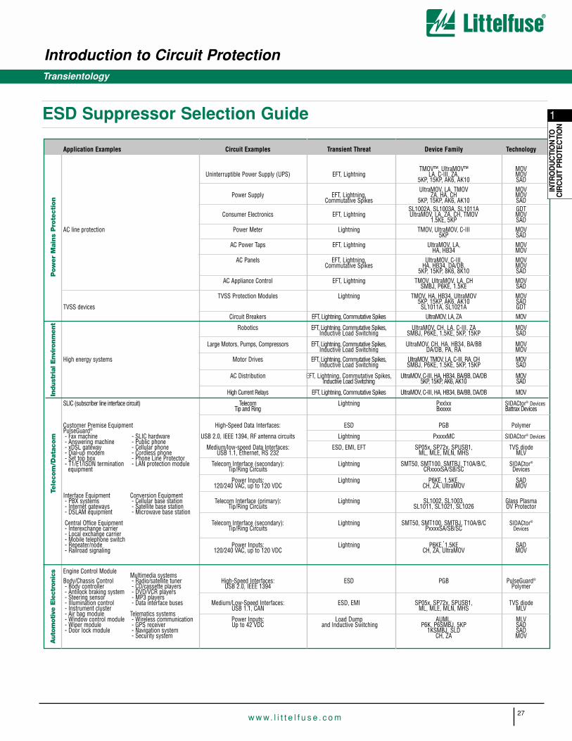
Application Examples Circuit Examples Transient Threat Device Family Technology
TMOV™, UltraMOV™ MOVUninterruptible Power Supply (UPS) EFT, Lightning LA, C-III, ZA, MOV
5KP, 15KP, AK6, AK10 SADUltraMOV, LA, TMOV MOV
Power Supply EFT, Lightning, ZA, HA, CH MOVCommutative Spikes 5KP, 15KP, AK6, AK10 SAD
SL1002A, SL1003A, SL1011A GDTConsumer Electronics EFT, Lightning UltraMOV, LA, ZA, CH, TMOV MOV
1.5KE, 5KP SADAC line protection Power Meter Lightning TMOV, UltraMOV, C-III MOV
5KP SADAC Power Taps EFT, Lightning UltraMOV, LA, MOV
HA, HB34 MOVAC Panels EFT, Lightning, UltraMOV, C-III, MOV
Commutative Spikes HA, HB34, DA/DB, MOV5KP, 15KP, 8K6, 8K10 SAD
AC Appliance Control EFT, Lightning TMOV, UltraMOV, LA, CH MOVSMBJ, P6KE, 1.5KE SAD
TVSS Protection Modules Lightning TMOV, HA, HB34, UltraMOV MOV5KP, 15KP, AK6, AK10 SAD
TVSS devices SL1011A, SL1021A GDTCircuit Breakers EFT, Lightning, Commutative Spikes UltraMOV, LA, ZA MOV
Robotics EFT, Lightning, Commutative Spikes, UltraMOV, CH, LA, C-III, ZA MOVInductive Load Switching SMBJ, P6KE, 1.5KE, 5KP, 15KP SAD
Large Motors, Pumps, Compressors EFT, Lightning, Commutative Spikes, UltraMOV, CH, HA, HB34, BA/BB MOVInductive Load Switching DA/DB, PA, RA MOV
High energy systems Motor Drives EFT, Lightning, Commutative Spikes, UltraMOV, TMOV, LA, C-III, RA, CH MOVInductive Load Switching SMBJ, P6KE, 1.5KE, 5KP, 15KP SAD
AC Distribution EFT, Lightning, Commutative Spikes, UltraMOV, C-III, HA, HB34, BA/BB, DA/DB MOVInductive Load Switching 5KP, 15KP, AK6, AK10 SAD
High Current Relays EFT, Lightning, Commutative Spikes UltraMOV, C-III, HA, HB34, BA/BB, DA/DB MOV
SLIC (subscriber line interface circuit) Telecom Lightning Pxxlxx SIDACtor® DevicesTip and Ring Bxxxxx Battrax Devices
Customer Premise Equipment High-Speed Data Interfaces: ESD PGB PolymerPulseGuard®
- Fax machine - SLIC hardware USB 2.0, IEEE 1394, RF antenna circuits Lightning PxxxxMC SIDACtor® Devices- Answering machine - Public phone- xDSL gateway - Cellular phone Medium/low-speed Data Interfaces: ESD, EMI, EFT SP05x, SP72x, SPUSB1, TVS diode- Dial-up modem - Cordless phone USB 1.1, Ethernet, RS 232 ML, MLE, MLN, MHS MLV- Set top box - Phone Line Protector- T1/E1/ISDN termination - LAN protection module Telecom Interface (secondary): Lightning SMT50, SMT100, SMTBJ, T10A/B/C, SIDACtor®
equipment Tip/Ring Circuits CRxxxxSA/SB/SC Devices
Power Inputs: Lightning P6KE, 1.5KE, SAD120/240 VAC, up to 120 VDC CH, ZA, UltraMOV MOV
Interface Equipment Conversion Equipment- PBX systems - Cellular base station Telecom Interface (primary): Lightning SL1002, SL1003, Glass Plasma- Internet gateways - Satellite base station Tip/Ring Circuits SL1011, SL1021, SL1026 OV Protector- DSLAM equipment - Microwave base station
Central Office Equipment Telecom Interface (secondary): Lightning SMT50, SMT100, SMTBJ, T10A/B/C SIDACtor®
- Interexchange carrier Tip/Ring Circuits PxxxxSA/SB/SC Devices- Local exchange carrier- Mobile telephone switch ,- Repeater/node Power Inputs: Lightning P6KE, 1.5KE SAD- Railroad signaling 120/240 VAC, up to 120 VDC CH, ZA, UltraMOV MOV
Engine Control ModuleMultimedia systems
Body/Chassis Control - Radio/satellite tuner High-Speed Interfaces: ESD PGB PulseGuard®
- Body controller - CD/cassette players USB 2.0, IEEE 1394 Polymer- Antilock braking system - DVD/VCR players- Steering sensor - MP3 players- Illumination control - Data interface buses Medium/Low-Speed Interfaces: ESD, EMI SP05x, SP72x, SPUSB1, TVS diode- Instrument cluster USB 1.1, CAN ML, MLE, MLN, MHS MLV- Air bag module Telematics systems- Window control module - Wireless communication Power Inputs: Load Dump AUML, MLV- Wiper module - GPS receiver Up to 42 VDC and Inductive Switching P6K, P6SMBJ, 5KP SAD- Door lock module - Navigation system 1KSMBJ, SLD SAD
- Security system CH, ZA MOV
ESD Suppressor Selection Guide
Introduction to Circuit Protection
27w w w. l i t t e l f u s e . c o m
1
INTR
OD
UC
TIO
N T
OC
IRC
UIT
PR
OTE
CTI
ON
Pow
er
Mai
ns
Pro
tect
ion
Indust
rial
Envi
ronm
ent
Tele
com
/Dat
acom
Auto
mot
ive
Ele
ctro
nic
s
Transientology
Varistor Products Overview . . . . . . . . . . . . . . . . . . . . . . . . . . . . . . . . . . . . . . . . . . . . . . . . . . . . . . . . . . . . . . . . . . . . . . . . . . . . . . . . . . . . . 29-30
Radial Lead VaristorsTMOV™ and iTMOV™ High Surge Current Radial Lead Thermally Protected Metal Oxide Varistors . . . . . . . . . . . . . . . . . . . . . . . . . . . . . . . . . 31-39
UltraMOV™ High Surge Current Radial Lead Metal Oxide Varistors. . . . . . . . . . . . . . . . . . . . . . . . . . . . . . . . . . . . . . . . . . . . . . . . . . . . . . . . . 40-51
C-III Series High Energy Radial Lead Varistors . . . . . . . . . . . . . . . . . . . . . . . . . . . . . . . . . . . . . . . . . . . . . . . . . . . . . . . . . . . . . . . . . . . . . . . 52-59
LA Series Radial Lead Metal-Oxide Varistors for Line Voltage Operation . . . . . . . . . . . . . . . . . . . . . . . . . . . . . . . . . . . . . . . . . . . . . . . . . . . . 60-70
ZA Series Radial Lead Metal-Oxide Varistors for Low to Medium Voltage Operation . . . . . . . . . . . . . . . . . . . . . . . . . . . . . . . . . . . . . . . . . . . . 71-84
Industrial High Energy VaristorsBA/BB Series Industrial High Energy Metal-Oxide Varistors . . . . . . . . . . . . . . . . . . . . . . . . . . . . . . . . . . . . . . . . . . . . . . . . . . . . . . . . . . . . . . 85-89
DA/DB Series Industrial High Energy Metal-Oxide Varistors . . . . . . . . . . . . . . . . . . . . . . . . . . . . . . . . . . . . . . . . . . . . . . . . . . . . . . . . . . . . . 90-93
HA Series Industrial High Energy Metal-Oxide Varistors. . . . . . . . . . . . . . . . . . . . . . . . . . . . . . . . . . . . . . . . . . . . . . . . . . . . . . . . . . . . . . . . . 94-97
HB34, HF34 and HG34 Series Industrial High Energy Metal-Oxide Varistors . . . . . . . . . . . . . . . . . . . . . . . . . . . . . . . . . . . . . . . . . . . . . . . . 98-104
DHB34 Series Industrial High Energy Metal-Oxide Varistors . . . . . . . . . . . . . . . . . . . . . . . . . . . . . . . . . . . . . . . . . . . . . . . . . . . . . . . . . . . 105-108
Industrial High Energy Disc Varistors
CA Series Industrial High Energy Metal-Oxide Disc Varistors . . . . . . . . . . . . . . . . . . . . . . . . . . . . . . . . . . . . . . . . . . . . . . . . . . . . . . . . . . 109-116
NA Series Industrial High Energy Metal-Oxide Square Disc Varistors . . . . . . . . . . . . . . . . . . . . . . . . . . . . . . . . . . . . . . . . . . . . . . . . . . . . . 117-121
Other Application-Specific VaristorsMA Series Axial Lead Metal-Oxide Varistors . . . . . . . . . . . . . . . . . . . . . . . . . . . . . . . . . . . . . . . . . . . . . . . . . . . . . . . . . . . . . . . . . . . . . . . 122-126
PA Series Base Mount Metal-Oxide Varistors . . . . . . . . . . . . . . . . . . . . . . . . . . . . . . . . . . . . . . . . . . . . . . . . . . . . . . . . . . . . . . . . . . . . . . . 127-131
RA Series Low Profile Metal-Oxide Varistors . . . . . . . . . . . . . . . . . . . . . . . . . . . . . . . . . . . . . . . . . . . . . . . . . . . . . . . . . . . . . . . . . . . . . . . 132-139
High Reliability Varistors High Reliability Series Mechanical and Environmental Testing for Aerospace, Military and High Reliability Applications . . . . . . . . . . . . . . . . . . . . . . . . . . . . . . . . . . . . . . . . . . . . . . . . . . . . . . . . . . . . . . . . . . . . . . . . . . . . . . 140-149
DSSC Qualified Parts List (QPL) MIL-R-83530 . . . . . . . . . . . . . . . . . . . . . . . . . . . . . . . . . . . . . . . . . . . . . . . . . . . . . . . . . . . . . . . . . . . . . . . . . . . . . 140
MIL-R-83530 Inspections . . . . . . . . . . . . . . . . . . . . . . . . . . . . . . . . . . . . . . . . . . . . . . . . . . . . . . . . . . . . . . . . . . . . . . . . . . . . . . . . . . . . . . . . . . . . . 141
DSSC Standard Military Drawing # 87063 . . . . . . . . . . . . . . . . . . . . . . . . . . . . . . . . . . . . . . . . . . . . . . . . . . . . . . . . . . . . . . . . . . . . . . . . . . . . . 142-143
DSSC Standard Military Drawing # 90065 . . . . . . . . . . . . . . . . . . . . . . . . . . . . . . . . . . . . . . . . . . . . . . . . . . . . . . . . . . . . . . . . . . . . . . . . . . . . . . . . 144
Littelfuse High Reliability Series TX Equivalents. . . . . . . . . . . . . . . . . . . . . . . . . . . . . . . . . . . . . . . . . . . . . . . . . . . . . . . . . . . . . . . . . . . . . . . . . 144-145
Custom Types . . . . . . . . . . . . . . . . . . . . . . . . . . . . . . . . . . . . . . . . . . . . . . . . . . . . . . . . . . . . . . . . . . . . . . . . . . . . . . . . . . . . . . . . . . . . . . . . . . . . . 146
Radiation Hardness/Neutron Effects . . . . . . . . . . . . . . . . . . . . . . . . . . . . . . . . . . . . . . . . . . . . . . . . . . . . . . . . . . . . . . . . . . . . . . . . . . . . . . . . . . . . . 147
Commercial Item Descriptions . . . . . . . . . . . . . . . . . . . . . . . . . . . . . . . . . . . . . . . . . . . . . . . . . . . . . . . . . . . . . . . . . . . . . . . . . . . . . . . . . . . . . . 148-149
PAGE
28w w w. l i t t e l f u s e . c o m
Varistor Products
2

2
VAR
ISTO
RP
RO
DU
CT
S
Varistor Products Overview
Varistor Products
29w w w. l i t t e l f u s e . c o m
Varistor Products OverviewThe Metal Oxide Varistor (MOV) components listed in this section areintended for a comprehensive range of applications and transient voltagesuppression products.
The product series in this section vary in size, form factor, and packagestyle as illustrated in Figure 1 in order to meet specific performance aswell as manufacturing needs of the user.
Additionally, Figure 2 forms a selection guide matrix for the designer byillustrating the various device’s working voltage transient energy andpeak current ratings range.
The data sheets in this section have been grouped by package style and arepresented in the following sequence:
• Radial Lead Styles- TMOV™, iTMOV™ and UltraMOV™ Varistors, C-III, LA and ZA Series
• High Energy Industrial Varistors- BA/BB, DA/DB HA, HB, HC, HF, HG, and DHB Series
• High Energy Industrial Varistor Discs- CA and NA Series
• Other Application Specific Varistors- MA, PA and RA Series
See Section 10 for comprehensive varistor application note support.
UltraMOV/C-III/LA SERIES ZA SERIES
BB, BA, DA, DB, HA, HB, HC, HF, HG, DHB SERIES
• Radial Package• AC Line Voltage Operation• UL/CSA Recognized• CECC Certified• VDE Certified
• Radial Package• Low Voltage Operation• UL/CSA Recognized• CECC Certified• VDE Certified
• High Energy
• Isolated
Capability • Low Inductance• Rigid Terminals • UL/CSA Recognized• Improved Creep and Strike
• Industrial Discs• Solderable Contacts• Edge Passivation
MA SERIES PA SERIES RA SERIES
• Axial Package• Wide Voltage Range• 3mm Disc
• Rigid Mountdown• NEMA Creep and Strike Distance• Quick Connect Terminal• UL/CSA Recognized
• Low Profile• High Temperature Capability• In-Line Leads• Precise Seating Plane• UL/CSA Recognized
FIGURE 1. VARISTOR PRODUCTS PACKAGE STYLES
BA
CA, NA SERIES
TMOV™ Varistor and iTMOV Varistors
• Thermally Protected MOV•
Radial Package•AC Line Voltage Operation•UL 1449 Recognized•
High Energy Capability
• Available indicating third leg
TM
Varistor Products
30w w w. l i t t e l f u s e . c o m
Varistor Products Overview
VOLTS DC3.5
VOLTS AC RMS4
14
10
35
25
175
130
200
150
330
250
365
264 320
369
275
615
460
850
660
970
750
1,200
1,000
7,000
6,000
MA SERIES
TMOV™ and TMOV™ Varistors
ZA SERIES
RA SERIES
C-III, LA, UltraMOV™ Varistors
PA SERIES
HA, HB, DA/ DB SERIES
BA/ BB SERIES
MAXIMUM STEADY-STATE APPLIED VOLTAGE
PEAKCURRENT
(A)ENERGY
(J)DISC SIZES/PACKAGES
40 - 100
50 - 6500
100 - 6500
6500
25,000 -40,000
50,000 -70,000
1,200 -10,000
0.07 -1.7
0.1 - 52
0.4 - 160
11 - 400
70 - 250
270 -1,050
6,500 -10,000 50 - 273
450 -10,000
20mm
5, 7, 10,14, 20 (mm)
5 x 8, 10 x 16,14 x 22 (mm)
7, 10, 14,20 (mm)
3mm
60mm
2,800
3,500
NA SERIES30,000 -40,000
270 -1050
34mm SQ.
20,000 -70,000
200 -10,000
CA SERIES
FIGURE 2. VARISTOR PRODUCT FAMILY SELECTION GUIDE
32, 40, 60 (mm)
32, 3440 (mm)
14, 20 (mm)
NEWi
Varistor Products Overview

2
VAR
ISTO
RP
RO
DU
CT
S
Varistor Products
31w w w. l i t t e l f u s e . c o m
Thermally Protected
TMOV® and iTMOV® Varistor Series ®
The Littelfuse TMOV and iTMOV thermally protected varistors represent anew development in integrated circuit protection (patent pending). Bothversions are comprised of radial leaded MOVs (Metal Oxide Varistors)with an integrated thermally activated element designed to open in theevent of overheating due to the abnormal over-voltage, limited current,conditions outlined in UL1449.
The iTMOV varistor differs from the TMOV varistor by the inclusion of athird lead for the purpose of indicating that the MOV has been disconnect-ed from the circuit. This lead facilitates connection to monitoring circuitry.
The TMOV and iTMOV varistors offer quick thermal response due to theclose proximity of the integrated thermal element to the MOV body. Theintegrated configuration also offers lower inductance than most discretesolutions resulting in improved clamping performance to fast over-voltagetransients. Additionally, TMOV and iTMOV varistors are wave solderable,thus simplifying end product assembly by reducing the expense andrework associated with hand soldering operations.
The TMOV and iTMOV varistors are both recognized surge suppressioncomponents to UL 1449. The TMOV and iTMOV varistor’s integratedthermal element, in conjunction with appropriate enclosure design, helpsfacilitate TVSS module compliance to UL1449 for both cord connectedand permanently connected applications.
TMOV and iTMOV varistors are compatible for use with industry standardwave-soldering processes or recommended hand-soldering methods.
Features• Patent Pending Integrated Thermal Protection Device
• Designed to facilitate compliance to UL1449 for TVSS product
• High peak surge current rating up to 10kA
• Wave solderable
• Standard lead form and spacing option
• Low Leakage
• -55°C to +85°C Operating Temperature Range
• Three-lead version available for indication purposes.
AGENCY APPROVALS:Documented in UL file E75961. CSA recognized.
20mm Devices-Recognized under the components program of UnderwritersLaboratories UL1449 and UL1414. Includes selected tests from UL1020,regarding thermal cutoffs for devices with voltage ratings up to 420VAC.
14mm Devices-Devices are approved as an MOV to UL1449 and UL1414.Approval to selected UL1020 requirements pending. Devices (14mm and20mm) with ratings greater than 420VAC are not affected by these abnormalvoltage conditions.
Accelerated Aging Testing-14 and 20mm devices comply with AccleratedAging Test requirements per. ANSI/IEEE C62.11 and may be used in second-ary surge arrestors without repeating this test.
AGENCY FILE NUMBERS: ULE56529 (UL1414)
ULE75961 (UL1449)
CSA LR91788
Applications• TVSS Products
• AC Panel Protection Modules
• AC Line Power Supplies
• Surge Protected Strip Connectors
• AC Power Meters
• Relocatable AC Power Taps
• GFCI (Ground Fault Current Interupter)
• UPS (Uninterruptable Power Supply)
• White Goods
• Plug-in TVSS
• Inverters
• AC/DC Power Supplies
®
Varistor Products
32w w w. l i t t e l f u s e . c o m
Thermally Protected
TMOV® and iTMOV® Varistor Series
MAXIMUM RATING (85¡C) SPECIFICATIONS (25¡C)CONTINUOUS TRANSIENT
ACVOLTS
ENERGY2ms
PEAK SURGECURRENT
8/20 s
VARISTORVOLTAGE AT 1mATEST CURRENT
MAXIMUMCLAMPINGVOLTAGE
8/20 s
TYPICALCAPACI-TANCE
f = 1MHz
VM(AC)RMS WTMVN(DC)
MINVN(DC)MAX VC IPK CPART
NUMBER (V) (J) (V) (V) (A) (pF)
TMOV14R130E 130 50 184 226 340 50 1000TMOV20R130E 130 100 184 226 340 100 1900TMOV14R140E 140 55 200 240 360 50 900TMOV20R140E 140 110 200 240 360 100 1750TMOV14R150E 150 60 216 264 395 50 800TMOV20R150E 150 120 216 264 395 100 1600TMOV14R175E 175 70 243 297 455 50 700TMOV20R175E 175 135 243 297 455 100 1400TMOV14R200E 200 75 281 344 530 50 630TMOV20R200E 200 154 281 344 530 100 1250
TMOV14R250E 250 100 351 429 650 50 500TMOV20R250E 250 170 351 429 650 100 1000TMOV14R275E 275 110 387 473 710 50 450TMOV20R275E 275 190 387 473 710 100 900
DEVICEMODEL
NUMBERBRAND-
ING
4T130E20T130E4T140E20T140E4T150E20T150E4T175E20T175E4T200E20T200E
4T250E20T250E4T275E20T275E
(mm)
DISC DIA-
METER
1420
1420
1420
1420
1420
1420
1420
SUPPRESSEDVOLTAGERATING
UL 1449TABLE 60.1
(V)
400400500400500400700700700700
800700900700
ITM2 x PULSE
(A)
4500650045006500450065004500650045006500
4500650045006500
ITM1 x PULSE
(A)
600010000600010000600010000600010000600010000
600010000600010000
TMOV14R115ETMOV20R115E
4T115E20T115E
1420
115 300115 300
3552
6000 450010000 6500
162 198162 198
50100
300 1100300 2400
TMOV14R230E 230 80 324 396 595 50 550TMOV20R230E 230 160 324 396 595 100 1100
4T230E20T230E
1420
700700
45006500
600010000
TMOV14R300E 300 125 423 517 775 50 400TMOV20R300E 300 250 423 517 775 100 800
4T300E20T300E
1420
900900
45006500
600010000
Absolute Maximum Ratings For ratings of individual members of a series, see Device Ratings and Specifications chart
Continuous:Steady State Applied Voltage:
AC Voltage Range (VM(AC)RMS) . . . . . . . . . . . . . . . . . . . . . . . . . . . . . . . . . . . . . . . . . . . . . . . . . . . . . . . . . . . . . . 115 to 750 VTransient:
Peak Pulse Current (ITM) For 8x20µs Current Wave, single pulse . . . . . . . . . . . . . . . . . . . . . . . . . . . . . . . . . . . . . . . . . . . . . . . . . 6000 to 10,000 A
Single-Pulse Energy CapabilityFor 2ms Current Wave . . . . . . . . . . . . . . . . . . . . . . . . . . . . . . . . . . . . . . . . . . . . . . . . . . . . . . . . . . . . . . . . . . 35 to 480 J
Operating Ambient Temperature Range (TA) . . . . . . . . . . . . . . . . . . . . . . . . . . . . . . . . . . . . . . . . . . . . . . . . . . . . . -55 to 85oCStorage Temperature Range (TSTG). . . . . . . . . . . . . . . . . . . . . . . . . . . . . . . . . . . . . . . . . . . . . . . . . . . . . . . . . . . 55 to 125oCTemperature Coefficient (αV) of Clamping Voltage (VC) at Specified Test Current . . . . . . . . . . . . . . . . . . . . . . . . . . . . . . <0.01 %/oCHi-Pot Encapsulation (Isolation Voltage Capability) . . . . . . . . . . . . . . . . . . . . . . . . . . . . . . . . . . . . . . . . . . . . . . . . . . . . . 2500 VThermal Protection Isolation Voltage Capability (when operated) . . . . . . . . . . . . . . . . . . . . . . . . . . . . . . . . . . . . . . . . . . . . 600 VInsulation Resistance . . . . . . . . . . . . . . . . . . . . . . . . . . . . . . . . . . . . . . . . . . . . . . . . . . . . . . . . . . . . . . . . . . . . . . . . . . 1,000 MΩ
Indicator Lead Rating (Lead-3 - iTMOV varistor only):Continuous RMS current . . . . . . . . . . . . . . . . . . . . . . . . . . . . . . . . . . . . . . . . . . . . . . . . . . . . . . . . . . . . . . . . . . . . . . . 100 mASurge Current, 8/20µs . . . . . . . . . . . . . . . . . . . . . . . . . . . . . . . . . . . . . . . . . . . . . . . . . . . . . . . . . . . . . . . . . . . . . . . 10,000 A
CAUTION: Stresses above those listed in “Absolute Maximum Ratings” may cause permanent damage to the device. This is a stress only rating and operation of the deviceat these or any other conditions above those indicated in the operational sections of this specification is not implied.
Device Ratings and Specifications - TMOV Varistor Series™
TMOV and iTMOV Varistor Series - Absolute Maximum Ratings
TMOV / iTMOV Varistor UNITS
NOTE: For 14mm devices with a voltage rating greater than 420V, please contact factory regarding availability.

2
VAR
ISTO
RP
RO
DU
CT
S
Thermally Protected
Varistor Products
33w w w. l i t t e l f u s e . c o m
TMOV® and iTMOV® Varistor SeriesDevice Ratings and Specifications - TMOV Varistor Series continued...
MAXIMUM RATING (85¡C) SPECIFICATIONS (25¡C)CONTINUOUS TRANSIENT
ACVOLTS
ENERGY2ms
PEAK SURGECURRENT
8/20 s
VARISTORVOLTAGE AT 1mATEST CURRENT
MAXIMUMCLAMPINGVOLTAGE
8/20 s
TYPICALCAPACI-TANCE
f = 1MHz
VM(AC)RMS WTMVN(DC)
MINVN(DC)MAX VC IPK CPART
NUMBER (V) (J) (V) (V) (A) (pF)
TMOV14R130M 130 50 184 226 340 50 1000TMOV20R130M 130 100 184 226 340 100 1900TMOV14R140M 140 55 200 240 360 50 900TMOV20R140M 140 110 200 240 360 100 1750TMOV14R150M 150 60 216 264 395 50 800TMOV20R150M 150 120 216 264 395 100 1600TMOV14R175M 175 70 243 297 455 50 700TMOV20R175M 175 135 243 297 455 100 1400TMOV14R200M 200 75 281 344 530 50 630TMOV20R200M 200 154 281 344 530 100 1250
TMOV14R250M 250 100 351 429 650 50 500TMOV20R250M 250 170 351 429 650 100 1000TMOV14R275M 275 110 387 473 710 50 450TMOV20R275M 275 190 387 473 710 100 900
DEVICEMODEL
NUMBERBRAND-
ING
4T130M20T130M4T140M20T140M4T150M20T150M4T175M20T175M4T200M20T200M
4T250M20T250M4T275M20T275M
(mm)
DISC DIA-
METER
1420
1420
1420
1420
1420
1420
1420
SUPPRESSEDVOLTAGERATING
UL 1449TABLE 60.1
(V)
400400500400500400700700700700
800700900700
ITM2 x PULSE
(A)
4500650045006500450065004500650045006500
4500650045006500
ITM1 x PULSE
(A)
600010000600010000600010000600010000600010000
600010000600010000
TMOV14R115MTMOV20R115M
4T115M20T115M
1420
115 300115 300
3552
6000 450010000 6500
162 198162 198
50100
300 1100300 2400
TMOV14R230M 230 80 324 396 595 50 550TMOV20R230M 230 160 324 396 595 100 1100
4T230M20T230M
1420
700700
45006500
600010000
TMOV14R300M 300 125 423 517 775 50 400TMOV20R300M 300 250 423 517 775 100 800
4T300M20T300M
1420
900900
45006500
600010000
TMOV14R320E 320 136 459 561 840 50 380TMOV20R320E 320 273 459 561 840 100 750TMOV14R385ETMOV20R385ETMOV14R420ETMOV20R420E
4T320E20T320E4T385E
20T385E4T420E
20T420E1420
1420
1420
420420
385385
900900
12001200
12001200
160320
150300
45006500
45006500
45006500
600010000
600010000
600010000
612612
558558
748748
682682
11201120
10251025
50100
50100
300600
360700
TMOV20R460E 20T460E 20 460 n/a 360 6500 10000 675 825 1240 100 200TMOV20R510E 20T510E 20 510 n/a 325 6500 10000 738 902 1355 100 350TMOV20R550ETMOV20R575E
20T550E20T575E 20
20575550
n/an/a
375360
65006500
10000 10000
856819
10471001
15681500
100 100
275300
MAXIMUM RATING (85°C) SPECIFICATIONS (25°C)CONTINUOUS TRANSIENT
ACVOLTS
ENERGY2ms
PEAK SURGECURRENT
8/20µs
VARISTORVOLTAGE AT 1mATEST CURRENT
MAXIMUMCLAMPINGVOLTAGE
8/20µs
TYPICALCAPACI-TANCE
f = 1MHz
VM(AC)RMS WTMVN(DC)MIN
VN(DC)MAX VC IPK CPART
NUMBER (V) (J) (V) (V) (A) (pF)
TMOV20R750E 750 100 1080 1320 1980 100 175
DEVICEMODELNUMBER
BRANDING
20T750E
(mm)
DISC DIA-
METER
20
SUPPRESSEDVOLTAGERATING
UL 1449TABLE 60.1
(V)
n/a
ITM2 x PULSE
(A)
6500
ITM1 x PULSE
(A)
10000TMOV20R625E 20T625E 20 625 n/a 52 10000 6500 900 1100 1001650 250
Device Ratings and Specifications - iTMOV Varistor Series
NOTE: For 14mm devices with a voltage rating greater than 420V, please contact factory regarding availability.
NOTE: For 14mm devices with a voltage rating greater than 420V, please contact factory regarding availability.

Varistor Products
34w w w. l i t t e l f u s e . c o m
TMOV® and iTMOV® Varistor SeriesDevice Ratings and Specifications - iTMOV Varistor Series continued...
TMOV14R320M 320 136 459 561 840 50 380TMOV20R320M 320 273 459 561 840 100 750TMOV14R385MTMOV20R385MTMOV14R420MTMOV20R420M
4T320M20T320M4T385M
20T385M4T420M
20T420M1420
1420
1420
420420
385385
900900
12001200
12001200
160320
150300
45006500
45006500
45006500
600010000
600010000
600010000
612612
558558
748748
682682
11201120
10251025
50100
50100
300600
360700
TMOV20R460MTMOV20R510M
20T460M20T510M 20
20510460
n/an/a
325360
65006500
10000 10000
738675
902825
13551240
100 100
350200
TMOV20R550MTMOV20R575M
20T550M20T575M 20
20575550
n/an/a
375360
65006500
10000 10000
856819
10471001
15681500
100 100
275300
TMOV20R750M 750 100 1080 1320 1980 100 17520T750M 20 480 650010000TMOV20R625M 20T625M 20 625 400 52 10000 6500 900 1100 1001650 250
MAXIMUM RATING (85¡C) SPECIFICATIONS (25¡C)CONTINUOUS TRANSIENT
ACVOLTS
ENERGY2ms
PEAK SURGECURRENT
8/20 s
VARISTORVOLTAGE AT 1mATEST CURRENT
MAXIMUMCLAMPINGVOLTAGE
8/20 s
TYPICALCAPACI-TANCE
f = 1MHz
VM(AC)RMS WTMVN(DC)
MINVN(DC)MAX VC IPK CPART
NUMBER (V) (J) (V) (V) (A) (pF)
DEVICEMODEL
NUMBERBRAND-
ING (mm)
DISC DIA-
METER
SUPPRESSEDVOLTAGERATING
UL 1449TABLE 60.1
(V)
ITM2 x PULSE
(A)
ITM1 x PULSE
(A)
NOTE: For 14mm devices with a voltage rating greater than 420V, please contact factory regarding availability.
Thermally Protected

2
VAR
ISTO
RP
RO
DU
CT
S
Varistor Products
35w w w. l i t t e l f u s e . c o m
VAR
ISTO
RP
RO
DU
CT
S
Thermally Protected
TMOV® and iTMOV® Varistor Series
1
2
3
3
21
ThermalFuseElement
MOV
ThermalFuseElement
MOV
Monitor Lead
iTMOV Varistor Application ExamplesThe application examples below show how the indicator lead on theiTMOV can be used to indicate that the thermal element has beenopened. This signifies that the circuit is no longer protected from transients by the MOV.
Application Example 1 (Figure 1)In this case, the LED is normally on, and is off when the thermal element opens.
Application Example 2 (Figure 2)This circuit utilizes an optocoupler to provide galvanic isolations between the iTMOV varistor and the indicating or alarm circuitry.
Application Example 3 (Figure 3)This circuit illustrates the use of the monitoring lead of the iTMOV varistor to ensure that equipment is only operated when overvoltage protection present. In normal operation the load switch relay solenoid ispowered via the indicator lead of the iTMOV varistor. In the event of thethermal element being activated, the relay will de-activate, cutting powerto the protected circuit and the fault LED will illuminate.
Please note: Indicator circuits are provided as a guideline only.Verification of actual indicator circuitry is the responsibility of the enduser. Component values selected must be appropriate for the specific AC line voltage service and application.
R
LED
Line Fuse
iTMOV Varistor
Neutral
Line
Figure 1. Application example 1
R
Line Fuse
iTMOV Varistor
Neutral
Figure 2. Application example 2
AC OPTOCOUPLER
TO STATUSANNUNCIATORLIGHT/ALARM
Line Fuse
iTMOV Varistor
Neutral
Figure 3. Application example 3
Fault LED(Normallyoff)
"Load Powered" neon lamp
Load Switch Relay(loss of protection)
R
To
Pro
tect
ed C
ircui
tT
o P
rote
cted
Circ
uit
To
Pro
tect
ed C
ircui
t
Line
Line
Lead Configurations
TMOV Varistor iTMOV Varistor
Note: MOVs are non-polarized passive elements

Varistor Products
36w w w. l i t t e l f u s e . c o m
TMOV® and iTMOV® Varistor Series
* Figure 4: Typical time to open circuit under UL1449 Abnormal Overvoltage Limited Current Test
0.1
1
10
10 100 1000 10000Time s
0.125A0.5A2.5A5A
Typical
For applications exceeding 85ºC ambienttemperature, the peak surge current and energyratings must be reduced as shown in Figure 3.
Figure 5: Peak Current & Energy Derating Curve
0
20
40
60
80
100
-55 50 60 70 80 90 100 110 120 130
AMBIENT TEMPERATURE (ºC)
PE
RC
EN
T O
F R
AT
ED
VA
LUE
Thermal Characteristics
Transient V-I Characteristic Curves
100
1000
10000
0.000001 0.00001 0.0001 0.001 0.01 0.1 1 10 100 1000 10000
Peak Current (A)
Cla
mpi
ng V
olta
ge (
V)
175V150V140V130V
320V275V
250V230V
Figure 6: V-I Characteristic Curves for 14mm Types
420V385V
115V
Maximum Leakage Current
Maximum Clamping Voltage
14mm
200V
460V510V550V575V625V750V
100
1000
10000
0.000001 0.00001 0.0001 0.001 0.01 0.1 1 10 100 1000 10000
Peak Current (A)
Cla
mpi
ng V
olta
ge (
V)
175V150V140V130V
320V
275V
250V230V
Figure 7: V-I Characteristic Curves for 20mm Types
420V385V
115V
Maximum Leakage Current
Maximum Clamping Voltage
20mm
200V
460V510V550V575V625V 750V
300V
Figure 9: Pulse Rating Curves for 20mm types
1
10
100
1000
10000
10 100 1000 10000
Impulse Duration ( s)
Pea
k C
urre
nt (
A)
1
102
103
∞∞
Model 20 mm2
104
105
106
10
Figure 8: Pulse Rating Curves for 14mm types
1
10
100
1000
10000
10 100 1000 10000
Impulse Duration ( s)
Pea
k C
urre
nt (
A)
1 10
102
103
∞
Model 14 mm2
104
105
106
Pulse Rating Curves
Note : The TMOV and iTMOV varistors are intended, in conjunction withappropriate enclosure design, to help facilitate TVSS module complianceto UL 1449, Section 37.4 (abnormal over-voltage limited current require-ments). Under these extreme abnormal over-voltage conditions, the unitswill exhibit substantial heating and potential venting prior to opening.Modules should be designed to contain this possibility. Application testingis strongly recommended.
Thermally Protected
2
VAR
ISTO
RP
RO
DU
CT
S
Varistor Products
37w w w. l i t t e l f u s e . c o m
VAR
ISTO
RP
RO
DU
CT
S
Thermally Protected
TMOV® and iTMOV® Varistor Series
Soldering RecommendationsBecause the TMOVTM and i TMOV varistors contain a thermal protectiondevice, care must be taken when soldering the devices into place. Twosoldering methods are possible. Firstly, hand soldering: It is recommend-ed to heat-sink the leads of the device. Secondly, wave-soldering: It iscritically important that all preheat stage and the solder bath tempera-tures are rigidly controlled. The recommended solder for the TMOV andi TMOV varistors is a 62/36/2 (Sn/Pb/Ag), 60/40 (Sn/Pb) or 63/37(Sn/Pb).Littelfuse also recommends an RMA solder flux.
Ordering Information
TMOV 20 R E150
DEVICE FAMILYLittelfuse Thermally Protected MOV
DISC DIAMETER (mm)14 or 20mm
CERAMIC SHAPER: Round
Series DesignatorE: 2- Leaded TMOV Varistor SeriesSupplied in Bulk Pack with 7.5mmlead spacing.M: 3-Leaded iTMOV Varistor SeriesSupplied in Bulk Pack with 7.5mmlead spacing (between leads 1 & 2)(Available in 20mm only)
VM(AC)RMS
115V to 420V
Standard Parts
0
50
100
150
200
250
300
0.0 0.5 1.0 1.5 2.0 2.5 3.0 3.5 4.0
TIME (MINUTES)
TE
MP
ER
AT
UR
E (
°C)
M A X IM U M W A V E 2 4 0 º C
PREHEAT
Figure 10: Wave Solder Profile
NOTE: By ordering the standard part number, i.e. TMOV20R150E, standardlead styles, packing and lead spacing will be supplied. These specifications areas follows:• Straight Leads• Bulk Packed• 7.5mm Lead Spacing• Leads not in-line except parts > 420 V
Tape and Reel• Add suffix L2T7 to the end of standard part number (ex. TMOV20R150EL2T7)• Tape and Reeled parts have in-line, crimped leads. See drawings on pg 32.
Alternative Leadstyles:• Contact factory for details
Additional Options

Varistor Products
38w w w. l i t t e l f u s e . c o m
E
e e1 e1
e3
e
e2
E
L
A
L
A
L3
SYMBOLVrmsModel
Voltage
TMOV Varistor
14mm 20mmModel Size
iTMOV Varistor
14mm 20mm
MIN MAX MIN MAX MIN MAX MIN MAXmm mm mm mm mm mm mm mm (in) (in) (in) (in) (in) (in) (in) (in)
A
Dia D
e
e1
e2
e3
E
L
L3
Dia b
Dia cOutside Lead
Only
ALL
115-175
200-420
385-460
460-750
625-750
115-420
460-750
ALL
ALL
ALL
ALL
115-175
200-320
510-575
ALL
ALL
ALL
17.0 22.0 23.0 28.0 17.0 22.0 23.0 28.0(0.669) (0.866) (0.906) (1.10) (0.669) (0.866) (0.906) (1.10) 13.5 17.0 19.0 23.0 13.5 17.0 19.0 23.0(0.531) (0.669) (0.748) (0.906) (0.531) (0.669) (0.748) (0.906) 6.5 8.5 6.5 8.5 6.5 8.5 6.5 8.5(0.256) (0.335) (0.256) (0.335) (0.256) (0.335) (0.256) (0.335)
0.76 0.86 0.76 0.86 0.76 0.86 0.76 0.86(0.030) (0.034) (0.030) (0.034) (0.030) (0.034) (0.030) (0.034)
0.95 1.05 0.95 1.05 (0.037) (0.041) (0.037) (0.041)
1.5 4.0 1.5 4.0 1.5 4.0 1.5 4.0(0.059) (0.157) (0.059) (0.157) (0.059) (0.157) (0.059) (0.157) 2.0 6.0 2.0 6.0 2.0 6.0 2.0 6.0(0.079) (0.236) (0.079) (0.236) (0.079) (0.236) (0.079) (0.236) 2.0 2.0
(0.079) (0.079)
4.0 6.0 4.0 6.0(0.138) (0.236) (0.157) (0.236)
9.0(0.335) 9.5(0.374) 11.0(0.433)
13.0(0.512)
12.0(0.472)
11.0(0.433)
9.5(0.374)
9.0(0.335)
9.0(0.335) 9.5(0.374) 11.0(0.433) 12.0(0.472) 13.0(0.512)
11.0(0.433)
9.5(0.374)
9.0(0.335)
25.4(1.00)
6.0(0.236)
6.0(0.236)
0.76 0.86 0.76 0.86(0.030) (0.034) (0.030) (0.034)
25.4(1.00)
25.4(1.00)
25.4(1.00)
Dia D Dia D
Dia b Dia b
Dia c
00
0 0 2.0(0.079)
2.0(0.079)
TMOV® and iTMOV® Varistor Series
General Dimensions, Bulk Pack Non-Crimped Devices
Thermally Protected
For 14mm ratings above 420 Vrms contact factory for specifications.
2
VAR
ISTO
RP
RO
DU
CT
S
Varistor Products
39w w w. l i t t e l f u s e . c o m
Thermally Protected
TMOV® and iTMOV® Varistor Series
SEATING PLANE
∅b
P2 ∆P
P
W2
t
W0 W1
∆H∆H∆P
∅D0
P
P0
H1
H0
B1
TMOV varistor with outer crimp
• Reel capacity varies with voltage.• Leads are crimped and in-line.• To order tape and reel option please add suffix L2T7 to end of standard
part number.• Tape and Reel option is available for rated voltages up to 420volts. Contact
factory regarding availability of higher voltages.
Contact Littelfuse for additional details.
Pack Quantities
NOTE: Tape and Reel available up to 420V only - please contact factory regarding availabilityof higher voltage parts.
iTMOV varistor with inner crimp
Tape and Reel Specifications - Additional Option L2T7

Varistor Products
40w w w. l i t t e l f u s e . c o m
UltraMOV™ Varistor Series
High Surge Current, Radial Lead
®
VD E ®
The UltraMOV Metal Oxide Varistor Series is designed for applicationsrequiring high peak surge current ratings and high energy absorptioncapability. UltraMOV varistors are primarily intended for use in AC LineVoltage applications such as Transient Voltage Surge Suppressors(TVSS), Uninterruptable Power Supplies (UPS), AC Power Taps, ACPower Meters, or other products that require voltage clamping of hightransient surge currents from sources such as lightning, inductive loadswitching, or capacitor bank switching.
These devices are produced in radial lead package sizes of 7, 10, 14,and 20mm and offered in a variety of lead forms. UltraMOVs are manufactured with recognized epoxy encapsulation and are rated forambient temperatures up to 85oC with no derating. This Series is LASER-branded and is supplied in bulk, ammo pack (fan-fold), or tapeand reel packaging.
Features• High Peak Surge Current Rating (ITM) Up to 10kA, Single 8 x 20
Pulse, (20mm)
• Standard Operating Voltage Range Compatible with Common ACLine Voltages (130VAC to 625VAC)
• Characterized for Maximum Standby Current (Leakage)
• Custom Voltage Types Available
• Standard Lead Form and Lead Space Options
AGENCY APPROVALS: Recognized under the components program ofUnderwriters Laboratories. Certified by CSA, VDE and CECC.
AGENCY FILE NUMBERS: UL E75961, CSA LR91788, VDE 116895E, CECC 42201-006.

2
VAR
ISTO
RP
RO
DU
CT
S
Varistor Products
41w w w. l i t t e l f u s e . c o m
UltraMOV™ Varistor Series
High Surge Current, Radial Lead
Absolute Maximum Ratings For ratings of individual members of a series, see Device Ratings and Specifications chart
Continuous:Steady State AC Voltage Range (VM(AC)RMS). . . . . . . . . . . . . . . . . . . . . . . . . . . . . . . . . . . . . . . . . . . . . . . . . . . . . . . 130 to 625V V
Transient:Single-Pulse Peak Current (ITM) 8x20µs Wave (See Figure 2) . . . . . . . . . . . . . . . . . . . . . . . . . . . . . . . . . . . . . . . . . . 1,750 to 10,000 ASingle-Pulse Energy Range (WTM) 2ms Square Wave . . . . . . . . . . . . . . . . . . . . . . . . . . . . . . . . . . . . . . . . . . . . . . . . . 12.5 to 400 J
Maximum Temporary Overvoltage of VM(AC)5 Minutes at 25oC . . . . . . . . . . . . . . . . . . . . . . . . . . . . . . . . . . . . . . . . . . . . . . . . . . . . . . . . . . . . . . . . . . . . . . . . . . . . . . . . 130 %5 Minutes at 125oC . . . . . . . . . . . . . . . . . . . . . . . . . . . . . . . . . . . . . . . . . . . . . . . . . . . . . . . . . . . . . . . . . . . . . . . . . . . . . . . 125 %
Operating Ambient Temperature Range (TA) . . . . . . . . . . . . . . . . . . . . . . . . . . . . . . . . . . . . . . . . . . . . . . . . . . . . . . . . . . . . -55 to 85 oCStorage Temperature Range (TSTG) . . . . . . . . . . . . . . . . . . . . . . . . . . . . . . . . . . . . . . . . . . . . . . . . . . . . . . . . . . . . . . . . . . -55 to125 oCTemperature Coefficient (αV) of Clamping Voltage (VC) at Specified Test Current . . . . . . . . . . . . . . . . . . . . . . . . . . . . . . . . . . <0.01 %/oCHi-Pot Encapsulation Isolation Voltage Capability, Per MIL-STD-202, Method 301 . . . . . . . . . . . . . . . . . . . . . . . . . . . . . . . . . . 2500 V
CAUTION: Stresses above those listed in “Absolute Maximum Ratings” may cause permanent damage to the device. This is a stress only rating and operation of the deviceat these or any other conditions above those indicated in the operational sections of this specification is not implied.
NOTE: 2MS SQ Wave Us. 100x1000 exponential condition for Ultra CIII, LA, TA and FCTC.
ULTRAMOV VARISTOR UNITS
MODEL NUMBER
DEVICE MODEL
NUMBER BRANDING
MAXIMUM RATING (85oC) SPECIFICATIONS (25oC)
CONTINUOUS TRANSIENTVARISTOR
VOLTAGE AT 1mA DC TEST CURRENT
MAXIMUMCLAMPING
VOLTAGE 8 x 20 µs
TYPICALCAPACI-TANCE
RMS VOLTS
DC VOLTS
ENERGY2ms
PEAK CURRENT8 x 20µs
VM(AC) VM(DC) WTM
VNOM MIN
VNOM MAX VC IPK f = 1MHz
(V) (V) (J) (V) (V) (A) (pF)
V07E130 7V130 130 170 12.5 184 226 340 10 180
V10E130 10V130 130 170 25 184 226 340 25 450
V14E130 14V130 130 170 50 184 226 340 50 1000
V20E130 20V130 130 170 100 184 226 340 100 1900
V07E140 7V140 140 180 13.5 200 240 360 10 160
V10E140 10V140 140 180 27.5 200 240 360 25 400
V14E140 14V140 140 180 55 200 240 360 50 900
V20E140 20V140 140 180 110 200 240 360 100 1750
V07E150 7V150 150 200 15 216 264 395 10 150
V10E150 10V150 150 200 30 216 264 395 25 360
V14E150 14V150 150 200 60 216 264 395 50 800
V20E150 20V150 150 200 120 216 264 395 100 1600
V07E175 7V175 175 225 17 243 297 455 10 130
V10E175 10V175 175 225 35 243 297 455 25 350
V14E175 14V175 175 225 70 243 297 455 50 700
V20E175 20V175 175 225 135 243 297 455 100 1400
V07E230 7V230 230 300 20 324 396 595 10 100
V10E230 10V230 230 300 42 324 396 595 25 250
V14E230 14V230 230 300 80 324 396 595 50 550
V20E230 20V230 230 300 160
ITM1 x PULSE
(A)
1750
3500
6000
10000
1750
3500
6000
10000
1750
3500
6000
10000
1750
3500
6000
10000
1750
3500
6000
10000 324 396 595 100 1100
ITM2 x PULSE
(A)
1200
2500
4500
6500
1200
2500
4500
6500
1200
2500
4500
6500
1200
2500
4500
6500
1200
2500
4500
6500
Device Ratings and Specifications

Varistor Products
42w w w. l i t t e l f u s e . c o m
High Surge Current, Radial Lead
UltraMOV™ Varistor SeriesDevice Ratings and Specifications (Continued)
V07E250 7V250 250 320 25 351 429 650 10 90
V10E250 10V250 250 320 50 351 429 650 25 220
V14E250 14V250 250 320 100 351 429 650 50 500
V20E250 20V250 250 320 170 351 429 650 100 1000
V07E275 7V275 275 350 28 387 473 710 10 80
V10E275 10V275 275 350 55 387 473 710 25 200
V14E275 14V275 275 350 110 387 473 710 50 450
V20E275 20V275 275 350 190 387 473 710 100 900
V07E300 7V300 300 385 30 423 517 775 10 70
V10E300 10V300 300 385 60 423 517 775 25 180
V14E300 14V300 300 385 125 423 517 775 50 400
V20E300 20V300 300 385 250 423 517 775 100 800
V07E320 7V320 320 420 32 459 561 840 10 65
V10E320 10V320 320 420 67 459 561 840 25 170
V14E320 14V320 320 420 136 459 561 840 50 380
V20E320 20V320 320 420 273 459 561 840 100 750
V07E385 7V385 385 505 36 558 682 1025 10 60
V10E385 10V385 385 505 75 558 682 1025 25 160
V14E385 14V385 385 505 150 558 682 1025 50 360
V20E385 20V385 385 505 300 558 682 1025 100 700
V07E420 7V420 420 560 40 612 748 1120 10 55
V10E420 10V420 420 560 80 612 748 1120 25 140
V14E420 14V420 420 560 160 612 748 1120 50 300
V20E420 20V420 420 560 320 612 748 1120 100 600
V07E440 7V440 440 585 44 643 787 1180 10 50
V10E440 10V440 440 585 85 643 787 1180 25 130
V14E440 14V440 440 585 170 643 787 1180 50 260
V20E440 20V440 440 585 340 643 787 1180 100 500
V07E460 7V460 460 615 48 675 825 1240 10 45
V10E460 10V460 460 615 90 675 825 1240 25 120
V14E460 14V460 460 615 180 675 825 1240 50 220
V20E460 20V460 460 615 360 675 825 1240 100 400
V10E510 10V510 510 670 80 738 902 1355 25 110
V14E510 14V510 510 670 165 738 902 1355 50 200
V20E510 20V510 510 670 325 738 902 1355 100 350
MODEL NUMBER
DEVICE MODEL
NUMBER BRANDING
MAXIMUM RATING (85oC) SPECIFICATIONS (25oC)
CONTINUOUS TRANSIENTVARISTOR
VOLTAGE AT 1mA DC TEST CURRENT
MAXIMUMCLAMPING
VOLTAGE 8 x 20 µs
TYPICALCAPACI-TANCE
RMS VOLTS
DC VOLTS
ENERGY2ms
PEAK CURRENT8 x 20µs
VM(AC) VM(DC) WTM
VNOM MIN
VNOM MAX VC IPK f = 1MHz
(V) (V) (J)
ITM1 x PULSE
(A)
1750
3500
6000
10000
1750
3500
6000
10000
1750
3500
6000
10000
1750
3500
6000
10000
1750
3500
6000
10000
1750
3500
6000
10000
1750
3500
6000
10000
1750
3500
6000
10000
3500
6000
10000
1200
2500
4500
6500
1200
2500
4500
6500
1200
2500
4500
6500
1200
2500
4500
6500
1200
2500
4500
6500
1200
2500
4500
6500
1200
2500
4500
6500
1200
2500
4500
6500
2500
4500
6500
ITM2 x PULSE
(A) (V) (V) (A) (pF)

2
VAR
ISTO
RP
RO
DU
CT
S
Varistor Products
43w w w. l i t t e l f u s e . c o m
UltraMOV™ Varistor Series
High Surge Current, Radial Lead
Device Ratings and Specifications (Continued)
V10E550 10V550 550 745 90 819 1001 1500 25 100
V14E550 14V550 550 745 180 819 1001 1500 50 180
V20E550 20V550 550 745 360 819 1001 1500 100 300
V10E625 10V625 625 825 100 900 1100 1650 25 90
V14E625 14V625 625 825 200 900 1100 1650 50 160
V20E625 20V625 625 825 400 900 1100 1650 100 250
NOTE:
1. Average power dissipation of transients should not exceed 0.25W, 0.4W, 0.6W and 1.0W for 7mm, 10mm, 14mm, and 20mm model sizes, respectively.
MODEL NUMBER
DEVICE MODEL
NUMBER BRANDING
MAXIMUM RATING (85oC) SPECIFICATIONS (25oC)
CONTINUOUS TRANSIENTVARISTOR
VOLTAGE AT 1mA DC TEST CURRENT
MAXIMUMCLAMPING
VOLTAGE 8 x 20 µs
TYPICALCAPACI-TANCE
RMS VOLTS
DC VOLTS
ENERGY2ms
PEAK CURRENT8 x 20µs
VM(AC) VM(DC) WTM
VNOM MIN
VNOM MAX VC IPK f = 1MHz
(V) (V) (J)
ITM1 x PULSE
(A)
3500
6000
10000
3500
6000
10000
2500
4500
6500
2500
4500
6500
ITM2 x PULSE
(A) (V) (V) (A) (pF)
100
90
80
70
60
50
40
30
20
10
0-55 50 60 70 80 90 100 110 120 130 140 150
AMBIENT TEMPERATURE ( oC)
PE
RC
EN
T O
F R
ATE
D V
AL
UE
FIGURE 1. CURRENT, ENERGY AND POWER DERATING CURVE
100
90
50
10
O1 T
T1
T2
TIME
PE
RC
EN
T O
F P
EA
K V
AL
UE
O1 = Virtual Origin of WaveT = Time From 10% to 90% of Peak
T1 = Virtual Front time = 1.25 • tT2 = Virtual Time to Half Value (Impulse Duration)
Example: For an 8/20µs Current Waveform:8µs = T1 = Virtual Front Time
20µs = T2 = Virtual Time to Half Value
FIGURE 2. PEAK PULSE CURRENT TEST WAVEFORM
Power Dissipation RatingsShould transients occur in rapid succession, the average power dissipa-tion is the energy (watt-seconds) per pulse times the number of pulsesper second. The power so developed must be within the specificationsshown on the Device Ratings and Specifications table for the specificdevice. Furthermore, the operating values need to be derated at hightemperatures as shown in Figure 1. Because varistors can only dissipatea relatively small amount of average power they are, therefore, not suitable for repetitive applications that involve substantial amounts ofaverage power dissipation.

Varistor Products
44w w w. l i t t e l f u s e . c o m
High Surge Current, Radial Lead
UltraMOV™ Varistor Series
Transient V-I Characteristic Curves
FIGURE 3.
FIGURE 4.
MODEL SIZE = 7MMTA = -55oC TO 85oCV7E130 TO V7E460 VM(AC) RATING
MAXIMUMLEAKAGE
MAXIMUM CLAMPVOLTAGE
420 440 460 385
230250
275300320
175150140130
10000
1000
10010-6 10-5 10-4 0.001 0.01 0.1 1 10 100 1000 10000
PEAK CURRENT (A)
MA
XIM
UM
PE
AK
VO
LTA
GE
(V
)
10000
1000
10010-6 10-5 10-4 0.001 0.01 0.1 1 10 100 1000 10000
PEAK CURRENT (A)
MA
XIM
UM
PE
AK
VO
LTA
GE
(V
)
10000
1000
10010-6 10-5 10-4 0.001 0.01 0.1 1 10 100 1000 10000
PEAK CURRENT (A)
MA
XIM
UM
PE
AK
VO
LTA
GE
(V
)
MODEL SIZE = 10MMTA = -55oC TO 85oCV10E130 TO V10E625 VM(AC) RATING
MAXIMUMLEAKAGE
MAXIMUM CLAMPVOLTAGE
625 460 440 385
230250
275300320
175150140130
420550510

2
VAR
ISTO
RP
RO
DU
CT
S
Varistor Products
45w w w. l i t t e l f u s e . c o m
UltraMOV™ Varistor Series
High Surge Current, Radial Lead
Transient V-I Characteristic Curves (Continued)
FIGURE 5.
FIGURE 6.
10000
1000
10010-6 10-5 10-4 0.001 0.01 0.1 1 10 100 1000 10000
PEAK CURRENT (A)
MA
XIM
UM
PE
AK
VO
LTA
GE
(V
)
MODEL SIZE = 14MMTA = -55oC TO 85oCV14E130 TO V14E625 VM(AC) RATING
MAXIMUMLEAKAGE
MAXIMUM CLAMPVOLTAGE
625 460 440 385
230250
275300320
175150140130
420550510
10000
1000
10010-6 10-5 10-4 0.001 0.01 0.1 1 10 100 1000 10000
PEAK CURRENT (A)
MA
XIM
UM
PE
AK
VO
LTA
GE
(V
)
MODEL SIZE = 20MMTA = -55oC TO 85oCV20E130 TO V20E625 VM(AC) RATING
MAXIMUMLEAKAGE
MAXIMUM CLAMPVOLTAGE
625 460 440 385
230250
275300320
175150140130
420550510

Varistor Products
46w w w. l i t t e l f u s e . c o m
High Surge Current, Radial Lead
UltraMOV™ Varistor Series
Pulse Rating Curves
FIGURE 7.
FIGURE 8.
10000
1000
100
10
110 100 1000 10000
IMPULSE DURATION (µs)
SU
RG
E C
UR
RE
NT
(A
)
MODEL SIZE = 7MMTA = -55oC TO 85oCV7E130 TO V7E460
104105
106
1
10
∞
103
102
2
MODEL SIZE = 10MMTA = -55oC TO 85oCV10E130 TO V10E625
10000
1000
100
10
110 100 1000 10000
IMPULSE DURATION (µs)
SU
RG
E C
UR
RE
NT
(A
)
1
104
105
106
2
∞
10
103
102

2
VAR
ISTO
RP
RO
DU
CT
S
Varistor Products
47w w w. l i t t e l f u s e . c o m
UltraMOV™ Varistor Series
High Surge Current, Radial Lead
Pulse Rating Curves (Continued)
FIGURE 9.
FIGURE 10.
MODEL SIZE = 14MMTA = -55oC TO 85oCV14E130 TO V14E625
10000
1000
100
10
110 100 1000 10000
IMPULSE DURATION (µs)
SU
RG
E C
UR
RE
NT
(A
)
104
105
106
1
2
102
103
10
∞
10000
1000
100
10
110 100 1000 10000
IMPULSE DURATION (µs)
SU
RG
E C
UR
RE
NT
(A
)
MODEL SIZE = 20MMTA = -55oC TO 85oCV20E130 TO V20E625
100000
104105
106
1
2
102
103
10
∞
Varistor Products
48w w w. l i t t e l f u s e . c o m
High Surge Current, Radial Lead
UltraMOV™ Varistor Series
Package Outline Dimensions (Lead Form Options L1 and L3)
Lead Dimensions (Lead Form Options L2 and L4)
SYMBOL
VRMSVOLTAGE
MODEL
VARISTOR MODEL SIZE
7mm 10mm 14mm 20mm
MIN MAX MIN MAX MIN MAX MIN MAX
A 130-320 - 12 (0.472)
- 16 (0.630)
- 20 (0.787)
- 26.5 (1.043)
385-625 - 13(0.512)
- 17 (0.689)
- 20.5 (0.807)
- 28 (1.102)
ØD All - 9 (0.354) - 12.5 (0.492)
- 17 (0.669)
- 23 (0.906)
e(Note 2)
All 4 (0.157) 6 (0.236) 6.5 (0.256)
8.5 (0.335)
6.5 (0.256)
8.5 (0.335)
9(0.354)
11(0.433)
e1(Note 3)
130-320 1.5 (0.059)
3.5 (0.138)
1.5 (0.059)
3.5 (0.138)
1.5 (0.059)
3.5 (0.138)
1.5 (0.059)
3.5 (0.138)
385-625 2.5 (0.098)
5.5 (0.217)
2.5 (0.098)
5.5 (0.217)
2.5 (0.098)
5.5 (0.217)
2.5 (0.098)
5.5 (0.217)
E 130-320 - 5.6 (0.220)
- 5.6 (0.220)
- 5.6 (0.220)
- 5.6 (0.220)
385-625 - 7.3 (0.287)
- 7.3 (0.287)
- 7.3 (0.287)
- 7.3 (0.287)
Øb All 0.585 (0.023)
0.685 (0.027)
0.76 (0.030)
0.86 (0.034)
0.76 (0.030)
0.86 (0.034)
0.76 (0.030)(Note 2)
0.86 (0.034)(Note 2)
Dimensions in millimeters, inches in parentheses.NOTES:
2. Standard lead space.
3. For in-line lead option L3, dimension e1 is “zero”. Straight lead form option L1 shown.
SYMBOL
VARISTOR MODEL SIZE
7mm 10mm 14mm 20mm
MIN MAX MIN MAX MIN MAX MIN MAX
A --
15(0.591)
--
19.5(0.768)
--
22.5(0.886)
--
29.0(1.142)
L (L2) 25.4(1.00)
--
25.4(1.00)
--
25.4(1.00)
--
25.4(1.00)
--
*L (L4) 2.41(0.095)
4.69(0.185)
2.41(0.095)
4.69(0.185)
2.41(0.095)
4.69(0.185)
2.41(0.095)
4.69(0.185)
Dimensions in millimeters, inches in parentheses.
*Seating plane interpretationper IEC-717
(Not available on tape or ammo pack)
VARISTOR VOLTAGE MODEL
STANDARD BULK PACK QUANTITY
VARISTOR MODEL SIZE
7mm 10mm 14mm 20mm
130-275 1500 1000 700 500
300-460 1500 700 600 400
510-625 1500 700 500 400
Standard Bulk Pack Quantity
2
VAR
ISTO
RP
RO
DU
CT
S
49w w w. l i t t e l f u s e . c o m
Varistor Products
UltraMOV™ Varistor Series
High Surge Current, Radial Lead
Tape Specifications for Reel or Ammo Pack (Fan-Fold)
7mm Devices 10, 14 and 20mm Devices
P1
P1
W0
W0
W0
P2
P2
W0
P1P0
P2
DH
E
DHDP
W1
W
F t
W2
P
DP
∆bH
∆D0
H1
P0
DH
E
DHDP
W1
W
F t
W2
P
DP
∆bH
∆D0
H1
P1P0
P2
DH
E
DHDP
W1
W
F t
W2
P
DP
∆bH
∆D0
H1
P0
DH
E
DHDP
W1
W
F t
W2
P
DP
∆bH
∆D0
H1
P1P0
E
DPDH DH
W1
W
F t
W2W0
P
DP
C
∆bH0
∆D0
H1SEATING PLANE
P2
Crimped Leads "L2"
P1
P1
W0
E
DPDH DH
W1
W
F t
W2
P
DP
C
∆bH0
∆D0
H1SEATING PLANE
P2
Crimped Leads "L2"
In Line Leads "L3" In Line Leads "L3"
Straight Leads "L1"Straight Leads "L1"

50w w w. l i t t e l f u s e . c o m
SYMBOL PARAMETER
MODEL SIZE
7mm 10mm 14mm 20mm
B1 Component Top to Seating Plane
C Crimp Length 2.4 Typ 2.6 Typ 2.6 Typ 2.6 Typ
P Pitch of Component 12.7 ± 1.0 25.4 ± 1.0 25.4 ± 1.0 25.4 ± 1.0
P0 Feed Hole Pitch 12.7 ± 0.2 12.7 ± 0.2 12.7 ± 0.2 12.7 ± 0.2
P1 Feed Hole Center to Pitch 3.85 ± 0.7 8.85 ± 0.7 8.85 ± 7.70 ± 0.7 0.7
P2 Hole Center to Component Center 6.35 ± 0.7 12.7 12.7 12.7 ± 0.7 ± 0.7 ± 0.7
F Lead to Lead Distance 5.0 ± 0.8 7.5 ± 0.8 7.5 ± 0.8 10.0 ± 0.8
∆h Component Alignment 2.0 Max
15 Max 19.5 Max 22.5 Max 29 Max
2.0 Max 2.0 Max 2.0 Max
W Tape Width 18.0 + 1.018.0 - 0.5
18.0 + 1.018.0 - 0.52
18.0 + 1.018.0 - 0.5
18.0 + 1.018.0 - 0.5
W0 Hold Down Tape Width 12.0 12.0 12.0 ± 0.3 ± 0.3 ± 0.3 12.0 ± 0.3
W1 Hole Position 9.0 + 0.759.0 - 0.50
9.0 + 0.759.0 - 0.50
9.0 + 0.759.0 - 0.50
9.0 + 0.759.0 - 0.50
W2 Hold Down Tape Position 0.5 Max 0.5 Max 0.5 Max 0.5 Max
H Height from Tape Center to Component Base 18.0 + 2.018.0 - 0.0
18.0 + 2.018.0 - 0.0
18.0 + 2.018.0 - 0.0
18.0 + 2.018.0 - 0.0
H0 Seating Plane Height 16.0 ± 0.5 16.0 ± 0.5 16.0 ± 0.5 16.0 ± 0.5
H1 Component Height 32.0 Max 36.0 Max 40.0 Max 46.5 Max
D0 Feed Hole Diameter 4.0 ± 0.2 4.0 ± 0.2 4.0 ± 0.2 4.0 ± 0.2
t Total Tape Thickness 0.7 ± 0.2 0.7 ± 0.2 0.7 ± 0.2 0.7 ± 0.2
∆p Component Alignment 3o Max, 1.00mm 3o Max, 1.00mm 3o Max, 1.00mm 3o Max
Dimensions are in mm.
Varistor Products
UltraMOV™ Varistor Series
High Surge Current, Radial Lead
DEVICE SIZE SHIPPING QUANTITY PER REEL
7 1000
10 500
14 500
20 500
REEL CAPACITY 330MM (13IN.)
• Conforms to ANSI and EIA specifications.
• Can be supplied to IEC Publication 286-2.
• Radial devices on tape are offered with crimped leads, straight leads, or in-line leads. See Ordering Information.
Tape Specifications for Reel or Ammo Pack

Varistor Products
51w w w. l i t t e l f u s e . c o m
High Surge Current, Radial Lead
UltraMOV™ Varistor Series
Ordering Information
NONSTANDARD LEAD SPACING OPTIONS:Blank: Standard lead spacing (see Dimensions Table)
5: 5mm Lead Spacing7: 7.5mm Lead Spacing1: 10mm Lead Spacing
PACKAGING:B: Bulk PackT: Tape and ReelA: Ammo Pack
LEAD FORMATION:L1: StraightL2: CrimpedL3: In-LineL4: Trim/Crimp
(Bulk pack only)
ENCAPSULATION:E = Epoxy
VM(AC)RMS:130 to 625 (V)
DISC DIAMETER:07, 10, 14, or 20 (mm)
DEVICE FAMILY: Varistor
V XX E XXX LX X X
UltraMOV™ is a trademark of Littelfuse, Inc.
Options(NOTE 2)
Standard Part #(NOTE 1)
NOTE:1. Standard Parts use base part number only.2. Parts with additional options append base part number with form,
packaging and lead space.3. Additional optional lead form, packaging or lead spacing requirements
are subject to availability and minimum order requirements. Pleasecontact a Littelfuse sales representative for more information.
REEL PART # LEAD PACKAGING LEAD DIA SPACE SPACE7 V07E– 5.0±1 Bulk 510 V10E– 7.5±1 Bulk 7.514 V14E– 7.5±1 Bulk 7.520 V20E– 10.0±1 Bulk 10
Standard Part Default Conditions
2
VAR
ISTO
RP
RO
DU
CT
S
Ultramov series varistors for Hi-Temperature operating conditions:• Phenolic Coated Ultramov Series devices are available with improved
maximum operating maximum temperature 125°C.• These devices also have improved temperature cycling performance
capability.• Ratings and Specifications are as per standard Ultramov Series
except Hi-Pot encapsulation Isolation Voltage Capability = 500V.• To order: change 'E' in part number to 'P' (e.g. V20P230) • Marked identifier will contain 'P' to denote Phenolic.• These devices are not UL, CSA, VDE or CECC certified.• Contact factory for further details.

Varistor Products
52w w w. l i t t e l f u s e . c o m
C-III Varistor SeriesThe C-III Series of metal-oxide varistors are specifically designed for highsurge energy absorption ratings. This is achieved through a specialdielectric material formulation which also results in higher repetitivesurge ratings than other MOV types.
The C-III series is primarily intended for use in AC line Transient VoltageSurge Suppressor (TVSS) product environment and other similar appli-cations requiring high transient energy and peak current capability in arelatively small package size.
The C-III series is supplied in 14 and 20mm disc versions with variouslead options.
These types are shipped in bulk or Tape and Reel packaging. Part number and brand information is provided in the Ratings table.
Features• High Energy Absorption Capability
WTM . . . . . . . . . . . . . . . . . . . . . . . . . . . . . . . . . . . . . 45J to 210J (2ms)
• High Pulse Life Rating
• High Peak Pulse Current CapabilityITM . . . . . . . . . . . . . . . . . . . . . . . . . . . . . . . . .6000A to 9000A (8/20µs)
• Wide Operating Voltage Range VM(AC)RMS . . . . . . . . . . . . . . . . . . . . . . . . . . . . . . . . . . 130V to 320V
• Available in Tape and Reel for Automatic Insertion; Also Available withCrimped and/or Trimmed Lead Styles
• No Derating Up to 85oC Ambient
AGENCY APPROVALS: Recognized under the components program ofUnderwriters Laboratories. Certified by CSA, VDE and CECC.
AGENCY FILE NUMBERS: UL E75961, CSA LR91788, VDE 116895E, CECC 42201-006.
ALSO SEE LITTELFUSE ULTRAMOV™ VARISTOR SERIES
®®
VD E
High Energy Radial Lead

2
VAR
ISTO
RP
RO
DU
CT
S
Varistor Products
53w w w. l i t t e l f u s e . c o m
High Energy Radial Lead
C-III Varistor SeriesAbsolute Maximum Ratings For ratings of individual members of a series, see Device Ratings and Specifications chart
Continuous:Steady State AC Voltage Range (VM(AC)RMS) . . . . . . . . . . . . . . . . . . . . . . . . . . . . . . . . . . . . . . . . . . . . . . . . . . . . . . . 130 to 320 V
Transients:Single-Pulse Peak Current (ITM) 8/20µs Wave (See Figure 2) . . . . . . . . . . . . . . . . . . . . . . . . . . . . . . . . . . . . . . . . . . . 6000 to 9000 A
Single-Pulse Energy Range (WTM) 2ms Rectangular Wave . . . . . . . . . . . . . . . . . . . . . . . . . . . . . . . . . . . . . . . . . . . . . . . . 45 to 210 J
Maximum Temporary Overvoltage of VM(AC):5 Minutes Duration @ 25oC . . . . . . . . . . . . . . . . . . . . . . . . . . . . . . . . . . . . . . . . . . . . . . . . . . . . . . . . . . . . . . . . . . . . . . . . . . . 130 %5 Minutes Duration @ 125oC . . . . . . . . . . . . . . . . . . . . . . . . . . . . . . . . . . . . . . . . . . . . . . . . . . . . . . . . . . . . . . . . . . . . . . . . . . 120 %
Operating Ambient Temperature Range (TA) . . . . . . . . . . . . . . . . . . . . . . . . . . . . . . . . . . . . . . . . . . . . . . . . . . . . . . . . . . . -55 to 85 oCStorage Temperature Range (TSTG) . . . . . . . . . . . . . . . . . . . . . . . . . . . . . . . . . . . . . . . . . . . . . . . . . . . . . . . . . . . . . . . . . -55 to125 oCTemperature Coefficient (αV) of Clamping Voltage (VC) at Specified Test Current . . . . . . . . . . . . . . . . . . . . . . . . . . . . . . . . . <0.01 %/oC
CAUTION: Stresses above those listed in “Absolute Maximum Ratings” may cause permanent damage to the device. This is a stress only rating and operation of thedeviceat these or any other conditions above those indicated in the operational sections of this specification is not implied.
C-III Series Ratings
C-III SERIES UNITS
g
PARTNUMBER BRAND
MAXIMUM RATINGS (85oC)
CONTINUOUS TRANSIENT
MAXIMUM VRMS VM(AC)
(V)
WITHSTANDINGENERGY (2ms)
WTM ( )(J)
PEAK CURRENT (8/20µs)
ITM1 1 PULSE(A)
ITM2 2 PULSES(A)
V130LA10CV130LA20CV130LA20CX325
130L10C130L20C130CX325
130130130
459090
600090009000
500070007000
V140LA10CV140LA20CV140LA20CX340
140L10C140L20C140CX340
140140140
50100100
600090009000
500070007000
V150LA10CV150LA20CV150LA20CX360
150L10C150L20C150CX360
150150150
55110110
600090009000
500070007000
V175LA10CV175LA20CV175LA20CX425
175L10C175L20C175CX425
175175175
60120120
600090009000
500070007000
V230LA20CV230LA40CV230LA40CX570
230L20C230L40C230X570
230230230
80160160
600090009000
500070007000
V250LA20CV250LA40CV250LA40CX620
250L20C250L40C250CX620
250250250
100170170
600090009000
500070007000
V275LA20CV275LA40CV275LA40CX680
275L20C275L40C275CX680
275275275
110190190
600090009000
500070007000
V300LA20CV300LA40CV300LA40CX745
300L20C300L40C300CX745
300300300
120210210
600090009000
500070007000
V320LA20CV320LA40C
320L20C320L40C
320320
130220
60009000
50007000
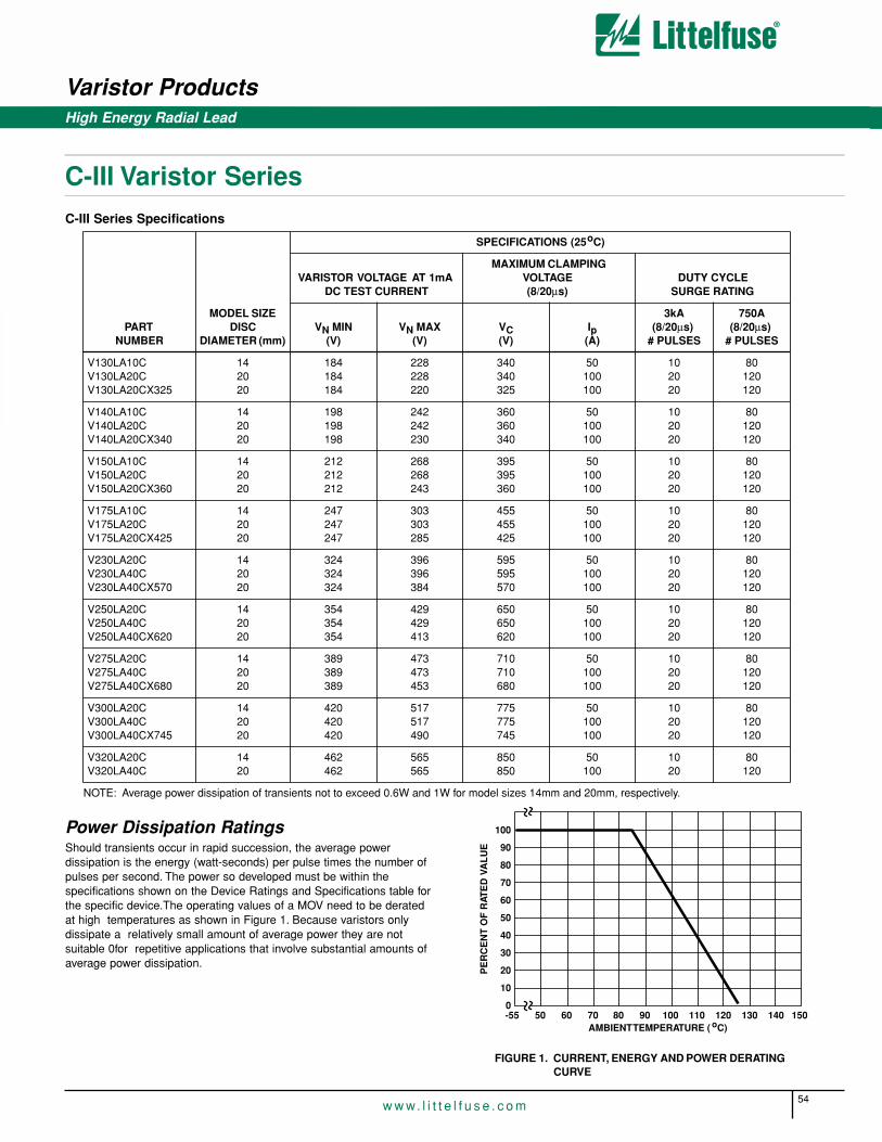
54w w w. l i t t e l f u s e . c o m
High Energy Radial Lead
C-III Varistor SeriesC-III Series Specifications
Power Dissipation RatingsShould transients occur in rapid succession, the average power dissipation is the energy (watt-seconds) per pulse times the number ofpulses per second. The power so developed must be within the specifications shown on the Device Ratings and Specifications table forthe specific device.The operating values of a MOV need to be deratedat high temperatures as shown in Figure 1. Because varistors only dissipate a relatively small amount of average power they are not suitable 0for repetitive applications that involve substantial amounts ofaverage power dissipation.
PARTNUMBER
MODEL SIZE DISC
DIAMETER (mm)
SPECIFICATIONS (25oC)
VARISTOR VOLTAGE AT 1mA DC TEST CURRENT
MAXIMUM CLAMPINGVOLTAGE(8/20µs)
DUTY CYCLESURGE RATING
VN MIN(V)
VN MAX(V)
VC(V)
Ip(A)
3kA(8/20µs)
# PULSES
750A(8/20µs)
# PULSES
V130LA10CV130LA20CV130LA20CX325
142020
184184184
228228220
340340325
50100100
102020
80120120
V140LA10CV140LA20CV140LA20CX340
142020
198198198
242242230
360360340
50100100
102020
80120120
V150LA10CV150LA20CV150LA20CX360
142020
212212212
268268243
395395360
50100100
102020
80120120
V175LA10CV175LA20CV175LA20CX425
142020
247247247
303303285
455455425
50100100
102020
80120120
V230LA20CV230LA40CV230LA40CX570
142020
324324324
396396384
595595570
50100100
102020
80120120
V250LA20CV250LA40CV250LA40CX620
142020
354354354
429429413
650650620
50100100
102020
80120120
V275LA20CV275LA40CV275LA40CX680
142020
389389389
473473453
710710680
50100100
102020
80120120
V300LA20CV300LA40CV300LA40CX745
142020
420420420
517517490
775775745
50100100
102020
80120120
V320LA20CV320LA40C
1420
462462
565565
850850
50100
1020
80120
NOTE: Average power dissipation of transients not to exceed 0.6W and 1W for model sizes 14mm and 20mm, respectively.
100
90
80
70
60
50
40
30
20
10
0-55 50 60 70 80 90 100 110 120 130 140 150
AMBIENT TEMPERATURE ( oC)
PE
RC
EN
T O
F R
ATE
D V
AL
UE
FIGURE 1. CURRENT, ENERGY AND POWER DERATING CURVE
Varistor Products

2
VAR
ISTO
RP
RO
DU
CT
S
Varistor Products
55w w w. l i t t e l f u s e . c o m
High Energy Radial Lead
C-III Varistor Series
FIGURE 2. PEAK PULSE CURRENT TEST WAVEFORM
100
90
50
10
O1 T
T1T2
TIME
PE
RC
EN
T O
F P
EA
K V
AL
UE
O1 = Virtual Origin of WaveT = Time From 10% to 90% of Peak
T1 = Virtual Front time = 1.25 • tT2 = Virtual Time to Half Value (Impulse Duration)
Example: For an 8/20µs Current Waveform:8µs = T1 = Virtual Front Time
20µs = T2 = Virtual Time to Half Value
FIGURE 3. MAXIMUM CLAMPING VOLTAGE FOR V130LA10CTO V320LA20C
1,000
100
PEAK AMPERES (A)
MA
XIM
UM
PE
AK
VO
LTA
GE
(V
)
V175LA10CV150LA10C
V140LA10CV130LA10C
MODEL SIZE = 14mmTA = -55oC TO 85oC130 TO 320VM(AC) RATING
10-2 10-1 100 101 102 103 10410-3
2,000
500
300
200
V300LA20CV275LA20C
V250LA20CV230LA20C
V320LA20C
FIGURE 4. MAXIMUM CLAMPING VOLTAGE FOR V130LA20C TO V320LA40C
1,000
100
MA
XIM
UM
PE
AK
VO
LTA
GE
(V
)
MODEL SIZE = 20mmTA = -55oC TO 85oC130 TO 320VM(AC) RATING
PEAK AMPERES (A)10-2 10-1 100 101 102 103 10410-3
V175LA20CV150LA20C
V140LA20CV130LA20C
V300LA40CV275LA40C
V250LA40CV230LA40C
V320LA40C
500
300
200
2,000
FIGURE 5. MAXIMUM CLAMPING VOLTAGE FOR V130LA20CX325 TO V300LACX745
1,000
100
PEAK AMPERES (A)
MA
XIM
UM
PE
AK
VO
LTA
GE
(V
)
V175LA20CX425V150LA20CX360
V140LA20CX340V130LA20CX325
MODEL SIZE = 20mmTA = -55oC TO 85oC130 TO 300VM(AC) RATING
10-2 10-1 100 101 102 103 10410-3
V300LA40CX745V275LA40CX680
V250LA40CX620V230LA40CX570
Transient V-I Characteristics Curves
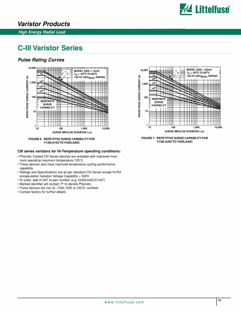
Varistor Products
56w w w. l i t t e l f u s e . c o m
High Energy Radial Lead
C-III Varistor Series
Pulse Rating Curves
FIGURE 6. REPETITIVE SURGE CAPABILITY FOR V130LA10C TO V320LA20C
10,000
1,000
100
10
110 100 1,000 10,000
SURGE IMPULSE DURATION (µs)
RAT
ED
PE
AK
SU
RG
E C
UR
RE
NT
(A
)
101
2
102
103
104
INDEFINITESURGE
CAPABILITY
MODEL SIZE = 14mmTA = -55oC TO 85oC130 TO 320VM(AC) RATING
FIGURE 7. REPETITIVE SURGE CAPABILITY FOR V130LA20C TO V320LA40C
10,000
1,000
100
10
110 100 1,000 10,000
SURGE IMPULSE DURATION (µs)
RAT
ED
PE
AK
SU
RG
E C
UR
RE
NT
(A
)
12
103
104
INDEFINITESURGE
CAPABILITY
MODEL SIZE = 20mmTA = -55oC TO 85oC130 TO 320VM(AC) RATING10
102
CIII series varistors for Hi-Temperature operating conditions:• Phenolic Coated CIII Series devices are available with improved maxi-
mum operating maximum temperature 125°C.• These devices also have improved temperature cycling performance
capability.• Ratings and Specifications are as per standard CIII Series except Hi-Pot
encapsulation Isolation Voltage Capability = 500V.• To order: add X1347 to part number (e.g. V230LA40CX1347)• Marked identifier will contain 'P' to denote Phenolic.• These devices are not UL, CSA, VDE or CECC certified.• Contact factory for further details.

Varistor Products
57w w w. l i t t e l f u s e . c o m
High Energy Radial Lead
C-III Varistor Series
SYMBOL DESCRIPTION
MODEL SIZE
14mm 20mm
P Pitch of Component 25.4 ± 1.0
P0 Feed Hole Pitch 12.7 ± 0.2
P1 Feed Hole Center to Pitch 8.85 ± 0.8
P2 Hole Center to Component Center
12.7 ± 0.7
F Lead to Lead Distance 7.50 ± 0.8
h Component Alignment 2.00 Max
W Tape Width 18.25 ± 0.75
W0 Hold Down Tape Width 12.0 ± 0.3
W1 Hole Position 9.125 ± 0.625
W2 Hold Down Tape Position 0.5 Max
H Height From Tape Center To Component Base
19.0 ± 1.0
H0 Seating Plane Height 16.0 ± 0.5
H1 Component Height 40 Max 46.5 Max
D0 Feed Hole Diameter 4.0 ± 0.2
t Total Tape Thickness 0.7 ± 0.2
U Under-crimp Width
3o
Max
p Component Alignment Max
8.0
Crimped Leads "LT"
Straight Leads "LS"
Under-crimped Leads "LU"
W0
P0
P1
DH
E
DHDP
W1
W
F t
W2
P
DP
∆bH
∆D0
H1
P2
E
DPDH DH
W1
W
F t
W2W0
P
DP
C
∆bH0
∆D0
H1SEATING PLANE
P1
P1
P2
W0
P1
P0
U
DH
E
DHDP
W1
W
F t
W2
PP2
DP
∆bHo
∆D0
H1
Tape and Reel Specification
2
VAR
ISTO
RP
RO
DU
CT
S

Varistor Products
58w w w. l i t t e l f u s e . c o m
High Energy Radial Lead
C-III Varistor Series
Tape and Reel Data• Conforms to ANSI and EIA Specifications
• Can be supplied to IEC publication 286-2
• Radial devices on tape and reel are supplied with either crimpedleads, straight leads, or under-crimped leads
Tape and Reel Ordering Information• Crimped leads are standard on LA types supplied in tape and reel
and are denoted by the model letter “T”. Also, in tape and reel,model letter “S” denotes straight leads and letter “U” denotes specialunder-crimped leads.
Example:
Shipping Quantity
Mechanical Dimensions
STANDARD MODEL
CRIMPED LEADS
STRAIGHT LEADS
UNDER CRIMP LEADS
V130LA20C V130LT20C V130LS20C V130LU20C
DEVICE SIZE
QUANTITY PER REEL
“T” REEL “S” REEL “U” REEL
14mm 500 500 500
20mm 500 500 500
VRMSVOLTAGEMODEL
VARISTOR MODEL SIZE
14mm 20mm
MIN MAX MIN MAX
ALL 20(0.787)
26.5 (1.043)
ALL 17(0.669)
23(0.906)
ALL 6.5(0.256)
8.5(0.335)
6.5(0.256)
8.5(0.335)
2.5 (0.098)
4.5 (0.177) 9.0 (0.354) 4.5 (0.177) 9.0 (0.354)
5.5 (0.216) 2.5 (0.098) 5.5 (0.216)130 - 320
ALL
SYMBOL
A
ØD
e
e1
-
- 11 (0.433) - 11 (0.433)
7.3 (0.287) - 7.3 (0.287)130 - 320E
Øb 0.76 (0.030)
0.86 (0.034)
0.76 (0.030)
0.86 (0.034)
Dimensions are in millimeters (inches)1. 10mm lead spacing also available. See additional lead
style options.
(0.531) (0.689)13.5 17.5
(0.531) (0.689)13.5 17.5
2. Parts with rated voltage in excess of 320Vrms AC are available. Contact factory for details.
Additional Lead Style OptionsRadial lead types can be supplied with combination preformed crimp andtrimmed leads. This option is suppliedto the dimensions shown below.
*Seating plane interpretation per IEC-717• To order this crimped and trimmed lead style, the standard radial
type model number “LA” is changed to the model number “LC”.Thisoption is supplied in bulk only.
Example:
• For 10 ± 1mm lead spacing on 20mm units only; append standardmodel numbers by adding “X10” suffix.
Example:• For other lead style variations to the above, please contact Littelfuse.
Reliability Performance of C-III SeriesThe electrical ratings of the C-III series of MOVs are conservatively stated. Samples of these devices have been tested under additionalstresses, over and above those called out in the data sheet. The resultsof this testing show an enhanced device performance.
The series of stress tests to which the units were subjected are a combi-nation of electrical, environmental and mechanical tests. A summary ofthe reliability tests performed on the C-III series are described in Table 1.
SYMBOL
VARISTOR MODEL SIZE
14mm 20mm
MIN MAX MIN MAX
A - 24.5(0.96)
- 31(1.22)
LTRIM 2.41(0.095)
4.69(0.185)
2.41(0.095)
4.69(0.185)
NOTE: Dimensions are in millimeters (inches).
CRIMPED AND TRIMMED LEAD
STANDARD MODEL ORDER AS
V130LA20C V130LC20C
STANDARD MODEL ORDER AS
V130LA20C V130LC20C

2
VAR
ISTO
RP
RO
DU
CT
S
Varistor Products
59w w w. l i t t e l f u s e . c o m
High Energy Radial Lead
C-III Varistor Series
TABLE 1.
AC Bias ReliabilityThe C-III series of metal oxide varistors was designed for use on the ACline. The varistor is connected across the AC line and is biased with aconstant amplitude sinusoidal voltage. It should be noted that the definitionof failure is a shift in the nominal varistor voltage (VN) exceeding ±10%.Although this type of varistor is still functioning normally after this magnitude of shift, devices at the lower extremities of VN tolerance will begin to dissipate more power.Because of this possibility, an extensive series of statistically designedtests were performed to determine the reliability of the C-III type of varistorunder AC bias combined with high levels of temperature stress. To date,this test has generated over 50,000 device hours of operation at a tempera-ture of 125oC, although only rated at 85oC. Changes in the nominal varistorvoltage, measured at 1mA, of less than 2% have been recorded (Figure 8).
Transient Surge Current/Energy Transient CapabilityThe transient surge rating serves as an excellent figure of merit for the C-IIIvaristor. This inherent surge handling capability is one of the C-III varistor’sbest features. The enhanced surge absorption capability results fromimproved process uniformity and enhanced construction. The homogeneityof the raw material powder and improved control over the sintering andassembly processes are contributing factors to this improvement.
In the low power AC mains environment, industry standards (UL, IEC,NEMA and IEEE) all suggest that the worst case surge occurrence will be3kA. Such a transient event may occur up to five times over the equipmentlife time (approximately 10 years). While the occu rences of five 3kAtransients is the required capability, the conservatively rated, repetitivesurge current for the C-III series is 20 pulses for the 20mm units and 10pulses for the 14mm series.
Additionally, all 20mm C-III devices are listed to the “PermanentlyConnected” category (10kA) of UL1449, by Underwriter’s Laboratories, Inc.
As a measure of the inherent device capability, samples of the 20mmV130LA20C devices were subjected to a worst case repetitive transientsurges test. After 100 pulses, each of 3kA, there was negligible changein the device characteristics. Changes in the clamping voltage, measuredat 100 amps, of less than 3% were recorded (Figure 9). Samples of the14mm Series V175LA20C were subjected to repetitive surge occurrencesof 750A. Again, there was negligible changes in any of the device characteristics after 250 pulses (Figure 10). In both cases the inherentdevice capability is far in excess of the expected worst case scenario.
TESTREFERENCE STANDARD
TESTCONDITIONS
TESTRESULTS
SurgeCurrent
UL 1449IEEE/ANSI C62.41
9000A(8/20µs) 1 Pulse
0/165
IEC 1051 7000A(8/20µs) 2 Pulses
0/105
3000A(8/20µs) 20 Pulses
0/75
750A(8/20µs) 120 Pulses
0/65
SurgeEnergy
UL 1449IEEE/ANSI C62.41IEC 1051
90J(2ms)1 Pulse
0/125
Operating Life
Mil-Std-202 Method 204D
125oC, 1000 Hours, Rated Bias Voltage
0/180
Temporary Overvoltage
N/A 120% Maximum Rated Varistor Voltage For 5 Minutes
0/70 FIGURE 8. HIGH TEMPERATURE OPERATING LIFE 125 oC FOR 1000 HOURS AT RATED BIAS
300
250
200
150
1000 100 200 300 400 500 600 700 800 900 1000 1100
TIME (HOURS)
VN
OM
AT
1m
A (
V)
V130LA20C
FIGURE 9. TYPICAL REPETITIVE SURGE CURRENTCAPABILITY OF C-III SERIES MOVs
FIGURE 10. TYPICAL REPETITIVE SURGE CURRENTCAPABILITY OF C-III SERIES MOVs
500
450
400
350
3000 10 20 30 40 50 60 70 80 90 100 110 120
NUMBER OF SURGES
(RATED FOR 20 SURGES)
CL
AM
PIN
G V
OLT
AG
E A
T 3
kA V130LA20C3kA (8/20µs)
600
550
500
450
400
350
3000 50 100 150 200 250 300
NUMBER OF SURGES
(RATED FOR 80 SURGES)
CL
AM
PIN
G V
OLT
AG
E A
T 7
50A
V175LA20C750A (8/20µs)

Varistor Products
60w w w. l i t t e l f u s e . c o m
LA Varistor Series
Line Voltage Operation, Radial Lead
The LA Series of transient voltage surge suppressors are radial-leadvaristors (MOVs) that are designed to be operated continuously acrossAC power lines. These UL recognized varistors require very little mounting space, and are offered in various standard lead form options.
The LA Series varistors are available in four model sizes: 7mm, 10mm,14mm and 20mm; and have a VM(AC)RMS voltage range from 130V
to 1000V, and an energy absorption capability up to 360J. Some LAseries model numbers are available with clamping voltage selections, designated by a model number suffix of either A or B. The “A” selection isthe standard model; the “B” selection provides a lower clamping voltage.
See LA Series Device Ratings and Specifications table for part numberand brand information.
Features• Energy Absorption Capability (WTM) . . .. . . . . . . . . . . . . . . . . Up to 360J
• Wide Operating Voltage Range VM(AC)RMS . . . . . . . . . . . . . . . . . . . . . . . . . . . . . . . . . . . . . 130V to 1000V
• No Derating Up to 85oC Ambient
• Available in Tape and Reel or Bulk Pack
AGENCY APPROVALS: Recognized under the components program ofUnderwriters Laboratories. Certified by CSA, VDE and CECC.
AGENCY FILE NUMBERS: UL E75961, E56529, E135010; CSALR91788; VDE 116895E; CECC 42201-006.
ALSO SEE LITTELFUSE ULTRAMOV™
AND C-III VARISTOR SERIES
® ®V
D E

2
VAR
ISTO
RP
RO
DU
CT
S
Varistor Products
61w w w. l i t t e l f u s e . c o m
LA Varistor Series
Line Voltage Operation, Radial Lead
Absolute Maximum Ratings For ratings of individual members of a series, see Device Ratings and Specifications chart
Continuous:Steady State Applied Voltage:AC Voltage Range (VM(AC)RMS) . . . . . . . . . . . . . . . . . . . . . . . . . . . . . . . . . . . . . . . . . . . . . . . . . . . . . . . . . . . . . . . . . 130 to 1000 V DC Voltage Range (VM(DC)) . . . . . . . . . . . . . . . . . . . . . . . . . . . . . . . . . . . . . . . . . . . . . . . . . . . . . . . . . . . . . . . . . . . . 175 to 1200 V
Transients:Peak Pulse Current (ITM)For 8/20µs Current Wave (See Figure 2) . . . . . . . . . . . . . . . . . . . . . . . . . . . . . . . . . . . . . . . . . . . . . . . . . . . . . . . . . . . 1200 to 6500 ASingle Pulse Energy RangeFor 10/1000µs Current Wave (WTM ) . . . . . . . . . . . . . . . . . . . . . . . . . . . . . . . . . . . . . . . . . . . . . . . . . . . . . . . . . . . . . . . 11 to 360 J
Operating Ambient Temperature Range (TA) . . . . . . . . . . . . . . . . . . . . . . . . . . . . . . . . . . . . . . . . . . . . . . . . . . . . . . . . . . . . -55 to 85 0CStorage Temperature Range (TSTG) . . . . . . . . . . . . . . . . . . . . . . . . . . . . . . . . . . . . . . . . . . . . . . . . . . . . . . . . . . . . . . . . . -55 to 125 0CTemperature Coefficient (αV) of Clamping Voltage (VC) at Specified Test Current . . . . . . . . . . . . . . . . . . . . . . . . . . . . . . . . . <0.01 %/0CHi-Pot Encapsulation (Isolation Voltage Capability) . . . . . . . . . . . . . . . . . . . . . . . . . . . . . . . . . . . . . . . . . . . . . . . . . . . . . . . . . 2500 V
(Dielectric must withstand indicated DC voltage for one minute per MIL-STD 202, Method 301)Insulation Resistance . . . . . . . . . . . . . . . . . . . . . . . . . . . . . . . . . . . . . . . . . . . . . . . . . . . . . . . . . . . . . . . . . . . . . . . . . . . . . . . 1000 MΩCAUTION: Stresses above those listed in “Absolute Maximum Ratings” may cause permanent damage to the device. This is a stress only rating and operation of the device at theseor any other conditions above those indicated in the operational sections of this specification is not implied.
Device Ratings and Specifications
PARTNUMBER
MODEL SIZE DISC DIA. (mm)
DEVICE MODEL
NUMBER BRAND-
ING
MAXIMUM RATING (85oC) SPECIFICATIONS (25oC)
CONTINUOUS TRANSIENT
VARISTOR VOLT-AGE AT 1mA DC TEST CURRENT
MAXIMUM CLAMPING VOLTAGE8 x 20µs
TYPICALCAPACI-TANCE
f = 1MHzVRMS VDC
ENERGY 10 x 1000µs
PEAKCURRENT 8 x 20µs
VM(AC) VM(DC) WTM ITM
VNOM MIN
VNOM MAX VC IPK C
(V) (V) (J) (A) (V) (V) (A) (pF)
V130LA1 7 1301 130 175 11 1200 184 255 390 10 180
V130LA2 7 1302 130 175 11 1200 184 228 340 10 180
V130LA5 10 1305 130 175 20 2500 184 228 340 25 450
V130LA10A 14 130L10 130 175 38 4500 184 228 340 50 1000
V130LA20A 20 130L20 130 175 70 6500 184 228 340 100 1900
V130LA20B 20 130L20B 130 175 70 6500 184 220 325 100 1900
V140LA2 7 1402 140 180 12 1200 198 242 360 10 160
V140LA5 10 1405 140 180 22 2500 198 242 360 25 400
V140LA10A 14 140L10 140 180 42 4500 198 242 360 50 900
V140LA20A 20 140L20 140 180 75 6500 198 242 340 100 1750
V150LA1 7 1501 150 200 13 1200 212 284 430 10 150
V150LA2 7 1502 150 200 13 1200 212 268 395 10 150
V150LA5 10 1505 150 200 25 2500 212 268 395 25 360
V150LA10A 14 150L10 150 200 45 4500 212 268 395 50 800
V150LA20A 20 150L20 150 200 80 6500 212 268 395 100 1600
V150LA20B 20 150L20B 150 200 80 6500 212 243 360 100 1600
V175LA2 7 1752 175 225 15 1200 247 303 455 10 130
V175LA5 10 1755 175 225 30 2500 247 303 455 25 350
V175LA10A 14 175L10 175 225 55 4500 247 303 455 50 700
V175LA20A 20 175L20 175 225 90 6500 247 303 455 100 1400
V230LA4 7 2304 230 300 20 1200 324 396 595 10 100
V230LA10 10 230L 230 300 35 2500 324 396 595 25 250
V230LA20A 14 230L20 230 300 70 4500 324 396 595 50 550
V230LA40A 20 230L40 230 300 122 6500 324 396 595 100 1100
LA SERIES UNITS
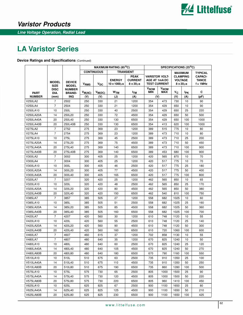
Varistor Products
62w w w. l i t t e l f u s e . c o m
Line Voltage Operation, Radial Lead
LA Varistor SeriesDevice Ratings and Specifications (Continued)
V250LA2 7 2502 250 330 21 1200 354 473 730 10 90
V250LA4 7 2504 250 330 21 1200 354 429 650 10 90
V250LA10 10 250L 250 330 40 2500 354 429 650 25 220
V250LA20A 14 250L20 250 330 72 4500 354 429 650 50 500
V250LA40A 20 250L40 250 330 130 6500 354 429 650 100 1000
V250LA40B 20 250L40B 250 330 130 6500 354 413 620 100 1000
V275LA2 7 2752 275 369 23 1200 389 515 775 10 80
V275LA4 7 2754 275 369 23 1200 389 473 710 10 80
V275LA10 10 275L 275 369 45 2500 389 473 710 25 200
V275LA20A 14 275L20 275 369 75 4500 389 473 710 50 450
V275LA40A 20 275L40 275 369 140 6500 389 473 710 100 900
V275LA40B 20 275L40B 275 369 140 6500 389 453 680 100 900
V300LA2 7 3002 300 405 25 1200 420 565 870 10 70
V300LA4 7 3004 300 405 25 1200 420 517 775 10 70
V300LA10 10 300L 300 405 46 2500 420 517 775 25 180
V300LA20A 14 300L20 300 405 77 4500 420 517 775 50 400
V300LA40A 20 300L40 300 405 165 6500 420 517 775 100 800
V320LA7 7 3207 320 420 25 1200 462 565 850 10 65
V320LA10 10 320L 320 420 48 2500 462 565 850 25 170
V320LA20A 14 320L20 320 420 80 4500 462 565 850 50 380
V320LA40B 20 320L40 320 420 150 6500 462 540 810 100 750
V385LA7 7 3857 385 505 27 1200 558 682 1025 10 60
V385LA10 10 385L 385 505 51 2500 558 682 1025 25 160
V385LA20A 14 385L20 385 505 85 4500 558 682 1025 50 360
V385LA40B 20 385L40 385 505 160 6500 558 682 1025 100 700
V420LA7 7 4207 420 560 30 1200 610 748 1120 10 55
V420LA10 10 420L 420 560 55 2500 610 748 1120 25 140
V420LA20A 14 420L20 420 560 90 4500 610 748 1120 50 300
V420LA40B 20 420L40 420 560 160 6500 610 720 1060 100 600
V460LA7 7 4607 460 615 37 1200 702 858 1130 10 55
V480LA7 7 4807 480 640 35 1200 670 825 1240 10 50
V480LA10 10 480L 480 640 60 2500 670 825 1240 25 120
V480LA40A 14 480L40 480 640 105 4500 670 825 1240 50 270
V480LA80B 20 480L80 480 640 180 6500 670 790 1160 100 550
V510LA10 10 510L 510 675 63 2500 735 910 1350 25 100
V510LA40A 14 510L40 510 675 110 4500 735 910 1350 50 250
V510LA80B 20 510L80 510 675 190 6500 735 860 1280 100 500
V575LA10 10 575L 575 730 65 2500 805 1000 1500 25 90
V575LA40A 14 575L40 575 730 120 4500 805 1000 1500 50 220
V575LA80B 20 575L80 575 730 220 6500 805 960 1410 100 450
V625LA10 10 625L 625 825 67 2500 900 1100 1650 25 80
V625LA40A 14 625L40 625 825 125 4500 900 1100 1650 50 210
V625LA80B 20 625L80 625 825 230 6500 900 1100 1650 100 425
PARTNUMBER
MODEL SIZE DISC DIA. (mm)
DEVICE MODEL
NUMBER BRAND-
ING
MAXIMUM RATING (85oC) SPECIFICATIONS (25oC)
CONTINUOUS TRANSIENT
VARISTOR VOLT-AGE AT 1mA DC TEST CURRENT
MAXIMUM CLAMPING VOLTAGE8 x 20µs
TYPICALCAPACI-TANCE
f = 1MHzVRMS VDC
ENERGY 10 x 1000µs
PEAKCURRENT 8 x 20µs
VM(AC) VM(DC) WTM ITM
VNOM MIN
VNOM MAX VC IPK C
(V) (V) (J) (A) (V) (V) (A) (pF)
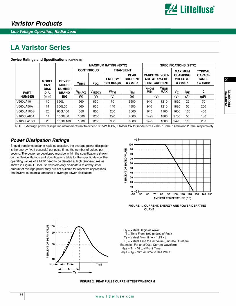
2
VAR
ISTO
RP
RO
DU
CT
S
Varistor Products
63w w w. l i t t e l f u s e . c o m
LA Varistor Series
Line Voltage Operation, Radial Lead
Device Ratings and Specifications (Continued)
Power Dissipation RatingsShould transients occur in rapid succession, the average power dissipationis the energy (watt-seconds) per pulse times the number of pulses per second. The power so developed must be within the specifications shownon the Device Ratings and Specifications table for the specific device.Theoperating values of a MOV need to be derated at high temperatures asshown in Figure 1. Because varistors only dissipate a relatively smallamount of average power they are not suitable for repetitive applicationsthat involve substantial amounts of average power dissipation.
V660LA10 10 660L 660 850 70 2500 940 1210 1820 25 70
V660LA50A 14 660L50 660 850 140 4500 940 1210 1820 50 200
V660LA100B 20 660L100 660 850 250 6500 940 1100 1650 100 400
V1000LA80A 14 1000L80 1000 1200 220 4500 1425 1800 2700 50 130
V1000LA160B 20 1000L160 1000 1200 360 6500 1425 1600 2420 100 250
NOTE: Average power dissipation of transients not to exceed 0.25W, 0.4W, 0.6W or 1W for model sizes 7mm, 10mm, 14mm and 20mm, respectively.
PARTNUMBER
MODEL SIZE DISC DIA. (mm)
DEVICE MODEL
NUMBER BRAND-
ING
MAXIMUM RATING (85oC) SPECIFICATIONS (25oC)
CONTINUOUS TRANSIENT
VARISTOR VOLT-AGE AT 1mA DC TEST CURRENT
MAXIMUM CLAMPING VOLTAGE8 x 20µs
TYPICALCAPACI-TANCE
f = 1MHzVRMS VDC
ENERGY 10 x 1000µs
PEAKCURRENT 8 x 20µs
VM(AC) VM(DC) WTM ITM
VNOM MIN
VNOM MAX VC IPK C
(V) (V) (J) (A) (V) (V) (A) (pF)
100
90
80
70
60
50
40
30
20
10
0-55 50 60 70 80 90 100 110 120 130 140 150
AMBIENT TEMPERATURE ( oC)
PE
RC
EN
T O
F R
ATE
D V
AL
UE
FIGURE 1. CURRENT, ENERGY AND POWER DERATING CURVE
FIGURE 2. PEAK PULSE CURRENT TEST WAVEFORM
100
90
50
10
O1 T
T1T2
TIME
PE
RC
EN
T O
F P
EA
K V
AL
UE
O1 = Virtual Origin of WaveT = Time From 10% to 90% of Peak
T1 = Virtual Front time = 1.25 • tT2 = Virtual Time to Half Value (Impulse Duration)
Example: For an 8/20µs Current Waveform:8µs = T1 = Virtual Front Time
20µs = T2 = Virtual Time to Half Value

Varistor Products
64w w w. l i t t e l f u s e . c o m
Line Voltage Operation, Radial Lead
LA Varistor Series
Transient V-I Characteristics Curves
FIGURE 3. CLAMPING VOLTAGE FOR V130LA1 - V300LA2 FIGURE 4. CLAMPING VOLTAGE FOR V130LA2 - V300LA4
FIGURE 5. CLAMPING VOLTAGE FOR V320LA7 - V480LA7 FIGURE 6. CLAMPING VOLTAGE FOR V130LA5 - V420LA10
FIGURE 7. CLAMPING VOLTAGE FOR V300LA10 - V660LA10 FIGURE 8. CLAMPING VOLTAGE FOR V130LA10A - V320LA20A
200
6,0005,000
4,000
3,000
1,000900800700600500400
300
10-3 10-2 10-1 100 101 102 104
MA
XIM
UM
PE
AK
VO
LTS
(V
)
PEAK AMPERES (A)
2,000
103
V150LA1
V130LA1
V300LA2
V275LA2V250LA2
MAXIMUM CLAMPING VOLTAGEMODEL SIZE 7mm130 TO 300VM(AC) RATINGTA = -55oC TO 85oC
10-3 10-2 10-1 100 101 102 104M
AX
IMU
M P
EA
K V
OLT
S (
V)
PEAK AMPERES (A)103
4,000
3,000
2,000
1,000900800700600500400
300
200
100
MAXIMUM CLAMPING VOLTAGEMODEL SIZE 7mm130 TO 300VM(AC) RATINGTA = -55oC TO 85oC V300LA4
V275LA4V250LA4
V230LA4
V130LA2V140LA2
V150LA2V175LA2
MAXIMUM CLAMPING VOLTAGEMODEL SIZE 7mm
TA = -55oC TO 85oC320 TO 480VM(AC) RATING
V420LA7V385LA7
V320LA7
V460LA7V480LA7
10-3 10-2 10-1 100 101 102 104103
5,000
3,000
2,000
1,000
500
PEAK AMPERES (A)
MA
XIM
UM
PE
AK
VO
LTS
(V
)
200
6,0005,000
4,000
3,000
1,000900800700600500400
300
10-3 10-2 10-1 100 101 102 104
MA
XIM
UM
PE
AK
VO
LTS
(V
)
PEAK AMPERES (A)
2,000
103
V275LA10V250LA10
MAXIMUM CLAMPING VOLTAGEMODEL SIZE 10mm130 TO 420VM(AC) RATINGTA = -55oC TO 85oC
V230LA10
V420LA10
V175LA5
V130LA5V140LA5
V150LA5
10-3 10-2 10-1 100 101 102 104103
5,000
3,000
2,000
1,000
500
V575LA10V510LA10V480LA10V385LA10
V300LA10V320LA10
PEAK AMPERES (A)
V625LA10V660LA10
MAXIMUM CLAMPING VOLTAGEMODEL SIZE 10mm
TA = -55oC TO 85oC300 TO 660VM(AC) RATING
MA
XIM
UM
PE
AK
VO
LTS
(V
)
200
6,0005,0004,000
3,000
1,000900800700600500400
300
10-3 10-2 10-1 100 101 102 104
MA
XIM
UM
PE
AK
VO
LTS
(V
)
PEAK AMPERES (A)
2,000
103
V275LA20AV250LA20A
MAXIMUM CLAMPING VOLTAGEMODEL SIZE 14mm130 TO 320VM(AC) RATINGTA = -55oC TO 85oC
V230LA20A
V175LA10A
V130LA10AV140LA10A
V150LA10A
V320LA20AV300LA20A
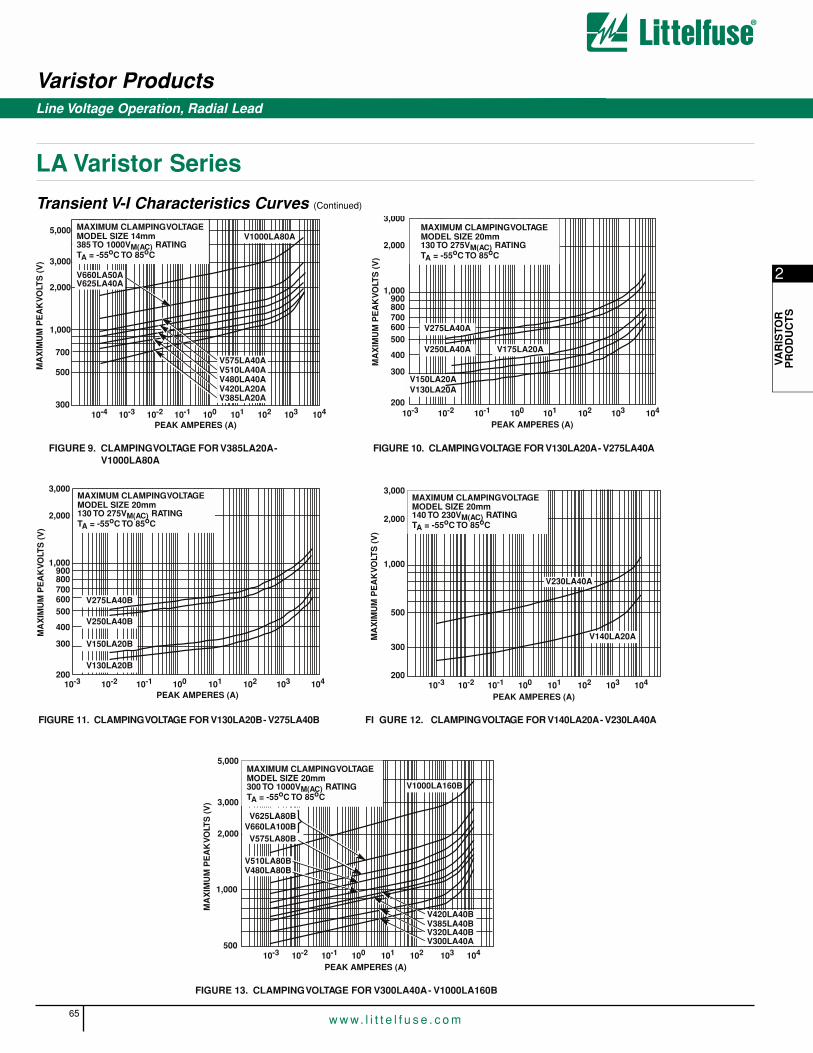
2
VAR
ISTO
RP
RO
DU
CT
S
Varistor Products
65w w w. l i t t e l f u s e . c o m
LA Varistor Series
Line Voltage Operation, Radial Lead
FIGURE 9. CLAMPING VOLTAGE FOR V385LA20A - V1000LA80A
FIGURE 10. CLAMPING VOLTAGE FOR V130LA20A - V275LA40A
FIGURE 11. CLAMPING VOLTAGE FOR V130LA20B - V275LA40B FI GURE 12. CLAMPING VOLTAGE FOR V140LA20A - V230LA40A
FIGURE 13. CLAMPING VOLTAGE FOR V300LA40A - V1000LA160B
5,000
3,000
1,000
500
30010-3 10-2 10-1 100 101 102 104
MA
XIM
UM
PE
AK
VO
LTS
(V
)
PEAK AMPERES (A)
2,000
10310-4
V1000LA80A
V660LA50A
V575LA40AV510LA40AV480LA40AV420LA20A
MAXIMUM CLAMPING VOLTAGEMODEL SIZE 14mm385 TO 1000VM(AC) RATINGTA = -55oC TO 85oC
V385LA20A
700
V625LA40A
3,000
2,000
1,000900800700600500
400
300
20010-3 10-2 10-1 100 101 102 104
MA
XIM
UM
PE
AK
VO
LTS
(V
)
PEAK AMPERES (A)103
V275LA40A
V250LA40A
V150LA20AV130LA20A
V175LA20A
MAXIMUM CLAMPING VOLTAGEMODEL SIZE 20mm130 TO 275VM(AC) RATINGTA = -55oC TO 85oC
3,000
2,000
1,000900800700600500
400
300
20010-3 10-2 10-1 100 101 102 104
MA
XIM
UM
PE
AK
VO
LTS
(V
)
PEAK AMPERES (A)103
V275LA40B
V250LA40B
V130LA20B
V150LA20B
MAXIMUM CLAMPING VOLTAGEMODEL SIZE 20mm130 TO 275VM(AC) RATINGTA = -55oC TO 85oC
3,000
2,000
500
20010-3 10-2 10-1 100 101 102 104
MA
XIM
UM
PE
AK
VO
LTS
(V
)
PEAK AMPERES (A)
1,000
103
MAXIMUM CLAMPING VOLTAGEMODEL SIZE 20mm140 TO 230VM(AC) RATINGTA = -55oC TO 85oC
300V140LA20A
V230LA40A
5,000
3,000
1,000
50010-3 10-2 10-1 100 101 102 104
MA
XIM
UM
PE
AK
VO
LTS
(V
)
PEAK AMPERES (A)
2,000
103
V625LA80BV660LA100B
V1000LA160B
MAXIMUM CLAMPING VOLTAGEMODEL SIZE 20mm300 TO 1000VM(AC) RATINGTA = -55oC TO 85oC
V575LA80B
V420LA40BV385LA40BV320LA40BV300LA40A
V510LA80BV480LA80B
Transient V-I Characteristics Curves (Continued)
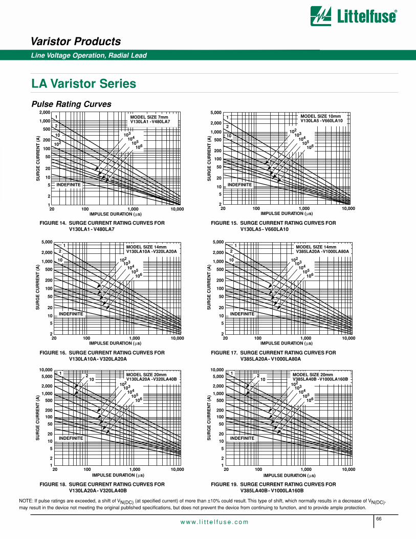
Varistor Products
66w w w. l i t t e l f u s e . c o m
Line Voltage Operation, Radial Lead
LA Varistor Series
Pulse Rating Curves
FIGURE 14. SURGE CURRENT RATING CURVES FOR V130LA1 - V480LA7
FIGURE 15. SURGE CURRENT RATING CURVES FOR V130LA5 - V660LA10
FIGURE 16. SURGE CURRENT RATING CURVES FOR V130LA10A - V320LA20A
FIGURE 17. SURGE CURRENT RATING CURVES FOR V385LA20A - V1000LA80A
FIGURE 18. SURGE CURRENT RATING CURVES FOR V130LA20A - V320LA40B
FIGURE 19. SURGE CURRENT RATING CURVES FOR V385LA40B - V1000LA160B
2,000
1,000
200
100
50
20
10
5
1
2
500
20 100 1,000 10,000IMPULSE DURATION (µs)
SU
RG
E C
UR
RE
NT
(A
)
1
2
10
102104
105
106
MODEL SIZE 7mmV130LA1 - V480LA7
103
INDEFINITE
5,000
2,000
200
100
50
20
10
5
2
500
20 100 1,000 10,000IMPULSE DURATION (µs)
SU
RG
E C
UR
RE
NT
(A
)
1
2
10104
105
106
MODEL SIZE 10mmV130LA5 - V660LA10
103
INDEFINITE
1,000 102
5,000
2,000
200
100
50
20
10
5
2
500
20 100 1,000 10,000IMPULSE DURATION (µs)
SU
RG
E C
UR
RE
NT
(A
)
12
10
104
105
106
MODEL SIZE 14mmV130LA10A - V320LA20A
103
INDEFINITE
1,000 102
5,000
2,000
200
100
50
20
10
5
2
500
20 100 1,000 10,000IMPULSE DURATION (µs)
SU
RG
E C
UR
RE
NT
(A
)
12
10
104
105
106
MODEL SIZE 14mmV385LA20A - V1000LA80A
103
INDEFINITE
1,000 102
10,000
2,000
200
100
50
20
10
5
2
500
20 100 1,000 10,000IMPULSE DURATION (µs)
SU
RG
E C
UR
RE
NT
(A
)
1 2
104
105
106
MODEL SIZE 20mmV130LA20A - V320LA40B
103
INDEFINITE
1,000
10210
5,000
1
10,000
2,000
200
100
50
20
10
5
2
500
20 100 1,000 10,000IMPULSE DURATION (µs)
SU
RG
E C
UR
RE
NT
(A
)
1 2
104
105
106
MODEL SIZE 20mmV385LA40B - V1000LA160B
103
INDEFINITE
1,000
10210
5,000
1
NOTE: If pulse ratings are exceeded, a shift of VN(DC) (at specified current) of more than ±10% could result. This type of shift, which normally results in a decrease of VN(DC),may result in the device not meeting the original published specifications, but does not prevent the device from continuing to function, and to provide ample protection.
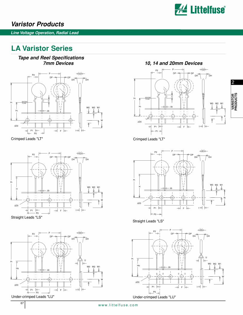
Varistor Products
67w w w. l i t t e l f u s e . c o m
Line Voltage Operation, Radial Lead
Tape and Reel Specifications
Crimped Leads "LT" Crimped Leads "LT"
Straight Leads "LS"Straight Leads "LS"
Under-crimped Leads "LU"
P1P0
E
DPDH DH
W1
W
F t
W2W0
P
DP
C
∆bH0
∆D0
H1SEATING PLANE
P2
P1
P1
W0
E
DPDH DH
W1
W
F t
W2
P
DP
C
∆bH0
∆D0
H1SEATING PLANE
P2
P0
DH
E
DHDP
W1
W
F t
W2
P
DP
∆bH
∆D0
H1
P1
P2
W0
P1P0
P2
DH
E
DHDP
W1
W
F t
W2W0
P
DP
∆bH
∆D0
H1
U
P1P0
P2
DH
E
DHDP
W1
W
F t
W2W0
P
DP
∆bHo
∆D0
H1
Under-crimped Leads "LU"
P0
U
DH
E
DHDP
W1
W
F t
W2
P
DP
∆bHo
∆D0
H1
P2
W0
P1
7mm Devices 10, 14 and 20mm Devices
2
VAR
ISTO
RP
RO
DU
CT
S
LA Varistor Series
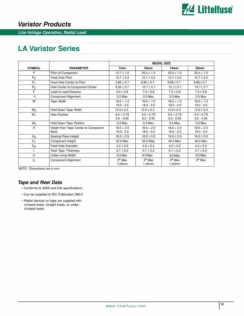
Varistor Products
68w w w. l i t t e l f u s e . c o m
SYMBOL PARAMETER
MODEL SIZE
7mm 10mm 14mm 20mm
P Pitch of Component 12.7 ± 1.0 25.4 ± 1.0 25.4 ± 1.0 25.4 ± 1.0
P0 Feed Hole Pitch 12.7 ± 0.2 12.7 ± 0.2 12.7 ± 0.2 12.7 ± 0.2
P1 Feed Hole Center to Pitch 3.85 ± 0.7 8.85 ± 0.7 8.85 ± 0.7 8.85 ± 0.7
P2 Hole Center to Component Center 6.35 ± 0.7 12.7 ± 0.7 12.7 ± 0.7 12.7± 0.7
F Lead to Lead Distance 5.0 ± 0.8 7.5 ± 0.8 7.5 ± 0.8 7.5 ± 0.8
h Component Alignment 2.0 Max 2.0 Max 2.0 Max 2.0 Max
W Tape Width 18.0 + 1.018.0 - 0.5
18.0 + 1.018.0 - 0.5
18.0 + 1.018.0 - 0.5
18.0 + 1.018.0 - 0.5
W0 Hold Down Tape Width 12.0 ± 0.3 12.0 ± 0.3 12.0 ± 0.3 12.0 ± 0.3
W1 Hole Position 9.0 + 0.759.0 - 0.50
9.0 + 0.759.0 - 0.50
9.0 + 0.759.0 - 0.50
9.0 + 0.759.0 - 0.50
W2 Hold Down Tape Position 0.5 Max 0.5 Max 0.5 Max 0.5 Max
H Height from Tape Center to Component Base
18.0 + 2.018.0 - 0.0
18.0 + 2.018.0 - 0.0
18.0 + 2.018.0 - 0.0
18.0 + 2.018.0 - 0.0
H0 Seating Plane Height 16.0 ± 0.5 16.0 ± 0.5 16.0 ± 0.5 16.0 ± 0.5
H1 Component Height 32.0 Max 36.0 Max 40.0 Max 46.5 Max
D0 Feed Hole Diameter 4.0 ± 0.2 4.0 ± 0.2 4.0 ± 0.2 4.0 ± 0.2
t Total Tape Thickness 0.7 ± 0.2 0.7 ± 0.2 0.7 ± 0.2 0.7 ± 0.2
U Under-crimp Width 8.0 Max 8.0 Max
p Component Alignment 3o Max1.00mm
3o Max1.00mm
3o Max1.00mm
3o Max
NOTE: Dimensions are in mm.
8.0 Max 8.0 Max
LA Varistor Series
Tape and Reel Data• Conforms to ANSI and EIA specifications
• Can be supplied to IEC Publication 286-2
• Radial devices on tape are supplied withcrimped leads, straight leads, or under-crimped leads
Line Voltage Operation, Radial Lead

2
VAR
ISTO
RP
RO
DU
CT
S
Varistor Products
69w w w. l i t t e l f u s e . c o m
Line Voltage Operation, Radial Lead
LA Varistor Series
Tape and Reel Ordering InformationCrimped leads are standard on LA types supplied in tape and reel andare denoted by the model letter “T”. Model letter “S” denotes straightleads and letter “U” denotes special under-crimped leads.
Example:
STANDARD MODEL
CRIMPED LEADS
STRAIGHT LEADS
UNDER-CRIMPED
LEADS
V130LA2 V130LT2 V130LS2 V130LU2
Standard Bulk Pack Quantity
SYMBOLVOLTAGE
MODEL
VARISTOR MODEL SIZE
7mm 10mm 14mm 20mm
MIN MAX MIN MAX MIN MAX MIN MAX
A V130LA-V320LA
--
12 (0.472)
--
16 (0.630)
--
20 (0.787)
--
26.5 (1.043)
V385LA-V1000LA
--
13(0.0512)
--
17 (0.689)
--
20.5 (0.807)
--
28 (1.102)
øD All --
9 (0.354) --
12.5 (0.492)
--
17 (0.669)
--
23 (0.906)
e All 4 (0.157) 6 (0.236) 6.5 (0.256)
8.5 (0.335)
6.5 (0.256)
8.5 (0.335)
6.5 (0.256)(Note 2)
8.5 (0.335)(Note 2)
e1 V130LA-V320LA
1.5 (0.059)
3.5 (0.138)
1.5 (0.059)
3.5 (0.138)
1.5 (0.059)
3.5 (0.138)
1.5 (0.059)
3.5 (0.138)
V385A-V1000LA
2.5(0.098)
5.5(0.217)
2.5 (0.098)
5.5 (0.217)
2.5 (0.098)
5.5 (0.217)
2.5 (0.098)
5.5 (0.217)
E V130LA-V320LA
--
5.6 (0.220)
--
5.6 (0.220)
--
5.6 (0.220)
--
5.6 (0.220)
V385LA-V660LA
--
7.5 (0.287)
--
7.5 (0.287)
--
7.5 (0.287)
--
7.5 (0.287)
V1000LA --
--
--
--
--
10.8 (0.425)
--
10.8 (0.425)
øb All(Note 3)
0.585 (0.023)
0.685 (0.027)
0.76 (0.030)
0.86 (0.034)
0.76 (0.030)
0.86 (0.034)
0.76 (0.030) (Note 2)
0.86 (0.034) (Note 2)
NOTES:
1. Dimensions in millimeters, inches in parentheses.
2. 10mm (9mm min, 11mm Max) ALSO AVAILABLE; See Additional Lead Style Options
3. 1000V parts supplied with lead wire of diameter 1.00 ± 0.05 (0.039 ± 0.002).
VARISTOR VOLTAGE
MODEL
STANDARD BULK PACK QUANTITY
VARISTOR MODEL SIZE
7mm 10mm 14mm 20mm
130-275 1500 1000 700 500
300-460 1500 700 600 400
510-625 1500 700 500 400

Varistor Products
70w w w. l i t t e l f u s e . c o m
LA Varistor Series
Line Voltage Operation, Radial Lead
Additional Lead Style OptionsRadial lead types can be supplied with combination preformed crimp andtrimmed leads. This option is supplied to the dimensions shown.
*Seating plane interpretation per IEC-717CRIMPED AND TRIMMED LEAD
SYMBOL
VARISTOR MODEL SIZE
7mm 10mm 14mm 20mm
MIN MAX MIN MAX MIN MAX MIN MAX
A --
15(0.591)
--
19.5 (0.768) --
22.5 (0.886) --
29.0 (1.142)
LTRIM 2.41 (0.095) 4.69 (0.185) 2.41 (0.095) 4.69 (0.185) 2.41 (0.095) 4.69 (0.185) 2.41 (0.095) 4.69 (0.185)
NOTE: Dimensions in millimeters, inches in parentheses.
• To order this crimped and trimmed lead style, standard radial typemodel numbers are changed by replacing the model letter “A” with “C”.
Example:
For crimped leads without trimming and any variations to the above,contact Littelfuse.
• For 10/±1mm lead spacing on 20mm diameter models only; appendstandard model numbers by adding “X10”.
Example:
STANDARD CATALOGMODEL ORDER AS:
V130LA20A V130LA20AX10
VARISTOR
VM(AC)130V to 1,000V
CLAMP VOLTAGE VARIANT(Where Applicable)
SERIES DESIGNATOR/LEAD STYLE DESIGNATOR
LC = Crimped and ClippedLS = StraightLT = CrimpedLU = Under Crimped
V XXX LA XX X
RELATIVE ENERGY INDICATOR(One or Two Digits)
Ordering InformationLA series Varistors are shipped standard in bulk pack with straight leadsand lead spacing outlined in the package dimensions on page 4-13.Contact your Littelfuse sales representative to discuss the non-standardoptions outlined below.
LA series varistors for Hi-Temperature operating conditions:• Phenolic Coated LA Series devices are available with improved maxi-
mum operating maximum temperature 125°C.• These devices also have improved temperature cycling performance
capability.• Ratings and Specifications are as per standard LA Series except Hi-Pot
encapsulation Isolation Voltage Capability = 500V.• To order: add X1347 to part number (e.g. V230LA20AX1347)• Marked identifier will contain 'P' to denote Phenolic.• These devices are not UL, CSA, VDE or CECC certified.• Contact factory for further details.

2
VAR
ISTO
RP
RO
DU
CT
S
Varistor Products
71w w w. l i t t e l f u s e . c o m
Low to Medum Voltage, Radial Lead
ZA Varistor SeriesThe ZA Series of transient voltage surge suppressors are radial-leadvaristors (MOVs) designed for use in the protection of low and medium-voltage circuits and systems. Typical applications include motor control,telecom, automotive systems, solenoid, and power supply circuits to protect circuit board components and maintain data integrity.
These devices are available in five model sizes: 5mm, 7mm, 10mm,14mm and 20mm, and feature a wide VDC voltage range of 5.5V to 615V.
See ZA Series Device Ratings and Specifications table for part numberand brand information.
Features• Wide Operating Voltage Range VM(AC)RMS . . . . . . . . . .4V to 460V
• DC Voltage Ratings . . . . . . . . . . . . . . . . . . . . . . . . . . . . . .5.5V to 615V
• No Derating Up to 85oC Ambient
• 5 Model Sizes Available . . . . . 5, 7, 10, 14, and 20mm
• Radial-Lead Package for Hard-Wired or Printed Circuit Board Designs
• Available in Tape and Reel or Bulk Pack
• Standard Lead Form Options
AGENCY APPROVALS: Recognized under the components program ofUnderwriters Laboratories. VDE certified.
AGENCY FILE NUMBERS: UL E135010, VDE 116895E.
®
VD E

Varistor Products
72w w w. l i t t e l f u s e . c o m
ZA Varistor Series
Low to Medum Voltage, Radial Lead
Absolute Maximum Ratings For ratings of individual members of a series, see Device Ratings and Specifications chart.
Continuous:Steady State Applied Voltage:AC Voltage Range (VM(AC)RMS). . . . . . . . . . . . . . . . . . . . . . . . . . . . . . . . . . . . . . . . . . . . . . . . . . . . . . . . . . . . . . . . . . . 4 to 460 V DC Voltage Range (VM(DC)) . . . . . . . . . . . . . . . . . . . . . . . . . . . . . . . . . . . . . . . . . . . . . . . . . . . . . . . . . . . . . . . . . . . . . 5.5 to 615 V
Transient:Peak Pulse Current (ITM)For 8/20µs Current Wave (See Figure 2). . . . . . . . . . . . . . . . . . . . . . . . . . . . . . . . . . . . . . . . . . . . . . . . . . . . . . . . . . . . . 50 to 6500 ASingle Pulse Energy Range (Note 1)For 10/1000µs Current Wave (WTM) . . . . . . . . . . . . . . . . . . . . . . . . . . . . . . . . . . . . . . . . . . . . . . . . . . . . . . . . . . . . . . . . 0.1 to 52 J
Operating Ambient Temperature Range (TA) . . . . . . . . . . . . . . . . . . . . . . . . . . . . . . . . . . . . . . . . . . . . . . . . . . . . . . . . . . . . -55 to85 oCStorage Temperature Range (TSTG) . . . . . . . . . . . . . . . . . . . . . . . . . . . . . . . . . . . . . . . . . . . . . . . . . . . . . . . . . . . . . . . . . . -55 to125 oCTemperature Coefficient (αV) of Clamping Voltage (VC) at Specified Test Current . . . . . . . . . . . . . . . . . . . . . . . . . . . . . . . . . . <0.01 %/oCHi-Pot Encapsulation (Isolation Voltage Capability). . . . . . . . . . . . . . . . . . . . . . . . . . . . . . . . . . . . . . . . . . . . . . . . . . . . . . . . . . 2500 V
(Dielectric must withstand indicated DC voltage for one minute per MIL-STD 202, Method 301)Insulation Resistance . . . . . . . . . . . . . . . . . . . . . . . . . . . . . . . . . . . . . . . . . . . . . . . . . . . . . . . . . . . . . . . . . . . . . . . . . . . . . . . 1000 MΩ
CAUTION: Stresses above those listed in “Absolute Maximum Ratings” may cause permanent damage to the device. This is a stress only rating and operation of the deviceat these or any other conditions above those indicated in the operational sections of this specification is not implied.
Device Ratings and Specifications (Note 1)
ZA SERIES UNITS
PARTNUMBER
MODEL SIZEDISC
DIA. (mm) BRAND
MAXIMUM RATING (85oC) SPECIFICATIONS (25oC)
CONTINUOUS TRANSIENT
VARISTOR VOLT-AGE AT 1mA DC TEST CURRENT
MAXIMUM CLAMPING VOLTAGE8 x 20µs
TYPICALCAPACI-TANCE
f = 1MHzVRMS VDC
ENERGY 10 x 1000µs
PEAK CURRENT 8 x 20µs
VM(AC) VM(DC) WTM ITM
VNOM MIN
VNOM MAX VC IPK C
(V) (V) (J) (A) (V) (V) (A) (pF)
V8ZA05 5 Z08 4 5.5 0.1 50 6 11 30 1 1400
V8ZA1 7 08Z1 4 5.5 0.4 100 6 11 22 2.5 3000
V8ZA2 10 08Z2 4 5.5 0.8 250 6 11 20 5 7500
V12ZA05 5 Z12 6 8 0.14 50 9 16 37 1 1200
V12ZA1 7 12Z1 6 8 0.6 100 9 16 34 2.5 2500
V12ZA2 10 12Z2 6 8 1.2 250 9 16 30 5 6000
V18ZA05 5 Z18 10 14 0.17 100 14.4 21.6 36 1 1000
V18ZA1 7 18Z1 10 14 0.8 250 14.4 21.6 36 2.5 2000
V18ZA2 10 18Z2 10 14 1.5 500 14.4 21.6 36 5 5000
V18ZA3 14 18Z3 10 14 3.5 1000 14.4 21.6 36 10 11000
V18ZA40 20 18Z40 10 14 80 (Note 2) 2000 14.4 (Note 3)
21.6 37 20 22000
V22ZA05 5 Z22 14 18 0.2 100 18.7 26 43 1 800
V22ZA1 7 22Z1 14 18 0.9 250 18.7 26 43 2.5 1600
V22ZA2 10 22Z2 14 18 2 500 18.7 26 43 5 4000
V22ZA3 14 22Z3 14 18 4 1000 18.7 26 43 10 9000
V24ZA50 20 24Z50 14 18(Note 4)
100 (Note 2) 2000 19.2 (Note 3)
26 43 20 18000
V27ZA05 5 Z27 17 22 0.25 100 23 31.1 53 1 600
V27ZA1 7 27Z1 17 22 1 250 23 31.1 53 2.5 1300
V27ZA2 10 27Z2 17 22 2.5 500 23 31.1 53 5 3000
V27ZA4 14 27Z4 17 22 5 1000 23 31.1 53 10 7000
V27ZA60 20 27Z60 17 22 120 (Note 2) 2000 23(Note 3)
31.1 50 20 13000

2
VAR
ISTO
RP
RO
DU
CT
S
Varistor Products
73w w w. l i t t e l f u s e . c o m
Low to Medum Voltage, Radial Lead
ZA Varistor Series
Device Ratings and Specifications (Note 1) (Continued)
V33ZA05 5 Z33 20 26 0.3 100 29.5 38 65 1 500
V33ZA1 7 33Z1 20 26 1.2 250 29.5 36.5 65 2.5 1100
V33ZA2 10 33Z2 20 26 3 500 29.5 36.5 65 5 2700
V33ZA5 14 33Z5 20 26 6 1000 29.5 36.5 65 10 6000
V33ZA70 20 33Z70 21 27 150 (Note 2) 2000 29.5 (Note 3)
36.5 58 20 13000
V36ZA80 20 36Z80 23 31 160 (Note 2) 2000 32(Note 3)
40 63 20 12000
V39ZA05 5 Z39 25 31 0.3 100 35 46 79 1 500
V39ZA1 7 39Z1 25 31 1.2 250 35 43 79 2.5 1100
V39ZA3 10 39Z3 25 31 3 500 35 43 76 5 2700
V39ZA6 14 39Z6 25 31 6 1000 35 43 76 10 6000
V39ZA20 20 39Z20 25 31 20 2000 35 43 76 20 12000
V47ZA05 5 Z47 30 38 0.4 100 42 55 93 1 400
V47ZA1 7 47Z1 30 38 1.8 250 42 52 93 2.5 800
V47ZA3 10 47Z3 30 38 4.5 500 42 52 93 5 2000
V47ZA7 14 47Z7 30 38 8.8 1000 42 52 93 10 4500
V47ZA20 20 47Z20 30 38 23 2000 42 52 93 20 11000
V56ZA05 5 Z56 35 45 0.5 100 50 66 110 1 360
V56ZA2 7 56Z2 35 45 2.3 250 50 62 110 2.5 700
V56ZA3 10 56Z3 35 45 5.5 500 50 62 110 5 1800
V56ZA8 14 56Z8 35 45 10 1000 50 62 110 10 3900
V56ZA20 20 56Z20 35 45 30 2000 50 62 110 20 10000
V68ZA05 5 Z68 40 56 0.6 100 61 80 135 1 300
V68ZA2 7 68Z2 40 56 3 250 61 75 135 2.5 600
V68ZA3 10 68Z3 40 56 6.5 500 61 75 135 5 1500
V68ZA10 14 68Z10 40 56 13 1000 61 75 135 10 3300
V68ZA20 20 68Z20 40 56 33 2000 61 75 135 20 10000
V82ZA05 5 Z82 50 68 2 400 73 97 135 5 240
V82ZA2 7 82Z2 50 68 4 1200 73 91 135 10 500
V82ZA4 10 82Z4 50 68 8 2500 73 91 135 25 1100
V82ZA12 14 82Z12 50 68 15 4500 73 91 145 50 2500
V100ZA05 5 Z100 60 81 2.5 400 90 117 165 5 180
V100ZA3 7 100Z 60 81 5 1200 90 110 165 10 400
V100ZA4 10 100Z4 60 81 10 2500 90 110 165 25 900
V100ZA15 14 100Z15 60 81 20 4500 90 110 175 50 2000
PARTNUMBER
MODEL SIZEDISC
DIA. (mm) BRAND
MAXIMUM RATING (85oC) SPECIFICATIONS (25oC)
CONTINUOUS TRANSIENT
VARISTOR VOLT-AGE AT 1mA DC TEST CURRENT
MAXIMUM CLAMPING VOLTAGE8 x 20µs
TYPICALCAPACI-TANCE
f = 1MHzVRMS VDC
ENERGY 10 x 1000µs
PEAK CURRENT 8 x 20µs
VM(AC) VM(DC) WTM ITM
VNOM MIN
VNOM MAX VC IPK C
(V) (V) (J) (A) (V) (V) (A) (pF)

Varistor Products
74w w w. l i t t e l f u s e . c o m
ZA Varistor Series
Low to Medum Voltage, Radial Lead
Device Ratings and Specifications (Note1) (Continued)
V120ZA05 5 Z120 75 102 3 400 108 138 205 5 140
V120ZA1 7 120Z 75 102 6 1200 108 132 205 10 300
V120ZA4 10 120Z4 75 102 12 2500 108 132 200 25 750
V120ZA6 14 120Z6 75 102 22 4500 108 132 210 50 1700
V120ZA20 20 120Z20 75 102 33 6500 108 132 210 100 1500
V150ZA05 5 Z150 92 127 4 400 135 173 250 5 120
V150ZA1 7 Z051 95 127 8 1200 135 165 250 10 250
V150ZA4 10 150Z4 95 127 15 2500 135 165 250 25 600
† V150ZA8 14 150Z8 95 127 20 4500 135 165 250 50 1400
V150ZA20 20 150Z20 95 127 45 6500 135 165 250 100 1000
V180ZA05 5 Z180 110 153 5 400 162 207 295 5 100
V180ZA1 7 180Z 115 153 10 1200 162 198 300 10 200
V180ZA5 10 180Z5 115 153 18 2500 162 198 300 25 500
V180ZA10 14 180Z10 115 153 35 4500 162 198 300 50 1100
V180ZA20 20 180Z20 115 153 52 6500 162 198 300 100 2400
V205ZA05 5 Z205 130 170 5.5 400 184 226 340 5 100
† V220ZA05 5 Z220 140 180 6 400 198 253 360 5 90
† V240ZA05 5 Z240 150 200 7 400 216 264 395 5 80
† V270ZA05 5 Z270 175 225 7.5 400 243 311 455 5 70
† V330ZA05 5 Z330 210 275 9 400 297 380 540 5 60
† V360ZA05 5 Z360 230 300 9.5 400 324 396 595 5 55
† V390ZA05 5 Z390 250 330 10 400 351 449 650 5 50
† V430ZA05 5 Z430 275 369 11 400 387 495 710 5 45
† V470ZA05 5 Z470 300 385 12 400 420 517 775 5 35
† V620ZA05 5 Z620 385 505 13 400 558 682 1025 5 33
† V680ZA05 5 Z680 420 560 14 400 610 748 1120 5 32
V715ZA05 5 Z715 440 585 15.5 400 643 787 1180 5 31
V750ZA05 5 Z750 460 615 17 400 675 825 1240 5 30
NOTES:
1. Average power dissipation of transients not to exceed 0.2W, 0.25W, 0.4W, 0.6W or 1W for model sizes 5mm, 7mm, 10mm, 14mm and 20mm, respectively.
2. Energy rating for impulse duration of 30ms minimum to one half of peak current (auto load dump).
3. 10mA DC test current.
4. Also rated to withstand 24V for 5 minutes.
5. Higher voltages available, contact Littelfuse.
† Also recognized to UL1449, “Transient Voltage Surge Suppressors” File #E75961.
PARTNUMBER
MODEL SIZEDISC
DIA. (mm) BRAND
MAXIMUM RATING (85oC) SPECIFICATIONS (25oC)
CONTINUOUS TRANSIENT
VARISTOR VOLT-AGE AT 1mA DC TEST CURRENT
MAXIMUM CLAMPING VOLTAGE8 x 20µs
TYPICALCAPACI-TANCE
f = 1MHzVRMS VDC
ENERGY 10 x 1000µs
PEAK CURRENT 8 x 20µs
VM(AC) VM(DC) WTM ITM
VNOM MIN
VNOM MAX VC IPK C
(V) (V) (J) (A) (V) (V) (A) (pF)

2
VAR
ISTO
RP
RO
DU
CT
S
Varistor Products
75w w w. l i t t e l f u s e . c o m
Low to Medum Voltage, Radial Lead
ZA Varistor Series
Power Dissipation RatingsShould transients occur in rapid succession, the average power dissipationrequired is simply the energy (watt-seconds) per pulse times the numberof pulses per second. The power so developed must be within the specifications shown on the Device Ratings and Specifications table forthe specific device. Furthermore, the operating values need to be deratedat high temperatures as shown in Figure 1. Because varistors can only dissipate a relatively small amount of average power they are, therefore,not suitable for repetitive applications that involve substantial amounts ofaverage power dissipation.
FIGURE 1. CURRENT, ENERGY AND POWER DERATING CURVE
100
90
80
70
60
50
40
30
20
10
0-55 50 60 70 80 90 100 110 120 130 140 150
AMBIENT TEMPERATURE ( oC)P
ER
CE
NT
OF
RAT
ED
VA
LU
E
FIGURE 2. PEAK PULSE CURRENT TEST WAVEFORM
100
90
50
10
O1 T
T1T2
TIME
PE
RC
EN
T O
F P
EA
K V
AL
UE
O1 = Virtual Origin of WaveT = Time From 10% to 90% of Peak
T1 = Virtual Front time = 1.25 • tT2 = Virtual Time to Half Value (Impulse Duration)
Example: For an 8/20µs Current Waveform:8µs = T1 = Virtual Front Time
20µs = T2 = Virtual Time to Half Value
FIGURE 3. CLAMPING VOLTAGE FOR V8ZA05 - V68ZA05
600500400300
200
100908070605040
30
20
MA
XIM
UM
PE
AK
VO
LTS
(V
)
PEAK AMPERES (A)10-2 10-1 100 101 102 103
MAX CLAMPING VOLTAGEMODEL SIZE 5mm8 TO 68VN(DC) RATINGTA = -55oC TO 85oC
10
V68ZA05V56ZA05V47ZA05V39ZA05V33ZA05V27ZA05V22ZA05V18ZA05V12ZA05
V8ZA05
10-3
FIGURE 4. CLAMPING VOLTAGE FOR V82ZA05 - V330ZA05
2000
1000
500
200MA
XIM
UM
PE
AK
VO
LTS
(V
)
PEAK AMPERES (A)
0.01 0.1 1 10 100 1000100
0.0010.0001
V330ZA05V270ZA05V240ZA05V220ZA05V205ZA05V180ZA05V150ZA05V120ZA05
V100ZA05
V82ZA05
MAX CLAMPING VOLTAGEMODEL SIZE 5mm82 TO 330VN(DC) RATINGTA = -55oC TO 85oC
Transient V-I Characteristics Curves
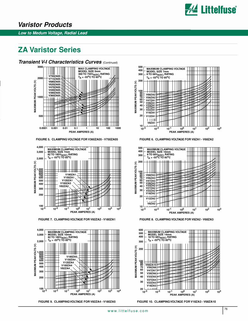
Varistor Products
76w w w. l i t t e l f u s e . c o m
ZA Varistor Series
Low to Medum Voltage, Radial Lead
Transient V-I Characteristics Curves (Continued)
FIGURE 5. CLAMPING VOLTAGE FOR V360ZA05 - V750ZA05 FIGURE 6. CLAMPING VOLTAGE FOR V8ZA1 - V68ZA2
FIGURE 7. CLAMPING VOLTAGE FOR V82ZA2 - V180ZA1 FIGURE 8. CLAMPING VOLTAGE FOR V8ZA2 - V68ZA3
FIGURE 9. CLAMPING VOLTAGE FOR V82ZA4 - V180ZA5 FIGURE 10. CLAMPING VOLTAGE FOR V18ZA3 - V68ZA10
3000
2000
1000
500
MA
XIM
UM
PE
AK
VO
LTS
(V
)
PEAK AMPERES (A)
0.01 0.1 1 10 100 10000.0010.0001
V750ZA05V715ZA05V680ZA05V620ZA05V470ZA05V430ZA05V390ZA05V360ZA05
MAX CLAMPING VOLTAGEMODEL SIZE 5mm360 TO 750VN(DC) RATINGTA = -55oC TO 85oC
500400
300
200
100908070605040
30
20
10
MA
XIM
UM
PE
AK
VO
LTS
(V
)
10-3 10-2 10-1 100 101 102 103
MAXIMUM CLAMPING VOLTAGE
8 TO 68VN(DC) RATINGTA = -55oC TO 85oC
PEAK AMPERES (A)
V68ZA2V56ZA2V47ZA1V39ZA1V33ZA1V27ZA1V22ZA1
V12ZA1V18ZA1
V8ZA1
MODEL SIZE 7mm
MA
XIM
UM
PE
AK
VO
LTS
(V
)
PEAK AMPERES (A)10-2 10-1 100 101 102 10310-3
MAXIMUM CLAMPING VOLTAGEMODEL SIZE 7mm82 TO 180VN(DC) RATINGTA = -55oC TO 85oC
4,000
3,000
2,000
1,000900800700600500400
300
200
100104
V180ZA1V150ZA1
V120ZA1V100ZA3
V82ZA2
500400
300
200
100908070605040
30
20
10
MA
XIM
UM
PE
AK
VO
LTS
(V
)
10-3 10-2 10-1 100 101 102 103
PEAK AMPERES (A)
V68ZA3V56ZA3V47ZA3V39ZA3V33ZA2V27ZA2V22ZA2V18ZA2
V8ZA2
V12ZA2
MAXIMUM CLAMPING VOLTAGEMODEL SIZE 10mm8 TO 68VN(DC) RATINGTA = -55oC TO 85oC
MA
XIM
UM
PE
AK
VO
LTS
(V
)
PEAK AMPERES (A)10-2 10-1 100 101 102 10310-3
MAXIMUM CLAMPING VOLTAGEMODEL SIZE 10mm82 TO 180VN(DC) RATINGTA = -55oC TO 85oC
4,000
3,000
2,000
1,000900800700600500400
300
200
100104
V180ZA5V150ZA4
V120ZA4V100ZA4
V82ZA4
600500400
300
200
100908070605040
30
2010-3 10-2 10-1 100 101 102 103
PEAK AMPERES (A)
MA
XIM
UM
PE
AK
VO
LTS
(V
)
V68ZA10V56ZA8V47ZA7V39ZA6V33ZA5V27ZA4V22ZA3V18ZA3
MAXIMUM CLAMPING VOLTAGE
18 TO 68VN(DC) RATINGTA = -55oC TO 85oC
MODEL SIZE 14mm
2
VAR
ISTO
RP
RO
DU
CT
S
Varistor Products
77w w w. l i t t e l f u s e . c o m
Low to Medum Voltage, Radial Lead
ZA Varistor Series
Transient V-I Characteristics Curves (Continued)
FIGURE 11. CLAMPING VOLTAGE FOR V82ZA12 - V180ZA10 FIGURE 12. CLAMPING VOLTAGE FOR V18ZA40 - V36ZA80
FIGURE 13. CLAMPING VOLTAGE FOR V39ZA20 - V180ZA20
MA
XIM
UM
PE
AK
VO
LTS
(V
)
PEAK AMPERES (A)10-2 10-1 100 101 102 10310-3
MAXIMUM CLAMPING VOLTAGEMODEL SIZE 14mm82 TO 180VN(DC) RATINGTA = -55oC TO 85oC
4,000
3,000
2,000
1,000900800700600
500400
300
200
100104
V180ZA10V150ZA8
V120ZA6V100ZA15
V82ZA12
300
200
10090807060
50
40
30
20
MA
XIM
UM
PE
AK
VO
LTS
(V
)
PEAK AMPERES (A)10-2 10-1 100 101 102 10310-3 104
MAXIMUM CLAMPING VOLTAGEMODEL SIZE 20mm18 TO 36VN(DC) RATINGTA = -55oC TO 85oC
V36ZA80V33ZA70
V27ZA60V24ZA50
V18ZA40
10-3 10-2 10-1 100 101 102 104103
1,000
500
300
200
30
PEAK AMPERES (A)
MA
XIM
UM
PE
AK
VO
LTS
(V
)
V56ZA20V47ZA20
V39ZA20
MAXIMUM CLAMPING VOLTAGEMODEL SIZE 20mm
TA = -55oC TO 85oC39 TO 180VM(AC) RATING V180ZA20
V150ZA20V120ZA20
100
50
V68ZA20
Pulse Rating Curves
FIGURE 14. SURGE CURRENT RATING CURVES FOR V8ZA05 FIGURE 15. SURGE CURRENT RATING CURVES FOR V12ZA05 - V68ZA05
50
20
10
5
2
1
0.5
0.2
0.1
SU
RG
E C
UR
RE
NT
(A
)
20 100 1,000 10,000IMPULSE DURATION (µs)
1
10
102
2
103
INDEFINITE
104105
106
MODEL SIZE 5mmV8ZA05
100
50
20
10
2
1
0.5
0.2
0.1
SU
RG
E C
UR
RE
NT
(A
)
20 100 1,000 10,000IMPULSE DURATION (µs)
INDEFINITE
104105
106
MODEL SIZE 5mmV12ZA05 - V68ZA05
110
102
2
103
Varistor Products
78w w w. l i t t e l f u s e . c o m
ZA Varistor Series
Low to Medum Voltage, Radial Lead
Pulse Rating Curves (Continued)
FIGURE 16. SURGE CURRENT RATING CURVES FOR V82ZA05 - V750ZA05
FIGURE 17. SURGE CURRENT RATING CURVES FORV8ZA1 - V12ZA1
FIGURE 18. SURGE CURRENT RATING CURVES FOR V18ZA1 - V68ZA2
FIGURE 19. SURGE CURRENT RATING CURVES FOR V82ZA2 - V180ZA1
FIGURE 20. SURGE CURRENT RATING CURVES FOR V8ZA2 - V127ZA2
FIGURE 21. SURGE CURRENT RATING CURVES FOR V18ZA2 - V68ZA3
50
20
10
5
2
1
0.5
0.2
SU
RG
E C
UR
RE
NT
(A
)
20 100 1,000 10,000IMPULSE DURATION (µs)
1
10
102
2103
INDEFINITE
104105
106
MODEL SIZE 5mmV82ZA05 - V750ZA05
500
200
100
20 100 1,000 10,000IMPULSE DURATION (µs)
SU
RG
E C
UR
RE
NT
(A
)
1
10
102
2
103
INDEFINITE
104105
106
200
100
50
20
10
5
2
1
0.5
0.2
MODEL SIZE 7mmV8ZA1 - V12ZA1
20 100 1,000 10,000IMPULSE DURATION (µs)
SU
RG
E C
UR
RE
NT
(A
)
1
10
102
2
103
INDEFINITE
500
200
100
50
20
10
2
1
0.5
0.2
104105
106
5
MODEL SIZE 7mmV18ZA1 - V68ZA2
2,000
1,000
200
100
50
20
10
5
1
2
500
20 100 1,000 10,000IMPULSE DURATION (µs)
SU
RG
E C
UR
RE
NT
(A
)
1
2
10
102104
105
106
103
INDEFINITE
MODEL SIZE 7mmV82ZA2 - V180ZA1
20 100 1,000 10,000IMPULSE DURATION (µs)
SU
RG
E C
UR
RE
NT
(A
)
1
10
102
2
103
INDEFINITE
500
200
100
50
20
10
2
1
0.5
0.2
104105
106
5
MODEL SIZE 10mmV8ZA2 - V12ZA2
1,000
500
100
50
20
10
5
1
2
200
20
SU
RG
E C
UR
RE
NT
(A
)
1
2
105
106
104
INDEFINITE
MODEL SIZE 10mmV18ZA2 - V68ZA3
100 1,000 10,000IMPULSE DURATION (µs)
102
103

2
VAR
ISTO
RP
RO
DU
CT
S
Varistor Products
79w w w. l i t t e l f u s e . c o m
Low to Medum Voltage, Radial Lead
ZA Varistor Series
Pulse Rating Curves (Continued)
FIGURE 22. SURGE CURRENT RATING CURVES FOR V82ZA4 - V180ZA5
5,000
2,000
1,000
500
200
100
50
20
10
5
220 100 1,000 10,000
IMPULSE DURATION (µs)
SU
RG
E C
UR
RE
NT
(A
)
1
10
102
2
103
INDEFINITE
104105
106
MODEL SIZE 10mmV82ZA4 - V180ZA5
FIGURE 23. SURGE CURRENT RATING CURVES FOR V18ZA3 - V68ZA10
200
100
50
20
10
5
1
2
20 100 1,000 10,000IMPULSE DURATION (µs)
SU
RG
E C
UR
RE
NT
(A
)
12
10
102
104
105
106
103
INDEFINITE
1,000
500MODEL SIZE 14mmV18ZA3 - V68ZA10

ZA Varistor Series
Varistor Products
80w w w. l i t t e l f u s e . c o m
Low to Medum Voltage, Radial Lead
NOTE: If pulse ratings are exceeded, a shift of VN(DC)(at specified current) of more then ±10% could result. This type of shift, which normally results in a decrease of VN(DC),may result in the device not meeting the original published specifications, but does not prevent the device from continuing to function, and to provide ample protection.
Pulse Rating Curves (Continued)
FIGURE 24. SURGE CURRENT RATING CURVES FOR V82ZA12 - V180ZA10
FIGURE 25. SURGE CURRENT RATING CURRENT FOR V18ZA40 - V68ZA20
FIGURE 26. SURGE CURRENT RATING CURVES FOR V120ZA20 - V180ZA20
5,000
2,000
200
100
50
20
10
5
2
500
20 100 1,000 10,000IMPULSE DURATION (µs)
SU
RG
E C
UR
RE
NT
(A
)
12
10
104
105
106
103
INDEFINITE
1,000 102
MODEL SIZE 14mmV82ZA12 - V180ZA10
2,000
200
100
50
20
10
5
2
500
20 100 1,000 10,000IMPULSE DURATION (µs)
SU
RG
E C
UR
RE
NT
(A
)
12
101,000
102
103
104
105
106
INDEFINITE
MODEL SIZE 20mmV18ZA40 - V68ZA20
10,0001,00010020
IMPULSE DURATION (µs)
SU
RG
E C
UR
RE
NT
(A
)
5,00010,000
2,000
500
100
20
10
2
1,000
200
50
1
5
12
10
102
103
104
105
106
INDEFINITE
MODEL SIZE 20mmV120ZA20 - V180ZA20

2
VAR
ISTO
RP
RO
DU
CT
S
Varistor Products
81w w w. l i t t e l f u s e . c o m
ZA Varistor Series
Low to Medum Voltage, Radial Lead
Tape and Reel Specifications
Crimped Leads "LT" Crimped Leads "LT"
Straight Leads "LS"Straight Leads "LS"
Under-crimped Leads "LU"
P1P0
E
DPDH DH
W1
W
F t
W2W0
P
DP
C
∆bH0
∆D0
H1SEATING PLANE
P2
P1
P1
W0
E
DPDH DH
W1
W
F t
W2
P
DP
C
∆bH0
∆D0
H1SEATING PLANE
P2
P0
DH
E
DHDP
W1
W
F t
W2
P
DP
∆bH
∆D0
H1
P1
P2
W0
P1P0
P2
DH
E
DHDP
W1
W
F t
W2W0
P
DP
∆bH
∆D0
H1
U
P1P0
P2
DH
E
DHDP
W1
W
F t
W2W0
P
DP
∆bHo
∆D0
H1
Under-crimped Leads "LU"
P0
U
DH
E
DHDP
W1
W
F t
W2
P
DP
∆bHo
∆D0
H1
P2
W0
P1
5 and 7mm Devices 10, 14 and 20mm Devices

Varistor Products
82w w w. l i t t e l f u s e . c o m
Tape and Reel Data• Conforms to ANSI and EIA specifications
• Can be supplied to IEC Publication 286-2
• Radial devices on tape are supplied withcrimped leads, straight leads, or under-crimped leads
NOTE: Leads are offset by Dim e1
SYMBOL PARAMETER
MODEL SIZE
5mm 7mm 10mm 14mm 20mm
P Pitch of Component 12.7 ± 1.0 12.7 ± 1.0 25.4 ± 1.0 25.4 ± 1.0 25.4 ± 1.0
P0 Feed Hole Pitch 12.7 ± 0.2 12.7 ± 0.2 12.7 ± 0.2 12.7 ± 0.2 12.7 ± 0.2
P1 Feed Hole Center to Pitch 3.85 ± 0.7 3.85 ± 0.7 8.85 ± 0.7 8.85 ± ± 0.7 8.85 0.7
P2 Hole Center to Component Center 6.35 ± 1.0 6.35 ± 1.0 12.7 ± 0.7 12.7 ± 0.7 12.7 ± 0.7
F Lead to Lead Distance 5.0 ± 1.0 5.0 ± 1.0 7.5 ± 1.0 7.5 ± 1.0 7.5 ± 1.0
h Component Alignment 2.0 Max 2.0 Max 2.0 Max 2.0 Max 2.0 Max
W Tape Width 18.0 + 1.018.0 - 0.5
18.0 + 1.018.0 - 0.5
18.0 + 1.018.0 - 0.5
18.0 + 1.018.0 - 0.5
18.0 + 1.018.0 - 0.5
W0 Hold Down Tape Width ±12.0 0.3 ±12.0 0.3 ±12.0 0.3 ±12.0 0.3 ±12.0 0.3
W1 Hole Position 9.0 + 0.759.0 - 0.50
9.0 + 0.759.0 - 0.50
9.0 + 0.759.0 - 0.50
9.0 + 0.759.0 - 0.50
9.0 + 0.759.0 - 0.50
W2 Hold Down Tape Position 0.5 Max 0.5 Max 0.5 Max 0.5 Max 0.5 Max
H Height from Tape Center toComponent Base
18.0 + 2.018.0 - 0.0
18.0 + 2.018.0 - 0.0
18.0 + 2.018.0 - 0.0
18.0 + 2.018.0 - 0.0
18.0 + 2.018.0 - 0.0
H0 Seating Plane Height 16.0 ± 0.5 16.0 ± 0.5 16.0 ± 0.5 16.0 ± 0.5 16.0 ± 0.5
H1 Component Height 29.0 Max 32.0 Max 36.0 Max 40.0 Max 46.5 Max
D0 Feed Hole Diameter 4.0 ± 0.2 4.0 ± 0.2 4.0 ± 0.2 4.0 ± 0.2 4.0 ± 0.2
t Total Tape Thickness 0.7 ± 0.2 0.7 ± 0.2 0.7 ± 0.2 0.7 ± 0.2 0.7 ± 0.2
U Under-crimp Width 8.0 Max
p Component Alignment 3o Max 3o Max 3o Max 3o Max 3o Max
NOTE: Dimensions are in mm.
8.0 Max 8.0 Max 8.0 Max 8.0 Max
Low to Medum Voltage, Radial Lead
ZA Varistor Series

2
VAR
ISTO
RP
RO
DU
CT
S
Varistor Products
83w w w. l i t t e l f u s e . c o m
Low to Medum Voltage, Radial Lead
ZA Varistor Series
Mechanical Dimensions
Tape and Reel Ordering InformationCrimped leads are standard on ZA types supplied in tape and reel andare denoted by the model letter “T”. Model letter “S” denotes straightleads and letter “U” denotes special under-crimped leads.
Example:
STANDARD MODEL
CRIMPED LEADS
STRAIGHT LEADS
UNDER-CRIMPED
LEADS
V18ZA3 V18ZT3 V18ZS3 V18ZU3
SHIPPING QUANTITY
SIZE
RMS (MAX)
VOLTAGE
QUANTITY PER REEL
“T” REEL “S” REEL “U” REEL
5mm All 1000 1000 1000
7mm All 1000 1000 1000
10mm All 500 500 500
14mm < 300V 500 500 500
14mm ≥ 300V 500 500 400
20mm < 300V 500 500 500
20mm ≥ 300V 500 500 400
SYM-BOL
VOLTAGE MODEL
VARISTOR MODEL SIZE
5mm 7mm 10mm 14mm 20mm
MIN MAX MIN MAX MIN MAX MIN MAX MIN MAX
A All --
10 (0.394)
--
12 (0.472)
--
16 (0.630)
--
20 (0.787)
--
26.5 (1.043)
øD All --
7 (0.276)
--
9 (0.354)
--
12.5 (0.492)
--
17 (0.669)
--
23 (0.906)
e All 4 (0.157)
6 (0.236)
4 (0.157)
6 (0.236)
6.5 (0.256)
8.5 (0.335)
6.5 (0.256)
8.5 (0.335)
6.5 (0.256)(Note 6)
8.5 (0.335)(Note 6)
e1 V8ZA-V56ZA
1 (0.039)
3 (0.118)
1 (0.039)
3 (0.118)
1 (0.039)
3 (0.118)
1 (0.039)
3 (0.118)
1 (0.039)
3 (0.118)
V68ZA-V100ZA
1.5 (0.059)
3.5 (0.138)
1.5 (0.059)
3.5 (0.138)
1.5 (0.059)
3.5 (0.138)
1.5 (0.059)
3.5 (0.138) (0.059) (0.138)
1.5 3.5
V120ZA-V180ZA
1 (0.039)
3 (0.118)
1 (0.039)
3 (0.118)
1 (0.039)
3 (0.118)
1 (0.038)
3(0.118) (0.038) (0.118)
V205ZA-V750ZA
1.5 (0.059)
3.5 (0.138)
--
--
--
--
--
--
--
--
E V8ZA-V56ZA
--
5 (0.197)
--
5 (0.197)
--
5 (0.197)
--
5 (0.197)
--
5 (0.197)
V68ZA-V100ZA
--
5.6 (0.220)
--
5.6 (0.220)
--
5.6 (0.220)
--
5.6 (0.220)
--
5.6 (0.220)
V120ZA-V180ZA
--
5 (0.197)
--
5 (0.197)
--
5 (0.197)
--
5 (0.197)
--
5 (0.197)
V205ZA-V750ZA
--
5.6 (0.220)
--
--
--
--
--
--
--
--
øb All 0.585 (0.023)
0.685 (0.027)
0.585 (0.023)
0.685 (0.027)
0.76 (0.030)
0.86 (0.034)
0.76 (0.030)
0.86 (0.034)
0.76 (0.030)
0.86 (0.034)
NOTES: Dimensions in millimeters, inches in parentheses.
6. 10mm ALSO AVAILABLE; See Additional Lead Style Options.
7. V24ZA50 and V24ZC50 only supplied with lead spacing of 6.35mm ± 0.5mm (0.25 ± 0.0196)Dimension E = 5.85 min. Does not apply to T&R parts.
1 3
Varistor Products
84w w w. l i t t e l f u s e . c o m
ZA Varistor Series
Low to Medum Voltage, Radial Lead
Additional Lead Style OptionsRadial lead types can be supplied with combination preformed crimp andtrimmed leads. This option is supplied to the dimensions shown.
• To order this crimped and trimmed lead style, standard radial typemodel numbers are changed by replacing the model letter “ZA” with“ZC”. This option is supplied in bulk only.
Example:
For crimped leads without trimming and any varitions to the above, contact Littelfuse.
• For 10/±1mm lead spacing on 20mm diameter models only; append stan-dard model numbers by adding “X10”.
Example:
*SEATING PLANE INTERPRETATION PER IEC-717 CRIMPED AND TRIMMED LEAD
STANDARD CATALOGMODEL ORDER AS:
V18ZA3 V18ZC3
VARISTOR
VARISTOR NOMINALVOLTAGE (VNOM)
(One, Two or Three Digits)
SERIES DESIGNATOR/LEAD STYLE DESIGNATOR
ZC = Crimped and ClippedZS = StraightZT = CrimpedZU = Under Crimped
V XXX ZA XX
RELATIVE ENERGY INDICATOR(One or Two Digits)
Ordering InformationZA series Varistors are shipped standard in bulk pack with straight leadsand lead spacing outlined in the package dimensions on page 4-13.Contact your Littelfuse sales representative to discuss the non-standardoptions outlined below.
ZA series varistors for Hi-Temperature operating conditions:• Phenolic Coated ZA Series devices are available with improved maxi-
mum operating maximum temperature 125°C.• These devices also have improved temperature cycling performance
capability.• Ratings and Specifications are as per standard ZA Series except Hi-
Pot encapsulation Isolation Voltage Capability = 500V.• To order: add X1347 to part number (e.g. V22ZA3X1347)• Marked identifier will contain 'P' to denote Phenolic.• These devices are not UL, CSA, VDE or CECC certified.• Contact factory for further details.
SYMBOL
VARISTOR MODEL SIZE
5mm 7mm 10mm 14mm 20mm
MIN MAX MIN MAX MIN MAX MIN MAX MIN MAX
A --
13.0 (0.512)
--
15(0.591)
--
19.5 (0.768)
--
22.5 (0.886)
--
29.0 (1.142)
LTRIM 2.41 (0.095)
4.69 (0.185)
2.41 (0.095)
4.69 (0.185)
2.41 (0.095)
4.69 (0.185)
2.41 (0.095)
4.69 (0.185)
2.41 (0.095)
4.69 (0.185)
NOTE: Dimensions in millimeters, inches in parentheses.
STANDARD CATALOGMODEL ORDER AS:
V18ZA40 V18ZA40X10
2
VAR
ISTO
RP
RO
DU
CT
S
Varistor Products
85w w w. l i t t e l f u s e . c o m
High Energy Industrial
BA/BB Varistor Series The BA and BB Series transient surge suppressors are heavy-duty industrial metal-oxide varistors (MOVs) designed to provide surge protection for motor controls and power supplies used in oil-drilling, mining,transportation equipment and other heavy industrial AC line applications.
These UL-recognized varistors have similar package construction but differ in size and ratings.The BA models are rated from 130 to880VM(AC) . The BB models from 1100 to 2800VM(AC) .
Both the BA and BB Series feature improved creep and strike capabilityto minimize breakdown along the package surface, a package designthat provides complete electrical isolation of the disc subassembly, andrigid terminals to insure secure wire contacts.
See BA/BB Series Device Ratings and Specifications table for part number and brand information.
Features• High Energy Absorption Capability WTM
BA Series . . . . . . . . . . . . . . . . . . . . . . . . . . . . . . . . . . . . . . . .3200JBB Series . . . . . . . . . . . . . . . . . . . . . . . . . . . . . . . . . . . . . .10,000J
• Wide Operating Voltage Range VM(AC)RMSBA Series . . . . . . . . . . . . . . . . . . . . . . . . . . . . . . . . . . . . .130V to 880VBB Series . . . . . . . . . . . . . . . . . . . . . . . . . . . . . . . . . . .1100V to 2800V
• Rigid Terminals for Secure Wire Contact
• Case Design Provides Complete Electrical Isolation of DiscSubassembly
• Littelfuse Largest Packaged Disc . . . . . . . . . . . . . . .60mm Diameter
• No Derating Up to 85oC Ambient
AGENCY APPROVALS: Recognized under the components program ofUnderwriters Laboratories (BA Series only).
AGENCY FILE NUMBERS: UL E75961.
BB SERIES
BA SERIES
®
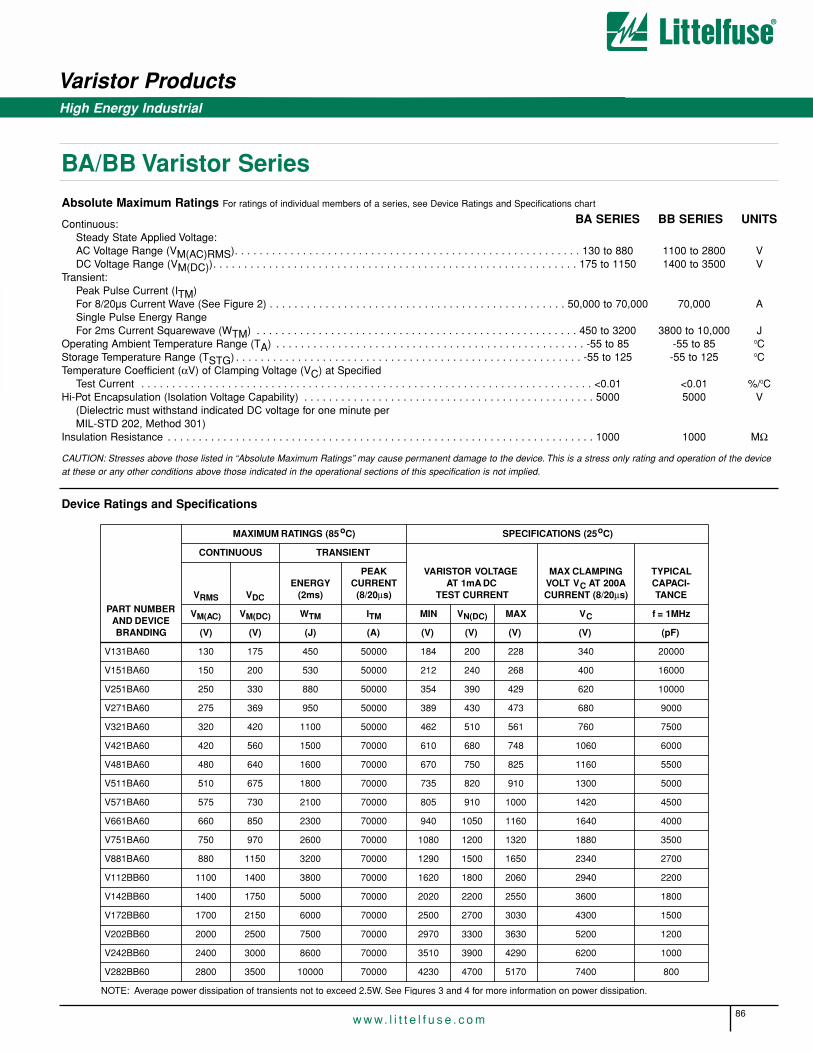
Varistor Products
86w w w. l i t t e l f u s e . c o m
High Energy Industrial
BA/BB Varistor Series Absolute Maximum Ratings For ratings of individual members of a series, see Device Ratings and Specifications chart
Continuous:Steady State Applied Voltage:AC Voltage Range (VM(AC)RMS). . . . . . . . . . . . . . . . . . . . . . . . . . . . . . . . . . . . . . . . . . . . . . . . . . . . . . . . 130 to 880 1100 to 2800 VDC Voltage Range (VM(DC)). . . . . . . . . . . . . . . . . . . . . . . . . . . . . . . . . . . . . . . . . . . . . . . . . . . . . . . . . . . 175 to 1150 1400 to 3500 V
Transient:Peak Pulse Current (ITM)For 8/20µs Current Wave (See Figure 2) . . . . . . . . . . . . . . . . . . . . . . . . . . . . . . . . . . . . . . . . . . . . . . . . 50,000 to 70,000 70,000 ASingle Pulse Energy RangeFor 2ms Current Squarewave (WTM) . . . . . . . . . . . . . . . . . . . . . . . . . . . . . . . . . . . . . . . . . . . . . . . . . . . . 450 to 3200 3800 to 10,000 J
Operating Ambient Temperature Range (TA) . . . . . . . . . . . . . . . . . . . . . . . . . . . . . . . . . . . . . . . . . . . . . . . . . . -55 to 85 -55 to 85 0CStorage Temperature Range (TSTG) . . . . . . . . . . . . . . . . . . . . . . . . . . . . . . . . . . . . . . . . . . . . . . . . . . . . . . . . -55 to 125 -55 to 125 0CTemperature Coefficient (αV) of Clamping Voltage (VC) at Specified
Test Current . . . . . . . . . . . . . . . . . . . . . . . . . . . . . . . . . . . . . . . . . . . . . . . . . . . . . . . . . . . . . . . . . . . . . . . . . <0.01 <0.01 %/0CHi-Pot Encapsulation (Isolation Voltage Capability) . . . . . . . . . . . . . . . . . . . . . . . . . . . . . . . . . . . . . . . . . . . . . . . 5000 5000 V
(Dielectric must withstand indicated DC voltage for one minute per MIL-STD 202, Method 301)
Insulation Resistance . . . . . . . . . . . . . . . . . . . . . . . . . . . . . . . . . . . . . . . . . . . . . . . . . . . . . . . . . . . . . . . . . . . . . 1000 1000 MΩ
CAUTION: Stresses above those listed in “Absolute Maximum Ratings” may cause permanent damage to the device. This is a stress only rating and operation of the deviceat these or any other conditions above those indicated in the operational sections of this specification is not implied.
Device Ratings and Specifications
BA SERIES BB SERIES UNITS
PART NUMBER AND DEVICE BRANDING
MAXIMUM RATINGS (85oC) SPECIFICATIONS (25oC)
CONTINUOUS TRANSIENT
VARISTOR VOLTAGEAT 1mA DC
TEST CURRENT
MAX CLAMPING VOLT VC AT 200A CURRENT (8/20µs)
TYPICALCAPACI-TANCEVRMS VDC
ENERGY (2ms)
PEAKCURRENT
(8/20µs)
VM(AC) VM(DC) WTM ITM MIN VN(DC) MAX VC f = 1MHz
(V) (V) (J) (A) (V) (V) (V) (V) (pF)
V131BA60 130 175 450 50000 184 200 228 340 20000
V151BA60 150 200 530 50000 212 240 268 400 16000
V251BA60 250 330 880 50000 354 390 429 620 10000
V271BA60 275 369 950 50000 389 430 473 680 9000
V321BA60 320 420 1100 50000 462 510 561 760 7500
V421BA60 420 560 1500 70000 610 680 748 1060 6000
V481BA60 480 640 1600 70000 670 750 825 1160 5500
V511BA60 510 675 1800 70000 735 820 910 1300 5000
V571BA60 575 730 2100 70000 805 910 1000 1420 4500
V661BA60 660 850 2300 70000 940 1050 1160 1640 4000
V751BA60 750 970 2600 70000 1080 1200 1320 1880 3500
V881BA60 880 1150 3200 70000 1290 1500 1650 2340 2700
V112BB60 1100 1400 3800 70000 1620 1800 2060 2940 2200
V142BB60 1400 1750 5000 70000 2020 2200 2550 3600 1800
V172BB60 1700 2150 6000 70000 2500 2700 3030 4300 1500
V202BB60 2000 2500 7500 70000 2970 3300 3630 5200 1200
V242BB60 2400 3000 8600 70000 3510 3900 4290 6200 1000
V282BB60 2800 3500 10000 70000 4230 4700 5170 7400 800
NOTE: Average power dissipation of transients not to exceed 2.5W. See Figures 3 and 4 for more information on power dissipation.

2
VAR
ISTO
RP
RO
DU
CT
S
Varistor Products
87w w w. l i t t e l f u s e . c o m
High Energy Industrial
BA/BB Varistor Series
Power Dissipation RatingsShould transients occur in rapid succession, the average power dissipationrequired is simply the energy (watt-seconds) per pulse times the number of pulses per second. The power so developed must be within the specifications shown on the Device Ratings and Characteristics table for the specific device. Furthermore, the operating values need to be derated at high temperatures as shown in Figure 1. Because varistors can only dissipate a relatively small amount of average power they are, therefore,not suitable for repetitive applications that involve substantial amounts ofaverage power dissipation.
100
90
80
70
60
50
40
30
20
10
0-55 50 60 70 80 90 100 110 120 130 140 150
AMBIENT TEMPERATURE ( oC)
PE
RC
EN
T O
F R
ATE
D V
AL
UE
FIGURE 2. PEAK PULSE CURRENT TEST WAVEFORM
100
90
50
10
O1 TT1
T2
TIME
PE
RC
EN
T O
F P
EA
K V
AL
UE
O1 = Virtual Origin of WaveT = Time From 10% to 90% of Peak
T1 = Virtual Front Time = 1.25 • tT2 = Virtual Time to Half Value (Impulse Duration)
Example: For an 8/20µs Current Waveform:8µs = T1 = Virtual Front Time
20µs = T2 = Virtual Time to Half Value
FIGURE 3. STANDBY POWER DISSIPATION vs APPLIED VRMS AT VARIED TEMPERATURES
TYPICAL TEMPERATURE COEFFICIENTOF POWER DISSIPATION = 2.2%/oC
MAX AT TA = 85oC
MAX AT TA = 25oC
TYP AT TA = 25oC
1.00.8
0.6
0.4
0.2
0.10.08
0.06
0.0480 90 100 110
PERCENTAGE OF MAXIMUM RATED V RMS (%)
PO
WE
R D
ISS
IPAT
ION
(W
) P
ER
kV
OF
RAT
ED
VR
MS
FIGURE 4. TYPICAL STABILITY OF STANDBY POWER DISSIPATION AT RATED V RMS vs TIME
1,000 HOURS, TA = 85oC
0.5
0.4
0.3
0.2
0.1
00 10 100 1,000
PO
WE
R D
ISS
IPAT
ION
(W
) P
ER
kV
OF
RAT
ED
VR
MS
TIME AT RATED VRMS (HOURS)
Typical Performance Curves
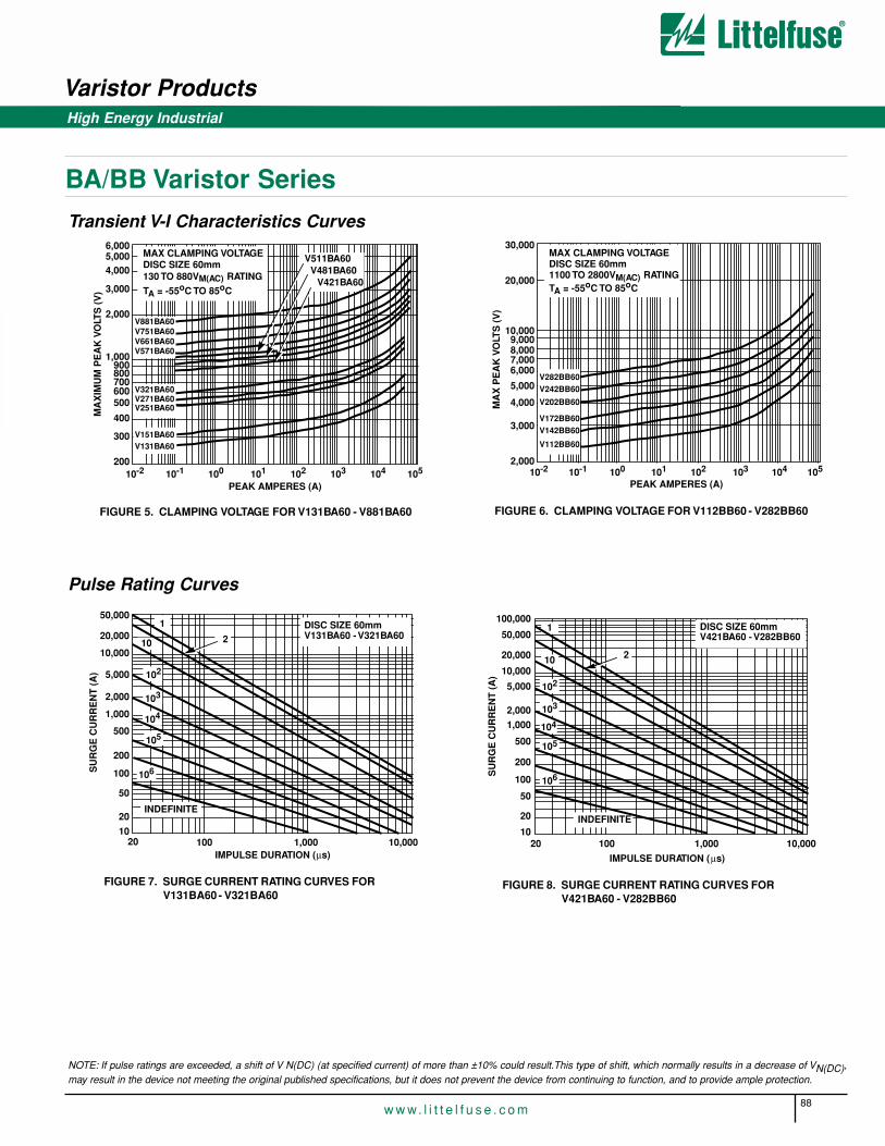
Varistor Products
88w w w. l i t t e l f u s e . c o m
BA/BB Varistor Series
High Energy Industrial
Transient V-I Characteristics Curves
FIGURE 5. CLAMPING VOLTAGE FOR V131BA60 - V881BA60
MAX CLAMPING VOLTAGEDISC SIZE 60mm130 TO 880VM(AC) RATING
TA = -55oC TO 85oC
6,0005,0004,000
3,000
2,000
1,000900800700600500
400
300
20010-2 10-1 100 101 102 103 104 105
PEAK AMPERES (A)
V881BA60V751BA60V661BA60V571BA60
V151BA60V131BA60
MA
XIM
UM
PE
AK
VO
LTS
(V
)
V511BA60V481BA60
V421BA60
V321BA60V271BA60V251BA60
FIGURE 6. CLAMPING VOLTAGE FOR V112BB60 - V282BB60
30,000
20,000
10,0009,0008,0007,0006,000
5,000
4,000
3,000
2,00010-2 10-1 100 101 102 103 104 105
PEAK AMPERES (A)M
AX
PE
AK
VO
LTS
(V
)
V282BB60V242BB60
V202BB60
V172BB60V142BB60
V112BB60
MAX CLAMPING VOLTAGEDISC SIZE 60mm1100 TO 2800VM(AC) RATINGTA = -55oC TO 85oC
NOTE: If pulse ratings are exceeded, a shift of V N(DC) (at specified current) of more than ±10% could result.This type of shift, which normally results in a decrease of VN(DC),may result in the device not meeting the original published specifications, but it does not prevent the device from continuing to function, and to provide ample protection.
Pulse Rating Curves
FIGURE 7. SURGE CURRENT RATING CURVES FOR V131BA60 - V321BA60
50,000
20,000
10,000
5,000
2,000
1,000
500
200
100
50
20
10
SU
RG
E C
UR
RE
NT
(A
)
IMPULSE DURATION (µs)1,000 10,000
10
102
103
104
105
INDEFINITE
106
20 100
2DISC SIZE 60mmV131BA60 - V321BA60
1
FIGURE 8. SURGE CURRENT RATING CURVES FOR V421BA60 - V282BB60
100,000
50,000
20,000
10,000
5,000
2,000
1,000
500
200
100
50
20
1020 100 1,000 10,000
IMPULSE DURATION (µs)
10
102
103
104
105
106
2
1 DISC SIZE 60mmV421BA60 - V282BB60
INDEFINITE
SU
RG
E C
UR
RE
NT
(A
)

Varistor Products
89w w w. l i t t e l f u s e . c o m
2
VAR
ISTO
RP
RO
DU
CT
S
High Energy Industrial
BA/BB Varistor Series
Mechanical Dimensions
BA SERIES
CL
100±1 (3.94± .039")
23.5±.75 (.925± .030")
Ordering Information
BB SERIES
7.0(0.28)
CL
VARISTOR
VM(AC)First Significant Digits
DISC SIZE (60mm)
V XX X XX 60
SERIES DESIGNATOR
VM(AC)Decade Multiplier
NOTES:
1. Typical weight:BA............................................................................................ ..250gBB...............................................................................................600g
Dimensions are in mm; inches in parentheses for reference only.

Varistor Products
90w w w. l i t t e l f u s e . c o m
High Energy Industrial
DA/DB Varistor SeriesThe DA and DB Series transient surge suppressors are heavy-duty
industrial metal-oxide varistors designed to provide surge protection for
motor controls and power supplies used in oil-drilling, mining, and trans-
portation equipment.
These UL-recognized varistors have identical ratings and specificationsbut differ in case construction to provide flexibility in equipment designs.
DA series devices feature rigid terminals to insure secure wire contacts.Both the DA and DB series feature improved creep and strike distancecapability to minimize breakdown along the package surface design thatprovides complete electrical isolation of the disc subassembly.
See DA/DB Series Device Ratings and Specifications table for part number and brand information.
Features• High Energy Absorption Capability
WTM . . . . . . . . . . . . . . . . . . . . . . . . . . . . . . . . . . . . . . . . . . Up To 1050J
• Wide Operating Voltage RangeVM(AC)RMS . . . . . . . . . . . . . . . . . . . . . . . . . . . . . . . . . . .130V to 750V
• Screw Terminals (DA Series),Quick Connect Push-On Connectors (DB Series)
• Case Design Provides Complete Electrical Isolation of Disc Subassembly
• 40mm Diameter Disc
• No Derating Up to 85oC Ambient
AGENCY APPROVALS: Recognized under the components program ofUnderwriters Laboratories.
AGENCY FILE NUMBERS: UL E75961.
DB SERIES
DA SERIES
®
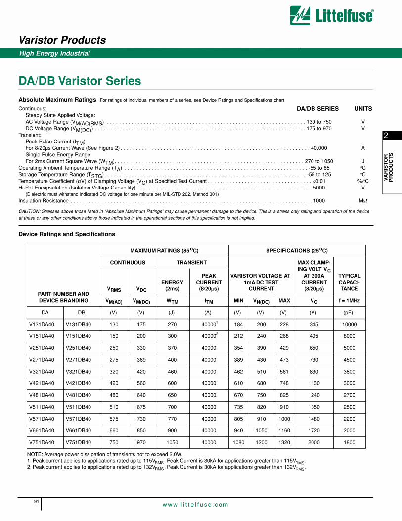
2
VAR
ISTO
RP
RO
DU
CT
S
Varistor Products
91w w w. l i t t e l f u s e . c o m
High Energy Industrial
DA/DB Varistor SeriesAbsolute Maximum Ratings For ratings of individual members of a series, see Device Ratings and Specifications chart
Continuous:Steady State Applied Voltage:AC Voltage Range (VM(AC)RMS) . . . . . . . . . . . . . . . . . . . . . . . . . . . . . . . . . . . . . . . . . . . . . . . . . . . . . . . . . . . . . . . . . 130 to 750 VDC Voltage Range (VM(DC)) . . . . . . . . . . . . . . . . . . . . . . . . . . . . . . . . . . . . . . . . . . . . . . . . . . . . . . . . . . . . . . . . . . . . . 175 to 970 V
Transient:Peak Pulse Current (ITM)For 8/20µs Current Wave (See Figure 2) . . . . . . . . . . . . . . . . . . . . . . . . . . . . . . . . . . . . . . . . . . . . . . . . . . . . . . . . . . . . . . 40,000 ASingle Pulse Energy RangeFor 2ms Current Square Wave (WTM). . . . . . . . . . . . . . . . . . . . . . . . . . . . . . . . . . . . . . . . . . . . . . . . . . . . . . . . . . . . . . 270 to 1050 J
Operating Ambient Temperature Range (TA) . . . . . . . . . . . . . . . . . . . . . . . . . . . . . . . . . . . . . . . . . . . . . . . . . . . . . . . . . . . . -55 to 85 oCStorage Temperature Range (TSTG) . . . . . . . . . . . . . . . . . . . . . . . . . . . . . . . . . . . . . . . . . . . . . . . . . . . . . . . . . . . . . . . . . . -55 to 125 oCTemperature Coefficient (αV) of Clamping Voltage (VC) at Specified Test Current . . . . . . . . . . . . . . . . . . . . . . . . . . . . . . . . . . <0.01 %/oCHi-Pot Encapsulation (Isolation Voltage Capability) . . . . . . . . . . . . . . . . . . . . . . . . . . . . . . . . . . . . . . . . . . . . . . . . . . . . . . . . . 5000 V
(Dielectric must withstand indicated DC voltage for one minute per MIL-STD 202, Method 301)Insulation Resistance . . . . . . . . . . . . . . . . . . . . . . . . . . . . . . . . . . . . . . . . . . . . . . . . . . . . . . . . . . . . . . . . . . . . . . . . . . . . . . . 1000 MΩ
CAUTION: Stresses above those listed in “Absolute Maximum Ratings” may cause permanent damage to the device. This is a stress only rating and operation of the deviceat these or any other conditions above those indicated in the operational sections of this specification is not implied.
Device Ratings and Specifications
DA/DB SERIES UNITS
PART NUMBER ANDDEVICE BRANDING
MAXIMUM RATINGS (85oC) SPECIFICATIONS (25oC)
CONTINUOUS TRANSIENT
VARISTOR VOLTAGE AT 1mA DC TEST
CURRENT
MAX CLAMP-ING VOLT VC
AT 200ACURRENT
(8/20µs)
TYPICAL CAPACI-TANCEVRMS VDC
ENERGY (2ms)
PEAKCURRENT
(8/20µs)
VM(AC) VM(DC) WTM ITM MIN VN(DC) MAX VC f = 1MHz
DA DB (V) (V) (J) (A) (V) (V) (V) (V) (pF)
V131DA40 V131DB40 130 175 270 40000 184 200 228 345 10000
V151DA40 V151DB40 150 200 300 40000 212 240 268 405 8000
V251DA40 V251DB40 250 330 370 40000 354 390 429 650 5000
V271DA40 V271DB40 275 369 400 40000 389 430 473 730 4500
V321DA40 V321DB40 320 420 460 40000 462 510 561 830 3800
V421DA40 V421DB40 420 560 600 40000 610 680 748 1130 3000
V481DA40 V481DB40 480 640 650 40000 670 750 825 1240 2700
V511DA40 V511DB40 510 675 700 40000 735 820 910 1350 2500
V571DA40 V571DB40 575 730 770 40000 805 910 1000 1480 2200
V661DA40 V661DB40 660 850 900 40000 940 1050 1160 1720 2000
V751DA40 V751DB40 750 970 1050 40000 1080 1200 1320 2000 1800
NOTE: Average power dissipation of transients not to exceed 2.0W.1: Peak current applies to applications rated up to 115V . Peak Current is 30kA for applications greater than 115V .2: Peak current applies to applications rated up to 132V . Peak Current is 30kA for applications greater than 132V .
RMS
RMS
RMS
RMS
1
2

Varistor Products
92w w w. l i t t e l f u s e . c o m
High Energy Industrial
DA/DB Varistor Series
Power Dissipation RatingsShould transients occur in rapid succession, the average power dissipa-tion required is simply the energy (watt- seconds) per pulse times thenumber of pulses per second. The power so developed must be within thespecifications shown on the Device Ratings and Specifications table forthe specific device. Furthermore, the operating values need to be deratedat high temperatures as shown in Figure 1. Because varistors can onlydissipate a relatively small amount of average power they are, therefore,not suitable for repetitive applications that involve substantial amounts ofaverage power dissipation.
FIGURE 1. CURRENT, ENERGY AND POWER DERATING CURVE
100
90
80
70
60
50
40
30
20
10
0-55 50 60 70 80 90 100 110 120 130 140 150
PE
RC
EN
T O
F R
ATE
D V
AL
UE
AMBIENT TEMPERATURE ( oC)
FIGURE 2. PEAK PULSE CURRENT TEST WAVEFORM
100
90
50
10
O1 T
T1T2
TIME
PE
RC
EN
T O
F P
EA
K V
AL
UE
O1 = Virtual Origin of WaveT = Time From 10% to 90% of Peak
T1 = Virtual Front time = 1.25 • tT2 = Virtual Time to Half Value (Impulse Duration)
Example: For an 8/20µs Current Waveform:8µs = T1 = Virtual Front Time
20µs = T2 = Virtual Time to Half Value
Transient V-I Characteristics Curve
FIGURE 3. CLAMPING VOLTAGE FOR V131DA40, V131DB40 - V751DA40, V751DB40
200
6,0005,0004,000
3,000
1,000900800700600500400
300
10-2 10-1 100 101 102 103 104 105
MAXIMUM CLAMPING VOLTAGEDISC SIZE 40mm130 TO 750 VM(AC) RATING
TA = -55oC to 85oC
V421DA/DB40
V151DA/DB40
V751DA/DB40
MA
XIM
UM
PE
AK
VO
LTS
(V
)
PEAK AMPERES (A)
V131DA/DB40
V321DA/DB40V271DA/DB40
V251DA/DB40
V511DA/DB40V481DA/DB40
V571DA/DB40V661DA/DB40
2,000
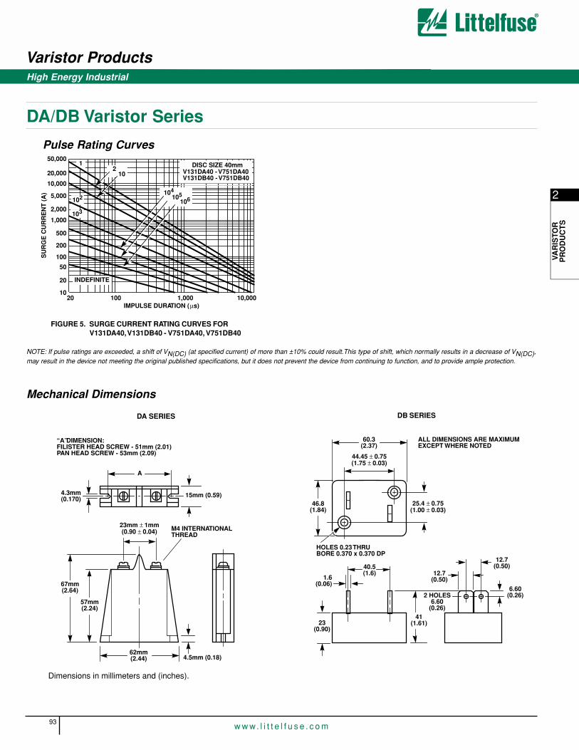
2
VAR
ISTO
RP
RO
DU
CT
S
Varistor Products
93w w w. l i t t e l f u s e . c o m
High Energy Industrial
DA/DB Varistor Series
Pulse Rating Curves
NOTE: If pulse ratings are exceeded, a shift of VN(DC) (at specified current) of more than ±10% could result.This type of shift, which normally results in a decrease of VN(DC),may result in the device not meeting the original published specifications, but it does not prevent the device from continuing to function, and to provide ample protection.
FIGURE 5. SURGE CURRENT RATING CURVES FOR V131DA40, V131DB40 - V751DA40, V751DB40
DISC SIZE 40mmV131DA40 - V751DA40
50,000
20,000
10,000
5,000
2,000
1,000
500
200
100
50
20
1020 100 1,000 10,000
SU
RG
E C
UR
RE
NT
(A
)
IMPULSE DURATION (µs)
V131DB40 - V751DB402
1
INDEFINITE
104
103
102 105106
10
DA SERIES
Dimensions in millimeters and (inches).
A
4.3mm(0.170)
15mm (0.59)
“A” DIMENSION:FILISTER HEAD SCREW - 51mm (2.01)PAN HEAD SCREW - 53mm (2.09)
23mm ± 1mm(0.90 ± 0.04)
57mm(2.24)
67mm(2.64)
62mm(2.44)
M4 INTERNATIONALTHREAD
4.5mm (0.18)
Mechanical Dimensions
DB SERIES
60.3(2.37)
44.45 ± 0.75(1.75 ± 0.03)
46.8(1.84)
25.4 ± 0.75(1.00 ± 0.03)
ALL DIMENSIONS ARE MAXIMUMEXCEPT WHERE NOTED
HOLES 0.23 THRUBORE 0.370 x 0.370 DP
12.7(0.50)
6.60(0.26)2 HOLES
6.60(0.26)
41(1.61)
40.5(1.6)
1.6(0.06)
23(0.90)
12.7(0.50)

Varistor Products
94w w w. l i t t e l f u s e . c o m
High Energy Industrial
HA Varistor SeriesHA Series transient surge suppressors are industrial high energy metal-oxide varistors (MOVs). They are designed to provide secondarysurge protection in the outdoor and service entrance environment (distribution panels) of buildings, and also in industrial applications formotor controls and power supplies used in the oil-drilling, mining, andtransportation fields.
The design of the HA Series of metal oxide varistors provide rigid terminals for screw mounting. Also available in a clipped lead version for through hole board placement or to accommodate soldered leads -designation “HC”.
See Ratings and Specifications table for part number and brand information.
Features• Wide Operating Voltage Range
VM(AC)RMS . . . . . . . . . . . . . . . . . . . . . . . . . . . . . . . . . . .130V to 750V
• Two Disc Sizes Available . . . . . . . . . . . . . . . . . . . . . 32mm and 40mm
• High Energy AbsorptionCapability. . . . . . . . . . . . . . . . . . . . . . . . . . . . . . .WTM = 200J to 1050J
• High Peak Pulse CurrentCapability,. . . . . . . . . . . . . . . . . . . . . . . . . . .ITM = 25,000A to 40,000A
• Rigid Terminals for Secure Mounting
• Available in Trimmed Version for Through Hole Board Mounting -Designation “HC”
• No Derating Up to 85oC Ambient
AGENCY APPROVALS: Recognized under the components program ofUnderwriters Laboratories. Certified by CSA.
AGENCY FILE NUMBERS: UL E75961, CSA LR91788.
ALSO SEE HB34 SERIES
®®

2
VAR
ISTO
RP
RO
DU
CT
S
Varistor Products
95w w w. l i t t e l f u s e . c o m
High Energy Industrial
HA Varistor Series
Absolute Maximum Ratings For ratings of individual members of a series, see Device Ratings and Specifications Chart
Continuous:Steady State Applied Voltage:AC Voltage Range (VM(AC)RMS) . . . . . . . . . . . . . . . . . . . . . . . . . . . . . . . . . . . . . . . . . . . . . . . . . . . . . . . . . . . . . . . . . . . . 130 to 750 VDC Voltage Range (VM(DC)) . . . . . . . . . . . . . . . . . . . . . . . . . . . . . . . . . . . . . . . . . . . . . . . . . . . . . . . . . . . . . . . . . . . . . . . 175 to 970 V
Transient:Peak Pulse Current (ITM)For 8/20µs Current Wave (See Figure 2) . . . . . . . . . . . . . . . . . . . . . . . . . . . . . . . . . . . . . . . . . . . . . . . . . . . . . . . . . . . . 25,000 to 40,000 ASingle Pulse Energy RangeFor 2ms Current Square Wave (WTM ) . . . . . . . . . . . . . . . . . . . . . . . . . . . . . . . . . . . . . . . . . . . . . . . . . . . . . . . . . . . . . . . 200 to 1050 J
Operating Ambient Temperature Range (TA) . . . . . . . . . . . . . . . . . . . . . . . . . . . . . . . . . . . . . . . . . . . . . . . . . . . . . . . . . . . . . . -55 to 85 oCStorage Temperature Range (TSTG) . . . . . . . . . . . . . . . . . . . . . . . . . . . . . . . . . . . . . . . . . . . . . . . . . . . . . . . . . . . . . . . . . . . -55 to 125 oCTemperature Coefficient (αV) of Clamping Voltage (VC) at Specified Test Current . . . . . . . . . . . . . . . . . . . . . . . . . . . . . . . . . . . . <0.01 %/oCHi-Pot Encapsulation (Isolation Voltage Capability). . . . . . . . . . . . . . . . . . . . . . . . . . . . . . . . . . . . . . . . . . . . . . . . . . . . . . . . . . . . 2500 V
(Dielectric must withstand indicated DC voltage for one minute per MIL-STD 202,Method 301)
Insulation Resistance. . . . . . . . . . . . . . . . . . . . . . . . . . . . . . . . . . . . . . . . . . . . . . . . . . . . . . . . . . . . . . . . . . . . . . . . . . . . . . . . . 1000M Ω
CAUTION: Stresses above those listed in “Absolute Maximum Ratings” may cause permanent damage to the device. This is a stress only rating and operation of the deviceat these or any other conditions above those indicated in the operational sections of this specification is not implied.
Device Ratings and Specifications
HA SERIES UNITS
PARTNUMBER AND
DEVICE BRANDING
MAXIMUM RATINGS (85oC) SPECIFICATIONS (25oC)
CONTINUOUS TRANSIENT
VARISTOR VOLTAGEAT 1mA DC TEST
CURRENT
MAXIMUM CLAMPING VOLTAGE
(VC) AT 200A (8/20µs)
TYPICALCAPACITANCE
AT f = 1MHzVRMS VDC
ENERGY (2ms)
PEAKCURRENT
(8/20µs)
VM(AC) VM(DC) WTM ITM MIN VN(DC) MAX VC C
(V) (V) ENERGY (A) (V) (V) (V) (V) (pF)
V131HA32V131HA40
130130
175175
200270
2500040000
184184
200 200
228228
350345
4700 10000
V151HA32V151HA40
150150
200200
220300
2500040000
212212
240240
268268
410405
4000 8000
V251HA32V251HA40
250250
330 330
330370
2500040000
354354
390390
429429
650630
25005000
V271HA32V271HA40
275275
369369
360400
2500040000
389389
430430
473473
710690
22004500
V321HA32V321HA40
320320
420420
390460
2500040000
462462
510510
561561
845825
1900 3800
V421HA32V421HA40
420420
560560
400600
2500040000
610610
680 680
748748
11201100
15003000
V481HA32V481HA40
480480
640 640
450650
2500040000
670670
750750
825825
12901230
1300 2700
V511HA32V511HA40
510510
675675
500700
2500040000
735735
820820
910910
13551295
1200 2500
V571HA32V571HA40
575 575
730730
550770
2500040000
805805
910910
10001000
15701480
11002200
V661HA32V661HA40
660 660
850850
600 900
2500040000
940940
10501050
11601160
18201720
10002000
V751HA32V751HA40
750750
970970
7001050
2500040000
10801080
12001200
13201320
20502000
8001800
Notes 1 & 2 are located at the top of the next page.
1
2
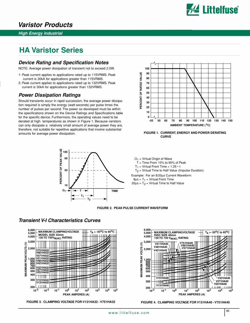
Varistor Products
96w w w. l i t t e l f u s e . c o m
HA Varistor Series
High Energy Industrial
FIGURE 4. CLAMPING VOLTAGE FOR V131HA40 - V751HA40
200
6,0005,0004,000
3,000
2,000
1,000900800700600500
400
300
10-2 10-1 100 101 102 103 104 105
MAXIMUM CLAMPING VOLTAGEDISC SIZE 40mm130 TO 750 VM(AC) RATING
TA = -55oC to 85oC
V421HA40
V151HA40
V751HA40
MA
XIM
UM
PE
AK
VO
LTS
(V
)
PEAK AMPERES (A)
V131HA40
V321HA40V271HA40
V251HA40
V511HA40V481HA40 V571HA40
V661HA40
Device Rating and Specification NotesNOTE: Average power dissipation of transient not to exceed 2.0W.
1: Peak current applies to applications rated up to 115VRMS. Peak current is 30kA for applications greater than 115VRMS.
2: Peak current applies to applications rated up to 132VRMS. Peak current is 30kA for applications greater than 132VRMS.
Power Dissipation RatingsShould transients occur in rapid succession, the average power dissipa-tion required is simply the energy (watt-seconds) per pulse times thenumber of pulses per second. The power so developed must be withinthe specifications shown on the Device Ratings and Specifications tablefor the specific device. Furthermore, the operating values need to be derated at high temperatures as shown in Figure 1. Because varistorscan only dissipate a relatively small amount of average power they are,therefore, not suitable for repetitive applications that involve substantialamounts for average power dissipation.
Transient V-I Characteristics Curves
100
90
80
70
60
50
40
30
20
10
0-55 50 60 70 80 90 100 110 120 130 140 150
PE
RC
EN
T O
F R
ATE
D V
AL
UE
AMBIENT TEMPERATURE ( oC)
FIGURE 1. CURRENT, ENERGY AND POWER DERATING CURVE
FIGURE 2. PEAK PULSE CURRENT WAVEFORM
100
90
50
10
O1 T
T1T2
TIME
PE
RC
EN
T O
F P
EA
K V
AL
UE
O1 = Virtual Origin of WaveT = Time From 10% to 90% of Peak
T1 = Virtual Front Time = 1.25 • tT2 = Virtual Time to Half Value (Impulse Duration)
Example: For an 8/20µs Current Waveform:8µs = T1 = Virtual Front Time
20µs = T2 = Virtual Time to Half Value
FIGURE 3. CLAMPING VOLTAGE FOR V131HA32 - V751HA32
200
6,0005,0004,000
3,000
2,000
1,000900800
600
400
300
10-3 10-2 10-1 100 101 102 103 104
MA
XIM
UM
PE
AK
VO
LTS
(V
)
PEAK AMPERES (A)
V421HA32
V321HA32V271HA32V251HA32
V151HA32V131HA32
105
500
700
MAXIMUM CLAMPING VOLTAGEMODEL SIZE 32mm130 TO 750VM(AC) RATING
V751HA32V661HA32V571HA32V511HA32V481HA32
TA = -55oC to 85oC
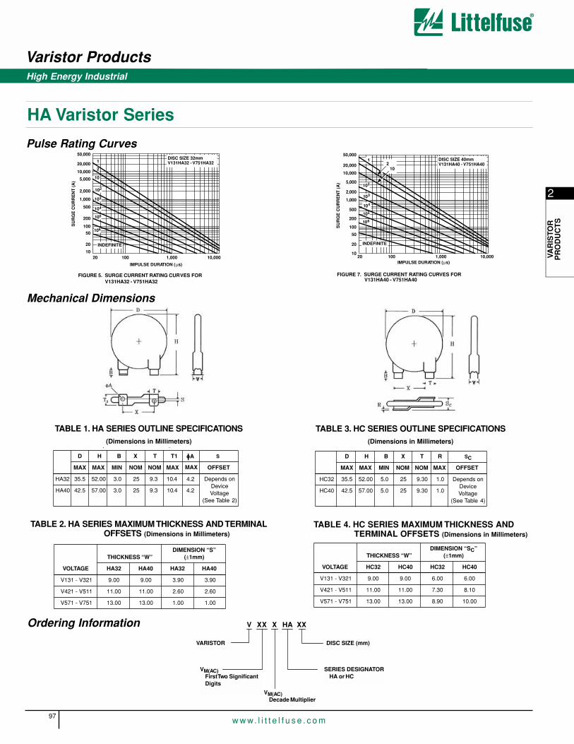
2
VAR
ISTO
RP
RO
DU
CT
S
Varistor Products
97w w w. l i t t e l f u s e . c o m
High Energy Industrial
HA Varistor Series
( )
D H B X T T1 S
MAX MAX MIN NOM NOM MAX OFFSET
HA32 35.5 52.00 3.0 25 9.3 10.4 Depends onDeviceVoltage
(See Table 2)
HA40 42.5 57.00 3.0 25 9.3 10.4
oA
MAX
4.2
4.2
D H B X T R SC
MAX MAX MIN NOM NOM MAX OFFSET
HC32 35.5 52.00 5.0 25 9.30 1.0 Depends onDeviceVoltage
(See Table 4)
HC40 42.5 57.00 5.0 25 9.30 1.0
VOLTAGE
THICKNESS “W”DIMENSION “S”
(±1mm)
HA32 HA40 HA32 HA40
V131 - V321 9.00 9.00 3.90 3.90
V421 - V511 11.00 11.00 2.60 2.60
V571 - V751 13.00 13.00 1.00 1.00
TABLE 2. HA SERIES MAXIMUM THICKNESS AND TERMINAL OFFSETS (Dimensions in Millimeters)
VOLTAGE
THICKNESS “W”DIMENSION “SC”
(±1mm)
HC32 HC40 HC32 HC40
V131 - V321 9.00 9.00 6.00 6.00
V421 - V511 11.00 11.00 7.30 8.10
V571 - V751 13.00 13.00 8.90 10.00
TABLE 4. HC SERIES MAXIMUM THICKNESS AND TERMINAL OFFSETS (Dimensions in Millimeters)
Ordering Information
VARISTOR
VM(AC)First Two Significant Digits
DISC SIZE (mm)
V XX X HA XX
SERIES DESIGNATORHA or HC
VM(AC)Decade Multiplier
Pulse Rating Curves
FIGURE 5. SURGE CURRENT RATING CURVES FOR V131HA32 - V751HA32
DISC SIZE 32mmV131HA32 - V751HA32
50,000
20,000
10,000
5,000
2,000
1,000
500
200
100
50
20
1020 100 1,000 10,000
SU
RG
E C
UR
RE
NT
(A
)
IMPULSE DURATION (µs)
10
2
1
INDEFINITE
102
103
104
105
106
FIGURE 7. SURGE CURRENT RATING CURVES FOR V131HA40 - V751HA40
DISC SIZE 40mmV131HA40 - V751HA40
50,000
20,000
10,000
5,000
2,000
1,000
500
200
100
50
20
1020 100 1,000 10,000
SU
RG
E C
UR
RE
NT
(A
)
IMPULSE DURATION (µs)
21
INDEFINITE
102
103
104
105
106
10
Mechanical Dimensions
TABLE 1. HA SERIES OUTLINE SPECIFICATIONS(Dimensions in Millimeters)
TABLE 3. HC SERIES OUTLINE SPECIFICATIONS(Dimensions in Millimeters)

Varistor Products
98w w w. l i t t e l f u s e . c o m
High Energy Industrial
HB34, HF34 and HG34 Varistor SeriesThe HB34, HF34, and HG34 Series of transient surge suppressors areindustrial high-energy Metal-Oxide Varistors (MOVs). They are designedto provide surge suppression in the AC mains outdoor and serviceentrance environment (distribution panels) of buildings. Applications alsoinclude industrial heavy motors, controls, and power supplies such asused in the oil-drilling, mining, and transportation fields, including HVACand motor/generator applications.
The HB34 Series provides rigid terminals for through-hole solder mounting on printed circuit boards, thereby eliminating the need forscrew mounting. The HF34 Series has the same rigid through-hole termi-nals as the HB34 with the addition of mounting holes for bolt-downmounting and longer terminals to allow for additional mounting flexibility.The HG34 has formed feet with mounting holes for vertical bolt-downmounting.
See Ratings and Specifications table for part numbers.
Features• Wide Operating Voltage Range
VM(AC)RMS. . . . . . . . . . . . . . . . . . . . . . . . . . . . . . . . . . . 130V to 750V
• High Energy AbsorptionCapability. . . . . . . . . . . . . . . . . . . . . . . . . . . . . . .WTM = 200J to 1050J
• High Peak Pulse CurrentCapability . . . . . . . . . . . . . . . . . . . . . . . . . . . . . . . . ITM = 40,000A
• Rigid Terminals for Secure Through-Hole Solder Mounting
• No Derating Up to 85oC Ambient
AGENCY APPROVALS: Recognized under the components program ofUnderwriters Laboratories. Certified by CSA.
AGENCY FILE NUMBERS: UL E75961, CSA LR91788.
®®
2
VAR
ISTO
RP
RO
DU
CT
S
Varistor Products
99w w w. l i t t e l f u s e . c o m
High Energy Industrial
HB34, HF34 and HG34 Varistor Series
Absolute Maximum Ratings For ratings of individual members of a series, see Device Ratings and Specifications chart
Continuous:Steady State Applied Voltage:AC Voltage Range (VM(AC)RMS) . . . . . . . . . . . . . . . . . . . . . . . . . . . . . . . . . . . . . . . . . . . . . . . . . . . . . . . . . . . . . . . . . . 130 to 750 VDC Voltage Range (VM(DC)). . . . . . . . . . . . . . . . . . . . . . . . . . . . . . . . . . . . . . . . . . . . . . . . . . . . . . . . . . . . . . . . . . . . . . 175 to 970 V
Transient:Peak Pulse Current (ITM)For 8/20µs Current Wave (See Figure 2) . . . . . . . . . . . . . . . . . . . . . . . . . . . . . . . . . . . . . . . . . . . . . . . . . . . . . . . . . . . . . . 40,000 ASingle Pulse Energy RangeFor 2ms Current Square Wave (WTM) . . . . . . . . . . . . . . . . . . . . . . . . . . . . . . . . . . . . . . . . . . . . . . . . . . . . . . . . . . . . . . 270 to 1050 J
Operating Ambient Temperature Range (TA) . . . . . . . . . . . . . . . . . . . . . . . . . . . . . . . . . . . . . . . . . . . . . . . . . . . . . . . . . . . . . -55 to 85 OC Storage Temperature Range (TSTG) . . . . . . . . . . . . . . . . . . . . . . . . . . . . . . . . . . . . . . . . . . . . . . . . . . . . . . . . . . . . . . . . . . -55 to 125 OC Temperature Coefficient (αV) of Clamping Voltage (VC) at Specified Test Current . . . . . . . . . . . . . . . . . . . . . . . . . . . . . . . . . . <0.01 %/OC
CAUTION: Stresses above those listed in “Absolute Maximum Ratings” may cause permanent damage to the device. This is a stress only rating and operation of the deviceat these or any other conditions above those indicated in the operational sections of this specification is not implied.
Device Ratings and Specifications
Hx34 SERIES UNITS
MODELNUMBER
SIZE
MAXIMUM RATINGS (85oC) SPECIFICATIONS (25oC)
CONTINUOUS TRANSIENT
VARISTOR VOLTAGEAT 1mA DC TEST
CURRENT
MAXIMUM CLAMPING VOLTAGE
(VC) AT 200A(8/20µs)
TYPICALCAPACI-TANCEVRMS VDC
ENERGY (2ms)
PEAKCURRENT
(8/20µs)
VM(AC) VM(DC) WTM ITM MIN VN(DC) MAX VC f = 1MHz
(mm) (V) (V) (V) (A) (V) (V) (V) (V) (pF)
V131HB34 34
34
130
140
175
188
270
291
40,000 184
198
200
220
228
248
345
375 9,000
10,000
V151HB34 34 150 200 300 40,000 212 240 268 405 8,000
V251HB34 34 250 330 370 40,000 354 390 429 650 5,000
V271HB34
V301HB34
34
34
275
300
370
410
400
430
40,000
40,000
389
433
430
478
473
526
730
780
4,500
4,100
V321HB34 34 320 420 460 40,000 462 510 561 830 3,800
V421HB34 34 420 560 600 40,000 610 680 748 1,130 3,000
V481HB34 34 480 640 650 40,000 670 750 825 1,240 2,700
V511HB34 34 510 675 700 40,000 735 820 910 1,350 2,500
V571HB34 34 570 730 770 40,000 805 910 1000 1,480 2,200
V661HB34 34 660 850 900 40,000 940 1050 1160 1,720 2,000
V751HB34 34 750 970 1050 40,000 1080 1200 1320 2,000 1,800
NOTE: Average power dissipation of transients not to exceed 2.0W.
1. Peak current applies to applications rated up to 115 V . Peak current is 30kA for applications greater than 115V .2. Peak current applies to applications rated up to 132V . Peak Current is 30kA for applications greater than 132V .3. Peak current applies to applications rated up to 123V . Peak Current is 30kA for applications greater than 123V .
RMSRMS
RMS
1
40,0003
RMS
RMS
RMS
2
V141HB34

Varistor Products
100w w w. l i t t e l f u s e . c o m
High Energy Industrial
HB34, HF34 and HG34 Varistor Series
40,000 4
MODELNUMBER
SIZE
MAXIMUM RATINGS (85oC) SPECIFICATIONS (25oC)
CONTINUOUS TRANSIENT
VARISTOR VOLTAGEAT 1mA DC TEST
CURRENT
MAXIMUM CLAMPING VOLTAGE
(VC) AT 200A(8/20µs)
TYPICALCAPACI-TANCEVRMS VDC
ENERGY (2ms)
PEAKCURRENT
(8/20µs)
VM(AC) VM(DC) WTM ITM MIN VN(DC) MAX VC f = 1MHz
(mm) (V) (V) (V) (A) (V) (V) (V) (V) (pF)
V131HF34 34
34
130
140
175
188
270
291
40,000 184
198
200
220
228
248
345
375
10,000
V151HF34
V141HF34
34 150 200 300 212 240 268 405 8,000
9,000
V251HF34 34 250 330 370 354 390 429 650 5,000
V271HF34 34 275 370 400 40,000 389 430 473 730 4,500
V321HF34 34 320 420 460 40,000 462 510 561 830 3,800
V421HF34 34 420 560 600 40,000 610 680 748 1,130 3,000
V481HF34 34 480 640 650 40,000 670 750 825 1,240 2,700
V511HF34 34 510 675 700 40,000 735 820 910 1,350 2,500
V571HF34 34 570 730 770 40,000 805 910 1000 1,480 2,200
V661HF34 34 660 850 900 40,000 940 1050 1160 1,720 2,000
V751HF34 34 750 970 1050 40,000 1080 1200 1320 2,000 1,800
2
40,0003
40,000 3
V301HF34 34 300 410 430 40,000 433 478 526 780 4,100
NOTE:1. Average power dissipation of transients not to exceed 2.0W per varistor2. 40kA capability depends on applications rated up to 115V RMS. 30kA applies if > 115 Vrms.3. 40kA capability depends on applications rated up to 123V RMS. 30kA applies if > 123 Vrms.4. 40kA capability depends on applications rated up to 132V RMS. 30kA applies if > 132 Vrms.
Device Ratings and Specifications

Varistor Products
101w w w. l i t t e l f u s e . c o m
40,0004
MODELNUMBER
SIZE
MAXIMUM RATINGS (85oC) SPECIFICATIONS (25oC)
CONTINUOUS TRANSIENT
VARISTOR VOLTAGEAT 1mA DC TEST
CURRENT
MAXIMUM CLAMPING VOLTAGE
(VC) AT 200A(8/20µs)
TYPICALCAPACI-TANCEVRMS VDC
ENERGY (2ms)
PEAKCURRENT
(8/20µs)
VM(AC) VM(DC)W
TMITM MIN V
N(DC) MAX VC f = 1MHz
(mm) (V) (V) (V) (A) (V) (V) (V) (V) (pF)
V131HG34
V141HG34
34
34
130
140
175
188
270
291
40,000 184
198
200
220
228
248
345
375
10,000
V151HG34 34 150 200 300 212 240 268 405 8,000
9,000
V251HG34 34 250 330 370 354 390 429 650 5,000
V271HG34 34 275 370 400 40,000 389 430 473 730 4,500
V321HG34 34 320 420 460 40,000 462 510 561 830 3,800
V421HG34 34 420 560 600 40,000 610 680 748 1,130 3,000
V481HG34 34 480 640 650 40,000 670 750 825 1,240 2,700
V511HG34 34 510 675 700 40,000 735 820 910 1,350 2,500
V571HG34 34 570 730 770 40,000 805 910 1000 1,480 2,200
V661HG34 34 660 850 900 40,000 940 1050 1160 1,720 2,000
V751HG34 34 750 970 1050 40,000 1080 1200 1320 2,000 1,800
2
40,0003
40,000 3
V301HG34 34 300 410 430 40,000 433 478 526 780 4,100
NOTE:1. Average power dissipation of transients not to exceed 2.0W per varistor2. 40kA capability depends on applications rated up to 115V RMS. 30kA applies if > 115 Vrms.3. 40kA capability depends on applications rated up to 123V RMS. 30kA applies if > 123 Vrms.4. 40kA capability depends on applications rated up to 132V RMS. 30kA applies if > 132 Vrms.
Device Ratings and Specifications
High Energy Industrial
HB34, HF34 and HG34 Varistor Series

Varistor Products
102w w w. l i t t e l f u s e . c o m
High Energy Industrial
Power Dissipation RatingsShould transients occur in rapid succession, the average power dissipation result is simply the energy (watt-seconds) per pulse times thenumber of pulses per second. The power so developed must be withinthe specifications shown on the Device Ratings and Specifications tablefor the specific device. The operating values must be derated as shownin Figure 1.
Transient V-I Characteristics Curves
FIGURE 2. PEAK PULSE CURRENT TEST WAVEFORM
100
90
50
10
O1 T
T1T2
TIME
PE
RC
EN
T O
F P
EA
K V
AL
UE
O1 = Virtual Origin of WaveT = Time From 10% to 90% of Peak
T1 = Virtual Front time = 1.25 • tT2 = Virtual Time to Half Value (Impulse Duration)
Example: For an 8/20µs Current Waveform:8µs = T1 = Virtual Front Time
20µs = T2 = Virtual Time to Half Value
FIGURE 3. CLAMPING VOLTAGE FOR V131HB34 - V751HB34
VO
LTA
GE
(V
)
10000
1000
100
CURRENT (A)
V751HB34
V131HB34
V321HB34
V511HB34
V481HB34V571HB34
V661HB34
TA = -55oC TO 85oCMAXIMUM CLAMPING VOLTAGEVARISTOR SIZE 34mm130 TO 750 VM(AC) RATING
V271HB34
V251HB34
V151HB34
V421HB34
-5 -4 1E-3 0.01 0.1 1 10 100 1,000 10,000 100,000
HB34, HF34 and HG34 Varistor Series

2
VAR
ISTO
RP
RO
DU
CT
S
Varistor Products
103w w w. l i t t e l f u s e . c o m
HB34, HF34 and HG34 Varistor Series
Ordering Information
FIGURE 4. SURGE CURRENT RATING CURVES FOR V131HB34 - V751HB34
DISC SIZE 34mmV131HB34 - V751HB34
50,000
20,000
10,000
5,000
2,000
1,000
500
200
100
50
20
1020 100 1,000 10,000
SU
RG
E C
UR
RE
NT
(A
)
IMPULSE DURATION (µs)
10
1
INDEFINITE
105102
2
103
104
106
NOTE: If pulse ratings are exceeded, a shift of VN(DC) (at specified current) of more than ±10% could result. This type of shift, which normally results in a decrease of VN(DC),may result in the device not meeting the original published specifications, but it does not prevent the device from continuing to function, and to provide ample protection.
Pulse Rating Curves
Mechanical Dimensions HB34
NOTE: Dimension in mm is typical, unless otherwise specified.
37.0 MAX
47.5MAX
22.0 ±1.0
6.0 ±0.1 0.55
S
42.5MAX
2.5 TO5.0
T
±0.1
2.30±0.2
VARISTOR DESIGNATOR
MAX ACRMS WORKING VOLTAGE(FIRST SIGNIFICANT DIGITS) VM(AC)
DISC SIZE (mm)
SERIES DESIGNATOR
VM(AC) VOLTAGE DECADE MULTIPLIER
V 25 1 HB 34
TABLE OF DIMENSIONS - THICKNESS AND TERMINAL OFFSETS
PART TYPE
T BODY THICKNESS
(MAXIMUM)
S MOUNTING TERMINAL
OFFSET
V131HB34 5.7 5.50 ±0.65
V151HB34 5.9 5.90 ±0.65
V251HB34 6.1 6.25 ±0.65
V271HB34 6.4 6.50 ±0.65
V321HB34 6.9 6.90 ±0.65
V421HB34 7.8 7.85 ±0.85
V481HB34 8.3 8.25 ±1.00
V511HB34 8.8 8.60 ±1.00
V571HB34 9.4 8.85 ±1.5
V661HB34 10.2 9.65 ±1.5
V751HB34 10.7 10.65 ±1.5
V141HB34 5.8 5.70 ±0.65
High Energy Industrial
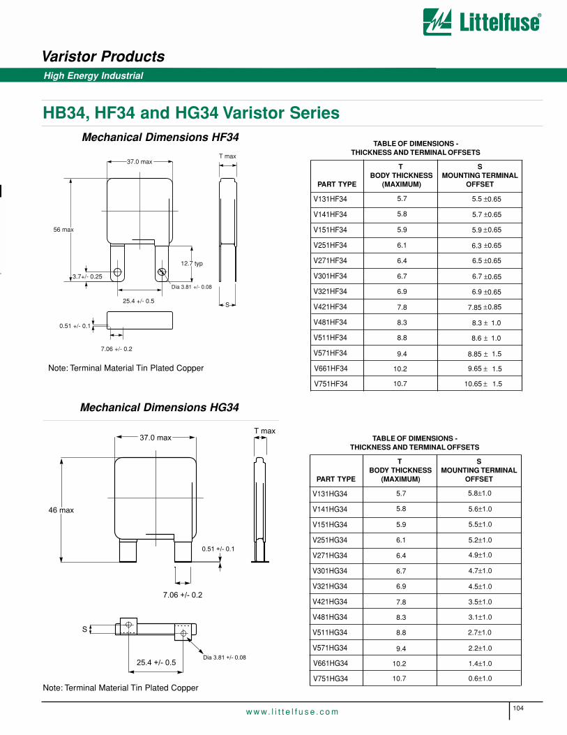
Varistor Products
104w w w. l i t t e l f u s e . c o m
HB34, HF34 and HG34 Varistor Series
High Energy Industrial
TABLE OF DIMENSIONS - THICKNESS AND TERMINAL OFFSETS
PART TYPE
T BODY THICKNESS
(MAXIMUM)
S MOUNTING TERMINAL
OFFSET
V131HF34 5.7 5.5 ±0.65
V141HF34 5.8 5.7 ±0.65
V151HF34 5.9 5.9 ±0.65
V251HF34 6.1 6.3 ±0.65
V271HF34 6.4 6.5 ±0.65
V301HF34 6.7 6.7 ±0.65
V321HF34 6.9 6.9 ±0.65
V421HF34 7.8 7.85 ±0.85
V481HF34 8.3 8.3 ± 1.0
V511HF34 8.8 8.6 ± 1.0
V571HF34 9.4 8.85 ± 1.5
V661HF34
V751HF34
10.2
10.7
9.65 ± 1.5
10.65 ± 1.5
Dia 3.81 +/- 0.08
7.06 +/- 0.2
0.51 +/- 0.1
12.7 typ
3.7+/- 0.25
56 max
S
T max
25.4 +/- 0.5
37.0 max
37.0 maxT max
46 max
25.4 +/- 0.5
7.06 +/- 0.2
Dia 3.81 +/- 0.08
0.51 +/- 0.1
S
TABLE OF DIMENSIONS - THICKNESS AND TERMINAL OFFSETS
PART TYPE
T BODY THICKNESS
(MAXIMUM)
S MOUNTING TERMINAL
OFFSET
V131HG34 5.7
V141HG34 5.8
V151HG34 5.9
V251HG34 6.1
V271HG34 6.4
V301HG34 6.7
V321HG34 6.9
V421HG34 7.8
V481HG34 8.3
V511HG34 8.8
V571HG34 9.4
V661HG34
V751HG34
10.2
10.7
5.8±1.0
5.6±1.0
5.5±1.0
5.2±1.0
4.9±1.0
4.7±1.0
4.5±1.0
3.5±1.0
3.1±1.0
2.7±1.0
2.2±1.0
1.4±1.0
0.6±1.0
Note: Terminal Material Tin Plated Copper
Note: Terminal Material Tin Plated Copper
Mechanical Dimensions HF34
Mechanical Dimensions HG34

2
VAR
ISTO
RP
RO
DU
CT
S
Varistor Products
105w w w. l i t t e l f u s e . c o m
High Energy Industrial
DHB34 Varistor SeriesThe DHB34 Series of transient surge suppressors are industrial high-energy Metal-Oxide Varistors (MOVs). They are designed to provide surgesuppression in the AC mains outdoor and service entrance environment (distribution panels) of buildings. DHB34 applications alsoinclude industrial heavy motors, controls, and power supplies such asused in the oil-drilling, mining, and transportation fields, including HVACand motor/generator applications.
The DHB34 Series provides rigid terminals for through-hole solder mounting on printed circuit boards, thereby eliminating the need for screwmounting.
See Ratings and Specifications table for part numbers.
Features• Wide Operating Voltage Range
VM(AC)RMS. . . . . . . . . . . . . . . . . . . . . . . . . . . . . . . . . . . 130V to 750V
• High Energy AbsorptionCapability. . . . . . . . . . . . . . . . . . . . . . . . . . . . . . .WTM = 200J to 1050J
• High Peak Pulse CurrentCapability . . . . . . . . . . . . . . . . . . . . . . . . . . . . . . . . ITM = 40,000A*
• Rigid Terminals for Secure Through-Hole Solder Mounting
• No Derating Up to 85oC Ambient
AGENCY APPROVALS: Recognized under the components program ofUnderwriters Laboratories. Certified by CSA.
AGENCY FILE NUMBERS: UL 1449, E75961, UL1414, E56529, CSA LR91788.
* NOTE: Ratings are for each individual varistor element in a dual assembly.
®®NEW
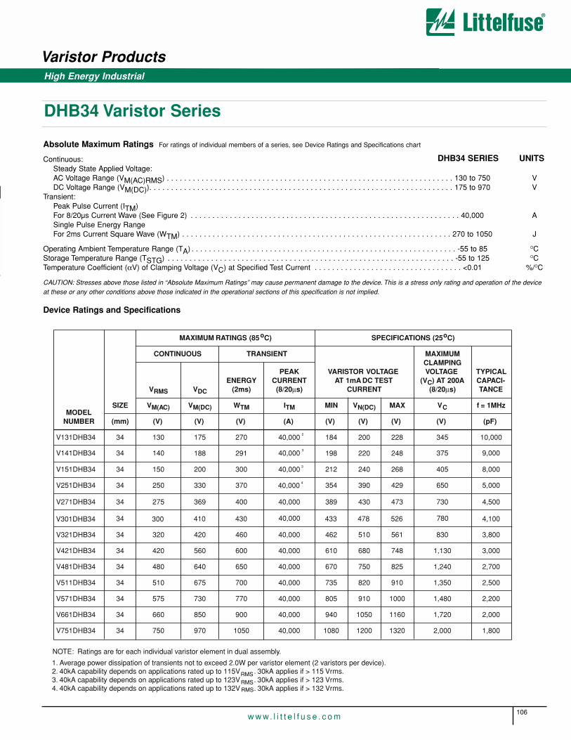
Varistor Products
106w w w. l i t t e l f u s e . c o m
High Energy Industrial
DHB34 Varistor Series
Absolute Maximum Ratings For ratings of individual members of a series, see Device Ratings and Specifications chart
Continuous:Steady State Applied Voltage:AC Voltage Range (VM(AC)RMS) . . . . . . . . . . . . . . . . . . . . . . . . . . . . . . . . . . . . . . . . . . . . . . . . . . . . . . . . . . . . . . . . . . 130 to 750 VDC Voltage Range (VM(DC)). . . . . . . . . . . . . . . . . . . . . . . . . . . . . . . . . . . . . . . . . . . . . . . . . . . . . . . . . . . . . . . . . . . . . . 175 to 970 V
Transient:Peak Pulse Current (ITM)For 8/20µs Current Wave (See Figure 2) . . . . . . . . . . . . . . . . . . . . . . . . . . . . . . . . . . . . . . . . . . . . . . . . . . . . . . . . . . . . . . 40,000 ASingle Pulse Energy RangeFor 2ms Current Square Wave (WTM) . . . . . . . . . . . . . . . . . . . . . . . . . . . . . . . . . . . . . . . . . . . . . . . . . . . . . . . . . . . . . . 270 to 1050 J
Operating Ambient Temperature Range (TA) . . . . . . . . . . . . . . . . . . . . . . . . . . . . . . . . . . . . . . . . . . . . . . . . . . . . . . . . . . . . . -55 to 85 OC Storage Temperature Range (TSTG) . . . . . . . . . . . . . . . . . . . . . . . . . . . . . . . . . . . . . . . . . . . . . . . . . . . . . . . . . . . . . . . . . . -55 to 125 OC Temperature Coefficient (αV) of Clamping Voltage (VC) at Specified Test Current . . . . . . . . . . . . . . . . . . . . . . . . . . . . . . . . . . <0.01 %/OC
CAUTION: Stresses above those listed in “Absolute Maximum Ratings” may cause permanent damage to the device. This is a stress only rating and operation of the deviceat these or any other conditions above those indicated in the operational sections of this specification is not implied.
Device Ratings and Specifications
DHB34 SERIES UNITS
40,000 4
MODELNUMBER
SIZE
MAXIMUM RATINGS (85oC) SPECIFICATIONS (25oC)
CONTINUOUS TRANSIENT
VARISTOR VOLTAGEAT 1mA DC TEST
CURRENT
MAXIMUM CLAMPING VOLTAGE
(VC) AT 200A(8/20µs)
TYPICALCAPACI-TANCEVRMS VDC
ENERGY (2ms)
PEAKCURRENT
(8/20µs)
VM(AC) VM(DC) WTM ITM MIN VN(DC) MAX VC f = 1MHz
(mm) (V) (V) (V) (A) (V) (V) (V) (V) (pF)
V131DHB34
V141DHB34
34
34
130
140
175
188
270
291
40,000 184
198
200
220
228
248
345
375
10,000
V151DHB34 34 150 200 300 212 240 268 405 8,000
9,000
V251DHB34 34 250 330 370 354 390 429 650 5,000
V271DHB34 34 275 369 400 40,000 389 430 473 730 4,500
V321DHB34 34 320 420 460 40,000 462 510 561 830 3,800
V421DHB34 34 420 560 600 40,000 610 680 748 1,130 3,000
V481DHB34 34 480 640 650 40,000 670 750 825 1,240 2,700
V511DHB34 34 510 675 700 40,000 735 820 910 1,350 2,500
V571DHB34 34 575 730 770 40,000 805 910 1000 1,480 2,200
V661DHB34 34 660 850 900 40,000 940 1050 1160 1,720 2,000
V751DHB34 34 750 970 1050 40,000 1080 1200 1320 2,000 1,800
NOTE: Ratings are for each individual varistor element in dual assembly.
2
40,0003
40,000 3
1. Average power dissipation of transients not to exceed 2.0W per varistor element (2 varistors per device).2. 40kA capability depends on applications rated up to 115V . 30kA applies if > 115 Vrms.3. 40kA capability depends on applications rated up to 123V . 30kA applies if > 123 Vrms.4. 40kA capability depends on applications rated up to 132V . 30kA applies if > 132 Vrms.
RMS
RMSRMS
V301DHB34 34 300 410 430 40,000 433 478 526 780 4,100
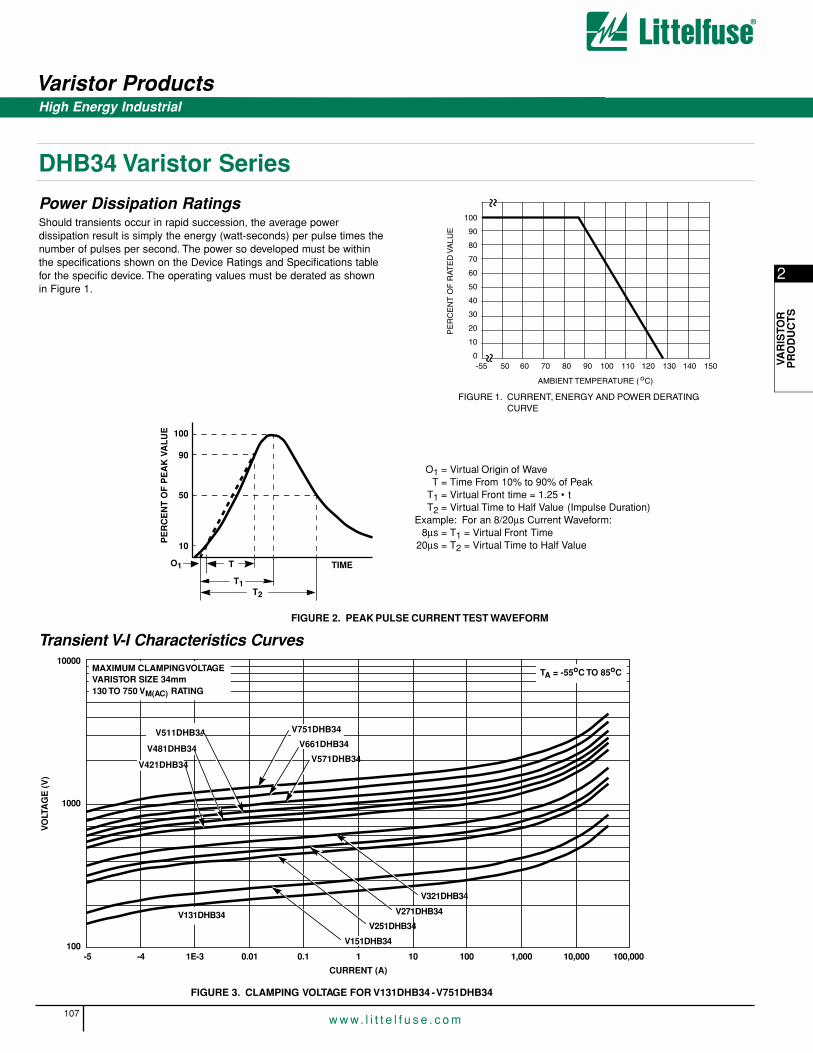
2
VAR
ISTO
RP
RO
DU
CT
S
Varistor Products
107w w w. l i t t e l f u s e . c o m
High Energy Industrial
Power Dissipation RatingsShould transients occur in rapid succession, the average power dissipation result is simply the energy (watt-seconds) per pulse times thenumber of pulses per second. The power so developed must be withinthe specifications shown on the Device Ratings and Specifications tablefor the specific device. The operating values must be derated as shownin Figure 1.
Transient V-I Characteristics Curves
FIGURE 2. PEAK PULSE CURRENT TEST WAVEFORM
100
90
50
10
O1 T
T1T2
TIME
PE
RC
EN
T O
F P
EA
K V
AL
UE
O1 = Virtual Origin of WaveT = Time From 10% to 90% of Peak
T1 = Virtual Front time = 1.25 • tT2 = Virtual Time to Half Value (Impulse Duration)
Example: For an 8/20µs Current Waveform:8µs = T1 = Virtual Front Time
20µs = T2 = Virtual Time to Half Value
FIGURE 3. CLAMPING VOLTAGE FOR V131DHB34 - V751DHB34
VO
LTA
GE
(V
)
10000
1000
100
CURRENT (A)
V751DHB34
V131DHB34
V321DHB34
V511DHB34
V481DHB34V571DHB34
V661DHB34
TA = -55oC TO 85oCMAXIMUM CLAMPING VOLTAGEVARISTOR SIZE 34mm130 TO 750 VM(AC) RATING
V271DHB34
V251DHB34
V151DHB34
V421DHB34
-5 -4 1E-3 0.01 0.1 1 10 100 1,000 10,000 100,000
DHB34 Varistor Series

Varistor Products
108w w w. l i t t e l f u s e . c o m
High Energy Industrial
DHB34 Varistor Series
FIGURE 4. SURGE CURRENT RATING CURVES FOR V131DHB34 - V751DHB34
DISC SIZE 34mmV131DHB34 - V751DHB34
50,000
20,000
10,000
5,000
2,000
1,000
500
200
100
50
20
1020 100 1,000 10,000
SU
RG
E C
UR
RE
NT
(A
)
IMPULSE DURATION (µs)
10
1
INDEFINITE
105102
2
103
104
106
NOTE: If pulse ratings are exceeded, a shift of VN(DC) (at specified current)of more than ±10% could result. This type of shift, which normally results in adecrease of VN(DC), may result in the device not meeting the original pub-lished specifications, but it does not prevent the device from continuing tofunction, and to provide ample protection.
Pulse Rating Curves
Dia 3.81 +/- 0.08
7.06 +/- 0.2
0.51 typ
12.7 typ
3.7 typ
56 max
S2
S1
T max
25.4 +/- 0.5
37.5 max
TABLE OF DIMENSIONS - THICKNESS AND TERMINAL OFFSETS
TYPE T MAXS1
+/- 1.15 mm
V131DHB34 7.8
V141DHB34 8.2
V151DHB34 8.8
V251DHB34 7.8
V271DHB34 8.7
V301DHB34 8.9
V321DHB34 9.3
V421DHB34 11.3
V481DHB34 12.2
V511DHB34 13.4
V571DHB34
V661DHB34
V751DHB34
14.8
S2+/- 2.30mm
5.702.85
6.003.00
6.303.15
6.003.00
6.503.25
7.003.50
7.243.66
9.004.50
9.604.80
10.505.25
11.605.80
13.306.6517.20
14.707.3518.20
VARISTOR DESIGNATOR
MAX ACRMS WORKING VOLTAGE(FIRST SIGNIFICANT DIGITS) VM(AC)
DISC SIZE (mm)
SERIES DESIGNATOR
VM(AC) VOLTAGE DECADE MULTIPLIER
V 13 1DHB34
Ordering Information
Mechanical Dimensions

2
VAR
ISTO
RP
RO
DU
CT
S
Varistor Products
109w w w. l i t t e l f u s e . c o m
CA Varistor SeriesThe CA Series of transient surge suppressors are industrial high-energydisc varistors (MOVs) intended for special applications requiring uniqueelectrical contact or packaging methods provided by the customer. Theelectrode finish of these devices is solderable and can also be used withpressure contacts. Discs of the same diameter may be stacked.
This series of industrial disc varistors are available in three diametersizes of 32, 40, and 60mm, with disc thicknesses ranging from 1.8mmminimum to 32mm maximum. They offer a wide voltage range of from250 to 2800 VM(AC)RMS .
For information on soldering considerations, refer to AN8820 update.“Recommendations for Soldering Terminal Leads to MOV Varistor Discs”.
Features• Provided In Disc Form For Unique Packaging By Customer
• Solderable Electrode Finish Options
• Pressure Contacts and/or Disc Stacking May be Utilized
• Standard Disc Sizes 32mm, 40mm, and 60mm Diameter
• Available Edge Passivation Insulation
• Wide Operating Voltage Range VM(AC)RMS 250V to 2800V
• High Peak Pulse Current Range . . . . . . . . . . ITM 20,000A to70,000A
• Very High Energy Capability WTM . . . . . . . . . . . . . . .330J to 10,000J
• No Derating Up to 85oC Ambient
High Energy Industrial Disc

Varistor Products
110w w w. l i t t e l f u s e . c o m
High Energy Industrial Disc
CA Varistor SeriesAbsolute Maximum Ratings For ratings of individual members of a series, see Device Ratings and Specifications chart
Continuous:Steady State Applied Voltage:AC Voltage Range (VM(AC)RMS) . . . . . . . . . . . . . . . . . . . . . . . . . . . . . . . . . . . . . . . . . . . . . . . . . . . . . . . . . . . . . . . . . . 250 to 2800 VDC Voltage Range (VM(DC)). . . . . . . . . . . . . . . . . . . . . . . . . . . . . . . . . . . . . . . . . . . . . . . . . . . . . . . . . . . . . . . . . . . . . . 330 to 3500 V
Transient:Peak Pulse Current (ITM)For 8/20µs Current Wave (See Figure 2) . . . . . . . . . . . . . . . . . . . . . . . . . . . . . . . . . . . . . . . . . . . . . . . . . . . . . . . . . . . 20,000 to 70,000 ASingle Pulse Energy RangeFor 2ms Current Square Wave (WTM) . . . . . . . . . . . . . . . . . . . . . . . . . . . . . . . . . . . . . . . . . . . . . . . . . . . . . . . . . . . . . . 330 to 10,000 J
Operating Ambient Temperature Range (TA). . . . . . . . . . . . . . . . . . . . . . . . . . . . . . . . . . . . . . . . . . . . . . . . . . . . . . . . . . . . . . 55 to 85 OCStorage Temperature Range (TSTG) . . . . . . . . . . . . . . . . . . . . . . . . . . . . . . . . . . . . . . . . . . . . . . . . . . . . . . . . . . . . . . . . . . . 55 to 85 OCTemperature Coefficient (αV) of Clamping Voltage (VC) at Specified Test Current . . . . . . . . . . . . . . . . . . . . . . . . . . . . . . . . . . . <0.01 %OC
CAUTION: Stresses above those listed in “Absolute Maximum Ratings” may cause permanent damage to the device. This is a stress only rating and operation of the deviceat these or any other conditions above those indicated in the operational sections of this specification is not implied.
Device Ratings and Specifications
CA SERIES UNITS
MODELNUMBER
SIZE
MAXIMUM RATINGS (85oC) SPECIFICATIONS (25oC)
CONTINUOUS TRANSIENT
VARISTOR VOLTAGE AT1mA DC TEST CURRENT
MAXCLAMPINGVOLT VC AT
200ACURRENT
(8/20µs)
TYPICALCAPACI-TANCEVRMS VDC
ENERGY(2ms)
PEAKCURRENT
(8/20µs)
VM(AC) VM(DC) WTM ITM MIN VN(DC) MAX VC f = 1MHz
(mm) (V) (V) (J) (A) (V) (V) (V) (V) (pF)
V131CA32 32 130 175 200 20000 184 200 228 350 4700
V151CA32 32 150 200 220 20000 212 240 268 410 4000
V251CA32V251CA40V251CA60
324060
250 330 330370880
200004000050000
354 390 429 680650620
25005000
10000
V271CA32V271CA40V271CA60
324060
275 369 360400950
200004000050000
389 430 473 750730680
220045009000
V321CA32V321CA40V321CA60
324060
320 420 390460
1100
200004000050000
462 510 561 850830760
190038007500
V421CA32V421CA40V421CA60
324060
420 560 400600
1500
250004000070000
610 680 748 120011301060
150030006000
V481CA32V481CA40V481CA60
324060
480 640 450650
1600
250004000070000
670 750 825 130012401160
130027005500
V511CA32V511CA40V511CA60
324060
510 675 500700
1800
250004000070000
735 820 910 144013501300
120025005000
V571CA32V571CA40V571CA60
324060
575 730 550770
2100
250004000070000
805 910 1000 160014801420
110022004500
V661CA32V661CA40V661CA60
324060
660 850 600900
2300
250004000070000
940 1050 1160 182017201640
100020004000
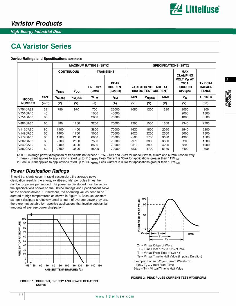
2
VAR
ISTO
RP
RO
DU
CT
S
Varistor Products
111w w w. l i t t e l f u s e . c o m
CA Varistor Series
High Energy Industrial Disc
Power Dissipation RatingsShould transients occur in rapid succession, the average power dissipation result is the energy (watt-seconds) per pulse times the number of pulses per second. The power so developed must be withinthe specifications shown on the Device Ratings and Specifications tablefor the specific device. Furthermore, the operating values need to be derated at high temperatures as shown in Figure 1. Because varistorscan only dissipate a relatively small amount of average power they are,therefore, not suitable for repetitive applications that involve substantialamounts of average power dissipation.
V751CA32V751CA40V751CA60
324060
750 970 70010502600
250004000070000
1080 1200 1320 205020001880
80018003500
V881CA60 60 880 1150 3200 70000 1290 1500 1650 2340 2700
V112CA60V142CA60V172CA60V202CA60V242CA60V282CA60
606060606060
110014001700200024002800
140017502150250030003500
38005000600075008600
10000
700007000070000700007000070000
162020202500297035104230
180022002700330039004700
206025503030363042905170
294036004300520062007400
22001800150012001000800
NOTE: Average power dissipation of transients not exceed 1.5W, 2.0W and 2.5W for model 32mm, 40mm and 60mm, respectively.
MODELNUMBER
SIZE
MAXIMUM RATINGS (85oC) SPECIFICATIONS (25oC)
CONTINUOUS TRANSIENT
VARISTOR VOLTAGE AT1mA DC TEST CURRENT
MAXCLAMPINGVOLT VC AT
200ACURRENT
(8/20µs)
TYPICALCAPACI-TANCEVRMS VDC
ENERGY(2ms)
PEAKCURRENT
(8/20µs)
VM(AC) VM(DC) WTM ITM MIN VN(DC) MAX VC f = 1MHz
(mm) (V) (V) (J) (A) (V) (V) (V) (V) (pF)
1. Peak current applies to applications rated up to 115V . Peak Current is 30kA for applications greater than 115V .2. Peak current applies to applications rated up to 132V . Peak Current is 30kA for applications greater than 132V .
RMS
RMS
RMS
RMS
FIGURE 1. CURRENT, ENERGY AND POWER DERATING CURVE
100
90
80
70
60
50
40
30
20
10
0-55 50 60 70 80 90 100 110 120 130 140 150
AMBIENT TEMPERATURE ( oC)
PE
RC
EN
T O
F R
AT
ED
VA
LU
E
FIGURE 2. PEAK PULSE CURRENT TEST WAVEFORM
100
90
50
10
O1 TT1
T2
TIME
PE
RC
EN
T O
F P
EA
K V
AL
UE
O1 = Virtual Origin of WaveT = Time From 10% to 90% of Peak
T1 = Virtual Front Time = 1.25 • tT2 = Virtual Time to Half Value (Impulse Duration)
Example: For an 8/20µs Current Waveform:8µs = T1 = Virtual Front Time
20µs = T2 = Virtual Time to Half Value
Device Ratings and Specifications (continued)

112w w w. l i t t e l f u s e . c o m
High Energy Industrial Disc
CA Varistor Series
Transient V-I Characteristics Curves
FIGURE 3. CLAMPING VOLTAGE FOR V131CA32 - C751CA32 FIGURE 4. CLAMPING VOLTAGE FOR V131CA40 - V751CA40
FIGURE 5. CLAMPING VOLTAGE FOR V251CA60 - V881CA60 FIGURE 6. CLAMPING VOLTAGE FOR V112CA60 - V282CA60
200
6,0005,0004,000
3,000
2,000
1,000900800
600
400
300
10-3 10-2 10-1 100 101 102 103 104
MA
XIM
UM
PE
AK
VO
LTS
(V
)
PEAK AMPERES
V421CA32
V321CA32V271CA32V251CA32
105
500
700
MAXIMUM CLAMPING VOLTAGEDISC SIZE 32mm130 TO 750 VM(AC) RATING
V751CA32V661CA32V571CA32V511CA32V481CA32
TA = -55oC TO 85oC
V151CA32V131CA32
200
6,0005,0004,000
3,000
2,000
1,000900800700600500
400
300
10-2 10-1 100 101 102 103 104 105
MAXIMUM CLAMPING VOLTAGEDISC SIZE 40mm130 TO 750 VM(AC) RATING
V421CA40
V151CA40
V751CA40
MA
XIM
UM
PE
AK
VO
LTS
(V
)PEAK AMPERES
V131CA40
V321CA40V271CA40V251CA40
V511CA40V481CA40 V571CA40
V661CA40
TA = -55oC TO 85oC
MAX CLAMPING VOLTAGEDISC SIZE 60mm250 TO 880VM(AC) RATING
TA = -55oC TO 85oC
6,0005,0004,000
3,000
2,000
1,000900800700600500
400
300
20010-2 10-1 100 101 102 103 104 105
PEAK AMPERES (A)
V881CA60V751CA60V661CA60V571CA60
MA
XIM
UM
PE
AK
VO
LTS
(V
)
V511CA60V481CA60
V421CA60
V321CA60V271CA60V251CA60
30,000
20,000
10,0009,0008,0007,0006,000
5,000
4,000
3,000
2,00010-2 10-1 100 101 102 103 104 105
PEAK AMPERES (A)
MA
X P
EA
K V
OLT
S (
V)
V282CA60V242CA60
V202CA60
V172CA60V142CA60
V112CA60
MAX CLAMPING VOLTAGEDISC SIZE 60mm1100 TO 2800VM(AC) RATING
TA = -55oC TO 85oC
Varistor Products

2
VAR
ISTO
RP
RO
DU
CT
S
Varistor Products
113w w w. l i t t e l f u s e . c o m
CA Varistor Series
High Energy Industrial Disc
Pulse Rating Curves
FIGURE 7. SURGE CURRENT RATING CURVES FOR V131CA32 - V321CA32
FIGURE 8. SURGE CURRENT RATING CURVES FOR V421CA32 - V751CA32
FIGURE 9. SURGE CURRENT RATING CURVES FOR V131CA40 - V751CA40
FIGURE 10. SURGE CURRENT RATING CURVES FOR V251CA60 - V321CA60
FIGURE 11. SURGE CURRENT RATING CURVES FOR V421CA60 - V282CA60
50,000
20,000
10,000
5,000
2,000
1,000
500
200
10050
20
10
IMPULSE DURATION (µs)20 100 1,000 10,000
SU
RG
E C
UR
RE
NT
(A
)
DISC SIZE 32mmV131CA32 - V321CA321
2
10
102
105
106
INDEFINITE
104
103
1 2
10
102
INDEFINITE
106
105
50,000
20,000
10,000
5,000
2,000
1,000
500
200
10050
20
10
IMPULSE DURATION (µs)20 100 1,000 10,000
SU
RG
E C
UR
RE
NT
(A
)
DISC SIZE 32mmV421CA32 - V751CA32
104
103
DISC SIZE 40mmV131CA40 - V751CA40
50,000
20,000
10,000
5,000
2,000
1,000
500
200
100
50
20
1020 100 1,000 10,000
SU
RG
E C
UR
RE
NT
(A
)
IMPULSE DURATION (µs)
106
10
21
INDEFINITE
104
103
102 105
50,000
20,000
10,000
5,000
2,000
1,000
500
200
100
50
2010
IMPULSE DURATION (µs)1,000 10,000
10
102
103
INDEFINITE
106
20 100
2DISC SIZE 60mmV251CA60 - V321CA60
1
SU
RG
E C
UR
RE
NT
(A
)
105
104
100,000
50,000
20,000
10,000
5,000
2,000
1,000
500
200
100
50
20
1020 100 1,000 10,000
IMPULSE DURATION (µs)
10
102
103
106
2
1 DISC SIZE 60mmV421CA60 - V282CA60
INDEFINITE
SU
RG
E C
UR
RE
NT
(A
)
104
105
NOTE: If pulse ratings are exceeded, a shift of VN(DC) (at specified current) of more than ±10% could result. This type of shift, which normally results in a decrease of VN(DC),may result in the device not meeting the original published specifications, but does not prevent the device from continuing to function, and to provide ample protection.

Varistor Products
114w w w. l i t t e l f u s e . c o m
High Energy Industrial Disc
CA Varistor Series
Series Dimensions
2.0
0.25
DIAMETER(SEE TABLE)
PASSIVATIONCOLLARELECTRODE
THICKNESS
ELECTRODE
OPTIONALDISC DIAMETER
MODELSIZE
MILLIMETERS INCHES
MIN MAX MIN MAX
32 31.0 33.0 1.220 1.299
40 38.0 40.0 1.496 1.575
60 58.0 62.0 2.283 2.441
MODELVRMS
VM(AC)
THICKNESS (32mm DISC MODELS) THICKNESS (40mm AND 60mm DISC MODELS)
MILLIMETERS INCHES MILLIMETERS INCHES
MIN MAX MIN MAX MIN MAX MIN MAX
130† 1.4 2.4 0.071 0.094 1.4 2.8 0.055 0.134
150† 1.7 2.8 0.083 0.110 1.5 3.0 0.06 0.150
250 1.6 2.2 0.063 0.087 2.0 2.7 0.079 0.106
275 1.8 2.5 0.071 0.098 2.2 3.0 0.087 0.118
320 2.1 2.9 0.083 0.114 2.6 3.5 0.102 0.138
420 2.9 3.9 0.114 0.154 3.5 4.7 0.138 0.185
480 3.1 4.3 0.122 0.169 3.8 5.2 0.150 0.205
510 3.5 4.7 0.138 0.185 4.2 5.7 0.165 0.224
575 3.8 5.1 0.150 0.201 4.6 6.3 0.181 0.248
660 4.4 6.0 0.173 0.236 5.3 7.2 0.209 0.283
750 5.1 6.9 0.240 0.327 6.1 8.3 0.240 0.327
880†† - - - - 7.3 10.3 0.287 0.406
1100†† - - - - 9.2 13.0 0.362 0.512
1400†† - - - - 11.5 16.0 0.453 0.630
1700†† - - - - 14.0 19.0 0.551 0.748
2000†† - - - - 17.0 22.5 0.669 0.886
2400†† - - - - 20.0 27.0 0.787 1.063
2800†† - - - - 24.0 32.0 0.945 1.260
† Available in 32mm and 40mm only.
†† Available in 60mm size only.

2
VAR
ISTO
RP
RO
DU
CT
S
Varistor Products
115w w w. l i t t e l f u s e . c o m
CA Varistor Series
High Energy Industrial Disc
Passivation LayerThe standard CA Series is supplied with passivation layer around the outside perimeter of the disc forming an electrical insulator as detailed inthe dimensional drawing. The CA Series is also available without a passivation layer for applications where the customer provides a suitableencapsulation or potting material as recommended below.(See Ordering Information.)
Encapsulated RecommendationsAfter lead attachment, the disc/lead assembly may be coated or encapsulated in a package to provide electrical insulation and isolationfrom environmental contamination as required by the application.Coating/Filler materials for containers may include silicones,polyurethanes, and some epoxy resins.Two examples of acceptablepolyurethanes are Dexter Hysol (US7013, parts A and B) and Rhenatech(resin 4714, hardener 4900), or their equivalents. Materials containinghalogens, sulfides, or alkalines are not recommended.
Electrode MetallizationThe standard CA Series is supplied with sintered silver electrodes onCA32 devices and arc-sprayed copper-over-aluminum electrodes for CA40and CA60 series. CA40 parts are also available with sintered silver elec-trode, see “Ordering information.” In general, when discs are stacked toattain a specific operating voltage or energy capability, the copper finish istypically chosen. Likewise, the copper finish is used with high temperaturelead attach soldering operations (wave solder). The silver metallization istypically used for solder reflow lead attach operations (I-R, Vapour-Phase).The recommended temperature profile of a belt-fed convection oven isshown in Figure 13.
Stacking and Contact PressureRecommendationsWhen applications require the stacking of Littelfuse CA discs or whenelectrical connection is made by pressure contacts, the minimum pres-sure applied to the disc electrode surface should be 2.2kGs (5 pounds).The maximum recommended pressure applied to the disc electrode isdependent upon diameter size and is given in the following table.
MODELNUMBER
SIZE(mm)
TYPICAL DISCWEIGHT (GRAMS)
V131CA32V131CA40
3240
921
V151CA32V151CA40
3240
1123
V251CA32V251CA40V251CA60
324060
81739
V271CA32V271CA40V271CA60
324060
101842
V321CA32 32 11
V321CA40 40 22
V321CA60 60 50
V421CA32 32 15
V421CA40 40 28
V421CA60 60 66
V481CA32 32 16
V481CA40 40 31
V481CA60 60 71
V511CA32 32 18
V511CA40 40 35
V511CA60 60 80
V571CA32 32 20
V571CA40 40 38
V571CA60 60 88
V661CA32 32 23
V661CA40 40 44
V661CA60 60 101
V751CA32 32 26
V751CA40 40 51
V751CA60 60 116
V881CA60 60 141
V112CA60V142CA60V172CA60V202CA60V242CA60V282CA60
606060606060
178220265317377450
TE
MP
ER
ATU
RE
(oC
)
250
200
150
100
50
00 100 200 300 400 500 600 700 800 900
TIME (SEC)
FIGURE 13. TYPICAL BELT OVEN TEMPERATURE PROFILE
MODEL SIZE (mm) MAXIMUM PRESSURE
32 16N/CM2 (23LBs/IN2)
40 8N/CM2 (11.5LBs/IN2)
60 4N/CM2 (5.7LBs/IN2)
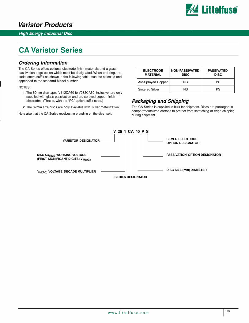
Varistor Products
116w w w. l i t t e l f u s e . c o m
High Energy Industrial Disc
CA Varistor Series
Ordering InformationThe CA Series offers optional electrode finish materials and a glass passivation edge option which must be designated. When ordering, thecode letters suffix as shown in the following table must be selected andappended to the standard Model number.
NOTES:
1. The 60mm disc types V112CA60 to V282CA60, inclusive, are onlysupplied with glass passivation and arc-sprayed copper finish electrodes. (That is, with the “PC” option suffix code.)
2. The 32mm size discs are only available with silver metallization.
Note also that the CA Series receives no branding on the disc itself.
ELECTRODEMATERIAL
NON-PASSIVATEDDISC
PASSIVATEDDISC
Arc-Sprayed Copper NC PC
Sintered Silver NS PS
Packaging and ShippingThe CA Series is supplied in bulk for shipment. Discs are packaged incompartmentalized cartons to protect from scratching or edge-chippingduring shipment.
V 25 1 CA 40 P S
VARISTOR DESIGNATOR
MAX ACRMS WORKING VOLTAGE(FIRST SIGNIFICANT DIGITS) VM(AC)
SILVER ELECTRODEOPTION DESIGNATOR
DISC SIZE (mm) DIAMETER
SERIES DESIGNATOR
VM(AC) VOLTAGE DECADE MULTIPLIER
PASSIVATION OPTION DESIGNATOR

2
VAR
ISTO
RP
RO
DU
CT
S
Varistor Products
117w w w. l i t t e l f u s e . c o m
High Energy Industrial Square Disc
NA Varistor SeriesThe NA Series of transient surge suppressors are varistors (MOVs) insquare disc form, intended for special industrial high-energy applicationsrequiring unique electrical contact or packaging methods provided by thecustomer. The electrode finish of these devices is solderable and canalso be used with pressure contacts. Discs may also be stacked.
The NA Series varistor is a square 34mm device, with thicknesses ranging from 1.7mm minimum for the 250V device to 7.5mm maximumfor the 750V device. For information on mounting considerations refer toApplication Note AN8820.
This disc is also available with encapsulation and PCB leads. SeeLittelfuse HB34 Sales.
Features• Provided in Disc Form for Unique Packaging by Customer
• Solderable Electrode Finish.
• Pressure Contacts and/or Disc Stacking may be Utilized
• Wide Operating Voltage RangeVM(AC)RMS . . . . . . . . . . . . . . . . . . . . . . . . . . . . . . . . . . .250V to 750V
• Peak Pulse Current Capability (ITM). . . . . . . . . . . . . . . . . . . .40,000A
• High Energy Capability (WTM). . . . . . . . . . . . . . . . . . . .370J to 1050J
• No Derating Up to 8oC Ambient
ALSO SEE HB34 SERIES

Varistor Products
118w w w. l i t t e l f u s e . c o m
High Energy Industrial Square Disc
NA Varistor SeriesAbsolute Maximum Ratings For ratings of individual members of a series, see Device Ratings and Specifications chart
Continuous:Steady State Applied Voltage:AC Voltage Range (VM(AC)RMS) . . . . . . . . . . . . . . . . . . . . . . . . . . . . . . . . . . . . . . . . . . . . . . . . . . . . . . . . . . . . . . . . . . . . . . 250 to 750 VDC Voltage Range (VM(DC)) . . . . . . . . . . . . . . . . . . . . . . . . . . . . . . . . . . . . . . . . . . . . . . . . . . . . . . . . . . . . . . . . . . . . . . . . . . 330 to 970 VTransient:Peak Pulse Current (ITM)For 8/20µs Current Wave (See Figure 2) . . . . . . . . . . . . . . . . . . . . . . . . . . . . . . . . . . . . . . . . . . . . . . . . . . . . . . . . . . . . . . . . . . . 40,000 ASingle Pulse Energy RangeFor 2ms Current Square Wave (WTM) . . . . . . . . . . . . . . . . . . . . . . . . . . . . . . . . . . . . . . . . . . . . . . . . . . . . . . . . . . . . . . . . . . . 370 to1050 JOperating Ambient Temperature Range (TA) . . . . . . . . . . . . . . . . . . . . . . . . . . . . . . . . . . . . . . . . . . . . . . . . . . . . . . . . . . . . . . . -55 to 85 OCStorage Temperature Range (TSTG) . . . . . . . . . . . . . . . . . . . . . . . . . . . . . . . . . . . . . . . . . . . . . . . . . . . . . . . . . . . . . . . . . . . . -55 to 125 OCTemperature Coefficient (αV) of Clamping Voltage (VC) at Specified Test Current. . . . . . . . . . . . . . . . . . . . . . . . . . . . . . . . . . . . . <0.01 %/OC
CAUTION: Stresses above those listed in “Absolute Maximum Ratings” may cause permanent damage to the device. This is a stress only rating and operation of the deviceat these or any other conditions above those indicated in the operational sections of this specification is not implied.
Device Ratings and Specifications
NA SERIES UNITS
MODELNUMBER
SIZE
MAXIMUM RATINGS (85oC) SPECIFICATIONS (25oC)
CONTINUOUS TRANSIENT
VARISTOR VOLTAGEAT 1mA DC TEST
CURRENT
MAXIMUM CLAMPING VOLTAGE
(VC) AT 200A (8/20µs)
TYPICALCAPACI-TANCEVRMS VDC
ENERGY (2ms)
PEAKCURRENT
(8/20µs)
VM(AC) VM(DC) WTM ITM MIN VN(DC) MAX VC f = 1MHz
(mm) (V) (V) (J) (A) (V) (V) (V) (V) (pF)
V131NA34
V141NA34
34
34
130
140
175
188
270
291
40,000 184
198 220
200 228
248
345
375
10,000
V151NA34 34 150 200 300 40,000 212 240 268 405 8,000
9,000
V251NA34 34 250 330 370 40,000 354 390 429 650 5,000
V271NA34 34 275 369 400 40,000 389 430 473 730 4,500
V321NA34 34 320 420 460 40,000 462 510 561 830 3,800
V421NA34 34 420 560 600 40,000 610 680 748 1,130 3,000
V481NA34 34 480 640 650 40,000 670 750 825 1,240 2,700
V511NA34 34 510 675 700 40,000 735 820 910 1,350 2,500
V571NA34 34 575 730 770 40,000 805 910 1000 1,480 2,200
V661NA34 34 660 850 900 40,000 940 1050 1160 1,720 2,000
V751NA34 34 750 970 1050 40,000 1080 1200 1320 2,000 1,800
NOTE: Average power dissipation of transients not to exceed 2.0W.
1
40,0003
2
1. Peak current applies to applications rated up to 115V . Peak current is 30kA for applications greater than 115V .2. Peak current applies to applications rated up to 132V . Peak current is 30kA for applications greater than 132V .3. Peak current applies to applications rated up to 123V . Peak current is 30kA for applications greater than 123V .
RMS
RMS
RMS
RMS
RMS
RMS

2
VAR
ISTO
RP
RO
DU
CT
S
Varistor Products
119w w w. l i t t e l f u s e . c o m
NA Varistor Series
High Energy Industrial Square Disc
Power Dissipation RatingsShould transients occur in rapid succession, the average power dissipation required is simply the energy (watt-seconds) per pulse timesthe number of pulses per second. The power so developed must be within the specifications shown on the Device Ratings and Specificationstable for the specific device. The operating values must be derated asshown in Figure 1.
Transient V-I Characteristics Curves
FIGURE 1. CURRENT, ENERGY AND POWER DERATING CURVE
100
90
80
70
60
50
40
30
20
10
0-55 50 60 70 80 90 100 110 120 130 140 150
PE
RC
EN
T O
F R
ATE
D V
AL
UE
AMBIENT TEMPERATURE ( oC)
FIGURE 2. PEAK PULSE CURRENT TEST WAVEFORM
100
90
50
10
O1 T
T1T2
TIME
PE
RC
EN
T O
F P
EA
K V
AL
UE
O1 = Virtual Origin of WaveT = Time From 10% to 90% of Peak
T1 = Virtual Front time = 1.25 • tT2 = Virtual Time to Half Value (Impulse Duration)
Example: For an 8/20µs Current Waveform:8µs = T1 = Virtual Front Time
20µs = T2 = Virtual Time to Half Value
FIGURE 3. CLAMPING VOLTAGE FOR V131NA34 - V751NA34
VO
LTA
GE
(V
)
10000
1000
100
CURRENT (A)
V751NA34
V131NA34
V321NA34
V511NA34
V481NA34V571NA34
V661NA34
TA = -55oC TO 85oCMAXIMUM CLAMPING VOLTAGEVARISTOR SIZE 34mm130 TO 750 VM(AC) RATING
V271NA34
V251NA34
V151NA34
V421NA34
-5 -4 1E-3 0.01 0.1 1 10 100 1,000 10,000 100,000

Varistor Products
120w w w. l i t t e l f u s e . c o m
High Energy Industrial Square Disc
NA Varistor Series
FIGURE 4. SURGE CURRENT RATING CURVES FOR V131NA34 - V751NA34
DISC SIZE 34mmV131NA34 - V751NA34
50,000
20,000
10,000
5,000
2,000
1,000
500
200
100
50
20
1020 100 1,000 10,000
SU
RG
E C
UR
RE
NT
(A
)
IMPULSE DURATION (µs)
10
1
INDEFINITE
105102
2
103
104
106
Pulse Rating Curves
NOTE:If pulse ratings are exceeded, a shift of VN(DC) (at specified current) of more than ±10% could result. This type of shift, which normally results in a decrease of VN(DC),may result in the device not meeting the original published specifications, but it does not prevent the device from continuing to function, and to provide ample protection.
Mechanical Dimensions
(MILLIMETERS) MODELNUMBER
NA SERIESVARISTOR THICKNESS
MILLIMETERS INCHES
MIN MAX MIN MAX
V131NA34
V141NA34
1.40 2.30 0.055 0.090
V151NA34 1.50
1.45
2.80
2.55
0.059
0.057
0.011
0.100
V251NA34 1.70 2.30 0.066 0.090
V271NA34 1.80 2.70 0.070 0.106
V321NA34 2.10 3.00 0.082 0.118
V421NA34 3.00 4.00 0.118 0.157
V481NA34 3.20 4.40 0.125 0.173
V511NA34 3.60 4.90 0.141 0.192
V571NA34 4.00 5.60 0.118 0.220
V661NA34 4.50 6.80 0.176 0.267
V751NA34 5.20 7.50 0.204 0.294
NOTE: Parts available encapsulated with soldered tabs, to standard design or customer specific requirements. Also see HB34 Series.
2
VAR
ISTO
RP
RO
DU
CT
S
Varistor Products
121w w w. l i t t e l f u s e . c o m
NA Varistor Series
Passivation LayerThe standard NA Series is supplied with passivation layer around the outside perimeter of the disc forming an electrical insulator as detailed inthe dimensional drawing.
Encapsulated RecommendationsAfter lead attachment, the disc/lead assembly may be coated or encapsulated in a package to provide electrical insulation and isolationfrom environmental contamination as required by the application.Coating/Filler materials for containers may include silicones,polyurethanes, and some epoxy resins. Two examples of acceptablepolyurethanes are Dexter Hysol (US7013, parts A and B) and Rhenatech(resin 4714, hardener 4900), or their equivalents. Materials containinghalogens, sulfides, or alkalines are not recommended.
Electrode MetallizationThe NA Series is supplied with a sintered silver metallization for the electrode finish. The silver metallization is typically used for solder reflowlead attach operations (I-R, Vapour-Phase).
The recommended temperature profile of a belt-fed convection oven isshown in Figure 6.
Stacking and Contact PressureRecommendationsWhen applications require the stacking of Littelfuse NA discs or whenelectrical connection is made by pressure contacts, the minimum pres-sure applied to the disc electrode surface should be 2.2kGs (5 pounds).The maximum recommended pressure applied to the disc electrode is16N/CM2 (23LBs/IN2).
Packaging and ShippingThe NA Series is supplied in bulk for shipment. Discs are packaged incompartmentalized cartons to protect from scratching or edge-chippingduring shipment.
TE
MP
ER
ATU
RE
(oC
)
250
200
150
100
50
00 100 200 300 400 500 600 700 800 900
TIME (SEC)
FIGURE 6. TYPICAL BELT OVEN TEMPERATURE PROFILE
Ordering Information
VARISTOR DESIGNATOR
MAX ACRMS WORKING VOLTAGE(FIRST SIGNIFICANT DIGITS) VM(AC)
DISC SIZE (mm)
SERIES DESIGNATOR
VM(AC) VOLTAGE DECADE MULTIPLIER
V 25 1 NA 34
High Energy Industrial Square Disc

Varistor Products
122w w w. l i t t e l f u s e . c o m
Axial Lead
MA Varistor SeriesThe MA Series of transient surge suppressors are axial-lead metal-oxidevaristors (MOVs) for use in a wide variety of board level industrial andcommercial electronic equipment. They are intended to protect components and signal/data lines from low energy transients where thesmall axial lead package is required.
The MA Series is offered with standard (S suffix) or tightened (B suffix)clamping voltage.
See MA Series Device Ratings and Specifications table for part numberand brand information.
Features• 3mm Diameter Disc Size
• Small Axial Lead Package
• Wide Operating Voltage RangeVM(AC)RMS. . . . . . . . . . . . . . . . . . . . . . . .. . . . . . . . . . . . . .9V to 264VVM(DC) . . . . . . . . . . . . . . . . . . . . . . . . . . . . . . . . . . . . . . . .13V to 365V
• Available in Tape and Reel or Bulk Packaging
• No Derating Up to 85oC Ambient
2
VAR
ISTO
RP
RO
DU
CT
S
Varistor Products
123 w w w. l i t t e l f u s e . c o m
MA Varistor Series
Absolute Maximum Ratings For ratings of individual members of a series, see Device Ratings and Specifications chart
Continuous:Steady State Applied Voltage:AC Voltage Range (VM(AC)RMS) . . . . . . . . . . . . . . . . . . . . . . . . . . . . . . . . . . . . . . . . . . . . . . . . . . . . . . . . . . . . . . . . . . . . . 9 to 264 VDC Voltage Range (VM(DC)) . . . . . . . . . . . . . . . . . . . . . . . . . . . . . . . . . . . . . . . . . . . . . . . . . . . . . . . . . . . . . . . . . . . . . . . . 13 to 365 V
Transient:Peak Pulse Current (ITM)For 8/20µs Current Wave (See Figure 2) . . . . . . . . . . . . . . . . . . . . . . . . . . . . . . . . . . . . . . . . . . . . . . . . . . . . . . . . . . . . . . . 40 to 100 ASingle Pulse Energy RangeFor 10/1000µs Current Wave (WTM). . . . . . . . . . . . . . . . . . . . . . . . . . . . . . . . . . . . . . . . . . . . . . . . . . . . . . . . . . . . . . . . . . 0.06 to 1.7 J
Operating Ambient Temperature Range (TA). . . . . . . . . . . . . . . . . . . . . . . . . . . . . . . . . . . . . . . . . . . . . . . . . . . . . . . . . . . . . . . -55 to 85 OCStorage Temperature Range (TSTG) . . . . . . . . . . . . . . . . . . . . . . . . . . . . . . . . . . . . . . . . . . . . . . . . . . . . . . . . . . . . . . . . . . . . -55 to 125 OCTemperature Coefficient (αV) of Clamping Voltage (VC) at Specified Test Current . . . . . . . . . . . . . . . . . . . . . . . . . . . . . . . . . . . . <0.01 %/OCHi-Pot Encapsulation (Isolation Voltage Capability) . . . . . . . . . . . . . . . . . . . . . . . . . . . . . . . . . . . . . . . . . . . . . . . . . . . . . . . . . . . . 1000 V
(Dielectric must withstand indicated DC voltage for one minute per MIL-STD 202, Method 301) . . . . . . . . . . . . . . . . . . . . . . . . . . . . . . . . . . . . . 1000 MΩInsulation Resistance
CAUTION: Stresses above those listed in “Absolute Maximum Ratings” may cause permanent damage to the device. This is a stress only rating and operation of the deviceat these or any other conditions above those indicated in the operational sections of this specification is not implied.
Device Ratings and Specifications
MA SERIES UNITS
PARTNUMBER BRAND
MAXIMUM RATINGS (85oC) SPECIFICATIONS (25oC)
CONTINUOUS TRANSIENT
VARISTOR VOLTAGE AT 1mA DC TEST
CURRENT
MAX CLAMPING VOLTAGEVC AT 2.0A
(8/20µs)
TYPICAL CAPACI-TANCEVRMS VDC
ENERGY (10/1000µs)
PEAK CURRENT
(8/20µs)
VM(AC) VM(DC) WTM ITM MIN VN(DC) MAX VC f = 1MHz
(V) (V) (J) (A) (V) (V) (V) (V) (pF)
V18MA1AV18MA1BV18MA1S
18A 18B 18S
91010
131414
0.060.070.06
404040
141515
181818
232121
494449
550550550
V22MA1AV22MA1BV22MA1S
22A 22B 22S
101414
151818
0.090.100.09
404040
161919
222222
282626
555155
410410410
V27MA1AV27MA1BV27MA1S
27A 27B 27S
131717
192222
0.100.110.10
404040
212424
272727
343131
675967
370370370
V33MA1AV33MA1BV33MA1S
33A 33B 33S
18 20 20
232626
0.130.150.14
404040
2629.529.5
333333
4036.536.5
736773
300300300
V39MA2AV39MA2BV39MA2S
39A 39B 39S
22 25 25
283131
0.160.180.17
404040
313535
393939
474343
867986
250250250
V47MA2AV47MA2BV47MA2S
47A47B47S
27 30 30
343838
0.190.210.19
404040
374242
474747
575252
999099
210210210
V56MA2AV56MA2BV56MA2S
56A 56B 56S
32 35 35
404545
0.230.250.23
404040
445050
565656
686262
117108117
180180180
V68MA3AV68MA3BV68MA3S
68A 68B 68S
38 40 40
485656
0.260.300.27
404040
546161
686868
827575
138127138
150150150
V82MA3AV82MA3BV82MA3S
82A 82B 82S
45 50 50
606666
0.330.370.34
404040
657373
828282
999191
163150163
120120120
Axial Lead
Varistor Products
124w w w. l i t t e l f u s e . c o m
Axial Lead
MA Varistor SeriesDevice Ratings and Specifications (Continued)
Power Dissipation RatingsShould transients occur in rapid succession, the average power dissipationrequired is simply the energy (watt-seconds) per pulse times the numberof pulses per second. The power so developed must be within the specifi-cations shown on the Device Ratings and Specifications table for the specific device. Furthermore, the operating values need to be derated athigh temperatures as shown in Figure 1. Because varistors can only dissipate a relatively small amount of average power they are, therefore,not suitable for repetitive applications that involve substantial amounts ofaverage power dissipation.
V100MA4AV100MA4BV100MA4S
100101102
57 60 60
728181
0.400.450.42
404040
809090
100100100
120110110
200185200
100100100
V120MA1AV120MA2BV120MA2S
120121122
72 75 75
97101101
0.400.500.46
100100100
102108108
120120120
138132132
220205220
404040
V150MA1AV150MA2B
150151
88 92
121 127
0.500.60
100100
127135
150150
173165
255240
32 32
V180MA1AV180MA3B
180181
105110
144 152
0.600.70
100100
153162
180180
207198
310290
27 27
V220MA2AV220MA4B
220221
132138
181191
0.800.90
100100
187198
220220
253242
380360
21 21
V270MA2AV270MA4B
270271
163171
224 235
0.901.00
100100
229 243
270270
311297
460440
17 17
V330MA2AV330MA5B
330331
188200
257 274
1.001.10
100100
280297
330330
380363
570540
14 14
V390MA3AV390MA6B
390391
234242
322 334
1.201.30
100100
331351
390390
449 429
670640
12 12
V430MA3AV430MA7B
430431
253264
349365
1.501.70
100100
365387
430430
495473
740700
11 11
NOTE: Average power dissipation of transients not to exceed 200mW.
PARTNUMBER BRAND
MAXIMUM RATINGS (85oC) SPECIFICATIONS (25oC)
CONTINUOUS TRANSIENT
VARISTOR VOLTAGE AT 1mA DC TEST
CURRENT
MAX CLAMPING VOLTAGEVC AT 2.0A
(8/20µs)
TYPICAL CAPACI-TANCEVRMS VDC
ENERGY (10/1000µs)
PEAK CURRENT
(8/20µs)
VM(AC) VM(DC) WTM ITM MIN VN(DC) MAX VC f = 1MHz
(V) (V) (J) (A) (V) (V) (V) (V) (pF)
FIGURE 1. CURRENT, ENERGY AND POWER DERATING CURVE
100
90
80
70
60
50
40
30
20
10
0-55 50 60 70 80 90 100 110 120 130 140 150
AMBIENT TEMPERATURE ( oC)
PE
RC
EN
T O
F R
ATE
D V
AL
UE

2
VAR
ISTO
RP
RO
DU
CT
S
Varistor Products
125w w w. l i t t e l f u s e . c o m
MA Varistor Series
FIGURE 3. CLAMPING VOLTAGE FOR V18MA1A/S - V100MA4A/S FI GURE 4. CLAMPING VOLTAGE FOR V120MA1A/S - V430MA3A
FIGURE 5. CLAMPING VOLTAGE FOR V18MA1B - V100MA4B FIGURE 6. CLAMPING VOLTAGE FOR V120MA2B - V430MA7B
800
600
400
300
200
150
10080
60
40
30
2010-2 10-1 100 101 102
MA
XIM
UM
PE
AK
VO
LTS
(V
)
V100MA4A/SV82MA3A/S
V68MA3A/SV56MA2A/S
V39MA2A/SV33MA1A/S
V27MA1A/SV22MA1A/S
V18MA1A/S
PEAK AMPERES (A)
MAX CLAMPING VOLTAGEDISC SIZE 3mm18 TO 100VN(DC) RATINGTA = -55oC TO 85oC
V47MA2A/S
10-2 10-1 100 101 102
MA
XIM
UM
PE
AK
VO
LTS
(V
)
PEAK AMPERES (A)
MAX CLAMPING VOLTAGEDISC SIZE 3mm120 TO 430VN(DC) RATINGTA = -55oC TO 85oC
4,000
2,000
1,500
1,000
800
600
400
200
100
V430MA3AV390MA3A
V330MA2AV270MA2A
V220MA2A
V180MA1AV150MA1A
V120MA1A/S
600500400
300
200
100908070605040
30
20
MA
XIM
UM
PE
AK
VO
LTS
(V
)
10-3
PEAK AMPERES (A)10-2 10-1 100 101 102 103
V33MA1BV27MA1B
V22MA1B
V100MA4BV82MA3BV68MA3B
V18MA1B
MAX CLAMPING VOLTAGEDISC SIZE 3mm18 TO 100VN(DC) RATINGTA = -55oC TO 85oC
V47MA2BV56MA2B
V39MA2B
4,000
3,000
2,000
1,000900800700600500400
300
200
10010-3 10-2 10-1 100 101 102 103
PEAK AMPERES (A)
V430MA7BV390MA6BV330MA5BV270MA4BV220MA4BV180MA3BV150MA2BV120MA2B
MAXIMUM CLAMPING VOLTAGEDISC SIZE 3mm120 TO 430VN(DC) RATINGTA = -55oC TO 85oC
MA
XIM
UM
PE
AK
VO
LTS
(V
)Transient V-I Characteristics Curves
FIGURE 2. PEAK PULSE CURRENT TEST WAVEFORM
100
90
50
10
O1 T
T1T2
TIME
PE
RC
EN
T O
F P
EA
K V
AL
UE
O1 = Virtual Origin of WaveT = Time From 10% to 90% of Peak
T1 = Virtual Front time = 1.25 • tT2 = Virtual Time to Half Value (Impulse Duration)
Example: For an 8/20µs Current Waveform:8µs = T1 = Virtual Front Time
20µs = T2 = Virtual Time to Half Value
Axial Lead

Varistor Products
126w w w. l i t t e l f u s e . c o m
Axial Lead
MA Varistor Series
Mechanical Dimensions
Pulse Rating Curves
FIGURE 8. SURGE CURRENT RATING CURVES FOR V120MA SERIES - V430MA SERIES
100
50
20
10
5
2
1
0.5
0.2
0.1
SU
RG
E C
UR
RE
NT
(A
)
20 100 1,000 10,000IMPULSE DURATION (µs)
2
10
102103
1
104
105
106
INDEFINITE
DISC SIZE 3mmV120MA1A - V430MA7B
FIGURE 7. SURGE CURRENT RATING CURVES FOR V18MA SERIES - V100MA SERIES
50
20
10
5
2
1
0.5
0.2
0.1
2
10
102
103
DISC SIZE 3mmV18MA1A - V100MA4B
1
104
105
INDEFINITE
106
20 100 1,000 10,000
IMPULSE DURATION (µs)
SU
RG
E C
UR
RE
NT
(A
)
NOTE: If pulse ratings are exceeded, a shift of VN(DC) (at specified current) of more than ±10% could result. This type of shift, which normally results in a decrease of VN(DC),may result in the device not meeting the original published specifications, but it does not prevent the device from continuing to function, and to provide ample protection.
Tape and Reel Specification
Ordering Information
SYMBOL
INCHES MILLIMETERS
MIN MAX MIN MAX
Øb 0.024 0.026 0.61 0.66
ØD 0.135 0.177 3.43 4.5
G 0.098 0.177 3.43 4.5
H 0.118 0.236 3.0 6.0
L 1.130 1.220 28.70 31.0
Typical Weight = 25g
• Conforms to EIA Standard RS-296E
H1 H2
0.240± 0.040
2.062± 0.059
2.681MAX
0.063MAX
0.135-0.145
0.098-0.177
0.118-0.236
0.063MAX
0.02-0.023
0.200± 0.020
0.080MAX
0.240± 0.040
H1 = H2 ± 0.040
VARISTOR
VARISTOR VOLTAGE(VN at 1mA)
ENERGY/CLAMPING VOLTAGE VARIANT
SERIES DESIGNATORBulkUse “MT” for Tape and Reel
V XXX MA XX
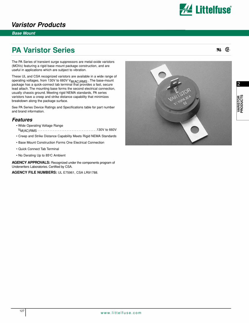
2
VAR
ISTO
RP
RO
DU
CT
S
Varistor Products
127w w w. l i t t e l f u s e . c o m
Base Mount
PA Varistor SeriesThe PA Series of transient surge suppressors are metal-oxide varistors(MOVs) featuring a rigid base mount package construction, and are useful in applications which are subject to vibration.
These UL and CSA recognized varistors are available in a wide range ofoperating voltages, from 130V to 660V VM(AC)RMS . The base-mountpackage has a quick-connect tab terminal that provides a fast, securelead attach. The mounting base forms the second electrical connection,usually chassis ground. Meeting rigid NEMA standards, PA series varistors have a creep and strike distance capability that minimizesbreakdown along the package surface.
See PA Series Device Ratings and Specifications table for part numberand brand information.
Features• Wide Operating Voltage Range
VM(AC)RMS . . . . . . . . . . . . . . . . . . . . . . . . . . . . . . . . . . .130V to 660V
• Creep and Strike Distance Capability Meets Rigid NEMA Standards
• Base Mount Construction Forms One Electrical Connection
• Quick Connect Tab Terminal
• No Derating Up to 85oC Ambient
AGENCY APPROVALS: Recognized under the components program ofUnderwriters Laboratories. Certified by CSA.
AGENCY FILE NUMBERS: UL E75961, CSA LR91788.
®®
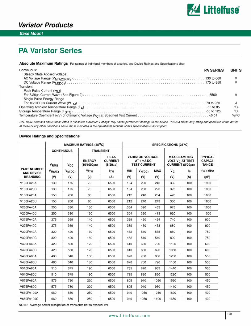
Varistor Products
128w w w. l i t t e l f u s e . c o m
Base Mount
PA Varistor Series
Absolute Maximum Ratings For ratings of individual members of a series, see Device Ratings and Specifications chart
Continuous:Steady State Applied Voltage:AC Voltage Range (VM(AC)RMS) . . . . . . . . . . . . . . . . . . . . . . . . . . . . . . . . . . . . . . . . . . . . . . . . . . . . . . . . . . . . . . . . . . . . . 130 to 660 VDC Voltage Range (VM(DC)) . . . . . . . . . . . . . . . . . . . . . . . . . . . . . . . . . . . . . . . . . . . . . . . . . . . . . . . . . . . . . . . . . . . . . . . . 175 to 850 V
Transient:Peak Pulse Current (ITM)For 8/20µs Current Wave (See Figure 2) . . . . . . . . . . . . . . . . . . . . . . . . . . . . . . . . . . . . . . . . . . . . . . . . . . . . . . . . . . . . . . . . . . 6500 ASingle Pulse Energy RangeFor 10/1000µs Current Wave (WTM) . . . . . . . . . . . . . . . . . . . . . . . . . . . . . . . . . . . . . . . . . . . . . . . . . . . . . . . . . . . . . . . . . . . 70 to 250 J
Operating Ambient Temperature Range (TA) . . . . . . . . . . . . . . . . . . . . . . . . . . . . . . . . . . . . . . . . . . . . . . . . . . . . . . . . . . . . . . . -55 to 85 OCStorage Temperature Range (TSTG) . . . . . . . . . . . . . . . . . . . . . . . . . . . . . . . . . . . . . . . . . . . . . . . . . . . . . . . . . . . . . . . . . . . . -55 to 125 OCTemperature Coefficient (αV) of Clamping Voltage (VC) at Specified Test Current . . . . . . . . . . . . . . . . . . . . . . . . . . . . . . . . . . . . . <0.01 %/OC
CAUTION: Stresses above those listed in “Absolute Maximum Ratings” may cause permanent damage to the device. This is a stress only rating and operation of the deviceat these or any other conditions above those indicated in the operational sections of this specification is not implied.
Device Ratings and Specifications
PA SERIES UNITS
PART NUMBER AND DEVICE BRANDING
MAXIMUM RATINGS (85oC) SPECIFICATIONS (25oC)
CONTINUOUS TRANSIENT
VARISTOR VOLTAGEAT 1mA DC
TEST CURRENT
MAX CLAMPING VOLT VC AT TEST CURRENT (8/20µs)
TYPICAL CAPACI-TANCEVRMS VDC
ENERGY (10/1000µs)
PEAKCURRENT
(8/20µs)
VM(AC) VM(DC) WTM ITM MIN VN(DC) MAX VC IP f = 1MHz
(V) (V) (J) (A) (V) (V) (V) (V) (A) (pF)
V130PA20A 130 175 70 6500 184 200 243 360 100 1900
V130PA20C 130 175 70 6500 184 200 220 325 100 1900
V150PA20A 150 200 80 6500 212 240 284 420 100 1600
V150PA20C 150 200 80 6500 212 240 243 360 100 1600
V250PA40A 250 330 130 6500 354 390 453 675 100 1000
V250PA40C 250 330 130 6500 354 390 413 620 100 1000
V275PA40A 275 369 140 6500 389 430 494 740 100 900
V275PA40C 275 369 140 6500 389 430 453 680 100 900
V320PA40A 320 420 160 6500 462 510 565 850 100 750
V320PA40C 320 420 160 6500 462 510 540 800 100 750
V420PA40A 420 560 170 6500 610 680 790 1160 100 600
V420PA40C 420 560 170 6500 610 680 690 1050 100 600
V480PA80A 480 640 180 6500 670 750 860 1280 100 550
V480PA80C 480 640 180 6500 670 750 790 1160 100 550
V510PA80A 510 675 190 6500 735 820 963 1410 100 500
V510PA80C 510 675 190 6500 735 820 860 1280 100 500
V575PA80A 575 730 220 6500 805 910 1050 1560 100 450
V575PA80C 575 730 220 6500 805 910 960 1410 100 450
V660PA100A 660 850 250 6500 940 1050 1210 1820 100 400
V660PA100C 660 850 250 6500 940 1050 1100 1650 100 400
NOTE: Average power dissipation of transients not to exceed 1W.

2
VAR
ISTO
RP
RO
DU
CT
S
Varistor Products
129w w w. l i t t e l f u s e . c o m
PA Varistor Series
Power Dissipation RatingsShould transients occur in rapid succession, the average power dissipationrequired is simply the energy (watt-seconds) per pulse times the numberof pulses per second. The power so developed must be within the specifications shown on the Device Ratings and Specifications table for the specific device. Furthermore, the operating values need to be deratedat high temperatures as shown in Figure 1. Because varistors can only dissipate a relatively small amount of average power they are, therefore,not suitable for repetitive applications that involve substantial amounts ofaverage power dissipation.
Transient V-I Characteristics Curves
FIGURE 1. CURRENT, ENERGY AND POWER DERATING CURVE
100
90
80
70
60
50
40
30
20
10
0-55 50 60 70 80 90 100 110 120 130 140 150
PE
RC
EN
T O
F R
ATE
D V
AL
UE
AMBIENT TEMPERATURE ( oC)
FIGURE 2. PEAK PULSE CURRENT TEST WAVEFORM
100
90
50
10
O1 T
T1T2
TIME
PE
RC
EN
T O
F P
EA
K V
AL
UE
O1 = Virtual Origin of WaveT = Time From 10% to 90% of Peak
T1 = Virtual Front time = 1.25 • tT2 = Virtual Time to Half Value (Impulse Duration)
Example: For an 8/20µs Current Waveform:8µs = T1 = Virtual Front Time
20µs = T2 = Virtual Time to Half Value
FIGURE 3. CLAMPING VOLTAGE FOR V130PA20A - V660PA100A
200
6,0005,000
4,000
3,000
1,000900800700600500400
300
10-3 10-2 10-1 100 101 102 104
MA
XIM
UM
PE
AK
VO
LTS
(V
)
PEAK AMPERES (A)
2,000
103
MAXIMUM CLAMPING VOLTAGE“A” SUFFIX130 TO 660VM(AC) RATINGTA = -55oC TO 85oC
V320PA40A
V660PA80AV575PA80AV510PA80AV480PA80AV420PA80A
V275PA40AV250PA40A
V150PA20A
V130PA20A
FIGURE 4. CLAMPING VOLTAGE FOR V130PA20C - V660PA100C
200
6,0005,000
4,000
3,000
1,000900800700600500400
300
10-3 10-2 10-1 100 101 102 104
MA
XIM
UM
PE
AK
VO
LTS
(V
)
PEAK AMPERES (A)
2,000
103
MAXIMUM CLAMPING VOLTAGE“C” SUFFIX130 TO 660VM(AC) RATING
TA = -55oC TO 85oC
V320PA40A
V150PA20C
V130PA20C
V660PA100CV575PA80CV510PA80CV480PA80CV420PA80C
V275PA40CV250PA40C
V320PA40C
Base Mount
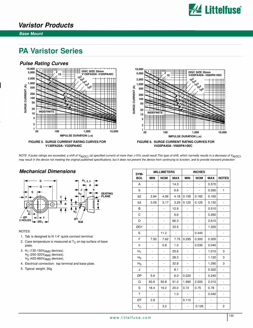
Varistor Products
130w w w. l i t t e l f u s e . c o m
Base Mount
PA Varistor Series
Pulse Rating Curves
Mechanical Dimensions
FIGURE 5. SURGE CURRENT RATING CURVES FOR V130PA20A - V320PA40C
FIGURE 6. SURGE CURRENT RATING CURVES FOR V420PA40A - V660PA100C
10,000
2,000
200
100
50
20
10
5
2
500
20 100 1,000 10,000
IMPULSE DURATION (µs)
SU
RG
E C
UR
RE
NT
(A
)
1 2
104
105
106
DISC SIZE 20mmV130PA20A - V320PA40C
103
INDEFINITE
1,000
10210
5,000
1
10,000
2,000
200
100
50
20
10
5
2
500
20 100 1,000 10,000IMPULSE DURATION (µs)
SU
RG
E C
UR
RE
NT
(A
)
1 2
104
105
106
DISC SIZE 20mmV420PA40A - V660PA100C
103
INDEFINITE
1,000
10210
5,000
1
NOTE: If pulse ratings are exceeded, a shift of VN(DC) (at specified current) of more than ±10% could result.This type of shift, which normally results in a decrease of VN(DC),may result in the device not meeting the original published specifications, but it does not prevent the device from continuing to function, and to provide transient protection
NOTES:
1. Tab is designed to fit 1/4” quick-connect terminal.
2. Case temperature is measured at TC on top surface of base plate.
3. H1 (130-150VRMS devices).H2 (250-320VRMS devices).H3 (420-660VRMS devices).
4. Electrical connection: top terminal and base plate.
5. Typical weight: 30g.
D
Q
S
F C
B
ØP2 HOLES ØD1
T
TC
H1, 2, 3
J h
Eb
b3
ØTTAB
b2
A
SEATINGPLANE
SYM-BOL
MILLIMETERS INCHES
NOTESMIN NOM MAX MIN NOM MAX
A - - 14.3 - - 0.570 -
b - - 6.6 - - 0.260 1
b2 3.94 4.06 4.18 0.155 0.160 0.165 -
b3 3.05 3.17 3.29 0.120 0.125 0.130 -
B - - 12.9 - - 0.510 -
C - - 6.6 - - 0.260 -
D - - 66.3 - - 2.610 -
ØD1 - - 33.5 - - 1.320 -
E - 11.2 - - 0.440 - -
F 7.50 7.62 7.75 0.295 0.300 0.305 -
h - 0.8 1.0 - 0.030 0.040 -
H1 - - 25.6 - - 1.010 3
H2 - - 28.3 - - 1.120 3
H3 - - 32.8 - - 1.290 3
J - - 8.1 - - 0.320 -
ØP 5.6 - 6.0 0.220 - 0.240 -
Q 50.6 50.8 51.0 1.990 2.000 2.010 -
S 18.4 19.2 20.0 0.72 0.75 0.78 -
T - - 1.0 - - 0.040 -
ØT 2.8 - - 0.110 - - -
TC - 3.2 - - 0.126 - 2

2
VAR
ISTO
RP
RO
DU
CT
S
Varistor Products
131w w w. l i t t e l f u s e . c o m
PA Varistor Series
Suggested Hardware and Mounting Arrangements
TYPICAL NON-ISOLATED MOUNTING TYPICAL ISOLATED MOUNTING
THERMALGREASE
LAYER
#10-32 PAN HEADSCREW
#10 FLAT WASHER
VARISTORMOUNTING
LOCK WASHER
#10-32 NUT
SURFACETHERMAL
GREASELAYER
#6 FLAT WASHERPHENOLIC SHOULDER
SPACER
VARISTOR
MOUNTING
LOCK WASHER#6-32 NUT
SURFACE
THERMALQUICK
CONNECT
MICA INSULATOR
WASHER
#6-32 SCREW
(NOTE 6)
NOTE:
6. GE G623, Dow Corning, DC3, 4, 340, or 640 Thermal Grease recommended for best heat transfer.
1,000V Isolation Kit containing the following parts can be ordered by part #A7811055 (Qty).
Ordering Information
(1) MICA insulation 1”/3.1”/0.005” thick
(1) 1/4 ” quick-connect terminal
(2) Phenolic shoulder washer
(1) Spacer
(2) #6-32/3 / 4 screw
(2) #6-32 nut
(2) #6 internal tooth lock washer
(2) #6 flat washer
VARISTOR
VM(AC)130V to 660V
CLAMPING VOLTAGESELECTION DESIGNATOR
A = StandardC = Low Clamp Voltage Option
SERIES DESIGNATOR
V XXX PA XX X
RELATIVE ENERGY INDICATOR
Base Mount

Varistor Products
132w w w. l i t t e l f u s e . c o m
Low Profile
RA Varistor SeriesThe RA Series transient surge suppressors are varistors (MOVs) supplied in a low-profile box that features a precise seating plane toincrease mechanical stability for secure circuit-board mounting. This feature makes these devices suitable for industrial applications critical to vibration. Their construction permits operation up to 125oC (ambient)without derating.
The RA series are available in voltage ratings up to 275V VM(AC)RMS,and energy levels up to 140J. These varistors are used in automotive,motor-control, telecommunication, and military applications.
See RA Series Device Ratings and Specifications table for part numberand brand information.
Features• Low Profile Outline with Precise Seating Plane
• No Derating up to 125oC Ambient
• Wide Operating Voltage RangeVM(AC)RMS. . . . . . . . . . . . . . . . . . . . . . . . . . . . . . . . . . . . . 4V to 275VVM(DC). . . . . . . . . . . . . . . . . . . . . . . . . . . . . . . . . . . . . . . .5.5V to 369V
• High Energy Absorption Capability W TM . . . . . . . . . . . . . up to 140J
• 3 Model Sizes Available . . . . . . . . . RA8, RA16, and RA22
• In-Line Leads
AGENCY APPROVALS: Recognized under the components program ofUnderwriters Laboratories. Certified by CSA.
AGENCY FILE NUMBERS: UL E75961, E56529, E135010;CSA LR91788.
®®
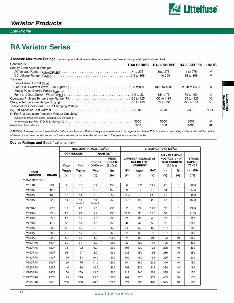
Varistor Products
133w w w. l i t t e l f u s e . c o m
2
VAR
ISTO
RP
RO
DU
CT
S
RA Varistor Series
Absolute Maximum Ratings For ratings of individual members of a series, see Device Ratings and Specifications chart
Continuous:Steady State Applied Voltage:
AC Voltage Range (VM(AC)RMS) . . . . . . . . . . . . . . . . . . . . . . . . . . . . . . . . . . . . . . . . 4 to 275 10to 275 4 to 275 VDC Voltage Range (VM(DC) . . . . . . . . . . . . . . . . . . . . . . . . . . . . . . . . . . . . . . . . . . . 5.5 to 369 14 to 369 18 to 369 V
Transient:Peak Pulse Current (ITM)For 8/20µs Current Wave (See Figure 2). . . . . . . . . . . . . . . . . . . . . . . . . . . . . . . . . . 100 to1200 1000 to 4500 2000 to 6500 ASingle Pulse Energy Range (Note 1)For 10/1000µs Current Wave (WTM ) . . . . . . . . . . . . . . . . . . . . . . . . . . . . . . . . . . . . . 0.4 to 23 3.5 to 75 70 to 160 J
Operating Ambient Temperature Range (TA) . . . . . . . . . . . . . . . . . . . . . . . . . . . . . . . . . -55 to 125 -55 to -125 -55 to -125 OCStorage Temperature Range (TSTG) . . . . . . . . . . . . . . . . . . . . . . . . . . . . . . . . . . . . . . . -55 to 150 -55 to 150 -55 to 150 OCTemperature Coefficient (αV) of Clamping Voltage(VC) at Specified Test Current . . . . . . . . . . . . . . . . . . . . . . . . . . . . . . . . . . . . . . . . . . . . . . <0.01 <0.01 <0.01 %/OCHi-Pot Encapsulation (Isolation Voltage Capability)
(Dielectric must withstand indicated DC voltage for one minute per MIL-STD 202, Method 301) . . . . . . . . . . . . . . . . . . . . . . . . . . . . . . . . . . . . . 5000 5000 5000 V
Insulation Resistance. . . . . . . . . . . . . . . . . . . . . . . . . . . . . . . . . . . . . . . . . . . . . . . . . . . . . 1000 1000 1000 MΩ
CAUTION: Stresses above those listed in “Absolute Maximum Ratings” may cause permanent damage to the device. This is a stress only rating and operation of the deviceat these or any other conditions above those indicated in the operational sections of this specification is not implied.
Device Ratings and Specifications (Note 1)
RA8 SERIES RA16 SERIES RA22 SERIES UNITS
PARTNUMBER BRAND
MAXIMUM RATINGS (125oC) SPECIFICATIONS (25oC)
CONTINUOUS TRANSIENT
VARISTOR VOLTAGE AT 1mA DC TEST
CURRENT
MAX CLAMPING VOLTAGE VC AT TEST CURRENT
(8/20µs)
TYPICAL CAPACI-TANCEVRMS VDC
ENERGY (10/1000µs)
PEAKCURRENT
(8/20µs)
VM(AC) VM(DC) WTM ITM MIN VN(DC) MAX VC IP f = 1MHz
(V) (V) (J) (A) (V) (V) (V) (V) (A) (pF)
† RA8 SERIES
V8RA8 8R 4 5.5 0.4 150 6 8.2 11.2 22 5 3000
V12RA8 12R 6 8 0.6 150 9 12 16 34 5 2500
V18RA8 18R 10 14 0.8 250 14.4 18 21.6 42 5 2000
V22RA8 22R 14 18(Note 3)
10(Note 2)
250 18.7 22 26 47 5 1600
V27RA8 27R 17 22 1.0 250 23 27 31.1 57 5 1300
V33RA8 33R 20 26 1.2 250 29.5 33 36.5 68 5 1100
V39RA8 39R 25 31 1.5 250 35 39 43 79 5 900
V47RA8 47R 30 38 1.8 250 42 47 52 92 5 800
V56RA8 56R 35 45 2.3 250 50 56 62 107 5 700
V68RA8 68R 40 56 3.0 250 61 68 75 127 5 600
V82RA8 82R 50 66 4.0 1200 74 82 91 135 10 500
V100RA8 100R 60 81 5.0 1200 90 100 110 165 10 400
V120RA8 120R 75 102 6.0 1200 108 120 132 205 10 300
V150RA8 150R 95 127 8.0 1200 135 150 165 250 10 250
V180RA8 180R 115 153 10.0 1200 162 180 198 295 10 200
V200RA8 200R 130 175 11.0 1200 184 200 228 340 10 180
† V220RA8 220R 140 180 12.0 1200 198 220 242 360 10 160
† V240RA8 240R 150 200 13.0 1200 212 240 268 395 10 150
† V270RA8 270R 175 225 15.0 1200 247 270 303 455 10 130
† V360RA8 360R 230 300 20.0 1200 324 360 396 595 10 100
Low Profile

Varistor Products
134w w w. l i t t e l f u s e . c o m
Low Profile
RA Varistor SeriesDevice Ratings and Specifications (Note 1) (Continued)
† V390RA8 390R 250 330 21.0 1200 354 390 429 650 10 90
† V430RA8 430R 275 369 23.0 1200 389 430 473 710 10 80
† RA16 SERIES
V18RA16 18R16 10 14 3.5 1000 14.4 18 21.6 39 10 11000
V22RA16 22R16 14 18(Note 3)
50(Note 2)
1000 18.7 22 26 43 10 9000
V27RA16 27R16 17 22 5.0 1000 23 27 31.1 53 10 7000
V33RA16 33R16 20 26 6.0 1000 29.5 33 36.5 64 10 6000
V39RA16 39R16 25 31 7.2 1000 35 39 43 76 10 5000
V47RA16 47R16 30 38 8.8 1000 42 47 52 89 10 4500
V56RA16 56R16 35 45 10.0 1000 50 56 62 103 10 3900
V68RA16 68R16 40 56 13.0 1000 61 68 75 123 10 3300
V82RA16 82R16 50 66 15.0 4500 74 82 91 145 50 2500
V100RA16 100R16 60 81 20.0 4500 90 100 110 175 50 2000
V120RA16 120R16 75 102 22.0 4500 108 120 132 205 50 1700
V150RA16 150R16 95 127 30.0 4500 135 150 165 255 50 1400
V180RA16 180R16 115 153 35.0 4500 162 180 198 300 50 1100
† V200RA16 200R16 130 175 38.0 4500 184 200 228 340 50 1000
† V220RA16 220R16 140 180 42.0 4500 198 220 242 360 50 900
† V240RA16 240R16 150 200 45.0 4500 212 240 268 395 50 800
† V270RA16 270R16 175 225 55.0 4500 247 270 303 455 50 700
† V360RA16 360R16 230 300 70.0 4500 324 360 396 595 50 550
† V390RA16 390R16 250 330 72.0 4500 354 390 429 650 50 500
† V430RA16 430R16 275 369 75.0 4500 389 430 473 710 50 450
† RA22 SERIES
V24RA22 24R22 14 18(Note 3)
100.0 (Note 2)
2000 19.2 24(Note 4)
26 43 20 18000
V36RA22 36R22 23 31 160.0(Note 2)
2000 32 36(Note 4)
40 63 20 12000
† V200RA22 200R22 130 175 70.0 6500 184 200 228 340 100 1900
† V240RA22 240R22 150 200 80.0 6500 212 240 268 395 100 1600
† V270RA22 270R22 175 225 90.0 6500 247 270 303 455 100 1400
† V390RA22 390R22 250 330 130.0 6500 354 390 429 650 100 1000
† V430RA22 430R22 275 369 140.0 6500 389 430 473 710 100 900
NOTES:
1. Average power dissipation of transients not to exceed 0.25W for RA8 Series, 0.60W for RA16 Series, or 1.0W for RA22 Series.
2. Energy ratings for impulse duration of 30ms minimum to one half of peak current value.
3. Also rated to withstand 24V for 5 minutes.
4. 10mA DC Test Current.
† Under UL File No. E75961 as a recognized component. CSA approved File No. LR91788.
PARTNUMBER BRAND
MAXIMUM RATINGS (125oC) SPECIFICATIONS (25oC)
CONTINUOUS TRANSIENT
VARISTOR VOLTAGE AT 1mA DC TEST
CURRENT
MAX CLAMPING VOLTAGE VC AT TEST CURRENT
(8/20µs)
TYPICAL CAPACI-TANCEVRMS VDC
ENERGY (10/1000µs)
PEAKCURRENT
(8/20µs)
VM(AC) VM(DC) WTM ITM MIN VN(DC) MAX VC IP f = 1MHz
(V) (V) (J) (A) (V) (V) (V) (V) (A) (pF)

Varistor Products
135w w w. l i t t e l f u s e . c o m
2
VAR
ISTO
RP
RO
DU
CT
S
RA Varistor Series
Power Dissipation RatingsShould transients occur in rapid succession, the average power dissipationrequired is simply the energy (watt-seconds) per pulse times the number of pulses per second. The power so developed must be within the specifi-cations shown on the Device Ratings and Specifications table for the specific device. Furthermore, the operating values need to be derated at high temperatures as shown in Figure 1. Because varistors can only dissipate a relatively small amount of average power they are, therefore,not suitable for repetitive applications that involve substantial amounts ofaverage power dissipation.
FIGURE 1. CURRENT, ENERGY AND POWER DERATING CURVE
100
90
80
70
60
50
40
30
20
10
0-55 50 60 70 80 90 100 110 120 130 140 150
AMBIENT TEMPERATURE ( oC)
PE
RC
EN
T O
F R
ATE
D V
AL
UE
100
90
50
10
O1 T
T1T2
TIME
PE
RC
EN
T O
F P
EA
K V
AL
UE
Low Profile
O1 = Virtual Origin of WaveT = Time From 10% to 90% of Peak
T1 = Virtual Front time = 1.25 • tT2 = Virtual Time to Half Value (Impulse Duration)
Example: For an 8/20µs Current Waveform:8µs = T1 = Virtual Front Time
20µs = T2 = Virtual Time to Half Value
FIGURE 2. PEAK PULSE CURRENT TEST WAVEFORM

Varistor Products
136w w w. l i t t e l f u s e . c o m
Low Profile
RA Varistor Series
Transient V-I Characteristics Curves (Continued)
FIGURE 5. CLAMPING VOLTAGE FOR V18RA16 - V68RA16
600500400
300
200
100908070605040
30
2010-3 10-2 10-1 100 101 102 103
PEAK AMPERES (A)
MA
XIM
UM
PE
AK
VO
LTS
(V
)
V68RA16V56RA16V47RA16V39RA16V33RA16V27RA16V22RA16V18RA16
MAXIMUM CLAMPING VOLTAGE18 TO 68VN(DC) RATINGTA = -55oC TO 125oC
FIGURE 3. CLAMPING VOLTAGE FOR V8RA8 - V68RA8
600500400
300
200
100908070605040
30
20
1010-3 10-2 10-1 100 101 102 103
PEAK AMPERES (A)
MA
XIM
UM
PE
AK
VO
LTS
(V
)
V68RA8V56RA8V47RA8V39RA8V33RA8V27RA8V22RA8V18RA8
V12RA8
V8RA8
MAXIMUM CLAMPING VOLTAGE8 TO 68VN(DC) RATING
TA = -55oC TO 125oC
FIGURE 4. CLAMPING VOLTAGE FOR V82RA8 - V430RA8
MA
XIM
UM
PE
AK
VO
LTS
(V
)PEAK AMPERES (A)
10-2 10-1 100 101 102 10310-3
V180RA8V150RA8V120RA8V100RA8
MAXIMUM CLAMPING VOLTAGEMODEL SIZE 5 x 8mm82 TO 430VN(DC) RATINGTA = -55oC TO 125oC
4,000
3,000
2,000
1,000900800700600
500400
300
200
100104
V82RA8
V270RA8
V360RA8
V220RA8V200RA8
V240RA8
V430RA8V390RA8
FIGURE 6. CLAMPING VOLTAGE FOR V82RA16 - V430RA16
MA
XIM
UM
PE
AK
VO
LTS
(V
)
PEAK AMPERES (A)10-2 10-1 100 101 102 10310-3
V180RA16V150RA16V120RA16V100RA16
MAXIMUM CLAMPING VOLTAGEMODEL SIZE 5 x 8mm82 TO 430VN(DC) RATINGTA = -55oC TO 125oC
4,000
3,000
2,000
1,000900800700600
500400
300
200
100104
V82RA16
V270RA16
V360RA16
V220RA8V200RA8
V240RA16
V430RA16V390RA16
FIGURE 7. CLAMPING VOLTAGE FOR V24RA22 - V36RA22
300
200
10090807060
50
40
30
20
MA
XIM
UM
PE
AK
VO
LTS
(V
)
PEAK AMPERES (A)10-2 10-1 100 101 102 10310-3 104
V36RA22
V24RA22
MAXIMUM CLAMPING VOLTAGE24 TO 36VN(DC) RATINGTA = -55oC TO 125oC
FIGURE 8. CLAMPING VOLTAGE FOR V200RA22 - V430RA22
MA
XIM
UM
PE
AK
VO
LTS
(V
)
PEAK AMPERES (A)10-2 10-1 100 101 102 10310-3
4,000
3,000
2,000
1,000900800700600500400
300
200
100104
MAXIMUM CLAMPING VOLTAGE200 TO 430VN(DC) RATINGTA = -55oC TO 125oC
V430RA22V390RA22
V270RA22V240RA22
V200RA22

2
VAR
ISTO
RP
RO
DU
CT
S
Varistor Products
137w w w. l i t t e l f u s e . c o m
RA Varistor Series
Pulse Rating Curves (Continued)
FIGURE 11. SURGE CURRENT RATING CURVES FOR V82RA8 - V430RA8
FIGURE 12. SURGE CURRENT RATING CURVES FOR V18RA16 - V68RA16
2,000
1,000
200
100
50
20
10
5
1
2
500
20 100 1,000 10,000
IMPULSE DURATION (µs)
SU
RG
E C
UR
RE
NT
(A
)
1
2
10
102104
105
106
V82RA8 - V430RA8
103
INDEFINITE
200
100
50
20
10
5
1
2
20 100 1,000 10,000IMPULSE DURATION (µs)
SU
RG
E C
UR
RE
NT
(A
)
12
10
102
104
105
106
V18RA16 - V68RA16103
INDEFINITE
1,000
500
NOTE: If pulse ratings are exceeded, a shift of VN(DC) (at specified current) of more than ±10% could result.This type of shift, which normally results in a decrease of VN(DC),may result in the device not meeting the original published specifications, but it does not prevent the device from continuing to function, and to provide ample protection.
Low Profile
FIGURE 9. SURGE CURRENT RATING CURVES FORV8RA8 - V12RA8
FIGURE 10. SURGE CURRENT RATING CURVES FOR V18RA8 - V68RA8
20 100 1,000 10,000
IMPULSE DURATION (µs)
SU
RG
E C
UR
RE
NT
(A
)
1
10
102
V8RA8 - V12RA82
103
INDEFINITE
104105
106
200
100
50
20
10
5
2
1
0.5
0.220 100 1,000 10,000
IMPULSE DURATION (µs)
SU
RG
E C
UR
RE
NT
(A
)
1
10
102
V18RA8 - V68RA8
2
103
INDEFINITE
500
200
100
50
20
10
2
1
0.5
0.2
104105
106
5
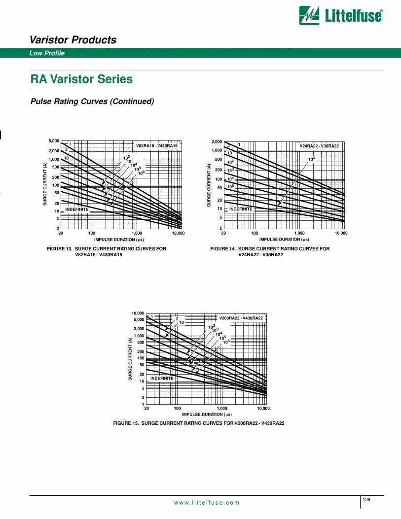
Varistor Products
138w w w. l i t t e l f u s e . c o m
FIGURE 13. SURGE CURRENT RATING CURVES FOR V82RA16 - V430RA16
FIGURE 14. SURGE CURRENT RATING CURVES FOR V24RA22 - V36RA22
5,000
2,000
200
100
50
20
10
5
2
500
20 100 1,000 10,000
IMPULSE DURATION (µs)
SU
RG
E C
UR
RE
NT
(A
)
12
10
104
105
106
V82RA16 - V430RA16
103
INDEFINITE
1,000 102
2,000
200
100
50
20
10
5
2
500
20 100 1,000 10,000
IMPULSE DURATION (µs)
SU
RG
E C
UR
RE
NT
(A
)
12
10
V24RA22 - V36RA221,000
102
103
104
105
106
INDEFINITE
Low Profile
RA Varistor Series
FIGURE 15. SURGE CURRENT RATING CURVES FOR V200RA22 - V430RA22
10,000
2,000
200
100
50
20
10
5
2
500
20 100 1,000 10,000IMPULSE DURATION (µs)
SU
RG
E C
UR
RE
NT
(A
)
1 2
104
105
106
V200RA22 - V430RA22
103
INDEFINITE
1,000
10210
5,000
1
Pulse Rating Curves (Continued)

2
VAR
ISTO
RP
RO
DU
CT
S
Varistor Products
139w w w. l i t t e l f u s e . c o m
Low Profile
RA Varistor Series
Mechanical Dimensions
Ordering InformationThe RA Series is supplied in bulk pack.
D MAX
Y
nMIN A MAX
SEATINGPLANE
5.0 MIN(0.197 MIN)
Øb± 0.05
(± 0.002)
EMAX
e± 1.0
(± 0.039)
0.5 MAXOFFSET(0.020 MAX)
X
SYMBOLRA8
SERIESRA16
SERIESRA22
SERIES
A MAX 8.85(0.348)
15.1(0.594)
19.1(0.752)
D MAX 11.45(0.450)
19.7(0.776)
25.5(1.004)
e 5(0.197)
7.5(0.295)
7.5(0.295)
E MAX 5.2(0.205)
6.3(0.248)
6.3(0.248)
n MAX 0.7(0.027)
0.7(0.027)
0.7(0.027)
Øb 0.635(0.025)
0.81(0.032)
0.81(0.032)
WEIGHT TYP
1 Gram 3.4 Grams 4.4 Grams
X 2.2(0.087)
2.2(0.087)
4.4(0.173)
Y 3.1 ± 0.5(0.122 ± 0.02)
6 ± 1(0.236 ± 0.04)
8.9 ± 1(0.35 ± 0.04)
NOTES:
5. Dimensions in mm, dimensions in inches in parentheses.
6. Inches for reference only.
V 200 RA 16
Relative Device Size Indicator Varistor Technology
Series DesignatorNominal Varistor Voltage

Varistor Products
140w w w. l i t t e l f u s e . c o m
High Reliability VaristorsThe high reliability Littelfuse varistor is the latest step in increased product performance, and is available for applications requiring qualityand reliability assurance levels consistent with military or other standards.(MIL-STD-19500, MIL-S-750, Method 202). Additionally, Littelfuse varistors are inherently radiation hardened compared to silicon diode suppressors as illustrated in Figure 1.
This series of high-reliability varistors involve five categories:
• DSSC Qualified Parts List (QPL) MIL-R-83530 4 Types Presently Available
• DSSC Standard Military Drawings Based on MIL-R 83530 63 TypesPresently Available:
- ZA Series - Drawing # 87063- DB Series - Drawing # 90065
• Littelfuse High Reliability Series Offers TX Equivalents 29 TypesPresently Available
• Custom Types Processed to Customer-Specific Requirements - (SCD)or to Standard Military Flow
• Commercial Items have been identified for Government use as follows:
- Commercial Item Description AA-55564-3 - Littelfuse ZA Series- Commercial Item Description AA-55564-2 - Littelfuse DA, DB Series- Commercial Item Description AA-55564-1 - Littelfuse PA Series
AGENCY APPROVALS• DSSC Approved
• QPL Listed
• CECC Certified
• ISO Approved
• UL Recognized
• CSA Certified
DSSC Qualified Parts List (QPL) MIL-R-83530TABLE 1. MIL-R-83530/1 RATINGS AND CHARACTERISTICS
PARTNUMBERM83530/
NOMINALVARISTORVOLTAGE
(V)TOLERANCE
(%)
VOLTAGERATING
(V)ENERGYRATING
(J)
CLAMPINGVOLTAGEAT 100A
(V)
CAPACITANCEAT 1MHz
(pF)
CLAMPINGVOLTAGEAT PEAK
CURRENTRATING
(V)ITM(A)
NEARESTCOMMERCIALEQUIVALENT(RMS) (DC)
1-2000B 200 ±10 130 175 50 325 3800 570 6000 V130LA20B
1-2200D 220 +10, -5 150 200 55 360 3200 650 6000 V150LA20B
1-4300E 430 +5, -10 275 369 100 680 1800 1200 6000 V275LA40B
1-5100E 510 +5, -10 320 420 120 810 1500 1450 6000 V320LA40B
This series of varistors are screened and conditioned in accordance with MIL-R-83530 as outlined in Table 2. Manufacturing system conforms toMIL-I-45208; MIL-Q-9858.
QPLMIL
Aerospace and Military

2
VAR
ISTO
RP
RO
DU
CT
S
Varistor Products
141w w w. l i t t e l f u s e . c o m
Aerospace and Military
High Reliability Varistors
MIL-R-83530 InspectionsTABLE 2. MIL-R-83530 GROUP A, B, AND C INSPECTIONS
INSPECTION
AQL(PERCENT
DEFECTIVE) MAJOR MINORNUMBER OF
SAMPLE UNITSFAILURESALLOWED
Group A SUBGROUP 1
High Temperature Life (Stabilization Bake) 100% - - - -
Thermal Shock 100% - - - -
Power Burn-In 100% - - - -
Clamping Voltage 100% - - - -
Nominal Varistor Voltage 100% - - - -
SUBGROUP 2
Visual and Mechanical Examination - 1.0% AQL7.6% LQ
25% AQL13.0% LQ
Per Plan -
Body Dimensions - Per Plan -
Diameter and Length of Leads - Per Plan -
Marking - Per Plan -
Workmanship - Per Plan -
SUBGROUP 3
Solderability - - - Per Plan -
Group B SUBGROUP 1
Dielectric Withstanding Voltage - - - Per Plan -
SUBGROUP 2
Resistance to Solvents - - - Per Plan -
SUBGROUP 3
Terminal Strength (Lead Fatigue) - - - Per Plan -
Moisture Resistance - - - Per Plan -
Peak Current - - - Per Plan -
Energy - - - Per Plan -
Group C EVERY 3 MONTHS
High Temperature Storage - - - 10 0
Operating Life (Steady State) - - - 10 0
Pulse Life - - - 10 0
Shock - - - 10 0
Vibration - - - 10 0
Constant Acceleration - - - 10 0
Energy - - - 10 0
Varistor Products
142w w w. l i t t e l f u s e . c o m
High Reliability Varistors
DSSC Standard Military Drawing # 87063Based on MIL-R-83530
TABLE 3. ZA SERIES RATINGS AND SPECIFICATIONS
87063DASHNO.
(SEECHAPTER 2)NEAREST
COMM.EQUIV.
(PAGE 143)SIZE
MAXIMUM RATINGS (85oC) SPECIFICATIONS (25oC)
CONTINUOUS TRANSIENT
VARISTOR VOLTAGEAT 1mADC
TEST CURRENT
MAXIMUM CLAMPING VOLTAGE
VC AT TEST CURRENT
(8/20µs)TYPICAL
CAPACITANCERMS DCENERGY
(10/1000µs)
PEAKCURRENT(8/20µs)
VM(AC) VM(DC) WTM ITM MIN VN(DC) MAX VC IC f = 1MHz
(V) (V) (J) (A) (V) (V) (V) (V) (A) (pF)
001 V22ZA05 1 14 18 0.2 35 18.7 22 26 51 2 400
002 V22ZA1 2 14 18 0.9 150 18.7 22 26 47 5 1600
003 V22ZA2 3 14 18 2.0 350 18.7 22 26 43 5 4000
004 V22ZA3 4 14 18 4.0 750 18.7 22 26 43 10 9000
005 V24ZA50 5 14 18 6.5 1500 19.2 24(PAGE 143)
26 43 20 18000
006 V27ZA05 1 17 22 0.25 35 23 27 31.1 59 2 300
007 V27ZA1 2 17 22 1.0 150 23 27 31.1 57 5 1300
008 V27ZA2 3 17 22 2.5 350 23 27 31.1 53 5 3000
009 V27ZA4 4 17 22 5.0 750 23 27 31.1 53 10 7000
010 V27ZA60 5 17 22 8.0 1500 23 27 31.1 50 20 15000
011 V33ZA05 1 20 26 0.3 35 29.5 33 38 67 2 250
012 V33ZA1 2 20 26 1.2 150 29.5 33 36.5 68 5 1100
013 V33ZA2 3 20 26 3.0 350 29.5 33 36.5 64 5 2700
014 V33ZA5 4 20 26 6.0 750 29.5 33 36.5 64 10 6000
015 V33ZA70 5 21 27 9.0 1500 29.5 33 36.5 58 20 13000
016 V36ZA80 5 23 31 10.0 1500 32 36 40 63 20 12000
017 V39ZA05 1 25 31 0.35 35 35 39 46 79 2 220
018 V39ZA1 2 25 31 1.5 150 35 39 43 79 5 900
019 V39ZA3 3 25 31 3.5 350 35 39 43 76 5 2200
020 V39ZA6 4 25 31 7.2 750 35 39 43 76 10 5000
021 V47ZA05 1 30 38 0.4 35 42 47 55 90 2 200
022 V47ZA1 2 30 38 1.8 150 42 47 52 92 5 800
023 V47ZA3 3 30 38 4.5 350 42 47 52 89 5 2000
024 V47ZA7 4 30 38 8.8 750 42 47 52 89 10 4500
025 V56ZA05 1 35 45 0.5 35 50 56 66 108 2 180
(PAGE 143)
(PAGE 143)
(PAGE 143)
Aerospace and Military
2
VAR
ISTO
RP
RO
DU
CT
S
Varistor Products
143w w w. l i t t e l f u s e . c o m
Aerospace and Military
High Reliability VaristorsTABLE 3. ZA SERIES RATINGS AND SPECIFICATIONS (Continued)
026 V56ZA2 2 35 45 2.3 150 50 56 62 107 5 700
027 V56ZA3 3 35 45 5.5 350 50 56 62 103 5 1800
028 V56ZA8 4 35 45 10.0 750 50 56 62 103 10 3900
029 V68ZA05 1 40 56 0.6 35 61 68 80 127 2 150
030 V68ZA2 2 40 56 3.0 150 61 68 75 127 5 600
031 V68ZA3 3 40 56 6.5 350 61 68 75 123 5 1500
032 V68ZA10 4 40 56 13.0 750 61 68 75 123 10 3300
033 V82ZA05 1 50 66 1.2 70 73 82 97 145 2 120
034 V82ZA2 2 50 66 3.5 300 73 82 91 135 10 500
035 V82ZA4 3 50 66 7.3 750 73 82 91 135 25 1100
036 V82ZA12 4 50 66 13.0 1500 73 82 91 145 50 2500
037 V100ZA05 1 60 81 1.5 70 90 100 117 175 2 90
038 V100ZA3 2 60 81 4.3 300 90 100 110 165 10 400
039 V100ZA4 3 60 81 8.9 750 90 100 110 165 25 900
040 V100ZA15 4 60 81 16.0 1500 90 100 110 175 50 2000
041 V120ZA05 1 75 102 1.8 100 108 120 138 205 2 70
042 V120ZA1 2 75 102 5.3 400 108 120 132 205 10 300
043 V120ZA4 3 75 102 11.0 1000 108 120 132 200 25 750
044 V120ZA6 4 75 102 19.0 2000 108 120 132 210 50 1700
045 V150ZA05 1 92 127 2.3 100 135 150 173 240 2 60
046 V150ZA1 2 95 127 6.5 400 135 150 165 250 10 250
047 V150ZA4 3 95 127 13.0 1000 135 150 165 250 25 600
048 V150ZA8 4 95 127 23.0 2000 135 150 165 255 50 1400
049 V180ZA05 1 110 153 2.7 150 162 180 207 290 2 50
050 V180ZA1 2 115 153 7.7 500 162 180 198 295 10 200
051 V180ZA5 3 115 153 16.0 1500 162 180 198 300 25 500
052 V180ZA10 4 115 153 27.0 3000 162 180 198 300 50 1100
87063DASHNO.
(SEESECTION 4)NEAREST
COMM.EQUIV.
(NOTE 1)SIZE
MAXIMUM RATINGS (85oC) SPECIFICATIONS (25oC)
CONTINUOUS TRANSIENT
VARISTOR VOLTAGEAT 1mADC
TEST CURRENT
MAXIMUM CLAMPING VOLTAGE
VC AT TEST CURRENT
(8/20µs)TYPICAL
CAPACITANCERMS DCENERGY
(10/1000µs)
PEAKCURRENT(8/20µs)
VM(AC) VM(DC) WTM ITM MIN VN(DC) MAX VC IC f = 1MHz
(V) (V) (J) (A) (V) (V) (V) (V) (A) (pF)

Varistor Products
144w w w. l i t t e l f u s e . c o m
High Reliability Varistors
DSSC Standard Military Drawing # 90065Based on MIL-R-83530
TABLE 4. DB SERIES RATINGS AND SPECIFICATIONS
Littelfuse High Reliability Series TX EquivalentsTABLE 5. AVAILABLE TX MODEL TYPES
90065DASHNO.
VOLTAGERATING
MAX(RMS)
ENERGYMAX(J)
PEAKCURRENT
(A)
NOMINALVARISTORVOLTAGE
(V)
MAX CLAMPINGVOLTAGE AT
TEST CURRENT TYPICALCAPACITANCE
(pF)(V) (I)
012 130 170 22500 200 +28, -16 345 200 10000
013 150 200 22500 240 ±28 405 200 8000
014 250 270 22500 390 +39, -36 650 200 5000
015 275 300 22500 430 ±43 730 200 4500
016 320 350 22500 510 +29, -48 830 200 3800
017 420 460 28800 680 +68, -70 1130 200 3000
018 480 510 28800 750 +74, -80 1240 200 2700
019 510 550 28800 820 +91, -85 1350 200 2500
020 575 600 28800 910 +95, -105 1480 200 2200
021 660 690 28800 1050 ±110 1720 200 2000
022 750 810 28800 1200 ±120 2000 200 1800
NOTE: See Section 4 (DB Series) for nearest equivalent commercial type.
TX MODELMODEL
SIZEDEVICEMARK
(SEE SECTION 4)NEAREST
COMMERCIALEQUIVALENT
V8ZTX1 7mm 8TX1 V8ZA1
V8ZTX2 10mm 8TX2 V8ZA2
V12ZTX1 7mm 12TX1 V12ZA1
V12ZTX2 10mm 12TX2 V12ZA2
V22ZTX1 7mm 22TX1 V22ZA1
V22ZTX3 14mm 22TX3 V22ZA3
V24ZTX50 20mm 24TX50 V24ZA50
V33ZTX1 7mm 33TX1 V33ZA1
V33ZTX5 14mm 33TX5 V33ZA5
V33ZTX70 20mm 33TX70 V33ZA70
V68ZTX2 7mm 68TX2 V68ZA2
V68ZTX10 14mm 68TX10 V68ZA10
V82ZTX2 7mm 82TX2 V82ZA2
V82ZTX12 14mm 82TX12 V82ZA12
V130LTX2 7mm 130TX V130LA2
V130LTX10A 14mm 130TX10 V130LA10A
V130LTX20B 20mm 130TX20 V130LA20A
V150LTX2 7mm 150TX V150LA2
V150LTX10A 14mm 150TX10 V150LA10A
V150LTX20B 20mm 150TX20 V150LA20B
V250LTX4 7mm 250TX V250LA4
V250LTX20A 14mm 250TX20 V250LA20A
V250LTX40B 20mm 250TX40 V250LA40B
V420LTX20A 14mm 420TX20 V420LA20A
V420LTX40B 20mm 420TX40 V420LA40B
V480LTX40A 14mm 480TX40 V480LA40A
V480LTX80B 20mm 480TX80 V480LA80B
V510LTX40A 14mm 510TX40 V510LA40A
V510LTX80B 20mm 510TX80 V510LA80B
TX MODELMODEL
SIZEDEVICEMARK
(SEE SECTION 4)NEAREST
COMMERCIALEQUIVALENT
Aerospace and Military

2
VAR
ISTO
RP
RO
DU
CT
S
Varistor Products
145w w w. l i t t e l f u s e . c o m
Aerospace and Military
High Reliability VaristorsThe TX series of varistors are 100% screened and conditioned in accordance with MIL-STD-750. Tests are as outlined in Table 6.
SCREENMIL-STD-750
METHOD CONDITIONTX
REQUIREMENTS
High Temperature Life(Stabilization Bake)
1032 24 hours min at max rated storage temperature. 100%
Thermal Shock(Temperature Cycling)
1051 No dwell is required at 25oC. Test condition A1, 5 cycles -55oC to 125 oC (extremes) >10 minutes.
100%
Humidity Life 85oC, 85% R.H., 168Hr. 100%
Interim Electrical VN(DC) VC(Note 3)
As specified, but including delta parameter as a minimum. 100% Screen
Power Burn-In 1038 Condition B, 85oC, rated VM(AC), 72 hours min. 100%
Final Electrical +VN(DC) VC(Note 3)
As specified - All parameter measurements must be completed within 96 hours after removal from burn-in conditions.
100% Screen
External Visual Examination 2071 To be performed after complete marking. 100%
MIL-STD-105
LTPDLEVEL AQL
Electrical (Bidirectional)VN(DC), VC (Per Specifications Table)
II 0.1 -
Dielectric Withstand VoltageMIL-STD-202, Method 301, 2500V Min at 1.0µADC
- - 15
SolderabilityMIL-STD-202, Method 208, No Aging, Non-Activated
- - 15
INSPECTION LOTS
FORMED AFTER
ASSEMBLY
LOTS PROPOSED
FOR TX TYPES100% SCREENING
REVIEW OF DATA
TX PREPARATION
FOR DELIVERY
QA ACCEPTANCE
SAMPLE PER
APPLICABLE DEVICE
SPECIFICATION
TABLE 7. QUALITY ASSURANCE ACCEPTANCE TEST
TABLE 6. TX EQUIVALENTS SEREIES 100% SCREENING
Varistor Products
146w w w. l i t t e l f u s e . c o m
High Reliability Varistors
Custom TypesIn addition to our comprehensive high-reliability series as referenced above.Littelfuse can screen and condition to customer-specific requirements.
Additional mechanical and environmental capabilities are defined in Table 8.
Radiation HardnessFor space applications, an extremely important property of a protectiondevice is its response to imposed radiation effects.
Electron IrradiationA Littelfuse MOV and a silicon transient suppression diode were exposedto electron irradiation. The V-I curves, before and after test, are shown inFigure 1.
It is apparent that the Littelfuse MOV was virtually unaffected, even at theextremely high dose of 108 rads, while the silicon transient suppressiondiode showed a dramatic increase in leakage current.
TABLE 8. MECHANICAL AND ENVIRONMENTAL CAPABILITIES (TYPICAL CONDITIONS)
TEST NAME TEST METHOD DESCRIPTION
Terminal Strength MIL-STD-750-2036 3 Bends, 90o Arc, 16oz. Weight
Drop Shock MIL-STD-750-2016 1500g's, 0.5ms, 5 Pulses, X1, V1, Z1
Variable Frequency Vibration MIL-STD-750-2056 20g's, 100-2000Hz, X1, V1, Z1
Constant Acceleration MIL-STD-750-2006 V2, 20,000g's Min
Salt Atmosphere MIL-STD-750-1041 35oC, 24Hr, 10-50g/m2 Day
Soldering Heat/Solderability MIL-STD-750-2031/2026 260oC, 10s, 3 Cycles, Test Marking
Resistance to Solvents MIL-STD-202-215 Permanence, 3 Solvents
Flammability MIL-STD-202-111 15s Torching, 10s to Flameout
Flammability UL1414 3 x 15s Torching
Cyclical Moisture Resistance MIL-STD-202-106 10 Days
Steady-State Moisture Resistance 85/85 96Hr
Biased Moisture Resistance Not Recommended for High-Voltage Types
Temperature Cycle MIL-STD-202-107 -55oC to 125oC, 5 Cycles
High-Temperature Life (Nonoperating) MIL-STD-750-1032 125oC, 24Hr
Burn-In MIL-STD-750-1038 Rated Temperature and VRMS
Hermetic Seal MIL-STD-750-1071 Condition D
V
200
100
80
60
40
20108 106 104 102
SILICONTRANSIENT
CURRENT (A)
PRE TEST108 RADS,18MeV ELECTRONS
LITTELFUSE MOV
SUPPRESSIONDIODE
FIGURE 1. RADIATION SENSITIVITY OF LITTELFUSE V130LA1 AND SILICON TRANSIENT SUPPRESSION DIODE
Aerospace and Military

2
VAR
ISTO
RP
RO
DU
CT
S
Varistor Products
147w w w. l i t t e l f u s e . c o m
Aerospace and Military
Neutron EffectsA second MOV-zener comparison was made in response to neutron fluence. The selected devices were equal in area.
Figure 2 shows the clamping voltage response of the MOV and the zenerto neutron irradiation to as high as 1015 N/cm2 . It is apparent that in con-trast to the large change in the zener, the MOV is unaltered. At higher-currents where the MOV’s clamping voltage is again unchanged, thezener device clamping voltage increases by as much as 36%.
At low reverse voltage, the device will conduct very little current (the saturation current). At higher reverse voltage VBO (breakdownvoltage),the current increases rapidly as the electrons are either pulledby the electric field (Zener effect) or knocked out by other electrons(avalanching). A further increase in voltage causes the device to exhibit a negative resistance characteristic leading to secondary breakdown.
This manifests itself through the formation of hotspots, and irreversibledamage occurs. This failure threshold decreases under neutron irradia-tion for zeners, but not for Zinc Oxide Varistors.
Gamma RadiationRadiation damage studies were performed on type V130LA2 varistors.Emission spectra and V-I characteristics were collected before and afterirradiation with 106 rads Co60 gamma radiation.
Both show no change, within experimental error, after irradiation.
Counterclockwise rotation of the V-I characteristics is observed in silicondevices at high neutron irradiation levels; in other words, increasing leakage at low current levels and increasing clamping voltage at highercurrent levels.
The solid and open circles for a given fluence represent the high and lowbreakdown currents for the sample of devices tested. Note that there is amarked decrease in current (or energy) handling capability withincreased neutron fluence.
Failure threshold of silicon semiconductor junctions is further reducedwhen high or rapidly increasing currents are applied. Junctions develophot spots, which enlarge until a short occurs if current is not limited orquickly removed.
The characteristic voltage current relationship of a PN-Junction is shownin Figure 3.
VOLT
S
200
10080
60
40
20
10810 107 106 104 103
AMPERES
300
50
30
1010 105
1.5K 200AT 1015
1.5K 200 INITIALVARISTOR V130A2
INITIAL AT 10 15
1.5K 200AT 1014
1.5K 200AT 1013
1.5K 200AT 1012
FIGURE 2. V-I CHARACTERISTIC RESPONSE TO NEUTRON IRRADIATION FOR MOV AND ZENER DIODE DEVICES
SATURATIONCURRENT
BREAKDOWNVOLTAGE
I
V
REDUCTION INFAILURE STRESSHOLDBY RADIAL
SECONDARYBREAKDOWN
REVERSEBIAS
FORWARDBIAS
FIGURE 3. V-I CHARACTERISTIC OF PN-JUNCTION
High Reliability Varistors

Varistor ProductsAerospace and Military
148w w w. l i t t e l f u s e . c o m
High Reliability VaristorsCommercial Item DescriptionsThe General Services Administration has authorized the use of the CommercialItem Description (CID) for all government agencies. There are 3 listed serieswithin Littelfuse leaded/Industrial range:A-A-55564-3 ZA SeriesA-A-55564-2 DA/DB SeriesA-A-55564-1 PA Series
The PIN number should be used to buy commercial product to the CID. Themanufacturer’s number shown should not be used for ordering purposes.
PIN consists of:Abbreviated CID number + Applicable Sheet (2 digits) + Dash number (-3 digits)e.g. AA55564 + 02 + -001 = AA5556402-001
001 V22ZA05 022 V47ZA1 043 V120ZA4002 V22ZA1 023 V47ZA3 044 V120ZA6003 V22ZA2 024 V47ZA7 045 V150ZA05004 V22ZA3 025 V56ZA05 046 V150ZA1005 V24ZA50 026 V56ZA2 047 V150ZA4006 V27ZA05 027 V56ZA3 048 V150ZA8007 V27ZA1 028 V56ZA8 049 V180ZA05008 V27ZA2 029 V68ZA05 050 V180ZA1009 V27ZA4 030 V68ZA2 051 V180ZA5010 V27ZA60 031 V68ZA3 052 V180ZA10011 V33ZA05 032 V68ZA10 053 V8ZA05012 V33ZA1 033 V82ZA05 054 V8ZA1013 V33ZA2 034 V82ZA2 055 V8ZA2014 V33ZA5 035 V82ZA4 056 V12ZA05015 V33ZA70 036 V82ZA12 057 V12ZA1016 V36ZA80 037 V100ZA05 058 V12ZA2017 V39ZA05 038 V100ZA3 059 V18ZA05018 V39ZA1 039 V100ZA4 060 V18ZA1019 V39ZA3 040 V100ZA15 061 V18ZA2020 V39ZA6 041 V120ZA05 062 V18ZA3021 V47ZA05 042 V120ZA1 063 V18ZA40
DASH NUMBERAA5556403-
EQUIV..LITTELFUSE
COMMERCIALPART
DASH NUMBERAA5556403-
EQUIV.LITTELFUSE
COMMERICALPART
DASHNUMBER
AA5556403-
EQUIV.LITTELFUSE
COMMERCIALPART
MFR’SCAGE
S6019
ZA Series A-A-55564-3
Aerospace and Military
High Reliability Varistors
Varistor Products
149w w w. l i t t e l f u s e . c o m
PA SERIES A-A-55564-1
DASH NUMBERAA5556401-
MFR’sCAGE
EQUIV.LITTELFUSE
COMMERCIALPART
DASHNUMBER
AA5556401-MFR’SCAGE
EQUIV.LITTELFUSE
COMMERCIALPART
001002003004005006007008009010
S6019
V130PA20AV130PA20CV150PA20AV150PA20CV250PA40AV250PA40CV275PA40AV275PA40CV320PA40AV320PA40C
011012013014015016017018019020
S6019
V420PA40AV420PA40CV480PA80AV480PA80CV510PA80AV510PA80CV575PA80AV575PA80CV660PA100AV660PA100C
DA/DB SERIES A-A-55564-2
DASH NUMBERAA5556402-
MFR’sCAGE
EQUIV.LITTELFUSE
COMMERCIALPART
DASHNUMBER
AA5556402-MFR’SCAGE
EQUIV.LITTELFUSE
COMMERCIALPART
001002003004005006007008009010011
S6019
V131DA40V151DA40V251DA40V271DA40V321DA40V421DA40V481DA40V511DA40V571DA40V661DA40V751DA40
012013014015016017018019020021022
S6019
V131DB40V151DB40V251DB40V271DB40V321DB40V421DB40V481DB40V511DB40V571DB40V661DB40V751DB40
2
VAR
ISTO
RP
RO
DU
CT
S

PAGE
Surface Mount Varistors Overview . . . . . . . . . . . . . . . . . . . . . . . . . . . . . . . . . . . . . . . . . . . . . . . . . . . . . . . . . . . . . . . . . . . . . . . . . . . . . . . . . 151
Multilayer Data Sheets
MHS Series Multilayer High-Speed Surface Mount ESD Voltage Suppressor . . . . . . . . . . . . . . . . . . . . . . . . . . . . . . . . . . . . . . . . . . . . . . 152-155
MLE Series Multilayer Surface Mount ESD Suppressor/Filter . . . . . . . . . . . . . . . . . . . . . . . . . . . . . . . . . . . . . . . . . . . . . . . . . . . . . . . . . . . 156-162
ML Series Multilayer Surface Mount Transient Voltage Surge Suppressor . . . . . . . . . . . . . . . . . . . . . . . . . . . . . . . . . . . . . . . . . . . . . . . . . 163-173
MLN SurgeArray™ Four Line Multilayer Transient Voltage Suppressor . . . . . . . . . . . . . . . . . . . . . . . . . . . . . . . . . . . . . . . . . . . . . . . . . . . . . 174-180
AUML Series Multilayer Surface Mount Automotive Transient Surge Suppressor. . . . . . . . . . . . . . . . . . . . . . . . . . . . . . . . . . . . . . . . . . . . . 181-189
CH Series Monolithic Chip Transient Voltage Suppressor . . . . . . . . . . . . . . . . . . . . . . . . . . . . . . . . . . . . . . . . . . . . . . . . . . . . . . . . . . . . . . 190-194
Pb
Pb
Pb
Pb
Pb
150w w w. l i t t e l f u s e . c o m
3Surface Mount Varistors

3
SU
RFA
CE
MO
UN
TVA
RIS
TOR
S
Surface Mount Varistors
151w w w. l i t t e l f u s e . c o m
Surface Mount Products OverviewAs with most electronic components, devices for Transient VoltageSuppression have evolved to meet specific customer needs and marketdemands. This is no more evident than with the Littelfuse MultilayerSuppressor technology. This product family combines the required electrical performance with the leadless chip, surface mount package.These devices provide the designer with a means to ensure circuit reliability in a form factor necessary to meet the space constraints oftoday’s densely packaged electronic products.
Multilayer Suppressors address a specific part of the transient voltagespectrum – the circuit board level environment where, although lower inenergy, transients from ESD, inductive load switching, and even lightningsurge remnants would otherwise reach sensitive integrated circuits. Each
of these events can relate to a product’s ElectroMagnetic Compatibility(EMC), or its immunity to transients that could cause damage or malfunc-tion. The importance of EMC is evident as it is the subject of numerousrecent international testing standards and legislation mandating compli-ance in many countries.Littelfuse offers five distinct versions of Multilayer Suppressors includingthe MHS Series ESD Suppressor for high data rates, the ML Serieswhich supports the broadest application range, the MLE Series intendedfor ESD while providing filter functions, the MLN Series Quad Array in a1206 chip and the AUML Series characterized for the specific transientsfound in automotive electronic systems.
MARKET SEGMENT
TYPICAL APPLICATIONSAND CIRCUITS EXAMPLES
DEVICE FAMILY
OR SERIES
DATA BOOK
SECTION TECHNOLOGY
SURFACE MOUNT
PRODUCT?
Low Volt-age, Board Level Products
• Hand-Held/Portable Devices
• EDP• Computer• I/O Port and Interfaces
• Controllers• Instrumentation• Remote Sensors• Medical Electronics, etc.
CH 3 MOV
MA, ZA, RA 2 MOV
ML, MLE, MLN 3 Multilayer Suppressor
SP72X 5 SCR/Diode Array †
AC Line, TVSS Products
• UPS
• AC Panels
• AC Power Taps
• TVSS Devices
• AC Appliance/Controls
• Power Meters
• Power Supplies
• Circuit Breakers
• Consumer Electronics
UltraMOV™, C-III, LA, HA, HB,
RA
2 MOV
CH 3 MOV
Automotive Electronics
• ABS• EEC• Instrument Cluster• Air Bag• Window Control/Wiper
Modules
• Body Controllers• Multiplex Bus• EFI
CH 3 MOV
ZA 2 MOV
AUML, ML, MLE, MLN,
3 Multilayer Suppressor
SP72X 5 SCR/Diode Array †
Telecommu-nications Products
• Cellular/Cordless Phone• Modems• Secondary Phone Line
Protectors• Data Line Connectors
• Repeaters• Line Cards• COE• T1/E1/ISDN
CH 3 MOV
ZA 2 MOV
ML, MLE, MLN, 3 Multilayer Suppressor
SP72X 5 SCR/Diode Array †Surgector™
Suppressor 5 Thyristor/Zener
Industrial, High Energy AC Products
• High Current Relays
• Solenoids
• Motor Drives
• AC Distribution Panels
• Robotics
• Large Motors/Pumps/Compressors
DA/DB, BA/BB, CA, HA, HB,
NA, PA
2 MOV
†Available in both surface mount and through-hole packages.
MHS
MHS
MHS
Transient Voltage Suppressor Device Selection Guide
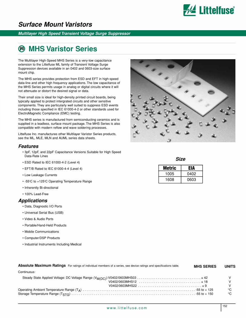
Surface Mount Varistors
152w w w. l i t t e l f u s e . c o m
Multilayer High Speed Transient Voltage Surge Suppressor
MHS Varistor SeriesThe Multilayer High-Speed MHS Series is a very-low capacitance extension to the Littelfuse ML family of Transient Voltage SurgeSuppression devices available in an 0402 and 0603-size surface mount chip.
The MHS series provides protection from ESD and EFT in high-speeddata-line and other high frequency applications. The low capacitance ofthe MHS Series permits usage in analog or digital circuits where it willnot attenuate or distort the desired signal or data.
Their small size is ideal for high-density printed circuit boards, being typically applied to protect intergrated circuits and other sensitive components. They are particularly well suited to suppress ESD eventsincluding those specified in IEC 61000-4-2 or other standards used forElectroMagnetic Compliance (EMC) testing.
The MHS series is manufactured from semiconducting ceramics and issupplied in a leadless, surface mount package. The MHS Series is alsocompatible with modern reflow and wave soldering processes.
Littelfuse Inc. manufactures other Multilayer Varistor Series products, see the ML, MLE, MLN and AUML series data sheets.
Features• 3pF, 12pF, and 22pF Capacitance Versions Suitable for High Speed
Data-Rate Lines
• ESD Rated to IEC 61000-4-2 (Level 4)
• EFT/B Rated to IEC 61000-4-4 (Level 4)
• Low Leakage Currents
• -55oC to +125oC Operating Temperature Range
• Inherently Bi-directional
• 100% Lead-Free
Applications• Data, Diagnostic I/O Ports
• Universal Serial Bus (USB)
• Video & Audio Ports
• Portable/Hand-Held Products
• Mobile Communications
• Computer/DSP Products
• Industrial Instruments Including Medical
Absolute Maximum Ratings For ratings of individual members of a series, see device ratings and specifications table.
Continuous:
Steady State Applied Voltage: DC Voltage Range (VM(DC)):V0402/0603MHS03 . . . . . . . . . . . . . . . . . . . . . . . . . . . . . . . . . . ≤ 42 VV0402/0603MHS12 . . . . . . . . . . . . . . . . . . . . . . . . . . . . . . . . . ≤ 18 VV0402/0603MHS22 . . . . . . . . . . . . . . . . . . . . . . . . . . . . . . . . . . ≤ 9 V
Operating Ambient Temperature Range (TA) . . . . . . . . . . . . . . . . . . . . . . . . . . . . . . . . . . . . . . . . . . . . . . . . . . . . . . . . . . . . -55 to + 125 OCStorage Temperature Range (TSTG) . . . . . . . . . . . . . . . . . . . . . . . . . . . . . . . . . . . . . . . . . . . . . . . . . . . . . . . . . . . . . . . . . . -55 to + 150 OC
MHS SERIES UNITS
Size
Metric EIA1005 04021608 0603
Pb
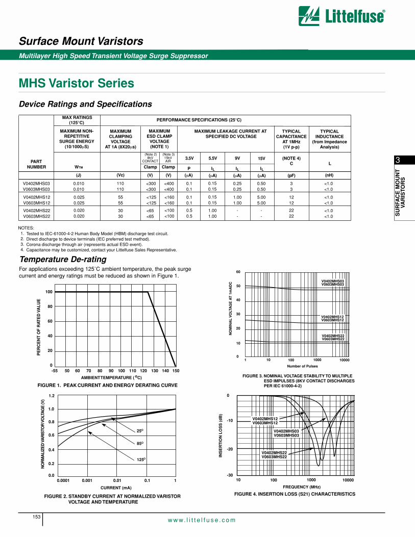
3
SU
RFA
CE
MO
UN
TVA
RIS
TOR
S
Surface Mount Varistors
153w w w. l i t t e l f u s e . c o m
Multilayer High Speed Transient Voltage Surge Suppressor
MHS Varistor Series
Device Ratings and Specifications
Temperature De-ratingFor applications exceeding 125˚C ambient temperature, the peak surgecurrent and energy ratings must be reduced as shown in Figure 1.
PARTNUMBER
MAX RATINGS(125°C)
PERFORMANCE SPECIFICATIONS (25°C)
MAXIMUMESD CLAMP
VOLTAGE(NOTE 1)
WTM Clamp
(Note 2)8kV
CONTACT
NOTES:1.2.
Tested to IEC-61000-4-2 Human Body Model (HBM) discharge test circuit.
3.Direct discharge to device terminals (IEC preferred test method).
4.Corona discharge through air (represents actual ESD event).Capacitance may be customized, contact your Littelfuse Sales Representative.
3.5V
V0402MHS12 0.025 <125 <160 0.1
V0402MHS03 0.010 <300 <400 0.1
MAXIMUM NON-REPETITIVE
SURGE ENERGY(10/1000µS)
Clamp
(Note 3)15kV AIR
MAXIMUM LEAKAGE CURRENT AT SPECIFIED DC VOLTAGE
5.5V 9V 15V
I L
(J) (V) (V) (µA) (µA) (µA) (µA)
TYPICALCAPACITANCE
AT 1MHz(1V p-p)
(NOTE 4)C
(pF)
TYPICALINDUCTANCE
(from ImpedanceAnalysis)
L
(nH)
0.15
0.15
1.00
0.25
5.00
0.50
12
3
<1.0
<1.0
MAXIMUMCLAMPINGVOLTAGE
AT 1A (8X20µs)
(Vc)
55
110
P I L I L
V0603MHS12
V0402MHS22V0603MHS22
0.025
0.0200.020
<125
<65<65
<160
<100<100
0.1
0.50.5
V0603MHS03 0.010 <300 <400 0.1
0.15
1.001.00
0.15
1.00
--
--
0.25
5.00
0.50
12
2222
3
<1.0
<1.0<1.0
<1.0
55
3030
110
100
80
60
40
20
0-55 50 60 70 80 90 100 110 120 130 140 150
PE
RC
EN
T O
F R
ATE
D V
AL
UE
AMBIENT TEMPERATURE ( oC)
FIGURE 1. PEAK CURRENT AND ENERGY DERATING CURVE
FIGURE 3. NOMINAL VOLTAGE STABILITY TO MULTIPLE ESD IMPULSES (8KV CONTACT DISCHARGES PER IEC 61000-4-2)
60
10
1
Number of Pulses
NO
MIN
AL
VO
LTA
GE
AT
1m
AD
C
10 100 1000 10000
20
30
40
50V0402MHS03
V0402MHS12
V0603MHS03
V0603MHS12
0
V0402MHS22V0603MHS22
1.2
0.00.0001
25
0.001 0.01 0.1 1
CURRENT (mA)
NO
RM
ALI
ZED
VA
RIS
TOR
VO
LTA
GE
(V)
FIGURE 2. STANDBY CURRENT AT NORMALIZED VARISTOR VOLTAGE AND TEMPERATURE
1.0
0.8
0.6
0.4
0.2
85
125
O
O
O
FIGURE 4. INSERTION LOSS (S21) CHARACTERISTICS
-30
FREQUENCY (MHz)
INS
ER
TIO
N L
OS
S (
dB
)
10 100 1000 10000
-20
-10
0
V0402MHS22V0603MHS22
V0402MHS12
V0402MHS03
V0603MHS12
V0603MHS03

Surface Mount VaristorsMultilayer High Speed Transient Voltage Surge Suppressor
154w w w. l i t t e l f u s e . c o m
MHS Varistor Series
Soldering RecommendationsThe principal techniques used for the soldering of components in surface mount technology are infared (IR) re-flow, vapour phase re-flowand wave soldering. Typical profiles are shown in Figures 5, 6 and 7.When wave soldering, the MHS suppressor is attached to the circuitboard by means of an adhesive. The assembly is then placed on aconveyor and run through the soldering process to contact the wave.
With IR and vapour phase re-flow, the device is placed in a solder pasteon a substrate. As the solder paste is heated, it re-flows and solders theunit to the board.
The recommended solder for the MHS suppressor is a 63/36/2(Sn/Pb/Ag), 60/40 (Sn/Pb) or 63/37 (Sn/Pb). Littelfuse alsorecommends an RMA solder flux.
Wave soldering is the most strenuous of the processes. To avoid thepossibility of generating stresses due to thermal shock, a preheat stagein the soldering process is recommended, and the peak temperature ofthe solder process should be rigidly controlled.
When using a re-flow process, care should be taken to ensure that theMHS chip is not subjected to a thermal gradient steeper than 4 degreesper second; the ideal gradient being 2 degrees per second. During thesoldering process, preheating within 100 degrees of the solder’s peaktemperature is essentail to minimize thermal shock. Examples of the sol-dering conditions for the MHS suppressor are given in the tables below.
Once the soldering process has been completed, it is still necessary to ensure that any further thermal shocks are avoided. One possiblecause of thermal shock is hot printed circuit boards being removed from the solder process and subjected to cleaning solvents at room temperature. The boards must be allowed to cool gradually to less than50˚C before cleaning.
Recommended Pad Outline
6.
7.
5.
DIMENSION A
mm
1.70 0.0200402
2.54 0.030
TABLE 1: PAD LAYOUT DIMENSIONS
0603
in
0.067
0.100
B
mm
0.510
0.760
in
0.610
0.890
C
mm
0.024
0.035
in
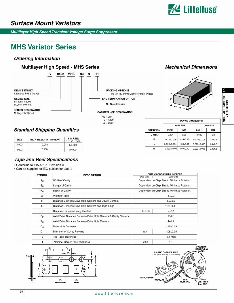
3
SU
RFA
CE
MO
UN
TVA
RIS
TOR
S
Surface Mount Varistors
155w w w. l i t t e l f u s e . c o m
Multilayer High Speed Transient Voltage Surge Suppressor
MHS Varistor Series
Ordering Information
V 0402
PACKING OPTIONSH: 7in (178mm) Diameter Reel (Note)
DEVICE FAMILYLittelfuse TVSS Device
H
DEVICE SIZE i.e. 40Mil x 20Mil(1.0mm x 0.5mm)
MHS 03 N
CAPACITANCE DESIGNATION
03 = 3pF12 = 12pF
END TERMINATION OPTION
N: Nickel Barrier
SERIES DESIGNATORMultilayer Hi-Speed
22 = 22pF
D
E
W
L
Mechanical Dimensions
7 INCH REEL ("H" OPTION)
10,000
SIZE
2,500
0402
0603
13 IN REEL"T" OPTION
10,000
50,000
Tape and Reel Specifications• Conforms to EIA-481-1, Revision A• Can be supplied to IEC publication 286-3
SYMBOL DESCRIPTION DIMENSIONS IN MILLIMETERS
A0 Width of Cavity Dependent on Chip Size to Minimize Rotation.
B0 Length of Cavity Dependent on Chip Size to Minimize Rotation.
K0 Depth of Cavity Dependent on Chip Size to Minimize Rotation.
W Width of Tape 8±0.2
F Distance Between Drive Hole Centers and Cavity Centers 3.5±.o5
E Distance Between Drive Hole Centers and Tape Edge 1.75±0.1
P1 Distance Between Cavity Centers 4±0.1
P2 Axial Drive Distance Between Drive Hole Centers & Cavity Centers 2±0.1
P0 Axial Drive Distance Between Drive Hole Centers 4±0.1
D0 Drive Hole Diameter 1.55±0.05
D1 Diameter of Cavity Piercing 1.05±0.05
T1 0.1 MaxTop Tape Thickness
0402 Size 0603 Size
2±0.05
N/A
Nominal Carrier Tape Thickness T 0.61 1.1
T
t1
D0 P0
P1 A0
P2
B0
F
E
W
PLASTIC CARRIER TAPE
EMBOSSMENTTOP TAPE 8mm
NOMINAL
PRODUCTIDENTIFYING
LABEL
178mmOR 330mmDIA. REEL
EMBOSSED PAPER (0402 SIZE ONLY)
DIMENSION
DEVICE DIMENSIONS
0402 SIZE
INCH MM
D Max. 0.024 0.60
E 0.10±0.006 0.25±0.15
L 0.039±0.004 1.00±0.10
W 0.020±0.004 0.50±0.10
0603 SIZE
INCH MM
0.035 0.9
0.015±0.008 0.4±0.2
0.063±0.006 1.6±1.5
0.032±0.006 0.8±1.5
Standard Shipping Quantities
Multilayer High Speed - MHS Series

Surface Mount Varistors
156w w w. l i t t e l f u s e . c o m
Multilayer Transient Voltage Suppressor
MLE Varistor SeriesThe MLE Series family of Transient Voltage Suppression devices are basedon the Littelfuse Multilayer fabrication technology. These components aredesigned to suppress ESD events, including those specified in IEC 61000-4-2 or other standards used for Electromagnetic Compliance testing. TheMLE Series is typically applied to protect integrated circuits and othercomponents at the circuit board level operating at 18VDC, or less.
The fabrication method and materials of these devices result in capaci-tance characteristics suitable for high frequency attenuation/low-pass filter circuit functions, thereby providing suppression and filtering in a single device.
The MLE Series is manufactured from semiconducting ceramics and is sup-plied in a leadless, surface mount package. The MLE Series is compatiblewith modern reflow and wave soldering procedures.
Littelfuse Inc. manufactures other Multilayer Series products. See the MLSeries data sheet for higher energy/peak current transient applications. Seethe AUML Series for automotive applications and the MLN Quad Array. Forhigh speed applications see the MHS series.
Features• Rated for ESD (IEC-61000-4-2)
• Characterized for Impedance and Capacitance
•-55oC to +125oC Operating Temperature Range
• Leadless 0402, 0603, 0805, and 1206 sizes
• Operating Voltages up to 18VM(DC)
• Multilayer Ceramic Construction Technology
• 100% Lead-Free
Applications• Protection of Components and Circuits Sensitive to ESD Transients
Occurring on Power Supplies, Control and Signal Lines
• Suppression of ESD Events Such as Specified in IEC-61000-4-2 or MIL-STD-883C Method-3015.7, for Electromagnetic Compliance (EMC)
• Used in Mobile Communications, Computer/EDP Products, MedicalProducts, Hand Held/Portable Devices, Industrial Equipment,Including Diagnostic Port Protection and I/O Interfaces
Size
Metric EIA1005 04021608 06032012 08053216 1206
Pb
3
SU
RFA
CE
MO
UN
TVA
RIS
TOR
S
Multilayer Transient Voltage Suppressor
Surface Mount Varistors
157w w w. l i t t e l f u s e . c o m
MLE Varistor Series
Absolute Maximum Ratings For ratings of individual members of a series, see device ratings and specifications table.
Continuous:Steady State Applied Voltage:DC Voltage Range (VM(DC)) . . . . . . . . . . . . . . . . . . . . . . . . . . . . . . . . . . . . . . . . . . . . . . . . . . . . . . . . . . . . . . . . . . . . . . . . . . ≤18 V
Operating Ambient Temperature Range (TA) . . . . . . . . . . . . . . . . . . . . . . . . . . . . . . . . . . . . . . . . . . . . . . . . . . . . . . . . . . . . . . -55 to + 125 OCStorage Temperature Range (TSTG). . . . . . . . . . . . . . . . . . . . . . . . . . . . . . . . . . . . . . . . . . . . . . . . . . . . . . . . . . . . . . . . . . . . -55 to + 150 OC
Device Ratings and Specifications
PARTNUMBER
MAX CONTINUOUSWORKING VOLTAGE
-55oC TO 125oC
PERFORMANCE SPECIFICATIONS (25oC)
NOMINALVOLTAGE
TYPICALCAPACITANCE
AT 1MHz
TYPICALLEAKAGE(NOTE 6)
(NOTE 1)VM(DC)
VNOM AT1mA DC IL
AT APPLIEDVOLTAGE
(V) MIN (V)MAX (V)
(NOTE 3)8kV CONTACT
Clamp(V)
(NOTE 4)15kV AIR
(pF) ( µA) VDC
V18MLE0603L 18 22 28 50at 1A
<100 0.1 3.5
0.3 5.5
5.0 15
25 18
V18MLE0805 18 22 28 50at 5A
<500 0.2 3.5
0.5 5.5
5.0 15
25 18
V18MLE0805L 18 22 28 50at 2A
<100 0.2 3.5
0.5 5.5
5.0 15
25 18
V18MLE1206 18 22 28 50at 10A
<1700 0.5 3.5
1.0 5.5
5.0 15
25 18
NOTES:1. For applications of 18VDC or less. Higher voltages available, contact your Littelfuse Sales Representative.2. Tested with IEC-61000-4-2 Human Body Model (HBM) discharge test circuit.3. Direct discharge to device terminals (IEC preferred test method).4. Corona discharge through air (represents actual ESD event).5. Capacitance may be customized, contact your Littelfuse Sales Representative.
V18MLE0603 18 22 28 50at 2A
<125 0.1 3.5
0.3 5.5
5.0 15
25 18
V18MLE0402 18 22 28 50at 1A
<140
<75
<135
<65
<85
<160 <40 0.1 3.5
0.3 5.5
2 15
10 18
MAXIMUM ESD CLAMP VOLTAGE (NOTE 2)
Clamp(V)
MAXIMUM CLAMPING VOLTAGE AT SPECIFIED
CURRENT (8/20µS)
(V)
Vc
<100
<70
<75
<65
<75
<125NEW
6. IL ratings at 18VDC are maximums, not typical.
MLE SERIES UNITS

MLE Varistor Series
Surface Mount VaristorsMultilayer Transient Voltage Suppressor
158w w w. l i t t e l f u s e . c o m
FIGURE 4. IMPEDANCE (Z) vs FREQUENCY TYPICAL CHARACTERISTIC
0.1
FREQUENCY (MHz)
IMP
ED
AN
CE
(Z
)
10 100 1000 10000
1
10
100
0.01
-0402
-0603
-0805
-1206
Typical Performance CurvesFor applications exceeding 1250C ambient temperature, the peak surge current and energy ratings must be reduced as shown in Figure 1.
1.2
0.00.0001
25
0.001 0.01 0.1 1
CURRENT (mA)
NO
RM
ALI
ZED
VA
RIS
TOR
VO
LTA
GE
(V)
FIGURE 3. STANDBY CURRENT AT NORMALIZED VARISTOR VOLTAGE AND TEMPERATURE
1.0
0.8
0.6
0.4
0.2
85
125
O
O
O
100
80
60
40
20
0-55 50 60 70 80 90 100 110 120 130 140 150
PE
RC
EN
T O
F R
ATE
D V
AL
UE
AMBIENT TEMPERATURE ( oC)
FIGURE 1. PEAK CURRENT AND ENERGY DERATING CURVE FIGURE 2. NOMINAL VOLTAGE STABILITY TO MULTIPLE ESD IMPULSES (8KV CONTACT DISCHARGES PER IEC 61000-4-2)
25
01
CURRENT (A)
NO
MIN
AL
VO
LTA
GE
AT
1m
AD
C
10 100 1000 10000
5
10
15
20
30

Multilayer Transient Voltage Suppressor
Surface Mount Varistors
159w w w. l i t t e l f u s e . c o m
MLE Varistor Series
Soldering RecommendationsThe principal techniques used for the soldering of components in surfacemount technology are Infrared (IR) re-flow, vapour phase re-flow, andwave soldering. When wave soldering, the MLE suppressor is attached to the circuit board by means of an adhesive. The assembly is thenplaced on a conveyor and run through the soldering process to contactthe wave. With IR and vapour phase re-flow, the device is placed in a solder paste on the substrate. As the solder paste is heated, it reflowsand solders the unit to the board.
The recommended solder for the MLE suppressor is a 62/36/2(Sn/Pb/Ag), 60/40 (Sn/Pb), or 63/37 (Sn/Pb). Littelfuse also recommends an RMA solder flux.
Wave soldering is the most strenuous of the processes. To avoid the possibility of generating stresses due to thermal shock, a preheat stagein the soldering process is recommended, and the peak temperature ofthe solder process should be rigidly controlled.
When using a reflow process, care should be taken to ensure that theMLE chip is not subjected to a thermal gradient steeper than 4 degreesper second; the ideal gradient being 2 degrees per second. During thesoldering process, preheating to within 100 degrees of the solder’s peaktemperature is essential to minimize thermal shock. Examples of the soldering conditions for the MLE series of suppressors are given in thetables below.
Once the soldering process has been completed, it is still necessary toensure that any further thermal shocks are avoided. One possible cause ofthermal shock is hot printed circuit boards being removed from the solderprocess and subjected to cleaning solvents at room temperature. Theboards must be allowed to cool gradually to less than 50oC before cleaning.
Termination OptionsLittelfuse offers three types of electrode termination finish for the MLE series:
1. Silver/Platinum
2. Silver/Palladium
3. Ni-Barrier (available for 0402-1206 package size)
(The ordering information section describes how to designate them.)
FIGURE 6. WAVE SOLDER PROFILE
FIGURE 7. VAPOR PHASE SOLDER PROFILE
TE
MP
ER
ATU
RE
(oC
)
TIME (MINUTES)
300
250
200
150
100
50
00 0.5 1.0 1.5 2.0 2.5 3.0 3.5 4.0 4.5
MAXIMUM WAVE 260oC
SECOND PREHEAT
FIRST PREHEAT
TE
MP
ER
ATU
RE
(oC
)
TIME (MINUTES)
250
200
150
100
50
00 0.5 1.0 1.5 2.0 2.5 3.0 3.5
RAMP RATE
PREHEAT ZONE
>50oC/s
MAXIMUMTEMPERATURE 222oC
40-80SECONDS
ABOVE 183oC
FIGURE 5. REFLOW SOLDER PROFILE
TE
MP
ER
ATU
RE
(oC
)
TIME (MINUTES)
250
200
150
100
50
00 0.5 1.0 1.5 2.0 2.5 3.0 3.5 4.0
MAXIMUM
PREHEAT DWELL
PREHEAT ZONE
TEMPERATURE 222oC
RAMP RATE<2oC/s
40-80SECONDS
ABOVE 183oC
3
SU
RFA
CE
MO
UN
TVA
RIS
TOR
S
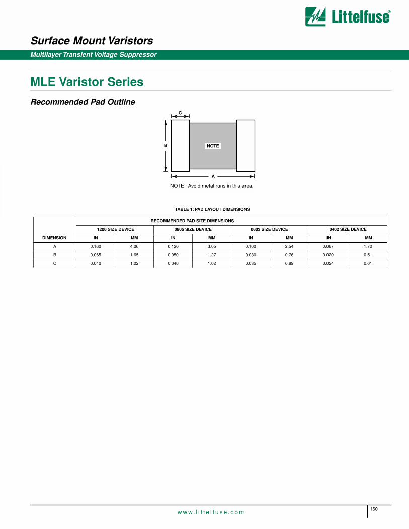
Surface Mount VaristorsMultilayer Transient Voltage Suppressor
160w w w. l i t t e l f u s e . c o m
MLE Varistor Series
Recommended Pad OutlineC
B
A
NOTE: Avoid metal runs in this area.
NOTE
DIMENSION
RECOMMENDED PAD SIZE DIMENSIONS
1206 SIZE DEVICE 0805 SIZE DEVICE 0603 SIZE DEVICE
IN MM IN MM IN MM
A 0.160 4.06 0.120 3.05 0.100 2.54
B 0.065 1.65 0.050 1.27 0.030 0.76
C 0.040 1.02 0.040 1.02 0.035 0.89
TABLE 1: PAD LAYOUT DIMENSIONS
0402 SIZE DEVICE
IN MM
0.067 1.70
0.020 0.51
0.024 0.61

3
SU
RFA
CE
MO
UN
TVA
RIS
TOR
S
Surface Mount Varistors
161w w w. l i t t e l f u s e . c o m
Multilayer Transient Voltage Suppressor
MLE Varistor Series
Standard Shipping Quantities
D
E
W
L
Mechanical Dimensions
DIMENSION
1206 SIZE 0805 SIZE 0603 SIZE
IN MM IN MM IN MM
E
0.071
L
0.02±0.01
W
0.125±0.012
DEVICE DIMENSIONS
0402 SIZE
IN MM
D Max
0.06±0.011
1.80
0.50±0.25
3.20±0.03
1.60±0.28
0.043
0.02±0.01
0.079±0.008
0.049±0.008
1.1
0.50±0.25
2.01±0.2
1.25±0.2
0.035
0.015±0.008
0.063±0.006
0.032±0.006
0.9
0.4±0.2
1.6±0.15
0.8±0.15
0.024
0.010±0.006
0.039±0.004
0.020±0.004
0.6
0.25±0.15
1.0±0.1
0.5±0.1
V 18 1206
PACKING OPTIONSA: Bulk Pack (not 0402 size) H: 7in (178mm) Diameter Reel T: 13in (330mm) Diameter Reel
DEVICE SIZE:i.e., 120 mil x 60 mil
DEVICE FAMILYLittelfuse TVSS Device
X
MAXIMUM DC WORKING VOLTAGE
MLE X X
CAPACITANCE OPTIONNo Letter: Standard
L: Low Capacitance Version
END TERMINATION OPTIONNo Letter: Ag/Pt
W: Ag/PdMULTILAYER SERIESDESIGNATOR
(3mm x 1.5mm)
(not 0402 size)
N: Nickel Barrier (0402-1206)
Ordering InformationVXXMLE TYPES
DEVICE SIZE “13” INCH REEL (“T” OPTION) “7” INCH REEL (“H” OPTION) BULK PACK (“A” OPTION)
1206 10,000 2,500 2500
0805 10,000 2,500 2500
0603 10,000 2,500 2500
0402 N/A N/A10,000

Surface Mount Varistors
162w w w. l i t t e l f u s e . c o m
Multilayer Transient Voltage Suppressor
MLE Varistor Series
Tape and Reel Specifications• Conforms to EIA - 481-1, Revision A
• Can be supplied to IEC publication 286 - 3
SYMBOL DESCRIPTION DIMENSIONS IN MILLIMETERS
A0 Width of Cavity Dependent on Chip Size to Minimize Rotation.
B0 Length of Cavity Dependent on Chip Size to Minimize Rotation.
K0 Depth of Cavity Dependent on Chip Size to Minimize Rotation.
W Width of Tape 8 ±0.2
F Distance Between Drive Hole Centers and Cavity Centers 3.5 ±0.05
E Distance Between Drive Hole Centers and Tape Edge 1.75 ±0.1
P1 Distance Between Cavity Centers 4 ±0.1
P2 Axial Drive Distance Between Drive Hole Centers & Cavity Centers 2 ±0.1
P0 Axial Drive Distance Between Drive Hole Centers 4 ±0.1
D0 Drive Hole Diameter 1.55 ±0.05
D1 Diameter of Cavity Piercing 1.05 ±0.05
T1 0.1 MaxTop Tape Thickness
0402 Size 0603, 0805, & 1206 Sizes
2±0.05
N/A
K0
t1
D0 P0
D1P1 A0
P2
B0
F
E
W
PLASTIC CARRIER TAPE
EMBOSSMENTTOP TAPE 8mm
NOMINAL
PRODUCTIDENTIFYING
LABEL
178mmOR 330mmDIA. REEL
EMBOSSED PAPER (0402 SIZE ONLY)

3
SU
RFA
CE
MO
UN
TVA
RIS
TOR
S
Surface Mount Varistors
163w w w. l i t t e l f u s e . c o m
Multilayer Transient Voltage Surge Suppressors
Size
ML Varistor SeriesThe ML Series family of Transient Voltage Surge Suppression devices isbased on the Littelfuse Multilayer fabrication technology. These compo-nents are designed to suppress a variety of transient events, includingthose specified in IEC 61000-4-2 or other standards used for ElectromagneticCompliance (EMC). The ML Series is typically applied to protect integratedcircuits and other components at the circuit board level.
The wide operating voltage and energy range make the ML Series suit-able for numerous applications on power supply, control and signal lines.
The ML Series is manufactured from semiconducting ceramics, and issupplied in a leadless, surface mount package. The ML Series is compat-ible with modern reflow and wave soldering procedures.
It can operate over a wider temperature range than zener diodes, andhas a much smaller footprint than plastic-housed components.
Littelfuse Inc. manufactures other Multilayer Series products. See theMLE Series data sheet for ESD applications, MHS Series data sheet forhigh-speed ESD applications, the MLN for multiline protection and theAUML Series for automotive applications.
Features• Leadless 0402, 0603, 0805, 1206 and 1210 Chip Sizes
• Multilayer Ceramic Construction Technology
•-55oC to +125oC Operating Temperature Range
• Operating Voltage Range VM(DC) = 5.5V to 120V
• Rated for Surge Current (8 x 20µs)
• Rated for Energy (10 x 1000µs)
• Inherent Bi-directional Clamping
• No Plastic or Epoxy Packaging Assures Better than 94V-0Flammability Rating
• Standard Low Capacitance Types Available
• 100% Lead-Free
Applications• Suppression of Inductive Switching or Other Transient Events Such
as EFT and Surge Voltage at the Circuit Board Level
• ESD Protection for Components Sensitive to IEC 61000-4-2, MIL-STD-883C Method 3015.7, and Other Industry Specifications (See Also the MLE or MLN Series)
• Provides On-Board Transient Voltage Protection for ICs and Transistors
• Used to Help Achieve Electromagnetic Compliance of End Products
• Replace Larger Surface Mount TVS Zeners in Many Applications
Metric EIA1005 04021608 06032012 08053216 12063225 12104532 18125650 2220
Pb

Surface Mount Varistors
164w w w. l i t t e l f u s e . c o m
Multilayer Transient Voltage Surge Suppressors
Absolute Maximum Ratings For ratings of individual members of a series, see Device Ratings and Specifications table.
Continuous:Steady State Applied Voltage:
DC Voltage Range (VM(DC)). . . . . . . . . . . . . . . . . . . . . . . . . . . . . . . . . . . . . . . . . . . . . . . . . . . . . . . . . . . . . . . . . . . . . . . . . 3.5 to 120 VAC Voltage Range (VM(AC)RMS) . . . . . . . . . . . . . . . . . . . . . . . . . . . . . . . . . . . . . . . . . . . . . . . . . . . . . . . . . . . . . . . . . . . . . 2.5 to 107 V
Transient:Non-Repetitive Surge Current, 8/20µs Waveform, (ITM) . . . . . . . . . . . . . . . . . . . . . . . . . . . . . . . . . . . . . . . . . . . . . . . . . . . . . 4 to 500 ANon-Repetitive Surge Energy, 10/1000µs Waveform, (WTM) . . . . . . . . . . . . . . . . . . . . . . . . . . . . . . . . . . . . . . . . . . . . . . . . . 0.02 to 1.2 J
Operating Ambient Temperature Range (TA) . . . . . . . . . . . . . . . . . . . . . . . . . . . . . . . . . . . . . . . . . . . . . . . . . . . . . . . . . . . . . . -55 to + 125 OCStorage Temperature Range (TSTG) . . . . . . . . . . . . . . . . . . . . . . . . . . . . . . . . . . . . . . . . . . . . . . . . . . . . . . . . . . . . . . . . . . . . -55 to + 150 OCTemperature Coefficient (αV) of Clamping Voltage (VC) at Specified Test Current . . . . . . . . . . . . . . . . . . . . . . . . . . . . . . . . . . . . . <0.01 %/OC
Device Ratings and Specifications
ML SERIES UNITS
ML Varistor Series
PARTNUMBER
MAXIMUM RATINGS (125oC) SPECIFICATIONS (25oC)
MAXIMUMCONTINUOUS
WORKINGVOLTAGE
MAXIMUMNON-
REPETITIVESURGE
CURRENT(8/20µs)
MAXIMUMNON-
REPETITIVESURGE
ENERGY(10/1000µs)
MAXIMUMCLAMPING
VOLTAGE AT10A
(OR AS NOTED)(8/20µs)
NOMINAL VOLTAGEAT 1mA DC TEST
CURRENT
TYPICALCAPACITANCE
AT f = 1MHz
VM(DC) VM(AC) ITM WTM VC
VN(DC)
MIN
VN(DC)
MAX C
(V) (V) (A) (J) (V) (V) (V) (pF)
V3.5MLA0603 3.5 2.5 30 0.1 10 at 2A 3.7 7.0 1100
V3.5MLA0805 3.5 2.5 120 0.3 10 at 5A 3.7 7.0 2200
V3.5MLA0805L 3.5 2.5 40 0.1 10 at 2A 3.7 7.0 1200
V3.5MLA1206 3.5 2.5 100 0.3 14 3.7 7.0 6000
V5.5MLA0402 5.5 4.0 20 0.050 15.5 at 1A 7.1 9.3 220
V9MLA0402 9 6.5 20 0.050 22 at 1A 11 14 120
V9MLA0402L 9 6.5 4 0.020 25 at 1A 11 14 33
V14MLA0402 14 10 20 0.050 30 at 1A 15.9 20.3 70
V5.5MLA0603 5.5 4.0 30 0.1 15.5 at 2A 7.1 9.3 660
V5.5MLA0805 5.5 4.0 120 0.3 15.5 at 5A 7.1 9.3 1600
V5.5MLA0805L 5.5 4.0 40 0.1 15.5 at 2A 7.1 9.3 860
V5.5MLA1206 5.5 4.0 150 0.4 15.5 7.1 9.3 4500
V9MLA0603 9.0 6.5 30 0.1 23 at 2A 11.0 16.0 420
V9MLA0805L 9.0 6.5 40 0.1 20 at 2A 11 14 450
V12MLA0805L 12 9.0 40 0.1 25 at 2A 14 18.5 350
V14MLA0603 14 10 30 0.1 30 at 2A 15.9 20.3 150
V14MLA0805 14 10 120 0.3 30 at 5A 15.9 20.3 480
V14MLA0805L 14 10 40 0.1 30 at 2A 15.9 20.3 270
V14MLA1206 14 10 150 0.4 30 15.9 20.3 1600
NEW
NEW
NEW
NEW
V5.5MLA0402L 5.5 4.0 20 0.050 30 at 1A 15.9 20.3 70NEW
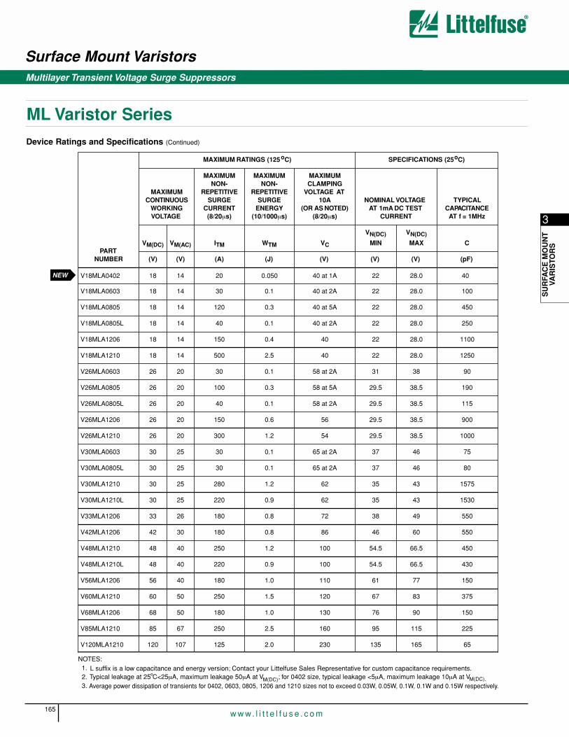
Surface Mount Varistors
165w w w. l i t t e l f u s e . c o m
3
SU
RFA
CE
MO
UN
TVA
RIS
TOR
S
Multilayer Transient Voltage Surge Suppressors
ML Varistor SeriesDevice Ratings and Specifications (Continued)
V18MLA0603 18 14 30 0.1 40 at 2A 22 28.0 100
V18MLA0402 18 14 20 0.050 40 at 1A 22 28.0 40
V18MLA0805 18 14 120 0.3 40 at 5A 22 28.0 450
V18MLA0805L 18 14 40 0.1 40 at 2A 22 28.0 250
V18MLA1206 18 14 150 0.4 40 22 28.0 1100
V18MLA1210 18 14 500 2.5 40 22 28.0 1250
V26MLA0603 26 20 30 0.1 58 at 2A 31 38 90
V26MLA0805 26 20 100 0.3 58 at 5A 29.5 38.5 190
V26MLA0805L 26 20 40 0.1 58 at 2A 29.5 38.5 115
V26MLA1206 26 20 150 0.6 56 29.5 38.5 900
V26MLA1210 26 20 300 1.2 54 29.5 38.5 1000
V30MLA0603 30 25 30 0.1 65 at 2A 37 46 75
V30MLA0805L 30 25 30 0.1 65 at 2A 37 46 80
V30MLA1210 30 25 280 1.2 62 35 43 1575
V30MLA1210L 30 25 220 0.9 62 35 43 1530
V33MLA1206 33 26 180 0.8 72 38 49 550
V42MLA1206 42 30 180 0.8 86 46 60 550
V48MLA1210 48 40 250 1.2 100 54.5 66.5 450
V48MLA1210L 48 40 220 0.9 100 54.5 66.5 430
V56MLA1206 56 40 180 1.0 110 61 77 150
V60MLA1210 60 50 250 1.5 120 67 83 375
V68MLA1206 68 50 180 1.0 130 76 90 150
V85MLA1210 85 67 250 2.5 160 95 115 225
V120MLA1210 120 107 125 2.0 230 135 165 65
NOTES:1.2.3.
PARTNUMBER
MAXIMUM RATINGS (125oC) SPECIFICATIONS (25oC)
MAXIMUMCONTINUOUS
WORKINGVOLTAGE
MAXIMUMNON-
REPETITIVESURGE
CURRENT(8/20µs)
MAXIMUMNON-
REPETITIVESURGE
ENERGY(10/1000µs)
MAXIMUMCLAMPING
VOLTAGE AT10A
(OR AS NOTED)(8/20µs)
NOMINAL VOLTAGEAT 1mA DC TEST
CURRENT
TYPICALCAPACITANCE
AT f = 1MHz
VM(DC) VM(AC) ITM WTM VC
VN(DC)
MIN
VN(DC)
MAX C
(V) (V) (A) (J) (V) (V) (V) (pF)
L suffix is a low capacitance and energy version; Contact your Littelfuse Sales Representative for custom capacitance requirements. Typical leakage at 25 C<25µA, maximum leakage 50µA at V ; for 0402 size, typical leakage <5µA, maximum leakage 10µA at V o
M(DC) M(DC). Average power dissipation of transients for 0402, 0603, 0805, 1206 and 1210 sizes not to exceed 0.03W, 0.05W, 0.1W, 0.1W and 0.15W respectively.
NEW

Surface Mount Varistors
166w w w. l i t t e l f u s e . c o m
Multilayer Transient Voltage Surge Suppressors
Temperature De-ratingWhen transients occur in rapid succession, the average power dissipa-tion is the energy (watt-seconds) per pulse times the number of pulsesper second. The power so developed must be within the specificationsshown on the Device Ratings and Specifications table for the specificdevice. For applications exceeding 125oC ambient temperature, the peaksurge current and energy ratings must be derated as shown in Figure 1.
100
80
60
40
20
0-55 50 60 70 80 90 100 110 120 130 140 150
PE
RC
EN
T O
F R
ATE
D V
AL
UE
AMBIENT TEMPERATURE ( oC)
FIGURE 1. PEAK CURRENT AND ENERGY DERATING CURVE
t1
t2
100
50
0
O1 TIME
PE
RC
EN
T O
F P
EA
K V
AL
UE
O1 = VIRTUAL ORIGIN OF WAVE
t1 = VIRTUAL FRONT TIME = 1.25 x t
(IMPULSE DURATION)
t = TIME FROM 10% TO 90% OF PEAK
t2 = VIRTUAL TIME TO HALF VALUE
EXAMPLE:FOR AN 8/20µs CURRENT WAVEFORM8µs = t1 = VIRTUAL FRONT TIME
20µs = t2 = VIRTUAL TIME TOHALF VALUE
FIGURE 2. PEAK PULSE CURRENT TEST WAVEFORM FOR CLAMPING VOLTAGE
t
FIGURE 3. LIMIT V-I CHARACTERISTIC FOR V5.5MLA0402 TO V18MLA0402
100
10
1µA
CURRENT (A)
Va
ris
tor
Vo
ltag
e (
V) MAXIMUM LEAKAGE
10µA 100µA 1mA 10mA 100mA 1A 10A 100A
MAXIMUM CLAMPING VOLTAGE
V18MLA0402V14MLA0402V09MLA0402V5.5MLA0402
ML Varistor Series
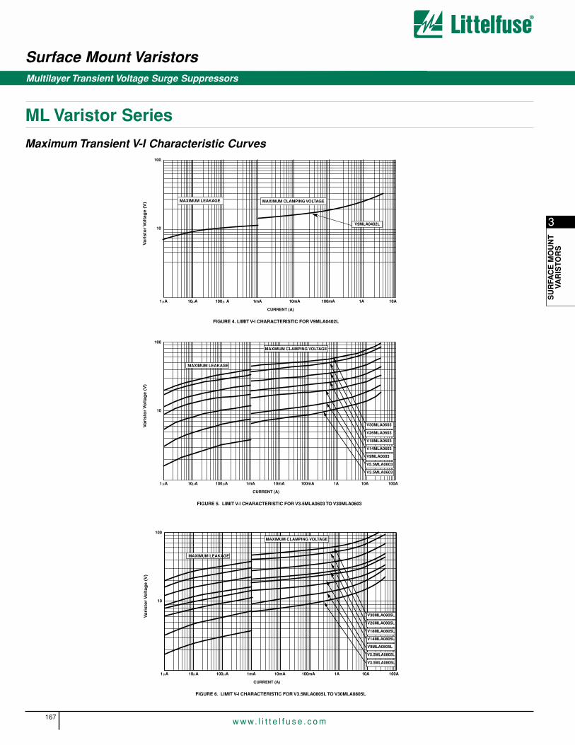
Surface Mount Varistors
167w w w. l i t t e l f u s e . c o m
3
SU
RFA
CE
MO
UN
TVA
RIS
TOR
S
Multilayer Transient Voltage Surge Suppressors
ML Varistor Series
Maximum Transient V-I Characteristic Curves
FIGURE 5. LIMIT V-I CHARACTERISTIC FOR V3.5MLA0603 TO V30MLA0603
100
10
1µA
CURRENT (A)
Va
ris
tor
Vo
ltag
e (
V)
V3.5MLA0603
MAXIMUM LEAKAGE
MAXIMUM CLAMPING VOLTAGE
V5.5MLA0603
V9MLA0603
10µA 100µA 1mA 10mA 100mA 1A 10A 100A
V14MLA0603
V18MLA0603
V26MLA0603
V30MLA0603
FIGURE 6. LIMIT V-I CHARACTERISTIC FOR V3.5MLA0805L TO V30MLA0805L
100
10
1µA
CURRENT (A)
Va
ris
tor
Vo
ltag
e (
V)
V3.5MLA0805L
MAXIMUM LEAKAGE
MAXIMUM CLAMPING VOLTAGE
V5.5MLA0805L
V9MLA0805L
10µA 100µA 1mA 10mA 100mA 1A 10A 100A
V14MLA0805L
V18MLA0805L
V26MLA0805L
V30MLA0805L
FIGURE 4. LIMIT V-I CHARACTERISTIC FOR V9MLA0402L
100
10
1µA
CURRENT (A)
Va
ris
tor
Vo
ltag
e (
V)
10µA 100µ A 1mA 10mA 100mA 1A 10A
MAXIMUM LEAKAGE MAXIMUM CLAMPING VOLTAGE
V9MLA0402L

Surface Mount Varistors
168w w w. l i t t e l f u s e . c o m
Multilayer Transient Voltage Surge Suppressors
Maximum Transient V-I Characteristic Curves (Continued)
FIGURE 7. LIMIT V-I CHARACTERISTIC FOR V3.5MLA0805 TO V26MLA0805
1mA
100
10
1µA
CURRENT (A)
Var
isto
r Vo
ltag
e (V
)
10µA 100µA 10mA 100mA 1A 10A 100A 1000A
V3.5MLA0805
MAXIMUM CLAMPING VOLTAGE
MAXIMUM LEAKAGE
V14MLA0805
V5.5MLA0805
V18MLA0805
V26MLA0805
FIGURE 9. LIMIT V-I CHARACTERISTIC FOR V18MLA1210 TO V120MLA1210
1mA
100
10
1µA
CURRENT (A)
Var
isto
r Vo
ltag
e (V
)
10µA 100µA 10mA 100mA 1A 10A 100A 1000A
MAXIMUM CLAMPING VOLTAGE
MAXIMUM LEAKAGE
1000
1
V60MLA1210
V85MLA1210
V120MLA1210
V48MLA1210, V48MLA1210L
V30MLA1210, V30MLA1210L
V26MLA1210
V18MLA1210
FIGURE 8. LIMIT V-I CHARACTERISTIC FOR V3.5MLA1206 TO V68MLA1206
1mA1µA
CURRENT (A)
Vari
sto
r V
olt
ag
e (
V)
10mA 1000A100mA 1A 10A 100A
MAXIMUM CLAMPVOLTAGE
10µA 100µA
MAXIMUMLEAKAGE
V56MLA1206V42MLA1206
V26MLA1206V33MLA1206
V18MLA1206
V68MLA1206
V3.5MLA1206
V5.5MLA1206V14MLA1206
100
10
1
1000
ML Varistor Series

Surface Mount Varistors
169w w w. l i t t e l f u s e . c o m
3
SU
RFA
CE
MO
UN
TVA
RIS
TOR
S
Multilayer Transient Voltage Surge Suppressors
ML Varistor Series
Device CharacteristicsAt low current levels, the V-I curve of the multilayer transient voltage suppressor approaches a linear (ohmic) relationship and shows atemperature dependent effect (Figure 10). At or below the maximum
working voltage, the suppressor is in a high resistance mode (approach-ing 106Ω at its maximum rated working voltage). Leakage currents atmaximum rated voltage are below 50µA, typically 25µA; for 0402 sizebelow 10µA, typically 5µA.
Speed of ResponseThe Multilayer Suppressor is a leadless device. Its response time is notlimited by the parasitic lead inductances found in other surface mountpackages. The response time of the Zinc Oxide dielectric material is lessthan 1 nanosecond and the ML can clamp very fast dV/dT events suchas ESD. Additionally, in “real world” applications, the associated circuitwiring is often the greatest factor effecting speed of response. Therefore,transient suppressor placement within a circuit can be considered important in certain instances.
100%
1E-9 1E-8
SUPPRESSOR CURRENT (ADC)
10%1E-7 1E-6 1E-5 1E-4 1E-3 1E-2
25 50 75 100 125oCSU
PP
RE
SS
OR
VO
LTA
GE
IN P
ER
CE
NT
OF
VN
OM
VA
LU
E A
T 2
5oC
(%
)
FIGURE 10. TYPICAL TEMPERATURE DEPENDANCE OF THE CHARACTERISTIC CURVE IN THE LEAKAGE REGION
oooo
GRAINS
DEPLETION
FIRED CERAMICDIELECTRIC
REGION
METALELECTRODES
DEPLETION
REGION
METAL ENDTERMINATION
FIGURE 11. MULTILAYER INTERNAL CONSTRUCTION
Energy Absorption/Peak Current CapabilityEnergy dissipated within the ML is calculated by multiplying the clampingvoltage, transient current and transient duration. An important advantage of the multilayer is its interdigitated electrode construction within the massof dielectric material. This results in excellent current distribution and thepeak temperature per energy absorbed is very low. The matrix of semicon-ducting grains combine to absorb and distribute transient energy (heat)(Figure 11). This dramatically reduces peak temperature; thermal stressesand enhances device reliability.
As a measure of the device capability in energy and peak current handling, the V26MLA1206A part was tested with multiple pulses at its peak current rating (150A, 8/20µs). At the end of the test, 10,000 pulseslater, the device voltage characteristics are still well within specification(Figure 13).
100
1020
V26MLA1206
40 60 80 100 120 140TEMPERATURE (oC)
CL
AM
PIN
G V
OLT
AG
E (
V)
V5.5MLA1206
0-20-40-60
FIGURE 12. CLAMPING VOLTAGE OVER TEMPERATURE(VC AT 10A)
100
100
V26MLA1206
2000 4000 6000 8000 10000 12000
NUMBER OF PULSES
VOLT
AG
E
FIGURE 13. REPETITIVE PULSE CAPABILITY
PEAK CURRENT = 150A8/20µs DURATION, 30s BETWEEN PULSES
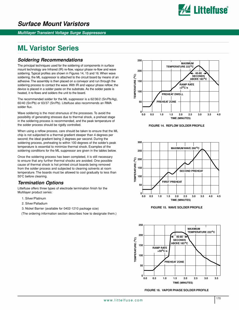
Surface Mount Varistors
170w w w. l i t t e l f u s e . c o m
Multilayer Transient Voltage Surge Suppressors
Soldering RecommendationsThe principal techniques used for the soldering of components in surfacemount technology are Infrared (IR) re-flow, vapour phase re-flow and wavesoldering. Typical profiles are shown in Figures 14, 15 and 16. When wavesoldering, the ML suppressor is attached to the circuit board by means of anadhesive. The assembly is then placed on a conveyor and run through thesoldering process to contact the wave. With IR and vapour phase reflow; thedevice is placed in a solder paste on the substrate. As the solder paste isheated, it re-flows and solders the unit to the board.
The recommended solder for the ML suppressor is a 62/36/2 (Sn/Pb/Ag),60/40 (Sn/Pb) or 63/37 (Sn/Pb). Littelfuse also recommends an RMA solder flux.
Wave soldering is the most strenuous of the processes. To avoid the possibility of generating stresses due to thermal shock, a preheat stage in the soldering process is recommended, and the peak temperature ofthe solder process should be rigidly controlled.
When using a reflow process, care should be taken to ensure that the MLchip is not subjected to a thermal gradient steeper than 4 degrees persecond; the ideal gradient being 2 degrees per second. During the soldering process, preheating to within 100 degrees of the solder’s peaktemperature is essential to minimize thermal shock. Examples of the soldering conditions for the ML suppressor are given in the tables below.
Once the soldering process has been completed, it is still necessary to ensure that any further thermal shocks are avoided. One possiblecause of thermal shock is hot printed circuit boards being removed from the solder process and subjected to cleaning solvents at room temperature. The boards must be allowed to cool gradually to less than50oC before cleaning.
Termination OptionsLittelfuse offers three types of electrode termination finish for theMultilayer product series:
1. Silver/Platinum
2. Silver/Palladium
3. Nickel Barrier (available for 0402-1210 package size)
(The ordering information section describes how to designate them.)
FIGURE 14. REFLOW SOLDER PROFILE
FIGURE 15. WAVE SOLDER PROFILE
FIGURE 16. VAPOR PHASE SOLDER PROFILE
TE
MP
ER
ATU
RE
(oC
)
TIME (MINUTES)
300
250
200
150
100
50
00.0 0.5 1.0 1.5 2.0 2.5 3.0 3.5 4.0 4.5
MAXIMUM WAVE 260oC
SECOND PREHEAT
FIRST PREHEAT
TE
MP
ER
ATU
RE
(oC
)
TIME (MINUTES)
250
200
150
100
50
00.0 0.5 1.0 1.5 2.0 2.5 3.0 3.5
RAMP RATE
PREHEAT ZONE
>50oC/s
MAXIMUMTEMPERATURE 222oC
40-80SECONDS
ABOVE 183oC
TE
MP
ER
ATU
RE
(oC
)
TIME (MINUTES)
250
200
150
100
50
00.0 0.5 1.0 1.5 2.0 2.5 3.0 3.5 4.0
MAXIMUM
PREHEAT DWELL
PREHEAT ZONE
TEMPERATURE 222oC
RAMP RATE<2oC/s
40-80SECONDS
ABOVE 183oC
ML Varistor Series
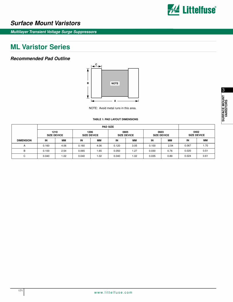
Surface Mount Varistors
171w w w. l i t t e l f u s e . c o m
3
SU
RFA
CE
MO
UN
TVA
RIS
TOR
S
Multilayer Transient Voltage Surge Suppressors
ML Varistor Series
Recommended Pad OutlineC
B
A
NOTE: Avoid metal runs in this area.
NOTE
DIMENSION
PAD SIZE
1210SIZE DEVICE
1206 SIZE DEVICE
0805 SIZE DEVICE
0603 SIZE DEVICE
IN MM IN MM IN MM IN MM
A 0.160 4.06 0.160 4.06 0.120 3.05 0.100 2.54
B 0.100 2.54 0.065 1.65 0.050 1.27 0.030 0.76
C 0.040 1.02 0.040 1.02 0.040 1.02 0.035 0.89
TABLE 1: PAD LAYOUT DIMENSIONS
0402 SIZE DEVICE
IN MM
0.067 1.70
0.020 0.51
0.024 0.61
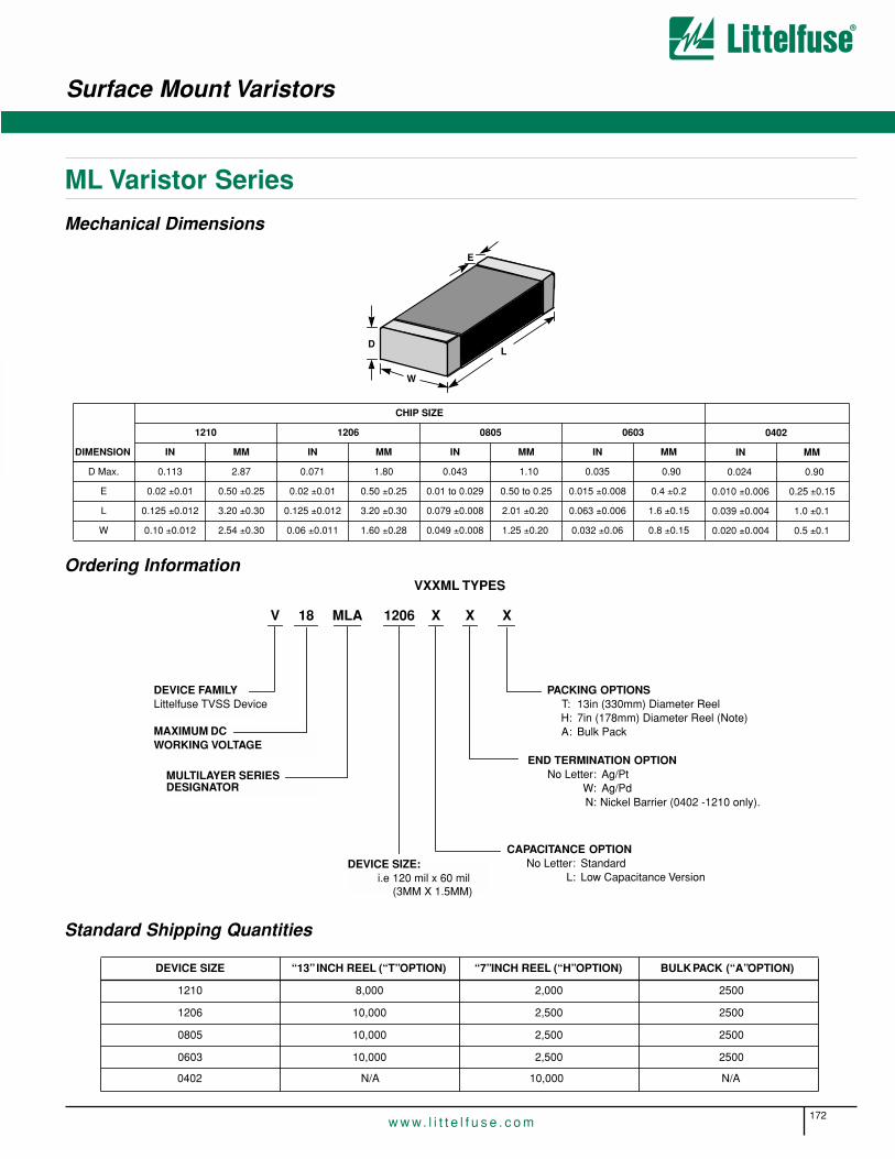
Surface Mount Varistors
172w w w. l i t t e l f u s e . c o m
Ordering InformationVXXML TYPES
E
L
W
D
Mechanical Dimensions
V 18 1206
PACKING OPTIONST: 13in (330mm) Diameter Reel H: 7in (178mm) Diameter Reel (Note)A: Bulk Pack
DEVICE SIZE:i.e 120 mil x 60 mil
DEVICE FAMILYLittelfuse TVSS Device
X
MAXIMUM DC WORKING VOLTAGE
MLA X X
CAPACITANCE OPTIONNo Letter: Standard
L: Low Capacitance Version
END TERMINATION OPTIONNo Letter: Ag/Pt
W: Ag/PdMULTILAYER SERIESDESIGNATOR
(3MM X 1.5MM)
N: Nickel Barrier (0402 -1210 only).
DIMENSION
CHIP SIZE
1210 1206 0805 0603
IN MM IN MM IN MM IN MM
D Max. 0.113 2.87 0.071 1.80 0.043 1.10 0.035 0.90
E 0.02 ±0.01 0.50 ±0.25 0.02 ±0.01 0.50 ±0.25 0.01 to 0.029 0.50 to 0.25 0.015 ±0.008 0.4 ±0.2
L 0.125 ±0.012 3.20 ±0.30 0.125 ±0.012 3.20 ±0.30 0.079 ±0.008 2.01 ±0.20 0.063 ±0.006 1.6 ±0.15
W 0.10 ±0.012 2.54 ±0.30 0.06 ±0.011 1.60 ±0.28 0.049 ±0.008 1.25 ±0.20 0.032 ±0.06 0.8 ±0.15
0402
IN MM
0.024 0.90
0.010 ±0.006 0.25 ±0.15
0.039 ±0.004 1.0 ±0.1
0.020 ±0.004 0.5 ±0.1
Standard Shipping Quantities
DEVICE SIZE “13” INCH REEL (“T” OPTION) “7” INCH REEL (“H” OPTION) BULK PACK (“A” OPTION)
1210 8,000 2,000 2500
1206 10,000 2,500 2500
0805 10,000 2,500 2500
0603 10,000 2,500 2500
0402 N/A 10,000 N/A
ML Varistor Series

3
SU
RFA
CE
MO
UN
TVA
RIS
TOR
S
Surface Mount Varistors
173w w w. l i t t e l f u s e . c o m
Multilayer Transient Voltage Surge Suppressors
ML Varistor Series
Tape and Reel Specifications• Conforms to EIA - 481-1, Revision A
• Can be supplied to IEC Publication 286 - 3
SYMBOL DESCRIPTION DIMENSIONS IN MILLIMETERS
A0 Width of Cavity Dependent on Chip Size to Minimize Rotation.
B0 Length of Cavity Dependent on Chip Size to Minimize Rotation.
K0 Depth of Cavity Dependent on Chip Size to Minimize Rotation.
W Width of Tape 8 ±0.2
F Distance Between Drive Hole Centers and Cavity Centers 3.5 ±0.05
E Distance Between Drive Hole Centers and Tape Edge 1.75 ±0.1
P1 Distance Between Cavity Centers 4 ±0.1
P2 Axial Drive Distance Between Drive Hole Centers & Cavity Centers 2 ±0.1
P0 Axial Drive Distance Between Drive Hole Centers 4 ±0.1
D0 Drive Hole Diameter 1.55 ±0.05
D1 Diameter of Cavity Piercing 1.05 ±0.05
T1 0.1 MaxTop Tape Thickness
0402 Size 0603, 0805, 1206 & 1210 Sizes
2±0.05
N/A
K0
t1
D0 P0
D1P1 A0
P2
B0
F
E
W
PLASTIC CARRIER TAPE
EMBOSSMENTTOP TAPE 8mm
NOMINAL
PRODUCTIDENTIFYING
LABEL
178mmOR 330mmDIA. REEL
EMBOSSED PAPER (0402 SIZE ONLY)

Surface Mount Varistors
174w w w. l i t t e l f u s e . c o m
Multiline Transient Voltage Surge Suppressor
MLN SurgeArray™ SuppressorThe MLN SurgeArray™ Suppressor is designed to help protect compo-nents from transient voltages that exist at the circuit board level. Thisdevice provides four independent suppressors in a single “1206” leadlesschip in order to reduce part count and placement time as well as savespace on printed circuit boards.
SurgeArray™ devices are intended to suppress ESD, EFT and other transients in order to protect integrated circuits or other sensitive components operating at any voltage up to 18VDC. SurgeArray devicesare rated to the IEC 61000-4-2 human body model ESD to help productsattain EMC compliance. The array offers excellent isolation and lowcrosstalk between sections.
The inherent capacitance of the SurgeArray Suppressor permits it to function as a filter/suppressor, thereby replacing separate zener/capacitor combinations.
The MLN array is manufactured using the Littelfuse Multilayer technologyprocess and is similar to the Littelfuse ML and MLE Series of discreteleadless chips.
The MLN can also be provided in a Dual version. Contact Littelfuse for information.
Features• Four Individual Devices in One 1206 Chip
• ESD Rated to IEC 61000-4-2 (Level 4)
• AC Characterized for Impedance and Capacitance
• Low Adjacent Channel Crosstalk, -55dB at 10MHz (Typ)
• Low Leakage (6nA at 5.5V, 30nA at 15V)
• Operating Voltage up to 18VM(DC)
• -55oC to 125oC Operating Temperature Range
• Low-Profile, PCMCIA Compatible
• 100% Lead-Free
Applications• Data, Diagnostic I/O Ports
• Analog Signal/Sensor Lines
• Portable/Hand-Held Products
• Mobile Communications/Cellular Phones
• Computer/DSP Products
• Industrial Instruments Including Medical
Pb
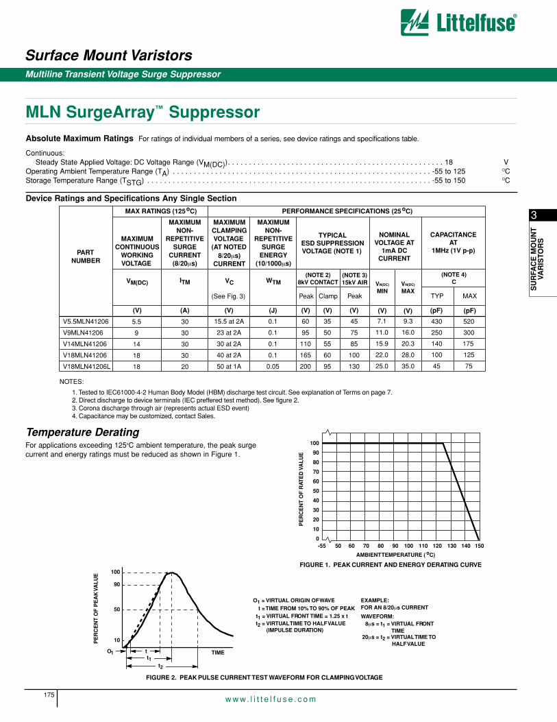
3
SU
RFA
CE
MO
UN
TVA
RIS
TOR
S
Surface Mount Varistors
175w w w. l i t t e l f u s e . c o m
Multiline Transient Voltage Surge Suppressor
MLN SurgeArray™ SuppressorAbsolute Maximum Ratings For ratings of individual members of a series, see device ratings and specifications table.
Continuous:Steady State Applied Voltage: DC Voltage Range (VM(DC)). . . . . . . . . . . . . . . . . . . . . . . . . . . . . . . . . . . . . . . . . . . . . . . . . . . 18 V
Operating Ambient Temperature Range (TA) . . . . . . . . . . . . . . . . . . . . . . . . . . . . . . . . . . . . . . . . . . . . . . . . . . . . . . . . . . . . . -55 to 125 OCStorage Temperature Range (TSTG) . . . . . . . . . . . . . . . . . . . . . . . . . . . . . . . . . . . . . . . . . . . . . . . . . . . . . . . . . . . . . . . . . . . -55 to 150 OC
Device Ratings and Specifications Any Single Section
Temperature DeratingFor applications exceeding 125oC ambient temperature, the peak surgecurrent and energy ratings must be reduced as shown in Figure 1.
PARTNUMBER
MAX RATINGS (125oC) PERFORMANCE SPECIFICATIONS (25oC)
MAXIMUMCONTINUOUS
WORKINGVOLTAGE
MAXIMUM NON-
REPETITIVE SURGE
CURRENT (8/20µs)
MAXIMUM CLAMPINGVOLTAGE
(AT NOTED
CURRENT 8/20µs)
MAXIMUM NON-
REPETITIVE SURGE
ENERGY (10/1000µs)
TYPICALESD SUPPRESSIONVOLTAGE (NOTE 1)
NOMINALVOLTAGE AT
1mA DCCURRENT
CAPACITANCEAT
1MHz (1V p-p)
VM(DC) ITM VC WTM
(V) (A) (V) (J) (V) (V) (pF)
V5.5MLN41206
V9MLN41206
V14MLN41206
V18MLN41206
V18MLN41206L
430 520
250 300
140 175
100 125
NOTES:
1. Tested to IEC61000-4-2 Human Body Model (HBM) discharge test circuit. See explanation of Terms on page 7.2. Direct discharge to device terminals (IEC preffered test method). See figure 2.3. Corona discharge through air (represents actual ESD event)4. Capacitance may be customized, contact Sales.
(See Fig. 3) Peak
(NOTE 2)8kV CONTACT
(NOTE 3)15kV AIR
Clamp
(V)
Peak
(V) (V)
VN(DC)
MINVN(DC)
MAX
(NOTE 4)C
TYP MAX
(pF)
45 75
5.5
9
14
18
18
30
30
30
30
20
7.1
11.0
15.9
22.0
25.0
9.3
16.0
20.3
28.0
35.0
60
95
110
165
200
35
50
55
60
95
45
75
85
100
130
0.1
0.1
0.1
0.1
0.05
15.5 at 2A
23 at 2A
30 at 2A
40 at 2A
50 at 1A
100
90
80
70
60
50
40
30
20
10
0-55 50 60 70 80 90 100 110 120 130 140 150
PE
RC
EN
T O
F R
ATE
D V
AL
UE
AMBIENT TEMPERATURE ( oC)
FIGURE 1. PEAK CURRENT AND ENERGY DERATING CURVE
tt1
t2
100
90
50
10
O1 TIME
PE
RC
EN
T O
F P
EA
K V
AL
UE
O1 = VIRTUAL ORIGIN OF WAVE
t1 = VIRTUAL FRONT TIME = 1.25 x t
(IMPULSE DURATION)
t = TIME FROM 10% TO 90% OF PEAK
t2 = VIRTUAL TIME TO HALF VALUE
EXAMPLE:FOR AN 8/20µs CURRENT
WAVEFORM:8µs = t1 = VIRTUAL FRONT
20µs = t2 = VIRTUAL TIME TOHALF VALUE
TIME
FIGURE 2. PEAK PULSE CURRENT TEST WAVEFORM FOR CLAMPING VOLTAGE
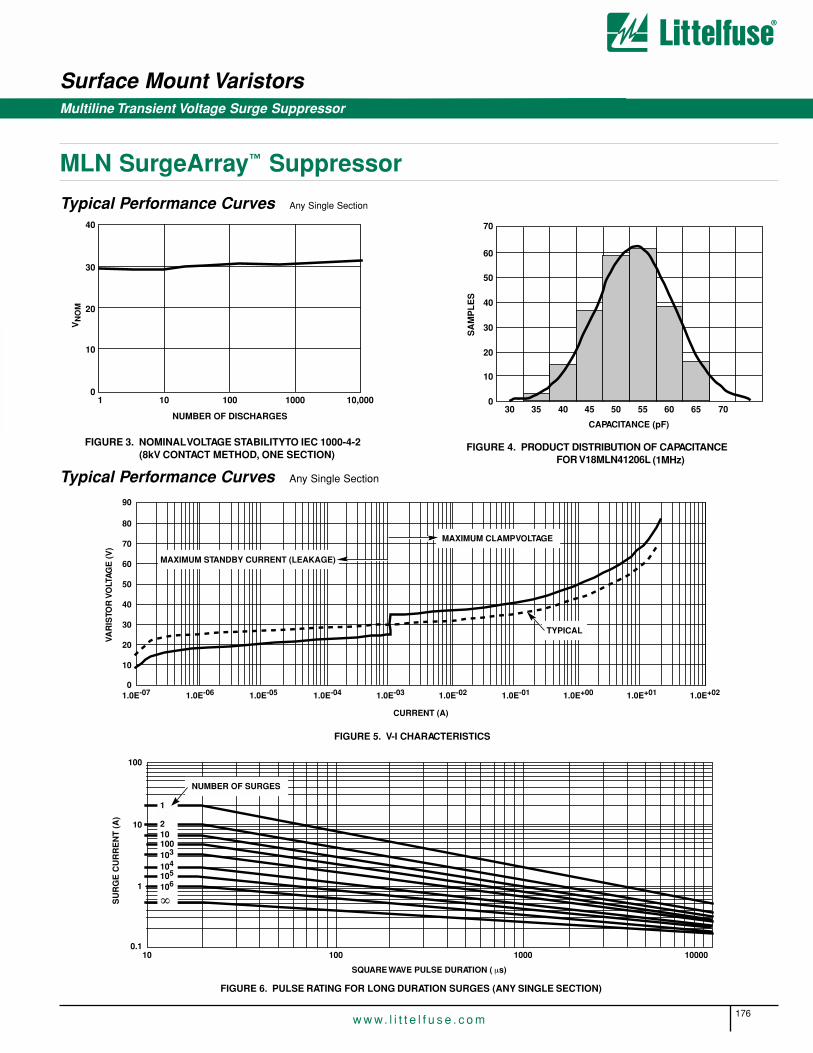
Surface Mount Varistors
176w w w. l i t t e l f u s e . c o m
Multiline Transient Voltage Surge Suppressor
Typical Performance Curves Any Single Section
FIGURE 3. NOMINAL VOLTAGE STABILITY TO IEC 1000-4-2 (8kV CONTACT METHOD, ONE SECTION)
40
30
20
10
01 10 100 1000
NUMBER OF DISCHARGES
VN
OM
10,000
FIGURE 4. PRODUCT DISTRIBUTION OF CAPACITANCE (1MHz)
70
60
50
40
30
20
10
0
SA
MP
LE
S
CAPACITANCE (pF)
7060504030 35 45 55 65
FOR V18MLN41206L
Typical Performance Curves Any Single Section
FIGURE 5. V-I CHARACTERISTICS
FIGURE 6. PULSE RATING FOR LONG DURATION SURGES (ANY SINGLE SECTION)
90
80
70
60
50
40
30
20
10
0
VAR
ISTO
R V
OLT
AG
E (
V)
1.0E-07
CURRENT (A)
1.0E-06 1.0E-05 1.0E-04 1.0E-03 1.0E-02 1.0E-01 1.0E+00 1.0E+01 1.0E+02
MAXIMUM STANDBY CURRENT (LEAKAGE)
MAXIMUM CLAMP VOLTAGE
TYPICAL
1
210100103
104
105
106
∞
100
10
1
0.110 100 1000 10000
SQUARE WAVE PULSE DURATION ( µs)
SU
RG
E C
UR
RE
NT
(A
)
NUMBER OF SURGES
MLN SurgeArray™ Suppressor

3
SU
RFA
CE
MO
UN
TVA
RIS
TOR
S
Surface Mount Varistors
177w w w. l i t t e l f u s e . c o m
Multiline Transient Voltage Surge Suppressor
MLN SurgeArray™ Suppressor
Typical Performance Curves Any Single Section (Continued)
FIGURE 7. STANDBY CURRENT AT NORMALIZED VARISTOR VOLTAGE AND TEMPERATURE (ANY SINGLE SECTION)
FIGURE 8. CAPACITANCE vs FREQUENCY
FIGURE 9. EQUIVALENT SERIES RESISTANCE
100
100.1µA 1µA 10µA 100µA 1mA
CURRENT (A)
NO
RM
AL
IZE
D V
AR
ISTO
R V
OLT
AG
E (
%) -40oC
25oC
85oC
125oC
70
65
60
55
50
45
401GHz100MHz10MHz1MHz
FREQUENCY
CA
PAC
ITA
NC
E (
pF
)
1000
1MHz
FREQUENCY
OH
MS
100
10
1
0.110MHz 100MHz 1GHz 10GHz

Surface Mount Varistors
178w w w. l i t t e l f u s e . c o m
Multiline Transient Voltage Surge Suppressor
Soldering RecommendationsThe principal techniques used for the soldering of components in surfacemount technology are Infrared (IR) Reflow, Vapour Phase Reflow, andWave Soldering. Typical profiles are shown in Figures 12, 13 and 14.When wave soldering, the MLN suppressor is attached to the circuitboard by means of an adhesive. The assembly is then placed on a con-veyor and run through the soldering process to contact the wave. With IRand Vapour Phase Reflow, the device is placed in a solder paste on thesubstrate. As the solder paste is heated, it reflows and solders the unit tothe board.
The recommended solder for the MLN suppressor is a 62/36/2(Sn/Pb/Ag), 60/40 (Sn/Pb), or 63/37 (Sn/Pb). Littelfuse also recommends an RMA solder flux.
Wave soldering is the most strenuous of the processes. To avoid the possibility of generating stresses due to thermal shock, a preheat stagein the soldering process is recommended, and the peak temperature ofthe solder process should be rigidly controlled.
Typical Performance Curves Any Single Section (Continued)
FIGURE 10. IMPEDANCE vs FREQUENCY
FIGURE 11. ADJACENT CHANNEL CROSSTALK
10000
1000
100
10
1
0.11MHz 10MHz 100MHz 1GHz 10GHz
FREQUENCY
IMP
ED
AN
CE
(Z
)
0
-20
-40
-60
-80
-100
-1201kHz 100kHz10kHz 1MHz 10MHz 100MHz 1GHz
FREQUENCY
CR
OS
STA
LK
(d
B)
VIN = 1VRMSZ = 50Ω
When using a reflow process, care should be taken to ensure that theMLN chip is not subjected to a thermal gradient steeper than 4 degreesper second; the ideal gradient being 2 degrees per second. During thesoldering process, preheating to within 100 degrees of the solders peaktemperature is essential to minimize thermal shock. Examples of the sol-dering conditions for the MLN array of suppressors are given in thetables below.
Once the soldering process has been completed, it is still necessary toensure that any further thermal shocks are avoided. One possible cause ofthermal shock is hot printed circuit boards being removed from the solderprocess and subjected to cleaning solvents at room temperature. Theboards must be allowed to gradually cool to less than 50oC before cleaning.
MLN SurgeArray™ Suppressor

3
SU
RFA
CE
MO
UN
TVA
RIS
TOR
S
Surface Mount Varistors
179w w w. l i t t e l f u s e . c o m
Multiline Transient Voltage Surge Suppressor
FIGURE 12. IR REFLOW SOLDER PROFILE
TE
MP
ER
ATU
RE
(oC
)
TIME (MINUTES)
250
200
150
100
50
00 0.5 1.0 1.5 2.0 2.5 3.0 3.5 4.0
MAXIMUM
PREHEAT DWELL
PREHEAT ZONE
TEMPERATURE 222oC
RAMP RATE<2oC/s
40-80SECONDS
ABOVE 183oC
FIGURE 14. VAPOR PHASE SOLDER PROFILET
EM
PE
RAT
UR
E (
oC
)
TIME (MINUTES)
250
200
150
100
50
00 0.5 1.0 1.5 2.0 2.5 3.0 3.5
RAMP RATE
PREHEAT ZONE
>50oC/s
MAXIMUMTEMPERATURE 222oC
40-80SECONDS
ABOVE 183oC
FIGURE 13. WAVE SOLDER PROFILE
TE
MP
ER
ATU
RE
(oC
)
TIME (MINUTES)
300
250
200
150
100
50
00 0.5 1.0 1.5 2.0 2.5 3.0 3.5 4.0 4.5
MAXIMUM WAVE 260oC
SECOND PREHEAT
FIRST PREHEAT
Recommended Pad OutlineE
D
A
B
C
DIMENSION A B C D E
Millimeters 0.89 1.65 2.54 0.46 0.79
Inches 0.035 0.065 0.100 0.018 0.030
PL
T
S
X
BL
BW
W
L W T BW BL P X S
Inch 0.126 ±0.008 0.063 ±0.008 0.053 Max 0.016 ±0.004 0.007 +0.01/- 0.002 0.030 Ref 0.045 ±0.004 0.015 ±0.004
Millimeter 3.2 ±0.2 1.6 ±0.2 1.35 Max 0.41 ±0.1 0.18 +0.25/-0.05 0.76 Ref 1.14 ±0.1 0.38 ±0.1
Mechanical Dimensions
TABLE 1. PAD LAYOUT DIMENSIONS
MLN SurgeArray™ Suppressor

Surface Mount Varistors
180w w w. l i t t e l f u s e . c o m
Multiline Transient Voltage Surge Suppressor
Ordering InformationVXXMLN TYPES
V 18 1206
PACKING OPTIONSA: 2500 Piece Bulk PackH: 7in (178mm) Diameter Reel (Note)T: 13in (330mm) Diameter Reel (Note)
NOTE: See Standard Shipping Quantities table.
DEVICE SIZE:i.e., 120 mil x 60 mil
DEVICE FAMILYTVSS Device
MAXIMUM DC WORKING VOLTAGE
ML N
SERIES DESIGNATORN: Array
W T
END TERMINATION OPTIONW: Ag/Pd/Pt
MULTILAYER DESIGNATOR
4
NUMBER OF SECTIONS
Tape and Reel Specifications• Conforms to EIA - 481, Revision A
• Can be Supplied to IEC Publication 286 - 3
SYMBOL DESCRIPTION MILLIMETERS
A0 Width of Cavity Dependent on Chip Size to Minimize Rotation.
B0 Length of Cavity Dependent on Chip Size to Minimize Rotation.
K0 Depth of Cavity Dependent on Chip Size to Minimize Rotation.
W Width of Tape 8 ±0.2
F Distance Between Drive Hole Centers and Cavity Centers 3.5 ±0.5
E Distance Between Drive Hole Centers and Tape Edge 1.75 ±0.1
P1 Distance Between Cavity Center 4 ±0.1
P2 Axial Distance Between Drive Hole Centers and Cavity Centers 2 ±0.1
P0 Axial Distance Between Drive Hole Centers 4 ±0.1
D0 Drive Hole Diameter 1.55 ±0.05
D1 Diameter of Cavity Piercing 1.05 ±0.05
t1 Embossed Tape Thickness 0.3 Max
t2 Top Tape Thickness 0.1 Max
NOTE: Dimensions in millimeters.
Standard Shipping Quantities
K0
t1
t2
D0 P0
D1P1 A0
P2
B0
F
E
W
PLASTIC CARRIER TAPE
EMBOSSMENTTOP TAPE 8mm
NOMINAL
PRODUCTIDENTIFYING
LABEL
178mmOR 330mmDIA. REEL
DEVICE SIZE “13” INCH REEL (“T” OPTION) “7” INCH REEL (“H” OPTION) BULK PACK (“A” OPTION)
1206 10,000 2,500 2,500
MLN SurgeArray™ Suppressor

3
SU
RFA
CE
MO
UN
TVA
RIS
TOR
S
Surface Mount Varistors
181w w w. l i t t e l f u s e . c o m
Multilayer Transient Voltage Surge Suppressor
AUML Varistor SeriesThe AUML Series of Multilayer Transient Surge Suppressors was specifi-cally designed to suppress the destructive transient voltages found in anautomobile. The most common transient condition results from largeinductive energy discharges. The electronic systems in the automobile,e.g. antilock brake systems, direct ignition systems, engine control,airbag control systems, wiper motor controls, etc., are susceptible todamage from these voltage transients and thus require protection. TheAUML transient suppressors have temperature independent suppressioncharacteristics affording protection from -55oC to 125oC.
The AUML suppressor is manufactured from semiconducting ceramicswhich offer rugged protection and excellent transient energy absorptionin a small package. The devices are available in ceramic leadless chipform, eliminating lead inductance and assuring fast speed of response to transient surges. These Suppressors require significantly smaller spaceand land pads than silicon TVS diodes, offering greater circuit board layout flexibility for the designer.
Also see the Littelfuse ML, MLN and MLE Series of Multilayer Suppressors.
Features• Load Dump Energy Rated per SAE Specification J1113
• Leadless, Surface Mount Chip Form
• “Zero” Lead Inductance
• Variety of Energy Ratings Available
• No Temperature Derating up to 125oC Ambient
• High Peak Surge Current Capability
• Low Profile, Compact Industry Standard Chip Size; (1206, 1210,1812 and 2220 Sizes)
• Inherent Bidirectional Clamping
• No Plastic or Epoxy Packaging Assures Better than 94V-0Flammability Rating
• 100% Lead-Free
Size
Metric EIA3216 12063225 12104532 18125650 2220
Pb

Surface Mount Varistors
182w w w. l i t t e l f u s e . c o m
Multilayer Transient Voltage Surge Suppressor
AUML Varistor SeriesAbsolute Maximum Ratings For ratings of individual members of a series, see Device Ratings and Specifications chart
Continuous:Steady State Applied Voltage:DC Voltage Range (VM(DC)) . . . . . . . . . . . . . . . . . . . . . . . . . . . . . . . . . . . . . . . . . . . . . . . . . . . . . . . . . . . . . . . . . . . . . . . . . 18 V
Transient:Load Dump Energy, (WLD) . . . . . . . . . . . . . . . . . . . . . . . . . . . . . . . . . . . . . . . . . . . . . . . . . . . . . . . . . . . . . . . . . . . . . . . . 1.5 to 25 JJump Start Capability (5 minutes), (VJUMP) . . . . . . . . . . . . . . . . . . . . . . . . . . . . . . . . . . . . . . . . . . . . . . . . . . . . . . . . . . . . . 24.5 V
Operating Ambient Temperature Range (TA). . . . . . . . . . . . . . . . . . . . . . . . . . . . . . . . . . . . . . . . . . . . . . . . . . . . . . . . . . . . . -55 to 125 OCStorage Temperature Range (TSTG) . . . . . . . . . . . . . . . . . . . . . . . . . . . . . . . . . . . . . . . . . . . . . . . . . . . . . . . . . . . . . . . . . . -55 to 150 OCTemperature Coefficient (αv) of Clamping Voltage (VC) at Specified Test Current . . . . . . . . . . . . . . . . . . . . . . . . . . . . . . . . . . . <0.01 %/OC
CAUTION: Stresses above those listed in “Absolute Maximum Ratings” may cause permanent damage to the device. This is a stress only rating and operation of the device
at these or any other conditions above those indicated in the operational sections of this specification is not implied.
Device Ratings and Specifications
Power Dissipation RatingsWhen transients occur in rapid succession, the average power dissipa-tion is the energy (watt-seconds) per pulse times the number of pulsesper second. The power so developed must be within the specificationsshown on the Device Ratings and Characteristics table for the specificdevice. Certain parameter ratings must be derated at high temperaturesas shown in Figure 1.
AUML SERIES UNITS
PARTNUMBER
MAXIMUM RATINGS (125oC) SPECIFICATIONS (25oC)
MAXIMUM CONTINUOUS DC VOLTAGE
JUMP START
VOLTAGE(5 MIN)
LOAD DUMPENERGY
(10 PULSES)
NOMINAL VARISTOR VOLTAGE AT 10mA DC TEST CURRENT
MAXIMUM STANDBY LEAKAGE
(AT 13VDC)
MAXIMUM CLAMPING VOLTAGE (VC)
AT TEST CURRENT(8/20 µs)
VM(DC) VJUMP WLD
VN(DC) MIN
VN(DC) MAX IL VC IP
(V) (V) (J) (V) (V) ( µ A) (V) (A)
V18AUMLA1206 18 24.5 1.5 23 32 50 40 1.5
V18AUMLA1210 18 24.5 3 23 32 50 40 1.5
V18AUMLA1812 18 24.5 6 23 32 100 40 5
V18AUMLA2220 18 24.5 25 23 32 200 40 10
NOTES:
1. Average power dissipation of transients not to exceed 0.1W, 0.15W, 0.3W and 1W for model sizes 1206, 1210, 1812 and 2220 respectively.
2. Load dump energy rating (into the suppressor) of a voltage transient with a resultant time constant of 115ms to 230ms.
3. Thermal shock capability per Mil-Std-750, Method 1051: -55oC to 125oC, 5 minutes at 25oC, 25 Cycles: 15 minutes at each extreme.
4. For application specific requirements, please contact Littelfuse.
For automotive 24V and 42V applications please contact your Littelfuse representative or visit www.littelfuse.com for the latest product update.
FIGURE 1. CURRENT, ENERGY AND POWER DERATING CURVE
100
90
80
70
60
50
40
30
20
10
0-55 50 60 70 80 90 100 110 120 130 140 150
PE
RC
EN
T O
F R
AT
ED
VA
LU
E
AMBIENT TEMPERATURE (oC)

Surface Mount Varistors
183w w w. l i t t e l f u s e . c o m
3
SU
RFA
CE
MO
UN
TVA
RIS
TOR
S
Multilayer Transient Voltage Surge Suppressor
AUML Varistor Series
Temperature EffectsIn the leakage region of the AUML suppressor, the device characteristicsapproaches a linear (ohmic) relationship and shows a temperaturedependent affect. In this region the suppressor is in a high resistancemode (approaching 106Ω) and appears as a near open-circuit. Leakagecurrents at maximum rated voltage are in the microamp range. Whenclamping transients at higher currents (at and above the ten milliamp
V-I Characteristics Curves
range), the AUML suppressor approaches a 1-10 characteristic. In this region the characteristics of the AUML are virtually temperature independent. Figure 3 shows the typical effect of temperature on the V-I characteristics of the AUML suppressor.
FIGURE 2. MAXIMUM LEAKAGE CURRENT/CLAMPING VOLTAGE CURVE FOR AUML SERIES AT 25oC
FIGURE 3. TYPICAL V-I CHARACTERISTICS OF THE V18AUMLA2220 at -40oC, 25oC, 85oC AND 125oC
VOLT
AG
E
100
11mA 10mA 100mA 1A 10A 100A
CURRENT
100µA10µA
10
1210/1206
1812
2220
MAXIMUM LEAKAGE MAXIMUM CLAMPING VOLTAGE
1210/12061812
2220
100
10
1
VOLT
AG
E
1µA 100µA10µA 1mA
-40oC
25oC
85oC
10mA 100mA 1A 10A 100A 1000A
CURRENT
125oC
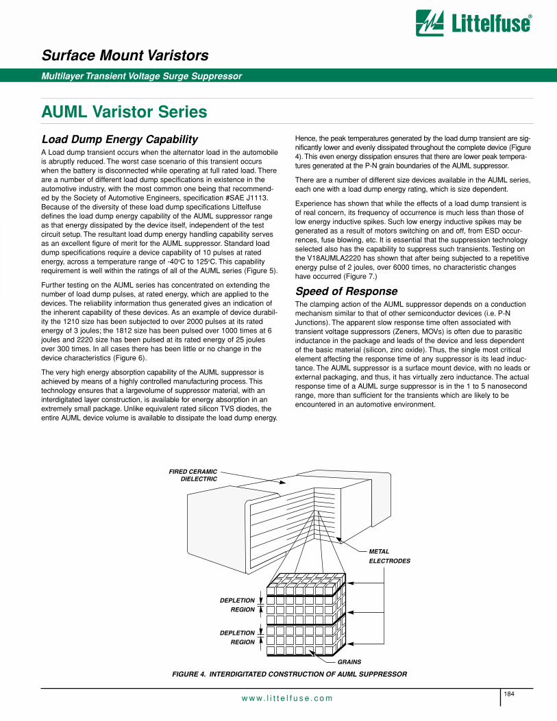
Surface Mount Varistors
184w w w. l i t t e l f u s e . c o m
Multilayer Transient Voltage Surge Suppressor
AUML Varistor Series
Load Dump Energy CapabilityA Load dump transient occurs when the alternator load in the automobileis abruptly reduced. The worst case scenario of this transient occurswhen the battery is disconnected while operating at full rated load. Thereare a number of different load dump specifications in existence in theautomotive industry, with the most common one being that recommend-ed by the Society of Automotive Engineers, specification #SAE J1113.Because of the diversity of these load dump specifications Littelfusedefines the load dump energy capability of the AUML suppressor rangeas that energy dissipated by the device itself, independent of the test circuit setup. The resultant load dump energy handling capability servesas an excellent figure of merit for the AUML suppressor. Standard loaddump specifications require a device capability of 10 pulses at ratedenergy, across a temperature range of -40oC to 125oC. This capabilityrequirement is well within the ratings of all of the AUML series (Figure 5).
Further testing on the AUML series has concentrated on extending thenumber of load dump pulses, at rated energy, which are applied to thedevices. The reliability information thus generated gives an indication ofthe inherent capability of these devices. As an example of device durabil-ity the 1210 size has been subjected to over 2000 pulses at its ratedenergy of 3 joules; the 1812 size has been pulsed over 1000 times at 6joules and 2220 size has been pulsed at its rated energy of 25 joulesover 300 times. In all cases there has been little or no change in thedevice characteristics (Figure 6).
The very high energy absorption capability of the AUML suppressor isachieved by means of a highly controlled manufacturing process. Thistechnology ensures that a largevolume of suppressor material, with aninterdigitated layer construction, is available for energy absorption in anextremely small package. Unlike equivalent rated silicon TVS diodes, theentire AUML device volume is available to dissipate the load dump energy.
Hence, the peak temperatures generated by the load dump transient are sig-nificantly lower and evenly dissipated throughout the complete device (Figure4). This even energy dissipation ensures that there are lower peak tempera-tures generated at the P-N grain boundaries of the AUML suppressor.
There are a number of different size devices available in the AUML series,each one with a load dump energy rating, which is size dependent.
Experience has shown that while the effects of a load dump transient isof real concern, its frequency of occurrence is much less than those oflow energy inductive spikes. Such low energy inductive spikes may begenerated as a result of motors switching on and off, from ESD occur-rences, fuse blowing, etc. It is essential that the suppression technologyselected also has the capability to suppress such transients. Testing onthe V18AUMLA2220 has shown that after being subjected to a repetitiveenergy pulse of 2 joules, over 6000 times, no characteristic changeshave occurred (Figure 7.)
Speed of ResponseThe clamping action of the AUML suppressor depends on a conductionmechanism similar to that of other semiconductor devices (i.e. P-NJunctions). The apparent slow response time often associated with transient voltage suppressors (Zeners, MOVs) is often due to parasiticinductance in the package and leads of the device and less dependent of the basic material (silicon, zinc oxide). Thus, the single most criticalelement affecting the response time of any suppressor is its lead induc-tance. The AUML suppressor is a surface mount device, with no leads orexternal packaging, and thus, it has virtually zero inductance. The actualresponse time of a AUML surge suppressor is in the 1 to 5 nanosecondrange, more than sufficient for the transients which are likely to beencountered in an automotive environment.

Surface Mount Varistors
185w w w. l i t t e l f u s e . c o m
3
SU
RFA
CE
MO
UN
TVA
RIS
TOR
S
Multilayer Transient Voltage Surge Suppressor
AUML Varistor Series
V(10mA)35
30
25
20
15
10
5
00 1 2 3 4 5 6 7 8 9 10 11 12
VO
LTA
GE
# OF LOAD DUMPS
# OF LOAD DUMPS
2220 = 25J1812 = 6J1210 = 3J
FIGURE 5. AUML LOAD DUMP PULSING OVER A TEMPERATURE RANGE OF -55˚C TO 125˚C
FIGURE 6. REPETITIVE LOAD DUMP PULSING AT RATED ENERGY
FIGURE 7. REPETITIVE ENERGY TESTING OF THE V18AUMLA2220 AT AN ENERGY LEVEL OF 2 JOULES
V(10mA)
V AT 10mA
35
100
101000 2000 3000 4000 5000 6000 7000
V18AUMLA2220
30
25
20
15
10
5
00 50 100 150 200 250 300 350 1,000 2,000
VO
LTA
GE
VO
LTA
GE
2220 = 25J 1812 = 6J
1210 = 3J
NUMBER OF PULSES

Surface Mount Varistors
186w w w. l i t t e l f u s e . c o m
Multilayer Transient Voltage Surge Suppressor
AUML Varistor Series
Soldering RecommendationsThe principal techniques used for the soldering of components in surfacemount technology are Infra Red (IR) Reflow, Vapour Phase Reflow, andWave Soldering. When wave soldering, the suppressor is attached to thecircuit board by means of an adhesive. The assembly is then placed on aconveyor and run through the soldering process to contact the wave.With IR and Vapour Phase Reflow, the device is placed in a solder pasteon the substrate. As the solder paste is heated, it reflows and solders theunit to the board.
The recommended solder is a 62/36/2 (Sn/Pb/Ag), 60/40 (Sn/Pb), or63/37 (Sn/Pb). Littelfuse also recommends an RMA solder flux.
Wave soldering is the most strenuous of the processes. To avoid the possibility of generating stresses due to thermal shock, a preheat stagein the soldering process is recommended, and the peak temperature ofthe solder process should be rigidly controlled.
When using a reflow process, care should be taken to ensure that the chipis not subjected to a thermal gradient steeper than 4 degrees per second;the ideal gradient being 2 degrees per second. During the solderingprocess, preheating to within 100 degrees of the solders peak temperatureis essential to minimize thermal shock. Examples of the soldering condi-tions for the AUML Series of suppressors are given in the tables below.
Once the soldering process has been completed, it is still necessary toensure that any further thermal shocks are avoided. One possible cause ofthermal shock is hot printed circuit boards being removed from the solderprocess and subjected to cleaning solvents at room temperature. Theboards must be allowed to gradually cool to less than 50oC before cleaning.
Termination OptionsLittelfuse offers two types of electrode termination finish for the Multilayerproduct series:
1. Silver/Platinum (standard)
2. Silver/Palladium (optional)
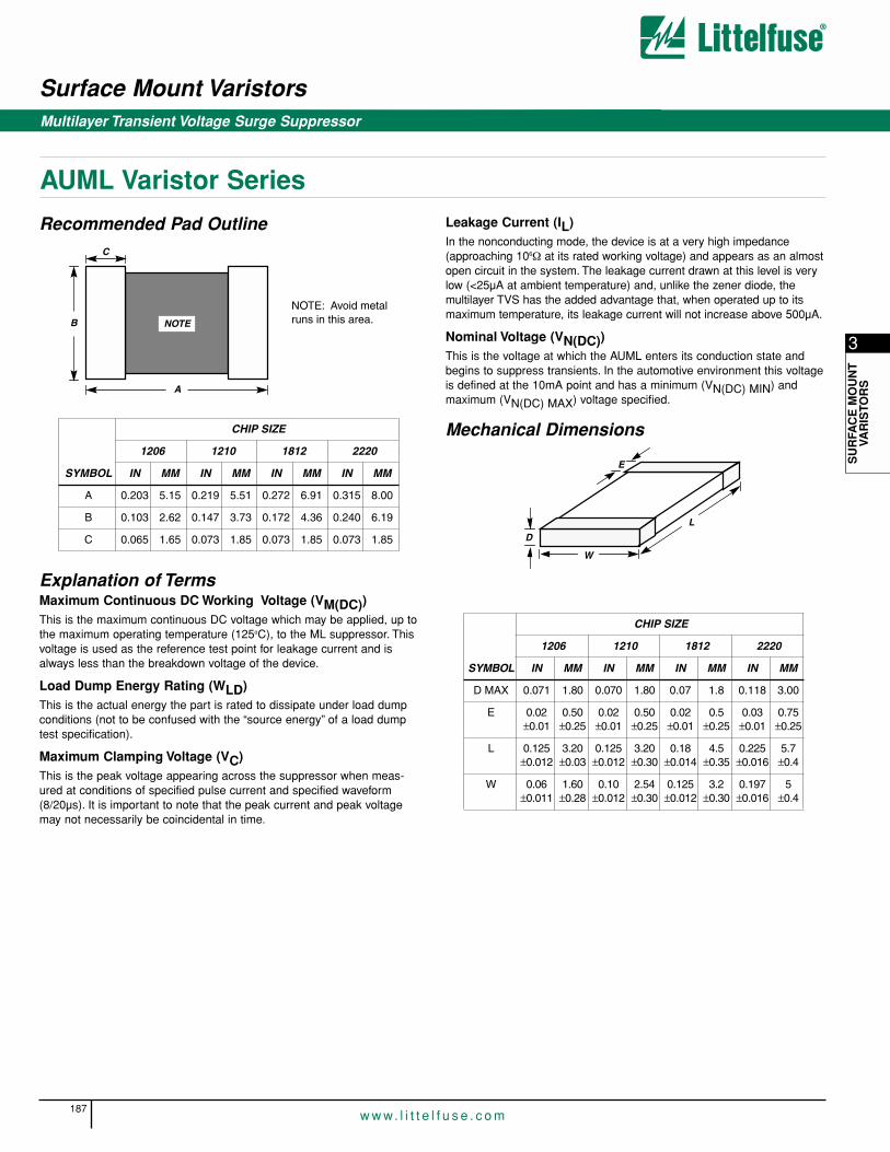
Surface Mount Varistors
187w w w. l i t t e l f u s e . c o m
3
SU
RFA
CE
MO
UN
TVA
RIS
TOR
S
Multilayer Transient Voltage Surge Suppressor
AUML Varistor Series
Explanation of TermsMaximum Continuous DC Working Voltage (VM(DC))This is the maximum continuous DC voltage which may be applied, up tothe maximum operating temperature (125oC), to the ML suppressor. Thisvoltage is used as the reference test point for leakage current and isalways less than the breakdown voltage of the device.
Load Dump Energy Rating (WLD)This is the actual energy the part is rated to dissipate under load dumpconditions (not to be confused with the “source energy” of a load dumptest specification).
Maximum Clamping Voltage (VC)This is the peak voltage appearing across the suppressor when meas-ured at conditions of specified pulse current and specified waveform(8/20µs). It is important to note that the peak current and peak voltagemay not necessarily be coincidental in time.
Leakage Current (IL)In the nonconducting mode, the device is at a very high impedance(approaching 106Ω at its rated working voltage) and appears as an almostopen circuit in the system. The leakage current drawn at this level is verylow (<25µA at ambient temperature) and, unlike the zener diode, the multilayer TVS has the added advantage that, when operated up to itsmaximum temperature, its leakage current will not increase above 500µA.
Nominal Voltage (VN(DC))This is the voltage at which the AUML enters its conduction state andbegins to suppress transients. In the automotive environment this voltageis defined at the 10mA point and has a minimum (VN(DC) MIN) andmaximum (VN(DC) MAX) voltage specified.
Mechanical Dimensions
Recommended Pad Outline
D
E
W
L

Surface Mount Varistors
188w w w. l i t t e l f u s e . c o m
Multilayer Transient Voltage Surge Suppressor
AUML Varistor Series
Ordering InformationV18AUMLAXXXX TYPES
Standard Shipping Quantities
V 18 AUML A 2220 X X
AUML SERIES
PACKING OPTIONS
END TERMINATION OPTION
DEVICE SIZE
LOAD DUMP ENERGY RATINGINDICATOR
AUTOMOTIVEMULTILAYER DESIGNATOR
MAXIMUM DCWORKING VOLTAGE
DEVICE FAMILYA: 2500 pc. Bulk PackH: 7in (178mm) Diameter Reel (Note)T: 13in (330mm) Diameter Reel (Note)
No Letter: Ag/Pt (Standard)W: ag/PdN: Ni/Sn (up to 1210 only)
i.e., 220 mil x 200 mil
Note: See quantity table
TVSS Device
Tape and Reel Specifications• Conforms to EIA - 481, Revision A
• Can be Supplied to IEC Publication 286 - 3
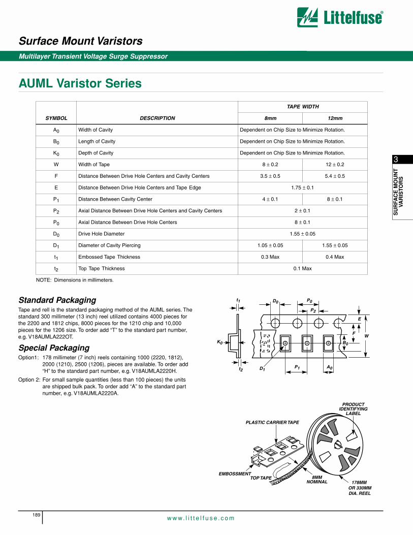
Surface Mount Varistors
189w w w. l i t t e l f u s e . c o m
3
SU
RFA
CE
MO
UN
TVA
RIS
TOR
S
Multilayer Transient Voltage Surge Suppressor
AUML Varistor Series
Standard PackagingTape and rell is the standard packaging method of the AUML series. Thestandard 300 millimeter (13 inch) reel utilized contains 4000 pieces forthe 2200 and 1812 chips, 8000 pieces for the 1210 chip and 10,000pieces for the 1206 size. To order add “T” to the standard part number,e.g. V18AUMLA222OT.
Special PackagingOption1: 178 millimeter (7 inch) reels containing 1000 (2220, 1812),
2000 (1210), 2500 (1206), pieces are available. To order add“H” to the standard part number, e.g. V18AUMLA2220H.
Option 2: For small sample quantities (less than 100 pieces) the unitsare shipped bulk pack. To order add “A” to the standard partnumber, e.g. V18AUMLA2220A.

Surface Mount Varistors
190w w w. l i t t e l f u s e . c o m
Transient Voltage Surge Suppressor
CH Varistor Series ®
CH series transient surge suppressors are small, metal-oxide varistors(MOVs) manufactured in leadless chip form. They are intended for use in avariety of applications from low voltage DC to off-line board-level protection.These devices, which have significantly lower profiles than traditionalradial-lead varistors, permit designers to reduce the size and weight andincrease the reliability of their equipment designs.
CH series varistors are available in a voltage range from 14V to 275V VM(AC)RMS , and energy ratings up to 23J.
See the Littelfuse Multilayer Suppressor Series also.
Features• Leadless, Surface Mount Chip in 5 x 8mm Size
• Voltage Ratings VM(AC)RMS,. . . . . . . . . . . . . . . . . . . . . .14V to 275V
• Supplied in Tape and Reel or Bulk Pack
• No Derating up to 125oC Ambient
AGENCY APPROVALS: Recognized under the components program ofUnderwriters Laboratories.
AGENCY FILE NUMBERS: UL E75961, E135010.

Surface Mount Varistors
191w w w. l i t t e l f u s e . c o m
3
SU
RFA
CE
MO
UN
TVA
RIS
TOR
S
Transient Voltage Surge Suppressor
CH Varistor Series
PARTNUMBER
MAXIMUM RATINGS (125oC) SPECIFICATIONS (25oC)
CONTINUOUS TRANSIENT
VARISTOR VOLTAGE AT 1mA DC TEST CURRENT
MAX CLAMPING VOLT VC AT TEST CURRENT (8/20µs)
TYPICAL CAPACI-TANCEVRMS VDC
ENERGY (10/1000µs)
PEAKCURRENT
(8/20µs)
VM(AC) VM(DC) WTM ITM MIN VN(DC) MAX VC IP f = 1MHz
(V) (V) (J) (A) (V) (V) (V) (V) (A) (pF)
V22CH8 14 18(Note 3)
10.0(Note 2)
250 18.7 22.0 26.0 47 5 1600
V27CH8 17 22 1.0 250 23.0 27.0 31.1 57 5 1300
V33CH8 20 26 1.2 250 29.5 33.0 36.5 68 5 1100
V39CH8 25 31 1.5 250 35.0 39.0 43.0 79 5 900
V47CH8 30 38 1.8 250 42.0 47.0 52.0 92 5 800
V56CH8 35 45 2.3 250 50.0 56.0 62.0 107 5 700
V120CH8 75 102 6.0 500 108.0 120.0 132.0 200 10 300
† V150CH8 95 127 8.0 500 135.0 150.0 165.0 250 10 250
† V180CH8 115 153 10.0 500 162.0 180.0 198.0 295 10 200
† V200CH8 130 175 11.0 500 184.0 200.0 228.0 340 10 180
† V220CH8 140 180 12.0 500 198.0 220.0 242.0 360 10 160
† V240CH8 150 200 13.0 500 212.0 240.0 268.0 395 10 150
† V360CH8 230 300 20.0 500 324.0 360.0 396.0 595 10 100
† V390CH8 250 330 21.0 500 354.0 390.0 429.0 650 10 90
† V430CH8 275 369 23.0 500 389.0 430.0 473.0 710 10 80
NOTES:
1. Power dissipation of transients not to exceed 0.25W.
2. Energy rating for impulse duration of 30ms minimum to one half of peak current value.
3. Also rated to withstand 24V for 5 minutes.
†V150 - V430 CH Varistors are recognized under UL file #E75961 as a recognized component.
Absolute Maximum Ratings For ratings of individual members of a series, see Device Ratings and Specifications chart
Continuous:Steady State Applied Voltage:AC Voltage Range (VM(AC)RMS) . . . . . . . . . . . . . . . . . . . . . . . . . . . . . . . . . . . . . . . . . . . . . . . . . . . . . . . . . . . . . . . . . . . . . 14 to 275 VDC Voltage Range (VM(DC)) . . . . . . . . . . . . . . . . . . . . . . . . . . . . . . . . . . . . . . . . . . . . . . . . . . . . . . . . . . . . . . . . . . . . . . . . 18 to 369 V
Transient: . . . . . . . . . . . . . . . . . . . . . . . . . . . . . . . . . . . . . . . . . . . . . . . . . . . . . . . . . . . . . . . . . . . . . . . . . . . . . . . . . . . . . . . . . . . . . VPeak Pulse Current (ITM)For 8/20µs Current Wave (See Figure 2) . . . . . . . . . . . . . . . . . . . . . . . . . . . . . . . . . . . . . . . . . . . . . . . . . . . . . . . . . . . . . . . 250 to 500 ASingle Pulse Energy RangeFor 10/1000µs Current Wave (WTM) . . . . . . . . . . . . . . . . . . . . . . . . . . . . . . . . . . . . . . . . . . . . . . . . . . . . . . . . . . . . . . . . . . . 1.0 to 23 J
Operating Ambient Temperature Range (TA). . . . . . . . . . . . . . . . . . . . . . . . . . . . . . . . . . . . . . . . . . . . . . . . . . . . . . . . . . . . . . . -55 to 125 OCStorage Temperature Range (TSTG). . . . . . . . . . . . . . . . . . . . . . . . . . . . . . . . . . . . . . . . . . . . . . . . . . . . . . . . . . . . . . . . . . . . . -55 to 150 OCTemperature Coefficient (αV) of Clamping Voltage (VC) at Specified Test Current . . . . . . . . . . . . . . . . . . . . . . . . . . . . . . . . . . . . . <0.01 %/OC
CAUTION: Stresses above those listed in “Absolute Maximum Ratings” may cause permanent damage to the device. This is a stress only rating and operation of the deviceat these or any other conditions above those indicated in the operational sections of this specification is not implied.
Device Ratings and Specifications
CH SERIES UNITS
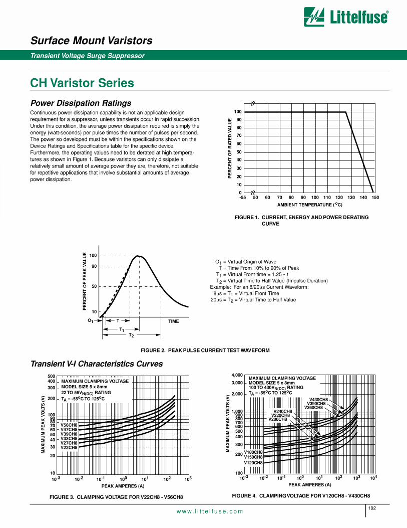
Surface Mount Varistors
192w w w. l i t t e l f u s e . c o m
Transient Voltage Surge Suppressor
CH Varistor Series
Power Dissipation RatingsContinuous power dissipation capability is not an applicable designrequirement for a suppressor, unless transients occur in rapid succession.Under this condition, the average power dissipation required is simply theenergy (watt-seconds) per pulse times the number of pulses per second.The power so developed must be within the specifications shown on theDevice Ratings and Specifications table for the specific device.Furthermore, the operating values need to be derated at high tempera-tures as shown in Figure 1. Because varistors can only dissipate a relatively small amount of average power they are, therefore, not suitablefor repetitive applications that involve substantial amounts of averagepower dissipation.
FIGURE 1. CURRENT, ENERGY AND POWER DERATING CURVE
100
90
80
70
60
50
40
30
20
10
0-55 50 60 70 80 90 100 110 120 130 140 150
AMBIENT TEMPERATURE ( oC)
PE
RC
EN
T O
F R
ATE
D V
AL
UE
FIGURE 2. PEAK PULSE CURRENT TEST WAVEFORM
100
90
50
10
O1 T
T1T2
TIME
PE
RC
EN
T O
F P
EA
K V
AL
UE
O1 = Virtual Origin of WaveT = Time From 10% to 90% of Peak
T1 = Virtual Front time = 1.25 • tT2 = Virtual Time to Half Value (Impulse Duration)
Example: For an 8/20µs Current Waveform:8µs = T1 = Virtual Front Time
20µs = T2 = Virtual Time to Half Value
FIGURE 3. CLAMPING VOLTAGE FOR V22CH8 - V56CH8
500400300
200
100908070605040
30
20
10
MA
XIM
UM
PE
AK
VO
LTS
(V
)
PEAK AMPERES (A)
10-3 10-2 10-1 100 101 102 103
V56CH8V47CH8V39CH8V33CH8V27CH8V22CH8
MAXIMUM CLAMPING VOLTAGEMODEL SIZE 5 x 8mm22 TO 56VN(DC) RATINGTA = -55oC TO 125oC
FIGURE 4. CLAMPING VOLTAGE FOR V120CH8 - V430CH8
4,000
3,000
2,000
1,000900800700600500400
300
200
10010-3 10-2 10-1 100 101 102 103 104
V180CH8V150CH8V120CH8
V430CH8V390CH8
V360CH8V240CH8
V220CH8V200CH8
PEAK AMPERES (A)
MA
XIM
UM
PE
AK
VO
LTS
(V
)
MAXIMUM CLAMPING VOLTAGEMODEL SIZE 5 x 8mm100 TO 430VN(DC) RATINGTA = -55oC TO 125oC
Transient V-I Characteristics Curves
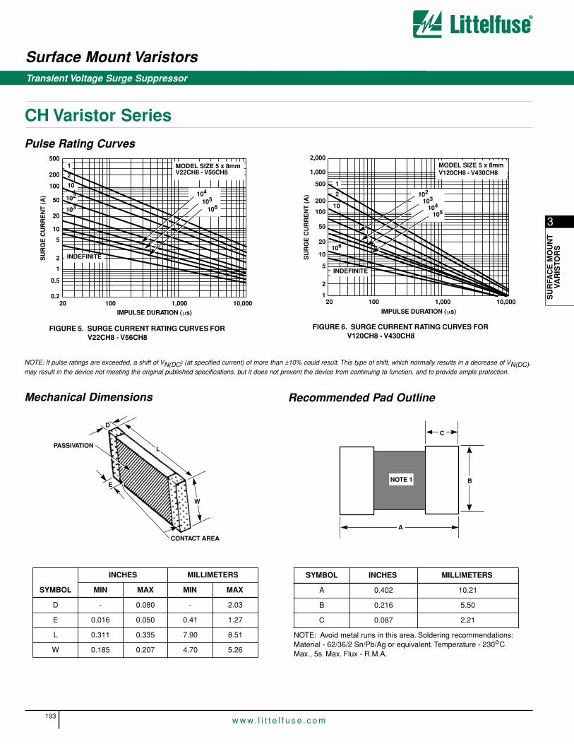
Surface Mount Varistors
193w w w. l i t t e l f u s e . c o m
3
SU
RFA
CE
MO
UN
TVA
RIS
TOR
S
Transient Voltage Surge Suppressor
CH Varistor Series
Recommended Pad Outline
FIGURE 5. SURGE CURRENT RATING CURVES FOR V22CH8 - V56CH8
500
200
50
20
10
5
2
1
0.2
0.5
100
20 100 1,000 10,000IMPULSE DURATION (µs)
SU
RG
E C
UR
RE
NT
(A
)
1
2
10
102
103
104
105
106
INDEFINITE
MODEL SIZE 5 x 8mmV22CH8 - V56CH8
Pulse Rating Curves
FIGURE 6. SURGE CURRENT RATING CURVES FOR V120CH8 - V430CH8
20 100 1,000 10,000
IMPULSE DURATION (µs)
2,000
1,000
500
200
100
50
20
10
5
2
1
1
2
10
102
103
104
105
INDEFINITE
MODEL SIZE 5 x 8mmV120CH8 - V430CH8
106
SU
RG
E C
UR
RE
NT
(A
)
NOTE: If pulse ratings are exceeded, a shift of VN(DC) (at specified current) of more than ±10% could result. This type of shift, which normally results in a decrease of VN(DC),may result in the device not meeting the original published specifications, but it does not prevent the device from continuing to function, and to provide ample protection.
Mechanical Dimensions
E
PASSIVATION
CONTACT AREA
W
L
D
NOTE 1
C
A
B
SYMBOL
INCHES MILLIMETERS
MIN MAX MIN MAX
D - 0.080 - 2.03
E 0.016 0.050 0.41 1.27
L 0.311 0.335 7.90 8.51
W 0.185 0.207 4.70 5.26
SYMBOL INCHES MILLIMETERS
A 0.402 10.21
B 0.216 5.50
C 0.087 2.21
NOTE: Avoid metal runs in this area. Soldering recommendations: Material - 62/36/2 Sn/Pb/Ag or equivalent. Temperature - 230oC Max., 5s. Max. Flux - R.M.A.
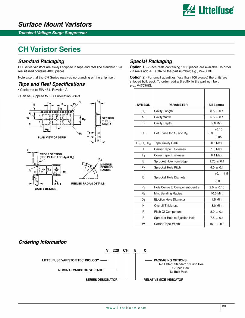
Surface Mount Varistors
194w w w. l i t t e l f u s e . c o m
Transient Voltage Surge Suppressor
CH Varistor Series
Standard PackagingCH Series varistors are always shipped in tape and reel.The standard 13inreel utilized contains 4000 pieces.
Note also that the CH Series receives no branding on the chip itself.
Tape and Reel Specifications• Conforms to EIA-481, Revision A
• Can be Supplied to lEG Publication 286-3
Special PackagingOption 1 - 7-inch reels containing 1000 pieces are available. To order7in reels add a T suffix to the part number; e.g., V47CH8T.
Option 2 - For small quantities (less than 100 pieces) the units areshipped bulk pack. To order, add a S suffix to the part number;e.g., V47CH8S.
Ordering Information
B0
DP2PP0
A0
D1
E
FW
CROSS SECTION(REF. PLANE FOR A0 & B0)
T
R1
R2K0
A0
R3B0H0
K0
SECTIONTHRUCAVITY
T1
TK
MINIMUMBENDINGRADIUS
R4
CAVITY DETAILS
REELED RADIUS DETAILS
PLAN VIEW OF STRIP
SYMBOL PARAMETER SIZE (mm)
B0 Cavity Length 8.5 ± 0.1
A0 Cavity Width 5.5 ± 0.1
K0 Cavity Depth 2.0 Min.
H0 Ref. Plane for A0 and B0
+0.100.3
-0.05
R1, R2, R3 Tape Cavity Radii 0.5 Max.
T Carrier Tape Thickness 1.0 Max.
T1 Cover Tape Thickness 0.1 Max.
E Sprocket Hole from Edge 1.75 ± 0.1
P0 Sprocket Hole Pitch 4.0 ± 0.1
D Sprocket Hole Diameter+0.1 1.5
-0.0
P2 Hole Centre to Component Centre 2.0 ± 0.15
R4 Min. Bending Radius 40.0 Min.
D1 Ejection Hole Diameter 1.5 Min.
K Overall Thickness 3.0 Min.
P Pitch Of Component 8.0 ± 0.1
F Sprocket Hole to Ejection Hole 7.5 ± 0.1
W Carrier Tape Width 16.0 ± 0.3
V 220 CH 8
RELATIVE SIZE INDICATOR
LITTELFUSE VARISTOR TECHNOLOGY
SERIES DESIGNATOR
NOMINAL VARISTOR VOLTAGE
PACKAGING OPTIONSNo Letter: Standard 13 Inch Reel
T: 7 Inch ReelS: Bulk Pack
X
3
SU
RFA
CE
MO
UN
TVA
RIS
TOR
S
195w w w. l i t t e l f u s e . c o m
Notes & Drawings

PGB1 Series Lead-Free Surface Mount ESD Suppressors
0603 Data Sheet . . . . . . . . . . . . . . . . . . . . . . . . . . . . . . . . . . . . . . . . . . . . . . . . . . . . . . . . . . . . . . . . . . . . . . . . . . . . . . . . . . . . . . . . . . . . . . 197-198
SOT23 Data Sheet. . . . . . . . . . . . . . . . . . . . . . . . . . . . . . . . . . . . . . . . . . . . . . . . . . . . . . . . . . . . . . . . . . . . . . . . . . . . . . . . . .See www.littelfuse.com
0805 Data Sheet . . . . . . . . . . . . . . . . . . . . . . . . . . . . . . . . . . . . . . . . . . . . . . . . . . . . . . . . . . . . . . . . . . . . . . . . . . . . . . . . . . .See www.littelfuse.com
PGB Series Surface Mount ESD Suppressors
0603 Data Sheet . . . . . . . . . . . . . . . . . . . . . . . . . . . . . . . . . . . . . . . . . . . . . . . . . . . . . . . . . . . . . . . . . . . . . . . . . . . . . . . . . . . . . . . . . . . . . . 199-200
SOT23 Data Sheet . . . . . . . . . . . . . . . . . . . . . . . . . . . . . . . . . . . . . . . . . . . . . . . . . . . . . . . . . . . . . . . . . . . . . . . . . . . . . . . . . . . . . . . . . . . . 201-202
0805 Data Sheet . . . . . . . . . . . . . . . . . . . . . . . . . . . . . . . . . . . . . . . . . . . . . . . . . . . . . . . . . . . . . . . . . . . . . . . . . . . . . . . . . . . . . . . . . . . . . . 203-204
PGD Series Connector Array ESD Suppressors . . . . . . . . . . . . . . . . . . . . . . . . . . . . . . . . . . . . . . . . . . . . . . . . . . . . . . . . . . . . . . . . . . . . . . . . . . 205
PAGE
196w w w. l i t t e l f u s e . c o m
Pb
PulseGuard® Suppressors
4

4
PU
LSE
GU
AR
D®
SU
PP
RE
SS
OR
S
Ordering Information
CATALOG NUMBER PIECES PER REEL
PGB1010603MR 1,000
PGB1010603NR 5,000
Design ConsiderationBecause of the fast rise-time of the ESD transient, placement ofPulseGuard suppressors is a key design consideration. To achieveoptimal ESD suppression, the devices should be placed on the circuitboard as close to the source of the ESD transient as possible. InstallPulseGuard suppressors directly behind the connector so that they arethe first board-level circuit component encountered by the ESD transient.They are connected from signal/data line to ground.
Polymeric ESD Suppressors
PulseGuard® Suppressors
197w w w. l i t t e l f u s e . c o m
PGB1 Series Lead-Free 0603 Surface Mount ESD SuppressorProduct OverviewPulseGuard ESD Suppressors help protect sensitive electronicequipment against electrostatic discharge (ESD). They supplement theon-chip protection of integrated circuitry and are best suited for low-voltage, high-speed applications where low capacitance is important.Data ports utilizing such high-speed protocols as USB 2.0, IEEE1394,HDMI and DVI can benefit from this new technology.
PulseGuard suppressors use polymer composite materials to suppress fast-rising ESD transients (as specified in IEC 61000-4-2 and MIL-STD-883C), while adding virtually no capacitance to the circuit.
Features• Lead-Free
• Ultra-low capacitance
• Low leakage current
• Fast response time
• Single line of protection
• Bi-directional
• Withstands multiple ESD strikes
• Standard EIA SOCM-1608 package
• Compatible with pick-and-place processes
• Available in 1,000 and 5,000 piece reels (EIA-RS481)
Typical Applications• HDTV Hardware
• Laptop/Desktop Computers
• Network Hardware
• Computer Peripherals
• Digital Cameras
• External Storage
• Set-Top Boxes
ReflowSolder
WaveSolder
1.27 (.050")
0.762 (.030")
3.30 (1.30")
0.762 (.030")
3.05 (1.20")
1.27 (.050")
0.508 (.020")
0.762 (.030")
1.60 (.063")
0.076 (.003") MIN
0.787 (.031")
0.356 (.014")
1.04 (.041") REF
0.254 (.010") MIN
Sn
Equivalent Circuit
Reference Dimensions:
21
Pb
NEW
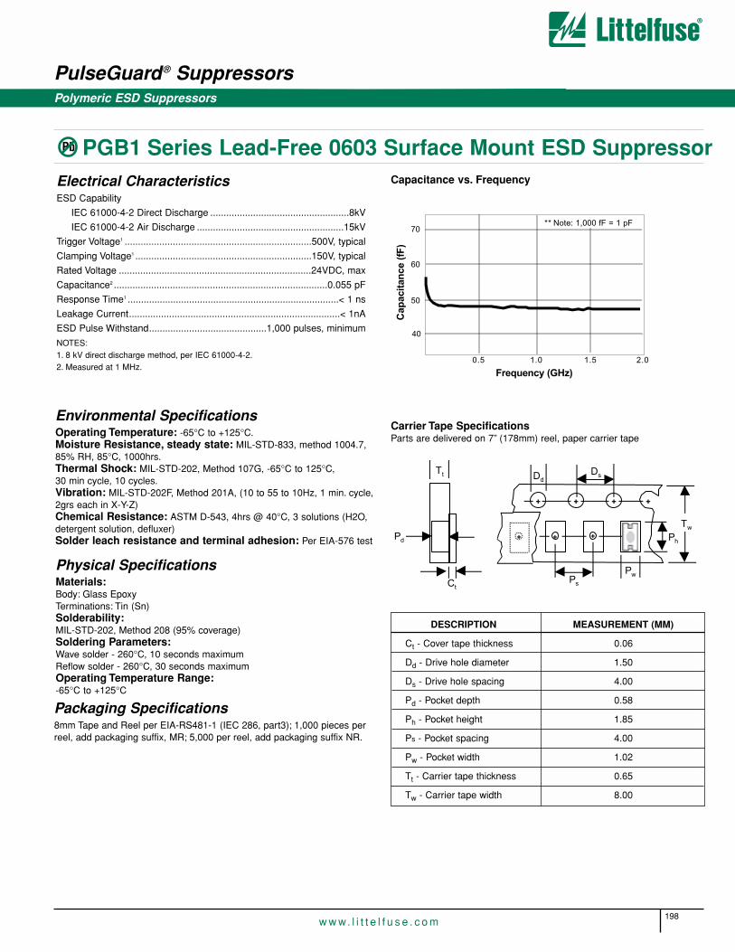
PulseGuard® Suppressors
198w w w. l i t t e l f u s e . c o m
Polymeric ESD Suppressors
PGB1 Series Lead-Free 0603 Surface Mount ESD SuppressorElectrical CharacteristicsESD Capability
IEC 61000-4-2 Direct Discharge ....................................................8kV
IEC 61000-4-2 Air Discharge .......................................................15kV
Trigger Voltage1 ......................................................................500V, typical
Clamping Voltage1 ..................................................................150V, typical
Rated Voltage ........................................................................24VDC, max
Capacitance2 ................................................................................0.055 pF
Response Time1 ...............................................................................< 1 ns
Leakage Current...............................................................................< 1nA
ESD Pulse Withstand............................................1,000 pulses, minimum
NOTES:1. 8 kV direct discharge method, per IEC 61000-4-2.2. Measured at 1 MHz.
Physical SpecificationsMaterials:Body: Glass EpoxyTerminations: Tin (Sn)Solderability:MIL-STD-202, Method 208 (95% coverage)Soldering Parameters:Wave solder - 260°C, 10 seconds maximumReflow solder - 260°C, 30 seconds maximumOperating Temperature Range:-65°C to +125°C
Environmental SpecificationsOperating Temperature: -65°C to +125°C.Moisture Resistance, steady state: MIL-STD-833, method 1004.7, 85% RH, 85°C, 1000hrs.Thermal Shock: MIL-STD-202, Method 107G, -65°C to 125°C, 30 min cycle, 10 cycles.Vibration: MIL-STD-202F, Method 201A, (10 to 55 to 10Hz, 1 min. cycle,2grs each in X-Y-Z)Chemical Resistance: ASTM D-543, 4hrs @ 40°C, 3 solutions (H2O,detergent solution, defluxer)Solder leach resistance and terminal adhesion: Per EIA-576 test
Packaging Specifications 8mm Tape and Reel per EIA-RS481-1 (IEC 286, part3); 1,000 pieces perreel, add packaging suffix, MR; 5,000 per reel, add packaging suffix NR.
Carrier Tape SpecificationsParts are delivered on 7” (178mm) reel, paper carrier tape
Capacitance vs. Frequency
+
+++ +
+++
Tw
Ds
PhPd
Dd
CtPs
Pw
Tt
** Note: 1,000 fF = 1 pF
Frequency (GHz)
Cap
acita
nce
(fF
)
60
50
1.0
70
40
2.01.50.5
DESCRIPTION
Ct - Cover tape thickness
Dd - Drive hole diameter
Ds - Drive hole spacing
Pd - Pocket depth
Ph - Pocket height
Ps - Pocket spacing
Pw - Pocket width
Tt - Carrier tape thickness
Tw - Carrier tape width
MEASUREMENT (MM)
0.06
1.50
4.00
0.58
1.85
4.00
1.02
0.65
8.00
Pb
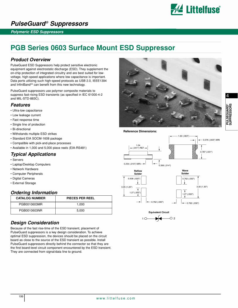
4
PU
LSE
GU
AR
D®
SU
PP
RE
SS
OR
S
PulseGuard® Suppressors
199w w w. l i t t e l f u s e . c o m
Polymeric ESD Suppressors
PGB Series 0603 Surface Mount ESD Suppressor
Product OverviewPulseGuard ESD Suppressors help protect sensitive electronicequipment against electrostatic discharge (ESD). They supplement theon-chip protection of integrated circuitry and are best suited for low-voltage, high-speed applications where low capacitance is important.Data ports utilizing such high-speed protocols as USB 2.0, IEEE1394 and InfiniBandSM can benefit from this new technology.
PulseGuard suppressors use polymer composite materials to suppress fast-rising ESD transients (as specified in IEC 61000-4-2 and MIL-STD-883C).
Features• Ultra-low capacitance
• Low leakage current
• Fast response time
• Single line of protection
• Bi-directional
• Withstands multiple ESD strikes
• Standard EIA SOCM-1608 package
• Compatible with pick-and-place processes
• Available in 1,000 and 5,000 piece reels (EIA-RS481)
Typical Applications• Servers
• Laptop/Desktop Computers
• Network Hardware
• Computer Peripherals
• Digital Cameras
• External Storage
Ordering InformationCATALOG NUMBER PIECES PER REEL
PGB0010603MR 1,000
PGB0010603NR 5,000
Design ConsiderationBecause of the fast rise-time of the ESD transient, placement ofPulseGuard suppressors is a key design consideration. To achieveoptimal ESD suppression, the devices should be placed on the circuitboard as close to the source of the ESD transient as possible. InstallPulseGuard suppressors directly behind the connector so that they arethe first board-level circuit component encountered by the ESD transient.They are connected from signal/data line to ground.
ReflowSolder
WaveSolder
1.27 (.050")
0.762 (.030")
3.30 (1.30")
0.762 (.030")
3.05 (1.20")
1.27 (.050")
0.508 (.020")
0.762 (.030")
1.60 (.063")
0.076 (.003") MIN
0.787 (.031")
0.356 (.014")
1.04 (.041") REF
0.254 (.010") MIN
Equivalent Circuit
Reference Dimensions:
21

PGB Series 0603 Surface Mount ESD Suppressor
PulseGuard® SuppressorsPolymeric ESD Suppressors
200w w w. l i t t e l f u s e . c o m
** Note: 1,000 fF = 1 pF
Frequency (GHz)
Cap
acita
nce
(fF
)
60
50
1.0
70
40
2.01.50.5
Capacitance vs. Frequency
+
+++ +
+++
Tw
Ds
PhPd
Dd
CtPs
Pw
Tt
Carrier Tape SpecificationsParts are delivered on 7” (178mm) reel, paper carrier tape
DESCRIPTION
Ct - Cover tape thickness
Dd - Drive hole diameter
Ds - Drive hole spacing
Pd - Pocket depth
Ph - Pocket height
Ps - Pocket spacing
Pw - Pocket width
Tt - Carrier tape thickness
Tw - Carrier tape width
MEASUREMENT (MM)
0.06
1.50
4.00
0.58
1.85
4.00
1.02
0.65
8.00
Electrical CharacteristicsESD Capability:
IEC 61000-4-2 Direct Discharge ....................................................8kV
IEC 61000-4-2 Air Discharge .......................................................15kV
Trigger Voltage1 ...................................................................1,000V, typical
Clamping Voltage1 ..................................................................150V, typical
Rated Voltage ........................................................................24VDC, max
Capacitance2 ................................................................................0.055 pF
Response Time1 ...............................................................................< 1 ns
Leakage Current3..............................................................................< 1nA
ESD Pulse Withstand............................................1,000 pulses, minimum
NOTES:1. 8 kV direct discharge method, per IEC 61000-4-2.2. Measured at 1 MHz.3. Measured at 6 VDC. Testing at fast ESD pulse rates (1-20Hz) may cause
a change in leakage current performance (6µA, max).
Environmental SpecificationsOperating Temperature: -65°C to +125°C.Moisture Resistance, steady state: MIL-STD-833, method 1004.7, 85% RH, 85°C, 1000hrs.Thermal Shock: MIL-STD-202, Method 107G, -65°C to 125°C, 30 min cycle, 10 cycles.Vibration: MIL-STD-202F, Method 201A, (10 to 55 to 10Hz, 1 min. cycle, 2grs each in X-Y-Z)Chemical Resistance: ASTM D-543, 4hrs @ 40°C, 3 solutions (H2O,detergent solution, defluxer)Solder leach resistance and terminal adhesion: Per EIA-576 test
Physical SpecificationsMaterials:Body: Glass EpoxyTerminations: Tin/Lead (Sn/Pb)Solderability:MIL-STD-202, Method 208 (95% coverage)Soldering Parameters:Wave Solder – 260°C, 10 seconds maximum.Reflow Solder – 260°C, 30 seconds maximum.
Packaging Specifications 8mm Tape and Reel per EIA-RS481-1 (IEC 286, part3); 1,000 pieces perreel, add packaging suffix, MR; 5,000 per reel, add packaging suffix NR.

4
PU
LSE
GU
AR
D®
SU
PP
RE
SS
OR
S
PulseGuard® SuppressorsPolymeric ESD Suppressors
201w w w. l i t t e l f u s e . c o m
PGB Series SOT23 Surface Mount ESD Suppressor
Product OverviewPulseGuard ESD Suppressors help protect sensitive electronicequipment against electrostatic discharge (ESD). They supplement theon-chip protection of integrated circuitry and are best suited for low-voltage, high-speed applications where low capacitance is important.Data ports utilizing such high-speed protocols as USB 2.0, IEEE1394 and InfiniBandSM can benefit from this new technology. PulseGuardsuppressors use polymer composite materials to suppress fast-risingESD transients (as specified in IEC 61000-4-2 and MIL-STD-883E).
Features• Ultra-low capacitance
• Low leakage current
• Fast response time
• 2-lines of protection
• Bi-directional
• Withstands multiple ESD strikes
• Standard JEDEC SOT23 outline
• Compatible with pick-and-place processes
• Available in 3,000 piece reels
Typical Applications• Servers
• Laptop/Desktop Computers
• Network Hardware
• Computer Peripherals
• Digital Cameras
• External Storage
Ordering Information
CATALOG NUMBER PIECES PER REEL
PGB002ST23WR 3,000
Design ConsiderationBecause of the fast rise-time of the ESD transient, placement ofPulseGuard suppressors is a key design consideration. To achieveoptimal ESD suppression, the devices should be placed on the circuitboard as close to the source of the ESD transient as possible. InstallPulseGuard suppressors directly behind the connector so that they arethe first board-level circuit component encountered by the ESD transient.They are connected from signal/data line to ground.
ReflowSolder
Note: For wave solder, increase the spacingin both the horizontal and vertical dimensions by0.254 (.010") where denoted by an asterisk (*)
2.24 (.088")
Reference Dimensions:
1.27 (.050")
1.27 (.050")
1.01 (.040")
2.032 (.080")*
0.51(.020")
0.635 (.025")
2.29(.090")
1.01 (.040")*
1.01 (.040")
0.076 (.003") MIN (TYP)
0.81(.032") REF
1.01 (.040") 2.032(.080")
2.997(.118")
0.762(.030")
Sn
Equivalent Circuit3
21

PulseGuard® SuppressorsPolymeric ESD Suppressors
202w w w. l i t t e l f u s e . c o m
PGB Series SOT23 Surface Mount ESD Suppressor
** Note: 1,000 fF = 1 pF
Frequency (GHz)
Cap
acita
nce
(fF
)
60
50
1.0
70
40
2.01.50.5
Capacitance vs. Frequency
Pd
Ct
Tt
+++ +
+Tw
Ds
Ph
Dd
Ps
Pw
++
Carrier Tape SpecificationsParts are delivered on 7” (178mm) reel, plastic carrier tape
DESCRIPTION
Ct - Cover tape thickness
Dd - Drive hole diameter
Ds - Drive hole spacing
Pd - Pocket depth
Ph - Pocket height
Ps - Pocket spacing
Pw - Pocket width
Tt - Carrier tape thickness
Tw - Carrier tape width
MEASUREMENT (MM)
0.06
1.50
4.00
1.02
3.23
4.00
2.46
0.30
8.00
Electrical CharacteristicsESD Capability
IEC 61000-4-2 Direct Discharge ....................................................8kV
IEC 61000-4-2 Air Discharge .......................................................15kV
Trigger Voltage1 . . . . . . . . . . . . . . . . . . . . . . . . . . . . . . . . 1,000V typical
Clamping Voltage1. . . . . . . . . . . . . . . . . . . . . . . . . . . . . . . . 150V typical
Rated Voltage . . . . . . . . . . . . . . . . . . . . . . . . . . . . . . . . . . . 24VDC max
Capacitance2 . . . . . . . . . . . . . . . . . . . . . . . . . . . . . . . . . . . . . . 0.055pF
Response Time1. . . . . . . . . . . . . . . . . . . . . . . . . . . . . . . . . . . . . . . <1ns
Leakage Current3 . . . . . . . . . . . . . . . . . . . . . . . . . . . . . . . . . . . . . <1nA
ESD Pulse Withstand1. . . . . . . . . . . . . . . . . . . . . 1,000 pulses minimum
Notes:
1. 8 kV direct discharge method, per IEC 61000-4-2.2. Measured at 1 MHz.3. Measured at 6 VDC. Testing at fast ESD pulse rates (1-20Hz) maycause a change in leakage current performance (6µA, max).
Environmental SpecificationsOperating Temperature: -65°C to +125°C.Moisture Resistance, steady state: MIL-STD-833, method 1004.7,85% RH, 85°C, 1000hrs.Thermal Shock: MIL-STD-202, Method 107G, -65°C to 125°C,30 min cycle, 10 cycles.Vibration: MIL-STD-202F, Method 201A, (10 to 55 to 10Hz, 1 min. cycle, 2grs each in X-Y-Z)Chemical Resistance: ASTM D-543, 4hrs @ 40°C, 3 solutions (H2O,detergent solution, defluxer)Solder leach resistance and terminal adhesion: Per EIA-576test
Physical SpecificationsMaterials:Body: Glass EpoxyTerminations: Tin/Lead (Sn/Pb)Solderability: MIL-STD-202, Method 208 (95% coverage)Soldering Parameters:Wave Solder – 260°C, 10 seconds maximum.Reflow Solder – 260°C, 30 seconds maximum.
Packaging Specifications 8mm Tape and Reel per EIA-RS481-1 (IEC 286, part3); 3,000 pieces perreel, add packaging suffix, WR.
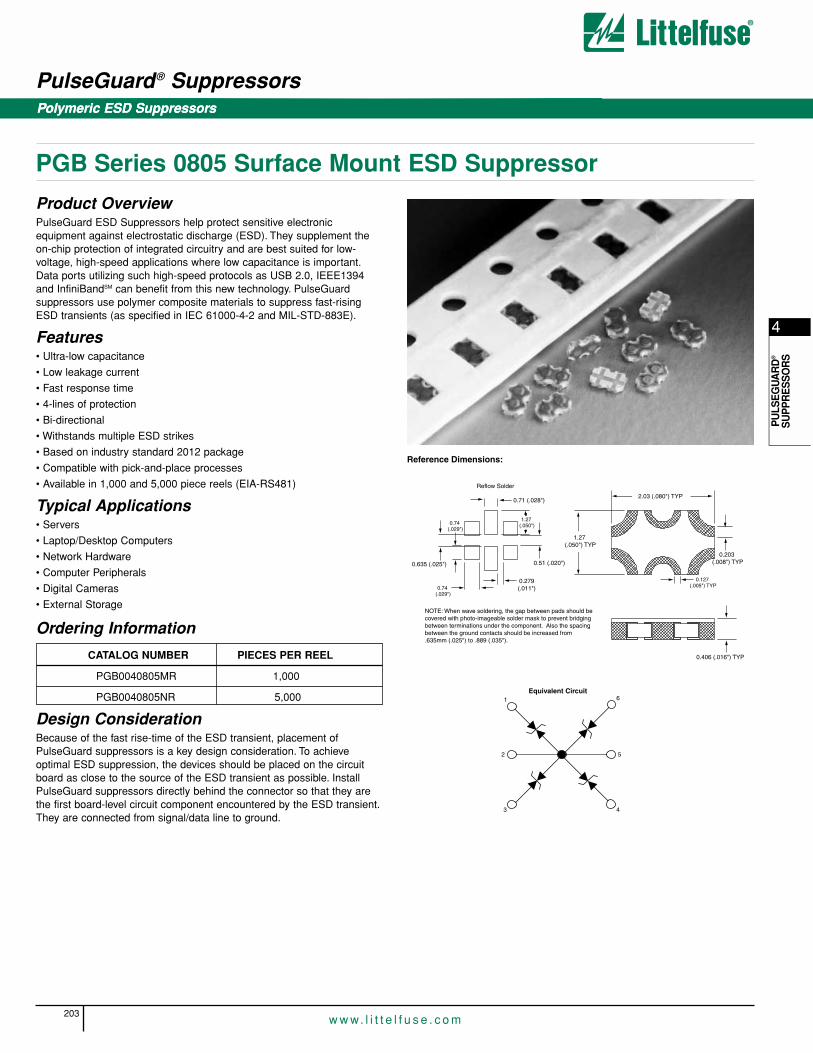
4
PU
LSE
GU
AR
D®
SU
PP
RE
SS
OR
S
Polymeric ESD Suppressors
PulseGuard® Suppressors
203w w w. l i t t e l f u s e . c o m
Polymeric ESD Suppressors
PGB Series 0805 Surface Mount ESD Suppressor
Product OverviewPulseGuard ESD Suppressors help protect sensitive electronicequipment against electrostatic discharge (ESD). They supplement theon-chip protection of integrated circuitry and are best suited for low-voltage, high-speed applications where low capacitance is important.Data ports utilizing such high-speed protocols as USB 2.0, IEEE1394 and InfiniBandSM can benefit from this new technology. PulseGuardsuppressors use polymer composite materials to suppress fast-risingESD transients (as specified in IEC 61000-4-2 and MIL-STD-883E).
Features• Ultra-low capacitance
• Low leakage current
• Fast response time
• 4-lines of protection
• Bi-directional
• Withstands multiple ESD strikes
• Based on industry standard 2012 package
• Compatible with pick-and-place processes
• Available in 1,000 and 5,000 piece reels (EIA-RS481)
Typical Applications• Servers
• Laptop/Desktop Computers
• Network Hardware
• Computer Peripherals
• Digital Cameras
• External Storage
Ordering Information
CATALOG NUMBER PIECES PER REEL
PGB0040805MR 1,000
PGB0040805NR 5,000
Design ConsiderationBecause of the fast rise-time of the ESD transient, placement ofPulseGuard suppressors is a key design consideration. To achieveoptimal ESD suppression, the devices should be placed on the circuitboard as close to the source of the ESD transient as possible. InstallPulseGuard suppressors directly behind the connector so that they arethe first board-level circuit component encountered by the ESD transient.They are connected from signal/data line to ground.
2.03 (.080") TYP
0.203 (.008") TYP
1.27 (.050") TYP
NOTE: When wave soldering, the gap between pads should be covered with photo-imageable solder mask to prevent bridging between terminations under the component. Also the spacingbetween the ground contacts should be increased from .635mm (.025") to .889 (.035").
Reflow Solder
0.71 (.028")
1.27 (.050")
0.51 (.020")0.635 (.025")
0.74 (.029")
0.74 (.029")
0.279(.011")
Equivalent Circuit
Reference Dimensions:
2
61
43
5
0.406 (.016") TYP
0.127 (.005") TYP

PulseGuard® SuppressorsPolymeric ESD Suppressors
204w w w. l i t t e l f u s e . c o m
PGB Series 0805 Surface Mount ESD Suppressor
+++ +
+++
Tw
Ds
Ph
Dd
Ps
Pw
Pd
Ct
Tt
Carrier Tape SpecificationsParts are delivered on 7" (178mm) reel, paper carrier tape
DESCRIPTION
Ct - Cover tape thickness
Dd - Drive hole diameter
Ds - Drive hole spacing
Pd - Pocket depth
Ph - Pocket height
Ps - Pocket spacing
Pw - Pocket width
Tt - Carrier tape thickness
Tw - Carrier tape width
MEASUREMENT (MM)
0.06
1.50
4.00
0.58
2.21
4.00
1.45
0.65
8.00
** Note: 1,000 fF = 1 pF
Frequency (GHz)
Cap
acita
nce
(fF
)
60
50
1.0
70
40
2.01.50.5
Capacitance vs. FrequencyElectrical CharacteristicsESD Capability
IEC 61000-4-2 Direct Discharge ....................................................8kV
IEC 61000-4-2 Air Discharge .......................................................15kV
Trigger Voltage1 ..................................................................1,000 V, typical
Clamping Voltage1..................................................................150V, typical
Rated Voltage ........................................................................24VDC, max
Capacitance2................................................................................0.055 pF
Response Time1................................................................................< 1ns
Leakage Current...............................................................................< 1nA
ESD Pulse Withstand1 ..........................................1,000 pulses, minimum
NOTES:
1. 8 kV direct discharge method, per IEC 61000-4-2.2. Measured at 1 MHz.3. Measured at 6 VDC. Testing at fast ESD pulse rates (1-20Hz) may cause
a change in leakage current performance (6µA, max).
Environmental SpecificationsOperating Temperature: -65°C to +125°C.Moisture Resistance, steady state: MIL-STD-833, method 1004.7,85% RH, 85°C, 1000hrs.Thermal Shock: MIL-STD-202, Method 107G, -65°C to 125°C, 30 min cycle, 10 cycles.Vibration: MIL-STD-202F, Method 201A, (10 to 55 to 10Hz, 1 min. cycle, 2grs each in X-Y-Z)Chemical Resistance: ASTM D-543, 4hrs @ 40°C, 3 solutions (H2O,detergent solution, defluxer)Solder leach resistance and terminal adhesion: Per EIA-576test
Physical SpecificationsMaterials:Body: Glass EpoxyTerminations: Tin/Lead (Sn/Pb)Solderability: MIL-STD-202, Method 208 (95% coverage)Soldering Parameters:Wave Solder – 260°C, 10 seconds maximum.Reflow Solder – 260°C, 30 seconds maximum.
Packaging Specifications 8mm Tape and Reel per EIA-RS481-1 (IEC 286, part3); 1,000 pieces perreel, add packaging suffix, MR; 5,000 per reel, add packaging suffix NR.

4
PU
LSE
GU
AR
D®
SU
PP
RE
SS
OR
S
Polymeric ESD Suppressors
PulseGuard® Suppressors
205w w w. l i t t e l f u s e . c o m
Polymeric ESD Suppressors
PGD Series Connector Array ESD SuppressorWith similar performance features as the surface mount ESD products,the connector array products provide the first line of defense againstESD events. For use in standard D-Subminiatures, these suppressorsintercept the ESD pulses before they enter the electronic equipment.The pulses are shunted to the grounded shell of the connector and keptoff of the circuit board. The connector configuration takes up zero boardspace and can also be used as a retrofit solution in cases where theESD problem was identified after the board design was complete.
Electrical Characteristics:
• Capacitance <2 pF1
• Leakage Current <0.1µA2
• Off state Resistance 10 MΩ2
• Clamping Voltage 100V3, typical• Operating Voltage 24 VDC• Peak Current 45A, at 15 kV• Bi-directional• Product Rated for 10,000 cycles
PHYSICAL SPECIFICATIONS:Body Material: PolyimideTerminations: Spring contactsVoltage Variable Material: Littelfuse polymeric formula.Soldering Parameters:
• Press-in fitting, soldering not necessary.
Packaging: Bulk, bagged and tagged.
ENVIRONMENTAL SPECIFICATIONS:Operating Temperature: -65°C to 125°CVibration: Withstands 10-55Hz per MIL-STD-202F, Method 201A and 10-2000Hz at 20 G’s per MIL-STD-202F, Method 204D, Condition D.Thermal Shock: Withstands 5 cycles of -50°C to 125°C
ORDERING INFORMATION:
1 Tested at 1 Megahertz2 Tested at 5 VDC3 Tested at 8 kV, Direct Contact, IEC 61000-4-2 ESD Waveform
Catalog Mounting Number PinNumber Option of Pins Size (in.)PGD009S030BSA01 90° Angle 9 0.018 - 0.028PGD009S030CSA01 90° Angle 9 0.030 - 0.040PGD009S030CSF01 Front 9 0.030 - 0.040PGD009S030BSR01 Rear 9 0.018 - 0.028PGD015S030BSA01 90° Angle 15 0.018 - 0.028PGD015S030CSA01 90° Angle 15 0.030 - 0.040PGD015S030CSF01 Front 15 0.030 - 0.040PGD015S030BSR01 Rear 15 0.018 - 0.028PGD025S030BSA01 90° Angle 25 0.018 - 0.028PGD025S030CSA01 90° Angle 25 0.030 - 0.040PGD025S030CSF01 Front 25 0.030 - 0.040PGD025S030BSR01 Rear 25 0.018 - 0.028PGD037S030BSA01 90° Angle 37 0.018 - 0.028PGD037S030CSA01 90° Angle 37 0.030 - 0.040PGD037S030CSF01 Front 37 0.030 - 0.040
90° Angle Mount
Front Mount
Polymeric ESD Suppressors
206w w w. l i t t e l f u s e . c o m
Notes & Drawings

207w w w. l i t t e l f u s e . c o m
5
TVS Diode Arrays
Product Number Description Packaging PageTVS Protection with Filter and Termination
SPUSB1AJT Upstream USB Port Terminator with ESD Suppression & EMI Filtering R1 = 12 ohms Surface Mount (SC70-6) . . . . . . . . . . . . . . . . . . . . . . . . . . . . . . . . . . . . . 208-210
SPUSB1BJT Upstream USB Port Terminator With ESD Suppression & EMI Filtering R1 = 22 ohms Surface Mount (SC70-6) . . . . . . . . . . . . . . . . . . . . . . . . . . . . . . . . . . . . . 208-210
SPUSB1CJT Upstream USB Port Terminator With ESD
Suppression & EMI Filtering R1 = 33 ohms Surface Mount (SC70-6) . . . . . . . . . . . . . . . . . . . . . . . . . . . . . . . . . . . . . 208-210Avalanche Diode Arrays
SP0502BAHT 2 Channel SMT Array Surface Mount (SOT23) . . . . . . . . . . . . . . . . . . . . . . . . . . . . . . . . . . . . . . 211-218SP0502BAJT 2 Channel SMT Array Surface Mount (SC70) . . . . . . . . . . . . . . . . . . . . . . . . . . . . . . . . . . . . . . . 211-218SP0503BAHT 3 Channel SMT Array Surface Mount (SOT143) . . . . . . . . . . . . . . . . . . . . . . . . . . . . . . . . . . . . . 211-218SP0504BAAT 4 Channel SMT Array Surface Mount (TSSOP8) . . . . . . . . . . . . . . . . . . . . . . . . . . . . . . . . . . . . 211-218SP0504BAHT 4 Channel SMT Array Surface Mount (SOT23-5) . . . . . . . . . . . . . . . . . . . . . . . . . . . . . . . . . . . . 211-218SP0504BAJT 4 Channel SMT Array Surface Mount (SC70-5) . . . . . . . . . . . . . . . . . . . . . . . . . . . . . . . . . . . . . 211-218SP0505BAHT 5 Channel SMT Array Surfact Mount (SOT23-6) . . . . . . . . . . . . . . . . . . . . . . . . . . . . . . . . . . . . . 211-218SP0505BAJT 5 Channel SMT Array Surface Mount (SC70-6) . . . . . . . . . . . . . . . . . . . . . . . . . . . . . . . . . . . . . 211-218SP0506BAAT 6 Channel SMT Array Surfact Mount (MSOP8). . . . . . . . . . . . . . . . . . . . . . . . . . . . . . . . . . . . . . 211-218
Chip Scale Package Avalanche DiodesSP0501BACT 1 Channel CSP Surface Mount (0402) . . . . . . . . . . . . . . . . . . . . . . . . . . . . . . . . . . . . . . . 219-221SP0504BACT 4 Channel CSP Unipolar Surface Mount (1.8 x 1.2mm). . . . . . . . . . . . . . . . . . . . . . . . . . . . . . . . . . 222-227SP0508BACT 8 Channel CSP Unipolar Surface Mount (3.1 x 1.2mm). . . . . . . . . . . . . . . . . . . . . . . . . . . . . . . . . . 222-227SP05016BACT 16 Channel CSP Unipolar Surface Mount (3.1 x 2.5mm). . . . . . . . . . . . . . . . . . . . . . . . . . . . . . . . . . 222-227SP0504BBCT 4 Channel CSP Bipolar Surface Mount (1.8 x 1.2mm). . . . . . . . . . . . . . . . . . . . . . . . . . . . . . . . . . 228-233SP0508BBCT 8 Channel CSP Bipolar Surface Mount (3.1 x 1.2mm). . . . . . . . . . . . . . . . . . . . . . . . . . . . . . . . . . 228-233SP05016BBCT 16 Channel CSP Bipolar Surface Mount (3.1 x 2.5mm). . . . . . . . . . . . . . . . . . . . . . . . . . . . . . . . . . 228-233
Low Voltage Rail Clamp ArraysSP0502AAHT 2 Channel Rail Clamp Array Surface Mount (SOT143) . . . . . . . . . . . . . . . . . . . . . . . . . . . . . . . . . . . . . 234-237SP0506AAAT 6 Channel Rail Clamp Array Surface Mount (MSOP8) . . . . . . . . . . . . . . . . . . . . . . . . . . . . . . . . . . . . . 234-237SP0506AABT 6 Channel Rail Clamp Array Surface Mount (SOIC8) . . . . . . . . . . . . . . . . . . . . . . . . . . . . . . . . . . . . . . 234-237
High Voltage Rail Clamp SCR/Diode ArraysSP720AB (T) 14 Channel SCR/Diode Array Surface Mount (SOIC16) . . . . . . . . . . . . . . . . . . . . . . . . . . . . . . . . . . . . . 238-243SP720AP 14 Channel SCR/Diode Array Leaded (PDIP16). . . . . . . . . . . . . . . . . . . . . . . . . . . . . . . . . . . . . . . . . . . 238-243SP721AB (T) 6 Channel SCR/Diode Array Surface Mount (SOIC8) . . . . . . . . . . . . . . . . . . . . . . . . . . . . . . . . . . . . . . 244-249SP721AP 6 Channel SCR/Diode Array Leaded (PDIP8). . . . . . . . . . . . . . . . . . . . . . . . . . . . . . . . . . . . . . . . . . . . 244-249SP723AB (T) 6 Channel High Energy SCR/Diode Array Surface Mount (SOIC8) . . . . . . . . . . . . . . . . . . . . . . . . . . . . . . . . . . . . . . 250-255SP723AP 6 Channel High Energy SCR/Diode Array Leaded (PDIP8). . . . . . . . . . . . . . . . . . . . . . . . . . . . . . . . . . . . . . . . . . . . 250-255SP724AHT 4 Channel SCR Diode Array Surface Mount (SOT23-6) . . . . . . . . . . . . . . . . . . . . . . . . . . . . . . . . . . . . 256-261

TVS Diode Arrays
208w w w. l i t t e l f u s e . c o m
Upstream USB Port Terminator with ESD Suppression & EMI Filtering
The Littelfuse SPUSB1 Series is a multifunctional USB port protectionnetwork designed to provide ESD protection, EMI/RFI filtering and linetermination for a single USB 1.1 port. The SPUSB1 can replace a mini-mum of ten typically larger “discrete” devices resulting in inventory andplacement cost savings.
The SPUSB1 Series combines Transient Voltage Suppression (TVS)avalanche diodes, EMI/RFI filtering components (R1 and C1), anda1.5kΩ termination resistor (R2). The filtering components are includedto satisfy recommendations in the USB 1.1 specification, and the 1.5kΩresistor (R2) is included as a pull-up resistor to VBUS.
The SPUSB1 Series can be used for termination and protectionof“upstream” USB devices such as PDAs, digital cameras, scanners andhubs which are often at risk from transient voltage surges and electromagnetic interference from both internal and external sources.
To support a wide range of circuit conditions, Littelfuse offers threeresistance values for the series resistor (R1). The series resistance plusthe USB driver output resistance must be close to the USB cable’s char-acteristic impedance of 45Ω (90Ω balanced) to minimize transmissionline reflections.
Circuit Diagram
Features• One upstream USB port terminator, EMI filter and transient overvoltage
protector in a single surface-mount package
• Compact SC70 package saves board space and lowers manufacturingcosts compared to discrete solutions
• ESD protection to 30kV contact discharge per MIL-STD- 883D,method 3015
• ESD protection to 15kV contact discharge per IEC 61000-4-2 international standard
Applications• Desktop/Laptop PCs
• USB peripherals (printers, scanners, zip drives)
• PDAs / wireless handsets
• Digital cameras
• MP3 Players
• Cable ModemsOrdering Information
2
C1
GND
1
3
C1
5
6
4
R2
R1
R1
V BUS
SC70-6
DEVICEBRAND
UFA
UFB
UFC
PKGTYPE
SC70-6
SC70-6
SC70-6
#/REEL
3000
3000
3000
C1 (pF)
47
47
47
PARTNUMBER
SPUSB1AJT
SPUSB1BJT
SPUSB1CJT
R1 (Ohm)
12
22
33
R2 (KOhm)
1.5
1.5
1.5
SPUSB1 Series

SPUSB1 Series
TVS Diode ArraysUpstream USB Port Terminator with ESD Suppression & EMI Filtering
209w w w. l i t t e l f u s e . c o m
Absolute Maximum Ratings
Supply Voltage V
Parameter Rating Unit
BUS
DC Power per Resistor
Package Power
Temperature Range: Operating Storage
5.5
100
200
-40 to +85 -65 to +150
V
mW
mW
C°
Resistance R1 (SPUSB1AJT only)
Parameter Unit
Ω
Ω
Ω
Specifications(at 25°C unless specified otherwise)
Resistance R1 (SPUSB1CJT only)
Resistance R1 (SPUSB1BJT only)
Resistance R2
Capacitance C1 @ 2.5 v DC, 1MHz
Diode Leakage at 3.3V
Diode Reverse Bias Stand-off Voltage, 1= 10µA
Signal Clamp Voltage: Positive Clamp, 10mA Negative Clamp, 10mA
In-system ESD Withstand Voltage Human Body Model (MIL-STD-883D, method 3015 IEC 81000-4-2, contact discharge method (I/O pins) IEC 81000-4-2, contact discharge method (V pin)
(1)
BUS
Clamping Voltage During ESD DischargeMIL-STD-883D (Method 3015), 8kV
(1)
MAXTYPMIN
kΩ
pF
nA
V
12
33
22
1.5
47
1
6%
26%
18%
1.2%
38%
5.5
14%
40%
26%
18%
56%
100
PositiveNegative
5.6-1.2
6.8-0.8
8.0-0.4
VV
±30±15±25
kVkVkV
VV
10-5
Note: (1) ESD applied to input/outputV pins with respect to GND, one at a time.
Clamping Voltage is measured at the opposite side of the EMI filter to the ESD pin (ie: if ESD is applied to pin1 then clampingvoltage is measured at pin 6). Unused pins are open.These parameters guaranteed by design.
DD
Standard
2
C1
GND
D1
D2 D3
D4
1
3
C1
5
6
4
R2
3.3V
R1
R1
V BUS
D+
USB 1.1CONNECTOR
D-
D+
USB 1.1CONTROLLERIC
D-
GND2
C1
GND
D1
D2 D3
D4
1
3
C1
5
6
4
R2
3.3V
R1
R1
V BUS
D-
USB 1.1CONNECTOR
D+
D-
USB 1.1CONTROLLERIC
D+
GND
Figure 1. Full-Speed Devices (12Mbits per second)For full speed operation the pull-up resistor R2 is connected to the D+ pin.
Figure 2. Low-Speed Devices (1.5Mbits per second)Low speed connection requires the pull-up resistor R2 to be connected to the D-pin. Please note the reversal of the D- and D+ pins on Figure 2 versus Figure 1.
APPLICATIONS INFORMATION
5
TVS
DIO
DE
AR
RAY
S
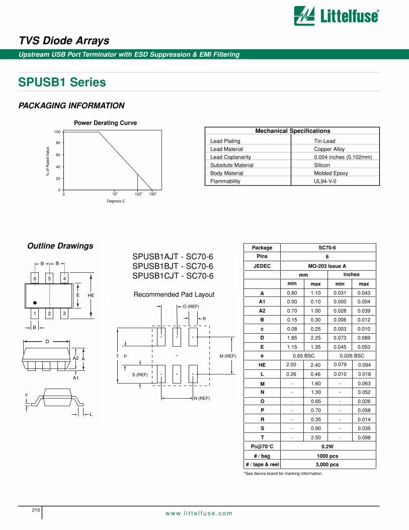
Upstream USB Port Terminator with ESD Suppression & EMI Filtering
SPUSB1 Series
TVS Diode Arrays
210w w w. l i t t e l f u s e . c o m
B
1 2 3
456
B
E HE
c
L
A1
A
D
A2
B
Outline DrawingsSPUSB1AJT - SC70-6SPUSB1BJT - SC70-6SPUSB1CJT - SC70-6
Package
Pins
JEDEC
A
A1
A2
B
c
D
E
e
HE
L
SC70-6
6
MO-203 Issue A
mm inches
min max min max
0.80 1.10 0.031 0.043
0.00 0.10 0.000 0.004
0.70 1.00 0.028 0.039
0.15 0.30 0.006 0.012
0.08 0.25 0.003 0.010
1.85 2.25 0.073 0.089
1.15 1.35 0.045 0.053
2.00 2.40
0.26 0.46
0.65 BSC 0.026 BSC
0.079 0.094
0.010 0.018
PD@70°C 0.2W
# / bag 1000 pcs
# / tape & reel 3,000 pcs
*See device brand for marking information.
M
N
O
P
R
S
T
- 1.60 - 0.063
- 1.30 - 0.052
- 0.65 - 0.026
- 0.70 - 0.058
- 0.35 - 0.014
- 0.90 - 0.035
- 2.50 - 0.098
Recommended Pad Layout
PT
+ + +
+ + +
+
S (REF)
N (REF)
M (REF)
O (REF)
R
Mechanical Specifications
Lead Plating Tin-Lead
Lead Material Copper Alloy
Lead Coplanarity 0.004 inches (0.102mm)
Subsitute Material Silicon
Body Material Molded Epoxy
Flammability UL94-V-0
100
125 1500
0 70
60
80
40
20
Degrees C
o o o
% o
f Rat
ed V
alue
Power Derating Curve
PACKAGING INFORMATION

TVS Diode Arrays
211w w w. l i t t e l f u s e . c o m
Surface Mount TVS Avalanche Diode Array
SP0502BA, SP0503BA, SP0504BA, SP0505BA, SP0506BAThe surface mount family of arrays are designed to suppress ESD and other transient overvoltage events. These arrays are used to meet theInternational Electrotechnical Compatibility (IEC transient immunity stan-dards IEC 61000-4-2 for Electrostatic Discharge Requirements). Theseries are used to help protect sensitive digital or analog input circuitson data, signal, or control lines with voltage levels up to 5VDC.
The monolithic silicon arrays are comprised of specially designed structures for transient voltage suppression(TVS). The size and shape of these structures have be tailored for transient protection.The low capacitance and clamp voltage are ideal for high speed signal line protection.
Ordering Information
Pinout
Part Number
SP0502BAHT
SP0503BAHT
SP0504BAHT
SP0505BAHT
SP0504BAAT
SP0506BAAT
SP0502BAJT
SP0504BAJT
SP0505BAJT
Quantity PerReel
3000
3000
3000
3000
4000
4000
3000
3000
3000
Package Type
SOT23
SOT143
SOT23-5
SOT23-6
TSSOP-8
MSOP-8
SC70-3
SC70-5
SC70-6
CH
2
3
4
5
4
6
2
4
5
1
2
3
1
2
3 4
6
5
8 7 6 5
4321
1
2 3
41
2
3 4
5
8 7 6 5
4321
SP0502BAHTSP0502BAJT
SP0506BAATSP0504BAATSP0505BAHTSP0505BAJT
SP0504BAHTSP0504BAJT
SP0503BAHT
Features• An Array of 2, 3, 4, 5 or 6 TVS Avalanche Diodes in a ultra small
SC70, SOT-23, SOT-143, MSOP or TSSOP packages
• ESD Capability Standards
IEC 61000-4-2, Direct Discharge . . . . . . . . 20kV (Level 4)
IEC 61000-4-2, Air Discharge . . . . . . . . . . . 30kV (Level 4)
MIL STD 883 3015.7. . . . . . . . . . . . . . . . . . . . . . . . . 30kV
• Input Protection for Applications Up to 5VDC
• Fast Response Time . . . . . . . . . . . . . . . . . . . . . . . . . . < 1ns
• Low Input Capacitance . . . . . . . . . . . . . . . . . . . 30pF Typical
• Operating Temperature Range . . . . . . . . . . . . -20°C to 85°C
Applications• Mobile phone handsets• Personal Digital Assistants (PDA)• Portable handheld equipment (Laptop, Palmtop computers)• Computer port, keyboard (USB1.1)• Digital still cameras• Digital video cameras• MP3 players
5
TVS
DIO
DE
AR
RAY
S

212w w w. l i t t e l f u s e . c o m
SP0502BA, SP0503BA, SP0504BA, SP0505BA, SP0506BA
TVS Diode ArraysSurface Mount TVS Avalanche Diode Array
Electrical Specifications TA = -25°C, Unless Otherwise Specified
PARAMETERReverse Standoff Voltage
Reverse Standoff Leakage Current
Signal Clamp Voltage
Positive
Negative
Clamp Voltage during ESD
MIL-STD-883 Method 3015 (HBM) test
8kV
8kV
ESD Test Level (1)
IEC-61000-2, Contact discharge
MIL-STD-883 Method 3015 (HBM)
Capacitance
Turn on/off Time
Temperature Range
Operating
Storage
Diode Dynamic Resistance
Forward Conduction
Reverse Conduction
TEST CONDITIONSI = 10µA
V = 5.0V
I = 10mA
I = 10mA
2.5V @ 1Mhz
MIN5.5
5.6
-1.2
20
30
-20
-65
MAX-
100
8
-0.4
85
150
UNITSV
nA
V
V
V
V
kV
kV
pF
ns
°C
°C
Ω
Ω
TYPICAL-
1
6.8
-0.8
12
-8
30
<1
1.0
1.4
Note:(1) ESD voltage applied between channel pins and ground, one pin at a time; all other channel pins are open; all ground pins are grounded.
Absolute Maximum Ratings
Storage Temperature Range
Parameter Rating Unit
Package Power Dissipation SC70 SOT23-3, SOT23-5, SOT23-6, SOT143 TSSOP, MSOP
-65 to + 150 ˚C
0.20.2250.5
WWW

213w w w. l i t t e l f u s e . c o m
Typical Diode Capacitance vs. Reverse Voltage
Dio
de
Cap
acita
nce
(pF)
Diode Reverse Voltage (V)0 1 2 3 4 5
0
20
40
60
Mechanical Specifications
Lead Plating Tin-Lead
Lead Material Copper Alloy
Lead Coplanarity 0.004 inches (0.102mm)
Subsitute Material Silicon
Body Material Molded Epoxy
Flammability UL94-V-0
Package Information
100
125 1500
0 70
60
80
40
20
Degrees C
o o o
% o
f Rat
ed V
alue
Notes:1. All dimensions are in millimeters.2. Dimensions include solder plating.3. Dimensions are exclusive of mold flash & metal burr.4. All specifications comply to JEDEC SPEC MO-203 ISSUE A.5. Blo is facing up for mold and facing down for trim/form,
i.e. reverse trim/form.6. Package surface matte finish VDI 11-13.
Power Derating Curve
SP0502BA, SP0503BA, SP0504BA, SP0505BA, SP0506BA
TVS Diode ArraysSurface Mount TVS Avalanche Diode Array
-3 -2 -1 0 1 2 3 4 5 6 7 8 9
1.6
1.4
1.2
1.0
0.8
0.6
0.4
0.2
0.0
-0.2
-0.4
-0.6
-0.8
-1.0
-1.2
-1.4
-1.6
Inpu
t Cur
rent
(A
)
Input Voltage (V)
Typical Input VI Characteristics(Pulse-mode measurements, pulse width = 0.7 mS nominal)
5
TVS
DIO
DE
AR
RAY
S

214w w w. l i t t e l f u s e . c o m
SP0502BA, SP0503BA, SP0504BA, SP0505BA, SP0506BA
TVS Diode ArraysSurface Mount TVS Avalanche Diode Array
e
HE
3
1 2
E
B
A1
A
D
C
L
A2
e
502
e
5 4
1 2 3
L
E HE
c
B
A1
A
D
A2
504
e
Outline Drawings
SP0502BAJT - SC70-3
SP0504BAJT - SC70-5
Package
Pins
JEDEC
A
A1
A2
B
c
D
E
e
HE
L
SC70-5
5
MO-203 Issue A
mm inches
min max min max
0.80 1.10 0.03 0.043
0.00 0.10 0.00 0.004
0.70 1.00 0.028 0.039
0.15 0.30 0.006 0.012
0.08 0.25 0.003 0.010
1.85 2.25 0.073 0.089
1.15 1.35 0.045 0.053
2.00 2.40
0.26 0.46
0.65 BSC 0.026 BSC
0.079 0.094
0.010 0.018
Package
Pins
JEDEC
A
A1
A2
B
c
D
E
e
HE
L
SC70-3
3
MO-203 Issue A
mm inches
min max min max
0.80 1.10 0.031 0.043
0.00 0.10 0.00 0.004
0.70 1.00 0.028 0.039
0.15 0.30 0.006 0.012
0.08 0.25 0.003 0.010
1.85 2.25 0.073 0.089
1.15 1.35 0.045 0.053
2.00 2.40
0.26 0.46
0.66 BSC 0.026 BSC
0.079 0.094
0.010 0.018

215w w w. l i t t e l f u s e . c o m
SP0502BA, SP0503BA, SP0504BA, SP0505BA, SP0506BA
Surface Mount TVS Avalanche Diode Array
B
1 2 3
456
e
E HE
c
L
A1
A
D
A2
e
505
Outline Drawings
SP0505BAJT - SC70-6
Package
Pins
JEDEC
A
A1
A2
B
c
D
E
e
HE
L
SC70-6
5
MO-203 Issue A
mm inches
min max min max
0.80 1.10 0.031 0.043
0.00 0.10 0.00 0.004
0.70 1.00 0.028 0.039
0.15 0.30 0.006 0.012
0.08 0.25 0.003 0.010
1.85 2.25 0.073 0.089
1.15 1.35 0.045 0.053
2.00 2.40
0.26 0.46
0.65 BSC 0.026 BSC
0.079 0.094
0.010 0.018
M
N
O
P
R
S
T
-
-
-
-
-
-
-
1.60
1.30
0.65
0.70
0.35
0.90
2.50
0.063
0.052
0.026
0.058
0.014
0.035
0.098
-
-
-
-
-
-
-
ee1
E
3
1 2
E1
b
A1
A
D
C
L1
502B
SP0502BAHT - SOT23
P
0N
M
Package
Pins
JEDEC
A
A1
b
c
D
E
E1
e
e1
L1
SOT23
3
TO-236
mm inches
min max min max
0.89 1.12 0.035 0.044
0.01 0.1 0.0004 0.004
0.3 0.5 0.012 0.020
0.08 0.2 0.003 0.008
2.8 3.04 0.110 0.120
2.1 2.64 0.083 0.104
1.2 1.4 0.047 0.055
1.90 BSC 1.90 BSC
0.54 REF 0.54 REF
0.95 BSC 0.95 BSC
M
N
O
P
2.29 .090
0.95 .0375
0.78 .030TYP
0.78 .030TYP
Recommended Pad Layout
Recommended Pad Layout
PT
+ + +
+ + +
+
S (REF)
N (REF)
M (REF)
O (REF)
R
TVS Diode Arrays
5
TVS
DIO
DE
AR
RAY
S
TVS Diode Arrays
216w w w. l i t t e l f u s e . c o m
SP0502BA, SP0503BA, SP0504BA, SP0505BA, SP0506BA
Surface Mount TVS Avalanche Diode Array
ee1
5 4
1 2 3
L1
E1 E
D
A
A1
c
B
504B
SP0504BAHT - SOT23-5
Recommended Pad Layout
O
P
N
M
Package
Pins
JEDEC
A
A1
b
c
D
E
E1
e
e1
L1
SOT23-5
5
MO-178
mm inches
min max min max
- 1.45 - 0.057
0 0.15 0 0.006
0.3 0.5 0.012 0.020
0.08 0.22 0.003 0.009
2.75 3.05 0.108 0.120
2.6 3.0 0.102 0.118
1.45 1.75 0.057 0.069
1.90 BSC 1.90 BSC
0.60 REF 0.60 REF
0.95 BSC 0.95 BSC
M
N
O
P
2.59 .102
0.95 .038
0.69 .027TYP
0.99 .039TYP
503B EE1
c
e
e1
1 2
4 3
b2 b A1
A
D
L
L1
Outline DrawingsSP0503BAHT - SOT143
3.40 (.134")3.60 (.140")
0.80 (.032")1.00 (.040")
2.20 (.087")REF
1.90 (.075")1.70
(.067")
1.00 (.040")1.20 (.048")
0.80 (.032")1.00 (.040")
BSC
MAX1.40 (.055")
Recommended Pad Layout
Package
Pins
JEDEC
A
A1
b
b2
c
D
E
E1
e
e1
L
L1
SOT143
4
TO-253
mm inches
min max min max
0.08 1.22 0.031 0.048
0.05 0.15 0.002 0.006
0.30 0.50 0.012 0.019
0.76 0.89 0.030 0.035
0.08 0.20 0.003 0.008
2.80 3.04 0.110 0.119
2.10 2.64 0.082 0.103
1.92 BSC 0.076 BSC
0.20 BSC 0.008 BSC
0.4 0.6 0.016 0.024
0.550 REF 0.022 REF
1.20 1.40 0.047 0.055
217w w w. l i t t e l f u s e . c o m
SP0502BA, SP0503BA, SP0504BA, SP0505BA, SP0506BA
Surface Mount TVS Avalanche Diode Array
b
1 2 3
456
e
E1 E505B
e1
L1
D
A
A1
c
Outline Drawings
SP0505BAHT - SOT23-6
Recommended Pad Layout
O
P
N
M
Package
Pins
JEDEC
A
A1
b
c
D
E
E1
e
e1
L1
SOT23-6
6
MO-178
mm inches
min max min max
- 1.45 - 0.057
0 0.15 0 0.006
0.3 0.5 0.012 0.020
0.08 0.22 0.003 0.009
2.75 3.05 0.108 0.120
2.6 3.0 0.102 0.118
1.45 1.75 0.057 0.069
1.90 BSC 1.90 BSC
0.60 REF 0.60 REF
0.95 BSC 0.95 BSC
PD@70°C .225W
M
N
O
P
2.59 .102
0.95 0.038
0.69 .027TYP
0.99 .039TYP
504 BAE
LF
D
E1
A
A1C
B
L1L2
SP0504BAAT - TSSOP-8 Package TSSOP-8
mm inches
min max min max
2.90 3.10 .144 .122
4.29 4.50 .17 .18
0.051 0.152 .002 0.006
- 0.30 - .12TYP
- 0.66 - .26TYP
D
E
E1
A
A1
B
C
L1
L2
0.51 0.76 .020 .030
0.102 0.203 .004 .008
6.40 REF .252 REF
1.194 REF .047 REF
TVS Diode Arrays
5
TVS
DIO
DE
AR
RAY
S
TVS Diode Arrays
218w w w. l i t t e l f u s e . c o m
SP0502BA, SP0503BA, SP0504BA, SP0505BA, SP0506BA
Surface Mount TVS Avalanche Diode Array
506 B
D
E1E
A
A1
BC
L1L2
LF
Outline DrawingsSP0506BAAT - MSOP-8
F1F
I
HG
Recommended Pad Layout
Package MSOP-8
mm inches
min max min max
2.90 3.10 .144 .122
4.78 4.98 .188 .196
2.90 3.10 .114 .122
0.87 1.17 .034 .046
0.05 0.25 .002 0.10
- 0.30TYP - .12TYP
- 0.65TYP - .25TYP
D
E
E1
A
A1
B
C
L1
L2
0.52 0.54 .017 .025
- 0.18TYP - .007TYP
F
F1
G
H
I
.208
.041
.015
.0256
.167
-5.28-
-
-
-
-
-
-
-
-
4.24
0.65
0.38
1.04
219w w w. l i t t e l f u s e . c o m
TVS Avalanche Diode in a Chip Scale Package
SP0501BACTThe product is a silicon P/N structure tailored for ESD protection and isoffered in the standard EIA 0402 size. The single channel Chip Scaledevice is used to help protect sensitive digital or analog input circuits ondata, signal, or control lines with voltage levels up to 5VDC. The bipolardevice is ideal for protection where AC signals are present.The state-of-the-art device is designed to suppress ESD and other transient over-voltage events to meet the International ElectrotechnicalCompatability (EMC transient immunity stantards IEC 61000-4-2 forElectrosatic Discharge Requirements). The monolithic silicon device iscomprised of specially designed structures for transient voltage suppres-sion (TVS). The size and shape of these structures has been tailoredfor transient protection. The low capacitance and clamp voltage are idealfor high speed signal line protection.
Ordering Information
Schematic
Features• Single channel suppressor in an EIA 0402 device size
• ESD Capability
- IEC 61000-4-2, Direct Discharge .................................30kV (Level 4)
- IEC 61000-4-2, Air Discharge ......................................30kV (Level 4)
- MIL STD 883D (Method 3015.7).................................................30kV
• Signal line protection for applications up to 5VDC
• Fast response time .........................................................................< 1ns
• Low input capacitance .........................................................30pF Typical
• Low clamp voltage (8kV test) ................................................13V Typical
• Low input leakage ....................................................1nA @ 3.3V Typical
• Operating temperature range ............................................-40°C to 85°C
Applications• Cell phone handsets
• Personal Digital Assistants (PDA)
• Portable handheld equipment (Laptop, Palmtop computers)
• Computer port, keyboard (USB1.1)
• Set-Top Box (Audio and Video ports)
• PCMCIA cards
SP0501BAC
TVS Diode Arrays
Bumps
2
Part Number
SP0501BACT
Quantity PerReel
3500
Package Sizemils (mm)
40x20 (1x 0.5)
DiodeChannels
1
5
TVS
DIO
DE
AR
RAY
S

220w w w. l i t t e l f u s e . c o m
SP0501BACT
TVS Diode ArraysTVS Avalanche Diode in a Chip Scale Package
Electrical Specifications TA = 25°C Unless Otherwise Specified
PARAMETER
Reverse Standoff Voltage
Reverse Standoff Leakage Current
Signal Clamp Voltage
Positive
Negative
Clamp Voltage during ESD
MIL-STD 833D (Method 3015.7)
ESD Test Level
IEC-61000-4-2, Contact discharge
MIL-STD-883D Method 3015 (HBM)
Capacitance
Turn on/off Time
Temperature Range
Operating
Storage
TEST CONDITIONS
I = 10µA
V = 5.5V
I = 10mA
I = 10mA
8kV
5V @ 1Mhz
MIN
±5.9
6.0
-9.2
30
30
-40
-65
MAX
-
100
9.2
- 6.0
85
150
UNITS
V
µA
V
V
V
V
kV
kV
pF
ns
°C
°C
TYPICAL
-
1
7.5
- 7.5
13
30
<1
50
40
30
20
10
00 1 5432
Voltage Across Device (V)
0.076(.003")
0.15 (.006")
0.36(.014")
0.076 (.003")
1.0 (.04")
0.5 (.02")
0.36 (.014")0.076 (.003")
NOTE** Metal Bump: 63/37 (Sn/Pb) alloy
Outline DrawingTypical Device Capacitance vs. Voltage
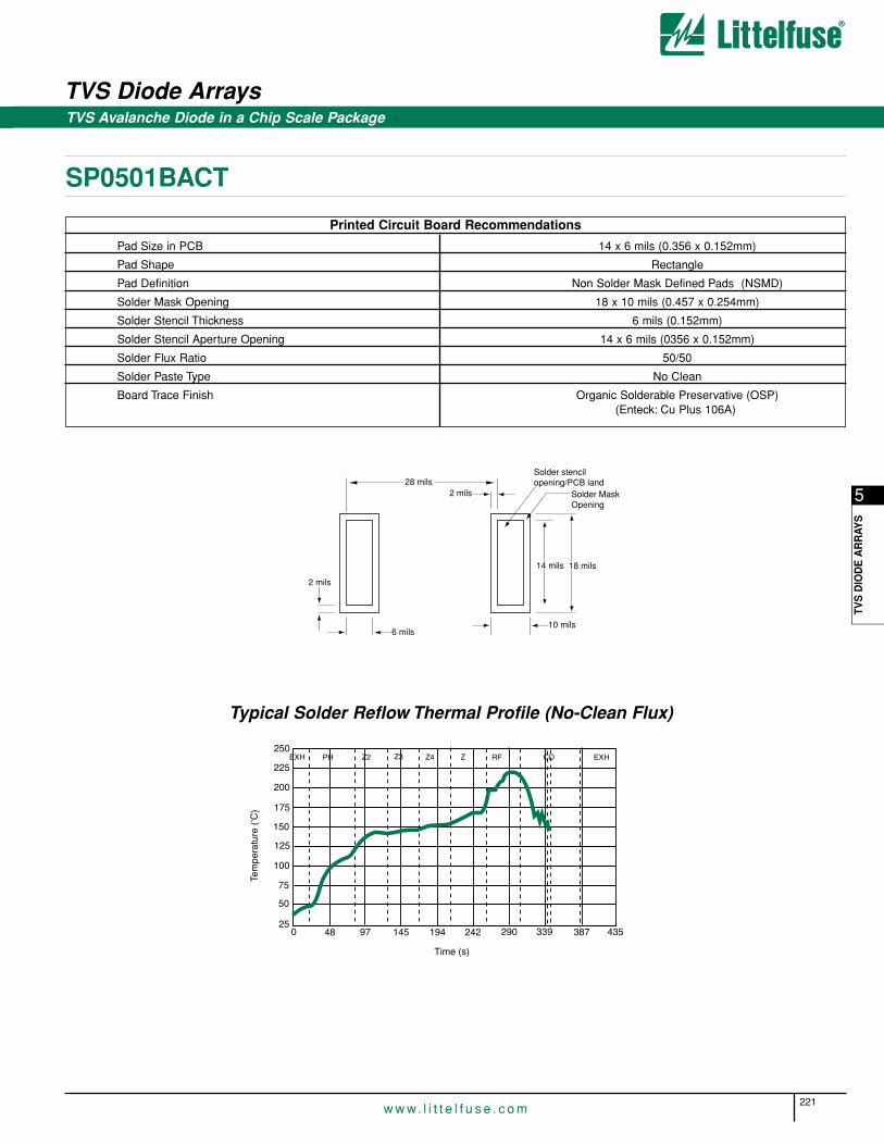
221w w w. l i t t e l f u s e . c o m
TVS Avalanche Diode in a Chip Scale Package
SP0501BACT
Printed Circuit Board Recommendations
Pad Size in PCB 14 x 6 mils (0.356 x 0.152mm)
Pad Shape Rectangle
Pad Definition Non Solder Mask Defined Pads (NSMD)
Solder Mask Opening 18 x 10 mils (0.457 x 0.254mm)
Solder Stencil Thickness 6 mils (0.152mm)
Solder Stencil Aperture Opening 14 x 6 mils (0356 x 0.152mm)
Solder Flux Ratio 50/50
Solder Paste Type No Clean
Board Trace Finish Organic Solderable Preservative (OSP) (Enteck: Cu Plus 106A)
28 mils
14 mils 18 mils
10 mils
2 mils
Solder stencilopening/PCB land
Solder MaskOpening
6 mils
2 mils
TVS Diode Arrays
5
TVS
DIO
DE
AR
RAY
S
Typical Solder Reflow Thermal Profile (No-Clean Flux)
0 48 97
Time (s)
145 194 242 290 339 387 435
EXHCDRFZZ4Z3Z2PHEXH250
225
200
175
150
125
100
75
50
25
Tem
pera
ture
(o C
)
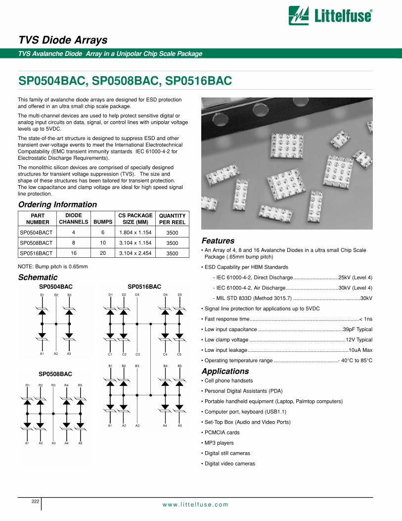
222w w w. l i t t e l f u s e . c o m
TVS Diode ArraysTVS Avalanche Diode Array in a Unipolar Chip Scale Package
SP0504BAC, SP0508BAC, SP0516BACThis family of avalanche diode arrays are designed for ESD protectionand offered in an ultra small chip scale package.
The multi-channel devices are used to help protect sensitive digital oranalog input circuits on data, signal, or control lines with unipolar voltagelevels up to 5VDC.
The state-of-the-art structure is designed to suppress ESD and othertransient over-voltage events to meet the International ElectrotechnicalCompatability (EMC transient immunity stantards IEC 61000-4-2 forElectrostatic Discharge Requirements).
The monolithic silicon devices are comprised of specially designed structures for transient voltage suppression (TVS). The size and shape of these structures has been tailored for transient protection.The low capacitance and clamp voltage are ideal for high speed signalline protection.
Ordering Information
NOTE: Bump pitch is 0.65mm
Schematic
Features• An Array of 4, 8 and 16 Avalanche Diodes in a ultra small Chip Scale
Package (.65mm bump pitch)
• ESD Capability per HBM Standards
- IEC 61000-4-2, Direct Discharge...............................25kV (Level 4)
- IEC 61000-4-2, Air Discharge....................................30kV (Level 4)
- MIL STD 833D (Method 3015.7) ..............................................30kV
• Signal line protection for applications up to 5VDC
• Fast response time...........................................................................< 1ns
• Low input capacitance ..........................................................39pF Typical
• Low clamp voltage ..................................................................12V Typical
• Low input leakage.....................................................................10uA Max
• Operating temperature range ............................................- 40°C to 85°C
Applications• Cell phone handsets
• Personal Digital Assistants (PDA)
• Portable handheld equipment (Laptop, Palmtop computers)
• Computer port, keyboard (USB1.1)
• Set-Top Box (Audio and Video Ports)
• PCMCIA cards
• MP3 players
• Digital still cameras
• Digital video cameras
PARTNUMBER
SP0504BACT
SP0508BACT
SP0516BACT
QUANTITYPER REEL
3500
3500
3500
CS PACKAGESIZE (MM)
1.804 x 1.154
3.104 x 1.154
3.104 x 2.454
DIODECHANNELS
4
8
16
BUMPS
6
10
20
B1 B2 B3
A1 A2 A3
D1 D2 D3 D4 D5
C1 C2 C3 C4 C5
B1 B2 B3 B4 B5
A1 A2 A3 A4 A5
R1 R2 R3 R4 R5
A1 A2 A3 A4 A5
SP0504BAC SP0516BAC
SP0508BAC

223w w w. l i t t e l f u s e . c o m
SP0504BAC, SP0508BAC, SP0516BAC
TVS Avalanche Diode Array in a Unipolar Chip Scale Package
TVS Diode Arrays
PARAMETER
Reverse Standoff Voltage
Reverse Standoff Leakage Current
Signal Clamp Voltage
Positive
Negative
Clamp Voltage during ESD
MIL-STD-883D Method 3015
ESD Test Level
IEC-61000-4-2, Contact discharge
MIL-STD-883D Method 3015 (HBM)
Capacitance
Turn on/off Time
Temperature Range
Operating
Storage
TEST CONDITIONS
I = 10µA
V =TBD
I = 10mA
I = 10mA
8kV Positive
8kV Negative
2.5VDC @ 1Mhz
MIN
± 5.5
5.6
- 1.2
25
30
- 40
- 65
MAX
-
100
8.0
- 0.4
47
85
150
UNITS
V
nA
V
V
V
V
kV
kV
pF
ns
°C
°C
TYPICAL
-
6.8
- 0.8
12
- 8
39
<1 5
TVS
DIO
DE
AR
RAY
S
PRINTED CIRCUIT BOARD RECOMMENDATIONS
PARAMETER VALUE
Pad Size on PCB 0.300mm
Pad Shape Round
Pad Definition Non-Solder Mask defined pads
Solder Mask Opening 0.350mm Round
Solder Stencil Thickness 0.125 - 0.150mm
Solder Stencil Aperture Opening (laser cut, 5% tapered walls) 0.360mm Round
Solder Flux Ratio 50/50 by volume
Solder Paste Type No Clean
Pad Protective Finish OSP (Entek Cu Plus 106A)
Tolerance — Edge To Corner Ball +50µm
Solder Ball Side Coplanarity +20µm
Maximum Dwell Time Above Liquidous 60 seconds
Soldering Maximum Temperature 260°C.
Typical Solder Reflow Thermal Profile (No-Clean Flux)
0 48 97
Time (s)
145 194 242 290 339 387 435
EXHCDRFZZ4Z3Z2PHEXH250
225
200
175
150
125
100
75
50
25
Tem
pera
ture
(o C
)

TVS Avalanche Diode Array in a Unipolar Chip Scale Package
SP0504BAC, SP0508BAC, SP0516BAC
TVS Diode Arrays
224w w w. l i t t e l f u s e . c o m
32 541
B
A
D
C
OrientationMarking
32 541
B
A
OrientationMarking
321
B
A
OrientationMarking
C3
D3
C2C1
D2D1
C5
D5
C4
D4
A3
B3
A2A1
B2B1
A5
B5
A4
B4
A3
B3
A2A1
B2B1
A5
B5
A4
B4
A3
B3
A2A1
B2B1
SP0504BAC
SP0508BAC
SP0516BAC
CSP Package
PACKAGE / PINOUT DIAGRAMS
Notes:
BOTTOM VIEW(Bumps Up View)
TOP VIEW(Bumps Down View)
CSP Package
BOTTOM VIEW(Bumps Up View)
TOP VIEW(Bumps Down View)
CSP Package
BOTTOM VIEW(Bumps Up View)
TOP VIEW(Bumps Down View)
1) These drawings are not to scale.
Solder Mask Opening0.350mm DIA.
Non-Solder Mask Defined Pad0.300mm DIA.
Solder Stencil Opening0.360mm DIA.
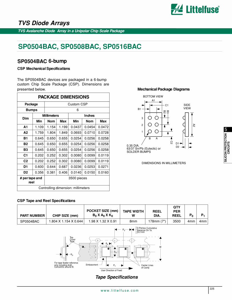
225w w w. l i t t e l f u s e . c o m
5
SIL
ICO
N P
RO
TEC
TIO
NC
IRC
UIT
S
SP0504BAC, SP0508BAC, SP0516BAC
TVS Diode ArraysTVS Avalanche Diode Array in a Unipolar Chip Scale Package
SP0504BAC 6-bump CSP Mechanical Specifications
The SP0504BAC
SP0504BAC
devices are packaged in a 6-bumpcustom Chip Scale Package (CSP). Dimensions arepresented below.
CSP Tape and Reel Specifications
PACKAGE DIMENSIONS
Package Custom CSP
Bumps 6
DimMillimeters Inches
Min Nom Max Min Nom Max
A1 1.109 1.154 1.199 0.0437 0.0454 0.0472
A2 1.759 1.804 1.849 0.0693 0.0710 0.0728
B1 0.645 0.650 0.655 0.0254 0.0256 0.0258
B2 0.645 0.650 0.655 0.0254 0.0256 0.0258
B3 0.645 0.650 0.655 0.0254 0.0256 0.0258
C1 0.202 0.252 0.302 0.0080 0.0099 0.0119
C2 0.202 0.252 0.302 0.0080 0.0099 0.0119
D1 0.600 0.644 0.687 0.0236 0.0253 0.0271
D2 0.356 0.381 0.406 0.0140 0.0150 0.0160
# per tape and reel
3500 pieces
Controlling dimension: millimeters
1
2
3
B
C1
B1
A1
B2
C2
DIMENSIONS IN MILLIMETERS
D1D2
A2
BOTTOM VIEW
SIDEVIEW
A
B3
0.35 DIA.63/37 Sn/Pb (Eutectic) orSOLDER BUMPS
PART NUMBER CHIP SIZE (mm)POCKET SIZE (mm)
B0 X A0 X K0
TAPE WIDTHW
REELDIA.
QTY PER
REEL P0 P1
1.804 X 1.154 X 0.644 1.98 X 1.32 X 0.91 8mm 178mm (7") 3500 4mm 4mm
Top
For tape feeder reference
CoverTape
P1only including draft.Concentric around B.
Ko
Embossment
User Direction of Feed
±0.2 mmPo
Center Linesof Cavity
W
10 Pitches CumulativeTolerance On Ta
Ao
Bo
Mechanical Package Diagrams
Tape Specifications

TVS Diode Arrays
226w w w. l i t t e l f u s e . c o m
SP0504BAC, SP0508BAC, SP0516BAC
TVS Avalanche Diode Array in a Unipolar Chip Scale Package
The SP0508BAC devices are packaged in a 6-bumpcustom Chip Scale Package (CSP). Dimensions arepresented below.
CSP Tape and Reel Specifications
PACKAGE DIMENSIONS
Package Custom CSP
Bumps 10
DimMillimeters Inches
Min Nom Max Min Nom Max
A1 1.109 1.154 1.199 0.0437 0.0454 0.0472
A2 3.059 3.104 3.149 0.1204 0.1222 0.1240
B1 0.645 0.650 0.655 0.0254 0.0256 0.0258
B2 0.645 0.650 0.655 0.0254 0.0256 0.0258
C1 0.202 0.252 0.302 0.0080 0.0099 0.0119
C2 0.202 0.252 0.302 0.0080 0.0099 0.0119
D1 0.600 0.644 0.687 0.0236 0.0253 0.0271
D2 0.356 0.381 0.406 0.0140 0.0150 0.0160
# per tape and reel
3500 pieces
Controlling dimension: millimeters
Mechanical Package Diagrams
4
5
B
C1
B1
A1
B2
C2
D1D2
A2
BOTTOM VIEW
SIDEVIEW
A
1
2
3
DIMENSIONS IN MILLIMETERS
AB
0.35 DIA.63/37 Sn/Pb (Eutectic) orSOLDER BUMPS
PART NUMBER CHIP SIZE (mm)POCKET SIZE (mm)
B0 X A0 X K0
TAPE WIDTHW
REELDIAMETER
QTY PER
REEL P0 P1
SP0508BAC 3.104 X 1.154 X 0.644 3.28 X 1.32 X 0.81 8mm 178mm (7") 3500 4mm 4mm
Top
For tape feeder reference
CoverTape
P1only including draft.Concentric around B.
Ko
Embossment
User Direction of Feed
±0.2 mmPo
Center Linesof Cavity
W
10 Pitches CumulativeTolerance On Ta
Ao
Bo
CSP Mechanical Specifications
SP0508BAC10-bump
Tape Specifications

The SP0516BAC
SP0516BAC
devices are packaged in a 20-bumpcustom Chip Scale Package (CSP). Dimensions arepresented below.
CSP Tape and Reel Specifications
PACKAGE DIMENSIONS
Package Custom CSP
Bumps 20
DimMillimeters Inches
Min Nom Max Min Nom Max
A1 2.409 2.454 2.499 0.0948 0.0966 0.0984
A2 3.059 3.104 3.149 0.1204 0.1222 0.1240
B1 0.645 0.650 0.655 0.0254 0.0256 0.0258
B2 0.645 0.650 0.655 0.0254 0.0256 0.0258
C1 0.202 0.252 0.302 0.0080 0.0099 0.0119
C2 0.202 0.252 0.302 0.0080 0.0099 0.0119
D1 0.600 0.644 0.687 0.0236 0.0253 0.0271
D2 0.356 0.381 0.406 0.0140 0.0150 0.0160
# per tape and reel
3500 pieces
Controlling dimension: millimeters
Mechanical Package Diagrams
4
5
B
C1
B1
A1
B2
C2
D1D2
A2
BOTTOM VIEW
SIDEVIEW
A
1
2
3
DIMENSIONS IN MILLIMETERS
ABCD
0.35 DIA.63/37 Sn/Pb (Eutectic) orSOLDER BUMPS
PART NUMBER CHIP SIZE (mm)POCKET SIZE (mm)
B0 X A0 X K0
TAPE WIDTHW
REELDIAMETER
QTY PER
REEL P0 P1
3.104 X 2.454 X 0.644 3.28 X 2.64 X 0.86 8mm 178mm (7") 3500 4mm 4mm
Top
For tape feeder reference
CoverTape
P1only including draft.Concentric around B.
Ko
Embossment
User Direction of Feed
±0.2 mmPo
Center Linesof Cavity
W
10 Pitches CumulativeTolerance On Ta
Ao
Bo
SP0516BAC 20-bump CSP Mechanical Specifications
TVS Diode Arrays
227w w w. l i t t e l f u s e . c o m
5
SIL
ICO
N P
RO
TEC
TIO
NC
IRC
UIT
S
TVS Avalanche Diode Array in a Unipolar Chip Scale Package
SP0504BAC, SP0508BAC, SP0516BAC
Tape Specifications
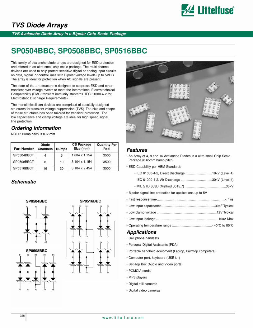
TVS Diode Arrays
228w w w. l i t t e l f u s e . c o m
TVS Avalanche Diode Array in a Bipolar Chip Scale Package
SP0504BBC, SP0508BBC, SP0516BBCThis family of avalanche diode arrays are designed for ESD protectionand offered in an ultra small chip scale package. The multi-channeldevices are used to help protect sensitive digital or analog input circuitson data, signal, or control lines with Bipolar voltage levels up to 5VDC.The array is ideal for protection when AC signals are present.
The state-of-the-art structure is designed to suppress ESD and othertransient over-voltage events to meet the International ElectrotechnicalCompatability (EMC transient immunity stantards IEC 61000-4-2 forElectrostatic Discharge Requirements).
The monolithic silicon devices are comprised of specially designed structures for transient voltage suppression (TVS). The size and shape of these structures has been tailored for transient protection. The low capacitance and clamp voltage are ideal for high speed signal line protection.
Ordering InformationNOTE: Bump pitch is 0.65mm
Schematic
Features• An Array of 4, 8 and 16 Avalanche Diodes in a ultra small Chip Scale
Package (0.65mm bump pitch)
• ESD Capability per HBM Standards
- IEC 61000-4-2, Direct Discharge .............................18kV (Level 4)
- IEC 61000-4-2, Air Discharge ..................................30kV (Level 4)
- MIL STD 883D (Method 3015.7) .............................................30kV
• Bipolar signal line protection for applications up to 5V
• Fast response time..........................................................................< 1ns
• Low input capacitance..........................................................39pF Typical
• Low clamp voltage .................................................................12V Typical
• Low input leakage ....................................................................10uA Max
• Operating temperature range ...........................................- 40°C to 85°C
Applications• Cell phone handsets
• Personal Digital Assistants (PDA)
• Portable handheld equipment (Laptop, Palmtop computers)
• Computer port, keyboard (USB1.1)
• Set-Top Box (Audio and Video ports)
• PCMCIA cards
• MP3 players
• Digital still cameras
• Digital video cameras
Part Number
SP0504BBCT
SP0508BBCT
SP0516BBCT
Quantity PerReel
3500
3500
3500
CS PackageSize (mm)
1.804 x 1.154
3.104 x 1.154
3.104 x 2.454
DiodeChannels
4
8
16
Bumps
6
10
20
B1 B2 B3
A1 A2 A3
D1 D2 D3 D4 D5
C1 C2 C3 C4 C5
B1 B2 B3 B4 B5
A1 A2 A3 A4 A5
B1 B2 B3 B4 B5
A1 A2 A3 A4 A5
SP0504BBC SP0516BBC
SP0508BBC

TVS Diode Arrays
229w w w. l i t t e l f u s e . c o m
5
SIL
ICO
N P
RO
TEC
TIO
NC
IRC
UIT
S
SP0504BBC, SP0508BBC, SP0516BBC
TVS Avalanche Diode Array in a Bipolar Chip Scale Package
Electrical Specifications TA = 25°C Unless Otherwise SpecifiedPARAMETER
Reverse Standoff Voltage
Reverse Standoff Leakage Current
Signal Clamp Voltage
Positive
Negative
Clamp Voltage during ESD
MIL-STD-883D Method 3015
ESD Test Level
IEC-61000-4-2, Contact discharge
MIL-STD-883D Method 3015 (HBM)
Capacitance
Turn on/off Time
Temperature Range
Operating
Storage
TEST CONDITIONS
I = 10µA
V = TBD
I = 10mA
I = 10mA
8 kV Positive
8 kV Negative
2.5VDC @ 1Mhz
MIN
± 5.9
6.0
- 9.2
18
30
- 40
- 65
MAX
-
100
9.2
- 6.0
85
150
UNITS
V
nA
V
V
V
V
kV
kV
pF
ns
°C
°C
TYPICAL
-
7.6
- 7.6
14
-14
39
<1
PRINTED CIRCUIT BOARD RECOMMENDATIONS
PARAMETER VALUE
Pad Size on PCB 0.300mm
Pad Shape Round
Pad Definition Non-Solder Mask defined pads
Solder Mask Opening 0.350mm Round
Solder Stencil Thickness 0.125 - 0.150mm
Solder Stencil Aperture Opening (laser cut, 5% tapered walls) 0.360mm Round
Solder Flux Ratio 50/50 by volume
Solder Paste Type No Clean
Pad Protective Finish OSP (Entek Cu Plus 106A)
Tolerance — Edge To Corner Ball +50µm
Solder Ball Side Coplanarity +20µm
Maximum Dwell Time Above Liquidous 60 seconds
Soldering Maximum Temperature 260°C.
Typical Solder Reflow Thermal Profile (No-Clean Flux)
0 48 97
Time (s)
145 194 242 290 339 387 435
EXHCDRFZZ4Z3Z2PHEXH250
225
200
175
150
125
100
75
50
25
Tem
pera
ture
(o C
)

TVS Avalanche Diode Array in a Bipolar Chip Scale Package
SP0504BBC, SP0508BBC, SP0516BBC
TVS Diode Arrays
230w w w. l i t t e l f u s e . c o m
32 541
B
A
D
C
OrientationMarking
32 541
B
A
OrientationMarking
321
B
A
OrientationMarking
C3
D3
C2C1
D2D1
C5
D5
C4
D4
A3
B3
A2A1
B2B1
A5
B5
A4
B4
A3
B3
A2A1
B2B1
A5
B5
A4
B4
A3
B3
A2A1
B2B1
SP0504BBC
SP0508BBC
SP0516BBC
CSP Package
PACKAGE / PINOUT DIAGRAMS
Notes:
BOTTOM VIEW(Bumps Up View)
TOP VIEW(Bumps Down View)
CSP Package
BOTTOM VIEW(Bumps Up View)
TOP VIEW(Bumps Down View)
CSP Package
BOTTOM VIEW(Bumps Up View)
TOP VIEW(Bumps Down View)
1) These drawings are not to scale.
Solder Mask Opening0.350mm DIA.
Non-Solder Mask Defined Pad0.300mm DIA.
Solder Stencil Opening0.360mm DIA.
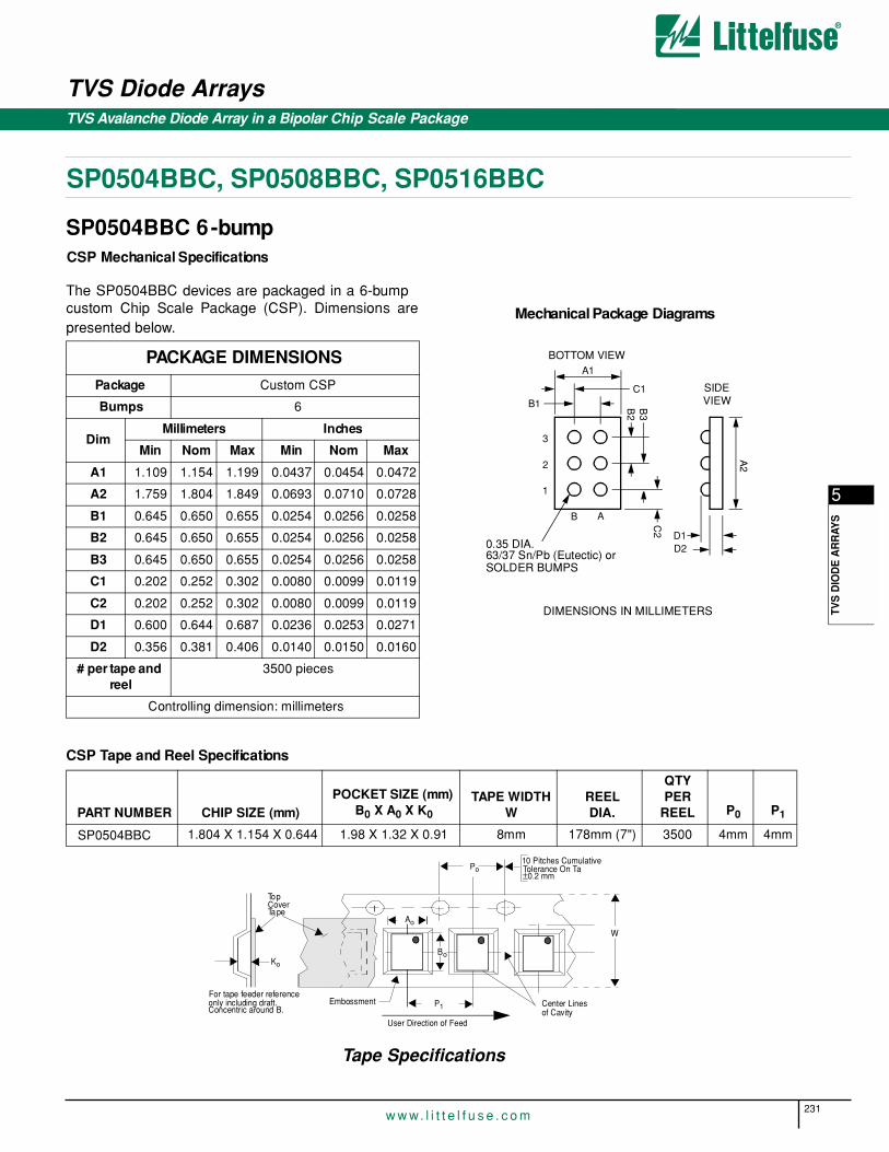
TVS Diode Arrays
231w w w. l i t t e l f u s e . c o m
TVS Avalanche Diode Array in a Bipolar Chip Scale Package
SP0504BBC, SP0508BBC, SP0516BBC
5
TVS
DIO
DE
AR
RAY
S
The SP0504BBC
SP0504BBC
devices are packaged in a 6-bumpcustom Chip Scale Package (CSP). Dimensions arepresented below.
CSP Tape and Reel Specifications
PACKAGE DIMENSIONS
Package Custom CSP
Bumps 6
DimMillimeters Inches
Min Nom Max Min Nom Max
A1 1.109 1.154 1.199 0.0437 0.0454 0.0472
A2 1.759 1.804 1.849 0.0693 0.0710 0.0728
B1 0.645 0.650 0.655 0.0254 0.0256 0.0258
B2 0.645 0.650 0.655 0.0254 0.0256 0.0258
B3 0.645 0.650 0.655 0.0254 0.0256 0.0258
C1 0.202 0.252 0.302 0.0080 0.0099 0.0119
C2 0.202 0.252 0.302 0.0080 0.0099 0.0119
D1 0.600 0.644 0.687 0.0236 0.0253 0.0271
D2 0.356 0.381 0.406 0.0140 0.0150 0.0160
# per tape and reel
3500 pieces
Controlling dimension: millimeters
Mechanical Package Diagrams
1
2
3
B
C1
B1
A1
B2
C2
DIMENSIONS IN MILLIMETERS
D1D2
A2
BOTTOM VIEW
SIDEVIEW
A
B3
0.35 DIA.63/37 Sn/Pb (Eutectic) orSOLDER BUMPS
PART NUMBER CHIP SIZE (mm)POCKET SIZE (mm)
B0 X A0 X K0
TAPE WIDTHW
REELDIA.
QTY PER
REEL P0 P1
1.804 X 1.154 X 0.644 1.98 X 1.32 X 0.91 8mm 178mm (7") 3500 4mm 4mm
Top
For tape feeder reference
CoverTape
P1only including draft.Concentric around B.
Ko
Embossment
User Direction of Feed
±0.2 mmPo
Center Linesof Cavity
W
10 Pitches CumulativeTolerance On Ta
Ao
Bo
SP0504BBC 6-bump CSP Mechanical Specifications
Tape Specifications

TVS Diode Arrays
232w w w. l i t t e l f u s e . c o m
TVS Avalanche Diode Array in a Bipolar Chip Scale Package
SP0504BBC, SP0508BBC, SP0516BBC
The SP0508BBC devices are packaged in a 6-bumpcustom Chip Scale Package (CSP). Dimensions arepresented below.
CSP Tape and Reel Specifications
PACKAGE DIMENSIONS
Package Custom CSP
Bumps 10
DimMillimeters Inches
Min Nom Max Min Nom Max
A1 1.109 1.154 1.199 0.0437 0.0454 0.0472
A2 3.059 3.104 3.149 0.1204 0.1222 0.1240
B1 0.645 0.650 0.655 0.0254 0.0256 0.0258
B2 0.645 0.650 0.655 0.0254 0.0256 0.0258
C1 0.202 0.252 0.302 0.0080 0.0099 0.0119
C2 0.202 0.252 0.302 0.0080 0.0099 0.0119
D1 0.600 0.644 0.687 0.0236 0.0253 0.0271
D2 0.356 0.381 0.406 0.0140 0.0150 0.0160
# per tape and reel
3500 pieces
Controlling dimension: millimeters
Mechanical Package Diagrams
4
5
B
C1
B1
A1
B2
C2
D1D2
A2
BOTTOM VIEW
SIDEVIEW
A
1
2
3
DIMENSIONS IN MILLIMETERS
AB
0.35 DIA.63/37 Sn/Pb (Eutectic) orSOLDER BUMPS
PART NUMBER CHIP SIZE (mm)POCKET SIZE (mm)
B0 X A0 X K0
TAPE WIDTHW
REELDIAMETER
QTY PER
REEL P0 P1
SP0508BBC 3.104 X 1.154 X 0.644 3.28 X 1.32 X 0.81 8mm 178mm (7") 3500 4mm 4mm
Top
For tape feeder reference
CoverTape
P1only including draft.Concentric around B.
Ko
Embossment
User Direction of Feed
±0.2 mmPo
Center Linesof Cavity
W
10 Pitches CumulativeTolerance On Ta
Ao
Bo
SP0508BBC10- bump CSP Mechanical Specifications
Tape Specifications
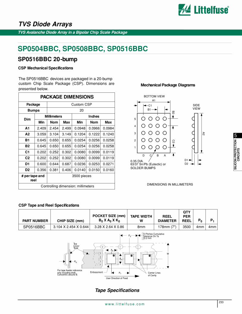
TVS Diode Arrays
233w w w. l i t t e l f u s e . c o m
5
SIL
ICO
N P
RO
TEC
TIO
NC
IRC
UIT
S
The SP0516BBC
SP0516BBC
devices are packaged in a 20-bumpcustom Chip Scale Package (CSP). Dimensions arepresented below.
CSP Tape and Reel Specifications
PACKAGE DIMENSIONS
Package Custom CSP
Bumps 20
DimMillimeters Inches
Min Nom Max Min Nom Max
A1 2.409 2.454 2.499 0.0948 0.0966 0.0984
A2 3.059 3.104 3.149 0.1204 0.1222 0.1240
B1 0.645 0.650 0.655 0.0254 0.0256 0.0258
B2 0.645 0.650 0.655 0.0254 0.0256 0.0258
C1 0.202 0.252 0.302 0.0080 0.0099 0.0119
C2 0.202 0.252 0.302 0.0080 0.0099 0.0119
D1 0.600 0.644 0.687 0.0236 0.0253 0.0271
D2 0.356 0.381 0.406 0.0140 0.0150 0.0160
# per tape and reel
3500 pieces
Controlling dimension: millimeters
Mechanical Package Diagrams
4
5
B
C1
B1
A1
B2
C2
D1D2
A2
BOTTOM VIEW
SIDEVIEW
A
1
2
3
DIMENSIONS IN MILLIMETERS
ABCD
0.35 DIA.63/37 Sn/Pb (Eutectic) orSOLDER BUMPS
PART NUMBER CHIP SIZE (mm)POCKET SIZE (mm)
B0 X A0 X K0
TAPE WIDTHW
REELDIAMETER
QTY PER
REEL P0 P1
3.104 X 2.454 X 0.644 3.28 X 2.64 X 0.86 8mm 178mm (7") 3500 4mm 4mm
Top
For tape feeder reference
CoverTape
P1only including draft.Concentric around B.
Ko
Embossment
User Direction of Feed
±0.2 mmPo
Center Linesof Cavity
W
10 Pitches CumulativeTolerance On Ta
Ao
Bo
SP0516BBC 20-bump CSP Mechanical Specifications
SP0504BBC, SP0508BBC, SP0516BBC
TVS Avalanche Diode Array in a Bipolar Chip Scale Package
Tape Specifications

TVS Diode Arrays
234w w w. l i t t e l f u s e . c o m
TVS Rail Clamp Array in a Surface Mount Package
SP0502AAH, SP0506AAA, SP0506AABThis family of rail clamp or “diode steering” arrays is designed for verylow capacitance ESD protection and is offered in small surface mountpackages. The multi-channel devices are used to help protect high speed sensitive digital or analog input circuits on data, signal, or controllines with unipolar voltage levels up to 5 VDC. The state-of-the-art structure is designed to suppress ESD and other transient over-voltageevents to meet the International Electrotechnical Compatibility (IEC) transient immunity standards IEC 61000-4-2 for Electrostatic Discharge Requirements.
The monolithic silicon devices are comprised of specially designed lowcapacitance structures for transient voltage suppression (TVS). The sizeand shape of these structures have be tailored for transient protection.The low capacitance and clamp voltage are ideal for high speed signalline protection.
Ordering Information
Schematic
Part Number
SP0502AAHT
SP0506AAAT
SP0506AABT
Quantity PerReel
30004000
2500
Package Type
SOT143
MSOP8
SOIC8
CH
2
6
6
1 2 3 4
8 7 6 5
CH 1 CH 2 V- CH 3
CH 6 V+ CH 5 CH 4
SP0506AAHTand
SP0506AABT
SP0502AAHT
1
2 3
4
V+
V-
CH 1 CH 2
Features
• A low capacitance 2, 6 and 18 channel array of rail clamp current steering diodes in small surface mount packages
• ESD Protection Capability (SP0502 and SP0506)- IEC 61000-4-2, Direct Discharge . . . . . . . . . . . . . . . . . . 8kV (Level 4)- MIL STD 3015.7 . . . . . . . . . . . . . . . . . . . . . . . . . . . . . . . . . . . . . . .
15kV• ESD Protection Capability (SP0518)
- IEC 61000-4-2, Direct Discharge . . . . . . . . . . . . . . . . . 15kV (Level 4)- MIL STD 3015.7 . . . . . . . . . . . . . . . . . . . . . . . . . . . . . . . . . . . . . . .
15kV• Input Protection for Applications Up to 5VDC • Fast Response Time . . . . . . . . . . . . . . . . . . . . . . . . . . . . . . . . . . . . . .< 1ns• Low Input Capacitance. . . . . . . . . . . . . . . . . . . . . . . . . . . . . . .3-7pFTypical• Low Clamp Voltage . . . . . . . . . . . . . . . . . . . . . . . . . . . . . . Vrail + 13VMax• Operating Temperature Range. . . . . . . . . . . . . . . . . . . . . - 20°C to +85°C
Applications• Cell phone hand sets • Personal Digital Assistants (PDA)• Portable handheld equipment (Laptop, Palmtop computers)• Computer port, keyboard (USB1.1)• Digital cameras• V6A port protection• Digital still camera• Digital video camera
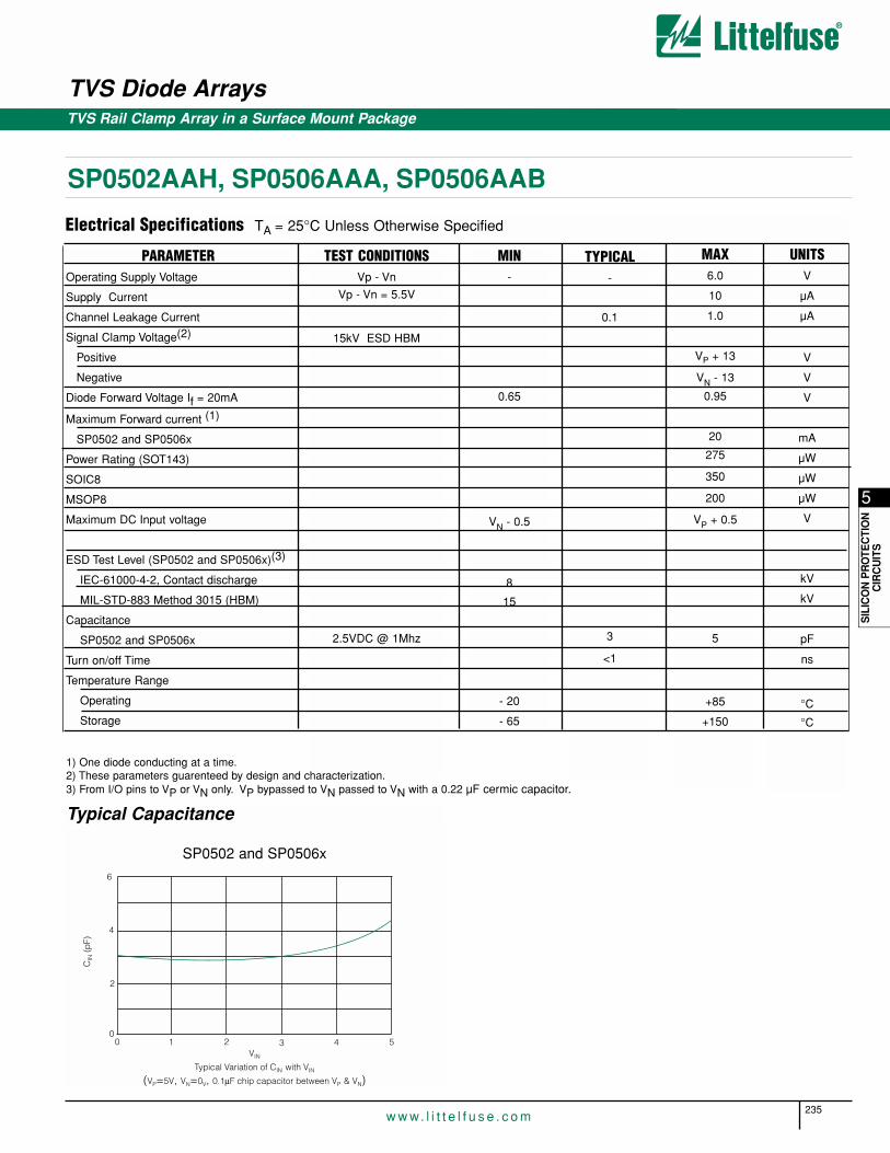
TVS Diode Arrays
235w w w. l i t t e l f u s e . c o m
5
SIL
ICO
N P
RO
TEC
TIO
NC
IRC
UIT
S
TVS Rail Clamp Array in a Surface Mount Package
SP0502AAH, SP0506AAA, SP0506AAB
Electrical Specifications TA = 25°C Unless Otherwise Specified
PARAMETEROperating Supply Voltage
Supply Current
Channel Leakage Current
Signal Clamp Voltage(2)
Positive
Negative
Diode Forward Voltage If = 20mA
Maximum Forward current (1)
SP0502 and SP0506x
Power Rating (SOT143)
SOIC8
MSOP8
Maximum DC Input voltage
ESD Test Level (SP0502 and SP0506x)(3)
IEC-61000-4-2, Contact discharge
MIL-STD-883 Method 3015 (HBM)
Capacitance
SP0502 and SP0506x
Turn on/off Time
Temperature Range
Operating
Storage
TEST CONDITIONSVp - Vn
Vp - Vn = 5.5V
15kV ESD HBM
2.5VDC @ 1Mhz
MIN-
0.65
VN - 0.5
8
15
- 20
- 65
MAX6.0
10
1.0
VP + 13
VN - 13
0.95
20
275
350
200
VP + 0.5
5
+85
+150
UNITSV
µA
µA
V
V
V
mA
µW
µW
µW
V
kV
kV
pF
ns
°C
°C
TYPICAL-
0.1
3
<1
Typical Capacitance
CIN
(p
F)
VIN
Typical Variation of CIN with VIN
(VP=5V, VN=0V, 0.1µF chip capacitor between VP & VN)
0 1 2 3 4 50
2
4
6
SP0502 and SP0506x
1) One diode conducting at a time.2) These parameters guarenteed by design and characterization.3) From I/O pins to VP or VN only. VP bypassed to VN passed to VN with a 0.22 µF cermic capacitor.

TVS Diode Arrays
236w w w. l i t t e l f u s e . c o m
SP0502AAH, SP0506AAA, SP0506AAB
TVS Rail Clamp Array in a Surface Mount Package
502A
E
E1
A
G G1
C
B2B
A1
E2
506 A
E
E1E2
A
A1
BB2
C1C
LF
Outline Drawings
SP0502AAH - SOT143
SP0506AAA - MSOP 8
Package SOT143
mm inches
min max min max
2.80 3.04 .110 .120
1.20 1.40 .047 .055
2.10 2.64 .083 .104
- .020REF - 1.920REF
- 1.920REF - .076
0.890 1.120 .035 .044
0.013 0.100 .0005 .0040
E
E1
E2
G
G1
A
A1
B
B2
C
Z
G
F
F1
0.760 0.940 .030 .037
0.370 0.510 .015 .020
0.0850 0.180 .0033 .0071
3.40 3.60 .134 .140
- 1.70 - .067
- 1.90 - .075
- 2.2REF - .087REF
XX1
X2
0.80 1.00 .032 .040
1.00 1.20 .040 .048
- 1.40 - .055
Package MSOP 8
mm inches
min max min max
2.90 3.10 .114 .122
2.90 3.10 .114 .122
4.78 4.98 .188 .196
0.87 1.17 .034 .046
0.05 0.25 .002 .010
- 0.30 - .012TYP
- 0.65 - .25TYP
E
E1
E2
A
A1
B
B2
C
C1
F
F1
Z
X
G
- 0.18 - .007TYP
0.52 0.54 .017 .025
- 0.65 - .0256
- 0.38 - .015
- 4.24 - .167
- 1.04 - .041
- 5.28 - .208
XX1
X2
G
F1
F
Z
GZ
X
F1F
Recommended Pad Layout
Recommended Pad Layout
Outline Drawings

TVS Diode Arrays
237w w w. l i t t e l f u s e . c o m
TVS Rail Clamp Array in a Surface Mount Package
SP0502AAH, SP0506AAA, SP0506AAB
SP0506 AAB
A1
A
B2B
C
E2
E
E1
C1
LF
SP0506AAB - SOIC 8
Package SOIC 8
mm inches
min max min max
4.80 5.00 .189 .197
3.80 4.19 .150 .165
5.80 6.20 .228 .244
1.35 1.75 .053 .069
0.10 0.25 .004 .010
0.33 0.51 .013 .020
- 1.27 - .050
E
E1
E2
A
A1
B
B2
C
C1
F
F1
Z
X
X1
0.40 1.27 .016 .050
0.19 0.25 .007 .010
- 1.27 - .05
0.60 0.80 .02 .03
- 3.81REF - .15REF
- 2.40 - .09
7.20 7.40 - .29
G - 5.00REF - .19REF
X1
GZ
X
F1F
Recommended Pad Layout
Outline Drawings
5
SIL
ICO
N P
RO
TEC
-TI
ON
CIR
CU
ITS

TVS Diode Arrays
238w w w. l i t t e l f u s e . c o m
Electronic Protection Array for ESD and Overvoltage Protection
SP720The SP720 is an array of SCR/Diode bipolar structures for ESD andover-voltage protection to sensitive input circuits. The SP720 has 2 protection SCR/Diode device structures per input. A total of 14 availableinputs can be used to protect up to 14 external signal or bus lines.Over-voltage protection is from the IN (pins 1-7 and 9-15) to V+ or V-.
The SCR structures are designed for fast triggering at a threshold of one+VBE diode threshold above V+ (Pin 16) or a -VBE diode thresholdbelow V- (Pin 8). From an IN input, a clamp to V+ is activated if a tran-sient pulse causes the input to be increased to a voltage level greaterthan one VBE above V+. A similar clamp to V- is activated if a negativepulse, one VBE less than V-, is applied to an IN input. Standard ESDHuman Body Model (HBM) Capability is:
Features• ESD Interface Capability for HBM Standards
- MIL STD 3015.7 . . . . . . . . . . . . . . . . . . . . . . . . . . . . . . . . . 15kV- IEC 61000-4-2, Direct Discharge,
Single Input . . . . . . . . . . . . . . . . . . . . . . . . . . . . . . 4kV (Level 2)Two Inputs in Parallel . . . . . . . . . . . . . . . . . . . . . . . 8kV (Level 4)
- IEC 61000-4-2, Air Discharge . . . . . . . . . . . . . . . . 15kV (Level 4)
• High Peak Current Capability- IEC 61000-4-5 (8/20µs) . . . . . . . . . . . . . . . . . . . . . . . . . . . . ±3A- Single Pulse, 100µs Pulse Width . . . . . . . . . . . . . . . . . . . . . ±2A- Single Pulse, 4µs Pulse Width . . . . . . . . . . . . . . . . . . . . . . . ±5A
• Designed to Provide Over-Voltage Protection- Single-Ended Voltage Range to . . . . . . . . . . . . . . . . . . . . . +30V- Differential Voltage Range to . . . . . . . . . . . . . . . . . . . . . . . ±15V
• Fast Switching. . . . . . . . . . . . . . . . . . . . . . . . . . . . . . . . 2ns Risetime
• Low Input Leakages . . . . . . . . . . . . . . . . . . . . . . . . 1nA at 25oC (Typ)
• Low Input Capacitance . . . . . . . . . . . . . . . . . . . . . . . . . . . . 3pF (Typ)
• An Array of 14 SCR/Diode Pairs
• Operating Temperature Range . . . . . . . . . . . . . . . . . . . -40oC to 105oC
Applications• Microprocessor/Logic Input Protection
• Data Bus Protection
• Analog Device Input Protection
• Voltage Clamp
Functional Block Diagram
Refer to Figure 1 and Table 1 for further detail. Refer to Application NoteAN9304 and AN9612 for additional information.
Ordering Information
HBM STANDARD MODE R C ESD (V)
IEC 61000-4-2 Air 330Ω 150pF >15kV
Direct 330Ω 150pF >4kV
Direct, Dual Pins 330Ω 150pF >8kV
MIL-STD-3015.7 Direct, In-circuit 1.5kΩ 100pF >15kV
PART NO.TEMP. RANGE
(oC) PACKAGEPKG. Min.
Order NO.
SP720AP -40 to 105 16 Ld PDIP E16.3 1500
1970
2500
SP720AB -40 to 105 16 Ld SOIC M16.15
SP720ABT -40 to 105 16 Ld SOICTape and Reel
M16.15
PinoutSP720 (PDIP, SOIC)
TOP VIEW
14
15
16
9
13
12
11
10
1
2
3
4
5
7
6
8
IN
IN
IN
IN
IN
IN
V-
IN
V+
IN
IN
IN
IN
IN
IN
IN
V+ 16
1
8
2
3 - 79 - 15
IN
IN
IN
V-
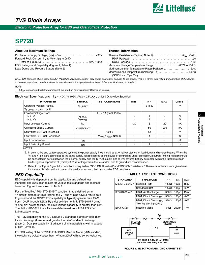
239w w w. l i t t e l f u s e . c o m
5
SIL
ICO
N P
RO
TEC
TIO
NC
IRC
UIT
S
SP720
TVS Diode ArraysElectronic Protection Array for ESD and Overvoltage Protection
ESD CapabilityESD capability is dependent on the application and defined test standard. The evaluation results for various test standards and methodsbased on Figure 1 are shown in Table 1.
For the “Modified” MIL-STD-3015.7 condition that is defined as an “in-circuit” method of ESD testing, the V+ and V- pins have a return pathto ground and the SP720 ESD capability is typically greater than 15kVfrom 100pF through 1.5kΩ. By strict definition of MIL-STD-3015.7 using “pin-to-pin” device testing, the ESD voltage capability is greater than 6kV.The MIL-STD-3015.7 results were determined from AT&T ESD Test Lab measurements.
The HBM capability to the IEC 61000-4-2 standard is greater than 15kVfor air discharge (Level 4) and greater than 4kV for direct discharge(Level 2). Dual pin capability (2 adjacent pins in parallel) is well in excessof 8kV (Level 4).
For ESD testing of the SP720 to EIAJ IC121 Machine Model (MM) standard,the results are typically better than 1kV from 200pF with no series resistance.
Absolute Maximum RatingsContinuous Supply Voltage, (V+) - (V-). . . . . . . . . . . . . . . . . . . . . . . . . +35VForward Peak Current, IIN to VCC, IIN to GND
(Refer to Figure 6) . . . . .. . . . . . . . . . . . . . . . . . . . . . . . . . . . . ±2A, 100µsESD Ratings and Capability (Figure 1, Table 1)Load Dump and Reverse Battery (Note 2)
Thermal InformationThermal Resistance (Typical, Note 1). . . . . . . . . . . . . . . . . . . . . θJA (oC/W)
PDIP Package . . . . . . . . . . . . . . . . . . . . . . . . . . . . . . . . . . . . . . . . . . . . .90SOIC Package . . . . . . . . . . . . . . . . . . . . . . . . . . . . . . . . . . . . . . . . . . . 130
Maximum Storage Temperature Range . . . .. . . . . . . . . . . . . . . -65oC to 150oCMaximum Junction Temperature (Plastic Package) . . . . . . . . . . . . . . . . . . . . . 150oCMaximum Lead Temperature (Soldering 10s) . . . . . . . . .. . . . . . .. . . . . . . . . .300oC
(SOIC Lead Tips Only)CAUTION: Stresses above those listed in “Absolute Maximum Ratings” may cause permanent damage to the device. This is a stress only rating and operation of the deviceat these or any other conditions above those indicated in the operational sections of this specification is not implied.
NOTE:1. θJA is measured with the component mounted on an evaluation PC board in free air.
Electrical Specifications TA = -40oC to 105oC; VIN = 0.5VCC , Unless Otherwise Specified
PARAMETER SYMBOL TEST CONDITIONS MIN TYP MAX UNITS
Operating Voltage Range,VSUPPLY = [(V+) - (V-)]
VSUPPLY - 2 to 30 - V
Forward Voltage Drop:IN to V-IN to V+
VFWDLVFWDH
IIN = 1A (Peak Pulse)--
22
--
VV
Input Leakage Current IIN -20 5 20 nA
Quiescent Supply Current IQUIESCENT - 50 200 nA
Equivalent SCR ON Threshold Note 3 - 1.1 - V
Equivalent SCR ON Resistance VFWD/IFWD; Note 3 - 1 - ΩInput Capacitance CIN 3 pF
Input Switching Speed tON 2 ns
NOTES:
2. In automotive and battery operated systems, the power supply lines should be externally protected for load dump and reverse battery. When the V+ and V- pins are connected to the same supply voltage source as the device or control line under protection, a current limiting resistor should be connected in series between the external supply and the SP720 supply pins to limit reverse battery current to within the rated maximum limits. Bypass capacitors of typically 0.01µF or larger from the V+ and V- pins to ground are recommended.
3. Refer to the Figure 3 graph for definitions of equivalent “SCR ON Threshold” and “SCR ON Resistance.” These characteristics are given here for thumb-rule information to determine peak current and dissipation under EOS conditions.
- -
- -
STANDARD TYPE/MODE RD CD ±VD
MIL STD 3015.7 Modified HBM 1.5kΩ 100pF 15kV
Standard HBM 1.5kΩ 100pF 6kV
IEC 61000-4-2 HBM, Air Discharge 330Ω 150pF 15kV
HBM, Direct Discharge 330Ω 150pF 4kV
HBM, Direct Discharge,Two Parallel Input Pins
330Ω 150pF 8kV
EIAJ IC121 Machine Model 0kΩ 200pF 1kV
H.V.SUPPLY
°±VD
IN
DUT
CD
R1
IEC 1000-4-2: R1 50 to 100MΩ
RD
CHARGESWITCH
DISCHARGESWITCH
MIL STD 3015.7: R1 1 to 10MΩ
FIGURE 1. ELECTROSTATIC DISCHARGE TEST
TABLE 1. ESD TEST CONDITIONS

TVS Diode Arrays
240w w w. l i t t e l f u s e . c o m
Electronic Protection Array for ESD and Overvoltage Protection
SP720
FIGURE 2. LOW CURRENT SCR FORWARD VOLTAGE DROP CURVE
FIGURE 3. HIGH CURRENT SCR FORWARD VOLTAGE DROP CURVE
600 800 1000 1200FORWARD SCR VOLTAGE DROP (mV)
100
80
60
40
20
0
FO
RW
AR
D S
CR
CU
RR
EN
T (
mA
)
TA = 25oCSINGLE PULSE
2.5
2
1.5
1
0.5
0
FO
RW
AR
D S
CR
CU
RR
EN
T (
A)
TA = 25oCSINGLE PULSE
VFWD
IFWD
0 1 2 3FORWARD SCR VOLTAGE DROP (V)
EQUIV. SAT. ONTHRESHOLD ~ 1.1V
FIGURE 4. TYPICAL APPLICATION OF THE SP720 AS AN INPUT CLAMP FOR OVER-VOLTAGE, GREATER THAN 1VBE ABOVE V+ OR LESS THAN -1VBE BELOW V-
+VCC+VCC
INPUT DRIVERS
PROTECTION CIRCUIT(1 OF 14 ON CHIP)
SP720 INPUT
ORSIGNAL
SOURCES
IN 9-15IN 1-7
SP720
V-
TO +VCC
LINEAR ORDIGITAL ICINTERFACE
V+

241w w w. l i t t e l f u s e . c o m
5
SIL
ICO
N P
RO
TEC
TIO
NC
IRC
UIT
S
SP720
TVS Diode ArraysElectronic Protection Array for ESD and Overvoltage Protection
Peak Transient Current Capability of the SP720The peak transient current capability rises sharply as the width of the current pulse narrows. Destructive testing was done to fully evaluate theSP720’s ability to withstand a wide range of transient current pulses. Thecircuit used to generate current pulses is shown in Figure 5.
The test circuit of Figure 5 is shown with a positive pulse input. For anegative pulse input, the (-) current pulse input goes to an SP720 ‘IN’input pin and the (+) current pulse input goes to the SP720 V- pin. TheV+ to V- supply of the SP720 must be allowed to float. (i.e., It is not tiedto the ground reference of the current pulse generator.) Figure 6 showsthe point of overstress as defined by increased leakage in excess of thedata sheet published limits.
The maximum peak input current capability is dependent on the V+ to V-voltage supply level, improving as the supply voltage is reduced. Values of 0, 5, 15 and 30 voltages are shown. The safe operating range of thetransient peak current should be limited to no more than 75% of themeasured overstress level for any given pulse width as shown in Figure 6.
When adjacent input pins are paralleled, the sustained peak currentcapability is increased to nearly twice that of a single pin. For compari-son, tests were run using dual pin combinations 1+2, 3+4, 5+6, 7+9,10+11, 12+13 and 14+15.
The overstress curve is shown in Figure 6 for a 15V supply condition. Thedual pins are capable of 10A peak current for a 10µs pulse and 4A peakcurrent for a 1ms pulse. The complete for single pulse peak current vs.pulse width time ranging up to 1 second are shown in Figure 6.
+
- CURRENTSENSE
VOLTAGEPROBE
14
15
16
9
13
12
11
10
1
2
3
4
5
7
6
8
IN
IN
IN
IN
IN
IN
V-
IN
V+
IN
IN
IN
IN
IN
IN
IN
+
-
R1 ~ 10Ω TYPICAL
SP720
VG
VG ADJ. 10V/A TYPICAL
R1
(-)
(+)
C1 ~ 100µF
C1
VARIABLE TIME DURATIONCURRENT PULSE GENERATOR
FIGURE 5. TYPICAL SP720 PEAK CURRENT TEST CIRCUIT WITH A VARIABLE PULSE WIDTH INPUT
0.001 0.01 0.1 1 PULSE WIDTH TIME (ms)
PE
AK
CU
RR
EN
T (
A)
10
7
6
5
4
3
2
1
0
0V5V
15V
V+ TO V- SUPPLY
100 1000
10
9
30V
15V
CAUTION: SAFE OPERATING CONDITIONS LIMIT
OF THE VALUES SHOWN ON EACH CURVE.PULSE WIDTH TO BE NO GREATER THAN 75% THE MAXIMUM PEAK CURRENT FOR A GIVEN
SINGLE PIN STRESS CURVESDUAL PIN STRESS CURVE
8
FIGURE 6. SP720 TYPICAL SINGLE PULSE PEAK CURRENT CURVES SHOWING THE MEASURED POINT OF OVER-STRESS IN AMPERES vs PULSE TIME IN MILLISECONDS (TA = 25oC)
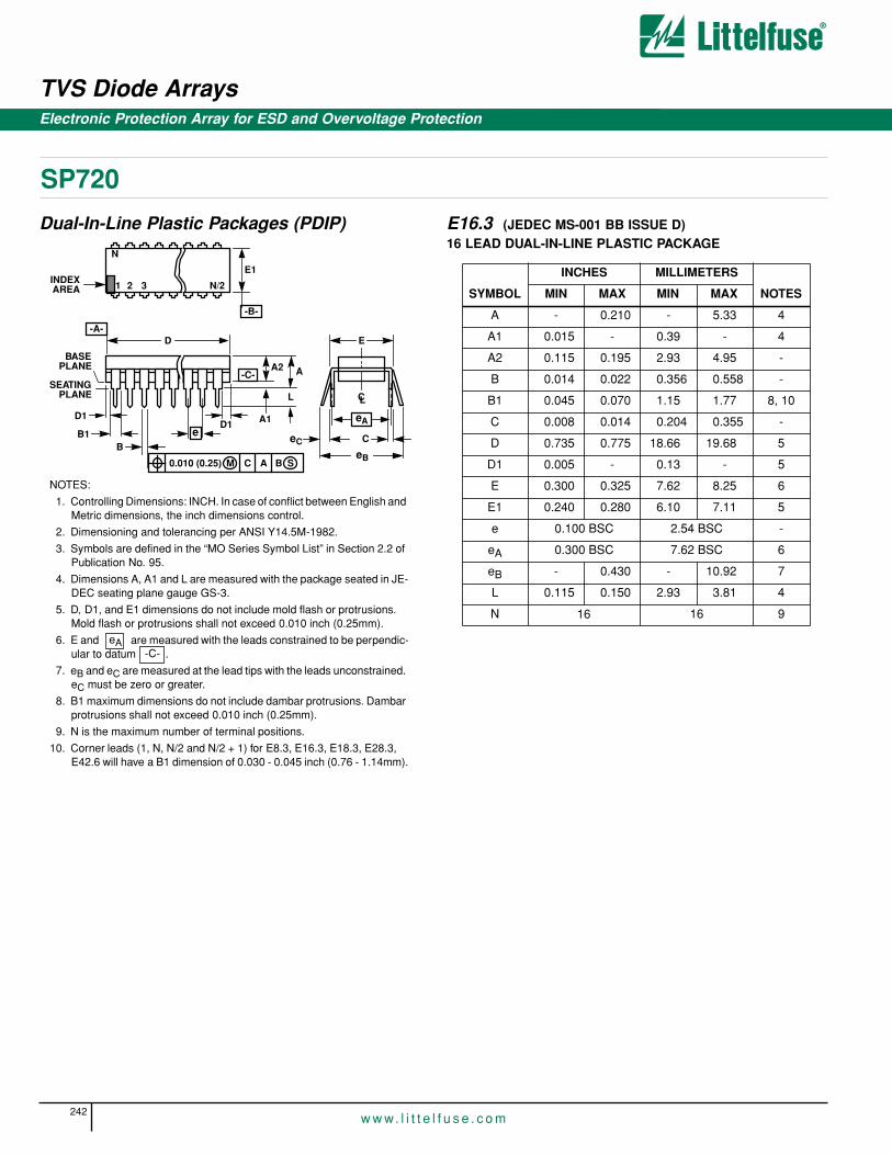
TVS Diode Arrays
242w w w. l i t t e l f u s e . c o m
Electronic Protection Array for ESD and Overvoltage Protection
SP720
Dual-In-Line Plastic Packages (PDIP)
NOTES:
1. Controlling Dimensions: INCH. In case of conflict between English and Metric dimensions, the inch dimensions control.
2. Dimensioning and tolerancing per ANSI Y14.5M-1982.
3. Symbols are defined in the “MO Series Symbol List” in Section 2.2 of Publication No. 95.
4. Dimensions A, A1 and L are measured with the package seated in JE-DEC seating plane gauge GS-3.
5. D, D1, and E1 dimensions do not include mold flash or protrusions. Mold flash or protrusions shall not exceed 0.010 inch (0.25mm).
6. E and are measured with the leads constrained to be perpendic-ular to datum .
7. eB and eC are measured at the lead tips with the leads unconstrained. eC must be zero or greater.
8. B1 maximum dimensions do not include dambar protrusions. Dambar protrusions shall not exceed 0.010 inch (0.25mm).
9. N is the maximum number of terminal positions.
10. Corner leads (1, N, N/2 and N/2 + 1) for E8.3, E16.3, E18.3, E28.3, E42.6 will have a B1 dimension of 0.030 - 0.045 inch (0.76 - 1.14mm).
eA-C-
CL
E
eA
C
eB
eC
-B-
E1INDEX
1 2 3 N/2
N
AREA
SEATING
BASEPLANE
PLANE
-C-
D1
B1B
e
D
D1
AA2
L
A1
-A-
0.010 (0.25) C AM B S
SYMBOL
INCHES MILLIMETERS
NOTESMIN MAX MIN MAX
A - 0.210 - 5.33 4
A1 0.015 - 0.39 - 4
A2 0.115 0.195 2.93 4.95 -
B 0.014 0.022 0.356 0.558 -
B1 0.045 0.070 1.15 1.77 8, 10
C 0.008 0.014 0.204 0.355 -
D 0.735 0.775 18.66 19.68 5
D1 0.005 - 0.13 - 5
E 0.300 0.325 7.62 8.25 6
E1 0.240 0.280 6.10 7.11 5
e 0.100 BSC 2.54 BSC -
eA 0.300 BSC 7.62 BSC 6
eB - 0.430 - 10.92 7
L 0.115 0.150 2.93 3.81 4
N 16 9 16
E16.3 (JEDEC MS-001 BB ISSUE D)16 LEAD DUAL-IN-LINE PLASTIC PACKAGE
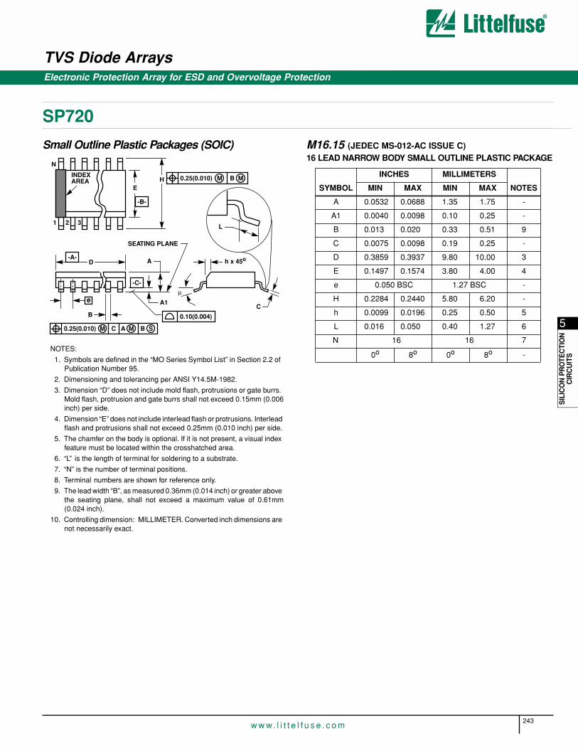
243w w w. l i t t e l f u s e . c o m
5
SIL
ICO
N P
RO
TEC
TIO
NC
IRC
UIT
S
SP720
TVS Diode ArraysElectronic Protection Array for ESD and Overvoltage Protection
Small Outline Plastic Packages (SOIC) M16.15 (JEDEC MS-012-AC ISSUE C)16 LEAD NARROW BODY SMALL OUTLINE PLASTIC PACKAGE
SYMBOL
INCHES MILLIMETERS
NOTESMIN MAX MIN MAX
A 0.0532 0.0688 1.35 1.75 -
A1 0.0040 0.0098 0.10 0.25 -
B 0.013 0.020 0.33 0.51 9
C 0.0075 0.0098 0.19 0.25 -
D 0.3859 0.3937 9.80 10.00 3
E 0.1497 0.1574 3.80 4.00 4
e 0.050 BSC 1.27 BSC -
H 0.2284 0.2440 5.80 6.20 -
h 0.0099 0.0196 0.25 0.50 5
L 0.016 0.050 0.40 1.27 6
N 16 16 7
0o 8o 0o 8o -NOTES:
1. Symbols are defined in the “MO Series Symbol List” in Section 2.2 of Publication Number 95.
2. Dimensioning and tolerancing per ANSI Y14.5M-1982.
3. Dimension “D” does not include mold flash, protrusions or gate burrs. Mold flash, protrusion and gate burrs shall not exceed 0.15mm (0.006inch) per side.
4. Dimension “E” does not include interlead flash or protrusions. Interlead flash and protrusions shall not exceed 0.25mm (0.010 inch) per side.
5. The chamfer on the body is optional. If it is not present, a visual index feature must be located within the crosshatched area.
6. “L” is the length of terminal for soldering to a substrate.
7. “N” is the number of terminal positions.
8. Terminal numbers are shown for reference only.
9. The lead width “B”, as measured 0.36mm (0.014 inch) or greater above the seating plane, shall not exceed a maximum value of 0.61mm(0.024 inch).
10. Controlling dimension: MILLIMETER. Converted inch dimensions are not necessarily exact.
INDEXAREA
E
D
N
1 2 3
-B-
0.25(0.010) C AM B S
e
-A-
L
B
M
-C-
A1
A
SEATING PLANE
0.10(0.004)
h x 45o
C
H
µ
0.25(0.010) BM M
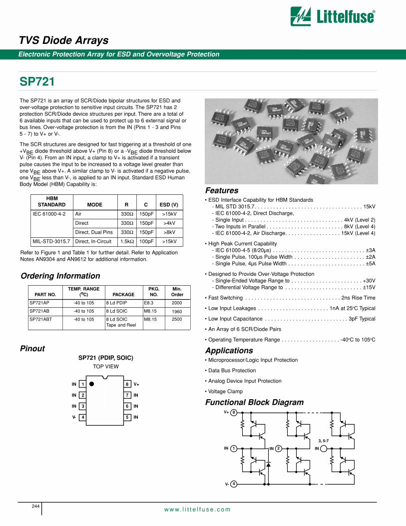
TVS Diode Arrays
244w w w. l i t t e l f u s e . c o m
Electronic Protection Array for ESD and Overvoltage Protection
SP721The SP721 is an array of SCR/Diode bipolar structures for ESD andover-voltage protection to sensitive input circuits. The SP721 has 2 protection SCR/Diode device structures per input. There are a total of 6 available inputs that can be used to protect up to 6 external signal orbus lines. Over-voltage protection is from the IN (Pins 1 - 3 and Pins 5 - 7) to V+ or V-.
The SCR structures are designed for fast triggering at a threshold of one+VBE diode threshold above V+ (Pin 8) or a -VBE diode threshold belowV- (Pin 4). From an IN input, a clamp to V+ is activated if a transientpulse causes the input to be increased to a voltage level greater thanone VBE above V+. A similar clamp to V- is activated if a negative pulse,one VBE less than V-, is applied to an IN input. Standard ESD HumanBody Model (HBM) Capability is:
Features• ESD Interface Capability for HBM Standards
- MIL STD 3015.7. . . . . . . . . . . . . . . . . . . . . . . . . . . . . . . . . . . 15kV- IEC 61000-4-2, Direct Discharge,- Single Input . . . . . . . . . . . . . . . . . . . . . . . . . . . . . . . . 4kV (Level 2)- Two Inputs in Parallel . . . . . . . . . . . . . . . . . . . . . . . . . 8kV (Level 4)- IEC 61000-4-2, Air Discharge. . . . . . . . . . . . . . . . . . 15kV (Level 4)
• High Peak Current Capability- IEC 61000-4-5 (8/20µs) . . . . . . . . . . . . . . . . . . . . . . . . . . . . . . ±3A- Single Pulse, 100µs Pulse Width . . . . . . . . . . . . . . . . . . . . . . . ±2A- Single Pulse, 4µs Pulse Width . . . . . . . . . . . . . . . . . . . . . . . . . ±5A
• Designed to Provide Over-Voltage Protection- Single-Ended Voltage Range to . . . . . . . . . . . . . . . . . . . . . . . +30V- Differential Voltage Range to . . . . . . . . . . . . . . . . . . . . . . . . . ±15V
• Fast Switching . . . . . . . . . . . . . . . . . . . . . . . . . . . . . . . 2ns Rise Time
• Low Input Leakages . . . . . . . . . . . . . . . . . . . . . . . 1nA at 25oC Typical
• Low Input Capacitance . . . . . . . . . . . . . . . . . . . . . . . . . . . 3pF Typical
• An Array of 6 SCR/Diode Pairs
• Operating Temperature Range . . . . . . . . . . . . . . . . . . . -40oC to 105oC
Applications• Microprocessor/Logic Input Protection
• Data Bus Protection
• Analog Device Input Protection
• Voltage Clamp
Functional Block Diagram
4
V+
V-
IN
3, 5-7
IN IN1
8
2
Refer to Figure 1 and Table 1 for further detail. Refer to ApplicationNotes AN9304 and AN9612 for additional information.
PinoutSP721 (PDIP, SOIC)
TOP VIEW
HBMSTANDARD MODE R C ESD (V)
IEC 61000-4-2 Air 330Ω 150pF >15kV
Direct 330Ω 150pF >4kV
Direct, Dual Pins 330Ω 150pF >8kV
MIL-STD-3015.7 Direct, In-Circuit 1.5kΩ 100pF >15kV
Ordering Information
PART NO.TEMP. RANGE
(oC) PACKAGEPKG. NO.
Min. Order
SP721AP -40 to 105 8 Ld PDIP E8.3 2000
1960
2500
SP721AB -40 to 105 8 Ld SOIC M8.15
SP721ABT -40 to 105 8 Ld SOICTape and Reel
M8.15
IN
IN
IN
V-
1
2
3
4
8
7
6
5
V+
IN
IN
IN

245w w w. l i t t e l f u s e . c o m
5
SIL
ICO
N P
RO
TEC
TIO
NC
IRC
UIT
S
SP721
TVS Diode ArraysElectronic Protection Array for ESD and Overvoltage Protection
Absolute Maximum Ratings Continuous Supply Voltage, (V+) - (V-). . . . . . . . . . . . . . . . . . . . . . . . . +35V
Forward Peak Current, IIN to VCC , IIN to GND(Refer to Figure 6). . . . . . . . . . . . . . . . . . . . . . . . . . . . . . . . . . ±2A, 100µs
ESD Ratings and Capability (Figure 1, Table 1)Load Dump and Reverse Battery (Note 2)
Thermal InformationThermal Resistance (Typical, Note 1) θJA (oC/W)
PDIP Package . . . . . . . . . . . . . . . . . . . . . . . . . . . . . . . . . . . . . . . . . . . .160SOIC Package . . . . . . . . . . . . . . . . . . . . . . . . . . . . . . . . . . . . . . . . . . . 170
Maximum Storage Temperature Range . . . . . . . . . . . . . . . . . . . . -65oC to 150oCMaximum Junction Temperature (Plastic Package) . . . .. . . . . . . . . . . . . . . . 150oCMaximum Lead Temperature (Soldering 10s). . . . . . . . . . . . . . .. . . . . . . . . . . .300oC
(SOIC Lead Tips Only)
PARAMETER SYMBOL TEST CONDITIONS MIN TYP MAX UNITS
Operating Voltage Range,VSUPPLY = [(V+) - (V-)]
VSUPPLY - 2 to 30 - V
Forward Voltage Drop
IN to V-IN to V+
VFWDLVFWDH
IIN = 1A (Peak Pulse) --
22
--
VV
Input Leakage Current IIN -20 5 +20 nA
Quiescent Supply Current IQUIESCENT - 50 200 nA
Equivalent SCR ON Threshold Note 3 - 1.1 - V
Equivalent SCR ON Resistance VFWD/IFWD; Note 3 - 1 - Ω
Input Capacitance CIN - 3 - pF
Input Switching Speed tON - 2 - ns
NOTES:
2. In automotive and battery operated systems, the power supply lines should be externally protected for load dump and reverse battery. When the V+ and V- Pins are connected to the same supply voltage source as the device or control line under protection, a current limiting resistor should be connected in series between the external supply and the SP721 supply pins to limit reverse battery current to within the rated maximum limits. Bypass capacitors of typically 0.01µF or larger from the V+ and V- Pins to ground are recommended.
3. Refer to the Figure 3 graph for definitions of equivalent “SCR ON Threshold” and “SCR ON Resistance”. These characteristics are given here for thumb-rule information to determine peak current and dissipation under EOS conditions.
ESD CapabilityESD capability is dependent on the application and defined test standard.Theevaluation results for various test standards and methods based on Figure 1are shown in Table 1.
For the “Modified” MIL-STD-3015.7 condition that is defined as an “in-circuit”method of ESD testing, the V+ and V- pins have a return path to ground andthe SP721 ESD capability is typically greater than 15kV from 100pF through1.5kΩ. By strict definition of MIL-STD-3015.7 using “pin-to-pin” device testing,the ESD voltage capability is greater than 6kV. The MIL-STD-3015.7 resultswere determined from AT&T ESD Test Lab measurements.
The HBM capability to the IEC 61000-4-2 standard is greater than 15kVfor air discharge (Level 4) and greater than 4kV for direct discharge(Level 2). Dual pin capability (2 adjacent pins in parallel) is well in excessof 8kV (Level 4).
For ESD testing of the SP721 to EIAJ IC121 Machine Model (MM) standard,the results are typically better than 1kV from 200pF with no series resistance.
CAUTION: Stresses above those listed in “Absolute Maximum Ratings” may cause permanent damage to the device. This is a stress only rating and operation of the deviceat these or any other conditions above those indicated in the operational sections of this specification is not implied.
NOTE:1. θJA is measured with the component mounted on an evaluation PC board in free air.
Electrical Specifications T A = -40oC to 105oC, VIN = 0.5VCC , Unless Otherwise Specified
H.V.SUPPLY
±VD
IN
DUT
CD
R1
IEC 1000-4-2: R150 to 100MΩ
RD
CHARGESWITCH
DISCHARGESWITCH
MIL-STD-3015.7: R11 to 10MΩ
FIGURE 1. ELECTROSTATIC DISCHARGE TEST
STANDARD TYPE/MODE RD CD ±VD
MIL-STD-3015.7 Modified HBM 1.5kΩ 100pF 15kV
Standard HBM 1.5kΩ 100pF 6kV
IEC 61000-4-2 HBM, Air Discharge 330Ω 150pF 15kV
HBM, Direct Discharge 330Ω 150pF 4kV
HBM, Direct Discharge,Two Parallel Input Pins
330Ω 150pF 8kV
EIAJ IC121 Machine Model 0kΩ 200pF 1kV
TABLE 1. ESD TEST CONDITIONS

TVS Diode Arrays
246w w w. l i t t e l f u s e . c o m
Electronic Protection Array for ESD and Overvoltage Protection
FIGURE 2. LOW CURRENT SCR FORWARD VOLTAGE DROP CURVE
FIGURE 3. HIGH CURRENT SCR FORWARD VOLTAGE DROP CURVE
600 800 1000 1200
FORWARD SCR VOLTAGE DROP (mV)
100
80
60
40
20
0
FO
RW
AR
D S
CR
CU
RR
EN
T (
mA
)
TA = 25oCSINGLE PULSE
2.5
2
1.5
1
0.5
0
FO
RW
AR
D S
CR
CU
RR
EN
T (
A)
TA = 25oCSINGLE PULSE
VFWD
IFWD
0 1 2 3FORWARD SCR VOLTAGE DROP (V)
EQUIV. SAT. ONTHRESHOLD ~ 1.1V
FIGURE 4. TYPICAL APPLICATION OF THE SP721 AS AN INPUT CLAMP FOR OVER-VOLTAGE, GREATER THAN 1VBE ABOVE V+ OR LESS THAN -1VBE BELOW V-
+VCC
INPUT DRIVERS
SP721 INPUT PROTECTION CIRCUIT (1 OF 6 SHOWN)
ORSIGNAL
SOURCES
IN 5 - 7IN 1 - 3
SP721
V-
TO +VCC
LINEAR ORDIGITAL ICINTERFACE
V+
+VCC
SP721
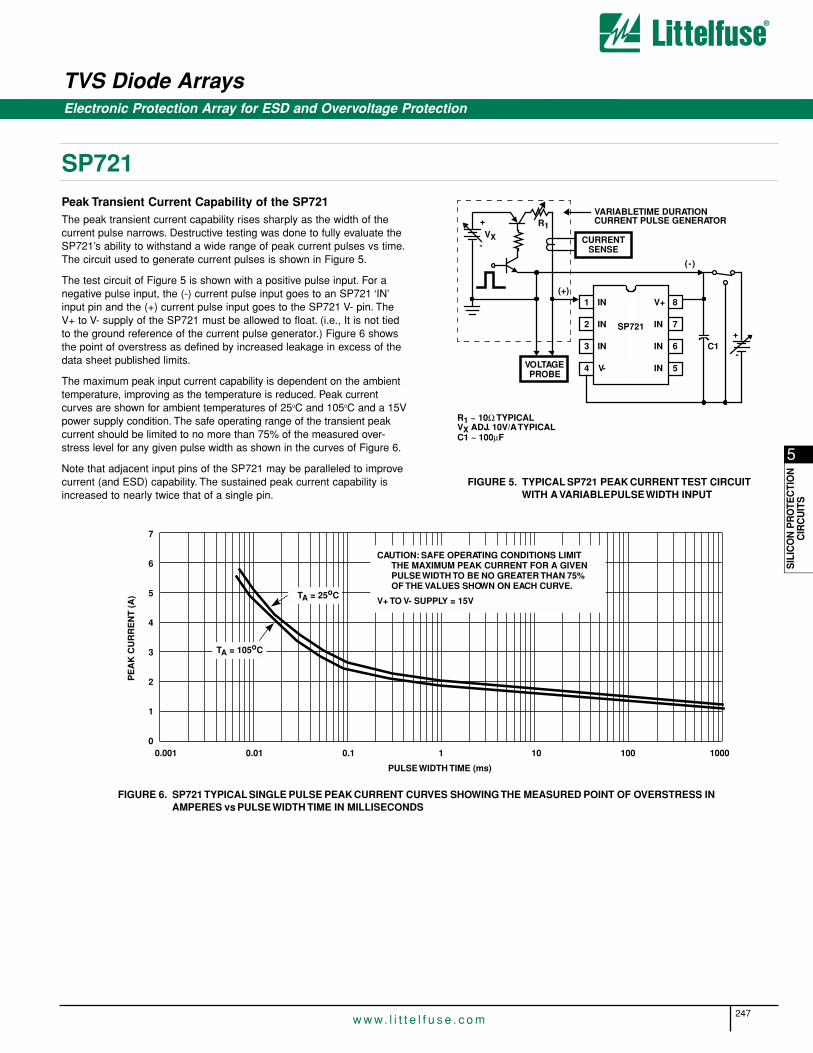
247w w w. l i t t e l f u s e . c o m
5
SIL
ICO
N P
RO
TEC
TIO
NC
IRC
UIT
S
SP721
TVS Diode ArraysElectronic Protection Array for ESD and Overvoltage Protection
Peak Transient Current Capability of the SP721The peak transient current capability rises sharply as the width of thecurrent pulse narrows. Destructive testing was done to fully evaluate theSP721’s ability to withstand a wide range of peak current pulses vs time.The circuit used to generate current pulses is shown in Figure 5.
The test circuit of Figure 5 is shown with a positive pulse input. For anegative pulse input, the (-) current pulse input goes to an SP721 ‘IN’input pin and the (+) current pulse input goes to the SP721 V- pin. TheV+ to V- supply of the SP721 must be allowed to float. (i.e., It is not tiedto the ground reference of the current pulse generator.) Figure 6 showsthe point of overstress as defined by increased leakage in excess of thedata sheet published limits.
The maximum peak input current capability is dependent on the ambienttemperature, improving as the temperature is reduced. Peak currentcurves are shown for ambient temperatures of 25oC and 105oC and a 15Vpower supply condition. The safe operating range of the transient peakcurrent should be limited to no more than 75% of the measured over-stress level for any given pulse width as shown in the curves of Figure 6.
Note that adjacent input pins of the SP721 may be paralleled to improvecurrent (and ESD) capability. The sustained peak current capability isincreased to nearly twice that of a single pin.
+
-
VOLTAGEPROBE
+
-
R1 ~ 10Ω TYPICAL
VX
VX ADJ. 10V/A TYPICAL
R1
(-)
(+)
C1 ~ 100µF
C1
VARIABLE TIME DURATIONCURRENT PULSE GENERATOR
1
2
3
4
8
7
6
5
V+
IN
IN
IN
IN
IN
IN
V-
SP721
CURRENTSENSE
FIGURE 5. TYPICAL SP721 PEAK CURRENT TEST CIRCUITWITH A VARIABLE PULSE WIDTH INPUT
0.001 0.01 0.1 1
PULSE WIDTH TIME (ms)
PE
AK
CU
RR
EN
T (
A)
10
7
6
5
4
3
2
1
0
TA = 105oC
100 1000
CAUTION: SAFE OPERATING CONDITIONS LIMIT
OF THE VALUES SHOWN ON EACH CURVE.PULSE WIDTH TO BE NO GREATER THAN 75% THE MAXIMUM PEAK CURRENT FOR A GIVEN
V+ TO V- SUPPLY = 15VTA = 25oC
FIGURE 6. SP721 TYPICAL SINGLE PULSE PEAK CURRENT CURVES SHOWING THE MEASURED POINT OF OVERSTRESS IN AMPERES vs PULSE WIDTH TIME IN MILLISECONDS

TVS Diode Arrays
248w w w. l i t t e l f u s e . c o m
Electronic Protection Array for ESD and Overvoltage Protection
SP721
Dual-In-Line Plastic Packages (PDIP)
CL
E
eA
C
eB
eC
-B-
E1INDEX
1 2 3 N/2
N
AREA
SEATING
BASEPLANE
PLANE
-C-
D1
B1B
e
D
D1
AA2
L
A1
-A-
0.010 (0.25) C AM B S
NOTES:
1. Controlling Dimensions: INCH. In case of conflict between English and Metric dimensions, the inch dimensions control.
2. Dimensioning and tolerancing per ANSI Y14.5M-1982.
3. Symbols are defined in the “MO Series Symbol List” in Section 2.2 of Publication No. 95.
4. Dimensions A, A1 and L are measured with the package seated in JEDEC seating plane gauge GS-3.
5. D, D1, and E1 dimensions do not include mold flash or protru-sions. Mold flash or protrusions shall not exceed 0.010 inch(0.25mm).
6. E and are measured with the leads constrained to be per-pendicular to datum .
7. eB and eC are measured at the lead tips with the leads uncon-strained. eC must be zero or greater.
8. B1 maximum dimensions do not include dambar protrusions. Dambar protrusions shall not exceed 0.010 inch (0.25mm).
9. N is the maximum number of terminal positions.
10. Corner leads (1, N, N/2 and N/2 + 1) for E8.3, E16.3, E18.3, E28.3, E42.6 will have a B1 dimension of 0.030 - 0.045 inch(0.76 - 1.14mm).
eA-C-
SYMBOL
INCHES MILLIMETERS
NOTESMIN MAX MIN MAX
A - 0.210 - 5.33 4
A1 0.015 - 0.39 - 4
A2 0.115 0.195 2.93 4.95 -
B 0.014 0.022 0.356 0.558 -
B1 0.045 0.070 1.15 1.77 8, 10
C 0.008 0.014 0.204 0.355 -
D 0.355 0.400 9.01 10.16 5
D1 0.005 - 0.13 - 5
E 0.300 0.325 7.62 8.25 6
E1 0.240 0.280 6.10 7.11 5
e 0.100 BSC 2.54 BSC -
eA 0.300 BSC 7.62 BSC 6
eB - 0.430 - 10.92 7
L 0.115 0.150 2.93 3.81 4
N 8 8 9
E8.3 (JEDEC MS-001-BA ISSUE D)8 LEAD DUAL-IN-LINE PLASTIC PACKAGE

249w w w. l i t t e l f u s e . c o m
5
SIL
ICO
N P
RO
TEC
TIO
NC
IRC
UIT
S
SP721
TVS Diode ArraysElectronic Protection Array for ESD and Overvoltage Protection
Small Outline Plastic Packages (SOIC)
INDEXAREA
E
D
N
1 2 3
-B-
0.25(0.010) C AM B S
e
-A-
L
B
M
-C-
A1
A
SEATING PLANE
0.10(0.004)
h x 45o
C
H
µ
0.25(0.010) BM M
NOTES:
1. Symbols are defined in the “MO Series Symbol List” in Section 2.2 of Publication Number 95.
2. Dimensioning and tolerancing per ANSI Y14.5M-1982.
3. Dimension “D” does not include mold flash, protrusions or gate burrs. Mold flash, protrusion and gate burrs shall not exceed 0.15mm (0.006inch) per side.
4. Dimension “E” does not include interlead flash or protrusions. Inter-lead flash and protrusions shall not exceed 0.25mm (0.010 inch) perside.
5. The chamfer on the body is optional. If it is not present, a visual index feature must be located within the crosshatched area.
6. “L” is the length of terminal for soldering to a substrate.
7. “N” is the number of terminal positions.
8. Terminal numbers are shown for reference only.
9. The lead width “B”, as measured 0.36mm (0.014 inch) or greater above the seating plane, shall not exceed a maximum value of0.61mm (0.024 inch).
10. Controlling dimension: MILLIMETER. Converted inch dimensions are not necessarily exact.
SYMBOL
INCHES MILLIMETERS
NOTESMIN MAX MIN MAX
A 0.0532 0.0688 1.35 1.75 -
A1 0.0040 0.0098 0.10 0.25 -
B 0.013 0.020 0.33 0.51 9
C 0.0075 0.0098 0.19 0.25 -
D 0.1890 0.1968 4.80 5.00 3
E 0.1497 0.1574 3.80 4.00 4
e 0.050 BSC 1.27 BSC -
H 0.2284 0.2440 5.80 6.20 -
h 0.0099 0.0196 0.25 0.50 5
L 0.016 0.050 0.40 1.27 6
N 8 8 7
0o 8o 0o 8o -
M8.15 (JEDEC MS-012-AA ISSUE C)8 LEAD NARROW BODY SMALL OUTLINE PLASTIC PACKAGE
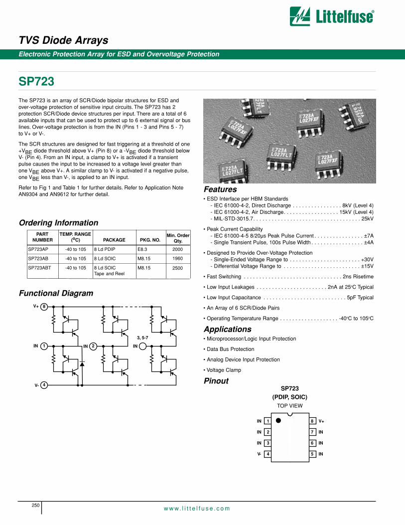
TVS Diode Arrays
250w w w. l i t t e l f u s e . c o m
Electronic Protection Array for ESD and Overvoltage Protection
SP723The SP723 is an array of SCR/Diode bipolar structures for ESD andover-voltage protection of sensitive input circuits. The SP723 has 2 protection SCR/Diode device structures per input. There are a total of 6available inputs that can be used to protect up to 6 external signal or buslines. Over-voltage protection is from the IN (Pins 1 - 3 and Pins 5 - 7) to V+ or V-.
The SCR structures are designed for fast triggering at a threshold of one+VBE diode threshold above V+ (Pin 8) or a -VBE diode threshold belowV- (Pin 4). From an IN input, a clamp to V+ is activated if a transientpulse causes the input to be increased to a voltage level greater thanone VBE above V+. A similar clamp to V- is activated if a negative pulse,one VBE less than V-, is applied to an IN input.
Refer to Fig 1 and Table 1 for further details. Refer to Application NoteAN9304 and AN9612 for further detail.
Features• ESD Interface per HBM Standards
- IEC 61000-4-2, Direct Discharge . . . . . . . . . . . . . . . . 8kV (Level 4)- IEC 61000-4-2, Air Discharge. . . . . . . . . . . . . . . . . . 15kV (Level 4)- MIL-STD-3015.7. . . . . . . . . . . . . . . . . . . . . . . . . . . . . . . . . . . 25kV
• Peak Current Capability- IEC 61000-4-5 8/20µs Peak Pulse Current . . . . . . . . . . . . . . . . ±7A- Single Transient Pulse, 100s Pulse Width . . . . . . . . . . . . . . . . . ±4A
• Designed to Provide Over-Voltage Protection- Single-Ended Voltage Range to . . . . . . . . . . . . . . . . . . . . . . . +30V- Differential Voltage Range to . . . . . . . . . . . . . . . . . . . . . . . . . ±15V
• Fast Switching . . . . . . . . . . . . . . . . . . . . . . . . . . . . . . . . 2ns Risetime
• Low Input Leakages . . . . . . . . . . . . . . . . . . . . . . . 2nA at 25oC Typical
• Low Input Capacitance . . . . . . . . . . . . . . . . . . . . . . . . . . . 5pF Typical
• An Array of 6 SCR/Diode Pairs
• Operating Temperature Range . . . . . . . . . . . . . . . . . . . -40oC to 105oC
Applications• Microprocessor/Logic Input Protection
• Data Bus Protection
• Analog Device Input Protection
• Voltage Clamp
PinoutSP723
(PDIP, SOIC)TOP VIEW
Ordering Information
Functional Diagram
PARTNUMBER
Min. OrderQty.
TEMP. RANGE (oC) PACKAGE PKG. NO.
SP723AP -40 to 105 8 Ld PDIP E8.3 2000
1960
2500
SP723AB -40 to 105 8 Ld SOIC M8.15
SP723ABT -40 to 105 8 Ld SOICTape and Reel
M8.15
4
V+
V-
IN
3, 5-7
IN IN1
8
2
IN
IN
IN
V-
1
2
3
4
8
7
6
5
V+
IN
IN
IN

251w w w. l i t t e l f u s e . c o m
5
SIL
ICO
N P
RO
TEC
TIO
NC
IRC
UIT
S
SP723
TVS Diode ArraysElectronic Protection Array for ESD and Overvoltage Protection
CAUTION: Stresses above those listed in “Absolute Maximum Ratings” may cause permanent damage to the device. This is a stress only rating and operation of the deviceat these or any other conditions above those indicated in the operational sections of this specification is not implied.
NOTE:1. θJA is measured with the component mounted on an evaluation PC board in free air.
Electrical Specification TA =40oC to 105oC, VIN = 0.5VCC, Unless Otherwise Specified
Absolute Maximum RatingsContinuous Supply Voltage, (V+) - (V-). . . . . . . . . . . . . . . . . . . . . . . . . +35VForward Peak Current, IIN to VCC, IIN to GND
(Refer to Figure 6). . . . . . . . . . . . . . . . . . . . . . . . . . . . . . . . . . ±4A, 100µsPeak Pulse Current, 8/20µs. . . . . . . . . . . . . . . . . . . . . . . . . . . . . . . . . . . ±7AESD Ratings and Capability (Figure 1, Table 1)Load Dump and Reverse Battery (Note 2)
Thermal InformationThermal Resistance (Typical, Note 1) θJA ( oC/W)
PDIP Package . . . . . . . . . . . . . . . . . . . . . . . . . . . . . . . . . . . . . . . . . . . .160SOIC Package . . . . . . . . . . . . . . . . . . . . . . . . . . . . . . . . . . . . . . . . . . . 170
Storage Temperature Range . . . . . . . . . . . . . . . . . . . . . . . . . . . . -65oC to 150oCMaximum Junction Temperature. . . . . . . . . . . . . . . . . . . . . . . . . . . . . . 150oCLead Temperature (Soldering 10s). . . . . . . . . . . . . .. . . . . . . . . . . . . . 300oC
(SOIC - Lead Tips Only)
ESD CapabilityESD capability is dependent on the application and defined test standard.The evaluation results for various test standards and methodsbased on Figure 1 are shown in Table 1.
The SP723 has a Level 4 HBM capability when tested as a device to theIEC 61000-4-2 standard. Level 4 specifies a required capability greaterthan 8kV for direct discharge and greater than 15kV for air discharge.
For the “Modified” MIL-STD-3015.7 condition that is defined as an “in-circuit” method of ESD testing, the V+ and V- pins have a return path toground and the SP723 ESD capability is typically greater than 25kV from100pF through 1.5kΩ. By strict definition of MIL-STD-3015.7 using “pin-to-pin” device testing, the ESD voltage capability is greater than 10kV.
For the SP723 EIAJ IC121 Machine Model (MM) standard, the ESD capa-bility is typically greater than 2kV from 200pF with no series resistance.
STANDARD TYPE/MODE RD CD ±VD
IEC 1000-4-2(Level 4)
HBM, Air Discharge 330Ω 150pF 15kV
HBM, Direct Discharge 330Ω 150pF 8kV
MIL-STD-3015.7 Modified HBM 1.5kΩ 100pF 25kV
Standard HBM 1.5kΩ 100pF 10kV
EIAJ IC121 Machine Model 0kΩ 200pF 2kV
H.V.SUPPLY
°±VD
IN
DUT
CD
R1
IEC 1000-4-2: R1 50 to 100MΩ
RD
CHARGESWITCH
DISCHARGESWITCH
MIL-STD-3015.7: R1 1 to 10MΩ
FIGURE 1. ELECTROSTATIC DISCHARGE TEST
TABLE 1. ESD TEST CONDITIONS
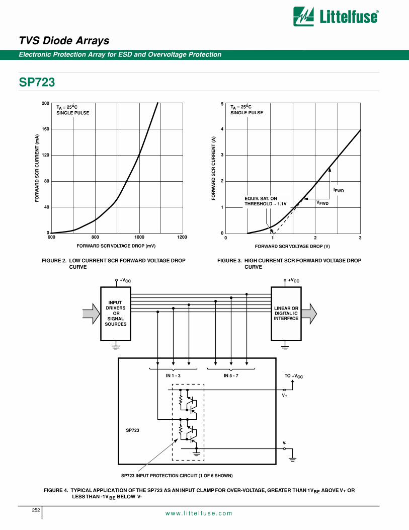
TVS Diode Arrays
252w w w. l i t t e l f u s e . c o m
Electronic Protection Array for ESD and Overvoltage Protection
SP723
FIGURE 2. LOW CURRENT SCR FORWARD VOLTAGE DROP CURVE
FIGURE 3. HIGH CURRENT SCR FORWARD VOLTAGE DROP CURVE
600 800 1000 1200
FORWARD SCR VOLTAGE DROP (mV)
200
160
120
80
40
0
FO
RW
AR
D S
CR
CU
RR
EN
T (
mA
)
TA = 25oCSINGLE PULSE
5
4
3
2
1
0
FO
RW
AR
D S
CR
CU
RR
EN
T (
A)
TA = 25oCSINGLE PULSE
VFWD
IFWD
0 1 2 3
FORWARD SCR VOLTAGE DROP (V)
EQUIV. SAT. ONTHRESHOLD ~ 1.1V
FIGURE 4. TYPICAL APPLICATION OF THE SP723 AS AN INPUT CLAMP FOR OVER-VOLTAGE, GREATER THAN 1VBE ABOVE V+ OR LESS THAN -1VBE BELOW V-
+VCC
INPUT DRIVERS
SP723 INPUT PROTECTION CIRCUIT (1 OF 6 SHOWN)
ORSIGNAL
SOURCES
IN 5 - 7IN 1 - 3
SP723
V-
TO +VCC
LINEAR ORDIGITAL ICINTERFACE
V+
+VCC

253w w w. l i t t e l f u s e . c o m
5
SIL
ICO
N P
RO
TEC
TIO
NC
IRC
UIT
S
SP723
TVS Diode ArraysElectronic Protection Array for ESD and Overvoltage Protection
Peak Transient Current Capability of the SP723The peak transient current capability rises sharply as the width of the current pulse narrows. Destructive testing was done to fully evaluate theSP723’s ability to withstand a wide range of peak current pulses vs time.The circuit used to generate current pulses is shown in Figure 5.
The test circuit of Figure 5 is shown with a positive pulse input. For anegative pulse input, the (-) current pulse input goes to an SP723 ‘IN’input pin and the (+) current pulse input goes to the SP723 V- pin. TheV+ to V- supply of the SP723 must be allowed to float. (i.e., It is not tiedto the ground reference of the current pulse generator.) Figure 6 showsthe point of overstress as defined by increased leakage in excess of thedata sheet published limits.
The maximum peak input current capability is dependent on the ambienttemperature, improving as the temperature is reduced. Peak currentcurves are shown for ambient temperatures of 25oC and 105oC and a 15Vpower supply condition. The safe operating range of the transient peakcurrent should be limited to no more than 75% of the measured over-stress level for any given pulse width as shown in the curves of Figure 6.
Note that adjacent input pins of the SP723 may be paralleled to improvecurrent (and ESD) capability. The sustained peak current capability isincreased to nearly twice that of a single pin.
+
-CURRENT
SENSE
VOLTAGEPROBE
6
7
8
5
1
2
3
4
IN
IN
IN
V-
V+
IN
IN
IN +
-
R1 ~ 10Ω TYPICAL
SP723
VX
VX ADJ. 10V/A TYPICAL
R1
(-)
(+)
C1 ~ 100µF
C1
VARIABLE TIME DURATIONCURRENT PULSE GENERATOR
FIGURE 5. TYPICAL SP723 PEAK CURRENT TEST CIRCUIT WITH A VARIABLE PULSE WIDTH INPUT
FIGURE 6. SP723 TYPICAL SINGLE PULSE PEAK CURRENT CURVES SHOWING THE MEASURED POINT OF OVERSTRESS IN AMPERES vs PULSE WIDTH TIME IN MILLISECONDS
0.001 0.01 0.1 1
PULSE WIDTH TIME (ms)
PE
AK
CU
RR
EN
T (
A)
10
14
12
10
8
6
4
2
0100 1000
CAUTION:
OF THE VALUES SHOWN ON EACH CURVE.PULSE WIDTH TO BE NO GREATER THAN 75% THE MAXIMUM PEAK CURRENT FOR A GIVEN
V+ TO V- SUPPLY = 15V
TA = 105oC
TA = 25oC
SAFE OPERATING CONDITIONS LIMIT

TVS Diode Arrays
254w w w. l i t t e l f u s e . c o m
Electronic Protection Array for ESD and Overvoltage Protection
SP723
Dual-In-Line Plastic Packages (PDIP) E8.3 (JEDEC MS-001-BA ISSUE D)8 LEAD DUAL-IN-LINE PLASTIC PACKAGE
CL
E
eA
C
eB
eC
-B-
E1INDEX
1 2 3 N/2
N
AREA
SEATING
BASEPLANE
PLANE
-C-
D1
B1B
e
D
D1
AA2
L
A1
-A-
0.010 (0.25) C AM B S
NOTES:
1. Controlling Dimensions: INCH. In case of conflict between English and Metric dimensions, the inch dimensions control.
2. Dimensioning and tolerancing per ANSI Y14.5M-1982.
3. Symbols are defined in the “MO Series Symbol List” in Section 2.2 of Publication No. 95.
4. Dimensions A, A1 and L are measured with the package seated in JEDEC seating plane gauge GS-3.
5. D, D1, and E1 dimensions do not include mold flash or protru-sions. Mold flash or protrusions shall not exceed 0.010 inch(0.25mm).
6. E and are measured with the leads constrained to be per-pendicular to datum .
7. eB and eC are measured at the lead tips with the leads uncon-strained. eC must be zero or greater.
8. B1 maximum dimensions do not include dambar protrusions. Dambar protrusions shall not exceed 0.010 inch (0.25mm).
9. N is the maximum number of terminal positions.
10. Corner leads (1, N, N/2 and N/2 + 1) for E8.3, E16.3, E18.3, E28.3, E42.6 will have a B1 dimension of 0.030 - 0.045 inch(0.76 - 1.14mm).
eA-C-
SYMBOL
INCHES MILLIMETERS
NOTESMIN MAX MIN MAX
A - 0.210 - 5.33 4
A1 0.015 - 0.39 - 4
A2 0.115 0.195 2.93 4.95 -
B 0.014 0.022 0.356 0.558 -
B1 0.045 0.070 1.15 1.77 8, 10
C 0.008 0.014 0.204 0.355 -
D 0.355 0.400 9.01 10.16 5
D1 0.005 - 0.13 - 5
E 0.300 0.325 7.62 8.25 6
E1 0.240 0.280 6.10 7.11 5
e 0.100 BSC 2.54 BSC -
eA 0.300 BSC 7.62 BSC 6
eB - 0.430 - 10.92 7
L 0.115 0.150 2.93 3.81 4
N 8 8 9
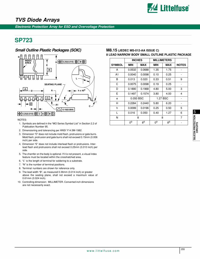
255w w w. l i t t e l f u s e . c o m
5
SIL
ICO
N P
RO
TEC
TIO
NC
IRC
UIT
S
SP723
TVS Diode ArraysElectronic Protection Array for ESD and Overvoltage Protection
Small Outline Plastic Packages (SOIC) M8.15 (JEDEC MS-012-AA ISSUE C)8 LEAD NARROW BODY SMALL OUTLINE PLASTIC PACKAGE
INDEXAREA
E
D
N
1 2 3
-B-
0.25(0.010) C AM B S
e
-A-
L
B
M
-C-
A1
A
SEATING PLANE
0.10(0.004)
h x 45o
C
H
µ
0.25(0.010) BM M
NOTES:
1. Symbols are defined in the “MO Series Symbol List” in Section 2.2 of Publication Number 95.
2. Dimensioning and tolerancing per ANSI Y14.5M-1982.
3. Dimension “D” does not include mold flash, protrusions or gate burrs. Mold flash, protrusion and gate burrs shall not exceed 0.15mm (0.006inch) per side.
4. Dimension “E” does not include interlead flash or protrusions. Inter-lead flash and protrusions shall not exceed 0.25mm (0.010 inch) perside.
5. The chamfer on the body is optional. If it is not present, a visual index feature must be located within the crosshatched area.
6. “L” is the length of terminal for soldering to a substrate.
7. “N” is the number of terminal positions.
8. Terminal numbers are shown for reference only.
9. The lead width “B”, as measured 0.36mm (0.014 inch) or greater above the seating plane, shall not exceed a maximum value of0.61mm (0.024 inch).
10. Controlling dimension: MILLIMETER. Converted inch dimensions are not necessarily exact.
SYMBOL
INCHES MILLIMETERS
NOTESMIN MAX MIN MAX
A 0.0532 0.0688 1.35 1.75 -
A1 0.0040 0.0098 0.10 0.25 -
B 0.013 0.020 0.33 0.51 9
C 0.0075 0.0098 0.19 0.25 -
D 0.1890 0.1968 4.80 5.00 3
E 0.1497 0.1574 3.80 4.00 4
e 0.050 BSC 1.27 BSC -
H 0.2284 0.2440 5.80 6.20 -
h 0.0099 0.0196 0.25 0.50 5
L 0.016 0.050 0.40 1.27 6
N 8 8 7
0o 8o 0o 8o -
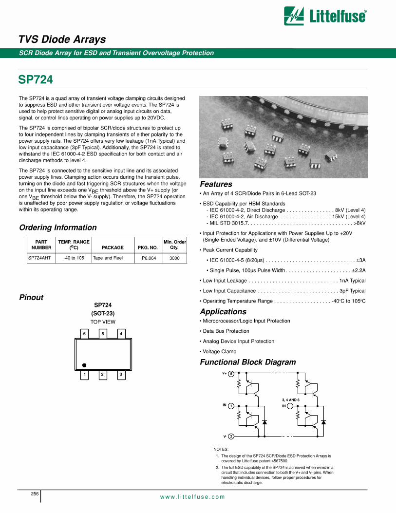
TVS Diode Arrays
256w w w. l i t t e l f u s e . c o m
SCR Diode Array for ESD and Transient Overvoltage Protection
SP724The SP724 is a quad array of transient voltage clamping circuits designedto suppress ESD and other transient over-voltage events. The SP724 isused to help protect sensitive digital or analog input circuits on data, signal, or control lines operating on power supplies up to 20VDC.
The SP724 is comprised of bipolar SCR/diode structures to protect up to four independent lines by clamping transients of either polarity to thepower supply rails. The SP724 offers very low leakage (1nA Typical) andlow input capacitance (3pF Typical). Additionally, the SP724 is rated towithstand the IEC 61000-4-2 ESD specification for both contact and airdischarge methods to level 4.
The SP724 is connected to the sensitive input line and its associatedpower supply lines. Clamping action occurs during the transient pulse,turning on the diode and fast triggering SCR structures when the voltageon the input line exceeds one VBE threshold above the V+ supply (orone VBE threshold below the V- supply). Therefore, the SP724 operationis unaffected by poor power supply regulation or voltage fluctuationswithin its operating range.
Features• An Array of 4 SCR/Diode Pairs in 6-Lead SOT-23
• ESD Capability per HBM Standards- IEC 61000-4-2, Direct Discharge . . . . . . . . . . . . . . . . 8kV (Level 4)- IEC 61000-4-2, Air Discharge . . . . . . . . . . . . . . . . . 15kV (Level 4)- MIL STD 3015.7. . . . . . . . . . . . . . . . . . . . . . . . . . . . . . . . . . . >8kV
• Input Protection for Applications with Power Supplies Up to +20V(Single-Ended Voltage), and ±10V (Differential Voltage)
• Peak Current Capability
• IEC 61000-4-5 (8/20µs) . . . . . . . . . . . . . . . . . . . . . . . . . . . . . . ±3A
• Single Pulse, 100µs Pulse Width. . . . . . . . . . . . . . . . . . . . . . ±2.2A
• Low Input Leakage . . . . . . . . . . . . . . . . . . . . . . . . . . . . . . 1nA Typical
• Low Input Capacitance . . . . . . . . . . . . . . . . . . . . . . . . . . . 3pF Typical
• Operating Temperature Range . . . . . . . . . . . . . . . . . . . -40oC to 105oC
Applications• Microprocessor/Logic Input Protection
• Data Bus Protection
• Analog Device Input Protection
• Voltage Clamp
Functional Block Diagram
Ordering Information
Pinout
PART Min. OrderQty. NUMBER
TEMP. RANGE (oC) PACKAGE PKG. NO.
P6.064 3000SP724AHT -40 to 105 Tape and Reel
1 2 3
6 5 4
SP724(SOT-23)TOP VIEW
NOTES:
1. The design of the SP724 SCR/Diode ESD Protection Arrays is covered by Littelfuse patent 4567500.
2. The full ESD capability of the SP724 is achieved when wired in a circuit that includes connection to both the V+ and V- pins. When handling individual devices, follow proper procedures for electrostatic discharge.
2
V+
V-
IN3, 4 AND 6
IN1
5
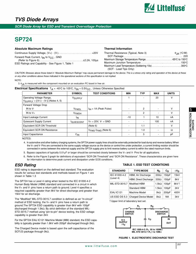
257w w w. l i t t e l f u s e . c o m
5
SIL
ICO
N P
RO
TEC
TIO
NC
IRC
UIT
S
SP724
TVS Diode ArraysSCR Diode Array for ESD and Transient Overvoltage Protection
Absolute Maximum Ratings Continuous Supply Voltage, (V+) - (V-). . . . . . . . . . . . . . . . . . . . . . . . . +20V
Forward Peak Current, IIN to VCC , GND(Refer to Figure 6). . . . . . . . . . . . . . . . . . . . . . . . . . . . . . . . .±2.2A, 100µs
ESD Ratings and Capability - See Figure 1, Table 1
Thermal InformationThermal Resistance (Typical, Note 3) θJA (oC/W)
SOT Package . . . . . . . . . . . . . . . . . . . . . . . . . . . . . .. . . . . . . . . . . . . . 220Maximum Storage Temperature Range. . . . . . . . . . . . . . . . . . . . . . .-65oC to 150oCMaximum Junction Temperature . . . . . . . . . . . . . . . .. . . . . . . . . . . . . . 150oCMaximum Lead Temperature (Soldering 10s) . . . . . . . . .. . . . . . . . . . . . . . . . 300oC
(SOT - Lead Tips Only)
PARAMETER SYMBOL TEST CONDITIONS MIN TYP MAX UNITS
Operating Voltage Range,VSUPPLY = [(V+) - (V-)] (Notes 4, 5)
VSUPPLY 1 - 20 V
Forward Voltage Drop
IN to V- VFWDL IIN = 1A (Peak Pulse) - 2 - V
IN to V+ VFWDH - 2 - V
Input Leakage Current IIN -10 1 10 nA
Quiescent Supply Current IQUIESCENT V+ = 20V, V- = GND - - 100 nA
Equivalent SCR ON Threshold (Note 6) - 1.1 - V
Equivalent SCR ON Resistance VFWD/IFWD (Note 6) - 1.0 - Ω
Input Capacitance CIN - 3 - pF
NOTES:
4. In automotive and other battery charging systems, the SP724 power supply lines should be externally protected for load dump and reverse battery. When the V+ and V- Pins are connected to the same supply voltage source as the device or control line under protection, a current limiting resistor should be connected in series between the external supply and the SP724 supply pins to limit reverse battery current to within the rated maximum limits.
5. Bypass capacitors of typically 0.01µF or larger should be connected closely between the V+ and V- Pins for all applications.
6. Refer to the Figure 3 graph for definitions of equivalent “SCR ON Threshold” and “SCR ON Resistance”. These characteristics are given here for information to determine peak current and dissipation under EOS conditions.
ESD RatingESD rating is dependent on the defined test standard. The evaluationresults for various test standards and methods based on Figure 1 areshown in Table 1.3
The SP724 has a Level 4 rating when tested to the IEC 61000-4-2Human Body Model (HBM) standard and connected in a circuit in whichthe V+ and V- pins have a return path to ground. Level 4 specifies arequired capability greater than 8kV for direct discharge and greater than15kV for air discharge.
The “Modified” MIL-STD-3015.7 condition is defined as an “in-circuit”method of ESD testing, the V+ and V- pins have a return path toground.The SP724 ESD capability is greater than 8kV with 100pF discharged through 1.5kΩ. By strict definition of the standard MIL-STD-3015.7 method using “pin-to-pin” device testing, the ESD voltage capability is greater than 2kV.
For the SP724 EIAJ IC121 Machine Model (MM) standard, the ESD capa-bility is typically greater than 1.8kV with 200pF discharged through 0kΩ.
The Charged Device model is based upon the self-capacitance of theSOT-23 package through 0kΩ.
CAUTION: Stresses above those listed in “Absolute Maximum Ratings” may cause permanent damage to the device. This is a stress only rating and operation of the device at theseor any other conditions above those indicated in the operational sections of this specification is not implied.
NOTE:3. θJA is measured with the component mounted on an evaluation PC board in free air.
Electrical Specifications TA = -40oC to 105oC, VIN = 0.5VCC , Unless Otherwise Specified
STANDARD TYPE/MODE RD CD ±VD
IEC 61000-4-2(Level 4)
HBM, Air Discharge 330Ω 150pF 15kV
HBM, Direct Discharge 330Ω 150pF 8kV
MIL-STD-3015.7 Modified HBM 1.5kΩ 100pF 8kV†
Standard HBM 1.5kΩ 100pF 2kV
EIAJ IC121 Machine Model 0kΩ 200pF 400V
US ESD DS 5.3 Charged Device Model 0kΩ NA 3kV
†Upper limit of laboratory test set.
H.V.SUPPLY
±VD
IN
DUT
CD
R1
IEC 1000-4-2: R1 50 to 100MΩ
RD
CHARGESWITCH
DISCHARGESWITCH
MIL STD 3015.7: R11 to 10MΩ
FIGURE 1. ELECTROSTATIC DISCHARGE TEST
TABLE 1. ESD TEST CONDITIONS

TVS Diode Arrays
258w w w. l i t t e l f u s e . c o m
SCR Diode Array for ESD and Transient Overvoltage Protection
SP724
FIGURE 2. LOW CURRENT SCR FORWARD VOLTAGE DROP CURVE
FIGURE 3. HIGH CURRENT SCR FORWARD VOLTAGE DROP CURVE
600 800 1000 1200
FORWARD SCR VOLTAGE DROP (mV)
200
160
120
80
40
0
FO
RW
AR
D S
CR
CU
RR
EN
T (
mA
)
TA = 25oCSINGLE PULSE
5
4
3
2
1
0
FO
RW
AR
D S
CR
CU
RR
EN
T (
A)
TA = 25oCSINGLE PULSE
0 1 2 3
FORWARD SCR VOLTAGE DROP (V)
EQUIV. SAT. ONTHRESHOLD ~ 1.1V
+VCC
INPUT DRIVERS
SP724 INPUT PROTECTION CIRCUIT (1 OF 4 SHOWN)
ORSIGNAL
SOURCES
IN 1, 3, 4 AND 6
SP724
V-
TO +VCC
LINEAR ORDIGITAL ICINTERFACE
V+
+VCC
0.01µF
FIGURE 4. TYPICAL APPLICATION OF THE SP724 AS AN INPUT CLAMP FOR OVER-VOLTAGE, GREATER THAN 1VBE ABOVE V+ OR LESS THAN -1VBE BELOW V-

259w w w. l i t t e l f u s e . c o m
5
SIL
ICO
N P
RO
TEC
TIO
NC
IRC
UIT
S
SP724
TVS Diode ArraysSCR Diode Array for ESD and Transient Overvoltage Protection
Peak Transient Current Capability for Long Duration SurgesThe peak transient current capability is inversely proportional to the widthof the current pulse. Testing was done to fully evaluate the SP724’s ability to withstand long duration current pulses using the circuit of Figure 5. Figure 6 shows the point of overstress as defined by increasedleakage in excess of the data sheet published limits. The safe operatingrange of the transient peak current should be limited to no more than75% of the measured overstress level for any given pulse width asshown in the curve of Figure 6.
The test circuit of Figure 5 is shown with a positive pulse input. For a negative pulse input, the (-) current pulse input goes to an SP724 ‘IN’input pin and the (+) current pulse input goes to the SP724 V- pin. The V+ to V- supply of the SP724 must be allowed to float. (i.e., It is not tied to the ground reference of the current pulse generator.)
Note that two input pins of the SP724 may be paralleled to improve current (and ESD) capability. The sustained peak current capability isincreased to nearly twice that of a single pin. FIGURE 5. TYPICAL SP724 PEAK CURRENT TEST CIRCUIT
WITH A VARIABLE PULSE WIDTH INPUT
+
- CURRENTSENSE
VOLTAGEPROBE
+
-
R1 ~ 10Ω TYPICAL
SP724
VX
VX ADJ. 10V/A TYPICAL
R1
(-)
(+)
C1 ~ 100µF
C1
VARIABLE TIME DURATIONCURRENT PULSE GENERATOR
12
3
65
4
FIGURE 6. SP724 TYPICAL NONREPETITIVE PEAK CURRENT PULSE CAPABILITY
0.001 0.01 0.1 1
SQUARE WAVE PULSE WIDTH (ms)
PE
AK
CU
RR
EN
T (
A)
10
7
6
5
4
3
2
1
0100 1000
NOTE:
OF THE VALUES SHOWN.PULSE WIDTH TO BE NO GREATER THAN 75% MAXIMUM PEAK CURRENT FOR A GIVEN
V+ TO V- SUPPLY = 15VTA = 25oC
8
TO ENSURE SAFE OPERATION LIMIT THE
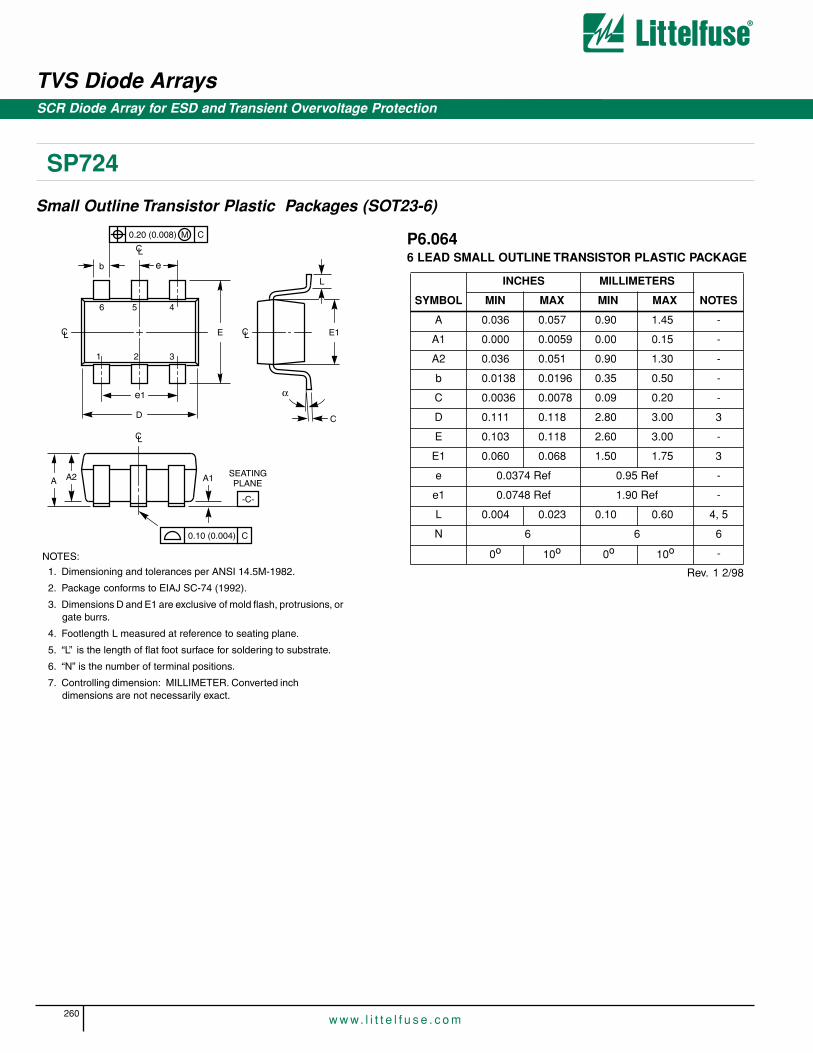
TVS Diode Arrays
260w w w. l i t t e l f u s e . c o m
SCR Diode Array for ESD and Transient Overvoltage Protection
SP724
Small Outline Transistor Plastic Packages (SOT23-6)
SYMBOL
INCHES MILLIMETERS
NOTESMIN MAX MIN MAX
A 0.036 0.057 0.90 1.45 -
A1 0.000 0.0059 0.00 0.15 -
A2 0.036 0.051 0.90 1.30 -
b 0.0138 0.0196 0.35 0.50 -
C 0.0036 0.0078 0.09 0.20 -
D 0.111 0.118 2.80 3.00 3
E 0.103 0.118 2.60 3.00 -
E1 0.060 0.068 1.50 1.75 3
e 0.0374 Ref 0.95 Ref -
e1 0.0748 Ref 1.90 Ref -
L 0.004 0.023 0.10 0.60 4, 5
N 6 6 6
0o 10o 0o 10o -
Rev. 1 2/98
P6.0646 LEAD SMALL OUTLINE TRANSISTOR PLASTIC PACKAGE
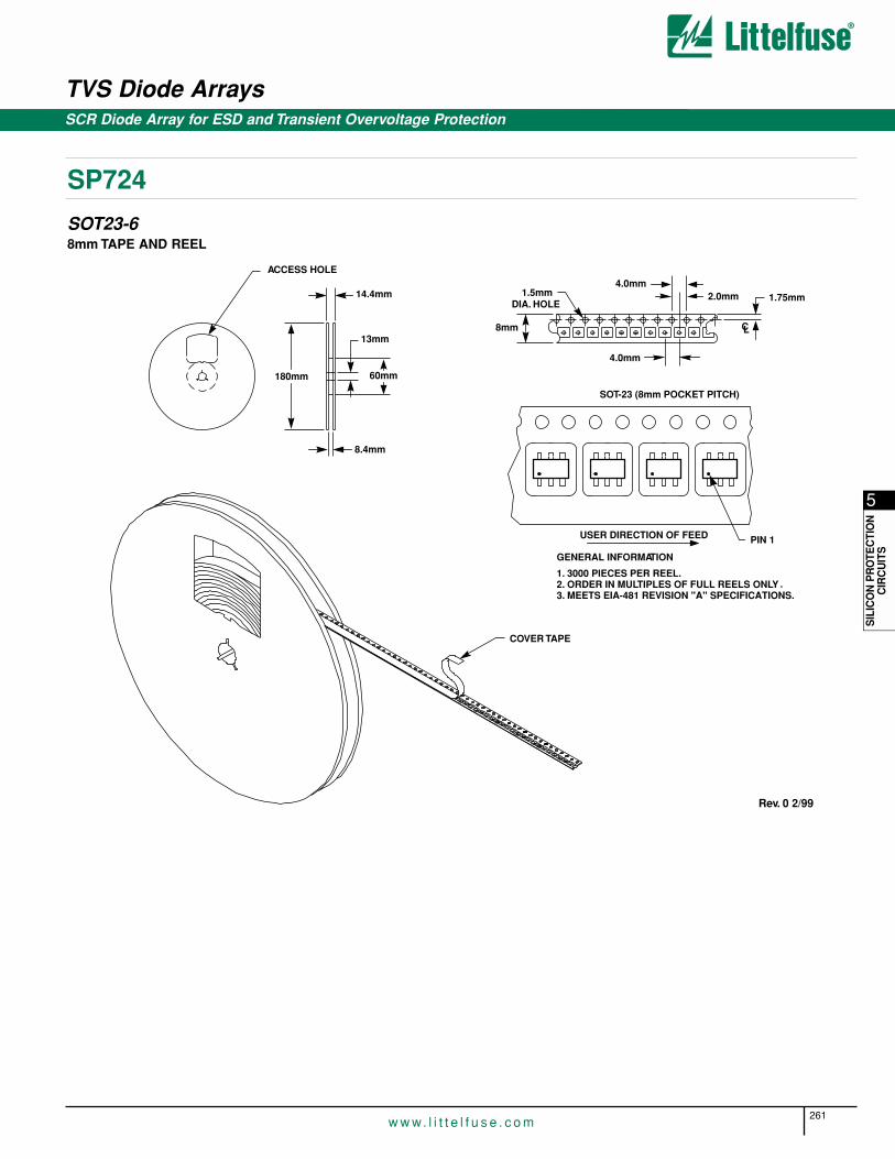
261w w w. l i t t e l f u s e . c o m
5
SIL
ICO
N P
RO
TEC
TIO
NC
IRC
UIT
S
SP724
TVS Diode ArraysSCR Diode Array for ESD and Transient Overvoltage Protection
SOT23-68mm TAPE AND REEL
GENERAL INFORMATION
1. 3000 PIECES PER REEL.2. ORDER IN MULTIPLES OF FULL REELS ONLY .3. MEETS EIA-481 REVISION "A" SPECIFICATIONS.
2.0mm4.0mm
CL
1.75mm1.5mmDIA. HOLE
8mm
4.0mm
8.4mm
180mm
14.4mm
13mm
60mm
ACCESS HOLE
COVER TAPE
Rev. 0 2/99
USER DIRECTION OF FEED PIN 1
SOT-23 (8mm POCKET PITCH)

262w w w. l i t t e l f u s e . c o m
Notes & Drawings

Silicon Avalanche Diodes6
263w w w. l i t t e l f u s e . c o m
PAGE
Silicon Avalanche Diodes . . . . . . . . . . . . . . . . . . . . . . . . . . . . . . . . . . . . . . . . . . . . . . . . . . . . . . . . . . . . . . . . . . . . . . . . . . . . . 263
AK6 series . . . . . . . . . . . . . . . . . . . . . . . . . . . . . . . . . . . . . . . . . . . . . . . . . . . . . . . . . . . . . . . . . . . . . . . . . . . . . . . . . . . . . . . . . 264
AK10 series . . . . . . . . . . . . . . . . . . . . . . . . . . . . . . . . . . . . . . . . . . . . . . . . . . . . . . . . . . . . . . . . . . . . . . . . . . . . . . . . . . . . . 265-266
SMBJ series . . . . . . . . . . . . . . . . . . . . . . . . . . . . . . . . . . . . . . . . . . . . . . . . . . . . . . . . . . . . . . . . . . . . . . . . . . . . . . . . . . . . 267-271
P6SMBJ series . . . . . . . . . . . . . . . . . . . . . . . . . . . . . . . . . . . . . . . . . . . . . . . . . . . . . . . . . . . . . . . . . . . . . . . . . . . . . . . . . . 272-276
1KSMBJ series . . . . . . . . . . . . . . . . . . . . . . . . . . . . . . . . . . . . . . . . . . . . . . . . . . . . . . . . . . . . . . . . . . . . . . . . . . . . . . . . . . 277-279
SA series . . . . . . . . . . . . . . . . . . . . . . . . . . . . . . . . . . . . . . . . . . . . . . . . . . . . . . . . . . . . . . . . . . . . . . . . . . . . . . . . . . . . . . 280-284
P6KE series . . . . . . . . . . . . . . . . . . . . . . . . . . . . . . . . . . . . . . . . . . . . . . . . . . . . . . . . . . . . . . . . . . . . . . . . . . . . . . . . . . . . 285-289
1.5KE series . . . . . . . . . . . . . . . . . . . . . . . . . . . . . . . . . . . . . . . . . . . . . . . . . . . . . . . . . . . . . . . . . . . . . . . . . . . . . . . . . . . . 290-294
5KP series . . . . . . . . . . . . . . . . . . . . . . . . . . . . . . . . . . . . . . . . . . . . . . . . . . . . . . . . . . . . . . . . . . . . . . . . . . . . . . . . . . . . . 295-299
15KP series. . . . . . . . . . . . . . . . . . . . . . . . . . . . . . . . . . . . . . . . . . . . . . . . . . . . . . . . . . . . . . . . . . . . . . . . . . . . . . . . . . . . . 300-303
Foldbak™ series . . . . . . . . . . . . . . . . . . . . . . . . . . . . . . . . . . . . . . . . . . . . . . . . . . . . . . . . . . . . . . . . . . . . . . . . . . . . . . . . . . . . 304
SLD™ series. . . . . . . . . . . . . . . . . . . . . . . . . . . . . . . . . . . . . . . . . . . . . . . . . . . . . . . . . . . . . . . . . . . . . . . . . . . . . . . . . . . . . . . . 305
15KP cells. . . . . . . . . . . . . . . . . . . . . . . . . . . . . . . . . . . . . . . . . . . . . . . . . . . . . . . . . . . . . . . . . . . . . . . . . . . . . . . . . . . . . . . . . . 306
ICTE / MPTE series. . . . . . . . . . . . . . . . . . . . . . . . . . . . . . . . . . . . . . . . . . . . . . . . . . . . . . . . . . . . . . . . . . . . . . . . . . . . . . . 307-308
LCE series . . . . . . . . . . . . . . . . . . . . . . . . . . . . . . . . . . . . . . . . . . . . . . . . . . . . . . . . . . . . . . . . . . . . . . . . . . . . . . . . . . . . . . 309-312
1N56 series. . . . . . . . . . . . . . . . . . . . . . . . . . . . . . . . . . . . . . . . . . . . . . . . . . . . . . . . . . . . . . . . . . . . . . . . . . . . . . . . . . . . . 313-316
1N60 series. . . . . . . . . . . . . . . . . . . . . . . . . . . . . . . . . . . . . . . . . . . . . . . . . . . . . . . . . . . . . . . . . . . . . . . . . . . . . . . . . . . . . 317-320

Silicon Avalanche Diodes
264w w w. l i t t e l f u s e . c o m
TestCurrent
(I T )
Max. Temp Coefficient
OF VB R
Max.Capacitance
0 Bias10k Hz
Min.Volts
Max.Volts mA
V C L
VoltsI P P
Amps (%/ o C) (nF)
ReverseBreakdown
Voltage (VB R)@ I T
Max. Clamping Voltage V C L ) @
Peak Pulse Current (I PP )
(note 1)Part
Numbers
StandoffVoltage
(VS O)Volts
Max.ReservseLeakage(I R) @ VS O
A
Note 1 . Using 8/20µS wave shape pulse as defined in IEC 1000.4.5
AK6 - 58
AK6 - 170 170 20 180 220 10 260 6,000 0.1 2.5
AK6 - 190 190
58 20
20
64 70
200 245 10
10 95
290 6,000
6,000
0.1
0.1 6.5
2.2
AK6 - 380 380 20 401 443 10 520 6,000 0.1 2.0
Maximum Ratings• Current Rating (IPP) 6KA (see note 1)
• Maximum Junction Temp. is 150°C
• Storage Temp. -55°C to 175°C
• Rated IPP measured with 8 x 20 µsec pulse
Mechanical Characteristics• Epoxy Encapsulated
• Axial lead terminals (solderable per MIL-STD-202 Method 208)
• Device code and logo marked on every device
Features• Foldbak™ technology for superior clamping factor
• Glass Passivated Junction for reliabilty
• Bi-directional
• Ultra compact: 12 times less volume than traditional discrete solutions
• Very Low Clamping Voltage
• Sharp Breakdown Voltage
• Low Slope Resistance
1.27mm
Max =12.7mm SQ
16.5mm maxAK6 -190
24mmlead
centres
10.0mm maxAK6 -170
The new AK6 series of high current transient suppressorshave been specially designed for use in A.C. Line Protectionand any demanding applications (AC or DC).They offer supe-rior clamping characteristics over standard S.A.D. technolo-gies by virtue of the Littelfuse Foldbak™ technology, whichprovides a clamping voltage which is lower than the ava-lanche voltage (but above the rated working voltage) there-fore any voltage rise due to increased current conduction iscontained to a minimum, providing the best possible protec-tion level. They can also be connected in series and/or parallel to create very high capacity protection solutions.
ELECTRICAL SPECIFICATION @ Tamb 25°C
AK6 Series
Agency Approvals: Recognized under the Components Program of Underwriters Laboratories - UL497B.
Agency File Numbers: E128662
®

Silicon Avalanche Diodes
265w w w. l i t t e l f u s e . c o m
6
SIL
ICO
N D
IOD
EA
RR
AYS
TestCurrent
(I T )
Max. Temp Coefficient
OF VB R
Max.Capacitance
0 Bias10k Hz
Min.Volts
Max.Volts mA
V C L
VoltsI P P
Amps (%/ o C) (nF)
AK10
AK10-170C 170 20 180 220 5 295 10,000 0.1 2.7
AK10-380C
ReverseBreakdown
Voltage (VB R)@ I T
Max. Clamping Voltage V C L ) @
Peak Pulse Current (I PP )
(note 1)Part
Numbers
StandoffVoltage
(VS O)Volts
Max.ReservseLeakage(I R) @ VS O
A
TBA
Note 1 . Using 8/20µS wave shape pulse as defined in IEC 1000.4.5
380 20 401 443 5 1.40.1569 10,000
Maximum Ratings• Current Rating (IPP) 10KA (see note 1)
• Maximum Junction Temp. is 150°C
• Storage Temp. -55°C to 175°C
• Rated IPP measured with 8 x 20 µsec pulse
Mechanical Characteristics• Epoxy Encapsulated
• Axial lead terminals (solderable per MIL-STD-202 Method 208)
• Device code and logo marked on every device
Features• Foldbak™ technology for superior clamping factor.
• Glass Passivated Junction
• Bi-directional
• Multijunction
• Very Low Clamping Voltage
• Sharp Breakdown Voltage
• Low Slope Resistance
1.27mm
Max =12.7mm SQ
16.5mm maxAK10 -380
24mmlead
centres
10.0mm maxAK10 -170
The new AK10 series of high current transient suppressors havebeen specially designed for use in A.C. Line Protection and anydemanding applications (AC or DC).They offer superior clampingcharacteristics over standard S.A.D. technologies by virtue of theLittelfuse Foldbak™ technology, which provides a clamping voltage which is lower than the avalanche voltage (but above therated working voltage) therefore any voltage rise due toincreased current conduction is contained to a minimum, providing the best possible protection level. They can also be connected in series and/or parallel to create very high capacity protection solutions.
ELECTRICAL SPECIFICATION @ Tamb 25°C
AK10 Series
Agency Approvals: Recognized under the Components Program of Underwriters Laboratories - UL497B.
Agency File Numbers: E128662
®

Silicon Avalanche Diodes
266w w w. l i t t e l f u s e . c o m
AK10 Series
Oscilogram of AK10-380 volt device (422 volt breakdown) tested at maximum surge dutyusing 10,000 Amp 8/20µS wave form: maximum clamping voltage is 508 volts.
®
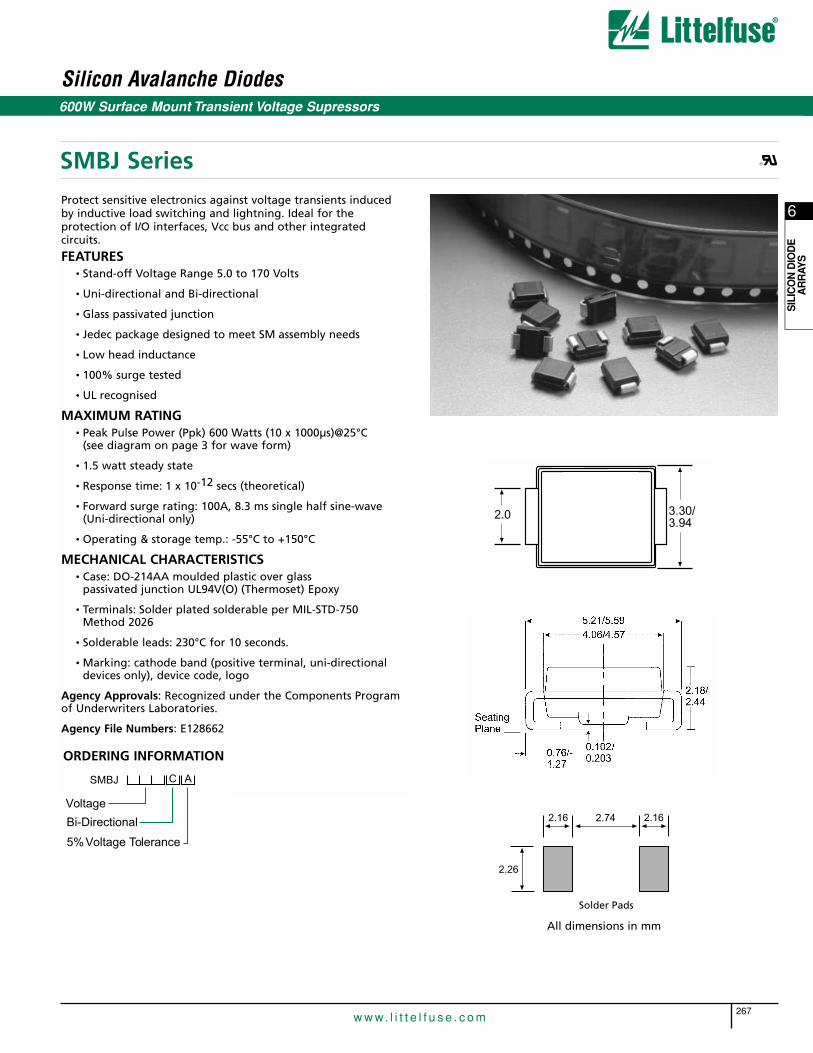
Silicon Avalanche Diodes
267w w w. l i t t e l f u s e . c o m
6
SIL
ICO
N D
IOD
EA
RR
AYS
2.0 3.30/3.94
Protect sensitive electronics against voltage transients inducedby inductive load switching and lightning. Ideal for theprotection of I/O interfaces, Vcc bus and other integratedcircuits.
FEATURES• Stand-off Voltage Range 5.0 to 170 Volts
• Uni-directional and Bi-directional
• Glass passivated junction
• Jedec package designed to meet SM assembly needs
• Low head inductance
• 100% surge tested
• UL recognised
MAXIMUM RATING• Peak Pulse Power (Ppk) 600 Watts (10 x 1000µs)@25°C
(see diagram on page 3 for wave form)
• 1.5 watt steady state
• Response time: 1 x 10-12 secs (theoretical)
• Forward surge rating: 100A, 8.3 ms single half sine-wave(Uni-directional only)
• Operating & storage temp.: -55°C to +150°C
MECHANICAL CHARACTERISTICS• Case: DO-214AA moulded plastic over glass
passivated junction UL94V(O) (Thermoset) Epoxy
• Terminals: Solder plated solderable per MIL-STD-750Method 2026
• Solderable leads: 230°C for 10 seconds.
• Marking: cathode band (positive terminal, uni-directionaldevices only), device code, logo
Agency Approvals: Recognized under the Components Programof Underwriters Laboratories.
Agency File Numbers: E128662
SMBJ
Voltage
C A
Bi-Directional
5% Voltage Tolerance
ORDERING INFORMATION
2.16 2.74 2.16
2.26
Solder Pads
All dimensions in mm
SMBJ Series
600W Surface Mount Transient Voltage Supressors
®

Silicon Avalanche Diodes
268w w w. l i t t e l f u s e . c o m
10000
1000
Cj (pf)
100
101 10 100 1000
Device Stand-off Voltage - Volts
@ Stand-off Voltage
Figure 1 - Capacitance
1µs 10µs 100µs 1ms 10ms
Pulse Time (tp)
Pp(kw)
100kw
20kw
5kw
2kw
500w
100w
Figure 2 - Peak Pulse Power vs. Pulse Time
SMBJ Series
600W Surface Mount Transient Voltage Supressors
®

Silicon Avalanche Diodes
269w w w. l i t t e l f u s e . c o m
6
SIL
ICO
N D
IOD
EA
RR
AYS
SMBJ5.0*
SMBJ5.0A*
SMBJ6.0*
SMBJ6.0A*
SMBJ6.5
SMBJ6.5A
SMBJ7.0
SMBJ7.0A
SMBJ7.5
SMBJ7.5A
SMBJ8.0
SMBJ8.0A
SMBJ8.5*
SMBJ8.5A*
SMBJ9.0
SMBJ9.0A
SMBJ10
SMBJ10A
SMBJ11
SMBJ11A
SMBJ12*
SMBJ12A*
SMBJ13
SMBJ13A
SMBJ14
SMBJ14A
SMBJ15*
SMBJ15A*
SMBJ16
SMBJ16A
SMBJ17
SMBJ17A
PartNumberUni-Polar
KD
KE
KF
KG
KH
KK
KL
KM
KN
KP
KQ
KR
KS
KT
KU
KV
KW
KX
KY
KZ
LD
LE
LF
LG
LH
LK
LL
LM
LN
LP
LQ
LR
DeviceCode
Uni-Polar
PartNumberBi-Polar
SMBJ5.0C*
SMBJ5.0CA*
SMBJ6.0C*
SMBJ6.0CA*
SMBJ6.5C
SMBJ6.5CA
SMBJ7.0C
SMBJ7.0CA
SMBJ7.5C*
SMBJ7.5CA*
SMBJ8.0C
SMBJ8.0CA
SMBJ8.5C*
SMBJ8.5CA*
SMBJ9.0C
SMBJ9.0CA
SMBJ10C
SMBJ10CA
SMBJ11C
SMBJ11CA
SMBJ12C*
SMBJ12CA*
SMBJ13C*
SMBJ13CA*
SMBJ14C
SMBJ14CA
SMBJ15C*
SMBJ15CA*
SMBJ16C
SMBJ16CA
SMBJ17C
SMBJ17CA
DeviceCode
Bi-Polar‘C’ or ‘CA’Version
AD
AE
AF
AG
AH
AK
AL
AM
AN
AP
AQ
AR
AS
AT
AU
AV
AW
AX
AY
AZ
BD
BE
BF
BG
BH
BK
BL
BM
BN
BP
BQ
BR
ReverseStand OffVoltage
VR
(Volts)
5.0
5.0
6.0
6.0
6.5
6.5
7.0
7.0
7.5
7.5
8.0
8.0
8.5
8.5
9.0
9.0
10.0
10.0
11.0
11.0
12.0
12.0
13.0
13.0
14.0
14.0
15.0
15.0
16.0
16.0
17.0
17.0
BreakdownVoltage
VBR (Volts) @ IT
MIN MAX (mA)
6.40
6.40
6.67
6.67
7.22
7.22
7.78
7.78
8.33
8.33
8.89
8.89
9.44
9.44
10.00
10.00
11.10
11.10
12.20
12.20
13.30
13.30
14.40
14.40
15.60
15.60
16.70
16.70
17.80
17.80
18.90
18.90
N/A
N/A
N/A
N/A
N/A
N/A
N/A
N/A
N/A
N/A
N/A
N/A
N/A
N/A
N/A
N/A
N/A
N/A
N/A
N/A
N/A
N/A
N/A
N/A
N/A
N/A
N/A
N/A
N/A
N/A
N/A
N/A
10
10
10
10
10
10
10
10
1
1
1
1
1
1
1
1
1
1
1
1
1
1
1
1
1
1
1
1
1
1
1
1
MaximumReverseLeakageIR @ VR
(µA)
800.0
800.0
800.0
800.0
500.0
500.0
200.0
200.0
100.0
100.0
50.0
50.0
20.0
20.0
10.0
10.0
5.0
5.0
5.0
5.0
5.0
5.0
5.0
5.0
5.0
5.0
5.0
5.0
5.0
5.0
5.0
5.0
MaximumClampingVoltageVC @ IPP
(Volts)
9.6
9.2
11.4
10.3
12.3
11.2
13.3
12.0
14.3
12.9
15.0
13.6
15.9
14.4
16.9
15.4
18.8
17.0
20.1
18.2
22.0
19.9
23.8
21.5
25.8
23.2
26.9
24.4
28.8
26.0
30.5
27.6
MaximumPeak Pulse
CurrentIPP
(A)
62.5
65.2
52.6
58.3
48.7
53.6
45.1
50.0
42.0
46.5
40.0
44.1
37.7
41.7
35.5
39.0
31.9
35.3
29.9
33.0
27.3
30.2
25.2
27.9
23.3
25.8
22.3
24.0
20.8
23.1
19.7
21.0
Note: Non ‘A’ devices have higher clamping voltage. Add suffix ‘C’ to denote bi-polar devices. VBR max not quoted.
1. For Bi-directional devices having VR of 10 volts and below, the IR limit is doubled.
2. For Uni-directional devices VF = 3.5 Volts max at IF = 50A, 300 µS square wave pulse. * Preferred voltages.
SMBJ Series
ELECTRICAL SPECIFICATION @ Tamb 25°C
600W Surface Mount Transient Voltage Supressors
®

Silicon Avalanche Diodes
270w w w. l i t t e l f u s e . c o m
SMBJ18*SMBJ18A*SMBJ20SMBJ20ASMBJ22SMBJ22ASMBJ24SMBJ24ASMBJ26*SMBJ26A*SMBJ28SMBJ28ASMBJ30SMBJ30ASMBJ33*SMBJ33A*SMBJ36*SMBJ36ASMBJ40SMBJ40ASMBJ43SMBJ43ASMBJ45SMBJ45ASMBJ48SMBJ48ASMBJ51SMBJ51ASMBJ54SMBJ54ASMBJ58
PartNumberUni-Polar
LS
LT
LU
LV
LW
LX
LY
LZ
MD
ME
MF
MG
MH
MK
ML
MM
MN
MP
MQ
MR
MS
MT
MU
MV
MW
MX
MY
MZ
ND
NE
NF
DeviceCode
Uni-Polar
PartNumberBi-Polar
SMBJ18C
SMBJ18CA
SMBJ20C
SMBJ20CA
SMBJ22C*
SMBJ22CA*
SMBJ24C*
SMBJ24CA*
SMBJ26C
SMBJ26CA
SMBJ28C
SMBJ28CA
SMBJ30C
SMBJ30CA
SMBJ33C
SMBJ33CA
SMBJ36C*
SMBJ36CA*
SMBJ40C
SMBJ40CA
SMBJ43C
SMBJ43CA
SMBJ45C
SMBJ45CA
SMBJ48C
SMBJ48CA
SMBJ51C*
SMBJ51CA*
SMBJ54C
SMBJ54CA
SMBJ58C
DeviceCode
Bi-Polar‘C’ or ‘CA’Version
BS
BT
BU
BV
BW
BX
BY
BZ
CD
CE
CF
CG
CH
CK
CL
CM
CN
CP
CQ
CR
CS
CT
CU
CV
CW
CX
CY
CZ
DD
DE
DF
ReverseStand OffVoltage
VR
(Volts)
18.0
18.0
20.0
20.0
22.0
22.0
24.0
24.0
26.0
26.0
28.0
28.0
30.0
30.0
33.0
33.0
36.0
36.0
40.0
40.0
43.0
43.0
45.0
45.0
48.0
48.0
51.0
51.0
54.0
54.0
58.0
BreakdownVoltage
VBR (Volts) @ IT
MIN
20.00
20.00
22.20
22.20
24.40
24.40
26.70
26.70
28.90
28.90
31.10
31.10
33.30
33.30
36.70
36.70
40.00
40.00
44.40
44.40
47.80
47.80
50.00
50.00
53.30
53.30
56.70
56.70
60.00
60.00
64.40
MAX
N/A
N/A
N/A
N/A
N/A
N/A
N/A
N/A
N/A
N/A
N/A
N/A
N/A
N/A
N/A
N/A
N/A
N/A
N/A
N/A
N/A
N/A
N/A
N/A
N/A
N/A
N/A
N/A
N/A
N/A
N/A
(mA)
1
1
1
1
1
1
1
1
1
1
1
1
1
1
1
1.0
1.0
1.0
1.0
1.0
1.0
1.0
1.0
1.0
1.0
1.0
1.0
1.0
1.0
1.0
1.0
MaximumReverseLeakageIR @ VR
(µA)
5.0
5.0
5.0
5.0
5.0
5.0
5.0
5.0
5.0
5.0
5.0
5.0
5.0
5.0
5.0
5.0
5.0
5.0
5.0
5.0
5.0
5.0
5.0
5.0
5.0
5.0
5.0
5.0
5.0
5.0
5.0
MaximumClampingVoltageVC @ IPP
(Volts)
32.2
29.2
35.8
32.4
39.4
35.5
43.0
38.9
46.6
42.1
50.0
45.4
53.5
46.6
59.0
53.3
64.3
58.1
71.4
64.5
76.7
69.4
80.3
72.7
85.5
77.4
91.1
82.4
96.3
87.1
103.0
MaximumPeak Pulse
CurrentIPP
(A)
18.6
20.5
16.7
18.5
15.2
16.9
14.0
15.4
12.4
14.2
12.0
13.2
11.2
12.4
10.2
11.3
9.3
10.3
8.4
9.3
7.8
8.6
7.5
8.3
7.0
7.7
6.6
7.3
6.2
6.9
5.8
Note: Non ‘A’ devices have higher clamping voltage. Add suffix ‘C’ to denote bi-polar devices. VBR max not quoted.
1. For Bi-directional devices having VR of 10 volts and below, the IR limit is doubled.
2. For Uni-directional devices VF = 3.5 Volts max at IF = 50A, 300 µS square wave pulse. * Preferred voltages.
SMBJ Series
ELECTRICAL SPECIFICATION @ Tamb 25°C
600W Surface Mount Transient Voltage Supressors
®

Silicon Avalanche Diodes
271w w w. l i t t e l f u s e . c o m
6
SIL
ICO
N D
IOD
EA
RR
AYS
PartNumberUni-Polar
DeviceCode
Uni-Polar
PartNumberBi-Polar
DeviceCode
Bi-Polar‘C’ or ‘CA’Version
ReverseStand OffVoltage
VR
(Volts)
BreakdownVoltage
VBR (Volts) @ IT
MIN MAX (mA)
MaximumReverseLeakageIR @ VR
(µA)
MaximumClampingVoltageVC @ IPP
(Volts)
MaximumPeak Pulse
CurrentIPP
(A)
SMBJ58ASMBJ60SMBJ60ASMBJ64SMBJ64ASMBJ70SMBJ70ASMBJ75SMBJ75ASMBJ78SMBJ78ASMBJ85SMBJ85ASMBJ90SMBJ90ASMBJ100SMBJ100ASMBJ110SMBJ110ASMBJ120SMBJ120ASMBJ130SMBJ130ASMBJ150*SMBJ150A*SMBJ160SMBJ160ASMBJ170SMBJ170ASMBJ188A
NGNHNKNLNMNNNPNQNRNSNTNUNVNWNXNYNZPDPEPFPGPHPKPLPMPNPPPQPRPS
SMBJ58CASMBJ60CSMBJ60CASMBJ64CSMBJ64CASMBJ70CSMBJ70CASMBJ75CSMBJ75CASMBJ78CSMBJ78CASMBJ85CSMBJ85CASMBJ90CSMBJ90CASMBJ100CSMBJ100CASMBJ110CSMBJ110CASMBJ120CSMBJ120CASMBJ130CSMBJ130CASMBJ150CSMBJ150CASMBJ160CSMBJ160CASMBJ170C*SMBJ170CASMBJ188CA
DGDHDKDLDMDNDPDQDRDSDTDUDVDWDXDYDZEDEEEFEGEHEKELEMENEPEQERES
58.060.060.064.064.070.070.075.075.078.078.085.085.090.090.0100.0100.0110.0110.0120.0120.0130.0130.0150.0150.0160.0160.0170.0170.0188.0
64.4066.7066.7071.1071.1077.8077.8083.3083.3086.7086.7094.4094.40100.00100.00111.00111.00122.00122.00133.00133.00144.00144.00167.00167.00178.00178.00189.00189.00 209.00
N/AN/AN/AN/AN/AN/AN/AN/AN/AN/AN/AN/AN/AN/AN/AN/AN/AN/AN/AN/AN/AN/AN/AN/AN/AN/AN/AN/AN/AN/A
1.01.01.01.01.01.01.01.01.01.01.01.01.01.01.01.01.01.01.01.01.01.01.01.01.01.01.01.01.01.0
5.05.05.05.05.05.05.05.05.05.05.05.05.05.05.05.05.05.05.05.05.05.05.05.05.05.05.05.05.05.0
93.6107.096.8114.0103.0125.0113.0134.0121.0139.0126.0151.0137.0160.0146.0179.0162.0196.0177.0214.0193.0231.0209.0268.0243.0287.0259.0304.0275.0328.0
6.45.66.25.35.84.85.34.54.94.34.73.94.43.84.13.43.73.03.42.83.12.62.92.22.52.12.32.02.22.0
SMBJ Series
ELECTRICAL SPECIFICATION @ Tamb 25°C
Note: Non ‘A’ devices have higher clamping voltage. Add suffix ‘C’ to denote bi-polar devices. VBR max not quoted.
1. For Bi-directional devices having VR of 10 volts and below, the IR limit is doubled.
2. For Uni-directional devices VF = 3.5 Volts max at IF = 50A, 300 µS square wave pulse. * Preferred voltages.
600W Surface Mount Transient Voltage Supressors
®
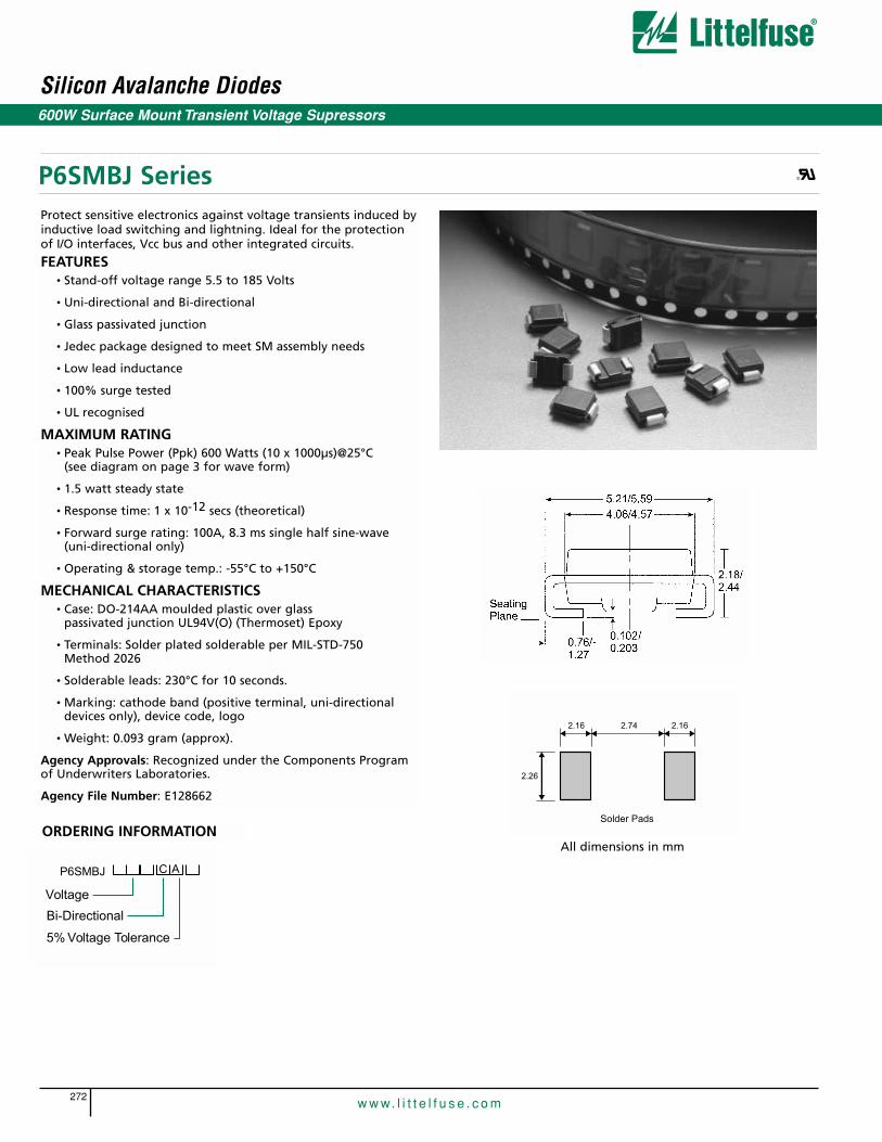
Silicon Avalanche Diodes
272w w w. l i t t e l f u s e . c o m
600W Surface Mount Transient Voltage Supressors
Protect sensitive electronics against voltage transients induced byinductive load switching and lightning. Ideal for the protectionof I/O interfaces, Vcc bus and other integrated circuits.
FEATURES• Stand-off voltage range 5.5 to 185 Volts
• Uni-directional and Bi-directional
• Glass passivated junction
• Jedec package designed to meet SM assembly needs
• Low lead inductance
• 100% surge tested
• UL recognised
MAXIMUM RATING• Peak Pulse Power (Ppk) 600 Watts (10 x 1000µs)@25°C
(see diagram on page 3 for wave form)
• 1.5 watt steady state
• Response time: 1 x 10-12 secs (theoretical)
• Forward surge rating: 100A, 8.3 ms single half sine-wave(uni-directional only)
• Operating & storage temp.: -55°C to +150°C
MECHANICAL CHARACTERISTICS• Case: DO-214AA moulded plastic over glass
passivated junction UL94V(O) (Thermoset) Epoxy
• Terminals: Solder plated solderable per MIL-STD-750Method 2026
• Solderable leads: 230°C for 10 seconds.
• Marking: cathode band (positive terminal, uni-directionaldevices only), device code, logo
• Weight: 0.093 gram (approx).
Agency Approvals: Recognized under the Components Programof Underwriters Laboratories.
Agency File Number: E128662
ORDERING INFORMATION
2.16
2.26
2.74 2.16
Solder Pads
All dimensions in mm
P6SMBJ C A
Voltage
Bi-Directional
5% Voltage Tolerance
P6SMBJ Series ®

Silicon Avalanche Diodes
273w w w. l i t t e l f u s e . c o m
6
SIL
ICO
N D
IOD
EA
RR
AYS
1 10
100
1000
10000
10 100 1000Device Stand-off Voltage - Volts
Pico-farads
@ Stand-off Voltage
Figure 1 - Capacitance
1s 100w
500w
5kw
20kw
2kw
100kw
10 s 10 ms100 s 1 msPulse Time (tp)
Pp(kw)
Figure 2 - Peak Pulse Power vs. Pulse Time
P6SMBJ Series
600W Surface Mount Transient Voltage Supressors
®

Silicon Avalanche Diodes
274w w w. l i t t e l f u s e . c o m
P6SMBJ 6V8 / P6SMBJ 6V8C 6V8 / 6V8C 5.50 6.12 7.48 10.0 1000.0 (4) 10.8 56.0 3.5
P6SMBJ 6V8A / P6SMBJ 6V8CA 6V8A /6V8CA 5.80 6.45 7.14 10.0 1000.0 (4) 10.5 57.0 3.5
P6SMBJ 7V5 / P6SMBJ 7V5C 7V5 / 7V5C 6.05 6.75 8.25 10.0 500.0 (4) 11.7 51.0 3.5
P6SMBJ 7V5A / P6SMBJ 7V5CA 7V5A / 7V5CA 6.40 7.13 7.88 10.0 500.0 (4) 11.3 53.0 3.5
P6SMBJ 8V2 / P6SMBJ 8V2C 8V2 / 8V2C 6.63 7.38 9.02 10.0 200.0 (4) 12.5 48.0 3.5
P6SMBJ 8V2A / P6SMBJ 8V2CA 8V2A / 8V2CA 7.02 7.79 8.61 10.0 200.0 (4) 12.1 50.0 3.5
P6SMBJ 9V1 / P6SMBJ 9V1C 9V1 / 9V1C 7.37 8.19 10.00 1.0 50.0 (4) 13.8 44.0 3.5
P6SMBJ 9V1A / P6SMBJ 9V1CA 9V1A / 9V1CA 7.78 8.65 9.55 1.0 50.0 (4) 13.4 45.0 3.5
P6SMBJ 10 / P6SMBJ 10C 10 / 10C 8.10 9.00 11.00 1.0 10.0 (4) 15.0 40.0 3.5
P6SMBJ 10A / P6SMBJ 10CA 10A / 10CA 8.55 9.50 10.50 1.0 10.0 (4) 14.5 41.0 3.5
P6SMBJ 11 / P6SMBJ 11C 11 / 11C 8.92 9.90 12.10 1.0 5.0 (4) 16.2 37.0 3.5
P6SMBJ 11A / P6SMBJ 11CA 11A / 11CA 9.40 10.50 11.60 1.0 5.0 (4) 15.6 38.0 3.5
P6SMBJ 12 / P6SMBJ 12C 12 / 12C 9.72 10.80 13.20 1.0 5.0 (4) 17.3 35.0 3.5
P6SMBJ 12A / P6SMBJ 12CA 12A / 12CA 10.20 11.40 12.60 1.0 5.0 16.7 36.0 3.5
P6SMBJ 13 / P6SMBJ 13C 13 / 13C 10.50 11.70 14.30 1.0 5.0 19.0 32.0 3.5
P6SMBJ 13A / P6SMBJ 13CA 13A / 13CA 11.10 12.40 13.70 1.0 5.0 18.2 33.0 3.5
P6SMBJ 15 / P6SMBJ 15C 15 / 15C 12.10 13.50 16.50 1.0 5.0 22.0 27.0 3.5
P6SMBJ 15A / P6SMBJ 15CA 15A / 15CA 12.80 14.30 15.80 1.0 5.0 21.2 28.0 3.5
P6SMBJ 16 / P6SMBJ 16C 16 / 16C 12.90 14.40 17.60 1.0 5.0 23.5 26.0 3.5
P6SMBJ 16A / P6SMBJ 16CA 16A / 16CA 13.60 15.20 16.80 1.0 5.0 22.5 27.0 3.5
P6SMBJ 18 / P6SMBJ 18C 18 / 18C 14.50 16.20 19.80 1.0 5.0 26.1 23.0 3.5
P6SMBJ 18A / P6SMBJ 18CA 18A / 18CA 15.30 17.10 18.90 1.0 5.0 25.2 24.0 `3.5
P6SMBJ 20 / P6SMBJ 20C 20 / 20C 16.20 18.00 22.00 1.0 5.0 29.1 21.0 3.5
P6SMBJ 20A / P6SMBJ 20CA 20A / 20CA 17.10 19.00 21.00 1.0 5.0 27.7 22.0 3.5
P6SMBJ 22 / P6SMBJ 22C 22 / 22C 17.80 19.80 24.20 1.0 5.0 31.9 19.0 3.5
P6SMBJ 22A / P6SMBJ 22CA 22A / 22CA 18.80 20.90 23.10 1.0 5.0 30.6 20.0 3.5
P6SMBJ 24 / P6SMBJ 24C 24 / 24C 19.40 21.60 26.40 1.0 5.0 34.7 17.0 3.5
P6SMBJ 24A / P6SMBJ 24CA 24A / 24CA 20.50 22.80 25.20 1.0 5.0 33.2 18.0 3.5
P6SMBJ 27 / P6SMBJ 27C 27 / 27C 21.80 24.30 29.70 1.0 5.0 39.1 15.0 3.5
P6SMBJ 27A / P6SMBJ 27CA 27A / 27CA 23.10 25.70 28.40 1.0 5.0 37.5 16.0 3.5
P6SMBJ 30 / P6SMBJ 30C 30 / 30C 24.30 27.00 33.0 1.0 5.0 43.5 14.0 3.5
P6SMBJ 30A / P6SMBJ 30CA 30A / 30CA 25.60 28.50 31.50 1.0 5.0 41.4 14.4 3.5
P6SMBJ 33 / P6SMBJ 33C 30 / 33C 26.80 29.70 36.30 1.0 5.0 47.7 12.6 3.5
P6SMBJ 33A / P6SMBJ 33CA 33A / 33CA 28.20 31.40 34.70 1.0 5.0 45.7 13.2 3.5
Part Device Reverse Breakdown Maximum Maximum Maximum MaximumNumber Code Standoff Voltage Reverse Clamping Peak Pulse Forward
Uni-polar Voltage VBR (Volts) @ IT Leakage Voltage Current VoltageVR IR @ VR VC @ IPP IPP @ VC (VF) @ IT
(Volts) Min Max (mA) (µA) (Volts) (A) (Volts)
Notes:
1. BV is measured using a pulse of 20 milliseconds or less.
2. VF, for Uni-directional devices, is measured using a 300 microsecond square wave pulse IF = 50A
3. IR is doubled for Bi-directional devices only with VR equal or less than 10 volts.
P6SMBJ Series
ELECTRICAL SPECIFICATION @ Tamb 25°C
600W Surface Mount Transient Voltage Supressors
®

Silicon Avalanche Diodes
275w w w. l i t t e l f u s e . c o m
66
SIL
ICO
N D
IOD
EA
RR
AYS
P6SMBJ 36 / P6SMBJ 36C 36 / 36C 29.10 32.40 39.60 1.0 5.0 52.0 11.6 3.5
P6SMBJ 36A / P6SMBJ 36CA 36A / 36CA 30.80 34.20 37.80 1.0 5.0 49.9 12.0 3.5
P6SMBJ 39 / P6SMBJ 39C 39 / 39C 31.60 35.10 42.90 1.0 5.0 56.4 10.5 3.5
P6SMBJ 39A / P6SMBJ 39CA 39A / 39CA 33.30 37.10 41.00 1.0 5.0 53.9 11.2 3.5
P6SMBJ 43 / P6SMBJ 43C 43 / 43C 34.80 38.70 47.30 1.0 5.0 61.9 9.6 3.5
P6SMBJ 43A / P6SMBJ 43CA 43A / 43CA 36.80 40.90 45.20 1.0 5.0 59.3 10.1 3.5
P6SMBJ 47 / P6SMBJ 47C 47 / 47C 38.10 42.30 51.70 1.0 5.0 67.8 8.9 3.5
P6SMBJ 47A / P6SMBJ 47CA 47A / 47CA 40.20 44.70 49.40 1.0 5.0 64.8 9.3 3.5
P6SMBJ 51 / P6SMBJ 51C 51 / 51C 41.30 45.90 56.10 1.0 5.0 73.5 8.2 3.5
P6SMBJ 51A / P6SMBJ 51CA 51A / 51CA 43.60 48.50 53.60 1.0 5.0 70.1 8.6 3.5
P6SMBJ 56 / P6SMBJ 56C 56 / 56C 45.4 50.40 61.60 1.0 5.0 80.5 7.4 3.5
P6SMBJ 56A / P6SMBJ 56CA 56A / 56CA 47.8 53.20 58.80 1.0 5.0 77.0 7.8 3.5
P6SMBJ 62 / P6SMBJ 62C 62 / 62C 50.2 55.80 68.20 1.0 5.0 89.0 6.8 3.5
P6SMBJ 62A / P6SMBJ 62CA 62A / 62CA 53.0 58.90 65.10 1.0 5.0 85.0 7.1 3.5
P6SMBJ 68 / P6SMBJ 68C 68 / 68C 55.1 61.20 74.80 1.0 5.0 98.0 6.1 3.5
P6SMBJ 68A / P6SMBJ 68CA 68A / 68CA 58.1 64.60 71.40 1.0 5.0 92.0 6.5 3.5
P6SMBJ 75/ P6SMBJ 75C 75 / 75C 60.7 67.50 82.50 1.0 5.0 108.0 5.5 3.5
P6SMBJ 75A / P6SMBJ 75CA 75A / 75CA 64.1 71.30 78.80 1.0 5.0 103.0 5.8 3.5
P6SMBJ 82 / P6SMBJ 82C 82 / 82C 66.4 73.80 90.20 1.0 5.0 118.0 5.1 3.5
P6SMBJ 82A / P6SMBJ 82CA 82A / 82CA 70.1 77.90 86.10 1.0 5.0 113.0 5.3 3.5
P6SMBJ 91 / P6SMBJ 91C 91 / 91C 73.7 81.90 100.00 1.0 5.0 131.0 4.5 3.5
P6SMBJ 91A / P6SMBJ 91CA 91A / 91CA 77.8 86.50 95.50 1.0 5.0 125.0 4.8 3.5
P6SMBJ 100 / P6SMBJ 100C 100 / 100C 81.0 90.00 110.00 1.0 5.0 144.0 4.2 3.5
P6SMBJ 100A / P6SMBJ 100CA 100A / 100CA 85.5 95.00 105.00 1.0 5.0 137.0 4.4 3.5
P6SMBJ 110 / P6SMBJ 110C 110 / 110C 89.2 99.00 121.00 1.0 5.0 158.0 3.8 3.5
P6SMBJ 110A / P6SMBJ 110CA 110A / 110CA 94.0 105.00 116.00 1.0 5.0 152.0 4.0 3.5
P6SMBJ 120 / P6SMBJ 120C 120 / 120C 97.2 108.00 132.00 1.0 5.0 173.0 3.5 3.5
P6SMBJ 120A / P6SMBJ 120CA 120A / 120CA 102.0 114.00 126.00 1.0 5.0 165.0 3.6 3.5
P6SMBJ 130 / P6SMBJ 130C 130 / 130C 105.0 117.00 143.00 1.0 5.0 187.0 3.2 3.5
P6SMBJ 130A / P6SMBJ 130CA 130A / 130CA 111.0 124.00 137.00 1.0 5.0 179.0 3.3 3.5
P6SMBJ 150 / P6SMBJ 150C 150 / 150C 121.0 135.00 165.00 1.0 5.0 215.0 2.8 3.5
P6SMBJ 150A / P6SMBJ 150CA 150A / 150CA 128.0 143.00 158.00 1.0 5.0 207.0 2.9 3.5
Part Device Reverse Breakdown Maximum Maximum Maximum MaximumNumber Code Standoff Voltage Reverse Clamping Peak Pulse Forward
Voltage VBR (Volts) @ IT Leakage Voltage Current VoltageVR IR @ VR VC @ IPP IPP @ VC (VF) @ IT
(Volts) Min Max (mA) (µA) (Volts) (A) (Volts)
Notes:
1. BV is measured using a pulse of 20 milliseconds or less.
2. VF, for Uni-directional devices, is measured using a 300 microsecond square wave pulse IF = 50A.
3. IR is doubled for Bi-directional devices only with VR equal or less than 10 volts.
P6SMBJ Series
ELECTRICAL SPECIFICATION @ Tamb 25°C
600W Surface Mount Transient Voltage Supressors
®

Silicon Avalanche Diodes
276w w w. l i t t e l f u s e . c o m
P6SMBJ 160 / P6SMBJ 160C 160 / 160C 130.0 144.00 176.00 1.0 5.0 230.0 2.6 3.5
P6SMBJ 160A / P6SMBJ 160CA 160A / 160CA 136.0 152.00 168.00 1.0 5.0 219.0 2.7 3.5
P6SMBJ 170 / P6SMBJ 170C 170 / 170C 138.0 153.00 187.00 1.0 5.0 244.0 2.5 3.5
P6SMBJ 170A / P6SMBJ 170CA 170A / 170CA 145.0 162.00 179.00 1.0 5.0 234.0 2.6 3.5
P6SMBJ 180 / P6SMBJ 180C 180 / 180C 146.0 162.00 198.00 1.0 5.0 258.0 2.3 3.5
P6SMBJ 180A / P6SMBJ 180CA 180A / 180CA 154.0 171.00 189.00 1.0 5.0 246.0 2.4 3.5
P6SMBJ 200 / P6SMBJ 200C 200 / 200C 162.0 180.00 220.00 1.0 5.0 287.0 2.1 3.5
P6SMBJ 200A / P6SMBJ 200CA 200A / 200CA 171.0 190.00 210.00 1.0 5.0 274.0 2.2 3.5
P6SMBJ 220 / P6SMBJ 220C 220 / 220C 175.0 198.00 242.00 1.0 5.0 344.0 1.8 3.5
P6SMBJ 220A / P6SMBJ 220CA 220A / 220CA 185.0 209.00 231.00 1.0 5.0 328.0 1.8 3.5
Part Device Reverse Breakdown Maximum Maximum Maximum MaximumNumber Code Standoff Voltage Reverse Clamping Peak Pulse Forward
Voltage VBR (Volts) @ IT Leakage Voltage Current VoltageVR IR @ VR VC @ IPP IPP @ VC (VF) @ IT
(Volts) Min Max (mA) (µA) (Volts) (A) (Volts)
P6SMBJ Series
ELECTRICAL SPECIFICATION @ Tamb 25°C
Notes:
1. BV is measured using a pulse of 20 milliseconds or less.
2. VF, for Uni-directional devices, is measured using a 300 microsecond square wave pulse IF = 50A
3. IR is doubled for Bi-directional devices only with VR equal or less than 10 volts.
600W Surface Mount Transient Voltage Supressors
®
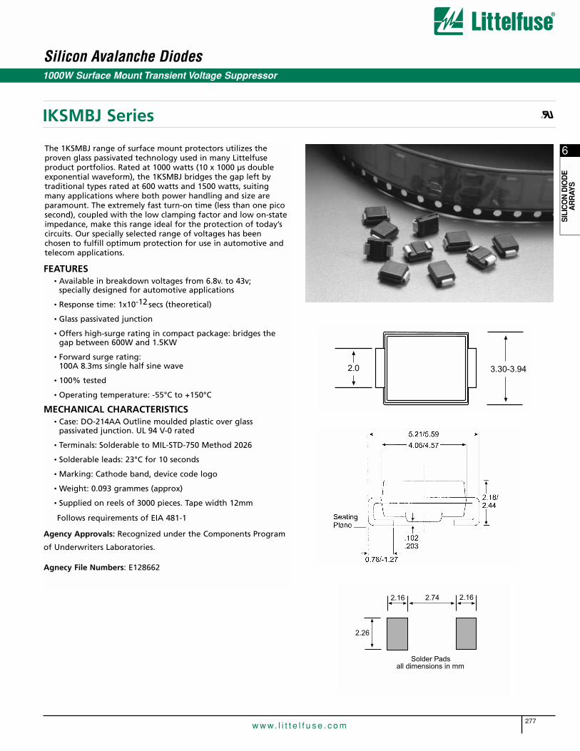
Silicon Avalanche Diodes
277w w w. l i t t e l f u s e . c o m
6
SIL
ICO
N D
IOD
EA
RR
AYS
1000W Surface Mount Transient Voltage Suppressor
The 1KSMBJ range of surface mount protectors utilizes theproven glass passivated technology used in many Littelfuseproduct portfolios. Rated at 1000 watts (10 x 1000 µs doubleexponential waveform), the 1KSMBJ bridges the gap left bytraditional types rated at 600 watts and 1500 watts, suitingmany applications where both power handling and size areparamount. The extremely fast turn-on time (less than one picosecond), coupled with the low clamping factor and low on-stateimpedance, make this range ideal for the protection of today’scircuits. Our specially selected range of voltages has beenchosen to fulfill optimum protection for use in automotive andtelecom applications.
FEATURES• Available in breakdown voltages from 6.8v. to 43v;
specially designed for automotive applications
• Response time: 1x10-12.secs (theoretical)
• Glass passivated junction
• Offers high-surge rating in compact package: bridges thegap between 600W and 1.5KW
• Forward surge rating:100A 8.3ms single half sine wave
• 100% tested
• Operating temperature: -55°C to +150°C
MECHANICAL CHARACTERISTICS• Case: DO-214AA Outline moulded plastic over glass
passivated junction. UL 94 V-0 rated
• Terminals: Solderable to MIL-STD-750 Method 2026
• Solderable leads: 23°C for 10 seconds
• Marking: Cathode band, device code logo
• Weight: 0.093 grammes (approx)
• Supplied on reels of 3000 pieces. Tape width 12mm
Follows requirements of EIA 481-1
Agency Approvals: Recognized under the Components Program
of Underwriters Laboratories.
Agnecy File Numbers: E128662
2.16 2.74 2.16
2.26
Solder Padsall dimensions in mm
2.0 3.30-3.94
IKSMBJ Series ®
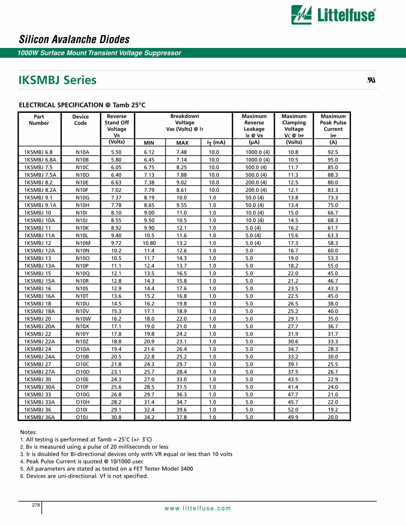
Silicon Avalanche Diodes
278w w w. l i t t e l f u s e . c o m
ReverseStand OffVoltage
VR
(Volts)
PartNumber
BreakdownVoltage
VBR (Volts) @ IT
MIN MAX IT (mA)
MaximumReverseLeakageIR @ VR
(µA)
MaximumClampingVoltageVC @ IPP
(Volts)
MaximumPeak Pulse
CurrentIPP
(A)
IKSMBJ Series
1KSMBJ 6.8 N10A 5.50 6.12 7.48 10.0 1000.0 (4) 10.8 92.51KSMBJ 6.8A N10B 5.80 6.45 7.14 10.0 1000.0 (4) 10.5 95.01KSMBJ 7.5 N10C 6.05 6.75 8.25 10.0 500.0 (4) 11.7 85.01KSMBJ 7.5A N10D 6.40 7.13 7.88 10.0 500.0 (4) 11.3 88.31KSMBJ 8.2 N10E 6.63 7.38 9.02 10.0 200.0 (4) 12.5 80.01KSMBJ 8.2A N10F 7.02 7.79 8.61 10.0 200.0 (4) 12.1 83.31KSMBJ 9.1 N10G 7.37 8.19 10.0 1.0 50.0 (4) 13.8 73.31KSMBJ 9.1A N10H 7.78 8.65 9.55 1.0 50.0 (4) 13.4 75.01KSMBJ 10 N10I 8.10 9.00 11.0 1.0 10.0 (4) 15.0 66.71KSMBJ 10A N10J 8.55 9.50 10.5 1.0 10.0 (4) 14.5 68.31KSMBJ 11 N10K 8.92 9.90 12.1 1.0 5.0 (4) 16.2 61.71KSMBJ 11A N10L 9.40 10.5 11.6 1.0 5.0 (4) 15.6 63.31KSMBJ 12 N10M 9.72 10.80 13.2 1.0 5.0 (4) 17.3 58.31KSMBJ 12A N10N 10.2 11.4 12.6 1.0 5.0 16.7 60.01KSMBJ 13 N10O 10.5 11.7 14.3 1.0 5.0 19.0 53.31KSMBJ 13A N10P 11.1 12.4 13.7 1.0 5.0 18.2 55.01KSMBJ 15 N10Q 12.1 13.5 16.5 1.0 5.0 22.0 45.01KSMBJ 15A N10R 12.8 14.3 15.8 1.0 5.0 21.2 46.71KSMBJ 16 N10S 12.9 14.4 17.6 1.0 5.0 23.5 43.31KSMBJ 16A N10T 13.6 15.2 16.8 1.0 5.0 22.5 45.01KSMBJ 18 N10U 14.5 16.2 19.8 1.0 5.0 26.5 38.01KSMBJ 18A N10V 15.3 17.1 18.9 1.0 5.0 25.2 40.01KSMBJ 20 N10W 16.2 18.0 22.0 1.0 5.0 29.1 35.01KSMBJ 20A N10X 17.1 19.0 21.0 1.0 5.0 27.7 36.71KSMBJ 22 N10Y 17.8 19.8 24.2 1.0 5.0 31.9 31.71KSMBJ 22A N10Z 18.8 20.9 23.1 1.0 5.0 30.6 33.31KSMBJ 24 O10A 19.4 21.6 26.4 1.0 5.0 34.7 28.31KSMBJ 24A O10B 20.5 22.8 25.2 1.0 5.0 33.2 30.01KSMBJ 27 O10C 21.8 24.3 29.7 1.0 5.0 39.1 25.51KSMBJ 27A O10D 23.1 25.7 28.4 1.0 5.0 37.5 26.71KSMBJ 30 O10E 24.3 27.0 33.0 1.0 5.0 43.5 22.91KSMBJ 30A O10F 25.6 28.5 31.5 1.0 5.0 41.4 24.01KSMBJ 33 O10G 26.8 29.7 36.3 1.0 5.0 47.7 21.01KSMBJ 33A O10H 28.2 31.4 34.7 1.0 5.0 45.7 22.01KSMBJ 36 O10I 29.1 32.4 39.6 1.0 5.0 52.0 19.21KSMBJ 36A O10J 30.8 34.2 37.8 1.0 5.0 49.9 20.0
ELECTRICAL SPECIFICATION @ Tamb 25°C
Notes: 1. All testing is performed at Tamb = 25˚C (+/- 3˚C)2. Bv is measured using a pulse of 20 milliseconds or less3. Ir is doubled for Bi-directional devices only with VR equal or less than 10 volts4. Peak Pulse Current is quoted @ 10/1000 µsec5. All parameters are stated as tested on a FET Tester Model 34006. Devices are uni-directional. Vf is not specified.
1000W Surface Mount Transient Voltage Suppressor
®
DeviceCode

Silicon Avalanche Diodes
279w w w. l i t t e l f u s e . c o m
6
SIL
ICO
N D
IOD
EA
RR
AYS
ReverseStand OffVoltage
VR
(Volts)
PartNumber
BreakdownVoltage
VBR (Volts) @ IT
MIN MAX
MaximumReverseLeakageIR @ VR
(µA)
MaximumClampingVoltageVC @ IPP
(Volts)
MaximumPeak Pulse
CurrentIPP
(A)
1KSMBJ 39 O10K 31.6 35.1 42.9 1.0 5.0 56.4 17.51KSMBJ 39A O10L 33.3 37.1 41.0 1.0 5.0 53.9 18.71KSMBJ 43 O10M 34.8 38.7 47.3 1.0 5.0 61.9 16.01KSMBJ 43A O10N 36.8 40.9 45.2 1.0 5.0 59.3 16.81KSMBJ 47 O10O 38.1 42.3 51.7 1.0 5.0 67.8 14.81KSMBJ 47A O10P 40.2 44.7 49.4 1.0 5.0 64.8 15.51KSMBJ 51 O10Q 41.3 45.9 56.1 1.0 5.0 73.5 13.71KSMBJ 51A O10R 43.6 48.5 53.6 1.0 5.0 70.1 14.31KSMBJ 56 O10S 45.4 50.4 61.6 1.0 5.0 80.5 12.31KSMBJ 56A O10T 47.8 53.2 58.8 1.0 5.0 77.0 13.01KSMBJ 62 O10U 50.2 55.8 68.2 1.0 5.0 89.0 11.31KSMBJ 62A O10V 53.0 58.9 65.1 1.0 5.0 85.0 11.81KSMBJ 68 O10W 55.1 61.2 74.8 1.0 5.0 98.0 10.21KSMBJ 68A O10X 58.1 64.6 71.4 1.0 5.0 92.0 10.81KSMBJ 75 O10Y 60.7 67.5 82.5 1.0 5.0 108.0 9.21KSMBJ 75A O10Z 64.1 71.3 78.8 1.0 5.0 103.0 9.71KSMBJ 82 P10A 66.4 73.8 90.2 1.0 5.0 118.0 8.51KSMBJ 82A P10B 70.1 77.9 86.1 1.0 5.0 113.0 8.81KSMBJ 91 P10C 73.7 81.9 100.0 1.0 5.0 131.0 7.51KSMBJ 91A P10D 77.8 86.5 95.5 1.0 5.0 125.0 8.01KSMBJ 100 P10E 81.0 90.0 110.0 1.0 5.0 144.0 7.01KSMBJ 100A P10F 85.5 95.0 105.0 1.0 5.0 137.0 7.31KSMBJ 110 P10G 89.2 99.0 121.0 1.0 5.0 158.0 6.31KSMBJ 110A P10H 94.0 105.0 116.0 1.0 5.0 152.0 6.61KSMBJ 120 P10I 97.2 108.0 132.0 1.0 5.0 173.0 5.81KSMBJ 120A P10J 102.0 114.0 126.0 1.0 5.0 165.0 6.11KSMBJ 130 P10K 105.0 117.0 143.0 1.0 5.0 187.0 5.31KSMBJ 130A P10L 111.0 124.0 137.0 1.0 5.0 179.0 5.61KSMBJ 150 P10M 121.0 135.0 165.0 1.0 5.0 215.0 4.71KSMBJ 150A P10N 128.0 143.0 158.0 1.0 5.0 207.0 4.81KSMBJ 160 P10O 130.0 144.0 176.0 1.0 5.0 230.0 4.31KSMBJ 160A P10P 136.0 152.0 168.0 1.0 5.0 219.0 4.6
IKSMBJ Series
ELECTRICAL SPECIFICATION @ Tamb 25°C
Notes: 1. All testing is performed at Tamb = 25˚C (+/- 3˚C)2. Bv is measured using a pulse of 20 milliseconds or less3. Ir is doubled for Bi-directional devices only with VR equal or less than 10 volts4. Peak Pulse Current is quoted @ 10/1000 µsec5. All parameters are stated as tested on a FET Tester Model 34006. Vf, for uni-directional devices, is measured using a 300 microsecond square wave pulse @ IT = 50A
1000W Surface Mount Transient Voltage Suppressor
®
DeviceCode
IT (mA)
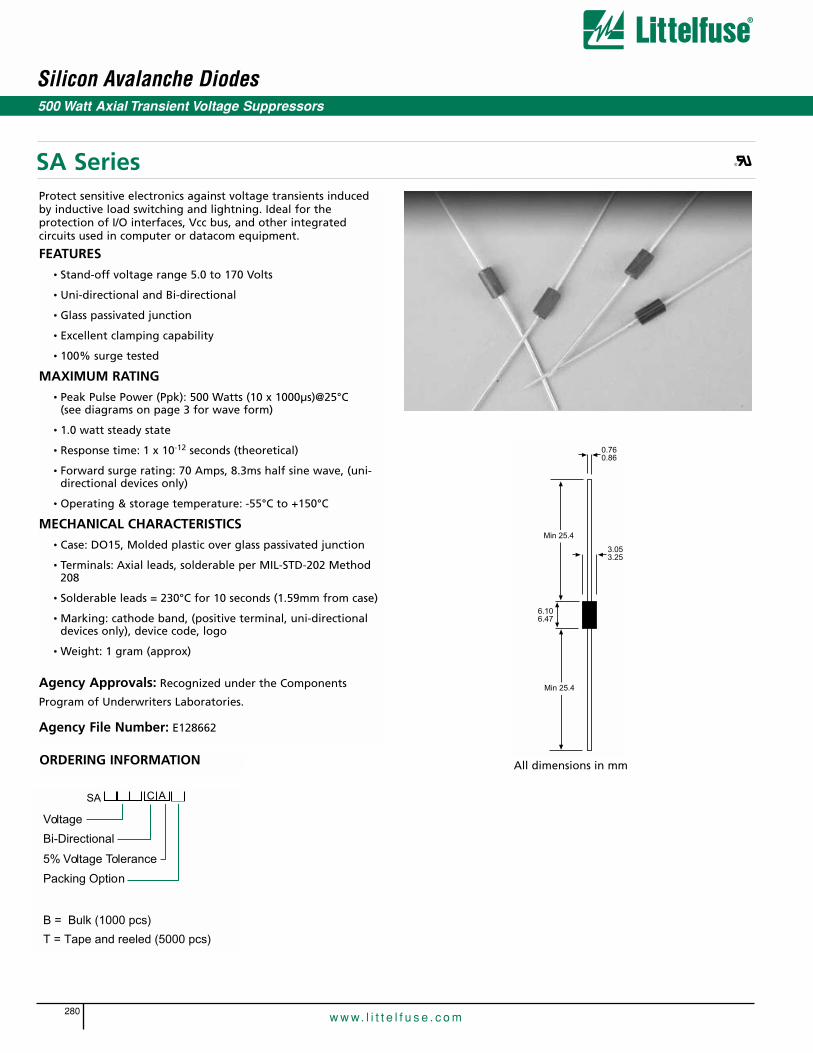
Silicon Avalanche Diodes
280w w w. l i t t e l f u s e . c o m
500 Watt Axial Transient Voltage Suppressors
SA SeriesProtect sensitive electronics against voltage transients inducedby inductive load switching and lightning. Ideal for theprotection of I/O interfaces, Vcc bus, and other integratedcircuits used in computer or datacom equipment.
FEATURES
• Stand-off voltage range 5.0 to 170 Volts
• Uni-directional and Bi-directional
• Glass passivated junction
• Excellent clamping capability
• 100% surge tested
MAXIMUM RATING
• Peak Pulse Power (Ppk): 500 Watts (10 x 1000µs)@25°C(see diagrams on page 3 for wave form)
• 1.0 watt steady state
• Response time: 1 x 10-12 seconds (theoretical)
• Forward surge rating: 70 Amps, 8.3ms half sine wave, (uni-directional devices only)
• Operating & storage temperature: -55°C to +150°C
MECHANICAL CHARACTERISTICS
• Case: DO15, Molded plastic over glass passivated junction
• Terminals: Axial leads, solderable per MIL-STD-202 Method 208
• Solderable leads = 230°C for 10 seconds (1.59mm from case)
• Marking: cathode band, (positive terminal, uni-directionaldevices only), device code, logo
• Weight: 1 gram (approx)
Agency Approvals: Recognized under the Components
Program of Underwriters Laboratories.
Agency File Number: E128662
0.760.86
3.053.25
Min 25.4
6.106.47
Min 25.4
SA C A
Voltage
Bi-Directional
5% Voltage Tolerance
Packing Option
B = Bulk (1000 pcs)
T = Tape and reeled (5000 pcs)
ORDERING INFORMATION All dimensions in mm
®

Silicon Avalanche Diodes
281w w w. l i t t e l f u s e . c o m
6
SIL
ICO
N D
IOD
EA
RR
AYS
10000
1000
Cj (Pf)
100
101 10 100 1000
Device Stand-off Voltage - Volts
Uni-directional
Bi-directional
Pulse Time (tp)
1µs 10µs 100µs 1ms 10ms100w
500w
Pp(kw) 2kw
5kw
20kw
100kw
Figure 1 - Capacitance vs. Working Voltage
Figure 2 - Peak Pulse Power vs. Pulse Time
500 Watt Axial Transient Voltage Suppressors
SA Series ®

Silicon Avalanche Diodes
282w w w. l i t t e l f u s e . c o m
SA5.0*
SA5.0A*
SA6.0*
SA6.0A*
SA6.5
SA6.5A
SA7.0
SA7.0A
SA7.5
SA7.5A
SA8.0
SA8.0A
SA8.5
SA8.5A
SA9.0
SA9.0A
SA10*
SA10A*
SA11
SA11A
SA12
SA12A
SA13
SA13A
SA14
SA14A
SA15
SA15A
SA16
SA16A
SA17
SA17A
SA18
SA18A
SA20*
SA20A*
PartNumber
(Uni)
PartNumber
(Bi)
SA5.0C
N/A
SA6.0C*
SA6.0CA*
SA6.5C
SA6.5CA
SA7.0A
SA7.0CA
SA7.5A
SA7.5CA
SA8.0C
SA8.0CA
SA8.5C
SA8.5CA
SA9.0C
SA9.0CA
SA10C
SA10CA
SA11C
SA11CA
SA12C
SA12CA
SA13C*
SA13CA*
SA14C
SA14CA
SA15C
SA15CA
SA16C
SA16CA
SA17C
SA17CA
SA18
SA18CA
SA20C
SA20CA
ReverseStand OffVoltage
VR
(Volts)
5.0
5.0
6.0
6.0
6.5
6.5
7.0
7.0
7.5
7.5
8.0
8.0
8.5
8.5
9.0
9.0
10.0
10.0
11.0
11.0
12.0
12.0
13.0
13.0
14.0
14.0
15.0
15.0
16.0
16.0
17.0
17.0
18.0
18.0
20.0
20.0
MIN
6.40
6.40
6.67
6.67
7.22
7.22
7.78
7.78
8.33
8.33
8.89
8.89
9.44
9.44
10.00
10.00
11.10
11.10
12.20
12.20
13.30
13.30
14.40
14.40
15.60
15.60
16.70
16.70
17.80
17.80
18.90
18.90
20.00
20.00
22.20
22.20
MAX
7.30
7.00
8.15
7.37
8.82
7.98
9.51
8.60
10.20
9.21
10.90
9.83
11.50
10.40
12.20
11.10
13.60
12.30
14.90
13.50
16.30
14.70
17.60
15.90
19.10
17.20
20.40
18.50
21.80
19.70
23.10
20.90
24.40
22.10
27.10
24.50
IT mA
10.00
10.00
10.00
10.00
10.00
10.00
10.00
10.00
1.00
1.00
1.00
1.00
1.00
1.00
1.00
1.00
1.00
1.00
1.00
1.00
1.00
1.00
1.00
1.00
1.00
1.00
1.00
1.00
1.00
1.00
1.00
1.00
1.00
1.00
1.00
MaximumReverseLeakageIR @ VR
(µA)
600.0
600.0
600.0
600.0
400.0
400.0
150.0
150.0
50.0
50.0
25.0
25.0
10.0
10.0
5.0
5.0
3.0
3.0
3.0
3.0
3.0
3.0
3.0
3.0
3.0
3.0
3.0
3.0
3.0
3.0
3.0
3.0
3.0
3.0
3.0
3.0
MaximumClampingVoltageVC @ IPP
(Volts)
9.6
9.2
11.4
10.3
12.3
11.2
13.3
12.0
14.3
12.9
15.0
13.6
15.9
14.4
16.9
15.4
18.8
17.0
20.1
18.2
22.0
19.9
23.8
21.5
25.8
23.2
26.9
24.4
28.8
26.0
30.5
27.6
32.2
29.2
35.8
32.4
MaximumPeak Pulse
CurrentIPP
(A)
52.0
54.3
43.9
48.5
40.7
44.7
37.8
41.7
35.0
38.8
33.3
36.7
31.4
34.7
29.5
32.5
26.6
29.4
24.9
27.4
22.7
25.1
21.0
23.2
19.4
21.5
18.8
20.6
17.6
19.2
16.4
18.1
15.5
17.2
13.9
15.4
Note: SA5.0A is not available in Bi-directional.Suffix ‘C’ denotes Bi-directional device. Suffix ‘A’ denotes 5% tolerance device, no suffix denotes a 10% tolerance device.1. For Bi-directional devices having VR of 10 volts and below, the IR limit is doubled.2. For Uni-directional devices VF = 3.5 Volts max at IF = 35A, 300 µS square wave pulse. * Preferred voltages.
MaxVoltage
TemperatureVariation
of VBR (mV/°C)
5.0
5.0
5.0
5.0
5.0
5.0
6.0
6.0
7.0
7.0
7.0
7.0
8.0
8.0
9.0
9.0
10.0
10.0
11.0
11.0
12.0
12.0
13.0
13.0
14.0
14.0
16.0
16.0
19.0
17.0
20.0
19.0
21.0
20.0
25.0
23.0
SA Series
ELECTRICAL SPECIFICATION @ Tamb 25°C
500 Watt Axial Transient Voltage Suppressors
BreakdownVoltage
VBR (Volts) @ IT
®
283w w w. l i t t e l f u s e . c o m
6
SIL
ICO
N D
IOD
EA
RR
AYS
Silicon Avalanche Diodes
SA22
SA22A
SA24
SA24A
SA26*
SA26A*
SA28
SA28A
SA30
SA30A
SA33
SA33A
SA36
SA36A
SA40
SA40A
SA43
SA43A
SA45
SA45A
SA48
SA48A
SA51
SA51A
SA54
SA54A
SA58
SA58A
SA60
SA60A
SA64
SA64A
SA70
SA70A
SA75
SA75A
SA78
SA78A
SA85
SA85A
SA90
SA90A
PartNumber
(Uni)
PartNumber
(Bi)
SA22C
SA22CA
SA24C
SA24CA
SA26C*
SA26CA*
SA28C*
SA28CA*
SA30C
SA30CA
SA33C
SA33CA
SA36C
SA36CA
SA40C
SA40CA
SA43C
SA43CA
SA45C
SA45CA
SA48C
SA48CA
SA51*
SA51CA*
SA54C
SA54CA
SA58C
SA58CA
SA60C
SA60CA
SA64C
SA64CA
SA70C
SA70CA
SA75C
SA75CA
SA78C
SA78CA
SA85C
SA85CA
SA90C
SA90CA
ReverseStand offVoltage
VR
(Volts)
22.0
22.0
24.0
24.0
26.0
26.0
28.0
28.0
30.0
30.0
33.0
33.0
36.0
36.0
40.0
40.0
43.0
43.0
45.0
45.0
48.0
48.0
51.0
51.0
54.0
54.0
58.0
58.0
60.0
60.0
64.0
64.0
70.0
70.0
75.0
75.0
78.0
78.0
85.0
85.0
90.0
90.0
BreakdownVoltage
VBR (Volts) @ IT
MIN
24.40
24.40
26.70
26.70
28.90
28.90
31.10
31.10
33.30
33.30
36.70
36.70
40.00
40.00
44.40
44.40
47.80
47.80
50.00
50.00
53.30
53.30
56.70
56.70
60.00
60.00
64.40
64.40
66.70
66.70
71.00
71.10
77.80
77.00
83.00
83.00
86.00
86.00
94.00
94.00
100.00
100.00
MAX
29.80
26.90
32.60
29.50
35.30
31.90
38.00
34.40
40.70
36.80
44.90
40.60
48.90
44.20
54.30
49.10
58.40
52.80
61.10
55.30
65.10
58.90
69.30
62.70
73.30
66.30
78.70
71.20
81.50
73.70
86.90
78.60
95.10
86.00
102.00
92.10
106.00
95.80
115.00
104.00
122.00
111.00
IT (mA)
1.00
1.00
1.00
1.00
1.00
1.00
1.00
1.00
1.00
1.00
1.0
1.0
1.0
1.0
1.0
1.0
1.0
1.0
1.0
1.0
1.0
1.0
1.0
1.0
1.0
1.0
1.0
1.0
1.0
1.0
1.0
1.0
1.0
1.0
1.0
1.0
1.0
1.0
1.0
1.0
1.0
MaximumReverseLeakageIR @ VR
(µA)
3.0
3.0
3.0
3.0
3.0
3.0
3.0
3.0
3.0
3.0
3.0
3.0
3.0
3.0
3.0
3.0
3.0
3.0
3.0
3.0
3.0
3.0
3.0
3.0
3.0
3.0
3.0
3.0
3.0
3.0
3.0
3.0
3.0
3.0
3.0
3.0
3.0
3.0
3.0
3.0
3.0
3.0
MaximumClampingVoltageVC @ IPP
(Volts)
39.4
35.5
43.0
38.9
46.6
42.1
50.0
45.4
53.5
48.4
59.0
53.3
64.3
58.1
71.4
64.5
76.7
69.4
80.3
72.7
85.5
77.4
91.1
82.4
96.3
87.1
103.0
93.6
107.0
96.8
114.0
103.0
125.0
113.0
134.0
121.0
139.0
126.0
151.0
137.0
160.0
146.0
MaximumPeak Pulse
CurrentIPP
(A)
12.7
14.1
11.6
12.8
10.7
11.9
9.9
11.0
9.3
10.3
8.5
9.4
7.8
8.6
7.0
7.8
6.5
7.2
6.2
6.9
5.8
6.5
5.5
6.1
5.2
5.7
4.9
5.3
4.7
5.2
4.4
4.9
4.0
4.4
3.7
4.1
3.6
4.0
3.3
3.6
3.1
3.4
Suffix ‘C’ denotes Bi-directional device. Suffix ‘A’ denotes 5% tolerance device, no suffix denotes a 10% tolerance device.1. For Bi-directional devices having VR of 10 volts and below, the IR limit is doubled.2. For Uni-directional devices VF = 3.5 Volts max at IF = 35A, 300 µS square wave pulse. * Preferred voltages.
MaxVoltage
TemperatureVariation
of VBR (mV/°C)
28.0
25.0
31.0
28.0
31.0
30.0
35.0
31.0
39.0
36.0
42.0
39.0
46.0
41.0
51.0
46.0
55.0
50.0
58.0
52.0
63.0
56.0
66.0
61.0
71.0
65.0
78.0
70.0
80.0
71.0
86.0
76.0
94.0
85.0
101.0
91.0
105.0
95.0
114.0
103.0
121.0
110.0
SA SeriesELECTRICAL SPECIFICATION @ Tamb 25°C
500 Watt Axial Transient Voltage Suppressors
®
SA100
SA100A
SA110
SA110A
SA120
SA120A
SA130
SA130A
SA150
SA150A
SA160
SA160A
SA170
SA170A
MIN
111.00
111.00
122.00
122.00
133.00
133.00
144.00
144.00
167.00
167.00
178.00
178.00
189.00
189.00
Silicon Avalanche Diodes
284w w w. l i t t e l f u s e . c o m
SA100CA
SA100CA
SA110C
SA110CA
SA120C
SA120CA
SA130C
SA130CA
SA150C
SA150CA
SA160C
SA160CA
SA170C
SA170CA
100.0
100.0
110.0
110.0
120.0
120.0
130.0
130.0
150.0
150.0
160.0
160.0
170.0
170.0
ELECTRICAL SPECIFICATION @ Tamb 25°C
MAX
136.00
123.00
149.00
135.00
163.00
147.00
176.00
159.00
204.00
185.00
218.00
197.00
231.00
209.00
1.0
1.0
1.0
1.0
1.0
1.0
1.0
1.0
1.0
1.0
1.0
1.0
1.0
1.0
3.0
3.0
3.0
3.0
3.0
3.0
3.0
3.0
3.0
3.0
3.0
3.0
3.0
3.0
179.0
162.0
196.0
177.0
214.0
193.0
231.0
209.0
268.0
243.0
287.0
259.0
304.0
275.0
2.8
3.1
2.6
2.8
2.3
2.0
2.2
2.4
1.9
2.1
1.7
1.9
1.6
1.8
135.0
123.0
148.0
133.0
162.0
146.0
175.0
158.0
203.0
184.0
217.0
196.0
230.0
208.0
SA Series
PartNumber
(Uni)
PartNumber
(Bi)
ReverseStand OffVoltage
VR
(Volts)
BreakdownVoltage
VBR (Volts) @ IT
MaximumReverseLeakageIR @ VR
(µA)
MaximumClampingVoltageVC @ IPP
(Volts)
MaximumPeak Pulse
CurrentIPP
(A)
MaxVoltage
TemperatureVariation
of VBR (mV/°C)
Suffix ‘C’ denotes Bi-directional device. Suffix ‘A’ denotes 5% tolerance device, no suffix denotes a 10% tolerance device.1. For Bi-directional devices having VR of 10 volts and below, the IR limit is doubled.2. For Uni-directional devices VF = 3.5 Volts max at IF = 35A, 300 µS square wave pulse. * Preferred voltages.
500 Watt Axial Transient Voltage Suppressors
®
IT (mA)
285w w w. l i t t e l f u s e . c o m
6
SIL
ICO
N D
IOD
EA
RR
AYS
Silicon Avalanche Diodes600 Watt Axial Transient Voltage Suppressors
Protect sensitive electronics against voltage transients induced by
inductive load switching and lightning. Ideal for the protection
of I/O interfaces, Vcc bus, and other integrated circuits.
FEATURES• Breakdown voltage range 6.8 to 440 Volts
• Uni-directional and Bi-directional
• Glass passivated junction
• Excellent clamping capability
• 100% surge tested
• UL recognised
MAXIMUM RATING• Peak Pulse Power (Ppk): 600 Watts (10 x 1000µs)@25°C
(see diagram on page 3 for wave form)
• 1.5 watt steady state
• Response time: 1 x 10-12 seconds (theoretical)
• Forward surge rating: 100 Amps, 8.3ms half sine wave, (uni-directional devices only)
• Operating & storage temperature: -55°C to +150°C
MECHANICAL CHARACTERISTICS• Case: DO-15, Molded plastic over glass passivated junction
• Terminals: Axial leads, solderable per MIL-STD-202”
Method 208
• Solderable leads = 230°C for 10 seconds (1.59mm from case)
• Marking: cathode band, (positive terminal, uni-directional devices only), device code, logo
• Weight: 1.2 grammes (approx)
Agency Approvals: Recognized under the ComponentsProgram of Underwriters Laboratories.
Agnecy File Number: E128662
0.760.86
3.053.25
Min 25.4
6.106.47
Min 25.4
P6KE C A
Voltage
Bi-Directional
5% Voltage Tolerance
Packaging Option
B = Bulk (1000 pcs)
T = Tape and reeled (5000 pcs)
ORDERING INFORMATION
P6KE Series
All dimensions in mm
®

Silicon Avalanche Diodes
286w w w. l i t t e l f u s e . c o m
Device Stand-off Voltage - Volts
1 10 100 1000
10000
1000
Cj (pf)
100
10
Pulse Time (tp)
1µs 10µs 100µs 1ms 10ms100w
500w
Pp(kw) 2kw
5kw
20kw
100kw
Figure 1 - Capacitance vs. Stand-off Voltage
Figure 2 - Peak Pulse Power vs. Pulse Time
600 Watt Axial Transient Voltage Suppressors
P6KE Series ®
287w w w. l i t t e l f u s e . c o m
6
SIL
ICO
N D
IOD
EA
RR
AYS
PP6KE6.8*
P6KE6.8A*
P6KE7.5*
P6KE7.5A*
P6KE8.2
P6KE8.2A
P6KE9.1
P6KE9.1A
P6KE10
P6KE10A
P6KE11
P6KE11A
P6KE12*
P6KE12A*
P6KE13
P6KE13A
P6KE15
P6KE15A
P6KE16
P6KE16A
P6KE18*
P6KE18A*
P6KE20
P6KE20A
P6KE22
P6KE22A
P6KE24
P6KE24A
P6KE27*
P6KE27A*
P6KE30*
P6KE30A*
PartNumber
(Uni)
PartNumber
(Bi)
PP6KE6.8C*
P6KE6.8CA*
P6KE7.5C*
P6KE7.5CA*
P6KE8.2C
P6KE8.2CA
P6KE9.1C
P6KE9.1CA
P6KE10C
P6KE10CA
P6KE11C
P6KE11CA
P6KE12C*
P6KE12CA*
P6KE13C
P6KE13CA
P6KE15C*
P6KE15CA*
P6KE16C
P6KE16CA
P6KE18C*
P6KE18CA*
P6KE20C*
P6KE20CA*
P6KE22C
P6KE22CA
P6KE24C
P6KE24CA
P6KE27C
P6KE27CA
P6KE30C*
P6KE30CA*
ReverseStand offVoltage
VR
(Volts)
5.50
5.80
6.05
6.40
6.63
7.02
7.37
7.78
8.10
8.55
8.92
9.40
9.72
10.20
10.50
11.10
12.10
12.80
12.90
13.60
14.50
15.30
16.20
17.10
17.80
18.80
19.40
20.50
21.80
23.10
24.30
25.60
BreakdownVoltage
VBR (Volts) @ IT
MIN
6.12
6.45
6.75
7.13
7.38
7.79
8.19
8.65
9.00
9.50
9.90
10.50
10.80
11.40
11.70
12.40
13.50
14.30
14.40
15.20
16.20
17.10
18.00
19.00
19.80
20.90
21.60
22.800
24.30
25.70
27.00
28.50
MAX
7.48
7.14
8.25
7.88
9.02
8.61
10.00
9.55
11.00
10.50
12.10
11.60
13.20
12.60
14.30
13.70
16.50
15.80
17.60
16.80
19.80
18.90
22.00
21.00
24.20
23.10
26.40
25.20
29.70
28.40
33.00
31.50
(mA)
10.0
10.0
10.0
10.0
10.0
10.0
1.0
1.0
1.0
1.0
1.0
1.0
1.0
1.0
1.0
1.0
1.0
1.0
1.0
1.0
1.0
1.0
1.0
1.0
1.0
1.0
1.0
1.0
1.0
1.0
1.0
1.0
MaximumReverseLeakageIR @ VR
(µA)
1000.0
1000.0
500.0
500.0
200.0
200.0
50.0
50.0
10.0
10.0
5.0
5.0
5.0
5.0
5.0
5.0
5.0
5.0
5.0
5.0
5.0
5.0
5.0
5.0
5.0
5.0
5.0
5.0
5.0
5.0
5.0
5.0
MaximumClampingVoltageVC @ IPP
(Volts)
10.8
10.5
11.7
11.3
12.5
12.1
13.8
13.4
15.0
14.5
16.2
15.6
17.3
16.7
19.0
18.2
22.0
21.2
23.5
22.5
26.5
25.2
29.1
27.7
31.9
30.6
34.7
33.2
39.1
37.5
43.5
41.4
MaximumPeak Pulse
CurrentIPP
(A)
56.0
57.0
51.0
53.0
48.0
50.0
44.0
45.0
40.0
41.0
37.0
38.0
35.0
36.0
32.0
33.0
27.0
28.0
26.0
27.0
23.0
24.0
21.0
22.0
19.0
20.0
17.0
18.0
15.0
16.0
14.0
14.4
Suffix ‘C’ denotes Bi-directional device. Suffix ‘A’ denotes 5% tolerance device, no suffix denotes a 10% tolerance device.1. For Bi-directional devices having VR of 10 volts and below, the IR limit is doubled.2. VF = 3.5 Volts max. for devices of VR <100v, and VF = 5.0 Volts max for devices of VR >100V. IF = 50A, 300 µS square wave.* Preferred voltages.
MaxVoltage
TemperatureVariation
of VBR (%/°C)
0.057
0.057
0.061
0.061
0.065
0.065
0.068
0.068
0.073
0.073
0.075
0.075
0.078
0.078
0.081
0.081
0.084
0.084
0.086
0.086
0.088
0.088
0.090
0.090
0.092
0.092
0.094
0.094
0.096
0.096
0.097
0.097
P6KE Series
ELECTRICAL SPECIFICATION @ Tamb 25°C
Silicon Avalanche Diodes600 Watt Axial Transient Voltage Suppressors
®
Silicon Avalanche Diodes
288w w w. l i t t e l f u s e . c o m
PartNumber
(Uni)
PartNumber
(Bi)
ReverseStand offVoltage
VR
(Volts)
BreakdownVoltage
VBR (Volts) @ IT
MaximumReverseLeakageIR @ VR
(µA)
MaximumClampingVoltageVC @ IPP
(Volts)
MaximumPeak Pulse
CurrentIPP
(A)
Suffix ‘C’ denotes Bi-directional device. Suffix ‘A’ denotes 5% tolerance device, no suffix denotes a 10% tolerance device.1. For Bi-directional devices having VR of 10 volts and below, the IR limit is doubled.2. VF = 3.5 Volts max. for devices of VR <100v, and VF = 5.0 Volts max for devices of VR >100V. IF = 50A, 300 µS square wave.* Preferred voltages.
MaxVoltage
TemperatureVariation
of VBR (%/°C)
P6KE Series
ELECTRICAL SPECIFICATION @ Tamb 25°C
P6KE33*
P6KE33A*
P6KE36*
P6KE36A*
P6KE39
P6KE39A
P6KE43
P6KE43A
P6KE47
P6KE47A
P6KE51
P6KE51A
P6KE56
P6KE56A
P6KE62
P6KE62A
P6KE68
P6KE68A
P6KE75
P6KE75A
P6KE82
P6KE82A
P6KE91
P6KE91A
P6KE100
P6KE100A
P6KE110
P6KE110A
P6KE120
P6KE120A
P6KE130
P6KE130A
P6KE150
P6KE150A
P6KE160
P6KE160A
P6KE33C
P6KE33CA
P6KE36C
P6KE36CA
P6KE39C
P6KE39CA
P6KE43C
P6KE43CA
P6KE47C
P6KE47CA
P6KE51C*
P6KE51CA*
P6KE56C
P6KE56CA
P6KE62C
P6KE62CA
P6KE68C*
P6KE68CA*
P6KE75C
P6KE75CA
P6KE82C
P6KE82CA
P6KE91C
P6KE91CA
P6KE100C
P6KE100CA
P6KE110C
P6KE110CA
P6KE120C
P6KE120CA
P6KE130C
P6KE130CA
P6KE150C
P6KE150CA
P6KE160C
P6KE160CA
26.80
28.20
29.10
30.80
31.60
33.30
34.80
36.80
38.10
40.20
41.30
43.60
45.4
47.8
50.2
53.0
55.1
58.1
60.7
64.1
66.4
70.1
73.7
77.8
81.0
85.5
89.2
94.0
97.2
102.0
105.0
111.0
121.0
128.0
130.0
136.0
MIN
29.70
31.40
32.40
34.20
35.10
37.10
38.70
40.90
42.30
44.70
45.90
48.50
50.4
53.2
55.8
58.9
61.2
64.6
67.5
71.3
73.8
77.9
81.9
86.5
90.0
95.0
99.0
105.0
108.0
114.0
117.0
124.0
135.0
143.0
144.0
152.0
MAX
36.30
34.70
39.60
37.80
42.90
41.00
47.30
45.20
51.70
49.40
56.10
53.60
61.6
58.8
68.2
65.1
74.8
71.4
82.5
78.8
90.2
86.1
100.0
95.5
110.0
105.0
121.0
116.0
132.0
126.0
143.0
137.0
165.0
158.0
176.0
168.0
(mA
1.0
1.0
1.0
1.0
1.0
1.0
1.0
1.0
1.0
1.0
1.0
1.0
1.0
1.0
1.0
1.0
1.0
1.0
1.0
1.0
1.0
1.0
1.0
1.0
1.0
1.0
1.0
1.0
1.0
1.0
1.0
1.0
1.0
1.0
1.0
1.0
5.0
5.0
5.0
5.0
5.0
5.0
5.0
5.0
5.0
5.0
5.0
5.0
5.0
5.0
5.0
5.0
5.0
5.0
5.0
5.0
5.0
5.0
5.0
5.0
5.0
5.0
5.0
5.0
5.0
5.0
5.0
5.0
5.0
5.0
5.0
5.0
47.7
45.7
52.0
49.9
56.4
53.9
61.9
59.3
67.8
64.8
73.5
70.1
80.5
77.0
89.0
85.0
98.0
92.0
108.0
103.0
118.0
113.0
131.0
125.0
144.0
137.0
158.0
152.0
173.0
165.0
187.0
179.0
215.0
207.0
230.0
219.0
12.6
13.2
11.6
12.0
10.5
11.2
9.6
10.1
8.9
9.3
8.2
8.6
7.40
7.80
6.80
7.10
6.10
6.50
5.50
5.80
5.10
5.30
4.50
4.80
4.20
4.40
3.80
4.00
3.50
3.60
3.20
3.30
2.80
2.90
2.60
2.70
0.098
0.098
0.099
0.099
0.100
0.100
0.101
0.101
0.101
0.101
0.102
0.102
0.103
0.103
0.104
0.104
0.104
0.104
0.105
0.105
0.105
0.105
0.106
0.106
0.106
0.106
0.107
0.107
0.107
0.107
0.107
0.107
0.108
0.108
0.108
0.108
600 Watt Axial Transient Voltage Suppressors
®

289w w w. l i t t e l f u s e . c o m
6
SIL
ICO
N D
IOD
EA
RR
AYS
Silicon Avalanche Diodes
PartNumber
(Uni)
PartNumber
(Bi)
ReverseStand offVoltage
VR
(Volts)
BreakdownVoltage
VBR (Volts) @ IT
MaximumReverseLeakageIR @ VR
(µA)
MaximumClampingVoltageVC @ IPP
(Volts)
MaximumPeak Pulse
CurrentIPP
(A)
MaxVoltage
TemperatureVariation
of VBR (%/°C)
P6KE170
P6KE170A
P6KE180
P6KE180A
P6KE200
P6KE200A
P6KE220
P6KE220A
P6KE250
P6KE250A
P6KE300
P6KE300A
P6KE350
P6KE350A
P6KE400
P6KE400A
P6KE440
P6KE440A
P6KE170C
P6KE170CA
P6KE180C
P6KE180CA
P6KE200C
P6KE200CA
P6KE220C*
P6KE220CA
P6KE250C
P6KE250CA
P6KE300C
P6KE300CA
P6KE350C
P6KE350CA
P6KE400C
P6KE400CA
P6KE440C
P6KE440CA
138.0
145.0
146.0
154.0
162.0
171.0
175.0
185.0
202.0
214.0
243.0
256.0
284.0
300.0
324.0
342.0
356.0
376.0
MIN
153.0
162.0
162.0
171.0
180.0
190.0
198.0
209.0
225.0
237.0
270.0
285.0
315.0
332.0
360.0
380.0
396.0
418.0
MAX
187.0
179.0
198.0
189.0
220.0
210.0
242.0
231.0
275.0
263.0
330.0
315.0
385.0
368.0
440.0
420.0
484.0
462.0
(mA)
1.0
1.0
1.0
1.0
1.0
1.0
1.0
1.0
1.0
1.0
1.0
1.0
1.0
1.0
1.0
1.0
1.0
1.0
5.0
5.0
5.0
5.0
5.0
5.0
5.0
5.0
5.0
5.0
5.0
5.0
5.0
5.0
5.0
5.0
5.0
5.0
244.0
234.0
258.0
246.0
287.0
274.0
344.0
328.0
360.0
344.0
430.0
414.0
504.0
482.0
574.0
548.0
631.0
602.0
2.50
2.60
2.30
2.40
2.10
2.20
1.75
1.83
1.67
1.75
1.40
1.45
1.20
1.25
1.05
1.10
0.95
1.00
0.108
0.108
0.108
0.108
0.108
0.108
0.108
0.108
0.110
0.110
0.110
0.110
0.110
0.110
0.110
0.110
0.110
0.110
ELECTRICAL SPECIFICATION @ Tamb 25°C
P6KE Series
Suffix ‘C’ denotes Bi-directional device. Suffix ‘A’ denotes 5% tolerance device, no suffix denotes a 10% tolerance device.1. For Bi-directional devices having VR of 10 volts and below, the IR limit is doubled.2. VF = 3.5 Volts max. for devices of VR <100v, and VF = 5.0 Volts max for devices of VR >100V. IF = 50A, 300 µS square wave.* Preferred voltages.
600 Watt Axial Transient Voltage Suppressors
®

Silicon Avalanche Diodes
290w w w. l i t t e l f u s e . c o m
1500 Watt Axial Transient Voltage Suppressors
Protect sensitive electronics against voltage transients induced byinductive load switching and lightning. Ideal for the protectionof I/O interfaces, Vcc bus, and other integrated circuits used intelecom, computer, datacom and industrial electronics.
FEATURES
• Breakdown voltage range 6.8 to 440 Volts
• Uni-directional and Bi-directional
• Glass passivated junction
• Low clamping factor
• 100% surge tested
• UL recognised
MAXIMUM RATING
• Peak Pulse Power (Ppk): 1500 Watts (10 x 1000µs)@25°C(see diagram on page 6 for wave form)
• 5 watt steady state
• Response time: 1 x 10-12 seconds (theoretical)
• Forward surge rating: 200 Amps, 8.3ms half sine wave, (uni-directional devices only)
• Operating & storage temperature: -55°C to +150°C
MECHANICAL CHARACTERISTICS
• Case: DO-201AD: Molded plastic over glass passivated junction
• Terminals: Axial leads, solderable per MIL-STD-202 Method 208
• Solderable leads = 230°C for 10 seconds (1.59mm from case)
• Marking: cathode band, (positive terminal, uni-directional devices only), device code, logo
• Weight: 1.5 grammes (approx)
Agency Approvals: Recognized under the ComponentsProgram of Underwriters Laboratories.
Agency File Number: E128662
Min 25.4
4.8265.207
Min 25.4
9.1559.527
0.966 - 1.066
1.5KE C A
Voltage
Bi-Directional
5% Voltage Tolerance
Packaging Option
B = Bulk (500 pcs)
T = Tape and reeled (1500 pcs)
ORDERING INFORMATION
1.5KE Series
All dimensions in mm
®

291w w w. l i t t e l f u s e . c o m
6
SIL
ICO
N D
IOD
EA
RR
AYS
Silicon Avalanche Diodes
1.5KE Series
10000
1000
100
10
Cj (pf)
@STAND-OFF VOLTAGE
Uni-directional
Bi-directional
1 10 100 1000
Device Stand-off Voltage - Volts
100
10
1
0.11µs 10µs 100µ 1ms 10ms
Pulse Time (tp)
Pe
ak
Pu
lse
Po
we
r -
Pp
(kW
)
Exponential wave-form
Square wave-pulse
s100ns
Figure 3 - Capacitance vs. Stand-off Voltage Figure 4 - Peak Pulse Power vs. Pulse Time
0°C 50°C 100°C 150°C 200°C
Tamb °C
100%
50%
0
Permissablearea ofoperation
0°C 50°C 100°C 150°C 200°C
Tamb °C
W1.0
0.75
0.50
0.25
0
Permissablearea ofoperation
Figure 2 - Continuous D.C. Power Derating CurveContinuous d.c. power dissipation
Figure 1 - Peak Power Derating CurvePeak pulse power in percent of 25ºC rating
1500 Watt Axial Transient Voltage Suppressors
®

Silicon Avalanche Diodes
292w w w. l i t t e l f u s e . c o m
1.5KE6.8*
1.5KE6.8A*
1.5KE7.5
1.5KE7.5A
1.5KE8.2
1.5KE8.2A
1.5KE9.1
1.5KE9.1A
1.5KE10
1.5KE10A
1.5KE11
1.5KE11A
1.5KE12
1.5KE12A
1.5KE13
1.5KE13A
1.5KE15
1.5KE15A
1.5KE16
1.5KE16A
1.5KE18*
1.5KE18A*
1.5KE20*
1.5KE20A*
1.5KE22
1.5KE22A
1.5KE24*
1.5KE24A*
1.5KE27*
1.5KE27A*
1.5KE30
1.5KE30A
1.5KE33*
1.5KE33A*
PartNumber
(Uni)
PartNumber
(Bi)
1.5KE6.8C*
1.5KE6.8CA*
1.5KE7.5C
1.5KE7.5CA
1.5KE8.2C
1.5KE8.2CA
1.5KE9.1C
1.5KE9.1CA
1.5KE10C
1.5KE10CA
1.5KE11C
1.5KE11CA
1.5KE12C
1.5KE12CA
1.5KE13C
1.5KE13CA
1.5KE15C*
1.5KE15CA*
1.5KE16C
1.5KE16CA
1.5KE18C*
1.5KE18CA*
1.5KE20C
1.5KE20CA
1.5KE22C
1.5KE22CA
1.5KE24C*
1.5KE24CA*
1.5KE27C*
1.5KE27CA*
1.5KE30C
1.5KE30CA
1.5KE33C
1.5KE33CA
ReverseStand offVoltage
VR
(Volts)
5.50
5.80
6.05
6.40
6.63
7.02
7.37
7.78
8.10
8.55
8.92
9.40
9.72
10.20
10.50
11.10
12.10
12.80
12.90
13.60
14.50
15.30
16.20
17.10
17.80
18.80
19.40
20.50
21.80
23.10
24.30
25.60
26.80
28.20
BreakdownVoltage
VBR (Volts) @ IT
MIN
6.12
6.45
6.75
7.13
7.38
7.79
8.19
8.60
9.00
9.50
9.90
10.50
10.80
11.40
11.70
12.40
13.50
14.30
14.40
15.20
16.20
17.10
18.00
19.00
19.80
20.90
21.60
22.80
24.30
25.70
27.00
28.50
29.70
31.40
MAX
7.48
7.14
8.25
7.88
9.02
8.61
10.00
9.55
11.00
10.50
12.10
11.60
13.20
12.60
14.30
13.70
16.50
15.80
17.60
16.80
19.80
18.90
22.00
21.00
24.20
23.10
26.40
25.20
29.70
28.40
33.00
31.50
36.30
34.70
mA
10.0
10.0
10.0
10.0
10.0
10.0
1.0
1.0
1.0
1.0
1.0
1.0
1.0
1.0
1.0
1.0
1.0
1.0
1.0
1.0
1.0
1.0
1.0
1.0
1.0
1.0
1.0
1.0
1.0
1.0
1.0
1.0
1.0
1.0
MaximumReverseLeakageIR @ VR
(µA)
1000.0
1000.0
500.0
500.0
200.0
200.0
50.0
50.0
10.0
10.0
5.0
5.0
5.0
5.0
5.0
5.0
5.0
5.0
5.0
5.0
5.0
5.0
5.0
5.0
5.0
5.0
5.0
5.0
5.0
5.0
5.0
5.0
5.0
5.0
MaximumClampingVoltageVC @ IPP
(Volts)
10.8
10.5
11.7
11.3
12.5
12.1
13.8
13.4
15.0
14.5
16.2
15.6
17.3
16.7
19.0
18.2
22.0
21.2
23.5
22.5
26.5
25.2
29.1
27.7
31.9
30.6
34.7
33.2
39.1
37.5
43.5
41.4
47.7
45.7
MaximumPeak Pulse
CurrentIPP
(A)
139.0
143.0
128.0
132.0
120.0
124.0
109.0
112.0
100.0
103.0
93.0
96.0
87.0
90.0
79.0
82.0
68.0
71.0
64.0
67.0
56.5
59.5
51.5
54.0
47.0
49.0
43.0
45.0
38.5
40.0
34.5
36.0
31.5
33.0
Suffix ‘C’ denotes Bi-directional device. Suffix ‘A’ denotes 5% tolerance device, no suffix denotes a 10% tolerance device.
1. For Bi-directional devices having VR of 10 volts and below, the IR limit is doubled.
2. VF = 3.5 Volts max. for devices of VR <100v, and VF = 5.0 Volts max for devices of VR >100V. IF = 100A, 300 µS square wave.
* Preferred voltages.
MaxVoltage
TemperatureVariation
of VBR (mV/°C)
0.057
0.057
0.061
0.061
0.065
0.065
0.068
0.068
0.073
0.073
0.075
0.075
0.078
0.078
0.081
0.081
0.084
0.084
0.086
0.086
0.088
0.088
0.090
0.090
0.092
0.092
0.094
0.094
0.096
0.096
0.097
0.097
0.098
0.098
1.5KE Series
ELECTRICAL SPECIFICATION @ Tamb 25°C
1500 Watt Axial Transient Voltage Suppressors
®

293w w w. l i t t e l f u s e . c o m
6
SIL
ICO
N D
IOD
EA
RR
AYS
Silicon Avalanche Diodes
1.5KE361.5KE36A1.5KE39*1.5KE39A*1.5KE431.5KE43A1.5KE471.5KE47A1.5KE51*1.5KE51A1.5KE561.5KE56A1.5KE621.5KE62A1.5KE681.5KE68A1.5KE751.5KE75A1.5KE821.5KE82A1.5KE911.5KE91A1.5KE1001.5KE100A1.5KE1101.5KE110A1.5KE120*1.5KE120A*1.5KE1301.5KE130A1.5KE1501.5KE150A1.5KE1601.5KE160A1.5KE1701.5KE170A1.5KE1801.5KE180A
PartNumber
(Uni)
PartNumber
(Bi)
1.5KE36C1.5KE36CA1.5KE39C1.5KE39CA1.5KE43C1.5KE43CA1.5KE47C1.5KE47CA1.5KE51C1.5KE51CA1.5KE56C1.5KE56CA1.5KE62C1.5KE62CA1.5KE68C1.5KE68CA1.5KE75C*1.5KE75CA*1.5KE82C1.5KE82CA1.5KE91C1.5KE91CA1.5KE100C1.5KE100CA1.5KE110C1.5KE110CA1.5KE120C*1.5KE120CA*1.5KE130C1.5KE130CA1.5KE150C1.5KE150CA1.5KE160CC1.5KE160CA1.5KE170C1.5KE170CA1.5KE180C1.5KE180CA
ReverseStand offVoltage
VR
(Volts)
29.1030.8031.6033.3034.8036.8038.1040.2041.3043.6045.447.850.253.055.158.160.764.166.470.173.777.881.085.589.294.097.2102.0105.0111.0121.0128.0130.0136.0138.0145.0146.0154.0
BreakdownVoltage
VBR (Volts) @ IT
MIN
32.4034.2035.1037.1038.7040.9042.3044.7045.9048.5050.4053.2055.8058.9061.2064.6067.5071.3073.8077.9081.9086.5090.0095.0099.00105.00108.00114.00117.00124.00135.00143.00144.00152.00153.00162.00162.00171.00
MAX
39.6037.8042.9041.0047.3045.2051.7049.4056.1053.6061.6058.8068.2065.1074.8071.4082.5078.8090.2086.10100.0095.50110.00105.00121.00116.00132.00126.00143.00137.00165.00158.00176.00168.00187.00179.00198.00189.00
(mA)
1.01.01.01.01.01.01.01.01.01.01.01.01.01.01.01.01.01.01.01.01.01.01.01.01.01.01.01.01.01.01.01.01.01.01.01.01.01.0
MaximumReverseLeakageIR @ VR
(µA)
5.05.05.05.05.05.05.05.05.05.05.05.05.05.05.05.05.05.05.05.05.05.05.05.05.05.05.05.05.05.05.05.05.05.05.05.05.05.0
MaximumClampingVoltageVC @ IPP
(Volts)
52.049.956.453.961.959.367.864.873.570.180.577.089.085.098.092.0108.0103.0118.0113.0131.0125.0144.0137.0158.0152.0173.0165.0187.0179.0215.0207.0230.0219.0244.0234.0258.0246.0
MaximumPeak Pulse
CurrentIPP
(A)
29.030.026.528.024.025.322.223.220.421.418.619.516.917.715.316.313.914.612.713.311.412.010.411.09.59.98.79.18.08.47.07.26.56.86.26.45.86.1
Suffix ‘C’ denotes Bi-directional device. Suffix ‘A’ denotes 5% tolerance device, no suffix denotes a 10% tolerance device.
1. For Bi-directional devices having VR of 10 volts and below, the IR limit is doubled.
2. VF = 3.5 Volts max. for devices of VR <100v, and VF = 5.0 Volts max for devices of VR >100V. IF = 100A, 300 µS square wave.
* Preferred voltages.
MaxVoltage
TemperatureVariation
of VBR (mV/°C)
0.099
0.099
0.100
0.100
0.101
0.101
0.101
0.101
0.102
0.102
0.103
0.103
0.104
0.104
0.104
0.104
0.105
0.105
0.105
0.105
0.106
0.106
0.106
0.106
0.107
0.107
0.107
0.107
0.107
0.107
0.108
0.108
0.108
0.108
0.108
0.108
0.108
0.108
1.5KE Series
ELECTRICAL SPECIFICATION @ Tamb 25°C
1500 Watt Axial Transient Voltage Suppressors
®
Silicon Avalanche Diodes
294w w w. l i t t e l f u s e . c o m
1.5KE200*
1.5KE200A*
1.5KE220
1.5KE220A
1.5KE250
1.5KE250A
1.5KE300
1.5KE300A
1.5KE350*
1.5KE350A*
1.5KE400
1.5KE400A
1.5KE440
1.5KE440A
1.5KE200C*
1.5KE200CA*
1.5KE220C
1.5KE220CA
1.5KE250C
1.5KE250CA
1.5KE300C*
1.5KE300CA*
1.5KE350C
1.5KE350CA
1.5KE400C*
1.5KE400CA*
1.5KE440C
1.5KE440CA
162.0
171.0
175.0
185.0
202.0
214.0
243.0
256.0
284.0
300.0
324.0
342.0
356.0
376.0
PartNumber
(Uni)
PartNumber
(Bi)
ReverseStand offVoltage
VR
(Volts)
BreakdownVoltage
VBR (Volts) @ IT
MIN
180.00
190.00
198.00
209.00
225.00
237.00
270.00
285.00
315.00
332.00
360.00
380.00
396.00
418.00
MAX
220.00
210.00
242.00
231.00
275.00
263.00
330.00
315.00
385.00
368.00
440.00
420.00
484.00
462.00
(mA)
1.0
1.0
1.0
1.0
1.0
1.0
1.0
1.0
1.0
1.0
1.0
1.0
1.0
1.0
MaximumReverseLeakageIR @ VR
(µA)
5.0
5.0
5.0
5.0
5.0
5.0
5.0
5.0
5.0
5.0
5.0
5.0
5.0
5.0
MaximumClampingVoltageVC @ IPP
(Volts)
287.0
274.0
344.0
328.0
360.0
344.0
430.0
414.0
504.0
482.0
574.0
548.0
631.0
602.0
MaximumPeak Pulse
CurrentIPP
(A)
5.2
5.5
4.3
4.6
5.0
4.4
3.5
3.6
3.0
3.1
2.6
2.8
2.4
2.5
MaxVoltage
TemperatureVariation
of VBR (mV/°C)
0.108
0.108
0.108
0.108
0.110
0.110
0.110
0.110
0.110
0.110
0.110
0.110
0.110
0.110
ELECTRICAL SPECIFICATION @ Tamb 25°C
1.5KE Series
Suffix ‘C’ denotes Bi-directional device. Suffix ‘A’ denotes 5% tolerance device, no suffix denotes a 10% tolerance device.
1. For Bi-directional devices having VR of 10 volts and below, the IR limit is doubled.
2. VF = 3.5 Volts max. for devices of VR <100v, and VF = 5.0 Volts max for devices of VR >100V. IF = 100A, 300 µS square wave.
* Preferred voltages.
1500 Watt Axial Transient Voltage Suppressors
®

295w w w. l i t t e l f u s e . c o m
6
SIL
ICO
N D
IOD
EA
RR
AYS
Silicon Avalanche Diodes
Designed specifically for the protection of sensitive electronicsused inautomotive, heavy industrial environments, and againstvoltage transients induced by lightning in other applications.Ideal for the protection of I/Ointerfaces, Vcc bus, and otherintegrated circuits.
FEATURES
• Stand-off voltage range 5.0 to 180 Volts
• Uni-directional and Bi-directional
• Glass passivated junction
• Low clamping factor
• 100% surge tested
• UL recognised
MAXIMUM RATING
• Peak Pulse Power (Ppk): 5000 Watts (10 x 1000µs)@25°C(see diagram on page 6 for wave form)
• 8 watt steady state
• Response time: 1 x 10-12 seconds (theoretical)
• Forward surge rating: 400 Amps, 8.3ms half sine wave, (uni-directional devices only)
• Operating & storage temperature: -55°C to +150°C
MECHANICAL CHARACTERISTICS
• Case: JEDEC R6; Molded plastic over glass passivated junction
• Terminals: Axial leads, solderable per MIL-STD-202 Method 208
• Solderable leads = 230°C for 10 seconds (1.59mm from case)
• Marking: cathode band, (positive terminal, uni-directional devicesonly), device code, logo
• Weight: 2.0 grammes (approx)
Agency Approvals: Recognized under the ComponentsProgram of Underwriters Laboratories.
Agency File Number: E128662
1.2 - 1.3
7.88.2
Min 25.4
8.69.0
Min 25.4
5KP C A
Voltage
Bi-Directional
5% Voltage Tolerance
Packaging Option
B = Bulk (500 pcs)
T = Tape and reeled (1000 pcs)
ORDERING INFORMATION
5KP Series
All dimensions in mm
5000 Watt Peak Pulse Power Transient Voltage Suppressor
®
Silicon Avalanche Diodes
296w w w. l i t t e l f u s e . c o m
0°C 50°C 100°C 150°C 200°C
Tamb °C
100%
50%
0
Permissablearea ofoperation
0°C 50°C 100°C 150°C 200°C
Tamb °C
W1.0
0.75
0.50
0.25
0
Permissablearea ofoperation
Figure 2 - Continuous D.C. Power Derating CurveContinuous d.c. power dissipation
Figure 1 - Peak Power Derating CurvePeak pulse power in percent of 25ºC rating
100
10
1
0.1
1µs 10 µs 100 µ 1ms 10ms
Pulse Time (tp)
Pe
ak
Pu
lse
Po
we
r -
Pp
(kW
)
Exponential wave-form
Square wave-pulse
s100 ns
100,000
40,000
20,000
10,00060004000
2000
1000
500
200
100
1 2 5 1 0 2 0 5 0 100 200
V(BR), Reverse Voltage, Volts
TJ=2 5°Cf=1.0MHzVsig=50mVp-p
Measured atStand-OffVoltage (VMW )
Measured atZero Bias
Cj (pf)
Figure 4 - Non-repetative Peak Pulse Power Rating CurveFigure 3 - Capacitance vs. Stand-off Voltage
5KP SERIES
5000 Watt Peak Pulse Power Transient Voltage Suppressor
®
297w w w. l i t t e l f u s e . c o m
6
SIL
ICO
N D
IOD
EA
RR
AYS
Silicon Avalanche Diodes
5KP5.0
5KP5.0A
5KP6.0
5KP6.0A
5KP6.5
5KP6.5A
5KP7.0
5KP7.0A
5KP7.5
5KP7.5A
5KP8.0
5KP8.0A
5KP8.5
5KP8.5A
5KP9.0
5KP9.0A
5KP10*
5KP10A*
5KP11
5KP11A
5KP12*
5KP12A*
5KP13
5KP13A
5KP14
5KP14A
5KP15
5KP15A
PartNumber
(Uni)
PartNumber
(Bi)
5KP5.0C*
N/A
5KP6.0C
5KP6.0CA
5KP6.5C
5KP6.5CA
5KP7.0C
5KP7.0CA
5KP7.5C
5KP7.5CA
5KP8.0C
5KP8.0CA
5KP8.5C
5KP8.5CA
5KP9.0C
5KP9.0CA
5KP10C
5KP10CA
5KP11C
5KP11CA
5KP12C
5KP12CA
5KP13C
5KP13CA
5KP14C
5KP14CA
5KP15C
5KP15CA
ReverseStand offVoltage
VR
(Volts)
5.0
5.0
6.0
6.0
6.5
6.5
7.0
7.0
7.5
7.5
8.0
8.0
8.5
8.5
9.0
9.0
10.0
10.0
11.0
11.0
12.0
12.0
13.0
13.0
14.0
14.0
15.0
15.0
BreakdownVoltage
VBR (Volts) @ IT
MIN
6.40
6.40
6.67
6.67
7.22
7.22
7.78
7.78
8.33
8.33
8.89
8.89
9.44
9.44
10.00
10.00
11.10
11.10
12.20
12.20
13.30
13.30
14.40
14.40
15.60
15.60
16.70
16.70
MAX
7.30
7.00
8.15
7.37
8.82
7.98
9.51
8.60
10.20
9.21
10.90
9.83
11.50
10.40
12.20
11.10
13.60
12.30
14.90
13.50
16.30
14.70
17.60
15.90
19.10
17.20
20.40
18.50
(mA)
50.0
50.0
50.0
50.0
50.0
50.0
50.0
50.0
5.0
5.0
5.0
5.0
5.0
5.0
5.0
5.0
5.0
5.0
5.0
5.0
5.0
5.0
5.0
5.0
5.0
5.0
5.0
5.0
MaximumReverseLeakageIR @ VR
(µA)
5000.0
5000.0
5000.0
5000.0
2000.0
2000.0
1000.0
1000.0
250.0
250.0
150.0
150.0
50.0
50.0
20.0
20.0
15.0
15.0
10.0
10.0
10.0
10.0
10.0
10.0
10.0
10.0
10.0
10.0
MaximumClampingVoltageVC @ IPP
(Volts)
9.6
9.2
11.4
10.3
12.3
11.2
13.3
12.0
14.3
12.9
15.0
13.6
15.9
14.4
16.9
15.4
18.8
17.0
20.1
18.2
22.0
19.9
23.8
21.5
25.8
23.2
26.9
24.4
MaximumPeak Pulse
CurrentIPP
(A)
520.0
543.0
439.0
485.0
407.0
447.0
378.0
417.0
350.0
388.0
333.0
367.0
314.0
347.0
295.0
325.0
266.0
294.0
249.0
274.0
227.0
251.0
210.0
232.0
194.0
215.0
188.0
206.0
MaxVoltage
TemperatureVariation
of VBR (mV/°C)
4.0
4.0
4.0
4.0
4.0
4.0
5.0
5.0
6.0
6.0
6.0
6.0
7.0
7.0
8.0
8.0
9.0
9.0
10.0
10.0
11.0
11.0
12.0
12.0
13.0
13.0
15.0
15.0
Suffix ‘C’ denotes Bi-directional device. Suffix ‘A’ denotes 5% tolerance device, no suffix denotes a 10% tolerance device.
1. For Bi-directional devices having VR of 10 volts and below, the IR limit is doubled.
2. VF = 3.5 Volts max. for devices of VR <100v, and VF = 5.0 Volts max for devices of VR >100V. IF = 100A, 300 µS square wave.
* Preferred voltages.
5KP Series
ELECTRICAL SPECIFICATION @ Tamb 25°C
5000 Watt Peak Pulse Power Transient Voltage Suppressor
®

Silicon Avalanche Diodes
298w w w. l i t t e l f u s e . c o m
Suffix ‘C’ denotes Bi-directional device. Suffix ‘A’ denotes 5% tolerance device, no suffix denotes a 10% tolerance device.1. For Bi-directional devices having VR of 10 volts and below, the IR limit is doubled.2. VF = 3.5 Volts max. for devices of VR <100v, and VF = 5.0 Volts max for devices of VR >100V. IF = 100A, 300 µS square wave.* Preferred voltages.
5KP16
5KP16A
5KP17
5KP17A
5KP18
5KP18A
5KP20
5KP20A
5KP22
5KP22A
5KP24*
5KP24A*
5KP26*
5KP26A*
5KP28
5KP28A
5KP30
5KP30A
5KP33
5KP33A
5KP36
5KP36A
5KP40
5KP40A
5KP43
5KP43A
PartNumber
(Uni)
PartNumber
(Bi)
5KP16C
5KP16CA
5KP17C
5KP17CA
5KP18C
5KP18CA
5KP20C
5KP20CA
5KP22C*
5KP22CA*
5KP24C
5KP24CA
5KP26C
5KP26CA
5KP28C
5KP28CA
5KP30C
5KP30CA
5KP33C*
5KP33CA*
5KP36C
5KP36CA
5KP40C
5KP40CA
5KP43C
5KP43CA
ReverseStand offVoltage
VR
(Volts)
16.0
16.0
17.0
17.0
18.0
18.0
20.0
20.0
22.0
22.0
24.0
24.0
26.0
26.0
28.0
28.0
30.0
30.0
33.0
33.0
36.0
36.0
40.0
40.0
43.0
43.0
BreakdownVoltage
VBR (Volts) @ IT
MIN
17.80
17.80
18.90
18.90
20.00
20.00
22.20
22.20
24.40
24.40
26.70
26.70
28.90
28.90
31.10
31.10
33.30
33.30
36.70
36.70
40.00
40.00
44.40
44.40
47.80
47.80
MAX
21.80
19.70
23.10
20.90
24.40
22.10
27.10
24.50
29.80
26.90
32.60
29.50
35.30
31.90
39.00
34.40
40.70
36.80
44.90
40.60
48.90
44.20
54.30
49.10
58.40
52.80
(mA)
5.0
5.0
5.0
5.0
5.0
5.0
5.0
5.0
5.0
5.0
5.0
5.0
5.0
5.0
5.0
5.0
5.0
5.0
5.0
5.0
5.0
5.0
5.0
5.0
5.0
5.0
MaximumReverseLeakageIR @ VR
(µA)
10.0
10.0
10.0
10.0
10.0
10.0
10.0
10.0
10.0
10.0
10.0
10.0
10.0
10.0
10.0
10.0
10.0
10.0
10.0
10.0
10.0
10.0
10.0
10.0
10.0
10.0
MaximumClampingVoltageVC @ IPP
(Volts)
28.8
26.0
30.5
27.6
32.2
29.2
35.8
32.4
39.4
35.5
43.0
38.9
46.6
42.1
50.1
45.5
53.5
48.4
59.0
53.3
64.3
58.1
71.4
64.5
76.7
69.4
MaximumPeak Pulse
CurrentIPP
(A)
176.0
192.0
164.0
181.0
155.0
172.0
139.0
154.0
127.0
141.0
116.0
128.0
107.0
119.0
99.0
110.0
93.0
103.0
85.0
94.0
78.0
86.0
70.0
78.0
65.0
72.0
MaxVoltage
TemperatureVariation
of VBR (mV/°C)
18.0
16.0
19.0
18.0
20.0
19.0
24.0
22.0
27.0
24.0
30.0
27.0
33.0
29.0
34.0
30.0
38.0
35.0
41.0
38.0
45.0
40.0
50.0
45.0
54.0
49.0
5KP Series
ELECTRICAL SPECIFICATION @ Tamb 25°C
5000 Watt Peak Pulse Power Transient Voltage Suppressor
®
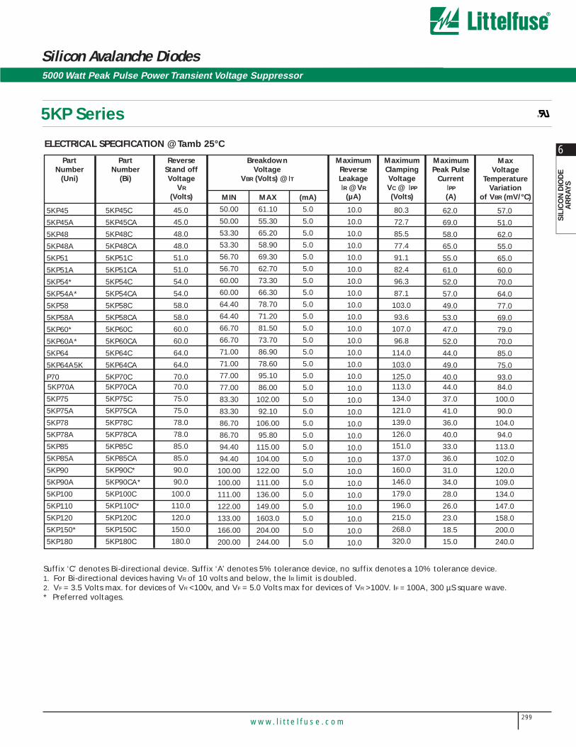
MIN
50.00
50.00
53.30
53.30
56.70
56.70
60.00
60.00
64.40
64.40
66.70
66.70
71.00
71.00
77.00
77.00
83.30
83.30
86.70
86.70
94.40
94.40
100.00
100.00
111.00
122.00
133.00
166.00
200.00
(mA)
5.0
5.0
5.0
5.0
5.0
5.0
5.0
5.0
5.0
5.0
5.0
5.0
5.0
5.0
5.0
5.0
5.0
5.0
5.0
5.0
5.0
5.0
5.0
5.0
5.0
5.0
5.0
5.0
5.0
MAX
61.10
55.30
65.20
58.90
69.30
62.70
73.30
66.30
78.70
71.20
81.50
73.70
86.90
78.60
95.10
86.00
102.00
92.10
106.00
95.80
115.00
104.00
122.00
111.00
136.00
149.00
1603.0
204.00
244.00
299w w w. l i t t e l f u s e . c o m
6
SIL
ICO
N D
IOD
EA
RR
AYS
Silicon Avalanche Diodes
PartNumber
(Uni)
PartNumber
(Bi)
ReverseStand offVoltage
VR
(Volts)
BreakdownVoltage
VBR (Volts) @ IT
MaximumReverseLeakageIR @ VR
(µA)
MaximumClampingVoltageVC @ IPP
(Volts)
MaximumPeak Pulse
CurrentIPP
(A)
MaxVoltage
TemperatureVariation
of VBR (mV/°C)
5KP Series
5KP45
5KP45A
5KP48
5KP48A
5KP51
5KP51A
5KP54*
5KP54A*
5KP58
5KP58A
5KP60*
5KP60A*
5KP64
5KP64A5K
P705KP70A
5KP75
5KP75A
5KP78
5KP78A
5KP85
5KP85A
5KP90
5KP90A
5KP100
5KP110
5KP120
5KP150*
5KP180
5KP45C
5KP45CA
5KP48C
5KP48CA
5KP51C
5KP51CA
5KP54C
5KP54CA
5KP58C
5KP58CA
5KP60C
5KP60CA
5KP64C
5KP64CA
5KP70C5KP70CA
5KP75C
5KP75CA
5KP78C
5KP78CA
5KP85C
5KP85CA
5KP90C*
5KP90CA*
5KP100C
5KP110C*
5KP120C
5KP150C
5KP180C
45.0
45.0
48.0
48.0
51.0
51.0
54.0
54.0
58.0
58.0
60.0
60.0
64.0
64.0
70.070.0
75.0
75.0
78.0
78.0
85.0
85.0
90.0
90.0
100.0
110.0
120.0
150.0
180.0
10.0
10.0
10.0
10.0
10.0
10.0
10.0
10.0
10.0
10.0
10.0
10.0
10.0
10.0
10.0
10.0
10.0
10.0
10.0
10.0
10.0
10.0
10.0
10.0
10.0
10.0
10.0
10.0
10.0
80.3
72.7
85.5
77.4
91.1
82.4
96.3
87.1
103.0
93.6
107.0
96.8
114.0
103.0
125.0113.0
134.0
121.0
139.0
126.0
151.0
137.0
160.0
146.0
179.0
196.0
215.0
268.0
320.0
62.0
69.0
58.0
65.0
55.0
61.0
52.0
57.0
49.0
53.0
47.0
52.0
44.0
49.0
40.044.0
37.0
41.0
36.0
40.0
33.0
36.0
31.0
34.0
28.0
26.0
23.0
18.5
15.0
57.0
51.0
62.0
55.0
65.0
60.0
70.0
64.0
77.0
69.0
79.0
70.0
85.0
75.0
93.084.0
100.0
90.0
104.0
94.0
113.0
102.0
120.0
109.0
134.0
147.0
158.0
200.0
240.0
Suffix ‘C’ denotes Bi-directional device. Suffix ‘A’ denotes 5% tolerance device, no suffix denotes a 10% tolerance device.1. For Bi-directional devices having VR of 10 volts and below, the IR limit is doubled.2. VF = 3.5 Volts max. for devices of VR <100v, and VF = 5.0 Volts max for devices of VR >100V. IF = 100A, 300 µS square wave.* Preferred voltages.
ELECTRICAL SPECIFICATION @ Tamb 25°C
5000 Watt Peak Pulse Power Transient Voltage Suppressor
®

Silicon Avalanche Diodes
300w w w. l i t t e l f u s e . c o m
15000 Watt Peak Pulse Power Transient Voltage Suppressor
15KP Series FEATURES
• Glass passivated junction
• Excellent clamping capability
• Fast response time
• Low zener impedance
• 100% surge tested
• UL recognised
MAXIMUM RATING
• Peak Pulse Power (Ppk): 15000 Watts (10 x 1000µs)@25°C(see diagram on page 3 for wave form)
• 7 watt steady state
• Response time: 1 x 10-12 seconds (theoretical)
• Forward surge rating: 200 Amps, 8.3ms half sine wave, (uni-directional devices only)
• Operating & storage temperature: -55°C to +150°C
MECHANICAL CHARACTERISTICS
• Case: JEDEC R6; Molded plastic over glass passivated junction
• Terminals: Axial leads, solderable per MIL-STD-202 Method 208
• Solderable leads = 230°C for 10 seconds (1.59mm from case)
• Polarity: Cathode indicated by colour band
• Weight: 2.0 grammes (approx)
Agency Approvals: Recognized under the Components Programof Underwriters Laboratories.
Agency File Number: E128662
1.2 - 1.3
7.88.2
Min 25.4
8.69.0
Min 25.4
ORDERING INFORMATION
15KP C A
Voltage
Bi-Directional
5% Voltage Tolerance
Packaging Option
B = Bulk (500 pcs)
T = Tape and reeled (1000 pcs)
All dimensions in mm
®
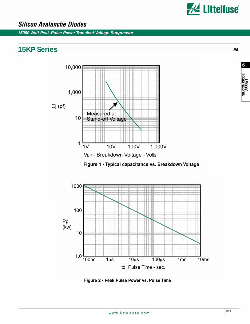
301w w w. l i t t e l f u s e . c o m
6
SIL
ICO
N D
IOD
EA
RR
AYS
Silicon Avalanche Diodes
10,000
1,000
10
11V 10V 100V 1,000V
VBR - Breakdown Voltage - Volts
Measured atStand-off Voltage
Cj (pf)
Figure 1 - Typical capacitance vs. Breakdown Voltage
Figure 2 - Peak Pulse Power vs. Pulse Time
1000
100
10
1.0
Pp(kw)
100ns 1µs 10µs 100µs 1ms
td. Pulse Time - sec.
10ms
15000 Watt Peak Pulse Power Transient Voltage Suppressor
15KP Series ®

Silicon Avalanche Diodes
302w w w. l i t t e l f u s e . c o mw w w. l i t t e l f u s e . c o m
Suffix ‘C’ denotes Bi-directional device. Suffix ‘A’ denotes 5% tolerance device, no suffix denotes a 10% tolerance device.
Maximum breakdown voltage is not specified.
* Preferred voltages.
15KP17
15KP17A
15KP18
15KP18A
15KP20
15KP20A
15KP22
15KP22A
15KP24
15KP24A
15KP26
15KP26A
15KP28
15KP28A
15KP30
15KP30A
15KP33*
15KP33A*
15KP36*
15KP36A*
15KP40*
15KP40A*
15KP43
15KP43A
15KP45
15KP45A
15KP48*
15KP48A*
15KP51
15KP51A
15KP54
15KP54A
15KP58
15KP58A
15KP60
15KP60A
15KP64
15KP64A
15KP70
15KP70A
PartNumber
(Uni)
PartNumber
(Bi)
15KP17C
15KP17CA
15KP18C
15KP18CA
15KP20C
15KP20CA
15KP22C
15KP22CA
15KP24C
15KP24CA
15KP26C
15KP26CA
15KP28C
15KP28CA
15KP30C
15KP30CA
15KP33C
15KP33CA
15KP36C*
15KP36CA*
15KP40C
15KP40CA
15KP43C
15KP43CA
15KP45C
15KP45CA
15KP48C*
15KP48CA*
15KP51C
15KP51CA
15KP54C*
15KP54CA*
15KP58C
15KP58CA
15KP60C
15KP60CA
15KP64C
15KP64CA
15KP70C*
15KP70CA*
ReverseStand offVoltage
VR
(Volts)
17.0
17.0
18.0
18.0
20.0
20.0
22.0
22.0
24.0
24.0
26.0
26.0
28.0
28.0
30.0
30.0
33.0
33.0
36.0
36.0
40.0
40.0
43.0
43.0
45.0
45.0
48.0
48.0
51.0
51.0
54.0
54.0
58.0
58.0
60.0
60.0
64.0
64.0
70.0
70.0
BreakdownVoltage
VBR (Volts) @ IT
MIN
18.9
18.9
20.0
20.0
22.2
22.2
24.4
24.4
26.7
26.7
28.9
28.9
31.1
31.1
33.3
33.3
36.7
36.7
40.0
40.0
44.4
44.4
47.8
47.8
50.0
50.0
53.3
53.3
56.7
56.7
60.0
60.0
64.4
64.4
66.7
66.7
71.1
71.1
77.8
77.8
(mA)
50.0
50.0
50.0
50.0
20.0
20.0
10.0
10.0
5.0
5.0
5.0
5.0
5.0
5.0
5.0
5.0
5.0
5.0
5.0
5.0
5.0
5.0
5.0
5.0
5.0
5.0
5.0
5.0
5.0
5.0
5.0
5.0
5.0
5.0
5.0
5.0
5.0
5.0
5.0
5.0
MaximumReverseLeakageIR @ VR
(µA)
5000.0
5000.0
5000.0
5000.0
1500.0
1500.0
500.0
500.0
150.0
150.0
50.0
50.0
25.0
25.0
15.0
15.0
10.0
10.0
10.0
10.0
10.0
10.0
10.0
10.0
10.0
10.0
10.0
10.0
10.0
10.0
10.0
10.0
10.0
10.0
10.0
10.0
10.0
10.0
10.0
10.0
MaximumClampingVoltageVC @ IPP
(Volts)
32.2
29.3
34.2
30.9
37.9
34.3
41.1
37.1
45.0
40.7
48.7
44.0
52.4
47.5
56.2
50.7
60.6
54.8
66.0
59.7
72.8
65.8
77.1
69.7
80.7
73.0
85.9
77.7
91.5
82.8
96.8
87.5
104.0
94.0
107.0
97.3
115.0
104.0
126.0
114.0
MaximumPeak Pulse
CurrentIPP
(A)
464.0
512.0
439.0
485.0
396.0
437.0
365.0
404.0
333.0
369.0
308.0
341.0
286.0
316.0
267.0
296.0
248.0
274.0
227.0
251.0
206.0
228.0
195.0
215.0
186.0
205.0
175.0
193.0
164.0
181.0
155.0
171.0
144.0
160.0
140.0
154.0
130.0
144.0
119.0
132.0
MaxVoltage
TemperatureVariation
of VBR (mV/°C)
19.0
17.0
20.0
18.0
24.0
21.0
27.0
24.0
30.0
27.0
32.0
29.0
35.0
31.0
27.0
34.0
42.0
38.0
46.0
41.0
51.0
46.0
55.0
50.0
57.0
52.0
62.0
56.0
66.0
60.0
70.0
63.0
76.0
68.0
78.0
71.0
84.0
76.0
92.0
83.0
15KP Series
ELECTRICAL SPECIFICATION @ Tamb 25°C
15000 Watt Peak Pulse Power Transient Voltage Suppressor
®

303w w w. l i t t e l f u s e . c o m
6
SIL
ICO
N D
IOD
EA
RR
AYS
Suffix ‘C’ denotes Bi-directional device. Suffix ‘A’ denotes 5% tolerance device, no suffix denotes a 10% tolerance device.
Maximum breakdown voltage is not specified.
* Preferred voltages.
15KP Series
15KP75
15KP75A
15KP78
15KP78A
15KP85
15KP85A
15KP90
15KP100
15KP110
15KP110A
15KP120
15KP130
15KP150
15KP160
15KP170
15KP180
15KP200
15KP220
15KP240
PartNumber
(Uni)
PartNumber
(Bi)
15KP75C
15KP75CA
15KP78C
15KP78CA
15KP85C
15KP85CA
15KP90C
15KP100C
15KP110C
15KP110CA
15KP120C
15KP130C
15KP150C
15KP160C
15KP170C
15KP180C
15KP200C
15KP220C
15KP240C
ReverseStand offVoltage
VR
(Volts)
75.0
75.0
78.0
78.0
85.0
85.0
90.0
100.0
110.0
110.0
120.0
130.0
150.0
160.0
170.0
180.0
200.0
220.0
240.0
BreakdownVoltage
VBR (Volts) @ IT
MIN
83.3
83.3
86.7
86.7
94.4
94.4
100.0
111.0
122.0
122.0
133.0
144.0
167.0
178.0
189.0
200.0
222.0
245.0
267.0
(mA)
5.0
5.0
5.0
5.0
5.0
5.0
5.0
5.0
5.0
5.0
5.0
5.0
5.0
5.0
5.0
5.0
5.0
5.0
5.0
MaximumReverseLeakageIR @ VR
(µA)
10.0
10.0
10.0
10.0
10.0
10.0
10.0
10.0
10.0
10.0
10.0
10.0
10.0
10.0
10.0
10.0
10.0
10.0
10.0
MaximumClampingVoltageVC @ IPP
(Volts)
135.0
122.0
140.0
126.0
152.0
137.0
160.0
179.0
196.0
178.0
214.0
231.0
268.0
287.0
304.2
321.0
356.0
393.0
428.0
MaximumPeak Pulse
CurrentIPP
(A)
111.0
123.0
107.0
119.0
99.0
109.0
94.0
84.0
77.0
84.0
70.0
65.0
56.0
52.0
49.0
47.0
42.0
38.0
35.0
MaxVoltage
TemperatureVariation
of VBR (mV/°C)
100.0
89.0
104.0
93.0
113.0
102.0
120.0
134.0
147.0
133.0
161.0
174.0
202.0
216.0
229.0
242.0
269.0
297.0
324.0
ELECTRICAL SPECIFICATION @ Tamb 25°C
Silicon Avalanche Diodes15000 Watt Peak Pulse Power Transient Voltage Suppressor
®

304w w w. l i t t e l f u s e . c o m
Silicon Avalanche DiodesAxial Leaded Telecommunications Transient Voltage Suppressors
FOLDBAK™ SERIESDesigned to protect sensitive telecommunications electronics fromtransients which originate from induced lightning, power crossand inductive load switching etc., especially where breakoverdevices would cause nuisance latch-up.
Typical equipment would be: line cards, PABX, modems,multiplexers and NTDs.
FEATURES
• Foldback characteristics
• 2200 watts Peak Power rated with 10/1000µS pulse
• 30,000 watts Peak Pulse Power based on 8/20µS
• UL 94V-0 flammability classification
DESCRIPTION
The foldback characteristic of this device eliminates the clampingof the DC current, or the battery, used in telecom systems, solatch-up is eliminated. Latch-up can occur with breakover devicesdue to the conduction follow-on current supplied by the DCsystem, after the device has responded to a transient.
With breakover devices, latch-up will happen more readily as theambient temperature rises because the holding current values willfall with rising temperature.
The Foldbak eliminates this problem while still providing highlevels of protection.
Min 25.4
4.8265.207
Min 25.4
9.1559.527
0.966 - 1.066
V-I Characteristic
ABSOLUTE MAXIMUM RATINGS @25˚C case temp (unless otherwise noted)SYMBOL
PPP
PM (AV)
Tj
T stg
PARAMETER
Peak Pulse Current10x1000µsec8-20µsec
Steady state power dissipation,lead length 9.5mm, TL - 85˚C (note 1)
Junction temperature
Storage temperature
VALUE
2,20020,000
5.0
-55 to 150
-55 to 150
Units
WW
W
˚C
˚C
Note 1. Mounted on copper pad area 40mm square
Characteristics @25˚C case temp (unless otherwise noted)
Note 2. Using 10/1000µS pulse
DEVICETYPE
FB120
FB160
Workingvoltage
(Vr)
volts
120
160
Maximumbreakover
Voltage(Vbo)
volts
170
220
Maximumleakage
current (Ir)@ Vr
µA
1.0
1.0
Minimumfoldback
voltage Vfb
volts
55
110
MaximumPeak Pulse
Current (lpp)@ Vcl Note 2
amps
170
220
Ipp
Irm
Vfb
Vrm
Vbo
Ibo
All dimensions in mm

305w w w. l i t t e l f u s e . c o m
6
SIL
ICO
N D
IOD
EA
RR
AYS
Silicon Avalanche DiodesAxial Leaded High Power Automotive Transient Voltage Suppressors
SLD™ SERIES
25.4 min
9.0max
8.0max
1.2 -1.3
The SLDTM series is specifically designed for automotiveapplications, available in both unidirectional and bidirectional.
The SLD 10U is designed to be used in series, for example three10Us in series for a 30 volt working; this configuration willprovide a very high power (a multiple of 3) capability and is a farsuperior solution than using devices in parallel, which will requireclosely matched devices in order to prevent ‘current hogging’and consequently, damage to the device.
FEATURES
• 2200 Watts Peak Power rated with 100µS/150mS pulse (applies to a single device)
• 50,000 Watts Peak Pulse Power based on 8/20µS (applies to a single device)
• UL 94V-0 Flammability classification
APPLICATION
• Designed to protect sensitive electronics which operate within an automotive system, such as: sound systems, satellitenavigation, climate control, engine management, stability control, ABS etc.
ABSOLUTE MAXIMUM RATINGS @25˚C case temp (unless otherwise noted)
SYMBOL
PPP
PM (AV)
Vf
Tj
Tstg
PARAMETER
Peak pulse power100µ/150m sec. Pulse8/20µ sec. Pulse
Steady state power dissipation,lead length 9.5mm, TL - 85 (note1)
Maximum instantaneous forward voltage @ 100amps (note 2)
Junction temperature
Storage temperature
VALUE
2,20050,000
6.3
3.5
-55 to +150
-55 to +150
UNIT
WattsWatts
Watts
Volts
°C
°C
Note 1. Mounted on copper pad area 40mm square.Note 2. Using 300 microsecond square pulse; applies to uni-directional only, and a single device only.For devices used in series, this value should be multiplied by thenumber of devices.
Characteristics @25˚C case temp (unless otherwise noted)
Note 3. Using 100µS / 150mS pulse as defined by ISO7637/2 pulse #5.Please note, U suffix denotes uni-directional.
Part Number
SLD 16U
SLD 24U
SLD 10U
3 x SLD 10Uin series
Workingvoltage
(Vr)
volts
16
24
10
30
BreakoverVoltage (bv) @It
min max It
volts volts mA
18.0 22.0 1.0
25.0 30.0 1.0
11.8 13.0 5.0
35.4 39.0 5.0
Maximumleakagecurrent(Ir) @ Vr
µA
10.0
1.0
10.0
10.0
All dimensions in mm
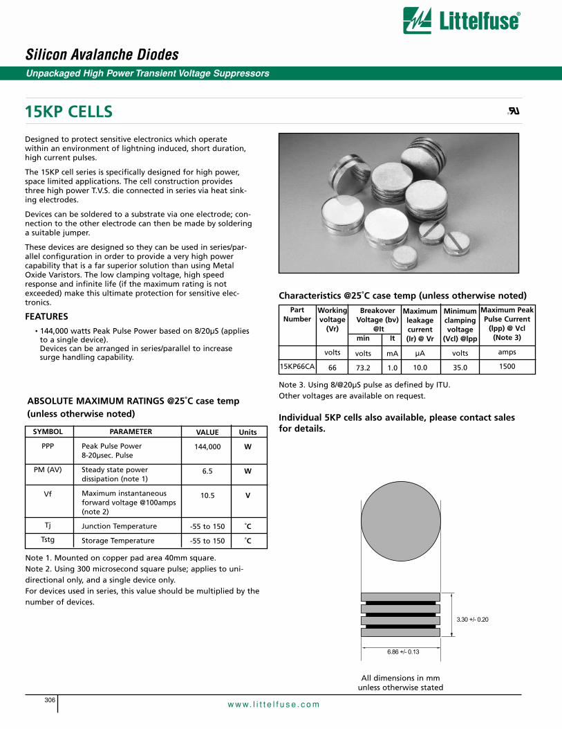
306w w w. l i t t e l f u s e . c o m
Silicon Avalanche DiodesUnpackaged High Power Transient Voltage Suppressors
15KP CELLS
Designed to protect sensitive electronics which operate within an environment of lightning induced, short duration,high current pulses.
The 15KP cell series is specifically designed for high power,space limited applications. The cell construction providesthree high power T.V.S. die connected in series via heat sink-ing electrodes.
Devices can be soldered to a substrate via one electrode; con-nection to the other electrode can then be made by solderinga suitable jumper.
These devices are designed so they can be used in series/par-allel configuration in order to provide a very high powercapability that is a far superior solution than using MetalOxide Varistors. The low clamping voltage, high speedresponse and infinite life (if the maximum rating is notexceeded) make this ultimate protection for sensitive elec-tronics.
FEATURES
• 144,000 watts Peak Pulse Power based on 8/20µS (applies to a single device). Devices can be arranged in series/parallel to increase surge handling capability.
3.30 +/- 0.20
6.86 +/- 0.13
All dimensions in mmunless otherwise stated
Characteristics @25˚C case temp (unless otherwise noted)
Note 3. Using 8/@20µS pulse as defined by ITU.Other voltages are available on request.
Individual 5KP cells also available, please contact salesfor details.
Part Number
15KP66CA
Workingvoltage
(Vr)
volts
66
BreakoverVoltage (bv)
@Itmin It
volts mA
73.2 1.0
Maximumleakagecurrent(Ir) @ Vr
µA
10.0
Minimumclampingvoltage
(Vcl) @lpp
volts
35.0
Maximum PeakPulse Current
(lpp) @ Vcl(Note 3)
amps
1500
Note 1. Mounted on copper pad area 40mm square.Note 2. Using 300 microsecond square pulse; applies to uni-directional only, and a single device only.For devices used in series, this value should be multiplied by thenumber of devices.
ABSOLUTE MAXIMUM RATINGS @25˚C case temp (unless otherwise noted)
SYMBOL
PPP
PM (AV)
Vf
Tj
Tstg
PARAMETER
Peak Pulse Power8-20µsec. Pulse
Steady state powerdissipation (note 1)
Maximum instantaneousforward voltage @100amps(note 2)
Junction Temperature
Storage Temperature
VALUE
144,000
6.5
10.5
-55 to 150
-55 to 150
Units
W
W
V
˚C
˚C
®

307w w w. l i t t e l f u s e . c o m
6
SIL
ICO
N D
IOD
EA
RR
AYS
Silicon Avalanche Diodes1500 Watt Axial Leaded Transient Voltage Suppressors
The ICTE/MPTE series 1500 W transient suppressors are designedspecifically for protection of CMOS, NMOS, BiMOS, and otherintegrated circuits available today for TTL, DTL, ECL, RTL, andlinear functions. This series offers the lowest clamping voltages.
FEATURES
• Stand-off voltage range 5 to 45 Volts
• Uni-directional and Bi-directional
• Glass passivated junction
• Very low clamping voltages
• 100% surge tested
MAXIMUM RATING
• Peak Pulse Power (Ppk): 1500 Watts (10 x 1000µs) @25°C(see diagram on page 3 for wave form)
• 5 watt steady state
• Response time: 1 x 10-12 seconds (theoretical)
• Forward surge rating 200 Amps, 8.3ms half sine wave, (uni-directional devices only)
• Operating & storage temperature: -55°C to +150°C
MECHANICAL CHARACTERISTICS
• Case: DO-201AD: Molded plastic over glass passivated junction
• Terminals: Axial leads, solderable per MIL-STD-202 Method 208
• Solderable leads = 230°C for 10 seconds (1.59mm from case)
• Marking: cathode band, (positive terminal, uni-directional devices only), device code, logo
• Weight: 1.5 grammes (approx)
Agency Approvals: Recognized under the ComponentsProgram of Underwriters Laboratories.
Agency File Number: E128662
Max 1.066
Min 25.4
4.8265.207
Min 25.4
9.1469.527
ORDERING INFORMATION
ICTE or MPTE C
Voltage
Bi-Directional
Packaging Option
B = Bulk (500 pcs)
T = Tape and reeled (1500 pcs)
All dimensions in mm
ICTE/MPTE Series ®

ICTE-5/MPTE-5*
ICTE-8/MPTE-8*
ICTE-10/MPTE-10
ICTE-12/MPTE-12
ICTE-15/MPTE-15
ICTE-18/MPTE-18*
ICTE-22/MPTE-22
ICTE-36/MPTE-36
ICTE-45/MPTE-45
PartNumber
ReverseStandoffVoltage
Vr(Volts)
5.0
8.0
10.0
12.0
15.0
18.0
22.0
36.0
45.0
MinimumBreakdown
VoltageVbr @1mA
(Volts)
6.0
9.4
11.7
14.1
17.6
21.2
25.9
42.4
52.9
MaximumReverseLeakageIr @ Vr(µA)
300.0
25.0
2.0
2.0
2.0
2.0
2.0
2.0
2.0
MaximumClampingVoltage
VC @ IPP 1=1A(Volts)
7.1
11.3
13.7
16.1
20.1
24.2
29.8
50.6
63.3
MaximumPeak Pulse
CurrentIPP
(A)
160.0
100.0
90.0
70.0
60.0
50.0
40.0
23.0
19.0
MaximumClampingVoltage
VC @ IPP 2=10A(Volts)
7.5
11.5
14.1
16.5
20.6
25.2
32.0
54.3
70.0
ICTE-8C/MPTE-8C
ICTE-10C/MPTE-10C
ICTE-12C/MPTE-12C
ICTE-15C/MPTE-15C
ICTE-18C/MPTE-18C
ICTE-22C/MPTE-22C
ICTE-36C/MPTE-36C
ICTE-45C/MPTE-45C
8.0
10.0
12.0
15.0
18.0
22.0
36.0
45.0
9.4
11.7
14.1
17.6
21.2
25.9
42.4
52.9
50.0
2.0
2.0
2.0
2.0
2.0
2.0
2.0
11.4
14.1
16.7
20.8
24.8
30.8
50.6
63.3
100.0
90.0
70.0
60.0
50.0
40.0
23.0
19.0
11.6
14.5
17.1
21.4
25.5
32.0
54.3
70.0
ICTE-5 is not available in Bi-directional. Suffix ‘C’ denotes Bi-directional device. * Preferred voltages.
VF max = 3.5 Volts max at IF = 50A 300µS square wave pulse
308w w w. l i t t e l f u s e . c o m
ELECTRICAL SPECIFICATION @ Tamb 25°C
Silicon Avalanche Diodes
Pulse Width (tp)
1µs 1.0µs 10µs 100µs 1.0ms 10ms0.1
1.0
10
100
Pp(kw)
Figure 2 - Peak Pulse Power Rating Curve
100,000
10,000
1000
1001 2 5 10 20 50 100 200
Pulse width (tp)
Cj (pf)
TJ=2 5°Cf=1.0 MHzVsig=50mVp-p
Measured atStand-OffVoltage (VR)
Measured atZero Bias
V(BR) - Breakdown Voltage - Volts
ICTE/MPTE Series
1500 Watt Axial Leaded Transient Voltage Suppressors
®
Figure 1 - Typical Junction Capacitance
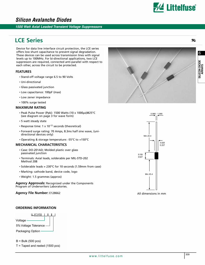
Silicon Avalanche Diodes
309w w w. l i t t e l f u s e . c o m
6
SIL
ICO
N D
IOD
EA
RR
AYS
1500 Watt Axial Leaded Transient Voltage Suppressors
Device for data line interface circuit protection, the LCE seriesoffers low shunt capacitance to prevent signal degradation.These devices can be used across transmission lines with signallevels up to 100MHz. For bi-directional applications, two LCEsuppressors are required, connected anti-parallel with respect toeach other, across the circuit to be protected.
FEATURES
• Stand-off voltage range 6.5 to 90 Volts
• Uni-directional
• Glass passivated junction
• Low capacitance: 100pF (max)
• Low zener impedance
• 100% surge tested
MAXIMUM RATING
• Peak Pulse Power (Ppk): 1500 Watts (10 x 1000µs)@25°C(see diagram on page 3 for wave form)
• 5 watt steady state
• Response time: 1 x 10-12 seconds (theoretical)
• Forward surge rating: 70 Amps, 8.3ms half sine wave, (uni-directional devices only)
• Operating & storage temperature: -55°C to +150°C
MECHANICAL CHARACTERISTICS
• Case: DO-201AD; Molded plastic over glass passivated junction
• Terminals: Axial leads, solderable per MIL-STD-202 Method 208
• Solderable leads = 230°C for 10 seconds (1.59mm from case)
• Marking: cathode band, device code, logo
• Weight: 1.5 grammes (approx)
Agency Approvals: Recognized under the ComponentsProgram of Underwriters Laboratories.
Agency File Number: E128662
0.966 - 1.066
Min 25.4
4.8265.207
9.1559.527
Min 25.4
L C E
Voltage
5% Voltage Tolerance
Packaging Option
B = Bulk (500 pcs)
T = Taped and reeled (1500 pcs)
ORDERING INFORMATION
LCE Series
All dimensions in mm
®

Silicon Avalanche Diodes
310w w w. l i t t e l f u s e . c o m
100
10
1.0
0.1
Ppp
m. P
eak
Pul
se P
ower
, kW
0.1µs 1.0µs 10µs 100µs 1.0ms 100ms
td, Pulse Width, (sec.)
10ms
Figure 1 - Peak Pulse Power Rating Curve
Figure 2 - AC Line Protection Application
Low CapacitanceTranszorb TVS OUT
+
+
Application Note: Devices must be used with two units in parallel,opposite in polarity , as shown in circuit for bi-directional line.
SCHEMATIC
TVS
DIODE
LCE Series
1500 Watt Axial Leaded Transient Voltage Suppressors
®

Silicon Avalanche Diodes
311w w w. l i t t e l f u s e . c o m
6
SIL
ICO
N D
IOD
EA
RR
AYS
BreakdownVoltage
VBR (Volts) @ IT
MIN MAX (mA)
LCE6.5*
LCE6.5A*
LCE7.0
LCE7.0A
LCE7.5*
LCE7.5A*
LCE8.0
LCE8.0A
LCE8.5
LCE8.5A
LCE9.0
LCE9.0A
LCE10
LCE10A
LCE11
LCE11A
LCE12*
LCE12A*
LCE13*
LCE13A*
LCE14
LCE14A
LCE15
LCE15A
LCE16
LCE16A
LCE17
LCE17A
LCE18
LCE18A
LCE20
LCE20A
PartNumber
ReverseStand offVoltage
VR
(Volts)
6.5
6.5
7.0
7.0
7.5
7.5
8.0
8.0
8.5
8.5
9.0
9.0
10.0
10.0
11.0
11.0
12.0
12.0
13.0
13.0
14.0
14.0
15.0
15.0
16.0
16.0
17.0
17.0
18.0
18.0
20.0
20.0
7.22
7.22
7.78
7.78
8.33
8.33
8.89
8.89
9.44
9.44
10.00
10.00
11.10
11.10
12.20
12.20
13.30
13.30
14.40
14.40
15.60
15.60
16.70
16.70
17.80
17.80
18.60
18.60
20.00
20.00
22.20
22.20
8.82
7.98
9.51
8.60
10.20
9.21
10.90
9.83
11.50
10.40
12.20
11.10
13.60
12.30
14.90
13.50
16.30
14.70
17.60
15.90
19.10
17.20
20.40
18.50
21.80
19.70
23.10
20.90
24.40
22.10
27.10
24.50
10.0
10.0
10.0
10.0
10.0
10.0
1.0
1.0
1.0
1.0
1.0
1.0
1.0
1.0
1.0
1.0
1.0
1.0
1.0
1.0
1.0
1.0
1.0
1.0
1.0
1.0
1.0
1.0
1.0
1.0
1.0
1.0
MaximumReverseLeakageIR @ VR
(µA)
1000.0
1000.0
500.0
500.0
250.0
250.0
100.0
100.0
50.0
50.0
10.0
10.0
5.0
5.0
5.0
5.0
5.0
5.0
5.0
5.0
5.0
5.0
5.0
5.0
5.0
5.0
5.0
5.0
5.0
5.0
5.0
5.0
MaximumClampingVoltageVC @ IPP
(Volts)
12.3
11.2
13.3
12.0
14.3
12.9
15.0
13.6
15.9
14.4
16.9
15.4
18.8
17.0
20.1
18.2
22.0
19.9
23.8
21.5
25.8
23.2
26.9
24.4
28.8
26.0
30.5
27.6
32.2
29.2
35.8
32.4
MaximumPeak Pulse
CurrentIPP
(A)
100.0
100.0
100.0
100.0
100.0
100.0
100.0
100.0
94.0
100.0
89.0
97.0
80.0
88.0
74.0
82.0
68.0
75.0
63.0
70.0
58.0
65.0
56.0
61.0
52.0
57.0
49.0
54.0
46.0
51.0
42.0
46.0
Suffix ‘A’ denotes 5% tolerance device, no suffix denotes a 10% tolerance device.
* Preferred voltages.
PeakInverse
BlockingVoltage
VPIB (Volts)
Capacitance@ 0 Volts
pF
100.0
100.0
100.0
100.0
100.0
100.0
100.0
100.0
100.0
100.0
100.0
100.0
100.0
100.0
100.0
100.0
100.0
100.0
100.0
100.0
100.0
100.0
100.0
100.0
100.0
100.0
100.0
100.0
100.0
100.0
100.0
100.0
WorkingInverse
BlockingVoltage
VWIB (Volts)
75.0
75.0
75.0
75.0
75.0
75.0
75.0
75.0
75.0
75.0
75.0
75.0
75.0
75.0
75.0
75.0
75.0
75.0
75.0
75.0
75.0
75.0
75.0
75.0
75.0
75.0
75.0
75.0
75.0
75.0
75.0
75.0
InverseBlockingLeakageCurrent @
IIB @ VWIB (µA)
1.0
1.0
1.0
1.0
1.0
1.0
1.0
1.0
1.0
1.0
1.0
1.0
1.0
1.0
1.0
1.0
1.0
1.0
1.0
1.0
1.0
1.0
1.0
1.0
1.0
1.0
1.0
1.0
1.0
1.0
1.0
1.0
100.0
100.0
100.0
100.0
100.0
100.0
100.0
100.0
100.0
100.0
100.0
100.0
100.0
100.0
100.0
100.0
100.0
100.0
100.0
100.0
100.0
100.0
100.0
100.0
100.0
100.0
100.0
100.0
100.0
100.0
100.0
100.0
LCE Series
ELECTRICAL SPECIFICATION @ Tamb 25°C
1500 Watt Axial Leaded Transient Voltage Suppressors
®

Silicon Avalanche Diodes
312w w w. l i t t e l f u s e . c o m
LCE22
LCE22A
LCE24
LCE24A
LCE26
LCE26A
LCE28
LCE28A
LCE30
LCE30A
LCE33
LCE33A
LCE36
LCE36A
LCE40
LCE40A
LCE43
LCE43A
LCE45
LCE45A
LCE48
LCE48A
LCE51
LCE51A
LCE54
LCE54A
LCE58
LCE58A
LCE60
LCE60A
LCE64
LCE64A
LCE70
LCE70A
LCE75
LCE75A
LCE80
LCE80A
LCE90*
LCE90A*
PartNumber
ReverseStand offVoltage
VR
(Volts)
22.0
22.0
24.0
24.0
26.0
26.0
28.0
28.0
30.0
30.0
33.0
33.0
36.0
36.0
40.0
40.0
43.0
43.0
45.0
45.0
48.0
48.0
51.0
51.0
54.0
54.0
58.0
58.0
60.0
60.0
64.0
64.0
70.0
70.0
75.0
75.0
80.0
80.0
90.0
90.0
BreakdownVoltage
VBR (Volts) @ IT
MIN
24.40
24.40
26.70
26.70
28.90
28.90
31.10
31.10
33.30
33.30
36.70
36.70
40.00
40.00
44.4
44.4
47.8
47.8
50.0
50.0
53.3
53.3
56.7
56.7
60.0
60.0
64.4
64.4
66.7
66.7
71.1
71.1
77.8
77.8
83.3
83.3
88.7
88.7
100.0
100.0
MAX
29.80
26.90
32.60
29.50
35.30
31.90
38.00
34.40
40.70
36.80
44.90
40.60
48.90
44.20
54.3
49.1
58.4
52.8
61.1
55.3
65.1
58.9
69.3
62.7
73.3
66.3
78.7
71.2
81.5
73.7
86.9
78.6
95.1
86.0
102.0
91.1
108.0
98.0
122.0
111.0
(mA)
1.0
1.0
1.0
1.0
1.0
1.0
1.0
1.0
1.0
1.0
1.0
1.0
1.0
1.0
1.0
1.0
1.0
1.0
1.0
1.0
1.0
1.0
1.0
1.0
1.0
1.0
1.0
1.0
1.0
1.0
1.0
1.0
1.0
1.0
1.0
1.0
1.0
1.0
1.0
1.0
MaximumReverseLeakageIR @ VR
(µA)
5.0
5.0
5.0
5.0
5.0
5.0
5.0
5.0
5.0
5.0
5.0
5.0
5.0
5.0
5.0
5.0
5.0
5.0
5.0
5.0
5.0
5.0
5.0
5.0
5.0
5.0
5.0
5.0
5.0
5.0
5.0
5.0
5.0
5.0
5.0
5.0
5.0
5.0
5.0
5.0
MaximumClampingVoltageVC @ IPP
(Volts)
39.4
35.5
43.0
38.9
46.6
42.1
50.1
45.5
53.5
48.4
59.0
53.3
64.3
58.1
71.4
64.5
76.7
69.4
80.3
72.7
85.5
77.4
91.1
82.4
96.3
87.1
103.0
93.6
107.0
96.8
114.0
103.0
125.0
113.0
134.0
121.0
142.0
129.0
160.0
146.0
MaximumPeak Pulse
CurrentIPP
(A)
38.0
42.0
35.0
39.0
32.0
36.0
30.0
33.0
28.0
31.0
25.4
28.1
23.3
25.8
21.0
23.3
19.5
21.6
18.7
20.6
17.5
19.4
16.5
18.2
15.6
17.2
14.6
16.0
14.0
15.5
13.2
14.6
12.0
13.3
11.2
12.4
10.6
11.6
9.4
10.3
Suffix ‘A’ denotes 5% tolerance device, no suffix denotes a 10% tolerance device.
Note: For Bi-directional protection two T.V.S. devices must be used when testing, Test T.V.S. in Avalanche direction,
Do not pulse in forward direction. * Preferred voltages.
Capacitance@ 0 Volts
pF
100.0
100.0
100.0
100.0
100.0
100.0
100.0
100.0
100.0
100.0
100.0
100.0
100.0
100.0
100.0
100.0
100.0
100.0
100.0
100.0
100.0
100.0
100.0
100.0
100.0
100.0
100.0
100.0
90.0
90.0
90.0
90.0
90.0
90.0
90.0
90.0
90.0
90.0
90.0
90.0
WorkingInverse
BlockingVoltage
VWIB (Volts)
75.0
75.0
75.0
75.0
75.0
75.0
75.0
75.0
75.0
75.0
75.0
75.0
75.0
75.0
75.0
75.0
150.0
150.0
150.0
150.0
150.0
150.0
150.0
150.0
150.0
150.0
150.0
150.0
150.0
150.0
150.0
150.0
150.0
150.0
150.0
150.0
150.0
150.0
300.0
300.0
InverseBlockingLeakageCurrent @
IIB @ VWIB (µA)
1.0
1.0
1.0
1.0
1.0
1.0
1.0
1.0
1.0
1.0
1.0
1.0
1.0
1.0
1.0
1.0
1.0
1.0
1.0
1.0
1.0
1.0
1.0
1.0
1.0
1.0
1.0
1.0
1.0
1.0
1.0
1.0
1.0
1.0
1.0
1.0
1.0
1.0
1.0
1.0
PeakInverse
BlockingVoltage
VPIB (Volts)
100.0
100.0
100.0
100.0
100.0
100.0
100.0
100.0
100.0
100.0
100.0
100.0
100.0
100.0
100.0
100.0
200.0
200.0
200.0
200.0
200.0
200.0
200.0
200.0
200.0
200.0
200.0
200.0
200.0
200.0
200.0
200.0
200.0
200.0
200.0
200.0
200.0
200.0
200.0
200.0
LCE Series
ELECTRICAL SPECIFICATION @ Tamb 25°C
1500 Watt Axial Leaded Transient Voltage Suppressors
®

Silicon Avalanche Diodes
313w w w. l i t t e l f u s e . c o m
6
SIL
ICO
N D
IOD
EA
RR
AYS
1500 Watt Metal Axial Leaded Transient Voltage Suppressors
FEATURES
• Hermetically sealed
• Breakdown voltage range 6.8 - 200 volts
• Glass passivated junction
• Excellent clamping capability
• Low zener impedance
•100% surge tested
•-55°C to +150°C
•Uni-polar
MAXIMUM RATING
•Peak Pulse Power (Ppk): 1500 Watts (10 x 1000µs)@25°C(see diagram on page 3 for wave form)
•1 watt steady state
•Response time: 1 x 10-12 seconds (theoretical)
•Operating & storage temperature: -55°C to +150°C
MECHANICAL CHARACTERISTICS
•Case: Metal hermetically sealed DO-13 package
•Terminals: Axial leads, solderable per MIL-STD-202 Method 208
•Solderable leads = 230°C for 10 seconds (1.59mm from case)
•Polarity: cathode indicated by colour band
•Weight: 1.5 grammes (approx)
Agency Approvals: Recognized under the ComponentsProgram of Underwriters Laboratories.
Agency File Number: E128662
1N56 Series
1 N 5 6 X X A
Voltage Reference
5% Voltage Tolerance
Packaging Option
B = Bulk (500 pcs)
ORDERING INFORMATION
Min 31.8
Max5.33
7.59.0
Min 25.4
Max0.8
5.58
All dimensions in mm
®

Silicon Avalanche Diodes
314w w w. l i t t e l f u s e . c o m
100
10
1
0.11µs 10µs 100µ 1ms 10ms
Pulse Time (tp)
Pe
ak
Pu
lse
Po
we
r -
Pp
(kW
)
Exponential wave-form
Square wave-pulse
s100ns
Figure 3 - Peak Pulse Power vs. Pulse Time
0°C 50°C 100°C 150°C 200°C
Tamb °C
100%
50%
0
Permissablearea ofoperation
0°C 50°C 100°C 150°C 200°C
Tamb °C
W1.0
0.75
0.50
0.25
0
Permissablearea ofoperation
Figure 2 - Continuous D.C. Power DeratingCurveContinuous d.c. power dissipation
Figure 1 - Peak Power Derating CurvePeak pulse power in percent of 25ºC rating
Measured @Zero Bias
Measured atStand-OffVoltage (VR)
Reverse Voltage, Volts V(BR)
Cj (pf)
1.0 2 5 10 20 50 100 200
20,000
10,000
60004000
2000
1000800600
400
200
100806040
30
10
Figure 4 - Typical Junction Capacitance
1500 Watt Metal Axial Leaded Transient Voltage Suppressors
1N56 Series ®

Silicon Avalanche Diodes
315w w w. l i t t e l f u s e . c o m
6
SIL
ICO
N D
IOD
EA
RR
AYS
1500 Watt Metal Axial Leaded Transient Voltage Suppressors
1N5629*
1N5629A*
1N5630
1N5630A
1N5631
1N5631A
1N5632
1N5632A
1N5633
1N5633A
1N5634
1N5634A
1N5635
1N5635A
1N5636
1N5636A
1N5637*
1N5637A*
1N5638*
1N5638A*
1N5639*
1N5639A*
1N5640
1N5640A
1N5641
1N5641A
1N5642
1N5642A
1N5643*
1N5643A*
1N5644*
1N5644A
1N5645
1N5645A
1N5646*
1N5646A*
PartNumber
ReverseStand OffVoltage
VR
(Volts)
5.50
5.80
6.05
6.40
6.63
7.02
7.37
7.78
8.10
8.55
8.92
9.40
9.72
10.20
10.50
11.10
12.10
12.80
12.90
13.60
14.50
15.30
16.20
17.10
17.80
18.80
19.40
20.50
21.80
23.10
24.30
25.60
26.80
28.20
29.10
30.80
BreakdownVoltage
VBR (Volts) @ IT
MIN
6.12
6.45
6.75
7.13
7.38
7.79
8.19
8.65
9.00
9.50
9.90
10.50
10.80
11.40
11.70
12.40
13.50
14.30
14.40
15.20
16.20
17.10
18.00
19.00
19.80
20.90
21.60
22.80
24.30
25.70
27.00
28.50
29.70
31.40
32.40
34.20
MAX
7.48
7.14
8.25
7.88
9.02
8.61
10.00
9.55
11.00
10.50
12.10
11.60
13.20
12.60
14.30
13.70
16.50
15.80
17.60
16.80
19.80
18.90
22.00
21.00
24.20
23.10
26.40
25.20
29.70
28.40
33.00
31.50
36.30
34.70
39.60
37.80
(mA)
10
10
10
10
10
10
1.0
1.0
1.0
1.0
1.0
1.0
1.0
1.0
1.0
1.0
1.0
1.0
1.0
1.0
1.0
1.0
1.0
1.0
1.0
1.0
1.0
1.0
1.0
1.0
1.0
1.0
1.0
1.0
1.0
1.0
MaximumReverseLeakageIR @ VR
(µA)
1000.0
1000.0
500.0
500.0
200.0
200.0
50.0
50.0
10.0
10.0
5.0
5.0
5.0
5.0
5.0
5.0
5.0
5.0
5.0
5.0
5.0
5.0
5.0
5.0
5.0
5.0
5.0
5.0
5.0
5.0
5.0
5.0
5.0
5.0
5.0
5.0
MaximumClampingVoltageVC @ IPP
(Volts)
10.8
10.5
11.7
11.3
12.5
12.1
13.8
13.4
15.0
14.5
16.2
15.6
17.3
16.7
19.0
18.2
22.0
21.2
23.5
22.5
26.5
25.2
29.1
27.7
31.9
30.6
34.7
33.2
39.1
37.5
43.5
41.4
47.7
45.7
52.0
49.9
MaximumPeak Pulse
CurrentIPP
(A)
139.0
143.0
128.0
132.0
120.0
124.0
109.0
112.0
100.0
103.0
93.0
96.0
87.0
90.0
79.0
82.0
68.0
71.0
64.0
67.0
56.5
59.5
51.5
54.0
47.0
49.0
43.0
45.0
38.5
40.0
34.5
36.0
31.5
33.0
29.0
30.0
Suffix ‘A’ denotes 5% tolerance device, no suffix denotes a 10% tolerance device.
1N5629 to 1N5647A VF max = 3.5V at IF = 50A 300 µS square wave pulse.
1N5648 to 1N5665A VF max = 5.0V at IF = 50A 300 µS square wave pulse.
* Preferred voltages.
MaxVoltage
TemperatureVariation
of VBR (mV/°C)
5.0
5.0
5.0
5.0
6.0
6.0
7.0
7.0
8.0
8.0
9.0
9.0
10.0
10.0
11.0
11.0
13.0
12.0
16.0
14.0
17.0
19.0
20.0
19.0
21.0
20.0
25.0
23.0
28.0
25.0
31.0
28.0
31.0
30.0
35.0
31.0
1N56 Series
ELECTRICAL SPECIFICATION @ Tamb 25°C
®
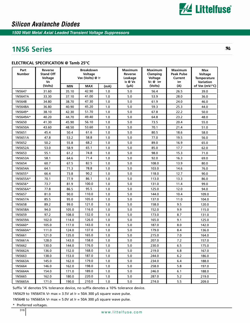
Silicon Avalanche Diodes
316w w w. l i t t e l f u s e . c o m
1N5647
1N5647A
1N5648
1N5648A
1N5649*
1N5649A*
1N5650
1N5650A
1N5651
1N5651A
1N5652
1N5652A
1N5653
1N5653A
1N5654
1N5654A
1N5655*
1N5655A*
1N5656*
1N5656A*
1N5657
1N5657A
1N5658
1N5658A
1N5659
1N5659A
1N5660*
1N5660A*
1N5661
1N5661A
1N5662
1N5662A
1N5663
1N5663A
1N5664
1N5664A
1N5665
1N5665A
PartNumber
ReverseStand OffVoltage
VR
(Volts)
31.60
33.30
34.80
36.80
38.10
40.20
41.30
43.60
45.4
47.8
50.2
53.0
55.1
58.1
60.7
64.1
66.4
70.1
73.7
77.8
81.0
85.5
89.2
94.0
97.2
102.0
105.0
111.0
121.0
128.0
130.0
136.0
138.0
145.0
146.0
154.0
162.0
171.0
BreakdownVoltage
VBR (Volts) @ IT
MIN
35.10
37.10
38.70
40.90
42.30
44.70
45.90
48.50
50.4
53.2
55.8
58.9
61.2
64.6
67.5
71.3
73.8
77.9
81.9
86.5
90.0
95.0
99.0
105.0
108.0
114.0
117.0
124.0
135.0
143.0
144.0
152.0
153.0
162.0
162.0
171.0
180.0
190.0
MAX
42.90
41.00
47.30
45.20
51.70
49.40
56.10
53.60
61.6
58.8
68.2
65.1
74.8
71.4
82.5
78.8
90.2
86.1
100.0
95.5
110.0
105.0
121.0
116.0
132.0
126.0
143.0
137.0
165.0
158.0
176.0
168.0
187.0
179.0
198.0
189.0
220.0
210.0
(mA)
1.0
1.0
1.0
1.0
1.0
1.0
1.0
1.0
1.0
1.0
1.0
1.0
1.0
1.0
1.0
1.0
1.0
1.0
1.0
1.0
1.0
1.0
1.0
1.0
1.0
1.0
1.0
1.0
1.0
1.0
1.0
1.0
1.0
1.0
1.0
1.0
1.0
1.0
MaximumReverseLeakageIR @ VR
(µA)
5.0
5.0
5.0
5.0
5.0
5.0
5.0
5.0
5.0
5.0
5.0
5.0
5.0
5.0
5.0
5.0
5.0
5.0
5.0
5.0
5.0
5.0
5.0
5.0
5.0
5.0
5.0
5.0
5.0
5.0
5.0
5.0
5.0
5.0
5.0
5.0
5.0
5.0
MaximumClampingVoltageVC @ IPP
(Volts)
56.4
53.9
61.9
59.3
67.8
64.8
73.5
70.1
80.5
77.0
89.0
85.0
98.0
92.0
108.0
103.0
118.0
113.0
131.0
125.0
144.0
137.0
158.0
152.0
173.0
165.0
187.0
179.0
215.0
207.0
230.0
219.0
244.0
234.0
258.0
246.0
287.0
274.0
MaximumPeak Pulse
CurrentIPP
(A)
26.5
28.0
24.0
25.3
22.2
23.2
20.4
21.4
18.6
19.5
16.9
17.7
15.3
16.3
13.9
14.6
12.7
13.3
11.4
12.0
10.4
11.0
9.5
9.9
8.7
9.1
8.0
8.4
7.0
7.2
6.5
6.8
6.2
6.4
5.8
6.1
5.2
5.5
MaxVoltage
TemperatureVariation
of VBR (mV/°C)
39.0
36.0
46.0
44.0
50.0
48.0
55.0
51.0
58.0
56.0
65.0
62.0
71.0
69.0
80.0
76.0
90.0
86.0
99.0
94.0
109.0
104.0
120.0
115.0
131.0
125.0
142.0
136.0
164.0
157.0
175.0
167.0
186.0
188.0
197.0
188.0
219.0
209.0
Suffix ‘A’ denotes 5% tolerance device, no suffix denotes a 10% tolerance device.
1N5629 to 1N5647A VF max = 3.5V at IF = 50A 300 µS square wave pulse.
1N5648 to 1N5665A VF max = 5.0V at IF = 50A 300 µS square wave pulse.
* Preferred voltages.
1N56 Series
ELECTRICAL SPECIFICATION @ Tamb 25°C
1500 Watt Metal Axial Leaded Transient Voltage Suppressors
®
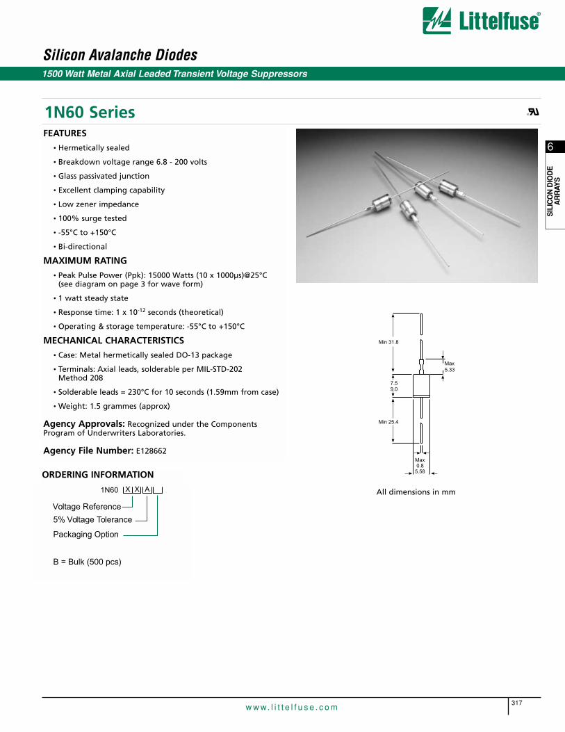
Silicon Avalanche Diodes
317w w w. l i t t e l f u s e . c o m
6
SIL
ICO
N D
IOD
EA
RR
AYS
1500 Watt Metal Axial Leaded Transient Voltage Suppressors
1N60 SeriesFEATURES
• Hermetically sealed
• Breakdown voltage range 6.8 - 200 volts
• Glass passivated junction
• Excellent clamping capability
• Low zener impedance
• 100% surge tested
• -55°C to +150°C
• Bi-directional
MAXIMUM RATING
• Peak Pulse Power (Ppk): 15000 Watts (10 x 1000µs)@25°C(see diagram on page 3 for wave form)
• 1 watt steady state
• Response time: 1 x 10-12 seconds (theoretical)
• Operating & storage temperature: -55°C to +150°C
MECHANICAL CHARACTERISTICS
• Case: Metal hermetically sealed DO-13 package
• Terminals: Axial leads, solderable per MIL-STD-202 Method 208
• Solderable leads = 230°C for 10 seconds (1.59mm from case)
• Weight: 1.5 grammes (approx)
Agency Approvals: Recognized under the ComponentsProgram of Underwriters Laboratories.
Agency File Number: E128662
Min 31.8
Max5.33
7.59.0
Min 25.4
Max0.8
5.58
1N60 X X A
Voltage Reference
5% Voltage Tolerance
Packaging Option
B = Bulk (500 pcs)
ORDERING INFORMATION
All dimensions in mm
®

Silicon Avalanche Diodes
318w w w. l i t t e l f u s e . c o m
0°C 50°C 100°C 150°C 200°C
Tamb °C
100%
50%
0
Permissablearea ofoperation
0°C 50°C 100°C 150°C 200°C
Tamb °C
W1.0
0.75
0.50
0.25
0
Permissablearea ofoperation
Figure 2 - Continuous D.C. Power Derating CurveContinuous d.c. power dissipation
Figure 1 - Peak Power Derating CurvePeak pulse power in percent of 25˚C rating
1N60 Series
1500 Watt Metal Axial Leaded Transient Voltage Suppressors
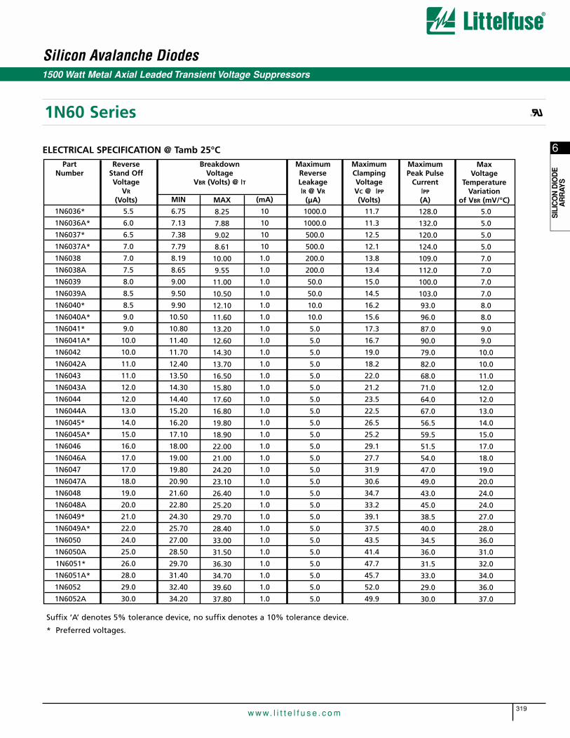
Silicon Avalanche Diodes
319w w w. l i t t e l f u s e . c o m
6
SIL
ICO
N D
IOD
EA
RR
AYS
1N6036*
1N6036A*
1N6037*
1N6037A*
1N6038
1N6038A
1N6039
1N6039A
1N6040*
1N6040A*
1N6041*
1N6041A*
1N6042
1N6042A
1N6043
1N6043A
1N6044
1N6044A
1N6045*
1N6045A*
1N6046
1N6046A
1N6047
1N6047A
1N6048
1N6048A
1N6049*
1N6049A*
1N6050
1N6050A
1N6051*
1N6051A*
1N6052
1N6052A
5.5
6.0
6.5
7.0
7.0
7.5
8.0
8.5
8.5
9.0
9.0
10.0
10.0
11.0
11.0
12.0
12.0
13.0
14.0
15.0
16.0
17.0
17.0
18.0
19.0
20.0
21.0
22.0
24.0
25.0
26.0
28.0
29.0
30.0
MIN
6.75
7.13
7.38
7.79
8.19
8.65
9.00
9.50
9.90
10.50
10.80
11.40
11.70
12.40
13.50
14.30
14.40
15.20
16.20
17.10
18.00
19.00
19.80
20.90
21.60
22.80
24.30
25.70
27.00
28.50
29.70
31.40
32.40
34.20
MAX
8.25
7.88
9.02
8.61
10.00
9.55
11.00
10.50
12.10
11.60
13.20
12.60
14.30
13.70
16.50
15.80
17.60
16.80
19.80
18.90
22.00
21.00
24.20
23.10
26.40
25.20
29.70
28.40
33.00
31.50
36.30
34.70
39.60
37.80
(mA)
10
10
10
10
1.0
1.0
1.0
1.0
1.0
1.0
1.0
1.0
1.0
1.0
1.0
1.0
1.0
1.0
1.0
1.0
1.0
1.0
1.0
1.0
1.0
1.0
1.0
1.0
1.0
1.0
1.0
1.0
1.0
1.0
1000.0
1000.0
500.0
500.0
200.0
200.0
50.0
50.0
10.0
10.0
5.0
5.0
5.0
5.0
5.0
5.0
5.0
5.0
5.0
5.0
5.0
5.0
5.0
5.0
5.0
5.0
5.0
5.0
5.0
5.0
5.0
5.0
5.0
5.0
11.7
11.3
12.5
12.1
13.8
13.4
15.0
14.5
16.2
15.6
17.3
16.7
19.0
18.2
22.0
21.2
23.5
22.5
26.5
25.2
29.1
27.7
31.9
30.6
34.7
33.2
39.1
37.5
43.5
41.4
47.7
45.7
52.0
49.9
128.0
132.0
120.0
124.0
109.0
112.0
100.0
103.0
93.0
96.0
87.0
90.0
79.0
82.0
68.0
71.0
64.0
67.0
56.5
59.5
51.5
54.0
47.0
49.0
43.0
45.0
38.5
40.0
34.5
36.0
31.5
33.0
29.0
30.0
Suffix ‘A’ denotes 5% tolerance device, no suffix denotes a 10% tolerance device.
* Preferred voltages.
5.0
5.0
5.0
5.0
7.0
7.0
7.0
7.0
8.0
8.0
9.0
9.0
10.0
10.0
11.0
12.0
12.0
13.0
14.0
15.0
17.0
18.0
19.0
20.0
24.0
24.0
27.0
28.0
36.0
31.0
32.0
34.0
36.0
37.0
PartNumber
ReverseStand OffVoltage
VR
(Volts)
BreakdownVoltage
VBR (Volts) @ IT
MaximumReverseLeakageIR @ VR
(µA)
MaximumClampingVoltageVC @ IPP
(Volts)
MaximumPeak Pulse
CurrentIPP
(A)
MaxVoltage
TemperatureVariation
of VBR (mV/°C)
1N60 Series
ELECTRICAL SPECIFICATION @ Tamb 25°C
1500 Watt Metal Axial Leaded Transient Voltage Suppressors
®
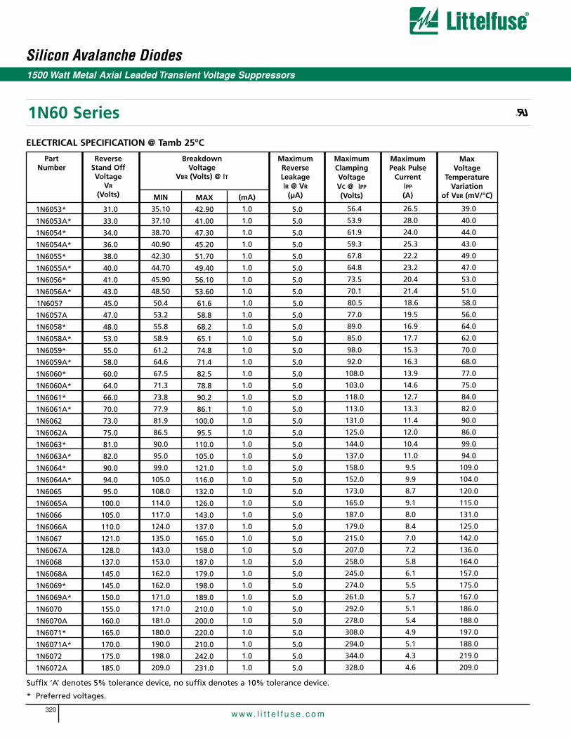
Silicon Avalanche Diodes
320w w w. l i t t e l f u s e . c o m
Suffix ‘A’ denotes 5% tolerance device, no suffix denotes a 10% tolerance device.
* Preferred voltages.
1N6053*
1N6053A*
1N6054*
1N6054A*
1N6055*
1N6055A*
1N6056*
1N6056A*
1N6057
1N6057A
1N6058*
1N6058A*
1N6059*
1N6059A*
1N6060*
1N6060A*
1N6061*
1N6061A*
1N6062
1N6062A
1N6063*
1N6063A*
1N6064*
1N6064A*
1N6065
1N6065A
1N6066
1N6066A
1N6067
1N6067A
1N6068
1N6068A
1N6069*
1N6069A*
1N6070
1N6070A
1N6071*
1N6071A*
1N6072
1N6072A
31.0
33.0
34.0
36.0
38.0
40.0
41.0
43.0
45.0
47.0
48.0
53.0
55.0
58.0
60.0
64.0
66.0
70.0
73.0
75.0
81.0
82.0
90.0
94.0
95.0
100.0
105.0
110.0
121.0
128.0
137.0
145.0
145.0
150.0
155.0
160.0
165.0
170.0
175.0
185.0
MIN
35.10
37.10
38.70
40.90
42.30
44.70
45.90
48.50
50.4
53.2
55.8
58.9
61.2
64.6
67.5
71.3
73.8
77.9
81.9
86.5
90.0
95.0
99.0
105.0
108.0
114.0
117.0
124.0
135.0
143.0
153.0
162.0
162.0
171.0
171.0
181.0
180.0
190.0
198.0
209.0
MAX
42.90
41.00
47.30
45.20
51.70
49.40
56.10
53.60
61.6
58.8
68.2
65.1
74.8
71.4
82.5
78.8
90.2
86.1
100.0
95.5
110.0
105.0
121.0
116.0
132.0
126.0
143.0
137.0
165.0
158.0
187.0
179.0
198.0
189.0
210.0
200.0
220.0
210.0
242.0
231.0
(mA)
1.0
1.0
1.0
1.0
1.0
1.0
1.0
1.0
1.0
1.0
1.0
1.0
1.0
1.0
1.0
1.0
1.0
1.0
1.0
1.0
1.0
1.0
1.0
1.0
1.0
1.0
1.0
1.0
1.0
1.0
1.0
1.0
1.0
1.0
1.0
1.0
1.0
1.0
1.0
1.0
5.0
5.0
5.0
5.0
5.0
5.0
5.0
5.0
5.0
5.0
5.0
5.0
5.0
5.0
5.0
5.0
5.0
5.0
5.0
5.0
5.0
5.0
5.0
5.0
5.0
5.0
5.0
5.0
5.0
5.0
5.0
5.0
5.0
5.0
5.0
5.0
5.0
5.0
5.0
5.0
56.4
53.9
61.9
59.3
67.8
64.8
73.5
70.1
80.5
77.0
89.0
85.0
98.0
92.0
108.0
103.0
118.0
113.0
131.0
125.0
144.0
137.0
158.0
152.0
173.0
165.0
187.0
179.0
215.0
207.0
258.0
245.0
274.0
261.0
292.0
278.0
308.0
294.0
344.0
328.0
26.5
28.0
24.0
25.3
22.2
23.2
20.4
21.4
18.6
19.5
16.9
17.7
15.3
16.3
13.9
14.6
12.7
13.3
11.4
12.0
10.4
11.0
9.5
9.9
8.7
9.1
8.0
8.4
7.0
7.2
5.8
6.1
5.5
5.7
5.1
5.4
4.9
5.1
4.3
4.6
39.0
40.0
44.0
43.0
49.0
47.0
53.0
51.0
58.0
56.0
64.0
62.0
70.0
68.0
77.0
75.0
84.0
82.0
90.0
86.0
99.0
94.0
109.0
104.0
120.0
115.0
131.0
125.0
142.0
136.0
164.0
157.0
175.0
167.0
186.0
188.0
197.0
188.0
219.0
209.0
PartNumber
ReverseStand OffVoltage
VR
(Volts)
BreakdownVoltage
VBR (Volts) @ IT
MaximumReverseLeakageIR @ VR
(µA)
MaximumClampingVoltageVC @ IPP
(Volts)
MaximumPeak Pulse
CurrentIPP
(A)
MaxVoltage
TemperatureVariation
of VBR (mV/°C)
1N60 Series
ELECTRICAL SPECIFICATION @ Tamb 25°C
1500 Watt Metal Axial Leaded Transient Voltage Suppressors
®

Zeners/Studs7
321w w w. l i t t e l f u s e . c o m
PAGE
Zeners/Studs . . . . . . . . . . . . . . . . . . . . . . . . . . . . . . . . . . . . . . . . . . . . . . . . . . . . . . . . . . . . . . . . . . . . . . . . . . . . . . . . . . 321
BZY91 series . . . . . . . . . . . . . . . . . . . . . . . . . . . . . . . . . . . . . . . . . . . . . . . . . . . . . . . . . . . . . . . . . . . . . . . . . . . . 322-323
BZY93 series . . . . . . . . . . . . . . . . . . . . . . . . . . . . . . . . . . . . . . . . . . . . . . . . . . . . . . . . . . . . . . . . . . . . . . . . . . . . . 324-325
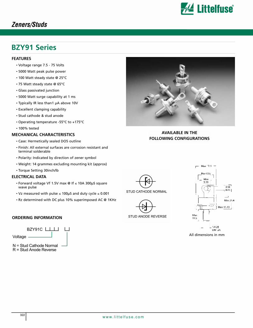
Zeners/Studs
322w w w. l i t t e l f u s e . c o m
BZY91C
Voltage
N = Stud Cathode NormalR = Stud Anode Reverse
STUD CATHODE NORMAL
STUD ANODE REVERSEORDERING INFORMATION
FEATURES
• Voltage range 7.5 - 75 Volts
• 5000 Watt peak pulse power
• 100 Watt steady state @ 25°C
• 75 Watt steady state @ 65°C
• Glass passivated junction
• 5000 Watt surge capability at 1 ms
• Typically IR less than1 µA above 10V
• Excellent clamping capability
• Stud cathode & stud anode
• Operating temperature -55°C to +175°C
• 100% tested
MECHANICAL CHARACTERISTICS
• Case: Hermetically sealed DO5 outline
• Finish: All external surfaces are corrosion resistant and terminal solderable
• Polarity: Indicated by direction of zener symbol
• Weight: 14 grammes excluding mounting kit (approx)
• Torque Setting 30inch/lb
ELECTRICAL DATA
• Forward voltage Vf 1.5V max @ If ≤ 10A 300µS square wave pulse
• Vz measured with pulse ≤ 100µS and duty cycle ≤ 0.001
• Rz determined with DC plus 10% superimposed AC @ 1KHz
BZY91 Series
AVAILABLE IN THEFOLLOWING CONFIGURATIONS
All dimensions in mm

Zeners/Studs
323w w w. l i t t e l f u s e . c o m
7
ZEN
ER
S/S
TUD
S
Ptotmax(W)
Tmb (°C)
100500-50-1000
25
50
75
150
100
200
100
10
1
0.11µs 10µs 100µ 1ms 10ms
Pulse Time (tp)
Pe
ak
Pu
lse
Po
we
r -
Pp
(kW
)
Exponential wave-form
Square wave-pulse
s100ns
Figure 2. Maximum total dissapation plotted against mountingbase temp
Figure 1. Non-repetitive peak pulse power rating curve
BZY91 Series
ZenerResistanceRZ (Ω) @ IZ
TypIZ
BZY91C7V5
BZY91C8V2
BZY91C9V1
BZY91C10*
BZY91C11
BZY91C12*
BZY91C13
BZY91C15*
BZY91C16
BZY91C18
BZY91C20*
BZY91C22
BZY91C24*
BZY91C27
BZY91C30*
BZY91C33*
BZY91C36
BZY91C39*
BZY91C43*
BZY91C47
BZY91C51
BZY91C56*
BZY91C62
BZY91C68
BZY91C75*
BZY91C7V5R
BZY91C8V2R
BZY91C9V1R
BZY91C10R
BZY91C11R
BZY91C12R
BZY91C13R
BZY91C15R*
BZY91C16R
BZY91C18R
BZY91C20R
BZY91C22R*
BZY91C24R
BZY91C27R*
BZY91C30R
BZY91C33R
BZY91C36R
BZY91C39R
BZY91C43R
BZY91C47R
BZY91C51R
BZY91C56R
BZY91C62R*
BZY91C68R
BZY91C75R
StudCathode
Part Number
Zener VoltageVZ (Volts) @ IZ
7.0
7.7
8.5
9.4
10.4
11.4
12.4
13.8
15.3
16.8
18.8
20.8
22.7
25.1
28.0
31.0
34.0
37.0
40.0
44.0
48.0
52.0
58.0
64.0
70.0
7.9
8.7
9.6
10.6
11.6
12.7
14.1
15.6
17.1
19.1
21.2
23.3
25.9
28.9
32.0
35.0
38.0
41.0
46.0
50.0
54.0
60.0
66.0
72.0
79.0
5.0
5.0
2.0
2.0
2.0
2.0
2.0
2.0
2.0
2.0
1.0
1.0
1.0
1.0
1.0
1.0
1.0
0.5
0.5
0.5
0.5
0.5
0.5
0.5
0.5
0.04
0.06
0.08
0.08
0.08
0.10
0.10
0.12
0.12
0.14
0.16
0.16
0.18
0.20
0.22
0.24
0.26
0.28
0.30
0.34
0.36
0.4
0.44
0.48
0.51
MIN MAX (Volts)(A)
StudAnode
Part Number
Maximum ReverseLeakage IR @ VR
0.2
0.3
0.4
0.4
0.4
0.5
0.5
0.6
0.6
0.7
0.8
0.8
0.9
1.0
1.1
1.2
1.3
1.4
1.5
1.7
1.8
2.0
2.2
2.4
2.6
5.0
5.0
5.0
1.0
1.0
1.0
1.0
1.0
1.0
1.0
1.0
1.0
1.0
1.0
1.0
1.0
1.0
1.0
1.0
1.0
1.0
1.0
1.0
1.0
1.0
5.1
5.6
6.2
6.8
7.5
8.2
9.1
10.0
11.0
12.0
13.0
15.0
16.0
18.0
20.0
22.0
24.0
27.0
30.0
33.0
36.0
39.0
43.0
47.0
51.0
Max (mA)
* Preferred voltages.
ELECTRICAL SPECIFICATION @ Tamb 25°C

Zeners/Studs
324w w w. l i t t e l f u s e . c o m
FEATURES
• Voltage Range 7.5 -75 Volts
• 1500 Watt Peak Pulse Power
• 20 Watt Steady State @ 75°C
• 15 Watt Steady State @ 100°C
• Glass passivated junction
• 1500 Watt surge capability at 1 ms
• Typically IR less than 5 µA above 10V
• Excellent clamping capability
• Stud cathode & stud anode
• Operating temperature -55°C to +175°C
• 100% tested
MECHANICAL CHARACTERISTICS
• Case: Hermetically sealed DO-4 outline
• Finish: All external surfaces are corrosion resistant and terminal solderable
• Polarity: Indicated by direction of zener symbol
• Weight: 4.2 grammes excluding mounting kit (approx)
• Torque setting 13inch/lb
ELECTRICAL DATA
• Forward voltage VF1.5V max @ IF ≤ 5A 300µS square wave pulse
• Vz measured with pulse ≤ 100µS and duty cycle ≤ 0.001
• Rz determined with DC plus 10% superimposed AC @ 1KHz
STUD CATHODE NORMAL
STUD ANODE REVERSE
BZY93C
Voltage
N = Stud Cathode NormalR = Stud Anode Reverse
ORDERING INFORMATION
All dimensions in mm
BZY93 Series
AVAILABLE IN THEFOLLOWING CONFIGURATIONS
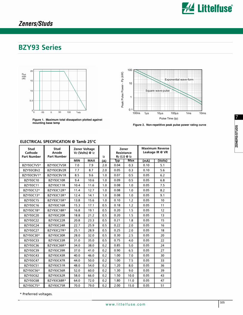
Zeners/Studs
325w w w. l i t t e l f u s e . c o m
7
ZEN
ER
S/S
TUD
S
Ptotmax(W)
0
5.0
10
15
20
-500 0 50 100 1mb
Figure 1. Maximum total dissapation plotted against mounting base temp
100
10
1
0.11µs 10µs 100µ 1ms 10ms
Pulse Time (tp)
Pe
ak
Pu
lse
Po
we
r -
Pp
(kW
)
Exponential wave-form
Square wave-pulse
s100ns
Figure 2. Non-repetitive peak pulse power rating curve
BZY93 Series
BZY93C7V5*
BZY93C8V2
BZY93C9V1*
BZY93C10
BZY93C11
BZY93C12*
BZY93C13*
BZY93C15
BZY93C16
BZY93C18*
BZY93C20
BZY93C22
BZY93C24
BZY93C27
BZY93C30*
BZY93C33
BZY93C36
BZY93C39
BZY93C43
BZY93C47
BZY93C51
BZY93C56*
BZY93C62
BZY93C68
BZY93C75*
BZY93C7V5R
BZY93C8V2R
BZY93C9V1R
BZY93C10R
BZY93C11R
BZY93C12R*
BZY93C13R*
BZY93C15R*
BZY93C16R
BZY93C18R*
BZY93C20R
BZY93C22R
BZY93C24R
BZY93C27R*
BZY93C30R
BZY93C33R
BZY93C36R*
BZY93C39R
BZY93C43R
BZY93C47R
BZY93C51R
BZY93C56R
BZY93C62R
BZY93C68R*
BZY93C75R
7.0
7.7
8.5
9.4
10.4
11.4
12.4
13.8
15.3
16.8
18.8
20.8
22.7
25.1
28.0
31.0
34.0
37.0
40.0
44.0
48.0
52.0
58.0
64.0
70.0
7.9
8.7
9.6
10.6
11.6
12.7
14.1
15.6
17.1
19.1
21.2
23.3
25.9
28.9
32.0
35.0
38.0
41.0
46.0
50.0
54.0
60.0
66.0
72.0
79.0
2.0
2.0
1.0
1.0
1.0
1.0
1.0
1.0
0.5
0.5
0.5
0.5
0.5
0.5
0.5
0.5
0.2
0.2
0.2
0.2
0.2
0.2
0.2
0.2
0.2
0.04
0.05
0.07
0.09
0.08
0.08
0.08
0.10
0.18
0.20
0.20
0.21
0.22
0.25
0.30
0.75
0.85
0.90
1.00
1.00
1.20
1.30
1.50
1.80
2.00
MIN MAX (Volts)0.3
0.3
0.5
0.5
1.0
1.0
1.0
1.2
1.2
1.5
1.5
1.8
2.0
2.0
2.5
4.0
5.0
6.5
7.0
7.5
8.0
9.0
10.0
11.0
15.0
0.10
0.10
0.05
0.05
0.05
0.05
0.05
0.05
0.05
0.05
0.05
0.05
0.05
0.05
0.05
0.05
0.05
0.05
0.05
0.05
0.05
0.05
0.05
0.05
0.05
5.1
5.6
6.2
6.8
7.5
8.2
9.1
10
11
12
13
15
16
18
20
22
24
27
30
33
36
39
43
47
51
MaxTyp (mA)
* Preferred voltages.
ZenerResistanceRZ (Ω) @ IZIZ
StudCathode
Part Number
Zener VoltageVZ (Volts) @ IZ
StudAnode
Part Number
Maximum ReverseLeakage IR @ VR
(A)
ELECTRICAL SPECIFICATION @ Tamb 25°C

Gas Discharge Tubes8
326w w w. l i t t e l f u s e . c o m
PAGE
Gas Discharge Tubes . . . . . . . . . . . . . . . . . . . . . . . . . . . . . . . . . . . . . . . . . . . . . . . . . . . . . . . . . . . . . . . . . . . . . . . . . . . 326
Broadband OptimizedTM SL1002 minitube series. . . . . . . . . . . . . . . . . . . . . . . . . . . . . . . . . . . . . . . . . . . . . . . . . . . . . . . . . . . . . 327-328
SL1003 minitube series . . . . . . . . . . . . . . . . . . . . . . . . . . . . . . . . . . . . . . . . . . . . . . . . . . . . . . . . . . . . . . . . . . . . . . . . . . . . . . 329-330
SL1011A medium duty arrester series . . . . . . . . . . . . . . . . . . . . . . . . . . . . . . . . . . . . . . . . . . . . . . . . . . . . . . . . . . . . . . . . . . . 331-332
SL1011B heavy duty arrester series . . . . . . . . . . . . . . . . . . . . . . . . . . . . . . . . . . . . . . . . . . . . . . . . . . . . . . . . . . . . . . . . . . . . . 333-334
Modified Protector 18A / 18B . . . . . . . . . . . . . . . . . . . . . . . . . . . . . . . . . . . . . . . . . . . . . . . . . . . . . . . . . . . . . . . . . . . . . . . . . . . . . . 335
SL1021A medium duty arrester series . . . . . . . . . . . . . . . . . . . . . . . . . . . . . . . . . . . . . . . . . . . . . . . . . . . . . . . . . . . . . . . . . . . 336-337
SL1021B heavy duty arrester series . . . . . . . . . . . . . . . . . . . . . . . . . . . . . . . . . . . . . . . . . . . . . . . . . . . . . . . . . . . . . . . . . . . . . 338-339
SL1024A medium duty arrester series . . . . . . . . . . . . . . . . . . . . . . . . . . . . . . . . . . . . . . . . . . . . . . . . . . . . . . . . . . . . . . . . . . . .340-341
SL1024B heavy duty arrester series . . . . . . . . . . . . . . . . . . . . . . . . . . . . . . . . . . . . . . . . . . . . . . . . . . . . . . . . . . . . . . . . . . . . . .342-343
SL1122A hybrid arrester series . . . . . . . . . . . . . . . . . . . . . . . . . . . . . . . . . . . . . . . . . . . . . . . . . . . . . . . . . . . . . . . . . . . . . . . . . 344-345
SL1026 maximum duty arrester series . . . . . . . . . . . . . . . . . . . . . . . . . . . . . . . . . . . . . . . . . . . . . . . . . . . . . . . . . . . . . . . . . . . 346-347

8
GA
S D
ISC
HA
RG
ETU
BES
Gas Discharge Tubes
327w w w. l i t t e l f u s e . c o m
High Performance Beta Range
2 ELECTRODE GDT
GRAPHICAL SYMBOL
SL1002A***SM
SL1002A***C
SL1002A***SM
SL1002A***C
SL1002A***SM
SL1002A***C
SL1002A***SM
SL1002A***C
1002
Voltage
Type2 Pole Arrester
Packing SpecB=Bulk/Tray Packed
A XXX
Pin Configuration
SL
ORDERING INFORMATION
All dimensions in mm
Broadband OptimizedTM SL1002 Series Gas Plasma Arresters ®
The SL1002 series has been especially developed for Broadbandequipment. Unique design features offer high levels of perform-ance on fast rising transients in the domain of 100V/µS to1KV/µS, which are those most likely from induced Lightning dis-turbances. These devices have Ultra low capacitance (typically1.2pF or less) and present insignificant signal losses up to 1.5GHz.These devices are extremely robust and are able to divert a5000A pulse without destruction. For AC Power Cross of longduration, overcurrent protection is recommended.
FEATURES• Surface mountable
• 5KA surge capability tested with 8/20µS pulse as defined by IEC 61000-4-5
• Excellent response to fast rising transients.
• Can be used to meet Telcordia GR1089 without series resistance
• 10/700 6KV capability, as per ITUT k.21, enhanced test level
• 2000 Amp 2/10µS surge rating
• Meets FCC part 68 10/160µs waveform, 200A test and10/560µs waveform 100A test.
Applications:• Broadband equipment.
• ADSL equipment.
• XDSL equipment.
• Satellite and CATV equipment.
• General telecom equipment.
Mechanical Specifications:Weight: 0.63g (0.022 oz.)Materials: Electrode Base: Nickel Iron Alloy
Electrode Plating: Bright SnBody: Ceramic
Device Marking: ‘LF’ logo, Voltage and date code

Nominal On-StateVoltage @ 1A (V)
20
20
20
20
20
20
Holdover
Voltage(1)
(V)
135
135
135
135
135
135
Gas Discharge Tubes
328w w w. l i t t e l f u s e . c o m
High Performance Beta Range
LITTELFUSE 2 TERMINAL MINI ARRESTER SERIESTOTALLY NON-RADIOACTIVE, UL RECOGNIZED
Notes:
(1) Tested according to ITU-T Rec.K12
(2) 10 shots, 8/20µs wave form per IEC 61000-4-5
(3) Measured @ 100 Volts
(4) Measured @ 1MHz, O volt bias
(5) Measured with 2/10µs wave form
(6) Measured with 10/350µs wave form
Broadband SL1002 Series Gas Plasma Arresters
Part Number
SL1002A090
SL1002A230
SL1002A250
SL1002A260
SL1002A350
SL1002A600
DC Voltage
(V)
90
230
250
260
350
600
Min DynamicBreakoverVoltage @
1kV/µs (Vbr)
360
400
400
400
500
800
Max DynamicBreakover
Voltage @ 1kV/µs (Vbr)
700
500
500
500
600
900
Max RepetitiveImpulse
DischargeCurrent(2) (kA)
5
5
5
5
5
5
Max SingleImpulse
DischargeCurrent(5) (A)
2
2
2
2
2
2
Max SingleImpulse
DischargeCurrent(6) (A)
2
2
2
2
2
2
MaxLeakageCurrent(3)
(nA)
100
100
100
100
100
100
MaxCapacitance(4)
(pF)
1.2
1.2
1.2
1.2
1.2
1.2
Vo
lta
ge
(V)
Time (ns)
0 200 400 600 800 1000 1200
Max dynamic breakovervoltage
Hold-over voltage
On-State voltage
Voltage vs Time Characteristic
Typical Insertion loss figures
@1.0 GHz = 0.01dB
@1.4 GHz = 0.1dB
@1.8 GHz = 0.53dB
@2.1 GHz = 0.81dB
@2.45 GHz = 1.0dB
@2.8 GHz = 1.2dB
@3.1 GHz= 1.5dB
@3.5 GHz = 2.1dB
®

8
GA
S D
ISC
HA
RG
ETU
BES
Gas Discharge Tubes
329w w w. l i t t e l f u s e . c o m
3 ELECTRODE GDT
GRAPHICAL SYMBOL
1003
Voltage
Type3 Pole Arrester
Packing SpecB=Bulk/Tray Packed
A XXX
Pin Configuration
SL
ORDERING INFORMATION
9.1±0.5
Ø6.0±0.1Ø6.15MAX
1003 A *** R
6.0 TYP
3.87 3.870.8
8.0/8.3
Ø6.1±0.1 Ø6.1±0.1
1003 A *** C
All dimensions in mm
SL1003 Series Minitube Gas Plasma Arresters
High Performance Beta Range
The SL1003 series has been especially developed for Broadbandequipment. Unique design features offer high levels of perform-ance on fast rising transients in the domain of 100V/µS to1KV/µS, which are those most likely from induced Lightning dis-turbances. These devices have Ultra low capacitance ( typically1.2pF or less ) and present insignificant signal losses up to1.5GHz. These devices are extremely robust and are able todivert a 5000A pulse without destruction. For AC Power Cross oflong duration, overcurrent protection is recommended.
FEATURES• Surface mountable
• 5KA surge capability tested with 8/20µS pulse as defined byIEC 61000-4-5
• GHz working frequency.
• Excellent response to fast rising transients.
• Can be used to meet Telcordia GR1089 without series resistance
• 10/700 6KV capability, as per ITUT k.21, enhanced test level
• 2000 Amp 2/10µS surge rating
Applications:• Broadband equipment.
• ADSL equipment.
• XDSL equipment.
• Satellite and CATV equipment.
• General telecom equipment.
®

NominalOn-StateVoltage @
1A (V)
20
20
20
20
20
Gas Discharge Tubes
330w w w. l i t t e l f u s e . c o m
LITTELFUSE 3 TERMINAL MINI ARRESTER SERIESTOTALLY NON-RADIOACTIVE, UL RECOGNIZED
Notes
(1) Tested according to ITU-T Rec.K12
(2) 10 shots, 8/20µs wave form per IEC 61000-4-5
(3) Measured @ 100 Volts
(4) Measured @ 1 MHz, 0 volt bias
(5) Measured with 2/10µs wave form
(6) Measured with 10/350µs wave form
(7) Measured @ 100VDC except 90V which is measured at 50VDC
Part Number
SL1003A090
SL1003A230
SL1003A250
SL1003A260
SL1003A350
DC Voltage(V)
90
230
250
260
350
Min DynamicBreakoverVoltage @
100 V/µs (Vbr)
360
400
400
400
500
Max DynamicBreakoverVoltage @
1 kV/µs (Vbr)
700
500
500
500
600
Max RepetitiveImpulse
DischargeCurrent2 (kA)
5
5
5
5
5
InsulationResistance7
(Ω)
1x10⁹ @50V
1x10⁹ @120V
1x10⁹ @170V
1x10⁹ @175V
1x10⁹ @200V
MaxCapacitance4
(pF)
1.2
1.2
1.2
1.2
1.2
HoldoverVoltage1
(V)
50
135
135
135
135
SL1003 Series Minitube Gas Plasma Arresters
High Performance Beta Range
AlternatingDischarge
Current3 (A)
5
5
5
5
5
Vo
lta
ge
(V)
Time (ns)
0 200 400 600 800 1000 1200
Max dynamic breakovervoltage
Hold-over voltage
On-State voltage
Voltage vs Time Characteristic
Typical Insertion loss figures
@1.0 GHz = 0.01dB
@1.4 GHz = 0.1dB
@1.8 GHz = 0.53dB
@2.1 GHz = 0.81dB
@2.45 GHz = 1.0dB
@2.8 GHz = 1.2dB
@3.1 GHz= 1.5dB
@3.5 GHz = 2.1dB
®

8
GA
S D
ISC
HA
RG
ETU
BES
Gas Discharge Tubes
331w w w. l i t t e l f u s e . c o m
2 ELECTRODE GDT
GRAPHICAL SYMBOL
1011 A
Voltage
Pin Configuration
SL
ORDERING INFORMATION
60 +_ 0.4
8.0 +_ 0.2
8.0 +_ 0.2 8.0 +_ 0.2
SL1011AxxxA SL1011AxxxC
All dimensions in mm
SL1011A Series Gas Plasma Arresters
High Performance Beta Range
The SL1011A series offers high levels of performance on fast ris-ing transients in the domain of 100V/µS to 1KV/µS, which arethose most likely from induced Lightning disturbances. TheSL1011A series also features ultra low capacitance (typically 1pFor less) making them ideal for the protection of high-speedtransmission equipment. These devices are extremely robust andare able to divert a 5,000A pulse without destruction.
FEATURES• Excellent response to fast rising transients.
• Ultra low capacitance.
• 5KA surge capability tested with 8/20µs pulse as defined byIEC 61000-4-5
• 20,000 A single shot surge capability tested with 8/20µs pulse as defined by IEC 61000-4-5
Applications:• Broadband equipment.
• ADSL equipment.
• XDSL equipment.
• Satellite and CATV equipment.
• General telecom equipment.
Mechanical Specifications:Weight: 2.7g (0.095 oz.)Materials: Electrode Base: Nickel Iron Alloy
Electrode Plating: Bright Sn Body: Ceramic
Device Marking: Littelfuse ‘LF’ marking, Voltage and date code.
®

SL1011A Series Gas Plasma Arresters
Gas Discharge TubesHigh Performance Beta Range
332w w w. l i t t e l f u s e . c o m
Part Number
SL1011A230
SL1011A250
SL1011A260
SL1011A350
SL1011A500
SL1011A600
Notes:(1) 10 shots, 8/20µs waveform.
(2) 10 shots, A.C. 60 Hz, 1 sec duration.
LITTELFUSE 2 TERMINAL ARRESTER SERIESTOTALLY NON-RADIOACTIVE, UL RECOGNIZED
DC Voltage(V)
230
250
260
350
500
600
DCBreakover
VoltageMin-Max
(V)
184-276
200-300
210-310
280-420
400-500
480-720
MaxDynamic
BreakoverVoltage @100V/µs2
(V)
375
400
420
500
750
450
MaxRepetitive
ImpulseDischargeCurrent1
(kA)
5
5
5
5
5
5
Max SingleImpulse
DischargeCurrent8/20µs
(kA)
20
20
20
20
20
20
Max SingleImpulse
DischargeCurrent
10/350µs(kA)
2.5
2.5
2.5
2.5
2.5
2.5
AlternatingDischargeCurrent
(A)
5
5
5
5
5
5
Vo
lta
ge
(V)
Time (ns)
0 200 400 600 800 1000 1200
Max dynamic breakovervoltage
Hold-over voltage
On-State voltage
Voltage vs Time Characteristic
®

8
GA
S D
ISC
HA
RG
ETU
BES
333w w w. l i t t e l f u s e . c o m
Gas Discharge Tubes
2 ELECTRODE GDT
GRAPHICAL SYMBOL
1011 B
Voltage
Pin Configuration
SL
ORDERING INFORMATION
All dimensions in mm
SL1011B Series Gas Plasma Arrester
High Performance Beta Range
60 +_ 0.4
8.0 +_ 0.2
8.0 +_ 0.2 8.0 +_ 0.2
SL1011BxxxA SL1011BxxxC
The SL1011B series offers high levels of performance on fast ris-ing transients in the domain of 100V/µS to 1KV/µS, which arethose most likely from induced Lightning disturbances. TheSL1011B series also features ultra low capacitance (typically 1pFor less) making them ideal for the protection of high-speedtransmission equipment. These devices are extremely robust andare able to divert a 10,000A pulse without destruction.
FEATURES• Excellent response to fast rising transients.
• Ultra low capacitance.
• 10KA surge capability tested with 8/20µs pulse as defined byIEC 61000-4-5
• 10,000 A single shot surge capability tested with 8/20µs pulse as defined by IEC 61000-4-5
Applications:• Broadband equipment.
• ADSL equipment.
• XDSL equipment.
• Satellite and CATV equipment.
• General telecom equipment.
Mechanical Specifications:Weight: 2.7g (0.095 oz.)Materials: Electrode Base: Nickel Iron Alloy
Electrode Plating: Bright Sn Body: Ceramic
Device Marking: Littelfuse ‘LF’ marking, Voltage and date code.
®
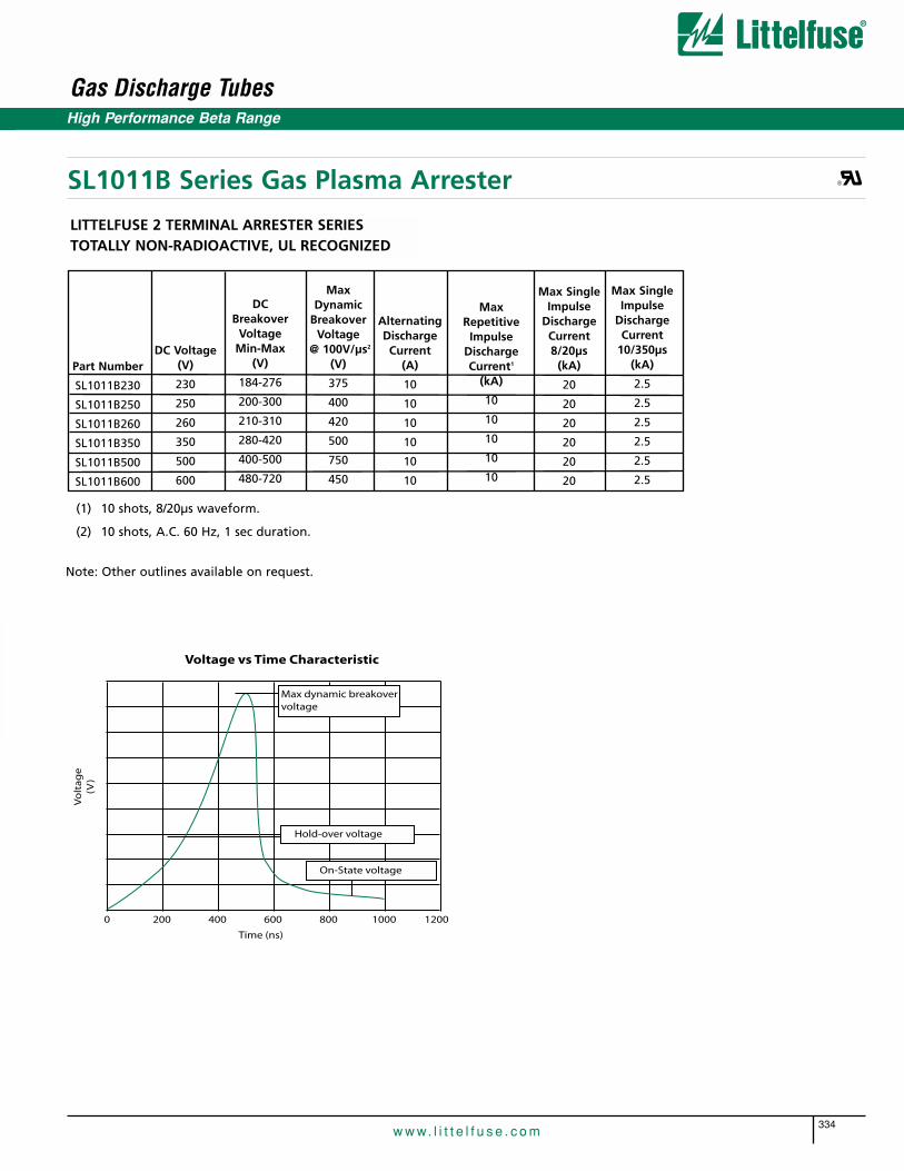
SL1011B Series Gas Plasma Arrester
Gas Discharge TubesHigh Performance Beta Range
334w w w. l i t t e l f u s e . c o m
Note: Other outlines available on request.
LITTELFUSE 2 TERMINAL ARRESTER SERIESTOTALLY NON-RADIOACTIVE, UL RECOGNIZED
Part Number
SL1011B230
SL1011B250
SL1011B260
SL1011B350
SL1011B500
SL1011B600
DC Voltage(V)
230
250
260
350
500
600
DC Breakover
VoltageMin-Max
(V)
184-276
200-300
210-310
280-420
400-500
480-720
MaxDynamic
BreakoverVoltage
@ 100V/µs2
(V)
375
400
420
500
750
450
AlternatingDischargeCurrent
(A)
10
10
10
10
10
10
Max SingleImpulse
DischargeCurrent8/20µs
(kA)
20
20
20
20
20
20
Max SingleImpulse
DischargeCurrent
10/350µs(kA)
2.5
2.5
2.5
2.5
2.5
2.5
MaxRepetitive
ImpulseDischargeCurrent1
(kA)
10
10
10
10
10
(1) 10 shots, 8/20µs waveform.
(2) 10 shots, A.C. 60 Hz, 1 sec duration.
Vo
lta
ge
(V)
Time (ns)
0 200 400 600 800 1000 1200
Max dynamic breakovervoltage
Hold-over voltage
On-State voltage
Voltage vs Time Characteristic
®

8
GA
S D
ISC
HA
RG
ETU
BES
Gas Discharge Tubes
335w w w. l i t t e l f u s e . c o m
LITTELFUSE 3 TERMINAL POTTED ARRESTERS, 18A, 18B,CONFORMS TO BT SPECIFICATION D2982B TOTALLYNON-RADIOACTIVE, UL RECOGNIZED
(1) Measured using a rate of rise of voltage of 100V/s.
(2) Measured using a rate of rise of voltage of 1KV/µsec.
(3) Measured at 1 sec duration, 5 shots @ 3 min intervals, 50Hz.
(4) Measured using 8/20µsec, 5 shots each polarity.
(5) Measured at ±170V dc (18A) or ±350V dc (18B).
(6) Measured at 1 MHz, Line to ground.
(7) Measured using BT test circuit.
ORDERINGINFORMATION
PROTECTOR 18APROTECTOR 18B
All dimensions in mm
Features
• Conforms to BT specifications D2982B
• Hermetically sealed eclosure for use in undergroundjoints and pole tops.
• Flying leads for easy connection to IDC or screwterminals.
• High surge capability
• Conforms to BT specification D2982B
• Flame retardent materials to UL 94V0
18A/18B Series Potted Gas Plasma Arresters
Modified Protector
3 ELECTRODE GDT
a=TIPb=RING
e=GROUND(centre electrode)
GRAPHICAL SYMBOL
a b
e
Max Alternating Impulse
Electrical DC Impulse Discharge Discharge Insulation Max
Characteristics Sparkover1 Sparkover2 Current3 Current4 Resistance5 Capacitance6 Holdover7
(V) (V) (A) (kA) (Ω) (pF) (V)
18A 210-310 800 5 5 1x10⁸ 30 100
18B 400-500 1000 5 5 1x10⁸ 30 100
®
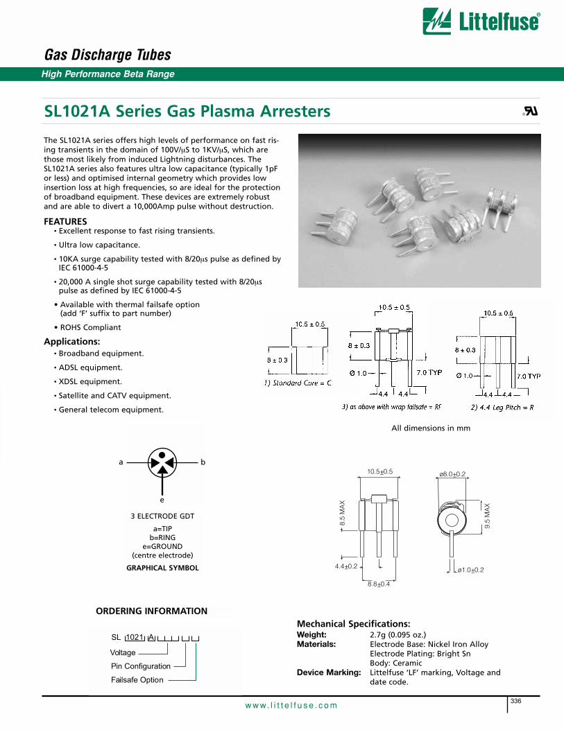
Gas Discharge Tubes
336w w w. l i t t e l f u s e . c o m
High Performance Beta Range
3 ELECTRODE GDT
a=TIPb=RING
e=GROUND(centre electrode)
GRAPHICAL SYMBOL
a b
e
1021 A
Voltage
Pin Configuration
Failsafe Option
SL
All dimensions in mm
ORDERING INFORMATION
SL1021A Series Gas Plasma Arresters
4.4+_0.2
8.8+_0.4
8.5
MA
X
10.5+_0.5 ø8.0+_0.2
9.5
MA
X
ø1.0+_0.2
The SL1021A series offers high levels of performance on fast ris-ing transients in the domain of 100V/µS to 1KV/µS, which arethose most likely from induced Lightning disturbances. TheSL1021A series also features ultra low capacitance (typically 1pFor less) and optimised internal geometry which provides lowinsertion loss at high frequencies, so are ideal for the protectionof broadband equipment. These devices are extremely robustand are able to divert a 10,000Amp pulse without destruction.
FEATURES• Excellent response to fast rising transients.
• Ultra low capacitance.
• 10KA surge capability tested with 8/20µs pulse as defined byIEC 61000-4-5
• 20,000 A single shot surge capability tested with 8/20µs pulse as defined by IEC 61000-4-5
• Available with thermal failsafe option (add ‘F’ suffix to part number)
• ROHS Compliant
Applications:• Broadband equipment.
• ADSL equipment.
• XDSL equipment.
• Satellite and CATV equipment.
• General telecom equipment.
Mechanical Specifications:Weight: 2.7g (0.095 oz.)Materials: Electrode Base: Nickel Iron Alloy
Electrode Plating: Bright Sn Body: Ceramic
Device Marking: Littelfuse ‘LF’ marking, Voltage and date code.
®
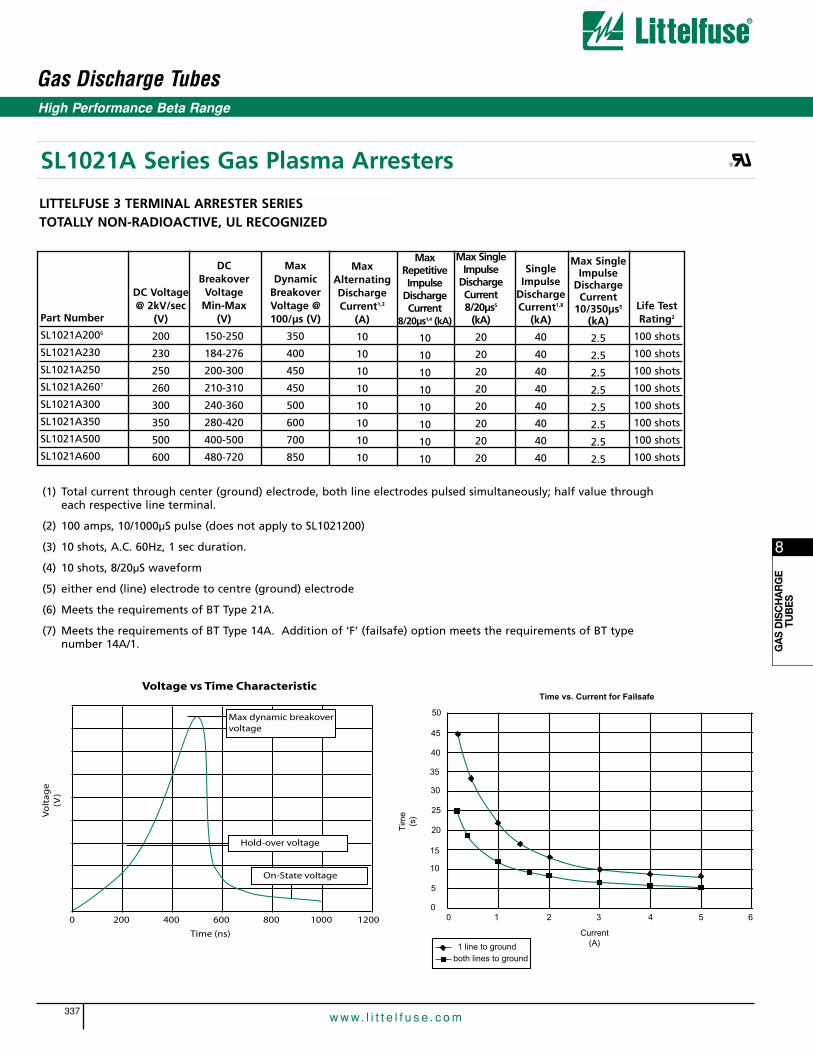
8
GA
S D
ISC
HA
RG
ETU
BES
Gas Discharge Tubes
337w w w. l i t t e l f u s e . c o m
Part Number
SL1021A2006
SL1021A230
SL1021A250
SL1021A2607
SL1021A300
SL1021A350
SL1021A500
SL1021A600
DC Voltage@ 2kV/sec
(V)
200
230
250
260
300
350
500
600
DCBreakover
VoltageMin-Max
(V)
150-250
184-276
200-300
210-310
240-360
280-420
400-500
480-720
MaxDynamic
BreakoverVoltage @100/µs (V)
350
400
450
450
500
600
700
850
MaxAlternatingDischargeCurrent1,3
(A)
10
10
10
10
10
10
10
10
Max SingleImpulse
DischargeCurrent
10/350µs5
(kA)
2.5
2.5
2.5
2.5
2.5
2.5
2.5
2.5
Max SingleImpulse
DischargeCurrent8/20µs5
(kA)
20
20
20
20
20
20
20
20
MaxRepetitiveImpulse
DischargeCurrent
8/20µs1,4 (kA)
10
10
10
10
10
10
10
10
Life TestRating2
100 shots
100 shots
100 shots
100 shots
100 shots
100 shots
100 shots
100 shots
(1) Total current through center (ground) electrode, both line electrodes pulsed simultaneously; half value througheach respective line terminal.
(2) 100 amps, 10/1000µS pulse (does not apply to SL1021200)
(3) 10 shots, A.C. 60Hz, 1 sec duration.
(4) 10 shots, 8/20µS waveform
(5) either end (line) electrode to centre (ground) electrode
(6) Meets the requirements of BT Type 21A.
(7) Meets the requirements of BT Type 14A. Addition of ‘F’ (failsafe) option meets the requirements of BT typenumber 14A/1.
LITTELFUSE 3 TERMINAL ARRESTER SERIESTOTALLY NON-RADIOACTIVE, UL RECOGNIZED
SL1021A Series Gas Plasma Arresters
High Performance Beta Range
SingleImpulse
DischargeCurrent1,8
(kA)
40
40
40
40
40
40
40
40
Vo
lta
ge
(V)
Time (ns)
0 200 400 600 800 1000 1200
Max dynamic breakovervoltage
Hold-over voltage
On-State voltage
Voltage vs Time Characteristic
50
45
40
35
30
25
20
15
10
5
00 1 2 3 4 5 6
Current(A)
Tim
e(s
)
1 line to groundboth lines to ground
Time vs. Current for Failsafe
®

Gas Discharge Tubes
338w w w. l i t t e l f u s e . c o m
ORDERING INFORMATION
1021 B
Voltage
Pin Configuration
Failsafe Option
SL
SL1021B Series Gas Plasma Arresters
3 ELECTRODE GDT
a=TIPb=RING
e=GROUND(centre electrode)
GRAPHICAL SYMBOL
a b
e
High Performance Beta Range
4.4+_0.2
8.8+_0.4
8.5
MA
X
10.5+_0.5 ø8.0+_0.2
9.5
MA
X
ø1.0+_0.2
All dimensions in mm
The SL1021B series offers high levels of performance on fast ris-ing transients in the domain of 100V/µS to 1KV/µS, which arethose most likely from induced Lightning disturbances. TheSL1021B series also features ultra low capacitance (typically 1pFor less) and optimised internal geometry which provides lowinsertion loss at high frequencies, so are ideal for the protectionof broadband equipment. These devices are extremely robustand are able to divert a 20,000Amp pulse without destruction.
FEATURES• Excellent response to fast rising transients.
• Ultra low capacitance.
• 10KA surge capability tested with 8/20µS pulse as defined byIEC 6100-4-5
• 20,000 A single shot surge capability tested with 8/20µs pulse as defined by IEC 6100-4-5
• Available with thermal failsafe option (add ‘F’ suffix to partnumber)
Applications:• Broadband equipment.
• ADSL equipment.
• XDSL equipment.
• Satellite and CATV equipment.
• General telecom equipment.
Mechanical Specifications:Weight: 0.63g (0.022 oz.)Materials: Electrode Base: Nickel Iron Alloy
Electrode Plating: Bright SnBody: Ceramic
Device Marking: Littelfuse ‘LF’ marking, Voltage and datecode. Blue.
®

8
GA
S D
ISC
HA
RG
ETU
BES
Gas Discharge Tubes
339w w w. l i t t e l f u s e . c o m
High Performance Beta Range
SL1021B Series Gas Plasma Arresters
LITTELFUSE 3 TERMINAL HEAVY DUTY ARRESTER SERIESTOTALLY NON-RADIOACTIVE, UL RECOGNIZED
(1) Total current through center (ground) electrode, both line electrodes pulsed simultaneously;half value through respective line terminal to ground.
(2) 100 amps, 10/1000µS pulse
(3) 10 shots, A.C. 60 Hz, 1sec. Duration.
(4) 10 shots, 8/20µS waveform
(5) either end (line) electrode to centre (ground) electrode
(6) Applies to ‘C’ option devices mounted in a suitable connector with high pressure contacts.
Part Number
SL1021B200
SL1021B230
SL1021B250
SL1021B260
SL1021B300
SL1021B350
SL1021B500
DC Voltage(V)
200
230
250
260
350
350
500
DCBreakover
VoltageMin-Max
(V)
150-250
184-276
200-300
210-310
240-360
280-420
400-500
MaxDynamic
BreakoverVoltage @100V/µs
320
350
400
420
450
500
750
MaxAlternatingDischargeCurrent1,3,6
(A)
20
20
20
20
20
20
20
MaxRepetitive
ImpulseDischargeCurrent
(kA)
10
10
10
10
10
10
10
MaxAlternatingDischarge
Current5 (A)
10
10
10
10
10
10
10
MaxImpulse
DischargeCurrent
(kA)
20
20
20
20
20
20
20
Life TestRating2
100 shots
100 shots
100 shots
100 shots
100 shots
100 shots
100 shots
Max SingleImpulse
DischargeCurrent
10/350µs5,6
(kA)
2.5
2.5
2.5
2.5
2.5
2.5
2.5
Vo
lta
ge
(V)
Time (ns)
0 200 400 600 800 1000 1200
Max dynamic breakovervoltage
Hold-over voltage
On-State voltage
Voltage vs Time Characteristic
50
45
40
35
30
25
20
15
10
5
00 1 2 3 4 5 6
Current(A)
Tim
e(s
)
1 line to groundboth lines to ground
Time vs. Current for Failsafe
®
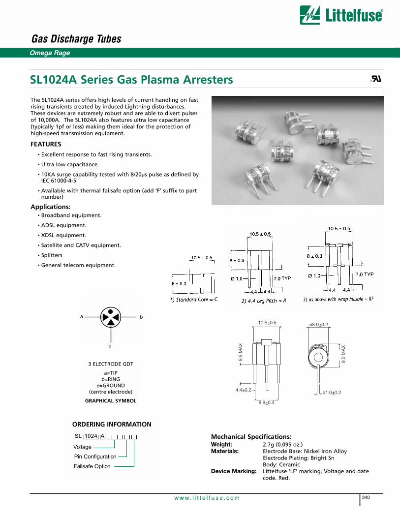
Gas Discharge Tubes
340
SL1024A Series Gas Plasma Arresters
Omega Rage
w w w. l i t t e l f u s e . c o m
ORDERING INFORMATION
3 ELECTRODE GDT
a=TIPb=RING
e=GROUND(centre electrode)
GRAPHICAL SYMBOL
a b
e
1024 A
Voltage
Pin Configuration
Failsafe Option
SL
4.4+_0.2
8.8+_0.4
8.5
MA
X
10.5+_0.5 ø8.0+_0.2
9.5
MA
X
ø1.0+_0.2
The SL1024A series offers high levels of current handling on fastrising transients created by induced Lightning disturbances.These devices are extremely robust and are able to divert pulsesof 10,000A. The SL1024A also features ultra low capacitance(typically 1pf or less) making them ideal for the protection ofhigh-speed transmission equipment.
FEATURES
• Excellent response to fast rising transients.
• Ultra low capacitance.
• 10KA surge capability tested with 8/20µs pulse as defined byIEC 61000-4-5
• Available with thermal failsafe option (add ‘F’ suffix to partnumber)
Applications:• Broadband equipment.
• ADSL equipment.
• XDSL equipment.
• Satellite and CATV equipment.
• Splitters
• General telecom equipment.
Mechanical Specifications:Weight: 2.7g (0.095 oz.)Materials: Electrode Base: Nickel Iron Alloy
Electrode Plating: Bright SnBody: Ceramic
Device Marking: Littelfuse ‘LF’ marking, Voltage and datecode. Red.
®

8
GA
S D
ISC
HA
RG
ETU
BES
Gas Discharge Tubes
341w w w. l i t t e l f u s e . c o m
SL1024A Series Gas Plasma Arresters
Omega Range
DCVoltage(V)
90
230
250
260
300
350
450
500
DCBreakover
VoltageMin-Max7
(V)
70-120
184-276
200-300
210-310
240-360
280-420
360-540
400-500
MaxDynamic
BreakoverVoltage @
100/µs(V)
600
450
475
475
650
700
750
800
AlternatingDischargeCurrent1,3
(A)
10
10
10
10
10
10
10
10
Max SingleImpulse
DischargeCurrent
10/350µs5,2
(kA)
2.5
2.5
2.5
2.5
2.5
2.5
2.5
2.5
MaxSingle
ImpulseDischargeCurrent
(kA)
20
20
20
20
20
20
20
20
MaxRepetitive
ImpulseDischargeCurrent
(kA)
10
10
10
10
10
10
10
10
(1) Total current through center (ground) electrode, both line electrodes pulsed simultaneously; half value througheach respective line terminal.
(2) Applies to ‘C’ option devices mounted in a suitable connector with high pressure contacts.
(3) 10 shots, A.C. 60Hz, 1 sec duration.
(4) 10 shots, 8/20µS waveform
(5) either end (line) electrode to center (ground) electrode
(6) Meets the requirements of BT Type 14. Addition of ‘F’ (failsafe) option meets the requirements of BT typenumber 14A/1.
(7) Vbr measured @ 2kv/sec except for 90V parts, which are measured @ 100V/sec.
LITTELFUSE 3 TERMINAL ARRESTER SERIESTOTALLY NON-RADIOACTIVE, UL RECOGNIZED
Part Number
SL1024A090
SL1024A230
SL1024A250
SL1024A260
SL1024A300
SL1024A350
SL1024A450
SL1024A500
Vo
lta
ge
(V)
Time (ns)
0 200 400 600 800 1000 1200
Max dynamic breakovervoltage
Hold-over voltage
On-State voltage
Voltage vs Time Characteristic
50
45
40
35
30
25
20
15
10
5
00 1 2 3 4 5 6
Current(A)
Tim
e(s
)
1 line to groundboth lines to ground
Time vs. Current for Failsafe
®

Gas Discharge Tubes
342w w w. l i t t e l f u s e . c o m
Omega Range
SL1024B Series Gas Plasma Arresters
ORDERING INFORMATION
3 ELECTRODE GDT
a=TIPb=RING
e=GROUND(centre electrode)
GRAPHICAL SYMBOL
a b
e
1024 B
Voltage
Pin Configuration
Failsafe Option
SL
4.4+_0.2
8.8+_0.4
8.5
MA
X
10.5+_0.5 ø8.0+_0.2
9.5
MA
X
ø1.0+_0.2
All dimensions in mm
The SL1024B series offers high levels of current handling on fastrising transients created by induced Lightning disturbances.These devices are extremely robust and are able to divert pulsesof 20,000 Amps. The SL1024B also features ultra low capacitance(typically 1pF or less) making them ideal for the protection ofhigh-speed transmission equipment.
FEATURES• Excellent response to fast rising transients.
• Ultra low capacitance.
• 20KA surge capability tested with 8/20µs pulse as defined byIEC 61000-4-5
• Available with thermal failsafe option (add ‘F’ suffix to partnumber)
Applications:• Broadband equipment.
• ADSL equipment.
• XDSL equipment.
• Satellite and CATV equipment.
• Splitters
• General telecom equipment.
Mechanical Specifications:Weight: 2.7g (0.095 oz.)Materials: Electrode Base: Nickel Iron Alloy
Electrode Plating: Bright SnBody: Ceramic
Device Marking: Littelfuse ‘LF’ marking, Voltage and datecode. Red.
®

8
GA
S D
ISC
HA
RG
ETU
BES
Gas Discharge Tubes
343w w w. l i t t e l f u s e . c o m
SL1024B Series Gas Plasma Arresters
Omega Range
DC Voltage
(V)
90
230
250
260
300
350
450
500
DCBreakover
VoltageMin-Max7
(V)
70-120
184-276
200-300
210-310
240-360
280-420
360-540
400-500
MaxDynamic
BreakoverVoltage @
100/µs(V)
600
450
475
475
650
700
750
800
AlternatingDischargeCurrent1,3
(A)
20
20
20
20
20
20
20
20
Max SingleImpulse
DischargeCurrent
10/350µs5,2
(kA)
2.5
2.5
2.5
2.5
2.5
2.5
2.5
2.5
MaxSingle
ImpulseDischargeCurrent8/20µs1.6
(kA)
40
40
40
40
40
40
40
40
MaxRepetitive
ImpulseDischargeCurrent8/20µs1,4
(kA)
20
20
20
20
20
20
20
20
(1) Total current through centre (ground) electrode, both line electrodes pulsed simultaneously; half value throughrespective line terminal to ground.
(2) 100 amps, 10/1000µS pulse
(3) 10 shots, A.C. 60 Hz, 1sec. Duration.
(4) 10 shots, 8/20µS waveform
(5) either end (line) electrode to centre (ground) electrode
(6) Applies to ‘C’ option devices mounted in a suitable connector with high pressure contacts.
(7) Measured @ 2kv/sec except for 90V parts which are measured @ 100V/sec.
LITTELFUSE 3 TERMINAL ARRESTER SERIESTOTALLY NON-RADIOACTIVE, UL RECOGNIZED
Part Number
SL1024B090
SL1024B230
SL1024B250
SL1024B260
SL1024B300
SL1024B350
SL1024B450
SL1024B500
AlternatingDischargeCurrent5,3
(A)
10
10
10
10
10
10
10
10
Vo
lta
ge
(V)
Time (ns)
0 200 400 600 800 1000 1200
Max dynamic breakovervoltage
Hold-over voltage
On-State voltage
Voltage vs Time Characteristic
50
45
40
35
30
25
20
15
10
5
00 1 2 3 4 5 6
Current(A)
Tim
e(s
)
1 line to groundboth lines to ground
Time vs. Current for Failsafe
®

Gas Discharge Tubes
344w w w. l i t t e l f u s e . c o m
High Performance Alpha Range
ORDERING INFORMATION
1122 A
Voltage
SL
All dimensions in mm
3 ELECTRODE GDT
a=TIPb=RING
e=GROUND(centre electrode)
GRAPHICAL SYMBOL
a b
e
SL1122A Series Hybrid Gas Plasma Arresters
The SL1122 series Hybrid features a high performance Alpha GasPlasma Tube in conjunction with a high speed Silicon AvalancheDiode ( SAD ). These devices are matched so that High speedpulses are initially clamped by the SAD, then as the current rises,the transient energy is switched through the Gas Tube. TheHybrid offers high levels of performance on fast rising transientsin the domain of 100V/µS to 10 KV/µS, so eliminates the dv/dtswitching delay normally exhibited by standard GDT’s. Thesedevices are extremely robust and are able to divert a 10,000Amppulse without destruction, so are ideal for central office ( tele-phone exchange ) protection.
FEATURES• Excellent response to fast rising transients.
• Flat response up to 10KV/µS.
• 10KA surge capability tested with 8/20µS pulse as defined byIEC 61000-4-5
• SAD ensures short circuit failure mode in the event of severetransient overload.
• Thermal failsafe.
Applications:• MDF protection
• Alarm panels.
• ADSL equipment.
• XDSL equipment.
• General Telecom Equipment
Mechanical Specifications:Weight: 2.7g (0.095 oz.)Materials: Electrode Base: Nickel Iron Alloy
Electrode Plating: Bright SnBody: Ceramic
Device Marking: Littelfuse ‘LF’ logo, voltage and date code
®

8
GA
S D
ISC
HA
RG
ETU
BES
Gas Discharge Tubes
345w w w. l i t t e l f u s e . c o m
CCT DIAGRAM
LITTELFUSE 3 TERMINAL ARRESTER SERIESTOTALLY NON-RADIOACTIVE, UL BREAKER VOLTAGE
Notes:
(1) Measured using a voltage rate of rise of 100V/s.
(2) In ionized mode
(3) Tested according to ITU-T Rec.K.12
(4) Either end electrode to center electrode
(5) Total current through center electrode, both line electrodes subject to simultaneous pulses
(6) 10 shots, AC 60Hz, 1 sec duration
(7) 10 shots, 8/20µs waveform
(8) Measured @ 100V
(9) Measured at MHz, line to ground
Part Number
SL1122A090
SL1122A200
SL1122A230
SL1122A260
SL1122A450
DCVoltage
(V)
90
200
230
260
450
BreakoverVoltage1,2,4
(V)
70-120
140-250
184-276
210-350
420-600
Max DynamicBreakoverVoltage @
1 kV/us (Vbr)
150
250
350
350
600
MaxRepetitive
ImpulseDischarge
Current4,7 (kA)
5
5
5
5
5
MaxRepetitive
ImpulseDischarge
Current5,7 (kA)
10
10
10
10
10
AlternatingDischargeCurrent4,6
(A)
5
5
5
5
5
Insulation
Resistance8
(Ω)
1x10⁸ @ 50V
1x10⁸ @ 120V
1x10⁸ @ 150V
1x10⁸ @ 175V
1x10⁸ @ 400V
Max
Capacitance9
(pF)
200
100
100
100
100
SL1122A Series Hybrid Gas Plasma Arresters
High Performance Alpha Range
HoldoverVoltage3
(V)
50
120
135
135
135
Nominal On-StateVoltage @
1A (V)
20
20
20
20
20
®
HYBRID
G.D.T. ONLY

Gas Discharge Tubes
346w w w. l i t t e l f u s e . c o m
Heavy Duty Delta Range
3 ELECTRODE GDT
a=TIPb=RING
e=GROUND(centre electrode)
GRAPHICAL SYMBOL
ORDERING INFORMATION
a b
e
1026 –
Voltage
SL
All dimensions in mm
SL1026 Series Gas Plasma ArrestersThe SL1026 series is a heavy-duty transient suppresser using GasPlasma technology. In response to a transient voltage whichexceeds the fixed breakover voltage (selected according to partnumber) the device changes from a very high impedance state toa low impedance state, there by conducting harmful currentaway from the protected system. The design is optimized for theprotection of electrical and electronic equipment employed inRailway systems: carefully designed geometry ensures the devicedoes not become a short circuit in the event of a failure due toconditions and events beyond the design criteria. An electricalmounting clip (PN SL1053 ) is available to aid mounting and con-nection. A mounting plate (PN SL 1056) is also available whichaccepts 10 SL1053’s. Mounting of the clips to the plate provides acommon ground connection; the plate can then be connected toa suitable ground via the screw terminal.
FEATURES• 55 kA surge capability (single shot) tested with 8/20µS pulse
as defined by IEC 61000-4-5
• 40 kA surge capability (repetitive)
• Will protect against Trapezoidal waveforms as specified inRIA 12.
• Will protect against capacitor discharge voltage transientwaveforms as specified in RIA 12.
• Will protect against double exponential voltage transientwaveforms as specified in IEC 571.
Applications:
• Signaling equipment.
• Communication equipment
• Control gear.
• Trackside cabinets.
• Cell phone base stations
Mechanical Specifications:Weight: 11g (0.388 oz.)Materials: Electrode Base: Nickel Iron Alloy
Electrode Plating: Bright SnBody: Ceramic
Device Marking: Color coded bodySL1026A275: Black/BlackSL1026A400: Black/YellowSL1026A700: Black/Red
®
TYPE 1053 Holder
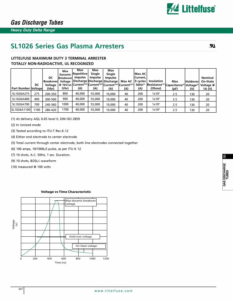
Gas Discharge Tubes
347w w w. l i t t e l f u s e . c o m
8
GA
S D
ISC
HA
RG
ETU
BES
LITTELFUSE MAXIMUM DUTY 3 TERMINAL ARRESTER TOTALLY NON-RADIOACTIVE, UL RECOGNIZED
(1) At delivery AQL 0.65 level II, DIN ISO 2859
(2) In ionized mode
(3) Tested according to ITU-T Rec.K.12
(4) Either end electrode to center electrode
(5) Total current through center electrode, both line electrodes connected together
(6) 100 amps, 10/1000µS pulse, as per ITU K 12
(7) 10 shots, A.C. 50Hz, 1 sec. Duration.
(9) 10 shots, 8/20µS waveform
(10) measured @ 100 volts
SL1026 Series Gas Plasma Arresters
Heavy Duty Delta Range
Part Number
SL1026A275
SL1026A400
SL1026A700
SL1026A1100
DCVoltage
275
400
700
1100
DCBreakover
Voltage(Vbr)
200-350
300-500
240-360
280-420
MaxDynamic
BreakoverVoltage
@ 1kV/us(Vbr)
800
900
1000
1700
MaxRepetitive
ImpulseDischargeCurrent(4)(9)
(A)
40,000
40,000
40,000
40,000
Max Single
ImpulseDischargeCurrent(4)(9)
(A)
55,000
55,000
55,000
55,000
Max Single
ImpulseDischargeCurrent(1)(4)
(A)
10,000
10,000
10,000
10,000
Max ACCurrent(4)(7)
(A)
40
40
40
40
Max ACCurrent, 9 cycles 50Hz(4)
(A)
200
200
200
200
InsulationResistance(10)
(Ohms)
1x10⁸
1x10⁸
1x10⁸
1x10⁸
MaxCapacitance(4)
(pF)
2.5
2.5
2.5
2.5
HoldoverVoltage(3)
(V)
130
130
130
130
NominalOn-StateVoltage @
1A (V)
20
20
20
20
Vo
lta
ge
(V)
Time (ns)
0 200 400 600 800 1000 1200
Max dynamic breakovervoltage
Hold-over voltage
On-State voltage
Voltage vs Time Characteristic
®

Resettable PTCs
9
Resettable PTCs . . . . . . . . . . . . . . . . . . . . . . . . . . . . . . . . . . . . . . . . . . . . . . . . . . . . . . . . . . . . . . . . . . . . . . . . . . . . . . . . . . . . . . . . . . . . . . . . . 348
1206L Series (Surface Mount) . . . . . . . . . . . . . . . . . . . . . . . . . . . . . . . . . . . . . . . . . . . . . . . . . . . . . . . . . . . . . . . . . . . . . . . . . . . . . . . . . . 349-350
1812L Series (Surface Mount) . . . . . . . . . . . . . . . . . . . . . . . . . . . . . . . . . . . . . . . . . . . . . . . . . . . . . . . . . . . . . . . . . . . . . . . . . . . . . . . . . . 351-352
3425L Series (Surface Mount) . . . . . . . . . . . . . . . . . . . . . . . . . . . . . . . . . . . . . . . . . . . . . . . . . . . . . . . . . . . . . . . . . . . . . . . . . . . . . . . . . . 353-354
30R Series (Radial Lead) . . . . . . . . . . . . . . . . . . . . . . . . . . . . . . . . . . . . . . . . . . . . . . . . . . . . . . . . . . . . . . . . . . . . . . . . . . . . . . . . . . . . . 355-356
60R Series (Radial Lead) . . . . . . . . . . . . . . . . . . . . . . . . . . . . . . . . . . . . . . . . . . . . . . . . . . . . . . . . . . . . . . . . . . . . . . . . . . . . . . . . . . . . . 357-358
PAGE
348w w w. l i t t e l f u s e . c o m
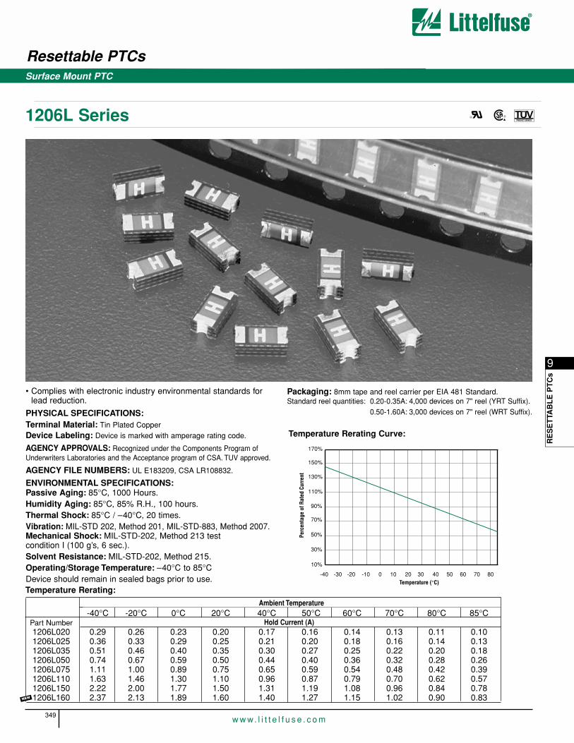
9
RE
SE
TTA
BL
E P
TC
s
1206L Series
Resettable PTCs
349w w w. l i t t e l f u s e . c o m
Surface Mount PTC
Temperature Rerating Curve:
-40°C -20°C 0°C 20°C 40°C 50°C 60°C 70°C 80°C 85°CPart Number1206L020 0.29 0.26 0.23 0.20 0.17 0.16 0.14 0.13 0.11 0.101206L025 0.36 0.33 0.29 0.25 0.21 0.20 0.18 0.16 0.14 0.131206L035 0.51 0.46 0.40 0.35 0.30 0.27 0.25 0.22 0.20 0.181206L050 0.74 0.67 0.59 0.50 0.44 0.40 0.36 0.32 0.28 0.261206L075 1.11 1.00 0.89 0.75 0.65 0.59 0.54 0.48 0.42 0.391206L110 1.63 1.46 1.30 1.10 0.96 0.87 0.79 0.70 0.62 0.571206L150 2.22 2.00 1.77 1.50 1.31 1.19 1.08 0.96 0.84 0.781206L160 2.37 2.13 1.89 1.60 1.40 1.27 1.15 1.02 0.90 0.83
Temperature Rerating:
• Complies with electronic industry environmental standards forlead reduction.
PHYSICAL SPECIFICATIONS:Terminal Material: Tin Plated CopperDevice Labeling: Device is marked with amperage rating code.
AGENCY APPROVALS: Recognized under the Components Program ofUnderwriters Laboratories and the Acceptance program of CSA. TUV approved.
AGENCY FILE NUMBERS: UL E183209, CSA LR108832.
ENVIRONMENTAL SPECIFICATIONS:Passive Aging: 85°C, 1000 Hours.Humidity Aging: 85°C, 85% R.H., 100 hours.Thermal Shock: 85°C / –40°C, 20 times.Vibration: MIL-STD 202, Method 201, MIL-STD-883, Method 2007.Mechanical Shock: MIL-STD-202, Method 213 test condition I (100 g’s, 6 sec.).Solvent Resistance: MIL-STD-202, Method 215.Operating/Storage Temperature: –40°C to 85°CDevice should remain in sealed bags prior to use.
Hold Current (A)
Ambient Temperature
® ®
-40 -30 -20 -10 0 10 20 30 40 50 60 70 80
10%
30%
50%
70%
90%
110%
130%
150%
170%
Temperature (°C)
Perc
enta
ge o
f Rat
ed C
urre
nt
Packaging: 8mm tape and reel carrier per EIA 481 Standard.Standard reel quantities: 0.20-0.35A: 4,000 devices on 7" reel (YRT Suffix).
0.50-1.60A: 3,000 devices on 7" reel (WRT Suffix).
NEW
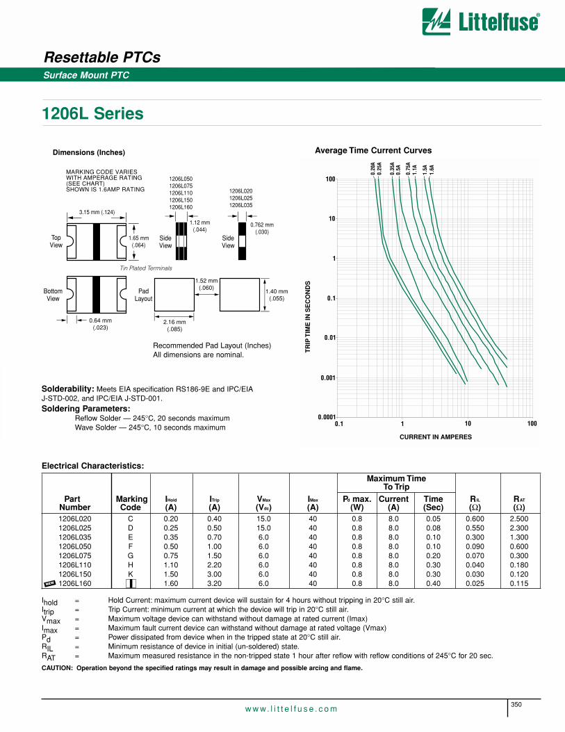
Surface Mount PTC
1206L Series
Resettable PTCs
350w w w. l i t t e l f u s e . c o m
Ihold = Hold Current: maximum current device will sustain for 4 hours without tripping in 20°C still air.Itrip = Trip Current: minimum current at which the device will trip in 20°C still air.Vmax = Maximum voltage device can withstand without damage at rated current (Imax)Imax = Maximum fault current device can withstand without damage at rated voltage (Vmax)Pd = Power dissipated from device when in the tripped state at 20°C still air.RIL = Minimum resistance of device in initial (un-soldered) state.RAT = Maximum measured resistance in the non-tripped state 1 hour after reflow with reflow conditions of 245°C for 20 sec.
CAUTION: Operation beyond the specified ratings may result in damage and possible arcing and flame.
Dimensions (Inches)
3.15 mm (.124)
1.65 mm(.064)
1.12 mm(.044)
0.762 mm(.030)
TopView
PadLayout
SideView
SideView
BottomView
1.40 mm(.055)
1.52 mm(.060)
2.16 mm(.085)
1206L0501206L0751206L1101206L1501206L160
1206L0201206L0251206L035
0.64 mm(.023)
Tin Plated Terminals
MARKING CODE VARIES WITH AMPERAGE RATING(SEE CHART)SHOWN IS 1.6AMP RATING
0.5A
0.75
A1.
1A
0.25
A0.
20A
0.35
A
1.5A
1.6A
100
10
1
0.1
0.01
0.001
TR
IP T
IME
IN S
EC
ON
DS
0.1 1 10 100
CURRENT IN AMPERES
0.0001
Average Time Current Curves
Solderability: Meets EIA specification RS186-9E and IPC/EIA J-STD-002, and IPC/EIA J-STD-001.Soldering Parameters:
Reflow Solder — 245°C, 20 seconds maximumWave Solder — 245°C, 10 seconds maximum
Recommended Pad Layout (Inches)All dimensions are nominal.
Part Marking IHold ITrip VMax IMax Pd max. Current Time RIL RAT
Number Code (A) (A) (Vdc) (A) (W) (A) (Sec) (Ω) (Ω)1206L020 C 0.20 0.40 15.0 40 0.8 8.0 0.05 0.600 2.5001206L025 D 0.25 0.50 15.0 40 0.8 8.0 0.08 0.550 2.3001206L035 E 0.35 0.70 6.0 40 0.8 8.0 0.10 0.300 1.3001206L050 F 0.50 1.00 6.0 40 0.8 8.0 0.10 0.090 0.6001206L075 G 0.75 1.50 6.0 40 0.8 8.0 0.20 0.070 0.3001206L110 H 1.10 2.20 6.0 40 0.8 8.0 0.30 0.040 0.1801206L150 K 1.50 3.00 6.0 40 0.8 8.0 0.30 0.030 0.1201206L160 1.60 3.20 6.0 40 0.8 8.0 0.40 0.025 0.115
Maximum TimeTo Trip
Electrical Characteristics:
NEW
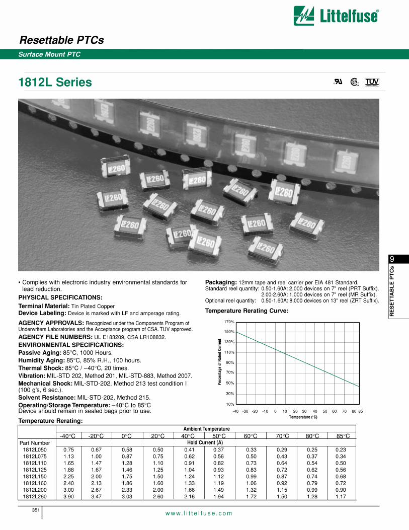
Resettable PTCs
351w w w. l i t t e l f u s e . c o m
9
RE
SE
TTA
BL
E P
TC
s
Surface Mount PTC
1812L Series
Temperature Rerating:
• Complies with electronic industry environmental standards forlead reduction.
PHYSICAL SPECIFICATIONS:Terminal Material: Tin Plated CopperDevice Labeling: Device is marked with LF and amperage rating.
AGENCY APPROVALS: Recognized under the Components Program ofUnderwriters Laboratories and the Acceptance program of CSA. TUV approved.
AGENCY FILE NUMBERS: UL E183209, CSA LR108832.
ENVIRONMENTAL SPECIFICATIONS:Passive Aging: 85°C, 1000 Hours.Humidity Aging: 85°C, 85% R.H., 100 hours.Thermal Shock: 85°C / –40°C, 20 times.Vibration: MIL-STD 202, Method 201, MIL-STD-883, Method 2007.Mechanical Shock: MIL-STD-202, Method 213 test condition I(100 g’s, 6 sec.).Solvent Resistance: MIL-STD-202, Method 215.Operating/Storage Temperature: –40°C to 85°CDevice should remain in sealed bags prior to use.
Packaging: 12mm tape and reel carrier per EIA 481 Standard.Standard reel quantity: 0.50-1.60A: 2,000 devices on 7" reel (PRT Suffix).
2.00-2.60A: 1,000 devices on 7" reel (MR Suffix).Optional reel quantity: 0.50-1.60A: 8,000 devices on 13" reel (ZRT Suffix).
® ®
-40 -30 -20 -10 0 10 20 30 40 50 60 70 80 85
10%
30%
50%
70%
90%
110%
130%
150%
170%
Temperature (°C)
Perc
enta
ge o
f Rat
ed C
urre
nt
Temperature Rerating Curve:
-40°C -20°C 0°C 20°C 40°C 50°C 60°C 70°C 80°C 85°CPart Number
1812L050 0.75 0.67 0.58 0.50 0.41 0.37 0.33 0.29 0.25 0.231812L075 1.13 1.00 0.87 0.75 0.62 0.56 0.50 0.43 0.37 0.341812L110 1.65 1.47 1.28 1.10 0.91 0.82 0.73 0.64 0.54 0.501812L125 1.88 1.67 1.46 1.25 1.04 0.93 0.83 0.72 0.62 0.561812L150 2.25 2.00 1.75 1.50 1.24 1.12 0.99 0.87 0.74 0.681812L160 2.40 2.13 1.86 1.60 1.33 1.19 1.06 0.92 0.79 0.721812L200 3.00 2.67 2.33 2.00 1.66 1.49 1.32 1.15 0.99 0.901812L260 3.90 3.47 3.03 2.60 2.16 1.94 1.72 1.50 1.28 1.17
Hold Current (A)
Ambient Temperature

Resettable PTCs
352w w w. l i t t e l f u s e . c o m
Surface Mount PTC
1812L Series
Ihold = Hold Current: maximum current device will sustain for 4 hours without tripping in 20°C still air.Itrip = Trip Current: minimum current at which the device will trip in 20°C still air.Vmax = Maximum voltage device can withstand without damage at rated current (Imax)Imax = Maximum fault current device can withstand without damage at rated voltage (Vmax)Pd = Power dissipated from device when in the tripped state at 20°C still air.RIL = Minimum resistance of device in initial (un-soldered) state.RAT = Maximum measured resistance in the non-tripped state 1 hour after reflow with reflow conditions of 245°C for 20 sec.
CAUTION: Operation beyond the specified ratings may result in damage and possible arcing and flame.
Dimensions (Inches)
260TopView
260BottomView
4.47 mm (.176)
3.15 mm(.124)
0.50 mm(.025)
Tin Plated Terminals
1.13 mm(.049)
SideView
.61 mm(.025)
SideView
1812L2001812L260
1812L0501812L0751812L1101812L1251812L1501812L160
PadLayout
3.30 mm(.130)
2.03 mm(.080)
2.29 mm(.090)
100
10
1
0.1
0.01
0.0010.1 1 10 100
.50A
.75A
1.10
A1.
25A
1.50
A
TIM
E IN
SE
CO
ND
S
CURRENT IN AMPERES
2.0A
2.6A
Average Time Current Curves
Recommended Pad Layout (Inches)All dimensions are nominal.
Solderability: Meets EIA specification RS186-9E and IPC/EIA J-STD-002, and IPC/EIA J-STD-001.Soldering Parameters:
Reflow Solder — 245°C, 20 seconds maximumWave Solder — 245°C, 10 seconds maximum
Part Ihold Itrip Vmax Imax Pd max. Current Time RIL RAT
Number (A) (A) (Vdc) (A) (W) (A) (Sec) (Ω) (Ω)1812L050 0.50 1.00 15.0 40 0.8 8.0 0.15 0.100 1.0001812L075 0.75 1.50 13.2 40 0.8 8.0 0.30 0.060 0.4201812L110 1.10 2.20 6.0 40 0.8 8.0 0.30 0.050 0.2261812L125 1.25 2.50 6.0 40 0.8 8.0 0.30 0.040 0.1841812L150 1.50 3.00 6.0 40 0.8 8.0 0.30 0.032 0.1371812L160 1.60 3.20 6.0 40 0.8 8.0 0.30 0.032 0.0991812L200 2.00 4.00 6.0 40 0.8 8.0 2.50 0.018 0.0701812L260 2.60 5.20 6.0 40 0.8 8.0 2.50 0.010 0.050
Maximum TimeTo Trip
Electrical Characteristics:
Resistance

Resettable PTCs
353w w w. l i t t e l f u s e . c o m
9
RE
SE
TTA
BL
E P
TC
s
Surface Mount PTC
3425L Series ® ®
• The 3425L Series Resettable devices utilize a unique polymer-based,Positive Temperature Coefficient (PTC) material to protect electrical circuits against overcurrent conditions.
• In normal operation, the 3425L Series PTC has many conductive pathsand a very low resistance. In an overcurrent condition, the temperatureof the polymer material rises. This dramatically reduces the conductivepaths resulting in an immediate rise in resistance. In this condition, thedevice provides circuit protection by significantly limiting the flow of current. However, once the cause of the initial overcurrent condition iseliminated, the 3425L Series PTC cools down and resets to a lowresistance value permitting the normal current flow to resume.
• The 3425L Series are surface mountable.
AGENCY APPROVALS: Recognized under the Components Programof Underwriters Laboratory and the Component Acceptance Program ofCSA. TUV approved.
AGENCY FILE NUMBERS: UL E183209, CSA LR 108832
PHYSICAL SPECIFICATIONS:Materials: Terminal Material: Tin Plated Brass to MIL-T-10727B
Solderability: Meets EIA specification RS186-9E and IPC/EIA J-STD-002, and IPC/EIA J-STD-001.
Device Labeling: Device is marked with the letter ‘L’, amperage ratingand date code.Packaging: Packaged in tape and reel carrier per EIA 481-2 standard
Standard reel quantities:
ENVIRONMENTAL SPECIFICATIONS:
Passive Aging: 85°C, 1000 Hours.
Humidity Aging: 85°C, 85% R.H., 100 hours.
Thermal Shock: 85°C / –40°C, 20 times.125°C / –55°C, 10 times.
Vibration: MIL-STD 202, Method 201. No resistance change.
Mechanical Shock: MIL-STD-202, Method 213 test condition I (100 g’s, 6 sec.).
Operating/Storage Temperature: –40°C to 85°C Devices shouldremain in sealed bags prior to use.
Part Reel PackagingNumber Quantity Suffix
3425L Series 1500 DR-40 -30 -20 -10 0 10 20 30 40 50 60 70 80 85
0
908070605040302010
100
130120110
140150160
Temperature (°C)
Perc
enta
ge o
f Rat
ed C
urre
nt
Rerating Curve For 3425L Series

Resettable PTCs
354w w w. l i t t e l f u s e . c o m
Surface Mount PTC
3425L Series
Dimensions (Inches)
MARKING
B
F
D
E
C
0.51-0.89(.020-.035)
3.05(.120)
0.635(.025)
0.635(.025)
A
Recommended Pad Layout (Inches)All dimensions are nominal.
Series A B C D E F
3425L 6.70 max 9.50 max 3.68 4.572 2.29 10.67(.264 max.) (.374 max.) (.145) (.180) (.090) (.420)
RECOMMENDED REFLOW CONDITIONS:(IR, Forced Air Convection, Vapor Phase)Devices are not designed to be wave soldered.
Catalog Ihold Itrip Vmax Imax Pd max. Current Time RIL RAT
Number (A) (A) (Vdc) (A) (W) (A) (Sec) (Ω) (Ω)
3425L150 1.50 3.0 15 40 1.9 8.0 5.0 0.060 0.253425L200 2.00 4.0 15 40 1.9 8.0 12.0 0.050 0.153425L250 2.50 5.0 15 40 1.9 8.0 25.0 0.035 0.103425L300 3.00 6.0 6 40 1.9 8.0 32.0 0.020 0.06
Maximum TimeTo Trip
Ihold = Hold Current: maximum current device will sustain for 4 hours without tripping in 20°C still air.Itrip = Trip Current: minimum current at which the device will trip in 20°C still air.Vmax = Maximum voltage device can withstand without damage at rated current (Imax)Imax = Maximum fault current device can withstand without damage at rated voltage (Vmax)Pd = Power dissipated from device when in the tripped state at 20°C still air.RIL = Minimum resistance of device in initial (un-soldered) state.RAT = Maximum measured resistance in the non-tripped state 1 hour after reflow with reflow conditions of 260°C for 20 sec.
CAUTION: Operation beyond the specified ratings may result in damage and possible arcing and flame.
ORDERING INFORMATION:
Resistance
1.50
A2.
00A
2.50
A3.
00A
1001010.1
100
10
1
0.1
0.01
CURRENT IN AMPERES
TIM
E IN
SE
CO
ND
S
Average Time Current Curves

Resettable PTCs
355w w w. l i t t e l f u s e . c o m
9
RE
SE
TTA
BL
E P
TC
s
Radial Leaded PTC
30R Series
• The 30R Series Resettable devices utilize a unique polymer-based,Positive Temperature Coefficient (PTC) material to protect electrical circuits against overcurrent conditions.
• In normal operation, the 30R Series PTC has many conductive pathsand a very low resistance. In an overcurrent condition, the temperatureof the polymer material rises. This dramatically reduces the conductivepaths resulting in an immediate rise in resistance. In this condition, thedevice provides circuit protection by significantly limiting the flow of current. However, once the cause of the initial overcurrent condition is eliminated, the 30R Series PTC cools down and resets to a lowresistance value permitting the normal current flow to resume.
• The 30R Series is a 30V Radial Leaded Device with a 40A Short Circuit Rating.
AGENCY APPROVALS: Recognized under the Components Programof Underwriters Laboratory and the Component Acceptance Program ofCSA. TUV approved.
AGENCY FILE NUMBERS: UL E183209, CSA LR 108832
PHYSICAL SPECIFICATIONS:Materials: Leads
30R090-250: Tin plated copper-clad steel, 24 AWG (0.020" Dia.)
30R300-900: Tin plated copper, 20 AWG (0.032" Dia.)
Lead Solderability: MIL-STD-202, Method 208E
Coating: Thermoset Coating
Device Labeling: Device is marked with the letter ‘L’, amperage rating,voltage rating & date code.
Packaging: Standard bulk packaging is 500 pieces per container.Optional tape and reel packaging per EIA 468-B is also available.
Standard reel quantities:
ENVIRONMENTAL SPECIFICATIONS:Passive Aging: 85°C, 1000 Hours. ±5% typical resistance change.
Humidity Aging: 85°C, 85% R.H., 1000 hours. ±5% typical resistance change.
Thermal Shock: 85°C / –40°C, 20 times. ±10% typical resistance change.
Vibration: MIL-STD 202, Method 201. No resistance change.
Mechanical Shock: MIL-STD-202, Method 213 test condition I (100 g’s, 6 sec.). No resistance change.
Max. Surface Temperature: 125°COperating/Storage Temperature: –40°C to 85°C
-40 -30 -20 -10 0 10 20 30 40 50 60 70 80 85
0
50
100
150
200
Temperature (°C)
Perc
enta
ge o
f Rat
ed C
urre
nt
Part ReelNumber Quantity
R30R090R30R110R30R135R30R160 3000
R30R185R30R250
Part ReelNumber Quantity
R30R300R30R400 1500
30R50030R600 Bulk Only30R700 500 Per30R800 Container30R900
Rerating Curve for 30R Series
® ®

Resettable PTCs
356w w w. l i t t e l f u s e . c o m
Radial Leaded PTC
30R Series
Dimension ‘D’ is 7.62 (0.30") MinimumDimension ‘E’ is 3.05 (0.12") Maximum
MARKING
MARKING
AA E E
B B
C
CD
D
Note: Stand-offs only used for 30R090-30R250
9.00
A8.
00A
7.00
A6.
00A
5.00
A4.
00A
3.00
A2.
50A
1.85
A1.
60A
1.35
A1.
10A
.900
A
5001001010.10.050.01
0.1
1
10
100
1000
TIM
E IN
SE
CO
ND
S
CURRENT IN AMPERES
Part Ihold Itrip Vmax Imax Pd max. Current Time RIL RAT
Number (A) (A) (Vdc) (A) (W) (A) (Sec) (Ω) (Ω)30R090 0.90 1.80 30 40 0.6 4.50 5.9 0.070 0.2230R110 1.10 2.20 30 40 0.7 5.50 6.6 0.050 0.1730R135 1.35 2.70 30 40 0.8 6.75 7.3 0.040 0.1330R160 1.60 3.20 30 40 0.9 8.00 8.0 0.030 0.1130R185 1.85 3.70 30 40 1.0 9.25 8.7 0.030 0.0930R250 2.50 5.00 30 40 1.2 12.5 10.3 0.020 0.0730R300 3.00 6.00 30 40 2.0 15.0 10.8 0.020 0.0830R400 4.00 8.00 30 40 2.5 20.0 12.7 0.010 0.0530R500 5.00 10.00 30 40 3.0 25.0 14.5 0.010 0.0530R600 6.00 12.00 30 40 3.5 30.0 16.0 0.005 0.0430R700 7.00 14.00 30 40 3.8 35.0 17.5 0.005 0.0330R800 8.00 16.00 30 40 4.0 40.0 18.8 0.005 0.0230R900 9.00 18.00 30 40 4.2 40.0 20.0 0.005 0.02
Resistance
Ihold = Hold Current: maximum current device will sustain for 4 hours without tripping in 20°C still air.Itrip = Trip Current: minimum current at which the device will trip in 20°C still air.Vmax = Maximum voltage device can withstand without damage at rated current (Imax)Imax = Maximum fault current device can withstand without damage at rated voltage (Vmax)Pd = Power dissipated from device when in the tripped state at 20°C still air.RIL = Minimum resistance of device in initial (un-soldered) state.RAT = Maximum resistance of device at 20°C measured one hour after tripping.
CAUTION: Operation beyond the specified ratings may result in damage and possible arcing and flame.
ORDERING INFORMATION:
Maximum TimeTo Trip
Dimensions (Inches) Average Time Current Curves
Part Number ‘A’ (Max.) ‘B’ (Max.) ‘C’ (Typ.)30R090 6.60 (0.26) 12.19 (0.48) 5.08 (0.20)30R110 6.60 (0.26) 14.22 (0.56) 5.08 (0.20)30R135 8.89 (0.35) 13.46 (0.53) 5.08 (0.20)30R160 8.89 (0.35) 15.42 (0.60) 5.08 (0.20)30R185 10.16 (0.40) 15.75 (0.62) 5.08 (0.20)30R250 11.43 (0.45) 18.29 (0.72) 5.08 (0.20)30R300 11.43 (0.45) 7.27 (0.68) 5.08 (0.20)30R400 13.97 (0.55) 20.07 (0.79) 5.08 (0.20)30R500 13.97 (0.55) 24.89 (0.98) 10.16 (0.40)30R600 16.51 (0.65) 24.89 (0.98) 10.16 (0.40)30R700 19.05 (0.75) 26.67 (1.05) 10.16 (0.40)30R800 21.59 (0.85) 29.21 (1.15) 10.16 (0.40)30R900 24.13 (0.95) 29.72 (1.17) 10.16 (0.40)
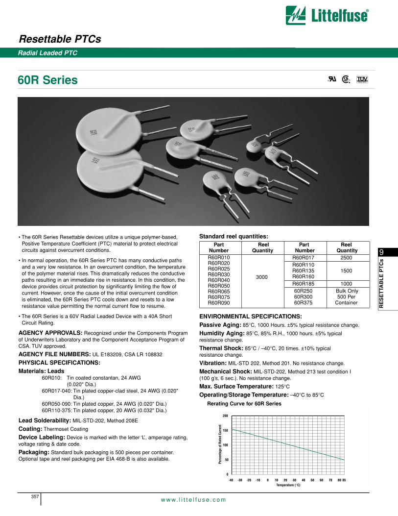
Resettable PTCs
357w w w. l i t t e l f u s e . c o m
9
RE
SE
TTA
BL
E P
TC
s
Radial Leaded PTC
60R Series
Standard reel quantities:
ENVIRONMENTAL SPECIFICATIONS:Passive Aging: 85°C, 1000 Hours. ±5% typical resistance change.
Humidity Aging: 85°C, 85% R.H., 1000 hours. ±5% typical resistance change.
Thermal Shock: 85°C / –40°C, 20 times. ±10% typical resistance change.
Vibration: MIL-STD 202, Method 201. No resistance change.
Mechanical Shock: MIL-STD-202, Method 213 test condition I (100 g’s, 6 sec.). No resistance change.
Max. Surface Temperature: 125°C
Operating/Storage Temperature: –40°C to 85°C
• The 60R Series Resettable devices utilize a unique polymer-based,Positive Temperature Coefficient (PTC) material to protect electrical circuits against overcurrent conditions.
• In normal operation, the 60R Series PTC has many conductive pathsand a very low resistance. In an overcurrent condition, the temperatureof the polymer material rises. This dramatically reduces the conductivepaths resulting in an immediate rise in resistance. In this condition, thedevice provides circuit protection by significantly limiting the flow of current. However, once the cause of the initial overcurrent condition is eliminated, the 60R Series PTC cools down and resets to a lowresistance value permitting the normal current flow to resume.
• The 60R Series is a 60V Radial Leaded Device with a 40A ShortCircuit Rating.
AGENCY APPROVALS: Recognized under the Components Programof Underwriters Laboratory and the Component Acceptance Program ofCSA. TUV approved.
AGENCY FILE NUMBERS: UL E183209, CSA LR 108832
PHYSICAL SPECIFICATIONS:Materials: Leads
60R010: Tin coated constantan, 24 AWG(0.020" Dia.)
60R017-040: Tin plated copper-clad steel, 24 AWG (0.020"Dia.)
60R050-090: Tin plated copper, 24 AWG (0.020" Dia.)60R110-375: Tin plated copper, 20 AWG (0.032" Dia.)
Lead Solderability: MIL-STD-202, Method 208E
Coating: Thermoset Coating
Device Labeling: Device is marked with the letter ‘L’, amperage rating,voltage rating & date code.
Packaging: Standard bulk packaging is 500 pieces per container.Optional tape and reel packaging per EIA 468-B is also available.
-40 -30 -20 -10 0 10 20 30 40 50 60 70 80 85
0
50
100
150
200
Temperature (°C)
Perc
enta
ge o
f Rat
ed C
urre
nt
Part ReelNumber QuantityR60R010R60R020R60R025R60R030 3000R60R040R60R050R60R065R60R075R60R090
Part ReelNumber Quantity
R60R017 2500R60R110R60R135 1500R60R160R60R185 100060R250 Bulk Only60R300 500 Per60R375 Container
Rerating Curve for 60R Series
® ®
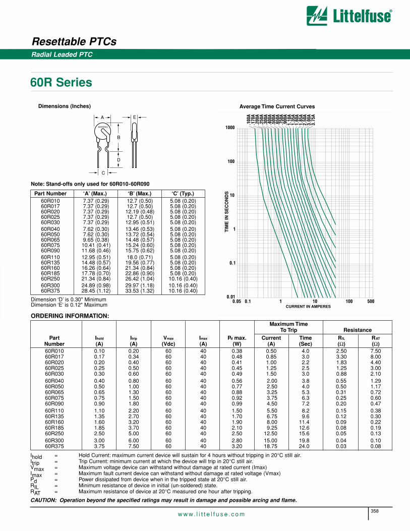
Resettable PTCs
358w w w. l i t t e l f u s e . c o m
Radial Leaded PTC
60R Series
Part Number ‘A’ (Max.) ‘B’ (Max.) ‘C’ (Typ.)60R010 7.37 (0.29) 12.7 (0.50) 5.08 (0.20)60R017 7.37 (0.29) 12.7 (0.50) 5.08 (0.20)60R020 7.37 (0.29) 12.19 (0.48) 5.08 (0.20)60R025 7.37 (0.29) 12.7 (0.50) 5.08 (0.20)60R030 7.37 (0.29) 12.95 (0.51) 5.08 (0.20)60R040 7.62 (0.30) 13.46 (0.53) 5.08 (0.20)60R050 7.62 (0.30) 13.72 (0.54) 5.08 (0.20)60R065 9.65 (0.38) 14.48 (0.57) 5.08 (0.20)60R075 10.41 (0.41) 15.24 (0.60) 5.08 (0.20)60R090 11.68 (0.46) 15.75 (0.62) 5.08 (0.20)60R110 12.95 (0.51) 18.0 (0.71) 5.08 (0.20)60R135 14.48 (0.57) 19.56 (0.77) 5.08 (0.20)60R160 16.26 (0.64) 21.34 (0.84) 5.08 (0.20)60R185 17.78 (0.70) 22.86 (0.90) 5.08 (0.20)60R250 21.34 (0.84) 26.42 (1.04) 10.16 (0.40)60R300 24.89 (0.98) 29.97 (1.18) 10.16 (0.40)60R375 28.45 (1.12) 33.53 (1.32) 10.16 (0.40)
MARKING
A
C
B
D
E
Dimension ‘D’ is 0.30" MinimumDimension ‘E’ is 0.12" Maximum
Note: Stand-offs only used for 60R010-60R090
3.75
A3.
00A
2.50
A1.
85A
1.60
A1.
35A
1.10
A.9
00A
.750
A.6
50A
.500
A.4
00A
.300
A.2
50A
.200
A.1
70A
.100
A
5001001010.10.050.01
0.1
10
100
1000
1TIM
E IN
SE
CO
ND
S
CURRENT IN AMPERES
Average Time Current Curves
Part Ihold Itrip Vmax Imax Pd max. Current Time RIL RAT
Number (A) (A) (Vdc) (A) (W) (A) (Sec) (Ω) (Ω)60R010 0.10 0.20 60 40 0.38 0.50 4.0 2.50 7.5060R017 0.17 0.34 60 40 0.48 0.85 3.0 3.30 8.0060R020 0.20 0.40 60 40 0.41 1.00 2.2 1.83 4.4060R025 0.25 0.50 60 40 0.45 1.25 2.5 1.25 3.0060R030 0.30 0.60 60 40 0.49 1.50 3.0 0.88 2.1060R040 0.40 0.80 60 40 0.56 2.00 3.8 0.55 1.2960R050 0.50 1.00 60 40 0.77 2.50 4.0 0.50 1.1760R065 0.65 1.30 60 40 0.88 3.25 5.3 0.31 0.7260R075 0.75 1.50 60 40 0.92 3.75 6.3 0.25 0.6060R090 0.90 1.80 60 40 0.99 4.50 7.2 0.20 0.4760R110 1.10 2.20 60 40 1.50 5.50 8.2 0.15 0.3860R135 1.35 2.70 60 40 1.70 6.75 9.6 0.12 0.3060R160 1.60 3.20 60 40 1.90 8.00 11.4 0.09 0.2260R185 1.85 3.70 60 40 2.10 9.25 12.6 0.08 0.1960R250 2.50 5.00 60 40 2.50 12.50 15.6 0.05 0.1360R300 3.00 6.00 60 40 2.80 15.00 19.8 0.04 0.1060R375 3.75 7.50 60 40 3.20 18.75 24.0 0.03 0.08
Resistance
Ihold = Hold Current: maximum current device will sustain for 4 hours without tripping in 20°C still air.Itrip = Trip Current: minimum current at which the device will trip in 20°C still air.Vmax = Maximum voltage device can withstand without damage at rated current (Imax)Imax = Maximum fault current device can withstand without damage at rated voltage (Vmax)Pd = Power dissipated from device when in the tripped state at 20°C still air.RIL = Minimum resistance of device in initial (un-soldered) state.RAT = Maximum resistance of device at 20°C measured one hour after tripping.
CAUTION: Operation beyond the specified ratings may result in damage and possible arcing and flame.
ORDERING INFORMATION:
Dimensions (Inches)
Maximum TimeTo Trip

9
RE
SE
TTA
BL
E P
TC
s
Resettable PTCs
359w w w. l i t t e l f u s e . c o m

Surface Mount Fuses
10
Surface Mount Fuses. . . . . . . . . . . . . . . . . . . . . . . . . . . . . . . . . . . . . . . . . . . . . . . . . . . . . . . . . . . . . . . . . . . . . . . . . . . . . . . . . . . . . . . . . . . . . 360
466 series, SlimLine™ Lead-Free 1206, Very Fast-Acting Fuse . . . . . . . . . . . . . . . . . . . . . . . . . . . . . . . . . . . . . . . . . . . . . . . . . . . . . . . . . . 361-362
433 series, SlimLine™ 1206, Very Fast-Acting Fuse . . . . . . . . . . . . . . . . . . . . . . . . . . . . . . . . . . . . . . . . . . . . . . . . . . . . . . . . . . . . . . . . . . . . . . 363
429 series, 1206, Very Fast Acting . . . . . . . . . . . . . . . . . . . . . . . . . . . . . . . . . . . . . . . . . . . . . . . . . . . . . . . . . . . . . . . . . . . . . . . . . . . . . . . . . . 364
430 series, 1206, Slo-Blo® Fuse . . . . . . . . . . . . . . . . . . . . . . . . . . . . . . . . . . . . . . . . . . . . . . . . . . . . . . . . . . . . . . . . . . . . . . . . . . . . . . . . . . . . 365
434 series, SlimLine™ 0603, Very Fast-Acting Fuse . . . . . . . . . . . . . . . . . . . . . . . . . . . . . . . . . . . . . . . . . . . . . . . . . . . . . . . . . . . . . . . . . . . . . . 366
467 series, SlimLine™ Lead-Free 0603, Very Fast-Acting Fuse . . . . . . . . . . . . . . . . . . . . . . . . . . . . . . . . . . . . . . . . . . . . . . . . . . . . . . . . . . 367-368
431 series, 0603, Very Fast Acting . . . . . . . . . . . . . . . . . . . . . . . . . . . . . . . . . . . . . . . . . . . . . . . . . . . . . . . . . . . . . . . . . . . . . . . . . . . . . . . . . . 369
435 series, SlimLine™ Lead-Free 0402, Very Fast-Acting Fuse . . . . . . . . . . . . . . . . . . . . . . . . . . . . . . . . . . . . . . . . . . . . . . . . . . . . . . . . . . . . . 370
451/453 series, NANO2® Very Fast-Acting Fuse. . . . . . . . . . . . . . . . . . . . . . . . . . . . . . . . . . . . . . . . . . . . . . . . . . . . . . . . . . . . . . . . . . . . . . . . . 371
452/454 series, NANO2® Slo-Blo® Fuse . . . . . . . . . . . . . . . . . . . . . . . . . . . . . . . . . . . . . . . . . . . . . . . . . . . . . . . . . . . . . . . . . . . . . . . . . . . . . . . 372
455 series, NANO2® UMF Fast-Acting Fuse. . . . . . . . . . . . . . . . . . . . . . . . . . . . . . . . . . . . . . . . . . . . . . . . . . . . . . . . . . . . . . . . . . . . . . . . . . . . 373
154 series, SMF OMNI-BLOK® Fuse Block . . . . . . . . . . . . . . . . . . . . . . . . . . . . . . . . . . . . . . . . . . . . . . . . . . . . . . . . . . . . . . . . . . . . . . . . . . . . 374
464 series, NANO2® 250V UMF Fast-Acting Fuse . . . . . . . . . . . . . . . . . . . . . . . . . . . . . . . . . . . . . . . . . . . . . . . . . . . . . . . . . . . . . . . . . . . . . . . 375
465 seies, NANO2® 250V UMF Time Lag Fuse . . . . . . . . . . . . . . . . . . . . . . . . . . . . . . . . . . . . . . . . . . . . . . . . . . . . . . . . . . . . . . . . . . . . . . . . . 376
461 series, Telecom NANO2® Fuse (Teccor TeleLink® Fuse). . . . . . . . . . . . . . . . . . . . . . . . . . . . . . . . . . . . . . . . . . . . . . . . . . . . . . . . . . . . . 377-379
459/460 series, PICO® SMF Fuse. . . . . . . . . . . . . . . . . . . . . . . . . . . . . . . . . . . . . . . . . . . . . . . . . . . . . . . . . . . . . . . . . . . . . . . . . . . . . . . . . . . 380
202 series, FLAT-PAK® Fast-Acting Fuse. . . . . . . . . . . . . . . . . . . . . . . . . . . . . . . . . . . . . . . . . . . . . . . . . . . . . . . . . . . . . . . . . . . . . . . . . . . . . . 381
203 series, FLAT-PAK® Slo-Blo® Fuse . . . . . . . . . . . . . . . . . . . . . . . . . . . . . . . . . . . . . . . . . . . . . . . . . . . . . . . . . . . . . . . . . . . . . . . . . . . . . . . . 382
446/447 series, EBF Fuse Fast-Acting . . . . . . . . . . . . . . . . . . . . . . . . . . . . . . . . . . . . . . . . . . . . . . . . . . . . . . . . . . . . . . . . . . . . . . . . . . . . . . . 383
PAGE
Pb
Pb
Pb
360w w w. l i t t e l f u s e . c o m

10
SU
RFA
CE
MO
UN
TF
US
ES
w w w. l i t t e l f u s e . c o m361
Surface Mount FusesLead-Free Thin-Film
SlimLine™ Lead-Free 1206 Very Fast Acting Fuse 466 Series
2.03(.080")
2.03(.080")
WAVE SOLDER REFLOW SOLDER
3.81(.150")
1.27(.050")
.58(.023")
.56(.022")
.66(.026")
1.14(.045")
MARKING CODE VARIES WITH AMPERAGE RATING(SEE CHART)
1.52(.060")
3.18(.125")
3.18(.125")
4.83(.190")
1.65(.065")
1.52(.060")
Sn
SnSn
Cu
Coating
Reference Dimensions:
® ®
• Complies with electronic industry environmental standards for
lead reduction.
• Product is compatible with lead-free solders and higher
temperature profiles.
• Current ratings available up to 7A.• High performance materials provide improved performance in elevated
ambient temperature applications.
• Product is marked on top surface with code to allow amperage rating
identification without testing.
• Low profile for height sensitive applications.
• Flat top surface for pick-and-place operations.
• Element covering material is resistant to industry standard
cleaning operations.
• Mounting pad and electrical performance is identical to Littelfuse 429
and 433 Series products.
• Alloy based element construction provides superior inrush withstand
characteristics (I2t) over ceramic or glass based 1206 chip fuse products.
ELECTRICAL CHARACTERISTICS:
AGENCY APPROVALS: Recognized under the Components Programof Underwriters Laboratories and Certified by CSA.
AGENCY FILE NUMBERS: UL E10480, CSA LR 29862
INTERRUPTING RATINGS:0.125 – .375A 50A at 125 V AC/DC0.5 – 2A 50A at 63 V AC/DC2.5 – 3A 50A at 32 V AC/DC4 – 7A 35A at 24 V AC/DC
PHYSICAL SPECIFICATIONS:Materials: Body: Advanced High Temperature Substrate
Terminations: Copper/Nickel/100% TinElement Cover Coat: Conformal Coating
% of Ampere OpeningRating Time at 25°C100% 4 hours, Minimum200% 5 seconds, Maximum300% 0.2 seconds, Maximum
Soldering Parameters:Wave Solder — 260°C, 10 seconds maxReflow Solder — 260°C, 30 seconds max
NEWPb

362
Surface Mount Fuses
SlimLine™ Lead-Free 1206 Very Fast Acting Fuse 466 Series
w w w. l i t t e l f u s e . c o m
NominalCatalog Ampere Marking Voltage Resistance Melting I2tNumber Rating Code Rating Cold Ohms1 (A2 Sec.)2
0466.125 .125 B 125 4.000 0.000400466.200 .2 C 125 1.150 0.000550466.250 .25 D 125 0.690 0.00100466.375 .375 E 125 0.350 0.00280466.500 .5 F 63 0.220 0.00600466.750 .75 G 63 0.105 0.02760466 001. 1 H 63 0.072 0.04230466 1.25 1.25 J 63 0.056 0.06400466 01.5 1.5 K 63 0.046 0.11030466 1.75 1.75 L 63 0.037 0.13230466 002. 2 N 63 0.031 0.23260466 02.5 2.5 O 32 0.023 0.35160466 003. 3 P 32 0.020 0.57600466 004. 4 S 24 0.014 1.0240466 005. 5 T 24 0.011 1.6000466 007. 7 U 24 0.0076 3.969
1 Measured at 10% of rated current, 25°C.2 Measured at rated voltage.
ENVIRONMENTAL SPECIFICATIONS:Operating Temperature: –55°C - + 90°C.Vibration: Per MIL-STD-202F.
Insulation Resistance (After Opening): Greater than 10,000 ohms.
Resistance to Soldering Heat: Withstands 60 seconds above2000C and up to 2600C, maximum
Thermal Shock: Withstands 5 cycles of –55° to 125°C.
PACKAGING SPECIFICATIONS:8mm Tape and Reel per EIA-RS481-2 (IEC 286, part 3); 5,000 per reel,add packaging suffix, NR.
PATENTS: Patented
ORDERING INFORMATION:
25°C
PE
RC
EN
T O
F R
AT
ING
*
AMBIENT TEMPERATURE248°F212°F176°F140°F104°F68°F32°F-4°F-40°F-76°F120°C100°C80°C60°C40°C20°C0°C-20°C-40°C-60°C
80
60
40
20
100
120
140
• Ambient temperature effects are in addition to the normal derating.T
IME
IN S
EC
ON
DS
CURRENT IN AMPERES
0.01
0.1
0.1
1
1
10
100
10 1000.001
4A3A1 1/
2A2A1
3/4A
1 1/
2A1
1/4A
1A3/4A
1/2A
3/8A
1/4A
1/8A
5A 7A
Average Time Current CurvesTypical effect of temperature on current carrying capacity.
Lead-Free Thin-Film
Pb
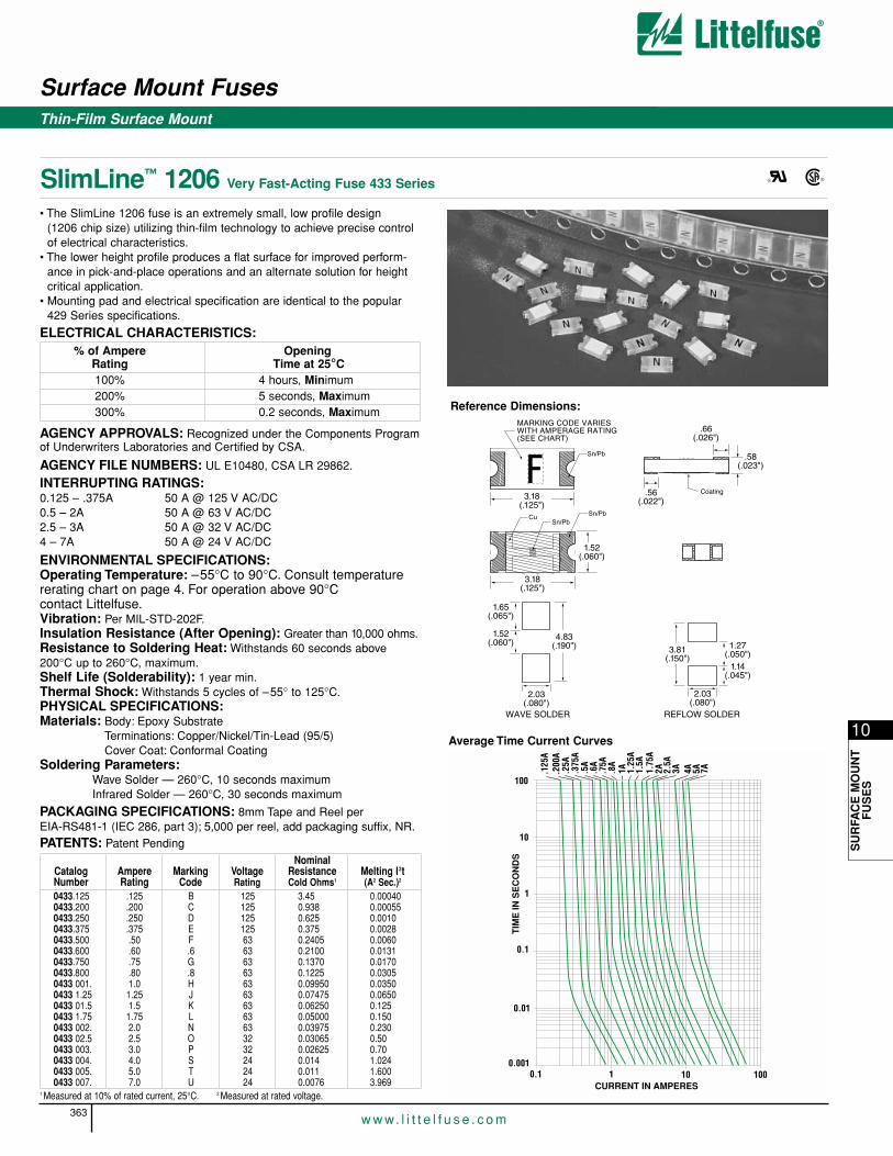
Thin-Film Surface Mount
363
Surface Mount Fuses
SlimLine™ 1206 Very Fast-Acting Fuse 433 Series
w w w. l i t t e l f u s e . c o m
10
SU
RFA
CE
MO
UN
TF
US
ES
• The SlimLine 1206 fuse is an extremely small, low profile design (1206 chip size) utilizing thin-film technology to achieve precise controlof electrical characteristics.
• The lower height profile produces a flat surface for improved perform-ance in pick-and-place operations and an alternate solution for heightcritical application.
• Mounting pad and electrical specification are identical to the popular429 Series specifications.
ELECTRICAL CHARACTERISTICS:% of Ampere Opening
Rating Time at 25°C100% 4 hours, Minimum200% 5 seconds, Maximum300% 0.2 seconds, Maximum
AGENCY APPROVALS: Recognized under the Components Programof Underwriters Laboratories and Certified by CSA.
AGENCY FILE NUMBERS: UL E10480, CSA LR 29862.
INTERRUPTING RATINGS:0.125 – .375A 50 A @ 125 V AC/DC0.5 – 2A 50 A @ 63 V AC/DC2.5 – 3A 50 A @ 32 V AC/DC4 – 7A 50 A @ 24 V AC/DC
ENVIRONMENTAL SPECIFICATIONS:Operating Temperature: –55°C to 90°C. Consult temperaturererating chart on page 4. For operation above 90°C contact Littelfuse.Vibration: Per MIL-STD-202F.Insulation Resistance (After Opening): Greater than 10,000 ohms.Resistance to Soldering Heat: Withstands 60 seconds above200°C up to 260°C, maximum.Shelf Life (Solderability): 1 year min.Thermal Shock: Withstands 5 cycles of –55° to 125°C.PHYSICAL SPECIFICATIONS:Materials: Body: Epoxy Substrate
Terminations: Copper/Nickel/Tin-Lead (95/5)Cover Coat: Conformal Coating
Soldering Parameters:Wave Solder — 260°C, 10 seconds maximumInfrared Solder — 260°C, 30 seconds maximum
PACKAGING SPECIFICATIONS: 8mm Tape and Reel per EIA-RS481-1 (IEC 286, part 3); 5,000 per reel, add packaging suffix, NR.PATENTS: Patent Pending
2.03(.080")
2.03(.080")
WAVE SOLDER REFLOW SOLDER
3.81(.150")
1.27(.050")
.58(.023")
.56(.022")
.66(.026")
1.14(.045")
MARKING CODE VARIES WITH AMPERAGE RATING(SEE CHART)
1.52(.060")
3.18(.125")
3.18(.125")
4.83(.190")
1.65(.065")
1.52(.060")
Sn/Pb
Sn/PbSn/Pb
Cu
Coating
Reference Dimensions:
® ®
TIM
E IN
SE
CO
ND
S
CURRENT IN AMPERES
0.01
0.1
0.1
1
1
10
100
10 1000.001
3A2.5A
2A1.75
A1.
5A1.
25A
1A.8A
.75A
.6A
.5A
.375
A.2
5A.2
00A
.125
A
4A 5A 7A
Average Time Current Curves
NominalCatalog Ampere Marking Voltage Resistance Melting I2tNumber Rating Code Rating Cold Ohms1 (A2 Sec.)2
0433.125 .125 B 125 3.45 0.000400433.200 .200 C 125 0.938 0.000550433.250 .250 D 125 0.625 0.00100433.375 .375 E 125 0.375 0.00280433.500 .50 F 63 0.2405 0.00600433.600 .60 .6 63 0.2100 0.01310433.750 .75 G 63 0.1370 0.01700433.800 .80 .8 63 0.1225 0.03050433 001. 1.0 H 63 0.09950 0.03500433 1.25 1.25 J 63 0.07475 0.06500433 01.5 1.5 K 63 0.06250 0.1250433 1.75 1.75 L 63 0.05000 0.1500433 002. 2.0 N 63 0.03975 0.2300433 02.5 2.5 O 32 0.03065 0.500433 003. 3.0 P 32 0.02625 0.700433 004. 4.0 S 24 0.014 1.0240433 005. 5.0 T 24 0.011 1.6000433 007. 7.0 U 24 0.0076 3.969
1 Measured at 10% of rated current, 25°C. 2 Measured at rated voltage.
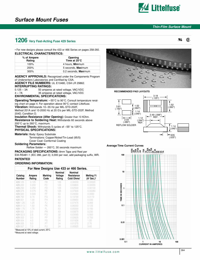
Thin-Film Surface Mount
364
Surface Mount Fuses
1206 Very Fast-Acting Fuse 429 Series
w w w. l i t t e l f u s e . c o m
Nominal NominalCatalog Ampere Marking Voltage Resistance Melting I2tNumber Rating Code Rating Cold Ohms1 (A2 Sec.)2
429.125 0.125 FB 125 2.30000 0.00020429.200 0.200 FC 125 0.93800 0.00055429.250 0.250 FD 125 0.62500 0.00100429.375 0.375 FE 125 0.37500 0.00280429.500 0.500 FF 63 0.24050 0.0060429.750 0.75 FG 63 0.13700 0.0170429 001 1.00 FH 63 0.09950 0.035429 1.25 1.25 FJ 63 0.07475 0.065429 01.5 1.50 FK 63 0.06250 0.125429 1.75 1.75 FL 63 0.05000 0.150429 002 2.0 FN 63 0.03975 0.230429 02.5 2.5 FO 32 0.03065 0.500429 003 3.0 FP 32 0.02625 0.700429 004 4.0 FS 24 0.01926 1.50429 005 5.0 FT 24 0.01375 2.70429 007 7.0 FU 24 0.00925 3.60
1 Measured at 10% of rated current, 25°C.2 Measured at rated voltage.
• For new designs please consult the 433 or 466 Series on pages 258-260.
ELECTRICAL CHARACTERISTICS:% of Ampere Opening
Rating Time at 25°C100% 4 hours, Minimum200% 5 seconds, Maximum300% 0.2 seconds, Maximum
AGENCY APPROVALS: Recognized under the Components Programof Underwriters Laboratories and Certified by CSA.AGENCY FILE NUMBERS: UL E10480, CSA LR 29862.INTERRUPTING RATINGS:0.125 – 3A 50 amperes at rated voltage, VAC/VDC4 – 7A 35 amperes at rated voltage, VAC/VDCENVIRONMENTAL SPECIFICATIONS:Operating Temperature: –55°C to 90°C. Consult temperature rerat-ing chart on page 4. For operation above 90°C contact Littelfuse.Vibration: Withstands 10–55 Hz per MIL-STD-202F,Method 201A and 10-2000 Hz at 20 G’s per MIL-STD-202F, Method204D, Condition D.Insulation Resistance (After Opening): Greater than 10 KOhm.Resistance to Soldering Heat: Withstands 60 seconds above200°C up to 260°C, maximum.Thermal Shock: Withstands 5 cycles of –55° to 125°C.PHYSICAL SPECIFICATIONS:Materials: Body: Epoxy Substrate
Terminations: Copper/Nickel/Tin-Lead (95/5)Cover Coat: Conformal Coating
Soldering Parameters:Reflow Solder — 260°C, 30 seconds maximum
PACKAGING SPECIFICATIONS: 8mm Tape and Reel per EIA-RS481-1 (IEC 286, part 3); 3,000 per reel, add packaging suffix, WR.
PATENTEDORDERING INFORMATION:
.2A
.25A
.375
A.5
A
.75A
1A 1.25
A1.
5A1.
75A
2A 2.5A
3A 4A 5A 7A
TIM
E IN
SE
CO
ND
S
CURRENT IN AMPERES
0.01
0.1
0.1
1
1
10
100
10 100
.125
A
0.001
Average Time Current Curves
REFLOW SOLDER
RECOMMENDED PAD LAYOUTS
3.81(.150")
1.52(.060")
2.03(.080")
.635(.025")
1.14(.045")
2.49 (.098")REF.
1.52(.060")
3.18(.125")
1.14(.045")
1.12(.044")REF.
® ®
For New Designs Use 433 or 466 Series.

Thin-Film Surface Mount
365
Surface Mount Fuses
1206 Slo-Blo® Fuse 430 Series
w w w. l i t t e l f u s e . c o m
10
SU
RFA
CE
MO
UN
TF
US
ES
ELECTRICAL CHARACTERISTICS:% of Ampere Opening
Rating Time @ 25°C
100% 4 hours, Minimum200% 1 sec., Min.; 120 sec., Max.300% 0.1 sec., Min.; 3 sec., Max.800% 0.002 sec., Min.; .05 sec., Max.
AGENCY APPROVALS: Recognized under the ComponentsProgram of Underwriters Laboratories and Certified by CSA.
AGENCY FILE NUMBERS: UL E10480, CSA LR 29862.
INTERRUPTING RATINGS:0.5A - 1.5A 50 amperes at 63 VAC/VDC2A 35 amperes at 63 VAC/VDC3A 50 amperes at 32 VAC/VDC
ENVIRONMENTAL SPECIFICATIONS:
Operating Temperature: –55°C to 90°C. Consult temperature rerating chart on page 4. For operation above 90°C contact Littelfuse.
Vibration: Withstands 10-55 Hz per MIL-STD-202F, Method 201A and10-2000 Hz at 20 G’s per MIL-STD-202F, Method 204D, Condition D.
Insulation Resistance (After Opening): Greater than 10,000 Ohms.
Resistance to Soldering Heat: Withstands 60 seconds above200°C up to 260°C, maximum.
Thermal Shock: Withstands 5 cycles of -50°C to +125°C.
PHYSICAL SPECIFICATIONS:Materials: Body: Epoxy Substrate
Terminations: Copper/Nickel/Tin-Lead (95/5)Cover Coat: Conformal Coating
Soldering Parameters:Reflow Solder: 260°C, 30 seconds maximum
PACKAGING SPECIFICATIONS: 8mm Tape and Reel per EIA-RS481-1 (IEC 286, part 3); 3,000 per reel, add packaging suffix,WR.
PATENTED
ORDERING INFORMATION:Amperage Voltage Nom. Cold Nominal
Catalog Rating Marking Rating Resistance Melting I2tNumber (A) Code (V) Cold Ohm1 (A2sec)2
0430.500 0.5 TF 63 .250 0.03050430 001. 1.0 TH 63 .097 0.1440430 01.5 1.5 TK 63 .056 0.2980430 002. 2.0 TN 63 .039 0.4940430 003. 3.0 TP 32 .020 1.33
1Measured at 10% of rated current, 25°C.2Measured at rated voltage.
TIM
E IN
SE
CO
ND
S
CURRENT IN AMPERES
0.01
0.1
0.1
1
1
10
100
10 1000.001
.5A
1A 1.5A
2A 3A
Average Time Current Curves
• Time delay feature withstands high in-rush currents and preventsnuisance openings.
• Package is visually distinct from fast-acting version for easy identification.
• Top side marking allows visual verification of amperage rating.
3.18 (.125")2.03 (.080")
REF.
1.52(.060")
1.52 (.060")3.81 (.150")
1.14(.045")
.635 (.025")
2.03(.080")
1.14 (.045")
REFLOW SOLDER
R .318(.013") REF.
Reference Dimensions:
® ®
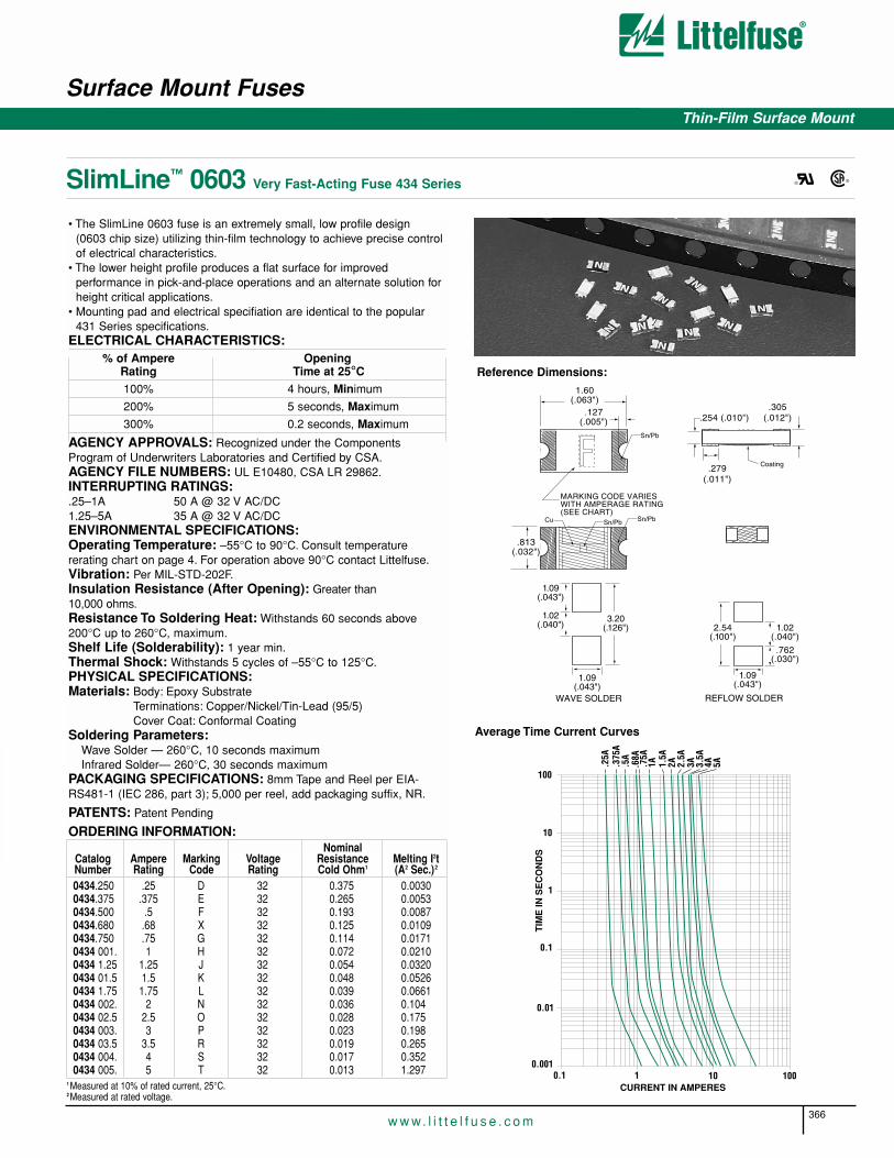
366
Surface Mount Fuses
w w w. l i t t e l f u s e . c o m
SlimLine™ 0603 Very Fast-Acting Fuse 434 Series ®®
• The SlimLine 0603 fuse is an extremely small, low profile design (0603 chip size) utilizing thin-film technology to achieve precise controlof electrical characteristics.
• The lower height profile produces a flat surface for improvedperformance in pick-and-place operations and an alternate solution forheight critical applications.
• Mounting pad and electrical specifiation are identical to the popular431 Series specifications.
ELECTRICAL CHARACTERISTICS:% of Ampere Opening
Rating Time at 25°C
100% 4 hours, Minimum
200% 5 seconds, Maximum
300% 0.2 seconds, Maximum
AGENCY APPROVALS: Recognized under the ComponentsProgram of Underwriters Laboratories and Certified by CSA.AGENCY FILE NUMBERS: UL E10480, CSA LR 29862.INTERRUPTING RATINGS:.25–1A 50 A @ 32 V AC/DC1.25–5A 35 A @ 32 V AC/DCENVIRONMENTAL SPECIFICATIONS:Operating Temperature: –55°C to 90°C. Consult temperature rerating chart on page 4. For operation above 90°C contact Littelfuse.Vibration: Per MIL-STD-202F.Insulation Resistance (After Opening): Greater than 10,000 ohms.Resistance To Soldering Heat: Withstands 60 seconds above200°C up to 260°C, maximum.Shelf Life (Solderability): 1 year min.Thermal Shock: Withstands 5 cycles of –55°C to 125°C.PHYSICAL SPECIFICATIONS:Materials: Body: Epoxy Substrate
Terminations: Copper/Nickel/Tin-Lead (95/5)Cover Coat: Conformal Coating
Soldering Parameters:Wave Solder — 260°C, 10 seconds maximumInfrared Solder— 260°C, 30 seconds maximum
PACKAGING SPECIFICATIONS: 8mm Tape and Reel per EIA-RS481-1 (IEC 286, part 3); 5,000 per reel, add packaging suffix, NR.
PATENTS: Patent Pending
ORDERING INFORMATION:
TIM
E IN
SE
CO
ND
S
CURRENT IN AMPERES
0.01
0.1
0.1
1
1
10
100
10 1000.001
3A2.5A
2A1.5A
1A.75A
.5A
.375
A.2
5A
3.5A
4A 5A.68A
Average Time Current Curves
NominalCatalog Ampere Marking Voltage Resistance Melting I2tNumber Rating Code Rating Cold Ohm1 (A2 Sec.)2
0434.250 .25 D 32 0.375 0.00300434.375 .375 E 32 0.265 0.00530434.500 .5 F 32 0.193 0.00870434.680 .68 X 32 0.125 0.01090434.750 .75 G 32 0.114 0.01710434 001. 1 H 32 0.072 0.02100434 1.25 1.25 J 32 0.054 0.03200434 01.5 1.5 K 32 0.048 0.05260434 1.75 1.75 L 32 0.039 0.06610434 002. 2 N 32 0.036 0.1040434 02.5 2.5 O 32 0.028 0.1750434 003. 3 P 32 0.023 0.1980434 03.5 3.5 R 32 0.019 0.2650434 004. 4 S 32 0.017 0.3520434 005. 5 T 32 0.013 1.297
1 Measured at 10% of rated current, 25°C.2 Measured at rated voltage.
1.09(.043")
REFLOW SOLDER
1.60(.063")
.127(.005")
MARKING CODE VARIES WITH AMPERAGE RATING(SEE CHART)
1.02(.040")
.762(.030")
2.54(.100")
1.09(.043")
WAVE SOLDER
3.20(.126")
1.09(.043")
1.02(.040")
.813(.032")
.305(.012")
.279(.011")
.254 (.010")
Sn/Pb
Sn/PbCu Sn/Pb
Coating
Reference Dimensions:
Thin-Film Surface Mount

Lead-Free Thin-Film
367
Surface Mount Fuses
SlimLine™ Lead-Free 0603 Very Fast-Acting Fuse 467 Series
w w w. l i t t e l f u s e . c o m
10
SU
RFA
CE
MO
UN
TF
US
ES
®®
• Complies with electronic industry environmental standards for lead reduction.
• Product is compatible with lead-free solders and higher temperature profiles.
• High performance materials provide improved performance in elevatedambient temperature applications.
• Product is marked on top surface with code to allow amperage ratingidentification without testing.
• Low profile for height sensitive applications.• Flat top surface for pick-and-place operations.• Element covering material is resistant to industry standard
cleaning operations.• Mounting pad and electrical performance is identical to Littelfuse 431
and 434 Series products.• Alloy based element construction provides superior inrush withstand
characteristics (I2t) over ceramic or glass based 0603 fuse products.ELECTRICAL CHARACTERISTICS:
1.09(.043")
REFLOW SOLDER
1.60(.063")
.305(.012")
.279(.011")
.18(.007")
.127(.005")
MARKING CODE VARIES WITH AMPERAGE RATING(SEE CHART)
R REF.
1.02(.040")
.762(.030")
2.54(.100")
1.09(.043")
WAVE SOLDER
3.20(.126")
1.09(.043")
1.02(.040")
.813(.032")
Sn
SnCu
Sn
Coating
Reference Dimensions:
% of Ampere OpeningRating Time at 25°C100% 4 hours, Minimum200% 5 seconds, Maximum300% 0.2 seconds, Maximum
Soldering Parameters:Wave Solder — 260°C, 10 seconds maxReflow Solder — 260°C, 30 seconds max
NEW
AGENCY APPROVALS: Recognized under the Components Programof Underwriters Laboratories and Certified by CSA.
AGENCY FILE NUMBERS: UL E10480, CSA LR 29862
INTERRUPTING RATINGS:0.25 – 1A 50A at 32V AC/DC1.25 – 5A 35A at 32V AC/DC
PHYSICAL SPECIFICATIONS:
Materials: Body: Advanced High Temperature SubstrateTerminations: Copper/Nickel/100% TinElement Cover Coat: Conformal Coating
Pb

Lead-Free Thin-Film
368
Surface Mount Fuses
SlimLine™ Lead-Free 0603 Very Fast-Acting Fuse 467 Series
w w w. l i t t e l f u s e . c o m
Average Time Current Curves
ENVIRONMENTAL SPECIFICATIONS:Operating Temperature: -550C - + 900C* For operation above 90°C contact Littelfuse
Vibration: Per MIL-STD-202F
Insulation Resistance (After Opening):Greater than 10,000 ohms.
Resistance to Soldering Heat: Withstands 60 seconds above2000C up to 2600C, maximum
Thermal Shock: Withstands 5 cycles of -550 to 1250C
PACKAGING SPECIFICATIONS:8mm Tape and Reel per EIA-RS481-2 (IEC 286, part 3); 5,000 per reel,add package suffix, NR.
Patents: Patended
Ordering Information:
Nominal NominalCatalog Ampere Marking Voltage Resistance1 Melting I2tNumber Rating Code Rating (Ω) (A2 Sec.)2
0467.250 .25 D 32 0.435 0.00300467.375 .375 E 32 0.275 0.00530467.500 .5 F 32 0.180 0.00870467.750 .75 G 32 0.112 0.01710467 001. 1 H 32 0.062 0.02120467 1.25 1.25 J 32 0.050 0.05180467 01.5 1.5 K 32 0.040 0.07660467 1.75 1.75 L 32 0.028 0.09030467 002. 2 N 32 0.024 0.11030467 02.5 2.5 O 32 0.020 0.14400467 003. 3 P 32 0.016 0.24030467 03.5 3.5 R 32 0.013 0.43060467 004. 4 S 32 0.011 0.57600467 005. 5 T 32 0.0085 0.9000
1 Measured at 10% of rated current, 25°C.2 Measured at rated voltage.
25°C
PE
RC
EN
T O
F R
AT
ING
*
AMBIENT TEMPERATURE248°F212°F176°F140°F104°F68°F32°F-4°F-40°F-76°F120°C100°C80°C60°C40°C20°C0°C-20°C-40°C-60°C
80
60
40
20
100
120
140
• Ambient temperature effects are in addition to the normal derating.
Typical effect of temperature on current carrying capacity.
TIM
E IN
SE
CO
ND
S
CURRENT IN AMPERES
0.01
0.1
0.1
1
1
10
100
10 1000.001
3 1/
2A3
A2
1/2A
2A1 3/
4A1
1/2A
1 1/
4A1A3/
4A
1/2A
3/8A
1/4A
4A 5A
Pb

10
SU
RFA
CE
MO
UN
TF
US
ES
Thin-Film Surface Mount
369
Surface Mount Fuses
w w w. l i t t e l f u s e . c o m
0603 Very Fast-Acting Fuse 431 Series
TIM
E IN
SE
CO
ND
S
CURRENT IN AMPERES
0.01
0.1
0.1
1
1
10
100
10 1000.001
5A2A1.5A
1A.75A
.5A
.375
A
.25A
2.5A
3A 4A3.5A
1.60 (.063")
.36 (.014")
.79 (.031")
.46 (.018")
R .20 (.008")
.43 (.017") REF.
1.04(.041")
REFLOW SOLDER
1.02 (.040")
.76 (.030")
1.09 (.043")
2.54(.100")
Reference Dimensions:
®®
OBSOLETE
• For new designs please use the 434 or 467 Series products.
ELECTRICAL CHARACTERISTICS:% of Ampere Opening
Rating Time at 25°C
100% 4 hours, Minimum
200% 5 seconds, Maximum
300% 0.2 seconds, Maximum
AGENCY APPROVALS: Recognized under the ComponentsProgram of Underwriters Laboratories and Certified by CSA.
AGENCY FILE NUMBERS: UL E10480, CSA LR 29862.
INTERRUPTING RATINGS:.25–1A 50 amperes at 32 VAC/VDC1–5A 35 amperes at 32 VAC/VDC
ENVIRONMENTAL SPECIFICATIONS:
Operating Temperature: –55°C to 90°C. Consult temperature rerating chart on page 4. For operation above 90°C contact Littelfuse.
Vibration: Withstands 10-55 HZ per MIL-STD-202F, Method 201A and 10-2000 HZ at 20 G’s per MIL-STD-202F, Method 204D, Condition D.
Insulation Resistance (After Opening):Greater than 500,000 ohms.
Resistance To Soldering Heat: Withstands 60 seconds above200°C up to 260°C, maximum.
Thermal Shock: Withstands 5 cycles of –50°C to 125°C.
PHYSICAL SPECIFICATIONS:
Materials: Body: Epoxy SubstrateTerminations: Copper/Nickel/Tin-Lead (95/5)Cover Coat: Conformal Coating
Soldering Parameters:Reflow Solder— 260°C, 30 seconds maximum
PACKAGING SPECIFICATIONS: 8mm Tape and Reel per EIA-RS481-1 (IEC 286, part 3); 5,000 per reel, add packaging suffix, NR.
PATENTED
ORDERING INFORMATION:
For New Designs Use 434 or 467 Series.Nominal
Catalog Ampere Voltage Resistance Melting I2tNumber Rating Rating Cold Ohm1 (A2 Sec.)431.250 0.25 32 0.375 0.0030431.375 0.375 32 0.265 0.0053431.500 0.5 32 0.193 0.0087431.750 0.75 32 0.114 0.0171431 001 1 32 0.072 0.0210431 01.5 1.5 32 0.048 0.0526431 002 2 32 0.036 0.104431 02.5 2.5 32 0.028 0.175431 003 3 32 0.023 0.198431 03.5 3.5 32 0.019 0.265431 004 4 32 0.017 0.352431 005 5 32 0.013 1.600
1 Measured at 10% of rated current, 25°C.
Average Time Current Curves
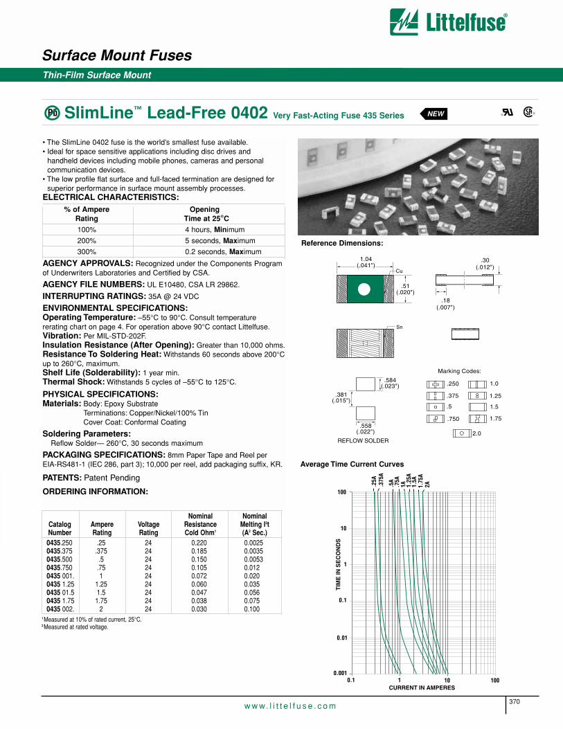
370
Surface Mount Fuses
w w w. l i t t e l f u s e . c o m
Thin-Film Surface Mount
SlimLine™ Lead-Free 0402 Very Fast-Acting Fuse 435 Series
• The SlimLine 0402 fuse is the world’s smallest fuse available.• Ideal for space sensitive applications including disc drives and
handheld devices including mobile phones, cameras and personalcommunication devices.
• The low profile flat surface and full-faced termination are designed forsuperior performance in surface mount assembly processes.
ELECTRICAL CHARACTERISTICS:% of Ampere Opening
Rating Time at 25°C
100% 4 hours, Minimum
200% 5 seconds, Maximum
300% 0.2 seconds, Maximum
AGENCY APPROVALS: Recognized under the Components Programof Underwriters Laboratories and Certified by CSA.
AGENCY FILE NUMBERS: UL E10480, CSA LR 29862.
INTERRUPTING RATINGS: 35A @ 24 VDC
ENVIRONMENTAL SPECIFICATIONS:Operating Temperature: –55°C to 90°C. Consult temperature rerating chart on page 4. For operation above 90°C contact Littelfuse.Vibration: Per MIL-STD-202F.Insulation Resistance (After Opening): Greater than 10,000 ohms.Resistance To Soldering Heat: Withstands 60 seconds above 200°Cup to 260°C, maximum.Shelf Life (Solderability): 1 year min.Thermal Shock: Withstands 5 cycles of –55°C to 125°C.
PHYSICAL SPECIFICATIONS:Materials: Body: Epoxy Substrate
Terminations: Copper/Nickel/100% TinCover Coat: Conformal Coating
Soldering Parameters:Reflow Solder— 260°C, 30 seconds maximum
PACKAGING SPECIFICATIONS: 8mm Paper Tape and Reel per EIA-RS481-1 (IEC 286, part 3); 10,000 per reel, add packaging suffix, KR.
PATENTS: Patent Pending
ORDERING INFORMATION:
Nominal NominalCatalog Ampere Voltage Resistance Melting I2tNumber Rating Rating Cold Ohm1 (A2 Sec.)0435.250 .25 24 0.220 0.00250435.375 .375 24 0.185 0.00350435.500 .5 24 0.150 0.00530435.750 .75 24 0.105 0.0120435 001. 1 24 0.072 0.0200435 1.25 1.25 24 0.060 0.0350435 01.5 1.5 24 0.047 0.0560435 1.75 1.75 24 0.038 0.0750435 002. 2 24 0.030 0.100
1 Measured at 10% of rated current, 25°C.2 Measured at rated voltage.
TIM
E IN
SE
CO
ND
S
CURRENT IN AMPERES
0.01
0.1
0.1
1
1
10
100
10 1000.001
2A1.5A
1.25
A1A.5
A
.25A
.375
A
.75A
1.75
A.558
(.022")
REFLOW SOLDER
1.04(.041")
.30(.012")
.18(.007")
Cu
Sn
.51(.020")
.381(.015")
.584(.023")
Marking Codes:
.250
.375
.5
.750
1.0
1.25
1.5
1.75
2.0
Reference Dimensions:
Average Time Current Curves
®®Pb NEW

10
SU
RFA
CE
MO
UN
TF
US
ES
371
Surface Mount Fuses
w w w. l i t t e l f u s e . c o m
Subminiature Surface Mount
NANO2® FUSE Very Fast-Acting 451/453 Series
The Nano2 SMF Fuse is a very small, square surface mount fuse that isalso available in a surface mount holder.• RoHS Compliant version now available, use ordering suffix ‘L’
(see example on data sheet).ELECTRICAL CHARACTERISTICS:
% of Ampere Ampere OpeningRating Rating Time
100% 1/16–15 4 hours, Minimum
200%1/16–10 5 seconds, Maximum12–15 20 seconds, Maximum
AGENCY APPROVALS: Recognized under the Components Programof Underwriters Laboratories and Certified by CSA. Approved by METIfrom 1 through 5 amperes.
AGENCY FILE NUMBERS: UL E10480, CSA LR 29862.INTERRUPTING RATINGS:1/16 – 8A 50 amperes at 125 VAC/VDC
300 amperes at 32 VDC10A 35 amperes at 125 VAC/50 amperes at 125 VDC
300 amperes at 32 VDC12A – 15A 50 amperes at 65 VAC/VDC
300 amperes at 24 VDC
ENVIRONMENTAL SPECIFICATIONS:Operating Temperature: –55°C to 125°C.Shock: MIL-STD-202, Method 213, Test Condition I(100 G’s peak for 6 milliseconds).Vibration: MIL-STD-202, Method 201 (10–55 Hz).Salt Spray: MIL-STD-202, Method 101, Test Condition B.Insulation Resistance (After Opening): MIL-STD-202, Method302, Test Condition A, (10,000 ohms minimum).Resistance to Soldering Heat: MIL-STD-202, Method 210, Test Condition B (10 sec. at 260°C).Thermal Shock: MIL-STD-202, Method 107, Test Condition B (–65 to 125°C).Moisture Resistance: MIL-STD-202, Method 106, High Humidity (90-98 RH), Heat (65°C).
100
10
1
0.1
0.01
0.001
1/16
A
1/8A
1/4A
3/8A
1/2A
3/4A
1A 1 1/
2A2A 2
1/2A
3A 3 1/
2A4A 5A 7A 10
A12
A15
A
0.05 0.1 1 10 100 1000
TIM
E IN
SE
CO
ND
S
CURRENT IN AMPERES
Average Time Current Curves
F
7 A
6.86(.270")
3.15(.124")
2.95(.116")1.96
(.077")
2.69(.106")
2.69(.106")
1.45(.057")
6.10(.240")
Recommended pad layout
Tin-Lead Silver Nominal NominalPlated Plated Ampere Voltage Resistance Melting I2t
Catalog # Catalog # Rating Rating Cold Ohms A2 Sec.– R451.062 0.062 125 5.50 0.00019– R451.080 0.080 125 4.05 0.00033– R451.100 0.100 125 3.10 0.00138– R451.125 0.125 125 1.70 0.00286
R451.160 0453.160 0.160 125 1.80 0.00306R451.200 0453.200 0.200 125 1.40 0.00652R451.250 0453.250 0.250 125 1.05 0.01126R451.315 0453.315 0.315 125 0.78 0.0231R451.375 0453.375 0.375 125 0.610 0.0425R451.400 0453.400 0.400 125 0.560 0.0484R451.500 0453.500 0.500 125 0.420 0.0795R451.630 0453.630 0.630 125 0.305 0.143R451.750 0453.750 0.750 125 0.245 0.185R451.800 0453.800 0.800 125 0.212 0.271R451 001. 0453 001. 1.0 125 0.153 0.459R451 1.25 0453 1.25 1.25 125 0.0780 0.664R451 01.5 0453 01.5 1.5 125 0.0630 0.853R451 01.6 0453 01.6 1.6 125 0.0580 1.060R451 002. 0453 002. 2.0 125 0.0367 0.530R451 02.5 0453 02.5 2.5 125 0.0286 1.029R451 003. 0453 003. 3.0 125 0.0227 1.650R451 3.15 0453 3.15 3.15 125 0.0215 1.920R451 03.5 0453 03.5 3.5 125 0.0200 2.469R451 004. 0453 004. 4 125 0.0160 3.152R451 005. 0453 005. 5 125 0.0125 5.566R451 06.3 0453 06.3 6.3 125 0.0096 9.17R451 007. 0453 007. 7 125 0.0090 10.32R451 008. 0453 008. 8 125 0.0077 20.23R451 010. 0453 010. 10 125 0.0056 26.46R451 012. 0453 012. 12 65 0.0049 47.97R451 015. 0453 015. 15 65 0.0037 97.82
PHYSICAL SPECIFICATIONS:Materials: Body: Ceramic
Terminations: Tin-Lead Alloy or Silver Plated CapsRoHS Compliant Terminations: Gold over Nickel Plated Caps
Soldering Parameters:Wave Solder — 260°C, 10 seconds maximumReflow Solder — 260°C, 30 seconds maximum
Solderability: MIL-STD-202, Method 208.PACKAGING SPECIFICATIONS: 12mm Tape and Reel per EIA-RS481-1 (IEC 286, part3); 1,000 pieces per reel, add packaging suffix, MR; 5,000 per reel, add packaging suffix NR.Options: For RoHS Compliant devices add the letter ‘L’ to end of packag-ing suffix. Example: R451001.NRL (RoHS Compliant 1A, 5,000 per reel).
PATENTED
® ®
Refer to pg. 374 for SMF Omni-Blok® Holder, Series 154 000.

372
Surface Mount Fuses
w w w. l i t t e l f u s e . c o m
Subminiature Surface Mount
NANO2®Slo-Blo® Fuse 452/454 Series
Tin-Lead Silver Nominal NominalPlated Plated Ampere Voltage Resistance Melting I2t
Catalog # Catalog # Rating Rating Cold Ohms A2 Sec.R452.375 0454.375 3/8 125 1.20 0.101R452.500 0454.500 1/2 125 0.700 0.240R452.750 0454.750 3/4 125 0.360 0.904R452 001. 0454 001. 1 125 0.225 1.98R452 01.5 0454 01.5 11/2 125 0.0930 3.65R452 002. 0454 002. 2 125 0.0625 8.20R452 02.5 0454 02.5 21/2 125 0.0450 15.0R452 003. 0454 003. 3 125 0.0340 20.16R452 03.5 0454 03.5 31/2 125 0.0224 26.53R452 004. 0454 004. 4 125 0.0186 34.40R452 005. 0454 005. 5 125 0.0136 53.72
The NANO2 Slo-Blo fuse has enhanced inrush withstand characteristicsover the NANO2 Fast-Acting fuse. The unique time delay feature of thisfuse design helps solve the problem of nuisance “opening” by accommo-dating inrush currents that normally cause a fast-acting fuse to open.• RoHS Compliant version now available, use ordering suffix ‘L’
(see example on data sheet).ELECTRICAL CHARACTERISTICS:
% of Ampere OpeningRating Time
100% 4 hours, Minimum
200% 1 second, Min.; 60 seconds, Max.
300% 0.2 seconds, Min.; 3 seconds, Max.800% 0.02 seconds, Min.; 0.1 seconds, Max.
AGENCY APPROVALS: Recognized under the Components Programof Underwriters Laboratories and Certified by CSA.AGENCY FILE NUMBERS: UL E10480, CSA LR 29862.INTERRUPTING RATINGS:50 amperes at 125 VAC/VDCENVIRONMENTAL SPECIFICATIONS:Operating Temperature: –55°C to 125°C.Shock: MIL-STD-202, Method 213, Test Condition I (100 G’s peak for 6 milliseconds).Vibration: MIL-STD-202, Method 201 (10–55 Hz, .06 in. total excursion).Salt Spray: MIL-STD-202, Method 101, Test Condition B (48 hrs.).Insulation Resistance (After Opening): MIL-STD-202, Method 302, Test Condition A, (10,000 ohms minimum).Resistance to Soldering Heat: MIL-STD-202, Method 210, (3 sec. at 260°C).Thermal Shock: MIL-STD-202, Method 107, Test Condition B (–65 to 125°C).Moisture Resistance: MIL-STD-202, Method 106, High Humidity (90-98 RH), Heat (65°C).PHYSICAL SPECIFICATIONS:Materials: Body: Ceramic
Terminations: Tin-Lead Alloy or Silver Plated CapsRoHS Compliant Terminations: Gold over Nickel Plated Caps
Soldering Parameters:Wave Solder — 260°C, 3 seconds maximumReflow Solder — 230°C, 30 seconds maximum
Solderability: MIL-STD-202, Method 208.PACKAGING SPECIFICATIONS: 12mm Tape and Reel per EIA-RS481-1 (IEC 286, part3); 1,000 pieces per reel, add packaging suffix, MR; 5,000 per reel, add packaging suffix NR.Options: For RoHS Compliant devices add the letter ‘L’ to end of packag-ing suffix. Example: 0455001.NRL (RoHS Compliant 1A, 5,000 per reel).PATENTEDORDERING INFORMATION:
1000
100
10
1
0.1
0.0110001001010.1
3/8A
1/2A
3/4A
1A 1 1/
2A2A 2
1/2A
3A 3 1/
2A4A 5A
TIM
E IN
SE
CO
ND
S
CURRENT IN AMPERES
Refer to pg. 271 for SMF Omni-Blok® Holder, Series 154 000T.
® ®
Average Time Current Curves
1 AT
6.86(.270")
3.15(.124")
2.95(.116")1.96
(.077")
2.69(.106")
2.69(.106")
1.45(.057")
6.10(.240")
Recommended pad layout
F
10
SU
RFA
CE
MO
UN
TF
US
ES
373
Surface Mount Fuses
w w w. l i t t e l f u s e . c o m
Subminiature Surface Mount
NANO2® UMF Fast-Acting Fuse 455 Series
• The Nano2 UMF Fuse is a very small, square surface mount fuse design.• Designed to International (IEC) Standards for use globally.• Meets IEC 60127-4 UMF specifications for Fast-Acting Fuses• RoHS Compliant version now available, use ordering suffix ‘L’
(see example on data sheet).
ELECTRICAL CHARACTERISTICS:% of Ampere Opening
Rating Time
125% 1 hour, Minimum
200% 2 minutes, Maximum
1000% 0.001 sec, Min; .01 sec Max
AGENCY APPROVALS: Listed to IEC 60127-4, Universal Modular Fuse-Links (UMF), 125V.
AGENCY FILE NUMBERS: UL E184655.
INTERRUPTING RATINGS: 50 amperes at 125 VAC/VDC
ENVIRONMENTAL SPECIFICATIONS:Operating Temperature: –55°C to 125°C.
Shock: MIL-STD-202, Method 213, Test Condition I (100 G’s peak for 6 milliseconds).
Vibration: MIL-STD-202, Method 201 (10–55 Hz).
Salt Spray: MIL-STD-202, Method 101, Test Condition B.
Insulation Resistance (After Opening): MIL-STD-202, Method302, Test Condition A, (10,000 ohms minimum).
Resistance to Soldering Heat: MIL-STD-202, Method 210, Test Condition B (10 sec. at 260°C).
Thermal Shock: MIL-STD-202, Method 107, Test Condition B (–65 to 125°C).
Moisture Resistance: MIL-STD-202, Method 106, High Humidity (90-98 RH), Heat (65°C).
PHYSICAL SPECIFICATIONS:Materials: Body: Ceramic
Terminations: Tin-Lead AlloyRoHS Compliant Terminations: Gold over Nickel Plated Caps
.Soldering Parameters:Wave Solder — 260°C, 10 seconds maximumReflow Solder — 260°C, 30 seconds maximum
Solderability: MIL-STD-202, Method 208.
PACKAGING SPECIFICATIONS: 12mm Tape and Reel per EIA-RS481-1 (IEC 286, part3); 1,000 pieces per reel, add packaging suffix, MR; 5,000 per reel, add packaging suffix NR.
Options: For RoHS Compliant devices add the letter ‘L’ to end of packag-ing suffix. Example: 0455001.NRL (RoHS Compliant 1A, 5,000 per reel).
PATENTEDORDERING INFORMATION:
100
10
1
0.1
0.01
0.001
.5A
1A 1.6A
0.05 0.1 1 10 100 1000
TIM
E IN
SE
CO
ND
S
CURRENT IN AMPERES
.4A
Average Time Current Curves
F1 A
2.69(.106")
2.69(.106")
1.45(.057")
6.10(.240")
Nominal NominalCatalog Ampere Voltage Cold Resistance Melting I2tNumber Rating Rating (Ohms)1 (A2 sec)
0455.400 0.4 125 0.420 0.07950455.500 0.5 125 0.305 0.1430455 001. 1.0 125 0.078 0.6450455 01.6 1.6 125 0.0532 1.060
1Measured at 10% of rated current, 25°C.
6.86(.270")
3.15(.124")
2.95(.116")1.96
(.077")
Recommended pad layout

374w w w. l i t t e l f u s e . c o m
For NANO2® Surface Mount Fuses
Fuse Blocks and Clips
SMF OMNI-BLOK® Fuse Block Molded Base Type 154 Series
With Very Fast-Acting Fuse InstalledCatalog Ampere FuseNumber Rating Furnished1
154.062 1/16 0453.062154.125 1/8 0453.125154.250 1/4 0453.250154.375 3/8 0453.375154.500 1/2 0453.500154.750 3/4 0453.750154 001 1 0453 001.154 01.5 1.5 0453 01.5154 002 2 0453 002.154 02.5 2.5 0453 02.5154 003 3 0453 003.154 03.5 3.5 0453 03.5154 004 4 0453 004.154 005 5 0453 005.154 007 7 0453 007.154 008 8 0453 008.154 010 10 0453 010.
With Slo-Blo® Fuse InstalledCatalog Ampere FuseNumber Rating Furnished2
154.375T 3/8 0454.375154.500T 1/2 0454.500154.750T 3/4 0454.750154 001T 1 0454 001.154 01.5T 11/2 0454 01.5154 002T 2 0454 002.154 02.5T 21/2 0454 02.5154 003T 3 0454 003.154 03.5T 31/2 0454 03.5154 004T 4 0454 004.154 005T 5 0454 005.
1 453 Series Fuse has silver plated end caps, installed to accommodate solder reflow process.Use either 451 or 453 Series for replacement purposes, page 371.
2 454 Series Fuse has silver plated end caps, installed to accommodate solder reflow process.Use either 452 or 454 Series for replacement purposes, page 372.
The SMF Omni-Blok® Fuseholder permits quick and easy replacement of Nano2® SMF surface mount fuses. The fuse block and pre-installedfuse combination can be placed on the PC board in one efficient manufacturing operation. Fuse replacement is accomplished withoutexposing the PC board to the detrimental effects of solder heat. Refer to notes 1 and 2, below, for fuse/fuseholder combinations available.
APPROVALS: Recognized under the Components Program ofUnderwriters Laboratories and Certified by CSA.
SPECIFICATIONS:Electrical: 8 Amperes, 125 Volts.Molded Parts: Thermoplastic (94V0).Terminals: Tin/Lead Alloy Plated Beryllium Copper.Ambient Temperature: –55°C to +125°C.Shock: MIL-STD-202, Method 213, Test Condition I (100 G’s peak for 6 milliseconds).Vibration: MIL-STD-202, Method 201 (10–55 Hz).Thermal Shock: MIL-STD-202, Method 107, Condition A (200 cycles: 30 minutes at –55°C, 30 minutes at 125°C).Soldering Parameters (Fuse Installed):
Reflow — 154 000: 500°F (260°C), 30 sec.154 000T: 445°F (230°C), 30 sec.
Solderability: MIL-STD-202, Method 208.Packaging: 16mm Tape and Reel for use with automatic pick andplace equipment per EIA Standard 481; 1,500 per reel, add suffix DR.
PATENTEDORDERING INFORMATION:
LF7 A
L F
3.81(.150")2.13
(.084")REF.
10.62(.418")
4.24(.167")
9.73(.383") REF.
3.81(.150")
5.03(.198")
1 5 5
FUSE
Recommended Pad Layout
® ®

10
SU
RFA
CE
MO
UN
TF
US
ES
Nominal NominalCatalog Ampere Voltage Cold Resistance Melting I2tNumber Rating Rating (Ohms) (A2 sec)
0464.500 0.5 250 0.283 0.30464 001. 1.0 250 0.100 0.80464 1.25 1.25 250 0.059 1.20464 01.6 1.6 250 0.048 1.90464 002. 2.0 250 0.038 2.8 0464 02.5 2.5 250 0.032 4.50464 3.15 3.15 250 0.024 9.4 0464 004. 4.0 250 0.018 15.1 0464 005. 5.0 250 0.014 23.1 0464 06.3 6.3 250 0.011 40.0
*For information and availability of additional ratings please contact Littelfuse
375
Surface Mount Fuses
w w w. l i t t e l f u s e . c o m
NEW
• The Surface Mount Nano2 250V UMF product family complies with IECPublication IEC 60127-4-Universal Modular Fuse-Links [UMF]. This IEC standard has been accepted by UL/CSA making it the first global fuse standard.
• The Nano2 250V UMF fuse family is based on the proven NANO2
Fuse product technology.• Product is RoHS Compliant and compatible with lead-free solders and
higher temperature profiles.
ELECTRICAL CHARACTERISTICS:% of Ampere Opening
Rating Time
125% 1 hour, Minimum
200% 2 minutes, Maximum
1000% 0.001 sec, Min; 0.01 sec Max
AGENCY APPROVALS: Listed to IEC 60127-4, Universal Modular Fuse-Links (UMF), 250V. UL Listed. Approved by METI and CCC. K and VDEapprovals pending.
AGENCY FILE NUMBERS: UL E184655. METI NBK30502-E184655a,b.
INTERRUPTING RATINGS: 100 amperes at 250VAC
ENVIRONMENTAL SPECIFICATIONS:Operating Temperature: –55°C to 125°C.
Shock: MIL-STD-202, Method 213, Test Condition A.
Vibration: MIL-STD-202, Method 201 (10–55 Hz).
Insulation Resistance (After Opening): IEC60127-4 (0.1MΩ min@ 500VDC).
Resistance to Soldering Heat: IEC60127-4.
Thermal Shock: MIL-STD-202, Method 107, Test Condition B (–65 to 125°C, 5 cycles).
Moisture Resistance: MIL-STD-202, Method 106
PHYSICAL SPECIFICATIONS:Materials: Body: High Performance Ceramic
Terminations: Silver plated brass.Soldering Parameters:
Wave Solder — 260°C, 10 seconds maximumReflow Solder — 260°C, 30 seconds maximum
Solderability: IEC60127-4.
PACKAGING SPECIFICATIONS: 24mm Tape and Reel per EIA-RS481-1 (IEC 286, part 3); 1,500 per reel, add packaging suffix, DR.
PATENTEDORDERING INFORMATION:
Reference Dimensions:
REFLOW SOLDER
F
2.8(.11")
12.1(.475")
4.5 (.177")
6.7(.264")
6.8(.264")
WAVE SOLDER3.5
(.14")
AC250VF500mAL
6.9(.27")
5.6 (.22")
5.6(.22")
4.5(.177")
Height
END CAP
TOP VIEW
Subminiature Surface Mount
NANO2® 250V UMF FUSE Fast-Acting 464 Series
100
100
10
1
0.1
0.01
0.0011 10 10000.1
1 A
1.25
A1.
6 A
2 A
2.5
A3.
15 A
TIM
E IN
SE
CO
ND
S
CURRENT IN AMPERES
4 A
5 A
6.3
A
.8 A
.63
A.5
A
Average Time Current Curves
VD E
®UL

Nominal NominalCatalog Ampere Voltage Cold Resistance Melting I2tNumber Rating Rating (Ohms) (A2 sec)
0465 001. 1.0 250 0.107 2.80465 1.25 1.25 250 0.083 5.60465 01.6 1.6 250 0.056 9.20465 002. 2.0 250 0.039 14.9 0465 02.5 2.5 250 0.026 21.00465 3.15 3.15 250 0.021 31.7 0465 004. 4.0 250 0.016 48.4 0465 005. 5.0 250 0.0130 87.0 0465 06.3 6.3 250 0.0088 144.4
*For information and availability of additional ratings please contact Littelfuse
Subminiature Surface Mount
376
Surface Mount Fuses
w w w. l i t t e l f u s e . c o m
NANO2® 250V UMF FUSE Time Lag 465 Series NEW
Reference Dimensions:
REFLOW SOLDER
F
2.8(.11")
12.1(.475")
4.5 (.177")
6.7(.264")
6.8(.264")
WAVE SOLDER3.5
(.14")
AC250VT500mAL
6.9(.27")
5.6 (.22")
5.6(.22")
4.5(.177")
Height
END CAP
TOP VIEW
• The Surface Mount Nano2 250V UMF product family complies with IECPublication IEC 60127-4-Universal Modular Fuse-Links [UMF]. This IEC standard has been accepted by UL/CSA making it the first globalfuse standard.
• The Nano2 250V UMF fuse family is based on the proven NANO2 Fuseproduct technology.
• Product is RoHS Compliant and compatible with lead-free solders andhigher temperature profiles.
ELECTRICAL CHARACTERISTICS:% of Ampere Opening
Rating Time
125% 1 hour, Minimum
200% 2 minutes, Maximum
1000% 0.01 sec, Min; 0.1 sec Max
AGENCY APPROVALS: Listed to IEC 60127-4, Universal Modular Fuse-Links (UMF), 250V. UL Listed. Approved by METI and CCC. K and VDEapprovals pending.
AGENCY FILE NUMBERS: UL E184655. METI NBK30502-E184655a,b.
INTERRUPTING RATINGS: 100 amperes at 250VAC
ENVIRONMENTAL SPECIFICATIONS:Operating Temperature: –55°C to 125°C.
Shock: MIL-STD-202, Method 213, Test Condition A.
Vibration: MIL-STD-202, Method 201 (10–55 Hz).
Insulation Resistance (After Opening): IEC60127-4 (0.1MΩ min@ 500VDC).
Resistance to Soldering Heat: IEC60127-4.
Thermal Shock: MIL-STD-202, Method 107, Test Condition B (–65 to 125°C, 5 cycles).
Moisture Resistance: MIL-STD-202, Method 106
PHYSICAL SPECIFICATIONS:Materials: Body: High Performance Ceramic
Terminations: Silver plated brass.Soldering Parameters:
Wave Solder — 260°C, 10 seconds maximumReflow Solder — 260°C, 30 seconds maximum
Solderability: IEC60127-4.
PACKAGING SPECIFICATIONS: 24mm Tape and Reel per EIA-RS481-1 (IEC 286, part 3); 1,500 per reel, add packaging suffix, DR.
PATENTEDORDERING INFORMATION:
100
100
10
1
0.1
0.01
0.0011 10 10000.1
1 A
1.25
A1.
6 A
2 A
2.5
A3.
15 A
TIM
E IN
SE
CO
ND
S
CURRENT IN AMPERES
4 A
5 A
6.3
A
Average Time Current Curves
VD E
®UL

10
SU
RFA
CE
MO
UN
TF
US
ES
Telecom NANO2® Fuse 461 Series and Teccor TeleLink® Fuse ® ®
LF 1.25A T3.12
(.123")
3.12(.123")
10.10(.397")
3.25(.128")
3.43(.135")
12.6(.496")
6.10(.240")
Recommended Pad Layout1.70 typ(.067")
• Surface mount surge resistant Slo-Blo® fuse.• Meets UL 60950 3rd Edition power cross requirements stand
alone.• Designed to allow compliance with Telcordia GR-1089-CORE
and TIA-968-A (formerly FCC Part 68) Surge Specifications.• Provides coordinated protection with Littelfuse SIDACtor®
Protection Thyristors without series resistors.• Ideal for use in telecommunication equipment including line
cards, modems, fax machines, phones, answering machines,caller ID devices and other products connected to phone network.
• 2A rating has improved temperature rise performance under2.2A surge current testing when compared with 1.25A rating.
• Product is RoHS Compliant and compatible with lead-freesolders and higher temperature profiles when ordered withStandard Silver Plated Brass Caps.
• Standard product is RoHS Compliant and compatible withlead-free solders and higher temperature profiles.
Telecom TeccorNano2 TeleLink Nominal Nominal
Catalog Catalog Ampere Voltage Resistance Melting I2tNumber Number Rating Rating Cold Ohms A2 Sec.0461.500 F0500T 0.5 250 .560 .8401
0461 1.25 F1250T 1.25 250 .110 16.51
0461 002. F1251T 2.00 250 .050 17.51
ORDERING INFORMATION:
1 I2t is calculated at 10 msec or less. I2t at 10 times rated current has a typical value of:24 A2sec (2.0A), 22 A2sec (1.25A), 1.3 A2sec (0.5A).
AGENCY APPROVALS: Recognized under the ComponentsProgram of Underwriters Laboratories and Certified by CSA.
Littelfuse: UL E10480CSA LR29862
Teccor: UL E191008CSA LR702828
PHYSICAL SPECIFICATIONS:Materials: Body: Ceramic
RoHS Compliant Terminations: Silver Plated Brass Caps Terminations: Tin-Lead Alloy also available, add suffix, T.
Soldering Parameters:Reflow Solder — 230°C, 30 seconds maximum.Wave Solder — 260°C, 3 seconds maximum.
PACKAGING SPECIFICATIONS: 24mm Tape and Reel per EIA-RS481-2, (IEC 286 part 3); 2500 fuses per reel, add suffix, ER.
Reference Dimensions:
10001001010.10.001
0.01
0.1
1
10
100
CURRENT IN AMPERES
TIM
E IN
SEC
ONDS
1.25
A
2A.500
A
Miniature Surface Mount
377
Surface Mount Fuses
w w w. l i t t e l f u s e . c o m
Miniature Surface Mount
378
Surface Mount Fuses
w w w. l i t t e l f u s e . c o m
® ®
Maximum Temperature Rise:Telecom Nano2 Fuse Temperature Reading
04611.25 < 82˚C (180˚F)0461002. < 50˚C (122˚F)
• Higher Currents and PCB layout designs can affect this parameter.Readings are measured at rated current after temperature stabilizes.
Telecom NANO2® Fuse 461 Series and Teccor TeleLink® Fuse
INTERRUPTING RATINGS:50 amperes at 250 VAC.
PE
RC
EN
T O
F R
AT
ING
*
AMBIENT TEMPERATURE248°F212°F176°F140°F104°F68°F32°F-4°F-40°F-76°F120°C100°C80°C60°C40°C20°C0°C-20°C-40°C-60°C
80
60
40
20
100
120
140
Operating Temperature is -55˚C to +125˚C with proper correction factor applied
• Ambient temperature effects are in addition to the normal derating.
Temperature Derating Curve
Surge Minimum Minimum Max Repetitions FusePeak Peak Rise/Min. Each Choices
Voltage Current Decay Polarity (V) (A) (µs)
1 600 100 10/1000 25 1.25, 2.02 1000 100 10/360 25 1.25, 2.03 1000 100 10/1000 25 1.25, 2.04 2500 500 2/10 10 1.25, 2.05 1000 25 10/360 5 0.5, 1.25, 2.0
If sufficient series resistance is used, then the 0.5 fuse may be used in test conditions 1-4.
GR 1089 Inter-building requirements
GR 1089 1st level lighting surge inter-building (Equipment under test can not be damaged & must continue to operate properly)
GR 1089 AC power fault 2nd level (fuse can open but mustopen in a safe and controlled manner)
Test Vrms Short Duration FuseCircuit (A)
1 120, 277 25 15 min. 0.5, 1.25, 2.02 600 60 5 sec. 0.5, 1.25, 2.03 600 7 5 sec. 0.5, 1.25, 2.04 100-600 2.2 15 min.. 0.5, 1.25, 2.05 Diagram Diagram 15 min. 0.5, 1.25, 2.0
Fuse must open before wiring simulator fuse (MDL 2.0).
ELECTRICAL CHARACTERISTICS:
% of AmpereRating OpeningTime
100% 4 hours, Min.
250% 1 Second, Min.; 120 Seconds, Max.
GR 1089 AC power fault 1st level inter-building (fuse not allowed to open)
Test Vrms Short Duration Primary FuseCircuit Protector ChoicesCurrent
(A)1 50 .33 15 min. removed 1.25, 2.02 100 .17 15 min removed 1.25, 2.03 200,400, 600 1 60 x 1 sec. removed 1.25, 2.04 1000 1 60 x 1 sec. operative 1.25, 2.05 Diagram Diagram 60 x 5 sec. removed 1.25, 2.06 600 0.5 30s removed 1.25, 2.07 440 2.2 5 x 2 sec. removed 1.25, 2.08 600 3 1.1 sec. removed 1.25, 2.09 1000 5 0.4 sec. in place 1.25, 2.0
GR 1089 2nd level lightning surge telecom port (Equipmentunder test shall not become a fire, fragmentation, or electri-cal safety hazard)
Surge Minimum Minimum Max Repetitions FusePeak Peak Rise/Min. Each Choices
Voltage Current Decay Polarity(V) (A) (µs)
1 5000 500 2/10 1 0.5, 1.25, 2.0alternative 5000 5000/8=625 8/20 1 0.5, 1.25, 2.0The 0.5 fuse will open during these test conditions. The 1.25 & 2.0 will not open thus providing
operational compliance.

10
SU
RFA
CE
MO
UN
TF
US
ES
Miniature Surface Mount
379
Surface Mount Fuses
w w w. l i t t e l f u s e . c o m
Telecom NANO2® Fuse 461 Series and Teccor TeleLink® Fuse ®
Test Voltage Current Waveform Repetitions Fuse(V) (A) Choices
ImpulseFor handheld units 2500 62.5 10 x 700µs + 10 w/60 sec. rest 0.5, 1.25, 2.0Non handheld 1500 37.5 10 x 700µs + 10 w/60 sec. rest 0.5, 1.25, 2.0Steady-StateFor handheld units 1500 60Hz 0.5, 1.25, 2.0Non handheld 1000 60Hz 0.5, 1.25, 2.0
Surge Voltage Waveform Current Waveform Reps Recommended(V) (µs) (A) (µs) Fuse
Metallic A 800 10 x 560 100 10 x 560 1 ea. polarity 1.25Longitudinal A 1500 10 x 160 200 10 x 160 1 ea. polarity 1.25Metallic B 1000 9 x 720 25 5 x 320 1 ea. polarity 1.25Longitudinal B 1500 9 x 720 37.5 5 x 320 1 ea. polarity 1.25
For the type A events the 0.5 fuse will open, providing non-operational compliance. The 1.25 & 2.0 will not open, providingfor operational compliance with TIA-968-A type A surge events.
TIA –968-A (formerly FCC Part 68) Surge Waveforms(fuse can not open during type B events)
UL60950 (EN 60950) (formerly UL 1950) PowerCross (L = longitudinal, M = metallic)
Test Voltage Current Time FuseNumber (V) (A) Choices
L1 600 40 1.5 sec. 0.5, 1.25, 2.0L2 600 7 5 sec. 0.5, 1.25, 2.0L3 600 2.2 30 min. 0.5, 1.25, 2.0L4 200 2.2 30 min. 0.5, 1.25, 2.0L5 120 25 30 min. 0.5, 1.25, 2.0M1 600 40 1.5 sec. 0.5, 1.25, 2.0M2 600 7 5 sec. 0.5, 1.25, 2.0M3 600 2.2 30 min. 0.5, 1.25, 2.0M4 600 2.2 30 min. 0.5, 1.25, 2.0
Selection of test number depends on current limiting & fire enclosure/spacing ofend product
• 26 AWG line cord removes L1/M1 test requirement• L5 conducted only if product does not pass section 6.1.2 • L2,M2,L3,M3,L4,M4 conducted if not in a fire enclosure
Fuse must open before the wiring simulator fuse (MDL 2.0).
UL 60950 requirements
UL60950 (EN 60950) (formerly UL 1950) Impulse Test & Steady-state electric strength test
®
380
Surface Mount Fuses
w w w. l i t t e l f u s e . c o m
Subminiature Surface Mount
PICO® SMF 459 and 460 Series Fuses
• For newer designs the NANO2® fuse is recommended.ENVIRONMENTAL SPECIFICATIONS:Operating Temperature: –55°C to 125°C.Shock: MIL-STD-202, Method 213, Test Condition I (100 G’s peak for 6 milliseconds).Vibration: MIL-STD-202, Method 201 (10–55 Hz, .06 in. total excursion).Salt Spray: MIL-STD-202, Method 101, Test Condition B (48 hrs.).Insulation Resistance (After Opening): MIL-STD-202, Method302, (10,000 ohms minimum at 100 volts).Thermal Shock: MIL-STD-202, Method 107, Test Condition B (–65 to 125°C).Moisture Resistance: MIL-STD-202, Method 106, High Humidity (90-98 RH), Heat (65°).PHYSICAL SPECIFICATIONS:Materials: Body: Molded Thermoplastic
Terminations: Tin-Lead Plated CopperSolderability: MIL-STD-202, Method 208.
PACKAGING SPECIFICATIONS: 12mm Tape and Reel per EIA-RS481-1 (IEC 286, part 3); 500 per reel, add packaging suffix, UR.
ELECTRICAL CHARACTERISTICS:% of Ampere Opening
Rating Time100% 4 hours, Minimum200% 1 second, Maximum300% 0.1 second, Maximum
459 SERIES AGENCY APPROVALS: Recognized under theComponents Program of Underwriters Laboratories and Certified by CSA.AGENCY FILE NUMBERS: UL E10480, CSA LR 29862.459 SERIES INTERRUPTING RATINGS:50 amperes at 125 VAC.300 amperes at 125 VDC.Soldering Parameters:
Wave Solder — 260°C, 10 seconds maximumReflow Solder — 260°C, 30 seconds maximum
Resistance to Soldering Heat: MIL-STD-202, Method 210, Test Condition F (10 sec. at 260°C).PATENTEDORDERING INFORMATION:
PICO® SMFSlo-Blo® Type Fuse 460 Series
ELECTRICAL CHARACTERISTICS:% of Ampere Opening
Rating Time100% 4 hours, Minimum200% 1 second, Min.; 120 seconds, Max.300% 0.2 second, Min.; 3 seconds, Max.800% 0.02 second, Min.; 0.1 second, Max.
460 SERIES AGENCY APPROVALS: Recognized under theComponents Program of Underwriters Laboratories and Certified byCSA. Approved by METI from 1 through 5 amperes.
460 SERIES INTERRUPTING RATINGS:50 amperes at 125 VAC.50 amperes at 125 VDC.Soldering Parameters:
Wave Solder — 260°C, 3 seconds maximumReflow Solder — 230°C, 30 seconds maximum
Resistance to Soldering Heat: MIL-STD-202, Method 210 (3 sec. at 260°C)
ORDERING INFORMATION:Nominal Nominal
Catalog Ampere Voltage Resistance Melting I2tNumber Rating Rating Cold Ohms A2 Sec.
R460.500 1/2 125 1.19 0.210R460.750 3/4 125 0.497 0.760R460 001 1 125 0.280 2.01R460 01.5 11/2 125 0.116 3.94R460 002 2 125 0.071 7.60R460 02.5 21/2 125 0.052 13.0R460 003 3 125 0.038 21.0R460 03.5 31/2 125 0.024 26.8R460 004 4 125 0.0194 35.0R460 005 5 125 0.0133 54.8
® ®
Nominal NominalCatalog Ampere Voltage Resistance Melting I2tNumber Rating Rating Cold Ohms A2 Sec.R459.062 1/16 125 7.0 0.000075R459.125 1/8 125 1.70 0.00163R459.250 1/4 125 0.665 0.0106R459.375 3/8 125 0.395 0.0254R459.500 1/2 125 0.280 0.0546R459.750 3/4 125 0.175 0.155R459 001 1 125 0.125 0.281R459 01.5 11/2 125 0.0800 0.650R459 002 2 125 0.0468 0.421R459 02.5 21/2 125 0.0350 0.721R459 003 3 125 0.0290 1.23R459 03.5 31/2 125 0.0240 1.65R459 004 4 125 0.0200 2.35R459 005 5 125 0.0155 3.90
4.32(.170")
5 A 1 2 5 VLF 4 5 9
B 3® ®
3.05(.120")
2.97(.117")
7.24(.285")REF.
8.26(.325")
1.65(.065")
4.95(.195")
1.30(.051")REF.
2.03(.080")
RECOMMENDEDPAD LAYOUT
PICO® SMFVery Fast-Acting Type Fuse 459 Series
® ®

10
SU
RFA
CE
MO
UN
TF
US
ES
381
Surface Mount Fuses
w w w. l i t t e l f u s e . c o m
• For new designs please use the 464 Series, NANO2® 250V UMF Fuse.
Fast-Acting and Slo-Blo® Fuse versions of the Flat-Pak® Fuse designsare available. Both designs are available in either a gull-wing surfacemount package or a DIP configuration for through-hole mounting.These fuse designs feature a 250 VAC rating in a low profile, rectangular package.
ELECTRICAL CHARACTERISTICS:
% of Ampere OpeningRating Time
100% 4 hours, Minimum
200% 2 seconds, Maximum
AGENCY APPROVALS: Recognized under the ComponentsProgram of Underwriters Laboratories and Certified by CSA.
AGENCY FILE NUMBERS: UL E10480, CSA LR 29862.
INTERRUPTING RATING:50 amperes at 250 VAC.
ENVIRONMENTAL SPECIFICATION:Operating Temperature: –55°C to 125°C.
PHYSICAL SPECIFICATIONS:Materials: Body: Thermoplastic
Terminations: Tin/Lead Plated Copper
Soldering Parameters:Wave Solder — 260°C, 3 seconds maximum.Reflow Solder — 215°C, 30 seconds maximum.
Solderability: MIL-STD-202, Method 208.Cleaning: Board washable in most common solvents.
PACKAGING SPECIFICATIONS:SMF Fuses — 24mm Tape and Reel per EIA-RS481-2 (IEC 286, part 3); 500 per reel.DIP Fuses — Antistatic magazine, 100 per magazine.
PATENTED
Subminiature Surface Mount & Dip Types
FLAT-PAK® Fast Acting Fuse 202 Series
ORDERING INFORMATION
Nominal NominalCatalog Catalog1 Ampere Voltage Resistance Melting I2tNumber Number Rating Rating Cold Ohms A2 Sec.202.062 202.062G 1/16 250 7.90 0.000220202.125 202.125G 1/8 250 2.45 0.00180202.250 202.250G 1/4 250 0.880 0.0147202.500 202.500G 1/2 250 0.298 0.0363202.750 202.750G 3/4 250 0.166 0.0980202 001 202 001G 1 250 0.119 0.192202 01.5 202 01.5G 11/2 250 0.0701 0.540202 002 202 002G 2 250 0.0469 1.07202 02.5 202 02.5G 21/2 250 0.0455 1.76202 003 202 003G 3 250 0.0327 1.71
202 004 202 004G 4 250 0.0244 3.00202 005 202 005G 5 250 0.0174 4.68
1 SMF fuse marking includes the letter “G” next to the series number indicating “Gull-Wing”.
9.45(.372") 6.35
(.250")
4.19(.165")
0.53(.021")
10.16(.400")
.135"
0.30 (.012")
6o
202 FLAT- PAK
LF F 2A250 V
PAT 4563666
DIP Configuration(Thru-Hole) Mounting
9.45(.372") 6.35
(.250")
4.19(.165")
202G FLAT- PAK
LF F 2A250 V
PAT 4563666
SMF Configuration("Gull Wing" Surface Mount)
1.52(.060")
0.08 (.003")
1.40 (.055")
15.24 (.600")
17.12 (.674)
4.06 (.160)
11.53 (.454)2.79 (.110)
Recommended Pad Layout
Reference Dimensions:
100
10
0.1
0.01
0.00110001001010.10.05
1/16
A
1/8A
1/4A
1/2A
3/4A
1A 1 1/
2A2A 2
1/2A
3A 4A 5A
TIM
E IN
SE
CO
ND
S
CURRENT IN AMPERES
1
Average Time Current Curves
® ®

382
Surface Mount Fuses
w w w. l i t t e l f u s e . c o m
Subminiature Surface Mount & Dip Types
FLAT-PAK® Slo-Blo® Fuse 203 Series
9.45(.372") 6.35
(.250")
4.19(.165")
0.53(.021")
10.16(.400")
.135"
0.30 (.012")
6o
202 FLAT- PAK
LF F 2A250 V
PAT 4563666
DIP Configuration(Thru-Hole) Mounting
9.45(.372") 6.35
(.250")
4.19(.165")
202G FLAT- PAK
LF F 2A250 V
PAT 4563666
SMF Configuration("Gull Wing" Surface Mount)
1.52(.060")
0.08 (.003")
1.40 (.055")
15.24 (.600")
17.12 (.674)
4.06 (.160)
11.53 (.454)2.79 (.110)
Recommended Pad Layout
Reference Dimensions:
100
10
1
0.01
0.00110001001010.10.05
1/4A
1/2A
3/4A
1A 1 1/
2A2
A2
1/2A
3A 4A 5A
TIM
E IN
SE
CO
ND
S
CURRENT IN AMPERES
.1
Average Time Current Curves
• For new designs please use the 465 Series, NANO2® 250V UMF Fuse.
Fast-Acting and Slo-Blo® Fuse versions of the Flat-Pak Fuse designs areavailable. Both designs are available in either a gull-wing surface mountpackage or a DIP configuration for through-hole mounting.These fuse designs feature a 250 VAC rating in a low profile, rectangular package.
ELECTRICAL CHARACTERISTICS:
% of Ampere OpeningRating Time
100% 4 hours, Minimum
200%1 second, Minimum
30 seconds, Maximum
AGENCY APPROVALS: Recognized under the ComponentsProgram of Underwriters Laboratories and Certified by CSA.
AGENCY FILE NUMBERS: UL E10480, CSA LR 29862.
INTERRUPTING RATING:50 amperes at 250 VAC.
ENVIRONMENTAL SPECIFICATION:Operating Temperature: –55°C to 125°C.
PHYSICAL SPECIFICATIONS:Materials: Body: Thermoplastic
Terminations: Tin/Lead Plated Copper
Soldering Parameters:Wave Solder — 260°C, 3 seconds maximum.Reflow Solder — 215°C, 30 seconds maximum.
Solderability: MIL-STD-202, Method 208.Cleaning: Board washable in most common solvents.
PACKAGING SPECIFICATIONS:SMF Fuses — 24mm Tape and Reel per EIA-RS481-2 (IEC 286, part 3); 500 per reel.DIP Fuses — Antistatic magazine, 100 per magazine.
PATENTED
® ®
Nominal NominalCatalog Catalog1 Ampere Voltage Resistance Melting I 2tNumber Number Rating Rating Cold Ohms A2 Sec.203.250 203.250G 1/4 250 1.36 0.0126203.500 203.500G 1/2 250 0.433 0.112203.750 203.750G 3/4 250 0.158 0.327203 001 203 001G 1 250 0.0755 0.328203 01.5 203 01.5G 11/2 250 0.0390 0.850203 002 203 002G 2 250 0.0345 1.70203 02.5 203 02.5G 21/2 250 0.0237 2.87203 003 203 003G 3 250 0.0197 4.40203 004 203 004G 4 250 0.0148 8.75203 005 203 005G 5 250 0.0124 14.7
1 SMF fuse marking includes the letter “G” next to the series number indicating “Gull-Wing”.
ORDERING INFORMATION

383
Surface Mount Fuses
w w w. l i t t e l f u s e . c o m
10
SU
RFA
CE
MO
UN
TF
US
ES
350 Volt Surface Mount Fuse
EBF Fuse Fast-Acting Type 446/447 Series
• Ideal for use in electronic lighting ballast, power supply and powerinverter applications.
• Rated for use in 125, 250, 277 and 350 VAC circuits.• Based on the proven reliability of the automotive MINI® Fuse; available
from 2 through 10 amperes.ELECTRICAL CHARACTERISTICS:
% of Ampere OpeningRating Time
100% 4 hours, Minimum
200% 0.15 sec. Min., 5 Sec. Max
AGENCY APPROVALS: Recognized under the ComponentsProgram of Underwriters Laboratories and CSA Certified. Approved byMETI to 5 amperes.AGENCY FILE NUMBERS: UL: E71611, CSA LR 29862.INTERRUPTING RATINGS: 100 amperes at 350 VAC, 50 amperesat 125 VDC and 450 amperes at 60VDCENVIRONMENTAL SPECIFICATIONS:Operating Temperature: –40°C to +125°C.
PHYSICAL SPECIFICATIONS:Materials: Body: Plastic Body
Terminations: Tin-Lead (95/5) plated Zn, Ni barrierSoldering Parameters:
Reflow Solder — 235°C, 5 seconds maximum.No-clean process recommended.Wave Solder — Not recommended.Non-plated terminal surfaces may not meet MIL-STD-202, Method 208.
PACKAGING SPECIFICATIONS:24mm Tape and Reel per EIA-RS481 (Equivalent to IEC 286, part 3); 800 fuses per reel, add packaging suffix, ZR.Shelf Life: Up to 1 year in Factory sealed packaging.
ORDERING INFORMATION:
• Through-hole version of the 446 series.
ELECTRICAL CHARACTERISTICS: Same as 446 Series.
Dimensions: Contact Littelfuse for specifications.
Soldering Parameters: Contact Littelfuse for soldering parameters.Inside terminal face of each lead is non-plated zinc. Non-plated zinc terminal faces may not meet MIL-STD-202, method 208. To ensure thatthe fuse is acceptable for the application, appropriate application testingshould be performed.
Packaging Specifications: Bulk Pack (4,000 pieces per pack)
PATA604602
LF
350V
10.92(.430")
8.76(.345")
(.032")0.81(.295")
7.49
1.50 (.059") MAX
3.2 (.126")
0.81(.032")
3.2(.126")5.59
(.220")
3.81(.150")
1.52(.060")
1.44(.057")
5.91(.233")
8.81(.347")
4.03(.159")
1.27 (.050") Dia
10.11 (.398")
Reference Dimensions (Inches):
Recommended Pad Layout:
447 MountingHoles:
1000
100
10
1
0.1
0.0110001001010.1
2A 3A 4A 5A 7 1/
2A10
A
TIM
E IN
SE
CO
ND
S
CURRENT IN AMPERES
Average Time Current Curves
® ®
Ampere Voltage Nominal NominalCatalog Rating Rating Cold Melting I2tNumber (A) (VAC) Resistance(Ω) (A2sec)
0446 002. 2 350 0.0560 2.80446 003. 3 350 0.0340 9.40446 004. 4 350 0.0240 170446 005. 5 350 0.0180 250446 07.5 7.5 350 0.0110 680446 010. 10 350 0.0073 93
EBF Fuse Fast-Acting Type 447 Series ® ®

384
Surface Mount Fuses
w w w. l i t t e l f u s e . c o m

Axial Lead and Cartridge Fuses
Axial Lead and Cartridge Fuses . . . . . . . . . . . . . . . . . . . . . . . . . . . . . . . . . . . . . . . . . . . . . . . . . . . . . . . . . . . . . . . . . . . . . . . . . . . . . . . 385
251/253 series, PICO® II, Very Fast-Acting Fuse . . . . . . . . . . . . . . . . . . . . . . . . . . . . . . . . . . . . . . . . . . . . . . . . . . . . . . . . . . . . . . . . . . . . . . 386
263 series, PICO® II 250 Volt, Very Fast-Acting Fuse . . . . . . . . . . . . . . . . . . . . . . . . . . . . . . . . . . . . . . . . . . . . . . . . . . . . . . . . . . . . . . . . . . . 387
471 series, PICO® II, Time Lag Fuse . . . . . . . . . . . . . . . . . . . . . . . . . . . . . . . . . . . . . . . . . . . . . . . . . . . . . . . . . . . . . . . . . . . . . . . . . . . . . . . 388
473 series, PICO® II, Slo-Blo® Fuse . . . . . . . . . . . . . . . . . . . . . . . . . . . . . . . . . . . . . . . . . . . . . . . . . . . . . . . . . . . . . . . . . . . . . . . . . . . . . . . . 389
265/266/267 series, PICO®, Very Fast-Acting Fuse (High-Reliability) . . . . . . . . . . . . . . . . . . . . . . . . . . . . . . . . . . . . . . . . . . . . . . . . . . . . . . . 390
262/268/269/ series, MICROTM Very Fast-Acting Fuse (High-Reliability) . . . . . . . . . . . . . . . . . . . . . . . . . . . . . . . . . . . . . . . . . . . . . . . . . . . . . 391
272/273/274/278/279 series, MICROTM Very Fast-Acting Fuse . . . . . . . . . . . . . . . . . . . . . . . . . . . . . . . . . . . . . . . . . . . . . . . . . . . . . . . . . . . . 392
224/225/288/289/220 007 series, 2AG, Fast-Acting . . . . . . . . . . . . . . . . . . . . . . . . . . . . . . . . . . . . . . . . . . . . . . . . . . . . . . . . . . . . . . . . . . . . 393
229/230/290/291 series, 2AG, Slo-Blo® Fuse and Indicating Slo-Blo® Fuse . . . . . . . . . . . . . . . . . . . . . . . . . . . . . . . . . . . . . . . . . . . . . . . 394-395
312/318 series, 3AG Fast-Acting Fuse . . . . . . . . . . . . . . . . . . . . . . . . . . . . . . . . . . . . . . . . . . . . . . . . . . . . . . . . . . . . . . . . . . . . . . . . . . . . . 396
313/315 series, 3AG, Slo-Blo® Fuse . . . . . . . . . . . . . . . . . . . . . . . . . . . . . . . . . . . . . . . . . . . . . . . . . . . . . . . . . . . . . . . . . . . . . . . . . . . . . . . 397
314/324/394 series, 3AB, Fast-Acting Fuse . . . . . . . . . . . . . . . . . . . . . . . . . . . . . . . . . . . . . . . . . . . . . . . . . . . . . . . . . . . . . . . . . . . . . . . . . . 398
325/326/390 series, 3AB, Slo-Blo® Fuse . . . . . . . . . . . . . . . . . . . . . . . . . . . . . . . . . . . . . . . . . . . . . . . . . . . . . . . . . . . . . . . . . . . . . . . . . . . . 399
217 series, 5 x 20 mm, Medium Acting Fuse . . . . . . . . . . . . . . . . . . . . . . . . . . . . . . . . . . . . . . . . . . . . . . . . . . . . . . . . . . . . . . . . . . . . . . . . . 400
213/218 series, 5 x 20 mm, Slo-Blo® Fuse. . . . . . . . . . . . . . . . . . . . . . . . . . . . . . . . . . . . . . . . . . . . . . . . . . . . . . . . . . . . . . . . . . . . . . . . . . . 401
216 series, 5 x 20 mm, Fast-Acting Fuse. . . . . . . . . . . . . . . . . . . . . . . . . . . . . . . . . . . . . . . . . . . . . . . . . . . . . . . . . . . . . . . . . . . . . . . . . . . . 402
215 series, 5 x 20 mm, Slo-Blo® Fuse . . . . . . . . . . . . . . . . . . . . . . . . . . . . . . . . . . . . . . . . . . . . . . . . . . . . . . . . . . . . . . . . . . . . . . . . . . . . . . 403
219 series, 5 x 20 mm, Slo-Blo® Fuse. . . . . . . . . . . . . . . . . . . . . . . . . . . . . . . . . . . . . . . . . . . . . . . . . . . . . . . . . . . . . . . . . . . . . . . . . . . 404-405
232 series, 5 x 20 mm, Medium Acting Fuse . . . . . . . . . . . . . . . . . . . . . . . . . . . . . . . . . . . . . . . . . . . . . . . . . . . . . . . . . . . . . . . . . . . . . . . . . 406
235 series, 5 x 20 mm, Fast Acting Fuse. . . . . . . . . . . . . . . . . . . . . . . . . . . . . . . . . . . . . . . . . . . . . . . . . . . . . . . . . . . . . . . . . . . . . . . . . . . . 407
233/234 series, 5 x 20 mm, Medium Acting Fuse . . . . . . . . . . . . . . . . . . . . . . . . . . . . . . . . . . . . . . . . . . . . . . . . . . . . . . . . . . . . . . . . . . . . . 408
239 series, 5 x 20 mm, Slo-Blo® Fuse . . . . . . . . . . . . . . . . . . . . . . . . . . . . . . . . . . . . . . . . . . . . . . . . . . . . . . . . . . . . . . . . . . . . . . . . . . . . . . 409
672 series, 3.6 x 10 mm, Fast Acting Fuse . . . . . . . . . . . . . . . . . . . . . . . . . . . . . . . . . . . . . . . . . . . . . . . . . . . . . . . . . . . . . . . . . . . . . . . . . . 410
673 series, 3.6 x 10 mm, Slo-Blo® Fuse. . . . . . . . . . . . . . . . . . . . . . . . . . . . . . . . . . . . . . . . . . . . . . . . . . . . . . . . . . . . . . . . . . . . . . . . . . . . . 411
674 series, 3.6 x 10 mm, Fast Acting Fuse . . . . . . . . . . . . . . . . . . . . . . . . . . . . . . . . . . . . . . . . . . . . . . . . . . . . . . . . . . . . . . . . . . . . . . . . . . 412
675 series, 3.6 x 10 mm, Slo-Blo® Fuse. . . . . . . . . . . . . . . . . . . . . . . . . . . . . . . . . . . . . . . . . . . . . . . . . . . . . . . . . . . . . . . . . . . . . . . . . . . . . 413
676 series, 3.6 x 10 mm, Fast Acting Fuse . . . . . . . . . . . . . . . . . . . . . . . . . . . . . . . . . . . . . . . . . . . . . . . . . . . . . . . . . . . . . . . . . . . . . . . . . . 414
677 series, 3.6 x 10 mm, Slo-Blo® Fuse. . . . . . . . . . . . . . . . . . . . . . . . . . . . . . . . . . . . . . . . . . . . . . . . . . . . . . . . . . . . . . . . . . . . . . . . . . . . . 415
322 series, 3AB, Very Fast-Acting Fuse. . . . . . . . . . . . . . . . . . . . . . . . . . . . . . . . . . . . . . . . . . . . . . . . . . . . . . . . . . . . . . . . . . . . . . . . . . . . . 416
662 series, LT-5, Fast-Acting Fuse . . . . . . . . . . . . . . . . . . . . . . . . . . . . . . . . . . . . . . . . . . . . . . . . . . . . . . . . . . . . . . . . . . . . . . . . . . . . . 417-418
663 series, LT-5, Time Lag Fuse. . . . . . . . . . . . . . . . . . . . . . . . . . . . . . . . . . . . . . . . . . . . . . . . . . . . . . . . . . . . . . . . . . . . . . . . . . . . . . . 419-420
664 series, LT-5, Time Lag Extended Breaking Capacity Fuse . . . . . . . . . . . . . . . . . . . . . . . . . . . . . . . . . . . . . . . . . . . . . . . . . . . . . . . . 421-422
665 series, LT-5, Time Lag Fuse. . . . . . . . . . . . . . . . . . . . . . . . . . . . . . . . . . . . . . . . . . . . . . . . . . . . . . . . . . . . . . . . . . . . . . . . . . . . . . . 423-424
KLK series, AC, Fast-Acting Fuse . . . . . . . . . . . . . . . . . . . . . . . . . . . . . . . . . . . . . . . . . . . . . . . . . . . . . . . . . . . . . . . . . . . . . . . . . . . . . . . . . 425
KLKD series, DC, Fast Acting Fuse. . . . . . . . . . . . . . . . . . . . . . . . . . . . . . . . . . . . . . . . . . . . . . . . . . . . . . . . . . . . . . . . . . . . . . . . . . . . . . . . 426
FLM and FLQ series, Midget, Slo-Blo® Fuse . . . . . . . . . . . . . . . . . . . . . . . . . . . . . . . . . . . . . . . . . . . . . . . . . . . . . . . . . . . . . . . . . . . . . . 427-428
KLK, KLKD, BLS, BLF, and BLN series, Midget, Fast-Acting Fuse. . . . . . . . . . . . . . . . . . . . . . . . . . . . . . . . . . . . . . . . . . . . . . . . . . . . . . 429-430
Midget, KLQ and FLU Series Fuses . . . . . . . . . . . . . . . . . . . . . . . . . . . . . . . . . . . . . . . . . . . . . . . . . . . . . . . . . . . . . . . . . . . . . . . . . . . . . . . 431
CCMR series, Class CC Fuses . . . . . . . . . . . . . . . . . . . . . . . . . . . . . . . . . . . . . . . . . . . . . . . . . . . . . . . . . . . . . . . . . . . . . . . . . . . . . . . 432-433
PAGE
11
385w w w. l i t t e l f u s e . c o m

Subminiature
Axial Lead and Cartridge Fuses
PICO® II Very Fast-Acting Fuse 251/253
386w w w. l i t t e l f u s e . c o m
The PICO® II very fast-acting fuse is designed to meet an extensive arrayof performance characteristics in a space-saving subminiature package.• RoHS Compliant version now available, use ordering suffix ‘L’
(see example on data sheet).
ELECTRICAL CHARACTERISTICS:% of Ampere Ampere Opening
Rating Rating Time100% 1/16–15 4 hours, Minimum
1/16–7 1 second, Maximum200% 10 3 seconds, Maximum
12–15 10 seconds, Maximum
AGENCY APPROVALS: Recognized under the ComponentsProgram of Underwriters Laboratories and Certified by CSA.Approved by METI from 1 through 5 amperes.AGENCY FILE NUMBERS: UL E10480, CSA LR 29862.REFERENCE TO MIL SPEC: Available in FM10 on QPL for MIL-PRF-23419. To order, change 251 to 253 as shown below.INTERRUPTING RATINGS:300 amperes at rated voltage VDC.50 amperes at rated voltage VAC.ENVIRONMENTAL SPECIFICATIONS:Operating Temperature: –55°C to 125°C.Shock: MIL-STD-202, Method 213, Test Condition I (100 G’s peak for 6 milliseconds).Vibration: MIL-STD-202, Method 201 (10–55 Hz);Method 204, Test Condition C (55–2000 Hz at 10 G’s Peak).Moisture Resistance: MIL-STD-202, Method 106.PHYSICAL SPECIFICATIONS:Materials: Encapsulated, Epoxy-Coated Body; Solder Coated CopperWire Leads. RoHS Compliant Product: Pure Tin coated copper wire leads.Flammability Rating: UL 94V0Soldering Parameters:
Wave Solder — 260°C, 10 seconds maximum.Solderability: MIL-STD-202, Method 208.Lead Pull Force: MIL-STD-202, Method 211, Test Condition A (willwithstand a 7 lb. axial pull test).PATENTEDORDERING INFORMATION:
100
10
1
0.1
0.01
0.001
1/16
A
0.05 0.1 1 10 100 1000
1/8A
1/4A
3/8A
1/2A
3/4A
1A 1 1/
2A2A 2
1/2A
3A 3 1/
2A4A 5A 7A 10
A12
A15
A
TIM
E IN
SE
CO
ND
S
CURRENT IN AMPERES
1 1/
4A
Std. Type Mil. Type Nominal NominalCatalog Catalog Ampere Voltage Resistance Melting I2tNumber Number Rating Rating Cold Ohms A2 Sec.R251.062 R253.062 1/16 125 7.0 0.000113R251.125 R253.125 1/8 125 1.70 0.00174R251.250 R253.250 1/4 125 0.665 0.0116R251.375 R253.375 3/8 125 0.395 0.0296R251.500 R253.500 1/2 125 0.280 0.0598R251.750 R253.750 3/4 125 0.175 0.153R251 001 R253 001 1 125 0.128 0.256R251 1.25 11/4 125 0.100 0.390R251 01.5 R253 01.5 11/2 125 0.0823 0.587R251 002 R253 002 2 125 0.0473 0.405R251 02.5 21/2 125 0.0360 0.721R251 003 R253 003 3 125 0.0290 1.19R251 03.5 31/2 125 0.0240 1.58R251 004 R253 004 4 125 0.0204 2.45R251 005 R253 005 5 125 0.0155 4.14R251 007 R253 007 7 125 0.0105 10.4R251 010 R253 010 10 125 0.00705 25.5R251 012 12 32 0.0055 45.2R251 015 R253 015 15 32 0.00446 68.8
Average Time Current Curves
FL 1 A
38.1(1.5")
38.1(1.5")
7.11 (.280")REF.
EPOXY COATING
0.64 (.025")DIA.
2.41 (.095")DIA. REF.
NOTE: .025" diameter for 1/16 –10A, .032" diameter for 12 –15A.
Note: Higher Ampere Ratings Available.Contact Technical Assistance for Details
® ® QPL
PACKAGING SPECIFICATIONS: Tape and Reel per EIA-296;T1: 2.062" (52.4mm) taped spacing; 5,000 per reel.Options: For RoHS Compliant devices add the letter ‘L’ to end of packaging suffix. Example: R251001.NRT1L (RoHS Compliant 1A, 5,000 per reel).

Subminiature
Axial Lead and Cartridge Fuses
PICO® II 250 Volt Very Fast-Acting Fuse 263 Series
387w w w. l i t t e l f u s e . c o m
11
AX
IAL
LE
AD
AN
DC
AR
TR
IDG
E F
US
ES
The PICO® II 250 Volt Fuse is a specially designed axial leaded fuse thatachieves a 250 volt rating in a small package.• RoHS Compliant version now available, use ordering suffix ‘L’
(see example on data sheet).
ELECTRICAL CHARACTERISTICS:% of Ampere Opening
Rating Time100% 4 hours, Minimum200% 1 second, Maximum
300% 0.1 second, Maximum
AGENCY APPROVALS: Recognized under the ComponentsProgram of Underwriters Laboratories and Certified by CSA.
AGENCY FILE NUMBERS: UL E10480, CSA LR 29862.
INTERRUPTING RATING: 50 amperes at 250 VAC.
ENVIRONMENTAL SPECIFICATIONS:Operating Temperature: –55°C to 125°C.
Shock: MIL-STD-202, Method 213, Test Condition I (100 G’s peak for 6 milliseconds).
Vibration: MIL-STD-202, Method 201 (10–55 Hz); MIL-STD-202,Method 204, Test Condition C (55–2000 Hz at 10 G’s Peak).
Salt Spray: MIL-STD-202, Method 101, Test Condition B (48 hrs.).
Insulation Resistance (After Opening): MIL-STD-202, Method302, Test Condition A (10,000 ohms minimum at 100 volts).
Resistance to Soldering Heat: MIL-STD-202, Method 210, Test Condition C (10 sec at 260°C).
Thermal Shock: MIL-STD-202, Method 107, Test Condition B (–55°C to 125°C).
Moisture Resistance: MIL-STD-202, Method 106.
PHYSICAL SPECIFICATIONS:Materials: Encapsulated, Epoxy-Coated Body; Solder Coated Copper Leads. RoHS Compliant Product: Pure Tin coated copper wire leads.
Soldering Parameters:Wave Solder — 260°C, 10 seconds maximum.
Solderability: MIL-STD-202, Method 208.
Lead Pull Force: MIL-STD-202, Method 211, Test Condition A (will withstand 7 lb. axial pull test).
PATENTEDORDERING INFORMATION:
100
10
1
0.1
0.01
0.001
1/16
A
0.05 0.1 1 10 100
1/8A
1/4A
3/8A
1/2A
3/4A
1A 1 1/
2A2A 2
1/2A
3A 3 1/
2A4A 5A
TIM
E IN
SE
CO
ND
S
CURRENT IN AMPERES
Nominal NominalCatalog Ampere Voltage Resistance Melting I2tNumber Rating Rating Cold Ohms A2 Sec.263.062 1/16 250 5.50 0.000192263.125 1/8 250 1.75 0.00251263.250 1/4 250 0.715 0.0165263.375 3/8 250 0.391 0.0444263.500 1/2 250 0.252 0.1125263.750 3/4 250 0.150 0.0411263 001 1 250 0.105 0.087263 01.5 11/2 250 0.0635 0.398263 002 2 250 0.0444 0.74263 02.5 21/2 250 0.0340 1.197263 003 3 250 0.0274 1.77263 03.5 31/2 250 0.0224 2.33263 004 4 250 0.0193 3.08263 005 5 250 0.0145 5.55
Average Time Current Curves
® ®
FL 3 1/2 A
38.1(1.5")
38.1(1.5")
7.62 (.300")REF.
0.64 (.025")DIA.
3.683 (.145")DIA. REF.250 V
PACKAGING SPECIFICATIONS: Tape and Reel per EIA-296;T1: 2.062" (52.4mm) taped spacing; 3,000 per reel.Options: For RoHS Compliant devices add the letter ‘L’ to end of packaging suffix. Example: 263001. WRT1L (RoHS Compliant 1A, 3,000 per reel).

Subminiature
Axial Lead and Cartridge Fuses
PICO® II Time Lag Fuse 471 Series
388w w w. l i t t e l f u s e . c o m
• The PICO® II time-lag fuse is designed for applications that requiremoderate inrush withstand.
• For additional inrush withstand, consult the 473 Series.
• RoHS Compliant version now available, use ordering suffix ‘L’(see example on data sheet).
ELECTRICAL CHARACTERISTICS:% of Ampere Opening
Rating Time100% 4 hours, Minimum200% 120 seconds, Max.
AGENCY APPROVALS: Recognized under the ComponentsProgram of Underwriters Laboratories and Certified by CSA.Approved by METI from 1 through 5 amperes.AGENCY FILE NUMBERS: UL E10480, CSA LR 29862.INTERRUPTING RATINGS: 50 amperes at 125 VAC and VDC.
ENVIRONMENTAL SPECIFICATIONS:Operating Temperature: –55°C to 125°C.Shock: MIL-STD-202, Method 213, Test Condition I (100 G’s peak for 6 milliseconds).Vibration: MIL-STD-202, Method 201 (10–55 Hz);Method 204, Test Condition C (55–2000 Hz at 10 G’s Peak).Moisture Resistance: MIL-STD-202, Method 106.
PHYSICAL SPECIFICATIONS:Materials: Encapsulated, Epoxy-Coated Body; Solder Coated Copper Wire Leads. RoHS Compliant Product: Pure Tin coated copper wire leads.Flammability Rating: UL 94V0Soldering Parameters:
Wave Solder — 260°C, 10 seconds maximum.Solderability: MIL-STD-202, Method 208.Lead Pull Force: MIL-STD-202, Method 211, Test Condition A (willwithstand a 7 lb. axial pull test).
ORDERING INFORMATION:
100
10
1
0.1
0.01
0.0010.05 0.1 1 10 100 1000
1/2A
1A 1 1/
2A2A 2
1/2A
3A 4A 5A
TIM
E IN
SE
CO
ND
S
CURRENT IN AMPERES
Average Time Current Curves
FL 1 A
38.1(1.5")
38.1(1.5")
7.11 (.280")REF.
EPOXY COATING
0.64 (.025")DIA.
2.41 (.095")DIA. REF.
Nominal NominalCatalog Ampere Voltage Resistance Melting I2tNumber Rating Rating Cold Ohms A2 Sec.0471.500 1/2 125 0.189 0.1590471 001. 1 125 0.085 0.7220471 01.5 11/2 125 0.054 1.6100471 002. 2 125 0.039 2.5000471 02.5 21/2 125 0.030 4.3900471 003. 3 125 0.023 6.9600471 004. 4 125 0.012 10.6000471 005. 5 125 0.008 15.400
® ®
PACKAGING SPECIFICATIONS: Tape and Reel per EIA-296;T1: 2.062" (52.4mm) taped spacing; 5,000 per reel.Options: For RoHS Compliant devices add the letter ‘L’ to end of packaging suffix. Example: 0471001.NRT1L (RoHS Compliant 1A,5,000 per reel).

Subminiature
Axial Lead and Cartridge Fuses
PICO® II Slo-Blo® Fuse 473 Series
389w w w. l i t t e l f u s e . c o m
11
AX
IAL
LE
AD
AN
DC
AR
TR
IDG
E F
US
ES
The PICO® II Slo-Blo® fuse combines time delay performance characteristics with the proven reliability of a PICO® fuse.• RoHS Compliant version now available, use ordering suffix ‘L’
(see example on data sheet).
ELECTRICAL CHARACTERISTICS:% of Ampere Opening
Rating Time100% 4 hours, Minimum200% 1 second, Min.; 60 seconds, Max.300% 0.2 second, Min.; 3 seconds, Max.800% 0.02 second, Min.; 0.1 second, Max.
AGENCY APPROVALS: Recognized under the Components Programof Underwriters Laboratories and Certified by CSA. Approved by METIfrom 1 through 5 amperes.AGENCY FILE NUMBERS: UL E10480, CSA LR 29862.INTERRUPTING RATING:50 amperes at 125 VDC/VACENVIRONMENTAL SPECIFICATIONS:Operating Temperature: –55°C to 125°C.Shock: MIL-STD-202, Method 213, Test Condition I (100 G’s peak for 6 milliseconds).Vibration: MIL-STD-202, Method 201 (10–55 Hz); MIL-STD-202,Method 204, Test Condition C (55–2000 Hz at 10 G’s Peak).Salt Spray: MIL-STD-202, Method 101, Test Condition B.Insulation Resistance (After Opening): MIL-STD-202, Method 302, (10,000 ohms minimum at 100 volts).Resistance to Soldering Heat: MIL-STD-202, Method 210, Test Condition C (20 sec at 260°C).Thermal Shock: MIL-STD-202, Method 107, Test Condition B (–65°C to 125°C).Moisture Resistance: MIL-STD-202, Method 106(90–98% RH), Heat (65°C).PHYSICAL SPECIFICATIONS:Materials: Encapsulated, Epoxy-Coated Body; Solder Coated CopperWire Leads. RoHS Compliant Product: Pure Tin coated copper wire leads.Soldering Parameters:
Wave Solder — 260°C, 3 seconds maximum.Solderability: MIL-STD-202, Method 208.Lead Pull Force: MIL-STD-202, Method 211, Test Condition A (willwithstand a 10 lb. axial pull test).PATENTEDORDERING INFORMATION:
1000
100
10
1
0.1
0.0110001001010.1
.375
A.5
0A.7
5A1.
0A1.
5A2.
0A2.
5A3.
0A3.
5A4.
0A5.
0A7.
0A
TIM
E IN
SE
CO
ND
S
CURRENT IN AMPERES
Nominal NominalCatalog Ampere Voltage Resistance Melting I2tNumber Rating Rating Cold Ohms A2 Sec.473.375 3/8 125 1.74 0.0850473.500 1/2 125 1.13 0.210473.750 3/4 125 0.460 0.760473 001 1 125 0.267 2.01473 01.5 11/2 125 0.116 3.94473 002 2 125 0.0712 7.60473 2.25 21/4 125 0.0630 9.28473 02.5 21/2 125 0.0520 13.0473 003 3 125 0.0380 21.0473 03.5 31/2 125 0.0240 26.8473 004 4 125 0.0194 35.0473 005 5 125 0.0133 54.8473 007 7 125 0.0092 105.0
Average Time Current Curves
FL 1 A
38.1(1.5")
38.1(1.5")
7.11 (.280")REF.
0.64 (.025")DIA.
3.175 (.125")DIA. REF.
® ®
PACKAGING SPECIFICATIONS: Tape and Reel per EIA-296;T1: 2.062" (52.4mm) taped spacing; 4,000 per reel.Options: For RoHS Compliant devices add the letter ‘L’ to end of packaging suffix. Example: 473001.YRT1L (RoHS Compliant 1A, 4,000 per reel).
High-Reliability Subminiature
Axial Lead and Cartridge Fuses
PICO® Fuse Very Fast-Acting Fuse 265/266/267 Series
390w w w. l i t t e l f u s e . c o m
ELECTRICAL CHARACTERISTICS:% of Ampere Ampere Opening
Rating Rating Time100% 1/16–15 4 hours, Minimum
1/16–7 1 second, Maximum200% 10 3 seconds, Maximum
15 10 seconds, Maximum
AGENCY APPROVALS: Recognized under the Components Programof Underwriters Laboratories and Certified by CSA.
AGENCY FILE NUMBERS: UL E10480, CSA LR 29862.
FUSES TO MIL SPEC: 265 Series (except 1/16 ampere rating) isavailable in FM08A on QPL for MIL-PRF-23419/8. To order, change 265to 267.
INTERRUPTING RATINGS:300 amperes at rated voltage VDC50 amperes at rated voltage VAC
ENVIRONMENTAL SPECIFICATIONS:Operating Temperature: –55°C to 125°C.
Shock: MIL-STD-202, Method 213, Test Condition I (100 G’s peak for 6 milliseconds).
Vibration: MIL-STD-202, Method 201 (10–55 Hz);MIL-STD-202, Method 204, Test Condition C (55–2000 Hz at 10 G’s Peak).
Salt Spray: MIL-STD-202, Method 101, Test Condition B.
Seal Test: MIL-STD-202, Method 112, Test Condition A.
Insulation Resistance (After Opening): MIL-STD-202, Method302, Test Condition A (1/2 Megohm minimum).
Thermal Shock: MIL-STD-202, Method 107, Test Condition B (–65°C to 125°C).
Moisture Resistance: MIL-STD-202, Method 106.
PHYSICAL SPECIFICATIONS:.Materials: Gold-Plated Copper Leads, Type II
Weight: .32 Grams
Solderability: MIL-STD-202, Method 208.
Lead Pull Force: MIL-STD-202, Method 211, Test Condition A (will withstand a 5 lb. axial pull test).
AQL (Electrical Characteristics): Certified to 1% AQL.
Sampling: Per MIL-STD-105, Inspection Level II.
Traceability and Identification Records: Controlled by lot number and retained on file for a minimum of three years. Copies of Lot Certification Test data available when requested with order.
OPTIONS: Special screening tests, burn-in, etc. can be supplied onspecial order to meet specific requirements. For information on highercurrent ratings, contact Littelfuse.
PATENTED
Axial Lead Radial Lead NominalCatalog Catalog Ampere Voltage ResistanceNumber Number Rating Rating Cold Ohms265.062 266.062 1/16 125 7.0265.125 266.125 1/8 125 2.1265.250 266.250 1/4 125 0.71265.375 266.375 3/8 125 0.42265.500 266.500 1/2 125 0.28265.750 266.750 3/4 125 0.17265 001 266 001 1 125 0.125265 01.5 266 01.5 11/2 125 0.08265 002 266 002 2 125 0.055265 02.5 266 02.5 21/2 125 0.042265 003 266 003 3 125 0.03515265 004 266 004 4 125 0.023265 005 266 005 5 125 0.014265 007 266 007 7 125 0.01265 010 266 010 10 125 0.00645265 015 266 015 15 32 0.004
ORDERING INFORMATION:
Please contact Littelfuse for Average Time Current Curve.
3/4 A
3/4 A
TransparentInsulating Sleeve
TransparentInsulating Sleeve
(1.50") (1.50")7.11(.28")
7.11 (.28")
2.36 (.093")DIA.
2.36 (.093")DIA.
90°
8.38 (.33) (Note 1)
37.33(1.47")
(Note 1: 9.14 (.36") for 15 amp rating)
265 000 Series
266 000 Series
38.1 38.1
® ® QPL
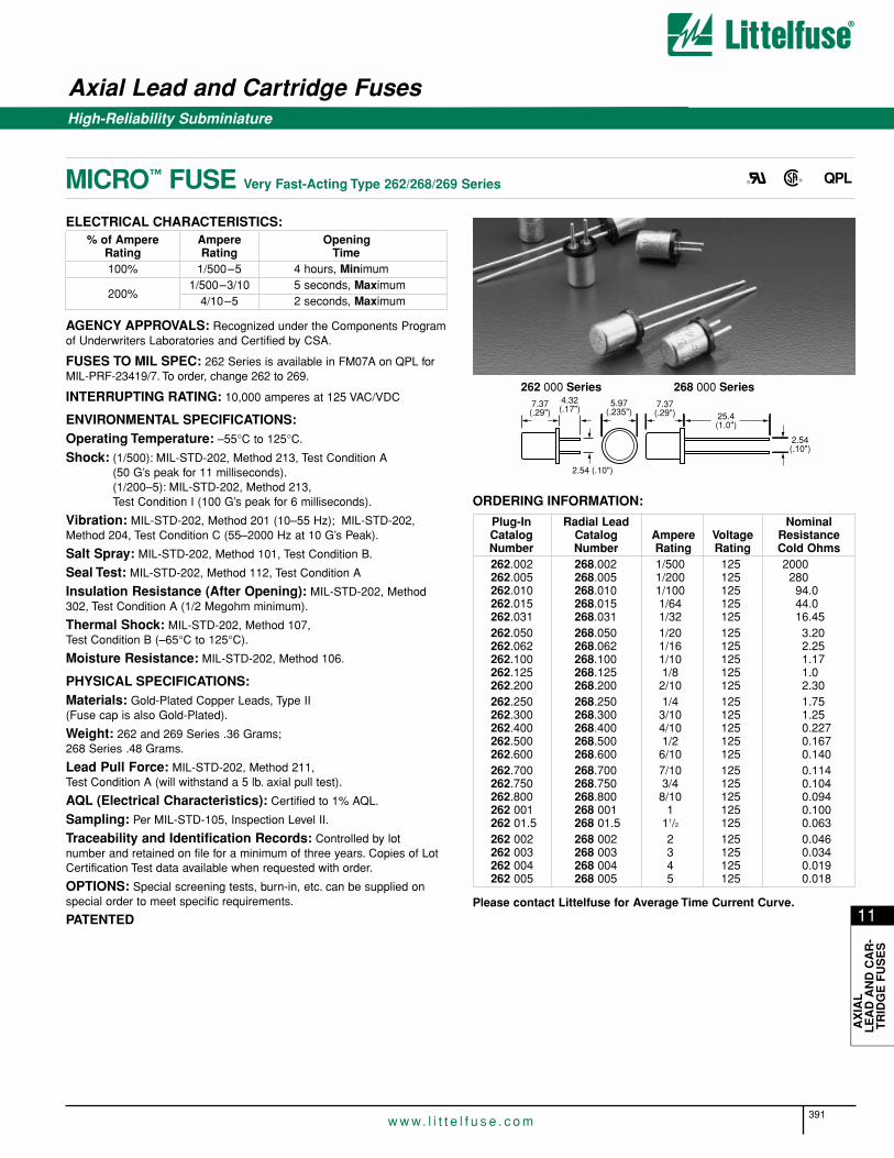
High-Reliability Subminiature
Axial Lead and Cartridge Fuses
MICRO™ FUSE Very Fast-Acting Type 262/268/269 Series
391w w w. l i t t e l f u s e . c o m
11
AX
IAL
LE
AD
AN
D C
AR
-T
RID
GE
FU
SE
S
ELECTRICAL CHARACTERISTICS:% of Ampere Ampere Opening
Rating Rating Time100% 1/500–5 4 hours, Minimum
200%1/500–3/10 5 seconds, Maximum
4/10–5 2 seconds, Maximum
AGENCY APPROVALS: Recognized under the Components Programof Underwriters Laboratories and Certified by CSA.
FUSES TO MIL SPEC: 262 Series is available in FM07A on QPL forMIL-PRF-23419/7. To order, change 262 to 269.
INTERRUPTING RATING: 10,000 amperes at 125 VAC/VDC
ENVIRONMENTAL SPECIFICATIONS:Operating Temperature: –55°C to 125°C.
Shock: (1/500): MIL-STD-202, Method 213, Test Condition A(50 G’s peak for 11 milliseconds).(1/200–5): MIL-STD-202, Method 213, Test Condition I (100 G’s peak for 6 milliseconds).
Vibration: MIL-STD-202, Method 201 (10–55 Hz); MIL-STD-202,Method 204, Test Condition C (55–2000 Hz at 10 G’s Peak).
Salt Spray: MIL-STD-202, Method 101, Test Condition B.
Seal Test: MIL-STD-202, Method 112, Test Condition A
Insulation Resistance (After Opening): MIL-STD-202, Method302, Test Condition A (1/2 Megohm minimum).
Thermal Shock: MIL-STD-202, Method 107, Test Condition B (–65°C to 125°C).
Moisture Resistance: MIL-STD-202, Method 106.
PHYSICAL SPECIFICATIONS:Materials: Gold-Plated Copper Leads, Type II (Fuse cap is also Gold-Plated).
Weight: 262 and 269 Series .36 Grams;268 Series .48 Grams.
Lead Pull Force: MIL-STD-202, Method 211, Test Condition A (will withstand a 5 lb. axial pull test).
AQL (Electrical Characteristics): Certified to 1% AQL.
Sampling: Per MIL-STD-105, Inspection Level II.
Traceability and Identification Records: Controlled by lot number and retained on file for a minimum of three years. Copies of LotCertification Test data available when requested with order.
OPTIONS: Special screening tests, burn-in, etc. can be supplied onspecial order to meet specific requirements.
PATENTED
Plug-In Radial Lead NominalCatalog Catalog Ampere Voltage ResistanceNumber Number Rating Rating Cold Ohms262.002 268.002 1/500 125 2000262.005 268.005 1/200 125 280262.010 268.010 1/100 125 94.0262.015 268.015 1/64 125 44.0262.031 268.031 1/32 125 16.45262.050 268.050 1/20 125 3.20262.062 268.062 1/16 125 2.25262.100 268.100 1/10 125 1.17262.125 268.125 1/8 125 1.0262.200 268.200 2/10 125 2.30262.250 268.250 1/4 125 1.75262.300 268.300 3/10 125 1.25262.400 268.400 4/10 125 0.227262.500 268.500 1/2 125 0.167262.600 268.600 6/10 125 0.140262.700 268.700 7/10 125 0.114262.750 268.750 3/4 125 0.104262.800 268.800 8/10 125 0.094262 001 268 001 1 125 0.100262 01.5 268 01.5 11/2 125 0.063262 002 268 002 2 125 0.046262 003 268 003 3 125 0.034262 004 268 004 4 125 0.019262 005 268 005 5 125 0.018
ORDERING INFORMATION:
Please contact Littelfuse for Average Time Current Curve.
® ® QPL
7.37(.29")
4.32(.17")
2.54 (.10")
5.97(.235")
7.37(.29") 25.4
(1.0")
2.54(.10")
262 000 Series 268 000 Series

Subminiature
Axial Lead and Cartridge Fuses
MICRO™ FUSE Very Fast-Acting Type 272/273/274/278/279 Series
392w w w. l i t t e l f u s e . c o m
Developed originally for the U.S. Space Program, MICRO fuse providesreliability in a compact design. The MICRO fuse is available in plug in orradial lead styles and a complete range of ampere ratings from 1/500 to5 amperes to suit a wide variety of design needs.
ELECTRICAL CHARACTERISTICS:% of Ampere Ampere Opening
Rating Rating Time100% 1/500–5 4 hours, Minimum
200%1/500–3/10 5 seconds, Maximum
4/10–5 2 seconds, Maximum
AGENCY APPROVALS: Recognized under the Components Programof Underwriters Laboratories and Certified by CSA.
AGENCY FILE NUMBERS: UL E10480, CSA LR 29862.
INTERRUPTING RATING: 10,000 amperes at 125 VAC/VDC.
FUSES TO MIL SPEC: 273 Series is available in Military QPL type(FM02). To order, change 273 to 274.
Operating Temperature:273 and 279: –55°C to 85°C.272 and 278: –55°C to 125°C
PATENTED
ORDERING INFORMATION:
Plug-In Radial Lead Nominal NominalCatalog Catalog Catalog Catalog Ampere Voltage Resistance Melting I2tNumber Number Number Number Rating Rating Cold Ohms A2 Sec.272.002 273.002 278.002 279.002 1/500 125 2200 0.00000000845272.005 273.005 278.005 279.005 1/200 125 280 0. 0.0000000810272.010 273.010 278.010 279.010 1/100 125 80.0 0.000000462272.015 273.015 278.015 279.015 1/64 125 44.0 0.00000123272.031 273.031 278.031 279.031 1/32 125 16.0 0.00000810272.050 273.050 278.050 279.050 1/20 125 3.20 0.0000666272.062 273.062 278.062 279.062 1/16 125 2.32 0.000115272.100 273.100 278.100 279.100 1/10 125 1.25 0.000385272.125 273.125 278.125 279.125 1/8 125 1.0 0.000691272.200 273.200 278.200 279.200 2/10 125 2.30 0.00409272.250 273.250 278.250 279.250 1/4 125 1.75 0.00640272.300 273.300 278.300 279.300 3/10 125 1.25 0.00945272.400 273.400 278.400 279.400 4/10 125 0.227 0.0251272.500 273.500 278.500 279.500 1/2 125 0.167 0.0716272.600 273.600 278.600 279.600 6/10 125 0.430 0.0411272.700 273.700 278.700 279.700 7/10 125 0.324 0.0710272.750 273.750 278.750 279.750 3/4 125 0.293 0.0900272.800 273.800 278.800 279.800 8/10 125 0.271 0.113272 001 273 001 278 001 279 001 1 125 0.0880 0.0648272 01.5 273 01.5 278 01.5 279 01.5 11/2 125 0.0578 0.160272 002 273 002 278 002 279 002 2 125 0.0425 0.300272 003 273 003 278 003 279 003 3 125 0.0275 0.759272 004 273 004 278 004 279 004 4 125 0.0202 1.38272 005 273 005 278 005 279 005 5 125 0.0156 2.21
100
10
1
0.1
0.01
0.0011 10 1000.01 0.10.005
1/64
A1/
100
A
1/20
0 A
1/32
A
1/16
A
1/8
A
1/4
A
1/2
A3/
4 A
1 A
1 1/
2 A
2 A
3 A
4 A
5 A
TIM
E IN
SE
CO
ND
S
CURRENT IN AMPERES
Average Time Current Curves
7.30(.29")
(.17")
8.89(.35")
2.54 (.10")
7.30(.29") 25.4 (1.0")
2.54 (.10")
25.4 (1.0")
2.54 (.10")
5.97(.235")
6.35(.25")
5.97(.235")
2.54 (.10")
8.89(.35")
6.35(.25")
272 000 Series 273 000 Series
278 000 Series
279 000 Series
NOTE: Amperage and voltage rating stamped on cap. Leads are solder-coatedcopper; .025" diameter.
(.17")4.32 4.32
® QPL®

Subminiature Glass Body
Axial Lead and Cartridge Fuses
2AG Fast-Acting Fuse 224/225/288/289 Series
393w w w. l i t t e l f u s e . c o m
11
AX
IAL
LE
AD
AN
DC
AR
TR
IDG
E F
US
ES
The 2AG Fast-Acting fuses are available in cartridge form or with axialleads. Axial leaded fuses are board washable. 2AG fuses provide thesame performance characteristics as their 3AG counterpart, while occupying one-third the space. Sleeved fuses are available.
ELECTRICAL CHARACTERISTICS:% of Ampere Opening
Rating Time110% 4 hours, Minimum135% 1 hour, Maximum200% 1 second, Maximum
AGENCY APPROVALS: All ratings are Listed by UL and Certified byCSA. 1 through 10 amperes approved by METI.AGENCY FILE NUMBERS: UL E10480, CSA LR 29862.FUSES TO MIL SPEC: 224 and 225 Series 1/8 through 7 amperesare available to DSCC Drawing #87108. To order, change 224 to 289 or225 to 288. See page 361.INTERRUPTING RATINGS:0.1–10A 10,000 amperes at 125 VAC0.1–1A 35 amperes at 250 VAC1.5–3.5A 100 amperes at 250 VACPACKAGING OPTIONS: 224 Series available on Tape and Reel perEIA-296. For 1500 pieces per reel, add packaging suffix DRT1.See page 8 for pitch Dimensions. 224, 225 series available inbulk packaging. For 1000 pieces bulk add packaging suffix M.
See Page 289 for Soldering Parameters and Environmental and Physicalspecifications.
PATENTEDORDERING INFORMATION:
100
10
1
0.1
0.01
0.0010.1 1 10 100 1000
1/8A
1/10
A
1/4A
3/8A
1/2A
3/4A
1A 1 1/
2A2A 2
1/2A
3A 4A 5A 6A 7A 8A 10A
TIM
E IN
SE
CO
ND
S
CURRENT IN AMPERES
Cartridge Axial Lead Nominal NominalCatalog Catalog Ampere Voltage Resistance Melting I2tNumber Number Rating Rating Cold Ohms A2 Sec.225.100 224.100 1/10 250 6.15 0.000750225.125 224.125 1/8 250 3.90 0.00286225.250 224.250 1/4 250 1.15 0.0300225.375 224.375 3/8 250 0.395 0.171225.500 224.500 1/2 250 0.265 0.365225.750 224.750 3/4 250 0.152 1.05225 001 224 001 1 250 0.102 2.22225 01.5 224 01.5 11/2 250 0.0705 0.800225 002 224 002 2 250 0.0490 1.50225 02.5 224 02.5 21/2 250 0.0365 2.68225 003 224 003 3 250 0.0310 4.62225 03.5 224 03.5 31/2 250 0.0258 6.70225 004 224 004 4 125 0.0233 9.40225 005 224 005 5 125 0.0179 17.00225 006 224 006 6 125 0.0147 22.1225 007 224 007 7 125 0.0123 40.0225 008 224 008 8 125 0.0100 56.0225 010 224 010 10 125 0.00675 116.0
2AG Special 350VFast-Acting Fuse
The 220 007 subminiature fuse is intended for fluorescent lighting ballastprotection or similar applications up to 350V.AXIAL LEAD PART NUMBER: 220 007 (ampere rating of 3A).DIMENSIONS: Same as 224 Series.ELECTRICAL CHARACTERISTICS: Same as 224 Series.INTERRUPTING RATING: 100 amperes at 350 VAC.PATENTEDContact Littelfuse concerning other ampere ratings.
Average Time Current Curves
® ®
225 000 Series 224 000 Series
4.5(.177")
14.48(.57")
14.48(.57")
4.5 (.177") .635(.025")
38.1(1.50") TYP.
Axial Lead Material: Solder coated copper.
®UL ® MIL

Axial Lead and Cartridge Fuses
394w w w. l i t t e l f u s e . c o m
Subminiature Glass Body
2AG Slo-Blo® Fuse 229/230/290/291 Series
1000
100
10
1
0.1
0.01
0.1 1 10 100 1000
1/4A
3/8A
1/2A
3/4A
1A 1 1/
2A2A 2
1/2A
3A 3 1/
2A4A 5A 7A
TIM
E IN
SE
CO
ND
S
CURRENT IN AMPERES
Average Time Current Curves
The 2AG Slo-Blo® fuses are available in cartridge form or with axialleads. Axial leaded fuses are board washable. 2AG fuses provide thesame performance characteristics as their 3AG counterpart, while occupying one-third the space. Sleeved fuses are available.ELECTRICAL CHARACTERISTICS:
% of Ampere OpeningRating Time110% 4 hours, Minimum135% 1 hour, Maximum
200%3 seconds, Minimum20 seconds, Maximum
AGENCY APPROVALS: Listed by Underwriters Laboratories andCertified by CSA through 3.5 amperes. Recognized under theComponents Program of Underwriters Laboratories from 4 through 7amperes. 1 through 7 amperes approved by METI.AGENCY FILE NUMBERS: UL E10480, CSA LR 29862.FUSES TO MIL SPEC: 229 and 230 Series are available to DSCCDrawing #87108. To order, change 229 to 290 or 230 to 291. See page361.INTERRUPTING RATINGS:0.25–3.5A 10,000 amperes at 125VAC4–7A 400 amperes at 125VAC0.25–1A 35 amperes at 250VAC1.25–3.5A 100 amperes at 250VACPACKAGING OPTIONS: 230 Series available on Tape and Reel perEIA-296. For 1500 pieces per reel, add packaging suffix DRT1W. Seepage 8 for pitch dimensions. 229 and 230 series available in bulk pack-aging. For 1000 pieces bulk, add packaging suffix M.
See page 360 for Soldering parameters and Environment and Physicalspecifications.
229 000 Series 230 000 Series
4.5(.177")
14.48(.57")
14.48(.57")
4.5 (.177") 0.635(.025")
38.1(1.50") TYP.
Axial Lead Material: Solder coated copper.
MIL®UL ® ®
ORDERING INFORMATION:Cartridge Axial Lead Nominal NominalCatalog Catalog Ampere Voltage Resistance Melting I2tNumber Number Rating Rating Cold Ohms A2 Sec.229.250 230.250 1/4 250 2.41 0.216229.350 230.350 .350 250 1.30 0.490229.375 230.375 3/8 250 0.580229.500 230.500 1/2 250 0.688 1.16229.600 230.600 6/10 250 0.477 1.75229.750 230.750 3/4 250 0.340 2.95229.800 230.800 8/10 250 0.304 3.45229 001 230 001 1 250 5.64229 1.25 230 1.25 11/4 250 0.145 9.80229 01.5 230 01.5 11/2 250 0.107 15.0229 002 230 002 2 250 0.0692 30.0229 2.25 230 2.25 21/4 250 0.0562 39.0229 02.5 230 02.5 21/2 250 0.0498 50.0229 003 230 003 3 250 0.0380 77.0229 03.5 230 03.5 31/2 250 0.0310 110.0229 004 230 004 4 125 0.0256 148.0229 005 230 005 5 125 0.0185 267.0229 006 230 006 6 125 0.0140 380.0229 007 230 007 7 125 0.0115 464.0
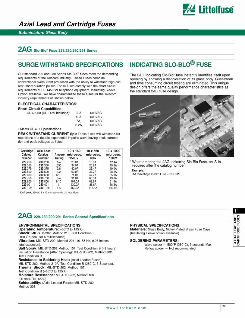
11
AX
IAL
LE
AD
AN
DC
AR
TR
IDG
E F
US
ES
Axial Lead and Cartridge Fuses
395w w w. l i t t e l f u s e . c o m
Subminiature Glass Body
2AG Slo-Blo® Fuse 229/230/290/291 Series
Our standard 229 and 230 Series Slo-Blo® fuses meet the demandingrequirements of the Telecom industry. These Fuses combine conventional overcurrent protection with the ability to withstand high cur-rent, short duration pulses. These fuses comply with the short circuitrequirements of UL 1459 for telephone equipment. Insulating SleeveOption available. We have characterized these fuses for the Telecomindustry requirements as shown below.
ELECTRICAL CHARACTERISTICS:Short Circuit Capabilities:
UL 60950 (UL 1459 Included): 60A, 600VAC40A, 600VAC7A, 600VAC
2.2A, 600VAC• Meets UL 497 Specifications
PEAK WITHSTAND CURRENT (lp): These fuses will withstand 50repetitions of a double exponential impulse wave having peak currents(lp) and peak voltages as listed.
SURGE WITHSTAND SPECIFICATIONS
Cartridge Axial Lead 10 x 160 10 x 560 10 x 1000Catalog Catalog Ampere microsec. microsec. microsec.Number Number Rating 1500V 800V 1000V229.250 230.250 1/4 23.0A 16.6A 12.4A229.350 230.350 .350 34.0A 25.8A 19.3A229.375 230.375 3/8 40.0A 25.4A 19.0A229.500 230.500 1/2 60.0A 37.7A 28.2A229.600 230.600 6/10 71.0A 47.2A 35.3A229.750 230.750 3/4 91.0A 65.5A 49.0A229.800 230.800 8/10 104.0A 68.9A 51.6A229 001 230 001 1 130.0A 88.6A 66.3A229 1.25 230 1.25 11/4
1 162.0A 118.1A 100.0A1 500A peak, 2500V, 2 x 10 microseconds, 20 repetitions.
The 2AG Indicating Slo-Blo® fuse instantly identifies itself uponopening by showing a discoloration of its glass body. Guessworkand time consuming circuit testing are eliminated. This uniquedesign offers the same quality performance characteristics asthe standard 2AG fuse design.
* When ordering the 2AG Indicating Slo-Blo Fuse, an ‘S’ isrequired after the catalog number.Example:-1A Indicating Slo-Blo® Fuse = 230 001S
INDICATING SLO-BLO® FUSE
ENVIRONMENTAL SPECIFICATIONS:Operating Temperature: –55°C to 125°C.Shock: MIL-STD-202, Method 213, Test Condition I (100 G’s peak for 6 milliseconds).Vibration: MIL-STD-202, Method 201 (10–55 Hz, 0.06 inches total excursion).Salt Spray: MIL-STD-202 Method 101, Test Condition B (48 hours).Insulation Resistance (After Opening): MIL-STD-202, Method 302, Test Condition B.Resistance to Soldering Heat: (Axial Leaded Fuses):MIL-STD-202, Method 210A, Test Condition B (260°C, 3 Seconds).Thermal Shock: MIL-STD-202, Method 107, Test Condition B (–65°C to 125°C).Moisture Resistance: MIL-STD-202, Method 106 (90-98% RH, 65°C).Solderability: (Axial Leaded Fuses): MIL-STD-202, Method 208.
PHYSICAL SPECIFICATIONS:Materials: Glass Body, Nickel-Plated Brass Fuse Caps.(Insulating sleeve option available).
SOLDERING PARAMETERS:Wave solder — 500°F (260°C), 3 seconds Max.Reflow solder — Not recommended.
2AG 229/230/290/291 Series General Specifications

Glass Body
Axial Lead and Cartridge Fuses
3AG Fast-Acting Type 312/318 Series
396w w w. l i t t e l f u s e . c o m
1000
100
10
1
0.1
0.011 10 1000.01 0.1
.031
A
.062
A
.125
A
.250
A.3
75 A
.500
A.7
50 A
1 A
1.5
A2
A2.
5 A
3 A
4 A
5 A
6 A
7 A
8 A
10 A
0.005
TIM
E IN
SE
CO
ND
S
CURRENT IN AMPERES
Cartridge Axial Lead Nominal NominalCatalog Catalog Ampere Voltage Resistance Melting I2tNumber Number Rating Rating Cold Ohms A2 Sec.312.031 318.031 1/32 250 23.3 0.0000300312.062 318.062 1/16 250 24.5 0.000249312.100 318.100 1/10 250 11.2 0.00102312.125 318.125 1/8 250 7.10 0.00289312.150 318.150 15/100 250 5.10 0.00550312.175 318.175 .175 250 3.85 0.00960312.187 318.187 3/16 250 3.40 0.0128312.200 318.200 2/10 250 3.00 0.0165312.250 318.250 1/4 250 2.00 0.0355312.300 318.300 3/10 250 1.40 0.0689312.375 318.375 3/8 250 0.820 0.185312.500 318.500 1/2 250 0.495 0.483312.600 318.600 6/10 250 0.360 0.880312.750 318.750 3/4 250 0.243 1.84312 001 318 001 1 250 0.189 0.760312 1.25 318 1.25 11/4 250 0.138 1.45312 01.5 318 01.5 11/2 250 0.103 2.35312 01.6 318 01.6 16/10 250 0.0930 2.80312 1.75 318 1.75 13/4 250 0.0850 3.60312 01.8 318 01.8 18/10 250 0.0820 3.85312 002 318 002 2 250 0.0700 5.20312 2.25 318 2.25 21/4 250 0.0590 7.20312 02.5 318 02.5 21/2 250 0.0510 9.54312 003 318 003 3 250 0.0424 14.0312 004 318 004 4 250 0.0291 28.5312 005 318 005 5 250 0.0223 50.0312 006 318 006 6 250 0.0177 81.1312 007 318 007 7 250 0.0145 118.0312 008 318 008 8 250 0.0121 166.0312 010 318 010 10 250 0.00925 298.0312 012 — 12 32 0.0071 —312 015 — 15 32 0.0052 —312 020 — 20 32 0.0034 —312 025 — 25 32 0.0024 —312 030 — 30 32 0.0019 —312 035 — 35 32 0.0013 —
Average Time Current Curves
312 000 Series 318 000 Series
6.35(.25")
32.385(1.275")
31.75(1.25")
6.985 (.275") 0.813(.032")
38.1(1.50") TYP.
Axial Lead Material: Solder coated copper.
A standard for cost-effective reliability and performance in circuit protec-tion, the 3AG fuse satisfies a broad range of application requirements.
ELECTRICAL CHARACTERISTICS:% of Ampere Ampere Opening
Rating Rating Time110% 1/32–35 4 hours, Minimum135% 1/32–35 1 hour, Maximum
1/32–10 5 sec., Maximum200% 12–30 10 sec., Maximum
35 20 sec., Maximum
AGENCY APPROVALS: Listed by Underwriters Laboratories andCertified by CSA through 30 amperes.1/100–10 amperes listed to UL 248-14 (UL 198-G)12–30 amperes listed to UL 275.AGENCY FILE NUMBERS: UL E10480, CSA LR 29862.FUSES TO MIL SPEC: See F02A cartridge type in Military Section.INTERUPTING RATING:10,000A @ 125VAC35A @ 250VAC
ORDERING INFORMATION:
®UL ® QPL

Glass Body
Axial Lead and Cartridge Fuses
3AG Slo-Blo® Fuse 313/315 Series
397w w w. l i t t e l f u s e . c o m
11
AX
IAL
LE
AD
AN
DC
AR
TR
IDG
E F
US
ES
1000
100
10
1
0.1
0.01
1/16
A
0.05 0.1 1 10 100 1000
1/10
A15
/100
A.1
75A
1/4A
3/8A
1/2A
3/4A
1A 1 1/
2A2A 3A 4A 5A 7A 8A 10
A12
A15
A20
A
30A
25A
TIM
E IN
SE
CO
ND
S
CURRENT IN AMPERES
Cartridge Axial Lead Nominal NominalCatalog Catalog Ampere Voltage Resistance Melting I2tNumber Number Rating Rating Cold Ohms A2 Sec.313.010 315.010 1/100 250 3300.0000 0.000121313.031 315.031 1/32 250 330. 0.00303313.040 315.040 4/100 250 220 0.00630313.062 315.062 1/16 250 91.0 0.0210313.100 315.100 1/10 250 33.3 0.0850313.125 315.125 1/8 250 22.3 0.152313.150 315.150 15/100 250 15.3 0.270313.175 315.175 .175 250 8.60 0.177313.187 315.187 3/16 250 7.95 0.230313.200 315.200 2/10 250 6.54 0.270313.250 315.250 1/4 250 4.27 0.385313.300 315.300 3/10 250 3.11 0.730313.375 315.375 3/8 250 2.08 1.23313.400 315.400 4/10 250 1.86 1.35313.500* 315.500 1/2 250 1.25 2.55313.600 315.600 6/10 250 0.914 4.00313.700 315.700 7/10 250 0.695 5.90313.750 315.750 3/4 250 0.617 7.16313.800 315.800 8/10 250 0.550 8.00313 001* 315 001 1 250 0.375 14.0313 01.2 315 01.2 12/10 250 0.276 21.5313 1.25 315 1.25 11/4 250 0.258 24.0313 01.5* 315 01.5 11/2 250 0.190 38.0313 01.6 315 01.6 16/10 250 0.170 49.6313 01.8 315 01.8 18/10 250 0.140 58.0313 002* 315 002 2 250 0.116 77.0313 2.25 315 2.25 21/4 250 0.0960 121.0313 02.5 315 02.5 21/2 250 0.0805 130.0313 02.8 315 02.8 28/10 250 0.0670 170.0313 003* 315 003 3 250 0.0588 200.0313 03.2 315 03.2 32/10 250 0.0525 209.0313 004* 315 004 4 250 0.0308 76.1313 005* 315 005 5 250 0.0212 140.0313 6.25* 315 6.25 61/4 250 0.0152 242.0313 06.3 315 06.3 6.30 250 0.0152 242.0313 007* 315 007 7 250 0.0127 347.0313 008* 315 008 8 250 0.0110 445.0313 010* 315 010 10 32 0.00820 760.0313 012 315 012 12 32 0.00640 1200.0313 015 315 015 15 32 0.00500 1870.0313 020 315 020 20 32 0.00220 9560.0313 025 315 025 25 32 0.00170 16500.0313 030 315 030 30 32 0.00120 26900.0
*These ratings available with an indicating option. Add the ‘ID’ designation to the series number. i.e. 313.500 ID.
Average Time Current Curves
®UL ® ® QPL
313 000 Series 315 000 Series
6.35 (.25")
32.385(1.275")
31.75(1.25")
6.985 (.275")
38.1(1.50") TYP.
Axial Lead Material: Solder coated copper.
0.813 (.032") ( - 15A)1.016 (.040") (20 - 30A)
1100/
A standard for cost-effective reliability and performance in circuit protec-tion, the 3AG fuse satisfies a broad range of application requirements.
AGENCY APPROVALS: Listed by Underwriters Laboratories andCertified by CSA through 8 amperes. 10-30A ratings are recognizedunder the components program of Underwriters Laboratories.313 000 Series approved by METI from 1 through 5 amperes.AGENCY FILE NUMBERS: UL E10480, CSA LR 29862.FUSES TO MIL SPEC: See F02B cartridge type in Military Section.
ORDERING INFORMATION:
ELECTRICAL CHARACTERISTICS:% of Ampere Opening
Rating Time110% 4 hours, Minimum135% 1 hour, Maximum200% 5 seconds, Minimum
PATENTEDINTERUPTING RATING:
0.01-8A 10,000A @ 125 VAC0.1-1A 35A @ 250 VAC1.2-3.2A 100A @ 250 VAC4-8A 200A @ 250 VAC10-30A 300A @ 32 VAC

Ceramic Body
Axial Lead and Cartridge Fuses
3AB Fast-Acting Fuse 314/324/394 Series
398w w w. l i t t e l f u s e . c o m
314 000 Series 324 000 Series
6.35 (.25")
32.385(1.275")
31.75(1.25")
6.985 (.275")
38.1(1.50") TYP.
Axial Lead Material: Solder coated copper.
0.813 (.032") ( - 15A) 1.016 (.040") (20 - 30A)
18/
Ceramic body construction permits higher interrupting ratings and volt-age ratings. Ideal for applications where high current loads are expected.
ELECTRICAL CHARACTERISTICS:% of Ampere Ampere Opening
Rating Rating Time110% 1/8–30 4 hours, Minimum135% 1/8–30 1 hour, Maximum
200%1/8–12 15 seconds, Maximum15–30 30 seconds, Maximum
AGENCY APPROVALS: Listed by Underwriters Laboratories and Certified by CSA through 15 amperes at 250 VAC/125 VDC.Recognized under the Components Program of UnderwritersLaboratories at 20-30A, certified by CSA at 20A, and approved by METI from 10 through 30 amperes.AGENCY FILE NUMBERS: UL E10480, CSA LR 29862.FUSES TO MIL SPEC: See F03A cartridge type in Military Section.
INTERRUPTING RATINGS:0.125 - 20A 10,000@ 125 VAC25- 30A 400A @ 125 VAC0.125 - .75A 35A @ 250 VAC1 - 3A 100A @ 250VAC4 - 15A 750A @ 250VAC20A 1,000A @ 250VAC
200A @ 300VAC25-30A 100A @ 250VAC
ORDERING INFORMATION:
1000
100
10
1
0.1
0.010.1 1 10 100 1000
1/8A
1/4A
3/8A
1/2A
3/4A
1A 2A 3A 4A 5A 6A 7A 8A 10A
12A
15A
20A
25A
30A
TIM
E IN
SE
CO
ND
S
CURRENT IN AMPERES
Cartridge Axial Lead Nominal NominalCatalog Catalog Ampere Voltage Resistance Melting I2tNumber Number Rating Rating Cold Ohms A2 Sec.314.125 324.125 1/8 250 6.20 0.00149314.250 324.250 1/4 250 1.95 0.0140314.375 324.375 3/8 250 0.820 0.050314.500 324.500 1/2 250 0.500 0.115314.750 324.750 3/4 250 0.250 0.466314 001 324 001 1 250 0.189 0.690314 002 324 002 2 250 0.0700 11.0314 003 324 003 3 250 0.0432 14.6314 004 324 004 4 250 0.0470 10.4314 005 324 005 5 250 0.0300 26.0314 006 324 006 6 250 0.0240 45.0314 007 324 007 7 250 0.0187 71.0314 008 324 008 8 250 0.0153 105.0314 010 324 010 10 250 0.0105 206.0314 012 324 012 12 250 0.00760 570.0314 015 324 015 15 250 0.00505 292.0314 020 324 020 20 250 0.00355 631.0314 025 324 025 25 250 0.00235 1450.0314 030 324 030 30 250 0.00182 2490.0
Average Time Current Curves
®UL ® ® QPL

Ceramic Body
Axial Lead and Cartridge Fuses
3AB Slo-Blo® Fuse 325/326/390 Series
399w w w. l i t t e l f u s e . c o m
11
AX
IAL
LE
AD
AN
DC
AR
TR
IDG
E F
US
ES
Ceramic body construction permits higher interrupting ratings and volt-age ratings. Ideal for applications where high current loads are expected.
ELECTRICAL CHARACTERISTICS:% of Ampere Ampere Opening
Rating Rating Time110% 1/100–30 4 hours, Minimum135% 1/100–30 1 hour, Maximum
200%1/100–3.2 5 sec., Min.; 30 sec. Max.
4–30 5 sec., Min.; 60 sec. Max.
AGENCY APPROVALS: Listed by Underwriters Laboratories from 1/4through 10 amperes. Certified by CSA from 1/4 through 30 amperes.Recognized under the component program of Underwriters Laboratoriesfor 12-30A.AGENCY FILE NUMBERS: UL E10480, CSA LR 29862.FUSES TO MIL SPEC: See F03B cartridge type in Military Section.
PATENTEDINTERRUPTING RATING:0.010 - 20A 10,000A @ 125 VAC25 - 30A 400A @ 125 VAC0.010 - 3.2A 100A @ 250 VAC4 - 20A 400A @ 250 VACORDERING INFORMATION:
1000
100
10
1
0.1
0.0110
CURRENT IN AMPERES
TIM
E IN
SEC
ONDS
100 10000.1 10.05
5.0A
4.0A
3.5A
3.0A
2.5A
2.0A
1.5A
1.0A
.750
A.5
00A
.375
A
Cartridge Axial Lead Nominal NominalCatalog Catalog Ampere Voltage Resistance Melting I2tNumber Number Rating Rating Cold Ohms A2 Sec.326.010 325.010 1/100 250 3300.0000 0.00148326.031 325.031 1/32 250 330. 0.0110326.062 325.062 1/16 250 91.0 0.0276326.100 325.100 1/10 250 33.3 0.0870326.125 325.125 1/8 250 22.3 0.100326.150 325.150 15/100 250 15.3 0.143326.175 325.175 .175 250 8.84 0.220326.187 325.187 3/16 250 7.67 0.230326.200 325.200 2/10 250 6.72 0.213326.250 325.250 1/4 250 4.40 0.432326.300 325.300 3/10 250 3.20 0.690326.375 325.375 3/8 250 2.14 1.20326.400 325.400 4/10 250 1.92 1.33326.500 325.500 1/2 250 1.29 2.50326.600 325.600 6/10 250 0.940 3.90326.700 325.700 7/10 250 0.716 6.42326.750 325.750 3/4 250 0.636 7.00326.800 325.800 8/10 250 0.568 8.20326 001 325 001 1 250 0.386 16.3326 01.2 325 01.2 12/10 250 0.284 22.0326 1.25 325 1.25 11/4 250 0.266 24.0326 01.5 325 01.5 11/2 250 0.196 40.1326 01.6 325 01.6 16/10 250 0.175 45.0326 002 325 002 2 250 0.120 80.0326 02.5 325 02.5 21/2 250 0.0830 136.0326 02.8 325 02.8 28/10 250 0.0690 170.0326 003 325 003 3 250 0.0600 200.0326 03.2 325 03.2 32/10 250 0.0535 214.0326 004 325 004 4 250 0.0755 9.71326 005 325 005 5 250 0.0518 25.0326 6.25 325 6.25 61/4 250 0.0343 60.4326 007 325 007 7 250 0.0225 47.3326 008 325 008 8 250 0.0191 67.1326 010 325 010 10 250 0.0131 137.0326 012 325 012 12 250 0.0066 129.0326 015 325 015 15 250 0.0049 245.0326 020 325 020 20 250 0.0033 575.0326 025 325 025 25 125 0.0024 1030.0326 030 325 030 30 125 0.0019 1690.0
Average Time Current Curves
326 000 Series 325 000 Series
6.35 (.25")
32.385(1.275")
31.75(1.25")
6.985 (.275")
38.1(1.50") TYP.
Axial Lead Material: Solder coated copper.
1100/0.813 (.032") ( -15A)
1.016 (.040") (20 -30A)
®UL ® ® QPL
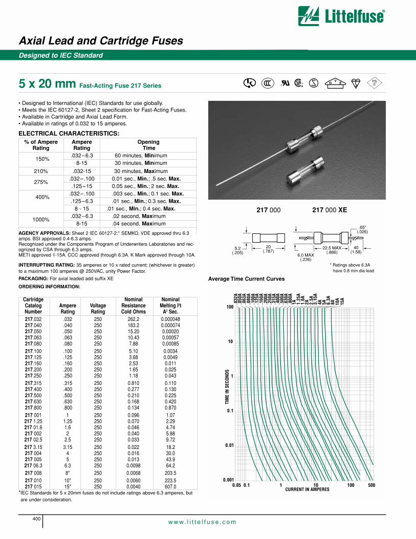
• Designed to International (IEC) Standards for use globally.• Meets the IEC 60127-2, Sheet 2 specification for Fast-Acting Fuses.• Available in Cartridge and Axial Lead Form.• Available in ratings of 0.032 to 15 amperes.
ELECTRICAL CHARACTERISTICS:% of Ampere Ampere Opening
Rating Rating Time
150%.032–6.3 60 minutes, Minimum
8-15 30 minutes, Minimum
210% .032-15 30 minutes, Maximum
275%.032– .100 0.01 sec., Min.; .5 sec. Max..125–15 0.05 sec., Min.; 2 sec. Max.
400%.032– .100 .003 sec., Min.; 0.1 sec. Max..125–6.3 .01 sec., Min.; 0.3 sec. Max.
8 - 15 .01 sec., Min.; 0.4 sec. Max.
1000%.032–6.3 .02 second, Maximum
8-15 .04 second, Maximum
AGENCY APPROVALS: Sheet 2 IEC 60127-2:* SEMKO, VDE approved thru 6.3amps. BSI approved 0.4-6.3 amps.Recognized under the Components Program of Underwriters Laboratories and rec-ognized by CSA through 6.3 amps.METI approved 1-15A. CCC approved through 6.3A. K Mark approved through 10A.
INTERRUPTING RATING: 35 amperes or 10 x rated current; (whichever is greater)to a maximum 100 amperes @ 250VAC, unity Power Factor.
PACKAGING: For axial leaded add suffix XE
ORDERING INFORMATION:
Cartridge Nominal NominalCatalog Ampere Voltage Resistance Melting I2tNumber Rating Rating Cold Ohms A2 Sec.217.032 .032 250 262.2 0.000048217.040 .040 250 183.2 0.000074217.050 .050 250 15.20 0.00020217.063 .063 250 10.43 0.00057217.080 .080 250 7.88 0.00085217.100 .100 250 5.10 0.0034217.125 .125 250 3.68 0.0049217.160 .160 250 2.53 0.011217.200 .200 250 1.65 0.025217.250 .250 250 1.18 0.043217.315 .315 250 0.810 0.110217.400 .400 250 0.277 0.130217.500 .500 250 0.210 0.225217.630 .630 250 0.168 0.420217.800 .800 250 0.134 0.870217 001 1 250 0.096 1.07217 1.25 1.25 250 0.070 2.29217 01.6 1.6 250 0.046 4.74217 002 2 250 0.040 5.88217 02.5 2.5 250 0.033 9.72217 3.15 3.15 250 0.022 18.2217 004 4 250 0.016 30.0217 005 5 250 0.013 43.9217 06.3 6.3 250 0.0098 64.2217 008 8* 250 0.0068 203.5217 010 10* 250 0.0060 223.5217 015 15* 250 0.0040 607.0
Designed to IEC Standard
Axial Lead and Cartridge Fuses
5 x 20 mm Fast-Acting Fuse 217 Series
400w w w. l i t t e l f u s e . c o m
8A 10A
15A
6.3A
5A4A3.15
A2.
5A2A1.
6A1.
25A
1A.800
A.6
30A
.500
A.4
00A
.315
A.2
50A
.200
A.1
60A
.125
A.1
00A
.080
A.0
63A
.050
A.0
32A
5001001010.10.050.001
0.01
0.1
1
10
100
TIM
E IN
SEC
ONDS
CURRENT IN AMPERES*IEC Standards for 5 x 20mm fuses do not include ratings above 6.3 amperes, butare under consideration.
217 000 XE217 000
5.2(.205) 6.0 MAX
(.236)
40(1.58)
.65*(.026)
20(.787)
22.5 MAX(.886)
* Ratings above 6.3A have 0.8 mm dia lead
®®
VD E
Average Time Current Curves

Designed to IEC Standard
Axial Lead and Cartridge Fuses
5 x 20 mm Time Lag Fuse (Slo-Blo® Fuse) 218/213 Series
401w w w. l i t t e l f u s e . c o m
11
AX
IAL
LE
AD
AN
DC
AR
TR
IDG
E F
US
ES
10A
15A
8A6.3A
5A4A3.15
A2.
5A2A1.
6A1.
25A
1A.800
A.6
30A
.500
A.4
00A
.315
A.2
50A
.200
A.1
60A
.125
A.1
00A
.080
A.0
63A
.050
A.0
40A
.032
A
5001001010.10.050.001
0.01
0.1
1
10
100
TIM
E IN
SEC
ONDS
CURRENT IN AMPERES
Average Time Current Curves for 218/228
• Designed to International (IEC) Standards for use globally.• Meets the IEC 60127-2, Sheet 3 specification for Time Lag Fuses.• Available in Cartridge and Axial Lead Form.• Available in ratings of 0.032 to 15 amperes.
ELECTRICAL CHARACTERISTICS (218 Series):% of Ampere Ampere Opening
Rating Rating Time
150%.032–6.3 60 minutes, Minimum8 - 15 30 minutes, Minimum
210% .032–15 2 minutes, Maximum
275%.032– .100 0.2 sec., Min.; 10 sec. Max..125–15 0.6 sec., Min.; 10 sec. Max.
400%.032– .100 .04 sec., Min.; 3 sec. Max..125–15 .15 sec., Min.; 3 sec. Max.
1000%.032– .100 .01 sec., Min.; 0.3 sec. Max..125–15 0.02 sec., Min.; 0.3 sec. Max.
AGENCY APPROVALS: Sheet III IEC 60127-2:* 218 Series Approvals: SEMKO,VDE approved thru 6.3 amps. BSI approved 0.08-6.3 amps. Recognized under theComponents Program of Underwriters Laboratories and recognized by CSAthrough 15 amps. METI approved 1-15 amps. CCC approved through 6.3 amps.K Mark approved through 10 amps.
VOLTAGE RATING: 250 VAC
INTERRUPTING RATINGS: 35 amperes or 10 x rated current; (whichever isgreater) to a maximum 100A @ 250 VAC, unity power factor.ORDERING INFORMATION:For axial leaded add suffix XE
218 213 Surge WithstandCartridge Nominal Nominal Cartridge Nominal Nominal
Ampere Catalog Resistance Melting I2t Catalog Resistance MeltingRating Number Cold Ohmns A2Sec. Number Cold Ohms I2t A2Sec.
.032 218.032 58.45 0.00305 – – –
.040 218.040 35.70 0.0055 – – –
.050 218.050 23.30 0.0071 – – –
.063 218.063 18.1 0.012 – – –
.080 218.080 12.6 0.0265 – – –
.100 218.100 8.95 0.0495 – – –
.125 218.125 4.41 0.150 – – –
.160 218.160 2.44 0.225 – – –
.200 218.200 1.60 0.350 0213.200 1.60 0.350
.250 218.250 1.05 0.555 0213.250 1.05 0.555
.315 218.315 0.848 1.14 0213.315 0.848 1.14
.400 218.400 0.535 1.35 0213.400 0.535 1.35
.500 218.500 0.370 2.90 0213.500 0.370 2.90
.630 218.630 0.275 4.80 0213.630 0.275 4.80
.800 218.800 0.073 1.99 0213.800 0.165 9.421 218 001 0.055 3.33 0213 001. 0.117 19.20
1.25 218 1.25 0.042 5.80 0213 1.25 0.081 27.151.6 218 01.6 0.032 10.61 0213 01.6 0.055 44.22 218 002 0.029 14.80 0213 002. 0.044 92.7
2.5 218 02.5 0.022 23.85 0213 02.5 0.030 138.03.15 218 3.15 0.017 39.20 0213 3.15 0.022 226.5
4 218 004 0.013 70.95 0213 004. 0.017 2025 218 005 0.010 114.0 0213 005. 0.011 314
6.3 218 06.3 0.0075 204.0 0213 06.3 0.008 6008 218 008 0.0059 350.5 – – –
10 218 010 0.0045 583.0 – – –15 218 015 0.0030 1441.0
* IEC Standards for 5 x 20 fuses do not include ratings above 6.3A, but are under consideration.
213 000218 000
213 000 XE218 000 XE
5.2(.205")
6.0 MAX(.236")
40(1.58")
.65*(.026")
20(.787")
22.5 MAX(.886)
*Ratings above 6.3A have 0.8mm dia lead
®®
VD E

Designed to IEC Standard
Axial Lead and Cartridge Fuses
5 x 20 mm Fast-Acting Fuse 216 Series
402w w w. l i t t e l f u s e . c o m
• Designed to International (IEC) Standards for use globally.• Meets the IEC 60127-2, Sheet 1 specification for Fast Acting Fuses.• Available in Cartridge and Axial Lead Form.• Available in ratings of 0.050 to 10 amperes.• High breaking capacity.
ELECTRICAL CHARACTERISTICS:% of Ampere Ampere Opening
Rating Rating Time
150%.05–6.3 60 minutes, Minimum
8-10 30 minutes, Minimum
210% .05–10 30 minutes, Maximum
275%.05–4 0.01 sec., Min.; 2 sec. Max.5–6.3 0.01 sec., Min.; 3 sec. Max.8-10 0.04 sec., Min.; 20 sec. Max.
400%.05–6.3 .003 sec., Min.; 0.3 sec. Max.
8-10 .01 sec., Min.; 1.0 sec. Max.
1000%.05–6.3 .02 seconds, Maximum
8-10 .03 seconds, Maximum
AGENCY APPROVALS: Sheet I IEC 60127-2:* SEMKO approved thru 6.3 amps.Recognized under the Components Program of Underwriters Laboratories and rec-ognized by CSA through 10 amps. BSI approved 1A to 6.3A. VDE approved .05-6.3. METI approved 1A-10A. CCC approved through 6.3A. K Mark approved 1-10A.
INTERRUPTING RATING: 1500 amperes @ 250 VAC, 0.7-0.8 power factor.
PACKAGING: For axial leaded add suffix XE
ORDERING INFORMATION:
216 000 XE216 000
5.2(.205") 6.0 MAX
(.236")
40(1.58")
.65*(.026")
20(.787")
22.5 MAX(.886)
*Ratings above 6.3Ahave 0.8 dia lead
10A
6.3A
5A4A3.15
A2.
5A2A1.
6A1.
25A
1A.800
A.6
30A
.500
A.3
15A
.250
A.2
00A
.160
A.1
25A
.100
A
5001001010.10.050.001
0.01
0.1
1
10
100
TIM
E IN
SEC
ONDS
CURRENT IN AMPERES
Average Time Current Curves
Cartridge Nominal NominalCatalog Ampere Voltage Resistance Melting I2tNumber Rating Rating Cold Ohms A2 Sec.216.050 .050 250 15.90 0.00019216.063 .063 250 10.45 0.00055216.080 .080 250 7.89 0.00086216.100 .100 250 5.42 0.0033216.125 .125 250 3.68 0.0056216.160 .160 250 5.20 0.0018216.200 .200 250 3.35 0.0045216.250 .250 250 2.35 0.0092216.315 .315 250 1.85 0.015216.400 .400 250 1.67 0.028216.500 .500 250 1.20 0.045216.630 .630 250 0.790 0.097216.800 .800 250 0.588 0.18216 001 1 250 0.228 0.19216 1.25 1.25 250 0.153 0.49216 01.6 1.6 250 0.108 1.04216 002 2 250 0.0770 1.92216 02.5 2.5 250 0.0575 2.77216 3.15 3.15 250 0.0333 7.85216 004 4 250 0.0243 15.4216 005 5 250 0.0168 28.2216 06.3 6.3 250 0.0125 57.9216 008 8* 250 0.0120 66.1216 010 10* 250 0.00775 158.5
*IEC Standards for 5 x 20mm fuses do not include ratings above 6.3 amperes, but are under consideration.
®®
VD E

Designed to IEC Standard
Axial Lead and Cartridge Fuses
5 x 20 mm Time Lag Fuse (Slo-Blo® Fuse) 215 Series
403w w w. l i t t e l f u s e . c o m
11
AX
IAL
LE
AD
AN
DC
AR
TR
IDG
E F
US
ES
• Designed to International (IEC) Standards for use globally.• Meets the IEC 60127-2, Sheet 5 specification for Time Lag Fuses.• Available in Cartridge and Axial Lead Form.• Available in ratings of .2 to 12 amperes.• High breaking capacity.
ELECTRICAL CHARACTERISTICS:% of Ampere Ampere Opening
Rating Rating Time
150%.1-6.3 60 minutes, Minimum8-12 30 minutes, Minimum
210% .1-12 30 minutes, Maximum
275%.1-.8 .25 sec., Min.; 80 sec. Max.1-12 .75 sec., Min.; 80 sec. Max..1-.8 .05 sec., Min.; 5 sec. Max.
400% 1–3.15 .095 sec., Min.; 5 sec. Max.4–6.3 .150 sec., Min.; 5 sec. Max..1-.8 .005 sec., Min.; .15 sec., Max.
1000% 1-12 .010 sec., Min.; .15 sec., Max.
AGENCY APPROVALS: Sheet V IEC 60127-2:* SEMKO approved 1A-6.3A.BSI approved 1-6.3A. VDE approved 1A-12A. METI approved 1-12A. Recognizedunder the Components Program of Underwriters Laboratories and recognized byCSA from 0.5A-12A. K Mark approved 1A-12A.
INTERRUPTING RATING: 1500 amperes @ 250VAC, 0.7-0.8 power factor.
ORDERING INFORMATION:
Cartridge Nominal NominalCatalog Ampere Voltage Resistance Melting I2tNumber Rating Rating Cold Ohms A2 Sec.215.200 .200* 250 1.750 0.37215.250 .250* 250 1.170 0.56215.315 .315* 250 0.873 1.08215.400 .400* 250 0.560 1.45215.500 .500* 250 1.080 0.34215.630 .630* 250 0.660 0.56215.800 .800* 250 0.436 0.954215 001 1 250 0.110 1.05215 1.25 1.25 250 0.085 2.05215 01.6 1.6 250 0.0588 3.90215 002 2 250 0.043 6.95215 02.5 2.5 250 0.0312 10.65215 3.15 3.15 250 0.0220 21.2215 004 4 250 0.0163 38.7215 005 5 250 0.0125 82.85215 06.3 6.3 250 0.0099 132.5215 008 8* 250 0.0078 209.5215 010 10* 250 0.0060 360.5215 012 12* 250 0.0055 515.0
215 000 XE
5.2(.205") 6.0 MAX
(.236")
40(1.58)
.65*(.026")
20(.787)
215 000
22.5 MAX(.886)
*Ratings above 6.3Ahave 0.8 dia lead
10A
12A
8A6.3A
5A4A3.15
A2.
5A2A1.
6A1.
25A
1A
5001001010.10.050.001
0.01
0.1
1
10
100
CURRENT IN AMPERES
TIM
E IN
SEC
ONDS
*IEC Standards for 5 x 20mm fuses do not include ratings above 6.3 amperes, but are under consideration.IEC 60127-2, Sheet 5 does not include ratings below 1 ampere (under consideration by IEC).
®®
VD E
Average Time Current Curves

Designed to IEC Standard
Axial Lead and Cartridge Fuses
5 x 20 mm Time Lag Fuse (SIo-Blo® Fuse) 219 Series
404w w w. l i t t e l f u s e . c o m
• Designed to International (IEC) Standards for use globally.• Meets the IEC 60127-2, Sheet 6 specification for Time Lag Fuses.• Available in Cartridge and Axial Lead Format.• Available in ratings of 1.0 to 6.3 amperes.• Enhanced Breaking Capacity, medium I2t
ELECTRICAL CHARACTERISTICS:% of Ampere Opening
Rating Time150% 60 minutes, Minimum210% 2 minutes, Maximum
275% 0.6 sec., Min.; 10 sec. Max
400% .15 sec., Min.; 3 sec. Max
1000% 0.02 sec., Min.; 0.3 sec. Max.
AGENCY APPROVALS: Sheet 6 IEC 60127: SEMKO, BSI, METI, CCC, K Markand VDE approved 1A-6.3A. Recognized 1A to 6.3A under the components pro-gram of Underwriters Laboratories and recognized by CSA. METI A 1A to 6.3A.
INTERRUPTING RATINGS: 150 amperes @ 250VAC, unity power factor
PACKAGING: For Axial Leads add packaging suffix XE.
ORDERING INFORMATION:
Nominal Nominal NominalCatalog Ampere Voltage Resistance Melting I2tNumber Rating Rating Cold Ohms A2 Sec0219 001. 1 250 0.055 3.330219 1.25 1.25 250 0.042 5.800219 01.6 1.6 250 0.032 10.610219 002. 2 250 0.029 14.800219 02.5 2.5 250 0.022 23.850219 3.15 3.15 250 0.017 39.200219 004. 4 250 0.013 70.950219 005. 5 250 0.010 114.00219 06.3 6.3 250 0.0075 204.0
100 10001010.1CURRENT IN AMPERES
1A 1.25
A1.
6A2A 2.
5A3.
15A
4A 5A 6.3A
10000
1000
100
10
1
0.1
0.01
0.001
TIM
E IN
SE
CO
ND
S
Average Time Current Curves
219 000A Series 219 000A XE
5.2(.205") 5.8 MAX
(.228")
22.5 MAX(.886)
40(1.58)
.65(.026")
20(.787)
®®
VD E

Designed to IEC Standard
Axial Lead and Cartridge Fuses
5 x 20 mm Time Lag Fuse (SIo-Blo® Fuse) 219A Series
405w w w. l i t t e l f u s e . c o m
11
AX
IAL
LE
AD
AN
DC
AR
TR
IDG
E F
US
ES
®®
VD E
• Designed to International (IEC) Standards for use globally.• Meets the IEC 60127-2, Sheet 6 specification for Time Lag Fuses.• Available in Cartridge and Axial Lead Format.• Available in ratings of 1.0 to 6.3 amperes.• Enhanced Breaking Capacity, High I2t
ELECTRICAL CHARACTERISTICS:% of Ampere Opening
Rating Time150% 60 minutes, Minimum210% 2 minutes, Maximum
275% 0.6 sec., Min.; 10 sec. Max
400% .15 sec., Min.; 3 sec. Max
1000% 0.02 sec., Min.; 0.3 sec. Max.
AGENCY APPROVALS: Sheet 6 IEC 60127: SEMKO, BSI, VDE, METI, CCC, K Mark approved. Recognized under the components program of UnderwritersLaboratories and recognized by CSA.
INTERRUPTING RATINGS: 150 amperes @ 250VAC, unity power factor
PACKAGING: For Axial Leads add packaging suffix XE.
ORDERING INFORMATION:
Nominal Nominal NominalCatalog Ampere Voltage Resistance Melting I2tNumber Rating Rating Cold Ohms A2 Sec0219.125A .125 250 4.41 0.1500219.160A .160 250 2.44 0.2250219.200A .200 250 1.60 0.3500219.250A .250 250 1.05 0.5550219.315A .315 250 0.848 1.140219.400A .400 250 0.535 1.350219.500A .500 250 0.370 2.900219.630A .630 250 0.275 4.800219.800A .800 250 0.163 1.990219 001.A 1 250 0.117 19.20219 1.25A 1.25 250 0.082 27.20219 01.6A 1.6 250 0.055 44.20219 002.A 2 250 0.046 92.70219 02.5A 2.5 250 0.031 138.00219 3.15A 3.15 250 0.023 202.10219 004.A 4 250 0.016 330.00219 005.A 5 250 0.012 544.00219 06.3A 6.3 250 0.011 1093.0
219 000A Series 219 000A XE
5.2(.205") 5.8 MAX
(.228")
22.5 MAX(.886)
40(1.58)
.65(.026")
20(.787)
100 10001010.1CURRENT IN AMPERES
10000
1000
100
10
1
0.1
0.01
0.001
TIM
E IN
SE
CO
ND
S
125A
160A
200A
250A
315A
400A
500A
630A
800A
1A 1.25
A1.
6A2A 2.
5A3.
15A
4A 5A 6.3A
Average Time Current Curves

Axial Lead and Cartridge Fuses
406w w w. l i t t e l f u s e . c o m
Designed to METI Standard
5 x 20 mm Medium-Acting Fuse 232 Series
• Designed to Japanese Standard JIS C6575.• Available in Cartridge, Axial and Radial Lead Format.• Available in ratings of 1A to 10A.
ELECTRICAL CHARACTERISTICS:% of Ampere Opening
Rating Time130% 1 hour, Minimum160% 1 hour, Maximum200% 2 minutes, Maximum1000% .01 sec, Minimum
AGENCY APPROVALS: METI B Approval.INTERRUPTING RATING:1A-5A 10,000A @ 125VAC, 0.7-0.8 power factor6.3A-10A 300A @ 125VAC, 0.7-0.8 power factor100 amperes at 250 VAC, 0.7-0.8 power factor
PACKAGING: For Axial Leads add packaging suffix XE.For Radial Leads add packaging suffix XW. For tape and reel options contactLittelfuse.
ORDERING INFORMATION:
Nominal NominalCatalog Ampere Voltage Resistance Melting I2tNumber Rating Rating* Cold Ohms A2 Sec
0232 001. 1 125/250 0.0957 1.410232 1.25 1.25 125/250 0.0707 4.220232 01.6 1.6 125/250 0.0567 7.140232 002. 2 125/250 0.0385 8.470232 02.5 2.5 125/250 0.0297 14.250232 003. 3 125/250 0.0257 17.650232 3.15 3.15 125/250 0.0235 22.550232 004. 4 125/250 0.018 38.750232 005. 5 125/250 0.0145 58.250232 06.3 6.3 125/250 0.0105 92.850232 008. 8 125/250 .0076 187.50232 010. 10 125/250 .0061 298.5
*To order 125V rating, add part number suffix X125
100 10001010.1CURRENT IN AMPERES
1A 1.25
A1.
6A2A 2.
5A3A 3.
15A
4A 5A 6.3A
8A 10A
10000
1000
100
10
1
0.1
0.01
0.001
TIM
E IN
SE
CO
ND
S
232 000 XE
5.2(.205") 5.8 MAX
(.228")
40(1.58)
.65*(.026")
20(.787)
5.2(.205")
20(.787)
25±0.5
232 000 XW232 000
22.5 MAX(.886)
* Ratings above 6.3A have0.8mm dia lead.
Average Time Current Curves

Axial Lead and Cartridge Fuses
407w w w. l i t t e l f u s e . c o m
11
AX
IAL
LE
AD
AN
DC
AR
TR
IDG
E F
US
ES
Designed to UL/CSA Standards
5 x 20 mm Fast-Acting Fuse 235 Series
ELECTRICAL CHARACTERISTICS:% of Ampere Opening
Rating Time110% 4 hours, Minimum135% 1 hour, Maximum200% 5 second, Maximum
AGENCY APPROVALS: Listed by Underwriters Laboratories andCertified by CSA. Approved by METI from 1 through 6 amperes.
INTERRUPTING RATING:0.10-1A 10,000 amperes at 125 VAC, 0.7-0.8 power factor
35 amperes at 250 VAC, 0.7-0.8 power factor
1.25A-3.15A 10,000 amperes at 125 VAC, 0.7-0.8 power factor100 amperes at 250 VAC, 0.7-0.8 power factor
4A-6A 10,000 amperes at 125 VAC, 0.7-0.8 power factor
PACKAGING: For Axial Leads add packaging suffix XE. For tape andreel options contact Littelfuse.
ORDERING INFORMATION:
235 000 235 000 XE
5.2(.205")
6.0 MAX(.236")
40(1.58")
.65*(.026")
20(.787")
22.5 MAX(.886)
* Ratings above 6.3A have0.8mm dia lead.
• Designed to UL/CSA/ANCE 248 Standard.• Available in Cartridge and Axial Lead Format.• Available in ratings of 0.100 to 6 amperes.
Nominal NominalCatalog Ampere Voltage Resistance Melting I2tNumber Rating Rating Cold Ohms A2 Sec.235.100 .100 250 8.40 0.00160235.125 .125 250 5.75 0.00280235.200 .200 250 3.15 0.00890235.250 .250 250 2.25 0.0170235.300 .300 250 1.60 0.0330235.400 .400 250 1.08 0.0600235.500 .500 250 0.455 0.0710235.600 .600 250 0.318 0.115235.700 .700 250 0.263 0.160235.800 .800 250 0.195 0.260235 001 1 250 0.153 0.480235 1.25 1.25 250 0.106 1.12235 01.6 1.6 250 0.0775 2.08235 002 2 250 0.0600 2.72235 02.5 2.5 250 0.0438 5.59235 003 3 250 0.0348 8.62235 004 4 125 0.0248 17.60235 005 5 125 0.0185 28.15235 006 6 125 0.0150 48.60
100 10001010.1CURRENT IN AMPERES
.100
A.1
25A
.200
A.2
50A
.300
A.4
00A
.500
A.6
00A
.700
A.8
00A
1A 1.25
A1.
6A2A 2.
5A3A 4A 5A 6A
10000
1000
100
10
1
0.1
0.01
0.001
TIM
E IN
SE
CO
ND
S
Average Time Current Curves
®UL ®

Axial Lead and Cartridge Fuses
408w w w. l i t t e l f u s e . c o m
Designed to UL/CSA Standards
5 x 20 mm Medium-Acting Fuse 233/234 Series
• Designed to UL/ CSA/ANCE 248 Standard.• Available in Cartridge, Axial and Radial Lead Format.• Available in ratings of 1A to 10A.
ELECTRICAL CHARACTERISTICS:% of Ampere Ampere Opening
Rating Rating Time
110%1–3.5 4 hours, Minimum4–10 1 hour, Minimum
135% 1–10 3 sec., Min.; 1 hour Max.200% 1–10 0.4 sec., Min.; 4 sec., Max.
AGENCY APPROVALS: Listed by Underwriters Laboratories andCertified by CSA. Approved by METI and K Mark.
INTERRUPTING RATING:1-3.5A 10,000 amperes at 125 VAC, 0.7-0.8 power factor
100 amperes at 250 VAC, 0.7-0.8 power factor
4A-10A 10,000 amperes at 125 VAC, 0.7-0.8 power factor200 amperes at 250 VAC, 0.7-0.8 power factor
PACKAGING: For Axial Leads add packaging suffix XE. For tape andreel options contact Littelfuse.
ORDERING INFORMATION:Nominal Nominal
Catalog Ampere Voltage Resistance MeltingNumber Rating Rating Cold Ohms I2t A2Sec
0233 001 1 125 0.18 2.030233 1.25 1.25 125 0.13 3.480233 01.6 1.6 125 0.088 6.310233 002. 2 125 0.068 10.20233 02.5 2.5 125 0.052 17.50233 003. 3 125 0.043 27.00233 3.15 3.15 125 0.038 30.60233 03.5 3.5 125 0.034 37.30233 004. 4 125 0.032 53.00233 005. 5 125 0.022 92.40233 006. 6 125 0.018 1350233 06.3 6.3 125 0.017 156
0234 001 1 250 0.18 2.030234 1.25 1.25 250 0.13 3.480234 01.6 1.6 250 0.088 6.310234 002. 2 250 0.068 10.20234 02.5 2.5 250 0.052 17.50234 003. 3 250 0.043 27.00234 3.15 3.15 250 0.038 30.60234 03.5 3.5 250 0.034 37.30234 004. 4 250 0.032 10.70234 005. 5 250 0.022 21.20234 006. 6 250 0.018 33.90234 06.3 6.3 250 0.017 38.70234 008. 8 250 0.013 82.90234 010. 10 250 0.010 133
100 10001010.1CURRENT IN AMPERES
1A 1.25
A1.
6A2A 2.
5A3A 3.
15A
3.5A
4A 5A 6A 6.3A
10000
1000
100
10
1
0.1
0.01
0.001
TIM
E IN
SE
CO
ND
S
233 000 XE234 000 XE
5.2(.205") 5.8 MAX
(.228")
40(1.58)
.65*(.026")
20(.787)
233 000234 000
22.5 MAX(.886)
* Ratings above 6.3A have0.8mm dia lead.
Average Time Current Curves
®UL ®

11
AX
IAL
LE
AD
AN
DC
AR
TR
IDG
E F
US
ES
Axial Lead and Cartridge Fuses
409w w w. l i t t e l f u s e . c o m
Designed to UL/CSA Standards
5 x 20 mm Time Lag Fuse (Slo-Blo® Fuse) 239 Series
ELECTRICAL CHARACTERISTICS:% of Ampere Opening
Rating Time110% 4 hours, Minimum135% 1 hour, Maximum200% 5 seconds, Min.; 2 min., Max.
AGENCY APPROVALS: Listed by Underwriters Laboratories andCertified by CSA. Approved by METI and K Mark.
INTERRUPTING RATING:0.20-1A 10,000 amperes at 125 VAC, 0.7-0.8 power factor
35 amperes at 250 VAC, 0.7-0.8 power factor
1.25A-3.15A 10,000 amperes at 125 VAC, 0.7-0.8 power factor100 amperes at 250 VAC, 0.7-0.8 power factor
4A-5A 10,000 amperes at 125 VAC, 0.7-0.8 power factor
PACKAGING: For Axial Leads add packaging suffix XE. For tape andreel options contact Littelfuse.
ORDERING INFORMATION:
239 000 239 000 XE
5.2(.205")
5.8 MAX(0.228")
40(1.58")
.65*(.026")
20(.787")
22.5 MAX(.886)
* Ratings above 6.3A have0.8mm dia lead.
• Designed to UL/CSA/ANCE 248 Standard.• Available in Cartridge and Axial Lead Format.• Available in ratings of 0.200 to 7 amperes.
Nominal NominalCatalog Ampere Voltage Resistance Melting I2tNumber Rating Rating Cold Ohms A2 Sec.239.200 .200 250 3.90 0.170239.250 .250 250 3.00 0.3508239.300 .300 250 2.25 0.630239.400 .400 250 1.46 1.53239.500 .500 250 0.865 2.04239.600 .600 250 0.688 2.48239.700 .700 250 0.550 4.23239.750 .750 250 0.453 5.57239.800 .800 250 0.403 7.77239 001 1 250 0.313 11.60239 1.25 1.25 250 0.200 20.05239 01.6 1.60 250 0.122 31.25239 002 2 250 0.0975 51.95239 02.5 2.50 250 0.053 81.85239 003 3 250 0.0480 133.0239 3.15 3.15 250 0.0425 131.5239 004 4 125 0.0313 278.0239 005 5 125 0.0208 311.0239 007 7 125 0.0114 314.0
100 10001010.1CURRENT IN AMPERES
10000
1000
100
10
1
0.1
0.01
0.001
TIM
E IN
SE
CO
ND
S
.200
A.2
50A
.300
A.4
00A
.500
A.6
00A
.700
A.7
50A
.800
A1A 1.
25A
1.60
A2A 2.
50A
3.15
A3A 4A 5A
Average Time Current Curves
®UL ®

Axial Lead and Cartridge Fuses
410w w w. l i t t e l f u s e . c o m
ELECTRICAL CHARACTERISTICS:% of Ampere Opening
Rating Time100% 4 hours, Minimum200% 5 seconds, Max.
AGENCY APPROVALS: Listed by UnderwritersLaboratories and Certified by CSA from 0.050 through10 Amps.
INTERRUPTING RATING:50A@250V AC
PACKAGING OPTIONS:Please refer to the following suffixes when ordering:Bulk (1000 pieces): Add MXE suffix to the catalog part number.Tape and Reel (1500 pieces): Add DRT4 suffix to the catalogpart number.
TAPE AND REEL SPECIFICATIONS:Per EIA-296 with 10mm pitch and 56.5mm inside tape spacing.
ORDERING INFORMATION:
Glass Body
3.6 x 10 mm Fast-Acting Fuse 672 Series
• Designed to UL/CSA 248 Standard.• Fast-Acting, glass body fuse in a compact package.• This space saving fuse is ideally suited for lighting, power supply,
and adapter applications.
Catalog Ampere Voltage Nominal Nominal Number Rating Rating Resistance Melting i2t
Cold mOhms A2Sec.0672.100 .100 250 4.8250 0.001940672.125 .125 250 3.8620 0.002890672.200 .200 250 1.7302 0.01140672.250 .250 250 1.6120 0.02250672.300 .300 250 0.9250 0.02950672.400 .400 250 0.5840 0.06950672.500 .500 250 0.2322 0.1280672.600 .600 250 0.1765 0.2180672.750 .750 250 0.1310 0.2540672.800 .800 250 0.1215 0.3040672 001. 1.00 250 0.1056 0.5080672 01.5 1.50 250 0.0595 0.8840672 01.6 1.60 250 0.0565 0.9650672 002. 2.00 250 0.0378 2.270672 02.5 2.50 250 0.0342 3.730672 3.15 3.15 250 0.0253 5.950672 004. 4.00 250 0.0174 8.860672 04.5 4.50 250 0.0170 9.770672 005. 5.00 250 0.0145 15.60672 006. 6.00 250 0.0132 18.00672 06.3 6.30 250 0.0120 19.30672 06.5 6.50 250 0.0118 21.90672 007. 7.00 250 0.0111 25.80672 008. 8.00 250 0.0088 33.20672 010. 10.0 250 0.0056 88.5
®UL ®
672 000 Series
3.9 (.153")
30.0(1.181") TYP.
Axial Lead Material: Solder coated copper.
0.6 (.024") ( 0.1 -5A)0.8 (.031") (6 -7A)1.0 (.039") (8 -10A)
11.0(.433")
TIM
E IN
SE
CO
ND
S
CURRENT IN AMPERES
3.15
A
10A
2A 8A1.5A
1.25
A
1A500m
A
4A 5A 6A
0.1 1 10 100 10000.001
0.010
0.1
1
10
100
1000
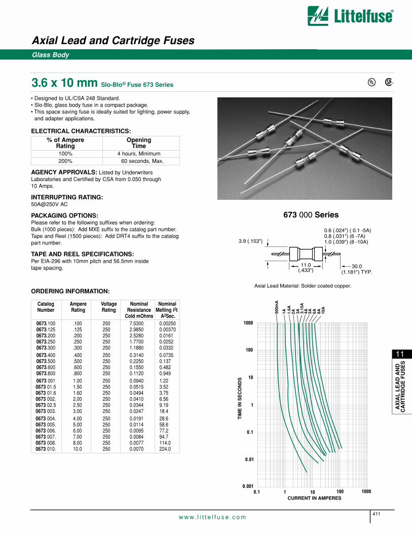
11
AX
IAL
LE
AD
AN
DC
AR
TR
IDG
E F
US
ES
Axial Lead and Cartridge Fuses
411w w w. l i t t e l f u s e . c o m
Glass Body
3.6 x 10 mm Slo-Blo® Fuse 673 Series
• Designed to UL/CSA 248 Standard.• Slo-Blo, glass body fuse in a compact package.• This space saving fuse is ideally suited for lighting, power supply,
and adapter applications.
ELECTRICAL CHARACTERISTICS:% of Ampere Opening
Rating Time100% 4 hours, Minimum200% 60 seconds, Max.
AGENCY APPROVALS: Listed by UnderwritersLaboratories and Certified by CSA from 0.050 through 10 Amps.
INTERRUPTING RATING:50A@250V AC
PACKAGING OPTIONS:Please refer to the following suffixes when ordering:Bulk (1000 pieces): Add MXE suffix to the catalog part number.Tape and Reel (1500 pieces): Add DRT4 suffix to the catalogpart number.
TAPE AND REEL SPECIFICATIONS:Per EIA-296 with 10mm pitch and 56.5mm inside tape spacing.
ORDERING INFORMATION:
®UL ®
Catalog Ampere Voltage Nominal Nominal Number Rating Rating Resistance Melting i2t
Cold mOhms A2Sec.0673.100 .100 250 7.5300 0.002500673.125 .125 250 2.9850 0.003700673.200 .200 250 2.5280 0.01610673.250 .250 250 1.7700 0.02520673.300 .300 250 1.1880 0.03320673.400 .400 250 0.3140 0.07350673.500 .500 250 0.2250 0.1370673.600 .600 250 0.1550 0.4820673.800 .800 250 0.1120 0.9490673 001 1.00 250 0.0940 1.220673 01.5 1.50 250 0.0515 3.520673 01.6 1.60 250 0.0494 3.750673 002. 2.00 250 0.0410 6.560673 02.5 2.50 250 0.0344 9.190673 003. 3.00 250 0.0247 18.40673 004. 4.00 250 0.0191 28.60673 005. 5.00 250 0.0114 58.60673 006. 6.00 250 0.0095 77.20673 007. 7.00 250 0.0084 94.70673 008. 8.00 250 0.0077 114.00673 010. 10.0 250 0.0070 224.0
673 000 Series
3.9 (.153")
30.0(1.181") TYP.
Axial Lead Material: Solder coated copper.
0.6 (.024") ( 0.1 -5A)0.8 (.031") (6 -7A)1.0 (.039") (8 -10A)
11.0(.433")
TIM
E IN
SE
CO
ND
S
CURRENT IN AMPERES
0.01
0.1
0.1
1
1
10
100
10 1000.001
1000
1000
500m
A
1A 1.6A
2A 3A 3.15
A4A 5A 6A 8A 10
A
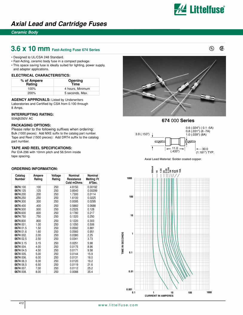
Axial Lead and Cartridge Fuses
412w w w. l i t t e l f u s e . c o m
Ceramic Body
3.6 x 10 mm Fast-Acting Fuse 674 Series
• Designed to UL/CSA 248 Standard.• Fast-Acting, ceramic body fuse in a compact package.• This space saving fuse is ideally suited for lighting, power supply,
and adapter applications.
ELECTRICAL CHARACTERISTICS:% of Ampere Opening
Rating Time100% 4 hours, Minimum200% 5 seconds, Max.
AGENCY APPROVALS: Listed by UnderwritersLaboratories and Certified by CSA from 0.100 through8 Amps.
INTERRUPTING RATING:50A@250V AC
PACKAGING OPTIONS:Please refer to the following suffixes when ordering:Bulk (1000 pieces): Add MXE suffix to the catalog part number.Tape and Reel (1500 pieces): Add DRT4 suffix to the catalogpart number.
TAPE AND REEL SPECIFICATIONS:Per EIA-296 with 10mm pitch and 56.5mm inside tape spacing.
ORDERING INFORMATION:
Catalog Ampere Voltage Nominal Nominal Number Rating Rating Resistance Melting i2t
Cold mOhms A2Sec.0674.100 .100 250 4.8150 0.001920674.125 .125 250 3.8540 0.002990674.200 .200 250 1.7300 0.01140674.250 .250 250 1.6100 0.02250674.300 .300 250 0.9395 0.02950674.400 .400 250 0.5860 0.06880674.500 .500 250 0.2325 0.1280674.600 .600 250 0.1780 0.2170674.750 .750 250 0.1320 0.2500674.800 .800 250 0.1220 0.3030674 001. 1.00 250 0.1050 0.5060674 01.5 1.50 250 0.0592 0.8810674 01.6 1.60 250 0.0560 0.9510674 002. 2.00 250 0.0380 2.250674 02.5 2.50 250 0.0341 3.730674 3.15 3.15 250 0.0251 5.980674 004. 4.00 250 0.0175 8.960674 04.5 4.50 250 0.0171 9.580674 005. 5.00 250 0.0144 15.90674 006. 6.00 250 0.0131 18.00674 06.3 6.30 250 0.0120 19.20674 06.5 6.50 250 0.0119 21.60674 007. 7.00 250 0.0112 25.20674 008. 8.00 250 0.0088 35.4
®UL ®
674 000 Series
3.9 (.153")
30.0(1.181") TYP.
Axial Lead Material: Solder coated copper.
0.6 (.024") ( 0.1 -5A)0.8 (.031") (6 -7A)1.0 (.039") (8A)
11.0(.433")
TIM
E IN
SE
CO
ND
S
CURRENT IN AMPERES
0.01
0.1
0.1
1
1
10
100
10 1000.001
1000
1000
500m
A
1A 1.5A
2A 2.5A
3.15
A4A 5A 6A 8A 10
A

Axial Lead and Cartridge Fuses
413w w w. l i t t e l f u s e . c o m
11
AX
IAL
LE
AD
AN
DC
AR
TR
IDG
E F
US
ES
Ceramic Body
• Designed to UL/CSA 248 Standard.• Slo-Blo, ceramic body fuse in a compact package.• This space saving fuse is ideally suited for lighting, power supply,
and adapter applications.
ELECTRICAL CHARACTERISTICS:% of Ampere Opening
Rating Time100% 4 hours, Minimum200% 60 seconds, Max.
AGENCY APPROVALS: Listed by Underwriters Laboratoriesand Certified by CSA from 0.100 through 5 Amps.
INTERRUPTING RATING:50A @ 250V AC
PACKAGING OPTIONS:Please refer to the following suffixes when ordering:Bulk (1000 pieces): Add MXE suffix to the catalog part number.Tape and Reel (1500 pieces): Add DRT4 suffix to the catalogpart number.
TAPE AND REEL SPECIFICATIONS:Per EIA-296 with 10mm pitch and 56.5mm inside tape spacing.
ORDERING INFORMATION:
®UL ®3.6 x 10 mm Slo-Blo® Fuse 675 Series
Catalog Ampere Voltage Nominal Nominal Number Rating Rating Resistance Melting i2t
Cold mOhms A2Sec.0675.100 .100 250 7.5100 0.002500675.125 .125 250 2.9750 0.003600675.200 .200 250 2.4850 0.01580675.250 .250 250 1.7520 0.02500675.300 .300 250 1.1710 0.03220675.400 .400 250 0.3035 0.07500675.500 .500 250 0.2270 0.1320675.600 .600 250 0.1504 0.4690675.800 .800 250 0.1110 0.9260675 001. 1.00 250 0.0930 1.220675 01.5 1.50 250 0.0510 3.510675 01.6 1.60 250 0.0490 3.710675 002. 2.00 250 0.0405 6.700675 02.5 2.50 250 0.0342 9.250675 003. 3.00 250 0.0245 18.30675 004. 4.00 250 0.0193 28.10675 005. 5.00 250 0.0113 58.8
675 000 Series
3.9 (.153")
30.0(1.181") TYP.
Axial Lead Material: Solder coated copper.
0.6 (.024")
11.0(.433")
TIM
E IN
SE
CO
ND
S
CURRENT IN AMPERES
0.01
0.1
0.1
1
1
10
100
10 1000.001
1000
1000
500m
A
1A 1.6A
2A 3A 3.5A
4A 5A 6A 8A 10A
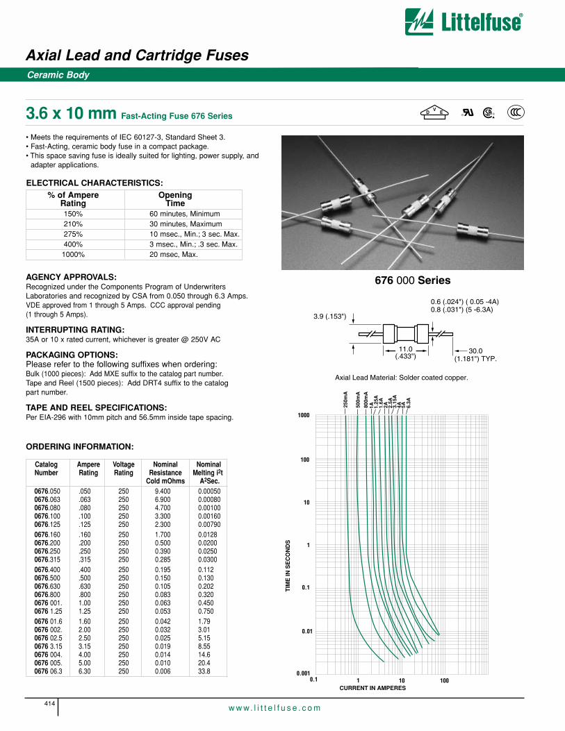
Axial Lead and Cartridge Fuses
414w w w. l i t t e l f u s e . c o m
Ceramic Body
3.6 x 10 mm Fast-Acting Fuse 676 Series
• Meets the requirements of IEC 60127-3, Standard Sheet 3.• Fast-Acting, ceramic body fuse in a compact package.• This space saving fuse is ideally suited for lighting, power supply, and
adapter applications.
ELECTRICAL CHARACTERISTICS:% of Ampere Opening
Rating Time150% 60 minutes, Minimum210% 30 minutes, Maximum275% 10 msec., Min.; 3 sec. Max.400% 3 msec., Min.; .3 sec. Max.1000% 20 msec, Max.
Catalog Ampere Voltage Nominal Nominal Number Rating Rating Resistance Melting i2t
Cold mOhms A2Sec.0676.050 .050 250 9.400 0.000500676.063 .063 250 6.900 0.000800676.080 .080 250 4.700 0.001000676.100 .100 250 3.300 0.001600676.125 .125 250 2.300 0.007900676.160 .160 250 1.700 0.01280676.200 .200 250 0.500 0.02000676.250 .250 250 0.390 0.02500676.315 .315 250 0.285 0.03000676.400 .400 250 0.195 0.1120676.500 .500 250 0.150 0.1300676.630 .630 250 0.105 0.2020676.800 .800 250 0.083 0.3200676 001. 1.00 250 0.063 0.4500676 1.25 1.25 250 0.053 0.7500676 01.6 1.60 250 0.042 1.790676 002. 2.00 250 0.032 3.010676 02.5 2.50 250 0.025 5.150676 3.15 3.15 250 0.019 8.550676 004. 4.00 250 0.014 14.60676 005. 5.00 250 0.010 20.40676 06.3 6.30 250 0.006 33.8
AGENCY APPROVALS:Recognized under the Components Program of UnderwritersLaboratories and recognized by CSA from 0.050 through 6.3 Amps.VDE approved from 1 through 5 Amps. CCC approval pending (1 through 5 Amps).
INTERRUPTING RATING:35A or 10 x rated current, whichever is greater @ 250V AC
PACKAGING OPTIONS:Please refer to the following suffixes when ordering:Bulk (1000 pieces): Add MXE suffix to the catalog part number.Tape and Reel (1500 pieces): Add DRT4 suffix to the catalog part number.
TAPE AND REEL SPECIFICATIONS:Per EIA-296 with 10mm pitch and 56.5mm inside tape spacing.
ORDERING INFORMATION:
®
VD E
676 000 Series
3.9 (.153")
30.0(1.181") TYP.
Axial Lead Material: Solder coated copper.
0.6 (.024") ( 0.05 -4A)0.8 (.031") (5 -6.3A)
11.0(.433")
TIM
E IN
SE
CO
ND
S
CURRENT IN AMPERES
0.01
0.1
0.1
1
1
10
100
10 1000.001
1000
250m
A
500m
A
800m
A1A 1.
25A
1.6A
2A 2.5A
3.15
A4A 5A 6.
3A
®

Axial Lead and Cartridge Fuses
415w w w. l i t t e l f u s e . c o m
Ceramic Body
3.6 x 10 mm Slo-Blo® Fuse 677 Series
• Meets the requirements of IEC 60127-3, Standard Sheet 4.• Slo-Blo, ceramic body fuse in a compact package.• This space saving fuse is ideally suited for lighting, power supply, and
adapter applications.
ELECTRICAL CHARACTERISTICS:% of Ampere Opening
Rating Time150% 60 minutes, Minimum210% 2 minutes, Maximum275% 400 msec., Min.; 10 sec. Max.400% 150 msec., Min.; .3 sec. Max.1000% 20 msec., Min.; 150 msec Max.
Catalog Ampere Voltage Nominal Nominal Number Rating Rating Resistance Melting i2t
Cold mOhms A2Sec.0677.250 .250 250 0.630 0.3120677.315 .315 250 0.460 0.4220677.400 .400 250 0.360 0.7550677.500 .500 250 0.310 1.320677.630 .630 250 0.178 2.550677.800 .800 250 0.125 3.250677 001. 1.00 250 0.092 6.950677 1.25 1.25 250 0.065 12.10677 01.6 1.60 250 0.048 18.20677 002. 2.00 250 0.035 20.80677 02.5 2.50 250 0.028 32.50677 3.15 3.15 250 0.020 40.80677 004. 4.00 250 0.016 95.00677 005. 5.00 250 0.014 1400677 06.3 6.30 250 0.009 240
AGENCY APPROVALS:Recognized under the Components Program of UnderwritersLaboratories and recognized by CSA from 0.250 through 6.3 Amps.VDE approved from 0.250 through 6.3 Amps. CCC approval pending(0.250 through 6.3 Amps).
INTERRUPTING RATING:35A or 10 x rated current, whichever is greater @ 250V AC
PACKAGING OPTIONS:Please refer to the following suffixes when ordering:Bulk (1000 pieces): Add MXE suffix to the catalog part number.Tape and Reel (1500 pieces): Add DRT4 suffix to the catalog part number.
TAPE AND REEL SPECIFICATIONS:Per EIA-296 with 10mm pitch and 56.5mm inside tape spacing.
ORDERING INFORMATION:
®®
VD E
677 000 Series
3.9 (.153")
30.0(1.181") TYP.
Axial Lead Material: Solder coated copper.
0.6 (.024") ( 0.250 -4A)0.8 (.031") (5 -6.3A)
11.0(.433")
TIM
E IN
SE
CO
ND
S
CURRENT IN AMPERES
0.01
0.1
0.1
1
1
10
100
10 100 1000
1000
250m
A31
5mA
400m
A
1.6A
2A 2.5A
3.15
A4A 5A 6.
3A
1A 1.25
A
500m
A
800m
A63
0mA
11
AX
IAL
LE
AD
AN
DC
AR
TR
IDG
E F
US
ES

Axial Lead and Cartridge Fuses
416w w w. l i t t e l f u s e . c o m
Special
3AB Very Fast-Acting Fuse 322 Series
ELECTRICAL CHARACTERISTICS:% of Ampere Ampere Opening
Rating Rating Time100% 1–30 4 hours, Minimum
250%1–10 .2 second, Maximum
12–30 1 second, Maximum
AGENCY APPROVALS: Recognized under the Components Programof Underwriters Laboratories from 1 through 10 amperes at 250 VAC/65 VDC, 12 through 30 amperes at 65VAC/VDC.
INTERUPTING RATINGS:1-10A 10,000A @ 125 VAC
100A @ 250 VAC12-30A 200A @ 65 VAC
ORDERING INFORMATION:
Cartridge NominalCatalog Ampere Voltage ResistanceNumber Rating Rating Cold Ohms322 001 1 250 0.26322 1.25 11/4 250 0.175322 002 2 250 0.132322 003 3 250 0.063322 004 4 250 0.044322 005 5 250 0.035322 006 6 250 0.027322 007 7 250 0.022322 008 8 250 0.019322 009 9 250 0.016322 010 10 250 0.0135322 012 12 65 0.0052322 015 15 65 0.0043322 020 20 65 0.0034322 025 25 65 0.0029322 030 30 65 0.0023
ELECTRICAL CHARACTERISTICS:% of Ampere Opening
Rating Time110% 4 hours, Minimum135% 1 hour, Maximum200% 10 seconds, Maximum
AGENCY APPROVALS: Listed by Underwriters Laboratories.
DESIGN STANDARDS: UL Standard 275. SAE (Society ofAutomotive Engineers) J554.
ORDERING INFORMATION:
NominalCatalog Ampere Voltage Resistance FuseNumber Rating Rating Cold Ohms Length307 004 4 32 0.0220 15.875 (5/8")307 006 6 32 0.0144 19.05 (3/4")307 07.5 71/2 32 0.0113 22.23 (7/8")307 009 9 32 0.00945 22.23 (7/8")307 014 14 32 0.0055 26.99 (11/16")307 020 20 32 0.0034 31.75 (11/4")307 030 30 32 0.0021 36.51 (17/16")
LOW VOLTAGE
SFE Fast-Acting Type 307 Series ®UL
For protection of silicon controlled rectifiers and similar solid-state devices.
307 000 Series
6.35 (.25")
SEE CHART
322 000 Series
6.35 (.25")
31.75(1.25")
®

11
AX
IAL
LE
AD
AN
DC
AR
TR
IDG
E F
US
ES
Axial Lead and Cartridge Fuses
417w w w. l i t t e l f u s e . c o m
Subminiature
ELECTRICAL CHARACTERISTICS:% of Ampere
Rating Time150% 1 hour, Minimum
210% 30 minutes, Maximum275% .010 sec Min.; 3 sec Max
400% .003 sec Min.; .030 sec Max
1000% .020 sec Maximum
AGENCY APPROVALS: IEC 60127-3/1: VDE and Semko approved50 mA through 3.15 A. Recognized under the Components ProgramUnderwriters Laboratories and CSA accepted 40mA through 5A.
INTERRUPTING RATINGS: 35A or 10X rated current;whichever is greater.
ENVIRONMENTAL SPECIFICATIONS:Operating Temperature: -40˚C to +85˚C.Case Resistance: Min 100 Mohms, according to EIA/IS-722, 4.7Vibration: 20gn, 20 min, 10Hz to 2,000Hz, 12 cycles according toEIA/IS-722, 4.10 (Frequency range 10-2000Hz, cross-over frequency 60Hz according to IEC 60068-2-6, test Fc)Mechanical Shock: 50g, half sine wave, 11ms, 3 times each directionaccording to IEC 60068-2-27.Resistance to Cleaning Solvents: Clean according to EIA/IS-722, 4.11Resistance to Soldering Heat: 10 sec. At 260˚C to IEC 60068-2-20,test TbTerminal Strength: Tensile load min. 9N, according to EIA/IS-722, 4.5.5
PHYSICAL SPECIFICATIONS:Materials: Temperature Resistant Body, UL 94V-0; Sn Coated CopperWire Terminals.Solderability: IEC 60068-2-20, test TaSoldering Parameters: Wave Solder – 235˚C, 2 seconds maximum.
PACKAGING:Please refer to the following suffixes when ordering:• 100 Piece Bulk: Short Leads use suffix HXSL;
Long Leads use suffix HXLL• 750 Piece Tape and Reel per IEC 286-2:
(Long Leads only) use suffix ZRLL
• 1000 Piece Ammo Pack use suffix MALLPATENTED
Nominal NominalCatalog Ampere Voltage Resistance Melting I2tNumber Rating Rating Cold mOhms A2 Sec0662.040 .040 250 7500 0.000160662.050 .050 250 4483 0.000400662.063 .063 250 3866 0.0010662.080 .080 250 2545 0.0010662.100 .100 250 2010 0.0020662.125 .125 250 1346 0.0060662.160 .160 250 2960 0.0140662.200 .200 250 2256 0.0240662.250 .250 250 1460 0.0580662.315 .315 250 1209 0.1040662.400 .400 250 180 0.0440662.500 .500 250 128 0.0900662.630 .630 250 96 0.1500662.800 .800 250 78 0.2200662 001. 1.00 250 64 0.3300662 1.25 1.25 250 45 0.6800662 01.6 1.60 250 37 0.9400662 002. 2.00 250 29 1.330662 02.5 2.50 250 24 1.940662 3.15 3.15 250 17 5.400662 004. 4.00 250 13 7.900662 005. 5.00 250 10 11.19
Refer to page 342 for LT-5TM holder information.
18.8
(.74
0")
8.5(.335")
8.45
(.33
3")
0.64(.025")
0.57
(.0
12")
5.08(.200")
4.3(
.169
")
8.5(.335")
8.45
(.33
3")
0.64(.025")
0.57
(.01
2")
5.08(.200")
ORDERING INFORMATION:
VD E
®LT-5™Fast-Acting Fuse 662 Series ®

Subminiature
Axial Lead and Cartridge Fuses
LT-5™Fast-Acting Fuse 662 Series
418w w w. l i t t e l f u s e . c o m
1000
100
10
1
0.1
0.01
0.00110
CURRENT IN AMPERES
TIM
E IN
SEC
ONDS
1000.1 10.05
5A4A3.15
A2.
5A2A1.
6A1.
25A
1A800m
A63
0mA
500m
A40
0mA
315m
A25
0mA
200m
A16
0mA
125m
A10
0mA
80m
A63
mA
50m
A40
mA
Average Time Current Curves
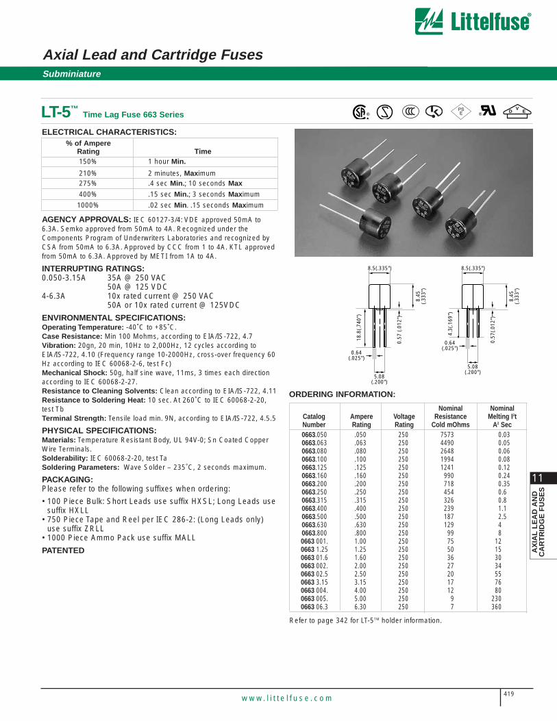
11
AX
IAL
LE
AD
AN
DC
AR
TR
IDG
E F
US
ES
Subminiature
LT-5™Time Lag Fuse 663 Series
ELECTRICAL CHARACTERISTICS:% of Ampere
Rating Time150% 1 hour Min.
210% 2 minutes, Maximum275% .4 sec Min.; 10 seconds Max
400% .15 sec Min.; 3 seconds Maximum
1000% .02 sec Min. .15 seconds Maximum
AGENCY APPROVALS: IEC 60127-3/4: VDE approved 50mA to6.3A. Semko approved from 50mA to 4A. Recognized under theComponents Program of Underwriters Laboratories and recognized byCSA from 50mA to 6.3A. Approved by CCC from 1 to 4A. KTL approvedfrom 50mA to 6.3A. Approved by METI from 1A to 4A.
INTERRUPTING RATINGS:0.050-3.15A 35A @ 250 VAC
50A @ 125 VDC4-6.3A 10x rated current @ 250 VAC
50A or 10x rated current @ 125VDC
ENVIRONMENTAL SPECIFICATIONS:Operating Temperature: -40˚C to +85˚C.Case Resistance: Min 100 Mohms, according to EIA/IS-722, 4.7Vibration: 20gn, 20 min, 10Hz to 2,000Hz, 12 cycles according toEIA/IS-722, 4.10 (Frequency range 10-2000Hz, cross-over frequency 60Hz according to IEC 60068-2-6, test Fc)Mechanical Shock: 50g, half sine wave, 11ms, 3 times each directionaccording to IEC 60068-2-27.Resistance to Cleaning Solvents: Clean according to EIA/IS-722, 4.11Resistance to Soldering Heat: 10 sec. At 260˚C to IEC 60068-2-20,test TbTerminal Strength: Tensile load min. 9N, according to EIA/IS-722, 4.5.5
PHYSICAL SPECIFICATIONS:Materials: Temperature Resistant Body, UL 94V-0; Sn Coated CopperWire Terminals.Solderability: IEC 60068-2-20, test TaSoldering Parameters: Wave Solder – 235˚C, 2 seconds maximum.
PACKAGING:Please refer to the following suffixes when ordering:
• 100 Piece Bulk: Short Leads use suffix HXSL; Long Leads usesuffix HXLL
• 750 Piece Tape and Reel per IEC 286-2: (Long Leads only)use suffix ZRLL
• 1000 Piece Ammo Pack use suffix MALL
PATENTED
18.8
(.74
0")
8.5(.335")
8.45
(.33
3")
0.64(.025")
0.57
(.0
12")
5.08(.200")
4.3(
.169
")
8.5(.335")
8.45
(.33
3")
0.64(.025")
0.57
(.01
2")
5.08(.200")
VD E
®
Nominal NominalCatalog Ampere Voltage Resistance Melting I2tNumber Rating Rating Cold mOhms A2 Sec0663.050 .050 250 7573 0.030663.063 .063 250 4490 0.050663.080 .080 250 2648 0.060663.100 .100 250 1994 0.080663.125 .125 250 1241 0.120663.160 .160 250 990 0.240663.200 .200 250 718 0.350663.250 .250 250 454 0.60663.315 .315 250 326 0.80663.400 .400 250 239 1.10663.500 .500 250 187 2.50663.630 .630 250 129 40663.800 .800 250 99 80663 001. 1.00 250 75 120663 1.25 1.25 250 50 150663 01.6 1.60 250 36 300663 002. 2.00 250 27 340663 02.5 2.50 250 20 550663 3.15 3.15 250 17 760663 004. 4.00 250 12 800663 005. 5.00 250 9 2300663 06.3 6.30 250 7 360
Refer to page 342 for LT-5TM holder information.
ORDERING INFORMATION:
Axial Lead and Cartridge Fuses
419w w w. l i t t e l f u s e . c o m
®

Axial Lead and Cartridge Fuses
420w w w. l i t t e l f u s e . c o m
Average Time Current Curves
1001010.1CURRENT IN AMPERES
50m
A63
mA
80m
A10
0mA
125m
A16
0mA
200m
A25
0mA
315m
A40
0mA
500m
A63
0mA
800m
A1A 1.
25A
1.6A
2A 2.5A
3.15
A4A 5A 6.
3A
1000
100
10
1
0.1
0.01
TIM
E IN
SE
CO
ND
S
0.05
LT-5™Time Lag Fuse 663 Series
Subminiature

Axial Lead and Cartridge Fuses
421w w w. l i t t e l f u s e . c o m
11
AX
IAL
LE
AD
AN
DC
AR
TR
IDG
E F
US
ES
• Similar to the 663 fuse, this fuse is designed with a higher breaking capacity.
• Meets IEC 60127-3/4 specifications (up to 6.3A).• Available in short and long lead variations.
ELECTRICAL CHARACTERISTICS:% of Ampere Ampere
Rating Rating Time150% 800mA-6.3A 1 hour Min.
210% 800mA-6.3A 2 minutes, Maximum275% 800mA-6.3A .4 sec Min.; 10 seconds Maximum
400% 800mA-6.3A .1 sec Min.; 3 seconds Maximum
1000% 800mA-6.3A .02 sec Min. .15 seconds Maximum
100% 8-10A 4 hours, Min.
200% 8-10A 60 seconds, Maximum
AGENCY APPROVALS: IEC 60127-3/4: VDE and Semko approvedfrom 800mA to 4A. Recognized under the components program ofUnderwriters Laboratories and recognized by CSA from 800mA to 6.3A.Approved by KTL from 800mA to 6.3A. Approved by METI and CCCfrom 1 to 4A. Listed by the Underwriters Laboratories for 8 and 10A rat-ings.
INTERRUPTING RATINGS: 100A at 250 VAC.
ENVIRONMENTAL SPECIFICATIONS:Operating Temperature: -40˚C to +85˚C.Case Resistance: Min 100 Mohms, according to EIA/IS-722, 4.7Vibration: 20gn, 20 min, 10Hz to 2,000Hz, 12 cycles according toEIA/IS-722, 4.10 (Frequency range 10-2000Hz, cross-over frequency 60Hz according to IEC 60068-2-6, test Fc)Mechanical Shock: 50g, half sine wave, 11ms, 3 times each directionaccording to IEC 60068-2-27.Resistance to Cleaning Solvents: Clean according to EIA/IS-722, 4.11Resistance to Soldering Heat: 10 sec. At 260˚C to IEC 60068-2-20,test TbTerminal Strength: Tensile load min. 9N, according to EIA/IS-722, 4.5.5
PHYSICAL SPECIFICATIONS:Materials: Temperature Resistant Body, UL 94V-0; Sn Coated CopperWire Terminals.Solderability: IEC 60068-2-20, test TaSoldering Parameters: Wave Solder – 235˚C, 2 seconds maximum.
PACKAGING:Please refer to the following suffixes when ordering:• 100 Piece Bulk: Short Leads use suffix HXSL;
Long Leads use suffix HXLL• 750 Piece Tape and Reel per IEC 286-2:
(Long Leads only) use suffix ZRLL
• 1000 Piece Ammo Pack use suffix MALLPATENTED
Subminiature
LT-5™Time Lag Extended Breaking Capacity Fuse 664 Series
18.8
(.74
0")
8.5(.335")
8.45
(.33
3")
0.64(.025")
0.57
(.0
12")
5.08(.200")
4.3(
.169
")
8.5(.335")
8.45
(.33
3")
0.64(.025")
0.57
(.01
2")
5.08(.200")
VD E
®
Nominal NominalCatalog Ampere Voltage Resistance Melting I2tNumber Rating Rating Cold mOhms A2 Sec0664.800 .800 250 168 2.20664 001. 1.00 250 123 4.40664 1.25 1.25 250 85 6.30664 01.6 1.60 250 60 100664 002. 2.00 250 39 160664 02.5 2.50 250 30 320664 3.15 3.15 250 20 570664 004. 4.00 250 17 770664 005. 5.00 250 11 1550664 06.3 6.30 250 9 2620664 008. 8.00 250 7 3970664 010. 10.00 250 6 440
Refer to page 342 for LT-5TM holder information.
ORDERING INFORMATION:
®®UL

Axial Lead and Cartridge Fuses
422w w w. l i t t e l f u s e . c o m
Subminiature
LT-5™Time Lag Extended Breaking Capacity Fuse 664 Series
800m
A1A 1.
25A
1.6A
2A 2.5A
3.15
A4A 5A 6.
3A8A 10
A
1000
100
10
1
0.1
0.01
TIM
E IN
SE
CO
ND
S
10 1001CURRENT IN AMPERES
Average Time Current Curves

11
AX
IAL
LE
AD
AN
DC
AR
TR
IDG
E F
US
ES
Axial Lead and Cartridge Fuses
423w w w. l i t t e l f u s e . c o m
Subminiature
LT-5™Time Lag Fuse 665 Series
ELECTRICAL CHARACTERISTICS:% of Ampere
Rating Time100% 4 hours Min200% 60 sec Max
AGENCY APPROVALS: Listed by Underwriters Laboratories from50mA to 10A. CSA Certified from 50mA to 6.3A.
INTERRUPTING RATINGS: 50A at 250VAC
ENVIRONMENTAL SPECIFICATIONS:Operating Temperature: -40˚C to +85˚C.Case Resistance: Min 100 Mohms, according to EIA/IS-722, 4.7Vibration: 20gn, 20 min, 10Hz to 2,000Hz, 12 cycles according toEIA/IS-722, 4.10 (Frequency range 10-2000Hz, cross-over frequency 60Hz according to IEC 60068-2-6, test Fc)Mechanical Shock: 50g, half sine wave, 11ms, 3 times each directionaccording to IEC 60068-2-27.Resistance to Cleaning Solvents: Clean according to EIA/IS-722, 4.11Resistance to Soldering Heat: 10 sec. At 260˚C to IEC 60068-2-20,test TbTerminal Strength: Tensile load min. 9N, according to EIA/IS-722, 4.5.5
PHYSICAL SPECIFICATIONS:Materials: Temperature Resistant Body, UL 94V-0; Sn Coated CopperWire Terminals.Solderability: IEC 60068-2-20, test TaSoldering Parameters: Wave Solder – 235˚C, 2 seconds maximum.
PACKAGING:Please refer to the following suffixes when ordering:• 100 Piece Bulk: Short Leads use suffix HXSL; Long Leads use suffix
HXLL• 750 Piece Tape and Reel per IEC 286-2: (Long Leads only) use suffix
ZRLL• 1000 Piece Ammo Pack use suffix MALL
PATENTED
Nominal I2tCatalog Ampere Voltage Resistance at 10 x InNumber Rating Rating Cold mOhms (A2 Sec)0665.063 .063 250 7548 0.01760665.080 .080 250 4427 0.03130665.100 .100 250 2715 0.04560665.125 .125 250 2038 0.05670665.160 .160 250 1238 0.06920665.200 .200 250 1091 0.1330665.250 .250 250 696 0.2580665.315 .315 250 465 0.3610665.400 .400 250 334 0.5280665.500 .500 250 243 0.8980665.630 .630 250 170 2.240665.800 .800 250 121 4.050665 001. 1.00 250 86 6.850665 1.25 1.25 250 66 7.93066501.6 1.60 250 46 17.50665 002. 2.00 250 34 28.60665 02.5 2.50 250 26 40.90665 3.15 3.15 250 20 55.00665 004. 4.00 250 15 67.20665 005. 5.00 250 12 142066506.3 6.30 250 9 2870665 008. 8.00 250 5 4220665 010. 10.0 250 4 564
18.8
(.74
0")
8.5(.335")
8.45
(.33
3")
0.64(.025")
0.57
(.0
12")
5.08(.200")
4.3(
.169
")
8.5(.335")
8.45
(.33
3")
0.64(.025")
0.57
(.01
2")
5.08(.200")
®
ORDERING INFORMATION:
®UL

Axial Lead and Cartridge Fuses
424w w w. l i t t e l f u s e . c o m
Subminiature
LT-5™Time Lag Fuse 665 Series
10 1001.01CURRENT IN AMPERES
1A 1.25
A1.
6A
800m
A63
0mA
2A 2.5A
3.15
A4A 5A 6.
3A8A 10
A
TIM
E IN
SE
CO
ND
S
63m
A80
mA
100m
A12
5mA
160m
A20
0mA
250m
A31
5mA
400m
A50
0mA
10000
1000
100
10
1
0.1
0.01
Average Time Current Curves
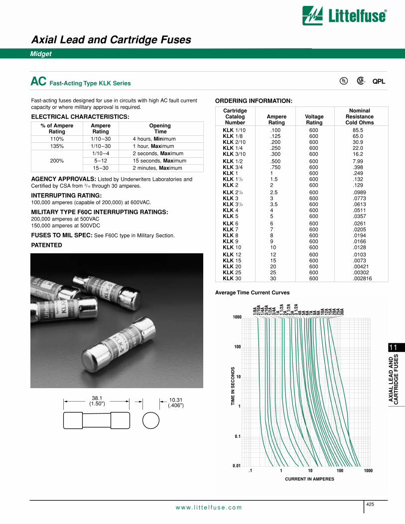
Axial Lead and Cartridge Fuses
425w w w. l i t t e l f u s e . c o m
11
AX
IAL
LE
AD
AN
DC
AR
TR
IDG
E F
US
ES
Midget
AC Fast-Acting Type KLK Series
Fast-acting fuses designed for use in circuits with high AC fault currentcapacity or where military approval is required.
ELECTRICAL CHARACTERISTICS:% of Ampere Ampere Opening
Rating Rating Time110% 1/10–30 4 hours, Minimum135% 1/10–30 1 hour, Maximum
1/10–4 2 seconds, Maximum200% 5–12 15 seconds, Maximum
15–30 2 minutes, Maximum
AGENCY APPROVALS: Listed by Underwriters Laboratories andCertified by CSA from 3/10 through 30 amperes.
INTERRUPTING RATING:100,000 amperes (capable of 200,000) at 600VAC.
MILITARY TYPE F60C INTERRUPTING RATINGS:200,000 amperes at 500VAC150,000 amperes at 500VDC
FUSES TO MIL SPEC: See F60C type in Military Section.
PATENTED
1000
100
10
1
0.1
0.0110 100 1000.1 1
1/8A
2/10
A1/
4A3/
10A
1/2A
3/4A
1A 1 1/
2A2A 2
1/2A
3A 3 1/
2A4A 5A 6A 7A 8A 9A 10
A12
A15
A20
A25
A30
A
TIM
E IN
SE
CO
ND
S
CURRENT IN AMPERES
ORDERING INFORMATION:
Cartridge NominalCatalog Ampere Voltage ResistanceNumber Rating Rating Cold Ohms
KLK 1/10 .100 600 85.5KLK 1/8 .125 600 65.0KLK 2/10 .200 600 30.9KLK 1/4 .250 600 22.0KLK 3/10 .300 600 16.2KLK 1/2 .500 600 7.99KLK 3/4 .750 600 .398KLK 1 1 600 .249KLK 11/2 1.5 600 .132KLK 2 2 600 .129KLK 21/2 2.5 600 .0989KLK 3 3 600 .0773KLK 31/2 3.5 600 .0613KLK 4 4 600 .0511KLK 5 5 600 .0357KLK 6 6 600 .0261KLK 7 7 600 .0205KLK 8 8 600 .0194KLK 9 9 600 .0166KLK 10 10 600 .0128KLK 12 12 600 .0103KLK 15 15 600 .0073KLK 20 20 600 .00421KLK 25 25 600 .00302KLK 30 30 600 .002816
Average Time Current Curves
38.1(1.50")
10.31(.406")
®UL ® QPL
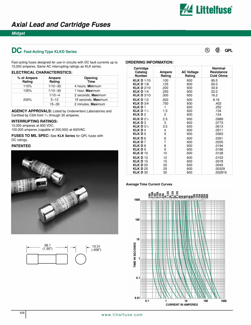
Axial Lead and Cartridge Fuses
426w w w. l i t t e l f u s e . c o m
Midget
DC Fast-Acting Type KLKD Series
Fast-acting fuses designed for use in circuits with DC fault currents up to10,000 amperes. Same AC interrupting ratings as KLK series.
ELECTRICAL CHARACTERISTICS:% of Ampere Ampere Opening
Rating Rating Time110% 1/10–30 4 hours, Minimum135% 1/10–30 1 hour, Maximum
1/10–4 2 seconds, Maximum200% 5–12 15 seconds, Maximum
15–30 2 minutes, Maximum
AGENCY APPROVALS: Listed by Underwriters Laboratories andCertified by CSA from 3/10 through 30 amperes.
INTERRUPTING RATINGS:10,000 amperes at 600 VDC.100,000 amperes (capable of 200,000) at 600VAC.
FUSES TO MIL SPEC: See KLK Series for QPL fuses with DC ratings.
PATENTED
1000
100
10
1
0.1
0.0110 100 10000.1 1
1/8A
2/10
A1/
4A3/
10A
1/2A
3/4A
1A 1 1/
2A2A 2
1/2A
3A 3 1/
2A4A 5A 6A 7A 8A 9A 10
A12
A15
A20
A25
A30
A
TIM
E IN
SE
CO
ND
S
CURRENT IN AMPERES
ORDERING INFORMATION:
Cartridge NominalCatalog Ampere AC Voltage ResistanceNumber Rating Rating Cold Ohms
KLK D 1/10 .100 600 85.5KLK D 1/8 .125 600 65.0KLK D 2/10 .200 600 30.9KLK D 1/4 .250 600 22.0KLK D 3/10 .300 600 16.2KLK D 1/2 .500 600 8.16KLK D 3/4 .750 600 .402KLK D 1 1 600 .252KLK D 11/2 1.5 600 .134KLK D 2 2 600 .124KLK D 21/2 2.5 600 .0989KLK D 3 3 600 .0773KLK D 31/2 3.5 600 .0613KLK D 4 4 600 .0511KLK D 5 5 600 .0363KLK D 6 6 600 .0261KLK D 7 7 600 .0205KLK D 8 8 600 .0194KLK D 9 9 600 .0166KLK D 10 10 600 .0128KLK D 12 12 600 .0103KLK D 15 15 600 .0078KLK D 20 20 600 .0045KLK D 25 25 600 .00329KLK D 30 30 600 .002816
Average Time Current Curves
38.1(1.50")
10.31(.406")
®UL ® QPL
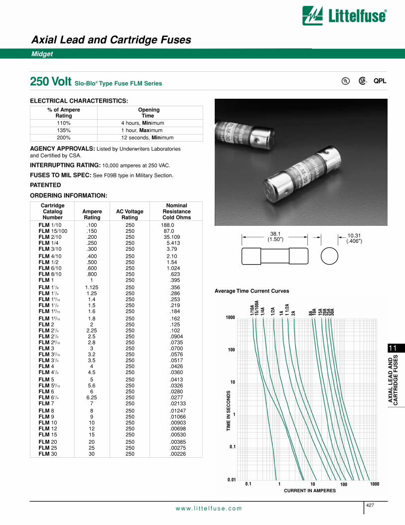
Axial Lead and Cartridge Fuses
427w w w. l i t t e l f u s e . c o m
11
AX
IAL
LE
AD
AN
DC
AR
TR
IDG
E F
US
ES
Midget
250 Volt Slo-Blo® Type Fuse FLM Series
1000
100
10
1
0.1
0.0110 100 10000.1 1
1/10
A15
/100
A1/
4A
1/2A
1A 1 1/
2A2A 8A 10
A15
A20
A25
A30
A
TIM
E IN
SE
CO
ND
S
CURRENT IN AMPERES
Cartridge NominalCatalog Ampere AC Voltage ResistanceNumber Rating Rating Cold Ohms
FLM 1/10 .100 250 188.0FLM 15/100 .150 250 87.0FLM 2/10 .200 250 35.109FLM 1/4 .250 250 5.413FLM 3/10 .300 250 3.79FLM 4/10 .400 250 2.10FLM 1/2 .500 250 1.54FLM 6/10 .600 250 1.024FLM 8/10 .800 250 .623FLM 1 1 250 .395FLM 11/8 1.125 250 .356FLM 11/4 1.25 250 .286FLM 14/10 1.4 250 .253FLM 11/2 1.5 250 .219FLM 16/10 1.6 250 .184FLM 18/10 1.8 250 .162FLM 2 2 250 .125FLM 21/4 2.25 250 .102FLM 21/2 2.5 250 .0904FLM 28/10 2.8 250 .0735FLM 3 3 250 .0700FLM 32/10 3.2 250 .0576FLM 31/2 3.5 250 .0517FLM 4 4 250 .0426FLM 41/2 4.5 250 .0360FLM 5 5 250 .0413FLM 56/10 5.6 250 .0326FLM 6 6 250 .0280FLM 61/4 6.25 250 .0277FLM 7 7 250 .02133FLM 8 8 250 .01247FLM 9 9 250 .01066FLM 10 10 250 .00903FLM 12 12 250 .00698FLM 15 15 250 .00530FLM 20 20 250 .00385FLM 25 25 250 .00275FLM 30 30 250 .00226
ELECTRICAL CHARACTERISTICS:% of Ampere Opening
Rating Time110% 4 hours, Minimum135% 1 hour, Maximum200% 12 seconds, Minimum
AGENCY APPROVALS: Listed by Underwriters Laboratories and Certified by CSA.
INTERRUPTING RATING: 10,000 amperes at 250 VAC.
FUSES TO MIL SPEC: See F09B type in Military Section.
PATENTED
ORDERING INFORMATION:
Average Time Current Curves
38.1(1.50")
10.31(.406")
®UL ® QPL
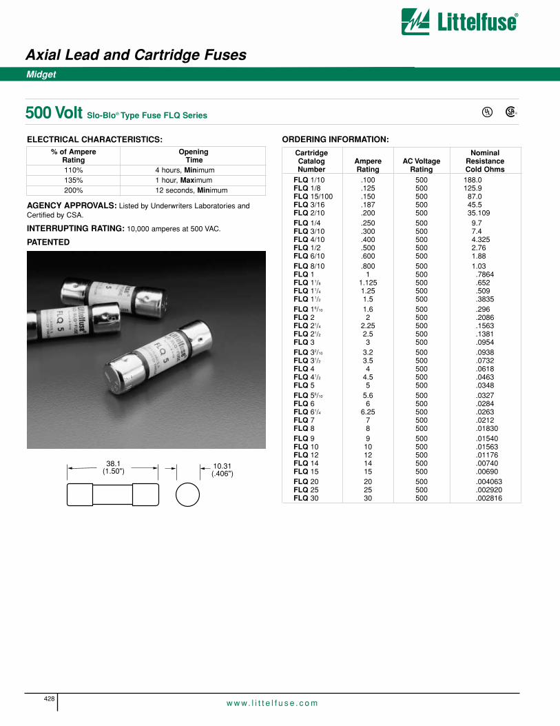
Axial Lead and Cartridge Fuses
428w w w. l i t t e l f u s e . c o m
Midget
500 Volt Slo-Blo® Type Fuse FLQ Series
ELECTRICAL CHARACTERISTICS:% of Ampere Opening
Rating Time110% 4 hours, Minimum135% 1 hour, Maximum200% 12 seconds, Minimum
AGENCY APPROVALS: Listed by Underwriters Laboratories andCertified by CSA.
INTERRUPTING RATING: 10,000 amperes at 500 VAC.
PATENTED
ORDERING INFORMATION:
Cartridge NominalCatalog Ampere AC Voltage ResistanceNumber Rating Rating Cold Ohms
FLQ 1/10 .100 500 188.0FLQ 1/8 .125 500 125.9FLQ 15/100 .150 500 87.0FLQ 3/16 .187 500 45.5FLQ 2/10 .200 500 35.109FLQ 1/4 .250 500 9.7FLQ 3/10 .300 500 7.4FLQ 4/10 .400 500 4.325FLQ 1/2 .500 500 2.76FLQ 6/10 .600 500 1.88FLQ 8/10 .800 500 1.03FLQ 1 1 500 .7864FLQ 11/8 1.125 500 .652FLQ 11/4 1.25 500 .509FLQ 11/2 1.5 500 .3835FLQ 16/10 1.6 500 .296FLQ 2 2 500 .2086FLQ 21/4 2.25 500 .1563FLQ 21/2 2.5 500 .1381FLQ 3 3 500 .0954FLQ 32/10 3.2 500 .0938FLQ 31/2 3.5 500 .0732FLQ 4 4 500 .0618FLQ 41/2 4.5 500 .0463FLQ 5 5 500 .0348FLQ 56/10 5.6 500 .0327FLQ 6 6 500 .0284FLQ 61/4 6.25 500 .0263FLQ 7 7 500 .0212FLQ 8 8 500 .01830FLQ 9 9 500 .01540FLQ 10 10 500 .01563FLQ 12 12 500 .01176FLQ 14 14 500 .00740FLQ 15 15 500 .00690FLQ 20 20 500 .004063FLQ 25 25 500 .002920FLQ 30 30 500 .002816
38.1(1.50")
10.31(.406")
®UL ®

Axial Lead and Cartridge Fuses
429w w w. l i t t e l f u s e . c o m
11
AX
IAL
LE
AD
AN
DC
AR
TR
IDG
E F
US
ES
Special Midget
13/8" Long Fast-Acting Type Fuse BLS Series
ELECTRICAL CHARACTERISTICS:% of Ampere Ampere Opening
Rating Rating Time100% 2/10–10 4 hours, Minimum135% 2/10–10 1 hour, Maximum
200%2/10–5 5 seconds, Maximum6–10 10 seconds, Maximum
AGENCY APPROVALS: Listed by Underwriters Laboratories from 1/2
through 5 amperes and Certified by CSA from 1/2 through 5 amperes.
INTERRUPTING RATING: 10,000 amperes at rated VAC.
PATENTED
ORDERING INFORMATION:
Cartridge NominalCatalog Ampere AC Voltage ResistanceNumber Rating Rating Cold Ohms
BLS 2/10 .200 600 36BLS 4/10 .400 600 11.5BLS 1/2 .500 600 1.25BLS 3/4 .750 600 .591BLS 8/10 .800 600 .524BLS 1 1 600 .944BLS 11/2 1.5 600 .190BLS 16/10 1.6 600 .180BLS 18/10 1.8 600 .143BLS 2 2 600 .2608BLS 3 3 600 .10625BLS 4 4 600 .0464BLS 5 5 600 .0330BLS 6 6 250 .0182BLS 7 7 250 .1045BLS 8 8 250 .012BLS 10 10 250 .00881
Slo-Blo®Indicating Type Fuse FLA Series
ELECTRICAL CHARACTERISTICS:% of Ampere Opening
Rating Time110% 4 hours, Minimum135% 1 hour, Maximum
AGENCY APPROVALS: Listed by Underwriters Laboratories.
INTERRUPTING RATING: 10,000 amperes at rated VAC.
INDICATING PIN: Extends 0.3" when fuse opens.NOTE: Fuses rated 12–30 amperes have dual tube construction.
Nominal NominalCatalog Ampere Resistance Catalog Ampere Resistance AC VoltageNumber Rating Cold Ohms Number Rating Cold Ohms Rating
FLA 1/10 .100 200.0 FLA 5 5 .06304 125FLA 15/100 .15 88.90 FLA 56/10 5.6 .05194 125FLA 2/10 .200 50.00 FLA 6 6 .04253 125FLA 1/4 .250 32.00 FLA 61/4 6.25 .03794 125FLA 3/10 .300 22.20 FLA 7 7 .03146 125FLA 4/10 .400 11.39 FLA 8 8 .01890 125FLA 1/2 .500 8.00 FLA 10 10 .01387 125FLA 6/10 .600 5.55 FLA 12 12 .00689 125FLA 8/10 .800 3.65 FLA 15 15 .00530 125FLA 1 1 1.9504 FLA 20 20 .00385 125FLA 11/8 1.125 1.7004 FLA 25 25 .00275 125FLA 11/4 1.250 1.4004 FLA 30 30 .00226 125FLA 14/10 1.4 1.1204 125FLA 11/2 1.5 .8204 125FLA 16/10 1.6 .7027 125FLA 18/10 1.8 .5637 125FLA 2 2 .4627 125FLA 21/4 2.25 .3557 125FLA 21/2 2.5 .2599 125FLA 28/10 2.8 .2048 125FLA 3 3 .1816 125FLA 32/10 3.2 .1587 125FLA 31/2 3.5 .1195 125FLA 4 4 .09772 125FLA 41/2 4.5 .07875 125
®UL
34.925(1.375")
10.31(.406")
38.1(1.50")
10.31(.406")
®UL ®
ORDERING INFORMATION:
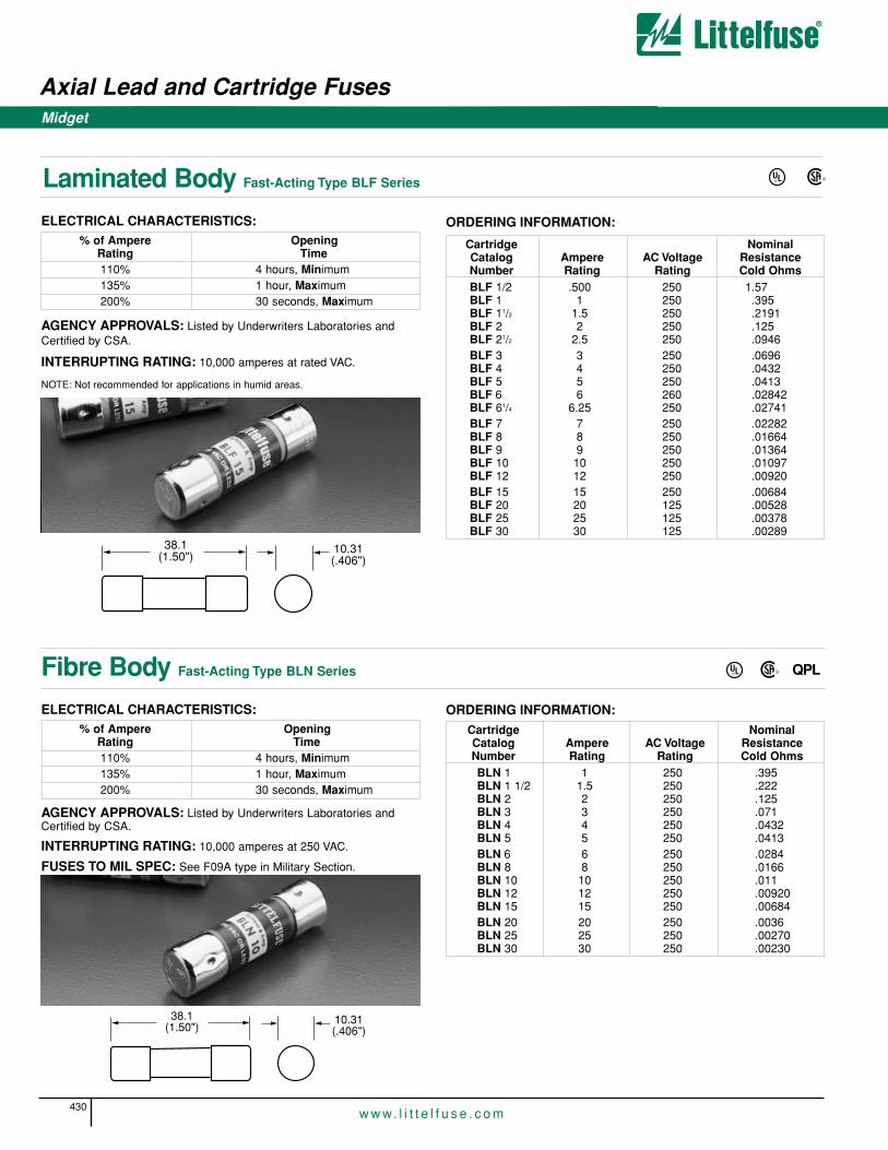
Axial Lead and Cartridge Fuses
430w w w. l i t t e l f u s e . c o m
Midget
Laminated Body Fast-Acting Type BLF Series
ELECTRICAL CHARACTERISTICS:% of Ampere Opening
Rating Time110% 4 hours, Minimum135% 1 hour, Maximum200% 30 seconds, Maximum
AGENCY APPROVALS: Listed by Underwriters Laboratories andCertified by CSA.
INTERRUPTING RATING: 10,000 amperes at rated VAC.
NOTE: Not recommended for applications in humid areas.
Fibre Body Fast-Acting Type BLN Series
ELECTRICAL CHARACTERISTICS:% of Ampere Opening
Rating Time110% 4 hours, Minimum135% 1 hour, Maximum200% 30 seconds, Maximum
AGENCY APPROVALS: Listed by Underwriters Laboratories andCertified by CSA.
INTERRUPTING RATING: 10,000 amperes at 250 VAC.
FUSES TO MIL SPEC: See F09A type in Military Section.
ORDERING INFORMATION:
Cartridge NominalCatalog Ampere AC Voltage ResistanceNumber Rating Rating Cold OhmsBLF 1/2 .500 250 1.57BLF 1 1 250 .395BLF 11/2 1.5 250 .2191BLF 2 2 250 .125BLF 21/2 2.5 250 .0946BLF 3 3 250 .0696BLF 4 4 250 .0432BLF 5 5 250 .0413BLF 6 6 260 .02842BLF 61/4 6.25 250 .02741BLF 7 7 250 .02282BLF 8 8 250 .01664BLF 9 9 250 .01364BLF 10 10 250 .01097BLF 12 12 250 .00920BLF 15 15 250 .00684BLF 20 20 125 .00528BLF 25 25 125 .00378BLF 30 30 125 .00289
ORDERING INFORMATION:
Cartridge NominalCatalog Ampere AC Voltage ResistanceNumber Rating Rating Cold OhmsBLN 1 1 250 .395BLN 1 1/2 1.5 250 .222BLN 2 2 250 .125BLN 3 3 250 .071BLN 4 4 250 .0432BLN 5 5 250 .0413BLN 6 6 250 .0284BLN 8 8 250 .0166BLN 10 10 250 .011BLN 12 12 250 .00920BLN 15 15 250 .00684BLN 20 20 250 .0036BLN 25 25 250 .00270BLN 30 30 250 .00230
®UL ® QPL
38.1(1.50")
10.31(.406")
38.1(1.50")
10.31(.406")
®UL ®

Axial Lead and Cartridge Fuses
431w w w. l i t t e l f u s e . c o m
11
AX
IAL
LE
AD
AN
DC
AR
TR
IDG
E F
US
ES
Midget
KLQ Series Fuse KLQ Series
• The Littelfuse KLQ series is designed to protect gaseous vapor fixtures, HID ballasts, and other electronic and lighting circuits.
• The KLQ is the same physical size as the Littelfuse BLS, but has moretime delay to handle transient and inrush currents.
VOLTAGE RATING: 600 VAC.
INTERRUPTING RATING: 10,000 amperes at rated VAC.
AMPERE RANGE: 1-6 amperes.
AGENCY APPROVALS: UL Listed per UL 248.
ORDERING INFORMATION:
FLU Series Fuse FLU Series
• The Littelfuse FLU series is designed specifically for the protection of multimeters.
• The 1000 VAC/VDC rating also makes the FLU ideal for a variety ofother applications.
VOLTAGE RATING: 1000 VAC/VDC.
INTERRUPTING RATING: 44/100A: 10kA11A: 20kA.
AMPERE RATINGS: 1 and 15 amperes.
AGENCY APPROVALS: Recognized under the components programof Underwriters Laboratories.
ORDERING INFORMATION:
Catalog Ampere AC VoltageNumber Rating RatingKLQ 001 1 600KLQ 16/10 1.6 600KLQ 002 2 600KLQ 003 3 600KLQ 005 5 600KLQ 006 6 600
Catalog Ampere AC VoltageNumber Rating RatingFLU 44/100 1 1000FLU 011 15 1000
®
38.1(1.50") 10.31
(.406")
34.925(1.375") 10.31
(.406")
®
(1.375") 10.31(.406")
34.925
®UL ®
44/100
11

Axial Lead and Cartridge Fuses
432w w w. l i t t e l f u s e . c o m
Midget
Class CC* Fast-Acting & Slo-Blo® Type Fuses CCMR Series
AGENCY FILE NUMBERS: UL E81895, CSA LR 29862.
VOLTAGE RATINGS: AC: 600 VoltsDC: 250 Volts (CCMR 2/10 – 2A)
(CCMR 4 1/2 – 10A)(CCMR 35 – 60A)
300 Volts (CCMR 2 1/4 – 4A)300 Volts (KLDR)300 Volts (KLKR)
Nominal Nominal NominalAmpere Catalog Resistance Catalog Resistance Catalog ResistanceRating Number Cold Ohms Number Cold Ohms Number Cold Ohms
1/10 – – KLDR.100 246 KLKR.100 79.331/8 – – KLDR.125 134.9 KLKR.125 56.52
15/100 – – KLDR.150 96 – –3/16 – – KLDR.187 66.4 – –2/10 CCMR.200 68.4 KLDR.200 57.8 KLKR.200 28.211/4 CCMR.250 43.3 KLDR.250 31.61 KLKR.250 19.223/10 CCMR.300 28.6 KLDR.300 25.5 KLKR.300 15.104/10 – – KLDR.400 13.6 – –1/2 CCMR.500 7.62 KLDR.500 15.9 KLKR.500 6.956/10 CCMR.600 8.2 KLDR.600 9.99 – –3/4 – – KLDR.750 6.08 KLKR.750 3.5818/10 CCMR.800 4.013 KLDR.800 6.2 – –
1 CCMR 001. 2.59 KLDR 001. 4.0 KLKR 001. .23421 1/8 – – KLDR 1.12 2.94 – –1 1/4 CCMR 1.25 1.687 KLDR 1.25 2.33 – –1 4/10 CCMR 01.4 1.33 KLDR 01.4 1.5 – –1 1/2 CCMR 01.5 1.24 KLDR 01.5 .898 KLKR 01.5 .225
1 6/10 CCMR 01.6 .9894 KLDR 01.6 .625 – –1 8/10 CCMR 01.8 .7783 KLDR 01.8 .486 – –
2 CCMR 002. .485 KLDR 002. .55 KLKR 002. .1352 1/4 CCMR 2.25 .4166 KLDR 2.25 .52 – –2 1/2 CCMR 02.5 .3375 KLDR 02.5 .333 KLKR 02.5 .0906
2 8/10 CCMR 02.8 .2400 KLDR 02.8 .26 – –3 CCMR 003. .2188 KLDR 003. .21 KLKR 003. .0776
3 2/10 CCMR 03.2 .1855 KLDR 03.2 .171 – –3 1/2 CCMR 03.5 .1346 KLDR 03.5 .239 KLKR 03.5 .0562
4 CCMR 004. .1231 KLDR 004. .118 KLKR 004. .04684 1/2 CCMR 04.5 .093 KLDR 04.5 .082 – –
5 CCMR 005. .0704 KLDR 005. .0399 KLKR 005. .03325 6/10 CCMR 05.6 .0535 KLDR 05.6 .0334 – –
6 CCMR 006. .0517 KLDR 006. .0315 KLKR 006. .02386 1/4 CCMR 6.25 .0464 KLDR 6.25 .03 – –
7 CCMR 007. .0369 KLDR 007. .0253 KLKR 007. .02087 1/2 CCMR 07.5 .027 KLDR 07.5 .0205 – –
8 CCMR 008. .023 KLDR 008. .0193 KLKR 008. .01779 CCMR 009. .0193 KLDR 009. .0155 KLKR 009. .0151
10 CCMR 010. .0133 KLDR 010. .0122 KLKR 010. .0132512 CCMR 012. .0114 KLDR 012. .0114 KLKR 012. .0085215 CCMR 015. .00708 KLDR 015. .00708 KLKR 015. .0074
17 1/2 CCMR 17.5 .00495 KLDR 17.5 .00495 – –20 CCMR 020. .00360 KLDR 020. .0036 KLKR 020. .0051125 CCMR 025. .00250 KLDR 025. .0025 KLKR 025. .00377530 CCMR 030. .00240 KLDR 030. .0024 KLKR 030. .00295435 CCMR 035. .00426 – – – –40 CCMR 040. .00286 – – – –45 CCMR 045. .00246 – – – –50 CCMR 050. .00182 – – – –60 CCMR 060. .00118 – – – –
®UL ®
Fast-acting KLKR fuses provide fast-acting protection to equipment containing surge sensitive components. Use KLKR fuses for non-inductive loads not requiring time delay. CCMR fuses (formerly KLMR)are specifically designed to withstand sustained starting currents of small motors. The CCMR fuses provide short-circuit protection for motorbranch-circuits. KLDR fuses are specifically designed to withstand themomentary high magnetizing currents of control transformers, solenoids,and similar inductive loads.
ELECTRICAL CHARACTERISTICS:% of Ampere Ampere Opening
Rating Rating Time110% 1/10–30 4 hours, Minimum135% 1/10–30 1 hour, Maximum
AGENCY APPROVALS: DC ratings are self-certified. KLKR Series:UL listed Fast-Acting Class CC per UL 248 and CSA Certified. KLDR, CCMR Series: UL listed Time-Delay Class CC per UL 248 and CSA Certified.*CCMR 35-60A UL Listed Time-Delay Class CD.INTERRUPTING RATING:
AC: 200,000 ampereDC: 20,000 amperes
ORDERING INFORMATION:

Axial Lead and Cartridge Fuses
433w w w. l i t t e l f u s e . c o m
11
AX
IAL
LE
AD
AN
DC
AR
TR
IDG
E F
US
ES
Midget
Class CC Fast-Acting & Slo-Blo® Type Fuses
1000
100
10
1
0.1
0.0110 100 1000.1 1
1/8A
2/10
A3/
10A
1/2A
6/10
A3/
4A1A 1.
8A2A 2
1/2A
3A 4A 6 1/
4A8A 10
A
TIM
E IN
SE
CO
ND
S
CURRENT IN AMPERES
Average Time Current Curve (KLDR)
1000
100
10
1
0.1
0.0110 100 1000.1 1
1/10
A1/
8A2/
10A
1/4A
3/10
A1/
2A3/
4A1A 1
1/2A
2A 3A 4A 5A 6A 8A 9A 10A
12A
15A
20A
25A
30A
TIM
E IN
SE
CO
ND
S
CURRENT IN AMPERES
Average Time Current Curve (KLKR)
1000
100
10
1
0.1
0.0110 100 10000.1 1
1/4A
1/2A
8/10
A1A 1
1/4A
1 1/
2A1
8/10
A2A 2
1/2A
3A 3 1/
2A4A 6A 8A 10
A12
A15
A20
A25
A30
A35
A60
A
CURRENT IN AMPERES
TIM
E IN
SEC
ONDS
Average Time Current Curve (CCMR)38.1 mm(1.50")
6.4 mm(.25")
12.7 mm(.50")
10.3 mm(.41")
0-30A
3.2 mm(.125")
21.6 mm(.850")
47.8 mm(1.880")
35-60A
®UL ®
Blade Terminal & Special Purpose Fuses
Blade Terminal And Special Purpose Fuses . . . . . . . . . . . . . . . . . . . . . . . . . . . . . . . . . . . . . . . . . . . . . . . . . . . . . . . . . . . . . . . . . . . . . . . . 434
257 series, ATO® Fuse . . . . . . . . . . . . . . . . . . . . . . . . . . . . . . . . . . . . . . . . . . . . . . . . . . . . . . . . . . . . . . . . . . . . . . . . . . . . . . . . . . . . . . . . . . . 435
297 series, MINI® Fuse . . . . . . . . . . . . . . . . . . . . . . . . . . . . . . . . . . . . . . . . . . . . . . . . . . . . . . . . . . . . . . . . . . . . . . . . . . . . . . . . . . . . . . . . . . 436
997 series, MINI® 42V Fuse . . . . . . . . . . . . . . . . . . . . . . . . . . . . . . . . . . . . . . . . . . . . . . . . . . . . . . . . . . . . . . . . . . . . . . . . . . . . . . . . . . . . . . . 437
299 series, MAXI™ Fuse . . . . . . . . . . . . . . . . . . . . . . . . . . . . . . . . . . . . . . . . . . . . . . . . . . . . . . . . . . . . . . . . . . . . . . . . . . . . . . . . . . . . . . . . . 438
999 series, MAXI™ 42V Fuse . . . . . . . . . . . . . . . . . . . . . . . . . . . . . . . . . . . . . . . . . . . . . . . . . . . . . . . . . . . . . . . . . . . . . . . . . . . . . . . . . . . . . . 439
298 series, MEGA® Slo-Blo® Fuse . . . . . . . . . . . . . . . . . . . . . . . . . . . . . . . . . . . . . . . . . . . . . . . . . . . . . . . . . . . . . . . . . . . . . . . . . . . . . . . . . . 440
498 series, MIDI® Fuse and Fuseholder . . . . . . . . . . . . . . . . . . . . . . . . . . . . . . . . . . . . . . . . . . . . . . . . . . . . . . . . . . . . . . . . . . . . . . . . . . . . . . 441
995 series, JCASE® 42V Slo-Blo® Cartridge Fuse . . . . . . . . . . . . . . . . . . . . . . . . . . . . . . . . . . . . . . . . . . . . . . . . . . . . . . . . . . . . . . . . . . . . . . 442
496 series, Cable Pro® Cable Protector . . . . . . . . . . . . . . . . . . . . . . . . . . . . . . . . . . . . . . . . . . . . . . . . . . . . . . . . . . . . . . . . . . . . . . . . . . . . . . . 443
242 and 259 series, Hazardous Area Fuses . . . . . . . . . . . . . . . . . . . . . . . . . . . . . . . . . . . . . . . . . . . . . . . . . . . . . . . . . . . . . . . . . . . . . . . . . . . 444
481 Series Alarm Indicating Fuse for Telecom . . . . . . . . . . . . . . . . . . . . . . . . . . . . . . . . . . . . . . . . . . . . . . . . . . . . . . . . . . . . . . . . . . . . . . . . . 445
482 Series Alarm Indicating Fuseholder for Telecom . . . . . . . . . . . . . . . . . . . . . . . . . . . . . . . . . . . . . . . . . . . . . . . . . . . . . . . . . . . . . . . . . 446-447
LVSP Surge Fuse . . . . . . . . . . . . . . . . . . . . . . . . . . . . . . . . . . . . . . . . . . . . . . . . . . . . . . . . . . . . . . . . . . . . . . . . . . . . . . . . . . . . . . . . . . . 448-449
PAGE
12
434w w w. l i t t e l f u s e . c o m
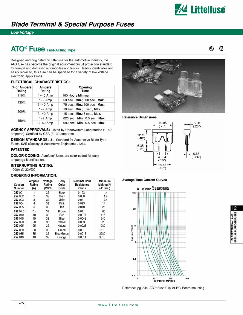
Blade Terminal & Special Purpose Fuses
435w w w. l i t t e l f u s e . c o m
12
BLA
DE
TE
RM
INA
L A
ND
SP
EC
IAL
PU
RP
OS
E F
US
ES
Low Voltage
ATO® Fuse Fast-Acting Type
Designed and originated by Littelfuse for the automotive industry, theATO fuse has become the original equipment circuit protection standardfor foreign and domestic automobiles and trucks. Readily identifiable andeasily replaced, this fuse can be specified for a variety of low voltageelectronic applications.
ELECTRICAL CHARACTERISTICS:% of Ampere Ampere Opening
Rating Rating Time110% 1–40 Amp 100 Hours Minimum
135%1–2 Amp .50 sec., Min.; 600 sec., Max.
3–40 Amp .75 sec., Min.; 600 sec., Max.
200%1–2 Amp .10 sec., Min.; 5 sec., Max.
3–40 Amp .15 sec., Min.; 5 sec., Max.
350%1–2 Amp .020 sec., Min.; 0.5 sec., Max.
3–40 Amp .080 sec., Min.; 0.5 sec., Max.
AGENCY APPROVALS: Listed by Underwriters Laboratories (1–40amperes). Certified by CSA (3–30 amperes).
DESIGN STANDARDS: U.L. Standard for Automotive Blade TypeFuses. SAE (Society of Automotive Engineers) J1284.
PATENTED
COLOR-CODING: Autofuse® fuses are color-coded for easy amperage identification.
INTERRUPTING RATING:1000A @ 32VDC
ORDERING INFORMATION:Average Time Current CurvesAmpere Voltage Body Nominal Cold Minimum
Catalog Rating Rating Color Resistance Melting I2tNumber (A) (VDC) Code Ohms (A2 Sec.)257 001 1 32 Black 0.123 .4257 002 2 32 Grey 0.050 1.4257 003 3 32 Violet 0.031 7.4257 004 4 32 Pink 0.023 14257 005 5 32 Tan 0.018 26257 07.5 71/2 32 Brown 0.011 60257 010 10 32 Red 0.0077 115257 015 15 32 Blue 0.0048 340257 020 20 32 Yellow 0.0033 520257 025 25 32 Natural 0.0025 1080257 030 30 32 Green 0.0019 1510257 035 35 32 Blue Green 0.0016 2280257 040 40 32 Orange 0.0014 3310
Reference pg. 344, ATO® Fuse Clip for P.C. Board mounting.
5.08(.20")
0.66(.026")
19.05(.75")
14.48(.57")
12.19(.48")
6.35(.25")
4.064(.16")
Reference Dimensions
®UL ®
1000
100
10
1
0.1
0.011000100101
TIM
E IN
SEC
ONDS
CURRENT IN AMPERES
1A 2A 3A 4A 10A
15A
20A
25A
30A
35A
40A
7.5A
5A

Blade Terminal & Special Purpose Fuses
436w w w. l i t t e l f u s e . c o m
Low Voltage
MINI® Fuse Fast-Acting Type
The MINI Fuse is smaller than its predecessor, the ATO® Fuse, whichpermit more fuses in the same amount of space. More fuses in the samespace satisfy the requirement that more circuits be individually fused innewer automobiles.
ELECTRICAL CHARACTERISTICS:% of Ampere Opening
Rating Time110% 100 Hours Minimum135% .75 sec., Min.; 600 sec., Max.200% .15 sec., Min.; 5 sec., Max.350% .080 sec., Min.; .250 sec., Max.600% .030 sec., Min.; .100 sec., Max.
AGENCY APPROVALS: Listed by Underwriters Laboratories.
DESIGN STANDARD: SAE (Society of Automotive Engineers) J2077.
PHYSICAL SPECIFICATIONS:Materials: Body: Nylon
Terminations: Silver-Plated
PATENTED
INTERRUPTING RATING:1000A @ 32VDC
ORDERING INFORMATION:
1000
100
10
1
0.1
0.0110001001010.1
2A 3A 4A 5A 7 1/
2A10
A
15A
20A
25A
30A
TIM
E IN
SE
CO
ND
S
CURRENT IN AMPERES
Average Time Current CurvesAmpere Voltage Body Nominal Cold Minimum
Catalog Rating Rating Color Resistance Melting I2tNumber (A) (VDC) Code Ohms (A2 Sec.)297 002 2 32 Grey 0.056 2.8297 003 3 32 Violet 0.034 9.4297 004 4 32 Pink 0.024 17297 005 5 32 Tan 0.018 25297 07.5 71/2 32 Brown 0.011 68297 010 10 32 Red 0.0073 93297 015 15 32 Blue 0.0045 270297 020 20 32 Yellow 0.0032 380297 025 25 32 Natural 0.0023 625297 030 30 32 Green 0.0018 1130
Reference pg. 344 for MINI® Fuse P.C. Board fuseholders.
MINI
0.18(.032")
10.92(.43")
10.92(.43")
8.04(.34")
7.37(.29")
2.79(.11")
3.81(.15")
Reference Dimensions
®UL
ATO® Fuse, MINI® Fuse,3AG Fuse PullerORDERING INFORMATION:Catalog Number: 097024

Blade Terminal & Special Purpose Fuses
437w w w. l i t t e l f u s e . c o m
12
BLA
DE
TE
RM
INA
L A
ND
SP
EC
IAL
PU
RP
OS
E F
US
ES
Low Voltage
MINI® 42V Fuse Fast-Acting Type
As power demand in vehicles continues to grow, the need for electricaland fuel economy is driving the necessity for a more efficient automotiveelectrical system.
Littelfuse is working closely with major automakers and wire harnesssuppliers to develop and establish new standars of circuit protection for42 volt automotive electrical systems.Advantages include:
• 42 Volt nominal rating / 58 Volt interrupting rating• Drop-in replacement for MINI® fuse• Same blade size and spacing as MINI® fuse• Same Time-Current characteristics as MINI® fuse• Rejection feature prevents interchangeability with
non-compliant 14 Volt fuses
1000
100
10
1
0.1
0.0110001001010.1
2A 3A 4A 5A 7 1/
2A10
A
TIM
E IN
SE
CO
ND
S
CURRENT IN AMPERES
15A
20A
25A
30A
Interrupting Rating: 1000A @ 58 VDC
Voltage Rating: 58 VDC
Ambient Temp: -40oC to +125oC
ELECTRICAL CHARACTERISTICS:% of Opening
(Rating) Time110% 100 hrs., Minimum135% 0.75 sec., Min.; 600 sec., Max.200% 0.15 sec., Min.; 5.0 sec., Max.350% 0.08 sec., Min.; 0.25 sec., Max.600% 0.030 sec., Min.; 0.10 sec., Max.
MINI
2.21(.09")
5.91(.23")
LF 3.81
(.15")
10.92(.43")
8.75(.34")
7.5(.30")
2.81(.11")
10.9(.43")
0.825(.033")
ORDERING INFORMATION:Ampere Voltage Typical Voltage
Catalog Rating Rating Body Typical Cold Drop at Rated Number (A) (VDC) Color Resistance (Ω) Current (mV) 997 002 2 58 Grey .056 171997 003 3 58 Violet .034 153997 004 4 58 Pink .024 121997 005 5 58 Tan .018 129997 07.5 7.5 58 Brown .011 135997 010 10 58 Red .0073 108997 015 15 58 Blue .0045 98997 020 20 58 Yellow .0032 96997 025 25 58 Natural .0023 86997 030 30 58 Green .0018 87
Average Time Current Curves

Blade Terminal & Special Purpose Fuses
438w w w. l i t t e l f u s e . c o m
Low Voltage
MAXI™ Fuse Slo-Blo® Type Fuse
The MAXI Fuse is available in a higher range of amperage ratings(20–80 amperes) than the MINI® Fuse and ATO® Fuse designs and islarger in physical size. A typical MAXI Fuse application in today’s moresophisticated automobile circuits is protection of the wiring harness byreplacing the fusible wire or fusible link, which is often a plain piece ofsmall wire.
ELECTRICAL CHARACTERISTICS:% of Ampere Ampere Opening
Rating Rating Time
135%20–60 60 sec., Min.; 1800 sec., Max.70–80 60 sec., Min.; 3600 sec., Max.
20 4 sec., Min.; 20 sec., Max.30 6 sec., Min.; 30 sec., Max.
200%40 8 sec., Min.; 40 sec., Max.50 10 sec., Min.; 50 sec., Max.60 15 sec., Min.; 60 sec., Max.
70–80 4 sec., Min.; 60 sec., Max.20 .7 sec., Min.; 2 sec., Max.30 1 sec., Min.; 4 sec., Max.
350%40 1.4 sec., Min.; 5 sec., Max.50 1.7 sec., Min.; 6 sec., Max.60 2 sec., Min.; 7 sec., Max.
70–80 .2 sec., Min.; 2 sec., Max.20 .15 sec., Min.; 1 sec., Max.
600% 30–60 .20 sec., Min.; 1 sec., Max.70–80 .04 sec., Min.; .15 sec., Max.
AGENCY APPROVALS: Recognized under the components programof Underwriters Laboratories.
DESIGN STANDARD: SAE (Society of Automotive Engineers) J1888.
PHYSICAL SPECIFICATIONS:Materials: Body: Plastic
Terminations: Silver-Plated
PATENTED
INTERRUPTING RATING:1000A @ 32VDC
ORDERING INFORMATION:
Average Time Current Curves
Ampere Voltage Body Nominal Cold MinimumCatalog Rating Rating Color Resistance Melting I2tNumber (A) (VDC) Code Ohms (A2 Sec.)299 020 20 32 Yellow 0.0031 1100299 025 25 32 Gray 0.0024 2087299 030 30 32 Green 0.0020 4070299 035 35 32 Brown 0.0017 6032299 040 40 32 Orange 0.0014 8450299 050 50 32 Red 0.0011 11300299 060 60 32 Blue 0.00089 15300299 070 70 32 Tan 0.00064 6900299 080 80 32 Natural 0.00054 8800
®
29.21(1.15")
8.85(.35")
29.21(1.15")
21.59(.85")
12.70(.50")
8.13(.32")
0.81(.032")
Reference Dimensions
1000
100
10
1
0.1
0.0110000100010010
TIM
E IN
SEC
ONDS
CURRENT IN AMPERES
20A
25A
30A
35A
40A
50A
60A
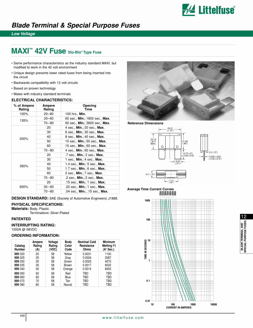
Blade Terminal & Special Purpose Fuses
439w w w. l i t t e l f u s e . c o m
12
BLA
DE
TE
RM
INA
L A
ND
SP
EC
IAL
PU
RP
OS
E F
US
ES
Low Voltage
MAXI™ 42V Fuse Slo-Blo® Type Fuse
• Same performance characteristics as the industry standard MAXI, butmodified to work in the 42 volt environment
• Unique design prevents lower rated fuses from being inserted into the circuit
• Backwards compatibility with 12 volt circuits
• Based on proven technology
• Mates with industry standard terminals
ELECTRICAL CHARACTERISTICS:% of Ampere Ampere Opening
Rating Rating Time100% 20–80 100 hrs., Min.
135%20–60 60 sec., Min.; 1800 sec., Max.70–80 60 sec., Min.; 3600 sec., Max.
20 4 sec., Min.; 20 sec., Max.30 6 sec., Min.; 30 sec., Max.
200%40 8 sec., Min.; 40 sec., Max.50 10 sec., Min.; 50 sec., Max.60 15 sec., Min.; 60 sec., Max.
70–80 4 sec., Min.; 60 sec., Max.20 .7 sec., Min.; 2 sec., Max.30 1 sec., Min.; 4 sec., Max.
350%40 1.4 sec., Min.; 5 sec., Max.50 1.7 sec., Min.; 6 sec., Max.60 2 sec., Min.; 7 sec., Max.
70–80 .2 sec., Min.; 2 sec., Max.20 .15 sec., Min.; 1 sec., Max.
600% 30–60 .20 sec., Min.; 1 sec., Max.70–80 .04 sec., Min.; .15 sec., Max.
DESIGN STANDARD: SAE (Society of Automotive Engineers) J1888.
PHYSICAL SPECIFICATIONS:Materials: Body: Plastic
Terminations: Silver-Plated
PATENTED
INTERRUPTING RATING:1000A @ 58VDC
ORDERING INFORMATION:
Average Time Current Curves
Ampere Voltage Body Nominal Cold MinimumCatalog Rating Rating Color Resistance Melting I2tNumber (A) (VDC) Code Ohms (A2 Sec.)999 020 20 58 Yellow 0.0031 1100999 025 25 58 Gray 0.0024 2087999 030 30 58 Green 0.0020 4070999 035 35 58 Brown 0.0017 6032999 040 40 58 Orange 0.0014 8450999 050 50 58 Red TBD TBD999 060 60 58 Blue TBD TBD999 070 70 58 Tan TBD TBD999 080 80 58 Naural TBD TBD
29.21(1.15")
22.15(.87")MAX.
8.00(.31")
12.70 (.5")± 0.38 (.015)
21.60(.85")
0.825 (.032)± 0.35 (.014")
3.3 (.13")
17.37(.68")
8.51 (.34")
Reference Dimensions
1000
100
10
1
0.1
0.0110000100010010
TIM
E IN
SEC
ONDS
CURRENT IN AMPERES
20A
25A
30A
35A
40A
50A
60A
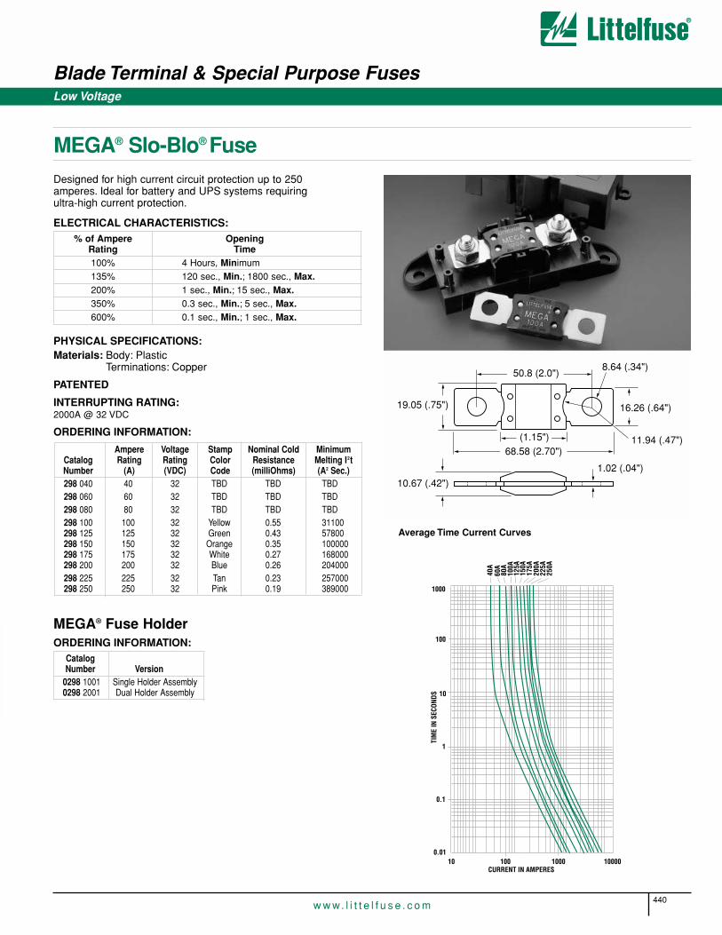
Blade Terminal & Special Purpose Fuses
440w w w. l i t t e l f u s e . c o m
Low Voltage
MEGA® Slo-Blo® FuseDesigned for high current circuit protection up to 250 amperes. Ideal for battery and UPS systems requiring ultra-high current protection.
ELECTRICAL CHARACTERISTICS:% of Ampere Opening
Rating Time100% 4 Hours, Minimum135% 120 sec., Min.; 1800 sec., Max.200% 1 sec., Min.; 15 sec., Max.350% 0.3 sec., Min.; 5 sec., Max.600% 0.1 sec., Min.; 1 sec., Max.
PHYSICAL SPECIFICATIONS:Materials: Body: Plastic
Terminations: Copper
PATENTED
INTERRUPTING RATING:2000A @ 32 VDC
ORDERING INFORMATION:
MEGA® Fuse HolderORDERING INFORMATION:
Ampere Voltage Stamp Nominal Cold MinimumCatalog Rating Rating Color Resistance Melting I2tNumber (A) (VDC) Code (milliOhms) (A2 Sec.)298 040 40 32 TBD TBD TBD298 060 60 32 TBD TBD TBD298 080 80 32 TBD TBD TBD298 100 100 32 Yellow 0.55 31100298 125 125 32 Green 0.43 57800298 150 150 32 Orange 0.35 100000298 175 175 32 White 0.27 168000298 200 200 32 Blue 0.26 204000298 225 225 32 Tan 0.23 257000298 250 250 32 Pink 0.19 389000
50.8 (2.0")
19.05 (.75") 16.26 (.64")
1.02 (.04")
8.64 (.34")
11.94 (.47")
10.67 (.42")
(1.15")68.58 (2.70")
Average Time Current Curves
CatalogNumber Version
0298 1001 Single Holder Assembly0298 2001 Dual Holder Assembly
1000
100
10
1
0.1
0.0110000100010010
TIM
E IN
SEC
ONDS
CURRENT IN AMPERES
40A
60A
80A
100A
125A
150A
175A
200A
225A
250A

Blade Terminal & Special Purpose Fuses
441w w w. l i t t e l f u s e . c o m
12
BLA
DE
TE
RM
INA
L A
ND
SP
EC
IAL
PU
RP
OS
E F
US
ES
Low Voltage
MIDI® FUSE
ELECTRICAL CHARACTERISTICS:% of Ampere Ampere
Rating Rating Opening Time100% 30-125A 100 hours, Minimum110% 30-125A 4 hours, Minimum150% 30-125A 90 sec., Min.; 3600 sec., Max.
30-125A 5 sec., Min.; 100 sec., Max.150-200A 1 sec., Min.; 15 sec., Max.30-125A .5 sec., Min.; 15 sec., Max.
150-200A .3 sec., Min.; 3 sec., Max.
AGENCY APPROVALS: Recognized under the components programof Underwriters Laboratories.
AGENCY FILE NUMBERS: E71611
INTERRUPTING RATINGS: 1000 amperes at 32 VDC
VOLTAGE RATINGS: 32 VDC
AMBIENT TEMP.: –40°C to +125°C
PATENTEDINTERRUPTING RATING:1000A @ 32 VDC
ORDERING INFORMATION:
Average Time Current Curves
The MIDI® Fuse offers a bolt-on space saving fuse for high current wiringprotection and provides time delay characteristics with “Diffusion PillTechnology”. The MIDI Fuse was designed and patented by Littelfuse.
MIDI® FUSE Fuseholders
41(1.61)
10(.394)
12(.47)
16(.63)
30(.1.18)
Ø 5.5 (.217)
0.4(.016) 4
(.157)
8(.315)
Catalog Ampere Voltage Nominal ColdNumber Rating Rating (VDC) Resistance (mΩ)
0498 030 30 32 2.10498 040 40 32 1.30498 050 50 32 1.040498 060 60 32 0.870498 070 70 32 0.720498 080 80 32 0.560498 100 100 32 0.450498 125 125 32 0.400498 150 150 32 0.330498 200 200 32 0.25
15.2(.60)
41.0(1.61)
3.8(.15)
(2 Holes)
51.35(2.022)
®
1000
100
10
1
0.1
0.0110000100010010
TIM
E IN
SEC
ONDS
CURRENT IN AMPERES
30A
40A
50A
60A
70A
80A
100A
125A
150A
200A
200%
300%
ORDERING INFORMATION: Catalog Number 498900.
SPECIFICATIONS:Electrical: Use with MIDI® Fuses from 40 to 150 amps. (32V)Body: Glass Filled Thermoplastic
Body Color: Black
Cover With Tether: Glass Filled Thermoplastic
Cover Color: Black
Ambient Temp.: –40°C to +125°C
Fuse Mounting: M5 Threaded Stud and Hex Nuts
Cable Positions: Optional
Side Stackable Feature

Blade Terminal & Special Purpose Fuses
442w w w. l i t t e l f u s e . c o m
Low Voltage
JCASE™ 42V Slo-Blo® Cartridge FuseAs power demand in vehicles continues to grow, the need for electrivaland fuel economy is driving the necessity for a more efficient automotiveelectrical system.
Littelfuse is working closely with major automakers and wire harnesssuppliers to develop and establish new standars of circuit protection for42 volt automotive electrical systems.Advantages include:
• 42 Volt nominal rating / 58 Volt interrupting rating• Unique keying design prevents lower rated fuses from being
inserted into the circuit• Same performance characteristics as industry standard JCASE
fuse but modified to work in the 42 volt environment
1000
100
10
1
0.1
0.0110001001010.5
TIM
E IN
SE
CO
ND
S
CURRENT IN AMPERES10000
20A
30A
40A
50A
60A
Interrupting Rating: 1000A @ 58 VDC
Voltage Rating: 58 VDC
Ambient Temp: -40oC to +125oC
ORDERING INFORMATION:
ELECTRICAL CHARACTERISTICS:% of Opening
(Rating) Time110% 100 hrs., Minimum135% 60 sec., Min.; 1800 sec., Max.200% 4.00 sec., Min.; 60.0 sec., Max.350% 0.20 sec., Min.; 17.0 sec., Max.600% 0.04 sec., Min.; 1.0 sec., Max.
10.10(.40")
5.50(.22")
18.7(.74")
27.0(1.06")
12.10(.48")
0.38(.015")
14.10(.56")
+ ++ 6.75 (.27")
1.00(.039")
4.40(.17")
10.00(.39")
24.4(.96")
10.00(.39")
12.00(.47")
45°
Average Time Current Curves
CatalogNumber
995 020995 025 995 030995 040995 050995 060
AmpereRating
(A)
2025 30405060
Voltage Rating(VDC)
585858585858
BodyColor
BlueNatural
PinkGreenRed
Yellow
Typical VoltageDrop at RatedCurrent (mV)
Nominal ColdResistance
(Ω)
125120 115115115115
.00486.00328 .00245.00152.00118.00095
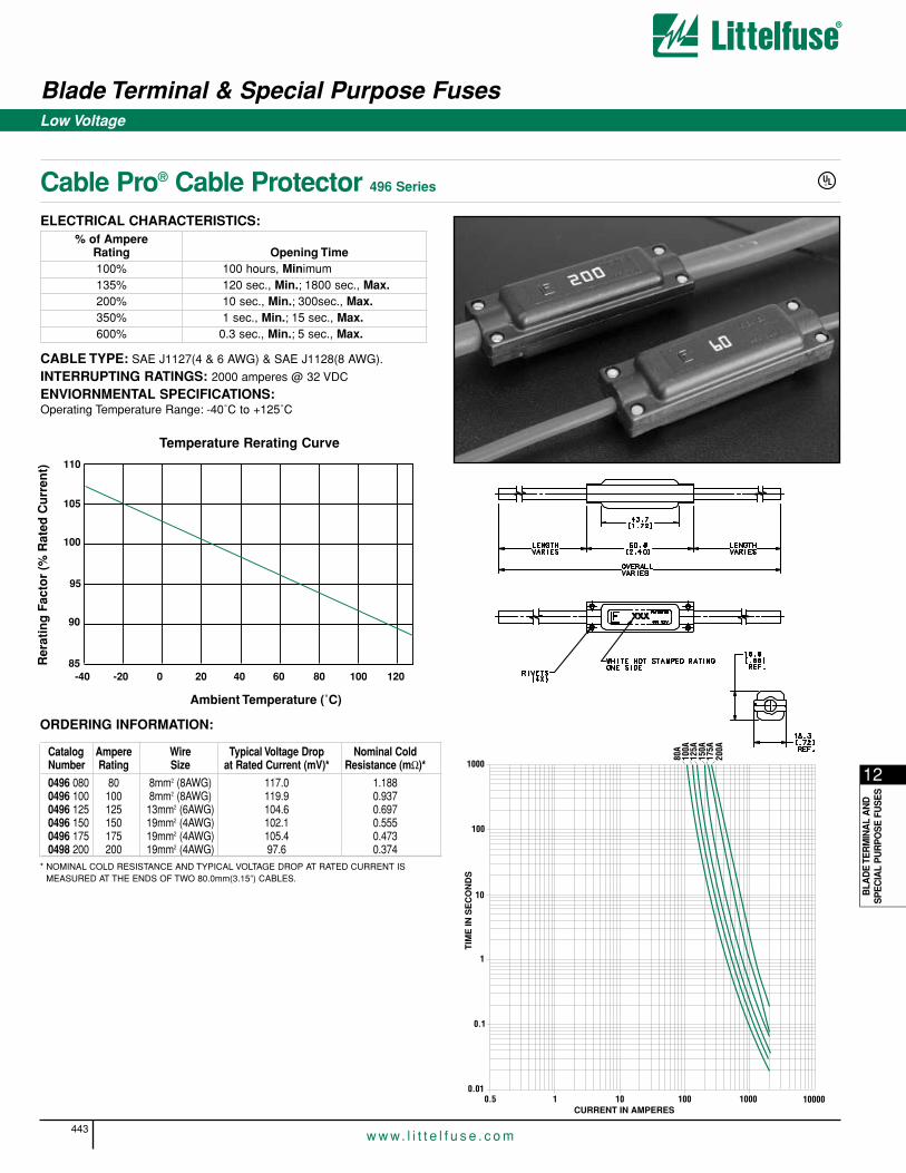
Low Voltage
Blade Terminal & Special Purpose Fuses
Cable Pro® Cable Protector 496 Series
443w w w. l i t t e l f u s e . c o m
12
BLA
DE
TE
RM
INA
L A
ND
SP
EC
IAL
PU
RP
OS
E F
US
ES
ELECTRICAL CHARACTERISTICS:% of Ampere
Rating Opening Time100% 100 hours, Minimum135% 120 sec., Min.; 1800 sec., Max.200% 10 sec., Min.; 300sec., Max.350% 1 sec., Min.; 15 sec., Max.600% 0.3 sec., Min.; 5 sec., Max.
CABLE TYPE: SAE J1127(4 & 6 AWG) & SAE J1128(8 AWG).
INTERRUPTING RATINGS: 2000 amperes @ 32 VDC
ENVIORNMENTAL SPECIFICATIONS:Operating Temperature Range: -40˚C to +125˚C
Catalog Ampere Wire Typical Voltage Drop Nominal ColdNumber Rating Size at Rated Current (mV)* Resistance (mΩ)*
0496 080 80 8mm2 (8AWG) 117.0 1.1880496 100 100 8mm2 (8AWG) 119.9 0.9370496 125 125 13mm2 (6AWG) 104.6 0.6970496 150 150 19mm2 (4AWG) 102.1 0.5550496 175 175 19mm2 (4AWG) 105.4 0.4730498 200 200 19mm2 (4AWG) 97.6 0.374
®UL
ORDERING INFORMATION:
1000
100
10
1
0.1
0.0110001001010.5
TIM
E IN
SE
CO
ND
S
CURRENT IN AMPERES10000
150A
12
5A
100A
80
A
175A
20
0A
110
105
100
95
90
85-40 -20 0 20 40 60 80 100 120
Ambient Temperature (˚C)
Rer
atin
g F
acto
r (%
Rat
ed C
urr
ent)
Temperature Rerating Curve
* NOMINAL COLD RESISTANCE AND TYPICAL VOLTAGE DROP AT RATED CURRENT ISMEASURED AT THE ENDS OF TWO 80.0mm(3.15”) CABLES.
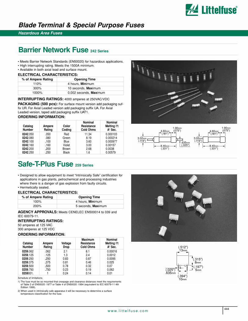
Hazardous Area Fuses
Blade Terminal & Special Purpose Fuses
444w w w. l i t t e l f u s e . c o m
Barrier Network Fuse 242 Series
Safe-T-Plus Fuse 259 Series
(.512")13mm
(.394")10mm
(.025").635mm
(.315")8mm
(.197")5mm
• Meets Barrier Network Standards (EN50020) for hazardous applications.• High interrupting rating. Meets the 1500A minimum.• Available in both axial lead and surface mount.
ELECTRICAL CHARACTERISTICS:% of Ampere Rating Opening Time
110% 4 hours, Minimum300% 10 seconds, Maximum1000% 0.002 seconds, Maximum
INTERRUPTING RATINGS: 4000 amperes at 250VAC/VDC
PACKAGING (500 pcs): For surface mount version add packaging suf-fix UR. For Axial Leaded version add packaging suffix UA. For AxialLeaded version, taped add packaging suffix UAT1.
ORDERING INFORMATION:Nominal Nominal
Catalog Ampere Color Resistance Melting I2tNumber Rating Coding Cold Ohms A2 Sec.0242.050 .050 Red 11.34 0.0001030242.080 .080 Green 8.19 0.0002140242.100 .100 Blue 3.60 0.0009770242.160 .160 Violet 3.00 0.001570242.200 .200 Brown 2.68 0.00380242.250 .250 Black 1.6 0.00579
• Designed to allow equipment to meet “Intrinsically Safe” certification forapplications in gas plants, petrochemical and processing industrieswhere there is a danger of gas explosion from faulty circuits.
• Hermetically sealed.
ELECTRICAL CHARACTERISTICS:% of Ampere Rating Opening Time
100% 4 hours, Minimum200% 5 seconds, Maximum
AGENCY APPROVALS: Meets CENELEC EN500014 to 039 and IEC 60079-11.
INTERRUPTING RATINGS:50 amperes at 125 VAC300 amperes at 125 VDC
ORDERING INFORMATION:
3.02mm(.119")
8.40mm(.331")
4.60mm(.181")
1.90mm(.075")
3.02mm(.119")
8.40mm(.331")
4.60mm(.181")
1.90mm(.075")
.635mm(.025")
Maximum NominalCatalog Ampere Voltage Resistance Melting I2tNumber Rating Drop Cold Ohms A2 Sec.0259.062 .062 2.1 8.1 0.000160259.125 .125 1.3 2.4 0.00120259.250 .250 0.83 0.87 0.00950259.375 .375 0.81 0.46 0.0250259.500 .500 0.78 0.32 0.070259.750 .750 0.23 0.19 0.0620259001. 1 0.24 0.14 0.01
Schedule of limitations.
1) The fuse must be so mounted that creepage and clearance distances meet the requirementsof Table 2 of EN50020 :1977 or Table 4 of EN50020 :1994 (equivalent to IEC 60079-11 4thEdition 1999).
2) When used in intrinsically safe apparatus it will be necessary to determine a surface temperature classification for the fuse.
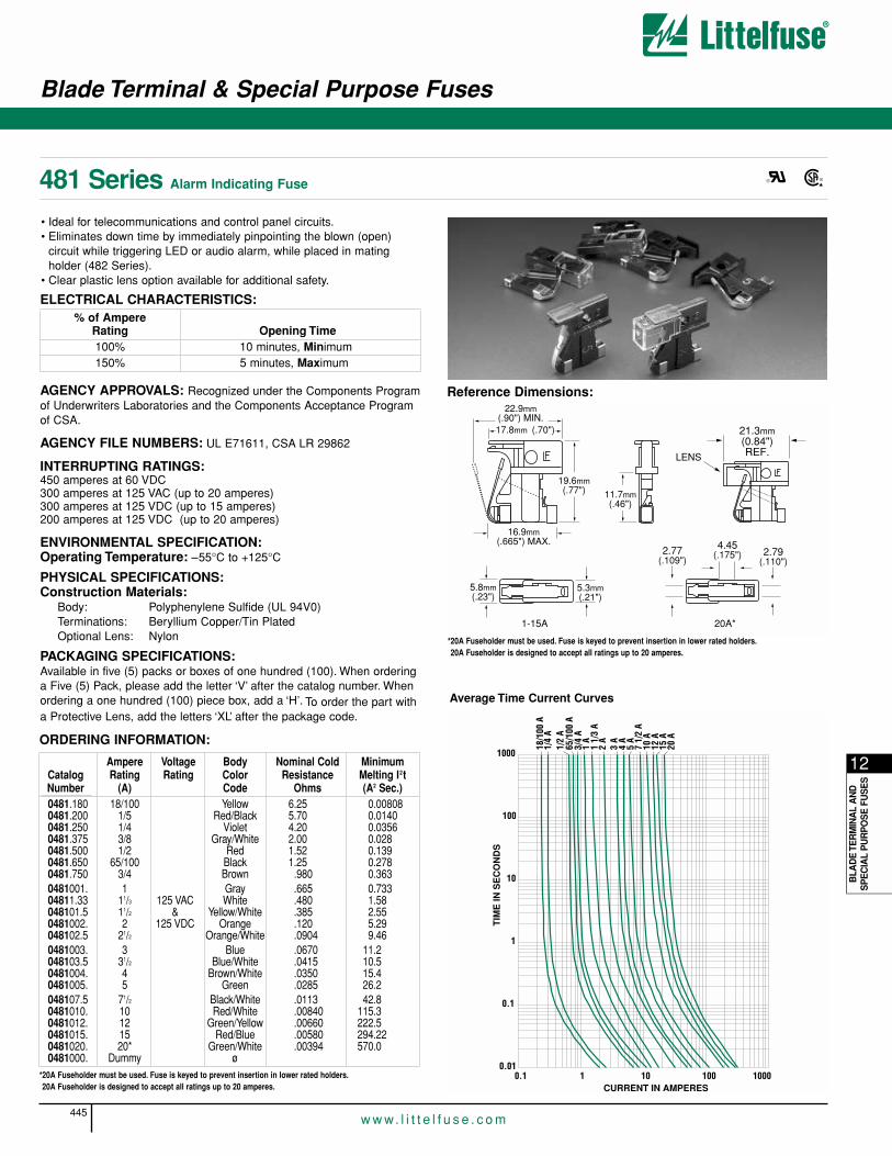
12
BLA
DE
TE
RM
INA
L A
ND
SP
EC
IAL
PU
RP
OS
E F
US
ES
Blade Terminal & Special Purpose Fuses
445w w w. l i t t e l f u s e . c o m
481 Series Alarm Indicating Fuse
1000
100
10
1
0.1
0.0110001001010.1
18/1
00 A
1/4
A1/
2 A
65/1
00 A
3/4
A1
A1
1/3
A2
A3
A4
A5
A7
1/2
A10
A12
A15
A20
A
TIM
E IN
SE
CO
ND
S
CURRENT IN AMPERES
Average Time Current Curves
• Ideal for telecommunications and control panel circuits.• Eliminates down time by immediately pinpointing the blown (open)
circuit while triggering LED or audio alarm, while placed in mating holder (482 Series).
• Clear plastic lens option available for additional safety.
® ®
ELECTRICAL CHARACTERISTICS:% of Ampere
Rating Opening Time100% 10 minutes, Minimum150% 5 minutes, Maximum
AGENCY APPROVALS: Recognized under the Components Programof Underwriters Laboratories and the Components Acceptance Programof CSA.
AGENCY FILE NUMBERS: UL E71611, CSA LR 29862
INTERRUPTING RATINGS:450 amperes at 60 VDC300 amperes at 125 VAC (up to 20 amperes)300 amperes at 125 VDC (up to 15 amperes)200 amperes at 125 VDC (up to 20 amperes)
ENVIRONMENTAL SPECIFICATION:Operating Temperature: –55°C to +125°C
PHYSICAL SPECIFICATIONS:Construction Materials:
Body: Polyphenylene Sulfide (UL 94V0)Terminations: Beryllium Copper/Tin PlatedOptional Lens: Nylon
PACKAGING SPECIFICATIONS:Available in five (5) packs or boxes of one hundred (100). When orderinga Five (5) Pack, please add the letter ‘V’ after the catalog number. Whenordering a one hundred (100) piece box, add a ‘H’. To order the part witha Protective Lens, add the letters ‘XL’ after the package code.
Ampere Voltage Body Nominal Cold MinimumCatalog Rating Rating Color Resistance Melting I2tNumber (A) Code Ohms (A2 Sec.)0481.180 18/100 Yellow 6.25 0.008080481.200 1/5 Red/Black 5.70 0.01400481.250 1/4 Violet 4.20 0.03560481.375 3/8 Gray/White 2.00 0.0280481.500 1/2 Red 1.52 0.1390481.650 65/100 Black 1.25 0.2780481.750 3/4 Brown .980 0.3630481001. 1 Gray .665 0.73304811.33 11/3 125 VAC White .480 1.58048101.5 11/2 & Yellow/White .385 2.550481002. 2 125 VDC Orange .120 5.29048102.5 21/2 Orange/White .0904 9.460481003. 3 Blue .0670 11.2048103.5 31/2 Blue/White .0415 10.50481004. 4 Brown/White .0350 15.40481005. 5 Green .0285 26.2048107.5 71/2 Black/White .0113 42.80481010. 10 Red/White .00840 115.30481012. 12 Green/Yellow .00660 222.50481015. 15 Red/Blue .00580 294.220481020. 20* Green/White .00394 570.00481000. Dummy ø
*20A Fuseholder must be used. Fuse is keyed to prevent insertion in lower rated holders.20A Fuseholder is designed to accept all ratings up to 20 amperes.
ORDERING INFORMATION:
22.9mm(.90") MIN.
5.8mm(.23")
5.3mm(.21")
16.9mm(.665") MAX.
11.7mm(.46")
17.8mm (.70")
19.6mm(.77")
21.3mm(0.84")REF.LENS
2.77(.109")
2.79(.110")
4.45(.175")
1-15A 20A*
Reference Dimensions:
*20A Fuseholder must be used. Fuse is keyed to prevent insertion in lower rated holders.20A Fuseholder is designed to accept all ratings up to 20 amperes.

Blade Terminal & Special Purpose Fuses
446w w w. l i t t e l f u s e . c o m
482 Series Alarm Indicating Fuseholder
The Alarm Indicating Fuseholder is designed for use with the Littelfuse 481 Alarm Fuse. It is designed to accept other manufacturer’sreplacement fuses as well.• Ideal for telecommunications and control panel circuits.The fuseholder is available in three versions:PCB Mount: Can be soldered directly to a printed circuit board. Ratedup to 15 amperes. Available in single pole or gangable up to 20 poles.Fuseholder is keyed to prevent insertion of 20 ampere fuse.Panel Mount – 20A: Available in a single pole version rated up to 20amperes. Large leads for wire attachment.Panel Mount – 15A: 15 ampere gangable version of fuseholder is keyed toprevent insertion of 20 ampere fuse.AGENCY APPROVALS: Recognized under the Components Programof Underwriters Laboratories and the Components Acceptance Programof CSA.
AGENCY FILE NUMBERS: UL E14721, CSA LR 29862
SPECIFICATIONS:PCB Mount and Panel Mount – 15A: Rated at 15 amperes up to125 VAC/VDCBody Material: ThermoplasticFuse Terminals: Tin-plated Beryllium CopperAlarm Terminal: Tin-plated BrassOperating Temperature: -550C to + 1250CPanel Mount – 20A: Rated at 20 amperes up to 125 VAC/VDCBody Material: Black PhenolicFuse Terminals: Tin-plated Beryllium CopperAlarm Terminal: Tin-plated BrassOperating Temperature: -400C to + 850C
Flush Side OptionsAvailable for PCB andPanel Mount Version.
5 POLE HOLDER ASSEMBLY WITH FLUSH OPTION
482 Series PCB Mount Fuseholder ® ®
Catalog Number Catalog NumberPCB Mount PCB Mount Flush Type Length
ORDERING INFORMATION: PCB Mount
0482 0001ZXB0482 0002ZXB0482 0003ZXB0482 0004ZXB0482 0005ZXB0482 0006ZXB0482 0007ZXB0482 0008ZXB0482 0009ZXB0482 00010ZXB0482 00011ZXB0482 00012ZXB0482 00013ZXB0482 00014ZXB0482 00015ZXB0482 00016ZXB0482 00017ZXB0482 00018ZXB0482 00019ZXB0482 00020ZXB
0482 0001ZXBF0482 0002ZXBF0482 0003ZXBF0482 0004ZXBF0482 0005ZXBF0482 0006ZXBF0482 0007ZXBF0482 0008ZXBF0482 0009ZXBF0482 00010ZXBF0482 00011ZXBF0482 00012ZXBF0482 00013ZXBF0482 00014ZXBF0482 00015ZXBF0482 00016ZXBF0482 00017ZXBF0482 00018ZXBF0482 00019ZXBF0482 00020ZXBF
1 Pole2 Pole3 Pole4 Pole5 Pole6 Pole7 Pole8 Pole9 Pole10 Pole11 Pole12 Pole13 Pole14 Pole15 Pole16 Pole17 Pole18 Pole19 Pole20 Pole
FEMALE LATCHING & FLUSH SIDEWITHOUT TABS
TYPICAL HOLDER ASSEMBLY
21.3mm(.84")TYP
6.4mm(.25")TYP
A
81.5mm(.73")
12.4mm(.49")
1.6mm(.062")TYP 4.1mm
(.16")TYP
19.8mm(.78" )
TYP ± .03
6.4mm(.250")±.005
10.7mm(.420")±.005
6.4mm(.250")±.005
Ø 2.3mm HOLES(.090")
(3 HOLES)
RECOMMENDED P. C. BOARDMOUNTING HOLES
TYPICAL HOLDER ASSEMBLY
A
6.40mm (.25”)
12.80mm (.50")19.05mm (.75")25.40mm (1.0")31.75mm (1.25")38.10mm (1.50")44.45mm (1.75")50.80mm (2.00")57.15mm (2.25")63.50mm (2.50")69.85mm (2.75")76.20mm (3.00")82.55mm (3.25")88.90mm (3.50")95.25mm (3.75")101.60mm (4.00")107.95mm (4.25")114.30mm (4.50")120.65mm (4.75")127.00mm (5.00")
PCB Mount – 15A: 15 ampere gangable version of fuseholder is keyed to prevent insertion of 20 ampere fuse. Please contact Littelfuse for ordering information.

Blade Terminal & Special Purpose Fuses
447w w w. l i t t e l f u s e . c o m
12
BLA
DE
TE
RM
INA
L A
ND
SP
EC
IAL
PU
RP
OS
E F
US
ES
482 Series 20A Panel Mount Fuseholder
Panel Mount – 20A: The 20 ampere single pole holder is designed toaccept all fuse ratings up to 20 amperes. 20 ampere fuseholders shouldbe spaced 12.7mm (0.50) apart when loaded to maximum capacity, center to center to insure proper heat dissipation under normal operation. Heatsinking may be required for operation in higher ambienttemperatures or alternate configurations.
AGENCY APPROVALS: Recognized under the Components Programof Underwriters Laboratories and the Components Acceptance Programof CSA.
AGENCY FILE NUMBERS: UL E71611, CSA LR 29862
SPECIFICATIONS:Panel Mount – 20A: Rated at 20 amperes up to 125 VAC/VDC
Body Material: Black Phenolic
Fuse Terminals: Tin-plated Copper Alloy
Alarm Terminal: Tin-plated Copper Alloy
Operating Temperature: -40o to +85oC
ORDERING INFORMATION:
CATALOG NUMBER: 0482 2001ZXPF
21.8mm(.86" ) ± .005
6.9mm(.27" ) ± .005
6.4mm(.25")
Alarm Terminal
15.7mm(.62")
.64mm (1.51")
10.41mm(.41" ) ±.010
25.4mm(.98" ) ±.03
RECOMMENDED PANEL MOUNTING HOLES
30.9mm (1.215")30.7mm (1.210")
30.9mm (1.212")
Ø 4.1mm(.160")
MOUNTING HOLE(2 HOLES)
TYPICAL CUT-OUT INPANEL OR CHASSIS
150''DIA,
(2 Holes)
21.34mm (.84")
(1.47")57.34mm
6.4mm(.25")
PanelMount
482 Series Panel Mount Fuseholder
Panel Mount – 15A: 15 ampere gangable version of fuseholder is keyed to prevent insertion of 20 ampere fuse. Please contact Littelfuse for ordering information.
FEMALE & MALE LATCHINGWITH TABS
FEMALE & MALE LATCHINGWITH TABS AND NO MOUNTING HOLES
FEMALE LATCHING & FLUSH SIDEWITH TABS
37.1mm(1.46")
6.4mm(.25")
25.4mm(1") 31.8mm
(1.25")
0.5mm(.02")REF
1.5mm(.06")REF
15.7mm(.62")
9.0mm (.355")
18.5mm(.73" ) ±.010
12.4mm(.49" ) ±.010
24.9mm(.98" ) ±.03
21.3mm(.84")
30.9mm (1.215")30.7mm (1.210")
TYPICAL 5 POLEHOLDER ASSEMBLY
21.8mm(.86" ) ± .005
6.9mm(.27" ) ± .005
30.9mm (1.215")30.7mm (1.210")
Ø 4.1mm(.160")
MOUNTING HOLE(2 HOLES)
TYPICAL CUT-OUT INPANEL OR CHASSIS
Catalog Number Catalog NumberPanel Mount Panel Flush Type Length
ORDERING INFORMATION: Panel Mount –15A
0482 0001ZXP0482 0002ZXP0482 0003ZXP0482 0004ZXP0482 0005ZXP0482 0006ZXP0482 0007ZXP0482 0008ZXP0482 0009ZXP0482 00010ZXP0482 00011ZXP0482 00012ZXP0482 00013ZXP0482 00014ZXP0482 00015ZXP0482 00016ZXP0482 00017ZXP0482 00018ZXP0482 00019ZXP0482 00020ZXP
0482 0001ZXPF0482 0002ZXPF0482 0003ZXPF0482 0004ZXPF0482 0005ZXPF0482 0006ZXPF0482 0007ZXPF0482 0008ZXPF0482 0009ZXPF0482 00010ZXPF0482 00011ZXPF0482 00012ZXPF0482 00013ZXPF0482 00014ZXPF0482 00015ZXPF0482 00016ZXPF0482 00017ZXPF0482 00018ZXPF0482 00019ZXPF0482 00020ZXPF
1 Pole2 Pole3 Pole4 Pole5 Pole6 Pole7 Pole8 Pole9 Pole10 Pole11 Pole12 Pole13 Pole14 Pole15 Pole16 Pole17 Pole18 Pole19 Pole20 Pole
6.40mm (.25”)
12.80mm (.50")19.05mm (.75")25.40mm (1.0")31.75mm (1.25")38.10mm (1.50")44.45mm (1.75")50.80mm (2.00")57.15mm (2.25")63.50mm (2.50")69.85mm (2.75")76.20mm (3.00")82.55mm (3.25")88.90mm (3.50")95.25mm (3.75")101.60mm (4.00")107.95mm (4.25")114.30mm (4.50")120.65mm (4.75")127.00mm (5.00")
* For additional terminal lengths please contact Littelfuse.

Blade Terminal & Special Purpose Fuses
448w w w. l i t t e l f u s e . c o m
Surge Fuses
LVSP Series surge fuse ®
The Littelfuse Varistor Surge Protection (LVSP) Fuses are intended forthe protection of TVSS products. The LVSP Series has been designed tosurvive the 8x20µs lightning surges described in various Standards(UL1449, IEC61000-4-5 & IEEE C62.41) without opening. This allowsthe TVSS to perform the necessary suppression. The LVSP Series is notrated for continuous current and the ratings are to specific 8x20µs surgecapability. The LVSP Series can be used to facilitate TVSS module com-pliance to UL1449 in permanently connected applications (abnormalovervoltage, unlimited current conditions)
Features:• Rated at 600 VAC - 200kA I.R.
• Available in Surge Ratings from 5-100kA (8x20µs)
• Very current limiting under AC short-circuit conditions
• Available in Cartridge, Bolt-in and PC board mount versions
• Provides short circuit protection in TVSS Systems and complementsthe Littelfuse Line of overvoltage products (HA, HB34, TMOV™ andiTMOV™ varistors as well as the AK-10 series TVS diodes)
AGENCY APPROVALS: Recognized under the components programof Underwriters Laboratories for Special Purpose Fuses.
AGENCY FILE NUMBERS: UL E71611
RATINGS: 5-100kA 8x20µs Surge withstand 600VAC 200kA I.R.
APPLICATIONS:• TVSS Products• Surge Arrestors
RECOMMENDED FUSE BLOCKS FOR LVSP FUSES:• LVSP (5-20)-2
- L60030M Series (Block)- LPSM Series (“Dead Front” Holder)
• LVSP (30-100)-2- LJ60030 Series (Block) - LPSJ30 (“Dead Front” Holder)
ORDERING INFORMATION:
Nominal Nominal Ipeak@Catalog 8x20µs Melting I2t Clearing I2t 100kA, 60HzNumber Surge Rating A2 Sec A2 Sec (A)LVSP 5 5,000 359 981 3,700LVSP 10 10,000 1,300 3,210 5,823LVSP 15 15,000 3,267 8,235 7,765LVSP 20 20,000 4,940 11,710 8,135LVSP 30 30,000 11,950 35,325 12,478LVSP 40 40,000 20,550 61,700 15,250LVSP 60 60,000 39,240 145,566 19,604LVSP 80 80,000 Contact FactoryLVSP 100 100,000 Contact Factory
1000
10000
100000
1000000
100 100
1000
10000
100000
200000
PE
AK
LE
T-T
HR
U IN
AM
PE
RE
S
AVAILABLE FAULT CURRENT SYMMETRICAL R.M.S. AMPERES
80kA60kA
20kA
30kA
10kA
5kA
40kA
*Contact the factory for additional rating or configuration availability
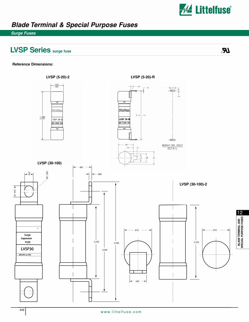
Blade Terminal & Special Purpose Fuses
449w w w. l i t t e l f u s e . c o m
12
BLA
DE
TE
RM
INA
L A
ND
SP
EC
IAL
PU
RP
OS
E F
US
ES
Surge Fuses
LVSP Series surge fuse
Reference Dimensions:
®
LVSP (5-20)-2 LVSP (5-20)-R
R
600 VAC or LESS
R
SurgeSuppression
FUSE
LVSP30
R
600 VAC or LESS
SurgeSuppression
FUSE
LVSP30
2XR .128
.334
.256
2.250
3.040
3.590
.080
.483
.500
.816
LVSP (30-100)
2.250
.816
LVSP (30-100)-2

Blade Terminal & Special Purpose Fuses
450w w w. l i t t e l f u s e . c o m

Fuseholders
13
w w w. l i t t e l f u s e . c o m
Fuseholders . . . . . . . . . . . . . . . . . . . . . . . . . . . . . . . . . . . . . . . . . . . . . . . . . . . . . . . . . . . . . . . . . . . . . . . . . . . . . . . . . . . . . . . . . . . . . . . . . . . . . 451
International Shock-Safe (Panel Mount) . . . . . . . . . . . . . . . . . . . . . . . . . . . . . . . . . . . . . . . . . . . . . . . . . . . . . . . . . . . . . . . . . . . . . . . . . . . . . . 452-453
Flip-Top Shock-Safe (Panel Mount). . . . . . . . . . . . . . . . . . . . . . . . . . . . . . . . . . . . . . . . . . . . . . . . . . . . . . . . . . . . . . . . . . . . . . . . . . . . . . . . . . . . . . 454
Shock-Safe . . . . . . . . . . . . . . . . . . . . . . . . . . . . . . . . . . . . . . . . . . . . . . . . . . . . . . . . . . . . . . . . . . . . . . . . . . . . . . . . . . . . . . . . . . . . . . . . . . . . 455-456
Low Profile (Snap Mount) . . . . . . . . . . . . . . . . . . . . . . . . . . . . . . . . . . . . . . . . . . . . . . . . . . . . . . . . . . . . . . . . . . . . . . . . . . . . . . . . . . . . . . . . . . . . . 457
Blown-Fuse Indicating (Snap Mount) . . . . . . . . . . . . . . . . . . . . . . . . . . . . . . . . . . . . . . . . . . . . . . . . . . . . . . . . . . . . . . . . . . . . . . . . . . . . . . . . . . . . 457
RF-Shielded (Panel Mount) . . . . . . . . . . . . . . . . . . . . . . . . . . . . . . . . . . . . . . . . . . . . . . . . . . . . . . . . . . . . . . . . . . . . . . . . . . . . . . . . . . . . . . . . . . . 458
Traditional (Panel Mount) . . . . . . . . . . . . . . . . . . . . . . . . . . . . . . . . . . . . . . . . . . . . . . . . . . . . . . . . . . . . . . . . . . . . . . . . . . . . . . . . . . . . . . . . . . . . . 459
Blown-Fuse Indicating . . . . . . . . . . . . . . . . . . . . . . . . . . . . . . . . . . . . . . . . . . . . . . . . . . . . . . . . . . . . . . . . . . . . . . . . . . . . . . . . . . . . . . . . . . . . . . . 460
Watertight (Panel Mount) . . . . . . . . . . . . . . . . . . . . . . . . . . . . . . . . . . . . . . . . . . . . . . . . . . . . . . . . . . . . . . . . . . . . . . . . . . . . . . . . . . . . . . . . . . . . . 461
RF Shielded/Watertight (Panel Mount) . . . . . . . . . . . . . . . . . . . . . . . . . . . . . . . . . . . . . . . . . . . . . . . . . . . . . . . . . . . . . . . . . . . . . . . . . . . . . . . . . . . 461
MicroTM or PICO® II Fuse. . . . . . . . . . . . . . . . . . . . . . . . . . . . . . . . . . . . . . . . . . . . . . . . . . . . . . . . . . . . . . . . . . . . . . . . . . . . . . . . . . . . . . . . . . . . . . 462
LT-5TM Fuse. . . . . . . . . . . . . . . . . . . . . . . . . . . . . . . . . . . . . . . . . . . . . . . . . . . . . . . . . . . . . . . . . . . . . . . . . . . . . . . . . . . . . . . . . . . . . . . . . . . . . . . . 462
In-Line. . . . . . . . . . . . . . . . . . . . . . . . . . . . . . . . . . . . . . . . . . . . . . . . . . . . . . . . . . . . . . . . . . . . . . . . . . . . . . . . . . . . . . . . . . . . . . . . . . . . . . . . 463-464
ATO® Fuse . . . . . . . . . . . . . . . . . . . . . . . . . . . . . . . . . . . . . . . . . . . . . . . . . . . . . . . . . . . . . . . . . . . . . . . . . . . . . . . . . . . . . . . . . . . . . . . . . . . . . . . . 464
MINI® Fuse . . . . . . . . . . . . . . . . . . . . . . . . . . . . . . . . . . . . . . . . . . . . . . . . . . . . . . . . . . . . . . . . . . . . . . . . . . . . . . . . . . . . . . . . . . . . . . . . . . . . 464-465
Indicating/Alarm Fuse. . . . . . . . . . . . . . . . . . . . . . . . . . . . . . . . . . . . . . . . . . . . (See page 446 in the Blade Terminal and Special Purpose fuse section)
OMNI-BLOK® Fuseholder . . . . . . . . . . . . . . . . . . . . . . . . . . . . . . . . . . . . . . . . . . . . . . . . . . . . . . . . (See page 374 in the Surface Mount Fuses section)
PAGE
451
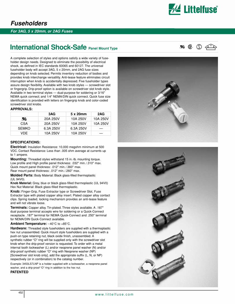
Fuseholders
452w w w. l i t t e l f u s e . c o m
For 3AG, 5 x 20mm, or 2AG Fuses
International Shock-Safe Panel Mount Type
A complete selection of styles and options satisfy a wide variety of fuse-holder design needs. Designed to eliminate the possibility of electricalshock, as defined in IEC standards 60065 and 60127. The universalfuseholder body will accept 3AG, 5 x 20mm, and 2AG fuse sizesdepending on knob selected. Permits inventory reduction of bodies andprovides knob interchange versatility. Anti-tease feature eliminates circuitinterruption when knob is accidentally depressed. Five fuseholder typesassure design flexibility. Available with two knob styles — screwdriver slotor fingergrip. Drip-proof option is available on screwdriver slot knob style.Available in two terminal styles — dual-purpose for soldering or 3/16"NEMA quick connect; and 1/4" NEMA/DIN quick connect. Quick fuse sizeidentification is provided with letters on fingergrip knob and color-codedscrewdriver slot knobs.
APPROVALS:3AG 5 x 20mm 2AG
20A 250V 10A 250V 10A 250VCSA 20A 250V 10A 250V 10A 250V
SEMKO 6.3A 250V 6.3A 250V —VDE 10A 250V 10A 250V —
SPECIFICATIONS:Electrical: Insulation Resistance: 10,000 megohm minimum at 500VDC. Contact Resistance: Less than .005 ohm average at currents upto 1 ampere.
Mounting: Threaded styles withstand 15 in.-lb. mounting torque.Low profile and High profile panel thickness: .032" min. /.310" max.Quick mount panel thickness: .012" min. /.360" max.Rear mount panel thickness: .012" min. /.260" max.
Molded Parts: Body Material: Black glass-filled thermoplastic (UL 94V0).Knob Material: Grey, blue or black glass-filled thermoplastic (UL 94V0)Hex Nut Material: Black glass-filled thermoplastic.
Knob: Finger-Grip, Fuse Extractor type or Screwdriver Slot, FuseExtractor type with plated copper alloy insert. Plated copper alloy contactclips. Spring loaded, locking mechanism provides an anti-tease featureand will not vibrate loose.
Terminals: Copper alloy. Tin-plated. Three styles available. A .187" dual purpose terminal accepts wire for soldering or a Quick-Connectreceptacle. .187" terminal for NEMA Quick-Connect and .250" terminalfor NEMA/DIN Quick-Connect available.
Ambient Temperature: –40°C to +85°C.
Hardware: Threaded style fuseholders are supplied with a thermoplastichex nut unassembled. Quick mount style fuseholders are supplied with apush-on type retaining nut, black oxide finish, unassembled. A synthetic rubber “O” ring will be supplied only with the screwdriver slotknob when the drip-proof version is requested. To order with a metal internal tooth lockwasher (L) and/or neoprene panel washer (N) and/ordrip-proof synthetic rubber “O” ring with Neoprene washer (NP)[Screwdriver slot knob only], add the appropriate suffix (L, N, or NP)respectively (or in combination) to the catalog number.
Example: 3453LS7LNP is a holder supplied with a lockwasher, a neoprene panelwasher, and a drip-proof “O” ring in addition to the hex nut.
PATENTED
®
® ®V
D E
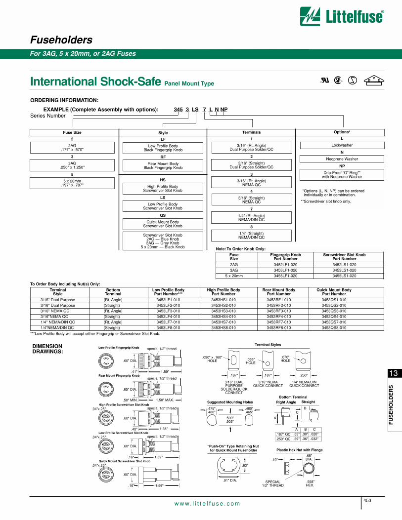
Fuseholders
453w w w. l i t t e l f u s e . c o m
13
FU
SE
HO
LD
ER
S
For 3AG, 5 x 20mm, or 2AG Fuses
International Shock-Safe Panel Mount Type ® ®V
D E
Fuse Size
2
2AG.177" x .570"
3
3AG.250" x 1.250"
5
5 x 20mm.197" x .787"
FUSE
FUSEFUSE
FUSE
.60" DIA.
.65" DIA.
.41" 1.59"
.50" MIN. 1.50" MAX.
Low Profile Fingergrip Knob
Rear Mount Fingergrip Knob
special 1/2" thread
special 1/2" thread
special 1/2" thread
special 1/2" thread
FUSE
FUSE
.40"
1.35"
High Profile Screwdriver Slot Knob.04"x.25"
FUSE
FUSE
´.16"
1.59"
Low Profile Screwdriver Slot Knob.04"x.25"
FUSE
FUSE
.16"
1.59"
Quick Mount Screwdriver Slot Knob.04"x.25"
Terminal Styles
Suggested Mounting HolesBottom Terminal
.090" x .160"HOLE .055"
HOLE
.070"HOLE
3/16" DUALPURPOSE
SOLDER/QUICKCONNECT
1/4" NEMA/DINQUICK CONNECT
3/16" NEMAQUICK CONNECT
.187" .187" .250"
.475"
.480".460".465"
.500"
.505"A
BC
A B C.187" QC.250" QC
.53" .30" .020"
.59" .36" .032"
Right Angle Straight
"Push-On" Type Retaining Nut for Quick Mount Fuseholder
Plastic Hex Nut with Flange
.91" DIA.
.63"
.19".65"DIA.
.558"HEX.
SPECIAL1/2" THREAD
.60" DIA.
.60" DIA.
.60" DIA.
DIMENSIONDRAWINGS:
To Order Body Including Nut(s) Only:
Terminal Bottom Low Profile Body High Profile Body Rear Mount Body Quick Mount BodyStyle Terminal Part Number*** Part Number Part Number Part Number
3/16" Dual Purpose (Rt. Angle) 3453LF1-010 3453HS1-010 3453RF1-010 3453QS1-0103/16" Dual Purpose (Straight) 3453LF2-010 3453HS2-010 3453RF2-010 3453QS2-0103/16" NEMA QC (Rt. Angle) 3453LF3-010 3453HS3-010 3453RF3-010 3453QS3-0103/16"NEMA QC (Straight) 3453LF4-010 3453HS4-010 3453RF4-010 3453QS4-0101/4" NEMA/DIN QC (Rt. Angle) 3453LF7-010 3453HS7-010 3453RF7-010 3453QS7-0101/4"NEMA/DIN QC (Straight) 3453LF8-010 3453HS8-010 3453RF8-010 3453QS8-010
***Low Profile Body will accept either Fingergrip or Screwdriver Slot Knob.
ORDERING INFORMATION:
EXAMPLE (Complete Assembly with options): 345 3 LS 7 L N NPSeries Number
Style
LF
Low Profile BodyBlack Fingergrip Knob
RF
Rear Mount BodyBlack Fingergrip Knob
HS
High Profile BodyScrewdriver Slot Knob
LS
Low Profile BodyScrewdriver Slot Knob
QS
Quick Mount BodyScrewdriver Slot Knob
Screwdriver Slot Knob2AG — Blue Knob3AG — Grey Knob
5 x 20mm — Black Knob
Terminals
1
3/16" (Rt. Angle)Dual Purpose Solder/QC
2
3/16" (Straight)Dual Purpose Solder/QC
3
3/16" (Rt. Angle)NEMA QC
4
3/16" (Straight)NEMA QC
7
1/4" (Rt. Angle)NEMA/DIN QC
8
1/4" (Straight)NEMA/DIN QC
Options*
L
Lockwasher
N
Neoprene Washer
NP
Drip-Proof “O” Ring**with Neoprene Washer
**Options (L, N, NP) can be orderedindividually or in combination.
**Screwdriver slot knob only.
Note: To Order Knob Only:
Fuse Fingergrip Knob Screwdriver Slot KnobSize Part Number Part Number
2AG 3452LF1-020 3452LS1-0203AG 3453LF1-020 3453LS1-020
5 x 20mm 3455LF1-020 3455LS1-020

Fuseholders
454w w w. l i t t e l f u s e . c o m
For 3AG, 5 x 20mm, or 2AG Fuses
Flip-Top Shock-Safe Panel Mount Type
Shock-Safe design eliminates any possibility of electrical shock, per IECStandards 60127 and 60065. Fuse carrier holds spare fuse for fast, easyfuse replacement and convenient servicing. Low profile design comple-ments modern panels.
APPROVALS: Recognized under the Components Program ofUnderwriters Laboratories and Certified by CSA.
SPECIFICATIONS:Electrical: Rating: See TABLE.Insulation Resistance: 10,000 megohm minimum at 500 VDC.Contact Resistance: Less than 0.01 ohm.
Mounting: Snap-in mounting. No hardware required. Panel thicknessrange: .032" through .125".
Molded Parts: Thermoplastic (UL 94V0) black standard (other colors available as special).
Fuse Carrier: Spring-loaded. Unlocks with a press of the finger. Locksinto place to prevent accidental circuit interruption. Permanently attachedto fuseholder body to prevent loss. Extracts fuse from live terminals.Holds spare fuse.
Terminals: Copper alloy, tin plate. Accepts quick-connect or solder.
Ambient Temperature: –40°C to +85°C.
Vibration: 10-55-10 Hz at .06" double amplitude (Method 201, MIL-STD-202).
PATENTED
ORDERING INFORMATION:
Max. Amps A B C D E FCatalog Number Fuse Size Q.C. Terminals At 250V. +.005"/-.000" +.005"/-.000"
346 877 3AG.250" x .032" 15 .75" 1.5" .27" 1.04" .688" 1.445"
.072" Dia. Hole
286 677 5 x 20mm.187" x .032"
10 .70" 1.03" .26" .94" .625" .953".055" Dia. Hole
286 377 2AG.110" x .020"
10 .61" .85" .20" .87" .550" .775".048" Dia. Hole
LOW PROFILE DESIGN
BARRIER-PROTECTEDTERMINALS
FUSE CARRIERHOLDS SPARE
FUSE
B FDC
A E
® ®
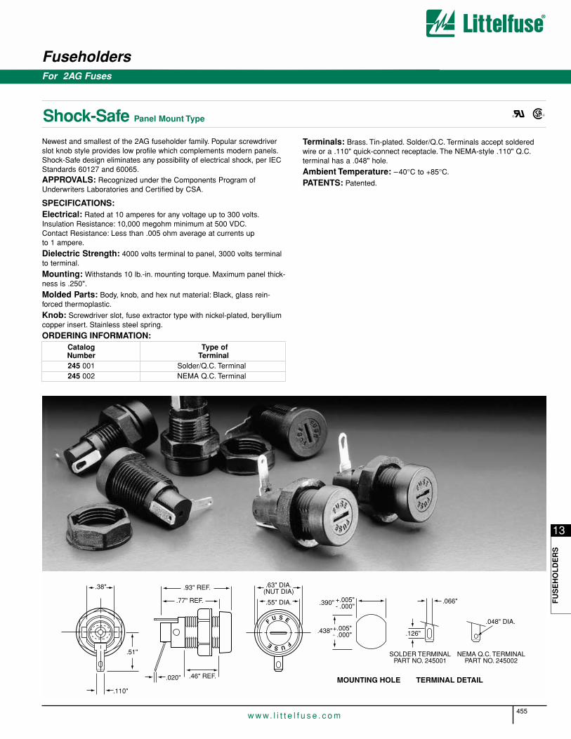
Fuseholders
455w w w. l i t t e l f u s e . c o m
13
FU
SE
HO
LD
ER
S
For 2AG Fuses
Shock-Safe Panel Mount Type
Newest and smallest of the 2AG fuseholder family. Popular screwdriverslot knob style provides low profile which complements modern panels.Shock-Safe design eliminates any possibility of electrical shock, per IECStandards 60127 and 60065.APPROVALS: Recognized under the Components Program ofUnderwriters Laboratories and Certified by CSA.
SPECIFICATIONS:Electrical: Rated at 10 amperes for any voltage up to 300 volts.Insulation Resistance: 10,000 megohm minimum at 500 VDC.Contact Resistance: Less than .005 ohm average at currents up to 1 ampere.
Dielectric Strength: 4000 volts terminal to panel, 3000 volts terminalto terminal.
Mounting: Withstands 10 lb.-in. mounting torque. Maximum panel thick-ness is .250".
Molded Parts: Body, knob, and hex nut material: Black, glass rein-forced thermoplastic.
Knob: Screwdriver slot, fuse extractor type with nickel-plated, berylliumcopper insert. Stainless steel spring.
ORDERING INFORMATION:Catalog Type ofNumber Terminal245 001 Solder/Q.C. Terminal245 002 NEMA Q.C. Terminal
Terminals: Brass. Tin-plated. Solder/Q.C. Terminals accept solderedwire or a .110" quick-connect receptacle. The NEMA-style .110" Q.C.terminal has a .048" hole.
Ambient Temperature: –40°C to +85°C.
PATENTS: Patented.
.93" REF.
.46" REF.
.55" DIA. +.005"- .000".390" .066"
SOLDER TERMINALPART NO. 245001
NEMA Q.C. TERMINALPART NO. 245002
.048" DIA.
.126"
.020"
.110"
.77" REF.
+.005"- .000"
.438"
.63" DIA.(NUT DIA)
.38"
.51"
® ®

Fuseholders
456w w w. l i t t e l f u s e . c o m
For 3AG, 5 x 20mm, or 2AG Fuses
Shock-Safe for 3AG or 5x20mm Fuses PC Board Type
yy
1.77".49"
.040"
.056"DIA.
.48"
.12".68"
.44"
.20".24"
.598"
.602".698".702"
.242"
.246"
Catalog Number Bottom Fuse LengthStandard Watertight Terminal Range*571 027 571 027P Straight
15/16" – 13/8"571 028 571 028P Rt. Angle571 007 571 007P Straight
113/32" – 11/2"571 008 571 008P Rt. Angle571 OCC 571 OCCP Straight
11/2"571 RCC 571 RCCP Rt. Angle*Fuse diameter is 13/32".
Similar to Shock-Safe fuseholders shown on preceding page, butdesigned for P.C. board mounting. Shock-Safe design per IEC Standards60127 and 60065. Two different knob styles available for use with 3AG(1/4" x 11/4") or 5 x 20mm fuses.APPROVALS: Recognized under the Components Program ofUnderwriters Laboratories (16A, 250V).Certified by CSA (15A, 250V).SEMKO approved (6.3A, 250V).VDE approved (10A, 250V).SPECIFICATIONS:Electrical: Rating: See APPROVALS.Insulation Resistance: 10,000 megohm minimum at 500 VDC.Contact Resistance: Less than .005 ohm average at a current of one ampere.Dielectric Strength: 4000 volts minimum.Mounting: Intended for soldering to printed circuit boards.Molded Parts: Body Material: Black glass-filled thermoplastic (UL 94V0).Knob: Screwdriver slot, fuse extractor type with nickel-plated, copperalloy insert. Spring-loaded, bayonet style.Knob Material: Grey or Black glass-filled thermoplastic (UL 94V0).Terminals: Brass. Tin-plated.Ambient Temperature: –40°C to +85°C.
ORDERING INFORMATION:Catalog FuseNumber Size345 101 1/4" x 11/4" Fuses
345 121 5 x 20mm FusesBody only: 345 101-010Knob only: 345 101-020 (1/4" x 11/4") Grey;
345 121-020 (5 x 20mm) Black.
For Midget Fuses Panel Mount Type
Two panel mount fuseholder designs are available for supplementary orClass CC branch circuit protection. Class CC fuses have a rejection feature on one end cap which mates with the rejection feature ofLittelfuse Class CC fuse blocks and fuseholders to prevent the installation of fuses with lower voltage ratings or interrupting ratings.
APPROVALS: Recognized under the Components Program ofUnderwriters Laboratories and Certified by CSA.
SPECIFICATIONS:Electrical: Rated at 30 amperes for any voltage up to 600 volts.
Dielectric Strength: 4000 volts minimum.
Mounting: Flange mounting either in front of or behind panel.Watertight version must be front panel mounted. Maximum panel thick-ness is .75".
Molded Parts: Black thermoplastic (UL 94V0).
Knob: Screw type, with engraved markings: unfilled characters (571007, 571 008, 571 007P, 571 008P), light blue characters (571 027, 571028, 571 027P, 571 028P).
Terminals: Brass. Tin-plated. Combination solder and 1/4" Quick-Connect. Side terminal has .125" diameter hole. Bottom terminal has.156" x .124" elongated hole.
Ambient Temperature: –40°C to +85°C.
Hardware: 571 007, 571 008, 571 027, 571 028, 571 OCC, and 571RCC, none; 571 007P, 571 008P, 571 027P, 571 028P, 571 OCCP, and571 RCCP, two O-rings for watertight seal per MIL-PRF-19207.
® ®V
D E
®®
Reference Dimensions
.76"
.86"
.92"DIA.
.446"
2.08"2.40"
1.31"1.75"
.032"
.15" MAX.172" DIA.
(2)
.15" MAX
1.12"
.890"1.310"
2 MOUNTING HOLES FORNo. 8 SCREWS
STANDARD MOUNTING (FLANGE IN FRONT OF PANEL)
Reference Dimensions
ORDERING INFORMATION:

Fuseholders
457w w w. l i t t e l f u s e . c o m
13
FU
SE
HO
LD
ER
S
For 3AG Fuses
Low Profile Snap Mount Type
APPROVALS: Recognized under the Components Program ofUnderwriters Laboratories and Certified by CSA.
SPECIFICATIONS:Electrical: 348 Series: Rated at 15 amps for any voltage up to 250 volts.344 Series: Rated at 15 amps at lamp voltage shown below.
Dielectric Strength: 1500 volts minimum.When designing indicating type fuseholders into a circuit, considerationshould be given to the resistance of fractional amperage fuses and theparallel resistance of the indicator lamp and its resistor.
Mounting: Panel thickness range: .031" through .125".Molded Parts: Black thermoplastic body (UL 94V0). Thermoplasticbezel, cap and lens (UL94V2). See tables below for colors.
Terminals: Brass. Tin-plated.
Ambient Temperature:Non-indicating: –40°C to +85°C.Indicating: –40°C to +60°C.
Fuse Installation: Insert a fuse into the cap and push the assemblyinto the body until it latches. Press in and down to unlatch for removal.
PATENTED
Blown-Fuse Indicating Snap Mount Type
APPROVALS AND SPECIFICATIONS: See above.
.054" DIA.
344 800 SERIES.250" X .032"
344 600 SERIES.187" X .020"NEMA Q.C.
.054" DIA.
.85"
1.95" (WITHFUSE ASSEMBLED)
.53"
.4"
.87" .42"
ORDERING INFORMATION:Catalog Number
3/16" Q.C. 1/4" Q.C. Lamp Lamp LensTerminals Terminals Lamp Type Voltage Current Resistor Color
344 601 344 801 Incandescent 6 40 ma No Amber344 602 344 802 Incandescent 14 80 ma No Amber344 603 344 803 Incandescent 28 40 ma No Amber344 604 344 804 Neon 120 1.2 ma Yes Clear344 605 344 805 Neon 240 .3 ma Yes Clear
348 000 Series
344 600 Series344 800 Series
Standard body and bezel color is black; otherbezel colors available on special order.
® ®
FUSE
PRESS
.85"
1.95" (WITHFUSE ASSEMBLED)
.28"
.4"
.87" .42"
.054" DIA.
348 800 SERIES.250" X .032"
348 600 SERIES.187" X .020"NEMA Q.C.
.054" DIA.ORDERING INFORMATION:Six-Digit Catalog Numbers Consist of:
Series Number Terminal Style Bezel Color Cap Color_ _ _ _ _ _
348 for 6 for 3/16" wide NEMA 7 for Black 1 for Red3AG Fuses Q.C. Terminal 7 for Black
8 for 1/4" wide
Example: 3 4 8 6 1 1
Mounting Hole: .625" square
Mounting Hole: .625" square
® ®

Fuseholders
458w w w. l i t t e l f u s e . c o m
For MicroTM Fuse Plug-In Fuses
RF-Shielded Front Panel Mount Type /Rear Panel Mount Type
Space Saving. RF-shielded design holds miniature MICRO™ fuse. Screw-on drip-proof knob construction permits use when presence of moisture existsat front of panels.
SPECIFICATIONS:Electrical: Rated at 5 amperes for any voltage up to 125 volts.
Mounting: Front panel mount, maximum panel thickness: .093". Rear panel mount, maximum panel thickness: .125".
Molded Parts: Black thermoset.
Housing, Knob and Nut: Aluminum, untreated.
Mounting Gasket: Neoprene or conductive silicone.
Seal: Buna “N” O-ring inside the knob.
Terminals: Beryllium copper. Silver plated.
Ambient Temperature: –40°C to +125°C.
Hardware: Hex nut or knurled nut as shown, unassembled.
.345"
.350"
.380"
.385"
.46" .015"
HEX NUT
PANELKNOB BODY
GASKET
.90" REF.
.66" REF.
.50" REF.
Mounting Hole
yyyy
.345"
.350"
.380"
.385"
.46" .015"
GASKET
BODY
PANEL
KNOBKNURLED NUT
.73" REF..10" REF..63" REF.
.50" REF. .22" .015"
Mounting Hole
Front Panel Mount282 000 Series
Rear Panel Mount282 000 Series
ORDERING INFORMATION:Catalog Number Gasket Type
282 001 Neoprene282 007 Conductive
ORDERING INFORMATION:Catalog Number Gasket Type
282 002 Neoprene282 008 Conductive

Fuseholders
459w w w. l i t t e l f u s e . c o m
13
FU
SE
HO
LD
ER
S
For 3AG Fuses
Traditional Panel Mount Type
APPROVALS: Recognized under the Components Program ofUnderwriters Laboratories and Certified by CSA.
SPECIFICATIONS:Electrical: Rated at 20 amperes for any voltage up to 250 volts.
Dielectric Strength: 2400 volts minimum.
Mounting: Withstands 15 lb.-in. mounting torque;maximum panel thickness: .187".
Molded Parts: Black thermoplastic (UL 94V0).
Knob: Bayonet style with lettering.
Terminals: Copper & copper alloy. Tin plated, except 1/4" Quick-Connectterminals are nickel plated.
Ambient Temperature: –40°C to +85°C.
FUSEHOLDERS TO MIL SPEC:1 See Military Section.
342 000 Series
® ® QPL
ORDERING INFORMATION:Catalog Number
Fluted Knurled Type ofKnob Knob Terminal
342 014 342 012 Solder342 038 342 058 3/16" Q.C.342 838 342 858 1/4" Q.C.
Knurled knob shown. Fluted knob alsoavailable. See table below.
.085" X .12"HOLE
.78"
1"
.7"
1"
.020"
.78"
1"
.032".63"
.14" DIA. HOLE
.502"
.510"
.187"
.475"
.480"
.69"DIA.
.69"HEX
FLATS
.250"
.69"DIA.TYP..56"
.69" DIA.
.59"
DETENT.06" DIA.HOLE
.45"FLATSTYP.
ORDERING INFORMATION:Catalog Number
Fluted Knurled Type ofKnob Knob Terminal
342 004 342 022 Solder342 028 342 048 3/16" Q.C.342 828 342 848 1/4" Q.C.
Fluted knob shown. Knurled knob alsoavailable. See table below.
Right Angle Terminal
342 000 Series
.7"
.11" DIA.
.090" X .12"HOLE
1.31"
.78"
1"
.3"
.7"
1"
.4"
.020" .032"
.502"
.510".45"FLATS
TYP.
.69"HEX
FLATS
.475"
.480"
Straight Bottom Terminal
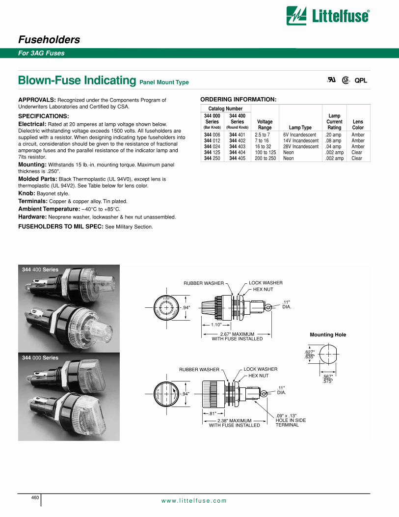
Fuseholders
460w w w. l i t t e l f u s e . c o m
For 3AG Fuses
Blown-Fuse Indicating Panel Mount Type
APPROVALS: Recognized under the Components Program ofUnderwriters Laboratories and Certified by CSA.
SPECIFICATIONS:Electrical: Rated at 20 amperes at lamp voltage shown below.Dielectric withstanding voltage exceeds 1500 volts. All fuseholders aresupplied with a resistor. When designing indicating type fuseholders intoa circuit, consideration should be given to the resistance of fractionalamperage fuses and the parallel resistance of the indicator lamp and 7its resistor.
Mounting: Withstands 15 lb.-in. mounting torque. Maximum panel thickness is .250".
Molded Parts: Black Thermoplastic (UL 94V0), except lens is thermoplastic (UL 94V2). See Table below for lens color.
Knob: Bayonet style.
Terminals: Copper & copper alloy. Tin plated.
Ambient Temperature: –40°C to +85°C.
Hardware: Neoprene washer, lockwasher & hex nut unassembled.
FUSEHOLDERS TO MIL SPEC: See Military Section.
Catalog Number344 000 344 400 LampSeries Series Voltage Current Lens
(Bar Knob) (Round Knob) Range Lamp Type Rating Color344 006 344 401 2.5 to 7 6V Incandescent .20 amp Amber344 012 344 402 7 to 16 14V Incandescent .08 amp Amber344 024 344 403 16 to 32 28V Incandescent .04 amp Amber344 125 344 404 100 to 125 Neon .002 amp Clear344 250 344 405 200 to 250 Neon .002 amp Clear
ORDERING INFORMATION:
344 400 Series
344 000 Series
2.67" MAXIMUMWITH FUSE INSTALLED
1.10"
LOCK WASHERRUBBER WASHERHEX NUT
.11"DIA..94"
.627"
.635"
.567"
.575"
2.38" MAXIMUMWITH FUSE INSTALLED
.09" x .13"HOLE IN SIDETERMINAL
.81"
LOCK WASHERRUBBER WASHERHEX NUT
.11"DIA..94"
® ® QPL

Fuseholders
461w w w. l i t t e l f u s e . c o m
13
FU
SE
HO
LD
ER
S
For 3AG Fuses
Watertight Panel Mount Type
APPROVALS: Recognized under the Components Program ofUnderwriters Laboratories.
SPECIFICATIONS:Electrical: Rated at 20 amperes for any voltage up to 250 volts.
Dielectric Strength: 1500 volts minimum.
Mounting: Withstands 15 lb.-in. mounting torque; maximum panelthickness is .250".
Molded Parts: Black thermoset (UL 94V0).
Knob: Screw type.
Seal: O-ring provides a watertight seal on the front side of the panel per MIL-PRF-19207.
Terminals: Copper & copper alloy. Tin plated. Solder type.
Ambient Temperature: –40°C to +85°C.
Hardware: O-rings (2) and hex nut, unassembled.
FUSEHOLDERS TO MIL SPEC: See Military Section.
ORDERING INFORMATION:Catalog Number: 342 006
RF Shielded/Watertight Panel Mount Type
Radio frequency shielded fuseholders eliminate possible transmission orreception of RF signals through the hole in the chassis in which the fuse-holder is mounted. These fuseholders comply with the watertight con-struction requirement of MIL-PRF-19207 and the Shock-Safe require-ments of IEC 60065 and 60127-6. A rubber O-ring and conductive gas-ket maintain RF shielding and watertight construction.
SPECIFICATIONS: The basic fuseholder used is the 345 603 Shock-Safe holder.
ORDERING INFORMATION:Catalog Brass ShieldingNumber Cap Finish340 312 Nickel plated340 313 Dull Black
340 300 Series
® QPL
QPL
2.35" MAX.
.88"DIA.
.17"MAX.
CAP
O-RING
R.F.I. GASKET
KEEP CHAIN
1"MAX.
.460"
.465".475".480"
.500"
.505"
MOUNTING HOLES
.625"
.635"
.81"
.94"DIA.
.12" DIA.HOLES
1.3 "
.81 "
.570"
.575"
MOUNTING HOLE
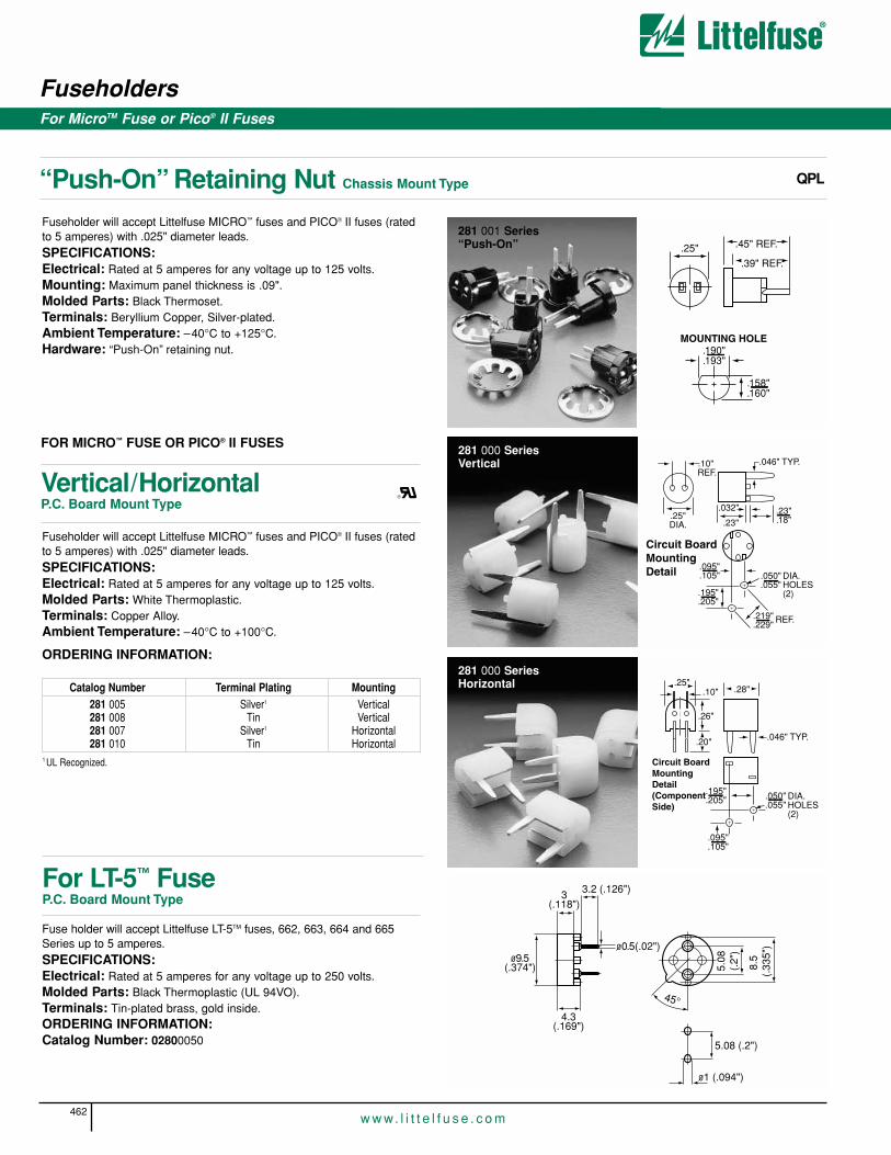
Fuseholders
462w w w. l i t t e l f u s e . c o m
For MicroTM Fuse or Pico® II Fuses
281 001 Series“Push-On”
281 000 SeriesVertical
281 000 SeriesHorizontal
Fuseholder will accept Littelfuse MICRO™ fuses and PICO® II fuses (ratedto 5 amperes) with .025" diameter leads.SPECIFICATIONS:Electrical: Rated at 5 amperes for any voltage up to 125 volts.Mounting: Maximum panel thickness is .09".Molded Parts: Black Thermoset.Terminals: Beryllium Copper, Silver-plated.Ambient Temperature: –40°C to +125°C.Hardware: “Push-On” retaining nut.
FOR MICRO™ FUSE OR PICO® II FUSES
Vertical/HorizontalP.C. Board Mount Type
Fuseholder will accept Littelfuse MICRO™ fuses and PICO® II fuses (ratedto 5 amperes) with .025" diameter leads.SPECIFICATIONS:Electrical: Rated at 5 amperes for any voltage up to 125 volts.Molded Parts: White Thermoplastic.Terminals: Copper Alloy.Ambient Temperature: –40°C to +100°C.
ORDERING INFORMATION:
Catalog Number Terminal Plating Mounting281 005 Silver1 Vertical281 008 Tin Vertical281 007 Silver1 Horizontal281 010 Tin Horizontal
1 UL Recognized.
®
.25".28".10"
.046" TYP.
.195"
.205" .050".055"
.095"
.105"
DIA.HOLES (2)
.26"
.20"
.45" REF..25"
.39" REF.
.158"
.160"
.190"
.193"
.10" REF.
.095"
.105"
.032"
.046" TYP.
.25"DIA. .23"
.23"
.18"
.195"
.205"
REF..219".229"
.050"
.055"DIA.HOLES (2)
For LT-5™ FuseP.C. Board Mount Type
Fuse holder will accept Littelfuse LT-5TM fuses, 662, 663, 664 and 665Series up to 5 amperes.SPECIFICATIONS:Electrical: Rated at 5 amperes for any voltage up to 250 volts.Molded Parts: Black Thermoplastic (UL 94VO).Terminals: Tin-plated brass, gold inside.ORDERING INFORMATION:Catalog Number: 02800050
3(.118")
3.2 (.126")
00.5(.02")
4.3(.169")
09.5(.374")
45°
5.08 (.2")
01 (.094")
5.08
(.2"
)
8.5
(.33
5")
QPL“Push-On” Retaining Nut Chassis Mount Type
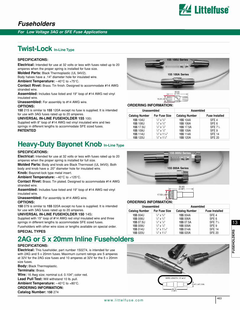
Fuseholders
463w w w. l i t t e l f u s e . c o m
13
FU
SE
HO
LD
ER
S
SPECIFICATIONS:Electrical: Intended for use at 32 volts or less with fuses rated up to 20amperes when the proper spring is installed for fuse size.Molded Parts: Black Thermoplastic (UL 94V2).Body halves have a .14" diameter hole for insulated wire.Ambient Temperature: –40°C to +75°C.Contact Rivet: Brass. Tin finish. Designed to accommodate #14 AWGstranded wire.Assembled: Includes fuse listed and 19" loop of #14 AWG red vinylinsulated wire.Unassembled: For assembly to #14 AWG wire.OPTIONS:150 215 is similar to 155 120A except no fuse is supplied. It is intendedfor use with 3AG fuses rated up to 20 amperes.UNIVERSAL IN-LINE FUSEHOLDER 155 100:Supplied with 8" loop of #14 AWG red vinyl insulated wire and twosprings in different lengths to accommodate SFE sized fuses.PATENTED
Heavy-Duty Bayonet Knob In-Line Type
SPECIFICATIONS:Electrical: Intended for use at 32 volts or less with fuses rated up to 20amperes when the proper spring is installed for full size.Molded Parts: Body and knob are Black Thermoset (UL 94V0). Bothbody and knob have a .20" diameter hole for insulated wire.Knob: Bayonet-lock type metal insert.Ambient Temperature: –40°C to +125°C.Contact Rivet: Brass. Tin plated. Designed to accommodate #14 AWGstranded wire.Assembled: Includes fuse listed and 19" loop of #14 AWG red vinylinsulated wire.Unassembled: For assembly to #14 AWG wire.OPTIONS:150 079 is similar to 155 020A except no fuse is supplied. It is intendedfor use with 3AG fuses rated up to 20 amperes.UNIVERSAL IN-LINE FUSEHOLDER 150 145:Supplied with 15" loop of #14 AWG red vinyl insulated wire and threesprings in different lengths to accommodate SFE sized fuses.Fuseholders with other wire sizes or lengths available on special order.
Unassembled AssembledCatalog Number For Fuse Size Catalog Number Fuse Installed
155 004U 1/4" x 5/8" 155 004A SFE 4155 006U 1/4" x 3/4" 155 006A SFE 6155 07.5U 1/4" x 7/8" 155 07.5A SFE 71/2
155 009U 1/4" x 7/8" 155 009A SFE 9155 014U 1/4" x 11/16" 155 014A SFE 14155 020U 1/4" x 11/4" 155 020A SFE 20
ORDERING INFORMATION:
17.53 (.69")
52.83(2.08")
155 100U Series
155 100A Series
155 000U Series
155 000A Series
SPECIAL TYPES
2AG or 5 x 20mm Inline FuseholdersSPECIFICATIONS:Electrical: This fuseholder, part number 150274, is intended for usewith 2AG and 5 x 20mm fuses. Maximum current ratings are 5 amperesat 32V for the 2AG size fuses and 10 amperes at 32V for the 5 x 20mmsize fuses.Body: Black Thermoplastic.Terminals: Brass.Wire: 16 Awg size; nominal o.d. 0.104"; color red.Lead Pull Test: Will withstand 10 lb. pull.Ambient Temperature: –40°C to +80°C.ORDERING INFORMATION:Catalog Number: 150 274
WIRE LENGTH: 13" 0.5"
46.74(1.84")
10.67 (.42") DIA.
+
Unassembled Assembled
Catalog Number For Fuse Size Catalog Number Fuse Installed155 104U 1/4" x 5/8" 155 104A SFE 4155 106U 1/4" x 3/4" 155 106A SFE 6155 17.5U 1/4" x 7/8" 155 17.5A SFE 71/2
155 109U 1/4" x 7/8" 155 109A SFE 9155 114U 1/4" x 11/16" 155 114A SFE 14155 120U 1/4" x 11/4" 155 120A SFE 20
ORDERING INFORMATION:
55.63(2.19")
15.24 (.60")
Twist-Lock In-Line Type
For Low Voltage 3AG or SFE Fuse Applications

Fuseholders
464w w w. l i t t e l f u s e . c o m
Special Types
For ATO® Fuses In-Line Type
SPECIFICATIONS:Electrical: Intended for use with 32 volts Autofuse® fuses rated to 20 or30 amperes depending on wire size and terminal combinations.
Mounting: Capable of snap-mounting to panel from rear. Fuseholdersinterlock for multiple mounting.
Molded Parts: Black Thermoplastic (UL 94V2).
Terminals: Brass. Tin-plated. Snap-lock into body.
Ambient Temperature: –40°C to +85°C.
Wire: Stranded with PVC insulation, black #14 AWG for 155 300 Seriesand orange #10 AWG for 155 400 Series.
PATENTEDORDERING INFORMATION:
Catalog NumberAssembled with Assembled with Fuse
8" Wire Loop, 8" Wire Loop AmperageUnassembled No Fuse and Fuse Rating
155 320U 155 300 155 303A 3(Terminals designed (#14 wire/ 155 304A 4for #14 AWG terminals rated 155 305A 5stranded wire and to 20A). 155 37.5A 7.5marked “14”). 155 310A 10
155 315A 15155 320A 20
155 430U 155 400 155 425A 25(Terminals designed (#10 wire/ 155 430A 30for #10 AWG terminals ratedstranded wire and to 30A).marked “10”).
UNASSEMBLED
For MINI® Fuses In-Line Type — Easy Crimp Fuseholder
SPECIFICATIONS:Terminals: Copper Alloy/Tin plated.Body: Black Thermoplastic.Operating Temperature: –40°C to +105°C.Use standard crimping tool and crimp the matted area to secure wire.(Possible crimp tool - Ideal #30-428 [Toothed Die slot] or equivalent).
ORDERING INFORMATION:
For ATO® Fuses P.C. Board Mount Type
SPECIFICATIONS:Electrical: Intended for use with 32 volts ATO® fuses rated to 15amperes.
Molded Parts: Black Thermoplastic
Terminals: Copper Alloy, Tin Plated
Ambient Temperature: –40°C to +85°C.ORDERING INFORMATION:
Catalog Number: 04450715
CatalogNumber Description153 002 20A Max. Rating — Terminals will accept #16–22 AWG (1.0-
.33 mm2) stranded wire (use appropriate wire size based onfuse usage). For example — Use #16 AWG wire for 20A fuse.
153 003 30A Max. Rating — Terminals will accept #10–14 AWG (5.0-2.0 mm2) stranded wire (use appropriate wire size based onfuse usage). For example — Use #10 AWG wire for 30A fuse.
Typical Multiple Mounting(Fuseholders interlocked)
Recommended Panel Mounting Hole (.04" / .078" thick panel)
10.16 (.40")
37.08(1.46")
30.48 (1.20")
24.64(.970")
19.05 (.75")
10.54 (.415")10.41 (.410")
27.94 (1.10")26.92 (1.06")
.254 (.01") R. Max.Add .400" to width for each additional fuseholder
Tool For Fuse Removal or Replacement; Part No. 097024.
MATTED(CRIMP) AREA
11.43 (.45")
END VIEW
17.02(.67")
52.58(2.07") Max
SIDE VIEW
6.35 (.25")17.02 (.67")
9.3(.366")
21.8(.858")
9.3(.366")
2.5(.098")
4.5(.177") Ref.
9(.354")
22(.866")

Fuseholders
465w w w. l i t t e l f u s e . c o m
13
FU
SE
HO
LD
ER
S
Special Types
For MINI® Fuses P.C. Board Mount Type
The MINI® Fuse P.C. board fuseholders bring the reliability and availability of the plug-in 32V MINI® Fuse to the circuit board. Vertical and horizontal mounting of units is offered to meet a variety of requirements in which circuit protection is desired for a low DC voltageP.C. board application. The fuseholder body has “standoffs” to accommodate board washing and incorporates a unique “board lock”anchor to maintain a firm mechanical bond to the PCB during fuse insertion and removal.
APPROVALS: Recognized under the Components Program ofUnderwriters Laboratories for 15 amperes and Certified by CSA for 10 amperes.
SPECIFICATIONS:Electrical: Rated 32 VDC.Mounting: Three fuseholders can be mounted side by side (stacked)and operated at rated current. Contact factory for applications involvingmore than three stacked fuseholders.
Molded Parts: Black Thermoplastic body (UL 94V0).
Terminals: Copper Alloy. Tin Plated.
Ambient Temperature: –40°C to +85°C.
Compatibility: Standard .062" PCB thickness.
CatalogNumber Description153 007 Horizontal Mount P.C.B. Holder153 008 Single or Stackable (End Unit) Vertical Mount
P.C.B. Holder153 009 Stackable Vertical Mount P.C.B. Holder
Tool For Fuse Removal or Replacement; Part No. 097024.
ORDERING INFORMATION:
® ®
.300"
.042" .015"
.31"REF.
.170"
.30"
.680"
32 VF .508" REF.
BOARDEDGE
.180"
.235"REF.
.150"
.300"
.180"
P.C.B. FOOTPRINT
.050"TYP.
.300"
.082"
®SHOWN WITH 297 SERIES
MINI FUSE INSTALLED
HORIZONTAL MOUNT(Part No. 153007)
15 A10 A
®
®
15 A10 A
®
®
.300"
.068"TYP.
P.C.B. FOOTPRINT
.300" TYP..149"TYP.
.050"TYP.
.300"
15 A10 A
32 V
.680"
.508"
.152"
.042"
F
.160"
.300".30"
.753"
.090"
.062" REF.PCB BOARD
.068"TYP.
.150"
®
®
15 A10 A
®
®
.050"TYP.
.068" TYP.
.300"
P.C.B. FOOTPRINT
.150"
.068" TYP.
.149"TYP.
Single or stackableend unit (RH)
(Part No. 153008)
VERTICAL MOUNTS
Stackable unit(Part No. 153009)
SHOWN WITH 297 SERIESMINI FUSE INSTALLED®
466w w w. l i t t e l f u s e . c o m
Notes & Drawings

Fuse Blocks and Clips
14
467w w w. l i t t e l f u s e . c o m
Fuse and Block Clips. . . . . . . . . . . . . . . . . . . . . . . . . . . . . . . . . . . . . . . . . . . . . . . . . . . . . . . . . . . . . . . . . . . . . . . . . . . . . . . . . . . . . . . . . . . . . 467
OMNI-BLOK® Fuse Block . . . . . . . . . . . . . . . . . . . . . . . . . . . . . . . . . . . . . . . . . . . . . . . . . . . . . . . . . . . . . . . . . . . . . . . . . . . . . . . . . . . . . . . 468-470
Midget Fuse . . . . . . . . . . . . . . . . . . . . . . . . . . . . . . . . . . . . . . . . . . . . . . . . . . . . . . . . . . . . . . . . . . . . . . . . . . . . . . . . . . . . . . . . . . . . . . . . . . . . . 471
3AG Screw Terminal . . . . . . . . . . . . . . . . . . . . . . . . . . . . . . . . . . . . . . . . . . . . . . . . . . . . . . . . . . . . . . . . . . . . . . . . . . . . . . . . . . . . . . . . . . . . . . . 472
Clips (Rivet/Eyelet Mount) . . . . . . . . . . . . . . . . . . . . . . . . . . . . . . . . . . . . . . . . . . . . . . . . . . . . . . . . . . . . . . . . . . . . . . . . . . . . . . . . . . . . . . . . . . 472
Clips (PCB) . . . . . . . . . . . . . . . . . . . . . . . . . . . . . . . . . . . . . . . . . . . . . . . . . . . . . . . . . . . . . . . . . . . . . . . . . . . . . . . . . . . . . . . . . . . . . . . . . . 473-475
Automatic Insertion Clips . . . . . . . . . . . . . . . . . . . . . . . . . . . . . . . . . . . . . . . . . . . . . . . . . . . . . . . . . . . . . . . . . . . . . . . . . . . . . . . . . . . . . . . . . . . 475
PAGE

Fuse Blocks and Clips
468w w w. l i t t e l f u s e . c o m
For NANO2® Surface Mount Fuses
.35"REF.
.50"REF.
.81"REF.
.04"REF.
.19"REF.
.730"±.005"
.050"
.055"DIA. HOLES (2 LOCATIONS)
Recommended Hole Pattern
1.22"REF.
.70"REF.
.24" REF.
.53" REF.
.016"REF.
45
B
.450"centers typ.
.70" typ.
.190" x .187" deepC bore with .050"
material remaining.090" REF. DIA. Thru
Solder type terminalsfeature elongated
hole on clip
With 2AG fuse installed
.35" typ.
.110" typ.
.50" typ.
Solder & Q.C. Types:
® ®
This low profile Omni-Blok® Fuse Block design is available with a choice of solder type terminals, Q.C. terminals or P.C. board mountableterminals. The PCB design is offered with either tin-plated brass termi-nals for normal applications or tin-plated beryllium copper terminals foruse in caustic environments. These fuse blocks feature individual barrierswhich reinforce the fuse clips while providing greater protection againstclip damage and electrical shock. The unique design permits self-alignment of clips to fuse cap. This, plus a one-piece clip/terminalassures low contact resistance. Multiple pole units may be broken apart to obtain desired number of poles.
APPROVALS: Recognized under the Components Program ofUnderwriters Laboratories and Certified by CSA.
SPECIFICATIONS:Electrical: Solder Type — 10A, 300V.
Q.C. Type — 10A, 300V.PCB Type — 10A, 300V.
Dielectric Strength: 1500V., Minimum.Clip/Terminals: Tin-Plated Spring Brass, except pn 254121 is Tin-Plated Beryllium Copper.Base: Black Thermoplastic, glass reinforced with UL 94V0 flammability rating.Ambient Temperature: –40°C to +85°C.
OPTIONS:1. Other colors available on special order. Contact factory.2. Two different style clips can be supplied for circuit identity or
polarization. Contact factory.
PATENTED
ORDERING INFORMATION:
P.C. Board Mount Type:
Catalog Number TypicalSolder Type Number Overall Clip/Terminals of Poles Width (B) Terminals254 001 1 0.35" Brass254 002 2 0.80" Brass254 003 3 1.25" Brass254 004 4 1.70" Brass254 005 5 2.15" Brass254 006 6 2.60" Brass254 007 7 3.05" Brass254 008 8 3.50" Brass
TypicalNEMA Style Number Overall Clip/
.110" Q.C. Terminals of Poles Width (B) Terminals254 201 1 0.35" Brass254 202 2 0.80" Brass254 203 3 1.25" Brass254 204 4 1.70" Brass254 205 5 2.15" Brass254 206 6 2.60" Brass254 207 7 3.05" Brass254 208 8 3.50" Brass
TypicalP.C. Number Overall Clip/
Board Mount of Poles Width (B) Terminals254 101 1 0.35" Brass254 121 1 0.35" Beryllium Copper
OMNI-BLOK® Fuse Block Molded Base Type

Fuse Blocks and Clips
469w w w. l i t t e l f u s e . c o m
14
FU
SE
BL
OC
KS
A
ND
CL
IPS
Catalog Typical Overall Clip/ Anti-RotationNumber Width Terminals Boss
Solder Type Terminals520 004 .40" Brass No
NEMA Style .110" Q.C. Terminals520 003 .40" Brass No520 005-GY .40" Brass Yes
PC Board Mount520 101 .40" Brass No
10A
520
XX
.03" STANDOFF.40"
.18"
.50"
.950 ±.005
RECOMMENDED HOLE PATTERN
.050"
.055" TYP.
1.03" WITH A 5X20mmFUSE INSTALLED
10A
520
XX
.40"
.110"
.090" DIA. THRU .07"x.13 HOLE
.50".54"
1.44"
.92"
45°
.016"
520 004
10A
520
XX
.40"
.110"
.090" DIA. THRU
.50".54"
1.44"
.92"
45°
.016"
.40"
.50".54"
1.44"
.92"
45°
.016"
.428".040 DIA.
520 003
520 005-GY
SOLDER TERMINALTYPES:
The metric Omni-Blok® fuse block, for 5 x 20mm size fuses, is a low profile design that is available with a choice of solder type terminals,NEMA style QC terminals, or PC board mountable terminals. Each ofthese designs has tin-plated brass terminals. A unique design featureprovides self-alignment of the clips to the fuse caps. This feature, plus aone-piece clip/terminal design, assures low contact resistance. An anti-rotation feature is also available on the solder and QC terminal designs.
APPROVALS: Recognized under the Components Program of Underwriters Laboratories and Certified by CSA. VDE and Semko approved.
SPECIFICATIONS:Electrical: UL/CSA VDE/Semko
Solder Type — 10A, 300V. 6.3A, 250V.Q.C. Type — 10A, 300V. 6.3A, 250V.PCB Type — 10A, 300V. 6.3A, 250V.
Dielectric Strength: 1500V., Minimum.Clip/Terminals: Tin-Plated Spring Brass.Base: Glass reinforced Thermoplastic, UL 94V0 flammability rating.Gray color (GY) for anti-rotational series, black color for all others.Ambient Temperature: –40°C to +85°C.
PATENTED
ORDERING INFORMATION:
Q.C. TERMINALTYPES:
P.C. MOUNT TYPE520 101
® ®V
D EMetric OMNI-BLOK® Fuse Block Molded Base Type
For 5 x 20mm Fuses
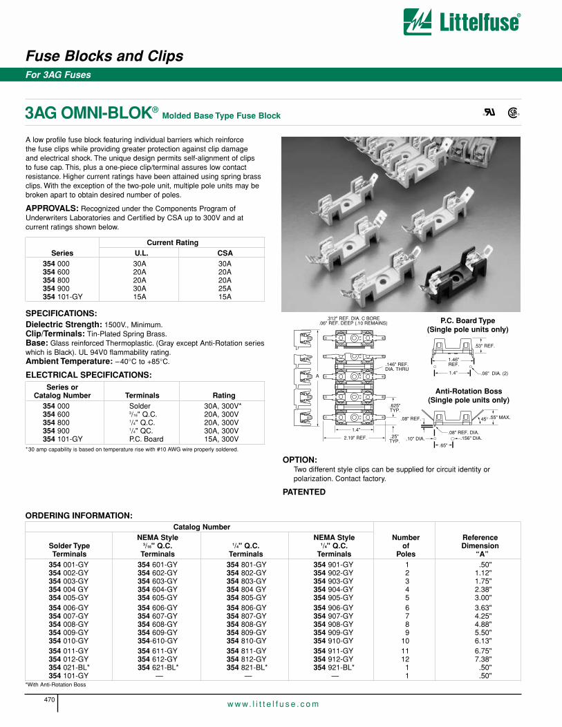
Fuse Blocks and Clips
470w w w. l i t t e l f u s e . c o m
For 3AG Fuses
3AG OMNI-BLOK®Molded Base Type Fuse Block
A low profile fuse block featuring individual barriers which reinforce the fuse clips while providing greater protection against clip damage and electrical shock. The unique design permits self-alignment of clips to fuse cap. This, plus a one-piece clip/terminal assures low contactresistance. Higher current ratings have been attained using spring brassclips. With the exception of the two-pole unit, multiple pole units may bebroken apart to obtain desired number of poles.
APPROVALS: Recognized under the Components Program ofUnderwriters Laboratories and Certified by CSA up to 300V and at current ratings shown below.
Current RatingSeries U.L. CSA
354 000 30A 30A354 600 20A 20A354 800 20A 20A354 900 30A 25A354 101-GY 15A 15A
SPECIFICATIONS:Dielectric Strength: 1500V., Minimum.Clip/Terminals: Tin-Plated Spring Brass.Base: Glass reinforced Thermoplastic. (Gray except Anti-Rotation serieswhich is Black). UL 94V0 flammability rating.Ambient Temperature: –40°C to +85°C.
ELECTRICAL SPECIFICATIONS:Series or
Catalog Number Terminals Rating354 000 Solder 30A, 300V*354 600 3/16" Q.C. 20A, 300V354 800 1/4" Q.C. 20A, 300V354 900 1/4" QC. 30A, 300V354 101-GY P.C. Board 15A, 300V
*30 amp capability is based on temperature rise with #10 AWG wire properly soldered.
OPTION:Two different style clips can be supplied for circuit identity or polarization. Contact factory.
PATENTED
® ®
ORDERING INFORMATION:Catalog Number
NEMA Style NEMA Style Number ReferenceSolder Type 3/16" Q.C. 1/4" Q.C. 1/4" Q.C. of DimensionTerminals Terminals Terminals Terminals Poles “A”
354 001-GY 354 601-GY 354 801-GY 354 901-GY 1 .50"354 002-GY 354 602-GY 354 802-GY 354 902-GY 2 1.12"354 003-GY 354 603-GY 354 803-GY 354 903-GY 3 1.75"354 004 GY 354 604-GY 354 804 GY 354 904-GY 4 2.38"354 005-GY 354 605-GY 354 805-GY 354 905-GY 5 3.00"354 006-GY 354 606-GY 354 806-GY 354 906-GY 6 3.63"354 007-GY 354 607-GY 354 807-GY 354 907-GY 7 4.25"354 008-GY 354 608-GY 354 808-GY 354 908-GY 8 4.88"354 009-GY 354 609-GY 354 809-GY 354 909-GY 9 5.50"354 010-GY 354-610-GY 354 810-GY 354 910-GY 10 6.13"354 011-GY 354 611-GY 354 811-GY 354 911-GY 11 6.75"354 012-GY 354 612-GY 354 812-GY 354 912-GY 12 7.38"354 021-BL* 354 621-BL* 354 821-BL* 354 921-BL* 1 .50"354 101-GY — — — 1 .50"
*With Anti-Rotation Boss
XX
.55" MAX.45°
XX
XX
XX
XX
A
.312" REF. DIA. C BORE.06" REF. DEEP (.10 REMAINS)
1.4"
2.19" REF.
.625"TYP.
.25"TYP.
.146" REF.DIA. THRU
.08" REF.
.08" REF. DIA..10" DIA. .156" DIA.
.65"
.53" REF.
.06" DIA. (2)1.4"
1.46"REF.
P.C. Board Type(Single pole units only)
Anti-Rotation Boss(Single pole units only)

Fuse Blocks and Clips
471w w w. l i t t e l f u s e . c o m
14
FU
SE
BL
OC
KS
A
ND
CL
IPS
For 1 1/2 Long Midget Fuses
600 Volt Molded Base Type
Space-saving, 600 volt, molded base fuse blocks with side barriers forisolation. For use with 13/32" x 11/2" midget fuses. By sliding and lockingblocks together, any number of poles can be achieved. Class CC fuseshave a rejection feature on one end cap which mates with the rejectionfeature of Littelfuse Class CC fuse blocks and fuseholders to prevent theinstallation of fuses with lower voltage ratings or interrupting ratings.
AGENCY APPROVALS: Midget Blocks: Recognized under theComponents Program of Underwriters Laboratories. Certified by CSA.Class CC Blocks: UL Listed. Certified by CSA.
SPECIFICATIONS:Electrical: Screw terminal, pressure plate terminal, and box lug terminals rated for 30 amperes. Q.C. terminals rated for 20 amperes.Dielectric Strength: 1200V Minimum.Clip/Terminals: Tin-Plated Copper Alloy.Box Lug: Copper.Screws and Captive Pressure Plate: Zinc-Plated Steel.Reinforcing Spring: Stainless Steel. Contact factory for availability.Base: Thermoplastic. UL 94V0 flammability rating.Ambient Temperature: 105°C Maximum.
PATENTED
DIMENSIONS:
ORDERING INFORMATION:Catalog Number Number of Maximum
Midget Class CC Poles Connector Type Wire SizeL60030M-1C L60030C-1C 1 Copper Box LugL60030M-2C L60030C-2C 2 Copper Box Lug # 6 CUL60030M-3C L60030C-3C 3 Copper Box LugL60030M-1SQ L60030C-1SQ 1 Screw/Q.C. TerminalL60030M-2SQ L60030C-2SQ 2 Screw/Q.C. Terminal #10 CUL60030M-3SQ L60030C-3SQ 3 Screw/Q.C. TerminalL60030M-1PQ L60030C-1PQ 1 Pressure Plate/Q.C. TerminalL60030M-2PQ L60030C-2PQ 2 Pressure Plate/Q.C. Terminal #10 CUL60030M-3PQ L60030C-3PQ 3 Pressure Plate/Q.C. Terminal
DIN Rail Adapter: Part No. FBDIN1.
Class CCRejection Feature Fuse Clip
Guide Spring
.495"REF.
.172" REF.
Screwwith
PressurePlate(P)
Screw(S)
BoxLug(C)
.172" REF.
.100"REF.
3.00"REF.
.650"REF.
1.250"REF .
.600"REF.
.783"REF .
1.490"REF..750"
REF.
.484 "REF.
.670"REF.1.360"
REF.
.770"REF.
.576"REF.
Installation of #FBDIN1 DIN RailAdapter to fuse block permitsassemblies to be snapped to 32mmasymmetrical or 35mm symmetrical(“hat” type) DIN rails.
GangMountableFuse blocksinterlock toform desirednumber of poles
® ® ®UL

Fuse Blocks and Clips
472w w w. l i t t e l f u s e . c o m
For 3AG Fuses
3AG Screw Terminal Laminated Base Type
AD
B
ONE POLE
C = Board Thickness E = Overall Height356 000, 359 000 and 556 000 Series
APPROVALS:1 356 000 Series (250V) Recognized under theComponents Program of Underwriters Laboratories.
SPECIFICATIONS:Electrical: Rated for currents up to 15 amperes (units with spring brassclips) or up to 30 amperes (beryllium copper clips).
Clips: 356 000 Series: Nickel-plated spring brass.359 000 Series: Silver-plated beryllium copper.
Terminals: 8-32THD screw type.
Base: Black phenolic laminate.
Mounting Hole: 3AG Block: Reference Dimensions.142"/.147" diameter with .295"/.302" x 82°C.S.
REFERENCE DIMENSIONS:
ORDERING INFORMATION:(Including Reference Dimensions)
For 3AG FusesNo. of DimensionPoles “A” Catalog Number
1 .78" 356 001 359 0012 1.69" 356 002 359 0023 2.59" 356 003 359 0034 3.50" 356 004 359 0045 4.41" 356 005 359 0056 5.31" 356 006 359 0067 6.21" 356 007 359 0078 7.12" 356 008 359 0089 8.03" 356 009 359 00910 8.94" 356 010 359 01011 9.84" 356 011 359 01112 10.75" 356 012 359 012
®
Fuse Type A B C D E3AG See 2.38" .25" .91" .73"
For 1/4" – 13/16" Diameter Fuses Rivet/Eyelet Mount Type
C
D
H, HOLE DIA.
A
B
C
D
H, HOLE DIA.
A
B
Earless Clip(without fuse stops)
Ear Clip(with fuse stops)
† See Ordering Information below.
For 1/4" Diameter Fuses Rivet/Eyelet Mount Solder Type
D
H, HOLE DIA.
.09" X .16"HOLE
A
B
C
B Straight Type, Solder Lug 45° Angle Type, Solder Lug
ORDERING INFORMATION:Catalog Number
Spring Brass Beryllium Copper FuseStyle Fuse Type Nickel-plated Silver-plated Diameter A B C D H Diameter
† Ear 3AG 101 001 121 001 1/4" .48" .31" .30" .16" .131"Midget 105 001 125 001 13/32" .75" .44" .52" .22" .196"NEC 1–30 amp 107 001 127 001 9/16" . 94" .59" .65" .25" .203"NEC 30–60 amp 109 001** 129 001 13/16" 1.31" .75" .87" .30" .265"
† Earless 3AG 101 002 121 002 1/4" .48" .31" .30" .16" .131"Midget 105 002 125 002 13/32" .75" .44" .52" .22" .196"NEC 1–30 amp 107 002 127 002 9/16" .94" .59" .65" .25" .203"NEC 30–60 amp 109 002** 129 002 13/16" 1.31" .75" .87" .30" .265"
Solder Lug 45° 3AG 101 003* 121 004 1/4" .47" .56" .31" .16" .131"Solder Lug Straight 3AG 102 064* — 1/4" .47" .64" .31" .16" .131"
*Tin-plated **Bare Phos. Bronze

Fuse Blocks and Clips
473w w w. l i t t e l f u s e . c o m
14
FU
SE
BL
OC
KS
A
ND
CL
IPS
For 1/4 Diameter Fuses
ORDERING INFORMATION:Catalog ClipNumber Material* Finish Style102 071 Spring Brass Tin-plated Ear102 074 Spring Brass Tin-plated Earless102 076 Spring Brass Hot Tin Ear122 083 Beryllium Copper Silver-plated Ear122 087 Beryllium Copper Silver-plated Earless122 088 Beryllium Copper Tin-plated Ear122 093 Beryllium Copper Tin-plated Earless
Bowed Tab P.C. Board Type
Catalog ClipNumber Material* Finish Style102 078 Spring Brass Tin-plated Earless102 079 Spring Brass Tin-plated Ear
Low Profile P.C. Board Type
Catalog ClipNumber Material* Finish Style102 080 Spring Brass Tin-plated Ear122 090 Beryllium Copper Silver-plated Ear
Low Profile P.C. Board Type
Catalog ClipNumber Material* Finish Style100 058 Spring Brass Tin-plated Ear
*NOTE: Spring brass clips are suitable for current levels up to 15 amperes; beryllium copper clipsup to 30 amperes.
A.300"(2 PL.)
.100" DIA. 4 HOLES
RECOMMENDED MOUNTING PATTERN
.31".125"REF.
.06"
.132" REF.DIA.
HOLE
.37"
.28"
.08"
.42".25"
.165"
.33"
A.300"(2 PL.)
.070" DIA. 4 HOLES
RECOMMENDED MOUNTING PATTERN
.30"
.28".06"
.05"
.11"
.21"
A
.200"
.100"
.052" DIA. 4 HOLES
RECOMMENDED MOUNTING PATTERN
.28"
.192"REF.
.125" REF..03"
.23"
.19"
.04"
Nominal LengthFuse Length “A”
5/8 .7503/4 .8757/8 1.0001 1.125
11/16 1.18711/4 1.34717/16 1.562
Nominal LengthFuse Length “A”
5/8 .7603/4 .8807/8 1.0051 1.130
11/16 1.19511/4 1.38017/16 1.570
Nominal LengthFuse Length “A”
1 0.78111/4 0.03517/16 1.250
Traditional P.C. Board Type
A.300"(2 PL.)
.078" DIA. 4 HOLES
RECOMMENDED MOUNTING PATTERN
.28" .31"
.28"
.06".03"R
.42".27"
.14"
Nominal LengthFuse Length “A”
5/8 .7503/4 .8757/8 1.0001 1.125
11/16 1.18711/4 1.34717/16 1.562
®
®
®
®
* Only 102 080 is recognized under the components program ofUnderwriters Laboratories.
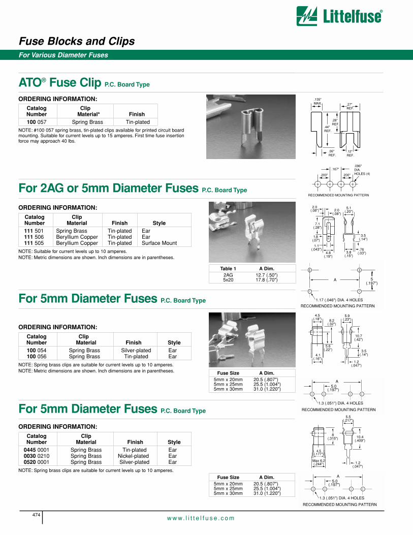
Fuse Blocks and Clips
474w w w. l i t t e l f u s e . c o m
For Various Diameter Fuses
ATO® Fuse Clip P.C. Board Type
A 5.0
(.197")
1.3 (.051") DIA. 4 HOLES
RECOMMENDED MOUNTING PATTERN
4.5 (.18")
5.9 (.23")
4.1 (.16")
1.2 (.047")
8.2 (.32")
10.7 (.42")
3.5 (.14")
5.6 (.22")
A 5(.197")
1.17 (.046") DIA. 4 HOLES
RECOMMENDED MOUNTING PATTERN
5.1 (.20")
7.1 (.28")
4.8 (.19")
3.8 (.15")
1.1 (.043")
2.0 (.08") 2.0
(.08")
.76 (.03")
1.8 (.07")
3.5 (.14")
Catalog ClipNumber Material Finish Style111 501 Spring Brass Tin-plated Ear111 506 Beryllium Copper Tin-plated Ear111 505 Beryllium Copper Tin-plated Surface Mount
NOTE: Suitable for current levels up to 10 amperes.NOTE: Metric dimensions are shown. Inch dimensions are in parentheses.
ORDERING INFORMATION:
For 5mm Diameter Fuses P.C. Board Type
Catalog ClipNumber Material Finish Style100 054 Spring Brass Silver-plated Ear100 056 Spring Brass Tin-plated Ear
NOTE: Spring brass clips are suitable for current levels up to 10 amperes.NOTE: Metric dimensions are shown. Inch dimensions are in parentheses.
ORDERING INFORMATION:
For 2AG or 5mm Diameter Fuses P.C. Board Type
Catalog ClipNumber Material* Finish100 057 Spring Brass Tin-plated
RECOMMENDED MOUNTING PATTERN
.200" .200"
.167".096" DIA. HOLES (4)
.27"REF.
.28"REF.
.44"REF.
.135"MAX.
.12"REF.
.06"REF.
NOTE: #100 057 spring brass, tin-plated clips available for printed circuit boardmounting. Suitable for current levels up to 15 amperes. First time fuse insertionforce may approach 40 lbs.
Table 1 A Dim.2AG 12.7 (.50")5x20 17.8 (.70")
Fuse Size A Dim.5mm x 20mm 20.5 (.807")5mm x 25mm 25.5 (1.004")5mm x 30mm 31.0 (1.220")
A 5.0
(.197")
1.3 (.051") DIA. 4 HOLES
RECOMMENDED MOUNTING PATTERN
5.5 (.217")
Max 6.2(.244")
4.5(.177")
1.2 (.047")
10.4 (.409")
8 (.315")
For 5mm Diameter Fuses P.C. Board Type
Catalog ClipNumber Material Finish Style
0445 0001 Spring Brass Tin-plated Ear0030 0210 Spring Brass Nickel-plated Ear0520 0001 Spring Brass Silver-plated Ear
NOTE: Spring brass clips are suitable for current levels up to 10 amperes.
ORDERING INFORMATION:
Fuse Size A Dim.5mm x 20mm 20.5 (.807")5mm x 25mm 25.5 (1.004")5mm x 30mm 31.0 (1.220")
ORDERING INFORMATION:

Catalog Clip Amp VoltageNumber Material Finish Style Rating Rating
0105 0003 Spring Brass Tin-plated Ear 15A 250VAC0125 0003 Beryllium Copper Tin-plated Ear 30A 250VAC
Fuse Blocks and Clips
475w w w. l i t t e l f u s e . c o m
14
FU
SE
BL
OC
KS
A
ND
CL
IPS
Catalog ClipNumber Material Finish Style
0111 0005MR Phosphor Tin-plated EarBronze
Ammo Pack 1000 Pcs.
20mm(.787")5mm
(.197")
1.05mm (.041") DIA. 4 HOLES
PCB MOUNTING HOLE SPECIPCATION
6mm(.236")
1mm(.039")
1.3mm (.051")
ORDERING INFORMATION:
For 5mm Diameter Fuses Automatic Insertion Type
2.1mm(.083")
4.7mm(.185")
7.8mm(.307")
2.6mm(.102")
1mm(.039")
5.3mm(.209")
3mm(.118")
12.7mm(.50")
5mm(.197")
6.35mm(.250")
18mm(.709")
9mm(.354")
4mm (.157")
18mm(.709")
16mm(.630")
0.6mm(.024")
12.7mm(.500")
1mm(.039")0.5mm(.020")
For Midget Fuses (13/32") PC Board Mount
2.1(.083")
12.4(.488")
03.45 (.136")/
11.1(.437")
11.4(.449")
22.2(.874")
0.710 ± 0.005(.028 ± .0002")
18.7(.736")
NOTE: #0111 005 phosphor bronze, tin-plated clips designed for automaticinsertion are suitable for current levels up to 10 amperes.
ELECTRICAL SPECIFICATIONS: 15A at 250VAC
ORDERING INFORMATION:
®

476w w w. l i t t e l f u s e . c o m
Notes & Drawings

Military Components
15
477w w w. l i t t e l f u s e . c o m
Military Components . . . . . . . . . . . . . . . . . . . . . . . . . . . . . . . . . . . . . . . . . . . . . . . . . . . . . . . . . . . . . . . . . . . . . . . . . . . . . . . . . . . . . . . . . . . . . 477
Fuses . . . . . . . . . . . . . . . . . . . . . . . . . . . . . . . . . . . . . . . . . . . . . . . . . . . . . . . . . . . . . . . . . . . . . . . . . . . . . . . . . . . . . . . . . . . . . . . . . . . . . . 478-481
Fuseholders . . . . . . . . . . . . . . . . . . . . . . . . . . . . . . . . . . . . . . . . . . . . . . . . . . . . . . . . . . . . . . . . . . . . . . . . . . . . . . . . . . . . . . . . . . . . . . . . . . . . . 481
PAGE

478w w w. l i t t e l f u s e . c o m
Fuses
Approved to MIL-PRF-15160
Military Components
F01A FUSES MIL-PRF-15160/1(Commercial Equivalent — 361 Series)
MIL Type Nickel-Plated Silver-PlatedDesignation Caps Caps
F01A 250V 1/200A 364.005 366.005F01A 250V 1/100A 364.010 366.010F01A 250V 1/32A 364.031 366.031F01A 250V 1/16A 364.062 366.062F01A 250V 1/10A 364.100
F01A 250V 1/8A 364.125 366.125F01A 250V 3/16A F01A 250V 2/10A F01A 250V 1/4A 364.250 366.250F01A 250V 3/8A 364.375 366.375F01A 250V 4/10A F01A 250V 1/2A 364.500 366.500F01A 125V 6/10A 364.600 F01A 125V 3/4A 364.750 366.750F01A 125V 8/10A
F01A 125V 1A 364 001 366 001F01A 125V 11/4 A F01A 125V 11/2 A 364 01.5 366 01.5F01A 125V 16/10A F01A 125V 2A 364 002 366 002F01A 125V 21/2 A F01A 125V 3A 364 003 366 003F01A 125V 3 2/10A F01A 125V 4A 364 004 F01A 125V 5A 364 005
F02A FUSES MIL-PRF-15160/2(Commercial Equivalent — 311, 312 Series)
MIL Type Nickel-Plated Silver-PlatedDesignation Caps Caps
F02A 250V 1/100A 392.010 397.010F02A 250V 1/32A 392.031 397.031F02A 250V 1/16A 392.062 397.062F02A 250V 1/8A 392.125 397.125F02A 250V 15/100A 392.150
F02A 250V 175/1000A 392.175 F02A 250V 3/16A 392.187 397.187F02A 250V 2/10A 392.200 397.200F02A 250V 1/4A 392.250 397.250F02A 250V 3/10A 392.300 397.300F02A 250V 3/8A 392.375 397.375F02A 250V 1/2A 392.500 397.500F02A 250V 6/10A 392.600 397.600F02A 250V 3/4A 392.750 397.750F02A 250V 1A 392 001 397 001F02A 250V 11/4 A 392 1.25 F02A 250V 11/2 A 392 01.5 397 01.5F02A 250V 16/10A 392 01.6 F02A 250V 2A 392 002 397 002F02A 250V 21/2 A 392 02.5 397 02.5F02A 250V 3A 392 003 397 003F02A 250V 4A 392 004 397 004F02A 250V 5A 392 005 397 005F02A 250V 6A 392 006 397 006F02A 125V 8A 392 008 397 008F02A 125V 10A 392 010 397 010F02A 32V 15A 392 015 397 015F02A 32V 20A 392 020 397 020F02A 32V 25A 392 025 397 025
F02B FUSES MIL-PRF-15160/2(Commercial Equivalent — 313 Series)
MIL Type Nickel-Plated Silver-PlatedDesignation Caps Caps
F02B 250V 1/100A 393.010 398.010F02B 250V 1/32A 393.031 398.031F02B 250V 1/25A 393.040 398.040F02B 250V 1/16A 393.062 398.062F02B 250V 1/10A 393.100 398.100F02B 250V 1/8A 393.125 398.125F02B 250V 15/100A 393.150 398.150F02B 250V 175/1000A 393.175 398.175F02B 250V 3/16A 393.187 398.187F02B 250V 2/10A 393.200 398.200F02B 250V 1/4A 393.250 398.250F02B 250V 3/10A 393.300 398.300F02B 250V 3/8A 393.375 398.375F02B 250V 4/10A 393.400 398.400F02B 250V 1/2A 393.500 398.500F02B 250V 6/10A 393.600 398.600F02B 250V 7/10A 393.700 398.700F02B 250V 3/4A 393.750 398.750F02B 250V 8/10A 393.800 398.800F02B 250V 1A 393 001 398 001F02B 250V 11/4 A 393 1.25 398 1.25F02B 250V 11/2 A 393 01.5 398 01.5F02B 250V 16/10A 393 01.6 398 01.6F02B 250V 18/10A 393 01.8 398 01.8F02B 250V 2A 393 002 398 002F02B 250V 21/4 A 393 2.25 398 2.25F02B 250V 21/2 A 393 02.5 398 02.5F02B 250V 2 8/10A 393 02.8 398 02.8F02B 250V 3A 393 003 398 003F02B 250V 3 2/10A 393 03.2 398 03.2
F03A FUSES MIL-PRF-15160/3(Commercial Equivalent — 314 Series)
MIL Type Nickel-Plated Silver-PlatedDesignation Caps Caps
F03A 250V 1/4A 394.250 399.250F03A 250V 1/2A 394.500 399.500F03A 250V 1A 394 001 399 001F03A 250V 11/4 A F03A 250V 11/2 A 394 01.5 399 01.5F03A 250V 2A 394 002 399 002F03A 250V 3A 394 003 399 003F03A 250V 4A 394 004 399 004F03A 250V 5A 394 005 399 005F03A 250V 6A 394 006 399 006F03A 250V 8A 394 008 399 008F03A 250V 10A 394 010 399 010F03A 250V 12A 394 012 399 012F03A 250V 15A 394 015 399 015F03A 125V 20A 394 020 399 020
F03A 125V 25A 394 025 399 025F03A 125V 30A 394 030 399 030
NOTES: 1. The suffix letter “S” added to the type designation indicates that silver-plated fusecaps are required.For example: F02A 250V 3/4A S.
2. Contact factory.
3. Boldface numbers indicate series; light type numbers indicate amperage value.

479w w w. l i t t e l f u s e . c o m
Fuses
Approved to MIL-PRF-15160
Military Components
F03B FUSES MIL-PRF-15160/3(Commercial Equivalent — 326 Series)
MIL Type Nickel-Plated Silver-PlatedDesignation Caps Caps
F03B 250V 1/100A 390.010 395.010F03B 250V 1/32A 390.031 395.031F03B 250V 1/16A 390.062 395.062F03B 250V 1/10A 390.100 395.100F03B 250V 1/8A 390.125 395.125F03B 250V 15/100A 390.150 395.150F03B 250V 175/1000A 390.175 395.175F03B 250V 3/16A 390.187 395.187F03B 250V 2/10A 390.200 395.200F03B 250V 1/4A 390.250 395.250F03B 250V 3/10A 390.300 395.300F03B 250V 3/8A 390.375 395.375F03B 250V 4/10A 390.400 395.400F03B 250V 1/2A 390.500 395.500F03B 250V 6/10A 390.600 395.600F03B 250V 7/10A 390.700 395.700F03B 250V 3/4A 390.750 395.750F03B 250V 8/10A 390.800 395.800F03B 250V 1A 390 001 395 001F03B 250V 12/10A 390 01.2 395 01.2F03B 250V 11/4 A 390 1.25 395 1.25F03B 250V 11/2 A 390 01.5 395 01.5F03B 250V 16/10A 390 01.6 395 01.6F03B 250V 2A 390 002 395 002F03B 250V 21/2 A 390 02.5 395 02.5F03B 250V 2 8/10A 390 02.8 395 02.8F03B 250V 3A 390 003 395 003F03B 250V 3 2/10A 390 03.2 395 03.2F03B 125V 4A 390 004 395 004F03B 125V 5A 390 005 395 005F03B 125V 61/4 A 390 6.25 395 6.25F03B 125V 7A 390 007 395 007F03B 125V 8A 390 008 395 008F03B 125V 10A 390 010 395 010F03B 125V 15A 390 015 395 015F03B 125V 20A 390 020 395 020F03B 125V 25A 390 025 395 025
F09A FUSES MIL-PRF-15160/9(Commercial Equivalent — BLN Series)
MIL Type Nickel-Plated Silver-PlatedDesignation Caps Caps
F09A 250V 1A 594 001 594 001SF09A 250V 2A 594 002 594 002SF09A 250V 3A 594 003 594 003SF09A 250V 4A 594 004 594 004SF09A 250V 5A 594 005 594 005SF09A 250V 6A 594 006 594 006SF09A 250V 7A 594 007 594 007SF09A 250V 8A 594 008 594 008SF09A 250V 10A 594 010 594 010SF09A 250V 12A 594 012 594 012SF09A 250V 15A 594 015 594 015SF09A 250V 20A 594 020 594 020SF09A 250V 25A 594 025 594 025SF09A 250V 30A 594 030 594 030S
F09B FUSES MIL-PRF-15160/9(Commercial Equivalent — FLM Series)
MIL Type Nickel-Plated Silver-PlatedDesignation Caps Caps
F09B 250V 3/10A 593.300 593.300SF09B 250V 4/10A 593.400 593.400SF09B 250V 1/2A 593.500 593.500SF09B 250V 6/10A 593.600 593.600SF09B 250V 8/10A 593.800 593.800SF09B 250V 1A 593 001 593 001SF09B 250V 11/8 A 593 1.12 593 1.12SF09B 250V 11/4 A 593 1.25 593 1.25SF09B 250V 14/10A 593 01.4 593 01.4SF09B 250V 11/2 A 593 01.5 593 01.5SF09B 250V 16/10A 593 01.6 593 01.6SF09B 250V 18/10A 593 01.8 593 01.8SF09B 250V 2A 593 002 593 002SF09B 250V 21/4 A 593 2.25 593 2.25SF09B 250V 21/2 A 593 02.5 593 02.5SF09B 250V 2 8/10A 593 02.8 593 02.8SF09B 250V 3A 593 003 593 003SF09B 250V 3 2/10A 593 03.2 593 03.2SF09B 250V 3 1/2 A 593 03.5 593 03.5SF09B 250V 4A 593 004 593 004SF09B 250V 41/2 A 593 04.5 593 04.5SF09B 250V 5A 593 005 593 005SF09B 250V 5 6/10A 593 05.6 593 05.6SF09B 250V 6A 593 006 593 006SF09B 250V 61/4 A 593 6.25 593 6.25SF09B 250V 7A 593 007 593 007SF09B 250V 8A 593 008 593 008SF09B 250V 9A 593 009 593 009SF09B 250V 10A 593 010 593 010SF09B 125V 12A 593 012 593 012SF09B 125V 15A 593 015 593 015SF09B 32V 20A 593 020 593 020SF09B 32V 25A 593 025 593 025SF09B 32V 30A 593 030 593 030S
F60C FUSES MIL-PRF-15160/60(Commercial Equivalent — KLK Series)
MIL Type Nickel-Plated Silver-PlatedDesignation Caps Caps
F60C 500V 1/8A 592.125 592.125SF60C 500V 2/10A 592.200 592.200SF60C 500V 1/4A 592.250 592.250SF60C 500V 3/10A 592.300 592.300SF60C 500V 3/8A 592.375 592.375SF60C 500V 1/2A 592.500 592.500SF60C 500V 3/4A 592.750 592.750SF60C 500V 1A 592 001 592 001SF60C 500V 11/2 A 592 01.5 592 01.5SF60C 500V 2A 592 002 592 002SF60C 500V 3A 592 003 592 003SF60C 500V 4A 592 004 592 004SF60C 500V 5A 592 005 592 005SF60C 500V 6A 592 006 592 006SF60C 500V 8A 592 008 592 008SF60C 500V 10A 592 010 592 010SF60C 500V 15A 592 015 592 015SF60C 500V 20A 592 020 592 020SF60C 500V 25A 592 025 592 025SF60C 500V 30A 592 030 592 030S
NOTES: 1. The suffix letter “S” added to the type designation indicates that silver-plated fusecaps are required.For example: F02A 250V 3/4A S.
2. Boldface numbers indicate series; light type numbers indicate amperage value.
15
MIL
ITA
RY
C
OM
PO
NE
NT
S

480w w w. l i t t e l f u s e . c o m
Fuses
Approved to MIL-PRF-23419
Military Components
FM02 FUSES MIL-PRF-23419/2(Commercial Equivalent —273 Series MICRO™ fuses)
MIL Type CatalogDesignation Number
FM02A 125V 1/500A 274.002FM02A 125V 1/200A 274.005FM02A 125V 1/100A 274.010FM02A 125V 1/64A 274.015FM02A 125V 1/32A 274.031FM02A 125V 1/16A 274.062FM02A 125V 1/10A 274.100FM02A 125V 1/8A 274.125FM02A 125V 2/10A 274.200FM02A 125V 1/4A 274.250FM02A 125V 3/10A 274.300FM02A 125V 4/10A 274.400FM02A 125V 1/2A 274.500FM02A 125V 6/10A 274.600FM02A 125V 3/4A 274.750FM02A 125V 1A 274 001FM02A 125V 11/2 A 274 01.5FM02A 125V 2A 274 002FM02A 125V 3A 274 003FM02A 125V 4A 274 004FM02A 125V 5A 274 005
FM04 FUSES MIL-PRF-23419/4(Commercial Equivalent —
275 Series PICO® fuses)Not recommended for new design — use FM 10
MIL Type CatalogDesignation Number
FM04A 125V 1/16A 277.062FM04A 125V 1/8A 277.125FM04A 125V 1/4A 277.250FM04A 125V 3/8A 277.375FM04A 125V 1/2A 277.500FM04A 125V 3/4A 277.750FM04A 125V 1A 277 001FM04A 125V 11/2 A 277 01.5FM04A 125V 2A 277 002FM04A 125V 3A 277 003FM04A 125V 4A 277 004FM04A 125V 5A 277 005FM04A 125V 7A 277 007FM04A 125V 10A 277 010FM04A 32V 15A 277 015
FM07 FUSES MIL-PRF-23419/7(Commercial Equivalent —262 Series MICRO™ fuses)
MIL Type CatalogDesignation Number
FM07A 125V 1/500A 269.002FM07A 125V 1/200A 269.005FM07A 125V 1/100A 269.010FM07A 125V 1/64A 269.015FM07A 125V 1/32A 269.031FM07A 125V 1/20A 269.050FM07A 125V 1/16A 269.062FM07A 125V 1/10A 269.100FM07A 125V 1/8A 269.125FM07A 125V 2/10A 269.200FM07A 125V 1/4A 269.250FM07A 125V 3/10A 269.300FM07A 125V 4/10A 269.400FM07A 125V 1/2A 269.500FM07A 125V 6/10A 269.600FM07A 125V 7/10A 269.700FM07A 125V 3/4A 269.750FM07A 125V 8/10A 269.800FM07A 125V 1A 269 001FM07A 125V 11/2 A 269 01.5FM07A 125V 2A 269 002FM07A 125V 3A 269 003FM07A 125V 4A 269 004FM07A 125V 5A 269 005
FM08 FUSES MIL-PRF-23419/8(Commercial Equivalent —
265 Series PICO® fuses)MIL Type Catalog
Designation NumberFM08A 125V 1/8A 267.125FM08A 125V 1/4A 267.250FM08A 125V 3/8A 267.375FM08A 125V 1/2A 267.500FM08A 125V 3/4A 267.750FM08A 125V 1A 267 001FM08A 125V 11/2 A 267 01.5FM08A 125V 2A 267 002FM08A 125V 21/2 A 267 02.5FM08A 125V 3A 267 003FM08A 125V 4A 267 004FM08A 125V 5A 267 005FM08A 125V 7A 267 007FM08A 125V 10A 267 010FM08A 32V 15A 267 015
FM10 FUSES MIL-PRF-23419/10(Commercial Equivalent —
251 Series PICO® fuses)MIL Type Catalog
Designation NumberFM10A 125V 1/16A 253.062FM10A 125V 1/8A 253.125FM10A 125V 1/4A 253.250FM10A 125V 3/8A 253.375FM10A 125V 1/2A 253.500FM10A 125V 3/4A 253.750FM10A 125V 1A 253 001FM10A 125V 11/2 A 253 01.5FM10A 125V 2A 253 002FM10A 125V 3A 253 003FM10A 125V 4A 253 004FM10A 125V 5A 253 005FM10A 125V 7A 253 007FM10A 125V 10A 253 010FM10A 32V 15A 253 015
NOTE: Boldface numbers of catalog number indicate series; light type numbers indicate amperage value.

15
MIL
ITA
RY
C
OM
PO
NE
NT
S
481w w w. l i t t e l f u s e . c o m
Fuses
Approved to DSCC Drawing No. 87108
Military Components
2AG Cartridge Fuses Fast-Acting(Commercial Equivalent — 225 Series)
DESC Part Voltage Ampere CatalogNumber Rating Rating Number
87108-001A 250V 1/8 288.12587108-003A 250V 1/4 288.25087108-005A 250V 3/8 288.37587108-007A 250V 1/2 288.50087108-011A 250V 3/4 288.75087108-015A 250V 1 288 00187108-019A 250V 11/2 288 01.587108-021A 250V 2 288 00287108-025A 250V 21/2 288 02.587108-027A 250V 3 288 00387108-029A 250V 31/2 288 03.587108-031A 125V 4 288 00487108-033A 125V 5 288 00587108-035A 125V 7 288 007
2AG Axial Lead Fuses Fast-Acting(Commercial Equivalent — 224 Series)
DESC Part Voltage Ampere CatalogNumber Rating Rating Number
87108-002A 250V 1/8 289.12587108-004A 250V 1/4 289.25087108-006A 250V 3/8 289.37587108-008A 250V 1/2 289.50087108-012A 250V 3/4 289.75087108-016A 250V 1 289 00187108-020A 250V 11/2 289 01.587108-022A 250V 2 289 00287108-026A 250V 21/2 289 02.587108-028A 250V 3 289 00387108-030A 250V 31/2 289 03.587108-032A 125V 4 289 00487108-034A 125V 5 289 00587108-036A 125V 7 289 007
2AG Cartridge Fuses Slo-Blo® Fuse(Commercial Equivalent — 229 Series)
DESC Part Voltage Ampere CatalogNumber Rating Rating Number
87108-003B 250V 1/4 290.25087108-005B 250V 3/8 290.37587108-007B 250V 1/2 290.50087108-009B 250V 6/10 290.60087108-011B 250V 3/4 290.75087108-015B 250V 1 290 00187108-017B 250V 11/4 290 1.2587108-019B 250V 11/2 290 01.587108-021B 250V 2 290 00287108-023B 250V 21/4 290 2.2587108-025B 250V 21/2 290 02.587108-027B 250V 3 290 00387108-029B 250V 3 1/2 290 03.587108-031B 125V 4 290 00487108-033B 125V 5 290 00587108-035B 125V 7 290 007
2AG Axial Lead Fuses Slo-Blo® Fuse(Commercial Equivalent — 230 Series)
DESC Part Voltage Ampere CatalogNumber Rating Rating Number
87108-004B 250V 1/4 291.25087108-006B 250V 3/8 291.37587108-008B 250V 1/2 291.50087108-010B 250V 6/10 291.60087108-012B 250V 3/4 291.75087108-016B 250V 1 291 00187108-018B 250V 11/4 291 1.2587108-020B 250V 11/2 291 01.587108-022B 250V 2 291 00287108-024B 250V 21/4 291 2.2587108-026B 250V 21/2 291 02.587108-028B 250V 3 291 00387108-030B 250V 3 1/2 291 03.587108-032B 125V 4 291 00487108-034B 125V 5 291 00587108-036B 125V 7 291 007
NOTE: Boldface numbers of catalog number indicate series; light type numbers indicate amperage value.
FUSEHOLDERS
Approved to MIL-PRF-19207Specifications Commercial Equivalent
MIL Type Catalog Catalog VoltageSpecification Designation Number Type Electrical Rating For Fuse Type Number Range
MIL-PRF19207/11 FHN20G 342 025 Drip-Proof 20A 250V Max 3AG, F02, F03 342 004P 250V MaxMIL-PRF19207/16 FHN26G2 342 024 Drip-Proof 30A 250V Max 3AG, F02, F03 342 012P 250V MaxMIL-PRF19207/16 FHN26W 342 021 Water-Tight 30A 250V Max 3AG, F02, F03 342 006 250V MaxMIL-PRF19207/36 FHN55W 340 267 Water-Tight — RFI 30A 250V Max 3AG, F02, F03 — 250V Max
Packaging16
348w w w. l i t t e l f u s e . c o m
PAGE
PACKAGING . . . . . . . . . . . . . . . . . . . . . . . . . . . . . . . . . . . . . . . . . . . . . . . . . . . . . . . . . . . . . . . . . . . . . . . . . . . . . . . . . . . . . . . . . . . . . 348
Littelfuse packaging specifications . . . . . . . . . . . . . . . . . . . . . . . . . . . . . . . . . . . . . . . . . . . . . . . . . . . . . . . . . . . . . . . . . . . . . . 349-350

16
PAC
KA
GIN
G
Littelfuse packaging specifications
Packaging
349w w w. l i t t e l f u s e . c o m
LITTELFUSE CASE QUANTITY QUANTITY COMPONENT TAPE REELPART NUMBER TYPE PER REEL PER BULK PACK SPACING (mm) SPACING (mm) DIMENSION (mm)
A B C
SMBJ series D0-214AA 3000 N/A 8 N/A 330
P6MSBJ series D0-214AA 3000 N/A 8 N/A 330
1KSMBJ series D0-214AA 3000 N/A 8 N/A 330
SA series D0-15 5000 1000 5 52.4 +/- 0.5 335
P6KE series D0-15 5000 1000 5 +/- 0.5 52.4 +/- 0.5 335
1.5KE, ICTE, MPTE, LCE series D0-201AD 1500 500 5 +/- 0.5 52.4 +/- 0.5 335
1N56, 1N60 series D0-13 1000 500 10 +/- 0.5 52.4 +/- 0.5 335
5KP series R6 1000 500 10 +/- 0.5 52.4 +/- 0.5 335
15KP series R6 1000 500 10 +/- 0.5 52.4 +/- 0.5 335
Foldbak series D0-201AD 1500 500 5 +/- 0.5 52.4 +/- 0.5 335
SLD series R6 1000 500 10 +/- 0.5 52.4 +/- 0.5 335
15KP cells / 5KP cells N/A N/A N/A N/A N/A N/A
T10A series D0-15 5000 1000 5 +/- 0.5 52.4 +/- 0.5 335
T10B series D0-201AD 1500 500 10 +/- 0.5 52.4 +/- 0.5 335
T10C series Case 3 N/A 500 N/A N/A N/A
SMBTJ series D0-214AA 3000 N/A 8 N/A 330
TO-220 series T0-220 N/A 500 N/A N/A N/A
1. T.V.S. PRODUCT
Littelfuse devices are available in Bulk or Tape and Reelpackaging, this option is requested by inserting either a ‘B’ or a‘T’ into the Littelfuse part number.
Littelfuse’s standard practice for tape and reel product meets therequirements of EIA Standard RS-296-D, “Lead Taping ofComponents in Axial Lead Configuration for Automatic Insertion’,level 1.
The quantity per reel or per bulk package are indicated below.Orders for all Littelfuse T.V.S. axial product are only processed andshipped in full reel / bulk increments, or multiples of.
Our surface-mount components are placed in embossed cavitiesof anti-static/conductive carrier tape, and sealed with a covertape. The taped devices are supplied in reels in protective boxes.The standard Littelfuse lead-tape packaging of surface-mountcomponents follow the requirements of EIA 481-1, shown below.
• Cover tape: This will not extend over the edge of the carrier tape or extend over any part of the sprocket holes
• Carrier tape: This will release from the reel hub as the last portion of the tape unwinds from the reel without damage to the carrier tape and with the components remaining in the cavities.
• Leader tape: A minimum length of 300mm leader (and trailer) of tape will be provided before the first (and after the last) component on the reel, with a minimum of forty empty component carrier pockets covered with tape.
3.5 Dia
C
76.2
B
A
All dimensions in mm
ROLL PAD
REELBLUE TAPE(CATHODE)
WHITE TAPE(ANODE)

PackagingLittelfuse packaging specifications
350w w w. l i t t e l f u s e . c o m
LITTELFUSEPART NUMBER
SL1002 series (Opt “C”)
SL1002 series (Opt “SM”)
SL1003 series (Opt “C”)
SL1003 series (Opt “R”)
SL1011 series (Opt “A”)
SL1011 series (Opt “C”)
SL1011 series (formed options)
SL1021 series
SL1026 series
SL1053
SL1122 series
PACKAGINGSPECIFICATION
1000 Bulk Packed
= 1000 pcs Reeled (Tape width -16m)
1000 Bulk Packed
10 x Trays of 100
1000 Taped & Reeled
1000 Bulk Packed
10 x Trays of 100
10 x Trays of 100
20 pcs per vacuum pack
1 pc per bag10 x Trays of 100
• Orientation for polarised components: Cathode (positive polarity) Adjacent to the sprocket holes. The quantity per reel will be as indicated in table. Orders for tape and reeled product will be processed and shipped in full reels only, any scheduled orders will be supplied in full reels or multiples thereof.
The packaging specification indicated in the table is standard forthe majority of configurations within the Littelfuse range. Somespecific pin configurations may not fall within the above, pleaseconsult the factory for details.
Direction of tape feed
Positive polaritySprocket holes Cover tape
Embossed carrier2. G.D.T. PRODUCT
Littelfuse G.D.T. devices are packaged according to their pinconfiguration. The packaging is designed to protect the deviceduring transit, this is partially important for devices with pins,thereby ensuring that they interface correctly with theirrespective connection systems.Littelfuse’s standard practice for tape and reel product (SL1011only) meets the requirements of EIA Standard RS-296-D, ‘LeadTaping Components in Axial Lead Configuration for AutomaticInsertion’ Standard Level 1. The quantity per reel or per bulk package are indicated below.Orders for all Littelfuse G.D.T. products are only processed andshipped in full reel / bulk increments, or multiples of.