
BOK DC/DC_Vorlage.indd - Mouser
306
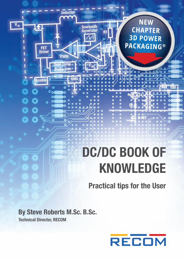
Rsd Csd D Rs Cs Ds N-FET Inductor V IN V OUT FET Driver Sawtooth Generator Over Temp. Protection R1 R2 Enable GND V REF PWM NEW CHAPTER 3D POWER PACKAGING ® DC/DC BOOK OF KNOWLEDGE Practical tips for the User By Steve Roberts M.Sc. B.Sc. Technical Director, RECOM
-
Upload
khangminh22 -
Category
Documents
-
view
2 -
download
0
Transcript of BOK DC/DC_Vorlage.indd - Mouser
Rsd Csd
DRs Cs
Ds
N-FET
Rsd Csd
DRs Cs
Ds
N-FET
Rs CsRs Cs
Inductor
V IN
V OUT
FETDriver
SawtoothGenerator
Over Temp.Protection
R1
R2
Enable GND
V REF
PWM
NEW CHAPTER
3D POWER PACKAGING®
DC/DC BOOK OF KNOWLEDGE
Practical tips for the User
By Steve Roberts M.Sc. B.Sc.Technical Director, RECOM
DC/DC Book of KnowledgePractical tips for the User
Steve Roberts, M.Sc. B.Sc.Technical Director, RECOM
Fifth Edition
© 2021 All rights RECOM Engineering GmbH & Co KG, Austria (hereafter RECOM)
The contents of this book or excerpts thereof may not be reproduced, duplicated or distributed in any form without the written permission of RECOM.The disclosure of the information contained in this book is correct to the best of the knowledge of the author, but no responsibility can be accepted for any mistakes, omissions or typographical errors. The diagrams illustrate typical applications and are not necessarily complete.

Preface from RECOM Management
When we introduced our first DC/DC Converter more than 25 years ago, there were little pub-lished technical material available and hardly any international standards to follow. There was a pressing need to communicate practical application information to our customers, which prompted us to add some simple Application Notes as an appendix to our first published prod-uct catalogue. The content of these guidelines grew over the years as we gained more and more expertise. Although they are still of a rudimentary nature, they are well received by our customer base and today they have become an 70-page Application Note package available for download from our website.
The advance of semiconductor technology and the shift towards highly integrated digital elec-tronics has diminished the knowledge base of analogue techniques in many design labs, uni-versities and technical colleges over the years. We often see a lack of practical know-how in analogue circuit design, particularly with regard to applied techniques, test and measurement and the understanding of filtering and noise suppression. Therefore, as experts in this arena, we saw the need for a much more comprehensive technical handbook that could be used as reference by hardware designers and students alike.
At the start of 2014, Steve Roberts, our Technical Director, started to invest his free time to start documenting the extensive application knowledge on the design, test and application of DC/DC converters available within the RECOM group. Despite all of the pressures of his demanding job, along with new product development and the technical planning of our new research and test labs, he has managed to complete this onerous task in time for Electronica 2014. Today, two years later, in the time for Electronica 2016 the third edition of the RECOM DC/DC Book of Knowledge has been enlarged to include an additional chapter on magnetics.
Steve has presented us with a handbook that we are sure will greatly benefit the engineering community and all those who are interested in DC/DC power conversion and its applications. The handbook will initially be available as a printed version and PDF, not only in English but also in German, Chinese and Japanese.
Board of Directors Gmunden, 2021
RECOM Group

Preface from the Author
The function of any AC/DC or DC/DC converter module is to meet one or more of the following requirements:
i: to match the secondary load to the primary power supply ii: to provide isolation between primary and secondary circuits iii: to provide protection against the effects of faults, short circuit or over heating iv: to simplify compliance with safety, performance or EMC legislation.
There are a number of different techniques available to achieve these aims, starting at its simplest with a linear regulator and going through to multi-stage, digitally controlled power supplies. This book aims to explain the various DC/DC circuits and topologies available so that users can better understand the advantages, limitations and operational boundaries of each of these solutions. The language used is necessarily technical, but is kept as simple as possible without trivialising the technology involved.
The author has many years of experience answering customers’ questions, helping with de-sign-ins, presenting at seminars, writing articles and even making Youtube videos. Despite this accumulated know-how, there is still something to learn new every day about this diverse and wide-ranging subject. This book is subtitled “Practical tips for the User” because it hopes to de-mystify the topic of power conversion, despite there being as many solutions as there are applications. If it succeed in passing at least some of our expertise and knowledge on to you, then it will have accomplished its goal.
The information given in this book is given in good faith and has been checked for veracity, but if the reader finds any errors, omissions and inaccuracies, please feel free to inform me.
Steve Roberts Gmunden, 2021 Technical [email protected]
RECOM
Contents
1. Introduction 11.1 Linear Regulators 1 1.1.1 Efficiency of a Linear Regulator 3 1.1.2 Other Properties of the Linear Regulator 4 1.1.3 LDO Linear Regulators 41.2 Switching Regulator 6 1.2.1 Switching Frequency and Inductor Size 7 1.2.2 Switching Regulator Topologies 71.2.2.1 Non-Isolated DC/DC Converter 8 1.2.2.1.1 Switching Transistors 8 1.2.2.1.2 Buck Converter 10 1.2.2.1.3 Buck Converter Applications 12 1.2.2.1.4 Boost Converter 13 1.2.2.1.5 Boost Converter Applications 15 1.2.2.1.6 Buck-Boost (Inverting) Converter 15 1.2.2.1.7 Buck/Boost Discontinuous and Continuous Mode 17 1.2.2.1.8 Synchronous and Asynchronous Conversion 18 1.2.2.1.9 Two Stage Boost/Buck (Ćuk Converter) 19 1.2.2.1.10 Two Stage Boost/Buck SEPIC Converter 21 1.2.2.1.11 Two Stage Boost/Buck ZETA Converter 23 1.2.2.1.12 Multiphase DC/DC Converters 241.2.2.2 Isolated DC/DC Converters 26 1.2.2.2.1 Flyback DC/DC Converter 26 1.2.2.2.2 Forward DC/DC Converter 28 1.2.2.2.3 Active Clamp Forward Converter 30 1.2.2.2.4 Push-Pull Converter 31 1.2.2.2.5 Half Bridge and Full Bridge Converters 34 1.2.2.2.6 Busconverter or Ratiometric Converter 35 1.2.2.2.7 Unregulated Push-Pull Converter 361.2.3 Parasitic Elements and their Effects 39 1.2.3.1 QR Converter 42 1.2.3.2 RM Converter 431.2.4 Efficiency of DC/DC Converters 45 1.2.5 PWM-Regulation Techniques 46 1.2.6 DC/DC Converter Regulation 491.2.6.1 Regulation of Multiple Outputs 491.2.6.2 Remote Sense 52 1.2.7 Limitations on the Input Voltage Range 54 1.2.8 Synchronous Rectification 56 1.2.9 Planar Transformers 57 1.2.10 Package Styles of DC/DC Converters 59
2. Feedback Loops 612.1 Introduction 61 2.2 Open Loop Design 61 2.3 Closed Loops 62 2.4 Feedback Loop Compensation 652.4.1 Right Half Plane Instability 67 2.5 Slope Compensation 67 2.6 Analyzing Loop Stability in Analogue and Digital Feedback Systems 692.6.1 Finding Analogue Loop Stability Experimentally 69 2.6.2 Finding Analogue Loop Stability using the Laplace Transform 69 2.6.3 Finding Digital Loop Stability using the Bilinear Transform 71 2.6.4 Digital Feedback Loop 73
3. Understanding the Datasheet Parameters 753.1 Measurement Methods – DC Characteristic 75 3.2 Measurement Methods – AC Characteristics 77 3.2.1 Measuring Minimum and Maximum Duty Cycle 78 3.2.2 Output Voltage Accuracy 79 3.2.3 Output Voltage Temperature Coefficient 79 3.2.4 Load Regulation 80 3.2.5 Cross Regulation 81 3.2.6 Line Regulation 81 3.2.7 Worst Case Output Voltage Accuracy 82 3.2.8 Calculating Efficiency 82 3.2.9 Input Voltage Range 83 3.2.10 Input Current 83 3.2.11 Short Circuit and Overload Current 85 3.2.12 Remote ON/OFF Control 86 3.2.13 Isolation Voltage 87 3.2.14 Isolation Resistance and Capacitance 90 3.2.15 Dynamic Load Response 913.2.16 Output Ripple/Noise 92 3.3 Understanding Thermal Parameters 93 3.3.1 Introduction 93 3.3.2 Thermal Impedance 94 3.3.3 Thermal Derating 95 3.3.4 Forced Cooling 97 3.3.5 Conducted and Radiated Cooling 98
4. DC/DC Converter Protections 1004.1 Introduction 100 4.2 Reverse Polarity Protection 100 4.2.1 Series Diode Reverse Polarity Protection 101 4.2.2 Shunt Diode Reverse Polarity Protection 102
4.2.3 P-FET Reverse Polarity Protection 102 4.3 Input Fuse 103 4.4 Output Over-Voltage Protection 104 4.5 Input Over-Voltage Protection 104 4.5.1 SCR Crowbar Protection 105 4.5.2 Clamping Elements 106 4.5.2.1 Varistor 106 4.5.2.2 Suppression Diode 107 4.5.3 OVP Using Several Elements 108 4.5.4 OVP Standards 109 4.5.5 OVP by Disconnection 110 4.6 Voltage Dips and Interruptions 111 4.7 Inrush Current Limiting 113 4.8 Load Limiting 115 4.9 Under Voltage Lockout 116
5. Input and Output Filtering 1185.1 Introduction 118 5.2 Back Ripple Current 119 5.2.1 Measuring Back Ripple Current 119 5.2.2 Back Ripple Current Countermeasures 120 5.2.3 Input Capacitor Selection 122 5.2.4 Input Current of DC/DC Converters in Parallel 123 5.3 Output Filtering 1255.3.1 Differential Mode Output Filtering 125 5.3.2 Common Mode Output Filtering 127 5.3.3 Common Mode Chokes 1285.4 Full Filtering 132 5.4.1 Filter PCB Layout 133
6. Safety 1366.1 Electric Shock 137 6.1.1 Insulation Class 137 6.1.2 Human Body Treshold Currents 138 6.1.3 Protection from Electric Shock 1406.1.4 Protective Earth 1436.2 Hazardous Energy 145 6.2.1 Fuses 145 6.2.1.1 Fuse Reaction Time and Inrush Currents 147 6.2.2 Circuit Breakers 148 6.3 Inherent Safety 149 6.4 Intrinsic Safety 150 6.4.1 Combustible Materials 151 6.4.2 Smoke 153
6.5 Injury Hazards 154 6.5.1 Hot Surfaces 154 6.5.2 Sharp Edges 154 6.6 Designing for Safety 155 6.6.1 FMEA 157 6.7 Medical Safety 159
7. Reliability 1617.1 Reliability Prediction 161 7.2 Environmental Stress Factor 164 7.3 Using MTBF Figures 165 7.4 Demonstrated MTBF 166 7.5 MTBF and Temperature 167 7.6 Designing for Reliability 168 7.7 PCB Layout Reliability Consideration 169 7.8 Capacitor Reliability 1737.8.1 MLCC 1737.8.2 Tantalum and Electrolytic Capacitors 176 7.9 Semiconductors Reliability 179 7.10 ESD 180 7.11 Inductors 182
8. LED Characteristics 1848.1 Driving LEDs with Constant Currents 186 8.2 Some DC Constant Current Sources 186 8.3 Connecting LEDs in String 188 8.4 Connecting LED Strings in Parallel 189 8.5 Balancing LED Current in Parallel Strings 190 8.6 Parallel Strings or Grid Array – Which is better? 192 8.7 LED Dimming 1948.7.1 Analogue versus PWM Dimming 194 8.7.2 Perceived Brightness 196 8.7.3 Dimming Conclusion 1968.8 Thermal Considerations 197 8.9 Temperature Derating 198 8.9.1 Adding Automatic Thermal Derating to an LED Driver 1988.9.2 Over-temperature Protection using a PTC Thermistor 1988.9.3 Over-temperature Protection using an Analogue Temperature Sensor IC 2008.9.4 Over-temperature Protection using a Microcontroller 202 8.10 Brightness Compensation 203 8.11 Some Circuit Ideas using RCD driver 205
9. Applications 2129.1 Introduction 212
9.2 Polarity Inversion 212 9.3 Power Doubler 213 9.4 Combining Switching Regulators and DC/DC Converters 214 9.5 Connecting Converters in Series 217 9.6 Increasing the Isolation 218 9.7 5V Rail Clean-up 218 9.8 Using CTRL Pin 220 9.9 Using VADJ Pin 221
10. Introduction to Magnetics 22210.1 Basics 22210.1.1 Core Saturation 22510.1.2 Air-gapped Inductors 22810.1.3 Core Shapes 23010.1.4 Core Losses 23210.1.4.1 Mutual Inductance Losses 23210.1.4.2 Eddy Current Losses 23310.1.4.3 The Skin Effect 23410.1.4.4 The Proximity Effect 23710.2 Buck Converter Design Worked Example 24010.2.1 Calculating the Losses in a Buck Converter 24210.2.1.1 Inductor Losses 24210.2.1.2 Calculating the MOSFET Loss 24410.2.1.3 Calculating the Diode Loss 24510.2.2 Boost Converter Design 24510.3 Introduction to Transformers 24610.3.1 Royer Push-Pull Self Oscillating Transformer 24610.3.2 Royer Transformer Design Considerations 24910.3.3 Transformer Design Considerations 25010.3.4 Forward Converter Transformer Design 25110.3.4.1 Introduction to Forward Converters 25110.3.4.2 Forward Converter Transformer Design 25210.3.5 Flyback Transformer Design 25510.3.5.1 Flyback Clamp Circuit and Associated Losses 26310.3.5.2 Transformer Design for Quasi-Resonant Flyback Mode 26510.4 Whole turns and fractional turns 26610.4.1 Transformer Leakage Inductance and Capacitance 26710.4.2 Methods of reducing Transformer Leakage Inductance 26810.4.3 Methods of reducing Transformer Leakage Capacitance 27010.5 Transformer Core Temperature 27110.6 Finalizing the Transformer Design: EMI 274

11. Advanced Assembly and Packaging 27611.1. Introduction 27611.2. The need for advanced packaging technology 27711.3. Packaging technologies 27911.3.1. Through hole 27911.3.2. Conventional SMD (Gull wing pins) 27911.3.3. QFN Chip carrier 28111.3.4. Solder Ball 28211.4. PCB substrate technology 28411.5. Stacked components 28711.6. Embedded components 28811.6.1. Embedded Magnetics 28811.6.2. Embedded active and passive components 28911.7. Conclusion 290
References and Further Reading 292
Application Guides and Notes 292
About RECOM 293
Acknowledgements 294

1
1. Introduction to Power Regulation
Modern AC/DC and DC/DC converters are designed to provide efficient power conversion to deliver a controlled, safe and well-regulated DC power supply for a variety of electronic instruments, devices and systems. It's not all too long ago that a transformer, rectifier and linear regulator was the main technology in power conversion, but just as the LED is slowly replacing the light bulb, so is the DC/DC converter gradually edging out the linear regulator and the primary-side switching controller is replacing the simple 50Hz mains transformer. In the past decade there has been of immense technical progress the development of switching regulators to allow the benefits of new circuits, components, and materials that previously simply did not exist before. This progress has made it possible to increase the performance and to improve the thermal behavior, while simultaneously substantially reducing the size, weight and cost of power supplies. Consequently, switching regulators are used today in large numbers and are the standard technology in both DC/DC and AC/DC power conversion.
1.1 Linear Regulators
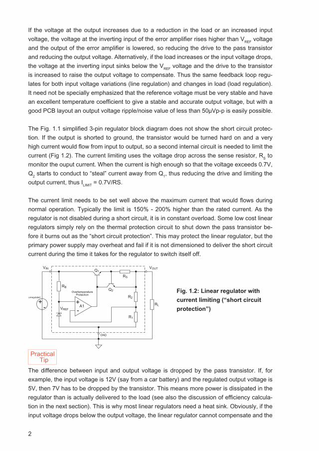
Linear voltage regulators deliver a stable output voltage from a more or less stable input volt-age source. In normal operation, even if the input voltage fluctuates rapidly, the output voltage remains stable. This means they can also very effectively filter out input ripple, not only at the fundamental frequency, but also as far as the fifth or tenth harmonic. The limitation is only the reaction speed of the internal error amplifier feedback circuit.
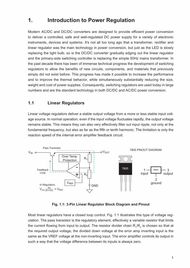
Fig. 1.1: 3-Pin Linear Regulator Block Diagram and Pinout
Most linear regulators have a closed loop control. Fig. 1.1 illustrates this type of voltage reg-ulation. The pass transistor is the regulatory element, effectively a variable resistor that limits the current flowing from input to output. The resistor divider chain R1/R2 is chosen so that at the required output voltage, the divided down voltage at the error amp inverting input is the same as the VREF voltage at the non-inverting input. The error amplifier controls its output in such a way that the voltage difference between its inputs is always zero.
��
���
����
����
������������ ��
����������
������������� �� ���
��������� ����
��� ��������������������
�� ���
�
��
���
������
�������
�������
������ ���� �����
���� ����
2
If the voltage at the output increases due to a reduction in the load or an increased input voltage, the voltage at the inverting input of the error amplifier rises higher than VREF voltage and the output of the error amplifier is lowered, so reducing the drive to the pass transistor and reducing the output voltage. Alternatively, if the load increases or the input voltage drops, the voltage at the inverting input sinks below the VREF voltage and the drive to the transistor is increased to raise the output voltage to compensate. Thus the same feedback loop regu-lates for both input voltage variations (line regulation) and changes in load (load regulation). It need not be specially emphasized that the reference voltage must be very stable and have an excellent temperature coefficient to give a stable and accurate output voltage, but with a good PCB layout an output voltage ripple/noise value of less than 50μVp-p is easily possible.
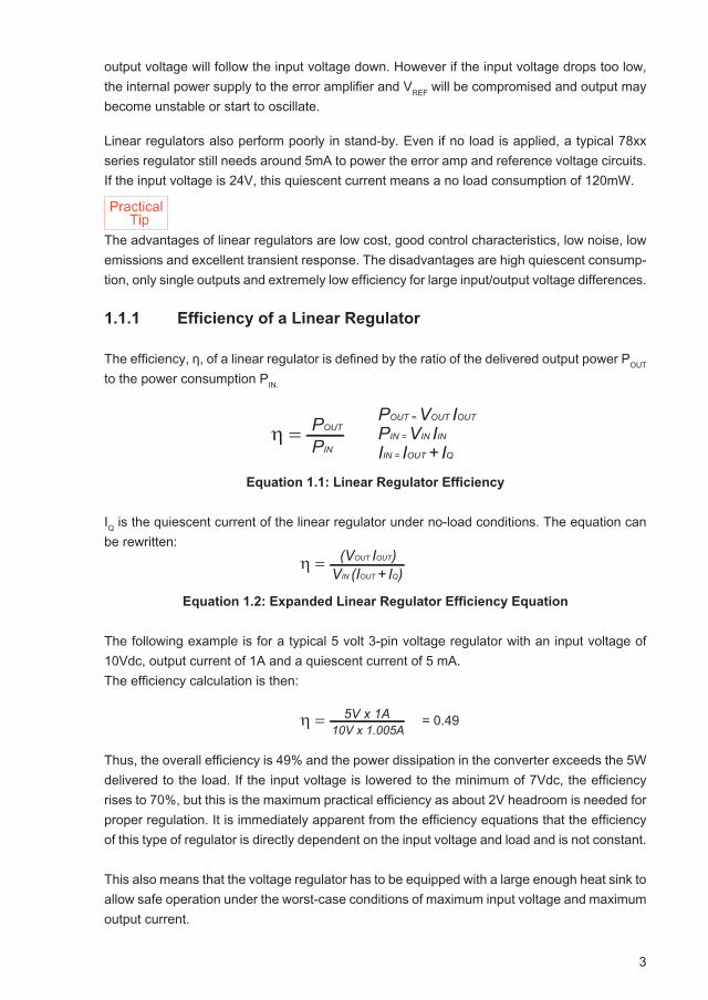
The Fig. 1.1 simplified 3-pin regulator block diagram does not show the short circuit protec-tion. If the output is shorted to ground, the transistor would be turned hard on and a very high current would flow from input to output, so a second internal circuit is needed to limit the current (Fig 1.2). The current limiting uses the voltage drop across the sense resistor, RS to monitor the ouput current. When the current is high enough so that the voltage exceeds 0.7V, Q2 starts to conduct to “steal” current away from Q1, thus reducing the drive and limiting the output current, thus ILIMIT = 0.7V/RS.
The current limit needs to be set well above the maximum current that would flows during normal operation. Typically the limit is 150% - 200% higher than the rated current. As the regulator is not disabled during a short circuit, it is in constant overload. Some low cost linear regulators simply rely on the thermal protection circuit to shut down the pass transistor be-fore it burns out as the “short circuit protection”. This may protect the linear regulator, but the primary power supply may overheat and fail if it is not dimensioned to deliver the short circuit current during the time it takes for the regulator to switch itself off.
The difference between input and output voltage is dropped by the pass transistor. If, for example, the input voltage is 12V (say from a car battery) and the regulated output voltage is 5V, then 7V has to be dropped by the transistor. This means more power is dissipated in the regulator than is actually delivered to the load (see also the discussion of efficiency calcula-tion in the next section). This is why most linear regulators need a heat sink. Obviously, if the input voltage drops below the output voltage, the linear regulator cannot compensate and the
��
����
��
��
����
���
���
��� ��� �
��
��
�� � �� ��� ��� ����
��
��
��
��
��
Practical Tip
Fig. 1.2: Linear regulator with
current limiting (“short circuit
protection”)
3
output voltage will follow the input voltage down. However if the input voltage drops too low, the internal power supply to the error amplifier and VREF will be compromised and output may become unstable or start to oscillate.
Linear regulators also perform poorly in stand-by. Even if no load is applied, a typical 78xx series regulator still needs around 5mA to power the error amp and reference voltage circuits. If the input voltage is 24V, this quiescent current means a no load consumption of 120mW.
The advantages of linear regulators are low cost, good control characteristics, low noise, low emissions and excellent transient response. The disadvantages are high quiescent consump-tion, only single outputs and extremely low efficiency for large input/output voltage differences.
1.1.1 Efficiency of a Linear Regulator
The efficiency, η, of a linear regulator is defined by the ratio of the delivered output power POUT to the power consumption PIN.
Equation 1.1: Linear Regulator Efficiency
IQ is the quiescent current of the linear regulator under no-load conditions. The equation can be rewritten:
Equation 1.2: Expanded Linear Regulator Efficiency Equation
The following example is for a typical 5 volt 3-pin voltage regulator with an input voltage of 10Vdc, output current of 1A and a quiescent current of 5 mA.The efficiency calculation is then:
= 0.49
Thus, the overall efficiency is 49% and the power dissipation in the converter exceeds the 5W delivered to the load. If the input voltage is lowered to the minimum of 7Vdc, the efficiency rises to 70%, but this is the maximum practical efficiency as about 2V headroom is needed for proper regulation. It is immediately apparent from the efficiency equations that the efficiency of this type of regulator is directly dependent on the input voltage and load and is not constant.
This also means that the voltage regulator has to be equipped with a large enough heat sink to allow safe operation under the worst-case conditions of maximum input voltage and maximum output current.
η = POUT
PIN
POUT = VOUT IOUT
PIN = VIN IIN
IIN = IOUT + IQ
η = (VOUT IOUT)VIN (IOUT + IQ)
η = 5V x 1A
10V x 1.005A
Practical Tip
4
1.1.2 Other Properties of the Linear Regulator
Linear regulators have a number of advantages on the one hand, but also have some disad-vantages that require special care in their application and use.
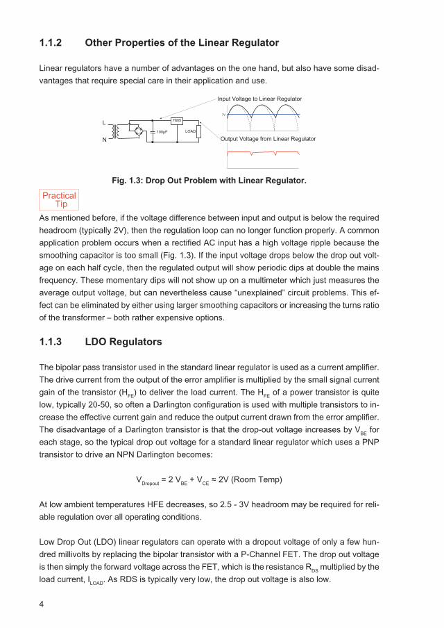
Fig. 1.3: Drop Out Problem with Linear Regulator.
As mentioned before, if the voltage difference between input and output is below the required headroom (typically 2V), then the regulation loop can no longer function properly. A common application problem occurs when a rectified AC input has a high voltage ripple because the smoothing capacitor is too small (Fig. 1.3). If the input voltage drops below the drop out volt-age on each half cycle, then the regulated output will show periodic dips at double the mains frequency. These momentary dips will not show up on a multimeter which just measures the average output voltage, but can nevertheless cause “unexplained” circuit problems. This ef-fect can be eliminated by either using larger smoothing capacitors or increasing the turns ratio of the transformer – both rather expensive options.
1.1.3 LDO Regulators
The bipolar pass transistor used in the standard linear regulator is used as a current amplifier. The drive current from the output of the error amplifier is multiplied by the small signal current gain of the transistor (HFE) to deliver the load current. The HFE of a power transistor is quite low, typically 20-50, so often a Darlington configuration is used with multiple transistors to in-crease the effective current gain and reduce the output current drawn from the error amplifier. The disadvantage of a Darlington transistor is that the drop-out voltage increases by VBE for each stage, so the typical drop out voltage for a standard linear regulator which uses a PNP transistor to drive an NPN Darlington becomes:
VDropout = 2 VBE + VCE ≈ 2V (Room Temp)
At low ambient temperatures HFE decreases, so 2.5 - 3V headroom may be required for reli-able regulation over all operating conditions.
Low Drop Out (LDO) linear regulators can operate with a dropout voltage of only a few hun-dred millivolts by replacing the bipolar transistor with a P-Channel FET. The drop out voltage is then simply the forward voltage across the FET, which is the resistance RDS multiplied by the load current, ILOAD. As RDS is typically very low, the drop out voltage is also low.
���������
��
���������� ��������� ������ ��
����������� ���������� ������ ��
�����
�
Practical Tip
5
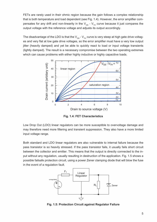
FETs are rarely used in their ohmic region because the gain follows a complex relationship that is both temperature and load dependent (see Fig. 1.4). However, the error amplifier com-pensates for any drift and non-linearity in the VGS - VTH curve because it just compares the output voltage with the reference voltage and adjusts its output accordingly.
The disadvantage of the LDO is that the VGS - VTH curve is very steep at high gate drive voltag-es and very flat at low gate drive voltages, so the error amplifier must have a very low output jitter (heavily damped) and yet be able to quickly react to load or input voltage transients (lightly damped). The result is a necessary compromise between the two operating extremes which can cause problems with either highly inductive or highly capacitive loads.
Fig. 1.4: FET Characteristics
Low Drop Out (LDO) linear regulators can be more susceptible to overvoltage damage and may therefore need more filtering and transient suppression. They also have a more limited input voltage range.
Both standard and LDO linear regulators are also vulnerable to internal failure because the pass transistor is so heavily stressed. If the pass transistor fails, it usually fails short circuit between the collector and emitter. This means that the output is directly connected to the in-put without any regulation, usually resulting in destruction of the application. Fig. 1.5 shows a possible failsafe protection circuit, using a power Zener clamping diode that will blow the fuse in the event of a regulation fault.
Fig. 1.5: Protection Circuit against Regulator Failure
��
��
��
��
��
����
�����������
� � � � � ���
��
��
��
��
��
� �
���
��
���
����
���
���
� ��������� �������������
���� � ����
���� ����� ����
��
�����������
���������������
�����
��
��
6
1.2. Switching Regulator
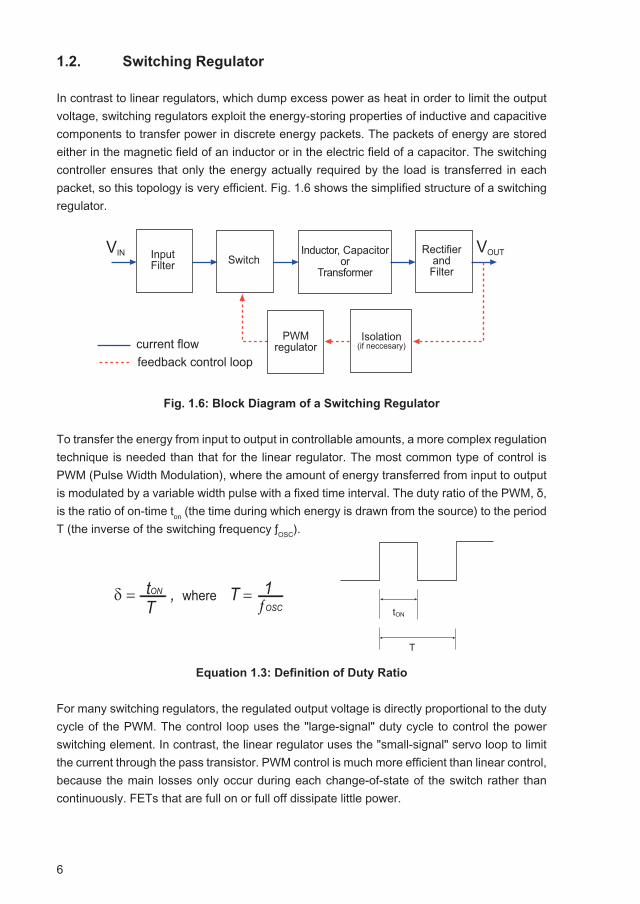
In contrast to linear regulators, which dump excess power as heat in order to limit the output voltage, switching regulators exploit the energy-storing properties of inductive and capacitive components to transfer power in discrete energy packets. The packets of energy are stored either in the magnetic field of an inductor or in the electric field of a capacitor. The switching controller ensures that only the energy actually required by the load is transferred in each packet, so this topology is very efficient. Fig. 1.6 shows the simplified structure of a switching regulator.
Fig. 1.6: Block Diagram of a Switching Regulator
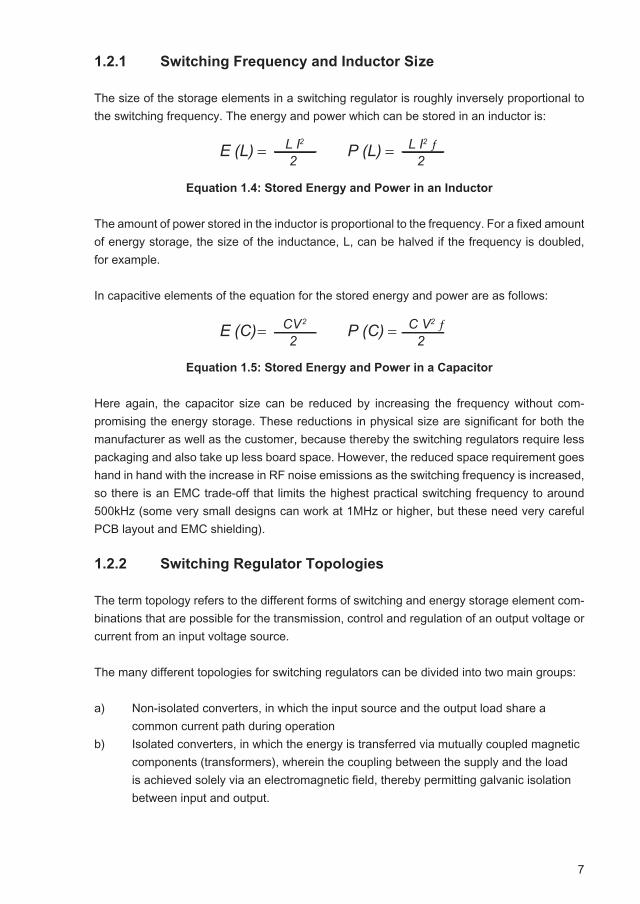
To transfer the energy from input to output in controllable amounts, a more complex regulation technique is needed than that for the linear regulator. The most common type of control is PWM (Pulse Width Modulation), where the amount of energy transferred from input to output is modulated by a variable width pulse with a fixed time interval. The duty ratio of the PWM, δ, is the ratio of on-time ton (the time during which energy is drawn from the source) to the period T (the inverse of the switching frequency ƒOSC).
Equation 1.3: Definition of Duty Ratio
For many switching regulators, the regulated output voltage is directly proportional to the duty cycle of the PWM. The control loop uses the "large-signal" duty cycle to control the power switching element. In contrast, the linear regulator uses the "small-signal" servo loop to limit the current through the pass transistor. PWM control is much more efficient than linear control, because the main losses only occur during each change-of-state of the switch rather than continuously. FETs that are full on or full off dissipate little power.
��� ��������������� �����
�������������������
�����������
������������������
������������
���������������������������������
������� �����������
δ = TtON , where T =
ƒOSC
1
�
���
7
1.2.1 Switching Frequency and Inductor Size
The size of the storage elements in a switching regulator is roughly inversely proportional to the switching frequency. The energy and power which can be stored in an inductor is:
Equation 1.4: Stored Energy and Power in an Inductor
The amount of power stored in the inductor is proportional to the frequency. For a fixed amount of energy storage, the size of the inductance, L, can be halved if the frequency is doubled, for example.
In capacitive elements of the equation for the stored energy and power are as follows:
Equation 1.5: Stored Energy and Power in a Capacitor
Here again, the capacitor size can be reduced by increasing the frequency without com-promising the energy storage. These reductions in physical size are significant for both the manufacturer as well as the customer, because thereby the switching regulators require less packaging and also take up less board space. However, the reduced space requirement goes hand in hand with the increase in RF noise emissions as the switching frequency is increased, so there is an EMC trade-off that limits the highest practical switching frequency to around 500kHz (some very small designs can work at 1MHz or higher, but these need very careful PCB layout and EMC shielding).
1.2.2 Switching Regulator Topologies
The term topology refers to the different forms of switching and energy storage element com-binations that are possible for the transmission, control and regulation of an output voltage or current from an input voltage source.
The many different topologies for switching regulators can be divided into two main groups:
a) Non-isolated converters, in which the input source and the output load share a common current path during operationb) Isolated converters, in which the energy is transferred via mutually coupled magnetic components (transformers), wherein the coupling between the supply and the load is achieved solely via an electromagnetic field, thereby permitting galvanic isolation between input and output.
P (L) = L I2 ƒ 2
P (C) = C V2 ƒ 2
E (L) = L I2 2
E (C) = CV2 2
8
1.2.2.1 Non-Isolated DC/DC Converter
The selection from the variety of available topologies is based on such considerations such as cost, performance and control characteristics, which are determined by the application requirements. No topology is better or worse than the other. Each topology has advantages as well as disadvantages and so the choice is a question of the needs of the user and the system application.
For non-isolated DC/DC converters there are five basic transformer-less topologies:
i. Buck or step-down converterii. Boost or step-up converteriii. Buck-boost or step-up-down converteriv. Two-stage Inverting Buck-boost (Ćuk converter)v. Two stage non-inverting Buck-boost (Sepic converter, ZETA converter)
The subsequent explanations assume that the PWM control circuit has a feedback control circuit (not shown) and the correct duty cycle is chosen for the desired output voltage. Also ideal switches (switching transistors or diodes) as well as ideal capacitors and inductors are assumed to better demonstrate the transmission properties of each topology, but before we look at the topologies, a few words about driving switching transistors are opportune.
1.2.2.1.1 Switching Transistors
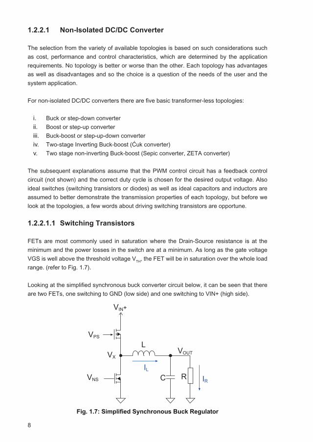
FETs are most commonly used in saturation where the Drain-Source resistance is at the minimum and the power losses in the switch are at a minimum. As long as the gate voltage VGS is well above the threshold voltage VTH, the FET will be in saturation over the whole load range. (refer to Fig. 1.7).
Looking at the simplified synchronous buck converter circuit below, it can be seen that there are two FETs, one switching to GND (low side) and one switching to VIN+ (high side).
Fig. 1.7: Simplified Synchronous Buck Regulator
� �
�����
��
�����
��
���
����
9
The low side FET in an N-Channel device that will go into saturation if the drive voltage VNS >> VTH and switch off if VNS < VTH.
If the high side FET is a P-Channel device, it will go into saturation if the drive voltage VPS << (VIN - VTH) and switch off if VPS > (VIN - VTH). However, P-Channel FETs have typically 3× the power dissipation of an equivalent sized N-Channel FET and are also more expensive. In many power applications, this is not acceptable and an N-Channel FET as high side driver is preferred, however, this means that the high side driver must be able to generate an output voltage that is higher than the input voltage VIN.
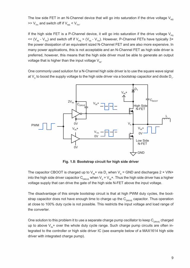
One commonly used solution for a N-Channel high side driver is to use the square wave signal at VX to boost the supply voltage to the high side driver via a bootstrap capacitor and diode D1.
Fig. 1.8: Bootstrap circuit for high side driver
The capacitor CBOOT is charged up to VIN+ via D1 when VX = GND and discharges 2 × VIN+ into the high side driver capacitor CDRIVE when VX = VIN+. Thus the high side driver has a higher voltage supply that can drive the gate of the high side N-FET above the input voltage.
The disadvantage of this simple bootstrap circuit is that at high PWM duty cycles, the boot-strap capacitor does not have enough time to charge up the CDRIVE capacitor. Thus operation at close to 100% duty cycle is not possible. This restricts the input voltage and load range of the converter.
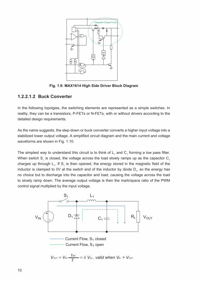
One solution to this problem it to use a separate charge pump oscillator to keep CDRIVE charged up to above VIN+ over the whole duty cycle range. Such charge pump circuits are often in-tegrated to the controller or high side driver IC (see example below of a MAX1614 high side driver with integrated charge pump).
��
��
��
�����
����
���������������
��
��� �������
���� �������
���
�
��
����
����
����
���
10
Fig. 1.9: MAX1614 High Side Driver Block Diagram
1.2.2.1.2 Buck Converter
In the following topolgies, the switching elements are represented as a simple switches. In reality, they can be a transistors, P-FETs or N-FETs, with or without drivers according to the detailed design requirements.
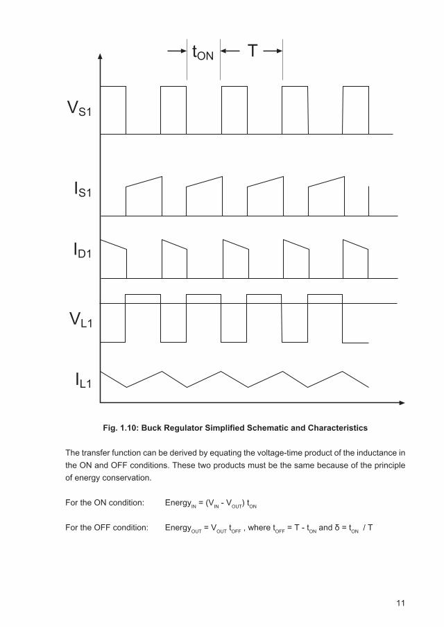
As the name suggests, the step-down or buck converter converts a higher input voltage into a stabilized lower output voltage. A simplified circuit diagram and the main current and voltage waveforms are shown in Fig. 1.10.
The simplest way to understand this circuit is to think of L1 and C1 forming a low pass filter. When switch S1 is closed, the voltage across the load slowly ramps up as the capacitor C1 charges up through L1. If S1 is then opened, the energy stored in the magnetic field of the inductor is clamped to 0V at the switch end of the inductor by diode D1, so the energy has no choice but to discharge into the capacitor and load, causing the voltage across the load to slowly ramp down. The average output voltage is then the mark/space ratio of the PWM control signal multiplied by the input voltage.
���������
�������
������������ �������
��
��� ����
�������������� �������������������� ������
�
�����
�� �
��
VOUT = tONVIN valid when VIN > VOUT = δ VIN ,T
11
Fig. 1.10: Buck Regulator Simplified Schematic and Characteristics
The transfer function can be derived by equating the voltage-time product of the inductance in the ON and OFF conditions. These two products must be the same because of the principle of energy conservation.
For the ON condition: EnergyIN = (VIN - VOUT) tON
For the OFF condition: EnergyOUT = VOUT tOFF , where tOFF = T - tON and δ = tON / T
����
���
���
���
���
���
12
Substituting gives: (VIN - VOUT) tON = VOUT (T - TON) VIN tON = VOUT T VOUT = VIN (tON / T) VOUT / VIN = δ
Equation 1.6: Transfer Function of Buck Converter
1.2.2.1.3 Buck Converter Applications
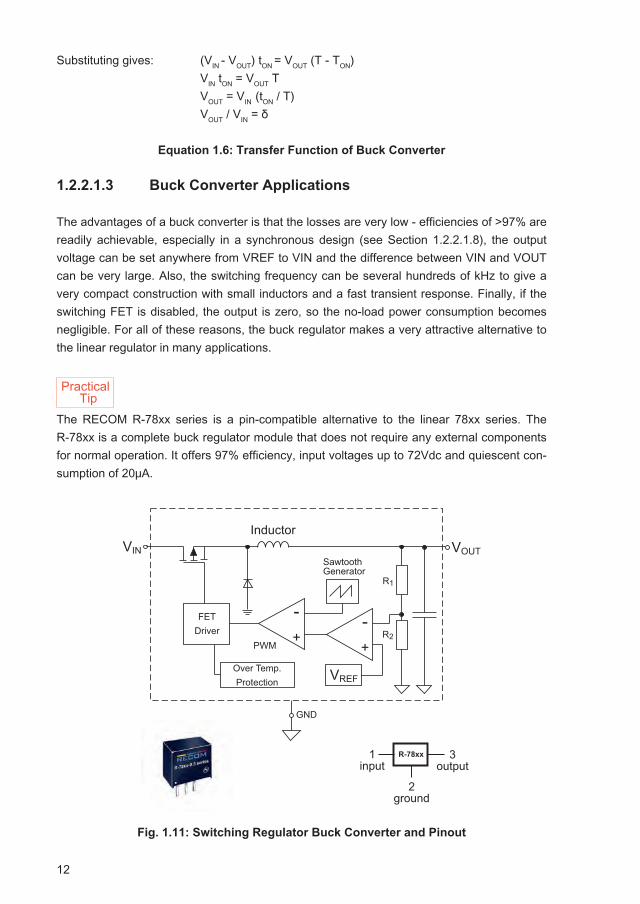
The advantages of a buck converter is that the losses are very low - efficiencies of >97% are readily achievable, especially in a synchronous design (see Section 1.2.2.1.8), the output voltage can be set anywhere from VREF to VIN and the difference between VIN and VOUT can be very large. Also, the switching frequency can be several hundreds of kHz to give a very compact construction with small inductors and a fast transient response. Finally, if the switching FET is disabled, the output is zero, so the no-load power consumption becomes negligible. For all of these reasons, the buck regulator makes a very attractive alternative to the linear regulator in many applications.
The RECOM R-78xx series is a pin-compatible alternative to the linear 78xx series. The R-78xx is a complete buck regulator module that does not require any external components for normal operation. It offers 97% efficiency, input voltages up to 72Vdc and quiescent con-sumption of 20μA.
Fig. 1.11: Switching Regulator Buck Converter and Pinout
��� ����
����
��������
�� ������������
�
�����
���
�����
��������
���������
���
��
��
������
�������
�������
������
Practical Tip
13
One disadvantage of a buck converter is that the PWM regulator feedback circuit requires a minimum output ripple to regulate properly, as the regulation is typically cycle- by-cycle. The output ripple is also dependent on the duty cycle, being a maximum at 50% duty cycle. So it is not possible to get R/N down to the μV level achieved by linear regulators. If a very clean supply is needed, a buck regulator can be followed by a linear regulator to get the best from both topologies. In the example below, the unregulated 24Vdc is dropped to 15V by a switch-ing regulator with an efficiency of 95%. The linear regulator then provides a clean 12V output with <5μV ripple and noise. The overall system efficiency is around 76%, compared to less than 50% with the linear regulator alone.
Fig. 1.12: Combination of buck regulator and linear regulator
Finally, any switching circuit will generate a pulsed input current which can cause EMI unless adequately filtered (refer to the input current characteristic IS1 in Fig. 1.10). A small 10μF capacitor placed very close to the input pins is thus recommended.
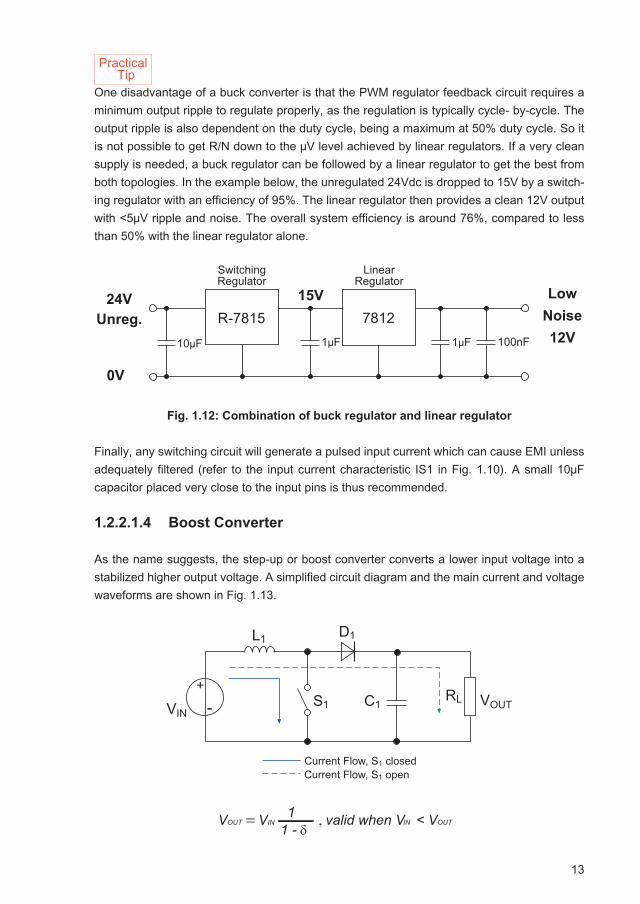
1.2.2.1.4 Boost Converter
As the name suggests, the step-up or boost converter converts a lower input voltage into a stabilized higher output voltage. A simplified circuit diagram and the main current and voltage waveforms are shown in Fig. 1.13.
���� ��� ��� �����
����������
���������� �����
��� �� �����
���
�����
���
������������
��
�������
��
����������� �������������������� ���������
�
�
��
������
VOUT = 1VIN valid when VIN < VOUT ,1 - δ
Practical Tip
14
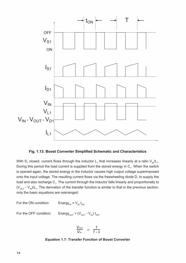
Fig. 1.13: Boost Converter Simplified Schematic and Characteristics
With S1 closed, current flows through the inductor L1 that increases linearly at a ratio VIN/L1. During this period the load current is supplied from the stored energy in C1. When the switch is opened again, the stored energy in the inductor causes high output voltage superimposed onto the input voltage. The resulting current flows via the freewheeling diode D1 to supply the load and also recharge C1. The current through the inductor falls linearly and proportionally to (VOUT - VIN)/L1. The derivation of the transfer function is similar to that in the previous section, only the basic equations are rearranged:
For the ON condition: EnergyIN = VIN tON
For the OFF condition: EnergyOUT = (VOUT - VIN) tOFF
Equation 1.7: Transfer Function of Boost Converter
VOUT
VIN= 1
1 - δ
����
���
��
���
���
���
���
����������������
���
���
15
1.2.2.1.5 Boost Converter Applications
The advantage of the boost converter is that the output voltage can be varied with the mark-space ratio of the PWM signal to be equal to or above VIN. This makes it especially suitable for increasing a low voltage battery output to a more useful higher voltage. However, in prac-tice, a boost ratio of more than ×2 or ×3 makes the feedback stability difficult. Also because the input current pulses increase proportionally to the boost gain, a converter that triples the input voltage draws triple the input current. This pulsed input current can cause EMI and volt-age drop issues in the input leads.One further disadvantage with the boost converter is that the output cannot be switched off without adding a second switch in series with the input as disabling the PWM controller allone does not disconnect the load from the input.
Finally, care must be taken not to allow the input voltage to rise above the output voltage. The PWM controller would then keep S1 permanently open and the input and output will be con-nected directly via L1 and D1 without regulation. Destructive currents can flow that will quickly destroy both the converter and the load. If this condition cannot be avoided, a topology that permits both buck and boost operation is needed.
1.2.2.1.6 Buck-Boost (Inverting) Converter
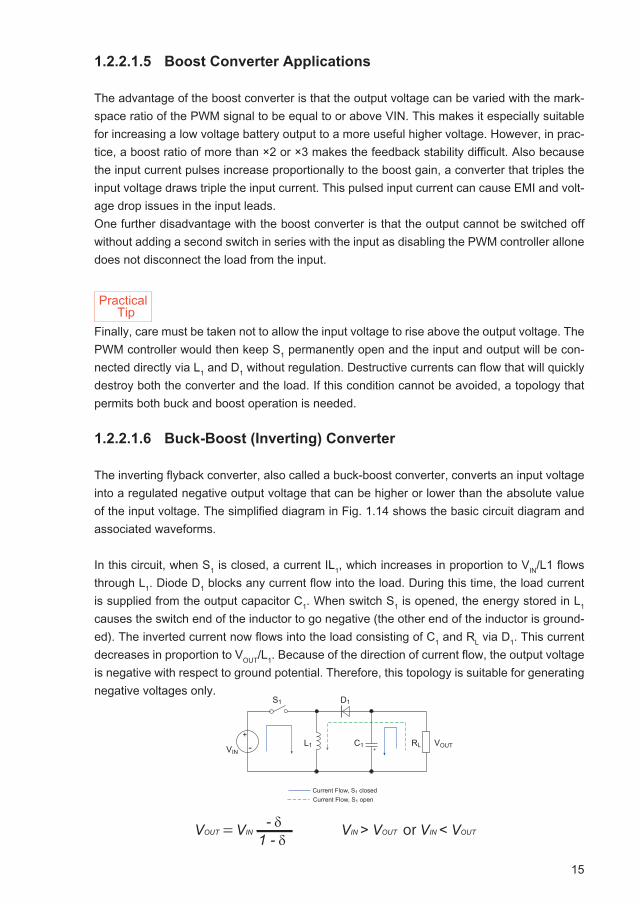
The inverting flyback converter, also called a buck-boost converter, converts an input voltage into a regulated negative output voltage that can be higher or lower than the absolute value of the input voltage. The simplified diagram in Fig. 1.14 shows the basic circuit diagram and associated waveforms.
In this circuit, when S1 is closed, a current IL1, which increases in proportion to VIN/L1 flows through L1. Diode D1 blocks any current flow into the load. During this time, the load current is supplied from the output capacitor C1. When switch S1 is opened, the energy stored in L1 causes the switch end of the inductor to go negative (the other end of the inductor is ground-ed). The inverted current now flows into the load consisting of C1 and RL via D1. This current decreases in proportion to VOUT/L1. Because of the direction of current flow, the output voltage is negative with respect to ground potential. Therefore, this topology is suitable for generating negative voltages only.
VOUT = - δ1 - δ
VIN VIN > VOUT or VIN < VOUT
�������
��
����������� �������������������� ���������
�
�
��
�� �� ���
Practical Tip
16
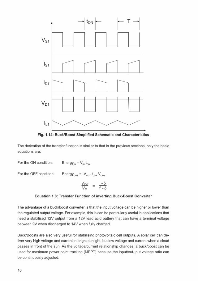
Fig. 1.14: Buck/Boost Simplified Schematic and Characteristics
The derivation of the transfer function is similar to that in the previous sections, only the basic equations are:
For the ON condition: EnergyIN = VIN tON
For the OFF condition: EnergyOUT = -VOUT tOFF VOUT
Equation 1.8: Transfer Function of inverting Buck-Boost Converter
The advantage of a buck/boost converter is that the input voltage can be higher or lower than the regulated output voltage. For example, this is can be particularly useful in applications that need a stabilised 12V output from a 12V lead acid battery that can have a terminal voltage between 9V when discharged to 14V when fully charged.
Buck/Boosts are also very useful for stabilising photovoltaic cell outputs. A solar cell can de-liver very high voltage and current in bright sunlight, but low voltage and current when a cloud passes in front of the sun. As the voltage/current relationship changes, a buck/boost can be used for maximum power point tracking (MPPT) because the input/out- put voltage ratio can be continuously adjusted.
����
���
���
���
���
���
VOUT
VIN= - δ
1 - δ
17
The biggest disadvantage is the inverted output voltage. Again, if used with a battery, then the output voltage inversion becomes irrelevant, because the battery supply can be left float-ing and the -VOUT can then be connected to ground to give a positive-going output voltage. Another disadvantage is that the switch S1 does not have a ground connection. This means that a level translator is needed in the PWM output circuit which can add cost and complexity to the design.
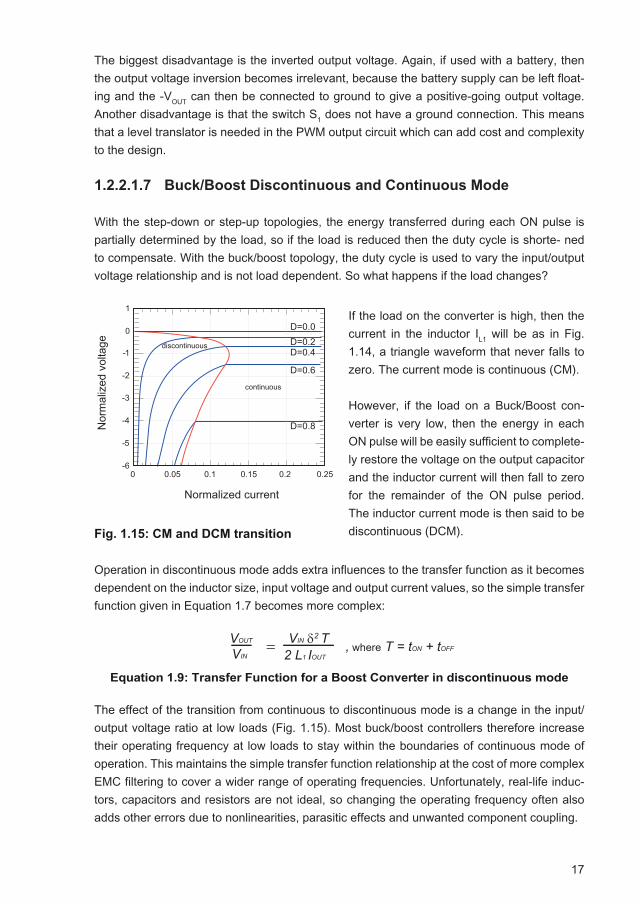
1.2.2.1.7 Buck/Boost Discontinuous and Continuous Mode
With the step-down or step-up topologies, the energy transferred during each ON pulse is partially determined by the load, so if the load is reduced then the duty cycle is shorte- ned to compensate. With the buck/boost topology, the duty cycle is used to vary the input/output voltage relationship and is not load dependent. So what happens if the load changes?
Fig. 1.15: CM and DCM transition
Operation in discontinuous mode adds extra influences to the transfer function as it becomes dependent on the inductor size, input voltage and output current values, so the simple transfer function given in Equation 1.7 becomes more complex:
Equation 1.9: Transfer Function for a Boost Converter in discontinuous mode
The effect of the transition from continuous to discontinuous mode is a change in the input/output voltage ratio at low loads (Fig. 1.15). Most buck/boost controllers therefore increase their operating frequency at low loads to stay within the boundaries of continuous mode of operation. This maintains the simple transfer function relationship at the cost of more complex EMC filtering to cover a wider range of operating frequencies. Unfortunately, real-life induc-tors, capacitors and resistors are not ideal, so changing the operating frequency often also adds other errors due to nonlinearities, parasitic effects and unwanted component coupling.
�����
�����
�����
�����
����������
�����
�
�
��
��
��
��
�
��� ��� ��� ��� ��� ���
����������������
���
�����
�����
�� �������������
VOUT
VIN= VIN δ2 T
2 L1 IOUT, where T = tON + tOFF
If the load on the converter is high, then the current in the inductor IL1 will be as in Fig. 1.14, a triangle waveform that never falls to zero. The current mode is continuous (CM).
However, if the load on a Buck/Boost con-verter is very low, then the energy in each ON pulse will be easily sufficient to complete-ly restore the voltage on the output capacitor and the inductor current will then fall to zero for the remainder of the ON pulse period. The inductor current mode is then said to be discontinuous (DCM).
18
1.2.2.1.8 Synchronous and Asynchronous Conversion
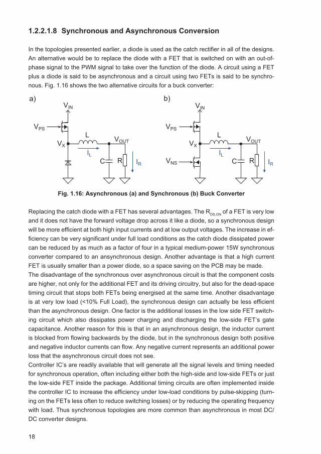
In the topologies presented earlier, a diode is used as the catch rectifier in all of the designs. An alternative would be to replace the diode with a FET that is switched on with an out-of-phase signal to the PWM signal to take over the function of the diode. A circuit using a FET plus a diode is said to be asynchronous and a circuit using two FETs is said to be synchro-nous. Fig. 1.16 shows the two alternative circuits for a buck converter:
Fig. 1.16: Asynchronous (a) and Synchronous (b) Buck Converter
Replacing the catch diode with a FET has several advantages. The RDS,ON of a FET is very low and it does not have the forward voltage drop across it like a diode, so a synchronous design will be more efficient at both high input currents and at low output voltages. The increase in ef-ficiency can be very significant under full load conditions as the catch diode dissipated power can be reduced by as much as a factor of four in a typical medium-power 15W synchronous converter compared to an ansynchronous design. Another advantage is that a high current FET is usually smaller than a power diode, so a space saving on the PCB may be made.The disadvantage of the synchronous over asynchronous circuit is that the component costs are higher, not only for the additional FET and its driving circuitry, but also for the dead-space timing circuit that stops both FETs being energised at the same time. Another disadvantage is at very low load (<10% Full Load), the synchronous design can actually be less efficient than the asynchronous design. One factor is the additional losses in the low side FET switch-ing circuit which also dissipates power charging and discharging the low-side FET’s gate capacitance. Another reason for this is that in an asynchronous design, the inductor current is blocked from flowing backwards by the diode, but in the synchronous design both positive and negative inductor currents can flow. Any negative current represents an additional power loss that the asynchronous circuit does not see.Controller IC’s are readily available that will generate all the signal levels and timing needed for synchronous operation, often including either both the high-side and low-side FETs or just the low-side FET inside the package. Additional timing circuits are often implemented inside the controller IC to increase the efficiency under low-load conditions by pulse-skipping (turn-ing on the FETs less often to reduce switching losses) or by reducing the operating frequency with load. Thus synchronous topologies are more common than asynchronous in most DC/DC converter designs.
���
���
��
��
����
����
�
�� �����
���
��
��
����
����
�
���
19
1.2.2.1.9 Two Stage Boost/Buck (Ćuk Converter)
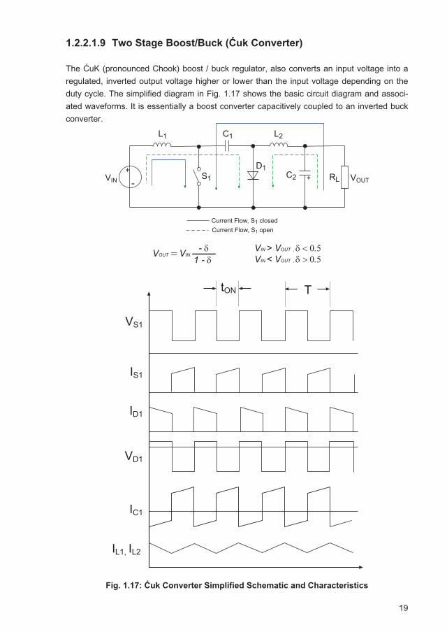
The ĆuK (pronounced Chook) boost / buck regulator, also converts an input voltage into a regulated, inverted output voltage higher or lower than the input voltage depending on the duty cycle. The simplified diagram in Fig. 1.17 shows the basic circuit diagram and associ-ated waveforms. It is essentially a boost converter capacitively coupled to an inverted buck converter.
Fig. 1.17: Ćuk Converter Simplified Schematic and Characteristics
��� ��
��������������� ��������������������� ����
�
���
��� �
�
� �����
VOUT = - δ1 - δ
VINVIN > VOUT , δ < 0.5VIN < VOUT , δ > 0.5
����
���
���
���
��������
���
���
20
It is immediately obvious compared to the previously presented topologies that this topology requires two inductors, however as the current flow in both inductors are the same, they can share a common core. When switch S1 is closed a current IL1 flows through L1 with a ramp rate of VIN/L1. Simultaneously, the positive terminal of C1 is grounded which causes C1 to discharge a negative voltage via L2 to recharge C2 and supply the load RL with an inverted current. The current flows through L2 with a ramp rate of (VC1 + VOUT)/L2. When S1 is opened, the energy stored in L1 boosts the inductor voltage which is then used to recharge C1 via D1. The current through the inductor L1 falls with the decay rate of (VC1 - VIN)/L1. Simultaneously, the capacitor C2 discharges through L2 and diode D1, which creates a decreasing L2 current with the decay rate VOUT/L2. The capacitor C1 is here plays a special role because it is responsible for the entire energy flow from input to output. The value of C1 is chosen so that the voltage in the steady state is necessarily constant.
Because of the direction of current flow, the output voltage is negative with respect to ground potential. Therefore, this topology is suitable for generating negative voltages only. For the consideration of the transfer function for this topology, the influence of both inductors has to be considered.
For L1, the applicable equations are:
For the ON condition: EnergyIN (L1) = VIN tON
For the OFF condition: EnergyOUT (L1) = (VC1 - VIN) tOFF
For L2, the applicable equations are:
For the ON condition: EnergyIN (L2) = (VC1 + VOUT) tON
For the OFF condition: EnergyOUT (L2) = - VOUT tOFF
Substituting gives two equations for the C1 capacitor voltage:
Which resolve to give the same result as for the single stage buck/boost converter:
Equation 1.10: Transfer Function of Ćuk Converter
The advantage of the Ćuk converter over the single stage buck/boost converter is that the cur-rents flowing in L1 and L2 are the same and continuous. The input and output currents are both effectively LC filtered which makes EMC very simple as very little high frequency interference is generated. And as the currents in both inductors are the same, they can share a common core, which simplifies the construction and helps to reduce ripple currents further.
VC1 = 11 - δ
VIN and VC1 = - VOUT
δ
VOUT - δ1 - δVIN
=
Practical Tip
21
The design is also very efficient because charging and discharging capacitors via inductors avoids high current spikes with their associative resistive losses. Also, a grounded S1 switch allows low loss FETs with simple drive circuits to be used.
The biggest disadvantage of the Ćuk converter is the heavy dependence on C1. All of the current flowing from input to output must go through this capacitor which must be non-po-larised as the voltage across it reverses with each half cycle. The high ripple current gener-ates internal heating which limits the operating temperature. In practice, bulky and expensive polypropylene capacitors must be used. Furthermore, the PWM control loop must be very carefully designed for stable operation. With four reactive components (two inductors and two capacitors), great care must be taken not to create unwanted resonances in the control circuit.
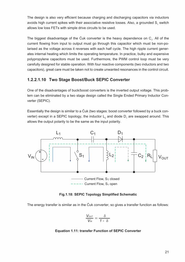
1.2.2.1.10 Two Stage Boost/Buck SEPIC Converter
One of the disadvantages of buck/boost converters is the inverted output voltage. This prob-lem can be eliminated by a two stage design called the Single Ended Primary Inductor Con-verter (SEPIC).
Essentially the design is similar to a Ćuk (two stages: boost converter followed by a buck con-verter) except in a SEPIC topology, the inductor L2 and diode D1 are swapped around. This allows the output polarity to be the same as the input polarity.
Fig.1.18: SEPIC Topology Simplified Schematic
The energy transfer is similar as in the Ćuk converter, so gives a transfer function as follows:
Equation 1.11: transfer Function of SEPIC Converter
��� ��
��������������� ��������������������� ����
�
�����
� �
�
�
����
VOUT δ1 - δVIN
=

22
Fig. 1.19: SEPIC Converter Characteristics.
The fact that the output voltage polarity is the same as the input voltage makes the SEPIC cir-cuit very useful for battery powered applications using rechargeable cells. The battery charger can then be used both to recharge the battery and to simultaneously power the application because they share the same common ground rail. Like the Ćuk converter, the SEPIC also has a continuous input current waveform which makes EMC filtering simpler.
Practical Tip
SEPICs are often used for LED lighting applications because the capacitor C1 provides in-herent output short circuit protection, the feedback loop can be easily modified for constant current instead of constant voltage regulation and a common V- rail makes EMC filtering sim-pler (LED lighting applications are required to meet strict input harmonic interference limits).
The disadvantages are that the SEPIC converter has a pulsed output current waveform sim-ilar to a conventional single stage buck/boost converter and, like the Ćuk converter, has a complex 4-pole feedback function that can easily break into resonance.
���
���
���
���
���
���
����
23
1.2.2.1.11 Two Stage Boost/Buck ZETA Converter
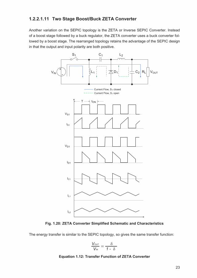
Another variation on the SEPIC topology is the ZETA or Inverse SEPIC Converter. Instead of a boost stage followed by a buck regulator, the ZETA converter uses a buck converter fol-lowed by a boost stage. The rearranged topology retains the advantage of the SEPIC design in that the output and input polarity are both positive.
Fig. 1.20: ZETA Converter Simplified Schematic and Characteristics
The energy transfer is similar to the SEPIC topology, so gives the same transfer function:
Equation 1.12: Transfer Function of ZETA Converter
��� ��
��������������� ��������������������� ����
�
���
���
�
�
� ����
VOUT δ1 - δVIN
=
���
���
���
���
����
���
���
���
24
The advantage of a ZETA topology over a SEPIC converter is that the feedback loop is more stable so that it can cope with a wider input voltage range and higher load transients without breaking into resonance. The output ripple is also significantly lower than an equivalent SE-PIC design.
The disadvantage is that a ZETA topology has a higher input ripple current, so it needs a larg-er C1 capacitor for the same energy transfer (the intermediate voltage is lower) and switch S1 is not grounded, so a level-shifting circuit is needed to drive the P-Channel FET.
1.2.2.1.12 Multiphase DC/DC Converters
Multiphase DC/DC converters are a good example of the principle of equilibrium in electron-ics. This means that for any desired benefit, a price must be paid for by some balancing disad-vantage. The push for ever faster switching speeds to increase processing power has caused the typical microprocessor core voltage to drop from 5V to 3.3V and then down to below 1V while the increasing gate complexity has led to the demand for ever higher supply currents. Low voltage, high current power supplies are, however, not easy to build.
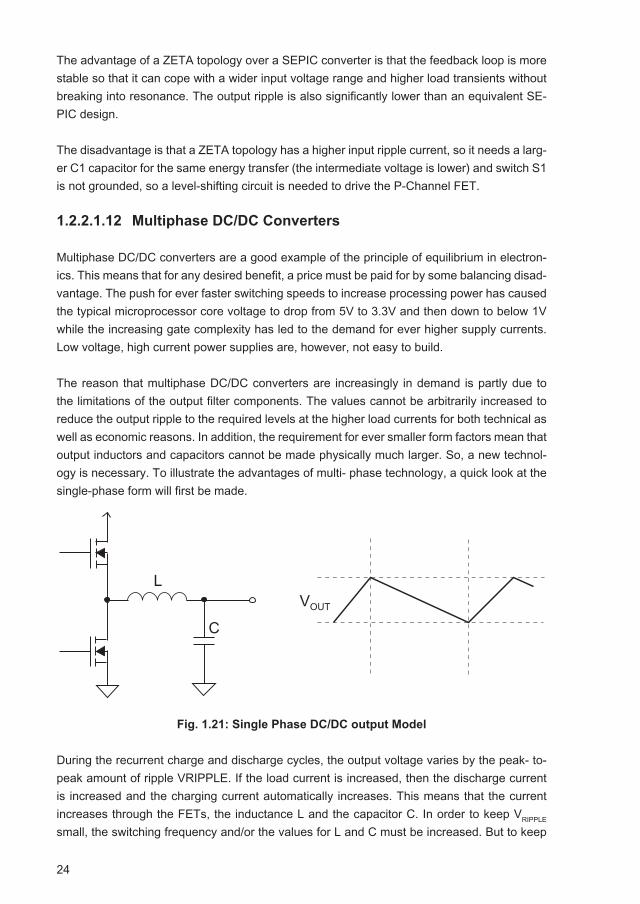
The reason that multiphase DC/DC converters are increasingly in demand is partly due to the limitations of the output filter components. The values cannot be arbitrarily increased to reduce the output ripple to the required levels at the higher load currents for both technical as well as economic reasons. In addition, the requirement for ever smaller form factors mean that output inductors and capacitors cannot be made physically much larger. So, a new technol-ogy is necessary. To illustrate the advantages of multi- phase technology, a quick look at the single-phase form will first be made.
Fig. 1.21: Single Phase DC/DC output Model
During the recurrent charge and discharge cycles, the output voltage varies by the peak- to-peak amount of ripple VRIPPLE. If the load current is increased, then the discharge current is increased and the charging current automatically increases. This means that the current increases through the FETs, the inductance L and the capacitor C. In order to keep VRIPPLE
small, the switching frequency and/or the values for L and C must be increased. But to keep
�
�
����
25
the efficiency high, the FETs, inductors and capacitors must have low series resistance, which leads to bulkier components and EMC concerns place a limit on the maximum frequency.
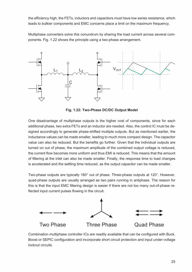
Multiphase converters solve this conundrum by sharing the load current across several com-ponents. Fig. 1.22 shows the principle using a two-phase arrangement.
Fig. 1.22: Two-Phase DC/DC Output Model
One disadvantage of multiphase outputs is the higher cost of components, since for each additional phase, two extra FETs and an inductor are needed. Also, the control IC must be de-signed accordingly to generate phase-shifted multiple outputs. But as mentioned earlier, the inductance values can be made smaller, leading to much more compact design. The capacitor value can also be reduced. But the benefits go further. Given that the individual outputs are turned on out of phase, the maximum amplitude of the combined output voltage is reduced, the current flow becomes more uniform and thus EMI is reduced. This means that the amount of filtering at the inlet can also be made smaller. Finally, the response time to load changes is accelerated and the settling time reduced, as the output capacitor can be made smaller.
Two-phase outputs are typically 180° out of phase. Three-phase outputs at 120°. However, quad-phase outputs are usually arranged as two pairs running in antiphase. The reason for this is that the input EMC filtering design is easier if there are not too many out-of-phase re-flected input current pulses flowing in the circuit.
Combination multiphase controller ICs are readily available that can be configured with Buck, Boost or SEPIC configuration and incorporate short circuit protection and input under-voltage lockout circuits.
��
�
������
��������� ����������� ����������
26
1.2.2.2 Isolated DC/DC Converters
In the family of isolated DC/DC converters there is a variety of topologies, but only three of them are applicable to the discussion of modern DC/DC converters. This section will limit its consideration to flyback, forward and push-pull converter topologies. In these types of isolated converters, the transfer of energy from input to the output is performed via a transformer. As with the non-isolated converters regulation is performed by the PWM controller, again by mon-itoring the output voltage in the feedback loop, but via an isolating stage. Ideal components are again assumed.
The other difference between transformer-based isolated converter topologies and the non-isolated topologies discussed previously is that the buck, boost or buck/boost function can be achieved with the transformer winding ratio, so freeing up the PWM driver to operate as a simple energy packet controller transferring more or less energy from input to output according to input voltage and output load requirements only.
The disadvantage of using a transformer is that the energy transfer from primary winding to secondary winding involves additional losses. So while a buck regulator can reach 97% con-version efficiency, transformer-based converters struggle to exceed 90%.
1.2.2.2.1 Flyback DC/DC Converter
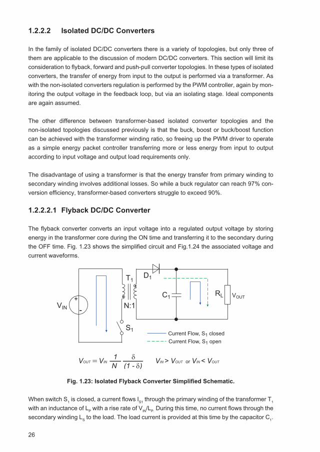
The flyback converter converts an input voltage into a regulated output voltage by storing energy in the transformer core during the ON time and transferring it to the secondary during the OFF time. Fig. 1.23 shows the simplified circuit and Fig.1.24 the associated voltage and current waveforms.
Fig. 1.23: Isolated Flyback Converter Simplified Schematic.
When switch S1 is closed, a current flows IS1 through the primary winding of the transformer T1
with an inductance of LP with a rise rate of VIN/LP. During this time, no current flows through the secondary winding LS to the load. The load current is provided at this time by the capacitor C1.
���
�
� ���
������������ �������������������� ��������
����
��
��
��
����
VOUT = δ(1 - δ)
VIN VIN > VOUT or VIN < VOUT 1N
27
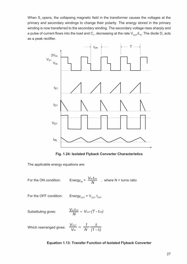
When S1 opens, the collapsing magnetic field in the transformer causes the voltages at the primary and secondary windings to change their polarity. The energy stored in the primary winding is now transferred to the secondary winding. The secondary voltage rises sharply and a pulse of current flows into the load and C1, decreasing at the rate VOUT/LS. The diode D1 acts as a peak rectifier.
Fig. 1.24: Isolated Flyback Converter Characteristics
The applicable energy equations are:
For the ON condition: EnergyIN = , where N = turns ratio
For the OFF condition: EnergyOUT = VOUT tOFF
Substituting gives:
Which rearranged gives:
Equation 1.13: Transfer Function of Isolated Flyback Converter
VIN tON
N
VOUT δ(1 - δ)VIN
1N=
= VOUT (T - tON)VIN tON
N
28
Thus the transfer functions of the buck/boost converter and the isolated flyback converter differ only by the transformer turns ratio factor of 1/N. The advantage of a flyback transformer design is that the output voltage multiplication can be very high with short duty cycles which makes this topology ideal for high output voltage power supplies. Another advantage is that multiple outputs (with different polarities if required) can be easily implemented by adding multiple secondary windings. The component count is also very low, so this topology is good for low cost designs.With output voltage or current monitoring and an isolated feedback path (typically via an opto-coupler) a very stable regulated output can be generated. But flyback converters can also be primary side regulated by monitoring the primary winding waveform and using the knee-point to detect when the secondary current has reached zero. This eliminates the optocoupler and reduces the component count still further.The disadvantage is that the transformer core needs careful selection. The air-gapped core should not saturate even though there is an average positive DC current flowing through the transformer so efficiency can be lost if it has a large magnetic hysteresis. Also eddy current losses in the windings can be a problem due to the high peak currents. These two effects limit the practical operational frequency range of this topology. Finally, the large inductive spike on the primary winding when S1, is turned off places a large voltage stress on the switching FET.
1.2.2.2.2 Forward DC/DC Converter
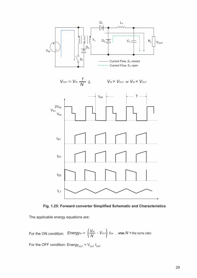
Although the forward converter seems similar to the flyback topology, it functions in a com-pletely different way. The input voltage is converted into a regulated output voltage as a function of the turns ratio of the transformer. Fig. 1.25 shows the simplified circuit and the associated voltage and current waveforms.
As in the flyback topology, when switch S1 is closed, a current IS1 flows through the primary winding of the transformer T1 with an inductance of LP with a rise rate of VIN/LP. The ris-ing primary current induces a secondary current in the transformer T1 due to the coupling between the primary and secondary windings, with a voltage magnitude of VIN/N. The sec-ondary current flows through the rectifying diode D1 and the output inductor L1, rising with a rate equal to VIN/(L1 N). This current also flows into the load RL and the output capacitor C1. Thus, the voltage across the capacitor C1 rises until the upper regulation threshold is exceeded and a ‘stop’ signal is sent (the feedback signal is usually via an optocoupler). The primary side controller then causes S1 to open, and the current flow from the voltage source is interrupted. The reset winding with diode D3 stops the transformer magnetic field from collapsing, but instead allows the current to decay at the same rate as it rose when S1 was closed. As a result, when S1 opens, a polarity reversal occurs at the secondary winding and the negative current decreases with the rate VOUT/L1 and flows through the catch diode D2 and the inductance L1 and finally flow into load and C1. The voltage across C1 decreases until such time as the lower control limit of the regulation is reached. A ‘start’ signal is sent, S1 is closed again and a new cycle begins.
Practical Tip
29
Fig. 1.25: Forward converter Simplified Schematic and Characteristics
The applicable energy equations are:
For the ON condition:
For the OFF condition: EnergyOUT = VOUT tOFF
���
�
�
��������������� ��������������������� ����
���
� �
��
�
�
��
����
EnergyIN = VIN
N- VOUT ( ) tON , where N = the turns ratio
VOUT = δVIN VIN > VOUT or VIN < VOUT 1N
����
���
���
������
���
���
��� �
30
Rearranging gives:
Equation 1.14: Transfer Function of Isolated Forward Converter
Unlike the flyback converter, a forward converter transfers energy from primary to secondary continuously via transformer action rather than storing packets of energy in the transformer core gap, thus the core needs no air gap with its associated losses and radiated EMI. The core can also have a higher inductance as hysteresis losses are not so critical. The reduced peak currents reduce winding and diode losses and lead to a lower input and output ripple current. For the same output power, a forward converter will therefore be more efficient.
The disadvantage is increased component cost and a minimum load requirement to stop the converter going into discontinuous mode with a corresponding dramatic change in the transfer function.
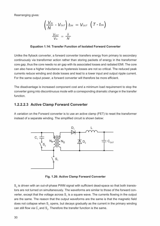
1.2.2.2.3 Active Clamp Forward Converter
A variation on the Forward converter is to use an active clamp (FET) to reset the transformer instead of a separate winding. The simplified circuit is shown below:
Fig. 1.26: Active Clamp Forward Converter
S2 is driven with an out-of-phase PWM signal with sufficient dead-space so that both transis-tors are not turned on simultaneously. The waveforms are similar to those of the forward con-verter, except that the voltage across S1 is a square wave. The currents flowing in the output are the same. The reason that the output waveforms are the same is that the magnetic field does not collapse when S1 opens, but decays gradually as the current in the primary winding can still flow via C1 and S2. Therefore the transfer function is the same.
VIN
N- VOUT ( ) tON = VOUT (T - tON)
������ ��
�
��
��
��
��
��
=VIN
VOUT δN
31
The addition of the active clamp has a number of advantages. The transformer reset wind-ing is no longer required and the voltage across S1 peaks at VIN and not 2×VIN as with the standard topology. The overall efficiency is higher because the diode losses are avoided and only the demagnetising current flows through S2. More importantly, the active clamp permits operation above 50% duty cycle with higher turns ratios without the penalties of high peak voltages across S1.
The disadvantage of the active clamp is that a second PWM signal needs to be generated and S2 needs a high-side driver. However, there are many controller ICs that integrate the necessary timing circuits and high-side drivers internally. The clamp capacitor C1 has a high ripple current, so great care must be taken to ensure that it does not overheat. The current in the clamp capacitor can be approximated by:
Where LMAG is the magnetising inductance of the transformer.。
Equation 1.15: Approximation for Clamp Capacitor Current
1.2.2.2.4 Push-Pull Converter
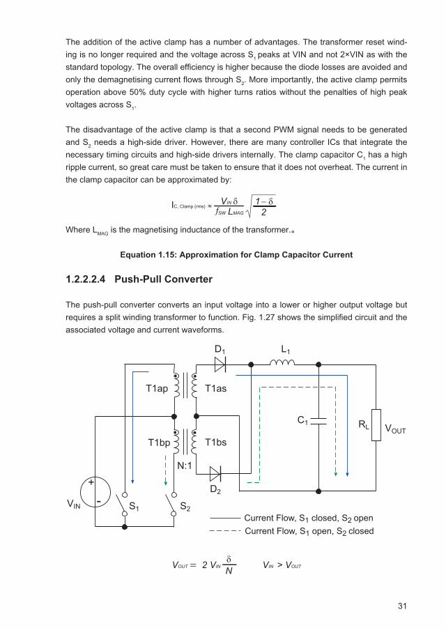
The push-pull converter converts an input voltage into a lower or higher output voltage but requires a split winding transformer to function. Fig. 1.27 shows the simplified circuit and the associated voltage and current waveforms.
IC, Clamp (rms) ≈ VIN δƒSW LMAG
12− δ
���
����
����
�
�
���
������� ��� �� ������ �� ���������� ��� �� ���� �� �����
����
����
����
����
����
��
����
2 VINVOUT = δN VIN > VOUT
32
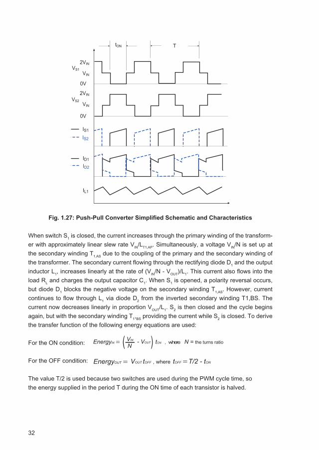
Fig. 1.27: Push-Pull Converter Simplified Schematic and Characteristics
When switch S1 is closed, the current increases through the primary winding of the transform-er with approximately linear slew rate VIN/LT1,AP. Simultaneously, a voltage VIN/N is set up at the secondary winding T1,AS due to the coupling of the primary and the secondary winding of the transformer. The secondary current flowing through the rectifying diode D1 and the output inductor L1, increases linearly at the rate of (VIN/N - VOUT)/L1. This current also flows into the load RL and charges the output capacitor C1. When S1 is opened, a polarity reversal occurs, but diode D1 blocks the negative voltage on the secondary winding T1,AS. However, current continues to flow through L1 via diode D2 from the inverted secondary winding T1,BS. The current now decreases linearly in proportion VOUT/L1. S2 is then closed and the cycle begins again, but with the secondary winding T1,BS providing the current while S2 is closed. To derive the transfer function of the following energy equations are used:
For the ON condition:
For the OFF condition:
The value T/2 is used because two switches are used during the PWM cycle time, sothe energy supplied in the period T during the ON time of each transistor is halved.
����
���
���
���
���
���
���
��� �
���
��
����
���
���
��
EnergyOUT = VOUT tOFF , where tOFF = T/2 - tON
EnergyIN = VIN
N- VOUT ( ) tON , where N = the turns ratio
33
Rearranging gives:
or
Equation 1.16: Transfer Function of Push-Pull Converter
Since the duty cycle is for both S1 and S2 close to 50%, it is very important to make sure that the two switches cannot be switched on simultaneously; otherwise very high short circuit (shoot-through) currents would flow. Therefore, a suitable dead time is required between the opening of one switch and the closing of the other.
Another problem that can occur in a push-pull converter is the magnetic flux displacement (flux walking). Since the push-pull converter uses the full range of the BH characteristic curve of the transformer, the smallest difference in the performance of the switches (saturation voltages, switching times, etc.) can result in an unbalance in the magnetic flux. The offset of the flux imbalance is unfortunately cumulative because the imbalance in the magnetic flux in the transformer cannot be completely reset to zero at the end of each switching cycle, so the offset remaining from the previous cycle becomes the starting point of the next cycle. The core material of the transformer can eventually become saturated, unbalancing the energy transfer still further. As a saturated core no longer acts as a classical inductor, one or both of the switches can then be destroyed by the high currents in the primary windings. This problem can be avoided by cycle-by-cycle current sensing and limiting.
On the other hand, because the Push-Pull converter uses both quadrants of the transformer BH curve as opposed to only the first quadrant in a forward converter, a push-pull topology can transfer double the power for the same sized transformer. This makes it a very cost-efficient topology suitable for scaling up for higher output powers or for making low power sub-minia-ture DC/DC converters.
As the duty cycle is typically set close to 50% for maximum efficiency, the input/output voltage ratio is then fixed by the turns ratio of the transformer. Therefore a regulated push-pull con-verter is best used with a regulated input voltage as a bus converter.
VIN
N- VOUT ( ) tON VOUT (T/2 - tON )=
VOUT
VIN= δ2
N
34
1.2.2.2.5 Half Bridge and Full Bridge Converters
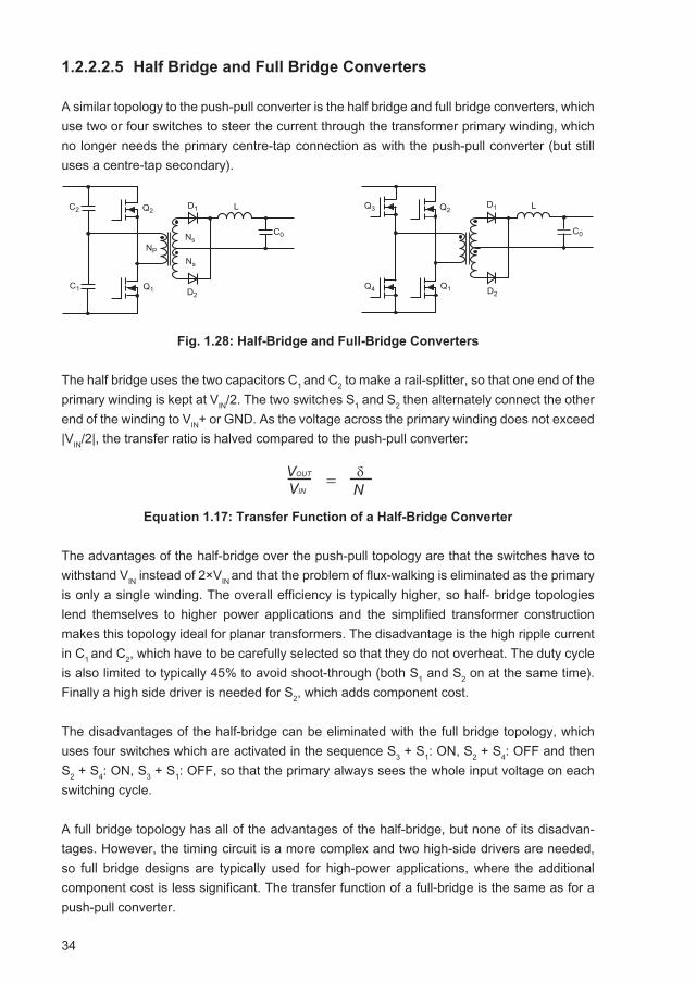
A similar topology to the push-pull converter is the half bridge and full bridge converters, which use two or four switches to steer the current through the transformer primary winding, which no longer needs the primary centre-tap connection as with the push-pull converter (but still uses a centre-tap secondary).
Fig. 1.28: Half-Bridge and Full-Bridge Converters
The half bridge uses the two capacitors C1 and C2 to make a rail-splitter, so that one end of the primary winding is kept at VIN/2. The two switches S1 and S2 then alternately connect the other end of the winding to VIN+ or GND. As the voltage across the primary winding does not exceed |VIN/2|, the transfer ratio is halved compared to the push-pull converter:
Equation 1.17: Transfer Function of a Half-Bridge Converter
The advantages of the half-bridge over the push-pull topology are that the switches have to withstand VIN instead of 2×VIN and that the problem of flux-walking is eliminated as the primary is only a single winding. The overall efficiency is typically higher, so half- bridge topologies lend themselves to higher power applications and the simplified transformer construction makes this topology ideal for planar transformers. The disadvantage is the high ripple current in C1 and C2, which have to be carefully selected so that they do not overheat. The duty cycle is also limited to typically 45% to avoid shoot-through (both S1 and S2 on at the same time). Finally a high side driver is needed for S2, which adds component cost.
The disadvantages of the half-bridge can be eliminated with the full bridge topology, which uses four switches which are activated in the sequence S3 + S1: ON, S2 + S4: OFF and then S2 + S4: ON, S3 + S1: OFF, so that the primary always sees the whole input voltage on each switching cycle.
A full bridge topology has all of the advantages of the half-bridge, but none of its disadvan-tages. However, the timing circuit is a more complex and two high-side drivers are needed, so full bridge designs are typically used for high-power applications, where the additional component cost is less significant. The transfer function of a full-bridge is the same as for a push-pull converter.
��
� �
��
��
��
��
��
��
����
�� ��
��
��
�� ��
��
��
VOUT
VIN= δ
N
35
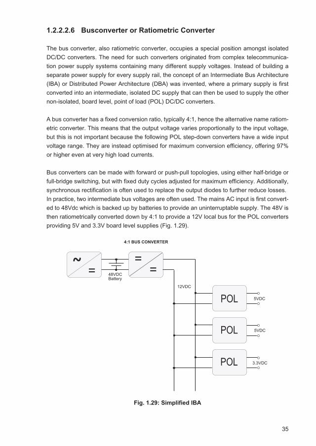
1.2.2.2.6 Busconverter or Ratiometric Converter
The bus converter, also ratiometric converter, occupies a special position amongst isolated DC/DC converters. The need for such converters originated from complex telecommunica-tion power supply systems containing many different supply voltages. Instead of building a separate power supply for every supply rail, the concept of an Intermediate Bus Architecture (IBA) or Distributed Power Architecture (DBA) was invented, where a primary supply is first converted into an intermediate, isolated DC supply that can then be used to supply the other non-isolated, board level, point of load (POL) DC/DC converters.
A bus converter has a fixed conversion ratio, typically 4:1, hence the alternative name ratiom-etric converter. This means that the output voltage varies proportionally to the input voltage, but this is not important because the following POL step-down converters have a wide input voltage range. They are instead optimised for maximum conversion efficiency, offering 97% or higher even at very high load currents.
Bus converters can be made with forward or push-pull topologies, using either half-bridge or full-bridge switching, but with fixed duty cycles adjusted for maximum efficiency. Additionally, synchronous rectification is often used to replace the output diodes to further reduce losses.In practice, two intermediate bus voltages are often used. The mains AC input is first convert-ed to 48Vdc which is backed up by batteries to provide an uninterruptable supply. The 48V is then ratiometrically converted down by 4:1 to provide a 12V local bus for the POL converters providing 5V and 3.3V board level supplies (Fig. 1.29).
Fig. 1.29: Simplified IBA
���
�
���
���
���
�����
����
����
������
������������
�����������������
36
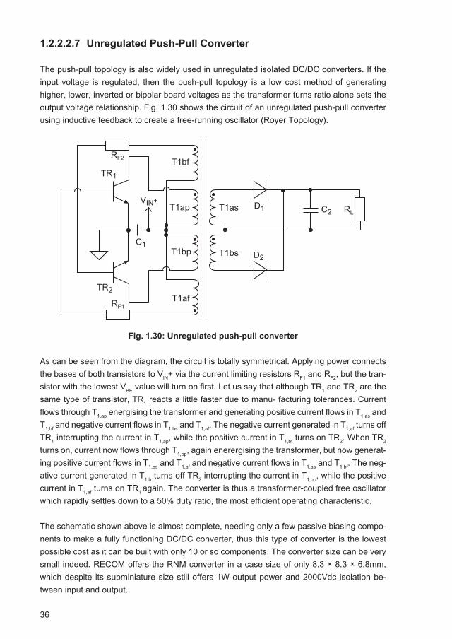
1.2.2.2.7 Unregulated Push-Pull Converter
The push-pull topology is also widely used in unregulated isolated DC/DC converters. If the input voltage is regulated, then the push-pull topology is a low cost method of generating higher, lower, inverted or bipolar board voltages as the transformer turns ratio alone sets the output voltage relationship. Fig. 1.30 shows the circuit of an unregulated push-pull converter using inductive feedback to create a free-running oscillator (Royer Topology).
Fig. 1.30: Unregulated push-pull converter
As can be seen from the diagram, the circuit is totally symmetrical. Applying power connects the bases of both transistors to VIN+ via the current limiting resistors RF1 and RF2, but the tran-sistor with the lowest VBE value will turn on first. Let us say that although TR1 and TR2 are the same type of transistor, TR1 reacts a little faster due to manu- facturing tolerances. Current flows through T1,ap energising the transformer and generating positive current flows in T1,as and T1,bf and negative current flows in T1,bs and T1,af. The negative current generated in T1,af turns off TR1 interrupting the current in T1,ap, while the positive current in T1,bf turns on TR2. When TR2 turns on, current now flows through T1,bp, again enerergising the transformer, but now generat-ing positive current flows in T1,bs and T1,af and negative current flows in T1,as and T1,bf. The neg-ative current generated in T1,b turns off TR2 interrupting the current in T1,bp, while the positive current in T1,af turns on TR1 again. The converter is thus a transformer-coupled free oscillator which rapidly settles down to a 50% duty ratio, the most efficient operating characteristic.
The schematic shown above is almost complete, needing only a few passive biasing compo-nents to make a fully functioning DC/DC converter, thus this type of converter is the lowest possible cost as it can be built with only 10 or so components. The converter size can be very small indeed. RECOM offers the RNM converter in a case size of only 8.3 × 8.3 × 6.8mm, which despite its subminiature size still offers 1W output power and 2000Vdc isolation be-tween input and output.
����
���� ����
��������
�������
��
����
��
���
�� ��
��
���
���
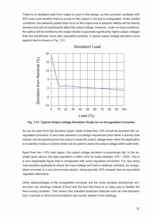
37
There is no feedback path from output to input in this design, so the converter oscillates with 50% duty cycle whether there is a load on the output or not and is unregulated. Under loaded conditions, the switching spikes that occur on the output due to parasitic effects will be heavily damped and will not significantly affect the output voltage. However, under no-load conditions, the spikes will be rectified by the output diodes to generate significantly higher output voltages than the transformer turns ratio calculation predicts. A typical output voltage deviation curve against load is shown in Fig. 1.31:
Fig. 1.31: Typical Output voltage Deviation Graph for an Unregulated Converter
As can be seen from the deviation graph, loads of less than 10% should be avoided with un-regulated converters. If zero load operation is a design requirement then either a dummy load resistor can be placed across the output to keep the output voltage down when the application is in standby mode or a Zener diode can be used to clamp the output voltage within safe limits.
Apart from the <10% load region, the output voltage deviation is surprisingly flat. In the ex-ample given above, the load regulation is within ±2% for loads between 10% - 100%. This is a very respectable figure that is comparable with some regulated converters. For very many cost sensitive applications where the input voltage and load is relatively constant, an unregu-lated converter is a very economical solution, being typically 30% cheaper than an equivalent regulated alternative.
Other disadvantages of the unregulated converter are the more complex transformer con-struction (six windings instead of four) and the fact that there is no easy way to disable the free-running oscillator. This means that standard protection features such as over-tempera-ture, overload or short-circuit protection are usually absent in this topology.
���������������
��������
���
�����
������
� ��
�������
�
� � � �� �� �� �� �� �� �� ����
��
�
�
�
�
�
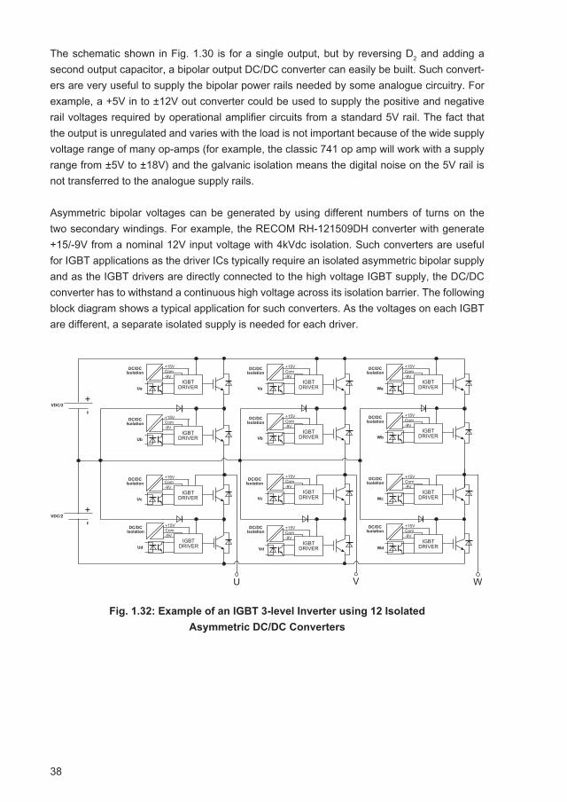
38
The schematic shown in Fig. 1.30 is for a single output, but by reversing D2 and adding a second output capacitor, a bipolar output DC/DC converter can easily be built. Such convert-ers are very useful to supply the bipolar power rails needed by some analogue circuitry. For example, a +5V in to ±12V out converter could be used to supply the positive and negative rail voltages required by operational amplifier circuits from a standard 5V rail. The fact that the output is unregulated and varies with the load is not important because of the wide supply voltage range of many op-amps (for example, the classic 741 op amp will work with a supply range from ±5V to ±18V) and the galvanic isolation means the digital noise on the 5V rail is not transferred to the analogue supply rails.
Asymmetric bipolar voltages can be generated by using different numbers of turns on the two secondary windings. For example, the RECOM RH-121509DH converter with generate +15/-9V from a nominal 12V input voltage with 4kVdc isolation. Such converters are useful for IGBT applications as the driver ICs typically require an isolated asymmetric bipolar supply and as the IGBT drivers are directly connected to the high voltage IGBT supply, the DC/DC converter has to withstand a continuous high voltage across its isolation barrier. The following block diagram shows a typical application for such converters. As the voltages on each IGBT are different, a separate isolated supply is needed for each driver.
Fig. 1.32: Example of an IGBT 3-level Inverter using 12 Isolated
Asymmetric DC/DC Converters
����������
������������
��������������
����������
������������
��������������
����������
������������
��������������
����������
������������
��������������
�
�
�
�
����������
������������
��������������
����������
������������
��������������
����������
������������
����������
������������
��������������
��������������
����������
������������
��������������
����������
������������
��������������
����������
������������
��������������
����������
������������
��������������
� � �
�����
�����
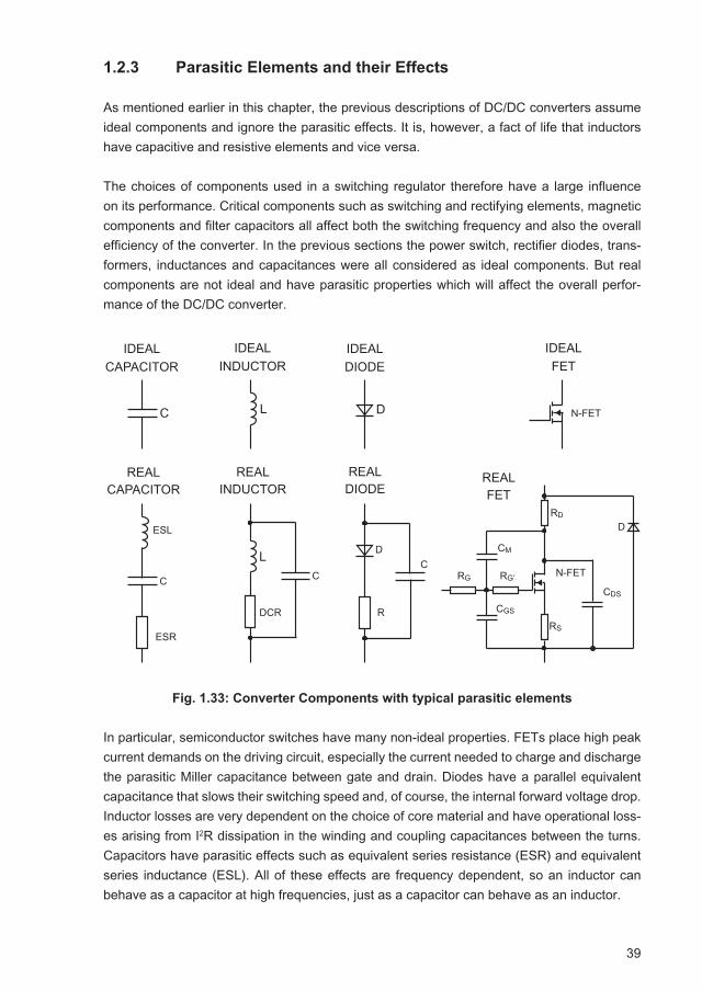
39
1.2.3 Parasitic Elements and their Effects
As mentioned earlier in this chapter, the previous descriptions of DC/DC converters assume ideal components and ignore the parasitic effects. It is, however, a fact of life that inductors have capacitive and resistive elements and vice versa.
The choices of components used in a switching regulator therefore have a large influence on its performance. Critical components such as switching and rectifying elements, magnetic components and filter capacitors all affect both the switching frequency and also the overall efficiency of the converter. In the previous sections the power switch, rectifier diodes, trans-formers, inductances and capacitances were all considered as ideal components. But real components are not ideal and have parasitic properties which will affect the overall perfor-mance of the DC/DC converter.
Fig. 1.33: Converter Components with typical parasitic elements
In particular, semiconductor switches have many non-ideal properties. FETs place high peak current demands on the driving circuit, especially the current needed to charge and discharge the parasitic Miller capacitance between gate and drain. Diodes have a parallel equivalent capacitance that slows their switching speed and, of course, the internal forward voltage drop. Inductor losses are very dependent on the choice of core material and have operational loss-es arising from I2R dissipation in the winding and coupling capacitances between the turns. Capacitors have parasitic effects such as equivalent series resistance (ESR) and equivalent series inductance (ESL). All of these effects are frequency dependent, so an inductor can behave as a capacitor at high frequencies, just as a capacitor can behave as an inductor.
��������������
�������������
����������
� � �
�������������
������������
���������
���
�
���
���
�
�
�
�
�
��
�����
�������
��������
�����
��
���
�����
���
���
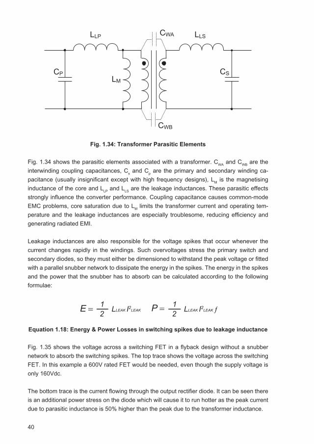
40
Fig. 1.34: Transformer Parasitic Elements
Fig. 1.34 shows the parasitic elements associated with a transformer. CWA and CWB are the interwinding coupling capacitances, Cs and Cp are the primary and secondary winding ca-pacitance (usually insignificant except with high frequency designs), LM is the magnetising inductance of the core and LLP and LLS are the leakage inductances. These parasitic effects strongly influence the converter performance. Coupling capacitance causes common-mode EMC problems, core saturation due to LM limits the transformer current and operating tem-perature and the leakage inductances are especially troublesome, reducing efficiency and generating radiated EMI.
Leakage inductances are also responsible for the voltage spikes that occur whenever the current changes rapidly in the windings. Such overvoltages stress the primary switch and secondary diodes, so they must either be dimensioned to withstand the peak voltage or fitted with a parallel snubber network to dissipate the energy in the spikes. The energy in the spikes and the power that the snubber has to absorb can be calculated according to the following formulae:
Equation 1.18: Energy & Power Losses in switching spikes due to leakage inductance
Fig. 1.35 shows the voltage across a switching FET in a flyback design without a snubber network to absorb the switching spikes. The top trace shows the voltage across the switching FET. In this example a 600V rated FET would be needed, even though the supply voltage is only 160Vdc.
The bottom trace is the current flowing through the output rectifier diode. It can be seen there is an additional power stress on the diode which will cause it to run hotter as the peak current due to parasitic inductance is 50% higher than the peak due to the transformer inductance.
���
�� ��
������
���
��
E = 12 LLEAK I2
LEAK P = 12 LLEAK I2
LEAK ƒ
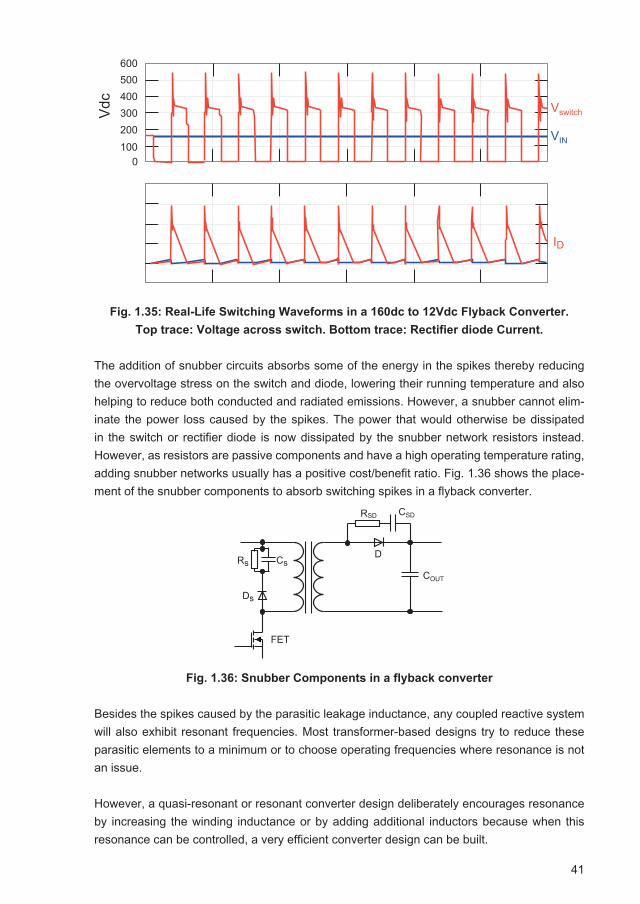
41
Fig. 1.35: Real-Life Switching Waveforms in a 160dc to 12Vdc Flyback Converter.
Top trace: Voltage across switch. Bottom trace: Rectifier diode Current.
The addition of snubber circuits absorbs some of the energy in the spikes thereby reducing the overvoltage stress on the switch and diode, lowering their running temperature and also helping to reduce both conducted and radiated emissions. However, a snubber cannot elim-inate the power loss caused by the spikes. The power that would otherwise be dissipated in the switch or rectifier diode is now dissipated by the snubber network resistors instead. However, as resistors are passive components and have a high operating temperature rating, adding snubber networks usually has a positive cost/benefit ratio. Fig. 1.36 shows the place-ment of the snubber components to absorb switching spikes in a flyback converter.
Fig. 1.36: Snubber Components in a flyback converter
Besides the spikes caused by the parasitic leakage inductance, any coupled reactive system will also exhibit resonant frequencies. Most transformer-based designs try to reduce these parasitic elements to a minimum or to choose operating frequencies where resonance is not an issue.
However, a quasi-resonant or resonant converter design deliberately encourages resonance by increasing the winding inductance or by adding additional inductors because when this resonance can be controlled, a very efficient converter design can be built.
��
�������
���
����
���
���
���
���
���
���
������
��
��
���
���
����
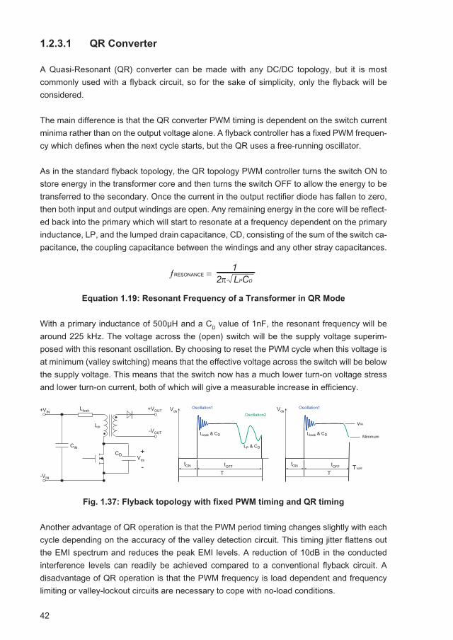
42
1.2.3.1 QR Converter
A Quasi-Resonant (QR) converter can be made with any DC/DC topology, but it is most commonly used with a flyback circuit, so for the sake of simplicity, only the flyback will be considered.
The main difference is that the QR converter PWM timing is dependent on the switch current minima rather than on the output voltage alone. A flyback controller has a fixed PWM frequen-cy which defines when the next cycle starts, but the QR uses a free-running oscillator.
As in the standard flyback topology, the QR topology PWM controller turns the switch ON to store energy in the transformer core and then turns the switch OFF to allow the energy to be transferred to the secondary. Once the current in the output rectifier diode has fallen to zero, then both input and output windings are open. Any remaining energy in the core will be reflect-ed back into the primary which will start to resonate at a frequency dependent on the primary inductance, LP, and the lumped drain capacitance, CD, consisting of the sum of the switch ca-pacitance, the coupling capacitance between the windings and any other stray capacitances.
Equation 1.19: Resonant Frequency of a Transformer in QR Mode
With a primary inductance of 500μH and a CD value of 1nF, the resonant frequency will be around 225 kHz. The voltage across the (open) switch will be the supply voltage superim-posed with this resonant oscillation. By choosing to reset the PWM cycle when this voltage is at minimum (valley switching) means that the effective voltage across the switch will be below the supply voltage. This means that the switch now has a much lower turn-on voltage stress and lower turn-on current, both of which will give a measurable increase in efficiency.
Fig. 1.37: Flyback topology with fixed PWM timing and QR timing
Another advantage of QR operation is that the PWM period timing changes slightly with each cycle depending on the accuracy of the valley detection circuit. This timing jitter flattens out the EMI spectrum and reduces the peak EMI levels. A reduction of 10dB in the conducted interference levels can readily be achieved compared to a conventional flyback circuit. A disadvantage of QR operation is that the PWM frequency is load dependent and frequency limiting or valley-lockout circuits are necessary to cope with no-load conditions.
ƒRESONANCE = 2π LPCD
1
TVAR
vIN
Minimum
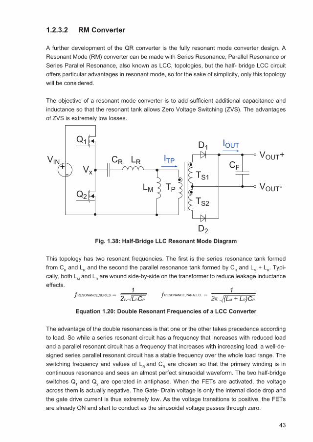
43
1.2.3.2 RM Converter
A further development of the QR converter is the fully resonant mode converter design. A Resonant Mode (RM) converter can be made with Series Resonance, Parallel Resonance or Series Parallel Resonance, also known as LCC, topologies, but the half- bridge LCC circuit offers particular advantages in resonant mode, so for the sake of simplicity, only this topology will be considered.
The objective of a resonant mode converter is to add sufficient additional capacitance and inductance so that the resonant tank allows Zero Voltage Switching (ZVS). The advantages of ZVS is extremely low losses.
Fig. 1.38: Half-Bridge LLC Resonant Mode Diagram
This topology has two resonant frequencies. The first is the series resonance tank formed from CR and LR and the second the parallel resonance tank formed by CR and LM + LR. Typi-cally, both LM and LR are wound side-by-side on the transformer to reduce leakage inductance effects.
Equation 1.20: Double Resonant Frequencies of a LCC Converter
The advantage of the double resonances is that one or the other takes precedence according to load. So while a series resonant circuit has a frequency that increases with reduced load and a parallel resonant circuit has a frequency that increases with increasing load, a well-de-signed series parallel resonant circuit has a stable frequency over the whole load range. The switching frequency and values of LR and CR are chosen so that the primary winding is in continuous resonance and sees an almost perfect sinusoidal waveform. The two half-bridge switches Q1 and Q2 are operated in antiphase. When the FETs are activated, the voltage across them is actually negative. The Gate- Drain voltage is only the internal diode drop and the gate drive current is thus extremely low. As the voltage transitions to positive, the FETs are already ON and start to conduct as the sinusoidal voltage passes through zero.
��
��������
��
��
��
�� ��
��
��
��
��
�
���
���
����
��
�����
ƒRESONANCE,SERIES = 2π LRCR
1 ƒRESONANCE,PARALLEL = 2π (LM + LR)CR
1
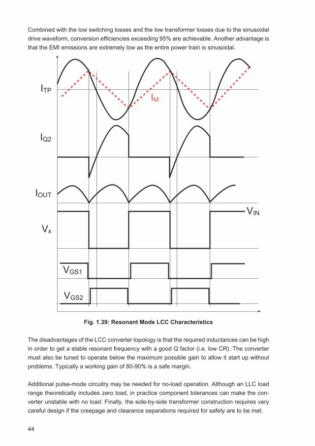
44
Combined with the low switching losses and the low transformer losses due to the sinusoidal drive waveform, conversion efficiencies exceeding 95% are achievable. Another advantage is that the EMI emissions are extremely low as the entire power train is sinusoidal.
Fig. 1.39: Resonant Mode LCC Characteristics
The disadvantages of the LCC converter topology is that the required inductances can be high in order to get a stable resonant frequency with a good Q factor (i.e. low CR). The converter must also be tuned to operate below the maximum possible gain to allow it start up without problems. Typically a working gain of 80-90% is a safe margin.
Additional pulse-mode circuitry may be needed for no-load operation. Although an LLC load range theoretically includes zero load, in practice component tolerances can make the con-verter unstable with no load. Finally, the side-by-side transformer construction requires very careful design if the creepage and clearance separations required for safety are to be met.
�����
���
����
���
��
����
����
45
1.2.4 Efficiency of DC/DC Converters
In comparison to linear regulators, the determination of the efficiency of switching regulators is much more complicated. The linear regulator has easily predetermined DC losses, the largest dissipation occurring in the pass transistor. A switching regulator, however, has not only DC losses but also AC losses which occur in the switches and in the components for energy storage. For example, the total loss of a switch is made up of not just the loss in the on and off states, but also the losses in the transition from switching on and off. In the case of a transformer, the total loss is calculated from the sum of AC (core), AC (winding) and DC (winding) losses.
The losses in the core of a transformer are caused mainly by the interaction between the magnetic flux and the core material (Hysteresis losses, Eddy current losses). The winding losses result mainly from the material of the transformer winding (Ohmic losses, skin effects). Either way the net effect is a rise of temperature in the transformer. To calculate the efficiency of a DC/DC converter, the losses of each part of the conversion cycle need to be found by averaging the losses over the whole range of the PWM duty cycle.
Switching regulators exhibit high efficiencies, since the power switch is turned on only for a short time relative to the whole switching cycle. The losses in the magnetic, inductive and capacitive components can be controlled and minimized by careful design and by proper se-lection, so that >96% conversion efficiency can be realised. This means only 4% of the input power is lost and converted into heat. Non-isolated converters are generally more effective than their isolated counterparts, since fewer parts are involved in the power conversion and transformer losses are eliminated. Yet despite a higher degree of complexity, isolated DC/DC converter efficiencies of over 85% can be achieved, depending on the power rating.One of the major causes of efficiency loss are the output diodes. If the output current is 1A and the forward voltage drop across the diode 0.6V, then 600mW will be lost in the diode alone. Thus high output current DC/DC converters often use FETs with synchro- nous switching to reduce rectification losses.It may be surprising to learn that lower power converters generally have lower efficiencies than higher power converters, especially considering the higher I2R losses that occur at high-er output currents. However, the internal power consumption of the switching controllers, shunt regulators and optocouplers (the “housekeeping” consumption) plays a significant role. If the total housekeeping demand is 1W, then a 10W converter can not have an efficiency exceeding 90%, but the maximum possible efficiency of a 100W converter would be 99%. Housekeeping losses also explain why all DC/DC converters have 0% efficiency under no-load conditions, as the converters still consume power but deliver no output power.
FETs consume more power when switching than in a steady on or off state. This is because the internal gate capacitance must be charged and discharged to switch the output. Peak gate currents of 2A or more are not unusual. A DC/DC converter running with no load will still be switching the FETs hundreds of thousands of times per second, so it is not unusual for a DC/DC converter to still run warm without any load.
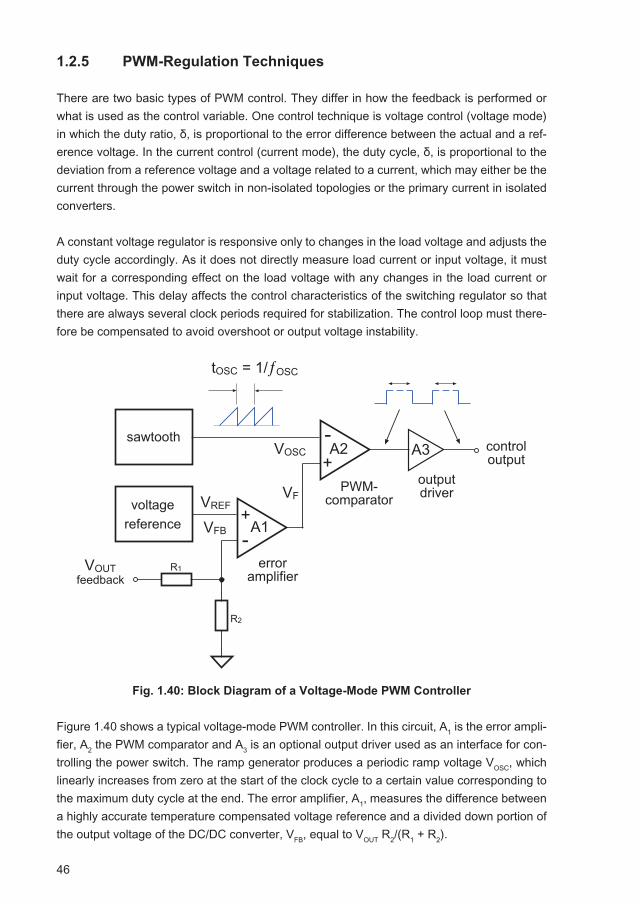
46
1.2.5 PWM-Regulation Techniques
There are two basic types of PWM control. They differ in how the feedback is performed or what is used as the control variable. One control technique is voltage control (voltage mode) in which the duty ratio, δ, is proportional to the error difference between the actual and a ref-erence voltage. In the current control (current mode), the duty cycle, δ, is proportional to the deviation from a reference voltage and a voltage related to a current, which may either be the current through the power switch in non-isolated topologies or the primary current in isolated converters.
A constant voltage regulator is responsive only to changes in the load voltage and adjusts the duty cycle accordingly. As it does not directly measure load current or input voltage, it must wait for a corresponding effect on the load voltage with any changes in the load current or input voltage. This delay affects the control characteristics of the switching regulator so that there are always several clock periods required for stabilization. The control loop must there-fore be compensated to avoid overshoot or output voltage instability.
Fig. 1.40: Block Diagram of a Voltage-Mode PWM Controller
Figure 1.40 shows a typical voltage-mode PWM controller. In this circuit, A1 is the error ampli-fier, A2 the PWM comparator and A3 is an optional output driver used as an interface for con-trolling the power switch. The ramp generator produces a periodic ramp voltage VOSC, which linearly increases from zero at the start of the clock cycle to a certain value corresponding to the maximum duty cycle at the end. The error amplifier, A1, measures the difference between a highly accurate temperature compensated voltage reference and a divided down portion of the output voltage of the DC/DC converter, VFB, equal to VOUT R2/(R1 + R2).
��������
����
������
��
��
�������� �� �
� �� ���������
����������
������������
���������������
��������
�
�
�
�
��
�� �
�������
���
����
����
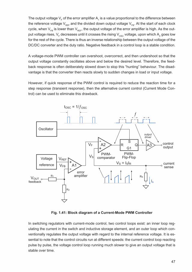
47
The output voltage VF of the error amplifier A1 is a value proportional to the difference between the reference voltage VREF and the divided down output voltage VFB. At the start of each clock cycle, when VFB is lower than VREF, the output voltage of the error amplifier is high. As the out-put voltage rises, VF decreases until it crosses the rising VOSC voltage, upon which A2 goes low for the rest of the cycle. There is thus an inverse relationship between the output voltage of the DC/DC converter and the duty ratio. Negative feedback in a control loop is a stable condition.
A voltage-mode PWM controller can overshoot, overcorrect, and then undershoot so that the output voltage constantly oscillates above and below the desired level. Therefore, the feed-back response is often deliberately slowed down to stop this “hunting” behaviour. The disad-vantage is that the converter then reacts slowly to sudden changes in load or input voltage.
However, if quick response of the PWM control is required to reduce the reaction time for a step response (transient response), then the alternative current control (Current Mode Con-trol) can be used to eliminate this drawback.
Fig. 1.41: Block diagram of a Current-Mode PWM Controller
In switching regulators with current-mode control, two control loops exist: an inner loop reg-ulating the current in the switch and inductive storage element, and an outer loop which con-ventionally regulates the output voltage with regard to the internal reference voltage. It is es-sential to note that the control circuits run at different speeds: the current control loop reacting pulse by pulse, the voltage control loop running much slower to give an output voltage that is stable over time.
��
������
��
��
�������������
���������� �
������������
����������� �
������
� � � ��
����������
�
�
��
�� ��
����������
���������
��
��
��
���
��� ������
� ���������
���
�
���� ��� ��

48
Let us first consider the block diagram shown in Fig. 1.41: the switching control element is an RS flip-flop which is set at the beginning of each clock period. The output is used to turn on the main power switch to the output current starts to ramp up. The reset input of the flip-flop is controlled by the PWM-comparator A2, whose inverting input has the output of the voltage control amplifier A1 and whose non-inverting input has a voltage Vs which is proportional to the switch current, measured across a shunt resistor Rs. The comparator will reset the flip-flop when the error amplifier voltage, Vf, exceeds Vs. Further improper toggling is excluded by the flip-flop for the rest of the period until the main oscillator is set again.
This arrangement has two main consequences:
First of all, the inductive storage element will always be charged up to the same energy level regardless of the input voltage, as the input voltage changes only affect the rate of rise and duration of the charging current. The converter is independent of the input voltage without the voltage control loop needing to intervene. This converter thus regulates for input voltage changes pulse by pulse.
Secondly, if the load changes, the outer control loop reacts because the Vout feedback volt-age no longer balances with the reference voltage. For example, if the load suddenly increas-es, the output voltage will fall, causing Vf to increase and extending the charging duration. The inner control loop initially has no regulating effect until the output voltage has risen back up the required regulated voltage and Vf drops back down to where Vs can take over control of the regulation again.
Current mode regulation is faster than voltage-mode and now the preferred mode for most designs. It has the twin advantages of starting to react to changes in load or input voltage within one oscillation period but still supplying a very tightly regulated output voltage during stable operating conditions.
One disadvantage of current-mode regulation is the efficiency loss due to the additional sense resistor. The resistor needs to be kept as small as possible to reduce this loss to a minimum, but needs to large enough to develop a sufficient voltage across it so that the PWM compara-tor can switch cleanly. A current-mode PWM comparator thus needs to be of a higher quality with lower input offset drift and better thermal stability than a voltage-mode PWM comparator.
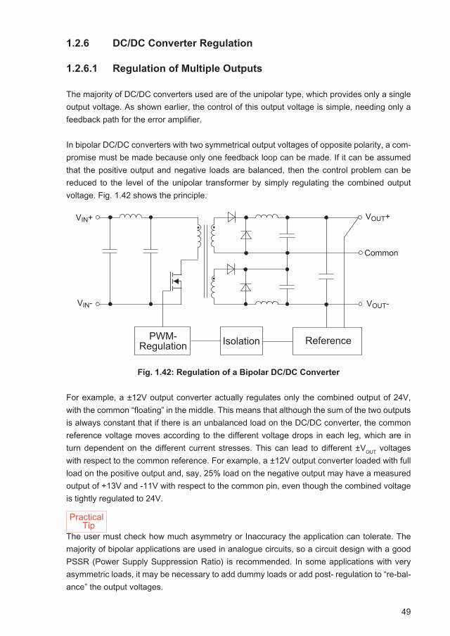
49
1.2.6 DC/DC Converter Regulation
1.2.6.1 Regulation of Multiple Outputs
The majority of DC/DC converters used are of the unipolar type, which provides only a single output voltage. As shown earlier, the control of this output voltage is simple, needing only a feedback path for the error amplifier.
In bipolar DC/DC converters with two symmetrical output voltages of opposite polarity, a com-promise must be made because only one feedback loop can be made. If it can be assumed that the positive output and negative loads are balanced, then the control problem can be reduced to the level of the unipolar transformer by simply regulating the combined output voltage. Fig. 1.42 shows the principle.
Fig. 1.42: Regulation of a Bipolar DC/DC Converter
For example, a ±12V output converter actually regulates only the combined output of 24V, with the common “floating” in the middle. This means that although the sum of the two outputs is always constant that if there is an unbalanced load on the DC/DC converter, the common reference voltage moves according to the different voltage drops in each leg, which are in turn dependent on the different current stresses. This can lead to different ±VOUT voltages with respect to the common reference. For example, a ±12V output converter loaded with full load on the positive output and, say, 25% load on the negative output may have a measured output of +13V and -11V with respect to the common pin, even though the combined voltage is tightly regulated to 24V.
The user must check how much asymmetry or Inaccuracy the application can tolerate. The majority of bipolar applications are used in analogue circuits, so a circuit design with a good PSSR (Power Supply Suppression Ratio) is recommended. In some applications with very asymmetric loads, it may be necessary to add dummy loads or add post- regulation to “re-bal-ance” the output voltages.
������
�������������� ��������� �� ������
��
��
����
����
Practical Tip
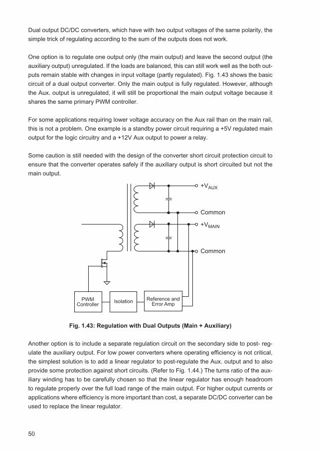
50
Dual output DC/DC converters, which have with two output voltages of the same polarity, the simple trick of regulating according to the sum of the outputs does not work.
One option is to regulate one output only (the main output) and leave the second output (the auxiliary output) unregulated. If the loads are balanced, this can still work well as the both out-puts remain stable with changes in input voltage (partly regulated). Fig. 1.43 shows the basic circuit of a dual output converter. Only the main output is fully regulated. However, although the Aux. output is unregulated, it will still be proportional the main output voltage because it shares the same primary PWM controller.
For some applications requiring lower voltage accuracy on the Aux rail than on the main rail, this is not a problem. One example is a standby power circuit requiring a +5V regulated main output for the logic circuitry and a +12V Aux output to power a relay.
Some caution is still needed with the design of the converter short circuit protection circuit to ensure that the converter operates safely if the auxiliary output is short circuited but not the main output.
Fig. 1.43: Regulation with Dual Outputs (Main + Auxiliary)
Another option is to include a separate regulation circuit on the secondary side to post- reg-ulate the auxiliary output. For low power converters where operating efficiency is not critical, the simplest solution is to add a linear regulator to post-regulate the Aux. output and to also provide some protection against short circuits. (Refer to Fig. 1.44.) The turns ratio of the aux-iliary winding has to be carefully chosen so that the linear regulator has enough headroom to regulate properly over the full load range of the main output. For higher output currents or applications where efficiency is more important than cost, a separate DC/DC converter can be used to replace the linear regulator.
�����
������
������
�������������
���� ���� �������� �����������
������
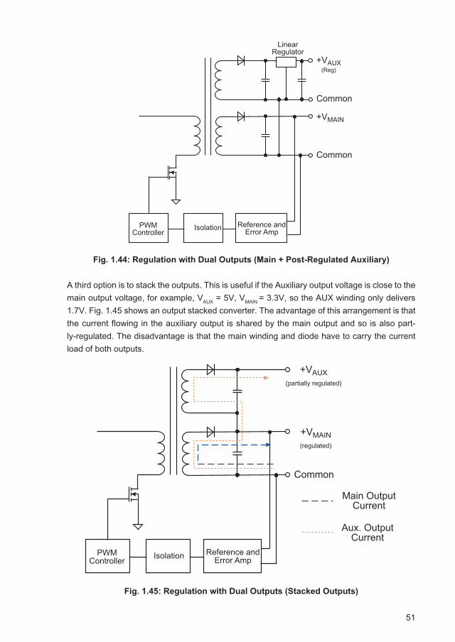
51
Fig. 1.44: Regulation with Dual Outputs (Main + Post-Regulated Auxiliary)
A third option is to stack the outputs. This is useful if the Auxiliary output voltage is close to the main output voltage, for example, VAUX = 5V, VMAIN = 3.3V, so the AUX winding only delivers 1.7V. Fig. 1.45 shows an output stacked converter. The advantage of this arrangement is that the current flowing in the auxiliary output is shared by the main output and so is also part-ly-regulated. The disadvantage is that the main winding and diode have to carry the current load of both outputs.
Fig. 1.45: Regulation with Dual Outputs (Stacked Outputs)
������
������
������
�������������
������ �� �������������������
� �������������
����������
�������������������������
���
������������
�������� �������������������
����������������
�����������������
����������������
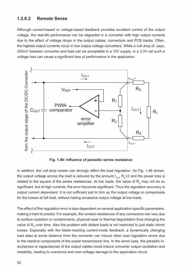
52
1.2.6.2 Remote Sense
Although current-based or voltage-based feedback provides excellent control of the output voltage, the real-life performance can be degraded in a converter with high output currents due to the effect of voltage drops in the output cables, connectors and PCB tracks. Often, the highest output currents occur in low output voltage converters. While a volt drop of, says, 200mV between converter and load can be acceptable in a 12V supply, in a 3.3V rail such a voltage loss can cause a significant loss of performance in the application.
Fig. 1.46: Influence of parasitic series resistance
In addition, the volt-drop losses can strongly affect the load regulation. As Fig. 1.46 shows, the output voltage across the load is reduced by the amount IOUT RS×2 and the power loss is related to the square of the series resistances. At low loads, the value of RS may not be so significant, but at high currents, the error becomes significant. Thus the regulation accuracy is output current dependent. It is not sufficient just to trim up the output voltage to compensate for the losses at full load, without risking excessive output voltage at low loads.
The effect of this regulation error is also dependent on several application-specific parameters, making it hard to predict. For example, the contact resistances of any connectors can vary due to surface oxidation or contaminants, physical wear or thermal degradation thus changing the value of RS over time. Also the problem with distant loads is not restricted to just static ohmic losses. Especially with the faster-reacting current-mode feedback, a dynamically changing load sited at some distance from the converter can induce other load regulation errors due to the reactive components of the power transmission line. In the worst case, the parasitic in-ductances or capacitances of the output cables could induce converter output oscillation and instability, leading to overshoot and over-voltage damage to the application circuit.
�
������
���������
��������������
�� �
�����
���
��
��
��
��
��
��
��
����
�����
����
������
����
�����
�����
���
�� �
����
��
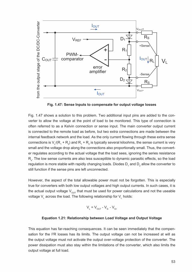
53
Fig. 1.47: Sense Inputs to compensate for output voltage losses
Fig. 1.47 shows a solution to this problem. Two additional input pins are added to the con-verter to allow the voltage at the point of load to be monitored. This type of connection is often referred to as a Kelvin connection or sense input. The main converter output current is connected to the remote load as before, but two extra connections are made between the internal feedback network and the load. As the only current flowing through these extra sense connections is VL/(R1 + R2) and R1 + R2 is typically several kiloohms, the sense current is very small and the voltage drop along the connections also proportionally small. Thus, the convert-er regulates according to the actual voltage that the load sees, ignoring the series resistance Rs. The low sense currents are also less susceptible to dynamic parasitic effects, so the load regulation is more stable with rapidly changing loads. Diodes D1 and D2 allow the converter to still function if the sense pins are left unconnected.
However, the aspect of the total allowable power must not be forgotten. This is especially true for converters with both low output voltages and high output currents. In such cases, it is the actual output voltage VOUT that must be used for power calculations and not the useable voltage VL across the load. The following relationship for VL holds:
VL = VOUT - VS- - VS+
Equation 1.21: Relationship between Load Voltage and Output Voltage
This equation has far-reaching consequences. It can be seen immediately that the compen-sation for the I2R losses has its limits. The output voltage can not be increased at will as the output voltage must not activate the output over-voltage protection of the converter. The power dissipation must also stay within the limitations of the converter, which also limits the output voltage at full load.
�
������
���������
��������������
�� �
�����
��
��
��
��
��
��
��
����
�����
����
������
����
�����
�����
���
�� �
����
��
������
������
��
���
��
��
54
As already discussed in this chapter, tremendous efforts are made by DC/DC converter man-ufacturers to raise the efficiency as high as possible, with the goal of attaining as close to 100% as possible. But the ability of the DC/DC converter to compensate for the I2R losses means that the system developer no longer has to pay attention to the output connection resistance. But here a new power loss is created in the system that dilutes the painstakingly created high efficiency. We can use Equation 1.22 to calculate this additional power loss caused by the output connection voltage drop:
PVD = (RS+ + RS-) I²OUT
Equation 1.22: Additional Power Loss due to Sense Feedback
We can use the RP60-4805S to illustrate the consequences of this equation. VS+ and VS- re-spectively represent the voltage difference between the output pins VOUT+ and VOUT- (meas-ured directly at the pins) and VL+ and VL- measured at the load terminals. This converter provides up to 12A at 5V output voltage (60W). If the load is connected via copper PCB tracks with a length of 10cm, a width of 10mm and a generous copper thickness of 70 microns, the bulk resistance of each track would be 2.5mΩ, give a total output connection resistance of 5mΩ. The power loss PVD would then be:
PVD = 0.005 × 12 × 12 = 0.72W
This additional power loss has an effect on the overall efficiency. The RP60 has a conversion efficiency of 90%, meaning 6W is dissipated internally at full load. The additional PVD loss of 0.72W thus represents an additional increase in the overall system losses of 8.3%.
A way out of this dilemma is the point of load (POL) concept. POL is a strategy to minimize the I2R losses. In this case, the DC/DC converter is positioned as close as possible to the load in order to keep the leads short and the losses small. Several converters are used, one per load, rather than one centralised power supply powering all of the loads.
1.2.7 Limitations on the Input Voltage Range
The input voltage range of a DC/DC converter is determined by the circuit topology as well as the components used. The input voltage and the duty cycle of a converter are inversely proportional to each other, so an increase in input voltage causes a reduction in the duty cy-cle. The minimum duty cycle is in turn dependent on the maximum peak current of the power switch and its maximum reverse voltage rating. If the duty cycle is small, the peak current is high compared with the average input current and in most topologies the highest switching voltage occurs when the current is then quickly interrupted. Theoretically, a DC/DC converter can work down to duty cycle of 0%, but in practice, a value of 5% - 10% is the practical mini-mum limit due to slew rate limitations, feedback compensation stability and the need to avoid any negative parasitic effects. This limits the maximum input voltage that the converter can accept.
55
There is also such a restriction at the upper end of the duty cycle range. The maximum value of the duty ratio is limited by the maximum power dissipation of the switch and the saturation characteristics of the transformer, or other inductances, core material. For large values of the duty cycle, the average current flow is at its maximum value and the power dissipation in the switch is high. In order not to run into saturation, the power inductors also need some time to reset the magnetic field in the core and need a minimum off time to do so. Theoretically, all DC/DC converters could work up to a duty cycle of 100%, but in practice a limit of 85% - 90% is sensible, which limits the minimum input voltage the converter can accept.
The range limitation of the duty cycle thus limits the range of input voltage. DC/DC converter input range is typically described by the ratio of maximum to minimum voltage, so isolated forward converters can typically work with an input voltage range of 2:1 or 4:1.
The nominal input voltage is standardised on the lead acid battery voltages of 12V, 24V and 48V that were used by the telecoms industry, the first major application area for DC/DC con-verters.
2:1 input range
Nominal Voltage Input Voltage Range
12V 9 – 18VDC24V 18 – 36VDC48V 36 – 72VDC
4:1 input range
Nominal Voltage Input Voltage Range
24V 9 – 36VDC48V 18 – 72VDC110V 40 – 160VDC
Of course, the choice of the nominal voltage is dependent on the transformer ratio and/or component choice, but the above ranges have now become established by habit. Some mili-tary-grade converters use the more logical definition of 28V nominal input voltage to describe a 18 - 75V converter designed to be used with military lead acid batteries that have two extra cells to deliver 28V instead of 24V.
Unregulated converters have a typical input voltage range of +/-10% nominal. The datasheet specifications are tested and guaranteed within this range. In practice, the DC/DC convert-er will function outside of this narrow +/-10% band, but as the performance has not been checked with wider undervoltage or overvoltage conditions, the actual performance must be tested in the end-user's application.
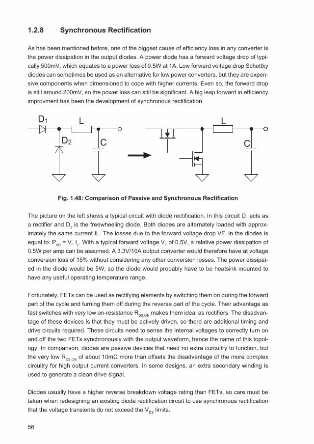
56
1.2.8 Synchronous Rectification
As has been mentioned before, one of the biggest cause of efficiency loss in any converter is the power dissipation in the output diodes. A power diode has a forward voltage drop of typi-cally 500mV, which equates to a power loss of 0.5W at 1A. Low forward voltage drop Schottky diodes can sometimes be used as an alternative for low power converters, but they are expen-sive components when dimensioned to cope with higher currents. Even so, the forward drop is still around 200mV, so the power loss can still be significant. A big leap forward in efficiency improvment has been the development of synchronous rectification.
Fig. 1.48: Comparison of Passive and Synchronous Rectification
The picture on the left shows a typical circuit with diode rectification. In this circuit D1 acts as a rectifier and D2 is the freewheeling diode. Both diodes are alternately loaded with approx-imately the same current IL. The losses due to the forward voltage drop VF, in the diodes is equal to: PVD = VF IL. With a typical forward voltage VF of 0.5V, a relative power dissipation of 0.5W per amp can be assumed. A 3.3V/10A output converter would therefore have at voltage conversion loss of 15% without considering any other conversion losses. The power dissipat-ed in the diode would be 5W, so the diode would probably have to be heatsink mounted to have any useful operating temperature range.
Fortunately, FETs can be used as rectifying elements by switching them on during the forward part of the cycle and turning them off during the reverse part of the cycle. Their advantage as fast switches with very low on-resistance RDS,ON makes them ideal as rectifiers. The disadvan-tage of these devices is that they must be actively driven, so there are additional timing and drive circuits required. These circuits need to sense the internal voltages to correctly turn on and off the two FETs synchronously with the output waveform, hence the name of this topol-ogy. In comparison, diodes are passive devices that need no extra curcuitry to function, but the very low RDS,ON of about 10mΩ more than offsets the disadvantage of the more complex circuitry for high output current converters. In some designs, an extra secondary winding is used to generate a clean drive signal.
Diodes usually have a higher reverse breakdown voltage rating than FETs, so care must be taken when redesigning an existing diode rectification circuit to use synchronous rectification that the voltage transients do not exceed the VDS limits.
��
�� � �
��
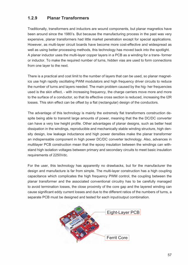
57
1.2.9 Planar Transformers
Traditionally, transformers and inductors are wound components, but planar magnetics have been around since the 1980’s. But because the manufacturing process in the past was very expensive, planar transformers had little market penetration except for special applications. However, as multi-layer circuit boards have become more cost-effective and widespread as well as using better processing methods, this technology has moved back into the spotlight.A planar inductor uses the multi-layer copper layers in a PCB as a winding for a trans- former or inductor. To make the required number of turns, hidden vias are used to form connections from one layer to the next.
There is a practical and cost limit to the number of layers that can be used, so planar magnet-ics use high rapidly oscillating PWM modulators and high frequency driver circuits to reduce the number of turns and layers needed. The main problem caused by the hig- her frequencies used is the skin effect, - with increasing frequency, the charge carriers move more and more to the surface of a conductor, so that its effective cross section is reduced, increasing the I2R losses. This skin effect can be offset by a flat (rectangular) design of the conductors.
The advantage of this technology is mainly the extremely flat transformers construction de-spite being able to transmit large amounts of power, meaning that the the DC/DC converter can have a very low height profile. Other advantages of planar designs, such as better heat dissipation in the windings, reproducible and mechanically stable winding structure, high den-sity design, low leakage inductance and high power densities make the planar transformer an indispensable component in high power DC/DC converter technology. Also, advances in multilayer PCB construction mean that the epoxy insulation between the windings can with-stand high isolation voltages between primary and secondary circuits to meet basic insulation requirements of 2250Vdc.
For the user, this technology has apparently no drawbacks, but for the manufacturer the design and manufacture is far from simple. The multi-layer construction has a high coupling capacitance which complicates the high frequency PWM control, the coupling between the planar transformer and the associated conventional circuitry has to be carefully managed to avoid termination losses, the close proximity of the core gap and the layered winding can cause significant eddy current losses and due to the different ratios of the numbers of turns, a separate PCB must be designed and tested for each input/output combination.
Eight-Layer PCB
Ferrit Core

58
Fig. 1.49: Construction of a Planar Transformer-based Converter
The windings in a planar transformer are the PCB tracks on a multilayer board. The primary and secondary windings are typically interleaved to reduce the leakage inductance. One diffi-culty of using the PCB tracks is the electrical connection to the end of the winding nearest the core. One common solution is to use a buried via as shown in Fig. 1.50 below. The diagram shows a 6-turn winding formed by a 3-turn top trace and a 3-turn bottom trace linked by a via. The two ends of the winding are thus conveniently placed outside the core.
3-turn Top Trace 3-turn Bottom Trace 6-turn Winding
Fig. 1.50: Interleaving planar multilayer tracks
�����������
���������������

59
1.2.10 Package Styles of DC/DC Converters
The following section is a general overview of some of the industry standard case styles of DC/DC converters. For information about pin allocation, pin diameter and tolerances, refer to the manufacturer’s data sheets.
One descriptor commonly used for the case style is the way the connection pins are arranged, so a SIL (Single In Line) or SIP (Single In-line Pins) case has a single row of pins and a DIL (Dual In Line) or DIP (Dual In-line Pins) case has two rows of contacts. The SIP case is com-monly used in very low power (<2W) and non-isolated DC/DC converters, while DIP cases are more often used in low power (<10W) converters. The main reason for the difference in case style is the weight of the converter. A very low power converter weighs only around 3g, so pin breakages due to vibration are rare. Low power converters are a little heavier, around 30g, so need two rows of pins for mechanical stability.
Higher power converters (>10W) can have significant output currents with low output voltages and typically have metal cases to allow additional heatsinking, so they need thicker connec-tion pins to carry both the higher current and extra weight. A descriptor commonly used for higher power converters is the case dimensions in inches, for example, 1” × 1”, 2” × 1”, 1.6” × 2” and 2” × 2” are common sizes.
Common in USA and in the telecommunication branch is a case size based on the “brick” format. A brick corresponds to the dimensions 2.4" × 6" × 0.5", corresponding to 61mm × 116.5mm × 12mm, and is used, inter alia, as a reference size for DC/DC converters. The different models in brick format are given in binary fractions of bricks such as half- brick, quar-ter-brick, eighth-brick or sixteenth-brick.
There have been various attempts to standardise the converter sizes and pin-outs to allow interchangeability of the converters between manufacturers, notably the DOSA (Distribut-ed-power Open Standards Alliance) and the rival POLA (Point Of Load Alliance), both con-centrating on digital point of load and ratiometric converters. However, most manufacturers simply offer a range of standard pinout options for any one converter series to cover their competitor’s products and permit drop-in second source replacement.
However, as there is no agreed standard to how the pins are numbered (some start top left hand corner as seen from above, some choose the PCB’s point of view, some include optional pins in the numbering sequence and some don’t), it often takes careful comparison between data sheets to ensure pin-compatibilty.
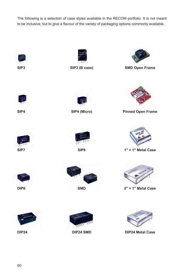
60
The following is a selection of case styles available in the RECOM portfolio. It is not meant to be inclusive, but to give a flavour of the variety of packaging options commonly available.
SIP3 SIP3 (B case) SMD Open Frame
SIP4 SIP4 (Micro) Pinned Open Frame
SIP7 SIP8 1" × 1" Metal Case
DIP6 SMD 2" × 1" Metal Case
DIP24 DIP24 SMD DIP24 Metal Case
61
2. Feedback Loops
2.1 Introduction
Some of the most important design criteria in dc/dc power conversion design are the calcula-tions and methodologies involved in the feedback loop compensation. If the feedback loop pa-rameters are not properly calculated, the converter can exhibit instability or regulation failure.
The function of a feedback loop in a DC/DC converter is to maintain the output at a fixed value which is dependent on a reference value only – i.e. it is independent of load, input voltage or environmental variations. This sounds simple and is relatively simple for static or slowly changing conditions, but to handle dynamic or step changes the feedback loop design becomes very complex. One of the most important compromises that has to be made is the balance between a smooth output during static operating conditions ( low jitter, small dead-band and good accuracy) and the response to dynamic operating conditions ( fast reaction time, quick settling time and low overshoot). In addition, the control loop must be stable under all operating conditions, including low load or even no load conditions. The feedback loop design is therefore one of the main factors defining the overall performance of the converter.
2.2 Open Loop Design
Not all DC/DC converters use feedback. The basic Royer relaxation oscillator used in the example shown in Figure 1.30 has no feedback network. The self-oscillating circuit runs at a frequency which is determined by the physical characteristics of the transformer and the input voltage only, according to the following relationship:
Equation 2.1: Transformer Equation
Where NP is the number of primary turns, B is the saturation flux and AE is the cross sectional area of the transformer. The formula can be rewritten to give the free-runningfrequency, ƒ:
Equation 2.2: Rearranged Transformer Equation
The factor “4” differs from the standard transformer equation which uses “4.44” because the Royer oscillator generates a square wave and not a sinusoidal signal. The output voltage is dependent upon the turns ratio of the number of turns on the primary winding, NP, to the num-ber of turns on the secondary winding, NS:
Equation 2.3: Transformer Ratio
ƒ = VIN
4 NP B AE
= VIN
VOUT
NP
NS
VIN = 4 NP B AE ƒ
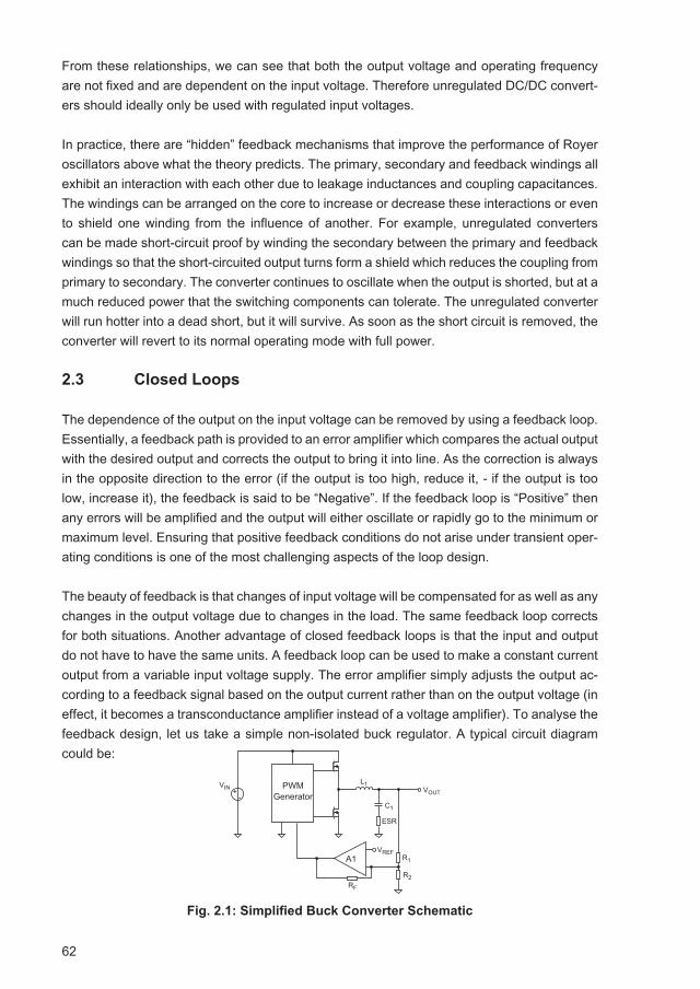
62
From these relationships, we can see that both the output voltage and operating frequency are not fixed and are dependent on the input voltage. Therefore unregulated DC/DC convert-ers should ideally only be used with regulated input voltages.
In practice, there are “hidden” feedback mechanisms that improve the performance of Royer oscillators above what the theory predicts. The primary, secondary and feedback windings all exhibit an interaction with each other due to leakage inductances and coupling capacitances. The windings can be arranged on the core to increase or decrease these interactions or even to shield one winding from the influence of another. For example, unregulated converters can be made short-circuit proof by winding the secondary between the primary and feedback windings so that the short-circuited output turns form a shield which reduces the coupling from primary to secondary. The converter continues to oscillate when the output is shorted, but at a much reduced power that the switching components can tolerate. The unregulated converter will run hotter into a dead short, but it will survive. As soon as the short circuit is removed, the converter will revert to its normal operating mode with full power.
2.3 Closed Loops
The dependence of the output on the input voltage can be removed by using a feedback loop. Essentially, a feedback path is provided to an error amplifier which compares the actual output with the desired output and corrects the output to bring it into line. As the correction is always in the opposite direction to the error (if the output is too high, reduce it, - if the output is too low, increase it), the feedback is said to be “Negative”. If the feedback loop is “Positive” then any errors will be amplified and the output will either oscillate or rapidly go to the minimum or maximum level. Ensuring that positive feedback conditions do not arise under transient oper-ating conditions is one of the most challenging aspects of the loop design.
The beauty of feedback is that changes of input voltage will be compensated for as well as any changes in the output voltage due to changes in the load. The same feedback loop corrects for both situations. Another advantage of closed feedback loops is that the input and output do not have to have the same units. A feedback loop can be used to make a constant current output from a variable input voltage supply. The error amplifier simply adjusts the output ac-cording to a feedback signal based on the output current rather than on the output voltage (in effect, it becomes a transconductance amplifier instead of a voltage amplifier). To analyse the feedback design, let us take a simple non-isolated buck regulator. A typical circuit diagram could be:
Fig. 2.1: Simplified Buck Converter Schematic
��
������
����
��
��
���
��
����
��� �����
���
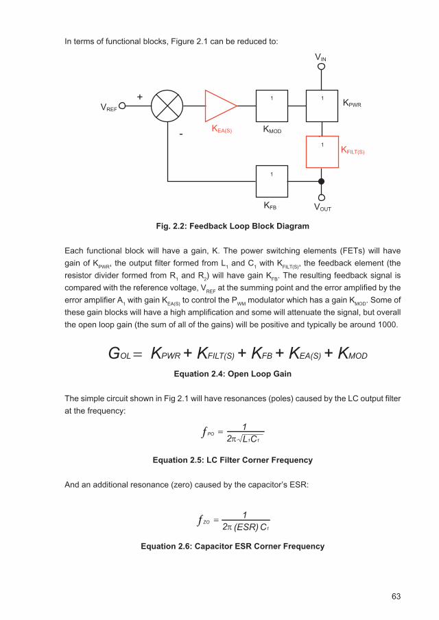
63
In terms of functional blocks, Figure 2.1 can be reduced to:
Fig. 2.2: Feedback Loop Block Diagram
Each functional block will have a gain, K. The power switching elements (FETs) will have gain of KPWR, the output filter formed from L1 and C1 with KFILT(S), the feedback element (the resistor divider formed from R1 and R2) will have gain KFB. The resulting feedback signal is compared with the reference voltage, VREF at the summing point and the error amplified by the error amplifier A1 with gain KEA(S) to control the PWM modulator which has a gain KMOD. Some of these gain blocks will have a high amplification and some will attenuate the signal, but overall the open loop gain (the sum of all of the gains) will be positive and typically be around 1000.
Equation 2.4: Open Loop Gain
The simple circuit shown in Fig 2.1 will have resonances (poles) caused by the LC output filter at the frequency:
Equation 2.5: LC Filter Corner Frequency
And an additional resonance (zero) caused by the capacitor’s ESR:
Equation 2.6: Capacitor ESR Corner Frequency
ƒPO = 2π L1C1
1
ƒZO = 2π (ESR) C1
1
�
������ ����
����
��������
��� ���
���
�
�
KPWR + KFILT(S) + KFB + KEA(S) + KMOD = GOL
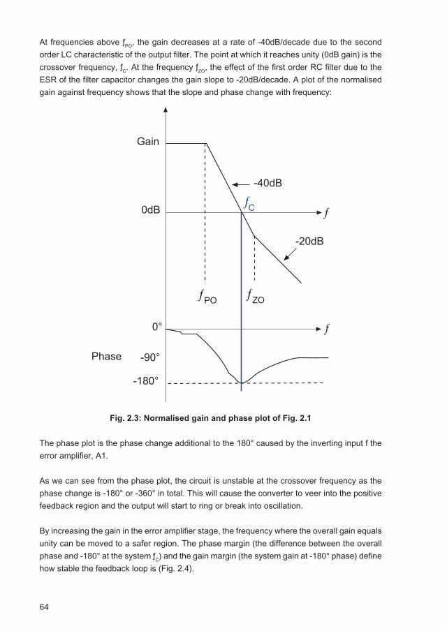
64
At frequencies above ƒPO, the gain decreases at a rate of -40dB/decade due to the second order LC characteristic of the output filter. The point at which it reaches unity (0dB gain) is the crossover frequency, ƒC. At the frequency ƒZO, the effect of the first order RC filter due to the ESR of the filter capacitor changes the gain slope to -20dB/decade. A plot of the normalised gain against frequency shows that the slope and phase change with frequency:
Fig. 2.3: Normalised gain and phase plot of Fig. 2.1
The phase plot is the phase change additional to the 180° caused by the inverting input f the error amplifier, A1.
As we can see from the phase plot, the circuit is unstable at the crossover frequency as the phase change is -180° or -360° in total. This will cause the converter to veer into the positive feedback region and the output will start to ring or break into oscillation.
By increasing the gain in the error amplifier stage, the frequency where the overall gain equals unity can be moved to a safer region. The phase margin (the difference between the overall phase and -180° at the system ƒC) and the gain margin (the system gain at -180° phase) define how stable the feedback loop is (Fig. 2.4).
�����
�����
��� ���
�
�
����
�����
��
����
�����
� ���
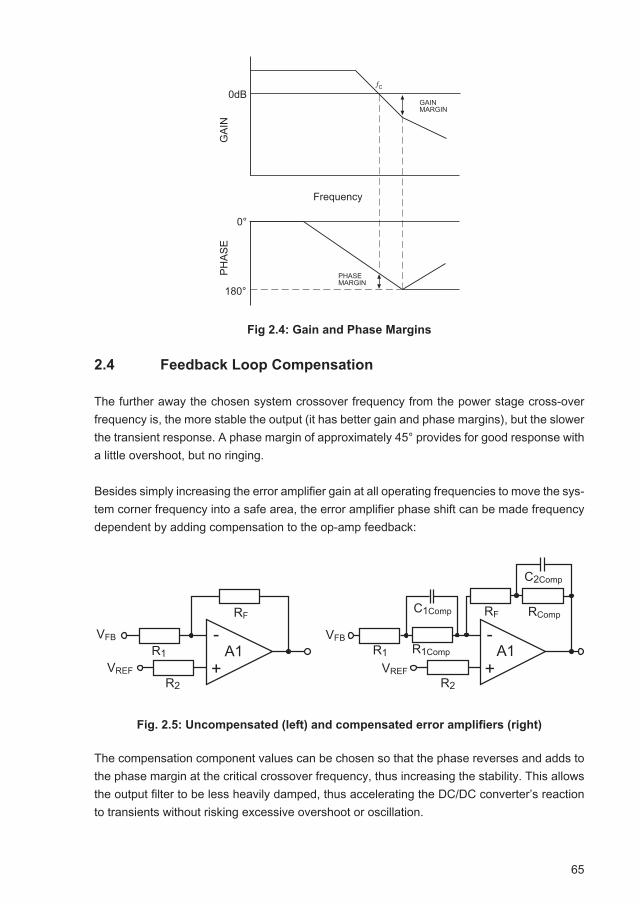
65
Fig 2.4: Gain and Phase Margins
2.4 Feedback Loop Compensation
The further away the chosen system crossover frequency from the power stage cross-over frequency is, the more stable the output (it has better gain and phase margins), but the slower the transient response. A phase margin of approximately 45° provides for good response with a little overshoot, but no ringing.
Besides simply increasing the error amplifier gain at all operating frequencies to move the sys-tem corner frequency into a safe area, the error amplifier phase shift can be made frequency dependent by adding compensation to the op-amp feedback:
Fig. 2.5: Uncompensated (left) and compensated error amplifiers (right)
The compensation component values can be chosen so that the phase reverses and adds to the phase margin at the critical crossover frequency, thus increasing the stability. This allows the output filter to be less heavily damped, thus accelerating the DC/DC converter’s reaction to transients without risking excessive overshoot or oscillation.
�����
����������
����
�����������
���������
��
�
��
�
���
����
���
��
�
�
����
�������������
������
������
���
��
��
��
����
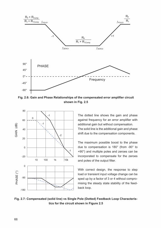
66
Fig. 2.6: Gain and Phase Relationships of the compensated error amplifier circuit
shown in Fig. 2.5
����������
����������� ������
��
�����������
��
��
�� ��
������
������������
��
��
�
���
���
���
���������
The dotted line shows the gain and phase against frequency for an error amplifier with additional gain but without compensation.The solid line is the additional gain and phase shift due to the compensation components.
The maximum possible boost to the phase due to compensation is 180° (from -90° to +90°) and multiple poles and zeroes can be incorporated to compensate for the zeroes and poles of the output filter.
With correct design, the response to step load or transient input voltage change can be sped up by a factor of 3 or 4 without compro-mising the steady state stability of the feed-back loop.
Fig. 2.7: Compensated (solid line) vs Single Pole (Dotted) Feedback Loop Characteris-
tics for the circuit shown in Figure 2.5
����
�����
�
��
���������
��
�
��
�
� �� � ��
��
��
�
�
�
��
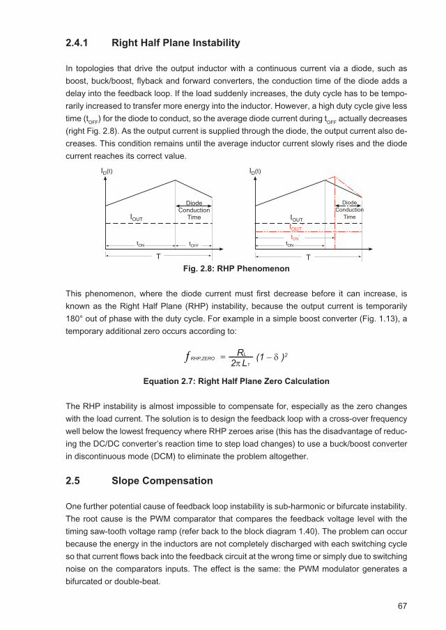
67
2.4.1 Right Half Plane Instability
In topologies that drive the output inductor with a continuous current via a diode, such as boost, buck/boost, flyback and forward converters, the conduction time of the diode adds a delay into the feedback loop. If the load suddenly increases, the duty cycle has to be tempo-rarily increased to transfer more energy into the inductor. However, a high duty cycle give less time (tOFF) for the diode to conduct, so the average diode current during tOFF actually decreases (right Fig. 2.8). As the output current is supplied through the diode, the output current also de-creases. This condition remains until the average inductor current slowly rises and the diode current reaches its correct value.
Fig. 2.8: RHP Phenomenon
This phenomenon, where the diode current must first decrease before it can increase, is known as the Right Half Plane (RHP) instability, because the output current is temporarily 180° out of phase with the duty cycle. For example in a simple boost converter (Fig. 1.13), a temporary additional zero occurs according to:
Equation 2.7: Right Half Plane Zero Calculation
The RHP instability is almost impossible to compensate for, especially as the zero changes with the load current. The solution is to design the feedback loop with a cross-over frequency well below the lowest frequency where RHP zeroes arise (this has the disadvantage of reduc-ing the DC/DC converter’s reaction time to step load changes) to use a buck/boost converter in discontinuous mode (DCM) to eliminate the problem altogether.
2.5 Slope Compensation
One further potential cause of feedback loop instability is sub-harmonic or bifurcate instability. The root cause is the PWM comparator that compares the feedback voltage level with the timing saw-tooth voltage ramp (refer back to the block diagram 1.40). The problem can occur because the energy in the inductors are not completely discharged with each switching cycle so that current flows back into the feedback circuit at the wrong time or simply due to switching noise on the comparators inputs. The effect is the same: the PWM modulator generates a bifurcated or double-beat.
���� ����
�����
���������������
����
���������������
����
�����
�
�� ����
�����
�
��
�� �
ƒRHP,ZERO = 2π
RL
L1(1 − δ )2
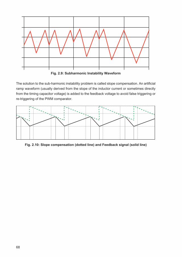
68
Fig. 2.9: Subharmonic Instability Waveform
The solution to the sub-harmonic instability problem is called slope compensation. An artificial ramp waveform (usually derived from the slope of the inductor current or sometimes directly from the timing capacitor voltage) is added to the feedback voltage to avoid false triggering or re-triggering of the PWM comparator.
Fig. 2.10: Slope compensation (dotted line) and Feedback signal (solid line)
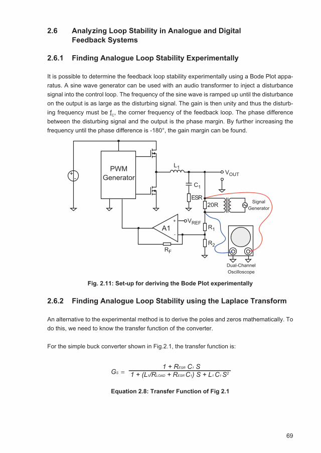
69
2.6 Analyzing Loop Stability in Analogue and Digital Feedback Systems
2.6.1 Finding Analogue Loop Stability Experimentally
It is possible to determine the feedback loop stability experimentally using a Bode Plot appa-ratus. A sine wave generator can be used with an audio transformer to inject a disturbance signal into the control loop. The frequency of the sine wave is ramped up until the disturbance on the output is as large as the disturbing signal. The gain is then unity and thus the disturb-ing frequency must be ƒC, the corner frequency of the feedback loop. The phase difference between the disturbing signal and the output is the phase margin. By further increasing the frequency until the phase difference is -180°, the gain margin can be found.
Fig. 2.11: Set-up for deriving the Bode Plot experimentally
2.6.2 Finding Analogue Loop Stability using the Laplace Transform
An alternative to the experimental method is to derive the poles and zeros mathematically. To do this, we need to know the transfer function of the converter.
For the simple buck converter shown in Fig.2.1, the transfer function is:
Equation 2.8: Transfer Function of Fig 2.1
��
������
����
��
��
���
��
����
��� �����
��������
�����
�
�
����������������������
1 + (L1/RLOAD + RESR C1) S + L1 C1 S21 + RESR C1 S
GS =
70
The letter ‘s’ indicates that the variable has a frequency dependence. The transfer function can be solved using the Laplace Transform (LT), but to understand the LT, first we need to consider the Fourier Transform.
The Fourier Transform (FT) is a special form of the LT. Fourier determined that any periodic signal is the sum of sinusoidal signals of various frequency, phase and amplitude (the Fourier Series). The transform shifts from the time domain to the frequency domain (and vice versa). The result of a Fourier Transform on a periodic signal is the equivalent Fourier Series or spec-trum. Figure 2.12 shows graphically the first six harmonics of a square wave:
Fig. 2.12: Graphical Representation of the Fourier Series of a Square Wave
The Fourier transform is an intergral function from minus infinity to plus infinity, which can be written as:
Equation 2.9: Fourier Transform
Mapped onto the S-domain, the variable of the FT is s = jω. The results are imaginary varia-bles only.
The Laplace Transform is a superset of the FT. The variable of LT is in the complex plane. The integration starts at zero instead of -∞. This means that it can also be used to analyse step or semi-infinite signals, such as a pulse or exponential decaying series. The Laplace transform can be written as:
Equation 2.10: Laplace Transform
Mapped onto the S-domain, the variable of the LT is s = σ + jω.Using the LT, it is possible to simulate the feedback loop mathematically and generate a pole-zero plot in the s-plane. The vertical axis is imaginary, the horizontal axis real. The higher up or down the imaginary axis one travels, the faster the oscillations occur. The further in the negative real axis one travels, the faster the decay and the further in the real positive axis, the faster the growth.
�������������
���������
F(ω ) = ∫∞
−∞ƒ(t) e-jωt dt
F(S) = ∫∞
0ƒ(t) e-st dt
71
Fig. 2.13: Pole-Zero Plot in the S-Domain showing typical Waveforms
Zeroes always lie on the real axis. Complex conjugate pole pairs in the left-half of the s-plane combine to generate a response that is a decaying sinusoid of the form Ae-σtsin (ωt + Ø), where A and Ø are initial conditions, σ is the rate of decay and ω is the frequency in radians/seconds.
A pole pair that lies on the imaginary axis, ±jω (i.e, with no real component) generates an oscillation with constant amplitude.
The distance of a Pole from the origin, 0, indicates how damped the response is: the closer to the origin, the slower the rate of decay. If a Pole lies on the origin, it means that the system is operating at DC.
If a Pole lies on the right hand plane, the system is unstable (this is the origin of the term RHP instability described in section 2.4.1)
2.6.3 Finding Digital Loop Stability using the Bilinear Transform
If a digital signal processor is used to generate the feedback loop compensation, the stability of the digital loop can be derived from the Laplace Transform using a further transform to correct for the sampling rate.
As the input signal to a digital system is no longer time-continuous, the s-plane values need to be transformed into the z-plane discrete-time values using a bilinear transform (Tustin’s Method).
�
����
����
������������� ���������������
72
The result of this mapping is that the stable region of z-plane becomes a circle with radius = 1 (unit circle).
Fig. 2.14: Z-plane Unit Circle
The far right edge of the circle (ω = 0) represents DC. The far left edge of the circle represents the aliasing frequency. Any poles that lie outside the circle will be unstable. The poles of the feedback loop can now be plotted in the z-plane, the positions of poles represent responses normalised to the sample rate rather than to continuous time as in the s-plane.
Digital compensation firstly assumes the DSP’s sampling frequency is much greater than the system crossover frequency, so that any simulations are accurate. Then there are two com-mon approaches to find the compensation values: re-design and direct design. With digital re-design, a linear model of a switching converter is established and the feedback loop com-pensation is simulated conventionally in the s-domain. The results of the analogue compen-sation are mapped into z-domain to complete the digital compensation design. For the direct design approach, a discrete model of switching power converter is wholly simulated and the compensation design is calculated directly in the z-domain. This requires accurate models of the analogue parts using such programs as SpiceTM or MatlabTM.
The result of either method is the same: a matrix of values stored in a look-up table. The DSP or μC will then take the digitised input signal, enter it into the computational matrix and output the resultant value either as an analogue control signal or, more often, as a direct PWM drive output. In the latter case, the comparator and PWM circuits will also be synthesised digitally. This eliminates the analogue control loop errors arising from slope compensation and RHP instability. If a different feedback compensation response is required to handle a different mode of operation, the digital controller can smoothly switch between look-up tables without resetting any of the output values, an ability that analogue controllers cannot match. Thus fewer compromises need be made in selecting the compensation characteristics.
It is this lack of compromise and ability to switch rapidly between fast transient response or a stable output that makes digital feedback loop so attractive. As the cost of micro- controllers continues to fall, more and more DC/DC converters will migrate towards fully digital or hybrid feedback loop controllers.
�������������������������
����������������������
���
��������� ������������
��
���
���
73
2.6.4 Digital Feedback Loop
Fig. 2.15: Microcontroller-based DC/DC Converter
The circuit above (Fig. 2.15) shows a simplified microcontroller-based DC/DC converter. All timing is under digital control - both the full-bridge power stage and the synchronous rectifi-cation on the output.
The microcontroller has integrated op-amp elements on-board. This means that the sense inputs can be connected directly to the microcontroller. As the microcontroller has information regarding input voltage, output voltage and output current, there is no need for external cir-cuits to monitor short circuits or overload conditions. The input voltage monitoring allows both a controlled start-up and a programmable under-voltage lockout with adaptive hysteresis. The fourth op-amp input is used to monitor overtemperature conditions, either within the DC/DC converter or at the remote load.The consequences of an over-temperature condition are programmable according to the required performance in the application, for example, shut-down and latch-off, shut-down and auto-restart after cooling down or power-limiting to reduce heat dissipation.
The external data connection allows operating conditions to be updated on-the-fly or various pre-programmed performance options to be selected. In addition, the bidirectional communi-cation bus allows fault reporting and status updates.
���
��
��
��
�
����
����
���� �
�
�
�
�
�
�
�
��
��
��
��
�������� ���
����� ���
������� ��
���
�� ��
����
�� ������
�� ��
����������
������
�
�
���������������
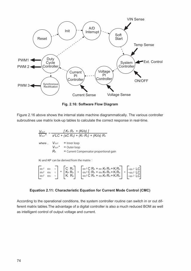
74
Fig. 2.16: Software Flow Diagram
Figure 2.16 above shows the internal state machine diagrammatically. The various controller subroutines use matrix look-up tables to calculate the correct response in real-time.
Equation 2.11: Characteristic Equation for Current Mode Control (CMC)
According to the operational conditions, the system controller routine can switch in or out dif-ferent matrix tables.The advantage of a digital controller is also a much reduced BOM as well as intelligent control of output voltage and current.
�����
�������
�������������������
��������
������
����������
����������������
����������
������
��������
����������
�������������
���������
����������
���
����������������������������
�����������
����� ���������
VOUT
VOUT* =
s2LC + (sC RA) + (KP RA) + (Ki/s) RA
[ KP RA + (Ki/s) ]
VOUT
VOUT*RA
= Inner loop= Outer loop= Current Compensator proportional gain
where,
ω12
ω22
ω32
ω1
ω2
ω3
1
1
1
C RA
KP RA
Ki RA
ω12
ω22
ω32
C RA + ω1 KP RA + Ki RA
C RA + ω2 KP RA + Ki RA
C RA + ω3 KP RA + Ki RA
x =
Ki and KP can be derived from the matrix:
−ω13
−ω23
−ω13
LCLCLC
=
75
3. Understanding Datasheet Parameters
Every respectable manufacturer supplies a technical datasheet with their product that details at the very least the basic operating parameters, overall dimensions and pin connections, but to compare one DC/DC converter with another just relying on the datasheet information often requires interpretation rather than just a simple comparison of numbers.
The problem is that many of the specifications are inter-related so some parameter fixing is needed, i.e, that specific values such as the ambient temperature or input voltage are kept constant during the measurement of the performance specification of interest. For example, a load regulation figure will be made with nominal input voltage, 25°C ambient temperature and be valid over a specified load range. But there are no agreed standards between manufactur-ers over the parameter fixing, so some will specify a regulation value for the whole 0% - 100% load range, others for 10% - 100% and still others for 20% - 80% load. This means a load regulation specification of ±5% for a load range of 10% - 100% is not necessarily worse than a rival converter with a load regulation specification of ±3% for a load range of 20% - 100%. Similarly a converter with a reliability specification of 1 million hours according to MIL-HDBK-217E is not necessarily more reliable than a converter with a reliability specification of “only” 800 thousand hours according to MIL-HDBK-217F or another converter with “only” 400 thou-sand hours according to Bellcore/Telcordia.
An unscrupulous manufacturer can use this lack of standardisation to present their product in a better light. A classic example is the output ripple and noise specification, usually given in millivolts peak-to-peak (mVp-p). A converter with 50mVp-p is better than one with 100mVp-p, right? Well not if the fine print at the back of the datasheet states that the first converter meas-urement was made with a 47μF electrolytic in parallel with a 0.1μF MLCC across the output pins to additionally filter the output and the second converter specification was made without any external components. Additional filter components may be in some cases necessary in order to get a reliable, repeatable measurement, but the customer should be aware that the way the measurement is made affects the measured value and a comparison between two converter specifications can only be done if both are known. In many cases, it is necessary for the customer to measure the critical specifications of concern themselves using the actual or anticipated operating conditions of the application. For example, datasheets do not usually give efficiency vs operating temperature graphs (although RECOM can supply such detailed information on request).
3.1 Measurement Methods – DC Characteristics
As already mentioned, the electrical behavior of a DC / DC converter is determined by many different parameters that are specified in the data sheet. To quickly and efficiently character-ise a converter and check the validity of the datasheet, it is often worthwhile to use a meas-urement matrix where the various combinations of load and input voltage can be compared.
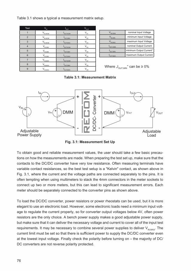
76
Table 3.1 shows a typical a measurement matrix setup.
Where „IOUT,MIN“ can be ≥ 0%
Table 3.1: Measurement Matrix
Fig. 3.1: Measurement Set Up
To obtain good and reliable measurement values, the user should take a few basic precau-tions on how the measurements are made. When preparing the test set up, make sure that the contacts to the DC/DC converter have very low resistance. Often measuring terminals have variable contact resistances, so the best test setup is a "Kelvin" contact, as shown above in Fig. 3.1, where the current and the voltage paths are connected separately to the pins. It is often tempting when using multimeters to stack the 4mm connectors in the meter sockets to connect up two or more meters, but this can lead to significant measurement errors. Each meter should be separately connected to the converter pins as shown above.
To load the DC/DC converter, power resistors or power rheostats can be used, but it is more elegant to use an electronic load. However, some electronic loads need a minimum input volt-age to regulate the current properly, so for converter output voltages below 4V, often power resistors are the only choice. A bench power supply makes a good adjustable power supply, but make sure that it can deliver the necessary voltage and current to cover all of the input test requirements. It may be necessary to combine several power supplies to deliver VIN,MAX. The current limit must be set so that there is sufficient power to supply the DC/DC converter even at the lowest input voltage. Finally check the polarity before turning on – the majority of DC/DC converters are not reverse polarity protected.
����
������
������
�
���
���
��� ����
����
����
������������������
�����������
��� ���
�
�
�
�
��
��
�
Test VIN IOUT VOUT
1 VIN,NOM IOUT,NOM VO1
2 VIN,NOM IOUT,MIN VO2
3 VIN,NOM IOUT,MAX VO3
4 VIN,MIN IOUT,NOM VO4
5 VIN,MIN IOUT,MIN VO5
6 VIN,MIN IOUT,MAX VO6
7 VIN,MAX IOUT,NOM VO7
8 VIN,MAX IOUT,MIN VO8
9 VIN,MAX IOUT,MAX VO9
VIN,NOM nominal Input Voltage
VIN,MIN minimum Input Voltage
VIN,MAX maximum Input Voltage
IOUT,NOM nominal Output Current
IOUT,MIN minimum Output Current*
IOUT,MAX maximum Output Current
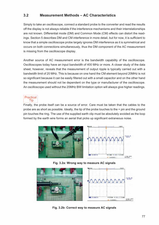
77
3.2 Measurement Methods – AC Characteristics
Simply to take an oscilloscope, connect a standard probe to the converter and read the results off the display is not always reliable if the interference mechanisms and their interrelationships are not known. Differential mode (DM) and Common Mode (CM) effects can distort the read-ings. Section 5 describes DM and CM interference in more detail, but for now, it is sufficient to know that a simple oscilloscope probe largely ignores DM interference as it is symmetrical and occurs on both connections simultaneously, thus the DM component of the AC measurement is missing from the oscilloscope display.
Another source of AC measurement error is the bandwidth capability of the oscilloscope. Oscilloscopes today have an input bandwidth of 400 MHz or more. A closer study of the data sheet, however, reveals that the measurement of output ripple is typically carried out with a bandwidth limit of 20 MHz. This is because on one hand the CM element beyond 20MHz is not so significant because it can be easily filtered out with a small capacitor and on the other hand the measurement should not be dependent on the type or manufacturer of the oscilloscope. An oscilloscope used without the 20MHz BW limitation option will always give higher readings.
Finally, the probe itself can be a source of error. Care must be taken that the cables to the probe are as short as possible. Ideally, the tip of the probe touches to the + pin and the ground pin touches the ring. The use of the supplied earth clip must be absolutely avoided as the loop formed by the earth wire forms an aerial that picks up significant extraneous noise.
Fig. 3.2a: Wrong way to measure AC signals
Fig. 3.2b: Correct way to measure AC signals
PracticalTip

78
If a probe with short contact paths cannot be used, then the proposal shown in Fig. 3.3 is useful. The impedance matching RC components avoid RF reflections that could interfere with the reading.
Fig. 3.3: Alternative AC Measurement Method
Note that the measured waveform is halved by the potential divider formed by the two 50 Ohm resistors, so the oscilloscope display should have ×2 multiplication. Even with the matching components, the coax cable should be kept as short as possible.
3.2.1 Measuring Minimum and Maximum Duty Cycle
In some applications, it would be useful to know more about the internal modulation of a DC/DC converter, the duty cycle signal is often not directly accessible from outside the module. However, with some experience, an interpretation of the input or output noise can reveal this information.
Fig. 3.4: Measuring the duty cycle from the Output Waveform
The minimum duty cycle δMIN is determined by the parameters VIN = VIN,MAX and IOUT = IOUT,MIN, the maximum duty cycle δmax by VIN = VIN,MIN and IOUT = IOUT,MAX. The period T is constant, be-cause it is the operating frequency of the DC/DC converter. Fig. 3.4 shows how the duty cycle can be extracted from the input current waveform.
�
�
���
���
������������������ ���
����
�� ����
����
���
���
���
�� ����� ��
�������������
�������������
�����������������������
�
�
�
������
������
� ��
���������������������
Practical Tip
79
3.2.2 Output Voltage Accuracy
The Output Voltage Accuracy characteristic, also called the Set Point Accuracy describes the specified tolerance of the output voltage. The parameter is usually specified in percent of the nominal output voltage, typically at room temperature, full load and nominal input voltage.
Equation 3.1: Output Accuracy
Output voltage inaccuracy occurs because of component tolerances, especially in the resistor divider that drops the output voltage down to the reference voltage of the PWM comparator (refer back to Fig. 1.46). For output voltages higher than 1.5Vdc, it is common that a 1.22V bandgap voltage reference is used ( a bandgap reference uses two PN junctions arranged so that the temperature coefficient of one junction cancels out that of the other to make a very stable reference voltage). For a 5V output voltage, the resistor divider will have a ratio of 3:1 so if 1% tolerance resistors are used, the output voltage accuracy will be 3%. In addition, the nearest standard value resistor may be used instead of the ideal value, so introducing another error.
Some regulated converters have a trim capability, with which the output voltage can be ad-justed within a certain range, typically ±10%. In this case, this specification applies with the trim pin left open (unused).
Unregulated converters have an output voltage that is load dependent. If the nominal output voltage was set to be accurate at 100% load, then the output voltage would be higher than the nominal voltage for all loads below 100%, which could reduce the useable load range of the converter. Therefore, the output voltage is typically set to be accurate at around 60% - 80% load (refer to Fig 1.31). At full load the output voltage is thus always slightly below VNOM.
3.2.3 Output Voltage Temperature Coefficient
Although the internal bandgap voltage reference has a very stable voltage over a range of op-erating temperatures, there will be some variation. The resulting temperature coefficient (TC) of the output voltage is defined as the relative deviation of the output voltage at the operating temperature extremes compared with the nominal output voltage at room temperature. The information is usually given in %/C or ppm/K. (ppm = parts per million). Tempcos are typically positive at low temperatures and negative at high temperatures.
To determine the TC, a thermal chamber cabinet is required which can generate the neces-sary ambient temperatures. At room temperature TRT the nominal voltage VOUT(TRT) is meas-ured at nominal load after the DC/DC converter has been run for a 20 minutes waiting time to allow for thermal stabilisation. Likewise the same procedure is carried out at the extremes of the operating temperature range. The calculation of the TC is carried out according to the equation below.
ACCV,OUT = VOUT - VOUT,NOM
VOUT,NOM100%
80
Equation 3.2: Temperature Coefficient Calculation
A typical TC value is ±0.02%/C meaning that if the output voltage is nominal at 25°C, the voltage would reduce by 1% at +75°C and increase by 1% at -25°C.
3.2.4 Load Regulation
Load regulation is defined as the maximum deviation of the measured output voltage over the permissible load range from the minimum load (ML) to full load (FL), given as a percentage. The input voltage is typically kept constant at the nominal value, VNOM. It should be noted that for many converters, a minimum load is required for proper regulation and there may be overload protection, so it is not valid to extrapolate the load regulation figure beyond ML or FL.
Normally, the output voltage changes linearly with the load current, so only two measuring points are needed within the specified load range for the load regulation calculation. If the specifications are done with a nominal current of, say, 80% of the maximum, then the load regulation can be measured in three ways: output voltages at ML and half load (half load = (ML+FL)/2), output voltages at FL and half load, or output voltages at ML and FL, all of which should give approximately the same result. These different calculations are possible from the test setup shown in Fig. 3.1 and the measurement scheme in Table 3.1. The following equa-tion gives the result based on measurements made with ML and FL:
Equation 3.3: Calculation of Load Regulation
If the datasheet specifies the Output Voltage Accuracy (OVA) figure at 50% load and states a load regulation of ±1%, then at full load, the relative change of the output voltage is -1% and at minimum load the relative change in the output voltage is +1%. Thus the measured output voltage can be higher or lower than the OVA figure by up to 1%. It can be confusing if the Output Voltage Accuracy is specified at full load, as then the load regulation result can only be negative, but by convention a ± percentage is still given. This means if the load regulation is specified at ±1% with OVA specified at 100% load, then the measured voltage can only be equal to or up to 1% lower than the OVA figure. This is in fact twice as accurate as the first definition.
Unregulated converters use Deviation against Load, measured with nominal VIN to indicate how the output voltage varies with load because they have neither load nor line regulation.
TC(T) [%/C] = VOUT(T)VNOM 100%,∆
∆T= VOUT(T) - VOUT(TRT)
VOUT(TRT) | TRT - T |or
TC(T) [ppm/K] = VOUT(T)VNOM 106∆
∆T= VOUT(T) - VOUT(TRT)
VOUT(TRT) | TRT - T |
REGLOAD = 100%VOUT,ML - VOUT,FL
VOUT,FL = 100%
V03 - V02
V02
81
3.2.5 Cross Regulation
This parameter only applies to converters with bipolar or multiple outputs. One output is fixed at full load and the other has a lower load, typically 25% (low load). Then the loads are switched so the first has 25% load and the second output 100% load. The cross regulation in percent is derived from whichever of the two following equations gives the highest figure:
Equation 3.4: Cross Regulation Calculation
3.2.6 Line Regulation
Line regulation is the deviation of the output voltage due to variations of the input voltage with-in its minimum (VL) and maximum limits (VH). The load is kept constant, usually at maximum current. Line regulation is specified as the percentage deviation of the output voltage relative to the nominal value of the output voltage. As with load regulation, the output voltage varies linearly with the input voltage, therefore the nominal input voltage (VN) and the difference between VL and VH may be used for determining this parameter. The following equation is based on output voltage deviation measurements with the full input voltage range VL to VH.
Equation 3.5: Calculation of Line Regulation
The nominal input voltage is usually defined approximately in the center of the input voltage range, so if the datasheet specifies the line regulation to be ±1%, for example, this means a change in the input voltage from VN to VH causes an increase in the output voltage of +1% and a change in the input voltage from VN to VL causes a drop in the output voltage of -1%.
Unregulated regulators are not line regulated. For a fixed load, the output voltage will increase with increasing input voltage and decrease with decreasing input voltage. The relationship is typically not 1:1 though, a 1% change in input voltage does not necessarily cause a corre-sponding 1% change in the output. The effect of input voltage on output voltage is specified at full load in the format “x%/1% of VIN”. For example if the line regulation of an unregulated converter is given as 1.2%/1% of VIN, then the output voltage will increase by 1.2% for every 1% increase in input voltage.
REGCROSS,1 = 100%VOUT1,LL - VOUT2,FL
VOUT2,FL
REGCROSS,2 = 100%,
where FL = Full Load, LL = Low Load
VOUT2,LL - VOUT1,FL
VOUT1,FL
VOUT,VNREGLINE = 100%
VOUT,VH - VOUT,VL = 100%
V09 - V06
V03
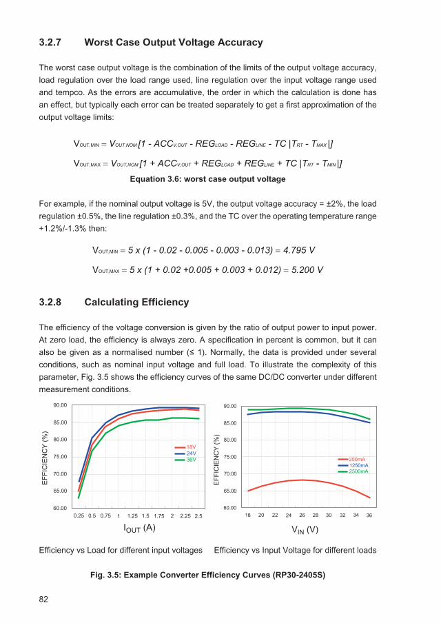
82
3.2.7 Worst Case Output Voltage Accuracy
The worst case output voltage is the combination of the limits of the output voltage accuracy, load regulation over the load range used, line regulation over the input voltage range used and tempco. As the errors are accumulative, the order in which the calculation is done has an effect, but typically each error can be treated separately to get a first approximation of the output voltage limits:
Equation 3.6: worst case output voltage
For example, if the nominal output voltage is 5V, the output voltage accuracy = ±2%, the load regulation ±0.5%, the line regulation ±0.3%, and the TC over the operating temperature range +1.2%/-1.3% then:
3.2.8 Calculating Efficiency
The efficiency of the voltage conversion is given by the ratio of output power to input power. At zero load, the efficiency is always zero. A specification in percent is common, but it can also be given as a normalised number (≤ 1). Normally, the data is provided under several conditions, such as nominal input voltage and full load. To illustrate the complexity of this parameter, Fig. 3.5 shows the efficiency curves of the same DC/DC converter under different measurement conditions.
Efficiency vs Load for different input voltages Efficiency vs Input Voltage for different loads
Fig. 3.5: Example Converter Efficiency Curves (RP30-2405S)
���� ��� ���� � ���� ��� ���� � ���� ��������
�����
�����
�����
�����
�����
�����
���������
������ �
��
�������
�
VOUT,MIN = VOUT,NOM [1 - ACCV,OUT - REGLOAD - REGLINE - TC |TRT - TMAX |]
VOUT,MAX = VOUT,NOM [1 + ACCV,OUT + REGLOAD + REGLINE + TC |TRT - TMIN |]
VOUT,MIN = 5 x (1 - 0.02 - 0.005 - 0.003 - 0.013) = 4.795 V
VOUT,MAX = 5 x (1 + 0.02 +0.005 + 0.003 + 0.012) = 5.200 V
�� �� �� �� �� �� �� �� �� �������
�����
�����
�����
�����
�����
�����
�����������������
������
����
������
83
3.2.9 Input Voltage Range
The input voltage range of DC/DC converter is defined as the input voltage limits VL and VH in between which the converter functions properly with a guaranteed regulated output voltage. Most converters will continue to operate outside of this range, but may not meet all of the datasheet specifications. Higher power converters may have an under voltage lockout (UVL) circuit that shuts down the converter if the input current rises too high due to too low input voltage. This is to protect the converter from input overcurrent damage. Sometimes “Absolute Maximum Ratings” are given in the datasheet to specify the maximum input voltage the con-verter will accept before the voltage limits on the internal components are exceeded.
The input voltage range given in the datasheet is for continuous voltages. Often higher tran-sient voltages can be applied without causing damage. For example the R-785.0-0.5 buck switching regulator with 5V output has an input voltage range of 6.5V to 32V and an abso-lute maximum input voltage of 34V, but will withstand a 50V/100ms surge transient and a 1000V/50μs fast transient.
3.2.10 Input Current
The input current is composed of two components, a DC component (the average input cur-rent) and an AC component (the back ripple current). The measurement of the back ripple current will be discussed in detail in section 5.2.1. The DC component of the input current is in turn composed of two components, the bias current and the input current due to the load. To find out the bias current, the load can be simply disconnected. The bias current is com-monly also referred to as the no load quiescent current (IQ) or housekeeping current. This cur-rent arises because the converter is still oscillating and dissipating power due to the various switching and parasitic losses, and the internal voltage regulators and voltage references are still operating, even though no output current flows. The bias current will be dependent on the input voltage and on the ambient temperature, so IQ is typically measured at VIN,NOM and 25°C room temperature. Converters that have an On/Off control or Standby mode can reduce the quiescent current still further by disabling the internal oscillators and regulators as well as the output power stage. Therefore IOFF is always less than IQ.
The load-dependent part of the input current is not always easy to interpret. Primarily it de-pends on the input voltage, so the relationship minimum input voltage = maximum input cur-rent is valid, but efficiency against load is non-linear (as shown in Fig. 3.5) and makes the ob-servation difficult. The efficiency is therefore a complex function of the output current and the input voltage. The developer who wants to calculate the maximum input current must know the minimum possible input voltage, the maximum load that could occur in that situation and the efficiency of the converter under those conditions (for example, by reading the efficiency values off a graph like shown in Fig 3.5). It is often inaccurate to make the calculation assum-ing the full load efficiency given in the datasheets, especially at other loads than full load.
Practical Tip
Practical Tip
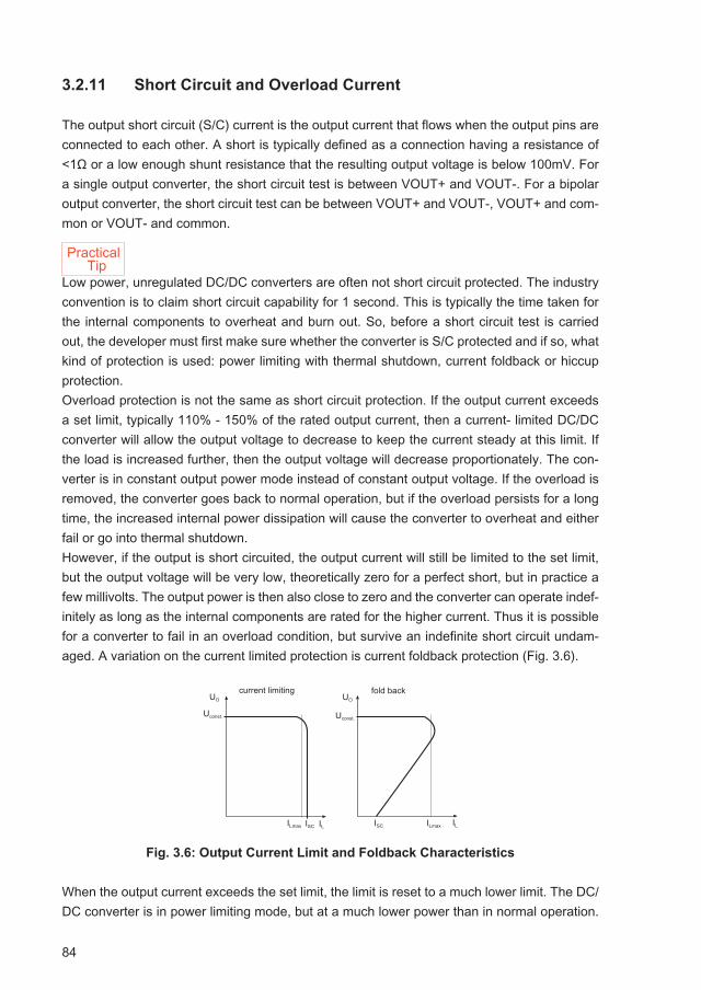
84
3.2.11 Short Circuit and Overload Current
The output short circuit (S/C) current is the output current that flows when the output pins are connected to each other. A short is typically defined as a connection having a resistance of <1Ω or a low enough shunt resistance that the resulting output voltage is below 100mV. For a single output converter, the short circuit test is between VOUT+ and VOUT-. For a bipolar output converter, the short circuit test can be between VOUT+ and VOUT-, VOUT+ and com-mon or VOUT- and common.
Low power, unregulated DC/DC converters are often not short circuit protected. The industry convention is to claim short circuit capability for 1 second. This is typically the time taken for the internal components to overheat and burn out. So, before a short circuit test is carried out, the developer must first make sure whether the converter is S/C protected and if so, what kind of protection is used: power limiting with thermal shutdown, current foldback or hiccup protection.Overload protection is not the same as short circuit protection. If the output current exceeds a set limit, typically 110% - 150% of the rated output current, then a current- limited DC/DC converter will allow the output voltage to decrease to keep the current steady at this limit. If the load is increased further, then the output voltage will decrease proportionately. The con-verter is in constant output power mode instead of constant output voltage. If the overload is removed, the converter goes back to normal operation, but if the overload persists for a long time, the increased internal power dissipation will cause the converter to overheat and either fail or go into thermal shutdown.However, if the output is short circuited, the output current will still be limited to the set limit, but the output voltage will be very low, theoretically zero for a perfect short, but in practice a few millivolts. The output power is then also close to zero and the converter can operate indef-initely as long as the internal components are rated for the higher current. Thus it is possible for a converter to fail in an overload condition, but survive an indefinite short circuit undam-aged. A variation on the current limited protection is current foldback protection (Fig. 3.6).
Fig. 3.6: Output Current Limit and Foldback Characteristics
When the output current exceeds the set limit, the limit is reset to a much lower limit. The DC/DC converter is in power limiting mode, but at a much lower power than in normal operation.
���������������� ����������
������� �������
�
��� �� �� ���
Practical Tip
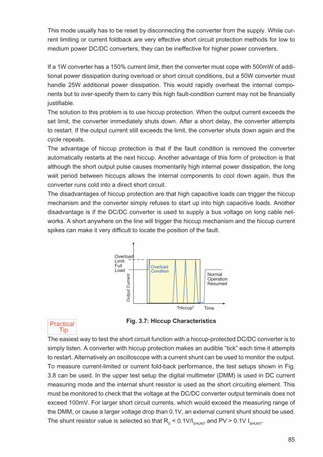
85
This mode usually has to be reset by disconnecting the converter from the supply. While cur-rent limiting or current foldback are very effective short circuit protection methods for low to medium power DC/DC converters, they can be ineffective for higher power converters.
If a 1W converter has a 150% current limit, then the converter must cope with 500mW of addi-tional power dissipation during overload or short circuit conditions, but a 50W converter must handle 25W additional power dissipation. This would rapidly overheat the internal compo-nents but to over-specify them to carry this high fault-condition current may not be financially justifiable.The solution to this problem is to use hiccup protection. When the output current exceeds the set limit, the converter immediately shuts down. After a short delay, the converter attempts to restart. If the output current still exceeds the limit, the converter shuts down again and the cycle repeats.The advantage of hiccup protection is that if the fault condition is removed the converter automatically restarts at the next hiccup. Another advantage of this form of protection is that although the short output pulse causes momentarily high internal power dissipation, the long wait period between hiccups allows the internal components to cool down again, thus the converter runs cold into a direct short circuit.The disadvantages of hiccup protection are that high capacitive loads can trigger the hiccup mechanism and the converter simply refuses to start up into high capacitive loads. Another disadvantage is if the DC/DC converter is used to supply a bus voltage on long cable net-works. A short anywhere on the line will trigger the hiccup mechanism and the hiccup current spikes can make it very difficult to locate the position of the fault.
Fig. 3.7: Hiccup Characteristics
The easiest way to test the short circuit function with a hiccup-protected DC/DC converter is to simply listen. A converter with hiccup protection makes an audible “tick” each time it attempts to restart. Alternatively an oscilloscope with a current shunt can be used to monitor the output.To measure current-limited or current fold-back performance, the test setups shown in Fig. 3.8 can be used. In the upper test setup the digital multimeter (DMM) is used in DC current measuring mode and the internal shunt resistor is used as the short circuiting element. This must be monitored to check that the voltage at the DC/DC converter output terminals does not exceed 100mV. For larger short circuit currents, which would exceed the measuring range of the DMM, or cause a larger voltage drop than 0.1V, an external current shunt should be used. The shunt resistor value is selected so that RS < 0.1V/ISHUNT and PV > 0.1V ISHUNT.
���������������������
���
�����
����
��
������ ���
���������������������
�����������������
Practical Tip
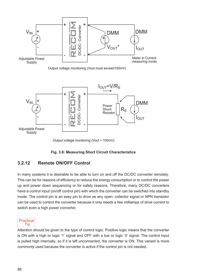
86
Fig. 3.8: Measuring Short Circuit Characteristics
3.2.12 Remote ON/OFF Control
In many systems it is desirable to be able to turn on and off the DC/DC converter remotely. This can be for reasons of efficiency to reduce the energy consumption or to control the power up and power down sequencing or for safety reasons. Therefore, many DC/DC converters have a control input (on/off control pin) with which the converter can be switched into standby mode. The control pin is an easy pin to drive as any open- collector signal or NPN transistor can be used to control the converter because it only needs a few milliamps of drive current to switch even a high power converter.
Attention should be given to the type of control logic. Positive logic means that the converter is ON with a high or logic ‘1’ signal and OFF with a low or logic ‘0’ signal. The control input is pulled high internally, so if it is left unconnected, the converter is ON. This variant is more commonly used because the converter is active if the control pin is not needed.
�
�
���
����
������
�����
���������
���
������
�
�
�
�
�
�
���
����
�� �������������
�
�
�
�
��
������������ �������
������������ �������
������������� ������������������� ��
������������� �������������� ������������ ��
��������������� �������� ���
����
������
������
����
������
������
Practical Tip
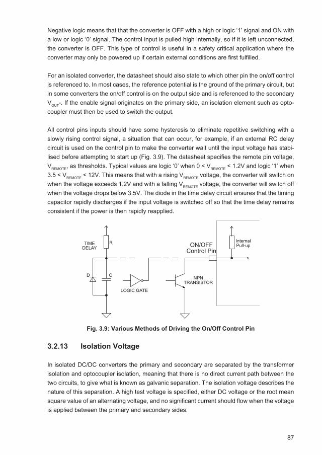
87
Negative logic means that that the converter is OFF with a high or logic ‘1’ signal and ON with a low or logic ‘0’ signal. The control input is pulled high internally, so if it is left unconnected, the converter is OFF. This type of control is useful in a safety critical application where the converter may only be powered up if certain external conditions are first fulfilled.
For an isolated converter, the datasheet should also state to which other pin the on/off control is referenced to. In most cases, the reference potential is the ground of the primary circuit, but in some converters the on/off control is on the output side and is referenced to the secondary VOUT-. If the enable signal originates on the primary side, an isolation element such as opto-coupler must then be used to switch the output.
All control pins inputs should have some hysteresis to eliminate repetitive switching with a slowly rising control signal, a situation that can occur, for example, if an external RC delay circuit is used on the control pin to make the converter wait until the input voltage has stabi-lised before attempting to start up (Fig. 3.9). The datasheet specifies the remote pin voltage, VREMOTE, as thresholds. Typical values are logic ‘0’ when 0 < VREMOTE < 1.2V and logic ‘1’ when 3.5 < VREMOTE < 12V. This means that with a rising VREMOTE voltage, the converter will switch on when the voltage exceeds 1.2V and with a falling VREMOTE voltage, the converter will switch off when the voltage drops below 3.5V. The diode in the time delay circuit ensures that the timing capacitor rapidly discharges if the input voltage is switched off so that the time delay remains consistent if the power is then rapidly reapplied.
Fig. 3.9: Various Methods of Driving the On/Off Control Pin
3.2.13 Isolation Voltage
In isolated DC/DC converters the primary and secondary are separated by the transformer isolation and optocoupler isolation, meaning that there is no direct current path between the two circuits, to give what is known as galvanic separation. The isolation voltage describes the nature of this separation. A high test voltage is specified, either DC voltage or the root mean square value of an alternating voltage, and no significant current should flow when the voltage is applied between the primary and secondary sides.
����������
� �
������������ ��
����������
���������������
���������
88
NOTE: A high potential (HiPot) tester with an accurate current limiting circuit must be used for these kinds of tests as hazardous voltages are used. Do not carry out the HiPot test on an ESD protected worktable as the surface has been treated to make it electrically conductive. Ensure that the HiPot tester has an emergency stop button and make sure that the earth connection to the tester is sound. The Device under Test (DUT) must be adequately insulated from any part that the operator could accidentally touch and the tester should incorporate automatic discharge circuitry to discharge the test voltage after the test has been completed. Follow the maker’s instructions to the letter!
While a converter may be DC galvanically isolated, a leakage current will flow if an AC isola-tion test is used. The AC current flows through the capacitive coupling between the windings in the transformer and through any EMC suppression capacitors placed across the isolation barrier. Therefore, for an AC HiPot test, not only the RMS voltage but also the permissible leakage current should be specified. Typical set limits are 1mA or 3mA, as any higher leakage currents as this could permanently damage the converter.
Due to the AC leakage current, an AC high voltage stresses the isolation barrier more than an equivalent steady state DC voltage. The stress increases with the frequency and voltage because:
Equation 3.7: AC leakage current
For this reason, a converter that is rated at 1kVdc/1 second should only be tested with 700Vac/1 second (when using a 50Hz signal). This sounds logical if you think that the peak voltage of a 700VacRMS waveform is 980V. However, if the frequency was increased, the leakage current will increase as well. A 100Hz test signal will generate double the leakage current than a 50Hz test signal. So, a converter that is rated at 1kVdc/1 second should only be tested with 360Vac/1 second when using a 100Hz test waveform. Fortunately, a 50Hz HiPot test frequency is the industry standard and although most manufacturers don’t mention the test frequency used, it can be safely assumed that 50Hz was used when comparing isolation values in datasheets. RECOM has a useful isolation voltage comparison tool on it’s website.
The equivalence between DC and AC HiPot testing is also not so straightforward with longer tests than 1 second. A 60 second test puts a lot more strain on the isolation barrier because of the phenomenom known as partial discharge (PD). Partial discharge describes the momen-tary breakdown due to the high applied voltage between coupling paths within an insulating medium due to internal voids or inconsistencies.
Consider the construction of a conventional enamelled transformer wire. (Fig. 3.10). The insu-lation lacquer is typically applied in several stages, so there could be discontinuities between layers as well as voids within the insulation.
ILEAK = dV(t)dt
CLEAK
Practical Tip
Practical Tip

89
Fig. 3.10: Cross section of a Magnet wire with Partial Discharge (PD)
Paths through Insulation
Momentary current flows as the partial discharges occur within the isolation medium, but the wire is still insulated. However, the voltage stress now has a reduced thickness of insulation barrier. The voltage stress can jump from one weakness to the next until it eventually can cause a complete input/output isolation failure.
The keyword here is “eventually”. It takes time for PD failures to join up and cause a total failure. The longer the HiPot voltage is applied, the more likely that a failure can occur. Thus a HiPot test for 1 minute is much more stressful than the typical production test of 1 second. A converter rated a 1000Vdc/1 second should only be tested at 500Vac/1 min to reduce the likelihood of such cumulative PD failures causing a problem.
Due to the potential of causing permanent damage to the converter during a HiPot test, there are two important practical issues that need special care when setting up a test. Firstly, it is important not to allow voltage gradients to develop within the converter as they can rapidly ex-ceed the breakdown ratings of the internal components. Therefore before carrying out a HiPot test, all of the inputs must be shorted to each other and all of the outputs shorted together. Secondly, as HiPot tests stress the converter isolation and cause cumulative damage to the insulation, it is recommended to reduce the HiPot voltage by 20% for each re-test.
Fig. 3.11: HiPot (Dielectric Strength) Testing
�������������
�������������
�������������
����������
���������
����
��
����
���
�������������������������������������������������������
������������ �������� �������� ���
�����
����
�����������
����
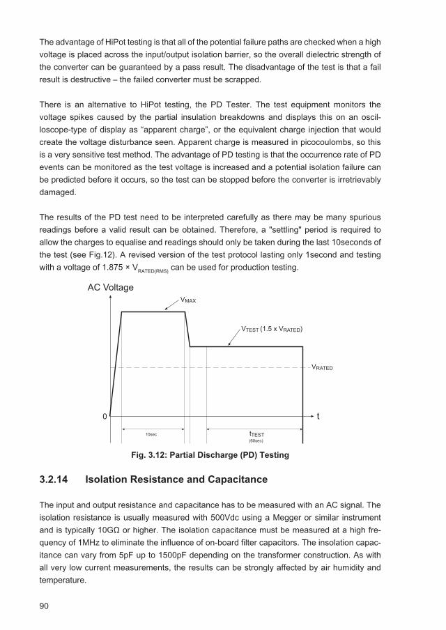
90
The advantage of HiPot testing is that all of the potential failure paths are checked when a high voltage is placed across the input/output isolation barrier, so the overall dielectric strength of the converter can be guaranteed by a pass result. The disadvantage of the test is that a fail result is destructive – the failed converter must be scrapped.
There is an alternative to HiPot testing, the PD Tester. The test equipment monitors the voltage spikes caused by the partial insulation breakdowns and displays this on an oscil-loscope-type of display as “apparent charge”, or the equivalent charge injection that would create the voltage disturbance seen. Apparent charge is measured in picocoulombs, so this is a very sensitive test method. The advantage of PD testing is that the occurrence rate of PD events can be monitored as the test voltage is increased and a potential isolation failure can be predicted before it occurs, so the test can be stopped before the converter is irretrievably damaged.
The results of the PD test need to be interpreted carefully as there may be many spurious readings before a valid result can be obtained. Therefore, a "settling" period is required to allow the charges to equalise and readings should only be taken during the last 10seconds of the test (see Fig.12). A revised version of the test protocol lasting only 1second and testing with a voltage of 1.875 × VRATED(RMS) can be used for production testing.
Fig. 3.12: Partial Discharge (PD) Testing
3.2.14 Isolation Resistance and Capacitance
The input and output resistance and capacitance has to be measured with an AC signal. The isolation resistance is usually measured with 500Vdc using a Megger or similar instrument and is typically 10GΩ or higher. The isolation capacitance must be measured at a high fre-quency of 1MHz to eliminate the influence of on-board filter capacitors. The insolation capac-itance can vary from 5pF up to 1500pF depending on the transformer construction. As with all very low current measurements, the results can be strongly affected by air humidity and temperature.
����� ������������
������
��������� ����������
���
�
���������
�
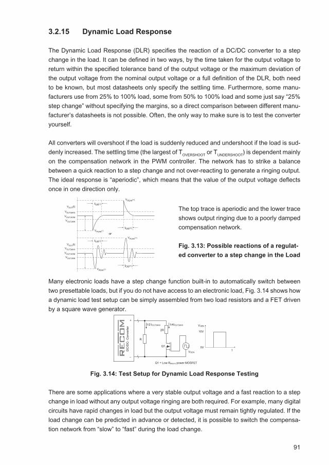
91
3.2.15 Dynamic Load Response
The Dynamic Load Response (DLR) specifies the reaction of a DC/DC converter to a step change in the load. It can be defined in two ways, by the time taken for the output voltage to return within the specified tolerance band of the output voltage or the maximum deviation of the output voltage from the nominal output voltage or a full definition of the DLR, both need to be known, but most datasheets only specify the settling time. Furthermore, some manu-facturers use from 25% to 100% load, some from 50% to 100% load and some just say “25% step change” without specifying the margins, so a direct comparison between different manu-facturer’s datasheets is not possible. Often, the only way to make sure is to test the converter yourself.
All converters will overshoot if the load is suddenly reduced and undershoot if the load is sud-denly increased. The settling time (the largest of TOVERSHOOT or TUNDERSHOOT) is dependent mainly on the compensation network in the PWM controller. The network has to strike a balance between a quick reaction to a step change and not over-reacting to generate a ringing output. The ideal response is “aperiodic”, which means that the value of the output voltage deflects once in one direction only.
Many electronic loads have a step change function built-in to automatically switch between two presettable loads, but if you do not have access to an electronic load, Fig. 3.14 shows how a dynamic load test setup can be simply assembled from two load resistors and a FET driven by a square wave generator.
Fig. 3.14: Test Setup for Dynamic Load Response Testing
There are some applications where a very stable output voltage and a fast reaction to a step change in load without any output voltage ringing are both required. For example, many digital circuits have rapid changes in load but the output voltage must remain tightly regulated. If the load change can be predicted in advance or detected, it is possible to switch the compensa-tion network from “slow” to “fast” during the load change.
The top trace is aperiodic and the lower trace shows output ringing due to a poorly damped compensation network.
Fig. 3.13: Possible reactions of a regulat-
ed converter to a step change in the Load
�������
��������
������
������
������
������
��������
�
�������
��������
��������
��������
��������
��������
��������
��������
��������
��
���
�����
�������� ��������
��
�
��
� � � � ����
���������������������������
�� �
� ����
�����
�
�
92
With analogue controllers, this is not easy, but with a digital controller, the DLR can be made programmable. This ability is one of the biggest advantages of digital control over analogue controllers.
Just as the output voltage will change if the load suddenly changes, so the output voltage will change if the input voltage suddenly changes. This parameter is rarely defined in the data-sheets as an abrupt change in the input voltage occurs only in few applications. If required, a test setup can be relatively easily built if the bench power supply has an external control input or a tracking input that can be connected to a square wave generator.
3.2.16 Output Ripple/Noise
All DC/DC Converters have some element of output ripple and noise. The ripple component arises from the charging and discharging currents in the output filter capacitance and has a typical frequency of either the operating frequency or double the operating frequency, de-pending on the topology.
Fig. 3.15: Output Ripple and Noise
Superimposed on the basic ripple wave form are switching spikes (noise) that arise from all of the parasitic effects each time the main switches change state. These occur at every peak and trough of the ripple waveform. The frequencies of the switching transients are typically orders of magnitude higher than the ripple frequency, somewhere in the MHz regions. The combined waveform gives the output Ripple/Noise (R/N) figure, which is typically measured as millivolts peak-to-peak (mVp-p). NOTE: refer to section 4.3 for the correct measurement technique.
Also superimposed on the output R/N waveform is a much slower oscillation which arises from the output voltage regulation circuit. With constant load and input voltage, the output voltage will meander up and down within the tolerance band with a frequency in the single figure Hz range. This “hunting” effect is due to hysteresis in the regulation circuit and is usually ignored in the R/N figure quoted in the datasheets as it is part of the output voltage accuracy specifi-cation and therefore not included in the R/N specification.
Fig. 3.16: Output Voltage “hunting”
�����������
�������
������������������
����
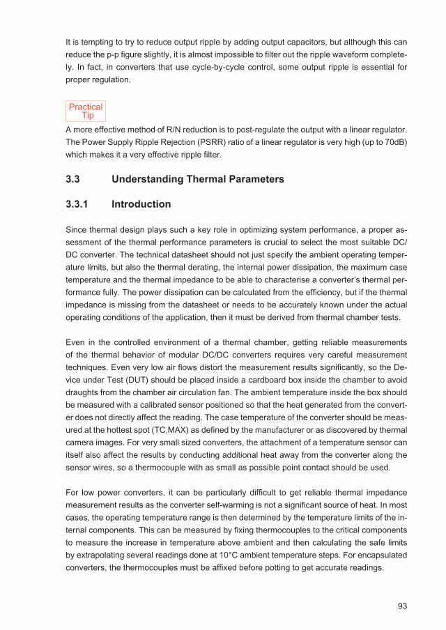
93
It is tempting to try to reduce output ripple by adding output capacitors, but although this can reduce the p-p figure slightly, it is almost impossible to filter out the ripple waveform complete-ly. In fact, in converters that use cycle-by-cycle control, some output ripple is essential for proper regulation.
A more effective method of R/N reduction is to post-regulate the output with a linear regulator. The Power Supply Ripple Rejection (PSRR) ratio of a linear regulator is very high (up to 70dB) which makes it a very effective ripple filter.
3.3 Understanding Thermal Parameters
3.3.1 Introduction
Since thermal design plays such a key role in optimizing system performance, a proper as-sessment of the thermal performance parameters is crucial to select the most suitable DC/DC converter. The technical datasheet should not just specify the ambient operating temper-ature limits, but also the thermal derating, the internal power dissipation, the maximum case temperature and the thermal impedance to be able to characterise a converter’s thermal per-formance fully. The power dissipation can be calculated from the efficiency, but if the thermal impedance is missing from the datasheet or needs to be accurately known under the actual operating conditions of the application, then it must be derived from thermal chamber tests.
Even in the controlled environment of a thermal chamber, getting reliable measurements of the thermal behavior of modular DC/DC converters requires very careful measurement techniques. Even very low air flows distort the measurement results significantly, so the De-vice under Test (DUT) should be placed inside a cardboard box inside the chamber to avoid draughts from the chamber air circulation fan. The ambient temperature inside the box should be measured with a calibrated sensor positioned so that the heat generated from the convert-er does not directly affect the reading. The case temperature of the converter should be meas-ured at the hottest spot (TC,MAX) as defined by the manufacturer or as discovered by thermal camera images. For very small sized converters, the attachment of a temperature sensor can itself also affect the results by conducting additional heat away from the converter along the sensor wires, so a thermocouple with as small as possible point contact should be used.
For low power converters, it can be particularly difficult to get reliable thermal impedance measurement results as the converter self-warming is not a significant source of heat. In most cases, the operating temperature range is then determined by the temperature limits of the in-ternal components. This can be measured by fixing thermocouples to the critical components to measure the increase in temperature above ambient and then calculating the safe limits by extrapolating several readings done at 10°C ambient temperature steps. For encapsulated converters, the thermocouples must be affixed before potting to get accurate readings.
Practical Tip
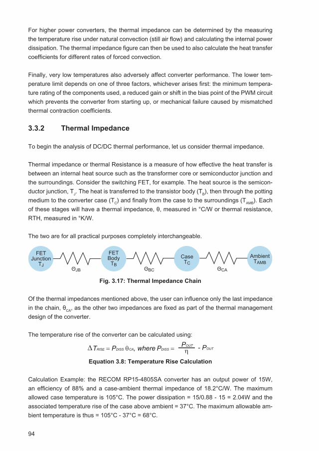
94
For higher power converters, the thermal impedance can be determined by the measuring the temperature rise under natural convection (still air flow) and calculating the internal power dissipation. The thermal impedance figure can then be used to also calculate the heat transfer coefficients for different rates of forced convection.
Finally, very low temperatures also adversely affect converter performance. The lower tem-perature limit depends on one of three factors, whichever arises first: the minimum tempera-ture rating of the components used, a reduced gain or shift in the bias point of the PWM circuit which prevents the converter from starting up, or mechanical failure caused by mismatched thermal contraction coefficients.
3.3.2 Thermal Impedance
To begin the analysis of DC/DC thermal performance, let us consider thermal impedance.
Thermal impedance or thermal Resistance is a measure of how effective the heat transfer is between an internal heat source such as the transformer core or semiconductor junction and the surroundings. Consider the switching FET, for example. The heat source is the semicon-ductor junction, TJ. The heat is transferred to the transistor body (TB), then through the potting medium to the converter case (TC) and finally from the case to the surroundings (TAMB). Each of these stages will have a thermal impedance, θ, measured in °C/W or thermal resistance, RTH, measured in °K/W.
The two are for all practical purposes completely interchangeable.
Fig. 3.17: Thermal Impedance Chain
Of the thermal impedances mentioned above, the user can influence only the last impedance in the chain, θCA, as the other two impedances are fixed as part of the thermal management design of the converter.
The temperature rise of the converter can be calculated using:
Equation 3.8: Temperature Rise Calculation
Calculation Example: the RECOM RP15-4805SA converter has an output power of 15W, an efficiency of 88% and a case-ambient thermal impedance of 18.2°C/W. The maximum allowed case temperature is 105°C. The power dissipation = 15/0.88 - 15 = 2.04W and the associated temperature rise of the case above ambient = 37°C. The maximum allowable am-bient temperature is thus = 105°C - 37°C = 68°C.
�����������
��
���������
������
� ���������
�� �� ��
TRISE = PDISS θCA, where PDISS = ∆ POUT
η - POUT
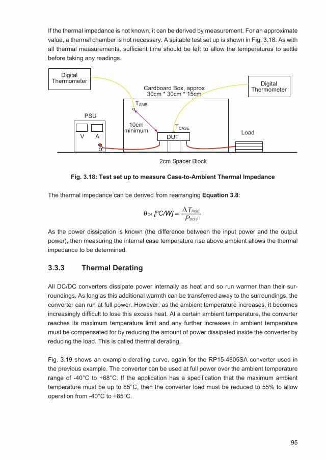
95
If the thermal impedance is not known, it can be derived by measurement. For an approximate value, a thermal chamber is not necessary. A suitable test set up is shown in Fig. 3.18. As with all thermal measurements, sufficient time should be left to allow the temperatures to settle before taking any readings.
Fig. 3.18: Test set up to measure Case-to-Ambient Thermal Impedance
The thermal impedance can be derived from rearranging Equation 3.8:
As the power dissipation is known (the difference between the input power and the output power), then measuring the internal case temperature rise above ambient allows the thermal impedance to be determined.
3.3.3 Thermal Derating
All DC/DC converters dissipate power internally as heat and so run warmer than their sur-roundings. As long as this additional warmth can be transferred away to the surroundings, the converter can run at full power. However, as the ambient temperature increases, it becomes increasingly difficult to lose this excess heat. At a certain ambient temperature, the converter reaches its maximum temperature limit and any further increases in ambient temperature must be compensated for by reducing the amount of power dissipated inside the converter by reducing the load. This is called thermal derating.
Fig. 3.19 shows an example derating curve, again for the RP15-4805SA converter used in the previous example. The converter can be used at full power over the ambient temperature range of -40°C to +68°C. If the application has a specification that the maximum ambient temperature must be up to 85°C, then the converter load must be reduced to 55% to allow operation from -40°C to +85°C.
������������������ �������
������������������������ ��������������������
��������� ����
���
���������
����
�����
���
������������
θCA [⁰C/W] = ∆TRISE
PDISS
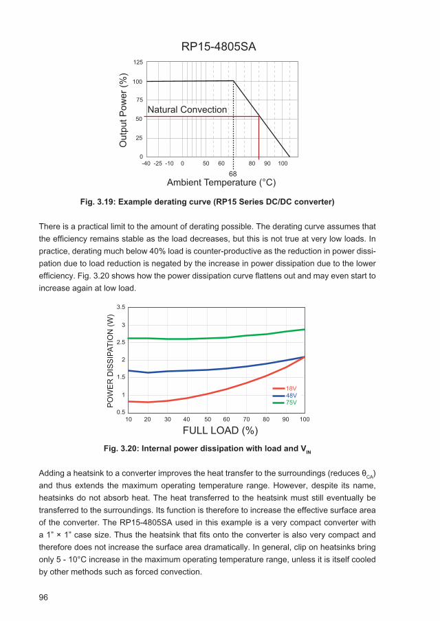
96
Fig. 3.19: Example derating curve (RP15 Series DC/DC converter)
There is a practical limit to the amount of derating possible. The derating curve assumes that the efficiency remains stable as the load decreases, but this is not true at very low loads. In practice, derating much below 40% load is counter-productive as the reduction in power dissi-pation due to load reduction is negated by the increase in power dissipation due to the lower efficiency. Fig. 3.20 shows how the power dissipation curve flattens out and may even start to increase again at low load.
Fig. 3.20: Internal power dissipation with load and VIN
Adding a heatsink to a converter improves the heat transfer to the surroundings (reduces θCA) and thus extends the maximum operating temperature range. However, despite its name, heatsinks do not absorb heat. The heat transferred to the heatsink must still eventually be transferred to the surroundings. Its function is therefore to increase the effective surface area of the converter. The RP15-4805SA used in this example is a very compact converter with a 1” × 1” case size. Thus the heatsink that fits onto the converter is also very compact and therefore does not increase the surface area dramatically. In general, clip on heatsinks bring only 5 - 10°C increase in the maximum operating temperature range, unless it is itself cooled by other methods such as forced convection.
���������������������
�����
����
� �
�
����������������� ���
��� ��� ��� � �� �� �� �� ���
��
�
��
��
��
���
���
���������
�� �� �� �� �� �� �� �� �� ������
�
���
�
���
�
���
���������� ��
�
����
����
����
��
�
���������
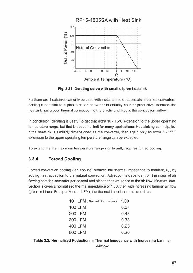
97
Fig. 3.21: Derating curve with small clip-on heatsink
Furthermore, heatsinks can only be used with metal-cased or baseplate-mounted converters. Adding a heatsink to a plastic cased converter is actually counter-productive, because the heatsink has a poor thermal connection to the plastic and blocks the convection airflow.
In conclusion, derating is useful to get that extra 10 - 15°C extension to the upper operating temperature range, but that is about the limit for many applications. Heatsinking can help, but if the heatsink is similarly dimensioned as the converter, then again only an extra 5 - 15°C extension to the upper operating temperature range can be expected.
To extend the the maximum temperature range significantly requires forced cooling.
3.3.4 Forced Cooling
Forced convection cooling (fan cooling) reduces the thermal impedance to ambient, θCA by adding heat advection to the natural convection. Advection is dependent on the mass of air flowing past the converter per second and also to the turbulence of the air flow. If natural con-vection is given a normalised thermal impedance of 1.00, then with increasing laminar air flow (given in Linear Feet per Minute, LFM), the thermal impedance reduces thus:
Table 3.2: Normalised Reduction in Thermal Impedance with Increasing Laminar
Airflow
������������������
���
�����
����
� �
�
����������������� ���
��� ��� ��� � �� �� �� �� ���
��
�
��
��
��
���
���
����������������������
10 LFM (Natural Convection) 1.00100 LFM 0.67200 LFM 0.45300 LFM 0.33400 LFM 0.25500 LFM 0.20
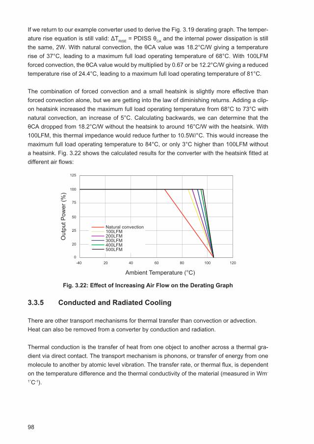
98
If we return to our example converter used to derive the Fig. 3.19 derating graph. The temper-ature rise equation is still valid: ΔTRISE = PDISS θCA and the internal power dissipation is still the same, 2W. With natural convection, the θCA value was 18.2°C/W giving a temperature rise of 37°C, leading to a maximum full load operating temperature of 68°C. With 100LFM forced convection, the θCA value would by multiplied by 0.67 or be 12.2°C/W giving a reduced temperature rise of 24.4°C, leading to a maximum full load operating temperature of 81°C.
The combination of forced convection and a small heatsink is slightly more effective than forced convection alone, but we are getting into the law of diminishing returns. Adding a clip-on heatsink increased the maximum full load operating temperature from 68°C to 73°C with natural convection, an increase of 5°C. Calculating backwards, we can determine that the θCA dropped from 18.2°C/W without the heatsink to around 16°C/W with the heatsink. With 100LFM, this thermal impedance would reduce further to 10.5W/°C. This would increase the maximum full load operating temperature to 84°C, or only 3°C higher than 100LFM without a heatsink. Fig. 3.22 shows the calculated results for the converter with the heatsink fitted at different air flows:
Fig. 3.22: Effect of Increasing Air Flow on the Derating Graph
3.3.5 Conducted and Radiated Cooling
There are other transport mechanisms for thermal transfer than convection or advection. Heat can also be removed from a converter by conduction and radiation.
Thermal conduction is the transfer of heat from one object to another across a thermal gra-dient via direct contact. The transport mechanism is phonons, or transfer of energy from one molecule to another by atomic level vibration. The transfer rate, or thermal flux, is dependent on the temperature difference and the thermal conductivity of the material (measured in Wm-
1°C-1).
���
�����
����
���
�
�������� ��������������
�� �� �� �� ���
�
��
��
��
���
���
��
�����
����������������������� ����� ���� ����� �����
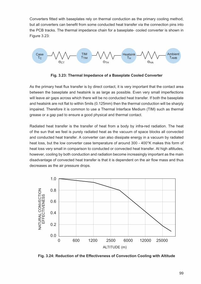
99
Converters fitted with baseplates rely on thermal conduction as the primary cooling method, but all converters can benefit from some conducted heat transfer via the connection pins into the PCB tracks. The thermal impedance chain for a baseplate- cooled converter is shown in Figure 3.23:
Fig. 3.23: Thermal Impedance of a Baseplate Cooled Converter
As the primary heat flux transfer is by direct contact, it is very important that the contact area between the baseplate and heatsink is as large as possible. Even very small imperfections will leave air gaps across which there will be no conducted heat transfer. If both the baseplate and heatsink are not flat to within 5mils (0.125mm) then the thermal conduction will be sharply impaired. Therefore it is common to use a Thermal Interface Medium (TIM) such as thermal grease or a gap pad to ensure a good physical and thermal contact.
Radiated heat transfer is the transfer of heat from a body by infra-red radiation. The heat of the sun that we feel is purely radiated heat as the vacuum of space blocks all convected and conducted heat transfer. A converter can also dissipate energy in a vacuum by radiated heat loss, but the low converter case temperature of around 300 - 400°K makes this form of heat loss very small in comparison to conducted or convected heat transfer. At high altitudes, however, cooling by both conduction and radiation become increasingly important as the main disadvantage of convected heat transfer is that it is dependent on the air flow mass and thus decreases as the air pressure drops.
Fig. 3.24: Reduction of the Effectiveness of Convection Cooling with Altitude
������
�������
����������
�����������
��� ��� ���
��������
���������
���������
�����
������������
� � � � �
�
��
��
��
��
100
4. DC/DC Converter Protection
4.1 Introduction
As mentioned in the Preface, one of the functions of a DC/DC converter is to protect the ap-plication. At the most simple level, this protection consists of matching the load to the primary power supply and stabilising the output voltage against input overvoltages and undervoltages, but a DC/DC converter is also a significant element ensuring system fault protection. For ex-ample, output overload limiting and short-circuit protection not only stops the converter from being damaged if the load fails, but also can protect the load from further damage by limiting the output power during a fault condition. In an application with several identical circuits or channels each separately powered by individual DC/DC converters, a fault in one output channel will not affect the other outputs, thus making the system single fault tolerant. Other converter protection features, such as over-temperature shut-down, are primarily designed to safeguard the converter from permanent damage caused by internal component overheating, but a side-effect is also to shut down the application if the ambient temperature gets too high, thus also protecting the components in the application from over-temperature failure.
Adding isolation between input and output breaks ground loops, eliminates source of interfer-ence and increases system reliability by protecting the application against transient damage. The elimination of power supply feedback effects is an important facet of DC/DC converter protection. For example, consider a heavy duty DC motor speed controller. The speed control-ler circuit needs a stable, noise-free supply to smoothly regulate the motor speed. But the high AC ripple drawn by the motor on top of the DC current can create significant voltage transients that could feed back into the speed controller regulation circuit to cause jitter or instability. An isolated DC/DC converter not only delivers a stable low-noise supply to the speed controller circuit, but by breaking the noise feedback loop also protects the motor from unwanted and erratic control signals that could damage the motor and associated drive chain.
However, a DC/DC converter is also constructed from electronic components that are just susceptible to failure if used outside their voltage, current and temperature limits as any other electronic circuit. This chapter investigates protection measures that may be needed to safe-guard the converter itself from damage.
4.2 Reverse Polarity Protection
DC / DC converter are not protected against reverse polarity connection. Swapping the VIN+ and VIN- terminals will almost certainly cause immediate failure, so care must be taken to en-sure that any input connectors or battery connections are polarised. If the primary supply is transformer, then a rectification diode failure could cause a negative- going output that would then also cause the DC/DC converters to fail.
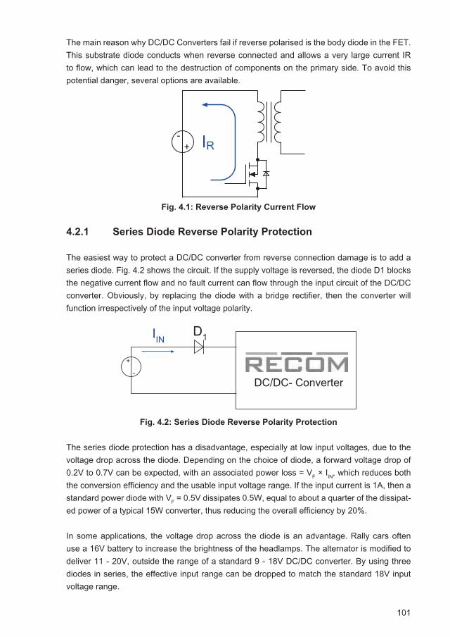
101
The main reason why DC/DC Converters fail if reverse polarised is the body diode in the FET. This substrate diode conducts when reverse connected and allows a very large current IR to flow, which can lead to the destruction of components on the primary side. To avoid this potential danger, several options are available.
Fig. 4.1: Reverse Polarity Current Flow
4.2.1 Series Diode Reverse Polarity Protection
The easiest way to protect a DC/DC converter from reverse connection damage is to add a series diode. Fig. 4.2 shows the circuit. If the supply voltage is reversed, the diode D1 blocks the negative current flow and no fault current can flow through the input circuit of the DC/DC converter. Obviously, by replacing the diode with a bridge rectifier, then the converter will function irrespectively of the input voltage polarity.
Fig. 4.2: Series Diode Reverse Polarity Protection
The series diode protection has a disadvantage, especially at low input voltages, due to the voltage drop across the diode. Depending on the choice of diode, a forward voltage drop of 0.2V to 0.7V can be expected, with an associated power loss = VF × IIN, which reduces both the conversion efficiency and the usable input voltage range. If the input current is 1A, then a standard power diode with VF = 0.5V dissipates 0.5W, equal to about a quarter of the dissipat-ed power of a typical 15W converter, thus reducing the overall efficiency by 20%.
In some applications, the voltage drop across the diode is an advantage. Rally cars often use a 16V battery to increase the brightness of the headlamps. The alternator is modified to deliver 11 - 20V, outside the range of a standard 9 - 18V DC/DC converter. By using three diodes in series, the effective input range can be dropped to match the standard 18V input voltage range.
��
��
����������������
���
�
�
��
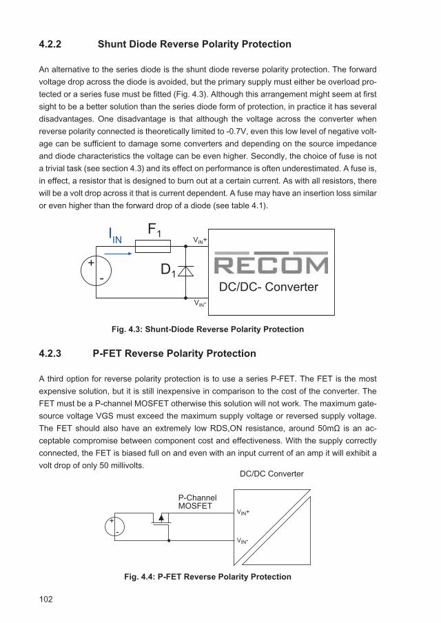
102
4.2.2 Shunt Diode Reverse Polarity Protection
An alternative to the series diode is the shunt diode reverse polarity protection. The forward voltage drop across the diode is avoided, but the primary supply must either be overload pro-tected or a series fuse must be fitted (Fig. 4.3). Although this arrangement might seem at first sight to be a better solution than the series diode form of protection, in practice it has several disadvantages. One disadvantage is that although the voltage across the converter when reverse polarity connected is theoretically limited to -0.7V, even this low level of negative volt-age can be sufficient to damage some converters and depending on the source impedance and diode characteristics the voltage can be even higher. Secondly, the choice of fuse is not a trivial task (see section 4.3) and its effect on performance is often underestimated. A fuse is, in effect, a resistor that is designed to burn out at a certain current. As with all resistors, there will be a volt drop across it that is current dependent. A fuse may have an insertion loss similar or even higher than the forward drop of a diode (see table 4.1).
Fig. 4.3: Shunt-Diode Reverse Polarity Protection
4.2.3 P-FET Reverse Polarity Protection
A third option for reverse polarity protection is to use a series P-FET. The FET is the most expensive solution, but it is still inexpensive in comparison to the cost of the converter. The FET must be a P-channel MOSFET otherwise this solution will not work. The maximum gate-source voltage VGS must exceed the maximum supply voltage or reversed supply voltage. The FET should also have an extremely low RDS,ON resistance, around 50mΩ is an ac-ceptable compromise between component cost and effectiveness. With the supply correctly connected, the FET is biased full on and even with an input current of an amp it will exhibit a volt drop of only 50 millivolts.
Fig. 4.4: P-FET Reverse Polarity Protection
����������������
���
��
��
��
����
����
���������������
��������� �����
��
��
��
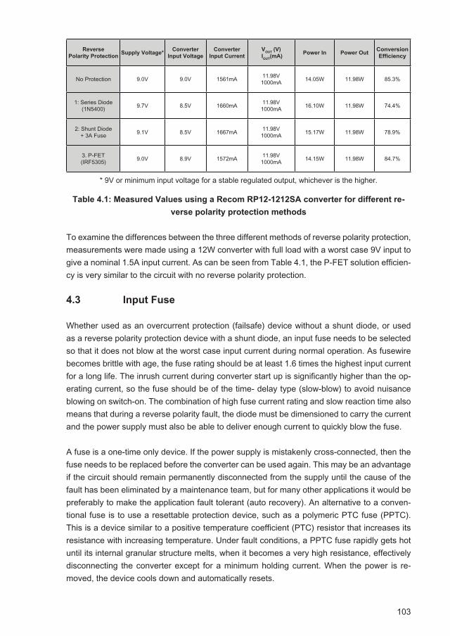
103
Table 4.1: Measured Values using a Recom RP12-1212SA converter for different re-
verse polarity protection methods
To examine the differences between the three different methods of reverse polarity protection, measurements were made using a 12W converter with full load with a worst case 9V input to give a nominal 1.5A input current. As can be seen from Table 4.1, the P-FET solution efficien-cy is very similar to the circuit with no reverse polarity protection.
4.3 Input Fuse
Whether used as an overcurrent protection (failsafe) device without a shunt diode, or used as a reverse polarity protection device with a shunt diode, an input fuse needs to be selected so that it does not blow at the worst case input current during normal operation. As fusewire becomes brittle with age, the fuse rating should be at least 1.6 times the highest input current for a long life. The inrush current during converter start up is significantly higher than the op-erating current, so the fuse should be of the time- delay type (slow-blow) to avoid nuisance blowing on switch-on. The combination of high fuse current rating and slow reaction time also means that during a reverse polarity fault, the diode must be dimensioned to carry the current and the power supply must also be able to deliver enough current to quickly blow the fuse.
A fuse is a one-time only device. If the power supply is mistakenly cross-connected, then the fuse needs to be replaced before the converter can be used again. This may be an advantage if the circuit should remain permanently disconnected from the supply until the cause of the fault has been eliminated by a maintenance team, but for many other applications it would be preferably to make the application fault tolerant (auto recovery). An alternative to a conven-tional fuse is to use a resettable protection device, such as a polymeric PTC fuse (PPTC). This is a device similar to a positive temperature coefficient (PTC) resistor that increases its resistance with increasing temperature. Under fault conditions, a PPTC fuse rapidly gets hot until its internal granular structure melts, when it becomes a very high resistance, effectively disconnecting the converter except for a minimum holding current. When the power is re-moved, the device cools down and automatically resets.
ReversePolarity Protection
Supply Voltage*Converter
Input VoltageConverter
Input CurrentV
OUT (V)
IOUT
(mA)Power In Power Out
Conversion Efficiency
No Protection 9.0V 9.0V 1561mA 11.98V1000mA 14.05W 11.98W 85.3%
1: Series Diode (1N5400) 9.7V 8.5V 1660mA 11.98V
1000mA 16.10W 11.98W 74.4%
2: Shunt Diode+ 3A Fuse 9.1V 8.5V 1667mA 11.98V
1000mA 15.17W 11.98W 78.9%
3. P-FET (IRF5305) 9.0V 8.9V 1572mA 11.98V
1000mA 14.15W 11.98W 84.7%
* 9V or minimum input voltage for a stable regulated output, whichever is the higher.
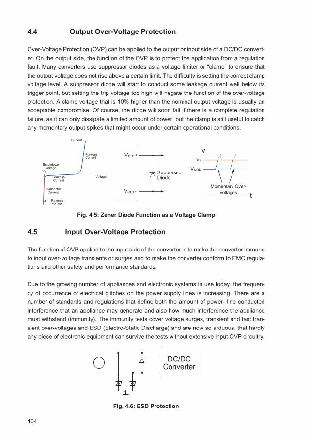
104
4.4 Output Over-Voltage Protection
Over-Voltage Protection (OVP) can be applied to the output or input side of a DC/DC convert-er. On the output side, the function of the OVP is to protect the application from a regulation fault. Many converters use suppressor diodes as a voltage limiter or “clamp” to ensure that the output voltage does not rise above a certain limit. The difficulty is setting the correct clamp voltage level. A suppressor diode will start to conduct some leakage current well below its trigger point, but setting the trip voltage too high will negate the function of the over-voltage protection. A clamp voltage that is 10% higher than the nominal output voltage is usually an acceptable compromise. Of course, the diode will soon fail if there is a complete regulation failure, as it can only dissipate a limited amount of power, but the clamp is still useful to catch any momentary output spikes that might occur under certain operational conditions.
Fig. 4.5: Zener Diode Function as a Voltage Clamp
4.5 Input Over-Voltage Protection
The function of OVP applied to the input side of the converter is to make the converter immune to input over-voltage transients or surges and to make the converter conform to EMC regula-tions and other safety and performance standards.
Due to the growing number of appliances and electronic systems in use today, the frequen-cy of occurrence of electrical glitches on the power supply lines is increasing. There are a number of standards and regulations that define both the amount of power- line conducted interference that an appliance may generate and also how much interference the appliance must withstand (immunity). The immunity tests cover voltage surges, transient and fast tran-sient over-voltages and ESD (Electro-Static Discharge) and are now so arduous, that hardly any piece of electronic equipment can survive the tests without extensive input OVP circuitry.
Fig. 4.6: ESD Protection
�������
��������������
����������������
��������������
� ��������������
� ����������
�������
��
������������ ���
������
��
�����������������
����
�����
�� �����
���������
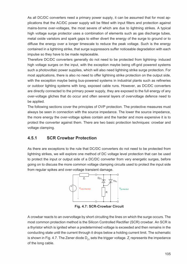
105
As all DC/DC converters need a primary power supply, it can be assumed that for most ap-plications that the AC/DC power supply will be fitted with input filters and protection against mains-borne over-voltages, the most severe of which are due to lightning strikes. A typical high voltage surge protector uses a combination of elements such as gas discharge tubes, metal oxide varistors and spark gaps to either divert the energy of the surge to ground or to diffuse the energy over a longer timescale to reduce the peak voltage. Such is the energy contained in a lightning strike, that surge suppressors suffer noticeable degradation with each impulse so they have to be made replaceable.Therefore DC/DC converters generally do not need to be protected from lightning- induced high voltage surges on the input, with the exception maybe being off-grid powered systems such a photovoltaic power supplies, which will also need lightning strike surge protection. For most applications, there is also no need to offer lightning strike protection on the output side, with the exception maybe being bus-powered systems in industrial plants such as refineries or outdoor lighting systems with long, exposed cable runs. However, as DC/DC converters are directly connected to the primary power supply, they are exposed to the full energy of any over-voltage gliches that do occur and often several layers of overvoltage defence need to be applied.The following sections cover the principles of OVP protection. The protective measures must always be seen in connection with the source impedance. The lower the source impedance, the more energy the over-voltage spikes contain and the harder and more expensive it is to protect the converter against them. There are two basic protection techniques: crowbar and voltage clamping.
4.5.1 SCR Crowbar Protection
As there are exceptions to the rule that DC/DC converters do not need to be protected from lightning strikes, we will explore one method of DC voltage level protection that can be used to protect the input or output side of a DC/DC converter from very energetic surges, before going on to discuss the more common voltage clamping circuits used to protect the input side from regular spikes and over-voltage transient damage.
Fig. 4.7: SCR-Crowbar Circuit
A crowbar reacts to an overvoltage by short circuiting the lines on which the surge occurs. The most common protection method is the Silicon Controlled Rectifier (SCR) crowbar. An SCR is a thyristor which is ignited when a predetermined voltage is exceeded and then remains in the conducting state until the current through it drops below a holding current limit. The schematic is shown in Fig. 4.7. The Zener diode DZ1 sets the trigger voltage. Zi represents the impedance of the long cable.
������������
�
�����������
�
������ �
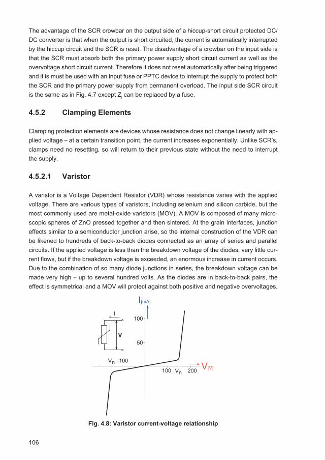
106
The advantage of the SCR crowbar on the output side of a hiccup-short circuit protected DC/DC converter is that when the output is short circuited, the current is automatically interrupted by the hiccup circuit and the SCR is reset. The disadvantage of a crowbar on the input side is that the SCR must absorb both the primary power supply short circuit current as well as the overvoltage short circuit current. Therefore it does not reset automatically after being triggered and it is must be used with an input fuse or PPTC device to interrupt the supply to protect both the SCR and the primary power supply from permanent overload. The input side SCR circuit is the same as in Fig. 4.7 except Zi can be replaced by a fuse.
4.5.2 Clamping Elements
Clamping protection elements are devices whose resistance does not change linearly with ap-plied voltage – at a certain transition point, the current increases exponentially. Unlike SCR’s, clamps need no resetting, so will return to their previous state without the need to interrupt the supply.
4.5.2.1 Varistor
A varistor is a Voltage Dependent Resistor (VDR) whose resistance varies with the applied voltage. There are various types of varistors, including selenium and silicon carbide, but the most commonly used are metal-oxide varistors (MOV). A MOV is composed of many micro-scopic spheres of ZnO pressed together and then sintered. At the grain interfaces, junction effects similar to a semiconductor junction arise, so the internal construction of the VDR can be likened to hundreds of back-to-back diodes connected as an array of series and parallel circuits. If the applied voltage is less than the breakdown voltage of the diodes, very little cur-rent flows, but if the breakdown voltage is exceeded, an enormous increase in current occurs. Due to the combination of so many diode junctions in series, the breakdown voltage can be made very high – up to several hundred volts. As the diodes are in back-to-back pairs, the effect is symmetrical and a MOV will protect against both positive and negative overvoltages.
Fig. 4.8: Varistor current-voltage relationship
�����
�
���
���
����
��� ���
���
������
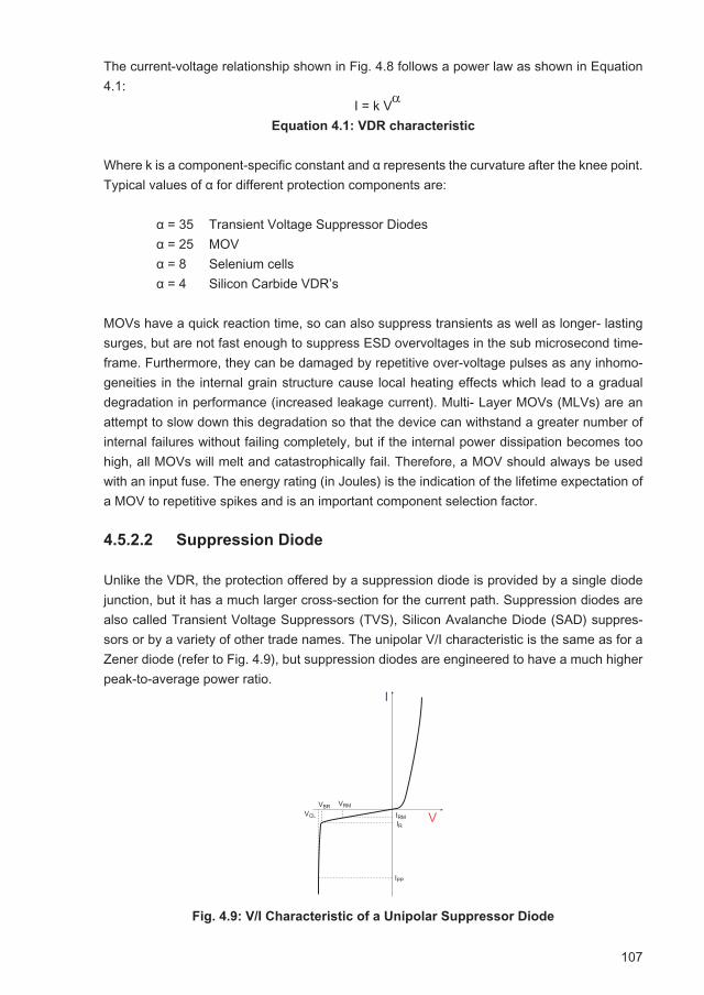
107
The current-voltage relationship shown in Fig. 4.8 follows a power law as shown in Equation 4.1:
I = k VEquation 4.1: VDR characteristic
Where k is a component-specific constant and α represents the curvature after the knee point. Typical values of α for different protection components are:
α = 35 Transient Voltage Suppressor Diodes α = 25 MOV α = 8 Selenium cells α = 4 Silicon Carbide VDR’s
MOVs have a quick reaction time, so can also suppress transients as well as longer- lasting surges, but are not fast enough to suppress ESD overvoltages in the sub microsecond time-frame. Furthermore, they can be damaged by repetitive over-voltage pulses as any inhomo-geneities in the internal grain structure cause local heating effects which lead to a gradual degradation in performance (increased leakage current). Multi- Layer MOVs (MLVs) are an attempt to slow down this degradation so that the device can withstand a greater number of internal failures without failing completely, but if the internal power dissipation becomes too high, all MOVs will melt and catastrophically fail. Therefore, a MOV should always be used with an input fuse. The energy rating (in Joules) is the indication of the lifetime expectation of a MOV to repetitive spikes and is an important component selection factor.
4.5.2.2 Suppression Diode
Unlike the VDR, the protection offered by a suppression diode is provided by a single diode junction, but it has a much larger cross-section for the current path. Suppression diodes are also called Transient Voltage Suppressors (TVS), Silicon Avalanche Diode (SAD) suppres-sors or by a variety of other trade names. The unipolar V/I characteristic is the same as for a Zener diode (refer to Fig. 4.9), but suppression diodes are engineered to have a much higher peak-to-average power ratio.
Fig. 4.9: V/I Characteristic of a Unipolar Suppressor Diode
��� ���
�����
���
����
�
α
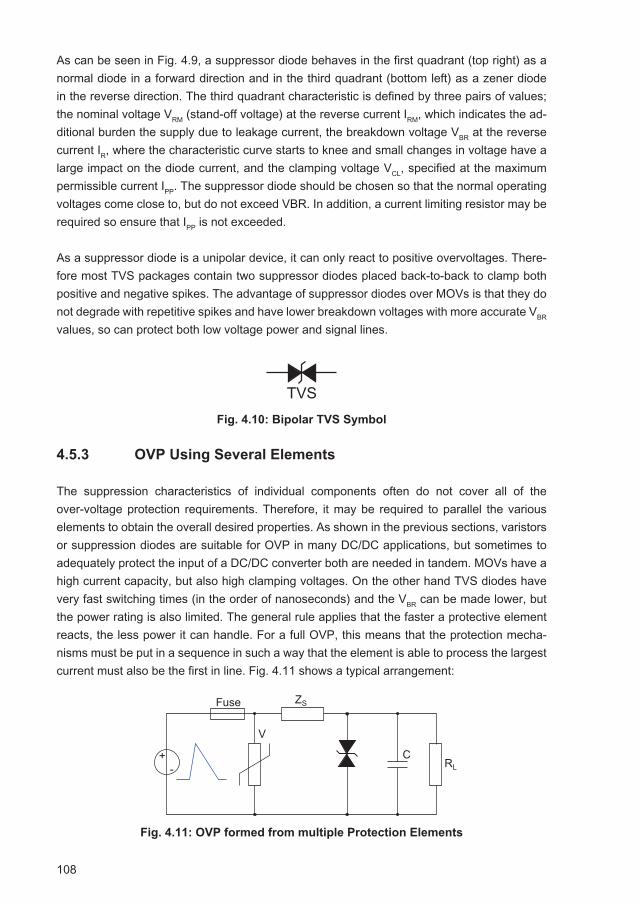
108
As can be seen in Fig. 4.9, a suppressor diode behaves in the first quadrant (top right) as a normal diode in a forward direction and in the third quadrant (bottom left) as a zener diode in the reverse direction. The third quadrant characteristic is defined by three pairs of values; the nominal voltage VRM (stand-off voltage) at the reverse current IRM, which indicates the ad-ditional burden the supply due to leakage current, the breakdown voltage VBR at the reverse current IR, where the characteristic curve starts to knee and small changes in voltage have a large impact on the diode current, and the clamping voltage VCL, specified at the maximum permissible current IPP. The suppressor diode should be chosen so that the normal operating voltages come close to, but do not exceed VBR. In addition, a current limiting resistor may be required so ensure that IPP is not exceeded.
As a suppressor diode is a unipolar device, it can only react to positive overvoltages. There-fore most TVS packages contain two suppressor diodes placed back-to-back to clamp both positive and negative spikes. The advantage of suppressor diodes over MOVs is that they do not degrade with repetitive spikes and have lower breakdown voltages with more accurate VBR values, so can protect both low voltage power and signal lines.
Fig. 4.10: Bipolar TVS Symbol
4.5.3 OVP Using Several Elements
The suppression characteristics of individual components often do not cover all of the over-voltage protection requirements. Therefore, it may be required to parallel the various elements to obtain the overall desired properties. As shown in the previous sections, varistors or suppression diodes are suitable for OVP in many DC/DC applications, but sometimes to adequately protect the input of a DC/DC converter both are needed in tandem. MOVs have a high current capacity, but also high clamping voltages. On the other hand TVS diodes have very fast switching times (in the order of nanoseconds) and the VBR can be made lower, but the power rating is also limited. The general rule applies that the faster a protective element reacts, the less power it can handle. For a full OVP, this means that the protection mecha-nisms must be put in a sequence in such a way that the element is able to process the largest current must also be the first in line. Fig. 4.11 shows a typical arrangement:
Fig. 4.11: OVP formed from multiple Protection Elements
���
���� ��
��
�
���
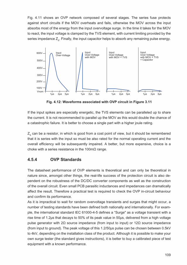
109
Fig. 4.11 shows an OVP network composed of several stages. The series fuse protects against short circuits if the MOV overheats and fails, otherwise the MOV across the input absorbs most of the energy from the input overvoltage surge. In the time it takes for the MOV to react, the input voltage is clamped by the TVS element, with current limiting provided by the series impedance ZS. Finally, the input capacitor helps to absorb any remaining pulse energy.
Fig. 4.12: Waveforms associated with OVP circuit in Figure 3.11
If the input spikes are especially energetic, the TVS elements can be paralleled up to share the current. It is not recommended to parallel up the MOV as this would double the chance of a catastrophic failure. It is better to choose a single part with a higher joule rating.
ZS can be a resistor, in which is good from a cost point of view, but it should be remembered that it is series with the input so must be also rated for the normal operating current and the overall efficiency will be subsequently impaired. A better, but more expensive, choice is a choke with a series resistance in the 100mΩ range.
4.5.4 OVP Standards
The datasheet performance of OVP elements is theoretical and can only be theoretical in nature since, amongst other things, the real-life success of the protection circuit is also de-pendent on the robustness of the DC/DC converter components as well as the construction of the overall circuit. Even small PCB parasitic inductances and impedances can dramatically affect the result. Therefore a practical test is required to check the OVP in-circuit behaviour and confirm its performance.As it is impractical to wait for random overvoltage transients and surges that might occur, a number of testing standards have been defined both nationally and internationally. For exam-ple, the international standard IEC 61000-4-5 defines a “Surge" as a voltage transient with a rise time of 1.2μs that decays to 50% of its peak value in 50μs, delivered from a high voltage pulse generator with 2Ω source impedance (from input to input) or 12Ω source impedance (from input to ground). The peak voltage of this 1.2/50μs pulse can be chosen between 0.5kV to 4kV, depending on the installation class of the product. Although it is possible to make your own surge tester (the standard gives instructions), it is better to buy a calibrated piece of test equipment with a known performance.
��� ��� ��� ��� ��� ��� ��� ��� ��� ��� ��� �����������
����
����
����
����
���� ������ ��������
������ ����������������
������ ����������������������
������ ���������������������������������
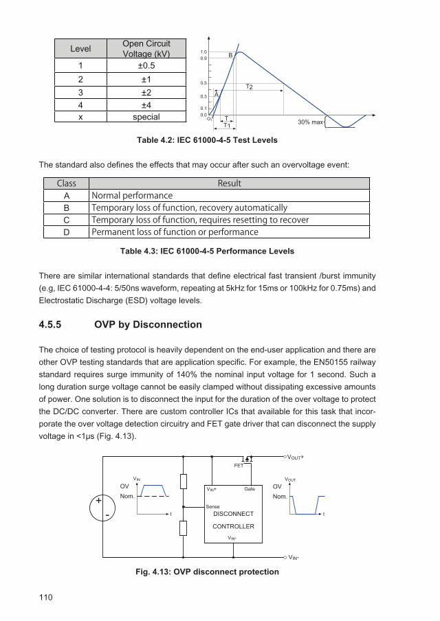
110
Table 4.2: IEC 61000-4-5 Test Levels
The standard also defines the effects that may occur after such an overvoltage event:
Table 4.3: IEC 61000-4-5 Performance Levels
There are similar international standards that define electrical fast transient /burst immunity (e.g, IEC 61000-4-4: 5/50ns waveform, repeating at 5kHz for 15ms or 100kHz for 0.75ms) and Electrostatic Discharge (ESD) voltage levels.
4.5.5 OVP by Disconnection
The choice of testing protocol is heavily dependent on the end-user application and there are other OVP testing standards that are application specific. For example, the EN50155 railway standard requires surge immunity of 140% the nominal input voltage for 1 second. Such a long duration surge voltage cannot be easily clamped without dissipating excessive amounts of power. One solution is to disconnect the input for the duration of the over voltage to protect the DC/DC converter. There are custom controller ICs that available for this task that incor-porate the over voltage detection circuitry and FET gate driver that can disconnect the supply voltage in <1μs (Fig. 4.13).
Fig. 4.13: OVP disconnect protection
������
���
���
������
��������
��
���
�
�
��
���
����
�����
��
����
��
����
�����
���������
������
��
��
�������
����
����
����
Level Open Circuit Voltage (kV)
1 ±0.52 ±13 ±24 ±4x special
Class ResultA Normal performanceB Temporary loss of function, recovery automaticallyC Temporary loss of function, requires resetting to recoverD Permanent loss of function or performance
111
The disconnect method of OVP is not only useful for long duration over-voltage protection, it is also one of the only reliable protection circuits for very low input voltages. A DC/DC convert-er’s input voltage of, say, 1.2V cannot be easily protected using conventional OVP elements because the temperature coefficient is a significant source of error: either the diodes will start to conduct at the nominal voltage or the clamping voltage will be too high to be useful.
Of course, the disadvantage of disconnect OVP is that the DC/DC converter is deprived of power during the overvoltage event. For short disconnect durations, the input voltage to the DC/DC can be maintained by adding a large capacitor across the input, but for long duration disconnects, a battery-back up or supercap system may be required. The next section ex-plores this solution.
4.6 Voltage Dips and Interruptions
In power distribution systems, sudden load increases can cause significant voltage drops. These short-term dips should ideally have no impact on the subsequent power supply com-ponents. To protect a DC/DC converter from input voltage dips and interruptions, the usual solution is to store sufficient energy in a capacitor to keep the converter operational during the brown-out or black-out periods. Fig. 4.14 shows a simple circuit.
Fig. 4.14: Bridging Input Voltage Dips and Interruptions
The circuit consists of a decoupling diode D and one or more capacitors C. The capacitor C is charged in normal operation to the operating voltage VIN - VDiode. With an input voltage dip or interruption, the diode blocks the reverse current flow and prevents the capacitor from discharging back into the supply, so that all of the stored energy in the capacitor C is now available to the DC/DC converter. The voltage on the capacitor now starts to decay as it dis-charges into the DC/DC converter, but it is a complex relationship to calculate because the DC/DC converter is a constant power device, so the input current is inversely proportional to the input voltage.
The energy stored in a capacitor, EC, is equal to the capacitance, C, multiplied by the square of the voltage, VC, where VC is equal to the input voltage VIN minus the volt drop across the diode, D.
����
������
������
�
���
����
����
112
If at t0 = 0, the input voltage is interrupted, the voltage on the capacitor will begin to decay exponentially according to the capacitor discharge equation:
The charged capacitor can be discharged until time t1. The time t1 is the time at which the capacitor voltage VC is equal to the minimum input voltage VIN,MIN of the DC/DC converter.The remaining energy in the capacitor is then:
The energy required to back up the input voltage over the period t0 - t1 is thus:
EBACK = EC(t0) - EC(t1) = 0.5 C (VIN² - VIN,MIN²)
This energy must supply the necessary input power over the back-up period tBACK.The required input power can be calculated from the output power and efficiency to give:
Equation 4.2: Back-up Time Calculation
This equation can be rearranged to give the required back up capacitance:
Equation 4.3: Bridging Capacitor Calculation
These equations tell us that the larger the back-up capacitance, the longer the back-up time, but as large capacitors take up a lot of board space, there are often physical limitations on the size of C. However, the equations also tell us that the stored energy is proportional to VC
2, so the wider the input voltage range of the DC/DC converter the better. The DC/DC converter should be selected so that nominal VIN is close to the maximum input voltage of the converter to get the maximum back-up time. Additionally, a high efficiency or load derating helps.
There are two disadvantages to the simple circuit in Fig. 4.14. The voltage drop across diode D is an additional loss that will reduce the efficiency during normal operation and the high inrush current to charge the large back-up capacitor can be a problem for the primary supply. Both of these problems can be solved by a variation of the disconnect controller shown in Fig. 4.17 that disconnects on an under-voltage instead of an over-voltage and also has a soft-start function to reduce the inrush current.
EC =21 C VC
2
EC (t1) = 21 C VIN,MIN
2
tBACK = EBACK
POUT
=
2 POUT
C (VIN2 - VIN,MIN
2)
CBACK =
2 tBACK POUT
(VIN2 - VIN,MIN
2)
VC (t) = VC (t = 0) e-t/RC
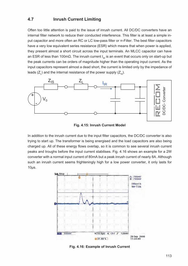
113
4.7 Inrush Current Limiting
Often too little attention is paid to the issue of inrush current. All DC/DC converters have an internal filter network to reduce their conducted interference. This filter is at least a simple in-put capacitor and more often an RC or LC low-pass filter or π-Filter. The best filter capacitors have a very low equivalent series resistance (ESR) which means that when power is applied, they present almost a short circuit across the input terminals. An MLCC capacitor can have an ESR of less than 100mΩ. The inrush current IIR is an event that occurs only on start-up but the peak currents can be orders of magnitude higher than the operating input current. As the input capacitors represent almost a dead short, the current is limited only by the impedance of leads (ZL) and the internal resistance of the power supply (ZIS).
Fig. 4.15: Inrush Current Model
In addition to the inrush current due to the input filter capacitors, the DC/DC converter is also trying to start up. The transformer is being energised and the load capacitors are also being charged up. All of these energy flows overlap, so it is common to see several inrush current peaks and troughs before the input current stabilises. Fig. 4.16 shows an example for a 2W converter with a normal input current of 80mA but a peak inrush current of nearly 8A. Although such an inrush current seems frighteningly high for a low power converter, it only lasts for 10μs.
Fig. 4.16: Example of Inrush Current
����
������
������
���
��
��� ��
�
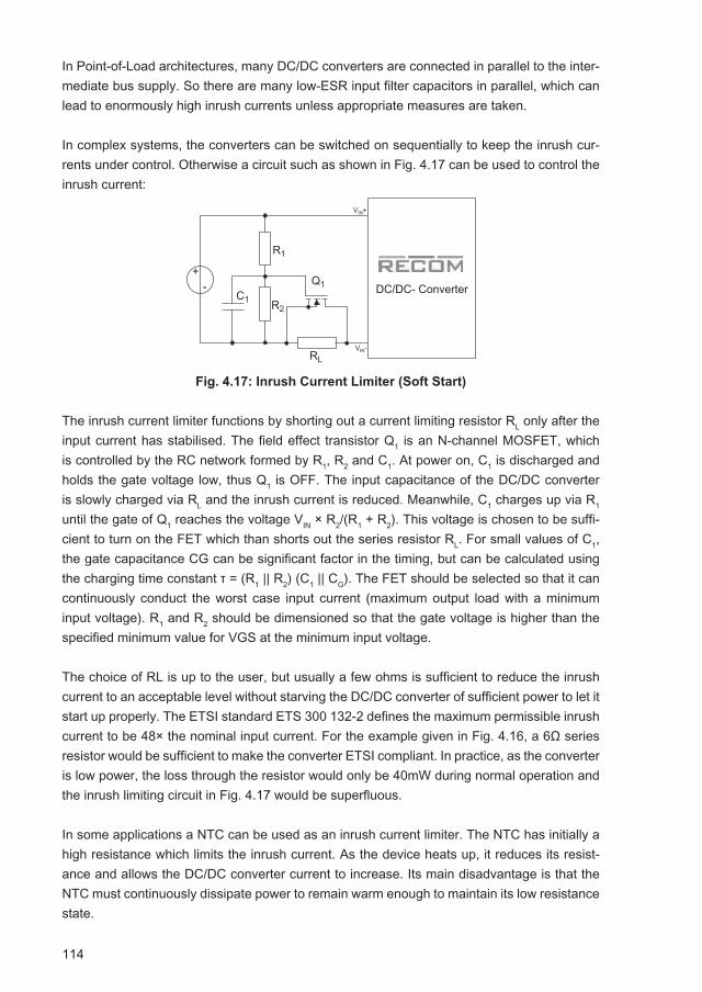
114
In Point-of-Load architectures, many DC/DC converters are connected in parallel to the inter-mediate bus supply. So there are many low-ESR input filter capacitors in parallel, which can lead to enormously high inrush currents unless appropriate measures are taken.
In complex systems, the converters can be switched on sequentially to keep the inrush cur-rents under control. Otherwise a circuit such as shown in Fig. 4.17 can be used to control the inrush current:
Fig. 4.17: Inrush Current Limiter (Soft Start)
The inrush current limiter functions by shorting out a current limiting resistor RL only after the input current has stabilised. The field effect transistor Q1 is an N-channel MOSFET, which is controlled by the RC network formed by R1, R2 and C1. At power on, C1 is discharged and holds the gate voltage low, thus Q1 is OFF. The input capacitance of the DC/DC converter is slowly charged via RL and the inrush current is reduced. Meanwhile, C1 charges up via R1 until the gate of Q1 reaches the voltage VIN × R2/(R1 + R2). This voltage is chosen to be suffi-cient to turn on the FET which than shorts out the series resistor RL. For small values of C1, the gate capacitance CG can be significant factor in the timing, but can be calculated using the charging time constant τ = (R1 || R2) (C1 || CG). The FET should be selected so that it can continuously conduct the worst case input current (maximum output load with a minimum input voltage). R1 and R2 should be dimensioned so that the gate voltage is higher than the specified minimum value for VGS at the minimum input voltage.
The choice of RL is up to the user, but usually a few ohms is sufficient to reduce the inrush current to an acceptable level without starving the DC/DC converter of sufficient power to let it start up properly. The ETSI standard ETS 300 132-2 defines the maximum permissible inrush current to be 48× the nominal input current. For the example given in Fig. 4.16, a 6Ω series resistor would be sufficient to make the converter ETSI compliant. In practice, as the converter is low power, the loss through the resistor would only be 40mW during normal operation and the inrush limiting circuit in Fig. 4.17 would be superfluous.
In some applications a NTC can be used as an inrush current limiter. The NTC has initially a high resistance which limits the inrush current. As the device heats up, it reduces its resist-ance and allows the DC/DC converter current to increase. Its main disadvantage is that the NTC must continuously dissipate power to remain warm enough to maintain its low resistance state.
����������������
��
����
��
��
��
� ��
� ��
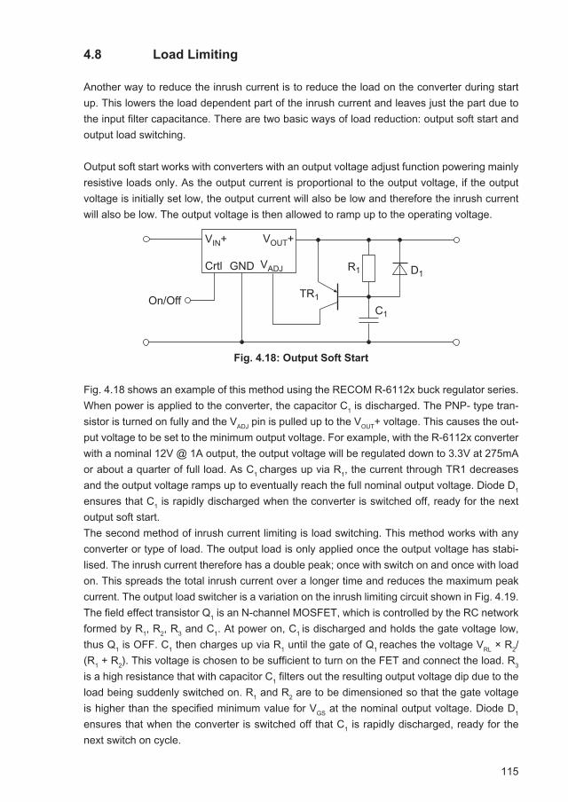
115
4.8 Load Limiting
Another way to reduce the inrush current is to reduce the load on the converter during start up. This lowers the load dependent part of the inrush current and leaves just the part due to the input filter capacitance. There are two basic ways of load reduction: output soft start and output load switching.
Output soft start works with converters with an output voltage adjust function powering mainly resistive loads only. As the output current is proportional to the output voltage, if the output voltage is initially set low, the output current will also be low and therefore the inrush current will also be low. The output voltage is then allowed to ramp up to the operating voltage.
Fig. 4.18: Output Soft Start
Fig. 4.18 shows an example of this method using the RECOM R-6112x buck regulator series. When power is applied to the converter, the capacitor C1 is discharged. The PNP- type tran-sistor is turned on fully and the VADJ pin is pulled up to the VOUT+ voltage. This causes the out-put voltage to be set to the minimum output voltage. For example, with the R-6112x converter with a nominal 12V @ 1A output, the output voltage will be regulated down to 3.3V at 275mA or about a quarter of full load. As C1 charges up via R1, the current through TR1 decreases and the output voltage ramps up to eventually reach the full nominal output voltage. Diode D1 ensures that C1 is rapidly discharged when the converter is switched off, ready for the next output soft start.The second method of inrush current limiting is load switching. This method works with any converter or type of load. The output load is only applied once the output voltage has stabi-lised. The inrush current therefore has a double peak; once with switch on and once with load on. This spreads the total inrush current over a longer time and reduces the maximum peak current. The output load switcher is a variation on the inrush limiting circuit shown in Fig. 4.19. The field effect transistor Q1 is an N-channel MOSFET, which is controlled by the RC network formed by R1, R2, R3 and C1. At power on, C1 is discharged and holds the gate voltage low, thus Q1 is OFF. C1 then charges up via R1 until the gate of Q1 reaches the voltage VRL × R2/(R1 + R2). This voltage is chosen to be sufficient to turn on the FET and connect the load. R3 is a high resistance that with capacitor C1 filters out the resulting output voltage dip due to the load being suddenly switched on. R1 and R2 are to be dimensioned so that the gate voltage is higher than the specified minimum value for VGS at the nominal output voltage. Diode D1 ensures that when the converter is switched off that C1 is rapidly discharged, ready for the next switch on cycle.
�� ��
��
����
���
�����
���� ���
������
� ��
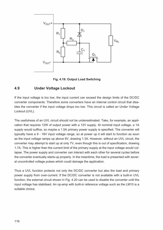
116
Fig. 4.19: Output Load Switching
4.9 Under Voltage Lockout
If the input voltage is too low, the input current can exceed the design limits of the DC/DC converter components. Therefore some converters have an internal control circuit that disa-bles the converter if the input voltage drops too low. This circuit is called an Under Voltage Lockout (UVL).
The usefulness of an UVL circuit should not be underestimated. Take, for example, an appli-cation that requires 12W of output power with a 12V supply. At nominal input voltage, a 1A supply would suffice, so maybe a 1.5A primary power supply is specified. The converter will typically have a 9 - 18V input voltage range, so at power up it will start to function as soon as the input voltage ramps up above 9V, drawing 1.3A. However, without an UVL circuit, the converter may attempt to start up at only 7V, even though this is out of specification, drawing 1.7A. This is higher than the current limit of the primary supply at the input voltage would col-lapse. The power supply and converter can interact with each other for several cycles before the converter eventually starts-up properly. In the meantime, the load is presented with sever-al uncontrolled voltage pulses which could damage the application.
Thus a UVL function protects not only the DC/DC converter but also the load and primary power supply from over-current. If the DC/DC converter is not available with a built-in UVL function, the external circuit shown in Fig. 4.20 can be used to disable the converter until the input voltage has stabilised. An op-amp with built-in reference voltage such as the LM10 is a suitable choice.
��
����
��
�����
��
�����
��
���
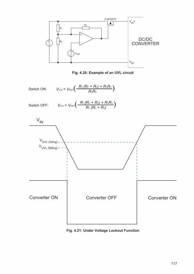
117
Fig. 4.20: Example of an UVL circuit
Switch ON:
Switch OFF:
Fig. 4.21: Under Voltage Lockout Function
��
��
����
��������
�
�
�
�
��
����
�� �����������
��
����
���
������������������������� ������������
����������� �
��������� �
VUVL = VREF ( R1 (R2 + R3) + R2R3
R2R3)
VUVL = VREF ( R1 (R2 + R3) + R2R3
R2 (R2 + R3) )
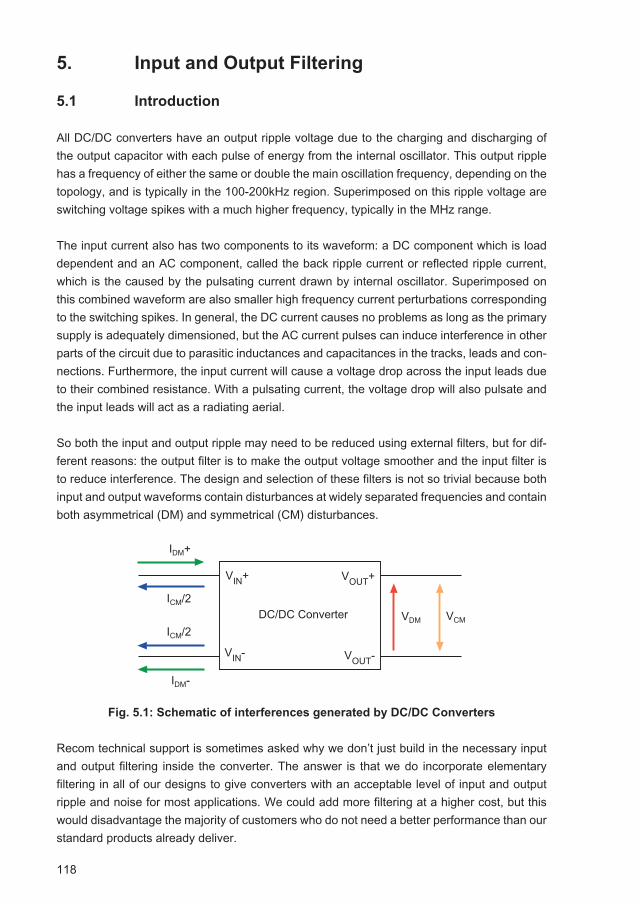
118
5. Input and Output Filtering
5.1 Introduction
All DC/DC converters have an output ripple voltage due to the charging and discharging of the output capacitor with each pulse of energy from the internal oscillator. This output ripple has a frequency of either the same or double the main oscillation frequency, depending on the topology, and is typically in the 100-200kHz region. Superimposed on this ripple voltage are switching voltage spikes with a much higher frequency, typically in the MHz range.
The input current also has two components to its waveform: a DC component which is load dependent and an AC component, called the back ripple current or reflected ripple current, which is the caused by the pulsating current drawn by internal oscillator. Superimposed on this combined waveform are also smaller high frequency current perturbations corresponding to the switching spikes. In general, the DC current causes no problems as long as the primary supply is adequately dimensioned, but the AC current pulses can induce interference in other parts of the circuit due to parasitic inductances and capacitances in the tracks, leads and con-nections. Furthermore, the input current will cause a voltage drop across the input leads due to their combined resistance. With a pulsating current, the voltage drop will also pulsate and the input leads will act as a radiating aerial.
So both the input and output ripple may need to be reduced using external filters, but for dif-ferent reasons: the output filter is to make the output voltage smoother and the input filter is to reduce interference. The design and selection of these filters is not so trivial because both input and output waveforms contain disturbances at widely separated frequencies and contain both asymmetrical (DM) and symmetrical (CM) disturbances.
Fig. 5.1: Schematic of interferences generated by DC/DC Converters
Recom technical support is sometimes asked why we don’t just build in the necessary input and output filtering inside the converter. The answer is that we do incorporate elementary filtering in all of our designs to give converters with an acceptable level of input and output ripple and noise for most applications. We could add more filtering at a higher cost, but this would disadvantage the majority of customers who do not need a better performance than our standard products already deliver.
����
�����
�����
����
��� ������������������
����
���� �� ��
�� ��
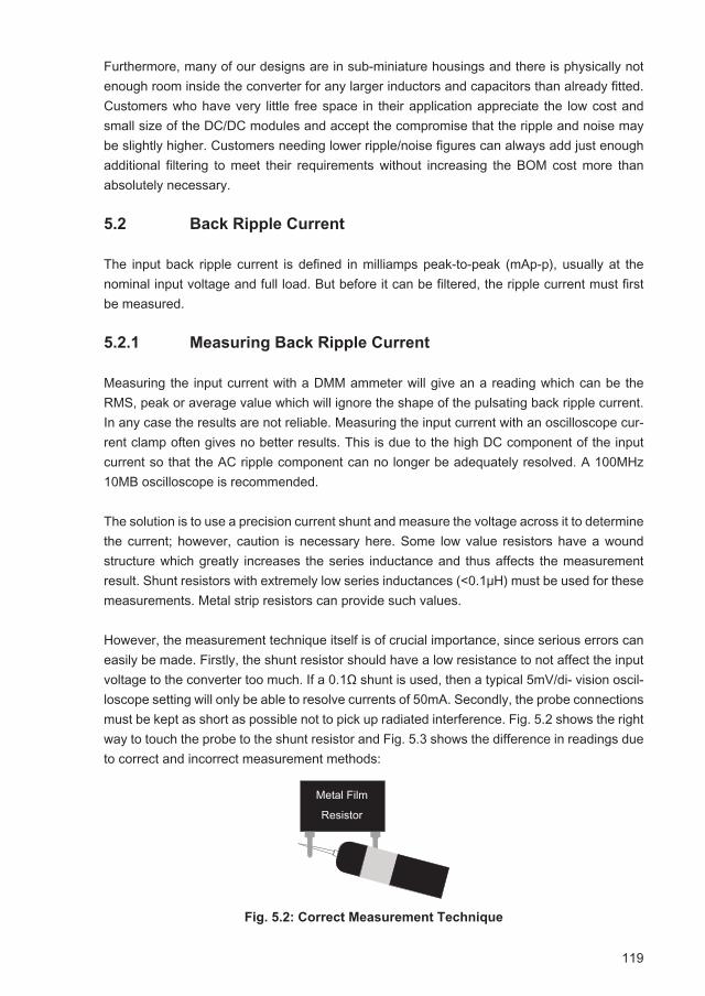
119
Furthermore, many of our designs are in sub-miniature housings and there is physically not enough room inside the converter for any larger inductors and capacitors than already fitted. Customers who have very little free space in their application appreciate the low cost and small size of the DC/DC modules and accept the compromise that the ripple and noise may be slightly higher. Customers needing lower ripple/noise figures can always add just enough additional filtering to meet their requirements without increasing the BOM cost more than absolutely necessary.
5.2 Back Ripple Current
The input back ripple current is defined in milliamps peak-to-peak (mAp-p), usually at the nominal input voltage and full load. But before it can be filtered, the ripple current must first be measured.
5.2.1 Measuring Back Ripple Current
Measuring the input current with a DMM ammeter will give an a reading which can be the RMS, peak or average value which will ignore the shape of the pulsating back ripple current. In any case the results are not reliable. Measuring the input current with an oscilloscope cur-rent clamp often gives no better results. This is due to the high DC component of the input current so that the AC ripple component can no longer be adequately resolved. A 100MHz 10MB oscilloscope is recommended.
The solution is to use a precision current shunt and measure the voltage across it to determine the current; however, caution is necessary here. Some low value resistors have a wound structure which greatly increases the series inductance and thus affects the measurement result. Shunt resistors with extremely low series inductances (<0.1μH) must be used for these measurements. Metal strip resistors can provide such values.
However, the measurement technique itself is of crucial importance, since serious errors can easily be made. Firstly, the shunt resistor should have a low resistance to not affect the input voltage to the converter too much. If a 0.1Ω shunt is used, then a typical 5mV/di- vision oscil-loscope setting will only be able to resolve currents of 50mA. Secondly, the probe connections must be kept as short as possible not to pick up radiated interference. Fig. 5.2 shows the right way to touch the probe to the shunt resistor and Fig. 5.3 shows the difference in readings due to correct and incorrect measurement methods:
Fig. 5.2: Correct Measurement Technique
����������
��������
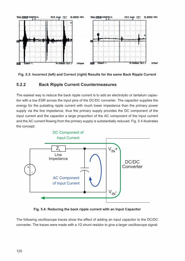
120
Fig. 5.3: Incorrect (left) and Correct (right) Results for the same Back Ripple Current
5.2.2 Back Ripple Current Countermeasures
The easiest way to reduce the back ripple current is to add an electrolytic or tantalum capac-itor with a low ESR across the input pins of the DC/DC converter. The capacitor supplies the energy for the pulsating ripple current with much lower impedance than the primary power supply via the line impedance, thus the primary supply provides the DC component of the input current and the capacitor a large proportion of the AC component of the input current and the AC current flowing from the primary supply is substantially reduced. Fig. 5.4 illustrates the concept:
Fig. 5.4: Reducing the back ripple current with an Input Capacitor
The following oscilloscope traces show the effect of adding an input capacitor to the DC/DC converter. The traces were made with a 1Ω shunt resistor to give a larger oscilloscope signal:
��
���������������
�
��������� ���
�������������������������
�������������������������
����
����
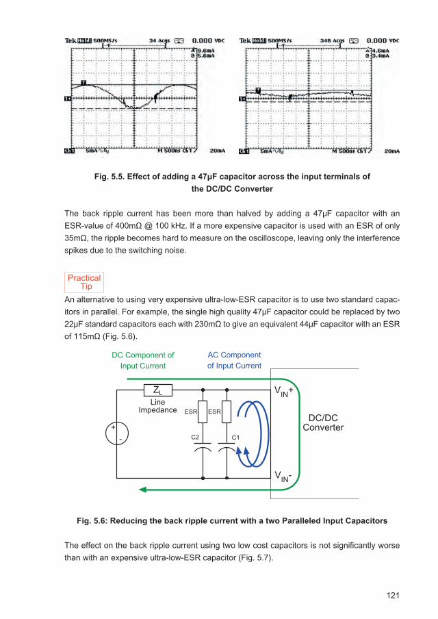
121
Fig. 5.5. Effect of adding a 47μF capacitor across the input terminals of
the DC/DC Converter
The back ripple current has been more than halved by adding a 47μF capacitor with an ESR-value of 400mΩ @ 100 kHz. If a more expensive capacitor is used with an ESR of only 35mΩ, the ripple becomes hard to measure on the oscilloscope, leaving only the interference spikes due to the switching noise.
An alternative to using very expensive ultra-low-ESR capacitor is to use two standard capac-itors in parallel. For example, the single high quality 47μF capacitor could be replaced by two 22μF standard capacitors each with 230mΩ to give an equivalent 44μF capacitor with an ESR of 115mΩ (Fig. 5.6).
Fig. 5.6: Reducing the back ripple current with a two Paralleled Input Capacitors
The effect on the back ripple current using two low cost capacitors is not significantly worse than with an expensive ultra-low-ESR capacitor (Fig. 5.7).
��
���������������
�
��������� ���
�������������������������
�������������������������
��� ���
�� ��
����
����
Practical Tip
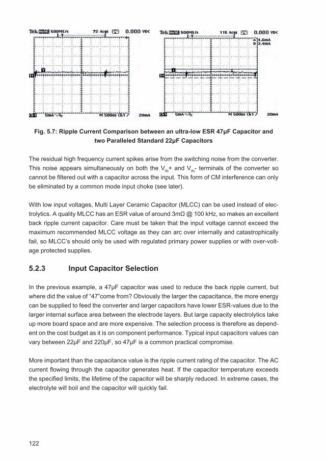
122
Fig. 5.7: Ripple Current Comparison between an ultra-low ESR 47μF Capacitor and
two Paralleled Standard 22μF Capacitors
The residual high frequency current spikes arise from the switching noise from the converter. This noise appears simultaneously on both the VIN+ and VIN- terminals of the converter so cannot be filtered out with a capacitor across the input. This form of CM interference can only be eliminated by a common mode input choke (see later).
With low input voltages, Multi Layer Ceramic Capacitor (MLCC) can be used instead of elec-trolytics. A quality MLCC has an ESR value of around 3mΩ @ 100 kHz, so makes an excellent back ripple current capacitor. Care must be taken that the input voltage cannot exceed the maximum recommended MLCC voltage as they can arc over internally and catastrophically fail, so MLCC’s should only be used with regulated primary power supplies or with over-volt-age protected supplies.
5.2.3 Input Capacitor Selection
In the previous example, a 47μF capacitor was used to reduce the back ripple current, but where did the value of “47”come from? Obviously the larger the capacitance, the more energy can be supplied to feed the converter and larger capacitors have lower ESR-values due to the larger internal surface area between the electrode layers. But large capacity electrolytics take up more board space and are more expensive. The selection process is therefore as depend-ent on the cost budget as it is on component performance. Typical input capacitors values can vary between 22μF and 220μF, so 47μF is a common practical compromise.
More important than the capacitance value is the ripple current rating of the capacitor. The AC current flowing through the capacitor generates heat. If the capacitor temperature exceeds the specified limits, the lifetime of the capacitor will be sharply reduced. In extreme cases, the electrolyte will boil and the capacitor will quickly fail.
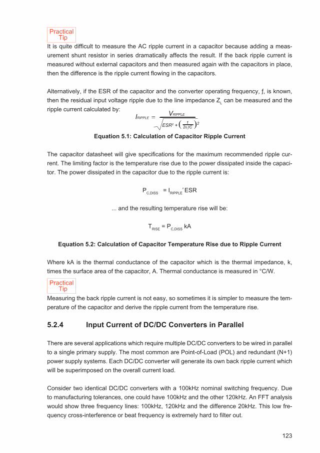
123
It is quite difficult to measure the AC ripple current in a capacitor because adding a meas-urement shunt resistor in series dramatically affects the result. If the back ripple current is measured without external capacitors and then measured again with the capacitors in place, then the difference is the ripple current flowing in the capacitors.
Alternatively, if the ESR of the capacitor and the converter operating frequency, ƒ, is known, then the residual input voltage ripple due to the line impedance ZL can be measured and the ripple current calculated by:
Equation 5.1: Calculation of Capacitor Ripple Current
The capacitor datasheet will give specifications for the maximum recommended ripple cur-rent. The limiting factor is the temperature rise due to the power dissipated inside the capaci-tor. The power dissipated in the capacitor due to the ripple current is:
PC,DISS = IRIPPLE² ESR
... and the resulting temperature rise will be:
TRISE = PC,DISS kA
Equation 5.2: Calculation of Capacitor Temperature Rise due to Ripple Current
Where kA is the thermal conductance of the capacitor which is the thermal impedance, k, times the surface area of the capacitor, A. Thermal conductance is measured in °C/W.
Measuring the back ripple current is not easy, so sometimes it is simpler to measure the tem-perature of the capacitor and derive the ripple current from the temperature rise.
5.2.4 Input Current of DC/DC Converters in Parallel
There are several applications which require multiple DC/DC converters to be wired in parallel to a single primary supply. The most common are Point-of-Load (POL) and redundant (N+1) power supply systems. Each DC/DC converter will generate its own back ripple current which will be superimposed on the overall current load.
Consider two identical DC/DC converters with a 100kHz nominal switching frequency. Due to manufacturing tolerances, one could have 100kHz and the other 120kHz. An FFT analysis would show three frequency lines: 100kHz, 120kHz and the difference 20kHz. This low fre-quency cross-interference or beat frequency is extremely hard to filter out.
IRIPPLE = ESR2 + ( )2
VRIPPLE
2πƒ 1
C
Practical Tip
Practical Tip
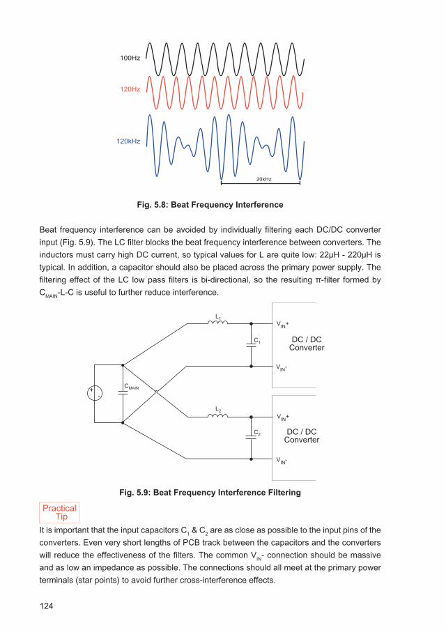
124
Fig. 5.8: Beat Frequency Interference
Beat frequency interference can be avoided by individually filtering each DC/DC converter input (Fig. 5.9). The LC filter blocks the beat frequency interference between converters. The inductors must carry high DC current, so typical values for L are quite low: 22μH - 220μH is typical. In addition, a capacitor should also be placed across the primary power supply. The filtering effect of the LC low pass filters is bi-directional, so the resulting π-filter formed by CMAIN-L-C is useful to further reduce interference.
Fig. 5.9: Beat Frequency Interference Filtering
It is important that the input capacitors C1 & C2 are as close as possible to the input pins of the converters. Even very short lengths of PCB track between the capacitors and the converters will reduce the effectiveness of the filters. The common VIN- connection should be massive and as low an impedance as possible. The connections should all meet at the primary power terminals (star points) to avoid further cross-interference effects.
�����
�����
������
�����
��
����������������
�����
��
�
��
� ����������������
����
����
����
����
Practical Tip
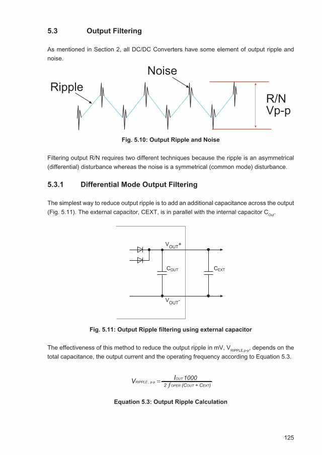
125
5.3 Output Filtering
As mentioned in Section 2, all DC/DC Converters have some element of output ripple and noise.
Fig. 5.10: Output Ripple and Noise
Filtering output R/N requires two different techniques because the ripple is an asymmetrical (differential) disturbance whereas the noise is a symmetrical (common mode) disturbance.
5.3.1 Differential Mode Output Filtering
The simplest way to reduce output ripple is to add an additional capacitance across the output (Fig. 5.11). The external capacitor, CEXT, is in parallel with the internal capacitor COut.
Fig. 5.11: Output Ripple filtering using external capacitor
The effectiveness of this method to reduce the output ripple in mV, VRIPPLE,p-p, depends on the total capacitance, the output current and the operating frequency according to Equation 5.3.
Equation 5.3: Output Ripple Calculation
���� ����
�����
�����
�����������
�������
VRIPPLE , p-p = 2 ƒOPER (COUT + CEXT)
IOUT 1000
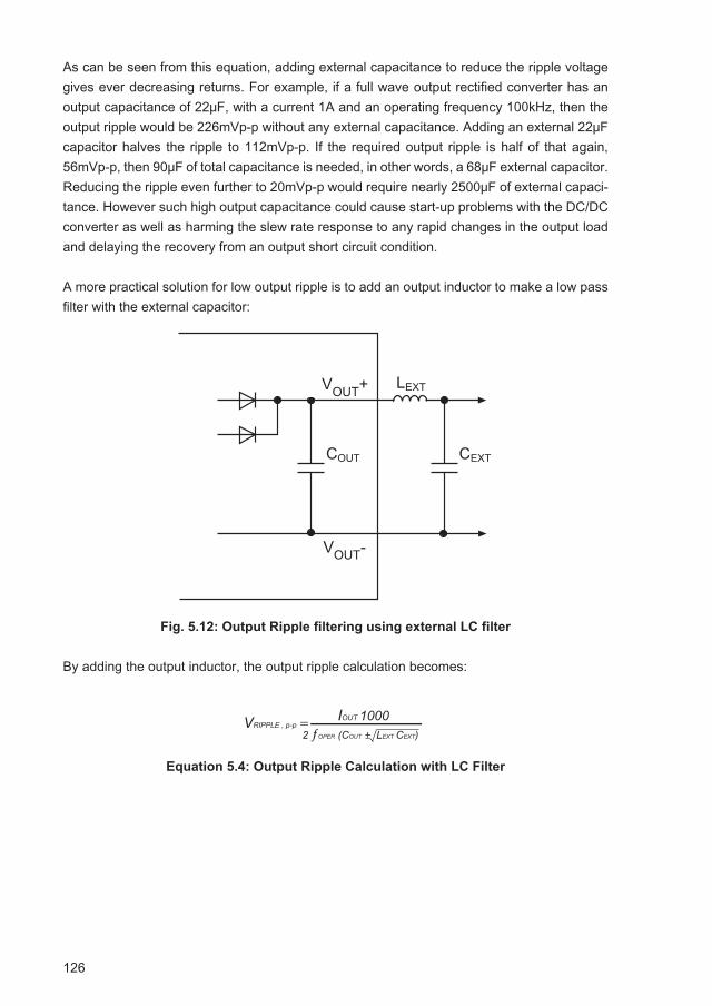
126
As can be seen from this equation, adding external capacitance to reduce the ripple voltage gives ever decreasing returns. For example, if a full wave output rectified converter has an output capacitance of 22μF, with a current 1A and an operating frequency 100kHz, then the output ripple would be 226mVp-p without any external capacitance. Adding an external 22μF capacitor halves the ripple to 112mVp-p. If the required output ripple is half of that again, 56mVp-p, then 90μF of total capacitance is needed, in other words, a 68μF external capacitor. Reducing the ripple even further to 20mVp-p would require nearly 2500μF of external capaci-tance. However such high output capacitance could cause start-up problems with the DC/DC converter as well as harming the slew rate response to any rapid changes in the output load and delaying the recovery from an output short circuit condition.
A more practical solution for low output ripple is to add an output inductor to make a low pass filter with the external capacitor:
Fig. 5.12: Output Ripple filtering using external LC filter
By adding the output inductor, the output ripple calculation becomes:
Equation 5.4: Output Ripple Calculation with LC Filter
���� ����
����
�����
�����
VRIPPLE , p-p = 2 ƒOPER (COUT + LEXT CEXT)
IOUT 1000
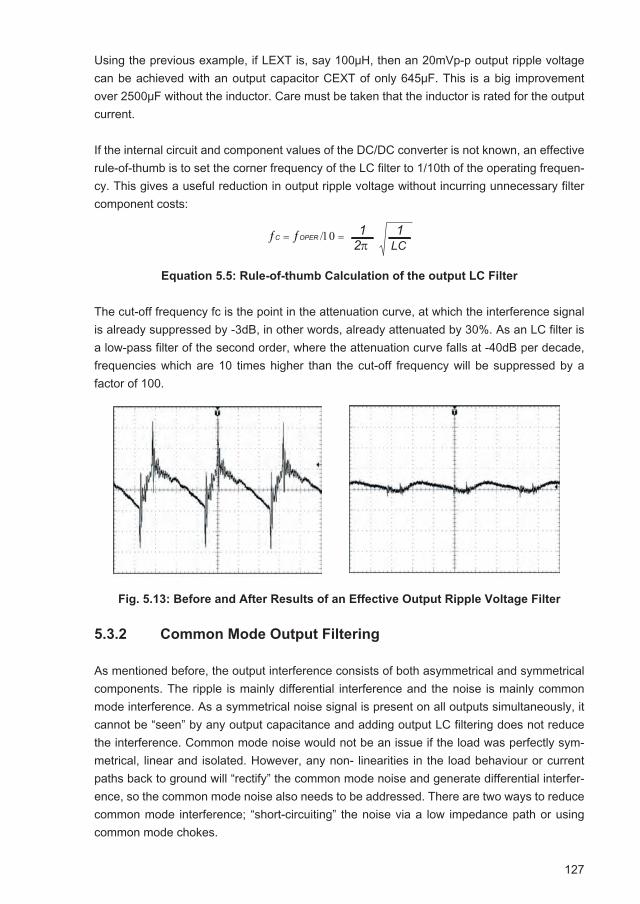
127
Using the previous example, if LEXT is, say 100μH, then an 20mVp-p output ripple voltage can be achieved with an output capacitor CEXT of only 645μF. This is a big improvement over 2500μF without the inductor. Care must be taken that the inductor is rated for the output current.
If the internal circuit and component values of the DC/DC converter is not known, an effective rule-of-thumb is to set the corner frequency of the LC filter to 1/10th of the operating frequen-cy. This gives a useful reduction in output ripple voltage without incurring unnecessary filter component costs:
Equation 5.5: Rule-of-thumb Calculation of the output LC Filter
The cut-off frequency fc is the point in the attenuation curve, at which the interference signal is already suppressed by -3dB, in other words, already attenuated by 30%. As an LC filter is a low-pass filter of the second order, where the attenuation curve falls at -40dB per decade, frequencies which are 10 times higher than the cut-off frequency will be suppressed by a factor of 100.
Fig. 5.13: Before and After Results of an Effective Output Ripple Voltage Filter
5.3.2 Common Mode Output Filtering
As mentioned before, the output interference consists of both asymmetrical and symmetrical components. The ripple is mainly differential interference and the noise is mainly common mode interference. As a symmetrical noise signal is present on all outputs simultaneously, it cannot be “seen” by any output capacitance and adding output LC filtering does not reduce the interference. Common mode noise would not be an issue if the load was perfectly sym-metrical, linear and isolated. However, any non- linearities in the load behaviour or current paths back to ground will “rectify” the common mode noise and generate differential interfer-ence, so the common mode noise also needs to be addressed. There are two ways to reduce common mode interference; “short-circuiting” the noise via a low impedance path or using common mode chokes.
ƒC = ƒOPER /10 =2π1
LC1
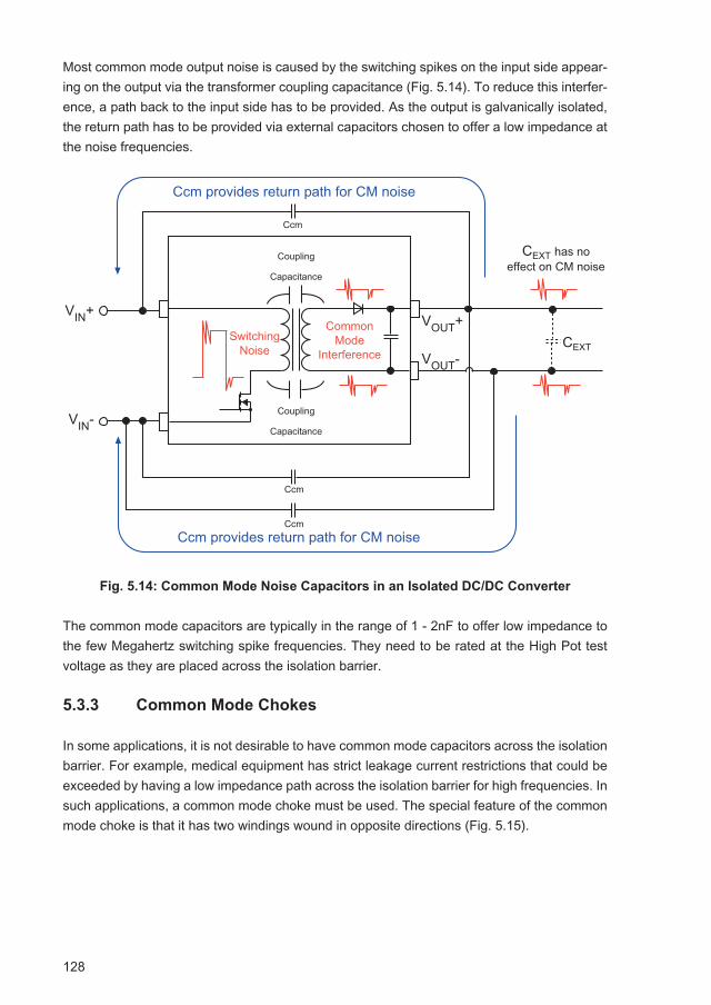
128
Most common mode output noise is caused by the switching spikes on the input side appear-ing on the output via the transformer coupling capacitance (Fig. 5.14). To reduce this interfer-ence, a path back to the input side has to be provided. As the output is galvanically isolated, the return path has to be provided via external capacitors chosen to offer a low impedance at the noise frequencies.
Fig. 5.14: Common Mode Noise Capacitors in an Isolated DC/DC Converter
The common mode capacitors are typically in the range of 1 - 2nF to offer low impedance to the few Megahertz switching spike frequencies. They need to be rated at the High Pot test voltage as they are placed across the isolation barrier.
5.3.3 Common Mode Chokes
In some applications, it is not desirable to have common mode capacitors across the isolation barrier. For example, medical equipment has strict leakage current restrictions that could be exceeded by having a low impedance path across the isolation barrier for high frequencies. In such applications, a common mode choke must be used. The special feature of the common mode choke is that it has two windings wound in opposite directions (Fig. 5.15).
�����������������������������
���� ���
�����������
���� ���
�����������
���������
�����������
��������������
������������������������������������
������������������������������������
���
���
���
����
���
���
�����
�����
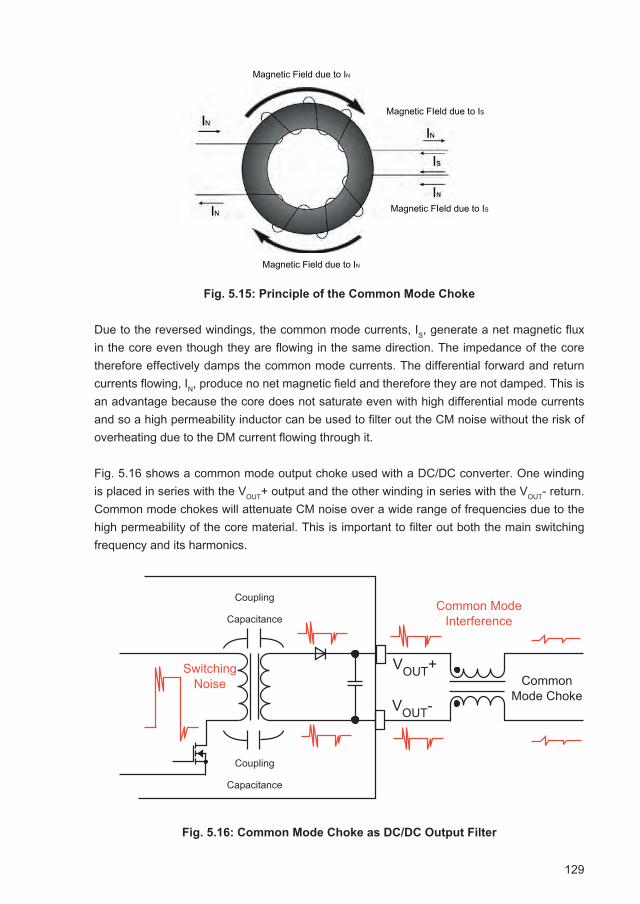
129
Fig. 5.15: Principle of the Common Mode Choke
Due to the reversed windings, the common mode currents, IS, generate a net magnetic flux in the core even though they are flowing in the same direction. The impedance of the core therefore effectively damps the common mode currents. The differential forward and return currents flowing, IN, produce no net magnetic field and therefore they are not damped. This is an advantage because the core does not saturate even with high differential mode currents and so a high permeability inductor can be used to filter out the CM noise without the risk of overheating due to the DM current flowing through it.
Fig. 5.16 shows a common mode output choke used with a DC/DC converter. One winding is placed in series with the VOUT+ output and the other winding in series with the VOUT- return. Common mode chokes will attenuate CM noise over a wide range of frequencies due to the high permeability of the core material. This is important to filter out both the main switching frequency and its harmonics.
Fig. 5.16: Common Mode Choke as DC/DC Output Filter
��������
�����������
��������
�����������
���������������� ������
������������ ������
��������������
�����
Magnetic Field due to IN
Magnetic FIeld due to IS
Magnetic FIeld due to IS
Magnetic Field due to IN
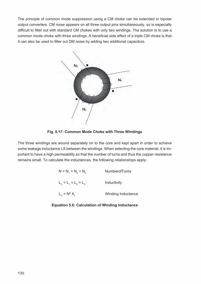
130
The principle of common mode suppression using a CM choke can be extended to bipolar output converters. CM noise appears on all three output pins simultaneously, so is especially difficult to filter out with standard CM chokes with only two windings. The solution is to use a common mode choke with three windings. A beneficial side effect of a triple CM choke is that it can also be used to filter out DM noise by adding two additional capacitors.
Fig. 5.17: Common Mode Choke with Three Windings
The three windings are wound separately on to the core and kept apart in order to achieve some leakage inductance LS between the windings. When selecting the core material, it is im-portant to have a high permeability so that the number of turns and thus the copper resistance remains small. To calculate the inductances, the following relationships apply:
N = N1 = N2 = N3 NumberofTurns
LC = L1 = L2 = L3 Inductivity
LC = N² AL Winding Inductance
Equation 5.6: Calculation of Winding Inductance
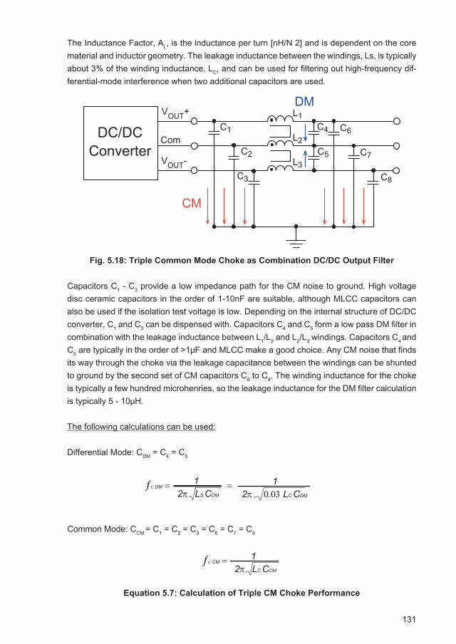
131
The Inductance Factor, AL, is the inductance per turn [nH/N 2] and is dependent on the core material and inductor geometry. The leakage inductance between the windings, Ls, is typically about 3% of the winding inductance, LC, and can be used for filtering out high-frequency dif-ferential-mode interference when two additional capacitors are used.
Fig. 5.18: Triple Common Mode Choke as Combination DC/DC Output Filter
Capacitors C1 - C3 provide a low impedance path for the CM noise to ground. High voltage disc ceramic capacitors in the order of 1-10nF are suitable, although MLCC capacitors can also be used if the isolation test voltage is low. Depending on the internal structure of DC/DC converter, C1 and C3 can be dispensed with. Capacitors C4 and C5 form a low pass DM filter in combination with the leakage inductance between L1/L2 and L2/L3 windings. Capacitors C4 and C5 are typically in the order of >1μF and MLCC make a good choice. Any CM noise that finds its way through the choke via the leakage capacitance between the windings can be shunted to ground by the second set of CM capacitors C6 to C8. The winding inductance for the choke is typically a few hundred microhenries, so the leakage inductance for the DM filter calculation is typically 5 - 10μH.
The following calculations can be used:
Differential Mode: CDM = C4 = C5
Common Mode: CCM = C1 = C2 = C3 = C6 = C7 = C8
Equation 5.7: Calculation of Triple CM Choke Performance
��
��
�� �� ��
����
��
��
��
��
��
��
����������� ��
���
���
���
ƒr, DM = 2π LS CDM
12π 0.03 LC CDM
1=
ƒr, CM = 2π LC CCM
1
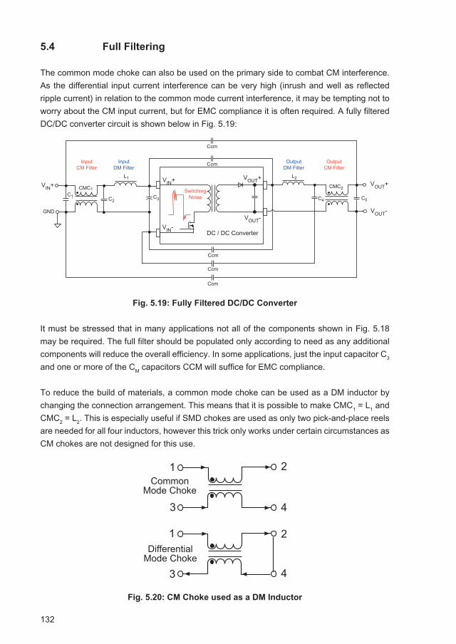
132
5.4 Full Filtering
The common mode choke can also be used on the primary side to combat CM interference. As the differential input current interference can be very high (inrush and well as reflected ripple current) in relation to the common mode current interference, it may be tempting not to worry about the CM input current, but for EMC compliance it is often required. A fully filtered DC/DC converter circuit is shown below in Fig. 5.19:
Fig. 5.19: Fully Filtered DC/DC Converter
It must be stressed that in many applications not all of the components shown in Fig. 5.18 may be required. The full filter should be populated only according to need as any additional components will reduce the overall efficiency. In some applications, just the input capacitor C3 and one or more of the CM capacitors CCM will suffice for EMC compliance.
To reduce the build of materials, a common mode choke can be used as a DM inductor by changing the connection arrangement. This means that it is possible to make CMC1 = L1 and CMC2 = L2. This is especially useful if SMD chokes are used as only two pick-and-place reels are needed for all four inductors, however this trick only works under certain circumstances as CM chokes are not designed for this use.
Fig. 5.20: CM Choke used as a DM Inductor
��������������
��������� �����
�������� �����
���
� ��
��
��
��
��
��
��������������
�������� �����
������� �����
��
� ��
� �
����
����
��� �
��� �
��� �
��� �����
����������������
����������������������
�
��
�
��
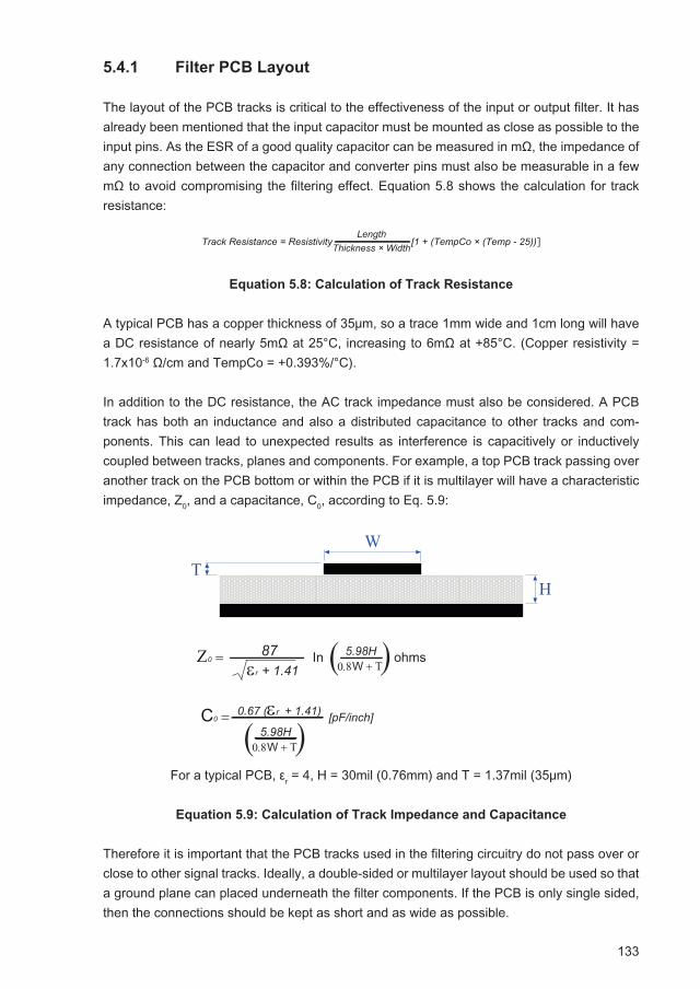
133
5.4.1 Filter PCB Layout
The layout of the PCB tracks is critical to the effectiveness of the input or output filter. It has already been mentioned that the input capacitor must be mounted as close as possible to the input pins. As the ESR of a good quality capacitor can be measured in mΩ, the impedance of any connection between the capacitor and converter pins must also be measurable in a few mΩ to avoid compromising the filtering effect. Equation 5.8 shows the calculation for track resistance:
Equation 5.8: Calculation of Track Resistance
A typical PCB has a copper thickness of 35μm, so a trace 1mm wide and 1cm long will have a DC resistance of nearly 5mΩ at 25°C, increasing to 6mΩ at +85°C. (Copper resistivity = 1.7x10⁻⁶ Ω/cm and TempCo = +0.393%/°C).
In addition to the DC resistance, the AC track impedance must also be considered. A PCB track has both an inductance and also a distributed capacitance to other tracks and com-ponents. This can lead to unexpected results as interference is capacitively or inductively coupled between tracks, planes and components. For example, a top PCB track passing over another track on the PCB bottom or within the PCB if it is multilayer will have a characteristic impedance, Z0, and a capacitance, C0, according to Eq. 5.9:
In ohms
For a typical PCB, εr = 4, H = 30mil (0.76mm) and T = 1.37mil (35μm)
Equation 5.9: Calculation of Track Impedance and Capacitance
Therefore it is important that the PCB tracks used in the filtering circuitry do not pass over or close to other signal tracks. Ideally, a double-sided or multilayer layout should be used so that a ground plane can placed underneath the filter components. If the PCB is only single sided, then the connections should be kept as short and as wide as possible.
Track Resistance = Resistivity [1 + (TempCo × (Temp - 25))]
Length Thickness × Width
�
�
�
Ζ0 = εr + 1.41
87 0.8W + Τ
5.98H( (
C0 = [pF/inch]0.67 (εr + 1.41)
0.8W + Τ5.98H( (
134
Fig. 5.21: Example of a Simple Class A Filter and PCB Layout (RP30-SF Series)
Filter components must also be considered as real components and not as ideal components. This means that at high frequencies the parasitic inductance of a capacitor or the parasitic ca-pacitance of an inductor may take the lead in determining the component behaviour. In other words, capacitors start behaving as inductors and vice- versa. Resistors may behave either as inductors or as capacitors. By skillful selection of the components, these problems may be contained or avoided completely. The most important design criterion is the resonance frequency where the behaviour changes. Fig. 5.22 shows the impedance vs frequency graph for a capacitive element.
Fig. 5.22: Resonance Frequency for a Capacitor
The solid line shows the frequency response of the component on its own for a 4.7nF capaci-tor with a parasitic ESR of 0.01Ωand a parasitic ESL = 2.5nH. The dotted line shows the same device in which additionally a bad connection has been simulated. The poor connection adds an additional ESR of 50 mΩ and an ESL of 50nH. As can be seen from the graph, the poor connection causes the resonant frequency to move down, meaning that the capacitor will start to behave like an inductor at a tenth of the calculated resonant frequency.
�� ����
����
�����������
�������������
�
��
�
��
��
�
��
���
���
����
���������
���������
����
����
�
��� ���
��� ��
��� ��
��� ���
��� ���
��� ���
��� ���
���� ���
���� ���
���� ���
���� ���
���� ���
���� ��
���� ��
135
For PCB designer, the behaviour shown in Fig. 5.23 has the following consequence that the ESL value for the ground terminal of the capacitor must be kept as low as possible. It is not sufficient just to make an electrical connection to the ground plane with a single via; multiple vias are needed to reduce both the DC impedance and the AC impedance.
Fig. 5.23: Multiple Via Ground Termination
For inductors, the length of the connecting track does not matter, since a long track will only in-crease the total inductance, however, it generally good practice to suppress any interference as close to the source as possible.
For all filter layouts, attention should be paid to the currents flowing in the circuit. Any current flowing in a loop will generate an EM field which can induce noise in other parts of the circuits. Ideally a star earth design should be used where all ground currents flow back to a single point. If a loop is unavoidable, then the loop area should be kept as small as possible.
However, with a good PCB layout and proper component selection, the results can be dra-matic.
Fig. 5.24: Example of Interference Before and After Filtering

136
6. Safety
The main aims of the various safety standards and regulations are to prevent injury, loss of life or damage to property by defining levels of protection against the following potential dangers:
• Electric Shock• Hazardous Energy• Fire and Smoke• Physical Injury• Radiation and Chemical Hazards
The terms “danger” and “hazard” are often used interchangeably. One way to differentiate is to think of a danger as a potential hazard. For example, a mains cable may carry a dangerous voltage, but the cable is still safe to handle because the wires are insulated. However, if the insulation was damaged or inferior, the cable would then be hazardous to touch.
As mentioned in the introduction to this book, one important use for DC/DC converters is to enhance the safety of the applications they are used in. If the DC/DC converter is a safety certified product, the application designer can treat the converter as a “black box” and rely on the DC/DC converter manufacturer to provide adequate internal safeguards to meet the safety regulations.
This does not mean that application designer is therefore no longer responsible for user safety in their designs as they must still show due diligence in identifying potential hazards and tak-ing the necessary steps to safeguard against them, but this task is made easier if the DC/DC converter is already certified. For example, if a DC/DC converter fails due to an internal short circuit fault, it can overheat but should not burn.
The materials used in the converter construction must therefore be non-flammable and self-extinguishing. However, if the application designer omits to provide adequate protection against this kind of fault (e.g. by failing to limit the input current to the converter), then the DC/DC converter could still get hot enough to cause another component or material to ignite and start a fire. The designer is therefore still responsible for the consequences of a component failure, even if the component is itself safety certified.
The tendency in safety certification regulations is to emphasize this responsibility on the ap-plication designer by including Hazard-Based Safety Engineering (HBSE) and Risk Manage-ment (RM) as part of the general safety certification process.
This is a major change in approach compared with the traditional electrical safety standards such as 60950 or ETS300 which concentrate purely on the DC/DC converter safety without considering the consequent risk should it fail in the end-application. This is also a reason why most DC/DC converter manufacturers state that their products are generally not suitable for use in safety critical applications.
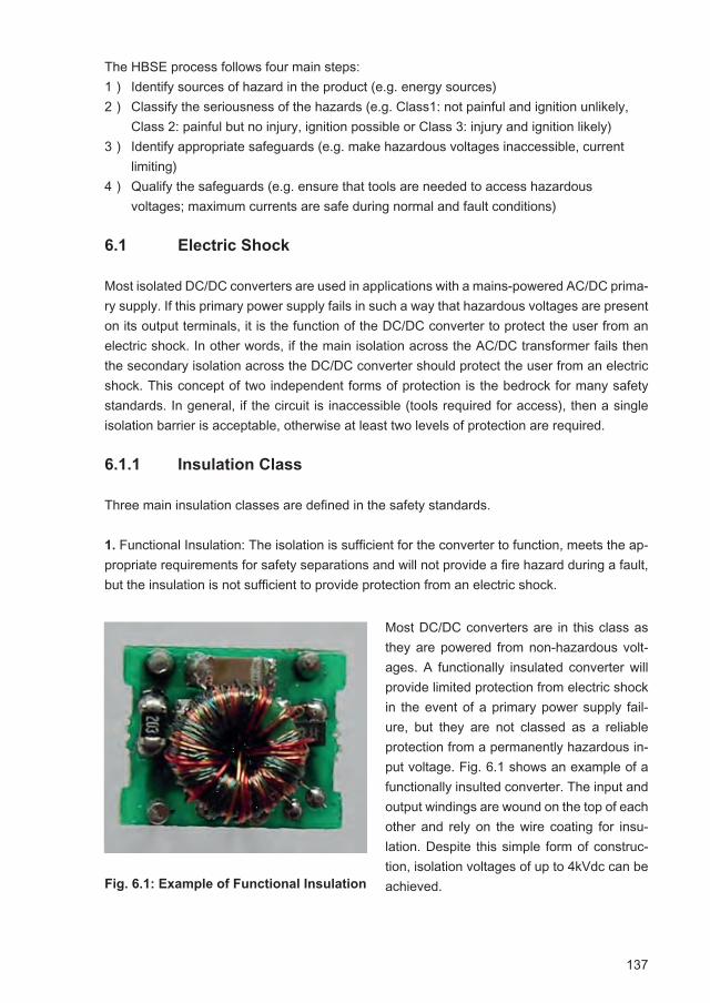
137
The HBSE process follows four main steps:1) Identify sources of hazard in the product (e.g. energy sources)2) Classify the seriousness of the hazards (e.g. Class1: not painful and ignition unlikely, Class 2: painful but no injury, ignition possible or Class 3: injury and ignition likely)3) Identify appropriate safeguards (e.g. make hazardous voltages inaccessible, current limiting)4) Qualify the safeguards (e.g. ensure that tools are needed to access hazardous voltages; maximum currents are safe during normal and fault conditions)
6.1 Electric Shock
Most isolated DC/DC converters are used in applications with a mains-powered AC/DC prima-ry supply. If this primary power supply fails in such a way that hazardous voltages are present on its output terminals, it is the function of the DC/DC converter to protect the user from an electric shock. In other words, if the main isolation across the AC/DC transformer fails then the secondary isolation across the DC/DC converter should protect the user from an electric shock. This concept of two independent forms of protection is the bedrock for many safety standards. In general, if the circuit is inaccessible (tools required for access), then a single isolation barrier is acceptable, otherwise at least two levels of protection are required.
6.1.1 Insulation Class
Three main insulation classes are defined in the safety standards.
1. Functional Insulation: The isolation is sufficient for the converter to function, meets the ap-propriate requirements for safety separations and will not provide a fire hazard during a fault, but the insulation is not sufficient to provide protection from an electric shock.
Fig. 6.1: Example of Functional Insulation
Most DC/DC converters are in this class as they are powered from non-hazardous volt-ages. A functionally insulated converter will provide limited protection from electric shock in the event of a primary power supply fail-ure, but they are not classed as a reliable protection from a permanently hazardous in-put voltage. Fig. 6.1 shows an example of a functionally insulted converter. The input and output windings are wound on the top of each other and rely on the wire coating for insu-lation. Despite this simple form of construc-tion, isolation voltages of up to 4kVdc can be achieved.
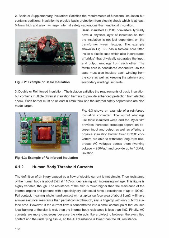
138
2. Basic or Supplementary Insulation: Satisfies the requirements of functional insulation but contains additional insulation to provide basic protection from electric shock which is at least 0.4mm thick and also has larger internal safety separations than functional insulation.
Fig. 6.2: Example of Basic Insulation
3. Double or Reinforced Insulation: The isolation satisfies the requirements of basic insulation but contains multiple physical insulation barriers to provide enhanced protection from electric shock. Each barrier must be at least 0.4mm thick and the internal safety separations are also made larger.
Fig. 6.3: Example of Reinforced Insulation
6.1.2 Human Body Threshold Currents
The definition of an injury caused by a flow of electric current is not simple. Then resistance of the human body is about 2kΩ at 110Vdc, decreasing with increasing voltage. This figure is highly variable, though. The resistance of the skin is much higher than the resistance of the internal organs and persons with especially dry skin could have a resistance of up to 100kΩ. Full contact, meaning whole hand contact with a typical surface area of about 8cm2, will have a lower electrical resistance than partial contact through, say, a fingertip with only 0.1cm2 sur-face area. However, if the current flow is concentrated into a small contact point that causes local burning or the skin is wet, then the internal body resistance is less than 1kΩ. Finally, AC currents are more dangerous because the skin acts like a dielectric between the electrified contact and the underlying tissue, so the AC resistance is lower than the DC resistance.
Basic insulated DC/DC converters typically have a physical layer of insulation so that the insulation is not just dependent on the transformer wires’ lacquer. The example shown in Fig. 6.2 has a toroidal core fitted inside a plastic case which also incorporates a “bridge” that physically separates the input and output windings from each other. The ferrite core is considered conductive, so the case must also insulate each winding from the core as well as keeping the primary and secondary windings separate.
Fig. 6.3 shows an example of a reinforced insulation converter. The output windings use triple insulated wires and the Mylar film provides increased creepage separation be-tween input and output as well as offering a physical insulation barrier. Such DC/DC con-verters are able to withstand long-term haz-ardous AC voltages across them (working voltage = 250Vac) and provide up to 10kVdc isolation.
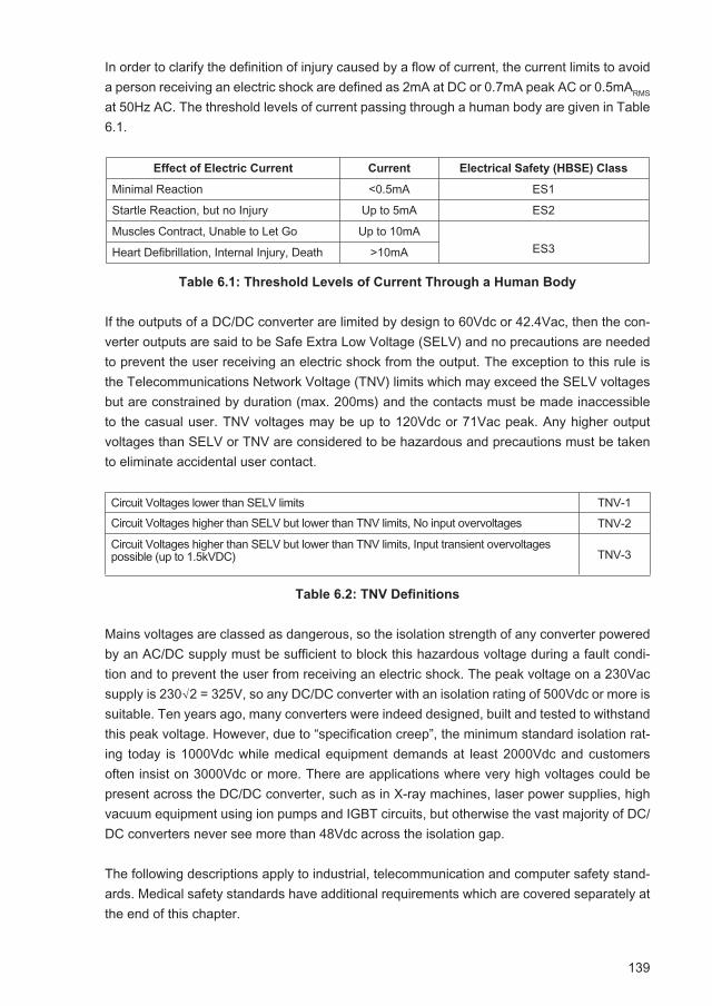
139
In order to clarify the definition of injury caused by a flow of current, the current limits to avoid a person receiving an electric shock are defined as 2mA at DC or 0.7mA peak AC or 0.5mARMS at 50Hz AC. The threshold levels of current passing through a human body are given in Table 6.1.
Effect of Electric Current Current Electrical Safety (HBSE) Class
Minimal Reaction <0.5mA ES1
Startle Reaction, but no Injury Up to 5mA ES2
Muscles Contract, Unable to Let Go Up to 10mAES3Heart Defibrillation, Internal Injury, Death >10mA
Table 6.1: Threshold Levels of Current Through a Human Body
If the outputs of a DC/DC converter are limited by design to 60Vdc or 42.4Vac, then the con-verter outputs are said to be Safe Extra Low Voltage (SELV) and no precautions are needed to prevent the user receiving an electric shock from the output. The exception to this rule is the Telecommunications Network Voltage (TNV) limits which may exceed the SELV voltages but are constrained by duration (max. 200ms) and the contacts must be made inaccessible to the casual user. TNV voltages may be up to 120Vdc or 71Vac peak. Any higher output voltages than SELV or TNV are considered to be hazardous and precautions must be taken to eliminate accidental user contact.
Circuit Voltages lower than SELV limits TNV-1Circuit Voltages higher than SELV but lower than TNV limits, No input overvoltages TNV-2Circuit Voltages higher than SELV but lower than TNV limits, Input transient overvoltages possible (up to 1.5kVDC) TNV-3
Table 6.2: TNV Definitions
Mains voltages are classed as dangerous, so the isolation strength of any converter powered by an AC/DC supply must be sufficient to block this hazardous voltage during a fault condi-tion and to prevent the user from receiving an electric shock. The peak voltage on a 230Vac supply is 230√2 = 325V, so any DC/DC converter with an isolation rating of 500Vdc or more is suitable. Ten years ago, many converters were indeed designed, built and tested to withstand this peak voltage. However, due to “specification creep”, the minimum standard isolation rat-ing today is 1000Vdc while medical equipment demands at least 2000Vdc and customers often insist on 3000Vdc or more. There are applications where very high voltages could be present across the DC/DC converter, such as in X-ray machines, laser power supplies, high vacuum equipment using ion pumps and IGBT circuits, but otherwise the vast majority of DC/DC converters never see more than 48Vdc across the isolation gap.
The following descriptions apply to industrial, telecommunication and computer safety stand-ards. Medical safety standards have additional requirements which are covered separately at the end of this chapter.
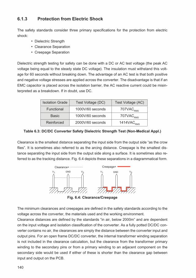
140
6.1.3 Protection from Electric Shock
The safety standards consider three primary specifications for the protection from electric shock:
• Dielectric Strength• Clearance Separation• Creepage Separation
Dielectric strength testing for safety can be done with a DC or AC test voltage (the peak AC voltage being equal to the steady state DC voltage). The insulation must withstand this volt-age for 60 seconds without breaking down. The advantage of an AC test is that both positive and negative voltage stresses are applied across the converter. The disadvantage is that if an EMC capacitor is placed across the isolation barrier, the AC reactive current could be misin-terpreted as a breakdown. If in doubt, use DC.
Isolation Grade Test Voltage (DC) Test Voltage (AC)
Functional 1000V/60 seconds 707VACRMS
Basic 1000V/60 seconds 707VACRMS
Reinforced 2000V/60 seconds 1414VACRMS
Table 6.3: DC/DC Converter Safety Dielectric Strength Test (Non-Medical Appl.)
Clearance is the smallest distance separating the input side from the output side “as the crow flies”. It is sometimes also referred to as the arcing distance. Creepage is the smallest dis-tance separating the input side from the output side along a surface. It is sometimes also re-ferred to as the tracking distance. Fig. 6.4 depicts these separations in a diagrammatical form.
Fig. 6.4: Clearance/Creepage
The minimum clearances and creepages are defined in the safety standards according to the voltage across the converter, the materials used and the working environment.Clearance distances are defined by the standards “in air, below 2000m” and are dependent on the input voltage and isolation classification of the converter. As a fully potted DC/DC con-verter contains no air, the clearances are simply the distance between the converter input and output pins. For an open frame DC/DC converter, the internal transformer winding separation is not included in the clearance calculation, but the clearance from the transformer primary winding to the secondary pins or from a primary winding to an adjacent component on the secondary side would be used if either of these is shorter than the clearance gap between input and output on the PCB.
�������������������
�� �� �������� ��

141
DC (AC) Voltage
Isolation Grade 12
(12)
36
(30)
75
(60)
150
(125)
300
(250)
450
(400)
600
(500)
800
(66)
VDC
(VAC)
Functional 0.4 0.5 0.7 1.0 1.6 2.4 3 4 mm
Basic 0.8 1 1.2 1.6 2.5 3.5 4.5 6 mm
Reinforced 1.6 2 2.4 3.2 5 7 9 13 mm
Table 6.4: Minimum Clearances in Air for Various Isolation Grades
The minimum creepage distances are defined by the operating voltage, surface conductivity of the materials used and the pollution degree. The creepage distance is measured at the closest point on the PCB between the primary and secondary tracks.
Fig. 6.5: PCB Layout of a DC/DC Converter showing the Minimum
Creepage and Clearance Separations
The Comparative Tracking Index (CTI) adds a factor to the creepage distance according to the surface conductivity of the insulating material separating the input from the output, typical-ly the converter’s PCB.
Insulant I: 600 ≤ CTIInsulant II: 400 ≤ CTI < 600Insulant IIIa: 175 ≤ CTI < 400Insulant IIIb: 100 ≤ CTI < 175
Table 6.5: Material Class Definitions
A standard FR4 PCB Board has a typical CTI of 200-250, rising to 400 with solder resist (Class 111a); however, if the board is PTFE coated, the CTI can be increased to > 600 (Class I). The Pollution Degree (PD) adds the factor of surface moisture or contaminants when calculating the minimum creepage separations, as the separation must be increased to compensate for the change in the Comparative Tracking Index (CTI) in dirty, industrial or outdoor environments.
Pollution Degree 1 Pollution Degree 2 Pollution Degree 3 Pollution Degree 4
No pollution, or only dry, non-conductive
pollution occurs which has no effect on con-
ductivity.
Normally only non- conductive pollution occurs. Temporary
condensation can occur
Conductive pollution and condensation often
occur.
Conductive pollution and condensation persistently occur.
Sealed Components Office Environments Industrial Environments Outdoor Environments
Table 6.6: Pollution Degree
��������
���������
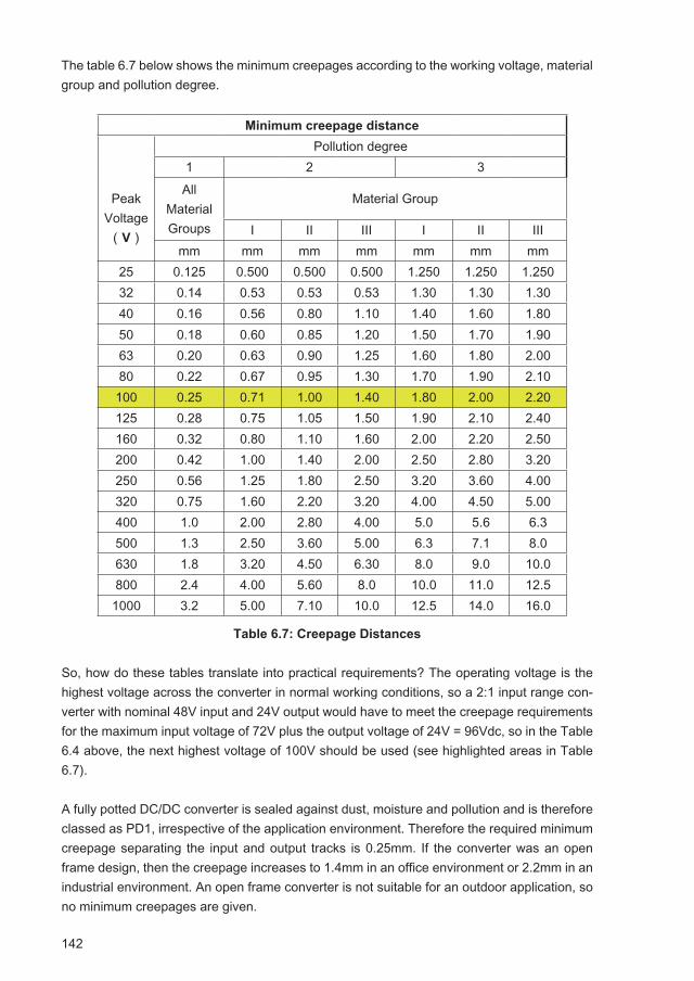
142
The table 6.7 below shows the minimum creepages according to the working voltage, material group and pollution degree.
Minimum creepage distance
PeakVoltage (V)
Pollution degree1 2 3All
MaterialGroups
Material Group
I II III I II IIImm mm mm mm mm mm mm
25 0.125 0.500 0.500 0.500 1.250 1.250 1.25032 0.14 0.53 0.53 0.53 1.30 1.30 1.3040 0.16 0.56 0.80 1.10 1.40 1.60 1.8050 0.18 0.60 0.85 1.20 1.50 1.70 1.9063 0.20 0.63 0.90 1.25 1.60 1.80 2.0080 0.22 0.67 0.95 1.30 1.70 1.90 2.10100 0.25 0.71 1.00 1.40 1.80 2.00 2.20125 0.28 0.75 1.05 1.50 1.90 2.10 2.40160 0.32 0.80 1.10 1.60 2.00 2.20 2.50200 0.42 1.00 1.40 2.00 2.50 2.80 3.20250 0.56 1.25 1.80 2.50 3.20 3.60 4.00320 0.75 1.60 2.20 3.20 4.00 4.50 5.00400 1.0 2.00 2.80 4.00 5.0 5.6 6.3500 1.3 2.50 3.60 5.00 6.3 7.1 8.0630 1.8 3.20 4.50 6.30 8.0 9.0 10.0800 2.4 4.00 5.60 8.0 10.0 11.0 12.51000 3.2 5.00 7.10 10.0 12.5 14.0 16.0
Table 6.7: Creepage Distances
So, how do these tables translate into practical requirements? The operating voltage is the highest voltage across the converter in normal working conditions, so a 2:1 input range con-verter with nominal 48V input and 24V output would have to meet the creepage requirements for the maximum input voltage of 72V plus the output voltage of 24V = 96Vdc, so in the Table 6.4 above, the next highest voltage of 100V should be used (see highlighted areas in Table 6.7).
A fully potted DC/DC converter is sealed against dust, moisture and pollution and is therefore classed as PD1, irrespective of the application environment. Therefore the required minimum creepage separating the input and output tracks is 0.25mm. If the converter was an open frame design, then the creepage increases to 1.4mm in an office environment or 2.2mm in an industrial environment. An open frame converter is not suitable for an outdoor application, so no minimum creepages are given.
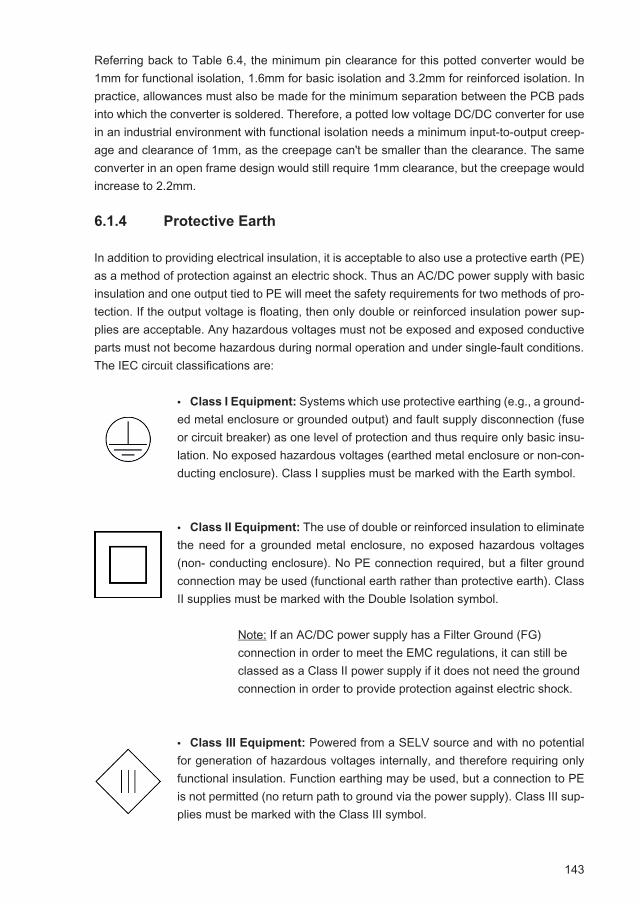
143
Referring back to Table 6.4, the minimum pin clearance for this potted converter would be 1mm for functional isolation, 1.6mm for basic isolation and 3.2mm for reinforced isolation. In practice, allowances must also be made for the minimum separation between the PCB pads into which the converter is soldered. Therefore, a potted low voltage DC/DC converter for use in an industrial environment with functional isolation needs a minimum input-to-output creep-age and clearance of 1mm, as the creepage can't be smaller than the clearance. The same converter in an open frame design would still require 1mm clearance, but the creepage would increase to 2.2mm.
6.1.4 Protective Earth
In addition to providing electrical insulation, it is acceptable to also use a protective earth (PE) as a method of protection against an electric shock. Thus an AC/DC power supply with basic insulation and one output tied to PE will meet the safety requirements for two methods of pro-tection. If the output voltage is floating, then only double or reinforced insulation power sup-plies are acceptable. Any hazardous voltages must not be exposed and exposed conductive parts must not become hazardous during normal operation and under single-fault conditions.The IEC circuit classifications are:
• Class I Equipment: Systems which use protective earthing (e.g., a ground-ed metal enclosure or grounded output) and fault supply disconnection (fuse or circuit breaker) as one level of protection and thus require only basic insu-lation. No exposed hazardous voltages (earthed metal enclosure or non-con-ducting enclosure). Class I supplies must be marked with the Earth symbol.
• Class II Equipment: The use of double or reinforced insulation to eliminate the need for a grounded metal enclosure, no exposed hazardous voltages (non- conducting enclosure). No PE connection required, but a filter ground connection may be used (functional earth rather than protective earth). Class II supplies must be marked with the Double Isolation symbol. Note: If an AC/DC power supply has a Filter Ground (FG) connection in order to meet the EMC regulations, it can still be classed as a Class II power supply if it does not need the ground connection in order to provide protection against electric shock.
• Class III Equipment: Powered from a SELV source and with no potential for generation of hazardous voltages internally, and therefore requiring only functional insulation. Function earthing may be used, but a connection to PE is not permitted (no return path to ground via the power supply). Class III sup-plies must be marked with the Class III symbol.
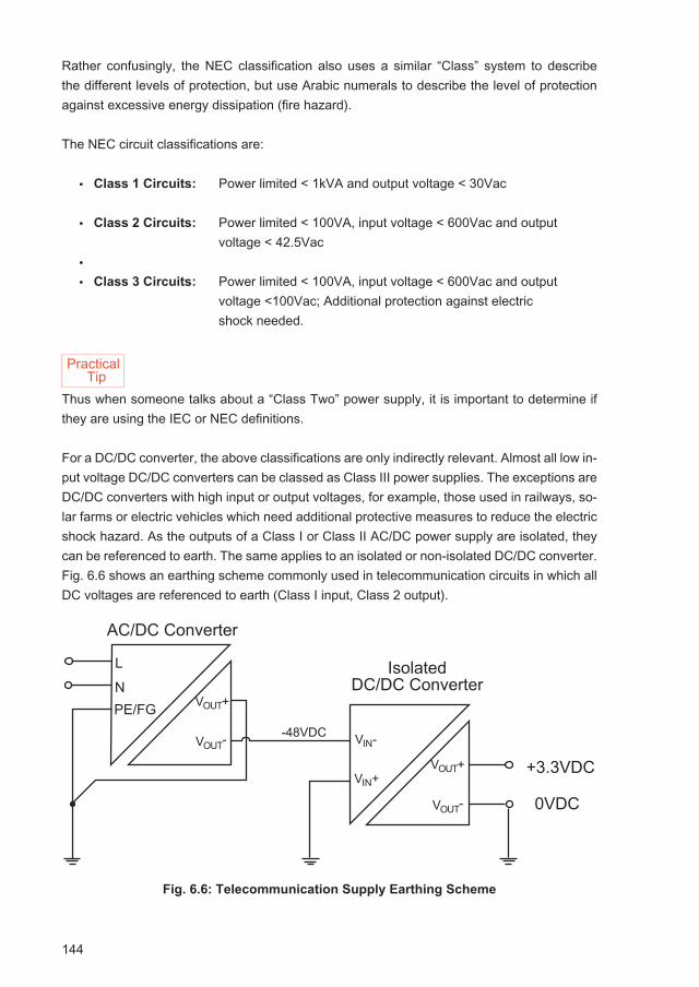
144
Rather confusingly, the NEC classification also uses a similar “Class” system to describe the different levels of protection, but use Arabic numerals to describe the level of protection against excessive energy dissipation (fire hazard).
The NEC circuit classifications are:
• Class 1 Circuits: Power limited < 1kVA and output voltage < 30Vac
• Class 2 Circuits: Power limited < 100VA, input voltage < 600Vac and output voltage < 42.5Vac• • Class 3 Circuits: Power limited < 100VA, input voltage < 600Vac and output voltage <100Vac; Additional protection against electric shock needed.
Thus when someone talks about a “Class Two” power supply, it is important to determine if they are using the IEC or NEC definitions.
For a DC/DC converter, the above classifications are only indirectly relevant. Almost all low in-put voltage DC/DC converters can be classed as Class III power supplies. The exceptions are DC/DC converters with high input or output voltages, for example, those used in railways, so-lar farms or electric vehicles which need additional protective measures to reduce the electric shock hazard. As the outputs of a Class I or Class II AC/DC power supply are isolated, they can be referenced to earth. The same applies to an isolated or non-isolated DC/DC converter. Fig. 6.6 shows an earthing scheme commonly used in telecommunication circuits in which all DC voltages are referenced to earth (Class I input, Class 2 output).
Fig. 6.6: Telecommunication Supply Earthing Scheme
�
�
����������
������
� ������������������
��������������
�������
����
�����
����
����
�����
�����
Practical Tip
145
6.2 Hazardous Energy
The IEC/UL 60950 definition of hazardous electrical energy is “available power level of 240VA or more, having a duration of 60s or more, or a stored energy level of 20J or more (for exam-ple, from one or more capacitors), at a potential of 2V or more”.These levels have been chosen because the energy dissipated in such an energy release (for example by a short circuit or by touching the energised parts) could be sufficient to cause injury or start a fire.A discussion of risk management occurs later in this chapter, but the main methods of reduc-ing the likelihood of injury or ignition due to hazardous energy are:
A discussion of risk management occurs later in this chapter, but the main methods of reduc-ing the likelihood of injury or ignition due to hazardous energy are:
• physical protection (e.g. enclosures, shielded connectors, encapsulation)• energy dissipation (e.g. capacitor discharging circuits)• spark suppression (e.g. snubber networks)• intrinsically safe (e.g. energy is limited by design)• over-current limiting (e.g. fuses)
These protection methods can be combined for additional safety. For example, sand-filled fuses are designed to rupture and disconnect the source of supply during a fault condition and additionally have a physical means (the sand) to prevent the melting hot fuse wire from becoming a source of ignition.
6.2.1 Fuses
Hazardous energy interruption is used to limit the available energy in a short circuit or over-cur-rent (OC) situation by inserting a fuse or circuit breaker into the supply. The interrupt rating of an OC protection device is given as both a current and voltage because there is a reaction time before the fault can be cleared which is dependent on both.For a fuse, the reaction time is given by: tclear = tmelt + tquench, where tmelt is the melting time which is dependent on the melting integral I2t, ambient temperature, pre-loading and fuse construc-tion and where tquench is the arcing time which is dependent on the voltage across the fuse and the fuse construction. During the clearing time, tclear, current will still flow through the fuse. This flow of current after the wire has melted is known as the energy let-through.It is important not to exceed the voltage rating of a fuse because otherwise the arcing energy cannot be safely contained within the fuse body and the resulting rapid temperature rise could cause the fuse to explode or become itself a source of ignition. The breaking capacity (the maximum current that the fuse can safely interrupt – not to be confused with the rated current) must be higher than the maximum available current from the power supply (sometimes called the prospective short circuit current).Selecting the most appropriate fuse current rating is very dependent on the application and environment it is in. The mechanism that interrupts the current is a fuse wire which will melt
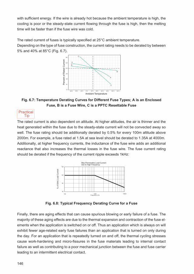
146
with sufficient energy. If the wire is already hot because the ambient temperature is high, the cooling is poor or the steady-state current flowing through the fuse is high, then the melting time will be faster than if the fuse wire was cold.
The rated current of fuses is typically specified at 25°C ambient temperature.Depending on the type of fuse construction, the current rating needs to be derated by between 5% and 40% at 85°C (Fig. 6.7).
Fig. 6.7: Temperature Derating Curves for Different Fuse Types; A is an Enclosed
Fuse, B is a Fuse Wire, C is a PPTC Resettable Fuse
The rated current is also dependent on altitude. At higher altitudes, the air is thinner and the heat generated within the fuse due to the steady-state current will not be convected away so well. The fuse rating should be additionally derated by 0.5% for every 100m altitude above 2000m. For example, a fuse rated at 1.5A at sea level should be derated to 1.35A at 4000m.Additionally, at higher frequency currents, the inductance of the fuse wire adds an additional reactance that also increases the thermal losses in the fuse wire. The fuse current rating should be derated if the frequency of the current ripple exceeds 1kHz:
Fig. 6.8: Typical Frequency Derating Curve for a Fuse
Finally, there are aging effects that can cause spurious blowing or early failure of a fuse. The majority of these aging effects are due to the thermal expansion and contraction of the fuse el-ements when the application is switched on or off. Thus an application which is always on will exhibit fewer age-related early fuse failures than an application that is turned on only during the day. For an application that is repeatedly turned on and off, the thermal cycling stresses cause work-hardening and micro-fissures in the fuse materials leading to internal contact failure as well as contributing to a poor mechanical junction between the fuse and fuse carrier leading to an intermittent electrical contact.
�
�
�
�
�
�
����� ����� ����� ��� ���� ���� ���� ���� ����� �������
��
��
��
���
���
���
���
����
� ���
��
����
����
������������������
�������������������
��������
��
��
���
���
��
�����
��
���
����
��
��������������� �������������� ���������������
Practical Tip
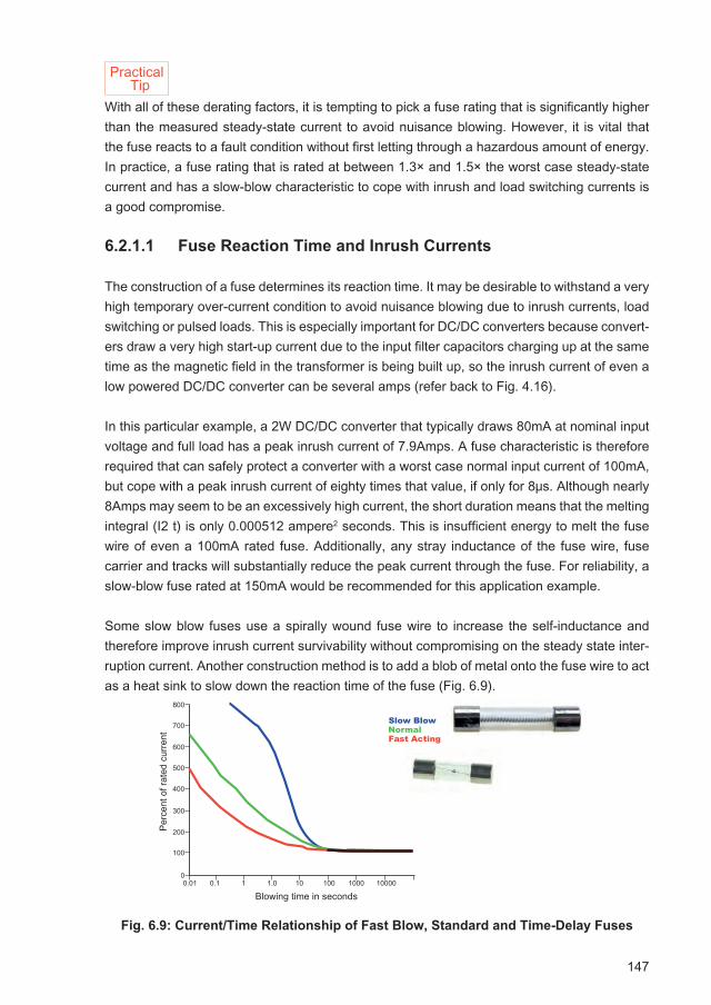
147
With all of these derating factors, it is tempting to pick a fuse rating that is significantly higher than the measured steady-state current to avoid nuisance blowing. However, it is vital that the fuse reacts to a fault condition without first letting through a hazardous amount of energy. In practice, a fuse rating that is rated at between 1.3× and 1.5× the worst case steady-state current and has a slow-blow characteristic to cope with inrush and load switching currents is a good compromise.
6.2.1.1 Fuse Reaction Time and Inrush Currents
The construction of a fuse determines its reaction time. It may be desirable to withstand a very high temporary over-current condition to avoid nuisance blowing due to inrush currents, load switching or pulsed loads. This is especially important for DC/DC converters because convert-ers draw a very high start-up current due to the input filter capacitors charging up at the same time as the magnetic field in the transformer is being built up, so the inrush current of even a low powered DC/DC converter can be several amps (refer back to Fig. 4.16).
In this particular example, a 2W DC/DC converter that typically draws 80mA at nominal input voltage and full load has a peak inrush current of 7.9Amps. A fuse characteristic is therefore required that can safely protect a converter with a worst case normal input current of 100mA, but cope with a peak inrush current of eighty times that value, if only for 8μs. Although nearly 8Amps may seem to be an excessively high current, the short duration means that the melting integral (I2 t) is only 0.000512 ampere2 seconds. This is insufficient energy to melt the fuse wire of even a 100mA rated fuse. Additionally, any stray inductance of the fuse wire, fuse carrier and tracks will substantially reduce the peak current through the fuse. For reliability, a slow-blow fuse rated at 150mA would be recommended for this application example.
Some slow blow fuses use a spirally wound fuse wire to increase the self-inductance and therefore improve inrush current survivability without compromising on the steady state inter-ruption current. Another construction method is to add a blob of metal onto the fuse wire to act as a heat sink to slow down the reaction time of the fuse (Fig. 6.9).
Fig. 6.9: Current/Time Relationship of Fast Blow, Standard and Time-Delay Fuses
���
���
���
���
���
���
���
���
����� ��� � ��� �� ��� ���� �����
��������������������������
�������� �����������
���
��
�����
� ��
���
���
Practical Tip
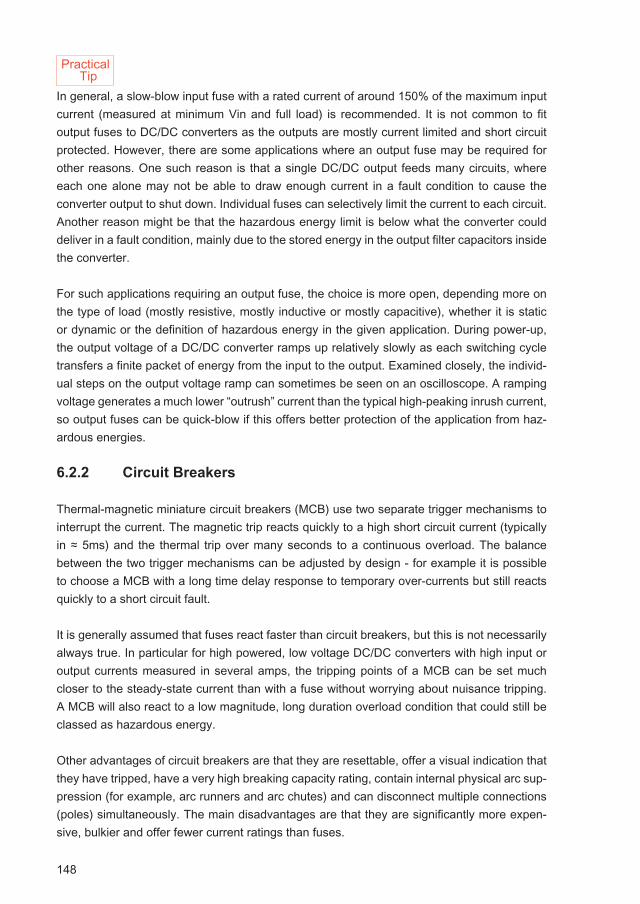
148
Practical Tip
In general, a slow-blow input fuse with a rated current of around 150% of the maximum input current (measured at minimum Vin and full load) is recommended. It is not common to fit output fuses to DC/DC converters as the outputs are mostly current limited and short circuit protected. However, there are some applications where an output fuse may be required for other reasons. One such reason is that a single DC/DC output feeds many circuits, where each one alone may not be able to draw enough current in a fault condition to cause the converter output to shut down. Individual fuses can selectively limit the current to each circuit. Another reason might be that the hazardous energy limit is below what the converter could deliver in a fault condition, mainly due to the stored energy in the output filter capacitors inside the converter.
For such applications requiring an output fuse, the choice is more open, depending more on the type of load (mostly resistive, mostly inductive or mostly capacitive), whether it is static or dynamic or the definition of hazardous energy in the given application. During power-up, the output voltage of a DC/DC converter ramps up relatively slowly as each switching cycle transfers a finite packet of energy from the input to the output. Examined closely, the individ-ual steps on the output voltage ramp can sometimes be seen on an oscilloscope. A ramping voltage generates a much lower “outrush” current than the typical high-peaking inrush current, so output fuses can be quick-blow if this offers better protection of the application from haz-ardous energies.
6.2.2 Circuit Breakers
Thermal-magnetic miniature circuit breakers (MCB) use two separate trigger mechanisms to interrupt the current. The magnetic trip reacts quickly to a high short circuit current (typically in ≈ 5ms) and the thermal trip over many seconds to a continuous overload. The balance between the two trigger mechanisms can be adjusted by design - for example it is possible to choose a MCB with a long time delay response to temporary over-currents but still reacts quickly to a short circuit fault.
It is generally assumed that fuses react faster than circuit breakers, but this is not necessarily always true. In particular for high powered, low voltage DC/DC converters with high input or output currents measured in several amps, the tripping points of a MCB can be set much closer to the steady-state current than with a fuse without worrying about nuisance tripping. A MCB will also react to a low magnitude, long duration overload condition that could still be classed as hazardous energy.
Other advantages of circuit breakers are that they are resettable, offer a visual indication that they have tripped, have a very high breaking capacity rating, contain internal physical arc sup-pression (for example, arc runners and arc chutes) and can disconnect multiple connections (poles) simultaneously. The main disadvantages are that they are significantly more expen-sive, bulkier and offer fewer current ratings than fuses.
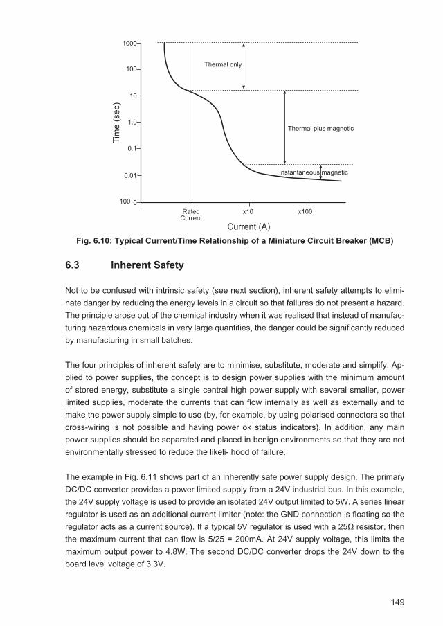
149
Fig. 6.10: Typical Current/Time Relationship of a Miniature Circuit Breaker (MCB)
6.3 Inherent Safety
Not to be confused with intrinsic safety (see next section), inherent safety attempts to elimi-nate danger by reducing the energy levels in a circuit so that failures do not present a hazard. The principle arose out of the chemical industry when it was realised that instead of manufac-turing hazardous chemicals in very large quantities, the danger could be significantly reduced by manufacturing in small batches.
The four principles of inherent safety are to minimise, substitute, moderate and simplify. Ap-plied to power supplies, the concept is to design power supplies with the minimum amount of stored energy, substitute a single central high power supply with several smaller, power limited supplies, moderate the currents that can flow internally as well as externally and to make the power supply simple to use (by, for example, by using polarised connectors so that cross-wiring is not possible and having power ok status indicators). In addition, any main power supplies should be separated and placed in benign environments so that they are not environmentally stressed to reduce the likeli- hood of failure.
The example in Fig. 6.11 shows part of an inherently safe power supply design. The primary DC/DC converter provides a power limited supply from a 24V industrial bus. In this example, the 24V supply voltage is used to provide an isolated 24V output limited to 5W. A series linear regulator is used as an additional current limiter (note: the GND connection is floating so the regulator acts as a current source). If a typical 5V regulator is used with a 25Ω resistor, then the maximum current that can flow is 5/25 = 200mA. At 24V supply voltage, this limits the maximum output power to 4.8W. The second DC/DC converter drops the 24V down to the board level voltage of 3.3V.
����
��� �
����
���
���
��
���
��� ����
������������
�������� ��
��
��
���
������������
�������������������
�������������������
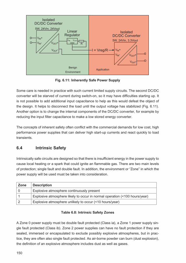
150
Fig. 6.11: Inherently Safe Power Supply
Some care is needed in practice with such current limited supply circuits. The second DC/DC converter will be starved of current during switch-on, so it may have difficulties starting up. It is not possible to add additional input capacitance to help as this would defeat the object of the design. It helps to disconnect the load until the output voltage has stabilized (Fig. 6.11). Another option is to change the internal components of the DC/DC converter, for example by reducing the input filter capacitance to make a low stored energy converter.
The concepts of inherent safety often conflict with the commercial demands for low cost, high performance power supplies that can deliver high start-up currents and react quickly to load transients.
6.4 Intrinsic Safety
Intrinsically safe circuits are designed so that there is insufficient energy in the power supply to cause local heating or a spark that could ignite an flammable gas. There are two main levels of protection; single fault and double fault. In addition, the environment or “Zone” in which the power supply will be used must be taken into consideration.
Zone Description
0 Explosive atmosphere continuously present1 Explosive atmosphere likely to occur in normal operation (<100 hours/year)2 Explosive atmosphere unlikely to occur (<10 hours/year)
Table 6.8: Intrinsic Safety Zones
A Zone 0 power supply must be double fault protected (Class ia), a Zone 1 power supply sin-gle fault protected (Class ib). Zone 2 power supplies can have no fault protection if they are sealed, immersed or encapsulated to exclude possibly explosive atmospheres, but in prac-tice, they are often also single fault protected. As air-borne powder can burn (dust explosion), the definition of an explosive atmosphere includes dust as well as gases.
������
�����������
���������� ������������
��������������
�������� �
���������� ������������
���������������
�����������
���� ���
����� �
��� �
����
����
����
���� ��� �
��� �
���������������
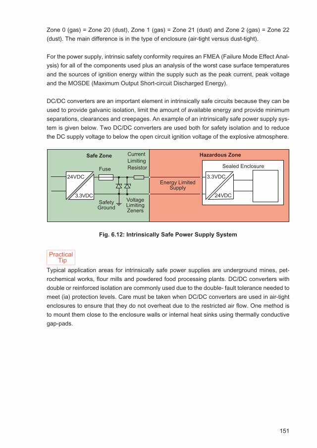
151
Zone 0 (gas) = Zone 20 (dust), Zone 1 (gas) = Zone 21 (dust) and Zone 2 (gas) = Zone 22 (dust). The main difference is in the type of enclosure (air-tight versus dust-tight).
For the power supply, intrinsic safety conformity requires an FMEA (Failure Mode Effect Anal-ysis) for all of the components used plus an analysis of the worst case surface temperatures and the sources of ignition energy within the supply such as the peak current, peak voltage and the MOSDE (Maximum Output Short-circuit Discharged Energy).
DC/DC converters are an important element in intrinsically safe circuits because they can be used to provide galvanic isolation, limit the amount of available energy and provide minimum separations, clearances and creepages. An example of an intrinsically safe power supply sys-tem is given below. Two DC/DC converters are used both for safety isolation and to reduce the DC supply voltage to below the open circuit ignition voltage of the explosive atmosphere.
Fig. 6.12: Intrinsically Safe Power Supply System
Typical application areas for intrinsically safe power supplies are underground mines, pet-rochemical works, flour mills and powdered food processing plants. DC/DC converters with double or reinforced isolation are commonly used due to the double- fault tolerance needed to meet (ia) protection levels. Care must be taken when DC/DC converters are used in air-tight enclosures to ensure that they do not overheat due to the restricted air flow. One method is to mount them close to the enclosure walls or internal heat sinks using thermally conductive gap-pads.
��������� �����������������������
��������������
���������
� ���
� ���
�����
�������������
�����������
�������������������
�������������������
Practical Tip
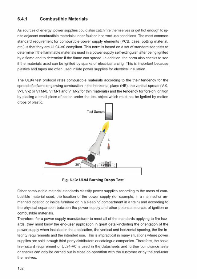
152
6.4.1 Combustible Materials
As sources of energy, power supplies could also catch fire themselves or get hot enough to ig-nite adjacent combustible materials under fault or incorrect use conditions. The most common standard requirement for combustible power supply elements (PCB, case, potting material, etc.) is that they are UL94-V0 compliant. This norm is based on a set of standardised tests to determine if the flammable materials used in a power supply self-extinguish after being ignited by a flame and to determine if the flame can spread. In addition, the norm also checks to see if the materials used can be ignited by sparks or electrical arcing. This is important because plastics and tapes are often used inside power supplies for electrical insulation.
The UL94 test protocol rates combustible materials according to the their tendency for the spread of a flame or glowing combustion in the horizontal plane (HB), the vertical spread (V-0, V-1, V-2 or VTM-0, VTM-1 and VTM-2 for thin materials) and the tendency for foreign ignition by placing a small piece of cotton under the test object which must not be ignited by molten drops of plastic.
Fig. 6.13: UL94 Burning Drops Test
Other combustible material standards classify power supplies according to the mass of com-bustible material used, the location of the power supply (for example, in a manned or un-manned location or inside furniture or in a sleeping compartment in a train) and according to the physical separation between the power supply and other potential sources of ignition or combustible materials.Therefore, for a power supply manufacturer to meet all of the standards applying to fire haz-ards, they must know the end-user application in great detail-including the orientation of the power supply when installed in the application, the vertical and horizontal spacing, the fire in-tegrity requirements and the intended use. This is impractical in many situations where power supplies are sold through third-party distributors or catalogue companies. Therefore, the basic fire-hazard requirement of UL94-V0 is used in the datasheets and further compliance tests or checks can only be carried out in close co-operation with the customer or by the end-user themselves.
��� ������
�����������

153
6.4.2 Smoke
More fire deaths arise from smoke inhalation than due to burns. Smoke is defined as all of the airborne products of combustion, including particles such as soot, gasses such as car-bon monoxide, volatiles such as organic molecules and aerosols such as steam. The visible parts of smoke, mainly caused by soot and steam, are not often inherently toxic unless they contain acids released by the fire, but by reducing visibility and impeding escape routes they contribute to the fire hazard. Gasses such as carbon monoxide cause hyperventilation which increases the lungs’ exposure to smoke and also binds with haemoglobin in the blood to deny the normal oxygen uptake in the body.Power supplies do not usually contain large quantities of combustible materials that would emit significant amounts of smoke in a fire, with the possible exception of the potting material. Potting is used to seal the power supply from environmental contaminants such as mois-ture, dust and corrosive elements, to provide a better thermal path between heat generating components and the case and to secure internal components against the effects of mechan-ical shock and vibration. In many applications, potting is essential to meet the environmental and thermal requirements of the application. The most commonly used potting materials are two-component epoxy, silicone rubber or polyurethane. Of these, only silicone rubber fails to meet stringent smoke requirements, but there are also low-smoke compounds available (unfortunately at high cost).One standard used to assess smoke hazard is the NF F Fire and Smoke test. The NF F 16-101/102 standards use a risk assessment table to determine the required specification for French railways. The risks of flammability and smoke emission can then be assessed ac-cording to the application or train route (if the train goes through tunnels, smoke is a greater hazard than if it is only used over-ground). The smoke rating is dependent on both the smoke opacity and the toxicity of the smoke. In the example given below, the power supply would be suitable for a subway train (requirements in white) because tests showed that the silicone rubber potting material had a low flammability but emitted too much smoke (F3/I3), but epoxy would be acceptable (F1/I2).
x = Silicone Rubber x = Epoxy
Table 6.9: Fire/Smoke Risk Assessment
Flammability
I0 for I.O.≥ 70 no inflammation at 960°C
I1 for I.O.45-69 no inflammation at 960°C
I2 for I.O.32-44 no inflammation at 850°C
I3 for I.O.28-31 no afterburning at 850°C
I4 for I.O. ≥ 20
NC not classified
Smoke emission
F0 for I.F. ≥ 5
F1 for I.F.6-20
F2 for I.F.21-40
F3 for I.F.41-80
F4 for I.F.81-120
F5 for I.F.≥ 120
�� �� �� �� �� ��
��
��
��
��
��
��
�
�
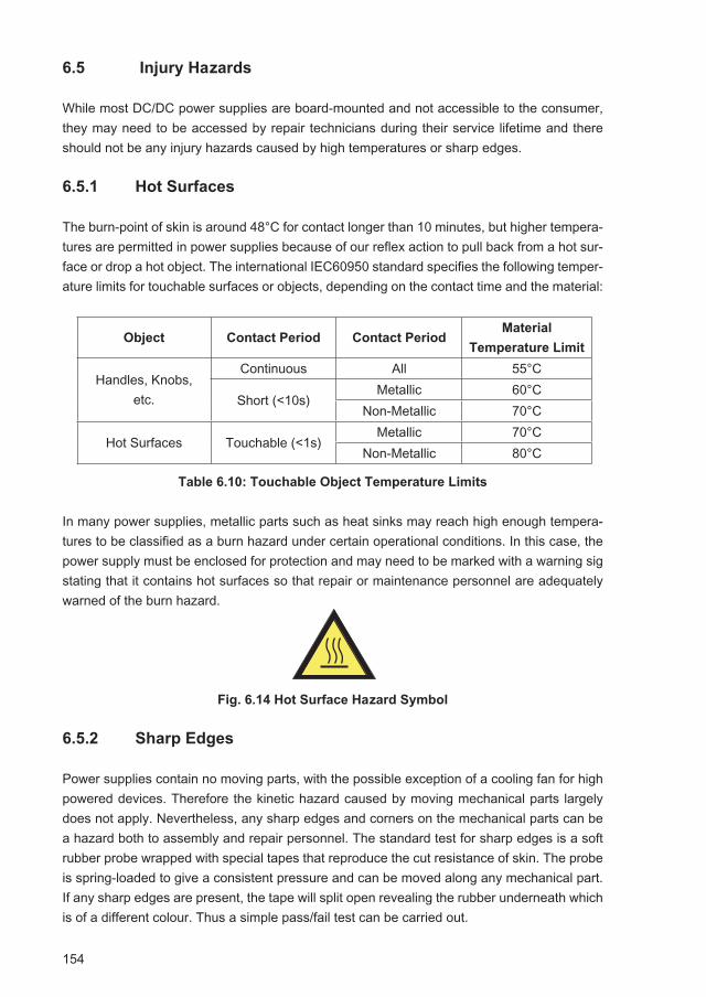
154
6.5 Injury Hazards
While most DC/DC power supplies are board-mounted and not accessible to the consumer, they may need to be accessed by repair technicians during their service lifetime and there should not be any injury hazards caused by high temperatures or sharp edges.
6.5.1 Hot Surfaces
The burn-point of skin is around 48°C for contact longer than 10 minutes, but higher tempera-tures are permitted in power supplies because of our reflex action to pull back from a hot sur-face or drop a hot object. The international IEC60950 standard specifies the following temper-ature limits for touchable surfaces or objects, depending on the contact time and the material:
Object Contact Period Contact PeriodMaterial
Temperature Limit
Handles, Knobs, etc.
Continuous All 55°C
Short (<10s)Metallic 60°C
Non-Metallic 70°C
Hot Surfaces Touchable (<1s)Metallic 70°C
Non-Metallic 80°C
Table 6.10: Touchable Object Temperature Limits
In many power supplies, metallic parts such as heat sinks may reach high enough tempera-tures to be classified as a burn hazard under certain operational conditions. In this case, the power supply must be enclosed for protection and may need to be marked with a warning sig stating that it contains hot surfaces so that repair or maintenance personnel are adequately warned of the burn hazard.
Fig. 6.14 Hot Surface Hazard Symbol
6.5.2 Sharp Edges
Power supplies contain no moving parts, with the possible exception of a cooling fan for high powered devices. Therefore the kinetic hazard caused by moving mechanical parts largely does not apply. Nevertheless, any sharp edges and corners on the mechanical parts can be a hazard both to assembly and repair personnel. The standard test for sharp edges is a soft rubber probe wrapped with special tapes that reproduce the cut resistance of skin. The probe is spring-loaded to give a consistent pressure and can be moved along any mechanical part. If any sharp edges are present, the tape will split open revealing the rubber underneath which is of a different colour. Thus a simple pass/fail test can be carried out.
155
Most low power DC/DC power supplies have injection moulded plastic cases, so the tooling can be designed to eliminate sharp edges. However, if the material leaks along the parting line, a thin sliver of excess plastic called “flash” can form a sharp edge. This needs to be re-moved by a deflashing process, either manually or via tumbling with abrasive materials. Some higher power converters have metal cases or contain heat sinks. These are usually made of soft metals such as aluminium or copper and it is relatively easy to remove any machining burrs with hand tools before assembly.
6.6 Designing for Safety
The first step to the hazard-based (HB) approach to design for safety is to evaluate any dan-gers present in the equipment; the next is to identify how these dangers could become haz-ards by examining the transfer to the human body and the final stage is to design protective measures to form an effective safeguard. All of these stages can be assessed during the de-sign evaluation process, before the equipment is even built. A successful approach is based on research to collect any shared knowledge about potential dangers, transfer mechanisms and human physiological susceptibility to injuries and to use sound engineering principles.
Fig. 6.15: Design for Safety Block Diagram
The block diagram above illustrates the design for safety process. The various safety norms, regulations and certificates have been developed based on previous investigations into acci-dents to make electrical and electronic products safe to use, but constructing power supplies just to pass the safety standard is not the same as designing for safety by considering the dangers, transfer mechanisms and injury hazards from the very beginning and designing in appropriate safeguards. An example of reducing danger by design might be to choose a bat-tery powered supply rather than mains supply for equipment that does not need to be continu-ously powered. The battery voltage can then be chosen to be extra low voltage and thus safe by design. Another example is the yellow-coloured transformers commonly used on building sites to supply power tools. By dropping the 230Vac mains supply to 110Vac and using a split winding output with a centre-tap tied to ground, the maximum AC voltage to ground will be 55V and thus safe by design (Fig. 6.16).
������������������������
������������� �������
������ ����������������
�������������
�������������������
����
��������������������
��������������������
���������
Practical Tip
156
Fig. 6.16: Safety by Design Example
If a danger cannot be eliminated by design, the next stage of the process is to investigate the possible transfer mechanisms that could lead to human contact and thus potential injury. The simplest method is to physically block any chance contact by adding shielding, enclosures or insulation. The Ingress Protection (IP) code defines the degrees of physical protection using a standardized probe dimensioned to represent a human finger with a 12.5mm diameter and 80mm length.
Level Object size Effective Protection
0 No effective protection against contact or ingress of objects
1 >50mmProtected against accidental large body part contact (such as hands), but no protection against deliberate contact
2 >12.5mm Protected against accidental finger contact
3 >2.5mm Protected against accidental contact via tools, thick wires, etc.
4 >1mmProtected against accidental contact via thin wires, small parts, etc.
5 Dust ProtectedIngress of dust is not entirely prevented, but does not affect operation. Complete protection against accidental contact
6 Dust TightSealed against dust. Complete protection against accidental contact
Table 6.11: Solid Particle Ingress Protection Levels
�������
�����������
��������� ����
������ �������������
����������
����������
���������
�������������
�����������
������ ��
������ ��

157
The second digit of the IP code represents liquid ingress protection, varying from level 0 (not protected against water ingress) to level 8 (total immersion).
Level Test Effective Protection
0 no protection none
1 dripping water protected against light rain
2 dripping water up to 15° protected against heavy rain
3 water spray protected against water spray at up to 60°
4 water splash protected against water from any angle
5 water jet protected against water from a nozzle
6 powerful water jet protected against water from a large nozzle
6K powerful water jet with pressure protected against powerful jets of water
7 immersion up to 1m protected against immersion for 30mins
8 immersion beyond 1m protected against continuous immersion
Table 6.12: Liquid Ingress Protection Levels
For indoor use, an IP rating of IP20 is considered adequate for dry area use. For damp indoor use (e.g. bathrooms), minimum IP41 (protection against small objects and dripping water) and for outdoor use, an IP rating of at least IP54 is required (dust tight and splashing water has no harmful effect), but more often IP67 (total protection against dust and water immersion) is required.
The final safeguard for safety by design is to warn the user so that they do put themselves into a dangerous situation by applying warning labels and providing important safety information leaflets and instruction sheets with the equipment. The safety information requirements are documented in all relevant health and safety standards and labels must be clearly marked with “Warning”, “Caution” or “Danger” according to the severity of the hazard. For DC/DC pow-er supplies, there is rarely any need to attach any hazard warning labels unless hazardous voltages are generated.
6.6.1 FMEA
Failure Mode and Effect Analysis (FMEA) is also an important technique in designing for safe-ty. At the simplest level, each separate component or element in the design can be considered to fail either as a short circuit or as an open circuit under normal operating conditions (nominal input voltage, full load and room temperature). The result of this failure can then be analysed to see the consequences for safety or performance for both the power supply and for any other equipment or systems intended to be connected to it. The FMEA can then be used to assess the severity of a failure according to the following definitions:

158
Severity Definition
CatastrophicResults in multiple fatalities and/or complete loss of multiple system functions
DangerousImpairs the safety of the system or creates dangerous conditions:
• A large reduction in safety margin or functional capability• Serious or fatal injury
Hazardous
Significantly reduces the safety of the system and creates hazardous conditions:
• Significant reduction in safety margin or functional capability• Physical distress including injuries• Major environmental damage and/or major property damage
MinorDoes not significantly reduce system safety:
• Some physical discomfort• Minor environmental damage, and/or minor property damage
No Effect Has no effect on safety or performance
Table 6.13: Failure Severity Rating
The FMEA can be used without considering the likelihood of occurrence as a basic de-sign-for-safety technique. However, if it is used as part of a risk assessment, then the risk is calculated according to: Risk = Severity × LikelihoodAnd therefore the probability of a fault occurring needs to be assessed:
Likelihood Definition
Probable
• Qualitative: Anticipated to occur one or more times during the entire system/operational life of an item.• Quantitative: Probability of occurrence per operational hour is greater than 1 × 10⁻⁵
Remote
• Qualitative: Unlikely to occur to each item during its total life. May occur several times in the life of an entire system or fleet.• Quantitative: Probability of occurrence per operational hour is less than 1 × 10⁻⁵, but greater than 1 × 10⁻⁷
Extremely Remote
• Qualitative: Not anticipated to occur to each item during its total life. May occur a few times in the life of an entire system or fleet.• Quantitative: Probability of occurrence per operational hour is less than 1 × 10⁻⁷, but greater than 1 × 10⁻⁹
Extremely Improbable
• Qualitative: So unlikely that it is not anticipated to occur during the entire operational life of an entire system or fleet.• Quantitative: Probability of occurrence per operational hour is less than 1 × 10⁻⁹
Table 6.14: Failure Probability Rating

159
6.7 Medical Safety
Compared to the industrial safety requirements, DC/DC power supplies have to comply with significantly stricter specifications in order to be certified as suitable for inclusion in medical devices. One of the most significant requirements is that a distinction is made between patient and operator protection. In the MOOP (Means of Operator Protection) category, the require-ments substantially follow the standard protection measures used for industrial devices, but in the category of MOPP (Means of Patient Protection), the requirements have been tightened up - in particular in relation to the insulation creepages and clearances separations. Table 6.15 shows some corresponding insulation requirements for both Method of Protection (MOP) protection categories.
Isolation
requirement
MOOP MOPP
Clearance CreepageIsolation
VoltageClearance Creepage
Isolation
Voltage
<250VAC2.0mm 3.2mm 1500VAC 2.5mm 4.0mm 1500VAC
4.0mm 6.4mm 3000VAC 5.0mm 8.0mm 4000VAC
<43VDC 1.0mm 2.0mm 1000VAC 1.0mm 2.0mm 1500VAC
<30VAC 2.0mm 4.0mm 2000VAC 2.0mm 4.0mm 3000VAC
Table 6.15: Medical Device Protection Requirements
As one of the basic safety principles is to provide two levels of protection in case once level fails, two protective measures (MOP - Means of Protection) are required for both the operator and patient safety (2×MOPP, 2×MOOP). The MOP can be split between several components so that, for example, an AC/DC power supply can be used to provide 2×MOOP followed by an isolated DC/DC converter to provide 2×MOPP, but it is the nature of medical grade designs to use a belt-and-braces approach and to require 2×MOPP and 2×MOOP for both the AC/DC and DC/DC power supplies. However, thanks to the MOOP / MOPP concept, the requirements for patient leakage currents have been relaxed compared with previous medical standards, depending on the classification of the application according to the type of patient contact. The three patient contact classifications are divided into Type B (Body - no direct pa-tient contact), Type BF (Body Float - physical contact with the patient) and CF (direct contact to the human heart). The closer the contact with the patient’s heart, the lower the allowable leakage currents. Table 6.16 shows the corresponding limits for normal operation (NC - Nor-mal Conditions) as well as for the case of an error (SFC - Single Fault Condition).
LeakageType B Type BF Type CF
NC SFC NC SFC NC SFC
Earth 500µA 1mA 500µA 1mA 500µA 1mA
Case 100µA 500µA 100µA 500µA 100µA 500µA
Patient 100µA 500µA 100µA 500µA 10µA 50µA
Table 6.16: Medical Device Leakage Current Limits
160
The advantage of the new, higher current limits is that it is much easier for medical grade DC/DC power supplies to also meet the EMC requirements. The previous limits caused significant problems because common mode filter capacitors between output and input were effectively banned.The hazard-based approach to medical safety provides power supply and medical device manufacturers with a new challenge as the certification includes a formal risk management (RM) process according to the ISO 14971 standard. Risk Management covers not only the analysis of risk in the design and manufacturing stage, but also includes requirements to monitor risk over time to account for aging, use and abuse effects that could compromise the equipment safety over the whole lifetime of the product.
Fig. 6.17: Risk Management Flow Diagram (based on ISO 14971)
The risk assessment process is based on a risk index matrix which analyses and assigns weights to risks that may arise from the power supply in normal operation and under fault conditions. In the risk matrix, the probability of occurrence (improbable to frequent) is bal-anced against the severity (negligible to catastrophic), each divided into 5 levels. The total risk is the product of likelihood and severity level. If the value is ≤ 6, the risk can usually be classified as acceptable, but the choice of the acceptability limit is left open to the user. In the following example, R1 is an acceptable risk, R2 is a reasonable risk for the application and R3 is unacceptable.
Table 6.17: Example of a Risk Matrix
The risk management plan also identifies the verification procedures to both ensure that the risk control measures are implemented in the device and to ensure that the implemented risk control measures actually reduce the risk. In many cases, the quality management systems of both manufacturer and user benefit from including the risk management process in the documentation and control procedures, especially as the risk control and monitoring activities must be carried out over the whole lifetime of the product life cycle including manufacture, installation, servicing and obsolescence.
������������� ��������������� ������������ ���� ������������������
�������������
�����
��� ���������������� ������
����������
���������������
��������������
������������
Severity Level
Negligible Minor Serious Critical CatastrophicWeighting 1 2 3 4 5
Probability Level
Frequent 5 R1 R3 R3 R3 R3Probable 4 R1 R2 R3 R3 R3
Occasional 3 R1 R1 R2 R3 R3Remote 2 R1 R1 R1 R2 R3
Improbable 1 R1 R1 R1 R1 R2

161
7. Reliability
7.1 Reliability Prediction
Almost since the advent of electronics, it has been vital for the user to know how long such de-vices will work properly. Since no one is able to know the future, statistical methods to predict the reliability of components, assemblies or devices have been developed.
One of the earliest systematic approaches to electronic component and assembly reliability was the US Army’s "Military Handbook - Reliability Prediction of Electronic Equipment ", com-monly known as MIL-HDBK-217, which consists mainly of a large database of the measured failure rates of various components based on the empirical analysis of a large number of field failures of electrical, electronic and electro-mechanical components carried out by the Univer-sity of Maryland.
The handbook was continuously updated and improved until 1995, by which the final version was called MIL-HDBK 217 Revision F, Notice 2. While this work is no longer updated, the data and methods are still one the most used today.
The handbook contains two methods of reliability prediction, Part Stress Analysis (PSA) and Parts Count Analysis (PCA). The PSA method requires a greater amount of detailed infor-mation and is usually more applicable to the later design phase, when measured data and preliminary results can be inserted into the reliability models, while the PCS method requires only minimal information such as part quantities, quality level and application environment. The biggest advantage of MIL HDBK 217 methodology is that the PCA method will give a reliability prediction based only on the Bill of Materials (BOM) and the anticipated use, thus a reliability figure can be given for a product that has not even been built yet:
λP = (Σ NC λC) (1 + 0.2 πE) πF πQ πL
Equation 7.1: Calculation of Failure Rate
Where: ΝC Number of Parts (per Component Type) λC Failure Rate of Each Part (base value taken from the database) πE Environmental Stress Factor (Application specific) πF Hybrid Function Stress (addition stress caused by component interaction) πQ Screening Level Factor (standard part tolerances or pre-screened) πL Maturity Factor (well-known and tested design or new approach)
162
The calculation will give a figure for each component used. The total reliability can then be found by adding up all of the individual results:
No. Parts Q’tyπ
P Failure rate
[10-6/h] TAMB
= 25°C
πP Failure rate
[10-6/h] TAMB
= 85°C
1 Transistor 2 0.0203 0.06092 Diodes 2 0.1089 0.54433 Resistor 3 0.0370 0.17164 Capacitors 5 0.1699 1.70005 Transformers 1 0.2256 1.92006 PCB, PIN 2 0.0092 0.0092
πP Total Failure rate 10-6/H 0.5708 4.4060MTBF Hours (MIL-HDBK-217F) 1.751.927 226.963
ConditionInput Nominal Input Nominal Input
Output Full Load Full Load
Table 7.1: Example of MTBF calculation by parts count for a simple DC/DC converter
Failure rates are defined either as the time interval between two failures - in hours - Mean Time Between Failures ( MTBF) or as the time interval to the first failure - Mean Time To Fail-ure (MTTF). The standard failure rate behaviour is described by the widely known "bathtub curve". Figure 7.1 shows the shape of the curve. The shape of the curve is approximately the same for all components and systems - only the elongation of the time axis is different. It is divided into three main areas: Infant Mortality (I), Useful Life (II) and End of Life (III). MTTF includes regions I and II, while MTBF includes only Region II.
Fig. 7.1: Bathtub Failure rate curve
Section I describes the area of early failures, which is usually caused by latent material de-fects or manufacturing faults which happen not to show up in the final production testing before the product is shipped. The infant mortality failure is usually of relatively short dura-tion- even for complex systems there are rarely early failures past 200 hours of use; in the case of DC/DC converters, most early failures will occur within the first 24 hours of operation. This may sound a short period of time for a converter with a guaranteed 3 year lifetime, but for a DC/DC converter running at 100kHz, the switching transistors and transformer will have already been exercised more than 140 million times in the first day of operation and any failure due to component defects are likely to have already occurred.
�����
������
��
����
�������
�����
������
�
�� �� ����
� �� ���
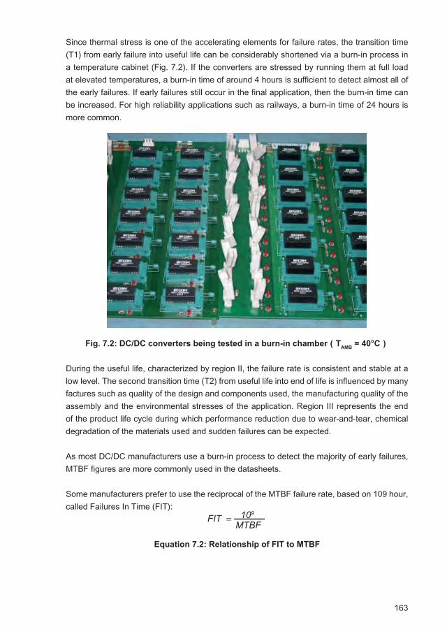
163
Since thermal stress is one of the accelerating elements for failure rates, the transition time (T1) from early failure into useful life can be considerably shortened via a burn-in process in a temperature cabinet (Fig. 7.2). If the converters are stressed by running them at full load at elevated temperatures, a burn-in time of around 4 hours is sufficient to detect almost all of the early failures. If early failures still occur in the final application, then the burn-in time can be increased. For high reliability applications such as railways, a burn-in time of 24 hours is more common.
Fig. 7.2: DC/DC converters being tested in a burn-in chamber(TAMB
= 40°C)
During the useful life, characterized by region II, the failure rate is consistent and stable at a low level. The second transition time (T2) from useful life into end of life is influenced by many factures such as quality of the design and components used, the manufacturing quality of the assembly and the environmental stresses of the application. Region III represents the end of the product life cycle during which performance reduction due to wear-and-tear, chemical degradation of the materials used and sudden failures can be expected.
As most DC/DC manufacturers use a burn-in process to detect the majority of early failures, MTBF figures are more commonly used in the datasheets.
Some manufacturers prefer to use the reciprocal of the MTBF failure rate, based on 109 hour, called Failures In Time (FIT):
Equation 7.2: Relationship of FIT to MTBF
FIT = MTBF109

164
7.2 Environmental Stress Factors
MIL-HDBK-217 contains reliability models based on common military applications. The kind of application in which a DC/DC converter is going to be used has a strong influence on its reli-ability. For example, if the converter is going to be fitted into a ship, then the corrosive effects of the salty air will reduce its lifetime even if it is used in a dry area.
Table 7.2: Application Classes according to MIL-HDBK-217
If the final application is known, then a correction factor for the MTBF calculation can be made based on Ground Benign (GB) as the reference environmental stress with a factor of 1:
Table 7.3: MTBF Correction Factors according to Environment
For example, a DC/DC converter with a MTBF figure of 1 million hours according to the data-sheet (based on GB conditions) would need to be “derated” to around 610 khours if used in portable equipment to take into account the additional environmental stresses due to knocks, bumps, sudden temperature changes, etc. associated with hand held equipment.
One of the perhaps surprising results of the MIL-HDBK-217 analysis is that space flight is as a benign an environment as ground based. Aboard a satellite or spaceship, the environmental
Environment πE Symbol MIL-HDBK-271F Description Commercial Interpretation or Examples
Ground GB Non-mobile, temperature and Laboratory equipment, testBenign humidity controlled environments instruments, desktop PC's,
readily accessible to maintenance static telecomsGround GM Equipment installed in wheeled or In-vehicle instrumentation,
Mobile tracked vehicles and equipment mobile radio and telecoms,
manually transported portable PC'sNaval NS Sheltered or below deck Navigation, radio equipment
Sheltered equipment on surface ships or submarines and instrumentation below deckAircraft AIC Typical conditions in cargo Pressurised cabin compart-
Inhabited compartments which can be ments and cockpits, in flightCargo occupied by aircrew entertainment and non-safety
critical applicationsSpace SF Earth orbital. Vehicle in neither Orbital communications satellite,
Flight powered flight nor in atmospheric re-entryequipment only operated once in
situations
Missile ML Severe conditions relating Severe vibrational shock and
Launch to missile launch very high accelerating forces,satellite launch conditions
Environment πE Symbol π
E Value Divisor
Ground Bengin GB 0.5 1.00Ground Mobile GM 4.0 1.64Naval Sheltered GNS 4.0 1.64Aircraft Inhabited Cargo AIC 4.0 1.64Space Flight SF 0.5 1.00Missile Launch ML 12.0 3.09
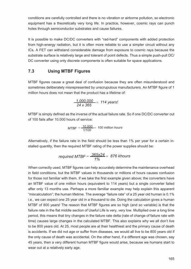
165
conditions are carefully controlled and there is no vibration or airborne pollution, so electronic equipment has a theoretically very long life. In practice, however, cosmic rays can punch holes through semiconductor substrates and cause failures.
It is possible to make DC/DC converters with “rad-hard” components with added protection from high-energy radiation, but it is often more reliable to use a simpler circuit without any ICs. A FET can withstand considerable damage from exposure to cosmic rays because the substrate surface is relatively large and tolerant of point defects. Thus a simple push-pull DC/DC converter using only discrete components is often suitable for space applications.
7.3 Using MTBF Figures
MTBF figures cause a great deal of confusion because they are often misunderstood and sometimes deliberately misrepresented by unscrupulous manufacturers. An MTBF figure of 1 million hours does not mean that the product has a lifetime of:
MTBF is simply defined as the inverse of the actual failure rate. So if one DC/DC converter out of 100 fails after 10,000 hours of service:
Alternatively, if the failure rate in the field should be less than 1% per year for a certain in-stalled quantity, then the required MTBF rating of the power supplies should be:
When correctly used, MTBF figures can help accurately determine the maintenance overhead in field conditions, but the MTBF values in thousands or millions of hours causes confusion for those not familiar with them. If we take the first example given above; the converters have an MTBF value of one million hours (equivalent to 114 years) but a single converter failed after only 13 months use. Perhaps a more familiar example may help explain this apparent “miscalculation”; the human lifetime. The average “failure rate” of a 25 year old human is 0.1% i.e., we can expect one 25 year old in a thousand to die. Doing the calculation gives a human MTBF of 800 years! The reason that MTBF figures are so high (and so variable) is that the failure rate in the flat middle section of Useful Life is very, very low. Multiplied over a long time period, this means that tiny changes in the failure rate delta (rate of change of failure rate with time) causes large changes in the calculated MTBF. This also explains why we all don’t live to be 800 years old. At 25, most people are at their healthiest and the primary cause of death is accidents. If we did not age or suffer from diseases, we would all live to be 800 years old if the only cause of death was accidental. On the other hand, if a different age was chosen, say 45 years, then a very different human MTBF figure would arise, because we humans start to wear out at a relatively early age.
114 years!24 x 3651,000,000 =
100 million hours1/10010,000 =MTBF =
876 khours1%
365x24 =required MTBF =
166
As the failure rate during the final End-of-Life phase follows an exponential law, reliability can be worked out from MTBF using the following formula:
Reliability = e-(T/MTBF)
Equation 7.3: Relationship of Reliability to MTBF
If the time (T) equals the MTBF, then the equation reduces to e1 or 37%. This can be interpret-ed as meaning that at T = MTBF, only 37% of the converters will still be working or, alterna-tively, that there is only a 37% confidence that all converters will be still working at T = MTBF.
7.4 Demonstrated MTBF
Most power supply manufacturers can’t wait many years to measure the actual failure rate and delta failure rate of their products, let alone wait more than 50 years to accumulate suf-ficient test data for high reliability products. The most practical way to get a reliability figure is to use the empirical results for the individual components according to such databases as MIL HDBK 217 and assume that the failure rates are constant. The result is not ideal, but it is a lot better than merely guessing or waiting decades for significant hard data. However, if enough products have been released on to the market or tested in long term test setups, a more accurate measure of reliability is available called the demonstrated MTBF, which is based on actual recorded failures. As the sample size and observation time are limited for practical reasons, the number of actual failures may be low, so statistical tools such as the χ2 (Chi-squared) distribution are needed to be able to calculate the demonstrated MTBF figure with a reasonable amount of confidence (say, 95%):
Where T = time (in hours), 0.05 equals the 95% certainty cut-off point and ν is the Chi-squared function’s degree of freedom.
Equation 7.4: Calculation of Demonstrated MTBF
There are other databases and statistical models that can be used to derive failure rates; the most common beside MIL HDBK 217F are Bellcore/Telcordia TR-NWT-332 and IEC61709. The results vary wildly between the methodologies because different assumptions are made and different operating stresses are used in the calculation (for example, MIL HDBK uses 100% load, Bellcore/Telcordia only 50% load). For the same 30W DC/DC converter, MIL HDBK 217F Notice 2 will give an MTBF of 435khours, Bellcore/Telcordia TR-332 an MTBF of more than 3 million hours and IEC61709 an MTBF of around 80 million hours. However, irrespective of which methodology is used, if two products have similar performance criteria but different MTBF figures, then as long as the same model and stress factors were used in the MTBF calculations, the product with the higher MTBF figure will also be in practice the most reliable.
χ2 (0.05,ν)2 TDemonstrated MTBF =
167
7.5 MTBF and Temperature
Reliability reduces with increased operating temperature, so the datasheet MTBF is typically only valid at room temperature and should be labelled as such. The reason why reliability is so temperature dependent is based on the activation energy for chemical processes. Back in 1898, the Swedish chemist Arrhenius published a proof showing that the rate of chemical reaction is temperature dependent and that for every 10°K increase in temperature, the rate of reaction approximately doubled.
Where k = rate of reaction, A = pre-exponential factor, EA = Activation Energy, kB = Bolzmann’s constant and T = temperature in °K.
Equation 7.5: Arrhenius Equation
The Arrhenius equation has found many applications outside of pure chemistry and can also be applied to the lifetime of electronic components where many of the aging effects are chem-ical in nature (for example, corrosion effects, breakdown of materials, dislocations in the sem-iconductor lattices, etc.). The equation can also be rearranged to give an acceleration factor which is temperature dependent. For electronic components, the activation energy is 0.6 Elec-tron-Volts, giving an acceleration factor of:
Equation 7.6: Acceleration Factor from Arrhenius
For most datasheet specifications, the reference temperature is taken to be nominal room temperature or 25°C. This gives the following acceleration factor according to temperature:
Table 7.4: Acceleration Factors for different ambient temperatures.
From this simple relationship, it can be seen that doubling the ambient temperature from 25°C to 50°C increases the aging effect by a factor of 6. If the temperature were further increased by 25°C to 75°C, then the aging effect would increase to around 30 times.
The same relationship works in reverse. Reducing the temperature increases the reliability of electronic components. However, at very low temperatures (below -20°C), other factors such as mechanical stresses due to the different contraction coefficients of the different materials or solder joints becoming brittle can cause a higher failure rate, so the Arrhenius relationship cannot be extrapolated without limit.
kB
0.6eVAcceleration Factor = exp( )TREF
1TAMB
1-( )
T(amb) Acceleration Factor
25°C 130°C 1.540°C 350°C 660°C 1270°C 2280°C 40
k = Α expkBT- EA( )
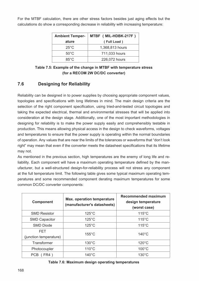
168
For the MTBF calculation, there are other stress factors besides just aging effects but the calculations do show a corresponding decrease in reliability with increasing temperature:
Ambient Temper-
ature
MTBF (MIL-HDBK-217F)
(Full Load)
25°C 1,368,813 hours50°C 711,033 hours85°C 226,072 hours
Table 7.5: Example of the change in MTBF with temperature stress
(for a RECOM 2W DC/DC converter)
7.6 Designing for Reliability
Reliability can be designed in to power supplies by choosing appropriate component values, topologies and specifications with long lifetimes in mind. The main design criteria are the selection of the right component specification, using tried-and-tested circuit topologies and taking the expected electrical, thermal and environmental stresses that will be applied into consideration at the design stage. Additionally, one of the most important methodologies in designing for reliability is to make the power supply easily and comprehensibly testable in production. This means allowing physical access in the design to check waveforms, voltages and temperatures to ensure that the power supply is operating within the normal boundaries of operation. Any values that are near the limits of the tolerances or waveforms that “don’t look right” may mean that even if the converter meets the datasheet specifications that its lifetime may not.As mentioned in the previous section, high temperatures are the enemy of long life and re-liability. Each component will have a maximum operating temperature defined by the man-ufacturer, but a well-structured design-for-reliability process will not stress any component at the full temperature limit. The following table gives some typical maximum operating tem-peratures and some recommended component derating maximum temperatures for some common DC/DC converter components:
ComponentMax. operation temperature
(manufacturer's datasheets)
Recommended maximum
design temperature
(worst case)
SMD Resistor 125°C 115°CSMD Capacitor 125°C 115°C
SMD Diode 125°C 115°CFET
(junction temperature)155°C 140°C
Transformer 130°C 120°CPhotocoupler 110°C 100°CPCB (FR4) 140°C 130°C
Table 7.6: Maximum design operating temperatures
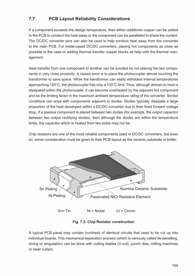
169
7.7 PCB Layout Reliability Considerations
If a component exceeds the design temperature, then either additional copper can be added to the PCB to conduct the heat away or the component can be paralleled to share the current. The DC/DC converter pins can also be used to help conduct heat away from the converter to the main PCB. For metal-cased DC/DC converters, placing hot components as close as possible to the case or adding thermal transfer copper blocks all help with the thermal man-agement.
Heat transfer from one component to another can be avoided by not placing the two compo-nents in very close proximity. A classic error is to place the photocoupler almost touching the transformer to save space. While the transformer can easily withstand internal temperatures approaching 120°C, the photocoupler has only a 100°C limit. Thus, although almost no heat is dissipated within the photocoupler, it can become overheated by the adjacent hot component and be the limiting factor in the maximum ambient temperature rating of the converter. Similar conditions can arise with components adjacent to diodes. Diodes typically dissipate a large proportion of the heat developed within a DC/DC converter due to their fixed forward voltage drop. If a passive component is placed between two diodes (for example, the output capacitor between two output rectifying diodes), then although the diodes are within the temperature limits, the capacitor which is heated from two sides may not be.
Chip resistors are one of the most reliable components used in DC/DC converters, but even so, some consideration must be given to their PCB layout as the ceramic substrate is brittle:
Sn= Tin Ni = Nickel Cr = Chrom
Fig. 7.3: Chip Resistor construction
A typical PCB panel may contain hundreds of identical circuits that need to be cut up into individual boards. This mechanical separation process (which is variously called de-panelling, dicing or singulation) can be done with cutting blades (V-cut), punch dies, milling machines or laser cutters.
����������
����������
������������������� �����
������ ��������������������
������������������������
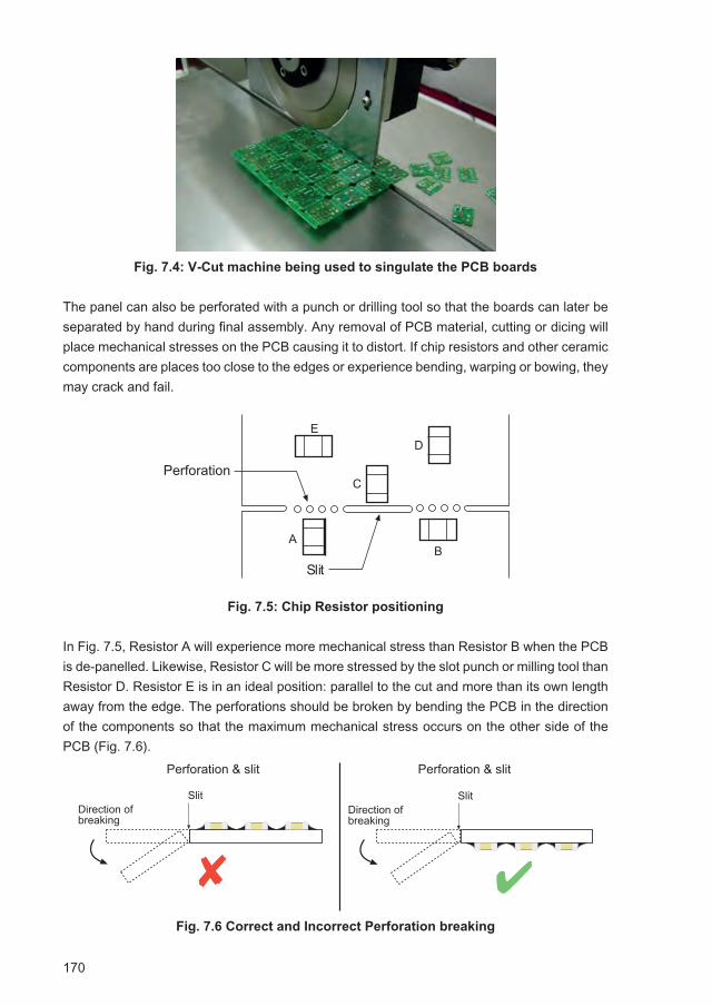
170
Fig. 7.4: V-Cut machine being used to singulate the PCB boards
The panel can also be perforated with a punch or drilling tool so that the boards can later be separated by hand during final assembly. Any removal of PCB material, cutting or dicing will place mechanical stresses on the PCB causing it to distort. If chip resistors and other ceramic components are places too close to the edges or experience bending, warping or bowing, they may crack and fail.
Fig. 7.5: Chip Resistor positioning
In Fig. 7.5, Resistor A will experience more mechanical stress than Resistor B when the PCB is de-panelled. Likewise, Resistor C will be more stressed by the slot punch or milling tool than Resistor D. Resistor E is in an ideal position: parallel to the cut and more than its own length away from the edge. The perforations should be broken by bending the PCB in the direction of the components so that the maximum mechanical stress occurs on the other side of the PCB (Fig. 7.6).
Fig. 7.6 Correct and Incorrect Perforation breaking
��
�
��
�����������
����
������������������������
������������������������
�������������� ��� �������������� ���
��
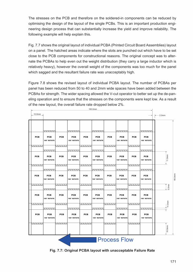
171
The stresses on the PCB and therefore on the soldered-in components can be reduced by optimising the design of the layout of the single PCBs. This is an important production engi-neering design process that can substantially increase the yield and improve reliability. The following example will help explain this.
Fig. 7.7 shows the original layout of individual PCBA (Printed Circuit Board Assemblies) layout on a panel. The hatched areas indicate where the slots are punched out which have to be set close to the PCB components for constructional reasons. The original concept was to alter-nate the PCBAs to help even out the weight distribution (they carry a large inductor which is relatively heavy), however the overall weight of the components was too much for the panel which sagged and the resultant failure rate was unacceptably high.
Figure 7.8 shows the revised layout of individual PCBA layout. The number of PCBAs per panel has been reduced from 50 to 40 and 2mm wide spaces have been added between the PCBAs for strength. The wider spacing allowed the V-cut operator to better set up the de-pan-eling operation and to ensure that the stresses on the components were kept low. As a result of the new layout, the overall failure rate dropped below 2%.
Fig. 7.7: Original PCBA layout with unacceptable Failure Rate
������
�������
�����
��� ��� ��� ��� ��� ��� ��� ��� ��� ���
����������� ����������� ����������� ����������� �����������
��� ��� ��� ��� ��� ��� ��� ��� ��� ���
����������� ����������� ����������� ����������� �����������
��� ��� ��� ��� ��� ��� ��� ��� ��� ���
����������� ����������� ����������� ����������� �����������
��� ��� ��� ��� ��� ��� ��� ��� ��� ���
����������� ����������� ����������� ����������� �����������
��� ��� ��� ��� ��� ��� ��� ��� ��� ���
����������� ����������� ����������� ����������� �����������
����
��
����
��
����
�
����
��
����
��
������������
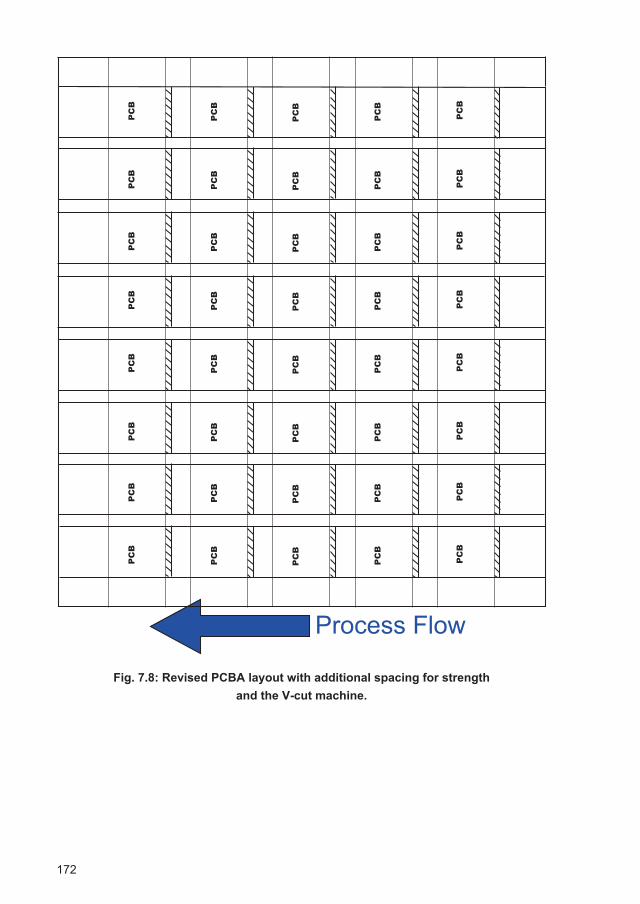
172
Fig. 7.8: Revised PCBA layout with additional spacing for strength
and the V-cut machine.
���
���
���
���
���
���
���
���
���
���
���
���
���
���
���
���
���
���
���
���
���
���
���
���
���
���
���
���
���
���
���
���
���
���
���
���
���
���
���
���
������������
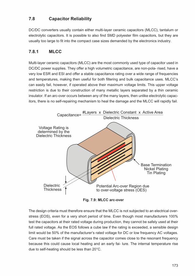
173
7.8 Capacitor Reliability
DC/DC converters usually contain either multi-layer ceramic capacitors (MLCC), tantalum or electrolytic capacitors. It is possible to also find SMD polyester film capacitors, but they are usually too large to fit into the compact case sizes demanded by the electronics industry.
7.8.1 MLCC
Multi-layer ceramic capacitors (MLCC) are the most commonly used type of capacitor used in DC/DC power supplies. They offer a high volumetric capacitance, are non-pola- rised, have a very low ESR and ESI and offer a stable capacitance rating over a wide range of frequencies and temperatures, making then useful for both filtering and bulk capacitance uses. MLCC’s can easily fail, however, if operated above their maximum voltage limits. This upper voltage restriction is due to their construction of many metallic layers separated by a thin ceramic insulator. If an arc-over occurs between any of the many layers, then unlike electrolytic capac-itors, there is no self-repairing mechanism to heal the damage and the MLCC will rapidly fail.
Fig. 7.9: MLCC arc-over
The design criteria must therefore ensure that the MLCC is not subjected to an electrical over-stress (EOS), even for a very short period of time. Even though most manufacturers 100% test the capacitors at their rated voltage during production, they cannot be safely used at their full rated voltage. As the EOS follows a cube law if the rating is exceeded, a sensible design limit would be 50% of the manufacturer’s rated voltage for DC or low frequency AC voltages. Care must be taken if the signal across the capacitor comes close to the resonant frequency because this could cause local heating and an early fai- lure. The internal temperature rise due to self-heating should be less than 20°C.
�������������������
��������������� ��������������� ��� �������������������
�����������������������������������������
��������������������������������
��������������������
������������ �������������������������������������� ������
��������������������

174
Another resonance effect that can occur with MLCC’s is acoustic noise caused by a piezoe-lectric phenomenon across the ceramic layers. If the acoustic resonant frequency matches the AC waveform across the capacitor, the capacitor can begin to sing or whine. The solution is to use a different size format MLCC with a higher or lower acoustic resonance. According to the manufacturers, singing capacitors do not affect their reliability, but obviously customers don’t appreciate noisy power supplies.
The main causes of MLCC failures are mechanical in nature. Cracks allow arc-overs to occur between the layers and lead to later failures due to the ingress of contaminants, humidity or corrosive elements (the metallic plating on the layers is particularly sensitive to sulphur corro-sion and sulphur dioxide is a common airborne contaminant present in industrial areas, in coal powered power stations, car exhausts or or as a by-product from organic decay processes). Cracks occur because the ceramic structure is brittle and easily damaged by any physical stress or asymmetric temperature gradients. As with chip resistors, the layout of the PCB is also important to avoid production stresses which could cause the capacitor to crack and fail. MLCC should be mounted parallel to any v-cut edges, slots or perforations in the PCB and be a least their own length away from any cut edges. Care must be taken with the pick-and-place machine not to over-stress the capacitors when they are dropped onto the PCB pads and the PCB itself should be well supported so that it does not flex or twist both during the soldering process or afterwards when the converter is assembled into the case.
The amount of solder paste used and the pad layout (land) is also important to reduce the stress on the capacitor due to uneven amounts of solder adhering to the terminations. A well reflow-soldered connection has a solder fillet that is concave with a buildup meniscus that rises to 75% of the height of the capacitor.
Fig. 7.10: MLCC solder fillet definitions
If too little solder paste is applied, the joint may not be reliable and fail in service. Also, the lead-free solder forms an alloy with the tin plating of the base termination which changes its mechanical strength and makes it more brittle if the proportion of solder to tin is low. On the other hand, if too much solder is applied, then the capacitor is subjected to asymmetric con-traction stresses as the PCB is cooled after passing through the IR oven which can create fissures in the ceramic layers.
���
�����������
������������
������������ ��������
����
�����
��������

175
In extreme cases, the surface tension of the molten solder can flip the capacitor on to its end (tombstoning):
Fig. 7.11: MLCC solder fillet shape
Hand-soldering is particularly hazardous for MLCC capacitors. Not only can the capacitor surface be easily scratched by the soldering iron tip, but the asymmetric heating of the capac-itor as each end of the termination is separately soldered causes considerable mechanical stresses within the structure which can lead to cracking. If an MLCC capacitor is accidentally dropped it should be discarded.
While ceramic capacitors can exhibit a very stable capacitance with temperature character-istic, the stability is very dependent on the tolerance specification. Cheaper types can vary wildly with temperature; as much as +22%, -82% over the full operating temperature range. A circuit designed to operate correctly at 25°C can therefore behave very differently at low or high ambient temperatures and become unreliable.
Fig.7.12: Change of capacitance with temperature for different MLCC classes
��������������������������������
��������������������
������� ���� ���������� ��� ������������������������ ��� �������������������
���� ������� ��� ������������ ��������������� � �������� ����� ���� �� ��������� ������������������������������������� �� ������ ����� �� ��������� ������������
����
����
�
��� ������ ��� ������
����
����
�
����������������� ��
���
���
���
���
���������������� ����������������
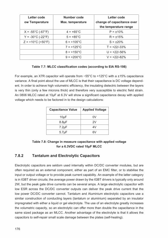
176
Letter code
ow Temperature
Number code
Max. temperature
Letter code
change of capacitance over
the temperature range
X = -55°C (-67°F) 4 = +65°C P = ±10%Y = -30°C (-22°F) 5 = +85°C R = ±15%Z = +10°C (+50°F) 6 = +105°C S = ±20%
7 = +125°C T = +22/-33%8 = +150°C U = +22/-56%9 = +200°C V = +22/-82%
Table 7.7: MLCC classification codes (according to EIA RS-198)
For example, an X7R capacitor will operate from −55°C to +125°C with a ±15% capacitance variance. A final point about the use of MLCC is that their capacitance is DC voltage depend-ent. In order to achieve high volumetric efficiency, the insulating dielectric between the layers is very thin (only a few microns thick) and therefore very susceptible to electric field strain. An 0806 MLCC rated at 10μF at 6.3V will show a significant capacitance decay with applied voltage which needs to be factored in to the design calculations:
Capacitance Value Applied Voltage
10µF 0V8.8µF 2V7.2µF 4V5.7µF 6V
Table 7.8: Change in measure capacitance with applied voltage
for a 6.3VDC rated 10μF MLCC
7.8.2 Tantalum and Electrolytic Capacitors
Electrolytic capacitors are seldom used internally within DC/DC converter modules, but are often required as an external component, either as part of an EMC filter, or to stabilise the input or output voltage or to provide peak current capability. An example of the latter category is in IGBT driver circuits; the average power drawn by the IGBT drivers is typically only around 2W, but the peak gate drive currents can be several amps. A large electrolytic capacitor with low ESR across the DC/DC converter outputs can deliver the peak drive current that the low power DC/DC converter cannot. Tantalum and Aluminium electrolytic capacitors use a similar construction of conducting layers (tantalum or aluminium) separated by an insulator impregnated with either a liquid or gel electrolyte. The use of an electrolyte greatly increases the volumetric capacity, so an electrolytic can offer more than double the capacitance in the same sized package as an MLCC. Another advantage of the electrolyte is that it allows the capacitors to self-repair small scale damage between the plates (self-healing).
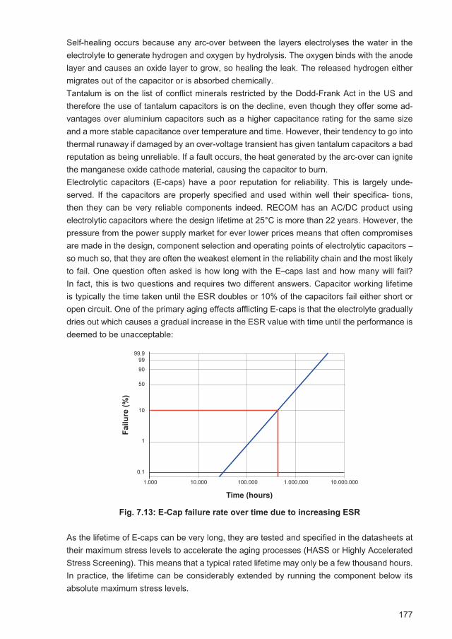
177
Self-healing occurs because any arc-over between the layers electrolyses the water in the electrolyte to generate hydrogen and oxygen by hydrolysis. The oxygen binds with the anode layer and causes an oxide layer to grow, so healing the leak. The released hydrogen either migrates out of the capacitor or is absorbed chemically.Tantalum is on the list of conflict minerals restricted by the Dodd-Frank Act in the US and therefore the use of tantalum capacitors is on the decline, even though they offer some ad-vantages over aluminium capacitors such as a higher capacitance rating for the same size and a more stable capacitance over temperature and time. However, their tendency to go into thermal runaway if damaged by an over-voltage transient has given tantalum capacitors a bad reputation as being unreliable. If a fault occurs, the heat generated by the arc-over can ignite the manganese oxide cathode material, causing the capacitor to burn.Electrolytic capacitors (E-caps) have a poor reputation for reliability. This is largely unde-served. If the capacitors are properly specified and used within well their specifica- tions, then they can be very reliable components indeed. RECOM has an AC/DC product using electrolytic capacitors where the design lifetime at 25°C is more than 22 years. However, the pressure from the power supply market for ever lower prices means that often compromises are made in the design, component selection and operating points of electrolytic capacitors – so much so, that they are often the weakest element in the reliability chain and the most likely to fail. One question often asked is how long with the E–caps last and how many will fail? In fact, this is two questions and requires two different answers. Capacitor working lifetime is typically the time taken until the ESR doubles or 10% of the capacitors fail either short or open circuit. One of the primary aging effects afflicting E-caps is that the electrolyte gradually dries out which causes a gradual increase in the ESR value with time until the performance is deemed to be unacceptable:
Fig. 7.13: E-Cap failure rate over time due to increasing ESR
As the lifetime of E-caps can be very long, they are tested and specified in the datasheets at their maximum stress levels to accelerate the aging processes (HASS or Highly Accelerated Stress Screening). This means that a typical rated lifetime may only be a few thousand hours. In practice, the lifetime can be considerably extended by running the component below its absolute maximum stress levels.
����� ������ ������� ��������� ����������
���
�
��
��
��
������
������������
���
����
���
�
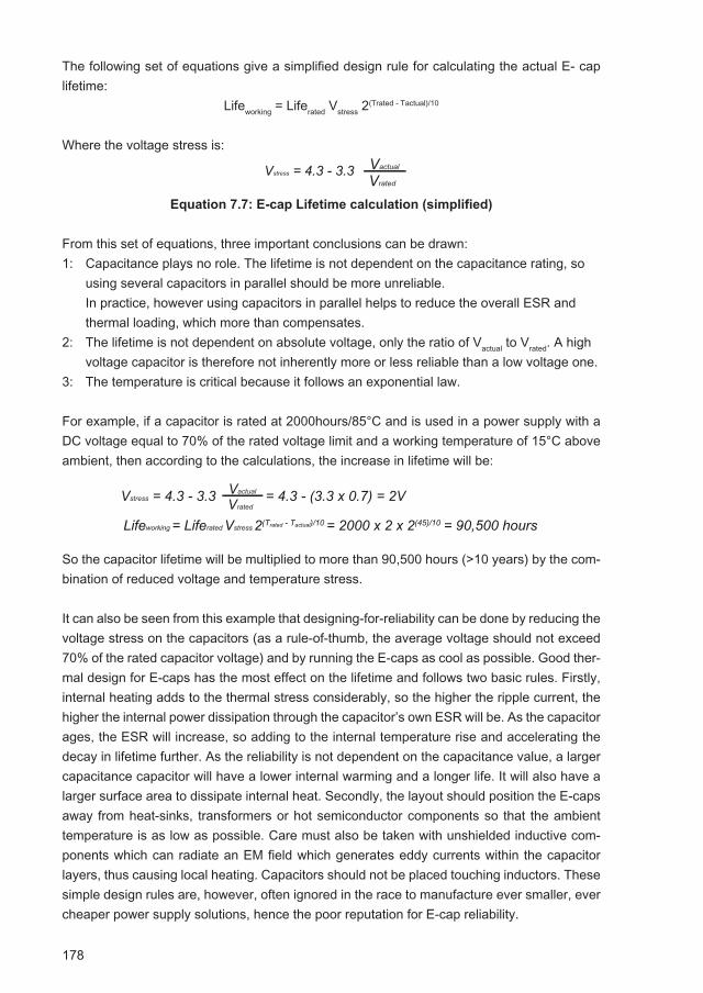
178
The following set of equations give a simplified design rule for calculating the actual E- cap lifetime:
Lifeworking = Liferated Vstress 2(Trated - Tactual)/10
Where the voltage stress is:
Equation 7.7: E-cap Lifetime calculation (simplified)
From this set of equations, three important conclusions can be drawn:1: Capacitance plays no role. The lifetime is not dependent on the capacitance rating, so using several capacitors in parallel should be more unreliable. In practice, however using capacitors in parallel helps to reduce the overall ESR and thermal loading, which more than compensates.2: The lifetime is not dependent on absolute voltage, only the ratio of Vactual to Vrated. A high voltage capacitor is therefore not inherently more or less reliable than a low voltage one.3: The temperature is critical because it follows an exponential law.
For example, if a capacitor is rated at 2000hours/85°C and is used in a power supply with a DC voltage equal to 70% of the rated voltage limit and a working temperature of 15°C above ambient, then according to the calculations, the increase in lifetime will be:
So the capacitor lifetime will be multiplied to more than 90,500 hours (>10 years) by the com-bination of reduced voltage and temperature stress.
It can also be seen from this example that designing-for-reliability can be done by reducing the voltage stress on the capacitors (as a rule-of-thumb, the average voltage should not exceed 70% of the rated capacitor voltage) and by running the E-caps as cool as possible. Good ther-mal design for E-caps has the most effect on the lifetime and follows two basic rules. Firstly, internal heating adds to the thermal stress considerably, so the higher the ripple current, the higher the internal power dissipation through the capacitor’s own ESR will be. As the capacitor ages, the ESR will increase, so adding to the internal temperature rise and accelerating the decay in lifetime further. As the reliability is not dependent on the capacitance value, a larger capacitance capacitor will have a lower internal warming and a longer life. It will also have a larger surface area to dissipate internal heat. Secondly, the layout should position the E-caps away from heat-sinks, transformers or hot semiconductor components so that the ambient temperature is as low as possible. Care must also be taken with unshielded inductive com-ponents which can radiate an EM field which generates eddy currents within the capacitor layers, thus causing local heating. Capacitors should not be placed touching inductors. These simple design rules are, however, often ignored in the race to manufacture ever smaller, ever cheaper power supply solutions, hence the poor reputation for E-cap reliability.
Vstress = 4.3 - 3.3 Vrated
Vactual = 4.3 − (3.3 x 0.7) = 2V
2(Trated - Tactual)/10 = 2000 x 2 x 2(45)/10 = 90,500 時間
Vstress = 4.3 - 3.3
Lifeworking = Liferated Vstress Vrated
Vactual = 4.3 - (3.3 x 0.7) = 2V
2(Trated - Tactual)/10 = 2000 x 2 x 2(45)/10 = 90,500 hours
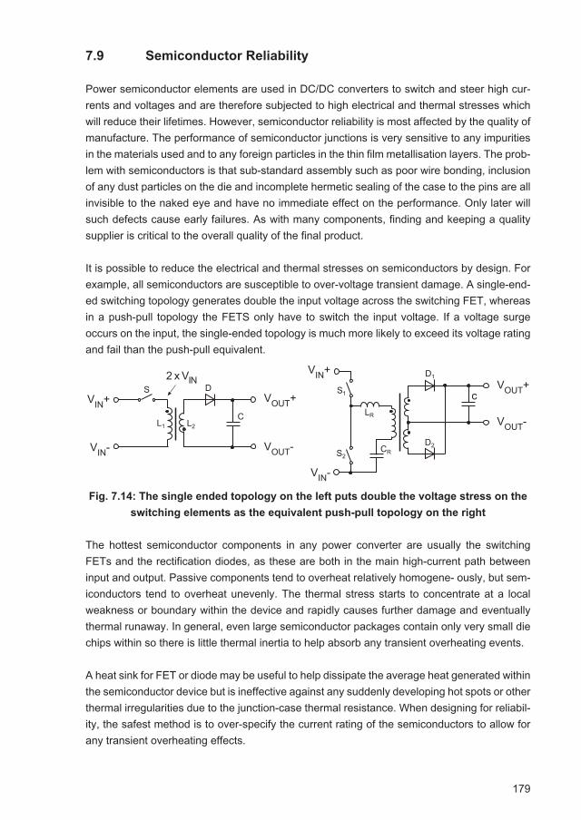
179
7.9 Semiconductor Reliability
Power semiconductor elements are used in DC/DC converters to switch and steer high cur-rents and voltages and are therefore subjected to high electrical and thermal stresses which will reduce their lifetimes. However, semiconductor reliability is most affected by the quality of manufacture. The performance of semiconductor junctions is very sensitive to any impurities in the materials used and to any foreign particles in the thin film metallisation layers. The prob-lem with semiconductors is that sub-standard assembly such as poor wire bonding, inclusion of any dust particles on the die and incomplete hermetic sealing of the case to the pins are all invisible to the naked eye and have no immediate effect on the performance. Only later will such defects cause early failures. As with many components, finding and keeping a quality supplier is critical to the overall quality of the final product.
It is possible to reduce the electrical and thermal stresses on semiconductors by design. For example, all semiconductors are susceptible to over-voltage transient damage. A single-end-ed switching topology generates double the input voltage across the switching FET, whereas in a push-pull topology the FETS only have to switch the input voltage. If a voltage surge occurs on the input, the single-ended topology is much more likely to exceed its voltage rating and fail than the push-pull equivalent.
Fig. 7.14: The single ended topology on the left puts double the voltage stress on the
switching elements as the equivalent push-pull topology on the right
The hottest semiconductor components in any power converter are usually the switching FETs and the rectification diodes, as these are both in the main high-current path between input and output. Passive components tend to overheat relatively homogene- ously, but sem-iconductors tend to overheat unevenly. The thermal stress starts to concentrate at a local weakness or boundary within the device and rapidly causes further damage and eventually thermal runaway. In general, even large semiconductor packages contain only very small die chips within so there is little thermal inertia to help absorb any transient overheating events.
A heat sink for FET or diode may be useful to help dissipate the average heat generated within the semiconductor device but is ineffective against any suddenly developing hot spots or other thermal irregularities due to the junction-case thermal resistance. When designing for reliabil-ity, the safest method is to over-specify the current rating of the semiconductors to allow for any transient overheating effects.
�����
� �
��
�
����
��
��
��
�������
����
����
�����
�����
�����
�����
����
����
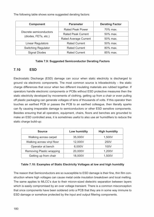
180
The following table shows some suggested derating factors:
Component Parameter Derating Factor
Discrete semiconductors (diodes, FETs, etc.)
Rated Peak Power 70% max.Rated Peak Current 50% max.
Rated Average Current 50% max.Linear Regulators Rated Current 50% max.
Switching Regulator Rated Current 80% max.Signal Diodes Rated Current 85% max.
Table 7.9: Suggested Semiconductor Derating Factors
7.10 ESD
Electrostatic Discharge (ESD) damage can occur when static electricity is discharged to ground via electronic components. The most common source is triboelectricity – the static charge differences that occur when two different insulating materials are rubbed together. If operators handle electronic components or PCBs without ESD protective measures then the static electricity developed by movements of clothing, getting up from a chair or even pulling off plastic packaging can generate voltages of tens of thousands of volts. If this operator then touches an earthed PCB or passes the PCB to an earthed colleague, then literally sparks can fly causing irreparable damage to semiconductors or other ESD sensitive components. Besides ensuring that all operators, equipment, chairs, floors and benches are grounded to make an ESD controlled area, it is sometimes useful to also use air humidifiers to reduce the static charge build-up:
Source Low humidity High humidity
Walking across carpet 35,000V 1,500VWalking across vinyl floor 12,000V 250V
Operator at bench 6,000V 100VRemoving Plastic wrapping 20,000V 1,200V
Getting up from chair 18,000V 1,500V
Table 7.10: Examples of Static Electricity Voltages at low and high humidity
The reason that Semiconductors are so susceptible to ESD damage is their fine, thin film con-struction where high voltages can cause metal oxide insulation breakdown and local melting. The same applies to MLCC’s due to their micron-sized dielectric separation between layers which is easily compromised by an over voltage transient. There is a common misconception that once components have been soldered onto a PCB that they are in some way immune to ESD damage or somehow protected by the input and output filtering components.
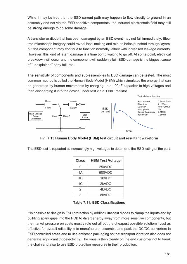
181
While it may be true that the ESD current path may happen to flow directly to ground in an assembly and not via the ESD sensitive components, the induced electrostatic field may still be strong enough to do some damage.
A transistor or diode that has been damaged by an ESD event may not fail immediately. Elec-tron microscope imagery could reveal local melting and minute holes punched through layers, but the component may continue to function normally, albeit with increased leakage currents. However, this kind of latent damage is a time bomb waiting to go off. At some point, electrical breakdown will occur and the component will suddenly fail. ESD damage is the biggest cause of “unexplained” early failures.
The sensitivity of components and sub-assemblies to ESD damage can be tested. The most common method is called the Human Body Model (HBM) which simulates the energy that can be generated by human movements by charging up a 100pF capacitor to high voltages and then discharging it into the device under test via a 1.5kΩ resistor.
Fig. 7.15 Human Body Model (HBM) test circuit and resultant waveform
The ESD test is repeated at increasingly high voltages to determine the ESD rating of the part:
Class HBM Test Voltage
0 250VDC1A 500VDC1B 1kVDC1C 2kVDC2 4kVDC3 8kVDC
Table 7.11: ESD Classifications
It is possible to design in ESD protection by adding ultra-fast diodes to clamp the inputs and by building spark gaps into the PCB to divert energy away from more sensitive components, but the market pressure on costs mostly rule out all but the cheapest possible solutions. Just as effective for overall reliability is to manufacture, assemble and pack the DC/DC converters in ESD controlled areas and to use antistatic packaging so that transport vibration also does not generate significant triboelectricity. The onus is then clearly on the end customer not to break the chain and also to use ESD protection measures in their production.
Typical characteristics Peak current 0.3A at 500VRise time 2〜25μsDuration 100〜200μsPeak power 1WCentre frequency 2.5MHzBandwidth 0.5MHz
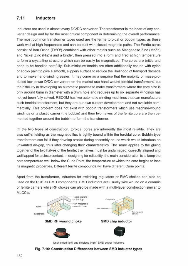
182
7.11 Inductors
Inductors are used in almost every DC/DC converter. The transformer is the heart of any con-verter design and by far the most critical component in determining the overall performance. The most common transformer types used are the ferrite toroidal or bobbin types, as these work well at high frequencies and can be built with closed magnetic paths. The Ferrite cores consist of Iron Oxide (Fe2O4) combined with other metals such as Manganese Zinc (MnZn) and Nickel Zinc (NiZn) and a binder, then pressed into a form and fired at high temperature to form a crystalline structure which can be easily be magnetized. The cores are brittle and need to be handled carefully. Sub-miniature toroids are often additionally coated with nylon or epoxy paint to give a smooth, slippery surface to reduce the likelihood of transport damage and to make hand-winding easier. It may come as a surprise that the majority of mass-pro-duced low power D/DC converters on the market use hand-wound toroidal transformers, but the difficulty in developing an automatic process to make transformers where the core size is only around 6mm in diameter with a 3mm hole and requires up to six separate windings has not yet been fully solved. RECOM has two automatic winding machines that can manufacture such toroidal transformers, but they are our own custom development and not available com-mercially. This problem does not exist with bobbin transformers which use machine-wound windings on a plastic carrier (the bobbin) and then two halves of the ferrite core are then ce-mented together around the bobbin to form the transformer.
Of the two types of construction, toroidal cores are inherently the most reliable. They are also self-shielding as the magnetic flux is tightly bound within the toroidal core. Bobbin type transformers can fail if they develop cracks during assembly or use which would introduce an unwanted air-gap, thus later changing their characteristics. The same applies to the gluing together of the two halves of the ferrite; the halves must be undamaged, correctly aligned and well lapped for a close contact. In designing for reliability, the main consideration is to keep the core temperature well below the Curie Point, the temperature at which the core begins to lose its magnetic properties. Different ferrite compounds will have different Curie points.
Apart from the transformer, inductors for switching regulators or EMC chokes can also be used on the PCB as SMD components. SMD inductors are usually wire wound on a ceramic or ferrite carriers while RF chokes can also be made with a multi-layer construction similar to MLCC’s.
SMD RF wound choke SMD chip inductor
Unshielded (left) and shielded (right) SMD power inductors
Fig. 7.16: Construction Differences between SMD inductor types
����
���������
�����������������������
�����������������������
������������
���������������
������ ������������
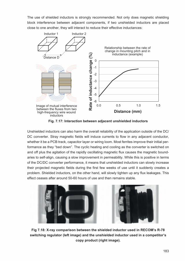
183
The use of shielded inductors is strongly recommended. Not only does magnetic shielding block interference between adjacent components, if two unshielded inductors are placed close to one another, they will interact to reduce their effective inductances:
Fig. 7.17: Interaction between adjacent unshielded inductors
Unshielded inductors can also harm the overall reliability of the application outside of the DC/DC converter. Stray magnetic fields will induce currents to flow in any adjacent conductor, whether it be a PCB track, capacitor layer or wiring loom. Most ferrites improve their initial per-formance as they “bed down”. The cyclic heating and cooling as the converter is switched on and off plus the agitation of the rapidly oscillating magnetic flux causes the magnetic bound-aries to self-align, causing a slow improvement in permeability. While this is positive in terms of the DC/DC converter performance, it means that unshielded inductors can slowly increase their projected magnetic fields during the first few weeks of use until it suddenly creates a problem. Shielded inductors, on the other hand, will slowly tighten up any flux leakages. This effect ceases after around 50-60 hours of use and then remains stable.
Fig 7.18: X-ray comparison between the shielded inductor used in RECOM’s R-78
switching regulator (left image) and the unshielded inductor used in a competitor’s
copy product (right image).
��� ��� ��� �����
��
��
��
��
��
�
����������������
�������
����
����
�����
��
���
��������� ���������� ���������� ��������������������� �������
��������������������
����������������������������������� ���������������� �� �������������������
���������
����������
���������� ����������
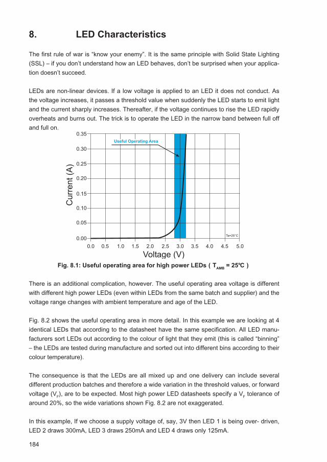
184
8. LED Characteristics
The first rule of war is “know your enemy”. It is the same principle with Solid State Lighting (SSL) – if you don’t understand how an LED behaves, don’t be surprised when your applica-tion doesn’t succeed.
LEDs are non-linear devices. If a low voltage is applied to an LED it does not conduct. As the voltage increases, it passes a threshold value when suddenly the LED starts to emit light and the current sharply increases. Thereafter, if the voltage continues to rise the LED rapidly overheats and burns out. The trick is to operate the LED in the narrow band between full off and full on.
Fig. 8.1: Useful operating area for high power LEDs(TAMB
= 25℃)
There is an additional complication, however. The useful operating area voltage is different with different high power LEDs (even within LEDs from the same batch and supplier) and the voltage range changes with ambient temperature and age of the LED.
Fig. 8.2 shows the useful operating area in more detail. In this example we are looking at 4 identical LEDs that according to the datasheet have the same specification. All LED manu-facturers sort LEDs out according to the colour of light that they emit (this is called “binning” – the LEDs are tested during manufacture and sorted out into different bins according to their colour temperature).
The consequence is that the LEDs are all mixed up and one delivery can include several different production batches and therefore a wide variation in the threshold values, or forward voltage (VF), are to be expected. Most high power LED datasheets specify a VF tolerance of around 20%, so the wide variations shown Fig. 8.2 are not exaggerated.
In this example, If we choose a supply voltage of, say, 3V then LED 1 is being over- driven, LED 2 draws 300mA, LED 3 draws 250mA and LED 4 draws only 125mA.
����
����
����
����
����
����
����
�������������������������
��� ��� ��� ��� ��� ��� ��� ��� ��� ��� ���
�����������
� �
����
���
������
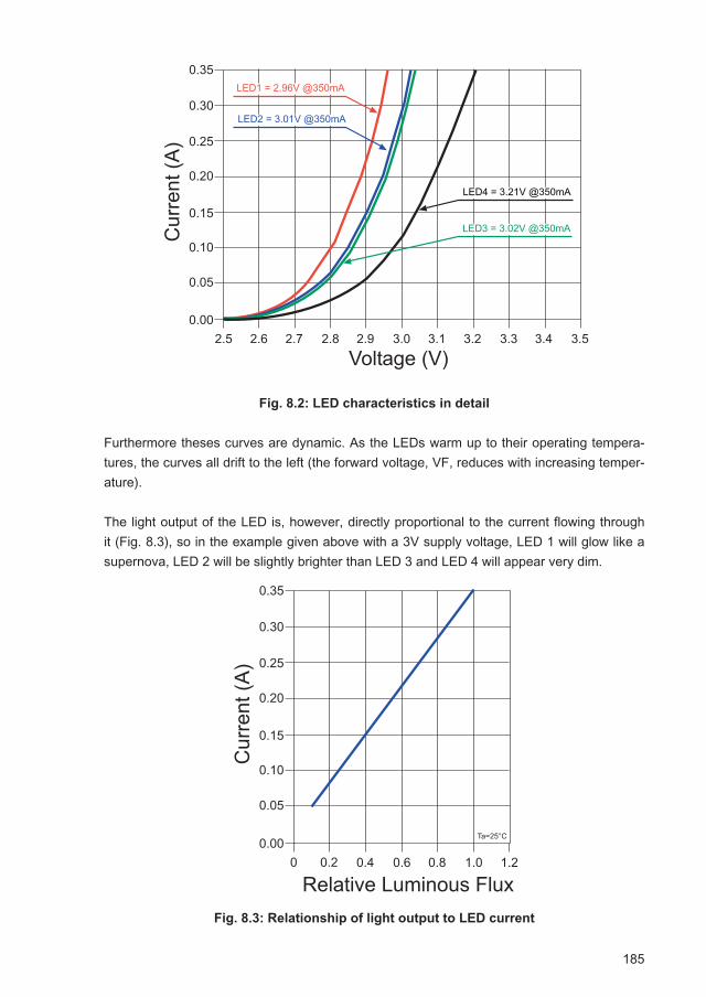
185
Fig. 8.2: LED characteristics in detail
Furthermore theses curves are dynamic. As the LEDs warm up to their operating tempera-tures, the curves all drift to the left (the forward voltage, VF, reduces with increasing temper-ature).
The light output of the LED is, however, directly proportional to the current flowing through it (Fig. 8.3), so in the example given above with a 3V supply voltage, LED 1 will glow like a supernova, LED 2 will be slightly brighter than LED 3 and LED 4 will appear very dim.
Fig. 8.3: Relationship of light output to LED current
����
����
����
����
����
����
����
����
��� ���
�����������
��
���
����
�� �� ��� ��� ��� ��� ��� ��� ���
������������������
�������������������
�������������������
�������������������
����
����
����
����
����
����
����
����
� ���
�������������� ������
��
����
����
��� ��� ��� ��� ���
������
186
8.1 Driving LEDs with a Constant Currents
The solution to this problem of the variability in forward voltage, VF, is to use a constant current rather than a constant voltage to drive the LEDs.
The LED driver automatically adjusts the output voltage to keep the output current constant and therefore the light output constant. This works with a single LED or with a chain of string of LEDs connected in series. As long as the current through all LEDs is the same, they will have the same brightness even if the VF across each LED is different (see Fig. 8.4).
As the LEDs warm up to their working temperature, the constant current driver automatically reduces the driving voltage to keep the current through the LEDs constant, so the brightness of the LEDs is also independent of working temperature.
Another major advantage is that a constant current driver does not allow any single LED in a chain to be overdriven and thus ensures that they all have a long operating life. If any LED fails short circuit, the remaining LEDs still operate with the correct current.
Fig. 8.4: LED String
8.2 Some DC Constant Current Sources
The simplest constant current source is a constant voltage supply driving the LEDs via a resistor. If the voltage drop across the resistor is about the same as the forward voltage of a LED, then a 10% change in VF causes a similar change in the LED current (compare this with the curves shown in Fig. 8.2 where a 10% change in VF causes about a 50% change in LED current). This solution is very cheap, but has a poor current regulation and is very wasteful in power. Many of the low cost cluster-type LED bulbs offered as replacement lamps for low voltage halogens use this method. Needless to say, if any LED fails short circuit, the resistor is overloaded and usually burns out after a relatively short while, thus the lifetime of these cluster LED lamps is relatively short.
The next simplest constant current source is a linear current regulator. There are several low cost LED drivers available on the markets that use this method or a standard linear voltage regulator can be used in constant current mode. The internal feedback circuit keeps the cur-rent regulated to within about ±5% but excess power has to be dumped as heat, so good heat sinking of the regulator is required. The disadvantage is the poor efficiency of this solution, which rather goes against the concept of using high efficiency SSL devices.
��� ��� ���
��������������������
��� ���������������� �������������
187
The best constant current source is a switching regulator. The price of the driver is higher than the other solutions, but the output current accuracy can be as accurate as ±3% over a wide range of LED loads and conversion efficiencies can be as high as 96% which means that only 4% of the energy is wasted as heat and the drivers can be used at high ambient temperatures.
Example of constant current sources for LEDs:
Fig. 8.5: Simple Resistor: Low cost, but inaccurate and wasteful
Fig. 8.6: Linear Regulator: Low cost and accurate, but wasteful
Fig. 8.7: Switching Regulator: Higher cost, but accurate and efficient
One important difference between the options shown above is the input and output voltage ranges.
A DC/DC switching regulator has a wide input voltage and output voltage range over which the constant current regulation works well (the RCD-24.0.35 works from 5V to 36Vdc has an output voltage range of 2-34Vdc, for example). A wide output voltage range not only allows many different combinations of LED string lengths, but also permits a wide dimming range.
The other two options shown above will have power dissipation problems if only 1 LED is needed, as the resistor or linear regulator will have a larger volt drop across them which will still further increase the power dissipation losses. The input voltage range has to also be re-stricted for the same reason.
��������
�����
��
����� ��� ���
�� ��
� �
���
��
��������
��
��������
���� ����������
����
���
�� �������
���
��
��������
���������� ���
�������
����������
���
���
����������
��
188
8.3 Connecting LEDs in Strings
The majority of high power white LEDs are designed to be run at 350mA constant current. This is because the chemistry of a white light LED sets the forward voltage at about 3V and 3.0V × 0.35A ~ 1Watt, which is a convenient LED power.Most DC/DC constant current LED drivers are buck or step-down converters. This means that the maximum output voltage is lower than the input voltage. Thus the number of LEDs that can be driven depends on the input voltage.
Input Voltage 5Vdc 12Vdc 24Vdc 36Vdc 5Vdc
Typical # of LEDs in String 1 3 7* 10* 15
Table 8.1: Number of LEDs that can be driven per string vs. Input voltage
If the input voltage is not regulated (e.g. a battery) then the maximum number of LEDs must be reduced depending on the minimum input voltage available.
Example:How many 1W LEDs can be driven from a 12V Lead acid battery?
Two LEDs is not very much! A way around this problem is to either use a boost converter where the output voltage is higher than the input voltage or to use two or more strings of LEDs in parallel. For each 350mA string of LEDs used, the driver current has to be increased to de-liver the correct overall current. So a single string needs a 350mA driver, two strings in parallel require a 700mA driver, three parallel strings would need a 1.05A source, etc. Therefore the choice of LED driver is dependent on the input voltage available and the number of strings of LEDs that need to be driven.
Fig. 8.8, 8.9 and 8.10 shows some possible combinations for a fixed 12Vdc supply using typ-ical 1W white LEDS. With a regulated 12V supply, up to three LEDs in a string can be driven (3 × 3.3V = 9.9V, which gives 2.1V headroom for the constant current driver regulation).
* Note: It is a common misconception that the number of LEDs that can be driven is depend-ent on the maximum VF given in the LED datasheets. This is not true in practice because when the LEDs reach their operating temperature, the VF falls significantly. Thus the typical VF given in the datasheet can be reliably used. A typical datasheet might state that VF is 3.3V minimum, 3.6V typical and 3.9V maximum at 25°C ambient. However at 50°C, the figures would be closer to 3.0V minimum, 3.3V typical and 3.6V max. Therefore a fixed 24V supply can reliably drive 7 LEDs and a 36V supply 10 LEDs, even if there is some voltage drop across the LED driver.
Battery voltage range 9 ~ 14Vdc DC/DC driver headroom 1V Therefore, LED driver output voltage range 8 ~ 13Vdc if LED forward voltage, VF 3.3V typical* then the maximum number of LEDs that can be driven 2
189
8.4 Connecting LED Strings in parallel
3 LEDs in a single string with 350mA driver:
Fig. 8.8: Advantages: accurate LED current, fail safe / Disadvantages: low number of
LEDs per driver
6 LEDs in two strings with 700mA driver:
Fig. 8.9: Advantages: double number of LEDs per driver - Disadvantages: not fail safe,
unbalanced currents in the strings
9 LEDs in three strings with 1050mA driver:
Fig. 8.10: Advantages: triple number of LEDs per driver - Disadvantages:
not fail safe, unbalan- ced currents in the strings
Connecting a single string of LEDs to an LED driver is the safest and surest method of dri- ving LEDS. If any LED fails open circuit, the current to the remai- ning LEDs in the string is broken. If any LED fails short circuit, the
Both strings will be overloaded with 500mA per string. The LEDs will probably cope with this for some time, depending on how well the LEDs are heat-sinked, but eventually the over-cur-rent will cause another LED to fail, whereupon the third string will take all of the 1A current and fail almost immediately.
���
��
��������
��
�����
���
���
��� �� ����
��
���
��
����
� ���
��
�����
���
���
��� �� ���
��
���
��
���
��
���
�������
���
��
����
�
���
��
�����
���
���
�������� ��
��
���
��
���
��
���
��
�����
��������
��
���
��
���
��
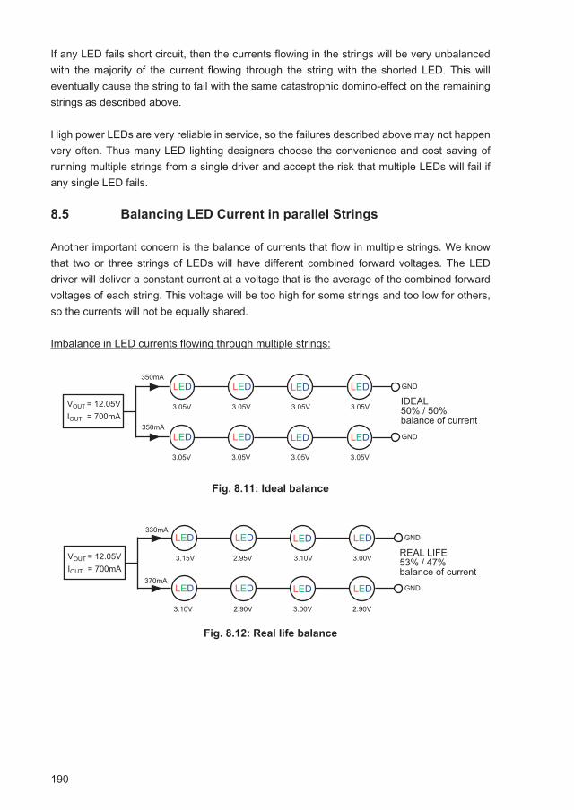
190
If any LED fails short circuit, then the currents flowing in the strings will be very unbalanced with the majority of the current flowing through the string with the shorted LED. This will eventually cause the string to fail with the same catastrophic domino-effect on the remaining strings as described above.
High power LEDs are very reliable in service, so the failures described above may not happen very often. Thus many LED lighting designers choose the convenience and cost saving of running multiple strings from a single driver and accept the risk that multiple LEDs will fail if any single LED fails.
8.5 Balancing LED Current in parallel Strings
Another important concern is the balance of currents that flow in multiple strings. We know that two or three strings of LEDs will have different combined forward voltages. The LED driver will deliver a constant current at a voltage that is the average of the combined forward voltages of each string. This voltage will be too high for some strings and too low for others, so the currents will not be equally shared.
Imbalance in LED currents flowing through multiple strings:
Fig. 8.11: Ideal balance
Fig. 8.12: Real life balance
��� ��� ���
������������������������������������������ ����
��� ���
��� ��� ������ ���
��������������������
�����������������������������
�����
�����
��� ��� ���
��������������������
��� ���
��� ��� ������ ���
��������������������
����������� ���� �����������������
�����
����
����� �������������� �����
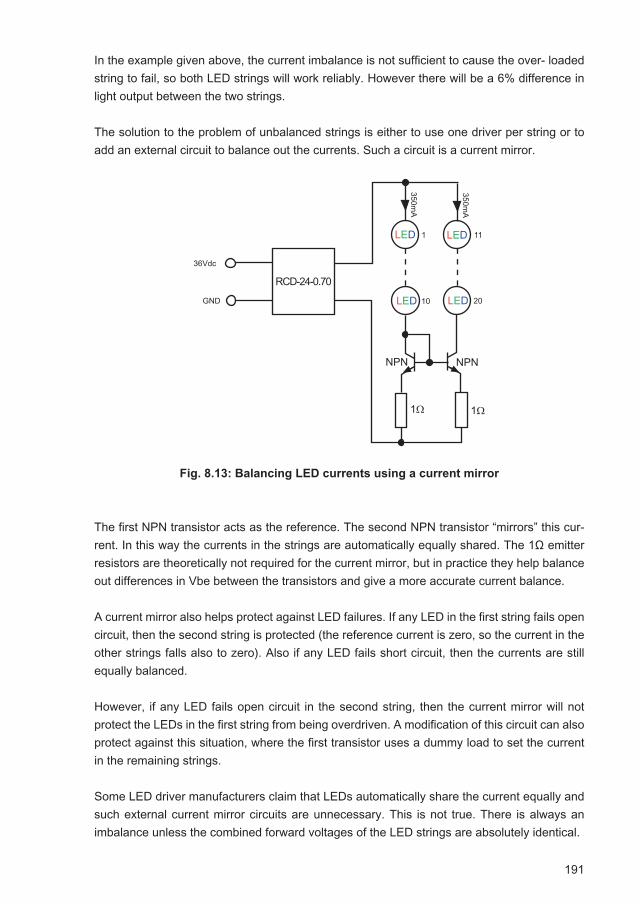
191
In the example given above, the current imbalance is not sufficient to cause the over- loaded string to fail, so both LED strings will work reliably. However there will be a 6% difference in light output between the two strings.
The solution to the problem of unbalanced strings is either to use one driver per string or to add an external circuit to balance out the currents. Such a circuit is a current mirror.
Fig. 8.13: Balancing LED currents using a current mirror
The first NPN transistor acts as the reference. The second NPN transistor “mirrors” this cur-rent. In this way the currents in the strings are automatically equally shared. The 1Ω emitter resistors are theoretically not required for the current mirror, but in practice they help balance out differences in Vbe between the transistors and give a more accurate current balance.
A current mirror also helps protect against LED failures. If any LED in the first string fails open circuit, then the second string is protected (the reference current is zero, so the current in the other strings falls also to zero). Also if any LED fails short circuit, then the currents are still equally balanced.
However, if any LED fails open circuit in the second string, then the current mirror will not protect the LEDs in the first string from being overdriven. A modification of this circuit can also protect against this situation, where the first transistor uses a dummy load to set the current in the remaining strings.
Some LED driver manufacturers claim that LEDs automatically share the current equally and such external current mirror circuits are unnecessary. This is not true. There is always an imbalance unless the combined forward voltages of the LED strings are absolutely identical.
��� ������
�
���
�����
���
���
�����
���
�
�� ��
��� �� ���
�� ��
�� ��

192
If, say, two parallel strings are mounted on a common heat-sink then if one string draws more current than the other, it will run brighter and hotter. The heat sink temperature will slowly rise, thus causing the VF of the second string to fall and cause it to also try and draw more cur-rent. In theory, the two strings should then balance out their currents because of the thermal negative feedback. In practice, this effect can be measured, but it is not enough to guarantee accurate current balancing.
Furthermore, if the two strings are in fact two separate LED lamps, there will be no thermal compensation feedback. The lamp with the lowest combined VF will draw the most current, will run the hottest and the VF will fall still further. This will make the imbalance worse and can lead to thermal runaway and LED failure.
When the circuit in Fig. 8.13 was first published, there was some criticism on the Web that a current mirror was not an ideal solution and even just adding the 1Ω resistors would help balance out the currents. This is true to an extent, but if you need an accurate current balance then the current mirror is still the simplest and best solution apart from running each lamp from its own driver.
8.6 Parallel Strings or Grid Array - Which is better?
In Section 8.4, the consequences of a single LED failure open circuit or short circuit were discussed. The larger the number of parallel strings, the lower the danger that a single fault in one string would cause the remaining strings to fail. Thus if five strings were connected in parallel, then if one LED string failed open circuit, then the remaining four strings would all be overdriven by only 125%. The LEDs would glow excessively bright, but they would be unlikely to fail as long as the heat sinking was adequate.
The disadvantage of connecting many strings in parallel is that a driver capable of delivering several Amps will be required and this could be expensive or hard to find. Also, some care is required with LED drivers capable of delivering many Amps of current; if the LED load is too low because, for example a connector to some of the strings has a faulty connection, the cur-rent will blow the remaining LEDs instantly. Great care needs to be taken that all connections are sound before the LED driver is turned on. Many expensive LED lamp fittings have been damaged by faulty wiring with high current LED drivers!
In practice, it is safer to limit the number of parallel strings to five or less per driver and to use several low current drivers rather than a single high current driver if many LEDs need to be driven.
Using long strings is also a good idea because if any LED fails short circuit, then the increase in current in that string will be proportionately less the longer the strings are.
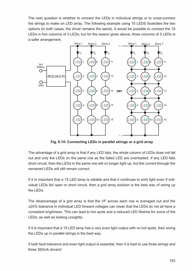
193
The next question is whether to connect the LEDs in individual strings or to cross-connect the strings to make an LED array. The following example using 15 LEDS illustrates the two options (in both cases, the driver remains the same). It would be possible to connect the 15 LEDs in five columns of 3 LEDs, but for the reason given above, three columns of 5 LEDs is a safer arrangement.
Fig. 8.14: Connecting LEDs in parallel strings or a grid array
The advantage of a grid array is that if any LED fails, the whole column of LEDs does not fall out and only the LEDs on the same row as the failed LED are overloaded. If any LED fails short circuit, then the LEDs in the same row will no longer light up, but the current through the remained LEDs will still remain correct.
If it is important that a 15 LED lamp is reliable and that it continues to emit light even if indi-vidual LEDs fail open or short circuit, then a grid array solution is the best way of wiring up the LEDs.
The disadvantage of a grid array is that the VF across each row is averaged out and the ±20% tolerance in individual LED forward voltages can mean that the LEDs do not all have a consistent brightness. This can lead to hot spots and a reduced LED lifetime for some of the LEDs, as well as looking unsightly.
If it is important that a 15 LED lamp has a very even light output with no hot spots, then wiring the LEDs up in parallel strings is the best way.
If both fault tolerance and even light output is essential, then it is best to use three strings and three 350mA drivers!
������
�������
���
�
������� ��
��� ���
��� ��� ���
��� ��� ���
��� ��� ���
��� ��� ���
�
�
�
�
�
�
�
��
�
��
�
��
�������� �������� �������
��� � ��� ���
��� ��� ���
��� ��� ���
��� ��� ���
��� ��� ���
�
�
�
�
�
�
�
��
�
��
�
��
�������� �������� �������
�� �� � �� �� �
���
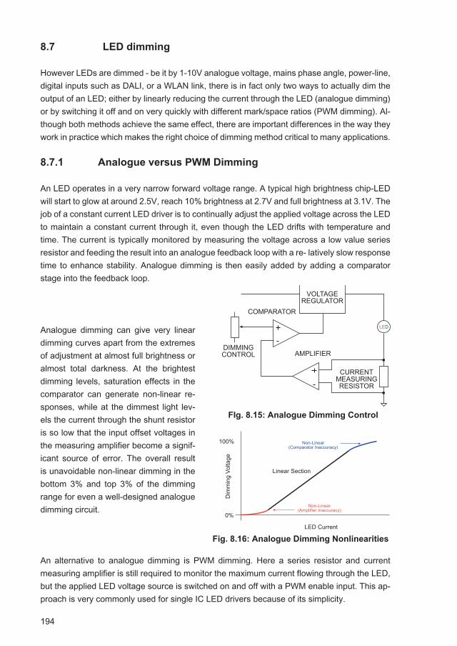
194
8.7 LED dimming
However LEDs are dimmed - be it by 1-10V analogue voltage, mains phase angle, power-line, digital inputs such as DALI, or a WLAN link, there is in fact only two ways to actually dim the output of an LED; either by linearly reducing the current through the LED (analogue dimming) or by switching it off and on very quickly with different mark/space ratios (PWM dimming). Al-though both methods achieve the same effect, there are important differences in the way they work in practice which makes the right choice of dimming method critical to many applications.
8.7.1 Analogue versus PWM Dimming
An LED operates in a very narrow forward voltage range. A typical high brightness chip-LED will start to glow at around 2.5V, reach 10% brightness at 2.7V and full brightness at 3.1V. The job of a constant current LED driver is to continually adjust the applied voltage across the LED to maintain a constant current through it, even though the LED drifts with temperature and time. The current is typically monitored by measuring the voltage across a low value series resistor and feeding the result into an analogue feedback loop with a re- latively slow response time to enhance stability. Analogue dimming is then easily added by adding a comparator stage into the feedback loop.
An alternative to analogue dimming is PWM dimming. Here a series resistor and current measuring amplifier is still required to monitor the maximum current flowing through the LED, but the applied LED voltage source is switched on and off with a PWM enable input. This ap-proach is very commonly used for single IC LED drivers because of its simplicity.
������������������������
�����������������������
����������
����������������
���
������������������������������� �
���������������������������� �
�����������
���
�����
����
��
����
��
��������������
Analogue dimming can give very linear dimming curves apart from the extremes of adjustment at almost full brightness or almost total darkness. At the brightest dimming levels, saturation effects in the comparator can generate non-linear re-sponses, while at the dimmest light lev-els the current through the shunt resistor is so low that the input offset voltages in the measuring amplifier become a signif-icant source of error. The overall result is unavoidable non-linear dimming in the bottom 3% and top 3% of the dimming range for even a well-designed analogue dimming circuit.
FIg. 8.15: Analogue Dimming Control
Fig. 8.16: Analogue Dimming Nonlinearities
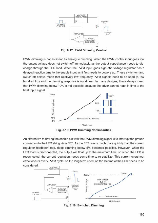
195
Fig. 8.17: PWM Dimming Control
PWM dimming is not as linear as analogue dimming. When the PWM control input goes low the output voltage does not switch off immediately as the output capacitance needs to dis-charge through the LED load. When the PWM input goes high, the voltage regulator has a delayed reaction time to the enable input as it first needs to powers up. These switch-on and switch-off delays mean that relatively low frequency PWM signals need to be used (a few hundred Hz) and the dimming response is non-linear. In many designs, these delays mean that PWM dimming below 10% is not possible because the driver cannot react in time to the brief input signal.
Fig. 8.18: PWM Dimming Nonlinearities
An alternative to driving the enable pin with the PWM dimming signal is to interrupt the ground connection to the LED string via a FET. As the FET reacts much more quickly than the current regulator feedback loop, deep dimming below 5% becomes possible. However, when the LED load is disconnected, the output will float up to the maximum limit, so when the LED is reconnected, the current regulation needs some time to re-stabilize. This current overshoot effect occurs every PWM cycle, so the long term effect on the lifetime of the LED needs to be considered.
Fig. 8.19: Switched Dimming
������������������������
���������
��������������
����������������
�� ������
���� ������
��
���
�����������
���
�����
�����
��
� �
����������������������������
�����������������
� �
� �
� �
������������������������
���������
��������������
����������������
�� ��
������������� �������������
����
����� �����
���
�����
����
��
���
� �������� �������
��������� ����
����� ������������
���������
���
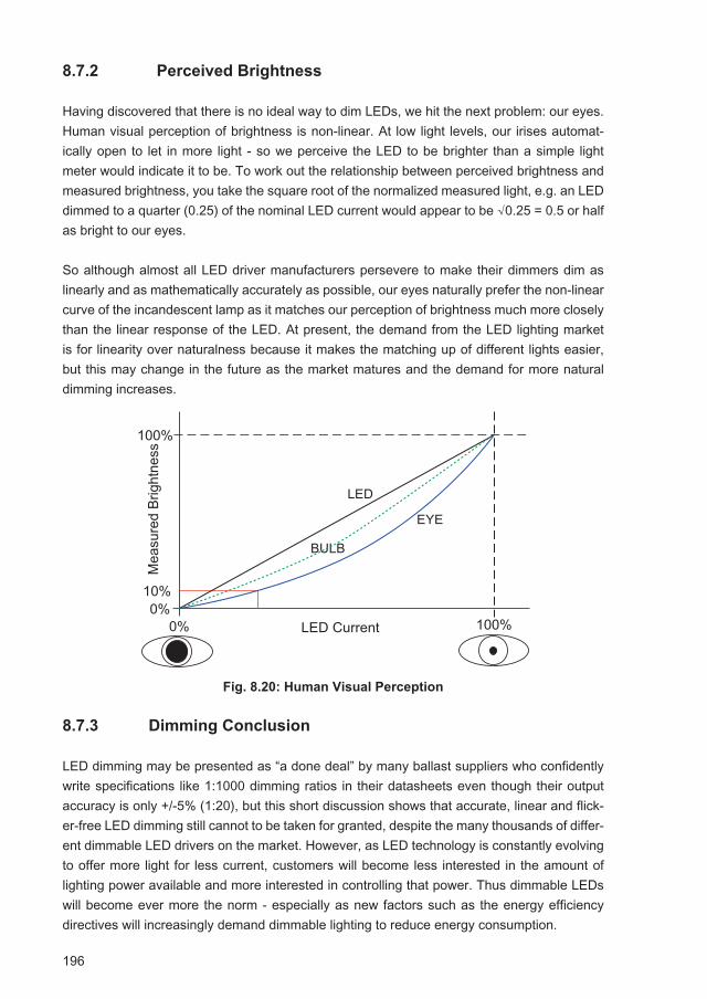
196
8.7.2 Perceived Brightness
Having discovered that there is no ideal way to dim LEDs, we hit the next problem: our eyes. Human visual perception of brightness is non-linear. At low light levels, our irises automat-ically open to let in more light - so we perceive the LED to be brighter than a simple light meter would indicate it to be. To work out the relationship between perceived brightness and measured brightness, you take the square root of the normalized measured light, e.g. an LED dimmed to a quarter (0.25) of the nominal LED current would appear to be √0.25 = 0.5 or half as bright to our eyes.
So although almost all LED driver manufacturers persevere to make their dimmers dim as linearly and as mathematically accurately as possible, our eyes naturally prefer the non-linear curve of the incandescent lamp as it matches our perception of brightness much more closely than the linear response of the LED. At present, the demand from the LED lighting market is for linearity over naturalness because it makes the matching up of different lights easier, but this may change in the future as the market matures and the demand for more natural dimming increases.
Fig. 8.20: Human Visual Perception
8.7.3 Dimming Conclusion
LED dimming may be presented as “a done deal” by many ballast suppliers who confidently write specifications like 1:1000 dimming ratios in their datasheets even though their output accuracy is only +/-5% (1:20), but this short discussion shows that accurate, linear and flick-er-free LED dimming still cannot to be taken for granted, despite the many thousands of differ-ent dimmable LED drivers on the market. However, as LED technology is constantly evolving to offer more light for less current, customers will become less interested in the amount of lighting power available and more interested in controlling that power. Thus dimmable LEDs will become ever more the norm - especially as new factors such as the energy efficiency directives will increasingly demand dimmable lighting to reduce energy consumption.
�����������
���
����
������
����
��
���
��
���
���
��
�� ���
��
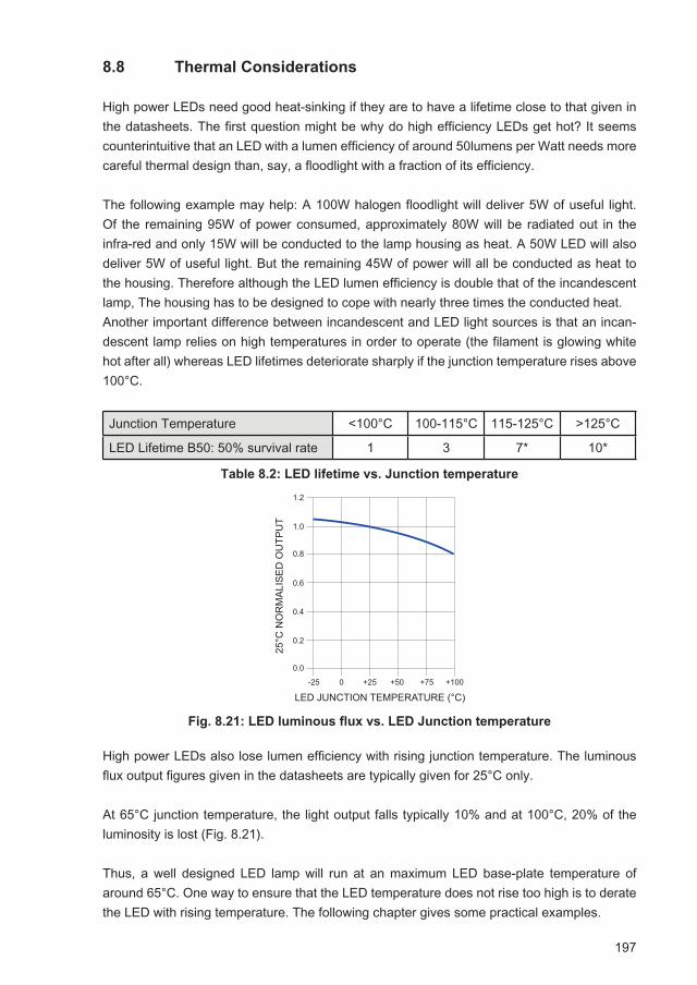
197
8.8 Thermal Considerations
High power LEDs need good heat-sinking if they are to have a lifetime close to that given in the datasheets. The first question might be why do high efficiency LEDs get hot? It seems counterintuitive that an LED with a lumen efficiency of around 50lumens per Watt needs more careful thermal design than, say, a floodlight with a fraction of its efficiency.
The following example may help: A 100W halogen floodlight will deliver 5W of useful light. Of the remaining 95W of power consumed, approximately 80W will be radiated out in the infra-red and only 15W will be conducted to the lamp housing as heat. A 50W LED will also deliver 5W of useful light. But the remaining 45W of power will all be conducted as heat to the housing. Therefore although the LED lumen efficiency is double that of the incandescent lamp, The housing has to be designed to cope with nearly three times the conducted heat.Another important difference between incandescent and LED light sources is that an incan-descent lamp relies on high temperatures in order to operate (the filament is glowing white hot after all) whereas LED lifetimes deteriorate sharply if the junction temperature rises above 100°C.
Junction Temperature <100°C 100-115°C 115-125°C >125°C
LED Lifetime B50: 50% survival rate 1 3 7* 10*
Table 8.2: LED lifetime vs. Junction temperature
Fig. 8.21: LED luminous flux vs. LED Junction temperature
High power LEDs also lose lumen efficiency with rising junction temperature. The luminous flux output figures given in the datasheets are typically given for 25°C only.
At 65°C junction temperature, the light output falls typically 10% and at 100°C, 20% of the luminosity is lost (Fig. 8.21).
Thus, a well designed LED lamp will run at an maximum LED base-plate temperature of around 65°C. One way to ensure that the LED temperature does not rise too high is to derate the LED with rising temperature. The following chapter gives some practical examples.
��� � ��� ��� ��� ����
���
���
���
���
���
���
���
����
�����
��
���
�����
���������������� ��������
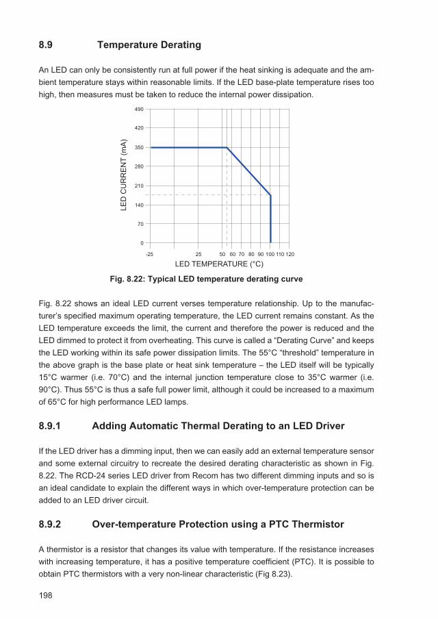
198
8.9 Temperature Derating
An LED can only be consistently run at full power if the heat sinking is adequate and the am-bient temperature stays within reasonable limits. If the LED base-plate temperature rises too high, then measures must be taken to reduce the internal power dissipation.
Fig. 8.22: Typical LED temperature derating curve
Fig. 8.22 shows an ideal LED current verses temperature relationship. Up to the manufac-turer’s specified maximum operating temperature, the LED current remains constant. As the LED temperature exceeds the limit, the current and therefore the power is reduced and the LED dimmed to protect it from overheating. This curve is called a “Derating Curve” and keeps the LED working within its safe power dissipation limits. The 55°C “threshold” temperature in the above graph is the base plate or heat sink temperature – the LED itself will be typically 15°C warmer (i.e. 70°C) and the internal junction temperature close to 35°C warmer (i.e. 90°C). Thus 55°C is thus a safe full power limit, although it could be increased to a maximum of 65°C for high performance LED lamps.
8.9.1 Adding Automatic Thermal Derating to an LED Driver
If the LED driver has a dimming input, then we can easily add an external temperature sensor and some external circuitry to recreate the desired derating characteristic as shown in Fig. 8.22. The RCD-24 series LED driver from Recom has two different dimming inputs and so is an ideal candidate to explain the different ways in which over-temperature protection can be added to an LED driver circuit.
8.9.2 Over-temperature Protection using a PTC Thermistor
A thermistor is a resistor that changes its value with temperature. If the resistance increases with increasing temperature, it has a positive temperature coefficient (PTC). It is possible to obtain PTC thermistors with a very non-linear characteristic (Fig 8.23).
��� �� �� �� ���
�
��
���
���
���
���
�����
���
�������
��
��������������� ���� ���� ��� ���
���
199
Fig. 8.23: Typical PTC thermistor resistance / temperature curve
As long as the temperature stays below a given threshold, in this case 70°C, the PTC ther-mistor has a relatively stable low resistance in the order of around one hundred ohms. Above this threshold, the resistance increases very rapidly: at 80°C the resistance is 1kΩ; at 90°C it is 10kΩ and at 100°C, it is 100kΩ.
Usefully, many PTC thermistors are also available pre-assembled to a mounting lug that can be very easily attached to the heat-sink casing of the LED lamp to monitor the temperature.We can use this response to make a very simple, low cost and reliable over-temperature pro-tection circuit using the analogue dimming input of the RCD-24 series LED drivers (Fig. 8.24 and Fig. 8.25).
The analogue dimming input is controlled by an external voltage and so if the input voltage is fixed, a PTC thermistor plus a two voltage divider resistors are the only additional components required to implement an automatic temperature derating function.
If different derating temperature points are required, PTC thermistors are available with dif-ferent threshold temperatures in 10°C steps from 60°C to 130°C, so it is simply a matter of selecting the right part to match the specification of the LED. If the input voltage is variable, then a zener diode or linear regulator could be added to provide a stable reference voltage.
Fig. 8.24: PTC Thermistor circuit
�� �� ��
��������
����������
�
� �������� ������������� ��� ���
���
���
���
���
���
���
���
�� ���
��������
���
���
�
�����������
����
� ��
��
��������������
200
Fig. 8.25: Resulting LED derating curve (red line)
8.9.3 Over-temperature Protection using an Analogue Temperature Sensor IC
There are many IC temperature sensors available that provide a linear output with temper-ature. They do not cost much more than PTC thermistors and have the advantage that the linearity and offsets are very accurate, so temperature monitoring with <1°C resolution is possible. The output needs to be amplified in order to generate a useful control signal voltage, so they are most often used with an operational amplifier stage.
The circuit suggestion below (Fig. 8.26) uses a common temperature sensor IC and operation amplifier. Similar products are available from a wide range of manufacturers. The output of the circuit is fed into the analogue voltage dimming input of the RCD driver series. This control input linearly dims the LED brightness according to the voltage present on the pin.
In the circuit below, the temperature sensor delivers a linear output voltage depending on its ambient temperature. The output is pre-calibrated to give 10mV/°C + 600mV, so at 55°C the output voltage will be 1.15V. The operation amplifier block contains two low power op-amps and a precision 200mV voltage reference. The offset adjustment preset adjusts the offset to 1.15V and the gain is set so that at 100°C, the LED is running at 50% nominal current. The ad-vantage of this circuit is that only one design is needed to compensate for different LED char-acteristics from different manufacturers as the corner point of the derating curve is adjustable.
��� � �� �� �� ���
���
��
���
���
���
���
���
�����
����� �
��
���� ����� �������
���
�� �� �� ��� ���
201
Fig. 8.26: Analogue over-temperature circuit
Fig. 8.27: Resulting LED derating curve (red line)
���
���
����
� ��
�
�
���
���
� �
�
������
�����
���
���
�
�
������������
�����������
�
�
��� � �� �� �� ���
���
��
���
���
���
���
���
�����
����� �
��
���� ����� �������
���
�� �� �� ��� ���
202
8.9.4 Over-temperature Protection using a Microcontroller
The second dimming input possibility of the RCD series is the PWM input. Pulse width modu-lation uses a digital control signal to alter the brightness of the LED by switching it on and off too rapidly for the eye to see. If the LED spends more time off than on, it will appear dim. If the LED spends more time on than off, it will appear bright. The PWM input responds to logic level inputs, so is ideal for interfacing to digital controllers.
There are some ICs that will directly convert a temperature to a PWM signal (e.g. some fan controllers, MAX6673, TMP05, etc) but some built-in intelligence is normally required to set the threshold temperature and to match the PWM signal with the derating curve of the LED. Therefore it is often simpler to use a microcontroller.
The circuit suggestion below (Fig. 8.28) uses a microcontroller to monitor and control up to eight LED drivers. As only six I/O pins are used, the circuit could be easily expanded to control more LED drivers or a remote over-temperature alert could be added using the free ports.
In this example, temperature sensing is realized via MAX6575L/H ICs which are low pow-er temperature sensors. Up to eight temperature sensors can share a three-wire interface. Temperatures are sensed by measuring the time delay between the microprocessor initiated trigger pulse and the falling edge of the subsequent pulse delays reported from the devices. Different sensors on the same I/O line use different timeout multipliers to avoid overlapping signals. A similar design could just as easily be built with other temperature sensors from different manufacturers– the TPM05 in daisy chain mode, for example.
The low power 74HC259 addressable latch can be reset with a reset pulse, so turning all LED drivers on. The microprocessor then can individually set each output after an appropriate time delay to generate eight PWM signals to independently control each LED driver.
Fig. 8.28: Microprocessor-based PWM controller for up to eight LED drivers
Alternatively, if the microcontroller has a I2C interface, there are a number of useful program-mable PWM generators available (e.g. PCA9635).
���
���
���
�����������
���
���� ���������� ���
�����������
���
����������������
� �
� ����
� �
������
� �
� ����
� �
��
���
� �
��
���
���
���
���
���������
����
� �
�
�
�
�
� � �
������
����
������
��
������
�
�������
�������
����
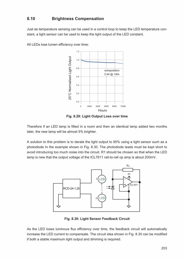
203
8.10 Brightness Compensation
Just as temperature sensing can be used in a control loop to keep the LED temperature con-stant, a light sensor can be used to keep the light output of the LED constant.
All LEDs lose lumen efficiency over time:
Fig. 8.29: Light Output Loss over time
Therefore if an LED lamp is fitted in a room and then an identical lamp added two months later, the new lamp will be almost 5% brighter.
A solution to this problem is to derate the light output to 95% using a light sensor such as a photodiode In the example shown in Fig. 8.30. The photodiode leads must be kept short to avoid introducing too much noise into the circuit. R1 should be chosen so that when the LED lamp is new that the output voltage of the ICL7611 rail-to-rail op amp is about 200mV.
Fig. 8.30: Light Sensor Feedback Circuit
As the LED loses luminous flux efficiency over time, the feedback circuit will automatically increase the LED current to compensate. The circuit idea shown in Fig. 8.30 can be modified if both a stable maximum light output and dimming is required.
���
����
����
�������
��� ��
��
��
����� ���� ���� ���� ���� �����
���
���
���
���
���
���
������������������������
���
���
��
�
�
������������������
��
�
�
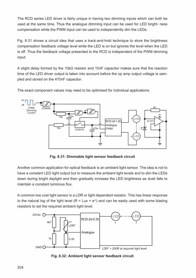
204
The RCD series LED driver is fairly unique in having two dimming inputs which can both be used at the same time. Thus the analogue dimming input can be used for LED bright- ness compensation while the PWM input can be used to independently dim the LEDs.
Fig. 8.31 shows a circuit idea that uses a track-and-hold technique to store the brightness compensation feedback voltage level while the LED is on but ignores the level when the LED is off. Thus the feedback voltage presented to the RCD is independent of the PWM dimming input.
A slight delay formed by the 10kΩ resistor and 10nF capacitor makes sure that the reaction time of the LED driver output is taken into account before the op amp output voltage is sam-pled and stored on the 470nF capacitor.
The exact component values may need to be optimised for individual applications.
Fig. 8.31: Dimmable light sensor feedback circuit
Another common application for optical feedback is an ambient light sensor. The idea is not to have a constant LED light output but to measure the ambient light levels and to dim the LEDs down during bright daylight and then gradually increase the LED brightness as dusk falls to maintain a constant luminous flux.
A common low cost light sensor is a LDR or light dependent resistor. This has linear response to the natural log of the light level (R = Lux × e-b) and can be easily used with some biasing resistors to set the required ambient light level.
Fig. 8.32: Ambient light sensor feedback circuit
���
���
��
�
�
����������� �������
��
���
��� ���
���� ��������������
��������������������
�
��
�
�
��� ���
������������
���
��� ��
�� ����
����
���
�����
��������������������� ����� �
�
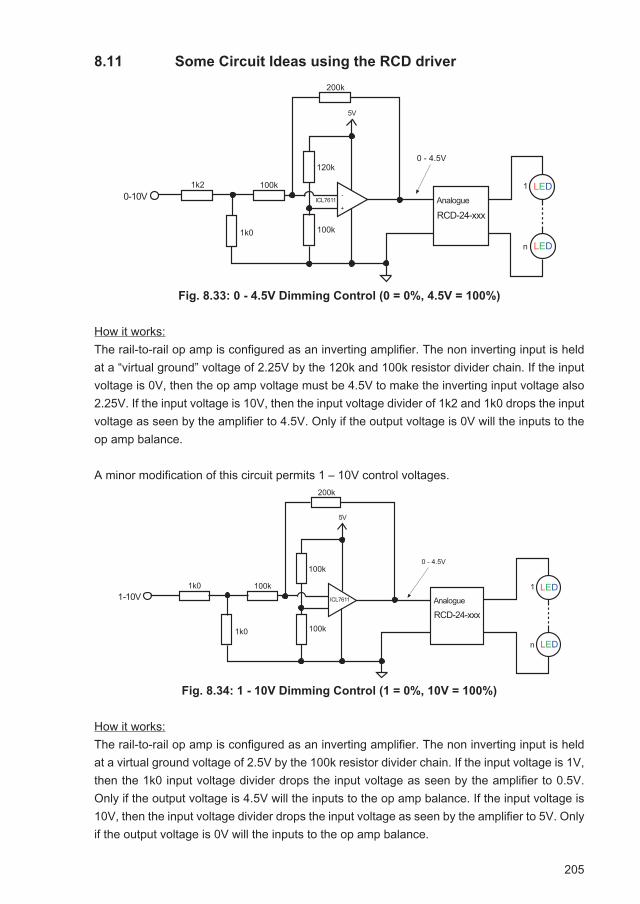
205
8.11 Some Circuit Ideas using the RCD driver
Fig. 8.33: 0 - 4.5V Dimming Control (0 = 0%, 4.5V = 100%)
How it works:The rail-to-rail op amp is configured as an inverting amplifier. The non inverting input is held at a “virtual ground” voltage of 2.25V by the 120k and 100k resistor divider chain. If the input voltage is 0V, then the op amp voltage must be 4.5V to make the inverting input voltage also 2.25V. If the input voltage is 10V, then the input voltage divider of 1k2 and 1k0 drops the input voltage as seen by the amplifier to 4.5V. Only if the output voltage is 0V will the inputs to the op amp balance.
A minor modification of this circuit permits 1 – 10V control voltages.
Fig. 8.34: 1 - 10V Dimming Control (1 = 0%, 10V = 100%)
How it works:The rail-to-rail op amp is configured as an inverting amplifier. The non inverting input is held at a virtual ground voltage of 2.5V by the 100k resistor divider chain. If the input voltage is 1V, then the 1k0 input voltage divider drops the input voltage as seen by the amplifier to 0.5V. Only if the output voltage is 4.5V will the inputs to the op amp balance. If the input voltage is 10V, then the input voltage divider drops the input voltage as seen by the amplifier to 5V. Only if the output voltage is 0V will the inputs to the op amp balance.
�������
��
����
����
���
����
�
����������
�����
��� ����
����
���
�����
��������
�
�
�������
��
����
����
���
����
�
����������
�����
��� ����
����
���
�����
��������
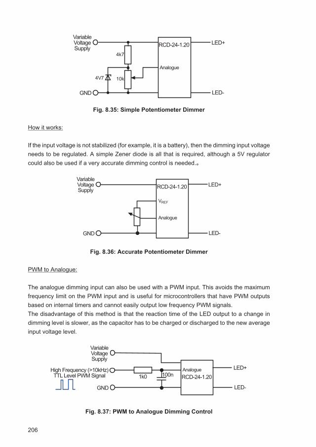
206
Fig. 8.35: Simple Potentiometer Dimmer
How it works:
If the input voltage is not stabilized (for example, it is a battery), then the dimming input voltage needs to be regulated. A simple Zener diode is all that is required, although a 5V regulator could also be used if a very accurate dimming control is needed.。
Fig. 8.36: Accurate Potentiometer Dimmer
PWM to Analogue:
The analogue dimming input can also be used with a PWM input. This avoids the maximum frequency limit on the PWM input and is useful for microcontrollers that have PWM outputs based on internal timers and cannot easily output low frequency PWM signals.The disadvantage of this method is that the reaction time of the LED output to a change in dimming level is slower, as the capacitor has to be charged or discharged to the new average input voltage level.
Fig. 8.37: PWM to Analogue Dimming Control
���
�����������
��������
��
���
������������������
�
����
����
�����������
��������
� �
�������������������
����
����
����
�������������������
� �
�������������������
����
����
��� ������������������ �������������������������
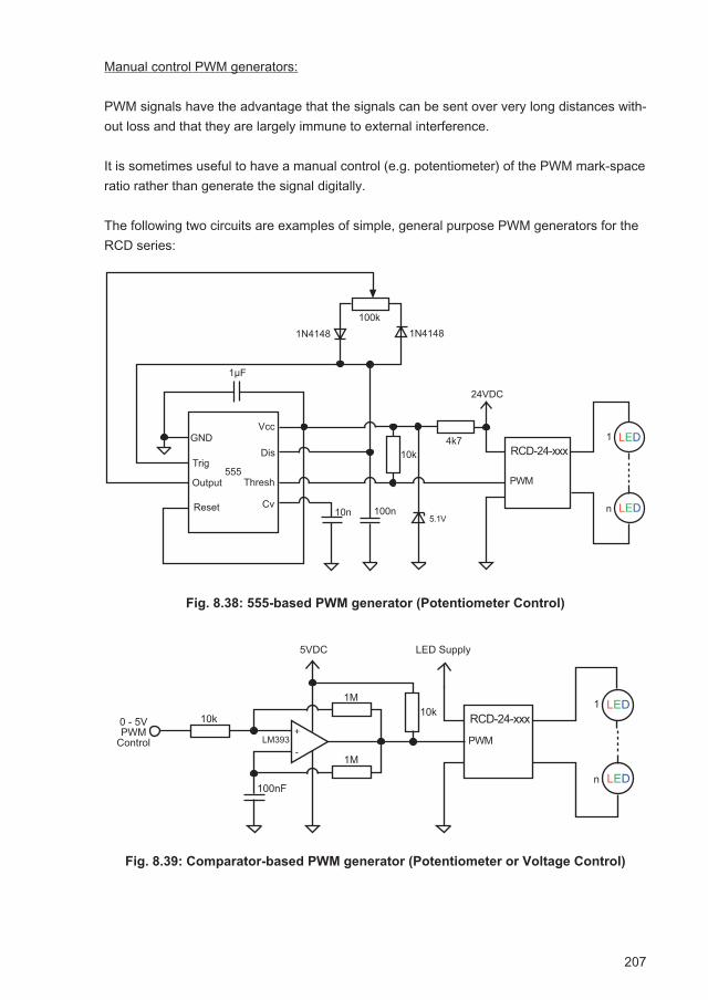
207
Manual control PWM generators:
PWM signals have the advantage that the signals can be sent over very long distances with-out loss and that they are largely immune to external interference.
It is sometimes useful to have a manual control (e.g. potentiometer) of the PWM mark-space ratio rather than generate the signal digitally.
The following two circuits are examples of simple, general purpose PWM generators for the RCD series:
Fig. 8.38: 555-based PWM generator (Potentiometer Control)
Fig. 8.39: Comparator-based PWM generator (Potentiometer or Voltage Control)
����
����
���
����
�
����������
��
������
����� �����
��� ����
�����
��
����
������
����� ��
������
���
���
���
��
��
���
����
�
����������
���
���
����� ���
��
���
����
����
�����
����������������
�
�
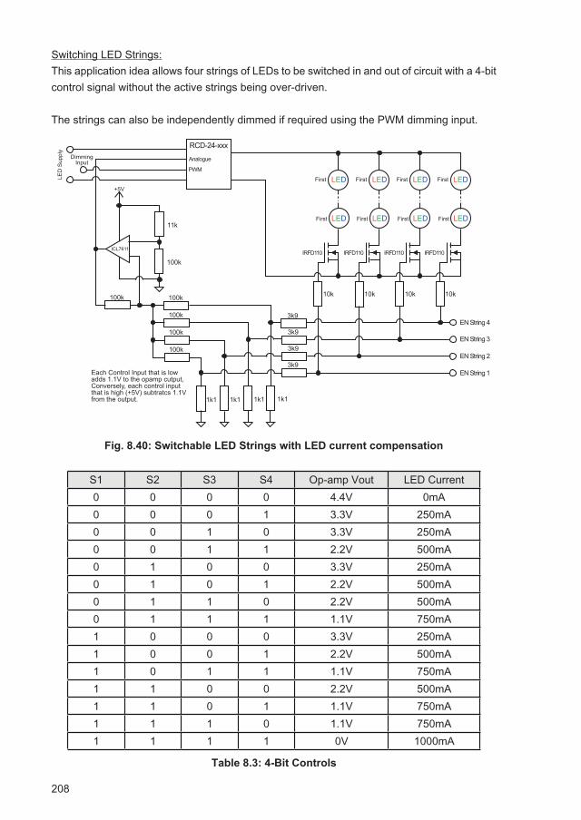
208
Switching LED Strings:This application idea allows four strings of LEDs to be switched in and out of circuit with a 4-bit control signal without the active strings being over-driven.
The strings can also be independently dimmed if required using the PWM dimming input.
Fig. 8.40: Switchable LED Strings with LED current compensation
S1 S2 S3 S4 Op-amp Vout LED Current0 0 0 0 4.4V 0mA0 0 0 1 3.3V 250mA0 0 1 0 3.3V 250mA0 0 1 1 2.2V 500mA0 1 0 0 3.3V 250mA0 1 0 1 2.2V 500mA0 1 1 0 2.2V 500mA0 1 1 1 1.1V 750mA1 0 0 0 3.3V 250mA1 0 0 1 2.2V 500mA1 0 1 1 1.1V 750mA1 1 0 0 2.2V 500mA1 1 0 1 1.1V 750mA1 1 1 0 1.1V 750mA1 1 1 1 0V 1000mA
Table 8.3: 4-Bit Controls
���
��������
����������
���
� �
��
��������
��������
��������
��������
��������
��������
�����
�����
� �
�����
� �
�����
� �
�����
��
��
��
������������
� �
� �
� �
� �
� �
� �
���
�������������������
�����
�����
�
������
�����������
�����������
�����������
������������������������������������������������������������������������������������������������������������������ �������������������������������
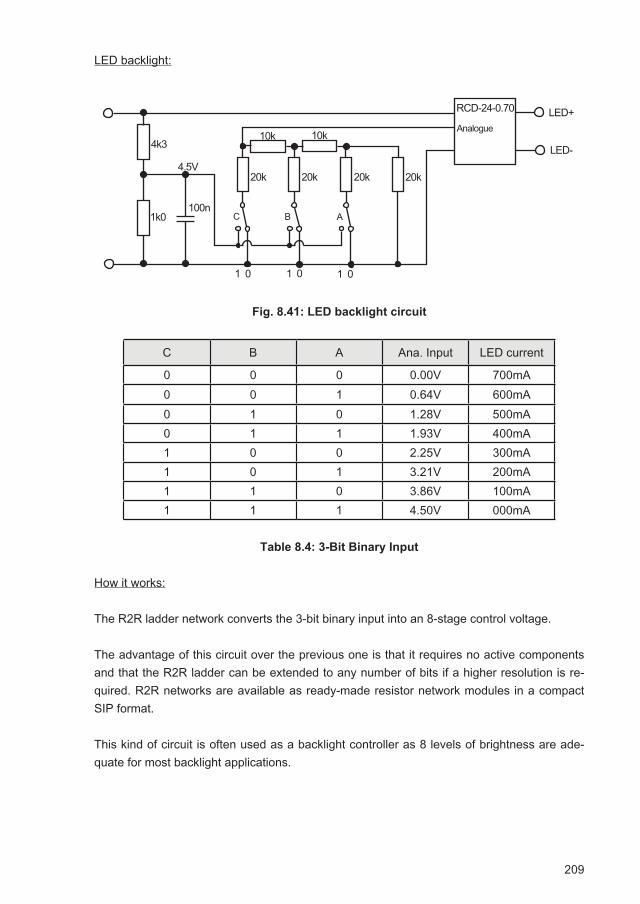
209
LED backlight:
Fig. 8.41: LED backlight circuit
C B A Ana. Input LED current
0 0 0 0.00V 700mA0 0 1 0.64V 600mA0 1 0 1.28V 500mA0 1 1 1.93V 400mA1 0 0 2.25V 300mA1 0 1 3.21V 200mA1 1 0 3.86V 100mA1 1 1 4.50V 000mA
Table 8.4: 3-Bit Binary Input
How it works:
The R2R ladder network converts the 3-bit binary input into an 8-stage control voltage.
The advantage of this circuit over the previous one is that it requires no active components and that the R2R ladder can be extended to any number of bits if a higher resolution is re-quired. R2R networks are available as ready-made resistor network modules in a compact SIP format.
This kind of circuit is often used as a backlight controller as 8 levels of brightness are ade-quate for most backlight applications.
�����������
��������
� ��
� ��
���
���
���������
����
���
����
����
��� ��� ���
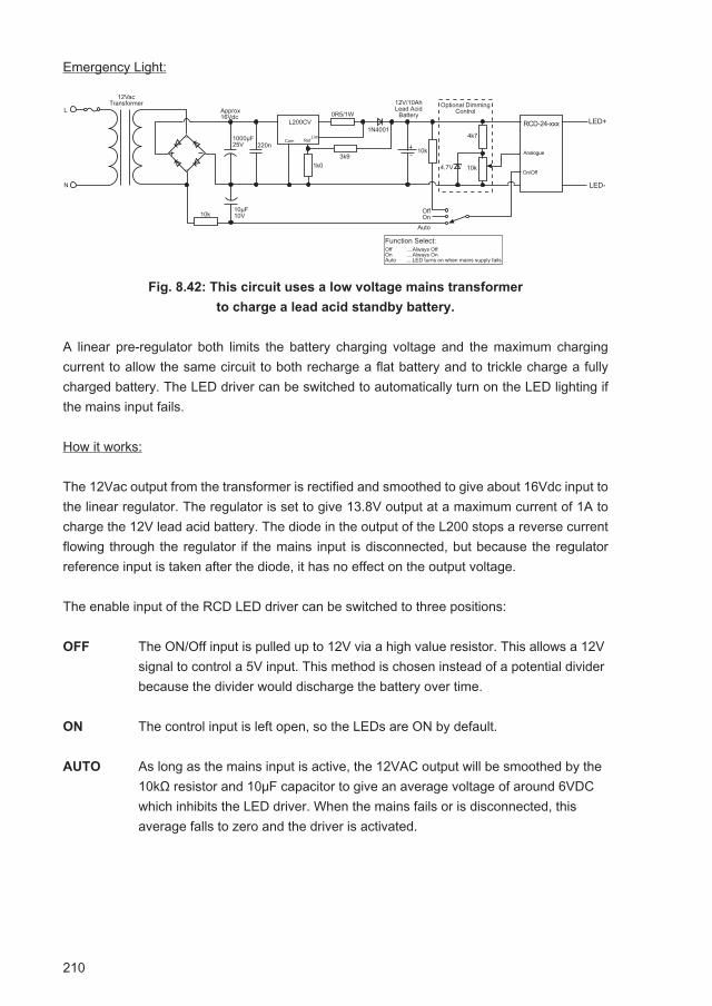
210
Emergency Light:
Fig. 8.42: This circuit uses a low voltage mains transformer
to charge a lead acid standby battery.
A linear pre-regulator both limits the battery charging voltage and the maximum charging current to allow the same circuit to both recharge a flat battery and to trickle charge a fully charged battery. The LED driver can be switched to automatically turn on the LED lighting if the mains input fails.
How it works:
The 12Vac output from the transformer is rectified and smoothed to give about 16Vdc input to the linear regulator. The regulator is set to give 13.8V output at a maximum current of 1A to charge the 12V lead acid battery. The diode in the output of the L200 stops a reverse current flowing through the regulator if the mains input is disconnected, but because the regulator reference input is taken after the diode, it has no effect on the output voltage.
The enable input of the RCD LED driver can be switched to three positions:
OFF The ON/Off input is pulled up to 12V via a high value resistor. This allows a 12V signal to control a 5V input. This method is chosen instead of a potential divider because the divider would discharge the battery over time.
ON The control input is left open, so the LEDs are ON by default.
AUTO As long as the mains input is active, the 12VAC output will be smoothed by the 10kΩ resistor and 10μF capacitor to give an average voltage of around 6VDC which inhibits the LED driver. When the mains fails or is disconnected, this average falls to zero and the driver is activated.
���
���
���
���
������
���
����������
����
���������
�
�
����
�������������
����������
����� ��� ����
�������
������
������������������������
� ��
���
������������������
����
����
������
�� �� ���
��������������� ���������� �� �������������� ������������������������������ ��
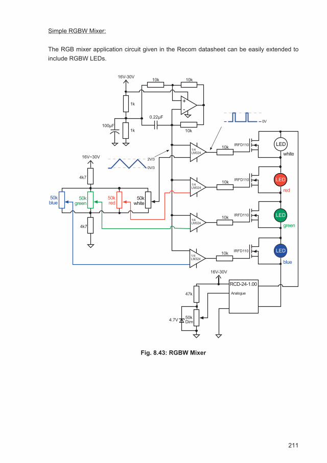
211
Simple RGBW Mixer:
The RGB mixer application circuit given in the Recom datasheet can be easily extended to include RGBW LEDs.
Fig. 8.43: RGBW Mixer
���
���
���
���
�����������
�������
�����������
�������
�����������
�������
�����������
�������
������
���
� ��
������
����� ��
��������
������
���
� ����
������
���
���
�������
����
�����
���
� ��
�������
��������
������
���� ��
��
����
����
�������
�
��

212
9. DC/DC Application Ideas
9.1 Introduction
Many applications require DC/DC conversion. So many, that it is estimated that the world mar-ket will exceed 35 billion dollars by 2020. But for many circuit designers, the DC/DC converter is a “black box”; a component to fulfil a function just like other components such as inductors or transistors. As a general purpose functional block, DC/DC converters can be used every-where and anywhere they may be needed; there is no “typical” area of application. This final section explores some of the more unusual ways in which DC/DC converters can be used to illustrate just how wide the field of applications for DC/DC converters is.
9.2 Polarity Inversion
An isolated DC/DC converter has a floating output. Equally valid is to think if it having a floating input. Therefore any isolated DC/DC converter can be used to invert the polarity of a supply voltage. If isolation is not needed but a common reference point is, then any output can be tied to any input and also tied to any desired reference voltage. The following figure shows some possible configurations to generate negative output voltages from positive inputs and vice-versa.
Fig. 9.1a + 9.1b: examples of polarity inversion using isolated converters
An application for the -48V to +5V converter might be a GSM transmitter module that is pow-ered from a telephone line (some additional input voltage limiting circuitry may be needed to cope with the 90V ringing signal). An application for the +5 to -15V supply is to provide the negative voltage rail for analogue circuitry such as operational amplifiers or ADCs.
It is also possible to use a switching regulator to provide a negative output voltage from a positive input voltage. This works because the buck regulator references the output voltage to the common pin, but only “sees” the voltage difference rather than the absolute voltage. If the output is grounded and the common pin left to float, the common pin will go negative to maintain the correct voltage difference. Figure 9.1a shows an application example where a positive 5V output switching regulator can be used to generate a negative 5V output from a positive 5V input: a feat impossible with a linear regulator.
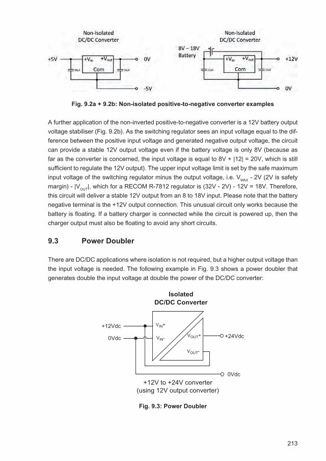
213
Fig. 9.2a + 9.2b: Non-isolated positive-to-negative converter examples
A further application of the non-inverted positive-to-negative converter is a 12V battery output voltage stabiliser (Fig. 9.2b). As the switching regulator sees an input voltage equal to the dif-ference between the positive input voltage and generated negative output voltage, the circuit can provide a stable 12V output voltage even if the battery voltage is only 8V (because as far as the converter is concerned, the input voltage is equal to 8V + |12| = 20V, which is still sufficient to regulate the 12V output). The upper input voltage limit is set by the safe maximum input voltage of the switching regulator minus the output voltage, i.e. VMAX - 2V (2V is safety margin) - |VOUT|, which for a RECOM R-7812 regulator is (32V - 2V) - 12V = 18V. Therefore, this circuit will deliver a stable 12V output from an 8 to 18V input. Please note that the battery negative terminal is the +12V output connection. This unusual circuit only works because the battery is floating. If a battery charger is connected while the circuit is powered up, then the charger output must also be floating to avoid any short circuits.
9.3 Power Doubler
There are DC/DC applications where isolation is not required, but a higher output voltage than the input voltage is needed. The following example in Fig. 9.3 shows a power doubler that generates double the input voltage at double the power of the DC/DC converter:
Fig. 9.3: Power Doubler
�����������������������
������������������������������������ �������������
������
������
���
���
���
��������
�����
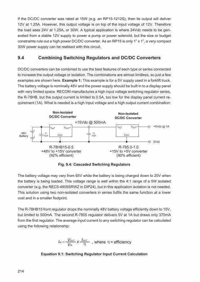
214
If the DC/DC converter was rated at 15W (e.g. an RP15-1212S), then its output will deliver 12V at 1.25A. However, this output voltage is on top of the input voltage of 12V. Therefore the load sees 24V at 1.25A, or 30W. A typical application is where 24Vdc needs to be gen-erated from a stable 12V supply to power a pump or power solenoid, but the size or budget constraints rule out a high power DC/DC converter. As an RP15 is only 1” x 1”, a very compact 30W power supply can be realised with this circuit.
9.4 Combining Switching Regulators and DC/DC Converters
DC/DC converters can be combined to use the best features of each type or series connected to increase the output voltage or isolation. The combinations are almost limitless, so just a few examples are shown here. Example 1: This example is for a 5V supply used in a forklift truck. The battery voltage is nominally 48V and the power supply should be built in to a display panel with very limited space. RECOM manufactures a high input voltage switching regulator series, the R-78HB, but the output current is limited to 0.5A, too low for the display panel current re-quirement (1A). What is needed is a high input voltage and a high output current combination:
Fig. 9.4: Cascaded Switching Regulators
The battery voltage may vary from 65V while the battery is being charged down to 20V when the battery is being loaded. This voltage range is well within the 4:1 range of a 5W isolated converter (e.g. the REC5-4805SRWZ in DIP24), but in this application isolation is not needed. This solution using two non-isolated converters in series fulfils the same function at a lower cost and in a smaller footprint.
The R-78HB15 front regulator drops the nominally 48V battery voltage efficiently down to 15V, but limited to 500mA. The second R-7805 regulator delivers 5V at 1A but draws only 370mA from the first regulator. The average input current to any switching regulator can be calculated using the following relationship:
Equation 9.1: Switching Regulator Input Current Calculation
���������������������������
���������������������������
�����
����
����������
����
��� �
���� ��
���
��� ���������� ���������������
������������
��� ������������������������
������������
��������������
������
� � ����� � � �����
VOUT
VINIIN = IOUT
η η, where = efficiencyx
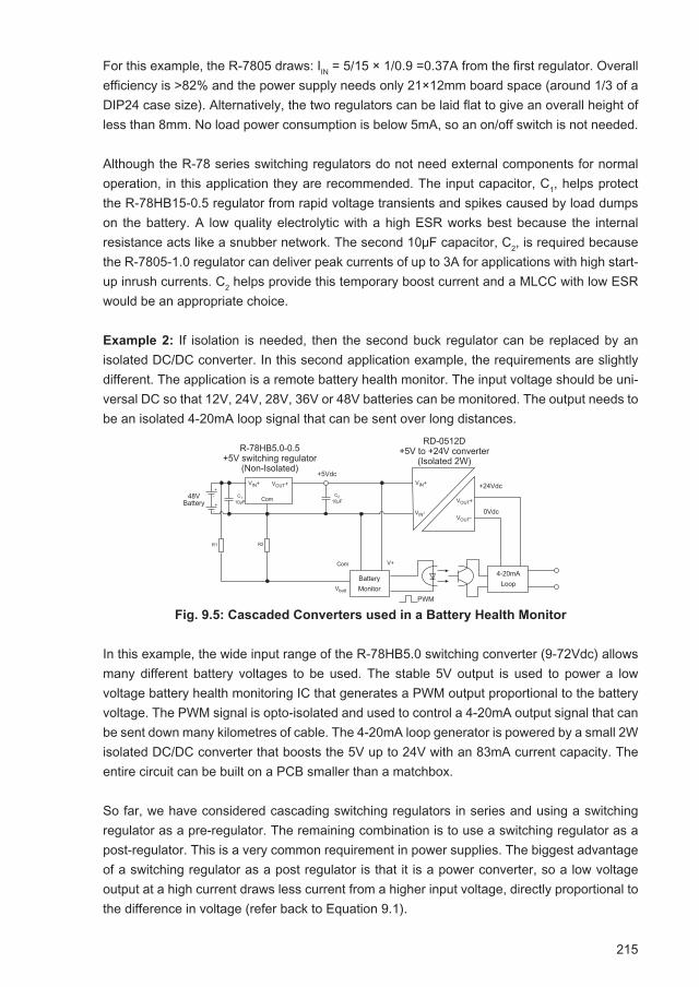
215
For this example, the R-7805 draws: IIN = 5/15 × 1/0.9 =0.37A from the first regulator. Overall efficiency is >82% and the power supply needs only 21×12mm board space (around 1/3 of a DIP24 case size). Alternatively, the two regulators can be laid flat to give an overall height of less than 8mm. No load power consumption is below 5mA, so an on/off switch is not needed.
Although the R-78 series switching regulators do not need external components for normal operation, in this application they are recommended. The input capacitor, C1, helps protect the R-78HB15-0.5 regulator from rapid voltage transients and spikes caused by load dumps on the battery. A low quality electrolytic with a high ESR works best because the internal resistance acts like a snubber network. The second 10μF capacitor, C2, is required because the R-7805-1.0 regulator can deliver peak currents of up to 3A for applications with high start-up inrush currents. C2 helps provide this temporary boost current and a MLCC with low ESR would be an appropriate choice.
Example 2: If isolation is needed, then the second buck regulator can be replaced by an isolated DC/DC converter. In this second application example, the requirements are slightly different. The application is a remote battery health monitor. The input voltage should be uni-versal DC so that 12V, 24V, 28V, 36V or 48V batteries can be monitored. The output needs to be an isolated 4-20mA loop signal that can be sent over long distances.
Fig. 9.5: Cascaded Converters used in a Battery Health Monitor
In this example, the wide input range of the R-78HB5.0 switching converter (9-72Vdc) allows many different battery voltages to be used. The stable 5V output is used to power a low voltage battery health monitoring IC that generates a PWM output proportional to the battery voltage. The PWM signal is opto-isolated and used to control a 4-20mA output signal that can be sent down many kilometres of cable. The 4-20mA loop generator is powered by a small 2W isolated DC/DC converter that boosts the 5V up to 24V with an 83mA current capacity. The entire circuit can be built on a PCB smaller than a matchbox.
So far, we have considered cascading switching regulators in series and using a switching regulator as a pre-regulator. The remaining combination is to use a switching regulator as a post-regulator. This is a very common requirement in power supplies. The biggest advantage of a switching regulator as a post regulator is that it is a power converter, so a low voltage output at a high current draws less current from a higher input voltage, directly proportional to the difference in voltage (refer back to Equation 9.1).
�����
����
�����������
���� �� ��
�������������������������� �������
����� ����� �
����������������������� �� �
� ����� ����
����
�����
��� ��
�����
���� ���������
���
����������
� �
������
� �� �����
� �������
� ��
�����
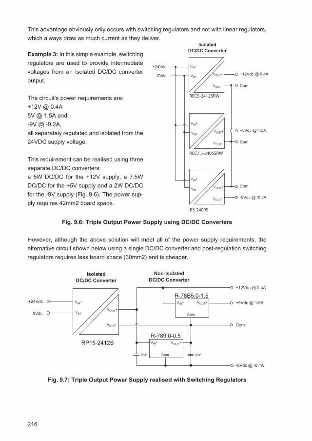
216
This advantage obviously only occurs with switching regulators and not with linear regulators,which always draw as much current as they deliver.
Fig. 9.6: Triple Output Power Supply using DC/DC Converters
However, although the above solution will meet all of the power supply requirements, the alternative circuit shown below using a single DC/DC converter and post-regulation switching regulators requires less board space (30mm2) and is cheaper.
Fig. 9.7: Triple Output Power Supply realised with Switching Regulators
Example 3: In this simple example, switching regulators are used to provide intermediate voltages from an isolated DC/DC converter output.
The circuit’s power requirements are:+12V @ 0.4A 5V @ 1.5A and-9V @ -0.2A,all separately regulated and isolated from the 24VDC supply voltage.
This requirement can be realised using three separate DC/DC converters:a 5W DC/DC for the +12V supply, a 7.5W DC/DC for the +5V supply and a 2W DC/DC for the -9V supply (Fig. 9.6). The power sup-ply requires 42mm2 board space.
REC5-2412SRW
REC7.5-2405SRW
RS-2409S
�����������������������
���������������������������
�������
�������������
������������
���
��������
����
����������
���������
�������������
���
������
����
����
���������
�����
���� �����
���� �����
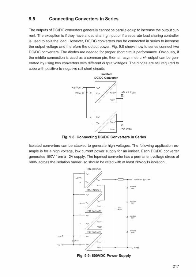
217
9.5 Connecting Converters in Series
The outputs of DC/DC converters generally cannot be paralleled up to increase the output cur-rent. The exception is if they have a load sharing input or if a separate load sharing controller is used to split the load. However, DC/DC converters can be connected in series to increase the output voltage and therefore the output power. Fig. 9.8 shows how to series connect two DC/DC converters. The diodes are needed for proper short circuit performance. Obviously, if the middle connection is used as a common pin, then an asymmetric +/- output can be gen-erated by using two converters with different output voltages. The diodes are still required to cope with positive-to-negative rail short circuits.
Fig. 9.8: Connecting DC/DC Converters in Series
Isolated converters can be stacked to generate high voltages. The following application ex-ample is for a high voltage, low current power supply for an ioniser. Each DC/DC converter generates 150V from a 12V supply. The topmost converter has a permanent voltage stress of 600V across the isolation barrier, so should be rated with at least 2kVdc/1s isolation.
Fig. 9.9: 600VDC Power Supply
�����������������������
������
���� ��������
����
����
���������
�����
����
���������
�����
����������
����������
����������
������������ �
���������
����������
���������
���������
���������
����
����
���������
����
�����
����
���������
�����
����
���������
�����
����
���������
�����
����
���������
�����
����
����
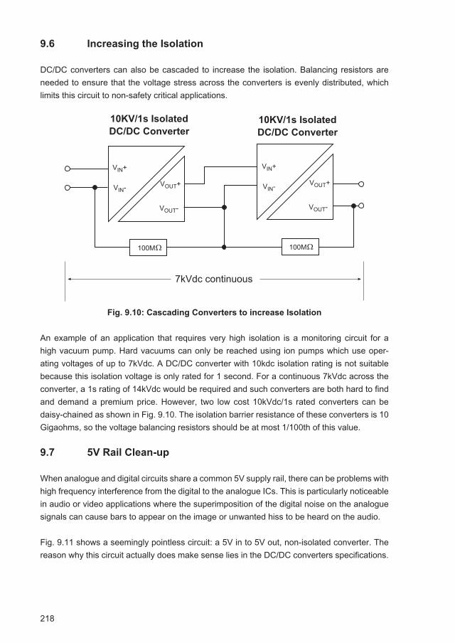
218
9.6 Increasing the Isolation
DC/DC converters can also be cascaded to increase the isolation. Balancing resistors are needed to ensure that the voltage stress across the converters is evenly distributed, which limits this circuit to non-safety critical applications.
Fig. 9.10: Cascading Converters to increase Isolation
An example of an application that requires very high isolation is a monitoring circuit for a high vacuum pump. Hard vacuums can only be reached using ion pumps which use oper-ating voltages of up to 7kVdc. A DC/DC converter with 10kdc isolation rating is not suitable because this isolation voltage is only rated for 1 second. For a continuous 7kVdc across the converter, a 1s rating of 14kVdc would be required and such converters are both hard to find and demand a premium price. However, two low cost 10kVdc/1s rated converters can be daisy-chained as shown in Fig. 9.10. The isolation barrier resistance of these converters is 10 Gigaohms, so the voltage balancing resistors should be at most 1/100th of this value.
9.7 5V Rail Clean-up
When analogue and digital circuits share a common 5V supply rail, there can be problems with high frequency interference from the digital to the analogue ICs. This is particularly noticeable in audio or video applications where the superimposition of the digital noise on the analogue signals can cause bars to appear on the image or unwanted hiss to be heard on the audio.
Fig. 9.11 shows a seemingly pointless circuit: a 5V in to 5V out, non-isolated converter. The reason why this circuit actually does make sense lies in the DC/DC converters specifications.
��������������������������� ��
��������������������������� ��
����� �����
����������������
����
� ������
� ��
����
� ������
� ��
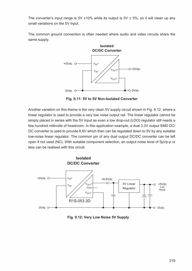
219
The converter’s input range is 5V ±10% while its output is 5V ± 5%, so it will clean up any small variations on the 5V input.
The common ground connection is often needed where audio and video circuits share the same supply.
Fig. 9.11: 5V to 5V Non-Isolated Converter
Another variation on this theme is the very clean 5V supply circuit shown in Fig. 9.12, where a linear regulator is used to provide a very low noise output rail. The linear regulator cannot be simply placed in series with the 5V input as even a low drop-out (LDO) regulator still needs a few hundred millivolts of headroom. In this application example, a dual 3.3V output SMD DC/DC converter is used to provide 6.6V which then can be regulated down to 5V by any suitable low-noise linear regulator. The common pin of any dual output DC/DC converter can be left open if not used (NC). With suitable component selection, an output noise level of 5μVp-p or less can be realised with this circuit.
Fig. 9.12: Very Low Noise 5V Supply
�����������������������
�����
�����
��������
����
���������
�����
����
����������
�����������������������
�������� ������
����
�����
���
�������
�������������
����
���������
�����
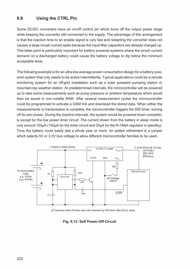
220
9.8 Using the CTRL Pin
Some DC/DC converters have an on/off control pin which turns off the output power stage while keeping the converter still connected to the supply. The advantage of this arrangement is that the reaction time to an enable signal is very fast and restarting the converter does not causes a large inrush current spike because the input filter capacitors are already charged up. This latter point is particularly important for battery powered systems where the inrush current demand on a discharged battery could cause the battery voltage to dip below the minimum acceptable level.
The following example is for an ultra-low average power consumption design for a battery-pow-ered system that only needs to be active intermittently. Typical applications could be a remote monitoring system for an off-grid installation such as a solar powered pumping station or mountain-top weather station. At predetermined intervals, the microcontroller will be powered up to take some measurements such as pump pressure or ambient temperature which would then be saved in non-volatile RAM. After several measurement cycles the microcontroller could be programmed to activate a GSM link and download the stored data. When either the measurements or transmission is complete, the microcontroller triggers the 555 timer, turning off its own power. During the inactive intervals, the system would be powered down complete-ly except for the low power timer circuit. The current drawn from the battery in sleep mode is only around 120μA (100μA for the timer circuit and 20μA for the R-78AA regulator in standby). Thus the battery could easily last a whole year or more. An added refinement is a jumper which selects 5V or 3.3V bus voltage to allow different microcontroller families to be used.
Fig. 9.13: Self Power-Off Circuit
��
����
��
����������������
� ���������������� �������������������������
��������
������ ��� ����
��������������
���
����
���
�������������������
� � ������ �����������
��
��
��������������������
�������������������������������������������������� �����������������������
�����
�����
���� �����
����
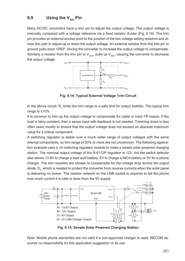
221
9.9 Using the VADJ
Pin
Many DC/DC converters have a trim pin to adjust the output voltage. The output voltage is internally compared with a voltage reference via a fixed resistor divider (Fig. 9.14). The trim pin provides an external access point to the junction of the two voltage setting resistors and al-lows the user to adjust up or down the output voltage. An external resistor from the trim pin to ground pulls down VREF, forcing the converter to increase the output voltage to compensate. Similarly a resistor from the trim pin to VOUT+ pulls up VREF, causing the converter to decrease the output voltage.
Fig. 9.14: Typical External Voltage Trim Circuit
In the above circuit, R3 limits the trim range to a safe limit for output stability. The typical trim range is ±10%.It is common to trim up the output voltage to compensate for cable or track I2R losses. If the load is fairly constant, then a sense input with feedback is not needed. Trimming down is less often used, mostly to ensure that the output voltage does not exceed an absolute maximum value for a critical component.A switching regulator is stable over a much wider range of output voltages with the same internal components, so trim range of 50% or more are not uncommon. The following applica-tion example uses a 1A switching regulator module to make a simple solar powered charging station. The nominal output voltage of the R-6112P regulator is 12V, but the switch selector also allows 13.8V to charge a lead acid battery, 6V to charge a NiCd battery or 5V for a phone charger. The trim resistors are chosen to compensate for the voltage drop across the output diode, D2, which is needed to protect the converter from reverse currents when the solar panel is delivering no power. The resistor network on the USB socket is required to tell the phone how much current it is safe to draw from the 5V supply.
Fig. 9.15: Simple Solar Powered Charging Station
Note: Mobile phone warranties are not valid if a non-approved charger is used. RECOM as-sumes no responsibility for this application suggestion or its use.
�����������������
���� ��� �
���� ��� �
��
��
��
��
�������
���
���
��
������� �����
��
� �
�
��� ��
�� ��
�
�
�
��
��� ������ ������
� ��������������� ������������ ����������� �� ����� �� �������
���������
��������
��
�����
���
��
�� ��
��
���� �� ��
���

222
10. Introduction to Magnetics
10.1 Basics
Any conductor carrying a voltage and current will generate both an electric and a magnetic field respectively. The magnetic field has two properties: the magnetic field intensity, H, and the magnetic flux density, B. For a single wire or a PCB track, the magnetic field intensity will be proportional only to the current flowing through it and the distance from the conductor (length of the field line), so it has the dimensions of amperes per metre (Am-1). The field intensity does not change with material, so it will be the same if the wire or track is copper, silver or gold plated, for example. If a conductor is wound into a coil, then the field intensity increases proportionally with each turn, again irrespective of the type of conductive material used, following the relationship:
Equation 10.1: In a solenoid, the magnetic field (H) equals permeability x turns
density (number of turns N in length l) x current
The magnetic flux describes the “contour lines” of equal magnetic field strength around the solenoid coil (Fig.10.1).
Figure 10.1: Cross-section of a solenoid showing contour lines of equal magnetic flux
The magnetic flux density (B) has the dimensions of Teslas (Newtons per ampere per meter, NA-1m-1) and is a linear function dependent on the magnetic field strength; H, and the perme-ability of air (µ0), which is a constant (4πx10-7 V.s.A-1m-1):
Equation 10.2: Magnetic Flux density
However, if the coil is wound around a magnetic material such as iron or ferrite core, then the field is distorted and channelled into the magnetic material.
H =µ0 NI
l
B = µ0 H
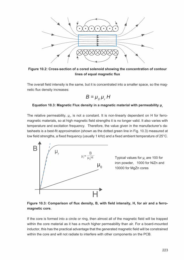
223
Figure 10.2: Cross-section of a cored solenoid showing the concentration of contour
lines of equal magnetic flux
The overall field intensity is the same, but it is concentrated into a smaller space, so the mag-netic flux density increases:
Equation 10.3: Magnetic Flux density in a magnetic material with permeability μr
The relative permeability, µr, is not a constant. It is non-linearly dependent on H for ferro-magnetic materials, so at high magnetic field strengths it is no longer valid. It also varies with temperature and excitation frequency. Therefore, the value given in the manufacturer’s da-tasheets is a best-fit approximation (shown as the dotted green line in Fig. 10.3) measured at low field strengths, a fixed frequency (usually 1 kHz) and a fixed ambient temperature of 25°C.
Figure 10.3: Comparison of flux density, B, with field intensity, H, for air and a ferro-
magnetic core.
If the core is formed into a circle or ring, then almost all of the magnetic field will be trapped within the core material as it has a much higher permeability than air. For a board-mounted inductor, this has the practical advantage that the generated magnetic field will be constrained within the core and will not radiate to interfere with other components on the PCB.
B = µ0 µr H
B
H
µr=B
µ0H
µ0
µrTypical values for µr are 100 for iron powder, 1000 for NiZn and 10000 for MgZn cores
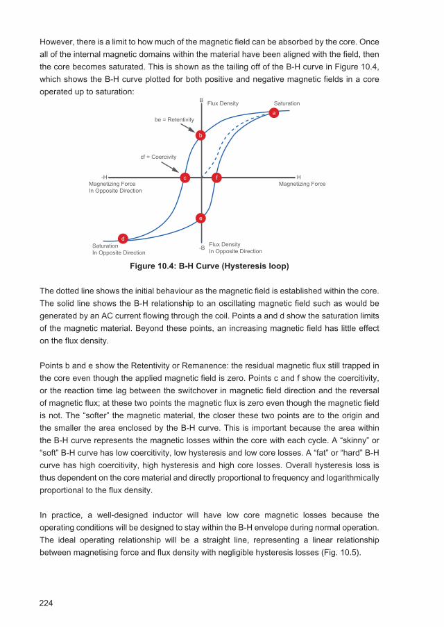
224
However, there is a limit to how much of the magnetic field can be absorbed by the core. Once all of the internal magnetic domains within the material have been aligned with the field, then the core becomes saturated. This is shown as the tailing off of the B-H curve in Figure 10.4, which shows the B-H curve plotted for both positive and negative magnetic fields in a core operated up to saturation:
Figure 10.4: B-H Curve (Hysteresis loop)
The dotted line shows the initial behaviour as the magnetic field is established within the core. The solid line shows the B-H relationship to an oscillating magnetic field such as would be generated by an AC current flowing through the coil. Points a and d show the saturation limits of the magnetic material. Beyond these points, an increasing magnetic field has little effect on the flux density.
Points b and e show the Retentivity or Remanence: the residual magnetic flux still trapped in the core even though the applied magnetic field is zero. Points c and f show the coercitivity, or the reaction time lag between the switchover in magnetic field direction and the reversal of magnetic flux; at these two points the magnetic flux is zero even though the magnetic field is not. The “softer” the magnetic material, the closer these two points are to the origin and the smaller the area enclosed by the B-H curve. This is important because the area within the B-H curve represents the magnetic losses within the core with each cycle. A “skinny” or “soft” B-H curve has low coercitivity, low hysteresis and low core losses. A “fat” or “hard” B-H curve has high coercitivity, high hysteresis and high core losses. Overall hysteresis loss is thus dependent on the core material and directly proportional to frequency and logarithmically proportional to the flux density.
In practice, a well-designed inductor will have low core magnetic losses because the operating conditions will be designed to stay within the B-H envelope during normal operation. The ideal operating relationship will be a straight line, representing a linear relationship between magnetising force and flux density with negligible hysteresis losses (Fig. 10.5).
be = Retentivity
cf = Coercivity
SaturationFlux Density
Magnetizing Force
Flux DensityIn Opposite Direction
SaturationIn Opposite Direction
Magnetizing ForceIn Opposite Direction
a
b
c
d
e
f-H
-B
H
B
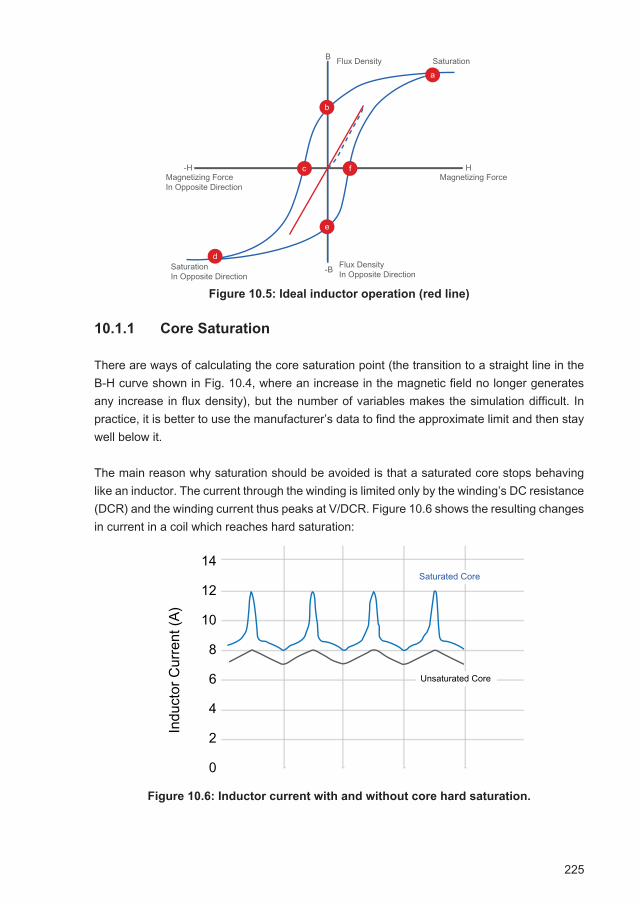
225
Figure 10.5: Ideal inductor operation (red line)
10.1.1 Core Saturation
There are ways of calculating the core saturation point (the transition to a straight line in the B-H curve shown in Fig. 10.4, where an increase in the magnetic field no longer generates any increase in flux density), but the number of variables makes the simulation difficult. In practice, it is better to use the manufacturer’s data to find the approximate limit and then stay well below it.
The main reason why saturation should be avoided is that a saturated core stops behaving like an inductor. The current through the winding is limited only by the winding’s DC resistance (DCR) and the winding current thus peaks at V/DCR. Figure 10.6 shows the resulting changes in current in a coil which reaches hard saturation:
Figure 10.6: Inductor current with and without core hard saturation.
SaturationFlux Density
Magnetizing Force
Flux DensityIn Opposite Direction
SaturationIn Opposite Direction
Magnetizing ForceIn Opposite Direction
a
b
c
d
e
f-H
-B
H
B
Indu
ctor
Cur
rent
(A)
14
12
10
8
6
4
2
0
Saturated Core
Unsaturated Core
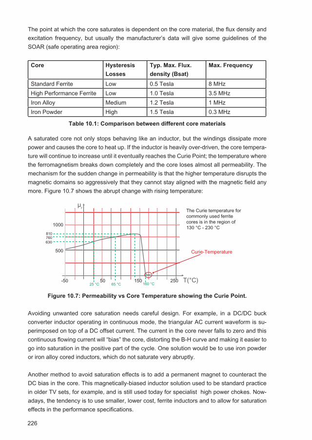
226
The point at which the core saturates is dependent on the core material, the flux density and excitation frequency, but usually the manufacturer’s data will give some guidelines of the SOAR (safe operating area region): Core Hysteresis
Losses
Typ. Max. Flux.
density (Bsat)
Max. Frequency
Standard Ferrite Low 0.5 Tesla 8 MHzHigh Performance Ferrite Low 1.0 Tesla 3.5 MHzIron Alloy Medium 1.2 Tesla 1 MHzIron Powder High 1.5 Tesla 0.3 MHz
Table 10.1: Comparison between different core materials
A saturated core not only stops behaving like an inductor, but the windings dissipate more power and causes the core to heat up. If the inductor is heavily over-driven, the core tempera-ture will continue to increase until it eventually reaches the Curie Point; the temperature where the ferromagnetism breaks down completely and the core loses almost all permeability. The mechanism for the sudden change in permeability is that the higher temperature disrupts the magnetic domains so aggressively that they cannot stay aligned with the magnetic field any more. Figure 10.7 shows the abrupt change with rising temperature:
Figure 10.7: Permeability vs Core Temperature showing the Curie Point.
Avoiding unwanted core saturation needs careful design. For example, in a DC/DC buck converter inductor operating in continuous mode, the triangular AC current waveform is su-perimposed on top of a DC offset current. The current in the core never falls to zero and this continuous flowing current will “bias” the core, distorting the B-H curve and making it easier to go into saturation in the positive part of the cycle. One solution would be to use iron powder or iron alloy cored inductors, which do not saturate very abruptly.
Another method to avoid saturation effects is to add a permanent magnet to counteract the DC bias in the core. This magnetically-biased inductor solution used to be standard practice in older TV sets, for example, and is still used today for specialist high power chokes. Now-adays, the tendency is to use smaller, lower cost, ferrite inductors and to allow for saturation effects in the performance specifications.
The Curie temperature for commonly used ferrite cores is in the region of 130 °C - 230 °C
Curie-Temperature
µr
T(°C)
1000
500
-50 50 150 250
760630
25 °C 65 °C 160 °C
810
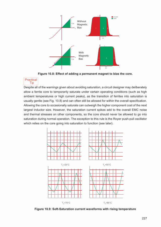
227
Figure 10.8: Effect of adding a permanent magnet to bias the core.
Despite all of the warnings given about avoiding saturation, a circuit designer may deliberately allow a ferrite core to temporarily saturate under certain operating conditions (such as high ambient temperatures or high current peaks), as the transition of ferrites into saturation is usually gentle (see Fig. 10.8) and can often still be allowed for within the overall specification. Allowing the core to occasionally saturate can outweigh the higher component cost of the next largest inductor size. However, the saturation current spikes add to the overall EMC noise and thermal stresses on other components, so the core should never be allowed to go into saturation during normal operation. The exception to this rule is the Royer push-pull oscillator which relies on the core going into saturation to function (see later).
Figure 10.9: Soft-Saturation current waveforms with rising temperature
B
B
H
LUnusedUsed
II
B
B
1 2 3
L
II
1 2 3
WithoutMagneticBias
WithMagneticBias
H
Practical Tip
TA=25°C TA=50°C
TA=70°C TA=85°C
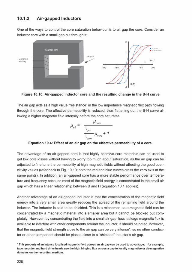
228
10.1.2 Air-gapped Inductors
One of the ways to control the core saturation behaviour is to air gap the core. Consider an inductor core with a small gap cut through it:
Figure 10.10: Air-gapped inductor core and the resulting change in the B-H curve
The air gap acts as a high value “resistance” in the low impedance magnetic flux path flowing through the core. The effective permeability is reduced, thus flattening out the B-H curve al-lowing a higher magnetic field intensity before the core saturates.
Equation 10.4: Effect of an air gap on the effective permeability of a core.
The advantage of an air-gapped core is that highly coercive core materials can be used to get low core losses without having to worry too much about saturation, as the air gap can be adjusted to fine tune the permeability at high magnetic fields without affecting the good coer-citivity values (refer back to Fig. 10.10: both the red and blue curves cross the zero axis at the same points). In addition, an air-gapped core has a more stable performance over tempera-ture and frequency because most of the magnetic field energy is concentrated in the small air gap which has a linear relationship between B and H (equation 10.1 applies).
Another advantage of an air-gapped inductor is that the concentration of the magnetic field energy into a very small area greatly reduces the spread of the remaining field around the inductor. The inductor is said to be shielded. This is a misnomer, as a magnetic field can be concentrated by a magnetic material into a smaller area but it cannot be blocked out com-pletely. However, by concentrating the field into a small air gap, less leakage magnetic flux is available to interfere with other components around the inductor. It should be noted, however, that the magnetic field strength close to the air gap can be very intense*, so no other conduc-tor or other component should be placed close to a “shielded” inductor’s air gap.
* This property of an intense localised magnetic field across an air gap can be used to advantage: for example,
tape recorder and hard drive heads use the high fringing flux across a gap to locally magnetise or de-magnetise
domains on the recording medium.
air gap
magnetic core
Excitationwinding
no air gapair gap 0.07 mm
-300 -150
-2
-1
1
2
150 300
HAm -1
B (T)
µeff =µcore
lgap
lcoreµcore + 1
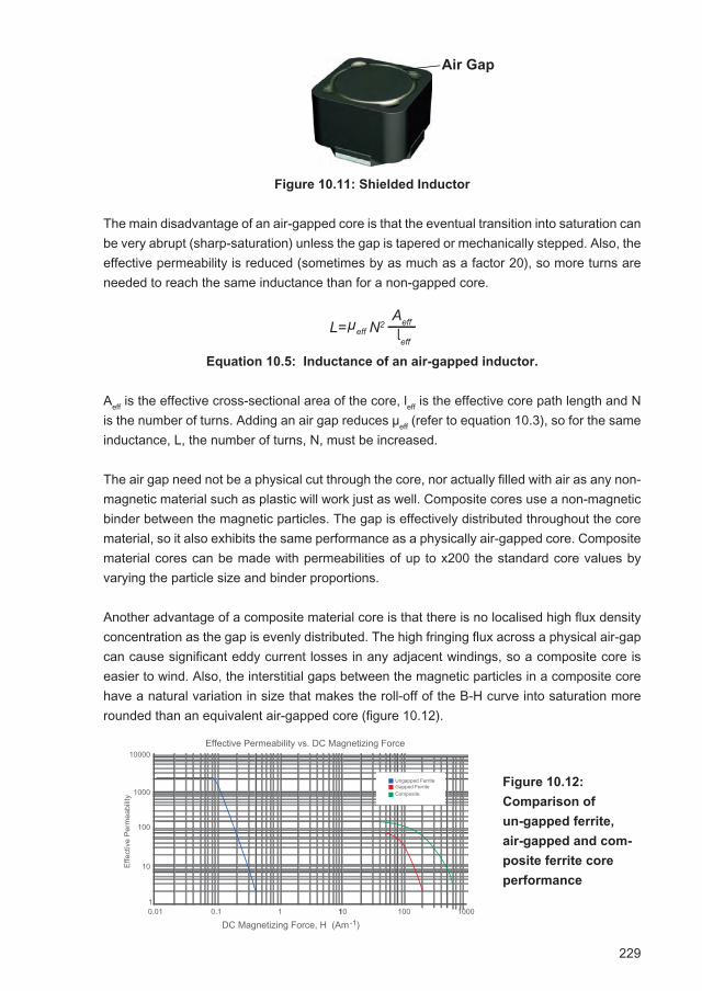
229
Figure 10.11: Shielded Inductor
The main disadvantage of an air-gapped core is that the eventual transition into saturation can be very abrupt (sharp-saturation) unless the gap is tapered or mechanically stepped. Also, the effective permeability is reduced (sometimes by as much as a factor 20), so more turns are needed to reach the same inductance than for a non-gapped core.
Equation 10.5: Inductance of an air-gapped inductor.
Aeff is the effective cross-sectional area of the core, leff is the effective core path length and N is the number of turns. Adding an air gap reduces µeff (refer to equation 10.3), so for the same inductance, L, the number of turns, N, must be increased.
The air gap need not be a physical cut through the core, nor actually filled with air as any non-magnetic material such as plastic will work just as well. Composite cores use a non-magnetic binder between the magnetic particles. The gap is effectively distributed throughout the core material, so it also exhibits the same performance as a physically air-gapped core. Composite material cores can be made with permeabilities of up to x200 the standard core values by varying the particle size and binder proportions.
Another advantage of a composite material core is that there is no localised high flux density concentration as the gap is evenly distributed. The high fringing flux across a physical air-gap can cause significant eddy current losses in any adjacent windings, so a composite core is easier to wind. Also, the interstitial gaps between the magnetic particles in a composite core have a natural variation in size that makes the roll-off of the B-H curve into saturation more rounded than an equivalent air-gapped core (figure 10.12).
L= leff Aeff µeff N2
Ungapped FerriteGapped FerriteComposite
10000
1000
100
10
10.01 0.1 1 110 100 1000
Effective Permeability vs. DC Magnetizing Force
Effe
ctiv
e Pe
rmea
bilit
y
DC Magnetizing Force, H (Am )-1
Figure 10.12:
Comparison of
un-gapped ferrite,
air-gapped and com-
posite ferrite core
performance
Air Gap
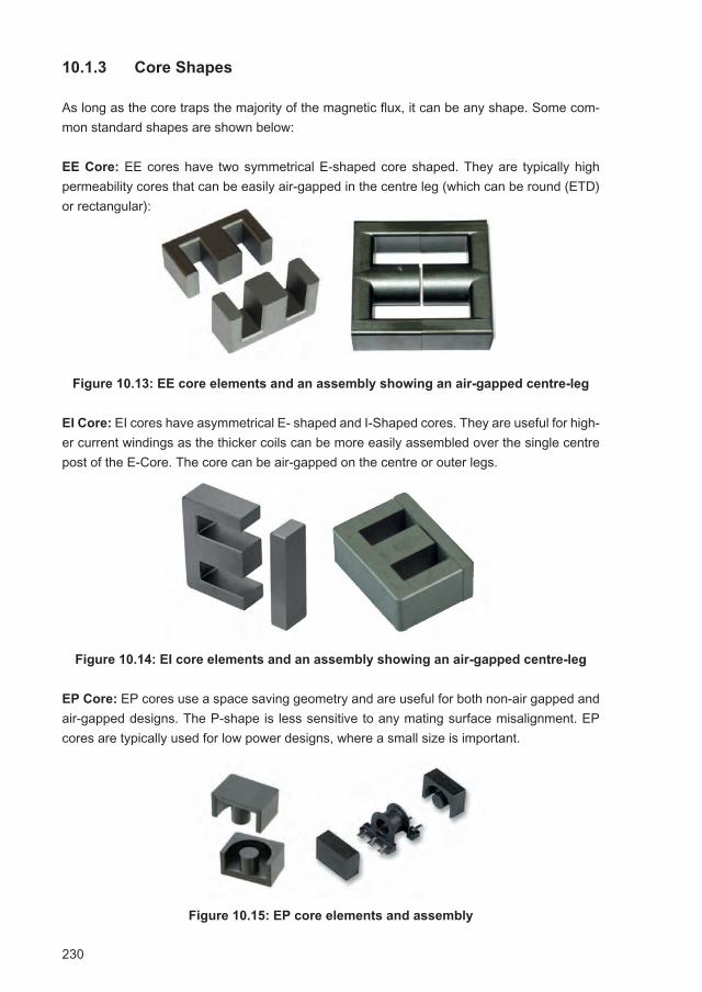
230
10.1.3 Core Shapes
As long as the core traps the majority of the magnetic flux, it can be any shape. Some com-mon standard shapes are shown below:
EE Core: EE cores have two symmetrical E-shaped core shaped. They are typically high permeability cores that can be easily air-gapped in the centre leg (which can be round (ETD) or rectangular):
Figure 10.13: EE core elements and an assembly showing an air-gapped centre-leg
EI Core: EI cores have asymmetrical E- shaped and I-Shaped cores. They are useful for high-er current windings as the thicker coils can be more easily assembled over the single centre post of the E-Core. The core can be air-gapped on the centre or outer legs.
Figure 10.14: EI core elements and an assembly showing an air-gapped centre-leg
EP Core: EP cores use a space saving geometry and are useful for both non-air gapped and air-gapped designs. The P-shape is less sensitive to any mating surface misalignment. EP cores are typically used for low power designs, where a small size is important.
Figure 10.15: EP core elements and assembly
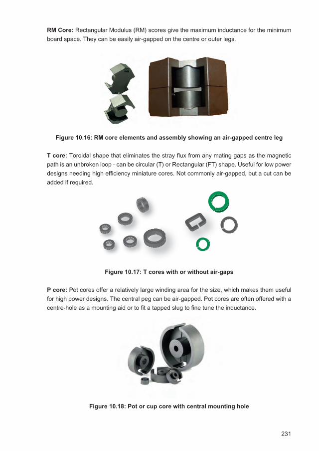
231
RM Core: Rectangular Modulus (RM) scores give the maximum inductance for the minimum board space. They can be easily air-gapped on the centre or outer legs.
Figure 10.16: RM core elements and assembly showing an air-gapped centre leg
T core: Toroidal shape that eliminates the stray flux from any mating gaps as the magnetic path is an unbroken loop - can be circular (T) or Rectangular (FT) shape. Useful for low power designs needing high efficiency miniature cores. Not commonly air-gapped, but a cut can be added if required.
Figure 10.17: T cores with or without air-gaps
P core: Pot cores offer a relatively large winding area for the size, which makes them useful for high power designs. The central peg can be air-gapped. Pot cores are often offered with a centre-hole as a mounting aid or to fit a tapped slug to fine tune the inductance.
Figure 10.18: Pot or cup core with central mounting hole
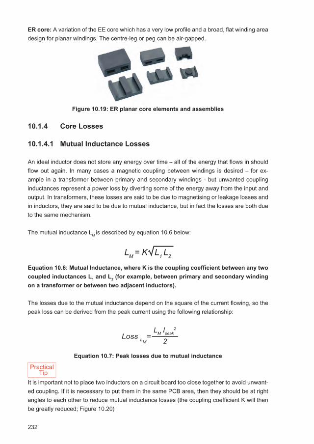
232
ER core: A variation of the EE core which has a very low profile and a broad, flat winding area design for planar windings. The centre-leg or peg can be air-gapped.
Figure 10.19: ER planar core elements and assemblies
10.1.4 Core Losses
10.1.4.1 Mutual Inductance Losses
An ideal inductor does not store any energy over time – all of the energy that flows in should flow out again. In many cases a magnetic coupling between windings is desired – for ex-ample in a transformer between primary and secondary windings - but unwanted coupling inductances represent a power loss by diverting some of the energy away from the input and output. In transformers, these losses are said to be due to magnetising or leakage losses and in inductors, they are said to be due to mutual inductance, but in fact the losses are both due to the same mechanism.
The mutual inductance LM is described by equation 10.6 below:
Equation 10.6: Mutual Inductance, where K is the coupling coefficient between any two
coupled inductances L1 and L
2 (for example, between primary and secondary winding
on a transformer or between two adjacent inductors).
The losses due to the mutual inductance depend on the square of the current flowing, so the peak loss can be derived from the peak current using the following relationship:
Equation 10.7: Peak losses due to mutual inductance
It is important not to place two inductors on a circuit board too close together to avoid unwant-ed coupling. If it is necessary to put them in the same PCB area, then they should be at right angles to each other to reduce mutual inductance losses (the coupling coefficient K will then be greatly reduced; Figure 10.20)
LM = K L1 L2
Loss LM=
LM Ipeak2
2
PracticalTip

233
Figure 10.20: Inductor Placement to reduce mutual inductance losses.
The right hand arrangement of two inductors will have lower coupling and thus lower mutual inductance losses.
10.1.4.2 Eddy Current Losses
All magnetic cores are electrically conductive, so by Lenz’s Law (if an induced current flows, its direction will always be to oppose the change which caused it), any changing magnetic fields within the core will induce currents (eddy currents) to flow that oppose the changes in magnetic flux. The effects of eddy currents are to both restrict the penetration of flux into the core and to increase the power loss in the core – both very undesirable effects. As the eddy current power losses are equal to i²(t)R, then the power losses increase with the square of the magnetic field excitation frequency. The total losses are approximated by Steinmetz’s equation:
Equation 10.8: Power loss due to eddy currents
Power LossEddy= KE f2 B2 VCore
Where KE is a constant dependent on the core ma-terial (e.g. iron, iron power, ferrite, etc.) , f is the fre-quency of the magnetic flux change, B is the max-imum magnetic field strength and Vcore is the core volume. For a fixed frequency, the square of the eddy current power losses per cubic centimetre of core material are linearly dependent on the square of the magnetising flux:
1
0.1 0.3
0.1
0.010.01
Pow
er le
ss d
ensi
ty W
atts
/ cm
3
Bmax Tesla
Ferrite core material1 MHz500kHz200kHz100kHz50kHz20kHz
Figure 10.21: Total power losses
for ferrite core material according
to Steinmetz
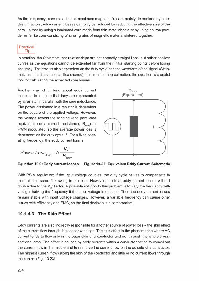
234
As the frequency, core material and maximum magnetic flux are mainly determined by other design factors, eddy current losses can only be reduced by reducing the effective size of the core – either by using a laminated core made from thin metal sheets or by using an iron pow-der or ferrite core consisting of small grains of magnetic material sintered together.
In practice, the Steinmetz loss relationships are not perfectly straight lines, but rather shallow curves as the equations cannot be extended far from their initial starting points before losing accuracy. The error is also dependent on the duty cycle and the waveform of the signal (Stein-metz assumed a sinusoidal flux change), but as a first approximation, the equation is a useful tool for calculating the expected core losses.
Equation 10.9: Eddy current losses Figure 10.22: Equivalent Eddy Current Schematic
With PWM regulation; if the input voltage doubles, the duty cycle halves to compensate to maintain the same flux swing in the core. However, the total eddy current losses will still double due to the Vin² factor. A possible solution to this problem is to vary the frequency with voltage, halving the frequency if the input voltage is doubled. Then the eddy current losses remain stable with input voltage changes. However, a variable frequency can cause other issues with efficiency and EMC, so the final decision is a compromise.
10.1.4.3 The Skin Effect
Eddy currents are also indirectly responsible for another source of power loss – the skin effect of the current flow through the copper windings. The skin effect is the phenomenon where AC current tends to flow only in the outer skin of a conductor and not through the whole cross- sectional area. The effect is caused by eddy currents within a conductor acting to cancel out the current flow in the middle and to reinforce the current flow on the outside of a conductor. The highest current flows along the skin of the conductor and little or no current flows through the centre. (Fig. 10.23)
Practical Tip
Another way of thinking about eddy current losses is to imagine that they are represented by a resistor in parallel with the core inductance. The power dissipated in a resistor is dependent on the square of the applied voltage. However, the voltage across the winding (and paralleled equivalent eddy current resistance, Reddy) is PWM modulated, so the average power loss is dependent on the duty cycle, δ. For a fixed oper-ating frequency, the eddy current loss is:
Reddy
(Equivalent)
L
Power LossEddy= δVin
2
Reddy
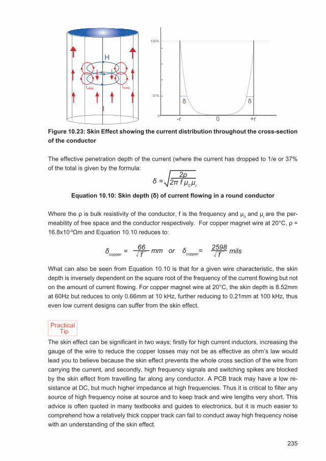
235
Figure 10.23: Skin Effect showing the current distribution throughout the cross-section
of the conductor
The effective penetration depth of the current (where the current has dropped to 1/e or 37% of the total is given by the formula:
Equation 10.10: Skin depth (δ) of current flowing in a round conductor
Where the ρ is bulk resistivity of the conductor, f is the frequency and μ0 and μr are the per-meability of free space and the conductor respectively. For copper magnet wire at 20°C, ρ = 16.8x10⁻⁹Ωm and Equation 10.10 reduces to:
What can also be seen from Equation 10.10 is that for a given wire characteristic, the skin depth is inversely dependent on the square root of the frequency of the current flowing but not on the amount of current flowing. For copper magnet wire at 20°C, the skin depth is 8.52mm at 60Hz but reduces to only 0.66mm at 10 kHz, further reducing to 0.21mm at 100 kHz, thus even low current designs can suffer from the skin effect.
The skin effect can be significant in two ways; firstly for high current inductors, increasing the gauge of the wire to reduce the copper losses may not be as effective as ohm’s law would lead you to believe because the skin effect prevents the whole cross section of the wire from carrying the current, and secondly, high frequency signals and switching spikes are blocked by the skin effect from travelling far along any conductor. A PCB track may have a low re-sistance at DC, but much higher impedance at high frequencies. Thus it is critical to filter any source of high frequency noise at source and to keep track and wire lengths very short. This advice is often quoted in many textbooks and guides to electronics, but it is much easier to comprehend how a relatively thick copper track can fail to conduct away high frequency noise with an understanding of the skin effect.
H
Ieddy
I0
δ
0-r +r
δ37%
100%
Ieddy
δ =2ρ
2π f μ0 μr
δcopper =66f
2598fmm or δcopper= mils
Practical Tip
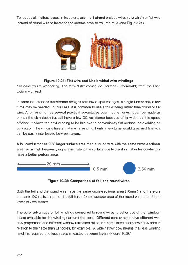
236
To reduce skin effect losses in inductors, use multi-strand braided wires (Litz wire*) or flat wire instead of round wire to increase the surface area-to-volume ratio (see Fig. 10.24)
Figure 10.24: Flat wire and Litz braided wire windings
* In case you’re wondering, The term “Litz” comes via German (Litzendraht) from the Latin Licium = thread.
In some inductor and transformer designs with low output voltages, a single turn or only a few turns may be needed. In this case, it is common to use a foil winding rather than round or flat wire. A foil winding has several practical advantages over magnet wires: it can be made as thin as the skin depth but still have a low DC resistance because of its width, so it is space efficient; it allows the next winding to be laid over a conveniently flat surface, so avoiding an ugly step in the winding layers that a wire winding if only a few turns would give, and finally, it can be easily interleaved between layers.
A foil conductor has 20% larger surface area than a round wire with the same cross-sectional area, so as high frequency signals migrate to the surface due to the skin, flat or foil conductors have a better performance:
Figure 10.25: Comparison of foil and round wires
Both the foil and the round wire have the same cross-sectional area (10mm²) and therefore the same DC resistance, but the foil has 1.2x the surface area of the round wire, therefore a lower AC resistance.
The other advantage of foil windings compared to round wires is better use of the “window” space available for the windings around the core. Different core shapes have different win-dow proportions and different window utilisation ratios; EE cores have a larger window area in relation to their size than EP cores, for example. A wide flat window means that less winding height is required and less space is wasted between layers (Figure 10.26).
0.5 mm 3.56 mm20 mm
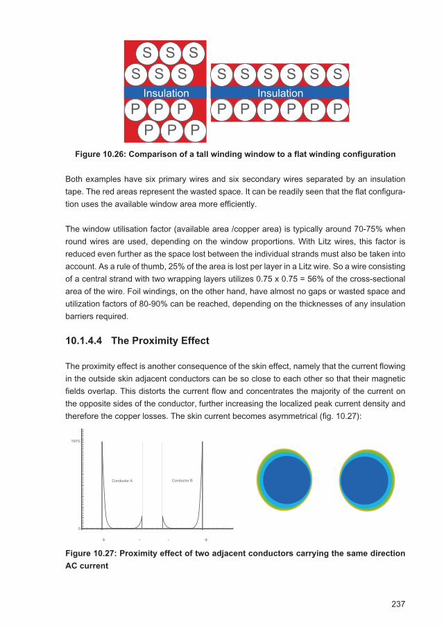
237
Figure 10.26: Comparison of a tall winding window to a flat winding configuration
Both examples have six primary wires and six secondary wires separated by an insulation tape. The red areas represent the wasted space. It can be readily seen that the flat configura-tion uses the available window area more efficiently.
The window utilisation factor (available area /copper area) is typically around 70-75% when round wires are used, depending on the window proportions. With Litz wires, this factor is reduced even further as the space lost between the individual strands must also be taken into account. As a rule of thumb, 25% of the area is lost per layer in a Litz wire. So a wire consisting of a central strand with two wrapping layers utilizes 0.75 x 0.75 = 56% of the cross-sectional area of the wire. Foil windings, on the other hand, have almost no gaps or wasted space and utilization factors of 80-90% can be reached, depending on the thicknesses of any insulation barriers required.
10.1.4.4 The Proximity Effect
The proximity effect is another consequence of the skin effect, namely that the current flowing in the outside skin adjacent conductors can be so close to each other so that their magnetic fields overlap. This distorts the current flow and concentrates the majority of the current on the opposite sides of the conductor, further increasing the localized peak current density and therefore the copper losses. The skin current becomes asymmetrical (fig. 10.27):
Figure 10.27: Proximity effect of two adjacent conductors carrying the same direction
AC current
S S SS S S S S S
P P P P P P P P PP P P
S S SInsulation Insulation
0
100%
+ - - +
Conductor A Conductor B
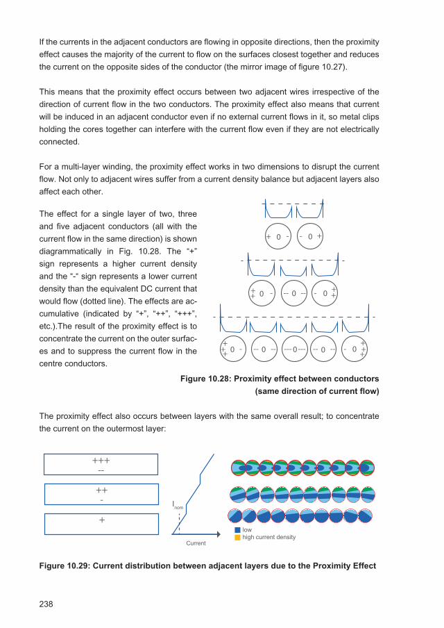
238
If the currents in the adjacent conductors are flowing in opposite directions, then the proximity effect causes the majority of the current to flow on the surfaces closest together and reduces the current on the opposite sides of the conductor (the mirror image of figure 10.27).
This means that the proximity effect occurs between two adjacent wires irrespective of the direction of current flow in the two conductors. The proximity effect also means that current will be induced in an adjacent conductor even if no external current flows in it, so metal clips holding the cores together can interfere with the current flow even if they are not electrically connected.
For a multi-layer winding, the proximity effect works in two dimensions to disrupt the current flow. Not only to adjacent wires suffer from a current density balance but adjacent layers also affect each other.
Figure 10.28: Proximity effect between conductors
(same direction of current flow)
The proximity effect also occurs between layers with the same overall result; to concentrate the current on the outermost layer:
Figure 10.29: Current distribution between adjacent layers due to the Proximity Effect
The effect for a single layer of two, three and five adjacent conductors (all with the current flow in the same direction) is shown diagrammatically in Fig. 10.28. The “+” sign represents a higher current density and the “-“ sign represents a lower current density than the equivalent DC current that would flow (dotted line). The effects are ac-cumulative (indicated by “+”, “++”, “+++”, etc.).The result of the proximity effect is to concentrate the current on the outer surfac-es and to suppress the current flow in the centre conductors.
+ - +-
+ - ---- +-
+ - ---- ---- +-------
0 0
0 0 0
0 0 0 0 0
+ +
+ +
+ +
Current
Inom
+++--
++-
+lowhigh current density
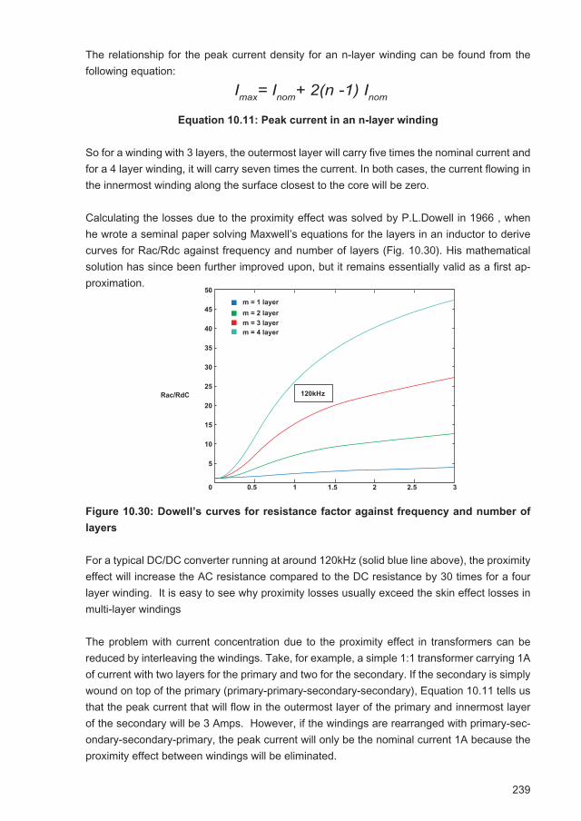
239
The relationship for the peak current density for an n-layer winding can be found from the following equation:
Equation 10.11: Peak current in an n-layer winding
So for a winding with 3 layers, the outermost layer will carry five times the nominal current and for a 4 layer winding, it will carry seven times the current. In both cases, the current flowing in the innermost winding along the surface closest to the core will be zero.
Calculating the losses due to the proximity effect was solved by P.L.Dowell in 1966 , when he wrote a seminal paper solving Maxwell’s equations for the layers in an inductor to derive curves for Rac/Rdc against frequency and number of layers (Fig. 10.30). His mathematical solution has since been further improved upon, but it remains essentially valid as a first ap-proximation.
Figure 10.30: Dowell’s curves for resistance factor against frequency and number of
layers
For a typical DC/DC converter running at around 120kHz (solid blue line above), the proximity effect will increase the AC resistance compared to the DC resistance by 30 times for a four layer winding. It is easy to see why proximity losses usually exceed the skin effect losses in multi-layer windings
The problem with current concentration due to the proximity effect in transformers can be reduced by interleaving the windings. Take, for example, a simple 1:1 transformer carrying 1A of current with two layers for the primary and two for the secondary. If the secondary is simply wound on top of the primary (primary-primary-secondary-secondary), Equation 10.11 tells us that the peak current that will flow in the outermost layer of the primary and innermost layer of the secondary will be 3 Amps. However, if the windings are rearranged with primary-sec-ondary-secondary-primary, the peak current will only be the nominal current 1A because the proximity effect between windings will be eliminated.
Imax= Inom+ 2(n -1) Inom
0 0.5 1 1.5 2 2.5 3
5
10
15
20
25
30
35
40
45
50
Rac/RdC
ƒ(x105Hz)
m = 1 layer
m = 2 layer
m = 3 layerm = 4 layer
120kHz
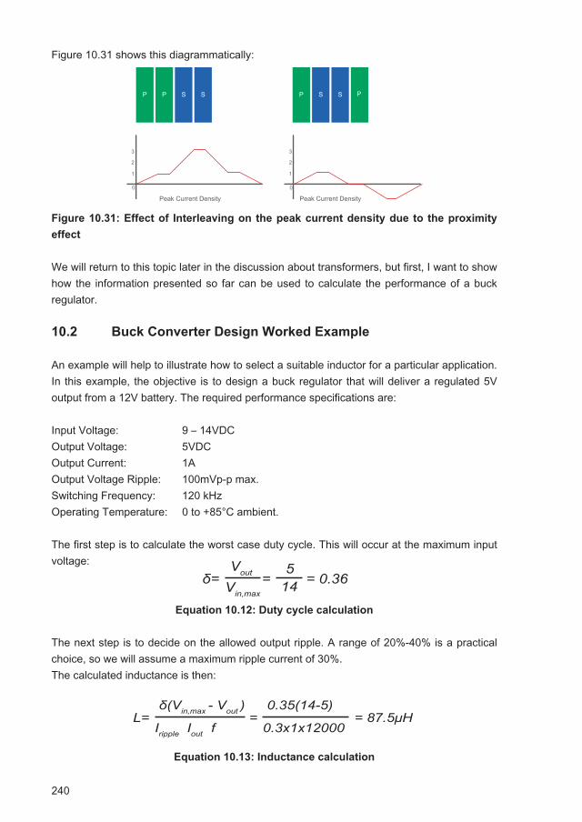
240
Figure 10.31 shows this diagrammatically:
Figure 10.31: Effect of Interleaving on the peak current density due to the proximity
effect
We will return to this topic later in the discussion about transformers, but first, I want to show how the information presented so far can be used to calculate the performance of a buck regulator.
10.2 Buck Converter Design Worked Example
An example will help to illustrate how to select a suitable inductor for a particular application. In this example, the objective is to design a buck regulator that will deliver a regulated 5V output from a 12V battery. The required performance specifications are:
Input Voltage: 9 – 14VDCOutput Voltage: 5VDCOutput Current: 1AOutput Voltage Ripple: 100mVp-p max.Switching Frequency: 120 kHzOperating Temperature: 0 to +85°C ambient.
The first step is to calculate the worst case duty cycle. This will occur at the maximum input voltage:
Equation 10.12: Duty cycle calculation
The next step is to decide on the allowed output ripple. A range of 20%-40% is a practical choice, so we will assume a maximum ripple current of 30%.The calculated inductance is then:
Equation 10.13: Inductance calculation
2
3
1
0
P P S S P S S P
2
3
1
0
Peak Current Density Peak Current Density
P
δ= =Vin,max
514 = 0.36
Vout
L= Iripple Iout f=
δ(Vin,max - Vout )
0.3x1x12000
0.35(14-5)= 87.5μH
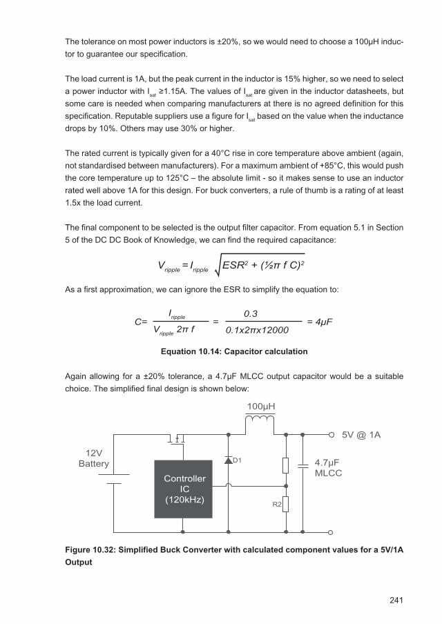
241
The tolerance on most power inductors is ±20%, so we would need to choose a 100µH induc-tor to guarantee our specification.
The load current is 1A, but the peak current in the inductor is 15% higher, so we need to select a power inductor with Isat ≥1.15A. The values of Isat are given in the inductor datasheets, but some care is needed when comparing manufacturers at there is no agreed definition for this specification. Reputable suppliers use a figure for Isat based on the value when the inductance drops by 10%. Others may use 30% or higher.
The rated current is typically given for a 40°C rise in core temperature above ambient (again, not standardised between manufacturers). For a maximum ambient of +85°C, this would push the core temperature up to 125°C – the absolute limit - so it makes sense to use an inductor rated well above 1A for this design. For buck converters, a rule of thumb is a rating of at least 1.5x the load current.
The final component to be selected is the output filter capacitor. From equation 5.1 in Section 5 of the DC DC Book of Knowledge, we can find the required capacitance:
As a first approximation, we can ignore the ESR to simplify the equation to:
Equation 10.14: Capacitor calculation
Again allowing for a ±20% tolerance, a 4.7µF MLCC output capacitor would be a suitable choice. The simplified final design is shown below:
Figure 10.32: Simplified Buck Converter with calculated component values for a 5V/1A
Output
Vripple = Iripple ESR2 + (½π f C)2
C= Vripple 2π f=
Iripple
0.1x2πx12000
0.3= 4μF
100μH
D1
R2
4.7μFMLCC
12VBattery
ControllerIC
(120kHz)
5V @ 1A
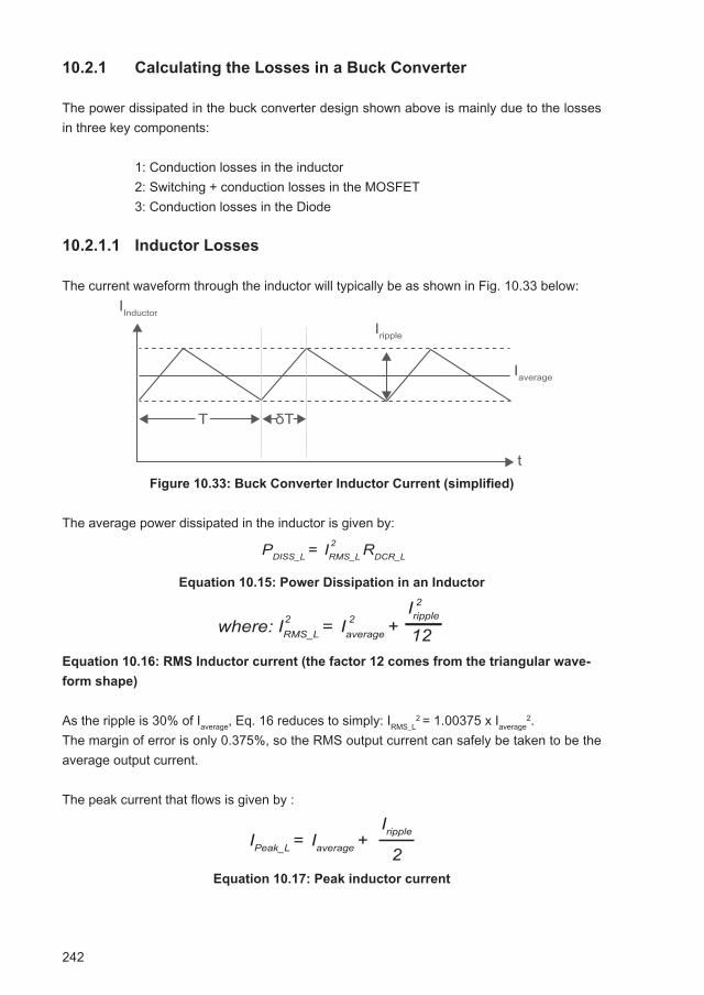
242
10.2.1 Calculating the Losses in a Buck Converter
The power dissipated in the buck converter design shown above is mainly due to the losses in three key components:
1: Conduction losses in the inductor 2: Switching + conduction losses in the MOSFET 3: Conduction losses in the Diode
10.2.1.1 Inductor Losses
The current waveform through the inductor will typically be as shown in Fig. 10.33 below:
Figure 10.33: Buck Converter Inductor Current (simplified)
The average power dissipated in the inductor is given by:
Equation 10.15: Power Dissipation in an Inductor
Equation 10.16: RMS Inductor current (the factor 12 comes from the triangular wave-
form shape)
As the ripple is 30% of Iaverage, Eq. 16 reduces to simply: IRMS_L2 = 1.00375 x Iaverage
2. The margin of error is only 0.375%, so the RMS output current can safely be taken to be the average output current.
The peak current that flows is given by :
Equation 10.17: Peak inductor current
IInductor
Iripple
Iaverage
t
T δT
2Iripple
PDISS_L = IRMS_L RDCR_L 2
where: IRMS_L = Iaverage + 2 2
2Iripple
12
IPeak_L = Iaverage +
Iripple
2
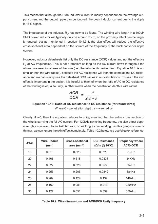
243
This means that although the RMS inductor current is mostly dependent on the average out-put current and the output ripple can be ignored, the peak inductor current due to the ripple is 15% higher.
The impedance of the inductor, RL, has now to be found. The winding wire length in a 100µH SMD power inductor will typically only be around 70cm, so the proximity effect can be large-ly ignored, but as mentioned in section 10.1.3.3, the skin effect will reduce the effective cross-sectional area dependent on the square of the frequency of the buck converter ripple current.
However, inductor datasheets list only the DC resistance (DCR) values and not the effective RL at AC frequencies. This is not a problem as long as the AC current flows throughout the whole cross-sectional area of the wire (i.e., the skin depth derived from Equation 10.8 is not smaller than the wire radius), because the AC resistance will then the same as the DC resist-ance and we can simply use the datasheet DCR values in our calculations. To see if the skin effect is important in the design, it is helpful to think of when the ratio of AC to DC resistance of the winding is equal to unity, in other words when the penetration depth = wire radius
Equation 10.18: Ratio of AC resistance to DC resistance (for round wires)
Where δ = penetration depth, r = wire radius
Clearly, if r=δ, then the equation reduces to unity, meaning that the entire cross section of the wire is carrying the full AC current. For 120kHz switching frequency, the skin effect depth is roughly equivalent to an AWG26 wire, so as long as our winding has this gauge of wire or thinner, we can ignore the skin effect completely. Table 10.2 below is a useful quick reference:
AWGWire Radius
(mm)
Cross-sectional
area (mm²)
DC Resistance
(Ω/m @ 20°C)
Frequency where
ACR=DCR
18 0.510 0.823 0.0210 21kHz
20 0.406 0.518 0.0333 34KHz
22 0.322 0.326 0.0530 55kHz
24 0.255 0.205 0.0842 88kHz
26 0.202 0.129 0.134 140kHz
28 0.160 0.081 0.213 220kHz
30 0.127 0.051 0.339 350kHz
Table 10.2: Wire dimensions and ACR/DCR Unity frequency
= r2
2rδ - δ2
ACRDCR
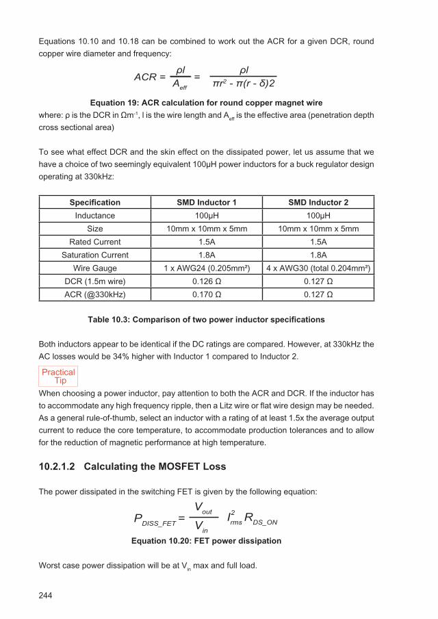
244
Equations 10.10 and 10.18 can be combined to work out the ACR for a given DCR, round copper wire diameter and frequency:
Equation 19: ACR calculation for round copper magnet wire
where: ρ is the DCR in Ωm-1, l is the wire length and Aeff is the effective area (penetration depth cross sectional area)
To see what effect DCR and the skin effect on the dissipated power, let us assume that we have a choice of two seemingly equivalent 100µH power inductors for a buck regulator design operating at 330kHz:
Specification SMD Inductor 1 SMD Inductor 2
Inductance 100µH 100µHSize 10mm x 10mm x 5mm 10mm x 10mm x 5mm
Rated Current 1.5A 1.5ASaturation Current 1.8A 1.8A
Wire Gauge 1 x AWG24 (0.205mm²) 4 x AWG30 (total 0.204mm²)DCR (1.5m wire) 0.126 Ω 0.127 ΩACR (@330kHz) 0.170 Ω 0.127 Ω
Table 10.3: Comparison of two power inductor specifications
Both inductors appear to be identical if the DC ratings are compared. However, at 330kHz the AC losses would be 34% higher with Inductor 1 compared to Inductor 2.
When choosing a power inductor, pay attention to both the ACR and DCR. If the inductor has to accommodate any high frequency ripple, then a Litz wire or flat wire design may be needed. As a general rule-of-thumb, select an inductor with a rating of at least 1.5x the average output current to reduce the core temperature, to accommodate production tolerances and to allow for the reduction of magnetic performance at high temperature.
10.2.1.2 Calculating the MOSFET Loss
The power dissipated in the switching FET is given by the following equation:
Equation 10.20: FET power dissipation
Worst case power dissipation will be at Vin max and full load.
ρlAeff
ρlπr2 - π(r - δ)2ACR = =
Practical Tip
PDISS_FET =
2Irms RDS_ON
Vout
Vin
245
For a typical power FET with a RDS_ON of 0.026Ω:
10.2.1.3 Calculating the Diode Loss
The power dissipated in the diode is given by the following equation:
Equation 10.21: Diode power dissipation
The worst case power dissipation will be again at Vin max and full load. For a typical power diode with a VF of 0.5V:
Thus the total losses in the buck converter (Inductor 1) will be 0.198W + 0.073W + 0.321W = 0.59W. This equates to a worst case full load efficiency of 89.4%. With the nominal input voltage of 12V, the efficiency will increase slightly to 90%.
And all this can be known before anyone has even reached for a soldering iron!
10.2.2 Boost Converter Design
If the design requirement is changed to a boost converter, then the above equations need to be modified. The calculation for the duty cycle given in Eq. 10.11 becomes:
Equation 10.22: Duty cycle calculation for a boost converter
then the calculation for the required inductor then becomes:
Equation 10.23: Inductor calculation for a boost converter
The average current in the inductor is no longer simply the maximum output current, but equal to Iout/1-δ. For a typical duty cycle of 50%, the current for the inductor is therefore double the output current. In practice, this means choosing an inductor that is rated at 4 times the maximum output current to allow for safe 85° ambient operation. The heavier gauge winding means that the skin effect rarely affects the inductor power dissipation.
PDISS_FET = x1x0.026 = 0.073W
145
PDISS_DIODE = (1 - )IrmsVF
Vout
Vin
PDISS_DIODE = (1 - )x1x0.5 = 0.321W
514
(1 - δ)2(Vout,max - Vin,min)
δ = 1 - Vin,min
Vout,max
L = (1 - δ)2(Vout,max - Vin,min)
Iripple Iout f
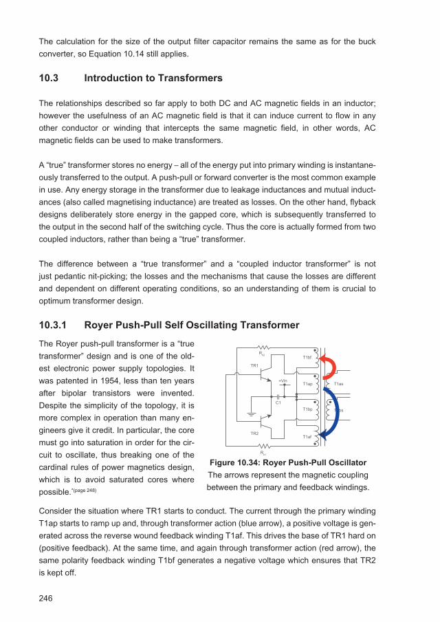
246
The calculation for the size of the output filter capacitor remains the same as for the buck converter, so Equation 10.14 still applies.
10.3 Introduction to Transformers
The relationships described so far apply to both DC and AC magnetic fields in an inductor; however the usefulness of an AC magnetic field is that it can induce current to flow in any other conductor or winding that intercepts the same magnetic field, in other words, AC magnetic fields can be used to make transformers.
A “true” transformer stores no energy – all of the energy put into primary winding is instantane-ously transferred to the output. A push-pull or forward converter is the most common example in use. Any energy storage in the transformer due to leakage inductances and mutual induct-ances (also called magnetising inductance) are treated as losses. On the other hand, flyback designs deliberately store energy in the gapped core, which is subsequently transferred to the output in the second half of the switching cycle. Thus the core is actually formed from two coupled inductors, rather than being a “true” transformer.
The difference between a “true transformer” and a “coupled inductor transformer” is not just pedantic nit-picking; the losses and the mechanisms that cause the losses are different and dependent on different operating conditions, so an understanding of them is crucial to optimum transformer design.
10.3.1 Royer Push-Pull Self Oscillating Transformer
Consider the situation where TR1 starts to conduct. The current through the primary winding T1ap starts to ramp up and, through transformer action (blue arrow), a positive voltage is gen-erated across the reverse wound feedback winding T1af. This drives the base of TR1 hard on (positive feedback). At the same time, and again through transformer action (red arrow), the same polarity feedback winding T1bf generates a negative voltage which ensures that TR2 is kept off.
TR2T1af
T1bp
T1ap T1as
T1bs
T1bf
TR1
Rb2
+Vin
C1
Rb1
The Royer push-pull transformer is a “true transformer” design and is one of the old-est electronic power supply topologies. It was patented in 1954, less than ten years after bipolar transistors were invented. Despite the simplicity of the topology, it is more complex in operation than many en-gineers give it credit. In particular, the core must go into saturation in order for the cir-cuit to oscillate, thus breaking one of the cardinal rules of power magnetics design, which is to avoid saturated cores where possible.*(page 248)
Figure 10.34: Royer Push-Pull Oscillator
The arrows represent the magnetic coupling between the primary and feedback windings.
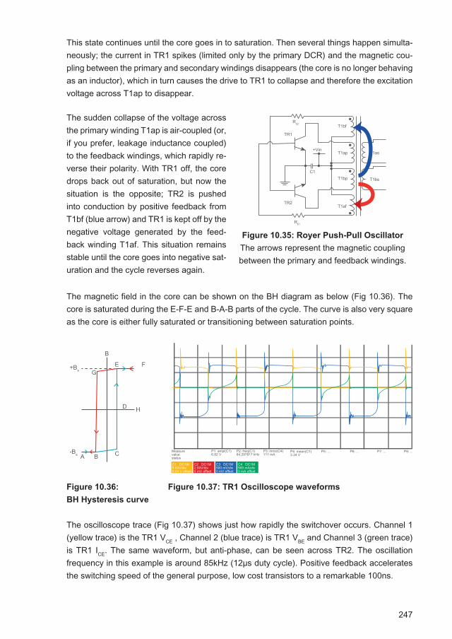
247
This state continues until the core goes in to saturation. Then several things happen simulta-neously; the current in TR1 spikes (limited only by the primary DCR) and the magnetic cou-pling between the primary and secondary windings disappears (the core is no longer behaving as an inductor), which in turn causes the drive to TR1 to collapse and therefore the excitation voltage across T1ap to disappear.
The magnetic field in the core can be shown on the BH diagram as below (Fig 10.36). The core is saturated during the E-F-E and B-A-B parts of the cycle. The curve is also very square as the core is either fully saturated or transitioning between saturation points.
Figure 10.36: Figure 10.37: TR1 Oscilloscope waveforms
BH Hysteresis curve
The oscilloscope trace (Fig 10.37) shows just how rapidly the switchover occurs. Channel 1 (yellow trace) is the TR1 VCE , Channel 2 (blue trace) is TR1 VBE and Channel 3 (green trace) is TR1 ICE. The same waveform, but anti-phase, can be seen across TR2. The oscillation frequency in this example is around 85kHz (12µs duty cycle). Positive feedback accelerates the switching speed of the general purpose, low cost transistors to a remarkable 100ns.
The sudden collapse of the voltage across the primary winding T1ap is air-coupled (or, if you prefer, leakage inductance coupled) to the feedback windings, which rapidly re-verse their polarity. With TR1 off, the core drops back out of saturation, but now the situation is the opposite; TR2 is pushed into conduction by positive feedback from T1bf (blue arrow) and TR1 is kept off by the negative voltage generated by the feed-back winding T1af. This situation remains stable until the core goes into negative sat-uration and the cycle reverses again.
TR2T1af
T1bp
T1ap T1as
T1bs
T1bf
TR1
Rb2
+Vin
C1
Rb1
Figure 10.35: Royer Push-Pull Oscillator
The arrows represent the magnetic coupling between the primary and feedback windings.
+Bs
H
B
EG
D
CBA
F
-BsMeasurevaluestatus
P1: ampl(C1)6.82 V
P2: freq(C1)84.297817 kHz
P3: mms(C4)111 mA
P4: mean(C1)3.34 V
P5: ... P6: ... P7: ... P8: ...
C1 DC1M5.00V/div0.00 V offset
C2 DC1M2.00V/div0 mV offset
C3 DC1M500 mV/div0 mV offset
C4 DC1M500 mA/div0 mA offset
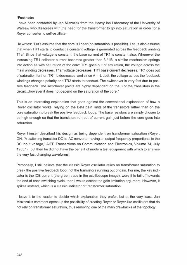
248
*Footnote:
I have been contacted by Jan Miszczak from the Heavy Ion Laboratory of the University of Warsaw who disagrees with the need for the transformer to go into saturation in order for a Royer converter to self-oscillate.
He writes: “Let’s assume that the core is linear (no saturation is possible). Let us also assume that when TR1 starts to conduct a constant voltage is generated across the feedback winding T1af. Since that voltage is constant, the base current of TR1 is constant also. Whenever the increasing TR1 collector current becomes greater than β * IB, a similar mechanism springs into action as with saturation of the core: TR1 goes out of saturation, the voltage across the main winding decreases, T1af voltage decreases, TR1 base current decreases, TR1 goes out of saturation further, TR1 Ic decreases, and since V = -L di/dt, the voltage across the feedback windings changes polarity and TR2 starts to conduct. The switchover is very fast due to pos-itive feedback. The switchover points are highly dependent on the β of the transistors in the circuit…however it does not depend on the saturation of the core.”
This is an interesting explanation that goes against the conventional explanation of how a Royer oscillator works, relying on the Beta gain limits of the transistors rather than on the core saturation to break the positive feedback loops. The base resistors are simply chosen to be high enough so that the transistors run out of current gain just before the core goes into saturation.
Royer himself described his design as being dependent on transformer saturation (Royer, GH, “A switching transistor DC-to-AC converter having an output frequency proportional to the DC input voltage,” AIEE Transactions on Communication and Electronics, Volume 74, July 1955.”) , but then he did not have the benefit of modern test equipment with which to analyse the very fast changing waveforms.
Personally, I still believe that the classic Royer oscillator relies on transformer saturation to break the positive feedback loop, not the transistors running out of gain. For me, the key indi-cator is the ICE current (the green trace in the oscilloscope image); were it to tail off towards the end of each switching cycle, then I would accept the gain limitation argument. However, it spikes instead, which is a classic indicator of transformer saturation.
I leave it to the reader to decide which explanation they prefer, but at the very least, Jan Miszczak’s comment opens up the possibility of creating Royer or Royer-like oscillators that do not rely on transformer saturation, thus removing one of the main drawbacks of the topology.
249
10.3.2 Royer Transformer Design Considerations
Without a core that goes into sharp saturation, the Royer push-pull free oscillator will not work well, if at all, so ferrite cores are most suitable. Also the feedback windings must be closely coupled to the primary windings so that the air-coupled leakage inductance can do its job of reversing the feedback winding polarity while the core is still in saturation. The number of turns on the primary winding can be chosen to give a reasonable operating frequency, f, using the relationship:
Equation 10.24: Royer Oscillation Frequency Relationship
For a 1:1 DC/DC converter running from nominal 5V (4.7V measured across the transistors) with a MnZn ferrite toroidal core with a positive saturation flux density, Bs, of 300mT, an ef-fective cross sectional area, Ae, of 5mm² and an operating frequency of 120 kHz, then the number of primary turns is:
As the primary winding is centre-tapped, the winding arrangement will be 7 + 7 turns. The feedback windings need to generate around 1V to properly drive the transistor base pins, so 2 turns are sufficient (2t/7t x 5V = 1.4V). The number of output turns equals the input turns for a 1:1 transformer (5V in, 5V out), but we need to allow an extra 0.7V for the output rectifier volt drop. If a centre-tapped secondary winding is used, then 8 + 8 turns would be sufficient.
The major advantage of the Royer topology, besides the simplicity of implementation and low turns count, is that because the core is fully used in all four quadrants, the power transmission for a given core size is double that of any single-ended topology.
The two transistors, TR1 and TR2, can be any general purpose NPN bipolar transistors. They should not be especially well matched otherwise the perfectly symmetrical circuit can have problems starting up, so never use dual transistor single package types.
Although the ICE current spike that occurs whenever the core goes into saturation is very short (in the order of a few microseconds), the continual cyclic overload can cause Safe Operating Area Region (SOAR) power dissipation issues. The transistor’s VCE rating must be at least double the maximum input voltage plus the overshoot voltage. A factor of safety of x3 to x4 the input voltage is usual.
The high rate of change caused by the saturation spikes is residually coupled to the output, causing similar output voltage spikes. Normally this is not a big problem as the spikes are
NP= 2Bs Ae 2 fVsupply x106
NP= = = 7 turns2Bs Ae 2 fVsupply x106
0.6x5x2x120x103
5x10⁶~
Practical Tip
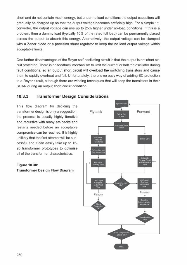
250
short and do not contain much energy, but under no load conditions the output capacitors will gradually be charged up so that the output voltage becomes artificially high. For a simple 1:1 converter, the output voltage can rise up to 25% higher under no-load conditions. If this is a problem, then a dummy load (typically 10% of the rated full load) can be permanently placed across the output to absorb this energy. Alternatively, the output voltage can be clamped with a Zener diode or a precision shunt regulator to keep the no load output voltage within acceptable limits.
One further disadvantages of the Royer self-oscillating circuit is that the output is not short cir-cuit protected. There is no feedback mechanism to limit the current or halt the oscillator during fault conditions, so an output short circuit will overload the switching transistors and cause them to rapidly overheat and fail. Unfortunately, there is no easy way of adding SC protection to a Royer circuit, although there are winding techniques that will keep the transistors in their SOAR during an output short circuit condition.
10.3.3 Transformer Design Considerations
Figure 10.38:
Transformer Design Flow Diagram
Specifications
Define DutyCycle
Flyback
Flyback
Forward
Forward
Calculate TurnsRatio
Calcutlate Required
InductanceSelect Core
Define Core andGap dimensions
CalculatePrimary, Resetand Secondary
turns
Use LargerGauge or
MultistrandWire
CalculateOutput Inductor
& CapacitorClampDissipation
OK?
END
Core Temperature& EMC OK?
Diode Ratings OK?
Calculate Primary turns
Use LargerGauge or Multistrand
Wire
Copper LossesOk?
This flow diagram for deciding the transformer design is only a suggestion; the process is usually highly iterative and recursive with many set-backs and restarts needed before an acceptable compromise can be reached. It is highly unlikely that the first attempt will be suc-cessful and it can easily take up to 15-20 transformer prototypes to optimise all of the transformer characteristics.
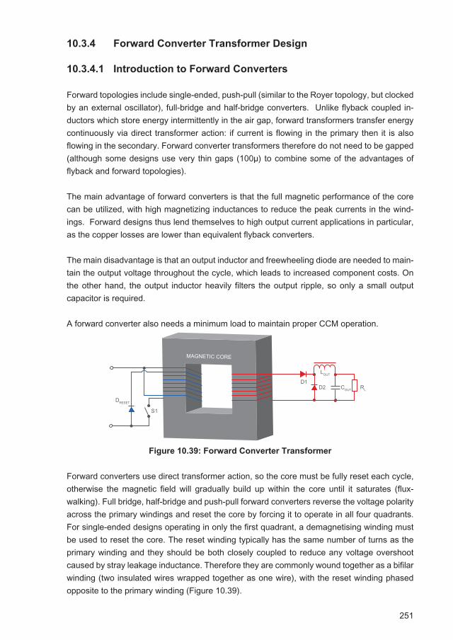
251
10.3.4 Forward Converter Transformer Design
10.3.4.1 Introduction to Forward Converters
Forward topologies include single-ended, push-pull (similar to the Royer topology, but clocked by an external oscillator), full-bridge and half-bridge converters. Unlike flyback coupled in-ductors which store energy intermittently in the air gap, forward transformers transfer energy continuously via direct transformer action: if current is flowing in the primary then it is also flowing in the secondary. Forward converter transformers therefore do not need to be gapped (although some designs use very thin gaps (100µ) to combine some of the advantages of flyback and forward topologies).
The main advantage of forward converters is that the full magnetic performance of the core can be utilized, with high magnetizing inductances to reduce the peak currents in the wind-ings. Forward designs thus lend themselves to high output current applications in particular, as the copper losses are lower than equivalent flyback converters.
The main disadvantage is that an output inductor and freewheeling diode are needed to main-tain the output voltage throughout the cycle, which leads to increased component costs. On the other hand, the output inductor heavily filters the output ripple, so only a small output capacitor is required.
A forward converter also needs a minimum load to maintain proper CCM operation.
Figure 10.39: Forward Converter Transformer
Forward converters use direct transformer action, so the core must be fully reset each cycle, otherwise the magnetic field will gradually build up within the core until it saturates (flux- walking). Full bridge, half-bridge and push-pull forward converters reverse the voltage polarity across the primary windings and reset the core by forcing it to operate in all four quadrants. For single-ended designs operating in only the first quadrant, a demagnetising winding must be used to reset the core. The reset winding typically has the same number of turns as the primary winding and they should be both closely coupled to reduce any voltage overshoot caused by stray leakage inductance. Therefore they are commonly wound together as a bifilar winding (two insulated wires wrapped together as one wire), with the reset winding phased opposite to the primary winding (Figure 10.39).
DRESET
S1
D1D2 RL
LOUT
COUT
MAGNETIC CORE
252
The single-ended forward converter design has advantage over the other forward variants because it is cheaper to make; requiring only a single supply voltage and few additional com-ponents. With a 1:1 reset-to-primary winding ratio, the core cannot saturate if the duty cycle stays below 50%, so flux-walking is never a problem. The disadvantage is that the peak MOS-FET voltage will be at least twice the input voltage, requiring a high performance transistor.
10.3.4.2 Forward Converter Transformer Design
The first step in a single-ended forward converter design is to define the duty cycle. As the core must be demagnetized every cycle, the magnetizing time cannot exceed the reset time, so the duty cycle is limited to 50% maximum. In practice, allowances for tolerances and sud-den changes in input voltage and load have to be made which limits the maximum duty cycle to around 45% under worst case conditions, which leads to a typical ratio of 40% during nor-mal operation at minimum Vin.
In the following example, we will consider a single-ended topology. As with the previous buck converter design, the same basic specification will be used.
Input Voltage: 9 – 14VDCOutput Voltage: 5VDCOutput Current: 1AOutput Voltage Ripple: 100mVp-p max.Switching Frequency: 120 kHzOperating Temperature: 0°C to +85°C ambient
For CCM operation, the same duty cycle calculation for the buck converter (Equation 10.12) can be used, just modified by the transformer turns ratio:
Equation 10.25: Duty cycle relationship
The number of primary winding turns can be found from the following relationship:
Equation 10.26: Primary winding turns relationship
Most 10W power ferrite cores have a Bsat value of 200-500mT. Let us assume that we can find a core with a maximum flux density of around 0.4T which does not go into saturation with an operating flux density variation of 0.3T over the whole temperature range.
δ = xVin, max
Vout
nsec
npri
npri = Bsat Ae fVin,max δmax

253
Finding the effective cross-sectional area, Ae, is not so easy, though, because it depends on the core geometry. We are stuck in a loop: to find the number of primary turns, we need to know the core geometry, but we can’t pick a suitable core unless we know the number of turns.
However, we do know that this is a low power design and that we need three windings (primary, reset and secondary), so a small core with a large winding area for the size would be useful – such as a pot core. A suitable core size could thus be a P9/5 Pot core. This has the following specifications:
Core:Type Ae Bsat (at 25°C) Diameter HeightP9/5-1S 10.1mm² 450mT 9.5mm 5.4mm
Bobbin:Type Winding Area Winding Width MLT Build HeightCP-P9/5-1S 3.1mm² 2.5mm 18.9mm 1.28mm
Having picked a core that looks suitable, the next step is to put the values back into the equa-tion to see if the number of primary, reset and secondary turns looks reasonable.
Equation 10.27: Primary Turns Calculation
This is the minimum number of turns, so we can choose 12 turns for the primary winding. The number of turns in the reset winding will be the same (12 turns) but because the reset winding does not need to carry the switching current, the wires can be made 3-4 gauges smaller.
The number of secondary turns can be calculated from the following relationship (where VL is the volt drop across the output inductor, typically 0.5V):
Equation 10.28: Secondary Turns Calculation
Again, this is the minimum number of turns, so we can choose more turns for the secondary winding for safety – a suitable number would be 20 turns.
For the primary and secondary windings, we can use AWG26 wire (to avoid the skin effect at 120kHz). AWG26 wire has a diameter of 0.202mm, so 12 turns will fit in a single layer.
npri = = f Ae ΔB
Vin,max δmax
120x103x10.1x10-6x0.3
9x0.45≥ 11.1 turns
nsec = = δmaxVin,min
npri (Vout + VDiode drop + VL)
0.45x9
12(5 + 0.5 + 0.5)≥ 17.7 turns
Practical Tip
254
The primary winding thus consists of two layers of six turns of bifilar-wound primary and reset windings (AWG26 and AWG30 respectively) and the secondary winding consists of two layers of ten turns of AWG26 wire. The build height of 4 layers is around 0.8mm, so we have enough space to add a few layers of insulating tape between the primary and secondary windings if we wish.
The average primary winding current will be:
If we assume an efficiency of 90%, the input power will be 5.5V x 1A / 0.9 = 6.1W. The highest average primary side on current will be at Vin,min, giving us:
The perimeter dimension is 18.9mm, so for a first approximation the resistance per turn can be calculated using Equation 10.29:
Equation 10.29: Wire Resistance calculation ρ, the resistivity of copper = 1.678 x 10⁻⁸ Ω m, l = wire length (m) and A is the cross-sectional area of the wire (πr²) in m²
For our example, the DC resistance of AWG26 wire would be 134mΩm-1, or 2.5mΩ per turn. The I²R copper losses would be 67.5mW on the primary and only 5mW on the secondary (1A is specified as the output current).
The total copper losses are thus 72.5mW, or around 1.5% of the total power through the trans-former - a very acceptable figure.
The output inductor should be sized to allow 30% of the AC ripple through to the output ca-pacitor. For higher current designs, it would be better to fit a larger inductor and a smaller capacitor to reduce the AC ripple stress on the capacitor, then a figure of 10%-20% ripple could be chosen.
The worst case ripple occurs at the maximum duty cycle, so the output inductor must be at least:
Equation 10.30: Output inductor calculation
Ipri,avg = δVin
Input Power
Ipri,avg, max = = 1.5A 0.45x96.1
RDC = Aρl
Lout= = 4fΔIout,ripple
Vsec
4x120x103x30%6 = 42µH
255
The output capacitor can be chosen using the same relationship as in Equation 10.14 for the buck converter:
There are three diodes used in the forward converter design; the reset winding diode and two output rectification diodes. Under 50% duty cycle conditions, each secondary side diode alternates to carry the output current when conducting. The equivalent continuous current in each secondary diode is then the output current divided by the square root of two; in our example, about 0.7A.
The secondary diodes must be each rated to carry the equivalent RMS output current which is also dependent on the duty cycle (in other words, don’t assume that the each diode carries only 50% of the average output current). A better design rule is to assume that both diodes carry the full output current. To reduce output diode losses at high output currents, Schottky diodes or synchronous rectification can be used.
The output diodes also have to be able to withstand the peak reverse voltages:
Equation 10.31: Reverse Blocking Voltage calculation for the secondary diodes.
The factor 1.5 allows for voltage ringing and some tolerances.
The power dissipation in the diode used for the reset winding is not normally significant, but it has to cope with a peak reverse voltage of at least double the maximum input voltage.
The reset winding diode should be a power diode with low forward voltage drop and adequate reverse voltage rating (typically 2.5x to 3x Vin,max). The reverse recovery speed is not important.
10.3.5 Flyback Transformer Design
Flyback converters use the pulsed energy stored in the air gap to transfer power across the transformer (actually two coupled inductors). In many ways, the flyback can be considered to be a transformer isolated buck/boost converter, with the advantage that the turns ratio can be used to step up or down the input voltage while still keeping the PWM duty cycle close to 50%. Thus flybacks are popular for AC/DC power supplies where a rectified AC input voltage of hundreds of volts needs to be dropped down to a low DC output voltage.
Practical Tip
C = = Vripple2πfIripple
0.1x2πx120000.3 = 4µF
VD,reset= 1.5 Vin,max=1.5 x x 14 = 31.5V npri
nsec
1218
Practical Tip

256
Another advantage, besides the inherent simplicity of the topology, is that an output inductor is not required, thus saving cost and reducing the size of the power supply.
Figure 10.40: Flyback Converter Transformer.
The secondary winding is wound in the opposite direction to the primary.
For this worked example, we will use again the same specification as in Section 10.2 for the buck converter design:
Input Voltage: 9 – 14VDCOutput Voltage: 5VDCOutput Current: 1AOutput Voltage Ripple: 100mVp-p max.Switching Frequency: 120 kHzOperating Temperature: 0°C to +85°C ambient
The first step is to define the duty cycle and turns ratio. These two parameters are interlinked – if we define one, we can determine the other. For a flyback design with current mode control, the maximum duty cycle at the worst case condition (minimum Vin ) will be 50% .
50% duty cycle is the theoretical maximum, but in practice we did to allow some dead-space between the switching cycles. This is to avoid shoot-through and any unwanted oscillation problems with the slope compensation. Therefore 40% is a safer choice.
The relationship between duty cycle, input voltage, effective output voltage and turns ratio is given by:
Equation 10.32: Relationship between turns ratio and duty cycle
COUT RL
DOUT
S1
DCLAMP
AIR GAP
Practical Tip
= x ns
np
1 - δmax
δmax
Vout + VDiode drop
Vin,min

257
For our example, the calculated turns ratio is:
Very often, the turns ration is not an even number and the nearest whole number of turns ratio must be used. Remember that it is the ratio that is important, not the absolute number of turns. For example, if the calculated ratio were to be, say, 1.5, then the best solution would not be a 1:1 or 1:2 transformer, but a 2:3 turns ratio. The nearest practical turns ratio solution should be fed back into Equation 26 to check that the duty cycle is still safe. Equation 10.27 is the same as Equation 10.26, but rearranged for duty cycle:
Equation 10.33: Relationship between duty cycle and turns ratio
Our 1:1 solution is very close to the calculated 1:1.09, so the maximum duty cycle would be 0.38.
The next stage in the flow chart is to calculate the inductance. But firstly, we need to calculate the average secondary winding current at the maximum duty cycle:
Equation 10.34: Average secondary current calculation
The secondary inductance can now be derived, knowing the oscillation frequency assuming an acceptable maximum ripple. As in the buck regulator example, we will take 120 kHz and 30% ripple:
Equation 10.35: Secondary Inductance calculation
The turns ratio gives us the primary inductance:
Equation 10.36: Primary Inductance calculation
Equation 10.36 gives us also 58µH for the primary inductance in our example (as would be expected from a 1:1 transformer).
Practical Tip
= x = 1.09, quasi 1:1 ns
np
1 - 0.40.4
5 + 0.59
δmax=+
np ns
np nsVin, min Vout + VDiode
Iavg, sec = = =1.63A1 - δmax
Iout
1-0.381
Lsec = = = 58µH Ripple Iavg, secf
(Vout + VDiode drop)(1-δmax)0.3x1.63x120x103
(5+0.5)(1-0.38)
Lpri = Lsec ( )2npri nsec
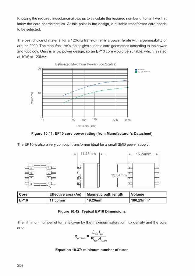
258
Knowing the required inductance allows us to calculate the required number of turns if we first know the core characteristics. At this point in the design, a suitable transformer core needs to be selected.
The best choice of material for a 120kHz transformer is a power ferrite with a permeability of around 2000. The manufacturer’s tables give suitable core geometries according to the power and topology. Ours is a low power design, so an EP10 core would be suitable, which is rated at 10W at 120kHz:
Figure 10.41: EP10 core power rating (from Manufacturer’s Datasheet)
The EP10 is also a very compact transformer ideal for a small SMD power supply:
Core Effective area (Ae) Magnetic path length Volume
EP10 11.30mm² 19.20mm 180,29mm³
Figure 10.42: Typical EP10 Dimensions
The minimum number of turns is given by the maximum saturation flux density and the core area:
Equation 10.37: minimum number of turns
101
10
100
100 1000
Pow
er (W
)
Frequency (kHz)
Estimated Maximum Power (Log Scales)Push-PullDC-DC Flyback
120 500 50
11.43mm 15.24mm
13.34mm
5
6
7
8
4
3
2
1
npri,min = Bsat ACore
Lpri Ipri

259
We know the output current, but not the primary current. Before we can go to the next step, we need to estimate the primary winding current. To do this, we need to know the efficiency, ƞ, of the transformer. We will use a typical value of 90%:
Equation 10.38: Average primary RMS current calculation
For the EP10, the core area is 11.30mm² (given in the datasheet) and the ferrite core material has a maximum flux density of 360mT at 100°C. As we are using current mode regulation, we can use the maximum flux density value. For voltage mode regulation, some headroom would be needed.
Thus the minimum number of turns is:
This is the absolute minimum number of turns. We can choose to wind more turns to give a wider safety margin if we want to. Typically around 10% extra is recommended, so 28 turns would be appropriate in this example. As the turns ratio is 1:1, we also know the number of secondary turns.
A 1:1 transformer is the simplest to wind, but if the ratio was different; say 3:2, then a turns ratio that is easily divisible by 3 and 2 would be more appropriate, e.g. 30:20 turns.
The restrictions on the maximum number of turns are the copper losses and the physical space available on the bobbin. The next step on our flow chart is to calculate the core losses.
The core losses due to the changing magnetic flux are dependent on the core characteristics, the ripple current and the number of turns (more turns reduces the flux swing):
Equation 10.39: Calculation of flux swing
The effective cross-sectional area (Ae) is from the manufacturer’s datasheet. The ripple cur-rent is typically chosen to be 30% of the average current.
Equation 10.39 gives the full flux swing in the core, to calculate the specific core losses, we need to use half of this value (49mT) and refer to a core loss table from the manufacturer of the ferrite material (refer to Fig. 10.21). The table indicates a relative core loss of around 10kW/m³ at 120kHz and 49mT, which equates for the EP10 with a core volume of 217mm³ to a specific core loss of:
LIavg,pri = = = 1.78A ŋVin,minδmax
Iout(Vout + VDiode drop)0.9x9x0.38
5.5
npri,min = = = 25 turnsBsat Ae
Lpri Ipri
0.36x11.3x10-6
58µHx1.78
Practical Tip
ΔB = = = 98mTnpri ACore
Lpri IRipple, pri
28tx11.3x10-6
58µHx1.78Ax0.3
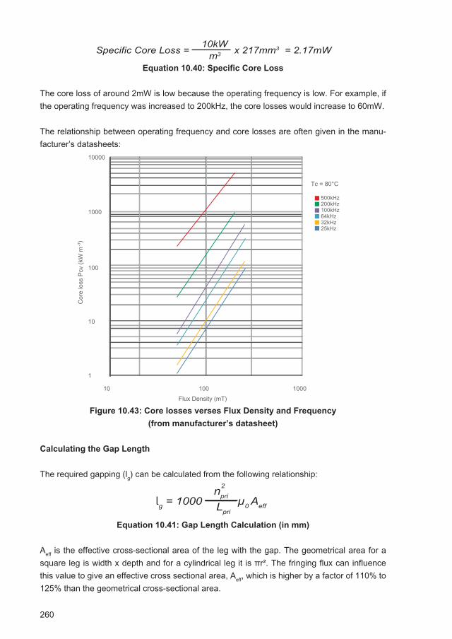
260
Equation 10.40: Specific Core Loss
The core loss of around 2mW is low because the operating frequency is low. For example, if the operating frequency was increased to 200kHz, the core losses would increase to 60mW.
The relationship between operating frequency and core losses are often given in the manu-facturer’s datasheets:
Figure 10.43: Core losses verses Flux Density and Frequency
(from manufacturer’s datasheet)
Calculating the Gap Length
The required gapping (lg) can be calculated from the following relationship:
Equation 10.41: Gap Length Calculation (in mm)
Aeff is the effective cross-sectional area of the leg with the gap. The geometrical area for a square leg is width x depth and for a cylindrical leg it is πr². The fringing flux can influence this value to give an effective cross sectional area, Aeff, which is higher by a factor of 110% to 125% than the geometrical cross-sectional area.
Specific Core Loss = x 217mm3 = 2.17mW 10kW
m3
1
10 100
10
100
1000
Tc = 80°C
10000
Cor
e lo
ss P
cv (k
W m
-3)
Flux Density (mT)
500kHz200kHz100kHz64kHz32kHz25kHz
1000
lg = 1000 µ0 AeffLpri
npri
2
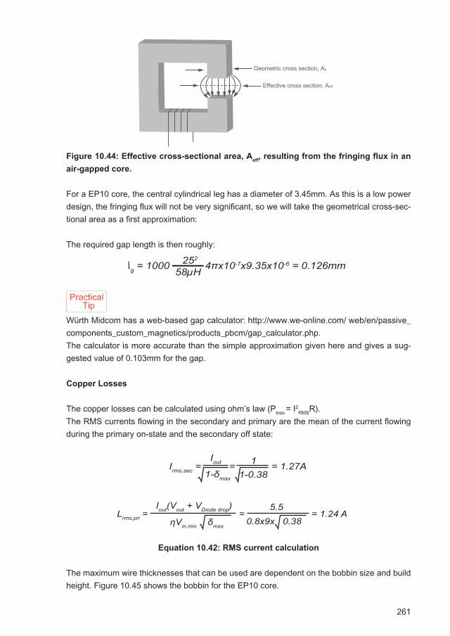
261
Figure 10.44: Effective cross-sectional area, Aeff
, resulting from the fringing flux in an
air-gapped core.
For a EP10 core, the central cylindrical leg has a diameter of 3.45mm. As this is a low power design, the fringing flux will not be very significant, so we will take the geometrical cross-sec-tional area as a first approximation:
The required gap length is then roughly:
Würth Midcom has a web-based gap calculator: http://www.we-online.com/ web/en/passive_components_custom_magnetics/products_pbcm/gap_calculator.php. The calculator is more accurate than the simple approximation given here and gives a sug-gested value of 0.103mm for the gap.
Copper Losses
The copper losses can be calculated using ohm’s law (Ploss = I2RMSR).
The RMS currents flowing in the secondary and primary are the mean of the current flowing during the primary on-state and the secondary off state:
Equation 10.42: RMS current calculation
The maximum wire thicknesses that can be used are dependent on the bobbin size and build height. Figure 10.45 shows the bobbin for the EP10 core.
Effective cross section, Aeff
Geometric cross section, Ae
lg = 1000 4πx10-7x9.35x10-6 = 0.126mm58µH
252
Practical Tip
Irms,sec = = = 1.27AIout
1-δmax
11-0.38
Lrms,pri = = = 1.24 A ƞVin,min δmax
Iout(Vout + VDiode drop)
0.8x9x 0.385.5
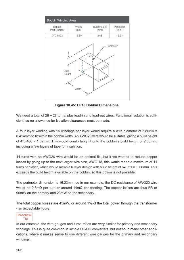
262
Figure 10.45: EP10 Bobbin Dimensions
We need a total of 28 + 28 turns, plus lead-in and lead-out wires. Functional Isolation is suffi-cient, so no allowance for isolation clearances must be made.
A four layer winding with 14 windings per layer would require a wire diameter of 5.80/14 = 0.414mm to fit within the bobbin width. An AWG20 wire would be suitable, giving a build height of 4*0.406 = 1.62mm. This would comfortably fit onto the bobbin’s build height of 2.08mm, including a few layers of tape for insulation.
14 turns with an AWG20 wire would be an optimal fit , but if we wanted to reduce copper losses by going up to the next larger wire size, AWG 18, this would mean a maximum of 11 turns per layer, which would mean a 6 layer design with build height of 6x0.51 = 3.06mm. This exceeds the build height available on the bobbin, so this option is not possible. The perimeter dimension is 16.23mm, so in our example, the DC resistance of AWG20 wire would be 0.5mΩ per turn or around 14mΩ per winding. The copper losses are thus I²R or 90mW on the primary and 23mW on the secondary.
The total copper losses are 45mW, or around 1% of the total power through the transformer - an acceptable figure.
In our example, the wire gauges and turns-ratios are very similar for primary and secondary windings. This is quite common in simple DC/DC converters, but not so in many other appli-cations, where it makes sense to use different wire gauges for the primary and secondary windings.
Perimeter
Bobbin Winding Area
BobbinPart Number
070-6052 5.80 2.08 16.23
Width(mm)
Build Height(mm)
Perimeter(mm)
Width
BuildHeight
Practical Tip
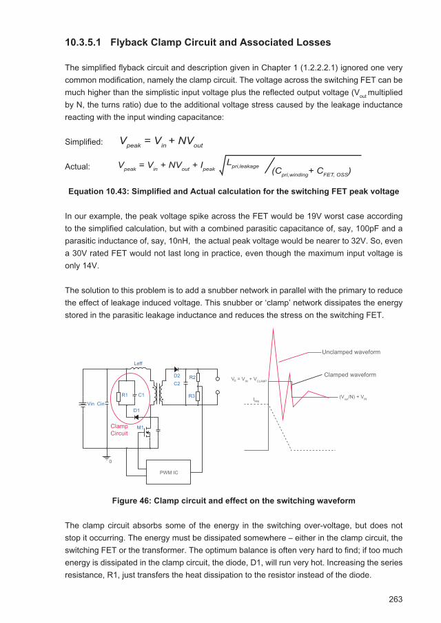
263
10.3.5.1 Flyback Clamp Circuit and Associated Losses
The simplified flyback circuit and description given in Chapter 1 (1.2.2.2.1) ignored one very common modification, namely the clamp circuit. The voltage across the switching FET can be much higher than the simplistic input voltage plus the reflected output voltage (Vout multiplied by N, the turns ratio) due to the additional voltage stress caused by the leakage inductance reacting with the input winding capacitance:
Simplified:
Actual:
Equation 10.43: Simplified and Actual calculation for the switching FET peak voltage
In our example, the peak voltage spike across the FET would be 19V worst case according to the simplified calculation, but with a combined parasitic capacitance of, say, 100pF and a parasitic inductance of, say, 10nH, the actual peak voltage would be nearer to 32V. So, even a 30V rated FET would not last long in practice, even though the maximum input voltage is only 14V.
The solution to this problem is to add a snubber network in parallel with the primary to reduce the effect of leakage induced voltage. This snubber or ‘clamp’ network dissipates the energy stored in the parasitic leakage inductance and reduces the stress on the switching FET.
Figure 46: Clamp circuit and effect on the switching waveform
The clamp circuit absorbs some of the energy in the switching over-voltage, but does not stop it occurring. The energy must be dissipated somewhere – either in the clamp circuit, the switching FET or the transformer. The optimum balance is often very hard to find; if too much energy is dissipated in the clamp circuit, the diode, D1, will run very hot. Increasing the series resistance, R1, just transfers the heat dissipation to the resistor instead of the diode.
Vpeak = Vin + NVout
Vpeak = Vin + NVout + Ipeak (Cpri,winding+ CFET, OSS)Lpri,leakage
Leff
0
C1
D1
M1
PWM IC
VD = VIN + VCLAMP
(Vout/N) + VINIPRI
D2C2
R2
R3R1
Vin Cin
Unclamped waveform
ClampCircuit
Clamped waveform
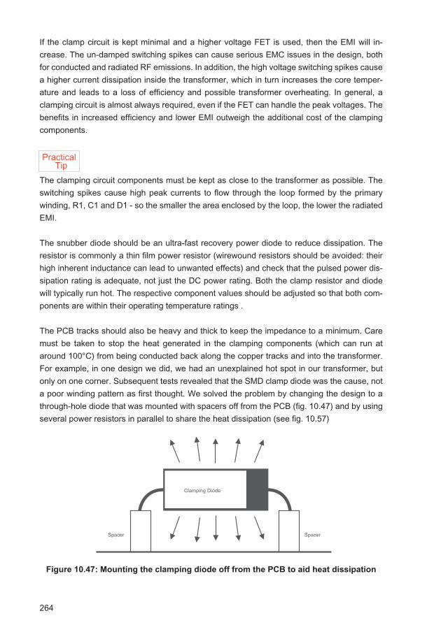
264
If the clamp circuit is kept minimal and a higher voltage FET is used, then the EMI will in-crease. The un-damped switching spikes can cause serious EMC issues in the design, both for conducted and radiated RF emissions. In addition, the high voltage switching spikes cause a higher current dissipation inside the transformer, which in turn increases the core temper-ature and leads to a loss of efficiency and possible transformer overheating. In general, a clamping circuit is almost always required, even if the FET can handle the peak voltages. The benefits in increased efficiency and lower EMI outweigh the additional cost of the clamping components.
The clamping circuit components must be kept as close to the transformer as possible. The switching spikes cause high peak currents to flow through the loop formed by the primary winding, R1, C1 and D1 - so the smaller the area enclosed by the loop, the lower the radiated EMI.
The snubber diode should be an ultra-fast recovery power diode to reduce dissipation. The resistor is commonly a thin film power resistor (wirewound resistors should be avoided: their high inherent inductance can lead to unwanted effects) and check that the pulsed power dis-sipation rating is adequate, not just the DC power rating. Both the clamp resistor and diode will typically run hot. The respective component values should be adjusted so that both com-ponents are within their operating temperature ratings .
The PCB tracks should also be heavy and thick to keep the impedance to a minimum. Care must be taken to stop the heat generated in the clamping components (which can run at around 100°C) from being conducted back along the copper tracks and into the transformer. For example, in one design we did, we had an unexplained hot spot in our transformer, but only on one corner. Subsequent tests revealed that the SMD clamp diode was the cause, not a poor winding pattern as first thought. We solved the problem by changing the design to a through-hole diode that was mounted with spacers off from the PCB (fig. 10.47) and by using several power resistors in parallel to share the heat dissipation (see fig. 10.57)
Figure 10.47: Mounting the clamping diode off from the PCB to aid heat dissipation
Practical Tip
Clamping Diode
Spacer Spacer
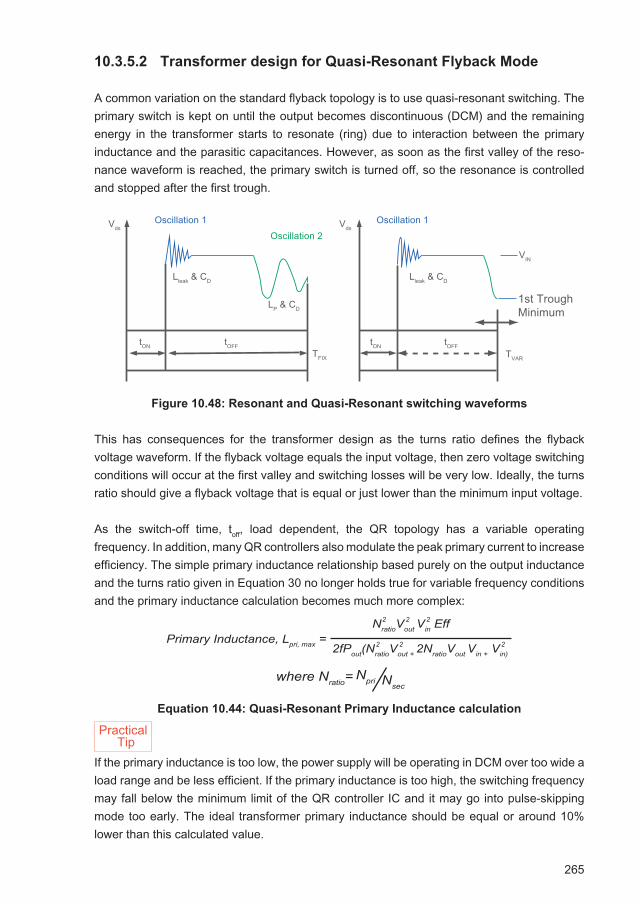
265
10.3.5.2 Transformer design for Quasi-Resonant Flyback Mode
A common variation on the standard flyback topology is to use quasi-resonant switching. The primary switch is kept on until the output becomes discontinuous (DCM) and the remaining energy in the transformer starts to resonate (ring) due to interaction between the primary inductance and the parasitic capacitances. However, as soon as the first valley of the reso-nance waveform is reached, the primary switch is turned off, so the resonance is controlled and stopped after the first trough.
Figure 10.48: Resonant and Quasi-Resonant switching waveforms
This has consequences for the transformer design as the turns ratio defines the flyback voltage waveform. If the flyback voltage equals the input voltage, then zero voltage switching conditions will occur at the first valley and switching losses will be very low. Ideally, the turns ratio should give a flyback voltage that is equal or just lower than the minimum input voltage.
As the switch-off time, toff, load dependent, the QR topology has a variable operating frequency. In addition, many QR controllers also modulate the peak primary current to increase efficiency. The simple primary inductance relationship based purely on the output inductance and the turns ratio given in Equation 30 no longer holds true for variable frequency conditions and the primary inductance calculation becomes much more complex:
Equation 10.44: Quasi-Resonant Primary Inductance calculation
If the primary inductance is too low, the power supply will be operating in DCM over too wide a load range and be less efficient. If the primary inductance is too high, the switching frequency may fall below the minimum limit of the QR controller IC and it may go into pulse-skipping mode too early. The ideal transformer primary inductance should be equal or around 10% lower than this calculated value.
VdsOscillation 1Oscillation 1
Oscillation 2
VIN
Vds
tON tOFFtON tOFFTVAR
1st TroughMinimum
Lleak & CDLleak & CD
LP & CD
TFIX
Practical Tip
Primary Inductance, Lpri, max = NratioVout Vin Eff22 2
2fPout(NratioVout + 2NratioVout Vin + Vin)2 22
where Nratio= Npri Nsec

266
The I²R losses in the windings can be calculated using the same relationships given in the section on flyback transformer design. The peak magnetising current in the transformer is inversely dependent on the inductance, so a high primary inductance is beneficial:
Equation 10.45: QR Converter Peak Primary current calculation
If we now compare the two transformer designs for equivalent flyback and forward topologies:
Value Flyback Forward
Core size EP10 P9/5Primary Winding 28 turns 12 turnsSecondary Winding 28 turns 20 turnsReset Winding none 12 turnsTOTAL 56t 44t
Table 10.4: Comparison of flyback and forward transformer designs
Although the forward converter design needs fewer turns it requires three separate windings, which is more time-consuming to assemble. This is why the flyback is often preferred over the forward topology for low power designs. However, for high current designs, the forward converter continuous transfer of energy versus the pulsating transfer of the flyback topology make the extra assembly work needed for the transformer design worthwhile.
10.4 Whole turns and fractional turns
For a simple transformer designs with a single output, the turns ratio can easily be chosen to have whole numbers of turns on the primary and secondary windings. However, for multiple output transformers, the turns ratio calculation can become tricky.
For example, if we take our flyback design with a single 5V output and want to add an auxiliary output of 1.5V then the addition winding will have the following number of turns:
But how do you wind half of a turn? The trick is to use an EE core and add a whole winding around one leg of the core instead of around the centre. As the magnetic flux is symmetrically divided throughout the core, half will flow through one leg and half through the other, so the full turn around one leg acts as a half turn:
Naux= Nsec Vout + VDiode drop
= 29. Vaux + VDiode drop
5.0+0.5
1.5+0.5= 10.5 turns
Ipk mag = Lpri fVin,max δmax
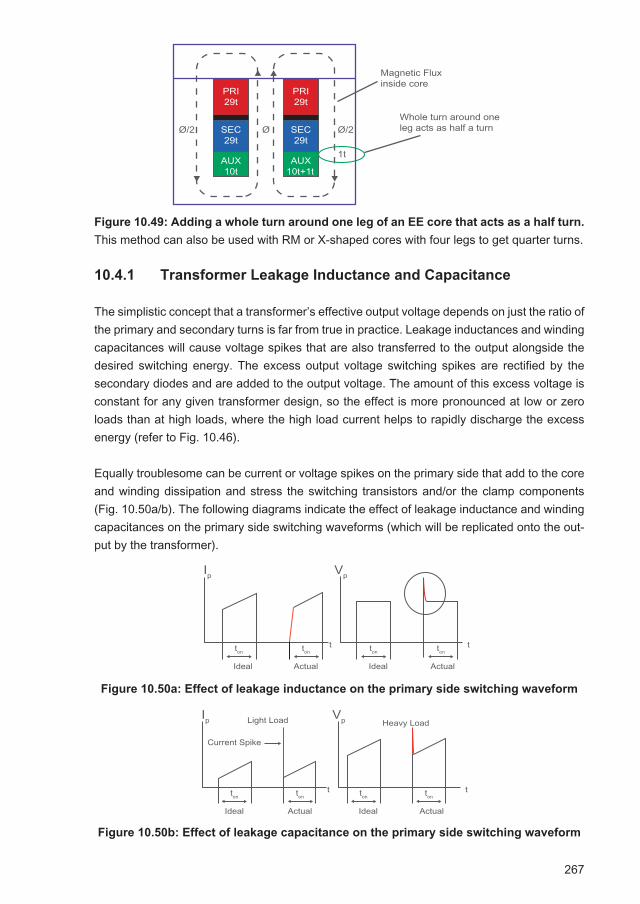
267
Figure 10.49: Adding a whole turn around one leg of an EE core that acts as a half turn.
This method can also be used with RM or X-shaped cores with four legs to get quarter turns.
10.4.1 Transformer Leakage Inductance and Capacitance
The simplistic concept that a transformer’s effective output voltage depends on just the ratio of the primary and secondary turns is far from true in practice. Leakage inductances and winding capacitances will cause voltage spikes that are also transferred to the output alongside the desired switching energy. The excess output voltage switching spikes are rectified by the secondary diodes and are added to the output voltage. The amount of this excess voltage is constant for any given transformer design, so the effect is more pronounced at low or zero loads than at high loads, where the high load current helps to rapidly discharge the excess energy (refer to Fig. 10.46).
Equally troublesome can be current or voltage spikes on the primary side that add to the core and winding dissipation and stress the switching transistors and/or the clamp components (Fig. 10.50a/b). The following diagrams indicate the effect of leakage inductance and winding capacitances on the primary side switching waveforms (which will be replicated onto the out-put by the transformer).
Figure 10.50a: Effect of leakage inductance on the primary side switching waveform
Figure 10.50b: Effect of leakage capacitance on the primary side switching waveform
PRI29t
SEC29t
AUX10t
PRI29t
SEC29t
AUX10t+1t
Ø/2
Magnetic Fluxinside core
Whole turn around one leg acts as half a turnØ/2
1t
Ø
Ip
ton
Ideal Actual ActualIdeal
ton tontt ton
Vp
Ip
ton
Current Spike
Light Load Heavy Load
Ideal Actual ActualIdeal
ton tontt ton
Vp
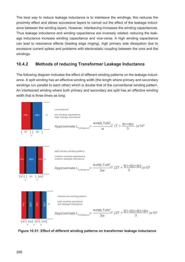
268
The best way to reduce leakage inductance is to interleave the windings; this reduces the proximity effect and allows successive layers to cancel out the effect of the leakage induct-ance between the winding layers. However, interleaving increases the winding capacitances. Thus leakage inductance and winding capacitance are inversely related: reducing the leak-age inductance increase winding capacitance and vice-versa. A high winding capacitance can lead to resonance effects (leading edge ringing), high primary side dissipation due to excessive current spikes and problems with electrostatic coupling between the core and the windings.
10.4.2 Methods of reducing Transformer Leakage Inductance
The following diagram indicates the effect of different winding patterns on the leakage induct-ance. A split winding has an effective winding width (the length where primary and secondary windings run parallel to each other) which is double that of the conventional winding pattern. An interleaved winding where both primary and secondary are split has an effective winding width that is three times as long:
Figure 10.51: Effect of different winding patterns on transformer leakage inductance
PRI SEC
conventional:
low winding capacitancehigh leakage inductance
split primary winding pattern:
medium winding capacitancemedium leakage inductance
w
B2B1
T
PRI PRISEC w
B2 B3B1T
T T T
T
interleaved winding pattern:
high winding cpacitancelow leakage inductancePR
I
PR
I
SE
C
SE
C w
B2 B3 B4B1
Approximate LLeakage.pri= w4πMLTxN2
pri
3B1+B2(T + )x109
Approximate LLeakage.pri= 2w4πMLTxN2
pri
3B1+B2+B3(2T + )x109
Approximate LLeakage.pri= 3w4πMLTxN2
pri
3B1+B2+B3+B4(3T + )x109
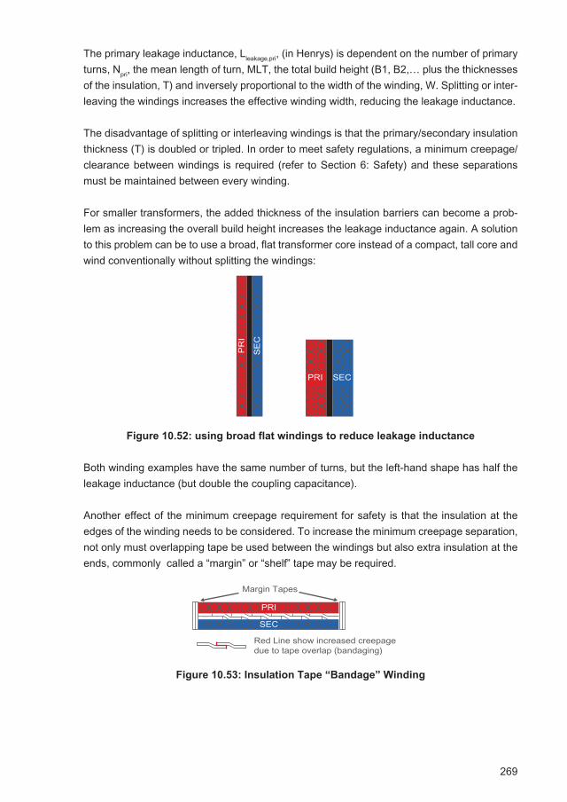
269
The primary leakage inductance, Lleakage,pri, (in Henrys) is dependent on the number of primary turns, Npri, the mean length of turn, MLT, the total build height (B1, B2,… plus the thicknesses of the insulation, T) and inversely proportional to the width of the winding, W. Splitting or inter-leaving the windings increases the effective winding width, reducing the leakage inductance.
The disadvantage of splitting or interleaving windings is that the primary/secondary insulation thickness (T) is doubled or tripled. In order to meet safety regulations, a minimum creepage/clearance between windings is required (refer to Section 6: Safety) and these separations must be maintained between every winding.
For smaller transformers, the added thickness of the insulation barriers can become a prob-lem as increasing the overall build height increases the leakage inductance again. A solution to this problem can be to use a broad, flat transformer core instead of a compact, tall core and wind conventionally without splitting the windings:
Figure 10.52: using broad flat windings to reduce leakage inductance
Both winding examples have the same number of turns, but the left-hand shape has half the leakage inductance (but double the coupling capacitance).
Another effect of the minimum creepage requirement for safety is that the insulation at the edges of the winding needs to be considered. To increase the minimum creepage separation, not only must overlapping tape be used between the windings but also extra insulation at the ends, commonly called a “margin” or “shelf” tape may be required.
Figure 10.53: Insulation Tape “Bandage” Winding
PR
I
SE
C
PRI SEC
PRI
SEC
Margin Tapes
Red Line show increased creepagedue to tape overlap (bandaging)
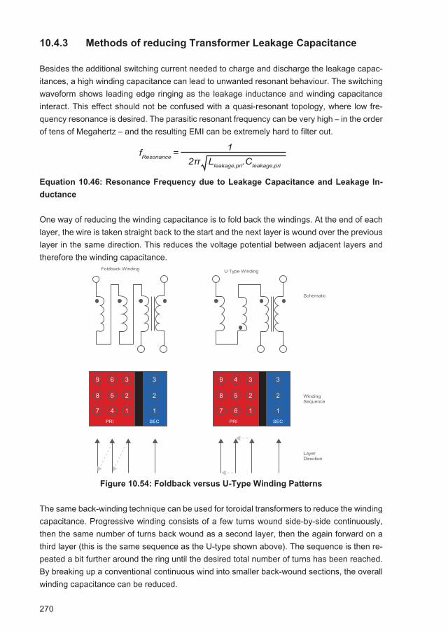
270
10.4.3 Methods of reducing Transformer Leakage Capacitance
Besides the additional switching current needed to charge and discharge the leakage capac-itances, a high winding capacitance can lead to unwanted resonant behaviour. The switching waveform shows leading edge ringing as the leakage inductance and winding capacitance interact. This effect should not be confused with a quasi-resonant topology, where low fre-quency resonance is desired. The parasitic resonant frequency can be very high – in the order of tens of Megahertz – and the resulting EMI can be extremely hard to filter out.
Equation 10.46: Resonance Frequency due to Leakage Capacitance and Leakage In-
ductance
One way of reducing the winding capacitance is to fold back the windings. At the end of each layer, the wire is taken straight back to the start and the next layer is wound over the previous layer in the same direction. This reduces the voltage potential between adjacent layers and therefore the winding capacitance.
Figure 10.54: Foldback versus U-Type Winding Patterns
The same back-winding technique can be used for toroidal transformers to reduce the winding capacitance. Progressive winding consists of a few turns wound side-by-side continuously, then the same number of turns back wound as a second layer, then the again forward on a third layer (this is the same sequence as the U-type shown above). The sequence is then re-peated a bit further around the ring until the desired total number of turns has been reached. By breaking up a conventional continuous wind into smaller back-wound sections, the overall winding capacitance can be reduced.
fResonance = 2π Lleakage,pri.Cleakage,pri
1
Schematic
WindingSequence
LayerDirection
Foldback Winding U Type Winding
PRI SEC
1
2
3
1
2
3
4
5
6
7
8
9
PRI SEC
1
2
3
1
2
3
6
5
4
7
8
9

271
Figure 10.55: Progressive Winding Pattern (often used with toroidal cores)
10.5 Transformer Core Temperature
Measuring the core temperature can be done by attaching a thermocouple to the winding bobbin before the transformer windings are wound. This gives a fairly accurate measurement of the internal core temperature, but voltage gradients within the windings can still mean that the hottest spot is not necessarily in the middle of bobbin.
The voltages generated within the windings can be very high – electrostatic effects can gener-ate high potentials within the winding and the high dv/dt voltage spikes can be coupled across to the thermocouple sensor even though it is insulated from the windings. The thermocouple sensor amplifier is effectively a low impedance path to ground and can be easily damaged by spikes and energy discharges. The solution is to use only isolated thermocouple amplifiers to measure transformer core temperatures.
An alternative way to check the transformer temperature is to use a thermal imaging camera. They are not cheap, but are considerably cheaper than they used to be, thanks to room tem-perature infrared sensors that do not need to be cryogenically cooled. Purchase or hire the highest resolution that you can afford, as the devil is always in the detail. Adding a x2 lens is also a good investment.
A good quality IR camera will also allow videos to be made. This is a very useful feature, as the application can be turned on at room temperature and the localized hot spots easily found before the temperature differences all even out at the final operating temperature.
Cross-section
Back windContinuous winding
Core
Back WindExpanded View Side View
Practical Tip
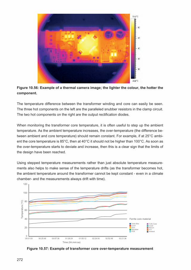
272
Figure 10.56: Example of a thermal camera image; the lighter the colour, the hotter the
component.
The temperature difference between the transformer winding and core can easily be seen. The three hot components on the left are the paralleled snubber resistors in the clamp circuit. The two hot components on the right are the output rectification diodes.
When monitoring the transformer core temperature, it is often useful to step up the ambient temperature. As the ambient temperature increases, the over-temperature (the difference be-tween ambient and core temperature) should remain constant. For example, if at 25°C ambi-ent the core temperature is 85°C, then at 40°C it should not be higher than 100°C. As soon as the over-temperature starts to deviate and increase, then this is a clear sign that the limits of the design have been reached.
Using stepped temperature measurements rather than just absolute temperature measure-ments also helps to make sense of the temperature drifts (as the transformer becomes hot, the ambient temperature around the transformer cannot be kept constant - even in a climate chamber- and the measurements always drift with time).
Figure 10.57: Example of transformer core over-temperature measurement
0
20
40
60
80
100
120
00:01:00 00:25:48 00:57:36 01:26:24 01:55:12 02:24:00 02:52:48 03:21:36
Tem
pera
ture
(°C
)
Time (hh:mm:ss)
Ferrite core material
Trafo-WireCout1DoutRsnubberPCB
Trafo-CaseCout2RshuntFETAmbient

273
The maximum allowed ambient temperature is simply when the transformer core has reached its maximum limit at worst case input voltage and full load. The transformer core over-tem-perature limit is dependent on its grade, but can be as low as 105°C depending on the type of magnet wire and insulation material grade used. Table 10.5 shows the common system class limits. Any further increase in ambient temperature has to be compensated for by derating the load to reduce the dissipated heat in the core.
Equation 10.47: Max Ambient temperature calculation
Transformer Grade(Insulation Tempera-ture Class)
MaximumTemperature Rise above ambient
Maximum core temperature during normal operation
Maximum core temperature during fault conditions
Class A 60°C 105°C 150°CClass E 75°C 120°C 165°CClass B 80°C 130°C 175°CClass F 100°C 155°C 190°C
Table 10.5: Common Transformer Classes
A certain amount of safety margin has to be allowed for so that the transformer does not fail early in normal operation.
Figure 10.58: Transformer Temperature Headroom allowances
*The hot spot allowance is a factor to allow for misalignment of the temperature sensor with the hottest part of the transformer. It varies between 5°C for a compact design to 30°C for a large transformer.
At a maximum ambient operating temperature of 85°C, a self-warming temperature rise of 25°C and a hot-spot allowance of 5°C would give a safety factor margin of 15°C for a Class B transformer.
Tambient,max = Tcore,max - Tdiss
AVG. TEMP. RISE
AMBIENT TEMP.
OVERALLTEMPERATURE
INSULATIONSYSTEMTEMP.RATING
SAFETY FACTOR
HOT SPOT ALLOWANCE* RISE
274
10.6 Finalizing the Transformer Design: EMI
Putting it simply, Electromagnetic Compatibility (EMC) is the bane of a transformer designer’s life. So many designs meet all of the power, efficiency and temperature requirements, only to fail during emissions testing. The differences between a fully compliant circuit and a failed prototype can be trivial or extremely complex – and there is no magic formula that offers a solution - only guidelines which if not followed will most likely make things worse.
Part of the reason for this lies often with the way we test for EMC. Broadband antennae or conducted emissions spectrum analysers pick up the overall signal including all of the under-lying elements, but cannot identify which component generates which part of the interference. Thus if three different components are all generating about the same levels of interference, solving two out of the three issues will not affect the overall signal very much. Only when all three sources are corrected, will the interference suddenly decrease.
What this means in practice, is that even if a circuit or component change is made which is useful, it may be overlooked because there appears to be no effect. Only when a different, completely unrelated change is also made does the benefit of the first change show through. This makes solving EMC issues by trial-and-error practically impossible.
So what are the guidelines that will give the design a glimmer of hope of meeting the EMC regulations? First and foremost: if you have a design that passes: use it again for as many other applications as possible. But, if you have to start from scratch, here are the basics:
1: The positioning of the transformer can affect adjacent parts and induce EMI. Especially gapped cores can radiate a strong enough field to induce conducted EMI in surrounding com-ponents. Position the transformer away from surrounding components or potential antennas such as PCB tracks, connectors or non-grounded metal parts.
2: Reducing the flux density reduces the radiated field. A larger core area with more turns will radiate less. Sometimes, going up to the next size transformer core dimension can solve EMC problems when all else fails.
3: Add grounded EM shielding to the transformer to reduce eddy current radiation, electrostat-ic build-up and high frequency coupling between primary and secondary.
4: For flyback designs, keep the clamp loop small and the FET drain connection short.
Point 3 deserves more explanation. There are two types of shield: a “belly-band” which is a single turn of foil tape or a few turns of wire wrapped around the outside of the transformer winding and connected to earth and to the core. It is shorted to itself, so stray eddy currents will be trapped and contained within the shield. If the transformer can be would so that the out-ermost layer of the winding is connected to ground, a belly-band shield may not be required, but core grounding can still be required.
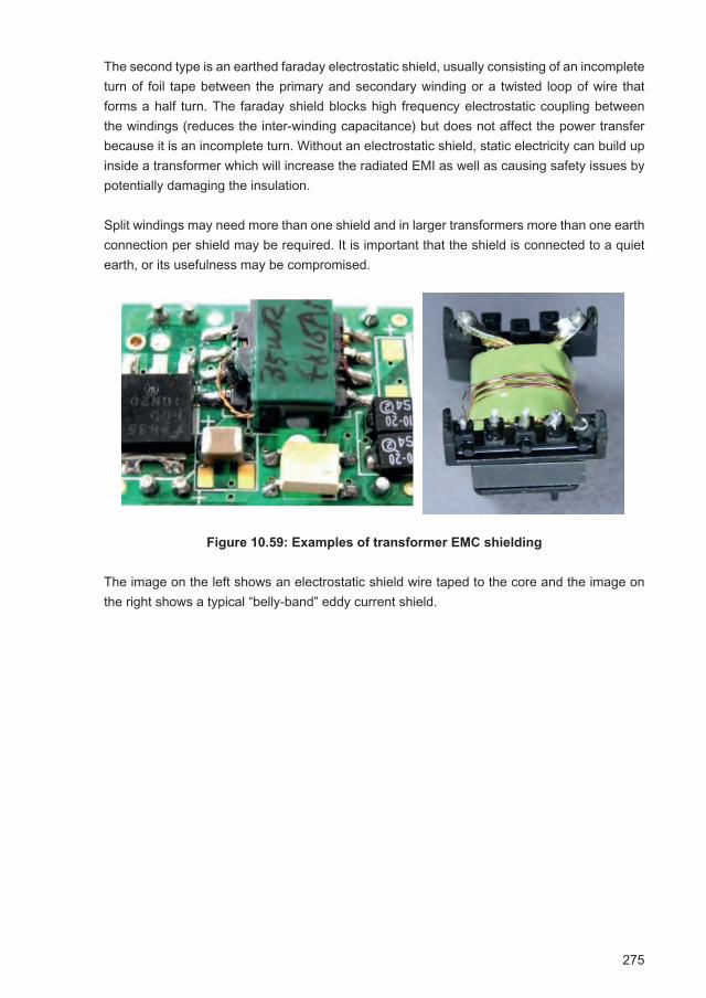
275
The second type is an earthed faraday electrostatic shield, usually consisting of an incomplete turn of foil tape between the primary and secondary winding or a twisted loop of wire that forms a half turn. The faraday shield blocks high frequency electrostatic coupling between the windings (reduces the inter-winding capacitance) but does not affect the power transfer because it is an incomplete turn. Without an electrostatic shield, static electricity can build up inside a transformer which will increase the radiated EMI as well as causing safety issues by potentially damaging the insulation.
Split windings may need more than one shield and in larger transformers more than one earth connection per shield may be required. It is important that the shield is connected to a quiet earth, or its usefulness may be compromised.
Figure 10.59: Examples of transformer EMC shielding
The image on the left shows an electrostatic shield wire taped to the core and the image on the right shows a typical “belly-band” eddy current shield.
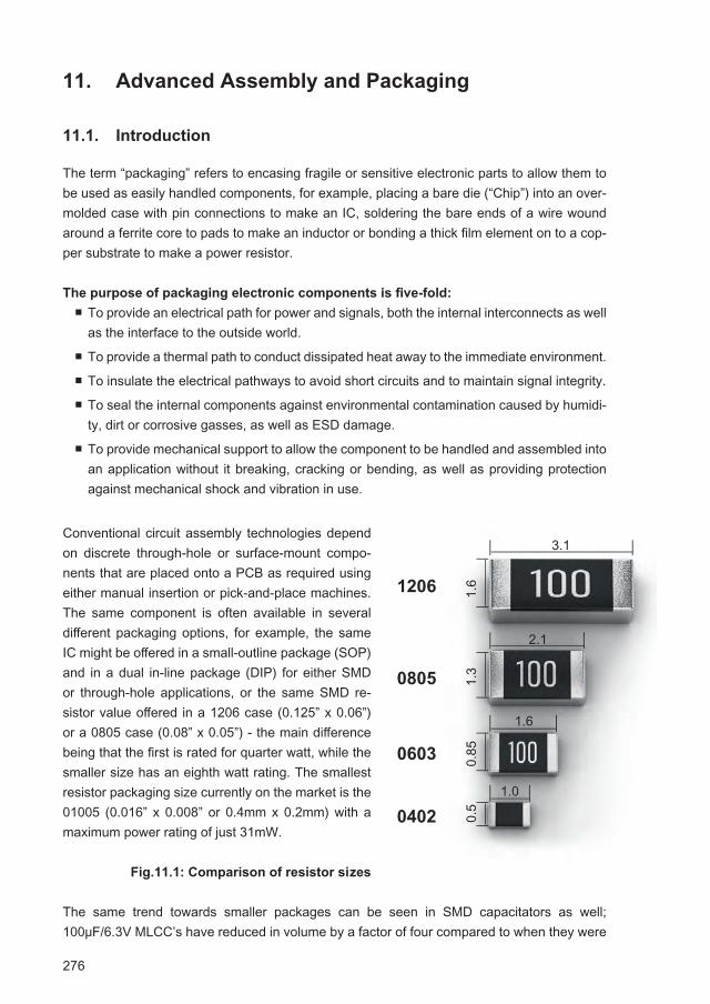
276
11. Advanced Assembly and Packaging
11.1. Introduction
The term “packaging” refers to encasing fragile or sensitive electronic parts to allow them to be used as easily handled components, for example, placing a bare die (“Chip”) into an over-molded case with pin connections to make an IC, soldering the bare ends of a wire wound around a ferrite core to pads to make an inductor or bonding a thick fi lm element on to a cop-per substrate to make a power resistor.
The purpose of packaging electronic components is fi ve-fold:
■ To provide an electrical path for power and signals, both the internal interconnects as well as the interface to the outside world.
■ To provide a thermal path to conduct dissipated heat away to the immediate environment.
■ To insulate the electrical pathways to avoid short circuits and to maintain signal integrity.
■ To seal the internal components against environmental contamination caused by humidi-ty, dirt or corrosive gasses, as well as ESD damage.
■ To provide mechanical support to allow the component to be handled and assembled into an application without it breaking, cracking or bending, as well as providing protection against mechanical shock and vibration in use.
Conventional circuit assembly technologies depend on discrete through-hole or surface-mount compo-nents that are placed onto a PCB as required using either manual insertion or pick-and-place machines. The same component is often available in several diff erent packaging options, for example, the same IC might be off ered in a small-outline package (SOP) and in a dual in-line package (DIP) for either SMD or through-hole applications, or the same SMD re-sistor value off ered in a 1206 case (0.125” x 0.06”) or a 0805 case (0.08” x 0.05”) - the main diff erence being that the fi rst is rated for quarter watt, while the smaller size has an eighth watt rating. The smallest resistor packaging size currently on the market is the 01005 (0.016” x 0.008” or 0.4mm x 0.2mm) with a maximum power rating of just 31mW.
Fig.11.1: Comparison of resistor sizes
The same trend towards smaller packages can be seen in SMD capacitators as well; 100μF/6.3V MLCC’s have reduced in volume by a factor of four compared to when they were
3.1
1206
0805
0603
0402
1.6
1.3
0.85
0.5
2.1
1.6
1.0
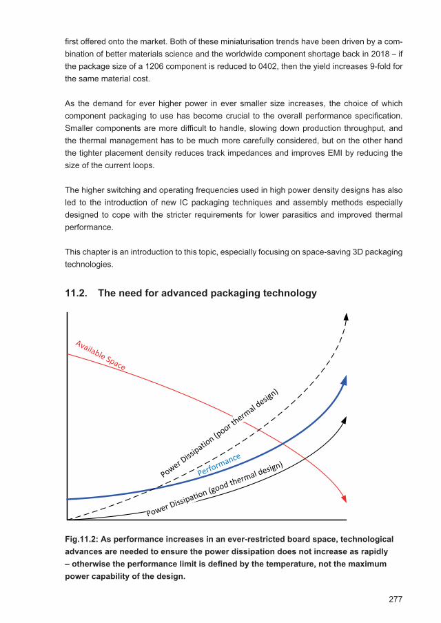
277
first offered onto the market. Both of these miniaturisation trends have been driven by a com-bination of better materials science and the worldwide component shortage back in 2018 – if the package size of a 1206 component is reduced to 0402, then the yield increases 9-fold for the same material cost.
As the demand for ever higher power in ever smaller size increases, the choice of which component packaging to use has become crucial to the overall performance specification. Smaller components are more difficult to handle, slowing down production throughput, and the thermal management has to be much more carefully considered, but on the other hand the tighter placement density reduces track impedances and improves EMI by reducing the size of the current loops.
The higher switching and operating frequencies used in high power density designs has also led to the introduction of new IC packaging techniques and assembly methods especially designed to cope with the stricter requirements for lower parasitics and improved thermal performance.
This chapter is an introduction to this topic, especially focusing on space-saving 3D packaging technologies.
11.2. The need for advanced packaging technology
Fig.11.2: As performance increases in an ever-restricted board space, technological
advances are needed to ensure the power dissipation does not increase as rapidly
– otherwise the performance limit is defined by the temperature, not the maximum
power capability of the design.
Available Space
Power Dissipation (good thermal design)Performance
Power Dissi
pation (poor th
ermal desig
n)

278
The object of high power density designs is to reduce the physical size of the design without the internal components overheating. Unfortunately, these two requirements are often mu-tually exclusive. One way to reduce the physical size of the components is to increase the switching frequency - if we take the simple buck converter, the required inductor value and smoothing capacitor values are inversely proportional to the frequency (refer to Eq. 10.13 and Eq. 10.14 in Chapter 10), so doubling the switching frequency with allow the designer to halve the sizes of both the inductor and capacitor. However, the power dissipated in the switching transistor due to the charging and discharging of the gate capacitance will also double if the switching frequency is doubled (refer to AC/DC Book of Knowledge, Eq. 6.1 in Chapter 6) – so increasing the operating frequency allows the passive components to be made smaller, but makes the switching transistors run hotter.
So there is a limit to how fast the switching frequency can be increased – the higher the fre-quency, the smaller the inductor and smoothing capacitor, but the higher the power dissipa-tion. In addition, losses due to parasitic inductances and capacitances become more critical – especially in the gate driver circuit and in the layout.
Given that the choice of the switching transistor technology in the controller IC is fixed (say, MOSFETs for cost and availability reasons) then alone the choice of the IC packaging can improve the overall performance significantly:
■ A smaller controller IC package has a lower thermal impedance as the physical path from the source of heat (the transistor junction) to the surface is shorter (lower ƟBC - refer to Fig 3.17 in Chapter 3)
■ A smaller package has shorter power connections which reduces their inductance which is a significant cause of internal power dissipation at higher frequencies. For example, a power transistor switching 24W at 1 MHz might dissipate over 2W in a SO-8 package, while the same transistor in a proprietary DirectFET® package would dissipate only 0.6W, simply due to lower parasitic inductance losses in the power connections.1
■ A smaller package has lower mass which increases the reliability of the solder connec-tions in harsh industrial environments.
For a complete power supply element such as a DC/DC converter, the packaging options for the finished product also effect the overall performance, even if the output power remains the same.
_____________________ 1 https://epc-co.com/epc/DesignSupport/Chip-ScalePackaging.aspx, Figure 3

279
11.3. Packaging technologies
11.3.1. Through hole
Fig. 11.3: Example of a through hole pin package
Through-hole is still a popular packaging option for power transistors (e.g. TO-220) and the majority of isolated DC/DC converters. The pins soldered through the PCB makes a very robust electrical connection that is highly resistant to mechanical shock and vibration and the relatively large pin spacing means that the danger of arc-over is reduced even in dirty, damp or high humidity industrial environments. For DC/DC converters with higher input or output currents a standard 1mm pin can carry up to 12A and the low impedance of a through hole pin ensures a solid power ground connection.
Finally, it should not be underestimated that many product assembly processes still include hand soldering of cables, heavy duty connectors, transistors pre-mounted on heatsinks or DC/DC converters onto an PCB already populated with SMD parts and it is much easier to manual solder through hole parts without thermally stressing the other components already mounted on the board.
11.3.2. Conventional SMD (Gull wing pins)
Fig.11.4: Gull wing SMD package
280
Surface mount devices are now so ubiquitous that it is often difficult to find an equivalent part with through-hole pinning and the component is only readily available as SMD. For many DC/DC converters and controller ICs, the conventional gull wing SMD pinned package is the most popular packaging style. The fact that all of the connections are around the edges of the package makes it simple for an Automated Optical Inspection (AOI) camera to be used at the end of an SMD production line to automatically check the quality of the solder joints. If any solder joints are not perfect, individual pins can be manually re-soldered in a repair station which significantly increases the overall yield and reduces waste.
The gull-wing pins are embedded into an injection-moulded or overmoulded plastic case which makes for very robust pins that are well sealed against moisture ingress. The internal connections are typically made via wire bonds – a special robot ultrasonically bonds a gold/copper alloy or aluminium wire to a pad on the die chip and then feeds out the wire as it moves in an arc to the appropriate pin end where it is again ultrasonically welded before the wire is cut off. This is repeated for each connection required (repeated several times if the connection is a high current one)
Fig. 11.5: Wire bonding
The use of loops in the wire allows for any thermal expansion or contraction without stressing the bonds. Wire bonding is very flexible as the wire loops can be made as short or as long as needed and multiple dies in the same package can also be connected this way.
281
Recom’s RxxCTxx isolated DC/DC converter is constructed using this technique:
Fig.11.6: X-ray of the RxxCTxx isolated DC/DC converter chowing the wire bond inter-
connections across multiple dies as well as to the external pins.
11.3.3. QFN Chip carrier
Fig. 11.7: QFN package
Quad Flat No-lead (QFN) packaging eliminates the pins altogether and uses an internal cop-per substrate and exposed solder lands for the electrical connections. It is commonly used for controller and logic ICs which need many external signal connections as all four edges of
282
the package can be used. The large square copper pad underneath the die can also be made exposed to allow a good thermal connection to the PCB.
The drawing above (Fig. 11.7) shows a QFN package with bond wires connecting connection pads on the top of the IC chip to the external solder lands which have been milled away at the edges to make “wettable flanks” – meaning that the lands extend up over the sides and there is a step milled out in the pads. This adds cost but addresses one of the biggest problems with QFN packages which is validating the reflow solder joints.
Fig.11.8: Wettable flank solder joint
Wettable side flanks draw up the liquid solder meniscus to create a solder filet that can be easily inspected using standard AOI machines. Automotive grade packages typically have this feature as it is an accepted method of monitoring the solder joints as part of the quality control requirements.
11.3.4. Solder Ball
Fig.11.9: Diagrammatic image of a BGA Package.
Package Body
Package Lead
Solder
PCB Contact
PCB
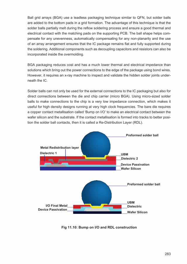
283
Ball grid arrays (BGA) use a leadless packaging technique similar to QFN, but solder balls are added to the bottom pads in a grid formation. The advantage of this technique is that the solder balls partially melt during the reflow soldering process and ensure a good thermal and electrical contact with the matching pads on the supporting PCB. The ball shape helps com-pensate for any unevenness, automatically compensating for any non-planarity and the use of an array arrangement ensures that the IC package remains flat and fully supported during the soldering. Additional components such as decoupling capacitors and resistors can also be incorporated inside the overmolding.
BGA packaging reduces cost and has a much lower thermal and electrical impedance than solutions which bring out the power connections to the edge of the package using bond wires. However, it requires an x-ray machine to inspect and validate the hidden solder joints under-neath the IC.
Solder balls can not only be used for the external connections to the IC packaging but also for direct connections between the die and chip carrier (micro BGA). Using micro-sized solder balls to make connections to the chip is a very low impedance connection, which makes it useful for high density designs running at very high clock frequencies. The bare die requires a copper contact metallisation called ‘Bump on I/O’ to make an electrical contact between the wafer silicon and the substrate. If the contact metallisation is formed into tracks to better posi-tion the solder ball contacts, then it is called a Re-Distribution Layer (RDL).
Fig 11.10: Bump on I/O and RDL construction
Wafer SiliconDevice Passivation
Metal Redistribution layer
Dielectric 2
Dielectric 1 UBM
Preformed solder ball
Wafer SiliconDevice Passivation
I/O Final Metal DielectricUBM
Preformed solder ball

284
Fig 11.11: X-Ray of the of the RPMB series controller IC. The micro BGA connections
and the RDL metallisation can be clearly seen.
Solder ball connections avoid the need for wire bonding, but then the chip needs to be turned over so that the connection pads are now on the bottom – hence the name fl ip chip.
Power devices such as DC/DC converters require fewer connections than logic ICs but need higher current carrying capability, so the ceramic IC substrate can be replaced by a copper leadframe that has been stamped out to make the appropriate electrical connections. The assembly technique is then called Flip-Chip On Leadframe (FCOL).
Fig. 11.12: Diagrammatic view of the RPX-2.5 converter with fl ip-chip on leadframe
construction
11.4. PCB substrate technology
The printed circuit board (PCB) has evolved from a simple non-conducting fl at substrate upon which to mount components to a high tech product in its own right, going from essentially a 2D to a complex 3D construction with up to 18 layers. In practice, however, cost constraints mean that two layer or four layer boards are still the most common for industrial-grade DC/DC converter construction.
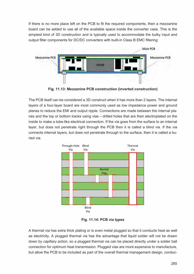
285
If there is no more place left on the PCB to fit the required components, then a mezzanine board can be added to use all of the available space inside the converter case. This is the simplest kind of 3D construction and is typically used to accommodate the bulky input and output filter components for DC/DC converters with built-in Class B EMC filtering:
Fig. 11.13: Mezzanine PCB construction (inverted construction)
The PCB itself can be considered a 3D construct when it has more than 2 layers. The internal layers of a four-layer board are most commonly used as low impedance power and ground planes to reduce the EMI and output ripple. Connections are made between the internal pla-nes and the top or bottom tracks using vias – drilled holes that are then electroplated on the inside to make a tube-like electrical connection. If the via goes from the surface to an internal layer, but does not penetrate right through the PCB then it is called a blind via. If the via connects internal layers, but does not penetrate through to the surface, then it is called a bu-ried via.
Fig. 11.14: PCB via types
A thermal via has extra thick plating or is even metal plugged so that it conducts heat as well as electricity. A plugged thermal via has the advantage that liquid solder will not be drawn down by capillary action, so a plugged thermal via can be placed directly under a solder ball connection for optimum heat transmission. Plugged vias are more expensive to manufacture, but allow the PCB to be included as part of the overall thermal management design, conduc-
Through-HoleVia
BlindVia
BuriedVias
ThermalVia
BlindVia
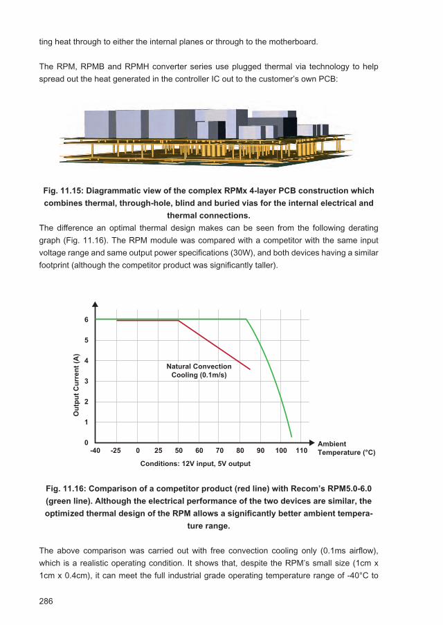
286
ting heat through to either the internal planes or through to the motherboard.
The RPM, RPMB and RPMH converter series use plugged thermal via technology to help spread out the heat generated in the controller IC out to the customer’s own PCB:
Fig. 11.15: Diagrammatic view of the complex RPMx 4-layer PCB construction which
combines thermal, through-hole, blind and buried vias for the internal electrical and
thermal connections.
The diff erence an optimal thermal design makes can be seen from the following derating graph (Fig. 11.16). The RPM module was compared with a competitor with the same input voltage range and same output power specifi cations (30W), and both devices having a similar footprint (although the competitor product was signifi cantly taller).
Fig. 11.16: Comparison of a competitor product (red line) with Recom’s RPM5.0-6.0
(green line). Although the electrical performance of the two devices are similar, the
optimized thermal design of the RPM allows a signifi cantly better ambient tempera-
ture range.
The above comparison was carried out with free convection cooling only (0.1ms airfl ow), which is a realistic operating condition. It shows that, despite the RPM’s small size (1cm x 1cm x 0.4cm), it can meet the full industrial grade operating temperature range of -40°C to
Ou
tpu
t C
urr
en
t (A
)
AmbientTemperature (°C)
Conditions: 12V input, 5V output
Natural ConvectionCooling (0.1m/s)
-40 -25 0 25 50 60 70 80 90 100 1100
1
2
3
4
5
6
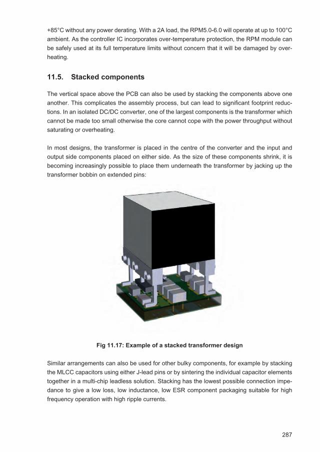
287
+85°C without any power derating. With a 2A load, the RPM5.0-6.0 will operate at up to 100°C ambient. As the controller IC incorporates over-temperature protection, the RPM module can be safely used at its full temperature limits without concern that it will be damaged by over-heating.
11.5. Stacked components
The vertical space above the PCB can also be used by stacking the components above one another. This complicates the assembly process, but can lead to significant footprint reduc-tions. In an isolated DC/DC converter, one of the largest components is the transformer which cannot be made too small otherwise the core cannot cope with the power throughput without saturating or overheating.
In most designs, the transformer is placed in the centre of the converter and the input and output side components placed on either side. As the size of these components shrink, it is becoming increasingly possible to place them underneath the transformer by jacking up the transformer bobbin on extended pins:
Fig 11.17: Example of a stacked transformer design
Similar arrangements can also be used for other bulky components, for example by stacking the MLCC capacitors using either J-lead pins or by sintering the individual capacitor elements together in a multi-chip leadless solution. Stacking has the lowest possible connection impe-dance to give a low loss, low inductance, low ESR component packaging suitable for high frequency operation with high ripple currents.
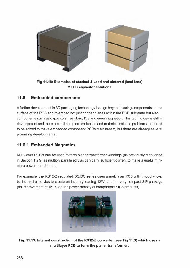
288
Fig 11.18: Examples of stacked J-Lead and sintered (lead-less)
MLCC capacitor solutions
11.6. Embedded components
A further development in 3D packaging technology is to go beyond placing components on thesurface of the PCB and to embed not just copper planes within the PCB substrate but alsocomponents such as capacitors, resistors, ICs and even magnetics. This technology is still indevelopment and there are still complex production and materials science problems that need to be solved to make embedded component PCBs mainstream, but there are already several promising developments.
11.6.1. Embedded Magnetics
Multi-layer PCB’s can be used to form planar transformer windings (as previously mentioned in Section 1.2.9) as multiply paralleled vias can carry suffi cient current to make a useful mini-ature power transformer.
For example, the RS12-Z regulated DC/DC series uses a multilayer PCB with through-hole, buried and blind vias to create an industry-leading 12W part in a very compact SIP package (an improvement of 150% on the power density of comparable SIP8 products):
Fig. 11.19: Internal construction of the RS12-Z converter (see Fig 11.3) which uses a
multilayer PCB to form the planar transformer.

289
Recom is also active in the EU Horizon 2020 programme as part of an industry / universitycollaboration investigating the uses of magnetic foils to make embedded inductors for sub-100V DC/DC converters with integrated GaN-on-CMOS wafer technology.
Fig. 11:20: Embedded magnetic sheet material investigation
(EU Horizon 2020 Project)
11.6.2. Embedded active and passive components
The simplest method of using the Z-axis in a multilayer PCB is to mill out a cavity and insert components below the surface to give a lower profi le design. This assembly method is so-metimes used in mobile phones where component height is severely restricted because of the large display.
Fig. 11.21: Diagrammatic view of a BGA assembly with recessed components
The disadvantage of this assembly method is that the solder paste for the recessed compo-nents cannot be applied using a conventional mechanical stencil. The solder paste must be dotted onto the bottom of the cavity using a paste jet printer.
Inserted components are sometimes used in DC/DC converters, notably in a product where a toroidal ferrite core is positioned inside a milled out cavity in a multilayer PCB which is then fi nished off with a top layer to create a fully recessed transformer. The production complexity is severe – not only because the ferrite ring must be free to move inside its cavity to allow
Recessed Component
Recessed Component
SMD Component SMD Component
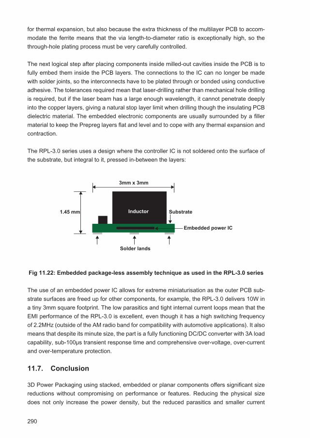
290
for thermal expansion, but also because the extra thickness of the multilayer PCB to accom-modate the ferrite means that the via length-to-diameter ratio is exceptionally high, so the through-hole plating process must be very carefully controlled.
The next logical step after placing components inside milled-out cavities inside the PCB is to fully embed them inside the PCB layers. The connections to the IC can no longer be made with solder joints, so the interconnects have to be plated through or bonded using conductive adhesive. The tolerances required mean that laser-drilling rather than mechanical hole drilling is required, but if the laser beam has a large enough wavelength, it cannot penetrate deeply into the copper layers, giving a natural stop layer limit when drilling though the insulating PCB dielectric material. The embedded electronic components are usually surrounded by a filler material to keep the Prepreg layers flat and level and to cope with any thermal expansion and contraction.
The RPL-3.0 series uses a design where the controller IC is not soldered onto the surface of the substrate, but integral to it, pressed in-between the layers:
Fig 11.22: Embedded package-less assembly technique as used in the RPL-3.0 series
The use of an embedded power IC allows for extreme miniaturisation as the outer PCB sub-strate surfaces are freed up for other components, for example, the RPL-3.0 delivers 10W in a tiny 3mm square footprint. The low parasitics and tight internal current loops mean that the EMI performance of the RPL-3.0 is excellent, even though it has a high switching frequency of 2.2MHz (outside of the AM radio band for compatibility with automotive applications). It also means that despite its minute size, the part is a fully functioning DC/DC converter with 3A load capability, sub-100μs transient response time and comprehensive over-voltage, over-current and over-temperature protection.
11.7. Conclusion
3D Power Packaging using stacked, embedded or planar components offers significant size reductions without compromising on performance or features. Reducing the physical size does not only increase the power density, but the reduced parasitics and smaller current
Solder lands
Embedded power IC
SubstrateInductor
3mm x 3mm
1.45 mm

291
loops mean that EMI can be kept under control even with high switching frequencies in the Megahertz range. The downside is that the thermal management becomes much more critical and the overall DC/DC converter temperature performance relies heavily on how is used in the final application.
The technologies used in 3D power packaging are now heavily influencing the design of new state-of-the-art DC/DC converters to offer more performance in less space without compromi-sing on cost or operating temperature specifications.
292
References and Further Reading
Bell, B (2003) “Introduction to Push-Pull Technologies”, National Semiconductor
Dixon, L (2002) “Control Loop Cookbook”, Texas Instruments Inc.
Ducard, G 2013 “Introduction to Digital Control of Dynamic systems”, Lecture Notes
Falin, J (2008) “Designing DC/DC Converters based on SEPIC Technology”, Texas Instruments Inc. Gerstl, D (2003), “Power Supply Reliability”, C&D Technologies
Kankanala, K (2011) “AN1369: Full-Bridge DC/DC Converter Reference Design”, Microchip Technology. Kessler, M (2010) “Synchronous Inverse SEPIC Technology”, Analog Dialogue, Analog Devices
Liang, R (2012) “Design Considerations for System-Level ESD Circuit Protection”, Texas Instruments Inc. Maimone, G (2010) “AN4067: Selecting L and C Components”, Freescale Semiconductor.
Mammano, B et al. (2005) “Safety Considerations in Power Supply Design”, Texas Instruments
McLyman, Colonel Wm. T (2004) “Transformer and Inductor Design Handbook”, 3rd ed., Kg Magnetics Inc., Marcel Dekker.
Peiravi, A (2009), “Testing and Reliability Improvement”, Dept. of Electrical Engineering, University of Mashhad Saliva, A (2013) “DN 2013-01: Design Guide for QR Flyback Converter”, Infinion INFA) Corp. Schramm, C (2004) “DC/DC-Wandler im Einsatz”, DATEL GmbH
Sheehan, R (2007) “Understanding and Applying Current-Mode Control Theory” , National Semi. Wald-ing, C (2008) “LLC Resonant Topology lowers switching losses”, Fairchild Semiconductor
Application Guides and Notes
ANP29 (2007) Zeta Converter Basics, Sipex Corporation
SLUP084 (2001) The Right-Half-Plane Zero – A Simplified Explanation, Texas Instruments Inc.
SLUP123-128 (2003) “Magnetics Design Handbook, Sections 1-5”, Texas Instruments Inc.
AN-1889 (2013) “How to Measure the Loop Transfer Function”, Texas Instruments Inc.
DN022 (2010) “Output Ripple and Noise Measurement Methods”, Ericsson Power
“Top 10 Circuit Protection Considerations” (2013) , Littelfuse
“Lighting and Electrical Equipment for use in Hazardous Atmospheres”, IEC Hazardous Fundamentals,
TP018 (2011): “Safety Requirements for Board-Mounted DC/DC Converters”, Ericsson Power Fuse Technology, Overcurrent Protection Group, Cooper Bussmann
AN9003 “A Users Guide to Intrinsic Safety”, Cooper Crouse-Hinds
Application Guide (2009) “Miniature Circuit Breakers”, ABB
“MLCC Application Guide” (2013), Walsin Technology Corp.
“Safety Application Guide for Multilayer Ceramic Capacitors”, Kyocera Corp

293
About RECOM
It was about 25 years ago when we showed our first hand made DC/DC converter to a leading German manufacturer of cellular phones. The product successfully passed all tests and a few weeks later we re-ceived our first order for 8000 pieces. A new product category was born – DC/DC converters in the form of a module.
In the recent decade DC/DC Converters have become a mass market product with many alternatives available at attractive prices – so much so, that for most customers today it is far more economical to use fully certified converter modules to power their on-board electronics than make their own. This not only speeds up the design process, it also makes EMC conformity much easier. Since in addition, as many design departments lack the analogue expertise needed to deal with electro-magnetic components and materials, modular DC/DC converters remain a well-established alternative to discrete power solutions today.
In the last few years RECOM has invented a number of innovative new converter products; such as the R-78 switching regulator, a pin-compatible replacement for linear regulators, which has spawned a large number of copy products from other manufacturers. This has helped the company to grow much faster than the power market on average. We have also penetrated new markets such as highly efficient, low standby consumption AC/DC power supplies, a comprehensive range of DC and AC LED Drivers and high performance applications such as medical electronics and railway technologies.
Today, RECOM‘s new, ultra-modern, campus-style headquarters in Gmunden / Austria provides room for expansion to meet our ambitious goals. A team of international engineers works in well-equipped, state-of-the-art labs to create a constant flow of new products and customer solutions. Extensive performance, stress and environmental tests performed in the early stages of each product design ensure that the prime objectives of reliability and quality are kept in the forefront of our design process. We have also invested heavily in our own EMC test lab and chamber to be independent from external facilities.
Our new headquarter also houses a fully automatic logistics centre to handle our inventory of 30.000 different products. Production and production engineering is performed at two RECOM factories in Ka-ohsiung / Taiwan. RECOM Manufacturing Ltd assembles, tests and ships the finished converters and RECOM Technology Ltd is a fully automated SMT fab equipped with six SMD lines to produce high runner products in very large quantities. This allows RECOM to provide both product depth and very competitive pricing to stay ahead as a global market leader.
At that time the shift from analogue to digital electronics acceler-ated the demand for DC/DC modules due to the need for stand-ardized on-board switching power supplies. In addition, I/O ports or amplifier channels required isolation to increase safety or to eliminate earth loops - another important requirement that DC/DC converters could fulfil. RECOM was there from the very early days to supply reliable, efficient and modular solutions for cus-tomers that did not want to invest the time and effort designing their own discrete converters.

294
Acknowledgements
I have wanted to write this book for some years, but the opportunity never arose. However, I was forced to spend nearly three months off work after a fairly serious skiing accident and so I took the opportunity lying down, so to speak. My first thanks go to our local hospital, LKH Gmunden, for allowing me to set up a temporary office around my hospital bed. I would also like to thank all those in RECOM that were involved to make this project happen.
I am indebted to Carl Schramm, RECOM Test Lab Consultant, for permission to use his pub-lication “DC/DC Wandler im Einsatz” upon which large parts of Sections 1 and 3 are based. I have added my own interpretations, additions and extensions to his original text, so any errors that remain are entirely my own.
References
I have used a number of references to fill in the gaps in my knowledge. I can particularly rec-ommend the application notes published by Texas Instruments Incorporated, ON Semicon-ductor, Maxim Integrated and Fairchild Semiconductor. For further reading, the professional magazines such as Electronic Product Design and Test, Power Systems Design and Elec-tronic Design regularly publish useful “how to” articles. Of course, the internet is the largest source of information and detailed information can often be found by following the links at the bottom of Wikipedia pages.
About the Author
Steve Roberts was born in England. He obtained a B.Sc. in Physics and Electronics at Brunel University, London (now University of West London) before working at University College Hospital. He later spent 12 years at the Science Museum as Head of Interactives, where he completed his M.Sc. at University College, London. He moved to Austria, joining RECOM’s Tech Support team developing custom converters and answering customer’s questions before becoming Technical Direc-tor for the RECOM group at their new headquarters in Gmunden, Austria.

Rsd Csd
DRs Cs
Ds
N-FET
FETDriver
SawtoothGenerator
Over Temp.Protection
R2
Enable GND
V REF
PWM
L1
S1 L2D1
C2C1C
in
VL1 V
C1
VIN
VS1
VL2 R
L VO
IL
IC2IL2
ID1
IS1
IC1IL1
RECOM Power GmbH andRECOM Engineering GmbH & Co KGMünzfeld 35, 4810 Gmunden, Austria
WE POWER YOUR PRODUCTS www.recom-power.com