DS1200 Series - Mouser Electronics
60
Rev.11.01.28_#1.3 DS1200-3 Series Page 1 DS1200 Series 1200 Watts Distributed Power System Total Power: 1000-1200 Watts Input Voltage: 90-264 Vac # of Outputs: Single Main Special Features • Active power factor correction • EN61000-3-2 harmonic compliance • Active AC inrush control • 1U X 2U form factor • 21.71 W / in 3 • +12 Vdc Output • +3.3 Vdc stand-by (+5 Vdc stand-by) • No minimum load required (main output only) • Hot plug operation • N + 1 redundant • Internal OR’ing fets • Active current sharing (10 - 100% load) • I 2 C communication interface bus • PMBus TM compliant • EEPROM for FRU data • Internal fan speed control • INTEL, SSI Std. logic timing • INTEL, SSI Std. FRU data format • Full digital control • 2 year warranty Safety UL/cUL 60950 (UL Recognized) NEMKO+ CB Report EN60950 EN60950 CE Mark China CCC Product Descriptions The DS1200-3 power supply features a very wide 90 to 264 Vac input voltage range and employ active power factor correction to minimize input harmonic current distortion and to ensure compliance with the international EN61000-3-2 standard – they have a power factor of 0.99 typical. The power supplies also feature active ac inrush control, to automatically limit inrush current at turn-on to 55 A maximum. The power supply employs a new ultra high efficiency conversion topology, together with an innovative power transformer and rectifier construction that further improves power density and reduces interconnect power losses. The power supply’s main +12 Vdc payload output is digitally programmable over the range 11.4 to 12.6 Vdc, and users have a choice of standard I 2 C or advanced PMBus TM communications. The control software runs under Windows® on any standard PC, and uses a highly intuitive graphical user interface to simplify power supply set-up. The DS1200-3 can deliver up to 98.4 A from its main +12 Vdc payload output, and up to 6 A from its +3.3 Vdc auxiliary output. The supply has a 1U x 2U form factor – it measures 10.9 x 3.3 inches, with a height of 1.6 inches – and has a power density of more than 21 watts per cubic inch. When fed with a 180 to 264 Vac input, the DS1200-3 can achieve a very high – 91 percent typical – conversion efficiency at 50 percent full load.
-
Upload
khangminh22 -
Category
Documents
-
view
5 -
download
0
Transcript of DS1200 Series - Mouser Electronics

Rev.11.01.28_#1.3DS1200-3 Series
Page 1
DS1200 Series
1200 Watts
Distributed Power System
Total Power: 1000-1200 Watts
Input Voltage: 90-264 Vac
# of Outputs: Single Main
Special Features• Active power factor correction
• EN61000-3-2 harmonic compliance
• Active AC inrush control
• 1U X 2U form factor
• 21.71 W / in3
• +12 Vdc Output
• +3.3 Vdc stand-by
(+5 Vdc stand-by)
• No minimum load required (main
output only)
• Hot plug operation
• N + 1 redundant
• Internal OR’ing fets
• Active current sharing
(10 - 100% load)
• I2C communication interface bus
• PMBusTM compliant
• EEPROM for FRU data
• Internal fan speed control
• INTEL, SSI Std. logic timing
• INTEL, SSI Std. FRU data format
• Full digital control
• 2 year warranty
SafetyUL/cUL 60950 (UL Recognized)
NEMKO+ CB Report EN60950
EN60950
CE Mark
China CCC
Product DescriptionsThe DS1200-3 power supply features a very wide 90 to 264 Vac input voltage range and employ active power factor correction to minimize input harmonic current distortion and to ensure compliance with the international EN61000-3-2 standard – they have a power factor of 0.99 typical. The power supplies also feature active ac inrush control, to automatically limit inrush current at turn-on to 55 A maximum.
The power supply employs a new ultra high efficiency conversion topology, together with an innovative power transformer and rectifier construction that further improves power density and reduces interconnect power losses. The power supply’s main +12 Vdc payload output is digitally programmable over therange 11.4 to 12.6 Vdc, and users have a choice of standard I2C or advanced PMBusTM communications. The control software runs under Windows® on any standard PC, and uses a highly intuitive graphical user interface to simplify power supply set-up.
The DS1200-3 can deliver up to 98.4 A from its main +12 Vdc payload output,and up to 6 A from its +3.3 Vdc auxiliary output. The supply has a 1U x 2U form factor – it measures 10.9 x 3.3 inches, with a height of 1.6 inches – and has a power density of more than 21 watts per cubic inch. When fed with a 180 to 264 Vac input, the DS1200-3 can achieve a very high – 91 percent typical –conversion efficiency at 50 percent full load.

Rev.11.01.28_#1.3DS1200-3 Series
Page 2Model Numbers
Options
AC Cord Retainer
Reversed(Handle to DC Connector)
Reversed(Handle to DC Connector)
Normal(DC Connector to Handle)
Normal(DC Connector to Handle)
Air Flow Direction
DS1200-3-002
DS1200-3
Standard
12.0Vdc
12.0Vdc
Output Voltage
0A
0A
Minimum Load
98.4A
98.4A
Maximum Load
5V@4A
3.3V@6A
Stand-BySupply

Rev.11.01.28_#1.3DS1200-3 Series
Page 3
oCoCoCoC
+50+701
+50+50
--10TA
DS1200-3DS1200-3-002DS1200-3-003DS1200-3-004
Ambient Operating Temperature
oC+85--40TSTGAll modelsStorage Temperature
%%
9095
--
2010
All modelsAll models
Humidity (non-condensing)Operating
Non-operating
feetfeet
10,00030,000
--
--
All modelsAll models
AltitudeOperating
Non-operating
WW
10001200
--
--
PO,maxAll models
Maximum Output Power (Main + Stand-by)VIAC ≤ 180VacVIAC > 180Vac
VdcVdcVdc
2500250050
---
---
All modelsAll modelsAll models
Isolation VoltageInput to outputs
Input to safety groundOutputs to safety ground
Table 1. Absolute Maximum Ratings:
Note 1 With power derating (see page 22 power derating curve)
Vac264-90VIN,ACAll modelsInput Voltage:
AC continuous operation
UnitMaxTypMinSymbolModelParameter
Electrical Specifications
Absolute Maximum Ratings
Stress in excess of those listed in the “Absolute Maximum Ratings” may cause permanent damage to the power supply. These are stress ratings only and functional operation of the unit is not implied at these or any other conditions above those given in the operational sections of this TRN. Exposure to any absolute maximum rated condition for extended periods may adversely affect the power supply’s reliability.
Rev.11.01.28_#1.3DS1200-3 Series
Page 4
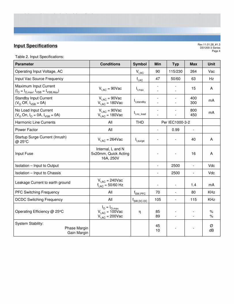
Input Specifications
mA400300
--
--
II,standby
VI,AC = 90VacVI,AC = 180Vac
Standby Input Current(VO Off, IVSB = 0A)
A16--Internal, L and N
5x20mm, Quick Acting 16A, 250V
Input Fuse
mA800450
--
--
II,no_load
VI,AC = 90VacVI,AC = 180Vac
No Load Input Current(VO On, IO = 0A, IVSB = 0A)
ØdB
--4510
System Stability:Phase Margin
Gain Margin
UnitMaxTypMinSymbolConditionsParameter
%%
--
--
8589
η
IO = IO,max
VI,AC = 100VacVI,AC = 200Vac
Operating Efficiency @ 25oC
KHz115-105fSW,DC-DCAllDCDC Switching Frequency
KHz80-70fSW,PFCAllPFC Switching Frequency
mA1.4--VI,AC = 240VacfI,AC = 50/60 Hz
Leakage Current to earth ground
Vdc-2500-Isolation – Input to Chassis
Vdc-2500-Isolation – Input to Output
A40--II,surgeVI,AC = 264VacStartup Surge Current (Inrush)@ 25°C
-0.99-AllPower Factor
Per IEC1000-3-2THDAllHarmonic Line Currents
A15--
--
II,maxVI,AC = 90VacMaximum Input Current(IO = IO,max, IVSB = IVSB,Max)
Hz6350/6047fI,ACInput Vac Source Frequency
Vac264115/23090VI,ACOperating Input Voltage, AC
Table 2. Input Specifications:

Rev.11.01.28_#1.3DS1200-3 Series
Page 5
--8Main Output Current
Share connectedNumber of Parallel Units1
%0.2±%VO
After thermal equilibrium (30 mins)
VO Long Term StabilityMax change over 24 hours
µF/A100-0-Start upVO Load Capacitance
%mSec
5-
--
--
±%VO
ts
50% load change, slew rate = 1A/µs
VO Dynamic ResponsePeak Deviation
Settling Time
Note 1 - VSB output do not use active current sharing. On paralleled units, maximum current on VSB output rail should not exceed the current of one unit.
%IO,max--20VO Minimum Current Share Loading
%IO,max
520
--
--
40% to 100% IO,max
10% to 40% IO,max
VO Current Share Accuracy
4.0-0.5IVSB
DS1200-3-002DS1200-3-004
50--VVSB
DS1200-3-002DS1200-3-004
5.255.004.75VVSB
DS1200-3-002DS1200-3-004
Table 3. Output Specifications:
6.0-0.5IVSB
DS1200-3DS1200-3-003
A
81.798.4
-00
IOVI,AC ≤ 180VacVI,AC > 180Vac
All models
Output Current
50--VVSB
DS1200-3DS1200-3-003 mVPK-PK
120--VOMeasure with a 0.1μF ceramic capacitor in parallel with a 10μF
tantalum capacitor, 0 to 20MHz bandwidth
All models
Output Ripple, pk-pk
3.473.303.13VVSB
DS1200-3DS1200-3-003 V
12.612.011.4VO
Inclusive of set-point, temperature change,
warm-up drift and dynamic load
All models
Output Regulation
UnitMaxTypMinSymbolConditionParameter
Output Specifications

Rev.11.01.28_#1.3DS1200-3 Series
Page 6
System Timing Specifications
mSec--11Delay from loss of AC to de-assertion of POWER GOOD.T5
mSec--5Delay from loss of AC input to AC_OK going to low.T8
mSec--100Duration of POWER GOOD being in the de-asserted state during an off/on cycle using AC or the PS_ON signal
T9
mSec--12Hold up time - time all output voltages, including VSB, stay within regulation after loss of AC.
T7
mSec300-10Delay from PS_ON active to output voltages within regulation limits.
T10
mSec1Delay from POWER GOOD de-asserted to output voltagesdropping out of regulation limits.
T6
mSec50-5VO rise time, 0V to VO in regulation.T3
mSec50--Delay from PS_ON deactive to POWER GOOD de-asserted low.T11
mSec1000-100Delay from output voltages within regulation limits to POWER GOOD asserted high.
T4
mSec2000--Delay from AC being applied to output voltages being within regulation with PS_ON asserted low.
T2
T1
Label
mSec1000--Delay from AC being applied to VSB being within regulation
Table 4. System Timing Specifications:
UnitMaxTypMinParameter

Rev.11.01.28_#1.3DS1200-3 Series
Page 7
System Timing Specifications
Figure 1. System Timing Diagram:
Rev.11.01.28_#1.3DS1200-3 Series
Page 8
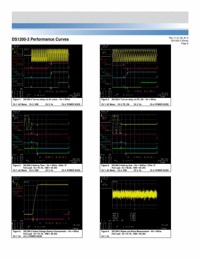
DS1200-3 Performance Curves
Figure 1: DS1200-3 Turn-on delay via AC mains – Vin = 90Vac
Ch 1: AC Mains Ch 2: VSB Ch 3: Vo Ch 4: POWER GOOD
Figure 5: DS1200-3 Output Voltage Startup Characteristic – Vin = 90VacFull Load: Vo = 81.7A, VSB = 4A (5V)
Ch 1: Vo Ch 2: POWER GOOD
Figure 2: DS1200-3 Turn-on delay via PS_ON – Vin = 90Vac
Ch 1: AC Mains Ch 2: PS_ON Ch 3: Vo Ch 4: POWER GOOD
Figure 4: DS1200-3 Hold-up time – Vin = 264Vac / 47Hz / 0°°°°Full Load: Vo = 98.4A, VSB = 4A (5V)
Ch 1: AC Mains Ch 2: VSB Ch 3: Vo Ch 4: POWER GOOD
Figure 6: DS1200-3 Ripple and Noise Measurement – Vin = 90Vac Full Load: Vo = 81.7A, VSB = 4A (5V)
Ch 1: Vo
Figure 3: DS1200-3 Hold-up Time – Vin = 90Vac / 63Hz / 0°°°°Full Load: Vo = 81.7A, VSB = 4A (5V)
Ch 1: AC Mains Ch 2: VSB Ch 3: Vo Ch 4: POWER GOOD
Rev.11.01.28_#1.3DS1200-3 Series
Page 9
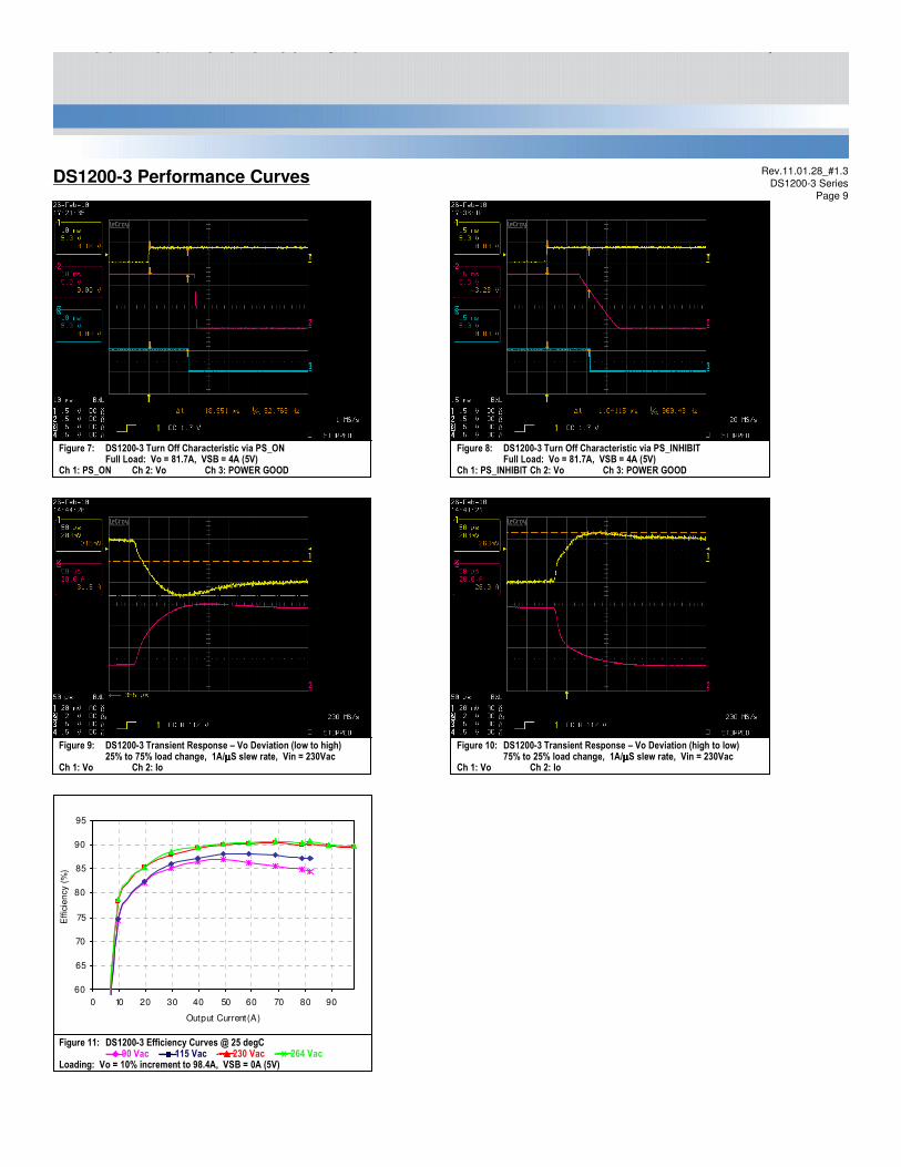
DS1200-3 Performance Curves
Figure 7: DS1200-3 Turn Off Characteristic via PS_ONFull Load: Vo = 81.7A, VSB = 4A (5V)
Ch 1: PS_ON Ch 2: Vo Ch 3: POWER GOOD
Figure 11: DS1200-3 Efficiency Curves @ 25 degC----- 90 Vac ----- 115 Vac ----- 230 Vac ----- 264 Vac
Loading: Vo = 10% increment to 98.4A, VSB = 0A (5V)
Figure 8: DS1200-3 Turn Off Characteristic via PS_INHIBITFull Load: Vo = 81.7A, VSB = 4A (5V)
Ch 1: PS_INHIBIT Ch 2: Vo Ch 3: POWER GOOD
Figure 10: DS1200-3 Transient Response – Vo Deviation (high to low)75% to 25% load change, 1A/µµµµS slew rate, Vin = 230Vac
Ch 1: Vo Ch 2: Io
Figure 9: DS1200-3 Transient Response – Vo Deviation (low to high)25% to 75% load change, 1A/µµµµS slew rate, Vin = 230Vac
Ch 1: Vo Ch 2: Io
x
60
65
70
75
80
85
90
95
0 10 20 30 40 50 60 70 80 90
Output Current(A)
Eff
icie
ncy (
%)
Rev.11.01.28_#1.3DS1200-3 Series
Page 10
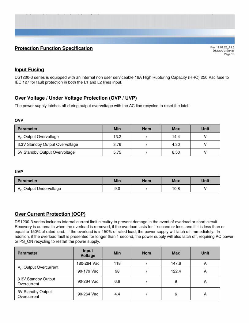
Protection Function Specification
Input Fusing
DS1200-3 series is equipped with an internal non user serviceable 16A High Rupturing Capacity (HRC) 250 Vac fuse to IEC 127 for fault protection in both the L1 and L2 lines input.
Over Voltage / Under Voltage Protection (OVP / UVP)
The power supply latches off during output overvoltage with the AC line recycled to reset the latch.
OVP
UVP
Over Current Protection (OCP)
DS1200-3 series includes internal current limit circuitry to prevent damage in the event of overload or short circuit. Recovery is automatic when the overload is removed, if the overload lasts for 1 second or less, and if it is less than or equal to 150% of rated load. If the overload is > 150% of rated load, the power supply will latch off immediately. In addition, if the overload fault is presented for longer than 1 second, the power supply will also latch off, requiring AC power or PS_ON recycling to restart the power supply.
V10.8/9.0VO Output Undervoltage
UnitMaxNomMinParameter
A9/6.690-264 Vac3.3V Standby Output Overcurrent
A6/4.490-264 Vac5V Standby Output Overcurrent
A147.6/118180-264 VacVO Output Overcurrent
A122.4/9890-179 Vac
ParameterInput
VoltageUnitMaxNomMin
V14.4/13.2VO Output Overvoltage
V4.30/3.763.3V Standby Output Overvoltage
V6.50/5.755V Standby Output Overvoltage
UnitMaxNomMinParameter
Rev.11.01.28_#1.3DS1200-3 Series
Page 11
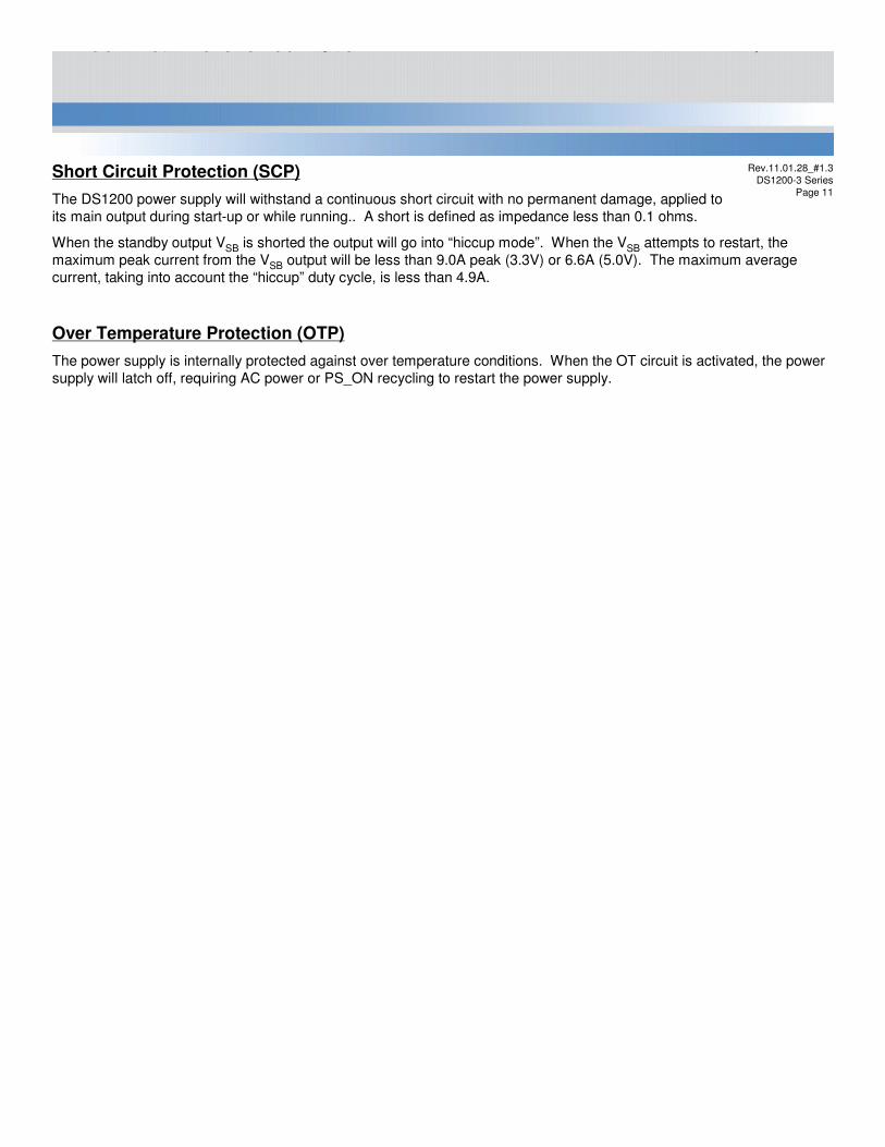
Short Circuit Protection (SCP)
The DS1200 power supply will withstand a continuous short circuit with no permanent damage, applied to its main output during start-up or while running.. A short is defined as impedance less than 0.1 ohms.
When the standby output VSB is shorted the output will go into “hiccup mode”. When the VSB attempts to restart, the maximum peak current from the VSB output will be less than 9.0A peak (3.3V) or 6.6A (5.0V). The maximum average current, taking into account the “hiccup” duty cycle, is less than 4.9A.
Over Temperature Protection (OTP)
The power supply is internally protected against over temperature conditions. When the OT circuit is activated, the power supply will latch off, requiring AC power or PS_ON recycling to restart the power supply.
Rev.11.01.28_#1.3DS1200-3 Series
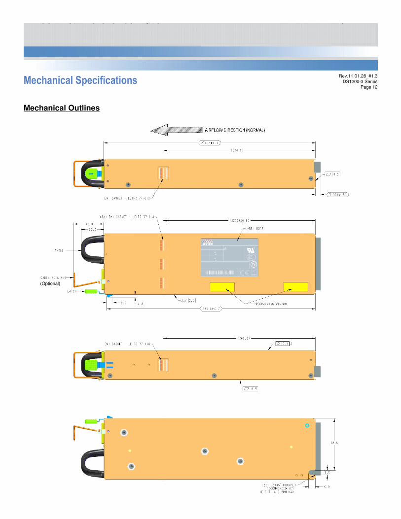
Page 12Mechanical Specifications
Mechanical Outlines
(Optional)

Rev.11.01.28_#1.3DS1200-3 Series
Page 13
Connector Definitions
AC Input Connector
Pin 1 – L1
Pin 2 – L2
Pin 3 – Earth Ground
Output Connector – Power Blades
PB1 – Main Output Return
PB2 – Main Output Return
PB3 – Main Output Return
PB4 – + Main Output (VO)
PB5 – + Main Output (VO)
PB6 – + Main Output (VO)
Output Connector – Control Signals
A1 – PS_ON
A2 – Main Output Remote Sense Return
A3 – Spare
A4 – PS_SEATED
A5 – StandBy Output
A6 – StandBy Output Return
B1 – AC_OK
B2 – Main Output Remote Sense
B3 – Main Output Current Share
B4 – PS_INHIBIT
B5 – StandBy Output
B6 – StandBy Output Return
C1 – SDA (I2C Data Signal)
C2 – SCL (I2C Clock Signal)
C3 – POWER GOOD
C4 – Spare
C5 – StandBy Output
C6 – StandBy Output Return
D1 – A0 (I2C Address BIT 0 Signal)
D2 – A1 (I2C Address BIT 1 Signal)
D3 – S_INT (Alarm)
D4 – StandBy Remote Sense
D5 – StandBy Output
D6 – StandBy Output Return
L1
L2
Earth Ground
PB3PB2PB1
A5
B5
C5
D5
A4
B4
C4
D4
A3
B3
C3
D3
A2
B2
C2
D2
A6A1
B6B1
C6C1PB6PB5PB4
D6D1
View from power supply output connector end
Rev.11.01.28_#1.3DS1200-3 Series
Page 14
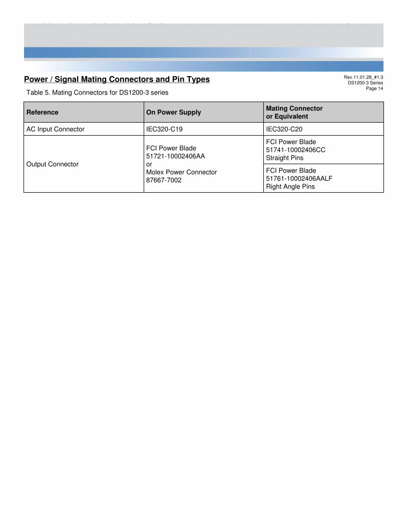
Power / Signal Mating Connectors and Pin Types
FCI Power Blade51741-10002406CCStraight Pins
FCI Power Blade 51721-10002406AAorMolex Power Connector87667-7002
Table 5. Mating Connectors for DS1200-3 series
FCI Power Blade51761-10002406AALFRight Angle Pins
Output Connector
IEC320-C20IEC320-C19AC Input Connector
Mating Connectoror Equivalent
On Power SupplyReference
Rev.11.01.28_#1.3DS1200-3 Series
Page 15
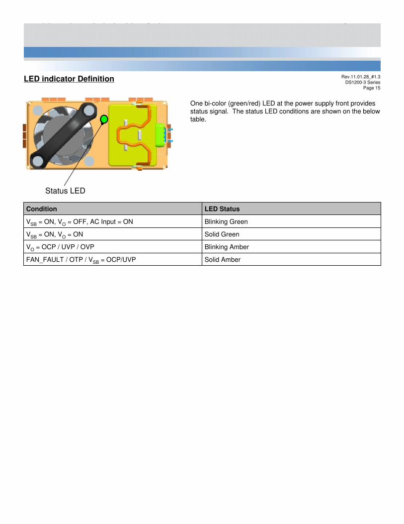
LED indicator Definition
One bi-color (green/red) LED at the power supply front provides status signal. The status LED conditions are shown on the belowtable.
Solid AmberFAN_FAULT / OTP / VSB = OCP/UVP
Blinking AmberVO = OCP / UVP / OVP
Solid GreenVSB = ON, VO = ON
Blinking GreenVSB = ON, VO = OFF, AC Input = ON
LED StatusCondition
Status LED

Rev.11.01.28_#1.3DS1200-3 Series
Page 16
Weight
The DS1200-3 series weight is 2.9 lbs. maximum.
Rev.11.01.28_#1.3DS1200-3 Series
Page 17Environmental Specifications
EMC Immunity
DS1200-3 series power supply is designed to meet the following EMC immunity specifications:
DescriptionDocument
Conducted and Radiated EMI LimitsFCC Docket No. 20780 Part 15Subpart J Class B/ EN55022, Level B
HarmonicsEN61000-3-2
Voltage FluctuationsEN61000-3-3
Electromagnetic Compatibility (EMC) - Testing and measurement techniques – Electrostatic discharge immunity test. +/-15KV air, +/-8KV contact discharge, performance Criteria B
IEC/EN 61000-4-2, Edition 1.2, 2001-04
Electromagnetic Compatibility (EMC) - Testing and measurement techniques, Radiated, radio-frequency, electromagnetic field immunity test
IEC/EN 61000-4-3, 2002, Amendment 1, 2002-08
Electromagnetic Compatibility (EMC) - Testing and measurement techniques, Electrical Fast Transient/Burst Immunity Test. 2KV for AC power port, 1.0KV for DC ports, I/O and signal ports performance Criteria B
IEC/EN 61000-4-4, 1995, Amendment 2, 2001-07
Electromagnetic Compatibility (EMC) - Testing and measurement techniques – 2KV common mode and 1KV differential mode for AC ports and 0.5kV differential mode for DC power, I/O and signal ports, performance criteria B.
IEC/EN 61000-4-5, Edition 1.1, 2001-04
Electromagnetic Compatibility (EMC) - Testing and measurement techniques : Voltage Dips and Interruptions: 30% reduction for 500ms-Criteria B>95% reduction for 10mS, Criteria A, >95% reduction for 5000mS, Criteria C
IEC/EN 61000-4-11, Edition 1.1, 2001-04
Information Technology Equipment-Immunity Characteristics, Limits and Method of Measurements
EN55024:1998
Table 6. Environmental Specifications:

Rev.11.01.28_#1.3DS1200-3 Series
Page 18
Safety Certifications
The DS1200-3 power supply is intended for inclusion in other equipment and the installer must ensure that it is in compliance with all the requirements of the end application. This product is only for inclusion by professional installers within other equipment and must not be operated as a stand alone product.
2009010907324565
109053
E186249
File #
(All CENELEC Countries)CB Certificate and Report
US and Canada RequirementsUL 60950 No.
Information Technology Equipment - Safety - Part 1:General Requirements (Bi-National standard, with UL 60950-1)
CSA 22.2 No. 60950
European RequirementsEN60950
International RequirementsEN60950 Deviations
China RequirementsCHINA CCC Approval
Table 7. Safety Certifications for DS1200-3 series power supply system
DescriptionDocument
Rev.11.01.28_#1.3DS1200-3 Series
Page 19
Table 6. Conducted EMI emission specifications of the DS1200-3 series
-
-
Typ
6
6
Max
dB-MarginAllCISPR 22 (EN55022) class B
dB-MarginAllFCC Part 15, class B
UnitMin Symbol Model Parameter
EMI Emissions
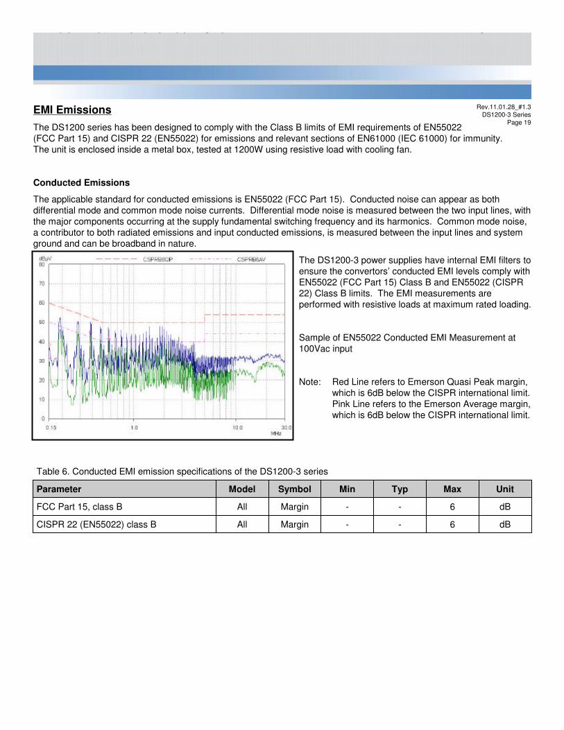
The DS1200 series has been designed to comply with the Class B limits of EMI requirements of EN55022 (FCC Part 15) and CISPR 22 (EN55022) for emissions and relevant sections of EN61000 (IEC 61000) for immunity. The unit is enclosed inside a metal box, tested at 1200W using resistive load with cooling fan.
Conducted Emissions
The applicable standard for conducted emissions is EN55022 (FCC Part 15). Conducted noise can appear as both differential mode and common mode noise currents. Differential mode noise is measured between the two input lines, with the major components occurring at the supply fundamental switching frequency and its harmonics. Common mode noise, a contributor to both radiated emissions and input conducted emissions, is measured between the input lines and system ground and can be broadband in nature.
The DS1200-3 power supplies have internal EMI filters to ensure the convertors’ conducted EMI levels comply with EN55022 (FCC Part 15) Class B and EN55022 (CISPR 22) Class B limits. The EMI measurements are performed with resistive loads at maximum rated loading.
Sample of EN55022 Conducted EMI Measurement at 100Vac input
Note: Red Line refers to Emerson Quasi Peak margin, which is 6dB below the CISPR international limit.Pink Line refers to the Emerson Average margin, which is 6dB below the CISPR international limit.
Rev.11.01.28_#1.3DS1200-3 Series
Page 20
Radiated Emissions
Unlike conducted EMI, radiated EMI performance in a system environment may differ drastically from that in a stand-alone power supply. The shielding effect provided by the system enclosure may bring the EMI level from Class A to Class B. It is thus recommended that radiated EMI be evaluated in a system environment. The applicable standard is EN55022 Class A (FCC Part 15). Testing ac-dc convertors as a stand-alone component to the exact requirements of EN55022 can be difficult, because the standard calls for 1m leads to be attached to the input and outputs and aligned such as to maximize the disturbance. In such a set-up, it is possible to form a perfect dipole antenna that very few ac-dc convertors could pass. However, the standard also states that ‘an attempt should be made to maximize the disturbance consistent with the typical application by varying the configuration of the test sample.
Rev.11.01.28_#1.3DS1200-3 Series
Page 21
Operating Temperature
The DS1200-3 series power supplies will start and operate within stated specifications at an ambient temperature from -10oC to 50oC under all load conditions with internal fan. DS1200-3-002 and DS1200-3-401 can operate up to 70oC with derated power.
Forced Air Cooling
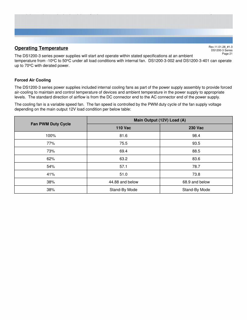
The DS1200-3 series power supplies included internal cooling fans as part of the power supply assembly to provide forced air-cooling to maintain and control temperature of devices and ambient temperature in the power supply to appropriate levels. The standard direction of airflow is from the DC connector end to the AC connector end of the power supply.
The cooling fan is a variable speed fan. The fan speed is controlled by the PWM duty cycle of the fan supply voltage depending on the main output 12V load condition per below table:
Main Output (12V) Load (A)
230 Vac110 VacFan PWM Duty Cycle
Stand-By ModeStand-By Mode38%
68.9 and below44.88 and below38%
73.851.041%
78.757.154%
83.663.262%
88.569.473%
93.575.577%
98.481.6100%
Rev.11.01.28_#1.3DS1200-3 Series
Page 22
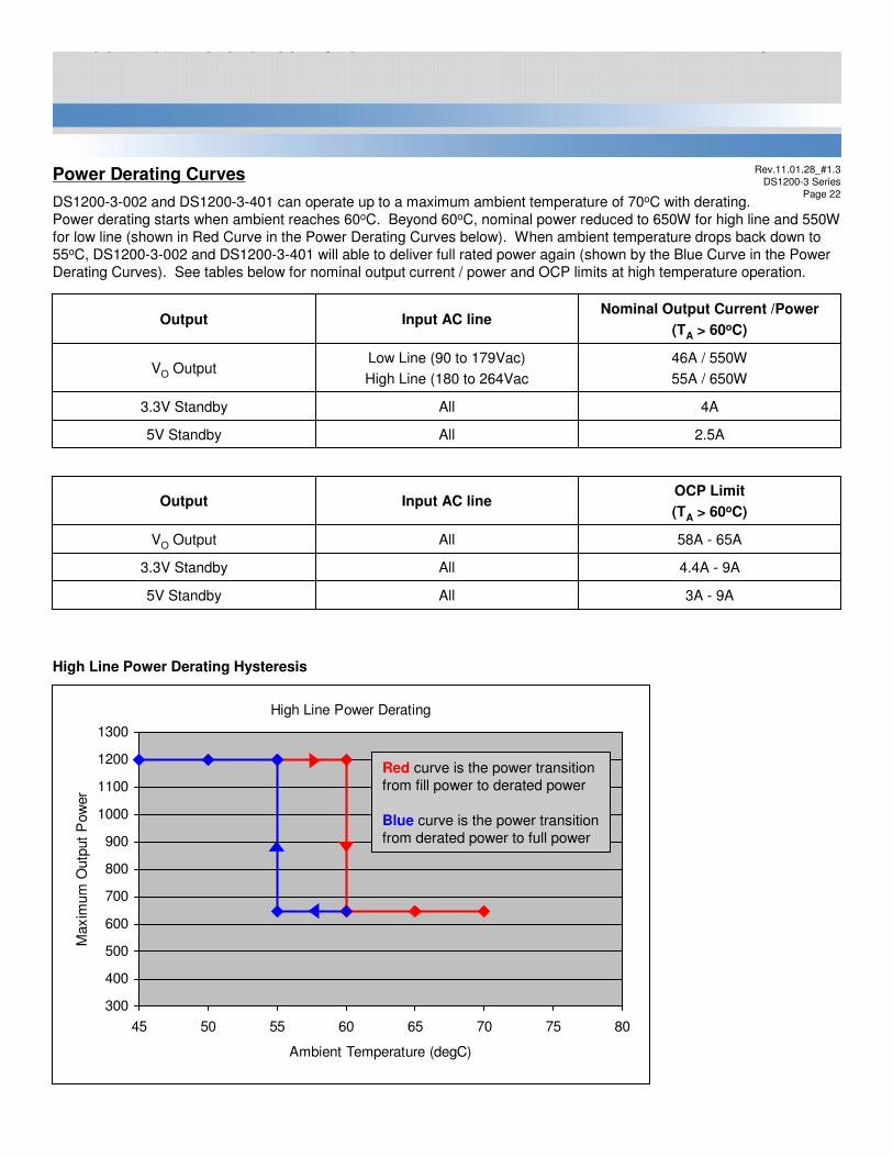
Power Derating Curves
DS1200-3-002 and DS1200-3-401 can operate up to a maximum ambient temperature of 70oC with derating. Power derating starts when ambient reaches 60oC. Beyond 60oC, nominal power reduced to 650W for high line and 550W for low line (shown in Red Curve in the Power Derating Curves below). When ambient temperature drops back down to 55oC, DS1200-3-002 and DS1200-3-401 will able to deliver full rated power again (shown by the Blue Curve in the Power Derating Curves). See tables below for nominal output current / power and OCP limits at high temperature operation.
High Line Power Derating Hysteresis
OCP Limit
(TA > 60oC)Input AC lineOutput
58A - 65AAllVO Output
4.4A - 9AAll3.3V Standby
2.5AAll5V Standby
All
All
Low Line (90 to 179Vac)
High Line (180 to 264Vac
Input AC line
4A3.3V Standby
3A - 9A5V Standby
46A / 550W
55A / 650WVO Output
Nominal Output Current /Power
(TA > 60oC)Output
High Line Power Derating
300
400
500
600
700
800
900
1000
1100
1200
1300
45 50 55 60 65 70 75 80
Ambient Temperature (degC)
Maxim
um
Outp
ut
Pow
er
Red curve is the power transitionfrom fill power to derated power
Blue curve is the power transitionfrom derated power to full power

Rev.11.01.28_#1.3DS1200-3 Series
Page 23
Low Line Power Derating Hysteresis
Note 1: Rated output power 1000W at 100Vac line condition, for lower line voltage derate output power to 550W (thermal limitation due to OTP Protection) for 56 to 60oC ambient temperature
Low Line Power Derating ≥ 100Vac
300
400
500
600
700
800
900
1000
1100
1200
1300
45 50 55 60 65 70 75 80
Ambient Temperature (degC)
Maxim
um
Outp
ut
Pow
er
Red curve is the power transitionfrom fill power to derated power
Blue curve is the power transitionfrom derated power to full power

Rev.11.01.28_#1.3DS1200-3 Series
Page 24
Storage and Shipping Temperature / Humidity
The DS1200-3 series power supplies can be stored or shipped at temperatures between –40oC to +85oCand relative humidity from 5% to 95% non-condensing.
Altitude
The DS1200-3 series will operate within specifications at altitudes up to 10,000 feet above sea level. The power supply shall not be damaged when stored at altitudes of up to 30,000 feet above sea level.
Humidity
The DS1200-3 series will operate within specifications when subjected to a relative humidity from 20% to 90% non-condensing. The DS1200-3 series can be stored in a relative humidity from 10% to 95% non-condensing.
Vibration
The DS1200-3 power supply will pass the following vibration specifications:
Non-Operating Random Vibration
Operating Random Vibration
mins20Duration
3 mutually perpendicular axisDirection
SLOPE PSDFREQ dB/oct g2/Hz
10-190 Hz --- 0.01 g2/Hz190-210 Hz -31.213dB/oct ---210-2000 Hz --- 0.003 g2/Hz
PSD Profile
Hz10-2000Frequency Range
gRMS2.7Acceleration
mins20Duration
3 mutually perpendicular axisDirection
SLOPE PSDFREQ dB/oct g2/Hz
10-500 Hz --- 0.002 g2/Hz
PSD Profile
Hz10-500Frequency Range
gRMS1.0Acceleration
Rev.11.01.28_#1.3DS1200-3 Series
Page 25
Shock
The DS1200-3 power supply will pass the following vibration specifications:
Non-Operating Half-Sine Shock
Operating Half-Sine Shock
Half-SinePulse
3 shock on each of 6 facesNo. of Shock
msec18Duration
G30Acceleration
Half-SinePulse
3 shock on each of 6 facesNo. of Shock
msec22Duration
G4Acceleration
Rev.11.01.28_#1.3DS1200-3 Series
Page 26Power and Control Signal Descriptions
AC Input Connector
This connector supplies the AC Mains to the DS1200-3 power supply.
Pin 1 - L1Pin 2 - L2Pin 3 - Earth Ground
Output Connector – Power Blades
These pins provide the main output for the DS1200-3. The + Main Output (VO) and the Main Output Return pins are the positive and negative rails, respectively, of the VO main output of the DS1200-3 power supply. The Main Output (VO) is electrically isolated from the power supply chassis.
PB1 - Main Output ReturnPB2 - Main Output ReturnPB3 - Main Output ReturnPB4 - + Main Output (VO)PB5 - + Main Output (VO)PB6 - + Main Output (VO)
Output Connector - Control Signals
The DS1200-3 series contains a 24 pins control signal header providing an analogue control interface, standby power and i2C interface signal connections.
PS_ON – (pin A1)
This signal input pin controls the normal turning ON and Off of the Main Output of the DS1200-3 power supply. The power supply main output (VO) will be enabled when this signal is pulled low, below 0.8 V. The Power supply output (except VSB
output) will be disabled when this input is driven higher than 2.4V, or left open circuited.
Main Output Remote Sense Return, Main Output Remote Sense – (pins A2, B2)
The main output of the DS1200-3 is equipped with a Remote Sensing capability that will compensate for a power path drop around the entire loop of 1 volt. This feature is implemented by connecting the Main Output Remote Sense (pin B2) and the Main Output Remote Sense Return (pin A2) to the positive and negative rails of the main output, respectively, at a location that is near to the load. Care should be taken in the routing of the sense lines as any noise sources or additional filtering components introduced into the voltage rail may affect the stability of the power supply. The DS1200-3 will operate appropriately without the sense lines connected; however it is recommended that the sense lines be connected directly to the main output terminals if remote sensing is not required. This remote sense circuit will not raise the power supply’s output voltage to the OVP trip level.
Main Output Remote Sense has no effect on the Standby Output (VSB).
Rev.11.01.28_#1.3DS1200-3 Series
Page 27
PS_SEATED – (pin A4)
This signal pin is connected to Main Output Return inside the power supply via a 220 ohm resistor. This pin is to be pull high on the system side by a resistor of 4.7K or higher. A TTL logic LOW indicates the power supply is inserted and seated into the system power supply connector. A Logic HIGH indicated the removal of the power supply.
StandBy Output, StandBy Output Return – (pins A5, A6, B5, B6, C5, C6, D5, D6)
The DS1200-3 provides a regulated 3.3 volt 6 amp (or 5.0 volt 4 amp) auxiliary output voltage to power critical circuitry that must remain active regardless of the on/off status of the power supply’s main output. The Standby Output (VSB) voltage is available whenever a valid AC input voltage is applied to the unit. The StandBy Output is independently short circuit protected and is referenced to the StandBy Output Return pins (A6, B6, C6, D6).
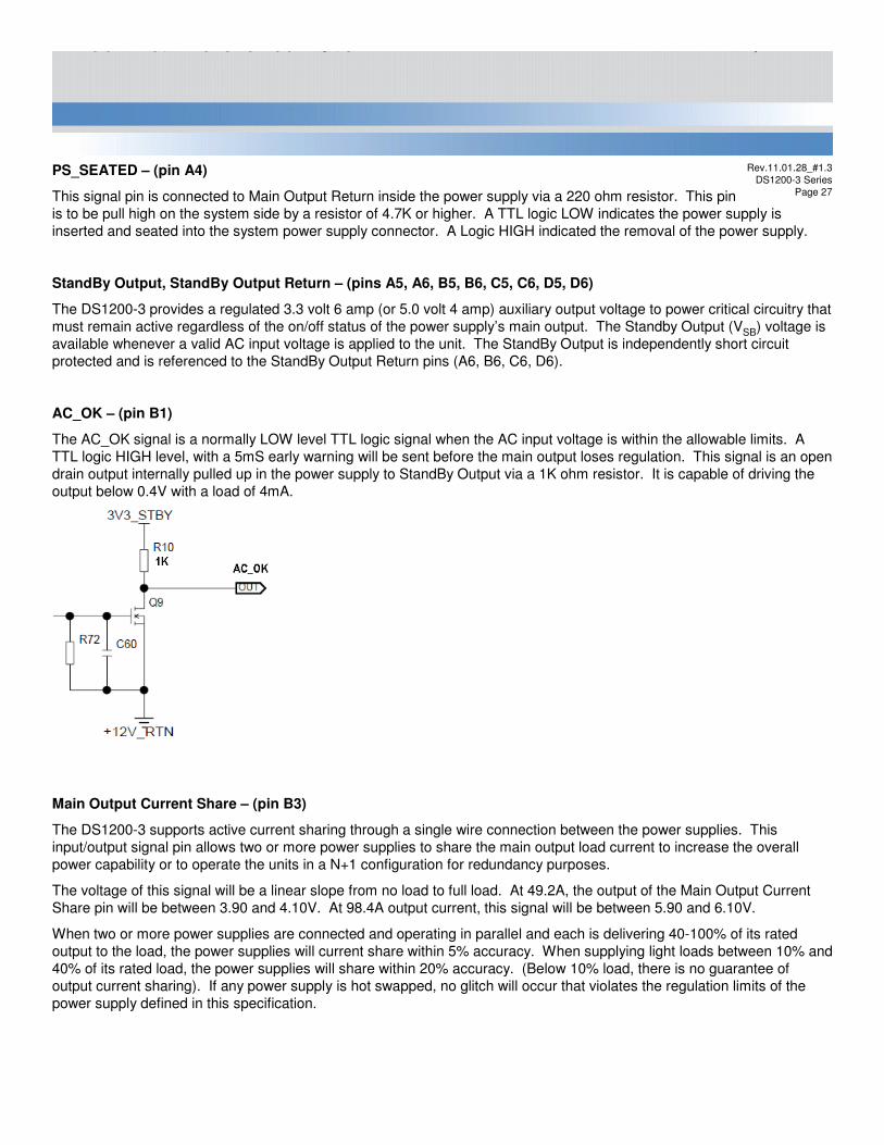
AC_OK – (pin B1)
The AC_OK signal is a normally LOW level TTL logic signal when the AC input voltage is within the allowable limits. A TTL logic HIGH level, with a 5mS early warning will be sent before the main output loses regulation. This signal is an open drain output internally pulled up in the power supply to StandBy Output via a 1K ohm resistor. It is capable of driving the output below 0.4V with a load of 4mA.
Main Output Current Share – (pin B3)
The DS1200-3 supports active current sharing through a single wire connection between the power supplies. This input/output signal pin allows two or more power supplies to share the main output load current to increase the overall power capability or to operate the units in a N+1 configuration for redundancy purposes.
The voltage of this signal will be a linear slope from no load to full load. At 49.2A, the output of the Main Output Current Share pin will be between 3.90 and 4.10V. At 98.4A output current, this signal will be between 5.90 and 6.10V.
When two or more power supplies are connected and operating in parallel and each is delivering 40-100% of its rated output to the load, the power supplies will current share within 5% accuracy. When supplying light loads between 10% and 40% of its rated load, the power supplies will share within 20% accuracy. (Below 10% load, there is no guarantee of output current sharing). If any power supply is hot swapped, no glitch will occur that violates the regulation limits of the power supply defined in this specification.

Rev.11.01.28_#1.3DS1200-3 Series
Page 28
PS_INHIBIT – (pin B4)
This signal pin should be grounded in the system. If left open, power supply operation will be inhibited (StandBy VSB output will remain on).
SDA, SCL and S_INT – (pin C1, C2, D3)
Please refer to “Communication Bus Descriptions” section.
POWER GOOD– (pin C3)
The POWER GOOD is an output signal driven high, by the power supply to indicate that all outputs are valid. If any of the power supply outputs fails below its regulation limits, this output will be driven low. The output signal is an open drain output internally pulled up in the power supply to internal standby supply (anode side of StandBy Output or’ing circuit) via a 1K ohm resistor. It is capable of driving the output below 0.4V with a load of 4mA.
A0, A1 – (pins D1, D2)
Please refer to “Communication Bus Descriptions” section.
StandBy Remote Sense – (pin D4)
The StandBy Output of the DS1200-3 is also equipped with a Remote Sensing capability that will compensate upto 50mV of voltage drop for the positive rail. The StandBy Output Remote Sense pin should be connected as close to the load as possible, or connected to the StandBy Output pins at the base of the output connector if not used. If left open, the remote sense might not work properly and the voltage level of StandBy Output can be lower than the guaranteed spec.
Rev.11.01.28_#1.3DS1200-3 Series
Page 29Communication Bus Descriptions
I2C Bus Signals
The DS1200-3 power supply contains enhanced monitoring and control functions implemented via the I2C bus. The DS1200-3 I2C functionality (PMBusTM and FRU data) can be accessed via the output connector control signals. The communication bus is powered either by the internal 3.3V supply or from an external power source connected to the StandBy Output (ie: accessing an unpowered power supply as long as the StandBy Output of another power supply connected in parallel is on).
If units are connected in parallel or in redundant mode, the StandBy Outputs must be connected together in the system. Otherwise, the I2C bus will not work properly when a unit is inserted into the system without the AC source connected.
Note: PMBusTM functionality can be accessed only when the PSU is powered-up.Guaranteed communication I2C speed is 100KHz.
SDA, SCL (I2C Data and Clock Signals) – (pin C1, C2)
I2C serial data and clock bus - these pins are internally pulled up to internal 3.3V supply with a 39K resistor. These pins must be pulled-up in the system by an 1K ohm resistor to the StandBy Output.
S_INT (Alarm) – (pin D3)
S_INT is used to send a signal to the system that a fault in the power supply occurred. This signal is normally logic level HIGH. It will go to a LOW logic level when a fault bit has been set in the power supply’s status register. To reset the S_INT signal back to normal (logic HIGH level), perform one of the following actions - (1) recycle input AC power, (2) toggle PSON signal and (3) issuance of a CLEAR_FAULTS PMBusTM command.
A0, A1 (I2C Address BIT 0, BIT1 Signals) – (pin D1, D2)
These two input pins are the address lines A0 and A1 to indicate the slot position the power supply occupies in the power bay and define the power supply addresses for FRU data and PMBusTM data communication. This allows the system to assign different addresses for each power supply. During I2C communication between system and power supplies, the system will be the master and power supplies will be slave.
They are internally pulled up to internal 3.3V supply with a 1K resistor.
I2C Bus Communication Interval
The interval between two consecutive I2C communications to the power supply should be at least 50ms to ensure proper monitoring functionality.
I2C Bus Signal Integrity
The noise on the I2C bus (SDA, SCL lines) due to the power supply will be less than 500mV peak-to-peak. This noise measurement should be made with an oscilloscope bandwidth limited to 100MHz. Measurements should be make at the power supply output connector with 3.2K ohm resistors pulled up to StandBy Output and 20pf ceramic capacitors to StandBy Output Return.
The noise on the address lines A0 and A1 will be less than 100mV peak-to-peak. This noise measurement should be made at the power supply output connector.

Rev.11.01.28_#1.3DS1200-3 Series
Page 30
I2C Bus Internal Implementation, Pull-ups and Bus Capacitances
I2C Bus - Recommended external pull-ups:
SystemBackplaneProcessor
SYSTEMBACKPLANE
POWER SUPPLY SIDESystem 3.3V (Internal Secondary Logic Supply
39K
39K
1K
1K
PSU MonitorFunction
PSU MicroController
SDA SDA
SCL SCL
A1 A1
A0 A0
FRUDATAEEPROM
GND
Interconnect
1K
1K
S_INTS_INT
Kohm-0.25-4 PSU
Kohm-1.0-Rext
1 PSURecommended external pull-up resistor
Electrical and Interface specifications of I2C signals (referenced to StandBy Output Return pin, unless otherwise indicated):
pF-0-CintSDA, SCL internal bus capacitance
Kohm-39-RintSDA, SCL internal pull-up resistor
UnitMaxTypMinSymbolConditionParameter
Rev.11.01.28_#1.3DS1200-3 Series
Page 31
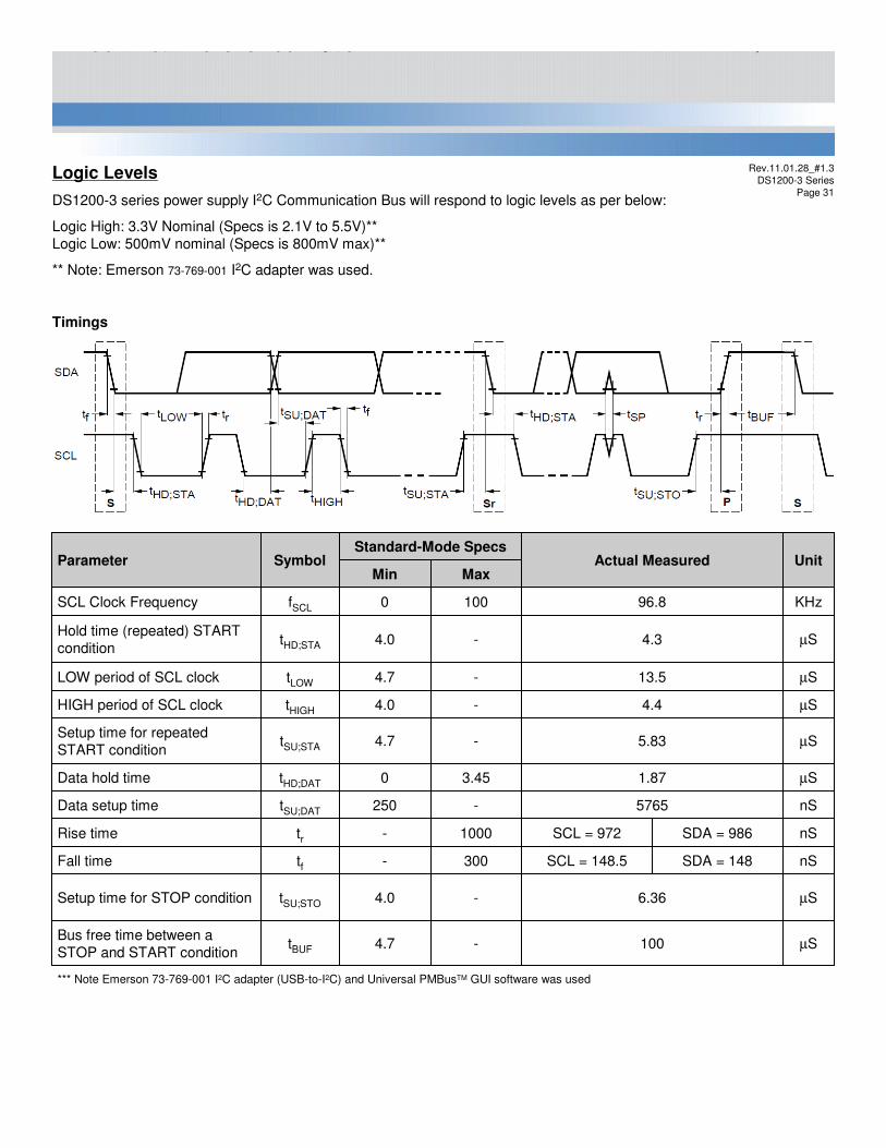
Logic Levels
DS1200-3 series power supply I2C Communication Bus will respond to logic levels as per below:
Logic High: 3.3V Nominal (Specs is 2.1V to 5.5V)**Logic Low: 500mV nominal (Specs is 800mV max)**
** Note: Emerson 73-769-001 I2C adapter was used.
Timings
SCL = 148.5
SCL = 972
µS1.873.450tHD;DATData hold time
µS5.83-4.7tSU;STA
Setup time for repeated START condition
µS4.4-4.0tHIGHHIGH period of SCL clock
µS13.5-4.7tLOWLOW period of SCL clock
µS4.3-4.0tHD;STA
Hold time (repeated) START condition
KHz96.81000fSCLSCL Clock Frequency
MaxMin
µS6.36-4.0tSU;STOSetup time for STOP condition
nSSDA = 148300-tfFall time
nSSDA = 9861000-trRise time
µS100-4.7tBUF
Bus free time between a STOP and START condition
5765
Actual Measured
*** Note Emerson 73-769-001 I2C adapter (USB-to-I2C) and Universal PMBusTM GUI software was used
nS-250tSU;DATData setup time
UnitStandard-Mode Specs
SymbolParameter

Rev.11.01.28_#1.3DS1200-3 Series
Page 32
Device Addressing
The DS1200-3 series will respond to supported commands on the I2C bus that are addressed accordingto pins A1 and A0 pins of output connector.
Address pins are held HIGH by default via pulled up to internal 3.3V (5V)supply with a 1K resistor. To set the address as “0”, the corresponding address line should be pulled down to logic ground level. Below table show the address of the power supply with A0 and A1 pins set to either “0” or “1”:
* Default PMBusTM address when A0 and A1 are left open
Slot ID Bits
0xAF*0x7E*114
0xAD0x7C013
0xAB0x7A102
0xA90x78001
A0A1
EEPROM (FRU)Read Address
PMBusTM AddressPSU Slot
Rev.11.01.28_#1.3DS1200-3 Series
Page 33
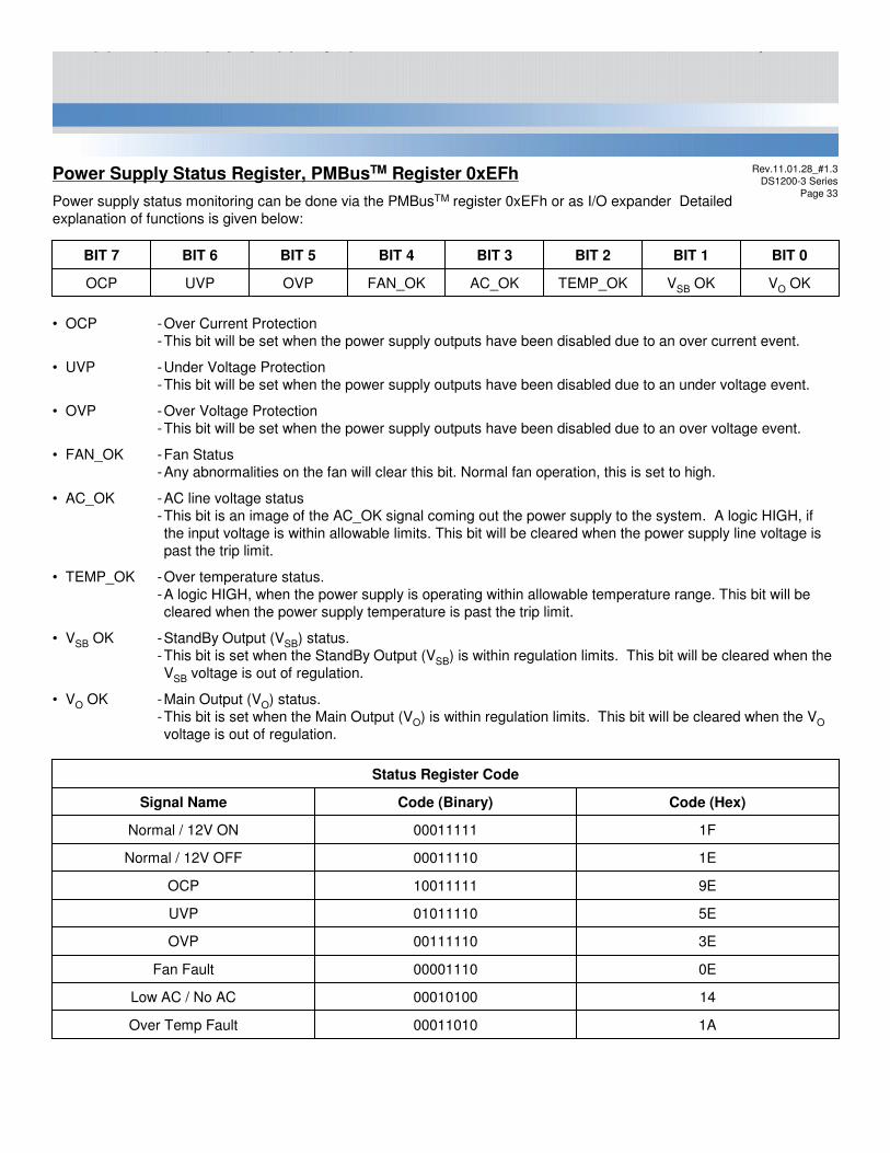
Power Supply Status Register, PMBusTM Register 0xEFh
Power supply status monitoring can be done via the PMBusTM register 0xEFh or as I/O expander Detailed explanation of functions is given below:
• OCP -Over Current Protection-This bit will be set when the power supply outputs have been disabled due to an over current event.
• UVP -Under Voltage Protection-This bit will be set when the power supply outputs have been disabled due to an under voltage event.
• OVP -Over Voltage Protection-This bit will be set when the power supply outputs have been disabled due to an over voltage event.
• FAN_OK -Fan Status-Any abnormalities on the fan will clear this bit. Normal fan operation, this is set to high.
• AC_OK -AC line voltage status-This bit is an image of the AC_OK signal coming out the power supply to the system. A logic HIGH, ifthe input voltage is within allowable limits. This bit will be cleared when the power supply line voltage ispast the trip limit.
• TEMP_OK -Over temperature status. -A logic HIGH, when the power supply is operating within allowable temperature range. This bit will becleared when the power supply temperature is past the trip limit.
• VSB OK -StandBy Output (VSB) status. -This bit is set when the StandBy Output (VSB) is within regulation limits. This bit will be cleared when theVSB voltage is out of regulation.
• VO OK -Main Output (VO) status. -This bit is set when the Main Output (VO) is within regulation limits. This bit will be cleared when the VO
voltage is out of regulation.
AC_OK
BIT 3
FAN_OK
BIT 4
OVP
BIT 5
VO OKVSB OKTEMP_OKUVPOCP
BIT 0BIT 1BIT 2BIT 6BIT 7
5E01011110UVP
0E00001110Fan Fault
3E00111110OVP
Status Register Code
00011010
00010100
10011111
00011110
00011111
Code (Binary)
9EOCP
1ENormal / 12V OFF
1FNormal / 12V ON
1AOver Temp Fault
14Low AC / No AC
Code (Hex)Signal Name
Rev.11.01.28_#1.3DS1200-3 Series
Page 34
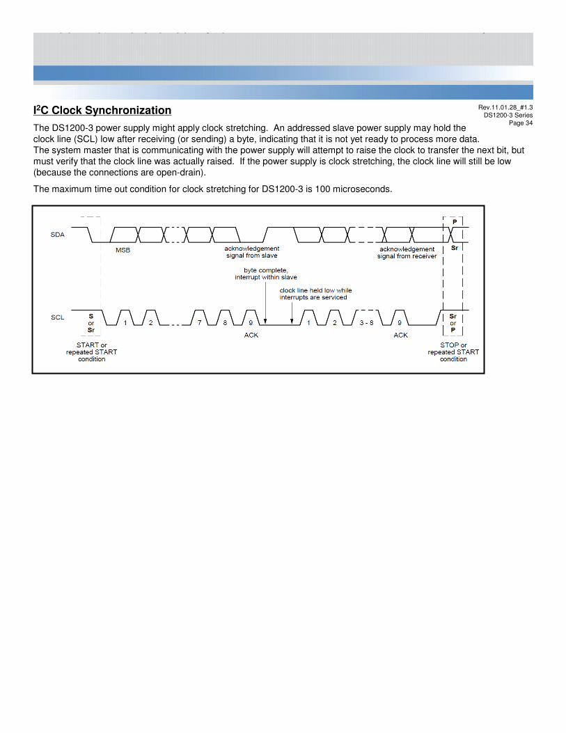
I2C Clock Synchronization
The DS1200-3 power supply might apply clock stretching. An addressed slave power supply may hold the clock line (SCL) low after receiving (or sending) a byte, indicating that it is not yet ready to process more data. The system master that is communicating with the power supply will attempt to raise the clock to transfer the next bit, but must verify that the clock line was actually raised. If the power supply is clock stretching, the clock line will still be low (because the connections are open-drain).
The maximum time out condition for clock stretching for DS1200-3 is 100 microseconds.
Rev.11.01.28_#1.3DS1200-3 Series
Page 35
00000000000000000000
0000000000
CHASSIS SERIAL NUMBER BYTES, Default value is 0.1718191A1B1C1D1E1F20
23242526272829303132
COMMON HEADER, 8 BYTES
SPEC VALUE
CF
00000000000000000000
CA
00
04
01
D2
00
0C
05
00
01
1B
01
(HEX)
207
0000000000
202
0
4
1
210
0
12
5
0
1
27
1
(DEC)
16
0C0D0E0F101112131415
0B
0A
09
08
07
06
05
04
03
02
01
00
(HEX)
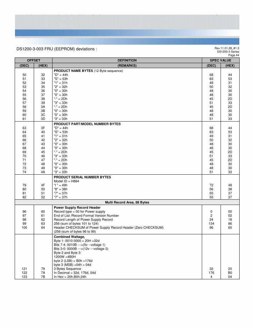
CHASSIS PART NUMBER BYTES (Default value is 0.)12131415161718192021
CHASSIS PART NUMBER Type/Length CAh (if used) Type = “ASCII+LATIN1” = (11)b Length = 10 Bytes = (001010)b11
CHASSIS TYPE (Default value is 0.)10
CHASSIS INFO AREA LENGTH in multiple of 8 bytes9
FORMAT VERSION NUMBER 7:4 - Reserved, write as 0000b3:0 - Format Version Number = 1h for this specification
8
CHASSIS SERIAL NUMBER Type/Length CFH (if used)Type = “ASCII+LATIN1” = (11)b Length = 15 Bytes = (001111)b
22
DEFINITION
CHASSIS INFO AREA( 32 BYTES)This area will be filled by the Mfg. Diag. or by the OS if used
CHASSIS INFO AREA OFFSET2
INTERNAL USE AREA OFFSET1
PRODUCT INFO AREA OFFSET4
BOARD INFO AREA OFFSET3
PAD (reserved) Default value is 0.6
MULTI RECORD AREA OFFSET5
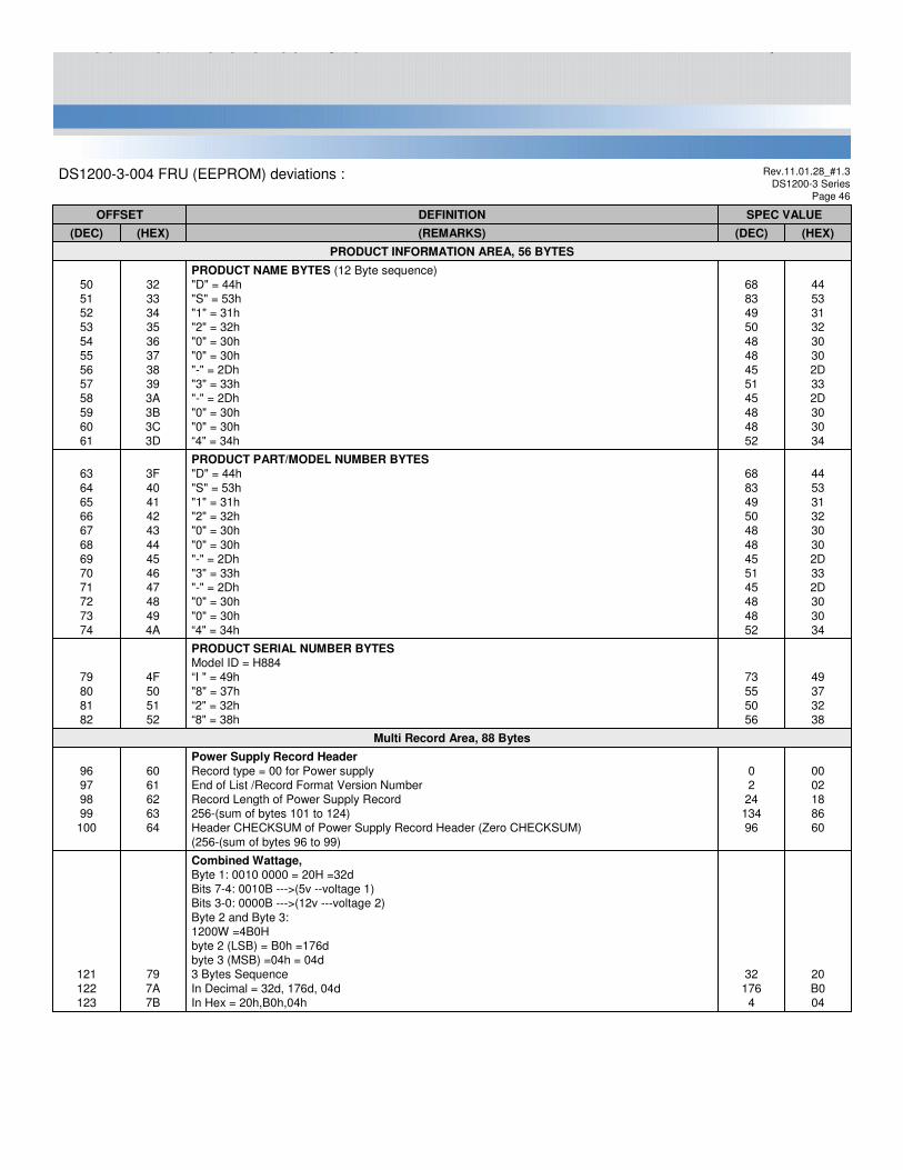
DS1200-3 FRU (EEPROM) Data:
ZERO CHECK SUM (256 – (Sum of bytes 0 to 6))7
FORMAT VERSION NUMBER (Common Header) 7:4 - Reserved, write as 0000b3:0 - Format Version Number = 1h for this specification
0
(REMARKS)(DEC)
OFFSET
FRU (EEPROM) Data
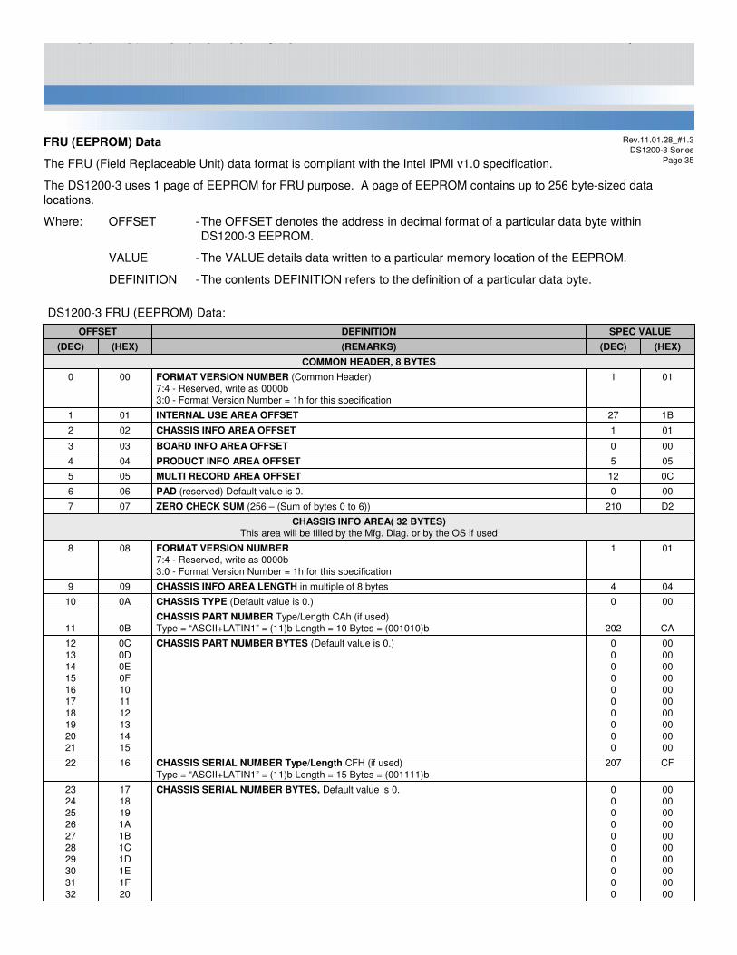
The FRU (Field Replaceable Unit) data format is compliant with the Intel IPMI v1.0 specification.
The DS1200-3 uses 1 page of EEPROM for FRU purpose. A page of EEPROM contains up to 256 byte-sized data locations.
Where: OFFSET -The OFFSET denotes the address in decimal format of a particular data byte within DS1200-3 EEPROM.
VALUE -The VALUE details data written to a particular memory location of the EEPROM.
DEFINITION -The contents DEFINITION refers to the definition of a particular data byte.

Rev.11.01.28_#1.3DS1200-3 Series
Page 36
0000000000
00000
CHASSIS SERIAL NUMBER BYTES, Default value is 0.2022232425
3334353637
011FORMAT VERSION NUMBER (Product Info Area)7:4 - Reserved, write as 0000b3:0 - Format Version Number = 1h for this specification
28
A1161CHKSUM (Zero CHKSUM if used)27
C1193End Tag (0C1h if used)2638
39
PRODUCT INFORMATION AREA, 56 BYTES
40
(HEX)(DEC)(REMARKS)(HEX)(DEC)
XXXX
XXXX
Refer to Section 1.2 Product Revision History (Model Revision) inlatest IPSEg. “0A” In Decimal = 048, 065In Hex = 30H, 41H
4C4D
7677
C2194PRODUCT VERSION NUMBER Type/Length (C2h)Type = “ASCII+LATIN1” = (11)b Length = 2 bytes = (000010)b
4B75
Part / Model Number“DS1200-3 ”In Decimal = 068, 083, 049, 050, 048, 048, 045, 051, 032, 032, 032, 032,In Hex = 44H, 53H, 31H, 32H, 30H, 30H, 2DH, 33H, 20H, 20H, 20H, 20H,
4453313230302D3320202020
688349504848455132323232
3F404142434445464748494A
636465666768697071727374
CC204PRODUCT PART/MODEL NUMBER Type/Length (CCH)Type = “ASCII+LATIN1” = (11)b Length = 12 Bytes = (001100)b
3E62
SPEC VALUE
4453313230302D3320202020
CC
4153544543
C5
19
07
688349504848455132323232
204
6583846967
197
25
7
32333435363738393A3B3C3D
31
2C2D2E2F30
2B
2A
29
Product Name, 12 Byte sequence“DS1200-3 ”In Decimal = 068, 083, 049, 050, 048, 048, 045, 051, 032, 032, 032, 032,In Hex = 44H, 53H, 31H, 32H, 30H, 30H, 2DH, 33H, 20H, 20H, 20H, 20H
PRODUCT NAME Type/Length (CCH) Type = “ASCII+LATIN1” = (11)b Length = 12 Bytes = (001100)b
49
505152535455565758596061
DEFINITION
Language (English)42
PRODUCT INFO AREA LENGTH (In multiples of 8 bytes)41
MANUFACTURER'S NAME 5 byte sequence“E”= 41h“M”= 53h“R”= 54h“S”= 45h“N”= 43h
4445464748
MANUFACTURER NAME TYPE / LENGTH (0C5H) Type “ASCII+LATIN1” 5 Bytes.
43
DS1200-3 FRU (EEPROM) Data:
OFFSET
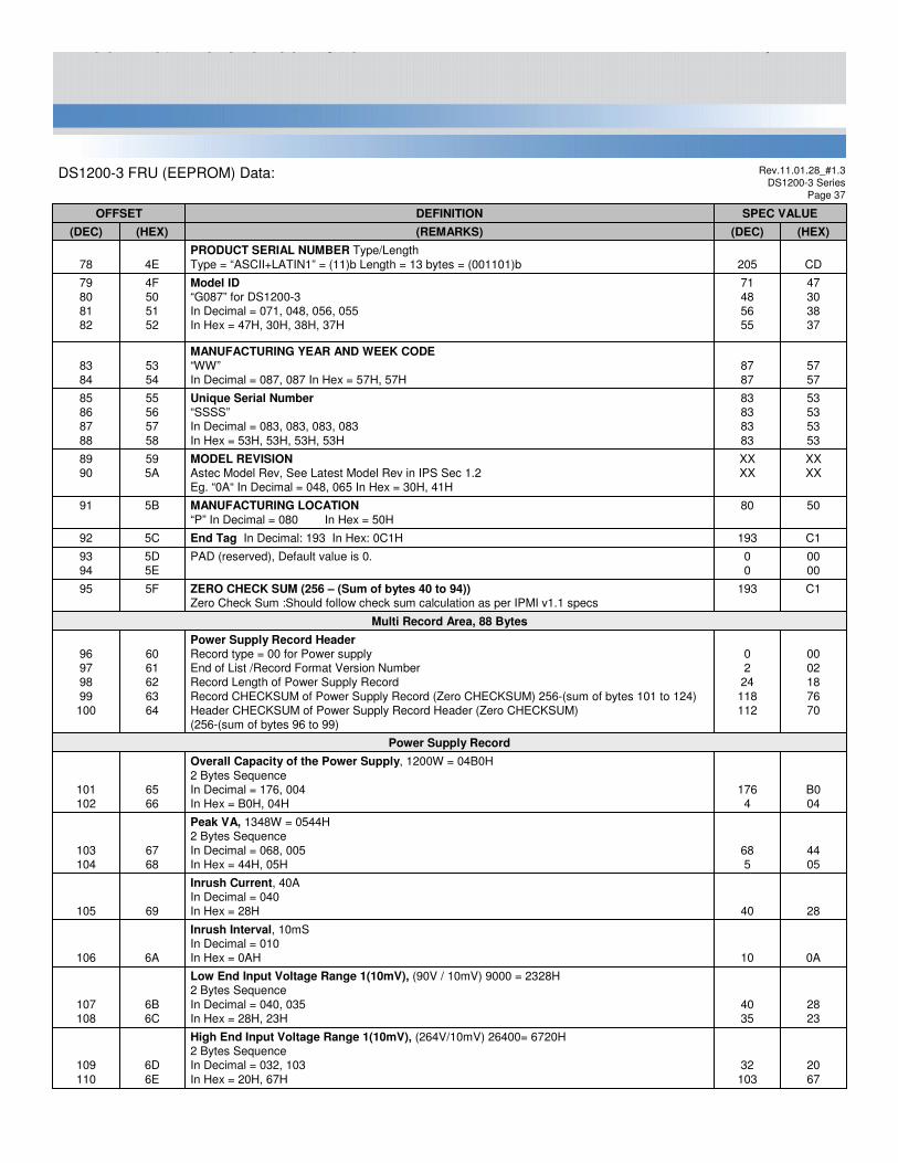
Rev.11.01.28_#1.3DS1200-3 Series
Page 37
47303837
71485655
4F505152
79808182
5080MANUFACTURING LOCATION
“P” In Decimal = 080 In Hex = 50H5B91
C1193End Tag In Decimal: 193 In Hex: 0C1H5C92
CD205PRODUCT SERIAL NUMBER Type/Length Type = “ASCII+LATIN1” = (11)b Length = 13 bytes = (001101)b4E78
Model ID“G087” for DS1200-3In Decimal = 071, 048, 056, 055In Hex = 47H, 30H, 38H, 37H
2067
32103
High End Input Voltage Range 1(10mV), (264V/10mV) 26400= 6720H2 Bytes SequenceIn Decimal = 032, 103In Hex = 20H, 67H
6D6E
109110
2823
4035
Low End Input Voltage Range 1(10mV), (90V / 10mV) 9000 = 2328H2 Bytes SequenceIn Decimal = 040, 035In Hex = 28H, 23H
6B6C
107108
0A10
Inrush Interval, 10mSIn Decimal = 010In Hex = 0AH6A106
2840
Inrush Current, 40AIn Decimal = 040In Hex = 28H69105
0002187670
02
24118112
Power Supply Record HeaderRecord type = 00 for Power supplyEnd of List /Record Format Version NumberRecord Length of Power Supply RecordRecord CHECKSUM of Power Supply Record (Zero CHECKSUM) 256-(sum of bytes 101 to 124)Header CHECKSUM of Power Supply Record Header (Zero CHECKSUM)(256-(sum of bytes 96 to 99)
6061626364
96979899100
B004
1764
Overall Capacity of the Power Supply, 1200W = 04B0H2 Bytes SequenceIn Decimal = 176, 004In Hex = B0H, 04H
6566
101102
Power Supply Record
4405
685
Peak VA, 1348W = 0544H2 Bytes SequenceIn Decimal = 068, 005In Hex = 44H, 05H
6768
103104
XXXX
XXXX
MODEL REVISIONAstec Model Rev, See Latest Model Rev in IPS Sec 1.2Eg. “0A“ In Decimal = 048, 065 In Hex = 30H, 41H
SPEC VALUE
C1
0000
53535353
5757
(HEX)
193
00
83838383
8787
(DEC)
5F
5D5E
595A
55565758
5354
(HEX)
Multi Record Area, 88 Bytes
Unique Serial Number“SSSS”In Decimal = 083, 083, 083, 083In Hex = 53H, 53H, 53H, 53H
85868788
MANUFACTURING YEAR AND WEEK CODE
“WW”In Decimal = 087, 087 In Hex = 57H, 57H
8384
8990
PAD (reserved), Default value is 0.9394
DEFINITION
ZERO CHECK SUM (256 – (Sum of bytes 40 to 94)) Zero Check Sum :Should follow check sum calculation as per IPMI v1.1 specs
95
DS1200-3 FRU (EEPROM) Data:
(REMARKS)(DEC)
OFFSET
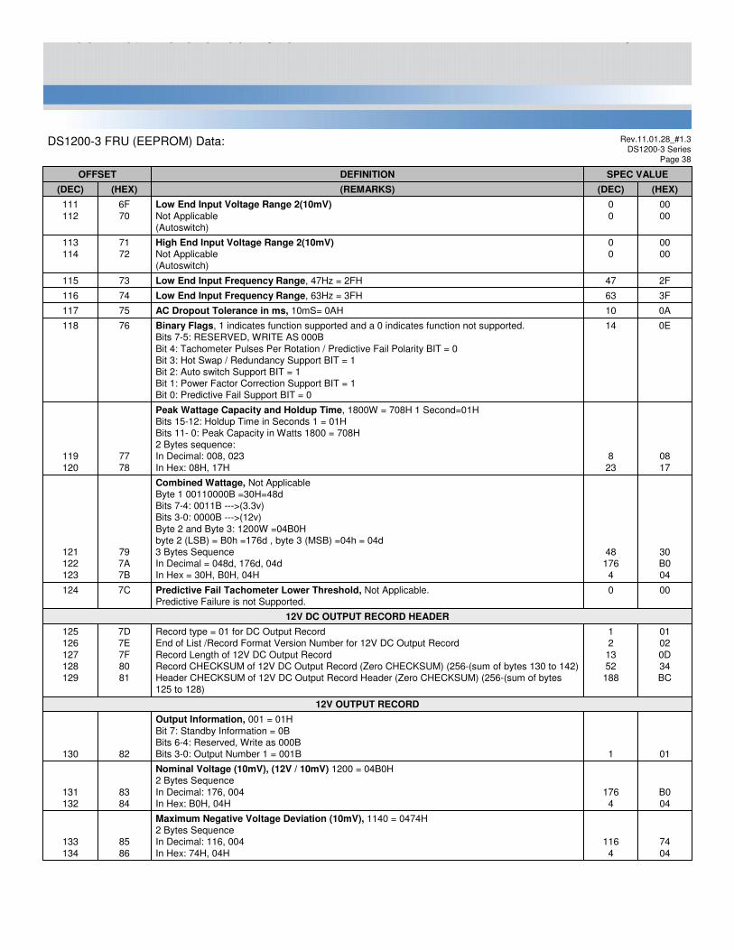
Rev.11.01.28_#1.3DS1200-3 Series
Page 38
0000
00
Low End Input Voltage Range 2(10mV)
Not Applicable(Autoswitch)
6F70
111112
(HEX)(DEC)(REMARKS)(HEX)(DEC)
12V OUTPUT RECORD
7404
1164
Maximum Negative Voltage Deviation (10mV), 1140 = 0474H2 Bytes SequenceIn Decimal: 116, 004In Hex: 74H, 04H
8586
133134
011
Output Information, 001 = 01HBit 7: Standby Information = 0BBits 6-4: Reserved, Write as 000BBits 3-0: Output Number 1 = 001B82130
B004
1764
Nominal Voltage (10mV), (12V / 10mV) 1200 = 04B0H2 Bytes SequenceIn Decimal: 176, 004In Hex: B0H, 04H
8384
131132
01020D34BC
12
1352188
Record type = 01 for DC Output Record End of List /Record Format Version Number for 12V DC Output Record Record Length of 12V DC Output RecordRecord CHECKSUM of 12V DC Output Record (Zero CHECKSUM) (256-(sum of bytes 130 to 142)Header CHECKSUM of 12V DC Output Record Header (Zero CHECKSUM) (256-(sum of bytes 125 to 128)
7D7E7F8081
125126127128129
000Predictive Fail Tachometer Lower Threshold, Not Applicable.Predictive Failure is not Supported.
7C124
12V DC OUTPUT RECORD HEADER
30B004
481764
Combined Wattage, Not ApplicableByte 1 00110000B =30H=48dBits 7-4: 0011B --->(3.3v)Bits 3-0: 0000B --->(12v)Byte 2 and Byte 3: 1200W =04B0Hbyte 2 (LSB) = B0h =176d , byte 3 (MSB) =04h = 04d3 Bytes SequenceIn Decimal = 048d, 176d, 04dIn Hex = 30H, B0H, 04H
797A7B
121122123
0817
823
Peak Wattage Capacity and Holdup Time, 1800W = 708H 1 Second=01HBits 15-12: Holdup Time in Seconds 1 = 01HBits 11- 0: Peak Capacity in Watts 1800 = 708H2 Bytes sequence:In Decimal: 008, 023In Hex: 08H, 17H
7778
119120
0A10AC Dropout Tolerance in ms, 10mS= 0AH75117
0E14Binary Flags, 1 indicates function supported and a 0 indicates function not supported.Bits 7-5: RESERVED, WRITE AS 000BBit 4: Tachometer Pulses Per Rotation / Predictive Fail Polarity BIT = 0Bit 3: Hot Swap / Redundancy Support BIT = 1Bit 2: Auto switch Support BIT = 1Bit 1: Power Factor Correction Support BIT = 1Bit 0: Predictive Fail Support BIT = 0
76118
3F63Low End Input Frequency Range, 63Hz = 3FH74116
2F47Low End Input Frequency Range, 47Hz = 2FH73115
0000
00
High End Input Voltage Range 2(10mV)Not Applicable(Autoswitch)
7172
113114
SPEC VALUEDEFINITION
DS1200-3 FRU (EEPROM) Data:
OFFSET
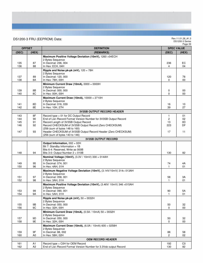
Rev.11.01.28_#1.3DS1200-3 Series
Page 39
EC04
2364
Maximum Positive Voltage Deviation (10mV), 1260 =04ECH2 Bytes SequenceIn Decimal: 236, 004In Hex: ECH, 04H
8788
135136
(HEX)(DEC)(REMARKS)(HEX)(DEC)
OEM RECORD HEADER
3V3SB OUTPUT RECORD
5802
882
Maximum Current Draw (10mA), (6.0A / 10mA) 600 = 0258H2 Bytes SequenceIn Decimal: 88, 002In Hex: 58H, 02H
9FA0
159 160
C082
192130
Record type = C0H for OEM RecordEnd of List /Record Format Version Number for 3.3Vsb output Record
A1A2
161162
82130
Output Information, 002 = 02H Bit 7: Standby Information = 1BBits 6-4: Reserved, Write as 000BBits 3-0: Output Number 2 = 010B94148
4A01
741
Nominal Voltage (10mV), (3.3V / 10mV) 330 = 014AH2 Bytes SequenceIn Decimal: 074, 001In Hex: 4AH, 01H
9596
149150
3A01
581
Maximum Negative Voltage Deviation (10mV), (3.14V/10mV) 314= 013AH2 Bytes SequenceIn Decimal: 058, 001In Hex: 3AH, 01H
9798
151152
5A01
901
Maximum Positive Voltage Deviation (10mV), (3.46V/ 10mV) 346 =015AH2 Bytes SequenceIn Decimal: 090, 001In Hex: 5AH, 01H
999A
153154
3200
500
Ripple and Noise pk-pk (mV), 50 = 0032H2 Bytes SequenceIn Decimal: 050, 000 In Hex: 32H, 00H
9B9C
155156
3200
500
Minimum Current Draw (10mA), (0.5A / 10mA) 50 = 0032H2 Bytes SequenceIn Decimal: 050, 000 In Hex: 32H, 00H
9D9E
157158
01020DDF
11
12
13223
17
Record type = 01 for DC Output Record End of List /Record Format Version Number for 3V3SB Output Record Record Length of 3V3SB Output Record Record CHECKSUM of 3V3SB Output Record (Zero CHECKSUM) (256-(sum of bytes 148 to 160)Header CHECKSUM of 3V3SB Output Record Header (Zero CHECKSUM)(256-(sum of bytes 143 to 146)
8F909192
93
143144145146
147
0000
00
Minimum Current Draw (10mA), 0000 = 0000H2 Bytes SequenceIn Decimal: 000, 000 In Hex: 00H, 00H
8B8C
139140
3V3SB OUTPUT RECORD HEADER
1027
1639
Maximum Current Draw (10mA), 10000 = 2710H2 Bytes SequenceIn Decimal: 016, 039In Hex: 10H, 27H
8D8E
141142
7800
1200
Ripple and Noise pk-pk (mV), 120 = 78H2 Bytes SequenceIn Decimal: 120, 000 In Hex: 78H, 00H
898A
137138
SPEC VALUEDEFINITION
DS1200-3 FRU (EEPROM) Data:
OFFSET

Rev.11.01.28_#1.3DS1200-3 Series
Page 40
00000000000000000000000000000000000000000000000000000000000000000000000000
0000000000000000000000000000000000000
PAD (reserved), Default value is 0.B3B4B5B6B7B8B9BABBBCBDBEBFC0C1C2C3C4C5C6C7C8C9CACBCCCDCECFD0D1D2D3D4D5D6D7
179180181182183184185186187188189190191192193194195196197198199200201202203204205206207208209210211212213214215
00000000000000000000
0000000000
RESERVEDRESERVEDRESERVEDRESERVEDRESERVEDRESERVEDRESERVEDRESERVEDRESERVEDRESERVED
A9AAABACADAEAFB0B1B2
169170171172173174175176177178
32008C
500
140
Record Length of OEM RecordRecord CHECKSUM of OEM Record (Zero CHECKSUM) Header CHECKSUM of OEM Record Header (Zero CHECKSUM) (256-(sum of bytes 161 to 164)
A3A4A5
163164165
(HEX)(DEC)(REMARKS)(HEX)(DEC)
000000
000
Manufacturer ID (3 bytes, Default is 0)A6A7A8
166167168
OEM RECORD
SPEC VALUEDEFINITION
DS1200-3 FRU (EEPROM) Data:
OFFSET
Rev.11.01.28_#1.3DS1200-3 Series
Page 41
000Zero CHECKSUM of Internal Use Area (if used). Default Value=0FF255
(HEX)(DEC)(REMARKS)(HEX)(DEC)
000000000000000000000000000000000000000000000000000000000000000000000000000000
000000000000000000000000000000000000000
RESERVED, Default value is 0.D8D9DADBDCDDDEDFE0E1E2E3E4E5E6E7E8E9EAEBECEDEEEFF0F1F2F3F4F5F6F7F8F9FAFBFCFDFE
216217218219220221222223224225226227228229230231232233234235236237238239240241242243244245246247248249250251252253254
INTERNAL USE AREA, 40 BYTES
SPEC VALUEDEFINITION
DS1200-3 FRU (EEPROM) Data:
OFFSET

Rev.11.01.28_#1.3DS1200-3 Series
Page 42
Multi Record Area, 88 Bytes
0002188660
02
2413496
Power Supply Record Header
Record type = 00 for Power supplyEnd of List /Record Format Version NumberRecord Length of Power Supply Record256-(sum of bytes 101 to 124)Header CHECKSUM of Power Supply Record Header (Zero CHECKSUM)(256-(sum of bytes 96 to 99)
6061626364
96979899100
48383834
72565652
PRODUCT SERIAL NUMBER BYTESModel ID = H884"H" = 48h "8" = 38h "8" = 38h "4" = 34h
4F505152
79808182
20B004
321764
Combined Wattage,Byte 1: 0010 0000 = 20H =32dBits 7-4: 0010B --->(5v --voltage 1)Bits 3-0: 0000B --->(12v ---voltage 2)Byte 2 and Byte 3:1200W =4B0Hbyte 2 (LSB) = B0h =176dbyte 3 (MSB) =04h = 04d3 Bytes SequenceIn Decimal = 32d, 176d, 04dIn Hex = 20h,B0h,04h
797A7B
121122123
(HEX)(DEC)(REMARKS)(HEX)(DEC)
PRODUCT PART/MODEL NUMBER BYTES"D" = 44h"S" = 53h"1" = 31h"2" = 32h"0" = 30h"0" = 30h"-" = 2Dh"3" = 33h"-" = 2Dh"0" = 30h"0" = 30h"2" = 32h
4453313230302D332D303032
688349504848455145484850
3F404142434445464748494A
636465666768697071727374
SPEC VALUE
4453313230302D332D303032
688349504848455145484850
32333435363738393A3B3C3D
PRODUCT NAME BYTES (12 Byte sequence)"D" = 44h"S" = 53h"1" = 31h"2" = 32h"0" = 30h"0" = 30h"-" = 2Dh"3" = 33h"-" = 2Dh"0" = 30h"0" = 30h"2" = 32h
505152535455565758596061
DEFINITION
PRODUCT INFORMATION AREA, 56 BYTES
DS1200-3-002 FRU (EEPROM) deviations:
OFFSET

Rev.11.01.28_#1.3DS1200-3 Series
Page 43
5VSB OUTPUT RECORD
(HEX)(DEC)(REMARKS)(HEX)(DEC)
9001
1441
Maximum Current Draw (10mA), (4.0A / 10mA) 400 = 0190H2 Bytes SequenceIn Decimal: 144, 001In Hex: 90H, 01H
9FA0
159 160
F401
2441
Nominal Voltage (10mV), (5.0V / 10mV) 5000 = 01F4h2 Bytes SequenceIn Decimal: 244, 001 In Hex: F4h, 01h
9596
149150
0B01
2191
Maximum Negative Voltage Deviation (10mV), (4.75V/10mV) 475 = 01DBh2 Bytes SequenceIn Decimal: 219, 001 In Hex: DBh, 01h
9798
151152
0D02
132
Maximum Positive Voltage Deviation (10mV), (5.25V/ 10mV) 525 = 020Dh2 Bytes SequenceIn Decimal: 013, 002In Hex: 0DH, 02H
999A
153154
01020DA9
47
12
13169
71
Record type = 01 for DC Output Record End of List /Record Format Version Number for 5VSB Output RecordRecord Length of 5VSB Output RecordRecord CHECKSUM of 5VSB Output Record (Zero CHECKSUM) (256-(sum of bytes 148 to 160)Header CHECKSUM of 5VSB Output Record Header (Zero CHECKSUM)(256-(sum of bytes 143 to 146)
8F909192
93
143144145146
147
5VSB OUTPUT RECORD HEADER
SPEC VALUEDEFINITION
DS1200-3-002 FRU (EEPROM) deviations:
OFFSET
Rev.11.01.28_#1.3DS1200-3 Series
Page 44
20B004
321764
Combined Wattage,Byte 1: 0010 0000 = 20H =32dBits 7-4: 0010B --->(5v --voltage 1)Bits 3-0: 0000B --->(12v ---voltage 2)Byte 2 and Byte 3:1200W =4B0Hbyte 2 (LSB) = B0h =176dbyte 3 (MSB) =04h = 04d3 Bytes SequenceIn Decimal = 32d, 176d, 04dIn Hex = 20h,B0h,04h
797A7B
121122123
48383737
72565555
PRODUCT SERIAL NUMBER BYTESModel ID = H884“I " = 49h "8" = 38h “7" = 37h “7" = 37h
4F505152
79808182
Multi Record Area, 88 Bytes
0002188660
02
2413496
Power Supply Record HeaderRecord type = 00 for Power supplyEnd of List /Record Format Version NumberRecord Length of Power Supply Record256-(sum of bytes 101 to 124)Header CHECKSUM of Power Supply Record Header (Zero CHECKSUM)(256-(sum of bytes 96 to 99)
6061626364
96979899100
(HEX)(DEC)(REMARKS)(HEX)(DEC)
PRODUCT PART/MODEL NUMBER BYTES"D" = 44h"S" = 53h"1" = 31h"2" = 32h"0" = 30h"0" = 30h"-" = 2Dh"3" = 33h"-" = 2Dh"0" = 30h"0" = 30h“3" = 33h
4453313230302D332D303033
688349504848455145484851
3F404142434445464748494A
636465666768697071727374
SPEC VALUE
4453313230302D332D303033
688349504848455145484851
32333435363738393A3B3C3D
PRODUCT NAME BYTES (12 Byte sequence)"D" = 44h"S" = 53h"1" = 31h"2" = 32h"0" = 30h"0" = 30h"-" = 2Dh"3" = 33h"-" = 2Dh"0" = 30h"0" = 30h“3" = 33h
505152535455565758596061
DEFINITION
DS1200-3-003 FRU (EEPROM) deviations :
OFFSET
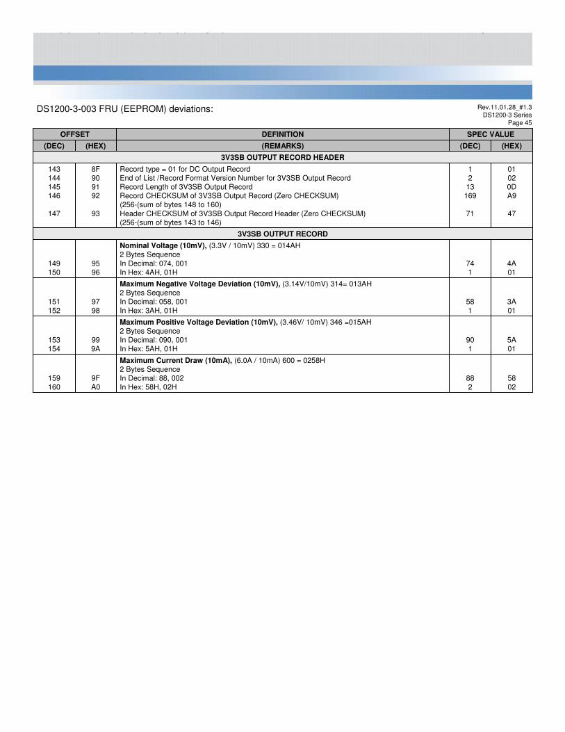
Rev.11.01.28_#1.3DS1200-3 Series
Page 45
(HEX)(DEC)(REMARKS)(HEX)(DEC)
3V3SB OUTPUT RECORD
5802
882
Maximum Current Draw (10mA), (6.0A / 10mA) 600 = 0258H2 Bytes SequenceIn Decimal: 88, 002In Hex: 58H, 02H
9FA0
159 160
4A01
741
Nominal Voltage (10mV), (3.3V / 10mV) 330 = 014AH2 Bytes SequenceIn Decimal: 074, 001In Hex: 4AH, 01H
9596
149150
3A01
581
Maximum Negative Voltage Deviation (10mV), (3.14V/10mV) 314= 013AH2 Bytes SequenceIn Decimal: 058, 001In Hex: 3AH, 01H
9798
151152
5A01
901
Maximum Positive Voltage Deviation (10mV), (3.46V/ 10mV) 346 =015AH2 Bytes SequenceIn Decimal: 090, 001In Hex: 5AH, 01H
999A
153154
01020DA9
47
12
13169
71
Record type = 01 for DC Output Record End of List /Record Format Version Number for 3V3SB Output Record Record Length of 3V3SB Output RecordRecord CHECKSUM of 3V3SB Output Record (Zero CHECKSUM) (256-(sum of bytes 148 to 160)Header CHECKSUM of 3V3SB Output Record Header (Zero CHECKSUM)(256-(sum of bytes 143 to 146)
8F909192
93
143144145146
147
3V3SB OUTPUT RECORD HEADER
SPEC VALUEDEFINITION
DS1200-3-003 FRU (EEPROM) deviations:
OFFSET
Rev.11.01.28_#1.3DS1200-3 Series
Page 46
49373238
73555056
PRODUCT SERIAL NUMBER BYTESModel ID = H884“I " = 49h "8" = 37h “2" = 32h “8" = 38h
4F505152
79808182
20B004
321764
Combined Wattage,Byte 1: 0010 0000 = 20H =32dBits 7-4: 0010B --->(5v --voltage 1)Bits 3-0: 0000B --->(12v ---voltage 2)Byte 2 and Byte 3:1200W =4B0Hbyte 2 (LSB) = B0h =176dbyte 3 (MSB) =04h = 04d3 Bytes SequenceIn Decimal = 32d, 176d, 04dIn Hex = 20h,B0h,04h
797A7B
121122123
Multi Record Area, 88 Bytes
0002188660
02
2413496
Power Supply Record Header
Record type = 00 for Power supplyEnd of List /Record Format Version NumberRecord Length of Power Supply Record256-(sum of bytes 101 to 124)Header CHECKSUM of Power Supply Record Header (Zero CHECKSUM)(256-(sum of bytes 96 to 99)
6061626364
96979899100
(HEX)(DEC)(REMARKS)(HEX)(DEC)
PRODUCT PART/MODEL NUMBER BYTES"D" = 44h"S" = 53h"1" = 31h"2" = 32h"0" = 30h"0" = 30h"-" = 2Dh"3" = 33h"-" = 2Dh"0" = 30h"0" = 30h“4" = 34h
4453313230302D332D303034
688349504848455145484852
3F404142434445464748494A
636465666768697071727374
SPEC VALUE
4453313230302D332D303034
688349504848455145484852
32333435363738393A3B3C3D
PRODUCT NAME BYTES (12 Byte sequence)"D" = 44h"S" = 53h"1" = 31h"2" = 32h"0" = 30h"0" = 30h"-" = 2Dh"3" = 33h"-" = 2Dh"0" = 30h"0" = 30h“4" = 34h
505152535455565758596061
DEFINITION
PRODUCT INFORMATION AREA, 56 BYTES
DS1200-3-004 FRU (EEPROM) deviations :
OFFSET

Rev.11.01.28_#1.3DS1200-3 Series
Page 47
(HEX)(DEC)(REMARKS)(HEX)(DEC)
5VSB OUTPUT RECORD
9001
1441
Maximum Current Draw (10mA), (4.0A / 10mA) 400 = 0190H2 Bytes SequenceIn Decimal: 144, 001In Hex: 90H, 01H
9FA0
159 160
F401
2441
Nominal Voltage (10mV), (5.0V / 10mV) 5000 = 01F4h2 Bytes SequenceIn Decimal: 244, 001 In Hex: F4h, 01h
9596
149150
0B01
2191
Maximum Negative Voltage Deviation (10mV), (4.75V/10mV) 475 = 01DBh2 Bytes SequenceIn Decimal: 219, 001 In Hex: DBh, 01h
9798
151152
0D02
132
Maximum Positive Voltage Deviation (10mV), (5.25V/ 10mV) 525 = 020Dh2 Bytes SequenceIn Decimal: 013, 002In Hex: 0DH, 02H
999A
153154
01020DA9
47
12
13169
71
Record type = 01 for DC Output Record End of List /Record Format Version Number for 5VSB Output RecordRecord Length of 5VSB Output Record Record CHECKSUM of 5VSB Output Record (Zero CHECKSUM) (256-(sum of bytes 148 to 160)Header CHECKSUM of 5VSB Output Record Header (Zero CHECKSUM)(256-(sum of bytes 143 to 146)
8F909192
93
143144145146
147
5VSB OUTPUT RECORD HEADER
SPEC VALUEDEFINITION
DS1200-3-004 FRU (EEPROM) deviations:
OFFSET

Rev.11.01.28_#1.3DS1200-3 Series
Page 48PMBusTM Interface Support
The DS1200-3 is compliant with the industry standard PMBusTM protocol for monitoring and control of the power supply via the I2C interface port.
DS1200-3 Series PMBusTM General Instructions
Equipment Setup
The following is typical I2C communication setup:
PMBusTM Writing Instructions
When writing to any PMBusTM R/W registers, ALWAYS do the following:
Disable Write Protect (command 10h) by writing any of the following accordingly:
Levels: 00h – Enable writing to all writeable commands
20h – Disables write except 10h, 01h, 00h, 02h and 21h commands
40h – Disables write except 10h, 01h, and 00h commends
80h – Disable write except 0x00h
To save changes on the USER PMBusTM Table:
Use send byte command: 15h STORE_USER_ALL
To save changes on the DEFAULT PMBusTM Table:
Use send byte command: 11h STORE_DEFAULT_ALL
Wait for 5 seconds, turn-off the PSU, wait for another 5 seconds before turning it on.
AC Source
DS1200-3
Voltmeter
E-LoadI2C AdaptorI2C Master
Rev.11.01.28_#1.3DS1200-3 Series
Page 49
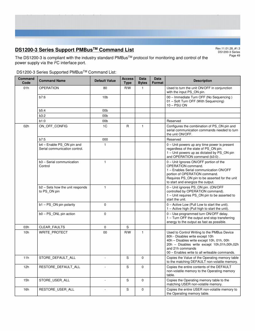
DS1200-3 Series Support PMBusTM Command List
The DS1200-3 is compliant with the industry standard PMBusTM protocol for monitoring and control of the power supply via the i2C interface port.
0 – Use programmed turn ON/OFF delay.1 – Turn OFF the output and stop transferring energy to the output as fast as possible.
0b0 – PS_ONL pin action
0 – Active Low (Pull Low to start the unit).1 – Active high (Pull high to start the unit).
0b1 – PS_ON pin polarity
S0CLEAR_FAULTS 03h
0 – Unit Ignores ON/OFF portion of the OPERATION command.1 – Enables Serial communication ON/OFF portion of OPERATION command. Requires PS_ON pin to be asserted for the unit to start and energize the output.
1b3 – Serial communication Control
0 – Unit ignores PS_ON pin. (ON/OFF controlled by OPERATION command).1 – Unit requires PS_ON pin to be asserted to start the unit.
1b2 – Sets how the unit responds to PS_ON pin
Reserved000b7:5
0 – Unit powers up any time power is present regardless of the state of PS_ON pin.1 – Unit powers up as dictated by PS_ON pin and OPERATION command (b3:0) .
1b4 – Enable PS_ON pin and Serial communication control.
Reserved00bb1:0
00bb3:2
00bb5:4
00 – Immediate Turn OFF (No Sequencing )01 – Soft Turn OFF (With Sequencing)10 – PSU ON
10bb7:6
Data
Format
0
0
0
0
1
1
1
Data
BytesDefault Value
Copies the Value of the Operating memory table to the matching DEFAULT non-volatile memory.
S-STORE_DEFAULT_ALL11h
Used to Control Writing to the PMBus Device80h - Disables write except 10h 40h – Disables write except 10h, 01h, 00h 20h – Disables write except 10h,01h,00h,02h and 21h commands00 – Enables write to all writeable commands.
R/W00WRITE_PROTECT10h
Copies the Operating memory table to the matching USER non-volatile memory.
S-STORE_USER_ALL15h
Copies the entire contents of the DEFAULT non-volatile memory to the Operating memory table.
S-RESTORE_DEFAULT_ALL12h
Copies the entire USER non-volatile memory to the Operating memory table.
S-RESTORE_USER_ALL16h
DS1200-3 Series Supported PMBusTM Command List:
Configures the combination of PS_ON pin and serial communication commands needed to turn the unit ON/OFF.
R1CON_OFF_CONFIG02h
Used to turn the unit ON/OFF in conjunction with the input PS_ON pin.
R/W80OPERATION01h
DescriptionAccess
TypeCommand Name
Command
Code

Rev.11.01.28_#1.3DS1200-3 Series
Page 50
DescriptionData
FormatData
BytesAccess
TypeDefault ValueCommand Name
Command Code
Provides a way for the hosts system to determine some key capabilities of a PMBusTM
device.
1R00CAPABILITY19h
b low Byte, b high byte 0000byte 2:3
m low Byte, m high byte 0501byte 0:1
R byte 0002byte 4:5
02R/W0000VOUT_TRIM 22h
Variable. Used by Factory to trim Vout Default before trimming, 0000.
2R/WXXXXVOUT_CAL_OFFSET 23h
Sets the Output Voltage ReferenceVout command sends discreet value to changeor trim output voltage. The value acts as Digital reference of the Power supply after additional operations are performed (to make the representation compatible). Affects OVP_WARNING and FAULT LIMIT, as well as POWER_GOOD_ON/OFF level.
Direct2R/WB004VOUT_COMMAND 21h
0 - Maximum supported bus speed, 100khz1 - Maximum supported bus speed, 400khz
1b6 - Maximum Bus Speed
0 – SMBus Alert Pin not supported
1 – SMBus Alert Pin supported
0b5 - SMBALERT#
0 - PEC not supported 1 - PEC supported
0b7 - Packet Error Checking
Reserved00000b4:0
Specifies the mode and parameters of Output Voltage related Data Formats
1R40VOUT_MODE20h
Sets the max adjustable output voltage limit. 13.8V.
Direct2R6405VOUT_MAX24h
Use to retrieve the m, b and R coefficients, needed for DIRECT data format
6BRCOEFFICIENTS30h
Sets the operating power limit condition.1550W
Linear2R070BPOUT_MAX31h
Sets the value of input, in volts, at which the unit should start. ACGOOD 88Vac
Linear2RC0EAVIN_ON35h
Sets the value of input, in volts, at which the unit should stop power conversion. ACBAD 79Vac
Linear2R9EF8VIN_OFF36h
The ratio of voltage across the Current Sense to actual current.
2RFF7FIOUT_CAL_GAIN38h
Used to null any offsets in the current sensing circuit. Normally used in conjunction with the IOUT_SCALE to minimize current sensing error.
2R0000IOUT_CAL_OFFSET39h
DS1200-3 Series Supported PMBusTM Command List:

Rev.11.01.28_#1.3DS1200-3 Series
Page 51
Used to configure up to 2 fans associated with one PMBus device
1R90FAN_ CONFIG_1_23Ah
1 – Fan is installed in position 10 – No Fan is installed in position 1
1b7
1 – Fan is commanded in RPM0 – Fan is commanded in DC
0b6
00 – 1 pulse per revolution01 – 2 pulses per revolution10 – 3 pulses per revolution11 – 4 pulses per revolution
01b5:4
1 – Fan is installed in position 20 – No Fan is installed in position 2
0b3
1 – Fan is commanded in RPM0 – Fan is commanded in DC
0b2
Sets the threshold for input current that causes over-current fault within 100ms. (13A)
Linear2R40D3IIN_OC_FAULT_LIMIT 5Bh
00 – 1 pulse per revolution01 – 2 pulses per revolution10 – 3 pulses per revolution11 – 4 pulses per revolution
00b1:0
Adjusts the operation of the Fans. The device may override the command, if it requires higher value, to maintain proper device temperature. RPM Control – Commands Speeds from 0-65535 RPM.Duty cycle Control – Commands Speeds from 0 to 100%
Direct2R/W6400FAN_COMMAND_13Bh
Sets Output Over voltage threshold. (13.8V) Direct2R/W6405VOUT_OV_FAULT_LIMIT40h
Unit Latches OFF. Resets on PSON or CONTROL pin recycle or AC recycle.
1R80VOUT_OV_FAULT_RESPONSE41h
Sets Over-voltage Warning threshold. (13V) Direct2R/W1405VOUT_OV_WARN_LIMIT42h
Sets Under-voltage Warning threshold. (11V)Direct2R/W4C04VOUT_UV_WARN_LIMIT43h
Sets Under-voltage Fault threshold. (10.2V) Direct2R/WFC03VOUT_UV_FAULT_LIMIT44h
Turn PSU OFF 1R80VOUT_UV_FAULT_RESPONSE45h
Sets the Over current threshold in Amps. (125A for Hi Line and 98A for Low Line)
Direct2RD430 High4826 Low
IOUT_OC_FAULT_LIMIT46h
OCP ride through. If OCP persists. 1RC0IOUT_OC_FAULT_RESPONSE47h
Sets the Over Current Warning threshold in Amps. (112A for Hi Line and 88A for Low Line)
Direct2RC02B high6022 Low
IOUT_OC_WARN_LIMIT4Ah
Secondary ambient temperature Fault threshold, in degree C. (58degC)
Direct2RA816OT_FAULT_LIMIT4Fh
Turn PSU OFF and will retry indefinitely 1RB8OT_FAULT_RESPONSE50h
Secondary ambient temperature warning threshold, in degree C. Operating limit. refer to section 3.1. (55 degC)
Direct2R70E3OT_WARN_LIMIT51h
Sets input over-voltage threshold. (275Vac) Linear2R26FAVIN_OV_FAULT_LIMIT55h
No interruption. 1R00VIN_OV_FAULT_RESPONSE56h
Sets the threshold of input voltage that triggers high voltage warning. (275Vac)
Linear2R26FAVIN_OV_WARN_LIMIT57h
(82Vac)Linear2R90EAVIN_UV_WARN_LIMIT58h
(80Vac)Linear2R80EAVIN_UV_FAULT_LIMIT59h
1R00VIN_UV_FAULT_RESPONSE5Ah
DescriptionData
BytesDefault Value
DS1200-3 Series Supported PMBusTM Command List:
Data Format
AccessType
Command NameCommand
Code

Rev.11.01.28_#1.3DS1200-3 Series
Page 52
Turn PSU OFF. cleared upon AC recycle. 1R00IIN-OC-FAULT_RESPONSE 5Ch
Sets the threshold by which the Power Good signal is asserted. (11.76V)
Direct2R9804POWER_GOOD_ON5Eh
Sets the threshold by which the Power Good signal is de-asserted. (10.2V)
Direct2RFC03POWER_GOOD_OFF5Fh
Sets the time (sec), from start condition (Power ON) until the output starts to rise. (2sec)
Direct2RC300TON_DELAY 60h
Sets the time (ms), for the output rises from 0 to regulation. (50ms)
Direct2R8813TON_RISE 61h
Sets the time (ms), from a stop condition (Power OFF) until the output starts to drop (converter OFF).(23ms)
Direct2RFC08TOFF_DELAY 64h
A communication, memory or logic fault has occurred.
b1 – CML
A temperature fault or warning has occurred b2 – TEMPERATURE
Unit is OFF b6 – OFF
Output over-voltage fault has occurred b5 – VOUT_OV
Output over-current fault has occurred b4 – IOUT_OC
An input under-voltage fault has occurred b3 - VIN_UV
A fault was declared because the device was busy and unable to respond.
b7 – BUSY
The POWER_GOOD signal is de-assertedb11 – POWER_GOOD#
A manufacturer specific fault or warning has occurred.
b12 – MFR
An input voltage, current or power fault or warning as occurred.
b13 – INPUT
An Output current or power fault or warning has occurred.
b14 – IOUT/POUT
An output voltage fault or warning has occurred b15 – VOUT
A fan or airflow fault or warning has occurred. b10 - FANS
A bit in STATUS_OTHER is set. b9 – OTHER
A fault type not given in bits [15:1] of the STATUS_WORD has been detected.
b8 – UKNOWN
A fault or warning not listed in bits[7:1] of this byte has occurred.
b0 – NONE_OF_THE_ABOVE
A communication, memory or logic fault has occurred.
b1 – CML
Output over-current fault has occurredb4 – IOUT_OC
An input under--voltage fault has occurred b3 - VIN_UV
A temperature fault or warning has occurred b2 - TEMPERATURE
Output over-voltage fault has occurred b5 – VOUT_OV
A fault was declared because the device was busy and unable to respond.
b7 – BUSY
Unit is OFF b6 – OFF
A Fault Warning not listed in bits[7:1] has occurred.
b0 – NONE OF THE ABOVE
Returns the summary of critical faults 1RSTATUS_BYTE78h
Summary of units Fault and warning status. 2RSTATUS_WORD79h
DescriptionData
BytesDefault Value
DS1200-3 Series Supported PMBusTM Command List:
Data Format
AccessType
Command NameCommand
Code
Rev.11.01.28_#1.3DS1200-3 Series
Page 53
Output voltage related faults and warnings 1R-STATUS_VOUT7Ah
VOUT Over--voltage Faultb7
VOUT Over-voltage warningb6
VOUT Under-voltage Warningb5
VOUT Under-voltage Faultb4
VOUT_MAX Warning, an attempt has been made to set output to a value higher that the highest permissible voltage.
b3
TON_MAX_FAULT b2
TOFF_MAX Warning b1
reserved b0
Output Current related faults and warnings 1RSTATUS_IOUT 7Bh
IOUT Over current Fault b7
IOUT Over current And Low Voltage shutdownFault
b6
b3
Memory Fault Detect, CRC Error b4
Packet Error Check Failed b5
b6
b1
b0
Invalid or unsupported Command Received b7
b2
Communications, Logic and Memory 1R-STATUS_CML 7Eh
Overtemperature Warning b6
Overtemperature Fault b7
Undertemperature Fault b4
Undertemperature Warning b5
reserved b3:0
IIN Overcurrent Fault b2
Unit is OFF for insufficient Input Voltage b3
IIN Overcurrent Warning b1
VIN Overvoltge Warning b6
VIN Undervoltage Warning b5
VIN Overvoltage Fault b7
VIN Undervoltage Fault b4
PIN overpower Warning b0
POUT Overpower Warningb0
POUT Overpower Faultb1
Power Limitingb2
IOUT Undercurrent Faultb4
IOUT Overcurrent Warningb5
Current Share Fault Set if Ishare level is much greater or lower than the actual output current.Refer to Output Specifications (Table 3) for Current sharing limits.
b3
Input related faults and warnings 1RSTATUS_INPUT7Ch
Temperature related faults and warnings 1R-STATUS_TEMPERATURE7Dh
DescriptionData
BytesDefault Value
DS1200-3 Series Supported PMBusTM Command List:
Data Format
AccessType
Command NameCommand
Code

Rev.11.01.28_#1.3DS1200-3 Series
Page 54
Manufacturer Status codes 1R-STATUS_MFR_SPECIFIC80h
Bulk OK, 1- Bulk is within range and is ready for use
b7
Not Used b6
Not Usedb5
Not Usedb4
Not Uesdb3
Not Uesdb2
Standby Fault, 1 If there’s a standby fault.b1
PS_ON Pin Status 1 – asserted, 0 - deasserted b0
1R-STATUS_FANS_1_2 81h
Fan 1 Fault b7
Fan 2 Fault b6
Fan 1 Warningb5
Fan 2 Warning b4
Manufacture Date, ASCII formatstructure : YYMMDD
7BR“xxxxxxx”MFR_Data9Dh
Unit serial number, ASCII format.13BR“xxxxxxxxxxxxx”MFR_Serial9Eh
Part 1 Revision 0000 – Revision 1.00001 – Revision 1.1
0001b7:5
Part 2 Revision0000 – Revision 1.00001 –Revision 1.1
0001b4:0
b1
b0
Fan_1 Speed Overridden b3
Fan_2 Speed Overridden b2
Returns the input power, in Watts.Linear2R-READ_PIN97h
Reads the PMBus revision number 1R11PMBUS_REVISION98h
Abbrev or symbol of manufacturers name.4BR, ASCII
“ALL”MFR_ID99h
Manufacturers Model number, ASCII format8BR, ASCII
“DS1200-3”MFR_MODEL9Ah
Manufacturers, revision number, ASCII format3BR, ASCII
“1.0”MFR_REVISION9Bh
Manufacturers facility, ASCII format4BR, ASCII
“xxx”MFR_LOCATION9Ch
Minimum Input Voltage (90Vac)Linear2RB4F8MFR_VIN_MINA0h
Maximum Input Voltage (264Vac)Linear2R10FAMFR_VIN_MAXA1h
Maximum Input Current (12A)Linear2R18F8MFR_IIN_MAXA2h
Returns input Voltage in Volts ac.Linear2R-READ_VIN88h
Returns input Current in AmperesLinear2R-READ_IIN89h
Returns Bulk Capacitor voltage in VoltsLinear2R-READ_VCAP8Ah
Returns the actual, measured voltage in Volts. Direct2R-READ_VOUT8Bh
Returns the output current in amperes. Direct2R-READ_IOUT8Ch
PSU Air inlet temp ( inside PSU) Direct2R-READ_TEMPERATURE_28Eh
Speed of Fan 1 Linear2R-READ_FAN_SPEED_1 90h
Returns the output power, in Watts. Linear2R-READ_POUT96h
DescriptionData
BytesDefault Value
DS1200-3 Series Supported PMBusTM Command List:
Data Format
AccessType
Command NameCommand
Code
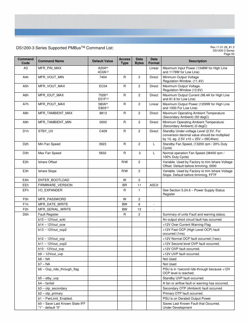
Rev.11.01.28_#1.3DS1200-3 Series
Page 55
Maximum Input Power (1348W for High Line and 1176W for Low Line)
LinearA20AHI
4C0ALO
MFR_PIN_MAX A3
Minimum Output VoltageRegulation Window. (11.4V)
Direct2R7404MFR_VOUT_MINA4h
Maximum Output Voltage.Regulation Window (12.6V)
Direct2REC04MFR_VOUT_MAXA5h
Maximum Output Current (98.4A for High Line and 81.6 for Low Line)
Direct2R7026HI
E01FLO
MFR_IOUT_MAXA6h
Maximum Output Power (1200W for High Line and 1000 For Low Line)
Linear2R580AHI
E803LO
MFR_POUT_MAXA7h
Maximum Operating Ambient Temperature (Secondary Ambient) (50 degC)
Direct2R8813MFR_TAMBIENT_MAXA8h
Minimum Operating Ambient Temperature (Secondary Ambient) (0 degC)
Direct2R0000MFR_TAMBIENT_MINA9h
Standby Under-voltage Level (2.5V, For conversion decimal value should be multiplied by 10, eg. 2.5V x10 = 25V = 09C4hex)
Direct2RC409STBY_UVD1h
-6BWMFR_DATE_WRITEF1h
-13BWMFR_SERIAL_WRITEF2h
Standby Fan Speed, (13200 rpm / 20% Duty Cycle)
L 2R3923Min Fan SpeedD2h
Normal operation Fan Speed (38400 rpm / 100% Duty Cycle)
L2R5832Max Fan SpeedD3h
Variable. Used by Factory to trim Ishare Voltage Offset. Default before tirmming, 0000
2R/WIshare OffsetE2h
Variable. Used by Factory to trim Ishare Voltage Slope. Default before tirmming, FF7F
2R/WIshare SlopeE3h
2WENTER_BOOTLOADEAh
ASCII11BRFIRMWARE_VERSIONEEh
See Section 5.24.6 – Power Supply Status Register
1RI/O_EXPANDEREFh
2WMFR_PASSWORDF0h
Summary of units Fault and warning status. 2RFault Register D0h
An output short circuit fault has occurred.b15 – 12Vout_sckt
+12V Over Current Warning Flagb14 – 12Vout_ocw
+12V Fast OCP (High Level OCP) fault occurred (1ms)
b13 – 12Vout_ocp2
+12V Normal OCP fault occurred (1sec).b12 – 12Vout_ocp
+12V Second level OVP fault occurred.b11 – 12Vout_ovp2
+12V OVP fault occurred.b10 - 12Vout_ovp
+12V UVP fault occurred.b9 – 12Vout_uvp
Not Usedb8 – NA
Not Usedb7 – NA
PSU is in 1second ride-through because +12V OCP level is reached.
b6 – Ocp_ride_through_flag
Standby UVP fault occurred.b5 – stby_uvp
A fan or airflow fault or warning has occurred.b4 – fanfail
Secondary OTP (Ambient) fault occurred.b3 – otp_secondary
Primary OTP fault occurred.b2 – otp_primary
PSU is on Derated Output Power b1 – PwrLimit_Enabled.
Saves Last Known Fault that Occurred.Under Development
b0 – Save Last Known State IFF "1" - default "0"
DescriptionData
BytesDefault Value
DS1200-3 Series Supported PMBusTM Command List:
Data Format
AccessType
Command NameCommand
Code
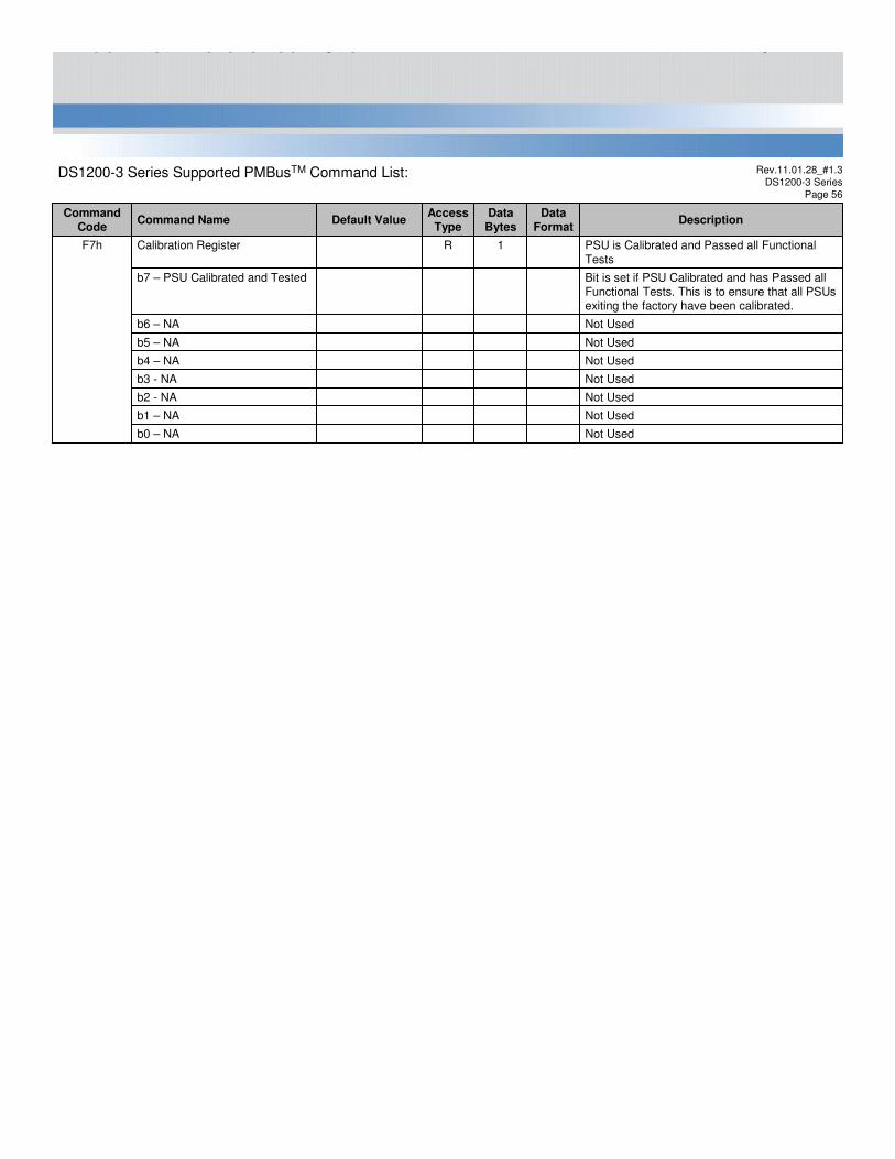
Rev.11.01.28_#1.3DS1200-3 Series
Page 56
Not Usedb5 – NA
Not Usedb4 – NA
PSU is Calibrated and Passed all Functional Tests
1RCalibration RegisterF7h
Bit is set if PSU Calibrated and has Passed all Functional Tests. This is to ensure that all PSUs exiting the factory have been calibrated.
b7 – PSU Calibrated and Tested
Not Usedb6 – NA
Not Usedb3 - NA
Not Usedb2 - NA
Not Usedb0 – NA
Not Usedb1 – NA
DescriptionData
BytesDefault Value
DS1200-3 Series Supported PMBusTM Command List:
Data Format
AccessType
Command NameCommand
Code

Rev.11.01.28_#1.3DS1200-3 Series
Page 57Application Notes
Current Sharing
The DS1200-3 series’ main output VO is equipped with current sharing capability. This will allow up to 4 power supplies to be connected in parallel for higher power application. Current share accuracy is typically 5% of full load. When supplying light loads between 10% and 40% of its rated load, the power supplies will share within 20% accuracy. Below 10% total loading, there is no guarantee of output current sharing.
Redundancy / Fault Tolerance
The DS1200-3 series power supplies will allow up to 4 power supplies to be connected in an N+1 redundant load.
Any failure of one power supply in parallel as well as hot swapping shall not cause more than a 5% change in any output. The Failure of one or more supplies will not cause the remaining supplies to violate any of the input or output specifications noted in this specification including all status signals.
The latch of the DS1200-3 power supply is designed to prevent the latch from depressed if the AC cord is attached to the power supply. In order to remove the power supply from system chassis, the AC cord must be removed first so the power supply will always be in the powered off state during the removal from system chassis.
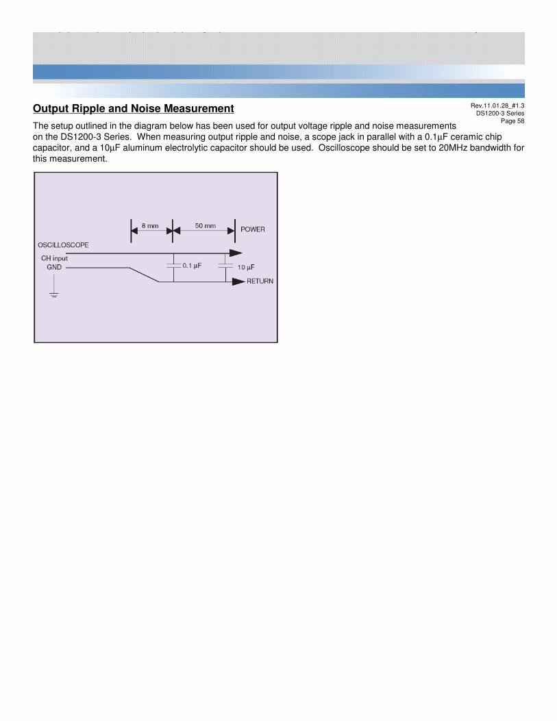
Rev.11.01.28_#1.3DS1200-3 Series
Page 58
Output Ripple and Noise Measurement
The setup outlined in the diagram below has been used for output voltage ripple and noise measurements on the DS1200-3 Series. When measuring output ripple and noise, a scope jack in parallel with a 0.1µF ceramic chip capacitor, and a 10µF aluminum electrolytic capacitor should be used. Oscilloscope should be set to 20MHz bandwidth for this measurement.

Rev.11.01.28_#1.3DS1200-3 Series
Page 59Americas5810 Van Allen Way
Carlsbad, CA 92008
USA
Telephone: +1 (760) 930 4600
Facsimile: +1 (760) 930 0698
Europe (UK)Waterfront Business Park
Merry Hill, Dudley
West Midlands, DY5 1LX
United Kingdom
Telephone: +44 (0) 1384 842 211
Facsimile: +44 (0) 1384 843 355
Asia (HK)14/F, Lu Plaza
2 Wing Yip Street
Kwun Tong, Kowloon
Hong Kong
Telephone: +852 2176 3333
Facsimile: +852 2176 3888
For global contact, visit:
www.powerconversion.com
techsupport.embeddedpower
@emerson.com
While every precaution has been taken to ensure
accuracy and completeness in this literature, Emerson
Network Power assumes no responsibility, and disclaims
all liability for damages resulting from use of this
information or for any errors or omissions.
Emerson Network Power.The global leader in enabling
business-critical continuity.
AC Power
Connectivity
DC Power
Embedded Computing
Embedded Power
Monitoring
Outside Plant
Power Switching & Controls
Precision Cooling
Racks & Integrated Cabinets
Services
Surge Protection
EmersonNetworkPower.Com
Emerson Network Power and the Emerson
Network Power logo are trademarks and
service marks of Emerson Electric Co.
©2008 Emerson Electric Co.

Mouser Electronics
Authorized Distributor
Click to View Pricing, Inventory, Delivery & Lifecycle Information: Emerson Network Power:
DS1200HE-3-004 DS1200HE-3-002