
ACT4751M - Mouser Electronics
72
ACT4751M AEC-Q100, USB Fast Charger Power IC with 40V Input, 4A, Programmable Output Voltage and Current FEATURES • AEC-Q100 Grade 1: -40 to +125°C • CISPR 25 Class 3: PASS • Certified USB Fast Charger, Reference Designs • Qualcomm® Certified, Quick Charger Designs • 4.5 V to 40 V Operational Input Voltage • Programmable Output Voltage by I 2 C 3 V to 24 V in 12.5 mV Step • Programmable Output Current Limit 4 A in 256 Step Resolution • 450 kHz to 2.25 MHz Fixed-Frequency Current-Mode Control with External Clock Sync, 100% Duty Operation, Stable with Low-cost MLCC • Out of AM Radio / Spread-Spectrum Operation • 50 mΩ Integrated High-Side / Low-Side FETs • 5 V / 350 mA Bias Buck Converter • 20 mA AUX LDO, Programmable Output Voltage •I 2 C Interface, Fast-mode Plus (Fm+, 1 MHz) with Configurable Address • Protections: UVLO, OVP, UVP (Hiccup/Latch-off), OCP, TSD • Automotive, Side-wall-plating, 5 mm × 5 mm QFN Package APPLICATIONS • USB Fast Charger (PD 3.0 PPS) • Quick Charge 4, Quick Charge 4+, Quick Charge 3.0 • High Power LED Lighting ACT4751M-101-REF04 (Test ID: 2254) 12V DC Input, USB Charger (USB PD 3.0) Reference Design: USB-C 80W × 1 ACT4751M-101-REF05 (QC20191223118) 4-Port Total 280W: Quick Charge 4 (USB-C 80W × 2) + Quick Charge 3.0 (Type-A 60W × 2) GENERIC DESCRIPTION The ACT4751M is a programmable DC-to-DC buck converter with bias supply rails. This synchronous step- down voltage regulator supports a wide input voltage of 4.5 V to 40 V and integrates both the high side and low side MOSFETS. These 50mΩ R DSON transistors enable high efficiency by reducing power losses. The ACT4751M main buck converter can be dynamically programmed to an output voltage between 3 V and 24 V in 12.5 mV steps via the I 2 C or analog feedback. Also, it can dynamically program output current between 0 A to 4 A in 256 steps via the I 2 C in a constant-current (CC) operation mode. The main-buck operates in a proprietary current mode control that supports external clock syncing for switching frequencies between 450 kHz and 2.25 MHz. The ACT4751M is a perfect solution for USB Power Delivery 3.0 Programmable Power Supply (PD 3.0 PPS) charging applications. The ACT4751M integrates a 5 V / 350 mA mini-buck converter and a 20 mA AUX LDO to simplify application system designs. These rails can power up USB PD controllers and the 1.5W VCONN line in active USB-C cables. The ACT4751M is available in an AEC-Q100 grade, half- etched-lead side-wall-plating, 5 mm x 5 mm QFN package with a power optimized footprint and exposed pad for improved thermal performance. ACT4751M Data Sheet, Rev. E, 16-Jul-2020 Subject to change without notice 1 www.qorvo.com
-
Upload
khangminh22 -
Category
Documents
-
view
5 -
download
0
Transcript of ACT4751M - Mouser Electronics

ACT4751MAEC-Q100, USB Fast Charger Power IC with 40V Input, 4A,
Programmable Output Voltage and Current
FEATURES• AEC-Q100 Grade 1: -40 to +125°C• CISPR 25 Class 3: PASS• Certified USB Fast Charger, Reference Designs• Qualcomm® Certified, Quick Charger Designs
• 4.5 V to 40 V Operational Input Voltage• Programmable Output Voltage by I2C
3 V to 24 V in 12.5 mV Step• Programmable Output Current Limit
4 A in 256 Step Resolution• 450 kHz to 2.25 MHz Fixed-Frequency Current-Mode
Control with External Clock Sync, 100% Duty Operation,Stable with Low-cost MLCC
• Out of AM Radio / Spread-Spectrum Operation• 50 mΩ Integrated High-Side / Low-Side FETs• 5 V / 350 mA Bias Buck Converter• 20 mA AUX LDO, Programmable Output Voltage• I2C Interface, Fast-mode Plus (Fm+, 1 MHz) with
Configurable Address• Protections:
UVLO, OVP, UVP (Hiccup/Latch-off), OCP, TSD• Automotive, Side-wall-plating, 5 mm × 5 mm QFN
Package
APPLICATIONS• USB Fast Charger (PD 3.0 PPS)• Quick Charge 4, Quick Charge 4+, Quick Charge 3.0• High Power LED Lighting
ACT4751M-101-REF04 (Test ID: 2254)12VDC Input, USB Charger (USB PD 3.0)
Reference Design: USB-C 80W × 1
ACT4751M-101-REF05 (QC20191223118)4-Port Total 280W: Quick Charge 4 (USB-C 80W × 2)
+ Quick Charge 3.0 (Type-A 60W × 2)
GENERIC DESCRIPTIONThe ACT4751M is a programmable DC-to-DC buckconverter with bias supply rails. This synchronous step-down voltage regulator supports a wide input voltage of 4.5V to 40 V and integrates both the high side and low sideMOSFETS. These 50mΩ RDSON transistors enable highefficiency by reducing power losses.
The ACT4751M main buck converter can be dynamicallyprogrammed to an output voltage between 3 V and 24 Vin 12.5 mV steps via the I2C or analog feedback. Also, itcan dynamically program output current between 0 A to4 A in 256 steps via the I2C in a constant-current (CC)operation mode. The main-buck operates in a proprietarycurrent mode control that supports external clock syncing forswitching frequencies between 450 kHz and 2.25 MHz.
The ACT4751M is a perfect solution for USB Power Delivery3.0 Programmable Power Supply (PD 3.0 PPS) chargingapplications. The ACT4751M integrates a 5 V / 350 mAmini-buck converter and a 20 mA AUX LDO to simplifyapplication system designs. These rails can power up USBPD controllers and the 1.5W VCONN line in active USB-Ccables.
The ACT4751M is available in an AEC-Q100 grade, half-etched-lead side-wall-plating, 5 mm x 5 mm QFN packagewith a power optimized footprint and exposed pad forimproved thermal performance.
ACT4751M Data Sheet, Rev. E, 16-Jul-2020Subject to change without notice 1 www.qorvo.com

ACT4751MAEC-Q100, USB Fast Charger Power IC with 40V Input, 4A, Programmable
Output Voltage and Current
Ordering Information
Figure 1. Part Numbering Structure
1. Standard product options are identified in this table. Contact factory for custom options, minimum order quantity
required.2. This device is RoHS Compliant and with Pb-free plating unless specified differently. The term Pb-free means
semiconductor products that are in compliance with current RoHS (Restriction of Hazardous Substances) standards.3. Package Code designator “Q” represents QFN4. Pin Count designator “I” represents 32 pins5. See the Factory Programming Options section for more information about CMI.
ACT4751M Data Sheet, Rev. E, 16-Jul-2020Subject to change without notice 2 www.qorvo.com

ACT4751MAEC-Q100, USB Fast Charger Power IC with 40V Input, 4A, Programmable
Output Voltage and Current
User Programmable Parameter Default
PART NUMBERControlScheme AEC-Q100
OutputVoltage[1]
Precise OutputCurrent Limit[2]
AUX LDOVoltage[3]
DC-biasCompensation
ACT4751MQI101 Current-mode YES,Grade 1
5.0 V 4 A 3.3 V YES
Not all options are released, please contact your local sales representatives [email protected] for a status and availability. Also, see Factory Programming Options.
Similar DevicesFollowing devices are similar to the ACT4751M device.
User Programmable Parameter Default
PART NUMBERControlScheme AEC-Q100
OutputVoltage[1]
Precise OutputCurrent Limit[2]
AUX LDOVoltage[3]
DC-biasCompensation
ACT4751QI102 Current-mode — 5.0 V 4 A 3.3 V —
ACT4752QI101 Current-mode — 5.0 V 4 A 3.3V YES
Factory Pre-Programmed Fixed Settings
PART NUMBERControlScheme
OutputVoltage[1] Output Current
Precise OutputCurrent Limit [2]
AUX LDOVoltage [3]
DC-biasCompensation
ACT4755QI101 Current-mode 12.0 V 4 A — — YES
ACT4756QI101 Current-mode 24.0 V 4 A 4 A ±100 mA 3.3V YES
Not all options are released, please contact your local sales representatives [email protected] for a status and availability. Also, see Factory Programming Options.
[1]: Upon requests, output voltage options are available from 3.0 V to 24.0 V in 12.5mV steps, where aminimum required quantity applies.
[2]: Upon requests, precise output current limit options are available from 1 A to 4 A in 15.6 mA steps, wherea minimum required quantity applies.
[3]: Upon requests, AUX LDO voltage options are available from 0.9 V to 4.05 V in 50 mV steps, where aminimum required quantity applies.
ACT4751M Data Sheet, Rev. E, 16-Jul-2020Subject to change without notice 3 www.qorvo.com

ACT4751MAEC-Q100, USB Fast Charger Power IC with 40V Input, 4A, Programmable
Output Voltage and Current
Specifications
Pin Configuration
Figure 2. 32-pin QFN, 5 mm ×5 mm, 0.5 mm pitch, TOP VIEW
Figure 3. Half-etched-lead, side-wall-plating AEC-Q100 package
ACT4751M Data Sheet, Rev. E, 16-Jul-2020Subject to change without notice 4 www.qorvo.com

ACT4751MAEC-Q100, USB Fast Charger Power IC with 40V Input, 4A, Programmable
Output Voltage and Current
Pin FunctionsPIN NAME DESCRIPTION
1 PGBIAS Power-good output of the Mini-buck Regulator and Auxiliary LDO. Open-drain and a pull-upresistor required. See PGBIAS Indicator Output.
2 VLDO Output voltage node of the Auxiliary LDO. Connect a good quality, fixed value 1 µF capacitorbetween this pin and the GND5V pin. See Auxiliary LDO.
3 V5V 5 V bias supply to the device and voltage feedback of the Mini-buck Regulator. Connect twogood quality capacitors in parallel, two 10 µF and one 0.1 µF between this pin and the GND5Vpin. Place the 0.1 µF capacitor with the minimum distance to the device.
4 GND5V Ground node for the Mini-buck Regulator.
5 SW5V Switching node of the Mini-buck Regulator.
6 VIN Power supply to the device. Connect a good quality 1 µF capacitor, at least, between this pinand the GND5V pin. On a PCB, tied to the PVIN pin.
7,8,17,18 PVIN Power supply to the Main-buck Regulator. Connect good quality two 22 µF capacitors, at least,between this pin and the PGND pins, also tie to the VIN pin.
9,10,15,16 PGND Ground node for the Main-buck Regulator.
11,12,13 SW Switching node of the Main-buck Regulator.
14 BOOT Bootstrap capacitor node for the Main-buck Regulator. Connect a good quality, fixed value 0.1µF capacitor between this pin and the SW pin.
19 PG Power-good output of the Main-buck Regulator. Open-drain and a pull-up resistor required.
20 CSN Current sense feedback input to the Main-buck Regulator. See Output Current Sensing.
21 FB_VO Voltage feedback input to the Main-buck Regulator. See Reference Voltage Input.
22 COMP Error amplifier output. Connect a compensation network between this pin and the AGND pin.See Main-buck Compensation Network.
23 AGND Ground node for analog blocks of the device.
24 DACOUT Reference voltage output from the DAC. Usually, short to the REFIN pin. See Output VoltageReference.
25 REFIN Reference voltage input to the Main-buck Regulator. See Reference Voltage Input.
26 ILIM Output current limit programming of the Main-buck Regulator. Connect a resistor between thispin and the AGND pin. See Output Current Reference.
27 ADDR I2C address selection. Connect a resistor between this pin and the ground. See I2C AddressSelection.
28 FREQ Switching frequency programming of the Main-buck Regulator. Connect a resistor between thispin and the AGND pin. See Clock Generator.
29 EN Enable logic input for the Main-buck Regulator. See Main-buck Enable Control.
30 SYNC Clock synchronizing input/output for the Main-buck Regulator. See Clock Synchronizer.
31 SCL Clock port of the I2C Interface. Open-drain and a pull-up resistor required.
32 SDA Data port of the I2C Interface. Open-drain and a pull-up resistor required.
Exposed PAD Substrate contact for power dissipation. Connect to the PGND pins with a broad pattern.
ACT4751M Data Sheet, Rev. E, 16-Jul-2020Subject to change without notice 5 www.qorvo.com

ACT4751MAEC-Q100, USB Fast Charger Power IC with 40V Input, 4A, Programmable
Output Voltage and Current
Absolute Maximum RatingsPARAMETER VALUE UNIT
PVIN, VIN ‒0.3 to +48.0 V
SW ‒0.3 to (PVIN + 1.0) V
FB_VO, CSN ‒0.3 to +28.0 V
Voltage difference between FB_VO and CSN ‒0.3 to +0.3 V
SW5V ‒0.3 to (VIN + 1.0) V
BOOT (VSW ‒ 0.3) to (VSW + 6.0) V
PGND, GND5V, w.r.t. AGND ‒0.3 to +0.3 V
EN, PG, PGBIAS, SYNC, REFIN, SDA, SCL, COMP,V5V (external supply)
‒0.3 to +6.0 V
Operation Junction Temperature ( TJ ) ‒40 to +150 °C
Storage Temperature ‒55 to +150 °C
Lead Temperature (Soldering 10sec) up to +300 °C
Do not exceed these limits to prevent damage to the device. Exposure to absolute maximum ratingconditions for long periods may affect device reliability.
All voltage values are with respect to the ground voltage unless otherwise specified.
Recommended Operating ConditionsPARAMETER VALUE UNIT
PVIN, VIN +4.2 to +40.0 V
V5V (External Supply) +4.5 to +5.5 V
EN, PG, PGBIAS, SYNC, REFIN, SDA, SCL, COMP ‒0.3 to +5.5 V
Operation Junction Temperature (TJ) ‒40 to +125 °C
Current Sensing Resistor (RCS) 5 to 80 mΩFrequency Programming Resistor (RFREQ) 40 to 200 kΩ
All voltage values are with respect to the ground voltage unless otherwise specified.
Package Thermal InformationPARAMETER VALUE UNIT
Thermal Resistance, Junction to Ambient (ΘJA)[1] 24 °C/W[1] Reference number, based on a real measurement of a ACT4751M evaluation board.
ACT4751M Data Sheet, Rev. E, 16-Jul-2020Subject to change without notice 6 www.qorvo.com

ACT4751MAEC-Q100, USB Fast Charger Power IC with 40V Input, 4A, Programmable
Output Voltage and Current
Electrical CharacteristicsPVIN = VIN = 12 V, V5V = 5 V (external supply), EN = 5 V, TA =-40 to +125°C, unless otherwise specified
PARAMETER SYMBOL TEST CONDITION MIN TYP MAX UNIT
BIAS BLOCK
VIN Mini-buckConsumption Current
II(VIN) EN = 0 V, V5V = 5.25 V, mini-buck ON andno switching
235 µA
V5V Quiescent Current IQ(V5V) EN = 0 V, V5V = 5.25 V, mini-buck ON andno switching
1.3 mA
V5V Non-switchingCurrent
II(V5V) EN = 5 V, V5V = 5.25 V, main-buck ON andno switching
2.8 mA
VIT(UVLO) VIN rising to release 4.2 4.5VIN Under-voltageLock-out Threshold VIT(UVLO,fall) VIN falling to lock 4.1
V
VIT(OVLO) VIN rising to lock 42 VIN Over-voltage Lock-out Threshold VIT(OVLO,fall) VIN falling to unlock 39
V
V5V Regulation VO(V5V) V5V error comparator threshold 4.8 5.0 5.2 V
V5V PG Threshold VIT(V5V) V5V rising 4.25 V
V5V Under-voltage VUVP(V5V) V5V falling 3.9 4.2 V
V5V Over-voltage VOVP(V5V) V5V rising 5.9 V
VLDO Regulation VO(VLDO) IVLOD = 10mA Reg0D[5:0] = 0x30 3.13 3.3 3.47 V
VLDO Under-voltage VUVP(VLDO) Reg0D[5:0] = 0x30 2.85 V
PGBIAS Output Voltage VOL(PGBIAS) PGBIAS at logic-L, 1 mA Current intoPGBIAS pin
0.3 V
Mini-buck Over-current IOCP(V5V) 375 450 mA
VLDO Over-current IOCP(VLDO) 20 mA
TSD(HARD) Hard TSD, temperature rising 155
TSD(SOFT) Soft TSD, temperature rising 145
Thermal Protection
TSD(OFF) TSD release, temperature falling 135
°C
SIGNAL PINS
II(FB_VO) 5 V target (DACOUT[10:0] = 0x190) 6 µA
II(CSN) 6 µA
Signal Pin Input Current
II(SYNC) 1 µA
Signal Pin OutputCurrent
IO(ADDR) RADDR = 50 kΩ while PGBIAS=L 20 µA
Signal Pin OutputVoltage
VO(FREQ) RFREQ = 40 kΩ 1.2 V
EN Threshold VIT(EN) 1.1 1.3 V
IO(EN,rise) VEN < VIT(EN) 1 EN Pin Pull-up Current
IO(EN,fall) VEN > VIT(EN) 2
µA
ACT4751M Data Sheet, Rev. E, 16-Jul-2020Subject to change without notice 7 www.qorvo.com

ACT4751MAEC-Q100, USB Fast Charger Power IC with 40V Input, 4A, Programmable
Output Voltage and Current
PARAMETER SYMBOL TEST CONDITION MIN TYP MAX UNIT
SYNC Pin InputThreshold
VIT(SYNC) SYNC pin in slave 0.5 1.4 V
VOH(SYNC) SYNC pin in master, outputs logic-H 3.2 V5VSYNC Pin OutputVoltage VOL(SYNC) SYNC pin in master, outputs logic-L 0 0.8
V
I2C PINS
Input Threshold VIT(I2C) SDA and SCL pins 0.5 1.25 V
Leakage Current ILK(SDA) VSDA = 5 V 1 µA
Output Voltage VOL(SDA) 5 mA Current into SDA pin 0.35 V
Input Capacitance CI(I2C) SDA and SCL pins 10 pF
MAIN-BUCK REGULATOR
VDACOUT(24) 24 V target (DACOUT[10:0] = 0x780), 50 µAcurrent DACOUT sourcing
-1.5% 3.0 +1.5%
VDACOUT(5) 5 V target (DACOUT[10:0] = 0x190), 50 µAcurrent DACOUT sourcing
-1.5% 0.625 +1.5%
VDACOUT Accuracy
ΔVDACOUT VDACOUT(n+1) - VDACOUT(n) 0 1.5625 mV
FB_VO Accuracy VO W.r.t. VREFIN, VREFIN = 3 V -1% 24 1% V
ILIM(100) 100% target (ILIM[7:0] = 0xFF) 97 102
ILIM(25) 25% target (ILIM[7:0] = 0x3F) 24 26
Output Current LimitProgramming Accuracy
ΔILIM ILIM(n+1) - ILIM(n) 0 0.4
µA
VCCMODE(100) Differential voltage (VFB_VO - VCSN) at VLIM =1.6 V
78 82Constant CurrentOperation ProgrammingAccuracy VCCMODE(25) Differential voltage (VFB_VO - VCSN) at VLIM =
0.4 V19 21
mV
PG Output Voltage VOL(PG) PG at logic-L, 1 mA Current into PG pin 0.3 V
PG Threshold UpperLimit[1]
VIH(VO) Threshold of Reg03[2], VO_FB w.r.t. VREFIN,VREFIN = 3 V
+4% +9%
PG Threshold LowerLimit[1]
VIL(VO) Threshold of Reg03[2], VO_FB w.r.t. VREFIN,VREFIN = 3 V
-9% -4%
FB_VOOver-voltage
VOVP VO_FB w.r.t. VREFIN, VREFIN = 3 V +9% V
VUVP(CC) Reg0B[3] = logic-L, VO_FB w.r.t. VREFIN,VREFIN = 3 V
2.7 2.8FB_VOUnder-voltage[2]
VUVP(CV) Reg0B[3] = logic-H, VO_FB w.r.t. VREFIN,VREFIN = 3 V
-9%
V
VIT(CC,rise) Enable CC loop, Reg09[3] = logic-H, VO_FBrising
2.3 2.5FB_VOConstant CurrentActivation Threshold VIT(CC,fall) Disable CC loop, Reg09[3] = logic-H, VO_FB
falling 2.2
V
IOCP(CBC,high) High-side FET limit to trigger 5.5 Main-buck Cycle-by-cycle Current Limit IOCP(CBC,low) Low-side FET limit to release 4.2
A
ACT4751M Data Sheet, Rev. E, 16-Jul-2020Subject to change without notice 8 www.qorvo.com

ACT4751MAEC-Q100, USB Fast Charger Power IC with 40V Input, 4A, Programmable
Output Voltage and Current
PARAMETER SYMBOL TEST CONDITION MIN TYP MAX UNIT
Discharge Resistance RDIS 1.2 kΩ[1] See Main-buck Power-Good for details.[2] See Under-Voltage Protection for details.
Timing Requirements
PARAMETER SYMBOL CONDiTION MIN TYP MAX UNIT
I2C BLOCK
SCL Clock Frequency fSCL (no internal time out) 0 1000 kHz
tLOW(SCL) Logic-L level 0.5 SCL Pulse Width
tHIGH(SCL) Logic-H level 0.26
µs
SDA Set-up Time tSU(SDA) 50 ns
SDA Hold Time tH(SDA) 0 ns
START Set-up Time tSU(START) 260 ns
STOP Set-up Time tSU(STOP) 260 ns
EN pin INPUT
EN Pulse Width tLOW(EN) Logic-L level 30 µs
SYNC pin INPUT
SYNC FrequencyRange
20kΩ < RADDR < 50kΩ 400 2500 kHz
SYNC FrequencyAccuracy
fSYNC
20kΩ < RADDR < 50kΩ, referring to thefrequency setpoint by RFREQ
75% 125%
SYNC Input Duty DIN(SYNC) 20kΩ < RADDR < 50kΩ 40% 60%
Switching CharacteristicsPVIN = VIN = 12 V, V5V = 5 V (external supply), EN = 5 V, TA =-40 to +125°C, unless otherwise specified
PARAMETER SYMBOL TEST CONDITION MIN TYP MAX UNIT
BIAS BLOCK
Mini-Buck SwitchingFrequency
fSW(V5V) 2.0 MHz
Mini-Buck Spread-Spectrum DitheringRange[1]
fSPSP(V5V) Frequency modulation range w.r.t. fSW(V5V)value
±7%
Mini-Buck Spread-Spectrum Cycle
NSPSP(V5V) Number of TON cycles 32 cycle
Mini-Buck Soft-StartTime
tSS(V5V) "VIN = VIT(UVLO)" to "V5V = VIT(V5V)" 0.5 ms
Mini-Buck UVP MaskTimer
tD(V5V,mask) 1 ms
Wait Timer before ErrorReset
tD(RESET) 100 ms
ACT4751M Data Sheet, Rev. E, 16-Jul-2020Subject to change without notice 9 www.qorvo.com

ACT4751MAEC-Q100, USB Fast Charger Power IC with 40V Input, 4A, Programmable
Output Voltage and Current
PARAMETER SYMBOL TEST CONDITION MIN TYP MAX UNIT
PGBIAS Delay tD(PGBIAS) "V5V = VIT(V5V)" to PGBIAS↑, target 3 ms(Reg08[4:3] = 11)
-10% 3 10% ms
AUX LDO Soft-StartTime[2]
tSS(LDO) Just for reference, Reg0D[5:0] = 0x31 100 µs
I2C BLOCK
SDA Fall Time tF(SDA) Pull-up to 5-V source via 10 kΩ 120 ns
MAIN-BUCK REGULATOR
fSW(MAIN)(min) RFREQ = 200 kΩ 400 450 500 kHzMain-Buck SwitchingFrequency fSW(MAIN)(max) RFREQ = 40 kΩ 2.0 2.25 2.5 MHz
SYNC Output DutyCycle
DOUT(SYNC) 50%
ΔfSYNC(low) 40% SYNC Input WDT ErrorDetection ΔfSYNC(high)
20kΩ < RADDR < 50kΩ, referring to thefrequency setpoint by RFREQ 210%
Main-Buck Spread-Spectrum DitheringRange[1]
fSPSP(MAIN) Frequency modulation range w.r.t. fSW(MAIN) ±7%
Main-Buck Spread-Spectrum Cycle
NSPSP(MAIN) Number of TON cycles 64 cycle
ON Time Control tON(min) 65 85 ns
OFF Time Control tOFF(min) 65 85 ns
Main-Buck Digital ServoClock Period
tW(SERVO) 8 µs
Hiccup Timer tW(HICCUP) 100 ms
tD(PG)(min) FB_VO > VIL(VO), 0 ms target (Reg08[7:6] =00)
10 µsPG Delay
tD(PG)(max) FB_VO > VIL(VO), 4 ms target (Reg08[7:6] =11)
-10% 4 10% ms
[1] No production test[2] Not actively controlled, application board dependent
ACT4751M Data Sheet, Rev. E, 16-Jul-2020Subject to change without notice 10 www.qorvo.com

ACT4751MAEC-Q100, USB Fast Charger Power IC with 40V Input, 4A, Programmable
Output Voltage and Current
Typical Characteristic Curves
Figure 4. Main-buck Startup by EN
VPVIN = 24 V, VFB_VO = 5 V (target), IOUT = 2 A
Figure 5. Main-buck Startup by PVIN Hot-plug
VPVIN = 24 V, VFB_VO = 5 V (target), IOUT = 2 A
Figure 6. Main-buck Shutdown by EN
VPVIN = 24 V, VFB_VO = 5 V (target), IOUT = 2 A
Figure 7. Main-buck Shutdown by PVIN Plug-out
VPVIN = 24 V, VFB_VO = 5 V (target), IOUT = 2 A
Figure 8. Mini-buck Startup
VIN = 24 V, IOUT = (no load)
Figure 9. Mini-buck Shutdown
VIN = 24 V, IOUT = (60 Ω load)
ACT4751M Data Sheet, Rev. E, 16-Jul-2020Subject to change without notice 11 www.qorvo.com
ACT4751MAEC-Q100, USB Fast Charger Power IC with 40V Input, 4A, Programmable
Output Voltage and Current
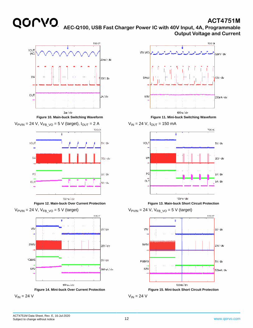
Figure 10. Main-buck Switching Waveform
VPVIN = 24 V, VFB_VO = 5 V (target), IOUT = 2 A
Figure 11. Mini-buck Switching Waveform
VIN = 24 V, IOUT = 150 mA
Figure 12. Main-buck Over Current Protection
VPVIN = 24 V, VFB_VO = 5 V (target)
Figure 13. Main-buck Short Circuit Protection
VPVIN = 24 V, VFB_VO = 5 V (target)
Figure 14. Mini-buck Over Current Protection
VIN = 24 V
Figure 15. Mini-buck Short Circuit Protection
VIN = 24 V
ACT4751M Data Sheet, Rev. E, 16-Jul-2020Subject to change without notice 12 www.qorvo.com
ACT4751MAEC-Q100, USB Fast Charger Power IC with 40V Input, 4A, Programmable
Output Voltage and Current
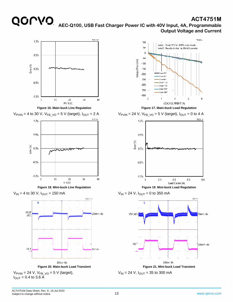
Figure 16. Main-buck Line Regulation
VPVIN = 4 to 30 V, VFB_VO = 5 V (target), IOUT = 2 A
Figure 17. Main-buck Load Regulation
VPVIN = 24 V, VFB_VO = 5 V (target), IOUT = 0 to 4 A
Figure 18. Mini-buck Line Regulation
VIN = 4 to 30 V, IOUT = 150 mA
Figure 19. Mini-buck Load Regulation
VIN = 24 V, IOUT = 0 to 350 mA
Figure 20. Main-buck Load Transient
VPVIN = 24 V, VFB_VO = 5 V (target),IOUT = 0.4 to 3.6 A
Figure 21. Mini-buck Load Transient
VIN = 24 V, IOUT = 35 to 300 mA
ACT4751M Data Sheet, Rev. E, 16-Jul-2020Subject to change without notice 13 www.qorvo.com

ACT4751MAEC-Q100, USB Fast Charger Power IC with 40V Input, 4A, Programmable
Output Voltage and Current
Figure 22. Main-buck Efficiency
VPVIN = 24 V, VFB_VO = 3,5,9,12,15,20,24 V (target), IOUT =0 to 4 A
Figure 23. Main-buck Efficiency (Log scale)
VPVIN = 24 V, VFB_VO = 3,5,9,12,15,20,24 V (target), IOUT =0 to 4 A
Figure 24. Main-buck Power Loss
VPVIN = 24 V, VFB_VO = 3,5,9,12,15,20,24 V (target), IOUT =0 to 4 A
Figure 25. Mini-buck Efficiency
VIN = 24 V, IOUT = 0 to 350 mA
Figure 26. Mini-buck Power Loss
VIN = 24 V, IOUT = 0 to 350 mA
ACT4751M Data Sheet, Rev. E, 16-Jul-2020Subject to change without notice 14 www.qorvo.com

ACT4751MAEC-Q100, USB Fast Charger Power IC with 40V Input, 4A, Programmable
Output Voltage and Current
Figure 27. Main-buck Programming 5 to 9 V
VPVIN = 24 V, IOUT = 2 A
Figure 28. Main-buck Programming 9 to 20 V
VPVIN = 24 V, IOUT = 2 A
Figure 29. Main-buck Programming 20 to 9 V
VPVIN = 24 V, IOUT = 2 A
Figure 30. Main-buck Programming 9 to 5 V
VPVIN = 24 V, IOUT = 2 A
Figure 31. Main-buck Programming 5 to 20 V
VPVIN = 24 V, IOUT = 2 A
Figure 32. Main-buck Programming 20 to 5 V
VPVIN = 24 V, IOUT = 2 A
ACT4751M Data Sheet, Rev. E, 16-Jul-2020Subject to change without notice 15 www.qorvo.com

ACT4751MAEC-Q100, USB Fast Charger Power IC with 40V Input, 4A, Programmable
Output Voltage and Current
Figure 33. Main-buck Constant Current
VPVIN = 24 V, VFB_VO = 5 V (target), IOUT = 1,2,3,4 A
Figure 34. Clock-master: SYNC Output and SW Waveform
VPVIN = 24 V, RADDR = (open)
Figure 35. Clock-slave: SYNC Input and SW Waveform
VPVIN = 24 V, RADDR = 50 kΩ
ACT4751M Data Sheet, Rev. E, 16-Jul-2020Subject to change without notice 16 www.qorvo.com

ACT4751MAEC-Q100, USB Fast Charger Power IC with 40V Input, 4A, Programmable
Output Voltage and Current
I2C RegistersIn this section, I2C register mappings and bit assignments are explained. Please refer to I2C Interface section how toaccess, how to setup these registers.
Register Address MapThis is an entire mapping of I2C registers on the ACT4751M device. Here are the meanings of each column in Table 1.
Reg Addr I2C register address number in hexadecimal
Reg Name Register name
R/W Read / Write type of registerR: Read onlyW: Write onlyR/W: Read and Write
Def Default value
F/P Factory Programming supportY: The default values can be programmed by a production test.N: The default values are fixed / hard-coded.
Description Description of the register
Please contact your local sales representatives for availabilities of different Factory Programming defaultsettings. See Factory Programming Options.
In Table 1 below, each register address value string is a link to the detailed bit description.
Table 1. Register Address Map
RegAddr
Reg Name R/W Def F/P Description
0x00 State-Machine R — N Current position of the state-machine
0x01 Interrupt #1 R — N Interrupt byte #1
0x02 Interrupt #2 R — N Interrupt byte #2
0x03 Status Flag R — N Status byte (no interrupt)
0x04 (Reserved) R — N (not in use)
0x05 Command R/W 0x00 N Command to trigger actions
0x06 Interrupt Mask #1 R/W 0x00 Y Interrupt mask byte #1 for the register Reg01
0x07 Interrupt Mask #2 R/W 0x00 Y Interrupt mask byte #2 for the register Reg02
0x08 Configuration byte #1 R/W 0x28 Y Configure various device behaviors #1
0x09 Configuration byte #2 R/W 0xF3 Y Configure various device behaviors #2
0x0A DACOUT[10:3] R/W 0x32 Y DACOUT programming value bit 10 to 3
0x0B DACOUT[2:0], Configurationbyte #3
R/W 0x10 Y DACOUT programming value bit 2 to 0Configure various device behaviors #3
0x0C ILIM Value R/W 0xFF Y ILIM programming value bit 7 to 0
0x0D AUX LDO Value R/W 0x30 Y VLDO programming value bit 5 to 0
0x0E Configuration byte #4 R/W 0x23 Y Configure various device behaviors #4
0x0F Configuration byte #5 R/W 0x9E Y Configure various device behaviors #5
ACT4751M Data Sheet, Rev. E, 16-Jul-2020Subject to change without notice 17 www.qorvo.com

ACT4751MAEC-Q100, USB Fast Charger Power IC with 40V Input, 4A, Programmable
Output Voltage and Current
Register Bit MapsFollowing sub-sections explain bit assignments of each I2C register. Here are the meanings of each column in below bittables.
Bit # Bit position (number)
Bit(s) Name Bit(s) name
Def Default value
Description Description of the bit(s)
0x00 State-MachineThe register 0x00 is Read Only type. It indicates current position of the state-machine. See Control Logic.
Table 2. Register 0x00
Bit # Bit(s) Name Def Description
7 0 (un-used bit)
6 0 (un-used bit)
5 0 (un-used bit)
4 0 (un-used bit)
3 State[3] 0
2 State[2] 0
1 State[1] 0
0 State[0] 0
See Table 3.
Table 3. State-Machine Bits [3:0]
Value (bin) Value (hex) Position of State-Machine
0000 0x00 No Power, in Under-Voltage Lock-Out
0001 0x01 Bias Ramp, initialing mini-buck[1]
0010 0x02 Bias Reset
0011 0x03 Bias Ramp checking RADDR [1]
0100 0x04 Bias Ramp
0101 0x05 Bias Ready checking RFREQ [1]
0110 0x06 RFREQ Checking Loop [2]
0111 0x07 Bias Ready
1000 0x08 Main-buck Ramp enabling main-buck [1]
1001 0x09 Main-buck Ramp
1010 0x0A Main-buck ON
1011 0x0B Main-buck Shutdown
1100 0x0C Main-buck Error
[1] Short transit, not staying loner at this position[2] Not in the Table 27, see RFREQ Checking Loop
ACT4751M Data Sheet, Rev. E, 16-Jul-2020Subject to change without notice 18 www.qorvo.com

ACT4751MAEC-Q100, USB Fast Charger Power IC with 40V Input, 4A, Programmable
Output Voltage and Current
0x01: Interrupt #1
0x02: Interrupt #2The registers 0x01 and 0x02 are Read Only. These 2 registers indicate cause(s) of the latest interrupt event by setting 1 atcorresponding bit(s), so bit(s) of 0 mean nothing happened (normal). In the Reg01 and Reg02, trigger events setting 1 aredescribed. See Interrupt Output.
Bits in these registers will be automatically cleared by reading the value with an I2C command.
This automatic bit-clear action applies if the cause of an interrupt is resolved at the timing of a READ action.For most of the bits in 0x01 and 0x02, the automatic bit-clear happens because these protection eventstrigger shutdown actions to resolve the error situation.
Table 4. Register 0x01
Bit # Bit(s) Name Def Description
7 Main-buck in CC/CV 0 Becomes 1 when the main-buck transits CC⇒CV or CV⇒CC. SeeCC / CV Interrupt/Monitor.
6 0 (un-used bit)
5 Out of Range, SYNC Input 0 Becomes 1 when the SYNC pin input clock is out of range. SeeClock Synchronizer.
4 Out of Range, RFREQ 0 Becomes 1 when the RFREQ value, probed, is out of range. SeeRFREQ Protection.
3 TSD(HARD) Event 0 Becomes 1 when the TJ exceeds the TSD(HARD) threshold. SeeThermal Protection.
2 TSD(SOFT) Event 0 Becomes 1 when the TJ exceeds the TSD(SOFT) threshold. SeeThermal Protection.
1 0 (un-used bit)
0 VIT(OVLO) Event 0 Becomes 1 when the VPVIN exceeds the VIT(OVLO) threshold. SeeOver-Voltage Lock-Out.
Table 5. Register 0x02
Bit # Bit(s) Name Def Description
7 0 (un-used bit)
6 Main-buck Over-current Event 0 Becomes 1 when the output current in Over-Current Protection.
5 VOVP Event 0 Becomes 1 when the VO exceeds the VOVP threshold. See Over-Voltage Protection
4 VUVP(CV) or VUVP(CC) Event 0 Becomes 1 when the VO falls below the VUVP(CV) or VUVP(CC)threshold. See Under-Voltage Protection.
3 AUX LDO Under-voltage 0 Becomes 1 when the VO(VLDO) falls below the VUVP(VLDO) threshold.See AUX LDO Under-Voltage Protection
2 IOCP(V5V) Event 0 Becomes 1 when the output current of the mini-buck exceeds theIOCP(V5V) threshold. See Mini-buck Over-Current Protection.
1 VOVP(V5V) Event 0 Becomes 1 when the VO(V5V) exceeds the VOVP(V5V) threshold. SeeMini-buck Over-Voltage Protection.
0 VUVP(V5V) Event 0 Becomes 1 when the VO(V5V) falls below the VUVP(V5V) threshold.See Mini-buck Under-Voltage Protection.
ACT4751M Data Sheet, Rev. E, 16-Jul-2020Subject to change without notice 19 www.qorvo.com

ACT4751MAEC-Q100, USB Fast Charger Power IC with 40V Input, 4A, Programmable
Output Voltage and Current
0x03: Status FlagThe register 0x03 is Read Only type. It indicates various status flags from internal circuit blocks.
Table 6. Register 0x03
Bit # Bit(s) Name Def Description
7 WDT High 0
6 WDT Low 0
1*: Clock input at SYNC is too high/low to accept.0: (normal), See SYNC Input Watch Dog Timer.
5 Mini-buck in 100% 0 1*: Mini-buck is operating in 100% mode.0: Mini-buck is operating out of 100% mode.See Mini-buck 100% Duty Operation.
4 Main-buck in CC 0 1*: Main-buck is operating in CC mode.0: Main-buck is operating in CV mode.See Programmable Current Limit.
3 Main-buck in 100% 0 1*: Main-buck is operating in 100% mode.0: Main-buck is operating out of 100% mode.See 100% Duty Operation.
2 PG of Main-buck 0 1*: Main-buck in "Power-good" condition0: Main-buck in NOT "Power-good" conditionSee Main-buck Power-Good.
1 0 (un-used bit)
0 0 (un-used bit)
0x04: (Reserved)The register 0x04 is reserved for future spins. Nothing is assigned to this register.
0x05: CommandThe register 0x05 is Read / Write type. A writing action to this register triggers a certain action at the device.
Table 7. Register 0x05
Bit # Bit(s) Name Def Description
7 0 (un-used bit)
6 0 (un-used bit)
5 0 (un-used bit)
4 0 (un-used bit)
3 0 (un-used bit)
2 0 (un-used bit)
1 Load DACOUT 0 Setting 1 to load DACOUT value in effect.Always reads 0. See Loading New DACOUT Value.
0 Enable Main-buck 0 Writing 1 to enable Main-buckSee Main-buck Enable Control
ACT4751M Data Sheet, Rev. E, 16-Jul-2020Subject to change without notice 20 www.qorvo.com

ACT4751MAEC-Q100, USB Fast Charger Power IC with 40V Input, 4A, Programmable
Output Voltage and Current
0x06: Interrupt Mask #1
0x07: Interrupt Mask #2The registers 0x06 and 0x07 are Read / Write type. These 2 registers are corresponding to the Reg01 and Reg02respectively. Any 1 bit in Reg06 and Reg07 prevents (masks) an interrupt event triggered by the corresponding bit in Reg01and Reg02. For example, Setting the Reg07[5] bit makes no interrupt event even though an over-voltage happened at theReg02[5] bit. See Interrupt Output.
When the Reg08[5] "Mask All" bit is 1, all Reg06 and Reg07 bits are overridden to 1 internally regardless ofregister values there.
Table 8. Register 0x06
Bit # Bit(s) Name Def Description
7 Mask Main-buck in CC/CV 0 1: mask bit 7 of Reg010: (no-mask)
6 0 (un-used bit)
5 Mask Out of Range, SYNC Input 0 1: mask bit 5 of Reg010: (no-mask)
4 Mask Out of Range, RFREQ 0 1: mask bit 4 of Reg010: (no-mask)
3 Mask TSD(HARD) Event 0 1: mask bit 3 of Reg010: (no-mask)
2 Mask TSD(SOFT) Event 0 1: mask bit 2 of Reg010: (no-mask)
1 0 (un-used bit)
0 Mask VIT(OVLO) Event 0 1: mask bit 0 of Reg010: (no-mask)
Table 9. Register 0x07
Bit # Bit(s) Name Def Description
7 0 (un-used bit)
6 Mask Main-buck Over-currentEvent
0 1: mask bit 6 of Reg020: (no-mask)
5 Mask VOVP Event 0 1: mask bit 5 of Reg020: (no-mask)
4 Mask VUVP(CV) or VUVP(CC) Event 0 1: mask bit 4 of Reg020: (no-mask)
3 Mask AUX LDO Under-voltage 0 1: mask bit 3 of Reg020: (no-mask)
2 Mask IOCP(V5V) Event 0 1: mask bit 2 of Reg020: (no-mask)
1 Mask VOVP(V5V) Event 0 1: mask bit 1 of Reg020: (no-mask)
0 Mask VUVP(V5V) Event 0 1: mask bit 0 of Reg020: (no-mask)
ACT4751M Data Sheet, Rev. E, 16-Jul-2020Subject to change without notice 21 www.qorvo.com

ACT4751MAEC-Q100, USB Fast Charger Power IC with 40V Input, 4A, Programmable
Output Voltage and Current
0x08: Configuration byte #1The register 0x08 is Read / Write type. It configures the device behaviors as described.
Table 10. Register 0x08
Bit # Bit(s) Name Def Description
7 PG Delay[1] 0
6 PG Delay[0] 0
See Table 11.See Main-buck Power-Good.
5 Mask All 1 1: overrides all Reg06 and Reg07 bits 1 internally.0: "masking" follows each bit of Reg06 and Reg07.
4 PGBIAS Delay[1] 0
3 PGBIAS Delay[0] 1
See Table 12 andSee PGBIAS Indicator Output.
2 0 (un-used bit)
1 0 (un-used bit)
0 0 (un-used bit)
Table 11. PG Delay [1:0]
Value (bin) Value (hex) PG pin Delay Time
00 0x00 0 ms (default)
01 0x01 0.25 ms
10 0x02 1 ms
11 0x03 4 ms
Table 12. PGBIAS Delay [1:0]
Value (bin) Value (hex) PGBIAS pin Delay Time
00 0x00 1 ms
01 0x01 1.25 ms (default)
10 0x02 1.5 ms
11 0x03 3 ms
ACT4751M Data Sheet, Rev. E, 16-Jul-2020Subject to change without notice 22 www.qorvo.com

ACT4751MAEC-Q100, USB Fast Charger Power IC with 40V Input, 4A, Programmable
Output Voltage and Current
0x09: Configuration byte #2The register 0x09 is Read / Write type. It configures the device behaviors as described.
Table 13. Register 0x09
Bit # Bit(s) Name Def Description
7 Servo Clock[1] 1
6 Servo Clock[0] 1
See Table 14.
5 Discharge in Servo 1 1: Use discharge resistor to drive VO servo down.0: Not use discharge resistor in servo.See Negative Transition with RDIS and Output Discharge Resistor.
4 Discharge at OFF 1 1: Use discharge resistor when main-buck disabled.0: Not use discharge resistor when main-buck disabled.See Main-buck Enable Control and Output Discharge Resistor.
3 Main-buck No UVP 0 1: disable main-buck under-voltage protection.0: use main-buck under-voltage protection.See UVP selection.
2 Hiccup / Latch-off 0 1: Latch-off action in main-buck.0: Hiccup action in main-buck.See Under-Voltage Hiccup and Under-Voltage Latch-off.Also, see SYNC Error Hiccup and SYNC Error Latch-off.
1 Enable Mini-buck 1 1: enable Mini-buck, automatically start-up Mini-buck.0: disable Mini-buck, manually start-up Mini-buck.See V5V, External 5V Supply.
0 Enable AUX LDO 1 1: enable AUX LDO, automatically start-up AUX LDO.0: disable AUX LDO, manually start-up AUX LDO.See AUX LDO Enable.
Table 14. Servo Clock [1:0]
Value (bin) Value (hex) Servo Clock Period
00 0x00 tW(SERVO) × 1
01 0x01 tW(SERVO) × 2
10 0x02 tW(SERVO) × 4
11 0x03 tW(SERVO) × 8 (default)
ACT4751M Data Sheet, Rev. E, 16-Jul-2020Subject to change without notice 23 www.qorvo.com

ACT4751MAEC-Q100, USB Fast Charger Power IC with 40V Input, 4A, Programmable
Output Voltage and Current
0x0A: DACOUT Value [10:3]The register 0x0A is Read / Write type. It programs DACOUT value.
Table 15. Register 0x0A
Bit # Bit(s) Name Def Description
7 DACOUT[10] 0
6 DACOUT[9] 0
5 DACOUT[8] 1
4 DACOUT[7] 1
3 DACOUT[6] 0
2 DACOUT[5] 0
1 DACOUT[4] 1
0 DACOUT[3] 0
See Table 16.3 more bits in Reg0B.See Output Voltage Reference.
Table 16. DACOUT[10:0]
Value (bin) Value (hex) DACOUT Voltage (mV) VO Voltage (V)
000 0000 0000 0x000 0.0 0.0000
…
000 1110 1111 0x0EF 373.4 2.9875
000 1111 0000 0x0F0 375.0 [1] 3.0000
000 1111 0001 0x0F1 376.6 3.0125
…
001 0000 1000 0x108 412.5 3.3
…
001 1001 0000 0x190 625.0 (default) 5
…
010 1101 0000 0x2D0 1125.0 9
…
011 1100 0000 0x3C0 1500.0 12
…
100 1011 0000 0x480 1875.0 15
…
111 0111 1111 0x77F 2998.4 23.9875
111 1000 0000 0x780 3000.0 [2] 24.0000
111 1000 0001 0x781 3000.0 24.0000
…
111 1111 1111 0x7FF 3000.0 24.0000
[1] Minimum value of the DACOUT range characterized.[2] Maximum value of the DACOUT range characterized.
ACT4751M Data Sheet, Rev. E, 16-Jul-2020Subject to change without notice 24 www.qorvo.com

ACT4751MAEC-Q100, USB Fast Charger Power IC with 40V Input, 4A, Programmable
Output Voltage and Current
0x0B: Configuration byte #3, DACOUT[2:0]The register 0x0B is Read / Write type. It configures the device behaviors as described.
Table 17. Register 0x0B
Bit # Bit(s) Name Def Description
7 Enable main-buck 100% 0 1: enable main-buck 100% mode.0: disable main-buck 100% mode.See 100% Duty Operation.
6 Enable main-buck Spread-Spectrum
0 1: enable main-buck spread-spectrum operation.0: disable main-buck spread-spectrum operation.See Spread-spectrum Operation.
5 0 (un-used bit)
4 Enable main-buck CC 1 1: enable main-buck Constant-current operation.0: disable main-buck Constant-current operation.See Programmable Current Limit.
3 Select main-buck UVP 0 1: select VUVP(CV).0: select VUVP(CC).See UVP selection.
2 DACOUT[2] 0
1 DACOUT[1] 0
0 DACOUT[0] 0
See Table 16.8 more bits in Reg0A.See Output Voltage Reference.
ACT4751M Data Sheet, Rev. E, 16-Jul-2020Subject to change without notice 25 www.qorvo.com

ACT4751MAEC-Q100, USB Fast Charger Power IC with 40V Input, 4A, Programmable
Output Voltage and Current
0x0C: ILIM ValueThe register 0x0C is Read / Write type. It programs ILIM value.
Table 18. Register 0x0C
Bit # Bit(s) Name Def Description
7 ILIM[7] 1
6 ILIM[6] 1
5 ILIM[5] 1
4 ILIM[4] 1
3 ILIM[3] 1
2 ILIM[2] 1
1 ILIM[1] 1
0 ILIM[0] 1
See Table 19.See Output Current Reference.
Table 19. ILIM[7:0]
Value (bin) Value (hex) ILIM Current (µA) Output Current (mA)with RCS=20 mΩand RILIM=16 kΩ
0000 0000 0x00 0.39 15.6
0000 0001 0x01 0.78 31.3
0000 0010 0x02 1.17 46.9
…
1111 1101 0xFD 99.2 3969
1111 1110 0xFE 99.6 3984
1111 1111 0xFF 100.0 (default)(= ILIM(100))
4000
ACT4751M Data Sheet, Rev. E, 16-Jul-2020Subject to change without notice 26 www.qorvo.com

ACT4751MAEC-Q100, USB Fast Charger Power IC with 40V Input, 4A, Programmable
Output Voltage and Current
0x0D: AUX LDO ValueThe register 0x0D is Read / Write type. It programs AUX LDO value.
Table 20. Register 0x0D
Bit # Bit(s) Name Def Description
7 0 (un-used bit)
6 0 (un-used bit)
5 LDO Voltage[5] 1
4 LDO Voltage[4] 1
3 LDO Voltage[3] 0
2 LDO Voltage[2] 0
1 LDO Voltage[1] 0
0 LDO Voltage[0] 0
See Table 21.See AUX LDO Output Voltage Programming.
Table 21. LDO Voltage[5:0]
Value (bin) Value (hex) VO(VLDO) Voltage (V)
00 0000 0x00 0.90
00 0001 0x01 0.95
00 0010 0x02 1.00
00 0011 0x03 1.05
…
00 0110 0x06 1.20
…
00 1100 0x0C 1.50
…
01 0010 0x12 1.80
…
10 0000 0x20 2.50
…
10 1010 0x2A 3.00
…
11 0000 0x30 3.30 (default)
…
11 1101 0x3D 3.95
11 1110 0x3E 4.00
11 1111 0x3F 4.05
ACT4751M Data Sheet, Rev. E, 16-Jul-2020Subject to change without notice 27 www.qorvo.com

ACT4751MAEC-Q100, USB Fast Charger Power IC with 40V Input, 4A, Programmable
Output Voltage and Current
0x0E: Configuration byte #4The register 0x0E is Read / Write type. It configures the device behaviors as described.
Table 22. Register 0x0E
Bit # Bit(s) Name Def Description
7 0 (un-used bit)
6 0 (un-used bit)
5 (fixed value) 1 always program this bit to 1.
4 0 (un-used bit)
3 Main-buck HSD[1] 0
2 Main-buck HSD[0] 0
See Table 23.See Main-buck EMI Tune-up.
1 (fixed value) 1 always program this bit to 1.
0 (fixed value) 1 always program this bit to 1.
Table 23. Main-buck Gate Driver Strength[1:0]
HSD[1] HSD[0] SW node Rising/Falling Time (ns)
SW node Falling Time (ns)
0 0 10.6 (default) 5.1 (default)
0 1 6.0 4.7
1 0 5.5 4.2
1 1 5.0 3.8
ACT4751M Data Sheet, Rev. E, 16-Jul-2020Subject to change without notice 28 www.qorvo.com

ACT4751MAEC-Q100, USB Fast Charger Power IC with 40V Input, 4A, Programmable
Output Voltage and Current
0x0F: Configuration byte #5The register 0x0F is Read / Write type. It configures the device behaviors as described.
Table 24. Register 0x0F
Bit # Bit(s) Name Def Description
7 Enable Mini-buck 100% 1 1: enable Mini-buck 100% mode.0: disable Mini-buck 100% mode.See Mini-buck 100% Duty Operation.
6 Enable Mini-buck Spread-Spectrum
0 1: enable Mini-buck spread-spectrum operation.0: disable Mini-buck spread-spectrum operation.See Mini-buck Spread-spectrum Operation.
5 Enable Mini-buck Forced CCM 0 1: enable Mini-buck Forced CCM operation.0: disable Mini-buck Forced CCM (= pulse-skipping) operation.See Mini-buck Forced Continuous Conduction Operation.
4 Mini-buck HSD[1] 1
3 Mini-buck HSD[0] 1
See Table 25.See Mini-buck EMI Tune-up.
2 Mini-buck LSD[1] 1
1 Mini-buck LSD[0] 1
See Table 26.See Mini-buck EMI Tune-up.
0 0 (un-used bit)
Table 25. Mini-buck High-side-driver Strength[1:0]
HSD[1] HSD[0] SW5V node Rising Speed
0 0 Better EMI (low noise)
0 1 (not valid, don’t choose)
1 0 (not valid, don’t choose)
1 1 Better Efficiency (default)
Table 26. Mini-buck Low-side-driver Strength[1:0]
LSD[1] LSD[0] SW5V node Falling Speed
0 0 Better EMI
0 1 (not valid, don’t choose)
1 0 (not valid, don’t choose)
1 1 Better Efficiency (default)
ACT4751M Data Sheet, Rev. E, 16-Jul-2020Subject to change without notice 29 www.qorvo.com

ACT4751MAEC-Q100, USB Fast Charger Power IC with 40V Input, 4A, Programmable
Output Voltage and Current
Device Functions
OverviewThe ACT4751M device is a wide input / output voltage, easy to use, stable and robust step-down (buck) switching regulatorIC.
The device truly supports plug-and-play operation by following the recommended schematic from the evaluation kit (EVK)design. This EVK operates in entire supported input voltage, output voltage and output current range without changinganything on the EVK board (except tuning a potentiometer for a target output voltage setting).
The device consists of following four major blocks.
• Main-buck regulatorThe Main-buck Regulator is a 4 A, synchronous, step-down DC-DC converter,featuring on-the-fly programming voltage and current-limit reference generators.
• Mini-buck regulatorThe Mini-buck Regulator is a 5 V output, 350 mA, always-ON, step-down DC-DC converter.
• Auxiliary (AUX) LDO regulatorThe Auxiliary LDO is a programmable output voltage, 20 mA low drop-out (LDO) linear regulator.
• Control LogicThe Control Logic is a state-machine (STM) logic and I2C interface controller
Functional Block Diagram
Figure 36. Functional Block Diagram
ACT4751M Data Sheet, Rev. E, 16-Jul-2020Subject to change without notice 30 www.qorvo.com

ACT4751MAEC-Q100, USB Fast Charger Power IC with 40V Input, 4A, Programmable
Output Voltage and Current
Control LogicThe ACT4751M device integrates a logic block that controls entire behavior of the device in a manner of state-machine(STM).
At a higher level, the STM consists of nine major status as shown in Table 27.
Table 27. Major States in STM
State Description IN OUT
Normal State
No Power No power at the VIN pin. any state@Power Removed, UVLO, orOVLO
Bias Ramp@Power Attached
Bias Ramp Power at the VIN pin, biasblocks ramping up.
No Power@Power Attached
RFREQ Check@Mini-buck UP
Bias Ready Bias blocks ready, waiting formain-buck enable.PGBIAS = logic-H
RFREQ Check@PGBIAS↑
Main-buck Ramp@EN↑
Main-buck Ramp Main-buck enabled and rampingup.PGBIAS = logic-H
Bias Ready@EN↑
Main-buck ON@PG↑
Main-buck ON Main-buck is up and running.PGBIAS = logic-H,PG = logic-H
Main-buck Ramp@PG↑ orMain-buck Servo@Servo Complete
Main-buck Servo@Register Change
Servo Main-buck is up and running,changing output voltage orcurrent target.PGBIAS = logic-H,PG = logic-L
Main-buck ON@Register Change
Main-buck Ramp@Servo Complete
Protection States
Bias Reset Critical error in bias blocks,waiting to reset. See ProtectionLevel 2.
any Normal State@Mini-buck OCP,OVP,UVP,@AUX LDO UVP,@RFREQ Out of Range,@Hard TSD
Bias Ramp@tD(RESET) Time-out
RFREQ Check Waiting for valid RFREQ. SeeRFREQ Protection.
Bias Ramp@(Mini-buck Up)
Bias Ready@RFREQ Validated
Main-buckShutdown
Main-buck disabled, or in errorto latched-OFF. See ProtectionLevel 3.
any state EN=H@iEN↓@Main-buck UVP(Latch-off)@SYNC Input Error Latch-off@Over-Voltage Protection@Over-Current Protection
Bias Ready@Shutdown Completed
Main-buck Error Main-buck in error to auto-restart. See Protection Level 4.
any state EN=H@Main-buck UVP(Hiccup)@SYNC Input Error Hiccup@Soft TSD
Main-buck Ramp@Hiccup Time-out orBias Ready@iEN↓
ACT4751M Data Sheet, Rev. E, 16-Jul-2020Subject to change without notice 31 www.qorvo.com

ACT4751MAEC-Q100, USB Fast Charger Power IC with 40V Input, 4A, Programmable
Output Voltage and Current
The STM controls the device by the State Diagram below.
Figure 37. State Diagram
I2C InterfaceThis I2C block offers a detailed control interface of the ACT4751M device to a host controller device. Through-out the I2Cinterface (at the SCL and SDA pins), the host device can
1. read various status bits of the device,2. write various setting bits to control behaviors of the device and read back those setting bits.
The I2C block is fully activated and ready (to communicate) when the PGBIAS Indicator Output becomeslogic-H (good).
See I2C Registers for contents and meaning of the I2C registers. This section explains how to access, how to program theseregisters.
The device complies with the I2C-bus specification (UM10204).
The SCL and SDA pins are open-drain and a pair of pull-up resistors are required.See SCL/SDA Pull-up Resistance for the resistor value selection.
ACT4751M Data Sheet, Rev. E, 16-Jul-2020Subject to change without notice 32 www.qorvo.com

ACT4751MAEC-Q100, USB Fast Charger Power IC with 40V Input, 4A, Programmable
Output Voltage and Current
Figure 38. I2C Block
I2C Address SelectionBy sensing the value of the RADDR resistor between the ADDR pin and the ground, the I2C block selects one of six I2Caddress options, so to avoid address collisions when using multiple ACT4751M devices sharing one I2C bus. See Figure 38.
This I2C address selection is directly tied to a selection of the Role of Clock Generator and columns "Clock Role", "SYNCpin" and "SYNC Polarity" in the Table 28 are there for the Clock Generator block.
Table 28. I2C Address with Clock Role
RADDR I2C Address(START)…MSB…LSB…(R/W bit)
Clock Role SYNC pin SYNC Polarity
GND Short 00 01 00 0 Stand-alone Disabled N/A
20 kΩ 00 01 00 1 Clock-slave Input SYNC↑30 kΩ 00 01 01 0 Clock-slave Input SYNC↓40 kΩ 00 01 01 1 Clock-slave Input SYNC↑50 kΩ 00 01 10 0 Clock-slave Input SYNC↓(open) 00 01 10 1 Clock-master Output N/A
I2C Protocol ImplementationThe I2C implementation of the device is explained in the Figure 39.
The Figure 39 is a scalable drawing, can be zoomed in on a PDF reader software or can be printed in a largesize paper, for an ese of readability.
In the Figure 39, there are four different scenarios I2C READ or WRITE command sequences. From left to right in the figure(or from top to bottom in a landscape view), these sequences are shown.
1. "One byte WRITE" to a register2. "Multi-byte WRITE" to registers3. "one byte READ" from a register, plus another "one byte READ" without setting a target read register4. (folded back, remaining portion of "3. one byte READ")
followed by(folded back, remaining portion of "5. multi-byte READ")
5. "Multi-byte READ" from registers
ACT4751M Data Sheet, Rev. E, 16-Jul-2020Subject to change without notice 33 www.qorvo.com

ACT4751MAEC-Q100, USB Fast Charger Power IC with 40V Input, 4A, Programmable
Output Voltage and Current
I2C One byte WRITEWriting one byte of data into a target register is completed by one 3-byte I2C WRITE command.
The one byte WRITE command byte format is
1. I2C START2. I2C ACT4751M (target) device address3. One zero bit for "write"4. I2C ACK from the ACT4751M
(This is the end of the 1st byte.)5. Target ACT4751M register address
(See Table 1.))6. I2C ACK from the ACT4751M
(This is the end of the 2nd byte.)7. Register value to write8. I2C ACK from the ACT4751M
(This is the end of the 3rd byte.)9. I2C STOP
I2C Multi-byte WRITEWriting multi-byte of data into target registers is completed by one multi-byte I2C WRITE command.
The multi-byte WRITE command byte format is
1. I2C START2. I2C ACT4751M (target) device address3. One zero bit for "write"4. I2C ACK from the ACT4751M
(This is the end of the 1st byte.)5. The first/starting target ACT4751M register address, assume the address is "N" (See Table 1.))6. I2C ACK from the ACT4751M
See "Reg Pointer" that the device sets the target register to "N", at the timing of the ACK.
(This is the end of the 2nd byte.)7. Register value to write to the "N" register8. I2C ACK from the ACT4751M
See "Reg Pointer" that the device automatically increments the target register at the timing of the ACK. So the next write data goes to "N+1".
(This is the end of the 3rd byte.)9. Register value to write to the "N+1" register10. I2C ACK from the ACT4751M
Another "Reg Pointer" increment to "N+2" at the ACK.
(This is the end of the 4th byte.)11. Register value to write to the "N+2" register12. I2C ACK from the ACT4751M
Another "Reg Pointer" increment to "N+3" at the ACK, though the "N+3" is not used in this example.
(This is the end of the 5th byte.)13. I2C STOP
ACT4751M Data Sheet, Rev. E, 16-Jul-2020Subject to change without notice 34 www.qorvo.com

ACT4751MAEC-Q100, USB Fast Charger Power IC with 40V Input, 4A, Programmable
Output Voltage and Current
I2C One byte READReading one byte of data from a target register is completed by a combination of
a. one 2-byte I2C WRITE command andb. one 2-byte I2C READ command.
The one byte READ command sequence is
1. I2C START2. I2C ACT4751M (target) device address3. One zero bit for "write"4. I2C ACK from the ACT4751M
(This is the end of the 1st byte in "WRITE".)5. Target ACT4751M register address, assume the address is "N"
(See Table 1.))6. I2C ACK from the ACT4751M
See "Reg Pointer" that the device sets the target register to "N", at the timing of the ACK.
(This is the end of the "WRITE" command.)7. I2C REPEATED START8. I2C ACT4751M (target) device address9. One high bit for "read"10. I2C ACK from the ACT4751M
(This is the end of the 1st byte in "READ".)11. The ACT4751M device send out the requested register data from "N"
Note that at 5th SCL of this data sending action, the device increments the "Reg Pointer" value to "N+1". Whether this byte date is successfully sent out or not (like a case of the host cancel the communication by a sudden STOP), the pointer is incremented at the 5th SCL.
12. I2C NACK from the host device(This is the end of the "READ" command.)
13. I2C STOP(This is the end of one byte "READ" sequence.)
Now, see what happens just sending a "READ" command without a leading "WRITE" command setting a target register. There may be some commands on this bus where "other slave devices" involved (not this device).
14. I2C START15. I2C ACT4751M (target) device address16. One high bit for "read"17. I2C ACK from the ACT4751M
(This is the end of the 1st byte in "READ".)18. The ACT4751M device send out the register data from "N+1"
Here is the key point in this example. The "Reg Pointer" stays at "N+1" from the step "11." So just sending a "READ" command without a "WRITE" command results in reading a "next register" from the last time.
19. I2C NACK from the host device(This is the end of the 2nd "READ" command.)
20. I2C STOP
This example "14…20" illustrates that it requires a pair of WRITE and READ commands to access a certain registerrepeatedly. Because every time a READ action happens the device increments the "reg pointer", a WRITE command isrequired to reset the "reg pointer".
ACT4751M Data Sheet, Rev. E, 16-Jul-2020Subject to change without notice 35 www.qorvo.com

ACT4751MAEC-Q100, USB Fast Charger Power IC with 40V Input, 4A, Programmable
Output Voltage and Current
I2C Multi-byte READReading multi-byte of data from target registers is completed by a combination of
a. one 2-byte I2C WRITE command andb. one multi-byte I2C READ command.
When sending multiple bytes in a READ command, the device automatically increment the target register one-by-one at thetiming of 5th SCL as explained in the I2C One byte READ section.
The multi-byte READ command sequence is
1. I2C START2. I2C ACT4751M (target) device address3. One zero bit for "write"4. I2C ACK from the ACT4751M
(This is the end of the 1st byte in "WRITE".)5. Target ACT4751M register address, assume the address is "N"
(See Table 1.))6. I2C ACK from the ACT4751M
See "Reg Pointer" that the device sets the target register to "N", at the timing of the ACK.
(This is the end of the "WRITE" command.)7. I2C REPEATED START8. I2C ACT4751M (target) device address9. One high bit for "read"10. I2C ACK from the ACT4751M
(This is the end of the 1st byte in "READ".)11. The ACT4751M device send out the requested register data from "N"
Because the "Reg Pointer" is "N" at the beginning of this byte, the device sends out data from "N". In parallel, the device increments the "Reg Pointer" to "N+1" at 5th SCL.
12. I2C ACK from the host device to continue reading data(This is the end of the 2nd byte in "READ".)
13. The ACT4751M device send out the "N+1" data
The "Reg Pointer" is "N+1" at the beginning of this byte, the device sends out data from "N+1". In parallel, the device increments the "Reg Pointer" to "N+2" at 5th SCL.
14. I2C ACK from the host device to continue reading data(This is the end of the 3rd byte in "READ".)
15. The ACT4751M device send out the "N+2" data
Another "Reg Pointer" increment.
16. I2C NACK from the host device(This is the end of the "READ" command.)
17. I2C STOP
ACT4751M Data Sheet, Rev. E, 16-Jul-2020Subject to change without notice 36 www.qorvo.com

ACT4751MAEC-Q100, USB Fast Charger Power IC with 40V Input, 4A, Programmable
Output Voltage and Current
01
23
45
67
89
1011
1213
1415
1617
1819
2021
2223
2425
2627
2829
3031
3233
3435
3637
3839
4041
4243
4445
4647
4849
5051
52
I2C
ST
AR
TA
DD
RW
AC
KR
EG
[N]
AC
KD
AT
A[N
]A
CK
ST
OP
SC
L
SD
AA
DD
RR
EG
[N]
DA
TA
[N]
SD
A d
river
HO
ST
SH
OS
TS
HO
ST
SH
Reg
Poi
nter
NN
+1
Reg
[N]
DA
TA
[N]
Reg
[N+
1]
Reg
[N+
2]
I2C
ST
AR
TA
DD
RW
AC
KR
EG
[N]
AC
KD
AT
A[N
]A
CK
DA
TA
[N+
1]A
CK
DA
TA
[N+
2]A
CK
ST
OP
SC
L
SD
AA
DD
RR
EG
[N]
DA
TA
[N]
DA
TA
[N+
1]D
AT
A[N
+2]
SD
A d
river
HO
ST
SH
OS
TS
HO
ST
SH
OS
TS
HO
ST
SH
Reg
Poi
nter
NN
+1
N+
2N
+3
Reg
[N]
DA
TA
[N]
Reg
[N+
1]D
AT
A[N
+1]
Reg
[N+
2]D
AT
A[N
+2]
I2C
ST
AR
TA
DD
RW
AC
KR
EG
[N]
AC
KrS
TA
RT
AD
DR
RA
CK
DA
TA
[N]
NA
CK
ST
OP
SC
L
SD
AA
DD
RR
EG
[N]
AD
DR
DA
TA
[N]
SD
A d
river
HO
ST
SH
OS
TS
HO
ST
SLA
VE
H
Reg
Poi
nter
NN
+1
Reg
[N]
DA
TA
[N]
Reg
[N+
1]D
AT
A[N
+1]
Reg
[N+
2]D
AT
A[N
+1]
I2C
ST
AR
TA
DD
RR
AC
KD
AT
A[N
+1]
NA
CK
ST
OP
SC
L
SD
AA
DD
RD
AT
A[N
+1]
SD
A d
river
HO
ST
SLA
VE
HO
ST
Reg
Poi
nter
N+
1N
+2
Reg
[N]
DA
TA
[N]
Reg
[N+
1]D
AT
A[N
+1]
Reg
[N+
2]D
AT
A[N
+1]
I2C
ST
AR
TA
DD
RW
AC
KR
EG
[N]
AC
KrS
TA
RT
AD
DR
RA
CK
DA
TA
[N]
AC
K
SC
L
SD
AA
DD
RR
EG
[N]
AD
DR
DA
TA
[N]
SD
A d
river
HO
ST
SH
OS
TS
HO
ST
SLA
VE
H
Reg
Poi
nter
NN
+1
Reg
[N]
DA
TA
[N]
Reg
[N+
1]D
AT
A[N
+1]
Reg
[N+
2]D
AT
A[N
+1]
PIN ACT475x Internal
1 byte WRITE
PIN ACT475x Internal
Multi-bypte WRITE
PIN ACT475x Internal
1 byte READ
PIN ACT475x Internal
..con
t'd..
brea
k &
ano
ther
1 b
yte
RE
AD
PIN ACT475x Internal
Multi-byte READ
23
1
DA
TA
[N+
1]A
CK
DA
TA
[N+
2]N
AC
KS
TO
P
DA
TA
[N+
1]D
AT
A[N
+2]
SLA
VE
HS
LAV
EH
OS
T
N+
2N
+3
82
34
56
7
..con
t'd..
cloc
k#1-
#2 o
f DA
TA
[N+
1] r
eadi
ng
DA
TA
[N+
1]
DA
TA
[N+
1]
SLA
VE
rST
AR
T
R
epea
ted
ST
AR
T
SD
A d
riven
by
SLA
VE
SD
A d
riven
by
HO
ST
82
34
56
71
82
34
56
71
82
34
56
71
82
34
56
71
Figure 39. I2C Communication Waveforms (supports zoom in from a PDF viewer)
ACT4751M Data Sheet, Rev. E, 16-Jul-2020Subject to change without notice 37 www.qorvo.com

ACT4751MAEC-Q100, USB Fast Charger Power IC with 40V Input, 4A, Programmable
Output Voltage and Current
Under-Voltage Lock-OutThe Under-Voltage Lock-Out (UVLO) function prevents the ACT4751M device working under too low input voltage at theVIN pin. As the VIN pin is connected to the PVIN pin on a PCB, the UVLO monitors PVIN too.
When the VIN pin voltage is below the VIT(UVLO) threshold, the device disables all the functions but this UVLO circuit. Duringthis UVLO period, the device minimizes power consumption and wait for the VIN pin voltage rises into a valid range.When the VIN pin voltage exceeds the VIT(UVLO) threshold, the device starts working, by following the Control Logicstate-machine. Once the UVLO released, the device keeps working as long as VIN pin voltage maintains higher than theVIT(UVLO,fall) threshold that has a hysteresis from the VIT(UVLO) value.
Over-Voltage Lock-OutThe Over-Voltage Lock-Out (OVLO) function prevents the ACT4751M device working from too high input voltage at the VINpin. As the VIN pin is connected to the PVIN pin on a PCB, the OVLO monitors PVIN too.
When the VIN pin voltage exceeds the VIT(OVLO) threshold, the device disables all the functions but this OVLO circuit. Duringthis OVLO period, the device minimizes power consumption and wait for the VIN pin voltage decrease back into a validrange.When the VIN pin voltage gets back normal (under VIT(OVLO,fall)), the device starts working, by following the Control Logic.
The Reg01[0] bit is set logic-H to indicate this error.
This OVLO does not protect the device from any potential damage caused by over-voltage events.See Note of Absolute Maximum Rating.The OVLO is only intended to reduce a risk of a chain-reaction that the VIN/PVIN over-voltage event triggersby disabling all output rails of the device.
Factory Programmed ROMThe ACT4751M integrates a read-only memory (ROM) block and that is programmed at its factory test. The data contents ofthe ROM configure various behaviors of the device and also some of the contents are default values of I2C registers. Whenthe Under-Voltage Lock-Out released, the Control Logic state-machine activates the ROM block as its first step and theSTM configures itself according to the ROM values.
See Factory Programming Options.
BIAS BlocksThe ACT4751M employs several bias voltage and bias current reference circuits those are necessary to maintain properoperations of regulator blocks. When the Under-Voltage Lock-Out released, the Control Logic state-machine activates thesereference and bias circuits before starting the Mini-buck Regulator.
ACT4751M Data Sheet, Rev. E, 16-Jul-2020Subject to change without notice 38 www.qorvo.com

ACT4751MAEC-Q100, USB Fast Charger Power IC with 40V Input, 4A, Programmable
Output Voltage and Current
Mini-buck RegulatorMost of ACT4751M device circuit blocks are designed to operate under a 5 V supply from the V5V pin and this 5 V mini-buck switching regulator generates the 5 V bias at the VO(V5V) target. The mini-buck employs an internally compensated,constant ON time (COT) control.
The mini-buck supplies up to 350 mA of output current by step-down converting power from the VIN pin.From the SW5V pin to the GND5V pin, a Mini-buck LC Output Filter is required. The output of this LC filter is connected tothe V5V pin.
Figure 40. Mini-buck Regulator with an LC Output Filter
The V5V pin is the supply of control circuits in the Main-buck Regulator and characterized at 5.0 V. Thedevice is designed to be functional down to the VUVP(V5V) threshold but near 4 V supply may not deliver itsfull performance. A short event at the V5V pin may cause a potential damage.
Mini-buck EnableThe mini-buck regulator generates a fundamental 5 V bias supply of the entire device operation, by default, the ControlLogic state-machine enables the mini-buck as soon as both Under-Voltage Lock-Out and Over-Voltage Lock-Out arereleased. And the mini-buck keeps ON all the time.
V5V, External 5V SupplyWhen there is a 5 V power supply always available in target systems, the mini-buck can be disabled by setting the I2CReg09[1] to logic-L to save power loss from its switching.
Mini-buck Power-GoodWhether the mini-buck is enabled or disabled, there is a voltage comparator monitoring the V5V pin to the VIT(V5V) target.See PGBIAS Indicator Output.
Mini-buck Soft-startThe mini-buck regulator executes a soft-start (slow-start) operation when enabled so to avoid in-rush current. This soft-start time is specified by the tSS(V5V) parameter and the device sweep its internal reference voltage from 0% to 100% in thetSS(V5V) period.
During this soft-start period, the mini-buck forces to use, so called, pulse-skip operation so to achieve smooth ramp up ofthe output voltage and it ignores the I2C Reg0F[5] setting.
Mini-buck Start-up into Pre-biased OutputThe mini-buck supports a start-up into a pre-biased output without any huge discharge current from the output.
Without this feature, a regulator circuit may discharge huge amount of current from its output capacitance so to force theoutput voltage closer to a reference voltage target of its soft-start operation during the internal reference voltage is lowerthan the pre-biased output by starting from 0%.See Mini-buck Soft-start.
By preventing its switching operation until the reference target of the soft-start reaches to its pre-biased level, theACT4751M device avoids the discharge event and achieves a smooth ramp up of the 5 V bias.
ACT4751M Data Sheet, Rev. E, 16-Jul-2020Subject to change without notice 39 www.qorvo.com

ACT4751MAEC-Q100, USB Fast Charger Power IC with 40V Input, 4A, Programmable
Output Voltage and Current
Mini-buck Switching Operations
Mini-buck Forced Continuous Conduction OperationBy setting I2C Reg0F[5] to Logic-H, the device operates in a forced continuous conduction mode (FCCM). With this FCCMoperation, the regulator maintains its switching frequency to meet the fSW(V5V) target. This fSW(V5V) parameter ensures thatits operation frequency do not interfere with AM radio frequency by staying above the AM band.
Mini-buck Pulse-skip OperationBy setting I2C Reg0F[5] to Logic-L, the device operates in a pulse-skipping mode, or so-called, in a light-load efficiencymode.
When its load current goes low, the inductor (coil) current starts flowing in reverse direction (negative current). As theregulator detects continuous reverse current flow cycles, it activates the pulse-skip operation by blocking the reverse currentflow.
By blocking a reverse current flow, an energy amount delivered during one switching period is bigger than the one periodenergy amount of FCCM operation and the output has a bigger ripple voltage. This bigger ripple results in less switchingevents to reduce power loss related to a switching action. So it improves its conversion efficiency.
During this pulse-skip operation, its switching frequency may stay inside AM radio frequency band.
Mini-buck 100% Duty OperationWhen the VIN pin voltage is close to the target output voltage VO(V5V), the mini-buck gets into 100% duty mode by settingI2C Reg0F[7].
Without this 100% duty mode (disabled), the device is designed to output a minimum OFF period at each cycle, eventhough its internal PWM comparator continuously demands more ON duty. This minimum OFF pulse helps to stay at itstarget switching frequency but it is not desirable when the input voltage is very close to the output as the output voltagestarts dropping.
When the 100% duty mode is enabled, the device stops forcing the minimum OFF pulse and the high-side FET maintainsON for multiple cycles without turning OFF as long as the PWM comparator indicates low feedback voltage. This 100% dutyoperation helps bringing the output voltage close to the input.
Reg03[5] is set logic-H to indicate that the regulator is in 100% duty operation.
This 100% duty operation lowers its switching frequency and may stay at AM radio frequency band.
Mini-buck Spread-spectrum OperationThe mini-buck provides a spread-spectrum switching frequency control by setting I2C Reg0F[6].
By activating the spread-spectrum function, the regulator modulates its switching frequency in the range of the fSPSP(V5V)parameter and it repeats this frequency dithering action by the NSPSP(V5V) times of switching period. The spread-spectrumoperation improves its EMI performance by lowering noise peaks.
ACT4751M Data Sheet, Rev. E, 16-Jul-2020Subject to change without notice 40 www.qorvo.com

ACT4751MAEC-Q100, USB Fast Charger Power IC with 40V Input, 4A, Programmable
Output Voltage and Current
Figure 41. Mini-buck Regulator Spread-spectrum Operation
Mini-buck EMI Tune-upFor the purpose of improving its EMI performance, this mini-buck provides programmable switching node slew rate. Bychanging the I2C Reg0F[4:3] for the high-side gate and I2C Reg0F[2:1] for the low-side gate, an application system designercan balance the tradeoff between its power conversion efficiency and its EMI noise level. By selecting slower transient rate,the noise performance improves; faster transient rate improves the efficiency.
See Table 25 for the high-side gate available options and see Table 26 for the low-side date available options.
Mini-buck Over-Current ProtectionThe over-current protection (OCP) limits its output current below the IOCP(V5V) threshold so to protect integrated FETdevices. When the output current exceeds this threshold, the device triggers the over-current protection.The Reg02[2] is set logic-H to indicate this error.
See Executing Protections for the execution of this protection.
Mini-buck Over-Voltage ProtectionThe over-voltage protection (OVP) monitors and maintains the V5V pin voltage not to exceed the VOVP(V5V) threshold. Forany reason, it exceeds the threshold, the device triggers the over-voltage protection.The Reg02[1] is set logic-H to indicate this error.
See Executing Protections for the execution of this protection.
Mini-buck Under-Voltage ProtectionThe under-voltage protection (UVP) monitors the V5V pin voltage at the drops the VUVP(V5V) threshold. For any reason, itfalls below the threshold, the device triggers the under-voltage protection.The Reg02[0] is set logic-H to indicate this error.
See Executing Protections for the execution of this protection.
To avoid triggering this under-voltage protection during its start-up period, the device masks this protection for a timer periodof the tD(V5V,mask) parameter when the Mini-buck Soft-start procedure starts. As this tD(V5V,mask) timer expires, the deviceactivates this under-voltage protection.
ACT4751M Data Sheet, Rev. E, 16-Jul-2020Subject to change without notice 41 www.qorvo.com

ACT4751MAEC-Q100, USB Fast Charger Power IC with 40V Input, 4A, Programmable
Output Voltage and Current
Auxiliary LDOFor the purpose of supporting one another small power rail, the ACT4751M integrates an auxiliary 20 mA LDO. This AUXLDO is powered by the V5V pin and its output voltage is regulated at the VO(VLDO) target.
Between the VLDO pin and the GND5V pin, an AUX LDO Output Capacitors is required.
Figure 42. AUX LDO Regulator
AUX LDO EnableThe AUX LDO is activated automatically when the V5V pin voltage exceeds the VIT(V5V) threshold. See Mini-buck Regulator.
In case of application where this power rail is not needed, the AUX LDO can be disabled by setting the I2C Reg09[0] tologic-L to save power.
AUX LDO Soft-startTo avoid a big inrush current, the AUX LDO execute a soft-start procedure. This soft-start sweeps its reference voltage from0% to 100% in the tSS(LDO) target period.
AUX LDO Power-GoodThere is a comparator monitoring the VLDO pin voltage. The output signal from this comparator is device internal. Thiscomparator does trigger no event in the Control Logic state-machine "main" sequence flow but, once the AUX LDO isactivated, it can trigger an "error" flow after the AUX LDO Soft-start operation completed.
AUX LDO Output Voltage ProgrammingThe output voltage of the AUX LDO is programmable from 0.9 V to 4.05 V in 50 mV step by the I2C Reg0D[5:0].See Table 21 for a target code to program and this table is calculated by the Eq.(1).
(1)
It’s default value is stored in the Factory Programmed ROM.See Factory Programming Options.
AUX LDO Over-Current ProtectionThe over-current protection (OCP) limits its output current not to exceed the IOCP(VLDO) threshold. When it exceeds, theAUX LDO reduces the output current in a fold-back manner. Because of this fold-back current action, the VLDO pin voltageeventually decreases to hit AUX LDO Under-Voltage Protection.
AUX LDO Under-Voltage ProtectionThe under-voltage protection (UVP) monitors the VLDO pin voltage at the VUVP(VLDO) threshold. For any reason, it fallsbelow the threshold, the device triggers the under-voltage protection.
See Executing Protections for the execution of this protection.
ACT4751M Data Sheet, Rev. E, 16-Jul-2020Subject to change without notice 42 www.qorvo.com

ACT4751MAEC-Q100, USB Fast Charger Power IC with 40V Input, 4A, Programmable
Output Voltage and Current
PGBIAS Indicator OutputThe PGBIAS pin is a dual role status indicator output. The PGBIAS is an open-drain type output and it requires a pull-upresistor. See PGBIAS/PG Pull-up Resistance for its value selection.
Figure 43. PGBIAS Block
Bias Block Power-goodBefore activating the Main-buck Regulator, the device needs to start-up all the supporting bias blocks those includes Mini-buck Regulator, Clock Oscillator and so on. Based on various internal block status signals, the PGBIAS pin indicateswhether the device is ready to activate the Main-buck or not.When the device is ready to activate the main-buck, the PGBIAS pin becomes logic-H. That means the PGBIAS pin at logic-L indicates it’s not ready.And also the PGBIAS pin indicates the I2C Interface block is ready.
PGBIAS Delay TimeThere is a programmable time delay from an internal timing the device ready to release the PGBIAS to an actual PGBIASrising edge so to adjust timing between the device and a host micro-controller.
This delay is set by the I2C Reg08[4:3]. See Table 12 for available options.
Interrupt OutputThe PGBIAS pin is double purposed to output an interrupt signal to a host micro-controller.
The device can disable this interrupt output by setting the Reg08[5] logic-H. With this bit at logic-H, the device only outputthe Bias Block Power-good signal.
Because it is invasive to certain micro-controllers those cannot program to distinguish a "power-good orpower-not-good" signal from an interrupt, this double purposed interrupt output function is disabled bydefault.
When any bits in Reg01 and Reg02 becomes logic-H from logic-L, this transition generates an interrupt event. This interruptevent causes a repeated narrow logic-L pulses from the PGBIAS pin. A timing sequence of this interrupt event indicator isdescribed in this list.
1. Starting from PGBIAS is at logic-H (good).2. Output 10 µs of logic-L pulse at the PGBIAS pin and return back to logic-H.3. Start a 480 µs timer and waits for an I2C read command to the register, causing this interrupt, from an I2C host.4. When a read command comes in, clear the Reg01 and Reg02 and complete the interrupt sequence.5. If there’s no read command, repeat "2."
This sequence is shown in Figure 44.
ACT4751M Data Sheet, Rev. E, 16-Jul-2020Subject to change without notice 43 www.qorvo.com

ACT4751MAEC-Q100, USB Fast Charger Power IC with 40V Input, 4A, Programmable
Output Voltage and Current
Figure 44. Interrupt Timing Diagram
When a host micro-controller is programmed to read the I2C registers every time when the PGBIAS pin becomes logic-L, thehost can receive and distinguish two types of notifications from the PGBIAS pin: a "power-good or power-not-good" signaland an interrupt signal.
The default value of the Reg08[5] bit is logic-H to disable the interrupt output. To enable the interrupt, a host controllerneeds to write logic-L at this bit during an initial I2C communication session.
Interrupt with ResetMany of interrupt trigger events executes the Reset Sequence. As long as the VIN pin voltage is valid, the device isdesigned to maintain its logic status including register values so that a micro-controller can obtain the cause of a reset afterthe reboot.
The timing diagram, with a reset sequence involved, is shown in Figure 45.
Note that the device maintains logic-H value of one or more bits in Reg01 and/or Reg02. That means thedevice starts sending an interrupt pulse sequence immediately after the reboot event.Further note that the pulse timing of this interrupt sequence is continued, inside the device, from the originaltrigger event. So the time position of first interrupt logic-L pulse after the reboot is undefined.
Figure 45. Interrupt Timing Diagram with a Reset
Thermal ProtectionThe ACT4751M provides a multi-level thermal protection from an over-heating related damages. Both level of protections isworking as a thermal shutdown (TSD) but different level of "shutdown" actions applied.
See Executing Protections.
Soft TSDWhen the device junction temperature TJ exceeds the TSD(SOFT) threshold, the "soft TSD" triggered.
The "soft TSD" shuts down the Main-buck Regulator as it is the major source of power loss and causing this high TJsituation. But this level of protection maintains Mini-buck Regulator and Auxiliary LDO so that a host microprocessor canfigure out the reason of shutdown through the I2C interface.The Reg01[2] bit is set logic-H to indicate this protection.
The "soft TSD" maintains the OFF state for the tW(HICCUP) period, then it auto-restarts the Main-buck Regulator when the TJbecomes cooled down below the TSD(OFF) threshold.
ACT4751M Data Sheet, Rev. E, 16-Jul-2020Subject to change without notice 44 www.qorvo.com

ACT4751MAEC-Q100, USB Fast Charger Power IC with 40V Input, 4A, Programmable
Output Voltage and Current
Hard TSDIn a case the TJ rises very quickly to hit the TSD(HARD) threshold just after passing TSD(SOFT) threshold, the device shutsdown all the blocks by executing the Reset Sequence.
Before hitting this "hard TSD", it is expected that the "soft TSD" prevents TJ rising by stopping the Main-buck Regulatorbecause the TSD(HARD) is higher than the TSD(SOFT). So only severe TJ rising event causes the "hard TSD" like a suddenoutput short while supplying the maximum current.
The Reg01[3] bit is set logic-H to indicate this protection.
ACT4751M Data Sheet, Rev. E, 16-Jul-2020Subject to change without notice 45 www.qorvo.com

ACT4751MAEC-Q100, USB Fast Charger Power IC with 40V Input, 4A, Programmable
Output Voltage and Current
Clock GeneratorThe ACT4751M provides a multi-function clock generator for the Main-buck Regulator. This generator consists of a self-running, programmable Clock Oscillator, a phase-locked loop (PLL) Clock Synchronizer to an external clock source, and aSwitching Frequency Selector.
Role of Clock GeneratorThe role of this generator is selected at the same time of the I2C Address Selection. Each of available I2C address options isdirectly assigned to a role as shown in Table 28. When choosing the I2C address, the role is decided too.
Stand-aloneThe stand-alone role is suitable for a situation that only one ACT4751M device is on a PCB. The Clock Oscillator blockis used for this roles so to use the oscillator for its own switching timing.
This role configures the SYNC Disabled.
Clock-masterThe clock-master role is chosen for a situation that this unit is a master of synchronized operation where multiple unitsof ACT4751M are on one PCB. The Clock Oscillator block is used for this role so to use the oscillator for its own andsharing switching timing.
This role configures the SYNC to Output Clock.
Clock-slaveThe clock-slave role is chosen for a situation that there is an external clock source available to follow. The ClockSynchronizer block is used for this role so to follow an external clock source by synchronizing to it. This type ofsituations is typically in these 2 cases.
1. Multiple units of ACT4751M are on one PCB and there is a clock-master unit (, not this unit). This unit follows themaster.
2. There is a stable system clock source, like a crystal oscillator, on a PCB. This unit follows the oscillator.
This role configures the SYNC to Input External Clock.
The Stand-alone role and the Clock-master role are similar, in terms of running the Clock Oscillator to self generate its ownclock. The difference is that the stand-alone role can’t not share the clock, on the other hand, the clock-master do share itsclock at the SYNC output pin.Function-wise, the clock-master is a superset of the stand-alone. The benefit of stand-alone role is a further power saving bynot driving SYNC pin when a clock sharing is not needed.
Switching Frequency SelectorThe RFREQ resistor selects a target operation switching frequency of the Main-buck Regulator. The RFREQ is connectedbetween the FREQ pin and the ground.
The RFREQ resistor must be connected regardless of application usages. The RFREQ resistor should beplaced between the FREQ pin and the AGND pin as close as possible with short PCB traces.
Figure 46. Clock Generator Block with RFREQ
Regardless of Role of Clock Generator, the device detects the RFREQ value for the use of tuning internal loop compensationparameters. This RFREQ detection is performed at the timing the PGBIAS Indicator Output becomes logic-H (good). The loopcompensation parameter is a function of the fSW(MAIN).
ACT4751M Data Sheet, Rev. E, 16-Jul-2020Subject to change without notice 46 www.qorvo.com

ACT4751MAEC-Q100, USB Fast Charger Power IC with 40V Input, 4A, Programmable
Output Voltage and Current
When selecting a role with the Clock Synchronizer, use the Table 29 for a target fSW(MAIN) clock at the SYNC input pin.
Table 29. Clock-slave, RFREQ Selection
fSW(MAIN) Range RFREQ
450 kHz to 600 kHz 178 kΩ600 kHz to 900 kHz 120 kΩ
900 kHz to 1.20 MHz 85.7 kΩ1.20 MHz to 1.50 MHz 66.7 kΩ1.50 MHz to 1.80 MHz 54.5 kΩ1.80 MHz to 2.10 MHz 46.2 kΩ2.10 MHz to 2.25 MHz 40.0 kΩ
The Recommended RFREQ Range is between 40 kΩ and 200 kΩ.
When selecting a role with the Clock Oscillator, follow the Table 30.
RFREQ ProtectionTo protect the device (trying to) working at a switching frequency value out of supported range, the device validates RFREQvalue at the timing of the RFREQ value detection. When RFREQ is out of the Recommended RFREQ Range, the device triggersa RFREQ error.And the Reg01[4] bit is set logic-H to indicate this error.
See RFREQ Check Loop for the execution of this protection.
Clock OscillatorA device of Clock-master or Stand-alone role activates this oscillator block.
This oscillator generates a main-buck switching clock signal based on the RFREQ resistor value. The frequency range can beprogrammed between 450 kHz and 2.25 MHz by following Eq.(2).
(2)
The Table 30 lists some calculation examples.
Table 30. Clock-master, RFREQ Selection
RFREQ fSW(MAIN)
200 kΩ 450 kHz
…
85.7 kΩ 1050 kHz
…
54.5 kΩ 1.650 kHz
…
40.0 kΩ 2250 kHz
The Recommended RFREQ Range is between 40 kΩ and 200 kΩ.
SYNC to Output ClockFor the purpose of applications requires a Clock Synchronizer feature, a Clock-master device outputs its clock signalgenerated by the Clock Oscillator at the SYNC output pin as a clock-master.This output clock signal is used by slave devices.
Note that the SYNC pin is a bi-directional input/output pin. See SYNC to Input External Clock.
ACT4751M Data Sheet, Rev. E, 16-Jul-2020Subject to change without notice 47 www.qorvo.com

ACT4751MAEC-Q100, USB Fast Charger Power IC with 40V Input, 4A, Programmable
Output Voltage and Current
SYNC DisabledA device of Stand-alone role disables the SYNC pin.See SYNC to Output Clock and SYNC to Input External Clock.
Clock SynchronizerA device of Clock-slave role activates this synchronizer block.
In applications where multiple ACT4751M devices are working together, each Clock Oscillator from multiple devicesgenerate slightly different frequency of clock signals due to a unit-to-unit variations. This situation rises an EMI concern oflow frequency beat.
To solve this EMI concern, the clock synchronizer follows one master clock source so to make all the devices working(synchronized) at the timing of this master clock.
The Clock-slave role paragraph explains two typical scenarios where a clock master is.
SYNC to Input External ClockThe external clock source signal to the synchronizer is applied at the SYNC input pin so to follow (synchronize to) anexternal clock master signal.
Note that the SYNC pin is a bi-directional input/output pin. See SYNC to Output Clock.
SYNC Input PolarityBy synchronizing switching timings of multiple devices reduces the EMI concern, however, it causes multiple devices turningon at the same time to increase transient current noise.
To relieve this "same time ON" situation, the device in the Clock-slave role can select clock edge to follow the master. Thesynchronizer is designed to follow either one of
1. a rising edge of the SYNC input (SYNC↑), or2. a falling edge of the SYNC input (SYNC↓).
This polarity selection is also done at the timing the I2C address is chosen from the I2C Address Selection.
SYNC Input Watch Dog TimerIn case an input signal at the SYNC pin is unstable, the main buck regulation becomes unstable. To avoid this sort ofunreliable SYNC input situations, the device monitors frequency of the external clock source at the SYNC input pin. Thiscircuit is a sort of watch dog timer (WDT) structure. This WDT circuit is based on the Table 29 setting. When the inputexternal clock signal is out of range between ΔfSYNC(low) and ΔfSYNC(high), a "SYNC WDT Error" event is triggered.
The Reg01[5] bit is set logic-H to indicate this error. And the Reg03[7] or Reg03[6] bit indicates whether the input clock ishigher or lower the range.
SYNC Input Error Hiccup Operation.By setting the Reg09[2] bit at logic-L, this WDT repeats a "wait" and "retry" cycle, that is so called a "hiccup" operation. Atthe first time a WDT event happens, the device disables its switching operation for the tW(HICCUP) of time period, and thenthe device tries to restart. If its SYNC input signal becomes stable, the main buck regulator continues working as normal;if the SYNC input is still unstable, the devices goes into another disabled state for another tW(HICCUP) period to repeat thehiccup operation.
See Protection Level 4 for the execution of this protection.
SYNC Input Error Latch-off Operation.By setting the Reg09[2] bit at logic-H, the main-buck regulator latches the OFF status at the first WDT event.
See Protection Level 3 for the execution of this protection.
ACT4751M Data Sheet, Rev. E, 16-Jul-2020Subject to change without notice 48 www.qorvo.com

ACT4751MAEC-Q100, USB Fast Charger Power IC with 40V Input, 4A, Programmable
Output Voltage and Current
Output Voltage ReferenceThe ACT4751M integrates a digital-to-analog converter (DAC) for the purpose of generating the reference voltage, used bythe Reference Voltage Input block and this DAC output is assigned at the DACOUT pin.
Figure 47. Output Voltage Reference
This DAC converts 11 bit data from Reg0A[7:0] and Reg0B[2:0] based on Eq.(3).
(3)
See Table 16 for this bit to voltage conversion table.
Because the device is designed to work with 5 V supply at the V5V pin, so VIN supply close to 4V may notbe enough for its full performance even though the device is fully functional.
As shown in Table 16, even though the I2C block accepts it as a valid data, any value above “0x780” istruncated as "0x780" to avoid an over-voltage condition.
Loading New DACOUT ValueAn attention is needed how to load the I2C register value into this DAC block. This is a unique situation in the device I2Coperation.
Because the 11 bit DACOUT control data are stored in 2 different registers, Reg0A[7:0] and Reg0B[2:0], an I2C host mustchange these 2 registers one-by-one and there is a timing gap where new target value is half written. This timing gap couldbe a problem driving the DACOUT into wrong direction. To void this timing gap, there is a special "load command" so to loadentire 11 bit without a timing gap.
When an I2C host finishes setting new DACOUT target value on both Reg0A[7:0] and Reg0B[2:0], then the host sets theReg05[1] bit. A logic-H to this bit triggers the DAC block loads new target value as 11 bit data.
The DAC block only loads new target value at a trigger by this "load command" bit.
See Servo Reference Control and Figure 49.
ACT4751M Data Sheet, Rev. E, 16-Jul-2020Subject to change without notice 49 www.qorvo.com

ACT4751MAEC-Q100, USB Fast Charger Power IC with 40V Input, 4A, Programmable
Output Voltage and Current
Output Current ReferenceThe ACT4751M integrates a current output, digital-to-analog converter (iDAC) for the purpose of generating the referencesignal, used by the Programmable Current Limit block and this iDAC current output is assigned at the ILIM pin.
The iDAC converts 8 bit data from the Reg0C[7:0] bits based on Eq.(4).
(4)
See Table 19 for this bit to current conversion table.
In a typical application, an external programming resistor RILIM is connected between the ILIM pin and the ground. TheProgrammable Current Limit block uses the voltage generated by the RILIM and the output current from this iDAC block asshown in the Eq.(5).
(5)
Figure 48. Output Current Reference
Servo Reference ControlFor the purpose of smooth, on-the-fly controls of the Main-buck Regulator, the device integrates the servo reference controlblock between the I2C registers and the digital-to-analog converters. It controls the Output Voltage Reference and theOutput Current Reference blocks.
The Figure 49 shows the structure of this servo control. The key components of this servo control are
1. two digital comparators, 11 bit one for Output Voltage Reference and 8 bit one for Output Current Reference, and2. two up/down counters, 11 bit one for Output Voltage Reference and 8 bit one for Output Current Reference, and3. a servo clock source and a clock divider.
For the servo block, input data comes from the I2C registers and the outputs from the up/down counters goes to OutputVoltage Reference and Output Current Reference. The up/down counters keep incrementing or decrementing its outputdigital code as long as corresponding digital comparator results are not "A = B" by synchronized to the Servo Clock Divider.
With the servo control, any target value change event to the Output Voltage Reference and/or Output Current Referenceare translated into a smooth step-by-step increment or decrement to avoid huge jumps. See On-the-fly ReferenceProgramming.
The servo block can handle changes on both the Output Voltage Reference and Output Current Reference in parallel. Forexample, while in the middle of the Output Voltage Reference servo, new value set for Output Current Reference results inboth references in servo, and vice versa.
This servo block is used in the Main-buck Soft-start too. See Loading New DACOUT Value.
ACT4751M Data Sheet, Rev. E, 16-Jul-2020Subject to change without notice 50 www.qorvo.com

ACT4751MAEC-Q100, USB Fast Charger Power IC with 40V Input, 4A, Programmable
Output Voltage and Current
Figure 49. Servo Control Block
Servo Clock DividerTo adjust the speed of servo transition, there is a clock divider between the servo master clock and the up/down counters. itis control by the Reg09[7:6] bits and see Table 14 for available options.
ACT4751M Data Sheet, Rev. E, 16-Jul-2020Subject to change without notice 51 www.qorvo.com

ACT4751MAEC-Q100, USB Fast Charger Power IC with 40V Input, 4A, Programmable
Output Voltage and Current
Main-buck RegulatorThe main-buck is the main step-down switching regulator of the ACT4751M device.
Figure 50. Main-buck Regulator
At a very high level, the SW pin (switching) node voltage is filtered by the output LC filter to have the output voltage. Then,the output voltage is fed back to the FB_VO input to close the regulator control loop.
The main-buck block requires following external components.
• An output LC filter. See Main-buck LC Output Filter.• A bootstrap capacitor. See Main-buck Bootstrap Capacitor.• A compensation capacitor. See Main-buck Compensation Network.• A current limit programming resistor. See Programmable Current Limit.• A current sense register. See Output Current Sensing.
Main-buck Enable ControlThe main-buck regulator is enabled and disabled by this enable control block. From the view point of power sequencing, theinput of the main-buck is the iEN signal from this block and the output is the Main-buck Power-Good signal.
Disable.When iEN is logic-L, the main-buck is disabled.
The main-buck provides an active discharge function when the Reg09[4] bit is logic-H. During the active discharge, thedevice activates the Output Discharge Resistor to force the output near ground level in shorter time. This feature is useful inapplications where the output is expected to start from the (near) ground voltage.
When the Reg09[4] bit is logic-L, the main-buck makes the output node high impedance at it disabled condition.Consumption current from load devices discharges the output and, generally, the output voltage value is uncontrolled.
Enable.When iEN is logic-H, the main-buck is enabled and it regulates the output as described in following sections.
No Controller to Drive the EN pin.The EN pin has an internal pull-up source as shown in the Figure 51, so the EN pin becomes logic-H by leaving it open(connected to nothing) and the main-buck gets enabled every time the Control Logic comes to the Bias Ready status.
By using an external delay circuit, the device can support an application specific needs in many flexible ways. See TimingControl between PGBIAS and EN.
EN Input BufferThe logic input buffer at the EN pin provides a programmable hysteresis capability. As shown in the Figure 51, There aretwo of 1-µA current sources at the EN pin where the first 1-µA element is always connected working as a constant bias andthe second 1-µA element gets connected to the EN pin when its input is logic-H as a hysteresis source.
ACT4751M Data Sheet, Rev. E, 16-Jul-2020Subject to change without notice 52 www.qorvo.com

ACT4751MAEC-Q100, USB Fast Charger Power IC with 40V Input, 4A, Programmable
Output Voltage and Current
Figure 51. EN Input Buffer
The Control Logic block operates based on its internal clock and a short Logic-L pulse input at the EN pinmay not be captured. To ensure valid Logic-L input, at least tLOW(EN) of Logic-L period is required.
Additional UVLO by the EN pin.A hysteresis voltage generated by the two current sources, in the Figure 51, can be used as a programmable UVLO, inaddition to the fixed value Under-Voltage Lock-Out that controls the bias blocks. This additional UVLO only controls themain-buck and the target voltage is programmed higher than VIT(UVLO), otherwise the VIT(UVLO) dominates the control. In theEq.(6), following three calculations are listed.
1. the detecting threshold voltage when VIN is rising2. the detecting threshold voltage when VIN is falling3. the hysteresis voltage from "1." and "2."
(6)
Based on the Eq.(6), some example calculation results are listed in the Table 31.
Table 31. EN pin Hysteresis Example
R1 (kΩ) R2 (kΩ) VIN,rise (V) VIN,fall (V) Current through R1,R2 (µA) @24V
Smaller Hysteresis Settings
700 100 8.9 8.2 30
800 100 10.0 9.2 26.7
900 100 11.1 10.2 24
1000 100 12.2 11.2 21.8
Bigger Hysteresis Settings
1500 250 6.9 5.4 13.7
1500 200 8.7 7.2 14.1
2000 200 11.2 9.2 10.9
1500 150 11.7 10.2 14.6
ACT4751M Data Sheet, Rev. E, 16-Jul-2020Subject to change without notice 53 www.qorvo.com

ACT4751MAEC-Q100, USB Fast Charger Power IC with 40V Input, 4A, Programmable
Output Voltage and Current
I2C Enable BitThe Reg05[0] bit is a second enable signal input to the main-buck. When the ACT4751M device is controlled by an I2C hostprocessor, this host does not need to control the EN pin. This saves one GPIO terminal at the host.
Internal Enable SignalThe Main-buck Regulator is controlled by a logic OR operation of 2 input signals
1. a logic input signal at the EN pin from the EN Input Buffer block and2. a logic setting bit in the I2C register at the Reg05[0] bit.
(7)
throughout this datasheet, call this logic OR operation result (iEN) as an iEN signal that is short for an internal EN. When theiEN signal becomes logic-H, the main-buck start working. When it reaches its target voltage, the device outputs the Main-buck Power-Good signal.
Output Discharge ResistorThe device provides a pull down resistor of the RDIS value, from the FB_VO pin to the PGND pin.
This RDIS is activated at two different occasions.
1. Active Discharge at DisableSee Main-buck Enable Control.
2. Active Negative Transition See Negative Transition with RDIS.
Reference Voltage InputThe main-buck regulates its output voltage based on the REFIN pin voltage as its reference. In a typical usage, theDACOUT pin, from the Output Voltage Reference block, is connected to the REFIN pin by shorting these adjacent pins on aPCB as shown in the Figure 47.
The output voltage, sensed by the FB_VO pin, is regulated at eight times of the REFIN voltage as shown in the Eq.(8). Bycombined with the Eq.(3), the output voltage is controlled by the I2C Table 16 in 12.5 mV step as shown in the Eq.(9). Thecalculated results from the Eq.(9) is found in the Table 16.
(8)
(9)
Even though the I2C block accepts it as a valid data, any value below 0x0F0 sets the output voltage below3.0 V and, by default, the Under-Voltage Protection (UVP) triggers a fault action.See Programmable Current Limit and Under-Voltage Protection.
External Reference VoltageIt is not necessary to connect the DACOUT and the REFIN pins for the main-buck voltage reference. When a stable andwell-regulated reference voltage source is available on a PCB, such external voltage reference can be used in a position ofthe Output Voltage Reference. The main-buck control loop is designed to follow whatever voltage comes into the REFIN pinby following the Eq.(8).
When the DACOUT pin is not used to feed the REFIN pin, there is no Main-buck Soft-start function and anexternal voltage reference driving the REFIN pin needs to ramp up slowly to avoid huge inrush current.
Main-buck Soft-startThe soft-start (or slow-start) function of the main-buck uses the Servo Reference Control so to avoid inrush current to theoutput capacitor, at a start-up event.
While the iEN is logic-L, the iEN signal reset the 11 bit up/down counter at the in the Figure 49. Simply, when theiEN becomes logic-H, the iEN signal releases the reset and the counter start ramping up to the DACOUT[10:0] target.
During this soft-start period, the main-buck forces to use, so called, pulse-skip operation so to achieve smooth ramp up ofthe output voltage.
ACT4751M Data Sheet, Rev. E, 16-Jul-2020Subject to change without notice 54 www.qorvo.com

ACT4751MAEC-Q100, USB Fast Charger Power IC with 40V Input, 4A, Programmable
Output Voltage and Current
Main-buck Soft-start into Pre-biased OutputThe main-buck supports a start-up operation into a pre-biased output so to avoid huge discharge current from the pre-biased output capacitor.
As described in Main-buck Soft-start, in a case of normal start-up ("non" pre-biased output), the soft-start function startsfrom zero target and the main-buck control loop try to follow the REFIN voltage that is rising by the servo. Here, at the inputsof the Error Amplifier, the reference is higher than the feedback.
In a case of pre-biased output without this "pre-bias" support, until its reference voltage comes to the pre-biased outputvoltage, the feedback is higher than the reference. So a regulator without the "pre-bias" support tries to pull down its pre-biased output toward the voltage target its reference points. Usually, this results in a huge reverse current flow from itsoutput capacitor.
The soft-start engine of the ACT4751M device is designed to do nothing until the REFIN voltage comes to the pre-biasedoutput voltage.
Error AmplifierThe main-buck has one error amplifier to maintain high feedback loop gain. The feedback input voltage at the FB_VO pinand the reference input voltage at the REFIN pin are compared by the error amplifier and its error output signal is assignedat the COMP pin.
A compensation network is required between the COMP pin and the ground. See Figure 50 and Main-buck CompensationNetwork.
Valley Current Mode Loop ControlThe ACT4751M employs a proprietary valley current mode control to regulate the output voltage. The control maintains itsoperation at a fixed frequency point for EMI noise sensitive applications. This unique current-mode yields very high loopgain bandwidth and good stability over wide range of its operating conditions.
Main-buck Switching Options
Forced Continuous Current OperationThe device operates in a forced continuous conduction mode (FCCM). With this FCCM operation, the regulator maintainsits switching frequency to meet the fSW(MAIN) targets. These fSW(MAIN) parameter ensures that its operation frequency do notinterfere with AM radio frequency by staying above the AM band.
Pulse-skip Operation
This function block is not used in this ACT4751M device option. This is a placeholder for other device optionsin the ACT475x family. See Ordering Information.
100% Duty OperationWhen the PVIN pin voltage is close to the target output voltage VO, the main-buck gets into 100% duty mode by setting theReg0B[7] bit.
Without this 100% duty mode (disabled), the device is designed to output a minimum OFF period at each cycle, eventhough its internal PWM comparator continuously demands more ON duty. This minimum OFF pulse helps to stay at itstarget switching frequency but it is not desirable when the input voltage is very close to the output as the output voltagestarts dropping.
When the 100% duty mode is enabled, the device stops forcing the minimum OFF pulse and the high-side FET maintainsON for multiple cycles without turning OFF as long as the PWM comparator indicates low feedback voltage. This 100% dutyoperation helps bringing the output voltage close to the input.
When keeping the high-side FET ON for a long time period, the bootstrap capacitor voltage becomes lower as a high-side gate driver consumes power from the bootstrap capacitor. To maintain a proper operation of the high-side FET, thebootstrap capacitor needs to be recharged occasionally. This refresh action happens at every eight cycles. This means that,at a worst case, its operation switching frequency becomes one eighth (1/8 = 12.5%) of the target setting.
The Reg03[3] bit is set logic-H to indicate that the regulator is in 100% duty operation. When using this 100% dutyoperation, consider to increase amount of output capacitance by monitoring the output voltage.
ACT4751M Data Sheet, Rev. E, 16-Jul-2020Subject to change without notice 55 www.qorvo.com

ACT4751MAEC-Q100, USB Fast Charger Power IC with 40V Input, 4A, Programmable
Output Voltage and Current
This 100% duty operation lowers its switching frequency and may stay at AM radio frequency band.
Spread-spectrum OperationThe main-buck provides a spread-spectrum switching frequency control by setting the Reg0B[6] bit.
By activating the spread-spectrum function, the regulator modulates its switching frequency in the range of the fSPSP(MAIN)parameter and it repeats this frequency dithering action by the NSPSP(MAIN) times of switching period. The spread-spectrumoperation improves its EMI performance by lowering noise peaks.
Figure 52. Main-buck Regulator Spread-spectrum Operation
Output Current SensingThe ACT4751M provides a current sense (CS) amplifier to monitor its output current, IOUT, precisely for the ProgrammableCurrent Limit and Over-Current Protection blocks. This CS amp uses the FB_VO pin and the CSN pin (current sensenegative) as its differential inputs and generates a device internal signal, VCS with a gain of 20, by following the Eq.(10). Asshown in Figure 50, the FB_VO and the CSN pins are monitoring an external current sense resistor RCS.
(10)
Programmable Current Limit
In this datasheet, following three function names refer to clearly different meanings and behaviors of thedevice.
Programmable Current LimitThe programmable current limit function is a regulation control of the main-buck output current at aprogramming target value (CC: constant-current operation), within a safe operation area (SOA) of thedevice. This means a continuous operation at this programmable current limit is safe and supported.
Cycle-by-cycle Current LimitThe Cycle-by-cycle Current Limit protection is a hard limit of the main-buck output current. Thethreshold of this protection is beyond the design and safe operation area of the device. Repeated eventsof this protection will degrade or damage the device permanently.
Over-Current ProtectionThe Over-Current Protection (OCP) is a superset of the cycle-by-cycle current limit protection. The OCPis also beyond the design and safe operation area of the device and repeated OCP events will degradeor damage the device permanently.
In addition to the normal voltage regulation (or "CV", constant voltage regulation), the device provides very tightly regulatedcurrent limit control (or a constant current "CC" control) to the VCCMODE target when the Reg0B[4] bit is logic-H.
To ensure enough operation headroom, this CC operation gets enabled when the FB_VO pin input voltage exceeds theVIT(CC,rise) target. And it gets disabled when the FB_VO voltage goes below the VIT(CC,fall) target.
ACT4751M Data Sheet, Rev. E, 16-Jul-2020Subject to change without notice 56 www.qorvo.com

ACT4751MAEC-Q100, USB Fast Charger Power IC with 40V Input, 4A, Programmable
Output Voltage and Current
While the output current is low enough, the current limit block does nothing and stays in the normal CV regulation. When theoutput current increases to hit the target constant current value, this block regulates the output current constant by allowingits output voltage droops. This voltage drop may trips the Main-buck Power-Good or Under-Voltage Protection blocks.
Rephrasing above paragraph with equations Eq.(4), Eq.(5) and Eq.(10), the current limit block regulates the output to meetthe Eq.(11).
(11)
When disabling this programmable current limit function or when programming this current limit higher than 4A, using anadditional Schottky diode in parallel with the low-side FET helps better rectification.
The Eq.(11) illustrates that the current limit accuracy is a function of RILIM/RCS (actually, it’s fullyproportional). Even though the device provides accurate CS amp and current limit blocks, total accuracy isfully depending on the RILIM and RCS accuracy, tolerance control on an application PCB.
CC / CV Interrupt/MonitorThe device is designed to switch between the CV and CC seamlessly. And the device can report its status through the I2C.
For certain applications, a host controller device wants to know the timing of this CC⇌CV transition.At a transition event, the Reg01[7] bit becomes logic-H to generate an interrupt.
When in CC, the Reg03[4] bit becomes logic-H. When in CV, the Reg03[4] bit becomes logic-L.
The device is optimized to support battery charging type applications with this CC / CV regulation. A suddentransition from a high current CC operation to a CV operation, like a mechanical switch to disconnect a (highcurrent) load, may cause an event of output voltage overshoot.
Main-buck Power-GoodThe PG pin is an indicator output of the main-buck. The PG is an open-drain type output and it requires a pull-up resistor.See PGBIAS/PG Pull-up Resistance for its value selection.
Figure 53. PG Block
When the device is in the Main-buck ON state, this PG pin becomes logic-H and it is logic-L in all the other states. In thisstatement, the "other states" includes the Servo state. To avoid generating an unstable PG signal, the PG block keeps itsoutput logic-L while the Servo Reference Control is working. Because the Main-buck Soft-start or On-the-fly ReferenceProgramming operation employs the Servo Reference Control, the PG pin becomes logic-L during such operation.
The PG pin becomes logic-L when executing the Output Voltage Reference servo operation even though thedevice is in CC regulation. Or it becomes logic-L when executing the Output Current Reference servo in CVregulation. This is because a transition between CV and CC is depending on a load condition and it couldhappen during a servo period. (The device is just reacting to the load, not actively choosing CV or CC.) To
ACT4751M Data Sheet, Rev. E, 16-Jul-2020Subject to change without notice 57 www.qorvo.com

ACT4751MAEC-Q100, USB Fast Charger Power IC with 40V Input, 4A, Programmable
Output Voltage and Current
avoid an inconsistent PG output, the Servo Reference Control blocks the PG pin regardless of voltage orcurrent target changes.
Main-buck Power-Good DetailThe PG pin indicates the device is in a regulation of either CV or CC. When the PG pin is "good", the device providesmultiple bits for the detail of this power-good operation through the I2C.
The Reg03[4] bit indicates whether the device in CV or CC.The Reg03[2] bit indicates whether the device in the CV regulation window of the VIH(VO) and VIL(VO) thresholds.The Reg01[7] bit indicates a transition between CV or CC.
Main-buck Power-Good DelayThe PG block has a programmable delay circuit at the output stage of the PG pin. The device can insert a certain delay timefrom the timing of device internal power-good judgement to actual PG pin transition. This programmable delay helps to builda flexible power sequencing design on a PCB.
The Reg08[7:6] bits controls this delay time and see Table 11 for available options.
On-the-fly Reference ProgrammingBy using the Servo Reference Control block, the main-buck supports on-the-fly programming of the Output VoltageReference and Output Current Reference. That means, through the I2C, the main-buck can accept a target value change ofthese two reference sources while the iEN is logic=H.
See Main-buck Power-Good.
Negative Transition with RDISIn the Output Voltage Reference is programmed for a lower target voltage from the current output, it may take long timeperiod to reach to the new target value when very little load current / activities there. To accelerate such light-load negativetransition, the device utilizes the Output Discharge Resistor block when the Reg09[5] bit is logic-H.
Main-buck EMI Tune-upFor the purpose of improving its EMI performance, this main-buck provides programmable switching node slew rate. Bychanging the Reg0E[3:2] bits, an application system designer can balance the tradeoff between its power conversionefficiency and its EMI noise level. By selecting slower transient rate, the noise performance improves; faster transient rateimproves the efficiency. See Table 23 for the available options.
Output Current Protections
In this datasheet, following three function names refer to clearly different meanings and behaviors of thedevice.
Programmable Current LimitThe Programmable Current Limit function is a regulation control of the main-buck output current at aprogramming target value (CC: constant-current operation), within a safe operation area (SOA) of thedevice. This means a continuous operation at this programmable current limit is safe and supported.
Cycle-by-cycle Current LimitThe Cycle-by-cycle Current Limit protection is a hard limit of the main-buck output current. Thethreshold of this protection is beyond the design and safe operation area of the device. Repeated eventsof this protection will degrade or damage the device permanently.
Over-Current ProtectionThe Over-Current Protection (OCP) is a superset of the cycle-by-cycle current limit protection. The OCPis also beyond the design and safe operation area of the device and repeated OCP events will degradeor damage the device permanently.
Cycle-by-cycle Current LimitThe cycle-by-cycle current limit protection monitors current flow on the integrated high-side and low-side FET devicesat every PWM cycle. When the high-side FET current flow exceeds the IOCP(CBC,high) threshold, the protection forces theSW pin to the low state (high-side FET: OFF, low-side FET: ON) until the low-side FET current flow comes below the
ACT4751M Data Sheet, Rev. E, 16-Jul-2020Subject to change without notice 58 www.qorvo.com

ACT4751MAEC-Q100, USB Fast Charger Power IC with 40V Input, 4A, Programmable
Output Voltage and Current
IOCP(CBC,low) target. During this protection working, the gate driver logic circuits ignore signals from main regulation controlblocks.
A result of the cycle-by-cycle current limit protection looks like a CC operation. And also, continuous cycle-by-cycleoperation reports the device in a CC operation by setting the Reg03[4] bit to logic-H.
Unlike the Programmable Current Limit operation, this cycle-by-cycle current limit protection is outside of the device safeoperating area and the system should not operates the device in a continuous cycle-by-cycle current limit.
Over-Current ProtectionThe over-current protection is a superset of the Cycle-by-cycle Current Limit protection. When the Cycle-by-cycle CurrentLimit block repeats four (4) consecutive pairs of IOCP(CBC,high) and IOCP(CBC,low) detections, the device triggers this over-current protection.The Reg02[6] bit is set logic-H to indicate this error.
See Executing Protections for the execution of this protection.
Practically, without any board level failure condition, the Cycle-by-cycle Current Limit protection reduces main inductorcurrent flow very effectively within one cycle before observing four times of events. So this over-current protection getstriggered by an event of shorting the output, shorting the SW pin or shorting the coil.
Over-Voltage ProtectionThe over-voltage protection (OVP) monitors and maintains the output voltage at the FB_VO pin not to exceed the VOVPthreshold. For any reason, it exceeds the threshold, the main-buck triggers the over-voltage protection.The Reg02[5] bit is set logic-H to indicate this error.
See Executing Protections for the execution of this protection.
Under-Voltage ProtectionThe under-voltage protection (UVP) monitors the output voltage at the FB_VO pin at the VUVP(CV) or the VUVP(CC) threshold.See UVP selection. For any reason, it falls below the threshold, the device triggers the under-voltage protection.The Reg02[4] bit is set logic-H to indicate this error.See Hiccup Operation, Latch-off Operation and Executing Protections for the execution of this protection.
UVP selectionTo support various application cases, the main-buck provides different UVP threshold options.
When using the CC block, the output voltage is expected to drop when transits from the CV to the CC operation. So theUVP is expected to trigger at lower threshold target for the CC operation. The Reg0B[3] bit at logic-L selects VUVP(CC) forthis purpose. Setting this bit at logic-H selects VUVP(CV) for the CV operation.
In case a wide CC operation range is needed more than the VUVP(CC) target, the UVP can be disabled by setting theReg09[3] bit at logic-H. With this Reg09[3] bit, the CC block keeps its operation to the full range down to the VIT(CC,fall)target.
By setting the Reg09[3] bit, the UVP protection "action" is disabled at the Control Logic block level regardlessof the FB_VO pin voltage. Still the status indicator bit Reg02[4] and its detector circuit is active and aninterrupt is generated when the FB_VO cross the threshold. The Reg07[4] mask bit helps this situation if aninterrupt is not needed.
By disabling the UVP by the Reg09[3] bit, there is no way to detect an event of output short. When a shortevent happens without the UVP, there are only the Thermal Protection and the Over-Current Protectionblocks to protect the device and a risk of damaging the device increases.
Hiccup OperationBy setting the Reg09[2] bit at logic-L, the main-buck regulator repeats a "wait" and "retry" cycle, that is so called a "hiccup"operation. At the first time the output voltage hits the UVP threshold, the device disables its switching operation for thetW(HICCUP) of time period, and then the device restart the switching. If a cause of the under-voltage condition goes awaywhile disabled, the main buck regulator keeps working as normal; if the cause is still there, the devices goes into anotherdisabled state for another tW(HICCUP) period to repeat the hiccup operation.
ACT4751M Data Sheet, Rev. E, 16-Jul-2020Subject to change without notice 59 www.qorvo.com

ACT4751MAEC-Q100, USB Fast Charger Power IC with 40V Input, 4A, Programmable
Output Voltage and Current
See Protection Level 4 for the execution of this protection.
When selecting the hiccup option, the device has no way to escape from an endless hiccup loop. A hostcontroller device is expected to take a proper procedure to stop this endless hiccup loop.
When the device is in the hiccup operation, always there is a repeating narrow time window where the outputvoltage overshoots. This time windows are between almost-end of soft-start operation and a sudden event ofreleasing hiccup cause(s). During this time window, the device has almost finished a soft-start operation andthe target reference voltage is high enough but the device does not judge next round of hiccup yet. So thedevice starts working at a very high duty cycle to overshoot.The latch-off option is free from this overshoot concern.
Latch-off OperationBy setting the Reg09[2] bit at logic-H, the main-buck regulator latches the OFF status.
See Protection Level 3 for the execution of this protection.
ACT4751M Data Sheet, Rev. E, 16-Jul-2020Subject to change without notice 60 www.qorvo.com

ACT4751MAEC-Q100, USB Fast Charger Power IC with 40V Input, 4A, Programmable
Output Voltage and Current
Executing ProtectionsThe ACT4751M integrates multiple levels of device protections. Each level of protection behavior is explained in followingsections in the order of severity.
Protection Level 1The level 1 protection is a complete shutdown of the device except very minimum functions.
When following protections are triggered, the device stops its entire function except UVLO and OVLO blocks because theinput voltage VIN (and PVIN) is out of acceptable operation range.See Recommended Operating Conditions.
• Under-Voltage Lock-Out• Over-Voltage Lock-Out
This level 1 protection status continues until both UVLO and OVLO are released.
The OVLO does not protect the device from any potential damage caused by over-voltage events.See Note of Absolute Maximum Rating.
Protection Level 2The level 2 protection is a whole device reset of the device by executing an auto-restart procedure.
When following protections are triggered, the device executes the Reset Sequence because the device cannot continue itsnormal operations safely.
• Mini-buck Over-Current Protection• Mini-buck Over-Voltage Protection• Mini-buck Under-Voltage Protection• AUX LDO Under-Voltage Protection• Hard TSD
Reset Sequence1. Stop the Mini-buck Regulator and Auxiliary LDO.2. Start a logic timer of the tD(RESET) reset blanking period.3. Restart the Mini-buck Regulator at the time out of "2." timer.
Protection Level 3The level 3 protection is a latch-OFF of the Main-buck Regulator function.
When following protections are triggered, the device turns OFF the Main-buck Regulator and remains OFF until the iENsignal becomes logic-L. This latch-OFF status is just like a device waiting for an enable trigger even though iEN maintainslogic-H from the timing of event caused this latch-OFF state.
• Latch-off Operation• SYNC Input Error Latch-off Operation• Over-Voltage Protection• Over-Current Protection
Protection Level 4The level 4 protection is a temporary disable of the Main-buck Regulator function, with an auto-restart. Or it is so called a"hiccup" operation.
When following protections are triggered, the device turns OFF the Main-buck Regulator for the tW(HICCUP) period and retryto activate the main-buck. When a cause of protection remains, another disable cycle is repeated for another tW(HICCUP)period.
• Hiccup Operation• SYNC Input Error Hiccup Operation• Soft TSD
ACT4751M Data Sheet, Rev. E, 16-Jul-2020Subject to change without notice 61 www.qorvo.com

ACT4751MAEC-Q100, USB Fast Charger Power IC with 40V Input, 4A, Programmable
Output Voltage and Current
Protection RFREQIn normal conditions, the RFREQ Protection is a short-period transition state. Only when the device cannot validate RFREQvalue in the Recommended RFREQ Range, due to a wrong PCB assembly, the device repeats this RFREQ validation forever.
This loop is a sort of dead-lock because the bias block is ready but cannot activate the main-buck due to the unreliableRFREQ. By repeating this RFREQ checking loop, the device ensures to keep sending an interrupt of the Reg01[4] bit.
This protection is only performed before entering the Bias Ready state and it is not continuously monitoring <Rfreq> afterpassing the Bias Ready state.
ACT4751M Data Sheet, Rev. E, 16-Jul-2020Subject to change without notice 62 www.qorvo.com

ACT4751MAEC-Q100, USB Fast Charger Power IC with 40V Input, 4A, Programmable
Output Voltage and Current
Application Information
Figure 54. Example Schematic: DC-DC Voltage Regulator Industrial-type Application
ACT4751M Data Sheet, Rev. E, 16-Jul-2020Subject to change without notice 63 www.qorvo.com

ACT4751MAEC-Q100, USB Fast Charger Power IC with 40V Input, 4A, Programmable
Output Voltage and Current
Figure 55. PCB Layout Example, Top Layer Figure 56. PCB Layout Example, 2nd Layer
Figure 57. PCB Layout Example, 3rd Layer Figure 58. PCB Layout Example, Bottom Layer
Component Selection
Mini-buck Components
Mini-buck Input CapacitorsBetween the VIN pin and the GND5V pin, a good quality, at least, 1 µF of capacitor is required. Please this capacitor asclose as the device.
Mini-buck LC Output Filter
The mini-buck is not designed to support excessive amount of output capacitance. Large amount of outputcapacitor(s) may cause failures, like over (in-rush) current. Strongly recommended to follow this designguideline.
The Mini-buck Regulator outputs 5 V self-biasing power at the V5V node. An LC output filter is needed between the SW5Vpin and the GND5V pin.
ACT4751M Data Sheet, Rev. E, 16-Jul-2020Subject to change without notice 64 www.qorvo.com

ACT4751MAEC-Q100, USB Fast Charger Power IC with 40V Input, 4A, Programmable
Output Voltage and Current
An inductor value of the LC output filter is 47 µH.
(At least) two pieces of output capacitors are recommended. The first high frequency capacitor must be connected veryclose to the device with the highest priority of all components. The target value of the high frequency capacitor is 0.1 µF.The second main capacitor is recommended to be 10 µF.
AUX LDO Components
AUX LDO Output CapacitorsThe Auxiliary LDO needs a good quality output capacitor between the VLDO pin and the ground. This capacitor isrecommended to be 1 µF.
Main-buck Components
Main-buck Input CapacitorsThe Main-buck Regulator has multiple of its power input pins PVIN at 2 edges of the device package. Good quality MLCCinput capacitors should be connected between the PVIN and the PGND pins, at both edges of the package. Depending onripple current amplitude and input ripple voltage amplitude, a couple of bulk capacitors may be used in parallel with the goodquality MLCC. These bulk capacitors are not necessary to be placed at both edges of the package.
Main-buck LC Output Filter
The main-buck is not designed to support excessive or insufficient amount of LC product. Stronglyrecommended to follow this design guideline.
When in 100% mode operation, the main-buck operates down to one eighth of switching frequency and itrequires bigger output capacitance. Strongly recommended to follow this design guideline.
The Main-buck Regulator is a topology of step-down (buck) switching regulator and it requires an LC output filter betweenthe SW node to the ground. This LC filter is a part of control stability design components, it must stay in a certain valuerange. The Table 32 shows a center target value set of the LC filter.
Table 32. Main-buck LC filter
Switching Frequency OutputVoltage Range
L1 COUT LC Resonant Frequency
below 12 V 4.7 µH 22µF x 5 7 kHz450 kHz
3 V to 24 V 6.8 µH 22µF x 5 5.8 kHz
below 20 V 3.3 µH 22µF x 4 9.3 kHz1050 kHz
3 V to 24 V 4.7 µH 22µF x 4 7.8 kHz
1650 kHz 3 V to 24 V 3.3 µH 22µF x 4 10.3 kHz
2.25 MHz 3 V to 24 V 2.2 µH 22µF x 4 11.4 kHz
Main-buck Bootstrap CapacitorThe Main-buck Regulator integrates N-type FET as its high-side switching device. To maintain a gate drive power supplyto the high-side N-type FET, a good quality MLCC should be connected between the BOOST pin and the SW pins. Therecommended value of this bootstrap capacitor is 0.1 µF.
Main-buck Compensation NetworkThe Main-buck Regulator requires a compensation capacitor between the COMP pin and the AGND pin as shown in Figure59.
ACT4751M Data Sheet, Rev. E, 16-Jul-2020Subject to change without notice 65 www.qorvo.com

ACT4751MAEC-Q100, USB Fast Charger Power IC with 40V Input, 4A, Programmable
Output Voltage and Current
Figure 59. Main-buck Compensation Capacitor
For entire frequency range, use 470 pF capacitor as shown in the Table 33.
Table 33. Main-buck Compensation Capacitor
Switching Frequency CCOMP (pF)
450 kHz 470
1050 kHz 470
1650 kHz 470
2.25 MHz 470
Other Components
RFREQ ResistanceSee Switching Frequency Selector.
RILIM ResistanceSee Output Current Reference.
SCL/SDA Pull-up ResistanceSee I2C Interface.
PGBIAS/PG Pull-up ResistanceThe PGBIAS and PG pins are designed to drive maximum 1 mA of sink current from the open-drain transistors. A pull-up resistor at the PGBIAS or the PG pin is required to limit the current into these pins below 1 mA. See PGBIAS IndicatorOutput and Main-buck Power-Good.
The lower end of recommended pull-up resistors range is determined by the current into these pins. In many applications,0.1 mA of current, that is one tenth of the maximum 1 mA, is more than enough. It is a simple Ohm’s law and therecommended minimum pull-up resistor is calculated as in Eq.(12).Note that a pull-up voltage source is an application system dependent.
(12)
The higher end of recommended pull-up resistors range is determined by the noise immunity. In many applications, as arule of thumb, a current more than 5 µA is robust enough staying away from noise issues. From here, it is a simple Ohm’slaw and the recommended maximum pull-up resistor is calculated as in Eq.(13).Note that a pull-up voltage source is an application system dependent.
ACT4751M Data Sheet, Rev. E, 16-Jul-2020Subject to change without notice 66 www.qorvo.com

ACT4751MAEC-Q100, USB Fast Charger Power IC with 40V Input, 4A, Programmable
Output Voltage and Current
(13)
Timing Control between PGBIAS and ENBy using an RC delay circuit from the PGBIAS output to the EN pin, the device can be programmed to meet applicationspecific timing needs. And, also, a proper delay timing circuit can mask only interrupt signal portion of output from thePGBIAS pin.
The Figure 60 is an example of a delay circuit configuration to meet following requirements.
• The EN pin receives only "power-good" signal, an interrupt signal filtered.• The PGBIAS pin maintains both "power-good" and "interrupt" signals.
Figure 60. Example PGBIAS drives EN with an RC filter
Application Examples
Figure 61. Example Diagram: High Brightness LED Driver
ACT4751M Data Sheet, Rev. E, 16-Jul-2020Subject to change without notice 67 www.qorvo.com

ACT4751MAEC-Q100, USB Fast Charger Power IC with 40V Input, 4A, Programmable
Output Voltage and Current
Factory Programming OptionsAt a production test before shipping, the ACT4751M device can have different behavior(s) from the descriptions in thisdatasheet by burning different configuration ROM bits.
In this section, there’s a quick summary of possible configuration options.
Please contact your local sales representatives for an availability of such options and a minimum purchasequantity may apply.
• Main-buck in 0.75 V to 6 V output• Many of I2C register default values• AUX LDO default value• Main-buck in a constant-ON (COT) control, instead of current-mode control• Stronger spread-spectrum for both mini-buck and main-buck• Different soft-start time of mini-buck• Lower PG threshold for the V5V pin• Alternative mini-buck control without using an external inductor
ACT4751M Data Sheet, Rev. E, 16-Jul-2020Subject to change without notice 68 www.qorvo.com

ACT4751MAEC-Q100, USB Fast Charger Power IC with 40V Input, 4A, Programmable
Output Voltage and Current
Package Outline and Dimensions
Figure 62. ACE-Q100, 32-pin QFN, 5 mm × 5 mm, 0.5 mm pitch, half-etched-lead side-wall-plating
ACT4751M Data Sheet, Rev. E, 16-Jul-2020Subject to change without notice 69 www.qorvo.com

ACT4751MAEC-Q100, USB Fast Charger Power IC with 40V Input, 4A, Programmable
Output Voltage and Current
Handling Precautions
Parameter Rating Standard
ESD — Human Body Model(HBM)
Class 2 ANSI/ESDA/JEDEC JS-001-2017
ESD — Charged Device Model(CDM)
Class C3 ANSI/ESDA/JEDEC JS-002-2014
MSL — Moisture Sensitivity Level Level 3 IPC/JEDEC J-STD-020
Caution!ESD-Sensitive Device
SolderabilityCompatible with both lead-free (260 °C max. reflow temperature) and tin/lead (245 °C max. reflow temperature) solderingprocesses.
REVISION HISTORYRev Date Orderable Part
Number AffectedDescription
1.0 Dec 06, 2019 ACT4751MQI101 Initial release
1.1 Dec 24, 2019 ACT4751MQI101 • Update conditions for characteristic tables• Update package descriptions• Marketing updates
Rev.C Jan 28, 2020 ACT4751MQI101 • Marketing updates• Revision numbering from Active-semi to Qorvo
Rev.D Mar 20, 2020 ACT4751MQI101 • Marketing updates• Correct default values in Table 23• Adjust recommended value in Table 29
Rev.E Jul 16, 2020 ACT4751MQI101 • Fix a wrong condition of tD(PGBIAS)
• Marketing updates
ACT4751M Data Sheet, Rev. E, 16-Jul-2020Subject to change without notice 70 www.qorvo.com

ACT4751MAEC-Q100, USB Fast Charger Power IC with 40V Input, 4A, Programmable
Output Voltage and Current
Product ComplianceThis part complies with RoHS directive 2011/65/EU as amended by (EU) 2015/863.
This part also has the following attributes:
• Lead Free• Halogen Free (Chlorine, Bromine)
Contact InformationFor the latest specifications, additional product information, worldwide sales and distribution locations:
WEB www.qorvo.com
TEL +1-844-890-8163
E-MAIL [email protected]
Important NoticeThe information contained herein is believed to be reliable; however, Qorvo makes no warranties regarding the informationcontained herein and assumes no responsibility or liability whatsoever for the use of the information contained herein. Allinformation contained herein is subject to change without notice. Customers should obtain and verify the latest relevantinformation before placing orders for Qorvo products. The information contained herein or any use of such informationdoes not grant, explicitly or implicitly, to any party any patent rights, licenses, or any other intellectual property rights,whether with regard to such information itself or anything described by such information. THIS INFORMATION DOES NOTCONSTITUTE A WARRANTY WITH RESPECT TO THE PRODUCTS DESCRIBED HEREIN, AND QORVO HEREBYDISCLAIMS ANY AND ALL WARRANTIES WITH RESPECT TO SUCH PRODUCTS WHETHER EXPRESS OR IMPLIEDBY LAW, COURSE OF DEALING, COURSE OF PERFORMANCE, USAGE OF TRADE OR OTHERWISE, INCLUDINGTHE IMPLIED WARRANTIES OF MERCHANTABILITY AND FITNESS FOR A PARTICULAR PURPOSE.
Without limiting the generality of the foregoing, Qorvo products are not warranted or authorized for use as criticalcomponents in medical, life-saving, or life-sustaining applications, or other applications where a failure would reasonably beexpected to cause severe personal injury or death.
Copyright 2020 © Qorvo, Inc. | Qorvo ® is a registered trademark of Qorvo, Inc.
ACT4751M Data Sheet, Rev. E, 16-Jul-2020Subject to change without notice 71 www.qorvo.com

Mouser Electronics
Authorized Distributor
Click to View Pricing, Inventory, Delivery & Lifecycle Information: Qorvo:
ACT4751MQI101SR ACT4751MQI101-T