monochrome_and_colour_televi... - Go ELECTRONICS
688
http://fribok.blogspot.com/
-
Upload
khangminh22 -
Category
Documents
-
view
1 -
download
0
Transcript of monochrome_and_colour_televi... - Go ELECTRONICS

http://fribok.blogspot.com/
http://fribok.blogspot.com/

Copyright © 2005, 1983, New Age International (P) Ltd., PublishersPublished by New Age International (P) Ltd., Publishers
All rights reserved.No part of this ebook may be reproduced in any form, by photostat, microfilm,xerography, or any other means, or incorporated into any information retrievalsystem, electronic or mechanical, without the written permission of the publisher.All inquiries should be emailed to [email protected]
PUBLISHING FOR ONE WORLD
NEW AGE INTERNATIONAL (P) LIMITED, PUBLISHERS4835/24, Ansari Road, Daryaganj, New Delhi - 110002Visit us at www.newagepublishers.com
ISBN (13) : 978-81-224-2489-8
http://fribok.blogspot.com/

To
My Wife
http://fribok.blogspot.com/

Out of the various television systems in use in different countries, India adopted the 625-Bmonochrome (black and white) and the compatible PAL-B colour systems. Most European andmany other countries are also using these standards. However, majority of the available bookson television deal with the American 525 line monochrome and NTSC colour systems. Moreover,in the latest editions of the popular books on this subject, emphasis has totally shifted to colourtelevision because of its wide acceptance in all the advanced countries. Since colour televisionhas just been introduced in India, both monochrome and colour transmissions will co-exist fora long time in this country. Keeping these facts in view, this text has been prepared to providean integrated approach with equal emphasis on both monochrome and colour systems.
The book has been designed to meet the requirements of a modern text book on ‘TelevisionEngineering’ for Electrical and Electronics Engineering students at the degree level. It willalso meet the needs of a comprehensive course on TV Engineering in Polytechnics and TechnicalSchools. In addition the book will be of immense value to practising engineers and technicians.Students engaged in self study will also benefit very much from this text.
The matter has been so presented that any Engineering student with a basic knowledgeof the various electronic building blocks and fundamentals of communication systems willhave no difficulty in understanding the subject.
Comprehensive design criteria for various sections of the receiver have been given ineach chapter without going into rigorous mathematical details. Due emphasis has also beenlaid on TV receiver servicing and servicing equipment. Detailed charts for locating faults andtrouble shootting together with alignment procedures for the various sections of the receiverhave also been included.
Early TV receivers manufactured in India and other countries used vacuum tube circuitry.However, with rapid advances in technology, hybrid circuitry soon came into use and transistorsreplaced most vacuum tubes. With the widespread development of integrated circuits, specialICs are now available and are fast replacing discrete circuitry employing transistors. Sincethese developments have been very fast, sets employing tubes, only transistors and ICs are inuse simultaneously. In view of this fact discussion of TV circuits using tubes, hybrid circuitryand ICs has been included in the chapter devoted to receiver circuits. The stress, however, ismore on solid state receiver circuits and design.
Because of the importance of colour transmission and reception, two comprehensivechapters have been exclusively devoted to the techniques of colour television and various colourtelevision systems. All modern colour receivers use solid-state devices in most sections of thereceiver. It is natural that receivers manufactured in India will also be of this type with specially
http://fribok.blogspot.com/

designed ICs for performing almost all the functions in the receiver. Therefore, the descriptionof colour receivers using vacuum tubes has been totally omitted. However, the functioning anduse of special instruments necessary for the manufacture, testing and servicing all types ofcolour receivers has been included in corresponding chapters.
Chapter 1 gives basic principles of TV transmission and reception. Chapters 2, 3 and 4deal with analysis and synthesis of TV pictures, composite video signal and channel bandwidthrequirements. Chapters 5 and 6 include discussion on receiver picture tubes and televisioncamera tubes. Chapter 7 is on TV studio equipment and transmission principles. Chapter 8gives a block schematic approach to monochrome TV receivers. Chapter 9 explains thepropagation phenomena and antenna systems with special reference to TV transmission andreception. Chapter 10 is devoted to various applications of television. In Chapters 11 to 24detailed circuit analysis and design principles of the various sections of the receiver are given.
In Chapters 25 and 26 fundamentals of colour television and various colour TV systemshave been fully described, naturally with a greater emphasis on the PAL-B & G systems.
Chapter 27 is exclusively devoted to special circuits like remote control tuning, automaticfine tuning etc. Chapter 28 deals with all types of equipment needed for testing, alignmentand servicing monochrome and colour receivers. Chapter 29 discusses in detail procedures foralignment of various sections of the receiver. Comprehensive details for trouble shooting andservicing are presented in Chapter 30. Diagnostic test charts are also included.
The manuscript and its various pre-drafts have been used successfully by the author fora selective one semester course on TV Engineering at the final degree level at BITS, Pilani.About twice the material necessary for a one semester course is included in the book. By ajudicious choice of chapters and sequencing the instructor can prepare suitable presentationsfor a two semester sequence for both degree and diploma students emphasising basic principles,overall systems or technological details.
To assist the student and the instructor a set of review questions are included at the endof each chapter.
R.R. Gulati
http://fribok.blogspot.com/

This book was published in 1983 and ever since its popularity has been growing. Its relevanceas a comprehensive course in Television Engineering lies in its excellent presentation of thefundamentals of television transmission and reception.
In it, analysis and synthesis of TV pictures, generation of composite video and audiosignals, channel bandwidth requirements and design factors for various sections of the receiverhave been evolved from first principles and supported with mathematical derivations wherenecessary.
However, the author wishes to point out that during the past two decades or so, televisionreceiver designs have gradually changed because of rapid technological advances in the fieldof entertainment electronics. Therefore, the students are advised to reinforce their learning byfurther reading books which describe latest techniques and circuits of modern televisionreceivers.
This author has contributed in this direction by writing the following three books nowpublished by NEW AGE INTERNATIONAL PUBLISHERS.
1. COLOUR TELEVISION–PRINCIPLES AND PRACTICE. This book describescolour TV principles in depth and gives detailed insight of colour TV systems andstandards, frequency synthesized tuning and channel selection, chroma processingsub-systems and matrixing, modern receiver circuits employing latest ICs and alsocolour receiver alignment and servicing.
2. MODERN TELEVISION PRACTICE–PRINCIPLES, TECHNOLOGY ANDSERVICING. The main feature of this book is the side by side coverage of B&W andcolour TV transmission and reception techniques for a better grasp of the entirefield of television engineering. The 2nd edition of this book published in 2002 alsocontains chapters on Satellite Television Technology, Cable Television, VCR andVideo Disc Recording and Playback, Teletext Broadcast Service and TV Games,Digital Television and Advanced Television Systems.
3. COMPOSITE SATELLITE AND CABLE TELEVISION. This book presents basicsand systematic exposition to various equipments, devices, and circuit formulationsinvolved in Satellite and Cable Television. Its 2nd edition contains extended coverageon Signal Encoding & Compression Techniques, Digital Satellite Transmission andReception, Conditional Access (CAS) System, Direct-to-Home Satellite Broadcasts,High Definition TV (HDTV) and TV Home Entertainment Theatres.
R. R. Gulati
http://fribok.blogspot.com/

Preface v
Suggested Further Reading vii
Introduction ........................................................................................................................ 1
1. Elements of a Television System ................................................................................... 8
1.1 Picture Transmission ................................................................................................. 81.2 Sound Transmission ................................................................................................. 111.3 Picture Reception ..................................................................................................... 111.4 Sound Reception ....................................................................................................... 121.5 Synchronization ........................................................................................................ 121.6 Receiver Controls ..................................................................................................... 131.7 Colour Television ...................................................................................................... 13
2. Analysis and Synthesis of Television Pictures ........................................................ 16
2.1 Gross Structure ........................................................................................................ 162.2 Image Continuity ...................................................................................................... 162.3 Number of Scanning Lines ...................................................................................... 192.4 Flicker ........................................................................................................................ 212.5 Fine Structure .......................................................................................................... 252.6 Tonal Gradation........................................................................................................ 31
3. Composite Video Signal ................................................................................................. 36
3.1 Video Signal Dimensions ......................................................................................... 363.2 Horizontal Sync Details ........................................................................................... 393.3 Vertical Sync Details ................................................................................................ 413.4 Scanning Sequence Details ...................................................................................... 473.5 Functions of Vertical Pulse Train ........................................................................... 493.6 Sync Details of the 525 Line System ...................................................................... 49
4. Signal Transmission and Channel Bandwidth ........................................................ 54
4.1 Amplitude Modulation ............................................................................................. 544.2 Channel Bandwidth ................................................................................................. 564.3 Vestigial Sideband Transmission ............................................................................ 574.4 Transmission Efficiency ........................................................................................... 584.5 Complete Channel Bandwidth ................................................................................ 59
http://fribok.blogspot.com/

4.6 Reception of Vestigial Sideband Signals ................................................................ 604.7 Frequency Modulation ............................................................................................. 624.8 FM Channel Bandwidth........................................................................................... 664.9 Channel Bandwidth for Colour Transmission ....................................................... 674.10 Allocation of Frequency Bands for Television Signal Transmission .................... 684.11 Television Standards ................................................................................................ 68
5. The Picture Tube ............................................................................................................. 74
5.1 Monochrome Picture Tube ....................................................................................... 745.2 Beam Deflection ....................................................................................................... 765.3 Screen Phosphor ....................................................................................................... 795.4 Face Plate .................................................................................................................. 795.5 Picture Tube Characteristics ................................................................................... 825.6 Picture Tube Circuit Controls ................................................................................. 82
6. Television Camera Tubes .............................................................................................. 86
6.1 Basic Principle .......................................................................................................... 866.2 Image Orthicon ......................................................................................................... 896.3 Vidicon ....................................................................................................................... 946.4 The Plumbicon .......................................................................................................... 976.5 Silicon Diode Array Vidicon..................................................................................... 996.6 Solid State Image Scanners ................................................................................... 100
7. Basic Television Broadcasting ................................................................................... 106
7.1 Television Studio .................................................................................................... 1067.2 Television Cameras ................................................................................................ 1087.3 Programme Control Room ..................................................................................... 1107.4 Video Switcher ........................................................................................................ 1117.5 Synchronizing System ............................................................................................ 1157.6 Master Control Room (MCR) ................................................................................. 1177.7 Generation of Amplitude Modulation ................................................................... 1187.8 Television Transmitter .......................................................................................... 1197.9 Positive and Negative Modulation ........................................................................ 1207.10 Sound Signal Transmission ................................................................................... 1227.11 Merits of Frequency Modulation ........................................................................... 1237.12 Generation of Frequency Modulation ................................................................... 1257.13 Stabilized Reactance Modulator ............................................................................ 1277.14 Generation of FM from PM.................................................................................... 1287.15 FM Sound Signal .................................................................................................... 130
8. Television Receiver ....................................................................................................... 134
8.1 Types of Television Receivers ................................................................................ 1348.2 Receiver Sections .................................................................................................... 1358.3 Vestigial Sideband Correction ............................................................................... 139
http://fribok.blogspot.com/

8.4 Choice of Intermediate Frequencies ..................................................................... 1408.5 Picture Tube Circuitry and Controls .................................................................... 1438.6 Sound Signal Separation ....................................................................................... 1438.7 Sound Section ......................................................................................................... 1448.8 Sync Processing and AFC Circuit ......................................................................... 1468.9 Vertical Deflection Circuit ..................................................................................... 1468.10 Horizontal Deflection Circuit ................................................................................ 147
9. Television Signal Propagation and Antennas ....................................................... 150
9.1 Radio Wave Propagation........................................................................................ 1509.2 Television Signal Transmission ............................................................................ 1529.3 Interference Suffered by Carrier Signals ............................................................. 1539.4 Preference of AM for Picture Signal Transmission ............................................. 1559.5 Antennas ................................................................................................................. 1569.6 Television Transmission Antennas ....................................................................... 1619.7 Television Receiver Antennas ............................................................................... 1649.8 Colour Television Antennas .................................................................................. 1709.9 Transmission Lines ................................................................................................ 1739.10 Attenuation Pads .................................................................................................... 178
10. Television Applications ................................................................................................ 182
10.1 Television Broadcasting ......................................................................................... 18210.2 Cable Television...................................................................................................... 18210.3 Closed Circuit Television (CCTV) ......................................................................... 18610.4 Theatre Television .................................................................................................. 18810.5 Picture Phone and Facsimile ................................................................................. 18910.6 Video Tape Recording (VTR) ................................................................................. 18910.7 Television via Satellite ........................................................................................... 19610.8 TV Games ................................................................................................................ 199
11. Video Detector ................................................................................................................ 210
11.1 Video (Picture) Signal Detection ........................................................................... 21011.2 Basic Video Detector .............................................................................................. 21111.3 IF Filter ................................................................................................................... 21311.4 DC Component of the Video Signal ...................................................................... 21511.5 Intercarrier Sound.................................................................................................. 21611.6 Video Detector Requirements ................................................................................ 21711.7 Functions of the Composite Video Signal ............................................................. 217
12. Video Section Fundamentals ...................................................................................... 220
12.1 Picture Reproduction ............................................................................................. 22012.2 Video Amplifier Requirements .............................................................................. 22012.3 Video Amplifiers ..................................................................................................... 22512.4 Basic Video Amplifier Operation .......................................................................... 228
http://fribok.blogspot.com/

12.5 Comparison of Video Signal Polarities in Tube and Transistor Circuits ........... 23012.6 Relative Merits of Grid and Cathode Modulation of the Picture Tube .............. 233
13. Video Amplifiers—Design Principles ....................................................................... 236
13.1 Vacuum Tube Amplifier ......................................................................................... 23613.2 High Frequency Compensation ............................................................................. 23813.3. Low Frequency Compensation .............................................................................. 24313.4 Transistor Video Amplifier .................................................................................... 24513.5 Transistor Circuit Analysis ................................................................................... 24613.6 Guidelines for Broad-Banding ............................................................................... 25013.7 Frequency Compensation ...................................................................................... 25113.8 Video Driver ............................................................................................................ 25413.9 Contrast Control Methods ..................................................................................... 25413.10 Screen Size and Video Amplifier Bandwidth ....................................................... 257
14. Video Amplifier Circuits .............................................................................................. 260
14.1 Direct Coupled Video Amplifier ............................................................................ 26014.2 Problems of DC Coupling ....................................................................................... 26214.3 Partial DC Coupling ............................................................................................... 26414.4 Consequences of AC Coupling ............................................................................... 26714.5 DC Reinsertion ....................................................................................................... 26914.6 AC Coupling with DC Reinsertion ........................................................................ 27014.7 The AC Coupling .................................................................................................... 27114.8 Video Preamplifier in an IC Chip ......................................................................... 272
15. Automatic Gain Control and Noise Cancelling Circuits ..................................... 276
15.1 Advantages of AGC ................................................................................................ 27615.2 Gain Control of VT and FET Amplifiers ............................................................... 27715.3 Gain Control of Transistor Amplifiers .................................................................. 27815.4 Types of AGC .......................................................................................................... 27915.5 Various AGC Systems ............................................................................................ 28115.6 Merits of Keyed AGC System ................................................................................ 28515.7 Delayed AGC........................................................................................................... 28515.8 Noise Cancellation .................................................................................................. 28615.9 Typical AGC Circuits ............................................................................................. 28715.10 AGC Adjustments ................................................................................................... 291
16. Sync Separation Circuits ............................................................................................. 296
16.1 Sync Separator—Basic Principle .......................................................................... 29616.2 Sync Separator Employing a Pentode .................................................................. 29816.3 Transistor Sync Separator ..................................................................................... 29916.4 Noise in Sync Pulses .............................................................................................. 30016.5 Typical Tube Sync Separator Circuit .................................................................... 30216.6 Transistor Noise Gate Sync Separator ................................................................. 303
http://fribok.blogspot.com/

16.7 Improved Noise Gate Sync Separator .................................................................. 30416.8 Sync Amplifier ........................................................................................................ 305
17. Sync Processing and AFC Circuits ........................................................................... 308
17.1 Sync Waveform Separation ................................................................................... 30817.2 Vertical Sync Separation ....................................................................................... 30917.3 Horizontal Sync Separation ................................................................................... 31117.4 Automatic Frequency Control ............................................................................... 31217.5 AFC Circuit Employing Push-Pull Discriminator ............................................... 31317.6 Single Ended AFC Circuit ..................................................................................... 31617.7 Phase Discriminator (AFC) with Push-Pull Sawtooth ........................................ 31817.8 DC Control Voltage ................................................................................................ 319
18. Deflection Oscillators ................................................................................................... 324
18.1 Deflection Current Waveforms.............................................................................. 32518.2 Generation of Driving Voltage Waveforms .......................................................... 32718.3 Blocking Oscillator and Sweep Circuits ............................................................... 32918.4 Multivibrator Deflection Oscillators ..................................................................... 33518.5 Complementary-Symmetry Relaxation Oscillator .............................................. 34018.6 Sine-Wave Deflection Oscillators .......................................................................... 341
19. Vertical Deflection Circuits ........................................................................................ 346
19.1 Requirements of the Vertical Deflection Stage .................................................... 34619.2 Vacuum Tube Vertical Deflection Stage ............................................................... 35419.3 Transistor Multivibrator Driven Vertical Output Stage ..................................... 35619.4 Blocking Oscillator Driven Output Stage ............................................................. 35719.5 Transformerless Output Circuit ............................................................................ 35819.6 Vertical Sweep Module .......................................................................................... 35919.7 The Miller Deflection Circuit ................................................................................. 36019.8 Integrated Circuit for the Vertical System .......................................................... 362
20. Horizontal Deflection Circuits ................................................................................... 366
20.1 Horizontal Output Stage........................................................................................ 36620.2 Equivalent Circuit .................................................................................................. 36720.3 Horizontal Amplifier Configurations .................................................................... 37020.4 Vacuum Tube Horizontal Deflection Circuit ........................................................ 37020.5 Sequence of Operations .......................................................................................... 37720.6 Horizontal Amplifier Controls ............................................................................... 37820.7 ‘S’ Correction ........................................................................................................... 38120.8 Improved Line Output Circuit .............................................................................. 38220.9 Output Circuit Stabilization .................................................................................. 38420.10 Transistor Horizontal Output Circuits ................................................................. 38520.11 Transistor Line Output Stage ............................................................................... 38620.12 Horizontal Combination IC-CA.920 ...................................................................... 388
http://fribok.blogspot.com/

20.13 Horizontal Deflection Circuits in Colour Receivers............................................. 39120.14 SCR Horizontal Output Circuit ............................................................................. 394
21. Sound System .................................................................................................................. 400
21.1 Sound Signal Separation ....................................................................................... 40021.2 Sound Take-off Circuits ......................................................................................... 40121.3 Inter-carrier Sound IF Amplifier .......................................................................... 40321.4 AM Limiting ............................................................................................................ 40421.5 FM Detection .......................................................................................................... 40521.6 FM Sound Detectors ............................................................................................... 40821.7 Sound Section Integrated Circuits ........................................................................ 42021.8 Audio Output Stage ................................................................................................ 423
22. RF Tuner .......................................................................................................................... 428
22.1 Tuner Operation ..................................................................................................... 42822.2 Factors Affecting Tuner Design ............................................................................ 42922.3 Basic Coupling Circuits ......................................................................................... 43022.4 Tuner Circuit Arrangement .................................................................................. 43422.5 Types of Tuners ...................................................................................................... 43622.6 Various Sections of a VHF Tuner .......................................................................... 43822.7 Electronic Tuning ................................................................................................... 44122.8 Vacuum Tube Tuner ............................................................................................... 44422.9 Transistor Tuners ................................................................................................... 44522.10 UHF Tuners ............................................................................................................ 447
23. Video IF Amplifiers ....................................................................................................... 452
23.1 Video IF Section...................................................................................................... 45223.2 IF Amplifiers ........................................................................................................... 45423.3 Vacuum Tube and Solid-State IF Amplifiers ....................................................... 45523.4 Vestigial Sideband Correction ............................................................................... 46023.5 The IF Sound Signal .............................................................................................. 46023.6 Adjacent Channel Interference ............................................................................. 46023.7 Video IF Amplifier Circuits ................................................................................... 46323.8 IF Sub-systems Employing ICs ............................................................................. 465
24. Receiver Power Supplies ............................................................................................. 472
24.1 Low Voltage Power Supplies ................................................................................. 47324.2 Types of Rectifier Circuits ..................................................................................... 47524.3 Heater Circuits ....................................................................................................... 47824.4 Voltage Regulators ................................................................................................. 47924.5 Low Voltage Power Supply Circuits ..................................................................... 48224.6 High Voltage Power Supply ................................................................................... 48324.7 Stabilized Thyristor Power Supply ....................................................................... 48424.8 Switch Mode Power Supply (SMPS) ..................................................................... 485
http://fribok.blogspot.com/

25. Essentials of Colour Television ................................................................................. 490
25.1 Compatibility .......................................................................................................... 49025.2 Natural Light .......................................................................................................... 49125.3 Colour Perception ................................................................................................... 49225.4 Three Colour Theory .............................................................................................. 49325.5 Luminance, Hue and Saturation........................................................................... 49525.6 Colour Television Camera ..................................................................................... 49725.7 The Luminance Signal ........................................................................................... 49825.8 Values of Luminance (Y) and Colour Difference Signals on Colours ................. 50225.9 Polarity of the Colour Difference Signals ............................................................. 50325.10 Colour Television Display Tubes ........................................................................... 50525.11 Delta-Gun Colour Picture Tube ............................................................................ 50525.12 Purity and Convergence......................................................................................... 50725.13 Precision-in-Line (P.I.L.) Colour Picture Tube .................................................... 51025.14 The Deflection Unit ................................................................................................ 51325.15 Purity and Static Convergence Adjustments ....................................................... 51425.16 Dynamic Convergence Adjustments ..................................................................... 51625.17 Trintron Colour Picture Tube ................................................................................ 51925.18 Pincushion Correction Techniques ....................................................................... 52125.19 Automatic Degaussing (ADG) Circuit................................................................... 52225.20 Grey Scale Tracking ............................................................................................... 523
26. Colour Signal Transmission and Reception ........................................................... 528
26.1 Colour Signal Transmission .................................................................................. 52826.2 Bandwidth for Colour Signal Transmission ......................................................... 53026.3 Modulation of Colour Difference Signals.............................................................. 53026.4 Weighting Factors .................................................................................................. 53326.5 Formation of the Chrominance Signal ................................................................. 53526.6 NTSC Colour TV System ....................................................................................... 53726.7 NTSC Colour Receiver ........................................................................................... 54126.8 Limitations of the NTSC System .......................................................................... 54426.9 PAL Colour Television System .............................................................................. 54426.10 Cancellation of Phase Errors ................................................................................. 54626.11 PAL-D Colour System ............................................................................................ 54726.12 The PAL Coder ....................................................................................................... 54926.13 PAL-D Colour Receiver .......................................................................................... 55126.14 Merits and Demerits of the PAL System .............................................................. 55926.15 SECAM System ...................................................................................................... 55926.16 Merits and Demerits of SECAM Systems ............................................................ 563
27. Remote Control and Special Circuits ....................................................................... 566
27.1 Remote Control ....................................................................................................... 56627.2 Electromechanical Control System ....................................................................... 569
http://fribok.blogspot.com/

27.3 Electronic Control Systems ................................................................................... 57127.4 Electronic Touch Tuning........................................................................................ 57327.5 Frequency Synthesizer TV Tuner ......................................................................... 57427.6 Automatic Fine Tuning (AFT) ............................................................................... 57527.7 Booster Amplifiers .................................................................................................. 57827.8 Automatic Brightness Control ............................................................................... 57927.9 Instant-on Circuitry ............................................................................................... 58027.10 Picture-tube Boosters ............................................................................................. 582
28. Alignment and Servicing Equipment ....................................................................... 586
28.1 Multimeter .............................................................................................................. 58628.2 Vacuum Tube Voltmeter (VTVM) ......................................................................... 58828.3 Digital Multimeters ................................................................................................ 59028.4 Cathode Ray Oscilloscope (CRO)........................................................................... 59128.5 Video Pattern Generator........................................................................................ 59928.6 Sweep Generator .................................................................................................... 60128.7 Marker Generator .................................................................................................. 60328.8 The Colour Bar Generator ..................................................................................... 60628.9 Vectroscope ............................................................................................................. 61128.10 High voltage Probe ................................................................................................. 613
29. Receiver Circuits and Alignment .............................................................................. 616
29.1 Monochrome TV Receiver Circuit ......................................................................... 61629.2 Monochrome Receiver Alignment ......................................................................... 61829.3 Television Test Charts ........................................................................................... 62629.4 All IC Television Receivers .................................................................................... 62829.5 Alignment of Colour Receivers .............................................................................. 630
30. Receiver Servicing ........................................................................................................ 638
30.1 Trouble Shooting Procedure .................................................................................. 63830.2 Trouble Shooting Monochrome Receivers ............................................................ 64130.3 Servicing of Various Functional Blocks ................................................................ 64430.4 Trouble Shooting Colour Receivers ....................................................................... 66330.5 Servicing Circuit Modules ..................................................................................... 66330.6 Safety Precautions in Televisions Servicing ........................................................ 666Appendices ......................................................................................................................... 671
A. Conversion Factors and Prefixes ...................................................................... 670B. Transient Response and Wave Shaping .......................................................... 671C. Television Broadcast Channels ........................................................................ 679D. Satellite Television ............................................................................................ 681
Index ................................................................................................................................. 685
http://fribok.blogspot.com/

http://fribok.blogspot.com/

Development of Television
Television* means ‘to see from a distance’. The desire in man to do so has been there for ages.In the early years of the twentieth century many scientists experimented with the idea ofusing selenium photosensitive cells for converting light from pictures into electrical signalsand transmitting them through wires.
The first demonstration of actual television was given by J.L. Baird in UK and C.F.Jenkins in USA around 1927 by using the technique of mechanical scanning employing rotatingdiscs. However, the real breakthrough occurred with the invention of the cathode ray tube andthe success of V.K. Zworykin of the USA in perfecting the first camera tube (the iconoscope)based on the storage principle. By 1930 electromagnetic scanning of both camera and picturetubes and other ancillary circuits such as for beam deflection, video amplification, etc. weredeveloped. Though television broadcast started in 1935, world political developments and thesecond world war slowed down the progress of television. With the end of the war, televisionrapidly grew into a popular medium for dispersion of news and mass entertainment.
Television Systems
At the outset, in the absence of any international standards, three monochrome (i.e. black andwhite) systems grew independently. These are the 525 line American, the 625 line Europeanand the 819 line French systems. This naturally prevents direct exchange of programme betweencountries using different television standards. Later, efforts by the all world committee onradio and television (CCIR) for changing to a common 625 line system by all concerned provedineffective and thus all the three systems have apparently come to stay. The inability to changeover to a common system is mainly due to the high cost of replacing both the transmittingequipment and the millions of receivers already in use. However the UK, where initially a 415line monochrome system was in use, has changed to the 625 line system with some modificationin the channel bandwidth. In India, where television transmission started in 1959, the 625-Bmonochrome system has been adopted.
The three different standards of black and white television have resulted in thedevelopment of three different systems of colour television, respectively compatible with thethree monochrome systems. The original colour system was that adopted by the USA in 1953on the recommendations of its National Television Systems Committee and hence called theNTSC system. The other two colour systems–PAL and SECAM are later modifications of theNTSC system, with minor improvements, to conform to the other two monochrome standards.
2
*From the Greek tele (= far) and the Latin visionis (from videre = to see).
http://fribok.blogspot.com/

INTRODUCTION 3
Regular colour transmission started in the USA in 1954. In 1960, Japan adopted theNTSC system, followed by Canada and several other countries. The PAL colour system whichis compatible with the 625 line monochrome European system, and is a variant of the NTSCsystem, was developed at the Telefunken Laboratories in the Federal Republic of Germany(FRG). This system incorporates certain features that tend to reduce colour display errors thatoccur in the NTSC system during transmission. The PAL system was adopted by FRG and UKin 1967. Subsequently Australia, Spain, Iran and several other countries in West and SouthAsia have opted for the PAL system. Since this system is compatible with the 625-B monochromesystem, India also decided to adopt the PAL system. The third colour TV system in use is theSECAM system. This was initially developed and adopted in France in 1967. Later versions,known as SECAM IV and SECAM V were developed at the Russian National Institute ofResearch (NIR) and are sometimes referred to as the NIR-SECAM systems. This system hasbeen adopted by the USSR, German Democratic Republic, Hungary, some other East Europeancountries and Algeria. When both the quality of reproduction and the cost of equipment aretaken into account, it is difficult to definitely establish the superiority of any one of thesesystems over the other two. All three systems have found acceptance in their respectivecountries. The deciding factor for adoption was compatibility with the already existingmonochrome system.
Applications of Television
Impact of television is far and wide, and has opened new avenues in diverse fields like publicentertainment, social education, mass communication, newscasts, weather reports, politicalorganization and campaigns, announcements and guidance at public places like airportterminals, sales promotion and many others. Though the capital cost and operational expensesin the production and broadcasting of TV programmes are high compared to other media, itsimportance for mass communication and propagation of social objectives like education arewell recognized and TV broadcasts are widely used for such purposes.
Closed Circuit Television (CCTV) is a special application in which the camera signalsare made available over cable circuits only to specified destinations. This has importantapplications where viewers need to see an area to which they may not go for reasons of safetyor convenience. Group demonstrations of surgical operations or scientific experiments,inspection of noxious or dangerous industrial or scientific processes (e.g. nuclear fuel processing)or of underwater operations and surveillance of areas for security purposes are some typicalexamples.
A special type of CCTV is what might be called wired community TV. Small communitiesthat fall in the ‘shadow’ of tall geographical features like hills can jointly put up an antenna ata suitable altitude and distribute the programme to the subscribers’ premises through cablecircuits. Another potential use of CCTV that can become popular and is already technicallyfeasible is a video-telephone or ‘visiphone’.
Equipment
Television broadcasting requires a collection of sophisticated equipment, instruments andcomponents that require well trained personnel. Television studios employ extensive lightingfacilities, cameras, microphones, and control equipment. Transmitting equipment for
http://fribok.blogspot.com/

4 MONOCHROME AND COLOUR TELEVISION
modulation, amplification and radiation of the signals at the high frequencies used for televisionbroadcast are complex and expensive. A wide variety of support equipment essential in broadcaststudios, control rooms and outside includes video tape recorders, telecine machines, specialeffects equipment plus all the apparatus for high quality sound broadcast.
Coverage
Most programmes are produced live in the studio but recorded on video tape at a convenienttime to be broadcast later. Of course, provision for live broadcast also has to be there for VIPinterviews, sports events and the like. For remote pick-ups the signal is relayed by cable or RFlink to the studio for broadcasting in the assigned channel. Each television broadcast station isassigned a channel bandwidth of 7 MHz (6 MHz in the American, 8 MHz in the British and 14MHz in the French systems). In the earlier days TV broadcast was confined to assigned VHFbands of 41 to 68 MHz and 174 to 230 MHz. Later additional channel allocations have beenmade in the UHF band between 470 and 890 MHz. Because of the use of VHF-UHF frequenciesfor television broadcast, reception of TV signals is limited to roughly the line of sight distance.This usually varies between 75 and 140 km depending on the topography and radiated power.Area of TV broadcast coverage can be extended by means of relay stations that rebroadcastsignals received via microwave links or coaxial cables. A matrix of such relay stations can beused to provide complete national coverage. With the rapid strides made in the technology ofspace and satellite communication it has now become possible to have global coverage by linkingnational TV systems through satellites. Besides their use for international TV networks, largecountries can use satellites for distributing national programmes over the whole area. Onemethod for such national coverage is to set up a network of sensitive ground stations for receivingsignals relayed by a satellite and retelecasting them to the surrounding area. Another methodis to employ somewhat higher transmitter power on the satellite and receive the downtransmissions directly through larger dish antenna on conventional television receivers fittedwith an extra front-end converter. A combination of both the methods was successfully testedin India where NASA’s ATS-6 satellite was used for the SITE programme trials in 1975-76.This resulted in the launching of INSAT 1-A in April 1982.
Recent Trends
In the last decade, transistors and integrated circuits have greatly improved the quality ofperformance of TV broadcasting and reception. Modern camera tubes like vidicon and plumbiconhave made TV broadcast of even dimly lit scenes possible. Special camera tubes are now usedfor different specific applications. The most sensitive camera tubes available today can produceusable signals even from the scenes where the human eye sees total darkness. With rapidadvances in solid state technology, rugged solid state image scanners may conceivably replacethe fragile camera tubes in the not-too-distant future. Experimental solid state cameras arealready in use for some special applications. Solid state ‘picture-plates’ for use in receivers areunder active development. Before long the highly vulnerable high vacuum glass envelope ofthe picture tube may be a thing of the past. Since solid state charge coupled devices are scannedby digital addressing, the camera scanner and picture plate can work in exact synchronismwith no non-linear distortions of the reconstructed picture.
An important recent technological advance is the use of pseudo-random scan. The signalso generated requires much less bandwidth than the one for conventional method of scanning.
http://fribok.blogspot.com/

INTRODUCTION 5
Besides all this, wider use of composite devices, made by integrated solid state technology, fortelevision studio and transmitter equipment as well as for receivers will result in higher qualityof reproduction, lower costs and power consumptions with increased reliability and compactness.Special mention may be made of the surface acoustic wave filter to replace the clumsy andexpensive IF transformer. Further, large screen TV reception systems based on projectiontechniques now under development will make it possible to show TV programmes to largeaudience as in a theatre.
With the rapid development of large scale integrated (LSI) electronics in the last decade,digital communication by pulse code modulation (PCM) has made immense progress. Theadvantage gained is, that virtual freedom from all noise and interference is obtained by usinga somewhat larger bandwidth and a specially coded signal. Even if the final transmission inTV is retained in its present form, so that all previous receivers remain usable, the processingof pictures from the camera to the transmitter input is likely to change over to PCM techniques.Unlike the case of monochrome TV standards, the International Telecommunication Union(ITU), a UN special agency, has already adopted a single set of standards accepted by allmember countries for the production and processing of picture signals by digital methods.Digital TV has become all the more attractive since solid state cameras compatible with digitalsignal processing and deflection circuitry have also been developed and are at present in thefield testing stage.
http://fribok.blogspot.com/
1
http://fribok.blogspot.com/

The fundamental aim of a television system is to extend the sense of sight beyond its naturallimits, along with the sound associated with the scene being televised. Essentially then, a TVsystem is an extension of the science of radio communication with the additional complexitythat besides sound the picture details are also to be transmitted.
In most television systems, as also in the C.C.I.R. 625 line monochrome system adoptedby India, the picture signal is amplitude modulated and sound signal frequency modulatedbefore transmission. The carrier frequencies are suitably spaced and the modulated outputsradiated through a common antenna. Thus each broadcasting station can have its own carrierfrequency and the receiver can then be tuned to select any desired station. Figure 1.1 shows asimplified block representation of a TV transmitter and receiver.
1.1 PICTURE TRANSMISSION
The picture information is optical in character and may be thought of as an assemblage of alarge number of bright and dark areas representing picture details. These elementary areasinto which the picture details may be broken up are known as ‘picture elements’, which whenviewed together, represent the visual information of the scene. Thus the problem of picturetransimission is fundamentally much more complex, because, at any instant there are almostan infinite number of pieces of information, existing simultaneously, each representing thelevel of brightness of the scene to the reproduced. In other words the information is a functionof two variables, time and space. Ideally then, it would need an infinite number of channels totransmit optical information corresponding to all the picture elements simultaneously. Presentlythe practical difficulties of transmitting all the information simultaneously and decoding it atthe receiving end seem insurmountable and so a method known as scanning is used instead.Here the conversion of optical information to electrical form and its transmission are carriedout element by element, one at a time and in a sequential manner to cover the entire scenewhich is to be televised. Scanning of the elements is done at a very fast rate and this process isrepeated a large number of times per second to create an illusion of simultaneous pick-up andtransmission of picture details.
A TV camera, the heart of which is a camera tube, is used to convert the opticalinformation into a corresponding electrical signal, the amplitude of which varies in accordancewith the variations of brightness. Fig. 1.2 (a) shows very elementary details of one type ofcamera tube (vidicon) to illustrate this principle. An optical image of the scene to be transmittedis focused by a lens assembly on the rectangular glass face-plate of the camera tube. The inner
8http://fribok.blogspot.com/

ELEMENTS OF A TELEVISION SYSTEM 9
FMsound
transmitter
FMmodulating
amplifier
Audioamplifier
Microphone
LightTelevisioncamera
AMmodulating
amplifierCombining
network
Transmitterantenna
Scanning andsynchronizing
circuits
Poweramplifier
RFamplifier
Crystaloscillator
Videoamplifier
Fig. 1.1 (a) Basic monochrome television transmitter.
Picture tube
Light
Loudspeaker
Audioamplifier
FMsound
demodulator
SoundIF
amplifierReceiverantenna
CommonIF
amplifiersRF
tunerVideo
detectorVideo
amplifier
Scanning andsynchronizing
circuits
Fig. 1.1 (b) Basic monochrome television receiver.
Fig. 1.1 Simplified block diagram of a monochrome television broadcasting system.
side of the glass face-plate has a transparent conductive coating on which is laid a very thinlayer of photoconductive material. The photolayer has a very high resistance when no lightfalls on it, but decreases depending on the intensity of light falling on it. Thus depending onthe light intensity variations in the focused optical image, the conductivity of each element ofthe photolayer changes accordingly. An electron beam is used to pick-up the picture informationnow available on the target plate in terms of varying resistance at each point. The beam isformed by an electron gun in the TV camera tube. On its way to the inner side of the glass face-plate it is deflected by a pair of deflecting coils mounted on the glass envelope and kept mutuallyperpendicular to each other to achieve scanning of the entire target area. Scanning is done inthe same way as one reads a written page to cover all the words in one line and all the lines onthe page (see Fig. 1.2 (b)). To achieve this the deflecting coils are fed separately from twosweep oscillators which continuously generate saw-tooth waveforms, each operating at adifferent desired frequency. The magnetic deflection caused by the current in one coil giveshorizontal motion to the beam from left to right at a uniform rate and then brings it quickly to
http://fribok.blogspot.com/

10 MONOCHROME AND COLOUR TELEVISION
the left side to commence the trace of next line. The other coil is used to deflect the beam fromtop to bottom at a uniform rate and for its quick retrace back to the top of the plate to start thisprocess all over again. Two simultaneous motions are thus given to the beam, one from left toright across the target plate and the other from top to bottom thereby covering the entire areaon which the electrical image of the picture is available. As the beam moves from element toelement, it encounters a different resistance across the target-plate, depending on the resistanceof the photoconductive coating. The result is a flow of current which varies in magnitude as theelements are scanned. This current passes through a load resistance RL, connected to theconductive coating on one side and to a dc supply source on the other. Depending on themagnitude of the current a varying voltage appears across the resistance RL and this correspondsto the optical information of the picture.
Electron gun
CathodePhotoconductivesurface
Electron beam
Magnetic deflection andfocusing coils
Conductive coatingGlass plate
Focusinglens
Light
Objectto be televised
Power supply
RL
Video signaloutput
Fig. 1.2 (a) Simplified cross-sectional view of a Vidicon TV camera tube.
Top
W dthWidth
Bottom
Hei
ght Trace Retrace
Fig. 1.2 (b) Path of scanning beam in covering picture area.
http://fribok.blogspot.com/

ELEMENTS OF A TELEVISION SYSTEM 11
If the scanning beam moves at such a rate that any portion of the scene content does nothave time to move perceptibly in the time required for one complete scan of the image, theresultant electrical signal contains the true information existing in the picture during the timeof the scan. The desired information is now in the form of a signal varying with time andscanning may thus be identified as a particular process which permits the conversion ofinformation existing in space and time coordinates into time variations only. The electricalinformation obtained from the TV camera tube is generally referred to as video signal (video isLatin for ‘see’). This signal is amplified and then amplitude modulated with the channel picturecarrier frequency. The modulated output is fed to the transmitter antenna for radiation alongwith the sound signal.
1.2 SOUND TRANSMISSION
The microphone converts the sound associated with the picture being televised intoproportionate electrical signal, which is normally a voltage. This electrical output, regardlessof the complexity of its waveform, is a single valued function of time and so needs a singlechannel for its transmission. The audio signal from the microphone after amplification isfrequency modulated, employing the assigned carrier frequency. In FM, the amplitude of thecarrier signal is held constant, whereas its frequency is varied in accordance with amplitudevariations of the modulating signal. As shown in Fig. 1.1 (a), output of the sound FM transmitteris finally combined with the AM picture transmitter output, through a combining network,and fed to a common antenna for radiation of energy in the form of electromagnetic waves.
1.3 PICTURE RECEPTION
The receiving antenna intercepts the radiated picture and sound carrier signals and feedsthem to the RF tuner (see Fig. 1.1 (b)). The receiver is of the heterodyne type and employs twoor three stages of intermediate frequency (IF) amplification. The output from the last IF stage
Control grid
Cathode
Heater
Base
Electron gun
Focusing anode
Accelerating anode
Deflection coils
EHT
Phosphorcoating
ScreenElectron beam
Final anode
Fig. 1.3 Elements of a picture tube.
http://fribok.blogspot.com/

12 MONOCHROME AND COLOUR TELEVISION
is demodulated to recover the video signal. This signal that carries the picture information isamplified and coupled to the picture tube which converts the electrical signal back into pictureelements of the same degree of black and white. The picture tube shown in Fig. 1.3 is verysimilar to the cathode-ray tube used in an oscilloscope. The glass envelope contains an electron-gun structure that produces a beam of electrons aimed at the fluorescent screen. When theelectron beam strikes the screen, light is emitted. The beam is deflected by a pair of deflectingcoils mounted on the neck of the picture tube in the same way and rate as the beam scans thetarget in the camera tube. The amplitudes of the currents in the horizontal and vertical deflectingcoils are so adjusted that the entire screen, called raster, gets illuminated because of the fastrate of scanning.
The video signal is fed to the grid or cathode of the picture tube. When the varyingsignal voltage makes the control grid less negative, the beam current is increased, making thespot of light on the screen brighter. More negative grid voltage reduces the brightness. if thegrid voltages is negative enough to cut-off the electron beam current at the picture tube therewill be no light. This state corresponds to black. Thus the video signal illuminates the fluorescentscreen from white to black through various shades of grey depending on its amplitude at anyinstant. This corresponds to the brightness changes encountered by the electron beam of thecamera tube while scanning the picture details element by element. The rate at which the spotof light moves is so fast that the eye is unable to follow it and so a complete picture is seenbecause of the storage capability of the human eye.
1.4 SOUND RECEPTION
The path of the sound signal is common with the picture signal from antenna to the videodetector section of the receiver. Here the two signals are separated and fed to their respectivechannels. The frequency modulated audio signal is demodulated after at least one stage ofamplification. The audio output from the FM detector is given due amplification before feedingit to the loudspeaker.
1.5 SYNCHRONIZATION
It is essential that the same coordinates be scanned at any instant both at the camera tubetarget plate and at the raster of the picture tube, otherwise, the picture details would split andget distorted. To ensure perfect synchronization between the scene being televised and thepicture produced on the raster, synchronizing pulses are transmitted during the retrace, i.e.,fly-back intervals of horizontal and vertical motions of the camera scanning beam. Thus, inaddition to carrying picture detail, the radiated signal at the transmitter also containssynchronizing pulses. These pulses which are distinct for horizontal and vertical motion control,are processed at the receiver and fed to the picture tube sweep circuitry thus ensuring that thereceiver picture tube beam is in step with the transmitter camera tube beam.
http://fribok.blogspot.com/
ELEMENTS OF A TELEVISION SYSTEM 13
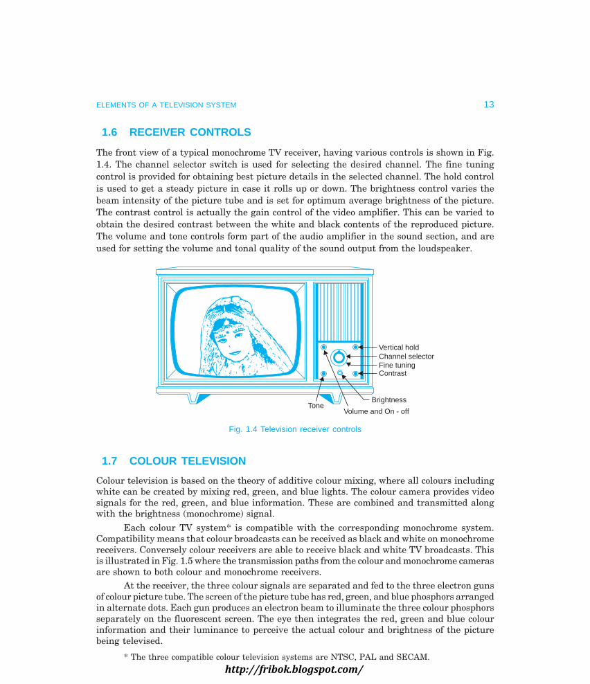
1.6 RECEIVER CONTROLS
The front view of a typical monochrome TV receiver, having various controls is shown in Fig.1.4. The channel selector switch is used for selecting the desired channel. The fine tuningcontrol is provided for obtaining best picture details in the selected channel. The hold controlis used to get a steady picture in case it rolls up or down. The brightness control varies thebeam intensity of the picture tube and is set for optimum average brightness of the picture.The contrast control is actually the gain control of the video amplifier. This can be varied toobtain the desired contrast between the white and black contents of the reproduced picture.The volume and tone controls form part of the audio amplifier in the sound section, and areused for setting the volume and tonal quality of the sound output from the loudspeaker.
Vertical holdChannel selectorFine tuningContrast
Brightness
Volume and On - offTone
Fig. 1.4 Television receiver controls
1.7 COLOUR TELEVISION
Colour television is based on the theory of additive colour mixing, where all colours includingwhite can be created by mixing red, green, and blue lights. The colour camera provides videosignals for the red, green, and blue information. These are combined and transmitted alongwith the brightness (monochrome) signal.
Each colour TV system* is compatible with the corresponding monochrome system.Compatibility means that colour broadcasts can be received as black and white on monochromereceivers. Conversely colour receivers are able to receive black and white TV broadcasts. Thisis illustrated in Fig. 1.5 where the transmission paths from the colour and monochrome camerasare shown to both colour and monochrome receivers.
At the receiver, the three colour signals are separated and fed to the three electron gunsof colour picture tube. The screen of the picture tube has red, green, and blue phosphors arrangedin alternate dots. Each gun produces an electron beam to illuminate the three colour phosphorsseparately on the fluorescent screen. The eye then integrates the red, green and blue colourinformation and their luminance to perceive the actual colour and brightness of the picturebeing televised.
* The three compatible colour television systems are NTSC, PAL and SECAM.
http://fribok.blogspot.com/

14 MONOCHROME AND COLOUR TELEVISION
Colour Receiver Controls
NTSC colour television receivers have two additional controls, known as Colour and Huecontrols. These are provided at the front panel along with other controls. The colour or saturationcontrol varies the intensity or amount of colour in the reproduced picture. For example, thiscontrol determines whether the leaves of a tree in the picture are dark green or light green,and whether the sky in the picture is dark blue or light blue. The tint or hue control selects thecorrect colour to be displayed. This is primarily used to set the correct skin colour, since whenflesh tones are correct, all other colours are correctly reproduced.
It may be noted that PAL colour receivers do not need any tint control while in SECAMcolour receivers, both tint and saturation controls are not necessary. The reasons for suchdifferences are explained in chapters exclusively devoted to colour television.
G
R
B
Optical filters
Colour camera
Object
vB
vG
vR R1
R2
R3
Combining matrixTransmission
path
Object
Monochromecamera
v = 0.3 v + 0.59 v + 0.11 vR G B
v
R
Colour picturetube
Colourreceiver
RGB
Red, green andblue guns
Red, greenand bluephosphors
Electron gunPhosphor
screenMonochrome
receiver
Black and whitepicture tube
Fig. 1.5. Signal transmission paths illustrating compatibility between colourand monochrome TV systems. R, G and B represent three camera tubes which develop
video signals corresponding to the red, green and blue contents of the scene being televised.
Review Questions
1. Why is scanning necessary in TV transmission ? Why is it carried out at a fast rate ?
2. What is the basic principle of operation of a television camera tube ?
3. What is a raster and how is it produced on the picture tube screen ?
4. Why are synchronizing pulses transmitted along with the picture signal ?
5. Why is FM preferred to AM for sound signal transmission ?
6. Describe briefly the functions of various controls provided on the front panel of a TV receiver.
7. Describe the basic principle of colour television transmission and reception.
8. Describe the function of saturation and hue controls in a NTSC colour TV receiver.
http://fribok.blogspot.com/

2
http://fribok.blogspot.com/

The basic factors with which the television system must deal for successful transmissionand reception of pictures are:
(a) Gross Structure: Geometric form and aspect ratio of the picture.
(b) Image Continuity: Scanning and its sequence.
(c) Number of Scanning Lines: Resolution of picture details.
(d) Flicker: Interlaced scanning.
(e) Fine Structure: Vertical and horizontal resolution.
(f) Tonal Gradation: Picture brightness transfer characteristics of the system.
2.1 GROSS STRUCTURE
The frame adopted in all television systems is rectangular with width/height ratio, i.e., aspectratio = 4/3. There are many reasons for this choice. In human affairs most of the motion occursin the horizontal plane and so a larger width is desirable. The eyes can view with more easeand comfort when the width of a picture is more than its height. The usage of rectangularframe in motion pictures with a width/height ratio of 4/3 is another important reason for adoptingthis shape and aspect ratio. This enables direct television transmission of film programmeswithout wastage of any film area.
It is not necessary that the size of the picture produced on the receiver screen be sameas that being televised but it is essential that the aspect ratio of the two be same, otherwise thescene details would look too thin or too wide. This is achieved by setting the magnitudes of thecurrent in the deflection coils to correct values, both at the TV camera and receiving picturetube. Another important requirement is that the same coordinates should be scanned at anyinstant both by the camera tube beam and the picture tube beam in the receiver. Synchronizingpulses are transmitted along with the picture information to achieve exact congruence betweentransmitter and receiver scanning systems.
2.2 IMAGE CONTINUITY
While televising picture elements of the frame by means of the scanning process, it is necessaryto present the picture to the eye in such a way that an illusion of continuity is created and any
16
http://fribok.blogspot.com/

ANALYSIS AND SYNTHESIS OF TELEVISION PICTURES 17
motion in the scene appears on the picture tube screen as a smooth and continuous change. Toachieve this, advantage is taken of ‘persistence of vision’ or storage characteristics of the humaneye. This arises from the fact that the sensation produced when nerves of the eye’s retina arestimulated by incident light does not cease immediately after the light is removed but persistsfor about 1/16th of a second. Thus if the scanning rate per second is made greater than sixteen,or the number of pictures shown per second is more than sixteen, the eye is able to integratethe changing levels of brightness in the scene. So when the picture elements are scannedrapidly enough, they appear to the eye as a complete picture unit, with none of the individualelements visible separately.
In present day motion pictures twenty-four still pictures of the scene are taken persecond and later projected on the screen at the same rate. Each picture or frame is projectedindividually as a still picture, but they are shown one after the other in rapid succession toproduce the illusion of continuous motion of the scene being shown. A shutter in the projectorrotates in front of the light source and allows the film to be projected on the screen when thefilm frame is still, but blanks out any light from the screen during the time when the next filmframe is being moved into position. As a result, a rapid succession of still-film frames is seen onthe screen. With all light removed during the change from one frame to the next, the eye seesa rapid sequence of still pictures that provides the illusion of continuous motion.
Scanning. A similar process is carried out in the television system. The scene is scannedrapidly both in the horizontal and vertical directions simultaneously to provide sufficient numberof complete pictures or frames per second to give the illusion of continuous motion. Instead ofthe 24 as in commercial motion picture practice, the frame repetition rate is 25 per second inmost television systems.
Horizontal scanning. Fig. 2.1 (a) shows the trace and retrace of several horizontallines. The linear rise of current in the horizontal deflection coils (Fig. 2.1 (b)) deflects the beamacross the screen with a continuous, uniform motion for the trace from left to right. At thepeak of the rise, the sawtooth wave reverses direction and decreases rapidly to its initial value.This fast reversal produces the retrace or flyback. The start of the horizontal trace is at the left
Startof a line
Trace Retrace
Raster
Endof a line
HH
WW
Fig. 2.1 (a) Path of scanning beam in covering picture area (Raster).
http://fribok.blogspot.com/

18 MONOCHROME AND COLOUR TELEVISION
edge of raster. The finish is at the right edge, where the flyback produces retrace back to theleft edge.
1st line 3rd line2nd line
Trace Retrace
i(H)
i(H) max
t
Raster of 625 lines
Right
Trace Retrace
t cRetrace period
Trace periodLeft
One cycle ofdeflection current
Fig. 2.1 (b) Waveform of current in the horizontal deflection coils producinglinear (constant velocity) scanning in the horizontal direction.
Note, that ‘up’ on the sawtooth wave corresponds to horizontal deflection to the right.The heavy lines in Fig. 2.1 (a) indicate the useful scanning time and the dashed lines correspondto the retrace time.
Vertical scanning. The sawtooth current in the vertical deflection coils (see Fig. 2.2)moves the electron beam from top to bottom of the raster at a uniform speed while the electronbeam is being deflected horizontally. Thus the beem produces complete horizontal lines onebelow the other while moving from top to bottom.
As shown in Fig. 2.2 (c), the trace part of the sawtooth wave for vertical scanning deflectsthe beam to the bottom of the raster. Then the rapid vertical retrace returns the beam to thetop. Note that the maximum amplitude of the vertical sweep current brings the beam to thebottom of the raster. As shown in Fig. 2.2 (b) during vertical retrace the horizontal scanningcontinues and several lines get scanned during this period. Because of motion in the scenebeing televised, the information or brightness at the top of the target plate or picture tubescreen normally changes by the time the beam returns to the top to recommence the wholeprocess. This information is picked up during the next scanning cycle and the whole process isrepeated 25 times to cause an illusion of continuity. The actual scanning sequence is howevera little more complex than that just described and is explained in a later section of this chapter.It must however be noted, that both during horizontal retrace and vertical retrace intervalsthe scanning beams at the camera tube and picture tube are blanked and no picture informationis either picked up or reproduced. Instead, on a time division basis, these short retrace intervalsare utilized for transmitting distinct narrow pulses to keep the sweep oscillators of the picturetube deflection circuits of the receiver in synchronism with those of the camera at thetransmitter. This ensures exact correspondence in scanning at the two ends and results indistortionless reproduction of the picture details.
http://fribok.blogspot.com/

ANALYSIS AND SYNTHESIS OF TELEVISION PICTURES 19
Top
Bottom
(a) Trace
Linearverticaltrace
(b) Retrace
Verticalretrace
i(V)
i(V) maxverticaltrace
Bottom
Retrace
Top 1st f a e1st frame 2nd f a e2nd framet
One cycle of verticaldeflection current Top
Trace period
Retrace period
Bottom t
Raster HH
W
(c) Current waveform in vertical deflection coils
Fig. 2.2 Vertical deflection and deflection current waveform.
2.3 NUMBER OF SCANNING LINES
Most scenes have brightness gradations in the vertical direction. The ability of the scanningbeam to allow reproduction of electrical signals according to these variations and the capabilityof the human eye to resolve these distinctly, while viewing the reproduced picture, depends onthe total number of lines employed for scanning.
It is possible to arrive at some estimates of the number of lines necessary by consideringthe bar pattern shown in Fig. 2.3 (a), where alternate lines are black and white. If the thicknessof the scanning beam is equal to the width of each white and black bar, and the number ofscanning lines is chosen equal to the number of bars, the electrical information correspondingto the brightness of each bar will be correctly reproduced during the scanning process. Obviouslythe greater the number of lines into which the picture is divided in the vertical plane, thebetter will be the resolution.However, the total number of lines that need be employed islimited by the resolving capability of the human eye at the minimum viewing distance.
Bea
mpa
th
Beam spot
DarkWhiteDWDWDW
Fig. 2.3 (a) Scanning spot perfectly aligned with black and white lines.
http://fribok.blogspot.com/

20 MONOCHROME AND COLOUR TELEVISION
Two adjacentblack picture
elements just resolvedD = 4HD = 4H
HH
n th bar(n + 1) th bar
Angle subtended at the eyeby picture elements at critical
viewing distance ( )
Eye of theobserver
Fig. 2.3 (b) Critical viewing distance as determined by the ability of the eye toresolve two separate picture elements.
Bea
mpa
th
Beam spot Adjacentblack and white lines
of resolution
Fig. 2.3 (c) Scanning beam focused on the junction of black and white lines.
The maximum number of alternate light and dark elements (lines) which can be resolvedby the eye is given by
Nv = 1
αρwhere Nv = total number of lines (elements) to be resolved in the vertical direction, α = minimumresolving angle of the eye expressed in radians, and ρ = D/H = viewing-distance/picture height.
For the eye this resolution is determined by the structure of the retina, and the brightnesslevel of the picture. it has been determined experimently that with reasonable brightnessvariations and a minimum viewing distance of four times the picture height (D/H = 4), theangle that any two adjacent elements must subtend at the eye for distinct resolution isapproximately one minute (1/60 degree). This is illustrated in Fig. 2.3 (b). Substituting thesevalues of α and ρ we get
Nv = 1
180 1 60 4860
( / / )π × ×≈
Thus if the total number of scanning lines is chosen close to 860 and the scanning beam asillustrated in Fig. 2.3 (a) just passes over each bar (line) separately while scanning all the linesfrom top to bottom of the picture frame, a distinct pick up of the picture information resultsand this is the best that can be expected from the system. This perhaps explains the use of 819lines in the original French TV system.
http://fribok.blogspot.com/

ANALYSIS AND SYNTHESIS OF TELEVISION PICTURES 21
In practice however, the picture elements are not arranged as equally spaced segmentsbut have random distribution of black, grey and white depending on the nature of the picturedetails or the scene under consideration. Statistical analysis and subjective tests carried out todetermine the average number of effective lines suggest that about 70 per cent of the totallines or segments get separately scanned in the vertical direction and the remaining 30 percent get merged with other elements due to the beam spot falling equally on two consecutivelines. This is illustrated in Fig. 2.3 (c). Thus the effective number of lines distinctly resolved,i.e., Nr = Nv × k, where k is the resolution factor whose value lies between 0.65 to 0.75. Assumingthe value of k = 0.7 we get, Nr = Nv × k = 860 × 0.7 = 602.
However, there are other factors which also influence the choice of total number of linesin a TV system. Tests conducted with many observers have shown that though the eye candetect the effective sharpness provided by about 800 scanning lines, but the improvement isnot very significant with line numbers greater than 500 while viewing pictures having motion.Also the channel bandwidth increases with increase in number of lines and this not only addsto the cost of the system but also reduces the number of television channels that can be providedin a given VHF or UHF transmission band. Thus as a compromise between quality and cost,the total number of lines inclusive of those lost during vertical retrace has been chosen to be625 in the 625-B monochrome TV system. In the 525 line American system, the total numberof lines has been fixed at 525 because of a somewhat higher scanning rate employed in thissystem.
2.4 FLICKER
Although the rate of 24 pictures per second in motion pictures and that of scanning 25 framesper second in television pictures is enough to cause an illusion of continuity, they are not rapidenough to allow the birghtness of one picture or frame to blend smoothly into the next throughthe time when the screen is blanked between successive frames. This results in a definiteflicker of light that is very annoying to the observer when the screen is made alternatelybright and dark.
This problem is solved in motion pictures by showing each picture twice, so that 48views of the scene are shown per second although there are still the same 24 picture framesper second. As a result of the increased blanking rate, flicker is eliminated.
Interlaced scanning. In television pictures an effective rate of 50 vertical scans per secondis utilized to reduce flicker. This is accomplished by increasing the downward rate of travel ofthe scanning electron beam, so that every alternate line gets scanned instead of every successiveline. Then, when the beam reaches the bottom of the picture frame, it quickly returns to thetop to scan those lines that were missed in the previous scanning. Thus the total number oflines are divided into two groups called ‘fields’. Each field is scanned alternately. This methodof scanning is known as interlaced scanning and is illustrated in Fig. 2.4. It reduces flicker toan acceptable level since the area of the screen is covered at twice the rate. This is like readingalternate lines of a page from top to bottom once and then going back to read the remaininglines down to the bottom.
http://fribok.blogspot.com/

22 MONOCHROME AND COLOUR TELEVISION
sRetrace lines not shown
Beginning of 2nd field
Beginning of1st field 1
2345
310311312313
313314315316
622623624625
End of 1st field End of 2nd field
Fig. 2.4 Principle of interlaced scanning. Note that the vertical retracetime has been assumed to be zero.
In the 625 lime monochrome system, for successful interlaced scanning, the 625 lines ofeach frame or picture are divided into sets of 312.5 lines and each set is scanned alternately tocover the entire picture area. To achieve this the horizontal sweep oscillator is made to work ata frequency of 15625 Hz (312.5 × 50 = 15625) to scan the same number of lines per frame(15625/25 = 625 lines), but the vertical sweep circuit is run at a frequency of 50 instead of25 Hz. Note that since the beam is now deflected from top to bottom in half the time and thehorizontal oscillator is still operating at 15625 Hz, only half the total lines, i.e., 312.5 (625/2 =312.5) get scanned during each vertical sweep. Since the first field ends in a half line and thesecond field commences at middle of the line on the top of the target plate or screen (seeFig. 2.4), the beam is able to scan the remaining 312.5 alternate lines during its downwardjourney. In all then, the beam scans 625 lines (312.5 × 2 = 625) per frame at the same rate of15625 lines (312.5 × 50 = 15625) per second. Therefore, with interlaced scanning the flickereffect is eliminated without increasing the speed of scanning, which in turn does not need anyincrease in the channel bandwidth.
It may be noted that the frame repetition rate of 25 (rather than 24 as used in motionpictures) was chosen to make the field frequency equal to the power line frequency of 50 Hz.This helps in reducing the undesired effects of hum due to pickup from the mains, becausethen such effects in the picture stay still, instead of drifting up or down on the screen. In theAmerican TV system, a field frequency of 60 was adopted because the supply frequency is60 Hz in USA. This brings the total number of lines scanned per second ((525/2) × 60 = 15750)lines to practically the same as in the 625 line system.
Scanning periods. The waveshapes of both horizontal and vertical sweep currents areshown in Fig. 2.5. As shown there the retrace times involved (both horizontal and vertical) aredue to physical limitations of practical scanning systems and are not utilized for transmittingor receiving any video signal. The nominal duration of the horizontal line as shown in Fig. 2.5 (a)is 64 µs (106/15625 = 64 µs), out of which the active line period is 52 µs and the remaining 12 µs
http://fribok.blogspot.com/

ANALYSIS AND SYNTHESIS OF TELEVISION PICTURES 23
is the line blanking period. The beam returns during this short interval to the extreme left sideof the frame to start tracing the next line.
Similarly with the field frequency set at 50 Hz, the nominal duration of the verticaltrace (see Fig. 2.5(b)) is 20 ms (1/50 = 20 ms). Out of this period of 20 ms, 18.720 ms are spentin bringing the beam from top to bottom and the remaining 1.280 ms is taken by the beam toreturn back to the top to commence the next cycle. Since the horizontal and vertical sweeposcillators operate continuously to achieve the fast sequence of interlaced scanning, 20 horizontal
lines 128064
20µ
µs
slines=
FHG
IKJ get traced during each vertical retrace interval. Thus 40 scanning
lines are lost per frame, as blanked lines during the retrace interval of two fields. This leavesthe active number of lines, Na, for scanning the picture details equal to 625 – 40 = 585, insteadof the 625 lines actually scanned per frame.
52 s64 s
12 s
1(H)
Trace
Retrace
f = 15625 Hz
t
Fig. 2.5 (a) Horizontal deflection current.
i(v)
Trace Retrace
f = 50 Hz
t18.720 ms18.720 ms 20 ms20 ms
1.280 ms
Fig. 2.5 (b) Vertical deflection current.
Scanning sequence. The complete geometry of the standard interlaced scanning patternis illustrated in Fig. 2.6. Note that the lines are numbered in the sequence in which these areactually scanned. During the first vertical trace actually 292.5 lines are scanned. The beamstarts at A, and sweeps across the frame with uniform velocity to cover all the picture elementsin one horizontal line. At the end of this trace the beam then retraces rapidly to the left side ofthe frame as shown by the dashed line in the illustration to begin the next horizontal line.Note that the horizontal lines slope downwards in the direction of scanning because the verticaldeflecting current simultaneously produces a vertical scanning motion, which is very slow
http://fribok.blogspot.com/

24 MONOCHROME AND COLOUR TELEVISION
compared with horizontal scanning. The slope of the horizontal trace from left to right is greaterthan during retrace from right to left. The reason is that the faster retrace does not allow thebeam so much time to be deflected vertically. After line one, the beam is at the left side readyto scan line 3, omitting the second line. However, as mentioned earlier it is convenient tonumber the lines as they are scanned and so the next scanned line skipping one line, is numberedtwo and not three. This process continues till the last line gets scanned half when the verticalmotion reaches the bottom of the raster or frame. As explained earlier skipping of lines isaccomplished by doubling the vertical scanning frequency from the frame or picture repetitionrate of 25 to the field frequency of 50 Hz. With the field frequency of 50 Hz the height of theraster is so set that 292.5 lines get scanned as the beam travels from top to bottom and reaches
291 to 292.5 o292.5 to 312.5 t312.5 to 605 o605 to 625
31st field = 312.5 lines 32nd field = 312.5 lines
One frame or picture = 625 lines
1st vertical trace(292.5 lines)
Inactive lines during1st vertical retrace
(20 lines)
2nd vertical trace(292.5 lines)
Inactive lines during2nd vertical retrace
(20 lines)
A
B B
C C
D D
A
Fig. 2.6 Odd line interlaced scanning procedure.
point B. Now the retrace starts and takes a period equal to 20 horizontal line periods to reachthe top marked C. These 20 lines are known as inactive lines, as the scanning beam is cut-offduring this period. Thus the second field starts at the middle of the raster and the first linescanned is the 2nd half of line number 313. The scanning of second field, starting at the middleof the raster automatically enables the beam to scan the alternative lines left unscanned duringthe first field. The vertical scanning motion otherwise is exactly the same as in the previousfield giving all the horizontal lines the same slope downwards in the direction of scanning. Asa result 292.5 lines again get scanned and the beam reaches the bottom of the frame when ithas completed full scanning of line number 605. The inactive vertical retrace again begins andbrings the beam back to the top at point A in a period during which 20 blanked horizontal lines(605 to 625) get scanned. Back at point A, the scanning beam has just completed two fields orone frame and is ready to start the third field covering the same area (no. of lines) as scannedduring the first field. This process (of scanning fields) is continued at a fast rate of 50 times asecond, which not only creates an illusion of continuity but also solves the problem of flickersatisfactorily.
http://fribok.blogspot.com/

ANALYSIS AND SYNTHESIS OF TELEVISION PICTURES 25
2.5 FINE STRUCTURE
The ability of the image reproducing system to represent the fine structure of an object isknown as its resolving power or resolution. It is necessary to consider this aspect separately inthe vertical and horizontal planes of the picture.
Vertical resolution. The extent to which the scanning system is capable of resolvingpicture details in the vertical direction is referred to as its vertical resolution. It has alreadybeen explained that the vertical resolution is a function of the scanning lines into which thepicture is divided in the vertical plane. Based on that discussion the vertical resolution in the625 lines system can then be expressed as
Vr = Na × k
where Vr is the vertical resolution expressed in number of lines, Na is the active number oflines and k is the resolution factor (also known as Kell factor).
Assuming a reasonable value of k = 0.69,
Vr = 585 × 0.69 = 400 lines
It is of interest to note that the corresponding resolution of 35 mm motion pictures isabout 515 lines and thus produces greater details as compared to television pictures.
Scanningspot
Alternate black and whitelines of resolution
Vertical bar pattern for determinationof amplifier requirements
e(t)Peak white level
Black level
tOutput video waveform
Fig. 2.7 (a) Determination of horizontal resolution.
W
HH
Fig. 2.7(b) Chess-board pattern for studyingvertical and horizontal resolution.
http://fribok.blogspot.com/

26 MONOCHROME AND COLOUR TELEVISION
Horizontal resolution. The capability of the system to resolve maximum number of pictureelements along the scanning lines determines horizontal resolution. This can be evaluated byconsidering a vertical bar pattern as shown in Fig. 2.7(a). It would be realistic to aim at equalvertical and horizontal resolution and as such the number of alternate black and white barsthat should be considered is equal to
Na × aspect ratio = 585 × 4/3 = 780
Before proceeding further it must be recognised that as all lines in the vertical plane arenot fully effective, in a similar way all parts of an individual line are not fully effective all thetime. As explained earlier, it ultimately depends on the random distribution of black and whiteareas in the picture. Thus for equal vertical and horizontal resolution, the same resolutionfactor may be used while determining the effective number of distinct picture elements in ahorizontal line. Therefore, the effective number of alternate black and white segments in onehorizontal line for equal vertical and horizontal resolution are :
N = Na × aspect ratio × k = 585 × 4/3 × 0.69 = 533
To resolve these 533 squares or picture elements the scanning spot must develop a videosignal of square wave nature switching continuously along the line between voltage levelscorresponding to black and peak white. This is shown along the bar pattern drawn in Fig. 2.7(a).Since along one line there are 533/2 ≈ 267 complete cyclic changes, 267 complete square wavecycles get generated during the time the beam takes to travel along the width of the pattern.Thus the time duration th of one square wave cycle is equal to
th = active period of each horizontal linenumber of cycles
= 52 10
267
6× − seconds
∴ thg frequency of the periodic wave
fh = 1 267 10
52
6
th= ×
= 5 MHz
Since the consideration of both vertical and horizontal resolutions is based on identicalblack and white bars in the horizontal and vertical planes of the picture frame, it amounts toconsidering a chessboard pattern as the most stringent case and is illustrated in Fig. 2.7(b).Here each alternate black and white square element takes the place of bars for determiningthe capability of the scanning system to reproduce the fine structure of the object being televised.The actual size of each square element in the chess pattern is very small and is equal tothickness of the scanning beam. It would be instructive to know as an illustration that the sizeof such a square element on the screen of a 51 cm picture tube is about 0.5 mm2 only.
Since the spacing of these small elements in the above consideration corresponds to thelimiting resolution of the eye, it will distinguish only the alternate light and dark areas but notthe shape of the variations along the scanning line. Thus the eye will fail to distinguish thedifference between a square wave of brightness variation and a sine wave of brightness variationin the reproduced picture. Therefore, if the amplifier for the square-wave signal is capable ofreproducing a sine-wave of frequency equal to the repetition frequency of the rectangularwave, it is satisfactory for the purpose of TV signals. It may be mentioned that even otherwise
http://fribok.blogspot.com/

ANALYSIS AND SYNTHESIS OF TELEVISION PICTURES 27
to handle a 5 MHz square wave would necessitate reproduction up to 11th harmonic of aperiodic sinusoidal wave of 5 MHz by the associated electronic circuitry. This would mean abandwidth of atleast up to 5 × 11 = 55 MHz which is excessive and almost impossible to providein practice. Another justification for restricting the bandwidth up to 5 MHz is that in practiceit is rare when alternate picture elements are black and white throughout the picture widthand height, and a bandwidth up to 5 MHz has been found to be quite adequate to produce mostdetails of the scene being televised.
Therefore, the highest approximate modulating frequency ‘fh’ that the 625 line televisionsystem must be capable of handling for successful transmission and reception of picture detailsis
fh = No. of active lines aspect ratio resolution factor
2 time duration of one active line× ×
×
= 585 4 3 0 69
2 52 10 6
× ×× × −
/ .
≈ 5 MHz
In the second (525 line) widely used television system, where the active number of linesis 485 and the duration of one active line is 57 µs, the highest modulating frequency fh ≈ 4MHz.
This explains the allocation of 6 MHz as the channel bandwidth in USA and othercountries employing the 525 line system in comparison to a channel bandwidth allocation of 7MHz in countries that have adopted the 625 line system. Similarly in the French 819 TVsystem where the highest modulating frequency comes to 10.4 MHz a channel bandwidth of14 MHz is allowed.
Colour resolution and bandwidth. As explained above a bandwidth of 5 MHz (4 MHz inthe American system) is needed for transmission of maximum horizontal detail in monochrome.However, this bandwidth is not necessary for the colour video signals. The reason is that thehuman eye’s colour response changes with the size of the object. For very small objects the eyecan perceive only the brightness rather than the colours in the scene. Perception of colours bythe eye is limited to objects which result in a video frequency output up to about 1.5 MHz. Thusthe colour information needs much less bandwidth than monochrome details and can be easilyaccommodated in the channel bandwidth allotted for monochrome transmission.
Low-frequency requirements. The analysis of the signals produced by the bar patterngives no information regarding the low-frequency requirement of a video amplifier used tohandle such signals. This requirement may be determined from consideration of a patternshown in Fig. 2.8(a). The signal output during vertical excursions of the beam would be asquare wave (see Fig. 2.8(b)) at vertical field frequency. It is apparent then, that any amplifiercapable of reproducing this waveform would be required to have good square-wave response at50 Hz. Any degradation in response as shown in Fig. 2.8(c) would result in brightness distortion.In order to have satisfactory square-wave response at field frequency, an amplifier must havegood sine-wave response with negligible phase distortion down to a much lower frequencythan the field frequency. In addition, to correct phase and amplitude response at the fieldfrequency, it is necessary to preserve the dc component of the brightness signal. Thus a goodfrequency response from dc to about 5 MHz becomes necessary for true reproduction of thebrightness variations and find details of any scene.
http://fribok.blogspot.com/

28 MONOCHROME AND COLOUR TELEVISION
e(t)
t(v)
t
VV
Fig. 2.8(a) Single bar pattern. Fig. 2.8(b) Ideal response to scanningof single bar pattern.
t
e(t)
Fig. 2.8(c) Distorted response due to poorlow frequency response of the system.
Influence of number of lines on bandwidth. As the number of lines employed in a televisionpicture is increased, the bandwidth necessary for a given quality of definition also increases.This is due to the fact that increasing the number of lines per picture decreases the timeduration of each line. This means that the spot travels across the screen at a higher velocityand results in increase of the highest modulating frequency. For example doubling the numberof lines per frame would very much improve the vertical resolution, infact it would get doubledbut would need increasing the bandwidth in the same ratio. If now, it is required to increasethe horizontal resolution so that it again equals the vertical resolution it would be necessary toscan double the number of alternate black and white signal elements in a line, and this wouldnecessitate multiplying the original highest video frequency by a factor of four. The conclusionis that, if the number of lines employed in a television system is increased, it is necessary toincrease the video frequency bandwidth in direct proportion to the increase in number of linesto maintain the same degree of vertical definition (as before), and in order to increase horizontaldefinition in the same proportion as the increase in vertical resolution the video frequencybandwidth must increase as the square of the increase in number of lines.
Effect of interlaced scanning on bandwidth. As already explained, interlaced scanningreduces flicker. However, scanning 50 complete frames of 625 lines in a progressive mannerwould also eliminate flicker in the picture but this would need double the scanning speedwhich in turn would double the video frequencies corresponding to the picture elements in aline. This would necessitate double the channel bandwidth of that required with interlacedscanning. It should be noted that by employing interlaced scanning, the basic concept ofinterchangeability of time and bandwidth is not violated, because more time in allowed fortransmission and this results in decrease of bandwidth needed for each TV channel. Thusinterlaced scanning reduces flicker and conserves bandwidth.
Effect of field frequency on bandwidth. With increase in field frequency the time availablefor each field decreases and this results in a proportionate decrease of the active line period.
http://fribok.blogspot.com/

ANALYSIS AND SYNTHESIS OF TELEVISION PICTURES 29
Hence, bandwidth increases in direct proportion to the increase in the field frequency.
Bandwidth requirement for transmission of synchronising pulses. The equalizing pulsesto be discussed later have a pulse width of 2.3 µs with an allowed rise time of 0.2 µs. Thehighest sinusoidal frequency which must lie in the pass band of the system for effectivetransmission of these pulses is given by the expression :
Highest necessary frequency = 1
2 × allowed rise time =
102 0 2
6
× . = 2.5 MHz
It is then clear that all sync pulses are safely preserved in the video circuitry where, ashas been shown, a frequency bandwidth considerably in excess of this figure has to be maintainedin order to preserve the required picture definition.
Interlace error. As explained earlier interlaced scanning provides a means of decreasingthe effect of flicker in the TV picture without increasing the system bandwidth. The selectionof 2 : 1 as the interlace ratio is the simplest with least circuit complications. Here, by selectingan odd number of lines, the symmetry in frame blanking pulses is achieved and this enablesperfect interlaced scanning. Any error in scanning timings and sequence would leave a largenumber of picture elements unresolved and thus the quality of the reproduced picture getsimpaired. Fig. 2.9 shows various cases of interlace error. For convenience of explanation theretrace time has been assumed to be zero. Interlace error occurs due to the time difference instarting the second field. For perfect interlace the second field should start from point ‘b’ (seeFig. 2.9 (a)), i.e., 32 µs away from ‘a’, the starting point of the first field. If it starts early or lateinterlace error will be there. For a 16 µs delay in the start of the second field (Fig. 2.9 (b)),starting points of the two fields will be 48 µs apart instead of the desired 32 µs. Then thepercentage interlace error
= 48 32
32100
− × = 50%
if the second field starts 16 µs early even then the error would be 50%. For a delay of 32 µs thetwo fields will overlap (Fig. 2.9 (c)) and the interlace error would be 100%, i.e., half the picturearea will go unscanned.
Assumed starting point of one scanning field
Start of alternate field
a b
(a) Perfect interlace
332 s 3 s32 s
a b
16 s
32 s
The two fields overlap
a, b
(b) 50% interlace error (c) 100% interlace error
Fig. 2.9 Examples of interlace error.
The above examples demonstrate that incorrect start of any field produces verticaldisplacement between the lines of the two fields. This brings these lines closer leaving gaps
http://fribok.blogspot.com/

30 MONOCHROME AND COLOUR TELEVISION
between the pairs thus formed. The result is a deterioration of the picture’s vertical resolutionbecause certain areas do not get scanned at all.
For perfect interlaced scanning it is essential that the starting points at the top of theframe is separated exactly one half line between first and second fields. To achieve this it isnecessary to feed two regularly spaced synchronising pulses to the field time base during eachframe period. One of these pulses must arrive in the middle of a line and the next at the end ofa line. This is shown in Fig. 2.10. Thus the vertical time base must be triggered 50 times persecond in the manner explained above. For half line separation between the two fields only thetopmost and the extreme bottom lines are then half lines whereas the remaining lines are allfull lines. If there are x number of full lines per field, where x may be even or odd, the totalnumber of full lines per frame is then 2x, an even number. To this, when the two half lines getadded the total number of lines per frame becomes odd. Thus for interlaced scanning the totalnumber of lines in any TV system must be odd. With an even number of lines the two fields arebound to fall on each other and interlaced scanning would not take place.
W
HH
A B
Trigger pulse instances
Fig. 2.10 Vertical trigger pulse instances.A—after 1st field, B—after 2nd field.
Further for correct interlacing it becomes necessary that at the transmitter automaticfrequency control must be utilized to maintain a horizontal scanning frequency that is exactly312.5 times as great as the field frequency, i.e., 50 Hz. This is accomplished by generating astable frequency at 15625 Hz by crystal controlled oscillator circuits. A frequency doublingcircuit produces a frequency of 31250 Hz, which is utilized to control the correct generation ofequalizing and vertical sync pulses. Four frequency division circuits each with a ratio of 5 : 1are employed to derive 50 Hz, the vertical scanning frequency (31250 = 5 × 5 × 5 × 5 × 50). Thusall the required frequencies are derived from a common stable source and they automaticallyremain interlocked in the correct ratios. To achieve this, i.e., frequency division, the totalnumber of lines per frame must be a product of small whole numbers. The frame frequency of625 satisfies all the above requirements. Similarly 525 lines in the American system and 819lines in the French system also meet these requirements.
http://fribok.blogspot.com/

ANALYSIS AND SYNTHESIS OF TELEVISION PICTURES 31
Comparison of various TV systems. Picture and sound signal standards for the principalmonochrome television systems are given at the end of chapter 4. The CCIR 625-B monochromesystem used in most parts of Europe and adopted by India has a video bandwidth of 5 MHz,whereas the British 625 line system has a video bandwidth of 5.5 MHz. Obviously, here 0.73has been used as the resolution factor instead of the 0.69 used in our system. So the Britishsystem is marginally better than the European system. The French TV system employs 819lines with a video bandwidth of 10.4 MHz. This system therefore has both much improvedvertical resolution and a better horizontal resolution.
The American 525 line system employs a frame frequency of 30 as compared to 25 in theCCIR 625-B monochrome system. Thus, the line frequency in this system is 15750, whichcompares very closely to our system where the line frequency is 15625. However, the Americansystem employs a bandwidth of 4 MHz which suggests that the horizontal resolution of thissystem is less than all other systems in use. It must be noted that the number of lines employedby a given TV system is not in itself, a guide to the quality of resolution available from thesystem. It is true that greater the number of lines the better the vertical resolution, but anassessment of the horizontal resolution, i.e., the bandwidth employed by the system is a betteroverall guide to the quality of definition.
2.6 TONAL GRADATION
In addition to proper bandwidth required to produce the details allowed by the scanning systemat the transmitting end and the picture tube at the receiving end, the signal-transmissionsystem should have proper transfer characteristics to preserve same brightness gradation asthe eye would perceive when viewing the scene directly. Any non-linearity in the pick-up andpicture tube should also be corrected by providing inverse nonlinearities in the channel circuitryto obtain overall linear characteristics. Note that the sensation in the eye to detect changes orbrightness is logarithmic in nature and this must be taken into account while designing theoverall channel.
Various other factors that influence the tonal quality of the reproduced picture are :
(a) Contrast. This is the difference in intensity between black and white parts of thepicture over and above the brightness level.
(b) Contrast ratio. The ratio of maximum to minimum brightness relative to the originalpicture is called contrast ratio. In broad daylight the variations in brightness are very widewith ratio as high as 10000 : 1, whereas the picture tube, because of certain limitations, cannotproduce a contrast with variations more than 50 : 1 or atmost 100 : 1. Ratio of brightnessvariations in the reproduced picture on the screen of the picture tube, to the brightness variationsin the original scene is known as Gamma of the picture. Its value is close to 0.5. In studios,under controlled conditions of light, the variations are less wide than outside and so thebrightness variations that can be reproduced by the picture tube are not very much differentthan that of the scene. Realism is still maintained because the viewer does not actually see thescene being televised. Another factor which makes stringent demands from the systemunnecessary is the fact that our eye can accommodate not more than 10 : 1 variations of lightintensity at any time. Too bright a representation of the bright areas in a picture would make
http://fribok.blogspot.com/

32 MONOCHROME AND COLOUR TELEVISION
grey areas appear as dark in comparison. This is true at all levels of light intensity withbrightness variations in relative ratios of 10 : 1. When a TV receiver is off, there is no beamimpinging on the fluorescent screen of the picture tube and no light gets emitted. Then withnormal light in the room the screen appears as dull white. But when the receiver is no, and aTV programme is being received the bright portions of the scene appear quite bright becausethe corresponding amplitude of the video signal makes the control-grid of the picture tubemuch less negative and the consequent increased beam current causes more light on the screen.However, for a very dark portion of the scene the corresponding video signal makes the gridhighly negative with respect to the cathode and thus cuts-off the beam current and no light isemitted on the corresponding portions on the screen. These areas appear to the eye as dark incomparison with the high light areas of the screen, whereas the same area in the absence ofbeam current when the set was off appeared close to a white shade. This as explained earlier isdue to the logarithmic response of the human eye and its inability to accommodate light intensityvariations greater than 10 : 1.
(c) Viewing distance. The viewing distance from the screen of the TV receiver should notbe so large that the eye cannot resolve details of the picture. The distance should also not be sosmall that picture elements become separately visible. The above conditions are met when thevertical picture size subtends an angle of approximately 15° at the eye. The distance alsodepends on habit, varies from person to person, and lies between 3 to 8 times the pictureheight. Most people prefer a distance close to five times the picture height. While viewing TV,a small light should be kept on in the room to reduce contrast. This does not strain the eyesand there is less fatigue.
Review Questions
1. Justify the choice of rectangular frame with width to height ratio = 4/3 for television transmis-sion and reception.
2. How is the illusion of continuity created in television pictures ? Why has the frame receptionrate been chosen to be 25 and not 24 as in motion pictures ?
3. What do you understand by interlaced scanning ? Show that it reduces flicker and conservebandwidth.
4. What do you understand by active and blanking periods in horizontal and vertical scanning ?Give the periods of nominal, active and retrace intervals of horizontal and vertical scanning asused in the 625 line system.
5. How many horizontal lines get traced during each vertical retrace ? What is the active number oflines that are actually used for picture information pick up and reception ?
6. Draw a picture frame chart showing the total number of active and inactive lines during eachfield and establish the need for terminating the first field in a half line and the beginning thesecond at the middle of a line at the top.
7. Justify the choice of 625 lines for TV transmission. Why is the total number of lines kept odd inall television systems ? What is the significance of choosing the number of lines as 625 and not623 or 627 ?
8. What do you understand by resolution or Kell-factor ? How does it affect the vertical resolutionof a television picture ? Show that the vertical resolution increases with increase in number ofscanning lines.
http://fribok.blogspot.com/

ANALYSIS AND SYNTHESIS OF TELEVISION PICTURES 33
9. What is meant by equal vertical and horizontal ‘resolution ?’ Derive an expression for the high-est modulating frequency in a television system and show that it is nearly 5 MHz. in the 625-Bmonochrome system.
10. Show that if the number of lines employed in a TV system is increased then the highest videofrequency must increase as the square of the increase in number of lines for equal improvementin vertical and horizontal resolution.
11. Show that the 625-B TV system is only marginally superior to the 525 line American system.
12. What do you understand by interlace error and how does it affect the quality of the picture ?Calculate the percentage interlace error when the second field is delayed by 8 µs. Retrace timemay be assumed to be negligible.
13. In the British 625 lines system the resolution factor employed is 0.73 instead of 0.69 as used inthe 625-B monochrome system. All other scanning details remaining the same, calculate thehighest modulating frequency used in the British system.
14. Explain the need for providing very good low frequency response and phase characteristics inamplifiers used in any TV link, for proper reproduction of brightness variations.
15. The relevant data for a closed circuit TV system is given below. Calculate the highest modulat-ing frequency that will be generated while scanning the most stringent case of alternate blackand white dots for equal vertical and horizontal resolution.
No. of lines = 250
Interlace ratio = 1 : 1
Picture repetition rate = 50/sec
Aspect ratio = 4/3
Vertical retrace time = 10% of the picture frame time
Horizontal retrace time = 20% of the total line time
Assume resolution factor = 0.8
Ans ≈ 2 MHz
16. Explain the meaning of terms-tonal gradation, contrast, contrast ratio and gamma of the pic-ture.
When a TV receiver is off, no electron beam strikes the picture tube screen and the screen facelooks a dull white. With the set on and a black and white picture showing on the screen, noelectron beam impinges on the darker area of the reproduced picture. But these areas now ap-pear quite black instead of the dull white of the switched-off set. Explain the reason for thisdifference in appearance.
http://fribok.blogspot.com/

3
http://fribok.blogspot.com/

Composite video signal consists of a camera signal corresponding to the desired pictureinformation, blanking pulses to make the retrace invisible, and synchronizing pulses tosynchronize the transmitter and receiver scanning. A horizontal synchronizing (sync) pulse isneeded at the end of each active line period whereas a vertical sync pulse is required after eachfield is scanned. The amplitude of both horizontal and vertical sync pulses is kept the same toobtain higher efficiency of picture signal transmission but their duration (width) is chosen tobe different for separating them at the receiver. Since sync pulses are needed consecutivelyand not simultaneously with the picture signal, these are sent on a time division basis andthus form a part of the composite video signal.
3.1 VIDEO SIGNAL DIMENSIONS
Figure 3.1 shows the composite video signal details of three different lines each correspondingto a different brightness level of the scene. As illustrated there, the video signal is constrainedto vary between certain amplitude limits. The level of the video signal when the picture detailbeing transmitted corresponds to the maximum whiteness to be handled, is referred to aspeak-white level. This is fixed at 10 to 12.5 percent of the maximum value of the signal whilethe black level corresponds to approximately 72 percent. The sync pulses are added at 75 percentlevel called the blanking level. The difference between the black level and blanking level isknown as the ‘Pedestal’. However, in actual practice, these two levels, being very close, tend tomerge with each other as shown in the figure. Thus the picture information may vary between10 percent to about 75 percent of the composite video signal depending on the relative brightnessof the picture at any instant. The darker the picture the higher will be the voltage within thoselimits.
Note that the lowest 10 percent of the voltage range (whiter than white range) is notused to minimize noise effects. This also ensures enough margin for excessive bright spots tobe accommodated without causing amplitude distortion at the modulator.
At the receiver the picture tube is biased to ensure that a received video voltagecorresponding to about 10 percent modulation yields complete whiteness at that particularpoint on the screen, and an analogous arrangement is made for the black level. Besides this,the television receivers are provided with ‘brightness’ and ‘contrast’ controls to enable theviewer to make final adjustments as he thinks fit.
D.C. component of the video signal. In addition to continuous amplitude variations forindividual picture elements, the video signal has an average value or dc component
36
http://fribok.blogspot.com/

COMPOSITE VIDEO SIGNAL 37
corresponding to the average brightness of the scene. In the absence of dc component thereceiver cannot follow changes in brightness, as the ac camera signal, say for grey pictureelements on a black background will then be the same as a signal for white area on a greyback-ground. In Fig. 3.1, dc components of the signal for three lines have been identified, eachrepresenting a different level of average brightness in the scene. It may be noted that thebreak shown in the illustration after each line signal is to emphasize that dc component of thevideo signal is the average value for complete frames rather than lines since the backgroundinformation of the picture indicates the brightness of the scene. Thus Fig. 3.1 illustrates theconcept of change in the average brightness of the scene with the help of three lines in separateframes because the average brightness can change only from frame to frame and not from lineto line.
0
12.5
20
40
60
7580
100
v/v %max
Com
posi
tevi
deo
sign
al(p
erce
ntof
max
)
nD
arke
rth
anda
rkD
ark
leve
l
Ped
. hei
ght
.e
D.C
. lev
el
DC
.ev
elD
.C. l
evel
Peak whitelevel
heig
htP
ed.
heig
ht
Blankinglevel
Horz syncpulses
One lineOne lineduration
64 s
64 s64 s
Picturedetails
.D
.C.l
evel
Ped
esta
l hei
ght
per odActive line
period52 s
SS
PP
0.4
0.2
0
0.2
0.4
0.6
0.8
1.0
t
Fig. 3.1 Arbitrary picture signal details of three scanning lines with different averagebrightness levels. Note that picture to sync ratio P/S = 10/4.
Pedestal height. As noted in Fig. 3.1 the pedestal height is the distance between thepedestal level and the average value (dc level) axis of the video signal. This indicates averagebrightness since it measures how much the average value differs from the black level. Evenwhen the signal loses its dc value when passed through a capacitor-coupled circuit the distancebetween the pedestal and the dc level stays the same and thus it is convenient to use thepedestal level as the reference level to indicate average brightness of the scene.
Setting the pedestal level. The output signal from the TV camera is of very small amplitudeand is passed through several stages of ac coupled high gain amplifiers before being coupled toa control amplifier. Here sync pulses and blanking pulses are added and then clipped at thecorrect level to form the pedestals. Since the pedestal height determines the average brightnessof the scene, any smaller value than the correct one will make the scene darker while a largerpedestal height will result in higher average brightness. The video control operator who observesthe scene at the studio sets the level for the desired brightness in the reproduced picture which
http://fribok.blogspot.com/

38 MONOCHROME AND COLOUR TELEVISION
he is viewing on a monitor receiver. This is known as dc insertion because this amounts toadding a dc component to the ac signal. Once the dc insertion has been acomplished the pedestallevel becomes the black reference and the pedestal height indicates correct relative brightnessfor the reproduced picture. However, the dc level inserted in the control amplifier is usuallylost in succeeding stages because of capacitive coupling, but still the correct dc component canbe reinserted when necessary because the pedestal height remains the same.
The blanking pulses. The composite video signal contains blanking pulses to make theretrace lines invisible by raising the signal amplitude slightly above the black level (75 percent) during the time the scanning circuits produce retraces. As illustrated in Fig. 3.2, thecomposite video signal contains horizontal and vertical blanking pulses to blank thecorresponding retrace intervals. The repetition rate of horizontal blanking pulses is thereforeequal to the line scanning frequency of 15625 Hz. Similarly the frequency of the vertical blankingpulses is equal to the field-scanning frequency of 50 Hz. It may be noted that though the levelof the blanking pulses is distinctly above the picture signal information, these are not used assync pulses. The reason is that any occasional signal corresponding to any extreme black portionin the picture may rise above the blanking level and might conceivably interfere with thesynchronization of the scanning generators. Therefore, the sync pulses, specially designed fortriggering the sweep oscillators are placed in the upper 25 per cent (75 per cent to 100 per centof the carrier amplitude) of the video signal, and are transmitted along with the picture signal.
Peak white level
0
1012.5%
20
30
40
50
60
70
75
80
90
100
72%
Am
plitu
de%
Blacklevel
nr
Horz sync pulseadded here (25%)
64 s64 s
Horzblankingpulses
160 s160 sVertical blanking pulse period
(No picture informationduring this interval)
Verticalde
Verticalsync pulse added here (25%) Blanking level
Pictureinformation
t
Fig. 3.2 Horizontal and vertical blanking pulses in video signal. Sync pulses are added abovethe blanking level and occupy upper 25% of the composite video signal amplitude.
Sync pulse and video signal amplitude ratio. The overall arrangement of combining thepicture signal and sync pulses may be thought of as a kind of voltage division multiplexingwhere about 65 per cent of the carrier amplitude is occupied by the video signal and the upper
http://fribok.blogspot.com/

COMPOSITE VIDEO SIGNAL 39
25 per cent by the sync pulses. Thus, as shown in Fig. 3.1, the final radiated signal has apicture to sync signal ratio (P/S) equal to 10/4. This ratio has been found most satisfactorybecause if the picture signal amplitude is increased at the expense of sync pulses, then whenthe signal to noise ratio of the received signal falls, a point is reached when the sync pulseamplitude becomes insufficient to keep the picture locked even though the picture voltage isstill of adequate amplitude to yield an acceptable picture. On the other hand if sync pulseheight is increased at the expense of the picture detail, then under similar conditions theraster remains locked but the picture content is of too low an amplitude to set up a worthwhilepicture. A ratio of P/S = 10/4, or thereabout, results in a situation such that when the signal tonoise ratio reaches a certain low level, the sync amplitude becomes insufficient, i.e., the syncfails at the same time as the picture ceases to be of entertainment value. This represents themost efficient use of the television system.
3.2 HORIZONTAL SYNC DETAILS
The horizontal blanking period and sync pulse details are illustrated in Fig. 3.3. The intervalbetween horizontal scanning lines is indicated by H. As explained earlier, out of a total line
Retrace ends
0
12.520
40
60
7580
100
Am
plitu
de%
0Horz
deflectionsawtooth
Retracebegins
Blanking begins
Trace
Retrace
Blanking ends
t
t
Horz blankingpulse = 12 sm
cPictureinformation = 52 sm
Horz syncpulse = 4.7 sm
Back porch= 5.8 sm
Front porch = 1.5 sm
P cturePictureH = 64 sm
Front porch (blanked)Back porch (blanked)
eona
Picture spaceon
the raster
Fig. 3.3 Horz line and sync details compared to horizontal deflection sawtoothand picture space on the raster.http://fribok.blogspot.com/

40 MONOCHROME AND COLOUR TELEVISION
period of 64 µs, the line blanking period is 12 µs. During this interval a line synchronizingpulse is inserted. The pulses corresponding to the differentiated leading edges of the syncpulses are actually used to synchronize the horizontal scanning oscillator. This is the reasonwhy in Fig. 3.3 and other figures to follow, all time intervals are shown between sync pulseleading edges.
The line blanking period is divided into three sections. These are the ‘front porch’, the‘line sync’ pulse and the ‘back porch’. The time intervals allowed to each part are summarizedbelow and their location and effect on the raster is illustrated in Fig. 3.3.
Details of Horizontal Scanning
Period Time (µs)
Total line (H) 64
Horz blanking 12 ± .3
Horz sync pulse 4.7 ± 0.2
Front porch 1.5 ± .3
Back porch 5.8 ± .3
Visible line time 52
Front porch. This is a brief cushioning period of 1.5 µs inserted between the end of thepicture detail for that line and the leading edge of the line sync pulse. This interval allows thereceiver video circuit to settle down from whatever picture voltage level exists at the end of thepicture line to the blanking level before the sync pulse occurs. Thus sync circuits at the receiverare isolated from the influence of end of the line picture details. The most stringent demand ismade on the video circuits when peak white detail occurs at the end of a line. Despite theexistence of the front porch when the line ends in an extreme white detail, and the signalamplitude touches almost zero level, the video voltage level fails to decay to the blanking levelbefore the leading-edge of the line sync pulse occurs. This results in late triggering of the timebase circuit thus upsetting the ‘horz’ line sync circuit. As a result the spot (beam) is late inarriving at the left of the screen and picture information on the next line is displaced to theleft. This effect is known as ‘pulling-on-whites’.
Line sync pulse. After the front proch of blanking, horizontal retrace is produced whenthe sync pulse starts. The flyback is definitely blanked out because the sync level is blackerthan black. Line sync pulses are separated at the receiver and utilized to keep the receiver linetime base in precise synchronism with the distant transmitter. The nominal time duration forthe line sync pulses is 4.7 µs. During this period the beam on the raster almost completes itsback stroke (retrace) and arrives at the extreme left end of the raster.
Back porch. This period of 5.8 µs at the blanking level allows plenty of time for lineflyback to be completed. It also permits time for the horizontal time-base circuit to reversedirection of current for the initiation of the scanning of next line. Infact, the relative timingsare so set that small black bars (see Fig. 3.3) are formed at both the ends of the raster in thehorizontal plane. These blanked bars at the sides have no effect on the picture details reproducedduring the active line period.
http://fribok.blogspot.com/

COMPOSITE VIDEO SIGNAL 41
The back porch* also provides the necessary amplitude equal to the blanking level(reference level) and enables to preserve the dc content of the picture information at thetransmitter. At the receiver this level which is independent of the picture details is utilized inthe AGC (automatic gain control) circuits to develop true AGC voltage proportional to thesignal strength picked up at the antenna.
3.3 VERTICAL SYNC DETAILS
The vertical sync pulse train added after each field is somewhat complex in nature. The reasonfor this stems from the fact that it has to meet several exacting requirements. Therefore, inorder to fully appreciate the various constituents of the pulse train, the vertical sync detailsare explored step by step while explaining the need for its various components.
The basic vertical sync added at the end of both even add odd fields is shown in Fig. 3.4.Its width has to be kept much larger than the horizontal sync pulse, in order to derive asuitable field sync pulse at the receiver to trigger the field sweep oscillator.
The standards specify that the vertical sync period should be 2.5 to 3 times the horizontalline period. If the width is less than this, it becomes difficult to distinguish between horizontaland vertical pulses at the receiver.
623H
624H
625H 1 t ha f
Lines 1, 2, 3rd1st half 3.5 to 17 818 19
(b)
(a)
20 e er od = (20 × 64 = 1280 ) 20 line period = (20 × 64 s = 1280 s)
2.5 H2.5 H(160 s)
313.5H/2
310H
311H
312H 3 3 3 3 5313.5 314 315 3 33316 to 330 331331 332
iEnd of first fieldBeginning of second field
inte valVertical pulse
intervalert ca blank ng in ervalVertical blanking interval
End of second (even) field Beginning of first (odd) field
Fig. 3.4 Composite video waveforms showing horizontal and basic vertical sync pulses atthe end of (a) second (even) field, (b) first (odd) field. Note, the widths of
horizontal blanking intervals and sync pulses are exaggerated.
*In colour TV transmission a short sample (8 to 10 cycles) of the colour subcarrier oscillatoroutput is sent to the receiver for proper detection of colour signal sidebands. This is known as colourburst and is located at the back porch of the horizontal blanking pedestal.
http://fribok.blogspot.com/

42 MONOCHROME AND COLOUR TELEVISION
If the width is greater than this, the transmitter must operate at peak power for anunnecessarily long interval of time. In the 625 line system 2.5 line period (2.5 × 64 = 160 µs)has been allotted for the vertical sync pulses. Thus a vertical sync pulse commences at the endof 1st half of 313th line (end of first field) and terminates at the end fo 315th line. Similarlyafter an exact interval of 20 ms (one field period) the next sync pulse occupies line numbers—1st, 2nd and 1st half of third, just after the second field is over. Note that the beginning ofthese pulses has been aligned in the figure to signify that these must occur after the end ofvertical stroke of the beam in each field, i.e., after each 1/50th of a second. This alignment ofvertical sync pulses, one at the end of a half-line period and the other after a full line period(see Fig. 3.4), results in a relative misalignment of the horizontal sync pulses and they do notappear one above the other but occur at half-line intervals with respect to each other. However,a detailed examination of the pulse trains in the two fields would show that horizontal syncpulses continue to occur exactly at 64 µs intervals (except during the vertical sync pulse periods)throughout the scanning period from frame to frame and the apparent shift of 32 µs is only dueto the alignment of vertical sync instances in the figure.
As already mentioned the horizontal sync information is extracted from the sync pulsetrain by differentiation, i.e., by passing the pulse train through a high-pass filter. Indeed pulsescorresponding to the differentiated leading edges of sync pulses are used to synchronise thehorizontal scanning oscillator. The process of deriving these pulses is illustrated in Fig. 3.5.Furthermore, receivers often use monostable multivibrators to generate horizontal scan, andso a pulse is required to initiate each and every cycle of the horizontal oscillator in the receiver.
Syncseparator
Compositevideo signal
Sync pulses
R2 C2L.P.F.
H.P.F.
C1 R1 Differentiated output
Integrated output
Fig. 3.5 Sync pulse separation and generation of vertical and horizontal sync pulses.
This brings out the first and most obvious shortcoming of the waveforms shown in Fig. 3.4.The horizontal sync pulses are available both during the active and blanked line periods butthere are no sync pulses (leading edges) available during the 2.5 line vertical sync period. Thusthe horizontal sweep oscillator that operates at 15625 Hz, would tend to step out of synchronismduring each vertical sync period. The situation after an odd field is even worse. As shown inFig. 3.4, the vertical blanking period at the end of an odd field begins midway through ahorizontal line. Consequently, looking further along this waveform, we see that the leadingedge of the vertical sync pulse comes at the wrong time to provide synchronization for thehorizontal oscillator. Therefore, it becomes necessary to cut slots in the vertical sync pulse athalf-line-intervals to provide horizontal sync pulses at the correct instances both after evenand odd fields. The technique is to take the video signal amplitude back to the blanking level
http://fribok.blogspot.com/

COMPOSITE VIDEO SIGNAL 43
4.7 µs before the line pulses are needed. The waveform is then returned back to the maximumlevel at the moment the line sweep circuit needs synchronization. Thus five narrow slots of4.7 µs width get formed in each vertical sync pulse at intervals of 32 µs. The trailing but risingedges of these pulses are actually used to trigger the horizontal oscillator. The resultingwaveforms together with line numbers and the differentiated output of both the field trains isillustrated in Fig. 3.6. This insertion of short pulses is known as notching or serration of thebroad field pulses.
Note that though the vertical pulse has been broken to yield horizontal sync pulses, theeffect on the vertical pulse is substantially unchanged. It still remains above the blankingvoltage level all of the time it is acting. The pulse width is still much wider than the horizontalpulse width and thus can be easily separated at the receiver. Returning to Fig. 3.6 it is seenthat each horizontal sync pulse yields a positive spiked output from its leading edge and anegative spiked pulse from its trailing edge. Time-constant of the differentiating circuit is sochosen, that by the time a trailing edge arrives, the pulse due to the leading edge has justabout decayed. The negative-going triggering pulses may be removed with a diode since onlythe positive going pulses are effective in locking the horizontal oscillator.
End of 2nd field
623623 624624 625625 11 22 33
1 2 3 4 5
4.7 s 27.3 s
623 624 625 1 2 3 4 5 6
(a)
End of 1st field
311311 312312 313313 314314 315315 316316
1 2 3 4 5
311 312 313 314 315 316 317 318
(b)
Fig. 3.6 Differentiating waveforms (a) pulses at the end of even (2nd) field and thecorresponding output of the differentiator (H.P.F.) (b) pulses at the end of odd (1st)
field and the corresponding output of the differentiator (H.P.F.) Note, the differentiated pulsesbearing line numbers are the only ones needed at the end of each field.http://fribok.blogspot.com/
44 MONOCHROME AND COLOUR TELEVISION
However, the pulses actually utilized are the ones that occur sequentially at 64 µsintervals. Such pulses are marked with line numbers for both the fields. Note that during theintervals of serrated vertical pulse trains, alternate vertical spikes are utilized. The pulses notused in one field are the ones utilized during the second field. This happens because of thehalf-line difference at the commencement of each field and the fact that notched vertical syncpulses occur at intervals of 32 µs and not 64 µs as required by the horizontal sweep oscillator.The pulses that come at a time when they cannot trigger the oscillator are ignored. Thus therequirement of keeping the horizontal sweep circuit locked despite insertion of vertical syncpulses is realized.
Now we turn to the second shortcoming of the waveform of Fig. 3.4. First it must bementioned that synchronization of the vertical sweep oscillator in the receiver is obtainedfrom vertical sync pulses by integration. This is illustrated in Fig. 3.5 where the time-constantR2C2 is chosen to be large compared to the duration of horizontal pulses but not with respect towidth of the vertical sync pulses. The integrating circuit may equally be looked upon as a low-pass filter, with a cuit-off frequency such that the horizontal sync pulses produce very littleoutput, while the vertical pulses have a frequency that falls in the pass-band of the filter. Thevoltage built across the capacitor of the low-pass filter (integrating circuit) corresponding tothe sync pulse trains of both the fields is shown in Fig. 3.7. Note that each horizontal pulsecauses a slight rise in voltage across the capacitor but this is reduced to zero by the time thenext pulse arrives. This is so, because the charging period for the capacitor is only 4.7 µs andthe voltage at the input to the integrator remains at zero for the rest of the period of 59.3 µs.Hence there is no residual voltage across the vertical filter (L.P. filter) due to horizontal sync-pulses. Once the broad serrated vertical pulse arrives the voltage across the output of the filterstarts increasing. However, the built up voltage differs for each field. The reason is not difficultto find. At the beginning of the first field (odd field) the last horz sync pulse corresponding tothe beginning of 625th line is separated from the 1st vertical pulse by full one line and anyvoltage developed across the filter will have enough time to return to zero before the arrival ofthe first vertical pulse, and thus the filter output voltage builds up from zero in response to thefive successive broad vertical sync pulses. The voltage builds up because the capacitor hasmore time to charge and only 4.7 µs to discharge. The situation, however, is not the same forthe beginning of the 2nd (even) field. Here the last horizontal pulse corresponding to thebeginning of 313th line is separated from the first vertical pulse by only half-a-line. The voltagedeveloped across the vertical filter will thus not have enough time to reach zero before thearrival of the first vertical pulse, which means that the voltage build-up does not start fromzero, as in the case of the 1st field. The residual voltage on account of the half line discrepancygets added to the voltage developed on account of the broad vertical pulses and thus thevoltage developed across the output filter is some what higher at each instant as compared tothe voltage developed at the beginning of the first-field. This is shown in dotted chain line inFig. 3.7.
The vertical oscillator trigger potential level marked as trigger level in the diagram(Fig. 3.7) intersects the two filter output profiles at different points which indicates that in thecase of second field the oscillator will get triggered a fraction of a second too soon as compared
http://fribok.blogspot.com/

COMPOSITE VIDEO SIGNAL 45
to the first field. Note that this inequlity in potential levels for the two fields continues duringthe period of discharge of the capacitor once the vertical sync pulses are over and the horizontalsync pulses take-over. Though the actual time difference is quite short it does prove sufficientto upset the desired interlacing sequence.
End of 2nd field 1st field11625625
End of 1st field 2nd field3 2312 3 3313
(a)
(b)
(c)
v0
0
After end of 2nd field
Trigger level After end of 1st field
Timeerror
Trigger pulsefor the vertical oscillator
t
Fig. 3.7 Integrating waveforms (a) pulses at the end of 2nd (even) field (b) pulses at the end of1st (odd) field (c) integrator output. Note the above sync pulses have purposely been drawn
without equalizing pulses.
Equalizing pulses. To take care of this drawback which occurs on account of the half-line discrepancy five narrow pulses are added on either side of the vertical sync pulses. Theseare known as pre-equalizing and post-equalizing pulses. Each set consists of five narrow pulsesoccupying 2.5 lines period on either side of the vertical sync pulses. Pre-equalizing and post-equalizing pulse details with line numbers occupied by them in each field are given in Fig. 3.8.The effect of these pulses is to shift the half-line discrepancy away both from the beginningand end of vertical sync pulses. Pre-equalizing pulses being of 2.3 µs duration result in thedischarge of the capacitor to essentially zero voltage in both the fields, despite the half-linediscrepancy before the voltage build-up starts with the arrival of vertical sync pulses. This isillustrated in Fig. 3.9. Post-equalizing pulses are necessary for a fast discharge of the capacitorto ensure triggering of the vertical oscillator at proper time. If the decay of voltage across thecapacitor is slow as would happen in the absence of post-equalizing pulses, the oscillator maytrigger at the trailing edge which may be far-away from the leading edge and this could lead toan error in triggering.
Thus with the insertion of narrow pre and post equalizing pulses, the voltage rise andfall profile is essentially the same for both the field sequences (see Fig. 3.9) and the verticaloscillator is triggered at the proper instants, i.e., exactly at an interval of 1/50th of a second.
http://fribok.blogspot.com/
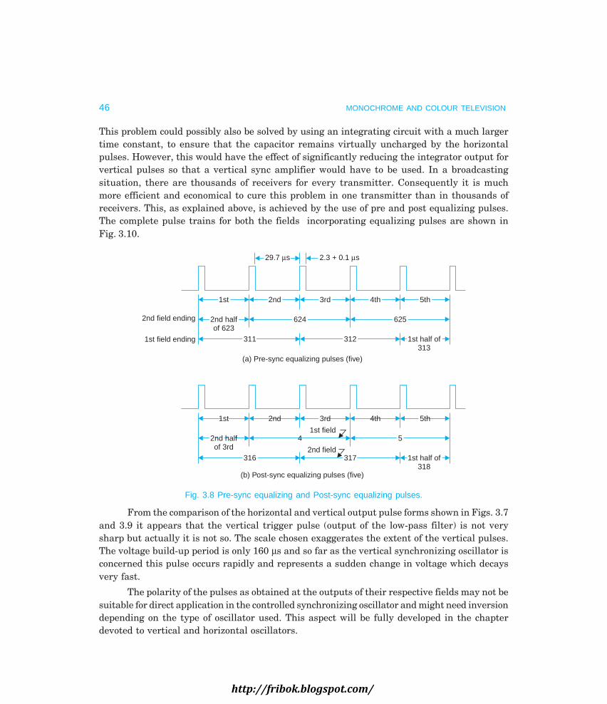
46 MONOCHROME AND COLOUR TELEVISION
This problem could possibly also be solved by using an integrating circuit with a much largertime constant, to ensure that the capacitor remains virtually uncharged by the horizontalpulses. However, this would have the effect of significantly reducing the integrator output forvertical pulses so that a vertical sync amplifier would have to be used. In a broadcastingsituation, there are thousands of receivers for every transmitter. Consequently it is muchmore efficient and economical to cure this problem in one transmitter than in thousands ofreceivers. This, as explained above, is achieved by the use of pre and post equalizing pulses.The complete pulse trains for both the fields incorporating equalizing pulses are shown inFig. 3.10.
29.7 s 2.3 + 0.1 s
1st1st 2nd2nd 3rd3rd 4th4th 5 h5th
2nd ha f2nd halfof 623
624624 625625
311311 312312 1st ha f of1st half of313
2nd field ending
1st field ending
(a) Pre-sync equalizing pulses (five)
s1st 2nd 33rd 4th 55th
2 d a2nd halfof 3rd
4 55
316316 317317 1st ha f of1st half of318
1st field
2nd field
(b) Post-sync equalizing pulses (five)
Fig. 3.8 Pre-sync equalizing and Post-sync equalizing pulses.
From the comparison of the horizontal and vertical output pulse forms shown in Figs. 3.7and 3.9 it appears that the vertical trigger pulse (output of the low-pass filter) is not verysharp but actually it is not so. The scale chosen exaggerates the extent of the vertical pulses.The voltage build-up period is only 160 µs and so far as the vertical synchronizing oscillator isconcerned this pulse occurs rapidly and represents a sudden change in voltage which decaysvery fast.
The polarity of the pulses as obtained at the outputs of their respective fields may not besuitable for direct application in the controlled synchronizing oscillator and might need inversiondepending on the type of oscillator used. This aspect will be fully developed in the chapterdevoted to vertical and horizontal oscillators.
http://fribok.blogspot.com/

COMPOSITE VIDEO SIGNAL 47
Active lines Pre-equalizing pulses Field sync pulses Post-equalizing pulses Blanking lines
End of 2nd field6621 6622 623
309309 310310 End of 1st field
rt-
Identical vertical syncbuilt-up
v0
0
Trigger level(no time error)
t
Fig. 3.9 Identical vertical sync voltage built-up across the integrating capacitor.
3.4 SCANNING SEQUENCE DETAILS
A complete chart giving line numbers and pulse designations for both the fields (correspondingto Fig. 3.10) is given below :
First Field (odd field)
Line numbers : one to 1st-half of 313th line (312.5 lines)
1, 2 and 3rd 1st-half, lines 2.5 lines—Vertical sync pulses
3rd 2nd-half, 4, and 5 2.5 lines—Post-vertical sync equalizing pulses.
6 to 17, and 18th 1st-half 12.5 lines—Blanking retrace pulses
18th 2nd-half to 310 292.5 lines—Picture details
311, 312, and 313th 1st-half 2.5 lines—Pre-vertical sync equalizing pulsesfor the 2nd field.
Total number of lines = 312.5
Second field (even field)
Line numbers : 313th 2nd-half to 625 (312.5 lines)
313th 2nd-half, 314, 315 2.5 lines—Vertical sync pulses
316, 317, 318th 1st-half 2.5 lines—Post-vertical sync equalizing pulses
318th 2nd-half-to 330 12.5 lines—Blanking retrace pulses
331 to 1st-half of 623rd 292.5 line—Picture details
623 2nd-half, 624 and 625 2.5 lines—Pre-vertical sync equalizing pulsesfor the 1st field
Total number of lines = 312.5
Total Number of Lines per Frame = 625
http://fribok.blogspot.com/

48M
ON
OC
HR
OM
E A
ND
CO
LOU
R T
ELE
VIS
ION
Fig. 3.10 Field synchronizing pulse trains of the 625 lines TV system.
End of 2ndfield
624 62511 22 33 44 55 66 7 88 9
10 11 1211 13 14 15 16 17 18 19 20
F d b an ing per od o 30 l nesField blanking period of 30 lines
2.5 l nes2.5 lines 2.5 l nes2.5 lines 2.5 l nes2.5 lines 12.5 l nes12.5 lines
309 310 311 312 313 314 315 316 317 318 319 320 321 322 323 324 325 326 327 328 329 330 331 332
5 Pre-equalizing
pulses
a
5 Verticalsync pulses
s5 Postequalizing
pulses
1 . 12.5 blanked lines
End of 1stfield (a) Pulse train at the end of 2nd field
(b) Pulse train at the end of 1st field
5 narrowequalizing
pulses
5 broad fieldsync pulses
5 narrowequalizing pulses
Blanking level
http://fribok.blogspot.com/

COMPOSITE VIDEO SIGNAL 49
Approximate location of line numbers. The serrated vertical sync pulse forces the verticaldeflection circuity to start the flyback. However, the flyback generally does not begin with thestart of vertical sync because the sync pulse must build up a minimum voltage across thecapacitor to trigger the scanning oscillator. If it is assumed that vertical flyback starts withthe leading edge of the fourth serration, a time of 1.5 lines passes during vertical sync beforevertical flyback starts. Also five equalizing pulses occur before vertical sync pulse train starts.Then four lines (2.5 + 1.5 = 4) are blanked at the bottom of the pricture before vertical retracebegins. A typical vertical retrace time is five lines. Thus the remaining eleven (20 – (4 + 5) =11) lines are blanked at the top of the raster. These lines provide the sweep oscillator enoughtime to adjust to a linear rise for uniform pick-up and reproduction of the picture.
3.5 FUNCTIONS OF VERTICAL PULSE TRAIN
By serrating the vertical sync pulses and the providing pre- and post-equalizing pulses thefollowing basic requirements necessary for successful interlaced scanning are ensured.
(a) A suitable field sync pulse is derived for triggering the field oscillator.
(b) The line oscillator continues to receive triggering pulses at correct intervals while theprocess of initiation and completion of the field time-base stroke is going on.
(c) It becomes possible to insert vertical sync pulses at the end of a line after the 2ndfield and at the middle of a line at the end of the 1st field without causing any interlaceerror.
(d) The vertical sync build up at the receiver has precisely the same shape and timing onodd and even fields.
3.6 SYNC DETAILS OF THE 525 LINE SYSTEM
In the 525 line American TV system where the total number of lines scanned per second is15750, the sync pulse details are as under :
Details of Horz Blanking
Period Time (µs)
Field line (H) 63.5
Horz blanking 9.5 to 11.5
Horz sync pulse 4.75 ± 0.5
Front porch 1.26 (minimum)
Back porch 3.81 (minimum)
Visible line 52 to 54
Details of vertical Blanking
Period Time
Total field (V) period = 1/60 sec. = 16.7 ms
Visible field time = 15 to 16 ms
Vertical blanking = 0.8 to 1.3 ms
http://fribok.blogspot.com/

50 MONOCHROME AND COLOUR TELEVISION
Total duration of six (serrated)vertical sync pulses = 3H = 190.5 µs
Each serrated pulse = H/2 = 31.75 µs
Each equalizing pulse(Six pre- and six post-equailzing pulses
are provided at H/2 intervals) = 0.04 H = 2.54 µs
Review Questions
1. Sketch composite video signal waveform for at least three three successive lines and indicate :(i) extreme white level, (ii) blanking level, (ii) pedestal height and (iv) sync pulse level. Justifythe choice of P/S ratio = 10/4 in the composite signal. Why is the combining of picture signal andsync pulses called a voltage division multiplex ?
2. Sketch composite video signal waveforms for the picture information shown in Fig. P 3.1.
W
HH
(a) (b)
Shaded areas indicate darkness
Fig. P3.1
3. Show picture information on a raster for the video signals drawn in Fig. P3.2.
White level
6 s64 s 64 s64 s
(a) (b)
Fig. P3.2
4. Sketch the details of horizontal blanking and sync pulses. Label on it (i) front porch, (ii) horizon-tal sync pulse, (iii) back porch and (iv) active line periods. Why are the front porch and backporch intervals provided before and after the horizontal sync pulse ? Explain why the blankingpulses are not used as sync pulses.
5. Enumerate the basic requriments that must be satisfied by the pulse train added after eachfield. Why is it necessary to serrate the broad vertical sync pulse ?
6. Sketch the pulse trains that follow after the second and first field of active scanning. Why arethe vertical sync pulses notched at 32 µs interval and not at 64 µs interval to provide horizontalsync pulses ?
http://fribok.blogspot.com/

COMPOSITE VIDEO SIGNAL 51
7. Explain how the horizontal and vertical sync pulses are separated and shaped at the receiver.For a time constant of 5 µs for the differentiating circuit, and 100 µs for the integrating circuit,plot the output waveforms from both the circuits for the entire vertical period. Calculate theerror in timing for successive vertical fields in the absence of equalizing pulses.
8. Sketch the complete pulse trains that follow at the end of both odd and even fields. Fully labelthem and explain how the half line discrepancy is removed by insertion of pre-equalizing pulses.
9. Justify the need for pre and post equalizing pulses. Why it is necessary to keep their durationequal to the half-line period ?
10. Justify the need for a blanking period corresponding to 20 complete lines after each active fieldof scanning. Why does the vertical retrace not begin with the incoming of the first serratedvertical sync pulse ?
11. Sketch the complete pulse trains that follow at the end of odd and even fields in the 525 linetelevision system. Justify the need for six instead of five pre and post equalizing pulses.
12. Show by any suitable means approximate correspondence between line numbers and the locationof the electron beam on the screen, both for odd and even fields.
http://fribok.blogspot.com/

4
http://fribok.blogspot.com/

In most television systems as also in the C.C.I.R 625 line, the picture signal is amplitudemodulated and sound signal frequency modulated before transmission. The channel bandwidthis determined by the highest video frequency required for proper picture reception and themaximum sound carrier frequency deviation permitted in a TV system.
Need for modulation. The need for modulation stems from the fact that it is impossibleto transmit a signal by itself. The greatest difficulty in the use of unmodulated wave is theneed for long antennas for efficient radiation and reception. For example, a quarter-wavelengthantenna for the transmitting frequency of 15 kHz would be 5000 meters long. A vertical antennaof this size is unthinkable and in fact impracticable.
Another important reason for not transmitting signal frequencies directly is that bothpicture and sound signals from different stations are concentrated within the same range offrequencies. Therefore, radiation from different stations would be hopelessly and inextricablymixed up and it would be impossible to separate one from the other at the receiving end. Thusin order to be able to separate the intelligence from different stations, it is necessary to translatethem all to different portions of the electromagnetic spectrum depending on the carrier frequencyassigned to each station. This also overcomes the difficulties of poor radiation at low frequencies.Once signals are translated before transmission, a tuned circuit provided in the RF section ofthe receiver can be used to select the desired station.
4.1 AMPLITUDE MODULATION
In amplitude modulation the intelligence to be conveyed is used to vary the amplitude of thecarrier wave. As an illustration, an amplitude modulated signal is shown in Fig. 4.1 (a) where
ec = Ec cos ωct is the carrier wave and
em = Em cos ωmt is the modulating signal.
Note that the camera signal is actually complex in nature but a single modulatingfrequency has been chosen for convenience of analysis.
The equation of the modulated wave is :
e = A cos ωct
where A = (Ec + kEm cos ωmt) when k is a constant of the modulator.
54
http://fribok.blogspot.com/

SIGNAL TRANSMISSION AND CHANNEL BANDWIDTH 55
+
–
0
Ec
e = E Cos tcc c
t
Unmodulated carrier wave
Emt
e = E Cos tmm m
Modulating signal
Ec
+
0
– Ec
–
E + E Cos tmc m
– (E + E Cos t)mc m
Modulated wave
t
LSB USB
Carrier
mfm mfm
fc – fm fc fc + fm
Fig. 4.1(a) Modulation of R.F. carrier Fig. 4.1(b) Frequency spectrum of AM wave.with a signal frequency.
On substituting the value of A we get :
e = (Ec + kEm cos ωmt) cos ωct = Ec (1 + m cos ωmt) cos ωct ...(4.1)
where m = kEE
m
c is the modulation index.
It may be noted that at kEm = Ec, m = 1 and the corresponding depth of modulation isthen termed as 100%.
Equation (4.1) may be expanded by the use of trigonometrical identities and expressedas :
e = Ec cos ωct + mEc
2 cos (ωc – ωm) t –
mEc
2 cos (ωc + ωm)t ...(4.2)
This result shows that if a carrier wave having frequency equal to fc is amplitude modulatedwith a single frequency fm, the resultant wave consists of the carrier (fc) and the sum anddifference components (fc ± fm) of the carrier frequency and the modulating frequency. However,if the modulating signal consists of more than a single frequency, as it would be for a videosignal, the equation can be extended to include the sum and difference of the carrier and allfrequency components of the modulating signal. This is illustrated in Fig. 4.1 (b) where fm hasbeen shown to be the highest modulating frequency. The region between fc and (fc + fm) iscalled the upper sideband (USB) and that between fc and (fc – fm) the lower sideband (LSB).
http://fribok.blogspot.com/

56 MONOCHROME AND COLOUR TELEVISION
Therefore if the modulated wave is to be transmitted without distortion by this method, thetransmission channel must be atleast of width 2fm centred on fc.
4.2 CHANNEL BANDWIDTH
In the 625 line TV system where the frequency components present in the video signal extendfrom dc (zero Hz) to 5MHz, a double sideband AM transmission would occupy a total bandwidthof 10 MHz. The actual band space allocated to the television channel would have to be stillgreater, because with practical filter characteristics it is not possible to terminate the bandwidthof a signal abruptly at the edges of the sidebands. Therefore, an attenuation slope of 0.5 MHzis provided at each edge of the two sidebands. This adds 1 MHz to the required total bandspace. In addition to this, each television channel has its associated FM (frequency modulated)sound signal, the carrier frequency of which is situated just outside the upper limit of 5.5 MHzof the picture signal. This, together with a small guard band, adds another 0.25 MHz to thechannel width, so that a practical figure for the channel bandwidth would be 11.25 MHz. Thisis illustrated in Fig. 4.2.
Am
plitu
de
c =Total channel width = 11.25 MHz
5 5 M z5.5 MHz 5 5 M z5.5 MHzP
Lower sideband (LSB) Upper sideband (USB)
Picture carrier
S
Guard band0.25 MHz
Attenuation slope
f(MHz)
5.5 5.75Frequency relative to picture carrier
5.5 5 4 3 2 1 0 1 2 3 4 5
Fig. 4.2 Total channel bandwidth using double sideband picture signal.P is picture carrier and S is sound carrier.
Such a bandwidth is too large, and if used, would limit the number of channels in agiven high frequency spectrum allocated for TV transmission. Therefore, to ensure spectrumconservation, some saving in the bandwidth allotted to each channel is desirable.
Single sideband transmission (SSB). A careful look at eqn. (4.2) reveals that the carriercomponent conveys no information because its amplitude and frequency remain constant nomatter what the amplitude of the modulating voltage is. However, the presence of the carrierfrequency is necessary at the receiver for recovering the modulating frequency fm, from theupper sideband by taking (fc + fm) – fc or from the lower sideband by taking fc – (fc – fm).Therefore, though superfluous from the point of view of transmission of intelligence, the carrierfrequency is radiated along with the sideband components in all radio-broadcast and TV systems.Such an arrangement results in simpler transmitting equipment and needs a very simple andinexpensive diode detector at the receiver for recovering the modulation components withoutundue distortion.
From eqn. (4.2) it is also obvious that the two sidebands are images of each other, sinceeach is equally affected by changes in the modulating voltage amplitude via the component
http://fribok.blogspot.com/

SIGNAL TRANSMISSION AND CHANNEL BANDWIDTH 57
mEc
2 . Also, any change in the frequency of the modulating signal results in identical changes
in the band spread of the two sidebands. It is seen, therefore, that all the information can beconveyed by the use of one sideband only and this results in a saving of 5 MHz per channel. Itmay, however, be noted that the magnitude of the detected signal in the receiver will be justhalf of that obtained when both the sidebands are transmitted. This is no serious drawbackbecause the IF (intermediate frequency) amplifier stages of the receiver provide enough gainto develop reasonable amplitude of the video signal at the output of video detector.
4.3 VESTIGIAL SIDEBAND TRANSMISSION
In the video signal very low frequency modulating components exist along with the rest of thesignal. These components give rise to sidebands very close to the carrier frequency which aredifficult to remove by physically realizable filters. Thus it is not possible to go to the extremeand fully suppress one complete sideband in the case of television signals. The low videofrequencies contain the most important information of the picture and any effort to completelysuppress the lower sideband would result in objectionable phase distortion at these frequencies.This distortion will be seen by the eye as ‘smear’ in the reproduced picture. Therefore, as acompromise, only a part of the lower sideband, is suppressed, and the radiated signal thenconsists of a full upper sideband together with the carrier, and the vestige (remaining part) ofthe partially suppressed lower sideband. This pattern of transmission of the modulated signalis known as vestigial sideband or A5C transmission. In the 625 line system, frquencies up to0.75 MHz in the lower sideband are fully radiated. The net result is a normal double sidebandtransmission for the lower video frequencies corresponding to the main body of pictureinformation.
As stated earlier, because of fillter design difficulties it is not possible to terminate thebandwidth of a signal abruptly at the edges of the sidebands. Therefore, an attenuation slopecovering approximately 0.5 MHz is allowed at either end. Any distortion at the higher frequencyend, if attenuation slope were not allowed, would mean a serious loss in horizontal detail,since the high frequency components of the video modulation determine the amount of horizontaldetail in the picture. Fig. 4.3 illustrates the saving of band space which results from vestigialsideband transmission. The picture signal is seen to occupy a bandwidth of 6.75 MHz insteadto 11 MHz.
Am
plitu
de
Sav g in ba d s a e4.25 MHz
Saving in band space To a chan e w dth = 7 MHzTotal channel width = 7 MHz
5.5 MHz0.5 MHz
0.25 MHz
Guard edge
SP1.25 MHz
0.75MHz
Full USB
LSLSB
Part of LSB removedby filter
Part of LSB removedby filter
5.5 5 4 2 .75 0 2 4 5.55.75
f(MHz)
1.25
Fig. 4.3 Total channel bandwidth using vestigial’ lower sideband.http://fribok.blogspot.com/

58 MONOCHROME AND COLOUR TELEVISION
4.4 TRASMISSION EFFICIENCY
Though the total power that is developed and radiated at the transmitter has no direct bearingon bandwidth requirements, the saving in power that can be effected by suppressing the carrierand one of the sidebands cannot be totally ignored. This can be demonstrated by consideringthe power relations in the modulated wave. Based on eqn. (4.2) the total power Pt, in themodulated wave is the sum of the carrier power Pc, and the power in the two sidebands. Thiscan be expressed as
Pt = Pc + PUSB + PLSB = ER
m ER
m ER
c c c2 2 2 2 2
2 8 8+ + ...(4.3)
where Ec
2 is the r.m.s. value of the sinusoidal carrier wave, and R is the resistance in which
the power is dissipated. Equation (4.3) can be simplified to read as
Pt = Pc + m
Pm
c
2 2
4 4+ Pc = Pc 1
2
2
+FHG
IKJ
m ...(4.4)
Note from the above expression that Pc remains constant but Pt depends on the value ofthe modulation index m. Also note that when several frequency components of differentamplitudes modulate the carrier wave, which in fact is the rule rather than an exception, thecarrier power Pt is unaffected but the total sideband power gets distributed in the individualsideband component powers. This is so because the total modulating voltage is equal to thesquare root of the sum of the squares of individual modulating voltages.
It can be seen from eqn. (4.4), that at 100% modulation (m = 1) the transmitted powerattains its maximum possible value. Pt(max) = 1.5 Pc, where the power contained in the twosidebands has a maximum value of 50% of the carrier power. It is clear then, that the carriercomponent that is redundent, so far as the transmission of intelligence is concerned, constitutesabout 72% of the total power that is radiated in the double sideband, full carrier (better knownas A3 modulation) AM system. Therefore, a lot of economy can be effected if the carrier poweris suppressed and not transmitted. Furthermore, suppression of one sideband results in moreeconomy and also halves the bandwidth requirements for transmission as compared to A3. Inpractice SSB is used to save power and bandwidth in mobile communication systems, telemetry,radio navigation, military and several other such applications. However, such a system needsthe generation of carrier frequency at the receiver for detection and this necessitates thetransmission of a low level pilot carrier along with either of the two sidebands. In addition tothis, a single sideband with suppressed carrier requires excellent frequency stability on thepart of both transmitter and receiver. Any deviation in frequency and phase of the generatedcarrier at the receiver would severely impair the quality of the picture when used for televisionsignal transmission. Such difficulties are not unsurmountable, but this tends to make thereceiver circuitry more complicated, which in turn adds to the cost of the receiver. In point topoint communication systems, where only one receiver is necessary, the additional expense isjustifiable and infact SSB is now the accepted mode of communication for such applications.However, in television and radio broadcast systems, where a very large number of receiverssimultaneously receive programme from one transmitter, additional cost of receivers is notjustified and as such SSB cannot be recmmended. Therefore, as stated earlier, in all TV systems,full carrier is radiated and vestigial sideband transmission is used. In radio broadcast wherethe channel bandwidth is only 100 kHz, both the sidebands are transmitted along with fullcarrier.
http://fribok.blogspot.com/

SIGNAL TRANSMISSION AND CHANNEL BANDWIDTH 59
4.5 COMPLETE CHANNEL BANDWIDTH
The sound carrier is always positioned at the extremity of the fully radiated upper sidebandand hence is 5.5 MHz away from the picture carrier. This is its logical place since it makes forminimum interference between the two signals. The FM sound signal occupies a frequencyspectrum of about ± 75 KHz around the sound carrier. However, a guard band of 0.25 MHz isallowed on the sound carrier side of the television channel to allow for adequate inter-channelseparation. The total channel bandwidth thus occupies 7 MHz and this represents a bandspacesaving of 4.25 MHz per channel, when compared with the 11.25 MHz space, which would berequired by the corresponding double sideband signal. Figure 4.4 show the complete channel.The frequency axis is scaled ralative to the picture carrier, which is marked as 0 MHz. Thismakes the diagram very informative, since details such as the widths of the upper and lowersidebands and the relative position of the sound carrier are easily read off.
=Total channel width = 7 MHz
5 55.5 MHz
4.433 M z4.433 MHzP C s
0.25 MHz
Sound signalsidebands 150 KHz
f(MHz)
Colour subcarrierAm
plitu
de
1.25
1.25 MHz
.75 0 1 2 3 4 5 5.5sUpper picture sideband
0.75 MHz
Fig. 4.4 C.C.I.R. (Indian and European) TV channel sideband spectrum.C is colour subcarrier frequency.
Fig. 4.5 (a) show television channel details of the British 625 line system, where thehighest modulating frequency employed is 5.5 MHz and the lower sideband up to 1.25 MHz
5.5 6.251.251 0 1 2 3 4 5 6
Vestigial LSB
Full upper sideband
Am
plitu
de
0.5 MHz
Tota chan e w th = 8 M zTotal channel width = 8 MHz
6 M z6 MHz
4.433 MHz
1.25MHz
P C S
0.25 MHz
Guard edge
150 KHzSound signalspectrum
f(MHz)
0.75MHz
Upper picture s de a d
Upper picture sideband5.5 MHz
Lower Picture sideband1.75 MHz
Fig. 4.5(a) U.K. TV channel standards.
http://fribok.blogspot.com/

60 MONOCHROME AND COLOUR TELEVISION
Tota channe w th = 6 M zTotal channel width = 6 MHz4.5 MHz
3.58 MHz3.58 MHzP C
S
0.25 MHz
Sound signalspectrum75 KHz
f(MHz)
Am
plitu
de1.25
.75 0 1 2 3 4
4.754.5
1.25MHz
Fig. 4.5(b) American TV channel standards.
is allowed to be radiated. The total bandwidth per channel is 8 MHz. Fig. 4.5 (b) illustrateschannel details of 525 line American system, where the highest allowed modulating frequencyis 4 MHz with a total bandwidth of 6 MHz. In the French 819 line system where the highestmodulating frequency is 10.4 MHz a channel bandwidth equal to 14 MHz is allowed. Thediagram in Fig. 4.6 shows how two adjacent C.C.I.R. 625 line channels in the VHF Band-I aredisposed one after the other.
54 55 56 57 58 59 60 61 62 63 64 65 66 67 68
Am
plitu
de
54 to 61
54 to 61(7 MHz)
61 to 68
61 to 68(7 MHz)
f(MHz)
5.5 MHz 5.5 MHz
BandChannel III
I BandChannel IV
I
P = 55.25MHz
S = 60.75MHz
P = 62.25MHz
S = 67.75MHz
Fig. 4.6 Sideband spectrum of two adjacent channels of the lower VHFband of television station allocations.
4.6 RECEPTION OF VESTIGIAL SIDEBAND SIGNALS
In principle an SSB signal with carrier cannot be demodulated by an envelope detector. Eithersynchronous demodulation or a square law device to produce effective multiplication of thecarrier with the sideband is required. However, it can be shown that if the sideband amplitudeis small compared to the carrier, then the envelope of the SSB with carrier signal nearlycorresponds to the modulating signal. In that case, envelope detection can be used and is thenormal practice in television receivers. With vestigial sideband however, the relative amplitudeof the frequencies for which both sidebands exist is double that of the true SSB component atthe envelope detector output. In the video signal it would be so for the low frequency content ofthe picture signal, and in effect, amounts to distortion in terms of relative amplitudes fordifferent frequencies and needs correction at the receiver.
This when expressed in another way means that if the picture carrier were successivelymodulated to an equal depth by a series of frequencies throughout the video frequency range
http://fribok.blogspot.com/

SIGNAL TRANSMISSION AND CHANNEL BANDWIDTH 61
employed by the system, and the resulting voltage output from the detector recorded, theoutput voltage against input frequency characteristic obtained would have the form shownin Fig. 4.7. The vestigial sideband extends to 0.75 MHz below the carrier and thereafter thissideband is linearly attenuated down to zero at 1.25 MHz. The detector output voltage wouldthus be twice as great between 0 Hz and 0.75 MHz than between 1.25 MHz to 5 MHz.
01 2 3 4 5 5.5
f(MHz)
1.0
2.0
Rel
ativ
evi
deo
dete
ctor
outp
utvo
ltage Output without receiver
response correction
utp nsOutput when receiver
response has the correct form
1.250.75
Video modulating frequency
Fig. 4.7 Receiver video detector output vs modulating frequency characteristicsillustrating the need for specially shaped receiver IF response curves.
1.25 0 1 2 3 4 5 5.75.75
5.5
f(MHz)
Rel
ativ
etr
ansm
itter
outp
ut
v0
P S7 MHz
5 MHz5 MHz
(a)
1.250 1 2 3 4 5 5.75
.7
f(MHz)
(b).75.5 .7
aa
Picture carrier
a + b = 1a + b = 1
.08
.2
.4
.5
.6
.8
.921
v0
Rel
ativ
ere
ceiv
erou
tput
bb
Fig. 4.8 Ideal characteristics of a TV transmitter and receiver. (a) transmitter outputcharacteristics for vestigial sideband signals. (b) desired receiver characteristics
for correct reproduction of video signals. Note that the picture carrier ispositioned half-way down the response curve.
http://fribok.blogspot.com/

62 MONOCHROME AND COLOUR TELEVISION
Between 0.75 MHz and 1.25 MHz the output voltage would fall linearly following the sidebandattenuation slope of the transmitter. To correct this discrepancy, it is necessary to so shapethe receiver response curve, that the frequencies present ‘twice’ are afforded less amplificationthan those occurring in one sideband only. The desired response is shown in Fig. 4.8. Theresponse curve is shaped to place the picture carrier half-way down the side corresponding tothe suppressed sideband. The width of the sloping edge on which the carrier is positioned istwice the width of the vestigial sideband. To understand how this achieves the desired result,refer to Fig. 4.8 and consider the treatment afforded to various frequencies within the videobandwidth. Frequencies between 5 MHz and 0.75 MHz i.e., those present in the upper sidebandonly, are seen to give unit output. Next, consider a frequency component at 0.5 MHz. This ispresent in both the sidebands. The total detector output is again unity. The component in thelower sideband gives rise to an output of a volts, while that in the upper sideband gives rise tob volts. From the geometry of the figure we see that (a + b) = 1. As a further example considerthe response at 0.7 MHz. This component in the vestigial sideband gives rise to an output =0.08 V, whilst in the upper sideband, it gives rise to 0.92 V. Again the sum of the two is unity,so that the same output is achieved for frequencies between 0.75 MHz and 5 MHz. Note that at0.75 MHz the output in the vestigial sideband is zero, and that in the upper sideband it isequal to one. The necessary correction detailed above is carried out at the IntermediateFrequency (IF) amplifier stages of the television receiver by suitably shaping the passbandcharacteristics of the tuned amplifiers. This matter is fully dealt with in Chapter 8.
Demerits of Vestigial Sideband Transmission(a) A small portion of the transmitter power is wasted in the vestigial sideband filters
which remove the remaining lower sideband.
(b) The attenuation slope of the receiver to correct the boost at lower video frequenciesplaces the carrier at 50 per cent output voltage which amounts to introducing a lossof about 6 db in the signal to noise voltage ratio relative to what be available if doublesideband transmission is used.
(c) Some phase and amplitude distortion of the picture signal occurs despite careful fil-ter design at the transmitter. Also, it is very difficult to tune IF stages of the receiverto correspond exactly with the ideal desired response as shown in Fig. 4.8 and this toointroduces some phase and amplitude distortion.
(d) More critical tuning at the receiver becomes necessary because for a given amount oflocal oscillator mismatch or drift after initial tuning, the degeneration of picture qualityis less with wider lower sideband than with narrow lower sideband. In this respectthe British 625 line system is superior because it allows 1.25 MHz unattenuatedlower sideband transmission as compared to 0.75 MHz in most other systems.
Despite these demerits of vestigial sideband transmission it is used in all televisionsystems because of the large saving it effects in the bandwidth required for each channel.
4.7 FREQUENCY MODULATION
The sound signal is frequency modulated because of its inherent merits of interference-freereception. Here the amplitude of the modulated carrier remains constant, whereas its frequencyis varied in accordance with variations in the modulating signal. The variation in carrier
http://fribok.blogspot.com/

SIGNAL TRANSMISSION AND CHANNEL BANDWIDTH 63
frequency is made proportional to the instantaneous value of the modulating voltage. The rateat which this frequency variation takes place is equal to the modulating frequency. It is assumedthat the phase relations of a complex modulating signal will be preserved. However, forsimplicity, it is again assumed that the modulating signal is sinusoidal. The situation isillustrated in Fig. 4.9 which shown the modulating voltage, and the resulting frequencymodulated wave. Fig. 4.9 also shows the frequency variation with time, which is seen to beidentical to the variations with time of the modulating voltage.
t
+ v
– v
0
t0
– v¢
+ v¢
Modulating signal
Frequency modulation(deviation in frequency greatly exaggerated)
t
+ f
– f
0
Frequency vs time in FM
d
Fig. 4.9 Basic FM modulation waveforms.
Analysis of Frequency-Modulated (FM) Wave. In order to understand clearly the meaningof instantaneous frequency fi and the associated instan-taneous angular velocity ωi = 2πfωi,the equation of an ac wave in the generalized form may first be written as :
e = A sin φ(t)where e = instantaneous amplitude
A = peak amplitudeφ(t) = total angular displacement at time t.The instantaneous angular velocity ωt is, by definition, the instantaneous rate of change
d tdtφ( )
of angular displacement φ(t).
Thus ωt = d t
dtφ( )
...(4.5)
A sinusoidal wave of constant frequency say fc(ωc = 2πfc) is a special case of eqn. (4.5) and thenφ(t) = ωct + θ where θ is the angular position at t = 0. Application of eqn. (4.5) yields the result
http://fribok.blogspot.com/

64 MONOCHROME AND COLOUR TELEVISION
ωt = d t
dtφ( )
= ωc
A frequency modulated wave with sinusoidal modulation can now be expressed as:
ωi = ωc + 2π∆f cos ωmt ...(4.6)
where ωi = instantaneous angular velocity
ωc = angular velocity of carrier wave
(average angular velocity).
ωm = 2π times the modulating frequency fm.
∆f = maximum deviation of instantaneous frequency from the average value.
It may be emphasized that the frequency deviation ∆f is proportional to the peakamplitude (cos ωm t = ± 1) of the modulating signal and is independent of the modulatingfrequency.
The equation of the FM wave can now be obtained by combining eqn. (4.5) and (4.6)to give the value of φ(t). The steps involved are as follows :
ωi = d t
dtφ( )
= ωc + 2π∆f cos ωm t
Integration gives :
φ(t) = ωc t + 2π∆ω
f
m
FHG
IKJ sin ωm t + θ
where the constant of integration θ defines the angular position at time t = 0.
Substituting the above value of φ(t) into the generalized form e = A sin φ(t) yields :
e = A sin ωπ∆ω
ωcm
mtf
t+FHG
IKJ
2sin ...(4.7)
where for the sake of simplicity angle θ has been assumed to be equal to zero.
Equation (4.7) is commonly written in the form
e = A sin (ωct + mf sin ωmt) ...(4.8)
where mf is termed the ‘modulation index’ of the FM wave and is defined as :
mf = modulation index = frequency deviation
modulating frequency =
∆ffm
It may be noted that for a given frequency deviation, the modulation index varies inverselyas the modulating frequency. Also mf is defined only for sinusoidal modulation unlike m of AMwhich is defined for any modulating signal.
Frequency Spectrum of the FM Wave. The eqn. (4.8) is of the form, sine of a sine, and canbe expressed as :
e = A [(sin ωc t cos (mf sin ωm t) + cos ωc t sin (mf sin ωm t)] ...(4.9)
The term cos (mf sin ωm t) can be expanded into
J0(mf) + 2J2(mf) cos 2ωm t + 2J4(mf) cos 4ωm t + ......
http://fribok.blogspot.com/

SIGNAL TRANSMISSION AND CHANNEL BANDWIDTH 65
and sin (mf sin ωm t) into :
2J1 (mf) sin ωm t + 2J3(mf) sin 3ωm t + ......
Substitution of these results into eqn. (4.9) and some manipulation yields :
e = AJ0(mf) sin ωc t
+ J1(mf)[sin (ωc + ωm)t – sin (ωc – ωm)t]
+ J2(mf)[sin (ωc + 2ωm)t – sin (ωc – 2ωm)t]
+ J3(mf)[sin (ωc + 3ωm)t – sin (ωc – 3ωm)t] + ......
+ Jn(mf) .......... + ...... ...(4.10)
where Jn* (mf) are Bessel functions of the first kind and nth order with argument mf.
The final expression obtained in eqn. (4.10) yields the following information :
(a) FM has infinite number of sidebands besides the carrier. The sidebands are separatedfrom the carrier by integer multiples of fm.
(b) For a given mf , Jn coefficients eventually decrease to negligible values as n increasesand the values for different n may be positive, negative or zero.
(c) The sidebands on either side of the carrier at equal distance from fc have equalamplitudes so that the sideband distribution is symmetrical about the carrierfrequency.
(d) For a given modulating frequency, increase in the amplitude of the modulating signalresults in an increase of ∆f and therefore of mf causing larger number of sidebands toacquire significant amplitudes. Thus higher amplitude signals would need moresidebands for transmission without distortion. However, the total transmitted powerstays constant.
(e) The way the number of significant J coefficients increase with mf is illustrated in thetable below.
Table 1. Bessel Functions of the 1st Kind
X n or order
(mf) J0 J1 J2 J3 J4 J5 J6 J7 J8
0.00 1.0 — — — — — — — —
0.25 0.98 0.12 — — — — — — —
0.5 0.94 0.24 0.03 — — — — — —
1.0 0.77 0.44 0.11 0.02 — — — — —
2.0 0.22 0.58 0.35 0.13 0.03 — — — —
3.0 – 0.26 0.34 0.49 0.31 0.13 0.04 — — —
4.0 – 0.40 – 0.07 0.36 0.43 0.28 0.13 0.05 — —
5.0 – 0.18 – 0.33 0.05 0.36 0.39 0.26 0.13 0.05 —
6.0 0.15 – 0.28 – 0.24 0.11 0.36 0.36 0.25 0.13 0.06
7.0 0.30 0.00 – 0.30 – 0.17 0.16 0.55 0.34 0.23 0.13
*Theory of Bessel’s functions is not necessary for us. Tabulated values of Bessel’s function arewidely available.
http://fribok.blogspot.com/

66 MONOCHROME AND COLOUR TELEVISION
(f) As seen in the table when the modulation index (mf) is less than 0.5, i.e., when thefrequency deviation is less than half the mdoulating frequency, the second and higher-order sideband components are relatively small and the frequency band required toacommodate the essential part of the signal is the same as in amplitude modulation.On the other hand when mf exceeds unity, there are important higher-order sidebandcomponents contained in the wave and this results in increased bandwidth require-ments.
(g) The modulation index actually depends on both the amplitude and frequency of themodulating tone. It is higher in FM systems that permit large frequency deviation fora maximum amplitude of the modulating tone. This is turn results in higher ordersignificant J coefficients and a larger bandwidth is required for reasonably distortionfree transmission.
(h) Since a lot of the higher sidebands have insignificant relative amplitudes, their ex-clusion will not distort the modulated wave unduly, and while calculating channelbandwidth J coefficients having values less than 0.05 for a calculated value of mf canbe neglected.
4.8 FM CHANNEL BANDWIDTH
Based on the above discussion the channel bandwidth
BW = 2nfm ...(4.11)
where fm is the frequency of the modulating wave and n is the number of the significant side-frequency components. The value of n is determined from the modulation index.
Though the higher frequencies in speech or music have much less amplitude as comparedto lower audio frequencies, we shall estimate the channel bandwidth for the worst case whereeven the highest frequency to be transmitted causes maximum permitted frequency deviation.
The maximum frequency deviation of commercial FM is limited to 75 kHz, and themodulating frequencies typically cover 25 Hz to 15 kHz.
If a 15 kHz tone has unit amplitude, i.e., equal to the maximum allowed amplitude, then
mf = 7515
= 5. From the Bessel function table, for mf = 5, the significant (0.05) value of Jn = 7,
i.e., n = 7. Therefore
BW = 2 × 7 × 15 = 210 kHz
Had the amplitude been less, the maximum frequency deviation would not be developed,and the bandwidth would be smaller. This brings out an interesting observation that infrequency modulation (with fixed ∆f) the bandwidth depends on the tone amplitude, whereasin amplitude modulation, the bandwidth depends on the tone frequency.
Similarly in the 625-B television system where the standards specify that the maxi-mum deviation (∆f) should not exceed ± 50 kHz for the highest modulating frequency of 15
kHz, mf = 5015
≈ 3
http://fribok.blogspot.com/

SIGNAL TRANSMISSION AND CHANNEL BANDWIDTH 67
This gives a value of n = 5 as seen in the given chart.
∴ BW = 2 × 5 × 15 = 150 kHz.
The bandwidth can also be estimated from ‘Carson’s Rule’ which states that to a goodapproximation, the bandwidth required to pass an FM wave is equal to twice the sum of thedeviation and the highest modulating frequency. Thus, for the standard FM transmission therequired bandwidth = 2(75 + 15) = 180 kHz. This nearly checks with the value of *210 kHzestimated earlier.
Similarly for the 625 line system the Carson’s Rule yields a bandwidth requirement of2(50 + 15) = 130 kHz and this is close to the value calculated earlier. The resultant deviation of± 75 kHz around the sound carrier is very much within the guard-band edge and reasonablyaway from any significant video sideband components.
It may be noted that in the American television system where the maximum permissibledeviation is ± 25 kHz around the sound carrier, a bandwidth of about 100 kHz is enough forsound signal transmission.
4.9 CHANNEL BANDWIDTH FOR COLOUR TRANSMISSION
As explained in the chapter devoted to the analysis and synthesis of TV pictures the colourvideo signal does not extend beyond about 1.5 MHz. Therefore, the colour information can betransmitted with a restricted bandwidth much less than 5 MHz. This feature allows the narrowband chrominance (colour) signal to be multiplexed with the wideband luminance (brightness)signal in the standard 7 MHz television channel. This is achieved by modulating the coloursignal with a carrier frequency which lies within the normal channel bandwidth. This is calledcolour subcarrier frequency and is located towards the upper edge of the video frequencies toavoid interference with the monochrome signal.
Am
plitu
de Sound signalspectrum
5.5 MHz
4 433 M z4.433 MHz
5.75
f(MHz)
(relative to picturecarrier)
1.25 0.75 0 1 2 3 4 5 5.5
7 MHzP C S
r str
Colour signalspectrumVideo signal spectrum
Fig. 4.10 C.C.I.R. 625 lines monochrome and the compatible PAL Colour channel bandwidth details.
In the PAL colour system which is compatible with the C.C.I.R. 625 line monochromesystem the colour subcarrier frequency is located 4.433 MHz way from the picture carrier. The
*In commercial FM broadcast a frequency spectrum of 200 kHz is allotted for each channel.
http://fribok.blogspot.com/
68 MONOCHROME AND COLOUR TELEVISION
bandwidth of colour signals is restricted to about ± 1.2 MHz around the subcarrier. Fig. 4.10gives necessary details of the location of monochrome (picture), colour and sound signalspectrums all within the same channel bandwidth of 7 MHz. It may be noted that in theAmerican television system where the channel bandwidth is 6 MHz, the colour subcarrier islocated 3.58 MHz away from the picture carrier.
4.10 ALLOCATION OF FREQUENCY BANDS FOR TELEVISION SIGNALTRANSMISSION
For effective amplitude modulation and better selectivity at the RF and IF tuned amplifiers inthe receiver, it is essential that the carrier frequency be chosen about ten times that of thehighest modulating frequency. Since the highest modulating frequency for picture signaltransmission is 5 MHz, the minimum carrier frequency that can be employed, cannot be muchless than 40 MHz. As an illustration consider a carrier frequency fc = 10 MHz. With the highestvideo modulating frequency = 5 MHz, a deviation of 50 per cent from the centre frequencywould be necessary in any tuned circuit to accommodate the lower and upper sidebandfrequencies. However, if the carrier frequency is fixed at, say 50 MHz, the percentage deviationrequired to pass the upper and lower sideband frequencies for the same modulating frequencywould be only 10 per cent. It is obvious from these observations that selectivity is bound to bepoor at the receiver tuned amplifiers with a carrier frequency of 10 MHz. The 3 db down pointswith a carrier frequency of 50 MHz are within 5 per cent deviation from the carrier frequencyand thus the selectivity is bound to be much better. Further, each television channel occupiesabout 7 MHz. In order to accommodate several TV channels, the carrier frequencies have to bein the region of the spectrum above about 40 MHz. This explains why television transmissionhas to be carried out at very high frequencies in the VHF and UHF bands. In radio broadcastwhere the highest modulating frequency is only 5 kHz, lower carrier frequencies can be used,and accordingly transmission is carried out in the medium wave band (550 kHz to 1600 kHz)and short wave bands extending up to about 30 MHz. Transmission at very high frequencieshas its own problems and limitations for long distance transmission and these are discussed inanother chapter.
4.11 TELEVISION STANDARDS
After having learnt about various aspects of television transmission and reception, it would beinstructive to review, in detail, the picture and sound signal standards as specified by theInternational Radio Consulative Committee (C.C.I.R) for the 625-B monochrome system andalso to compare its main characteristics with that of other principal television system. This isdetailed in Tables 2 and 3.
http://fribok.blogspot.com/
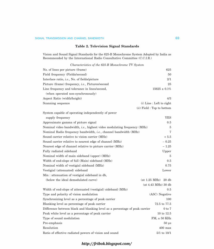
SIGNAL TRANSMISSION AND CHANNEL BANDWIDTH 69
Table 2. Television Signal Standards
Vision and Sound Signal Standards for the 625-B Monochrome System Adopted by India asRecommended by the International Radio Consultative Committee (C.C.I.R.)
Characteristics of the 625-B Monochrome TV System
No. of lines per picture (frame) 625
Field frequency (Fields/second) 50
Interlace ratio, i.e., No. of fields/picture 2/1
Picture (frame) frequency, i.e., Pictures/second 25
Line frequency and tolerance in lines/second, 15625 ± 0.1%
(when operated non-synchronously)
Aspect Ratio (width/height) 4/3
Scanning sequence (i) Line : Left to right
(ii) Field : Top to bottom
System capable of operating independently of power
supply frequency YES
Approximate gamma of picture signal 0.5
Nominal video bandwidth, i.e., highest video modulating frequency (MHz) 5
Nominal Radio frequency bandwidth, i.e., channel bandwidth (MHz) 7
Sound carrier relative to vision carrier (MHz) + 5.5
Sound carrier relative to nearest edge of channel (MHz) – 0.25
Nearest edge of channel relative to picture carrier (MHz) – 1.25
Fully radiated sideband Upper
Nominal width of main sideband (upper) (MHz) 5
Width of end-slope of full (Main) sideband (MHz) 0.5
Nominal width of vestigial sideband (MHz) 0.75
Vestigial (attenuated) sideband Lower
Min : attenuation of vestigial sideband in db,
(below the ideal demodulated curve) (at 1.25 MHz) 20 db
(at 4.43 MHz) 30 db
Width of end-slope of attenuated (vestigial) sideband (MHz) 0.5
Type and polarity of vision modulation (A5C) Negative
Synchronizing level as a percentage of peak carrier 100
Blanking level as percentage of peak carrier 72.5 to 77.5
Difference between black and blanking level as a percentage of peak carrier 0 to 7
Peak white level as a percentage of peak carrier 10 to 12.5
Type of sound modulation FM, ± 50 KHz
Pre-emphasis 50 µs
Resolution 400 max
Ratio of effective radiated powers of vision and sound 5/1 to 10/1
http://fribok.blogspot.com/

70 MONOCHROME AND COLOUR TELEVISION
The values to be considered are : (i) the r.m.s. value of the carrier at the peak of modulationenvelope for the vision signal. (ii) the r.m.s. value of the unmodulated carrier for amplitudemodulated and frequency modulated sound transmissions.
Details of Line-Blanking Intervals
Nominal duration of a horizontal line = 64 µs = H
Line blanking interval = 12 ± 0.3 µs
Front porch = 1.5 ± 0.3 µs
Sync pulse width = 4.7 ± 0.2 µs
Back porch = 5.8 ± 0.3 µs
Build up time (10% to 90%) of line blanking edges = 0.3 ± 0.1 µs
Interval between datum level and black edge of line blanking
signal (average calculated time for information) = 10.5 µs
Details of Field-Blanking Intervals
Field blanking period = 20 H (20 lines) = 1280 µs
Pre sync equalizing pulses, 5 pulses of duration 1/2 H, i.e.,
32 µs, total time = 160 µs
Equalizing pulses are narrow pulses with pulse width = 2.35 ± 0.1 µs
Field sync pulses at 12 H intervals,
5 such pulse, each pulsewidth = 27.3 µs
Interval between field sync pulses = 4.7 ± 0.2 µs
Interval between equalizing pulses = 29.65 µs
Post-sync equalizing pulses, 5 pulses same as for pre-
sync. eq. pulses
Build up time of field blanking edges. = 0.3 ± 0.1 µs
Build up time for field sync pulses = 0.2 ± 0.1 µs
Table 3. Principal Television System
Western Europe, North and SouthMiddle East, America including England USSR France
Particulars India and most US, Canada, MexicoAsian countries and Japan
Lines per frame 625 525 625 625 625
Frames per second 25 30 25 25 25
Field frequency (Hz) 50 60 50 50 50
Line frequency (Hz) 15,625 15,750 15,625 15,625 15,625
Video bandwidth (MHz) 5 ot 6 4.2 5.5 6 6
(Contd.) ...
http://fribok.blogspot.com/

SIGNAL TRANSMISSION AND CHANNEL BANDWIDTH 71
Channel bandwidth (MHz) 7 or 8 6 8 8 8
Video modulation Negative Negative Negative Negative Positive
Picture modulation AM AM AM AM FM
Sound signal modulation FM FM FM FM AM
Colour system PAL NTSC PAL SECAM SECAM
(i) England earlier used 405 line system in the 5 MHz channel.
(ii) France earlier used 819 line system with a channel bandwidth of 14 MHz.
Review Questions
1. Why is it necessary to mdoulate the picture and sound signals before transmission ?
Why is TV transmission carried out in the UHF and VHF bands ?
2. Show that in the 625-B system, a total channel bandwidth of 11.25 MHz would be necessary ifboth the sidebands of the amplitude mdoulated picture signal are fully radiated along with thefrequency modulated picture signal.
3. Why is an attenuation slope of 0.5 MHz allowed at both the edges of the AM picture signalsidebands ? Why is a guard band provided at the sound signal edge of the television channel ?
4. Why is it necessary to affect economy in channel bandwidth ? Why SSB is not used for picturesignal transmission ?
5. What is vestigial sideband transmission and why it is used for transmission of TV picture signals ?
6. Why is a portion of the lower sideband of the AM picture signal transmitted along with thecarrier and full USB ? Does it need any correction somewhere in the television link ? If so whereis it carried out ?
7. Sketch and fully label the desired response of a TV receiver that includes necessary correction onaccount of the discrepancy caused by VSB transmission. Comment on the response curve drawnby you.
8. Show that a total channel bandwidth of 7 MHz is necessary for successful transmission of bothpicture and sound signals in the 625 line TV system. Sketch frequency distribution of the chan-nel and mark the location of picture and sound signal carrier frequencies. Why is the soundcarrier located 5.5 MHz away from the picture carrier ?
9. Justify the allocation of 8 MHz in the British TV system and 6 MHz in the American system foreach TV channel. What is the separation between picture and sound carriers in each of thesesystems ?
10. What is ‘modulation index’ in FM transmission and how does it affect the bandwidth requiredfor each FM channel ?
11. Explain how you would proceed to determine the channel bandwidth for transmission of soundsignals (highest modulating frequency = 15 kHz) by frequency modulation. How does the permittedmaximum deviation affect the bandwidth requirements ?
12. Show that in the 625-B system where the maximum allowed frequency deviation is ± 50 kHz, abandwidth of 150 kHz is necessary for almost distortion free transmission by frequency modula-tion, the highest modulating frequency being 15 kHz, Repeat this for the American system wherethe maximum allowed deviation is ± 25 kHz. Verify the results by ‘Carson’s Rule’ of determiningchannel bandwidth.
http://fribok.blogspot.com/

5
http://fribok.blogspot.com/

74
The picture tube or ‘kinescope’ that serves as the screen for a television receiver is a specializedfrom of cathode-ray tube. It consists of an evacuated glass bulb or envelope, inside the neck ofwhich is rigidly supported an electron gun that supplies the electron beam. A luminescentphosphor coating provided on the inner surface of its face plate produces light when hit by theelectrons of the fast moving beam.
A monochrome picture tube has one electron gun and a continuous phosphor coatingthat produces a picture in black and white. For colour picture tubes the screen is formed ofthree different phosphors and there are three electron beams, one for each colour phosphor.The three colours—red, green and blue produced by three phosphors combine to producedifferent colours. More details of colour picture tubes are given in chapters devoted to colourtelevision.
5.1 MONOCHROME PICTURE TUBE
Modern monochrome picture tubes employ electrostatic focussing and electromagneticdeflection. A typical black and white picture tube is shown in Fig. 5.1. The deflection coils are
Neck
Bell
Tension band
Envelope or bulb
Screen (face plate)
Fig. 5.1. A rectangular picture tube.
mounted externally in a specially designed yoke that is fixed close to the neck of the tube. Thecoils when fed simultaneously with vertical and horizontal scanning currents deflect the beamat a fast rate to produce the raster. The composite video signal that is injected either at the
http://fribok.blogspot.com/

THE PICTURE TUBE 75
grid or cathode of the tube, modulates the electron beam to produce brightness variations ofthe tube, modulates the electron beam to produce brightness variations on the screen. Thisresults in reconstruction of the picture on the raster, bit by bit, as a function of time. However,the information thus obtained on the screen is perceived by the eye as a complete and continuousscene because of the rapid rate of scanning.Electron GunThe various electrodes that constitute the electron gun are shown in Fig. 5.2. The cathode isindirectly heated and consists of a cylinder of nickel that is coated at its end with thoriatedtungsten or barium and strontium oxides. These emitting materials have low work-function
Base
Glass envelope
Deflection windings
Electrostaticfocusing
K
P
G1 G2 G3
Control grid
Accelerating anode
Focusing anode
Centering magnets (two)
Pincushion error magnets (two)
2
HV connector
+
EHT18 KV
Final anode18 KV
Electron beam
Aluminizedcoating
Phosphorcoating
Glass faceplate
Inneraquadag
conductivecoating (18 KV)
Deflection yoke
1
Externalconductive coating
S
Fig. 5.2. Elements of a picture tube employing low voltageelectrostatic focusing and magnetic deflection.
and when heated permit release of sufficient electrons to form the necessary stream of electronswithin the tube. The control grid (Grid No. 1) is maintained at a negative potential with respectto cathode and controls the flow of electrons from the cathode. However, instead of a wiremeshstructure, as in a conventional amplifier tube, it is a cylinder with a small circular opening toconfine the electron stream to a small area. The grids that follow the control grid are theaccelerating or screen grid (Grid No. 2) and the focusing grid (Grid No. 3). These are maintainedat different positive potentials with respect to the cathode that vary between + 200 V to + 600 V.All the elements of the electron gun are connected to the base pins and receive their ratedvoltages from the tube socket that is wired to the various sections of the receiver.
Electrostatic FocussingThe electric field due to the positive potential at the accelerating grid (also known as 1st anode)extends through the opening of the control grid right to the cathode surface. The orientation of
http://fribok.blogspot.com/

76 MONOCHROME AND COLOUR TELEVISION
this field is such that besides accelerating the electrons down the tube, it also brings all theelectrons in the stream into a tiny spot called the crossover. This is known as the firstelectrostatic lens action. The resultant convergence of the beam is shown in Fig. 5.2. Thesecond lens system that consists of the screen grid and focus electrode draws electrons fromthe crossover point and brings them to a focus at the viewing screen. The focus anode is largerin diameter and is operated at a higher potential than the first anode. The resulting fieldconfiguration between the two anodes is such that the electrons leaving the crossover point atvarious angles are subjected to both convergent and divergent forces as they more along theaxis of the tube. This in turn alters the path of the electrons in such a way that they meet atanother point on the axis. The electrode voltages are so chosen or the electric field is so variedthat the second point where all the electrons get focused is the screen of the picture tube.Electrostatic focusing is preferred over magnetic focusing because it is not affected very muchby changes in the line voltage and needs no ion-spot correction.
Beam VelocityIn order to give the electron stream sufficient velocity to reach the screen material with properenergy to cause it to fluoresce, a second anode is included within the tube. This is a conductivecoating with colloidal graphite on the inside of the wide bell of the tube. This coating, calledaquadag, usually extends from almost half-way into the narrow neck to within 3 cm of thefluorescent screen as shown in Fig. 5.2. It is connected through a specially provided pin at thetop or side of the glass bell to a very high potential of over 15 kV. The exact voltage depends onthe tube size and is about 18 kV for a 48 cm monochrome tube. The electrons that get acceleratedunder the influence of the high voltage anode area, attain very high velocities before they hitthe screen. Most of these electrons go straight and are not collected by the positive coatingbecause its circular structure provides a symmetrical accelerating field around all sides of thebeam. The kinetic energy gained by the electrons while in motion is delivered to the atoms ofthe phosphor coating when the beam hits the screen. This energy is actually gained by theouter valence electrons of the atoms and they move to higher energy levels. While recturningto their original levels they give out energy in the form of electromagnetic radiation, thefrequency of which lies in the spectral region and is thus perceived by the eye as spots of lightof varying intensity depending on the strength of the electron beam bombarding the screen.
Because of very high velocities of the electrons which hit the screen, secondary emissiontakes place. If these secondary emitted electrons are not collected, a negative space chargegets formed near the screen which prevents the primary beam from arriving at the screen.The conductive coating being at a very high positive potential collects the secondary emittedelectrons and thus serves the dual purpose of increasing the beam velocity and removingunwanted secondary electrons. The path of the electron current flow is thus from cathode toscreen, to the conductive coating through the secondary emitted electrons and back to thecathode through the high voltage supply. A typical value of beam current is about 0.6 mA with20 kV applied at the aquadag coating.
5.2 BEAM DEFLECTION
Both electric and magnetic fields can be employed for deflecting the electron beam. However,in television picture tubes electromagnetic deflection is preferred for the following reasons :
http://fribok.blogspot.com/

THE PICTURE TUBE 77
(a) As already stated the electron beam must attain a very high velocity to deliver enoughenergy to the atoms of the phosphor coating. Because of this the electrons of the beam remainunder the influence of the deflecting field for a very short time. This necessitates application ofhigh deflecting fields to achieve the desired deflection. For example with an anode voltage ofabout 1 kV, as would be the case in most oscilloscopes, some 10 V would be necessary for 1 cmdeflection of the beam on the screen, whereas in a picture tube with 15 kV at the final anode,about 7500 V would be necessary to get full deflection on a 50 cm screen. It is very difficult togenerate such high voltages at the deflection frequencies. On the other hand with magneticdeflection it is a large current that would be necessary to achieve the same deflection. Since itis more convenient to generate large currents than high voltages, all picture tubes employelectromagnetic deflection.
(b) With electrostatic deflection the beam electrons gain energy. Thus larger deflectionangles tend to defocus the beam. Further, the deflection plates need to be placed further apartas the deflection angle is made larger, thus requiring higher voltages to produce the samedeflection field. Magnetic deflection is free from both these shortcomings and much largerdeflection angles can be achieved without defocusing or nonlinearities with consequent savingin tube length and cabinet size.
(c) For electrostatic deflection two delicate pairs of deflecting plates, are needed insidethe picture tube, whereas for magnetic deflection two pairs of deflecting coils are mountedoutside and close to the neck of the tube. Such a provision is economical and somewhat morerugged.
Deflection YokeThe physical placement of the two pairs of coils around the neck of the picture tube is illustratedin Fig. 5.3 and the orientation of the magnetic fields produced by them is shown in Fig. 5.4. Incombination, the vertical and horizontal deflection coils are called the ‘Yoke’. This yoke is fixedoutside and close to the neck of the tube just before it begins to flare out (see Fig. 5.2).
Electronbeam
H
V
Bottom
Horz rasterplane
Vertical deflectionwindings
Horizontal deflectionwindings
pTop
Vertical raster plane
Fig. 5.3. Cross-sectional view of a yoke showing location of vertical andhorizontal deflection windings about the neck of the picture tube.
http://fribok.blogspot.com/

78 MONOCHROME AND COLOUR TELEVISION
H–
H+
Magnetic field ofelectron beam
Verticaldeflection coil
Magneticfield lines
Verticaldeflection coil Electron
beam
Horizontaldeflection coil
V+ V–
Neck of the picture tubeHorizontal
deflection coil
Fig. 5.4. Horizontal and Vertical deflecting coils (pairs) around the neck of the picture tube.Note that the location of the beam on the picture tube screen will depend on the strength
and direction of currents in the two pairs of coils. For the directions of current shownthe beam will be deflected upwards and to the left.
The magnetic field of the coils reacts with the electron beam to cause its deflection. Thehorizontal deflection coil which sweeps the beam across the face of the tube from left to right issplit into two sections and mounted above and below the beam axis. The vertical deflection coilis also split into two sections and placed left and right on the neck in order to pull the beamgradually downward as the horizontal coils sweep the beam across the tube face. Each coil getsits respective sweep input from the associated sweep circuits, and together they form theraster upon which the picture information is traced. It may be noted that a perpendiculardisplacement results because the magnetic field due to each coil reacts with the magnetic fieldof the electron beam to produce a force that deflects the electrons at right angles to both thebeam axis and the deflection field.
Deflection AngleThis is the maximum angle through which the beam can be deflected without striking the sideof the bulb. Typical values of deflection angles are 70°, 90°, 110° and 114°. As shown in Fig. 5.5,it is the total angle that is specified. For instance a deflection angle of 110° means the electronbeam can be deflected 55° from the centre. The advantage of a large deflection angle is that forequal picture size the picture tube is shorter and can be installed in a smaller cabinet. However,a large deflection angle requires more power from the deflection circuits. For this reason thetubes are made with a narrow neck to put the deflection yoke closer to the electron beam. A110° yoke has a smaller hole diameter (about 3 cm) compared with neck diameters for tubeswith lesser deflection angles. Different screen sizes can be filled with the same deflectionangle, because bigger tubes have larger axial lengths.
http://fribok.blogspot.com/

THE PICTURE TUBE 79
S o p u uShort picture tube length110° deflection angle
Electron gun
Point of deflection
10110°
(a)
o p u uLonger picture tube length55° deflection angle
Electron gun
55° deflection angle
(b)
Fig. 5.5. Effect of deflection angle on picture tube length for the same face plate size.(a) Picture tube rated for 110° deflection angle, (b) Picture tube rated for 55° deflection angle
Note : The nominal deflection angle that is listed for picture tubesis usually the diagonal deflection angle.
Cosine WindingWith increased deflection angles it becomes necessary to use a special type of winding to generateuniform magnetic fields for linear deflection. In this arrangement the thickness of the deflectionwinding varies as the cosine of the angle from a central reference line. Such a winding isknown as ‘Cosine winding’ and its appearance in a deflection yoke is shown in Fig. 5.3. Nearlyall present day yokes are wound in this manner to ensure linear deflection.
5.3 SCREEN PHOSPHOR
The phosphor chemicals are generally light metals such as zinc and cadmium in the form ofsulphide, sulphate, and phosphate compounds. This material is processed to produce very fineparticles which are then applied on the inside of the glass plate. As already explained the highvelocity ellectrons of the beam on hitting the phosphor excite its atoms with the result that thecorresponding spot fluoresces and emits light. The phosphorescent characteristics of thechemicals used are such that an afterglow remains on the screen for a short time after thebeam moves away from any screen spot. This afterglow is known as persistence. Mediumpersistence is desirable to increase the average brightness and to reduce flicker. However, thepersistence must be less than 1/25 second for picture tube screens so that one frame does notpersist into the next and cause blurring of objects in motion. The decay time of picture tubephosphors is approximately 5 ms, and its persistence is referred to as P4 by the industry.
5.4 FACE PLATE
A rectangular image on a circular screen is wasteful of screen area. Therefore, all present daypicture tubes have rectangular face plates, with a breadth to height ratio of 4 : 3. A rectangulartube with 54 cm screen means that the distance between the two diagonal points is 54centimeters. Approximately 1.5 cm thickness provides the strength required for the large faceplate to withstand the air pressure on the evacuated glass envelope. In older receivers specialglass or plastic shields were placed in the cabinet in front of the picture tube to prevent anyglass from hitting the viewer in case of an implosion. Modern picture tubes incorporate integral
http://fribok.blogspot.com/

80 MONOCHROME AND COLOUR TELEVISION
implosion protection. There are a number of different systems in use. In one arrangement,known as kimcode, a metal rim band (see Fig. 5.1) is held around the tube by a tension strap orwith a layer of epoxy cement. In another system called Panoply, a special faceplate is held infront of the tube by epoxy cement. In all cases it is essential to check for implosion proofingwhile replacing any picture tube.
Yoke and Centering MagnetsThe yoke on all black and white tubes is positioned right up against the flare of the tube inorder to achieve complete coverge of the full screen area. If the yoke is not moved as far forwardas possible, the electron beam will strike the neck of the picture tube and cause a shadow nearthe corners of the face plate. The mounting system permits positioning of the yoke against thetube funnel and allows rotation of the yoke to ensure that horizontal lines run parallel to thenatural horizontal axis.
Electrical centering of the beam can be accomplished by supplying direct current throughthe horizontal and vertical deflection coils. However, this method is not used now because ofthe added current drain on the low voltage power supply. Modern tubes have a pair of permanentmagnets (see Fig. 5.2) for centering, in the form of rings usually mounted on the yoke cover.Poles of both the magnets can be suitably shifted with a pair of projecting tabs provided on themagnetic rings. When the two tabs (one from each ring) coincide with each other, the strongestfield is achieved; that is, the beam will be pushed furthest off centre. When the two tabs are180° apart (on opposite sides) the field is minimum and so is the decentering. The two ringsare rotated together to change the direction in which decentering occurs. This is illustrated inFig. 5.6.
Yoke frameWindings terminal board
Movable centeringmagnets (two)
Adjustablepin-cushionmagnets (two)
Vertical-deflectionwindings
(a) Back view (b) Front view
Vertical-deflection windings
Horz deflectionwindings
Fig. 5.6. Deflection yoke details.
The edge of the yoke linear (see Fig. 5.2) is used to hold small permanent magnets. Asshown in Fig. 5.6 these are positioned to correct any ‘pincushion error’.
Screen BrightnessIt is estimated that about 50 per cent of the light emitted at the screen, when the electronbeam strikes it, travels back into the tube. Another 20 percent or so is lost in the glass of the
http://fribok.blogspot.com/

THE PICTURE TUBE 81
tube because of internal reflections and only about 20 percent of it reaches the viewer. Imagecontrast is also impaired because of interference caused by the light which is returned to thescreen after reflection from some other points.
Also any ions is the beam, which do exist despite best precautions while degassing,damage the phosphor material on hitting it and thus cause a dark brownish patch on thescreen. This area usually centers around the middle of the screen because the greater mass ofthe ions prevents any appreciable deflection during their transit, with the result, that theyarrive almost at the centre of the screen.
To overcome these serious drawbacks practically all modern picture tubes employ avery thin coating of aluminium on the back surface of the screen phosphor. The aluminizedcoating is very thin and with a final anode voltages of 10 kV or more, the electrons of the beamhave enough velocity to penetrate this coating and excite the phosphor. Thus most of the lightthat would normally travel back and get lost in the tube is now reflected back to the screen bythe metal backing and this results in a much improved brilliancy. The aluminized coating isconnected to the high voltage anode coating and thus helps in draining off the secondary emittedelectrons at the screen. This further improves the brightness.
Ion-trap
In older picture tubes a magnetic beam, bender commonly known as ‘ion-trap’ was employedto deflect the heavy ions away from the screen. In present day picture tubes having a thinmetal coating on the screen, it is no longer necessary to provide an ion-trap. This is becausethe ions on account of their greater mass fail to penetrate the metal backing and do not reachthe phosphor screen.
Thus an aluminized coating when provided on the phosphor screen, not only improvesscreen brightness and contrast but also makes the use of ‘ion-traps’ unnecessary.
High Voltage Filter Capacitor
A grounded coating is provided on the outer surface of the picture tube. This provides shieldingfrom stray fields and also acts as one plate of the capacitor, the other plate being the inneranode coating with the glass bulb serving as the insulator between the two. The capacitor thusformed (see Fig. 5.2) serves as a filter capacitor for the high voltage supply. This capacitor canhold charge for a long time after the anode voltage is switched off and so before handling thepicture tube the capacitor must be discharged by shorting the anode button to the groundedwall coating.
Spark-gap Protection
On account of close spacing between the various-electrodes and the use of very high voltages,arcing of flashover can occur in the electron gum especially at the control grid. This arcingcauses voltage surges, which result in damage to the associated circuit components. Thereforefor protection of the receiver circuit, due to any arcing, metallic spark-gaps are provided asshunt paths for the surge currents. In some designs neon bulbs are used as spark gaps. Thegas in the neon tube ionizes when the potential exceeds a certain limit and thus provides ashunt path for the high voltage arc current.
http://fribok.blogspot.com/

82 MONOCHROME AND COLOUR TELEVISION
5.5 PICTURE TUBE CHARACTERISTICS
As shown in Fig. 5.7 the transfer characteristics of picture tubes are similar to the grid-platecharacteristics of vacuum tubes. The grid of the picture tube has a fixed bias that is set withthe brightness control for optimum average brightness of the picture on the screen. The videosignal that finally controls the brightness variations on the screen may be applied either at thegrid or cathode of the picture tube. Each method has its own merits and demerits and arediscussed in another chapter. This method of varying the beam current to control theinstantaneous screen brightness is called intensity or ‘Z’ axis modulation. The peak-to-peakamplitude of the ac video signal determines the contrast in the picture, between peak whitewith maximum beam current and black at cut-off. The contrast control is in the video amplifier,which controls the peak-to-peak amplitude of the video signal applied to the picture tube.
Cut-off bias(black)
VG K1 – 80 – 60 – 40 – 200
0.4
0.8
1.2
1.6
Peak white
mAAnode current
D.C. bias
Video signal
Fig. 5.7. Transfer characteristics of a picture tube. Note thealignment of blanking level with cut-off bias.
At cut-off the grid voltage is negative enough to reduce the beam current to a value lowenough to extinguish the beam, and this corresponds to the black level in the picture. Theparts of the screen without any luminescence look black in comparison with the adjacent whiteareas.
5.6 PICTURE TUBE CIRCUIT CONTROLS
Manufacturers usually recommend a sufficiently high voltage to the second anode of the picturetube to produce adequate screen brilliancy for normal viewing. This voltage is always obtainedfrom the output of the horizontal deflection circuit. The dc voltages to the screen grid and focus
http://fribok.blogspot.com/

THE PICTURE TUBE 83
grid are also taken from the horizontal stage and adjusted to suitable values by resistive potentialdivider networks. This is shown in Fig. 5.8.
+ Vcc
From videodetector
Video amplifier
Brightness control
+ 300 V
R4 2KVEHT
(Boosted B + Supply)
R3
R2
R1
+ 600V
Picture tubeG3G2G1
VG K = – 501
FF
+ 300 V
+ K
Contrast controlV V H H
Fig. 5.8. Picture tube circuit and associated controls.
A variable bias control either in the cathode circuit or control grid lead is provided tocontrol the electron density, which in turn controls the brightness on the screen. This control,known as the ‘brightness control’, is brought out at the front panel of the receiver to enable theviewer to adjust brightness.
As discussed earlier most modern picture tubes do not require critical focus adjustment.Therefore no focus control is normally provided and instead dc voltage at the focus electrode iscarefully set as explained above.
The contrast control through not strictly a part of the picture tube circuit forms part ofcathode or control grid circuit. This control is also provided at the front panel of the receiverand its variation enables adjustment of contrast in the reproduced picture.
Picture Tube Handling
The very high vacuum in a modern picture tube means that there is a danger of implosion ifthe tube is struck with a hard object or if it is made to rest on its neck. Because of the largevolume of the tube, there is a very high pressure on the glass shell.
In case it breaks the resulting implosion will often cause tube fragments to fly in alldirections at high speed. This may cause severe injury to the persons hit by the tube fragments.Manufacturers recommend the use of protective goggles and gloves whenever picture tubesare handled and such precautions should be observed. The tube neck is particularly fragileand must be handled with care.
http://fribok.blogspot.com/

84 MONOCHROME AND COLOUR TELEVISION
Review Questions
1. Sketch the sectional view of a picture tube that employs electrostatic focusing and electromag-netic deflection and label all the electrodes.
2. Explain briefly, how the electron beam is focused on the tube screen. What is meant by crossoverpoint in the electron gun ?
3. What type of phosphor is employed for picture tube screens ? Why is a medium persistencephosphor preferred ?
4. What is the function of aquadag coating on the inner side of the tube bell ? Why is a groundedcoating provided on the outer surface of the picture tube ?
5. Why is an aluminized coating provided on the phosphor screen ? How are any stary ions pre-vented from hitting the screen ?
6. What do you understand by a 54 cm picture tube ? Why is it necessary to employ implosionprotection in picture tubes ?
7. What precautions must be observed while handling a picture tube ? Why is it necessary to pro-vide spark-gap protection between the various electrodes ?
8. Discuss the merits of electromagnetic deflection over electrostatic deflection in television pic-ture tubes. Why is ‘cosine winding’ used for deflection coils ?
9. What is meant by the deflection angle of a picture tube ? What is the advantage of providing alarge deflection angle yoke ?
10. Explain how the yoke is mounted on the tube neck. Describe how the centering of the electronbeam is accomplished with the help of centering magnets. Why are small permanent magnetsprovided at the edges of the yoke liner ?
11. Show with a circuit diagram how dc potentials are supplied to the various electrodes of thepicture tube.
12. What are the functions of ‘brightness’ and ‘contrast’ controls ? Explain their action with suitablecircuit diagrams.
http://fribok.blogspot.com/

6
http://fribok.blogspot.com/

A TV camera tube may be called the eye of a TV system. For such an analogy to be correct thetube must possess characteristic that are similar to its human counterpart. Some of the moreimportant functions must be (i) sensitivity to visible light, (ii) wide dynamic range with respectto light intensity, and (iii) ability to resolve details while viewing a multielement scene.
During the development of television, the limiting factor on the ultimate performancehad always been the optical-electrical conversion device, i.e., the pick-up tube. Most typesdeveloped have suffered to a greater or lesser extent from (i) poor sensitivity, (ii) poor resolution,(iii) high noise level, (iv) undesirable spectral response, (v) instability, (vi) poor contrast rangeand (vii) difficulties of processing.
However, development work during the past fifty years or so, has enabled scientists andengineers to develop image pick-up tubes, which not only meet the desired requirements butinfact excel the human eye in certain respects. Such sensitive tubes have now been developedwhich deliver output even where our eyes see complete darkness. Spectral response has beenso perfected, that pick-up outside the visible range (in infra-red and ultraviolet regions) hasbecome possible. Infact, now there is a tube available for any special application.
6.1 BASIC PRINCIPLE
When minute details of a picture are taken into account, any picture appears to be composed ofsmall elementary areas of light or shade, which are known as picture elements. The elementsthus contain the visual image of the scene. The purpose of a TV pick-up tube is to sense eachelement independently and develop a signal in electrical form proportional to the brightness ofeach element. As already explained in Chapter 1, light from the scene is focused on aphotosensitive surface known as the image plate, and the optical image thus formed with alens system represents light intensity variations of the scene. The photoelectric properties ofthe image plate then convert different light intensities into corresponding electrical variations.In addition to this photoelectric conversion whereby the optical information is transduced toelectrical charge distribution on the photosensitive image plate, it is necessary to pick-up thisinformation as fast as possible. Since simultaneous pick-up is not possible, scanning by anelectron beam is resorted to. The electron beam moves across the image plate line by line, andfield by field to provide signal variations in a successive order. This scanning process dividesthe image into its basic picture elements. Through the entire image plate is photoelectric, itsconstruction isolates the picture elements so that each discrete small area can produce its ownsignal variations.
86
http://fribok.blogspot.com/

TELEVISION CAMERA TUBES 87
Photoelectric EffectsThe two photoelectric effects used for converting variations of light intensity into electricalvariations are (i) photoemission and (ii) photoconductivity. Certain metals emit electrons whenlight falls on their surface. These emitted electrons are called photoelectrons and the emittingsurface a photocathode. Light consists of small bundles of energy called photons. When light ismade incident on a photocathode, the photons give away their energy to the outer valenceelectrons to allow them to overcome the potential-energy barrier at the surface. The number ofelectrons which can overcome the potential barrier and get emitted, depends on the lightintensity. Alkali metals are used as photocathode because they have very low work-function.Cesium-silver or bismuth-silver-cesium oxides are preferred as photoemissive surfaces becausethey are sensitive to incandescent light and have spectral response very close to the humaneye.
The second method of producing an electrical image is by photoconduction, where theconductivity or resistivity of the photosensitive surface varies in proportion to the intensity oflight focused on it. In general the semiconductor metals including sel nium, tellurium and leadwith their oxides have this property known as photoconductivity. The variations in resistanceat each point across the surface of the material is utilized to develop a varying signal by scanningit uniformly with an electron beam.
Image Storage Principle
Television cameras developed during the initial stages of development were of the non-storagetype, where the signal output from the camera for the light on each picture element is producedonly at the instant it is scanned. Most of the illumination is wasted. Since the effect of light onthe image plate cannot be stored, any instantaneous pick-up has low sensitivity. Image disectorand flying-spot camera are examples of non-storage type of tubes. These are no longer in useand will not be discussed. High camera sensitivity is necessary to televise scenes at low lightlevels and to achieve this, storage type tubes have been developed. In storage type cameratubes the effect of illumination on every picture element is allowed to accumulate between thetimes it is scanned in successive frames. With light storage tubes the amount of photoelectricsignal an be increased 10,000 times approximately compared with the earlier non-storagetype.
The Electron Scanning Beam
As in the case of picture tubes an electron gun produces a narrow beam of electrons for scanning.In camera tubes magnetic focusing is normally employed. The electrons must be focused to avery narrow and thin beam because this is what determines the resolving capability of thecamera. The diameter of the beam determines the size of the smallest picture element andhence the finest detail of the scene to which it can be resolved. Any movement of electriccharge is a flow of current and thus the electron beam constitutes a very small current whichleaves the cathode in the electron gun and scans the target plate. The scanning is done bydeflecting the beam with the help of magnetic fields produced by horizontal and vertical coilsin the deflection yoke put around the tubes. The beam scans 312.5 lines per field and 50 suchfields are scanned per second.
http://fribok.blogspot.com/

88 MONOCHROME AND COLOUR TELEVISION
Video Signal
In tubes employing photoemissive target plates the electron beam deposits some charge on thetarget plate, which is proportional to the light intensity variations in the scene being televised.The beam motion is so controlled by electric and magnetic fields, that it is decelerated before itreaches the target and lands on it with almost zero velocity to avoid any secondary emission.Because of the negative acceleration the beam is made to move back from the target and on itsreturn journey, which is very accurately controlled by the focusing and deflection coils, it strikesan electrode which is located very close to the cathode from where it started. The number ofelectrons in the returning beam will thus vary in accordance with the charge deposited on thetarget plate. This in turn implies that the current which enters the collecting electrode variesin amplitude and represents brightness variations of the picture. This current is finally madeto flow through a resistance and the varying voltage developed across this resistance constitutesthe video signal. Figure 6.1 (a) illustrates the essentials of this technique of developing videosignal.
Faceplate
Lightimage
Target
Electron
image
Cameralens Photoemissive
coating
Scanningbeam
+RL
v0
Faceplate Photoconductivecoating
Lightimage
+RL
v0
Electron gun
Fig. 6.1(a). Production of video Fig. 6.1(b). Production of video signalsignal by photoemission. by photoconduction.
In camera tubes employing photoconductive cathodes the scanning electron beam causesa flow of current through the photoconductive material. The amplitude of this current variesin accordance with the resistance offered by the surface at different points. Since the conductivityof the material varies in accordance with the light falling on it, the magnitude of the currentrepresents the brightness variations of the scene. This varying current completes its pathunder the influence of an applied dc voltage through a load resistance connected in series withpath of the current. The instantaneous voltage developed across the load resistance is thevideo signal which, after due amplification and processing is amplitude modulated andtransmitted. Figure 6.1 (b) shows a simplified illustration of this method of developing videosignal.
Electron MultiplierWhen the surface of a metal is bombarded by incident electrons having high velocities, secondaryemission takes place. Aluminium, as an example, can release several secondary electrons foreach incident primary electron. Camera tubes often include an electron multiplier structure,making use of the secondary emission effect to amplify the small amount of photoelectric current
http://fribok.blogspot.com/

TELEVISION CAMERA TUBES 89
that is later employed to develop video signal. The electron multiplier is a series of cold anode-cathode electrodes called dynodes mounted internally, with each at a progressively higherpositive potential as illustrated in Fig. 6.2. The few electrons emitted by the photocathode areaccelerated to a more positive dynode. The primary electrons can then force the ejection ofsecondary emission electrons when the velocity of the incident electrons is large enough. Thesecondary emission ratio is normally three or four, depending on the surface and the potentialapplied. The number of electrons available is multiplied each time the secondary electronsstrike the emitting surface of the next more positive dynode. The current amplification thusobtained is noise free because the electron multiplier does not have any active device or resistors.Since the signal amplitude is very low any conventional amplifier, if used instead of the electronmultiplier, woul cause serious S/N ratio problems.
Dynode 4+ (400 V)
Glass envelopeDynode 3( 300 V)+
Dynode 2( 00 V)+ 2
Dynode 1( 00 V)+ 1
Secondaryelectrons
Photoelectrons
Incident light
Anode(+ 600 V)
Dynode 5(+ 500 V)
Photo cathode(0 V)
Fig. 6.2. Illustration of an electron-multiplier structure.
Types of Camera TubesThe first developed storage type of camera tube was ‘Iconoscope’ which has now been replacedby image-orthicon because of its high light sensitivity, stability and high quality picturecapabilities. The light sensitivity is the ratio of the signal output to the incident illumination.Next to be developed was the vidicon and is much simpler in operation. Similar to the vidiconis another tube known as plumbicon. The latest device in use for image scanning is the solidstate image scanner.
6.2 IMAGE ORTHICON
This tube makes use of the high photoemissive sensitivity obtainable from photocathodes,image multiplication at the target caused by secondary emission and an electron multiplier. Asectional view of an image orthicon is shown in Fig. 6.3. It has three main sections: imagesection, scanning section and electron gun-cum-multiplier section.
http://fribok.blogspot.com/

90 MONOCHROME AND COLOUR TELEVISION
Wiremeshscreen
Image acceleratorGrid no. 6– 300 V Decelerator
Grid no. 5, 40 V
Photoelectrons(electron image)
Grid no. 4 andwall coating, 80 V
Grid no. 3,80 V
Grid no. 2, anddynode no. 1,
300 V
Electron gun
Scanning beam
Return beam
Cameralens
Photocathode– 600 V
Target– 3 to – 5 V
Secondary electrons
Glass plate
Deflectioncoil
Focusingcoil
Alignmentcoil Five stage
electronmultiplier
Electron gunand
multiplier section
Scanning sectionImagesection
Fig. 6.3. Principle of operation of Image Orthicon (non-field mesh type).
(i) Image SectionThe inside of the glass face plate at the front is coated with a silverantimony coating sensitizedwith cesium, to serve as photocathode. Light from the scene to be televised is focused on thephotocathode surface by a lens system and the optical image thus formed results in the releaseof electrons from each point on the photocathode in proportion to the incident light intensity.Photocathode surface is semitransparent and the light rays penetrate it to reach its innersurface from where electron emission takes place. Since the number of electrons emitted atany point in the photocathode has a distribution corresponding to the brightness of the opticalimage, an electron image of the scene or picture gets formed on the target side of the photocoatingand extends towards it. Through the convertion efficiency of the photocathode is quite high, itcannot store charge being a conductor. For this reason, the electron image produced at thephotocathode is made to move towards the target plate located at a short distance from it. Thetarget plate is made of a very thin sheet of glass and can store the charge received by it. Thisis maintained at about 400 volts more positive with respect to the photocathode, and theresultant electric field gives the desired acceleration and motion to the emitted electrons towardsit. The electrons, while in motion, have a tendency to repel each other and thin can result indistortion of the information now available as charge image. To prevent this divergence effectan axial magnetic field, generated in this region by the ‘long focus coil’ is employed. Thismagnetic field imparts helical motion of increasing pitch and focuses the emitted electrons onthe target into a well defined electron image of the original optical image. The image side ofthe target has a very small deposit of cesium and thus has a high secondary emission ratio.Because of the high velocity attained by the electrons while in motion from photocathode tothe target plate, secondary emission results, as the electrons bombard the target surface. These
http://fribok.blogspot.com/

TELEVISION CAMERA TUBES 91
secondary electrons are collected by a wire-mesh screen, which is located in front of the targeton the image side and is maintained at a slightly higher potential with respect to the target.The wire-mesh screen has about 300 meshes per cm2 with an open area of 50 to 75 per cent, sothat the screen wires do not interfere with the electron image. The secondary electrons leavebehind on the target plate surface, a positive charge distribution, corresponding to the lightintensity distribution on the original photocathode.
For storage action this charge on the target plate should not spread laterally over itssurface, during the storage time, since this would destory the resolution of the device. Toachieve this the target is made out of extremely thin sheet of glass. The positive chargedistribution builds up during the frame storage time (40 ms) and thus enhances the sensitivityof the tube. It should be clearly understood, that the light from the scene being televisedcontinuously falls on the photocathode, and the resultant emitted electrons on reaching thetarget plate cause continuous secondary emission. This continuous release of electrons resultsin the building up of positive charge on the target plate.
Because of the high secondary emission ratio, the intensity of the positive chargedistribution is four to five times more as compared to the charge liberated by the photocathode.This increase in charge density relative to the charge liberated at the photocathode is knownas ‘image multiplication’ and contributes to the increased sensitivity of image orthicon. Asshown in Fig. 6.3, the two-sided target has the charge image on one side while an electronbeam scans the opposite side. Thus, while the target plate must have high resistivity laterallyfor storage action, it must have low resistivity along its thickness, to enable the positive chargeto conduct to the other side which is scanned. It is for this reason that the target plate is verythin, with thickness close to 0.004 mm. Thus, whatever charge distribution builds up on oneside of the target plate due to the focused image, appears on the other side, which is scanned,and it is from here that the video signal is obtained.
(ii) Scanning SectionThe electron gun structure produces a beam of electrons that is accelerated towards the target.As indicated in the figure, positive accelerating potentials of 80 to 330 volts are applied to grid2, grid 3, and grid 4 which is connected internally to the metalized conductive coating on theinside wall of the tube. The electron beam is focused at the target by magnetic field of theexternal focus coil and by voltage supplied to grid 4. The alignment coil provides magneticfield that can be varied to adjust the scanning beam’s position, if necessary, for correct location.Deflection of electron beam’s to scan the entire target plate is accomplished by magnetic fieldsof vertical and horizontal deflecting coils mounted on yoke external to the tube. These coils arefed from two oscillators, one working at 15625 Hz, for horizontal deflection, and the otheroperating at 50 Hz, for vertical deflection.
The target plate is close to zero potential and therefore electrons in the scanning beamcan be made to stop their forward motion at its surface and then return towards the gunstructure. The grid 4 voltage is adjusted to produce uniform deceleration of electrons for theentire target area. As a result, electrons in the scanning beam are slowed down near the target.This eliminates any possibility of secondary emission from this side of the target plate. If acertain element area on the target plate reaches a potential of, say, 2 volts during the storagetime, then as a result of its thinness the scanning beam ‘sees’ the charge deposited on it, part
http://fribok.blogspot.com/
92 MONOCHROME AND COLOUR TELEVISION
of which gets diffused to the scanned side and deposits an equal number of negative charges onthe opposite side. Thus out of the total electrons in the beam, some get deposited on the targetplate, while the remaining stop at its surface and turn back to go towards the first electrode ofthe electron multiplier. Because of low resistivity across the two sides of the target, the depositednegative charge neutralizes the existing positive charge in less than a frame time. The targetcan again become charged as a result of the incident picture information, to be scanned duringthe successive frames. As the target is scanned element by element, if there are no positivecharges at certain points, all the electrons in the beam return towards the electron gun andnone gets deposited on the target plate. The number of electrons, leaving cathode of the gun, ispractically constant, and out of this, some get deposited and remaining electrons, which travelbackwards provide signal current that varies in amplitude in accordance with the pictureinformation. Obviously then, the signal current is maximum for black areas on the picture,because absence of light from black areas on the picture does not result in any emission on thephotocathode, and there is no secondary emission at the corresponding points on the target,and no electrons are needed from the beam to neutralize them. On the contrary for high lightareas, on the picture, there is maximum loss of electrons from the target plate, due to secondaryemission, and this results in large deposits of electrons from the beam and this reduces theamplitude of the returning beam current. The resultant beam current that turns away fromthe target, is thus, maximum for black areas and minimum for bright areas on the picture.High intensity light causes large charge imbalance on the glass target plate. The scanningbeam is not able to completely neutralize it in one scan. Therefore the earlier impressionpersists for several scans.
Image Resolution. It may be mentioned at this stage that since the beam is of low velocitytype, being reduced to near zero velocity in the region of the target it is subjected to strayelectric fields in its vicinity, which can cause defocusing and thus loss of resolution. Also oncontact with the target, the electrons would normally glide along its surface tangentially for ashort distance and the point of contact becomes ill defined. The beam must strike the target atright angle at all points of the target, for better resolution. These difficulties are overcome inthe image-orthicon by the combined action of electrostatic field because of potential on grid 4,and magnetic field of the long focusing coil. The interaction of two fields gives rise to cycloidalmotion to the beam in the vicinity of target, which then hits it at right angle no matter whichpoint is being scanned. This very much improves the resolving capability of the picture tube.
(iii) Electron MultiplierThe returning stream of electrons arrive at the gun close to the aperture from which electronbeam emerged. The aperture is a part of a metal disc covering the gun electrode. When thereturning electrons strike the disc which is at a positive potential of about 300 volts, withrespect to the target, they produce secondary emission. The disc serves as first stage of theelectron multiplier. Successive stages of the electron multiplier are arranged symmetricallyaround and back of the first stage. Therefore secondary electrons are attracted to the dynodesat progressively higher positive potentials. Five stages of multiplication are used, details ofwhich are shown in Fig. 6.4. Each multiplier stage provides a gain of approximately 4 and thusa total gain of (4)5 ≈ 1000 is obtained at the electron multiplier. This is known as signalmultiplication. The multiplication so obtained maintains a high signal to noise ratio. Thesecondary electrons are finally collected by the anode, which is connected to the highest supply
http://fribok.blogspot.com/

TELEVISION CAMERA TUBES 93
voltage of + 1500 volts in series with a load resistance RL. The anode current through RL hasthe same variations that are present in the return beam from the target and amplified by theelectron multiplier. Therefore voltage across RL is the desired video signal; the amplitude ofwhich varies in accordance with light intensity variations of scene being televised. The outputacross RL is capacitively coupled to the camera signal amplifier. With RL = 20 K-ohms andtypical dark and high light currents of magnitudes 30 µA and 5 µA respectively, the cameraoutput signal will have an amplitude of 500 mV peak-to-peak.
Grid no. 2 anddynode no. 1,
300 V
Dynodeno. 3,880 V
Dynodeno. 5,
1450 V
Scanning beam
Return beam(signal current)
Electron gun
Secondaryelectrons Dynode
no. 2,600 V
Dynodeno. 4,
1160 V
Anode
Signal outputto amplifier0.03 F
R20 K
L
1500 V
Cc
Fig. 6.4. Electron-multiplier section of the Image Orthicon.
Field Mesh Image Orthicon. The tube described above is a non-field mesh image orthicon.In some designs an additional pancake-shaped magnetic coil is provided in front of the faceplate. This is connected in series with the main focusing coil. The location of the coil results ina graded magnetic field such that the optically focused photocathode image is magnified byabout 1.5 times. Thus the charge image produced on the target plate is bigger in size and thisresults in improved resolution and better overall performance. Such a camera tube is knownas a field mesh Image Orthicon.
Light Transfer Characteristics and Applications—During the evolution of image orthicontubes, two separate types were developed, one with a very close target-mesh spacing (less than0.001 cm) and the other with somewhat wider spacing. The tube, with very close target meshspacing, has very high signal to noise ratio but this is obtained at the expense of sensitivityand contrast ratio. This is a worthwhile exchange where lighting conditions can be controlledand picture quality is of primary importance. This is generally used for live shows in thestudios. The other type with wider target-mesh spacing has high sensitivity and contrast ratiowith more desirable spectral response. This tube has wider application for outdoor or otherremote pickups where a wide range of lighting conditions have to be accommodated. Morerecent tubes with improved photocathodes have sensitivities several times those of previoustubes and much improved spectral response. Overall transfer characteristics of such tubes aredrawn in Fig. 6.5. Tube ‘A’ is intended primarily for outdoor pick-ups where as tube ‘B’ is muchsuited for studio use and requires strong illumination. The knee of the transfer characteristicsis reached when the illumination causes the target to be fully charged with respect to the meshbetween successive scans by the electron beam. The tube is sometimes operated slightly abovethe knee, to obtain the black border effect (also known as Halo effect) around the high lightareas of the target.
http://fribok.blogspot.com/

94 MONOCHROME AND COLOUR TELEVISION
A
B
10.0
1.0
0.10.0001 0.001 0.01 0.1 1.0
Illumination on photocathode(ft – candles)
Out
putc
urre
nt(
A)
Fig. 6.5. Light transfer characteristics of two different Image Orthicons.
6.3 VIDICON
The Vidicon came into general use in the early 50’s and gained immediate popularity becauseof its small size and ease of operation. It functions on the principle of photoconductivity, wherethe resistance of the target material shows a marked decrease when exposed to light. Fig. 6.6
Target connection30 to 60 V
Target
Lightimage
Glassface plate
Grid no. 4(decelerator)
275 V
Focusingcoil Horizontal and vertical
deflecting coils
Grid no. 3 (beam focus)275 to 300 V
Cathode, 0V
Grid no. 1,0 to 100 V
Grid no. 2 (accelerator)300 VAlignment coil
Fig. 6.6. Vidicon camera tube cross-section.
illustrates the structural configuration of a typical vidicon, and Fig. 6.7 shows the circuitarrangement for developing camera signal output. As shown there, the target consists of athin photo conductive layer of either selenium or anti-mony compounds. This is deposited on atransparent conducting film, coated on the inner surface of the face plate. This conductivecoating is known as signal electrode or plate. Image side of the photolayer, which is in contactwith the signal electrode, is connected to DC supply through the load resistance RL. The beamthat emerges from the electron gun is focused on surface of the photo conductive layer bycombined action of uniform magnetic field of an external coil and electrostatic field of grid No3. Grid No. 4 provides a uniform decelerating field between itself, and the photo conductive
http://fribok.blogspot.com/

TELEVISION CAMERA TUBES 95
layer, so that the electron beam approaches the layer with a low velocity to prevent anysecondary emission. Deflection of the beam, for scanning the target, is obtained by vertical andhorizontal deflecting coils, placed around the tube.
RL50 K
Signal plate
Photolayer
I = 0.3 Am Cc
Camerasignal output
BlackR = 20 M
WhiteR = 2 M
Scanning beam
Electrongun
+ 40 V
Fig. 6.7. Circuit for output signal from a Vidicon camera tube.
Charge ImageThe photolayer has a thickness of about 0.0001 cm, and behaves like an insulator with aresistance of approximately 20 MΩ when in dark. With light focused on it, the photon energyenables more electrons to go to the conduction band and this reduces its resistivity. Whenbright light falls on any area of the photoconductive coating, resistance across the thickness ofthat portion gets reduces to about 2 MΩ. Thus, with an image on the target, each point on thegun side of the photolayer assumes a certain potential with respect to the DC supply, dependingon its resistance to the signal plate. For example, with a B + source of 40 V (see Fig. 6.7), anarea with high illumination may attain a potential of about + 39 V on the beam side. Similarlydark areas, on account of high resistance of the photolayer may rise to only about + 35 volts.Thus, a pattern of positive potentials appears, on the gun side of the photolayer, producing acharge image, that corresponds to the incident optical image.
Storage ActionThough light from the scene falls continuously on the target, each element of the photocoatingis scanned at intervals equal to the frame time. This results in storage action and the netchange in resistance, at any point or element on the photoconductive layer, depends on thetime, which elapses between two successive scannings and the intensity of incident light. Sincestorage time for all points on the target plate is same, the net change in resistance of allelementary areas is proportional to light intensity variations in the scene being televised.
Signal CurrentAs the beam scans the target plate, it encounters different positive potentials on the side of thephotolayer that faces the gun. Sufficient number of electrons from the beam are then depositedon the photolayer surface to reduce the potential of each element towards the zero cathodepotential. The remaining electrons, not deposited on the target, return back and are not utilizedin the vidicon. However, the sudden change in potential on each element while the beam
http://fribok.blogspot.com/

96 MONOCHROME AND COLOUR TELEVISION
scans, causes a current flow in the signal electrode circuit producing a varying voltage acrossthe load resistance RL. Obviously, the amplitude of current and the consequent output voltageacross RL are directly proportional to the light intensity variations on the scene. Note that,since, a large current would cause a higher voltage drop across RL, the output voltage is mostnegative for white areas. The video output voltage, that thus develops across the load resistance(50 K-ohms) is adequate and does not need any image or signal multiplication as in an imageorthicon. The output signal is further amplified by conventional amplifiers before it leaves thecamera unit. This makes the vidicon a much simpler picture tube.
Leaky Capacitor Concept
Another way of explaining the development of ‘charge image’ on the photolayer is to considerit as an array of individual target elements, each consisting of a capacitor paralleled with alight dependent resistor. A number of such representations are shown in Fig. 6.8. As seenthere, one end of these target elements is connected to the signal electrode and the other endis unterminated facing the beam.
Light
Glassfaceplate
C
R
C
R
Cc
RL
40V+
v0
Light dependentresistor
Target element
Scanning beam
Electron gun
Fig. 6.8. Schematic representation of a Vidicon target area.
In the absence of any light image, the capacitors attain a charge almost equal to the B +(40 V) voltage in due course of time. However, when an image is focused on the target theresistors in parallel with the capacitors change in value depending on the intensity of light oneach unit element. For a high light element, the resistance across the capacitor drops to afairly low value, and this permits lot of charge from the capacitor to leak away. At the time ofscanning, more electrons are deposited, on the unterminated end of this capacitor to rechargeit to the full supply voltage of + 40 V. The consequent flow of current that completes its paththrough RL develops a signal voltage across it. Similarly for black areas of the picture, theresistance across the capacitors remains fairly high, and not much charge is allowed to leakfrom the corresponding capacitors. This in turn needs fewer number of electrons from thebeam to recharge the capacitors. The resultant small current that flows, develops a lowervoltage across the load resistance.
http://fribok.blogspot.com/

TELEVISION CAMERA TUBES 97
The electron beam thus ‘sees’ the charge on each capacitor, while scanning the target,and delivers more or less number of electrons to recharge them to the supply voltage. Thisprocess is repeated every 40 ms to provide the necessary video signal corresponding to thepicture details at the upper end of the load resistor. The video signal is fed through a blockingcapacitor to an amplifier for necessary amplification.
Light Transfer CharacteristicsVidicon output characteristics are shown in Fig. 6.9. Each curve is for a specific value of ‘dark’current, which is the output with no light. The ‘dark’ current is set by adjusting the targetvoltage. Sensitivity and dark current both increase as the target voltage is increased. Typicaloutput for the vidicon is 0.4 µA for bright light with a dark current of 0.02 µA. Thephotoconductive layer has a time lag, which can cause smear with a trail following fast movingobjects. The photoconductive lag increases at high target voltages, where the vidicon has itshighest sensitivity.
Dark current = 0.2 A
0.02 A
0.0.004 A
A BC
0.1 1.0 10 100 10000.010.001
0.01
0.1
1.0
Illumination on tube face,(ft-candles)
Out
putc
urre
ntA
Fig. 6.9. Light transfer characteristics of Vidicon.
ApplicationsEarlier types of vidicons were used only where there was no fast movement, because of inherentlag. These applications included slides, pictures, closed circuit TV etc. The present day improvedvidicon finds wide applications in education, medicine, industry, aerospace and oceanography.It is, perhaps, the most popular tube in the television industry. Vidicon is a short tube with alength of 12 to 20 cm and diameter between 1.5 and 4 cm. Its life is estimated to be between5000 and 20,000 hours.
6.4 THE PLUMBICON
This picture tube has overcome many of the less favourable features of standard vidicon. It hasfast response and produces high quality pictures at low light levels. Its smaller size and lightweight, together with low-power operating characteristics, makes it an ideal tube fortransistorized television cameras.
Except for the target, plumbicon is very similar to the standard vidicon. Focus anddeflection are both obtained magnetically. Its target operates effectively as a P–I–N semi-conductor diode. The inner surface of the faceplate is coated with a thin transparent conductive
http://fribok.blogspot.com/

98 MONOCHROME AND COLOUR TELEVISION
layer of tin oxide (SnO2). This forms a strong N type (N+) layer and serves as the signal plate ofthe target. On the scanning side of this layer is deposited a photoconductive layer of pure leadmonoxide (PbO) which is intrinsic or ‘I’ type. Finally the pure PbO is doped to form a P typesemiconductor on which the scanning beam lands. The details of the target are shown in Fig. 6.10(a). The overall thickness of the target is 15 × 10– 6 m. Figure 6.10 (b) shows necessary circuitdetails for developing the video signal. The photoconductive target of the plumbicon functionssimilar to the photoconductive target in the vidicon, except for the method of discharging eachstorage element. In the standard vidicon, each element acts as a leaky capacitor, with theleakage resistance decreasing with increasing light intensity. In the plumbicon, however, eachelement serves as a capacitor in series with a reverse biased light controlled diode. In thesignal circuit, the conductive film of tin oxide (SnO2), is connected to the target supply of 40volts through an external load resistance RL to develop the camera output signal voltage.Light from the scene being televised is focussed through the transparent layer of tin-oxide onthe photoconductive lead monoxide. Without light the target prevents any conduction becauseof absence of any charge carriers and so there is little or no output current. A typical value ofdark current is around 4 nA (4 × 10– 9 Amp). The incidence of light on the target results inphotoexcitation of semiconductor junction between the pure PbO and doped layer. The resultantdecrease in resistance causes signal current flow which is proportional to the incident light oneach photo element. The overall thickness of the target is 10 to 20 µm.
Light
Glassfaceplate
n-type layer(SnO )2
p-type layer(doped PbO)
Scanning beam
Intrinsic layer(Pure PbO)
(a)
Cc
Camerasignaloutput
RL
+ 40V
50 K
Signal plateSnO2
I0 = 0.3 A
IntrinsicPbO
Doped PbO
Scanningbeam
Cathode ofelectron gun
(b) (c)
I A)(
1
0.1
0.011 10 100
Target illumination(lumens)
Fig. 6.10. Plumbicon camera tube (a) target details(b) output signal current and (c) characteristics.
Light Transfer CharacteristicsThe current output versus target illumination response of a plumbicon is shown in Fig. 6.1 (c).It is a straight line with a higher slope as compared to the response curve of a vidicon. Thehigher value of current output, i.e., higher sensitivity, is due to much reduced recombinationof photogenerated electrons and holes in the intrinsic layer which contains very fewdiscontinuities. For target voltages higher than about 20 volts, all the generated carriers areswept quickly across the target without much recombinations and thus the tube operates in aphotosaturated mode. The spectral response of the plumbicon is closer to that of the humaneye except in the red colour region.
http://fribok.blogspot.com/

TELEVISION CAMERA TUBES 99
6.5 SILICON DIODE ARRAY VIDICON
This is another variation of vidicon where the target is prepared from a thine n-type siliconwafer instead of deposited layers on the glass faceplate. The final result is an array of siliconphotodiodes for the target plate. Figure 6.11 shows constructional details of such a target. Asshown there, one side of the substrate (n-type silicon) is oxidized to form a film of silicondioxide (SiO2) which is an insulator. Then by photomasking and etching processes, an array offine openings is made in the oxide layer. These openings are used as a diffusion mask forproducing corresponding number of individual photodiodes. Boron, as a dopent is vapourizedthrough the array of holes, forming islands of p-type silicon on one side of the n-type siliconsubstrate. Finally a very thin layer of gold is deposited on each p-type opening to form contactsfor signal output. The other side of the substrate is given an antiflection coating. The resultingp-n photodiodes are about 8 µm in diameter. The silicon target plate thus formed is typically0.003 cm thick, 1.5 cm square having an array of 540 × 540 photodiodes. This target plate ismounted in a vidicon type of camera tube.
Light
Antireflectioncoating
Substrate(n-type silicon)
Gold coating forsignal output
Gold overlay
p-type silicon
Scanning beam
Depletion region
Silicon dioxide(insulator)
n + layer
Fig. 6.11. Constructional details (enlarged) of asilicon diode array target plate.
Scanning and OperationThe photodiodes are reverse biased by applying +10 V or so to the n + layer on the substrate.This side is illuminated by the light focused on to it from the image. The incidence of lightgenerates electron-hole pairs in the substrate. Under influence of the applied electric field,
http://fribok.blogspot.com/

100 MONOCHROME AND COLOUR TELEVISION
holes are swept over to the ‘p’ side of the depletion region thus reducing reverse bias on thediodes. This process continues to produce storage action till the scanning beam of electron gunscans the photodiode side of the substrate. The scanning beam deposits electrons on the p-sidethus returning the diodes to their original reverse bias. The consequent sudden increase incurrent across each diode caused by the scanning beam represents the video signal. The currentflows through a load resistance in the battery circuit and develops a video signal proportionalto the intensity of light falling on the array of photodiodes. A typical value of peak signalcurrent is 7 µA for bright white light.
The vidicon employing such a multidiode silicon target is less susceptible to damage orburns due to excessive high lights. It also has low lag time and high sensitivity to visible lightwhich can be extended to the infrared region. A particular make of such a vidicon has the tradename of ‘Epicon’. Such camera tubes have wide applications in industrial, educational andCCTV (closed circuit television) services.
6.6 SOLID STATE IMAGE SCANNERS*
The operation of solid state image scanners is based on the functioning of charge coupleddevices (CCDs) which is a new concept in metal-oxide-semiconductor (MOS) circuitry. TheCCD may be thought of to be a shift register formed by a string of very closely spaced MOScapacitors. It can store and transfer analog charge signals—either electrons or holes—thatmay be introduced electrically or optically.
The constructional details and the manner in which storing and transferring of chargeoccurs is illustrated in Fig. 6.12. The chip consists of a p-type substrate, the one side of whichis oxidized to form a film of silicon dioxide, which is an insulator. Then by photolithographicprocesses, similar to those used in miniature integrated circuits an array of metal electrodes,known as gates, are deposited on the insulator film. This results in the creation of a very largenumber of tiny MOS capacitors on the entire surface of the chip.
321
S substrate p-type1 S1O2
(a)
(b)
Surface potentialt1
t2
t3Electronenergy
t1t2
t3
3
2
1
(c)
Fig. 6.12. A three phase n-channel MOS charge coupled device. (a) construction (b) transferof electrons between potential wells (c) different phases of clocking voltage waveform.
* For more details on Solid State Image Scanners refer to IEEE Trans on ‘Charge CoupledDevices—Technology and Applications’ Edited by Roger Melen and Dennis Buss.
http://fribok.blogspot.com/

TELEVISION CAMERA TUBES 101
The application of small positive potentials to the gate electrodes results in thedevelopment of depletion regions just below them. These are called potential wells. The depthof each well (depletion region) varies with the magnitude of the applied potential. As shown inFig. 6.12 (a), the gate electrodes operate in groups of three, with every third electrode connectedto a common conductor. The spots under them serve as light sensitive elements. When anyimage is focused onto the silicon chip, electrons are generated within it, but very close to thesurface. The number of electrons depends on the intensity of incident light. Once producedthey collect in the nearby potential wells. As a result the pattern of collected charges representsthe optical image.
Charge TransferThe charge of one element is transferred along the surface of the silicon chip by applying amore positive voltage to the adjacent electrode or gate, while reducing the voltage on it. Theminority carriers (electrons in this case) while accumulating in the so called wells reduce theirdepths much like the way a fluid fills up in a container. The acumulation of charge carriesunder the first potential wells of two consecutive trios is shown in Fig. 6.12 (b) where at instantt1 a potential φ1 exists at the corresponding gate electrodes. In practice the charge transfer iseffected by multiphase clock voltage pulses (see Fig. 6.12 (c)) which are applied to the gates ina suitable sequence. The manner in which the transition takes place from potential wells underφ1 to those under φ2 is illustrated in Fig. 6.12 (b). A similar transfer moves charges from φ2 to φ3and then from φ3 to φ1 under the influence of continuing clock pulses. Thus, after one completeclock cycle, the charge pattern moves one stage (three gates) to the right. The clocking sequencecontinues and the charge finally reaches the end of the array where it is collected to form thesignal current.
Scanning of Television PicturesA large number of CCD arrays are packed together to form the image plate. It does not need anelectron gun, scanning beam, high voltage or vacuum envelope of a conventional camera tube.The potential required to move the charge is only 5 to 10 volt. The spot under each trio servesas the resolution cell. When light image is focused on the chip, electrons are generated inproportion to the intensity of light falling on each cell.
1
2
3
1 2 31 2 3
Out
Addressregister
Driving phasesReadoutregister
Fig. 6.13. Basic organization of line addressed charge transfer area imaging devices.
http://fribok.blogspot.com/

102 MONOCHROME AND COLOUR TELEVISION
The principle of one-dimensional charge transfer as explained above can be integratedin various ways to render a solid-state area image device. The straightforward approach consistsof arranging a set of linear imaging structures so that each one corresponds to a scan line inthe display. The lines are then independently addressed and read into a common output diodeby application of driving pulses through a set of switches controlled by an address register asshown in Fig. 6.13. To reduce capacitance, the output can be simply a small diffused diode inone corner of the array. The charge packets emerging from any line are carried to this diode byan additional vertical output register. In such a line addressed structure (Fig. 6.13) where thesequence of addressing the lines is determined by the driving circuitry, interlacing can beaccomplished in a natural way.
Cameras Employing Solid-State ScannersCCDs have a bright future in the field of solid state imaging. Full TV line-scan arrays havealready been constructed for TV cameras. However, the quality of such sensors is not yetsuitable for normal TV studio use. RCA SID 51232 is one such 24 lead dual-in-line imagesenser. It is a self-scanned senser intended primarily for use in generating standard interlaced525 line television pictures. The device contains 512 × 320 elements and is constructed with a3 phase n-channel, vertical frame transfer organization using a sealed silicon gate structure.Its block diagrams is shown in Fig. 6.14 (a). The image scanner’s overall picture performanceis comparable to that 2/3 inch vidicon camera tubes but undesirable characteristics such as lagand microphonics are eliminated.
Bias chargecircuit
IG1 IG2 fH1 fH2 fH3
Horz registerfIS
fVB1
ff
VB2
VB3
fV 1A
VA2
VA3
ff
Storage area
Image area
fOG
OS
OD
RD fR
Outputcircuit
(a)
Optical glass window
ODOSRD
R
OGff
Output transistor drainOutput transistor sourceOutput reset transistor drainOutput reset transistor gate clockOutput gate clock
IG , G nput gates1 2
VA1fI I
f f ff f
VA2 VA3 VB1
VB2 VB3
Vertical registerclocks
fH1, f ff
H2 H3
S
,
Output register source clockI
Horz register clocks
(b)
Fig. 6.14. A 512 × 320 element senser (RCA SID 51232) for very compact TV cameras,(a) chip’s block diagram, (b) view with optical glass window.
http://fribok.blogspot.com/
TELEVISION CAMERA TUBES 103
The SID 51232 is supplied in a hermetic, edge contacted, 24-connection ceramic dual-in-line package. The package contains an optical glass window (see Fig. 6.14 (b)) which allows animage to be focussed into senser’s 12.2 mm image diagonal.
Review Questions
1. What is the basic principle of a camera pick-up tube ? Describe the two photoelectric effects usedfor converting variations of light intensity into electrical signals.
2. What do you understand by image storage capability of a modern television pick-up tube ? Explainwhy storage type tubes have must higher sensitivity as compared to the earlier non-storagetype.
3. Draw cross-sectional view of an image orthicon camera tube and explain how it develops videosignal when light from any scene is focused on its face plate.
4. What do you understand by image multiplication and signal multiplication in an image orthiconcamera tube ? Why is an electron multiplier preferred over conventional amplifiers for amplify-ing the video signal at the output of the camera tube ?
5. In an image orthicon, what is the function of the wire-mesh screen and why is it located veryclose to the target plate ? Explain with the help of transfer characteristics the effect of target-mesh spacing on the overall performance of the tube.
6. In an image orthicon :
(a) Why is the electron beam given a cycloidal motion before it hits the target plate ?
(b) Why is the electron beam velocity brought close to zero on reaching the target plate ?
(c) What is the function of the decelerator grid ?
7. Explain with the help of suitable sketches, how video signal is developed in a vidicon cameratube ? How is the vidicon different from an image-orthicon and what are its special applications.
8. What do you understand by ‘dark current’ in a vidicon ? Explain how the inherent smear effect ina vidicon is overcome in a Plumbicon. Explain with a suitable sketch the mechanism by whichthe video siganl is developed from the P-I-N structure of its target.
9. Give constructional details of the vidicon target prepared from a thin n-type silicon wafer whichoperates as an array of photodiodes. Explain how the signal voltage is developed from such atarget.
10. Explain with suitable sketches the basic principle of a solid state image scanner. Describe brieflythe manner in which the CCD array is scanned to provide interlaced scanning.
http://fribok.blogspot.com/

7
http://fribok.blogspot.com/

The composite video signal generated by camera and associated circuitry is processed in thecontrol room before routing it to the transmitter. At transmitter, picture carrier frequencyassigned to the station is generated, amplified and later amplitude modulated with the incomingvideo signal. The sound output associated with the scene is simultaneously processed andfrequency modulated with channel sound carrier frequency. The two outputs, one from picturesignal transmitter and the other from sound signal transmitter are combined in a suitablenetwork and then fed to a common antenna network for transmission. As is obvious, the pictureand sound signals, though generated and processed simultaneously pass through twoindependent transmitters at the broadcasting station. Thus, it is logical, that the twotransmitting arrangements be studied separately. The first part of this chapter deals withtelevision studio setup and picture signal transmission, while the later part is devoted tofrequency modulation and sound signal transmission.
7.1 TELEVISION STUDIO
A TV studio is an acoustically treated compact anechoic room. It is suitably furnished andequipped with flood lights for proper light effects. The use of dimmerstats with flood lightsenables suitable illumination level of any particular area of the studio depending on the sceneto be televised. Several cameras are used to telecast the scene from different angles. Similarlya large number of microphones are provided at different locations to pick up sound associatedwith the programme.
The camera and microphone outputs are fed into the control room by coaxial cables. Thecontrol room has several monitors to view pictures picked up by different cameras. A monitoris a TV receiver that contains no provision for receiving broadcast signals but operates on adirect input of unmodulated signal. A large number of such monitors are used to keep a checkon the content and quality of pictures being telecast. Similarly, headphones are used to monitorand regulate sound output received from different microphones through audio mixers.
In addition to a live studio, video tape recording and telecine machine rooms are locatedclose to the control room. In most cases, programmes as enacted in the studio are recorded ona video tape recorder (VTR) through the control room. These are later broadcast with the VTRoutput passing through the same control room. Figure 7.1 illustrates a typical layout of atelevision studio setup. As shown, the telecine machines together with a slide scanner areinstalled next to the control room. Such a facility enables telecasting of cinematograph filmsand advertisement slides. All the rooms are interconnected by coaxial cables and shieldedwires. In large establishments, there are several such studio units with their outputs feeding
106
http://fribok.blogspot.com/
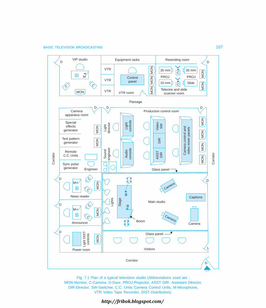
BASIC TELEVISION BROADCASTING 107
DCorridor
Visitors
Glass panel
Ligh
ts
Sta
ge
MM
Boom
Main studioCaptions
Camera
Camera
CameraD
L
MO
N
D
Ligh
tDIS
Tco
ntro
ls
Power room
MO
N
C
CM
D
Announcer
News reader
MO
N
C
CM
D
Cor
ridor
MO
NM
ON
Engineer
Sync pulsegenerator
RemoteC.C. Units
Test patterngenerator
Specialeffects
generator
Cameraapparatus room
D D
MO
NM
ON
MO
NM
ON
Cor
ridor
Ligh
tdi
rect
orS
ound
engi
neer
Aud
ioco
nsol
eLi
ght
cont
rols
Vid
eoS
WA
SS
TD
IRD
IR
Cam
era
cont
rol a
ndvi
deo
mix
erpa
nels
Production control roomD
Glass panel
Passage
MON
CC
M
DVIP studio
VTR
VTR
VTR
Controlpanel
VTR room
Equipment racks
MO
NM
ON
MO
N
MO
NM
ON
Rewinding room
C
C35 mm 35 mm
16 mm Slide
Telecine and slidescanner room
PROJ PROJ
D
Fig. 7.1 Plan of a typical television studio (Abbreviations used are :MON-Monitor, C-Camera, D-Door, PROJ-Projector, ASST DIR- Assistant Director,
DIR-Director, SW-Switcher, C.C. Units Camera Control Units, M-Microphone,VTR Video Tape Recorder, DIST-Distribution).
http://fribok.blogspot.com/

108 MONOCHROME AND COLOUR TELEVISION
the transmitter through a switcher in the master control room, which selects one programmeat a time. Even in studio set-ups with only one control room, there are several studio rooms, allconnected to the same control room. This enables preparation of different programmes in otherstudios while a programme is being telecast or recorded from one studio.
7.2 TELEVISION CAMERAS
Television cameras may assume different physical and electrical configurations. However, ingeneral they may be divided into two basic groups—self contained cameras and two-unit systemsthat employ separate camera heads driven by remote camera control equipment located in thecentral apparatus room (see Fig. 7.1). A self contained camera has all the elements necessaryto view a scene and generate a complete television signal. Such units are employed for outdoorlocations and normally have a VTR and baby flood lights as an integral part of the televisingsetup. The remote camera head usually contains only photosensitive pick-up tube, its associateddeflection circuitry, video preamplifier and a video monitor. Thus the bulk of the circuitry iscontained in the camera control unit, which is connected to the camera head by means of amulticonductor cable. This cable not only carries video, deflection and sync signals but alsofeeds high voltage supplies necessary for the camera tube. The remote camera control unitcontains most of the electrical operating and set-up controls. For this reason, it is usuallylocated near a viewing monitor so that the results of any adjustments may be easily viewed onthe monitor screen. All camera controls are available on a panel in the production controlroom.
Camera LensesTelevision cameras can produce images to different scales depending on the focal length (viewingangle) of the lens employed. Lenses of longer focal length are narrow angle lenses while thoseof shorter focal length are wide angle lenses. Narrow angle lenses (below 20°) are suitable forcloseups of distant objects because of the magnifying effect due to their longer focal length.Lenses with angles over 60° are most suited for location shots which cover large areas. Mediumangle lenses (20 to 60°) are called universal lenses and are used for televising normal scenes.All lenses consist of a combination of simple lens elements to minimize spherical aberrationand other optical distortions.
Lens TurretA judicious choice of lens can considerably improve the quality of image, depth of field and theimpact which is intended to be created on the viewer. Accordingly a number of lenses withdifferent viewing angles are provided. Their focal lengths are slightly adjustable by movementof the front element of the lens located on the barrel of the lens assembly. This lens complimentof the TV camera is mounted on a turret. The lens turret is screwed in the front of the cameraand rotation of the turret brings the desired lens in front of the camera tube. An image orthiconturret assembly holds four lenses of focal lengths 35 mm, 50 mm, 150 mm and a zoom lens of 40to 400 mm. Figure 7.2 shows such a lens turret mounted in front of a television camera.
http://fribok.blogspot.com/

BASIC TELEVISION BROADCASTING 109
Lens turret
Stand
View finder
TV camera
Fig. 7.2. A television camera with lens turret and view finder.
Zoom LensA zoom lens has a variable focal length with a range of 10 : 1 or more. In this lens the viewingangle and field view can be varied without loss of focus. This enables dramatic close-up control.The smooth and gradual change of focal length by the cameraman while televising a sceneappears to the viewer as it he is approaching or receding from the scene.
The variable focal length is obtained by moving individual lens elements of a compoundlens assembly. A zoom lens can in principle simulate any fixed lens which has a focal lengthwithin the zoom range. It may, however, be noted that the zoom lens is not a fast lens. Thespeed of a lens is determined by the amount of light it allows to pass through it. Thus underpoor lighting conditions, faster fixed focal length lenses mounted on the turret are preferred.
In many camera units only a zoom lens is provided instead of the turret lens assembly.This alone enables the camera operator to have close-ups, wide coverage of the scene anddistant shots without loss of focus. This is particularly so in colour TV cameras where thescene is often well defined and suitably illuminated for proper reproduction of colour details.
Camera MountingsAs shown in Fig. 7.2, studio cameras are mounted on light weight tripod stands with rubberwheels to enable the operator to shift the camera as and when required. It is often necessary tobe able to move the camera up and down and around its central axis to pick-up differentsections of the scene. In such cases, pan-tilt units may be used which typically provide a 360°rotational capability and allow tilting action of plus or minus 90°. In many applications, primarilyclosed circuit systems, where it is desirable to be able to remotely move the camera bothhorizontally and vertically, small servo motors are provided as part of the camera mount.Small motors are also used for remote focusing of the lens unit. In exceptional cases when anoverview of a scene is necessary, a remotely controlled camera is hung from the ceiling.
View FinderTo permit the camera operator to frame the scene and maintain proper focus, an electronicview-finder is provided with most TV cameras. This view-finder is essentially a monitor whichreproduces the scene on a small picture tube. It receives video signals from the control room
http://fribok.blogspot.com/

110 MONOCHROME AND COLOUR TELEVISION
stabilizing amplifier. The view-finder has its own deflection circuitry as in any other monitor,to produce the raster. The view-finder also has a built-in dc restorer for maintaining averagebrightness of the scene being televised.
Studio LightingsIn a television studio it is necessary to illuminate each area of action separately besides providingan average level of brightness over the entire scene. Lighting scheme is so designed that shadowsare prevented. As many as 50 to 100 light fittings of different types are often provided in moststudios. The light fixtures used include spot lights, broads and flood lights of 0.5 KW to 5 KWratings. A number of such fittings are suspended from the top so that these can be shiftedunseen by the viewer. In big studios catwalks (passages close to the ceiling) are built for easeof changing location of the suspended light fixtures.
The brightness level in different locations of the studio is controlled by varying effectivecurrent flow through the corresponding lamps. For a smooth current control, dimmerstats(autotransformers) are used for low rating lamps are silicon controlled rectifiers (SCRs) forhigher power lights. The power to all the lines is fed through automatic voltage stabilizers inorder to maintain a steady voltage supply. The mains distribution boards and switches arelocated in a separate room close to the studios. The dimmerstats and other light controlequipment is mounted on a separate panel in the programme control room.
Audio Pick-upThe location and placement of microphones depends on the type of programme. For paneldiscussions, news-reading and musical programmes the microphones may be visible to theviewer and so can be put on a desk or mounted on floor stands. However, for plays and manyother similar programmes the microphones must be kept out of view. For such applicationsthese are either hidden suitably or mounted on booms. A microphone boom is an adjustableextended rod from a stand which is mounted on a movable platform. The booms carrymicrophones close to the area of pick-up but keep them high enough to be out of the camerarange. Boom operators manipulate boom arms for distinct sound pick-up yet keeping themicrophones out of camera view.
7.3 PROGRAMME CONTROL ROOM
As explained earlier all video and audio outputs are routed through a common control room.This is necessary for a smooth flow and effective control of the programme material. This roomis called the Programme Control Room (PCR). It is manned by the programme director, hisassistant, a camera control unit engineer, a video mixer expert, a sound engineer and a lightingdirector. The programme director with the help of this staff effects overall control of theprogramme while it is telecast live or recorded on a VTR. The camera and sound outputs fromthe announcer’s booth and VIP studios are also routed through the programme control room.
The video and audio outputs from different studios and other ancillary sources areterminated on separate panels in the control room. One panel contains the camera control unitand video mixer. In front of this panel are located a number of monitors for editing andpreviewing all incoming and outgoing programmes. Similarly another panel (see Fig. 7.1) housesmicrophone controls and switch-in controls of other allied equipment. This panel is under
http://fribok.blogspot.com/

BASIC TELEVISION BROADCASTING 111
control of the sound engineer who in consulation with the programme director selects andcontrols all available sound outputs.
Fig. 7.3. A typical programme control room.
The producer and the programme assistant have in front of them a talk-back controlpanel for giving instructions to the cameramen, boom operator, audio engineer and floormanager. The producer can also talk over the intercom system to the VTR and telecine machineoperators. The lighting is controlled by switches and faders from a dimmer console which isalso located in the programme control room. Figure 7.3 shows a view of a typical programmecontrol room.
Camera Control Unit (C.C.U.)The camera control unit has provision to control zoom lens action and pan-tilt movement besidesbeam focus and brightness control of camera tubes. The C.C.U. engineer manipulates variouscontrols under directions from the producer. In broadcast stations, the video signal must bemaintained within very close tolerances of amplitudes. The C.C.U. engineer has the necessaryfacilities to adjust parameters such as video gain, camera sensitivity, blanking level videopolarity etc. For live broadcast of programmes televised far away from the studios, microwavelinks are used. The modulated composite video signal received over the microwave link isdemodulated and processed in the usual manner by the C.C.U. engineer for transmission onthe channel allocated to the station.
7.4 VIDEO SWITCHER
A video switcher is a multicontact crossbar switch matrix with provision for selecting any oneor more out of a large number of inputs and switching them on to outgoing circuits. The inputsources include cameras, VTRs and telecine machine outputs, besides test signals and special
http://fribok.blogspot.com/

112 MONOCHROME AND COLOUR TELEVISION
effects generators. Thus at this point the programme producer with the assistance of videoswitcher may select the output of any camera, or mix the output of two or more cameras.Similarly various effects such as fades, wipes, dissolves, supers and so on may be introducedand controlled with a mixer. The results obtained from these switching procedures are quitefamiliar to any one who has watched commercial television programmes. Through switching,a rather restricted two-dimensional picture presented by one camera can be given additionalperspective by changing the display to another camera that views the same scene from asomewhat different angle. Also information being viewed by a number of cameras at variouslocations can be presented on a single monitor. The ultimate destination of the outputs fromthe video switcher may be transmitter or a VTR. It could as well as be a string of monitors ina closed circuit television system.
Types of Video Switchers. Broadcast switchers incorporate some method of verticalblanking interval controlled switching. Switching in this manner, during the vertical blankingperiod, eliminates any visible evidence of switching that might be observed as a disruptionduring the normal vertical scan. There are three types of video switchers :
(i) Mechanical Pushbutton Switcher. In this type the signals are terminated on theactual switch contacts. The bank of switches is interlocked to prevent simultaneous operation.This type of switcher is used primarily for portable field units or in CCTV systems becauseswitching is not frequent and momentary disturbances in the picture during switching can betolerated.
MON 5
MON 4
MON 3
MON 2
MON 1
C - 3
C - 2
C - 1
Fig. 7.4. A 3 × 5 Switching matrix.
(ii) Relay Switcher. The relay switcher or relay cross-bar is an electromechanicalswitcher. Here magnetically activated read switch contacts are used to effect switching. The
http://fribok.blogspot.com/

BASIC TELEVISION BROADCASTING 113
relays can be operated by remote control lines. Reed relays have fast operate time (around1 ms) and so can be used to enable switching during the vertical blanking interval. Figure 7.4shows a 3 × 5 switching matrix employing a reed relay switcher. This is an example of adistribution-type switcher system where all inputs are available to all monitors. The X’s indicatethe possibility of combinations that may be achieved. If the crosspoint indicated by the ‘X’ onthe intersection of the lines from camera 3 and monitor 2 were selected, the scene viewed bycamera 3 would appear an monitor 2. Similarly any or all of the remaining monitors may beselected to view any camera that is desired. Isolation amplifiers, though not shown, are usedin-between the cameras and monitors.
(iii) Electronic Switcher. These are all electronic switchers and use solid state devicesthat provide transition times of the order of a few micro-seconds. Their size is generally verysmall and due to inherent reliability need much less maintenance. Almost all present dayswitchers employed in broadcasting are electronic switchers.
Camera-1
Camera-20%
100%
% Brightness
(a)
v0
Mixingnetwork
Amp Amp
Cam
era-
1ou
tput
Cam
ea-
2C
amer
a-2
outp
ut
Common controlshaft
(b)
(c)
Camera-1
Camera-20%
100%
% Brightness
Fig. 7.5. Two types of switching transitions (a) lap-dissolve(b) circuit for affecting lap-dissolve transition, (c) fade out-fade in transition.
Types of Switching Transitions. The actual switching transition is either carried outby a lap-dissolve operation or a fade out-fade in form of switching. Both methods are illustratedin Fig. 7.5. The lap-dissolve switching (Fig. 7.5(a)) may be accomplished by two potentiometers
http://fribok.blogspot.com/

114 MONOCHROME AND COLOUR TELEVISION
connected to the two signals that are to be switched. Signal amplitude from say camera number1 is slowly reduced, while that from camera number 2 is increased at the same rate. This, asshown in Fig. 7.5(b) may be done through variable resistors connected at the inputs of twoamplifiers. The values of these potentiometers may be changed as described above to controlthe gain of amplifiers whose outputs are then combined, Fig. 7.5(c) illustrates the fade out-fade in method of video transfer. It can also be carried out by two potentiometers employed inthe lap-dissolve method. However, in this case, by separate actuation of the two potentiometers,signal number 1 is slowly reduced in amplitude until zero signal level is obtained, and thensignal No. 2 is slowly raised from 0 to 100 per cent by the second potentiometer. The amplifiersused are commonly called mixers or faders.
Electronic Switcher ConfigurationFigure 7.6 is a functional block diagram of very simple broadcast switcher-mixer. It has fiveinputs out of which any two may be selected to drive the two buffer amplifiers. These, in turnfeed into a mixer amplifier.
1 2 3 4 5
Camerainputs
Captionscamera
VTR
Bus A
Bus B
Mixeramplifiers
Mixercontrol
Bufferamplifiers Switched
output
Sync input
Fig. 7.6. A simple switcher for mixing outputs from two buses.
The mixer transfers video signals by fade out-fade in method. The potentiometers at theremote mixer amplifier can be positioned to select 100 per cent output from either A or B bus.Assume A and B inputs were at 100 per cent and 0 per cent levels respectively. If camera No.2 is selected on the A bus, it would appear at the output. Similarly, if camera No. 3 is selectedon the B bus, it will not appear at the mixer output. However, when the levers that control thepotentiometers are moved through their full travel, the output from the mixer amplifier wouldtransfer from A bus to B bus at a relatively slow rate providing a transition from camera No. 2to camera No. 3. Similarly more complex switchers can be designed to provide different switchingmatrices.
Special Effects GeneratorA special effects generator is normally located along with the camera control units in thecamera apparatus room. It is programmed to generate video signals for providing special effects.Its output is available at a panel in the production control room. The special effects signalsinclude curtain moving effects, both horizontal and vertical. These are inserted while changingfrom one scene to another. Similarly many other patterns are available which can be interposedin-between any two programmes. Infact several options are available and can be selected whileordering the equipment.
http://fribok.blogspot.com/

BASIC TELEVISION BROADCASTING 115
7.5 SYNCHRONIZING SYSTEM
To generate a meaningful picture on the raster of a monitor or receiver, some means are neededto synchronize the scanning systems of both the camera and the monitor. In a multicamerasystem, as is often the case in broadcasting, it is necessary to have them all synchronized by asingle sync pulse generator. Accordingly a common sync drive circuitry is provided which controlsscanning sequence, insertion and timing of sync pulses in all the cameras. With such a control,when the scene shifts from one camera to another, the synchronizing waveforms are in phaseso that the monitor or home receiver is not interrupted in its scanning process. In the absenceof such a provision, while switching from one camera to another, the monitor or receiver wouldhave to read just its scanning procedure for the incoming camera and the picture might rollmomentarily. Figure 7.7(a) shows one method of driving multiple cameras from a single syncgenerator. The sync line is terminated in a 75 ohm resistor because the output of most TVcamera equipment is designed to work into a 75 ohm load.
Syncgenerator
Camera1
Camera2
Camera3
75 terminationresistor
W
MON 1Camera
MON 2
MON 3
MON 4
MON 5
Distributionamplifier
75 W
Fig. 7.7(a) A sync generator driving Fig. 7.7(b) Connections to several monitorsseveral camera units for displaying the output of a single camera.
Camera 1 Camera 2 Camera 3
MON
Push buttons
Fig. 7.7(c). Switcher for selecting any camera output to one monitor.
http://fribok.blogspot.com/

116 MONOCHROME AND COLOUR TELEVISION
Distribution of Camera Outputs to MonitorsMonitors usually have well designed video amplifiers with bandwidth as large as 30 MHz.This enables excellent reproduction of pictures. Any defects are clearly seen. This is usefulwhile testing and adjusting studio and other allied equipment. Several monitors may be usedto display the scene viewed by one camera. When the number of monitors is large and they arelocated at a considerable distance from each other, a distribution amplifier (see Fig. 7.7(b)) isused to route the video signal to all of them. Similarly it is often desirable to provide means forviewing the output from different cameras on a monitor. This is simply done by selecting themonitor inputs from one camera or another by push button switches as shown in Fig. 7.7(c).The switches not depressed connect terminating resistors to the appropriate cameras. Inoperation all switches are interlocked so that only one camera can be connected to the monitorat any time. Depressing one switch releases all other.
Distributionamplifier
Distributionamplifier
Distributionamplifier
Distributionamplifier
Distributionamplifier
Syncshaper
Horzdrive
shaper
Syncdeveloping
circuits
15625 Hz
Verticaldrive
shaper
Dividercircuits
and gating
Verticalblankingshaper
Blankingmixer
Horz.blankingshaper
2 : 1Divider
31250Hz
15625Hz
50 HzVertical drive
VD
50 HzVerticalblanking
VB
Mixedblanking
MB
Horz drive HD
MixedsyncMS
50 Hz
31250Hz
Pulseshaper
and buffer
Masteroscillator
31.25 KHz
2f XTLoscillator
31.25 KHz
H
2fmultivibrator
H
Mains lockerror
voltage AFC(phase detector
circuit)
Shapingcircuit
From mains(50 Hz)
50 Hz
625 : 131250
Hz
Extsource
Fig. 7.8. Block diagram of a drive and sync pulse generator (SPG).
Sync Pulse Generation (SPG) CircuitryFigure 7.8 is a block representation of a drive and sync pulse generator which would provideall the pulse waveforms necessary to meet C.C.I.R. standards. The generator contains (i) acrystal controlled or mains locked timing system, (ii) pulse shapers which generate requiredpulse trains for blanking, synchronizing and deflection drives and (iii) distribution amplifiers.
http://fribok.blogspot.com/

BASIC TELEVISION BROADCASTING 117
A synchronized master oscillator generates an output at 2fH, viz., 2 × 15625 = 31250 Hzwhich drives other circuits. As shown in the figure, this oscillator can be synchronized from(i) a crystal controlled oscillator operating at exact 2fH, (ii) an external source, or (iii) 50 Hzmains supply. In the mains frequency lock mode, the 2fH multivibrator is controlled by a phasedetector circuit which compares the 50 Hz square wave derived from the master oscillatorthrough a divider chain with the 50 Hz square wave derived from mains supply. The errorsignal which develops at output of the phase detector corrects the frequency of the multivibratorand locks it with the mains frequency. While broadcasting programme received from anotherTV station, its sync pulses are processed and fed at the ‘external source’ input to slave the synccircuitry of the station to that of the incoming station.
The master oscillator frequency is twice the horizontal frequency, and is coincident withthe frequency of the equalizing and serration pulses which are driven from its output. Thebuffer amplifier isolates the master oscillator from the rest of the circuitry. The divider andgating block serves two functions. The most important function is to accurately divide themaster oscillator frequency by a factor of 625, thus deriving a 50 Hz output that is phaselocked with the original 31.25 kHz source. The output is correctly shaped in a shaper circuitbefore using it to initiate vertical drive and vertical blanking waveforms. The sync developingcircuit provides equalizing and serration pulses.
The output from the master oscillator (31.25 kHz) is also fed to a 2 : 1 divider to deriveoutput at 15625 Hz, the horizontal frequency. This is used to derive horizontal blanking,horizontal drive and horizontal sync signals in appropriate circuits.
The basic building block necessary for generating and shaping the various sync anddrive sources include frequency dividers, pulse shapers or stretchers, delay circuits, addersand logic gates. The circuitry of a modern SPG (sync pulse generator) employs ICs andtransistors. This results in a compact, accurate and reliable unit.
The various outputs from the SPG are derived through distribution amplifiers whichdevelop the necessary power and act as buffers between the generation and distribution points.
7.6 MASTER CONTROL ROOM (MCR)
In small broadcasting houses the PCR has a master switcher for routing the composite videosignal and allied audio output directly to the transmitter. The ancillary equipment is mostlylocated in the Central apparatus room. However, in bigger establishments which have a largenumber of studios and production control rooms, all outputs from various sources are routedthrough the master control room. This room houses centralized video equipment like syncpulse generators, special effects generator, test equipment, video and audio monitors besides amaster routing switcher.
Picture Signal TransmissionAt the production control room video signal amplitude as received from the camera is very lowand direct coupled amplifiers are used to preserve dc component of the signal. Further on, accoupling is provided because it is often technically easier and less expensive to use such acoupling. This involves loss of dc component which, however, is reinserted at the transmitterbefore modulation. This is carried out by a dc restorer circuit often called a blanking levelclamp.
http://fribok.blogspot.com/

118 MONOCHROME AND COLOUR TELEVISION
In the master control room the composite video signal is raised to about one volt P-Plevel before feeding it to the cable that connects the control room to the transmitter. Thoughthe transmitter is located close to the studios, often in the same building, matching networksare provided at both ends of the connecting cable to avoid unnecessary attenuation and frequencydistortion.
7.7 GENERATION OF AMPLITUDE MODULATION
In AM transmitters where efficiency is the prime requirement, amplitude modulation is effectedby making the output current of a class C amplifier proportional to the modulating voltage.This amounts to applying a series of current pulses at the frequency of the carrier to theoutput tuned (tank) circuit where the amplitude of each pulse follows the variations of themodulating signal. The resonant frequency of the tuned circuit is set equal to the carrierfrequency. In the tank circuit each current pulse causes a complete sine wave at the resonantfrequency whose amplitude is proportional to the applied current pulse.
The accumulative effect of this flywheel action of the resonant circuit is generation of acontinuous sine wave voltage at the output of tank circuit. The frequency of this voltage isequal to carrier frequency having amplitude variations proportional to magnitude of themodulating signal.
t0
v0
v0v0RLRF
in
AFin
C (RF)B
+CN
(neutralizingcapacitor)
B+
RF input
0Total bias
Fixed bias
– Vg
t
t0
ip
Fig. 7.9. Grid modulated class C amplifier.
In practice AM may be generated by applying the modulating voltage source in serieswith any of the DC supplies of the class C amplifier. Thus grid (or base), plate (or collector) andcathode (or emitter) modulation are all possible. As an illustration Fig. 7.9 shows the basiccircuit and corresponding waveforms of a grid modulated class C amplifier. The modulatingvoltage is in series with the fixed negative grid bias and so the amplitude of the total bias isproportional to the amplitude of the modulating signal, and varies at the rate of the modulatingfrequency. Since the carrier RF source is also in series with the bias and modulating voltage,these get superimposed and the total bias appears as shown in Fig. 7.9. The resulting plate
http://fribok.blogspot.com/

BASIC TELEVISION BROADCASTING 119
current flows in pulses and the amplitude of each pulse is proportional to the instantaneousbias and therefore to the instantaneous modulating voltage. As explained earlier the applicationof these pulses to the tank circuit then yields amplitude modulation.
In an AM transmitter, amplitude modulation can be generated at any point after thecrystal oscillator. If the output stage in the transmitter is plate modulated the method is calledhigh level modulation. If modulation is applied at any other point, including some other electrodeof the output amplifier then so-called low-level modulation is produced. The end product,however, of both the system is the same.
It is not practicable to use plate modulation at the output stage in a television transmitter,because of the difficulty of generating high video powers at the large bandwidths required.Accordingly, grid modulation of the output stage is the highest level of modulation employedin TV transmitters. It is called ‘high-level’ modulation in TV broadcasting and anything else isthen called ‘low-level’ modulation. In recent television transmitter designs, it has become astandard practice to affect modulation in two stages. A carrier frequency of 40 MHz is employedin a balanced modulator configuration and a band ranging from 35 to 45 MHz is obtained as itsoutput. In some designs vestigial sideband correction is also carried out in the modulatoroutput circuit. Its output is then mixed with an appropriate high frequency to get the desiredchannel carrier frequency and its sidebands as the difference product. This process is illustratedfor channel 4 (Band-1) in Fig. 7.10.
USB = 40 to 45 MHzLSB = 35 to 40 MHz
Balancedmodulator
First local– oscillator
40 MHz
Second local– oscillator
102.25 MHz
Video input0–5 MHz
MixerBandpassfilter (LSB) 57.25 to
67.25 MHz
Channel 4Channel carrier = 62.25 MHzUSB = 62.25 to 67.25 MHzLSB = 57.25 to 62.25 MHz
Fig. 7.10. Modulation and frequency translation.
7.8 TELEVISION TRANSMITTER
A simplified functional block diagram of a television transmitter is shown in Fig. 7.11. Necessarydetails of video signal modulation with picture carrier of allotted channel are shown in picturetransmitter section of the diagram. Note the inclusion of a dc restorer circuit (DC clamp) beforethe modulator. Also note that because of modulation at a relatively low power level, an amplifieris used after the modulated RF amplifier to raise the power level. Accordingly this amplifiermust be a class-B push-pull linear RF amplifier. Both the modulator and power amplifiersections of the transmitter employ specially designed VHF triodes for VHF channels andklystrons in transmitters that operate in UHF channels.
Vestigial Sideband FilterThe modulated output is fed to a filter designed to filter out part of the lower sidebandfrequencies. As already explained this results in saving of band space.
http://fribok.blogspot.com/
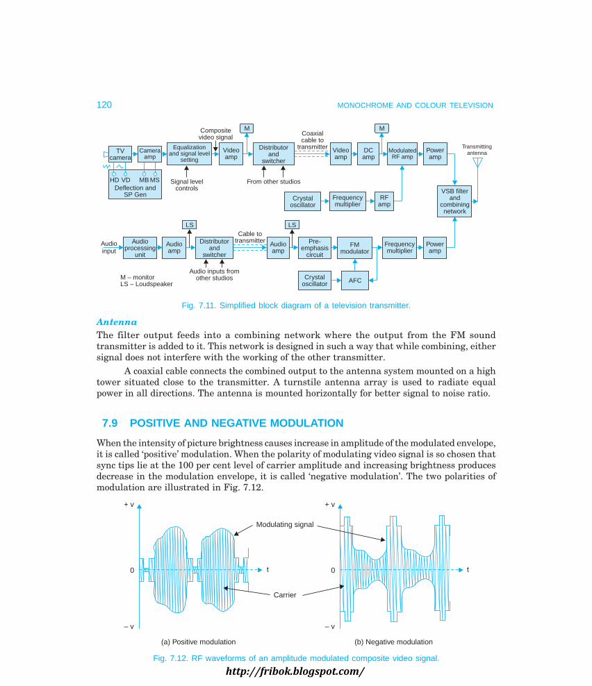
120 MONOCHROME AND COLOUR TELEVISION
Transmittingantenna
LS LS
Audioinput
Audioprocessing
unit
Audioamp
Distributorand
switcher
Audio inputs fromother studios
Cable totransmitter Audio
amp
Pre-emphasis
circuit
FMmodulator
Frequencymultiplier
Poweramp
AFCCrystaloscillator
M – monitorLS – Loudspeaker
Cameraamp
TVcamera
Equalizationand signal level
setting
HD VD MB MSDeflection and
SP Gen
Signal levelcontrols
Compositevideo signal
M
Videoamp
Distributorand
switcher
From other studios
Coaxialcable to
transmitter Videoamp
DCamp
ModulatedRF amp
Poweramp
M
RFamp
Frequencymultiplier
Crystaloscillator
VSB filterand
combiningnetwork
Fig. 7.11. Simplified block diagram of a television transmitter.
AntennaThe filter output feeds into a combining network where the output from the FM soundtransmitter is added to it. This network is designed in such a way that while combining, eithersignal does not interfere with the working of the other transmitter.
A coaxial cable connects the combined output to the antenna system mounted on a hightower situated close to the transmitter. A turnstile antenna array is used to radiate equalpower in all directions. The antenna is mounted horizontally for better signal to noise ratio.
7.9 POSITIVE AND NEGATIVE MODULATION
When the intensity of picture brightness causes increase in amplitude of the modulated envelope,it is called ‘positive’ modulation. When the polarity of modulating video signal is so chosen thatsync tips lie at the 100 per cent level of carrier amplitude and increasing brightness producesdecrease in the modulation envelope, it is called ‘negative modulation’. The two polarities ofmodulation are illustrated in Fig. 7.12.
+ v
0
– v
Modulating signal
Carrier
t
+ v
0
– v
t
(a) Positive modulation (b) Negative modulation
Fig. 7.12. RF waveforms of an amplitude modulated composite video signal.
http://fribok.blogspot.com/

BASIC TELEVISION BROADCASTING 121
Comparison of Positive and Negative Modulation(a) Effect of Noise Interference on Picture Signal. Noise pulses created by automobile ignitionsystems are most troublesome. The RF energy contained in such pulses is spread more or lessuniformly over a wide frequency range and has a random distribution of phase and amplitude.When such RF pulses are added to sidebands of the desired signal, and sum of signal and noiseis demodulated, the demodulated video signal contains pulses corresponding to RF noise peaks,which extend principally in the direction of increasing envelope amplitude. This is shown inFig. 7.13. Thus in negative system of modulation, noise pulse extends in black direction of thesignal when they occur during the active scanning intervals. They extend in the direction ofsync pulses when they occur during blanking intervals. In the positive system, the noise extendsin the direction of the white during active scanning, i.e., in the opposite direction from the syncpulse during blanking.
Black
White
Noise pulse extendstowards blackNoise pulse
t
(a)
Whitet
Black
Noise pulse extendstowards white
(b)
Noise pulse
Fig. 7.13. Effect of noise pulses (a) with negative modulation,(b) with positive modulation.
Obviously the effect of noise on the picture itself is less pronounced when negativemodulation is used. With positive modulation noise pulses will produce white blobs on thescreen whereas in negative modulation the noise pulses would tend to produce black spotswhich are less noticeable against a grey background. This merit of lesser noise interference onpicture information with negative modulation has led to its use in most TV systems.
(b) Effect of Noise Interference on Synchronization. Sync pulses with positive modulationbeing at a lesser level of the modulated carrier envelope are not much affected by noise pulses.However, in the case of negatively modulated signal, it is sync pulses which exist at maximumcarrier amplitude, and the effect of interference is both to mutilate some of these, and to
http://fribok.blogspot.com/

122 MONOCHROME AND COLOUR TELEVISION
produce lot of spurious random pulses. This can completely upset the synchronization of thereceiver time bases unless something is done about it. Because of almost universal use ofnegative modulation, special horizontal stabilizing circuits have been developed for use inreceivers to overcome the adverse effect of noise on synchronization.
(c) Peak Power Available from the Transmitter. With positive modulation, signalcorresponding to white has maximum carrier amplitude. The RF modulator cannot be drivenharder to extract more power because the non-linear distortion thus introduced would affectthe amplitude scale of the picture signal and introduce brightness distortion in very brightareas of the picture. In negative modulation, the transmitter may be over-modulated duringthe sync pulses without adverse effects, since the non-linear distortion thereby introduced,does not very much affect the shape of sync pulses. Consequently, the negative polarity ofmodulation permits a large increase in peak power output and for a given setup in the finaltransmitter stage the output increases by about 40%.
(d) Use of AGC (Automatic Gain Control) Circuits in the Receiver. Most AGC circuits inreceivers measure the peak level of the incoming carrier signal and adjust the gain of the RFand IF amplifiers accordingly. To perform this measurement simply, a stable reference levelmust be available in the signal. In negative system of modulation, such a level is the peak ofsync pulses which remains fixed at 100 per cent of signal amplitude and is not affected bypicture details. This level may be selected simply by passing the composite video signal througha peak detector. In the positive system of modulation the corresponding stable level is zeroamplitude at the carrier and obviously zero is no reference, and it has no relation to the signalstrength. The maximum carrier amplitude in this case depends not only on the strength of thesignal but also on the nature of picture modulation and hence cannot be utilized to developtrue AGC voltage. Accordingly AGC circuits for positive modulation must select some otherlevel (blanking level) and this being at low amplitude needs elaborate circuitry in the receiver.Thus negative modulation has a definite advantage over positive modulation in this respect.
The merits of negative modulation over positive modulation, so far as picture signaldistortion and AGC voltage source are concerned, have led to the use of negative modulationin almost all TV systems now in use.
7.10 SOUND SIGNAL TRANSMISSION
The outputs of all the microphones are terminated in sockets on the sound panel in theproduction control room. The audio signal is accorded enough amplification before feeding it toswitchers and mixers for selecting and mixing outputs from different microphones. The soundengineer in the control room does so in consultation with the programme director. Some pre-recorded music and special sound effects are also available on tapes and are mixed with soundoutput from the studio at the discretion of programme director. All this needs prior planningand a lot of rehearsing otherwise the desired effects cannot be produced. As in the case ofpicture transmission, audio monitors are provided at several stages along the audio channel tokeep a check over the quality and volume of sound.
http://fribok.blogspot.com/

BASIC TELEVISION BROADCASTING 123
Preference of FM over AM for Sound TransmissionContrary to popular belief both FM and AM are capable of giving the same fidelity if thedesired bandwidth is allotted. Because of crowding in the medium and short wave bands inradio transmission, the highest modulating audio frequency used in 5 kHz and not the fullaudio range which extends up to about 15 kHz. This limit of the highest modulating frequencyresults in channel bandwidth saving and only a bandwidth of 10 kHz is needed per channel.Thus, it becomes possible to accommodate a large number of radio broadcast stations in thelimited broadcast band. Since most of the sound signal energy is limited to lower audiofrequencies, the sound reproduction is quite satisfactory.
Frequency modulation, that is capable of providing almost noise free and high fidelityoutput needs a wider swing in frequency on either side of the carrier. This can be easily allowedin a TV channel, where, because of very high video frequencies a channel bandwidth of 7 MHzis allotted. In FM, where highest audio frequency allowed is 15 kHz, the sideband frequenciesdo not extend too far and can be easily accommodated around the sound carrier that lies 5.5 MHzaway from the picture carrier. The bandwidth assigned to the FM sound signal is about 200 kHzof which not more than 100 kHz is occupied by sidebands of significant amplitude. The latterfigure is only 1.4 per cent of the total channel bandwidth of 7 MHz. Thus, without encroachingmuch, in a relative sense, on the available band space for television transmission all theadvantages of FM can be availed.
7.11 MERITS OF FREQUENCY MODULATION
Frequency modulation has the following advantages over amplitude modulation.
(a) Noise ReductionThe greatest advantage of FM is its ability to eliminate noise interference and thus increasethe signal to noise ratio. This important advantage stems from the fact that in FM, amplitudevariations of the modulating signal cause frequency deviations and not a change in the amplitudeof the carrier. Noise interference results in amplitude variations of the carrier and thus can beeasily removed by the use of amplitude limiters.
It is also possible to reduce noise in FM by increasing frequency deviation. This deviationcan be made as large as required without increasing the transmitter power. Higher audiofrequencies are mostly harmonics of the lower audio range. They have low amplitudes and socause a small deviation of the carrier frequency. Noise power interference is also generally lowin amplitude and so results in frequency deviation similar to that caused by higher audiofrequencies. Thus higher audio frequencies are most susceptible to noise effects. If thesefrequencies were artificially boosted in amplitude at the transmitter and correspondinglyreduced at the receiver, improvement in noise immunity could be expected. This in fact is thestandard practice in all FM transmission and reception. In AM on the other hand, the signalmodulation can be increased relative to noise modulation only by increasing the transmitteroutput power. A 20 db improvement in signal-to-noise voltage ratio requires ten-times increasein frequency deviation in FM but an increase of 100 times in AM power output. Evidently anAM system in this respect reaches an economical limit long before the FM system, providedadditional bandwidth is available for FM transmission.
In an FM receiver, if two signals are being received simultanesouly, the weaker signalwill be eliminated almost entirely if it possesses less than half the amplitude of the other
http://fribok.blogspot.com/

124 MONOCHROME AND COLOUR TELEVISION
stronger signal. However, in AM the interfering signal or station can be heard or received evenwhen a 100 : 1 relationship exists between their amplitudes.
Pre-emphasis and De-emphasis. The boosting of higher audio modulating frequencies,in accordance with a prearranged response curve is termed pre-emphasis, and the compensationat the receiver is called de-emphasis. Examples of circuits used for each function are shown inFig. 7.14. As is obvious from these configurations, the pre-emphasis and de-emphasis networksare high-pass and low-pass filters respectively. The time constant of the filter for pre-emphasisat transmitter and later de-emphasis at receiver has been standardized at 50 µs in all theCCIR systems. However, in systems employing American FM and TV standards, networkshaving a time constant of 75 µs are used. A 50 µs (= RC) de-emphasis corresponds to a frequency
response curve that is 3 db down at the frequency given by 1
2πRC, which comes to 3180 Hz.
Figure 7.15 shows pre-emphasis and de-emphasis curves corresponding to a time constant of50 µs.
+ Vcc
L = 0.5HL/R = 50 sm
R = 10 KW
Cc
v0AF in
+ Vcc
RC = 50 sm
R = 50 KW
v0AF in
RLC = .001 Fm
Pre-emphasizedAF out
OR
Fig. 7.14(a). Pre-emphasis circuits.
CcR = 50 K
C = .001 F
v.in AF out
RC = 50 s
Pre-emphasizedAF in fromFM demodulator
CcL = 0.5 Hv.in AF out
ORR = 10 K L/R = 50 s
Fig. 7.14(b). De-emphasis circuits.
Pre-emphasis curve
De-emphasis curve
25 Hz 3180 Hz 15 KHzf(log scale)
12.6
– 3
+ 30
12.6
db
Fig. 7.15. 50 µs emphasis curves.
http://fribok.blogspot.com/

BASIC TELEVISION BROADCASTING 125
(b) Transmitter EfficiencyThe amplitude of the FM wave is independent of the depth of modulation, whereas in AM it isdependent on this parameter. This means that low level modulation can be used in FM and allsucceeding amplifiers can be class ‘C’ which are more efficient. Thus, unlike AM, all amplifiershandle constant power and this results in more economical FM transmitters.
(c) Adjacent Channel InterferenceBecause of the provision of a guard band in between any two TV channels, there is lessinterference than in conventional AM broadcasts.
(d) Co-channel Interference
The amplitude limiter in the FM section of the receiver works on the principle of passing thestronger signal and eliminating the weaker. In this manner, a relatively weak interferingsignal or any pick-up from a co-channel station (a station operating at the same carrierfrequency) gets eliminated in a FM system.
It may be noted that from general broadcast point of view FM needs much widerbandwidth than AM. It is 7 to 15 times as large as that needed for AM. Besides, FM transmittersand receivers tend to be more complex and hence are expensive. However, in TV transmissionand reception, where handling of the picture signal is equally complex, FM sound does not addvery much to the cost of equipment.
7.12 GENERATION OF FREQUENCY MODULATION
The primary requirement of an FM generator is a variable output frequency, where thevariations are proportional to the instantaneous value of the modulating voltage. In one methodof FM generation, either the inductance or capacitance of the tank circuit of an LC oscillator isvaried to change the frequency. If this variation can be made directly proportional to theamplitude of the modulating voltage, true FM will be obtained.
A voltage-variable reactance is generally placed across the oscillator tank circuit. Theoscillator is tuned to deliver the assigned carrier frequency with the average reactance of thevariable element present in parallel with its own tank circuit. The capacitance (or inductance)of the reactance element changes on application of modulating voltage to cause frequencydeviations in the oscillator frequency. Larger the departure of modulating voltage from zero,greater is the reactance variation, and in turn higher is the frequency deviation.
Basic Reactance Modulator
An FET, tube or transistor when suitably biased can be used as a variable reactance element.Similarly a varactor diode can also be used for this purpose. The basic circuit arrangements ofa reactance modulator either with an FET or with a vacuum tube are shown in Fig. 7.16.Provided certain simple conditions are met, the impedance Z as seen at the terminals markedA – A′ in the figures, is almost entirely reactive. The conditions which must be met are, (i) thecurrent ig should be negligible compared to the plate (or drain) current, and (ii) the impedanceXC >> R, preferably by more than 5 : 1.
http://fribok.blogspot.com/

126 MONOCHROME AND COLOUR TELEVISION
C
R vvg
A
S
Aig
DGi
Zvv
(a)
C
R vvg
A
K
Aig
PG
i
Zvv
(b) (c)
gm
– Vg
0
Fig. 7.16. Basic reactance modulator circuits (a) employing an FET (b) employing a VT(c) relation between bias voltage and transconductance of the device.
With these assumptions, the following analysis, which is valid for both the circuits canbe made : With a voltage v applied across the terminals A – A′, currents i and ig will flow in theplate (or drain) circuit and bias circuit respectively. The current ig will develop a voltage vg = ig
× R = V R
R jXC
×−
. The current i because of tube or FET action = gmvg = g R V
R jXm
C
× ×−
, where gm is
the mutual conductance of the device.
∴ Z = vi
= R jXg R
C
m
−×
= 1
gm
1 −FHG
IKJj
XR
C .
If XC >> R, the above equation will reduce to ;
Z = – jX
g RC
m ×This impedance is clearly a capacitive reactance, which may be written as :
Xeq = X
g RC
m =
12πfg RCm
= 1
2πf Ceq
∴ Ceq = gmRC
The following conclusions follow from this result :
(i) The equivalent capacitance depends on the device transconductance and can there-fore be varied with bias voltage. The approximate relation between the bias voltageand gm is illustrated in Fig. 7.16 (c).
(ii) The capacitance can be originally adjusted to any value (within reasonable limits), byvariation of the components R and C.
(iii) gmRC has the dimensions of capacitance.
(iv) From the circuits and analysis made, it is clear that if R and C are interchanged, the
impedance across A – A′ will become inductive with Leq = RCgm
.
(v) Similarly it can be shown that by using L and R instead of C and R in the biasingcircuit, both capacitive and inductive reactances can be obtained across the terminalsA – A′.
http://fribok.blogspot.com/

BASIC TELEVISION BROADCASTING 127
Transistor Reactance ModulatorFigure 7.17 shows a circuit of an LC oscillator that is frequency modulated by a capacitivereactance (RC) transistor modulator. As shown, the audio frequency voltage is applied at thebase of the transistor Q1. The amplitude variations of this driving voltage vary the forwardbias to change the transistor collector current. This changes β of the transistor which resultsin a proportionate change in the equivalent capacitance across the oscillator tank circuit. Notethe use of RF chokes in the circuit. They are used to isolate various points of the circuit for accurrent while providing a dc path.
R1
R2
R
AF in
C(RF)RE CE
C
Q1
Cf
CcRFC
Reactancemodulator
R3RFC
Q2
R4
CE
C2
C1RE L
C
FMoutput
Tank circuit
Oscillator
+ Vcc
Fig. 7.17. Reactance modulator circuit.
Varactor Diode ModulatorThe circuit of Fig. 7.18 shows such a modulator. It is seen that the varactor diode has beenback-biased to provide the junction capacitance effect. The bias is varied by the modulatingvoltage which is injected in series with the dc bias source through transformer T1. Theinstantaneous changes in the bias voltage cause corresponding changes in the junctioncapacitance, which in turn vary the oscillator frequency accordingly. It is often used for automaticfrequency control and remote tuning.
T1
AF in
– VD
Cb
(RF)
RFCCc
Tooscillator
tankcircuit
Varactordiode
Fig. 7.18. Varactor diode modulator.
7.13 STABILIZED REACTANCE MODULATOR
Although the oscillator on which the reactance modulator operates cannot be crystal controlled,it must nevertheless have the stability of a crystal if it is to be a part of a commercial transmitter.
http://fribok.blogspot.com/

128 MONOCHROME AND COLOUR TELEVISION
This suggests that frequency stabilization of the reactance modulator is required. The blockdiagram of Fig. 7.19 shows a typical AFC (automatic frequency control) system used with thereactance controlled FM transmitter. Here a fraction of the output is taken from the limiterand fed to a mixer, which also receives the signal from a crystal oscillator. The resultingdifference signal at a frequency which is much less than that of the master oscillator, is amplifiedand fed to a phase* discriminator. The output of the discriminator which is connected to thereactance modulator, provides a dc control voltage to counteract rapidly any drift in the averagefrequency of the master oscillator. The time constant of the discriminator load is quite large (ofthe order of 100 ms). Hence the discriminator will react to slow changes in the incomingfrequency, but not to normal frequency changes due to frequency modulation, which are toofast. Note that the discriminator must be connected to give a positive output if the inputfrequency is higher than the discriminator tuned frequency and a negative output if it is lower.Thus any drift in the oscillator frequency towards the higher side will produce a positive controlvoltage and this fed in series with the input of the reactance modulator, will increase its trans-conductance. This increases its output capacitance (Ceq = gmRC) and thus lowers the oscillator’scentre frequency. Analogous sequence of operations will take place to raise the oscillatorfrequency when it drifts on the lower side of its centre frequency. In the transmitter blockdiagram of Fig. 7.11 a reactance modulator with such a frequency control has been incorporated.
Reactancemodulator
AF inCrystal
oscillatorMixer
IFamplifier
f – fs 0
fs
f0
DC control voltage RFdiscriminator
FM outLimiter
FrequencymultiplierBuffer
Masteroscillator
Fig. 7.19. A typical transmitter AFC system.
7.14 GENERATION OF FM FROM PM
The direct modulators have the disadvantage of being based on an oscillator which is notstable enough for communication or broadcast purposes. As explained above, it needsstabilization which adds to circuit complexity. Note that the use of a crystal oscillator is notpossible because it cannot be successfully frequency modulated. It is possible, however, togenerate FM via Phase Modulation (PM) where a crystal oscillator can be used. It has been
shown in Chapter 4 that the instantaneous angular frequency for an FM signal ωi = d t
dtφ( )
= ωc
+ 2π∆f cos ωmt (eqn. 4.6) for a sinusoidal modulating signal. Conversely an FM signal of amplitude
*Phase discriminator circuits are discussed in Chapter 21, which is devoted to FM sound detection.
http://fribok.blogspot.com/
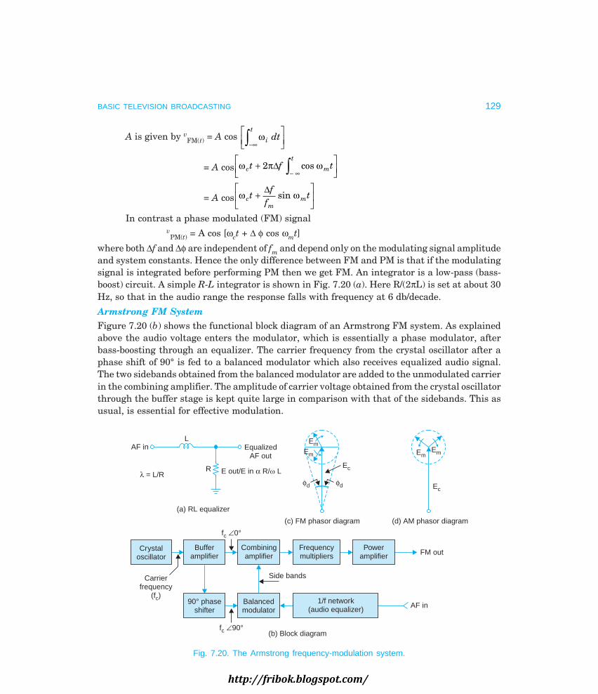
BASIC TELEVISION BROADCASTING 129
A is given by vFM(t) = A cos ω i
tdt
−∞zLNM OQP
= A cos ω π∆ ωc m
tt f t+L
NMOQP− ∞z2 cos
= A cos ω ωcm
mtf
ft+
LNM
OQP
∆sin
In contrast a phase modulated (FM) signal v
PM(t) = A cos [ωct + ∆ φ cos ωmt]
where both ∆f and ∆φ are independent of fm and depend only on the modulating signal amplitudeand system constants. Hence the only difference between FM and PM is that if the modulatingsignal is integrated before performing PM then we get FM. An integrator is a low-pass (bass-boost) circuit. A simple R-L integrator is shown in Fig. 7.20 (a). Here R/(2πL) is set at about 30Hz, so that in the audio range the response falls with frequency at 6 db/decade.
Armstrong FM SystemFigure 7.20 (b) shows the functional block diagram of an Armstrong FM system. As explainedabove the audio voltage enters the modulator, which is essentially a phase modulator, afterbass-boosting through an equalizer. The carrier frequency from the crystal oscillator after aphase shift of 90° is fed to a balanced modulator which also receives equalized audio signal.The two sidebands obtained from the balanced modulator are added to the unmodulated carrierin the combining amplifier. The amplitude of carrier voltage obtained from the crystal oscillatorthrough the buffer stage is kept quite large in comparison with that of the sidebands. This asusual, is essential for effective modulation.
AF inL
EqualizedAF out
E out/E in R/ LR = L/R
(a) RL equalizer
Em
Em
Ec
dd
(c) FM phasor diagram
EmEm
Ec
(d) AM phasor diagram
Crystaloscillator
Bufferamplifier
Combiningamplifier
Frequencymultipliers
Poweramplifier FM out
AF in
Side bands
f 0°c
Carrierfrequency
(fc)
f 90°c (b) Block diagram
90° phaseshifter
Balancedmodulator
1/f network(audio equalizer)
Fig. 7.20. The Armstrong frequency-modulation system.
http://fribok.blogspot.com/

130 MONOCHROME AND COLOUR TELEVISION
As shown in the phasor diagram of Fig. 7.20 (c), the two sideband phasors rotate inunison but in opposite direction, and the sum of the carrier and sidebands causes the carrier tochange phase by the angle φd. It will be noted that the phase relation of carrier and sidefrequencies is at 90° with respect to the AM situation as shown in Fig. 7.20 (d) where only theamplitude of the carrier is varied and not the phase. It may also be noted that the resultantphasor (see Fig. 7.20 (c)) in the case of phase modulation varies in amplitude besides phasedeviation and thus a little amplitude modulation is also present in the output. However, thechange in amplitude is made very small, though at a price, by making the phase deviation verysmall. A typical value is ∆f = 50 Hz at a carrier frequency of 1 MHz corresponding to a maximumphase deviation of 5 × 10– 5 radians. For such a small phase deviation, incidental amplitudevariation is negligible.
The most convenient crystal oscillator frequency is around 1 MHz, while TV broadcastcarrier frequencies are in the region of 50 to 100 MHz. Frequency multipliers are used to raisethe carrier frequency. It may be noted that in frequency multiplication, ∆f and the carrierfrequency get multiplied by the same factor. Usually to achieve the final ∆f of ± 75 kHz, alarger multiplying factor is required than that needed to raise the carrier frequency to therequired value. This is accomplished by shifting the carrier frequency down by a hetrodyningprocess at some point within the multiplier chain.
7.15 FM SOUND SIGNAL
As explained in an earlier section, audio signals from different microphones are received atthe sound panel in the production control room. After due amplification all the outputs are fedinto a switcher, where if necessary they are mixed and the desired output is selected. The finaloutput goes to a distributor in the master control room, where both picture and sound signalsfrom different studios are received. This distributor is switched to select corresponding pictureand sound signals from the desired studio. As in case of video signals the audio signals are alsorouted to the sound transmitter through a cable (see Fig. 7.11) with matching networks oneither side.
At transmitter the audio signal is frequency modulated and transferred to assignedchannel sound carrier frequency by the use of multipliers. It is later amplified through severalstages of power amplifiers to raise the power output to desired level. Audio monitors are providedat various points to keep a check on the sound quality. It is finally fed to the common antennaarray through a combining network for radiation along with the modulated picture signal.
Review Questions
1. Draw the layout of a typical television studio and explain how the picture and sound signals areprocessed in the control room. What is the role of a special effects generator ?
2. What is the difference between a self-contained and a two-unit camera system ? What is thefunction of view finder which is provided at the hood of camera ?
3. Explain how in a multicamera system, synchronization is maintained between the cameras andcontrol monitor. Explain with a functional block diagram how sync and equalizing pulses aregenerated and kept phase-locked with a common master oscillator.
http://fribok.blogspot.com/

BASIC TELEVISION BROADCASTING 131
4. Draw a 3 × 5 switching matrix designed to select output from different cameras on any of the fivemonitors. Explain how an electronic video switcher accomplishes a smooth change-over from oneoutput to another through a mixer amplifier.
5. Draw a block diagram to show how the video signal is modulated and processed at the picturetransmitter. Why is high level modulation not used in a TV transmitter ?
6. Discuss the merits and demerits of positive and negative amplitude modulation and justify thechoise of negative modulation in most TV systems.
7. Why is FM chosen for transmission of sound signal in TV systems ? Why are pre-emphasis andde-emphasis circuits provided at the FM transmitter and receiver respectively ?
8. How is frequency modulation produced ? Draw the circuit of a basic reactance modulator andprove that its output reactance varies with changes in the amplitude of the drive voltage.
9. Draw the block diagram of an AFC circuit that forms part of a reactance FM modulator to stabi-lize the centre frequency of the master oscillator. Explain its control action.
10. Explain briefly how a phase modulator can be used to generate frequency modulation. Draw theblock schematic diagram of an Armstrong modulator and explain how an FM output is obtainedfrom it. What is the main merit of this modulator ?
http://fribok.blogspot.com/

8
http://fribok.blogspot.com/

The preceding chapters were devoted to the complexities and essential requirements ofgeneration and transmission of composite video and sound signals associated with the televisedscene. As is logical, we should now turn our attention to the receiver. In effect, a televisionreceiver is a combination of an AM receiver for the picture signal and an FM receiver for theassociated sound. In addition, the receiver also provides suitable scanning and synchronizingcircuitry for reproduction of image on the screen of picture tube. We shall confine our discussionto monochrome (black and white) receivers. The basic principle and essential details of colourreceivers are described in Chapters 25 and 26. However, it may be noted that all the circuitsfor a black-and-white picture are also needed in a colour receiver. The colour television pictureis just a monochrome picture with colour added in the main areas of picture information.
8.1 TYPES OF TELEVISION RECEIVERS
The receiver may use tubes for all stages, have all solid-state devices-transistors and integratedcircuits, or combine tubes and transistors as a hybrid receiver. A typical chassis of a monochromereceiver is shown in Fig. 8.1.
Video and sound(intercorrier) IF section
Video and audiooutput circuits
Sync andvertical
deflectioncircuits
Vertical (line)output
transformer
Damper diode
Horz output andhorizontal EHTsection
YokePowersupply
Picture tubeVertical holdOn/offvolume
Brightness
Contrast
VHF tuner
Loudspeaker
Fig. 8.1. Rear view of a black and white receiver with the back removed.
134
!
http://fribok.blogspot.com/
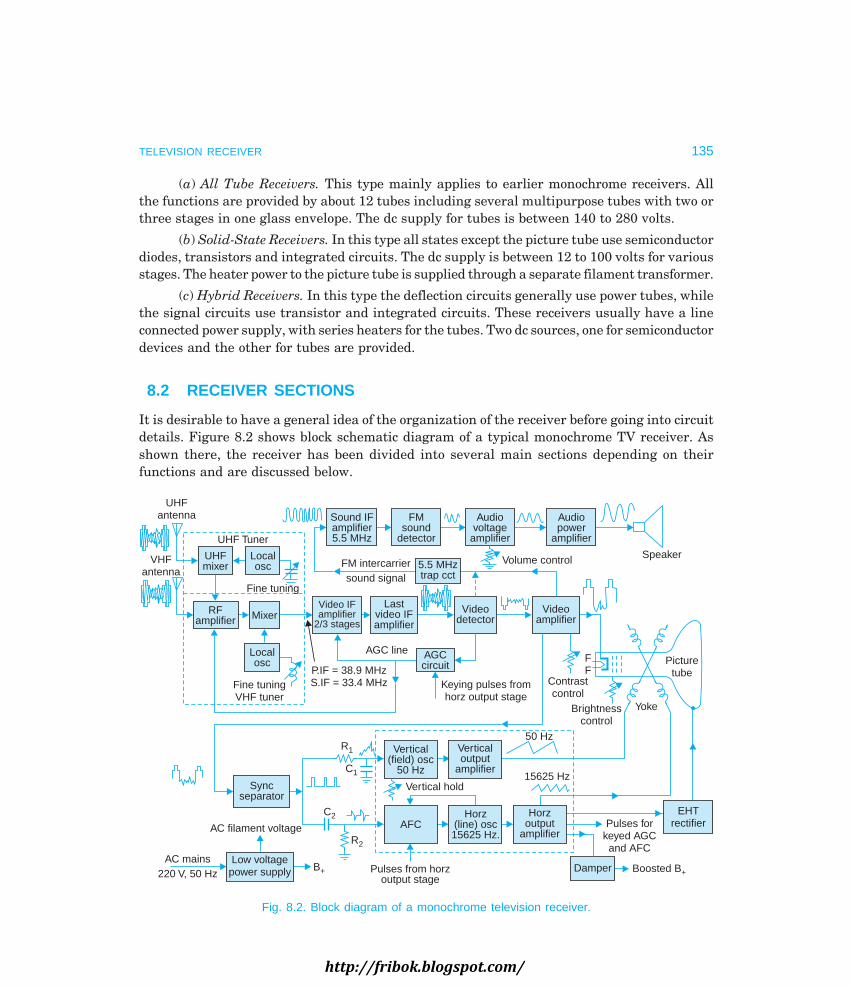
TELEVISION RECEIVER 135
(a) All Tube Receivers. This type mainly applies to earlier monochrome receivers. Allthe functions are provided by about 12 tubes including several multipurpose tubes with two orthree stages in one glass envelope. The dc supply for tubes is between 140 to 280 volts.
(b) Solid-State Receivers. In this type all states except the picture tube use semiconductordiodes, transistors and integrated circuits. The dc supply is between 12 to 100 volts for variousstages. The heater power to the picture tube is supplied through a separate filament transformer.
(c) Hybrid Receivers. In this type the deflection circuits generally use power tubes, whilethe signal circuits use transistor and integrated circuits. These receivers usually have a lineconnected power supply, with series heaters for the tubes. Two dc sources, one for semiconductordevices and the other for tubes are provided.
8.2 RECEIVER SECTIONS
It is desirable to have a general idea of the organization of the receiver before going into circuitdetails. Figure 8.2 shows block schematic diagram of a typical monochrome TV receiver. Asshown there, the receiver has been divided into several main sections depending on theirfunctions and are discussed below.
Localosc
UHFmixer
MixerRFamplifier
Videoamplifier
Videodetector
Lastvideo IFamplifier
Video IFamplifier
2/3 stages
Fine tuning
UHF Tuner
UHFantenna
VHFantenna
Localosc
Fine tuningVHF tuner
P.IF = 38.9 MHzS.IF = 33.4 MHz
AGCcircuit
AGC line
Keying pulses fromhorz output stage
Sound IFamplifier5.5 MHz
FMsound
detector
Audiovoltage
amplifier
Audiopower
amplifier
5.5 MHztrap cct
FM intercarriersound signal
Volume control Speaker
FF
Contrastcontrol
Brightnesscontrol
Yoke
Picturetube
EHTrectifierPulses for
keyed AGCand AFC
Boosted B+Damper
Horz(line) osc15625 Hz.
AFC
Pulses from horzoutput stage
Verticaloutput
amplifier
Vertical(field) osc
50 Hz
Horzoutput
amplifier
50 Hz
15625 HzVertical hold
R2
C2
C1
R1
Syncseparator
Low voltagepower supply
AC filament voltage
B+AC mains
220 V, 50 Hz
Fig. 8.2. Block diagram of a monochrome television receiver.
http://fribok.blogspot.com/

136 MONOCHROME AND COLOUR TELEVISION
Antenna SystemStrongest signal is induced in the antenna if it has same polarization as the transmittingantenna. All TV antennas are mounted in horizontal position for better reception and favourablesignal to noise ratio. The need for good signal strength has led to the use of tuned antennas.For channels located in the VHF band, a half wave-length antenna is most widely used. Suchantennas behave like low ‘Q’ tuned circuits and a single antenna tuned to the middle frequencyof various channels of interest can serve the purpose. Various antennas in use are of dipoletype with reflectors and directors. A folded dipole with a reflector is used because its responseis more uniform over a band of frequencies. A Yagi antenna, i.e., a dipole with one reflector andtwo or more directors, is a compact high gain directional array, and is often used in fringeareas. In areas where signal strength is very low, booster amplifiers with suitable matchingnetwork are used. On the other hand, in areas situated close to a transmitting antenna, wheresignal strength is quite high, various types of indoor antennas are frequently employed.
Since it is not possible for one dipole antenna to cover both upper and lower VHF bandchannels effectively; high and low band dipoles are mounted together and connected to a commontransmission line. For channels in the UHF bound, where the attenuation is very high and thesignals reaching the antenna are weaker, special antennas like fan dipole, rhombic and parabolicreflector type are often used.
A transmission line connects antenna to the receiver input terminals for the RF tuner.A twin-lead is generally used. This type is an unshielded balanced line with characteristicimpedance equal to 300 ohms. When there is a problem of interference, a shielded coaxialcable is used. This cable has high attenuation, especially at UHF channel frequencies. It has acharacteristic impedance of 75 ohms.
The current practice is to design input circuit of the TV receiver for a 300 ohmtransmission line. It has been found that a 300 ohm transmission line used with a half-wavedipole produces a broad frequency response without too large a loss due to mismatching. Afolded dipole has an impedance close to 300 ohms at its resonant frequency, and a much uniformresponse is obtained with this antenna. Receivers designed to receive UHF channels have twoinputs; one to match a 300 ohm transmission line and the other for a 75 ohm coaxial cable. Asignal strength of the order of 500 µV to 1 mV and a signal to noise ratio of 30 : 1 are consideredadequate for satisfactory reception of both picture details and sound output.
RF SectionThis section consists of RF amplifier, mixer and local oscillator and is normally mounted on aseparate sub-chassis, called the ‘Front End’ or ‘RF Tuner’. Either tubes or transistors can beused. With tubes, local oscillator and mixer functions are usually combined in one stage calledthe ‘frequency converter’. The purpose of the tuner unit is to amplify both sound and picturesignals picked up by the antenna and to convert the carrier frequencies and their associatedbands into the intermediate frequencies and their sidebands . The receiver uses superhetrodyneprinciple as used in radio receivers. The signal voltage or inoformation from various stationsmodulated over different carrier frequencies is hetrodyned in the mixer with the output froma local oscillator to transfer original information on a common fixed carrier frequency calledthe intermediate frequency (IF). The setting of the local oscillator frequency enables selectionof desired station. The standard intermediate frequencies for the 625-B system are-PictureIF = 38.9 MHz, Sound IF = 33.4 MHz.
http://fribok.blogspot.com/

TELEVISION RECEIVER 137
In principle an RF amplifier is not necessary and signal could be fed directly to thetuned input circuit of the mixer. However, the problems of a relatively weak input signal withlow signal to noise ratio, local oscillator radiation and image rejection are such, that a stage ofamplification ahead of the mixer is desirable. The tuning for different channels is carried outwith a channel selector switch which changes resonant frequencies of the associated tunedcircuits by varying either inductance or capacitance of these circuits. The RF section is shownseparately in Fig. 8.3 (a), where the channel selector switch has been set for channel 4 (Band I),
Finetuning
Localosc
101.15 MHz
Sound IF = 33.4 MHz
Picture IF38.9 MHz
IF outRF
amplifier Mixer
VHF tuner
(Ganged)Channel selector
switch
Fig. 8.3 (a). Block diagram of a VHF tuner. Selector switchset for channel 4 band I (61-68 MHz).
Fig. 8.3 (b). Ideal response curve of the RF amplifier when set for channel 4.
i.e., 61 to 68 MHz. The picture carrier frequency in this channel is 62.25 MHz and the soundcarrier 67.75 MHz. The RF amplifier must have sufficient bandwidth to accept both the pictureand sound signals. This is illustrated in Fig. 8.3 (b). The local oscillator frequency is set at101.15 MHz. In the mixer, both sum and difference (sideband) frequencies are generated. Theoutput circuit of the mixer is however, tuned to deliver difference frequencies i.e., theintermediate frequencies and their sidebands. The required IFs are then produced as here:(Local oscillator frequency of 101.15 MHz)–(Picture carrier frequency of 62.25 MHz) = PictureIF of 38.9 MHz, (Local oscillator frequency of 101.15 MHz)–(Sound carrier frequency of 67.75MHz) = 33.4 MHz. The desired output response from the mixer is shown in Fig. 8.4. Notice thatfrequency changing process reverses the relative positions of the sound and picture signals.This is obvious, since the oscillator works above the signal frequencies, and ‘difference’frequencies produced, when the picture and sound frequencies are substracted must give a
http://fribok.blogspot.com/

138 MONOCHROME AND COLOUR TELEVISION
higher IF from the lower frequency picture signal. It may be noted that picture and soundsignals would remain in the same relative position, i.e., with sound carreir frequency higherthan picture carrier frequency if local oscillator frequency is set below, instead of above thecarriers. The local oscillator frequency is kept higher because of ease of oscillator design andseveral other merits. The ratio of highest to lowest radio frequency that the local oscillatormust generate, when the oscillator frequency is chosen to be higher than the incoming carrierfrequency, is much less than when the local oscillator frequency is kept below the incomingchannel frequency. It is much easier to design an oscillator that maintains almost a constantoutput amplitude and a sinusoidal waveshape when its overall frequency range is less. Thisjustifies the choice of higher local oscillator frequency.
Fig. 8.4. Location of sound and picture IF frequencies at the output of mixer.
The tuning of RF and oscillator tuned circuits is pre-set for switching in different channels.Despite the fact that modern tuner units are remarkably stable, most receiver manufacturersprovide a fine tuning control for small adjustments of local oscillator frequencies. The controlis varied to obtain best picture results on the screen.
IF Amplifier Section
A short length of coaxial cable feeds tuner output to the first IF amplifier. This section is alsocalled video IF amplifier since composite video signal is the envelope of the modulated pictureIF signal. Practically all the gain and selectivity of the receiver is provided by the IF section.With tubes, 2 or 3 IF stages are used. With transistors, 3 to 4 If stages are needed. In integratedcircuits, one IC chip contains all the IF amplifier stages.
Essential Functions of the IF Section
The main function of this sections is to amplify modulated IF signal over its entire bandwidthwith an input of about 0.5 mV signal from the mixer to deliver about 4 V into the video detector.This needs an overall gain of about 8000. This gain should be adjustable, by automatic gaincontrol, over a wide range to accommodate input signal variations at the antenna from 50 µVto 0.5 V, to deliver about 4 V peak-to-peak signal at the input of the video detector. To achievedesired gain, atleast three stages of tuned amplifiers are cascaded and to obtain desiredbandwidth the resonant frequencies of these stages are staggered. Such an arrangementprovides desired gain and selectivity.
http://fribok.blogspot.com/

TELEVISION RECEIVER 139
8.3 VESTIGIAL SIDEBAND CORRECTION
Another important function assigned to IF section is to equalize the amplitudes of side-bandcomponents, because of vestigial sideband transmission. The need for this was fully explainedin Chapter 4, and a reference to Fig. 4.8 will show, that for vestigial side-band correction thepicture carrier frequency gain must be 6 db down on the IF frequency response curve. It is alsonecessary to shape the IF response curve around the picture IF frequency in such a way thatall lower video frequencies, which got a boost on account of partial lower side-band transmission(besides the full upper side band), are duly attenuated and get restored to their actual level.This is achieved by suitable tuning and shaping the response of the IF stages. This is fullyillustrated in Fig. 8.5, which shows ideal overall response of the IF section.
Unwanted strongadjacent channel beatsignal 94.15–53.75= 40.4 MHz
f(MHz)4140393837363534333231
Trap circuitTrap circuit
– 40
– 36
– 30
– 26– 24
– 18
– 12
– 6
0
db
Vestigialsidebandcorrection
Higher adjacentchannel–4f = 62.25 MHzcP
f = 67.75 MHzcS
Required channel-3(Band I)(54–61 MHz)f = 55.25 MHzcP
f = 60.75 MHzLocal osc frequency = 94.15 MhzcS
Lower adjacentchannel–2f = 48.25 MHzcP
f = 53.75 MHzcS
100%
50%
Sound signalattenuation
Rel
ativ
e ga
in
5%
Sound IF33.4 MHz
Picture IF38.9 MHz
Unwanted strongadjacent channel
beat signal94.15–62.25= 31.9 MHz
Fig. 8.5. Overall picture IF response curve of a receiver tuned to channel 3-(Band I).The diagram shows disposition of IF frequencies, vestigial sideband correction,
sound signal attenuation and locations of unwanted adjacent channelinterfering beat frequencies.
In the IF amplifier circuitry, provision must be made for rejection of signals from adjacentchannels. For this purpose special tuned circuits, called trap circuits, are connected in thesignal path in such a way that the offending frequencies are removed. These trap circuits aredisposed at convenient places in the IF amplifiers. Their position will vary from receiver toreceiver, but generally they are placed in the input circuit of the first IF amplifier. The way inwhich these unwanted adjacent channel IF signals appear is illustrated in Fig. 8.5. As anexample, suppose that the receiver is switched to channel 3 on Band I. The local oscillator
http://fribok.blogspot.com/
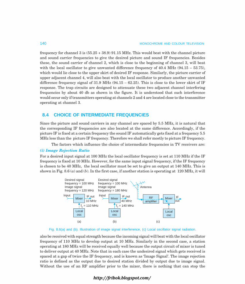
140 MONOCHROME AND COLOUR TELEVISION
frequency for channel 3 is (55.25 + 38.9) 91.15 MHz. This would beat with the channel pictureand sound carrier frequencies to give the desired picture and sound IF frequencies. Besidesthese, the sound carrier of channel 2, which is close to the beginning of channel 3, will beatwith the local oscillator to give unwanted difference frequency of 40.4 MHz (94.15 – 53.75),which would lie close to the upper skirt of desired IF response. Similarly, the picture carrier ofupper adjacent channel 4, will also beat with the local oscillator to produce another unwanteddifference frequency signal of 31.9 MHz (94.15 – 62.25). This is close to the lower skirt of IFresponse. The trap circuits are designed to attenuate these two adjacent channel interferingfrequencies by about 40 db as shown in the figure. It is understood that such interferencewould occur only if transmitters operating at channels 2 and 4 are located close to the transmitteroperating at channel 3.
8.4 CHOICE OF INTERMEDIATE FREQUENCIES
Since the picture and sound carriers in any channel are spaced by 5.5 MHz, it is natural thatthe corresponding IF frequencies are also located at the same difference. Accordingly, if thepicture IF is fixed at a certain frequency the sound IF automatically gets fixed at a frequency 5.5MHz less than the picture IF frequency. Therefore we shall refer mostly to picture IF frequency.
The factors which influence the choice of intermediate frequencies in TV receivers are:
(i) Image Rejection RatioFor a desired input signal at 100 MHz the local oscillator frequency is set at 110 MHz if the IFfrequency is fixed at 10 MHz. However, for the same input signal frequency, if the IF frequencyis chosen to be 40 MHz, the local oscillator must be set to give an output at 140 MHz. This isshown in Fig. 8.6 (a) and (b). In the first case, if another station is operating at 120 MHz, it will
Mixer
Localosc
(a)
Input IF out
10 MHz
f = 110 MHzc
Mixer
Localosc
(b)
Input IF out
40 MHz
f = 140 MHzc
Desired signalfrequency = 100 MHzImage signalfrequency = 120 MHz
Desired signalfrequency = 100 MHzImage signalfrequency = 180 MHz
(c)
Antenna
RFamplifier
Mixer IFout
Localosc
Fig. 8.6(a) and (b). Illustration of image signal interference, (c) Local oscillator signal radiation.
also be received with equal strength because the incoming signal will beat with the local oscillatorfrequency of 110 MHz to develop output at 10 MHz. Similarly in the second case, a stationoperating at 180 MHz will be received equally well because the output circuit of mixer is tunedto deliver output at 40 MHz. Note that in each case the undesired signal which gets received isspaced at a gap of twice the IF frequency, and is known as ‘Image Signal’. The image rejectionratio is defined as the output due to desired station divided by output due to image signal.Without the use of an RF amplifier prior to the mixer, there is nothing that can stop the
http://fribok.blogspot.com/

TELEVISION RECEIVER 141
reception of image signal if that is present. With RF amplifier the output due to image signalcan be very much reduced or completely eliminated. With lower IF frequency, say 10 MHz, theimage frequency at 120 MHz is not very far away from desired frequency of 100 MHz andmight pass through the pass-band of RF amplifier through somewhat attenuated. But if the IFfrequency is kept high, as shown in Fig. 8.6 (b), image signal frequency is 80 MHz away fromthe desired signal and has no chance of passing through the RF amplifier. Thus the use of RFamplifier helps in reducing interference due to image signals and a higher IF frequency resultsin a very high image rejection ratio.
By choosing an IF greater than half the entire band to be covered it is possible to eliminateimage interference. For the lower VHF band (41 to 68 MHz) the IF frequency comes to 13 MHz.In the upper VHF band (174 to 230 MHz) desired IF frequency is 28 MHz. In the UHF band(470 to 528 MHz), where the image problem is most serious, half of the difference of entireband results in the choice of an IF frequency of 56 MHz. But this is higher than the lowestfrequency used in the lower VHF band and because of direct pick-up problems in that band, itcannot be used. Therefore, the IF frequency must be less than 41 MHz.
(ii) Pick-up Due to Local Oscillator Radiation from TV ReceiversIf the output from the local oscillator of a TV receiver gets coupled to the antenna, it will getradiated and may cause interference in another receiver. This is shown in Fig. 8.6 (c). Hereagain advantage lies with higher IF frequency, because with higher IF there is a greaterseparation between the resonant circuits of local oscillator and RF amplifier circuits. Thuslesser signal is coupled from the local oscillator through the RF amplifier to the antenna circuitand interference due to local oscillator radiation is reduced.
(iii) Ease of Separation of Modulating Signal fromIF Carrier at the Demodulator
For ease of filtering out the IF carrier freuency, it is desirable to have a much higher IF frequencyas compared to the highest modulating frequency. In radio receivers the IF frequency is 455KHz and the highest audio frequency is only 5 KHz. In TV receivers, with the highest modulatingfrequency of 5 MHz, an IF frequency of atleast 40 MHz is desirable.
(iv) Image Frequencies Should Not Lie in the FM BandThe FM band is from 88 MHz to 110 MHz. With IF frequency chosen close to 40 MHz, theimage frequencies of the lower VHF band fall between 121 to 148 MHz and thus cannot causeany interference in the FM band. Higher TV channels are much above the FM band.
(v) Interference or Direct Pick-Up from Bands Assigned for other ServicesAmateur and industrial applications frequency band lies between 21 to 27 MHz. If the IFfrequency is chosen above 40 MHz, even the second harmonics of this band will not cause anyserious direct pick-up problems.
(vi) GainIt is easier to build amplifiers with large gain at relatively low frequencies. The TV setsmanufactured some 30 years back used IF frequency as low as 12 MHz. This was mostly due tolimitations of active devices available, and the poor quality of components marketed at thattime. With the rapid strides made by electronics industry during the past three decades, activedevices which can perform very well at high frequencies are now easily available. The quality
http://fribok.blogspot.com/

142 MONOCHROME AND COLOUR TELEVISION
of components and other techniques have also considerably improved. Thus the gain criteria isno longer a constraint in choosing higher IF frequencies. The merits of having high IF frequencyare thus obvious and this has lead to the choice of IF frequencies close of 40 MHz. In the 625-B system adopted by India and several other countries the recommended IF frequencies are :Picture IF = 38.9 MHz, Sound IF = 33.4 MHz. It will be of interest to note that sets manufacturedin USA have picture IF = 45.75 MHz and sound IF = 41.25 MHz. In the British 625 line system,because of channel bandwidth difference, the picture IF = 39.5 MHz and sound IF = 33.5 MHz.
Video Detector. Modulated IF signals after due amplification in the IF section are fed tothe video detector. The detector is designed to recover composite video signal and to transformthe sound signal to another lower carrier frequency. This is done by rectifying the input signaland filtering out unwanted frequency components. A diode is used, which is suitably polarizedto rectify either positive or negative peaks of the input signal. Figure 8.7 shows a simplifiedcircuit arrangement of a video detector. Note the use of an L-C filter instead of the usual RCconfiguration employed in ratio receiver detectors. This is to avoid undue attenuation of thevideo signal while filtering out carrier components. The video signal shown in Fig. 8.7 is ofcorrect polarity for feeding to the cathode of picture tube after one stage of video amplification.
Fig. 8.7. (a) Last IF amplifier output (modulated IF signal)(b) Video detector and sound signal separation circuit.
Video Amplifier. The picture tube needs video signal with peak-to-peak amplitude of 80to 100 volts for producing picture with good contrast. With an input of about 2 volts from thedetector, the video amplifier is designed to have a gain that varies between 40 to 60. A contrastcontrol which essentially is gain control of the video amplifier is provided on the front panel ofthe receiver to adjust contrast between black and white parts of the picture. A large constrastmakes the picture hard, whereas too low a value leaves it weak or soft.
The video amplifier is dc coupled from the video detector to the picture tube, in order topreserve the dc component for correct brightness. However, in some video amplifier designs,on account of complexities of a direct coupled amplifier, ac coupling is instead used. The dccomponent of the video signal is restored by a diode clamper before feeding it to cathode or gridof the picture tube. In video amplifiers that employ tubes, one stage is enough to provide thedesired gain. In transistor amplifier designs, a suitable configuration of two transistors and adriver often becomes necessary to obtain the same gain.
http://fribok.blogspot.com/

TELEVISION RECEIVER 143
Besides gain, response of the amplifier should ideally be flat from dc (zero) to 5 MHz toinclude all essential video components. This needs rigorous design considerations because theband of frequencies to be covered extends from dc through audio range to radio frequencies. Aloss in gain of high frequency components in the video signal would reduce sharpness of thepicture whereas a poor low frequency response will result in loss of boundary details of lettersetc. It is also essential that phase distortion in the amplifer is kept to a minimum. Excessivephase distortion at low frequencies results in smear effect over picture details. Thus the videoamplifier of a television receiver needs careful design to achieve desired characteristics. Variouswide-banding techniques are employed to extend bandwidth of the amplifier.
8.5 PICTURE TUBE CIRCUITRY AND CONTROLS
The output from the video amplifier may be fed either at the cathode or control grid of thepicture tube. In either case a particular polarity of the video signal is essential for correctreproduction of picture details. In most cases cathode drive is preferred. The grid is thus leftfree to receive retrace blanking pulses to ensure that no retrace lines are seen on the screen forany setting of the brightness control. Figure 8.8 shows the passage of video signal from videodetector to the picture tube.
Videoamplifier
Brightnesscontrol
Contrastcontrol
B+
EHT
V 80 V P – P
Amplified videosignal
Compositevideo signal
vin
ModulatedIF signal
Videodetector
Fig. 8.8. Passage of video signal from detector to picture tube.
8.6 SOUND SIGNAL SEPARATION
The picture and sound signals on their respective carriers are amplified together in the IFsection. On application of the two signals to the video detector, the picture IF (38.9 MHz) actsas the carrier and beats with the sound carrier (33.4 MHz) and its associated FM side-bandfrequencies, to produce difference i.e., 5.5 MHz ± 50 KHz components.This is called inter-carrier beat signal and is in effect the second conversion of sound carrier frequency. The resultantproduct, however, retains its original FM modulation.
If amplitude variations in the FM modulated difference signal of 5.5 MHz is to be avoidedto suppress audio signal distortion, the amplitude of sound IF carrier (33.4 MHz) togetherwith its side bands must be attenuated by about 20 db below the picture IF carrier level. Thisis achieved by shaping the lower skirt of the IF section response in such a way that the soundIF lies at — 26 db (5 per cent of the maximum) on the voltage gain axis of the IF response. This
http://fribok.blogspot.com/

144 MONOCHROME AND COLOUR TELEVISION
is clearly shown in Fig. 8.5, where a small pedestal has been created at 33.4 MHz to achievethe desired objective. Note that any drift in the local oscillator frequency has no effect on theinter-carrier sound beat frequencies. This is so, because any shift in the local oscillator frequency,shifts both the picture and sound IFs by the same amount. The video detector circuit is modified(see Fig. 8.7) by providing a resonant trap circuit to isolate the sound signal. In some receiversthe inter-carrier sound signal is separated after one stage of amplification in the video amplifier.
8.7 SOUND SECTION
As shown in the receiver block diagram (Fig. 8.2), the relatively weak FM sound signal, now ona carrier frequency of 5.5 MHz is given at least one stage of amplification before feeding it tothe FM detector. This stage is a tuned amplifier, with enough bandwidth to pass the FM soundsignal. This tuned amplifier is known as sound IF. The FM detector is normally a ratio detectoror a discriminator preceded by a limiter. The characteristics of a typical FM detector are shownin Fig. 8.9. As shown, the audio output is proportional to deviations from the carrier frequency.The frequency of audio signal depends on the rate of frequency deviation. At the output of FMdetector, a de-emphasis circuit is provided that has the same time constant (50 µs) as that ofthe pre-emphasis circuit employed at the sound transmitter. This restores the amplitude ofhigher audio frequencies to their correct level. The audio signal receives atleast one stage ofamplification before it is passed on to the audio output (power) amplifier. The volume and tonecontrols form part of the audio amplifiers. These are brought out at the front panel of thereceiver. The power amplifier is either a single ended or push-pull configuration employingtubes or transistors. Special ICs have been developed which contain FM demodulator andmost parts of the audio amplifier. These are fast replacing discrete circuits hitherto used inthe sound section of the receiver. The audio amplifier feeds into one or two loudspeakers providedat a convenient location along front panel of the receiver.
Fig. 8.9. Response curve of an FM detector.
Automatic Gain Control (AGC)AGC circuit controls gain of RF and IF stages to deliver almost constant signal voltage to thevideo detector, despite changes in the signal picked up by the antenna. The change in gain is
http://fribok.blogspot.com/

TELEVISION RECEIVER 145
achieved by shifting the operating point of the amplifying devices (tubes or transistors) used inthe amplifiers. The operating point is changed by a bias voltage that is developed in the AGCcircuit. Any shift in the operating point changes gm (mutual conductance) of the tube or powergain of the transistor circuit which in turn results in change of stage gain.
Sync level in the composite video signal is fixed irrespective of the picture signal details.Hence, sync pulse tops represent truly the signal strength. A peak rectifier is used to developa control voltage which is proportional to the sync level. The composite video signal to the peakrectifier in the AGC circuit is either obtained from the output of video detector or after onestage of video amplification. The output is filtered and the dc voltage thus obtained is fed tothe input (bias) circuits of the RF and IF amplifiers to control their gain. Decoupling circuitsare used to avoid interaction between different amplifier stages. AGC is normally not appliedto the last IF stage because at that level the signal strength is quite large and any shift in theinitially chosen operating point can cause distortion because of partial operation on the non-linear portion of the device characteristics.
Since AGC voltage is proportional to the signal strength, even weak RF signals will alsodevelop some control voltage. This when applied to the RF amplifier will tend to reduce itsgain, though the stage should provide maximum possible gain for weak signals to maintainhigh signal to noise ratio. Therefore, the RF amplifier is not fed any AGC voltage till the signalstrength attains a certain predetermined level. This is achieved by providing a voltage delaycircuit in the AGC line. Such a provision is known as delayed AGC. The AGC control, as explainedabove is illustrated in Fig. 8.10 by a block schematic circuit arrangement.
PeakAGC
rectifier
Rectifiedoutput
Composite videosignal (input)
To IF amplifiers
Decouplingnetwork
AGC biasline
C1 AGCfilter
RL
R1
0v0
R2 C2
To RFamplifier
R3
C3
AGCdelaycircuit
Fig. 8.10. Block diagram of AGC system.
Sync SeparationThe horizontal and vertical sync pulses that form part of the composite video signal are separatedin the sync separator. The composite video signal is either taken from the video detector outputor after one stage of video amplification. A sync separator is a clipper that is suitably biased toproduce output, only during sync pulse amplitude of the video signal. In some receivers, anoise gate preceds the sync separator. This suppresses strong noise pulses if present in thevideo signal. A sync pulse train as obtained from a sync separator is shown in Fig. 3.5.
http://fribok.blogspot.com/

146 MONOCHROME AND COLOUR TELEVISION
8.8 SYNC PROCESSING AND AFC CIRCUIT
The pulse train as obtained from the sync separator is fed simultaneously to a differentiatingand an integrating circuit. The differentiated output (see Fig. 3.5) provides sharp pulses fortriggering the horizontal oscillator, while output from the integrator controls the frequency ofthe vertical oscillator. As explained in Chapter 3, pre and post equalizing pulses ensure identicalvertical sync pulses both after the first and second fields.
An integrating circuit is a low-pass filter and hence sharp noise pulses do not appear atits output. However, the differentitator, being a high-pass filter, develops output in responseto noise pulses in addition to the spiked horizontal sync pulses. This results in occasionalwrong triggering of the horizontal oscillator which results in diagonal tearing of the reproducedpicture. To overcome this difficulty, a special circuit known as automatic frequency control(AFC) circuit (Fig. 8.11) is employed. The AFC circuit employs a discriminator arrangementwhich compares the incoming horizontal sync pulses and the voltage that develops across theoutput of the horizontal deflection amplifier. The AFC output is a dc control voltage that is freeof noise pulses. This control voltage is used to synchronize the horizontal oscillator with thereceived horizontal sync pulses.
Syncdiscriminator
D.C.controlvoltage
R
CFilter
Horz fly back pulsesfrom H.O.T.
Syncvoltage
Fig. 8.11. Block diagram of AFC circuit.
8.9 VERTICAL DEFLECTION CIRCUIT
Blocking oscillators or cathode coupled multivibrators are normally employed as verticaldeflection oscillators. The controlling time constants are suitably chosen to develop outputcorresponding to trace and retrace periods. The necessary sawtooth voltage is developed bycharging and discharging a capacitor with different time constants. This capacitor forms partof the waveshaping circuit which is connected across the oscillator.
The frequency of the oscillator is controlled by varying the resistance of the RC couplingnetwork and is locked in synchronizm by the vertical sync pulses. A part of the coupling networkresistance is a potentiometer that is located on the fornt panel of the reciver. This is known as‘Vertical Hold Control’ (see Fig. 8.2) and enables resetting of the vertical oscillator frequencywhen it drifts far away from 50 Hz.
The output from the oscillator-cum-waveshaping circuit if fed to a power amplifier, theoutput of which is coupled to the vertical deflection coils to produce vertical deflection of thebeam on picture tube screen.
http://fribok.blogspot.com/

TELEVISION RECEIVER 147
8.10 HORIZONTAL DEFLECTION CIRCUIT
The horizontal oscillator (see Fig. 8.2) is similar to the vertical oscillator and is set to developsweep drive voltage at 15625 Hz. However, the frequency of this oscillator is controlled by dccontrol voltage developed by the AFC circuit. Since the noise pulses in the control voltage arecompletely suppressed, most receivers do not provide any horizontal frequency (hold) control,as is normally done for the vertical oscillator. The oscillator output is waveshaped to producelinear rise of current in the horizontal deflection coils. Since the deflection coils need about oneamp of current to sweep the entire raster, the output of the oscillator is given one stage ofpower amplification (as for vertical deflection) and then fed to the horizontal deflection coils.
Low Voltage Power SupplyThe usual B + or low voltage power supply is obtained by rectifying and filtering the ac mainssupply. If necssary the mains voltage is stepped up or down before rectification. Silicon diodesare normally used for rectification. In some power supply designs, which do not employ amains transformer, voltage doubler circuits are used to raise the dc voltage. For circuits thatemploy transistors and integrated circuits, regulated low voltage power supplies are normallyprovided. While branching the dc supply to various sections of the receiver, decoupling networksare used to avoid any undue coupling between different sections of the receiver. The filamentpower is supplied by either connecting all the heaters in series across the ac mains or by a lowvoltage winding on the mains transformer.
High Voltage (EHT) SupplyAs already stated in the chapter on picture tubes, an anode voltage of the order of 15 kV isneeded for sufficient brightness in black and white picture tubes. This is known as HV or EHT(extra high tension) supply.
From horzosc
Horzdeflectionamplifier
High voltage rectifier
EHT(15–18 kV)
HV winding
To horzdeflection coils
Boosted Bsupply
+
Fig. 8.12. Basic circuit of E.H.T. supply.
http://fribok.blogspot.com/

148 MONOCHROME AND COLOUR TELEVISION
To obtain such a high voltage by stepping up the mains voltage with a transformer isalmost impossible and prohibitive in cost. A novel method used for obtaining EHT source isillustrated in Fig. 8.12. During retrace intervals of horizontal scanning, high voltage pulses ofamplitude between 6 to 9 kV are developed across the primary winding of the horizontal ouptuttransformer. As shown in the figure these are stepped up by an autotransformer winding toabout 10 to 15 kV and then fed to a high voltage rectifier. The output of the rectifier is filteredto provide required dc voltage.
Such an arrangement does not load very much the horizontal output stage because thecurrent demand from this high voltage source is less than 1 mA.
The horizontal output circuit is so designed, that in addition to providing EHT source,the energy stored in the horizontal deflection coils during retrace is tapped through a diodecalled damper diode to charge a capacitor. The voltage thus developed across the capacitor,actually adds 200 to 300 volts to normal B + voltage to give a boosted B + supply of 400 to 700volts. This voltage is also suitable for first and second anodes of the picture tube. Thisarrangement makes the horizontal deflection circuit very efficient.
Review Questions
1. Draw block diagram of an RF Tuner (Front End) and explain how incoming signals from differentstations are translated to common picture IF and sound IF frequencies. Illustrate your answerby choosing carrier frequencies of any channel in the VHF band.
2. What do you understand by image rejection ratio ? Explain how by providing an RF amplifier,image signal reception is greatly minimized. What are the other merits of using an RF amplifierbefore the frequency converter ?
3. Describe briefly the factors that influenced the choice of picture IF = 38.9 MHz and sound IF =33.4 MHz in the 625-B monochrome television system.
4. What are the essential functions which are assigned to IF section of the receiver ? Show bysketching output voltage verses frequency response of the IF section, how vestigial sidebandcorrection is carried out. Why is the sound signal amplitude attenuated to about 5 per cent of themaximum output voltage ?
5. Explain how composite video signal is detected ? How is the polarity of the video output signaldecided ? Why is it dependent on the number of video amplifier stages ?
6. What do you understand by intercarrier sound system ? Explain why any shift in the local oscillatorfreuency does not effect the frequency of the intercarrier beat signal. Where and how is theintercarrier sound signal separated from the video signal ?
7. Draw a block diagram of the sound channel in a TV receiver. Explain briefly how the inter-carrier sound signal as obtained at the video detector, is processed to produce sound output. Whyis a de-emphasis circuit provided after the FM detector ?
8. Explain briefly how sync pulses are separated from the composite video signal and processed tosynchronize the vertical and horizontal oscillators.
9. Describe briefly how EHT and boosted B + voltages are developed from the horizontal outputcircuit of the sweep amplifier.
10. Draw block diagram of a monochrome TV receiver and label its various sections Indicate bywaveshapes the nature of signal at the input and output of each block of the receiver.
http://fribok.blogspot.com/

9
"
http://fribok.blogspot.com/

9.1 RADIO WAVE PROPAGATION
Radio waves are electromagnetic waves, which when radiated from transmitting antennas,travel through space to distant places, where they are picked up by receiving antennas. Althoughspace is the medium through which electromagnetic waves are propagated, but depending ontheir wavelengths, there are three distinctive methods by which propagation takes place. Theseare: (a) ground wave or surface wave propagation, (b) sky wave propagation, and (c) spacewave propagation.
(a) Ground Wave PropagationVertically polarized electromagnetic waves radiated at zero or small angles with ground, areguided by the conducting surface of the ground, along which they are propagated. Such wavesare called ground or surface waves. The attenuation of ground waves, as they travel along thesurface of the earth is proportional to frequency, and is reasonably low below 1500 kHz.Therefore, all medium wave broadcasts and longwave telegraph and telephone communicationis carried out by ground wave propagation.
(b) Sky Wave PropagationGround wave propagation, above about 1600 kHz does not serve any useful purpose as thesignal gets very much attenuated within a short distance of its transmission. Therefore, mostradio communication in short wave bands up to 30 MHz (11 metres) is carried out by skywaves. When such waves are transmitted high up in the sky, they travel in a straight line untilthe ionosphere is reached. This region which begins about ‘120 km above the surface of theearth, contains large concentrations of charged gaseous ions, free electrons and neutralmolecules. The ions and free electrons tend to bend all passing electromagnetic waves. Theangle by which the wave deviates from its straight path depends on (i) frequency of the radiowave (ii) angle of incidence at which the wave enters the ionosphere (iii) density of the chargedparticles in the ionosphere at the particular moment and (iv) thickness of the ionosphere atthe point. Figure 9.1 illustrates the path of several waves entering the ionosphere at differentincident angles. With increase in frequency, the allowable incident angle at the ionospherebecomes smaller until finally a frequency is reached, when it becomes impossible to deflect thebeam back to earth. For ordinary ionospheric conditions this frequency occurs at about 35 to40 MHz. Above this frequency, the sky waves cannot be used for radio communication betweendistant points on the earth. This is why no frequencies beyond about 30 MHz (11 metres) areallotted for radio communication.
150
#
"
http://fribok.blogspot.com/

TELEVISION SIGNAL PROPAGATION AND ANTENNAS 151
Fig. 9.1. Ray paths for different angles of incidence (φ) at the ionosphere.
(c) Space Wave PropagationAs explained above, propagation of radio waves above about 40 MHz (which is the beginning oftelevision transmission band) is not possible through either surface or sky wave propagation.Thus, the only alternative for transmission in the VHF and UHF bands, despite largeattenuation, is by radio waves which travel in a straight line from transmitter to receiver. Thisis known as space wave propagation. Its maximum range, because of the nature of propagation,is limited to the line of sight distance between the transmitter and receiver.
For not too large distances, the surface of the earth can be assumed to be flat and differentrays of wave propagation can reach the receiver from transmitter as shown in Fig. 9.2(a). Asseen there, ht and hr, are the heights of transmitting and receiving antennas respectively, andd is the distance that separates them from each other. Both the direct wave AB and reflectedwave ACB contribute to the field strength at the receiving antenna. Assuming the earth’ssurface to be perfectly reflecting, the total field strength E, due to both direct and reflectedwaves, for reasonably large value of d can be expressed as:
E* = 4
2
πfh h
dt r E0
htht
dd
hrhr
A
B
Transmitting antenna(T)
Receiving antenna(R)Direct wave
Reflectedwave
CGround surface
TR
Earth RE
hrhr
htht
RRRR
Line o s ght d s a ce d
Line of sight distance d
Fig. 9.2(a). Space wave propagation. For the Fig. 9.2(b). Computation of line-of-sightsake of clarity, the antenna heights have been distance. The height of antennas has been
greatly exaggerated in comparison with the greatly exaggerated in comparison withdistance between them. R, the radius of earth.
*E = 2 20E
dfh hd
t rsinπ
but when d is large, as is often the case, the sine of the angle can be
replaced by the angle and thus the above expression becomes
E = 4
2πfh h
dt r E0
http://fribok.blogspot.com/

152 MONOCHROME AND COLOUR TELEVISION
where E0 is the field strength at unit distance from the transmitter, and f is the frequency ofthe transmitted signal. The field strength varies inversely as tbe square of the distance betweenthe two antennas but is directly proportional to their heights.
Various Aspects of Space Wave Propagation(i) Effect of Earth’s Curvature. Earth’s curvature limits the maximum distance between
the transmitting and receiving antennas. This is depicted in Fig. 9.2(b). The maximum line ofsight distance d between the two antennas can be easily found out. Neglecting (hr)
2 and (ht)2,
being very small as compared to R, the radius of the earth, the line-of-sight distance d ≈
4.22( ht + hr ) km.
where ht and hr are expressed in metres. In reality etectromagnetic waves are bent slightly asthey glide along the surface of the earth and this increases the line-of sight distance by a smallamount. It is evident that the ground coverage will increase with increase in height of bothtransmitting and receiving antennas. It is due to this reason that television transmitting andreceiving antennas are placed as high as possible, for example atop tall buildings and on highplateaus. Another advantage is that the local noise disturbance pick-up is reduced by placingthe antennas at high altitudes.
(ii) Effect of Atmospherics. The presence of gas molecules and water vapour affects thedielectric constant and hence the refractive index of the atmosphere. As a result, the spacewaves are differently refracted or reflected under varying conditions of atmosphere. This undercertain conditions enables the propagation to reach points very much beyond the line of sight.Similarly under adverse weather conditions the signal attenuation increases, thereby reducingeffective distance of transmission.
Occasionally the concentration of charged particles in the ionosphere increases sharplyand it becomes possible for waves up to 60 MHz to return to earth. Though this enhances therange of sky wave propagation, but the exact time and place of occurrence of such phenomenacannot be predicted Thus this phenomenon has little value for commercial operation, but doesexplain to some extent the distant reception of high frequency and TV signals, which occurs attimes under unusual conditions.
(iii) Effect of Obstacles. Tall and massive objects like hills and buildings, will obstructsurface waves, which travel close to ground. Consequently, shadow zones and diffraction willresult. For this reason in some areas antennas higher than those indicated by theoreticalexpressions are needed. On the other hand, some areas receive such signals by reflection only.Again, in some areas strong reflected signals are received besides direct signals. This cancause a form of interference known as ‘ghosting’ on the screen of a television receiver becauseof a phase difference between the two signals.
9.2 TELEVISION SIGNAL TRANSMISSION*
The RF carrier power output of commonly used VHF television transmitters varies from 10 to50 kW. A satisfactory level of signal strength is said to exist when the image produced on the
*Television broadcast channels are given in Appendix C.
http://fribok.blogspot.com/

TELEVISION SIGNAL PROPAGATION AND ANTENNAS 153
screen of the receiver overrides noise by an acceptable margin. Signal strength is a function ofpower radiated, transmitting and receiving antenna heights, and the terrain above which thepropagation occurs. The acceptable signal to noise ratio at the picture tube screen is measuredin terms of peak-to-peak video signal voltage (half tone), injected at the grid or cathode of thepicture tube versus the r.m.s. random noise voltage at that point. A peak signal to r.m.s. noiseratio of 45 db is generally considered adequate to produce a good quality picture.
Field strength is indicated by the amount of signal received by a receiving antenna at aheight of 10 metres from ground level, and is measured in microvolts per metre of antennadipole length. The field strength for very good reception in thickly populated and built-upareas is 2500 µV/ metre for channels 2 to 4 (47 to 68 MHz), and 3550 µV/metre for channels 5to 11 (174 to 223 MHz). For channels in the UHF band, a field strength of about 5000 µV/metrebecomes necessary. This is so because of the lower sensitivity of the receiver for higher channels.
Range of TransmissionA sample calculation shows that for a transmitting antenna height of 225 metres above groundlevel the radio horizon is 60 km. If the receiving antenna height is 16 metres above groundlevel the total distance is increased to 76 km. Greater distance between antennas may beobtained by locating them on top of very tall buildings or hillocks. However, links longer than120 km are hardly ever used for TV transmission because of limitations of radiated power,high channel frequencies and antenna heights. Thus, depending on the transmitter power andother factors the service area may extend up to 120 km for the channels in the VHF band butdrops to about 60 km for UHF channels.
Booster StationsSome areas are either shadowed by mountains or are too far away from the transmitter forsatisfactory television reception. In such cases booster stations can be used. A booster stationmust be located at such a place, where it can receive and rebroadcast the programme to receiversin adjoining areas. Mussoorie (U.P.) is one such booster station. Its receiving and transmittingantennas are located on top of a hill. The station receives Delhi TV station (channel 4)programmes and relays them in channel 10 to the surrounding areas and regions on the otherside of the hills.
9.3 INTERFERENCE SUFFERED BY CARRIER SIGNALS
In addition to thermal and man-made noise, the carrier signal must compete with variousother forms of interfering signals originating from other television stations, radio transmitters,industrial radiating devices and TV receivers. When the interfering signal has a frequencythat lies within the channel to which a TV receiver is tuned, the extent of interference dependsonly on the relative field strengths of the desired signal and the interfering signal. If theinterfering signal frequency spectrum lies outside the desired channel, selectivity of the receiveraids in rejecting the interference.
(a) Co-channel InterferenceTwo stations operating at the same carrier frequency, if located close by, will interfere witheach other. This phenomenon which is common in fringe areas is called co-channel interference.As the two signal strengths in any area almost equidistant from the two co-channel stations
http://fribok.blogspot.com/

154 MONOCHROME AND COLOUR TELEVISION
become equal, a phenomenon known as ‘venetian-blind’ interference occurs. This takes theform of horizontal black and white bars, superimposed on the picture produced by the tunedchannel. These bars tend to move up or down on the screen. As the strength of the interferingsignal increases, the bars become more prominent, until at a signal-to-interference ratio of 45db or so, the interference becomes intolerable. The horizontal bars are a visible indication ofthe beat frequency between the two interfering carriers. Figure 9.3 shows the bar pattern thatappears on the screen. The frequency of the beat note, which is equal to frequency separationbetween the two carriers, is usually of the order of a few hertz. This is so because mosttransmitters operate almost at the correct assigned frequencies. Motion of the bars, upwardsor downwards occurs whenever the beat frequency is not an exact multiple of the field frequency.Co-channel interference was a serious problem in early days of TV transmission, when thechannel allocation was confined to VHF band only. This necessitated the repetition of channelsat distances not too far from each other. Now, when a large number of channels in the UHFband are available such a problem does not exist. The sharing of channel numbers is carefullyplanned so that within the ‘service area’ of any station, signals from the distant stations undernormal conditions of reception are so weak as to be imperceptible. However, during a period ofabnormal reception conditions (often during spring) when the signals from distant VHF stationsare received much more strongly, co-channel interference can occur in fringe areas. The use ofhighly directional antennas is very helpful in etiminating co-channel interference.
Interferingbars
Fig. 9.3. Venetian-blind interference caused by beat frequencybetween picture carriers of co-channels.
(b) Adjacent Channel InterferenceStations located close by and occupying adjacent channels, present a different interferenceproblem. Adjacent channel interference (see Fig. 8.5) may occur as a result of beats betweenany two of these frequencies or between a carrier and any sidebands. A coarse dot structure isproduced on the screen if picture carrier of the desired channel beats with sound carrier of thelower adjacent channel. The beat pattern is more pronounced if the lower adjacent soundcarrier is relatively strong and is not sufftciently attenuated in the receiver.
The next most prominent source of interference is the one produced by picture sidebandcomponents of the upper adjacent channel. The beat frequency between adjacent picture carrieris 7 MHz. Since this is far beyond the video frequency range, the resultant beat pattern is notdiscernible. However, the picture sidebands of the upper adjacent channel may beat with thedesired channel carrier and produce an interfering image. To prevent adjacent channelinterference, several sharply tuned band eliminator filters (trap circuits) are provided in the
http://fribok.blogspot.com/
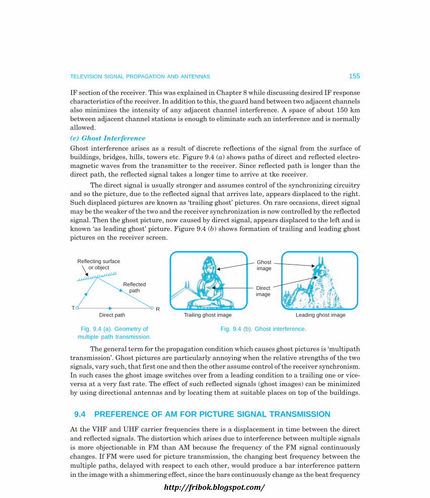
TELEVISION SIGNAL PROPAGATION AND ANTENNAS 155
IF section of the receiver. This was explained in Chapter 8 while discussing desired IF responsecharacteristics of the receiver. In addition to this, the guard band between two adjacent channelsalso minimizes the intensity of any adjacent channel interference. A space of about 150 kmbetween adjacent channel stations is enough to eliminate such an interference and is normallyallowed.
(c) Ghost InterferenceGhost interference arises as a result of discrete reflections of the signal from the surface ofbuildings, bridges, hills, towers etc. Figure 9.4 (a) shows paths of direct and reflected electro-magnetic waves from the transmitter to the receiver. Since reflected path is longer than thedirect path, the reflected signal takes a longer time to arrive at tke receiver.
The direct signal is usually stronger and assumes control of the synchronizing circuitryand so the picture, due to the reflected signal that arrives late, appears displaced to the right.Such displaced pictures are known as ‘trailing ghost’ pictures. On rare occasions, direct signalmay be the weaker of the two and the receiver synchronization is now controlled by the reflectedsignal. Then the ghost picture, now caused by direct signal, appears displaced to the left and isknown ‘as leading ghost’ picture. Figure 9.4 (b) shows formation of trailing and leading ghostpictures on the receiver screen.
Ghostimage
Directimage
Trailing ghost image Leading ghost imageDirect pathR
Reflectedpath
T
Reflecting surfaceor object
Fig. 9.4 (a). Geometry of Fig. 9.4 (b). Ghost interference.multiple path transmission.
The general term for the propagation condition which causes ghost pictures is ‘multipathtransmission’. Ghost pictures are particularly annoying when the relative strengths of the twosignals, vary such, that first one and then the other assume control of the receiver synchronism.In such cases the ghost image switches over from a leading condition to a trailing one or vice-versa at a very fast rate. The effect of such reflected signals (ghost images) can be minimizedby using directional antennas and by locating them at suitable places on top of the buildings.
9.4 PREFERENCE OF AM FOR PICTURE SIGNAL TRANSMISSION
At the VHF and UHF carrier frequencies there is a displacement in time between the directand reflected signals. The distortion which arises due to interference between multiple signalsis more objectionable in FM than AM because fhe frequency of the FM signal continuouslychanges. If FM were used for picture transmission, the changing best frequency between themultiple paths, delayed with respect to each other, would produce a bar interference patternin the image with a shimmering effect, since the bars continuously change as the beat frequency
http://fribok.blogspot.com/

156 MONOCHROME AND COLOUR TELEVISION
changes. Hence, hardly any steady picture is produced. Alternatively if AM were used, themultiple signal paths can atmost produce a ghost image which is steady. In addition to this,circuit complexity and bandwidth requirements are much less in AM than FM. Hence AM ispreferred to FM for broadcasting the picture signal.
9.5 ANTENNAS
In the preceding sections of this chapter, while explaining various methods of propagation, itwas taken for granted that transmitters can somehow transmit and receivers have some meansof receiving what is transmitted. Actually a structure must be provided, both for effectiveradiation of energy at the transmitter and efficient pick up at the receiver. An antenna is sucha structure. It is generally a metallic object, often a rod or wire, that is used to convert high-frequency current into electromagnetic waves, and vice versa. Though their functions aredifferent, transmitting and receiving antennas behave identically.
Radiation MechanismAn antenna may be thought of as a short length of a transmission line. When high frequencyalternating source is applied at its one end, the resulting forward and reverse travelling wavescombine to form a standing wave pattern on the line. However, all the forward energy does notget reflected at the open end, and a small portion escapes from the system and is thus radiated.
The electromagnetic radiation from the transmitting antenna has two components—amagnetic field associated with current in the antenna and an electric fleld associated with thepotential. The two fields are perpendicular to each other in space and both are perpendicularto he direction of propagation of the wave. This is illustrated in Fig. 9.5. An electromagneticwave is horizontally polarized if its electric field is in the horizontal direction. Thus an antennafixed horizontally produces horizontally polarized waves. Similarly a vertical antenna producesvertically polarized waves.
E
z
H
Directionof propagation
x
y
x
z
y
E
H
E-Electric fieldH-Magnetic field
Dipoleantenna
R.F. energy
Fig. 9.5. Transverse electromagnetic wave in free space.
http://fribok.blogspot.com/

TELEVISION SIGNAL PROPAGATION AND ANTENNAS 157
The amount of energy that is radiated in space by a transmission line antenna is however,extremely small, unless the wires of the line are suitably oriented and their lengths madecomparable to the wavelength, If the two wires of the transmission line are opened up, there isless likelihood of cancellation of radiation from the two-wire tips and this improves the efficiencyof radiation. This type of radiator is called a dipole. When total length of the two wires is half-wavelength, the antenna is called a half-wave dipole. Figure 9.6 shows the evolution of suchan antenna from the basic transmission line. As shown there, the antenna is effectively a pieceof quarter-wavelength transmission line bent out and open circuited at the far ends. Such alength has low impedance at the end connected to the main feeder transmission line. This inturn means that a large current will flow at the input of the half-wave dipole and efficientradiation will take place.
/2/2
/2/2
T.line
(a) Transmission line (b) Opened-outtransmission line
(c) Conductorsin line
(d) Half-wavedipole (centrefed)
Fig. 9.6. Evolution of the dipole.
With the help of Maxwell’s equations it is possible to deduce expressions for the energyradiated by an antenna, the direction or directions in which it propagates and the field strengthat any distance from it.* The results show that the field strength depends on the powertransmitted and is inversely proportional to the distance from the radiating source. Thecoefficient of current (I2
rms) in the expression for the radiated power has the dimensions ofresistance and is called radiation resistance. In effect, radiation resistance is the equivalentresistance which dissipates the same amount of power as that radiated from the antennawhen same current flows through them. For a quarter-wave antenna the radiation resistanceis 36.5 ohms, and for a half-wave antenna it is 73 ohms.
Radiation Patterns of Resonant Antennas
A resonant antenna is a transmission line whose length is an exact multiple of wavelengthsand is open at both ends. The current distribution and radiation patterns of such resonantwires of different wavelengths which are remote from the ground are shown in Figs. 9.7 and9.8. As seen there, for a λ/2 dipole the radiation is maximum at right angles to it, and eventuallyfalls to zero in line with the antenna. This may be explained by considering that at right anglesto the short length of the antenna the distance from a remote point to any part of the antennawire is practically the same. Thus reinforcement of radiation will take place in this direction.
*Such analysis is beyond the scope of this book.
http://fribok.blogspot.com/

158 MONOCHROME AND COLOUR TELEVISION
L = /2(a)
l L =(b)
l L = 3(c)
l/2
Fig. 9.7. Current distribution on resonant dipoles.
Dipole
L = /2(a)
l L =(b)
l L = 3(c)
l/2
54° 42°
Fig. 9.8. Radiation patterns (Polar diagrams) of various resonant dipoleslocated remote from ground.
When the distant point lies in a direction other than normal, there will be somecancellation and finally full cancellation will take place at points that are in line with theantenna. Thus the radiation pattern cross section, as presented in Fig. 8.8 (a) is a figure ofeight with its axis at right angles to the dipole. Moreover, exactly the same radiation patternwill exist in any other plane, and so the three-dimensional pattern is the surface of revolutionobtained by rotating the cross section about an axis coinciding with the dipole. For an antennaof length equal to a whole wavelength the polarity of current, (as shown in Fig. 9.7 (b)) on onehalf of the antenna is opposite to that on the other half As a result, the radiation at rightangles from this antenna will be zero because the field due to one half fully cancels the fielddue to the other half of the antenna. The direction of maximum radiation exists at 54° to theantenna. The pattern acquires lobes and there are four such for this antenna. As the length ofthe dipole is increased to three half-wavelengths, the current distribution is changed to that ofFig. 9.7(c) and the radiation pattern takes the shape shown in Fig. 9.8 (c). As the length of theaerial wire is further increased, the number of lobes in the radiation pattern increases, but theangle of largest lobe with the direction of antenna decreases.Nonresonant AntennasA nonresonant antenna (Fig. 9.9(a)) is one which is correctly terminated and as such only aforward travelling wave exists and there are no standing waves. As shown in Fig. 9.9(b) the
Voltage and currentdistribution
Antenna
R (Terminatingresistance)
(a)
LL
Antennawire
Feed
(b)
Fig. 9.9. Nonresonant antenna (a) layout and current distribution(b) typical directional radiation pattern for L = 4λ.
http://fribok.blogspot.com/

TELEVISION SIGNAL PROPAGATION AND ANTENNAS 159
radiation pattern, though similar to the corresponding resonant antenna, is unidirectional. Infact there are half the number of lobes compared to the resonant antenna. This is due toabsence of the reflected wave, which otherwise combines vectorially with the forward wave tocreate the radiation pattern.
Ungrounded AntennasWhen the antenna is very close to the ground, its radiation pattern gets modified on account ofreflections from the ground. If the ground is assumed to be a perfect conductor, a true mirrorimage of the actual antenna is considered to exist below the ground. The overall radiationpattern is then the sum of patterns caused by an array of two nearby antennas. Some typicalradiation patterns for various heights above ground are shown in Fig. 9.10.
(a) Height aboveground = /4
(b) Height aboveground = /2
(c) Height aboveground =
Fig. 9.10. Vertical radiation patterns of an ungrounded half-wave horizontal dipolewith varying heights above the ground surface.
Grounded AntennasWhen one end of the antenna is actually grounded, the image of the antenna behaves as if ithas been joined to the physical antenna and the combination acts as an antenna of double thesize. The current distribution and radiation patterns of different earthed vertical antennas areshown in Fig. 9.11. As shown there, the voltage and current distribution on such a groundedλ/4 antenna, commonly known as the basic Marconi antenna, is the same as those of theungrounded half-wave Hertz antenna. As is obvious Marconi antenna needs half the length ascompared to Hertz antenna to produce the same radiation pattern.
/4/2/2
(a) Current distribution
Antenna
(b) Radiation patterns
Antenna length = /4 Antenna length = /2 Antenna length =
Fig. 9.11. Current distribution and vertical directional patterns of grounded antennas.
Antenna GainAs explained above, all practical antennas concentrate their radiation in some direction, to agreater or lesser extent. Thus the field (power) density in the direction is greater than what it
http://fribok.blogspot.com/

160 MONOCHROME AND COLOUR TELEVISION
would have been if the antenna were omnidirectional. This may be interpreted that the antennahas a gain in a particular direction. The directive gain is thus defined as the ratio of the powerdensity in the direction of maximum radiation to the power density that would be radiated byan isotropic antenna. The gain being a ratio of powers is expressed in decibels.
Antenna ArraysIt is clear from previous discussion that radiation from different types of antennas is not uniformin all directions. Though an antenna can be suitably oriented to get maximum response in anydesired direction, additional directive gain in preferred directions can be obtained by usingmore than one radiator arranged in a specific manner in space. Such arrangements of radiatorsare known as antenna arrays. The simplest type of array consists of two antennas A1 and A2separated by a distance d. A special case of directivity is obtained when d = λ/4 and the currentsin the two antennas have a phase difference of 90° between them. This results in a cardioidshaped directional pattern as shown in Fig. 9.12.
d
A1 A2
d = /4
Fig. 9.12. Cardioid shaped directional pattern formed by parallel half-wave antennas.A1 and A2 are the locations of two antennas with currents 90° out of phase.
A broadside array consists of a number of identical radiators equally spaced along a lineand carrying same amount of current in phase from the same source. As indicated in Fig. 9.13(a),this arrangement is strongly directional at right angles to the plane of the array.
RadiationpatternDipoles
Support
/4/4
Feed line
Radiationpattern
Dipoles
Fig. 9.13 (a). Broadside array and pattern. Fig. 9.13 (b). End-fire array and pattern.
Another arrangement known as end-fire array consists of a number of conductors equallyspaced in a line (Fig. 9.13(b)), carrying same magnitude of current but with a progressivephase difference between them. The directional pattern of such an antenna has directivityalong the array axis in the direction, in which antenna currents become more lagging.
It is possible to combine several different arrays to obtain highly directional radiationpatterns. Such combinations are often used in HF transmission/reception for point to pointcommunication. Gains, well in excess of 50, are not uncommon with such arrangements.
http://fribok.blogspot.com/

TELEVISION SIGNAL PROPAGATION AND ANTENNAS 161
Folded DipoleAs shown in Fig. 9.14 (a), the folded dipole is made of two half-wave antennas joined at theends with one open at the centre where the transmission line is connected. The spacing betweenthe two conductors is small compared with a half wave length. This antenna has the samedirectional characteristics and signal pick up as that of a straight dipole but its impedance isapproximately 300 ohms. This is nearly four times that of a dipole, because for the same powerapplied, the antenna now draws half the current than it would have, in the case of a dipole.Hence the impedance (Z0) = 4 × 72 = 288 ohms for a half-wave dipole with equal diameterarms. This is generally considered as 300 ohms.
/2/20 48 actual0.5
nominal
0.48 actual
I/2
I/2
I
Transmissionline (300 )
Fig. 9.14 (a). Folded dipole antenna. Fig. 9.14 (b). High impedance foldeddipole antenna.
If elements of unequal diameter are used, or an additional closed conductor of the samediameter is added in between the two (Fig. 9.14(b)), an impedance as large as 650 ohms can beobtained.
Parasitic ElementsIt is not necessary for all the elements of an array to be connected to the output of thetransmitter. An element connected direct to the transmitter is called a driver, whereas a radiatornot directly connected is called a parasitic element. Such a parasitic radiator receives energythrough the induction field of a driven element, rather than by a direct connection to thetransmission line. In general, a parasitic element longer than the driver and close to it reducessignal strength in its own direction, and increases it in the opposite direction. This in effectamounts to reflection of energy towards the driver and thus, this element is called a reflector.Again, a parasitic element shorter than the driver from which it receives energy, tends toincrease radiation in its own direction, and is therefore called a director. The number of directorsand their lengths can be varied to obtain increased directivity and broad band response.
9.6 TELEVISION TRANSMISSION ANTENNAS
As already explained, television signals are transmitted by space wave propagation and so theheight of antenna must be as high as possible in order to increase the line-of-sight distance.Horizontal polarization is standard for television broadcasting, as signal to noise ratio isfavourable for horizontally polarized waves when antennas are placed quite high above thesurface of the earth.
Turnstile ArrayTo obtain an omnidirectional radiation pattern in the horizontal plane, for equal televisionsignal radiation in all directions, an arrangement known as ‘turnstile array’ is often used. In
http://fribok.blogspot.com/

162 MONOCHROME AND COLOUR TELEVISION
this type of antenna two crossed dipoles are used in a turnstile arrangement as shown inFig. 9.15(a). These are fed in quadrature from the same source by means of an extra λ/4 line.Each dipole has a figure of eight pattern in the horizontal plane, but crossed with each other.The resultant field in all directions is equal to the square root of the sum of the squares offields radiated by each conductor in that direction. Thus the resultant pattern as shown inFig. 9.15(b) is very nearly circular in the plane of the turnstile antenna. Fig. 9.15(c) showsseveral turnstiles stacked one above the other for vertical directivity.
A
B
Individualantenna
90° lag
Combinedpattern
Patterns ofindividualantennas
Fig. 9.15 (a). Turnstile array. Fig. 9.15 (b). Directional pattern inthe plane of turnstile.
Horizontalplane
/2
/2/2
/2/2
/2/2
Fig. 9.15 (c). Stacked turnstile array.
Dipole Panel Antenna SystemAnother antenna system that is often used for band I and band III transmitters consists ofdipole panels mounted on the four sides at the top of the antenna tower as shown in Fig. 9.16.Each panel consists of an array of full-wave dipoles mounted in front of reftectors. For obtainingunidirectional pattern the four panels mounted on the four sides of the tower are so fed thatthe current in each lags behind the previous by 90°. This is achieved by varying the field cablelength by λ/4 to the two alternate panels and by reversal of polarity of the current.
http://fribok.blogspot.com/

TELEVISION SIGNAL PROPAGATION AND ANTENNAS 163
/2l/2
/2l/2
/2l/2
ll
(a) (b)
Dipole 1
Tower
2
3
4
Fig. 9.16. Dipole panel antenna system (a) panel of dipoles (b) radiation patternof four tower mounted dipole antenna panels.
Combining NetworkThe AM picture signal and FM sound signal from the corresponding transmitters are fed to thesame antenna through a balancing unit called diplexer. As illustrated in Fig. 9.17, the antennacombining system is a bridge configuration in which first two arms are formed by the tworadiators of the turnstile antenna and the other two arms consist of two capacitive reactances.Under balanced conditions, video and sound signals though radiated by the same antenna, donot interfere with the functioning of the transmitter other than their own.
Antenna loadnorth-south turnstile
elements
Antenna loadeast-west turnstile
elements
Balun
Picturetransmitter
Soundtransmitter
Reactance Reactance
Fig. 9.17. Equivalent bridge circuit of a diplexer for feeding picture and soundtransmitters to a common turnstile array.
http://fribok.blogspot.com/

164 MONOCHROME AND COLOUR TELEVISION
9.7 TELEVISION RECEIVER ANTENNAS
For both VHF and UHF television channels, one-half-wave length is a practical size andtherefore an ungrounded resonant dipole is the basic antenna often employed for reception oftelevision signals. The dipole intercepts radiated electromagnetic waves to provide inducedsignal current in the antenna conductors. A matched transmission line connects the antennato the input terminals of the receiver. It may be noted that the signal picked up by the antennacontains both picture and sound signal components. This is possible, despite the 5.5 MHzseparation between the two carriers, because of the large bandwidth of the antenna. In fact asingle antenna can be designed to receive signals from several channels that be close to eachother.
Antennas for VHF ChannelsAlthough most receivers can produce a picture with sufficient contrast even with a weak signal,but for a picture with no snow and ghosts, the required antenna signal strength lies between100 and 2000 µV. Thus, while a half-wave dipole will deliver satisfactory signal for receiverslocated close to the transmitter, elaborate arrays become necessary for locations far away fromthe transmitter.
Yagi-Uda AntennaThe antenna widely used with television receivers for locations within 40 to 60 km from thetransmitter is the folded dipole with one reflector and one director. This is commonly known asYagi-Uda or simply Yagi antenna. The elements of its array as shown in Fig. 9.18(a) are arrangedcollinearly and close together. This antenna provides a gain close to 7 db and is relativelyunidirectional as seen from its radiation pattern drawn in Fig. 9.18(b). These characteristicsare most suited for reception from television transmitters of moderate capacity. To avoid pick-up from any other side, the back lobe of the radiation pattern can be reduced by bringing theradiators closer to each other. The resultant improvement in the front to back ratio of thesignal pick-up makes the antenna highly directional and thus can be oriented for efficientpick-up from a particular station. However, bringing the radiators closer has the adverse effectof lowering the input impedance of the array. The separation shown in Fig. 9.18(a) is an optimumvalue.
550.55 450.45
/10 /10
Driven element
(a)
Reflector
Director
(b)
Radiation pattern
Fig. 9.18. Yagi-Uda antenna (a) antenna (b) radiation pattern.
http://fribok.blogspot.com/

TELEVISION SIGNAL PROPAGATION AND ANTENNAS 165
Antenna LengthAs mentioned earlier, it is not necessary to erect a separate antenna for each channel becausethe resonant circuit formed by the antenna is of low ‘Q’ (quality factor) and as such has a broadband response. For the lower VHF channels (Band I—channels 2 to 4) the length of the antennamay be computed for a middle value. While this antenna will not give optimum results at otherfrequencies, the reception will still be quite satisfactory in most cases if the stations are notlocated far away.
Though the antenna length used should be as computed by the usual expression:
Wavelength (λ) = 3 108×f (Hz)
metres, but in practice it is kept about 6 per cent less than the
calculated value. This is necessary because the self-capacitance of the antenna alters the currentdistribution at its ends. The small distance between the two quarter wave rods of the driver,where the lead-in line is connected can be taken as too small and hence neglected. Note thatthis gap does not affect the current distribution significantly.
Antenna MountingThe receiving antenna is mounted horizontally for maximum pick-up from the transmittingantenna. As stated earlier, horizontal polarization results in more signal strength, less reflectionand reduced ghost images. The antenna elements are normally made out of 1/4″ (0.625 cm) to1/2″ (1.25 cm) dia aluminium pipes of suitable strength. The thickness of the pipe should be sochosen that the antenna structure does not get bent or twisted during strong winds or occasionalsitting and flying off of birds. A hollow conductor is preferred because on account of skin effect,most of the current flows over the outer surface of the conductor.
The antenna is mounted on a suitable structure at a height around 10 metres above theground level. This not only insulates it from the ground but results in induction of large signalstrength which is free from any interference.
The centre of the closed section of the half-wave folded dipole is a point of minimumvoltage, allowing direct mounting at this point to the grounded metal mast without shortingthe signal voltage. A necessary precaution while mounting the antenna is that it should be atleast two metres away from other antennas and large metal objects. In crowded city areasclose to the transmitter, the resultant signal strength from the antenna can sometimes be verylow on account of out of phase reflections from surrounding buildings. In such situations,changing the antenna placement only about a metre horizontally or vertically can make a bigdifference in the strength of the received signal, because of standing waves set up in suchareas that have large conductors nearby. Similarly rotating the antenna can help minimizereception of reflected signals, thereby eliminating the appearance of ghost images.
In areas where several stations are located nearby, antenna rotators are used to turn itsdirection. These are operated by a motor drive to set the broad side of the antenna for optimumreception from the desired station. However, in installations where a rotating mechanism isnot provided, it is a good practice to connect the antenna to the receiver before it is fixed inplace permanently and proceed as detailed below:
(i) Try changing the height of the antenna to obtain maximum signal strength.
(ii) Rotate the antenna to check against ghost images and reception of signals from far-off stations.
http://fribok.blogspot.com/

166 MONOCHROME AND COLOUR TELEVISION
(iii) When more than one station is to be received, the final placement must be a compro-mise for optimum reception from all the stations in the area. In extreme cases, it may bedesirable to erect more than one antenna.
Indoor AntennasIn strong signal areas it is sometimes feasible to use indoor antennas provided the receiver issufficiently sensitive. These antennas come in a variety of shapes. Most types have selectorswitches which are used for modifying the response pattern by changing the resonant frequencyof the antenna so as to minimize interference and ghost signals. Generally the switch is rotatedwith the receiver on, until the most satisfactory picture is obtained on the screen. Almost alltypes of indoor antennas have telescopic dipole rods both for adjusting the length and also forfolding down when not in use.
Fringe Area AntennaIn fringe areas where the signal level is very low, high-gain antenna arrays are needed. Thegain of the antenna increases with the number of elements employed. A Yagi antenna with alarge number of directors is commonly used with success in fringe areas for stations in theVHF band. As already mentioned, a parasitic element resonant at a lower frequency than thedriven element will act as a mild reflector, and a shorter parasitic element will act as a mild‘concentrator’ of radiation. As a parasitic element is brought closer to the driven element, thenregardless of its precise length, it will load the driven element more and therefore reduce itsinput impedance. This is perhaps the main reason for invariable use of a folded dipole as thedriven element of such an array. A gain of more than 10 db with a forward to back ratio ofabout 15 is easily obtained with such an antenna. Such high gain combinations are sharplydirectional and so must be carefully aimed while mounting, otherwise the captured signal willbe much lower than it should be. A typical Yagi antenna for use in fringe areas is shown inFig. 9.19 (a). In such antennas the reflectors are usually 5 per cent longer than the dipole andmay be spaced from it at 0.15 to 0.25 wavelength depending on design requirements. Similarlythe directors may be 4 per cent shorter than the antenna element, but where broadbandcharacteristics are needed successive directors are usually made shorter (see Fig. 9.19 (a)) tobe resonant for the higher frequency signals of the spectrum.
2 41 m2.41 m2 12 m2.12 m
2 46 m2.46 mReflector
Antenna
Directors
Transmissionline feed point
Supportingmast
(a)
Direction ofsignal pick-up
(b)
00.5 m
1.2 m1.2 m
Fig. 9.19 (a) A typical Yagi antenna, (b) Channel four antenna.
http://fribok.blogspot.com/

TELEVISION SIGNAL PROPAGATION AND ANTENNAS 167
In some fringe area installations, transistorised booster amplifiers are also used alongwith the Yagi antenna to improve reception. These are either connected just close to the antennaor after the transmission line, before the signal is delivered to the receiver.
Yagi Antenna DesignThe following expressions can be used as a starting point while designing any Yagi antennaarray.
Length of dipole (in metres) ≈ 143(MHz)f
( f is the centre frequency of the channel)
Length of reflector (in metres) ≈ 152/f (MHz)
Length of first director (in metres) ≈ 137/f (MHz)
Length of subsequent directors reduces progressively by 2.5 per cent.
Spacing between reflector and dipole = 0.25λ ≈ 75/f (MHz)
Spacing between director and dipole = 0.13λ ≈ 40/f (MHz)
Spacing between director and director = 0.13λ ~− 39/f (MHz)
The above lengths and spacings are based on elements of 1 to 1.2 cm in diameter. It maybe noted that length of the folded dipole is measured from centre of the fold at one end to thecentre of the fold at the other end.
It must be remembered that the performance of Yagi arrays can only be assessed if allthe characteristics like impedance, gain, directivity and bandwidth are taken into accounttogether. Since there are so many related variables, the dimensions of commercial antennasmay differ from those computed with the expressions given above. However, for single channelantennas the variation is not likely to be much. Figure 9.19 (b) shows a dimensioned sketch ofchannel four (61 to 68 MHz) antenna designed for locations not too far from the transmitter. Ithas an impedance = 40 + j20 Ω, a front to back pick up ratio = 30 db, and an overall length =0.37 wavelength.
Multiband AntennasIt is not possible to receive all the channels of lower and higher VHF band with one antenna.The main problem in using one dipole for both the VHF bands is the difficulty of maintaininga broadside response. This is because the directional pattern of a low-band dipole splits intoside lobes at the third and fourth harmonic frequencies in the 174 to 223 MHz band. On theother hand a high-band dipole cut for a half wavelength in the 174 to 233 MHz band is notsuitable for the 47 to 68 MHz band because of insufficient signal pick-up at the lower frequencies.As a result, antennas for both the VHF bands generally use either separate dipoles for eachband or a dipole for the lower VHF band modified to provide broadside unidirectional responsein the upper VHF band also.
Diplexing of VNF AntennasWhen it is required to combine the outputs from the lower and upper VHF band antennas to acommon lead-in wire (feeder) it is desirable to employ a filter network that not only matchesthe signal sources to the common feeder but also isolates the signals in the antennas from eachother. Such a filter arrangement is called a ‘diplexer’. Its circuit with approximate component
http://fribok.blogspot.com/

168 MONOCHROME AND COLOUR TELEVISION
values for bands I (47 to 68 MHz) and III (174 to 263 MHz) is given in Fig. 9.20 (a). The mannerin which it is connected to the two antennas is shown in Fig. 9.20 (b). Similarly a triplexerfilter can be employed when three different antennas are to feed their outputs to a commonsocket in the receiver. The combining arrangement can be further modified to connect theoutput from a UHF antenna to the same feeder line.
15 pF 9.4 pF 0.16 Hm 0.1 Hm
30pF
From bandantennaI
From bandantennaIII
Common downlead to receiver
0.05 Hm
(a)
Diplexer
(b)
Commondown-lead
VHF band -antenna
IUHF band -antenna
III
Fig. 9.20. Diplexing antenna outputs (a) diplexer network,H.P.-L.P.-filter combination (b) diplexer connections.
Conical Dipole AntennaThe VHF dual-band antenna pictured in Fig. 9.21 (a) is generally called a conical or fan dipole.As shown in Fig. 9.21 (b), this antenna consists of two half-wave dipoles inclined at about 30°from the horizontal plane, similar to a section of a cone. In some designs a horizontal dipole isprovided in between the two half-wave dipoles. The dipoles are tilted by about 30° inwardtowards the wavefront of the arriving signal. This as shown in the figure results in a totalincluded angle of 120° between the two conical sections in the broadside direction. A straightreflector is provided behind the conical dipoles.
Dipoles
Mast
Lead wire
(a)
Reflector
(b)
30°
120°120°
/2/2
/4/4
Reflector
Direction of wave travel
Fig. 9.21. VHF fan (conical) dipole with reflector (a) pictorial view,(b) spacing of elements.
With the dipole lengths chosen for channel 2, this antenna is extensively used as areceiving antenna to cover both the VHF bands. The antenna resistance is about 150 ohms.
The response pattern of the antenna contains only one major lobe on all the channels.This is so because for the 174-223 MHz band, the tilting of the dipole rods shifts the direction
http://fribok.blogspot.com/

TELEVISION SIGNAL PROPAGATION AND ANTENNAS 169
of the split lobes produced at the third and fourth harmonic frequencies so that they combineto produce a main forward lobe in the broadside direction. This is an improvement over theconventional dipole where an element cut for the low frequencies will have a multilobed patternon the higher channels, and an element cut for the high frequencies will have a poor responseon the lower channels. Though, one conical antenna array may be adequate for all VHF channels,sometimes three or four such arrays are stacked high for better and more uniform reception.In-line AntennaAnother combination antenna which is known as in-line antenna is shown in Fig. 9.22. Itconsists of a half-wave folded dipole with reflector for the lower VHF band, that is in line withthe shorter half-wave folded dipole meant for the upper VHF band. The distance between thetwo folded dipoles is approximately one-quarter wavelength at the high-band dipole frequency.This is the length of the line connecting the short dipole to the long dipole, where thetransmission line to the receiver is connected. The directivity pattern of the in-line antenna isrelatively uniform on all VHF channels, with a unidirectional broadside response. Its inputresistance is about 150 ohms.UHF AntennasThe basic principle of antennas for picking up signals from stations that operate in the UHFband is more or less the same as that in the VHF band. However, on account of higherattenuation suffered by the UHF signals, it becomes necessary to have very high gain anddirective antennas. Besides this, higher gain is also necessary because receivers are less sensitiveand tend to be more noisy at these frequencies than at lower frequencies. Therefore at microwavefrequencies, some special type of antennas are used, in which the optical properties of reflection,refraction and diffraction are utilized to concentrate the radiated waves for higher directivityand more gain. Though a large number of microwave antennas for specific applications havebeen developed, the two types that find wide application for television reception are brieflydescribed below.
Reflector
Low-band foldeddipole
High-bandfolded dipole
Directors
Fig. 9.22. In-line YAGI antenna array for lower and upper VHF bands.
http://fribok.blogspot.com/

170 MONOCHROME AND COLOUR TELEVISION
Bow-Tie or Di-Fan AntennaThis di-fan half-wave dipole is the simplest type of UHF antenna as the basic Yagi is for theVHF band. As shown in Fig. 9.23, the dipoles are triangular in shape made out of metal sheet,instead of rods. This unit has a broad band response with radiation pattern resembling thefigure of eight. When a screen reflector is placed at its back the response becomes unidirectional.For greater gain two or four sets of dipoles can be put together to form an array. Note the useof a mesh screen reflector instead of a rod as used in VHF antennas. Screen reflectors are moreefficient than rods but their big size and bulk makes it impossible to use them in VHF antennas.
Parabolic Reflector AntennaIn this type of antenna (see Fig. 9.24) the dipole is placed at the focal point of a parabolicreflector. The principle is the same as that of parabolic reflectors of the headlights of a vehiclethough in an inverse way. The incoming electromagnetic waves are concentrated by the reflectortowards the dipole. This provides both high gain and directivity. Note that instead of using anentire parabolic structure only a section is used. The use of such a reflector provides a gain of8 db over that of a resonant half-wave dipole.
Mesh-screenreflector
Speciallydesigned dipoles
Reflector
Dipole
Lead-in wire
Fig. 9.23. Fan dipole UHF antenna. Fig. 9.24. Parabolic reflector antenna.
In areas where both VHF and UHF stations are in operation, combination antennasserve to simplify reception problems from all the channels. Various combinations of differentVHF and UHF antennas are in use. One such combination consists of a low-band conical antennafor VHF signals and a broad-band fan dipole for the microwave frequency region. A singlelead-in line delivers signals to the receiver through the use of a special coupling device whichis mounted directly on the antenna itself.
9.8 COLOUR TELEVISION ANTENNAS
The requirements to be met by colour television antennas are somewhat different than thosefor monochrome receivers. In monochrome receiver antennas, the emphasis is on higher gain
http://fribok.blogspot.com/

TELEVISION SIGNAL PROPAGATION AND ANTENNAS 171
while it may vary from channel to channel because of the wide frequency range. This, in itself,is no problem. In fact manufacturers generally design antennas to deliver more gain on higherfrequency channels than on lower channels in order to compensate for higher transmissionlosses and lower receiver sensitivity at very high frequencies. However, in such antennas thegain not only varies from channel to channel but also from one end of the channel to the other.As an illustration Fig. 9.25 shows the response curve of a typical wide range monochromeantenna for channel 4, i.e., from 61 to 68 MHz. As shown there, the gain changes by about 4 dbfrom beginning to end of the channel. If this antenna is used for colour TV reception from thesame channel, the colour signal spectrum, which lies around 66.68 MHz will receive almost 2db less gain than the video carrier and most of its sidebands. While it is true that the channelsound signal spectrum receives even lesser gain than the colour components but this does notaffect the receiver reproduction. This is so because the picture contrast and sound volumecontrols provided in the receiver can be varied independently to get desired picture and soundoutputs. However, the reduction in gain of colour signal frequencies cannot be separatelycompensated for and this results in poor colour picture quality. In colour television, the relativephase angle of the combined colour difference signal phasor determines the colour in the picture.Any change in gain is accompanied by a phase shift of the incoming signal. Thus a change ingain in the region of colour signal spectrum tends to change the hues in the picture. For examplea slight shift of the colour signal phasor can turn red colour to orange and yellow to green. Infact, if a large phase shift occurs, no colours may get reproduced. Therefore the most importantrequirement of a colour TV antenna is a flat response over the entire channel. As labelledalong the response curve in Fig. 9.25, the antenna output should not vary by more than one dbover the frequency range of any one channel for satisfactory reproduction of colour details.
61 62 63 64 65 66 67 68
62.25 Picturecarrier
66.68 Coloursub carrier
67.75Sound carrier
Frequency (MHz)
Permissiblevariation forcolour reception
2
4
6
8
10
dh g
ain
over
dip
ole
Fig. 9.25. Typical response curve of a wide range antenna for channel 4.
Log Periodic AntennasThe stringent requirement of almost flat response besides high gain over any single channelhas led to the development of a relatively new class of broadband antennas. The most popularof this type is the log periodic antenna. The name log periodic stems from the fact that theimpedance of the antenna has a periodic variation when plotted against logarithm of frequency.
http://fribok.blogspot.com/

172 MONOCHROME AND COLOUR TELEVISION
Figure 9.26 (a) illustrates this periodic nature of the antenna impedance. Such a behaviourresults from the geometric relationship between the relative lengths of the antenna elementsand the distances which separate them from each other. This naturally results in the antennagetting larger and larger as the distance from the smallest element increases.
The basic construction of a log periodic antenna consisting of a six element array isillustrated in Fig. 9.26 (b). As shown there, the largest dipole is at the back and each adjacentelement is shorter by a fixed ratio typically 0.9. Also the distance between the dipoles becomesshorter and shorter by a constant factor which is typically 35 per cent of quarter wave spacing.As a result, the resonant frequencies for the dipoles overlap to cover the desired frequencyrange. All the dipoles are active elements without parasitic reflectors or directors. The activedipoles, as shown in the figure, are interconnected by a crossed wire net which transposes thesignal by 180°.
Impe
danc
e
log f Transmissionline
Staggered feedersystem
Fig. 9.26 (a). Periodic nature of the impedance Fig. 9.26 (b). Constructional details of a logof a log periodic antenna when plotted on a periodic antenna.
logarithmic scale.
When this antenna is pointed in the direction of the desired station, only one or two ofthe dipole elements in the antenna react to that frequency and develop the necessary signal.All the other elements remain inactive, i.e., do not develop any signal at that particularfrequency. However, for any other incoming channel some other elements will resonate todevelop the signal. Thus only one or two elements combine to deliver the signal from any onechannel. Such an arrangement results in a uniform gain response over each channel.
When the largest dipole is cut for channel 2, the array will cover all the low-band VHFchannels as antenna resonance moves towards the shorter elements at the front. However, forthe high-band VHF channels from 174 to 223 MHz the elements operate as 3 λ/2 dipoles. Theyare angled in as a ‘V’ to line up with the split lobes in the directional response for third harmonicresonance. Figure 9.27 shows such a log periodic antenna.
When the largest dipole is cut for the lowest channel in the UHF band of 470 to 890MHz, the array can cover all the UHF channels. The ‘V’ angle is not necessary in the UHFarray because this frequency range is less than 2 : l. The UHF antenna array can be mountedalong with the VHF array where a U/V splitter, i.e., a diplexer network connects the twoantennas to a common transmission line for the downlead. It may be noted that the antennadescribed above is only one type of log periodic antenna out of a wide variety, quite different inappearance.
http://fribok.blogspot.com/

TELEVISION SIGNAL PROPAGATION AND ANTENNAS 173
Vee’d elements
Mast
Fig. 9.27. A colour log periodic antenna. The elements are vee’dto eliminate dual phase problems.
When colour transmission is to be received from only one channel, there is no need for aspecially designed antenna. For example, the antenna designed for monochrome reception onchannel four only can also be used with good results for receiving colour transmission from thesame channel. However, the elements of the antenna must be cut and spaced accurately toensure almost uniform gain over the entire channel. The antenna shown in Fig. 9.19 (b) can beused with colour receivers for receiving colour transmission from channel four.
9.9 TRANSMISSION LINES
A transmission line is used for delivering the antenna signal to the receiver. The desirablerequirements of a transmission line are:
(i) the losses along the line should be minimum.
(ii) there should be no reflection of the signal on the line.
(iii) the line itself should not pick up any stray signals. To prevent this the line should bebalanced or shielded or both.
The two main types ef transmission lines are the two wire parallel conductor type andthe concentric (co-axial) type. Flat twin-lead, tubular twinlead, open wire line and co-axialtype transmission lines are shown in Fig. 9.28. Flat-twin lead and tubular-twin lead transmissionlines are constructed in the form of a plastic ribbon and are generally called twin-lead eitherflat or tubular. These together with the open wire line though balanced are not shielded lines.A line is balanced when each of the two conductors has the same capacitance (or voltage) toground. The balance corresponds to the dipole antenna itself which has balanced signals ofopposite phase in the arms. The connections of a balanced line between the antenna and receiverare shown in Fig. 9.29 (a). The balanced line is connected to the two ends of a centre-tappedantenna input transformer. Then any in-phase stray field cutting across both the wires of abalanced line will induce an equal voltage in each line. The consequent currents tend to inducevoltages of opposite polarity in the centre tapped input transformer which cancel each other.However, the antenna signal from the dipole has opposite phases in the two sides of the line
http://fribok.blogspot.com/

174 MONOCHROME AND COLOUR TELEVISION
and the voltages that are induced in the input transformer reinforce each other and consequentlya large signal voltage is delivered to the receiver from the secondary side of the inputtransformer. A shielded line, i.e., the coaxial cable is completely enclosed with a metal sheathor braid that is grounded to serve as a shield for the inner conductor. The shield prevents straysignals from inducing current in the centre conductor. Usually the shield is grounded to thereceiver chassis. With only one conductor the line is unbalanced. The connections of a co-axialtransmission line between the antenna and receiver are shown in Fig. 9.29 (b). Though theline is unbalanced, a balanced transformer (balun) can be used at the input of the receiver forconverting the input signal from unbalanced to balanced form, if necessary. It may be notedthat if the two inner conductors (insulated) are used within the shield then the line is bothbalanced and shielded. Shielded lines generally have more capacitance and higher losses. Theattenuation is caused by I2R losses in the a.c. resistance of the line. This reduces the amplitudeof the antenna signal delivered by the line to the receiver. The longer the line and higher thefrequency, the greater is the attenuation. The characteristic impedance of the line which resultsfrom uniform spacing between the two conductors is the same regardless of length of the line.
InnerconductorBraided conductor
shield
Outside jacket Inner insulation
(d) Coaxial cable
Insulating spacer Bare wire
(c) Open wire line
(b) Tubular twin lead
Plastic insulation Conductors
(a) Flat twin lead
Conductors
Plastic insulation
Fig. 9.28. Transmission lines.
Antenna
Shielded cable
To receive
Antenna
Lead-inwire
Matching transformer
To receiver
Fig. 9.29 (a). Connections from antenna to Fig. 9.29 (b). Unbalanced match.receiver input terminals (balanced).
Flat Twin-LeadThe flat parallel wire is one of the most popular transmission lines in use for the VHF range.The wires are encased in a plastic ribbon of polyethylene which is strong, flexible and unaffected
http://fribok.blogspot.com/

TELEVISION SIGNAL PROPAGATION AND ANTENNAS 175
by sunlight, water or cold. The characteristic impedance ranges from 75 ohms to 300 ohms. Asstated earlier this line is balanced. It is, however, unshielded and therefore not recommendedfor noisy locations. It should not be run close to power lines to avoid pick-up of 50 Hz hum. Itshould also be kept away from large metal structures which can alter the balance of the line.Since most receivers have a balanced input impedance of 300 ohms, the 300 ohms twin-lead(spacing about 1 cm, wire gauge 20 to 22) is convenient for impedance matching. The losses ina flat twin lead are much greater when the line is wet.
Tubular Twin-LeadIn this type the two parallel conductors are embedded in a polyethylene plastic tubing with airas dielectric for most of the inside area. Though expensive it has low losses and is especiallysuited for the UHF band of frequencies. The twin line is enclosed in a strong ptastic jacket forprotection against adverse weather conditions.
Open-wire LineAs shown in Fig. 9.28 (c), this line is constructed with low loss insulating spacers between theparallel bare-wire conductors. The open wire line causes least attenuation because air is thedielectric between conductors. However, the characteristic impedance is relatively high. Witha spacing of about 1.5 cm the impedance of this line is about 450 ohms.
Co-axial CableThis line consists of a central conductor in a dielectric that is completely enclosed by a metallicshield which may be a tubing or a flexible braid of copper or aluminium. A plastic jacketmoulded over the line provides protection. Because of the grounded shield the coaxial cable isimmune to any stray pick-ups. With an outside diameter of about 1 cm the characteristicimpedance is 75 ohms. Because of higher attenuation and higher costs, a shielded line is usedonly when the surrounding noise is very severe or where multiple lines must be run close toeach other. In cable distribution systems, coaxial cable is a necessity despite its high losses.The losses in this system are compensated by the use of distribution amplifiers. Specialconnectors are available for terminating coaxial lines. Foam coaxial cable is also available.The use of foam as dielectric reduces the attenuation by about 20 per cent at 100 MHz.
Characteristic ImpedanceWhen a transmission line has a length comparable with a wavelength of the signal, thecharacteristic impedance of the line depends on the small inductance of the conductors and thedistributed capacitance between the conductors. It can be shown that the characteristic
impedance Z0 = L C/ ohms, where L is the inductance per unit length and C the capacitance
per unit length. The closer the conductor spacing, the greater is the capacitance and smallerthe Z0 of the line.
Resonant and Non-resonant LinesWhen a line is terminated by a resistive load equal to Z0 of the line, there is no reflection andmaximum power transfer takes place from source to load. Such a line is non-resonant becausethere are no reflections. A line terminated by Z0 then becomes effectively an infinitely longline because there is no discontinuity at the load. The length of the line is not critical. Whensuch a line having Z0 = 300 ohms is connected to the 300 ohms antenna input terminals of thereceiver, there is no reflection and maximum energy is delivered to the receiver from the
http://fribok.blogspot.com/
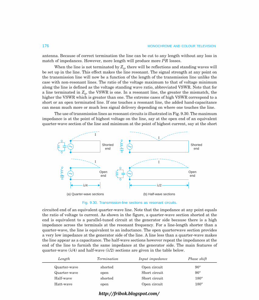
176 MONOCHROME AND COLOUR TELEVISION
antenna. Because of correct termination the line can be cut to any length without any loss inmatch of impedances. However, more length will produce more I2R losses.
When the line is not terminated by Z0, there will be reflections and standing waves willbe set up in the line. This effect makes the line resonant. The signal strength at any point onthe transmission line will now be a function of the length of the transmission line unlike thecase with non-resonant lines. The ratio of the voltage maximum to that of voltage minimumalong the line is defined as the voltage standing wave ratio, abbreviated VSWR. Note that fora line terminated in Z0, the VSWR is one. In a resonant line, the greater the mismatch, thehigher the VSWR which is greater than one. The extreme cases of high VSWR correspond to ashort or an open terminated line. If one touches a resonant line, the added hand-capacitancecan mean much more or much less signal delivery depending on where one touches the line.
The use of transmission lines as resonant circuits is illustrated in Fig. 9.30. The maximumimpedance is at the point of highest voltage on the line, say at the open end of an equivalentquarter-wave section of the line and minimum at the point of highest current, say at the short
I
I
Shortedend
Shortedend
II
Openend
Openend
4/4 /2/2
(a) Quarter-wave sections (b) Half-wave sections
Fig. 9.30. Transmission-line sections as resonant circuits.
circuited end of an equivalent quarter-wave line. Note that the impedance at any point equalsthe ratio of voltage to current. As shown in the figure, a quarter-wave section shorted at theend is equivalent to a parallel-tuned circuit at the generator side because there is a highimpedance across the terminals at the resonant frequency. For a line-length shorter than aquarter-wave, the line is equivalent to an inductance. The open quarterwave section providesa very low impedance at the generator side of the line. A line less than a quarter-wave makesthe line appear as a capacitance. The half-wave sections however repeat the impedances at theend of the line to furnish the same impedance at the generator side. The main features ofquarter-wave (λ/4) and half-wave (λ/2) sections are given in the table below.
Length Termination Input impedance Phase shift
Quarter-wave shorted Open circuit 90°
Quarter-wave open Short circuit 90°
Half-wave shorted Short circuit 180°
Hatt-wave open Open circuit 180°
http://fribok.blogspot.com/

TELEVISION SIGNAL PROPAGATION AND ANTENNAS 177
Such transmission lines are often called STUBS. A stub can be used (i) for impedancematching, (ii) as an equivalent series resonant circuit to short an interfering r.f. signal, and(iii) for phasing signals correctly in antennas. A quarter-wave line produces a phase change of90° whereas a halt-wave section shifts the phase by 180°. To reduce interference, an open λ/4stub at the interfering signal frequency can be used. One side is connected across the antennainput terminals of the receiver, while the open end produces a short at the receiver input onequarter-wave back.
A 300 ohms twin-lead is designed to have almost a constant impedance for all the channelsin a band. This is used to connect the antenna output to the input of the receiver. Matching theimpedance of a multiband antenna to the characteristic impedance of the line is not criticalbecause an impedance mismatch of 2.5 to 1 results in a one db loss of the signal.
Quarter-wave Matching SectionA quarter-wave section can be used for matching two unequal impedances Z1 and Z2. The
characteristic impedance Z0 of the quarter-wave section should then be, Z0 = Z Z1 2 . This is
iliustrated in Fig. 9.31, where an antenna with an impedance equal to 75 ohms is matched toa 300 ohms transmission line by a quarter-wave matching section. This section should then
have an impedance equal to Z Z1 2 = 75 300× = 150 ohms. The required length of the quarter-
wave section can be estimated using the expression λ/4 (metres) = v 80
f (MHz), where ‘v’ is the
velocity factor which varies between 0.6 to 0.8 depending on the type of lead-in wire used.
75 Antenna
Z = 1500 //4
Quarter-wavematching section
Z = Z × Z0 1 2
Z = 3000
Transmissionline
Fig. 9.31. Use of a quarter-wave section formatching antenna to transmission line.
Balun (Balancing Unit)Two quarter-wave sections of the type discussed above can be combined to make a balancingand impedance transforming unit. This is illustrated in Fig. 9.32 (a). This is called a Balun andis used for matching balanced and unbalanced impedances. Two quarter-wave lines each havingan impedance equal to 150 ohms are connected in parallel at one end, resulting in 75 ohmsimpedance across points A and B. Either A or B can be grounded to provide an unbalancedimpedance at the ungrounded point with respect to ground. At the other end the two 150 ahmsquarter-wave sections are connected in series to provide 300 ohms impedance between pointsC and D. The quarter wavelength of the line isolates the ground point from C or D, allowing abalanced impedance with respect to ground. Either side of the Balun can be used for input
http://fribok.blogspot.com/

178 MONOCHROME AND COLOUR TELEVISION
with the other side as output. It is usefully employed for matching a 72 ohms coaxial line to the300 ohms receiver input or in the reverse direction, i.e., a 300 ohms twin-lead to a 72 ohmsunbalanced input. As illustrated in Fig. 9.32 (b) bifilar windings are uscd to simulate the 150ohms transmission line sections. The windings, as illustrated in Fig. 9.32 (c), are on a ferritecore to increase the inductance, thus making the line electrically longer.
n75
unbalanced
A1 5
C
26
D84
B3 7
c 300
balanced
(a)
n75
unbalanced
A1 5
C
26
D84
B3 7
c300
balanced
(b)
Bifilarwindings
A
B
C
D
Twin wireFerrite core
(c)
Fig. 9.32. Balun to match between 75Ω unbalanced and 300Ω balanced impedances(a) with λ/4 matching sections, (b) equivalent transformer, (c) constructional details.
9.10 ATTENUATION PADS
In cases where excessive antenna signal causes overloading, the signal can be attenuatedwithout introducing any mismatch by using resistive networks called pads. Two different padconfigurations are illustrated in Fig. 9.33, where component values for different attenuationsare given in separate charts. The resistors used in such pads are low wattage carbon resistances.Wire-wound resistors are not used because of their inductance. The use of a resistance matchingpad has the advantage of providing both attenuation and impedance match that is independentof frequency.
R1 R1
R1 R1
R2
300output
Ω300input
Ω
(a)
R3 R3
R4
72output
Ω72input
Ω
(b)
R3R2Attenuation
6 db 22Ω390Ω
10 db
20 db
33Ω
56Ω
220Ω
68Ω
Attenuation
6 db
10 db
20 db
R4
100Ω
51Ω
15Ω
R1
47Ω
82Ω
120Ω
Fig. 9.33. Resistance pads (a) balanced ‘H’ pad for 300Ω twin lead(b) unbalanced ‘T’ pad for 72Ω coaxial line.http://fribok.blogspot.com/

TELEVISION SIGNAL PROPAGATION AND ANTENNAS 179
Review Questions
1. Describe briefly the different methods by which radio waves of different frequencies are propa-gated. Why space wave propagation is the only effective mode of radiation above about 40 MHz ?
2. What do you understand by line-of-sight distance in space wave propagation ? What are theeffects of atmospherics and obstacles on space waves ? Why is it necessary to keep both thetransmitting and receiving antennas as high as possible for television ?
3. What do you understand by wave polarization ? Why is horizontal polarization preferred fortelevision and FM broadcasts ? Why is TV transmission limited to about 100 km ? What arebooster stations and under what conditions are they employed ?
4. Describe briefly co-channel and adjacent channel interference effects. Discuss the techniquesemployed to eliminate such interference in fringe areas.
5. What is a ghost image and what causes it to appear on the receiver screen along with the repro-duced picture ? Differentiate between leading and trailing ghost pictures. Why is AM preferredover FM for picture signal transmission ?
6. Describe briefly radiation mechanism from an antenna. Explain the evolution of a dipole foreffective radiation. Sketch approximate radiation patterns for ungrounded resonant antennas oflengths λ/4, λ/2 and 3λ/2 and justify them.
7. Define directional gain and front to back ratio as applied to receiving antennas. What is anantenna array ? Sketch radiation patterns for (i) a broadside array and (ii) end-fire array. Howare these patterns modified when the antennas are very close to the ground ?
8. What is the function of a reflector and a director in a Yagi antenna. Explain why such antennaconfigurations are highly directional. What is the effect of increasing the number of directorelements ?
9. What are the special requirements of a fringe area television antenna and how are these achieved ?Give constructional details of a typical fringe area antenna and explain the precautions thatmust be taken while mounting it.
10. Give constructional details of a turnstile antenna and explain by drawing radiation pattern itssuitability for television transmission. Draw the circuit of a diplexer arrangement employed forfeeding the output from both picture and sound signal transmitters to the same antenna.
11. Why is it not possible to use the same antenna for reception for both lower and upper VHFchannels ? Describe any one type of multiband array commonly employed to cover all the chan-nels in the VHF band.
12. Describe briefly the basic principle of bow-tie (di-fan) and parabolic reflector type of antennascommonly employed for reception from UHF television channels.
13. Explain why an antenna used for colour TV reception must deliver almost constant output volt-age over any one channel.
14. Sketch a typical log periodic antenna and explain its special characteristics. Why are its elementsbent in a ‘V’ shape ?
15. Describe with suitable sketches various types of lead-in wires used for connecting the antennato the TV receiver. What is the essential difference betwecn balanced and unbalanced lines andhow are they connected to the receiver ? Why is a coaxial cable preferred for connecting a UHFantenna ?
16. What is a stub ? Explain how quarter-wave line sections can be used for providing an impedancematch between a low impedance antenna and 300 ohms lead-in line.
17. What is a ‘Balun’ ? Give its constructional details and explain how it can be used as an imped-ance matching network between two different impedances at high frequencies.
18. Under what conditions does it become necessary to use an attenuator pad between the transmis-sion line and receiver ? Draw ‘H’ and ‘T’ pad configurations and explain how besides providing amatch between the line and receiver the desired attenuation is also achieved.
http://fribok.blogspot.com/

10
"
http://fribok.blogspot.com/

Television, by its use in broadcasting has opened broad new avenues in the fields ofentertainment and dissemination of information. The not-so-well-known applications are inthe area of science, industry and education, where the television camera has contributedimmeasurably to man’s knowledge of his environment and of himself. The television camera isprobably best described as an extension of the human eye because of its ability to relayinformation instantaneously. Its capability to view events occurring in extremely hazardouslocations has led to its use in areas of atomic radiation, underwater environments and outerspace. Some of its important applications which are of direct interest to our society are describedbriefly in this chapter.
10.1 TELEVISION BROADCASTING
Broadcasting means transmission in all directions by electromagnetic waves from thetransmitting station. Broadcasting, that deals mostly with entertainment and advertising, isprobably the most familiar use of television. Millions of television sets in use around the worldattest to its extreme popularity. Most programmes produced live in the studio are recorded onvideo tape at a convenient time to be shown later. Initially television transmission was confinedto the VHF band only but later a large number of channel allocations were made in the UHFband also. The distance of transmission, as explained earlier, is confined to line of the sightbetween the transmitting and receiving antennas. The useful service range is up to 120 km forVHF stations and about 60 km for UHF stations. Television broadcasting initially started withmonochrome picture but around 1952 colour transmission was introduced. Despite its complexityand higher cost, colour television has become such a commercial success that it is fastsuperseding the monochrome system.
10.2 CABLE TELEVISION
In recent years master antenna (MATV) and community antenna (CATV) television systemshave gained widespread popularity. The purpose of a MATV system is to deliver a strongsignal (over 1 mV) from one or more antennas to every television receiver connected to thesystem. Typical applications of a MATV system are hotels, motels, schools, apartment buildingsand so on.
The CATV system is a cable system which distributes good quality television signal to avery large number of receivers throughout an entire community. In general, this system feeds
182
$%
"
http://fribok.blogspot.com/

TELEVISION APPLICATIONS 183
increased TV programmes to subscribers who pay a fee for this service. A CATV system mayhave many more active (VHF and UHF) channels than a receiver tuner can directly select.This requires use of a special active converter in the head-end.
(a) MATVThe block diagram of a basic MATV system is shown in Fig. 10.1 (a). One or more antennas areusually located on roof top, the number depending on a available telecasts and their direction.Each antenna is properly oriented so that all stations are received simultaneously. In order toallow a convenient match between the coaxial transmission line and components that make upthe system, MATV systems are designed to have a 75 Ω impedance. Since most antennas havea 300 Ω impedance, a balun is used to convert the impedance to 75 ohms. As shown in thefigure, antenna outputs feed into a 4-way hybrid. A hybrid is basically a signal combininglinear mixer which provides suitable impedance matches to prevent development of standingwaves. The standing waves, if present, result in ghosts appearing in an otherwise good TVpicture.
The output from the hybrid feeds into a distribution amplifier via a preamplifier. Thefunction of these amplifiers is to raise the signal amplitude to a level which is sufficient toovercome the losses of the distribution system while providing an acceptable signal to everyreceiver in the system. The output from the distribution amplifier is fed to splitters throughcoaxial trunk lines. A splitter is a resistive-inductive device which provides trunk line isolationand impedance match.
Coaxial distribution lines carry television signals from the output of splitters to pointsof delivery called subscriber tap-offs. The subscriber taps, as shown in Fig. 10.1 (b), can beeither transformer coupled, capacitive coupled or in the form of resistive pads. They provideisolation between receivers on the same line thus preventing mutual interference. The tapslook like ac outlets and are normally mounted in the wall. Wall taps may be obtained with300 Ω output 75 Ω output and a dual output. The preferred method is to use a 75 Ω type witha matching transformer. The matching transformer is usually mounted at the antenna terminalsof the receiver and will have a VHF output and a UHF output. Since improperly terminatedlines will develop standing waves, the end of each 75 Ω distribution cable is terminated with a75 Ω resistor called a terminator.
(b) CATVFormerly CATV system were employed only in far-fringe areas or in valleys surrounded bymountains where reception was difficult or impossible because of low level signal conditions.However, CATV systems are now being used in big cities where signal-level is high but allbuildings render signals weak and cause ghosts due to multipath reflections. In either case,such a system often serves an entire town or city. A single antenna site, which may be on topof a hill, mountain or sky-scraper is chosen for fixing antennas. Several high gain and properlyoriented antennas are employed to pick up signals from different stations. In areas whereseveral signals are coming from one direction, a single broad based antenna (log-periodic) maybe used to cover those channels. Most cable television installations provide additional serviceslike household, business and educational besides commercial TV and FM broadcast programmes.These include news, local sports and community programmes, burgler and fire alarms, weatherreports, commercial data retrieval, meter reading, document reproduction etc. Educational
http://fribok.blogspot.com/

184 MONOCHROME AND COLOUR TELEVISION
services include computer aided instructions, centralized library services and so on. Many ofthe above options require extra subscription fee from the subscriber.
Balun Balun Balun Balun
4 way hybrid(linear mixer)
Preamplifier
Distributionamplifier
Coaxialcable
TR
TR
TR
Splitter
TR TR TR TRTRTR
R RCableCable
Tap-off points
CableTR-Televisionreceiver
Terminationresistance 75 R
bDistribution
ns
Signalprocessing
nt
Antennasystem
Fig. 10.1 (a) Block diagram of an MATV system.
(i) Transformer (ii) Capacitive (iii) Resistive
Fig. 10.1 (b) Subscriber taps of different types.
http://fribok.blogspot.com/

TELEVISION APPLICATIONS 185
Since several of the above mentioned service need two-way communication between thesubscriber and a central processor, the coaxial distribution network has a large number ofcable pairs, usually 12 or 24. This enables the viewer to choose any channel or programme outof the many that are available at a given time.
CATV Plan. Figure 10.2 shows the plan of a typical CATV system. The signals fromvarious TV channels are processed in the same manner as in a MATV system. In fact, a CATVsystem can be combined with a MATV set-up. When UHF reception is provided in addition toVHF, as often is the case, the signal from each UHF channel is processed by a translator. Atranslator is a frequency converter which hterodynes the UHF channel frequencies down to aVHF channel. Translation is advantageous since a CATV system necessarily operates withlengthy coaxial cables and the transmission loss through the cable is much greater at UHFthan at VHF frequencies. As in the case of MATV, various inputs including those fromtranslators are combined in a suitable mixer. The set-up from the antennas to this combiner iscalled a head-end.
FM bandamplifier
Combiningnetwork
TVmodulator
TVTVTVTVTV
FM channels From VHF and UHFantenna systems
Local programme
Amplifiersand
translatorsa
nHeadend
Amplifier
Equalizer
Coaxialcable
Distributionamplifier
Leveladjustment
Amplifiers
Trunk lines todistant locations
Trunk lines todistant locations
R RR
Splitter
R RR
Splitter
Tap-off points
Termination resistor 75
Fig. 10.2. A simplified block diagram of a CATV system.http://fribok.blogspot.com/

186 MONOCHROME AND COLOUR TELEVISION
Further, as shown in the figure the CATV outputs from the combiner network are fed toa number of trunk cables through a broadband distribution amplifier. The trunk cables carrysignals from the antenna site to the utilization site (s) which may be several kilometres away.Feeder amplifiers are provided at several points along the line to overcome progressive signalattenuation which occurs due to cable losses. Since cable losses are greater at higher frequenciesit is evident that high-band attenuation will be greater than low-band attenuation. Therefore,to equalize this the amplifiers and signal splitters are often supplemented by equalizers. Anequalizer or tilt control consists of a bandpass filter arrangement with an adjustable frequencyresponse. It operates by introducing a relative low-frequency loss so that outputs from theamplifiers or splitters have uniform relative amplitude response across the entire VHF band.
The signal distribution from splitters to tap-off points is done through multicore coaxialcables in the same way as in a MATV system. In any case the signal level provided to a televisionreceiver is of the order of 1.5 mV. This level provides good quality reception without causingacompanying radiation problems from the CATV system, which could cause interference toother installations and services.
10.3 CLOSED CIRCUIT TELEVISION (CCTV)
Closed circuit television is a special application in which camera signals are made availableonly to a limited number of monitors or receivers. The particular type of link used depends ondistance between the two locations, the number and dispersion of receivers and mobility ofeither camera or receiver. Figure 10.3 illustrates various link arrangements which are oftenused. The simplest link is a cable where video signal from the camera is connected directlythrough a cable to the receiver. A television monitor, which is a receiver, without RF and IFcircuits, is only required for reception in such a link arrangement. About one volt peak-to-peaksignal is required by the monitor. Since the video signal is normally delivered via cables andeven when transmitted, it is over a limited region and for restricted use, CCTV neede notfollow television broadcast standards.
Videoamplifier
CableMonitor
MCamera
P – PAD
(a) Direct camera link to one monitor
M
Camera M
M
P
P
Equalizer
Distributionamplifier
(b) Direct camera link to several monitors
(Figure 10.3 Contd. .....)
http://fribok.blogspot.com/

TELEVISION APPLICATIONS 187
Camera Transmitter
TRP
P
TR
TR
(c) Wireless link to several receivers
Camera CCU& T–R
CU& T
TRP
P
TR
TR
Microwave link
Cameracontrol unit
and trans-receiver
Control unitand transmitter
(d) Output of a remotely controlled camera feeding severalTV receivers located at a distance
Fig. 10.3. Commonly used closed-circuit television (CCTV) systems.
CCTV ApplicationsThere are numerous applications of CCTV and a few are briefly described here.
(i) Education. One instructor may lecture to a large number of students sitting at dif-ferent locations. Similarly close-ups of demonstration experiments and other aids can be shwonon monitors during these lectures.
(ii) Medicine. Several monitors and camera units can be installed to observe seriouslyill patients in intensive care units. In medical institutions, operations when performed can beshown to medical students without their actually gathering around the oepration table.
(iii) Business. Television cameras can be installed at different locations in big depart-mental stores to keep an eye over customers and sales personnel.
(iv) Surveillance. In banks, railway yards ports, traffic points and several other similarlocations, closed circuit TV can be effectively used for surveillance.
(v) Industry. In industry CCTV has applications in remote inspection of materials. Ob-servance of nuclear reactions and other such phenomena would have been impossible withouttelevision. Similarly television has played a great role in the scanning of earth’s surface andprobing of other planets.
(vi) Home. In homes a CCTV monitor finds its application in seeing the caller beforeopening the door.
(vii) Aerospace and Oceanography. Here a wireless link is used between the transmitterand receiver. In some applications camera is remotely controlled over a microwave radio link.As shown in Fig. 10.3 (c), for aerospace and oceanography a carrier is used for transmitting thesignal and a complete receiver is then necessary for reception.
http://fribok.blogspot.com/

188 MONOCHROME AND COLOUR TELEVISION
10.4 THEATRE TELEVISION
Television programmes can be shown to a large audience in theatres. Similarly cinematographicfilms can be telecast for viewing on television receivers. Some examples of such applicationsare as follows.
(i) TV Programmes in TheatresSpecial programmes can be shown on a large screen by optical projection in a theatre wherespherical mirrors and reflectors are used to enlarge the image. With about 80 KV on the finalanode of the picture tube, there is enough light to show pictures on a standard theatre screen.The same idea can be used for projecting TV programmes at home on a small screen.
(ii) Film RecordersFilm recorders produce a cinematographic film by photographing a television picture displayedon the screen of a picture tube. For doing so the film has to be pulled down frame by frameduring successive blanking intervals. A video tap recording can only be rebroadcast in countrieswhere the same TV standards are in use, whereas film recordings offer a ready means ofexporting programmes to other countries using different standards.
(iii) Telecine Machines and Slide ProjectorsMany television programmes originate from 35 mm and 16 mm photographic cinema films.Slides are also often used in TV programmes. Therefore, telecine machines and slide projectorsform part of the television studio equipment for transmitting motion pictures and advertisementslides. Telecine machines are cinema projectors equipped with mirror or prism reflectorarrangement for focusing pictures, as produced by them, on the face of a TV camera. Slidescanners also have a similar optical arrangement for transmitting still from different slides.For high utilization of the projectorcamera chain, an optical multiplexer is often used. Thisswitches or directs one of the several optical image sources to the lens of a single camera, thusenabling the use of one TV camera for receiving programmes from three or four film and slideprojectors. For the accompanying sound signal pick-up, the usual optical or magnetic trackplayback facility is incorporated in the multiplexer setup.
An additional problem of using telecine projectors is the difference in frame rate ofmotion pictures and television scanning. Motion pictures are taken at the rate of 24 frames/secbut while screening, each frame is projected twice to reduce flicker. This amounts to an effectiveframe rate of 48/sec. However, in TV transmission, while the frame rate is 25, the field rate is50 on account of interlaced scanning. Thus, there is a difference of one picture frame/sec betweenthe two and if not corrected, would cause a rolling bar on the raster besides loss of some signaloutput. In order to overcome this discrepancy, the film in the telecine projector is pulled downby the shutter mechanism at the rate of 25 frames/sec. It is achieved by a suitable speedcorrection in the drive mechanism. This naturally results in a little faster movement of scenesand objects on the television screen but the distortion caused is so small that it is hardlynoticeable. The corresponding small increase in the pitch of reproduced sound also goesundetected.
Similarly in the 525 line system where the frame rate is 30/sec, it becomes necessary tosuitably modify the film rate of 24 to achieve compatibility between the two in order to preventrolling and loss of any picture information. The necessary correction is carried out by projecting
http://fribok.blogspot.com/

TELEVISION APPLICATIONS 189
one frame three times and the following frame two times. This sequence is repeated alternatelyby means of an intermittent shutter mechanism of 3 : 2 pull-down cycle for the film. The pull-down is carried out by a shutter which operates at the rate of 60 pulls per second. Thus, out ofa total of 24 frames, 12 are projected three times while the rest only two times. This thenmakes the film rate of 24 frames equal to the scanning rate of (12 × 3 + 12 × 2 = 60) 60 fields persecond.
The speed alteration and sequencing explained above makes direct scanning of motionpictures possible through any TV network. While slides are used for stills, small advertisementfilms are recorded beforehand on video tapes for telecasting when required.
(iv) Pay TelevisionSpecial programmes like first-run films, sports events and cultural programmes that arenormally not broadcast on the usual TV channels because of their higher cost are made availableto television subscribers either through the cable television network or on special channels. Atthe receiver a special decoder is used to receive the picture. The decoder also has the provisionto register an extra charge for such special screenings. This service is optional but a fixedcharge is made for initial installation.
10.5 PICTURE PHONE AND FACSIMILE
This is another fascinating application of television where two people can see each other whiletalking over the telephone line. A picture phone installation includes a unit that contains asmall picture tube and a miniature TV camera. The highest modulating frequency in picture-phone services is normally limited to about 1.5 MHz.
Facsimile is another application of electronic transmission of visual information, usuallya still picture, over telephone lines. Since there is no motion, a slow scanning rate is employed.Facsimile is employed for sending copies of documents over telephone lines.
10.6 VIDEO TAPE RECORDING (VTR)
Video tape recording was introduced in 1956 and it proved to be a vast improvement over theearlier method of recording motion pictures taken from the screen of the television receiver.Video tape retains the ‘live’ quality of broadcasting and has the capability of being edited andduplicated without any delay. The other advantages are (i) immediate playback capability, (ii)convenience of repeating the recorded material as many times as the viewer wishes, and (iii)ease of duplication for distribution to a large number of users.
The video signal can be recorded on a magnetic tape for picture reproduction in a similarway as the audio tape is used for reproduction of sound. In an audio recorder, the plastic tape(mylar) that has a very fine coating of ferric oxide is made to move in physical contact with thetape head. Any electrical signal applied to the tape head magnetizes the magnetic particles onthe tape, as it passes across the head. For each cycle of the signal, two tiny bar magnets areproduced on the tape and the length of bar magnets is inversely proportional to the frequencyof applied signal. Thus, on a recorded tape these bar magnets form a chain with like polesadjacent to each other. When a recorded tape moves across the playback head, there is a
http://fribok.blogspot.com/

190 MONOCHROME AND COLOUR TELEVISION
change in flux linkages with the head and hence a voltage is developed across its coil terminals.This technique of recording and reproducing audio signals is illustrated in Fig. 10.4.
HN N
S SN
N
Tapewidth Gap length
Bar magnets
Tapemotion
One wavelengthRecording
headv
v
0 t
Input signal
v0
0 t
Output signal
S N N S S N
Tape head
Output
Fig. 10.4(a) Electrical signal recorded in the Fig. 10.4(b) Development of signalform of bar magnets on the magnetic tape. during playback.
Audio RangeEach head has a certain gap length. As the recording frequency increases, the length of the barmagnets decreases. A limiting frequency is reached when at a given tape speed, total length ofthe two adjacent bar magnets becomes equal to the gap length. At this frequency, output of theplayback head will be zero since each bar magnet will produce equal and opposite voltage inthe coil, with the result that no net flux passes through core of the head. For a tape speed of 19cm (7.5″) per second and with a gap length of 6.3 microns (0.00025″) the usable frequencycomes to about 15 KHz and is enough for audio recording.
Audio Signal Dynamic RangeSince output voltage from a playback head is directly proportional to the rate of change of flux,for every doubling of frequency the output voltage will become twice. In other words, everytime the frequency gets halved (one octave lower), the output falls by 6 db. Assuming that theentire audio range occupies 9 octaves, output at frequencies that lie in the lowest octave will be54 db below the output in the highest octave. This discrepancy is got over by providing equalizingcircuits in the playback amplifier. The equalizing network is designed to have characteristicswhere the output voltage falls by 6 db per octave to allow for the rising response at the playbackhead.
AC BiasIf the signal to be recorded is applied directly to the record head, the output will be highlydistorted on account of non-linearity of B-H curve of the core material around its zero axis.This difficulty is solved by superimposing the recording signal on a high frequency ac voltage.The amplitude of the high frequency bias is so chosen that its positive and negative peaks liewithin the linear portions of the B-H curve. As shown in Fig. 10.5, the two outputs (marked Xand Y) add up to give linear output with improved signal to noise ratio. The ac bias frequency
http://fribok.blogspot.com/

TELEVISION APPLICATIONS 191
is kept fairly high so that the beat signal between the highest signal frequency and bias frequencydoes not fall in the audio range. An ac bias frequency close to 60 KHz is considered adequateand is normally employed in audio tape recorders.
B
+ Output
(X)
(Y)
HH
– Output
Mixed inputsignal
Sum ofX and Youtputs(a+b)
t
t
t(a+b)
High frequencybiasing signal
(b)
Recordingsignal
(a)
Fig. 10.5. Effect of a.c. (ultrasonic) biasing in audio tape recording.
Video RecordingThe above introduction to audio recording will enable a better appreciation of the specialproblems of recording video signals on a magnetic tape.
Video FrequenciesFor recording up to the highest video frequency of 5 MHz if the head gap is kept at 0.00025″(6.3 microns) a tape speed of the order of 39 metres (1300 inches) per second would be necessary.With the head fixed as in audio recording and moving the tape at such a high speed wouldresult in excessive wear and tear besides mechanical instability. Decreasing the gap belowabout 6 microns to lower the tape speed is not possible because of technological problems.However, it is not essential that only tape should move and head remains stationary. It is therelative speed of tape and head which is responsible for the output voltage. Hence the relativespeed is increased by moving the tape head in opposite direction to the tape movement. Inpractice tape heads are mounted on the periphery of a drum which rotates around an axisrelative to the direction of tape movement. This enables reduction in tape speed to as low as7.5 inches (≈ 20 cm) per second.
Video Signal Dynamic RangeAs described earlier, output voltage from a playback head is directly proportional to the rate ofchange of flux. In case of video frequencies consisting of dc to 5 MHz, theoretically there wouldbe infinite number of octaves. Even if frequencies down to 25 Hz are required to be retained (dccan be recovered by clamping), the band between 25 Hz to about 5 MHz would occupy nearly17 octaves. This means that the average output on account of frequencies in the lowest octavewill be about 100 db below the output in the highest octave. It is very difficult to handle such alarge dynamic range where low frequencies run into noise levels. The octave problem could besolved by translating video frequencies to higher frequencies by amplitude modulation. Forexample, a carrier frequency of 10 MHz would provide sidebands in the range of 5 to 15 MHz.This covers only two octaves. However, amplitude modulation is not used because of the followingreasons:
http://fribok.blogspot.com/
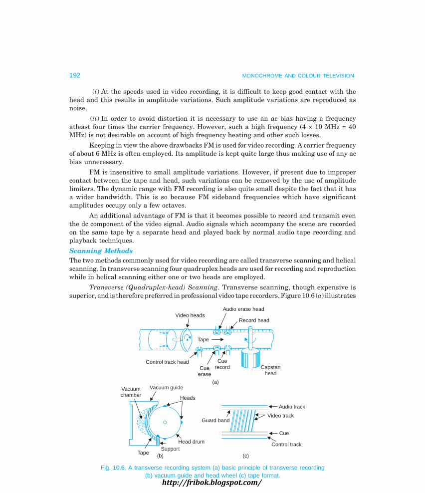
192 MONOCHROME AND COLOUR TELEVISION
(i) At the speeds used in video recording, it is difficult to keep good contact with thehead and this results in amplitude variations. Such amplitude variations are reproduced asnoise.
(ii) In order to avoid distortion it is necessary to use an ac bias having a frequencyatleast four times the carrier frequency. However, such a high frequency (4 × 10 MHz = 40MHz) is not desirable on account of high frequency heating and other such losses.
Keeping in view the above drawbacks FM is used for video recording. A carrier frequencyof about 6 MHz is often employed. Its amplitude is kept quite large thus making use of any acbias unnecessary.
FM is insensitive to small amplitude variations. However, if present due to impropercontact between the tape and head, such variations can be removed by the use of amplitudelimiters. The dynamic range with FM recording is also quite small despite the fact that it hasa wider bandwidth. This is so because FM sideband frequencies which have significantamplitudes occupy only a few octaves.
An additional advantage of FM is that it becomes possible to record and transmit eventhe dc component of the video signal. Audio signals which accompany the scene are recordedon the same tape by a separate head and played back by normal audio tape recording andplayback techniques.
Scanning MethodsThe two methods commonly used for video recording are called transverse scanning and helicalscanning. In transverse scanning four quadruplex heads are used for recording and reproductionwhile in helical scanning either one or two heads are employed.
Transverse (Quadruplex-head) Scanning. Transverse scanning, though expensive issuperior, and is therefore preferred in professional video tape recorders. Figure 10.6 (a) illustrates
Video headsAudio erase head
Record head
Tape
Control track headCue
erase
Cuerecord Capstan
head
(a)Vacuumchamber
Vacuum guide
Heads
Head drumSupport
Tape (b)
Audio track
Video trackGuard band
Cue
Control track
(c)
Fig. 10.6. A transverse recording system (a) basic principle of transverse recording(b) vacuum guide and head wheel (c) tape format.
http://fribok.blogspot.com/
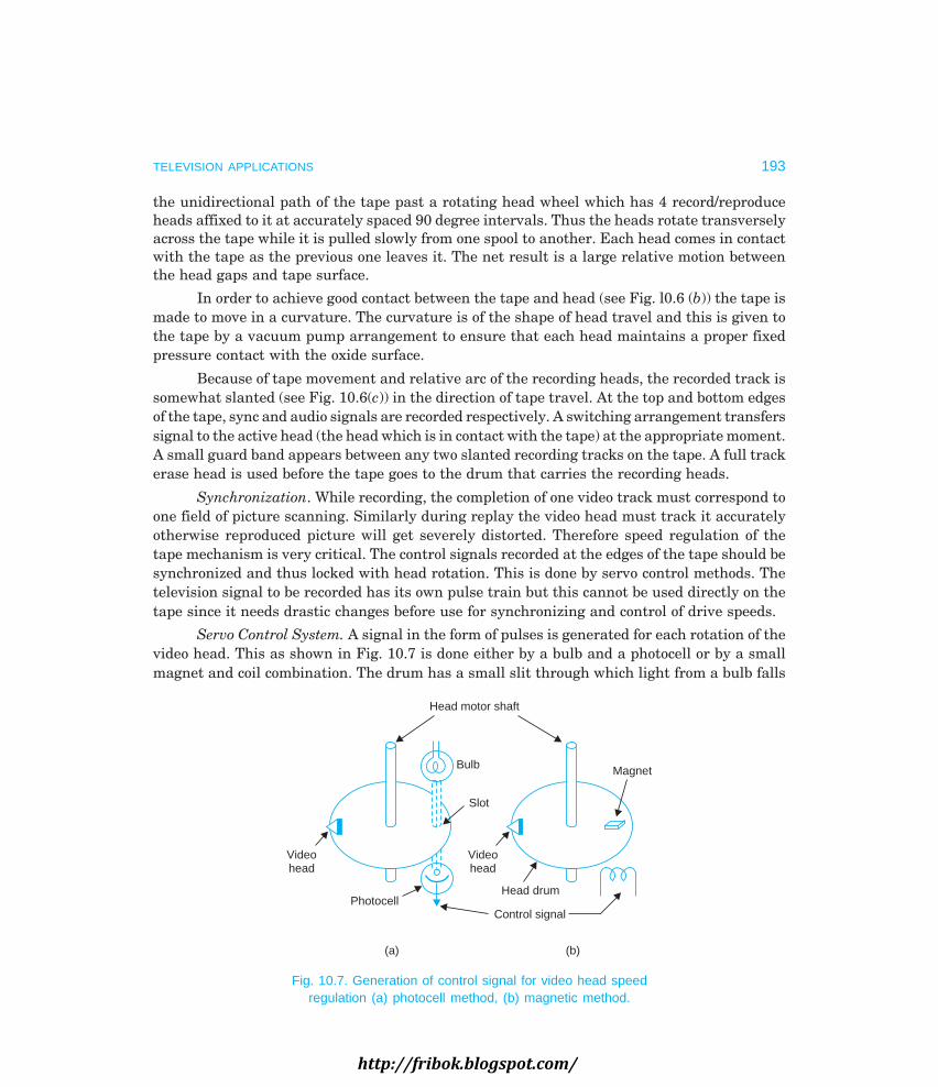
TELEVISION APPLICATIONS 193
the unidirectional path of the tape past a rotating head wheel which has 4 record/reproduceheads affixed to it at accurately spaced 90 degree intervals. Thus the heads rotate transverselyacross the tape while it is pulled slowly from one spool to another. Each head comes in contactwith the tape as the previous one leaves it. The net result is a large relative motion betweenthe head gaps and tape surface.
In order to achieve good contact between the tape and head (see Fig. l0.6 (b)) the tape ismade to move in a curvature. The curvature is of the shape of head travel and this is given tothe tape by a vacuum pump arrangement to ensure that each head maintains a proper fixedpressure contact with the oxide surface.
Because of tape movement and relative arc of the recording heads, the recorded track issomewhat slanted (see Fig. 10.6(c)) in the direction of tape travel. At the top and bottom edgesof the tape, sync and audio signals are recorded respectively. A switching arrangement transferssignal to the active head (the head which is in contact with the tape) at the appropriate moment.A small guard band appears between any two slanted recording tracks on the tape. A full trackerase head is used before the tape goes to the drum that carries the recording heads.
Synchronization. While recording, the completion of one video track must correspond toone field of picture scanning. Similarly during replay the video head must track it accuratelyotherwise reproduced picture will get severely distorted. Therefore speed regulation of thetape mechanism is very critical. The control signals recorded at the edges of the tape should besynchronized and thus locked with head rotation. This is done by servo control methods. Thetelevision signal to be recorded has its own pulse train but this cannot be used directly on thetape since it needs drastic changes before use for synchronizing and control of drive speeds.
Servo Control System. A signal in the form of pulses is generated for each rotation of thevideo head. This as shown in Fig. 10.7 is done either by a bulb and a photocell or by a smallmagnet and coil combination. The drum has a small slit through which light from a bulb falls
Videohead
Videohead
Head motor shaft
Bulb
Slot
Head drum
Control signal
Magnet
Photocell
(a) (b)
Fig. 10.7. Generation of control signal for video head speedregulation (a) photocell method, (b) magnetic method.
http://fribok.blogspot.com/

194 MONOCHROME AND COLOUR TELEVISION
on a photocell once during each revolution of the drum. In the second method, a small magnetfixed on the drum, induces a small voltage pulse as it passes over a fixed coil once during eachrevolution. The drum pulses thus generated are compared with the incoming field sync pulsesobtained during recording. The comparator produces an error signal corresponding to thedifference in phase and frequency between the two signals. This is amplified and applied toeddy current brakes provided on the head motor. The brakes adjust the motor speed to providenecessary synchronization. On replay the drum pulses are compared with 50 Hz pulses derivedfrom supply mains. The error signal thus derived from the comparator is used for controllingspeed of the head motor. In addition to this the drum pulses are also used to ensure that thehead runs accurately at the centre of the recorded track. Maximum video output is the indicationof correct video head tracking.
The use of four recording heads together with switching arrangements, a vacuum systemfor good tape contact with recording heads and elaborate synchronizing facilities contribute tothe high cost of this system. However, it is justified because professional VTRS which employquadruplex system of recording with a full bandwidth of 5 MHz providc such good qualitypictures that they look like a live programme.
Helical Scan Recording. Smaller and low-priced video tape recorders employ 0.5″ or 1″tape and provide a bandwidth up to about 2.5 MHz. Such recorders normally use one head anda relatively simple drive mechanism. In this system of recording the tape is wrapped around adrum inside which the head rotates. The video head protrudes through a horizontal slit in thedrum to come in contact with the tape. Figure 10.8(a) shows the mechanical layout of thismethod of recording. The video head rotates at 50 revolutions per second such that one field ofpicture information is recorded in one revolution. As shown in the figure, the tape comes incontact at the upper edge of the drum and leaves it at its bottom edge. Thus the recorded trackis in the form of a helix and this gives it the name of helical scanning. While a single video headis used for both recording and playback, the tape passes before a full track erase head before itgoes around the drum. A typical one inch tape format is shown in Fig. 10.8(b).
Rotatingdrum
Videohead
Takeupspool
Audio and controltrack head
Capstanspindle
Tape
(a)
Tape head
Tape
Rotatingdrum
Guard bandAudio track
Videotrack
Control trackCue track
Guard track
(b)
Fig. 10.8. Helical scanning system (a) single head wrap scanning (b) 1″ tape format.http://fribok.blogspot.com/

TELEVISION APPLICATIONS 195
It consists of an audio track and guard band at the top and audio cue, guard and controltracks at the bottom. The video tracks across the tape are at an angle of 5° to the tape lengthaxis separated by 4 mil (0.004″) guard bands.
Quadruplex Head Recording and Playback Circuits. Figure 10.9 shows the basic blockschematic arrangements of recording and playback in a quadruplex head VTR. In record modethe composite video signal of about 1 V P-P amplitude, as obtained from a camera set up, feedsinto a two stage wide-band video amplifier in the video tape recorder. The output from thisamplifier is fed to the FM modulator via a pre-emphasis network and driver.
Video
inputVideoamp
Pre-emphasiscircuit
Driveramp
FMmodulator
Recordinghead amp
Slipringbrushes
Headdrum
Fourvideoheads
Motor
Amp
Head drummotor drive
Ultrasonicbiasing network
A.C. biasoscillator
Audio
inputAmp
Servocontrol cct
Syncseparator
and shaper
Audio recordhead
Fig. 10.9(a) Simplified block diagram of a quadruplex head video tape recording system.
To TVreceiver
AMmodulator
Tomonitor
Videoamplifier
FMdemodulator
Equalizerand
limiter ccts
Switcheramp
Slipringbrushes
Headdrum
Videoheads
Motor
Motor
Capstan
Head drummotor drive
Capstanmotor drive
Servocontrol ccts
Amplifier
Speed controlsignals
AudiooutputAudio head
Fig. 10.9(b) Simplified block diagram of a quadruplex head video tape system in the playback mode.
http://fribok.blogspot.com/

196 MONOCHROME AND COLOUR TELEVISION
The modulator output is amplified by the recording head amplifier and fed to the recordheads through slip-ring brushes. The accompanying audio signal is amplified, given an ac bias,and then fed to the audio head. As shown in Fig. 10.9 (a) a sync separator circuit is also connectedacross the output of the wide-band video amplifier. The sync pulses, after separation, aresuitably shaped and used to synchronize and control the head drum motor speed by servocontrol techniques.
During playback (see Fig. 10.9 (b)) the video head outputs are collected through slip-ring brushes. These are then fed to an electronic switcher, which selects and amplifies thesignal from the head that is in contact with the tape. The selection takes place during horizontalretrace blanking intervals so that the switching transients are not visible. The selected outputis fed to the FM demodulator through an equalizing network and several limiter stages. Thedetected output is amplified by a four stage video amplifier before feeding it to a monitor or anamplitude modulator. After modulation with the carrier frequency of any one of the band Ichannels, the incoming programme can be viewed on a TV receiver.
The speed control signals are recovered from the corresponding tape tracks and processedfor driving the capstan motor and synchronizing the head drum motor drive. The audio signal,as obtained from the audio playback head, is amplified and fed to the monitor or a modulatorfor use in a TV receiver.
Video Disc Recorder. Optical video disc recording is a recent development. It uses alaser beam in its pick up system. The video disc is 12″ (301.6 mm) in diameter and is made oftransparent plastic. Since its reverse surface is coated with aluminium to reflect the laserbeam, it has an appearance of a metallic disc. Sound and image signals are stored in tiny pitslocated in a substrate l.l mm from the surface. There are close to 14 billion pits on one surfaceof a disc. The reflection of the laser beam from the disc is intermittently interrupted accordingto the distribution and width of these pits and the reflected laser beam is converted into electricalsignals. Since there is no friction from a stylus as in the case of conventional audio pickups, thesound and image quality of the laser beam type video disc is almost permanent. The rotationalspeed of the disc is so controlled that the relative beam velocity is constant from the outermostedge to the innermost end. One revolution of each track forms one frame of picture and oneside of the disc can record up to 54000 frames. Both, one hour and half an hour duration disesare now available. In the later type of video disc, sound is FM modulated and recorded in twoseparate channels. Therefore, the two channels may be used for recording and reproduction ofbilingual programmes or high fidelity stereo music.
10.7 TELEVISION VIA SATELLITE
The conventional methods for extended coverage of TV by microwave space communicationand coaxial cable links are relatively expensive. Geostationary communication satelliteslaunched into synchronous orbits around the earth in recent years have enabled not only nationalbut also international television programmes to be relayed between a number of ground stationsaround the world. Three artificial satellites placed in equatorial orbits at 120° from each othercover practically the whole populated land area of the world.
High power, highly directive land based transmitters transmit wideband microwavesignals to the geostationary satellite above the transmitter. Each microwave channel has abandwidth of several tens of megahertz and can accommodate many TV signals and thousands
http://fribok.blogspot.com/

TELEVISION APPLICATIONS 197
of telephone channels or suitable combinations of these. The satellites usually powered bysolar batteries receive the transmission, demodulate and amplify it and remodulate it on adifferent carrier before transmitting again. The transmitting antenna on the satellite, by theuse of a suitable reflector, can direct the radiated beam to a narrow region on the earth andeconomize on power to provide a satisfactory service in the desired area. Higher power satellitescan provide large power flux densities so that smaller size antennas can be used for reception.For national distribution the transmission is downwards from a wide angle antenna so thatthe whole national area is ‘illuminated’ by the transmission if possible. For internationaldistribution the transmission is also towards the other one or two satellites (which are in lineof sight direction) from highly directive antennas. The demodulation-amplification-remodulationtransmission process is repeated in the second satellite. The final ‘down channel’ transmissionis received (in the same or a different country) by a large cross-section antenna and processedin low noise receivers and finally reradiated from the regular TV transmitters.
There are a number of ‘INTELSAT’* satellites over the Atlantic, Pacific and IndianOceans operating as relay stations to some 40 ground stations around the world. Theinternational system of satellite communication caters to the continental 625/50 and theAmerican 525/60 systems. As television standards differ from country to country, thetransmitting station adopts the standards of the originating country. The ground stationconverts the received signal with the help of digital international conversion equipment to thelocal standards before relaying it.
Frequency modulation is used for both ‘up channel’ and ‘down channel’ transmission.FM, though it needs a larger bandwidth, offers good immunity from interference and requiresless power in the satellite transmitter.
Frequency AllocationThe frequency bands recommended for satellite broadcasting are 620 to 790 MHz, 2.5 to2.69 GHz, and 11.7 to 12.2 GHz on a shared basis with other fixed and mobile services. Thesatellite antenna size and the RF power naturally depend upon the frequency of operation.Space erectable antennas are used for the 620-790 MHz band, with the size limited to about 15metres, while rigid antennas are used both for 2.5 and 20 GHz bands, the size being limited toabout 3 metres.
For the ground terminal, the maximum diameter of the antenna is restricted by theallowable beamwidth and frequency. The cost and complexity of the receiver increases withincrease in frequency.
Extended Coverage of TelevisionBesides the use of satellites for international TV relaying, satellites can be used for distributingnational programmes over extended regions in large countries because of their ability to coverlarge areas. For this, satellites can be used in three following ways.
(i) Rebroadcast System. In this system emission from a low power satellite is receivedwith the help of a high sensitivity medium size (about 9 m) antenna on a high sensitivity lownoise earth station. The received satellite programme is rerelayed over the high power terrestialtransmitter for reception on conventional TV receivers. This method is suitable for metropolitan
*INTELSAT stands for INternational TELecommunication SATellite-consortium.
http://fribok.blogspot.com/

198 MONOCHROME AND COLOUR TELEVISION
areas where a large number of TV receivers are in operation. This method also enables nationalhook-up of television programmes on all distantly located television transmitters. For a largecountry like India, to do so by microwave or coaxial cable links would be expensive.
(ii) Limited Rebroadcast System. In rural areas where clusters of villages and townsexist, and the receiver density is moderate, low power transmitters can be used to cover thelimited area. This reduces the ground segment cost by eliminating the need for special front-end equipment, dish antennas and convertors for each receiver.
The SITE (Satellite Instructional Television Experiment) programme conducted by Indiain cooperation with NASA of USA in 1975-76 was a limited rebroadcast system. A high powersatellite ATS-6 (Application Technology Satellite) positioned at a height of 36,000 km, in ageostationary synchronous orbit with sub-satellite longitude of 33° East was used for beamingTV programmes over most parts of the country. TV programmes from the earth station atAhmedabad were transmitted to ATS-6 at 6 GHz FM carrier with the help of a 14 m parabolicdish antenna. The FM carrier had a bandwidth of 40 MHz. The ‘down transmission’ from thesatellite was done from a 80 W FM transmitter at 860 MHz. The transmitted signal consistedof a video band of 5 MHz and two audio signals frequency modulated on two audio subcarriersof 5.5 MHz and 6 MHz. This enabled transmission in two different languages and reception ofany one of these. A block diagram of this system is shown in Fig. 10.10.
Deflccts
VideoampLPF
Limt-discrim
IFampBPF
IFampMixer
RFamp
Localosc
860 MHz 70 MHz
790 MHz
Antennafeeder tothe indoorreceiver
3m dishreceivingantenna Front end
and converter
5.5
6f(MHz)0
fcPVideo
fcs1 fcs2
(c)
BPFLimt-
discrim
Localosc
Mixer Amp AFamp
(b)
(a)
ATS-6Satellite
6 GHz
14m dishEarthstation860
MHz
Fig. 10.10. Direct reception system from a satellite. (a) ATS-6 Satellite (b) front end converterand receiver block diagram (c) base band frequency spectrum.
http://fribok.blogspot.com/

TELEVISION APPLICATIONS 199
(iii) Direct Transmission. Direct reception of broadcast programme is the only possibilityin areas remote from terrestial broadcast stations. In this system the cost of reception is veryhigh even with high power satellite transmissions. This is so because of the need for a specialantenna to receive the signals and front-end convertor unit to modify the signals intoconventional broadcast standards. Advances in technology reducing the cost of low noise front-end for rcceivers may make direct individual reception feasible in the near future. Japan wasthe first country to launch a medium scale satellite (‘YURI’) in April 1978 for experimentalpurposes towards direct reception. It radiates two colour channels in the 12 GHz band. Theadditional receiver equipment consists of 1 to 1.6 metres parabolic dish antenna and a front-end convertor to feed UHF-AM TV signals to the conventional receiver.
Cost of Satellite CommunicationThe cost of satellite communication would be very much lower than it is but for the limited lifeof the satellite. The life is limited because a geosynchronous satellite using high gain antennarequires close control of both its position and altitude in ‘Orbit’. The position and altitudecontrol rockets require fuel that has to be put in once for all before launch. Thus for a givenpayload, the longer the life the heavier is the satellite and correspondingly expensive. Allcommunication satellites are therefore designed for a maximum operating life limited by itspositioning fuel capacity. This of course has an advantage too. Successive generations ofcommunication satellites can incorporate the latest developments in electronics andcommunication technology, packing much more capacity into satellites of comparable size. Itis noteworthy that the cost per channel of one hop satellite communication has decreased overthe last decade by a factor of more than ten. We can therefore hope that with advances intechnology direct reception at reasonable costs will become a reality in a not too distant future.
10.8 TV GAMES
Television games is a relatively new application of digital electronics and IC technology to TVproducts. The first of the solid-state games used Transistor-Transistor Logic (TTL). The earlierset-ups provided logic for playing question answer games on the television screen. Later paddletype games were developed which included generation of sounds to give a touch of reality tothe game being played. Then colour was added to the display and the challenge of contestamongst players increased by programming the game electronics to adapt to the player’s skills.Now with the development of microprocessors (µP) further sophistication has become possible,where, for example in card games, players can compete against the computer and against eachother.
Though logic can be developed to play almost any game but most common andcommercially available games include tennis, soccer, squash and rifle shooting. The receiverscreen shows the game in progress and also displays its current score. As the game proceedsthe score display is updated properly. As an illustration, if the game being played is tennis, thescreen (see Fig. 10.11) will show the court lines, the net, the rackets and the ball. The movementof the ball is fully shown as it is hit from one side to the other. In addition, individual scores aredisplayed on both sides of the court. Suitable sounds are generated when any contact occursand these are reproduced on a loudspeaker in synchronism with the action. In some games likefootball, players are also shown along with movements of the ball.
http://fribok.blogspot.com/

200 MONOCHROME AND COLOUR TELEVISION
TV screen Court boundary
NetBall
Racket
Racket4 2
Fig. 10.11. Tennis game display on a receiver screen.
Functional Organization of TV GamesAny television game consists of two parts-the game unit and TV receiver. The game unit containscomplete electronic circuitry necessary for generating signals, which when fed to the televisionreceiver display the current status of the game on the screen. Functionally a TV game unitconsists of three sub-units or blocks. These are: (i) player or user’s control unit, (ii) game cumcontrol circuit logic unit and (iii) RF oscillator and modulator section. Figure 10.12 showsthese blocks or units and also the manner in which the modulated game video signal is fed tothe receiver.
TV game unit
Player(s)or user(s)controls
Game andcontrollogic
RF oscand
modulator
TVreceiver
Antennaswitch
Fig. 10.12. Functional blocks of a TV game system.
The player control block contains various controls available to players for playing thegame. In addition, it has the associated circuitry for generating corresponding command signalsto initiate various actions.
The game and control logic section is the heart of any TV game. It produces video signalsnecessary for displaying game characters and game field on the screen. The characters may besimple paddles, bats, rackets or complex figures representing men, women and other objectsnecessary for the game. The interface circuitry for both player and game-action control formspart of the character and field video generation circuits. This section also provides logic circuitsfor game-playing rules, score display and totalling during the game.
The control and logic section also inserts sound signals at appropriate points in thegame by pulse detection gating. 1n addition to all this it has a sync generation section whichdevelops both horizontal and vertical sync pulses needed to time the composite video signalscorrectly.
http://fribok.blogspot.com/

TELEVISION APPLICATIONS 201
The composite video signal which contains full game and sync information feeds intothe VHF oscillator-modulator block. The oscillator is set for channels 3 or 4 and its output aftermodulation provides input signal for the TV receiver. It is normally fed to the receiver inputterminals through a special antenna isolation switch. The output signal level from the oscillator-modulator unit is kept low to avoid any interference to other television sets operating in thevicinity.
Development of TV Game CircuitsEarlier TV game units, built with TTL consisted of different general purpose chipsinterconnected on a printed circuit board. These games being simple in nature needed a limitednumber of printed circuit boards. However, with time, the number of games offered by thesame game unit increased and this made the units more complex. The corresponding complexityof electronic circuits required to implement these games made the TTL hardware too bulkyand unmanageable. Accordingly manufacturers of TV games have now switched over to theuse of dedicated (special purpose) ICs and microprocessors for designing all types of complexgames and their logic circuits.
Dedicated ICs for TV GamesSingle customer built LSI chips are now available which contain almost all the circuitry whichgoes into the making of a game unit. Besides a modulator, a clock-generator and a regulatedpower supply, such ICs need only a few discrete components like resistors and capacitors toproduce multi game units. TV game industry has made big strides during the past decade anda large number of dedicated n-channel MOS chips, both for 625/50 scan (PAL-Colour) and 525/60 scan (NTSC-Colour) systems are now available. These include a choice of ball and paddlegames with true game rules, realistic courts, and individual player identification. The battlegames offer all the thrilis and excitements of real battle scenes.
The organization of a TV game unit employing a specially built IC is illustrated inFig. 10.13. As shown there, all outputs (command signals) from the user’s panel and clockgenerator chip feed into this IC. The various outputs from the IC are combined in a videosummer unit to form a composite video signal for feeding onto the modulator unit.
Clockgenerator
User’s paneland
commandcircuits
Control logicand circuits inthe game chip
(IC)
Video andaudio
summer
RF oscand
modulator
Modulated audioand video signals
Toreceiver
Composite videosignals
Videoand
audio outputs
Controlsignals
Regulatedpower supply
Fig. 10.13. Block diagram of a TV game system employing a dedicated IC chip.
In order to illustrate various functions performed by such ICs, a 28 lead dual-in-linededicated IC package is shown in Fig. 10.14. It contains logic and controls for six selectablegames which can be played by one or two persons with vertical paddle motion. The games
http://fribok.blogspot.com/

202 MONOCHROME AND COLOUR TELEVISION
Pin No. Designation Function
1 NC No connection
2 VSS Negative supply input, nominally 0 V (ground)
3 Audio output Three different audio tones for hit, boundary,reflection and score can be selected. The sound outputlasts for about 35 ms
4 VCC Positive dc supply, + 7 V to + 9 V
5 Ball angles (i) Input set to logic ‘1’ (open circuit) selects ± 20°rebound angles
(ii) Input set to logic ‘0’ (Vss i.e. ground) selects ± 20°and ± 40° rebound angles
6 Ball output The ball video signal is output at this pin.
7 Ball speed (i) Input set to logic ‘1’ selects a low speed of ballmotion
(ii) Input set to logic ‘0’ selects a higher speed of ballmotion
8. Manual service With input logic at ‘1’ the game stops after eachservice. However, when logic is switched to ‘0’, thecircuitry changes to automatic service mode
9, 10 Player outputs Right Player (RP) and Left Player (LP) video outputsare available at these pins
11, 12 Right and Left Paddle/ As shown in the figure an R-C network connected
ball position (location) to each of these pins enables vertical position controlof the paddle/ball through a 10 K potentiometer.
13 Bat size (i) Logic 1—large paddle/bat size
(ii) Logic 0—small paddle/bat size
14, 15 NC No connection
16 Sync output Standard horizontal and vertical sync and blankingpulses aie available at this pin.
17 Clock input The output of the master clock (chip) is fed at this pin(Frequency = 2 MHz)
18 to 23 Game Selection To select a particular game the corresponding switch(see figure) is set for logie ‘0’ i.e. connected to VSS.Other game selection switches remain at logic ‘1’ i.e.open circuit.
24 Score and field output The score and field output video signals are availableat this pin.
25 Game Reset The input switch is momentarily connected to Vss (logic0) to reset the score counters and to start a new game.Normally this pin connection stays at logic ‘1’.
26 Shot input This input is driven by a positive pulse indirectlyobtained from the user’s panel to indicate a ‘shot’
27 Hit input This pin is also driven by a positive pulse triggeredby the shot input if the target is hit.
28 NC No connectionhttp://fribok.blogspot.com/

TELEVISION APPLICATIONS 203
which can be played are tennis, soccer, squash, practice (one man squash) and two rifle shootinggames. It features automatic on-screen score display from 0 to 15, sound generation for hit,boundary and service, selectable paddle size, ball speed, two different rebound angles, automaticor manual ball service and visually defined areas for all ball games. The video signal output issuitable for black and white display on a standard domestic TV receiver. The functions ofvarious pin connections on this IC (see Fig. 10.14) are as follows.
To summingcct
2 9 10 4
Vss Vcc+LPRP0V
Videooutputs
Leftpaddle/ball
location
12
CR
5 Ball-angles ± 20° /± 20° and ± 40°
23
22
21
20
19
Gameselect
18
25Game reset
Rightpaddle/ball
location
11
10Kpot
1 14 15 28
NC
TV GAMEDEDICATED
INTEGRATEDCIRCUIT
From clockgenerator
17
6
24
Clock input
Ball output
Score andfield output
16Sync output
Audio output3
To summingcct
26
500 Hz, 1 KHz,and 2 KHz
Shot input
Hit input27
7Ball speed
8Manual service
Bat size 13
Fig. 10.14. Block diagram of a TV game dedicated IC. (Note: The pinnumbers and their locations are arbitrary).
TV Games with Colour DisplayInitially, designers of TV games were hesitant to provide colour display because of thecomplications of colour signal generation and modulation. However, now with the availabilityofseparate ICs for such purposes, addition of colour needs little more than adding one or two
http://fribok.blogspot.com/
204 MONOCHROME AND COLOUR TELEVISION
integrated circuits to the schematic. National Semiconductor’s LMI 889 is one such IC whichaccepts luminance (brightness), syne, chrominance (colour) and audio inputs and produces anRF modulated composite video signal. This IC includes two RF oscillators which are tuned toVHF low-band channels 3 and 4. Either output can be selected by applying a voltage to theexternal R-L-C tank circuit. The sound oscillator is isolated from the rest of the IC, and can beexternally frequency modulated with a varactor diode or by switching a capacitor across thetank circuit. The crystal controlled colour subcarrier oscillator feeds two chroma modulatorswith quadrature signals for generating (B-Y) and (R-Y) colour-difference signals. Two RFmodulators then add video, chroma and sound to the selected carrier frequencies.
Microprocessor (µP) Controlled TV GamesSome of the available games have a µP as the basic control element and use plug in ROM(Read Only Memory) cartridges to store game sets. Many side benefits are accrued byincorporating a µP into a particular video game. Most obvious of these are the versatility of thedesign, the multiplicity of games available and the ease with which a particular game designcan be modified.
A µP controlled game may include, as its functional components, a microprocessor,Random Access Memory (RAM), Read Only Memory (ROM), Cassettes or other secondarymagnetic storage medium besides a key board or other player control blocks, a video interface,a modulator and course a receiver as the display unit.
A block schematic of such a system is shown in Fig. 10.15. A brief description of thevarious blocks follows:
(i) Display Unit. The television receiver is used as the display unit. The receiver han-dles the signal fed to it in the usual and displays appropriate patterns at desired positions onits screen. The rate of display is made fast enough to maintain the illusion of continuity as isthe normal practice in television broadcasts. The display on the screen is organised by thegames system in a standard format which is usually 150 rows × 250 columns.
(ii) Player Controls/Keyboard and Interface. This unit provides a link between the sys-tem and players. The knobs on the keyboard are moved to initiate various actions. For in-stance in a tennis gams the rate and direction of displacement of the control knob will decidehow quickly and in which direction the bat will move for hitting the ball. The outputs from thekeyboard are analog in nature. The associated interface accepts the serial analog inputs andconverts them into parallel digital form for processing by the µP (microprocessor). Similarlyother command knobs generate appropriate analog signals which are necessary for a particu-lar game.
(iii) Memory—RAM (Random Access Memory) and ROM (Read Only Memory). As shownin the figure the memory consists of two blocks—RAMs and ROMs. The RAMs store informa-tion temporarily which continuously updated or changed on receipt of commands from theplayers. The ROMs store fixed instructions for the µP for its processing the received data andsending out command signals to associated units. The ROMs also contain instructions forgenerating video signals for fixed patterns. For example in a football game, ROM stores thedot pattern of a football. When the game is in progress, it feeds this data continuously to the µPalong with the information it receives about speed and direction of motion of the ball.
http://fribok.blogspot.com/

TELEVISION APPLICATIONS 205
(iv) Row and Column Counters. The receiver screen is divided into 150 rows and 250columns. This is done to determine the position of the object on the screen. The row and col-umn counters are used to determine the row and column position of any object. To display aparticular object at a certain place on the screen, the counters are suitably set by the µP. Thecounters in turn feed digital signals to the PVI (Programmable Video Interface) for generatingcorresponding video signals. For example, to give the impression of a horizontal movement ofany object, the µP on receipt of such information from the memory, continuously changes thecolumn counter to indicate the next horizontal position. Accordingly the column counter con-tinuously feeds digital command signals to the PVI for generation of varying video signals toflash the object at its correct location on the screen.
TVreceiver
Indoor antenna
Selectorswitch
Combiningnetwork
VideoModulator
(AM)
AudioModulator
(FM)
Compositevideo
signals
Audiosignals
Programmablevideo
Interface(PVI)
Sync pulses
Syncgenerator
Rowcounter
Rowco-ordinates
Commandsignals
Columncounter
Controlclock
generator
Player controls(Key board)
and Interface
Columnco-ordinates
Microprocessor( P)
and Interfaceµ
Cassetteand
Interface
ROMand
Interface
RAMand
Interface
Memory
Fig. 10.15. Simplified block schematic of a microprocessor controlled TV games setup.
(v) Programmable Video Interface (PVI). This unit generates video and audio signals onreceipt of digital commands from the µP both directly and indirectly. The µP continuouslyfeeds the PVI with dot pattern output of various objects and indicates their motion and loca-tion through Row and Column counters. The PVI also receives input from the clock generatorto produce audio signals to indicate various sound outputs at appropriate moment. The syncpulses are also added here to form a composite video signal.
(vi) Sound Generator. In order to make playing of TV games more realistic, suitablesounds are generated for various events Iike service, rebounds, shots, etc. The audio signalsare processed within the PVI. The µP is programmed to control a square wave generator (clockgenerator) whose fundamental frequency, f0, is usually about 7800 Hz. For each differentoccurrence a special bit (= 1) is set on. An 8-bit number (n) in the PVI determines the type ofsound to be generated like a rattle, collision, a shrill whistle etc. This as stated above isdetermined by the µP and depends on the nature of game and the occurrence of differentsounds while the game is in progress. The PVI on receipt of a particular 8-bit number sends an
http://fribok.blogspot.com/

206 MONOCHROME AND COLOUR TELEVISION
audio signal whose frequency is given by
f = f
n n0
17800
1( ) ( )+=
+ Hz
The sound output can have a frequency as low as 30 Hz. The audio signal is either feddirectly to a separate loudspeaker or is reproduced on the receiver loudspeaker in the usualway.
(vii) Microprocessor (µP). The heart of the TV games system is the microprocessor. Itprocesses the data fed to it and generates digital output which is used by the PVI to generateproper video and audio signals continuously. The memory unit (RAMs and ROMs) inform theµP how to process the data and send appropriate command signals. For example in a tennisgame, as the player moves the control knob in an effort to hit the ball it generates a particularcontrol signal. On receipt of this information via the memory unit, the µP decides whether rowand column locations of the racket and ball overlap or not (for a contact) at the same instance.lf contact is made the direction of the ball is reversed. The ball’s dot structure remains thesame while its address location changes continuously to show the ball in motion. However, ifno contact is made the µP decides whether the point where the ball landed (X, Y co-ordinates)are within the acceptable areas, that is, inside the court or outside it and accordingly givescredit.
The output signal is also used to update the score on the screen. Similarly the µP decidesthe nature of’ the sound to be produced and sends a command signal for its generation.
The above explanation is a simplified view of what actually goes on in the system. Theactual process involved is more complex and requires detailed and complicated programming.
(viii) Cassette Recorder and Interface. A large number of games can be stored in cassettes.These are fed to the memory via a suitable interface. The cassette output is analog and theinterface converts it into digital form. This allows the RAMs to readily store the contents of therequired ‘game’ from the cassette player. When a different game is desired, the tape is advancedor rewound till the desired game appears on the tape head. Information about one or twogames is permanently stored in the memory unit and thus these can be played without anyinput from an external cassette receiver.
(ix) VHF Modulator. The video and audio outputs from the PVl together with sync pulsescan be fed directly to the receiver through a cable. However, in modern systems these signalsmodulate VHF carriers of a particular channel (usually 2 or 3) as is normally done in a TVtransmitter. The modulated output is fed to the receiver input terminals via a coaxial cable. Insome designs the modulated signal is radiated through a small antenna. The receiver antennaintercepts the radiated signal and processes it in the usual way to reproduce visual display onthe screen and sound in the loudspeaker.
References1. Riley, M.P. ‘Video Tape Recording’, Television August 75, Vol. 25 No. 10. Sept. 75, Vol 25, No. 11.
Oct. 75, Vol. 25, No. 12. Nov., 75 Vol. 27, No. 1.
2. Wentworth, John W., ‘The Technology of Program Production and Recording’ Proc. 1RE, 50 (No. 5)(May 1962) 830-836.
http://fribok.blogspot.com/
TELEVISION APPLICATIONS 207
3. Mahanvelu, A.S. and Rao B.S., ‘Basic consideration in the planning of Broadcasting SatelliteSystem’ J. 1nst. Electron, Telecom Engrs, New Delhi (No. 6) (June 1976), 347-355.
4. Rao, B.S., Ramaiah and Swaminathan, V.L. ‘Television Receiver far Direct Reception from Broad-casting Satellite’, J. 1nst., Electron. Telecom Engrs, New Delhi (No. 8) (August 1973) 453-458.
5. TV Games, WESCON Professional Program, 1976, Western Electronics Shown and Convention.
6. Kam, L.I., Technical Aspects of Video Gamas, Signetics Corp. IEE Trans, on Consumer Electron-ics, CE-24, No. l, CE-23, No. 3.
Journal of Electronic Industry (JEI) Jan, March, June, July, Sept. and Oct. 1978.
Review Questions
1. Draw the block diagram of a MATV system and explain how television signals are picked upfrom several stations and distributed to various locations in an apartment building or hotel.How is the impedance match maintained at different subscriber tap points ?
2. Describe the main merits and applications of a CATV system. Draw a typical layout of thissystem of signal distribution and label all the blocks. Why are amplifiers and equalizers re-quired along trunk distribution lines ?
3. How is a CCTV system different from regular TV broadcasts ? Enumerate various applicationsof this system of television. Describe with suitable block diagrams various methods employed tofeed/transmit video signal to different monitors/receivers.
4. Discuss special problems of video tape recording and explain haw these are overcome for record-ing video signals on a magnetic tape. What is a basic difference between transverse and helicalscan recording ? Explain with suitable diagrams the basic difference between these two methodsof video recording.
5. Draw block diagrams illustrating record and playback modes of a quadruplex head VTR system.Label all the blocks and explain sequence of operations both for recording and playback. How isscanning and speed synchronization achieved in such a recording and reproduction system ?
6. Describe briefly various systems which can be employed for distributing national television pro-grammes by a satellite over extended regions in large countries like India. What is the functionof a special front-end used along with TV receivers for direct reception from a satellite ?
7. Describe with a block diagram the functional organization of a TV game set-up and explain theuse of dedicated ICs for processing and control of analog signals generated at the user’s panels.
8. Draw a schematic block diagram of a TV games set-up which employs a microprocessor for process-ing input data and generating digital outputs for the PVI.
http://fribok.blogspot.com/

11
http://fribok.blogspot.com/
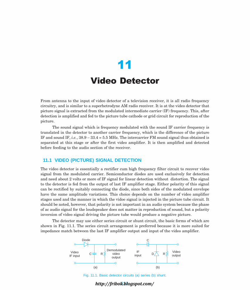
From antenna to the input of video detector of a television receiver, it is all radio frequencycircuitry, and is similar to a superhetrodyne AM radio receiver. It is at the video detector thatpicture signal is extracted from the modulated intermediate carrier (IF) frequency. This, afterdetection is amplified and fed to the picture tube cathode or grid circuit for reproduction of thepicture.
The sound signal which is frequency modulated with the sound IF carrier frequency istranslated in the detector to another carrier frequency, which is the difference of the pictureIF and sound IF, i.e., 38.9 – 33.4 = 5.5 MHz. The intercarrier FM sound signal thus obtained isseparated at this stage or after the first video amplifier. It is then amplified and detectedbefore feeding to the audio section of the receiver.
11.1 VIDEO (PICTURE) SIGNAL DETECTION
The video detector is essentially a rectifier cum high frequency filter circuit to recover videosignal from the modulated carrier. Semiconductor diodes are used exclusively for detectionand need about 2 volts or more of IF signal for linear detection without distortion. The signalto the detector is fed from the output of last IF amplifier stage. Either polarity of this signalcan be rectified by suitably connecting the diode, since both sides of the modulated envelopehave the same amplitude variations. This choice depends on the number of video amplifierstages used and the manner in which the vidoe signal is injected in the picture tube circuit. Itshould be noted, however, that polarity is not important in an audio system because the phaseof ac audio signal for the loudspeaker does not matter in reproduction of sound, but a polarityinversion of video signal driving the picture tube would produce a negative picture.
The detector may use either series circuit or shunt circuit, the basic forms of which areshown in Fig. 11.1. The series circuit arrangement is preferred because it is more suited forimpedance match between the last IF amplifier output and input of the video amplifier.
Diode
VideoIF input
Demodulatedvideooutput
RC
(a)
C
IFinput
VideooutputRD
(b)
Fig. 11.1. Basic detector circuits (a) series (b) shunt.
210
http://fribok.blogspot.com/
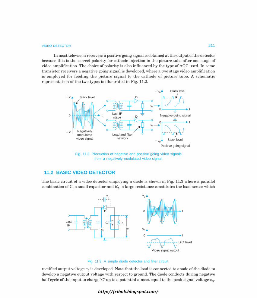
VIDEO DETECTOR 211
In most television receivers a positive going signal is obtained at the output of the detectorbecause this is the correct polarity for cathode injection in the picture tube after one stage ofvideo amplification. The choice of polarity is also influenced by the type of AGC used. In sometransistor receivers a negative going signal is developed, where a two stage video amplificationis employed for feeding the picture signal to the cathode of picture tube. A schematicrepresentation of the two types is illustrated in Fig. 11.2.
+ v
– v
0 t
Black level
Negativelymodulated
video signal
D
DLast IFstage
Load and filternetwork
v0
v0
+ v0
0 t
Black level
Negative going signal
0t
Black level– v0
Positive going signal
Fig. 11.2. Production of negative and positive going video signalsfrom a negatively modulated video signal.
11.2 BASIC VIDEO DETECTOR
The basic circuit of a video detector employing a diode is shown in Fig. 11.3 where a parallelcombination of C, a small capacitor and RL, a large resistance constitutes the load across which
Cd
D
C
vvs
–+
vv0
RLLastIF
vs
0 t
t
v0
0
D.C. level
Video signal output
Fig. 11.3. A simple diode detector and filter circuit.
rectified output voltage v0 is developed. Note that the load is connected to anode of the diode todevelop a negative output voltage with respect to ground. The diode conducts during negativehalf cycle of the input to charge ‘C’ up to a potential almost equal to the peak signal voltage vS.
http://fribok.blogspot.com/

212 MONOCHROME AND COLOUR TELEVISION
The difference is due to diode trop, since the forward resistance of the diode though small isnot zero. On the downward and positive half of each carrier cycle the diode becomes non-conducting, and during this interval some of the charge on capacitor ‘C’ decays through RL, tobe replenished at the next negative peak. The time constant of RLC network is kept largecompared with the time period of the applied IF signal. Then the circuit settles down to acondition, in which short current pulses flow through the diode only during the tip of each IFcycle to replenish the charge lost. The time constant of the network must, however, allow thecapacitor voltage to follow the comparatively slow variations of the envelope of the modulatedcarrier. This condition can be shown to occur approximately when
1R CL
= ωm × m
m1 2−
where ωm is the highest modulating frequency and m is the modulation index.With the highestmodulating frequency of 5 MHz and assuming an average modulation index of about 0.4, thetime constant (RLC) comes to nearly 0.08 µs. The period tC of the carrier (IF = 38.9 MHz)frequency = 0.025 µs and that of the highest modulating frequency (5 MHz) = 0.2 µs. In practicea time constant close to half the period of the highest modulating frequency is chosen foreffective and distortion free detection. This, in our case, is 0.1 µs and is nearly equal to thecalculated value of 0.08 µs. This time constant (0.1 µs) is seen to be much higher than the IFtime period and thus an output voltage that is very nearly equal to that of the envelope of theAM wave is ensured. If the RLC time constant is made too small, the output waveform willhave a large IF ripple content which is not desirable. However, if the RLC product is kept toolarge it will not affect the negative going half-cycle of the envelope waveform, but will causedistortion of the positive going movements of the modulated envelope. This is known as positivepeak clipping.
Choice of RL and CWhen the diode is conducting, it is obvious that some part of the output voltage is droppedacross Rd, the series diode forward resistance. The detector effeciency then depends on theratio of RL/Rd, where RL is the load resistance. Thus, for higher efficiency, a diode with a smallforward resistance must be chosen and RL should be kept as high as possible. As RL is increased,C has to be reduced to maintain the correct time constant. The smaller the value of C the moresignificant becomes Cd, the anode to cathode capacitance of the diode. A reference to Fig. 11.3will show that C and Cd form a potential divider across the input circuit. During positive halfcycles of the applied carrier voltage, when the diode does not conduct, the entire signal voltagesplits across these two capacitors. This results in some unwanted positive half of the appliedvoltage being developed across the load capacitor C. This reduces the net negative-going outputand hence the efficiency. Therefore in an effort to increase RL, C cannot be reduced too muchbecause then most of the unwanted positive going voltage would develop across RL and reducethe net output voltage greatly.Since the voltage divides itself in inverse proportion to thecapacitances, and the larger voltage appears across the smaller of the two capacitors in series,the ratio C/Cd should be as large as possible. If C is to be decreased to use a high value of RL,then Cd must be very small.
http://fribok.blogspot.com/

VIDEO DETECTOR 213
Choice of the DiodeFor the time constant fixed at 0.1 µs, RL varying between 2.7 K and 5 K in parallel with C,between 15 pF and 30 pF are commonly employed as load network for the detector in televisionreceivers. Since RL is only a few kilo ohm, the forward resistance of the diode must be as smallas possible. The diode capacitance Cd must also be very small because the value of C chosen forthe network is only around 20 pF. Some of the semiconductor diodes that meet the aboverequirements are 0A79, IN69 and IN64, and are often used in video detector circuits.
It would be instructive to compare the values of RL and C chosen for the TV receiverdetector with that of a broadcast radio receiver. The corresponding values for a radio receiverdetector are : RL = 500 K and C = 100 pF (see Fig. 11.4) and are based on the same considerationsas explained for the television detector.
vs
D
100pF
C
Filter circuitRf
50 K
100pF
Cf
RL
500 K0v0
IF = 455 KHzf = 5 KHzm
C = 100 pFR = 500 KL
R C = 50 sL
Fig. 11.4. Detector and filter circuit of a radio receiver.
11.3 IF FILTER
The detector output voltage, v0 consists of three components—(i) the required video signal,(ii) an IF ripple voltage superposed on the video waveform and (iii) a dc component of amplitudealmost equal to the average amplitude of the AM wave. The IF carrier component is removedby passing the signal through an IF filter. The dc component, if not required, is blocked byinserting a coupling capacitor in series with the signal path. However, the dc component formsa useful source of AGC voltage and represents the average brightness of the scene.
A brief survey of the filter circuit used along with a radio receiver detector will be helpfulbefore looking into the special problems involved in detection of video signals. Such a detectorcircuit with provision to filter out IF ripple frequency is shown in Fig. 11.4 Rf is chosen to bevery much greater than Xcf (reactance of Cf) at the intermediate frequency of 455 KHz. Most ofthe IF voltage gets dropped across Rf and v0 is practically ripple free. Cf being small acts as anopen circuit for the audio signal. Rf and RL then form a potential divider for the desired audiosignal, and a part of this signal is also lost across Rf. However, since Rf << RL (nearly 1/10th)the loss of audio signal is very small. The filter configuration shown is standard in radio receivers.
The RC filter circuit used in radio receivers is not practicable for video detectors becauseof very low values of load resistance. A suitable value of Rf to attenuate IF would seriouslyattenuate the video signal as well, because of small value of RL across which the video outputvoltage develops. A series inductor is therefore used in place of Rf and the RC filter is thus
http://fribok.blogspot.com/

214 MONOCHROME AND COLOUR TELEVISION
replaced by an LC filter (see Fig. 11.5). At the IF frequency (38.9 MHz), the inductor Lf hasmuch higher reactance than that of the shunt capacitor Cf but at the video frequencies the
vsvs 0v0
D
Lf
100 H
C Cf 10 pF RLLastIF
Fig. 11.5. Basic video detector and fitter circuit.
reactance of Lf is much lower as compared to that of Cf. As labelled in Fig. 11.5, Lf = 100 µH andCf = 10 pF have been chosen to illustrate the filter action. At IF frequency the ratio of thereactance of series inductor to that of shunt capacitor (XLf /XCf) is nearly equal to 60. Thismeans an attenuation of about 35 db for the ripple voltage and is considered adequate. However,the attenuation of the video signal will be different for different frequency components of thecomposite signal. The higher video frequencies suffer more attenuation than the lower ones.In order to overcome this discrepancy the load is modified to include an inductor in series withRL. The reactance of this compensating coil (LC) increases with frequency and thus themagnitude of the complex load increases to counteract the additional drop across Lf, the seriesinductor. A typical value of such a compensating coil is of the order of 200 µH. Such anarrangement also takes care of the input capacitance of the following video amplifier whichwould otherwise tend to attenuate high frequency components of the video signal. The filtercircuit thus modified, ensures low, and almost constant attenuation over the entire frequencyrange. This is known as video bandwith compensation. The bandwidth must extend up to 6MHz to include sound intercarrier frequency of 5.5 MHz and its FM sidebands besides thevideo signal.
Figure 11.6, shows a practical video detector circuit. It employs a load resistance = 3.9 Kand a compensating coil = 250 µH. Its output is dc coupled to the video driver. The resistors R1and R2 form a voltage divider across the 12 V dc supply to fix necessary forward bias at thebase of the emitter follower (driver). The capacitor C1 provides effective ac bypass across R2.
Fromlast video
IF
100Ω
+ 12 V
C1 R2 15 K
RL
R1
+ 12 V
= 4.7 K
= 3.9 K
L
250 Hc
µ
To driverof videoamplifier
C2
LfD
Fig. 11.6. A practical video detector circuit.http://fribok.blogspot.com/
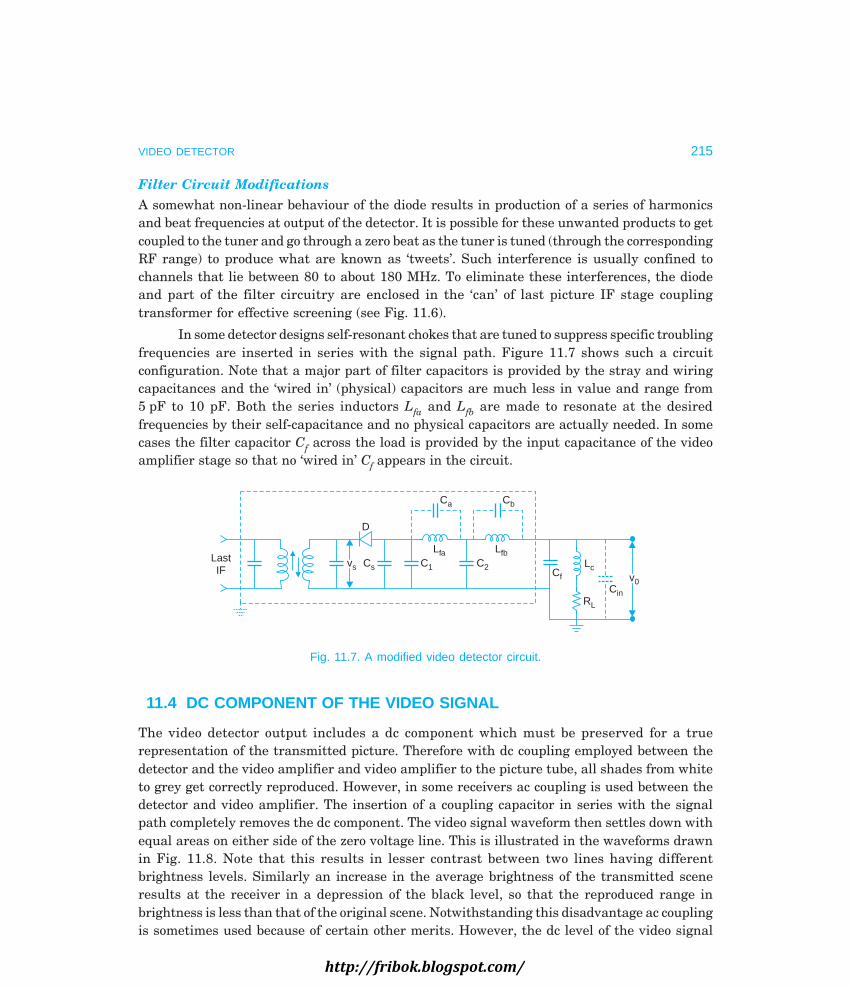
VIDEO DETECTOR 215
Filter Circuit ModificationsA somewhat non-linear behaviour of the diode results in production of a series of harmonicsand beat frequencies at output of the detector. It is possible for these unwanted products to getcoupled to the tuner and go through a zero beat as the tuner is tuned (through the correspondingRF range) to produce what are known as ‘tweets’. Such interference is usually confined tochannels that lie between 80 to about 180 MHz. To eliminate these interferences, the diodeand part of the filter circuitry are enclosed in the ‘can’ of last picture IF stage couplingtransformer for effective screening (see Fig. 11.6).
In some detector designs self-resonant chokes that are tuned to suppress specific troublingfrequencies are inserted in series with the signal path. Figure 11.7 shows such a circuitconfiguration. Note that a major part of filter capacitors is provided by the stray and wiringcapacitances and the ‘wired in’ (physical) capacitors are much less in value and range from5 pF to 10 pF. Both the series inductors Lfa and Lfb are made to resonate at the desiredfrequencies by their self-capacitance and no physical capacitors are actually needed. In somecases the filter capacitor Cf across the load is provided by the input capacitance of the videoamplifier stage so that no ‘wired in’ Cf appears in the circuit.
LastIF
D
Cs C1vvs C2
LfbLfa
Ca Cb
Cf
Lc
RL
Cin
vv0
Fig. 11.7. A modified video detector circuit.
11.4 DC COMPONENT OF THE VIDEO SIGNAL
The video detector output includes a dc component which must be preserved for a truerepresentation of the transmitted picture. Therefore with dc coupling employed between thedetector and the video amplifier and video amplifier to the picture tube, all shades from whiteto grey get correctly reproduced. However, in some receivers ac coupling is used between thedetector and video amplifier. The insertion of a coupling capacitor in series with the signalpath completely removes the dc component. The video signal waveform then settles down withequal areas on either side of the zero voltage line. This is illustrated in the waveforms drawnin Fig. 11.8. Note that this results in lesser contrast between two lines having differentbrightness levels. Similarly an increase in the average brightness of the transmitted sceneresults at the receiver in a depression of the black level, so that the reproduced range inbrightness is less than that of the original scene. Notwithstanding this disadvantage ac couplingis sometimes used because of certain other merits. However, the dc level of the video signal
http://fribok.blogspot.com/

216 MONOCHROME AND COLOUR TELEVISION
can be reinserted by what is known as ‘dc reinsertion’ technique before injecting it at the gridor cathode of the picture tube. This is fully explained in Chapter 14.
Ct
Black levelWhite lineGrey line
Peak white level
v0
0v0
0
Black level
Fig. 11.8 (a). Video detector output for two Fig. 11.8 (b). Effect of a.c. coupling. Thedifferent lines, one grey and the other white. black level is now different and thus
Note the black level is same for both the lines. the d.c. component is lost.
11.5 INTERCARRIER SOUND
In addition to recovering the composite video signal, rectifying action of the diode in the videodetector also results in frequency translation of the sound IF signal. The strong picture IFcarrier at 38.9 MHz acts as a local oscillator and heterodynes with the attenuated sound IFcarrier at 33.4 MHz to produce a difference frequency of 5.5 MHz. The resulting new IF togetherwith its FM sidebands is known as intercarrier sound signal. The video detector circuit ismodified (see Fig. 11.9) to extract the sound signal. As shown in the figure, a parallel tunedcircuit, commonly known as sound IF trap is inserted in the signal path. It is tuned somewhatbroadly with a centre frequency of 5.5 MHz. This offers a high impedance to the sound componentof the detected signal to remove it effectively from the video signal path. A tuned secondarycircuit delivers the intercarrier IF to sound section of the receiver. In some TV receivers theintercarrier sound signal is allowed one stage of amplification in the video amplifier and thenseparated through a trap circuit. It may be noted that in colour receivers two separate diodecircuits are used, one as a 5.5 MHz sound convertor and the other for video signal detection.This done to reduce interference in colour pictures due to the beat note produced at the differencefrequency of sound carrier and colour subcarrier frequencies.
4.7pF
4.7pF
D Lfa Lfb
To sound IF
Sound trap circuit
RL3.9K
4.7 K
Videoamplifier
Compensatingnetwork
Fig. 11.9. Video detector circuit with intercarrier sound trap.
http://fribok.blogspot.com/

VIDEO DETECTOR 217
11.6 VIDEO DETECTOR REQUIREMENTS
It is now obvious that in practice the video detector diode load is more complex than a simpleshunt combination of resistance and capacitance because of the many functions it is requiredto perform. The requirements are as follows:
(a) The detector load must provide a suitable impedance as seen through the diode, atinput of the detector to tune and damp secondary of the last IF coupling circuitcorrectly.
(b) The detector load must remove from the output, the IF content in the signal as muchas possible. For this purpose the load usually includes one or two low-pass filtersections.
(c) The detector load should have a trap circuit (a series rejector circuit) for separatingthe intercarrier sound signal.
(d) The detector load must also include a provision to boost the higher video frequenciesto compensate for the loss due to input capacitance of the video amplifier.
It is obvious from these requirements that rigorous theoretical design of such a diodedetector is very complex and therefore, in practice the design is usully reached by empiricalmethods based on filter circuit theory.
11.7 FUNCTIONS OF THE COMPOSITE VIDEO SIGNAL
Figure 11.10 illustrates various paths for the composite video signal as obtained from thevideo detector. We can consider that the signal is coupled to several parallel branches fordifferent functions. Therefore, each circuit can be operated independently of the others. Forinstance clipping the sync pulses in the sync-separator stage does not interfere with the videoamplifier supplying signal to the picture tube. Similarly, the AGC circuit rectifies the videosignal for developing AGC bias. With the same video signal the video amplifier provides completevideo signal to the picture tube for reconstruction of the televised scene. In some receiverdesigns a cathode or emitter follower is used to isolate the video detector from these circuits.In many receivers the video signal for the sync-separation circuit is tapped after one stage ofvideo amplification.
From IF
amplifier
Videodetector andfilter circuit
To video amplifier
To colour amplifiers(in colour receivers)
To AGC circuit
To sync separator
Forpicture tube
Fig. 11.10. Functions of the composite video signal.
http://fribok.blogspot.com/

218 MONOCHROME AND COLOUR TELEVISION
Review Questions
1. Draw the basic circuit of a video detector and explain design criteria for the choice of time constantof the load circuit. What determines the polarity of the diode in the detector circuit ?
2. Describe the factors that influence the choice of RL and C in the load circuit. Suggest suitablevalues of RL and C for the 525 line system where IF = 45.75 MHz and fm = 4 MHz.
3. Explain why is it necessary to employ and L-C instead of R-C filter to remove IF ripple from thedetected output. Give typical values of L and C and justify them.
4. Why is the filter circuit generally modified to include self-resonant inductors in the signal path ?What precautions are taken to prevent undesired harmonics from reaching the tuner ?
5. Explain how compensation is provided in the detector load circuit to extend its bandwidth. Whyis it necessary to have a bandwidth of nearly 6 MHz ? Sketch the complete circuit and label allcomponents.
6. How is the FM sound signal at 33.4 MHz translated to a new carrier frequency of 5.5 MHz andseparated from the composite video signal ?
7. Give a practical video detector circuit imcorporating the following features: (i) effective IF filter-ing, (ii) suppression of harmonics, (iii) separation of the intercarrier sound signal, and (iv) fre-quency compensation. Give typical values of all the circuit components.
http://fribok.blogspot.com/

12
http://fribok.blogspot.com/
The amplitude of composite video signal at the output of video detector is not large enough todrive the picture tube directly. Hence, further amplification is necessary, and this is providedby the video amplifier. The manner in which video signal is applied to the picture tube (cathodeor control grid) decides the type of video section circuitry. The video signal on application tothe picture tube varies the intensity of its beam as it is swept across the screen by deflectioncircuits. The gain control of the video amplifier constitutes the contrast control, whereas thebrightness control forms part of the picture tube circuit.
12.1 PICTURE REPRODUCTION
Figure 12.1 shows how the input video signal voltage for one line, impressed between grid andcathode of the picture tube results in reproduction of picture elements for that line. It shouldbe noted that the results are the same when reversed video signal is applied between cathodeand control grid. In fact the video signal should so align itself that its black level drives thegrid voltage to cut-off. Any grid voltage more negative than that is called blacker than blackand this part of the video signal corresponds to sync-voltage amplitude. At the grid of picturetube sync pulses really have no function, but these are used in the synchronizing section of thereceiver to time deflection circuits for vertical and horizontal scanning.
12.2 VIDEO AMPLIFIER REQUIREMENTS
In order to produce a suitable image on the screen of picture tube, the video amplifier mustmeet the following requirements.
(i) GainThe video signal must be strog enough to vary the intensity of the picture tube scanning beamto produce a full range of bright and dark values on the screen. This is illustrated in Fig. 12.1,where the signal amplitude is large enough to provide the desired contrast between white anddark parts of the scene being televised. However, with a video signal having smaller peak-to-peak variations, the brightness extends from dark, at cutoff bias, to some shade of grey, withthe result that there is less contrast between dark and light areas. Figure 12.2 illustrates thelight variations produced when the signal amplitude is reduced to about half as compared tothe signal amplitude required for full contrast. Any further reduction in the video signalamplitude will result in a washed-out picture, and there will be little difference between darkand light areas of the picture. A video signal amplitude of about 75 volts peak-to-peak is needed
220
http://fribok.blogspot.com/

VIDEO SECTION FUNDAMENTALS 221
Illumination
White
Greyshades
Blackt
Horzblanking
Bias
0
Light transfercharacteristics of the
picture tube
–100 –75VGK
Blackerthanblack Black
Whitet
Fig. 12.1. Light output with correct amplitude of the composite video signal.
odr
Variousshadesof grey
Illumination
White
Grey
Dark grey
Black
Horzblanking
0
WhiteBlack
– 75VGK
Fig. 12.2. Effect of insufficient video signal amplitude on brightness variations in the picture.
to obtain a picture with full contrast. Some colour picture tubes need higher signal amplitudesof the order of 150 V peak-to-peak, for proper reproduction of the picture. With a detectoroutput betwen 2 to 4 volts in all tube receivers, a gain between 25 to 50, at the video amplifieris considered adequate. A single pentode valve can develop this gain and most TV receivers
http://fribok.blogspot.com/

222 MONOCHROME AND COLOUR TELEVISION
using tubes have one stage of video amplification between video detector and picture tube.However, in transistor receivers where detector output seldom exceeds 2 volts, a two to fourstage video amplifier becomes necessary to fully modulate the beam of the picture tube.
(ii) BandwidthAs explained in an earlier chapter higher frequencies are needed to reproduce horizontalinformation of the picture. The lowest frequency for picture information in the horizontaldirection can be considered as 10 KHz when the camera beam scans all white and all blacklines alternately. Note that the active line period has been taken as 50 µs instead of the actualperiod of 52 µs. Similarly when the beam scans half white and half black lines in succession,the video frequency generated is 20 KMz. This is illustrated in Fig. 12.3 where different alternateblack and white widths have been closen to demonstrate the generation of high frequencysignal. Thus, for reproducing very minute details, a very high video frequency would benecessary, but keeping in view the limitations of channel bandwidth, the upper limit has beenfixed at 5 MHz.
o e mWidth of picture or 50 s» m s» m50 seie p8
Height ofthe picture
18720 s» m
= ½ cycle of26.7Hz 25 Hz»
100 KHz = 5 s »m
m »
m »
m »
200 KHz = 2.5 s
500 KHz = 1 s
5 MHz = 0.1 s
½ cycleof
(a) Horizontal information (b) Vertical information
Fig. 12.3. Relationship between picture size and video frequencies.
The signal frequencies corresponding to picture information scanned in the verticaldirection are much lower compared with those for reproduction within a line. If the videovoltage it taken from top to bottom through all the horizontal lines in a field, the variation willcorrespond to a half-cycle of a signal with a frequency of approximately 25 Hz. When thebrightness of the picture varies from frame to frame the resultant signal frequency is lowerthan 25 Hz. However, this is considered as a change in dc level corresponding to a change inthe brightness of the scene; and this can become almost zero Hz (i.e., dc) when the averagebrightness does not change over a long period of time. Ideally then, the video amplifier responseshould be linear from dc to the highest modulation frequency of 5 MHz. This is possible onlywhen the video amplifier is direct coupled.
(iii) Fequency DistortionThe gain at high frequencies falls-off because of shunting effect of the device’s outputcapacitance, stray capacitances and input capacitance of the picture tube. When ac coupling isemployed the gain decreases at low frequencies on account of increasing reactance of the couplingcapacitor. This inequality in gain at different frequency components of the signal is calledfrequency distortion. Excessive frequency distortion cannot be tolerated because it changespicture information. If high frequency content of the video signal is lost due to poor high
http://fribok.blogspot.com/

VIDEO SECTION FUNDAMENTALS 223
frequency response the rapid changes between black and white for small adjacent pictureelements in the horizontal line cannot be reproduced. This results in loss of horizontal detail.For example in the test pattern shown in Fig. 12.4, the individual black lines close to thecentre will loose their identity and instead appear as an illdefined black patch. Similarly smalldetails such as individual hairs of a person’s eyebrows do not appear clearly. However, in aclose up of the same face, where each area of the picture gets enlarged, the sharpness of eachdetail improves because a relatively low frequency range is required for proper reproduction ofdetails. Frequencies from about 100 KHz down to 25 Hz represent the main parts of the pictureinformation, out of which frequencies from 100 KHz to about 10 KHz correspond to black-and-white information of most details in the horizontal direction and frequencies from 10 KMzdown to 25 Hz represent changes of shading in the vertical direction. If the low frequencyresponse is poor, the picture as a whole is weak with poor contrast. The lettering, if any, is notsolid and the average brightness appears to be changing gradually from top to bottom of theraster, instead of complete change of brightness in the actual scene.
Horzresolution
Verticalresolution
Fig. 12.4. Test chart for determining vertical and horizontal resolution.
(iv) Phase DistortionPhase distortion is not important in audio amplifiers, because the ear does not detect changesin relative phases of the various frequency components present in a given sound signal. However,it is important in video amplifiers, since phase shift implies time shift, which in turn meansposition shift in the reproduced visual image. The resultant shift in relative positions of thevarious picture elements is detected by the eye as distortion. Therefore relative phases of allthe frequency components present in the video signal must be preserved. The time delay dueto phase shift is not harmfull if all frequency components have the same amount of delay. Theonly effect of such uniform delay would be to shift the entire signal to a later time. No distortionresults because all components would be in their proper place in the video signal waveshapeand so also in the reproduced picture. Therefore, the phase angle delay should be directlyproportional to the frequency or all frequency components must have the same time delay.This is illustrated in Fig. 12.5 (a) and (b). It should be noted that the signal inversion of exactly180° in any one stage of the video amplifier does not mean phase distortion. There is no timedelay, but only a polarity reversal.
http://fribok.blogspot.com/

224 MONOCHROME AND COLOUR TELEVISION
Frequency(a)
Frequency(b)
Phaseangle
delay °
Timedelay( s)
Fig. 12.5. Phase response of the amplifier:(a) Phase angles proportional to frequency.
(b) Corresponding time delay which is constant.
Figure 12.6 shows frequency response of an RC coupled amplifier where fL and fH are thelower and upper 3 db down frequencies. The corresponding phase shift angles at thesefrequencies are +45° and –45° relative to midband frequencies. Phase distortion is very important
Ha po er o tsHalf power points
0fL fH
f
(a)
Gain(db)
Lowfrequency
Midfrequency
Highfrequency
100%
– 70.7%
(b)
+ 90°
+ 45°
0°
– 45°
– 90°
fL fH
Phase f
Fig. 12.6. (a) Frequency and (b) phase response of a practical amplifier.
at low video frequencies because here even a small phase delay is equivalent to a relativelylarge time delay. As an illustration consider an amplifier designed to have fL = 2.5 Hz. Thephase shift at 2.5 Hz = 45° and that at 10 fL (25 Hz) it is nearly 6°. The relative time delay
between this frequency and midband frequencies would be 6
3601025
6
× ≈ 660 µs, which in turn
would mean that the picture information due to the two frequency components (2.5 Hz and
25 Hz) would get displaced with respect to each other by nearly 66064
~− 10 lines. To correct this
discrepancy even if phase shift at 25 Hz is made = 1°, the corresponding time delay would be120 µs and the picture information will get displaced by about 1.5 lines on the raster. The eyesare very sensitive to time delay errors and see this as ‘smear’ on the picture. At very high videofrequencies the effects of phase distortion are not as evident on the screen because the timedelay at these frequencies is relatively small. For example, if fH, the upper corner frequency ofthe amplifier is set at 5 MHz, the corresponding time delay with respect to midband frequencies
is only 45
3601
5 101
406××
−~ th of a µs. The consequent displacement of the picture elements is
too small to be detected. Thus, a video amplifier with flat frequency response up to the highestuseful frequency, has negligible time delay distortion for very high video frequencies.
http://fribok.blogspot.com/

VIDEO SECTION FUNDAMENTALS 225
(v) Amplitude Distortion of Nonlinear DistortionIf the operating point on the transfer characteristics of a device for a given load and signalamplitude is not carefully chosen, amplitude distortion occurs where different amplitudes ofthe signal receive different amplification. This can result in limiting and clipping of the signalor in weak signal output. If sync pulse voltage gets compressed, synchronization may be lost,because the video amplifier usually provides composite video signal for the sync separator.Very often some gain has to be sacrificed to avoid amplitude distortion.
(vi) Manual Contrast ControlIt should be possible to vary amplitude of the video signal for optimum setting of contrastbetween white and black parts of the picture. Any control that varies the amount of ac videosignal will operate as a contrast adjustment. Therefore contrast varies when gain is varied ineither picture IF section or video amplifier. However, such a control is not possible in the IFsection because all receivers employ automatic gain control circuits to maintain almost aconstant voltage at the output of the video detector. Also, with intercarrier sound, any changeof gain in the IF section would affect the sound volume. Therefore, contrast control is providedin the video amplifier, and this in effect, is the gain control of video amplifier.
12.3 VIDEO AMPLIFIERS
It is obvious from the preceding discussion that video amplifiers must meet several exactingdemands and this calls for careful and rigorous design considerations. The wide-bandrequirement starting from almost dc to several MHz with minimum phase distortion is perhapsthe most stringent requirement. Both direct-coupled and RC coupled configurations are usedand each type has its own merits and demerits. Both types need high frequency compensation,and this is met by shunt-peaking and series-peaking techniques. Though a dc amplifier doesnot need any low frequency compensation, the RC coupled amplifier employs special lowfrequency boost techniques to extend the bandwidth at the lower end of its response.
A basic RC coupled amplifier configuration, which applies to both tubes and transistors,is shown in Fig. 12.7. It is designed to work under class ‘A’ operation. The gain of this amplifier
Videoamplifiervin
B+B–
Ct
Ccv0
Rg =250 K
R= 2.5 K
L
0.1 Fm
18PF
Gain(Contrast)
control
Fig. 12.7. Basic R.C. coupled amplifierNote: The component values shown are of a typical video
amplifier employing a pentode.
http://fribok.blogspot.com/

226 MONOCHROME AND COLOUR TELEVISION
falls off rapidly at high frequencies because of shunting effect of inter-electrode, input, andstray capacitances in parallel with the load resistance RL. Video stages use low value of RLcompared with audio amplifiers because of large bandwidth requirements. Typical values are2 KΩ to 8 KΩ in tube versions. Although gain is reduced, lowering RL extends the high frequencyresponse. The effect of Ct does not become important until its reactance is low enough to becomecomparable with the resistance RL. Then, the shunt reactance Xct lowers the impedance ZL,and this causes a fall in the gain at higher frequencies. The lower the RL, and smaller theshunt capacitance Ct, better is the high frequency response. However, practical video amplifiersgenerally use a relatively higher value of RL with peaking coils to boost the gain at higherfrequencies. A typical arrangement known as ‘shunt peaking’ is shown in Fig. 12.8. Here asmall inductor, L0 is connected in series with RL. This peaking coil resonates with Ct to boostthe gain at high frequencies (see Fig. 12.8 (b)), where the response of the uncompensated RCcoupled amplifier would normally drop off. The resistance of the coil is very small and so itdoes not effect dc voltages and response at the middle frequencies. A peaking coil is effectivefor frequencies above about 400 KHz.
+–
Vcc
RL RBRE
vfn
Bias+
–
Q Ct L0
Cc
v0
(a) (b)
vin
0 fv0
0 fv0
0 f
With shuntpeakingWithout shunt
peaking
The response curve of C and Lin parallel
t 0
Fig. 12.8 (a). Video amplifier employing shunt Fig. 12.8 (b). Frequency response of the amplifier.coil (peaking) frequency compensation.
Another arrangement to extend the high frequency response is known as ‘series peaking’compensation (Fig. 12.9). In this circuit, LC is in series with the two main components of Ct. At
+
RL
RE
vfn
+–
Q Cout
LC
Cc v0
(a) Video amplifier with series peaking
vin
0 fCin
Rin
RD
To picturetube input
circuitv0
0
Effect of Lc
With seriespeaking
Without seriespeaking
(b) Frequency response
Fig. 12.9. Video amplifier employing series peaking coil compensation.
http://fribok.blogspot.com/

VIDEO SECTION FUNDAMENTALS 227
one side of LC is Cout of the video amplifier and on the other side is Cin of the next stage or inputcapacitance of the picture tube. This arrangement reduces shunting capacitance across RLwhich results in more gain, while LC resonates with Cin to provide a rise in voltage across Cinat high frequencies. A series peaking coil usually has a shunt damping resistance such as RD,the function of which is to prevent oscillations or ringing in the coil with abrupt changes insignal.
The circuit of Fig. 12.10 combines shunt and series peaking which results in more gain,extended high frequency response and improved transient behaviour.
vfn Videoamplifier
Contrastcontrol
R1 C2
.005 FmCf
10 Fm
C0
5 PFL0
35 Hm
RL
4 K
RD = 10 K
Rf
10 KB +B –
Lc = 145 Hm
Cln
12 PF
0.1 Fm
Ccv0
To picture tubecircuit
Rin
400 K
Fig. 12.10. Video amplifier employing both shunt and series peaking for high frequencycompensation and a special decoupling circuit to boost low frequency response.
Note that the component values shown in the circuit are for a tube amplifier.
The low frequency response is affected by increased reactance of the coupling and bypasscapacitors. This can be improved by using largest possible values of these capacitors. In adition,the decoupling filter RfCf in the B+ supply line (Fig. 12.10) can be used to boost gain and reducephase shift distortion at very low frequencies. The capacitor Cf offers large reactance at lowfrequencies and then Rf in series with RL becomes the effective load. The increased load resultsin higher gain for low frequencies. This rise in gain compensates for the reduction in gaincaused by reactance of the coupling capacitor CC. Furthermore, phase shift caused by shuntcapacitor Cf is opposite to phase shift caused by series capacitor CC. As a result Cf tends tocorrect phase distortion introduced by the coupling cpacitor. A small paper or ceramic capacitorC2 is normally provided across Cf to bypass very high video frequencies because Cf, being alarge value electrolytic capacitor, has a non-negligible inductance and fails to provide a bypassat these frequencies.
Gain ControlThe change in gain of the video amplifier to provide contrast control can be effected in differentways. A common method is to vary the cathode/emitter resistance R1. This resistance is leftunbypassed and its variation alters the negative feedback which in turn changes the gain ofthe amplifier. The change in the value of R1 also varies the bias and the consequent shift in theoperating point can introduce amplitude distortion. To overcome this problem, in many videoamplifier designs, a potentiometer is provided at the output of the video amplifier to alters the
http://fribok.blogspot.com/

228 MONOCHROME AND COLOUR TELEVISION
magnitude of the video signal applied to the picture tube. This method is the same as volumecontrol in an audio amplifier.
5.5 MHz Sound TrapThe video amplifiers usually have a trap circuit, tuned to the intercarrier sound frequency of5.5 MHz to keep the sound signal out of the picture signal. If sound signal is not separated atthe video detector, the trap circuit can be modified to deliver the intercarrier sound signal tothe sound IF amplifier. This is illustrated in Fig. 12.11 (a) where L1 and C1 constitute the trapcircuit and winding L2 coupled to L1 serves as take-off point for the 5.5 MHz sound signal.
vinVideo
amplifier
B+
–
5.5 MHztrap cct
To sound
IF amp
L2
L1C1 Cc
RLRD
v0
Lc
L0
(a)
vinVideo
amplifier
B+
Lc
Cc
RL C
v0
L0
(b)
RD
L
5.5 MHztrap cct
Fig. 12.11. Video amplifier circuits (a) with parallel resonant trap in serieswith the output. The trap circuit also serves as the sound take-off circuit
(b) with series resonant 5.5 MHz trap in shunt with the load.
As shown in the figure, the trap circuit is in series with the output and when tuned toresonance at 5.5 MHz, offers maximum impedance. Therefore, the sound signal is removedbecause maximum voltage across the trap is developed at this frequency.
In Fig. 12.11 (b) another trap circuit arrangement is shown. Here L and C form a seriesresonant circuit tuned to 5.5 MHz. This trap circuit is in shunt with the load, and at resonance,provides practically a short circuit to the intercarrier sound signal. This prevents it fromappearing across the picture tube input.
If the 5.5 MHz sound signal together with its sidebands is not fully suppressed it causesbeat interference which results in diagonal lines on the picture having small wiggles. Theweave in the lines is the result of frequency variations in the FM sound signal. This effect isalso called ‘wormy’ picture. The interference disappears when there is no voice or music, leavingjust the straight lines corresponding to the 5.5 MHz carrier without modulation. The trapcircuits are tuned for minimum interference in the picture.
12.4 BASIC VIDEO AMPLIFIER OPERATION
Before attempting to discuss complete video section circuits it is desirable to recapitulate theoperation of a basic RC coupled amplifier, which after adding compensating elements servesas the video amplifier. The circuit of such an amplifier employing a pentode is drawn in
http://fribok.blogspot.com/

VIDEO SECTION FUNDAMENTALS 229
Fig. 12.12 (a). The voltage drop across RK provides grid bias and ensures class ‘A’ operation.The load resistance RL provides output voltage between the plate and ground. While Rs is thescreen voltage dropping resistance. The bypass capacitor CS, connected between screen gridand ground provides an effective short at all frequencies of interest. CK connected across RK isa bypass for the ac component of the current to prevent degeneration of the input signal.
The input signal waveform and corresponding plate current and plate voltage waveformsare shown in Figs. 12.12 (b) to (d). When the input signal swings to the extreme positive,maximum current flows and the plate voltage swings to its minimum value. Again, when theinput signal attains its maximum negative value, the plate current becomes minimum andplate voltage attains its maximum positive value. Thus, the output voltage is 180° out of phasewith respect to the input voltage. The dc component of the plate voltage is blocked by couplingcapacitor (CC) and the amplified ac component then appears across the output terminals of theamplifier.
An RC coupled amplifier employing a transistor in the common emitter configurationperforms in the same way as its tube counterpart, but with a difference, that instead of voltageit needs current drive for its operation. Normally potentiometer biasing is provided for settingthe operating point. The voltage and current polarities for an n-p-n transistor are the same aswith a vacuum tube. However, with a p-n-p transistor all signal polarities are negative withrespect to ground.
t0
VGK
P–P 4V
(v )in
(b) Input voltage(a) Amplifier circuit
vin
Cc G1G2
P
Rg
RKCK
KCS4 F
25 K
250 v+ Vpp
–
RL5 K
RS
Ccv0
0
20
40
mAiP
t
P–P value = 31 mA
IP (average value)0
(c) Plate current
0
75
t
P–P value = 140 V
(d) Plate voltage
150
225
185
volts
VP0
Fig. 12.12. R.C. coupled amplifier.
http://fribok.blogspot.com/

230 MONOCHROME AND COLOUR TELEVISION
12.5 COMPARISON OF VIDEO SIGNAL POLARITIES IN TUBE ANDTRANSISTOR CIRCUITS
As explained earlier a negative going signal is a must when the video signal is injected at thecathode. Similarly positive going signal is required for feeding at the grid of the picture tube.If opposite polarity is used the result will be a negative picture, in the same sense as aphotographic negative. Besides this, the polarity of video signal with respect to ground alsoaffects the biasing of the device employed in the video amplifier. These aspects are examinedin greater detail both for tube and transistor amplifiers using grid and cathode modulation ofthe picture tube.
Grid Modulation of the Picture Tube(i) Transistor Circuits. The circuit arrangement shown in Fig. 12.13 is of a direct coupled videoamplifier employing a n-p-n transistor to grid modulate the picture tube. The resistors R1 andR2 together with RE, that is bypassed by CE, provide forward biasing at the base-emitter junction.This biasing arrangement provides good stability of the operating point against devicereplacement, temperature variations, dc supply changes and ageing of circuit components.
vin
vin
0
v0
0
vco
t
1C
0Ico
t
Brightness controlB+
PIXtube
B.C.
Rx
G1
K
RL
v0C
E
Bn – p – n
CERER2
R1
Fig. 12.13. Direct coupled video amplifier circuit to grid modulate the picture tube.
Since a positive going signal is needed at the collector, a negative going video signal isrequired to the base. The value of emitter resistance RE is chosen to set the operating point ‘Q’for minimum collector current in the absence of input signal. In fact the base-emitter bias is soset that when video signal is applied, the sync tips make the base most positive. Thus thecollector current becomes maximum for sync tip levels and the collector acquires minimumpositive potential. This is the correct polarity for obtaining minimum beam current of thepicture tube. Since the operating point of the transistor is set close to cut-off bias, the collectorvoltage, in the absence of any video signal is highest, which makes the grid of the picture tubeleast negative with respect to cathode. Therefore, with no video voltage drive, though thetransistor draws a minimum current, the picture tube beam current is maximum.
http://fribok.blogspot.com/

VIDEO SECTION FUNDAMENTALS 231
Notice that the cathode of picture tube is returned to the brightness control which setsthe cathode at a voltage which is more positive with respect to ground than the grid. Brightnesscontrol is achieved by varying net negative voltage between grid and cathode. The resistanceRX fixes the minimum limit of bias and prevents the possibility of a net positive voltage on thegrid.
If a p-n-p transistor is employed the base-emitter junction must be enough forwardbiased, with no input signal, so that the positive going sync tips drive the bias backwardstowards the Ib = 0 point. Note that the input signal is all positive and the least positive level isreached on peak-white and the transistor then passes maximum current. The maximum collectorcurrent results in least negative collector voltage which in turn makes the picture tube gridless negative with respect to its cathode and the beam current increases to reproduce thepeak-white values of the picture. It may also be noted that in the absence of any video signalthe transistor collector is at a minimum negative potential and the corresponding beam currentis large. Similarly a p-n-p transistor needs a dc source of opposite polarity than a n-p-nconfiguration. This necessitates interchanging of the locations of orightness control and resistorRX to make sure that the picture tube grid never attains a positive potential.
(ii) Vacuum Tube Circuit. In the case of a vacuum tube a positive supply voltage isneeded and a positive drive to the grid is necessary to increase the plate current. Therefore,the working conditions of a vacuum tube video amplifier are exactly similar to those of an-p-n transistor. However, the potentials needed are much higher and the biasing technique issomewhat different. Thus in a vacuum tube amplifier, with no input signal the tube draws aminimum current, and the picture tube beam current is maximum.
Cathode Modulation of the Picture TubeWhen the video signal is injected at the cathode of picture tube a negative going signal isneeded at the anode/collector of the video amplifier and this necessitates a positive going signalat the grid/base of the amplifier.
(i) Tube Circuit. The necessary circuit details of the video section and the signal wave-forms at the input and output of the video amplifier are illustrated in Fig. 12.14. The tube isbiased close to VGK = 0 point so that maximum current corresponds to peak-white and mini-mum plate current occurs on sync pulse tips. The anode voltage waveform is then negativegoing as required for correct cathode modulation. The picture tube beam current is again highwith no signal at input of the amplifier.
(ii) Transistor Circuits. Fig. 12.15 shows a p-n-p configuration and associated wave-forms. The transistor input circuit is back biased towards Ib = 0 µA so that on peak-whites thebase current and hence the collector current is very small. Minimum collector current resultsin maximum negative voltage at the collector, so that once again the necessary negative goingcollector signal is derived for the picture tube cathode. In the absence of any input video signalthe collector voltage is more negative and hence the signal beam current is maximum.
If a n-p-n transistor is employed in the video amplifier designed for cathode modulation,the signal polarities both at the input and output terminals are exactly the same as shown inFig. 12.14 for a vacuum tube configuration. Therefore the picture tube beam current will behigh with no input signal to the amplifier.
http://fribok.blogspot.com/

232 MONOCHROME AND COLOUR TELEVISION
– vin
vin
0
v0
0 t
ip
0 t
B+
PIXtube
B.C.
G1
v0
CKRK
Rg
t
RL
K
RX
Fig. 12.14. Direct coupled video amplifier circuit to cathode modulate the picture tube.
– vin
vin
0
– ic
0t
B –
PIXtube
B.C.
RX
GK
RLR1
v0
p – n – p
CERER2
t
– v0
0t
Fig. 12.15. Direct coupled transistor (p-n-p) video amplifier circuitto cathode modulate the picture tube.
These results may be summarized as follows:
(i) The sense of the video signal relative to black level seen either at the input or out-put terminals is the same in tube and transistor circuits.
(ii) When the tube or n-p-n transistor is called upon to deliver maximum plate/collectorcurrent the p-n-p transistor has to pass minimum collector current and vice versa.
(iii) The picture tube beam current is maximum with no input video signal both for gridmodulation and cathode modulation when dc coupling is used.
http://fribok.blogspot.com/

VIDEO SECTION FUNDAMENTALS 233
12.6 RELATIVE MERITS OF GRID AND CATHODE MODULATION OF THEPICTURE TUBE
The main points to be considered in assessing relative merits of the two systems are as follows:
(i) Picture Tube Input CharacteristicsThis is a measure of the beam current change for a given change in the video signal drivevoltage. The advantage lies with cathode modulation. The beam current is determined by thegrid-cathode voltage and by the positive voltage on the first anode with respect to cathode.With grid modulation, the only factor which determines the change in beam current resultsfrom a given change in video signal voltage between the grid and the cathode. No other electrodevoltage is effected with the applied voltage. However, when cathode modulation is applied asecond factor influences the beam current. This is the voltage between the first anode andcathode. Thus as the video signal input voltage moves, from black-level towards peak-whitethe cathode moves more negative, not only to the control grid but also to the first anode. Asstated above the voltage on the first anode and cathode itself have a marked influence uponthe beam current of the picture tube. Thus the change in beam current brought about byeffective reduction in grid-to-cathode. negative bias, is further augmented due to increase inpositive voltage between the first anode and cathode. However, with grid modulation the voltagebetween the first anode and cathode remains constant. If follows then, that for a given changein the input signal voltage, the change in beam current is less with grid modulation than withcathode modulation. For the same input, the beam current is about 20% greater on peak-whitewith cathode modulation, or the video amplifier gain can be smaller for the same beam current.
(ii) Feed to the Sync SeparatorMost commonly used sync separator circuits employ either a tube or a transistor, which is cut-off during the picture information part of the video signal but is driven into conduction by thesync pulses. A negative going video signal is then needed at the grid of the tube or base of then-p-n transistor being used as a sync separator. With cathode modulation the right polarity isavailable at the anode/collector of the tube/transistor. It is not so when grid modulation isemployed and thus cathode modulation has the added advantage over grid modulation ofautomatically providing the right polarity of the video signal needed to drive the sync separator.However, if a p-n-p transistor is used for sync separation, the grid modulation will providesignal with the correct polarity. With transistor receivers employing a two stage video amplifier,the question of feeding the sync separator is no longer important since both positive and negativepolarities of the video signal are always available.
(iii) Safety of Picture Tube in the Event of Video Amplifier FailureWith tube receivers or the ones employing an n-p-n transistor for video signal amplificationthe advantage lies with cathode modulation if direct coupling is used. Should the emission ofthe video amplifier tube fail or the n-p-n transistor stop conducting, the plate/collector currentdrops to zero and the cathode of the picture tube attains a positive potential equal to B+ supply.This immediately cuts-off the beam current and thus no damage is caused to the picture tube.With grid modulation such a fault will make the grid highly positive causing excessive beamcurrent. The shorts between plate and cathode (collector and emitter) are rare and need not beconsidered. When a p-n-p transistor is employed in the video amplifier the effects would beopposite.
http://fribok.blogspot.com/
234 MONOCHROME AND COLOUR TELEVISION
(iv) Cathode to Heater Voltage StressIn tube receivers using series heater arrangement the picture tube is placed at or near theground end of the chain to give it. maximum protection against possibility of damage due toshort circuits across the heater line. Thus the heater is at negative end of the dc supply. Withgrid modulation the cathode voltage of the picture tube is at a higher potential than whencathode modulation is used. The stress is therefore more in the case of grid modulation. However,in modern picture tubes the likelihood of cathode heater breakdown has been minimized. Alsowith capacitive coupling the voltages get reduced, and therefore this point does not very muchinfluence the choice of modulation method.
In conclusion, it may be said, that the video amplifier is one of the most importantsection of the receiver. It not only amplifies the video signal which extends from almost dc to avery high video frequency of 5 MHz, it also acts as the source for feeding the video signal to thesync separator and automatic gain control circuits. In most cases the sound signal is alsoseparated at this stage after amplification. It would then be desirable to take up a detailedconsideration of the video section design and circuitry. The next two chapters are devoted tothese aspects of video amplifiers.
Review Questions
1. What are the essential requirements that a video amplifier must meet for faithful reproductionof picture details ?
2. How does phase distortion in the video signal affect the quality of the picture ? What causes‘smear’ in the picture and how can this be minimized ?
3. Draw the circuit diagram of an RC coupled amplifier employing an n-p-n transistor in commonemitter configuration and explain its operation as a voltage amplifier. Sketch its frequencyresponse and explain why the gain falls-off both at very high and low frequencies.
4. Describe briefly with circuit diagrams the techniques employed to extend the bandwidth of anRC coupled amplifier to accommodate full range of the video signal.
5. Why are trap circuits provided in video amplifiers to attenuate frequency spectrum occupied bythe FM sound signal ? What is the undesired effect of sound signal on the reproduced picture ?
6. Draw simple circuit diagram of a dc coupled video amplifier that feeds the grid of the picturetube. Sketch suitable input and output voltage waveforms and justify that the chosen polarity ofthe video signal will result in correct reproduction of the picture on the screen. Identify thelocation of the brightness control in the circuit drawn by you.
7. Discuss relative merits of cathode and grid modulation of the picture tube. Explain why cathodemodulation is considered superior to grid modulation.
http://fribok.blogspot.com/

13
http://fribok.blogspot.com/

The choice of basic amplifier that can be modified to meet the requirements of a video amplifieris restricted to direct coupled and RC coupled configurations. The techniques employed toachieve broad-band characteristics are same for tube and transistor amplifiers. However, theirmode of operation and impedance levels are quite different from each other. Therefore, whileexplaining design fundamentals, video amplifiers employing tubes and transistors areconsidered separately.
13.1 VACUUM TUBE AMPLIFIER
The basic circuit of a video amplifier employing RC coupling, together with its ac equivalentcircuits valid for medium, high and low frequency regions are shown in Fig. 13.1. The capacitorC0 represents output capacitance of the tube, Cs stray shunt and wiring capacitance and Ciinput capacitance of the picture tube circuitry. All the three capacitances are effectively inparallel, and when added constitute Ct = C0 + Cs + Ci. The total shunt cpacitance seldomexceeds 20 pF and thus acts as an open circuit to frequencies in the low and midband ranges.The coupling capacitor CC is chosen to be quite large to provide nearly a complete ac short,even at very low frequencies.
Gain ExpressionsIt is an easy matter to deduce gain expressions for the three frequency regions from thecorresponding equivalent circuits of the basic amplifier configuration (Fig. 13.1). The resultsare summarized below as a starting point for explaining wide-banding techniques.
(i) Gain at midband (Amid) (see Fig. 13.1 (b))
A(mid) = – gm R || ≈ – gm RL ...(13.1)
where R || = RL || Rg || rp ≈ RL, because load resistance in video amplifiers seldom exceeds10 K-ohms. The minus sign signifies phase reversal of 180°.
(ii) Gain at high frequencies (see Fig. 13.1 (c))
A(HF) = – gmZt
where Zt = RL || XCt.
Substituting for XCt =
1ωCt
and simplifying yields
| A(HF) | = A
C R
mid
t L
( )
( )1 2+ ω ∠ – θH
236
http://fribok.blogspot.com/

VIDEO AMPLIFIERS—DESIGN PRINCIPLES 237
RS RL
+16 Fm
B+
CSG2
G1C0
Kvin
CC
CS RgCt
v0v0
Ct = C + C + C0 S 1
R|| = t || R || R = Rp L g L
vin = V = vG1K S
Fig. 13.1 (a). Basic R.C. coupled amplifier.
g vm g rp RL Rg 0v0 » RL 0v0g vm g
Fig. 13.1. (b). A.c. equivalent circuit valid at medium frequencies.
Rg 0v0RLCLvg
Rgv0v0RLCL
tpg vm g
0v0RLCLg vm g
rp
Fig. 13.1 (c). A.c. equivalent circuit valid at high frequencies.
g vm g tp RL Rgv0v0 »
CC
RLRg
v0v0
CC
g vm g
Fig. 13.1 (d). A.c. equivalent circuit valid at low frequencies.
Defining the upper 3 db frequency as
fH = 1
2πC Rt L or ωH =
1C Rt L
| A(HF) | = A mid( ) tan
12
1
+FHG
IKJ
∠ −FHG
IKJ
−
ωω
ωω
H
H...(13.2)
At ω = ωH, RL = XCt and ∠θH = – 45° (relative to phase-shift at midband).
Note that at f = fH = 1
2πC Rt L , Zt = 0.707 of its midband value and thus the gain at this
frequency falls to become – 3 db with respect to the midband gain.(iii) Gain at Low Frequencies (A(LF)) (see Fig. 13.1 (d)). Proceeding in the same way as for
the high frequency gain expression, and after a little manipulation, the gain in the low frequencyregion can be expressed as
http://fribok.blogspot.com/

238 MONOCHROME AND COLOUR TELEVISION
| A(LF) | = A
C RC g
(mid)
11
2
+FHG
IKJω
∠ + θL where r R
r Rp L
p L+ + Rg ≈ Rg.
Defining the lower 3 db down frequency as
fL = 1
2πC RC g or ωL =
1C RC g
the gain expression can be written as
| A(LF) | = A
L
(mid)
12
+ FHG
IKJ
ωω
∠ + tan–1 ωω
LFHG
IKJ ...(13.3)
At ω = ωL, Rg = XCC and θL = + 45° (relative to phase shift at midband).
Note that at f = fL = 1
2πC RC g , Zt = 0.707 of its midband value, and the gain at this
frequency again falls to –3 db with respect to midband gain. The frequencies fH and fL areknown as corner frequencies and the gain at these frequencies is 70.7% of the midband value.
BandwidthThe bandwidth of an amplifier is defined as
BW = (fH – fL) ≈ fH = 1
2πC Rt L...(13.4)
In an RC coupled amplifier, even when RL is made as low as 0.5 K-ohms, fH seldomexceeds 3 MHz. However, it is not possible to make the load resistance (RL), too small, becausethe gain requirement (gain = gmRL) of the video amplifier is not fully met. Therefore, someother means have to be devised to extend the frequency range upto 5 MHz without undulyreducing RL.
13.2 HIGH FREQUENCY COMPENSATION
The bandwidth is normally extended by making the plate load complex in such a way that itsmagnitude increases with increase in frequency. Thus, the compensation technique is aimedat pushing up the upper –3 db frequency fH, which normally would occur at a relatively lowfrequency due to the presence of shunt capacitance Ct. Negative feedback is also applied toincrease the bandwidth but this results in some loss of gain. The various HF compensationtechniques are as follows:
(a) Shunt Inductance PeakingA small inductor of the order of 50 to 250 µH is added in series with the load resistor RL.Though connected in series with RL, the coil is in fact a part of the shunt plate circuit. This isllustrated in Fig. 13.2, where the compensated amplifier configuration together with its highfrequency equivalent circuit is drawn. As shown there, the effective circuit, in shunt with thesignal path, consists of Ct in parallel with series combination of RL and inductor Lpx. Theinductor increases the net plate circuit impedance at high frequency end of the frequency
http://fribok.blogspot.com/

VIDEO AMPLIFIERS—DESIGN PRINCIPLES 239
range being handled, and thus partly compensates for the decreasing reactance of Ct. Thisresults in shifting the higher corner frequency fH to a still higher value to enhance bandwidthof the amplifier.
–
+mvg
rp Lpx
RL
Ct
v0
(b)(a)
vg
RK CK+
XCK << RK
CS
+
Ct
RL
RS
B+
L Shunt peaking coilpx
To picture tubecircuit
Fig. 13.2. Video amplifier employing shunt peaking (a) Circuit (b) Equivalent circuit.
The combined impedance of RL, Lpx and Ct can be expressed as
Zt = ( ) ( ) ( )
( ) ( )
X X R X
R X X
L Ct L Ct
L L Ct
px
px
2 2 2 2
2 2
1/2+
+ −
L
NMM
O
QPP ...(13.5)
As stated earlier the gain at fH where XCt = RL, falls to 70.7% of the midband value.Therefore, to extend the midband range, Zt should increase at this frequency to yield a gain
equal to the midband gain. This can be readily achieved by setting XLpx =
RL
2 and XCt = RL (at
fH) in equation (13.5). This, on substitution, yields
Zt =
RR R
RR
R
LL L
LL
L
2
2
22 2 2
22
1/2FHG
IKJ × +
+ −FHG
IKJ
L
N
MMMMM
O
Q
PPPPP
( ) ( )
( ) = RL ...(13.6)
Thus, the midband gain extends to fH, where, without compensation it was down by3 db.
Procedure for fixing RL and Lpx. It is necessary to first determine the total shuntingcapacitance (Ct) and the highest frequency (f) up to which flat response is desired before fixingthe values of RL and Lpx. The highest frequency of interest in the 625 line system is 5 MHz. Thevalue of Ct can be estimated from the data of the tube chosen for the amplifier, and by measuringstray capacitances if necessary.
With both f and Ct known, the values of RL and Lpx can be found as under.
RL = 1
2πfCt from f
C RHt L
=FHG
IKJ
12π
...(13.7)
http://fribok.blogspot.com/
240 MONOCHROME AND COLOUR TELEVISION
Since XLpx is to have a value equal to RL/2,
∴ 2πfLpx = 0.5RL = 0 5
2.
πfCt (from equation 13.7)
or Lpx = 0 54 2 2
.π f Ct
...(13.8)
On substituting RL2 =
1
4 2 2 2π f Ct
in equation (13.8)
we get Lpx = 0.5 CtRL2 ...(13.9)
This equation can be written in a general form as
Lpx = nCtRL2 ...(13.10)
where ‘n’ can be made to have any value of < 1, in order to vary frequency response in theregion close to the new value of fH. It may be noted that the circuit will resonate if ‘n’ exceetsunity.
Effect of varying Lpx. If gain versus frequency plot of such an amplifier is drawn fordifferent values of ‘n’, it is revealing to note, that for values of ‘n’ greater than 0.5, the responsehas a peak which becomes more pronounced as ‘n’ increases. Furthermore, increasing thevalue of inductance (i.e., n) increases the amplitude of the hump and also steepens the rate atwhich the gain falls off above fH. It is characteristic of compensating coils that while they liftthe response curve in the desired region, the subsequent fall-off of gain is more rapid than inthe uncompensated circuits. Too steep an edge in the response curve is not a desirablecharacteristic, since it can give rise to a tendency to produce overshoot or transients. In fact nosingle value of ‘n’ can give (i) constant gain throughout the pass-band, (ii) linear phase response,and (iii) fast transient response without overshoot, all at the same time. It can be shown, thatfor optimum frequency response, a value of n = 0.414, for least phase distortion; n = 0.322 andfor critical damping n = 0.25 is necessary.
In the practical development of a particular circuit, it is usual to start-off with an inductorof value Lpx = 0.5 RL
2Ct and then experiment with larger or smaller inductors until the desiredresponse is obtained. It may be noted that time delay due to phase shift at high frequencies isvery small and if linear phase characteristics are not obtainable while satisfying otherrequirements, it will not cause any problems.
(b) Series Inductance Peaking
In this arrangement the compensating coil is inserted in series with CC, which means that theinductor is in series with the signal path, rather than in shunt with it. Figure 13.3 shows thiscircuit arrangement with its equivalent circuit. In practice, the coil is fixed very close to theplate pin of the tube, and in this position it effectively separates the total shunt capacitance Ct,into two parts, with C0 on the tube side and (Cs + Ci) on the other side of the coil. As seen in theequivalent circuit, this arrangement takes the form of a low-pass filter. The value of Lpy is sochosen, that the filter passes all frequencies within the required video band, but offers a risingattenuation above the upper limit of this frequency hand.
http://fribok.blogspot.com/

VIDEO AMPLIFIERS—DESIGN PRINCIPLES 241
–
+mvg
rp
Lpy
RL Ct
v0
(b)(a)
vg
RK CK
CS
C1
RLRS
B+
LpyTo picturetube circuit
C2
C2
C1 + C = C2 t
Fig. 13.3. Video amplifier with series compensation (a) Circuit, (b) Equivalent circuit.
Since the total shunt capacitance gets divided into two parts, it is possible to choose ahigher value of RL, because C0 is only across RL and not Ct as was the case in shunt compensation.A 50% increase in RL becomes possible, i.e., Eqn. (13.7) can be modified to become
RL = 15
2.
πf CH t. ..(13.10)
This results in higher gain of the amplifier.
Choice of Lpy. It is obvious that the behaviour of the filter will be affected by the dispositionof the total shunt capacitance across the input (shown as C1) and across the output (shown asC2) of the resultant filter configuration. A typical value of C2/C1 is 0.75. A useful basic designformula for the inductor is given by
Lpy = nRL2Ct ...(13.11)
where n varies between 0.5 and 1. With a ratio of C2/C1 = p = 0.75, a value of n = 0.67 iscommonly used, since it gives optimum frequency response.
Though with series compensation more gain is possible and a better rise time performanceresults, but the fall-off in gain just beyond and upper edge of the required band is much steeper.This can cause excessive overshoot and even oscillations. This tendency towards ringing canbe reduced by connecting a resistance in parallel with Lpy. A typical practical value of such adamping resistance is 5RL and varies between 15 and 20 K-ohms.
(c) Combined Shunt and Series Peaking Coils
Shunt and series inductance compensation can be combined to get a peformance slightly superiorto that of the series peaking circuit. The corresponding amplifier configuration with itsequivalent circuit is shown in Fig. 13.4. The following formulae may be used as a guide toestablish approximate values of Lpx and Lpy
Lpx = nxRL2Ct and Lpy = nyRL
2Ct ...(13.12)
where nx and ny are the corresponding values of n and are dictated by the value of p, i.e.,(C2/C1). As a starting point, approximate values can be determined with the help of the followingchart:
http://fribok.blogspot.com/

242 MONOCHROME AND COLOUR TELEVISION
p nx ny
(i) Linear frequency response 0.6 0.14 0.58
(ii) Optimum phase response 0.72 0.1 0.46
(iii) Critical damping 0.8 0.063 0.39
–
+mvg
rp
Lpy
RL
Ct
(b)(a)
vg
RK CK
CS
C1
RL
RS
B+
Lpy
C2
C2Lpx
0v0
Lpx
0v0
Fig. 13.4. Video amplifier employing both shunt and series compensation(a) Circuit (b) Equivalent circuit.
It may be noted that in any case it would be necessary to test experimentally withvarious inductors to achieve the desired response. This is best done by using a visual displaysystem*. In addition, the transient response may be checked by feeding a square-wave signalto the amplifier, and measuring the rise-time of the output waveform with a cathode-rayoscilloscope.
Cathode Compensation. The basic principle of this method is to apply negative feedbackover the low and middle frequency regions, but arrange to remove it progressively in the HFregion. Because of negative feedback the overall gain gets reduced but it results in a considerableincrease in bandwidth. The simplest of the various possible circuit arrangements is shown inFig. 13.5 (a), where the value of Ck has been so chosen, that it completely bypasses Rk at highvideo frequencies, but at medium and low frequencies, its reactance becomes comparable withRk. This results in negative feedback which increases as the frequency decreases. In fact atmedium and low frequencies, the reactance of Ct is large compared with RL, and that of Ck islarge compared with Rk, thus the amplifier effectively performs as one with a plate load of RLand an unbypassed cathode resistance Rk. However, at higher frequencies when the shuntingeffect of Ct on RL becomes appreciable, the reactance of Ck becomes comparable with Rk, andthis reduces feedback to improve gain and maintain the frequency response.
Condition for Maximum Flatness of Frequency Response. Gain of the above amplifierthat employs cathode degeneration can be expressed in the form
A
A(mid)
(HF) = 1 + jωCtRL + gmRk
11
++
j C Rj C R
t L
k k
ωω ...(13.13)
*Necessary details of visual display system are given in Chapter 28.
http://fribok.blogspot.com/

VIDEO AMPLIFIERS—DESIGN PRINCIPLES 243
(a)
RK CK
C1
B+
RL
Rg
CC
vin
(b)
RK
CK
C1
B+
RL
Rg
CC
vin
LK
Fig. 13.5. Widebanding by cathode compensation (a) Reactance of CK
comparable to RK at medium and low frequencies, (b) LK and CK
resonate at the upper edge of the video frequency band.
Differentiating Eqn. (13.13) with respect to ω and equating this equal to zero yields
RLCt = RkCk ...(13.14)
This is the condition that must be met for maximum flatness of the frequency response.As already stated the improvement in bandwidth occurs at the expense of overall gain. However,this sacrifice is worth it, because with negative feedback the amplifier gain becomes morestable and in addition there is a considerable reduction of distortion in the output of the amplifier.
Another cathode compensation method is shown in Fig. 13.5 (b), where an inductor Lk inseries with Ck shunts the cathode resistor. The values of Lk and Ck are so chosen, that thecombination exhibits series resonance at the upper edge of the video frequency band. Atresonance the very low impedance of the series tuned circuit effectively short circuits thefeedback resistor and negative feedback is virtually reduced to zero. Typically, the ratio ofcathode to plate circuit time constants falls in the range of 0.5 to 2.0.
13.3 LOW FREQUENCY COMPENSATION
In video amplifiers that employ ac coupling a large coupling capacitor is normally used toobtain a fairly low value of fL. No special low frequency compensation is thought necessarybecause of the annoying effects of too good a low frequency response. This aspect is fullyexplained in the next chapter.
Direct Coupled Video AmplifierWhen direct coupling is used the question of low frequency compensation does not arise butthe problems of high frequency response are the same as with RC coupled amplifiers. Thoughsuch amplifiers can amplify changes in dc level, they have other inherent problems of drift,need for a highly regulated power supply and the high voltage dc source for adjustments ofvoltages at the grid and cathode in the absense of ac coupling. All this adds to cost and thereforein many cases partial dc coupling is preferred.
Selection of Tubes for Video AmplifiersThe ability to provide high gain and to handle signals up to 5 MHz are the primary considerationsin selection of tubes for use as video amplifiers. To achieve a high gain and large signal swings
http://fribok.blogspot.com/

244 MONOCHROME AND COLOUR TELEVISION
without excessive distortion, pentodes and beam power tetrodes having high current and largepower dissipation ratings are preferred.
Figure of MeritThe figure of merit of a high frequency tube is defined as the product of gain and bandwidth.
This can be expressed as:
Gain × bandwidth = A(mid) × (fH – fL)
Substituting for A(mid) = gmRL and setting (fH – fL) ≈ fH = 1
2πC Rt L we get,
Figure of Merit = gm × RL × 1
2πC Rt L =
gCm
t2π...(13.15)
Obviously, larger the value of this expression, better is the tube for use as a video-amplifier. However, because of large power needs, and the consequent large electrode structure,the output capacitance (C0) of such tubes cannot be made very small. This reduces the figure ofmerit of such tubes (fH reduces) and it becomes necessary to provide HF compensation toachieve the desired bandwidth. PCL84 is one such tube which has been specially designed foruse in TV receivers. The pentode section of this tube is used as a video amplifier whereas thetriode section is connected as a cathode follower for feeding video signal to AGC and synccircuits.
Video Amplifier CircuitBased on the design criteria developed in the earlier sections of this chapter, video amplifierdesign employing tube PCL84 has been more or less standardized. A typical circuit is drawn inFig. 13.6 with component values labelled on it. The tube employs a load resistance to the orderof 4 K-ohms and with a steady plate current close to 18 mA, the amplifier delivers enoughpeak-to-peak video signal to produce a full contrast picture.
CK
Fromvideo detector
Lp×2 5.6 K
100 V 22 K
Ry
LpyLp×1
RL4 K
+ 200 V
3 KPF47W
0.7 VPCL84
4 Fm
+
4 KPF0.1
mF 56 K
20 K potcontrastcontrol
+ 200 V
To cathode ofpicture tube
To triode sectionof PCL84L.C. 4.7 K
Fig. 13.6. Complete video amplifier circuit with gain control in the screen grid circuit.
http://fribok.blogspot.com/

VIDEO AMPLIFIERS—DESIGN PRINCIPLES 245
The main design features of this video amplifier are summarized below :
(i) The plate circuit contains both shunt and series compensating coils, that are mutu-ally coupled to provide adequate frequency broadbanding.
(ii) Cathode compensation is also provided by using a small cathode bypass capacitor.
(iii) The amplifier is designed for a full gain of about 30. The screen grid voltage isvaried to contol the gain and this serves as the contrast control.
(iv) The amplifier is dc coupled and has excellent low frequency response. In many designspartial dc coupling is used for optimum results.
13.4 TRANSISTOR VIDEO AMPLIFIER
Gain requirement from both tube and transistor video amplifiers is usually the same, andvaries between 25 to 60, depending on the video signal amplitude available at the output ofvideo detector and the transfer characteristics of the picture tube. Transistor video amplifiersare almost always direct coupled. This not only solves the gain and phase shift problems at lowfrequencies, but also makes the use of large coupling capacitors unnecessary. Direct couplingin transistor circuits does not present any serious problems so far as dc supply is concerned,because the magnitudes of voltage needed are much less than in tube circuits. However, theoutput transistor must have a VCC supply of the order of about 150 volts for delivering a videosignal of nearly 75 volts peak-to-peak to modulate the picture tube.
Transistors for Video AmplifiersThe output capacitance of transistors is comparable with that of tubes, but because transistorsoperate at lower impedances, the frequency and phase response in the collector circuit of anRC coupled transistor amplifier remains unaffected up to a higher frequency than in the tubeplate circuits.
The input capacitance of bipolar transistors is in general, much greater than that oftubes, but its effect on the previous collector circuit, can be nullified by using interstage emitterfollowers.
In a transistor amplifier the upper frequency limit is determined not by stray and shuntcapacitances, but by the reduction in current gain, as the cut-off frequency of the transistor isapproached. Low power transistors amplify up to very high frequencies and the problem is oneof limiting the bandwidth rather than extending it. However, this remark is not applicable topower transistors. The high signal voltage, that the last video amplifier stage is expected todeliver with restricted load resistance, needs large collector current operation. This in turnneeds a transistor of about 2 watt rating with a high breakdown voltage. When the above twoconditions are met, the desired gain at high frequencies cannot be easily achieved, because itis difficult to make transistors with lesser collector to base capacitance and high junctionbreakdown ratings. Therefore, it becomes necessary to use peaking coils in the collector circuitsof transistor video amplifiers to extend the high frequency range.
Amplifier ConfigurationOne high gain, high frequency transistor could by itself provide the required gain and bandwidth,but input and output impedance requirements make a single stage transtor amplifier difficult
http://fribok.blogspot.com/

246 MONOCHROME AND COLOUR TELEVISION
to design. Therefore, all video amplifier configurations are preceded by a driver stage, connectedas an emitter follower. The driver connects the video detector to the output stage and meetsthe following requirements:
(i) It presents a high input impedance to allow the use of a high detector load (about 5KΩ). This ensures higher detector efficiency and more output voltage.
(ii) It has low output impedance which facilitates matching to the input of the videoamplifier transistor.
(iii) Since the gain of the driver is less than one, it has a large bandwidth to ensure fulltransmission of video and intercarrier sound signals.
(iv) The driver output is in phase with its input, and thus provides the correct polarity ofvideo signal for cathode modulation of the picture tube after one stage of amplification.
13.5 TRANSISTOR CIRCUIT ANALYSIS
Common emitter circuit arrangement is the best suited configuration as a video amplifier,because of its moderate input and output impedances, high voltage and current gains besidesa large power output. Figure 13.7 shows hybrid-pi model of a transistor in the common emittermode. The equivalent circuit (model) has been simplified by reflecting, collector to base junctioncapacitance (Ccb or Cµ), to the input loop and neglecting the high collector to base resistance(rb′ c, or rµ).
Brx B
vbvbe bvb e¢ rp Cp Cm
E
C
RLrce
g vm b e¢
C = Cin p + Cm
= Cp + C (1 + g R )m m L
Fig. 13.7. Hybrid-pi(π) model of a transistor in common emitter configuration.
In the equivalent circuit (See Fig. 13.7):(i) rx is the base spreading resistance expressed as a lumped parameter. Its value var-
ies between 50 to 150 ohms.(ii) rπ is base to emitter junction resistance. Note that be common emitter input resist-
ance in the ‘h’ parameter model, i.e., hie = rx + rπ.(iii) gm (mA/V) is a constant of proportionality between collector current and base-emit-
ter voltage. It varies with collector current and is governed by the relation
gm = IV
C
T , where VT =
KTV
(VT = 0.026 V at room temperature.)
(iv) Cπ is the sum of diffusion capacitance and emitter to base junction capacitance.(v) β is the short circuit current gain of the transistor at low frequencies. It varies with
collector current and falls-off rapidly at collector currents beyond 10 mA.
http://fribok.blogspot.com/

VIDEO AMPLIFIERS—DESIGN PRINCIPLES 247
β = gm × rπ ...(13.16)
when β decreases, both gm and rπ are effected, and get reduced.
(vi) rce is collector to emitter resistance.
(vii) Cm (reflected Miller capacitance) = Cµ(1 + Av)
where Av is the voltage gain of the stage.(viii) Cin (total input capacitance) = Cπ + Cµ(1 + Av) ...(13.17)
(ix) RL is external load resistance.
(x) v′be is the effective voltage between base and emitter.
fβ (Half Power Frequency)The circuit of Fig. 13.7 takes the form shown in Fig. 13.8 (a) when RL is set equal to zero. Notethat rce disappears from the circuit once RL is made zero.
The input side of the circuit has a single time constant, consisting of rπ in parallel withCin. From this, 3 db down frequency
fH = fβ = 1
2π πr Cin...(13.18)
RS
vS
B rx B¢
vbvb¢e rπ Cin
gm vb e¢
i = shortcircuit current
c
Single timeconstant
With R = 0 A = 0C = C = C + C
L v
in in µπ
Fig. 13.8 (a). Equivalent circuit for the calculation of short-circuit CE current gain.
20 db decade
f(MHz)fTfB
A1
Bandwidth
1.0
(–3db) 70.7%
β
Fig. 13.8 (b). Short-circuit CE current gain vs frequency.
The short circuit current gain, Ais, can be expressed as
Ais = β
1 + ffb
At f << fβ, Ais = β and for f >> fβ, Ais ≈ β βf
f...(13.19)
http://fribok.blogspot.com/

248 MONOCHROME AND COLOUR TELEVISION
When f is set equal to fβ, the short circuit current gain drops by 3 db (see Fig. 13.8 (b)).This frequency fβ, at which the short circuit current gain becomes 70.7% of its maximum valueis the half-power or—3 db frequency. The frequency range up to fβ is then referred to as thebandwidth of the circuit.
fT (Unity Current Gain Frequency)fT is defined as the frequency at which Ais attains a magnitude equal to unity, that is:
1 = β βf
fT (from Eqn. 13.19)
or fT = β fβ ...(13.20)
Substituting values of β and fβ from (13.16) and (13.18) in (13.20), we get
fT = gCm
in2π...(13.21)
Since at short circuit Av = 0, Eqn. (13.17) reduces to
Cin = Cπ + Cµ
∴ fT = g
C Cm
2π π µ( )+...(13.22)
or ωT = g
C Cm
( )π µ+ ≈
gC
m
π | since Cπ >> Cµ. ...(13.23)
The above expression shows that fT is a function of the transistor parameters only.Since fT controls the gain at high frequencies it is also known as ‘Figure of Merit’ of the transistor.
Most of the above parameters are listed in transistor manuals. However, someparameters, if not given, can either be measured or calculated from the various relationsgiven above.
Voltage Gain of the Basic AmplifierThe circuit of the basic amplifier employing a BJT (transistor) in common emitter configurationis shown in Fig. 13.9 (a). In its equivalent circuit (Fig. 13.9 (b)), biasing resistance RB has notbeen included, because its shunting effect on input impedance of the transistor is negligible.Similarly rce being very large, in comparison with RL has been neglected.
RS
vS
B rx B¢
vbvb¢e
rπ
gm vb e¢
a
b
Rth
C × Dπ
E
RL
CT
v0C
(b)
CT
v0
vS
RS
RB RL
VCC
(a)
Fig. 13.9. Basic transistor amplifier in CE configuration (a) Circuit (b) Equivalent circuit.
http://fribok.blogspot.com/

VIDEO AMPLIFIERS—DESIGN PRINCIPLES 249
The Factor ‘D’Before proceeding to find voltage gain, it will be useful to define a factor D, to which, thecorner frequency of the amplifier is related.
From Eqn. (13.17), Cin = Cπ + Cµ (1 + Av)
Av at midband = gm RL
∴ Cin = Cπ + Cµ(1 + gmRL) ≈ Cπ + CµgmRL
Since ωT = gC
m
π (from Eqn. 13.23)
∴ Cin = Cπ(1 + CµRL ωT) ...(13.24)
= Cπ × D
where D = (1 + CµRL ωT) ...(13.25)
Voltage GainFrom the equivalent circuit of the amplifier (Fig. 13.9 (b)), the expression for voltage gain atany frequency (ω) can be expressed as
Av = −
+ + + +βωπ π π
R
r r R j DC r R rL
x S S x( )[ ( || )]1
If follows from this expression that
| A(mid) | = β
π
Rr r R
L
x S( )+ +....(13.26)
Gain Bandwidth ProductThe corner frequency occurs when the reactance of Cin (= Cπ × D) equals Rth, where Rth is theThevenin’s equivalent of the circuit (Fig. 13.9 (b)) to the left of points a and b.
Rth = r R rr R r
S x
S x
π
π
( )++ +
...(13.27)
where RS is the source resistance.
On equating XCin = Rth and some manipulation we get :
fH = β βf
Bor ωH =
βωβ
B
where ωβ = 1
r Cπ π and the other factor
B = r r R
R rx S
S x
+ ++
π ...(13.28)
fH (= bandwidth) can also be expressed as
fH = BD
× fT
β (since fT = fβ × β)
or ωH = BD
T× ωβ
...(13.29)
http://fribok.blogspot.com/

250 MONOCHROME AND COLOUR TELEVISION
Finally, Gain × Bandwidth = A(mid) × ωH
= β
π
Rr r R
L
x S+ + ×
BD
T×ωβ
(from Eqs. (13.26) and (13.29))
Substituting for B from Eqn. (13.28)
G × B . W = ωT L
S xDR
R r×
+ ...(13.30)
13.6 GUIDELINES FOR BROAD-BANDING
Equation (13.30) serves as a guideline for explaining the means to extend high frequencyresponse of the amplifier with or without sacrificing midband gain. This is explained byconsidering separately all the constituents of the Gain-Bandwidth expression.
(a) The gain-bandwidth product increases with decrease of source resistance RS. Thus areasonable first step while designing a video amplifier is to choose the lowest possiblevalue of RS. This requirement is readily met, since the driver stage is an emitterfollower, and its output resistance can be made very low without any appreciable lossin gain.
(b) ωT (fT = βfβ) does not stay constant and drops-off both at very low and high values ofemitter current. However, there is a range of IE (emitter current) over which it stayshigh and substantially constant. Therefore, it is advantageous to fix the transistoroperation, in this region, as far as possible.
(c) Once the transistor and its operating point (IE or IC) have been chosen, rx gets fixedand cannot be varied.
(d) If Cµ, that forms part of factor D is decreased, the bandwidth will increase with nocorresponding loss in gain. However, the value of Cµ is dictated by the VCC supplychosen or the maximum collector voltage rating of the transistor. Therefore, Cµ ismore or less fixed and cannot be changed for extending high frequency region of theamplifier.
(e) The last variable is RL, that can be changed to control bandwidth. But, this too cannotbe varied much because of large peak-to-peak output voltage required to modulatethe picture tube, and the maximum permissible dissipation of the transistor.
Output Circuit Corner Frequency
Input capacitance of the picture tube, together with transistor output and wiring capacitanceseasily add up to about 15 pF and very much limit the value of RL. In fact the net outputcapacitance (CT) of the video amplifier in parallel with RL provides another corner frequencywhich turns out to be lower than the input circuit corner frequency. This, then controls thebandwidth of the amplifier. As stated above, decreasing RL will push up the output cornerfrequency, but the load resistance cannot be made too small because it will increase the powerdissipation of the device.
http://fribok.blogspot.com/

VIDEO AMPLIFIERS—DESIGN PRINCIPLES 251
13.7 FREQUENCY COMPENSATION
It is clear from the above discussion that a high fT and high power dissipation transistor isnecessary for video amplifiers. These two requirements, though necessary, are mutuallycontradictory to a large extent.
In the past these requirements were met by cascoding, where the power dissipation wasshared equally by the two transistors employed in such a configuration.
With advances in technology, transistors with high power dissipation and reasonablyhigh fT have now become available. However, the configuration still requires some highfrequency compensation and is normally provided by a shunt or peaking coil in the collectorcircuit.
This and other relevant details are explained by a design example.
Video Amplifier Design DataOutput voltage 75 V (p-p)Bandwidth 5 MHzDetector output voltage 2 V (p-p)Voltage gain 40Configuration Common EmitterCoupling DirectVCC supply 150 VTransistor BF 178
Transistor parameters at IC = 15 mA are : rx = 50 ohm, rπ = 200 ohms, Cπ = 100 pF, β = 20,fT = 120 MHz, Cµ at 150 V = 1.25 pF, max collector dissipation = 1.7 watts, minimum collectoremitter breakdown voltage = 145 V.
Choice of RL and Operating PointTo avoid non-linear distortion due to saturation and cut-off, the best course for such a largeoutput is to draw several load lines on the characteristics of the chosen transistor and calculatedistortion for each load by the usual three or five point analysis. This would help to decide theoptimum value of RL. Note that too small and too large a value of load resistance is not acceptablefor reasons already explained.
Such an exercise on the characteristics of BF178 led to the following results:
IC ≈ IE = 15 mA
RL = 4.9 K
VCE (min) inclusive of drop across RE = 30 V
(RE is the emitter resistance)
This leaves 120 V to accmmodate the output signal with enough margin for the blankingexcursion.
For class ‘A’ operation the following relations are valid:
Pmax = V
R RCC
L E
2
4( )+...(13.31)
http://fribok.blogspot.com/

252 MONOCHROME AND COLOUR TELEVISION
IE = V
R RCC
L E2( )+...(13.32)
Choosing RE = 100 ohms and allowing a 10% limit in VCC variations, i.e., VCC max = 165 V,Pmax from eqn. (13.31) = 1.36 watts and IC ≈ IE from eqn. (13.32) = 15 mA.
The calculated value of IC checks with that found graphically. Similarly the calculatedvalue of Pmax is within the max. permissible dissipation. However, the transistor would need asuitable heat sink and this is always provided.
Amplifier CircuitThe circuit of the amplifier is drawn in Fig. 13.10 (a) and its equivalent circuit valid at highfrequencies is shown in Fig. 13.10 (b). Besides other circuit elements the two corner frequencies(break points) are labelled as f, 3 db (in) and f, 3 db (out) in the equivalent circuit.
CT
Lpx
RLg vm b e¢
f–3 db(out)
Cin
(b)f–3 db(in)
bvb e¢Rb rp
B¢
rx
vbevbe
B
RS
vS
(a)
CT
PIXTube
vS
RS
Driver circuitrepresentation
R2
BF 178
C300 PF
ER
100E
W
KR1
RL
Lpx
+ VCC
Fig. 13.10. Transistor video amplifier (a) Circuit (b) Equivalent circuit valid at high frequencies.
Voltage GainEquation (13.26) can be modified to include the effects of biasing network and the inadequatelybypassed RE. Putting Rb = R1 || R2 (biasing network resistors) and adding (1 + β)RE ≈ βRE(reflected emitter resistance) to rπ, the new voltage gain can be calculated. With the givendesign values even if Rb is taken as 7 K it can be neglected in comparison with the othershunting resistances. With this assumption the new voltage gain
| Av(mid) | = β
βπ
RR r r R
L
s x E+ + +...(13.33)
http://fribok.blogspot.com/

VIDEO AMPLIFIERS—DESIGN PRINCIPLES 253
Assuming Rs = 150 Ω, | Av(mid) | ≈ 40
This nearly checks with the midband gain computed from the approximate relationvalid with feedback:
| Av(mid) | ≈ RR
KL
E=
4 9100.
= 49
Input Circuit Corner Frequency f3 db (in)
f3 db (in) = 1
2πC Rin th...(13.34)
where Cin = Cπ + Cµ(1 + Av) = 100 + 1.25(1 + 40) = 150 pF
Equation (13.27) can be modified to include βRE. This takes the form
Rth = rπ || (Rs + rx + βRE) = r R r Rr R r R
s x E
s x E
π βπ β
( )+ ++ + + ...(13.35)
On substituting numerical values, Rth = 200 150 50 2000200 150 50 2000
( )+ ++ + + ≈ 180 Ω
∴ f3 db (in) = 1
2πC Rin th =
102 150 180
12
π × × ≈ 5.8 MHz
This result shows that the input circuit does not need any compensation and wouldsafely transmit up to the highest modulating frequency of 5 MHz.
Output Circuit Corner Frequency (f3 db (out))The total collector network capacitance in a well laid out receiver would by typically as follows:
Picture tube cathode and leads = 7 pF
Heat dissipator = 3 pF
BF 178 output capacitance = 3 pF
Total capacitance CT = 13 pF
∴ f3 db (out) (uncompensated) = 1
2πR CL T =
12 4.9 K 13 pFπ × ×
≈ 2.6 MHz.
Frequency CompensationThe above result shows that the output circuit has a lower corner frequency and hence woulddetermine the extent of compensation needed to push this corner frequency to about 5 MHz.
The design criteria for calculating the values of peaking coils are the same as used intube circuits. For shunt compensation:
From equation 13.9 we have
Lpx = 0.5 CTRL2
On substituting RL = 4.9 kΩ and CT = 13 pF
Lpx = 0.5 × 13 × 10–12 × (4.9 × 103)2 ≈ 158 × 10–6 H = 158 µH
An inductor of this value will form part of the collector load to provide necessarycompensation.
http://fribok.blogspot.com/

254 MONOCHROME AND COLOUR TELEVISION
Broad-Banding by Negative FeedbackIn addition to shunt compensation the emitter resistance RE is bypassed by a very small (300pF) capacitor CE (see Fig. 13.10 (a)) to provide negative feedback at medium and low videofrequencies. This not only improves the bandwidth but also ensures stable operation of theamplifier. The value of CE is determined by the consideration that emitter and collector networktime constants should be approximately equal.
13.8 VIDEO DRIVER
The output resistance of the driver together with the input resistance and capacitance of thevideo transistor form a network whose time constant should be compatible with the requiredbandwidth. Assuming 3 db point at 5 MHz and with Cin = 180 pF
R(out) ≤ 10
2 5 10
12
6π × × × 180 ≈ 150 ohms
Therefore, ideally, ignoring Rin, the output resistance of the driver stage should notexceed this value. This checks with the value of RS used while determining midband gain andinput corner frequency.
However, in most practical designs. a value of 500 ohms can be used, because of increasein bandwith available by partially decoupling the emitter resistance of the output transistor.
The emitter follower will have a gain nearly equal to 0.9. This will feed about 1.8 V videosignal to the output transistor which in turn will deliver ≈ 75 (p-p) (gain ≈ 40) for the picturetube.
Video Detector LoadingA high frequency transistor like BF 184 having β = 75 and fT = 300 MHz, if employed as anemitter follower with RE = 470 ohms will have Rin = 75 × 470 = 35 KΩ, and Cin = 5 pF. This isacceptable to a video detector circuit having a 3.9 KΩ load resistance.
Video Driver Biasing
The bias in the driver stage must be carefully set to permit maximum collector voltage swing.With a high input signal, the output will clip if the transistor cuts off or if VCE reaches zero.The result is loss of detail in dark grey or white parts of the picture and a buzzing tone in thesound output. For this reason the upper biasing resistance is often a pre-set variable resistor.The video detector diode is invariably direct coupled to the driver and thus held at the samesteady bias voltage as the base of the emitter follower. The biasing network is often designedto provide a small forward bias on the diode to reduce distortion on small input signals.
13.9 CONTRAST CONTROL METHODS
Contrast control is a manual control for setting level of the video signal fed to control grid orcathode of the picture tube. Its setting determines the ratio of light to dark in the picture.
http://fribok.blogspot.com/

VIDEO AMPLIFIERS—DESIGN PRINCIPLES 255
Contrast Control in Vacuum Tube Video Amplifiers(a) Cathode Network Control. In this method negative feedback is applied in one form or theother, taking into account the biasing requirements of the tube. Figure 13.11 (a) shows onesuch method, where the adjustment of the contrast control does not change the operatingpoint of the amplifier. This maintains a constant black level of the video signal.
(b) Plate Network Control. In this arrangement (Fig. 13.11 (b)) the contrast controlpotentiometer regulates the magnitude of the video signal to the picture tube. The straycapacitance of the potentiometer and its connecting leads can reduce high frequency responseof the amplifier. To minimize shunt capacitance the control is usually mounted close to thevideo amplifier with the shaft mechanically coupled to the front panel of the receiver. In addition,the capacitors shown along with the potentiometer, provide frequency compensation to maintainthe same frequency response, at different settings of the contrast control.
To platecircuit
B+
RK1
RK2
Rg
C1
Contrastcontrol
Videoinput
(a)
B+
Rg
Videoinput
(b)
RK
CKContrastcontrol
R2
R3
To picturetube circuit
C3C1
C2
CC
LPX
RL
B+B–
Fig. 13.11. Contrast control circuits in vacuum tube video amplifiers(a) Control network in cathode circuit, (b) Control network in plate circuit.
Contrast Control in Transistor Circuits(a) Base Network control. A contrast control technique that maintains a constant black level isshown in Fig. 13.12 (a). If the values of R3 and R4 are chosen to give a voltage that is equal tothe black level of the video signal at the emitter of Q1, the black level of the signal fed to Q2 willremain constant over the contrast control range. Because of bandwidth requirements, R2 shouldnot be higher than 1 K-ohm. The parallel value of R3, R4 should be about one quarter of thevalue of R2 thus giving a contrast range of about 5 : 1.
(b) Emitter Network Control. Fig. 13.12 (b) shows one type of emitter network contrastcontrol. It is a degeneration control. When the arm of potentiometer R4 is at ground, its resistanceis unbypassed causing maximum feedback. This results in small video output. Any variation ofthe arm towards the emitter reduces feedback to deliver more output. This provides the desiredcontrast control. C1R1, and C2R2 are video peaking networks which cause higher gain at lowcontrast settings for high frequencies, making the picture sharper.
(c) Collector Network Control. As shown in Fig. 13.12 (c) the 25-K frequency-compensatedpotentiometer operates like a volume control. Setting of contrast control determines the peak-to-peak amplitude of the video signal taken from the collector of the video amplifier and
http://fribok.blogspot.com/

256 MONOCHROME AND COLOUR TELEVISION
coupled to the cathode of picture tube. Because of the high impedance level of the collectornetwork, stray capacitances place severe restrictions on the circuit layout. The compensationshould be so provided that for any setting of the contrast control almost equal time constantsare obtained in the two arms of the connecting network.
From videodetector
Rb2
To AGCcircuit R1
R2a
Contrastcontrol
a¢
R4 CE
RE
Q2
To picturetube circuit
RL
Lpx
+ VCC2
+ VCC1
R3
Q1
RL1
(a)
From driveroutput
To picturetube circuit
+ VCC
RL
Lpx
Contrast control
C3
PB
C1
R1
R4R2 C2
(b)
Brightnesscontrol
B+
R4
To cathode ofpicture tube
CCC1
Contrastcontrol
25 K
R3CERER2
R1 RL
Videoinput
Lpx
+ VCC
(c)
R3
Fig. 13.12. Contrast control circuits in transistor video amplifiers(a) Base network control (b) Emitter network control (c) Collector network control.
http://fribok.blogspot.com/

VIDEO AMPLIFIERS—DESIGN PRINCIPLES 257
13.10 SCREEN SIZE AND VIDEO AMPLIFIER BANDIWDTH
It may not be immediately apparent but the size of the screen on which the picture is reproducedwill also govern how much finer details the picture should possess. On a small scrren thenumber of active lines that carry video information are very close to each other. This disablesthe eye to distinguish fine details, unless the viewer comes very close to the screen. The reasonstems from the fact, that unless the two adjacent objects subtend an angle of one minute ormore at the observer’s eye, they cannot be seen as distinct units. With small screens the distancenecessary for the eye to resolve details is so short that the viewer normally never comes thatclose to the screen.
Manufacturers of small screen TV receivers take advantage of this fact and design videoamplifiers with a bandwidth that is much less than 5MHz. This reduction, in the highestmodulating frequency to be reproduced, also makes full bandwidth in the RF and IF tunedamplifiers unnecessary. All this results in considerable reduction in the overall cost of thereceiver which is a big factor in a highly competitive consumer goods industry.
Review Questions
1. Draw small signal equivalent circuit of an R.C. coupled amplifier employing a vacuum tube and
derive expressions to show that its bandwidth ≈ 12πR CL t
, where RL is the load resistance and Ct
the total shunting capacitance.
2. Describe briefly the methods normally employed to extend the bandwidth of an R.C. coupledamplifier to meet video signal requirements. Show that in order to extend midband to the highercorner (– 3 db) frequency, the required value of shunt peaking coil inductance, Lpx = nCtRL
2,where n < 1.
3. What are the relative merits of shunt and series compensation techniques employed to extendthe bandwidth of an amplifier. Illustrate your answer by drawing equivalent circuits of amplifiersemploying the two types of compensation.
4. Describe different methods of low frequency compensation. What are the special problems ofdirect coupled amplifiers ?
5. Draw equivalent circuit of a grounded emitter amplifier and derive expressions for voltage gainand gain-bandwidth product.
6. Design a video amplifier to meet the following requirements :
Output voltage = 60 V (p-p), bandwidth = 4 MHz, detector output voltage 1.2 V (p-p), voltage gain= 50, configuration—common emitter, coupling—direct, VCC supply = 100 V, Transistor-BF 177.Its approximate parameters are :
rx = 50 ohms, rπ = 200 Ω, cπ = 100 pF, β = 25, fT = 120 MHz, Cπ at 100 V = 1 pF, maximum collectordissipation = 0.8 watt. Take total collector network cpacitance = 16 pF. Assume any other data ifnecessary.
7. Describe with suitable circuit diagrams different methods of contrast control used in both tubeand transistor video amplifiers. Mention relative merits of each type.
http://fribok.blogspot.com/

14
http://fribok.blogspot.com/

The essential requirements of video section circuitry and general wideband techniques wereexplained in the previous two chapters. The merits of cathode over grid modulation of thepicture tube were brought out in an earlier chapter. This is now the most preferred method offeeding video signal to the picture tube unless there are strong reasons in favour of gridmodulation. However, there are several methods of coupling the video amplifier to the picturetube. This, together with other relevant circuit details, is discussed in this chapter.
Various Coupling Methods. Though it cannot be denied that for near perfect reproductionof the transmitted picture, dc link has to be maintained between the video detector and picturetube, but dc coupling has its own problems which when fully taken care of add to the cost of thereceiver. Therefore in many video amplifier designs full dc coupling is dispensed with yetmaintaining optimum reception which is subjectively acceptable. The various possible couplingarrangements between the video amplifier and picture tube may be classified as:
(a) DC coupling
(b) Partial dc coupling
(c) AC coupling with dc restoration
(d) AC coupling
Though the circuit details differ from chassis to chassis, typical circuits of each type areexamined to identify merits and demerits of the various types of coupling.
14.1 DIRECT COUPLED VIDEO AMPLIFIER
A commonly used video amplifier employing PCL 84 (pentode-triode) is shown in Fig. 14.1.The video signal is directly coupled from video detector to cathode of the picture tube. Themain features of this circuit are as follows:
(i) Frequency CompensationThe plate circuit contains both shunt and series peaking coils to provide enhanced high frequencyrespouse. Additional broadbanding is achieved by using a small (0.003 µF) cathode bypass(Ck) capacitor. The network L1R1 in the grid circuit of the tube provides frequency compensationto offset its input capacitance.
(ii) Contrast ControlGain of the amplifier is controlled by varying dc voltage (potentiometer R6) at screen grid ofthe pentode. This becomes the contrast control. The need for two decoupling capacitors at thescreen grid arises from the fact that electrolytic capacitors have a small self-inductance which
260
http://fribok.blogspot.com/

VIDEO AMPLIFIER CIRCUITS 261
is sufficient to introduce considerable reactance at high frequencies. Therefore, to provideadequate decoupling at high frequencies the 4 µF electrolytic capacitor (C1) is shunted by asmall 0.005 µF capacitor (C2) as a high frequency bypass.
SPG
Fromvideo
detector
L1
4.7K
PCL 84
L3
L2
RL
+ 200V
4K
R56K
2
R
22K
3
L4
C1 C24 Fm
.005Fm
Rk
47Ck
.003 Fm
R5
R4
1K22K
To AGCcircuit
+150V
To syncseparator
PCL 84(Triodesection)
R7
R6
Contrastcontrol 20K
Pot500KPot
200V+
Brightnesscontrol
R8 R9
VDR
C3 0.1 Fm
Verticalblanking(50 Hz)
Horzblanking
(15625 Hz)
2.2M+500V
470KLHT
C001
F
4
m.
G2
G3G1
K
80V P–PR
5.6K
10
R1
Fig. 14.1. Direct coupled video amplifier.
(iii) Sync and AGC Take-off PointsThe triode section of PCL 84 is connected as a cathode follower. The resistors R4 and R5 form apotential divider at the cathode of the triode to feed necessary video voltage to the sync separatorcircuit. AGC circuit is fed directly from output of the cathode follower. The use of cathodefollower avoids any loading effects from sync separator and AGC circuits and thus fully isolatesthe video amplifier from these circuits. In the absence of such a provision some additionalcapacitance appears across the output of the amplifier and tends to lower its high frequencyresponse.
(iv) Flyback Suppression PulsesField and line flyback suppression pulses are injected at the control grid and first anode of thepicture tube through isolating networks. These negative going pulses are of sufficient amplitudeto cut-off the beam current during flyback intervals.
(v) Brightness Control and Switch-off SpotBrightness control is achieved by varying positive voltage at the grid (G1) of the picture tubewith potentiometer R8 that is connected in series with a VDR (voltage dependent resistance)across B+ supply. The VDR has a special function to perform. When the receiver is switched-offthe time-base circuits stop immediately and the picture tube spot assumes central position on
http://fribok.blogspot.com/
262 MONOCHROME AND COLOUR TELEVISION
the screen. The cathode and grid potentials rapidly becomes equal to chassis potential sincethe B+ voltage disappears. However, the picture tube’s cathode remains hot for some time andkeeps emitting electrons. At the same time the EHT capacitance formed by the aquadag coatingof the tube does not immediately discharge since the resistance of the EHT circuit is very high.For a few moments, therefore, beam current continues to flow with zero grid-cathode bias andno deflection fields. A bright spot known as ‘switch-off spot’ appears on the screen centre,which can in due course burn a small portion of the phosphor coating on the screen. Suppressionof the switch-off spot is brought about in this circuit by the VDR which forms the lower arm ofthe brightness control potential divider. When the receiver is switched off and the B+ voltagedisappears, the resistance of the VDR immediately becomes very high. This allows the chargeon the associated capacitor C3 to remain for a short time so that the grid is momentarilypositive with respect to cathode. The result of this is that a high beam current passes for abrief instant and this discharges the EHT smoothing capacitor. This happens as the normal B+voltage is decreasing and before the raster finally collapses. Thus the heavy beam current isspread over the screen face and not concentrated on a central spot.
14.2 PROBLEMS OF DC COUPLING
Direct coupling, though very desirable has the following stringent requirements, which, whenprovided for add very much to the cost of the receiver.
(a) Regulated EHT SupplyRegulation of normal type of EHT systems used in most television receivers is not good. Fullcontrast range to be handled by the picture tube with dc coupling puts a heavy demand on thehigh voltage supply. On signal levels that correspond to peak whites, excessive beam currentflows and this results in a drop of voltage. In turn this tends to an instantaneous increase indeflection sensitivity so that the picture expands (blooms) as the voltage falls. The increase indeflection sensitivity is due to the fact that as EHT voltage falls, forward velocity of the electrons,that constitute beam current, decreases. The electrons then spend a longer time under thedeflection field, and are deflected more by a given field than they would normally be. Therefore,either a well regulated EHT system should be provided, or the natural range of brightnesslevels, which occur in the original transmitted picture, should be artificially restricted at thereceiver. The latter, that is, partial loss of dc component of the video signal is lesser of the twoevils and involves a commercial compromise. This is explained in another section of this chapter.However, as stated earlier, in terms of absolute picture fidelity, both the complete retention ofdc component and a well regulated EHT system are necessary.
(b) Beam Current LimitingIn a dc coupled video stage, for cathode injection, the picture tube can be driven to a highbrightness level if the input signal is removed. This increase in beam current is expensive bothin high voltage supply source and the life of the picture tube.
A simple circuit which limits the mean beam current to a pre-determined value (withoutlimiting the contrast range) is shown in Fig. 14.2 (a). With this circuit arrangement, dc couplingis maintained only on low key scenes, where it is most important. In this circuit,
V3 = (Id + Ib)R1 = IdR1 + IbR1,
http://fribok.blogspot.com/

VIDEO AMPLIFIER CIRCUITS 263
The diode will remain conducting and clamp the picture tube cathode to collector of theamplifying transistor, so long as IbR1 < V2.
vin
RB1
RL
L0
+ VCC
+V2
RERB2 R1
C1
IdIb
+ V3D K
G1
Brightnesscontrol
vin
RB1
RB2 RE RL
Vcc+
Lpx
Ry
Lpy
VCo
R1
R2
C
0.1 F1
mPicture
tube
Verticalblanking
Fig. 14.2 (a). Beam current limiting. Fig. 14.2 (b). Partial dc coupling.
At the threshold of limiting,
Ib × R1 = V2 = V3
Therefore Id = 0
Beyond this threshold V2 < V3 and the capacitor C1 charges to V3 – V2, that is, thepicture tube drive is now ac coupled. The picture tube, therefore, receives an additional back-bias proportional to the excess mean drive.
It may be noted that it is not possible to establish precise limiting threshold because themean value of V2 varies with the picture content. However, by a suitable choice of the value ofR1, excess of picture tube EHT current and the consequent blooming (or breathing) of thepicture are prevented. In video circuits, that employ partial dc coupling, beam current isautomatically reduced, making use of a diode unnecessary.
(c) Other Direct Coupling ProblemsBesides the need for a regulated EHT supply and beam current limiting, the complexity indirect coupled amplifiers arises on account of the following :
(i) It is necessary to have a stable (regulated) B+ source to avoid any drift in the outputof the amplifier.
(ii) The reflections from any passing aeroplanes result in a steep rise and fall of inputsignal at the antenna of the receiver. This, despite an efficient fast acting AGC, causesa momentary flutter of the reproduced picture. It occurs because of very good lowfrequency response of the amplifier that extends down to zero Hertz.
(iii) There is a possibility of heater to cathode insulation breakdown during picture high-lights because of high dc voltage, equal to the plate voltage that appears on thecathode of the picture tube.
(iv) For cathode injection, if the detector output is directly coupled to the video amplifier,the latter must be biased to conduct heavily when no signal is present. This is expensiveboth in B+ current and life of the device.
http://fribok.blogspot.com/

264 MONOCHROME AND COLOUR TELEVISION
14.3 PARTIAL DC COUPLING
As mentioned earlier the solution to direct coupling problems, as a compromise, lies inattenuating the dc voltage before applying it to picture tube and providing a low frequencybypass to reduce some of its annoying effects. This arrangement is a common feature in mosttelevision receivers and is known as ‘partial dc coupling’. The relevant portion of a transistorvideo amplifier is shown in Fig. 14.2 (b). In this circuit
(i) C1, R1 and R2 constitute dc attenuator and low frequency filter circuit. The longtime constant circuit R1, C1 in series with video signal path to the picture tube cathode makesthe aeroplane flutter effect less annoying. The capacitor C1 (0.1 µF) fails to bypass very lowfrequencies, with the result, that R1 provides series attenuation in the signal path to offendinglow frequency pulsations. As obvious, low frequency components of the video signal get at-tenuated by a factor R2/(R1 + R2), and this is what gives the circuit the name ‘partial dc cou-pling’.
(ii) The values of R1 and R2 are chosen so as to considerably reduce the dc voltage thatreaches the cathode of picture tube. This not only attenuates the low frequency content of the
video signal but the consequent reduction in the working dc voltge VR
R RCO ×+
FHG
IKJ
2
1 2 at the cath-
ode reduces the magnitude of dc voltages required at the accelerating and focusing anode ofthe picture tube. This in turn results in a saving in the cost of power supply circuit.
(iii) The reduction in the cathode voltage reduces any possibility of heater cathode break-down of the picture tube.
(iv) Since the dc component is partly removed by potential divider action of R1 and R2,the difference in the mean level brightness from scene to scene is reduced. This restricts theoverall range to be handled by the tube and hence limits the maximum demand that is madeon the EHT system.
Video Amplifier CircuitA transistorised video amplifier circuit with emitter follower drive and partial dc coupling isshown in Fig. 14.3. The salient features of this circuit are :
(i) Signal from the video detector is dc coupled to the base of Q1. This transistor com-bines the functions of an emitter follower and CE amplifier. The high input impedance ofemitter follower minimizes loading of the video detector. The sync circuit is fed from the collec-tor of this transistor, where as signal for the sound section and AGC circuit is taken from theoutput of the emitter follower.
(ii) The output from the emitter follower is dc coupled to the base of Q2. This is a 5 Wpower transistor, with a heat-sink mounted on the case. The collector supply is 140 V, toprovide enough voltage swing for the 80 V P-P video signal output.
(iii) In the output circuit of Q2, contrast control forms part of the collector load. Thevideo output signal is coupled by the 0.22 µF (C2) capacitor to the cathode of picture tube. Thepartial dc coupling is provided by the 1 M (R2) resistor connected at the collector of Q2.
(iv) The parallel combination of L1 and C1 is tuned to resonate at 5.5 MHz to providemaximum negative feedback to the sound signal. This prevents appearance of sound signal atthe output of video amplifier.
http://fribok.blogspot.com/

VIDEO AMPLIFIER CIRCUITS 265
C1
1.2V
2.4V
0.22 Fm
To syncseparator
1.8K
+ 20V
To soundIF amp
Contrastcontrol
14VQ1Driver
1.8V
470W
47K20K
12V+
Video detectorcircuit
To AGCcircuit
68W .0022 Fm
0.002 Fm5.5 MHz
trapL1
Q2output
90V
Pot
5K
1.8K
140V+
L2
15PF
C2
R2
0.22 Fm
1M
10K 47K
+ 140V
100K Pot
Brightnesscontrol
Neonlamp
R15K
3 C3.047 Fm
EHT
80V P–P
Verticalblanking
Fig. 14.3. Video amplifier employing partial dc coupling.
(v) The neon bulb in the grid circuit provides protection of a spark-gap since the neonbulb ionizes and shorts to ground with excessive voltage. The ‘spark gaps’ are employed toprotect external receiver circuitry from ‘flash overs’ within the tube. The accumulation of chargeat the various electrodes of the picture tube results in the appearance of high voltates at theelectrodes, which if not discharged to ground, will do so through sections of the receiver cir-cuitry and cause damage.
(vi) Note that dc voltages at the base and emitter of the two transistors have been suit-ably set to give desired forward bias.
(vii) Vertical retrace blanking pulses are fed at the grid of the picture tube through C3,and the grid-return to ground is provided by R3.
(viii) Brightness control. The adjustement of average brightness of the reproduced sceneis carried out by varying the bias potential between cathode and control grid of the picturetube. In the circuit being considered a 100 KΩ potentiometer is provided to adjust dc voltage atthe cathode. This bias sets correct operating point for the tube and in conjunction with thevideo blanking pulses cuts-off the electron beam at appropriate moments.
The setting of grid bias depends upon the strength of signal being received. A signal ofsmall amplitude, say from a distant station, requires more fixed negative bias on the grid thana strong signal. The dependency of picture tube grid bias on the strength of the arriving signalis illustrated in Fig. 14.4. For a weak signal, the bias must be advanced to the point wherecombination of the relatively negative blanking voltage plus the tube bias drives the tube intocut-off. However, with a strong signal the negative grid bias must be reduced, otherwise someof the picture details are lost. Since the bias of the picture tube may required an adjustmentfor different stations, or under certain conditions from the same station, the brightness controlis provided at the front panel of the receiver.
http://fribok.blogspot.com/

266 MONOCHROME AND COLOUR TELEVISION
Picture tubetransfer characteristics
Averagebrightness
Black
VGK–90 –60 –30
0
DC bias
Weak signal
Strongsignal
Reduced biasB
right
ness
Fig. 14.4. Optimum setting of contrast control for differentamplitudes of the video signal.
The effects of brightness and contrast controls described earlier overlap to some extent.If setting of the contrast control is increased so that the video signal becomes stronger, thenthe brightness control must be adjusted to meet the new condition, so that no retrace lines arevisible and the picture does not look milky or washed out. Too small a value of the negativegrid bias allows average illumination of the scene to increase thus making part of the retracevisible. In addition, the picture assumes a washed out appearance. Too low a setting of thebrightness control, which results in a high negative bias on the picture tube grid, will causesome of the darker portions of the image to be eliminated. Besides this overall illumination ofthe scenes will also decrease. To correct this latter condition, either the brightness control canbe adjusted or the contrast control setting can be advanced until correct illumination is obtained.If the brightness control is varied over a wide range the focus of the picture tube may beaffected. However, in the normal range of brightness setting made by the viewer, changes infocus do not present any problem.
It is now apparent that despite the fact that video signal, as received from any televisionstation, contains all the information about the background shadings of the scene being televised,an optimum setting of both contrast control and brightness control by the viewer is a must toachieve desired results. Many viewers do not get the best out of their receivers because ofincorrect settings of these controls. However, to ensure that retrace lines are not seen on thescreen due to incorrect setting of either contrast or brightness control, all television receiversprovide blanking pulses on the grid electrode of the picture tube.
http://fribok.blogspot.com/
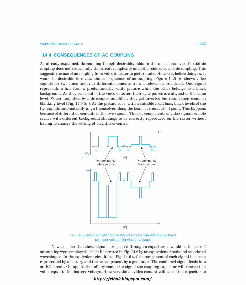
VIDEO AMPLIFIER CIRCUITS 267
14.4 CONSEQUENCES OF AC COUPLING
As already explained, dc coupling though desirable, adds to the cost of receiver. Partial dccoupling does not reduce fully the circuit complexity and other side effects of dc coupling. Thissuggests the use of ac coupling from video detector to picture tube. However, before doing so, itwould be desirable to review the consequences of ac coupling. Figure 14.5 (a) shows videosignals for two lines taken at different moments from a television broadcast. One signalrepresents a line from a predominently white picture while the other belongs to a blackbackground. As they come out of the video detector, their sync pulses are aligned to the samelevel. When amplified by a dc coupled amplifier, they get inverted but retain their commonblanking level (Fig. 14.5 (b)). At the picture tube, with a suitable fixed bias, black levels of thetwo signals automatically align themselves along the beam current cut-off point. This happensbecause of different dc contents in the two signals. Thus dc components of video signals enablescenes with different background shadings to be correctly reproduced on the raster withouthaving to change the setting of brightness control.
0
–vin
t
v0
0 t(b)
(a)Predominantlywhite picture
Predominantlyblack picture
Fig. 14.5. Video amplifier signal waveforms for two different pictures(a) Input voltage (b) Output voltage.
Now consider that these signals are passed through a capacitor as would be the case ifac coupling were employed. This is illustrated in Fig. 14.6 by an equivalent circuit and associatedwaveshapes. In the equivalent circuit (see Fig. 14.6 (a)) dc component of each signal has beenrepresented by a battery and the ac component by a generator. The combined signal feeds intoan RC circuit. On application of any composite signal the coupling capacitor will charge to avalue equal to the battery voltage. However, the ac video content will cause the capacitor to
http://fribok.blogspot.com/

268 MONOCHROME AND COLOUR TELEVISION
charge and discharge as the applied voltage exceeds and falls around the dc voltage across thecapacitor. Thus, while the dc component is blocked by the capacitor, the current whichcontinuously flows through the load resistance develops an ac voltage drop across it. Theresulting output waveshapes and their locations along with corresponding input waveshapesare shown in Figs. 14.6 (b) and (c). Note that while the output waveshapes are almost identicalto their input counterparts, their sync and blanking levels no longer align with each other.Each signal has set itself around the zero axis as a consequence of ac coupling. This leads tothe following undesired effects.
(i) Visible Retrace LinesThe retrace lines become visible because the blanking pulses do not remain at a constant leveland may not have enough amplitude to cause retrace blanking. Most modern receivers,irrespective of the coupling employed, incorporate special vertical and horizontal retraceblanking circuits as a means of preventing retrace lines from becoming visible.
(a)
+
+ –
–
C
R
vc
vp
ag
0v0
Outputvoltages
Videosignal’s
ac componentand
dc component
Inputvoltages
t
–
0
+
vin
t
–
0
+
v0
DC component
(b)
t
–
0
+
vin
(c)
DC component
t
–
0
+
v0
Fig. 14.6. Effect of RC coupling on the dc component of video signals(a) equivalent circuit of video signal and RC network (b) a predominantly
white scene, and (c) a predominantly dark scene.
(ii) Possible Loss of SyncThis occurs due to loss of dc component. The sync pulse amplitudes now vary with picturecontent and this can lead to inadequate amplitude of sync pulses at the output of sync separator.
http://fribok.blogspot.com/

VIDEO AMPLIFIER CIRCUITS 269
Therefore, if synchronization is to remain stable, the dc level must be restored (sync pulsesmust line up) before the video signal is fed to the sync separator circuitry.
(iii) Loss of Average Brightness of the SceneThis means that bright and dark scenes may not be easily distinguishable. With loss of dccomponent the average brightness information is lost. Thus signals from different brightnessbackgrounds will lose this identity and reproduce pictures with a background of some greyshade.
(iv) Poor Colour ReproductionIn colour television a change in the luminance (brightness) signal will cause a change in thebrightness of a colour. Therefore loss of dc component of the video signal will result in poorcolour reproduction.
14.5 DC REINSERTION
As explained earlier, relative relationship of ac signal to the blanking and sync pulses remainssame with or without the dc component. Furthermore, brighter the line, greater is the separationbetween the picture information variations and the associated pulses. As the scene becomesdarker, the two components move closer to each other. It is from these relationships that avariable bias can be developed to return the pulses to the same level which existed before thesignal was applied to the RC network.
DC Restoration with a DiodeA simple transistor-diode clamp circuit for lining up sync pulses is shown in Fig. 14.7 (a). TheVCC supply is set for a quiescent voltage of 15 V. In the absence of any input signal the couplingcapacitor ‘C’ charges to 15 V and so the voltage across the parallel combination of resistor Rand diode D will be zero. Assume that on application of a video signal, the collector voltageswings by 8 V peak to peak. The corresponding variations in collector to emitter voltage areillustrated in Fig. 14.7 (b). The positive increase in collector voltage is coupled through C to theanode of diode D, turning it on. Since a forward biased diode may be considered to be a short,it effectively ties (clamps) the output circuit to ground (zero level). In effect, each positive syncpulse tip will be clamped to zero level, thereby lining them up and restoring the dc level of thevideo signal.
11V
15V
19V
0
–8
–4
0
+ v0
t
Clamp level
DC level
VCE
t
VVCO
v0
D–
+4VR
–+
C
CVCE
+ VCC
RL
+ 15V
vin
(a) (b) (c)
Fig. 14.7. Diode dc restorer (a) circuit (b) collector voltage (c) output voltage.
http://fribok.blogspot.com/

270 MONOCHROME AND COLOUR TELEVISION
In the case under consideration the diode will cause the coupling capacitor to charge toa peak value of 19 V. However, during negative excursion of the collector voltage the capacitorfails to discharge appreciably, because the diode is now reverse biased and the value of R hasbeen chosen to be quite large. The average reverse bias across the diode is – 4 V, being thedifference between the quiescent collector voltage and peak value across the capacitor. Notethat as the input video signal varies in amplitude a corresponding video signal voltage appearsacross the resistor R and it varies in amplitude from 0 to – 8 V (peak to peak). This, as shownin Fig. 14.7 (c), is the composite video signal clamped to zero.
Similarly as and when the average brightness of the scene varies the capacitor C chargesto another peak value thereby keeping the sync tips clamped to zero level.
Reversing the diode in the restorer circuit will result in negative peak of the inputsignal being clamped to zero. This would mean that the dc output voltage of the circuit will bepositive. The video signal can also be clamped to any other off-set voltage by placing a dcvoltage of suitable polarity in series with the clamping diode.
Limitations of Diode ClampingIt was assumed while explaining the mechanism of dc restoration that charge across the couplingcapacitor C does not change during negative swings of the collector voltage. However, it is notso because of the finite value of RC. The voltage across C does change somewhat when thecondenser tends to discharge through the resistor R. Another aspect that merits attention isthe fact that whenever average brightness of the picture changes suddenly the dc restorer isnot capable of instant response because of inherent delay in the charge and discharge of thecapacitor. Some receivers employ special dc restoration techniques but cost prohibits their usein average priced sets.
14.6 AC COUPLING WITH DC REINSERTION
Figure 14.8 is the circuit of a video amplifier employing ac coupling with dc restoration. Thecoupling capacitor C1 offers negligible reactance to the high frequency content of the videosignal and it gets coupled to the picture tube grid directly. With no input signal, C2 charges tothe steady dc potential existing at ‘X’ through R4, R6 and R7. With arrival of video signal thepotential at ‘X’ falls during negative swing of the collector voltage. This causes C2 to dischargethrough R4, R3, VCC source, R7 and diode D1. However during positive voltage swing at thecollector, C2 fails to regain its charge because during this interval the diode is reverse biasedand R6 has been chosen to be too large. Thus the reduced voltage across C2 is maintained atthis level during intervals between sync tips because of the relatively large value of C2 andassociated resistors. The resultant difference of potential between ‘X’ and VC2, that effectivelyappears between ‘Y’ and ground (see Fig. 14.8) gets applied to the grid via isolating resistanceR5. This amounts to restoring dc component of the video signal, which otherwise is blocked bythe coupling capacitor. When the average brightness of the scene increases the video sync tipsmove further away from the picture signal content and the point ‘X’ then attains a new lesspositive potential during sync tip intervals. This further lowers the potential across the capacitorC2. The enhanced difference in potential between the point ‘X’ and the new value of VC2 gets
http://fribok.blogspot.com/

VIDEO AMPLIFIER CIRCUITS 271
applied to the grid of the tube. This, being positive, reduces the net negative voltage betweenthe grid and cathode and the scene then moves to a brighter area on the picture tubecharacteristics. Any decrease in average brightness of the scene being televised will have theopposite effect and net grid bias will become more negative to reduce background illuminationof the picture on the raster. Thus the diode with the associated components serves to restorethe dc content of the picture signal and the difference in potential between ‘X’ and ‘Y’ serves asa variable dc bias to change the average brightness of the scene.
v0
0 tR1
L1vin
Lastvideoamp
L2 C2
XR4
– +
R5
C1
v0 To gridof picture tube
R3
R2 +
–VCC
VC2 R6 D1
Y
R7
Fig. 14.8. Practical dc restorer circuit.
14.7 THE AC COUPLING
Cost is a strong determining factor in the design of commercial television receivers. If it ispossible to reduce the cost of a set without impairing the picture quality too much, then asacrifice in quality for cost is justifiable and is made in some receiver designs. Therefore manyreceivers use only ac coupling. In other words the dc component is removed from the signaland never reinserted.
The AC Coupled Video Amplifier
Figure 14.9 shows an ac coupled video amplifier. The coupling capacitor (0.22 µF) and resistanceof the brightness control network constitute the ac coupling network. The contrast control islocated in the emitter circuit of the first video amplifier. It is also ac coupled to the outputvideo amplifier. The amplifier employs the usual broadbanding techniques. It has a sound trap(resonant) circuit in the emitter lead of the output transistor. An interesting feature of thiscircuit is the provision of a spot-killer switch. This swith opens when the receiver is switchedoff. Its operation removes dc voltage at the cathode of picture tube reducing grid-cathode voltageto zero. The residual beam current increases and quickly discharges the EHT smoothingcapacitor thereby reducing intensity of the switch-off spot.
http://fribok.blogspot.com/

272 MONOCHROME AND COLOUR TELEVISION
Fromvideo
detector
Contrastcontrol 300
PotW
27 W
+ 24 V
RL
Q1
10 Fm
+ 24 V
33 K
2.2 K
15 KQ2
10 W
2000 PF Tunedto
5.5 MHz
1000 PF
33 K
100 W
–
+150 V 20
Fm
500 Hm
8.2 K
Spotkiller switch
0.22 Fm
CC
1 K
100 K
SPG
180 K
250 K PotBrightness
control
Verticalblanking
Horzblanking
.001Fm
470 K
550 V+
EHT
2.2 M
+400 V
0100 V P–P
150 Hm
Fig. 14.9. AC coupled video amplifier circuit.
14.8 VIDEO PREAMPLIFIER IN AN IC CHIP
The use of integrated circuits between video detector and video output amplifier is very commonin all solid state TV receivers. TBA 890 is one such dedicated IC which performs the followingfunctions. Figure 14.10 shows circuit connection at various pins of this IC.
39 PF5.5 MHz trap
To sound IF
Fromvideo
detector(Pin 8 of TCA 540
if used)
4.7 K 10PF
2.2 K
NC
Vertical sync pulses(To vertical osc)
15 nF 50 Fm0.2 Fm
100W
+ AFC flybackpulses
910111213141516
+
8754321 6
TBA 890 IC
+
16 V
100 W
0.1 Fm125
Fm
1.5K
56W 10 nF 16 mF
+100W
180W
150W
33 nF
47 K33 nFAFC
output(To Horz osc)
Delayed AGCto tuner
AFCflybackpulses
– 47mF
100 K Pot
AGC level
AGC to1st IF
100 Hm
Contrastcontrol
1.5 K 390 W 220W
56 W1K Pot
82 W
680 W 1 K
+ 16 V
+ 130 V
3.5 K
100 Hm
OA79
2N3501
0.22 Fm
1 nF
1.5 K K
470 K
33 K+
130 VBrightness
control
56 K
100 Kpot
68 nF
22 K
G2
G1
+
Fig. 14.10. Video output amplifier driven by the IC TBAS90.
(i) First Video AmplifierThe output from video detector feeds at pin 9 and this is also the sound take-off point. Thevideo preamplifier employs atleast two stages of differential amplifiers and is preceded by a
http://fribok.blogspot.com/

VIDEO AMPLIFIER CIRCUITS 273
driver stage to provide impedance matching. The voltage gain from this stage is about 70 db.Input signal from the detector is clamped at 3 V and the video output is obtained at pin 11 ofthe IC. The output drives video output transistor 2N 3501 through a contrast control networkas shown in the figure. The VCC supply to the IC is a stabilized + 16 V derived/from the lowvoltage (LV) rectifier and filter network.
(ii) Sync SeparatorThe sync separator receives input from the video preamplifier and is suitably biased to deliverclean sync pulses. The circuit also employs a noise suppression circuit. Integrated verticalsync pulses are fed to the vertical oscillator through a capacitor from pin number 14 on the IC.The amplitude of the vertical sync output is around 11 V.
(iii) AFC CircuitThe horizontal AFC circuit employs a single ended discriminator. It derives sync pulse inputfrom the sync separator and flyback pulses of opposite polarity from the horizontal outputtransformer at pins 4 and 10. The vertical blanking pulses are also added at pin 10 from thevertical output transformer. The AFC control voltage is available at pin 2 and is fed to theinput of horizontal oscillator through an anti-hunt filter circuit. AFC output voltage rangesfrom 2 to 10 volts.
(iv) AGC CircuitThe IC includes a keyed AGC circuit and receives flyback pulses through pin 10 along with theAFC circuit. The AGC output voltage varies from 1 to 12 V and is fed to the IF section from pin7 as shown in the figure. Delayed AGC voltage for the tuner is available at pin 6 and itsamplitude varies from 0.3 to 12 V.
Review Questions
1. Enumerate the various coupling methods employed between video detector and picture tube.Why does dc coupling add to the cost of the receiver ?
2. Describe the main features of the dc coupled video amplifier shown in Fig. 14.1.
What is a ‘switch-off ’ spot ? Explain how its undesirable effect on the screen is minimized byusing a VDR in the brightness control circuit.
3. Explain briefly the essential requirements, which must be met, while providing dc coupling inthe video section of the receiver. Describe with a suitable circuit diagram how a diode can beused to limit beam current of the picture tube to a safe upper limit.
4. What do you understand by partial dc coupling ? Explain with a circuit diagram how some of theannoying features of dc coupling are almost eliminated by partial dc coupling. Justify that it is areasonable compromise between cost and quality.
5. Describe the consequences of ac coupling. Show with a suitable circuit diagram 1and illustra-tions how dc component of the video signal is restored back by diode clamping in an otherwise accoupled video amplifier.
6. Explain how the removal of dc component from the video signal affects the overall contrast rangeand necessitates repeated adjustments of the brightness control.
7. State the arguments that are advanced in favour of employing ac coupling in the video section ofa TV receiver. Draw the circuit diagram of a typical coupled video amplifier and explain its mainfeatures.
http://fribok.blogspot.com/

15
http://fribok.blogspot.com/

Automatic gain control (AGC) circuit varies the gain of a receiver according to the strength ofsignal picked up by the antenna. The idea is the same as automatic volume control (AVC) inradio receivers. Useful signal strength at the receiver input terminals may vary from 50 µV to0.1 V or more, depending on the channel being received and distance between the receiver andtransmitter. The AGC bias is a dc voltage proportional to the input signal strength. It is obtainedby rectifying the video signal as available after the video detector. The AGC bias is used tocontrol the gain of RF and IF stages in the receiver to keep the output at the video detectoralmost constant despite changes in the input signal to the tuner.
15.1 ADVANTAGES OF AGC
The advantages of AGC are:
(a) Intensity and contrast of the picture, once set with manual controls, remain almostconstant despite changes in the input signal strength, since the AGC circuit reducesgain of the receiver with increase in input signal strength.
(b) Contrast in the reproduced picture does not change much when the receiver is switchedfrom one station to another.
(c) Amplitude and cross modulation distortion on strong signals is avoided due to reductionin gain.
(d) AGC also permits increase in gain for weak signals. This is achieved by delaying theapplication of AGC to the RF amplifier until the signal strength exceeds 150 µV or so.Therefore the signal to noise ratio remains large even for distant stations. This reducessnow effect in the reproduced picture.
(e) Flutter in the picture due to passing aeroplanes and other fading effects is reduced.
(f) Sound signal, being a part of the composite video signal, is also controlled by AGCand thus stays constant at the set level.
(g) Separation of sync pulses becomes easy since a constant amplitude video signalbecomes available for the sync separator.
AGC does not change the gain in a strictly linear fashion with change in signal strength,but overall control is quite good. For example, with an antenna signal of 200 µV the combinedRF and IF section gain will be 10,000 to deliver 2 V of video signal at the detector output,
276
http://fribok.blogspot.com/

AUTOMATIC GAIN CONTROL AND NOISE CANCELLING CIRCUITS 277
whereas with an input of 2000 µV, the gain instead of falling to 1000 to deliver the sameoutput, might attain a value of 1500 to deliver 3 V at the video detector.
Basic AGC CircuitThe circuit of Fig. 15.1 illustrates how AGC bias is developed and fed to RF and IF amplifiers.The video signal on rectification develops a unidirectional voltage across RL. This voltage mustbe filtered since a steady dc voltage is needed for bias. R1 and C1, with a time constant of about0.2 seconds, constitute the AGC filter. A smaller time constant, will fail to remove low frequencyvariations in the rectified signal, whereas, too large a time constant will not allow the AGCbias to change fast enough when the receiver is tuned to stations having different signalstrengths. In addition, a large time constant will fail to suppress flutter in the picture whichoccurs on account of unequal signal picked up by the antenna after reflection from the wings ofan aeroplane flying nearby. With tubes, a typical AGC filter has 0.1 µF for C1 and 2 M for R1.
IFamplifier
AGCrectifier
Video signalinput
Rectifiedoutput
RL
R1
C2R2
AGCfilter
C1AGC biasline
R3C3
Decouplingnetwork
RF amp
Fig. 15.1. Basic AGC circuit.
For transistors, typical values are 20 kΩ for R1 and 10 µF for C1. The filtered outputvoltage across C1 is the source of AGC bias to be distributed by the AGC line. Each stagecontrolled by AGC has a return path to the AGC line for bias, and thus the voltage on the AGCline varies the bias of the controlled stages.
15.2 GAIN CONTROL OF VT AND FET AMPLIFIERS
The gain of a vacuum tube or FET amplifier can be determined from the equation AV = gmZL,where gm is the transconductance of the device and ZL the impedance of the load. The impedanceis determined by the components used in the tuned circuit and does not lend itself to simplemanipulation. However, gm of both tubes and field-effect transistors can be controlled by varyingtheir bias. Hence all AGC systems vary the bias of RF and IF stages of the receiver to controltheir gain. The variation of gm with control grid voltage for a vacuum tube is illustrated in
http://fribok.blogspot.com/

278 MONOCHROME AND COLOUR TELEVISION
Fig. 15.2(a). The transconductance is smaller near cut-off but increases as the bias decreasestowards zero. It also decreases if operation of the tube is brought close to saturation. Theregion near cut-off bias is used for AGC operation. The self-bias is chosen to fix the operatingpoint for high gain. The AGC voltage which is negative gets added to it and shifts the operatingpoint to change the gain. The resulting change in gain compensates for variations in the inputsignal thereby maintaining almost constant signal amplitude at the output of video detector.Figure 15.2 (b) shows how the control grid is returned to the AGC line for negative bias. Intube circuits a negative bias varying between – 2V and – 20V is developed by the AGC circuitdepending on the strength of incoming signal. In order to obtain high gain and minimum crossmodulation effects, pentodes with remote cut-off characteristics are preferred in video IFamplifier circuits.
–30 –20 –100
(a)
VGK
Cut-offbias
gm
(b)
IF amp
IFtransformer
vin100 W
0.001 Fm
470 PF5 K
AGC bias–2 V to –20 V
Fig. 15.2. AGC action in tube circuits (a) plot of gm vS grid bias,(b) method of returning AGC bias to the control grid.
15.3 GAIN CONTROL OF TRANSISTOR AMPLIFIERS
The transistor is a current controlled device. Therefore, in transistor amplifiers it is desirableto consider power gain instead of voltage gain for exploring means of their gain control by AGCtechniques. The power gain (G) of a transistor amplifier may be determined by the equation,
G ≈ β2RR
L
in
where β and Rin are the short circuit current gain and input resistance of the transistorrespectively. Here again it is convenient to vary one of the parameters of the transistor inorder to control overall amplification of the receiver. The magnitude of β depends on theoperating point of a transistor which is established by the base to emitter (VBE) forward bias.Shifting the operating point, both towards collector current cut-off and collector currentsaturation causes a decrease in β which in turn reduces the power gain. Figure 15.3 shows theeffect of change in VBE on collector current and power gain of an amplifier employing a silicontransistor. A number of conclusions may be drawn from the curves shown in the figure. First,
http://fribok.blogspot.com/

AUTOMATIC GAIN CONTROL AND NOISE CANCELLING CIRCUITS 279
the amount of change in VBE which is necessary to shift the operating point of the transistorfrom cut-off to saturation is small, only 0.4 to 0.5 V. This is much smaller as compared to about30 V in a vacuum tube. Second, at some optimum value of forward bias (0.7 V in this case)power gain of the amplifier is maximum and does not change much for small variations in thebias voltage. However, the gain decreases as the bias is either increased (shifting the operatingpoint towards saturation) or decreased (moving it towards cut-off).
IC
00.4 0.7 1.0 V
VBE
00.4 0.7 1.0 V
VBE
G
ReverseAGC
ForwardAGC
Towardssaturation
Towardscut-off
Saturation
Cut-off
Fig. 15.3. Variation of collector current (IC) and power gain (G) of a transistoramplifier as its base to emitter voltage (VBE) is varied.
15.4 TYPES OF AGC
If the operating point is shifted towards saturation for controlling the amplifier gain, it iscalled forward AGC. An AGC system which operates by shifting the operating point towardscut-off is referred to as reverse AGC.
In many TV receiver designs, either forward or reverse AGC is exclusively employed foraffecting gain control. However, in some receivers both forward and reverse AGC aresimultaneously employed in different parts of the RF and IF amplifier chain. It may be notedthat receivers which use either reverse or forward AGC do not operate the amplifiers at peakgain but fix the no-signal operating point at such a value that the stage gain may be increasedor decreased without having to move to the other side of the power gain peak.
Reverse AGCThe power gain curve in Fig. 15.3 is not symmetrical, that is, the reverse AGC region of thecurve falls off more rapidly than does the forward AGC region. This means that reverse AGCwill require a smaller change in voltage for full gain control than will forward AGC. However,
http://fribok.blogspot.com/

280 MONOCHROME AND COLOUR TELEVISION
operation in this region, which is close to cut-off makes the receiver more susceptible to overloadand cross modulation distortion on strong signals.
The circuit of Fig. 15.4 (a) is of a single stage transistor (n-p-n) IF amplifier employingreverse AGC. The voltage divider formed by R1 and R2 provides a suitable fixed forward biasfrom the VCC supply. The resistor R3 and capacitor C1 constitute the AGC decoupling network.
Frommixer
C1
R4 C2
0.005 FR1+
VCC R2R31 K
– AGC bias
+
+
–
VCC
To 2ndIF amp
Fig. 15.4 (a). Tuned amplifier with reverse AGC.
Forward AGCForward AGC is often preferred for controlling gain of video IF amplifiers because it is morelinear in its control action. Besides a change in β, the input resistance (Rin) of the transistoralso decreases with increase in forward bias. This results in a power mismatch between thetuned IF transformer and the transistor, thereby providing an additional control on powergain.
Frommixer
C1
R4 C2
R1+
VCC R2R3
+ AGC bias
+
+
–
VCC
To 2ndIF amp
C3
ACground
R (largeresistance)
5
Fig. 15.4 (b). Tuned amplifier with forward AGC.
A single stage tuned IF amplifier employing forward AGC is shown in Fig. 15.4 (b). Inthis case, for any increase in signal strength the base to emitter forward bias must increase to
http://fribok.blogspot.com/

AUTOMATIC GAIN CONTROL AND NOISE CANCELLING CIRCUITS 281
shift the operating point of the transistor towards saturation. Similarly a decrease in signalstrength would require a decrease in forward bias. To achieve this, the AGC system mustdeliver a positive going voltage to the base of amplifier. If a p-n-p transistor is used the forwardAGC system would develop a negative going voltage proportional to the signal strength. Asshown in the figure, amplifiers employing forward AGC often use a large resistor (R5) in serieswith the collector circuit. When AGC voltage varies to increase collector current, effective VCEdecreases, thereby allowing the transistor to approach saturation quickly for faster AGC action.
AGC is applied to the tuner and 1st and 2nd IF stages but not to the third or last IFstage because amplitude of the input signal to the third IF amplifier is quite large and anyshift in the chosen optimum operating point by the application of AGC would result in amplitudedistortion. Another reason for not applying AGC bias to the last IF stage is the fact that theAGC control is proportional to stage gain and this is more suited to RF and first two IF stagesbecause the RF signal amplitude here is quite small and these stages can be designed for moregain without any appreciable distortion.
15.5 VARIOUS AGC SYSTEMS
An ‘average’ or simple AGC system, as used in radio receivers, is not suited for control of gainin TV receivers. The average value of any video signal depends on brightness of the scenebesides signal strength and so is not a true representation of the RF signal picked up at theantenna. For example, a dark scene would develop more AGC bias as compared to a white one,the signal strength remaining the same. This, if used to control the gain of the receiver, wouldtend to make dark scenes more dark and white ones more bright.
With the present system of transmission, the carrier is always brought to the same levelwhen synchronizing pulses are inserted irrespective of the average level of the video signal.The amplitude of the sync level would change only if the signal strength changes. The syncamplitude level, then can serve as the true reference level of the strength of the picked upsignal. The system based on sampling the sync tip levels is known as ‘Peak’ AGC system.Either the modulated picture IF carrier signal or the detected video signal can be rectified bythe AGC stage to supply AGC bias voltage. In most receivers, however, the AGC circuit usessignal from the video amplifier because the higher signal level allows better control by AGCbias. It is necessary to provide dc coupling between the video amplifier and AGC system inorder to keep the pedestals of the video signal aligned. The peak rectifier output then will be atrue measure of the signal picked up by the antenna.
Peak AGC SystemA typical peak detector circuit is shown in Fig. 15.5, where a separate diode is used to rectifythe signal which is fed to it through capacitor C1 from the output of the last IF amplifier.During positive half cycles of the modulated video signal, diode D1 conducts and the capacitorC1 charges to peak value of the input signal with the polarity marked across the capacitor.During periods other than sync pulse intervals the diode is reverse biased and no current flowsthrough it. However, the capacitor tends to discharge through secondary winding of the IFtransformer and R1. Time constant of the discharge path is 270 µs and this being much greaterthan the line period of 64 µs, the capacitor discharges only partially and regains charge
http://fribok.blogspot.com/

282 MONOCHROME AND COLOUR TELEVISION
corresponding to the sync tip (peak) amplitude on each successive sync pulse. Thus the currentthat flows through R1 is proportional to the peak value of the modulated video signal and thevoltage drop across it becomes the source of AGC bias.
Ls
D2Video detector
circuit
D1
270 PF–+
C1R2
560 K –
+R1 1 M0.22 Fm+
–
AGCvoltage
C2
Lp
Last IFstage
Discharge pathof C1
Fig. 15.5. Peak AGC system.
Negative voltage drop across R1 is filtered by R2 and C2 to remove 15625 Hz ripple of thehorizontal sync pulses. The output AGC voltage thus obtained is fed to IF and RF stages as anAGC control voltage.
Drawbacks of non-keyed AGC. The peak AGC system which is also called the non-keyedAGC system suffers from the following drawbacks, though it measures the same signalstrength.
(a) The AGC voltage developed across the peak rectifier load tends to increase duringvertical sync pulse periods because the video signal amplitude remains almost at thepeak value every time the vertical sync pulses occur. This results in a 50 Hz rippleover the negative AGC voltage and reduces gain of the receiver during these intervals.The reduced gain results in weak vertical sync pulse which in turn can put the verticaldeflection oscillator out of synchronism causing rolling of the picture. To overcomethis drawback a large time constant filter would be desirable to filter out the 50 Hzripple from the AGC bias. But with too large a time constant the AGC voltage fails torespond to fast changes like aeroplane flutter and quick change of stations.
(b) In fringe areas noise pulses develop an additional AGC voltage which tends to reducethe overall gain. This effect is more pronounced for dark scenes. The net effect is thatS/N ratio further deteriorates and this results in a lot of snow on the picture.
(c) Even when the input signal strength is quite low, a small AGC voltage gets developedand this reduces the gain of the receiver, when actually, maximum possible gain isdesired for a satisfactory picture and sound output.
To overcome these drawbacks special AGC circuits known as ‘keyed’ or ‘gated’ AGCcircuits have been developed and are used in almost all present day television receivers. Theproblem of reduction of gain with weak input signals is resolved by using ‘delayed’ AGC action.
http://fribok.blogspot.com/

AUTOMATIC GAIN CONTROL AND NOISE CANCELLING CIRCUITS 283
Keyed AGC SystemIn this system, the AGC rectifier is allowed to conduct only during horizontal sync pulse periods,with the help of flyback pulses derived from the output of the horizontal deflection circuit ofthe receiver. Video signal is also coupled to AGC rectifier to produce AGC voltage proportionalto signal strength. However, AGC tube or transistor is generally biased to cut-off so that itconducts only for the short time the keying pulse is applied. This ensures that the rectifierconducts only when the blanking and sync pulses are on. As shown in Fig. 15.6 (a) the flybackpulses are generated during the retrace period of horizontal sweep circuit. Thus the time offlyback pulses corresponds to the time of sync and blanking, assuming that the picture is infull synchronization. The gating or AND function means that both inputs must be ‘on’ at thesame time to produce AGC output.
Flyback pulsesfrom H.O.T.
Signal fromvideo amplifier
On
OffOff
Fig. 15.6 (a). Keying pulses at horizontal sync rate for AGC circuit.
Horizontaloutput transformer
(H.O.T.)
Keying pulses
400 V P–P
AGC winding
180 K
R6 Fromvideo amp
80 V P–P56 K– 25 V
330 KR750 K140 V
+
+ 115 V
C1
+
–0.001 FmR5
Discharge pathof C1¢
390 KR3
230 KR4+
–
B
A
2.2 MR2
8.2 MR1
70 V+
DelayedRF AGC
0.22 Fm C3
IF AGC
– 2 V to – 20 V0.01 Fm C2
AGC control
Fig. 15.6 (b). Typical triode keyed AGC circuit.
The basic circuit of a keyed AGC system employing a triode is shown in Fig. 15.6 (b).Video signal is directly coupled from video amplifier to the grid of AGC tube. Because of dccoupling the grid is at + 115 volts and so the cathode is maintained at + 140 volts to develop agrid bias voltage equal to – 25 V (115 – 140). Without any video signal on the grid the tubestays beyond cut-off. No dc potential is applied to the plate of the triode, but instead, positive
http://fribok.blogspot.com/

284 MONOCHROME AND COLOUR TELEVISION
going flyback pulses derived from the horizontal deflection output transformer are fed throughC1, which drive the plate positive during the sync pulse periods. The video signal of largeamplitude drives the grid positive and clamps it at almost zero potential when the signal risestowards blanking level, so that the tube can conduct as the plate is pulsed positive at thattime. When plate current flows, it charges C1 with the plate side negative. The path for thecharging current includes cathode to plate circuit in the tube, C1 and AGC winding on thehorizontal output transformer (H.O.T.). Between pulses when the tube does not conduct, C1partially discharges through the path marked on the diagram to charge C2, the AGC filtercapacitor. The time constant of the filter circuit is much larger than 64 µs and therefore arelatively steady dc voltage is developed to serve as the AGC source. Since the tube conductsonly during horizontal sync pulse periods, even when the vertical sync pulse train arrives,AGC voltage developed across the points A and B represents true signal strength and has notendency to vary during vertical sync periods. The potentiometer R7 is adjusted for optimumgrid bias. The function of R6 is to isolate the AGC tube form the video amplifier which suppliesvideo signal. The chain of resistors (R1 through R4) is for delayed AGC action which is explainedin a subsequent section of this chapter.
Transistor Keyed AGCA basic keyed AGC circuit designed to develop a positive AGC voltage is shown in Fig. 15.7.The p-n-p transistor Q1 is biased to cut-off under no signal conditions. Negative going retracepulses are applied to the collector circuit. The base-emitter junction gets forward biased whenthe video signal at the base approaches its minimum value. This corresponds to sync pulseperiods and it is then that the collector is pulsed ‘on’ by the flyback pulses. The keying pulsesare fed to the collector of the keyer transistor via diode D1. When the transistor conducts,current flow through R1, R2, Q1, D1, winding on H.O.T. and C1 thereby charging it with thepolarity marked on it. The voltage developed across C1 is the AGC output voltage. Diode D1prevents discharge of C1 during the time between keying pulses. In the absence of D the chargeon C1 will forward bias the collector to base junction of Q1 and allow the capacitor to dischargeresulting in loss of AGC voltage. However, the diode has the correct polarity to couple negativeflyback pulses from AGC winding to the collector of the transistor. The capacitor C1 and resistorsR3 and R4 form a filter to develop a steady dc voltage for controlling overall gain of the receiver.
AGCvoltage
+ 1.5 V to + 4 V
R4 6.8 K
5.6 K
R3
10 Fm C1
+
–
Winding onH.O.T.
D1Q1
++ 10 V3.2 V
to 3.3 V3 KPot R2
R1370 W
AGC level
25 V P–P
Flyback pulses
2.8 Vto 3.7 V
4.7 K
4 K
Fromvideo amp
2 V P–P
Fig. 15.7. Typical transistor keyed AGC circuit.
http://fribok.blogspot.com/

AUTOMATIC GAIN CONTROL AND NOISE CANCELLING CIRCUITS 285
It may be noted that in comparison to vacuum tube circuits, the peak-to-peak amplitudeof the keying pulses and video signal is much smaller. Typical transistor circuit values are 25V peak-to-peak for flyback pulses and 2, V p-p for the video signal. For an n-p-n transistor thepolarity of both the inputs is opposite to that needed for a p-n-p transitor.
15.6 MERITS OF KEYED AGC SYSTEM
(a) A long time constant to filter out 50 Hz ripple is no longer necessary because conductiontakes place only during the horizontal retrace periods and no undue build up ofvoltage occurs during vertical sync intervals. The relatively short time constant filter,used to remove 15625 Hz ripple, enables the AGC bias to respond to flutter and fastchange of stations, thereby ensuring a steady picture and sound output.
(b) AGC voltage developed is a true representation of the peak of fixed sync level andthus corresponds to the actual incoming signal strength.
(c) Noise effects are minimized because conduction is restricted to a small fraction of thetotal line period.
15.7 DELAYED AGC
The picture produced on the raster should be as noise free as possible. This is achieved by low-noise circuits. However, despite careful circuit design, each stage in the receiver contributessome noise. The cumulative effect of this, if not checked, would be a noisy picture. Noise effectcan be overcome by high amplification of the incoming RF signal.
The amplified signal will then swamp out effects of stage noise as it is processed by thereceiver. It is, therefore, necessary to operate the RF amplifier at maximum gain, particularlyfor weak RF signals. In the circuits discussed so far, the AGC voltage is fed not only to the firstand second IF amplifiers, but also to the RF amplifier. Thus the negative AGC bias wouldreduce the gain of RF amplifier even for low-level RF signals. This undesirable effect is overcomeby delaying the AGC voltage to the RF amplifier for weak RF signals. The technique usedwhich is a delay in voltage, not in time, is called delayed AGC.
Delayed AGC CircuitIn Fig. 15.6 (b) delay action is achieved through the voltage divider R1, R2, R3 and R4 tiedbetween B + supply and ground. This places the RF AGC take-off point (grid of the RF amplifier)at approximately + 70 V to ground. Since the cathode of the RF amplifier tube returns toground, the grid to cathode circuit acts like a diode and is forced into conduction. Since aconducting diode may be considered to be a short, the AGC take-off point is clamped toapproximately zero volt because the cathode of the amplifier returns to ground. The bias clampwill continue to conduct until the input signal becomes sufficiently strong to provide a negativeAGC voltage which is large enough to overcome the forward bias applied to the bias clampdiode and turn it off. This will restore normal AGC action to the RF amplifier for input signalamplitudes higher than a predetermined level. It can be set by varying the potentiometer R7.
Another method of obtaining delayed AGC is to use a separate diode for clamping action.This method is explained later while discussing a typical tube AGC circuit.
http://fribok.blogspot.com/

286 MONOCHROME AND COLOUR TELEVISION
15.8 NOISE CANCELLATION
The need for minimizing noise set-up in AGC and sync separator circuits has given rise toseveral methods of noise cancellation. Three commonly used methods are described. InFig. 15.8 (a) diode D2 is used as a switch which opens in the presence of noise preventing itfrom reaching the video amplifier. The necessary forward bias enabling it to pass noise freevideo signals is set by the potentiometer R3. When a strong noise signal arrives the diode getsreverse biased thereby stopping noise pulses from reaching the video amplifier. Since the videosignal to both AGC keyer and sync separator is obtained from the output of video amplifier,noise pulses are prevented from reaching these circuits.
Videoamp
To syncseparator
To picturetube circuit
To keyed AGCcircuit
Noisepulse
Bias
0 0L1
D2
L2R4Noise
gate
R1C1
R3R2+
Noise gatelevel
Video detector
D1
From lastvideo
IF amp
Fig. 15.8 (a). Diode noise gate circuit.
In the noise cancellation circuit of Fig. 15.8(b) the signal inputs to the control grid (G1)suppressor grid (G3) and plate (P) of a pentode are applied in such a way that the tube conductsonly if all the three inputs are present at the same time. This arrangement is often referred toas a coincidence gate or an AND gate. Noise cancellation is achieved by setting the control gridbias in such a way that it goes to cut-off when a strong noise pulse arrives.
Special tubes with sharp cut-off characteristics have been developed for use in TVreceivers and 6HA7 is one such tube—a twin pentode, where one section is for AGC and theother for sync separation. As shown in Fig. 15.8 (b) the cathode, control grid and screen gridare common to both the sections. The control grid serves as the noise gate for both the circuits.However, there are two suppressor grids and two plates to separate sync output from onepentode and AGC voltage from the other.
Another noise cancellation circuit is shown in Fig. 15.8 (c), where noise is eliminated byusing a separate noise gate. It separates noise from the composite video signal, amplifies itand then adds it to the inverted composite video signal. The noise gate is a grounded baseamplifier, normally set to cut-off. Any incoming noise pulse of sufficient amplitude counteractsthe fixed reverse bias and sets the amplifier into conduction. Thus the noise pulse is amplifiedwithout inversion of its polarity. The gain of the noise gate amplifier is set equal to that of the
http://fribok.blogspot.com/

AUTOMATIC GAIN CONTROL AND NOISE CANCELLING CIRCUITS 287
video amplifier. Since the two noise pulses are equal in amplitude but opposite in polarity,they cancel on addition. Thus the AGC and sync separator circuits remain immune to incomingnoise pulses. This system is frequently used in solidstate receivers.
80 VP–P
From videoamp
+ 110 V
+ 170 V
VG2
G2
G3(2)
+ 170 VIp1
P2P1G3(1)
KG1
+
135 V+
Noisegate
C2
VG3(1) + 95 V
VG1
From plateof video amp
From grid ofvideo amp
135 V
AGCbias circuit
Keyingpulses
+
–C1 RL
+ 250 V
Syncoutput
Plate current
t
NCut-off
–+
0
Ip1
VG1
0
N N3 VP–P
t0
N
NNoise pulse(N)
+
0 t
VG3(1)
70 VP–P
700 VP–P
+ Keyingpulses
Platevoltage
Fig. 15.8 (b). Keyed AGC and sync separator circuits with a common noise gate.
KeyedAGC
Videopamp
Noise gate(Groundedbase amp)
Noise pulseNo noise pulse
Keying pulses
AGCoutput
Noise pulseonly
Fig. 15.8 (c). Noise cancellation by a separate noise gate amplifier.
15.9 TYPICAL AGC CIRCUITS
As already explained there is a considerable difference between the methods of controllinggain of vacuum tube and transistor amplifiers. Transistor keyed AGC circuits are complexthan their tube counterparts. In some circuits three or more transistors are used to developthe required AGC voltage. There is no standard approach to such circuits and they may varyfrom chassis to chassis. Some typical AGC circuits employing tubes and transistors are discussed.
Keyed AGC with a Twin-TriodeThe keyed AGC circuit shown in Fig. 15.9 employs a twin-triode for generating AGC voltage.One section (V1) of the tube is used for developing a dc voltage proportional to the peak value
http://fribok.blogspot.com/

288 MONOCHROME AND COLOUR TELEVISION
of the input video signal. The second triode (V2) is connected for keyed AGC action. The videosignal is dc coupled to the grid of V1 through a frequency compensating network. It is connectedas a cathode follower with R3 as its load resistance. The time constant of R3 in parallel with C3is chosen to be quite large as compared to the line period of 64 µs. Therefore, the voltage whichdevelops across this network is a dc voltage proportional to the peak value of sync pulses. Thisis direct coupled to the grid of V2 which conducts during flyback pulse intervals to charge thecapacitor C2. In between sync pulses C2 discharges to develop a negative voltage at point Awith respect to ground. The potentiometer R5 is varied to adjust optimum bias voltage for V2 topermit sufficient conduction for developing suitable AGC voltage with a known input signalstrength. Note that any strong noise pulse will make G2 positive with respect to K2 causingclamping action. Thus noise pulses are prevented from developing any AGC voltage. Theresistors R7 and R8 form a potential divider and the voltage which develops across the filtercircuit R8–C5 is fed to the IF section of the receiver.
From video amp
50 V P–P
R56 K
1 C82 PF
1
P1
V1 V2
P2
C2
+
–
Flyback pulses
400 V P–P
K2G2
K1
G1
CinR2
C3 R3470 K
.01 Fm C41 Fm
R5
R6 15 K
10 KPotAGC
levelR8
R4 12 K R7 100 K
A 100 K
R9
R10 4.7 M
B+250 V
DelayedAGC
B
D1
C6 2 Fm
2 FmC5
330 KIF AGC
Fig. 15.9. Keyed AGC with delay circuit for RF amplifier.
The values of resistors R7 through R10 are so chosen that at low RF signal levels D1remains forward biased from B + supply. Thus point B of the AGC circuit is clamped to groundand no AGC voltage gets applied to the RF amplifier. Any change in the negative potential atA affects the potential at point B through the isolating resistor R9. When the input signalstrength increases, say when another strong channel is selected, point A becomes more negativewith the result that at a predetermined voltage level the potential at B changes to becomenegative. This reverse biases diode D1 removing its clamping action. Thus full AGC voltagebecomes available on the RF amplifier AGC bias line. This then amounts to a delay in applyingAGC to the tuner section of the receiver.
http://fribok.blogspot.com/

AUTOMATIC GAIN CONTROL AND NOISE CANCELLING CIRCUITS 289
AGC Circuit for Solid-State ReceiversA typical circuit is shown in Fig. 15.10 where transistor Q1 is keyed to develop AGC bias andQ2 serves as the AGC amplifier. The video signal is dc coupled at the base of Q1 and its emitteris fed with a suitable dc voltage to reverse bias the emitter-base junction in the absence of anyvideo signal. The flyback pulses are fed at the collector of this transistor through the diode.The pulsed current completes its path back to the winding on the H.O.T. through C1 whichthen charges with positive polarity towards ground. R5-C1 acts as the AGC filter and thisvoltage is dc coupled to the base of Q2. The forward-bias on the emitter-base junction of thistransistor varies with the voltage across C1 and thus controls the collector current throughload resistance R10. A strong input signal at the antenna will develop more negative voltageacross C1, thereby, reducing the forward bais on Q2. This in turn will decrease its collectorcurrent making the collector more positive. The receiver employs forward AGC control on theRF and IF amplifiers and the voltage developed at the collector is then of the right polarity todecrease gain of these stages. R7-C3 constitute an additional filter circuit for the RF bias line.R8 is the isolating resistance and R9-C4 acts as filter for IF bias line. Another transistor can beadded to this circuit to achieve delay action for the RF amplifier.
+ VCC
8 VP–P
Fromvideo amp
Driver8 VP–P
33 K
R1
+
200 V
R11 1 K047 Fm
R3
R2
C2 K Pot
330
KeyerQ (BC 147)1
Winding onH.O.T.
2.5 Fm–+
C1 R5
4.7 K
47 K R4
27 V+
Flyback pulses
R10
1.5 K
Q2Amplifier(BC 147)
R6
120
R8
3.3 K R9
680
22 K
R7 RF amp bias2 to 5 V
C 25 F3 m+–
IF amp bias4 to 12 V+
– 25 FmC4
Fig. 15.10. Keyed automatic gain control circuit with AGC amplifier.
Improved AGC CircuitAn improved AGC circuit is shown in Fig. 15.11. The bias for the two IF amplifiers is developedby Q2, the AGC ‘keyer’. For the RF amplifier, bias is supplied by Q3, the AGC driver. It will beseen that there are different modes of AGC operation, depending on the level of incomingsignal. On very low signals, no AGC bias is developed, and the controlled IF and RF stages arefixed biased. On medium-level signals the AGC keyer turns on and biases the two IF amplifiers.As the signal level increases further the AGC driver is also turned on, biasing the RF amplifier,while the bias on the controlled IF amplifiers continues to increase. A point is reached beyondwhich the bias of the IF amplifiers is clamped. When the incoming signal level becomes veryhigh, both RF bias and IF bias again increase to reduce the gain of the controlled amplifiers.
The circuit operates in the following manner. The negative going (sync) composite videosignal from the video detector is fed to the video driver Q1 (p-n-p) which is connected as an
http://fribok.blogspot.com/

290 MONOCHROME AND COLOUR TELEVISION
emitter follower and develops at its emitter a negative-going composite video signal,superimposed on a + 3.8 V dc level. This is dc coupled to the base of Q2 through R15, an isolatingresistor. The AGC keyer Q2 is normally at cut-off. This is so because its emitter-base junctionis reverse biased and no dc voltage is applied at its collector. The transistor Q3 is also normallygated to cut-off. Therefore, with no or on very low-level RF signals, both Q2 and Q3 remain incut-off.
Fromvideo detector
3 VQ1
Videodriver
3.8 V
D1
R15
L1
R17
C4
50 Fm
Q2
1.5 V
R16
R18
+ 12 V
Negative keyingpulses
Winding onH.O.T.
AGCkeyer
150 W 82 W
R2R19
R3 560
+ 3.5 V
R4 100
+ 1.5 V
R5 680C3 C2
3 Fm
R9Delayed AGC
to tuner
Decouplingnetwork
R1 680
VCC+12 V
4.5 V
D2
D34 V 0.5 V
VDR1+
–C1
4 FmR8 4.7 K
Q3AGCdriver
+ 3.5 V
5.6 K R10
D4
1.5 KR12Delay
Adj
R13
1.5 K
+ VCC12 V
4.2 V
R7470C6
C7
R691
Q5
2nd videoIF
R11C5
Q4
C8R20R14
1st videoIF
Fig. 15.11. Improved AGC circuit. Note that the voltages shown are with no signal applied.
The series dc voltage divider consisting of R1 through R5 develops about + 3.5 V at thejunction of R3 and R4 from the 12 V dc supply. This potential is coupled via diode D2 to the baseof transistor Q5 in the second IF amplifier. Bias for the base of Q4 (first video IF amplifier) isderived from the junction of R6 and R7 located in the emitter lead of Q5. The operating pointsof both Q4 and Q5 are chosen for forward AGC control.
From the same VCC source another circuit is completed through D3, VDR1 and R8, therebyproviding about 4 V across C1 and 0.5 V at the base of Q3. The voltage drop across R5, the
http://fribok.blogspot.com/

AUTOMATIC GAIN CONTROL AND NOISE CANCELLING CIRCUITS 291
emitter resistance of Q3 is about 1.5 V on account of current which flows through it from theVCC source. This is enough to keep Q3 in cut-off. The voltage drop across R5 (1.5 V) is fed as biasvoltage to the RF amplifier through the decoupling network R9-C3. Thus with very low inputsignal levels the IF and RF amplifiers operate at a fixed bias chosen to provide maximum gain.
When the incoming RF signal level increases sufficiently the negative sync pulseamplitude at the emitter of Q1 overcomes the reverse-bias on the emitter-base junction of Q2.As a result, the negative-going horizontal keying pulses injected in the collector circuit of Q2from the H.O.T. cause collector current flow during sync pulse intervals. This results in ahigher voltage across C1 and thus D2 is reverse biased. The increased potential on C1 is nowcoupled through R10 and R11 to the base of Q5. The enhanced forward bias on Q5 while increasingits collector current takes it to a region of reduced power gain. Similarly the increased voltagedrop across R7 is enough to shift the operating point of Q4 to reduce its gain. Thus the gain ofboth, 1st and 2nd video IF amplifiers is reduced. Note that the increased positive AGC voltageappearing across C1 is prevented from reaching the emitter of Q2 by diode D3 and will thereforenot effect the current flow in this transistor. Similarly diode D1 which couples keying pulses tothe collector of Q2 prevents application of positive AGC voltage in its collector circuit. For thesignal levels just considered the AGC driver transistor Q3 remains cut-off and no additionalAGC bias for the RF amplifier is developed.
When the incoming RF signal level increases sufficiently, the large positive AGC voltagedeveloped across C1 decreases the resistance of the voltage dependent resistance VDR1, withthe result that a higher dc voltage is applied to the base of Q3. This turns on Q3 and theresultant increased positive voltage across its emitter resistance (R5) furnishes additional RFAGC bias. Potentiometer R12 sets the collector voltage level of Q3 thus determining the conditionfor conduction of this transistor. R12 therefore acts as the tuner AGC delay control.
With still higher signal levels, IF AGC voltage will increase unitl it becomes 0.5 V morepositive than the voltage across R12. D4 then conducts clamping the IF AGC voltage at thatlevel. Any added increase in the received RF signal will now cause the RF amplifier AGCvoltage to increase rapidly. Finally on very strong signals, when the tuner AGC voltage exceed7 V, Q3 conducts heavily causing the voltage drop across R5 to rise rapidly. The additionalvoltage drop across R5 raises the potential at point A to such a level the diode D2 again getsforward biased. Thus the IF AGC will again increase causing further reduction of gain in theIF section.
15.10 AGC ADJUSTMENTS
Some receivers do not have any AGC adjustments. Other receivers have as many as threeadjustments that affect the operation of the AGC system. In case a noise cancellation controlforms part of the AGC circuit, it should be first advanced till the noise cancellation circuitbecomes inoperative. This will ensure that no sync inversion occurs while other adjustmentsare made. After all other AGC adjustments have been made the noise threshold control shouldbe advanced to the point of most stable sync.
Many receivers have a tuner AGC delay control. This control should be adjusted onmedium-strength signals. As the tuner delay is increased the signal will become noise free.
http://fribok.blogspot.com/
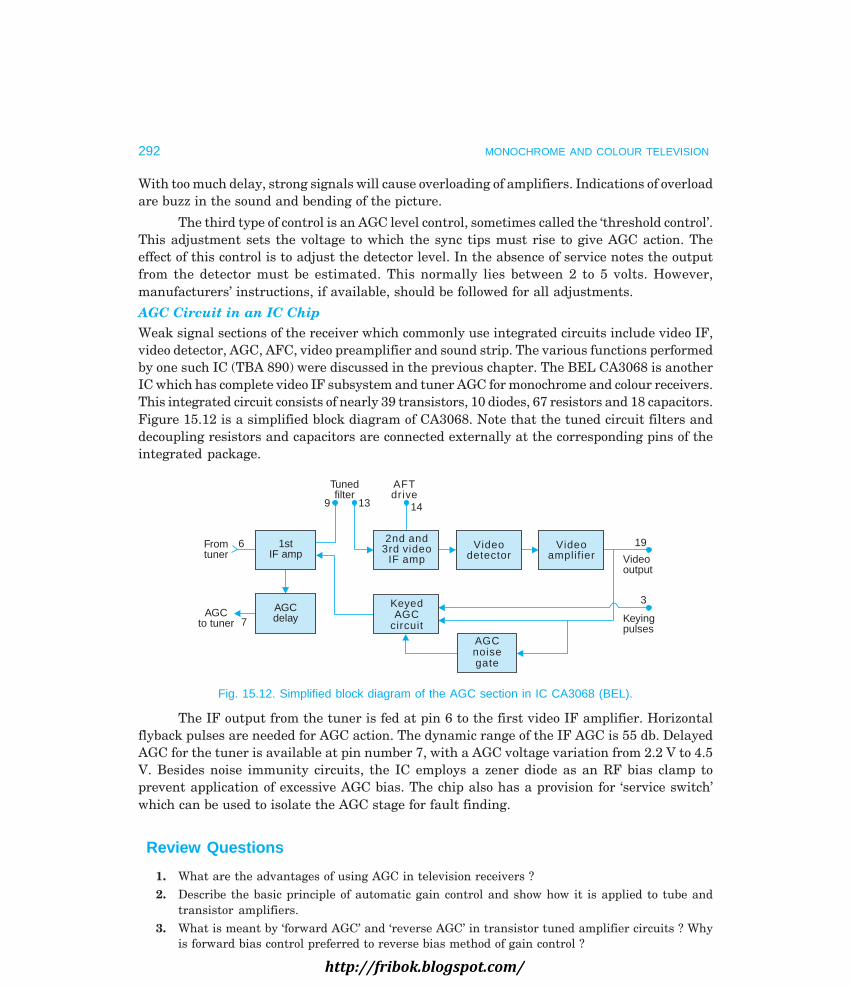
292 MONOCHROME AND COLOUR TELEVISION
With too much delay, strong signals will cause overloading of amplifiers. Indications of overloadare buzz in the sound and bending of the picture.
The third type of control is an AGC level control, sometimes called the ‘threshold control’.This adjustment sets the voltage to which the sync tips must rise to give AGC action. Theeffect of this control is to adjust the detector level. In the absence of service notes the outputfrom the detector must be estimated. This normally lies between 2 to 5 volts. However,manufacturers’ instructions, if available, should be followed for all adjustments.
AGC Circuit in an IC ChipWeak signal sections of the receiver which commonly use integrated circuits include video IF,video detector, AGC, AFC, video preamplifier and sound strip. The various functions performedby one such IC (TBA 890) were discussed in the previous chapter. The BEL CA3068 is anotherIC which has complete video IF subsystem and tuner AGC for monochrome and colour receivers.This integrated circuit consists of nearly 39 transistors, 10 diodes, 67 resistors and 18 capacitors.Figure 15.12 is a simplified block diagram of CA3068. Note that the tuned circuit filters anddecoupling resistors and capacitors are connected externally at the corresponding pins of theintegrated package.
Fromtuner
AGCto tuner
AGCdelay
1stIF amp
6
7
Tunedfilter
9 13 14
AFTdrive
2nd and3rd video
IF ampVideo
detectorVideo
amplifier
KeyedAGC
circuitAGCnoisegate
19
Videooutput
Keyingpulses
3
Fig. 15.12. Simplified block diagram of the AGC section in IC CA3068 (BEL).
The IF output from the tuner is fed at pin 6 to the first video IF amplifier. Horizontalflyback pulses are needed for AGC action. The dynamic range of the IF AGC is 55 db. DelayedAGC for the tuner is available at pin number 7, with a AGC voltage variation from 2.2 V to 4.5V. Besides noise immunity circuits, the IC employs a zener diode as an RF bias clamp toprevent application of excessive AGC bias. The chip also has a provision for ‘service switch’which can be used to isolate the AGC stage for fault finding.
Review Questions
1. What are the advantages of using AGC in television receivers ?
2. Describe the basic principle of automatic gain control and show how it is applied to tube andtransistor amplifiers.
3. What is meant by ‘forward AGC’ and ‘reverse AGC’ in transistor tuned amplifier circuits ? Whyis forward bias control preferred to reverse bias method of gain control ?
http://fribok.blogspot.com/

AUTOMATIC GAIN CONTROL AND NOISE CANCELLING CIRCUITS 293
4. What is the basic principle of peak AGC system ? Explain how the control voltage is developedand applied to IF and RF amplifier stages of the receiver.
5. What is delayed AGC and how is it developed ? Why is delayed AGC applied only to the RFamplifier and somtimes to the first IF amplifier of the receiver ? Why is AGC not applied to thelast IF amplifier ?
6. Describe with a simple circuit the basic principle of a ‘keyed AGC’ system. How does it overcomethe shortcomings of a ‘non keyed’ (peak AGC) control system ?
7. A keyed AGC system employing tubes is shown in Fig. 15.9. Explain how the AGC voltage isdeveloped and applied to RF section of the receiver. What is the function of diode D1 ?
8. Draw circuit diagram of a keyed AGC system employing transistors and having a noise gate.Explain how the AGC voltage is developed and amplified.
9. Explain briefly various types of noise gates used to suppress noise pulses in the video signalbefore it is applied to the AGC and sync separator circuits.
10. The circuit of an improved keyed AGC system is shown in Fig. 15.11. It is designed to operate indifferent modes depending on the level of incoming RF signal. Explain step by step how thecontrol voltage is developed and applied to RF and IF sections of the receiver.
http://fribok.blogspot.com/

16
!
http://fribok.blogspot.com/

The synchronising pulses generally called ‘sync’ are part of the composite video signal as thetop 25 percent of the signal amplitude. The sync pulses include horizontal, vertical andequalizing pulses. There are separated from the video signal by the sync separator. The clippedline (horizontal) and field (vertical) pulses are processed by appropriate line-pulse and field-pulse circuitry. The sync output thus obtained is fed to the horizontal and vertical deflectionoscillators to time the scanning frequencies. As a result, picture information is in correct positionon the raster. The sequence of operations is illustrated in Fig. 16.1 by a block schematic diagram.
From video detector
Videoamp To cathode of
picture tubeCompositevideo signal
Sync separatorand noise
cancellationcircuit
Syncpulsesonly
IntegratorH V
DifferentiatorHorzAFC
Horz deflectionoscillator and
sweep generator(15625 Hz)
Horzdeflectionamplifier
DC control voltage
15625 Hz
To horizontaldeflection
coils
To verticaldeflection
coils
50 HzVerticaldeflectionamplifier
Vertical deflectionoscillator and
sweep generator(50 Hz)
Fig. 16.1. Block diagram of the sync separator and deflection circuits in a television receiver.
16.1 SYNC SEPARATOR—BASIC PRINCIPLE
The problem of taking off the sync pulses from the video waveform is a comparatively simpleone, since the action consists of merely biasing the device used in the circuit, in such a way,that only the top portions of the video signal cause current flow in the device. This is readilyachieved by self-biasing the tube or transistor used in the circuit.
Two basic circuits, one employing a tube and the other a transistor are shown in Fig. 16.2to illustrate this method of sync separation. Self-biasing or automatic bias means that the dc
296
"
!
http://fribok.blogspot.com/

SYNC SEPARATION CIRCUITS 297
bias voltage is produced by the ac signal itself. The requirements are to charge the inputcapacitor by rectifying the input signal while it approaches its maximum value and have anRC time-constant long enough to maintain the bias on the capacitor between peaks of the acinput signal. The video signal is normally obtained from the video amplifier and coupled to theinput of the sync-separator circuit. In Fig. 16.2 (a) video signal is fed to the grid of the triodewith sync pulses as the most positive part of the waveform. In the quiescent state there is no
Videoinput
C1+ –
R11 M
0.1 Fm
+ VPP
RL
v0
Videoinput
C2+ –
R250 K
2 Fm
+ VCC
RL
v0
Fig. 16.2 (a). Basic sync separator circuit Fig. 16.2 (b). Basic sync separator circuitemploying a triode. employing a transistor.
Dynamiccharacteristics
Cut-off
GK
Ot
Plate currentpulsesip
t
Se -b asSelf-biasSync pulse tips
which causegrid current
flow.
Dynamiccharacteristics
iC SaturationCollector current
pulses
Forward biasOReverse bias
Horz syncpulses
t
Slicing levelEffectivebias line
Inputcomposite
video signal
Fig. 16.2 (c). Illustration of tube circuit operation. Fig. 16.2 (d). Illustration of transistor circuit operation.
bias on the tube. On the arrival of the signal, first few pulses drive a heavy grid current andthe capacitor C1 quickly charges up with the grid side negative. Between peaks of the inputsignal, C1 discharges slightly through R1. The R1, C1 time constant is made large enough tokeep C1 charged to about 90 percent of the peak positive input. The effect is to develop anautomatic negative bias so that the operating point sweeps back form VGK = 0 to a point wellbeyond cut-off. After a few pulses the tube settles down into a steady bias such that it iscompletely cut-off except during the positive going sync pulses. The tube then operates under‘class-C’ condition i.e., biased well beyond cut-off. This is illustrated in Fig. 16.2 (c). To maintaina steady bias, the sync tip levels of the video signal make the grid slightly positive every cycle
http://fribok.blogspot.com/

298 MONOCHROME AND COLOUR TELEVISION
to cause a small grid current flow, which quickly replenishes the charge lost by the capacitorthrough the grid leak resistance R1. The average negative bias developed across the capacitorC1 then controls the plate current during sync pulse periods, which in turn gives rise tocorresponding negative-going voltage pulses at the plate. Between pulses, the plate voltagerises to + VPP since there is no voltage drop across the plate load resistor.
The corresponding transistor circuit is shown in Fig. 16.2 (b) where C2, R2 couplingprovides self-bias between the base and emitter of the transistor. The capacitor charges becauseof the base current that flows during sync amplitude levels of the composite video signal. Thecircuit operation is illustrated in Fig. 16.2 (d) where the negative voltage developed across C2reverse biases the emitter-base junction in such a way that only positive sync voltage drivesthe transistor into conduction to produce sync output in the collector circuit. The sync amplitudevaries between VCC and collector voltage corresponding to the maximum collector current.
The bias voltage values in transistor circuits are less than in tube circuits because thebase-emitter junction requires only a fraction of a volt as forward bias, to produce collectorcurrent output. The RC time constant is the same (about 0.1 second) as in tube circuits butwith large C and small R because of the lower input resistance of a transistor.
16.2 SYNC SEPARATOR EMPLOYING A PENTODE
The triodes have relatively large interelectrode capacitances and therefore their performancein sync-separator circuits is inferior to that of pentodes. Accordingly a pentode is preferred toa triode in such circuits. A typical sync separator employing a pentode is shown in Fig. 16.3.
V80 V P–P
C5
To verticaloscillator
3900 PF
R4
270 K
C475 PF
C3
Integrating circuitTo horizontalAFC
150 K
B+
56 K
15 K0.1 Fm
R1M
1
– 40 V
R270 K
20.1 Fm
2000 PF
C1R3
8.2 KFrom videoamplifier
C2
Fig. 16.3. Vacuum tube (pentode) sync separator circuit. Note that thegrid bias voltage with a normal input signal is about – 40V.
The components and DC source voltage are so chosen that both plate and screen-grid voltagesare low. This limits the dynamic region of the tube to a narrow range, with a cut-off bias of theorder of about 5 volts. With the input voltage on, the plate voltage attains a minimum valueduring sync tip intervals. The actual minimum plate voltage obtained, and hence the syncpeak-to-peak amplitude, depends on the value of plate load resistance and peak plate current.
http://fribok.blogspot.com/

SYNC SEPARATION CIRCUITS 299
It should be noted (see Fig. 16.2 (c)) that the effect of driving the tube into grid current on eachsync pulse tip is to clamp the sync pulse tops to zero (ground) potential, so that the sync tipsalign at the same level despite wide variations in the inter-pulse periods. This in effect amountsto restoration of dc component of the video signal, which is lost due to the presence of seriescoupling capacitor C1.
One may ask as to why the video signal is not dc coupled from video amplifier to sync-separator. The reason is that changes in dc conditions, both because of variations of the averagebrightness of the scene and signal amplitude, when stations are changed, are bound to takeplace over a period of time and would make it very difficult to arrange for a constantly efficientsync separator action. The ac coupling, with its own automatic and flexible dc restorationfunction, provides the signal in the form, where it becomes easy to slice-off sync pulses of equalamplitude. The resistance R3 provides isolation between the sync separator and video amplifiercircuits. Because of saturation occurring at the sync tip level of the video signal, any noiseresting on the sync tips does not get reproduced in the output.
16.3 TRANSISTOR SYNC SEPARATOR
A sync separator employing an n-p-n transistor is shown in Fig. 16.4. The capacitor C1 tends tocharge up to the peak input signal voltage less the base-emitter forward voltage drop. There isa marked difference in the signal voltage amplitude necessary to drive tube and transistorsync separators, since a transistor requires only about 0.6 V or so at the base to produce collectorcurrent output. An input video signal of the order of 5 to 10 V is all that is necessary to give riseto output sync pulses whose amplitude approaches about 50 volts peak-to-peak.
From collectorof the video
amplifier
R3 C1R2 3.3 K
C20.22 F
4700 PF
R1 820 K
24 V+
– 2.7 V 15 K 22 K
130 V+
330PF
Tohorz AFC Integrating circuit
C3
R3
330 PF
To verticaloscillator
C447 K10 V P–P
50 V P–P
Fig. 16.4. Transistor sync separator circuit. Note that the reversebias voltage with a normal input signal is about – 2.7V.
As shown in Fig. 16.4 a transistor sync separator often employs a fairly high value ofcollector load resistance with the result that the transistor bottoms (saturates) at a very lowvalue of base (input) current. Full amplitude sync pulses are thus developed for a wide rangeof input signal strength levels. In general, a higher value of load resistance reduces the peakdrive current needed to bottom the transistor but leads to broadening of the output pulses.This is due to charge storage effect, where the charge carriers stored in the base region takelonger to dispel, if the collector load resistance is increased. This necessitates the use of
http://fribok.blogspot.com/

300 MONOCHROME AND COLOUR TELEVISION
transistors having fast switching capability which implies that the transistor must have ahigh upper cut-off frequency. In sync separators which employ switching transistors, a smallforward bias is sometimes given to ensure that tips of the pulses drive the transistor well intothe bottoming condition to produce good clean output pulses.
The factors which must be kept in view while designing a transistor sync separator canbe summarized as follows:
(i) To achieve a reasonable voltage gain the β of the transistor should be large.(ii) A transistor with a small output leakage current must be chosen because the leakage
current lowers the collector voltage and thus reduces net amplitude of the sync output.(iii) To ensure a steep front edge of sync pulses a high frequency transistor is desirable.(iv) Since the transistor is off most of the time a low power transistor can be employed.
16.4 NOISE IN SYNC PULSES
Noise pulses are produced by ignition interference from automobiles, arcing brushes in motors,and by atmospheric noise. The noise is either radiated to the receiver or coupled through the
v0
0
Noise pulse
t
Duration of blocking
Video
input
Noise pulse
Excessivegrid/base current
0V
Gridor base
Average bias
Chassis potential Clipping level
Fig. 16.5 (a). Effect of a strong noise pulse on sync output.
http://fribok.blogspot.com/

SYNC SEPARATION CIRCUITS 301
Sync
output
Syncseparator
0.1 Fm
1 MR1
C1
R2
C2
200 PF
270 K
Video
input
Fig. 16.5 (b). Double time-constant bias circuit at the input of a sync separator.
power line. Especially with weak signals the noise can act as false synchronizing pulses.Furthermore, when noise pulses have much higher amplitude than the sync voltage, largegrid/base current flows which charges the coupling capacitor to a much higher voltage than isnormal and this results in a noise set-up. Because of the long time constant of self-biasingnetwork, the sync separator is held much beyond cut-off for a period which depends on theamplitude and width of the noise pulse and the time constant of the input circuit. As shown inFig. 16.5 (a) the sync separator gets blocked and there is weak or no sync output till the biasreturns to its normal value. During strong noise periods, the picture does not hold still untilsynchronization is restored again. Thus in order to reduce the effect of noise, sync circuitsgenerally employ one or more of the following techniques :
(i) Double Time-constant for Signal BiasThe time constant of the grid/base leak-bias circuit, at the input of sync separator, must belong enough, to maintain bias from line to line and through the time of vertical sync pulses inorder to maintain a constant clipping level. As stated earlier, a time constant of the order of 0.1second is adequate for this purpose. But such large values would result in long blocking onstrong noise pulses. In a similar way too long a time-constant will tend to increase the negativebias then its normal value during vertical sync intervals when the composite video signalvoltage stays close to its peak value. This results in shortening of horizontal signal pulses soonafter the vertical pulse train during each field. However, if the time constant is made too shortto overcome the above drawbacks, this may not maintain bias between sync pulses, speciallyduring the vertical sync pulse time. The result may be inadequate sync separation during andimmediately after the vertical sync pulses. Therefore the problem of reducing the effect of highfrequency noise pulses without changing the time constant of the average bias network issolved by providing a double time constant circuit at the input of the sync separator. Thecircuit configuration is shown in Fig. 16.5 (b). It may be noted that the two sync separatorcircuits described earlier (Fig. 16.3 and Fig. 16.4) also have double time constant circuits attheir inputs. The network R1,C1 provides the normal grid/base leak-bias, with a time constantof 0.1 second for the sync signal. The small capacitance C2 (200 pF) and resistance R2 (270 KΩ)provide a short time-constant. The double time constant thus provided enables the negativebias to change quickly to reduce the effect of noise pulses in the input to the sync separator.The capacitor C2 being small can quickly charge when noise pulses produce grid/base currentthus increasing the bias for noise. The change in voltage across C1 and C2 is inverselyproportional to their capacitance values. Therefore a noise pulse will charge C2 to a voltage500 times more than that across C1. Since R2C2 time constant is 50 µs, C2 can discharge throughR2 between sync pulses. Thus the bias is maintained at the normal value for sync pulses.
http://fribok.blogspot.com/

302 MONOCHROME AND COLOUR TELEVISION
Another advantage which accrues by the addition of a short time-constant circuit is thatit acts like a frequency response compensator and maintains the sharp rise time of input syncpulses.(ii) Sync Clipper after Sync SeparatorThe sync output limited by saturation does not result in sharp sync pulses. The clipping levelis also not uniform because of shift in self-bias caused by sharp noise pulses. Many sync-separatorcircuits have a sync clipper stage where sync output of the separator is clipped and amplified.The purpose is to provide sharp sync-pulses with equal and high amplitude, free from noisepulses and without any camera signal. Clipping in successive stages allows the top and bottomof sync pulses to remain sharp and prevents noise pulses from having higher amplitude thanthe sync.(iii) Use of Noise Cancellation CircuitsThe use of a double time constant circuit as a noise suppressor is only suitable for non-recurringnoise. If noise pulses are periodic, the small charge on C1 (see Fig. 16.5 (b)) contributed by eachnoise pulse will be cumulative and noise set-up will still occur. Therefore, in many sync separatorcircuits some form of noise suppression switch is provided. Several such noise cancellationcircuits which were described in the previous chapter along with AGC circuits are also used insync separator circuits.
16.5 TYPICAL TUBE SYNC SEPARATOR CIRCUIT
The separator circuit shown in Fig. 16.6 employs a pentode as a sync-separator followed by atriode which provides gain and ensures sharp edged sync output. The video signal is coupled to
C3R3V1
C2
R2
470 PF0.01 Fm
From videoamplifier
circuit
C1
R12.2 M 120 K
– 6 V
C4 R62.5 Fm
6.8 K
470 K– 1 V
4.7 KPFR4 R5220 K 82 K
8.2 KL1
B+
C5
1.5 KPFTo AFCcircuit
8.2 K110 V
R7
V2
To verticalsweep oscillator
R8
Fig. 16.6. A typical vacuum tube sync separator circuit.
the separator through a cathode follower from the video amplifier. A double time-constantcircuit is provided at the input to reduce the effect of noise pulses on clipping level. The triodealso operates on self-bias developed through network R3, C3, which couples the pentode to thetriode. Since the amplitude of the sync output at the plate of the pentode is almost steady, thetime-constant R3, C3 has been chosen to be quite small (2.5 ms). This is adequate, both for asteady auto-bias generation and suppression of occasional excessive noise pulse amplitudes.
http://fribok.blogspot.com/

SYNC SEPARATION CIRCUITS 303
The load of the triode consists of a small inductor L1 and an 8.2 KΩ resistor in series.Sync pulses to the vertical oscillator are fed from plate of the triode whereas the input of thehorizontal automatic frequency contol (AFC) circuit is connected to the junction of L1 andresistance R7. The sharp peaked pulses that develop across the inductor when triode conductsare of the desired shape and amplitude for feeding to the AFC circuit. The coil L1 is shunted bya resistance R8 to suppress onset of self oscillations when shock excited by sharp plate currentpulses.
In some AFC circuits, discussed in the next chapter, a balanced sync pulse output isnecessary. This can be easily obtained by inserting a suitable resistor in the cathode lead of thetriode. The two outputs, one at the plate and the other at the cathode of the triode are then180° out of phase with respect to each other.
16.6 TRANSISTOR NOISE GATE SYNC SEPARATOR
A transistorized sync-separator employing a noise gate is shown in Fig. 16.7. The noise gatetransistor Q2 is in series with the emitter of the sync separator Q1. The tansistor Q2 is sobiased that it normally stays in saturation. The sync separator then operates normally and itsemitter current completes its path through Q2, which has only about 0.6 V between its collectorand emitter when saturated. Any sharp noise pulse in the video signal gets coupled to the baseof Q2 through diode D2 and this cuts-off the noise gate transistor Q2. In the absence of anycollector current through Q2, the emitter of Q1 rises to + 20 volts and this blocks the transistorQ1. Hence no sync separation occurs during the noise pulse interval. It may be noted thatnormal amplitude of the negative video signal fed at the input of Q2 is not sufficient to turn ifoff. However, if a noise spike with a negative amplitude beyond the sync tip appears, it turnsthe noise gate off. However, noise pulses which are not longer than sync tip will not cause thenoise gate to turn off.
N
Fromvideo
amplifiercircuit
0.068 Fm 0.0068 Fm
4.7 K
470 K + 340 V
180 K
100 K
Q1
D120 V+
27 K120 K
D2N
From videodetectoroutput
27 K0.05 Fm
Q2 Noise gatetransistor
39 K0.0056 Fm
0.056 Fm
0.015 FmVertical sync
output
Horz syncoutput
Fig. 16.7. Transistor sync separator with a noise gate.
http://fribok.blogspot.com/

304 MONOCHROME AND COLOUR TELEVISION
16.7 IMPROVED NOISE GATE SYNC SEPARATOR
The circuit of Fig. 16.8 is another example of a typical sync clipper cum noise invertor. Q1, ann-p-n transistor, acts as the sync separator. In the absence of any signal, the base-to-emittervoltage is zero and the transistor is off. When a positive-going signal appears at its input,thetransistor is turned on. As shown along the circuit a 4 V (p-p) positive composite video signal isapplied at the sync input terminals through the isolating resistor R6. This turns Q1 on andbase current flows drawing the vertical sync pulses through C1, D1, emitter-base junction andD2. The resulting current charges the capacitor C1 with the polarity marked across it. Sincethe sync pulse is the highest component of the composite video signal, the voltage developedacross C1 at the end of the vertical sync pulse (which is 160 µs wide) is approximately 4 V.When the vertical sync pulse passes, the base of Q1 is held negative with respect to the emitterand it is cut off again. Capacitor C1 tends to discharge through R1 during the interval of 18.84ms between vertical sync pulses but the time-constant C1R1 is so large (220 ms) that C1 candischarge only about 8 percent of the voltage across it. When the next vertical sync pulsearrives, its peak is approximately 8 percent more positive than the change on C1. Thus Q1 isagain turned on during the sync pulse interval and this part of the input signal gets amplifiedto develop a 20 V p-p negative going sync pulse at the collector.
input
4V P–P
1 K
R6
D3 5.6 K 0.1 Fm
R7 C5
R8R9D4
15 K5.6 K
0.47 Fm+
C4
R4 6.8 M
5.6 K
R5 C6 220 Fm0.22 Fm
Q21M
+ C1
R1
C2D1
0.0056 Fm
100 K R2 D2
Q1 C3 0.01 Fm
To horzAFC circuit
To verticaloscillator
R3
VCC
3 K
+22 V
Q1 – Sync separatorQ – Noise inverter2
Fig. 16.8. Improved transistor noise gate sync separator.
After the vertical pulse interval, the horizontal sync pulses which are 4.7 µs wide, arrive.Because the charge on C1 is still high to keep Q1 in cut-off, the horizontal sync pulses areprovided another path through C2 to turn it on. Base current again flows during the horizontalsync pulse interval, charging capacitor C2. In the 59 µs interval between consecutive horizontalsync pulses, C2 discharges through R2 (R2C2 = 560 µs) by about 12 percent only and thus keepsQ1 in cut-off state. When the next horizontal sync pulse arrives, it is sufficiently positive toturn Q1 ‘on’ again. The negative horizontal sync pulses developed at the collector of Q1 areagain of about 20 V peak-to-peak. Thus there are two separate input paths for the vertical andhorizontal sync pulses, ensuring that both are amplified by Q1, while eliminating the videoinformation between sync pulses.
http://fribok.blogspot.com/

SYNC SEPARATION CIRCUITS 305
The fact that the positive horizontal sync pulse is coupled directly to the base of Q1, backbiases diode D1 during the horizontal sync pulse interval. This prevents the base current of thetransistor from discharging C1. Diode D2 prevents transistor conduction in the reverse directionwhen the negativegoing signal adds to the charge on the base input capacitors to exceed thebase-emitter voltage rating.
Noise Invertor. As shown in Fig. 16.8 the noise invertor transistor Q2 together with itsassociated circuitry is in parallel with the input to the sync separator. This offsets the effectsof high amplitude noise pulses in the following manner. The diode D4 rectifies the normalincoming positive going composite video signal and acts as a peak detector on account of thelong time constant of R4C4(R4C4 = 3.2 sec). The resulting dc voltage across C4 is equal to peakof the sync pulses. This positive voltage gets applied to the cathode of D3 through resistors R8and R7. In turn this reverse biases D3 under normal signal conditions and no signal appearsthrough D3 at the base of Q2. It stays in cut-off and does not affect the normal operation of thesync separator. However, when a sudden noise spike appears as shown in the figure, voltageacross C4 cannot change quickly, and the diode D3 will couple the spike through C5 to the baseof Q2. The transistor Q1 then conducts heavily and effectively shorts its collector circuit toground. This results in shorting of the entire input signal to the sync separator, includingvideo information and sync pulses, during time of the noise spike. As soon as the noise pulsedisappears, however, Q2 cuts off again and the next video signal and sync pulses will beuneffected. Capacitor C6 prevents any dc short across Q2.
16.8 SYNC AMPLIFIER
An amplifier is not always used before a sync separator. It will depend on the type of transistorused as a separator and the polarity of the sync pulses at the output of the video detector. Ifthe video detector output is taken from its anode and its amplitude is sufficiently high, it canbe fed directly to a p-n-p type sync separator. This eliminates the need for a sync amplifierbefore the separator. If an n-p-n type transistor is employed, as in Fig. 16.8, it is necessary toreverse the polarity of a negative-going video signal at the output of the detector before it canbe coupled to the separator. In that case the output of a common emitter video amplifier maybe used as input to the sync separator.
IC Sync CircuitIn some receivers sync-separator function is performed in an integrated circuit. This IC is apart of the sync-AGC module that combines noise inversion, sync separation and AGC.
Noise cancellation and amplification are first performed in the IC. The resultant noisefree video signal emerges at a particular pin of the IC and is applied to a time-constant networkthat is kept outside the IC. This enables the use of different time-constant network to suit aparticular receiver design. The output from the network is fed back to the IC where syncseparation takes place. Over 20 volts of separated sync is available, both positive and negativegoing at different pins. The IC also receives gating pulses from the horizontal output circuit forAGC operation.
http://fribok.blogspot.com/

306 MONOCHROME AND COLOUR TELEVISION
Review Questions
1. Draw the basic circuit diagram of a sync separator employing a triode with grid leak bias. Com-ment on choice of the time-constant of the biasing circuit. Why is a pentode preferred to a triodein tube sync-separator circuits ?
2. Draw the circuit of a sync separator employing a p-n-p transistor. Show input and output wave-forms. Why are high-frequency-transistors with small output leakage current employed in synccircuits ?
3. What are the undesirable effects of high amplitude noise pulses in sync-separator circuits ?Explain how the use of a double time-constant biasing circuit overcomes the effect of noise ininput signal to a sync separator. Why is a sync clipper often employed after the sync separator ?
4. Explain the operation of sync separator shown in Fig. 16.6. What is the use of inductor in platecircuit of the triode ?
5. Draw the circuit diagram of a typical transistor noise gate sync separator and explain its opera-tion.
6. The circuit of an improved noise gate sync separator is shown in Fig. 16.8. Describe its operationand in particular explain how the noise invertor transistor Q2. cancels the effect of noise pulses.
http://fribok.blogspot.com/

17
!
http://fribok.blogspot.com/

The receiver has two separate scanning circuits, one to deflect the electron beam, of the picturetube, in the vertical direction and the other in the horizontal direction. Each scanning circuitconsists of a waveform generator, i.e. oscillator and a power output stage. The synchronizingpulses obtained from the sync-pulse separator are used to control the vertical and horizontaldeflection oscillators, so that picture tube is scanned in synchronism with the original picturesource at the transmitter. The horizontal sync pulses hold the line structure of the picturetogether by locking in the frequency of the horizontal oscillator; and the vertical sync pulseshold the picture frames locked-in vertically by triggering the vertical oscillator. The equalizingpulses help the vertical synchronization to be the same in even and odd fields for good interlacing.
17.1 SYNC WAVEFORM SEPARATION
This means separating the vertical and horizontal sync pulses. It is the difference in the pulsetime duration of the horizontal (line) and vertical (field) sync pulses which makes it possible toseparate them. The horizontal sync pulse with a width of 4.7 µs and repeated at 15625 Hzrepresents a high frequency signal, whereas the vertical sync pulse with a total width of 160 µswhich repeats 50 times in a second, is relatively a very low frequency signal. Therefore, thevertical and horizontal sync pulses can be separated from each other by RC filters. A low-passfilter, connected across the incoming sync pulse train, will develop appropriate trigger pulses
tO
– VCC
H H E E E EV sync pulses
Clippinglevel
X YTo vertical
oscvo1
R1
C1
0.047 F
LPF= 50 to 60 S
vo2To AFC circuit
Spiked horz sync pulses
R2HPF= 0.5 S
C2
Q2
– VCC
100 K5 F33 Q1
2 K
2 K 1 K
Fromvideo amplifier
Q1 – Emitter followerQ – Sync separator2
Fig. 17.1. Separation of vertical and horizontal sync pulses.
308
#
!
http://fribok.blogspot.com/

SYNC PROCESSING AND AFC CIRCUITS 309
for synchronizing the vertical oscillator. Similarly, a high-pass filter will deliver sharpdifferentiated pulses for the horizontal oscillator from the same pulse train. This, as shown inFig. 17.1, is done simultaneously by feeding output from the sync pulse separator to the low-pass and high-pass filter configurations, connected in parallel. The resistor R1 and capacitorC1 constitute the low-pass filter, also known as integrating circuit. The high-pass filter, alsoknown as differentiating circuit, consists of C2 and R2 and has a very small time constant.
The integrated output across C1 that builds up 50 times during one second is used fortriggering the vertical oscillator. However, the spiked (differentiated) output that developsacross R2 is fed to the automatic frequency control (AFC) circuit, the output of which is employedfor holding the horizontal oscillator at the correct frequency. The use of the AFC circuit ensurescorrect synchronization even in the presence of noise pulses. The serrated vertical sync pulsesalso develop only a spiked output across R2, because the time constant of the circuit R2C2 isrelatively too small to produce any appreciable voltage across R2.
The sync separator shown in Fig. 17.1 is preceded by an emitter follower to isolate itfrom the video amplifier. The small amount of forward bias at the base of Q2 ensures goodbottoming and thus clean output sync pulses are fed to the filter circuits. The output waveshapesfrom the integrating and differentiating circuits are shown alongside corresponding filterconfigurations.
17.2 VERTICAL SYNC SEPARATION
The time constant of the low-pass filter circuit (see Fig. 17.1) is chosen to be much larger thanthe width of each serrated vertical pulse. This value is not very critical and a time constantR1C1 of about ten times the serrated pulse width is adequate. When the combined sync waveform,beginning with horizontal and equalizing pulses appears at the input of such a circuit, thecapacitor C1 charges along an exponential curve governed by the time constant of the filtercircuit. Since this time constant is very large compared with the duration of the horizontal andequalizing pulses, the voltage output across C1 during these intervals of the input wave is avery small fraction of the ultimate value. This is shown in the output waveform of the integrator.When the trailing edges of the horizontal or equalizing pulses appear, the small charge storedon the capacitor discharges along an exponential curve governed by the same time constant.The overall result is a very small toothed voltage across the capacitor, which lasts for a timecomparable to the width of each horizontal or equalizing pulse, and thus the amplitude of thefilter output voltage is negligible during the horizontal and equalizing sync periods.
However, when the vertical sync pulse (serrated) arrives, cumulative charging of thecapacitor occurs, because the duration of each serrated vertical sync pulse is long comparedwith the gaps between serrations. Consequently,the charge accumulated from the first inputserration (29.7 µs) has little opportunity to discharge during the following notch (2.3 µs). Thenext broad pulse adds to the charge already built-up across the capacitor which again is onlypartially discharged during the next gap. The five broad pulses which constitute the verticalsync pulse thus cause a gradual increase in voltage across the capacitor, with small spikessuperimposed on it. At the output of the low-pass filter, therefore, the voltage rise appears tobe almost smooth corresponding to the vertical pulse. This pulse amplitude is substantially
http://fribok.blogspot.com/

310 MONOCHROME AND COLOUR TELEVISION
greater than the small spikes caused by the horizontal and equalizing pulses. As soon as thevertical sync pulse has passed the integrated output pulse decays almost to zero during thepost-equalizing pulse period, and stays at this level during the horizontal pulse train thatfollows.
The purpose and effectiveness of the equalizing pulses is apparent from the plot shownin the figure. The inclusion of equalizing pulses, before and after the field pulses, ensuresidentical integrated output despite insertion of field waveform in the middle of one line for onefield, and at the end of the line on alternate fields.
In many vertical sync control circuits the integrated field pulse waveform is clipped bya reverse biased diode, along the line XY as shown in Fig. 17.1,and thus the voltage changesacross C1 due to line pulses are not seen by the field oscillator circuit at all.
Cascaded Integrator SectionsA very large time constant for the integrating circuit removes horizontal sync pulses, and alsoreduces the vertical sync amplitude across the integrating capacitor. This rising edge of thesync pulse is then not sharp and this can lead to incorrect triggering of the oscillator.However,when the R1C1 time constant is chosen to be relatively small the horizontal sync pulses cannotbe filtered out and serrations in the vertical pulse produce notches in the integrated output.Thus though the vertical sync pulse rise is quite sharp, the output voltage attains the sameamplitude at different charging excursions. This can also lead to wrong synchronization andso the notches must be filtered out. The resulting outputs with large and small time constantare illustrated in Fig. 17.2 (a).
Input pulse Serration
v
0
Insufficientintegration
(RC too short)
Excessiveintegration
(RC too large)
t
Fig. 17.2 (a). Effect of time-constant on vertical sync output.
vivi v0
R1 R2
10 K 10 K
0.005 F 0.005 FC1 C2
Fig. 17.2 (b). Two-section integrator for vertical sync.http://fribok.blogspot.com/

SYNC PROCESSING AND AFC CIRCUITS 311
ivi v0v0
R1 R2
100 K
2.2 nF4.7 nF
C1 C3
R3
39 K22 K
C22.2 nF
Fig. 17.2 (c). Three-section integrator for vertical sync.
To overcome the above described discrepancy, most receivers employ a two-sectionintegrating circuit with each RC section having a time constant of about 50 µs. Such a circuitis illustrated in Fig. 17.2 (b). The operation of the circuit can be considered as though the R1C1section provides integrated voltage across C1 that is applied to the next integrating sectionR2C2. The overall time constant for both sections together is large enough to filter out horizontalsync pulses while the shorter time constant of each section allows the integrated voltage torise more sharply because each integration is performed with a time constant of 50 µs. In somedesigns even a three section integrator is provided and such a configuration is illustrated inFig. 17.2 (c).
17.3 HORIZONTAL SYNC SEPARATION
The high pass filter circuit and the differentiated output are shown in Fig. 17.1 along with thesync separator circuit. The time constant of this circuit (R2C2) is kept much smaller (normally1/10th) than the width of the horizontal pulse. A time constant between 0.5 µs to 1 µs is oftenemployed.
The physical action of the differentiator is as follows. When a leading edge of the incomingpulse train is applied to the C2,R2 circuit, the initial voltage across the capacitor C2 is zero, andso full amplitude of the leading edge appears across the resistor R2 and the output wave followsalmost exactly the shape of the input leading edge. When the flat top of the input rectangularwave is reached, on further charging of the capacitor occurs, and the circuit discharges alongan exponential curve governed by the timeconstant of the circuit. Since this time-constant isvery short compared to the duration of input pulse, the discharge completes itself before thetrailing edge of the pulse arrives.
When the trailing edge of the input pulse occurs, it produces another pulsed output (seeFig. 17.1) of opposite polarity to that of the first pulse. Since the trailing edge componentextends in opposite direction to the leading edge output, it has no effect on the triggering of thehorizontal oscillator.
The equalizing and vertical sync pulses (notched) produce two leading edge componentswhen they occur during each line scanning interval of 64 µs. The extra leading-edge pulsesoccur when the horizontal oscillator is insensitive to sync pulses and hence have no effect onits frequency. As was explained in Chapter 3, the leading edge of each horizontal sync pulse,alternate equalizing pulses, and alternate serrations of the vertical sync pulse are correctlytimed to initiate the horizontal retrace periods. Moreover as explained above, the differentiatingcircuit is insensitive to the flat top portions of the rectangular waves, that is, the amplitude of
http://fribok.blogspot.com/

312 MONOCHROME AND COLOUR TELEVISION
the differentiated output is independent of the duration of the input pulse. There is, therefore,no particular response to the vertical sync pulses, except at their edges and they as such haveno effect on the triggering of the horizontal oscillator.
17.4 AUTOMATIC FREQUENCY CONTROL
The direct use of the incoming sync pulses to control vertical and horizontal sweep oscillators,though simple and most economical is normally unsuitable, because of their susceptibility tonoise disturbance arising from electrical apparatus and equipment operating in the vicinity ofthe television receiver. The noise pulses extending in the same direction as the desired syncpulses cause greatest damage when they arrive during interval between the sync pulses. Noisepulses which are most troublesome, possess high amplitude, are of very short duration andtend to trigger the oscillator prior to its proper time.
When the vertical oscillator is so triggered the picture moves vertically, either upwardsor downwards, until proper sync pulses in the signal again assume control. If the horizontaloscillator is incorrectly triggered a series of lines in a narrow band will be jumbled up, givingthe appearance of streaking or tearing across the picture. The horizontal sweep system of thereceiver is effected more by noise pulses than the vertical system.
To understand this fully, it is necessary to examine the nature of interfering voltages.The energy of the noise pulses is distributed over a wide range of frequencies. For a peak tooccur, the phase relationship amongst various frequencies must be such as to permit theiraddition to form a high amplitude pulse. This condition, however, usually exists only for abrief interval which explains the small width of these pulses.
The high frequency noise pulses, when they reach the vertical sync separator, i.e. low-pass filter, get suppressed along with the line sync and equalizing pulses because of large timeconstant of the circuit. The presence of this low-pass filter (the integrating network) is mainlyresponsible for greater immunity to noise pulses enjoyed by the vertical system. This explainswhy no special circuit is used between the sync separator and the vertical oscillator. However,when a wide noise pulse is received, it contains enough energy to cause off-time firing of thevertical oscillator, but the annoyance caused to the viewer on account of occasional rolling ofthe picture is seldom great.
On the other hand, circuit leading to the horizontal oscillator, being a high-pass filter,passes noise pulses readily along with the narrow horizontal sync pulses. This results in seriousinterference with the normal functioning of the horizontal sweep oscillator which, in turn,results in frequent ‘tearing’ of the picture. In order to ensure that the horizontal oscillatoroperates at the correct frequency, and is basically immune to noise pulses, all horizontaldeflection oscillators are controlled by some form of a circuit known as the automatic frequencycontrol circuit (AFC circuit).
The AFC circuit receives sync pulses and output from the horizontal oscillatorsimultaneously and compares them regarding their phase and frequency. The discriminator inthe AFC circuit develops a slowly varying voltage, the magnitude of which depends on deviationof frequency of the horizontal oscillator from its correct frequency. In case the oscillator frequencyis equal to the incoming horizontal sync frequency, i.e. 15625 Hz, no output voltage is developed.
http://fribok.blogspot.com/

SYNC PROCESSING AND AFC CIRCUITS 313
The AFC circuit output is filtered by a low-pass filter to obtain an almost dc voltage, whichthen controls the frequency of the horizontal sweep oscillator. Thus the use of AFC circuit anda low-pass filter at its output, eliminates the effect of sharp noise pulses. The use of this indirectmethod of frequency control results in excellent horizontal oscillator stability and immunityfrom noise interference.
AFC OperationThe block schematic arrangement of a frequently used AFC circuit for the horizontal deflectionoscillator is illustrated in Fig. 17.3. Horizontal sync voltage and a fraction of the horizontaldeflection voltage, normally taken from the horizontal output circuit, and suitably processedto form horizontal flyback pulses, are coupled in the sync discriminator. The discriminatorconsists of two diodes and associated circuitry. It detects the difference in frequency and developsa dc output voltage proportional to the difference in frequency between the two input voltages.The dc control voltage indicates whether the oscillator is ‘on’ or ‘off ’ the sync frequency. Thegreater the difference between the correct sync frequency and the oscillator frequency, largeris the dc control voltage. This dc control voltage is fed to a large time constant filter, the outputof which is used to control the oscillator frequency. The shunt by-pass capacitor of this low-pass filter eliminates the effect of noise pulses. A large time constant filter could not be useddirectly, in the horizontal system ; because while suppressing noise pulses it would haveprevented the desired horizontal sync pulses from reaching the horizontal sweep oscillator.This explains the need and use of the AFC circuit.
Sync input
Syncdiscriminator
Horzoscillator
Horz outputamplifier
DC control voltage
R1
C1LPFTo deflection
circuit
Flyback pulses
Integrator
R2
C2
Fig. 17.3. Block diagram of the horizontal AFC system.
The automatic frequency control circuit is generally called flywheel sync, sync lock,stabilized sync or horizontal AFC, based on the technique employed to develop the controlvoltage. Most present day receivers use either a push-pull or a single-ended phase discriminatorAFC circuit for sensing any error in the horizontal oscillator frequency.
17.5 AFC CIRCUIT EMPLOYING PUSH-PULL DISCRIMINATOR
A typical circuit arrangement employing push-pull phase discriminator is shown in Fig. 17.4.The sync pulses of equal amplitude but of opposite polarity are obtained from the phase splittercircuit and coupled to the diodes D1 and D2, through capacitors C1 and C2 respectively. R1 andR2 are of equal value and act as load resistors to the two diodes. The diodes are so connectedthat the application of sync pulses of opposite polarity forward biases them simultaneously.
http://fribok.blogspot.com/

314 MONOCHROME AND COLOUR TELEVISION
The horizontal deflection waveform, phase reversed and coming effectively from a voltagesource is applied at the point marked ‘A’ in the circuit diagram. This is actually obtained froma winding (L1) on the horizontal output transformer in the form of flyback pulses and thenprocessed by the integrating network R6, C3.
Fromsync separator
E1
10V P–P
C4
R55.6 K
10 Fµ
100 Ω R3
B++ 10 V
C1 V1+ –
0.033 Fµ1 K R1
–
+VB –
+
Phasesplitter
0.033 Fµ– +
100 ΩR4
C2680 ΩR7 R9
R8
V2
15 K C5 0.3 Fµ 3.3 FµC6
R10 330 Ω
D2R2C3 0.1 Fµ1 K
R6
2.2 KD1
A
L1Winding
on H.O.T.
Flybackpulses
DC control voltageto horz oscillator
E2 8V P–P–+
–+
0
Fig. 17.4. Push-pull AFC circuit.
It is convenient to study the functioning of this circuit under three different conditions:(a) when sawtooth feedback voltage is only present, (b) when only sync pulses are present and(c) when both sawtooth and sync pulses are simultaneously present.
(a) When only sawtooth voltage is applied (no sync pulses) D1 conducts during the negativeand D2 during the positive half of the sawtooth cycle, charging C1 and C2 with polarities shown.When voltage peaks have passed C1 discharges via R3, B+, B–, (ground) R8, R7 and R1. SimilarlyC2 discharges through R2, R7, R8, B– and R4. This raises the lower end of R2 (marked V2) aboveground potential and the upper end of R1 (marked V1) below ground potential. Equilibrium is
reached when | V1 | = | V2 | = 12 E2 (peak-to-peak) of the applied sawtooth voltage. Thus VB
equals zero and the upper end of R7 stays at ground potential. When put in another way thismeans that the two equal and opposite currents flowing through R8 develop a net zero voltageacross it. In steady state, small pulses of make-up current flow at the positive and negativepeaks of the sawtooth through D2,C2 and C1,D1 respectively.
(b) When only sync signal is present, the positive going sync pulses are coupled from thecollector of the sync splitter through C1 to the anode of D1. At the same time negative goingsync pulses are coupled via C2 to the cathode of D2. As a result of these pulses, current flowsalong the path C1, D1, D2, C2, R4, B–, B+, and R3 thereby charging the capacitors C1 and C2 toapproximately peak value of the sync pulses with polarities shown across them. During thetime between sync pulses, the capacitor C1 discharges through R3, B+, B–, R8, R7 and R1. At thesame time the capacitor C2 discharges via R2, R7, R8 and R4. Two equal but opposite voltages,caused by equal capacitor discharge currents develop across R8. These voltages cancel eachother leaving a net zero voltage across R7 and R8. Thus VB equals zero and this point continues
http://fribok.blogspot.com/

SYNC PROCESSING AND AFC CIRCUITS 315
to be at ground potential. Note that V1 and V2 are of such polarity that both the diodes arereverse biased during the time between sync pulses.
(c) Now if sync and sawtooth voltages are applied simultaneously, as they would beunder normal conditions, three cases are possible—(i) pulses in synchronism, i.e. oscillatorfrequency is correct, (ii) oscillator frequency is more than the sync frequency, and (iii) oscillatorfrequency is less than the sync frequency.
(i) For this case as shown in Fig. 17.5 (a), sync pulses and sawtooth voltage arrivesymmetrically, i.e. the sync pulses occur when the sawtooth is passing through its zero pointduring retrace. As a result the circuit behaves as though each signal were applied to the phasedetector independent of each other. Thus the sync pulses deposit equal charges on C1 and C2,causing smaller but identical make-up currents to be drawn from the sawtooth source. Themagnitudes of V1 and V2 remain equal (VB = 0) and no control voltage is developed across R8.Therefore, the frequency of the horizontal deflection oscillator remains unchanged.
(ii) When the oscillator frequency is high (see Fig. 17.5 (b)) the sync pulses arrive late ina relative sense, i.e. when the sawtooth is already in its positive half cycle. Thus the sawtoothforward biases D2 and reverse biases D1 with the result that D2 conducts harder than D1. Thusmore charge is added to C2 and less to C1. During the discharge periods of these capacitorsunequal currents flow through R8 and a positive error voltage is developed across it. Thedischarge currents also cause V2 to increase and V1 to decrease from their quiescent valuesmaking VB positive. The low-pass network R9, C5 filters the control voltage and feeds a dc errorvoltage to the horizontal oscillator. This forces the oscillator frequency to return to its normalvalue.
0
E1
0
0
Sync pulses
Sync frequency= 15625 Hz
Sync pulses
V (D1) =AK V (D2)AK
(a) f osc = f sync, dc control voltage = 0
(b) f osc > f sync, dc control voltage is positive
(c) f osc < f sync, dc control voltage is negative
V (D1) <AK V (D2)AK
(V D1)AK
Retrace Trace
V (D1) >AK V (D2)AK
Sync pulses
(V D2)AK
Anode to cathode voltage across diode D1 Anode to cathode voltage across diode D2
Fig. 17.5. Timing relationships between reference sync pulses and sawtooth voltage obtainedfrom output of the horizontal deflection oscillator circuit. (a) correct oscillator frequency
(b) oscillator frequency higher than sync frequency (c) oscillator frequency lower than sync frequency.
http://fribok.blogspot.com/

316 MONOCHROME AND COLOUR TELEVISION
(iii) As shown in Fig. 17.5 (c) when the oscillator frequency is low, sync pulses occurduring the time the sawtooth is in its negative half cycle forward biasing D1 more than D2.Analogous arguments establish that for this case a negative control voltage is developed acrossR8. This, after filtering is applied to the horizontal oscillator causing its frequency to increaseto its normal value.
Thus the sync discriminator continuously measures the frequency difference betweenthe sawtooth and sync pulses to produce a dc correction voltage that locks the horizontaloscillator at the synchronizing frequency. In Fig. 17.4, R10 and C6 constitute an anti-hunt,circuit whose function is described in a later section of the chapter.
17.6 SINGLE ENDED AFC CIRCUIT
The single ended or Gruen phase detector AFC circuit does not require push-pull sync input.Instead, as shown in Fig. 17.6 (a), negative going sync pulses of about 30V P-P are coupledthrough C1 from the sync separator to the common cathode ends of the two diodes D1 and D2.The phase detector diodes are also fed flyback pulses obtained from a winding (L1) on thehorizontal output transformer. The pulses are passed through an integrating circuit (R5, C4)and converted into a sawtooth voltage of about 20V P-P before being fed at point ‘X’ in thecircuit.
0+
– 20 V P–P
Feedback sawtooth C3
C4
R6
L11000 PF
X
R5 Windingon H.O.T.
DCAFC voltage
55 K
0.1 F
R7
C7
0.033F
C6
100 K
820 PF
C5
C2
D168 pF
V1R1
V2R2 D2
C1
180 K
180 K
0.001 FR3
2.2 K
T1 T3
T2
30 V
B–
Q1
B+ 30 V
27 KR4
From
syncseparator
Fig. 17.6 (a). Single ended (GRUEN) discriminator for horizontal AFC.
Circuit OperationAssume that only sync pulses are applied to the phase detector. During the time T1 (see syncpulse waveform) the sync separator is cut-off and its collector voltage is equal to B+ voltage. Asa result the coupling capacitor C1 is fully charged. When the negative sync pulse (T2) arrives,i.e. Q1 saturates, the two diodes are simultaneously forward biased. Note that the diodes areeffectively in parallel for the sync input due to the large (820 pF) capacitor C5 to ground fromthe anode of D1. This enables C1 to discharge through two different paths. One path for dischargeis through R3, Q1, B– and D2 while the other is completed via R3, Q1, B–, C4, C3 and D1. In this
http://fribok.blogspot.com/

SYNC PROCESSING AND AFC CIRCUITS 317
process C3 is charged with positive polarity towards C4. Because of very short time constantduring the discharge period, C1 discharges almost completely.
During the following long period (T3) between sync pulses both diodes are turned offand C1 charges through two independent paths. One charging path is through B+, R4, R3, C1,and R2. The second path is completed via B+, R4, R3, C1, R1, C3 and C4. The capacitors C3 and C4being practically short at the sync frequency, two equal and opposite voltage drops (V1 and V2)develop across R1 and R2 respectively producing a net zero voltage at point X (across the twodiodes) with respect to ground. In addition C3 discharges and attains its earlier status. Thevoltage drops V1 and V2 provided reverse bias across D1 and D2 respectively and thus permitconduction only during peak values of the applied signals.
It may be noted that a small (62 pF) capacitor C2 is connected across D2. This providesfrequency compensation and ensures that the sawtooth voltage-drops, across D1 and D2 areidentical in magnitude and waveshape. However, despite this precaution to correct mismatchbetween the components that constitute the phase detector, in practice a small voltage of theorder of a few tenths of a volt does exist between point X and ground.
When only sawtooth voltage is applied at X, practically the entire voltage appears acrossD1 and D2 in series opposition and forces them into conduction alternately. When the sawtoothis positive to ground, D1 is turned on and the current which flows through it and R2 charges C3.During the negative half cycle, D1 is turned off, but D2 conducts through R1, C3 and C4 therebydischarging C3. Once again voltage drops V1 and V2 are equal and opposite and zero net voltageis developed at point ‘X’.
When sync pulses and sawtooth voltage are simultaneously applied, as is necessary fornormal operation of any AFC circuit, three possible conditions can occur. These are illustratedin Fig. 17.6 (b) with sync waveform ‘A’ as the reference.
A 0 Reference horizontal sync
B 0 f osc = f syncControl voltage is zero
C 0
D 0
f osc > f syncControl voltage is positive
f osc < f syncControl voltage is negative
Trace Retrace
Fig. 17.6 (b). Three possible conditions of horizontal sweep relativeto sync pulse in a single ended AFC circuit.
http://fribok.blogspot.com/

318 MONOCHROME AND COLOUR TELEVISION
First (see waveform B), the sync pulses may occur when sweep (sawtooth) voltage ispassing through zero. It is as if the sync pulses were applied without the sawtooth and viceversa. Consequently, no dc error voltage is produced. In a practical circuit, however, as statedearlier, a small voltage appears across the two diodes.
Second, the frequency of the oscillator may be higher than the sync pulse frequency.When this happens (see waveform C in Fig. 17.6 (b)) horizontal sync will occur during negativehalf cycle of the feedback sawtooth voltage. In this event D2 conducts harder than D1, leavinga net potential across C3 with positive on its plate that is tied to the anode of D1. Subsequentlywhen C3 discharges via D1 and R2, V2 becomes greater than V1. Thus a net positive voltage isdeveloped across R1 and R2. This control voltage at X when fed after filtering to the horizontaloscillator forces its frequency to decrease.
In the third case the frequency of the oscillator may be lower than the sync pulse rate.Under this condition (waveform D) sync pulses will occur during positive half cycle of thefeedback sweep voltage with the result that D1 will conduct harder than D2. Consequently C3will now attain a net negative charge on its plate tied to D1. On discharging through D2,R1, thecapacitor C3 now develops a higher voltage across R1 than R2. Thus the net voltage ( | V1 | –| V2 |) across point ‘X’ and ground will be negative. Such a control voltage forces the oscillatorto increase its frequency returning it to its normal operation.
17.7 PHASE DISCRIMINATOR (AFC) WITH PUSH-PULL SAWTOOTH
A sync discriminator in which flyback pulses of opposite polarity are coupled to the two diodesis illustrated in Fig. 17.7 (a). The flyback pulses of large amplitude are obtained from the twoends of a centre tapped winding, wound on the horizontal output transformer. These pulsesare coupled at the points, marked A and B on the circuit diagram, where they are integratedby two RC networks (RA, CA and RB, CB) to develop sawtooth outputs of opposite polarity. Theamplitude of the sawtooth voltage around its centre-zero axis is of the order of 20 volts.
Windingon horizontal
outputtransformer
3.3 KPF
CARA
39 K
A 390 KDC control
voltage
1.5 KPF100 KR1D1
R3C2
100 KR2D2
C1
RB
+
B 39 KCB
3.3 KPF
20 V
400 V
Fig. 17.7 (a). Phase discriminator circuit with push-pull sawtooth.
http://fribok.blogspot.com/

SYNC PROCESSING AND AFC CIRCUITS 319
Referencehorz sync
Oscillator ‘on’frequency
Oscillator fast,D conductsmore than D2
1
Oscillator slow,D conductsless than D2
1
Diode D1 Diode D2
Fig. 17.7 (b). Timing relationships between the reference sawtooth and sync pulses.
The anodes of diodes D1 and D2 are tied together and positive going sync pulses from thesync separator and invertor circuit are applied at this junction. The dc control voltage thatdevelops across the diode load resistors R1 and R2 depends on deviation of the horizontaloscillator frequency from that of the incoming sync pulses. The waveforms in Fig. 17.7 (b) showhow the net voltage across each diode varies in accordance with variations of the oscillatorfrequency. As explained in the previous (single ended) circuit it is the charging and dischargingaction of the sync coupling capacitor C1, through two different paths that results in thedevelopment of a net zero positive or negative control voltage. The control voltage is coupled tothe grid of a reactance tube, normally the triode portion of a pentode-triode tube. NetworkC2,R3 is provided to compensate for any imbalance in the ac voltage applied to the two diodes.The pentode section together with its triode acts as a sinusoidal oscillator cum waveshaper.The reactance tube acts as a variable capacitor/inductor across the tank circuit of the oscillatorto keep the frequency of oscillations at 15625 Hz.
It may be noted that in any sync discriminator circuit it is possible by reversing thepolarity of the sawtooth voltage, which is fed to the discriminator, to obtain control voltage ofopposite polarity for the conditions of a fast or a slow oscillator. The dc control voltage, asobtained from the various discriminator circuits, varies between ± 2 and ± 6 volts.
17.8 DC CONTROL VOLTAGE
The time constant of the RC filter provided at the output of the discriminator, determines howfast the dc control voltage can change its amplitude to correct the oscillator frequency. A timeconstant much larger than 64 µs is needed for the shunt capacitor to bypass horizontal syncand sawtooth components in the control circuit while filtering out noise pulses. However, alarge time constant may not permit the control voltage to change within a fraction of a secondwhen sync is temporarily lost while changing channels. Also, if the time-constant is too large,
http://fribok.blogspot.com/

320 MONOCHROME AND COLOUR TELEVISION
the dc control voltage may be effected by the vertical sync pulses, causing bend at the top of thepicture. A typical value of the AFC filter time-constant is about 0.005 second, i.e., a periodnearly equal to 75 horizontal lines.
Hunting in AFC CircuitsThe filtering circuit that follows the diode section of the discriminator controls the performanceof the AFC circuit. Too large a time constant makes the control sluggish, while insufficientdamping, on account of too small a time constant, causes the oscillator to ‘hunt’ returning tothe correct frequency. Excessive hunting in the AFC circuit appears as ‘weaving’ or ‘gear-tooth’ on the picture.
The manner in which the oscillator frequency deviates from the correct value on accountof hunting is illustrated in Fig. 17.8 (a). In order to prevent this a double section filter is oftenused for the dc control voltage. In this network a shown in Fig. 17.8 (b), the R1C1 time constantof 0.005 sec is large enough to filter out noise, horizontal sync and flyback pulse effects. The
+
0
–
Err
orvo
ltage
Time
Error voltage withoutantihunt circuit
15626 Hz
15625 Hz
15624 HzHor
izon
talo
scill
ator
freq
uenc
y
Oscillator hunting due todifference in timing
between error voltage andoscillator frequency
+
0
Err
orvo
ltage
–Error voltage withantihunt circuit
Oscillator frequencyhunting
15626 Hz
Hor
izon
tal
osci
llato
rfr
eque
ncy
15625 Hz
Fig. 17.8 (a). Horizontal oscillator hunting and its correction by the antihunt circuit.
From AFCcircuit
R1
1 M
C10.005 F R2 56 K
0.1 FC2
Antihuntcircuit
To horizontaloscillator
Fig. 17.8 (b). AFC filter circuit with antihunt network.
http://fribok.blogspot.com/

SYNC PROCESSING AND AFC CIRCUITS 321
second section, R2 and C2 in series, is known as the ‘anti-hunt network’. The relatively lowresistance of R2 serves as a damping resistance across C1 making the output voltage moreresistive and less capacitive, thereby reducing time delay (see Fig. 17.8 (a)) in the change ofcontrol voltage.
Review Questions
1. Draw basic low-pass (integrating) and high-pass (differentiating) filter configurations, whichare employed to separate vertical and horizontal sync information. Comment on the choice oftime constants of these circuits. Sketch accurately, output voltage waveforms of the filter circuits,when fed with a pulse train separated from the incoming composite video signal.
2. Why is a cascaded network preferred for developing vertical sync pulses ? Why is it not necessaryto employ an AFC circuit for developing control voltage for the vertical deflection oscillator ?
3. Draw a basic (block schematic) AFC circuit and explain how the control voltage is developed.Explain fully how the effect of noise pulses is leiminated.
4. Draw a typical push-pull sync discriminator (AFC) circuit and explain with the help of neatlydraw waveforms, how a control voltage, proportionate to the deviation of horizontal oscillatorfrequency is developed.
5. Why is a single-ended AFC discriminator preferred to the push-pull circuit ? Draw its circuitdiagram and explain with the help of necessary waveforms, how the control voltage develops,when the oscillator frequency is (i) correct, (ii) fast and (iii) slow.
6. Why is an anti-hunt circuit used while filtering the error voltage obtained from any AFC dis-criminator ? Draw its circuit configuration and explain how hunting is suppressed.
http://fribok.blogspot.com/
18
$
http://fribok.blogspot.com/

In order to produce a picture on the screen of a TV receiver that is in synchronism with the onescanned at the transmitting end, it is necessary to first produce a synchronized raster. Thevideo signal that is fed to the picture tube then automatically generates a copy of the transmittedpicture on the raster.
While actual movement of the electron beam in a picture tube is controlled by magneticfields produced by the vertical and horizontal deflection coils, proper vertical and horizontaldriving voltages must first be produced by synchronized oscillators and associated waveshapingcircuits. As illustrated in Fig. 18.1, for vertical deflection the frequency is 50 Hz, while forhorizontal deflection it is 15625 Hz. The driving waveforms thus generated are applied topower amplifiers which provide sufficient current to the deflecting coils to produce a full rasteron the screen of picture tube.
Free running relaxation type of oscillators are preferred as deflection voltage sourcesbecause these are most suited for generating the desired output waveform and can be easilylocked into synchronism with the incoming sync pulses.
Verticaloscillator
50 Hz
Waveshapingcircuit
Horizontaloscillator15625 Hz
Waveshapingcircuit
Verticalsync input
DC controlvoltage
To vertical deflectionamplifier
To horizontal deflectionamplifier
Fig. 18.1. Deflection oscillators and waveshaping.
The oscillators commonly used in both vertical and horizontal deflection sections of thereceiver are:
(i) Blocking oscillator,
(ii) Multivibrator,
(iii) Complementary pair relaxation oscillator,
(iv) Overdriven sine-wave oscillator.
324
%
$
http://fribok.blogspot.com/

DEFLECTION OSCILLATORS 325
It may be noted that complementary pair circuits are possible only with transistorswhile all other types may employ tubes or transistors.
As explained earlier, both vertical and horizontal deflection oscillators must lock withcorresponding incoming sync pulses directly or indirectly to produce a stable television picture.
18.1 DEFLECTION CURRENT WAVEFORMS
Figure 18.2 illustrates the required nature of current in deflection coils. As shown there it hasa linear rise in amplitude which will deflect the beam at uniform speed without squeezing orspreading the picture information. At the end of ramp the current amplitude drops sharply fora fast retrace or flyback. Zero amplitude on the sawtooth waveform corresponds to the beam atcentre of the screen. The peak-to-peak amplitude of the sawtooth wave determines the amountof deflection from the centre. The electron beam is at extreme left (or right) of the raster whenthe horizontal deflecting sawtooth wave has its positive (or negative) peak. Similarly the beamis at top and bottom for peak amplitudes of the vertical deflection sawtooth wave. The sawtoothwaveforms can be positive or negative going, depending on the direction of windings on theyoke for deflecting the beam from left to right and top to bottom. In both cases (Fig. 18.2) thetrace includes linear rise from start at point 1 to the end at point 2, which is the start of retracefinishing at point 3 for a complete sawtooth cycle.
+ I
I
0 t
Trace Retrace2
13
O c eOne cycle(a)
+ I
I
0t
–I(P–P)
Trace
Retrace
31
2
(b)
Fig. 18.2. Deflection current waveforms (a) for positivegoing trace (b) for negative going trace.
Driving Voltage WaveformThe current which flows into the horizontal and vertical deflecting coils must have a sawtoothwaveform to obtain linear deflection of the beam during trace periods. However, because ofinductive nature of the deflecting coils, a modified sawtooth voltage must be applied across thecoils to achieve a sawtooth current through them. To understand this fully, consider theequivalent circuit of a deflecting coil (Fig. 18.3) consisting of a resistance R in series with a
http://fribok.blogspot.com/

326 MONOCHROME AND COLOUR TELEVISION
pure inductance L, where R includes the effect of driving source (internal) resistance. Thevoltage drops across R and L for a sawtooth current, when added together would give thevoltage waveform that must be applied across the coil. The voltage drop across R (Fig. 18.3 (a))has the same sawtooth waveform as that of the current that flows through it. However, the
voltage across L depends on the rate of change of current v LdidtL =F
HGIKJ and the magnitude of
inductance. A faster change in iL, produces more self induced voltage vL. Furthermore, for aconstant rate of change in iL, the value of vL is constant. As a result, vL in Fig. 18.3 (b) is at a
i
0 tCoil current
vR
0 t(a)
vL
0 t
(b)v
t0
(c)Trapezoid
vR
vL L
R
1
vv
Deflectioncoil
Fig. 18.3. Current and voltage waveshapes in a deflection coil(a) voltage drop across the resistive component of coil impedance(b) voltage drop across the inductive component of coil impedance
(c) resultant voltage ‘v’ (VR + vL) across input terminals of thecoil for a sawtooth current in the winding.
relatively low level during trace time, but because of fast drop in iL during the retrace period,a sharp voltage peak or spike appears across the coil. The polarity of the flyback pulse isopposite to the trace voltage, because iL is then decreasing instead of increasing. Therefore, asawtooth current in L produces a rectangular voltage. This means, that to produce a sawtoothcurrent in an inductor, a rectangular voltage should be applied across it. When the voltagedrops across R and L are added together, the result (see Fig. 18.3 (c)) is a trapezoidal waveform.Thus to produce a sawtooth current in a circuit having R and L in series, which in the case
http://fribok.blogspot.com/

DEFLECTION OSCILLATORS 327
under consideration represents a deflection coil, a trapezoidal voltage must be applied acrossit. Note that for a negative going sawtooth current, the resulting trapezoid will naturally havean inverted polarity as illustrated in Fig. 18.4.
i
0 t
Trace Retrace
v
0 t
TraceRetrace
Fig. 18.4. Inverted polarity of i and v.
As explained above, for linear deflection, a trapezoidal voltage wave is necessary acrossthe vertical deflecting coils. However, the resulting voltage waveform for the horizontal yokewill look closer to a rectangular waveshape, because voltage across the inductor overridessignificantly the voltage across the resistance on account of higher rate of rise and fall of coilcurrent.
Effect of Driving Source Impedance on Waveshapes
In deflection circuits employing vacuum tubes, the magnitude of R is quite large because ofhigh plate resistance of the tube. Therefore, voltage waveshape across the vertical deflectioncoils and that needed to drive the vertical output stage is essentially trapezoidal. However, ina horizontal output circuit employing a tube, the waveshape will be close to rectangular becauseof very high scanning frequency.
When transistors are employed in vertical and horizontal deflection circuits, the drivingimpedance is very low and equivalent yoke circuits appear to be mainly inductive. This needsan almost rectangular voltage waveshape across the yoke. To produce such a voltage waveshape,the driving voltage necessary for horizontal and vertical scanning circuits would then be nearlyrectangular. Thus the driving voltage waveforms to be generated by the deflection oscillatorcircuits would vary depending on deflection frequency, device employed and deflection coilimpedance.
18.2 GENERATION OF DRIVING VOLTAGE WAVEFORMS
Sawtooth voltage is usually obtained as the voltage output across a capacitor that is chargedslowly employing a large time constant to generate the trace period and then quickly dischargedthrough a short time constant circuit to obtain the retrace period. The initial exponential rise
http://fribok.blogspot.com/

328 MONOCHROME AND COLOUR TELEVISION
of voltage across the capacitor is linear, and thus alternate charging and discharging of thecapacitor at the rate of deflection frequency results in a sawtooth output voltage across it. Thisis illustrated in Fig. 18.5(a) where CS is allowed to charge through a large resistance R1 froma dc (B+) source. The charging time is controlled by switch ‘S’ which is kept open during thetrace period at the deflection frequency. At the end of trace, switch ‘S’ is closed for a time equalto the retrace period, and the capacitor discharges quickly through a small resistance. R2.
Actually, switch ‘S’ represents a vacuum tube or a transistor that can be switched ‘on’ or‘off ’ at the desired rate. When the tube or transistor is in cut-off state, it corresponds to ‘off ’position of the switch. In the ‘on’ state during which the active device is allowed to go intosaturation, the tube or transistor conducts heavily allowing the capacitor to discharge throughits very low internal resistance which corresponds to resistance R2 shown in series with theswitch. In this application the tube or transistor is called a ‘discharge device’ and capacitor CSis often referred to as ‘sawtooth capacitor’ or ‘sweep capacitor’.
As mentioned earlier the trace voltage should rise linearly. For this, only linear part ofthe exponential volt-time characteristic is used. To achieve this, the time constant (RC) of thecircuit should at least be thrice the trace period. Same result can also be achieved by employinga higher B+ voltage. The waveshapes shown in Fig. 18.5(b) illustrate the effect of chargingtime constant (RC) and source voltage B+ on linearity and magnitude of the sawtooth voltage.
Trapezoidal Voltage GenerationAs explained earlier it is often necessary to modify the sawtooth voltage to some form of atrapezoidal voltage before feeding it to the output stages for obtaining linear deflection. Figure18.6 shows a basic circuit for generating such a voltage. It is the same circuit discussed earlierbut employs a transistor as discharge switch and has a small resistance RP (peaking resistance)in series with the sawtooth capacitor CS. The transistor which is biased to cut-off by batteryVBB is driven into saturation by the incoming, large but narrow positive going pulses. It thusacts as a discharge switch to produce a fast retrace. During long intervals in-between positivepulses, CS charges towards B+ through the large resistance R1 to provide trace voltage. Sincethe value of RP is small as compared to R1, voltage developed across it is quite small while CScharges. However, on arrival of a positive pulse, Q1 goes into full conduction thus providing avery low resistance path (small RC) for the capacitor to discharge. The high discharge currentwhich also flows through RP develops a large negative voltage pulse across it. This is illustratedby the waveform drawn along RP in Fig. 18.6. As shown by another waveform, the spikedvoltage across RP adds to the sawtooth voltage across CS to produce a trapezoidal voltage v0between point ‘A’ and ground. Note that exact charge and discharge periods must be inaccordance with the synchronized vertical and horizontal scanning rates. This function isassigned to the vertical and horizontal oscillators.
Chargingpath
Dischargepath
Cp
DCsupply
R1
CS
+v0v0
R2
S
Fig. 18.5 (a). Basic circuit for generating a sawtooth voltage.
http://fribok.blogspot.com/

DEFLECTION OSCILLATORS 329
v0
0
Lineartrace
High B+
Low B+
RetraceNonlinear
trace
Same timeconstant
TimeShort time
constant circuitLong time
constant circuit
Fig. 18.5 (b). Effect of charging time constant (RC) and source voltage(B+) on linearity and magnitude of v0.
VCS
VRP
V0
B+
R1
v0A
Q1CS
RP
RB
Vin
VBB +
–
Fig. 18.6. Generation of trapezoidal sweep voltage.
18.3 BLOCKING OSCILLATOR AND SWEEP CIRCUITS
This oscillator may be thought of as a tuned-plate (or collector) configuration that is disignedto produce an extreme case of intermittent oscillations. The feedback transformer is polarizedto produce such a large amount of feedback that the cumulative action is almost instantaneous.In circuits employing tubes, the grid current that flows on account of regeneration developssuch a large negative self-bias that the tube is immediately driven to much beyond cut-off.This prevents the circuit from generating continuous sinusoidal oscillations, at the naturalresonant frequency of the feedback transformer, depending on its inductance and straycapacitance. Thus only a single short pulse of large amplitude is generated. The cycle is repeatedwhen the self-bias returns to the conduction region. The number of times per second the oscillatorproduces pulse and then blocks itself, is the pulse repetition rate or oscillator frequency.
http://fribok.blogspot.com/

330 MONOCHROME AND COLOUR TELEVISION
Similarly in a transistor blocking oscillator, feedback action switches the transistorbetween saturation and cut-off at a rate that is controlled by choice of time constant in theinput circuit of the oscillator. This repetition rate or oscillator frequency is chosen to be 50 Hzand 15625 Hz for the vertical and horizontal deflections respectively.
Vacuum Tube Blocking Oscillator and Sweep GeneratorThe switch S in Fig. 18.5 (a) can be replaced by a blocking oscillator to control the charge anddischarge periods of the capacitor. Such a circuit is illustrated in Fig. 18.7(a) where tube V1acts both as a blocking oscillator and discharge tube. The grid voltage waveform is illustratedin Fig. 18.7 (b). When the oscillator is cut-off by blocking action, CS charges through the seriesresistance of R1 and R2 towards B+. During oscillator pulses the tube conducts heavily and itsplate resistance falls to a very low value. This provides a very low time constant path, for thecapacitor CS to discharge, with discharge current in the same direction as the normal platecurrent during oscillator conduction. Thus the blocking oscillator behaves like a switch wherethe ‘on’ and ‘off’ periods are automatically controlled by the frequency of blocking oscillator.The ‘on’ and ‘off’ periods are set equal to the retrace and trace periods respectively.
Syncinput
C3
LS0.01 Fm
C1T1
LP
R3 2 M
4 MR4 Hold
control
R1 2 M
R2
1 M
V1
CS
C2To vertical
output stage
0.05 Fm–
Height (size)control
350 V
B+
(a)
VCS
0
040 V
t
–120 V
–10 V
Grid
volta
ge
0
+ Tube conducts
t
Cut-off bias
Discharge path= C (R + R )t 1 3 4
(b)
+
Fig. 18.7. A vacuum tube blocking oscillator (a) circuit (b) grid voltage waveform.
Frequency ControlFrequency of the oscillator can be adjusted by varying resistance R4 which is part of resistancein the grid-leak bias circuit. A lower time constant and smaller value of R4 will allow a faster
http://fribok.blogspot.com/

DEFLECTION OSCILLATORS 331
discharge for a higher frequency. Increasing the time constant C1(R3 + R4) results in a loweroscillator frequency. The oscillator frequency control is adjusted to the point where sync voltagecan lock the oscillator at the sync frequency to make the picture hold still. For this reason thefrequency adjustment resistor R4 is generally called the hold control. The range of frequencycontrol for the vertical oscillator is usually from 40 to 60. For the horizontal oscillator, whichemploys an automatic frequency control, the horizontal hold adjustment is usually provided inthe AFC circuit.
Height ControlThe capacitor CS is allowed to charge through R1 and R2 towards B+ for a fixed interval equalto the trace period. During this period tube V1 (Fig. 18.7(a)) remains is cut-off. Decreasing theresistance R2 reduces time constant. Hence CS charges at a faster rate and attains a highervoltage at the end of trace period. Thus a reduction in the value of R2 increases amplitude ofthe sawtooth voltage which, after amplification, causes a larger current through the deflectingcoils to increase size of the picture. Similarly, increasing resistance R2 results in reducing sizeof the picture. The fixed resistance R1 in series with potentiometer R2 limits the range ofvariation for easier adjustment. This method of size control is generally used in vertical deflectioncircuits and is known as height control.
Synchronizing the Blocking Oscillator
A blocking oscillator in its free running state is not very stable and its frequency changes withvariations in electrode voltages. This, however, can be easily controlled and kept constant byan external sync signal. The frequency can be synchronized either by sync pulses that triggerthe oscillator into conduction at the sync frequency or by changing the grid bias with a dccontrol voltage. The vertical sweep oscillator is usually locked with pulses obtained byintegrating the vertical sync pulses, whereas the horizontal oscillator frequency is synchronizedwith the dc control voltage produced by the horizontal AFC circuit.
0
Grid
volta
ge
Cut-offbias
Synchronized operation
t
unniFree
running
Sync pulses
t
SSync10 V
0
Fig. 18.8 (a). Blocking oscillator synchronization with positive trigger pulses.
http://fribok.blogspot.com/

332 MONOCHROME AND COLOUR TELEVISION
0
Driv
e vo
ltage
t
Cut-off bias
Controlvoltage
010 VControlledfrequency
Free running
+
Fig. 18.8 (b). Effect of positive dc control voltage on frequency.
The waveforms of Fig. 18.8 (a) illustrate how a vacuum tube blocking oscillator can besynchronized by small positive pulses injected in the grid circuit of the oscillator. The syncvoltage is applied in series with the grid winding of the transformer through a capacitor asshown in Fig. 18.7 (a). The positive sync pulses arrive at the time marked ‘sync’ when thedeclining grid voltage is close to cut-off and cancels part of the grid bias voltage produced bythe oscillator. A small sync voltage is sufficient to drive the grid voltage momentarily abovethe cut-off voltage. This initiates plate current flow and then the oscillator goes through acomplete cycle. The next positive sync pulse arrives at a similar point, in the following cycle,forcing the oscillator to begin the next cycle. As a result the sync pulses force the oscillator tooperate at the sync frequency.
Free Running Frequency of the Oscillator
Operating the oscillator at the same frequency as the synchronizing pulses does not providegood triggering, because the oscillator frequency can drift, above the sync frequency, resultingin no synchronization. This is because the sync pulse will have no controlling influence whenthe tube or transistor has already been switched into conduction by its own bias. For bestsynchronization, the free-running oscillator frequency, is adjusted slightly lower than the forcedor sync frequency so that the time between sync pulses is shorter than the time between pulsesof the free running oscillator. Then each synchronizing pulse occurs just before an oscillatorpulse and forces the tube or transistor into conduction thereby triggering every cycle, to holdthe oscillator locked at the sync frequency. If the free-running frequency is too low, the syncpulses will arrive early and fail to raise the bias to a level that can cause conduction becausethe grid bias will still be at a large negative value.
This also explains why equalizing pulses or any noise pulses which occur at the middleof the cycle fail to trigger the oscillator. False triggering due to noise pulses that occur close tothe sync pulses can be reduced by returning the grid to a positive voltage instead of the chassisground.
http://fribok.blogspot.com/
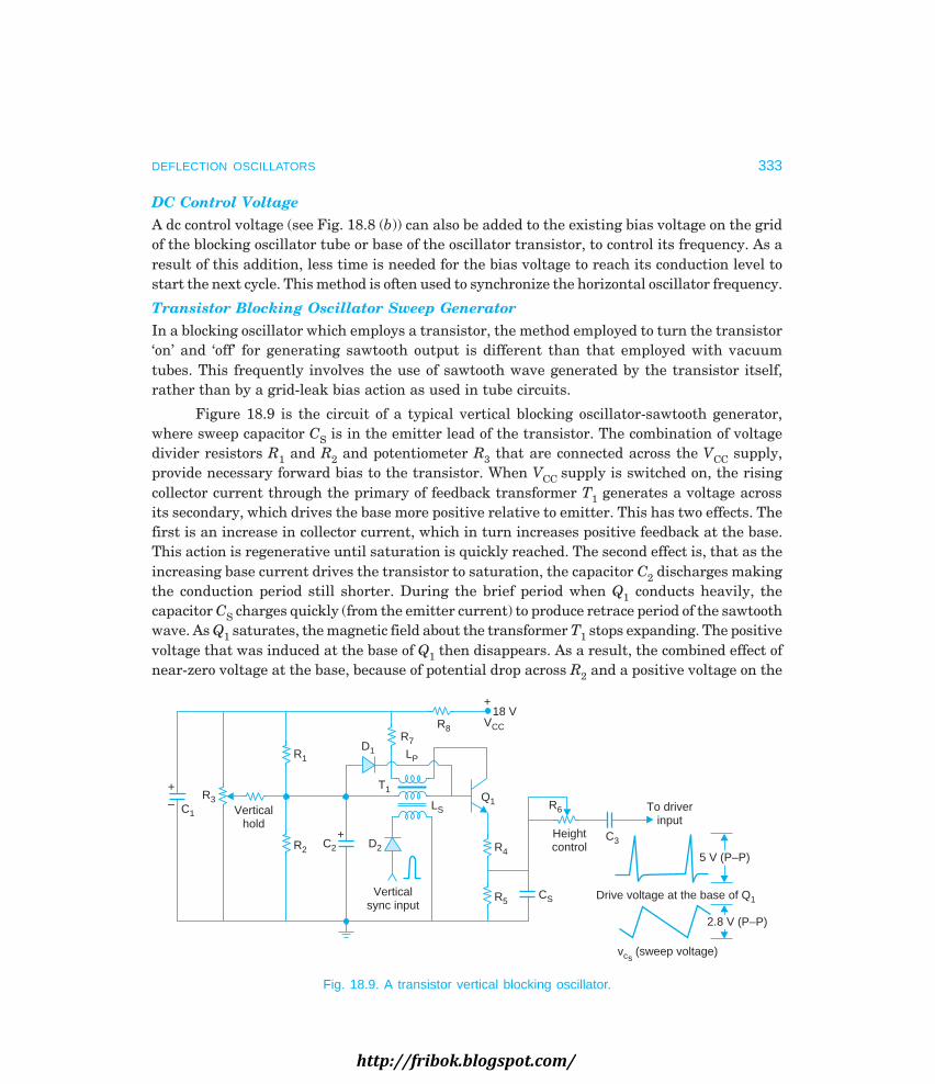
DEFLECTION OSCILLATORS 333
DC Control VoltageA dc control voltage (see Fig. 18.8 (b)) can also be added to the existing bias voltage on the gridof the blocking oscillator tube or base of the oscillator transistor, to control its frequency. As aresult of this addition, less time is needed for the bias voltage to reach its conduction level tostart the next cycle. This method is often used to synchronize the horizontal oscillator frequency.
Transistor Blocking Oscillator Sweep GeneratorIn a blocking oscillator which employs a transistor, the method employed to turn the transistor‘on’ and ‘off’ for generating sawtooth output is different than that employed with vacuumtubes. This frequently involves the use of sawtooth wave generated by the transistor itself,rather than by a grid-leak bias action as used in tube circuits.
Figure 18.9 is the circuit of a typical vertical blocking oscillator-sawtooth generator,where sweep capacitor CS is in the emitter lead of the transistor. The combination of voltagedivider resistors R1 and R2 and potentiometer R3 that are connected across the VCC supply,provide necessary forward bias to the transistor. When VCC supply is switched on, the risingcollector current through the primary of feedback transformer T1 generates a voltage acrossits secondary, which drives the base more positive relative to emitter. This has two effects. Thefirst is an increase in collector current, which in turn increases positive feedback at the base.This action is regenerative until saturation is quickly reached. The second effect is, that as theincreasing base current drives the transistor to saturation, the capacitor C2 discharges makingthe conduction period still shorter. During the brief period when Q1 conducts heavily, thecapacitor CS charges quickly (from the emitter current) to produce retrace period of the sawtoothwave. As Q1 saturates, the magnetic field about the transformer T1 stops expanding. The positivevoltage that was induced at the base of Q1 then disappears. As a result, the combined effect ofnear-zero voltage at the base, because of potential drop across R2 and a positive voltage on the
+
– C1
R3
R1
R2
Verticalhold
C2 D2+
T1
D1
R7
R8
LP
LSQ1
+
VCC
18 V
R4
R5CS
R6
Verticalsync input
Heightcontrol
C3
To driverinput
Drive voltage at the base of Q1
5 V (P–P)
2.8 V (P–P)
v (sweep voltage)cs
Fig. 18.9. A transistor vertical blocking oscillator.
http://fribok.blogspot.com/

334 MONOCHROME AND COLOUR TELEVISION
emitter due to charge on CS, reverse biases the base-emitter junction and the transistorimmediately goes to cut-off. This sudden change in collector current and the consequent collapseof magnetic flux in the primary of T1 induces a large reverse voltage in the secondary windingwhich aids in keeping the transistor in cut-off state. This voltage at the base could damage thetransistor but for the protective action of diode D1. The diode acts as a short across the secondary(base) winding of the transformer during the brief back-emf period, protecting the transistor.
After Q1 is cut-off, base capacitor C2 starts charging towards positive voltage at thejunction of R1 and R2. It reaches this positive voltage level very quickly and then levels off.This is indicated by the base voltage waveform drawn along the circuit diagram. As soon as Q1cuts off and emitter current ceases, CS starts discharging through R5 producing trace portionof the sawtooth waveform. When the capacitor has discharged to the point where emittervoltage no longer keeps Q1 cut-off, it turns on and the entire cycle is repeated.
The frequency of the oscillator is controlled primarily by the time constant R5, CS. Notethat during discharge of capacitor CS, Q1 is cut-off and network R5, CS is isolated from rest tothe circuitry. This provides excellent frequency stability.
Any change in the setting of potentiometer R3 alters forward biasing and thus controlsthe instant at which Q1 breaks into conduction. This changes frequency of the oscillator and sopotentiometer R3 acts as ‘hold control’. Similarly potentiometer R6 which controls the magnitudeof sawtooth voltage that is fed to the driver is called ‘size’ or ‘height control’. In transistorcircuits the driver, which is an emitter follower, is necessary to isolate the oscillator from lowinput impedance of the corresponding output stage.
Synchronization
Sync pulses received as part of the composite video signal from the transmitting station towhich the receiver is tuned are applied after due processing through diode D2 to the tertiarywinding of the feedback transformer. While D2 prevents vertical oscillator waveforms frombeing fed back to the sync circuit, the tertiary (third winding) on T1 provides isolation betweenthe oscillator and sync circuit.
The positive going sync pulses drive the base more positive and turn on Q1 a little earlierthat it would have normally under free running condition. The sync pulses thus lock the verticaloscillator to the transmitter field frequency to prevent any rolling of the picture.
Another transistor blocking oscillator circuit is shown in Fig. 18.10. In this circuitsawtooth network is in the collector circuit and the sawtooth capacitor CS charges during traceperiod and discharged during retrace interval. The setting of potentiometer R2 controls initiationof conduction of the transistor and thus acts as ‘hold control’ over a narrow range of the oscillatorfrequency. The output voltage across CS is of the order of 1 volt and is enough to operate thefollowing driver stage.
http://fribok.blogspot.com/

DEFLECTION OSCILLATORS 335
VCS
0 t
+ 18 V
R1330 W
+CS 100 Fm
D1
T1
R2
Holdcontrol
R3
Q1
5 Fm+
C1
D2
Sync input
To input ofthe verticalstage driver
Fig. 18.10. Vertical deflection blocking oscillator.
18.4 MULTIVIBRATOR DEFLECTION OSCILLATORS
A multivibrator is another type of relaxation oscillator which employs two amplifier stages,where the output of one is coupled to the input of the other. This results in overall positivefeedback and the circuit operates such that when one stage conducts, it forces the other to cut-off. Soon the stage that cuts off returns to conduction to force the first stage to cut-off. Thissequence repeats to generate square or rectangular output with a frequency that is controlledby the coupling networks between the two amplifier stages. As in the case of a blocking oscillatorthe multivibrator is used as a controlled switch to charge a capacitor through a resistance togenerate the required sawtooth wave output. The amplifiers may employ tubes or transistorsas active devices.
Multivibrators may be classified as bistable, monostable and astable. A bistablemultivibrator has two stable stages and needs two external trigger signals to complete onecycle of oscillation. The monostable type has one stable stage and completes one cycle of outputwith only one external pluses. However, and astable multivibrator is a free running type anddoes not need any external trigger pulse for its normal operation. It is this type of multivibratorthat is employed as a deflection oscillator and its frequency is synchronized with the horizontalAFC voltage or vertical sync pulses. Multivibrators can also be classified on the basis of couplingbetween stages. The two types that are used in TV receivers are plate (or collector) coupledand cathode (or emitter) coupled.
Transistor Free Running MultivibratorThe circuit configuration shown in Fig. 18.11 (a) is of a free running collector coupledmultivibrator where two common emitter amplifiers are cross coupled to provide positive
http://fribok.blogspot.com/

336 MONOCHROME AND COLOUR TELEVISION
feedback. Note that the base resistances are returned to VCC supply to ensure precise operationof the multivibrator. The circuit operation can be easily explained if the sequence of operationsis followed from the instant when one transistor just conducts and the other goes to cut-off.
Figure 18.11 (b) illustrates the collector and base voltage waveforms for one completecycle. At the instant marked t0, transistor Q2 just conducts to saturation and transistor Q1returns to cut-off. As this happens, the rising voltage at the collector of Q1 charges the capacitorC2 to VCC, since, VBE(sat)) ≈ 0. The charging current of C2 flows through the base of Q2 to completeits circuit. RB2 is selected to provide enough current from VCC to the base of Q2, to keep it insaturation, even when the charging current of C2 becomes zero and C2 charges to VCC.
+ VCC
RL2R2
R1
C1+
RB1RB2C2
+
RL1
Q1 Q2
C3
EvCE1EvBE1 EvBE2
EvCE2
v0
Sync input
(a)
Off
Q1
RB1
VCC
vC1C1–+
Q2On
(c)
+
VCE1
VCC
0(Q1)
t
Off On
t
–VCC
0
VBE1
(Q1)
+ t0 t1 t2
vCE2
VCC
0(Q2)
t
OffOn
vBE2
(Q2)
–VCC
t
+VCC
–VCC
0
v (v )C1 C2
t1
(b)
tA tB
t1t0 t2
(d)
Fig. 18.11. Free running transistor multivibrator (a) circuit (b) collector and basevoltage waveforms (c) relevant circuit with Q1 ‘off ’ and Q2 ‘on’ (d) charging
curve of capacitor C1 from VCC towards VCC.
In a similar manner C1 would have got charged to VCC in the previous cycle when Q1was in saturation. Actually at t = t0 the capacitor C1 which was previously charged to VCC getsearthed with its positively charged plate towards ground, the moment Q2 goes into fullconduction. As shown in Fig. 18.11(c), C1 is then in parallel with emitter-base junction of the‘off’ transistor Q1. This puts a reverse bias on Q1 equal to – VCC at t = t0, which is well beyondcut-off bias of the transistor.
The capacitor C1 now starts charging from – VCC towards + VCC as shown in Fig. 18.11 (d).At t = t1 the negative voltage across C1 reduces to zero and permits base current flow in the
http://fribok.blogspot.com/

DEFLECTION OSCILLATORS 337
transistor Q1. This action is regenerative and Q1 instantly goes to saturation which in turncuts-off Q2. The time constant RB1C1 controls the off period (t1 – t0) of Q1 and can be set equalto the retrace period of the required sawtooth wave.
The moment Q1 goes into saturation the positively charged plate of C2 is effectivelygrounded through Q1. It then begins to charge towards + VCC at a rate determined by the timeconstant RB2C2. Once again when VC2 = 0, the second transition takes place to complete onecycle of operation. This cycle then repeats and permits the circuit to function as a free runningmultivibrator. The time constant RB2C2 can be made equal to the trace period. As shown in thecircuit, RB1 consists of R1 and R2 where R2 is a potentiometer to adjust the retrace period andthereby controls the frequency of the multivibrator.
The output voltage at either of the collectors is a rectangular wave with an amplitude= VCC – VCE(sat).
Multivibrator FrequencyAs shown in Fig. 18.11 (b) the total period
T = 1f
= tA i.e. (t – t0) + tB i.e. (t2 – t1).
A reference to Fig. 18.11 (c) will show that VC1 takes a time equal to tA to return to zerofrom – VCC while charging toward + VCC . Then at the instant t1, νc1 = 0 and we can write.
0 = VCC – (VCC + VCC) exp (– tA/RB1C1)
This expression when solved yields tA = 0.69 RB1C1.
Similarly it can be shown that tB = 0.69 RB2C2.
∴ T = tA + tB = 0.69 RB1C1 + 0.69 RB2C2.
SynchronizationThe synchronizing pulses may be positive or negative and may be applied to the emitter, baseor collector of one or both the transistors. The frequency of switching action of the astablemultivibrator is kept lower than that of the synchronizing pulses, to force the transistor toswitch states slightly before the free-running transition time. The sync pulses are applied atthe base of the controlling transistor. The ‘on-off’ periods of the multivibrator are used togenerate sawtoothed output across a capacitor as explained in the previous sections.
Cathode/Emitter Coupled MultivibratorIn this type of multivibrator only one RC coupling is provided between the two amplifiers.Positive feedback for regenerative action is obtained through a common resistance in thecathode/emitter leads of the two amplifiers. The oscillator action is explained by considering acathode coupled multivibrator. As shown in Fig. 18.12 (a) the coupling from tube V1 to V2 isthrough an RC network while from V2 to V1 it is through the common cathode resistance RK.When V1 conducts the reduced plate voltage is coupled to the grid of V2 via C2 thereby cuttingit off. Thus the cut-off period of V2 depends on the time constant C2 (100 KΩ + R2) while C2discharges. However, when V2 goes into conduction, the cut-off period of V1 depends on thetime constant for charge of C2. The charge path is through the low resistance of grid-cathode ofV2 (when grid current flows), RK and RL1 while V1 is off. As a result C2 charges fast to providea small cut-off period for V1. The cathode coupled multivibrator therefore automatically produces
http://fribok.blogspot.com/

338 MONOCHROME AND COLOUR TELEVISION
an unsymmetrical output as V2 must remain in cut-off for a much longer period than V1. ThusV2 provides the trace period and V1 the retrace period.
Sawtooth GenerationThe circuit of Fig. 18.12 (a) can be modified as shown by dotted chain lines to generate asawtooth output for feeding into the horizontal output deflection amplifier. The sawtoothcapacitor is connected in the plate circuit of V2, which stays in cut-off for a long time andconducts for a short time. This stage then acts as a discharge tube to generate a sawtoothoutput as explained earlier. Figure 18.12 (b) illustrates how the sawtooth voltage outputcorresponds to cut-off and conduction periods of V2. The variable resistance R2 in the gridcircuit of V2 serves as the frequency (hold) control. The grid resistance R1 for V1 does notcontrol the oscillator frequency because its grid voltage is controlled by the voltage drop across.Rk. However, this grid is best suited for frequency control because of its isolation from theoscillator voltages.
Frequency Control
The horizontal sweep oscillators are normally synchronized by the negative dc control voltageobtained from the AFC circuit. In the cathode coupled multivibrator (Fig. 18.12 (a)), negativedc control voltage is applied at the grid of V1. The added negative grid voltage reduces platecurrent of V1 when it conducts. This results in a smaller drop in its plate voltage and lessnegative drive at the grid of V2. Then less time is needed for C2 to discharge down to cut-off.This reduction in the cut-off period results in an increased multivibrator frequency. Variationsin the AFC negative voltage thus apply necessary correction in the cut-off period of V2 to keepthe oscillator synchronized with the horizontal sync pulses.
(a) (b)
O e cy leOne cycle
Cut offCut off
Trace Retrace
t
Conducting
B+
Ip1Ip2RL1
RL2
V2C2
V1
330 PF100 K
R2
100 K
Frequencycontrol
R11 M
Syncinput
1 K RK
+
CS
CC
680 PF
470 PF v0
v0
To horzdeflection amplifier
Fig. 18.12. Cathode coupled multivibrator (a) circuit (b) waveforms.
http://fribok.blogspot.com/
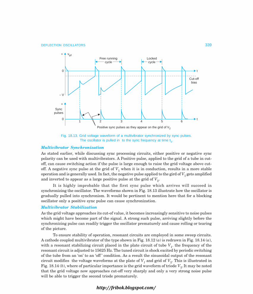
DEFLECTION OSCILLATORS 339
+ vg2
0
– V
0
+
Syncpulses
1 2 3 4 5 6t
Positive sync pulses as they appear on the grid of V2
Cut-offbias
t
Free runningcycle
Lockedcycle
Fig. 18.13. Grid voltage waveform of a multivibrator synchronized by sync pulses.The oscillator is pulled in to the sync frequency at time t3.
Multivibrator SynchronizationAs stated earlier, while discussing sync processing circuits, either positive or negative syncpolarity can be used with multivibrators. A Positive pulse, applied to the grid of a tube in cut-off, can cause switching action if the pulse is large enough to raise the grid voltage above cut-off. A negative sync pulse at the grid of V1 when it is in conduction, results in a more stableoperation and is generally used. In fact, the negative pulse applied to the gird of V1 gets amplifiedand inverted to appear as a large positive pulse at the grid of V2.
It is highly improbable that the first sync pulse which arrives will succeed insynchronizing the oscillator. The waveforms shown in Fig. 18.13 illustrate how the oscillator isgradually pulled into synchronism. It would be pertinent to mention here that for a blockingoscillator only a positive sync pulse can cause synchronization.
Multivibrator StabilizationAs the grid voltage approaches its cut-of value, it becomes increasingly sensitive to noise pulseswhich might have become part of the signal. A strong such pulse, arriving slightly before thesynchronizing pulse can readily trigger the oscillator prematurely and cause rolling or tearingof the picture.
To ensure stability of operation, resonant circuits are employed in some sweep circuits.A cathode coupled multivibrator of the type shown in Fig. 18.12 (a) is redrawn in Fig. 18.14 (a),with a resonant stabilizing circuit placed in the plate circuit of tube V1. the frequency of theresonant circuit is adjusted to 15625 Hz. The tuned circuit is shock excited by periodic switchingof the tube from an ‘on’ to an ‘off ’ condition. As a result the sinusoidal output of the resonantcircuit modifies the voltage waveforms at the plate of V1 and grid of V2. This is illustrated inFig. 18.14 (b), where of particular importance is the grid waveform of triode V2. It may be notedthat the grid voltage now approaches cut-off very sharply and only a very strong noise pulsewill be able to trigger the second triode prematurely.
http://fribok.blogspot.com/

340 MONOCHROME AND COLOUR TELEVISION
B+ 250 V
Resonant circuittuned to
15625 HzC1L1
RL2 100 K
RL1 C2
V2
V1
C3 Rg47 PF
Syncinput
RK
CC
CS
v0
(a)
Cut-off
(i) Plate voltage waveshapeof V without resonant
circuit1
(iv) Grid voltage of Vwith no resonant
circuit
2
(ii) Voltage acrossresonant circuit
(i + ii) = (iii)
(iii) Plate voltage of Vwith resonant circuit
1 (v) Grid voltage waveformof V with resonant
circuit2
(b)
Cut-off
Fig. 18.14. Cathode coupled multivibrator with a stabilizing resonant circuit(a) circuit (b) waveforms.
18.5 COMPLEMENTARY-SYMMETRY RELAXATION OSCILLATOR
A complementary-symmetry relaxation oscillator, designed to drive the vertical deflection outputcircuit, is illustrated in Fig. 18.15 (a). Transistors Q1(p-n-p) and Q2(n-p-n) which are directlycoupled, constitute the oscillator pair, while Q3 is the waveshaping transistor. Resistors R1and R2 form a potential divider across VCC supply through the decoupling network R3, C6, toprovide positive voltage both at the base of Q1 and collector of Q2. The voltage at the emitter ofQ1 is developed by capacitor C1, when it charges towards VCC (+ 20 V), through resistance R4and potentiometer R5 connected in series.
At the instant dc supply is switched on to the circuit, both the transistors are at cut-off,because the base of Q1 is biased positively and its emitter is at zero potential. However, capacitorC1 starts charging at once driving emitter of Q1 positive. When the rising voltage across C1offsets the positive voltage at the base of Q1, the transistor turns on. This makes the base of Q2positive which also goes into conduction. The collector current of Q2 flows through R1 and theresulting drop across it, lowers the potential at the base of Q1, thus making it more negativewith respect to its emitter. This results in increased current through Q1 and the regenerativefeedback action that follows soon saturates Q1. When Q1 is on, its emitter current startsdischarging C1. As soon as the emitter voltage drops sufficiently to remove forward bias on Q1it is driven out of conduction. This in turn cuts off Q2, thereby completing the regenerativecycle. The capacitor C1 starts charging again towards VCC to repeat the sequence of eventsexplained above.
In the absence of any sync input, Q1 and Q2 repeat the on-off cycle at a rate determinedby the time constant C1(R4 + R5). This time constant determines frequency of the oscillator.Potentiometer R5 is the ‘hold control’ and can be varied to change the frequency. A negativegoing vertical sync pulse applied at the base of Q1, through the integrating networks R9, C3
http://fribok.blogspot.com/

DEFLECTION OSCILLATORS 341
and R10,C4, brings the transistor out of cut-off before it normally would. This synchronizes theoscillator to the applied sync pulses.
The voltage waveform (i) at the emitter of Q1 (see Fig. 18.15 (b)) is a sawtooth wavedeveloped by the charging and discharging of C1. Waveform (ii) is the sharp positive pulsedeveloped at the emitter of Q2 when both the transistors are turned on.
+
VCC
20 VR3
C6R5
R4
R1
Q1 C1
+
Q2R2
R10
C4C3
R9
Syncinput
R6
i
ii iii
Q3
R8
R7
VCC+ From horzoutput circuit
C5 To verticaloutput
amplifier
C2
+ iii
ii
i
Fig. 18.15 (a). Complementary symmetry relaxation oscillator. Fig. 18.15 (b). Wave shapesat the emitters of Q1, Q2
and collector of Q3.
Wave ShapingThe wave shaping transistor Q3 is normally biased to cut-off. It is triggered ‘on’ by the positivepulse developed at the emitter of Q2 and directly coupled to its base. Capacitor C2 connectedacross the collector and emitter of Q3 charges during the ‘off ’ period of Q3 and discharges whenthe transistor turns on for a short interval of time. The resulting sawtooth voltage across C2(waveshape(iii)) is coupled through C5 to the vertical output stage of the receiver.
The rate at which C2 charges during the ‘off ’ interval of Q3 is determined by resistors R7and R8. R7 is a potentiometer that can be varied to control the amplitude of the vertical sweepand through this the height of the picture.
The voltage towards which C2 charges is derived from a rectifier in the horizontal outputcircuit. Any change, in the horizontal deflection output voltage, will also alter the dc voltagefed to this circuit and affect the amplitude of the sawtooth voltage. Thus, if horizontal size ofthe picture changes, vertical size also changes proportionately, preserving the ratio of heightto width of the picture.
18.6 SINE-WAVE DEFLECTION OSCILLATORS
High frequency sine-wave oscillators are more stable in their operation as compared tocorresponding relaxation oscillators. Since the horizontal sweep frequency is quite high suchoscillators are often used in horizontal deflection circuits. For such an application the oscillatoris overdriven so that the tube or transistor acts like a switch and allows a sawtooth forming
http://fribok.blogspot.com/
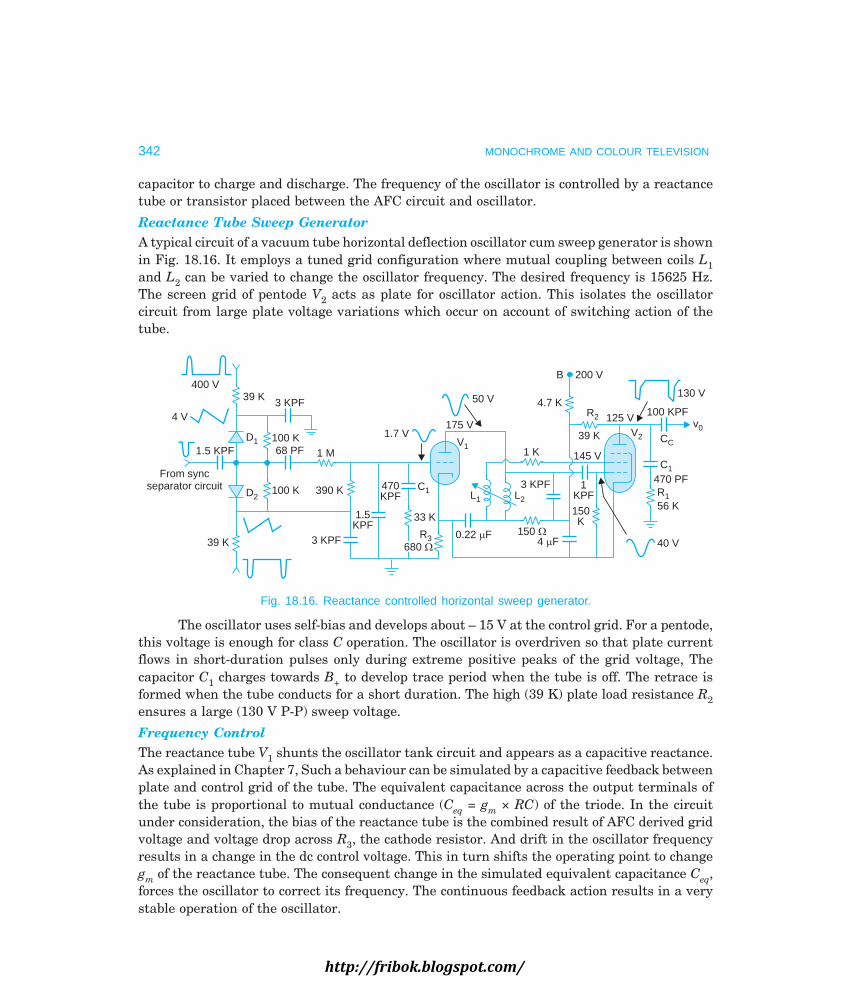
342 MONOCHROME AND COLOUR TELEVISION
capacitor to charge and discharge. The frequency of the oscillator is controlled by a reactancetube or transistor placed between the AFC circuit and oscillator.
Reactance Tube Sweep GeneratorA typical circuit of a vacuum tube horizontal deflection oscillator cum sweep generator is shownin Fig. 18.16. It employs a tuned grid configuration where mutual coupling between coils L1and L2 can be varied to change the oscillator frequency. The desired frequency is 15625 Hz.The screen grid of pentode V2 acts as plate for oscillator action. This isolates the oscillatorcircuit from large plate voltage variations which occur on account of switching action of thetube.
400 VB 200 V
4.7 KR2
39 K V2
125 V
130 V
100 KPF
CC
v0
C1470 PFR156 K
40 V
145 V
1KPF
150K
1 K
3 KPFL2L1
150 W4 mF
0.22 mF
V1
175 V
50 V
1.7 V
C1470KPF
33 K
R3680 W
1.5KPF
390 K
3 KPF
100 K
68 PF 1 M100 K
D2
D1
3 KPF39 K
4 V
1.5 KPF
From syncseparator circuit
39 K
Fig. 18.16. Reactance controlled horizontal sweep generator.
The oscillator uses self-bias and develops about – 15 V at the control grid. For a pentode,this voltage is enough for class C operation. The oscillator is overdriven so that plate currentflows in short-duration pulses only during extreme positive peaks of the grid voltage, Thecapacitor C1 charges towards B+ to develop trace period when the tube is off. The retrace isformed when the tube conducts for a short duration. The high (39 K) plate load resistance R2ensures a large (130 V P-P) sweep voltage.
Frequency ControlThe reactance tube V1 shunts the oscillator tank circuit and appears as a capacitive reactance.As explained in Chapter 7, Such a behaviour can be simulated by a capacitive feedback betweenplate and control grid of the tube. The equivalent capacitance across the output terminals ofthe tube is proportional to mutual conductance (Ceq = gm × RC) of the triode. In the circuitunder consideration, the bias of the reactance tube is the combined result of AFC derived gridvoltage and voltage drop across R3, the cathode resistor. And drift in the oscillator frequencyresults in a change in the dc control voltage. This in turn shifts the operating point to changegm of the reactance tube. The consequent change in the simulated equivalent capacitance Ceq,forces the oscillator to correct its frequency. The continuous feedback action results in a verystable operation of the oscillator.
http://fribok.blogspot.com/

DEFLECTION OSCILLATORS 343
Reactance Transistor Sweep GeneratorFigure 18.17 shows a transistor sine-wave oscillator whose frequency is controlled by a reactancetransistor. In this circuit a Hartley oscillator is used. It performs the same functions as itsvacuum tube counterpart discussed earlier. The output of the sine-wave transistor oscillator isusually fed to the horizontal output circuit through a driver to provide isolation between theoutput stage and oscillator circuit.
To horzoutput
amplifier470
Horz osc
Q2
19 V
330
– 1VC1
0.0068 F
Holdcontrol
Biasvoltage3.3 K
C0.027
F
2
Q1
R21 K 360
5 F
Reactancetransistor
FromAFC 15 K
0.01 F
22 V+
Fig. 18.17. Transistor sine-wave horizontal deflection oscillator and its associated reactance transistor.
As shown in the circuit diagram a reactance transistor (Q1) is used between the AFCoutput and horizontal oscillator. It acts like an inductor instead of a capacitor, In order tosimulate such a behaviour the phase shift network C2, R2 couples some of the oscillator’s voltageinto the emitter of the reactance transistor and at the same time shifts its phase by 90°. Sincethe feedback is returned to the emitter, transistor Q1 can be considered to be a common baseamplifier. As such, the emitter voltage and collector current are 180° out of phase. Thus thetransistor current lags behind the collector voltage by 90°. Therefore, the oscillator ‘sees’ thereactance transistor as if an inductor has been connected across its tank circuit.
Any change in the oscillator frequency is sensed by the AFC circuit which couples aproportionate dc error voltage into the base of the reactance transistor. This shifts the operatingpoint of the transistor in the same way as AGC bias does to control gain of tuned amplifiers.
Any decrease in oscillator frequency results in a positive dc control voltage therebyincreasing forward bias of the reactance transistor. The resulting increase in collector currentshifts the operating point where the transistor gain is lower. In turn, this acts to decrease theeffective reactance at the output terminals of the transistor. This causes the total inductanceshunting the oscillator tuned circuit to decrease. As a result, frequency of the oscillator isincreased to return to its correct value. The reverse would occur if the bias were to decrease forany increase in the oscillator frequency.
Review Questions
1. Sketch and label the current waveforms that must flow in the deflection yoke coils to produce afull rester. Explain the basic principle of generating such waveforms.
2. Why is a trapezoidal voltage waveform necessary to drive the vertical deflection coils ? What isthe effect of source impedance and frequency on the shape of the driving voltage waveform ? Howis the basic sawtooth voltage modified to obtain the desired driving voltage waveform ?
http://fribok.blogspot.com/

344 MONOCHROME AND COLOUR TELEVISION
3. Draw the circuit diagram of a blocking oscillator-cum-waveshaper which employs a single triodeand discuss its operation. Explain the operation of ‘hold control’ and ‘height control’ as providedin the circuit drawn by you.
4. A blocking oscillator that employs a transistor is shown in Fig. 18.9. Explain how the circuitoperates to develop a sawtooth voltage. In particular, explain the operation of hold and heightcontrols. Why are diodes D1 and D2 provided in the feedback transformer circuit ?
5. Explain with suitable waveforms how the frequency of the blocking oscillator is controlled withthe help of sync information. Why is the free running frequency of the oscillator kept somewhatlower than the desired frequency ? What will happen if the uncontrolled frequency is higher thanthe correct frequency ?
6. Draw the basic circuit of a multivibrator employing transistors. How are the feedback networksdesigned to obtain correct trace and retrace periods ? Explain how the sync pulses control thefrequency of such an oscillator.
7. The circuit of a complementary-symmetry relaxation oscillator is given in Fig. 18.15 (a). Describebriefly how the circuit operates to generate sawtooth output voltage. Discuss with suitable wave-forms how the sync pulses keep the oscillator in synchronism with corresponding oscillator atthe transmitter.
8. Why is a sine-wave oscillator preferred in horizontal deflection circuits ? Explain with a circuitdiagram how a reactance tube/transistor connected between the AFC circuit and oscillator operatesto maintain a constant frequency.
http://fribok.blogspot.com/

19
http://fribok.blogspot.com/

The output from the vertical and horizontal oscillators is too low to drive the deflection coils togenerate a full raster. Therefore, amplifiers are used to produce enough power to fully drivethe coils in the deflection yoke. The horizontal oscillator drives the horizontal output stage toproduce horizontal scanning and the vertical oscillator drives the vertical output stage to producevertical deflection. These two motions occur simultaneously to produce raster on the screen.
19.1 REQUIREMENTS OF THE VERTICAL DEFLECTION STAGE
The purpose of a field-scan output amplifier is to convert the input sawtooth or trapezoidalvoltage waveform into a sawtooth current in the field deflection coils, of sufficient magnitudeto scan the face of the picture tube. There are many different vertical-output circuitconfigurations in use that employ all tubes, combined tubes and transistors (hybrid) and onlytransistors. However, all circuits operate under class ‘A’ or ‘AB’ condition to ensure linearoperation.
The limitations of inductive coupling that is employed between the output stage andyoke coils, together with the imperfection of active devices, make it necessary to modify theoutput voltage waveform to achieve linear deflection. This necessitates the use of negativefeedback and other waveshaping techniques. Furthermore, transistor circuits need somewhatdifferent approach than the one employing vacuum tubes. All this tends to make the deflectioncircuits somewhat complex. However, this problem is solved by first discussing various sectionsof the circuit separately and then putting them together to study the complete set-up.
(a) Vertical Yoke DriveA voltage stepdown transformer provides an efficient means of coupling the output stage tothe deflection coils. Figure 19.1 (a) shows such an arrangement that employs a vacuum tube asthe vertical sweep amplifier. The output transformer matches the relatively high impedanceof the tube to the low impedance deflection coils. The impedance of the coils is mainly resistivebecause of the low frequency spectrum that constitutes the 50 Hz trapezoidal sweep voltage.This makes the design of the output circuit basically the same as that of an audio output stageto match a loudspeaker.
In order to amplify the 50 Hz sawtooth with little distortion the frequency response ofthe amplifier must extend down to 1 Hz. The turns ratio of the output transformer is chosen tomatch the scanning coil impedance to the optimum output impedance of the tube. This is inthe range of 30 : 1 to 6 : 1 depending upon the impedance of the coils. Typical value of primaryinductance is around 45 mH with a dc resistance of the order of 40 ohms. The resistance of thesecondary winding is quite low and varies between 5 and 10 ohms.
346
&
http://fribok.blogspot.com/

VERTICAL DEFLECTION CIRCUITS 347
AmplifierVertical
yokewindings
Couplingtransformer
Lp LS
R1C1
B+
vin
Fig. 19.1 (a). Vertical output stage employing an isolated primaryand secondary step-down transformer.
R1C1
B+
C2
C3
Yokewindings
Lp
LS
Tap
To verticaloutputstage
Fig. 19.1 (b). Vertical output circuit employingan autotransformer.
In many circuit designs an autotransformer coupling (Fig. 19.1 (b)) is employed becauseof its higher efficiency. The position of the tap determines the effective turns ratio of thetransformer. If all other conditions are indentical, for the same input power an autotransformergives a greater output power. The primary and secondary ac currents flow in opposite directionsthrough a common portion of the autotransformer winding and thus tend to cancel each other.Since the net current flowing through these windings is smaller, power losses are less ascompared to an isolated winding transformer. This means that for the same power ratings athinner wire can be used in an autotransformer. In practice this results in a smaller and lessexpensive transformer.
A shown in Fig. 19.1 (b) a coupling capacitor (C2) is used to prevent any dc current flowin the deflection coils which would otherwise shift centering of the electron beam. The capacitorC3 connected between secondary tap and ground is effectively in parallel with the secondarycircuit. It improves frequency response of the transformer by speeding up collapse of the inducedfield during retrace.
The self-induced voltage in the secondary winding during retrace is stepped up becauseof the large turns ratio between the primary and secondary. Therefore, the transformer windingmust be insulated to withstand induced voltage peaks. As shown in Figs. 19.1 (a) and (b) the
http://fribok.blogspot.com/

348 MONOCHROME AND COLOUR TELEVISION
network R1,C1 provides decoupling, to prevent any undesired feedback from output stage toany other stage through the common dc source.
In vertical output stages that employ transistors, an output transformer is not necessary,because power transistors provide large output current at a relatively low impedance level,and thus can be coupled through a capacitor directly to the yoke coils. The circuit arrangementthat is often used is shown in Fig. 19.2. The choke shown in the collector circuit isolates thecollector signal path from the power supply. There are some solid state vertical output circuitswhich use an isolation transformer with a unity turns ratio. This arrangement provides acdriving current to the yoke without the need for a large electrolytic coupling capacitor. A VDR(voltage dependent resistance) is often used in the output circuit across the choke (Fig. 19.2) toprotect the output transistor against voltage transients in the collector circuit.
vin
R1
1 V
+ 12 V
Q1
Driver
R2
Q2
Output
VDRChoke
120 V+
L1 L2
CC
Deflectioncoils
Fig. 19.2. Basic circuit of a transistor vertical amplifier.
(b) Vertical Deflection CoilsThe magnetic field for vertical deflection is developed by two coils mounted 180° apart on theneck of the picture tube. Physically these coils are a part of the yoke assembly that also containshorizontal windings. During the vertical deflection period the flux generated by the sawtoothcurrent in the windings, moves the electron beam down and then returns it to the top for aquick retrace. The vertical yoke inductance and resistance are kept as low as possible toaccomplish higher deflection efficiency.
Most field scanning coils are designed with an inductance that varies between 3 mHand 50 mH with a resistance of 4 to 50 ohms. The impedance and number of turns of the coilsare dependent on the required deflection angle. Wider deflection angle tubes require a strongermagnetic field to cover the entire raster. The peak-to-peak sawtooth current needed by differentvertical deflecting coils varies between 300 mA to 2.5 Amp. Typically, a short neck 36 cmpicture tube requires a 45 mH deflection coil and a peak-to-peak driving current of 400 mA.
The two halves of the deflecting coils are normally connected in series across the secondaryof the drive transformer in vacuum tube circuits. However, in transistor circuits these areconnected in parallel to provide impedance match for maximum efficiency.
(c) Vertical LinearityThe patterns of Fig. 19.3 illustrate the effect of three different current waveforms on thereproduced raster. When the sawtooth wave is linear (Fig. 19.3 (a)), the vertical scan allowsequal spacing between horizontal lines and there is no distortion. In Fig. 19.3 (b) the sawtoothwave tends to become flat towards its close, hence the magnetic field increases at a reducedrate with the result that the horizontal lines crowd together at the bottom of the raster. In the
http://fribok.blogspot.com/

VERTICAL DEFLECTION CIRCUITS 349
third pattern (Fig. 19.3 (c)) the horizontal lines are crowded at the top of the raster because ofthe slow rate of change of current at the beginning of the sawtooth wave. Non-linear verticalscanning is more noticeable than horizontal non-linearity. Crowding of horizontal lines in anyregion of the raster makes the objects look flatter in that part of the picture. However, whenthe scanning rates becomes faster than normal in any portion of the raster the correspondingpicture area appears elongated. Non-linearity may be caused due to any of the following reasons.
Top
Retrace
Trace
Time Bottom
Verticaldeflectionsawtooth
Fig. 19.3 (a). Linear sawtooth causing equal spacing between the lines on the raster.
Fig. 19.3 (b). Non-linear sawtooth causing crowding of lines at the bottom of the raster.
Fig. 19.3 (c). Non-linear sawtooth causing crowding of lines at the top of the raster.
(i) A short time-constant sawtooth forming RC circuit develops a non-linear sweepbecause too much of the exponential charging curve forms part of the trace period. Similarnonlinear compression at the bottom of the raster may be caused by positive peak clipping ofthe trapezoidal voltage driving the grid/base of the vertical output stage. This is generally theresult of incorrect tube/transistor bias. However, such shortcomings can be easily avoided by acareful design of the sawtooth forming circuit and appropriate choice of the device’s operatingbias.
(ii) The magnetizing current of the coupling transformer will also cause nonlineardistortion. This can be made quite small if the transformer has a high primary inductance.This, however, leads to a heavier and costlier output transformer.
The solution to this problems, which is often employed, is to use a transformer with not-too-high a primary inductance but modify the input voltage to the amplifier for optimum results.
http://fribok.blogspot.com/

350 MONOCHROME AND COLOUR TELEVISION
(iii) Another aspect, which needs attention, is the attenuation caused at low frequenciesby the finite primary inductance of the output transformer, that effectively appears in parallelwith the deflecting coils. This is corrected by applying negative feedback from the output circuitto input of the amplifier through a frequency selective network.
(iv) Another problem is the pincushion distortion. Since magnetic deflection of the electronbeam is along the path of an arc, with point of deflection as its centre, the screen should ideallyhave corresponding curvature for linear deflection. However, in flat screen picture tubes it isnot so and distances at the four corners are greater as compared to central portion of the faceplate. Therefore electron beam travels farther at the corners causing more deflection at theedges. This results in a stretching effect where top, bottom, left and right edges of the rastertend to bow inwards towards the centre of the screen. The result, as illustrated in Fig. 19.4, isa pincushion like raster. Such a distortion is more severe with large screen picture tubes havingdeflection angles of 90° or more.
Raster
Top pincushioning
Sidepincushioning
Fig. 19.4. Pincushion distortion of the raster.
In black and white receivers, pincushion distortion is eliminated by suitable design ofthe yoke and the use of small permanent magnets mounted close to the yoke. These magnetsare so positioned that they stretch the raster along the sides of the picture and thus compensatefor the pincushion distortion. In colour picture tubes the deflection current in the yoke ismodified by special pincushion correction circuits.*
In output stages, (see Fig. 19.5) which use power triodes, the linearity is often controlledby shifting the operating point on the transfer characteristic, by varying a part of the cathodebias resistance. The variable resistance then performs as Linearity Control.
Transistor vertical output stages are generally similar to their vacuum tube counterparts.Since the input impedance of a power transistor is only the order of a few hundred ohms, itbecomes necessary to drive the output stage from an emitter follower (driver) so as not to placetoo high a load on the sawtooth generator. In high power transistor circuits some form ofthermal stabilization is also provided for stable operation. This ensures linear operation by
*This is explained along with dynamic convergence circuits in chapters devoted to colour television.
http://fribok.blogspot.com/

VERTICAL DEFLECTION CIRCUITS 351
maintaining the operating point at the set optimum value. Negative feedback is also used tomaintain a frequency response that is flat down to 1 Hz.
Verticaldeflection
coils on yoke
Vertical outputtransformer (V.O.T.)
Th
560 W
560 W
Thermistor
C3+350 V
1000 V (P–P)
Vertical outputamplifier
+100 FmC2
RK
1 KP1
270 W
Linearitycontrol
Rg 1 MC1
0.1 Fm
50 Hz
140 V (P–P)
Fromvertical
oscillator R1
R2
Fig. 19.5 (a). Triode vertical deflection amplifier.
Input sawtoothvoltage
Adjustable bias(Linearity control)
0VGK
iPOutput plate
current in primary ofV.O.T.
Fig. 19.5 (b). Cancellation of non-linear curvature of the sawtooth wave byoptimum choice of the operating point on the output characteristics of the tube.
Whenever possible direct coupling is employed between the driver and output stage toavoid use of a large coupling capacitor. If necessary, linearity correction is also employed bymodifying the waveshaping network. This is fully explained in a later section of the chapterwhile describing a typical transistor output circuit.
(d) Suppression of Undesired OscillationsDuring retrace time when the current through vertical deflecting coils suddenly drops to zero,energy stored in the collapsing magnetic field sets up high frequency oscillations. The frequency
http://fribok.blogspot.com/

352 MONOCHROME AND COLOUR TELEVISION
of ‘ringing’ thus produced, depends on the inductance and the distributed capacitance of thedeflecting coils. The effect of such oscillations, if not suppressed, would be to pull the beamupwards and downwards alternately instead of the smooth motion downwards. This results ina narrow white strip at the top of the screen. The strip then appears more bright than the restof the raster. To prevent ringing two shunt damping resistances are connected across the twohalves of the vertical scanning coils. Figure 19.6 (a) illustrates the ringing effect on the deflectioncurrent and Fig. 19.5 (a) the use of damping resistors R1 and R2 across the vertical scanningcoils. It may be noted that the output from the amplifier contains considerable power and thedamping resistors do not attenuate the signal appreciably.
(e) Height of the RasterTo fill the entire raster from top to bottom of the screen a definite amplitude of sawtoothcurrent must flow into the deflecting coils. The output amplifier is designed to meet thisrequirement. In addition a control is provided at the input of the amplifier to finally adjust theheight of the picture. This control is known as ‘height control’. In some designs the linearitycontrol resistor when provided in the cathode (or emitter) lead of the amplifying device is leftunbypassed (by a capacitor) and also acts as the height control. A change in the linearitycontrol resistance varies gain of the stage which in turn controls the height of the raster. Theeffects of either insufficient or excessive drive are illustrated in Fig. 19.6 (b) which clearlyindicate the need for a ‘height control’.
Undesired oscillations
i(v)
0 t
Screen
T1
T2
T3
(S ) Correct amplitude (T )11
(S ) Excessive amplitude (T )22
(S ) Insufficient amplitude (T )33
Fig. 19.6 (a). Effect of ringing on the Fig. 19.6 (b). Effect of deflection currentvertical deflection current. amplitude on the height of the raster.
Another factor which affects the height of the picture is the increase in resistance of thedeflection coils when current flows through them. To counteract this, a thermistor (see Fig. 19.5)is added between the coils in the yoke to equalize the resistance under high heating conditions.When temperature of the windings rises, the thermistor also gets heated and its resistancedecreases sufficiently to compensate for the increase in winding resistance. This maintains aconstant deflection current to prevent any change in the height of the raster.
(f) Vertical Rolling of the PictureThe rolling of the picture upwards or downwards on the screen occurs on account of incorrectvertical scanning frequency. This is illustrated in Fig. 19.7 for the case when the vertical
http://fribok.blogspot.com/

VERTICAL DEFLECTION CIRCUITS 353
oscillator frequency is higher than 50 Hz. It may be noted that relative timings of verticalblanking in the composite video signal and vertical retrace in the sawtooth deflection currentare not the same, with the result that vertical blanking occurs during trace time instead ofduring retrace time. For a vertical frequency that is higher than 50 Hz, each sawtooth advancesinto trace time for succeeding blanking pulses. As a result the black bar produced across thescreen, by the vertical blanking pulse, appears lower and lower down the screen for successivecycles. The opposite effect takes place when the oscillator frequency is lower than 50 Hz. Thepicture rolls at a faster rate if the oscillator frequency deviates much from 50 Hz. However,when the sync frequency and sawtooth frequency are the same, every vertical retrace occurswithin the blanking time. The blanking bars are then produced at the top and bottom edges ofthe raster and are not visible. Thus, when the vertical oscillator is locked by sync pulses eachframe is reproduced over the previous one, and the picture holds still.
Verticalsync
Verticalsync
Videosignal
Verticalblanking
time
Verticalsawtooth
50 Hz
60 Hz
Rolling barPicture
Fig. 19.7. Vertical rolling when the deflection frequencyis more than 50 Hz. Note that horizontal blanking details
have been omitted for clarity.
As explained in the previous chapter, the oscillator frequency is controlled by the ‘holdcontrol’. Since no elaborate sync processing circuitry is provided for the vertical sync pulses,the vertical hold control is provided on the front panel of all TV receivers, for resetting thefrequency, when picture rolls continuously up or down.
The vertical jumping of the picture that sometimes occurs should not be confused withvertical rolling. Vertical jumping occurs on account of unequal sync pulse amplitudes for oddand even fields. Occasional jumping is caused by wrong triggering of the vertical oscillator bya stray noise pulse.
(g) Internal Vertical BlankingThe voltage pulses produced during retrace intervals, in the vertical output circuit are coupledto the picture tube to provide additional blanking during vertical retrace time. This is in additionto the blanking voltage at the cathode or grid circuit of the picture tube, which is part of thecomposite video signal. In receivers, that do not fully retain dc component of the video signalat the picture tube, the blanking pulses fail to reach the required level to cut-off the beam,
http://fribok.blogspot.com/

354 MONOCHROME AND COLOUR TELEVISION
when vertical retrace is taking place. Thus the horizontal lines that get traced during thisperiod, appear on the screen. However, the use of blanking pulses ensures complete blankingduring retrace for any setting of the brightness control, with or without the dc component.
All receivers use a vertical retrace suppression circuit, to turn-off the electron beam,until it is back at the top of the screen to begin the next vertical trace. Figure 19.8 shows twodifferent circuit arrangements, one for obtaining positive pulses, that are suitable for injectingin the cathode circuit and the other for obtaining negative pulses to be applied at the grid ofpicture tube. The amplitude of these pulses varies between 50 to 150 V in different circuits.
vinVerticalamplifier
B +
To verticalcoils
To cathodeof picture tube
0.02 F
20 K
+
(a)
vinVerticalamplifier
B +
–
20 K
0.05 F
To grid ofpicture tube
To verticalcoils
(b)
Fig. 19.8. Circuits for obtaining internal vertical blanking pulses(a) positive retrace pulses (b) negative retrace pulses.
In transistor circuits, where such high amplitudes cannot be obtained, the low amplitudepulses as obtained from the output stage are fed into the video amplifier, which amplifies thembefore feeding to the picture tube circuit.
In the circuit shown in Fig. 19.8 (a) the pulses are obtained at the primary of the outputcircuit to yield positive going pulses, whereas in the circuit of Fig. 19.8 (b) negative goingpulses are obtained from the secondary of the same output transformer.
Based on the above discussion about the problems of vertical output stage and thetechniques used to overcome them, it is reasonable to assume that a large number of circuitarrangements are possible to achieve linear vertical deflection. However, a few typical circuitsare discussed to broadly identify various configurations that have found wide acceptance intelevision receiver practice.
19.2 VACUUM TUBE VERTICAL DEFLECTION STAGE
Figure 19.9 is the circuit of a vertical output stage which is widely used in vacuum tube receiver.As is the common practice, a single tube (triodepentode), serves both as oscillator and outputstage. While the pentode section performs as vertical output stage, both triode and pentode (V1and V2) operate together as an unsymmetrical free-running plate coupled multivibrator. Positive
http://fribok.blogspot.com/

VERTICAL DEFLECTION CIRCUITS 355
going pulses which are obtained from winding LS2 on the output transformer are fed back viaR1 and C1 to the grid of V1 to provide multivibrator action. The pentode conducts for a longerperiod to supply a sawtooth current to the deflection coils. During this period the triode is cut-off and a sawtooth voltage builds up at its plate due to C2 charging through R2, P2 and R3 fromB++ supply. The potentiometer P2 (1 M) can be varied to adjust the amplitude of sawtooth andhence serves as height control.
R5
R4
120 K39 K
D1Vertical
syncinput
4.7 KPF 4.7 KPFC4
10 nFP1
500 KHold
control
200 K5 K
10 nF
0.2 Fm 2 M
C R6
R2V1
470 K
1 M
P2
VDR1R3 300 K
B++From H.O.T.
circuit
Heightcontrol
C2
33 nF
180 K
12 nF
1 MP3
100 nF
100 nF
390 K
56 KOverall linearity
control100 Fm 330 W
P4V2
33 K
100 K
33 nF Top rasterlinearity control
VDR2
Lp
230 VV.O.T.
LS110 nF Th
Verticaldeflection
coils
3.3 KPFC3
LS2R1C1
10 nF 15 K50 V 60 V
To picturetube grid
Vertical blankingpulses
Fig. 19.9. Vacuum tube vertical output stage driven by a multivibrator sweep circuit.
For improved linearity and constant aspect ratio the dc voltage for charging C2 is obtainedfrom the horizontal output circuit. The VDR1 connected across R3 and ground stabilizes this dcsource. Any change in width of the picture will indirectly affect B++ supply and hence varyamplitude of the sawtooth voltage. The resultant change in drive voltage to the vertical outputstage will vary height of the picture, thereby maintaining a constant aspect ratio.
The setting of potentiometer P3 makes it possible to alter the shape of sawtooth voltageapplied to the grid of V2. This is done to obtain a certain curvature in the sawtooth current thatflows through the deflection coils for improving overall linearity. In addition, setting ofpotentiometer P4 (100 K) in the negative feedback path from winding LS2 to the grid of V2(pentode) affects the form of drive voltage just after flyback and hence serves as top linearityadjustment. The network R6 (2 M), C5 (0.2 µf) provides a small negative feedback from grid ofV2 to the input circuit of V1 to ensure stable operation of the circuit.
The vertical sync pulses are integrated by network R4, C4 which constitutes a low-passfilter. The output across C4 is passed through the parallel combination of diode D1 and resistanceR5 to obtain sharp positive going pulses. These are fed to the grid of V1 to synchronize thefrequency of the multivibrator.
The vertical blanking pulses are taken from the secondary of the output transformerthrough capacitor C3. The voltage dependent resistance VDR2 provides protection to the outputtube and transformer by suppressing high voltage transients that develop across the primarywinding during retrace periods.
http://fribok.blogspot.com/

356 MONOCHROME AND COLOUR TELEVISION
19.3 TRANSISTOR MULTIVIBRATOR DRIVEN VERTICAL OUTPUT STAGE
In this circuit (see Fig. 19.10) three transistors Q1, Q2 and Q3 form a collector coupledmultivibrator. The output of Q1 is fed to the base of Q3 through emitter follower Q2 and outputof Q3 is coupled back to the input of Q1 through network C7, R7 to complete positive feedbackloop for multivibrator action. The emitter follower Q2 provides impedance match between Q1and Q3, effectively isolates sawtooth forming capacitors C1 and C2 from the low input impedanceof the output transistor, and provides increased current drive to the base of Q3 to obtain fullvertical deflection. The resistance R8 and capacitor C6 form a filter to bypass any pickup byvertical coils from the adjoining horizontal deflection coils.
R3
C3
Syncinput
R6
R5P1
39 K
OscillatorQ1
100 K
Verticalhold
C1
C2
+
+
8 Fm
8 Fm
100 W
R9
R1
P2
Verticallinearity
R4
R2
Q2
Driver
C4
+ + 12 V VCC2
D1C7
R7
6.8 K
0.002 Fm
H. pulses
Q3
4.7 W R10
P320 W
500 W
Vertical height
Output
VDR
+ VCC1
Choke
C5Deflection
coils
R8
C6
5.6 K
0.01 Fm 0.01 Fm
300 Fm
Retraceblanking
Fig. 19.10. Transistor vertical output stage driven by a multivibrator oscillator.
The capacitors C1 and C2 charge towards VCC2 to generate the trace portion of the sawtoothwave. Initially dc voltage at the collector of Q1 is low and it stays at cut-off. As the capacitor C1charges and reaches a certain value, Q1 starts conducting. It is reinforced by positive feedbackfrom Q3 to the base of Q1. This action being regenerative, Q1 instantly goes to saturation andQ3 is cut-off. The series capacitors C1 and C2 then quickly discharge to almost zero voltagethrough the collector-emitter path of Q1 thus generating retrace period. At this point Q1 againreturns to cut-off because of disappearance of dc voltage, both at its collector and base.
A portion of the sawtooth wave at the emitter of Q3 is fed through potentiometer P2 andresistance R9 to the junction of C1 and C2, where capacitor C2 integrates it to form a parabolicwave. Since this is in series with the voltage across C1, the shape of the sawtooth wave fed tothe base of Q2 and through that to the base of Q3 is also modified. This is done to improvelinearity of the sawtooth current to the yoke coils. Potentiometer P2 thus acts as linearitycontrol. Similarly potentiometer P3 is adjusted to control negative feedback in the output stageand acts as vertical height control.
http://fribok.blogspot.com/
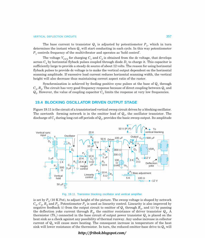
VERTICAL DEFLECTION CIRCUITS 357
The base current to transistor Q1 is adjusted by potentiometer P1, which in turndetermines the instant when Q1 will start conducting in each cycle. In this way potentiometerP1 controls frequency of the multivibrator and operates as ‘hold control’.
The voltage VCC2 for charging C1 and C2 is obtained from the dc voltage, that developsacross C4 by horizontal flyback pulses coupled through diode D1 to charge it. This capacitor issufficiently large to provide a steady dc source of about 12 volts. The reason for using horizontalflyback pulses to provide dc voltage is to make the vertical output dependent on the horizontalscanning amplitude. If excessive load current reduces horizontal scanning width, the verticalheight will also decrease thus maintaining correct aspect ratio of the raster.
Synchronization is achieved by feeding positive sync pulses at the base of Q1 throughC3, R3. The circuit has very good frequency response because of direct coupling between Q1 andQ3. However, the value of coupling capacitor C5 limits the response at very low frequencies.
19.4 BLOCKING OSCILLATOR DRIVEN OUTPUT STAGE
Figure 19.11 is the circuit of a transistorized vertical sweep circuit driven by a blocking oscillator.The sawtooth forming network is in the emitter lead of Q1, the oscillator transistor. Thedischarge of C1 during long cut-off periods of Q1, provides the basic sweep output. Its amplitude
Vertical syncinput
T1
D1
1 Fm1 K
P1 500W
Verticalhold
50 Fm+
3 Fm +C1
R1
10 K15 K
Heightcontrol
P2
Q1
D2
Oscillator
10 Fm
20 K
R3
10 V
10 KC2
0.02Fm
Linearitycontrol
P3 10 K5 W R4
R210 K
C31 Fm
Q2
50 K 100 FmDriver
800 W
200 W
100W
(cold) Th1
3 KR53 W
5 K
P4 Bias adjustment
100 W–12 V
– 12 V
Deflectionyoke
Q3
T2
VDR1
IV
Output C4 500 Fm
50 V (P–P) Tovertical blanking
Fig. 19.11. Transistor blocking oscillator and vertical amplifier.
is set by P2 (10 K Pot), to adjust height of the picture. The sweep voltage is shaped by networkC2, C3, R2 and P3. Potentiometer P3 is used as linearity control. Linearity is also improved bynegative feedback (i) from the output circuit to emitter of Q1 through R3, and (ii) by passingthe deflection yoke current through R4, the emitter resistance of driver transistor Q2. Athermistor (Th1) connected in the base circuit of output power transistor Q3 is placed on theheat sink as a check against any possibility of thermal runway. Any undue increase in collectorcurrent of Q3 will cause more heating. The consequent increase in temperature of the heatsink will lower resistance of the thermistor. In turn, the reduced emitter-base drive to Q3 will
http://fribok.blogspot.com/

358 MONOCHROME AND COLOUR TELEVISION
lower its collector current. Transistor Q3 is also stabilized by leaving its emitter resistance R5unbypassed. Potentiometer P4 is varied for optimum bias, more so, when it becomes necessaryto replace Q3. The VDR1 connected across T2 keeps the amplitude of output waveform withinnarrow limits. The sweep output is fed to the deflection coils (connected in series) through C4,a large electrolytic capacitor. The induced sharp pulses (typically 50 V) during retrace serve asvertical blanking pulses.
The oscillator frequency is set by varying P1 (hold control) to be slightly less than 50 Hz.Sync pulses, which are injected at the base of Q1 through T1, synchronize the frequency withthat at the transmitter. In practice, the vertical hold control is varied until the oscillatorfrequency locks with the incoming sync pulses to provide a steady picture.
19.5 TRANSFORMERLESS OUTPUT CIRCUIT
The high wattage transistor needed for the output stage can be replaced by two medium powertransistors in a suitable push-pull configuration as is the common practice in audio amplifiers.One such method uses p-n-p and n-p-n transistors in a complementary symmetry as illustratedby the basic circuit of Fig. 19.12. The output impedance provided by the complementary pair isquite low and so there is no need for an output transformer. This results in higher efficiencyand improved performance because the output transformer is often heavy, expensive andintroduces frequency distortion.
Inputvoltage
Driver
Feedback
– 24 V
Q3
Fromvertical oscillator
+ 24 V
Q3
D1
Q2
24 V
2.5 Amp (P–P)
Yoke current
Deflectioncoils
Verticalpower
amplifier
Fig. 19.12. Transformerless vertical output amplifier.
The output transistors Q2 and Q3 operate class B and are alternately driven intoconduction by a common trapezoidal input signal. When Q2 is on and Q3 is off, current flowsthrough the yoke from the positive 24 V supply. On alternate half of the input signal when Q3is on and Q2 is off, current flows in the opposite direction from the negative 24 V supply. Thisamounts to an ac current flow through the yoke. Diode D1 is forward biased and voltage dropacross it provides suitable bias to Q2 and Q3 thereby preventing any crossover distortion. Theconduction of D1 also ties the bases of Q2 and Q3 allowing signal output from the driver (Q1) tofeed both of them simultaneously.
http://fribok.blogspot.com/

VERTICAL DEFLECTION CIRCUITS 359
19.6 VERTICAL SWEEP MODULE
Figure 19.13 is the block schematic diagram of a typical vertical sweep module. It employsnine transistors and four diodes besides a large number of capacitors and resistors. Variousblocks are suitably labelled.
Verticalsync
Verticaloscillator
Sawtoothgenerator
Differentialamplifier Driver
Verticaloutput
Holdcontrol
Heightcontrol
Verticalcentering
dc dc feedback path
Verticaloutput
Phaseinvertor
ac feedback path
Yoke
+ 24 V
– 24 V
Power supply
D2
D1C1
C2
+
+
15625 Hz pulsesfrom H.O.T.
Q1 Q2 Q3 Q4 Q5 Q6 Q8
Q9Q7
ac
Fig. 19.13. Block diagram of a vertical sweep module.
OscillatorA explained in the previous chapter, transistors Q1 and Q2 operate as complementary symmetryoscillator and provide output at 50 Hz. Hold control forms part of this circuit. Its output iswaveshaped by transistor Q3 and the associated capacitor, to provide a sawtooth voltage. Thewave shaping circuit has provision for varying amplitude of the sawtooth voltage and this isthe height control.
Differential AmplifierTransistors Q4, Q5 constitute a differential amplifier with two ac and two dc inputs. One acinput is the sawtooth voltage developed by Q3 and the other is the feedback signal from verticalwindings of the yoke. Such an arrangement acts to eliminate, by negative feedback, anydistortion introduced by the output stages, ensuring a linear vertical sweep. It also makes theuse of linearity control and consequent adjustments unnecessary.
The single ended output of the differential amplifier (transistors Q4, Q5) is direct coupledto the output stage. The two dc inputs to the differential amplifier determine the output levelwhich in turn controls vertical (dc) centering of the beam. One of the two dc inputs is a clampeddc voltage that holds the base of Q4 at near zero voltage. However, the second dc input (at thebase of Q5) is made dependent by feedback on the dc output voltage at the point where deflectionwindings are connected. The reference dc voltage is obtained from the two dc supplies througha potentiometer which is initially varied to obtain correct centering of the beam.
Driver, Phase Invertor and Output AmplifierThe driver transistor Q6 couples output from the differential amplifier direct to the outputtransistor Q8 and via phase invertor Q7 to the other output transistor Q9. Transistors Q8 and
http://fribok.blogspot.com/

360 MONOCHROME AND COLOUR TELEVISION
Q9 are connected as quasi-complementary pair and conduct alternately to provide the totalvertical scan.
DC SupplyThe power supply block has two rectifiers D1 and D2 with associated filter capacitors C1 andC2. It provides both positive and negative dc supply sources for the various blocks. The inputfor dc supplies is derived from the receiver’s horizontal scanning circuit. Any change in horizontalscanning will be reflected as a change in dc voltage for the vertical module thus maintaining afixed aspect ratio of the picture.
19.7 THE MILLER DEFLECTION CIRCUIT
Linearity requirements of colour receivers are very rigorous and need a careful design of thevertical stage. While circuits described in the previous two sections are used both in monochromeand colour receivers, a new circuit known as Miller sweep circuit has found wide acceptance inrecent colour receiver designs. This circuit is capable of generating a sawtooth voltage ofexceptionally good linearity. As a result, no linearity control is necessary. The basic sweepgeneration circuit makes use of the Miller effect to enormously increase effective size of thesawtooth forming capacitor.
The simulation of such a large capacitance in the ramp forming circuit can be illustratedby the circuit arrangement shown in Fig. 19.14. The basic amplifier used in this circuit has avery high gain (|A| ≈ 106), inverted output and a very high input impedance. Because of largegain and heavy feedback provided by capacitor CM the net voltage vi at the input terminals ofthe amplifier is nearly equal to zero and hardly any current flows across the terminals markedX and Z. Thus X and Z are virtually a short from the circuit analysis point of view.
CM
vCMi
R
V vivi
S1
Ceff
Z Z
X
Gain 10»6
Y
v0
i
Fig. 19.14 Basic Miller sweep circuit.
The sawtooth forming current i that flows through R = V v
Ri–
≈ VR
, (vi ≈ 0). Since
practically no current flows between X and Z, the current i completes its path through CM and
charges it. Therefore i is also equal to v vXi
CM
– 0 ≈ – vXCM
0 , where XCM is the reactance of capacitor
CM. The current i being equal to V/R is independent of v0, the effective voltage across CM and
http://fribok.blogspot.com/

VERTICAL DEFLECTION CIRCUITS 361
so remains constant to charge the capacitor thus developing a linear ramp across it. The
admittance across the terminals X, Z = ivi
= –vvi
0 × 1 0
Xi
vXC CM M
since =FHG
IKJ
–
= 2πfACM because vv
A Xfi
CC
M
M
0 12
= =FHG
IKJ
– andπ
Thus effective value of the capacitance in series with R is gain times the value of CM.With |A| ≈ 106, the effective capacitance (Ceff) will appear to be one million times the externalsawtooth forming capacitor CM. Consequently the charging time constant of the sawtoothforming RC circuit becomes very large and only a small portion of the RC charging curve isused to form trace portion of the sawtooth. Switch S1 (see Fig. 19.14) can be opened and closedat appropriate moments to generate a sawtooth voltage at the output. In actual deflectioncircuits a transistor switch which is a part of the oscillator circuit controls the charge anddischarge periods. In this manner a sawtooth of excellent linearity is obtained which is lateramplified to the desired level. Note that the ramp voltage that appears at the output terminalsof the amplifier increases in negative direction because of 180° phase reversal between inputand output of the basic amplifier.
Miller Vertical Sweep Circuit
Figure 19.15 is a simplified schematic diagram of a Miller vertical defection circuit. The circuitemploys a complimentary symmetry power amplifier to drive the yoke. The waveshaping circuithas a high gain amplifier; a driver circuit and an oscillator switching transistor. Because ofoverall positive feedback the circuit behaves like a relaxation type of free running oscillator.Transistor Q1 switches at the vertical frequency rate to provide trace and retrace periods.
The circuit employs four feedback paths to accomplish all the functions. Feedback pathA effectively increases the value of Miller capacitor CM thus ensuring excellent sweep linearity.Feedback path B provides positive feedback needed to convert the high gain amplifier into asawtooth generating multivibrator. CM charges through Q1 but discharges through Q2. Theadjustments of this part of the circuit include height control, and hold control (frequency control)but there is no linearity control. Feedback path C is used to improve frequency stability of theoscillator circuit.
While the Miller sweep circuit provides a very linear sawtooth but the curvature of thetube face plate and its rectangular construction (pincushion effect) necessitate modification ofthe current that flows through the deflection windings. Therefore feedback path D is used tointroduce ‘S’ shaping or correction to the yoke current to compensate for the stretch at the topand bottom of the raster. ‘S’ compensation is also achieved by generating a parabola of currentand combining it with the sweep output. The modified yoke current then provides lineardeflection despite curvature of the face plate. In addition, a pincushion correction circuit isconnected in series with the yoke to cause necessary change in the current waveshape.
http://fribok.blogspot.com/
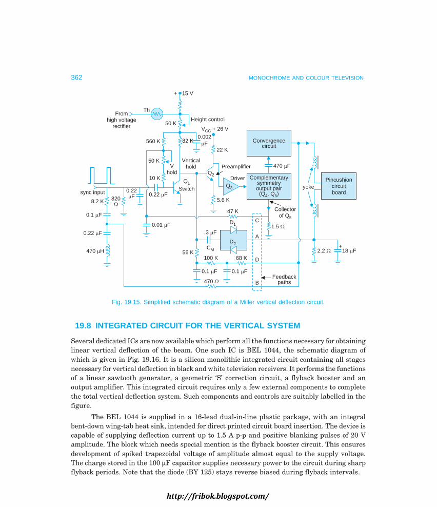
362 MONOCHROME AND COLOUR TELEVISION
D2
Q3 yokePincushion
circuitboard
Complementarysymmetryoutput pair
(Q , Q )54
Convergencecircuit
+ 15 V
ThFrom
high voltagerectifier 50 K
Height control
V + 26 VCC
0.002Fm
22 K
82 K560 K
50 KV
hold
Verticalhold
10 K QSwitch
1
Q2
0.22 Fm0.22
Fm820W
sync input
8.2 K
0.1 Fm
0.01 Fm0.22 Fm
470 Hm
0.1 Fm 0.1 Fm
470 W B
D68 K100 K56 K
CM
.3 Fm
D1
47 K
A
C1.5 W
Feedbackpaths
2.2 W 18 mF+
Collectorof Q5
470 FmPreamplifier
Driver
5.6 K
Fig. 19.15. Simplified schematic diagram of a Miller vertical deflection circuit.
19.8 INTEGRATED CIRCUIT FOR THE VERTICAL SYSTEM
Several dedicated ICs are now available which perform all the functions necessary for obtaininglinear vertical deflection of the beam. One such IC is BEL 1044, the schematic diagram ofwhich is given in Fig. 19.16. It is a silicon monolithic integrated circuit containing all stagesnecessary for vertical deflection in black and white television receivers. It performs the functionsof a linear sawtooth generator, a geometric ‘S’ correction circuit, a flyback booster and anoutput amplifier. This integrated circuit requires only a few external components to completethe total vertical deflection system. Such components and controls are suitably labelled in thefigure.
The BEL 1044 is supplied in a 16-lead dual-in-line plastic package, with an integralbent-down wing-tab heat sink, intended for direct printed circuit board insertion. The device iscapable of supplying deflection current up to 1.5 A p-p and positive blanking pulses of 20 Vamplitude. The block which needs special mention is the flyback booster circuit. This ensuresdevelopment of spiked trapezoidal voltage of amplitude almost equal to the supply voltage.The charge stored in the 100 µF capacitor supplies necessary power to the circuit during sharpflyback periods. Note that the diode (BY 125) stays reverse biased during flyback intervals.
http://fribok.blogspot.com/

VERTICAL DEFLECTION CIRCUITS 363
Tabs
+ 12 V
16
33 K
22 K
Geometriccorrection
1 8 9
100 F BY 125+
+ 20 V
7
6 +
470 F
Flybackbooster
Outputamplifier
Geometric ‘S’Correction
circuit
Linearsawtoothgenerator
10Syncpulseinput
Deflectioncoils
L = 177 mHR = 7.5
10 K
22 t+
Heightcontrol
10
10
1.2
32
15 K
n
130 K
50 KFrequencycontrol
1514
0.15 F
+
–
Fig. 19.16. Functional block diagram of the vertical system employing BEL 1044IC.
Review Questions
1. A well designed vertical scanning section of the television receiver must include the followingprovisions:
(i) adjustment for vertical linearity,
(ii) means for suppressing undesired oscillations in the yoke current,
(iii) constant height of the raster,
(iv) correct aspect ratio.
Explain either with the help of separate circuits or by drawing complete circuit of a typicalvertical deflection section, the techniques employed to meet the above requirements.
2. Draw simplified circuit diagram of a vertical deflection amplifier employing transistors and explainits operation. Indicate how positive retrace pulse can be obtained from the output transformer ofthe circuit drawn by you.
3. The circuit of a commonly used vertical deflection section, that employs tubes is shown in Fig. 19.9.Explain in brief, the operation of this circuit and the need for various controls provided in differ-ent parts of the circuit.
4. The circuit of a typical multivibrator controlled vertical output stage that employs a somewhatdifferent method for generating sweep voltage and linearity control is shown in Fig. 19.10. Describebriefly all the essential features of this deflection circuit and also explain how vertical rolling ofthe picture is prevented.
http://fribok.blogspot.com/

364 MONOCHROME AND COLOUR TELEVISION
5. Specially designed modules for the vertical stage are often used in TV receivers. Draw schematicblock diagram of one such module and explain the operation of each section. Why is the dc supplysource for the module often made dependent on output of the horizontal scanning circuit ?
6. What do you understand by Miller effect ? Explain with a suitable circuit diagram how a largecapacitance is simulated at the input of a high gain inverting amplifier for developing a linearsweep.
7. Draw schematic diagram of a typical Miller vertical deflection circuit and explain how a highlylinear sweep output is developed by employing suitable positive and negative feedbacks.
8. Draw functional diagram of the vertical system IC-BEL 1044 and explain how various sectionsof the IC function to develop deflection sweep output.
http://fribok.blogspot.com/
20
'(
http://fribok.blogspot.com/

The horizontal output stage is a power amplifier which feeds horizontal deflection windings inthe yoke to deflect the beam across the width of the picture tube screen. Though the functionof this stage is similar to the vertical output stage, its design and operation are very muchdifferent on account of the higher deflection frequency, very short retrace period and higherefficiency.
Since the horizontal output load is primarily inductive*, the deflection current inducesvery high voltage pulses in the output transformer while falling sharply during the retraceperiod. This energy which is in the form of high voltage pulses is rectified to produce a highvoltage dc source (EHT) for the final anodes of the picture tube. Furthermore, the energyassociated with the high voltage pulses tends to setup high frequency oscillations in the outputcircuit. To suppress this high frequency ringing, a diode damper is used instead of resistorsemployed in the vertical system. The diode while conducting, charges a capacitor, the voltageacross which adds to the existing B+ supply to produce a higher dc source voltage commonlyknown as boosted B+ supply. In this manner, part of the energy from the deflection coils isrecycled to develop a voltage source for the horizontal stage and other circuits.
Another interesting feature of the horizontal output circuit is that the unidirectionaldamper diode current which also flows through the deflection coils is used to complete a part ofthe horizontal trace. This results in improved efficiency because the amplifier need not supplydeflection current for the entire cycle.
20.1 HORIZONTAL OUTPUT STAGE
A schematic block diagram of the horizontal output stage is shown in Fig. 20.1. The mainsections of the stage are (a) output amplifier V1, (b) output transformer T1 (commonly knownas flyback transformer), (c) damper diode D1, (d) high voltage rectifier D2 and (e) deflectionwindings in the yoke.
The amplifier operates with self-bias and is designed to perform as a switch which closerfor a fixed period during each horizontal deflection cycle to supply power to the output trans-former. The transformer’s main functions are to provide impedance match between the outputstage and deflection windings and to act as a step-up high voltage transformer for D2, the EHT
366
)
'(
* L/R for the vertical deflection yoke is about three times the L/R for the horizontal deflectionyoke, but the horizontal scanning frequency is about 300 times the vertical scanning frequency. That iswhy the horizontal scanning load looks essentially inductive whereas the vertical scanning load lookseffectively resistive.
http://fribok.blogspot.com/

HORIZONTAL DEFLECTION CIRCUITS 367
rectifier. The damper diode D1 conducts soon after the flyback stroke to suppress shock excitedoscillations. While doing so the damper also causes horizontal scan of the beam on the left-halfof the raster.
Horz drive15625 Hz V
Horz outputamplifier
1
B+++CB
B+
T1
Horizontal output(Flyback)
transformer
High voltagepulses
DDamperdiode
1
10 to 16 kV (EHT)To anode
of picture tube
Horizontaldeflection coils
in the yoke
DHigh voltage
rectifier
2
Fig. 20.1. Block diagram of the horizontal output stage.
20.2 EQUIVALENT CIRCUIT
The various functions which the horizontal stage performs make its design and operationquite complex. Therefore, it is convenient to first consider a basic equivalent circuit of thestage to help understand its functions and sequence of operations.
V
Amplifiercircuit
Dampercircuit
Deflectionwinding
S1
S2
R
CL
r
Raster
Electronbeam
Picture tubescreen
Fig. 20.2. Simplified equivalent circuit of the horizontal output stage.With no excitation, the electron beam is in the centre of the picture tube screen.
The circuit shown in Fig. 20.2 is a simplified equivalent circuit of the deflection part ofthe horizontal output stage where the amplifier* has been simulated by a constant voltage
* For a typical horizontal deflection coil L = 2 mH, r = 4 Ω, I (p-p) = 3 A, trace period (ts) = 54 µS
and retrace or flyback time (tf) = 10 µS. ∴ VL = Ldidt
= 3 mH × 3
54.µS = 110 V and corresponding voltage
drop vr = I × r = 3 × 4 = 12 V. Since vr << vL, a constant voltage V applied across the deflecting coilscauses a near linear sweep current through it.
http://fribok.blogspot.com/

368 MONOCHROME AND COLOUR TELEVISION
source V together with switch S1 to control the flow of current to the deflection coils. Theinductor L and the small series resistance r represent lumped inductance and resistance of theflyback transformer and deflection windings. The capacitor C in parallel with this circuitaccounts for distributed and stray capacitance of the output stage. The damper circuit isrepresented by switch S2 and a resistance R in series with it. The switch S2 represents damperdiode D1 which when conducts charges CB through R.
The sequence of operations which cause deflection of the beam across the screen areillustrated in Fig. 20.3 by various circuits and associated waveforms. The location of the beamon the screen is also shown in each case. The direction of beam deflection has been arbitrarilychosen to be from left to right for the direction of current flow from the voltage source.
When switches S1, S2 are open, i.e., when both the amplifier and damper diode are notconducting, no current flows through L and r (see Fig. 20.2), and the beam is at the centre ofthe screen. At t0 (Fig. 20.3(a)) when S1 closes (amplifier is turned on) current iL flows and riseslinearly to deflect the beam towards right side of the raster. The beam reaches the edge of thescreen when iL attains a value equal to I at instant t1. Since the coil resistance is very small,
the voltage vL′ across the coil i r LdidtL +F
HGIKJ is nearly constant during this period. Its polarity is
positive and magnitude small because of the relatively slow rate of rise of current. At instantt1, the sharp negative spike of the input signal turns off the amplifier, i.e., switch S1, opens.With S1, S2 both open (Fig. 20.3 (b)) the C-L-r circuit gets into free oscillations with a period T,
very nearly equal to 2π LC seconds (since r is small). The initial conditions are such that iL
continues to grow further until vc = 0 (t = t2). The entire circuit energy, 12 L (Imax)
2 is now in the
inductance. T/4 seconds later (t = t3) this energy transfers to C (less a very small loss in r) so
that 12 L (Imax)
2 = 12 C(vc max)
2 or vc max = ImaxLC
. The capacitance C, being only stray capacitances
of the circuit, is very small (a few hundred pico-farads atmost). Therefore V*C max is usuallyvery high, of the order of a few thousands of volts.
After another T/4 seconds (t = t4), once more VC = 0 and iL = – Imax. In fact the currentvaries in a co**-sinusoidal manner from its positive peak to its negative peak in a time equal toT/2. If the switches (S1, S2) remained open this process of energy exchange would go on formany cycles, the successive values of VC max and Imax decaying slowly until the whole energy
* 12 L (Imax)
2 = 12 C(VC max)
2
∴ VC max = LC
Imax
Assuming C, the distributed capacitance = 750 pF
VC max = 6 kV
** iL = Im cos ω0t, where ω0 = 1LC
and vL = Vm sin ωot, where Vm = ω0LImax.
http://fribok.blogspot.com/

HORIZONTAL DEFLECTION CIRCUITS 369
was dissipated in the resistance r. This process is illustrated in Fig. 20.3 (b) with an expandedscale.
v
S1 S2
RC
LiL
r
I
vL
0t0 t1t
Raster
t0
Trace on right side(t –t )01(a)
v
S1 S2
RC
L
rt0
Beam deflectionduring (t –t )12
t2t1
(b)
iL t, v
iL L, v
ImaxI
vL0
t0 t1 t2
t3 t41
vSelf oscillations
t
Voltageacross the parallel
tuned circuit
v
S1 S2
RC
L
r
(c)
t
iL L, vImax
I
vL
t00
Amplifiercurrent
t4 t5
t3
Retraceperiod
S onnext cycle begins
1
Current throughdamper diodeand deflection
windingsvL
t4 t2t0
t3
t0
t5t4
Quick retraceduring (t –t )24
Trace on left side(t –t )45
iL
t1
Fig. 20.3. Sequence of operations during scanning of one horizontal line.(a) amplifier turns on but damper is open (b) amplifier turns off and damper
continues to be open (c) amplifier continues to be off but damper diode turns on.
However, continued oscillations beyond the first half-cycle are not desirable becausethe continuing oscillatory current in the coil will shift the beam back and forth at the left sideof the raster instead of allowing it to trace the next horizontal line at its proper place. Therefore,in order to suppress free oscillations beyond its first half cycle, switch S2 closes at instant t4 todissipate the energy stored in the L, C, r circuit. In fact polarity of the oscillatory voltagechanges at t4 to become positive and thus forward biases the damper diode D1 (closes switchS2). With R shunted across L, C, the combination becomes non-oscillatory and the current iLand voltage vL then decrease to zero with a time constant approximately equal to L/R where Rrepresents the resistance of the boosted B+ circuit in series with S2. The resulting current andvoltage waveforms are shown in Fig. 20.3 (c).
L and C are so chosen that the periods of self-oscillations T is twice the horizontal retracetime. Thus as the coil current decreases from positive maximum to zero and reverses to attainits maximum negative value in time T/2, the beam gets deflected to the left edge of the raster
http://fribok.blogspot.com/

370 MONOCHROME AND COLOUR TELEVISION
to complete a fast retrace. The resonant circuit is set at about 60 KHz to provide the desired
flyback time of about 8 µS 106
2 6 1084× ×
=FHG
IKJµS .
Further, the impedance of the B++ circuit is so set, or in the circuit under considerationR is so chosen that the current decays to zero in time (t5 – t4) which is approximately equal tohalf the trace period. The decaying current from its maximum negative value to zero deflectsthe beam to the centre of the screen without any supply of energy from the voltage source. Thisamounts to recovery of energy, because if not utilized this would not only be wasted but alsocause undesired oscillations spoiling the raster.
The switch S1 (amplifier) closes at t5 to again connect the voltage source to the LCcircuit and just then S2 (damper) opens to cut-off the damping circuit. The current then smoothlyrises to take over deflection of the beam to the right of the raster. This is illustrated inFig. 20.3 (c). The cycle described above repeats line after line to trace the entire raster.
20.3 HORIZONTAL AMPLIFIER CONFIGURATIONS
Horizontal output amplifiers may employ (i) vacuum tubes, (ii) transistors and (iii) siliconcontrolled rectifiers. While the end result is same, the mode of operation is somewhat differentin each case. Therefore, horizontal output stages employing different devices are describedseparately. It may also be noted that deflection circuits in colour receivers differ somewhatfrom corresponding circuits in black and white receivers. However, initially, the discussion isconfined to monochrome receivers only.
20.4 VACUUM TUBE HORIZONTAL DEFLECTION CIRCUIT
Fig. 20.4 is the circuit diagram of an earlier version of horizontal output stage used inmonochrome receivers. It employs an autotransformer between the amplifier and deflectioncoils. Each section of the stage is described separately.
(a) Output AmplifierThe amplifier employs a beam power tube having high voltage and power ratings. It is drivenby a trapezoidal voltage of approximately 80 V (P-P) which is obtained from the horizontaldeflection oscillator. In some circuits a sawtooth voltage that has little or no negative goingspike is used to drive the amplifier. In any case, on application of the input signal, grid currentflows to develop self-bias. The time constant of the coupling network C1, R1 is so chosen thatfor approximately half of the cycle the input signal drives the grid voltage less negative thancut-off. This results in a linear rise of plate current (see Fig. 20.4) to cause part deflection ofthe electron beam. With no input drive present, the bias would be zero because there is noprovision for self-bias in the cathode circuit. Therefore, the output tube (V1) should not beoperated without grid drive because in the absence of any protective bias the tube will drawexcessive current. A slow-blow fractional ampere fuse ‘F ’ is provided in the cathode circuit toprotect the tube and transformer against excessive current. The screen grid has the usualdecoupling network and a provision to control screen grid voltage. The variation of R2 changes
http://fribok.blogspot.com/

HORIZONTAL DEFLECTION CIRCUITS 371
plate current and thus acts as width control. This is fully explained later along with othermethods of width control.
vg
0
Grid current flows
0 t
Cut-off biasGr taGrid voltage
l rr nPlate current
B++to othercircuits
R6
R2
C6
F
C5
vg
R1330 K
0.003 Fm
C1 – 20VFromhorizontaloscillator
80 VV1
Outputamplifier Ip
R3 L7
L6
AGC
Widthcontrol
AFC
Outputtransformer
T1 5
L4 R4
D2
L5
L3
4
L2
3
2
L1 D11B++
CB
+0.1 Fm
250 V B+
P
Damperdiode
K
0.02 Fm
C2
C3
A
B
Horizontaldeflectionwindings
in the yoke
C4
+
EHT
HV rectifier
t
Ip
Fig. 20.4. Circuit diagram of a horizontal output stage employing vacuum tubes.
(b) Output TransformerThe circuit employs an autotransformer because of its higher efficiency as compared to onehaving isolated primary and secondary windings. It is wound on a ferrite core to minimizelosses. As shown in Fig. 20.5(a) a small air-gap is provided between the ‘U’ and ‘I ’ sections ofthe core to prevent magnetic saturation due to heavy plate current that flows through a sectionof the winding. The EHT winding and other sections of the autotransformer winding are woundon opposite limbs of the core to obtain higher leakage inductance necessary for third harmonictuning.
In Fig. 20.4 the winding between 1 and 4 is the primary (Lp) for plate current of theamplifier. This includes L1, L2, L3 and has an inductance of about 100 mH with a windingresistance of about 20 ohms. Winding L1 is the secondary, to step-down voltage for the deflectioncoils. Since there is no isolated secondary winding for polarity inversion, all the taps on theauto-transformer have voltages of the same polarity as the plate voltage on the amplifier. Thedrop in plate current induces voltage of positive polarity across the plate coil for retrace. The
http://fribok.blogspot.com/

372 MONOCHROME AND COLOUR TELEVISION
winding L4 at the top steps up the primary voltage to supply ac input to the high voltagerectifier. For a vacuum tube rectifier, its filament power is taken through a small winding L5on the same transformer L4 is a separate winding with a large number of turns of fine wire. Ithas an inductance of the order of 650 mH. The amount of step-up is limited by the fact that anyincrease in inductance reduces resonant frequency of the output circuit.
‘ ’I section High voltage winding ‘U’ section
Adjustable thirdharmonic ring
Primary winding
(a) (b)
H.V.winding
Other windings
Fig. 20.5. Horizontal output transformer (a) constructional details (b) pictorial view.
Beam deflection. As shown in the waveforms drawn along Fig. 20.4, plate current startsflowing just when the drive signal crosses cut-off bias of the tube. The sawtooth rise of currentin the primary circuit induces a negative going rectangular voltage across the secondary winding.This causes a flow of sawtooth current in the deflection windings from terminal B to A todeflect the beam from centre to right side of the raster. Note that the direction of current flowin the yoke windings is opposite to that assumed in the equivalent circuit. However, this doesnot interfere with the deflection of beam towards the left side of screen because the yoke is sowound that the resulting magnetic field has the correct polarity for causing deflection towardsright edge of the raster.
The deflection current is alternating in nature and is coupled to the yoke throughcapacitor C2 which blocks the flow of any dc in the deflection windings. This (dc) if allowed willshift the beam from its central location. In some circuits where the blocking capacitor is notused, other techniques are used to bring the beam back to the centre.
Horizontal retrace. Figure 20.6 illustrates input voltage, deflection current and yokevoltage waveforms. As shown, the grid voltage drops sharply to a value much below cut-offsoon after the peak of the sawtooth part of the drive voltage is reached. This cuts off the outputtube instantly and V1 ceases to sustain current in the output circuit. The tube remains in cut-off until the grid voltage again rises sharply to permit conduction during the next cycle. Theinductance of the output transformer and deflection coils together with their self capacitanceact as an L, C circuit that can oscillate at its resonance frequency when excited from a suitablesource of energy. When plate current drops to zero, the sudden collapse of magnetic field in thedeflection circuit generates a high value of induced voltage (typically 6 KV). The energy whichthus becomes available in the deflection circuit sets the L, C circuit into ringing at its natural
http://fribok.blogspot.com/

HORIZONTAL DEFLECTION CIRCUITS 373
resonant frequency. As explained earlier with the help of an equivalent circuit, the first halfcycle of free oscillations results in a quick flyback of the electron beam. It is often necessary toadd an additional capacitor (C3 in Fig. 20.4) to make the resonant frequency nearly equal to60 KHz for obtaining the desired retrace period.
Raster
Damperon
Sawtooth currentthrough yoke
Horzamplifier
on
Retrace time(D on, D and V off)12 1
Path of beamdeflection
I
I
0
V on1
Retrace
Tracet ×2 × I
Transitionpoint
Damperon
acTrace e t c eNext cycle(a)
t
Cut-off
vg
0Input
grid voltage
Bias (–20 V)
HV rectifier ‘on’
(b)
ti ‘o ’HV rectifier ‘off’
v
6 kV
One half-cycleof undampedoscillations
Oscillations dampedby damper currentDamper
on0
(c)t
Plate voltage(V )1
Fig. 20.6. Voltage and current relationships in the horizontal output stage.
During retrace the polarity of induced voltage across D1 is such that it remains cut-offalong with the output tube. This is necessary because any flow of current either in V1 or D1 willinduce a counter voltage that will oppose the current to fall at a fast rate and thus lengthen theretrace period. Thus the first half-cycle of oscillations continues undamped for a fast flyback. If
http://fribok.blogspot.com/

374 MONOCHROME AND COLOUR TELEVISION
the oscillations are not suppressed after this, they would cause ripples on the scanning currentwaveform. This results in white vertical bars on the left side of the raster. The bars are on theleft side of the raster because the oscillations occur immediately after flyback and these arewhite because the electron beam scans these areas several times during each horizontal linetraced.
(c) Damper DiodeAs soon as the polarity of the oscillatory voltage (Fig. 20.6 (c)) reverses, the damper diode (D1)is forward biased and it conducts to dissipate energy stored in the deflection circuit. The diode,while suppressing undesired self-oscillations after the first half cycle, charges CB and causesdeflection of the beam (see Fig. 20.6) from the left edge of the screen to its centre. This is bestexplained by considering the two effects separately.
Boosted B+ supply. The part of circuit in Fig. 20.4 which is associated with the productionof B+ boost is redrawn in Fig. 20.7 (a). Initially when the flyback transformer is not energizedthe damper diode conducts to supply B+ voltage to the plate of V1. However, when the circuit is
To horzamp plate
4
3
L3
L2
L1
2T1D1K
P
Damperdiode
1+
CB500 V
B+
BoostedB+
B+
BoostedB+
CB
K
P D1H.O.T.
L2
T1
Fig. 20.7 (a). Boosted B+ circuit with an Fig. 20.7 (b). Boosted B+ circuit with a H.O.T.autotransformer in the output circuit. having isolated primary and secondary windings.
functioning, the diode stays reverse biased most of the time because of high voltage VCBd iacross capacitor CB. Immediately after retrace when induced voltage reverses polarity its
magnitude is higher than VCB and so the damper diode is turned on. A part of the damper
current completes its path through the boost capacitor CB and charges it to a still higherpotential. In practice the voltage that develops across the capacitor varies between 200 to 600V. In the circuit under consideration the damper has been tapped up on the autotransformerwinding and the voltage that builds up across CB is about 500 volts. As illustrated in Fig. 20.7(a) this voltage is in series with the B+ supply. Therefore the potential difference between thepositive side of CB and chassis ground is around 800 V and is knowns as boosted B+ supply.This source is used as a dc supply for the horizontal output amplifier and several other circuits.
http://fribok.blogspot.com/

HORIZONTAL DEFLECTION CIRCUITS 375
While supplying current the booster capacitor partially discharges during the time the damperis off. However, this is replenished when the damper conducts during the next cycle. Thepartial charge and discharge of capacitor CB at the rate of horizontal scan results in a ripplevoltage at this frequency. To remove this ripple a filter circuit, (R6, C6 in Fig. 20.4) is oftenprovided.
Figure 20.7 (b) is a boosted B+ circuit of a horizontal deflection stage employing anoutput transformer with isolated primary and secondary windings. While the direction ofinduced voltage can be independently decided but in the circuit under consideration the polarityof the induced voltage in the secondary is opposite to that in the primary. As such, the anode ofthe damper diode is connected to the upper end of the secondary winding and B+ supply isconnected at its lower end. The diode, initially conducts to charge CB to the B+ voltage. However,when the transformer is energized the ac voltage across LS, soon after flyback, forward biasesD1 which conducts to charge the boost capacitor to a still higher voltage. Thus the entire boostedB+ voltage appears across the boost capacitor.
The generation of B++ voltage explains the principle of energy recovery, where a majorpart of the energy stored in the coils at maximum deflection is recycled. This improves theefficiency of the horizontal output circuit.
Reaction Scanning. The damper diode D1 conducts and charges capacitor CB as explainedabove. As shown in Fig. 20.8, a part of the diode current also flows through the deflectionwindings. As CB charges, the damper diode current decreases. Finally it becomes zero whenthe voltage across CB biases the damper diode out of conduction. The diode current that flowsthrough the yoke coils is made to decrease linearly by careful circuit design and this deflectsthe beam towards the centre. Note that direction of current flow is opposite to that due to platecurrent of V1. This is illustrated in Fig. 20.6 (a).
To plateof V1 4
3
2
T1
B++ 1CB
1d
K
P
D1
1d
B+ C2
Deflectioncoils
Fig. 20.8. Reaction scanning by the damper current.
The circuit is so designed that before the damper current declines to zero, output tubeV1 starts conducting and the resulting current then completes the trace to the right. As shown
http://fribok.blogspot.com/

376 MONOCHROME AND COLOUR TELEVISION
in the waveform (Fig. 20.6 (a)) the amplifier and damper currents combine to cause horizontaldeflection of the picture tube beam. In fact the declining diode current and the rising platecurrent add to provide a sawtooth current for linear horizontal deflection. This is known as‘Reaction Scanning’.
(d) Generation of High VoltageDuring flyback periods the magnitude of induced voltage across the primary (windings L1 toL3 in Fig. 20.4) coil is very high. In typical vacuum tube circuits it varies between 3 to 6 KV. Byplacing a suitably wound coil (L4) in the magnetic circuit and connecting it to the primarywinding in a series aiding fashion, an additional voltage of about 6 to 8 KV is developed byautotransformer action. The corresponding circuit diagram and associated waveshapes areshown in Fig. 20.9. This circuit arrangement results in a total voltage of 9 to 14 KV across twoends of the combined winding. Further, by suitably controlling the distributed parameters ofthe primary and secondary circuits and utilizing the technique of third harmonic tuning,(discussed in a subsequent section), the total voltage can be enhanced by about 10 to 15 percent.Thus a pulse of the order of 11 to 16 KV is generated. This is fed to the high voltage rectifier D2which conducts to charge the filter capacitor to provide EHT supply. It may be noted that thehigh voltage rectifier conducts for a short time during the flyback period because D2 is reversebiased at other times on account of 11 to 16 KV dc at its cathode (filament). The conduction ofD2 partially dicharges CB but it is soon made up when D1 conducts. Note that while D2 conductsboth V1 and D1 remain cut-off to avoid any loading.
B+ supply
VCB
To otherload circuits
+
+1
L1
2 Todeflectionwindings
Todamper circuit
L2
3
L3
L4
4
5
To amplifiercircuit
T1
R4
L5
D2
HV rectifier
EHT 12 to 16 kV
To picturetube anodeC4
+500 pF
(a) (b)
D plate voltage (ac)2
+
–
0 t
Pulse frequency = 15625 Hz
0
7.5
15
22.5
kv
15625 Hz ripple
(EHT)
t
Fig. 20.9. High voltage (EHT) generation (a) circuit (b) waveshapes.
(e) Monochrome YokeSince the current in the scanning coils deflects the electron beam, the yoke is rated in terms ofdeflection angle in addition to other essential parameters necessary for generating the required
http://fribok.blogspot.com/

HORIZONTAL DEFLECTION CIRCUITS 377
magnetic field intensity. Small screen tubes employ yokes having a deflection angle of 90°.However, the broad screen tubes are provided with 114° deflection angle yokes. Deflectioncoils suitable for 31 to 61 cm picture tubes are available.
The deflection yoke consists of two sets of coils, one for horizontal deflection and theother for vertical deflection. The coils are independently wound in two halves. These are placedon the yoke at right angles to each other in alternate quadrature segments. The yoke assemblyis slipped on to the neck of the picture tube and is oriented to produce a raster parallel to thenatural X and Y axes.
In earlier deflection coils additional capacitors were used to balance the distributedcapacitance of the two halves and their capacitance with respect to chassis earth. This isnecessary if each half coil is to produce equal retrace period for eliminating the possibility ofmultiple harmonics. However, in the latest designs of scanning coils lumped components areno longer necessary. The two halves of each coils are so wound that they provide the exactdesired balance necessary for undistorted scanning. The ratio of inductance to resistance(L/R = time constant) is kept low to achieve minimum permissible limits of distortion. Theflared portion of the coils may not exactly match the slope on the neck of the picture tube and,therefore, a pull-back of about 3 mm is provided to permit adjustment of the scanning coils.
Circuit efficiency. The peak energy stored in the inductance L of the deflecting coils is12 L(Imax)
2 where Imax is the peak current. If the damper diode technique is not used, this energy
is dissipated in a resistor during each cycle. The power lost is equal to 18 LIy
2 fh where Iy is the
peak-to-peak amplitude of the deflection current and fh is the horizontal scanning frequency.For a 61 cm picture tube yoke L = 2 mH, and Iy = 3 amp. The power consumed is thus about 35watts. This value is about 25 percent of the total power taken by the television receiver. By thesimple technique of replacing the damper resistor R by an efficiency diode the power loss is cutto about one quarter of this value for the same deflection. As illustrated in the waveformsdrawn in Fig. 20.6 (a) the total sweep corresponds to a current of 2I and yet the peak energy
stored in the inductor is 12 LI2 and not 1
2 L(2I)2. This observation verifies the statement madeabove that the power loss in the magnetic coils can be cut to one quarter of its previous valueby the principle of energy recovery.
The efficiency of the stage is further improved by storing a part of the excess energy ina capacitor (CB) and feeding it to auxiliary circuits in the receiver.
The ingenious way the flyback pulses are utilized, to produce EHT supply, results inoverall economy, because, if the same voltage were obtained from the supply mains, it wouldrequire a very bulky and expensive step-up transformer and filters.
The use of first half-cycle of the sinusoidal oscillation is yet another important feature ofelectronic circuit design which results in such an inexpensive method of obtaining flybackperiod of a few micro-seconds. All these innovations have resulted in very efficient horizontaloutput circuits that form part of all present day television receivers.
20.5 SEQUENCE OF OPERATIONS
It is now obvious that efficient design of the horizontal output circuit and the various auxiliaryfunctions that it performs make its operation quite complex. It is thus desirable to summarize
http://fribok.blogspot.com/

378 MONOCHROME AND COLOUR TELEVISION
the sequence of operations for a clear understanding of the functioning of horizontal outputstage. These are:
(a) Self-bias is used to control conduction of the output tube and is so adjusted that thetube conducts only during a part of the input voltage swing to supply sawtooth current. Therising plate current provides a little more than half of the total rater scanning on the right sideof the screen. The damper diode remains reverse biased during this interval. The high voltagerectifier also does not conduct because of the large dc voltage at its cathode.
(b) The output tube suddenly goes to cut-off because of sharp fall of the grid signalvoltage. This shock-excites the secondary circuit and it sets into oscillations. The onset ofoscillations induces high voltage pulses which make the anode of the high voltage rectifierhighly positive. It then conducts during the short pulse periods to provide EHT. Note that thedamper diode and output tube continue to be in cut-off during this interval.
(c) The first half-cycle of oscillation is allowed to continue undamped for a fast flybackthat brings the picture tube beam to the left side of the raster. During this half-cycle theoscillatory voltage has a polarity which makes the damper diode plate negative. Therefore,both the output tube and damper remain in cut-off while the retrace takes place. Note that thehigh voltage rectifier goes off soon after the sharp high voltage pulse occurs.
(d) After the first half-cycle of oscillation is over the voltage wave polarity reverses tomake the damper diode plate positive. It then conducts (i) to damp oscillations, (ii) to chargethe boost capacitor to provide boosted B+ supply and (iii) to deflect the beam towards thecentre of the screen by ‘reaction scanning’. The damper capacitor (CB) which is in series withthe damper diode continues to build up charge and finally biases the damper out of conduction.
(e) Before the damper current declines to zero the output tube once again starts conductingto continue the trace to right side of the raster.
20.6 HORIZONTAL AMPLIFIER CONTROLS
A horizontal output amplifier of a monochrome receiver may have a drive control, a widthcontrol and a linearity or efficiency control.
(a) Drive ControlThis control can be used to adjust the width of the raster by varying peak-to-peak amplitude ofthe drive voltage to the amplifier. A capacitive or resistive potentiometer is provided in thegrid circuit to control the magnitude of input voltage. In modern receivers such a control is notprovided and instead width of the picture is adjusted by controlling current in the deflectioncoils. However, optimum drive voltage is obtained by adjusting output voltage of the horizontaloscillator.
(b) Width Control
Figure 20.10 (a) illustrates five possible methods of controlling width of the picture. Eachcontrol has been suitably numbered for convenience of explanation.
http://fribok.blogspot.com/

HORIZONTAL DEFLECTION CIRCUITS 379
in C4
R1
V1
FromT1
VDR
(1) Widthcontrol
B+ B++
(v) Widthcontrol
R2
R3
CB
T1
D2
(iii) Widthcontrol
(ii) Widthcontrol
(iv) WidthcontrolC1 C3
‘S’ correction
Yokecoils
L1
B+ supply filter+
Linearitycontrol
C2
D1 (Damper)
Fig. 20.10 (a). Horizontal output amplifier controls. Note that in anyreceiver only one method of width control is used.
Electron beam
Deflectioncentre
8.5° d
d
d8.5°
10°
Picture tubescreen
‘S’ shaped current
+I
0 t
–I
Fig. 20.10 (b). Effect of flat screen Fig. 20.10 (c). Modified deflection current.on beam deflection.
(i) This control operates by varying screen grid voltage of the amplifier tube. Any in-crease in screen voltage causes an increase in plate current. This means an increase in deflec-tion energy which is converted into an increase in horizontal deflection. Reducing the screenvoltage will have the opposite effect.
(ii) In this method a small variable coil (10 to 40 mH) is placed across part of the flybacktransformer. It acts as an additional load on the horizontal output stage and absorbs some
http://fribok.blogspot.com/

380 MONOCHROME AND COLOUR TELEVISION
energy. A reduction in its inductance causes higher current flow through the coil and thus lesscurrent flows through the yoke. This results in reduction of picture width.
(iii) A variation of the above method is to place a coil in series with the deflection windings.In this case, the width control limits the current that can flow through the yoke. Shorting itwill result in maximum deflection. Note that using a coil rather than a resistor as a widthcontrol has the advantage of controlling the yoke current without any appreciable loss of power.
(iv) In this method of width control, a small capacitor C1 (50 to 150 pF) is connectedacross the deflection coils. This lowers the resonance frequency of self oscillations. A lowerfrequency increases retrace time which in turn causes the high voltage to decrease. Any reduc-tion in the picture tube anode voltage lowers the beam velocity. Thus the beam stays for alonger period under the influence of the deflection field and more deflection is caused. Thevalue of C1 is chosen for optimum deflection.
(v) Another method of width control, part circuit of which is shown in Fig. 20.10 (a) bydotted chain lines, accrues from the EHT and raster width stabilization circuit which is oftenprovided in modern receivers. A fraction of the high voltage pulse (see Fig. 20.11) which devel-ops in the flyback transformer is fed to a series circuit consisting of a VDR and a potentiometer(R2). The VDR rectifies the unsymmetrical pulse voltage. The resulting current develops volt-age drops across it and resistor R2. The amplifier input circuit is modified to include thesevoltage drops in the self-bias circuit. The negative voltage drop across the VDR adds to theself-bias voltage and counteracts any increase in the pulse voltage. However, drop across thepotentiometer which is in opposition to the self-bias voltage can be varied for optimum outputcircuit current which is turn controls the width of the raster. Thus R2 can be used as a widthcontrol. The stabilizing action of the circuit is explained in Section 20.9.
(c) Linearity ControlSome non-linearity can be caused in the centre of the screen where the deflecting dampercurrent drops and tube current takes over. As shown in Fig. 20.10 (a), one method of correctingthis consists of a variable inductor connected in series with the damper diode. The coil L1forms a parallel tuned circuit with C2 to be resonant at the horizontal scanning frequency. Theswitch like operation of the damper (D1) shock excites the tuned circuit into ringing at thesame frequency. The self-oscillatory voltage at the plate of D1 is modified when damper conducts.It attains the shape of a parabolic ripple voltage of magnitude 30 to 50 volts. The phase andtiming of this ac (15625 Hz) voltage controls the conduction time of the damper. Adjusting thecoil inductance changes the phase of the anode voltage which in turn changes damperconduction. Thus by properly adjusting the coil inductance a smooth transition from dampercurrent to amplifier current can be obtained so as to have linear deflection of the beam fromleft edge of the screen to its right side end. In fact when the coil is properly adjusted for lineardeflection, dc current of the horizontal output stage will be minimum. This improves efficiencyof the stage. Therefore, this coil is also known as efficiency coil and the control as efficiencycontrol.
Yoke coils of present day monochrome receivers are so well designed that they do notneed any linearity adjustment. However, in colour receivers, on account of other complexitiesadjustment of the efficiency coil is very important and such a control is always provided.
http://fribok.blogspot.com/

HORIZONTAL DEFLECTION CIRCUITS 381
Nonlinearity is also caused due to resistance of deflection coils and on-resistance of theswitching device which is not zero. During scans, the voltage available to the yoke inductancedecreases as the deflection current rises because of increasing voltage drops across theseresistances. This causes appreciable nonlinearity and a correction becomes necessary. This isprovided by saturable core reactor (LC) connected in series with the deflection coils (seeFig. 20.11). The saturable reactor (also called linearity coil) consists of a small coil wound on aferrite core. When the scan current is low, core does not saturate and hence voltage dropacross the coil is maximum. However, as the deflection current increases, the ferrite coresaturates and drop across it is reduced. Thus the decreasing voltage drop across the saturablereactor compensates for the increasing drop in the deflection windings and the driving device’sforward resistance. This ensures an almost constant voltage source across the coil inductanceand a sawtooth current flows to cause linear deflection.
+EHT
C6
D2R8
R7
R6 C5
3.3 K1.2 K
LC
0.2 Fm
Deflectioncoils
E17
6
5
CB
AGC
B++ 4
C2
E2
R4
D1
+250 V
2
3
Width controlR2
R5
C3
22 M
C4
F
1
8
Horizontal output(flyback) transformer
AFC
R3
V1
C1Vin
R1–
+
–
+ VDR
+500 K
Fig. 20.11. Improved line (horizontal) output circuit.
20.7 ‘S’ CORRECTION
A linear variation of current in the deflection coils will cause linear displacement of the spot onthe picture tube screen if the face plate has a suitable curvature. However, in modern wideangle picture tubes which have nearly a flat screen, a uniform angular motion of the beam willresult in nonlinear deflection. As the deflection angle increases the electron beam has to travelfarther to reach the face of the picture tube. Thus more displacement occurs for the same angleof deflection. As shown in Fig. 20.10 (b) a deflection angle of 10° is necessary to scan a distance
http://fribok.blogspot.com/

382 MONOCHROME AND COLOUR TELEVISION
d at the centre of the screen, whereas an angle of 8.5° is necessary for the same deflection atthe edges. Therefore, to produce linear deflection the rate of change of deflection should decreaseas the beam approaches edges of the screen. Hence, in order to produce an undistorted picturedisplay, the rate of change of scanning current must be reduced as the deflection angle increases.This means that nearly an ‘S’ shaped current should flow into the deflection windings. This isillustrated in Fig. 24.10 (c). A capacitor in series with the yoke coils (C3 in Fig. 20.10(a)) providesthe required S-correction. A parabolic voltage develops across the capacitor when the sawtoothdeflection current tends to flow through it. This modifies the sawtooth current in such a waythat a faster rate of deflection occurs while the beam is at central portion of the screen thanwhen it approaches the edges. Thus the effect of a flat screen is counteracted and linear deflectionoccurs across the entire width of the faster.
20.8 IMPROVED LINE OUTPUT CIRCUIT
Modern horizontal output circuits employ feedback techniques to achieve linear deflection andmake the raster size almost independent of mains voltage variations. Figure 20.11 is theschematic diagram of such a circuit where V1 is the output tube, D1 the damper or efficiencydiode and D2 the EHT rectifier. It may be noted that the damper diode is in the primary circuitof the autotransformer.
Circuit OperationThe circuit employes self-bias technique to control conduction and cut-off periods of the outputtube. The resistor R3 prevents excessive grid current flow during positive peaks of the trapezoidaldrive voltage. In each cycle, when V1 conducts, the linearly rising current in winding 1, 2develops a rectangular voltage across the secondary (5, 7) winding. The resulting sawtoothcurrent through the yoke coils deflects the beam from centre to right side of the raster.
As soon as the grid drive voltage goes negative, tube is cut-off and current flow ceasesboth in V1 and D1. The standing current in the primary winding shock excites the associated L,C circuit. The resulting variation of the self-oscillatory current from its positive to negativepeak during the first half cycle of oscillation deflects the beam to the left side of the raster thusproviding a fast flyback. The associated induced voltage keeps the cathode of D1 highly negativeduring this period and no current flows through V1 and D1 during flyback. As soon as thesecond half cycle of self oscillation begins, cathode of D1 becomes negative and damper diodeconducts via winding 2, 4, capacitor CB, winding 5, 6, ground points E1, E2 and B+ supply. Thedamper current induces a voltage in winding 5, 6, which circulates a sawtooth current in theyoke to deflect the beam from left to middle of the screen.
The current that flows through CB charges it with the polarity marked across it. As soonas potential at the cathode of D1 becomes equal to B+ supply, V1 takes over and conducts againto deflect the beam from middle to right side of the raster. This sequence continues till theboost capacitor CB is charged to the maximum possible value. Once CB is fully charged itbecomes the supply source for V1. However, B+ voltage source continues to supply make-upcurrent during each cycle to replenish part energy lost by CB while feeding V1 and other auxiliarycircuits.
http://fribok.blogspot.com/

HORIZONTAL DEFLECTION CIRCUITS 383
The capacitor C5 in the secondary circuit is for ‘S’ correction while the linearity coil LCcompensates for any nonlinearity introduced by resistive voltage drops in the output circuitand supply source. Resistors R6 and R7 connected across C5 and LC respectively suppress anyself-oscillations when the circuit is shock excited by deflection current flow.
The voltage induced in winding 1, 8, during flyback together with the voltages acrossother sections of the autotransformer becomes the high voltage ac source which is rectified bydiode D2 to provide EHT supply. Many line output circuits employ a stack of selenium rectifiers(for example TUS 15) instead of a vacuum tube rectifier.
Third Harmonic TuningIn the equivalent circuit shown in Fig. 20.12 (a) L1 is the effective primary inductance and C1the primary capacitance. The inductance LK represents leakage inductance of the EHT windingwhen referred to the primary side. Similarly CK is the effective capacitance across LK while C2accounts for the capacitance between EHT winding and ground. The leakage inductance isdeliberately made large so that it resonates with the stray capacitance at about third harmonic(2.8 times) of the flyback frequency. The correct tuning is obtained by varying location of thethird harmonic ring (see Fig. 20.5) between the two winding and observing voltage waveshapeon a cathode ray oscilloscope. When tuned properly, the phase of the third harmonic voltagecancels part of peak voltage at the plate of V1. At the same time, phase of the third harmonicringing tends to increase the amplitude of high voltage pulse delivered to the EHT rectifier.The two effects are illustrated in Figs. 20.12(b) and (c). While the reduction in peak voltage byabout 10% at the plate of output tube permits the use of a tube having lower voltage breakdownratings, the enhanced high voltage pulse yield 15 to 20% higher EHT voltage. All this resultsin increased economy and more efficient operation.
V L1
S
C1 C2
Lk
Ck
HV rectifier
(a)V (f )p 0
Net plate voltage
V (third harmonic voltage)LK
(b)
Enhancedhigh voltage pulse
EHT winding voltage pulse
Third harmonic voltage
(c)Note that figures (b) and (c) are not to the same time scale.
Fig. 20.12. EHT winding equivalent circuit and third harmonic tuning.(a) Equivalent circuit with HV (EHT) circuit referred to the primary side
(b) Effect of third harmonic tuning on the plate voltage (c) Increased HVpulse amplitude due to in-phase third harmonic voltage.
http://fribok.blogspot.com/

384 MONOCHROME AND COLOUR TELEVISION
20.9 OUTPUT CIRCUIT STABILIZATION
Output tube’s operating conditions influence EHT supply and raster width. This is stabilizedby regulating the plate current through a feedback loop from the output circuit. A componentof the grid bias voltage is obtained by rectifying a part of the pulse voltage which developsacross the output transformer. The feedback circuit in Fig. 20.11 includes a VDR and apotentiometer.
A VDR is a semiconductor the resistance of which decreases as the voltage across itsterminals increases. It has symmetrical nonlinear V-I characteristics (see Fig. 20.13) andtherefore allows equal current flow in either direction if a symmetrical voltage is impressedacross it. However, if an unsymmetrical voltage of sufficient amplitude is applied, rectificationtakes place. This implies that unequal current flows in forward and reverse directions. Thus anet voltage develops across the VDR and its value depends on the magnitude of the impressedvoltage.
In the circuit under consideration (Fig. 20.11) a direct current flows through VDR andR2 because of dc voltage across the boost capacitor. On this direct component is superimposeda pulsating current which is derived via C3 from the flyback pulses. This is illustrated inFig. 20.13 where the voltage and current waveshapes have been assumed to be rectangular forthe sake of simplicity. As indicated in Fig. 20.13 the working point ‘w’ is determined by themean value of this current. The voltage across the VDR fluctuates and its mean value is negative.This actually means that voltage drop across the VDR decreases because the magnitude ofreverse current is more than the forward current.
Vgmean
–I
11
22
33
44
55
66
0 WW11
22
33
44
55
66–1200 –800 –400 400 800 12000
I(mA)
V
I
Negative controlvoltage
VDR (mean)
+V
R2
VDR
Fig. 20.13. VDR characteristics and development of control voltage.http://fribok.blogspot.com/

HORIZONTAL DEFLECTION CIRCUITS 385
The pulsating negative voltage is filtered by the RC network formed by grid-leak resistorR1 and capacitance of the oscillator drive circuit. Thus an additional dc voltage proportional tothe pulse amplitude becomes part of the amplifier grid bias. The potentiometer R2 is set foroptimum bias so that both the EHT voltage and raster width are of correct values. It due to anyreason the EHT voltage rises, it is obvious that the magnitude of the negative voltage acrossthe VDR will increase. However, this cannot happen in practice because an increase in thenegative control voltage reduces EHT pulse voltage on account of reduction in tube plate current.Similarly any decrease in EHT pulse will be counteracted by a decrease of the negative controlvoltage. Thus any tendency for increase in raster width or EHT voltage which may occur dueto mains voltage fluctuations or any other reason is prevented by adding or subtracting acontrol voltage to the self-bias circuit.
Width ControlThe steady current that flows through the VDR and R2 fixes the threshhold value for properfunctioning of the VDR. Since the voltage drops across the VDR and R2 are opposite in polarity,the potentiometer R2 can be varied to control the operating point of V1 for optimum deflectioncurrent. Thus R2 acts as a width control.
The capacitor C4 is chosen to obtain the correct flyback period (frequency to self-oscillations) and thus the required EHT voltage.
The boosted B++ supply which is developed in the line output stage feeds the vertical(frame) output circuit in addition to the first and second anodes of the picture tube. The feedbackcircuit tries to maintain the boosted B++ supply at a constant value. However, if any smallchanges occur, they affect the horizontal and vertical output stages equally thus maintainingcorrect aspect ratio of the reproduced picture.
Auxiliary WindingsInstead of providing separate windings, AGC and AFC circuits are fed from tappings on theautotransformer. The AFC circuit receives voltage that develops across tap 7 and ground.Similarly the AGC circuit is connected across tap 5 and ground. The connections can beinterchanged between taps 5 and 7 depending on the polarity of the pulses needed at the AFCand AGC circuits.
22.10 TRANSISTOR HORIZONTAL OUTPUT CIRCUITS
The two major disadvantages of a vacuum tube horizontal output stage are (i) lot of power iswasted in the tube’s heater circuit and (ii) a vacuum tube has a relatively high plate resistancethat necessitates the use of a matching transformer between the tube and yoke coils. In atransistor circuit such problems are not there. However, the output transistor while having ahigh current rating must be able to switch at fast speeds. This is difficult to obtain in the sametransistor and proved to be the major obstacle in transistorizing the horizontal output stage.While transistors are now available which can switch a peak power of 200 watts and have anaverage power rating of 20 to 50 watts but their breakdown voltage capability VCE(max) andVCB(max) is limited to about 1500 volts.
http://fribok.blogspot.com/

386 MONOCHROME AND COLOUR TELEVISION
Output TransformerThe output transformer of a transistor line output stage has a somewhat different role thanthat used in a corresponding vacuum tube circuit. In tube circuits the output transformer isprimarily responsible for obtaining rapid retrace because of its self-oscillations. In addition, itis used for providing impedance match to the yoke windings and high voltage pulses to theEHT rectifier. In transistor circuits, retrace time is determined by the resonant circuit formedby effective inductance of the output circuit and an external capacitor connected in the collectorcircuit of the transistor. This capacitor is known as the flyback capacitor. The output transformeris instead tuned with its distributed capacitance to about third harmonic of the yoke oscillations.This as explained earlier reduces collector to emitter voltage and increases amplitude of highvoltage pulses.
Boosted B+ Voltage
In transistor circuits the high dc voltage is developed in a different way. While the circuit hasa damper diode but there is no boost capacitor. Instead, the B+ needs of transistor circuits aremet from taps on the output transformer. The dc pulses from the taps are rectified and filteredto obtain different dc voltage.
Driver Stage
In vacuum tube circuits the output trapezoid of the horizontal deflection oscillator is a sufficientamplitude to drive the output stage directly. In transistor circuits a driver stage is providedbetween the oscillator and output stage. This stage is a buffer amplifier that isolates the oscillatorfrom the output stage and has sufficient gain to meet the input power requirements of thehorizontal output stage. The drive power is usually large. For example, during the intervalwhen output transistor is on, the base current may exceed 400 mA. Note that because of lowimpedance values in transistor circuits, the drive voltage is usually an asymmetrical rectangularwave instead of a trapezoid.
20.11 TRANSISTOR LINE OUTPUT STAGE
Figure 20.14 is the circuit of a basic line (horizontal) output stage. The corresponding inputand output signal waveforms are illustrated in Fig. 20.15. The damper diode D1 and flybackcapacitor C1 are connected directly across the collector and emitter of the transistor. The valueof the flyback capacitor C1 is so chosen that it forms a resonant circuit with the equivalentinductance L of the deflection circuit at a frequency whose period is twice the retrace interval.During the period marked T1 in Fig. 20.15(c) the input signal forward biases the output transistorinto full conduction and the resulting current through the yoke coil deflects the beam to theright of the raster. The damper diode remains reverse biased by the VCC supply during thisinterval. At instant t1 the sharp negative pulse at the base of Q1 turns it off and the currentsharply declines to initiate retrace. The beam returns to the left of the raster during the firsthalf cycle of self-oscillations. The self-induced voltage across the coil keeps the damper diodeback-biased during this (T2) interval.
The polarity of the induced voltage reverses at instant t3 and forward biases D1 whichthen conducts to deflect the beam to the centre of the screen. The energy stored in the coil is
http://fribok.blogspot.com/
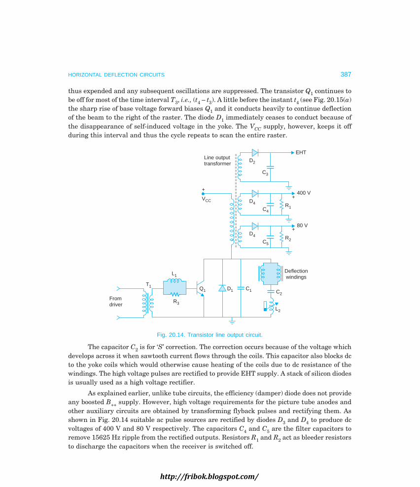
HORIZONTAL DEFLECTION CIRCUITS 387
thus expended and any subsequent oscillations are suppressed. The transistor Q1 continues tobe off for most of the time interval T3, i.e., (t4 – t3). A little before the instant t4 (see Fig. 20.15(a)the sharp rise of base voltage forward biases Q1 and it conducts heavily to continue deflectionof the beam to the right of the raster. The diode D1 immediately ceases to conduct because ofthe disappearance of self-induced voltage in the yoke. The VCC supply, however, keeps it offduring this interval and thus the cycle repeats to scan the entire raster.
Fromdriver
T1
L1
R3
Q1 D1 C1 C2
L2
Deflectionwindings
D4
C5R2
80 V
D4
C4R1
400 V
D2
C3
EHTLine outputtransformer
VCC
++
+
Fig. 20.14. Transistor line output circuit.
The capacitor C2 is for ‘S’ correction. The correction occurs because of the voltage whichdevelops across it when sawtooth current flows through the coils. This capacitor also blocks dcto the yoke coils which would otherwise cause heating of the coils due to dc resistance of thewindings. The high voltage pulses are rectified to provide EHT supply. A stack of silicon diodesis usually used as a high voltage rectifier.
As explained earlier, unlike tube circuits, the efficiency (damper) diode does not provideany boosted B++ supply. However, high voltage requirements for the picture tube anodes andother auxiliary circuits are obtained by transforming flyback pulses and rectifying them. Asshown in Fig. 20.14 suitable ac pulse sources are rectified by diodes D3 and D4 to produce dcvoltages of 400 V and 80 V respectively. The capacitors C4 and C5 are the filter capacitors toremove 15625 Hz ripple from the rectified outputs. Resistors R1 and R2 act as bleeder resistorsto discharge the capacitors when the receiver is switched off.
http://fribok.blogspot.com/

388 MONOCHROME AND COLOUR TELEVISION
(a)
(b)
0
0
t1 t2 t3 t4 t5
Driving voltageat the base ofoutput transistor
40 Sm24 Sm
Offdirection
Outputtransistorturns off
Outputtransistorturns on
Damperturns on
Damperturns off Yoke and transistor
collector voltage
Yoke energy returns to power supply
Transistorconducts
Transistorconducts
Retrace
(c)0
(d)
Electron beam
Right sideof the raster
Left sideof theraster
Right sideof the raster
Retrace
Raster (beamdeflection)
T1T1 T2 T3T3
t3
tt2
t1
tt4tt5
Yoke current
Damperconducts
Fig. 20.15. Waveforms corresponding to horizontal output stage shown in Fig. 20.14.
20.12 HORIZONTAL COMBINATION IC CA 920
The ‘BEL’ CA 920 is a 16-pin dual-in-line plastic package, line (horizontal) oscillator combinationIC which contains all the small signal stages for horizontal deflection in television receivers.The various functions performed by the device are (i) sync pulse separation with optional noisegating, (ii) current controlled line oscillator, (iii) phase comparison between sync pulses andoscillator output, (iv) high synchronizing noise immunity and (v) phase comparison betweenthe oscillator waveform and middle of the line flyback pulse for automatic correction of switchingdelays in the horizontal driving and output stages.
http://fribok.blogspot.com/

HORIZONTAL DEFLECTION CIRCUITS 389
Phase comparison can take place either between the oscillator signal and sync pulse orbetween the sync pulse and line flyback signal. With phase comparison between sync pulseand line flyback signal, the various inherent phase shifts that are associated with the oscillartor,line driver and line output stages are automatically compensated for. The disadvantage,however, of this method is that the amplitude, shape and duration of the line flyback pulse aredependent on picture tube beam current and other dynamic variations. Hence design on thefiltering circuits cannot be optimum both for good synchronizing and noise immunity. If,however, phase comparison between sync pulse and oscillator signal is used, the controlledphase position is independent of the amplitude, shape and duration of the line flyback pulse.The difficulty in this case is that the static and dynamic changes in the switching times of theoutput stage may now appear and suitable measures have to be taken for their correction.Simple discrete circuit for flywheel synchronization will not be able to provide a fully satisfactorysolution because of the contradictory requirements involved. By incorporating two control loops,one comparing the sync pulse and the oscillator signal and the other the oscillator signal andthe line flyback pulse, the problem is comprehensively solved in this IC (CA 920).
Typical Application CircuitA typical drive circuit using CA 920 for horizontal deflection in TV receivers is shown inFig. 20.16. Composite video signal having peck to peak amplitude of 1 to 7 volts with positivegoing sync pulses is applied at the input. The low-pass filter R1, C1 with cut-off frequency ofabout 500 KHz filters out noise present without introducing excessive delay to the signal.Before this video signal is applied to terminal (8) of the IC, proper clamping should be done sothat only the sync tips drive the sync separator stage. This is achieved by the circuit consistingof R2, R3, C2 and C3. R2, C2 along with base-emitter junction of the input transistor within theIC, clamps the video signal while R3, C3 combination ensures that only since tips drive currentinto terminal (8) irrespective of video signal amplitude. A good set of values for R2, R3, C2 andC3 are 1.5 M, 10 K, 100 KPR and 1 KPF respectively. Impulsive noise present in the compositevideo is separated from the signal by the circuit D1, R7, to R11, C6 and C7 and applied to terminal(9) of the IC. This voltage inhibits the sync separator stage under impulsive noise conditionsthus making pin (9), the noise gating terminal of the IC. The composite sync at terminal (7) isprocessed into vertical sync by means of the integrator R4, C4. The time constant of thisintegrator is chosen to be around 100 µs in order to obtain as large an amplitude as possible forthe vertical sync pulses and for maximum rejection of horizontal sync pulses. The horizontalsync pulses are separated by the differentiator R5, R6, C5 combination. This circuit providesvoltage division, and has a time constant of approximately 8 µs.
A value of 10 KPF for Cosc and 2.7 K for Rosc are chosen to be connected at terminals (14)and (15) respectively to determine free running frequency of the oscillator and to obtain optimumtransconductance for the oscillator. The free running frequency can be adjusted by the resistornetwork R12, R13, R14 and RH. The capacitors C8 and C9 act as low-pass filter in this controlloop. The control current I12 is converted into a dc voltage by this filter. This dc voltage drivesa controlling current determined by R16 connected between terminals (12) and (15). A value of33 K for R16 is optimum in order to achieve equal pull-in and hold ranges.
The flyback pulse derived from the line output transformer is fed at terminal (5) of theIC through a suitable resistor to provide approximately 1 mA of current. The control current I4at terminal (4) of phase comparator is converted into a dc voltage by R18, C11 combination and
http://fribok.blogspot.com/
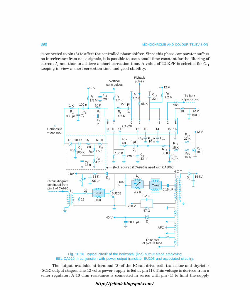
390 MONOCHROME AND COLOUR TELEVISION
is connected to pin (3) to affect the controlled phase shifter. Since this phase comparator suffersno interference from noise signals, it is possible to use a small time-constant for the filtering ofcurrent I4 and thus to achieve a short correction time. A value of 22 KPF is selected for C11keeping in view a short correction time and good stability.
12345678
9 10 11 12 13 14 15 16CA920
Yoke
Compositevideo input
R1 C2C1330 pF
1 K 100 n
12 V
R1.5 M
2C20 n
4
10 K
R2.7 K
4
Verticalsync pulses
Flybackpulses
R4.7 K
6
220 pF
R4.7 K
5 C5
68 K
R3
C3in
C22 n
11R2.2 M
18
12 V+
To horzoutput circuit
560
10 12 V100 Fm
D1 100 n R8 6.8 K
C6680 R9
R7 100 K R10 1.5 K
C733 n
R114.7 K
D333 K
.05 Fm
2 kV
Circuit diagramcontinued frompin 2 of CA920
T1 27
22 150
BU205
0.002Fm
LC
4.7 K0.2 Fm
0.15 Fm
200 V47 W
2000 Fm40 V
D1
AFC
To heaterof picture tube
H O T
D216 kV
(Not required if CA920 is used with CA3068)
C833 n
220 n100 K
R15680 10 Fm
C9
C12 Cosc10 n
R1633 K
Rosc2.7 K
R1215 K
R1315 K
R1110 K
R1427 K
12 V
10 Hm
Fig. 20.16. Typical circuit of the horizontal (line) output stage employingBEL CA920 in conjunction with power output transistor BU205 and associated circuitry.
The output, available at terminal (2) of the IC can drive both transistor and thyristor(SCR) output stages. The 12 volts power supply is fed at pin (1). This voltage is derived from azener regulator. A 10 ohm resistance is connected in series with pin (1) to limit the supply
http://fribok.blogspot.com/

HORIZONTAL DEFLECTION CIRCUITS 391
current in case of increased supply voltage. The total supply current drawn by the entirecircuit is about 25 mA at 12 volts. This circuit when used in conjunction with a typical lineoutput stage using transistors BD 115, BU 205 and line output transformer AT 2048/12 providesequally large pull-in and hold ranges of about ± 4.5 percent.
The output circuit shown in Fig. 20.16 in conjunction with this IC employs a BU 205power transistor and the associated output transformer. This set-up is suitable for driving theyoke of a 51 cm picture tube. The stage operates from a 200 V dc source obtained from aregulated power supply. Besides providing beam deflection and other outputs, the circuitproduces an auxiliary low voltage of 40 V required for audio, and RF-IF stages. The stage alsoprovides heating power to the picture tube filament circuit.
20.13 HORIZONTAL DEFLECTION CIRCUITS IN COLOUR RECEIVERS
While the basic mode of operation is the same, horizontal deflection circuits in colour receiversare somewhat different than those provided in black and white receivers. The following arethe main distinguishing features of colour receiver line circuits.
(a) A colour receiver picture tube may require as high as 25-KV at its final anode butsuch a requirement seldom exceeds 18 KV in a monochrome receiver. In addition, many colourreceiver picture tubes need another high dc source of about 6 KV for electrostatic focusing ofthe electron beam. Since these dc supplies are developed in the horizontal output circuit, colourreceivers employ special high voltage rectifier circuits to generate them.
High Voltage Tripler CircuitTo generate a very high voltage dc source a voltage-tripler circuit is often used. This arrangementminimizes insulation requirements of high-voltage transformers. Figure 20.17 shows theschematic of such a tripler circuit. The entire circuit is potted and can only be replaced as aunit in the event of failure. Though there are five rectifiers in the module, two are used tocouple the rectified dc from one rectifier to another. The other three rectifiers and associatedcapacitors make up the voltage tripler. Rectifiers instead of resistors are used to couple the dcvoltages because there would be loss of both voltage and power if resistors were used.
H.O.T.
HV tripler
25 kV
R1220 MR212 M
10 MR3
R427.5 M
1.5 M
R5
200 pF
+6 kV
To picture tubefocus anode
0.1 Fm
Fig. 20.17. High voltage tripler circuit.http://fribok.blogspot.com/

392 MONOCHROME AND COLOUR TELEVISION
R1 and R2 are special high voltage resistors. R1 (220 M) is a bleeder that discharges thehigh voltage picture tube capacitor after the receiver is switched off. The other high-voltageresistor R2 is connected to a tap on the tripler circuit. This together with potentiometer R3 andresistor R4 forms a voltage divider network to supply high voltage dc to the focus electrode ofthe picture tube.
All the high-valued resistors can be adversely affected by handling. Leakage paths causedby fingerprints may result in a dramatic drop in resistance. Therefore, these parts should behandled as little as possible, and when necessary should be held by their leads. If dust or dirtaccumulates on them, it should be removed by washing them with alcohol or any other ‘Freon’type cleaning solvent.
(b) The electron beam current of a black and white picture tube generally does notexceed 500 µA. The beam current of a colour picture tube may be two to three times this value.At maximum brightness a colour picture tube may dissipate as much as 25 W. The internalresistance of the high voltage power supply in the line output circuit is usually large andvariation of brightness results in blooming and poor focus unless suitable regulator circuitsare employed. Since the beam current of colour picture tubes is very large such effects aremore pronounced in colour receivers.
High Voltage RegulationIn an attempt to keep the picture tube anode voltage almost constant under varying brightnessconditions many monochrome and all colour receivers employ special high voltage regulatorcircuits. One such arrangement which is used in vacuum tube circuits was discussed in Section20.9 while explaining an improved horizontal output circuit.
Solid state colour receivers do not usually employ direct high voltage regulators, because,compared to vacuum tubes, transistor line output circuits have very low impedance levels. Assuch, changes in high voltage load current do not cause large changes in dc output voltages.Nevertheless, most transistor colour receivers do incorporate some form of high voltageregulation. It may be noted that it is not practicable to regulate the bias of an output transistoras is often done in tube circuits because the transistor acts more like a switch than an amplifier.Therefore, regulation of sweep and high voltage in transistor colour receivers is often done byregulating B+ supply voltage that feeds the horizontal output stage. Such regulator circuitsare described in Chapter 24 which is devoted to receiver power supplies.
(c) In order to reduce X-ray radiation from a television receiver under breakdownconditions, special hold-down circuits are used to automatically disable the rectifier when afault occurs which would tend to increase excessively the generation of EHT supply. Whilemost monochrome receivers do not include such circuits but a hold-down circuit is a must incolour receivers where the EHT voltage is very high.
Hold-down CircuitAn example of a high voltage hold-down circuit used in transistor colour receiver circuits isshown in Fig. 20.18. The circuit is so designed that an increase in high voltage above 30 KVcauses an SCR to conduct and ground the horizontal oscillator supply voltage. This causes thehorizontal oscillator to cease functioning resulting in a loss of both, the high voltage and theraster.
http://fribok.blogspot.com/
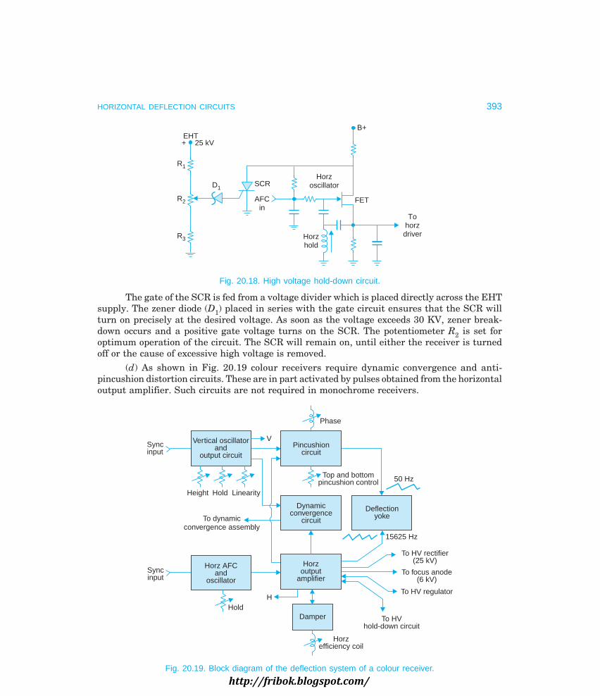
HORIZONTAL DEFLECTION CIRCUITS 393
+ 25 kVEHT
R1
R2
R3
D1SCR
AFCin
Horzoscillator
B+
FET
Horzhold
Tohorz
driver
Fig. 20.18. High voltage hold-down circuit.
The gate of the SCR is fed from a voltage divider which is placed directly across the EHTsupply. The zener diode (D1) placed in series with the gate circuit ensures that the SCR willturn on precisely at the desired voltage. As soon as the voltage exceeds 30 KV, zener break-down occurs and a positive gate voltage turns on the SCR. The potentiometer R2 is set foroptimum operation of the circuit. The SCR will remain on, until either the receiver is turnedoff or the cause of excessive high voltage is removed.
(d) As shown in Fig. 20.19 colour receivers require dynamic convergence and anti-pincushion distortion circuits. These are in part activated by pulses obtained from the horizontaloutput amplifier. Such circuits are not required in monochrome receivers.
Syncinput
Vertical oscillatorand
output circuitPincushion
circuit
V
Phase
Top and bottompincushion control 50 Hz
Dynamicconvergence
circuit
Deflectionyoke
Horz AFCand
oscillator
Horzoutput
amplifier
Damper
Height Hold Linearity
To dynamicconvergence assembly
Syncinput
HoldH
Horzefficiency coil
To HVhold-down circuit
To HV regulator
To focus anode(6 kV)
To HV rectifier(25 kV)
15625 Hz
Fig. 20.19. Block diagram of the deflection system of a colour receiver.
http://fribok.blogspot.com/
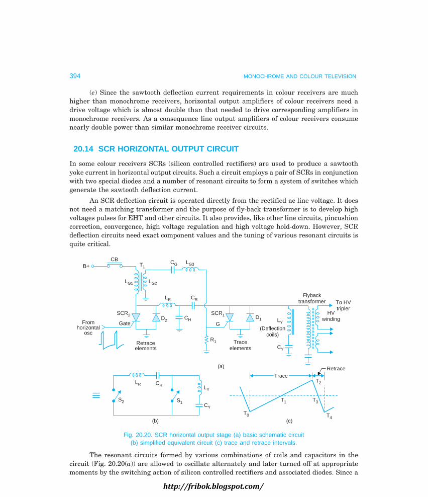
394 MONOCHROME AND COLOUR TELEVISION
(e) Since the sawtooth deflection current requirements in colour receivers are muchhigher than monochrome receivers, horizontal output amplifiers of colour receivers need adrive voltage which is almost double than that needed to drive corresponding amplifiers inmonochrome receivers. As a consequence line output amplifiers of colour receivers consumenearly double power than similar monochrome receiver circuits.
20.14 SCR HORIZONTAL OUTPUT CIRCUIT
In some colour receivers SCRs (silicon controlled rectifiers) are used to produce a sawtoothyoke current in horizontal output circuits. Such a circuit employs a pair of SCRs in conjunctionwith two special diodes and a number of resonant circuits to form a system of switches whichgenerate the sawtooth deflection current.
An SCR deflection circuit is operated directly from the rectified ac line voltage. It doesnot need a matching transformer and the purpose of fly-back transformer is to develop highvoltages pulses for EHT and other circuits. It also provides, like other line circuits, pincushioncorrection, convergence, high voltage regulation and high voltage hold-down. However, SCRdeflection circuits need exact component values and the tuning of various resonant circuits isquite critical.
CBB+
LG1 LG2
LG3CGT1
CRLR
SCR2
GateFromhorizontal
osc
Retraceelements
D2 CH
SCR1
R1
D1G
Traceelements
(a)
CY
LY
(Deflectioncoils)
Flybacktransformer To HV
triplerHV
winding
Retrace
T2
TraceTrace
T3T1
T0 T4(c)(b)
S2
LR CR
S1
LY
CY
Fig. 20.20. SCR horizontal output stage (a) basic schematic circuit(b) simplified equivalent circuit (c) trace and retrace intervals.
The resonant circuits formed by various combinations of coils and capacitors in thecircuit (Fig. 20.20(a)) are allowed to oscillate alternately and later turned off at appropriatemoments by the switching action of silicon controlled rectifiers and associated diodes. Since a
http://fribok.blogspot.com/

HORIZONTAL DEFLECTION CIRCUITS 395
large number of resonant circuits, each tuned to a different frequency, are used to obtaindifferent segments of the sawtooth current, the circuit operation is quite complicated. Thereforethe explanation that follows has been greatly simplified for a better understanding of the basicprinciple of its operation.
Circuit ComponentsIn Fig. 20.20(a) two SCR units are used in the horizontal output circuit. SCR1 conducts fortrace periods while SCR2 turns on during retrace periods. Switching of SCR2 for retrace iscalled the commutating operation. Each SCR has a special fast recovery diode with inverseparallel connections. The purpose is to allow current in both directions from cathode to anodein either the SCR or its diode, depending on which anode is positive. When the diode conductsits low resistance drops the SCR anode voltage to the cur-off level. During trace time SCR1 ison and SCR2 is off. In effect, SCR1 and D1 together comprise a controlled single pole-singlethrow switch (S1) while SCR2 and D2 form another similar switch (S2) as shown in Fig. 20.20(b).The components LR, CR, CH, and CY supply the necessary energy storage and timing functions.The inductance LG1 gives a charge path for CR and CH from B+, thereby providing a means to‘recharge’ the system from the power supply. The secondary winding (LG2) on transformer T1supplies necessary gating current to SCR1. The capacitor CH controls the retrace time becauseit is charged to B+ voltage through LR. Pulses from the horizontal oscillator at 15625 Hz turnon the retrace SCR at appropriate moments. The conduction in SCR2 cuts-off the retrace siliconcontrolled rectifier SCR1. Thus the trace and retrace periods are controlled and synchronizedwith the horizontal oscillator.
Circuits OperationFigure 20.20(b) is the simplified equivalent circuit of the SCR deflection circuit. The waveformsshown in Fig. 20.20(c) illustrate approximate time intervals during which switches S1 and S2(trace and retrace SCR-diode combinations) close or open to circulate sawtooth current in thedeflection windings.
If the circuit has been functioning for many cycles and retrace has just been completed,the yoke (LY) magnetic field is at its maximum value and the electron beam is on the left sideof the raster. This corresponds to time T0 in Fig. 20.20(c) where the induced current throughLY is at its peak negative value.
Trace Time
Referring to Fig. 20.20(b), during the first half of trace time (T0 to T1) switch S1 (SCR1 and D1combination) is closed causing collapse of the magnetic field around the yoke inductance (LY).The resulting current deflects the beam to approximately middle of the screen and charges thecapacitor CY. During the second half of the trace time interval (T1 to T2) the current in the yokecircuit reverses because the capacitor CY discharges back into the yoke inductance Ly. Thiscurrent causes the picture tube beam to complete the trace. Note that SCR1 and D1 combination(S1) continues to provide current conduction path during the entire trace interval when currentchanges from negative to its positive maximum value.
Retrace InitiationThe forward scan stops at T2 because a pulse applied to SCR2 from the horizontal oscillatortriggers it into conduction (S2 closes). Both S1 and S2 remain closed for a very short interval.
http://fribok.blogspot.com/

396 MONOCHROME AND COLOUR TELEVISION
The charge previously stored on CR is released into the commutating circuit comprising of LR,CR and CH. Thus the current through SCR1 rapidly falls to zero causing the turning off ofswitch S1 and the initiation of flyback. As stated earlier the frequency of various resonantcircuits is so chosen that trace and retrace intervals are correctly obtained.
Retrace
With S1 open and S2 closed current flows through a series resonant circuit comprising of LR,CR, LY and CY. The natural resonant frequency of this circuit is much higher than that of theyoke circuit LY and CY because the value of capacitor CR is much smaller than that of CY. As aresult a fast flyback becomes possible. The retrace current comes to zero (T2 to T3) at themidway point of the flyback interval, and just then SCR2 stops conduction. However, diode D2now becomes forward biased due to reversal of polarity of the oscillatory voltage. Thus S2continues to be closed and a retrace current flows in the opposite direction to complete theflyback at instant T4. This action (current flow) effectively transfer the energy stored in CRback to the inductance LY of the horizontal deflection coils. At time T4 the diode D1 becomesforward biased due to reversal of voltage polarity (S1 closes) and shortly afterwards S2 opens.The field about the yoke inductance (LY) starts to collapse and the resulting current againcommences the next trace period. The cycle repeats to provide horizontal scanning at the rateof deflection frequency.
Note that during flyback the primary of T1 is connected between B+ source and groundvia SCR2 and D2. When D2 stops conduction, LGI is disconnected from ground and CR chargesthrough this winding from the B+ supply to replenish energy in the deflection coil circuit. Itmay also be observed (see Fig. 20.20(a)) that the voltage developed across LGI (primary of T1)during the charging of CR is coupled to the gate of SCR1 through the secondary of T1 andwaveshaping network comprising of CG, LG3 and R1. In turn, the gate waveform that is generatedpossesses adequate amplitude to enable SCR2 to conduct while its anode is sufficiently positive.
Review Questions
1. Why is the design of the horizontal output stage very much different than that of the verticalstage, while their functions are very similar to each other ? What are the special features whichmake the operation of the line output stage very efficient ?
2. Explain fully with a suitable functional diagram and waveshapes, how the first half-cycle of self-oscillations in the output circuit is used to obtain a fast retrace of the beam. How is the continu-ation of ringing suppressed ?
3. Show how the energy stored into the deflection windings is recycled to generate boosted B++supply.
4. Explain with a circuit diagram how the high voltage pulses, induced in the output transformerwindings, are used to generate EHT supply.
5. What do you understand by reaction scanning ? Explain step by step the sequence of operationsin the line output stage for reaction scanning. Draw suitable wave-shapes and diagrams to illus-trate your answer.
6. Explain the functions of linearity and width controls normally provided in the horizontal outputstage. Describe their operation by drawing relevant portions of the output circuit.
http://fribok.blogspot.com/

HORIZONTAL DEFLECTION CIRCUITS 397
7. With reference to Fig. 20.11 explain how the feedback circuit maintains a constant EHT supplyand width of the picture through the voltage drop across the VDR. What is the function ofpotentiometer R2 ?
8. What do you understand by third harmonic tuning in the line output transformer ? Justify thatis results in lesser peak power from the output tube and more ac voltage from the EHT rectifier.
9. In what respects a transistor line output stage is different from a corresponding vacuum tubecircuit ? Why is a driver stage necessary in transistor output circuits ? Why is a separate flybackcapacitor provided in such circuits ?
10. Draw the circuit diagram of a typical horizontal output stage which employs a transistor andexplain how it functions to provide linear horizontal scanning. What is ‘S’ correction and how isthis applied ?
11. Discuss briefly the main features of the horizontal combination IC, CA 920. With reference toFig. 20.16 explain the circuit operation of this IC.
12. Describe fully the distinguishing features of horizontal deflection circuits of colour receivers.Why is the deflection current very high in colour receivers ?
13. Draw the circuit of a high voltage tripler and explain how EHT voltage of the order of 25 KV isdeveloped. Why is it necessary to handle high valued resistors very carefully ?
14. Why is a hold-down circuit necessary in colour TV receivers ? Draw the circuit diagram of such acircuit and explain how it operates to disable the horizontal oscillator when EHT exceeds theprescribed upper limit.
15. Draw basic circuit of a horizontal output stage employing SCRs. Explain how the circuit func-tions to provide linear trace and retrace periods. What are the merits and demerits of suchdeflections circuits ?
http://fribok.blogspot.com/

21
http://fribok.blogspot.com/

A television signal transmitted from a broadcast station consists of an amplitude modulatedRF picture carrier and a separate frequency modulated RF sound carrier both within the 7MHz channel bandwidth alloted to the station. This signal is intercepted by the receiver antennaand coupled through a transmission line to the RF section in the tuner. The block diagram ofFig. 21.1 shows various stages through which the sound signal passes in a monochrome and acolour receiver, before it is finally delivered to the loudspeaker.
In the tuner FM sound signal is amplified along with the picture signal and thentransferred to the sound IF frequency from the channel carrier frequency. The sound IF signaltogether with its sidebands is passed through the IF amplifiers without much amplification.At the video detector it is made to beat with the strong picture IF carrier frequency to transferthe modulating audio signal to yet another sound IF frequency which is equal to the differenceof the two intermediate frequencies (38.9 HHz—33.4 MHz = 5.5 MHz). This amounts toheterodyning the sound signal twice. Since the 5.5 MHz sound carrier is obtained by mixingthe two IF carrier frequencies, this method of processing the sound signal is known as ‘Inter-Carrier Sound System’.
The 5.5 MHz FM sound signal thus obtained is coupled from either video detector orvideo amplifier to the sound IF amplifier. The sound IF signal, together with its sidebands isamplified to a level of several volts for the FM detector. This stage converts FM modulation toequivalent amplitude modulation and then detects it to recover the audio output. This isamplified in the audio section to have enough output to drive the loudspeaker.
21.1 SOUND SIGNAL SEPARATION
The output from the last IF stage consists of picture IF (38.9 MHz) amplitude modulated withthe composite video signal and sound IF (33.4 MHz) frequency modulated with the audio signal.The two intermediate frequencies with their sidebands occupy a frequency spectrum of about6.75 MHz. This signal is coupled to the video detector (see Fig. 11.6) which employs a diodeand rectifies the centre zero modulated signal to produce a dc component, sum and differencefrequencies of the various constituents of the input signal and their harmonics. The resultantband of frequencies is passed through a low-pass filter that forms part of the video detector.The cut-off frequency of the filter configuration is set at 5.75 MHz. Thus all the sum componentsand higher order harmonics which lie above the cut-off frequency (5.75 MHz) are filtered out.The output then consists of two distinct components. The band the lies between 0 and 5 MHzis the demodulated video signal and is fed to the video amplifier. The second component that
400
http://fribok.blogspot.com/

SOUND SYSTEM 401
lies around 5.5 MHz is formed as the difference of the picture IF and sound IF with its sidebandsi.e., 38.9 — (33.4 ± sidebands) = 5.5 MHz ± sidebands.
Tunerand IFsection
Videodetector
Sound IFamplifier
FM sounddetector
Audioamplifier
Sound IFdetector
Videoamplifier
(Monochrome receiver)
Alternativepath
Antenna
(Colour receiver)
5.5 MHz
5.5 MHz 5.5 MHz Audio signal
These stages are identical forboth colour and monochrome receivers
Speaker
Fig. 21.1. Sound signal path in monochrome and colour receivers.
In fact the strong picture signal intermediate frequency acts as the carrier frequency toa relatively low amplitude sound signal intermediate frequency and its sidebands to provideanother frequency translation to the sound signal. This shifts the sound mdulation around amuch lower carrier frequency of 5.5 MHz which is the difference of the two intermediatefrequencies. This technique of separating the sound signal is known as the intercarrier soundsystem. The output has some amplitude variations. If these variations are large, it becomesdifficult to remove them at the limiter stage, with the result that the audio output is severelydistorted. This can be minimized by keeping the sound carrier signal amplitude very low. Thisexplains why the sound IF which lies on the left skirt of the overall IF response is attenuatedby about 20 db in comparison with the picture IF frequency. In fact this is the pivotal point formaking the intercarrier sound system a success. Accordingly, the sound carrier together withits sidebands is given only 5 percent gain, in comparison with the video signal, to obtain a beatnote at the detector, which contains only the frequency modulation of the original sound IFcarrier and practically nothing of the video modulation.
Another factor that needs attention is the buzzing sound that results from the 50 Hzvertical sync signal interference with the 5.5 MHz sound signal. This is known as intercarrierbuzz and is the result of cross-modulation between the two signals. Similarly, the 15625 Hzhorizontal sync can result in a hissing sound in the loudspeaker. Here again the remedy lies inkeeping the magnitude of the sound signal much lower than the picture signal to keep the beatnote amplitude low. This, together with the limiting that is provided after the sound IF stage,eliminates practically all amplitude variations in the FM sound signal and normally nointercarrier buzz or hiss is audible in the loudspeaker.
21.2 SOUND TAKE-OFF CIRCUITS
The usual sound take-off point in a monochrome solid state receiver is at the output of videodriver stage. In Fig. 21.2 the video driver is connected as a phase-splitter where the emitter
http://fribok.blogspot.com/

402 MONOCHROME AND COLOUR TELEVISION
circuit feeds the video output amplifier and the tuned transformer T1 in the collector circuitseparates sound IF from the composite video signal. Since the emitter circuit contains fullcomposite signal, including the 5.5 MHz sound IF and its sidebands, a shunt trap (L1, C1)tuned to 5.5 MHz is used to eliminate this source of intereference. The transformer T1 is tunedto 5.5 MHz and delivers sound signal to the base of Q2, the sound IF amplifier. This transformeris tapped to provide proper impedance match and to maintain a hight Q of the tuned circuit.
5.5 MHzsound take-off
tansformer(T )1
6801000 pF
From videodetector
100 K
330
Q1
5.6 K
Bias30 Fµ
0.01 Fµ
Q2
Sound Famplifier
I
C1 100 pF
L1 5.5 MHz
– VCC
To videooutputamplifier
Fig. 21.2. Sound take-off circuit in a monochrome receiver.
A typical sound take-off and detector circuit used in colour receivers is shown in Fig. 21.3.It can be seen that the sound take-off point is located before the video detector to minimize the1.07 MHz interference that would be produced if the sound IF (5.5 MHz) is permitted to beat
3rd videoF amplifierI
From 2ndvideo FI
To soundIF amplifier(5.5 MHzand itsside-bands)
Sound take-offpoint
Sounddetector
D1L2
R1 C2L1
C1
C3 C4
L3 5.5MHzL7R3
10pF
R2 C6
C5
L4
33.4 MHz trap+ VCC
D2 C7
Videodetector
L5 L6
C8 To videoamp(0–5 MHz)
5.5 MHz trap
Fig. 21.3. Sound take-off and detector circuit in a colour receiver.
http://fribok.blogspot.com/

SOUND SYSTEM 403
with the 4.43 MHz colour subcarrier. Conversion of sound IF to intercarrier sound (5.5 MHz) isaccomplished by the diode D1 which acts like a series detector. The input to the detector is viaa series resonant circuit C1, L1. This circuit is tuned to about 36 MHz and is broad enough toinclude both picture and sound IFs. R1 and C2 are the load resistor and IF filter. C3 and L3constitute a filter that separates the sound IF from the composite video that also appears atthe output of the sound IF detector. The inductor L2 blocks the video IF and its harmonics.
Since the sound take-off is before the video detector, greater attenuation of the 5.5 MHzsound IF is possible in the video detector circuit. This is done (see Fig. 21.3) by bridge type trapcircuits located before and after the detector. The trap circuit located before the video detector(D2) is tuned to 33.4 MHz and the one after the detector is tuned to 5.5 MHz. Thus signals atthese frequencies are highly attenuated and do not reach the cathode of the picture tube.
21.3 INTER-CARRIER SOUND IF AMPLIFIER
The amplitude of the inter-carrier sound signal at the output of the video detector is very lowand so at least two stages of sound IF amplification are provided before feeding it to the FMdetector. This second IF stage is also used as a limiter, if necessary. Each IF stage is a tunedamplifier with a centre frequency of 5.5 MHz and a bandwidth of over 150 KHz to provide fullgain to the FM sidebands. The desired bandwidth, though large, is easily attained because it isa relatively small percentage (≈ 2%) of the intermediate frequency. This is similar to a radioreceiver IF amplifier where the necessary bandwidth of 10 KMz is also nearly 2% of the 455 KHzIF frequency. However, the design and tuning of a TV sound IF stage is critical since in FM,narrow IF bandwidth causes amplitude distortion on loud signals because of insufficientresponse for maximum frequency deviation. This effect corresponds to clipping and limiting inan audio amplifier which can make the sound unintelligible. In AM, however, the loss of highfrequencies that results on account of insufficient IF bandwidth is not too obvious in thereproduced sound.
IF input(5.5 MHz 75 KHz)±
C1
.01 FmR1 R2
R4
+ VCC
Q1
+ VCC
C2
3.7 K R3C3 50 pF Sound F
outputI
CN
3 pF
R , R -Biasing networkC , R -Decoupling circuitC -Neutralizing capacitor
1 2
2 4
N
Fig. 21.4. Circuit diagram of a typical sound IF amplifier.
Figure 21.4 shows the circuit diagram of a typical transistor IF amplifier. The signalfrom the video detector is coupled through an impedance matching transformer, the secondaryof which is broadly tuned to the intercarrier sound IF frequency. The output transformer has
http://fribok.blogspot.com/

404 MONOCHROME AND COLOUR TELEVISION
several extra turns on the primary winding to provide neutralization through a very smallcapcitor. Without negative feedback the stage will have a tendency to oscillate which can causeundesired high pitched sound from the speaker.
21.4 AM LIMITING
The frequency modulated sound signal has some amplitude variations, both because of heatformation at the video detector and due to somewhat unequal amplification at the RF and IFstages of the receiver. AM interference can be eliminated by limiting amplitude variations.Amplitude modulation rejection can be accomplished either by using the last IF stage as anFM limiter or by using an FM detector that does not respond to amplitude variations. FMdiscriminator circuits require a limiter for removing AM if present from a FM signal beforedetection. However, the ratio-detector and the quadrature-grid detector donot need a limitingstage because they are insensitive to amplitude variations in the FM signal.
The Limiter
The limiter is similar to the preceding IF stage but its dynamic range is kept narrow to achievethe desired clipping action. The dynamic range is reduced by using self-bias at the input andcausing early saturation by reducing dc supply to the output circuit. Figure 21.5 (a) shows atypical FET amplitude limiter. Note the use of Rg,Cg for self-bias and R1 for reducing the drainvoltage. The stage operates as a class C amplifier. With varying signal amplitudes, the biasautomatically adjusts itself to a value that allows just the positive tips of the signal to drive thegate positive and cause gate current flow. This maintains necessary self-bias to cause limiting.
R1
CN
v(limited)
0
SoundF input(v )
I
in
C2
Rg Cg
Rs CS
FETR2
B+
C1
Fig. 21.5 (a). Amplitude limiter circuti employing an FET.
http://fribok.blogspot.com/

SOUND SYSTEM 405
v0
2
Limiting threshold
Limiting range
0 .5 V 4.5 Vvin
3
41
5 V
Fig. 21.5 (b). Typical limiter response characteristics.
Figure 21.5 (b) shows typical response characteristics of the amplitude limiter. It indicatesclearly that limiting takes place only for a certain range of input voltages, outside which outputvaries with input. When the input voltage is too low (range 1 to 2) the stage behaves like aclass A amplifier and no limiting takes place. Once the signal amplitude (peak-to-peak) exceedsthe dynamic range, limiting action commences to deliver a constant output voltage. In thelimiting region (range 2 to 3), as the input voltage increases the output current flows for asomewhat shorter portion of the input cycle to maintain a constant output voltage. Note that,though the current flows in short pulses (class C operation), the output voltage is sinusoidal.This is due to the flywheel action of the output tuned (tank) circuit. However, when the inputvoltage increases sufficiently (range 3 to 4), the angle of output current flow is reduced somuch that less power is fed to the output circuit and the output voltage is reduced.
Thus to ensure proper limiting action the input signal amplitude should remain withinthe limiting region. In TV receivers this is ensured by AGC action.
Most present day receivers employ transistors in the sound section and use a ratio-detector which does not need a limiter. However, the last IF stage is designed to limit largeamplitude variations, if any, and also to provide reasonable gain to the FM sound signal.
21.5 FM DETECTION
FM detection is carried out in two steps. The frequency-modulated IF signal of constantamplitude is first converted into a proportionate voltage that is both frequency and amplitudemodulated. This latter voltage is then applied to a detector arrangement which detects amplitudechanges but ignores frequency variations.
Slope DetectionAmplitude variations in an FM signal can be provided by using one of the sloping sides of atuned circuit. Consider a frequency-mudulated signal fed to a tuned amplifier (Fig. 21.6 (a))whose resonant frequency is on one side of the centre frequency of the FM signal. As shown inFig. 21.6 (b), the circuit is detuned to bring the centre frequency (5.5 MHz) to point A on theselectivity curve. The input to the amplifier is shown to have a frequency variation for a givenaudio modulation. As the input signal frequency shifts, the frequency deviations of the carriersignal are converted into proportionate amplitude variations (see Fig. 21.6 (b)). These AMvariations result from the unequal IF gain above and below the carrier frequency. Thus the IFoutput varies in amplitude at the audio rate, in addition to its cotinuously changing frequency.
http://fribok.blogspot.com/

406 MONOCHROME AND COLOUR TELEVISION
The resulting AM signal can be coupled to a diode detector to recover the audio voltage.
Audio signal
FM signal
vin
Tunedcircuit
v0
B+
Fig. 21.6 (a). Tuned amplifier.
Frequencydeviation ofFM input signalat audio rate
< f , f , > f0 0 0
(f = 5.5 MHz)0
Frequency(MHz)
Output FMsignal withamplitude
variations ataudio rate
Low gain
Tuned circuitresponse curve
v0
Highgain
Mediumgain
Lowgain
A
0
Fig. 21.6 (b). Slope detection of an FM signal.
Transformer ActionWhile the slope detector described above illustrates the principle of FM detection, it is bothinefficient and linear over a very limited frequency range. In practical FM detectors, tunedcircuits and other coupling techniques are used to transform frequency deviations of theincoming carrier into corresponding amplitude variations. In order to fully understand thistransformation, it would be necessary to examine the phase relationships in a tuned transformeras the frequency of the signal applied to it changes.
As shown in Fig. 21.7 (a), the primary is a parallel reasonant circuit but the secondarybehaves like a series resonant circuit because the voltage is induced in series with the secondaryas a result of the primary current. The magnitude of the induced voltage (e induced) is equal to± jωMIp where M is the mutual inductance between the two windings. The sign of the inducedvoltage depends on the direction of winding. It is simpler to assume connections giving negative
http://fribok.blogspot.com/

SOUND SYSTEM 407
mutual-inductance and so the phasor diagrams of Fig. 21.7 (b) and subsequent circuitscorrespond to this assumption.
Ip
vin
C1 e1 Lp
PM
SiC
LS
C2
e2
e(Induced)
Fig. 21.7 (a). Primary-secondary relationships in a tuned circuit.
90°θ0
e2
ic
e(induced) e1
iP
θ1 < 90°
e2iC
e(induced) e1
iP
90° θ2 > 90°e2
iC
e(induced)
e1
iP
(i) At resonance (ii) Above resonance (iii) Below resonance
Fig. 21.7 (b). Phase relationships in a tuned circuit.
Three cases will be examine: (i) at resonance, (ii) above resonance and (iii) belowresonance.
(i) At resonance. The induced voltage (e induced) ‘sees’ a resistive circuit at resonance.Therefore, the secondary current (ic) is in phase with the voltage. This current while flowinginto the secondary tuned circuit produces a voltage drop (ec) across C2 which lags the currentby 90°. The voltage across the capacitor is also the voltage across the secondary winding and isnot the same as the induced voltage. The relations between the primary and secondary voltagesare illustrated in Fig. 21.7 (b). Notice that the output secondary voltage (ec) for case (i) is 90°out of phase with the voltage across the primary.
(ii) Above resonance. If the frequency of operation is increased above resonance (above5.5 MHz in FM sound signal) the secondary series circuit impedance will appear to be induc-tive. As shown in the corresponding phasor diagram the secondary current (ic) now lags theinduced voltage by some angle that depends on Q of the circuit and the amount of input signalfrequency deviation. Since the voltage across the capacitor C2 lags the current by 90° thephase angle θ1 between the primary voltage and the secondary terminal voltage is now lessthan 90°.
(iii) Below resonance. When the input signal deviates below resonance, the secondarycircuit becomes capacitive. The secondary current now leads the induced voltage (see phasordiagram for input frequency below resonace) by an angle which depends on the extent of
http://fribok.blogspot.com/

408 MONOCHROME AND COLOUR TELEVISION
frequency deviation and Q of the circuit. Therefore, the secondary terminal voltage (e2) andthe primary voltage (e1) are more than 90° apart.
Thus it is evident from the phasor diagrams that a change in frequency will cause achange in phase between the primary and secondary voltages. If these voltages are suitablyadded together vectorially, as is done in practical discriminators, their vector sum will be seento change in amplitude. This explains the technique of generating amplitude variations in theFM signal before feeding it to the diode detectors for demodulation.
21.6 FM SOUND DETECTORS
Earlier television receivers used specially designed multifunction vacuum tubes in FM sounddetectors. However, tubes were soon replaced by solid state circuitry. In fact FM detector wasone of the first receiver circuit block to be made into an integrated circuit. Since that time anumber of different sound ICs have been developed. One of the aims of this development hasbeen to cut down or eliminate the need for tuned circuit alignment. The other factors whichbrought about quick IC development have been system performance, cost and reduced circuitcomplexity. In general FM sound detectors may be classified as under:
1. Discriminator
2. Ratio detector
3. Quadrature detector
4. Differential peak detector
5. Phase-locked loop detector
One of the earlier sucessful detectors was the Foster-Seely discriminator. Since adiscriminator must be preceded by a good limiter, it was soon replaced by a ratio detectorwhich has an inbuilt limiter. The ratio detector was commonly used in hybrid television receiverstill the advent of ICs for the sound section. Earlier ICs employed ratio or quadrature detectorsfor demodulating the FM sound signal. However, recent sound ICs employ either a differentialpeak or a phase-locked loop detector because they need least tuned circuit alignment. Whensolid state devices were not available specially designed tubes (gated-beam) were developedwhich perform as limiter, detector and first audio amplifier, all in one glass envelope. However,their use is now limited to the old ‘all tube’ receivers which are still in operation.
1. The Foster Seeley Discriminator
As already explained detection of the frequency modulated signal is carried out by firstmodifying the frequency spectrum of the wave in such a manner that its envelope fluctuates inaccordance with the frequency deviations. In the Foster-Seeley discriminator (see Fig. 21.8 (a))this is carried out by the vector addition of the instantaneous voltages that develop across theinput transformer. Since the magnitude of the resultant voltage depends on the instantaneousphase angle between the primary and secondary voltages this detector is also known as ‘phase-shift’ discriminator. The resulting amplitude-modulated wave is then applied to the diodes D1and D2, that form part of the balanced AM detector, to recover the audio modulating voltage.
http://fribok.blogspot.com/

SOUND SYSTEM 409
ep
eS1
eS2
.e1
» ep
.e2
D1100 K
L1C1
R1
+
–
250 pF
Aid1
Audiooutput
C2
R2
–
+D2
B
250 pF
FM signalfrom thelimiter
Discriminator(input) transformer
(5.5 MHz) id2
250 pF
C3
100 K
Fig. 21.8 (a). Foster Seely discriminator.
e1eS1
eS2
e2
ep
75°
eS1 e1
ep
e2eS2
90°
90°
e1eS1
eS2
e2
ep
105°
At resonance Above resonance Below resonance
Fig. 21.8 (b). Discriminator transformer voltages.
The action of the discriminator may be explained as follows:
The input transformer is double-tuned with both primary and secondary resonant atthe centre frequency of 5.5 MHz. In addition to the inductive coupling between the two tunedcircuits, the primary voltage ep, is also coupled through capacitor C3 (250 pF) at the centre ofthe secondary winding. The centre tap of the secondary winding is also connected to the commonpoints of R1, R2 and C1, C2 through L1, a radio frequency choke. Thus the circuit composed ofC3 and L1, with the other end of L1 grounded, comes effectively across the primary winding. Atand around 5.5 MHz the reactance of L1 greatly exceeds that of C3. Therefore, voltage acrossL1 is almost equal to ep, the applied primary voltage. Accordingly the voltage fed to each diodeis the vector sum of the primary voltage and the corresponding half-secondary voltage. As isobvious from the circuit diagram (Fig. 21.8 (a)), the induced voltage across the secondary dividesinto two parts at the centre-tap and is thus applied in push-pull to the diode plates. However,the primary voltage which effectively appears between the centre-tap and ground is applied inparallel to the two diodes. Therefore, the IF signal voltage for the two diodes is the resultant(vector sum) of the induced secondary voltage applied in push-pull and the primary voltageapplied in parallel to the two diodes.
Diode Voltage Phase-Relations. As explained earlier, in a tuned circuit the secondaryvoltage is 90° out of phase with the primary voltage at resonance. As the applied IF frequencyswings above and below the resonant frequency, the phase angle varies around 90°. In thecircuit of Fig. 21.8 (a) the secondary voltage is devided into two equal halves es1 and es2 by the
http://fribok.blogspot.com/

410 MONOCHROME AND COLOUR TELEVISION
centre tap connection. The voltages are of opposite polarity with respect to each other. Thus atthe resonant frequency of the tuned-secondary circuit, the secondary voltages es1 and es2 are inquadrature with voltage ep existing across the primary inductance. When the applied frequencyis either higher or lower than the resonant frequency of the secondary, the phase angles of es1and es2 relative to ep will differ from 90°. The vector relations and magnitudes of the resultantphasors e1 and e2 are illustrated in Fig. 21.8 (b).
At the centre (IF) frequency both es1 and es2 are 90° out of phase with ep with the resultthat e1 is equal to e2. At some IF signal frequency swing above the centre frequency, ep is shown75° out of phase with es1 instead of 90°. This makes ep closer to es1 and as a reuslt e1 increaseswhile e2 decreases. Similarly for some carrier frequency swing below the centre frequency,angle of es with ep increases to 105°, thus making e2 greater then e1. The voltages e1 and e2 areapplied across the diodes D1 and D2 respectively. With no modulation, i.e., when IF frequencyis equal to the centre frequency, e1 is equal to e2 and both the diodes conduct to pass equalcurrents. Since R1 is equal to R2, the net output voltage is zero. However, when the centrefrequency swings above resonance to make e1 greater than e2, id1 exceeds id2 and the net outputvoltage is positive. Similarly when the carrier frequency swings below the centre frequency, e2exceeds e1, and id2 becomes greater than id1 to develop a net negative output voltage. Note thatthe RF choke does not permit any current flow at the IF frequency and all high frequencycomponents of the rectified current complete their path through ground. The rectified dccomponent, however, complete its path through the RF choke.
The time-constant R1C1 = R2C2 is kept much larger than the period of IF frequency sothat voltages across C1 and C2 cannot follow high frequency variations. However, it is keptmuch smaller than the highest audio signal period so that the voltage variations across thetwo capacitors can follow the audio variations. Note that the voltages across C1 and C2 subtractfrom each other to develop audio voltage across the output terminals A and B.
Discriminator Response. The output voltage is the arithmetic difference of e1 and e2which vary with the instantaneous frequency as shown in Fig. 21.9 (a). Therefore, deviationsin the instantaneous frequency away from the carrier frequency cuase the rectified outputvoltage VAB to vary in accordance with the curve of Fig. 21.9 (b). The slope of this curve shows
Peakseparation
100KHz
100KHz
f(MHz)0 fC(5.5 MHz)
e , e1 2
e1e2
Rel
ativ
e re
spon
se
Fig. 21.9 (a). Variation of e1 and e2 with frequency.
http://fribok.blogspot.com/

SOUND SYSTEM 411
+ VAB
0fC f(MHz)
5.5 MHz
–
Peak separation= 200 KHz
Below fC Above fC
Fig. 21.9 (b). Discriminator (‘S’ shaped) response curve.
that the rectified output VAB will reproduce with reasonable accuracy, the variations of theinstantaneous frequency as long as the operation is confined to the region between the peaksof e1 and e2. In the illustration this is shown to be ± 100 KHz with a centre frequency of 5.5 MHz.
2. Ratio DetectorIn the Foster-Seeley discriminator any amplitude variations of the input signal give rise tounwanted changes in the resulting output voltage. This makes limiting necessary. It is possibleto modify the discriminator circuit to provide limiting, so that the amplitude limiter can bedispensed with. A circuit so modified is called a ratio detector.
De-emphasiscircuit
Volume control
To audioamplifier
Belowresonance
Aboveresonance
e2
Sound IFinput
Lp
ep
T1
Lt
R3
.e2
id2
id1
.e1
eS2
eS1
D1e1
Belowresonance
Aboveresonance
5.5 MHz
D2
C4
R4
v2C2
A
C1v1
vR1
R2vR2
G
R1
C3
5 Fm v3
C5
CC
Fig. 21.10. Typical balanced ratio detector.
http://fribok.blogspot.com/

412 MONOCHROME AND COLOUR TELEVISION
Balanced Ratio-Detector. The circuit of a balanced ratio detector is shown in Fig. 21.10.Neglecting capacitor C3 for the moment, this arrangement is seen to differ from the Foster-Seeley discriminator in (i) diode D1 has been reversed and (ii) the output voltage is obtainedbetween the grounded junction of R1 and R2 and A, the common point of capacitors C1 and C2.
The input coupling transformer T1 has the same function as in a phase-shift discriminator.Both the primary and secondary tuned circuits are resonant at the IF (centre) frequency. Thesecondary is centre-tapped to provide equal voltages of opposite polarity for the diode rectifiers.The primary voltage is applied in parallel to both the diodes by a tertiary winding Lt which iswound on the same core and is connected at the centre-tap of the secondary winding. Lt iswound directly over the primary winding for very close coupling so that the phase of the primaryvoltage across Lp and Lt is practically the same. This arrangement (with the tertiary winding)of providing primary voltage to the secondary circuit is preferred in order to match the highimpedance primary to the relatively low impedance secondary circuit. The resistor R3 in serieswith Lt, limits the peak diode current for improved operation.
vR1
R1
vR2
v3
ep
eS1 eS2
D1 D2
v1 v2
iD1
.e2
.e1
R3 iD2
C1
+
– +
–
– +C3
A
C2C4 C5
R4CC
G
To audioamplifier
R2
G
Fig. 21.11. Equivalent circuit of the balanced ratio detector.
Circuit Operation. Consider the equivalent circuit of the ratio detector shown in Fig. 21.11.The primary voltage ep combines with the secondary voltages es1 and es2 to produce resultantvoltages e1 and e2 as illustrated by the phasor diagrams of Fig. 21.8 (b). The two series circuitsformed by equal resistors R1, R2 and equal capacitors C1, C2 are connected in parallel acrossthe plate of D1 and cathode of D2. The voltages e1 and e2 are applied across the diodes D1 andD2 respectively. The rectified currents marked iD1 and iD2 flow through R3 to charge capacitorsC1 and C2 with the polarity marked across each capacitor. The voltages v1 and v2 which developacross C1 and C2 are approximately equal to the peak value of the IF signal applied to eachrectifier. The net voltage (| v1 | + | v2 |) which develops across the two capacitors also appearsacross the series combination of R1 and R2. Since R1 = R2 and their common point is grounded,the total voltage gets equally divided across the two resistors with the result that vR1 = vR2
http://fribok.blogspot.com/

SOUND SYSTEM 413
= | | | |v v1 2
2+
. Therefore, the net output voltage (vAG) at the audio take-off points A and G
equals
| v1 | – | | | |v v1 2
2+
= | | | |v v1 2
2−
.
At the centre frequency where e1 = e2, equal voltages are developed across the capacitorsmaking v1 = v2. This results in zero audio output voltage. When the FM input signal is abovecentre frequency, e1 is greater than e2, with the result that v1 exceeds v2. This makes point Amore positive producing audio output voltage of positive polarity. Below the centre frequencye2 is greater than e1, and thus v2 exceeds v1. The result is audio output voltage of negativepolarity at point A. The response curve of the ratio detector is also S-shaped and is essentiallythe same as shown in Fig. 21.9 (b) for the discriminator circuit.
An important characteristic of the ratio detector circuit can be illustrated by consideringnumerical values of v1 and v2. Assume that at the centre frequency, v1 = v2 = 4 V. As thefrequency deviates above its central value, v1 increases in magnitude and v2 decreases by thesame value. If v1 becomes 6 V, v2 reduces to 2 V. This makes point A more poisitive by 2 volts
with respect to ground (6 2)
22 V
− =FHG
IKJ . Similarly, when frequency swings below the centre
frequency by the same amount, v1 reduces to 2 V and v2 rises to 6 V. This makes point A, 2 volts
negative with respect to ground (6 2)
22 V
− = −FHG
IKJ . Thus an audio output voltage with a peak
value of 2 volts is generated. This is exactly half the magnitude to the output voltage obtainedfrom a discriminator (Fig. 21.8 (a)) under similar input voltage conditions. This is so, because,in a discriminator the voltages across the capacitors combine to produce the audio outputvoltage whereas in the detector under discussion, the output arises as a result of variations inthe ratio | v1 | / | v2 |, while the sum | v1 | + | v2 | remains substantially constant. In fact itis this behaviour that gives it the name—ratio detector.
Stabilizing Voltage. In order to make the ratio detector insensitive to AM interference,the total voltage v3 = v1 + v2, must be stabilized so that it cannot vary at the audio frequencyrate. This is achieved by connecting a large capacitor C3 across the series combination of C1and C2. Since C3 is large it acts as a low impedance load to any change in amplitude that mightotherwise occur. For example a momentary increase in the amplitude of v3 causes a largecharging current to flow through the diodes into C3. This represents power absorbed from theprimary and secondary resonance circuits, and so reduces the voltage applied to the diodes.Conversely, if the amplitude of the incoming signal tends to drop below the average amplitude,then C3 prevents the voltage v3 from dropping by discharging into R1 and R2. It is thus seenthat the presence of C3 prevents amplitude variations which would otherwise occur in thevoltage v3 and likewise in voltages v1 and v2.
It may be noted that when a channel is changed and the magnitude of sound IF signalshifts to a new value, the voltage across C3 changes to another value and maintains itself. A5 µF capacitor (C3) is considered adequate for this purpose. The capacitor C4 is connectedacross the audio output terminals to bypass higher frequency components. However, the audio
http://fribok.blogspot.com/

414 MONOCHROME AND COLOUR TELEVISION
voltage (VAG) effectively develops across C4 and varies in accordance with frequency modulationof the sound carrier.
The audio output is followed by a de-emphasis circuit (R4, C5) before feeding into theaudio section.
Single Ended Ratio Detector. A simple and economical ratio detector is shown inFig. 21.12. This is a single ended or an unbalanced version because the two diodes are notequally balanced with respect to ground. A component of the diode currents id1 and id2 flowsthrough the series circuit formed by the two diodes, R1 and C1 in parallel and the secondarywinding circuit. However, some current flows via C2 and ground to complete the circuit. Notethat a part of the D1 current (id1) flows through C2 towards the ground while the correspondingpart of D2 current (id2) flows through C2 in the opposite direction. Thus the two diode currentssubtract across C2 to develop a voltage which varies at the audio rate. This function in theother ratio detectors is carried out by the capacitors connected across the series circuit formedby the diodes. The resistors R2 and R3 (1 K) in series with D1 and D2 respectively limit the peakdiode currents to improve dynamic balance of the diodes at higher signal conditions. One ofthe series resistances (R2) is variable and may be adjusted for better balance. The time-constantof R1 in parallel with C1 is so large (200 ms) that the circuit neither responds to fast noiseamplitude changes nor to the relatively slow changes in amplitude due to spurious amplitudemodulation. This as explained ealier provides the desired limiting action. R4,C3 is the de-emphasis circuit which also filters out unwanted IF components from the diode currents. Sincethe output voltage has only one ground terminal no dc level shift is necessary.
vinQ1 ep
Sound F ampI M
eS1
eS2
L1
ep
.002 Fm+ VCC
C2 C3
27 K
R4
.002 Fm 100 K
R5
1 K
0.01 Fm
C40A 79
D2 R3id2
22 K
R2D1 id1
1 K0A 79
Sound IFsignal5.5 MHz75 KHz
±
+ VCC
R1 C110 Fm
AF out
Fig. 21.12. Single-ended ratio detector.
3. Quadrature DetectorQuadrature detection is another approach to FM demodulation. This method combines thefunctions of a limiter, a discriminator and an audio voltage amplifier. A specially designedtube known as gated-beam tube performs all these functions. The transistor version of thismethod employs several transistors to provide the same functions. Normally this forms a sectionof an IC specially developed for sound section of the receiver.
http://fribok.blogspot.com/

SOUND SYSTEM 415
Gated-Beam Tube. A dual-control quadrature detector or gated-beam tube is a speciallyconstructed sharp cut-off pentode. The important characteristic of this tube is that the platecurrent can be sharply cut-off either by control grid or suppressor grid. When the control gridvoltage changes from negative to positive the plate current rises sharply from zero to attain itsmaximum value. The cut-off voltage is usually close to – 2 V. Thus the control (limiter) gridprovides limiting action to any amplitude variations which may be present in the incoming FMsound signal.
The electrons passing through the limiter grid are accelerated by the positive potentialon the screen grid. The quadrature grid (suppressor grid) also exercises similar control overthe plate current to produce sharp cut-off and saturation characteristics. If the quadraturegrid is made strongly negative the plate current of the tube is cut-off, on matter how positivethe limiter grid is. Thus the two grids act as current control gates and unless both permitconduction simultaneously, no plate current can flow. It is this action which gives the tube itsname of gated beam tube. Later circuits used a pentode having similar cut-off characteristics.Such circuits came to be known as quadrature grid detectors.
Circuit Operation. A typical quadrature grid detector employing a pentode is shown inFig. 21.13. The plate and screen grid are operated at positive potentials in a manner similar tocorresponding circuits of conventional tube amplifiers. The FM signal vL is coupled to thelimiter grid (G1) through a circuit broadly tuned to the intercarrier sound IF frequency. For aninput signal over one volt peak-to-peak, the tube will be driven from cut-off to saturation orvice-versa to conform with the positive and negative excursions of the input signal. This resultsin excellent limiting and almost a square wave beam current is produced in the region beyondthe input grid.
From soundF amplifier
10 to 500 mVI
Tuned to5.5 MHz 75 KHz±
vL
RK
300 W
K
G1
2.5 V
G2
G3
90 VPIP
680 KRL
300 V+
C3
– 4 V
C1
Iq
1.5 M
R1 CC
120 V
100K
VqC4
10 pF
470 KR2
B+
L1
Volumecontrol
C2
.047 Fm
Bias network
Quadraturecoil tuned to5.5 MHz
To audiopoweramplifier
CK
0.001 Fm
Fig. 21.13. Quadrature grid FM detector circuit.
http://fribok.blogspot.com/
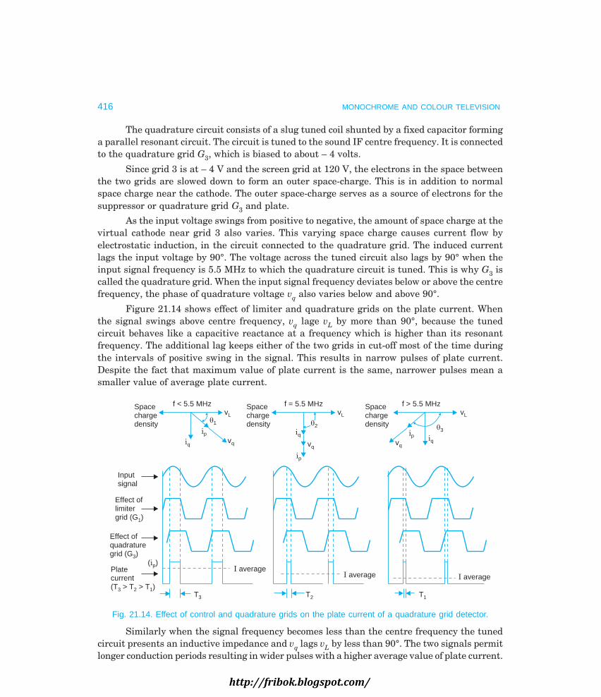
416 MONOCHROME AND COLOUR TELEVISION
The quadrature circuit consists of a slug tuned coil shunted by a fixed capacitor forminga parallel resonant circuit. The circuit is tuned to the sound IF centre frequency. It is connectedto the quadrature grid G3, which is biased to about – 4 volts.
Since grid 3 is at – 4 V and the screen grid at 120 V, the electrons in the space betweenthe two grids are slowed down to form an outer space-charge. This is in addition to normalspace charge near the cathode. The outer space-charge serves as a source of electrons for thesuppressor or quadrature grid G3 and plate.
As the input voltage swings from positive to negative, the amount of space charge at thevirtual cathode near grid 3 also varies. This varying space charge causes current flow byelectrostatic induction, in the circuit connected to the quadrature grid. The induced currentlags the input voltage by 90°. The voltage across the tuned circuit also lags by 90° when theinput signal frequency is 5.5 MHz to which the quadrature circuit is tuned. This is why G3 iscalled the quadrature grid. When the input signal frequency deviates below or above the centrefrequency, the phase of quadrature voltage vq also varies below and above 90°.
Figure 21.14 shows effect of limiter and quadrature grids on the plate current. Whenthe signal swings above centre frequency, vq lage vL by more than 90°, because the tunedcircuit behaves like a capacitive reactance at a frequency which is higher than its resonantfrequency. The additional lag keeps either of the two grids in cut-off most of the time duringthe intervals of positive swing in the signal. This results in narrow pulses of plate current.Despite the fact that maximum value of plate current is the same, narrower pulses mean asmaller value of average plate current.
Spacechargedensity
f < 5.5 MHz
1
vL
vq
ip
iq
Spacechargedensity
f = 5.5 MHz
vq
iq
ip
vL
Spacechargedensity
vL
f > 5.5 MHz
3
iqip
vq
I averageI average I average
T1T2T3
( )ipPlatecurrent(T > T > T )3 2 1
Effect ofquadraturegrid (G )3
Effect oflimitergrid (G )1
Inputsignal
2
Fig. 21.14. Effect of control and quadrature grids on the plate current of a quadrature grid detector.
Similarly when the signal frequency becomes less than the centre frequency the tunedcircuit presents an inductive impedance and vq lags vL by less than 90°. The two signals permitlonger conduction periods resulting in wider pulses with a higher average value of plate current.
http://fribok.blogspot.com/

SOUND SYSTEM 417
These pulses are integrated by the network RL and C3. Note that changes in the phase of vqresult from frequency deviations in the FM signal. Similarly variations in the average value ofplate current follow amplitude and frequency of the modulating audio signal. Thus the integratedoutput voltage at the plate of the tube gives the required audio output. C3 also acts as a platebypass capacitor for 5.5 MHz signals. R1,C1 constitute the de-emphasis network.
Tansistor Quadrature Detector. The transistor version of the quadrature detector employsthree identical transistors. The circuit arrangement is shown in Fig. 21.15. Transistors Q1 andQ2 perform the same functions as the limiter and quadrature grids in a gated-beam tube. Thesound IF signal is fed directly to the base of Q1, but is given a 90° phase-shift before applyingit to the base of Q2. The phase shift is accomplished by driving the signal through a very smallcapacitor C2. The circuit formed by L and C3 does not produce any further phase-shift at 5.5 MHzbecause it is tuned to be resonant at this frequency.
+ VCC
Section of asound C
Fromsound IF
and limiter
C1 R1 v1Q1
i1
2 K20 pF
5 pF R2
1.7 KC2
C3
C5 0.01 F
L R4
Biasvoltage
iR3
R3300 500 R6
i2
Q2
v2
R5
4.7 K
Q3 C40.01 F
Audio output
Fig. 21.15. Circuit diagram of a solid state quadrature FM detector.
The sound IF signal attains sufficient amplitude before it is coupled to the detectorcircuit and the biasing is so set that the two transistors are driven into saturation during thepositive swing of the input signal applied to each transistor. The emitters of the two transistorsare grounded through a common resistor R3. Thus the output voltage that develops across R3depends on the conduction of both Q1 and Q2. Since the voltage drop across R3 reverse biasesthe two transistors, the net bias automatically adjusts itself to keep the magnitude of peakcurrent through R3 at nearly a constant value. However, the duration for which the twotransistors conduct together varies and depends on the relative phase angle between the twoinput signals.
As shown in the waveforms of Fig. 21.16, at the centre frequency where the phasedifference between the two voltages is 90°, the current through R3 flows for a period T2 todevelop an average current I2. However, when the signal frequency becomes more than thecentre frequency, the phase angle between the two input voltages exceeds 90° and current
http://fribok.blogspot.com/

418 MONOCHROME AND COLOUR TELEVISION
through R3 flows for a longer period to develop an average current I1 which is greater than I2.When the input signal frequency become less than the centre frequency, the relative phaseangle reduces to less than 90° and the magnitude of average current through R3 changes to I3which is less than I2.
t0
v , v1 2f < 5.5 MHz
< 90°Assumedsaturationlevel
iR3
I3T3(T < T < T )3 2 1
t0
v , v1 2f = 5.5 MHz
= 90°
I2
T2
t0
v , v1 2f > 5.5 MHz
> 90°
I1
T1
Fig. 21.16. Effect of frequency deviations on the average output current in a transistorquadrature detector. Note that cut-off bias for both Q1 and Q2 has been assumed as zero volt.
Since the relative phase change between the input voltages to Q1 and Q2 results fromfrequency deviations in the FM signal, the output voltage which develops across R3 due tovariations in the average value of current through it follows the audio modulation. The audiovoltage thus developed is in the input circuit of transistor Q3 where it is amplified beforefeeding it to the audio section. Note that capacitor C4 (0.01 µF) by passes all IF components todevelop only audio voltage at the collector of Q3.
It is interesting to note that in a gated-beam tube the limiter grid and quadrature gridact like two gates in series and when the phase angle between vL and vq exceeds 90°, theaverage output current decreases. However, in the transistor circuit, under similar conditionsthe average output current increases. This is because the two transistors Q1 and Q2 act as twogates in parallel to permit current flow when either of the two input signals is positive. Thusthere is a 180° phase difference between the output currents of the two quadrature detectorsfor the same frequency swing. Since the audio signal is symmetrical about its centre zero axisthere is no difference in the sound reproduced at the loudspeaker.
4. Differential Peak FM DetectorIn this system a new technique known as differential peak detection is used to develop audiovoltage from the frequency modulated signal. Figure 21.17 (a) is the block diagram of thisdetector. It forms part of the IC, CA 3065 described in a later section of this chapter. Thedetector employs only a single tuning coil.
The two peak detectors employ differential amplifier configurations with emitter followersat their inputs. The output circuits of the two detectors have identical RC networks of suitable
http://fribok.blogspot.com/

SOUND SYSTEM 419
time constant to provide peak detection of the signals fed to them. The high input impedanceof the emitter followers isolates the detectors from the preceding sound IF section.
The external frequency sensitive network comprises of a parallel LC circuit and a seriescapacitor. The voltage e1 obtained from the sound IF amplifier and limiter output is fed (actuallyapplied at the input terminal of the IC) both to this frequency selective network and one of thepeak detectors.
At the centre frequency (fc = 5.5 MHz) the parallel circuit behaves like an inductor inseries with capacitor C2. This combination provides a slight boost to the signal across C2 so asto make e2 equal to e1. The signal voltage e2 is applied at the input of the other peak detector.The two peak detectors develop proportionate dc voltages at their output terminals which feedinto corresponding input terminals of the differential amplifier. Since e1 is equal to e2, thedifferential output voltage is zero in the absence of any modulation. As the intercarrier frequencyswings to become low, the parallel network L1,C1 along with C2 in series, approaches its seriesresonant frequency. Thus e2 (across C2) attains a higher magnitude than e1.This in turn resultsin a negative output voltage from the differential amplifier. As the carrier frequency
Peakdetector
Differentialamplifier
Peakdetector
L1
C1 C2Frequencyselectivenetwork
e1
– –
FMsoundsignal
e2
Electronicattenuator
eout
++
Fig. 21.17 (a). Block diagram of a differential peak detector.
|e | – |e |1 2
0
1 f/fC
+
–
Fig. 21.17 (b). Difference signal as a function of frequency.
http://fribok.blogspot.com/

420 MONOCHROME AND COLOUR TELEVISION
increases above fc, the parallel network (L1,C1) approaches its parallel resonant frequency andits impedance rises to make e2 less than e1. The differential amplifier output then swings tobecome positive. An analysis of the frequency response of e1 and e2 indicates that | e1 | – | e2|follows the normal ‘S’ curve (see Fig. 21.17 (b)) resulting in FM detection. The linearity of thisdetector is good and total harmonic distortion in the output is less than one percent.
5. Phase-Locked Loop FM DetectorThe latest in FM detection is the phase-locked loop detector shown in Fig. 21.18. It may beclassed as an inductorless detector requiring no alignment. In this circuit a dc error voltage isdeveloped by a phase detector that compares the phase of the input FM signal with that of alocally generated oscillator of the same frequency. The dc control voltage obtained at the outputof low-pass filter is directly related to the degree of phase difference between the two signals.This control voltage which is returned to the voltage controlled oscillator (VCO) afteramplification forces the oscillator to change its frequency thereby reducing the phase error.Whenthe free-running frequency of the VCO becomes close to the input signal frequency, the systemlocks at this frequency and the VCO tracks the input FM signal. Since the dc control voltagewill vary in step with the frequency deviations of the FM signal, it represents audio modulation.Thus the output from the dc amplifier is the demodulated audio signal. The IC contains avoltage amplifier (audio amplifier) the output of which can drive an audio power amplifier.The capacitor C1 is the de-emphasis capacitor connected to the corresponding pin of themonolithic IC package. For a noise-free reception, this FM detector requires a good limiterpreceding the phase detector.
Low-passfilter
FM sound signalfrom the limiteroutput
Phasecomparator
LimiterVoltage
controlledoscillator
DC amplifier Audio voltageamplifier
Audiooutput
De-emphasiscapacitor
(VCO)
C1
Fig. 21.18. Schematic block diagram of a phase-looked loop FM detector.
21.7 SOUND SECTION INTEGRATED CIRCUITS
As already stated early hybrid receivers employed some form of a ratio detector for FM detectionand vacuum tubes like ECL 82 (triode-pentode) for the audio section. The tubes were laterreplaced by transistors and a large number of circuits were developed for high quality soundreproduction. However, as soon as the integrated circuit technology was perfected, a largenumber of monolythic ICs were developed to perform the functions of sound IF limiter-amplifier,FM detector and audio pre-amplifier. In addition many ICs for the audio section are also nowavailable. Out of the many sound section ICs that have been developed, TAA570, TBA750Aand CA3065 are commonly used in modern circuits. All such ICs employ complex circuitry inorder to minimize the use of transformer couplings and inductors.
http://fribok.blogspot.com/

SOUND SYSTEM 421
IC-TAA570This IC employs a four-stage differential amplifier in the sound IF amplifier and limiter section.All the four stages receive their collector voltages through a multiemitter transistor whichprovides a self-limiting action on the voltage-swings at the collectors. All this results in verygood noise suppression and excellent amplitude limiting. The FM detector section is asymmetrical phase detector which is a modified version of the transistor quadrature detectordescribed earlier. The audio driver section is designed to give a maximum gain of about 80 dband can deliver an AF output equal to 1.8 volts for a frequency deviation of 50 KHz.
Figure 21.19 shows necessary details of its external connections and the circuit of theassociated audio output stage. This is commonly used in hybrid Television receivers.
110
9
8
76
54
3
2
Fromsoundtake-offpoint
T1
0.1 FC4
200 pF
C6 0.022 F
TAA 570
C3 0.022F
0.22 FL2
20 H
R1
+ 15 VZenerdiode
C5
0.1 F
C7
470
22 K Volumecontrol
C1
5 K R3
C8
P1
C11
2 M 1/2PCL 86
+ 10 V
1 K500 K
R5
R7
+ 4 V
1/2PCL 86
V2R6
0.01 F
R91.5K2 MC100.003
FV10.022 F
P2Tonecontrol
500KL1C2
R2
Quadraturecoil
RL330 K
0.005 FC9
T2 Speaker
200 V
150
0.01 F
+
B+
Fig. 21.19. Sound section of a hybrid receiver employing IC TAA570.
The sound IF signal from the video detector is coupled through the tuned matchingtransformer T1 to the input terminals (pins 8 and 9) of the IC. Stabilized dc supply is fed atpins 3 and 5 through resistor R1 and decoupling capacitor C7. L2 is the choke and C1 thedecoupling capacitor to the dc supply at pin 5.
The components shown within the dotted-chain box consitute the quadrature circuitwhere L1,C2 form a tuned circuit resonant at 5.5 MHz and R2 is the damping resistance acrossthe quadrature coil. De-emphasis is provided by capacitor C3 connected at pin 6 of the IC. Thecapacitors C4, C5 and C6 are bypass capacitors at the various pins of the integrated circuit. R3is the load resistor of the audio amplifier transistor and its output is available at pin 3. Theoutput from the IC is coupled to the voltage amplifier tube V1 (1/2 PCL86) through C8 andpotentiometer P1 which is the volume control. Potentiometer P2, that is connected at the plateof V1 through a capacitor (C10) functions as tone control. The output tube V2(1/2 PCL86) providespower amplification and the sound output is delivered to the loudspeaker through T2 the
http://fribok.blogspot.com/

422 MONOCHROME AND COLOUR TELEVISION
matching output transformer. The series circuit formed by C9, R9 and connected across theprimary circuit of the output transformer acts as tone correction network. Negative feedbackis applied from the plate of V2 to that of V1 through R6 for improved tone control operation. R5,the cathode resistor of V2, has been left unbypassed to provide overall gain stability and improvedfrequency response of the audio amplifier. Resistance R7 in series with the control grid circuitis for suppression of any parasitic oscillations.
IC-BEL CA 3065This is a linear IC chip specially designed for the sound section of monochrome televisionreceivers. Its circuit basically consists of (i) a regulated power supply, (ii) an IF amplifier-limiter, (iii) an FM detector, (iv) an electronic attenuator and buffer amplifier and (v) an audiodriver. The schematic diagram of this IC is shown in Fig. 21.20.
vin
2
1
3 4 9
C1
5
RS
B+
0.047 Fµ 11 6
Voltageregulators
Electronicattenuator
0.047Fµ
100K
DC volumecontrol
Audio signal7
8
14
10 13
12
Substrate0.05 Fµ
C2
L1
e2
e1 Differentialphase
detector
CA 3065
Sound IFamp-limiter andactive low-passfilter
Audiodriver
0.3 Fµ
Tonecontrol
Audiooutput
Bufferamplifier
De-emphasis0.0047 Fµ
25 K
0.47 FµSound take-offtransformer
Fig. 21.20. Block diagram of the IC(BEL) CA 3065 in a typical circuit application.Note terminal 5 may be connected to any positive voltage through a suitable resistor
(Rs) provided power rating of the IC is not exceeded.
(i) Regulated power supply. The input power supply to the IC is regulated through acombination of zener diodes. Separately regulated and decoupled dc supply is fed to differentsections of the IC for stable circuit operation.
(ii) IF amplifier-limiter. The single ended differential amplifier is the basic configura-tion for each of the three stages of the amplifier-limiter section of CA 3065. The quiescentcurrents of different transistors employed in the amplifiers are so adjusted that best possiblelimiting and AM rejection characteristics are obtained. The limiting amplifier is followed by
http://fribok.blogspot.com/

SOUND SYSTEM 423
an active low-pass filter which suppresses harmonics from the signal. The output of this filterfeeds the FM detector.
(iii) FM detector. A differential peak detector, the working principle of which was ex-plained in an earlier section (see Fig. 21.17), is used for obtaining audio voltage from thefrequency modulated signal. As shown in Fig. 21.20 voltage e1 obtained from the amplifier-limiter is applied at terminal 9 of the IC and thus fed simultaneously to the frequency selectivenetwork and one peak detector. The signal voltage e2 obtained at the output of the frequencyselective network (L1, C1, and C2) is applied at the input (pin 10) of the other peak detector.The outputs from the two peak detectors feed into the differential amplifier, the output ofwhich is the demodulated audio signal.
(iv) Electronic attenuator and buffer amplifier. The output of the differential peak de-tector is fed to the electronic attenuator which performs the conventional function of the audiovolume control. The stage employs a single ended differential cascade amplifier. The gain ofthis differential amplifier is controlled by varying the quiescent current of the transistors.This is achieved by changing the B+ voltage to one of its dc inputs, while the other dc input iskept at constant. An external variable resistance connected between terminal 6 of the IC andground is used to vary the dc potential. Because there is no audio signal present across thevariable resistance from terminal 6 to ground, there is no possibility of any noise or hum pick-up in the audio signal. This type of volume control is called a dc volume control.
The output of the attenuator is fed to a buffer amplifier which is an emitter follower andisolates the attenuator from the external load. The detected output is available at terminal 8 ofthe IC and the de-emphasis capacitor is connected at pin 7.
(v) Audio driver. The output of the buffer stage feeds into an audio driver which is asimple common emitter amplifier sandwitched between two emitter followers for input isolationand low output impedance. Typical gain of this stage is 20 db. Terminal 13 is available forincorporating suitable tone control network.
21.8 AUDIO OUTPUT STAGE
The output from the IC (CA 3065) can drive a PCL84/PCL86 audio amplifier, a solid statecomplementary output stage, or a sound IC like the BEL CA810.
A complete sound IF circuit employing CA 3065 along with a complementary transistoroutput amplifier is shown in Fig. 21.21. The output from the IC at pin 12 is fed to the drivertransistor Q1 through coupling capacitor C3. Transistor Q1 (BC 148B) forms a boot-strappeddriver stage which feeds the matched output pair Q2 and Q3 (AC 187/01, AC 188/01). Theoutput transistors drive the loudspeaker (8 ohms) through the electrolytic capacitor C4, R1 andR2 and thermistor (Th) provide necessary temperature compensation in the biasing circuit ofthe output pair. The stage operates class AB to avoid cross-over distortion. Typical data of theaudio amplifier is as under:
Supply voltage 15 V
No signal current 55 mA
Current drain at 2.5 W 300 mA
http://fribok.blogspot.com/

424 MONOCHROME AND COLOUR TELEVISION
Max. power output 2.5 W
Third harmonic distortion at 2.5 W 3%
A.M. rejection 35 db
Speaker impedance 8 Ω
5
6
7
+
15 V
+
390
Q2
AC 187/01Speaker
(8 )22
Th1 R1
C4 1000 F
500 K
Q3
AC 188/01
R2
Q1
BC 148 B
33
100 K
De-emphasis0.047 F
0.0047 F
0.047 F
100 F
13
14
8
124.7 K
109
4
3
vin
T1
1
2
Soundtake-off
transformer
0.01 F
L = 14 H1
Tonecontrol
220 K
12 pFC2
68 pF
C1
0.22 F
L1
0.47 F
CA 3065 5 F
DC volumecontrol
56 1
C3
Fig. 21.21. External circuitry of the sound IC (BEL) CA 3065 along-with a 2.5W audio amplifier.
Audio IC CA 810The IC BEL CA 810 has been specially developed for the audio section of television receivers.This audio amplifier as illustrated in Fig. 21.22 is capable of delivering 4 W output power intoan 8 ohm load. Good frequency response and high input impedance are some of the salientfeatures of this circuit. Its typical performance characteristics are as under:
(1) Supply voltage 16.0 V
(2) Maximum output power at 10% THD 4.1 W
(3) Input sensitivity at 50 mW output power 9.2 mV
(4) Input sensitivity at maximum output power 70 mV
(5) Zero signal current drain 8.6 mA
(6) Supply current at maximum power output 380 mA
(7) Input impedance 100 KΩ(8) Frequency response (3 db) 20 Hz to 20 KHz
http://fribok.blogspot.com/

SOUND SYSTEM 425
10
11
14
Tabs CA 810
+ 16 V
100
320 F+
+100 F
1
6
9
8
7
16
vin
+10 F
100 K
680 pF
0.0056 F
100 F51
100 F+
0.1 F
+
1
1000 F
Speaker(8 )
Fig. 21.22. Audio amplifier employing IC (BEL) CA 810.
Review Questions
1. Explain the mechanism of separating the sound signal in a video detector. What is the pivotalpoint the makes the intercarrier sound system a success ?
2. Explain with suitable circuits and phasor diagrams the phase relationships between the inputand output of a tuned circuit when the input signal frequency is varied below and above resonance.
3. Explain the basic principle of FM detection. Describe with a circuit diagram how FM detectiontakes place in a Foster-Seeley detector. Why such a circuit must precede by a voltage limiter ?
4. Draw the circuit diagram of any type of ratio detector and explain how the audio signal is de-tected. How is the limiting action achieved in a ratio detector ?
5. Explain with a circuit diagram and waveshapes, how FM detection takes place in a quadraturegrid detector that employs a specially designed pentode. Why it is called quadrature detection ?
6. Fig. 21.15 is the circuit of a quadrature FM detector which employs transistors. Explain how thecircuit performs as a limiter, FM detector and audio preamplifier. How is the detection mecha-nism different from the circuit employing a gated-beam tube ?
7. Explain with a suitable circuit diagram the basic principle of peak FM detection. Explain themanner in which FM signal is made to acquire amplitude variations before feeding it to thedifferential amplifier.
8. Draw schematic block diagram of a phase-locked loop FM detector and explain how the circuitperforms to demodulate the FM signal.
9. The block schematic of the sound IC CA 3056 is given in Fig. 21.20. Explain briefly the functionof each block. Why is the electronic attenuator block called a dc volume control ?
10. Draw the circuit diagram of an audio output stage that can be fed from the sound IC AC 3065and explain how it produces enough audio output power with negligible distortion.
http://fribok.blogspot.com/

22
http://fribok.blogspot.com/
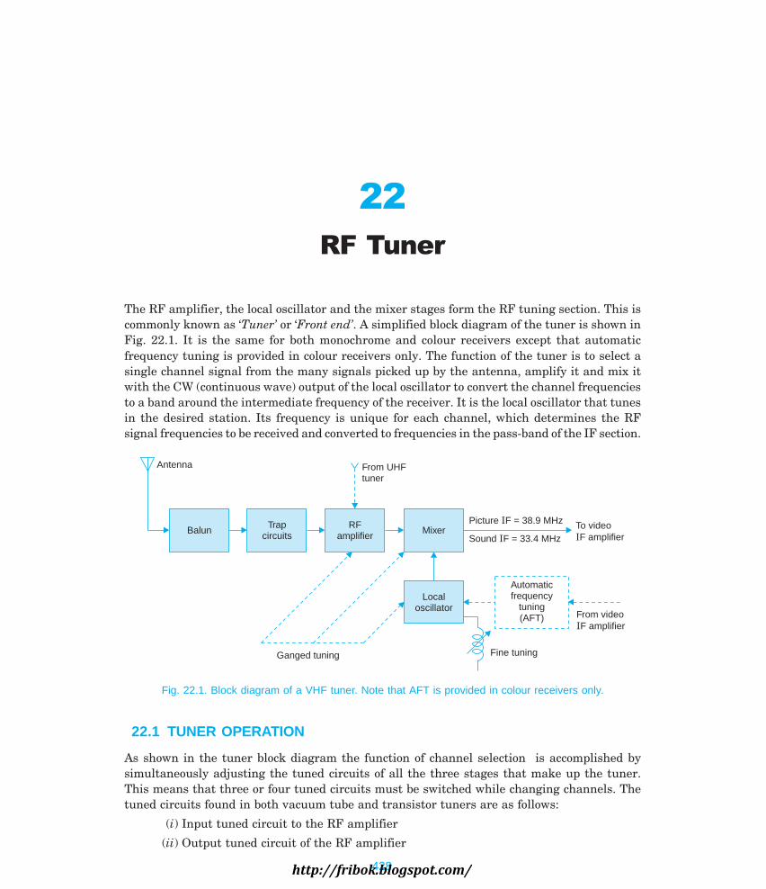
The RF amplifier, the local oscillator and the mixer stages form the RF tuning section. This iscommonly known as ‘Tuner’ or ‘Front end’. A simplified block diagram of the tuner is shown inFig. 22.1. It is the same for both monochrome and colour receivers except that automaticfrequency tuning is provided in colour receivers only. The function of the tuner is to select asingle channel signal from the many signals picked up by the antenna, amplify it and mix itwith the CW (continuous wave) output of the local oscillator to convert the channel frequenciesto a band around the intermediate frequency of the receiver. It is the local oscillator that tunesin the desired station. Its frequency is unique for each channel, which determines the RFsignal frequencies to be received and converted to frequencies in the pass-band of the IF section.
Balun Trapcircuits
RFamplifier
MixerPicture F = 38.9 MHzI
Sound F = 33.4 MHzITo videoF amplifierI
Antenna From UHFtuner
Localoscillator
Automaticfrequency
tuning(AFT) From video
F amplifierI
Ganged tuning Fine tuning
Fig. 22.1. Block diagram of a VHF tuner. Note that AFT is provided in colour receivers only.
22.1 TUNER OPERATION
As shown in the tuner block diagram the function of channel selection is accomplished bysimultaneously adjusting the tuned circuits of all the three stages that make up the tuner.This means that three or four tuned circuits must be switched while changing channels. Thetuned circuits found in both vacuum tube and transistor tuners are as follows:
(i) Input tuned circuit to the RF amplifier
(ii) Output tuned circuit of the RF amplifier
428
http://fribok.blogspot.com/

RF TUNER 429
(iii) Input tuned circuit to the mixer
(iv) Local oscillator tuned circuit
In some tuners the mixer input tuned circuit is left out and thus they have only threetuned circuits. Each tuned circuit consists of a coil and a capacitor. The resonating capacitanceconsists of distributed capacitance of the circuit plus small fixed ceramic capacitors. The finetuning control is varied to obtain exact picture and sound intermediate frequencies for whichthe receiver is designed. The correct setting of the local oscillator frequency is indicated by thebest picture obtained on the screen. Physically, the tuner is wired as a sub-assembly on aseparate chassis which is mounted on the main receiver chassis. The IF signal from the tuneris coupled to the first picture IF amplifier through a short coaxial cable. The AGC line and B+supply are connected from the main chassis to the tuner subchassis. The tuner is enclosed in acompact shielded box and all connections are usually brought out at the top of the tuner viafeed through capacitors. In tube-type receivers, the filament power to the tuner tubes is alsosupplied from the common power supply.
Though the principle of selection in television receivers is the same as that in radioreceivers the design of the tuner is very different from the heterodyning section of the radioreceiver. This is because of large band width requirements and very high frequencies employedfor TV transmission. In fact tuner design techniques differ so much at ultra high frequenciesthat all true multichannel receivers employ separate tuners for the VHF and UHF channels.We will confine our discussion to channels with frequencies 47 to 223 MHz in the VHF band(30 to 300 MHz). The basic principle of UHF tuners is discussed separately in a later part ofthis chapter.
22.2 FACTORS AFFECTING TUNER DESIGN
The factors that must be considered before attempting to learn details of the tuner circuitryare:
(a) Choice of IF and Local Oscillator FrequenciesThe merits of choosing intermediate frequencies close to 40 MHz were fully explained inChapter 8. However, it may again be emphasized that such a choice results in (i) high imagerejection ratio, (ii) reduced local oscillator radiation, (iii) ease of detection and (iv) good selectivityat the IF stages. The local oscillator frequency is kept higher than the channel carrier frequencysince this results in a relatively narrow oscillator frequency range. It is then easier to designan oscillator that is stable and delivers almost constant output voltage over its entire frequencyrange.
Intermediate frequencies have been standardized in accordance with the total bandwidthallotted to each channel in different TV systems. In the 625-B monochrome system, the pictureIF = 38.9 MHz and sound IF = 33.4 MHz.
(b) Need for an RF Amplifier StageIn principle an RF amplifier is not necessary and the signal could be fed directly to the tunedinput circuit of the mixer as is the normal practice in radio receivers. However, at very highfrequencies the problems of image signals, radiation from the local oscillator through theantenna circuit and conversion loss at the mixer are such that a stage of amplification prior to
http://fribok.blogspot.com/

430 MONOCHROME AND COLOUR TELEVISION
the mixer is desirable. Another very important purpose of providing one stage of amplificationis to feed enough RF signal into the mixer for a clean picture without snow. White specklescalled snow are caused by excessive noise signals present in the video signal. The mixer circuitgenerates most of the noise because of heterodyning. Except in areas very close to the transmitterthe signal level is moderate and a low noise RF amplifier stage with a gain of about 25 dbbecomes necessary to obtain the desired signal-to-noise ratio of 30 : 1. In fringe areas wherethe signal level is very low an additional RF amplifier known as booster is often employed tomaintain a reasonable signal-to-noise ratio.
In all tuner designs the gain of the RF amplifier is controlled by AGC voltage to counterany variations in the input signal to the receiver. A signal level of about 400 µV at the input tothe receiver is considered adequate for a snow free picture.
(c) Coupling NetworksParallel tuned networks are used to accomplish the desired selectivity in RF and IF sections ofthe receiver. For minimum power loss the coupling network should match the output impedanceof one stage to the input impedance of the following stage. In circuits employing tubes thisdoes not present any problem because the output and input impedance levels are not verydifferent and the main criterion is to transfer maximum voltage to the next stage. However, intransistor amplifiers, where the input circuit also consume power, the interstage couplingnetwork must be designed to transfer maximum power from the output of one stage to theinput of the following stage. The coupling design is further complicated by the fact that intransistors the output and input impedance levels are much different from each other. Forexample the input impedance of a common base configuration at very high frequencies is onlya few tens of ohms, whereas its output impedance is of the order of several tens of kilo-ohms.
22.3 BASIC COUPLING CIRCUITS
Before attempting to discuss specific coupling arrangements it is necessary to have a clearconcept of impedance levels, matching and bandwidth of tuned circuits. Consider the basictuned coupling circuits of Fig. 22.2. In Fig. 22.2(a) the impedance matching is obtained byconnecting the input between terminals 2 and 3 instead of 1 and 3. Since the ratio of impedancelevels is associated with square of the turns ratio, the input impedance between points 2 and 3will be one fourth of the impedance between points 1 and 3, if point 2 is at the centre tap of thecoil.
Figure 22.2(b) shows another approach to selecting any impedance level where thecapacitor C has been split into two separate capacitors C1 and C2 to provide a tap. In this case
Z2–3 = Z1–2 × CC
1
2
2FHG
IKJ . Thus the input impedance Z2–3 increases with a decrease in the value of
C2. Note that as in the previous circuit the resonant frequency and quality factor (Q) of thetuned circuit remain the same if C = (C1 × C2)/(C1 + C2) is maintained.
Figure 22.2(c) shows the basic transformer coupling configuration where the tunedprimary circuit is coupled to a nonresonant secondary. In this case if N1 and N2 are the numberof turns in the primary and secondary respectively, the required turns ratio for an impedance
match between the two sides is n = N1/N2 = r ri0 / where r0 represents the impedance of the
driving circuit and ri that of the load circuit.http://fribok.blogspot.com/

RF TUNER 431
CL
1
2
3
L
1
2
3
C2
C1
vS
Lp Ls
ri
r0 N1 N2
f =01
2 LCp
(a)
f =01
2 LCp
(b)
n =N
N1
2
=r
ro
i
(c)
Fig. 22.2. Impedance matching in coupling circuits (a) by inductive tapping(b) by capacitive tapping and (c) by transformer action.
The use of these concepts is illustrated by a practical example. Assume that a couplingnetwork is to be designed for a high frequency bandpass amplifier using a common emitterconfiguration both in the input and output circuits. Taking r0 of transistor Q1 = 10 K ohms andri of transistor Q2 = 500 ohms, the calculated value of Lp (primary inductance) and Ls (secondaryinductance) for a given bandwidth turns out to be of the order of a few µH and a fraction of aµH respectively. To construct a transformer with a high value of unloaded Q of, say, 100 usinga very low primary inductance of a few µH is very difficult. In practice the problem is solved byusing a tapped primary winding where the inductance of the primary winding can be mademany times the calculated value. An auto-transformer can also be used by choosing appropriatetaps both for input and output circuits. Figure 22.3 (a) shows such a configuration.
Qoutput
1
ro ri
Qinput
2
1
2
3
4
Fig. 22.3 (a). Interstage network using autotransformercoupling with tuned primary winding.
Capacitive CouplingIn many applications difficulty is often encountered in obtaining ‘unity’ coupling betweenprimary and secondary windings. This problem becomes particularly severe in common-baseamplifier configurations operating at higher channel frequencies because the input impedancebecomes as low as 20 ohms. In such cases capacitive coupling is often used. Figure 22.3(b)shows such a circuit configuration. Since C1 is effectively shunted by the low input resistanceof the common-base circuit (transistor Q2) the total capacitance CT = C1 + C2, and f0 (centre
http://fribok.blogspot.com/

432 MONOCHROME AND COLOUR TELEVISION
frequency) = 1/ 2 1πL CT . To achieve a higher quality factor the value of inductance L1 can be
increased and CT accordingly decreased. However, this would need connecting the output oftransistor Q1 to a suitable tapping on the coil to maintain the desired impedance match.
Qoutput
1
rori
Qinput
2
L1C1
C2
Ci
Fig. 22.3 (b). Interstage network employing capacitivecoupling using two capacitors.
Double Tuned NetworksA single tuned circuit, employing any one form of the couplings discussed above, is normallyused in the input circuit of the RF amplifier to provide a match with the antenna circuit. Theoutput circuit of this amplifier is usually double tuned because most of the second channelrejection of the tuner is effected here. The advantages of double tuned interstage couplingnetworks (Fig. 22.4 (a)) over single tuned circuits are:
(i) the frequency response is flatter within the pass-band.
(ii) the drop in response is sharper immediately adjacent to the ends of the pass-band.
(iii) attenuation of frequencies not in the pass-band is higher.
vin
Ip Is
vo
Fig. 22.4 (a). Double tuned circuit.
The above advantages are clearly seen in the response curves shown in Fig. 22.4 (b). Forloose coupling the response curve has a single peak at f0 like a single tuned circuit but with lowamplitude. As the coupling is increased, the output amplitude increases and at a middle valueof coupling called ‘critical coupling’ the secondary has its maximum amplitude and greatestbandwidth without double-peaks. When the coupling is further increased to what is known asovercoupling, two peaks result in the secondary output to broaden the output response. Varyingthe coupling beyond critical coupling results in greater bandwidth of the coupled circuits thatare tuned to the same resonant frequency. Also as shown in the response curve, for anovercoupled case the drop in response is sharper on either edge of the pass-band.
http://fribok.blogspot.com/

RF TUNER 433
Qoutput
1 Qinput
2
r0
1 3
2 5
r14
Loosecoupling
Criticalcoupling
Overcoupling
t0
Is
fo
Fig. 22.4 (b). Effect of coefficient of coupling Fig. 22.4 (c). Double tuned interstage coupling(k) on the response curve of a network employing inductive coupling with a
double tuned circuit. tap on the secondary to obtain impedancematch and selectivity.
Various forms of interstage coupling networks employing two tuned circuits are commonlyused where both the primary and secondary sides are tuned to the same resonant frequency.Figure 22.4(c) shows a typical circuit where the secondary winding has been tapped to obtainthe desired impedance match and selectivity. In all double tuned circuits damping resistancescan be connected across both the primary and secondary circuits to get larger bandwidth withmore flat top. The use of resistors, however, reduces gain because of decrease in the value of Qof both the circuits.
Impedance CouplingAnother form of coupling, that employs a common impedance Zm for mutual coupling betweentwo tuned circuits, is shown in Fig. 22.5 (a). This method is also called band-pass couplingbecause it usually has the bandwidth of an overcoupled double tuned transformer. In Fig. 22.5(b)coil Lm is common to both the tuned circuits with L1, C1 and L2, C1. As a result, signal voltageacross Lm is coupled from one tuned circuit to the other. There is no direct coupling between L1and L2 and both L1, C and L2, C2 are pretuned by means of brass slugs to the same centrefrequency. The bandwidth is controlled by the value of Lm. The greater the value of Lm thegreater the mutual impedance and greater is the bandwidth. This type of coupling is commonlyemployed between the RF amplifier and the mixer. Values of Lm and damping resistances arechosen to provide a band pass of approximately 7 MHz.
L1
L2
Zm
v1 v0
C1C2
Rd2Rd1
L1
v1 v0
C1C2
Rd2Rd1
Lm
L2
Fig. 22.5 (a). Mutual coupling through Fig. 22.5 (b). Inductive (Lm)a common impedance Zm. bottom coupling.
http://fribok.blogspot.com/

434 MONOCHROME AND COLOUR TELEVISION
L1
L2
v1 v0
C1 C2
Rd2Rd1
Cm
Fig. 22.5 (c). Capacitive (Cm) bottom coupling.
v0v1 Rd1
L1
C1 L2C2
Rd2
Bandwidthadjustment
Cb
Fig. 22.6. Interstage broadband coupling withadjustable bandwidth.
Another form of this type of coupling is shown in Fig. 22.5 (c) where the coil Lm isreplaced by a capacitor Cm. The smaller the value of Cm the greater the mutual impedance andmore the bandwidth. The circuit arrangement shown in Fig. 22.6 is yet another method ofcoupling between stage in order to achieve a broadband response. Here a small capacitorconnects the primary and secondary windings. The value of the capacitor is low (10 to 20 PF)and it controls the bandwidth. A damping resistance is sometimes connected across the tunedcircuits to adjust the bandwidth.
22.4 TUNER CIRCUIT ARRANGEMENT
For earlier receivers special tubes were developed for use in tuner circuit. The tubes, bothpentodes and triodes, are miniature type with reduced interelectrode capacitance and leadinductance. A pentode yields more gain but a triode is preferred because it generates lessnoise. This is because noise originating in a tube varies directly with the number of positiveelements within a tube. To compensate for lower gain available from a triode special dualtriodes have been developed for use in a cascode configuration. Special frame grid constructionhaving sturdy supports is employed to reduce microphonic effects. Fine grid wire with closespacing between cathode and control grid results in increased transconductance. Thin gridalso results in reduced grid to cathode (Cgk) capacitance. By means of grid guide plates, theelectron flow is concentrated into a smaller area to reduce noise which otherwise results due to
http://fribok.blogspot.com/

RF TUNER 435
random motion of electrons. The twin triode RF amplifier is followed by triode-pentode mixerto convert channel frequencies into the IF region.
In tuners employing transistors, three transistors are normally employed, one each inRF amplifier, local oscillator and mixer circuits. In almost all tuners, whether tube or transistorversion, a single tuned circuit provides coupling between the antenna circuit and RF amplifierand a double-tuned circuit is used between the RF amplifier and mixer.
NeutralizationUnwanted feedback due to junction or interelectrode capacitances is much greater in transistorthan in tubes. This needs neutralizing. In a transistor amplifier circuit the signal fed fromcollector to base via the collector-base junction capacitance may be either regenerative ordegenerative depending on the frequency of the signal and the nature of the collector load. Thepurpose of neutralization is to deliberately feed a signal from the collector to the base which is180° out of phase with the feedback signal travelling through the collector-to-base junctioncapacitance. The neutralizing signal cancels the effect of undesired feedback.
vo
vinL1
AGCbias
+ VCC
L2
CN
C1
C2
R1
CN
vo
vin L1
AGCbias
+ VCC
L2
vo
vin
L1
AGCbias
+ VCC
L2
CN
C1
(a) (b)
C3
Fig. 22.7. Methods of neutralizing a high frequency amplifier stage. CN is the neutralizingcapacitor (a) feedback voltage from secondary of output transformer (b) feedback from tapped
primary coil (c) feedback through capacitive voltage divider (C1, C2) across L1.
http://fribok.blogspot.com/

436 MONOCHROME AND COLOUR TELEVISION
Figure 22.7 illustrates three methods of obtaining signal voltage which is opposite inpolarity to the collector voltage. The feedback capacitor CN couples back the neutralizing voltageand blocks any dc voltage between the collector and base. In the circuit of Fig. 22.7(a) feedbackvoltage is obtained from the secondary winding which is 180° out of phase with respect to theprimary. In Fig. 22.7(b) the bottom end of L1 has signal of opposite polarity with respect to thetop. The ground is provided by C1. Therefore the neutralizing voltage fed back by CN cancelsthe internal feedback.
The circuit of Fig. 22.7(c) uses a capacitive voltage divider arrangement for feedback. Itmay be noted that the junction of C1 and C2 is grounded thus providing out of phase voltage atthe two ends of the winding with respect to ground. Thus the voltage fed back through CN isout of phase with the internal feedback voltage. The isolating resistance R1 is needed in thecollector circuit to prevent shorting of the signal through low impedance of the dc supply. Thisfeedback arrangement is often used in RF amplifiers while the previous two circuits find favourin IF amplifiers.
22.5 TYPES OF TUNERS
All TV receivers have separate VHF and UHF tuners. The VHF tuner may be single channel ormultichannel to cover all Band I and Band III channels. Normal switching methods of tunedcircuit selection are not used because longer leads may cause parasitic oscillations. The VHFtuners are either turret type or rotary-wafer type.
(i) Turret TunerThe turret or drum type tuner is so named because coils for the various channels are mountedon a slotted drum type structure that is rotated by the channel selector. The tuned circuits aremounted on separate strips for each channel which are clipped into the turret. The coils requiredare selected by rotating the turret thus maintaining the shortest possible length of connections.Each strip has coils for RF amplifier, mixer and local oscillator for a single channel. Theschematic of a VHF turret tuner shown in Fig. 22.8 illustrates the manner in which a coil stripon the drum makes connections with the rest of the circuit.
(ii) Wafer or Incremental TunerThis tuner employs a wafer switch type construction where a tier of wafer switches permitsselection of the proper RF, mixer and oscillator coils. The coils are usually mounted around theouter rim of the switch with a few turns of wire for the lower channels and progressivelydecreasing for the higher channels. The wafer switch is rotated to connect one set of RF, mixerand oscillator coils for each channel. Figure 22.9 shows schematic of VHF tuner-wafer switches.Note that the coils for RF amplifier, oscillator and mixer stages are on separate wafer switchesganged on a common shaft. The oscillator coils are always on the front section for convenienceof adjusting the inductance to set the frequency.
The wafer type tuners are also called incremental tuners because the change of channelis accomplished by a progressive shorting of sections of the total inductance. For channels 2 to6 individual coils are connected in series and are progressively shorted out. For channels 7 to11 only a single turn or half a turn is sufficient for tuning.
http://fribok.blogspot.com/

RF TUNER 437
RF amplifier
Antenna coil RF coil
Contactson the drum
Coilscoupled
Mixer coil
Removable strip on the turret drum
Coils coupled Oscillatorcoil
AGC
From antennacircuit
B+ TP B+
B+ IF OUT
Mixer
Oscillator
Turret drum
To coils
Fig. 22.8. VHF turret tuner.
Commonshaft
78
9
10
11
121
2
3
4
5
6
To local oscillator circuit
78
9
10
11
121
2
3
5
6
4
To mixer circuit
78
9
10
11
121
2
3
5
6
4
To RFamplifier circuit
Fromantennainputnetwork
Coilscoupled
Fig. 22.9. Channel switching arrangement in a VHF wafer (incrimental) tuner.
Channel I is not assigned for TV broadcasting any more and this position on the selectorswitch is generally used to turn on the UHF tuner. The recent version of tuner wafer constructionutilizes a printed circuit wafer. In this method all coils for higher channels are replaced byprinted circuit inductances. This method has the advantage of greater reliability, greateruniformity of alignment and lower cost.
http://fribok.blogspot.com/
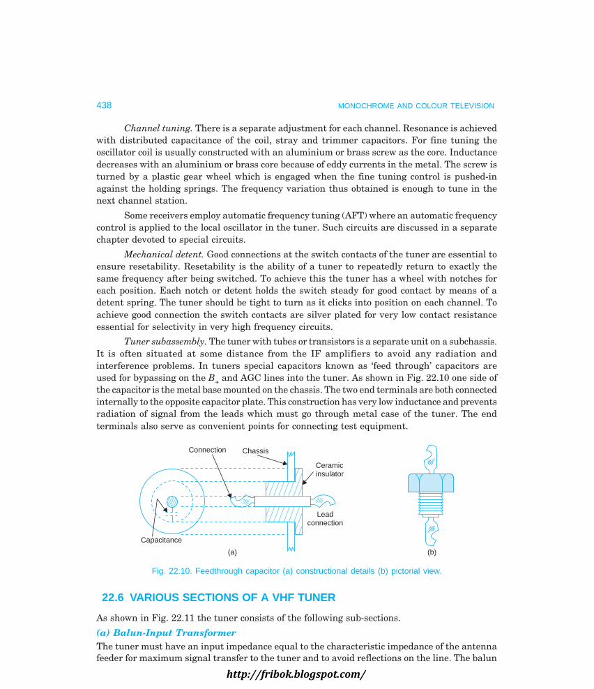
438 MONOCHROME AND COLOUR TELEVISION
Channel tuning. There is a separate adjustment for each channel. Resonance is achievedwith distributed capacitance of the coil, stray and trimmer capacitors. For fine tuning theoscillator coil is usually constructed with an aluminium or brass screw as the core. Inductancedecreases with an aluminium or brass core because of eddy currents in the metal. The screw isturned by a plastic gear wheel which is engaged when the fine tuning control is pushed-inagainst the holding springs. The frequency variation thus obtained is enough to tune in thenext channel station.
Some receivers employ automatic frequency tuning (AFT) where an automatic frequencycontrol is applied to the local oscillator in the tuner. Such circuits are discussed in a separatechapter devoted to special circuits.
Mechanical detent. Good connections at the switch contacts of the tuner are essential toensure resetability. Resetability is the ability of a tuner to repeatedly return to exactly thesame frequency after being switched. To achieve this the tuner has a wheel with notches foreach position. Each notch or detent holds the switch steady for good contact by means of adetent spring. The tuner should be tight to turn as it clicks into position on each channel. Toachieve good connection the switch contacts are silver plated for very low contact resistanceessential for selectivity in very high frequency circuits.
Tuner subassembly. The tuner with tubes or transistors is a separate unit on a subchassis.It is often situated at some distance from the IF amplifiers to avoid any radiation andinterference problems. In tuners special capacitors known as ‘feed through’ capacitors areused for bypassing on the B+ and AGC lines into the tuner. As shown in Fig. 22.10 one side ofthe capacitor is the metal base mounted on the chassis. The two end terminals are both connectedinternally to the opposite capacitor plate. This construction has very low inductance and preventsradiation of signal from the leads which must go through metal case of the tuner. The endterminals also serve as convenient points for connecting test equipment.
Connection
Capacitance
Ceramicinsulator
Leadconnection
Chassis
(a) (b)
Fig. 22.10. Feedthrough capacitor (a) constructional details (b) pictorial view.
22.6 VARIOUS SECTIONS OF A VHF TUNER
As shown in Fig. 22.11 the tuner consists of the following sub-sections.
(a) Balun-Input TransformerThe tuner must have an input impedance equal to the characteristic impedance of the antennafeeder for maximum signal transfer to the tuner and to avoid reflections on the line. The balun
http://fribok.blogspot.com/

RF TUNER 439
matches the twin wire ribbon feeder impedance of 300 ohm to the 75 ohm input impedance ofRF amplifier. It consists of two 150 ohm (Z0) quarter-wave sections of bifilar windings on aferrite core. As shown in Fig. 22.12, at one end the two quarter-wave lines are connected inparallel to give 75 ohm impedance and at the other end they are connected in series to providean impedance equal to 300 ohms. If a coaxial cable is used to connect the antenna to RF amplifier,an identical parallel arrangement can be used on both sides of the balun to provide the match.Either side of the balun can be used for input with the opposite side for output.
BalumHP filter
and trapsRF
amplifierTunedcircuits
MixerTunedcircuits IF
out
Antenna
Tunedcircuit
AGC bias
Localoscillator
Ganged tuning for channel selection
Finetuning
Fig. 22.11. Sub-sections of a VHF tuner in a monochrome receiver.
The capacitors C1 and C2 (200 pF), one in each lead, isolate the antenna from the chassisas a safety precaution, in transformerless receivers and to prevent damage due to lightning.The 2 MΩ shunt resistors R1 and R2 discharge any static charge accumulated on the capacitors.
(b) HP Filter and Trap CircuitsFigure 22.12 shows various trap circuits and a high-pass (HP) filter that follow the balun.Unwanted spurious signals which lie in the IF band of 32 to 42 MHz are rejected by twotrap circuits connected on either side of the HP filter configuration. The HP filter has a cut-off frequency of 45 MHz and thus rejects all frequencies below channel number 2. These filter
300Antenna
input
W
200 pF
C1
R1
2 M
2 M
200 pF
C2
R2
Balun 75W
To RFamplifier
HP filterand traps
Fig. 22.12. Typical input circuit of a VHF tuner.
http://fribok.blogspot.com/

440 MONOCHROME AND COLOUR TELEVISION
sections are essential because low ‘Q’ RF circuits may not be able to attenuate the adjacentchannel frequencies due to their broad bandwidth, particularly when the receiver is tuned tolower channels. It is very difficult to reject such signals once they reach the mixer and IFstages. In some receivers a parallel resonant trap circuit is provided in series with the signalpath to reject signals from the commercial FM broadcast band extending from 88 to 108 MHz.The balun and filter circuits are normally placed side by side on separate mounts very close tothe tuner.
(c) RF AmplifierThe RF amplifier is designed to provide adequate gain to weak signals. It is essential to maintaina high signal-to-noise ratio at the mixer which generates lot of noise. The equivalent noisevoltage at the input of the RF amplifier sets a limit to the minimum signal strength thatshould be received to avoid excessive snow effects. As already stated RF amplifier besidesproviding gain to the selected channel signals (i) prevents radiation from the local oscillatorand (ii) rejects image frequency signals.
The RF stage is best suited for AGC because the signal amplitude is small and the gaincontrol is most effective with least distortion. Application of AGC is usually delayed to the RFamplifier in order to maintain good S/N ratio for weak signals.
The RF amplifier should have a pass-band (see Fig. 22.13) broad enough to pass theselected channel and allow for small variations in the tuned circuit frequencies. Double tunedcircuits adjusted to provide a flat top response are used for coupling the RF amplifier to themixer stage. The response as shown in Fig. 22.13 has a dip of about 1 db in-between the twopeaks.
7 MHz
4.43 MHz
5.5 MHz
.5 dbP C S
t
0f(MHz)
100%
70.7%
50%
v0
Fig. 22.13. RF amplifier response.
(d) Local OscillatorThe local oscillator generates an unmodulated sinusoidal (CW) voltage that is heterodyned inthe mixer with the incoming RF signal to affect its frequency translation to the IF band. Thelocal oscillator frequency is changed whenever a different channel is selected to maintaindifference equal to the intermediate frequency between the local oscillator frequency and thetuned channel carrier frequency. The fine tuning control allows the oscillator frequency to bevaried over a narrow range.
http://fribok.blogspot.com/

RF TUNER 441
An important characteristic of the local oscillator used in tuners is its freedom from‘drift’. Drift occurs due to temperature changes, ageing of circuit components, changes in dcvoltage and variation of the oscillator load. Special compensation techniques are used to obtainoscillator stability. In monochrome receivers a small amount of drift can be tolerated but incolour receivers even very small frequency changes can result in the loss of colour portion ofthe signal. Therefore in tuners designed for colour receivers, ATC (automatic tuning control)or AFT (automatic frequency tuning) circuit is used for strict control of the oscillator frequency.
In tuners employing transistors the problem is more serious because transistor operationis highly temperature dependent and sensitive to dc supply fluctuations. In such circuits, inaddition to the use of usual compensation techniques and high quality components, a stabilizedpower supply and special capacitors with zero temperature coefficient are employed.
(e) Mixer StageThe function of this circuit is to convert the incoming RF signal frequencies from differentchannels into a common IF pass-band of the receiver. This is achieved in the mixer byheterodyning or beating the local oscillator frequency with the signal obtained from the RFamplifier. The mixer stage, combined with the local oscillator, may be considered as a frequencyconverter. To produce frequency translation, rectification in the mixer is necessary. This isachieved by keeping the amplitude of the local oscillator signal large and operating the mixertube or transistor in the non-linear region of its dynamic characteristics. The operation in thenonlinear region results in serve amplitude distortion which in turn generates sum anddifference frequencies of all the constituents of the input to the mixer. Higher harmonic productswith decreasing amplitudes are also generated. However, the major products at the output ofthe mixer are the sum and difference frequencies (sidebands) which the input signal producesby beating with the strong local oscillator frequency.
Since the difference between the RF signal and local oscillator signal frequencies isappreciable, the two sideband regions are quite apart from each other. The desired IF band isthus easily separated by a tuned circuit. The double tuned circuit used at the output of themixer is broadly tuned to select the desired band between 33.15 to 40.15 MHz and reject allother frequencies.
The conversion gain at the mixer stage is defined as the IF signal output divided by theRF signal input. Since the conversion trans-conductance in vacuum tubes is quite low, a gainof only about six is possible. With an RF input of 2 mV an IF output of about 12 mV becomesavailable. In mixers using transistors a conversion power gain between 15 to 20 db is obtainedfor most VHF channels.
22.7 ELECTRONIC TUNING
Varactors or varicaps are used for electronic tuning in tuner circuits. Varactor is a specialsilicon diode, the junction capacitance of which is used for tuning. This capacitance variesinversly with the amount of reverse bias applied across the diode. The resonant frequency ofthe tuned circuits in which they are connected, is controlled merely by changing the reversebias across the varactor. Figure 22.14(a) illustrates how a varactor diode D is used in a resonantcircuit. The capacitor C1 is quite large and thus has negligible reactance at resonant frequency
http://fribok.blogspot.com/
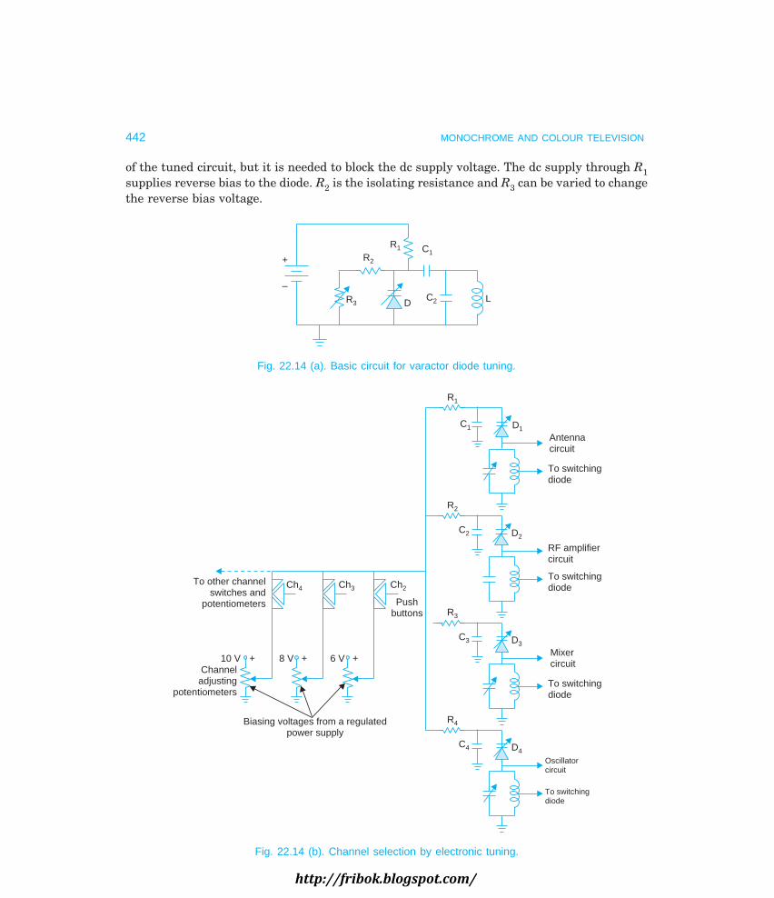
442 MONOCHROME AND COLOUR TELEVISION
of the tuned circuit, but it is needed to block the dc supply voltage. The dc supply through R1supplies reverse bias to the diode. R2 is the isolating resistance and R3 can be varied to changethe reverse bias voltage.
+
–
R1
R2
R3
C1
C2 LD
Fig. 22.14 (a). Basic circuit for varactor diode tuning.
R1
C1 D1
Antennacircuit
To switchingdiode
R2
C2 D2
RF amplifiercircuit
To switchingdiode
R3
C3 D3
Mixercircuit
To switchingdiode
R4
C4 D4
Oscillatorcircuit
To switchingdiode
6 V +8 V +10 V +Channeladjusting
potentiometers
To other channelswitches and
potentiometers
Biasing voltages from a regulatedpower supply
Ch4 Ch3 Ch2
Pushbuttons
Fig. 22.14 (b). Channel selection by electronic tuning.
http://fribok.blogspot.com/
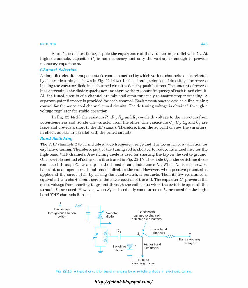
RF TUNER 443
Since C1 is a short for ac, it puts the capacitance of the varactor in parallel with C2. Athigher channels, capacitor C2 is not necessary and only the varicap is enough to providenecessary capacitance.
Channel SelectionA simplified circuit arrangement of a common method by which various channels can be selectedby electronic tuning is shown in Fig. 22.14 (b). In this circuit, selection of dc voltage for reversebiasing the varactor diode in each tuned circuit is done by push buttons. The amount of reversebias determines the diode capacitance and thereby the resonant frequency of each tuned circuit.All the tuned circuits of a channel are adjusted simultaneously to ensure proper tracking. Aseparate potentiometer is provided for each channel. Each potentiometer acts as a fine tuningcontrol for the associated channel tuned circuits. The dc tuning voltage is obtained through avoltage regulator for stable operation.
In Fig. 22.14 (b) the resistors R1, R2, R3, and R4 couple dc voltage to the varactors frompotentiometers and isolate one varactor from the other. The capacitors C1, C2, C3 and C4 arelarge and provide a short to the RF signals. Therefore, from the ac point of view the varactors,in effect, appear in parallel with the tuned circuits.
Band SwitchingThe VHF channels 2 to 11 include a wide frequency range and it is too much of a variation forcapacitive tuning. Therefore, part of the tuning coil is shorted to reduce its inductance for thehigh-band VHF channels. A switching diode is used for shorting the tap on the coil to ground.One possible method of doing so in illustrated in Fig. 22.15. The diode D1 is the switching diodeconnected through C1 to a tap on the tuned-circuit inductance L1. When D1 is not forwardbased, it is an open circuit and has no effect on the coil. However, when positive potential isapplied at the anode of D1 by closing the band switch, it conducts. Then its low resistance isequivalent to a short circuit across the lower section of the coil. The capacitor C1 prevents thediode voltage from shorting to ground through the coil. Thus when the switch is open all theturns in L1 are used. However, when S1 is closed only some turns on L1 are used for the high-band VHF channels 5 to 11.
+
Bias voltagethrough push-button
switchVaractordiode
L1
C1S1
D1Switchingdiode
Higher bandchannels
To otherswitching diodes
Bandswidthganged to channel
selector push-buttons
Lower bandchannels +
Band switchingvoltage
Fig. 22.15. A typical circuit for band changing by a switching diode in electronic tuning.
http://fribok.blogspot.com/

444 MONOCHROME AND COLOUR TELEVISION
Only one switching diode is shown in Fig. 22.15. Actually each of the tuned circuits inthe tuner has a switching diode connected to a tap on the corresponding coil. The positiveband-switching voltage is applied to all the switching diodes. Note that switch S1 is gangedwith the channel selector to apply switching voltage when higher channels are selected. Asexplained earlier the push buttons continue to apply tuning voltage to the varactors for selectingeach of the channels.
22.8 VACUUM TUBE TUNER
The tuner circuit shown in Fig. 22.16 (a) employs a twin-triode (PCC 88) in the RF section anda pentode-triode in the converter section.
RF AmplifierThe two triodes of PCC 88 connected in a cascode configuration constitute the RF amplifier.The grounded cathode stage V1 drives the grounded grid amplifier V2. The tube V1 has AGCbias and is dc coupled to the cathode of V2 through an inductor. RF input signal is appliedthrough coupling transformer T1 to the grid of V1. In its plate lead is the resonant circuitformed by Lk, C0 and Cin which form a pye type filter with a response broad enough to includeall VHF channels. The plate load of V1 is very small (input resistance looking into the cathodeof V2) and hence provides very little gain. Neutralization is affected by balancing the bridgeformed by C1, C2 (variable), Cgp and Cgk. Most of the gain (close to that of a pentode) is given bythe grounded-grid stage V2 that needs no neutralization. Since V1 and V2 are identical andsame dc current flows through them, the plate-cathode voltage for each tube is one-half of theB+ supply. The voltage divider network formed by R1 and R2 provides the necessary grid biasfor V2. The amplified signal in the output circuit of V2 is coupled by transformer T2 to the mixergrid. Tuning of all the resonant circuits is obtained by the self input and output capacitancesand no physical capacitors are normally provided. RF tuning for each station is changed byswitching coils in transformer T2.
Mixer StageThe pentode-triode combination in a single glass envelope (PCF 80) functions as a converter.RF signal is coupled through L1 and oscillator output through L3 to the grid circuit (L2) of thepentode. The local oscillator coil L3 is positioned close to the mixer grid coil (L2) for inductivecoupling. A non-linear operation of V3 is set with proper biasing obtained through both Rk-Ckin the cathode circuit and the grid-leak bias produced by the injected oscillator voltage. Thenon-linear operation results in heterodyning action.
Both plate and screen voltage dc supplies have decoupling networks to ensure properoperation of the mixer. Plate circuit of the mixer is tuned to select the desired IF band. It iscoupled to the first IF amplifier through the tuned transformer T3.
Local OscillatorA modified Colpitt’s oscillator (commonly known as ultraudion oscillator) employing the triodesection of tube PCC 80 supplies sinusoidal voltage of constant amplitude at the desired frequencyfor each channel. Special feature of this oscillator is the use of tube capacitances alone forfeedback and tuning. As shown in the equivalent circuit (Fig. 22.16(b)) of the tank circuit, theoscillator coil L3 is connected from plate to grid across Cgp. The capacitances Cpk and Cgk form
http://fribok.blogspot.com/

RF TUNER 445
a capacitive voltage divider across L3 and the oscillator voltage which develops across Cgk isfed back to the grid for sustained oscillations. Total capacitance across L3 is Cgp in parallelwith the series combination of Cgk and Cpk. The self capacitance values very between 2 to 3 pFneeding an inductance (L3) of about 1 µH for tuning channel 4 in the VHF band.
RF amplifier
B+ R1
R2 C3
V2
5 K L1
T2
Cin
LK
PCC 88
B+
T1
C2
V1C12 pF
Fromantennacircuit
1 M
0.003 F
5 to 8 pF
AGC bias
L2
56 K
150K
0.003F CKRK
PCF 80
Mixer68 pF
V3
10 K
T3
To Fsection
I
560
RFC
L3 20 pF
v4 56 K 250 V
+
0.003F
Oscillator
CT 27K
0.003 F
C0
Fig. 22.16 (a). Vacuum tube VHF tuner.
To plate :
To cathode
To grid
Cpk
Cgk
Cgp L3
Fig. 22.16 (b). Ultraudion oscillator’s equivalent circuit.
22.9 TRANSISTOR TUNERS
With their low power drain, miniature size and reliability, transistor are now universally usedin tuners of modern TV receivers. However, the transistors chosen must have the requiredhigh frequency performance, provide adequate gain and low noise figure to achieve good overallsensitivity.
While the mixer stage employs a common emitter configuration, both common base andcommon emitter configurations can be used for the RF amplifier and local oscillator. Thegrounded base circuit, needs no neutralization, but on account of its very low input impedance,
http://fribok.blogspot.com/

446 MONOCHROME AND COLOUR TELEVISION
presents matching problems. Its signal handling capacity is also low in comparison with acommon emitter arrangement. The grounded emitter configuration provides high overall gainand has a large signal handling capacity. But its parameters change with shift in the operatingpoint due to AGC action and introduce higher cross-modulation. However, this can be reducedby inserting a small unbypassed resistance in the emitter circuit.
A dual gate MOSFET transistor can also be used in the RF section. It has the advantageof good gain, high input impedance, low noise factor and less cross-modulation effects. Thedual-gate feature permits the use of simple AGC circuitry requiring very low control power.The BEL 2N300 FET has all the above merits and is employed as an RF amplifier in manytuner designs.
Transistor VHF TunerThe circuit of a commonly used transistorized VHF tuner is shown in Fig. 22.17. It employs BF196 for the RF amplifier and mixer stages, and BF 194-B in the local oscillator circuit. All thethree transistors operate in grounded emitter configuration. The 75 ohm impedance of thebalun on antenna side is matched to the input of Q1 (RF amplifier) by a tap on coil (L1) and theimpedance transforming network formed by the two capacitors (10 pF and 15 pF) which shuntthe coupling coil. Forward AGC voltage is fed at the base of BF196 via 1 KΩ resistance and adecoupling network. The 47 ohm resistance inserted in the base circuit helps to suppress any
+ 15 V
1 K
From antennacircuit
470pF
Balun
L1
470pF
T1
10 pF
15pF
1 K 3 n
3 n
47
1 K
620
BF 196
5.6pF
Q1
C2
AGC bias
L2T2
L3C4
L43 n
C1
390VCC
+ 15 V
8.2K
10 pFC3
2.7 pF
10pF
C5
C63 pF
1nF
2 K
+ 15 V22 KOscillator
2 pF L5
1 K2 pF
33pF
BF 194
1 k
Q3
1 n3 n
+ 15 V
3 K
470
D
C71 nR3
10 K
R23.3 K
Finetuning
3 n 10pF
150
T3
To Famplifier
I
Q2
BF 196Mixer
1 K
Fig. 22.17. Transistor VHF tuner.
http://fribok.blogspot.com/

RF TUNER 447
parasitic oscillations. The RF amplifier output circuit is double-tuned and mutually coupledthrough common inductor L4. Note that capacitors C2 and C3 are effectively in parallel with L2,L4 and L3, L4 respectively to provide tuning. The cores of L2 and L3 are adjusted to obtain abroad tuning with peaks at the picture and sound carrier frequencies.
The output from the RF amplifier is coupled to the base of mixer transistor Q2 throughthe voltage divider and matching network formed by capacitors C4 and C5. The oscillator outputis also fed at the base of Q2 through capacitor C6. The mixer output circuit is double tuned andfeeds the first IF amplifier. The 150 ohm resistor across the secondary winding of T3 is adamping resistance to achieve broad tuning.
In the local oscillator circuit, L5 in parallel with a 2 pF capacitor constitutes the tankcircuit. The oscillator output frequency is adjusted by varying L5. A varactor diode D is usedfor fine tuning. As shown in the circuit, it is connected in parallel with the tank circuit. Reversebias voltage to the diode is fed through the voltage divider formed by R2 and R3. Thepotentiometer R3 is provided on the front panel of the receiver. It serves as fine tuning controlbecause varying R3 changes the reverse bias voltage and hence the capacitance across the tankcircuit. The capacitor C7 blocks dc voltage shorting to ground.
22.10 UHF TUNERS
There are two types of UHF tuners. In one type the converter section of the UHF tuner convertsthe incoming signals from the UHF band (470 to 890 MHz) to the VHF band. Usually the UHFchannels are converted to VHF channel numbers 5 or 6 and the VHF tuner, in turn, processesthese signals in the usual way. Since the relative positions of video and sound IFs are specified,the converter oscillator of the UHF tuner is tuned to a frequency lower than the incomingUHF signal to take into account the double-heterodyning action involved.
In the second type, the UHF signal is heterodyned with local oscillator output to translatethe incoming channel directly to the IF band. The output thus obtained from the UHF tuner iscoupled to the VHF tuner, where the RF amplifier and mixer stages operate as IF amplifiers,when the VHF station selector is set to the UHF position. In this position the VHF oscillator isdisabled by cutting off its dc supply. The RF tuned circuits are also changed to IF tuned circuits.
In present day tuners, this type is preferred. Figure 22.18 illustrates the block schematicof this circuit. Separate antennas are used for VHF and UHF channels. The UHF tuner doesnot employ an RF amplifier because the input signal strength being very low is comparable tothe noise generated in the RF amplifier. If used it lowers the signal-to-noise ratio and fails toboost the signal level above the noise level. Therefore, the incoming UHF signal is directlycoupled to the mixer where a diode is used for heterodyning instead of a transistor or a specialtube. The reason for using a diode is two-fold. Firstly, the local oscillator output at ultra highfrequencies is too low to cause effective mixing with an active device whereas it is adequatewhen a diode is employed. Secondly the noise level with a diode is lower than when an activedevice is used. Since the diode is a non-linear device it can produce beating of the incomingchannel frequencies with the local oscillator frequency to generate side-band frequencies.
http://fribok.blogspot.com/

448 MONOCHROME AND COLOUR TELEVISION
Antenna inputcircuit
Diodemixer
Localoscillator
Antenna inputcircuit
RF amplifier (VHF)
IF amplifier (UHF)
Mixer (VHF)
IF amp (UHF)
Local oscillaltor (VHF)
Oscillator disabled (UHF)Finetuning
IF out
P – 38.9 MHzS – 33.4 MHzC – 34.47 MHz
UHF antenna
VHF antenna
Fine tuning
Fig. 22.18. Block diagram of a UHF-VHF tuner.
The weak output from the UHF tuner is coupled to the VHF tuner where both the RFamplifier and mixer stages acts as IF amplifiers to boost the signal to the level normally obtainedwhen a VHF channel is tuned.
In conclusion the various functions performed by a television receiver tuner may besummarized as follows:
1. It selects the desired station and rejects others.2. It converts all incoming channel frequencies to a common IF band.3. It provides gain to the weak input signal picked up by the antenna. This improves
S/N ratio and reduces snow on the picture.4. It isolates the local oscillator from the feeder circuit to prevent undesired radiation
through the antenna.5. It improves image rejection ratio and thus reduces interference from source operating
at frequencies close to the image frequencies of various channels.6. It prevents spurious pick-ups from sources which operate in the IF band of the receiver.7. It provides matching between the antenna and input circuits of the receiver, thus
eliminating the appearance of ghost images on the screen.8. It rejects any pick-up from stations operating in the FM band.9. It has provision to select any channel out of the various allotted in the VHF and UHF
bands for TV transmission.10. It has a fine tuning control for accurate setting of the selected station.
Review Questions
1. Describe with a simple block diagram the circuit arrangement of a VHF tuner. Why does an RFamplifier stage always precede the mixer ?
http://fribok.blogspot.com/
RF TUNER 449
2. Describe different impedance coupling circuits which are often employed between the RF amplifierand mixer. Sketch typical frequency response of the RF amplifier.
3. Why is neutralization applied to high frequency amplifier circuits ? Describe with circuit diagramsthe methods which are normally employed for neutralization in transistor amplifier circuits.
4. Describe with suitable sketches different types of mechanical switching arrangements used forchannel selection in tuners. What are ‘feed through’ capacitors and why are they used in a tunersub-assembly ?
5. Draw detailed block schematic circuit of a VHF tuner and give necessary details of balun andfilter circuit configurations provided at the input of the tuner. Why is a fine tuning control providedin all tuners ?
6. Describe briefly the basis design requirements that must be met in the RF amplifier mixer andlocal oscillator of a tuner for a stable and snow free reproduction of the picture.
7. What is electronic tuning ? Explain with circuit diagrams how different channel can be selectedby this method.
8. The circuit diagram of a typical vacuum tube tuner is shown in Fig. 22.16 (a). Explain fully, howthe circuit functions to produce frequency translation of all incoming channels to the common IFband. Why a cascode configuration has been employed in the RF section of the tuner ?
9. A commonly used transistor VHF tuner is shown in Fig. 22.17. Explain its working and thefunction of all the components used in the tuner.
10 Describe with a block schematic diagram the working principle of a UHF tuner. Why is an RFamplifier not used in UHF tuners ?
http://fribok.blogspot.com/

23
http://fribok.blogspot.com/

The tuner selects the desired TV channel and converts its band of frequencies to the intermediatefrequency band of the receiver. While the total bandwidth of the channel is 7 MHz, the pictureand sound intermediate frequencies are separated by 5.5 MHz. The receiver intermediatefrequencies have been fixed at 33.4 MHz for the sound signal and 38.9 MHz for the picturesignal. In the PAL colour system, colour subcarrier frequency is located 1.07 MHz before thesound carrier and its IF frequency is 34.47 MHz. Thus the band of frequencies to be handled bythe IF sections of both monochrome and colour receivers lies between 33.15 MHz to 40.15MHz. Practically all the gain and selectivity of the receiver is provided by the IF section.
As shown in the block diagram of Fig. 23.1, in colour receivers the sound take-off pointis at the 3rd video IF amplifier. In monochrome receivers, where video and sound detectionoccurs together, the sound IF is separated at the output of the video detector. The video detectoroutput feeds the video amplifier, sync separator and AGC circuits.
Colour receiver
Sound IFdetector
3rd video IFamplifier
Videodetector
To soundIF amplifier(5.5 MHz)
Video ampAGC circuitSync separator
Monochromereceiver
2nd video IFamplifier
1st video IFamplifier
AGC bias
Coaxial cableFrom
mixer output
Picture IF = 38.9 MHzSound IF = 33.4 MHzColour IF = 34.47 MHz
Fig. 23.1. IF section and sound take-off points for monochrome and colour receivers.
23.1 VIDEO IF SECTION
The desired overall response curve of the IF section of a black and white receiver and that of acolour receiver are shown separately in Fig. 23.2. In a monochrome receiver (Fig. 23.2 (a)) thesound IF lies at about 5% of the maximum amplitude because of intercarrier sound detectionrequirements. However, in colour receivers (see Fig. 23.2 (b)) where the sound take-off is beforethe video detector, the sound IF lies at almost zero level on the overall IF response curve. Thisis so because sound signal is no longer required in the video detector and if present can resultin sound bars on the reproduced picture. Therefore, an additional trap circuit is provided at
452
http://fribok.blogspot.com/
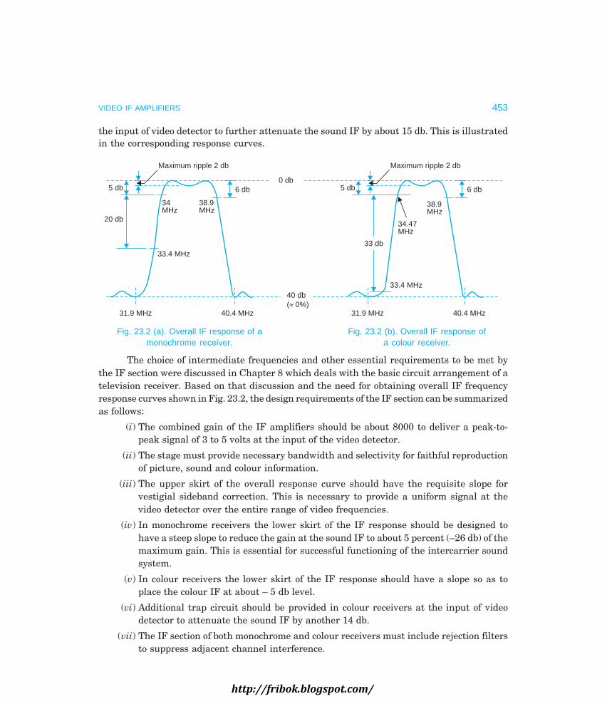
VIDEO IF AMPLIFIERS 453
the input of video detector to further attenuate the sound IF by about 15 db. This is illustratedin the corresponding response curves.
Maximum ripple 2 db
6 db
38.9MHz
34MHz
5 db
20 db
33.4 MHz
31.9 MHz 40.4 MHz
Maximum ripple 2 db
6 db
38.9MHz
34.47MHz
5 db
33.4 MHz
31.9 MHz 40.4 MHz
33 db
0 db
40 db( %)» 0
Fig. 23.2 (a). Overall IF response of a Fig. 23.2 (b). Overall IF response ofmonochrome receiver. a colour receiver.
The choice of intermediate frequencies and other essential requirements to be met bythe IF section were discussed in Chapter 8 which deals with the basic circuit arrangement of atelevision receiver. Based on that discussion and the need for obtaining overall IF frequencyresponse curves shown in Fig. 23.2, the design requirements of the IF section can be summarizedas follows:
(i) The combined gain of the IF amplifiers should be about 8000 to deliver a peak-to-peak signal of 3 to 5 volts at the input of the video detector.
(ii) The stage must provide necessary bandwidth and selectivity for faithful reproductionof picture, sound and colour information.
(iii) The upper skirt of the overall response curve should have the requisite slope forvestigial sideband correction. This is necessary to provide a uniform signal at thevideo detector over the entire range of video frequencies.
(iv) In monochrome receivers the lower skirt of the IF response should be designed tohave a steep slope to reduce the gain at the sound IF to about 5 percent (–26 db) of themaximum gain. This is essential for successful functioning of the intercarrier soundsystem.
(v) In colour receivers the lower skirt of the IF response should have a slope so as toplace the colour IF at about – 5 db level.
(vi) Additional trap circuit should be provided in colour receivers at the input of videodetector to attenuate the sound IF by another 14 db.
(vii) The IF section of both monochrome and colour receivers must include rejection filtersto suppress adjacent channel interference.
http://fribok.blogspot.com/

454 MONOCHROME AND COLOUR TELEVISION
23.2 IF AMPLIFIERS
It is now obvious that the IF section of both monochrome and colour receivers is essentially thesame but for small differences in the response curves. Each IF stage is a tuned amplifier.Because of the selective properties of the tuned amplifier the gain is quite large and falls offsharply at frequencies that lie on either side of the passband. In some IF circuit designs adouble tuned circuit is used for coupling one stage to the other. This circuit arrangement isshown in Fig. 23.3 where Cin and Cout are the self shunting capacitances of the input andoutput circuits respectively. Their values are generally of the order of 10 to 15 pF.
C1 R1 R2C2
B+ AGC bias
C0Cin
To base or gridof next stage
IF transformer
From collector orplate of previousstage
Fig. 23.3. Double tuned transformer of an IF amplifier.
Thus the required values of inductance are between 1 and 2 µH for resonance at about40 MHz. Usually Lp and Ls each have a slug for tuning the primary and the secondary circuits.Besides the use of double-tuned circuits the quality factors of the tuned circuits are lowered toachieve desired bandwidth. This is affected by connecting damping resistors across the tunedcircuits.
In Fig. 23.3, R1-C1 and R2-C2 are decoupling networks for the dc supply and AGC circuitsrespectively. It may be noted that C1 and C2 are actually parts of the tuned circuits. C1 returnsLp to Cout and C2 returns Ls to Cin to form resonant circuits.
Several tuned amplifier stages are cascaded together to provide a large gain to amplifythe weak RF signal received from the mixer. Each stage operates under class ‘A’ condition forminimum distortion. At least one stage is AGC controlled to change the gain in accordancewith changes in the signal picked up by the antenna so as to deliver a signal of almost constantpeak to peak amplitude to the video detector. The last IF stage is not fed with AGC biasbecause here the signal amplitude is quite large and any shift in the operating point by theAGC bias would result in amplitude distortion.
The overall design of the video IF strip becomes quite complex because in addition togain and bandwidth, matching of tuned circuits, stability, neutralizing and trap circuits arealso to be taken into account for proper functioning of the video IF section.
Neutralizing and matching of tuned circuits were discussed at length in the last chapter.The same problems are there in the video IF stages. However, here matching and neutralization
http://fribok.blogspot.com/

VIDEO IF AMPLIFIERS 455
are less difficult because the operating frequency range is narrow, fixed and much lower thanthat obtained in tuner circuits.
23.3 VACUUM TUBE AND SOLID-STATE IF AMPLIFIERS
Video IF amplifiers employ miniature pentodes which may not need any neutralizing. Two orthree stages in cascade are enough to provide the necessary gain of about 70 db. In vacuumtubes the input and output impedances are fairly high even at very high frequencies and so thequality factor Q, of the coupling networks remains high, thus enabling higher gain per stage.Furthermore, in tube circuits, the input and output impedances are comparable and so thisdoes not present any serious impedance matching problems.
All present day receivers employ transistors and ICs in the IF section. In transistor IFamplifiers, three or four stages of tuned amplifiers become necessary to obtain the desiredgain. This is so because the low input impedance of the common emitter configuration at veryhigh frequencies shunts the tuned circuit to lower its Q, and this results in reduced gain perstage. The wide difference in the input and output impedance levels necessitates the use ofspecial coupling techniques in transistor amplifiers. The junction capacitance is also large andmakes neutralizing necessary for stable operation.
Integrated circuits have been developed where one chip contains all the three or four IFstages. It also includes the video detector and other allied circuits. The ICs do not, however,contain IF transformers or other coupling impedances. Tiny IF transformers and other circuitcomponents not included in the integrated circuit are mounted around the IC module. TheseICs are used in both hybrid and all-solid state receivers.
Amplifier BandwidthThe overall bandwidth, gain and waveshape of the response curve, close to the ideal (Fig. 23.2)can be achieved in two ways—by synchronous tuning or by stagger tuning of the individualstages. In synchronous tuning the stages are tuned to the same centre frequency and theresponse of each stage is suitably designed to provide the required overall response. However,
1.0
0.707
0.5
0f0
f
B.W.
Response curve ofindividual stages
Overall response curve oftwo identical tuned circuits
Rel
ativ
eam
plitu
de
B.W.0.64
Fig. 23.4. Comparison of response curve of an individual stage with overallresponse curve of an identical cascaded pair.
http://fribok.blogspot.com/

456 MONOCHROME AND COLOUR TELEVISION
when cascaded amplifiers are tuned to the same frequency the overall bandwidth shrinksdrastically. The reason is that overall gain equals the product of individual gain values, nottheir sum. Then the peak values become more peaked while the low-gain frequencies becomemore attenuated. Figure 23.4 illustrates the response of individual stages and overall responsewhen two identical stages are cascaded. As is obvious from the overall response curve, thepeak value become more peaked while the low-gain frequencies are reduced in amplitude. Theresultant sharp peaked response with narrow bandwidth is undesirable for the wide passbandneeded in the video IF amplifier. Thus if synchronous tuning is to be used a large number of IFstages, each designed to have a very wide bandwidth, would be necessary to achieve desiredselectivity and gain. This obviously turns out to be very difficult and hence is not much used.
Stagger TuningConsider two single tuned amplifiers each with the same bandwith ∆1 but with their centrefrequencies separated or staggered by an amount equal to the bandwidth (∆1). The individualresponse curves are illustrated in Fig. 23.5 (a), and the overall response of the pair is shown in
Fig. 23.5 (b). As a result of stagger tuning the overall bandwidth (to 0.707 point) is 2 times
the bandwidth of a single stage. It is also seen that staggering has reduced total amplificationat the centre frequency (f0) to half the value obtained before detuning. This is so because at thecentre frequency each detuned stage has an amplification of 0.707 of the peak amplification ofthe individual stage (0.7 × 0.7 = 0.5). Thus the equivalent voltage amplification per stage of thestaggered pair is 0.707 times the amplification of the same two stages when used withoutstaggering.
1.0
0.707
0.5
0
(a) f0f0f
Rel
ativ
e re
spon
se
1.0
0.707
0.5
0
(b) f0f
Rel
ativ
e re
spon
se
∆1∆1 ∆∆1
∆1
2
22 ∆1
∆1
2
1.0
0.707
0.5
0.35
Rel
ativ
e vo
ltage
am
plitu
de
0f0
f
(c)
0.64 ∆1
∆2 12 ∆1
∆1∆1
Fig. 23.5. Basic relationships in a stagger-tuned pair and its comparison withsingle-tuned and double-tuned circuits (a) response of individual stages in a staggered pair(b) overall characteristics of the pair (c) comparison of non-staggered and staggered pairs.
It may be noted that, since amplification curve of the stagger tuned pair has a bandwidthcorresponding to that of a critically coupled double-tuned stage, the half-power bandwidth of
http://fribok.blogspot.com/

VIDEO IF AMPLIFIERS 457
the staggered pair is 2 times as large as the half-power bandwidth (∆1 = f0/Q) of an individual
single-tuned stage. Hence the equivalent nominal gain-bandwidth product per stage of a stagger-
tuned pair is 0.707 × 2 = 1.00 times that of the individual single-tuned stages.
Next consider that stagger tuning is retained but the bandwidth of individual tunedcircuits is decreased. This is illustrated in Fig. 23.5(c) where overall response of the two stagestagger tuned pair is compared with the corresponding two-stage non-staggered pair havingthe same resonant circuits. By readjusting circuit Q’s and by detuning to give the staggeredpair the same bandwidth as that of an individual single-tuned stage, it is possible to obtain astaggered pair which has the same equivalent voltage amplification per stage as that of thesingle-tuned stage. Thus two-stage staggering systems will have the characteristics shown bythe outer curve in Fig. 23.5 (c).
To clarify this further, suppose that the bandwidth of each individual stage is decreasedto 0.707 of its original value. To do this ‘Q’ of the individual circuit is raised to 1.4 times itsprevious value, which will increase the gain by a factor of 1.4. Now if the stages are staggeredby an amount equal to the reduced bandwidth, the overall gain is one-half the product of 1.4times 1.4, i.e., 1/2(1.4 × 1.4) = 1. Thus the overall gain is equal to that obtained earlier whenboth circuits were tuned to the same frequency. This is the effect of stagger tuning.
Note that in comparison, the two-stage indentically tuned system with the same gainper stage, as the staggered pair under consideration, will have a bandwidth of only 0.644 timesthat of the staggered pair. This is because of the narrowing which results when two identicallytuned single-tuned stages are cascaded. This is also illustrated in Fig. 23.5(c).
The concept of stagger tuning is extended to all the three IF stages to get the desiredbandwidth. As shown in Fig. 23.6 (a) each circuit is tuned to a different centre frequency. TheQ of the coil tuned to the centre frequency of the band is considerably lowered by damping toget a broad response in the middle range of frequencies. The final response of the triplet isshown in Fig. 23.6 (b).
1.0
0.707
0 f01 f02 f03 f(MHz)
(a)
Rel
ativ
e re
spon
se
1.0
0.707
0f(MHz)
(b)
Rel
ativ
e am
plitu
dere
spon
se
B.W 5 MHz»
Fig. 23.6. Illustration of stagger—tuning when extended to all the three IF stages.(a) response of individual stages each tuned to a different centre frequency
(b) final response of the triplet when Q of each stage is readjusted to a suitable value.Q of fo2 (circuit) < Qs of fo1 and fo3 circuits.
http://fribok.blogspot.com/

458 MONOCHROME AND COLOUR TELEVISION
A similar response can be achieved by employing double-tuned circuits in all the threeIF stages. However, stagger tuning is preferred since it is (i) less expensive, (ii) easy to tuneand (iii) more stable because no two circuits have the same centre frequency and therefore theprobability of self-oscillations on account of feedback is low.
Interstage CouplingThe stagger tuning described above is a method of obtaining desired bandwidth and is not aform of coupling. Stagger tuning can be accomplished with either transformer coupling or withimpedance coupling. Figure 23.7 (a) is an example of impedance coupling often used in vacuumtube IF stages. AGC bias is fed through R2 at the control grid. In the absence of any signalAGC voltage drops to zero and the small cathode resistor R1 prevents the tube from beingoperated without bias. The plate load consists of a tunable coil. The output signal is takenacross this (IF) coil and delivered to the next stage through a capacitor.
A similar coupling arrangement in transistor circuits is shown in Fig. 23.7 (b). However,in this circuit a tap on the coil provides better impedance match to the low input impedance ofthe transistor employed in the next IF stage.
To plateof previous
stage
IFcoil
AGCbias
R4
R2
R1
C1
C0
C2
R5
To gridof nextstage
IFcoil
R3B+
Decouplingnetwork
C3
(a)
vin
R2
Ci
IFcoil
Cc
v0
C1 R1
+ VCC
AGC
(b)
Fig. 23.7. Typical examples of impedance coupling in IF amplifier stages(a) in vacuum tube circuits (b) in transistor circuits.
Bifilar IF CoilsThis type of coil has two windings like a transformer but is not double-tuned. As shown inFig. 23.8 (a), a bifilar coil is wound with twin conductor wires each insulated from the other.One winding is for the plate or collector and the other winding is for the grid or base of the nextstage. Because of unity coupling the output is essentially a single-peaked response, becausethe double-humped overcoupled response changes into two independent peaks which are widelyseparated. Only one of the peaks (the lower frequency one) is used for tuned amplifierapplications. Since the IF signal is inductively coupled to the next stage, no coupling capacitoris needed. Only the primary is tuned and the coil acts like a single-tuned circuit. Because ofthese merits it is widely often used in IF stages. The circuit of the coupling network employinga bifilar coil is shown in Fig. 23.8 (b). A tuning slug is moved inside the former on which the coilis wound for tuning to the desired frequency.
http://fribok.blogspot.com/

VIDEO IF AMPLIFIERS 459
P S
P S
Symbol
Slug adjustingscrew
Primary
Secondary
Primary
SecondaryCoil
former
(a) (b)
Bifilar coilcoupling
From 1st IFamplifier 10 K
R1C1
RK
AGC
C2 R2
B+
To next IFamplifier
Fig. 23.8. Bifilar IF coil and coupling (a) pictorial view and symbol (b) typical coupling circuit.
Link-couplingThis method is generally used to couple the IF signal from mixer to first IF stage on the mainchassis. The circuit arrangement is shown in Fig. 23.9. The link from tuner to the IF stage is a75 ohms coaxial cable with shielded plugs at both ends to couple the signal at a low impedancelevel. As a result, the effect of stray capacitance is minimized. Since the shield of the cable isgrounded, it prevents any pick-up from interfering signals. The shielded cable also preventsany radiation of the mixer output which otherwise can cause interference in the receiver. Asshown in Fig. 23.9, the secondary of the transformer T1 has just a few turns for a stepdown ofvoltage and impedance to provide a match to the coaxial cable. Similarly at the other end ofthe cable a step-up transformer T2 is provided to raise the signal voltage that is fed to the gridor base of the first IF amplifier stage. Thus the IF signal is effectively coupled from the mixeroutput to the IF input by means of a low impedance coaxial cable of suitable length withoutradiation or any stray pick-up. The link coupling generally has the response of an overcoupledstage.
From mixer plateor collector
C0
L1 L2
T1
C1 R1
B+
Coaxial cable
L3 L4
T2
R2 C2
Cin
To 1st IF amplifier’sgrid or base
AGC bias
Fig. 23.9. Link coupling from mixer output to the input of1st IF amplifier on the main chassis.
http://fribok.blogspot.com/

460 MONOCHROME AND COLOUR TELEVISION
23.4 VESTIGIAL SIDEBAND CORRECTION
The need for vestigial sideband correction was clearly established in Chapter 4 which dealswith channel bandwidth requirements. As explained there, if such a correction is not applied,frequencies between dc to 0.75 MHz will appear twice in the video detector output and thusproduce an output that is double of that at higher video frequencies. Also, frequencies that liebetween 0.75 to 1.25 MHz will have intermediate values because of the attenuation slope inthis region at the transmitting end. The result of this would be that frequencies up to 0.75MHz will get undue emphasis as compared to higher video frequencies. The extra gain for lowvideo frequencies increases contrast in the reproduced picture that is usually accompanied byexcessive smear. Similarly, a relatively lower emphasis of the high video frequencies reduceshigh frequency detail that is essential to make the picture sharp and clear. This clearlyestablishes the need for vestigial sideband correction.
In order to equalize the effect of vestigial sideband transmission, the overall IF responseis aligned to give the picture carrier approximately 50 percent of maximum response as shownin Fig. 23.2. As a result, sideband frequencies of the double sideband signal are allowed anaverage response of 50 percent as compared to 100 percent response for the single sidebandfrequencies. Thus at low frequencies, the output that results from the two sidebands adds upto give an output equal to that at higher video frequencies. The relative output from the videodetector will then be the same for all video modulating signals having the same amplitude,irrespective of whether they are transmitted with single or double sidebands. The necessaryattenuation slope around the picture IF frequency is provided by suitably choosing the centrefrequencies of the IF stages and also by varying their coefficient of coupling. Additional filter(trap) circuits are also used to control the exact shape of the IF section response.
23.5 THE IF SOUND SIGNAL
The picture and sound IF signals are amplified together in the IF section of the receiver.However, the gain around the sound IF frequency is reduced to about 5 percent of the maximumgain, both for successful working of the intercarrier sound system and to avoid appearance ofsound bars on the screen. Special rejection filters (trap circuits) are provided normally at theinput of the first IF stage, to achieve the desired attenuation slope.
23.6 ADJACENT CHANNEL INTERFERENCE
Several interfering signals are picked up by the receiver antenna along with the signal fromthe selected channel. Many of these are suppressed in the RF tuner and do not reach the firstIF stage. However, some adjacent channel interfering signals are so strong and close to theselected channel, that they pass through the tuner section, and appear at the input of the firstIF stage. The major sources of interference are the difference products of the local oscillatorfrequency beating with the sound carrier of the lower adjacent channel and the picture carrierof the upper adjacent channel. As explained in Chapter 8, these occur at 40.4 MHz and 31.9MHz, i.e., at the two edges of the IF pass-band. It is essential to reject them at the output of RFtuner, because the IF stages provide a very large gain and it is very difficult to remove such
http://fribok.blogspot.com/

VIDEO IF AMPLIFIERS 461
signals once they pass through the IF section. Therefore, trap circuits that provide a rejectionof at least 40 db are included at the input of the first IF stage to stop their passage to thesucceeding IF stages. The effect of such trap circuits is illustrated in the response curve ofFig. 23.2.
IF Wave TrapsA wave trap is a resonant circuit tuned to attenuate a specific frequency. Basically there arefive types of trap circuits used at the input of the video IF amplifiers. These are (a) seriestuned, (b) parallel tuned, (c) absorption type, (d) degeneration type and (e) bridge typeconfigurations.
(a) Series trap circuit—The series trap is a parallel resonant circuit. It offers very highimpedance at the rejection frequency to which it is tuned. It is connected in series between twoIF stages as shown in Fig. 23.10 (a). Since the trap is a sharply tuned-circuit designed to rejectone frequency or at most, a narrow band of frequencies, it offers negligible impedance to allother frequencies and thus the desired signal is passed without any attenuation.
(b) Parallel trap circuit—This trap is a series resonant circuit connected in shunt withthe path of the IF signal. Its impedance is very small at the frequency to which it is tuned. Itthus acts as a short at the frequency that is to be rejected and bypasses it to ground. Itsconnection in the IF stage is illustrated in Fig. 23.10 (b). It is important that the parallel trapcircuit has a very high Q so that is rejects only a narrow range of frequencies.
(a) (b)
Trapcircuit
vin
v0
VCC
Trap circuit
vin
v0
VCC
Fig. 23.10. Trap circuits in IF amplifier configurations (a) series (parallel resonant)trap circuit (b) shunt (series resonant) trap circuit.
(c) Absorption trap circuit—The absorption trap circuit shown in Fig. 23.11 (a) isinductively coupled to the plate or collector load inductance of the IF stage. The trap is tunedto the frequency that is to be rejected. As a result, at this frequency maximum current flowswithin the trap circuit. Since the trap circuit draws energy from the tuned load coil, a sharpdecrease in the Q of the tuned load circuit occurs with the result that the stage gain at theundesired frequency is very much reduced. This amounts to a large attenuation at the frequencyto which the absorption trap is tuned.
(d) Degenerative trap circuit—This circuit, illustrated in Fig. 23.11 (b), applies a largenegative feedback to the IF amplifier at the frequency to be rejected. A parallel L-C circuit isinserted in the cathode or emitter lead of the tube or transistor employed in the IF stage. Thecircuit is tuned to the frequency that is to be attenuated. Thus, at resonance, it develops a
http://fribok.blogspot.com/

462 MONOCHROME AND COLOUR TELEVISION
large voltage across it which results in a sharp fall in the gain because of the degenerativeaction. At all other frequencies the impedance of the trap circuit is very small and hencepractically no degenerative feedback occurs at these frequencies.
(b)
Degenerativetrap circuit
v0
VCC
vin
(a)
v0
VCC
Absorptiontrap circuit
vin
Fig. 23.11. Resonant trap circuits (a) absorption (b) degenerative.
(e) Bridged ‘T’ trap circuit—The circuit configuration of a bridged ‘T ’ filter is shown inFig. 23.12 (a). The special feature of this circuit is that the value of R is so chosen that iteffectively cancels the coil resistance. Then the parallel resonant circuit formed by L, C1 andC2 attains a very high Q. The values of L, C1 and C2 are suitably chosen to reject the desiredfrequency. Because of the large effective Q, this network is highly selective. It is put in serieswith the signal path and the slug in the trap coil is varied for minimum output. An attenuationof the order of 40 db can be easily attained if necessary. The circuit of Fig. 23.12 (b) is anotherversion of this trap circuit. The bridged ‘T ’ trap is most widely used because of its highlyselective attenuation characteristics.
(a)
vin
C1 C2
R v0
L
(b)
R v0
L
vin
C
Fig. 23.12. Two different configurations of a bridged ‘T’ trap circuit.
IF AlignmentIt is obvious from the discussion in the preceding sections that several stringent requirementsmust be met while tuning the IF station of the receiver. This is normally carried out with asweep generator and the output from the video detector is displayed on a cathode-ray oscilloscope
http://fribok.blogspot.com/

VIDEO IF AMPLIFIERS 463
screen for ease of tuning. The sweep generator has markers which are used for locating variousfrequencies on the displayed pattern for tuning the coils. The detailed procedure for tuning theRF and IF stages of a TV receiver is explained in a subsequent chapter.
23.7 VIDEO IF AMPLIFIER CIRCUITS
A typical circuit of a monochrome receiver IF stage employing tubes is shown Fig. 23.13. Allthe three tubes are miniature pentodes having very low interelectrode capacitances. Only thefirst stage is AGC controlled. Additional bias voltage has been provided through thepotentiometer network R1 and R2 from the screen voltage dc supply. This ensures operation inthe linear region. A part of the cathode resistor of both V1 and V2 has been left unbypassed inorder to provide negative feedback. This results in overall stability of the stage. However, nosuch feedback is necessary in the last stage. The dc supply to the plate and screen grid circuitsof all the tubes is through decoupling networks in order to avoid any interaction amongst thethree sections of the amplifier.
L4L3L2
L1
C1 C233pF
68pF
10 pF 15 pFFromtuner
Coaxial cable
40.4 MHz 33.4 MHz 31.9 MHz
10K
15 KT1
V1
3n 10K
1 KT2
V2
3n 1 KT3
3n
To videodetector
+ 200 VT , T , T are
bifilar transformers1 2 3
EF183 EF184 EF184
1503n
3n
1 K
1503n
+ 200 V+ 200 VAGC
3n3n
R182R2
3n
L5 22+
1.5 K3n
1n
Fig. 23.13. Vacuum tube video IF amplifier.
The coupling between the stages is through bifilar wound coils. The secondary circuitsof the coupling transformers T1 and T2 are shunted by suitable resistors for obtaining thedesired bandwidth. The overall voltage gain can be varied between 6000 to 10,000 by the AGCbias. At the input of the first stage, coil L5 resonates with the input capacitance of V1 to couplethe signal from the tuner to its control grid. The tapping on this coil is for impedance matchbetween the coaxial cable and input circuit of the first IF amplifier.
A three section filter is connected at the input of IF section to prevent entry of interferingsignals into the amplifier. The first section is tuned to reject interfering signal from the upperadjacent channel. This section is a modified form of the parallel trap circuit. Coil L1 and capacitorC1 are tuned to 40.4 MHz to reject this frequency. However, coil L2 that forms a parallel resonant
http://fribok.blogspot.com/

464 MONOCHROME AND COLOUR TELEVISION
circuit with C1 is tuned to a frequency somewhat higher than the interfering signal frequency.This ensures a steep rise in impedance just after a sharp fall at 40.4 MHz. This also helps toshape the upper skirt of the IF response curve and no separate trap circuit has been used tolower the gain at the picture IF for vestigial sideband correction. The second filter sectionattenuates the IF sound signal (33.4 MHz) to the desired level. The third section is a seriestrap circuit tuned to reject the lower channel interfering frequency of 31.9 MHz. The entirefilter section and coupling transformers are shielded to avoid any radiation and undue couplingwith each other.
IF Section Employing TransistorsThe circuit shown in Fig. 23.14 is that of a three-section four-transistor video IF amplifier.Each one of the transistor has a very high cut-off frequency and a relatively low junctioncapacitance.
270
L8
T3
3n5.6K
5pF To videodetector
Q4
4703n
3n
2.7K
C4
C5
68pF
22pF8.2K
T2
L7
330
+ 27 V
330820
RFCL6
3n
8.2K
3n
3K 10pF
Q3
T1
C2
15pF
3n
6.8KRE 10W
Q233pF
3n2.7K
580
3303n
C3
22pF
1.2K3n
Q1
C1
22pF
22pF
2.7KL4
15pF10pF
33pF
L3L2
L1
18pF
From tuner
31.9MHz
33.4MHz
40.4MHz
3n
3n
AGC
L5
4K
R1
15K
Fig. 23.14. Video IF amplifier with cascoded interstage.
At the input of the first IF amplifier stage a three section filter is provided. The firstsection is a series trap that blocks the lower channel interfering frequency. Similarly, the thirdsection filters out the upper channel beat frequency. Section two of the filter unit is designedto attenuate the sound IF frequency to about 20 db below the picture IF level. Coil L4 is forfrequency compensation against the low input impedance of the common emitter configuration.This coil is shunted by a resistor (R1) to damp any oscillations.
Coils L5 to L8 are IF chokes inserted in the dc supply lines and the AGC circuit. Thesignal frequencies are thus contained within the respective stages and returned to groundthrough separate decoupling capacitors. Besides this, the biasing circuits and the collectorsupply points are provided with separate decoupling networks. Hence stable operation is ensuredwithout any possibility of self-oscillations due to mutual coupling paths. The IF signal is coupledto the base of transistor Q1 through the coupling capacitor C1. AGC is fed only to the first
http://fribok.blogspot.com/

VIDEO IF AMPLIFIERS 465
amplifier and the remaining two stages employ self biasing. The collector load is a single tunedcircuit set at a suitable frequency for stagger-tuning. The output from the load circuit (T1) iscoupled to the base of Q2 through capacitors C2 and C3 which form a voltage divider in additionto providing impedance match between the two stages.
The second stage combines a grounded emitter stage (Q2) that drives a grounded base(Q3) amplifier. The output of Q2 is dc coupled to the emitter of Q3. The two transistors thuscombine to form a cascode pair which gives somewhat large gain compared to a single stagewith large bandpass characteristics. The transistor Q2 is not neutralized because it has verylow collector load impedance. RE is a 10 ohms resistor inserted in the emitter lead of Q3 forthermal stabilization. Most of the gain is in the grounded-base stage Q3, which needs noneutralization. The primary winding of transformer T2 is a tuned circuit connected at thecollector of Q3. The impedance match to the next stage is achieved through the secondarywinding of T2 and capacitors C4 and C5. The third IF amplifier has again a common emitterconfiguration employing a single coil tuned load. The secondary is wound for impedancematching and feeds into the cathode of the diode that is a part of the video detector.
IF Amplifiers Using FETsSome receiver designs employ dual-gate MOSFETs in the IF section. With their high inputand output impedances, matching problems between succeeding stages are greatly simplified.Normally, three stages in cascade provide the desired gain and selectivity. One gate of theMOSFET receives the signal while the other gate is fed with bias from AGC line. With rapidadvances in IC technology, MOSFETs and transistors have been replaced with IC modules inthe IF section.
23.8 IF SUB-SYSTEMS EMPLOYING ICs
Many dedicated ICs have been developed which include AGC, video detector, and soundconversion circuits besides a multisection IF amplifier. Some of such ICs also include provisionsfor processing chroma (colour) signal and part AFT (automatic frequency tuning) control circuits.
Initially when a synchronous demodulator IC (TCA 540) became available it was widelyused in the IF section of solid state receivers in conjunction with IF amplifiers employingtransistors BF 167 and BF 173. However, such circuits have now been superseded by monolithicICs which incorporate many other functions besides video IF amplification. BEL CA 3068 isone such IC the description of which follows.
Video IF Sub-system CA 3068The BEL CA 3068 is a 20 lead quad-in-line (plastic package) IC specially designed to
perform as a complete IF sub-system in monochrome and colour receivers. This package includesa wrap around shield that serves to minimize interlead capacitance. The IC and other associatedcomponents are housed in a modular box and all interconnections to it are made via feedthrough capacitors or insulated lead throughs. The module is soldered on the main printedcircuit board (PCB).
The main sections of IC CA 3068 are:(i) High gain wide-band IF amplifiers (overall gain 87 db)
(ii) Keyed AGC with noise immunity circuits
http://fribok.blogspot.com/

466 MONOCHROME AND COLOUR TELEVISION
(iii) Delayed AGC for the tuner(iv) Video detector(v) Video preamplifier
(vi) Intercarrier sound detector(vii) Sound IF amplifier
(viii) Zener regulated dc reference source
As shown in the functional diagram of this IC (Fig. 23.15), the IF signal from the tuneris fed through terminal 6 to a cascode high frequency wideband amplifier, Negative AGC voltageis used to control the biasing of the amplifier. It is designed to have a reverse AGC control overa wide range (55 db) with excellent operational stability. The output of the cascode amplifierfeeds into the 1st IF amplifier which is followed by another multistage wide-band amplifier.The combined gain of these amplifiers is enough to provide an overall gain of about 87 db. Thebandwidth is controlled by external tuned circuits. The IF output is available at terminal 14 ofthe IC for automatic frequency tuning (AFT) circuit in the tuner.
From tuner
Cascodeamp
Wide-bandamp
Intercarriersound detector
SoundIF amp Sound IF
output
6 2
Delaycircuit IF AGC
Noisegate
Zenerreferencevoltage
18
19
Videooutput
Videoamp
Videodetector
IIWide-band
amp
IWide-band
amp
TunerAGC
7
3
Horz keyingpulses
To tuner(AGC)
V deo IF amplif erVideo IF amplifier
Fig. 23.15. Functional block diagram of the IC CA3068.
The video amplifier output is fed to the AGC circuit via a noise gate. The IF AGC circuitalso receives horizontal keying pulses through terminal 3 of the IC and develops a negativeAGC voltage (terminal 4) proportional to the input signal carrier strength. The AGC circuit isdesigned to operate in two modes. Gain reduction up to 40 db is controlled in the first mode,while a further gain reduction of 15 db is obtained in the 2nd mode. This results in precise gaincontrol and stable operation.
The AGC output also feeds the tuner AGC delay circuit. The delay is set by externalcomponents and dc supply connected at terminal 8. The biasing network of the delay circuit isso designed that a crossover occurs at a predetermined RF input to the receiver. The reverseAGC gets applied to the tuner after a desired voltage delay. If necessary, reverse AGC availableat terminal 7 is inverted through an external discrete transistor to get a forward AGC in casethe tuner employs n-p-n bipolar transistor. A forward swing of 2 to 7 volts is thus achieved.
http://fribok.blogspot.com/
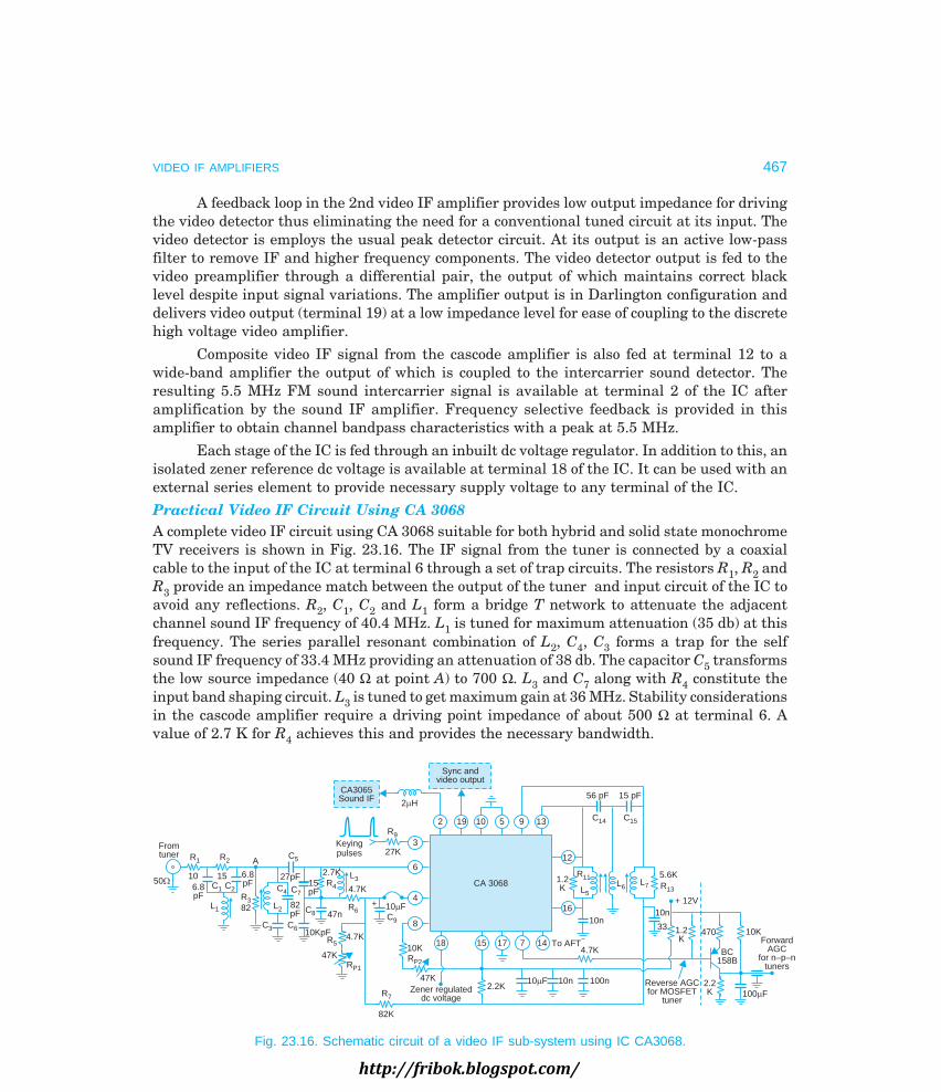
VIDEO IF AMPLIFIERS 467
A feedback loop in the 2nd video IF amplifier provides low output impedance for drivingthe video detector thus eliminating the need for a conventional tuned circuit at its input. Thevideo detector is employs the usual peak detector circuit. At its output is an active low-passfilter to remove IF and higher frequency components. The video detector output is fed to thevideo preamplifier through a differential pair, the output of which maintains correct blacklevel despite input signal variations. The amplifier output is in Darlington configuration anddelivers video output (terminal 19) at a low impedance level for ease of coupling to the discretehigh voltage video amplifier.
Composite video IF signal from the cascode amplifier is also fed at terminal 12 to awide-band amplifier the output of which is coupled to the intercarrier sound detector. Theresulting 5.5 MHz FM sound intercarrier signal is available at terminal 2 of the IC afteramplification by the sound IF amplifier. Frequency selective feedback is provided in thisamplifier to obtain channel bandpass characteristics with a peak at 5.5 MHz.
Each stage of the IC is fed through an inbuilt dc voltage regulator. In addition to this, anisolated zener reference dc voltage is available at terminal 18 of the IC. It can be used with anexternal series element to provide necessary supply voltage to any terminal of the IC.
Practical Video IF Circuit Using CA 3068A complete video IF circuit using CA 3068 suitable for both hybrid and solid state monochromeTV receivers is shown in Fig. 23.16. The IF signal from the tuner is connected by a coaxialcable to the input of the IC at terminal 6 through a set of trap circuits. The resistors R1, R2 andR3 provide an impedance match between the output of the tuner and input circuit of the IC toavoid any reflections. R2, C1, C2 and L1 form a bridge T network to attenuate the adjacentchannel sound IF frequency of 40.4 MHz. L1 is tuned for maximum attenuation (35 db) at thisfrequency. The series parallel resonant combination of L2, C4, C3 forms a trap for the selfsound IF frequency of 33.4 MHz providing an attenuation of 38 db. The capacitor C5 transformsthe low source impedance (40 Ω at point A) to 700 Ω. L3 and C7 along with R4 constitute theinput band shaping circuit. L3 is tuned to get maximum gain at 36 MHz. Stability considerationsin the cascode amplifier require a driving point impedance of about 500 Ω at terminal 6. Avalue of 2.7 K for R4 achieves this and provides the necessary bandwidth.
CA 3068
3
6
4
8
18 15 17 7 14
16
12
2 19 5 9 1310
ForwardAGC
for n–p–ntuners
10K470
BC158B
100 Fm2.2K
Reverse AGCfor MOSFET
tuner
1.2K
33
10n+ 12V
5.6KR13
L7L6L5
R111.2K
10n
4.7KTo AFT
100n10n10 Fm2.2KZener regulated
dc voltage
47K
RP2
10K
82K
R7
R5
RP1
4.7K
47K
10 FmC9
+R647nC8
10KpFC6C3
4.7K
L32.7KR415
pF
27pF
C7C4
L2 82pF
C5AR2
15C2C1
6.8pF
R382L1
6.8pF
10
R1
Fromtuner
50W
Keyingpulses 27K
R9
2 Hm56 Fp 15 Fp
C15C14
Sync andvideo output
CA3065Sound IF
Fig. 23.16. Schematic circuit of a video IF sub-system using IC CA3068.
http://fribok.blogspot.com/

468 MONOCHROME AND COLOUR TELEVISION
The network C8, C9, R6 and C6 smoothens the AGC voltage available at terminal (4).Capacitor C9 is charged through R7, R5 combination. An isolated low dc voltage at terminal(16), derived from the main supply to the IC, is used to feed the required bias at terminals (13)and (12). The series combination of 10 KΩ resistor and Rp2 sets the delay for the tuner AGCvoltage, available at terminal 7 of the IC. The value of R9 is selected to keep the keying currentto about 0.8 mA. At this current the voltage at terminal (3) is around 8 volts.
The required IF response is obtained, through the interstage coupling network, consistingof R11, R13, L5, L6, L7, C14 and C15 and the single tuned circuit at the input consisting of L3, C7and R4. In the interstage coupling network, a terminating resistance R13 of about 5.6 K isnecessary at terminal (9) in order to ensure good stability of the cascode amplifier. SimilarlyR11 is needed to present a driving source impedance of about 1 K at terminals 12 and 13.Typical value of L7, L5 and L6 are 0.9 µH, 0.2 µH, and 0.06 µH respectively. The values of 15 PFand 56 PF for C15 and C14 determine resonant frequencies of these tuned circuits to be aroundthe centre frequency of the band. Note that while tuning various coils the jumper at pin 4 isremoved to disable application of AGC voltage to the controlled amplifiers. A signal of 10 mV(rms) (– 40 db) is applied at the input of IF sub-system for tuning various resonant and trapcircuits Potentiometer Rp1 is adjusted to get an output of 6 V p-p.
Typical performance characteristics of the above video IF system using CA 3068 aregiven below:
Typical dc supply voltage 11 VQuiescent circuit current 15 to 45 mAIF sensitivity for video output of 4 V p-p 250 µVMax video output 7 V p-p6 db bandwidth 4.5 MHzAttenuation at 40.4 MHz 40 dbAttenuation at 33.4 MHz 28 dbSound IF output 500 µVDynamic range of IF AGC 55 dbTuner AGC voltage variation 2.2 V to 4.5 V
Review Questions
1. Enumerate design requirements of the IF section of a TV receiver. Draw ideal overall responsecurve of the IF section of a colour receiver and mark on it the following frequencies: picturecarrier, colour sub-carrier, sound carrier and adjacent channel interfering frequencies.
2. Explain fully how by stagger tuning the IF stages, desired gain bandwidth requirements are metwithout having to increase the number of cascaded stages.
3. What are bifilar-wound coils ? Explain with circuit diagram how such coils are usefully employedfor interstage coupling. What is link coupling and why is it used to couple the output from thetuner to the first IF stage ?
4. Explain fully the need for vestigial sideband correction and the manner in which it is achieved.Illustrate your answer by using numerical frequency values corresponding to any televisionchannel in Band-I
http://fribok.blogspot.com/
VIDEO IF AMPLIFIERS 469
5. Why is FM sound signal attenuated by about 26 db with respect to the maximum signalamplitude ? Explain various trap (rejection) circuits that are usually employed to attenuate thesound signal and for correcting effects of vestigial side-band transmission.
6. Explain main features of the three section picture IF amplifier configuration shown in Fig. 23.13.Why are trap circuits provided at the input of first IF stage ?
7. Draw the circuit diagram of a typical three stage IF section employing transistors. Explain howthe circuit functions to obtain the desired bandwidth and required wave-shape of the overall IFresponse curve.
8. Draw block schematic diagram of an IF sub-system employing the IC CA 3068. Enumerate itsmain features and explain how it performs the functions assigned to it.
http://fribok.blogspot.com/

24
http://fribok.blogspot.com/
Television receiver power supply provides low voltage (LV) and high voltage (HV) dc sources.In addition, filament power source for vacuum tubes also forms part of the power supply.
Low Voltage SupplyThe low voltage dc that is needed for feeding various sections of the receiver circuit is obtainedby rectifying and filtering the mains supply. It may be classified as unregulated and regulateddc supply. Most tube-type TV receiver power supplies are unregulated. Small changes in dcoutput voltage due to normal fluctuations in the mains supply, do not affect the performanceof the receiver drastically, because the circuits are designed to operate satisfactorily forreasonable variations in the B+ voltage. Solid state receivers employ a regulated low voltage dcsource because transistors and ICs are very sensitive to over voltage.
In receivers, that employ only tubes, B+ voltage is generally between 100 and 350 voltswith moderate current demands. For transistor receivers, a VCC source between 15 to 100 voltsis necessary, but the current drain is quite high. However, receivers that use hybrid circuitry,need a dc supply from 15 to 250 volts.
For the horizontal output stage and other auxiliary circuits a dc supply over 600 V isrequired. This is met from the ‘boosted’ B+ supply, that is economically generated in thehorizontal output circuit by augmenting the existing B+ supply.
EHT SupplyIn monochrome receivers an EHT supply of 10 to 16 KV is required at the final anode of thepicture tube. The colour picture tube needs a still higher dc voltage, that ranges from 15 to25 KV. The current drain is, however, very small and seldom exceeds one milliampere. Asalready explained in chapter 20, EHT is generated by stepping up and rectifying high voltageretrace pulses produced in the horizontal output transformer of the deflection circuit. Thedesign of the horizontal output stage determines regulation of the high voltage supply. Incolour receivers, besides providing a regulated low voltage (B+) supply, a regulator is also usedfor high voltage supply to prevent changes in focus and convergence in the colour picture tube.Note that if only one power supply of the usual type is decided upon for both low and highvoltage requirements it would turn out to be bulky, very expensive and quite out of proportionwith other sections of the receiver.
The power drawn from the ac source is about 100 watts in hybrid monochrome receiversbut rises to nearly 200 watts in colour receivers of this type. Present day monochrome receiverswhich employ only transistor and ICs consume as low as 60 watts of mains power.
472
http://fribok.blogspot.com/

RECEIVER POWER SUPPLIES 473
24.1 LOW VOLTAGE POWER SUPPLIES
Low voltage power supplies either operate from a transformer or are supplied directly fromthe line. The latter type of receivers are sometimes referred to as ‘line connected’ while thoseusing a transformer are said to be ‘line isolated’.
Transformers have separate high voltage and low voltage secondaries. The low-voltagesecondary windings supply power to heat tube filaments. High voltage secondary windingsdrive the rectifier circuits, which after filtering produce B+ supply.
The line connected receiver is so termed because one side of the ac supply line is connectedto the receiver chassis. This could be dangerous if a user came in contact simultaneously withthe receiver chassis and some external ground, unless the mains cord is plugged to connectneutral or earth wire to the chassis. Voltage doublers are used in line connected receivers toobtain higher dc voltages.
Most high quality receivers employ a mains transformer because, though expensive, itgives many advantages. The main merits of using a transformer are as under:
(a) Since the ac source is completely isolated by separate primary and secondary windings,there is no shock hazard in touching the chassis or other exposed metal parts.
(b) The B+ voltage generation is efficient because full-wave rectification can be employedby using a centre tapped high voltage secondary.
(c) A separate filament winding can be provided for parallel connections of heater circuitsand so tubes having different filament ratings can be used.
(d) The dc voltage bias that is often needed on the heaters of picture and damper tubescan be easily fed to the isolated filament winding.
(e) With a mains input transformer if tappings are provided on the primary, the ac voltageto the receiver can be changed to counteract persistent low or high ac mains voltagechanges. Such a provision if made is referred to as an in-built voltage regulator.
In some receiver designs an autotransformer is employed for stepping up the voltage.Though, this is economical in transformer cost, it does not provide isolation from the ac mains,unless is made sure that the ‘hot’ side of the line is not connected to the chassis.
Power Supply Input CircuitA typical circuit arrangement of the input section of a power supply employing a transformeris shown in Fig. 24.1. Besides the features already discussed, a hash filter is used at the mains-supply input points. The power line acts as an antenna and may feed undesirable signals intothe receiver, from motors, neon signs or any sparking contacts. Such a disturbance is calledhash because it does not have a specific frequency. The inductors block any line transients andother disturbing frequencies, while the capacitors acts as a short to such line disturbances. Inaddition, the filter helps in confining to itself the signals generated within the receiver. Thesesignals would otherwise interfere with other sets through the mains line. Examples of suchsignals generated within a receiver are horizontal and vertical sweep voltage and theirharmonics. In some power supply designs only two capacitors are used as line filter. Theimpedance of the filter capacitors is sufficiently high at 50 Hz to effectively isolate the chassisground from the ac line.
http://fribok.blogspot.com/
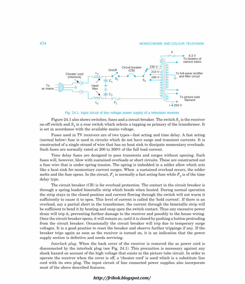
474 MONOCHROME AND COLOUR TELEVISION
Toac mains
Cheater cord(interlock)
L1
Hashfilter
L2 F1
S1C1
C2
S2
On/offCircuit breaker
(CB)230 V
210 V
190 V
6.3 VTo heaters ofvarious tubes
F
To full-wave rectifierand filter circuit
To picture tubefilament
+ 250 V
Fig. 24.1. Input circuit of low voltage power supply of a television receiver.
Figure 24.1 also shows switches, fuses and a circuit breaker. The switch S1 is the receiveron-off switch and S2 is a rear switch which selects a tapping on primary of the transformer. Itis set in accordance with the available mains voltage.
Fuses used in TV receivers are of two types—fast acting and time delay. A fast acting(normal below) fuse is used in circuits which do not have surge and transient currents. It isconstructed of a single strand of wire that has no heat sink to dissipate momentary overloads.Such fuses are normally rated at 200 to 300% of the full load current.
Time delay fuses are designed to pass transients and surges without opening. Suchfuses will, however, blow with sustained overloads or short circuits. These are constructed outa fuse wire that is under spring tension. The spring is imbedded in a solder allow which actslike a heat sink for momentary current surges. When a sustained overload occurs, the soldermelts and the fuse opens. In the circuit, F1 is normally a fast acting fuse while F2 is of the timedelay type.
The circuit breaker (CB) is for overload protection. The contact in the circuit breaker isthrough a spring loaded bimetallic strip which bends when heated. During normal operationthe strip stays in the closed position and current flowing through the switch will not warm itsufficiently to cause it to open. This level of current is called the ‘hold current’. If there is anoverload, say a partial short in the transformer, the current through the bimetallic strip willbe sufficient to bend it by heating and snap open the switch contact. Thus any excessive powerdrain will trip it, preventing further damage to the receiver and possibly to the house wiring.Once the circuit breaker opens, it will remain so, until it is closed by pushing a button protrudingfrom the circuit breaker. Occasionally the circuit breaker will trip due to temporary surgevoltages. It is a good practice to reset the breaker and observe further trippings if any. If thebreaker trips again as soon as the receiver is turned on, it is an indication that the powersupply section is defective and needs servicing.
Interlock plug. When the back cover of the receiver is removed the ac power cord isdisconnected by the interlock plug (see Fig. 24.1). This precaution is necessary against anyshock hazard on account of the high voltage that exists in the picture tube circuit. In order tooperate the receiver when the cover is off, a ‘cheater cord’ is used which is a substitute linecord with its own plug. The input circuit of line connected power supplies also incorporatemost of the above described features.
http://fribok.blogspot.com/

RECEIVER POWER SUPPLIES 475
Rectifiers. Earlier TV receivers employed vacuum tubes as rectifiers in both low andhigh voltage power supplies. As selenium, germanium and silicon rectifiers became availableat cheaper rates, they gradually replaced tubes. Almost all present day receivers use siliconrectifiers. These are manufactured with current ratings ranging from 500 mA to 10 Amps ormore. Large units are stud-mounted.
The advantage of a semiconductor diode is its very low internal voltage drop besides theabsence of any filament heating power. A silicon diode has a forward voltage drop of about onevolt as compared to nearly 20 volts in vacuum tube diodes. However, one precaution must beobserved when using silicon rectifiers. Their forward resistance is so low that when the set isturned on a large surge current flows through them to the filter capacitors. Therefore, to limitthe diode current below its maximum current rating a resistor of about 10 ohms should beinserted in series with the diode circuits.
24.2 TYPES OF RECTIFIER CIRCUITS
Figure 24.2 shows a full-wave centre-tap and a full-wave bridge rectifier circuit that arecommonly used with an isolating power transformer.
ACmains Centre-up
D1
D2 Capacitivefilter
+
IL
C+
RLVDC
Fig. 24.2 (a). Full wave rectifier with capacitor input filter.
ACmains
D4
D2
D3
D1
ChokeVDC
Load
+
IL
C
L–Sectionfilter
+
Fig. 24.2 (b). Bridge rectifier with choke input.
The rectifier configurations that can be line-connected and do not employ transformersare illustrated in Fig. 24.3. For the bridge rectifier circuit (Fig. 24.3 (a)), one lead of the dcoutput cannot be grounded unless both the ac input lines are insulated from the chassis. Thehalf-wave rectifier circuit (Fig. 24.3 (b)) is much less efficient and needs large values of filtercomponents as compared to a full-wave rectifier circuit for the same percentage ripple. However,
http://fribok.blogspot.com/

476 MONOCHROME AND COLOUR TELEVISION
in this configuration one side of the line and that of the filtered output can be grounded asshown in the circuit.
ACmains
D4
D2
D3
D1
LVDC
+
IL
p section filter
+
RLC2C1
+
R
10W
Neutral (ground)
Fig. 24.3 (a). Bridge rectifier (direct on line) with π section filter.
ACmains
Neutral (ground)
R1D1 R2
C2C1
+ +
RL
VDC+
IL
Fig. 24.3 (b). Half-wave rectifier (direct on line) with RC (π) filter.
In all the rectifier circuits discussed so far the positive side of the rectified output hasbeen shown above the ground (chassis) potential. Note, that there is no rule that chassis groundshould be most negative point. In any rectifier circuit the polarity of the dc output voltage canbe interchanged by simply reversing the direction of all the rectifier diodes employed in thecircuit. In fact such a reversal is necessary when p-n-p transistors are employed in any sectionof the receiver. Similarly in some circuits a negative biasing voltage is needed and so a reversalof polarity becomes necessary.
Filter CircuitsA suitable filter circuit is added to the rectifier output for filtering out the ac ripple content.Thus at the output terminals of the filter an almost pure dc source becomes available.
A capacitor filter (Fig. 24.2 (a)) tends to deliver a dc output voltage close to the peakvalue of the ac input voltage wave. However, unless a very large capacitor is used, its regulationis poor and ripple content rise with any increase in load current. Thus it is used only when loadcurrent is small and stays constant.
A choke input or inverted ‘L’ filter (Fig. 24.2 (b)) has somewhat better regulation. Theripple content in the output voltage becomes independent, if the load current is maintainedlarger then a certain minimum value. Therefore, this type of filter is often employed when theload current is more than about 200 mA. In contrast, a ‘Pi’ section filter (Fig. 24.3(a)) provides
http://fribok.blogspot.com/

RECEIVER POWER SUPPLIES 477
higher dc voltage from the same ac input and has a very low ripple factor. It is often used forload currents that lie between 50 to 200 mA. Since its regulation is poor, it is mostly useful forfixed loads. A resistor in place of the choke (inductor) can also be used and is equally effectiveif value of the resistor equals reactance of the choke at the ripple frequency. The resultingR-C filter is shown in Fig. 24.3(b). Its use is limited to very low load currents because of the dcvoltage drop across the resistor. However, because of the lower cost of the resistor than that ofthe choke, it is used in many circuits.
Voltage DoublersBy a series combination of half-wave diodes and their filter capacitors, the amount of dc outputvoltage can be doubled, tripled or quadrupled. In practical applications the voltage doubler isoften used for the B+ source with a half-wave line connected supply as shown in Fig. 24.4 (a).The circuit operation is quite simple. During the negative half-cycle of the input ac voltage,diode D1 is forward biased and conducts to charge C1 with positive polarity towards the anodeof D2. During the positive half-cycle, D1 gets reverse biased but diode D2 is forward biased by avoltage equal to the instantaneous addition of the varying line voltage and fixed voltage acrossthe capacitor. The current that flows through D2 charges the capacitor C2 with the polaritymarked across it. Under steady state conditions and with RL removed, C1 charges to a valueequal to the peak value of the input ac voltage. The capacitor C2 charges to twice the peak ofthe input mains voltage. With load resistor restored across the output terminals, capacitors C1and C2 discharge a little during the interval when the diodes are not conducting and thus theactual output voltage is somewhat less than the peak-to-peak value of the input wave.
ACmains
R Em D2
C2D1
+
RL
Vdc+
» 2Em
+
C1
Em
D1
RL
+ Vdc
ACmains
C1
C2
D2Em+
» 2EmEm
+
Fig. 24.4 (a). Half wave voltage doubler. Fig. 24.4 (b). Half-wave voltage doublerwith a step-up transformer.
+
+
C1
D1 + Vdc
RL» 2Em
C2D2
EmAC
mains
Fig. 24.4 (c). Full-wave voltage doubler.
An important feature of this doubler is that one side of ac input and the dc output arecommon. For this reason the half-wave doubler is generally used in a line-connected supply
http://fribok.blogspot.com/

478 MONOCHROME AND COLOUR TELEVISION
without a power transformer. As shown in the figure, the grounded side of the dc output iscommon to the neutral or ground side of the ac input. The common connection reduces theproblem of stray pick-up of 50 Hz hum in the receiver.
Another half-wave voltage doubler circuit is shown in Fig. 24.4 (b). The circuit operationis the same as described above. However, by using an input transformer the line voltage can bestepped up to obtain a still higher dc output voltage.
Full-wave DoublerConsider the circuit of Fig. 24.4 (c). During the positive half-cycle D1 conducts to charge C1with the polarity marked across it. In the next half-cycle (negative) D2 conducts to charge C2with negative polarity towards the ground terminals. Thus if the load resistor RL is quite largeboth C1 and C2 charge to the peak value to deliver a dc output voltage equal to twice the peakvalue of the secondary voltage. This circuit is seldom used in TV receivers since it does nothave a common connection for the ac input and the dc output.
The idea of voltage doubling can be extended to obtain still higher dc voltages. However,it is not often used because the voltage regulation becomes worse unless very large capacitorsare employed.
24.3 HEATER CIRCUITS
For receivers that use tubes, the heaters can be connected either in parallel on in series. Whena low voltage winding exists on the mains transformer or when a separate filament transformeris provided, all the heaters are connected in parallel across that winding. The filament currentrating of the tubes may be different but they must have the same voltage rating. One end ofthe filament winding is tied to chassis ground to save wiring. Each heater returns to the groundend of the winding by an individual ground connection. This is illustrated in Fig. 24.5 (a). Adecoupling filter L1, C1 is used to prevent feedback of signals between RF and IF amplifierthrough the common heater line. The inductor or choke consists of a few turns of thick wireand has an inductance around 1 µH. Ferrite beads are also used instead of RF chokes. Thereactance of the choke is negligible at 50 Hz and therefore heaters remain effectively in parallelacross the filament winding. The picture tube heater has its own filament winding. A dc biasvoltage is added to this heater supply to raise the filament potential close to that of the cathode.This minimizes the possibility of arcing between these two electrodes.
AC mains
+ 250 V
To picture tube heater
F6.3 V
Filamenttransformer
PilotlightC1
1 Hm
0.001Fm
L1
Fig. 24.5 (a). Parallel heater circuit.
http://fribok.blogspot.com/

RECEIVER POWER SUPPLIES 479
ACmains
Interlock
RF choke
C1
0.056 Fµ
S F
R2
R1
Fusibleresistor
To LV dc supply rectifierand filter circuit
Current limiting resistor
Horzamp
Horzdamper
Audioamp
Audiodetector
Videoamp
IFamp
C20.001 Fµ
L
IFamp
Horzosc
SyncandAGC
Verticalosc andoutput
Picturetube
Oscand mixer
RFamp
VHF tuner
0.001 Fµ C3
Fig. 24.5 (b). Series heater circuit.
Series HeatersIn Fig. 24.5 (b) all the heaters including the picture tube are in series across the supply mains.In this arrangement the current rating of all the tubes must be same though their voltageratings can be different. The sum of the heater voltage drops should be approximately equal tothe line supply voltage. In case it is not so, a series resistor is included in the heater circuitchain. Note that the high voltage rectifier is not in the series string as it receives filamentpower from the horizontal output transformer.
All the tubes in series must have the same warm-up time otherwise this results inrepeated burn-out of some filaments. Some heater strings have a thermistor in series to limitthe current until the tubes become hot, since the filament resistance is much less when coldthan when it is hot.
Order of series heater connections. Though all the series filaments have the same current,a point closer to the grounded end of the string has lesser potential difference to chassis ground.Therefore, less hum voltage can be coupled into the signal circuits by heater cathode leakagein the tube. This is why the tubes in the VHF tuner are last in the chain while the horizontaldeflection amplifier and damper tubes are first. This aspect is illustrated in the series filamentcircuit shown in Fig. 24.5 (b).
24.4 VOLTAGE REGULATORS
Voltage regulators are used for keeping the rectified dc output voltage constant despitevariations in the dc load current or in the ac input voltage. The use of a voltage regulator alsoreduces ripple content in the dc supply and lowers the ac output impedance of the powersupply. Low impedance minimizes coupling between amplifier stages through the common B+line. Regulation is also important in order to maintain constant raster size. In colour receiversregulation of the EHT supply is equally important to maintain focus and convergence withchanges in brightness. Even in monochrome receivers some regulation of the EHT supply isnecessary to avoid blooming and breathing of the reproduced picture. Breathing refers toblooming at a regular slow rate.
http://fribok.blogspot.com/

480 MONOCHROME AND COLOUR TELEVISION
Types of Voltage RegulatorsOne method of keeping the output voltage constant is to build a power supply with much morecurrent capacity than actually required. However, this turns out to be very expensive and isnormally not favoured. Another approach is to regulate the ac input voltage. The inputtransformer for the LV supply is designed to have a saturable core to limit any increase in theac input voltage. Similarly, to prevent any decrease in voltage, an oil-filled capacitor of about4 µF is connected across the secondary to tune it to resonance. However, this method does notprovide a very effective regulation of the dc supply.
The most common method, that is quite cheap and yields excellent regulation is the useof electronic regulators. The various types that find application is good quality receivers arebriefly described below:
(a) Zener diode voltage regulator. Figure 24.6 (a) is the circuit of a zener regulator designedto feed the sound IC of a TV receiver. The zener (Fig. 24.6 (b)) operates under reverse bias tomaintain a fixed voltage (equal to its breakdown voltage) across its terminals.
Bsupply
+ SoundIC
+ 120V
ACinput Iin
+ 200V
+ 170VIz
ZenerVZ
RS V0 = 10V
IL
0.1 Fm
(a)
IZ
VZ
IZ (min)
IZ (max)
Constant voltagerange
0Reverse
bias voltage(b)
Fig. 24.6. Zener voltage regulator (a) circuit (b) Zener V-I characteristics.
The input voltage is kept higher than the required dc output voltage. Usually IZ(max)= 10 IZ(min) in the useful range where VZ = V0 remains constant. Assuming Vin to be constant,Iin must remain same to keep V0 constant. Thus any change in IL should result in a correspondingchange in IZ to keep the voltage drop across RS constant. However, when Vin changes Iin adjuststo a new value to keep the drop across RS equal to the difference between Vin and Vo. Theessential conditions to be met for keeping the zener in its break down region are: (i) IL shouldnot exceed a value which results in an IZ less than the breakdown current, i.e., IZ(min). (ii) whenthe load circuit opens, i.e., IL = 0, then IZ should not exceed the maximum rated current of thezener. Too large or too small an input voltage can also result in failure of the regulator todeliver a constant output voltage. Since the zener is connected in shunt across the load, thisregulator is known as a shunt regulator.
The zener regulator, though simple and inexpensive, suffers from several limitations.The first problem is the power dissipated in the zener which varies with changes in load current.The second disadvantage is its somewhat non-ideal current-voltage characteristics. The voltageacross the zener changes by a small percentage of the nominal output voltage with large changesin IZ.
http://fribok.blogspot.com/

RECEIVER POWER SUPPLIES 481
(b) Series regulator. A series emitter follower regulator overcomes the above drawbacksbut is not very efficient. Figure 24.7 illustrates the principle of an improved series regulatorwhich employs an error voltage amplifier. Voltage across the zener acts as reference voltage.The value of R1 is chosen to keep the zener in its breakdown region. Any change in the outputvoltage changes VAB proportionally. This results in a net change in VBE of transistor Q2. Becauseof transistor action, even a small change in the base-emitter voltage results in a large changein collector current, which effectively amounts to amplifying the error signal. Since R3 is chosento be large to keep IR3 almost constant, any change in IC2 is accompanied by a correspondingchange in IB1. Thus, any increase in the output voltage V0, will result in an increase in IC2,which in turn will decrease IB1 to reduce IE1 (IC1 ≈ IE1 ≈ IL). A decrease in IE1 will reduce theload current thus restoring the voltage across RL (load) back to its nominal value V0. Similarlywhen V0 tends to decrease the feed back loop action will increase IE1(≈ IL) to keep the outputvoltage constant.
+Q1
IC IE
R3 IB1
IC2IR3
R1 R4
R2IB2
Q2
VBE
IZ Zenerdiode
Unregulateddc voltage
Outputvoltage adjustment
B
V BAR5
V0 RL
Load
A
IL
Regulateddc voltage
Fig. 24.7. Basic series voltage regulator.
CA3085
+
125V± 10%
Unregulated dcinput
R22K
1
2
3
1
BZ148 ZD1 46
78
1000 pF
2N3501Q1
100 W68 W
4.7 K100 Fm
+
Q2
2N2905Q3
2N3055+ 110V
R2 82 K
R3
6.7 K
lp
Regulatedoutput
Fig. 24.8. High voltage regulator employing IC CA 3085.http://fribok.blogspot.com/

482 MONOCHROME AND COLOUR TELEVISION
(c) IC voltage regulator. Many voltage regulator ICs are available which provide excellentregulation over a wide range of input and output voltages. BEL CA 3085 is one such IC. It hasa current capability up to 100 mA at 6 V dc output. By employing CA3085A and CA3085Bhigher voltage and current rating can be obtained. Figure 24.8 is the circuit of a high voltageregulator employing CA3085. As shown there, additional pass transistor have been used toachieve high voltage operation. Note that the input voltage to the IC proper has been reducedto a convenient value through R1, ZD1 so that it operates within its maximum ratings. SimilarlyR2, R3 combination determines the magnitude of the regulated output voltage for feeding thecomparator in the IC.
24.5 LOW VOLTAGE POWER SUPPLY CIRCUITS
There is a wide range of low voltage power supply circuits used in TV receivers. Tworepresentative circuits are discussed.
(1) Transformer Power Supply with Series Heater CircuitIn some power supply designs for all-tube receivers a transformer is used for generating B+voltage but the tube heaters are connected in series across the ac line. This approach beingeconomical is often used. Figure 24.9 shows the circuit arrangement. Note that a separatefilament winding is provided for the picture tube heater. Resistors R1 and R2 form a potentialdivider to provide necessary bias on the picture tube heater.
240 V
+
200 V
150 V
+
R1
R2
+
+3.3 K
2 × 20 Fm
10 H +
LD1
D2
To picture tubefilament
0.1 Fm
SF1 RFC
Heaterchain
3.3 n 3.3 n
F2
V1 V2 V3 V4 V5 V6
Fig. 24.9. Transformer connected power supply with heaters in series across the ac supply.
(2) Line Connected Power SupplyFigure 24.10 is the circuit of a line connected power supply often used in hybrid receivers. Itemploys a half-wave rectifier (D1) to feed dc voltage to the vacuum tube circuits. Various loadsare isolated through decoupling networks. The diode D3 isolates the two 240 V (A and B) dccircuits from each other. Both D1 and D2 are bypassed by capacitors (3.3 nF) to suppress highfrequency surge voltages.
http://fribok.blogspot.com/

RECEIVER POWER SUPPLIES 483
230 V50 Hz
On-offswitch
F
10 W
5 W
D1
BY127 +
3.3 n
L
+
2 × 100Fm
230 W
100 FmBY126+
100 Fm
D3
240 V(B)
240 V(A)
50 Fm 50 Fm+ +
230 V220 W1 K
120 WV1 V2 V3 V4 V5 V6BY127
D2
3.3 n
50 Fm+
150 W
1.2 K 100 Fm–+
150 W
– 25 V
1000 Fm 300 W
AC128(Q )1
+
100 W
ZD1
FZ12A
6.8 n
10 Fm– 12 V
+
Fig. 24.10. Line connected power supply for a hybrid television receiver.
The heater circuit is designed to feed negative low voltage supply to transistor (p-n-p)circuits besides heating the filaments. This is achieved by connecting a diode (D2) in serieswith the heater string and the low voltage load circuit. The diode conducts in only one direction,thus limiting the heater current to the desired value and also affecting rectification for the lowvoltage dc supply. The transistor Q1 with zener diode ZD1 operates as a shunt voltage regulatorto supply a stabilized dc source at – 12 V.
24.6 HIGH VOLTAGE POWER SUPPLY
Practically all television receivers produce EHT supply by rectifying the sharp retrace pulsesthat are generated in the high voltage winding of the horizontal output transformer. Details ofhorizontal output circuit and the manner in which high voltage pulses occur have already beenexplained in Chapter 20. However, it may be noted that the flyback transformer and rectifierare generally in a separate metal cage. In addition to offering protection against shock, theenclosure is a dust proof cover and is a shield against X-rays.
The rectifier tube is often mounted on insulating supports to keep the high voltage leadsaway from the chassis. At the bottom of the high voltage tube socket, an interconnecting loopof heavy wire, known as corona ring is often used to minimize high voltage arcing aroundthese terminals. Silicon diode rectifiers are now available in sealed stacks and are replacingvacuum diode rectifiers.
http://fribok.blogspot.com/

484 MONOCHROME AND COLOUR TELEVISION
Boosted B+ Supply. As explained earlier the damper diode conducts through the boostcapacitor CB (see Fig. 20.11) to develop a dc voltage across it. This in series with B+ supplyresults in boosted B++ supply. It feeds the horizontal output stage that employs a vacuum tubeand also to other auxiliary circuits.
24.7 STABILIZED THYRISTOR POWER SUPPLY
An economical power supply for television receivers can also be constructed by using a thyristoras a controlled rectifier. This enables a dc potential in the range of 100 to 240 V to be derivedfrom ac mains without a transformer and with minimal dissipation in the used devices. Thebasic thyristor power supply circuit is shown in the block diagram of Fig. 24.11. The controlcircuit triggers the thyristor in the latter half of positive half-cycle of the mains waveform sothat mean dc voltage presented to the output filter can take a value less than the peak mainsvoltage.
Inputfilter
Thyristor(rectifier)
Outputfilter
ControlcircuitReference Feedback
DC outputAC mains
Fig. 24.11. Block diagram of a thyristor power supply.
An input filter is used to limit the peak thyristor current to a permitted value to reduceRF switching currents flowing back into the mains. It is usually a section of the control circuitIC. The output low-pass filter takes the form of a single RC combination because of the powerlevels involved. An active filter using a series power transistor may be used to reduce the sizeof smoothing capacitors.
Thyristor power supplies have superior performance as compared to their hybridcounterparts in terms of stabilization and heat dissipation. Such power supplies have beensuccessfully used in both monochrome and colour receivers to deliver stabilized 200 V dc forload currents ranging from 300 to 400 mA. Figure 24.12 is the simplified circuit of such athyristor controlled power supply. The initiation of conduction of the thyristor is controlled bya phase-shifting network. For this purpose mains waveform is delayed by the series networkR5, C2 and applied to the trigger diac. A diac is a bidirectional thyristor with no gate. Itscharacteristic has a negative resistance region which starts at a critical potential called thebreakdown voltage. When the voltage across C2 reaches the diac breakdown voltage, the diacconducts and current pulse is applied to the gate of the thyristor causing it to conducts. Tostabilize the output the trigger point must be varied as a function of mains input and dc output.The transistor Q1 is used for this purpose. It controls the charge current of C2 and hence thetrigger point for the thyristor. The base of the transistor is connected to a potential divideracross the mains input. If the ac input (mains) voltage tends to increase, the base current
http://fribok.blogspot.com/

RECEIVER POWER SUPPLIES 485
increases. The resulting increase in collector current of Q1 reduces charge current through thecapacitor C2. This delays the trigger point and tends to maintain the output voltage constant.Additional feedback is provided from output through the resistor R8. Any tendency for theoutput to rise due to a change in load current causes base current of Q1 to be increased whichreduces the charge current and delay the thyristor trigger point. The reverse would happen ifeither ac mains voltage or dc output voltage happen to decrease. Hence the effects of mainsvoltage variations and load changes on the dc output voltage are reduced to a minimum. R4 isfor adjustment of the output voltage to the exact desired value.
AC input220 V ± 15%
2 A R1 L1820 Hm
Inputfilter
ThermistorRF choke
220 nFC1
2.2 K
15 K R3
R4
R2470 K
Q1
BC147
220 nF C2
Diac
33 KR5
C3
A K
Thyristor
G R7
2.2 K200 nF
82 W
R9
RC filter
200 V
450 mAmax.
C5500 Fm
600 Fm C4
22 KR6
R8
470 K
Fig. 24.12. Stabilized thyristor power supply circuit.
The L1, C1 network, besides suppressing ratio interference, protects the thyristor frompossible damage caused by mains transients. The switch-on surge current of some 100 A isreduced by the inclusion of a thermistor R1 to protect the on-off switch.
24.8 SWITCH MODE POWER SUPPLY (SMPS)
The use of ICs and modular construction is very common is modern television receivers. Thishas led to the introduction of switching mode power supplies to meet the dc requirements ofsuch receivers. These are smaller, lighter and dissipate less power than equivalent seriesregulated supplies.
Basic Principle
In a switched mode supply the regulating elements consist of series connected transistors thatact as rapidly opening and closing switches. The input ac is first converted (Fig. 24.13) tounregulated dc, which, in turn is chopped by the switching elements operating at a rapid rate,typically 20 KHz. The resultant 20 KHz pulse train is transformer coupled to an output networkwhich provides final rectification and smoothing of the dc output. Regulation is accomplishedby control circuits which vary the duty cycle (on-off periods) of the switching elements if theoutput voltage tends to vary.
http://fribok.blogspot.com/

486 MONOCHROME AND COLOUR TELEVISION
Duty-cyclecontrol
lu
Regulateddc output
Output rectifierand filter
Small powertransformerSwitching
elementsInput rectifier
and filter
Cpu
ACinput
Fig. 24.13. Basic circuit of a switched mode regulated power supply.
Operating Advantages and DisadvantagesThe advantages of a SMPS over a conventional regulated supply are:
(i) The switching transistors are basically on-off devices and hence dissipate very littlepower when either on (saturated) or off (non-conducting). Efficiencies ranging from 65 to 85percent are typical of such supplies as compared to 30 to 45 percent efficiencies for linearsupplies.
(ii) On account of the higher switching rate (20 KHz) the power transformer, inductorand filter capacitors are much smaller and lighter than those required for operation at powerline frequencies. Typically a switching power supply is less than one third in size and weight ofa comparable series regulated supply.
(iii) A switched-mode supply can operate under low ac input voltage. It has a relativelylong hold-up period if input power is lost momentarily. This is so because more energy can bestored in its input filter capacitors.
Disadvantages. Although the advantages are impressive a SMPS has the followinginherent disadvantages:
(i) Electromagnetic interference (EMI) is a natural by-product of the on-off switchingwithin these supplies. This interference can get coupled to various sections of the receiver andhinder their normal operation. For this reason, switching supplies have built-in shields andfilter networks which substantially reduce EMI and also control output ripple and noise. Inaddition, special shields are provided around those sections of the receiver circuitry which arehighly susceptible to electromagnetic interference.
(ii) The control circuitry is expensive, quite complex and somewhat less reliable.
Typical Circuit of a SMPSFigure 24.14 shows simplified circuit and associated waveforms of a typical switching modepower supply. Regulation is achieved by a pair of push-pull switching transistors (Q1 and Q2)operating under the control of a feedback network consisting of a pulse-width modulator and avoltage comparison amplifier. The waveforms illustrate the manner in which the duty-cycle iscontrolled to deliver a constant dc output voltage. The voltage comparison amplifier continuouslycompares a fraction of the output voltage with a stable reference source Vr1 and develops a
http://fribok.blogspot.com/

RECEIVER POWER SUPPLIES 487
control voltage (Vcontrol) for the turn-on comparator. The comparator compares Vcontrol with atriangular ramp waveform occurring at a frequency of 40 KHz. When the ramp voltage is morepositive than the control level, a turn-on signal is generated. As shown in the waveforms, anyincrease or decrease in the control voltage (Vcontrol) will very width of the turn-on voltage andthis in turn will alter the width of drive pulses to both Q1 and Q2. The drive pulses passthrough steering logic which ensures alternate switching of Q1 and Q2. Thus each switch operatesat 20 KHz, i.e., one-half of the ramp frequency. When Q1 is on, current flows in the upper halfof the primary winding of transformer T1 and completes its path through its centre tap. Similarlywhen Q2 conducts current flows in opposite direction through the lower half of the same windingto complete its return path thus providing transformer action.
Input rectifier and filter
ACinput
Q1T1
Q2
Vf
Referenceand
bias supplies A
Pulse-width modulator( C chip)I
Steeringlogic
Drive Q1
Drive Q2
40 KHzramp
generator
Turn-oncomparator
Vramp
VcontrolV0 sample
Vr1
Voltagecomparison
amplifier
DCoutput
Rectifierand filter
Vr2
Q1
off
off
on
onQ2
Switched output to theprimary of transformer
Drive Q (20 KHz)2
Drive Q (20 KHz)1
Turn on control voltage A
Vcontrol
Fig. 24.14. Typical switched-mode power supply circuit.
Since the dc output voltage is proportional to the duty-cycle of current through thetransformer, increasing the ‘on’ periods of the switching transistor will increase the output
http://fribok.blogspot.com/

488 MONOCHROME AND COLOUR TELEVISION
voltage and vice-versa. Thus the control voltage automatically monitors the duty-cycle tomaintain a constant dc output voltage despite any input voltage or load current variations. Insome such supplies only one transistor is used as the chopping and control element. In suchdesigns a 20 KHz clock pulse is used to time the on-off periods.
The comparator, ramp generator and steering or control logic usually form part of adedicated IC. Though, not shown, in the modular chip it contains additional circuits for overvoltage protection, over-current protection and prevention of any inrush of ac current.
Review Questions
1. Distinguish between ‘line connected’ and ‘line isolated’ power supplies. Discribe the merits anddemerits of each type.
2. Draw the circuit diagram of the input side of a typical low voltage power supply and explainbesides other components the need for (i) a circuit breaker, (ii) fusible resistors, and (iii) a hashfilter.
3. Draw circuit configurations of different filtering arrangements and explain special applicationsof each type. Which filter circuit is often employed in TV receiver power supplies ?
4. Explain with suitable circuit diagrams the action of half-wave and full-wave voltage doublecircuits. What is their special application in television receiver power supplies ?
5. Compare the series and parallel arrangement of feeding the heater circuits in a TV receiver.Why is a particular order used when connecting tube filaments in sereis ? Why is the filament ofthe picture tube generally fed from an isolated low voltage ac source ?
6. Why is it necessary to provide regulated dc source to solid-state circuits in a TV receiver ? Drawsuitable circuit diagrams of atleast two types of voltage regulators and explain their operation.
7. Explain how a thyristor can be used to provide a regulated dc supply to TV receivers. Draw atypical circuit and explain its operation.
8. What is the basic principle of a switched mode power supply ? What are its merits and demerits ?Explain with a suitable circuit diagram the operating principle of such a regulated power supply.
http://fribok.blogspot.com/

25
!
http://fribok.blogspot.com/

We all know how pleasing it is to see a picture in natural colours or watch a colour film incomparison with its black and white version. In fact monochrome reception of natural daylightscenes and pictures taken in black and white are totally unrealistic because they lack colour.However, we accept them because we have been conditioned to do so by constant exposure andlifelong usage to black and white drawings, photographs, films an monochrome television.
It is desirable that a TV system should produce a picture with realistic colours, adequatebrightness and good definition that can be easily perceived by our eyes. A monochrome picturedoes contain the brightness information of the televised scene but lacks in colour detail of thevarious parts of the picture. The have a colour picture it is thus necessary to add colour to thepicture produced on a white raster.
It may be recalled that in a monochrome TV system, the problem of picking upsimultaneous information from the entire scene about the brightness levels is solved by scanning.In colour TV it becomes necessary to pick up and reproduce additional information about thecolours in the scene. It did not seem to be an easy task and the difficulties in achieving thisseemed unsurmountable. However, this challenge was met by the scientists and engineersworking on it in U.S.A. All colour TV systems in use at present owe their origin to the NTSCsystem which was invented and developed in the United States of America. The RadioCorporation of America (RCA) played a prominent role in the development of colour TV. Theinvention and fabrication of the tricolour shadowmask tube was their major single contributionwhich made a high quality colour television system possible.
25.1 COMPATIBILITY
Regular colour TV broadcast could not be started till 1954 because of the stringent requirementof making colour TV compatible with the existing monochrome system.
Compatibility implies that (i) the colour television signal must produce a normal blackand white picture on a monochrome receiver without any modification of the receiver circuitryand (ii) a colour receiver must be able to produce a black and white picture from a normalmonochrome signal. This is referred to as reverse compatibility.
To achieve this, that is to make the system fully compatible the composite colour signalmust meet the following requirements:
(i) It should occupy the same bandwidth as the corresponding monochrome signal.
(ii) The location and spacing of picture and sound carrier frequencies should remain thesame.
490
"
!
http://fribok.blogspot.com/

ESSENTIALS OF COLOUR TELEVISION 491
(iii) The colour signal should have the same luminance (brightness) information as woulda monochrome signal, transmitting the same scene.
(iv) The composite colour signal should contain colour information together with theancillary signals needed to allow this to be decoded.
(v) The colour information should be carried in such a way that it does not affect thepicture reproduced on the screen of a monochrome receiver.
(vi) The system must employ the same deflection frequencies and sync signals as used formonochrome transmission and reception.
In order to meet the above requirements it becomes necessary to encode the colourinformation of the scene in such a way that it can be transmitted within the same channelbandwidth of 7 MHz and without disturbing the brightness signal. Similarly at the receivingend a decoder must be used to recover the colour signal back in its original form for feeding itto the tricolour picture tube.
Before going into details of encoding and decoding the picture signal, it is essential togain a good understanding of the fundamental properties of light. It is also necessary tounderstand mixing of colours to produce different hues on the picture screen together withlimitations of the human eye to perceive them. Furthermore a knowledge of the techniquesemployed to determine different colours in a scene and to generate corresponding signal voltagesby the colour television camera is equally essential. Therefore this chapter is mainly devotedto these aspects of colour TV, while transmission and reception of colour pictures is explainedin the following chapter.
25.2 NATURAL LIGHT
When white light from the sum is examined it is found that the radiation does not consist of asingle wavelength but it comprises of a band of frequencies. In fact white light is a very small
Spectrum of electromagnetic radiation
Visible spectrum
105
1010
Radio waves Infra-red
f(Hz)
λ (meters)3 × 10
33 × 10
–23 × 10
–73 × 10
–123 × 10
–17
1015
1020
1025
Ultra-violet X-rays Cosmic rays
780 700 600 550 500 400 380
Red Orange Yellow Green Blue Indigo Violet
( in nm)
(1 nm = 10 m)
λ–9
Fig. 25.1. Region of sunlight in the electromagnetic spectrum.http://fribok.blogspot.com/

492 MONOCHROME AND COLOUR TELEVISION
part of the large spectrum of electromagnetic waves which, in total, extend from very low tobeyond 1025 Hz. The visible spectrum extends over only an octave that centers around afrequency of the order of 5 × 10¹⁴ Hz. When radiation from the entire visible spectrum reachesthe eye in suitable proportions we see white light. If, however, part of the range is filtered out,and only the remainder of the visible spectrum reaches the eye, we see a colour. The entireelectromagnetic spectrum is shown in Fig. 25.1 where the visible spectrum has been expandedand shown separately to demonstrate the range of colours it contains. Note that the variouscolours merge into one another with no precise boundaries.
25.3 COLOUR PERCEPTION
All objects that we observe are focused sharply by the lens system of the eye on its retina. Theretina which is located at the back side of the eye has light sensitive organs which measure thevisual sensations. The retina is connected with the optic nerve which conducts the light stimulias sensed by the organs to the optical centre of the brain.
According to the theory formulated by Helmholtz the light sensitive organs are of twotypes—rods and cones. The rods provide brightness sensation and thus perceive objects onlyin various shades of grey from black to white. The cones that are sensitive to colour are broadlyin three different groups. One set of cones detects the presence of blue colour in the objectfocused on the retina, the second set perceives red colour and the third is sensitive to the greenrange. Each set of cones, may be thought of as being ‘tuned’ to only a small band of frequenciesand so absorb energy from a definite range of electromagnetic radiation to convey the sensationof corresponding colour or range of colour. The combined relative luminosity curve showingrelative sensation of brightness produced by individual spectral colours radiated at a constantenergy level is shown in Fig. 25.2. It will be seen from the plot that the sensitivity of thehuman eye is greatest for green light, decreasing towards both the red and blue ends of thespectrum. In fact the maximum is located at about 550 nm, a yellow green, where the spectralenergy maximum of sunlight is also located.
1.00
0.75
0.5
0.25
350 400 450 500 550 600 650 700 750
Violet Indigo Blue Green Yellow Orange Red
Wavelength in nanometers
nm
Rel
ativ
e se
nsiti
vity
of t
he e
ye
Fig. 25.2. Approximate relative response of the eye to different colours.
http://fribok.blogspot.com/

ESSENTIALS OF COLOUR TELEVISION 493
25.4 THREE COLOUR THEORY
All light sensations to the eye are divided (provided there is an adequate brightness stimuluson the operative cones) into three main groups. The optic nerve system then integrates thedifferent colour impressions in accordance with the curve shown in Fig. 25.2 to perceive theactual colour of the object being seen. *This is known as additive mixing and forms the basis ofany colour television system. A yellow colour, for example, can be distinctly seen by the eyewhen the red and green groups of the cones are excited at the same time with correspondingintensity ratio. Similarly and colour other than red, green and blue will excite different sets ofcones to generate the cumulative sensation of that colour. A white colour is then perceived bythe additive mixing of the sensations from all the three sets of cones.
Mixing of ColoursMixing of colours can take place in two ways—subtractive mixing and additive mixing. Insubtractive mixing, reflecting properties of pigments are used, which absorb all wavelengthsbut for their characteristic colour wavelengths. When pigments of two or more colours aremixed, they reflect wavelengths which are common to both. Since the pigments are not quitesaturated (pure in colour) they reflect a fairly wide band of wavelengths. This type of mixingtakes place in painting and colour printing.
In additive mixing which forms the basis of colour television, light from two or morecolours obtained either from independent sources or through filters can create a combinedsensation of a different colour. Thus different colours are created by mixing pure colours andnot by subtracting parts from white.
The additive mixing of three primary colours—red, green and blue in adjustableintensities can create most of the colours encountered in everyday life. The impression ofwhite light can also be created by choosing suitable intensities of these colours.
Red, green and blue are called primary colours. These are used as basic colours intelevision. By pairwise additive mixing of the primary colours the following complementarycolours are produced:
Red + Green = Yellow
Red + Blue = Magenta (purplish red shade)
Blue + Green = Cyan (greenish blue shade)
Colour plate 1 depicts the location of primary and complementary colours on the colourcircle.
If a complementary is added in appropriate proportion to the primary which it itselfdoes not contain, white is produced. This is illustrated in Fig. 25.3 (a) where each circlecorresponds to one primary colour. Colour plate 2 shows the effect of colour mixing. SimilarlyFig. 25.3 (b), illustrates the process of subtractive mixing. Note that as additive mixing of thethree primary colours produces white, their subtractive mixing results in black.
*Research has shown that the actual neural process of colour perception is substantially differentfrom the tricolour process. However, all colour reproduction processes in television or printing usevariations of this process and is found satisfactory.
http://fribok.blogspot.com/
abc
Highlight

494 MONOCHROME AND COLOUR TELEVISION
30%41% 11%
100%White
89%70%
59%
Green
Cyan(green + blue)
Yellow(red + green)
Red
Magenta(red + blue) Blue
Fig. 25.3 (a). Additive colour mixing. The diagramshows the effect of projecting green, red and blue beams
on a white screen in such a way that they overlap.
Black
Green(white – blue – red)
Cyan(white – red)
Yellow(white – blue)
Red(white – blue – green)
Magenta(white – green) Blue
(white – green – red)
Fig. 25.3 (b). Subtractive colour mixing. The diagram showsthe effect of mixing colour pigments under white light.
Grassman’s LawThe eye is not able to distinguish each of the colours that mix to form a new colour but insteadperceives only the resultant colour. Thus the eye behaves as though the output of the threetypes of cones are additive. The subjective impression which is gained when green, blue andred lights reach the eye simultaneously, may be matched by a single light source having thesame colour. In addition to this, the brightness (luminance) impression created by the combinedlight source is numerically equal to the sum of the brightnesses (luminances) of the threeprimaries that constitute the single light. This property of the eye of producing a responsewhich depends on the algebraic sum of the red, green and blue inputs is known as Grassman’sLaw. White has been seen to be reproduced by adding red, green and blue lights. The intensityof each colour may be varied. This enables simple rules of addition and subtraction.
http://fribok.blogspot.com/
abc
Highlight
abc
Highlight
abc
Highlight

ESSENTIALS OF COLOUR TELEVISION 495
Tristimulus Values of Spectral ColoursBased on the spectral response curve of Fig. 25.2 and extensive tests with a large number ofobservers, the primary spectral colours and their intensities required to produce differentcolours by mixing have been standardized. The red green and blue have been fixed atwavelengths of 700 nm, 546.1 nm and 438.8 nm respectively. The component values (or fluxes)of the three primary colours to produce various other colours have also been standardized andare called the tristimulus values of the different spectral colours. The reference white for colourtelevision has been chosen to be a mixture of 30% red, 59% green and 11% blue. Thesepercentages for the light fluxes are based on the sensitivity of the eye to different colours.
Thus one lumen (lm) of white light = 0.3 lm of red + 0.59 lm of green + 0.11 lm of blue. Inaccordance with the law of colour additive mixing one lm of white light (see Fig. 25.3 (a)) is also= 0.89 lm of yellow + 0.11 lm of blue or = 0.7 lm of cyan + 0.3 lm of red or = 0.41 lm of magenta+ 0.59 lm of green. It may be noted that if the concentration of luminous flux is reduced by acommon factor from all the constituent colours, the resultant colour will still be white, thoughits level of brightness will decrease. The brightness of different spectral colours is associatedwith that of white. Yellow, for example, appears 89% as bright as the reference white, reflectingthe addition of 59% brightness of green and 30% brightness of red. Similarly any othercombination of primary colours will produce a different colour with a different relative brightnesswith reference to white which has been taken as 100 percent.
25.5 LUMINANCE, HUE AND SATURATION
Any colour has three characteristics to specify its visual information. These are (i) luminance,(ii) hue or tint, and (iii) saturation. These are defined as follows:
(i) Luminance or BrightnessThis is the amount of light intensity as perceived by the eye regardless of the colour. In blackand white pictures, better lighted parts have more luminance than the dark areas. Differentcolours also have shades of luminance in the sense that though equally illuminated appearmore or less bright as indicated by the relative brightness response curve of Fig. 25.2. Thus ona monochrome TV screen, dark red colour will appear as black, yellow as white and a light bluecolour as grey.
(ii) HueThis is the predominant spectral colour of the received light. Thus the colour of any object isdistinguished by its hue or tint. The green leaves have green hue and red tomatoes have redhue. Different hues result from different wavelengths of spectral radiation and are perceivedas such by the sets of cones in the retina.
(iii) SaturationThis is the spectral purity of the colour light. Since single hue colours occur rarely alone, thisindicates the amounts of other colours present. Thus saturation may be taken as an indicationof how little the colour is diluted by white. A fully saturated colour has no white. As an example.vivid green is fully saturated and when diluted by white it becomes light green. The hue andsaturation of a colour put together is known as chrominance. Note that it does not contain thebrightness information. Chrominance is also called chroma.
http://fribok.blogspot.com/
shree
Highlight
shree
Highlight
shree
Highlight

496 MONOCHROME AND COLOUR TELEVISION
Chromaticity Diagram. Chromaticity diagram is a convenient space coordinate represen-tation of all the spectral colours and their mixtures based on the tristimulus values of theprimary colours contained by them. Fig. 25.4 (a) is a two dimensional representation of hueand saturation in the X-Y plane (see colour plate 3). If a three dimensional representation isdrawn, the ‘Z ’ axis will show relative brightness of the colour.
Y
.9
.8
.7
.6
.5
.4
.3
.2
.1
0 .1 .2 .3 .4 .5 .6 .7 .8X
400 (nm)
460
Greenishblue
BluePurple
Blue green
Bluishgreen
Whitisharea
C
White
Pink Red
Purplish pinkReddish purple
Purplish red
700 – 740 (nm)
620
Orange
Yellowish orangeYellow
Yellow green
Greenish yellow
Yellowish green
560
530
520(nm)
Green
Fig. 25.4 (a). Chromaticity diagram. Note that red, green and blue have beenstandardized at wavelengths of 700, 646.1 and 438.8 nanometers respectively.
X and Y denote colour coordinates. For example white lies at X = 0.31 and Y = 0.32.
BlackG
R
BG
B
RW
Brightnessincreased
Grey shades
Fig. 25.4 (b). Representation of luminance (brightness).
http://fribok.blogspot.com/

http://fribok.blogspot.com/

http://fribok.blogspot.com/

ESSENTIALS OF COLOUR TELEVISION 497
As seen in the figure the chromaticity diagram is formed by all the rainbow coloursarranged along a horseshoe-shaped triangular curve. The various saturated pure spectralcolours are represented along the perimeter of the curve, the corners representing the threeprimary colours—red, green and blue. As the central area of the triangular curve is approached,the colours become desaturated representing mixing of colours or a white light. The white lieson the central point ‘C’ with coordinates x = 0.31 and y = 0.32. Actually there is no specificwhite light—sunlight, skylight, daylight are all forms of white light. The illuminant ‘C’ markedin Fig. 25.4 (a) represents a particular white light formed by combining hues having wavelength:700 nm (red) 546.1 nm (green) and 438.8 nm (blue) with proper intensities. This shade of whitewhich has been chosen to represent white in TV transmission and reception also correspondsto the subjective impression formed in the human eye by seeing a mixture of 30 percent of redcolour, 59 percent of green colour and 11 percent of the blue colour at wavelengths specifiedabove.
A practical advantage of the chromaticity diagram is that, it is possible to determine theresult of additive mixing of any two or more colour lights by simple geometric construction.The colour diagram contains all colours of equal brightness. Since brightness is represented bythe ‘Z ’ axis, as brightness increase, the colour diagram becomes larger as shown in Fig. 25.4 (b).
25.6 COLOUR TELEVISION CAMERA
Figure 25.5 shows a simple block schematic of a colour TV camera. It essentially consists ofthree camera tubes in which each tube receives selectively filtered primary colours. Each cameratube develops a signal voltage proportional to the respective colour intensity received by it.Light from the scene is processed by the objective lens system. The image formed by the lens issplit into three images by means of glass prisms. These prisms are designed as diachroic mirrors.A diachroic mirror passes one wavelength and rejects other wavelengths (colours of light).Thus red, green, and blue colour images are formed. The rays from each of the light splittersalso pass through colour filters called trimming filters. These filters provide highly preciseprimary colour images which are converted into video signals by image-orthicon or vidiconcamera tubes. Thus the three colour signals are generated. These are called Red (R), Green (G)and Blue (B) signals.
Y signal voltage
.3V + .59V + .11VR G BY
R30 K
C
R2
270 K
20 K
R3
VG
VB
VR
R170 K
Videopreamplifiers
Redcamera
Greencamera
Bluecamera
Greenlight
G
Bluelight B
Colourfilters
R
Redlight
Light from
the scene
Zoom lenspackage
Diachroicmirrors
Fig. 25.5. Plan of a colour television camera showing generation of coloursignals and Y matrix for obtaining the luminance (brightness) signal.http://fribok.blogspot.com/

498 MONOCHROME AND COLOUR TELEVISION
Simultaneous scanning of the three camera tubes is accomplished by a master deflectionoscillator and sync generator which drives all the three tubes. The three video signals producedby the camera represent three primaries of the colour diagram. By selective use of these signals,all colours in the visible spectrum can be reproduced on the screen of a special (colour) picturetube.
Colour Signal GenerationAt any instant during the scanning process the transmitted signal must indicate the proportions,of red, green and blue lights which are present in the element being scanned. Besides this, tofulfil the requirements of compatibility, the luminance signal which represents the brightnessof the elements being scanned must also be generated and transmitted along with the coloursignals. Figure 25.5 illustrates the method of generating these signals. The camera outputvoltages are labelled as VR, VG and VB but generally the prefix V is omitted and only thesymbols R, G, and B are used to represent these voltages. With the specified source of whitelight the three cameras are adjusted to give equal output voltage.
Gamma CorrectionTo compensate for the non-linearity of the system including TV camera and picture tubes, acorrection is applied to the voltages produced by the three camera tubes. The output voltagesare then referred as R′, G′ and B′. However, in our discussion we will ignore such a distinctionand use the same symbols i.e., R, G and B to represent gamma corrected output voltages.Furthermore, for convenience of explanation the camera outputs corresponding to maximumintensity (100%) of standard white light to be handled are assumed adjusted at an arbitraryvalue of one volt. Then on grey shades, i.e., on white of lesser brightness, R, G and B voltageswill remain equal but at amplitude less than one volt.
25.7 THE LUMINANCE SIGNAL
To generate the monochrome or brightness signal that represents the luminance of the scene,the three camera outputs are added through a resistance matrix (see Fig. 25.5) in the proportionof 0.3, 0.59 and 0.11 of R, G and B respectively. This is because with white light which containsthe three primary colours in the above ratio, the camera outputs were adjusted to give equalvoltages. The signal voltage that develops across the common resistance RC represents thebrightness of the scene and is referred to as ‘Y’ signal. Therefore,
Y = 0.3 R + 0.59 G + 0.11 B
Colour Voltage AmplitudesFigure 25.6 (a) illustrates the nature of output from the three cameras when a horizontal lineacross a picture having vertical bars of red, green and blue colours is scanned. Note that at anyone instant only one camera delivers output voltage corresponding to the colour being scanned.
In Fig. 25.6 (b) different values of red colour voltage are illustrated. Here the red pinkand pale pink which are different shades of red have decreasing values of colour intensity.Therefore the corresponding output voltages have decreasing amplitudes. Thus we can saythat R, G or B voltage indicates information of the specific colour while their relative amplitudesdepend on the level of saturation of that colour.
http://fribok.blogspot.com/

ESSENTIALS OF COLOUR TELEVISION 499
VB
0 t
VG
0 t
VR
0 t
Red Green Blue
HH
VB
0 t
VG
0 t
VR
0 t
Red PinkPalepink
HH
1.0
1.0
1.0
Fig. 25.6 (a). Camera video output voltages Fig. 25.6 (b). Decreasing amplitudes of thefor red green and blue colour bars. red camera output indicates effect
‘H’ indicates one horizontal scanning line. of colour desaturation.
Next consider the scanning across a picture that has yellow and white bars besides thethree pure colour bars. The voltages of the three camera outputs are drawn below the colourbar pattern in Fig. 25.7. Notice the values shown for yellow, as an example of a complementarycolour. Since yellow includes red and green, video voltage is produced for both these primarycolours. Since there is no blue in yellow, the blue camera output voltage is at zero for theyellow bar. The white bar at the right includes all the three primary colours and so all thethree cameras develop output voltage when this bar is scanned.
0
100%VB
t
0
100%VG
t
0
100%VR
t
HH
Red Green Blue Yellow White
Fig. 25.7. Red, green and blue camera video outputvoltages for the bar pattern shown above.http://fribok.blogspot.com/

500 MONOCHROME AND COLOUR TELEVISION
‘Y’ Signal AmplitudeAs already stated the ‘Y ’ signal contains brightness variations of the picture information, andis formed by adding the three camera outputs in the ratio, Y = 0.3 R + 0.59 G + 0.11 B.
These percentages correspond to the relative brightness of the three primary colours.Therefore a scene reproduced in black and white by the ‘Y ’ signal looks the same as when it istelevised in monochrome. Figure 25.8 illustrates how the ‘Y ’ signal voltage is formed from thespecified proportions of R, G, and B voltages for the colour bar pattern. The addition, as alreadyexplained is carried out (see Fig. 25.5) by the resistance matrix. Note that the ‘Y ’ signal forwhite has the maximum amplitude (1.0 or 100%) because it includes R, G and B.
1.0
0 t
1.0
0 t
1.0
0 t
1.0
0 t
Colour barpattern
HH
WhiteYellow(R + G)
Cyan(B + G)
Magenta(R + B)Green Red Blue
vR
vG
vB
vY
White YellowCyan Green
Magenta RedB ueBlue
1.00 0.890.70 0.59
0.41 0.300.11
Fig. 25.8. Formation of the luminance (Y) video signal with the resistance matrix fromcolour camera outputs. Note that yellow appears 89% (.3R + .59G) bright as compared
to 100% for white. Similarly cyan, green, magenta, red and blue appear 70%, 59%, 41%,30% and 11% bright respectively as compared to assumed 100% brightness for white.
For the other bars the magnitude of Y decreases or changes in accordance with thecolour or colours that form the bars (see colour plate 5). All the voltage values can be calculatedas illustrated by the writeup below Fig. 25.8. If only this ‘Y ’ signal is used to reproduce thepattern, it will appear as monochrome bars shading-off from white at the left to grey in thecentre and black at the right. These values correspond to the staircase pattern of Y voltageshown in the figure. Note the progressive decrease in voltage for the relative brightness of thevarious colour bars.
Production of Colour Difference VoltagesThe ‘Y ’ signal is modulated and transmitted as is done in a monochrome television system.However, instead of trasmitting all the three colour signals separately the red and blue camera
http://fribok.blogspot.com/

ESSENTIALS OF COLOUR TELEVISION 501
outputs are combined with the Y signal to obtain what is known as colour difference signals.Colour difference voltages are derived by subtracting the luminance voltage from the colourvoltages. Only (R – Y) and (B – Y) are produced. It is only necessary to transmit two of thethree colour difference signals since the third may be derived from the other two. The reasonfor not choosing (G – Y) for transmission and how the green signal is recovered are explainedin a later section of this chapter. The circuit of Fig. 25.5 is reproduced in Fig. 25.9 to explainthe generation of (B – Y) and (R – Y) voltages. The voltage VY as obtained from the resistancematrix is low because RC is chosen to be small to avoid crosstalk. Hence it is amplified before itleaves the camera subchassis. Also the amplified Y signal is inverted to obtain – Y as theoutput. This is passed on to the two adder circuits. One adder circuit adds the red cameraoutput to – Y to obtain the (R – Y) signal. Similarly the second adder combines the blue cameraoutput to – Y and delivers (B – Y) as its output. This is illustrated in Fig. 25.9. The differencesignals thus obtained bear information both about the hue and saturation of different colours.
Colour lightsthrough
diachroicmirrors
Redcamera
Greencamera
Bluecamera
VB
VG
VR (R–Y)Adder
–Y(Inverter)
(B–Y)Adder
Y amplifier
(R–Y)
(Y)
(B–Y)
R2
R3
VY
RC
R1
Fig. 25.9. Production of luminance and colour-difference signals.Note that Y = 0.3R + 0.59G + 0.11B
(R – Y) = 0.7R – 0.59G – 0.11Band (B – Y) = 0.89B – 0.59G – 0.3R.
Compatibility ConsiderationsThe colour difference signals equal zero when white or grey shades are being transmitted.This is illustrated by two examples.
(a) On peak whites let R = G = B = 1 volt
Then Y = 0.59G + 0.3R + 0.11B = 0.59 + 0.3 + 0.11 = 1 (volt)
∴ (R – Y) = 1 – 1 = 0, volt and (B – Y) = 1 – 1 = 0 volt
(b) On any grey shade let R = G = B = v volts (v < 1)
Then Y = 0.59v + 0.3v + 0.11v = v
∴ (R – Y) = v – v = 0 volt and (B – Y) = v – v = 0 volt
http://fribok.blogspot.com/

502 MONOCHROME AND COLOUR TELEVISION
Thus it is seen that colour difference signals during the white or grey content of a colourscene of during the monochrome transmission completely disappear and this is an aid tocompatibility in colour TV systems.
25.8 VALUES OF LUMINANCE (Y) AND COLOUR DIFFERENCE SIGNALSON COLOURS
When televising colour scenes even when voltages R, G and B are not equal, the ‘Y ’ signal stillrepresents monochrome equivalent of the colour because the proportions 0.3, 0.59 and 0.11taken of R, G and B respectively still represent the contribution which red, green and bluelights make to the luminance. This aspect can be illustrated by considering some specific colours.
Desaturated PurpleConsider a desaturated purple colour, which is a shade of magenta. Since the hue is magenta(purple) it implies that it is a mixture of red and blue. Two word desaturated indicates thatsome white light is also there. The white light content will develop all the three i.e., R, G andB voltages, the magnitudes of which will depend on the intensity of desaturation of the colour.Thus R and B voltages will dominate and both must be of greater amplitude than G. As anillustration let R = 0.7, G = 0.2 and B = 0.6 volts. The white content is represented by equalquantities of the three primaries and the actual amount must be indicated by the smallestvoltage of the three, that is, by the magnitude of G.
Thus white is due to 0.2 R, 0.2 G and 0.2 B. The remaining, 0.5 R and 0.4 B togetherrepresent the magenta hue.
(i) The luminance signal Y = 0.3 R + 0.59 G + 0.11 B. Substituting the values of R, G,and B we get Y = 0.3 (0.7) + 0.59 (0.2) + 0.11(0.6) = 0.394 (volts).
(ii) The colour difference signals are:
(R – Y) = 0.7 – 0.394 = + 0.306 (volts)
(B – Y) = 0.6 – 0.394 = + 0.206 (volts)
(iii) Reception at the colour receiver—At the receiver after demodulation, the signals, Y,(B – Y) and (R – Y), become available. Then by a process of matrixing the voltages B and R areobtained as:
R = (R – Y) + Y = 0.306 + 0.394 = 0.7 V
B = (B – Y) + Y = 0.206 + 0.394 = 0.6 V
(iv) (G – Y) matrix—The missing signal (G – Y) that is not transmitted can be recoveredby using a suitable matrix based on the explanation given below:
Y = 0.3 R + 0.59G + 0.11B
also (0.3 + 0.59 + 0.11)Y = 0.3R + 0.59G + 0.11B
Rearranging the above expression we get:
0.59(G – Y) = – 0.3 (R – Y) – 0.11 (B – Y)
∴ (G – Y) = − 0 30 59
..
(R – Y) – 0 110 59..
(B – Y) = – 0.51(R – Y) – 0.186 (B – Y)
http://fribok.blogspot.com/

ESSENTIALS OF COLOUR TELEVISION 503
Substituting the values of (R – Y) and (B – Y)
(G – Y) = – (0.51 × 0.306) – 0.186(0.206) = – 0.15606 – 0.038216 = – 0.194
∴ G = (G – Y) + Y = – 0.194 + 0.394 = 0.2, and this checks with the given value.
(v) Reception on a monochrome receiver—Since the value of luminance signal Y = 0.394V, and the peak white corresponds to 1 volt (100%) the magenta will show up as a fairly dullgrey in a black and white picture. This is as would be expected for this colour.
Desaturated OrangeA desaturated orange having the same degree of desaturation as in the previous example isconsidered now. Taking R = 0.7, G = 0.6, and B = 0.2, it is obvious that the output voltages dueto white are R = 0.2, G = 0.2 and B = 0.2. Then red and green colours which dominate andrepresent the actual colour content with, R = 0.5 and G = 0.4 give the orange hue. Proceedingas in the previous example we get:
(i) Luminance signal Y = 0.3 R + 0.59G + 0.11 B. Substituting the values of R, G and Bwe get Y = 0.586 volt.
(ii) Similarly, the colour difference signal magnitudes are:
(R – Y) = (0.7 – 0.586) = + 0.114
(B – Y) = (0.2 – 0.586) = – 0.386
and (G – Y) = – 0.51(R – Y) – 0.186(B – Y) = 0.014
(iii) At the receiver by matrixing we get
R = (R – Y) + Y = 0.7
G = (G – Y) + Y = 0.6
B = (B – Y) + Y = 0.2
This checks with the voltages developed by the three camera tubes at the transmittingend.
(iv) Reception on a monochrome receiver—Only the luminance signal is received and, asexpected, with Y = 0.586, the orange hue will appear as bright grey.
25.9 POLARITY OF THE COLOUR DIFFERENCE SIGNALS
As has been demonstrated by the above two examples, both (R – Y) and (B – Y) can be eitherpositive or negative depending on the hue they represent. The reason is that for any primary,its complement contains the other two primaries. Thus a primary and its complement can beconsidered as opposite to each other and hence the colour difference signals turn out to be ofopposite polarities. This is illustrated by the colour phasor diagram of Fig. 25.10. Observe thata purplish-red hue is represented by + (R – Y) while its complement, a bluish-green huecorresponds to – (R – Y). Similarly + (B – Y) and – (B – Y) represent purplish-blue and greenish-yellow hues respectively (see colour plate 4). Note that green colour is obtained by a combinationof – (R – Y) and – (B – Y) while cyan is obtained by a combination of – (R – Y) and + (B – Y)signals. Furthermore, any one of the three primaries or their complementaries can be obtainedby a combination of two of the above four signals. It may also be noted that the colour differencevideo signals have no brightness component and represent only the different hues.
http://fribok.blogspot.com/

504 MONOCHROME AND COLOUR TELEVISION
14°
90°
13°56°
RedPurplish-red
+ (R–Y)
Magenta
(B–Y)Purplish-blue+
Blue
Light blue
Cyan– (R–Y)
Bluish-green
Green
– (B–Y)Greenish-yellow
Yellow
Orange
Fig. 25.10. Colour circle showing location and magnitude (100%)of primary and complementary colours.
Unsuitability of (G – Y) Signal for TransmissionAs shown earlier, (G – Y) = – 0.51(R – Y) – 0.186 (B – Y). Since the required amplitudes of both(R – Y) and (B – Y) are less than unity, they may be derived using simple resistor attenuatorsacross the respective signal paths. However, if (G – Y) is to be one of the two transmittedsignals then
(i) if (R – Y) s the missing signal, its matrix would have to be based on the expression:
(R – Y) = − 0 59
0 3..
(G – Y) – 0 110 3..
(B – Y)
The factor 0.59/0.3 (= 1.97) implies gain in the matrix and thus would need an extraamplifier.
(ii) Similarly if (B – Y) is not ransmitted, the matrix formula would be:
(B – Y) = − 0 590 11
..
(G – Y) – 0 30 11
..
(R – Y)
The factor 0.59/0.11 = 5.4 and 0.3/0.11 = 2.7, both imply gain and two extra amplifierswould be necessary in the matrices. This shows that it would be technically less convenientand uneconomical to use (G – Y) as one of the colour difference signals for transmission.
In addition, since the proportion of G in Y is relatively large in most cases, the amplitudeof (G – Y) is small. It is either the smallest of the three colour difference signals, or is atmostequal to the smaller of the other two. The smaller amplitude together with the need for gain inthe matrix would make S/N ratio problems more difficult then when (R – Y) and (B – Y) arechosen for transmission.
http://fribok.blogspot.com/

http://fribok.blogspot.com/

http://fribok.blogspot.com/
ESSENTIALS OF COLOUR TELEVISION 505
25.10 COLOUR TELEVISION DISPLAY TUBES
The colour television picture tube screen is coated with three different phosphors, one for eachof the chosen red, green and blue primaries. The three phosphors are physically separate fromone another and each is energized by an electron beam of intensity that is proportional to therespective colour voltage reproduced in the television receiver. The object is to produce threecoincident rasters with produce the red, green and blue contents of the transmitted picture.While seeing from a normal viewing distance the eye integrates the three colour informationto convey the sensation of the hue at each part of the picture. Based on the gun configurationand the manner in which phosphors are arranged on the screen, three different types of colourpicture tubes have been developed. These are:
1. Delta-gun colour picture tube
2. Guns-in-line or Precision-in-line (P-I-L) colour picture tube.
3. Single sun or Trintron Colour picture tube.
25.11 DELTA-GUN COLOUR PICTURE TUBE
This tube was first developed by the Radio Corporation of America (R.C.A.). It employs threeseparate guns (see Fig. 25.11 (a)), one for each phosphor. The guns are equally spaced at 120°interval with respect to each other and tilted inwards in relation to the axis of the tube. Theyform an equilateral triangular configuration.
As shown in Fig. 25.11 (b) the tube employs a screen where three colour phosphor dotsare arranged in groups known as triads. Each phosphor dot corresponds to one of the threeprimary colours. The triads are repeated and depending on the size of the picture tube,approximately 1,000,000 such dots forming nearly 333,000 triads are deposited on the glassface plate. About one cm behind the tube screen (see Figs. 25.11 (b) and (c)) is located a thinperforated metal sheet known as the shadow mask. The mask has one hole for every phosphordot triad on the screen. The various holes are so oriented that electrons of the three beams onpassing through any one hole will hit only the corresponding colour phosphor dots on thescreen. The ratio of electrons passing through the holes to those reaching the shadow mask isonly about 20 percent. The remaining 80 percent of the total beam current energy is dissipatedas a heat loss in the shadow mask. While the electron transparency in other types of colourpicture tubes is more, still, relatively large beam currents have to be maintained in all colourtubes compared to monochrome tubes. This explains why higher anode voltages are needed incolour picture tubes than are necessary in monochrome tubes.
Generation of Colour RastersThe overall colour seen is determined both by the intensity of each beam and the phosphorswhich are being bombarded. If only one beam is ‘on’ and the remaining two are cut-off, dots ofonly one colour phosphor get excited. Thus the raster will be seen to have only one of theprimary colours. Similarly, if one beam is cut-off and the remaining two are kept on, the rastersproduced by excitation of the phosphors of two colours will combine to create the impression ofa complementary colour. The exact hue will be determined by the relative strengths of the twobeams. When all the three guns are active simultaneously, lighter shades are produced on thescreen. The is so because red, green and blue combine in some measure to form white, and this
http://fribok.blogspot.com/

506 MONOCHROME AND COLOUR TELEVISION
combines with whatever colours are present to desaturate them. Naturally, intensity of thecolour produced depends on the intensity of beam currents. Black in a picture is just the absenceof excitation when all the three beams are cut-off. If the amplitude of colour difference signalsdrops to zero, the only signal left to control the three guns would be the Y signal and thus ablack and white (monochrome) picture will be produced on the screen.
G
RB
Electronguns
12120° °120°
120°120°
Tube neck
(a)
B
RG
Dot triad screen
(b)
Shadow mask havinground apertures
Delta guns
Electron beams
R G
B
Colourphosphorscreen
Shadowmask
R
G
B
R1
R2
R3
– V (V )Y K
Cathodes
Puritymagnets
Biasvoltage
G2G1 G3
Deflection andconvergence coils
HV anode
(c)
G1V²¢ (V – V )YB
G1V² (V – V )YG
G1V ¢ (V – V )YR
G – Control grids1
G – Screen gridsG – Focus grids
2
3
Fig. 25.11. Delta-gun colour picture tube (a) guns viewed from the base (b) electron beams,shadow mask and dot-triad phosphor screen (c) schematic diagram showing application
of ‘Y’ and colour difference signals between the cathodes and control grids.
Primary Colour SignalsThe demodulators in the receiver recover (B – Y) and (R – Y) video signals. The (G – Y) colourvideo signal is obtained from these two through a suitable matrix. All the three colour differencesignals are then fed to the three grids of colour picture tube (see Fig. 24.11 (c)). The inverted
http://fribok.blogspot.com/

ESSENTIALS OF COLOUR TELEVISION 507
luminance signal (– Y) is applied at the junction of the three cathodes. The signal voltagessubtract from each other to develop control voltages for the three guns, i.e.,
V′G1 – Vk = (VR – VY) – (– VY) = VR
V″G1 – Vk = (VG – VY) – (– VY) = VG
and V′″G1 – Vk = (VB – VY) – (– VY) = VB
In some receiver designs the Y signal is subtracted in the matrix and resulting colourvoltages are directly applied to the corresponding control grids. The cathode is then returnedto a fixed negative voltage.
25.12 PURITY AND CONVERGENCE
While deflecting the three beams by vertical and horizontal deflecting coils it is necessary toensure that each beam produces a pure colour and all the three colour rasters fully overlapeach other. For obtaining colour purity each beam should land at the centre of the correspondingphosphor dot irrespective of the location of the beams on the raster. This needs precise alignment
AB
Tabs for rotatingthe magnets
Two ring magnets with asmall spacing between them
Green beam
S
Blue beam
Strong magneticfield
N
Red beam
(a)
B
A
N
S
(c) (b)
N S
B
A
Tabs movedapart
BB
GGRR
BB
GG
RR
Tabs rotatedtogether
Fig. 25.12. Two pole purity magnet assembly (a) strong magnetic field when tabs (A and B)are nearly together (b) spreading the tabs reduces magnetic field (c) rotating the magnets
together rotates the magnetic field to cause change in the direction of beam deflection.
http://fribok.blogspot.com/

508 MONOCHROME AND COLOUR TELEVISION
of the colour beam and is carried out by a circular magnet assembly known as the puritymagnet. It is mounted externally on the neck of the tube and close to the deflection yoke. Thepurity magnet assembly consists of several flat washer like magnets held together by springclamps in such a way that these can be rotated freely. The tabs on the magnets can be movedapart to reduce resultant field strength. This is illustrated for a two pole magnet in Fig. 25.12.As shown in the same figure, the tabs when moved together change the direction of magneticfield. Two, four and six pole magnet units are employed to achieve individual and collectivebeam deflections. Thus to affect purity and static convergence the beams can be deflected upor down, right or left and diagonally by suitably orienting the purity magnets.
Yoke PositionThe position of the yoke on the tube neck determines the location of the deflection centre of theelectron beams. A wrong setting will result in poor purity due to improper entry angles of thebeams into the mask openings. Since deflection due to yoke fields affects the landing of thebeams on the screen more towards the edges of the tube, the yoke is moved along the neck ofthe tube to improve purity in those regions.
ConvergenceThe technique of bringing the beams together so that they hit the same part of the screen atthe same time to produce three coincident rasters is referred to as convergence. Convergenceerrors are caused by (i) non-coincident convergence planes, (ii) nonuniformity of the deflectionfield and (iii) flat surface of the picture tube screen. Figure 25.13 illustrates correct and incorrectconvergence of beams. Proper convergence is achieved by postional adjustment of the individualbeams. It falls into two parts referred to as (i) static and (ii) dynamic convergence. Staticconvergence involves movement of the beams by permanent magnetic fields which, oncecorrectly set, bring the beams into convergence in the central area of the screen.
R G B
Converged beams(no correction)
ScreenCorrectly converged beams due toincrease in convergence voltage
Horizontal convergence waveform
Fig. 25.13. Over-convergence of electron beams at the screen edgesunless a corrective deflection field is utilized.
http://fribok.blogspot.com/

ESSENTIALS OF COLOUR TELEVISION 509
Convergence over the rest of the screen is achieved by continuously varying (dynamic)magnetic fields, the instantaneous strengths of which depend upon the positions of the spotson the screen. These fields are set up by electromagnets which carry currents at horizontal(line) and vertical (field) frequencies. In practice convergence coils are often connected in serieswith respective yoke windings.
Pincushion CorrectionThe use of permanent magnets for the elimination of pincushion distortion is not feasible forcolour receivers because the magnets would tend to introduce purity problems. Therefore,dynamic pincushion correction is used with colour picture tubes. Such a correction automaticallyincreases horizontal width and vertical size in those regions of the raster that are shrunkenbecause of pincushion distortion.
DegaussingThe main cause of poor purity is the susceptibility of the mask and its mounting frame tobecome magnetized by the earth’s magnetic field and/or by any other strong magnetic fields.The effect of these localized magnetic fields is the deviation of electron beams from their normalpath. Thus the beams strike wrong phosphors causing poor purity especially at the edges ofthe screen. To prevent such effects the picture tubes are magnetically shielded. It is done byplacing a thin silicon steel (mu metal) housing around the bell of the tube. Since the maskstructure and shield material have non-zero magnetic retentivity they get weakly magnetizedby the earth’s magnetic field and other extraneous fields such as from magnetic toys, domesticelectrical apparatus etc. Thus over a time despite initial adjustments or whenever the colourreceiver is moved from the one location to another the stray field changes to affect purity. Toovercome this drawback, some form of automatic degaussing is incorporated in all colourreceivers. Degaussing means demagnetizing iron and steel parts of the picture tube mountings.A magnetic object can be demagnetized by placing it in an alternating magnetic field whichbecomes weaker over a period of time. This way the magnetized object is forced to assume thestrength of the external degaussing field and becomes weaker and weaker as the degaussingfield diminishes. A degaussing coil is used for this purpose. It is wrapped round the tube bowlclose to the rim-band of the screen. The circuit is so designed that when the receiver is firstswitched on, a strong mains current passes through the coil and then dies away to aninsignificant level after a few moments. This way the effects of localized manetic fields areremoved each time the receiver is used.
Drawbacks of the Delta-gun TubeWhile the delta-gun colour picture tube has been in use for nearly two decades it suffers fromthe following drawbacks:
(i) Convergence is difficult and involves considerable circuit complexity and serviceadjustments. In most delta-gun tubes, four static convergence magnets and a dynamic conver-gence assembly are employed. In all about 12 pre-set controls become necessary to achieveproper vertical and horizontal convergence over the entire screen.
(ii) The focus cannot be sharp over the entire screen because the focus and convergenceplanes cannot remain coincident for the three beams which emanate from guns positioned at120° with respect to each other around the tube axis.
http://fribok.blogspot.com/

510 MONOCHROME AND COLOUR TELEVISION
(iii) The electron transparency of the mask is very low since it intercepts over 80 percentof the beam currents.
Therefore the delta-gun tube has been superseded by the P.I.L. and Trintron colourpicture tubes. It is now manufactured mostly for replacement purposes.
25.13 PRECISION-IN-LINE (P.I.L.) COLOUR PICTURE TUBE
This tube as the name suggests has three guns which are aligned precisely in a horizontal line.The gun and mask structure of the P.I.L. tube together with yoke mounting details areillustrated in Fig. 25.14. The in-line gun configuration helps in simplifying convergenceadjustments. As shown in the figure colour phosphors are deposited on the screen in the form
GG
B G R
Three gunsin-line
Tube neck
Slot shaped aperturegrille (mask)
R
B Three in-line guns
Electron beams
BG
R Vertical-stripephosphor screen
(b)
(a)
(c)
Picturetube
Purity and staticconvergence magnets
Clamp
Base
Deflectionyoke
Fig. 25.14. Precision in-line (P-I-L) or cathodes-in-line colour picture tube (a) in-line guns (b) electron beams, aperture grille and striped three colour phosphor screen
(c) mountings on neck and bowl of the tube.
of vertical strips in triads. (R, G, B) which are repeated along the breadth of the tube. To obtainthe same colour fineness as in a delta-gun tube the horizontal spacing between the strips of
http://fribok.blogspot.com/

ESSENTIALS OF COLOUR TELEVISION 511
the same colour in adjacent triads is made equal to that between the dots of the same colour inthe delta-gun tube. As shown in Fig. 25.14 (b), the aperture mask has vertical slots correspondingto colour phosphor stripes. One vertical line of slots is for one group of fine strips of red greenand blue phosphors. Since all the three electron beams are on the same plane, the beam in thecentre (green) moves along the axis of the tube. However, because of inward tilt of the rightand left guns the blue and red beams travel at an angle and meet the central beam at theaperture grille mask. The slots in the mask are so designed that each beam strikes its ownphosphor and is prevented from landing on other colour phosphors.
The P.I.L. tube is more efficient, i.e., has higher electron transparency and needs fewerconvergence adjustments on account of the in-line gun structure. It is manufactured withminor variations under different trade names in several countries and is the most used tube inpresent day colour receivers.
Purity and Static ConvergenceModern P.I.L. tubes are manufactured with such precision that hardly any purity and staticconvergence adjustments are necessary. However, to correct for small errors due to mountingtolerances and stray magnetic fields multipole permanent magnet units are provided. Such aunit is mounted on the neck of the tube next to the deflection yoke. The various magnets aresuitably oriented to achieve colour purity, static convergence and straightness of horizontalraster lines.
Convergence ErrorsThe need for the three rasters to be accurately superposed on each other with no east to west(lateral) or north to south (vertical) displacement (i.e., in proper colour register) puts stringentconstraints on distribution of the deflection field. Non-optimum distribution of the field alongwith the fact that the screen is a nearly flat surface (and not spherical) can produce two kindsof lack of colour registration, commonly known as convergence errors. These are (a) astigmatismand (b) coma effects.
(a) Astigmatism. As shown in Fig. 25.15 (a), with a uniform field the rays from a verticalrow of points (P, G, Q) converge short of the screen producing a vertical focal line on thescreen. However, rays (R, G, B) from a row of horizontal points converge beyond the screenproducing a horizontal line on the screen. Such an effect is known as astigmatism and causesconvergence errors. In the case of a P.I.L. tube, beams R, G and B emerge only from a horizontalline and so any vertical astigmatism will have no effect. However, if horizontal astigmatism isto be avoided, the horizontal focus must be a point on the screen and not a line for any deflection.A given change in the shape of the deflection field produces opposite changes in vertical andhorizontal astigmatic effects. Since vertical astigmatism is of no consequence in a P-I-L tube,suitable field adjustments can be made to ensure that the beams coming from in-line guns in ahorizontal line converge at the same point on the screen irrespective of the deflection angle.Such a correction will however, be at the cost of a much larger vertical astigmatism but asstated above it does not interfere with the correct registration of various colours.
(b) Coma Effect. Due to nonuniformity of the deflection field all the beams are not deflectedby the same amount. As shown in Fig. 25.15 (b) the central beam (green) deflects by a smalleramount as compared to the other two beams. For a different nonuniformity of the deflectionfield, the effect could be just opposite producing too large a displacement of the central beam.Such a distortion is known as coma and results in misconvergence of the beams.
http://fribok.blogspot.com/

512 MONOCHROME AND COLOUR TELEVISION
P
Q
R G B
Vertical focusshort of screen
FVFV
Horizontal focus line
Verticalfocus line
FH
Horz focusbeyond screen
Screencentre
Screen plane
Fig. 25.15 (a). Astigmatism in a uniform deflection field.
B R
G
B R
G
B RGB R G
Fig. 25.15 (b). The coma effect—central beam deflectionless (or more) than the side beams.
Field Distribution for Optimum ConvergenceIn order to correct astigmatic and coma effects different field configurations are necessary. Tohelp understand this, it is useful to visualize the deflection field in roughly two parts, the halfof it closer to the screen and the other half closer to the guns. Astigmatism is caused by onlythat part of the field which is coloser to the screen whereas coma effects occur due tononuniformities of the field all over the deflection area.
To correct for misconvergence due to astigmatism in a P.I.L. tube the horizontal deflectionfield must be pincushion shaped and the vertical deflection field barrel shaped (Fig. 26.16 (a))in the half near the screen. But such a field configuration produces undue amounts of coma
http://fribok.blogspot.com/

ESSENTIALS OF COLOUR TELEVISION 513
error. To circumvent this, the gun end of the field can be modified in such a way that the comaproduced by the screen end field is just neutralized, thus giving a scan that is free from allconvergence errors. This needs that the field distribution at the gun end be barrel shapedhorizontally and pincushion vertically. The above two requirements are illustrated inFig. 26.16 (b) which shows necessary details of horizontal and vertical field distributions relativeto each other along the axis of the tube. Though complicated, the above constraints of fielddistribution are met by proper deflection coil design and thus both astigmatic and coma effectsare eliminated.
Horz axis
(i) Pincushion (ii) Barrel
Fig. 25.16 (a). Field configurations (i) pincushion horizontaldeflection field (ii) barrel shaped vertical deflection field.
Pincushiontype
Deflectionfield
Gunend
Barreltype Field for vertical deflection
Field for horizontal deflection
Screenend
Fig. 25.16 (b). Quantitative visualization of deflection field distributionfor astigmatism and coma corrections in a P-I-L picture tube.
25.14 THE DEFLECTION UNIT
Based on the field convergence techniques described above several picture tube manufacturersintroduced deflection units for providing automatic self-convergence. However, such designswere initially limited to relatively small screen picture tubes. Around 1973 Philips introduceda self converging picture tube and deflection coil combination system for 110° deflection andsecreen size up to 66 cm (26″). It makes use of the in-line gun array in conjunction with a
http://fribok.blogspot.com/

514 MONOCHROME AND COLOUR TELEVISION
specially designed saddle shaped deflection coil assembly. The system is known as 20 AX andneeds the least number of corrections for obtaining purity and true convergence. The yokeassembly is provided with a plastic ring for axial alignment over a distance of about 5 mm.Similarly there is a provision to rotate the yoke assembly by a small angle (≈ 7°) to correctraster orientation.
In this and other similar systems marketed by other manufacturers, the three electronguns, mask and deflection yoke assembly are constructed with such precision that hardly anypurity and convergence adjustments are necessary. However, small errors do occur on accountof mounting tolerances, stray magnetic field effects and nonuniform field distribution. Smallcorrections are therefore inevitable in such assemblies.
25.15 PURITY AND STATIC CONVERGENCE ADJUSTMENTS
As stated earlier a multipole magnetic assembly is provided along with the yoke. The assemblyincorporates four ring shaped permanent magnet units. The magnetic rings comprise of (i) twopairs of 2-pole magnets, (ii) one pair of 4-pole magnets and (iii) one pair of 6-pole magnets.Each pair consists of an inner and outer ring of identical magnetic configuration. As in anypurity magnet assembly, rotating one of the two rings varies the resultant magnetic fieldstrength and rotating them together varies direction of the resultant field. For mutual rotationin opposite direction the rings are coupled by small pinion gears. Details of various adjustmentsfor a typical multipole unit are as under:
(a) Horizontal colour purity. As illustrated in Fig. 25.17 horizontal colour purity isobtained by varying field strength of the 2-pole magnet situated between the 4-pole and 6-polemagnets.
R G B
N
S
(i)
R G B
N
S
(ii)
Fig. 25.17. Horizontal colour purity. All the three beams moveequally in the horizontal direction.
(b) Static convergence. It is obtained by varying the field strength and direction of the 4-pole and 6-pole magnet pairs. The 4-pole field moves the outer electron beams (red and blue)equally in oppsite directions. The 6-pole field moves the outer electron beams equally in the
http://fribok.blogspot.com/

ESSENTIALS OF COLOUR TELEVISION 515
same direction. The central beam (green) is unaffected. Magnetic field direction and consequentdeflections are illustrated in Fig. 25.18.
S
S
N NG
R B
(i)
S
SN
N
GR B
(ii)
(a)
S
S
N N
GR B
(i)
S
N
S
S
N
N
G
R B
(ii)
S N
(b)
Fig. 25.18. Static convergence (a) the outer electron beams (R and B) move equallyin opposite directions (b) the outer electron beams move equally in the same direction.
R G BN S
(i) (ii)
R G BNS
Fig. 25.19. Raster (horizontal axis) symmetry. All the threebeams move equally in the vertical direction.
http://fribok.blogspot.com/

516 MONOCHROME AND COLOUR TELEVISION
(c) Raster symmetry. Horizontal axis or raster symmetry is adjusted by varying the fieldstrength of the 2-pole magnet located at the rear of the multi-pole unit. All the three beams(Fig. 25.19) are equally moved in a vertical direction.
25.16 DYNAMIC CONVERGENCE ADJUSTMENTS
The display unit consisting of picture tube and deflection unit is inherently self-converging.However, small adjustments become necessary and are provided. For this purpose two types offour-pole dynamic magnetic fields are used. One is generated by additional windings on theyoke ring of the deflection unit. It is energized by adjustable sawtooth currents synchronizedwith scanning. The other type of dynamic field is generated by sawtooth and parabolic currentswhich are synchronized with scanning and flow through the deflection coils.
(i) Line symmetry. Figure 25.20 (a) shows a situation in which the plane where thebeams are converged automatically is slightly tilted with respect to the screen plane due tosome small left-right asymmetry in the distribution of the horizontal deflection field. As aresult, horizontal convergence errors of opposite signs occur at the sides of the screen. Thesame type of error can be caused by a horizontal deviation of the undeflected beams from thescreen centre. As shown in Fig. 25.20 (b) such an error can be corrected by a 4-pole field aligneddiagonally with respect to the deflection fields. This field is generated by driving a sawtoothcurrent at line frequency through an additional four-pole winding provided around the core ofthe deflection yoke. The sawtooth current is obtained directly from the line deflection circuit.
RG B
Electron guns
Tiltedconvergence
plane
Screen
R G BB G R Raster
Fig. 25.20 (a). Horizontal convergence errors.
http://fribok.blogspot.com/

ESSENTIALS OF COLOUR TELEVISION 517
R BG
R BG
W di sWindings
Additional 4-pole windings on the yoke core
Sawtooth current at 15625 Hz fed to the 4-pole windings
Fig. 25.20 (b). Line symmetry correction (horizontal red-to-blue distance)at the ends of horizontal axis.
(ii) Field symmetry. As illustrated in Fig. 25.21 (a) vertical displacement of the plane ofthe beams with respect to the centre of the vertical deflection causes horizontal convergenceerrors during vertical deflection. These errors can be corrected by feeding a rectified sawtoothcurrent at field frequency through the additional 4-pole winding on the deflection unit.
Top
Bottom
GG
GG
R G B
RGB
aRaster
Fig. 25.21 (a). Field symmetry. Red-blue cross-over of the vertical lines causehorizontal convergence errors at the ends of vertical axis.
(iii) Line balance. Vertical displacement of the plane of beams with respect to centre ofthe horizontal deflection field causes cross-over of the horizontal red and blue lines. This is
http://fribok.blogspot.com/

518 MONOCHROME AND COLOUR TELEVISION
illustrated in Fig. 25.21 (b). The same type of error can also be caused by top-bottom asymme-try of the horizontal deflection field. It can be corrected by a four-pole field which is alignedorthogonally with respect to the deflection fields. Such a field is generated by unbalancing (seecorresponding figures) the line deflection current through the two halves of the horizontaldeflection coils.
RGB
Raster
BGR
G
G
I + DI
I – DI
–I – DI
–I + DI
Fig. 25.21 (b). Red-blue cross-over of horizontal lines causesvertical convergence errors at the end of horizontal axis.
(iv) Line balance parabola. If the plane of the beams (electron guns) happens to be ro-tated with respect to its normal orientation, a parabolic vertical convergence error occurs dur-ing both horizontal and vertical deflection (Fig. 25.22). This error can be corrected by feedinga parabolic current at line frequency through the line deflection coils.
(v) Field balance at top and bottom. Left-right asymmetry of the vertical deflectionfield or horizontal deviation of the undeflected beams from the screen centre causes verticalconvergence errors during vertical deflection. This is illustrated (Fig. 25.23) separately for topand bottom of the screcn. The correction at the top is made by unbalancing the field defelctioncoils during the first-half of the field scan. Similarly correction at the bottom is made byunbalancing the field deflection coils during the second-half of the field scan.
http://fribok.blogspot.com/

ESSENTIALS OF COLOUR TELEVISION 519
R
G
B
Raster R
G
B
GGGG
Fig. 25.22. Rotation of electron beams causes verticalconvergence errors of a parabolic nature.
Raster
I + DI
RGB
G
I – DI
Raster
–I – DI
BGR
G
–I + DI
Fig. 25.23 (a). Vertical misconvergence Fig. 25.23 (b). Vertical misconvergenceat the top. at the bottom.
25.17 TRINTRON COLOUR PICTURE TUBE
The Trintron or three in-line cathodes colour picture tube was developed by ‘SONY’ Corporationof Japan around 1970. It employs a single gun having three in-line cathodes. This simplifies
http://fribok.blogspot.com/

520 MONOCHROME AND COLOUR TELEVISION
constructional problems since only one electron gun assembly is to be accommodated. Thethree phosphor triads are arranged in vertical strips as in the P.I.L. tube. Each strip is only afew thousandth of a centimetre wide. A metal aperture grille like mask is provided very closeto the screen. It has one vertical slot for each phosphor triad. The grille is easy to manufactureand has greater electron transparency as compared to both delta-gun and P.I.L. tubes. Thebeam and mask structure, together with constructional and focusing details of the Trintronare shown in Fig. 25.24. The three beams are bent by an electrostatic lens system and appearto emerge from the same point in the lens assembly. Since the beams have a common focusplane a sharper image is obtained with good focus over the entire picture area. All this simplifiesconvergence problems and fewer adjustments are necessary.
G R
Cathodes in-line
Tube neck
(a)
RG
B
GGR
BBThree in-line
cathodes
Electron beams
Aperture grille(mask)
Vertical striped three colourphosphor screen
(b)
BGR
B
G
R
Cathodes
G1 G2
Focus
Convergence plates
(c)
Aperture mask(grille)
Phosphorscreen
B
Fig. 25.24. Trintron (cathodes in-line) colour picture tube (a) gun structure(b) electron beams, vertical-striped three colour phosphor screen
(c) constructional, focus and convergence details.
The latest version of Trintron was perfected in 1978. It incorporates a low magnificationelectron gun assembly, long focusing electrodes and a large aperture lens system. The newhigh precision deflection yoke with minimum convergence adjustments provides a high qualitypicture with very good resolution over large screen display tubes.
http://fribok.blogspot.com/

ESSENTIALS OF COLOUR TELEVISION 521
25.18 PINCUSHION CORRECTION TECHNIQUES
As mentioned earlier, dynamic pincushion corrections are necessary in colour picture tubes.Figure 25.25 (a) is the sketch of a raster with a much exaggerated pincushion distortion. Thenecessary correction is achieved by introducing some cross modulation between the twodeflection fields.
N
Correct raster shape
S
EW
Raster withpincushiondistortion
Fig. 25.25 (a). Pincushion distortion.
E-W CorrectionTo correct E-W (horizontal) pincushioning, the horizontal deflection sawtooth current must beamplitude modulated at a vertical rate so that when the electron beam is at the top or bottom
Horzamplifier
B+
From verticaloutput circuit
C1 R1
To horizontaldeflection coilsH.O.T.
Horz drive
64 sm
Centre20 ms
Vertical envelope
BottomTopSawtooth line
deflection current
Fig. 25.25 (b). Horizontal (E – W) pincushion correction circuit and waveforms.
http://fribok.blogspot.com/
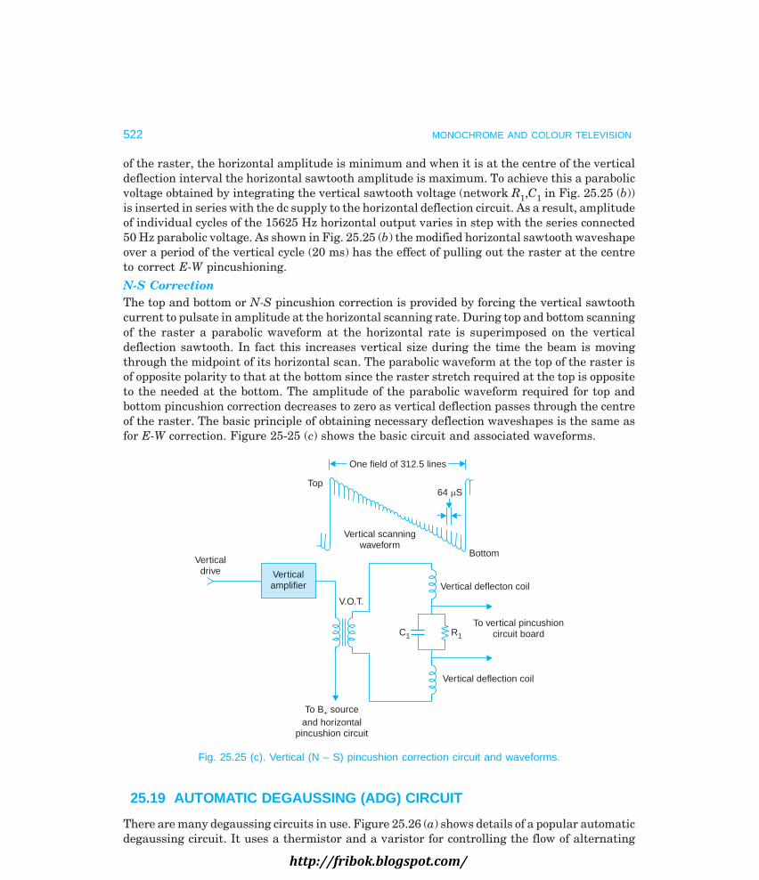
522 MONOCHROME AND COLOUR TELEVISION
of the raster, the horizontal amplitude is minimum and when it is at the centre of the verticaldeflection interval the horizontal sawtooth amplitude is maximum. To achieve this a parabolicvoltage obtained by integrating the vertical sawtooth voltage (network R1,C1 in Fig. 25.25 (b))is inserted in series with the dc supply to the horizontal deflection circuit. As a result, amplitudeof individual cycles of the 15625 Hz horizontal output varies in step with the series connected50 Hz parabolic voltage. As shown in Fig. 25.25 (b) the modified horizontal sawtooth waveshapeover a period of the vertical cycle (20 ms) has the effect of pulling out the raster at the centreto correct E-W pincushioning.
N-S CorrectionThe top and bottom or N-S pincushion correction is provided by forcing the vertical sawtoothcurrent to pulsate in amplitude at the horizontal scanning rate. During top and bottom scanningof the raster a parabolic waveform at the horizontal rate is superimposed on the verticaldeflection sawtooth. In fact this increases vertical size during the time the beam is movingthrough the midpoint of its horizontal scan. The parabolic waveform at the top of the raster isof opposite polarity to that at the bottom since the raster stretch required at the top is oppositeto the needed at the bottom. The amplitude of the parabolic waveform required for top andbottom pincushion correction decreases to zero as vertical deflection passes through the centreof the raster. The basic principle of obtaining necessary deflection waveshapes is the same asfor E-W correction. Figure 25-25 (c) shows the basic circuit and associated waveforms.
64 Sm
One field of 312.5 lines
Top
Vertical scanningwaveform
BottomVertical
drive Verticalamplifier
V.O.T.
Vertical deflecton coil
To vertical pincushioncircuit boardR1C1
Vertical deflection coil
To B sourceand horizontal
pincushion circuit
+
Fig. 25.25 (c). Vertical (N – S) pincushion correction circuit and waveforms.
25.19 AUTOMATIC DEGAUSSING (ADG) CIRCUIT
There are many degaussing circuits in use. Figure 25.26 (a) shows details of a popular automaticdegaussing circuit. It uses a thermistor and a varistor for controlling the flow of alternating
http://fribok.blogspot.com/

ESSENTIALS OF COLOUR TELEVISION 523
current through the degaussing coil. When the receiver is turned on the ac voltage drop acrossthe thermistor is quite high (about 60 volts) and this causes a large current to flow through thedegaussing coil. Because of this heavy current, the thermistor heats up, its resistance falls andvoltage drop across it decreases. As a result, voltage across the varistor decreases therebyincreasing its resistance. This in turn reduces ac current through the coil to a very low value.The circuit components are so chosen that initial surge of current through the degaussing coilis close to 4 amperes and drops to about 25 mA in less than a second. This is illustrated inFig. 25.26 (b). Once the thermistor heats up degaussing ends and normal ac voltage is restoredto the B+ rectifier circuit.
S1
220 Vac mains
ThermistorPowertransformer
Varistori
Degaussing coil
To rectifiercircuit
of B supply+
(a)
Residualcurrent
i
0
(b)
Fig. 25.26. Automatic degaussing (ADG) (a) typical circuit (b) variation of current in thedegaussing coil when receiver is just switched on.
25.20 GREY SCALE TRACKING
It may be recalled that red, green and blue lights must combine in definite proportions toproduce white light. The three phosphors have different effeciencies. Also the three guns maynot have identical Ip/Vgk characteristics and cut-off points. Therefore, it becomes necessary toincorporate suitable adjustments such that monochrome information is rproduced correctly(with no colour tint) for all settings of the contrast control. In practice, this amounts to twodistinct steps:
(a) Adjustment of Low LightsNon-concident Ip/Vgk characteristics and consequent difference in cut-off points of the threeguns, results in appearance of coloured tint instead of pure dark grey shades in areas of lowbrightness. To correct this it is necessary to bring the cut-off points in coincidence. This isachieved by making the screen grid (i.e., 1st anode) voltage different from each other.Potentiometers are normally provided for this purpose in the dc voltage supply to the threescreen grids.
(b) Adjustment of High LightsIt is equally necessary to ensure that all other levels of white are also correctly reproduced.This amounts to compensating for the slightly different slopes and also for the substantiallydifferent phosphor efficiencies. This is achieved by varying the video (luminance) signal driveto the three guns. Since the red phosphor has the lowest efficiency, maximum video signal isfed to the red cathode and then by the use of potentiometers video signal amplitudes to thegreen and blue guns are varied (see Fig. 25.11) to obtain optimum reproduction of high lights.
http://fribok.blogspot.com/
524 MONOCHROME AND COLOUR TELEVISION
References1. J. Kasshock, Deflection in the 20 AX systems, IEEE Trans. BTR, Vol. 20, No. 4, Nov. 1974.
2. P.G.J. Barton, The 20 AX system and picture tube, IEEE Trans. BTR, Vol. 20, No. 4 Nov. 1974.
Review Questions
1. What do you understand by compatibility in TV transmission ? Enumerate essential require-ments that must be met to make a colour system fully compatible.
2. Explain briefly how the human eye perceives brightness and colour sensations. Comment on thespectral response of the human eye ?
3. Explain the terms—(i) primary colours, (ii) complementary colours, (iii) additive colour mixing,(iv) hue, (v) saturation, (iv) luminance, and (vii) chrominance.
4. Describe with a diagram the construction of a colour TV camera and its optical system. Why arethe outputs of all the three camera tubes set equal when standard white light is made incident ?
5. Explain how the ‘Y’ and colour difference signals are developed from camera outputs. Why is the‘Y’ signal set = 0.3R + 0.59G – 0.11B ?
6. Why is the (G – Y) difference signal not chosen for transmission ? Explain how it is obtained inthe receiver for modulating the corresponding beam of the picture tube.
7. Explain how colour difference signals disappear at the output of the signal combining matrix onwhite and grey shades. What is the significance of ‘Y’ signal in colour transmission and reception ?
8. While televising a static desaturated colour scene, the camera outputs were found to have thefollowing amplitudes:
VR = 0.7 V, VG = 0.6 V and VB = 0.3 V
What is the basic hue of the scene ? Compute values of (G–Y) and Y signals and establish thattrue hue and brightness will be reproduced in the receiver. What shade will such a signal pro-duce in a monochrome receiver ?
9. Describe with suitable diagrams the gun arrangement and constructional details of a delta-guncolour picture tube. Why is it necessary to connect a very high voltage at the final anode of acolour picture tube ?
10. Define purity and convergence and explain why elaborate static and dynamic corrections becomenecessary to obtain colour purity and coincident rasters.
11. What are the drawbacks of a delta-gun tube ? Describe constructional details of a P.I.L. tube andexplain how it is different from a delta gun colour tube. When are its distinguishing features ?
12. Define astigmatism and coma errors with reference to a P.I.L. tube and describe the fielddistribution which must be obtained to overcome such distortions in the reproduced picture.
13. Describe how a multipole ring magnets assembly can be used to deflect the electron beam indifferent directions. Describe purity and static convergence adjustments which are normallyprovided with a P.I.L. tube-deflection assembly.
14. Describe briefly the dynamic convergence errors in a P.I.L. tube. Explain the corrections that arenormally made to achieve almost distortionless reproduction of colours on the screen of a P.I.L.tube. Explain why vertical (N – S) raster shap correction is not necessary in such a picture tube.
15. Describe essential features of a Trintron colour picture tube. Explain why is it considered supe-rior both the delta-gun and P.I.L. picture tubes.
http://fribok.blogspot.com/

ESSENTIALS OF COLOUR TELEVISION 525
16. What is pincushion correction and explain how both E – W and N – S pincushions corrections arecarried out.
17. What do you understand by degaussing and why it is necessary ? Describe with a typical circuithow degaussing is affected each time the receiver is switched on.
18. What do you understand by grey scale tracking ? Explain how it is carried out both for low andhigh light levels of the video signal.
http://fribok.blogspot.com/

26!#
http://fribok.blogspot.com/

Three different systems of colour television (CTV) emerged after prolonged research andexperimentation. These are:
(i) The American NTSC (National Television Systems Committee) system.
(ii) The German PAL (Phase Alteration by Line) systems.
(iii) The French SECAM (Sequential Couleures a memoire) system.
When quality of the reproduced picture and cost of equipment are both taken into account,it becomes difficult to establish the superiority of one system over the other. Therefore, all thethree CTV systems have found acceptance in different countries and the choice has been mostlyinfluenced by the monochrome system already in use in the country.
Since India adopted the 625 line CCIR (B standards) monochrome system it has chosento introduce the PAL system* (B & G standards) because of compatibility between the two,and also due to its somewhat superior performance over the other two systems.
In many respects transmission and reception techniques employed in the NTSC andPAL systems are similar. These are, therefore, treated together before going into encoding anddecoding details of each system. The SECAM system, being much different from the other two,is described separately in the later part of this chapter.
26.1 COLOUR SIGNAL TRANSMISSION
The colour video signal contains two independent informations, that of hue and saturation. Itis a difficult matter to modulate them to one and the same carrier in such a way that these canbe easily recovered at the receiver without affecting each other. The problem is accentuated bythe need to fit this colour signal into a standard TV channel which is almost fully occupied bythe ‘Y’ signal. However, to satisfy compatibility requirements the problem has been ingeniouslysolved by combining the colour information into a single variable and by employing what isknown as frequency interleaving.
528
$
!#
*In the CCIR PAL I standards the picture and sound carrier are 6 MHz apart and the channelbandwidth is 8 MHz. The only difference between PAL-B and PAL-G is in the channel bandwidth.PAL-B with channel bandwidth of 7 MHz does not provide any inter-channel gap, whereas PAL-G withchannel bandwidth of 8 MHz provides a band gap of 1 MHz in-between successive channels.
http://fribok.blogspot.com/
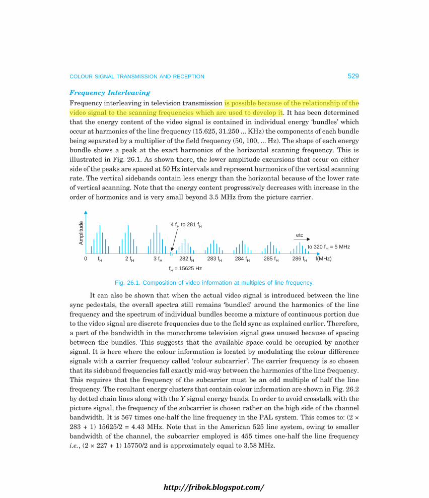
COLOUR SIGNAL TRANSMISSION AND RECEPTION 529
Frequency Interleaving
Frequency interleaving in television transmission is possible because of the relationship of thevideo signal to the scanning frequencies which are used to develop it. It has been determinedthat the energy content of the video signal is contained in individual energy ‘bundles’ whichoccur at harmonics of the line frequency (15.625, 31.250 ... KHz) the components of each bundlebeing separated by a multiplier of the field frequency (50, 100, ... Hz). The shape of each energybundle shows a peak at the exact harmonics of the horizontal scanning frequency. This isillustrated in Fig. 26.1. As shown there, the lower amplitude excursions that occur on eitherside of the peaks are spaced at 50 Hz intervals and represent harmonics of the vertical scanningrate. The vertical sidebands contain less energy than the horizontal because of the lower rateof vertical scanning. Note that the energy content progressively decreases with increase in theorder of hormonics and is very small beyond 3.5 MHz from the picture carrier.
4 f to 281 fH H
etc
to 320 f = 5 MHzH
Am
plitu
de
0 fH 2 fH 3 fH 282 fH 283 fH 284 fH 285 fH 286 fH f(MHz)
fH = 15625 Hz
Fig. 26.1. Composition of video information at multiples of line frequency.
It can also be shown that when the actual video signal is introduced between the linesync pedestals, the overall spectra still remains ‘bundled’ around the harmonics of the linefrequency and the spectrum of individual bundles become a mixture of continuous portion dueto the video signal are discrete frequencies due to the field sync as explained earlier. Therefore,a part of the bandwidth in the monochrome television signal goes unused because of spacingbetween the bundles. This suggests that the available space could be occupied by anothersignal. It is here where the colour information is located by modulating the colour differencesignals with a carrier frequency called ‘colour subcarrier’. The carrier frequency is so chosenthat its sideband frequencies fall exactly mid-way between the harmonics of the line frequency.This requires that the frequency of the subcarrier must be an odd multiple of half the linefrequency. The resultant energy clusters that contain colour information are shown in Fig. 26.2by dotted chain lines along with the Y signal energy bands. In order to avoid crosstalk with thepicture signal, the frequency of the subcarrier is chosen rather on the high side of the channelbandwidth. It is 567 times one-half the line frequency in the PAL system. This comes to: (2 ×283 + 1) 15625/2 = 4.43 MHz. Note that in the American 525 line system, owing to smallerbandwidth of the channel, the subcarrier employed is 455 times one-half the line frequencyi.e., (2 × 227 + 1) 15750/2 and is approximately equal to 3.58 MHz.
http://fribok.blogspot.com/
shree
Highlight
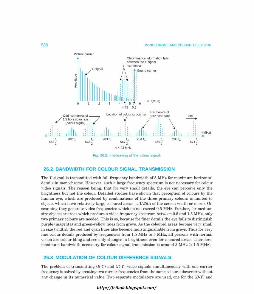
530 MONOCHROME AND COLOUR TELEVISION
Chrominance information fallsbetween the Y signalharmonics
Sound carrier
Picture carrier
Y signal
Am
plitu
de
0 1 2 3 4 5 64.43 5.5
f(MHz)
Odd harmonics of1/2 horz scan rate
(colour signal)
Location of colour subcarrierHarmonics ofhorz scan rate etc
f(MHz)
563f2H 282 fH 565
f2H 283 fH 567
f2H 284 fH 569
f2H 571
f2H285 fH
» 4.43 MHz
Fig. 26.2. Interleaving of the colour signal.
26.2 BANDWIDTH FOR COLOUR SIGNAL TRANSMISSION
The Y signal is transmitted with full frequency bandwidth of 5 MHz for maximum horizontaldetails in monochrome. However, such a large frequency spectrum is not necessary for colourvideo signals. The reason being, that for very small details, the eye can perceive only thebrightness but not the colour. Detailed studies have shown that perception of colours by thehuman eye, which are produced by combinations of the three primary colours is limited toobjects which have relatively large coloured areas (≈ 1/25th of the screen width or more). Onscanning they generate video frequencies which do not exceed 0.5 MHz. Further, for mediumsize objects or areas which produce a video frequency spectrum between 0.5 and 1.5 MHz, onlytwo primary colours are needed. This is so, because for finer details the eye fails to distinguishpurple (magenta) and green-yellow hues from greys. As the coloured areas become very smallin size (width), the red and cyan hues also become indistinguishable from greys. Thus for veryfine colour details produced by frequencies from 1.5 MHz to 5 MHz, all persons with normalvision are colour bling and see only changes in brightness even for coloured areas. Therefore,maximum bandwidth necessary for colour signal transmission is around 3 MHz (± 1.5 MHz).
26.3 MODULATION OF COLOUR DIFFERENCE SIGNALS
The problem of transmitting (B-Y) and (R-Y) video signals simultaneously with one carrierfrequency is solved by creating two carrier frequencies from the same colour subcarrier withoutany change in its numerical value. Two separate modulators are used, one for the (B-Y) and
http://fribok.blogspot.com/

COLOUR SIGNAL TRANSMISSION AND RECEPTION 531
the other for the (R-Y) signal. However, the carrier frequency fed to one madulator is given arelative phase shift of 90° with respect to the other before applying it to the modulator. Thus,the two equal subcarrier frequencies which are obtained from a common generator are said to
C = (R – Y) + (B – Y)2 2
q = tan–1 R – Y
B – Y( )
C(t)
q(t)
Resultant subcarrierphasor
(R – Y)t
(B – Y)t
+ (R – Y)
Location of(R – Y) and (B – Y)subcarrier phasors
+ 0.7
– 0.3
Red
0.76
– 0.11
+ .89
Blue
+ (B – Y)
0.9
– 0.59
– 0.590.83
Green
0.59
0.59
Magenta
0.83
0.3
– 0.7Cyan
0.76
0.90.11
– 0.89 Yellow
Fig. 26.3. Quadrature amplitude modulated colour difference signals and theposition of resultant subcarrier phasor for the primary and complementary colours.
Note that the magnitudes shown correspond to unweighted values of colour difference signals.
http://fribok.blogspot.com/

532 MONOCHROME AND COLOUR TELEVISION
be in quadrature and the method of modulation is known as quadrature modulation. Aftermodulation the two outputs are combined to yield C, the resultant subcarrier phasor. Sincethe amplitude of C, the chrominance signal, corresponds to the magnitudes of colour differencesignals, its instantaneous value represents colour saturation at that instant. Maximumamplitude corresponds to greatest saturation and zero amplitude to no saturation i.e., white.Similarly, the instantaneous value of the C phasor angle (θ) which may vary from 0° to 360°represents hue of the colour at that moment. Thus the chrominance signal contains fullinformation about saturation and hue of various colours. This being a crucial point in coloursignal transmission, is illustrated by a few examples. However, it would be necessary to firstexpress (R-Y) and (B-Y) in terms of the three camera output voltages. This is done by substitutingY = 0.59G + 0.3R + 0.11B in these expressions. Thus (R-Y) becomes R – 0.59G – 0.3R – 0.11B =0.7R – 0.59G – 0.11B. Similarly, (B-Y) becomes B – 0.59G – 0.3R – 0.11B = 0.89B – 0.59G– 0.3R.
Now suppose that only pure red colour is being scanned by the colour camera. Thiswould result in an output from the red camera only, while the green and blue outputs will bezero. Therefore, (R-Y) signal will become simply + 0.7R and (B-Y) signal will be reduced to– 0.3R. The resultant location of the subcarrier phasor after modulation is illustrated in Fig.26.3. Note that the resultant phasor is counter clockwise to the position of + (R-Y) phasor.
Next consider that the colour camera scans a pure blue colour scene. This yields (R-Y)= – 0.11B and (B-Y) = 0.89 B. The resultant phasor for this colour lags + (B-Y) vector by a smallangle. Similarly the location and magnitude for any colour can be found out. This is illustratedin Fig. 26.3 for the primary and complementary colours.
Another point that needs attention is the effect of desaturation on the colour phasors.Since desaturation results in reduction of the amplitudes of both (B-Y) and (R-Y) phasors, theresultant chrominance phasor accordingly changes its magnitude depending on the degree ofdesaturation. Thus any change in the purity of a colour is indicated by a change in the magnitudeof the resultant subcarrier phasor.
Colour Burst SignalSuppressed carrier double sideband working is the normal practice for modulating colour-difference signals with the colour subcarrier frequency. This is achieved by employing balancedmodulators. The carrier is suppressed to minimize interference produced by the chrominancesignals both on monochrome receivers when they are receiving colour transmissions and inthe luminance channel of colour receivers themselves. As explained in an earlier chapter theratio of the sideband power to carrier power increases with the depth of modulation. However,even at 100% modulation two-thirds of the total power is in the carrier and only one-third isthe useful sideband power. Thus suppressing the carrier clearly eliminates the main potentialsource of interference. In addition of this, the colour-difference signals which constitute themodulating information are zero when the picture detail is non-coloured (i.e., grey, black orwhite shades) and so at such times the sidebands also disappear leaving no chrominancecomponent in the video signal.
As explained above the transmitted does not contain the subcarrier frequency but it isnecessary to generate it in the receiver with correct frequency and phase relationship for properdetection of the colour sidebands. To ensure this, a short sample of the subcarrier oscillator,
http://fribok.blogspot.com/

COLOUR SIGNAL TRANSMISSION AND RECEPTION 533
(8 to 11 cycles) called the ‘colour burst’ is sent to the receiver along with sync signals. This islocated in the back porch of the horizontal blanking pedestal. The colour burst does not interferewith the horizontal sync because it is lower in amplitude and follows the sync pulses. Its exactlocation is shown in Fig. 26.4. The colour burst is gated out at the receiver and is used inconjuction with a phase comparator circuit to lock the local subcarrier oscillator frequency andphase with that at the transmitter. As the burst signal must maintain a constant phaserelationship with the scanning signals to ensure proper frequency interleaving, the horizontaland vertical sysc pulses are also derived from the subcarrier through frequency divider circuits.
Horz sync pulse
Burst of 8–11cycles of colour
subcarrier
Hor on a blank ng in ervalHorizontal blanking interval
Fig. 26.4. Location of colour burst on the back porch of each horizontal sync pulse.
26.4 WEIGHTING FACTORS
The resultant chrominance signal phasor (C) is added to the luminance signal (Y) beforemodulating it with the channel carrier for transmission. The amplitude, i.e., level line of Ysignal becomes the zero line for this purpose. Such an addition is illustrated in Fig. 26.5 for atheoretical 100 percent saturated, 100 percent amplitude colour bar signal. The peak-to-peakamplitude of green signal (± 0.83) gets added to the corresponding luminance amplitude of0.59. For the red signal the chrominance amplitude of ± 0.76 adds to its brightness of 0.3.Similarly other colours add to their corresponding luminance values to form the chroma signal.However, observe that it is not practicable to transmit this chroma waveform because thesignal peaks would exceed the limits of 100 percent modulation. This means that on modulationwith the picture carrier some of the colour signal amplitudes would exceed the limits ofmaximum sync tips on one side and white level on the other. For example, in the case ofmagenta signal, the chrominance value of ± 0.83 when added to its luminance amplitude of0.41 exceeds the limits of 100 percent modulation of both white and black levels. Similarly bluesignal amplitude greatly exceeds the black level and will cause a high degree of overmodulation.
http://fribok.blogspot.com/

534 MONOCHROME AND COLOUR TELEVISION
– 1
– .5
0
+ .5
+
Rel
ativ
eam
plitu
de
– 1
0
Rel
ativ
eam
plitu
de
.2
.4
.2
.4
.6
.81.0
0.9
0.76
0.9
0.76
0.83
0.83
0.83
0.83
0.76
0.76
0.9
0.9
Colour bar
White MagentaYellow Cyan Green Red Blue Black
1.00.89
0.70.59
0.410.3
0.110.00
Subcarrierburst, 10
cycles
si(a) Y signal
h a g(b) Chrominance signal
0.9
0.76
0.9
0.76
0.83
0.83
0.83
0.83
0.76
0.76
0.9
0.9
0.89
.7.59
.41.3
.11
1.4
1.0
0
.4
Sync pulse
0
Colour burst
Rel
ativ
evi
deo
sign
alam
plitu
de
.100%
76%
0%1.0
Pic
ture
carr
ier
ampl
itude
(c) Composite colour signal (a - b)
Fig. 26.5. Generation of composite colour signal for a theoretical 100% saturated,100% amplitude colour bar signal. As seen from the relative amplitude scales,
the composite video signal would cause gross over-modulation. Therefore in practice thecolour difference signals are reduced in amplitude to avoid any excessive over-modulation.
If overmodulation is permitted the reproduced colours will get objectionably distorted.Therefore, to avoid overmodulation on 100 percent saturation colour values, it is necessary toreduce the amplitude of colour difference video signal before modulating them with the coloursubcarrier. Accordingly, both (R–Y) and (B–Y) components of the colour video signal are scaled
http://fribok.blogspot.com/

COLOUR SIGNAL TRANSMISSION AND RECEPTION 535
down by multiplying them with what are known as ‘weighting factors’. Those used are 0.877for the (R–Y) component and 0.493 for the (B–Y) component. The compensated values areobtained by using potentiometers at the outputs of (R–Y) and (B–Y) adders (see Fig. 25.9).Note that no reduction is made in the amplitude of Y signal. It may also be noted that since thetransmitter radiates weighted chrominance signal values, these must be increased to theuncompensated values at the colour TV receiver for proper reproduction of different hues.This is carried out by adjusting gains of the colour difference signal amplifiers. The unweightedand weighted values of colour difference signals are given below in Table 26.1.
Table 26.1
B – Y R – Y G – Y CSC B – Y R – Y CSC
Colour Luminance Unweighted Weightedsignal (λ)
White 1 0 0 0 0 0 0 0
Yellow 0.89 –.89 +.11 +.11 .9 –.4385 +.096 0.44
Cyan 0.7 +.3 –.7 +.3 .76 +.148 –.614 0.63
Green 0.59 –.59 –.59 +.41 .83 –.29 –.517 0.59
Magenta 0.41 +.59 +.59 –.41 .83 +.29 +.517 0.59
Red 0.3 –.3 +.7 –.3 .76 –.148 +.614 0.63
Blue 0.11 +.89 –.11 –.11 .9 +.4388 –.096 0.44
Black 0 0 0 0 0 0 0 0
CSC = (B Y) (R Y)2 2− + −
(B – Y) weighted = 0.493 (B – Y) unweighted
(R – Y) weighted = 0.877 (R – Y) unweighted
26.5 FORMATION OF THE CHROMINANCE SIGNAL
Using the information of Table 26.1, Fig. 26.6 illustrates the formation of the chroma signal fora colour bar pattern after the colour difference signals have been scaled down in accordancewith corresponding weighting factors. Note that new amplitudes of the chrominance subcarriersignals are 0.63 for red and cyan, 0.59 for green and magenta and 0.44 for blue and yellow.These amplitudes will still cause overmodulation to about 33%. This is permitted, because inpractice, the saturation of hues in natural and staged scenes seldom exceeds 75 percent. Sincethe amplitude of chroma signal is proportional to the saturation of hue, maximum chromasignal amplitudes are seldom encountered in practice. Therefore, the weighted chroma valuesresult in a complete colour signal that will rarely, if ever, overmodulate the picture carrier ofa CTV transmitter. Hence it is not necessary to further decrease the signal amplitudes byemploying higher weighting factors.
http://fribok.blogspot.com/

536 MONOCHROME AND COLOUR TELEVISION
0%
76%
100%
Rel
ativ
eca
rrie
ram
plitu
de
Blankingperiod
Zero carrier level1.4
1.0Peakwhite
0
.4
Rel
ativ
evi
deo
ampl
itude
0.44
0.44
0.63
0.63 0.
590.
59
0.59
0.59 0.
630.
63
0.44
0.44
Mag
enta
Gre
en
Cya
n
Yel
low
Whi
te
Red
Blu
e
Bla
ck
Colour bar
Sync pulse
Colour burst
Blacklevel
Y signal
Chrominancesignal
Fig. 26.6. 100% saturated, 100% amplitude colour-bar signal in which thecolour difference signals are reduced by weighting factors to restrict the
chrominance signal excursions to 33% beyond black and peak white levels.
Chroma Signal Phasor DiagramThe compensation (readjustment) of chroma signal values results in a change of chroma phaseangles. In the NTSC system it is a common practice to measure phase angles relative to the
0° 13°
– 0.493 (B – Y)
Yellow0.44
76.5° 119°
0.63Red
0.877 (R – Y)
0.59Magenta
0.493 (B – Y)
193°0.44Blue
256.5°299°
0.63Cyan
– 0.877 (R – Y)
0.59Green
Fig. 26.7. Magnitude and phase relationships of compensatedchrominance signals for the primary and complementary colours.http://fribok.blogspot.com/

COLOUR SIGNAL TRANSMISSION AND RECEPTION 537
– (B–Y) phasor. This location has been designated 0° or the reference phase position on thephasor diagram (see Fig. 26.7) because this is also the phase of the colour burst that istransmitted on the back porch of each horizontal sync pulse. Referring to Fig. 26.7 thecompensated colour magenta is represented by a phasor at an angle of 119°. In the samemanner the diagram indicates phase angles and amplitudes of other colour signals. Note thatprimary colours are 120° apart and complementary colours differ in phase by 180° from theircorresponding primary colours.
26.6 NTSC COLOUR TV SYSTEM
The NTSC colour system is compatible with the American 525 line monochrome system. Inorder to save bandwidth, advantage is taken of the fact that eye’s resolution of colours alongthe reddish blue-yellowish green axis on the colour circle is much less than those colours whichlie around the yellowish red-greenish blue axis. Therefore two new colour video signals, whichcorrespond to these colour regions, are generated. These are designated as I and Q signals.The I signal lies in a region 33° counter clockwise to + (R – Y) where the eye has maximumcolour resolution. It* is derived from the (R – Y) and (B – Y) signals and is equal to 0.60R– 0.28G – 0.32B. As shown in Fig. 26.8 it is located at an angle of 57° with respect to the colourburst in the balanced modulator circuits. Similarly the Q** signal is derived from colourdifference signals by suitable matrix and equals 0.21R –0.52G + 0.31B. It is located 33° counter
0°– (B – Y)
– Q
327° 237°
– I
– (R – Y)
(B – Y)
33°
147°
+ Q
9090°
(R – Y)
+ I
33°
57°
333°
147°57°
0°Burst
Isc
Qsc
Fig. 26.8. Phasor diagrams of the I and Q signals in the NTSC system.
clockwise to the +(B – Y) signal and is thus in quadrature with the I signal. As illustrated inFig. 26.8 the Q signal covers the regions around magenta (reddish-blue) and yellow-greenshades. Similarly orange hues correspond to phase angles centred around + I and the
*I = 0.74(R – Y) – 0.27(B – Y).
**Q = 0.48(R – Y) + 0.41(B – Y).
http://fribok.blogspot.com/

538 MONOCHROME AND COLOUR TELEVISION
complementary blue-green (cyan) hues are located around the diametrically opposite – I signal.Since the eye is capable of resolving fine details in these regions, I signal is allowed to possessfrequencies up to 1.5 MHz. However, the eye is least sensitive to colours that lie around the ±Qsignals, and therefore it is allowed a bandwidth of only ±0.5 MHz with respect to the coloursubcarrier.
It may be noted that both I and Q signals are active up to 0.5 MHz and being at rightangles to each other, combine to produce all the colours contained in the chrominance signal.However, the Q signal drops out after 0.5 MHz and only I signal remains between 0.5 and 1.5MHz to produce colours, the finer details of which the eyes can easily perceive.
To help understand this fact it may be recalled that only one colour difference signal isneeded for producing colours which are a mixture of only two colours. Thus the Q signal is notnecessary for producing colours lying in the region of orange (red + green) and cyan (green +blue) hues. Hence at any instant when Q = 0 and only I signal is active the colours produced onthe screen will run the gamut from reddish orange to bluish green.
Bandwidth ReductionDouble sideband transmission is allowed for the Q signal and it occupies a channel bandwidthof 1 MHz (± 0.5 MHz). However, for the I signal the upper sideband is restricted to a maximumof 0.5 MHz while the lower sideband is allowed to extent up to 1.5 MHz. As such it is a form ofvestigial sideband transmission. Thus in all, a bandwidth of 2 MHz is necessary for coloursignal transmission. This is a saving of 1 MHz as compared to a bandpass requirement of 3MHz if (B – Y) and (R – Y) are directly transmitted.
It is now obvious that in the NTSC system, advantage is taken of the limitations of thehuman eye to restrict the colour signal bandwidth, which in turn results in reduced interferencewith the sound and picture signal sidebands. The reduction in colour signal sidebands is alsodictated by the relatively narrow channel bandwidth of 6 MHz in the American TV system.
Exact Colour Subcarrier FrequencyThe colour subcarrier frequency in the NTSC system has been chosen to have an exact valueequal to 3.579545 MHz. The reason for fixing it with such a precision is to maintain compatibilitybetween monochrome and colour systems. Any interference between the chrominance signaland higher video frequencies is minimized by employing suppressed carrier (colour subcarrier)transmission and by using a notch filter in the path of the luminance signal. However, when acolour transmission is received on a monochrome receiver a dot pattern structure appearsalong each raster line on the receiver screen. This is caused by the colour signal frequenciesthat lie within the pass-band of the video section of the receiver. As illustrated below such aninterference can be eliminated if the subcarrier frequency is maintained at the exact valuementioned above.
Assume that the interfering colour signal has a sinusoidal variation which rides on theaverage brightness level of the monochrome signal. This produces white and black dots on thescreen. If the colour subcarrier happens to be a multiple of the line frequency (n × fh) the phaseposition of the disturbing colour frequency will be same on successive even or odd fields. Thusblack and white dots will be produced at the same spots on the screen and will be seen as apersistent dot pattern interference. However, if a half-line offset is provided by fixing the sub-carrier frequency to be an odd multiple of the half-line frequency, the disturbing colour signal
http://fribok.blogspot.com/
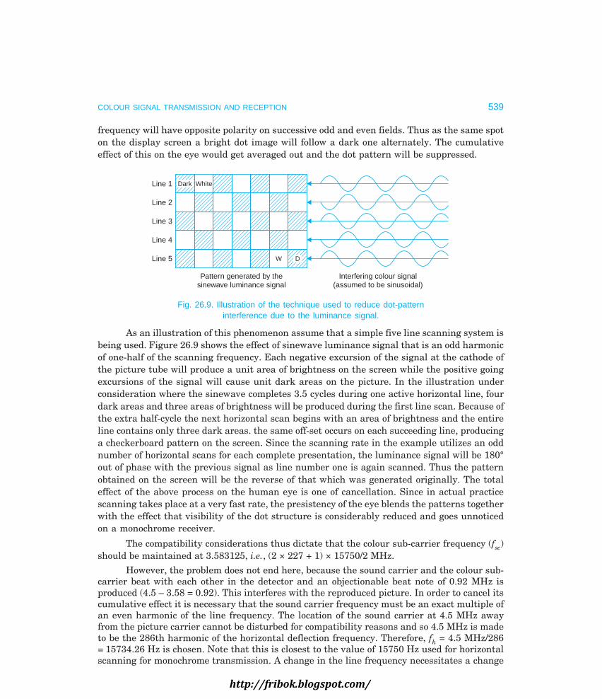
COLOUR SIGNAL TRANSMISSION AND RECEPTION 539
frequency will have opposite polarity on successive odd and even fields. Thus as the same spoton the display screen a bright dot image will follow a dark one alternately. The cumulativeeffect of this on the eye would get averaged out and the dot pattern will be suppressed.
Line 1
Line 2
Line 3
Line 4
Line 5
Dark White
W D
Interfering colour signal(assumed to be sinusoidal)
Pattern generated by thesinewave luminance signal
Fig. 26.9. Illustration of the technique used to reduce dot-patterninterference due to the luminance signal.
As an illustration of this phenomenon assume that a simple five line scanning system isbeing used. Figure 26.9 shows the effect of sinewave luminance signal that is an odd harmonicof one-half of the scanning frequency. Each negative excursion of the signal at the cathode ofthe picture tube will produce a unit area of brightness on the screen while the positive goingexcursions of the signal will cause unit dark areas on the picture. In the illustration underconsideration where the sinewave completes 3.5 cycles during one active horizontal line, fourdark areas and three areas of brightness will be produced during the first line scan. Because ofthe extra half-cycle the next horizontal scan begins with an area of brightness and the entireline contains only three dark areas. the same off-set occurs on each succeeding line, producinga checkerboard pattern on the screen. Since the scanning rate in the example utilizes an oddnumber of horizontal scans for each complete presentation, the luminance signal will be 180°out of phase with the previous signal as line number one is again scanned. Thus the patternobtained on the screen will be the reverse of that which was generated originally. The totaleffect of the above process on the human eye is one of cancellation. Since in actual practicescanning takes place at a very fast rate, the presistency of the eye blends the patterns togetherwith the effect that visibility of the dot structure is considerably reduced and goes unnoticedon a monochrome receiver.
The compatibility considerations thus dictate that the colour sub-carrier frequency (fsc)should be maintained at 3.583125, i.e., (2 × 227 + 1) × 15750/2 MHz.
However, the problem does not end here, because the sound carrier and the colour sub-carrier beat with each other in the detector and an objectionable beat note of 0.92 MHz isproduced (4.5 – 3.58 = 0.92). This interferes with the reproduced picture. In order to cancel itscumulative effect it is necessary that the sound carrier frequency must be an exact multiple ofan even harmonic of the line frequency. The location of the sound carrier at 4.5 MHz awayfrom the picture carrier cannot be disturbed for compatibility reasons and so 4.5 MHz is madeto be the 286th harmonic of the horizontal deflection frequency. Therefore, fh = 4.5 MHz/286= 15734.26 Hz is chosen. Note that this is closest to the value of 15750 Hz used for horizontalscanning for monochrome transmission. A change in the line frequency necessitates a change
http://fribok.blogspot.com/

540 MONOCHROME AND COLOUR TELEVISION
in the field frequency since 262.5 lines must be scanned per field. Therefore the field frequency(fv) is changed to be 15734.26/262.5 = 59.94 Hz in place of 60 Hz.
The slight difference of 15.74 Hz in the line frequency (15750 – 15734.26 = 15.74 Hz)and of 0.06 Hz in the field frequency (60 – 59.94 = 0.06 Hz) has practically no effect on thedeflection oscillators because an oscillator that can be triggered by 60 Hz pulses can also besynchronized to produce 59.94 Hz output. Similarly the AFC circuit can easily adjust the linefrequency to a slightly different value while receiving colour transmission.
As explained earlier the colour sub-carrier frequency must be an odd multiple of halfthe line frequency to suppress dot pattern interference. Therefore fsc is fixed at (2n + 1) fh/2,i.e., 455 × 15734.26/2 = 3.579545 MHz. To obtain this exact colour sub-carrier frequency, acrystal controlled oscillator is provided.Encoding of Colour Picture InformationFigure 26.10 illustrates the enconding process of colour signals at the NTSC transmitter. Asuitable matrix is used to get both I and Q signals directly from the three camera outputs.Since I = 0.60R – 0.28G – 0.32B, the green and blue camera outputs are inverted before feedingthem to the appropriate matrix. Similarly for Q = 0.21R – 0.52G + 0.31B, in invertor is placedat the output of green camera before mixing it with the other two camera outputs.
0 – 0.5MHzfilter
Adder
0 – 1.5MHzfilter
Balancedmodulator
( )I
M
A
T
R
I
X
R
G
Q
Y
I
B
Sync andblanking pulses
Maintransmitter
Sound signal
snan
Compositechrominance
signal
1.0
0
Y
3.58 MHz1.0
0
1.0
0
0.5MHz
Q sideband spectrum
AntennaY
1.0
0
Y signal spectrum
4.2 MHz
Composite Y signal
Balancedmodulator
(Q)
3.58 MHz
sidebands h mic
n
Chromi-nancesignal
AdderC
147°
B.P.filter
90°phaseshift
57°phaseshift
Burstgate
Coloursubcarriergenerator
fsc 3.579545 MHz
Burst gatekeying pulses
fsc0°
Subcarrier burst
57°
1.0
0
Y I sidebandspectrum
3.58 MHz
0.5 MHz1.5 MHz
Fromcolour
camera
Fig. 26.10. Functional diagram of a NTSC coder.
http://fribok.blogspot.com/

COLOUR SIGNAL TRANSMISSION AND RECEPTION 541
The bandwidths of both I and Q are restricted before feeding them to the correspondingbalanced modulators. The subcarrier to the I modulator is phase shifted 57° clockwise withrespect to the colour burst. The carrier is shifted by another 90° before applying it to the Qmodulator. Thus relative phase shift of 90° between the two subcarriers is maintained forquadrature amplitude modulation.
It is the characteristic of a balanced modulator that while it suppresses the carrier andprovides frequency translation, both the amplitude and phase of its output are directly relatedto the instantaneous amplitude and phase of the modulating signal. Thus, with the subcarrierphase angles shifted to the locations of I and Q, the outputs from both the modulators retainfull identity of the modulating colour difference signals. The sideband restricted output fromthe I modulator combines with the output of Q modulator to form the chrominance signal. It isthen combined with the composite Y signal and colour burst in an adder to form compositechrominance signal. The output from the adder feeds into the main transmitter and modulatesthe channel picture carrier frequency. Note that colour subcarrier has the same frequency(3.579545 MHz) for all the stations whereas the assigned picture carrier frequency is differentfor each channel.
26.7 NTSC COLOUR RECEIVER
A simplified block diagram of the NTSC colour receiver is shown in Fig. 26.11. The signal fromthe selected channel is processed in the usual way by the tuner, IF and video detector stages.The sound signal is separately detected, demodulated and amplified before feeding it to theloudspeaker. Similarly AGC, sync separator and deflection circuits have the same form as inmonochrome receivers except for the inclusion of purity, convergence and pincushion correctioncircuits.
At the output of video detector the composite video and chrominance signals reappearin their original premodulated form. The Y signal is processed as in a monochrome receiverexcept that the video amplifier needs a delay line. The delay line introduces a delay of about500 ns which is necessary to ensure time coincidence of the luminance and chroma signalsbecause of the restricted bandwidth of the latter.
Decoding of the Chroma (C) SignalThe block diagram of Fig. 26.11 shows more details of the colour section of the receiver. Thechroma signal is available along with other components of the composite signal at the outputof the video preamplifier. It should be noted that the chrominance signal has colour informationduring active trace time of the picture and the burst occurs during blanking time when thereis no picture. Thus, although the ‘C’ signal and burst are both at 3.58 MHz, they are notpresent at the same time.
Chrominance Bandpass AmplifierThe purpose of the bandpass amplifier is to separate the chrominance signal from the compositevideo signal, amplify it and then pass it on to the synchronous demodulators. The amplifierhas fixed tuning with a bandpass wide enough (≈ 2 MHz) to pass the chroma signal. The colourburst is prevented from appearing at its output by horizontal blanking pulses which disablethe bandpass amplifier during the horizontal blanking intervals. The blanking pulses are
http://fribok.blogspot.com/

542 MONOCHROME AND COLOUR TELEVISION
generally applied to the colour killer circuit which is turn biases-off the chrominance amplifierduring these periods.
Subcarriercolour burstseparator
Automaticfrequency
and phase controlcircuit (AFPC)
f = 3.579545 MHzColour subcarrier
oscillator
57°delay
Oscillatorcontrolcircuit
R – Yamp
G – Yamp
B – Yamp
R – Y
G – Y
B – Y
To correspondingcontrol grids ofthe colourpicture tube
M
A
T
R
I
X
0–0.5 MHzfilter
0–1.5 MHzfilter
Synchronousdemodulator
(Q)
Synchronousdemodulator
( )I
90°delay
Burst blanking and3.58 MHz chromabandpass amplifier
Colourkiller
circuit
f pulsesH
Timed horz keyingpulses
Colourburst
dc
Tint orhue control
Saturationor
colourcontrol
I video signal
Videoamplifier
ContrastcontrolQ video signal
Videopreamplifier
Videodetector
Tuner andvideo IFamplifier
AntennaSound strip
SpeakerTo AGC circuit
To sync separator and deflection circuits
Delay line – YTo cathodes of colourpicture tube
f 0°sc
Fig. 26.11. Simplified block diagram of a NTSC receiver.
Colour DemodulatorsSynchronous demodulators are used to detect the molulating signal. Such a demodulator maybe thought of as a combination of phase and amplitude detectors because the output is dependenton both phase and amplitude of the chroma signal. As shown in the block diagram (Fig. 26.11)each demodulator has two input signals, the chroma which is to be demodulated and a constantamplitude output from the local subcarrier oscillator. The oscillator output is coupled to thedemodulators by phase-shifting networks. The I demodulator oscillator voltage has a phase of57° with respect to the burst phase (fsc ∠ 0°) and so has the correct delay to detect the I colourdifference signal. Similarly the oscillator voltage to the Q demodulator is delayed by 147° (57°+ 90°) for detecting the Q colour-difference signal. Thus the I and Q synchronous demodulatorsconvert the chroma signal (a vector quantity) into its right-angle components (polar torectangular conversion).
http://fribok.blogspot.com/

COLOUR SIGNAL TRANSMISSION AND RECEPTION 543
The Colour MatrixThis matrix is designed to produce (R – Y), (G – Y) and (B – Y) signals from the I and Q videosignals. Colour difference signal amplifiers are required to perform two functions. Whileamplifying the signals they also compensate for the chroma signal compression (weightingfactors) that was introduced at the transmitter as a means of preventing overmodulation. The(R – Y) amplifier provides a relative boost of 1.14 = 1/87.7% while the (B – Y) amplifier does soby a factor of 2.03 = 1/49%. Similarly the (G – Y) amplifier reduces its output level to become0.7(70%) in a relative sense.
The grids and cathode of the picture tube constitute another matrix. The grids are fedpositive colour difference signals and the cathode receives – Y signal. The resultant voltagesbetween the three grids and cathode become: (R – Y) – (– Y) = R, (G – Y) – (– Y) = G and (B – Y)– (– Y) = B and so correspond to the original red, green and blue signals generated by thecolour camera at the transmitting end.
Burst SeparatorThe burst separator circuit has the function of extracting 8 to 11 cycles of reference colourburst which are transmitted on the back porch of every horizontal sync pulse. The circuit istuned to the subcarrier frequency and is keyed ‘on’ during the flyback time by pulses derivedfrom the horizontal output stage. The burst output is fed to the colour phase discriminatorcircuit also known as automatic frequency and phase control (AFPC) circuit.
Colour Subcarrier OscillatorIts function is to generate a carrier wave output at 3.579545 MHz and feed it to the demodulators.The subcarrier frequency is maintained at its correct value and phase by the AFPC circuit.Thus, in a way the AFPC circuit holds the hue of reproduced colours at their correct values.
Colour Killer CircuitAs the name suggests this circuit becomes ‘on’ and disables the chroma bandpass amplifierduring monochrome reception. Thus it prevents any spurious signals which happen to fallwithin the bandpass of the chroma amplifier from getting through the demodulators and causingcoloured interference on the screen. This colour noise is called ‘confetti’ and looks like snowbut with large spots in colour. The receiver thus automatically recognizes a colour ormonochrome signal by the presence or absence of the colour sync burst. This voltage is processedin the AFPC circuit to provide a dc bias that cuts off the colour killer circuit. Thus when thecolour killer circuit is off the chroma bandpass amplifier is ‘on’ for colour information. In somereceiver designs the colour demodulators are disabled instead of the chroma bandpass amplifierduring monochrome reception.
Manual Colour ControlsThe two additional operating controls necessary in the NTSC colour receivers are colour(saturation) level control and tint (hue) control. These are provided on the front panel of thecolour receiver. The colour control changes the gain of the chrominance bandpass amplifierand thus controls the intensity or amount of colour in the picture. The tint control varies phaseof the 3.58 MHz oscillator with respect to the colour sync burst. This circuit can be either in theoscillator control or AFPC circuit.
http://fribok.blogspot.com/

544 MONOCHROME AND COLOUR TELEVISION
26.8 LIMITATIONS OF THE NTSC SYSTEM
The NTSC system is sensitive to transmission path differences which introduce phase errorsthat results in colour changes in the picture. At the transmitter, phase changes in the chromasignal take place when changeover between programmes of local and television network systemstakes place and when video tape recorders are switched on. The chroma phase angle is alsoeffected by the level of the signal while passing through various circuits. In addition crosstalkbetween demodulator outputs at the receiver causes colour distortion. All this requires the useof an automatic tint control (ATC) circuit with provision of a manually operated tint control.
26.9 PAL COLOUR TELEVISION SYSTEM
The PAL system which is a variant of the NTSC system, was developed at the TelefunkenLaboratories in the Federal Republic of Germany. In this system, the phase error susceptibilityof the NTSC system has been largely eliminated. The main features of the PAL system are:
(i) The weighted (B – Y) and (R – Y) signals are modulated without being given a phaseshift of 33° as is done in the NTSC system.
(ii) On modulation both the colour difference quadrature signals are allowed the samebandwidth of about 1.3 MHz. This results in better colour reproduction. However, thechroma signal is of vestigial sideband type. The upper sideband attenuation slopestarts at 0.57 MHz, i.e., (5 – 4.43 = 0.57 MHz) but the lower sideband extends to 1.3MHz before attenuation begins.
(iii) The colour subcarrier frequency is chosen to be 4.43361875 MHz. It is an odd multi-ple of one-quarter of the line frequency instead of the half-line offset as used in theNTSC system. This results in somewhat better cancellation of the dot pattern inter-ference.
(iv) The weighted (B – Y) and (R – Y) signals are modulated with the subcarrier in thesame way as in the NTSC system (QAM) but with the difference, that phase of thesubcarrier to one of the modulators (V modulator) is reversed from + 90° to – 90° atthe line frequency. In fact the system derives its name, phase alteration by line (i.e.,PAL), from this mode of modulation. This technique of modulation cancels hue errorswhich result from unequal phase shifts in the transmitted signal.
As explained earlier the (B – Y) and (R – Y) subcarrier components in the chrominancesignal are scaled down by multiplying them with the ‘weighting’ factors. For brevity the weightedsignals are then referred to as U and V components of the chrominance signal where U = 0.493(B – Y) and V = 0.877 (R – Y). Thus as illustrated in Fig. 26.12 (a)
CPAL = U sin ωst ± V cos ωst
= U V2 2+ sin (ωst ± θ) where tan θ = V/U
The switching action naturally occurs during the line blanking interval to avoid anyvisible disturbance.
http://fribok.blogspot.com/

COLOUR SIGNAL TRANSMISSION AND RECEPTION 545
V axis
+ 90°
VC
U U axisColourburst
reference
– U
Line N Line N + 1
– 90° C– V
– U U
U axisBurstreference
V axis
Fig. 26.12 (a). Sequence of modulation i.e., phase change of ‘V’ signalon alternate lines in the PAL colour system.
The PAL BurstIf the PAL signal were applied to an NTSC type decoder, the (B – Y) output would be U asrequired but the (R – Y) output would alternate as + V and – V from line to line. Therefore, theV demodulator must be switched at half the horizontal (line) frequency rate to give ‘+ V ’ onlyon all successive lines. Clearly the PAL receiver must be told how to achieve the correct switchingmode. A colour burst (10 cycles at 4.43 MHz) is sent out at the start of each line. Its function isto synchronize the receiver colour oscillator for reinsertion of the correct carrier into the U andV demodulators.
Resultant burstphase for line N
+ V axis
V component(line N)
B/ 2
B/ 2
B
45°
45°
B/ 2
+ U axis
V component(line N + 1)
B
– U
U component(lines N and N + 1)
Resultant burstphase for line N + 1
– V
Fig. 26.12 (b). Illustration of PAL colour burst swing.
While in NTSC the burst has the phase of – (B – Y) and a peak-to-peak amplitude equalto that of the sync, in PAL the burst is made up to two components (see Fig. 26.12 (b)), a
– (B – Y) component as in NTSC but with only 1/ 2 of the NTSC amplitude and an (R – Y)
http://fribok.blogspot.com/

546 MONOCHROME AND COLOUR TELEVISION
component which like all the (R – Y) information is reversed in phase from line to line. This± (R – Y) burst signal has an amplitude equal to that of the – (B – Y) burst signal, so that theresultant burst amplitude is the same as in NTSC. Note that the burst phase actually swings 45° (see Fig. 26.12 (b)) about the – (B – Y) axis from line to line. However the sign of (R – Y)burst component indicates the same sign as that of the (R – Y) picture signal. Thus the necessaryswitching mode information is always available. Since the colour burst shifts on alternatelines by ± 45° about the zero reference phase it is often called the swinging burst.
26.10 CANCELLATION OF PHASE ERRORS
As already pointed out the chroma signal is susceptible to phase shift errors both at thetransmitter and in the transmission path. This effect is sometimes called ‘differential phaseerror’ and its presence results in changes of hue in the reproduced picture. This actually resultsfrom a phase shift of the colour sideband frequencies with respect to colour burst phase. ThePAL system has a built-in protection against such errors provided the picture content remainsalmost the same from line to line. This is illustrated by phasor diagrams. Figure 26.13 (a)shows phasors representing particular U and V chroma amplitudes for two consecutive lines ofa field. Since there is no phase error the resultant phasor (R) has the same amplitude on boththe lines. Detection along the U axis in one synchronous detector and along the V axis inanother, accompanied by sign switching in the latter case yields the required U and V coloursignals. Thus correct hues are produced in the picture.
Burst(i)
U
q
R+ V
Line N(NTSC line)
(ii)
– V R
U
Line N + 1(PAL line)
V axis
V R
UU axis
q
(iii)
q
Fig. 26.13 (a). No phase error—(i) and (ii) show subcarrier phasors on two consecutivelines while (iii) depicts location of resultant phasor at the demodulator. Note that the
phasor (U ± jV) chosen for this illustration represents a near magenta shade.
Line NR1
R
δ
VA
θ
UA
(i) (ii) (iii)
θδ
UBLine N + 1
R2
RVB
V
UU axis
θ
R2
R
R1
V axis
δδ
Fig. 26.13 (b). Cancellation of phase error.(δ). (i) and (ii) show subcarrier phasors on two consecutivelines when a phase shift occurs. (iii) location of resultant phasor at the demodulator.http://fribok.blogspot.com/
COLOUR SIGNAL TRANSMISSION AND RECEPTION 547
Now suppose that during transmission the phasor R suffers a phase shift by an angle δ.As shown in Fig. 26.13 (b) (i), the corresponding changes in the magnitude of U and V wouldmean a permanent hue error in the NTSC system. However, in the PAL system (Fig. 26.13 (b)(ii)) the resultant phasor at the demodulator will swing between R1 and R2 as illustrated inFig. 26.13 (b) (iii). It is now obvious that the phase error would cancel out if the two lines aredisplayed at the same time. In actual practice however, the lines are scanned in sequence andnot simultaneously. The colours produced by two successive lines, therefore, will be slightly oneither side of the actual hue.
Since the lines are scanned at a very fast rate the eye due to persistence of vision willperceive a colour that lies between the two produced by R1 and R2 respectively. Thus thecolour seen would more or less be the actual colour. It is here, where the PAL system claimssuperiority over the NTSC system.
26.11 PAL-D COLOUR SYSTEM
The use of eye as the averaging mechanism for the correct hue is the basis of ‘simple PAL’colour system. However, beyond a certain limit the eye does see the effect of colour changes onalternate lines, and so the system needs modification. Remarkable improvement occurs in thesystem if a delay line is employed to do the averaging first and then present the colour to theeye. This is known as PAL-D or Delay Line PAL method and is most commonly used in PALcolour receivers. As an illustration of the PAL-D averaging technique, Fig. 26.14 shows thebasic circuit used for separating individual U and V products from the chrominance signal. Forconvenience, both U and V have been assumed to be positive, that is, they correspond to someshade of magenta (purple). Thus for the first line when the V modulator product is at 90° to the+ U axis, the phasor can be expressed as (U + jV). This is called the NTSC line. But on thealternate (next) line when the V phase is switched to – 90°, the phasor becomes (U – jV) andthe corresponding line is then called the PAL line.
As shown in Fig. 26.14 (a), a delay line and, adding and subtracting circuits are interposedbetween the chrominance amplifier and demodulators. The object of the delay line is to delaythe chrominance signal by almost exactly one line period of 64 µs. The chrominance amplifierfeeds the chrominance signal to the adder, the subtractor and the delay line. The delay line inturn feeds its output to both the adder and subtractor circuits. The adder and subtractor circuits,therefore, receive the two signals simultaneously. These may be referred to at any given timeas the direct line and delay line signals. For the chosen hue, if the present incoming line is anNTSC line, the signal entering the delay-line and also reaching the adder and subtractor is (U+ jV). But then the previous line must have been the PAL line i.e., (U – jV) and this signal issimultaneously available from the delay line. The result is (see Fig. 26.14 (a)) that the signalinformation of two picture lines, though transmitted in sequence, are presented to the adderand subtractor circuits simultaneously. The adder yields a signal consisting of U informationonly but with twice the amplitude (2U). Similarly, the subtraction circuit produces a signalconsisting only of V information, with an amplitude twice that of the ‘V ’ modulation product.
To permit precise addition and subtraction of direct and delayed line signals, the delayline must introduce a delay which is equivalent to the duration of an exact number of half-
http://fribok.blogspot.com/

548 MONOCHROME AND COLOUR TELEVISION
cycles of the chrominance signal. This requirement would not be met if the line introduced adelay of exactly 64 µs. At a frequency of 4.43361875 MHz the number of cycles which takeplace in 64 µs are 4.43361875 × 106 × 64 × 10–6 = 283.7485998 Hz, ≈ 283.75 Hz. A delay linewhich introduces a delay equal to the duration of 283.5 subcarrier cycles is therefore suitable.This is equal to a time delay of 63.943 µs (1/fsc × 283.5).
Chrominancebandpassamplifier
Delay line63.943 Sm
+Adder
–Subtractor
Line nosN – 1
NN + 1N + 2
Direct signalU – jVU + jVU – jVU + jV
and so on
U + jVU – jV
From videopreamplifier
Directsignal
U – jVU + jV
Delayedsignal
U + jVU – jV
(U + jV) + (U – jV) = 2U(U – jV) + (U + jV) = 2U
U output
U demodulator
V demodulator
V output
(U + jV) – (U – jV) = + 2 jV(U – jV) – (U + jV) = – 2 jV
U + jVU – jV
(a)
V axis+ jV
R¢
BVB
VA
UAUA UBUB
(b)
U axis
Fig. 26.14. (a) Basic principle of Pal-D demodulation. (b) Summation ofconsecutive line phasors in a PAL-D receiver.
The addition and subtraction of consecutive line phasors can also be illustrated vectoriallyby phasor diagrams. Figure 26.14 (b) is such a phasor diagram pertaining to the phase errorillustration of Fig. 26.13 (b). The U and V signals thus obtained are fed to their respectivesynchronous demodulators for recovery of the colour difference signals.
Choice of Colour Subcarrier FrequencyIf the sub-carrier frequency is chosen on the half-line offset basis as is done in the NTSCsystem, an annoying vertical line-up of dots occurs on certain hues. This is due to phase reversalof the sub-carrier at line frequency. To overcome this difficulty, a quarter-line offset is giveninstead and fsc is made an odd multiple of one quarter of the line frequency. For optimumresults this is slightly modified by adding 25 Hz to it, to provide a phase reversal on eachsuccessive field. Thus the actual relationship between fsc, fh and fv can be expressed as
fsc = f f f fh v h v
4 2 4 2( ) ( )2 567 1 1135× + + = + or = fh (284 – 1/4) +
fv
2
http://fribok.blogspot.com/

COLOUR SIGNAL TRANSMISSION AND RECEPTION 549
This on substituting the values of fh and fv gives
fsc = 4.43361875 MHz.
It may be mentioned that though formation of any dot pattern on the screen must besuppressed by appropriate choice of sub-carrier frequency, it is of low visibility and appearsonly when colour transmission is received on a monochrome receiver. Since the chrominancesignal disappears on grey or white details in a picture, the interference appears only in colouredareas of the scene. All colours appear as shades of grey on a monochrome receiver and thus thedot effect is visible only in those coloured parts of the picture which are reproduced in lightershades of grey.
Colour Subcarrier GenerationThe colour subcarrier frequency of 4.43361875 MHz is generated with a crystal controlledoscillator. In order to accomplish minimum raster disturbance through the colour subcarrier itis necessary to maintain correct frequency relationships between the scanning freqeunciesand the subcarrier frequency. It is therefore usual to count down from the subcarrier frequencyto twice the line frequency (2fh) pulses which are normally fed to monochrome sync pulsegenerators. There are several ways in which frequency division can be accomplished. In theearly days of colour television it was necessary to choose frequencies which had low-orderfactors so that division could take place in easy stages, but such constraints are no longernecessary. The PAL subcarrier frequency is first generated directly. Then the 25 Hz outputobtained from halving the field frequency is subtracted from the subcarrier frequency. Thefrequency thus obtained is first divided by 5 and then by 227. Such a large division is practicableby using a chain of binary counters and feeding back certain of the counted down pulses toearlier points of the chain that the count down is changed from a division of 28 to a division of227.
26.12 THE PAL CODER
Figure 26.15 is the functional diagram of a PAL coder. The gamma corrected R, G and Bsignals are matrixed to form the Y and the weighted colour difference signals. The bandwidthsof both (B – Y) and (R – Y) video signals are restricted to about 1.3 MHz by appropriate low-pass filters. In this process these signals suffer a small delay relative to the Y signal. In orderto compensate for this delay, a delay line is inserted in the path of Y signal.
The weighted colour difference video signals from the filters are fed to correspondingbalanced modulators. The sinusoidal sub-carrier is fed directly to the U modulator but passesthrough a ± 90° phase switching circuit on alternate lines before entering the V modulator.Since one switching cycle takes two lines, the squarewave switching signal from themultivibrator to the electronic phase switch is of half-line frequency i.e., approximately 7.8 KHz.The double sideband suppressed carrier signals from the modulators are added to yield thequadrature amplitude modulated (Q.A.M.) chrominance (C) signal. This passes through a filterwhich removes harmonics of the subcarrier frequency and restricts the upper and lowersidebands to appropriate values. The output of the filter feeds into an adder circuit where it iscombined with the luminance and sync signals to form a composite colour video signal. Thebandwidth and location of the composite colour signals (U and V) is shown along with the Ysignal in Fig. 26.15.
http://fribok.blogspot.com/

550 MONOCHROME AND COLOUR TELEVISION
+ 90°
– 90°
Chrominance signalsidebands
fP Y signal fSC fS
f(MHz)1.3 0.57
Transmittingantenna
Maintransmitter
Soundsignal
Videoamplifier
BPfilter
C signal
Balancedmodulator (U)
AdderDelaylineAdder
Y
Mixed syncFrom ‘X’
R
G (B – Y)Fromcolour
camera
LPfilter
M
A
T
R
I
X
U
(R – Y) VLPfilter
Burstgate
Adder
f 0°Sc Ð
AdderBalanced
modulator (V)Adder
Modulated carrierVideo signal
0
0
(B – Y) or U
f
°Sc
Ð ± 90
Timedgating pulses
(f )H
Burstgate
Burst gatepulse shaper
and delaycircuit
Frequencydividing
(count-down)circuit
Blanking andsync pulsegenerating
circuit
fH
fH/2
fH
fv
Mixedsync
To X
7.8 MHzmultivibratorSync
pulsesat f /2H
B
Colour subcarriergenerator
f = 4.43361875 MHz
7.8 KHz switching signal
fScÐ0°
Electronic phaseswitching circuit
Complete chromasignal (U + V)
(R – Y) or V
Y C G M R B
Fig. 26.15. Basic organization of the PAL coder.
Notice that the colour burst signal is also fed to the modulators along with the U and Vsignals through the adders. The burst signals are obtained from the circuits that feed thecolour subcarrier signal to the two modulators. However, before feeding the burst signals tothe U and V adders these are passed through separate burst gates. Each burst gate is controlledby delayed pulses at fH rate obtained from the frequency dividing circuit. The gating pulsesappear during the back porch period. Thus, during these intervals the (B – Y) i.e., U modulatoryields a subcarrier burst along –U while the (R – Y) i.e., V modulator gives a burst of the sameamplitude but having a phase of ± 90° on alternate lines relative to the – U phasor. At theoutputs of the two modulators, the two burst components combine in the adder to yield anoutput which is the vector sum of the two burst inputs. This is a subcarrier sinewave (≈ 10cycles) at + 45° on one line and – 45° on the next line with reference to – U phasor.
The colourplexed composite signal thus formed is fed to the main transmitter to modulatethe station channel picture carrier in the normal way. The sound signal after being frequencymodulated with the channel sound carrier frequency also forms part of the RF signal that isfinally radiated through the transmitter antenna system.
http://fribok.blogspot.com/

COLOUR SIGNAL TRANSMISSION AND RECEPTION 551
26.13 PAL-D COLOUR RECEIVER
Various designs of PAL decoder have been developed. The one shown in the colour receiverblock diagram of Fig. 26.16 is a commonly used arrangement. It will be noticed that the generalpattern of signal flow is very close to that of the NTSC receiver. Necessary details of varioussections of the receiver are discussed.
+90°
–90°
Electronic switch(7.8 KHz)
Subcarrieroscillator
Variablereactanceelements
f = 4.43361875 MHzsc
f 90°sc ÐControlpulses
Identcircuit
7.8 KHztunedamp
(APC)Phasediscriminator
circuit
Burstgate andamplifier
H
f 0°sc Ð
HColourkiller
circuit
Burstblanking
circuit
Chromabandpassamplifier
PALdelayline
Subtractor
Saturation
AdderSynchronousdemodulator
(U)
Synchronousdemodulator
(V)
(B – Y)amp
(G – Y)matrix
and amp
(R – Y)amp
B – Y
G – Y
R – Y
BrightnessContrast
Videooutput
amplifier
Notchfilter
Delayline
Videoamplifier
Syncseparator
HorzAFC andoscillator
Horzoutputcircuit
H hold
H pulses
HV rectifier and regulator circuits
Damper circuit Amplitude settings
– Y video signalto picture tube
cathodes
V hold
V pulses
Vertical oscillatorand
output circuit
Dynamic conver-gence circuit and
windings
Pincushioncircuit
Deflectionyoke
fpuses
H
AGCcircuit
AGC biasTo IF and RF amplifiers
Videodetector
Videopreamplifier
Channel selectorswitch
Fine tuning
VHF and UHFtuner
Video IFamplifiers
Sounddetector
Soundstrip
ToneVolume
Speaker
AFTcircuit
VHF and UHFantennas
To picturetube grids
Fig. 26.16. Block diagram of a PAL-D colour receiver.http://fribok.blogspot.com/

552 MONOCHROME AND COLOUR TELEVISION
1. TunerIt is necessary to maintain local oscillator frequency at the correct value to obtain exact colourburst frequency for proper reproduction of different colours in the picture. Therefore, colourreceiver tuners employ an additional circuit known as automatic frequency tuning (AFT). Thiscircuit actually controls the local oscillator frequency to obtain a picture IF of exactly 38.9MHz at the converter output. The discriminator in the AFT circuit measure the intermediatefrequency and develops a dc control voltage proportional to the frequency deviations if any.This error voltage is applied to the reactance section of the local oscillator to maintain itsfrequency at the correct value. More details of AFT are given in the next chapter along withother special circuits.
2. Sound StripThe frequency modulated sound IF signal is processed in the usual way to obtain audio output.The volume and tone controls are associated with the audio amplifier, the output of whichfeeds into the loudspeaker. Thus the sound strip of a colour receiver is exactly the same as ina black and white receiver.
3. AGC, Sync-separator and Deflection CircuitsThe AGC and sync-separator circuits function in the same way as in a monochrome receiver.However, the deflection circuits, besides developing normal horizontal and field scanningcurrents also provide necessary wave-forms for dynamic convergence and pincushion correction.In addition, pulses from the horizontal output transformer are fed to several circuits in thecolour section of the receiver.
4. Luminance ChannelThe video amplifier in the luminance channel is dc coupled and has the same bandwidth as inthe monochrome receiver. It is followed by a delay line to compensate for the additional delaythe colour signal suffers because of limited bandpass of the chrominance. This ensures timecoincidence of the luminance and chrominance signals. The channel also includes a notch filterwhich attenuates the subcarrier by about 10 db. This helps to suppress the appearance of anydot structure on the screen along with the colour picture. The inverted composite video signalavailable at the output of luminance channel is fed to the junction of three cathodes of thepicture tube. This part of the circuit also includes drive adjustment necessary for setting of theblack level and obtaining correct reproduction of colours.
5. Colour Signal ProcessingThe signal available at the output of video detector is given some amplification (videopreamplifier) before feeding it to the various sections. All modern receivers use ICs for processingthe colour signal. However, for a better understanding, the operation of each stage is describedwith the help of discrete component circuitry.
(a) Chrominance bandpass amplifier. As noted previously the chroma bandpass amplifierselects the chrominance signal and rejects other unwanted components of the composite signal.The burst blanking, colour level control and colour killer switch also form part of this multistageamplifier.
(i) Burst Blanking. The output from the video preamplifier (Fig. 26.17) is fed to thefirst stage of chroma bandpass amplifier through an emitter follower stage (Q1). Negative
http://fribok.blogspot.com/

COLOUR SIGNAL TRANSMISSION AND RECEPTION 553
going horizontal blanking pulses are coupled to the base of Q1 through diode D1. The pulsesdrive Q1 into cut-off during colour burst intervals and thus prevent it from reaching thedemodulators.
(ii) Bandpass Stage. The emitter follower output is fed to the bandpass stage througha tuned circuit consisting of L1 and C3. The necessary bandwidth centered around 4.43 MHz isadjusted by R5 and R6. The tuning of L1 also incorporates necessary correction on account ofvestigial sideband transmission of the chrominance signal.
(iii) Automatic Colour Control (ACC). The biasing of amplifier (Q2) in Fig. 26.17 isdetermined by the dc control voltage fed to it by the ACC circuit. The ACC circuit is similar tothe AGC circuit used for automatic gain control of RF and IF stages of the receiver. It developsa dc control voltage that is proportional to the amplitude of colour burst. This voltage when fedat the input of Q2 shifts its operating point to change the stage gain. Thus net overall chromasignal output from the bandpass amplifier tends to remain constant.
Fromvideo
preamplifier
C1
D1
R1
Timed horizontalblanking pulses
R3R4
R2
+ VCC
Q1 C2
L1
0.01 Fm C4
Tuning
R6
R5
C34.7 K
33 pF
470470
R8C6
.01 Fm
C5 L2Q2
R7 1.8 K
+ 30 V
C7
To secondstage
DC control voltage proportionalto the colour burst obtained
from APC circuit
Fig. 26.17. Colour burst blanking circuit and 1st stage of the chroma bandpass amplifier.
(iv) Manual Colour (Saturation) Control. As shown in Fig. 26.18 the chroma signalfrom the first stage is applied through R1 and R2 to the emitter of Q3 and cathode of D2, thecolour control diode. The diode is forward biased by a voltage divider formed by R3, R4 and R5the colour control potentiometer. When the diode is excessively forward biased (R5 at + 30 Vposition) it behaves like a short circuit. Under this condition the chroma signal gets shortedvia C1 to ground and there is no input to the demodulators. As a result, a black and whitepicture is produced on the screen. If R5 is so adjusted that forward bias on D1 is almost zero,the diode would present a very high impedance to the signal. Under this condition all theavailable signal feeds into the amplifier and a large signal voltage appears at the output of thechroma bandpass amplifier. This is turn produces a picture with maximum saturation. Atother settings of R5, conductance of D1 would cause the signal current to divide between theemitter of Q3 and C1 resulting in intermediate levels of picture colour saturation. No tint orhue control is provided in PAL receivers because of the inbuilt provision for phase shiftcancellation. In same receiver designs the saturation control is combined with the contrastcontrol.
http://fribok.blogspot.com/

554 MONOCHROME AND COLOUR TELEVISION
Fromoutput of1st stage
1 K 39 K
R1 R2
Q3
C3
R8
+ 30 V
To nextstage
R6
7.5 K + 30 V
R7
1.2 K
C20.01Fµ
D2
C11.2 Fµ
R4
R5
R3
6.8 K47 K
+ 30 V
Saturationcontrol
Fig. 26.18. Saturation control in the chroma bandpass amplifier.
(v) Colour Killer Circuit. The colour killer and associated circuits are shown inFig. 26.19. The forward bias of Q5, the last stage of bandpass amplifier depends on the state ofthe colour killer circuit. When a colour signal is being received, the 7.8 KHz (switching rate ofthe (R – Y) signal) component is available at the APC (automatic phase control) circuit of thereference subcarrier oscillator. It is applied via C1 to the base of tuned amplifier Q6. Theamplified 7.8 KHz signal is ac coupled to Q7. Diode D3 conducts on negative half cycles chargesthe capacitor C2 with the polarity marked across it. The discharge current from this capacitorprovides forward bias to Q7, the emitter follower. Such an action results in a square wavesignal at the output of Q7. It is coupled back via a 680 ohm resistor to the tuned circuit in thecollector of Q6. This provides positive feedback and thus improves the quality factor of thetuned circuit.
The colour killer diode D4 rectifies the square-wave output from the emitter of Q7. Theassociated RC filter circuit provides a positive dc voltage at point ‘A’ and this serves a source offorward bias to the chrominance amplifier Q5. Diode D5 is switched on by this bias and soclamps the voltage produced at ‘A’ by the potential divider (3.3 K and 680 ohm) across the+ 15 V line.
When a monochrome transmission is received there is no 7.8 KHz input to the colourkiller diode D4 and no positive voltage is developed at its cathode (point A). Both D5 and thebase emitter junction of Q5 are now back biased by the – 20 V potential returned at ‘A’ via the220 K resistor. The chrominance signal channel, therefore, remains interrupted.
(b) Separation of U and V modulation products. As explained in section 26.11 the additionof two picture lines radiated in sequence but presented to the adder circuit simultaneouslyyields a signal consisting of only U information but with an amplitude equal to twice theamplitude of the chrominance signal’s U modulation product. Similarly the subtraction of thetwo lines produces a signal consisting of V information with an amplitude equal to twice thatof the V modulation product.
http://fribok.blogspot.com/

COLOUR SIGNAL TRANSMISSION AND RECEPTION 555
7.8 KHzinput fromAPC circuit
C1
.01 Fm
33 K 470
7.8 KHztuned amplifier
10 Fm
120 K
Q6
D3
10 Fm+C2
0.047 Fm
0.047 Fm680
7.8 KHztuned circuit
+ 15 V
180
Q7
47 K
2.2 K
+ 30 V
680 Driver
Q4
Q5
563.3 K
0.001 Fm3.9 K
Chrominancesignal from the
previous chromaamplifier stage
100
+ 30 V
0.01 Fm
To PAL delay linecircuit in the receiver
(see Fig. 26.16)
Bias voltage to thecolour killer circuit
C4
D4
25 Fm 0.1Fm
22 K 4.7 K+ D5
680
3.3 K
+ 15 V– 20 V
220 K
A22 K
Colour killercircuit
C3 6.8 K
0.022 Fm D6Identdiode Ident pulses to the
steering diode circuitof the 7.8 KHz bistable
multivibrator(electronic switch)
Fig. 26.19. Colour killer and allied circuits.
Synchronous Demodulators. The output from the adder and substractor (Fig. 26.16)consists of two independent double sideband, suppressed carrier RF signals. These are the Umodulation product and the line-by-line phase inverted V modulation product. The twoindividual RF signals are fed to their respective demodulators. Each of the demodulators alsoreceives a controlled subcarrier of correct phase to allow recovery of the colour difference signalwaveforms. It may be noted that the modulators do not have to handle Q.A.M. (u ± jv) RFsignals as is the case in the NTSC system. Therefore, it is not absolutely necessary to employsynchronous demodulators. However, synchronous demodulators are preferred in practicebecause they yield an accurate and constant no-colour zero voltage level above and belowwhich (sometimes positive and sometimes negative) the colour different signal voltage varies.
(c) Colour difference amplifiers and matrixing. There are two approaches to driving thecolour picture tube. In one scheme, the three colour difference signals are amplified and fed tothe appropriate grids of the picture tube. The – Y signal is fed to the junction of three cathodesfor matrixing. In another approach R, G, and B video signals are obtained directly by a suitablematrix from the modulator outputs. Each colour signal is then separately amplified and appliedwith negative polarity (– R, – G, – B) to the respective cathodes. The grids are then returned tosuitable negative dc potentials. This, i.e., R, G, B method is preferred in transistor amplifiersbecause less drive voltages are necessary when R, G, and B are directly fed to the picture tube.
http://fribok.blogspot.com/

556 MONOCHROME AND COLOUR TELEVISION
The use of dc amplifiers would involve difficulties, especially in maintaining a constant‘no colour’ voltage level at the picture tube grids. It is usual to employ ac amplifiers and thenestablish a constant no-colour level by employing dc clamps. The clamping is affected duringline blanking periods by pulses derived from the line time base circuitry. Thus the dc level isset at the beginning of each active line period. The discharge time constants of the ac couplingnetworks are chosen to be quite large so that the dc level does not change significantly betweenthe beginning and end of one active line period.
6. Subcarrier Generation and ControlThe primary purpose of this section is to produce a subcarrier of correct frequency to replacethe subcarrier suppressed in the two chrominance signal balanced modulators at the transmitterend encoder. Not only must the generated subcarrier be of exactly the right frequency but itmust also be of the same phase reference as the original subcarrier. A crystal oscillator is usedin the receiver and this is forced to work at the correct frequency and phase by the action of anautomatic frequency and phase control circuit. This is usually called the APC circuit. The APCcircuit compares the burst and locally generated reference subcarrier to develop a controlvoltage. The burst signal is obtained through the burst gate amplifier circuit. The identificationcircuit and electronic switch for line switching the subcarrier to the V modulator also formpart of the subcarrier generation circuitry.
(a) Burst gate amplifier. The burst gate or burst amplifier as it is often called separatesthe colour burst from the chrominance signal. It is essentially a gated class B or C operatedtuned amplifier with a centre frequency equal to 4.43 MHz. The bandpass of the amplifier isapproximately 0.6 MHz. The burst gate shown in Fig. 26.20 uses a p-n-p transistor in thecommon emitter configuration. The biasing circuit is so arranged that transistor Q11 is normallyreverse biased. The circuit has two inputs. One of the inputs is a large amplitude delayedhorizontal retrace pulse obtained from the flyback transformer. It momentarily drives theamplifier out of cut-off and allows the amplifier to function normally. The other input is thechrominance signal obtained from the video preamplifier.
Burstblanking pulse
generatorHorz
flyback pulsesfrom the horizontal
deflection transformer
Delaycontrol
Gating pulses
Chrominancesignal from video
preamplifier
0.01 Fm
4.7 K
220 pF
12 K
Q11
10 W
560 pF
Bursttransformer
To diodesin the APC
circuit
v1
v2
5 Fm4.7 K+
0.1 Fm
390
+ 30 V
(see Fig. 26.22)
Fig. 26.20. Burst gate amplifier.
For proper operation the timing of the horizontal pulse and the colour burst must besuch that the amplifier is turned on and kept operative during the time when the colour burstis at the input of the burst gate. Under this condition the output of the burst gate contains onlythe amplified colour burst. The horizontal retrace pulse obtained at the flyback transformer is
http://fribok.blogspot.com/

COLOUR SIGNAL TRANSMISSION AND RECEPTION 557
generated during the horizontal sync pulse interval. Since this occurs before the colour burst,a pulse-shaping and time-delay network is placed between the flyback transformer and theburst gate. With correct delay time, the pulse will occur at the same time as the burst and theamplifier output will have maximum burst amplitude and duration. The sinusoidal burst signalavailable at the centre-tapped secondary of the output transformer provides anti-phase inputsto the phase detector diodes in the APC circuit.
(b) Reference subcarrier oscillator. A typical circuit of a reference subcarrier oscillator isshown in Fig. 26.21. It is a crystal controlled oscillator of the inverted Colpitt’s type. The tunedcircuit, i.e., the crystal is connected between the base and emitter circuit of transistor Q10.Normally the total external capacitance required across the crystal to make the oscillatorwork at 4.43361875 MHz is around 20 pF. The capacitor C5 and the variable capacitance(varactor) diode D9 provide this. The oscillator has a resonant circuit in the collector lead ofQ10 which is tuned 4.43 MHz. This removes the harmonic content in the oscillator output.From the collector the subcarrier signal at 4.43361875 MHz is ac coupled to the input of anamplifier which amplifies the oscillator output and passes it on to the U and V demodulatorcircuits. The amplifier output is also fed to an emitter follower (Q9) for providing input to theAPC circuit.
f + 90°To APC circuit
(see Fig. 26.22)
Sc Ð
To U and Vdemodulator circuits
through amplifier(see Fig. 26.16)
+ 20 V
Q9
CC
15 pF
100 K
15 K470 pF
150 KQ10
1 K
200 pF
5.6 K
C5
15 K4.43 MHzcrystal
0.1 Fm4.43 MHz
220 pF
1 K
+ 20 V
22 K
18 K
1 M
1 M
47 K
47 K
DC controlvoltage fromAPC circuit
(see Fig. 26.22)
Q8 D9
56047 pF
68 K
Fig. 26.21. Reference subcarrier oscillator and allied circuits.
(c) Automatic phase control (APC) circuit. The simplified schematic diagram of a typicalphase discriminator circuit is shown in Fig. 26.22. It receives two inputs, the locally generatedreference subcarrier and the transmitted burst. The burst output is available at the centre-tapped transformer (see Fig. 26.20) of the burst gate amplifier. In the absence of any subcarrierinput, the two diodes, D7 and D8 conduct equally to charge C7 and C8 with equal voltages but ofopposite polarity. If the circuit is perfectly balanced and the slider of the balancing control is inthe centre, no control voltage is developed.
http://fribok.blogspot.com/

558 MONOCHROME AND COLOUR TELEVISION
v2
v1Antiphase
burst inputsfrom burst
gate amplifier(see Fig. 26.20)
C7+D7
100 K
20 K
100 K
To 7.8 KHztuned amp input
(see Fig. 26.19) Balancecontrol
C8
+
D8
(X)
f + 90°Sc Ð
tag
Controlvoltage
To subcarrieroscillator viadc amplifier
(see Fig. 26.21)
From reference subcarrier oscillator output
Fig. 26.22. Simplified circuit of the phase detector in the APC circuit.
The effect of the reference oscillator input at the common connection of the APC circuit(marked X) may now be considered.
With the subcarrier oscillator frequency exactly correct, its phase is arranged to beshifted by 90° with reference to the incoming burst. Thus the two inputs to the APC circuit arein quadrature. The charges on the two capacitors will still remain equal since the subcarriersignal passes through zero potential when the diodes are pulsed into conduction by the peaksof the burst signal. The line-by-line phase alternation of ± 45° about the 180° axis of the burstsignal does not affect the circuit balance because mean phase is still 180°. In fact the burstshift of ± 45° favours one diode on one line but to the other during the next line. Thus the meanoutput voltage remains zero.
There is, however, always a 7.8 KHz ac component superimposed on the mean level ofthe output voltage. This is taken off and fed to the 7.8 KHz tuned amplifier, the output ofwhich feeds the identification and colour killer circuits. It may be noted that the 7.8 KHzsignal is not passed on by the dc amplifier (Q8) (Fig. 26.21) to the reference oscillator controlelement because the frequency response of the circuit is kept quite low.
If the oscillator frequency tends to increase the reference signal to the common connectionnow passes through zero ahead of the centre of the time interval when the burst pulses the twodiodes. The net input to D8 becomes greater than D7 and charge on C8 exceeds that on C7. Thisresults in a net positive control voltage. This positive output is inverted by the dc amplifier Q8.The negative going output from Q8 reduces reverse bias across the varactor diode D9 with theresult that the capacitance of D9 increases. This in turn reduces the oscillator frequency.
If the oscillator frequency tends to decrease, analogous arguments will establish thatreverse bias across D9 will increase thereby decreasing its capacitance. This will lead to increasein the oscillator frequency. Thus the APC circuit continuously senses the subcarrier frequencyand applies necessary correction. The maximum oscillator frequency error an APC circuit cancorrect when first switched on to an incoming signal is known as its ‘pull in’ range. This istypically ± 400 KHz in this circuit.
(d) Identification (Ident) circuit. In Fig. 26.16 a single pole two-way switch has beenshown for alternately reversing phase of the subcarrier output before applying it to the V
http://fribok.blogspot.com/
COLOUR SIGNAL TRANSMISSION AND RECEPTION 559
demodulator. The switch is actually a bistable multivibrator controlled by line pulses from theflyback transformer. It thus switches at the required rate of 7.8 KHz. However, it is necessarythat the instant and sequence of switching is synchronized with that of the swinging burst atthe transmitter. An identification signal is developed for this purpose. In Fig. 26.19 the 7.8 KHzsquare wave from the emitter of Q7 is coupled via C3 (0.022 µF) to the anode of diode D6, the‘Indent’ diode. The diode D6 conducts on positive half cycles and develops a positive dc voltageat its cathode. This identification voltage is applied to the coupling network of the 7.8 KHzbistable multivibrator (electronic switch) through the steering diodes. It overrides one is everytwo of the negative going line trigger pulses to maintain correct sequence of switching.
26.14 MERITS AND DEMERITS OF THE PAL SYSTEM
The problem of differential phase errors has been successfully overcome in the PAL system.This is its main merit. In addition the use of PAL-D technique in receivers for electricallyaccumulating adjacent line colour signals considerably circumvents hue errors. Thus a manualhue control becomes unnecessary. However, the delay line technique of reception also involvesa reduction in the vertical resolution of the chrominance signal but the effect is less pronouncedbecause the two chrominance signals are radiated continuously and the receiver interpolatesbetween the signals of two consecutive lines.
The use of phase alternation by line technique and associated control circuitry togetherwith the need of a delay line in the receiver makes the PAL system more complicated andexpensive. The receiver cost is higher for the PAL colour system. In addition, the PAL systempresents problems in magnetic recording since a complete colour coding sequence requireseight fields instead of four necessary in the NTSC system.
26.15 SECAM SYSTEM
The SECAM system was developed in France. The fundamental difference between the SECAMsystem on the one hand and the NTSC and PAL systems on the other is that the latter transmitand receive two chrominance signals simultaneously while the SECAM system is ‘‘sequentiala memoire’’, i.e., only one of the two colour difference signals is transmitted at a time. Thesubcarrier is frequency modulated by the colour difference signals before transmission. Themagnitude of frequency deviation represents saturation of the colour and rate of deviation itsfineness.
If the red difference signal is transmitted on one line then the blue difference signal istransmitted on the following line. This sequence is repeated for the remaining lines of theraster. Because of the odd number of lines per picture, if nth line carriers (R – Y) signal duringone picture, it will carry (B – Y) signal during scanning of the following picture. At the receiveran ultrasonic delay line of 64 µs is used as a one line memory device to produce decoded outputof both the colour difference signals simultaneously. The modulated signals are routed to theircorrect demodulators by an electronic switch operating at the rate of line frequency. The switchis driven by a bistable multivibrator triggered from the receiver’s horizontal deflection circuitry.The determination of proper sequence of colour lines in each field is accomplished by
http://fribok.blogspot.com/

560 MONOCHROME AND COLOUR TELEVISION
identification (Ident) pulses which are generated and transmitted during vertical blankingintervals.
SECAM IIIDuring the course of development the SECAM system has passed through several stages andthe commonly used system is known as SECAM III. It is a 625 line 50 field system with achannel bandwidth of 8 MHz. The sound carrier is + 5.5 MHz relative to the picture carrier.The nominal colour subcarrier frequency is 4.4375 MHz. As explained later, actually twosubcarrier frequencies are used. The Y signal is obtained from the camera outputs in the sameway as in the NTSC and PAL systems. However, different weighting factors are used and theweighted colour difference signals are termed DR and DB where |DR| = 1.9 (R – Y) and |DB|= 1.5 (B – Y).
Modulation of the SubcarrierThe use of FM for the subcarrier means that phase distortion in the transmission path will notchange the hue of picture areas. Limiters are used in the receiver to remove amplitude variationsin the subcarrier. The location of subcarrier, 4.4375 MHz away from the picture carrier reducesinterference and improves resolution. In order to keep the most common large deviations awayfrom the upper end of the video band, a positive frequency deviation of the subcarrier is allowedfor a negative value of (R – Y). Similarly for the blue difference signals a positive deviation ofthe subcarrier frequency indicates a positive (B – Y) value. Therefore, the weighted coloursignals are: DR = – 1.9 (R – Y) and DB = 1.5 (B – Y). The minus sign for DR indicates thatnegative values of (R – Y) are required to give rise to positive frequency deviations when thesubcarrier is modulated.
In order to suppress the visibility of a dot pattern on monochrome reception, two differentsubcarriers are used. For the red difference signal it is 282 fH = 4.40625 MHz and for the bluedifference signal it is 272 fH = 4.250 MHz.
Pre-emphasisThe colour difference signals are bandwidth limited to 1.5 MHz. As is usual with frequencymodulated signals the SECAM chrominance signals are pre-emphasised before they aretransmitted. On modulation the subcarrier is allowed a linear deviation = 280 DR KHz for thered difference signals and 230 DB KHz for the blue difference signals. The maximum deviationallowed is 500 KHz in one direction and 350 KHz in the other direction for each signal althoughthe limits are in opposite directions for the two chrome signals.
After modulating the carrier with the pre-emphasised and weighted colour differencesignals (DR and DB), another form of pre-emphasis is carried out on the signals. This takes theform of increasing the amplitude of the subcarrier as its deviation increases. Such a pre-emphasisis called high-frequency pre-emphasis. It further improves signal to noise ratio and interferenceis very much reduced.
Line Identification SignalThe switching of DR and DB signals line-by-line takes place during the line sync pulse period.The sequence of switching continues without interruption from one field to the next and ismaintained through the field blanking interval. However, it is necessary for the receiver to beable to deduce as to which line is being transmitted. Such an identification of the proper sequence
http://fribok.blogspot.com/

COLOUR SIGNAL TRANSMISSION AND RECEPTION 561
of colour lines in each field in accomplished by identification pulses that are generated duringvertical blanking periods. The signal consists of a sawtooth modulated subcarrier (see Fig. 26.23)which is positive going for a red colour-difference signal and negative going for the blue colour-difference signal. At the receiver the Ident pulses generate positive and negative control signalsfor regulating the instant and sequence of switching.
Matrixand
weightingcircuits
R
G
B
Delay line Adder
HFpre-emphasis
FMmodulator
LFpre-amphasis
Subcarrieroscillator
LPF
Sync pulsegenerator
Switchingcontrol
Identgenerator
fScfH
Electronicswitch
To transmitter
(Compositechrominance
signal)
Y
DR
DB
Sync and blanking pulses
DR DB
10 to 20 Sm 10 to 30 Sm
Colour identification signals
Fig. 26.23. Functional diagram of a SECAM III Coder.
SECAM CoderFigure 26.23 is a simplified functional diagram of a SECAM III coder. The colour camerasignals are fed into a matrix where they are combined to form the luminance (Y = 0.3R + 0.59G+ 0.11B) and colour-difference signals. The SECAM weighting and sign factors are applied tothe colour-difference signals so that the same subcarrier modulator can be used for both thechrominance (DR and DB) signals. The Ident signal is also added in the same matrix.
An electronic switch which changes its mode during every line blanking interval directsDR and DB signals to the frequency modulator in a sequential manner, i.e., when DR is beingtransmitted on the line, then DB is not used and vice versa.
http://fribok.blogspot.com/

562 MONOCHROME AND COLOUR TELEVISION
Sync Pulse Generation and ControlThe line frequency pulses from the sync pulse generator are passed through selective filterswhich pick out the 272nd and 282nd harmonics of fH. These harmonics are amplified and usedas the two subcarrier references. The sync pulse generator also synchronizes the switchingcontrol unit which in turn supplies operating pulses to the electronic switch for choosing betweenDR and DB signals. The switching control also operates the circuit which produces modulatedwaveforms of the Ident signal. These are added to the chrominance signals during field blankingperiod and before they are processed for modulation.
The output from the electronic switch passes through a low-pass filter which limits thebandwidth to 1.5 MHz. The bandwidth limited signals are pre-emphasized and then used tofrequency modulate the subcarrier. The modulator output passes through a high frequencypre-emphasis filter having a bell-shaped response before being added to the Y signal. The syncand blanking pulses are also fed to the same adder. The adder output yields compositechrominance signal which is passed on to the main transmitter.
SECAM DecoderSECAM receivers are similar in most respects to the NTSC and PAL colour receivers andemploy the same type of colour picture tubes. The functional diagram of a SECAM III decoderis shown in Fig. 26.24. The chroma signal is first filtered from the composite colour signal. Thebandpass filter, besides rejecting unwanted low frequency luminance components, has inversecharacteristics to that of the bell-shaped high frequency pre-emphasis filter used in the coder.The output from the bandpass filter is amplified and fed to the electronic line-by-line switchvia two parallel paths. The 64 µs delay lines ensures that each transmitted signal is usedtwice, one on the line on which it is transmitted and a second time on the succeeding line ofthat field. The electronic switch ensures that DR signals, whether coming by the direct path orthe delayed path, always go to the DR demodulator. Similarly DB signals are routed only to theDB demodulator.
Composite coloursignal
Delay line Y amplifier Notch filterY signal
Amplifiersand
matrix
To picturetube
VR
VG
VB
AmplifierAmplifier
DBDR
De-emphasis
De-emphasis
Discriminator
Discriminator
Limiter
Limiter
1
2
2
1
Electronic switch
64 Sdelayline
µ
Amplifier
Chrona signal
HF de-emphasisand chroma
bandpass filter
Switchcontrol
Identcircuit
Line pulses Field pulses
f /2¢H
Fig. 26.24. Functional diagram of a SECAM III decoder.
http://fribok.blogspot.com/

COLOUR SIGNAL TRANSMISSION AND RECEPTION 563
The switch is operated by line frequency pulses. In case phasing of the switch turns outto be wrong, i.e., it is directing DR and DB signals to the wrong demodulators, the output ofeach demodulator during the Indent signal period becomes positive instead of negative going.A sensing circuit in the Ident module then changes the switching phase.
The electronic switch directs the frequency modulated signals to limiters and frequencydiscriminators. The discriminators have a wider bandwidth than that employed for detectingcommercial FM sound broadcasts. After demodulation the colour difference signals are de-emphasized with the same time constant as employed while pre-emphasing.
As in other receivers the matrix networks combine the colour difference signals withthe Y signal to give primary colour signals R, G and B which control the three electronic beamsof the picture tube.
It may be noted that a SECAM receiver requires only two controls—brightness andconstrast, both for monochrome and colour reception. The saturation and hue controls are notneeded because the system is immune to these distortions. This is so because the colour signalsare constant amplitude, frequency modulated signals and the frequency deviations which carrycolour information are not affected during transmission.
NIR SECAM SystemThe advent of the commercially available delay lines primarily developed for the SECAM andPAL system led to the development of other SECAM systems. In the later versions known asSECAM IV and SECAM V, quadrature amplitude modulation (as in the NTSC system) andsynchronous detectors are used instead of the frequency modulators and discriminators. Thesewere developed at the Russian National Institute for Research (NIR) and are sometimes referredto as NIR-SECAM systems. Here the transmitted chrominance signals amplitude is notproportional to the vector sum of the two chrominance components but is proportional to thesquare root of the vector sum. The signal are, however, transmitted on a sequential basiswhich is the distinguishing feature of all SECAM systems. At the receiver, one line time delayis used in the decoder so that both types of transmitted signals are available during all thelines of the picture. A change-over switch is required to route the constant one phase signalover one path and the varying or other phase signal over another path. The rest of the receivercircuit is similar and produces R, B and G signal voltages at the electrodes of the picture tubeto reproduce all the colours on the screen.
26.16 MERITS AND DEMERITS OF SECAM SYSTEMS
Several advantages accrue because of frequency modulation of the subcarrier and transmissionof one line signal at a time. Because of FM, SECAM receivers are immune to phase distortion.Since both the chrominance signals are not present at the same time, there is no possibility ofcross-talk between the colour difference signals. There is no need for the use of Q.A.M. at thetransmitter and synchronous detectors at the receiver. The subcarrier enjoys all the advantagesof FM. The receiver does not need ATC and ACC circuits. A separate manual saturation controland a hue control are not necessary. The contrast control also serves as the saturation control.All this makes the SECAM receiver simple and cheaper as compared to NTSC and PAL receivers.
http://fribok.blogspot.com/
564 MONOCHROME AND COLOUR TELEVISION
It may be argued that the vertical resolution of the SECAM system is inferior since oneline signal combines with that of the previous to produce colours. However, subjective tests donot bring out this deficiency since our visual perception for colours is rather poor.
In addition, while SECAM is a relatively easy signal to record there is one seriousdrawback in this system. Here luminance is represented by the amplitude of a voltage but hueand saturation are represented by the deviation of the sub-carrier. When a composite signalinvolving luminance and chrominance is faded out in studio operation it is the luminancesignal that is readily attenuated and not the chrominance. This makes the colour more saturatedduring fade to black. Thus a pink colour will change to red during fade-out. This is not the casein NTSC or PAL systems. Mixing and lap dissolve presents similar problems.
In conclusion it may be said that all television systems are compromises since changingone parameter may improve one aspect of performance but degrade another, for exampleincreasing bandwidth improves resolution of the picture but also increases noise. In fact whenall factors are taken into account it is difficult to justify the absolute superiority of one systemover the other. In many cases political and economic factors have been the apparentconsiderations in adopting a particular monochrome and the compatible colour system. It cantherefore be safely concluded that the three colour systems will co-exist. Possibly some consensuson international exchange will be reached in due course of time.
Review Questions
1. Explain how by frequency interleaving the colour information is accommodated within the samechannel bandwidth of 7 MHz.
2. Explain with a block diagram how both (B – Y) and (R – Y) signals are combined around the samesub-carrier frequency by quadrature modulation. Why is the colour signal bandwidth requirementmuch less than that of the Y signal ?
3. Discuss the factors which influence the choice of sub-carrier frequency in a colour TV system.Justify the choice of 3.579545 MHz as the subcarrier frequency in the NTSC system. How does itaffect the line and field frequencies ?
4. Why are the modulated sub-carrier vectors shifted by 33° to constitute Q and I signals in theNTSC system ? Why different bandwidths are assigned to Q and I signals ?
5. Explain how the differential phase-error is continuously corrected in the PAL system whileaffecting Q.A.M. of the colour difference signals. Establish the value of fsc as used in the PALsystem. How does it help to suppress the appearance of a dot pattern structure on the screen ?
6. Explain with a suitable block diagram the encoding process in the PAL colour system. Why is thecolour burst signal transmitted after each scanning line ?
7. Explain the delay line method of separating U and V signals in a PAL receiver. What is thefunction of a colour killer circuit in the path of chrominance signal in the receiver ?
8. Describe the manner in which the APC circuit functions to keep the reference subcarrier frequencyconstant in the PAL system. What is IDENT signal and how is it separated in the receiver ?Explain how it is used to control the electronic switch and colour killer circuit.
9. What is the basic difference between the SECAM and other colour TV system. Describe brieflythe encoding and decoding processes of the SECAM III system.
10. Discuss the relative merits and demerits of the three television systems. Explain the factorswhich influence the choice of any one of the three systems.
http://fribok.blogspot.com/

27!
!
http://fribok.blogspot.com/
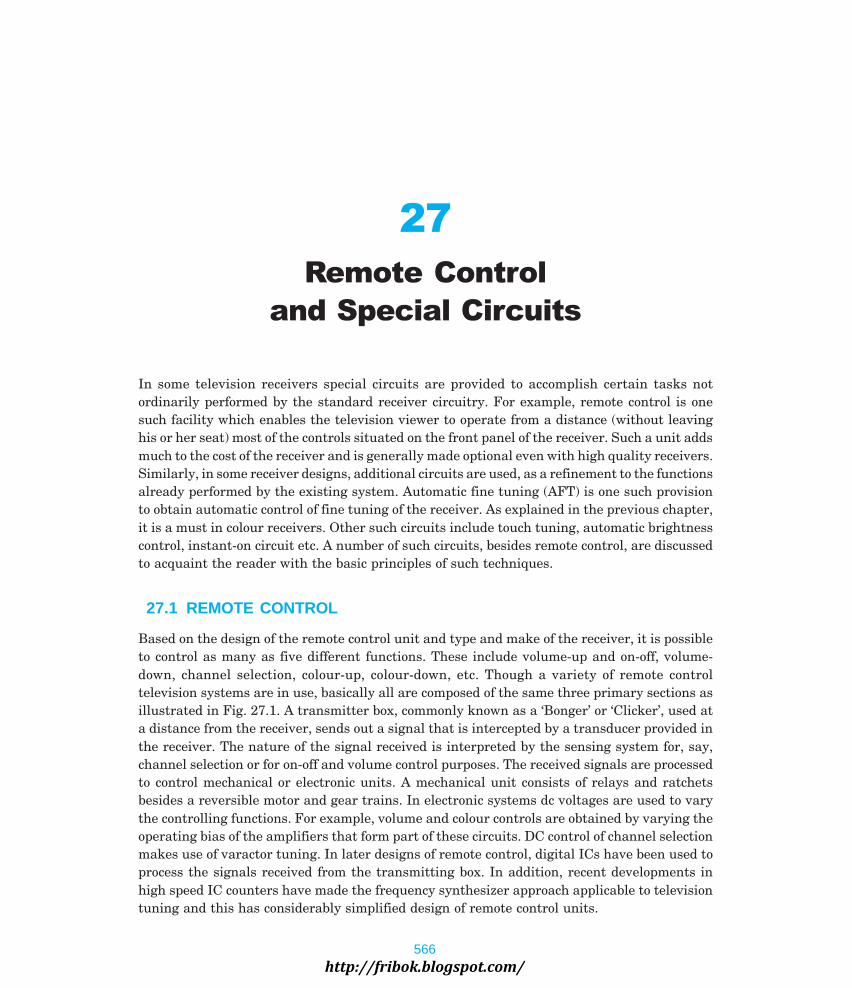
In some television receivers special circuits are provided to accomplish certain tasks notordinarily performed by the standard receiver circuitry. For example, remote control is onesuch facility which enables the television viewer to operate from a distance (without leavinghis or her seat) most of the controls situated on the front panel of the receiver. Such a unit addsmuch to the cost of the receiver and is generally made optional even with high quality receivers.Similarly, in some receiver designs, additional circuits are used, as a refinement to the functionsalready performed by the existing system. Automatic fine tuning (AFT) is one such provisionto obtain automatic control of fine tuning of the receiver. As explained in the previous chapter,it is a must in colour receivers. Other such circuits include touch tuning, automatic brightnesscontrol, instant-on circuit etc. A number of such circuits, besides remote control, are discussedto acquaint the reader with the basic principles of such techniques.
27.1 REMOTE CONTROL
Based on the design of the remote control unit and type and make of the receiver, it is possibleto control as many as five different functions. These include volume-up and on-off, volume-down, channel selection, colour-up, colour-down, etc. Though a variety of remote controltelevision systems are in use, basically all are composed of the same three primary sections asillustrated in Fig. 27.1. A transmitter box, commonly known as a ‘Bonger’ or ‘Clicker’, used ata distance from the receiver, sends out a signal that is intercepted by a transducer provided inthe receiver. The nature of the signal received is interpreted by the sensing system for, say,channel selection or for on-off and volume control purposes. The received signals are processedto control mechanical or electronic units. A mechanical unit consists of relays and ratchetsbesides a reversible motor and gear trains. In electronic systems dc voltages are used to varythe controlling functions. For example, volume and colour controls are obtained by varying theoperating bias of the amplifiers that form part of these circuits. DC control of channel selectionmakes use of varactor tuning. In later designs of remote control, digital ICs have been used toprocess the signals received from the transmitting box. In addition, recent developments inhigh speed IC counters have made the frequency synthesizer approach applicable to televisiontuning and this has considerably simplified design of remote control units.
566
%
!
!
http://fribok.blogspot.com/

REMOTE CONTROL AND SPECIAL CIRCUITS 567
Pushbuttons
Remotetransmitting box
(Bonger)
Signalwaves
SpeakerMicrophone
Intercept andsignal processing
circuitsin the receiver
Mechanical driveor electroniccontrol units
Volume
Colour
To tuner
Fig. 27.1. Basic remote control system.
Transmitting UnitThe transmitting unit may be mechanically actuated or electronic in nature. It generatesultrasonic sound waves at frequencies around 40 KHz. In the air these waves are directedtowards the receiver where they operate the pick-up transducer which is normally a piezo-electric microphone. The use of frequencies around 40 KHz is advantageous because these aretoo high for the human ear and can be confined by the walls to the rooms, with very littlepossibility of interference to receivers in other rooms or beyond the receiver at which they areaimed. Furthermore, it is quite easy to generate accoustic signals by purely mechanical meanswithout the need of a battery or any other powering source.
Control FrequenciesThere are no standard values but the frequency range normally employed for remote controlfunctions lies between 37 KHz to 44 KHz. Some typical values for the main functions are:
41.25 KHz–Channel selection
37.75 KHz–Volume up
43.25 KHz–Volume down
The contrast and brightness controls are usually not included for remote control becauseAGC circuit automatically changes the receiver gain to maintain the desired contrast andbrightness in the reproduced picture.
Generation of FrequenciesSince each function needs a distinct signal to actuate it, several frequencies are to be generatedto perform different functions. A mechanical source or an electronic oscillator may be used togenerate ultrasonic sound waves.
The BongerThe most common method employed to generate different frequencies by mechanical means isthe use of vibrating rods. As shown in Fig. 27.2 the transmitting box (Bonger) contains severalcylindrical aluminium rods of slightly different lengths. For each rod a separate control buttonis provided on the front panel of the hand-held remote control box. When any control button ispushed a spring loaded hammer strikes the corresponding rod and sets it into longitudinalmode vibrations at a definite frequency. The sound energy thus generated is radiated throughan open grille provided at the top of the box. For example, an aluminium rod of 7.5 cm lengthhas a fundamental resonant frequency of about 40 KHz and would thus radiate energy at thisfrequency. Therefore, to control three or four functions within the television receiver, three orfour rods of somewhat different lengths are employed, each actuated by a separate hammer
http://fribok.blogspot.com/
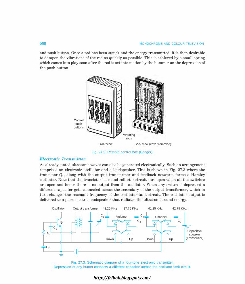
568 MONOCHROME AND COLOUR TELEVISION
and push button. Once a rod has been struck and the energy transmitted, it is then desirableto dampen the vibrations of the rod as quickly as possible. This is achieved by a small springwhich comes into play soon after the rod is set into motion by the hammer on the depression ofthe push button.
Controlpush
buttons
Vibratingrods
Front view Back view (cover removed)
Fig. 27.2. Remote control box (Bonger).
Electronic TransmitterAs already stated ultrasonic waves can also be generated electronically. Such an arrangementcomprises an electronic oscillator and a loudspeaker. This is shown in Fig. 27.3 where thetransistor Q1, along with the output transformer and feedback network, forms a Hartleyoscillator. Note that the transistor base and collector circuits are open when all the switchesare open and hence there is no output from the oscillator. When any switch is depressed adifferent capacitor gets connected across the secondary of the output transformer, which inturn changes the resonant frequency of the oscillator tank circuit. The oscillator output isdelivered to a piezo-electric loudspeaker that radiates the ultrasonic sound energy.
RB
C2
C1
Q1
Oscillator Output transformer 43.25 KHz 37.75 KHz 41.25 KHz 42.75 KHz
C3 C5
C4
Volume
Down Up Down Up
C6
Channel
Capacitivespeaker
(Transducer)
+
Fig. 27.3. Schematic diagram of a four-tone electronic transmitter.Depression of any button connects a different capacitor across the oscillator tank circuit.
http://fribok.blogspot.com/

REMOTE CONTROL AND SPECIAL CIRCUITS 569
Pick-up TransducerAt the receiver the ultrasonic energy is picked up by a crystal type microphone, which convertssound energy into corresponding electrical signals. The microphone employs a barium-titanatecrystal element that has piezoelectric properties. A small bar of this material is placed betweentwo conducting electrodes. When it is mechanically strained by the striking sound waves alongone axis a proportionate voltage is generated along the other axis at the frequency of transmittedsound waves. A small ‘U ’ shaped piece of aluminium is added to the assembly. Beyond thisassembly and at a distance of approximately one-quarter wavelength corresponding to afrequency of about 40 KHz, a small rectangular horn is attached. Both the one-quarterwavelength space and the horn serve to match the impedance of the barium titanate assemblyto the air. The combination of this microphone and the amplifiers in the system provide sufficientsensitivity for operating various controls from a distance of about 7 to 10 metres.
Remote Control ReceiversThe remote control receiving systems may be broadly classified as electromechanical andelectronic.
27.2 ELECTROMECHANICAL CONTROL SYSTEM
The block diagram of Fig. 27.4 shows three different functions each controlled by anelectromechanical circuit. The transmitter has provision to generate three ultrasonic signalshaving frequencies 41.25 KHz, 37.75 KHz, and 43.25 KHz. The microphone picks up the radiatedtone and converts it into an electrical signal. The broad-band (30 to 50 KHz) high gain (≈ 106)amplifier amplifies this signal and delivers it to an array of tuned circuits. Each tuned circuitis resonant to one of the three frequencies that can be radiated by the transmitter. The outputof each circuit is coupled to the armature of a functional relay through a driver. Thus, dependingon the function to be performed, the corresponding series tuned circuit develops a large voltageacross its inductor. As shown in Fig. 27.5 the tuned circuit L1, C1 on receipt of a signal at 37.75KHz will cause driver transistor Q1 to pass operating current through the armature of relayK1. The operation of K1 connects 220 V ac across the upper winding of the driver motor. At thesame time the phase shifting network R2, C3, comes in series with the lower winding. Theresulting rotating magnetic field develops torque to rotate the motor armature in such a directionthat the volume control shaft moves clockwise to raise the sound output. The motor speed isnormally reduced to about 10 rmp before coupling it to the associated control potentiometer.When signal at 43.25 KHz is received, relay K2 will close thereby reversing the direction ofrotating field. This will result in the rotation of volume control shaft in the opposite directionand audio output will be lowered. Similarly identical circuits can be added and actuated bydifferent frequency tones to control colour saturation and other functions.
In the case of channel selection by remote control the tuning motor turns the stationselector shaft in only one direction. Unused channels can be skipped by indexing or programmingan index wheel, that turns with the tuner shaft in such a way, that the motor stops only for thetuner shaft positions of the channels used, but passes through the tuning position of channelsnot in use. This is easily possible by providing an earth return circuit to the motor at channellocations that are to be skipped.
http://fribok.blogspot.com/

570 MONOCHROME AND COLOUR TELEVISION
Microphone Remote control chassis in receiver
M M
To channelselectionstepper
Channelmotor Volume control motor
To controlpotentiometer
Auto-manualswitch
Functionalrelays Channel
Volumeup
Volumedown
41.25KHz
Tunedrelay
drivers
37.75KHz
43.25KHz
K3 K1 K2
To othercontrolcircuits
if provided
Broadband highgain amplifier
Ultrasonic wavesfrom the remote
transmitter
Fig. 27.4 Block diagram of a remote control system for three receiver functions.
10 W R2
C3
Phaseshiftingnetwork
Volumemotor
windings
C1
L1 37.75KHz
C2
L2 43.25KHz
K1
K2
220 Vac
0.8 Fm
Motor downrelay
Driver
C5Q2
C4Q1
+ 15 V
DriverMotor up
relay
R1
From broadbandamplifier
Fig. 27.5 Volume control motor and its associated circuits.
http://fribok.blogspot.com/

REMOTE CONTROL AND SPECIAL CIRCUITS 571
27.3 ELECTRONIC CONTROL SYSTEMS
The later versions of remote control either use only one motor or are fully electronic and employdc voltages to vary the controlled positions. For example, a varactor tuner that does not havea rotating switch needs only a dc potential for channel selection. Similarly other functions canbe controlled by changing dc conditions in the controlled circuits.
Memory CircuitIn motor operated remote control systems the levels of volume, colour and channel selectedare ‘remembered’ from one viewing session to the next by the mechanical positions of variouscontrols. In all electronic (motorless) remote control systems a memory circuit is used to‘remember’ the control positions established during the last viewing session. If memory is notprovided, turning-off the receiver returns all the control voltages to zero and it becomesnecessary to readjust all controls each time the receiver is switched-on for use.
The schematic diagram of a memory circuit used to control sound volume is shown inFig. 27.6. The ‘memory module’ consists of a neon bulb (NE), a lowleakage capacitor C6 and aMOSFET Q1. The neon lamp acts as an open circuit unless the voltage across it reaches theionizing potential. Similarly, the input impedance of the MOSFET, being of the order of 108
ohms, behaves almost like an open circuit. Thus any charge once stored in the memory capacitorC6 will stay on for a long time.
L2
L1vin37.75 KHz
vin43.25 KHz
Frombroadbandamplifier
C1
C2
C4+
.01 Fm
C3
.01 Fm
+
D1
4.7 M
4.7 M
D2
DCamp
Filtercircuit
.02 FmC5
D3
D4
A
Clampdiode
Clampdiode
– 80 V
R1
10 MNeon bulb
(NE)C6
1.5 FMemorycapacitor
m
+ 100 V
+ 30 V
Q1
R210 K
To audioIC
DC controlvoltage
Fig. 27.6. Memory circuit for volume control in an all electronic remote system.
A dc control voltage is used to activate the memory circuit. For example, when soundvolume is to be increased, the tuned circuit L1, C1 couples a large voltage at 37.75 KHz to thediode D1. The rectified positive voltage is filtered by C5 and applied to the junction of D3 andD4. As soon as this voltage exceeds 100 V, D3 turns on and clamps the junction point (A) to theexternal 100 V supply. Thus a 100 V dc source gets applied across the neon lamp and associatedcircuit. About 80 volts are dropped across the neon diode when it conducts and the remaining20 volts become available to charge C6 via R1. The magnitude of the voltage that builds upacross the memory capacitor depends on how long the ‘volume up’ key of the transmitter isdepressed. However, this voltage does not exceed 5 to 6 volts because of the large time constantof the charging circuit. The charge across C6 can stay on for several months after the receiveris switched off.
http://fribok.blogspot.com/

572 MONOCHROME AND COLOUR TELEVISION
The voltage across C6 is the bias for Q1, the MOSFET memory follower. The voltageacross R2, the source resistance of Q1, is proportional to the voltage across C6. Thus the voltagechange caused by the depression of ‘volume up’ button gets applied to the dc amplifier which inturn changes the bias on the audio IC to increase power delivered to the loudspeaker.
In order to decrease the volume, the transmitter is activated to produce a tone at 43.25KHz. This is selected by the filter L2, C2 and rectified by diode D2. Since D2 is connected inopposite direction from that of D1, a negative control voltage is developed across the memorycapacitor. Note that the negative clamp voltage (– 80 V) is lower than the positive clamp sothat the FET gate voltage does not exceed its cut-of voltage.
The decreased output voltage across R2 results in a change of bias voltage to the audioIC in the opposite direction thereby reducing sound output from the loudspeaker. Similarlythe output across R2 may be utilized for operating a one shot-flip-flop, that energizes a relay toaccomplish the on-off function.
For controlling other functions identical circuitry is provided and its output is fed tocorresponding circuit points in the receiver. Not that for electronic tuning several input circuitswould be necessary to charge the memory capacitor to different voltages for each channel.
Remote Control Circuits Employing Digital ICsNow, when a large variety of digital ICs are available at a reasonable cost, many manufacturersof remote control equipment have introduced new control circuits, where almost allelectromechanical units have been replaced by electronic circuitry employing ICs. As anillustration, receiver ‘on-volume-up’ and ’volume-down-off’ functions when controlledelectronically operate in the following manner.
When the receiver is off and a remote ‘on-volume-up’ signal is received, a digital keyerstarts counting pulses from a slow rate digital clock provided in the same IC. Fifteen discretecounts complete the sequence of switching on the receiver and raising the sound volume to itsmaximum level. The digital numbers, as counted by the keyer, are converted to discrete voltagelevels by a D/A (digital-to-analog) converter. The voltage level that becomes available aftercount number one on a particular pin of the IC, is used for switching-on the receiver. In effect,this control voltage (dc) turns on a transistor, that is initially off, to feed current to a lamp thatis connected in its emitter circuit. The lamp illuminates a light dependent resistor (LDR) thatforms part of the gate circuit of a thyristor. When the lamp turns on, the resistance of the LDRdecreases to allow enough gate current and the thyristor is turned on. The thyristor is in serieswith the mains supply circuit to the receiver and as soon as it turns on, power is switched on tothe receiver.
As long as the ‘on-volume-up’ control is kept depressed the sound volume increases insteps. At each successive count (1 to 14) the control voltage increases to initiate action thatresults in increase of volume. Normally, volume changes proceed at the rate of three levels persecond. To turn the receiver off, the ‘volume-down-off’ switch is depressed. The keyer countsup till count 15 is reached. At this stage the keyer is timed to be gated out, which in turnresults in cutting off supply to the receiver.
All Electronic SystemAs explained earlier, the command signals at different frequencies are separated by tunedcircuits and then routed to the appropriate circuitry for performing corresponding functions.
http://fribok.blogspot.com/

REMOTE CONTROL AND SPECIAL CIRCUITS 573
However, in an all electronic system, this function is performed by a specially designed ICcalled a ‘digital decoder’. The internal circuitry of this IC contains a counter that is turned on,on receipt of any command signal. It is designed to count any pulses present, for a predeterminedcount period normally 1/50th of a second, and compare this with a previous count. In fact theincoming signal is counted seven times. If all values agree within prescribed tolerance, thecounter considers the input valid and a confidence counter is incremented by one. Whenconfidence counter reaches seven, the voltage on the IC pin, corresponding to the frequencycount, is activated and performs the required function. Thus different voltage will appear atcorresponding pins to perform different functions. All the command frequencies are exactharmonics of 50 Hz. This harmonic relationship provides noise immunity by preventingerroneous triggering.
27.4 ELECTRONIC TOUCH TUNING
Recently several new approaches to the design of TV channel tuning have emerged. The idealtuning system should incorporate (i) individual channel selection, (ii) no channel alignment,(iii) digital channel display, (iv) remote control and (v) touch type control. The only feasibleapproach which can meet the above requirements is an all electronic tuning system. It employsa varactor tuner and a totally electronic system for channel selection, tuning and identification.
The requirement of parity tuning for both VHF and UHF channels has led to the use ofdigital and dedicated ICs in such control circuits. Some designs employ micro-processors forinitiation, control, selection and interface purposes, However, it is not necessary to providetuning for all the 80 and odd UHF channels because more than six such channels are seldomavailable in any area or location. The more popular designs centre around approximately 18channels–the twelve standard VHF channels and about six variable UHF channels which areselected on the basis of local area requirements. In one typical design the VHF potentiometersare set to correspond to a given channel readout. The UHF channels, however, are tuned in bythe potentiometers and the corresponding channel indicator number is set to agree with thechannel tuned with a single patchboard switching matrix.
Channel Selection
Channel entry is by means of a touch channel selection keyboard called touch tuning. It usesvery low pressure sensitive switches arranged much the same way as in a pocket calculatorkeyboard. The basic organization of the keyboard circuit is shown in Fig. 27.7. With an inactivekeyboard the input to Q1 is low and the oscillator is disabled. When a key is depressed, thebase of Q1 is pulled high (forward biased) via varactor potentiometers connected to + 30 V.This actuates the gate in the oscillator circuit and allows it to oscillate. The oscillator outputpulses cycle the counter until it addresses the decoder output (active low) of the depressed key.As this key decodes the output becomes low and the oscillator is stopped via Q1. The associatedcircuits are programmed for individual channel selection.
The counter in this circuit can be sequentially advanced for external sources such as aremote control tuner by gating a single pulse to the counter.
http://fribok.blogspot.com/
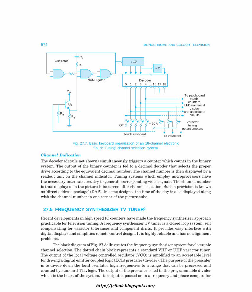
574 MONOCHROME AND COLOUR TELEVISION
¸ 10
¸ 2
Off
Touch keyboard
+ 30 V
To varactors
Varactortuning
potentiometers
To patchboardmatrix,
counters,LED numerical
displayand associated
circuits
0 1 2 3 4 16 17 18Decoder
C1
R1
Oscillator
NAND gates
Vcc
Q1
RE
RB
Fig. 27.7. Basic keyboard organization of an 18-channel electronic‘Touch Tuning’ channel selection system.
Channel IndicationThe decoder (details not shown) simultaneously triggers a counter which counts in the binarysystem. The output of the binary counter is fed to a decimal decoder that selects the properdrive according to the equivalent decimal number. The channel number is then displayed by areadout unit on the channel indicator. Tuning systems which employ microprocessors havethe necessary interface circuitry to generate corresponding video signals. The channel numberis thus displayed on the picture tube screen after channel selection. Such a provision is knownas ‘direct address package’ (DAP). In some designs, the time of the day is also displayed alongwith the channel number in one corner of the picture tube.
27.5 FREQUENCY SYNTHESIZER TV TUNER2
Recent developments in high speed IC counters have made the frequency synthesizer approachpracticable for television tuning. A frequency synthesizer TV tuner is a closed loop system, selfcompensating for varactor tolerances and component drifts. It provides easy interface withdigital displays and simplifies remote control design. It is highly reliable and has no alignmentproblems.
The block diagram of Fig. 27.8 illustrates the frequency synthesizer system for electronicchannel selection. The dotted chain block represents a standard VHF or UHF varactor tuner.The output of the local voltage controlled oscillator (VCO) is amplified to an acceptable levelfor driving a digital emitter coupled logic (ECL) prescaler (divider). The purpose of the prescaleris to divide down the local oscillator high frequencies to a range that can be processed andcounted by standard TTL logic. The output of the prescaler is fed to the programmable dividerwhich is the heart of the system. Its output is passed on to a frequency and phase comparator
http://fribok.blogspot.com/

REMOTE CONTROL AND SPECIAL CIRCUITS 575
where it is compared with a crystal controlled reference frequency. Then the comparator outputis fed to an integrator-amplifier, which in turn provides voltage control to the varactor tunerinput.
VHF or UHF tuner
RF amp Mixer
Local osc VCO
Varactor input Integratoramp
Crystaloscillator
Divider
Frequency and phasecomparator
Amp Prescaler
To IF section
Programmabledigital divider
Channel numberprogramme
Fig. 27.8. Block diagram of a frequency synthesizer TV tuner.
The divide ratio of the programmable counter determines the desired channel. At thecomparator, there are two significant signals–the counted output and the reference signal.When these two signals differ in frequency or phase, a dc error voltage is applied to the tunerVCO with a suitable polarity in order to reduce the frequency and phase error to zero. At thistime the VCO is at the selected channel frequency. A touch tuning type entry system is usedfor channel selection and a modern seven segment display is employed for channel indication.
27.6 AUTOMATIC FINE TUNING (AFT)
The local oscillator frequency in the RF tuner is set to provide exact IF frequencies. However,despite many remedial measures to improve the stability of the oscillator circuit, some driftdoes occur on account of ambient temperature changes, component aging, power supply voltagefluctuations and so on. For a monochrome receiver a moderate amount of change in the localoscillator frequency can be tolerated without much effect on the reproduced picture and soundoutput. The fine tuning control is adjusted occasionally to get a sharp picture. The soundoutput is automatically corrected because of the use of intercarrier sound system. However,requirements of frequency stability of the local oscillator in a colour TV receiver are muchmore stringent. This is so, because proper fine tuning of colour receivers is judged both by thesharpness of the picture and quality of colour.
If the local oscillator frequency becomes higher than the correct value, the picture IF,subcarrier IF and sound IF frequencies will also become higher by the same amount and fallon incorrect positions on the IF response curve. This will result in poor picture quality becausethe amplitudes of low-frequency video sidebands clustered around the picture IF will decrease.
http://fribok.blogspot.com/

576 MONOCHROME AND COLOUR TELEVISION
At the same time chrominance signal sidebands clustered around the location of subcarrierwill receive more gain and hence become stronger than normal. Similarly, if the local oscillatorfrequency changes to become less than the desired value opposite effects would result andcolour reproduction will become weak. In case the decrease in frequency is more than 1 MHz,the colour burst may be lost and only a black and white picture will be seen on the screen.Similar troubles can also result in receivers that employ remote control tuning because of non-availability of fine tuning control and imperfections of the mechanical/electronic systememployed for channel selection.
Automatic Frequency Control (AFC)In order to simplify the operation from the point of view of setting the fine tuning controlcorrectly, and to overcome the problem of local oscillator drift, all colour receivers and thoseemploying remote control use an AFT circuit.
Manualfine tuning
Localosc
Reactancecircuit
or varactordiode
DCamp
Frequencysensitive
discriminator
Tunedcircuit
IFsectionMixer
RFamp
Tuner
From 3rd IF amp (38.9 MHz)
DC control voltage
Varactorcapacitance (pF)
38.9 MHz
Reversebias0 4V
Bias point+Forward
bias
Fig. 27.9 Block diagram of an AFT circuit.
The AFT circuit is actually automatic frequency control (AFC) on the local oscillator inthe tuner. This control aims at obtaining a picture IF frequency of exactly 38.9 MHz at theconverter output. This is possible only if the local oscillator frequency in the tuner is maintainedat a value which is exactly 38.9 MHz higher than the incoming channel carrier frequency. Toachieve this, the IF frequency, as obtained from the IF amplifier section, is measured by adiscriminator circuit that forms part of the AFT control. The block diagram of such an AFTcircuit is illustrated in Fig. 27.9. Here the discriminator has basic function similar to thatdescribed in Chapter 21 for FM sound detection. Its output is a dc correction voltage thatindicates the deviation of the IF frequency from its exact value of 38.9 MHz. Since this frequencydepends on the oscillator input to the mixer, the AFT voltage indicates the error in local oscillatorfrequency. The ‘S’ shaped response curve of the discriminator is very steep and frequencyshifts as little as 50 KHz are clearly indicated. The AFT control voltage is zero at balance i.e.when the IF frequency is exactly 38.9 MHz. For frequency deviations on either side of 38.9MHz the net dc correcting voltage is either positive or negative depending on whether thefrequency, is above or below the correct value. The dc control voltage thus developed is appliedto a reactance circuit or to a varactor diode that forms part of the local oscillator tank circuit.
http://fribok.blogspot.com/

REMOTE CONTROL AND SPECIAL CIRCUITS 577
The junction capacitance of the varactor diode varies with the applied dc control voltage andthus changes the resonant frequency of the oscillator tuned circuit to shift the frequency to thecorrect value.
AFT or AFC CircuitA typical automatic frequency control circuit together with the discriminator characteristics isshown in Fig. 27.10 (a). Signal from the IF amplifier section of the receiver is coupled by C1and L1 to the base of transistor Q1. This stage is an IF amplifier that couples its output to the‘Foster-Seeley’ or phase shift discriminator. The transformer T1 is tuned to 38.9 MHz. Whenthe input signal is at exact IF frequency the control voltage developed across the outputterminals A and B is zero. However, if the local oscillator frequency is not at its nominal valuefor the particular selected channel, the picture IF frequency will be either above or below 38.9MHz. In this event the discriminator output voltage will be either a positive or a negative dcvoltage. In some circuit designs this is amplified by a dc amplifier before being applied to thevaractor in the tuner assembly. A typical value for the AFT error voltage is ±6 volts and can bemeasured across the output points A and B.
C3
C4
R3
R4
AR7
S1
AFTdefectswitch
DC controlvoltage totuner viaamplifier
D1
D2
– 6 V
6 V
0
+FromIF section
L1
C1
R6
10 pFQ1 Lt
T1
C2
R5
R1
+ Vcc
Controlvoltage
Discriminator ‘S’ curve
B
38.9 MHz
f(MHz)R2
Fig. 27.10 (a). A typical automatic frequency control (AFC) circuit.
From IFsection
L1 C1C2
R2
R1
+ Vcc
FTIQ detector1
R3FTI
sensitivitycontrol
FTIoutput
Q2R4
+ 100 V
Fine tuningindicator
(Neon lamp)
Fig. 27.10 (b). A typical fine tuning indicator (FTI) circuit.
http://fribok.blogspot.com/

578 MONOCHROME AND COLOUR TELEVISION
AFT Defeat SwitchThe switch S1 shown across the output terminals is known as the ‘AFT defeat switch’ and canbe closed to turn off the AFT circuit for manual fine tuning adjustments.
FTI CircuitIn some AFT circuits a fine tuning indicator (FTI) is provided to give a visual indication of anyincorrect fine tuning. A neon lamp fixed at a suitable location on the front panel lights up toindicate that tuning is ‘off ’ and must be corrected. A simplified circuit of such a control isshown in Fig. 27.10(b). A sample of the IF signal, after one stage of amplification if necessary,is applied across the parallel resonant circuit L1, C1 that is tuned to the IF frequency. Thevoltage developed across the tuned circuit is fed to the base of transistor Q1 through a self-biasnetwork R2, C2. The voltage developed across the emitter resistor R3 drives the output transistorQ2. The transistor Q1 is connected as an emitter follower and provides both current gain andisolation between the tuned circuit and low input resistance of the output transistor. In theabsence of any input signal the transistor Q2 stays at cut-off and full 100 V dc gets appliedacross the neon lamp which is enough to ionize the gas in it. When the IF frequency is at itscorrect value of 38.9 MHz, maximum voltage is developed across the tuned circuit. This resultsin enough drive voltage across R3 and transistor Q2 goes into full conduction. The resultingcollector current reduces the voltage across the neon lamp below its ionizing potential and itgoes off. If the tuning is off the input to the base circuit of Q1 decreases because, when theparallel resonant circuit does not receive a 38.9 MHz signal its impedance drops considerablythereby shunting the base input of Q1. This results in reduced input to Q2 and it goes to cut-off.Now there is no shunting effect across the indicating lamp and it lights up. Thus when theindicator light is on it is a sign that the fine tuning is off and needs adjustment.
27.7 BOOSTER AMPLIFIERS
As radio communication systems developed the receivers became more and more sensitive.Early TV receivers needed 200 to 300 µV of signal for a picture of reasonable quality. Thepresent day sets give a similar picture with an antenna signal strength of about 50 µV in thelower VHF range.
In areas where the signal strength is somewhat less, raising the antenna or using anantenna that is directional and has higher gain results in an acceptable picture. However, indeep fringe areas where the signal from the desired station is very weak and fails to produceany worthwhile picture, an additional RF amplifier external to the receiver becomes necessary.Such amplifiers are known as booster amplifiers and are normally mounted on the antennamast close to the antenna terminals. A booster amplifiers is a broad-band transistor RF amplifierdesigned to have a reasonable gain but a very high internal signal-to-noise ratio. It may beemphasized that a booster capable of providing a high gain but incapable of providing a goodsignal-to-noise ratio will give a picture with lot of snow. Similarly, a booster amplifier havingminimum internal noise but low gain will fail to provide a satisfactory picture. Thus a boosteramplifier must have both the attributes, i.e. reasonable gain and high signal-to-noise ratio.
In booster amplifiers that employ only one transistor, either a grounded-emitter or agrounded-base configuration is used. Though the grounded-emitter arrangement gives a
http://fribok.blogspot.com/

REMOTE CONTROL AND SPECIAL CIRCUITS 579
somewhat higher gain the grounded-base configuration is more stable and is therefore preferred.Such amplifiers are untuned and are designed to give a small boost to signals from severalnearby stations. However, when the interest is in a single station a tuned amplifier can beused to yield higher gain.
The circuit diagram shown in Fig. 27.11 is that of a booster amplifier specially designedto receive channel 4 (61 to 68 MHz) station in deep fringe areas. It gives a gain of about 20 db,with a noise figure between 2.00 to 2.50 db. The first stage is designed with a minimum noisefigure (NF) criterion. The second stage is designed to give necessary gain and the last stage isfor matching its output impedance to the lead-in cable. Between the first and second stages atuned LC circuit has been provided for proper tuning of the frequency band of 61 to 68 MHz. Abrass core is used for tuning this circuit. The small amount of power required by the boosteramplifier is fed through the transmission line that couples the antenna to the receiver and isswitched on along with the receiver.
To tunerinput1 KpF
3.9 K
2.2KpF68 K
BF 200
49 K
Q3
4.7 KpF
3.3 K
2.7 K8.2 K
+ Vcc
Q2
3.3 K47 KpF
BF 200
2.2 KpF1.5 K8.2 K
4.7 KpF
16.7 KpF
3.3 KTuning
L
Q1
BF 200
47 KpF
330 pFFrom
antenna
Fig. 27.11. Booster amplifier circuit for channel 4 (61-68 MHz).
27.8 AUTOMATIC BRIGHTNESS CONTROL
The amount of light in the room where the TV set is in use determines the setting of thebrightness control for a satisfactory picture. The contrast control is also linked, to some extent,with the brightness setting and often needs readjustment when the brightness control is varied.The brighter the room the greater is the need to advance the settings of both brightness andcontrast controls for a bright picture and effective reproduction of the various shades of grey inthe scene.
A circuit which automatically accomplishes this is known as ‘automatic brightness control’(A.B.C.). It forms a part of the video amplifier circuitry. A typical circuit arrangement isillustrated in Fig. 27.12. The controlling element is an LDR (light dependent resistance) whichis actually photo-sensitive material whose resistance varies with changes in light intensityfalling on it. The LDR is mounted on the front panel of the cabinet to sense changes ofillumination in the room. It forms a part of the video amplifier circuit that controls the screen-grid voltage of the video amplifier tube and the bias voltage (grid to cathode potential) of thepicture tube. As shown in Fig. 27.12 resistor R1 (which is in parallel with the LDR) and resistor
http://fribok.blogspot.com/

580 MONOCHROME AND COLOUR TELEVISION
R2 form a potential divider across the B+ supply to feed necessary dc voltages both at G2 of V1and control grid of the picture tube. When illumination in the room increases, say, when lightsare switched on or during daylight, the resistance of the LDR decreases. Because of thepotentiometer arrangement this increases the screen grid voltage to tube V1. The increasedscreen grid voltage provides greater contrast because of enhanced amplification of the compositevideo signal. At the same time the increased potential also appears at the grid of the picturetube. This decreases the net dc negative bias, between the grid and cathode of the picture tube,which in turn results in increased screen brightness. For a decrease in light intensity the LDRresistance increases and the resultant fall in the video amplifier screen grid and picture tubegrid voltages decrease both contrast and brightness in proportion to changes in the generalillumination of the room.
5.5 MHz
P V1 (Video amp)
G2G1
Videosignal
RgK
LDR
+ 200 VB +
R4
R5
R3
Brightness control
R1Light
CC
Contrast control
Picturetube
R2
+
–
Fig. 27.12. Automatic brightness control circuit.
In video amplifiers that employ transistors, the LDR is placed in parallel with the emitterresistance. Any change in the effective emitter resistance, due to changes in room illumination,alters both the gain and quiescent dc potential at the collector, which is directly coupled to thepicture tube circuitry. Thus any variation in brightness automatically affects both the contrastand brightness of the reproduced picture. In some designs a switch is provided which disablesthe ‘ABC’ circuit if necessary.
27.9 INSTANT-ON CIRCUITRY
In television receivers that employ tubes there is some delay in reception after the switch isturned on because of the warn-up period required by the picture and other tubes before theyassume normal operation. Though transistors virtually require no warm-up time, in receiverswhich employ all transistors there is also a small delay in reception because of the time requiredby the picture tube cathode to attain full emission. To overcome this delay and permitinstantaneous reception when the receiver switch is turned on, the filament circuitry is modified.
http://fribok.blogspot.com/

REMOTE CONTROL AND SPECIAL CIRCUITS 581
The circuit of Fig. 27.13 (a) shows power supply arrangement of a all transistor televisionreceiver. The diodes D1 and D2 connected to the secondary winding L2 together with the filternetwork meet dc voltage requirements of all the stages. However, a separate low voltage windingL3 is provided for the filament (heater) of the picture tube. To provide instant-on feature themaster switch S1 on the primary side of the mains transformer is kept closed all the timeunless the set is not to be used for several days or still longer periods. When the double polesinglethrow (DPST) switch S2 is in the open position, the centre tap of winding L1 remainsdisconnected and thus no dc voltage is produced by the full-wave rectifier circuit. However, inthe filament winding the switch is shunted by diode D3 and about one-third of the normalfilament current continues to flow through the picture tube heater, even when S2 is off. This isenough to permit the picture to come on almost instantly when S2 is closed, which in its ‘on’position shunts D3 and permits application of full filament voltage to the picture tube.
+ +
100 Fm100 Fm
B+R
D1
D2
+ +
Filter
B+
DPST switch
S2
L2L1
AC mains
S1L3
Masterswitch
D3To picture
tube filament
(a)
DPSTswitch D1 R1
S2
R2
D2S1
AC mains
(b)
Tube filamentsin series
Fig. 27.13. Instant-on circuits (a) power supply employing mainstransformer (b) direct on line power supply.
http://fribok.blogspot.com/

582 MONOCHROME AND COLOUR TELEVISION
For tube-type television receivers that do not employ mains transformer the circuitarrangement employed to provide instant-on feature is shown in Fig. 27.13 (b). As shownthere, the upper switch of the DPST assembly, when off, disconnects power from the dc voltagerectifier circuit while the lower switch permits partial supply to the heater string through D2that shunts it. When switch S2 is thrown on, both dc supply and full filament current areimmediately restored and the picture appears on the screen without any warm-up delay. Thoughthe receiver, when put under instant-on facility (master switch closed), consumes about 30watts of power there is no sudden surge of current through the filaments when the receiver isturned on. This results in extended life of the tubes. Besides this, the heat that is generatedwithin the cabinet when the set is not in use (S2 off) helps reduce undesired effects of dampnesson various windings and components in areas of high humidity.
27.10 PICTURE-TUBE BOOSTERS
After a prolonged use the emission from the cathode of the picture tube declines and thereproduced picture exhibits symptoms of low contrast and reduced brilliancy. To extend thelife of such picture tubes their filament voltage is increased which in turn raises the heatapplied to the cathode, so that the latter then assumes normal emission. In some receiverdesigns a built-in provision is made for raising the filament voltage from its normal value of 6volts to about 8 volts. This is shown in Fig. 27.14 where the ‘brightness’ screw provided withthe receiver can be fixed in the socket to bypass the 3 ohm resistor normally used to initiallykeep the voltage at 6 volts at the heater terminals. In the absence of such a provision a separatebooster transformer can be used instead of the 6 volts winding on the mains transformer. Asuitable arrangement can also be provided in receivers that have all the filaments (heaters) ina string across the mains supply. It has been observed that the reactivated life of the picturetube gets extended by several years with the use of such boosters.
Picture tubefilamentwinding
Picturetube
Socket
3 5 wattW
F
FK
ACmains
To rectifierand filter
circuit
Fig 27.14. Picture tube booster arrangement.
http://fribok.blogspot.com/

REMOTE CONTROL AND SPECIAL CIRCUITS 583
References1. Robert W. Wolff, Novel electronic TV Touch Tuning System Using Digital Circuit Techniques,
IEEE Trans. BTR, Vol. 20, No. 2, May 1974.
2. E.G. Breeze and others, A Frequency Synthesizer for TV Receivers, IEEE Trans. BTR Vol. 20,No. 4, November 1974.
Review Questions
1. What are the main components of a television remote control system ? Describe by a block dia-gram how such a system functions.
2. Why are the frequencies of command signals chosen in the 40 KHz range ? Explain how are thesegenerated both by a mechanical ‘bonger’ and an electronic oscillator.
3. Explain briefly the transducers used for transmitting and receiving command signals. How arethe command signals separated at the receiver ?
4. Describe with suitable diagrams how (i) remote volume control and (ii) remote channel selectionare carried out on receipt of command signals. Explain how a memory circuit is used for channelselection in a varactor controlled tuner.
5. Enumerate the needs an ideal electronic channel tuning system should meet. Explain briefly the“Touch Tuning” method of channel selection and identification.
6. Describe with a suitable block diagram the basic principle of a frequency synthesizer TV tuner.Explain how the selected channel number is displayed on the picture tube screen.
7. Explain with a circuit diagram the functioning of an automatic fine tuning control. Describe howthe fine tuning indicator circuit operates to give indication of incorrect fine tuning.
8. Write descriptive notes on the following :
(i) booster amplifiers
(ii) automatic brightness control
(iii) instant-on circuits
(iv) picture tube boosters.
http://fribok.blogspot.com/

28
# #&
http://fribok.blogspot.com/

The alignment procedure and servicing techniques necessary for television receivers are farmore exacting than the methods commonly employed for tuning and repairing broadcastreceivers. Thus, while a cathode ray oscilloscope (CRO) and a vacuum tube voltmeter (VTVM)may be considered a luxury for radio receiver work, it is not so for television receivermanufacture and servicing. In order to meet particular needs of TV receivers, special equipmentand versions of basic electronic instruments have been developed. These include a sweep-cum-marker generator, a video pattern generator, a wobbuloscope and oscilloscopes having specialfacilities. In addition to this, various probes are available for high frequency work and highvoltage measurements.
Most of these instruments are beyond the reach of a common service engineer becauseof their prohibitive cost. He may have to manage with just a pattern generator, a multimeterand a few other assorted tools. In any case no instrument can be fully effective unless itsprinciple of operation, use and limitations are fully understood. It is all the more necessary fora technician who cannot afford to possess costly equipment to fully acquaint himself with theoperation and use of the instruments he possesses. Therefore, this chapter is devoted to basicprinciple and applications of all important testing instruments. The alignment and servicingof television receivers and discussed in the next two chapters.
28.1 MULTIMETER
This is a commonly used instrument for measuring voltages, currents and resistances inelectronic circuits. It employs a sensitive permanent magnet moving-coil movement forindicating the quantity under measurement. Various switches are provided on the front panelof the instrument for converting it into a multirange voltmeter, milliammeter or ohmmeter.On ac ranges, semiconductor diodes convert alternating voltages and currents to correspondingdc quantities before measuring them.
Voltage MeasurementsAlmost all electronic circuits are high impedance low power configurations. Therefore, it isessential that the voltmeter when connected across the circuit should not load it. This is onlypossible if its impedance (resistance) is much higher than the circuit impedance. To achievethis, movements which draw only 50 to 100 µA for full scale deflection are employed inmultimeters. The input resistance of a voltmeter is defined as the resistance the meter offersper volt of the value indicated by the range of the meter. Thus a voltmeter having an inputresistance of 10 K ohms per volt will have an input resistance of (250 × 10 K) 2500 K, when seton 250 V range. A sensitivity of the order of 20 K ohms/volt is essential for reasonably accurate
586
'
# #&
http://fribok.blogspot.com/

ALIGNMENT AND SERVICING EQUIPMENT 587
measurements in television receivers. For example in AGC voltage measurements, a meterhaving low input resistance will not only yield erroneous readings but also upset the prevailingcircuit conditions.
The meter has less input resistance on corresponding ac ranges because more ac inputis necessary to provide equivalent dc current for meter deflection. A multimeter can measureac voltages upto about 50 KHz only. Beyond this frequency the lead and circuit capacitancetogether with limitations of the meter bridge rectifier affect the accuracy considerably. Allmeters are normally calibrated to read r.m.s. values of the applied ac voltage.
Current MeasurementThe same movement is used for voltage and current measurements. Since the movement cancarry only a very small current, shunts are provided to extend its range. The values of shuntresistances are so chosen that for the current indicated on the range switch, the meter drawsfull-scale deflection current. For ac current measurements, a bridge rectifier converts ac to dcbefore applying it to the same circuit configuration.
Resistance MeasurementA commonly used ohmmeter circuit employing the same movement is shown in Fig. 28.1. Theterminals marked A and B are initially shorted and R2 (zero adjustment) varied till the meterrecords full scale deflection. This corresponds to zero external resistance. The unknownresistance is connected across the same two terminals. The current indicated by the movementis inversely proportional to the value of resistance under measurement. Thus the currentmagnitudes can be calibrated to indicate resistance values. With terminals A and B open, nocurrent flows through the meter and zero current corresponds to infinite resistance or opencircuit. Since the circuit current is proportional to 1/Rx, the ohms (resistance) scale is highlynon linear. On account of excessive scale crowding near the zero current value, higher valueresistances cannot be accurately measured unless a separate range is provided. This requireshigher battery voltage in the meter.
Internalresistance
of themovement
Movement
Rm
R2
R1 A
(Currentlimiting
resistance)
Zeroadj
E
+ – B
Rx (resistance tobe measured)
(a)
+
–1.5 V
ARx
B
(b)
(Rx1 range)Zero adj
11.5 W 1138 W 21850 W 10 K
M
1 k500
150100
50 40 30 20 15 105
0Ohm scale
50 A(full scale deflection current)
S = 20000 /V
m
W
Fig. 28.1. Ohmmeter section of a multimeter (a) basic circuit (b) actual circuit configuration and scale.
http://fribok.blogspot.com/

588 MONOCHROME AND COLOUR TELEVISION
28.2 VACUUM TUBE VOLTMETER (VTVM)
A VTVM has a very high input impedance so that its loading effect is much less. It is veryuseful for measurement of dc voltages across high resistance circuits and ac voltages at higherfrequencies. VTVMs are generally of two types:
(i) Rectifier-Amplifier TypeThe schematic diagram of Fig. 28.2 illustrates the principle of this type of voltmeter. At itsinput a rectifier converts the ac voltage under measurement to a proportionate dc voltage. TheRC time constant of the load across the diode is made very large as compared to the period ofthe input ac signal. The dc output voltage developed across the combination is nearly equal tothe peak value of the positive half-cycle of the input wave. The dc voltage thus obtained isamplified by a direct coupled amplifier before feeding it to the movement. To limit the magnitudeof input voltage to the dc amplifier a multi-step attenuator is used between the rectifier circuitand amplifier. This attenuator serves as a range selector.
Rangeselectionnetwork
and switch
DC(differential)
amplifier DCmovement
VTVM
AC
DC
Coaxial cable
Diode
R C
AC probe
DC probe
TipV (dc)in
V (ac)in
Probetip
Fig. 28.2. Block diagram of a rectifier amplifier (peak-reading) type of VTVM.
The load resistance R across the rectifier can be made very high to obtain an inputimpedance of the order of tens of mega-ohms. The meter draws very little current because thevoltage across the RC combination stays almost equal to the positive peak value of the inputsignal. The power required by the movement to cause deflection is provided by the dc powersupply that feeds the amplifier. Though the meter measures peak value of the input voltage itis calibrated to indicate r.m.s. value of the sinusoidal input voltage. For inputs other thansinusoidal a correction factor would be necessary to know the correct amplitude of the signalunder measurement. Since a dc amplifier cannot provide large gain the sensitivity of thisvoltmeters is limited to about one volt full scale deflection. It can measure as voltages atfrequencies up to 50 MHz. Its range can be extended to more than 100 MHz with the help of aspecial probe where the rectifier block is shifted closer to the point of measurement to ward-offcable capacitance effects. This is illustrated in Fig. 28.2.
DC voltage measurement. The section comprising of range selector switch, dc amplifierand movement of the rectifier amplifier VTVM is essentially a dc voltmeter. A separate probewith an isolating resistance is provided for dc voltage measurements. An ac/dc switch is usedfor change over from ac to dc voltage measurements. The input resistance for dc voltagemeasurements is made large by using a high impedance circuit at the input terminals of thedirect couple amplifier. An input resistance of the order of several mega-ohms can easily be
http://fribok.blogspot.com/

ALIGNMENT AND SERVICING EQUIPMENT 589
obtained by this arrangement. Thus a rectifier-amplifier VTVM can be used both for ac and dcvoltage measurements.
(ii) Amplifier-Rectifier TypeIn the amplifier-rectifier type of VTVM, the ac voltage to be measured is first amplified by awide-band ac amplifier stabilized by negative feedback. The output from the amplifier is rectifiedand the resulting direct current is used for deflection on the dc movement. Figure 28.3 showsthe basic circuit arrangement of this VTVM. Because of rectification this type of VTVM givesan indication proportional to the average amplitude of the input wave. However, the scale iscalibrated to read r.m.s values.
VTVM
Rangeselector
switch andnetwork
ACwide-band(stabilized)amplifier
Rectifier(H-W/F-W)
M
Shielded cable
B+
RK1
RK2
Rgvin
(ac)
Tip
Cathode follower(high input impedance) probe
Fig. 28.3. Block diagram of an amplifier-rectifier (average reading) type of VTVM.
Since reactive coupling is used in the amplifier the frequency range is limited to about10 MHz. A probe containing a cathode follower or a source follower when used along with thismeter raises the input impedance of the voltmeter to several megaohms. Since an ac coupledamplifier can easily provide a large gain, a sensitivity of the order of 1 mV full scale deflectioncan be easily obtained. Thus, a very high sensitivity, high input impedance and fairly broadfrequency range make this VTVM very useful for ac voltage measurements in audio and videocircuits. This meter is also know as AC milli-voltmeter. Note that there is no provision for dcvoltage measurements in this type of electronic voltmeter.
Resistance measurement with a VTVM. All rectifier-amplifier type VTVMs have aprovision for measurement of any unknown resistance. This is done by placing the unknownresistance in series with an internal battery and a resistive network which serves as the rangeselector for resistance measurements. A separate switch connects this network to the input ofthe dc amplifier. The voltage developed across the resistance to be measured is amplified andinterpreted as resistance on the corresponding scale. Note that the resistance scale in a VTVMreads increasing resistance from left to right which is opposite to the scale markings on amultimeter. This is so because a VTVM reads a higher resistance as a higher voltage where asa multimeter indicates a higher resistance as a smaller current.
Some VTVMs incorporate a facility to measure dc current besides voltage and resistancemeasurements. This is achieved by converting current to a corresponding voltage drop andthen measuring it by the dc VTVM. The scale, however, is calibrated to indicate input currentmagnitudes.
(iii) Electronic MultimetersElectronic multimeters ae new type of VTVMs which employ transistors, FETs and othersemiconductor devices instead of vacuum tubes. Such electronic meters are easily portable
http://fribok.blogspot.com/

590 MONOCHROME AND COLOUR TELEVISION
like the conventional multimeters because of low voltage (battery) dc supply requirements.They have the same building blocks, i.e. measuring circuits, amplifier circuits and an analogmeter movement. The input impedance is usually very high (≈ 11 M) and is same for all thevoltage ranges.
28.3 DIGITAL MULTIMETERS
A digital multimeter (DMM) displays voltage, current or resistance measurements, as discretenumerals instead of a pointer deflection on a continuous scale as in an analog meter. Numericalreadout is advantageous because it reduces parallax, human reading and interpolation errors.Features such as autoranging and automatic polarity further reduce measurement errors andany possible instrument damage through overload or reversed polarity.
While there are numerous techniques used in DMMs, the basic principle of operation isthe same. The electrical quantity to be measured must be converted to a number of pulsesproportional to the unknown voltage. These pulses are counted and then displayed on a seven-segment display.
The basic circuit for dc voltage measurements is illustrated in Fig. 28.4. The input voltageVx generates a pulse whose width is proportional to this voltage. The leading edge of the pulseallows the clock pulses to go to the counter, and the trailing edge stops them. The number ofpulses counted will be proportional to the voltage under measurement. Referring to Fig. 28.4,T = KVx where K is a constant of proportionality. If Vx = 7.388 V and K = 0.001, then T = 7.388× .001 = 7.388 ms. If the clock or oscillator has a frequency f = 1000 KHz, then the number ofpulses ‘n’ that pass to the counter are : n = T × number of pulses per ms. Therefore, n = 7.388× 103 = 7388. On a four-digit meter, the reading will be 7.388. The decimal point is determinedby the range selector unless there is an autoranging in which case internal circuitry makes thedetermination.
v1
0t1 t2
t
v2
0t1 t2
tv3
0 t
TT
TTTo counter input circuit
Clock output(f = 100 KHz)
Output from the pulsegenerator (T = KV )X
Digital displaywhen V = 7.388 VX
CounterANDgate
Pulse generator(pulse width isproportional
to V )X
Clock(high frequencypulse generator)
v2
v1 v3
VX +
Fig. 28.4. Functional diagram of a digital voltmeter.
DMMs are becoming increasingly popular as their price has become more competitive.
http://fribok.blogspot.com/

ALIGNMENT AND SERVICING EQUIPMENT 591
28.4 CATHODE RAY OSCILLOSCOPE (CRO)
A CRO provides a visual display of any time varying electrical signal and so it may be regardedas a fast X-Y recorder where the electron beam of the cathode-ray tube is the pencil and thephosphor coating on its screen is the sheet on which the plot gets drawn. The electron gun inthe C.R. tube has external provision both for focusing the beam to produce a well-defined traceand controlling its intensity for varying the brilliancy of the trace which appears on the screen.These controls are provided on the front panel of the scope.
Two pairs of deflecting plates mounted at right angles to each other, ahead of the electrongun, provide deflection of the electron beam both along the horizontal (X) axis and vertical (Y)axis of the screen. Electrostatic deflection is employed. By varying dc potential across thedeflecting plates the spot can be shifted anywhere on the screen. To achieve this, two additionalcontrols known as ‘horizontal shift’ and ‘vertical shift’ are located on the front panel of theoscilloscope.
The deflection sensitivity (volt/cm of deflection of the electron beam) is very low and soamplifiers are always used to achieve the desired deflection. Gain controls for both horizontaland vertical deflection amplifiers are located on the front panel to facilitate adjustment ofbreadth and height of the trace obtained on the screen.
Time-BaseA large proportion of scope applications require a time-base that produces linear motion of thebeam along the horizontal axis. This is achieved by applying a sawtooth sweep voltage acrossthe horizontal pair of deflecting plates. This is generated within the scope by a special circuit.The ramp of the sweep voltage produces a bright solid line on the screen while its sudden fallafter the trace period results in a quick retrace or flyback. Auxiliary circuits are used to blankthe retrace.
All general purpose scopes employ a cathode coupled multivibrator circuit to generatesawtooth voltage. The ‘OFF’ and ‘ON’ periods of a multivibrator are used to control the chargeand discharge of a capacitor to develop sawtooth voltage. Since the voltage developed acrossthe capacitor is very low, it is amplified by the horizontal amplifier before applying it to thehorizontal deflecting plates. Thus the gain control of the horizontal amplifier serves to changethe horizontal scale of the displayed pattern. The sweep circuit (oscillator) has two controls forsetting the sweep frequency —one for coarse adjustment in discrete steps and the other forfine adjustments between any two coarse steps. This is achieved by changing the time constantof the sweep circuit. These two controls (coarse timebase and fine frequency) are also availableon the front panel as shown in Fig. 28.5.
Visual Display of SignalsSimultaneous application of a time varying voltage to the vertical deflecting plates (direct orthrough the amplifier) and a sweep voltage to the horizontal deflecting plates results in a traceon the screen of the signal applied to the vertical input terminals. If the sweep frequency is asub-multiple of the frequency of the signal applied to the vertical deflecting plates, the spotwill follow identical paths on successive sweeps and the pattern will appear as a stationaryplot of the unknown waveform. The number of cycles of the applied signal which appear on thescreen depend on the ratio of the vertical signal frequency and the sweep frequency. If the
http://fribok.blogspot.com/

592 MONOCHROME AND COLOUR TELEVISION
unknown signal frequency is not an exact multiple of the sweep frequency the pattern movesback and forth on the screen. However, the pattern can be made stationary by manipulatingthe fine frequency control.
Intensity Focus
V H
Position
Sweep(fine frequency)X100
X10X1000
X1 CalVertical
step-attenuatorVertical
gain
TV(H)
5020 10 1
5020
10
1ExtV
Verticalinput
G GIV (p–p)
Screen cal PilotOff
On Int
ExtTV (H)
Syncselector
Line(50 Hz)
Horzinput
Sweep selector
ms
ms
H
Horzgain
Synclevel
Screen
Fig. 28.5. Front panel view and operating controls of a general purpose oscilloscope.
SynchronizationTo keep the pattern locked at the set rate, a part of the vertical input signal is processed andapplied to the input of the sweep generator to control its frequency, so that the two remain instep. This is termed as ‘internal synchronization’. A switch on the front panel permits theapplication of either internal or external synchronization. Such a provision is helpful whilealigning television receivers with a sweep generator.
In some oscilloscopes a provision for ‘trigger mode’ sweep is also available. This enablesprecise locking of the time base with any portion of the input signal. Such a facility is helpfulfor studying one-shot outputs or transients.
Special Time-Base CircuitsOscilloscopes suitable for TV manufacture and servicing include additional special sweep circuitswhich generate horizontal sweep (sawtooth) voltage at 25 Hz and 7812.5 Hz. These when
http://fribok.blogspot.com/

ALIGNMENT AND SERVICING EQUIPMENT 593
triggered from the video input signal applied at the vertical input provide a stationary trace oftwo successive vertical or horizontal cycles of the video signal on the screen. These special timebase modes are termed as TVV (TV Vertical) and TVH (TV Horizontal) and are labelled assuch on the corresponding sweep switch positions.
In most scopes, attenuators are provided both at the vertical (Y) and horizontal (X)input terminals to reduce the amplitude of the input signal, if necessary, before applying it tothe corresponding amplifier. The block schematic diagram of Fig. 28.6 shows the location of allthe controls that are normally available on the front panel of a typical oscilloscope.
AC mainsPowersupply
LV dc
HV dc
+
+–
–1V
(p–p)Cal
50501
1ms msTV(H)
ExtSweepselector
Horzsweep
oscillator
Sync selectorInt
Ext
Line 50 Hz
Synclevel
control
Finecontrol
Internal sweep
Horzinput
Line 50 HzHorzgain
control
Horizontalamplifier
Push-pullhorz amp
Horz positioncontrol
Horz selectorswitch 0 t
TraceRetrace
V
HH
VScreen
Verticalpositioncontrol
Push-pullvert. amp
Verticalgain
control
VerticalamplifierCompensated
step attenuator
X1X10
X100
X1000
Verticalinput
Fig. 28.6. Simplified block diagram of a cathode ray oscilloscope.
CRO Applications(a) As a voltmeter. In certain circuits where a relatively low impedance of the voltmeter willcause loading or detuning of the circuit a CRO can be effectively used as a voltmeter. As shownin Fig. 28.7 (a), the unknown voltage is applied across the Y-input terminals and the time-basecircuit is switched off. This results in a vertical line on the screen. The length of this line ismeasured on the graticule inscribed on a clear plastic plate which is placed over the outsideface of the CRT screen. The graticule is initially calibrated by applying an ac voltage of knownamplitude. Note that the vertical line on the screen denotes peak-to-peak value of the appliedsignal.
http://fribok.blogspot.com/

594 MONOCHROME AND COLOUR TELEVISION
v
0 t
Y(in)
Y = A sin tX
in ω
in = 0 (Sweep switch at EXT)
p–p
V
H
CRO screen
H
V
Y input
X input(Horz)
Fig. 28.7 (a). Voltage measurement with a CRO.
Trace
Retrace51
02
46
8
73
000
T2 T
12
34
56
78
Retrace
Sweepvoltage
Trace
X(in)
Sweep frequency= ½ Y(in) frequency
Y(in) = A sin tX(in) = Sawtooth sweep voltage
ω
For a stationary patternfrequency of Y(in) = nx frequency ofX input where n is even
Y(in)
0
1 5
2 6 t84
3 7TT
Fig. 28.7 (b). Display of a periodic signal on the CRO screen.
q
t = 0
3 74
56
t
Screen
H1H2
H2
H1Sin q =
Ellipse
X(in)0
23
45
67 8
t
t = 0
822
10
Y(in)
Y(in) = A sin ( t + )X(in) = A sin ( t)w
w q
1
Fig. 28.7 (c). Phase-shift measurement with a CRO.http://fribok.blogspot.com/

ALIGNMENT AND SERVICING EQUIPMENT 595
In TV receivers this method can be usefully employed for measuring peak-to-peakvoltages in the horizontal and vertical sweep circuits where a VTVM will not give any correctindication of such nonsinusoidal waveforms.
CROLissajous pattern
(circle)
Sinusoidaloscillator
(calibrated)
Sinusoidalsource whosefrequency is tobe measured
V H
Y(in) 1
2
4
3
0 t
t = 0
ScreenPattern (circle)
f = tv h
X(in)0
123 4
t
t = 0
qY(in) = A sin (n t)X
w(in) = A sin ( t + )w q
(relative phase shift= 90°)
and n = 1 i.e. f = fq
hv
0°360°
45°315°
90°270°
135°225°
180°
Lissajous patterns for n = 1 at different relative phase angles.
Horz tangent line
Verticaltangent
line3 : 1f : f 2 : 1v ®h 3 : 2
Lissajous patterns when f > f .hv
f =vfh h
v
. tt
f =vf =t =
t =
h
h
v
frequency into vertical inputfrequency into horizontal inputnumber of loops which touch the horztangent linenumber of loops which touch thevertical tangent line
Fig. 28.8. Frequency measurement with a CRO.
http://fribok.blogspot.com/

596 MONOCHROME AND COLOUR TELEVISION
(b) Time function display (sec Fig. 28.7 (b)). As already explained any complex signalcan be displayed on the CRO screen by suitably manipulating the time base and synchronizingcontrols. However, the limitations are (i) bandwidth of the vertical amplifier and (ii) maximumsweep frequency of the available scope. For an accurate display of the video signal, the verticalamplifier must have a bandwidth that extends at least up to 5 MHz and has high verticalsensitivity. The means to provide these attributes makes the oscilloscope quite expensive.Somewhat costlier scopes have dc coupled vertical amplifiers and trigger-mode coupled timebasecircuits. The amplifier bandwidth usually extends from dc to 10 MHz with a sensitivity of 5 to20 mV/cm. The time-base has calibrated ranges from about 1 µs/cm to 0.1 s/cm. The horizontalamplifier is also dc coupled.
(c) Phase-shift measurement. The circuit arrangement for measurement of phase-shiftbetween the input and output of any circuit having reactive elements is illustrated inFig. 28.7 (c). Such a technique can be usefully employed for checking phase-shift characteristicsof a video amplifier. Note that the ellipse produced on the scope screen is independent of themagnitudes of input and output signals. When the major axis of the ellipse lies in the first orthird quadrant, the phase angle is between 0° to 90° or 270° to 360°. However, when the majoraxis lies in the second or fourth quadrant, the phase angle range is 90° to 180° or 180° to 270°.For a phase angle θ < π, the spot moves clockwise and when θ > π, the spot moves anticlockwise.
(d) Frequency measurement. The unknown frequency of any signal can be measuredwith a CRO if an oscillator with accurate calibration is available. The method of connecting theunknown and known frequency sources is illustrated in Fig. 28.8. The resulting ‘Lissajouspatterns’ indicate the ratio between the two frequencies. The patterns shown in the figure arefor sinusoidal sources. The measurement of horizontal and vertical sweep frequencies in a TVreceiver presents a problem because of their trapezoidal waveshape. Though with a littlepractice, the somewhat complex pattern that appears on the screen can be correctly interpreted,it is easier to employ the comparison method. Two complete cycles of the receiver sweep signalwhose frequency is to be measured are first obtained on the scope screen. The sweep signal isthen removed and instead the output of a calibrated sinusoidal oscillator is connected. Itsfrequency is varied to again obtain two complete cycles without disturbing the timebase controls.The frequency indicated on the oscillator scale is the frequency of the signal under measurement.If the scope has a calibrated timebase, the unknown frequency (period) can be read directly.
TV Picture on Oscilloscope ScreenWhile discussing the applications of a CRO it is interesting to learn how the cathode ray tubein the oscilloscope can be used to produce a picture on its screen in green colour. The circuitconnections are shown in Fig. 28.9. The procedure to obtain the picture is as under:
(i) Connect the video signal from a suitable point in the video amplifier of the given TVreceiver to the intensity modulation or ‘Z ’ axis input terminal of the scope. This terminalcouples the signal to the control grid of the cathode ray tube. It is normally located at the backpanel of most scopes.
(ii) Extend the 50 Hz deflection voltage from the TV receiver to the ‘Y ’ input terminalsof the scope. Similarly connect horizontal sweep voltage of the receiver to the ‘X ’ input terminalsof the scope with timebase switch set on ‘external’. This should be done through an isolatingresistance to prevent detuning of the horizontal oscillator. The sweep output of the scope
http://fribok.blogspot.com/

ALIGNMENT AND SERVICING EQUIPMENT 597
timebase circuit, when set at 15625 Hz can also be used instead of the output form horizontalsection of the receiver.
Television receiver
LS
Audiosection
Horzdeflectionsection
Verticaldeflectionsection
Videoamp
Video signal
Vertical sweep (50 Hz)
Horizontal sweep (15625 Hz)
Sweepselector
Ext
V H
CRO
To control gridof the CRT
Picture tube
Fig. 28.9. Display of television pictures on the screen of an oscilloscope.
(iii) Vary the horizontal and vertical gain controls of the scope to obtain a raster with anaspect ratio of 4 : 3. A video signal of 25 V P-P amplitude will produce a reasonable picture. Incase a negative picture is obtained connect the video signal from another point in the videoamplifier where the polarity is opposite to that obtained earlier.
CRO ProbesIt is essential to use a pair of conductors to connect the signal to be observed to the verticalinput terminals of the scope. Normally a shielded cable is used to prevent pick up of anyinterfering signals or hum due to hand capacitance. The capacitance of such a cable togetherwith the input capacitance of the scope is of the order of 60 to 70 pF. Though the shuntingeffect of this capacitance would not alter the wave shape of any audio signal but will affect thecomplex nature of the video signal when connected for viewing it on the scope screen. Thuswhile observing high frequency signals a simple ‘direct probe’ as it is called, will not serve thepurpose.
Low Capacitance ProbeTo avoid undesirable loading by the leads and scope capacitance, a high impedance or lowcapacitance probe is used. Figure 28.10 shows the probe connections and its equivalent circuit.It can be shown that if the time constants R1C1 and R2C2 are made equal, all the frequencies inany complex input signal would be equally effected during transmission from the signal sourcepoint to the scope input terminals. In the figure R2 (1 MΩ) and C″2 (≈ 20 pF) represent inputimpedance of a typical oscilloscope’s vertical amplifier circuit. The resistor R1 is normally chosento be 9 MΩ to increase the scope impedance to 10 MΩ. The capacitor C1 is varied to make R1C1= R2C2. As is obvious from the circuit configuration of the probe, the input signal gets attenuated
http://fribok.blogspot.com/
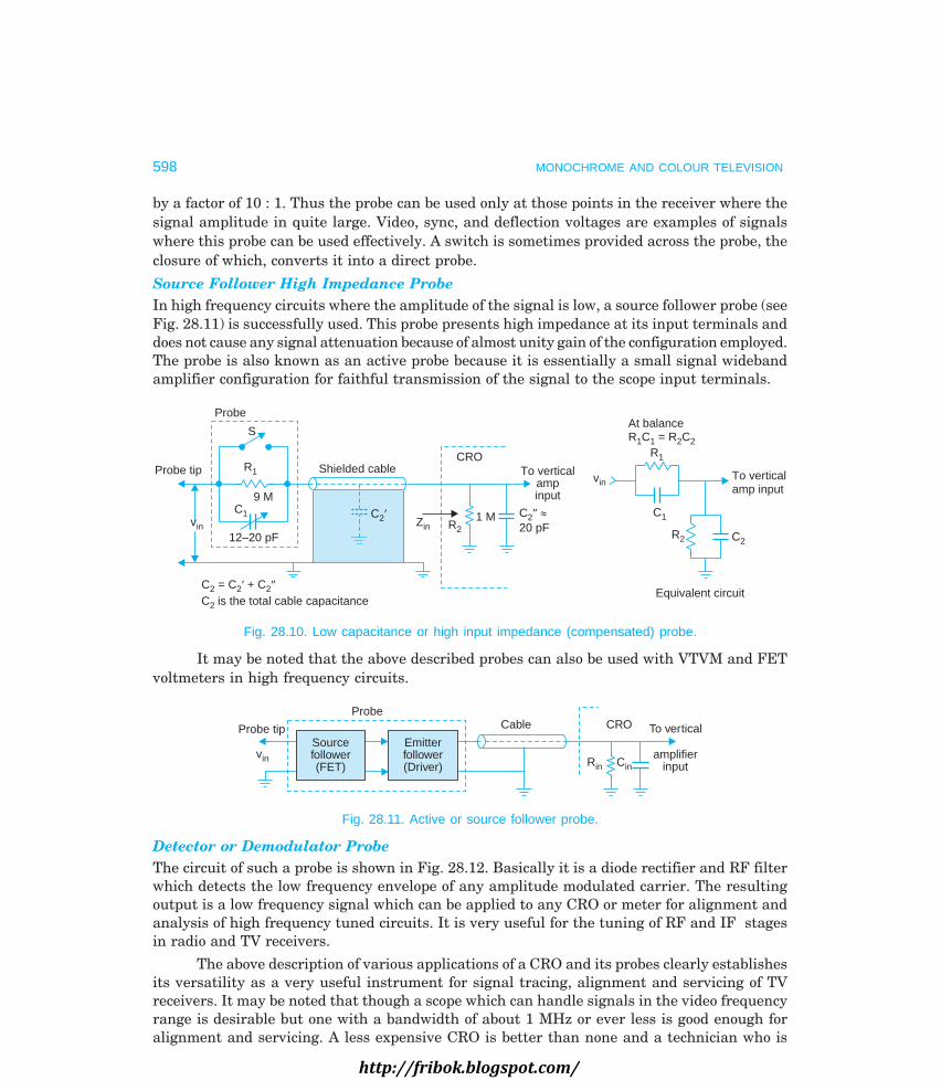
598 MONOCHROME AND COLOUR TELEVISION
by a factor of 10 : 1. Thus the probe can be used only at those points in the receiver where thesignal amplitude in quite large. Video, sync, and deflection voltages are examples of signalswhere this probe can be used effectively. A switch is sometimes provided across the probe, theclosure of which, converts it into a direct probe.
Source Follower High Impedance ProbeIn high frequency circuits where the amplitude of the signal is low, a source follower probe (seeFig. 28.11) is successfully used. This probe presents high impedance at its input terminals anddoes not cause any signal attenuation because of almost unity gain of the configuration employed.The probe is also known as an active probe because it is essentially a small signal widebandamplifier configuration for faithful transmission of the signal to the scope input terminals.
ivin
Probe
Probe tip
S
R1
C1
9 M
12–20 pF
Shielded cable
C2¢Zin R2
1 M C20 pF
2² »
CROTo vertical
ampinput
vin
R1
R2 C2
C1
To verticalamp input
At balanceR C = R C1 1 2 2
Equivalent circuitC = +2 2 2
2
C CC is the total cable capacitance
¢ ²
Fig. 28.10. Low capacitance or high input impedance (compensated) probe.
It may be noted that the above described probes can also be used with VTVM and FETvoltmeters in high frequency circuits.
Probe tip
vin
ProbeCable CRO To vertical
amplifierinputCinRin
Sourcefollower(FET)
Emitterfollower(Driver)
Fig. 28.11. Active or source follower probe.
Detector or Demodulator ProbeThe circuit of such a probe is shown in Fig. 28.12. Basically it is a diode rectifier and RF filterwhich detects the low frequency envelope of any amplitude modulated carrier. The resultingoutput is a low frequency signal which can be applied to any CRO or meter for alignment andanalysis of high frequency tuned circuits. It is very useful for the tuning of RF and IF stagesin radio and TV receivers.
The above description of various applications of a CRO and its probes clearly establishesits versatility as a very useful instrument for signal tracing, alignment and servicing of TVreceivers. It may be noted that though a scope which can handle signals in the video frequencyrange is desirable but one with a bandwidth of about 1 MHz or ever less is good enough foralignment and servicing. A less expensive CRO is better than none and a technician who is
http://fribok.blogspot.com/

ALIGNMENT AND SERVICING EQUIPMENT 599
fully familiar with its use, capability and limitations soon learns to make the maximum use ofthe instrument he possesses.
Probe
Tip
vin
270 pF Diode 250 K
100 K
Cable
To scopeverticalinput
Fig. 28.12. Demodulator probe.
28.5 VIDEO PATTERN GENERATOR
A pattern generator provides video signals, direct and with RF modulation, on the standardTV channels for alignment, testing and servicing of television receivers. The output signal isdesigned to produce simple geometric patterns like vertical and horizontal bars, chequer-board,cross-hatch, dots etc. These patterns are used for linearity and video amplifier adjustments. Inaddition to this, FM sound signal is also provided in pattern generators for aligning soundsection of the receiver.
SW1
SW2
SW3
SW4
SW5
Vertical bars
Chequer-board
Cross-hatched
Horizontal bars
White
PatternsControl switchesBlanking andgating pulses
Vertical (mV) bargenerator
(multivibrator-divider and
shaping circuits)
Frequencycontrol
Cross-hatch andchequer board
pattern generatorBlanking andgatingpulses Horz (nV) bar
generator(multivibrator-
divider andshaping circuits)
Frequencycontrol
Compositesync
Patterns videosignal
Blanking andgating pulse
generator
Masteroscillator
Syncgeneration anddelay circuits
Patternvideo signal
and syncadder
VHFmodulator (AM)
FMmodulator
1 KHztone generator
High
Low
CompositemodulatorRF output
Modulated soundsignal output
Channelcarrier
5.5 MHzcarrier
Fig. 28.13. Simplified functional block diagram of a pattern-cum-sound signal generator.
http://fribok.blogspot.com/
600 MONOCHROME AND COLOUR TELEVISION
A simplified functional block diagram of the pattern cum FM sound signal generator isshown in Fig. 28.13. The generator employs two stable chains of multivibrators, dividers andpulse shaping circuits, one below the line frequency to produce a series of horizontal bars andthe other above 15625 Hz to produce vertical bars. The signals are modified into short durationpulses which when fed to the video section of the receiver along with the sync pulse trainproduce fine lines on the screen.
Multivibrators produce square wave video signal at m times the horizontal frequency toprovide m vertical black and white bars. After every m cycles, the horizontal blanking pulsetriggers the multivibrator for synchronizing the bar signal on every line. A control on the frontpanel of the pattern generator enables variation of multivibrator frequency to change thenumber of bars.
Similarly square wave pulses derived either from 50 Hz mains or from the masteroscillator are used to trigger another set of multivibrators to generate squarewave video signalthat is n times the vertical frequency. These on feeding the video amplifier produce horizontalblack and white bars. The number of horizontal bars can also be varied by a potentiometerthat controls the switching rate of the corresponding multivibrator. The bar pattern signal iscombined with the sync and blanking pulses in the video adder to produce composite videosignals before feeding it to the modulator.
Provision of switches in the signal paths of the two multivibrators enables generation ofvarious patterns. If both mH and nV switches are off, there will be a blank white raster. WithmH switch on, vertical bars will be produced and when only nV switch is on, horizontal barsare generated. With both switches on, a cross hatch pattern will be produced.
The horizontal bar pattern is used for checking vertical linearity. These bars should beequally spaced throughout the screen for linearity. If necessary frame linearity preset controlsin the receiver can be varied to get best possible results. Similarly the vertical bar pattern canbe used for checking and setting horizontal linearity. With the cross-hatch pattern formed byvertical and horizontal lines, the linearity may be adjusted more precisely because any unequalspacing of the lines is easily discernible. If the pattern rolls up or down or loses horizontalsynchronization, the frequency preset controls in the receiver oscillator circuits can be adjustedtill the pattern becomes stationary. Picture centering and aspect ratio can also be checkedwith the cross-hatch pattern by counting the number of squares on the vertical and horizontalsides of the screen. In practice the picture tube screen is usually so placed that it faces a mirrorfixed opposite to it on the work bench. The technician can thus observe the patterns in themirror while making adjustments at the back side of the receiver.
Besides linearity and sweep frequency checks the pattern generator can also be used fordetecting any spurious oscillations in sweep generation circuits, interaction between the twooscillators, poor interlacing, barrel and pincushion effects etc. As already mentioned almost allpattern generators provide additional facilities for aligning sound section and checking RFand IF stages of the receiver. Modulated picture signal on limited number of channels is alsoavailable for injecting into the RF section of the receiver. Similarly FM sound signal with acarrier frequency of 5.5 MHz ± 100 KHz modulated by 1 KHz tone is provided for aligningsound IF and discriminator circuits. A 75/300 ohms VHF balun is usually available as a standardaccessory to the pattern generator.
http://fribok.blogspot.com/
ALIGNMENT AND SERVICING EQUIPMENT 601
28.6 SWEEP GENERATOR
The familiar RF generator when used for alignment and testing of RF and IF stages of a TVreceiver permits recording of circuit performance at one frequency at a time. Therefore, plottingof the total response curve point by point over the entire channel bandwidth becomes a laboriousprocess and takes a long time. To overcome this difficulty, a special RF generator known assweep generator is used. It delivers RF output voltage at a constant amplitude which sweepsacross a range of frequencies and continuously repeats this at a predetermined rate.
The sweep generator is designed to cover the entire VHF and UHF spectrum. Anyfrequency in these bands can be selected as the centre frequency by a dial located on theinstrument panel.
Sweep WidthFrequency sweep is obtained by connecting a varactor diode across the high frequency oscillatorcircuit. A modified triangular voltage at 50 Hz∗ is used to drive the varactor diode. Thus thefrequency sweeps on either side of the oscillator’s centre frequency at the rate of driving voltagefrequency. The amplitude of the driving voltage applied across the varactor diodes can bevaried to control maximum frequency deviation on either side of the carrier frequency. This isknown as sweep-width and can be adjusted to the desired value up to a maximum of about± 15 MHz. A width control (potentiometer) is provided for this purpose.
Alignment ProcedureThe output of the sweep generator is connected to the input terminals of the tuned circuitunder test. The frequency and ‘sweep-width’ dials are adjusted to sweep the range which liesin the passband of the circuit. With an input signal of constant amplitude, the output voltagevaries in accordance with the frequency-gain characteristics of the circuit. The magnitude ofthe output voltage varies with time as the oscillator frequency sweeps back and forth throughthe centre frequency. The RF output is detected either by video detector in the receiver or by ademodulator probe. The detected output varies at the sweep rate of 50 Hz and its instantaneousamplitude changes in accordance with the circuit characteristics. Thus the output signal is alow frequency signal at 50 Hz and can be displayed on an ordinary scope provided the lowfrequency response of its vertical amplifier is flat down to at least 50 Hz.
Time-base for Visual DisplaySince the HF oscillator frequency sweeps at the rate of 50 Hz, the detected output voltage alsovaries at the same rate and completes its back and forth cycle in 20 ms (1/50th sec.). In orderto obtain a linear display of the detected signal the scope sweep voltage must vary accordinglyand have a frequency of 50 Hz. Therefore, to obtain exact correspondence a triangular sweepvoltage is developed and made available on the sweep generator along with other outputs.
The basic circuit configuration used for alignment of any tuned circuit with a sweepgenerator and scope is shown in Fig. 28.14. The time-base switch of the scope is set on ‘external’and its horizontal input terminals are connected to the ‘sweep output’ terminals on the sweepgenerator. Thus the application of a 50 Hz triangular voltage to the horizontal deflecting platesresults in a linear display on the scope screen, both during trace and retrace periods. Theresulting patterns are shown in Fig. 28.15.
∗In U.S.A. where the supply frequency is 60 Hz a sweep rate of 60 or 120 is used.
http://fribok.blogspot.com/

602 MONOCHROME AND COLOUR TELEVISION
Sweep generator
CROsweep
RFout
Receiver circuitunder alignment
Video detectoror demodulator
probe
Centre frequency35 MHz
Scope
V H
Sweep switch at extSweep voltage (50 Hz)
Fig. 28.14. Test equipment connections for alignment of RF, IF sections of the receiver.
Effect of Phase ShiftIf there is a slight phase difference between the 50 Hz voltage used for modulating the RFsignal and that available for horizontal deflection of the scope beam, the retrace portion of thecurve will not follow precisely the trace path. This is illustrated in Fig. 28.15 (c). To correct thisdeviation, a phase control is made available on the front panel of the sweep generator.
Retrace
Trace
(c)(b)(a)
b
a c30 MHz 40 MHz
b¢
a¢ c¢
tRetraceblanked
Tracev(H)
0
aSweep voltage
v(H)
0
(d)
a¢
b¢c¢c
bt
RetraceTrace
V
Trace
Retrace
H H
V
Fig. 28.15. Development of the response curve on the scope screen (a) trace (b) retrace(c) effect of phase shift (d) effect of retrace blanking or use of sawtooth sweep.
Phase ReversalA phase reversal switch is also provided on the sweep generator. This is to ensure that the lowfrequency side of the response curve lies on the left side of the oscilloscope screen. If displayedotherwise it would cause unnecessary confusion. In some sweep generators a polarity switch isalso provided to reverse the polarity of the trace if necessary.
Retrace BlankingModern sweep generators employ a sawtooth sweep with negligible retrace time instead of atriangular sweep. Besides eliminating any phase shift problems the ramp sweep produces azero reference line on the CRO screen during retrace periods. In sweep generators that employ
http://fribok.blogspot.com/

ALIGNMENT AND SERVICING EQUIPMENT 603
a triangular sweep, a blanking switch is used to blank the retrace part of the pattern. Theresulting pattern is illustrated in Fig. 28.15 (d).
The vertical deflection on the scope screen is calibrated with a known voltage which isavailable either on the oscilloscope or sweep generator. This enables measurement of voltagesat all critical frequencies with the retrace line as the reference.
28.7 MARKER GENERATOR
Though the sweep generator provides a visual display of the characteristics of the circuit oramplifier, this alone is inadequate because it does not give any precise information of thefrequency on the traced curve. For this, a separate RF generator known as marker generator isused. This generator, though essentially an RF signal generator in the VHF and UHF bands, isof much higher accuracy than the familiar signal generators. The output of the marker generatoris set at the desired frequency within the pass-band of the circuit under test. As indicated inFig. 28.16, the outputs from the two generators are mixed together before applying to theinput terminals of the circuit under test. The two signals heterodyne to produce outputs at thesum and difference of the two frequencies. These appear at the detector output and representamplitude characteristics of the circuit. Because of the limited frequency response of the scope’svertical amplifier, the sum and most difference frequency signals generated, when the sweepfrequency varies over a wide range, fail to produce any vertical deflection on the screen. However,as the sweep frequency approaches and just crosses the marker frequency, the differencefrequency signals which are produced, lie within the pass band of the vertical amplifier. Thusthey produce a pip on the screen along with the trace generated by the low frequency output ofthe detector. In order to get a sharp pip, a suitable capacitor is shunted across the verticalinput terminals of the scope.
Markergenerator
Marker pip
V HCRO
Ext
Sweep
Marker injection(35 MHz)
Sweep generator
Biasvoltage
CROsweep
Sweep30-40 MHz
IFsection
of the receiver
Demodulatorprobe or video
detector
Sweep voltage
AGC biasas needed
Fig. 28.16. Pre-injection of marker generator output in the sweep generator output.
Since the pip is produced at the marker frequency, it can be shifted to any point on theresponse curve by varying the marker generator frequency. This enables exact location of thetrap and IF frequencies while tuning the RF and IF stages of the receiver.
Marker generator, besides providing dial controlled frequency often have a provision togenerate crystal controlled fixed frequency outputs at several important frequencies. Theseadditional frequencies in a generator designed for CCIR 625 line system include : 31.4 MHz
http://fribok.blogspot.com/

604 MONOCHROME AND COLOUR TELEVISION
(band edge), 31.9 MHz (trap frequency), 33.4 MHz (sound IF), 34.47 MHz (colour IF), 36.15MHz (band centre), 38.9 MHz (picture IF), 40.4 MHz (trap frequency) and 41.4 MHz (bandedge). These birdy type markers can be switched in, either individually or simultaneously bytoggle or push button switches provided for this purpose. Such a provision is very useful forexact alignment of IF section of the receiver.
Marker InjectionThere are two methods of adding marker signals to the oscilloscope display set up. The pre-injection method, where the sweep generator and marker generator outputs are mixed beforethey are applied to the circuit under test, suffers from the following drawbacks :
(i) The marker signal has to pass through the tuned circuit being aligned and so theamplitude of the marker pip on the response curve will depend or the gain of the tuned circuitor amplifier at that particular frequency. Thus with a constant marker input a large pip will beproduced on top of the response curve, but will slowly decrease in amplitude as it is moveddown the skirts (slopes) of the response curve and will eventually disappear at the base line.
(ii) To counteract this, if the amplitude of the marker output is kept high, it will overloadthe circuit under test in its pass band region, resulting in distortion of shape of the curve.
Therefore the pre-injection method has been replaced with what is known as post-injectiontechnique. In this method a fraction of the sweep generator output is separately mixed withthe marker generator output. The available output is then mixed with the detected outputbefore applying it to the scope. The circuit connections are illustrated in Fig. 28.17.
Oscilloscope
V HExt
Sweep
PS
(a)
HV Scope
Sweep cummarker generator
MarkersignalsMarker
generator
Sweepgenerator
InIn
RFsweep (sample)
Mixer
Mixer
In In
Out
RFsweepsignal
Sweep voltage
RF and IFsections
Videodetector
Scopesweep Out In
Marker AGCbias
RFout
Sweep-markergenerator
Impedancetransformer
Tuner andIF sections
Videodetector
(b)
Fig. 28.17. Post-injection of marker output (a) basic circuit arrangement(b) connections as in a sweep-marker generator.
http://fribok.blogspot.com/

ALIGNMENT AND SERVICING EQUIPMENT 605
Sweep-Marker GeneratorEarlier sweep and marker generators ware manufactured as separate units. However, nowthe two instruments are combined into a single instrument known as ‘ sweep-marker generator’.It includes a built-in marker adder for post-injection of the marker signal. Such units alsoprovide a variable dc bias source for feeding a fixed bias to the RF and IF sections of thereceiver. This is necessary during alignment when the internal AGC bias must be disabled forcorrect tuning.
The frequency spectrum covered by a quality sweep generator includes VHF and UHFranges in both manual and auto modes. The RF output is about 0.5 V rms across 75 ohms witha continuously variable attenuator up to 50 db or 0 to 60 db in 10 db steps. The marker sectionprovides crystal controlled output at all important frequencies. The output can be internallymodulated with a 1 KHz tone when necessary. These accessories include a demodulator probe,a balun and special cables with matched terminations.
Telonic (USA) 1011 B VHF sweep generator (see Fig. 28.18) needs special mention becauseof its versatility and reliability. It covers a frequency range of 5-300 MHz in manual, auto andprogram modes. Its auto-track feature (option 402 B) eliminates manual adjustment of thesweep generator. This option automatically tunes the centre frequency of sweep generator totrack the IF of the tuner. Similarly the autotrace option 409 B accepts detected output of thetuner and yields a constant display to the scope. Simultaneously actual input amplitude isindicated by the height of a pulse on the display.
Fig. 28.18. Telonic 1011 B VHF sweep generator.
The generator can provide different marker systems. Option 206B produces a ‘birdy’type marker whenever the frequency of the sweep generator is equal to the frequency of anexternally applied CW signal. Another option 297B produces a birdy maker at the user’s desiredfrequency. One to seven markers are available. Similarly option 337 B provides IF centredpulse pair markers at any spacing from 1 to 12 MHz for local oscillator adjustments. Yet anotherchoice, option 342 B, produces a pulse marker pair at sound and video of the selected channel.
http://fribok.blogspot.com/

606 MONOCHROME AND COLOUR TELEVISION
The main specifications of the Telonic 1011 B sweep generator are as under :
Frequency range 5-300 MHz
Sweep width 5-30 MHz in manual, auto and program modes
Sweep rate Sawtooth, electronically line synchronized to 50/60 Hzline with capability to sweep at half the line rate.
RF output 0.5 V rms, 0.25 V with continuously variableattenuator (option 103 B)
Flatness ± 0.5 dB over full range.
Spurious and harmonics – 30 db max.
Line voltage 105/125 V or 210/250 V
Television WobbuloscopeThis instrument combines a sweep generator, a marker generator and an oscilloscope all inone. It is a very useful single unit for alignment of RF, IF and video sections of a TV receiver.It may not have all the features of a high quality sweep generator but is an economical andcompact piece of equipment specially designed for television servicing. The oscilloscope usuallyhas provision for TV-V and TV-H sweep modes. A RF output down to 1 MHz is also availablefor video amplifier testing.
Analyst GeneratorAn analyst generator not only provides all the outputs which are available on a pattern generatorbut also duplicates all essential signals of the television receiver. Besides providing RF, IF andvideo signals in the form of patterns, composite video signal including sync, intercarrier sound,separate sync, audio, flyback and yoke test signals are also available. These outputs are normallyused for trouble shooting and not for alignment purposes.
28.8 THE COLOUR BAR GENERATOR
The composite colour video signal at the output of video detector consists of luminance (Y)signal, the chrominance signal, the colour burst, sync pulses and blanking pulses. In practice,the amplitude of video signal is continuously varying due to the changing picture content.Therefore, such a waveform is not useful for adjustments and trouble shooting purposes. Thecolour bar generator acts as a substitute transmitter and supplies the receiver a known non-varying colour pattern signal for alignment and servicing purposes.
The Gated Rainbow Colour Bar GeneratorThe gated colour bar generator develops such a composite video signal that it produces a rainbowcolour bar pattern on the receiver screen. The pattern consists of 10 colour bars ranging incolour from shades of red on the left side, through blue in the centre, to green in the far rightside. The colour bar pattern, the associated video waveform and corresponding phaserelationships of the gated pattern are illustrated in Fig. 28.19. Each colour in the bar patternhas been identified and lined up with the associated modulating waveform. Note that thecomposite video signal for the pattern consists of a horizontal sync pulse and 11 equal amplitudebursts of the colour subcarrier frequency. The burst to the right of the horizontal sync pulse isthe colour burst. The other bursts (1 to 10) differ in phase from one another and correspond todifferent colours in the bar pattern.
http://fribok.blogspot.com/

ALIGNMENT AND SERVICING EQUIPMENT 607
One hor zon a l e s an i clud ng re ra eOne horizontal line scan including retrace
Horz sync
4.7 sm
Generator waveform
1 2 3 4 5 6 7 8 9 10
Colour burstO
rang
e
Yello
w-o
rang
e
Red
Mag
enta
Red
ish-
blue
Blu
e
Gre
enis
h-bl
ue
Cya
n
Blu
ish-
gree
n
Gre
en
1 2 3 4 5 6 7 8 9
10
Picture tube screen
Fig. 28.19 (a). Colour bar pattern display on the screen of a colour picture tubeand corresponding output waveform of the rainbow generator.
°0°
3030°
060°090°
20120°
150°150°
°180°
210210°
40240°7270°
00300°
330°330°
Colourburst
–(B–Y)
blv
Horz blankinginterval
Yellow-orange
1
2
3
Red(R–Y)
Orange4
5
Magenta
Reddish-blue
6
Blue (B–Y)
Greenish-blue
7
8
Cyan9
Bluish green–(R–Y)
10Green
Fig. 28.19 (b). Illustration of colour signal phase relationships with respect to colour burst.
http://fribok.blogspot.com/

608 MONOCHROME AND COLOUR TELEVISION
The basic principle of the colour bar generator is quite simple. Any two signals of differentfrequencies have a phase difference that is continuously changing. As shown in Fig. 28.20 acrystal oscillator is provided to generate a frequency = 4.41799375 MHz. This is 15625 Hzlower than the colour subcarrier frequency (4.43361875 – 4.41799375 = 15625 Hz). Since thedifference in frequency is equal to the horizontal scanning rate, the relative phase between thetwo carrier frequencies will change by 360° per horizontal line. Thus the effective carrier signalat 4.41799375 MHz will appear as a signal that is constantly changing in phase (360° duringeach horizontal line time) when compared to the 4.43361875 MHz reference oscillator in thetelevision receiver. It is the phase of the chrominance signal which determines the colour seenand therefore such a frequency relationship provides the colour bar signal. Since there is acomplete change of phase of 360° for each horizontal sweep, a complete range of colours isproduced during each horizontal line. Each line displays all the colours simultaneously sincethe phase between the frequency of crystal oscillator and that of the horizontal scanning ratefrequency is zero at the beginning of each such line and advances to become 360° at the end ofeach horizontal sweep stroke.
As shown in the block diagram of Fig. 28.20 the colour bar pattern is produced by gating‘on’ and ‘off’ the 4.41799375 MHz oscillator at a rate 12 times higher than the horizontal sweepfrequency (15625 × 12 = 187.5 KHz). The gating at a frequency of 187.5 KHz produces colourbars with blanks between each colour bar. The colour bars have a duration corresponding to15° and are 30° apart all around the colour spectrum. When viewed on the picture tube screenof a normally operated colour receiver, these bars appear as shown in Fig. 28.19 (a). (The barsare also shown in colour plate No. 5).
Horz sync,vertical sync
and blanking pulses
Crystal oscillatorf = 4.41799375 MHz(subcarrier oscillator)
Gating pulses(187.5 KHz)
A
D
D
E
R
Modulator
Channel 3 or 4carrier
oscillator
0
Amplitude modulated RFoutput of the colour bar
generator
Fig. 28.20. Simplified block diagram of a gated rainbow colour bar generator.
It may be noted that out of the twelve gated bursts, only 10 show on the picture tube ascolour bars. This is so, because one of the bursts occurs at the same time as the horizontal syncpulse and is thus eliminated. The other burst occurs immediately after the horizontal syncpulse and becomes the colour sync burst which is used to control the subcarrier referenceoscillator in the television receiver. Thus phase angles from 0° to 30°, that correspond to thecolour burst and colours such as yellow (13°) are blanked out during horizontal retrace and donot appear on the picture tube screen.
http://fribok.blogspot.com/

ALIGNMENT AND SERVICING EQUIPMENT 609
The adder while gating the crystal oscillator output also combines horizontal sync, verticalsync and blanking pulses to it. The composite colour video signal available at the output of theadder can be fed directly to the chrominance bandpass amplifier in the TV receiver. However,it is usually amplitude modulated with the carrier of either channel 3 or 4. The option is givenso that the service engineer can select a channel that does not have a local live transmissionthat might cause interference.
Receiver Operation with Colour Bar SignalThe modulated RF output of the colour bar generator is fed to the antenna terminals of thereceiver. This signal is processed by the various RF and IF sections of the receiver and detectedat the video detector. As shown in Fig. 28.21, it is then applied to the colour demodulators viathe chroma bandpass amplifier. If the alignment of all the stages is proper the waveformfeeding the colour demodulators will be essentially the same as that which modulates the RFcarrier in the colour bar generator. The main difference is that the horizontal sync which occurat the line rate are removed by the 4.43 MHz tuned circuits in the bandpass amplifier.
One horz line scanincluding retrace
Colour syncinterval
Horz syncinterval
1 2 3 9 104 5 6 7 8
To blue gun control grid
1 2 3 4 5 6 79 108
To green gun control grid
1 2 3 4 56 7 9 108
To red gun control grid
Picture tube signals necessary to producea colour bar pattern (f = 15625 Hz)
+–
+
+–
(B–Y)
(G–Y)
(R–Y)
MATRIX
Udemodulator
Vdemodulator
f 0°Sc Ð
f 0°Sc б9
4.43361875 MHzsubcarrieroscillator
–
+
Delayline
ChromabandpassamplifierColour
bar signalfrom videodetectoroutput
Fig. 28.21. Simplified block diagram of colour section of thereceiver showing passage of colour bar signal.
The input to each demodulator consists of gated colour bar signal and a locally generatedconstant amplitude subcarrier oscillator signal. The demodulator output after matrixing yield(R – Y), (G – Y), and (B – Y) colour difference signals. As shown by the waveforms drawn alongthe matrix in Fig. 28.21, the three signals are out of phase with respect to each other and areserrated because of interruptions by the gating signal. These signals are amplified before feedingto the corresponding control grids of the colour picture tube. Not that at the instant the voltageon the blue gun control grid is maximum positive (bar 6), it is zero and negative at the red andgreen guns respectively. Such a combination will increase the blue gun beam current, reduce
http://fribok.blogspot.com/

610 MONOCHROME AND COLOUR TELEVISION
considerably the red gun beam current and almost cut-off the green beam. The net result willbe, that a blue bar will be produced on the screen. Similarly, it can be argued that the 3rd barwill attain a red colour and the 10th bar will be green. The other bars will vary in colour,depending on the relative amplitude of the pulse to each control grid of the picture tube.
NTSC Colour Bar GeneratorAnother type of colour bar generator is the NTSC colour generator. It is compatible with the525 line American TV system and its output signal also includes the Y signal component. TheY signal corresponds to the shades of grey that would be produced in a black and white receiverby the seven bars of colour that constitute of the pattern. Each of the seven colour barscorresponds to a burst of 3.58 MHz. The amplitude of the burst represents saturation of thecolour bar and its phase corresponds to the colour. The NTSC colour bar pattern consists ofthree primary colours, their complementary colours at 100 percent saturation and a white bar.
A colour bar generator is very useful for colour signal tracking in various sections of thereceiver. It is also used for initial adjustments of colour sync, range of tint, colour controls, etc.
Colour-Bar Pattern GeneratorThis instrument is a combination of a pattern generator and a colour bar generator. It is usefulfor black and white and colour receiver alignment and servicing. The Philips PM 5501 (see Fig.28.22) is one such generator specially designed for use at customer’s house. It provides the fiveessential test patterns, necessary to make installations, fast checks and repairs on bothmonochrome and colour receivers. The patterns are selected by push buttons. The instrumentis extremely light and portable.
Fig. 28.22. Philips PM 5501 colour-bar pattern generator.
The PM5501 operates according to the CCIR 625 line system G, TV standards. To ensurefast operation, two fixed RF signals can be selected, one on VHF channel 7 and the other forUHF channel 30. When required, channel 7 may be altered to any frequency in Band III (170to 230 MHz). The same applies to UHF channel 30, which can be changed internally to anychannel in the frequency range, 470 to 600 MHz.
http://fribok.blogspot.com/
ALIGNMENT AND SERVICING EQUIPMENT 611
For accurately tuning and checking the sound performance of a colour television receiver(CTV), the generator has a 1 KHz tone available. This tone also makes checks on interferencebetween luminance-sound and chroma-sound.
The main technical specifications of this colour bar pattern generator are given below.
Test signals(a) 8 bars, linearized, grey scale
(b) cross-hatch pattern
(c) 100% white pattern (with burst)
(d) red pattern (50% saturated)
(e) standard colour bar with white reference 75% contrast (internally changeable to fullbars)
Video carrier
(a) VHF band III : 170–230 MHz
(b) UHF band IV : 470–600 MHz
RF output
> 100 mV p-p (75 ohm impedance)
Video modulation—Am, negative
Sound carrier
Frequency—5.5 MHz (or 6 MHz by internal adjustment)
Modulation—FM
Internal signal—1 KHz sine wave
FM sweep 40 KHz on 5.5 MHz.
Chroma : PAL—G and I standards
Power : 115–230 V, 50–60 Hz, 6 watt,
Dimensions (w × h × d) : 23 × 11 × 21 cm,
Weight : 1.25 Kg.
28.9 VECTROSCOPE
This test instrument combines a keyed colour-bar generator with an oscilloscope and is usedfor alignment and testing the colour section of a TV receiver. The amplitude and phase of thechrominance signal represent colour saturation and hue of the scene. The information can alsobe displayed on the oscilloscope screen in the form of a Lissajous pattern. The resultant displayis called a vectrogram. A separate colour-bar generator can also be used with a conventionalCRO to produce a vectrogram. The necessary connections and the resulting pattern are shownin Fig. 28.23. With the gated colour bar generator connected at the input terminals of thereceiver, serrated (R—Y), and (B—Y) video signals become available at the correspondingcontrol grids of the colour picture tube. These two outputs are connected to the vertical and
http://fribok.blogspot.com/
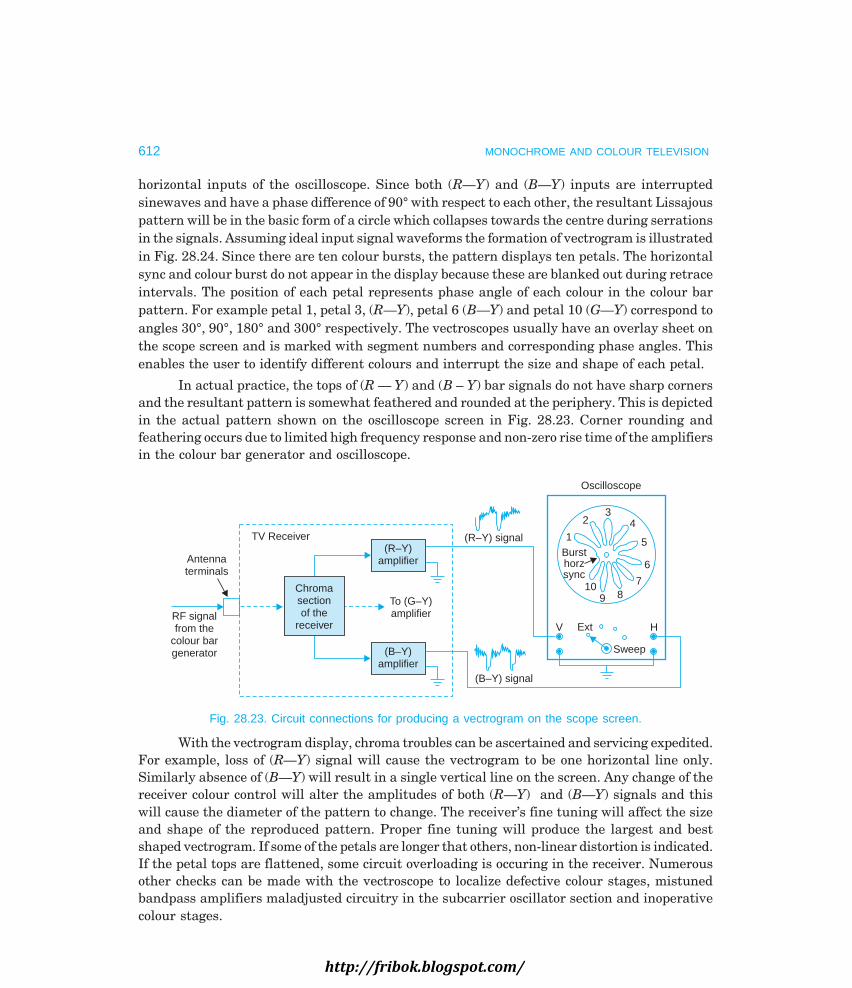
612 MONOCHROME AND COLOUR TELEVISION
horizontal inputs of the oscilloscope. Since both (R—Y) and (B—Y) inputs are interruptedsinewaves and have a phase difference of 90° with respect to each other, the resultant Lissajouspattern will be in the basic form of a circle which collapses towards the centre during serrationsin the signals. Assuming ideal input signal waveforms the formation of vectrogram is illustratedin Fig. 28.24. Since there are ten colour bursts, the pattern displays ten petals. The horizontalsync and colour burst do not appear in the display because these are blanked out during retraceintervals. The position of each petal represents phase angle of each colour in the colour barpattern. For example petal 1, petal 3, (R—Y), petal 6 (B—Y) and petal 10 (G—Y) correspond toangles 30°, 90°, 180° and 300° respectively. The vectroscopes usually have an overlay sheet onthe scope screen and is marked with segment numbers and corresponding phase angles. Thisenables the user to identify different colours and interrupt the size and shape of each petal.
In actual practice, the tops of (R — Y) and (B – Y) bar signals do not have sharp cornersand the resultant pattern is somewhat feathered and rounded at the periphery. This is depictedin the actual pattern shown on the oscilloscope screen in Fig. 28.23. Corner rounding andfeathering occurs due to limited high frequency response and non-zero rise time of the amplifiersin the colour bar generator and oscilloscope.
1
23
4
5
6
789
10
Bursthorzsync
Oscilloscope
(R–Y) signal
V HExt
Sweep
(B–Y) signal
(R–Y)amplifier
To (G–Y)amplifier
(B–Y)amplifier
Chromasectionof the
receiver
TV Receiver
Antennaterminals
RF signalfrom the
colour bargenerator
Fig. 28.23. Circuit connections for producing a vectrogram on the scope screen.
With the vectrogram display, chroma troubles can be ascertained and servicing expedited.For example, loss of (R—Y) signal will cause the vectrogram to be one horizontal line only.Similarly absence of (B—Y) will result in a single vertical line on the screen. Any change of thereceiver colour control will alter the amplitudes of both (R—Y) and (B—Y) signals and thiswill cause the diameter of the pattern to change. The receiver’s fine tuning will affect the sizeand shape of the reproduced pattern. Proper fine tuning will produce the largest and bestshaped vectrogram. If some of the petals are longer that others, non-linear distortion is indicated.If the petal tops are flattened, some circuit overloading is occuring in the receiver. Numerousother checks can be made with the vectroscope to localize defective colour stages, mistunedbandpass amplifiers maladjusted circuitry in the subcarrier oscillator section and inoperativecolour stages.
http://fribok.blogspot.com/

ALIGNMENT AND SERVICING EQUIPMENT 613
15° 15°15°
32
1 5
66
4422
1
3
4
5
6
70
88
910
t
(R–Y) signal appliedto vertical input
of the CRO
Lissajous pattern
Colour burst
Horz sync
88
7
99010
0
12 3 4
5
6
78
910
t
(B–Y) signal appliedto horizontal input
of the CRO(time–base disabled)
Fig. 28.24. Ideal keyed rainbow vectrogram (lissajous pattern)produced by (R—Y) and (B—Y) colour difference signals.
28.10 HIGH VOLTAGE PROBE
A high voltage probe is necessary for measuring EHT voltages in TV receivers. Since themaximum voltage range on multimeters seldom exceeds 1 KV, it becomes necessary to attenuatehigh voltages before connecting them to a multimeter.
Most voltage probes use a compensated string of resistive network to form a voltagedivider. The attenuation ratio is usually 100 : 1. However, for measuring voltages of the orderof 30 KV or so, resistance type of probe is not suitable because of stray conduction paths set upby the resistors. Therefore capacitor type probes are used to provide an attenuation of 1000 : 1.Such probes contain two or more capacitors with values selected to provide desired voltagereduction and to match the input impedance of the meter. Special high voltage probes havebeen developed for TV service work which have built-in meters to measure voltages up to30 KV. For safety such probes have a separate earth terminal which should be connected toground when carrying out EHT measurement.
In addition to all the instruments and accessories described above a regulated powersupply, a tube tester and a transistor tester are equally necessary pieces of equipment. Withthe increased use of ICs it is desirable to posses an IC tester and additional low voltage regulatedpower supplies.
http://fribok.blogspot.com/

614 MONOCHROME AND COLOUR TELEVISION
Review Questions
1. Describe with suitable circuit diagrams how voltage, current and resistance measurements aremade in a multimeter. Why a movement having very low full scale deflection current is employedin multimeters ?
2. Why are VTVMs preferred for both dc and ac voltage measurements in electronic circuits ? Whyis the input resistance of a VTVM much higher than a multimeter when set to measure volts ?
3. Discuss relative merits of the two main types of electronic voltmeters. Why is an amplifier-rectifier type of VTVM preferred over a rectifier-amplifier type for measurements in video circuits ?What is the function of probes in dc and ac voltage measurements ?
4. Explain with suitable circuit diagrams how a CRO can be employed for measurement of phase-shift and frequency. Why is a probe necessary for faithful display of a video signal ?
5. Draw a circuit diagram to illustrate the use of CRO for displaying a television picture on itsscreen instead of on receiver’s own picture tube. Explain all the necessary steps and precautionsthat must be observed for obtaining a well defined picture with a correct aspect ratio.
6. Describe how various patterns are generated in a video pattern generator. Explain typicalapplications of this instrument for testing and aligning a TV receiver.
7. Explain the need and method of sweeping the carrier frequency around its chosen central value.Describe briefly the use of all controls which are normally provided on the front panel of a sweep-cum-marker generator.
8. Explain with a diagram of connections how a sweep generator can be employed to obtain theresponse curve of a wide band tuned circuit on a CRO.
9. Why is it necessary to inject marker signals into the sweep generator output ? Why is post-injection of marker generator output preferred over the pre-injection method ? What is thesignificance of crystal controlled spot frequencies in a marker generator ?
10. Describe the basic principle of a colour bar generator and explain how it is employed to check thechroma section of a colour receiver.
11. Explain how Lissajous patterns obtained on a vectroscope can be interpreted to localize colourreceiver faults.
12. Write short notes on the following : (i) TV wobbuloscope, (ii) Analyst generator (iii) Demodulatorprobe, (iv) EHT probe.
http://fribok.blogspot.com/

29
! #
http://fribok.blogspot.com/

High component density and complexity of circuits in television receivers justify the use ofintegrated circuits to replace complex circuit blocks. The use of ICs reduces component, assembly,and production line costs. On account of these merits and better performance, there is anincreasing trend to use more and more ICs in television receivers. All present day TV receiversincorporate two or more ICs to replace discrete circuitry in low power and complex sections oftheir circuits.
Comprehensive details of various sections of the receiver employing tubes, transistorsand ICs are discussed in the previous chapters. In order to show how various blocks fit together,complete circuit of a monochrome receiver is explained. In addition, circuit organization ofboth monochrome and colour receivers employing ICs in most sections of the receiver are alsodiscussed. Tuning and alignment of different sub-assemblies of the receiver is explained alongwith circuit details.
29.1 MONOCHROME TV RECEIVER CIRCUIT
Out of the numerous receiver circuits that are in use, one developed by Bharat Electronics Ltd.(BEL) has been chosen for detailed discussion. It is a multichannel fully solid-state receiverconforming to CCIR 625-B system. It employs three ICs. The design of the receiver is so simplethat it can be assembled* with a minimum of tooling and test facilities. Such an exercise can bevery instructive for fully grasping alignment and servicing techniques of a television receiver.Fig. 29.1 on the foldout page shows the circuit diagram of this receiver. A brief description ofthe circuit follows:
(a) TunerThe receiver employs a turret type tuner and provides all channels between 3 to 10 in the VHFrange. A high pass filter with a cut-off frequency of 40 MHz is used at the input to reduceinterference due to IF signals. The tuner operates from a + 12 V supply and has an effectiveAGC range of 50 db.
(b) Video IF SectionThe video IF sub-system consists of IC, BEL CA**3068 and other associated components housedin a modular box to avoid any possible RF interference. All interconnections to this module are
616
(
! #
*The technical manual of the receiver can be obtained on request from M/s Bharat ElectronicsLtd. Jalahalli, P.O., Bangalore 560013 India. The manual gives all necessary circuit details, coil data,list of components, assembly and alignment details.
**For more details on CA3068 refer section 23.8.
http://fribok.blogspot.com/

http://fribok.blogspot.com/
RECEIVER CIRCUITS AND ALIGNMENT 617
either through feed through capacitors or insulated lead throughs. The IF sub-assembly provides(i) a gain around 75 db to the incoming signal from the tuner, (ii) required selectivity andbandwidth, (iii) attenuation to adjacent channel interfering frequencies, (iv) attenuation of 26db to sound IF for intercarrier sound, (v) sound IF and video outputs and (vi) AGC voltage tothe IF section and tuner.
(c) Sound IF Sub-system and Audio SectionThe important functions performed by this sub-system are:
(i) to amplify intercarrier IF signal available from the picture IF amplifier,
(ii) to recover sound signal,
(iii) to amplify the sound signal and deliver at least 2 watts of audio power to the loud-speaker.
The circuit of BEL CA*3065 IC consists of (i) a regulated power supply, (ii) a sound IFamplifier-limiter, (iii) an FM limiter, (iv) an electronic attenuator and a buffer amplifier, and(v) an audio driver.
The sound section operates from a + 12 V supply. It employs transistor BC 148B as aboot-strapped driver and matched transistor pair, 2N5296 and 2N6110, at the output stage.The bandwidth of the audio amplifier is from 40 Hz to 15 KHz and can deliver 2 watts of usefulaudio power.
(d) Video Amplifier and Picture Tube BiasingThis section of the receiver uses transistors BF 195 C as driver (buffer), BD115 as video amplifierand BC147B in the blanking circuit. The video amplifier delivers 90 V p-p signal to the cathodeof picture tube 500-C1P4. The current limiting is provided by diode 0A79 and associated circuitry.Transistor Q 503 switches amplifier transistor Q502 only during the time when video signal ispresent and turns it off during horizontal and vertical sync periods. The horizontal blankingpulses of 60 V p-p and vertical blanking pulses of 40 V p-p are applied to the base of transistorQ503. High voltage output of 1.1 KV from the horizontal output circuit is rectified and fed tofocusing grids of the picture tube through a potential divider. Brightness control operatesfrom a + 200 V supply. The contrast control functions by varying input signal amplified to thevideo amplifier transistor Q 502.
(e) Horizontal Oscillator Sub-systemThis section employs transistor Q 401 (BC 148 A), IC, CA 920 and associated passive components.Composite video signal from the IF section is applied to pin 8 of IC 401 (CA 920). The functionsof the horizontal subsystem are:
(i) to generate a line frequency signal, the frequency of which can be current controlled,
(ii) to separate sync information from the composite signal,
(iii) to compare the phase of sync pulses with that of the oscillator output and generate acontrol voltage for automatic tuning of the oscillator,
*For more details on CA 3065 refer section 21.7.
http://fribok.blogspot.com/

618 MONOCHROME AND COLOUR TELEVISION
(iv) phase comparison between the oscillator waveform and middle of the line flybackpulse, to generate a control voltage for correction of the switching delay time in thehorizontal driving and output stages, and
(v) shaping and amplification of the oscillator output to obtain pulses capable of drivingthe horizontal deflection driver circuit.
(f) Horizontal Output CircuitOutput from the horizontal oscillator is applied to the base of horizontal driver transistorQ802 through a coupling capacitor (C 803). The transistor switches from cut-off to saturationwhen a pulse is applied to its base and provides the necessary drive for Q803 (BU 205). Theoutput transistor (Q803) drives the line output transformer to provide deflection current tothe yoke coils. In addition, the output circuit (i) generates flyback pulses for blanking, AFCand AGC keying, (ii) provides auxiliary power supplies and generates high voltage (+ 18 KV)for anode of the picture tube and (iii) produces 1.1 KV dc for the focusing grids. The heatersupply of 6.3 V for the picture tube is taken across winding 10-11 of the line output transformer.
(g) Vertical Deflection CircuitAs shown in Fig. 29.1, the circuit operates from a 40 V dc supply obtained through the lineoutput transformer. This sub-system is a self oscillatory synchronized oscillator with a matchedpair of output transistors. Clipped vertical sync pulses are fed at the base of Q 70 (BC 148 C) toprovide it with a stable drive. Resistor R 724 senses yoke current and feeds a voltage proportionalto this current back to the base of Q 702 (BC148 B) for adjustment of the picture height.Coupling network between the collector of Q 701 and the base of Q 702 incorporates thenecessary ‘S’ correction and provides linearity of the deflection current. Hold control formspart of the input circuit of transistor Q 701.
(h) Power Supply CircuitThe power supply circuit is a conventional transformerless half-wave rectifier and filter circuit.It provides 200 V for feeding various sections of the receiver.
Front panel control. Four controls i.e. on/off volume control, channel selector and finetuning, contrast control and brightness control are brought out at the front panel of the receiver.In addition, vertical hold and horizontal hold controls are available on the side panel foroccasional adjustments.
29.2 MONOCHROME RECEIVER ALIGNMENT
The exact procedure for aligning the tuner and IF stages is based on their design and is perfectedafter a great deal of experimentation by the manufacturers of television receivers. Therefore,the alignment should be carried out strictly in accordance with the procedure recommended inthe literature of the receiver.
It is wrong for a service engineer to tamper with the RF and IF sections of the receiverunless he has full equipment, expertise and service manual of the receiver. In most cases thesestages require a ‘touch up’ alignment in which relatively few adjustments are necessary andan experienced technician can accomplish this task by looking at the picture and hearing thesound in the loudspeaker.
http://fribok.blogspot.com/

RECEIVER CIRCUITS AND ALIGNMENT 619
However, if alignment is necessary or a new set is to be aligned it is necessary to carryout the following checks before proceeding with the alignment of RF and IF sections of thereceiver.
(i) The vertical and horizontal sweep circuits should be checked for a steady and distur-bance free raster.
(ii) Video amplifier and picture tube circuitry should be checked for proper bandwidthand low frequency phase shift characteristics,
(iii) Using a pattern generator or otherwise, necessary adjustments should be made toensure linearity, correct aspect ratio and proper interlacing.
Alignment SequenceIt is a good practice to carry out receiver alignment in the following sequence:
(i) Setting up of trap circuits at proper frequencies,(ii) Alignment of IF stages,
(iii) Sound section alignment,(iv) Tracking of RF and mixer stages,(v) Tracking of oscillator circuits to obtain best picture and sound output.
Alignment PrecautionsWhile the detailed alignment procedure may differ from receiver to receiver, it is worthwhileto observe the following precautions before commencing alignment of any section of the receiver:
(i) Shielded wire should be used for interconnecting sweep generator, receiver underalignment and scope to avoid stray field pick up effects.
(ii) All connecting leads and cables must be kept as small as possible to minimize highfrequency signal losses.
(iii) All the equipment and receiver should have a common ground because a floatingground would result in incorrect alignment. For grounding receivers having a direct on linetype of supply, an isolating transformer should be used between the supply mains and receiver.
(iv) It should be ensured that the load resistance across which the scope is connectedhas one end at ground potential and is also strapped to the ground terminal of the scope.
(v) A low pass filter formed by a cable (see Fig. 29.2) or a suitable probe should be usedfor connecting signal output from the detector to the scope terminals. The 100 K-ohm resist-ance in series and the capacitance of the cable form a low-pass filter thus bypassing highfrequency pick-ups.
Fromvideo detector
output
100 K Shielded cable
C
V H
Oscilloscope
Fig. 29.2. A low-pass filter circuit in place of a proper probe.
http://fribok.blogspot.com/

620 MONOCHROME AND COLOUR TELEVISION
(vi) A balun (Fig. 29.3 (a)) should be used for connecting sweep generator output to thereceiver input terminals to provide a match. In case a balun is not available a network shownin Fig. 29.3 (b) can be used. This not only provides the desired match between the 75-ohmsweep generator output and 300-ohm receiver but also satisfies the balanced input requirement.
Improper termination of the sweep generator cable or faulty grounding of the equipmentcan be checked by grasping the cable and watching the response curve. A change in the shapeor size of the pattern when the cable is held indicates presence of standing waves on the cable.This must be corrected by proper grounding before proceeding with alignment.
300W75W
Fromsweep
generator
To receiverinputcircuit
(a)
120W
120W
300W68W
Sweep generator
CROsweep
MarkerOut In
RFout
Cable
(b)
TV receiver
Antennainput
terminals
Fig. 29.3. Impedance match between the sweep generator and receiver input terminals(a) by a balun and (b) by a resistive network.
(vii) Any overloading of the circuit should be avoided. The output from the sweep gen-erator must be kept as low as possible to avoid distortion of the reproduced pattern.
(viii) Even when there is no possibility of adjacent channel interference the trap circuitsshould be correctly adjusted. This is necessary because any incorrect tuning of trap circuitsmay result in attenuation of the frequencies which are a part of the desired response.
(ix) To avoid stray capacitance effects, insulated hexagonal wrench and screw drivershould be used for trimmer settings and a narrow shanked screw driver for slug adjustments.
(x) No force should be applied on adjustments which have been sealed. Acetone or anyother suitable thinner should be applied to soften the cement before making adjustments.
Alignment of Trap CircuitsIt is desirable that the trap circuits are tuned before IF alignment because it helps in quickerand more precise alignment of the IF section. The trap circuits can be aligned by setting thesweep generator to deliver amplitude modulated RF output or by employing an RF signalgenerator (marker generator) modulated with a 1 KHz tone as the signal source. A VTVM or aCRO connected across the detector load resistor serves as the detector indicator. The localoscillator should be disabled to avoid any interference while setting trap circuits. As shown inFig. 29.4 the signal generator is connected at different input points (shown by arrows) to tunedifferent rejection circuits. Each time the frequency and signal level should be adjusteddepending on the frequency to be rejected and the location of signal source. The cores of the
http://fribok.blogspot.com/

RECEIVER CIRCUITS AND ALIGNMENT 621
resonant (trap) circuits are varied till minimum response is obtained on the scope or VTVMshows least voltage. The sound IF frequency rejection circuit should also be tuned along withother trap circuits to give a small output on the VTVM. This helps in obtaining desired responsewhile tuning IF stages with a sweep generator.
Marker generator
Marker selectionswitches
On Off
RFout
Modulator
Matchingnetwork
Tuner
Localoscillatordisabled
VTVMTrapcircuits
IFamplifier
Videodetector
L
Detectorload
RL
Fig. 29.4. Alignment of trap circuits.
IF Section AlignmentThe primary purpose of IF amplifier alignment is to obtain a response curve of proper shape,frequency coverage and gain. Correct alignment of the combined picture and sound IF stagesis necessary for a good picture and distortion free sound. There are two methods of aligning IFstages:
(a) Marker generator and electronic voltmeter method. For staggered-tuned IF stages ofthe receiver, the individual stages are tuned at predetermined frequencies using a CW markergenerator and VTVM. The electronic voltmeter is connected at the output of video detector.After adjusting all the trap circuits for minimum output and tuned band-pass circuits formaximum output, a sweep generator, a marker generator and a scope is used to check theoverall response curve. Necessary touch-up of tuned circuits is made while comparing theresponse curve with the one issued by the manufacturer of the receiver.
(b) Sweep cum marker generator and scope method. One such method is to inject theoutput of the sweep cum marker generator into the input circuit of the last IF amplifier andobserve the response on a scope connected to the video detector output. The tuned circuit ofthe IF stage is adjusted for proper shape and amplitude following the curves given in theservice manual of the receiver. The process is repeated by moving the sweep and markergenerator closer to the tuner up to and including the mixer circuit. The additional circuits arealigned each time, following the manufacturer’s reference curves.
In another method each IF stage is aligned separately. A demodulator probe is used fordetection and a scope for observing the response curve. When the individual stages have been‘coarse’ aligned, an overall response is taken and fine adjustments made if required.
http://fribok.blogspot.com/

622 MONOCHROME AND COLOUR TELEVISION
Overall IF ResponseThe overall IF response includes all the IF tuned circuits from the mixer output in the
tuner to the video detector. Figure 29.5 shows necessary connections of the sweep-markergenerator and CRO to the receiver for obtaining an overall visual response curve of the IFsection.
V H
Sweep-markergenerator
CROsweep Bias
MarkerOut In
RFout
Fixed biasto IF amplifiers
Impedancetransformer
Trapcircuits
Detectorprobe
1stIF
amp
2ndIF
amp
3rdIF
amp
IF section
Oscilloscope
50 Hz sweep
Fig. 29.5. Set-up for the alignment of video IF section of the receiver.
Initial adjustments. Before proceeding to adjust double-tuned circuits of the IF sectionmake the following connections and adjustments:
(i) Disable the horizontal scanning oscillator to prevent the appearance of any spikeson the response curve. In the absence of any specific service instructions connect a dummyload across the horizontal sweep amplifier to prevent B+ voltage from going too high.
(ii) Disable AGC bias and instead connect the recommended fixed bias from a bias boxor from the sweep generator if available.
(iii) Connect sweep cum marker generator output to the mixer input (see Fig. 29.5)through an impedance matching transformer. If such a transformer is not available makeconnection through a 0.002 µF coupling capacitor.
(iv) In case the sensitivity of the scope’s vertical amplifier is low, take output after onestage of video amplifier through an isolating resistor. Note that the voltage fed to the CRO isnot the IF signal but only a dc voltage varying at 50 Hz. It is thus desirable that the scopeamplifiers are either dc coupled or have a very good low frequency response.
(v) Calibrate the graticule of the CRO screen by feeding a low frequency ac voltage ofknown amplitude. This is necessary for meaning relative amplitudes of the picture and soundcarriers with reference to the maximum amplitude of the response curve. Note that just seeingthe response curve does not serve any purpose unless relative amplitudes at different frequen-cies are correctly set.
(vi) Set the sweep-mode switch of the scope on ‘external’ and connect 50 Hz sweep volt-age from the generator to the horizontal input terminals of the scope.
(vii) Set the dial of the sweep generator at about 36 MHz and adjust sweep width controlto get an overall variation from 28 to 43 MHz.
(viii) Disable tuner oscillator to prevent any interference with sweep and marker signals.(ix) Set the marker generator to deliver simultaneous outputs at all important frequen-
cies along the response curve. Make connections for post-injection of these signals through thebuilt-in adder.
http://fribok.blogspot.com/

RECEIVER CIRCUITS AND ALIGNMENT 623
(x) Switch on all equipment and receiver. Allow a small warm up time before proceed-ing to adjust various tuned circuits.
IF Alignment Procedure(i) Observe the pattern which appears on the scope screen and make horizontal gain
control adjustments if necessary to obtain a suitable spread of the pattern.
(ii) To make sure that the IF stages are not being overloaded, vary step attenuator ofthe sweep generator to see that the height of the curve varies with changes in the RF outputvoltage. If the shape of the curve changes while doing so, the output of the generator should befurther reduced till the amplitude of the curve varies without changing its shape.
(iii) Adjust phase control and polarity switch if necessary to obtain a single trace ofdesired polarity.
(iv) Use the blanking control to get a reference line during retrace interval of the sweep.
(v) Adjust slugs of the various tuned circuits to obtain an overall response as given inthe service manual. In general, the response should be almost flat between 34 to 38 MHz. Usevariable markers to locate these frequencies. Retune trap circuits to get almost 50% amplitudeat the picture carrier marker of 38.9 MHz with reference to the maximum on the responsecurve. Similarly adjust the amplitude at the sound carrier marker to about 5 to 10% of themaximum amplitude. Vary the cores of adjacent channel trap circuits to obtain proper slopesat the two ends of the response, taking care that the amplitude at these frequencies is practi-cally zero.
While adjusting tuned transformers, their slugs may produce two resonant points. Theadjustment which is obtained with the core farther away from centre of the coil is normally thecorrect position for optimum band-width. In case the IF section is very much misaligned, eachstage starting from the last IF amplifier should be separately tuned before making finaladjustments as outlined above.
Sound IF AlignmentThe circuit connections for aligning the sound IF and discriminator circuit are shown in Fig. 29.6.For sound IF alignment put the tuner switch on an ‘OFF’ channel position and proceed asunder:
(i) Connect the sweep generator through a 0.001 µF capacitor to the sound IF take-offpoint.
(ii) Set the sweep generator at the intercarrier sound IF frequency of 5.5 MHz and thesweep width to about 1 MHz. (± .5 MHz).
(iii) Set the marker output at 5.5 MHz. In case a separate marker generator is used,loosely couple it to the same point as the sweep generator.
(iv) Adjust tuned circuit to obtain a proper response curve on the scope screen. The markershould lie at the centre of the curve.
(v) If the marker appears at some other point on the curve or the two slopes of the traceare not identical, again vary the IF transformer cores to get correct response.
http://fribok.blogspot.com/

624 MONOCHROME AND COLOUR TELEVISION
Marker
Scope
V H
Markergenerator
Out5.5 MHz
5.6 MHz(sweep)
C
RFout
Sweep generator
Horzsweep
50 Hz sweep
Sound take-offpoint
Sound IFamplifier
Detectorprobe
Fig. 29.6. Set up for the alignment of sound IF section of the receiver.
FM Detector AlignmentWithout changing the input points and settings of sweep and marker generators shift the CROat the output of detector circuit (Fig. 29.7 (a)). A convenient point is the centre point of thevolume control. Use a 47 K-ohm isolating resistor between the scope and volume control take-off-point. Adjust discriminator transformer cores to obtain an ‘S’ shaped curve as shown inFig. 29.7 (b). In case the two halves of the response curve above and below the base line are notidentical, readjust the transformer cores to get the desired response. Note that the disappearanceof the marker will indicate correct setting of the detector at the centre (5.5 MHz) frequency.
Sweep-Markergenerator
(Marker setfor 5.5 MHz)
RFout
5-6MHz Impedance
matchingnetwork
Limiter,sound IF
andFM detector
Sound take-offpoint
Marker
V H Sweep
CRO
(a)
(b)
V0
0
Marker
5.5MHz
f(MHz)
DfDffDf
Fig. 29.7. Sound FM detector alignment (a) set-up (b) response curve.
RF Tuner AlignmentThe main requirements of tuner alignment are:
(i) Adjustment of tuned circuits at the antenna input terminals, RF amplifier outputand mixer input, to obtain a bandwidth of 7 MHz.
(ii) Setting of the local oscillator to correct frequency for each channel.
The initial precautions are the same as detailed for IF section alignment. In additionthe receiver, sweep and marker generators should be placed on a metal plate acting as a ground
http://fribok.blogspot.com/

RECEIVER CIRCUITS AND ALIGNMENT 625
plane. The equipment and receiver should be properly bonded and grounded to the metalplate.
The circuit connections are shown in Fig. 29.8. The tuner should be left to have itsnormal AGC bias and the local oscillator should not be disabled. However, the horizontal sweeposcillator may be cut-off to avoid any undesired pick up. The shield cover of the tuner must beleft ‘on’ because its capacitance has an effect an all tuner adjustments. The alignment procedureis as under:
(i) Connect the sweep and marker generator combination to the receiver input termi-nals through a balun or any other matching termination.
(ii) Set the sweep and marker generator frequencies in accordance with the channelsetting on the tuner.
(iii) Adjust width control to obtain a sweep of about 10 MHz.
(iv) Adjust slugs of the tuned circuits (antenna input, RF amplifier output, mixer input)to obtain maximum gain and a symmetrical response curve. The markers on either side willindicate the channel bandwidth.
(v) Proceed as above for the remaining channels and ensure that practically same band-width and response curve is obtained on all the channels. Note that for each channel it wouldbe necessary to reset the sweep generator and marker frequencies to new values.
V H
Sweep-markergenerator
CROsweep
MarkerOut In
RFout Ext
Sweep
CRO
Impedancetransformer
Antennaterminals
VHFtuner
VCC
+ 12 VAGC
Marker in
Marker out
50 Hz sweep
Mixertest point
RFdetectorprobe
Impedancetransformer
Fig. 29.8. A typical set-up for the alignment of a VHF tuner.
Local Oscillator AdjustmentsIt is often recommended that the tuner oscillator be adjusted on each active channel beforeattempting RF tuner alignment. This does not require any equipment. The fine tuning controlshould be set in the centre of the range and the slug of each channel oscillator varied for bestpossible picture and sound. The individual oscillator coil slugs are generally accessible, one ata time, through a hole in front of the tuner. It may be noted that in case a tuner coil or wafer ischanged it would be necessary to use an RF oscillator to tune local oscillator frequencies totheir correct values. Similarly the use of the RF generator would be necessary when the receiveris tuned and aligned for the time after assembly.
http://fribok.blogspot.com/

626 MONOCHROME AND COLOUR TELEVISION
29.3 TELEVISION TEST CHARTS
A wide range of optical test charts have been designed to provide precise functional informationboth for checking camera channel performance and stringent quality control at all the stagesof television equipment and receiver manufacture. These include resolution test chart forevaluating picture sharpness, grey scale or gamma chart for testing contrast capability of thesystem and linearity test charts to test geometrical distortion and overall linearity. Universaltest charts are also available which have a number of patterns combined together to rapidlyevaluate linearity, resolution etc. of the television system.
A test pattern generator which is a miniature television station capable of producingnon-moving pictures is used for transmitting these charts. All TV stations transmit a particularuniversal test chart for some time before the commencement of their programmes. This enablesthe viewers to have a quick check about the performance of their receivers. Though the shortduration for which the test chart is transmitted is not enough for fault finding or alignment ofthe receiver but it does provide enough information about the nature of the fault if any. Manyuniversal test charts have been developed but the one designed by the Radio, Electronics, andTelevision Manufacturers Association of America (RETMA) is commonly used. This chart isshown in Fig. 29.9. The letters noted on the various parts of the chart are used as referencewhile explaining the functions of corresponding sections of the chart.
200
300
400
500
B
200
300
400
500
B
200
300
400
500
B
200
300
400
500
B
L L
L L
L
L
L
L
200
G
200
G
200
G
200
G
200
G
200
G
I
I
I
I
10
FF FF
FF
KK
200
300
400
500
600
200
300 40
0
500
600
200
300
400
500600
200
300
400
500600
3
4
567
EE
DDDD
EE
9 8 7 4 31
2
2
3
4
5
6
7
8
9
10
300
J
50
350
600
JC
C
C C
A
5
H
H
H
Fig. 29.9. A typical TV test chart.
http://fribok.blogspot.com/

RECEIVER CIRCUITS AND ALIGNMENT 627
The chart has a large white circular area at the centre against a grey background andfour small circles at the four corners. These circles have different geometrical patterns andstripes within them, which help in the evaluation of picture quality at a quick glance. Thepurpose of the various geometrical patterns in the chart is explained below:
(i) The large white circle (A) at the centre indicates by its shape any distortion in hori-zontal and vertical linearity and correctness of aspect ratio. The small circles (B) evaluategeometry and resolution of the picture at the corners. These circles are also used for settingheight, width, centering and linearity of the picture. All the circles should appear round andthe ones at the corners should be equally visible. The centre of the raster can be set by lookingat the location of the four small circles.
(ii) The diagonal lines (C) in the white circle are for checking interlacing. The linesshould be thin and uniform. If interlacing is poor the lines would appear jagged.
The tapered vertical and horizontal wedges of black and white stripes inside the white circleevaluate horizontal and vertical resolution respectively.
(iii) The horizontal wedges (D) are for checking vertical resolution. The points at whichthe horizontal stripes appear to be merging with each other is an indication of vertical resolu-tion. This is shown by numbers written along the wedges. With a well adjusted camera lenssystem and good focus setting in the picture tube, a vertical resolution of more than 400 linescan be obtained in practice.
(iv) The vertical wedges (E) are for determining horizontal resolution and video band-width. The number written close to the point where the vertical stripes just do not appeardistinct indicates horizontal resolution. One part of the wedge is marked to read video band-width directly. For example, resolution lines of 200 correspond to a video bandwidth of 2.5MHz and 400 lines correspond to 5 MHz. Resolution wedges are also provided in the fourcorner circles to give an indication of resolution in the respective areas. The aspect ratio of4 : 3 is correct if the outer edges of the four central wedges appear to make a perfect square.
(v) The broad vertical striped boxes (F) in the centre and on the left and right handsides of the chart have a resolution of 200 lines. These enable adjustments for horizontal lin-earity of the picture. The spacing between the vertical lines should be same for proper linearity.
(vi) The narrow groups of horizontal stripes (G) inside and outside the white circle enableevaluation of vertical linearity. For correct linearity the width and spacing of the stripes shouldbe uniformly equal.
(vii) The four gradation bars (H) are for contract and brightness checks. Each shadingstep should stand out separate and distinct from others for wide contrast and proper brightnesssettings. With too little a contrast the shading steps will appear washed out or faded. However,with excessive contrast the shading steps will lost their form and the black shadings will ap-pear very black. The brightness and contrast controls can be properly set by observing thesegradation bars.
(viii) Black horizontal bars (I) located inside the white circle above and below the hori-zontal gradation bars are for checking low frequency response of the video amplifier. Theselines should appear sharply defined with no leading or trailing edges. A smear effect or streak-ing indicates poor low frequency response.
http://fribok.blogspot.com/

628 MONOCHROME AND COLOUR TELEVISION
(ix) The single resolution lines (J) in the white circle indicate ringing if any in the videoamplifier response.
(x) The concentric circles (K) at the centre are for checking focusing and sharpness ofthe picture tube beam. The focus adjustment should be such that the central spot is smallestwith surrounding circles clearly visible.
(xi) The corners of the eight white small triangles (L) along the edges of the chart serveas boundaries of the raster on the picture tube.
(xii) The uniform grey background of the white circle is useful for observing any noiseinterference effects on the picture.
29.4 ALL IC TELEVISION RECEIVERS
Integrated circuit technology has advanced at a very rapid pace during the past decade or so.Dedicated or special purpose ICs are now available for most sections of both monochrome andcolour receivers. The only sections for which ICs have not yet been made are the tuner, videooutput for large screen receivers and horizontal deflection output circuits. No IC has beendeveloped for the tuner because its associated external circuitry has lot of coils and associatedswitches and this defeats the very purpose of integrating the circuit. Video amplifier andhorizontal sweep sections have been fully integrated for small screen receivers, but, it has notbeen possible sofar to do so for large screen receivers. This is mostly due to fabrication difficultiesbecause of high voltages involved in these circuits. However, with a view to obtain morecompactness and lower costs, new composite ICs are being developed which can perform allthe functions now assigned to two or more integrated chips. For example, an IC has beenperfected which incorporates video preamplifier, noise cancellation circuit, sync separator,horz AFC, vertical driver and vertical output stage. The chip contains 107 transistors, 25 diodes,157 resistors and 4 capacitors. It is sealed in a 24 pin dual-in-line plastic package. This IC canbe used in a 30 cm (12″) black and white television receiver circuit without any additional heatsink. Similarly another chip has been developed which not only houses the entire sound sectionof the receiver but also contains additional circuit blocks for use in video tape recording andplayback circuits.
Monochrome TV Receiver Employing ICsThe schematic diagram of a modern monochrome receiver employing nine ICs is shown inFig. 29.10. The functions performed by the various ICs are indicated in respective sections.The commonly used IC in each stage together with the exact or near alternatives are listed ineach block.
The performance data of all integrated circuit chips is given in the manuals issued bytheir manufacturers. The functional circuits of all the commonly used ICs in various sectionsof the receiver have already been discussed in corresponding previous chapters and hence arenot repeated here.
It may be noted that VHF-UHF tuner, touch control tuning and remote control circuitshave not yet found their way in the black and white television receivers manufactured inIndia. The obvious reasons are the limited number of channels on which TV programmes are
http://fribok.blogspot.com/

RECEIVER CIRCUITS AND ALIGNMENT 629
transmitted and high cost of such sophisticated innovations. In fact, with the introduction ofcolour television, receiver manufactures in the country may further simplify the circuitry oftheir black and white receivers to cut down costs in order to maintain sales.
TDA2620
Tuningpots
TDA2630/31
VoltagestabilizerTAA550
Touch controlchannelselection
AFCcircuit
Horzoscillator
Horzdriver
Horzoutputamp
Verticaloutputamp
Verticaloscillator
Verticaldriver
Sync-separator
CA920/TBA920
TDA2650
EHT
Inverter
Videooutput
amplifier
Videopre-amp
Videodetector
Video IFsection
BandpassfilterTuner
Antenna
SoundIF
FMdetector
Audiodriver
Audiopoweramp
Soundtake-offcircuit
Speaker
CA810/TDA2610CA3065/TBA750A
FMsound signal
CA3068/TDA2540/41 BF 336/BD160
Control circuitTDA2640
Switched-mode
power supply
B+1
B+2AC mains
Picture tube
Fig. 29.10. Block diagram of a modern monochrome (B and W) receiver employing integrated circuitsin most sections of its circuitry. The various ICs are shown in separate dotted chain boxes.
Modern Colour Television ReceiversIn countries where colour transmission started soon after the introduction of black and whitetelevision, colour receiver manufacture also passed through ‘vacuum tube’ hybrid, and solid-state versions. However, at present integrated circuits are used in almost all sections of colourreceivers. As mentioned earlier, the ICs meant for the picture (vision) IF, sound and severalother sections of the TV receivers have been so designed that they are equally suitable for usein monochrome and colour receiver circuits. This is so, because, except for the chroma decodersection and picture tube circuitry, both B & W and colour receivers perform identical functions.
In India, where colour transmission begun late it was natural that colour receivermanufacturers took advantage of the advances in semiconductor technology and opted forcircuits which employ ICs in almost all sections of the receiver. The schematic block diagramof a colour receiver employing 15 ICs is shown in Fig. 29.11. The receiver has been broadlydivided into several blocks. Each sections is indicated by a dotted chain line boundary. Thevarious sub-sections have been suitably labelled to indicate the function(s) performed by them.The designation and numbers of commonly used ICs are also given in each block. It may benoted that in the IF section surface acoustic wave filters (SAW) have been used instead of the
http://fribok.blogspot.com/

630 MONOCHROME AND COLOUR TELEVISION
conventional IF bandpass (tuned) circuits. This results in improved performance and betterselectivity.
Colourpicture tube
B+1
B+2
AC mains
Switched-modepower supply
andcontrol circuits
(TDA2640)
Antenna
AFTCA3064
TunerSAWfilter
(SW173)
Video IF,video
pre-ampand AGC(CA3068)
Soundtake-offcircuit
Inverter
TDA2620
Tuningpots
Touch controlchannel selection
VoltagestabilizerTAA550
TDA2630/31
SL480Remotecontrol
receiver
SL490Remotecontrol
transmitter
Remote control section(when provided)
Sound channel
CA3065Sound IF, detector
and pre-amp
CA810Audio output
amplifierSpeaker
Flyback V blanking
Brt Cont Sat
Lum-chromacombination
Chroma
Chromadelay line
circuit(DL50)
ACC
BurstColourkiller
Ident
f /2H
(R–Y) fsc
(B–Y) fsc
Referencecombination
Luminance U V Flyback pulses
R
G
B
R
G
B
Demodulators,matrixing
andpre-amplifiercombination
Videooutputstages
(BF337)
Colourdecoder
TBA560C +TBA540 +TBA520 +TBA530 EHT
Tripler
E-Wcorrection
circuits
Horzoutputstage
Convergencecircuits
Verticaloutput
Verticaldriver
Verticaloscillator
Syncseparator
AFCcircuit
Horzosc
Horzdriver
TDA2650
CA920/TBA920
Flyback pulses
Fig. 29.11. Schematic block diagram of a PAL-D colour receiver employingtouch control channel selection.
Dedicated ICs are marketed by several manufacturers for various sections of the receiver.However, the operating conditions, VCC supply, pin numbers and in some cases the functionsperformed are somewhat different from each other. Therefore, their choice for any receivercircuit has to be carefully made to ensure compatibility, correct interfacing and sequence ofsignal processing. The chart drawn on page 710 gives a list of ICs for various sections of thecolour receiver. It may be noted that some ICs are exactly identical to the ones shown in theblock diagram, while others are near alternatives. Therefore, the selection for each subsectionwill depend on the required performance and the choice made for other sections of the receiver.
29.5 ALIGNMENT OF COLOUR RECEIVERS
The precautions and sequence for aligning colour receivers is the same as detailed formonochrome receivers in the earlier sections of this chapter. It is recommended that themanufacturer’s service instructions should be strictly followed. The height, width, centring,linearity etc. are adjusted before proceeding with the alignment of various tuned circuits. TheRF and IF stages are provided with fixed bias voltages as recommended in the service manual.
Picture Tube AdjustmentsAs explained in the previous chapter, the in-line picture tube yoke assembly and convergencecircuits are so designed that very few adjustments are necessary for optimum purity, and
http://fribok.blogspot.com/

RECEIVER CIRCUITS AND ALIGNMENT 631
convergence. The various techniques used to achieve this were also explained along with thepicture tube constructional details. The procedure outlined below is for ‘touch up’ adjustmentsto ensure optimum purity and convergence.
Integrated circuits (ICs) for various sections of a colour receiver
No. Function ICs
1. Automatic frequency *CA 3064
tuning (AFT) MC 1364
2. Picture (vision) IF *CA 3068
TDA 2540/41
TCA 270
3. IF interstage filters *SW 173
(surface acoustic wave SW 172
filter) (SAW) SW 174
4. Sound section *CA 3065
(SIF and preamp.) TBA 120
TBA 750A
5. Audio (sound) output *CA 810
TDA 2610
6. Sync processing *CA 920
(inclusive of horz osc. and AFC) TBA 920
TDA 2590
7. Vertical deflection *TDA 2650 (Class B)
TDA 2600 (switched mode)
8. Colour decoder*TBA 560CTBA 540TBA 520TBA 530
RS|
T|(various sections)
Other IC combinations for the (i) TBA 540 + TBA 560C + TCA 800
colour decoder (R.G.B. outputs)
(ii) TDA 2560 + TDA 2522 + TDA 2530
(y and colour difference signals)
9. Switched mode power supply *TDA 2640
drive (SMP) TDA 2581
10. Channel selection and control
(a) Touch control *TDA 2620 + TDA 2630/31 + TAA 550
(b) Remote control SL 480 + SL 490 and ML 922
(c) µP based control CT 2012 + CT 1650 + CT 2030
*ICs labelled in the block diagram of the colour receiver (Fig. 29.11).http://fribok.blogspot.com/

632 MONOCHROME AND COLOUR TELEVISION
(a) Purity adjustment. A blank snow-free raster is first obtained. Many receivers haveservice switches at the rear of the receiver chassis for such purposes. The blue and green gunsare switched off leaving a red raster only. The deflection yoke is loosened and moved until auniform red raster is obtained. If small areas of impurity remain, purity magnets are adjustedas instructed in the alignment literature, for best results. Blue and green rasters are nextchecked for uniformity by switching-in the other two guns, one at a time. All the guns are thenswitched on to provide a white raster. The yoke is now tightened in position after ensuringthat there is no raster tilt. Colour plate No. 6 shows the effect of incorrect purity adjustments.
(b) Static convergence. After restoring the receiver to normal functioning a blank whiteraster is first obtained. A colour pattern generator set for dot pattern is connected to the inputof the receiver. The channel selector switch is moved to a channel recommended for suchadjustments. The brightness control is moved for a dark background and small white dots. Thefine tuning control is adjusted for best picture. Residual colour if any is removed by varyingthe saturation control. The static convergence adjustments are then made (see section 25.15)so that the colour dots if any superimpose (converge) to form single white dots at the centre.An example of proper static convergence is shown in Fig. 29.12.
Fig. 29.12. Static convergence-correctly converged dot pattern.
(c) Dynamic convergence. For dynamic convergence adjustments, the colour patterngenerator is now switched for a cross-hatched pattern. The various receiver controls are set fora sharp stable cross-hatched pattern on the receiver screen. In case the convergence is poor,dynamic convergence controls (see section 25.16) are manipulated till a white cross-hatch pattern
(a) (b)
Fig. 29.13. Dynamic convergence adjustments (a) properly convergedcross-hatch pattern (b) misconverged cross-hatch pattern.
http://fribok.blogspot.com/
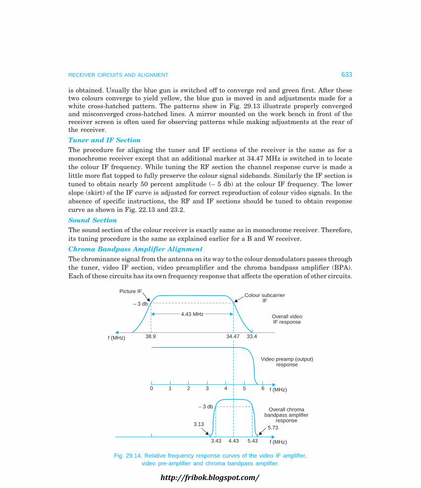
RECEIVER CIRCUITS AND ALIGNMENT 633
is obtained. Usually the blue gun is switched off to converge red and green first. After thesetwo colours converge to yield yellow, the blue gun is moved in and adjustments made for awhite cross-hatched pattern. The patterns show in Fig. 29.13 illustrate properly convergedand misconverged cross-hatched lines. A mirror mounted on the work bench in front of thereceiver screen is often used for observing patterns while making adjustments at the rear ofthe receiver.
Tuner and IF SectionThe procedure for aligning the tuner and IF sections of the receiver is the same as for amonochrome receiver except that an additional marker at 34.47 MHz is switched in to locatethe colour IF frequency. While tuning the RF section the channel response curve is made alittle more flat topped to fully preserve the colour signal sidebands. Similarly the IF section istuned to obtain nearly 50 percent amplitude (– 5 db) at the colour IF frequency. The lowerslope (skirt) of the IF curve is adjusted for correct reproduction of colour video signals. In theabsence of specific instructions, the RF and IF sections should be tuned to obtain responsecurve as shown in Fig. 22.13 and 23.2.
Sound SectionThe sound section of the colour receiver is exactly same as in monochrome receiver. Therefore,its tuning procedure is the same as explained earlier for a B and W receiver.
Chroma Bandpass Amplifier AlignmentThe chrominance signal from the antenna on its way to the colour demodulators passes throughthe tuner, video IF section, video preamplifier and the chroma bandpass amplifier (BPA).Each of these circuits has its own frequency response that affects the operation of other circuits.
Picture IF
– 3 db
f (MHz) 38.9 34.47 33.4
4.43 M z4.43 MHz Overall videoIF response
Colour subcarrierIF
Video preamp (output)response
f (MHz)6543210
5.733.13
– 3 db
f (MHz)5.434.433.43
Overall chromabandpass amplifier
response
Fig. 29.14. Relative frequency response curves of the video IF amplifier,video pre-amplifier and chroma bandpass amplifier.
http://fribok.blogspot.com/

634 MONOCHROME AND COLOUR TELEVISION
The necessary requirements for the RF, IF and video amplifier sections have already beenexplained. As shown in Fig. 29.14, the upper slope of the overall IF response and the roll-offcharacteristics of the video preamplifier affect the amplifier and phase of the chrominancesignal feeding the bandpass amplifier. The chrominance sidebands which are close to 3.5 MHzhave higher amplitudes than those near 5.3 MHz. If these inequalities are not compensatedfor, severe phase distortion will occur and seriously affect the colour reproduction in the picture.
The method of compensation used to achieve a flat overall response in the chrominancesignal frequency range is to adjust the input tuned circuit of the chroma BPA in such a waythat its frequency response curve is opposite to the slopes of the IF section and video preamplifiercharacteristic curves. This needs critical alignment of the bandpass amplifier. This is usuallycarried out in two steps. First the BPA is sweep aligned in the same way as the video IF sectionis aligned. This is done to ensure that the interstage and output tuned circuits of the BPA arecorrectly adjusted for a flat response of ± 1.0 MHz around 4.43 MHz. Then the video sweepmodulation technique is used to adjust the input circuit of the BPA for a flat topped overallreceiver response. The receiver RF and IF stages are aligned before setting the bandpasscharacteristics of the chroma amplifier.
The alignment procedure is as under:
A video sweep generator is adjusted for an output with a sweep width of 4 MHz centeredaround 4.43 MHz and varying at 50 Hz. It is connected to the input of chroma bandpass amplifierthrough a suitable network. The various tuned circuits ahead of the input network are adjustedwith the help of a detector probe and CRO for a flat topped response of ± 1 MHz around4.43 MHz.
The overall alignment of the receiver is next carried out to ensure correct passage of thechroma signal from receiver input terminals to the demodulators. The circuit hook-up for thisand corresponding waveshapes at various points are shown in Fig. 29.15. A video sweepgenerator is adjusted for an output with a sweep width of 0 to 6 MHz varying at a rate of 50 Hz.Markers at 3.43 MHz, 4.43 MHz, and 5.43 MHz are added to it through an absorption marker.The signal is then fed to an encoder where blanking, sync and colour burst signals are added toit. Thus the signal becomes a standard TV signal.
The composite signal obtained from the encoder is amplitude modulated in an IFmodulator with a carrier frequency of 38.9 MHz. The IF modulator output feeds into a converterwhere the video IF signal is further translated to the desired channel frequency band. Theconverter is fed with the desired CW channel carrier signal from an RF oscillator. The bandwidthrestricted RF signal available at the output of the converter is fed through an attenuator at theinput terminals of the receiver under alignment. Its channel selector switch is thrown at thesame channel, the carrier frequency of which was employed at the converter.
With tuner and video IF sections properly aligned, the output of the video detector willbe a modulated signal that sweeps from 0-6 MHz. This signal passes through the videopreamplifier before reaching the input of the BPA. The combined roll-off characteristics of thevideo IF and video preamplifier sections cause the higher frequencies of the signal spectrum tobecome attenuated. As already explained, the BPA is tuned to a centre frequency of 4.43 MHz,with a bandwidth of about ± 1 MHz. Thus frequency components below 3 MHz in the inputsignal are eliminated. The input and output tuned circuits of the BPA are now adjusted to
http://fribok.blogspot.com/
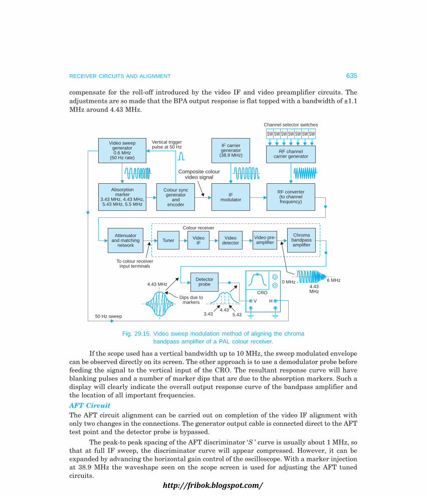
RECEIVER CIRCUITS AND ALIGNMENT 635
compensate for the roll-off introduced by the video IF and video preamplifier circuits. Theadjustments are so made that the BPA output response is flat topped with a bandwidth of ±1.1MHz around 4.43 MHz.
SW SW SW SW SW SW SW
Channel selector switches
RF channelcarrier generator
IF carriergenerator
(38.9 MHz)
Vertical triggerpulse at 50 Hz
Video sweepgenerator0.6 MHz
(50 Hz rate)
Absorptionmarker
3.43 MHz, 4.43 MHz,5.43 MHz, 5.5 MHz
Colour syncgenerator
andencoder
IFmodulator
RF converter(to channelfrequency)
Video pre-amplifier
Videodetector
VideoIFTuner
Attenuatorand matching
network
To colour receiverinput terminals
Colour receiver
Detectorprobe
Chromabandpassamplifier
Composite colourvideo signal
4.43 MHz
50 Hz sweep
Dips due tomarkers
3.434.43
5.43
V H
CRO
0 MHz 6 MHz4.43MHz
Fig. 29.15. Video sweep modulation method of aligning the chromabandpass amplifier of a PAL colour receiver.
If the scope used has a vertical bandwidth up to 10 MHz, the sweep modulated envelopecan be observed directly on its screen. The other approach is to use a demodulator probe beforefeeding the signal to the vertical input of the CRO. The resultant response curve will haveblanking pulses and a number of marker dips that are due to the absorption markers. Such adisplay will clearly indicate the overall output response curve of the bandpass amplifier andthe location of all important frequencies.
AFT CircuitThe AFT circuit alignment can be carried out on completion of the video IF alignment withonly two changes in the connections. The generator output cable is connected direct to the AFTtest point and the detector probe is bypassed.
The peak-to peak spacing of the AFT discriminator ‘S ’ curve is usually about 1 MHz, sothat at full IF sweep, the discriminator curve will appear compressed. However, it can beexpanded by advancing the horizontal gain control of the oscilloscope. With a marker injectionat 38.9 MHz the waveshape seen on the scope screen is used for adjusting the AFT tunedcircuits.
http://fribok.blogspot.com/

636 MONOCHROME AND COLOUR TELEVISION
Review Questions
1. Explain the merits of employing ICs in TV receivers. Draw the block schematic of a receiverwhich employs ICs and enumerate the functions performed by each integrated circuit.
2. A universal test chart is shown in Fig. 29.4. Explain briefly various parts of the chart whendisplayed on the receiver screen enable detection of specific faults in the receiver.
3. What precautions should be observed before commencing alignment of any section of the receiver ?Enumerate the checks which must be carried out before proceeding with alignment of the RFand IF sections of the receiver.
4. Describe the initial adjustments which must be made before aligning IF section of the receiver.Explain with a circuit diagram how would you proceed to align the tuned circuits of IF amplifiers.What are the adjustments which are necessary on the sweep generator, marker generator andoscilloscope for obtaining proper response curve on the CRO screen ?
5. Describe briefly the alignment procedure and precautions for aligning the following sections ofthe receiver.
(i) sound IF section (ii) FM discriminator circuit
(iii) RF tuner (iv) local oscillator.
6. Explain briefly how you would proceed to carry out (a) purity adjustment, (b) static convergenceand (c) dynamic convergence adjustments in a colour receiver.
7. Describe with a suitable circuit diagram the method of aligning the chroma bandpass amplifierof a colour receiver.
http://fribok.blogspot.com/

30
#
http://fribok.blogspot.com/

Trouble shooting and repairing any equipment needs a step-by-step logical approach to locateand correct any fault in its operation. For efficient servicing of television receivers it is notenough to have adequate knowledge of functions of the various blocks of the receiver but it isalso essential to have full familiarity with voltages and their waveshapes that are obtained atvarious points in the circuit when the set is operating normally. It is also important to be fullyconversant with the functions and the effect of manipulation of all controls and adjustmentsprovided in a receiver.
A set of proper tools and equipment helps very much in tracing any fault and repairingit. A technician who is fully conversant with the use and limitations of the instruments hepossesses, and can intelligently analyze the visual and analog indications he gets with them,can do the job much faster and with good results.
Trouble shooting is a skill in itself and does not come automatically by reading booksand remembering circuits alone. Even the handbooks which are exclusively devoted to servicinggive only a guideline to locate faults because it is impossible to list all possible varieties offaults and their remedies. Servicing needs long experience and there are no short cuts to it. Adetermined effort and hard work coupled with a thorough understanding of the operatingprinciples of the receiver is necessary to become a good servicing engineer. An ability to correctlyinterpret service literature and carry out alignment and adjustments accordingly is equallyimportant to obtain best results.
30.1 TROUBLE SHOOTING PROCEDURE
General procedure for trouble shooting a black and white receiver is given in the chart drawnon the next two pages. The first step towards finding the cause of failure of a receiver is visualinspection of the components, tubes, transistors and ICs mounted on various printed circuitboards, modules and chassis of the receiver. Such an inspection sometimes leads quickly to thedefective device or part in the receiver. For example, burnt or charred resistors can often bespotted by visual observation. Similarly overheated transformers, oil or wax filled capacitorsand coils can be located by a peculiar small caused by overheating and shorting. In addition adisoldered wire of a coil or component, broken load of a transistor or other similar faults can befound out by a preliminary visual inspection.
638
)
#
http://fribok.blogspot.com/
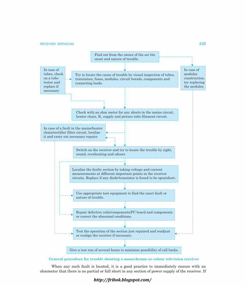
RECEIVER SERVICING 639
Find out from the owner of the set the
onset and nature of trouble.
Try to locate the cause of trouble by visual inspection of tubes,
transistors, fuses, modules, circuit borads, components and
connecting leads.
In case of
tubes, check
on a tube
tester and
replace if
necessary
In case of
modular
construction,
try replacing
the modules
Check with an ohm meter for any shorts in the mains circuit,
heater chain, B supply and picture tube filament circuit.+
In case of a fault in the mains/heater
chain/rectifier filter circuit, localize
it and carry out necessary repairs
Switch on the receiver and try to locate the trouble by sight,
sound, overheating and odours
Localize the faulty section by taking voltage and current
measurements at different important points in the receiver
circuits. Replace if any diode/transistor is found to be open/short.
Use appropriate test equipment to find the exact fault or
nature of trouble.
Repair defective coils/components/PC board and components
or correct the abnormal conditions.
Test the operation of the section just repaired and readjust
or realign the receiver if necessary.
Give a test run of several hours to minimize possibility of call backs.
General procedure for trouble shooting a monochrome or colour television receiver
When any such fault is located, it is a good practice to immediately ensure with anohmmeter that there is no partial or full short in any section of power supply of the receiver. If
http://fribok.blogspot.com/
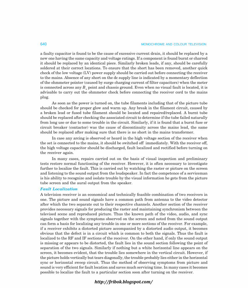
640 MONOCHROME AND COLOUR TELEVISION
a faulty capacitor is found to be the cause of excessive current drain, it should be replaced by anew one having the same capacity and voltage ratings. If a component is found burnt or charredit should be replaced by an identical piece. Similarly broken leads, if any, should be carefullysoldered at their correct locations. To ensure that the short has been removed, another quickcheck of the low voltage (LV) power supply should be carried out before connecting the receiverto the mains. Absence of any short on the dc supply line is indicated by a momentary deflectionof the ohmmeter pointer (caused by surge charging current of filter capacitors) when the meteris connected across any B+ point and chassis ground. Even when no visual fault is located, it isadvisable to carry out the ohmmeter check before connecting the receiver cord to the mainsplug.
As soon as the power is turned on, the tube filaments including that of the picture tubeshould be checked for proper glow and warm up. Any break in the filament circuit, caused bya broken lead or fused tube filament should be located and repaired/replaced. A burnt tubeshould be replaced after checking the associated circuit to determine if the tube failed naturallyfrom long use or due to some trouble in the circuit. Similarly, if it is found that a burnt fuse orcircuit breaker (contactor) was the cause of discontinuity across the mains lead, the sameshould be replaced after making sure that there is no short in the mains transformer.
In case any arcing is observed or heard in the high voltage section of the receiver whenthe set is connected to the mains, it should be switched off immediately. With the receiver off,the high voltage capacitor should be discharged, fault localized and rectified before turning onthe receiver again.
In many cases, repairs carried out on the basis of visual inspection and preliminarytests restore normal functioning of the receiver. However, it is often necessary to investigatefurther to localize the fault. This is carried out by watching the raster or picture on the screenand listening to the sound output from the loudspeaker. In fact the competence of a servicemanis his ability to recognize and isolate trouble by the visual information he gets from the picturetube screen and the aural output from the speaker.
Fault LocalizationA television receiver is an economical and technically feasible combination of two receivers inone. The picture and sound signals have a common path from antenna to the video detectorafter which the two separate out to their respective channels. Another section of the receiverprovides necessary signals for producing the raster and maintaining synchronism between thetelevised scene and reproduced picture. Thus the known path of the video, audio, and syncsignals together with the symptoms observed on the screen and noted from the sound outputcan form a basis for localizing any trouble in one or more sections of the receiver. For example,if a receiver exhibits a distorted picture accompanied by a distorted audio output, it becomesobvious that the defect is in a circuit which is common to both the signals. Thus the fault islocalized to the RF and IF sections of the receiver. On the other hand, if only the sound outputis missing or appears to be distorted, the fault lies in the sound section following the point ofseparation of the two signals. Similarly if nothing but a white horizontal line appears on thescreen, it becomes evident, that the trouble lies somewhere in the vertical circuit. However, ifthe picture holds vertically but tears diagonally, the trouble probably lies either in the horizontalsync or horizontal sweep circuit. Thus the method of observing symptoms from picture andsound is very efficient for fault location and saves much servicing time. In many cases it becomespossible to localize the fault to a particular section soon after turning on the receiver.
http://fribok.blogspot.com/

RECEIVER SERVICING 641
Signal Source for Observing FaultsThough any transmission from a local TV station can be used for observing possible faults butcontinuous change of picture details on the screen makes it difficult to observe minorirregularities in the reproduced picture. A test pattern obtained either from a test chartgenerator or an analyst generator shows much more than a picture and so is very useful fordetecting all types of faults in the picture. However, if these instruments are not available, apattern generator set to produce a cross-hatched pattern on the screen can be used as inputsignal source. In any case, an initial observation by tuning in any one of the local channels ishelpful for localizing trouble to one of the major functional areas of the receiver. Once this hasbeen done, the normal trouble shooting tools can be used to isolate defective component orcomponents of that section.
30.2 TROUBLE SHOOTING MONOCHROME RECEIVERS
Though it is not practicable to list all symptoms of various faults but most troubles in a blackand white receiver can be grouped into functional areas or circuits in the receiver. This approachis often followed and the chart that follows gives all necessary details. The probable cause ofany trouble as listed in the chart is based on the assumption that the receiver had been workingsatisfactorily and suddenly developed the observed symptoms. It may be noted that if alignmentand tracking has been tampered with, sound and/or picture could be lost because of off-resonanceconditions in the tuned circuits. It is further assumed that all tubes inclusive of picture tubeare glowing and there is no fault in the filament circuit(s).
Trouble Shooting Chart Based on Symptoms in a Monochrome Receiver
No. Symptoms Defective Stage(s) Probable Fault(s)
1. No sound, no raster L.V. Power supply B+ shorted, defectiverectifier(s), (failure of lowvoltage systems).
2. No sound, no picture, but rasternormal
RF tuner, IF section,video section
A bad tube, transistor, IC orany part in the commonsections of the receiver, looseantenna or transmission lineconnections.
3. No sound, but picture normal Sound IF, FM detector,audio
Defective sound IF,discriminator, audioamplifier, audio outputtransformer andloudspeaker.
4. Sound distorted, butpicture normal
Sound IF, FM detector,audio
Misaligned sound IF ordiscriminator, gassy tubes,leaky transistors, bad IC,short or open capacitors inaudio amplifier, shortedoutput transformer, defectivespeaker.
(Contd.)...http://fribok.blogspot.com/

642 MONOCHROME AND COLOUR TELEVISION
5. Sound normal, but noraster
High voltage power supply,picture tube circuit
Failure of high voltage powersupply, defective picturetube, high negative bias onpicture tube control grid,defective video amplifier.
6. Sound normal, rasternormal but no picture
Video output, videodriver, picture tube circuit
Defective tubes, transistors,IC or components in stagesafter sound take-off.
7. Sound normal, butpicture distorted
IF stages, AGC, verticaland horizontal sweepcircuits
Misaligned IF stages,defective AGC tube/transistor, wrong AGC biassetting, nonlinearity invertical and horizontal sweepcircuits.
8. No vertical deflection Vertical sweep circuit Vertical oscillator notworking, vertical outputtransformer open, defectiveoutput tube/transistor, lowB+ supply, open verticaldeflection coil.
9. Insufficient vertical height Vertical sweep circuit Weak oscillator tube/transistor, low boosted B+supply, faulty otuputtransformer, shorted turns indeflection coil, faulty VDR ifused, leaky coupling orbypass capacitors, openresistors.
10. No vertical sync. (Picturerolls)
Sync separator, verticalsweep circuit
Defective in sync separator tovertical input circuit, verticaloscillator frequency too highor too low, misadjustedvertical hold control.
11. Non-linear verticalsweep (distorted picture)
Vertical sweep circuit Faulty tubes/transistors,fault in feedback loop,misadjusted verticallinearity control.
12. Poor interlacing or linepairing
Vertical deflection section Open capacitor in verticalsync integrator, opendecoupling capacitor(s) inoscillator and output stages.
13. Insufficient width of raster Horizontal deflection circuit Weak oscillator tube/transistor, defective (shorted)horizontal output trans-former, weak horizontaloutput tube/transistor.
(Contd.)...http://fribok.blogspot.com/

RECEIVER SERVICING 643
14. Foldover in picture butsound normal
Horizontal deflection circuit Incorrect horizontal linearity,defective damper, incorrecthorizontal sweep.
15. Non-linearity in the horizontaldirection
Horizontal deflection circuit Incorrect horizontal sweepoutput, wrong linearitycontrol setting.
16. Keystone effect in the raster Horizontal and vertical outputcircuits
Partial short in vertical/horizontal coils.
17. Picture not centered but soundnormal
Picture tube circuit Incorrect setting of centeringcontrols, defective centeringcontrols.
18. Negative picture AGC circuit, video detector,picture tube circuit
Overloaded video signal,wrong polarity of detectordiode.
19. No horizontal sync (heavyslanting streaks across thescreen) but sound normal
Sync separator, AFC,horizontal oscillator
Horizontal sweep out ofsynchronism, defective syncseparator, defective diode inthe AFC circuit.
20. Incorrect picture size, but soundnormal
Horizontal and vertical sweepcircuits, yoke coils
Weak tubes/transistors invertical and horizontal sweepoutput circuits, low B+supply, defective yoke.
21. Poor resolution IF section, video amplifier Misaligned IF amplifiers,insufficient video amplifierbandwidth.
22. Weak picture and sound, butboth of good quality
Tuner and IF sections Defect in antenna system,improperly oriented antenna,defective tubes/transistors inRF and IF sections, defectiveIC in the IF section.
23. Picture and sound weak andalso of poor quality
RF tuner, IF section Shift in local oscillatorfrequency, change in finetuning control, improper IFalignment.
24. Hum or motor boating fromloudspeaker
Audio section Defective filter capacitors,defective decouplingcapacitor.
25. Sound bars on picture screen Video IF section Misaligned sound IF traps(too much gain at the soundIF frequency).
http://fribok.blogspot.com/

644 MONOCHROME AND COLOUR TELEVISION
30.3 SERVICING OF VARIOUS FUNCTIONAL BLOCKS
After the trouble is localized to a single functional area, the next step is to isolate the troubleto a circuit and then to the faulty component or components. It is not advisable to charge intothe receiver with a soldering iron and screw driver without a logical search for the cause oftrouble. The circuit diagram, if available, should first be studied and various measurementstaken before deciding to change any component or removing any device for checking it. Thissaves time and needs least use of the soldering iron.
The major faults that occur in a monochrome TV receiver and their servicing procedure,based on the available indications and observations, is explained below. For convenience andease of understanding various faults have been divided according to main sections of the receiver.
1. Low Voltage Power Supply (B+ )Low voltage power supply feeds dc voltage to various sections of the receiver and filamentvoltage to tubes. All solid state receivers normally have a regulated dc source and a separatefilament transformer for heater of the picture tube. It is important to realize that any fault inthe B+ supply affects performance of all sections of the receiver. Therefore it is necessary toensure that this part of the receiver is performing satisfactorily before attempting to localizefaults in other sections of the receiver.
Low voltage power supplies either operate from a transformer or are derived from theline. Whenever servicing a line connected receiver, an isolation transformer with 1 : 1 voltageratio must be used to avoid accidental shocks and ensure protection to test instruments.
(a) An inoperative (dead) set. This implies that there is no light on the screen and nosound from the loudspeaker. The tube filaments may or may not be glowing or some of thetubes may only be glowing.
Transformer type power supply—Check for:
(i) defective thermal cut-out (if provided), fuse or on-off switch,(ii) defective power cord, cable or interlock,
(iii) burnt filament of the rectifier tube (if used) or weak rectifier,(iv) open filament winding(s),(v) defective transformer secondary or open centre tap on secondary,
(vi) open filter choke,(vii) shorted filter capacitor(s),
(viii) open filament winding of picture tube.
Line connected power supply(i) defective thermal cut-out, fuse or on-off switch,
(ii) defective power cord plug, cable, or interlock,(iii) open or short in the filament circuit,(iv) shorted filament bypass capacitor,(v) open silicon rectifiers,
(vi) open filter choke or resistor in B+ line,(vii) open filament winding of picture tube.
http://fribok.blogspot.com/

RECEIVER SERVICING 645
Note. A short in some section of the B+ load will cause all voltages to read low and often causethe fuse to blow out or the circuit breaker (if provided) to trip. Excessive current drain due to shorts inthe load can be traced by opening connection at different branching points of B+ line and monitoring dcvoltage with a voltmeter. When there is a partial short, the trouble is most likely at the point of lowestvoltage. A multimeter can be used to locate the defective component in the power supply line.
(b) Insufficient width and height of raster (Fig. 30.1)—This occurs due to low B+ supply.The vertical and horizontal deflection circuits are normally stabilized for ± 10% mains voltagevariations. However, if the mains voltage drops more than 10% the deflection circuits areaffected. The dc supply can also drop due to a fault in its rectifier-filter circuits. Check for:
(i) open filter capacitor,
(ii) open diode in voltage doubler or bridge rectifier circuit,
(iii) excessive current drain at some point in B+ line.
Fig. 30.1. Shrunken raster (insufficient width and height) due to low B+ supply.
(c) Hum bar(s) or bend in the raster and/or hum in sound output from the speaker(Fig. 30.2)—Check for:
(i) open output filter capacitors,
(ii) filament to cathode leakage in tube receivers.
(d) Poor sync, folded picture, non linearity in vertical scanning, motorboating in soundoutput—Check for:
(i) open filter capacitor(s).
(ii) faulty decoupling capacitor(s).
(iii) poor regulation of B+ supply.
2. High Voltage Power Supply and Picture Tube CircuitryBefore proceeding to locate faults in EHT and picture tube circuits, it should be ensured thatthe horizontal sweep amplifier and its damper circuit are functioning normally. Note thatwithout horizontal scanning there is no high voltage and no brightness.
http://fribok.blogspot.com/

646 MONOCHROME AND COLOUR TELEVISION
Fig. 30.2. Hum bar in picture due to 50 Hz hum voltage in the video signal.
E.H.T. Supply(a) Not raster—Check for:
(i) open or shorted picture tube filament,(ii) defective (open or short) HV rectifier,
(iii) defective damper diode,(iv) shorted or open EHT winding,(v) defective picture tube.
Note. A dim picture may be produced due to a weak EHT rectifier or a partial short in EHTwinding on the horizontal output transformer (H.O.T.).
Fig. 30.3. Blooming of the reproduced picture.
http://fribok.blogspot.com/

RECEIVER SERVICING 647
(b) Blooming of picture (Fig. 30.3)—This is caused by poor EHT regulation. Check for:
(i) leaky HV capacitor,(ii) weak HV rectifier,
(iii) high resistance in the EHT lead due to a defective series resistor,(iv) insufficient rectifier filament voltage,(v) defective picture tube.
(c) Break-up of raster, jumping of picture, horizontal tearing, series of light streaks onthe screen—These faults are due to arcing and corona in the EHT section. An arcing occurswhen potential difference between any two points is greater than the voltage, the dielectricbetween them can withstand. Corona is normally associated with an electric discharge from asharp point in a high voltage circuit.
Arcing may be seen on the picture tube screen or directly from the source of arc. Similarlycorona may be heard as a sizzling or frying noise. It may also be recognized by a purplish-bluedischarge at the source or by the presence of ozone gas smell. Although corona may not havean immediate effect on the picture, it will cause gradual deterioration of components if leftunchecked. For any visible arcing check for:
(i) high voltage leads lying too close to chassis ground,
(ii) improper grounding of external aquadag coating of the picture tube,
(iii) partial short at the mountings of high voltage rectifier unit.
Picture Tube CircuitryNo raster, sound normal—Check for:
(i) defective picture tube.(ii) incorrect voltages at various electrodes of the picture tube (rare),
(iii) incorrect setting of picture tube controls because of defect(s) in external circuitry,
Manufacturers usually supply data for rated voltages at various electrodes. In the absenceof such information check the following with a voltmeter.
(i) with cathode as reference the control grid voltage should be between – 30 V and – 120V, and
(ii) the second grid voltage should be about 400 volts while that of the focus grid (G4)between 0-400 V.
(iv) loose/broken connections in picture tube socket, yoke plugs, and high voltage leads,(v) defective video amplifier coupling circuit.
3. Horizontal Sweep CircuitsThe horizontal sweep circuit operates at 15625 Hz and is synchronized by an AFC circuit. Thissection is also the source for EHT supply. In solid state receivers, other dc voltages are alsoobtained from the horizontal sweep system.
(a) Single vertical line in the centre of the screen, sound normal (Fig. 30.4)—Check for:
(i) open horizontal deflection coil.(ii) open linearity coil,
(iii) open dc blocking capacitor.
http://fribok.blogspot.com/

648 MONOCHROME AND COLOUR TELEVISION
Fig. 30.4. Single vertical line in the centre of the raster due tofailure of horizontal sweep circuit.
(b) Poor horizontal linearity—Check for:
(i) incorrect drive voltage amplitude,(ii) incorrect drive voltage waveform,
(iii) leaky coupling capacitor between horizontal oscillator and output stage,(iv) defective output tube/transistor,(v) shorted linearity control.
(c) Horizontal foldover (Fig. 30.5)—Foldover is a severe form of nonlinearity. Check for:
(i) defective output tube/transistor,(ii) faulty biasing circuit of horizontal output stage,
(iii) defective oscillator or output circuit.
Fig. 30.5. Horizontal foldover at left side of the raster.http://fribok.blogspot.com/

RECEIVER SERVICING 649
(d) Horizontal keystone effect (Fig. 30.6)—This is indicated by a dim and narrow rasterwith its bottom wider than the top or vice versa. Check for:
(i) defective horizontal yoke (shorted turns),(ii) shorted balancing capacitor across one section of the horizontal deflection coils.
Fig. 30.6. Horizontal keystoning effect. The pattern shown is the resultof a shorted horizontal coil in the deflection yoke.
(e) Ringing (Fig. 30.7)(i) defective tube/transistor,
(ii) linearity coil damping resistance open,(iii) defective L.O.T.,(iv) incorrect yoke balancing capacitor,(v) open capacitor in the cathode of the damper tube.
Fig. 30.7. Ringing-white vertical bars due to improper horizontal damping.The pattern shown is due to open capacitor in cathode circuit of the damper diode (tube).http://fribok.blogspot.com/

650 MONOCHROME AND COLOUR TELEVISION
(f) Loss of horizontal sync (horizontal pulling) (Fig. 30.8)
(i) defective sync separator circuit,
(ii) low sync amplitude,
(iii) defective AFC circuit,
(iv) defect in anti-hunt circuit,
(v) incorrect horz oscillator frequency beyond control of the AFC circuit.
Fig. 30.8. Loss of horizontal synchronization.
4. Vertical Sweep CircuitThis circuit feeds vertical deflection coils and operates at 50 Hz. It is synchronized by syncpulses developed at the output of a low-pass filter.
Fig. 30.9. Loss of vertical sweep.
http://fribok.blogspot.com/

RECEIVER SERVICING 651
(a) Bright horizontal line on the screen, sound normal (Fig. 30.9)—Check for:
(i) open vertical deflection coil connections,
(ii) faulty tubes/transistors in the circuit,
(iii) faulty IC if employed,
(iv) vertical oscillator not functioning.
(b) Insufficient picture height (Fig. 30.10)
(i) weak oscillator and/or output tubes/transistors,
(ii) defective IC if employed.
(iii) faulty output transformer,
(iv) misadjusted height control,
(v) shorted turns in deflection coil.
Fig. 30.10. Insufficient height of the picture.
(c) Poor vertical linearity (height satisfactory)—Check for:
(i) low B+ voltage,
(ii) defective tube/transistors/IC,
(iii) leaky coupling capacitor,
(iv) incorrect linearity control setting,
(v) wrong drive voltage due to fault in negative feedback loop of the oscillator,
(vi) partial short in output transformer.
(d) Picture rolls vertically (Fig. 30.11)—Check for:
(i) oscillator frequency too high or too low,
(ii) incorrect setting of hold control,
(iii) fault in vertical sync processing circuit.
http://fribok.blogspot.com/

652 MONOCHROME AND COLOUR TELEVISION
Fig. 30.11. Picture rolls vertically at a fast rate dueto complete loss of vertical synchronization.
(e) Poor interlacing (Fig. 30.12)—Check for:
(i) open capacitor in vertical sync integrator,
(ii) open decoupling capacitor in vertical or horizontal sweep cricuits.
Fig. 30.12. Horizontal wedge showing poor interlacing.
(f) Vertical keystoning (Fig. 30.13)—Check for:
(i) shorted turns in vertical deflection coils,
(ii) defective vertical output transformer,
(iii) defective thermistor across deflection coils.
http://fribok.blogspot.com/
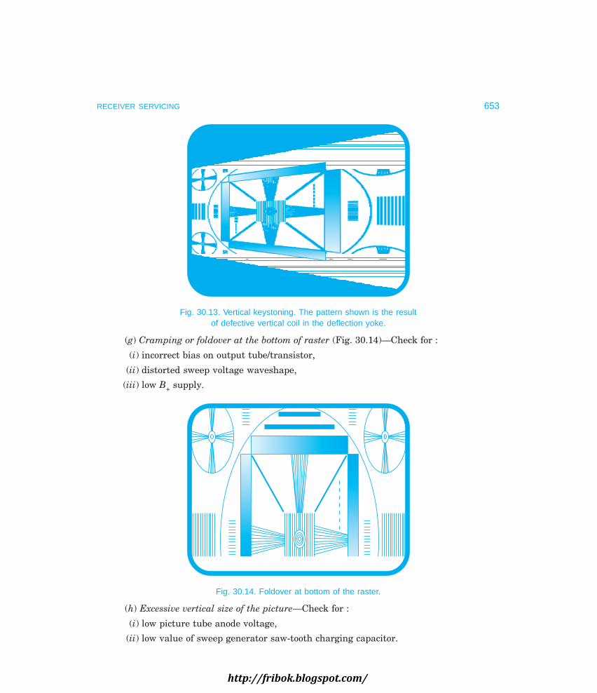
RECEIVER SERVICING 653
Fig. 30.13. Vertical keystoning. The pattern shown is the resultof defective vertical coil in the deflection yoke.
(g) Cramping or foldover at the bottom of raster (Fig. 30.14)—Check for :
(i) incorrect bias on output tube/transistor,
(ii) distorted sweep voltage waveshape,
(iii) low B+ supply.
Fig. 30.14. Foldover at bottom of the raster.
(h) Excessive vertical size of the picture—Check for :
(i) low picture tube anode voltage,
(ii) low value of sweep generator saw-tooth charging capacitor.
http://fribok.blogspot.com/

654 MONOCHROME AND COLOUR TELEVISION
5. Sync Separator and Processing CircuitThe sync pulses are separated from the composite video signal by a sync separator. Filtercircuits separate vertical and horizontal sync pulses from each other. The vertical sync pulsesare integrated to form vertical oscillator control voltage. However, horizontal sync pulses arefed to the AFC circuit which develops a dc control voltage for the horizontal oscillator. Thenoise pulse effect is thus reduced.
(a) Poor or complete loss of both vertical and horizontal sync, picture breaks into stripsand rolls vertically (Fig. 30.15)—Check for:
(i) defective sync separator,
(ii) defective coupling capacitor to sync circuit,
(iii) faulty tube/transistor/IC used in the system.
Fig. 30.15. Complete loss of both vertical and horizontal synchronization.The picture breaks into strips and rolls vertically.
(b) Loss of vertical sync (picture rolls vertically) (Fig. 30.16)—Check for:
(i) defective integrating circuit (leaky capacitor or open resistance),
(ii) short, open or leaky coupling capacitor.
(c) Loss of horizontal sync (picture breaks into strips and rolls in horizontal direction—Check for:
(i) defective diodes in AFC circuit,
(ii) defective coupling capacitor,
(iii) open diode load resistance,
(iv) absence of flyback pulses from L.O.T.
(d) Vertical jitter (picture jumps up or down)—Check for:
(i) open capcitor in low pass filter (integrating circuit),
(ii) defective sync separator tube/transistor/IC,
http://fribok.blogspot.com/

RECEIVER SERVICING 655
(iii) incorrect bias on sync tube/transistor,
(iv) incorrect B+ to the circuit,
(v) open by-pass capacitor.
Fig. 30.16. Vertical scanning not synchronized–picture slowly slips frames vertically.
(e) Picture pulling (bend in the picture with edges of raster straight) (Fig. 30.17)—Checkfor:
(i) incorrect bias to sync separator,
(ii) excessive hum in vertical sync.
Fig. 30.17. Picture pulling-bend in the picture.
Note. With excessive hum in vertical sync, picture tends to show vertical blanking bar acrossthe middle of the picture.
http://fribok.blogspot.com/

656 MONOCHROME AND COLOUR TELEVISION
(f ) Gear-tooth effects (cogwheel distortion)—This is usually caused by hunting in thehorizontal AFC circuit. Check for:
(i) incorrect component values in AFC circuit,
(ii) leaky anti-hunt capacitor.
(g) Horizontal pulling (Fig. 30.18)—Check for:
(i) defective AFC diodes,
(ii) leaky or open anti-hunt capacitor,
(iii) leaky sync coupling capacitor,
(iv) defective sync tube/transistor/IC.
Fig. 30.18. Horizontal pulling.
(h) Incorrect horizontal phasing (picture moves to the sides with a vertical bar betweenthe two pictures)—Check for:
(i) leaky wave-shaping capacitor,
(ii) defective AFC diodes.
6. Video Amplifier CircuitIt is a wide-band amplifier which increases the amplitude of the composite video signal beforeapplying it to the picture tube grid or cathode. The video amplifier could be dc coupled, accoupled, or partially dc coupled with upper 3 db down frequency extending up to about 5 MHz.
(a) No picture, raster normal, sound satisfactory—Check for:
(i) short between grid and cathode of picture tube,
(ii) no B+ supply to video amplifier,
(iii) defective video amplifier tube/tansistor/IC,
(iv) open compensating coils,
(v) open load resistor,
http://fribok.blogspot.com/
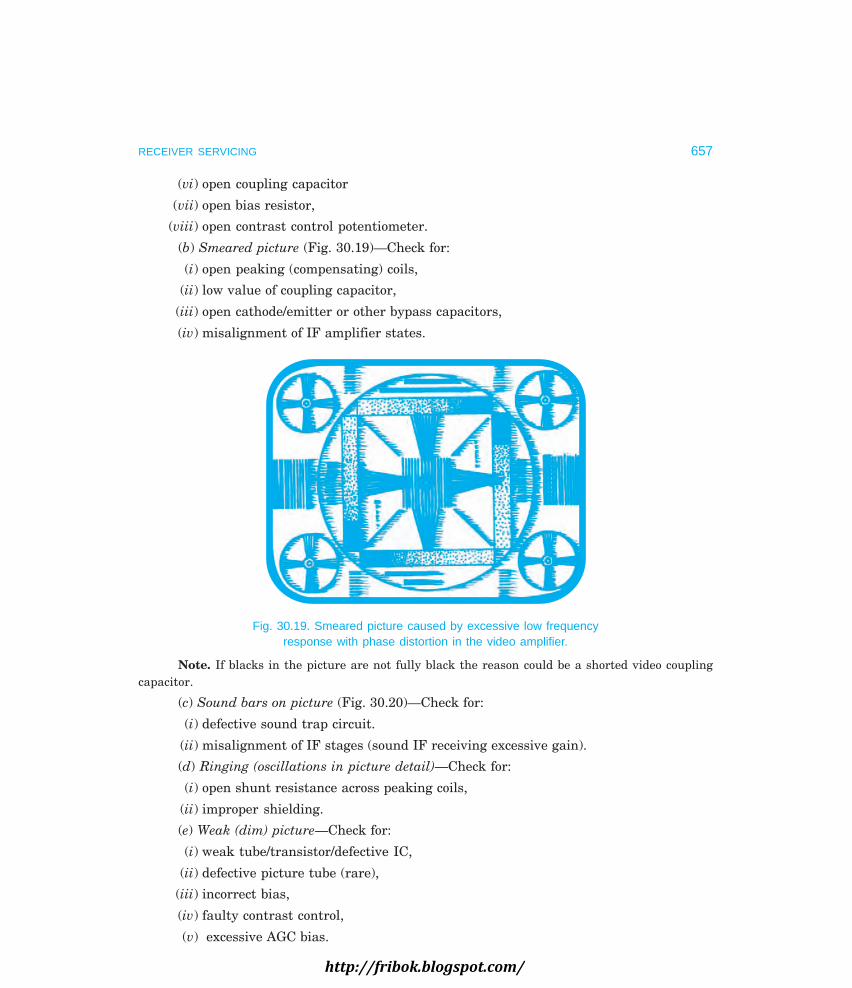
RECEIVER SERVICING 657
(vi) open coupling capacitor
(vii) open bias resistor,
(viii) open contrast control potentiometer.
(b) Smeared picture (Fig. 30.19)—Check for:
(i) open peaking (compensating) coils,
(ii) low value of coupling capacitor,
(iii) open cathode/emitter or other bypass capacitors,
(iv) misalignment of IF amplifier states.
Fig. 30.19. Smeared picture caused by excessive low frequencyresponse with phase distortion in the video amplifier.
Note. If blacks in the picture are not fully black the reason could be a shorted video couplingcapacitor.
(c) Sound bars on picture (Fig. 30.20)—Check for:
(i) defective sound trap circuit.
(ii) misalignment of IF stages (sound IF receiving excessive gain).
(d) Ringing (oscillations in picture detail)—Check for:
(i) open shunt resistance across peaking coils,
(ii) improper shielding.
(e) Weak (dim) picture—Check for:
(i) weak tube/transistor/defective IC,
(ii) defective picture tube (rare),
(iii) incorrect bias,
(iv) faulty contrast control,
(v) excessive AGC bias.
http://fribok.blogspot.com/

658 MONOCHROME AND COLOUR TELEVISION
Fig. 30.20. White bars on the picture due to presence ofsound signal at the output of video amplifier.
(f) Intermittent picture—Check for:
(i) defective tube/transistor/IC,
(ii) poor soldering at joints,
(iii) dirty or worn out brightness and contrast controls,
(iv) intermittent capacitors or resistors in circuit due to rise in temperature.
7. Video DetectorIt demodulates the picture (IF) signal to recover composite video signal. It also heterodynespicture and sound IFs to produce intercarrier sound signal.
No sound, no picture, raster normal—Check for:
(i) open diode,
(ii) open bandwidth compensation coil,
(iii) defective filter circuit components,
(iv) open coupling capacitor,
(v) short in the last IF transformer secondary,
(vi) incorrect biasing circuit (if provided).
8. Sound SectionIt amplifies the intercarrier sound signal picked up from the video detector or first videoamplifier. An FM detector demodulates it and the resulting audio signal is amplified by anaudio amplifier before it feeds the speaker.
(a) No sound, picture and raster normal—Check for:
(i) faulty tube/transistor/IC,
(ii) low dc supply,
(iii) defective discriminator circuit,
http://fribok.blogspot.com/

RECEIVER SERVICING 659
(iv) misaligned sound IF amplifier,
(v) open circuit from sound take-off point to sound IF input.
(b) Weak or distorted sound—Check for:
(i) weak tube/transistor/faulty IC,
(ii) low sound IF amplifier gain,
(iii) low dc supply,
(iv) improper alignment of sound IF,
(v) improper alignment of FM discriminator,
(vi) defective loudspeaker,
(vii) partially shorted audio output transformer.
(c) Hum in sound, picture and raster normal—Check for:
(i) open filter capacitor in L.V. supply,
(ii) open ground lead of volume control,
(iii) poor shielding,
(iv) poor alignment of FM detector,
(v) heater cathode short in tube circuits.
(d) Buzz in sound, picture and raster normal—Check for:
(i) improper alignment of the secondary of FM detector,
(ii) improper alignment of sound IF and limiter stages,
(iii) open capacitor in ratio detector,
(iv) improper picture IF alignment.
9. AGC CircuitThe AGC circuit develops a voltage proportional to the channel signal strength which is usedfor controlling gain of IF and RF stages. RF amplifier is normally supplied with delayed AGC.
(a) Weak picture—This is due to excessive bias voltage to IF and RF amplifier stages.Check for:
(i) incorrect adjustment of AGC control,
(ii) faulty tube/transistor/IC,
(iii) shorted AGC filter,
(iv) faulty keying circuit.
(b) Loss of sync—If AGC is low, one of the IF stages may become over-loaded and causedistortion of sync pulses. Check for:
(i) weak AGC tube/transistor/faulty IC,
(ii) low value of delay resistor,
(iii) inadequate AGC filtering.
(c) Dark picture and buzz in sound—Check for:
(i) defective tube/transistor/faulty IC,
http://fribok.blogspot.com/

660 MONOCHROME AND COLOUR TELEVISION
(ii) leaky AGC filter capacitor,
(iii) low AGC on strong signals.
(d) Negative picture (Fig. 30.21)—The negative or reversed black and white in the pictureis caused by reversal of the polarity of video signal. This occurs as a result of rectification in anoverloaded amplifier which is usually the last IF stage. Check for:
(i) absence of composite video signal from the video amplifier section to the AGC cir-cuit.
(ii) absence of reference flyback pulses from the H.O.T.,
(iii) faulty tube/transistor/IC in the AGC circuit,
(iv) leaky or shorted capacitor in AGC circuit.
Fig. 30.21. Negative picture.
10. Video (picture) IF SectionThe IF section provides most of the gain and is AGC controlled. It needs precise tuning forvestigial sideband correction and successful working of intercarrier sound system.
(a) No picture, no sound, but raster normal—Check for:
(i) no L.V. supply.
(ii) open tube/transistor/inoperative IC,
(iii) excessive AGC bias,
(iv) open/shorted IF transformer winding,
(v) break in printed board (module),
(vi) open cathode/emitter resistance.
(b) Poor contrast or weak picture (Fig. 30.22)—Check for:
(i) low B+ supply,
(ii) weak tube/tansistor/faulty IC,
http://fribok.blogspot.com/
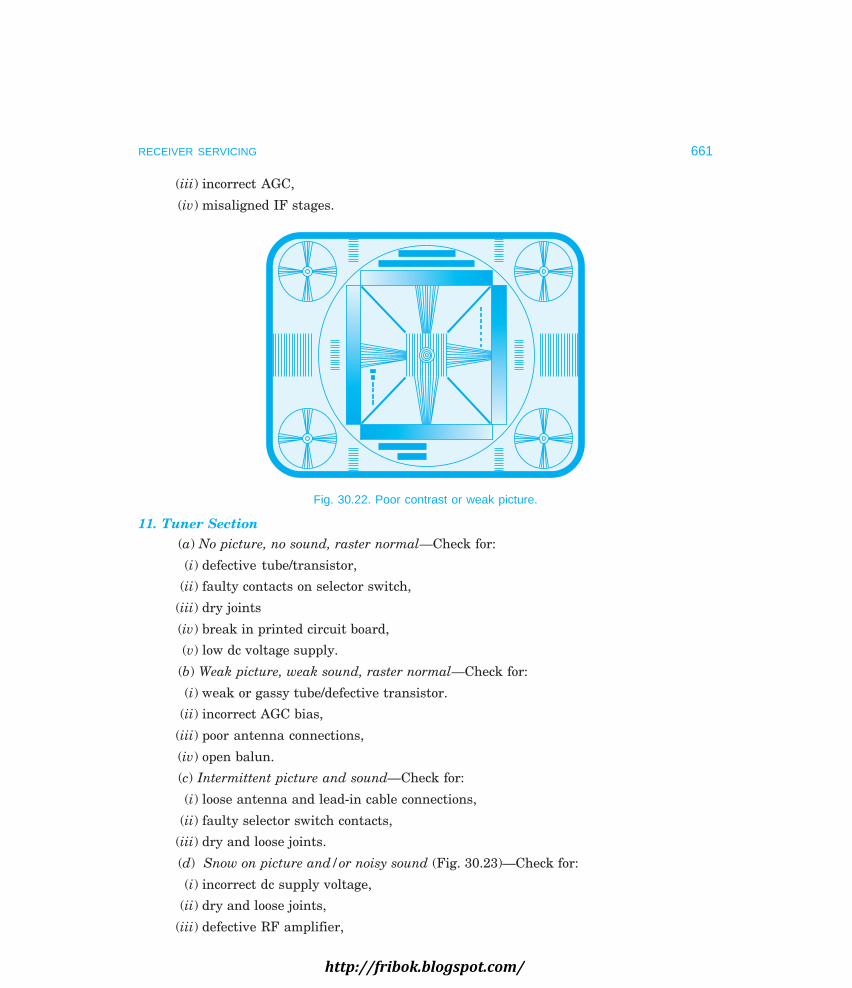
RECEIVER SERVICING 661
(iii) incorrect AGC,
(iv) misaligned IF stages.
Fig. 30.22. Poor contrast or weak picture.
11. Tuner Section(a) No picture, no sound, raster normal—Check for:
(i) defective tube/transistor,
(ii) faulty contacts on selector switch,
(iii) dry joints
(iv) break in printed circuit board,
(v) low dc voltage supply.
(b) Weak picture, weak sound, raster normal—Check for:
(i) weak or gassy tube/defective transistor.
(ii) incorrect AGC bias,
(iii) poor antenna connections,
(iv) open balun.
(c) Intermittent picture and sound—Check for:
(i) loose antenna and lead-in cable connections,
(ii) faulty selector switch contacts,
(iii) dry and loose joints.
(d) Snow on picture and/or noisy sound (Fig. 30.23)—Check for:
(i) incorrect dc supply voltage,
(ii) dry and loose joints,
(iii) defective RF amplifier,
http://fribok.blogspot.com/

662 MONOCHROME AND COLOUR TELEVISION
(iv) weak local oscillator,
(v) open balun.
Fig. 30.23. White speckled background of snow due to poor signal to noise ratio.
12. Miscellaneous Faults(a) Ghost picture (Fig. 30.24)—Check for:
(i) wrong balun connections,
(ii) improper shielding of tuner,
(iii) wrong orientation of antenna.
Fig. 30.24. Ghost images due to reflections of arriving signals.
http://fribok.blogspot.com/
RECEIVER SERVICING 663
(b) Picture not centered, sound normal—Check for:
(i) misadjusted centering controls,
(ii) defective centering controls.
(c) Only a portion of the picture area in focus—Check for:
(i) incorrect voltage in the focus electrode circuit.
(d) Brightness control partially or completely inoperative—Check for:
(i) defective brightness control
(ii) low B+ voltage to brightness control,
(iii) defective picture tube (rare).
(c) Contrast control ineffective—Check for:
(i) excessive input signal at antenna,
(ii) defective contrast control,
(iii) shorted AGC bypass capacitor.
(f) Retrace lines visible—Check for:
(i) open input capacitor or resistor in blanking circuit,
(ii) open bypass capcitor to blanking circuit.
30.4 TROUBLE SHOOTING COLOUR RECEIVERS
The general procedure for trouble shooting and servicing colour receivers is the same as formonochrome receivers. The chart given in section 30.1 can also be followed for localizing defectivesections of the receiver. This is so, because, except for the chroma section of the receiver, theremaining circuitry performs identical functions in both B and W and colour receivers. However,the chart given on the next page can serve as a good guide for identifying defective section(s) ina colour receiver. It may be mentioned that most auxiliary circuit blocks in the chroma sectionaffect the colour killer circuit and disable it when they become inoperative. Thus, it may benecessary to bypass the colour killer block while locating a faulty circuit in the chroma section.
30.5 SERVICING CIRCUIT MODULES
(a) Printed-Circuit Servicing TechniquesPrinted-circuit wiring is used in television receiver manufacture to ensure uniformity of product,speed of assembly, and ease in servicing. When working on printed-circuit boards, extremecare should be exercised while soldering and desoldering components. Due to the nature oflaminating process, the printed circuit board should not be exposed to prolonged hightemperatures. In manufacturing, excessive heating is prevented by a special technique calledwave soldering. To avoid excessive heating a small soldering iron (25 to 40 watts) should beused. Whenever possible the soldering iron should be kept next to or below the printed-circuitboard to permit the solder to flow onto the iron, thus preventing the spread of solder over theboard. The soldering iron should always be wiped clean before desoldering. Special desoldering
http://fribok.blogspot.com/

664 MONOCHROME AND COLOUR TELEVISION
1. Video IF/videodetector
Clean rasterat maximumcontrastsetting
No picture No colour No sound/normal
2. Luminancechannelamplifier
No visibleraster even atmaximumbrightnesssetting
No picture No colour Normal
3. Soundchannel
Normal Normal Normal No sound
4. Verticaldeflection
Brighthorizontal line
No picture No colour Normal
5. Horizontaldeflection
No raster No picture No colour No sound B+ supply formost sectionsof thereceiver isobtainedfrom the line(horz) outputstage
6. Colour killercircuit
Normal Picture withcolour snow atmaximumsetting ofsaturationcontrol
— Normal
7. Chromabandpassamplifier
Normal Black and whitepicture
No colour Normal
8. Burst gateamplifier
Normal Normal No definitecolours(colours roll)
Normal Colour killercircuitassumedoperative
tools are available where a suction device is used. The solder on melting is sucked into a tubeclearing the point of solder. While working on a printed board, care must be taken not to smearsolder across other connections or leave splinters adhering to the board.(b) Repairing Cracks in Printed-Circuit BoardsCracks in printed-boards may make good contact while cold and open up as the receiver heatsup. To repair this type of crack a copper wire should be soldered across the crack. The wire willexpand and contract along with the copper pattern and thus form a permanent joint.
Fault Localization in a Colour Receiver
SymptomsNo. Defective Remarks
stage :Raster Picture Colour Sound
http://fribok.blogspot.com/

RECEIVER SERVICING 665
(c) Integrated Circuits (ICs)It is now feasible to assemble into a single silicon chip dozens of units including diodes,transistors, FETs, resistors and associated wiring with overall size limited only by the necessityof bringing out connecting leads. The tiny integrated circuit has number identified leads broughtout for external connections. The ICs have many packages, like circular square or rectangular.Some ICs have prongs that fit into holes in the printed circuit board for soldering to the metallic-conducting strips.
Schematically ICs are often shown in triangular form. Only those terminals are usuallynumbered that are actively used for the particular circuit or electronic device formed. Becauseof their tiny strcuture and the necessity to avoid overheating, greate care must be exercisedwhile soldering and removing ICs.
Testing of ICs. Testing of ICs is a complex procedure due to large number or componentsinside the package. Various testers are now available for testing different ICs. If the fault isisolated to the IC and its external circuit, it is usually easier to check the external componentsof the circuit first. If they are good, the IC is suspected and should be replaced with a new one.
In most schematics, the detail of the internal construction of the IC is not shown. Testingin such cases is restricted to checking of dc and signal voltages at the various pins as shown onthe schematic.
(d) Servicing Plug-in ModulesThe trend in present day receivers is towards use of plug-in mdoules. Suitable inter-circuitryis often used to unify transistors and components needed for performing certain television
9. Automaticfrequencyand phasecontrolcircuit
Normal Normal Loss of coloursynchronization,no propercolours in thepicture
Normal
10. Referencesubcarrieroscillator
Normal Normal No colour Normal
11. Colourdemodulator(U, V.)
Normal Normal Loss of blue orred colour inthe picturedepending onwhichdemodulator isinoperative
Normal The greencolourreproductionwill also beaffected.
12. Colourdifferenceamplifiers(R–Y), (G–Y),(B–Y)
Normal Normal Loss ofcorrespondingcolour andother coloursproduced bymixing thiscolour
Normal Picture willnot havepropercolours
http://fribok.blogspot.com/

666 MONOCHROME AND COLOUR TELEVISION
functions into one sectional module. Thus a module may contain all the circuitry for the verticalsweep system; sound section; video detector, video amplifier and so on. Such modulus withplug-in facilities, simplify servicing to some extent and reduce component replacement time.While the use of replaceable modules often minimizes the number of steps required for troubleshooting, it is still necessary to check connecting circuits outside the module. Frontpaneloperating controls can be used for checking circuit operation because they are not located inthe sealed unit but are connected to the terminals of the plug-in module. Disadvantages of theuse of modules include the need for stocking various replacement modules of differentmanufactures, and their higher cost compared to replacement of a single transistor, diode,capacitor etc.
30.6 SAFETY PRECAUTIONS IN TELEVISION SERVICING
The following general safety precautions should be observed during operation of test equipmentand servicing of television receivers:
(i) A contact with ac line can be fatal. Line connected receivers must have insulation sothat no chassis point is available to the user. After servicing all insulators, bushes, knobs etc.must be replaced in their original position. The technician must use an isolation transformerwhenever a line connected receiver is serviced.
(ii) Voltage in the receiver, such as B+ and EHT can also be dangerous. The service manshould stand or sit on an insulated surface and use only one hand when probing a receiver. Theinterlock and the back cover of the receiver must always be replaced properly to ensure thatthe receiver’s high voltage points are not accessible to the user.
(iii) Fire hazard is another major problem and must get the attention it deserves. Tech-nicians should be very careful not to introduce a fire hazard in the process of repairing TVreceivers. The parts replaced must have correct or higher power rating to avoid overheating.This is particularly important in high power circuits.
(iv) The picture tube is another source of danger by implosion. If the envelope is dam-aged, the glass may shatter violently and its pieces fly great distance with force. It can causeserious injury on hitting any part of the body. Though in modern picture tubes internal protec-tion is provided but it is necessary to handle it carefully and not to strike it with any hardobject.
(v) Many service instruments are housed in metal cases. For proper operation, the groundterminal of the instrument is always connected to the ground of the receiver being serviced. Itshould be made certain that both the instrument box and the receiver chassis are not con-nected to the hot side of the ac line or any point above ground potential.
(vi) All connections with test leads or otherwise to the high-voltage points must be madeafter disconnecting the receiver from ac mains.
(vii) High voltage capacitors may store charge large enough to be hazardous. Such ca-pacitors must be discharged before connecting test leads.
(viii) Only shielded wires and probes should be used. Fingers should never be allowed toslip down to the meter probe tip when the probe is in contact with a high voltage circuit.
http://fribok.blogspot.com/

RECEIVER SERVICING 667
(ix) The receiver should not be connected to a power source which does not have a suit-able fuse to interrupt supply in case of a short circuit in the line cord or at any other point inthe receiver.
(x) Another hazard is that the receiver may produce X-radiation from the picture tubescreen and high voltage rectifier. It is of utmost importance that the voltage in these circuitsare maintained at the designed values and are not exceeded.
Review Questions
1. Describe briefly the basic trouble shooting procedure a technician must employ to quickly local-ize the fault in a TV receiver. Justify how a fault can be localized by observing the picture andlistening to the sound.
2. Tabulate likely fault(s) and faulty section(s) of the receiver for the following visual indications:(i) no sound, no picture but raster normal,
(ii) sound normal but no raster,(iii) poor interlacing,(iv) keystone effect in the raster,(v) negative picture,
(vi) poor resolution,(vii) audio bars on picture screen.
(viii) weak picture and sound but of good quality.3. Indicate the effect of following faults on the raster, picture and sound.
(i) open filter choke,(ii) defective (gassy) damper diode,
(iii) high resistance in the EHT lead,(iv) horizontal oscillator not working,(v) Excessive AGC voltage,
(vi) vertical oscillator drifts,(vii) fine tuning not proper,
(viii) shunt resistance across the peaking coil open,(ix) brightness control open,(x) open balun.
4. Enumerate the visual and aural (sound) indications that would result in a colour receiver whenthe following circuits of the chroma section become defective/imperative:(i) Colour killer circuit,
(ii) Automatic frequency and phase control circuit,(iii) Reference subcarrier oscillator,(iv) (R–Y) video amplifier,(v) ‘U’ demodulator.
5. Write short notes on:(i) printed circuit board servicing,
(ii) testing of ICs,(iii) servicing plug-in modules.
6. Enumerate safety precautions which must be observed while servicing a television receiver.
http://fribok.blogspot.com/

http://fribok.blogspot.com/

1 ampere (A) = 1 C/sec 1 mile = 5,280 ft
1 angstrom unit (Å) = 10–10m = 1.609 Km
1 coulomb (C) = 1 A-sec milli (m) = × 10–3
1 electron volt (eV) = 1.60 × 10⁻¹⁹ J nano (n) = × 10–9
1 farad (F) = 1 C/V 1 newton = 1 Kg-m/sec2
1 foot (ft) = 0.305 m Permeability
1 giga (G) = × 109 of free space
1 henry (H) = 1 V-sec/A (µ0) = 4π × 10–7H/m
1 hertz (Hz) = 1 cycle/sec Permittivity
1 inch (in.) = 2.54 cm of free space
1 joule (J) = 107 ergs (e0) = (36π × 109)–1
kilo (K) = × 103 F/m
1 kilogram (Kg) = 2.205 lb pico (p) = × 10–12
1 kilometer (Km) = 0.622 mile 1 pound (lb) = 453.6 g
1 lumen = 0.0016 W 1 tesla (T) = 1 Wb/m2
(at 0.55 µm) 1 ton = 2,000 lb
1 lumen per square 1 volt (V) = 1 W/A
foot = 1 ft-candle 1 watt (W) = 1 J/sec
mega (M) = × 106 1 weber (Wb) = 1 V-sec
1 meter (m) = 39.37 in. 1 weber per
micro (µ) = × 10–6 square meter
1 micron = 10–6m (Wb/m)2 = 104 gauss
1 mil = 10–3 in.Note 1: Since nano and kilo-pico mean the same multiplier i.e., 10–9, nano-farads (nF) or (n) and
kilo-pico farads (KpF) are used interchangeably to denote capacitance values.
Note 2: To minimise congestion of information on the diagrams, the symbol Ω is often omittedfrom resistor values i.e., 50 Ω, 100 Ω, 10 KΩ, 1 MΩ etc. appear as 50, 100, 10 K, 1 M etc.
671
Appendix A
http://fribok.blogspot.com/

Deflection coils are essentially reactive-resistive circuits. In order to obtain linear rise of currentfor uniform deflection of the electron beam, non-sinusoidal voltages are applied to the yokecoils. This involves transient response in LCR circuits. Similarly RC and RL circuits are usedfor defferentiating and integrating synchronizing pulses for control of scanning oscillators. Inorder to fully understand the generation of such waveshapes it is necessary to have a goodgrasp of the phenomena of transient response and time constant in such circuits.
RC circuit—In the circuit of waveshapes B.1 (a), a step pulse of magnitude E and ofrelatively long period as compared to RC* of the circuit is applied to the series RC combination.Assuming that the capacitor has no charge on it initially i.e., vC = 0 at t = 0, the voltage acrossC rises exponentially when current flows through it and approaches E as limit according to theequation vC = E (1 –e–t/RC). This equation can be easily derived by writing the general equationof voltage drops around the circuit:
E – IR – 1
00C
i dttz = (B.1)
On differentiating this and solving for i we obtain
i = I0 e–t/RC (B.2)
where I0 = E/R (B.3)
Substituting this in equation (B.2) we obtain
i = E/R e–t/RC (B.4)
∴ vC = 1
00C
I et RCt /z dt =
10C
E R e dtt RCt
/ – /z = E (1 – e–t/RC) (B.5)
Capacitor charge—The equation (B.4) implies that on application of the step voltage (att = 0) the amount of current flow is maximum (= E/R) since there is no voltage across thecapacitor to oppose the applied voltage. The capacitor charges most rapidly at the beginning ofthe charging period. However, as C charges, the capacitor voltage increases and the net drivevoltage decreases thereby reducing the circuit current. The fall in current is exponential(equation B.4) and so is the rise of voltage across the capacitor (equation B.5). The voltage
672
Appendix B
*R × C = V/I × Q/V = I t
I×
= t. Thus RC product has the dimension of time.
http://fribok.blogspot.com/

APPENDIX 673
across the resistor (vR) is always equal to i × R. This voltage has the same waveshape as that ofthe current because the resistance is constant. The waveshapes shown in Fig. B.1 (a) illustratethe exponential behaviour of the circuit. Note that when C is fully charged the current is zeroand voltage across R also drops to zero. At any instant the voltage drops around the circuitmust equal the applied voltage. Thus when E = 10 V, then at any time when C is charged to6.3 V, vR = 3.7 V.
Capacitor discharge—As soon as the input voltage become zero, current starts flowingin the opposite direction and the capacitor discharges exponentially till vC becomes zero. Thisis also illustrated in Fig. B.1 (a). Such a behaviour can be verified by writing voltage loopequation at t = t1. Thus
0 = 1
1Ci dt Ri
t
t+z (B.6)
Equation (B.6) on solving yields the following results
i = – E/R e t t RC–( ) /− 1 (B.7)
and vC = E e t t RC–( ) /− 1 (B.8)
These equations confirm the statements made above. The voltage across the capacitordecreases most rapidly at the beginning of the discharge because vC, now acting as the appliedvoltage has the highest value and can drive maximum discharge current around the circuit.The magnitude of the discharge current has the peak value = E/R at t = t1 and then decreasesbecause of the declining value of vC. After C is completely discharged the current is zero. Thevoltage vR has the same wave shape as that of the current.
RC time constant—The series resistance R limits the amount of current. A larger valueof C requires a longer time to charge to the final value. Thus both R and C determine the rateat which the circuit current rises and falls. A convenient measure of the charge and dischargetime of the circuit is the RC product. Since this has the dimension of time it is called timeconstant (τ) of the circuit. With R in ohms and C in farads, τ has the dismension of seconds.From equation (B.5) it is obvious that vC/E after one time constant (τ) is 63 percent. Thus thecapacitor charges to 63 percent of the maximum applied voltage in a time equal to one RC.Similarly equation (B.4) yields the value of i = I0 e
–1 = 0.37 I0 for τ = 1. Thus the current dropsby 63 percent of the maximum value to become 37 percent of its original value. In the samemanner during discharge the time required for C to discharge 63 percent or down to 37 percentof its original voltage, is one time constant (RC).
Note that the capacitor is practically fully charged to the applied voltage after a timeequal to four* time constants. On discharge, the capacitor voltage is reduced to almost zerovoltage after four time constants.
In conclusion note the following facts about the charge and discharge of the capacitor.When the applied voltage is more that vC the capacitor will charge. The capacitor will continueto charge as long as the applied voltage is maintained and is greater that vC. The rate ofcharging is determined by the RC time constant. When vC equals the applied voltage, however,the capacitor cannot take any more charge regardless of the time constant. Furthermore, if the
*In a period = 4 RC, the voltage across C is 98 percent of the applied voltage.
http://fribok.blogspot.com/

674 MONOCHROME AND COLOUR TELEVISION
vR
Rvin
C vC
vin
E
0t
t1T
vC
t1t0
Exponentialresponse
iC
t1t0
v = RR iC
t1t0
vR
t1t0
r << RC Differentiatedoutput
Integratedoutput
r >> RC
vC
E
0 t
vR
Rvin
L vL
vin
E
0t
t1
iL
t1t0
vL
t1t0
v = RR iL
t0
vL
t1t
r << L/R Differentiatedoutput
Integratedoutput
r >> L/RvC
E
0 t
t1
Fig. B.1(a) RC circuit. Fig. B.1(b) LC circuit.
http://fribok.blogspot.com/

APPENDIX 675
applied voltage decreases the capacitor will discharge. The capacitor will discharge as long asits voltage is greater than the applied voltage. Once the capacitor voltage drops to zero, itcannot discharge any more. Thus the capacitor charges as long as the applied voltage is greaterthan vC. Similarly the capacitor discharges as long as vC is able to produce discharge current.If C is discharging and the applied voltage changes to become greater than vC, the capacitorwill stop discharging and start charging, In any case both charge and discharge paths areexponential and obey the general equations derived earilier. Also it should be noted that 63percent change of voltage in one RC time refers to 63 percent of the net voltage available forproducing charging and discharging currents. As an example if 10 V is applied for charging acapacitor that already has 2 V across it, the capacitor voltage will increase by 63 percent of 8 Vin one RC time, adding 5.04 V. This when added to the original 2 V produces 7.04 V across thecapacitor.
RL circuit—In B.1 (b), a series RL circuit and associated voltage and current waveshapesare shown. Note that when voltage is applied to such a circuit, the current cannot attain itssteady-state value instantaneously but builds up exponentially because of the self-inducedvoltage across the inductance. The general equation of the voltage drop around the circuit is
E = iR + L didt
(B.9)
On solving this equation we get i = E/R (1 – e–Rt/L) (B.10)
and vL = Ee–Rt/L (B.11)
Similarly when the step voltage E drops to zero at t = t1, Equation (B.9) yieldsi = E/Re–(R/L)( )t t− 1 (B.12)
and vL = – Ee R L t t–( / )( )− 1 (B.13)Thus it is obvious from the above results that the rise of inductive current corresponds
to rise of voltage across the capacitor (see Fig. in B.1). Similarly the fall of voltage across theinductor corresponds to fall of current in the RC circuit. The transient waveshapes are exactlythe same, with current in the inductive circuit substituted for capacitive voltage. The voltageacross R follows the current variations in either case.
The time constant for an inductive circuit is given by τ = R/L†, where τ is in seconds,with L in henries and R in ohms. The time constant indicates similar 63 percent change as inthe RC circuits. The transient response is completed in four time constants. However, notethat higher resistance provides a shorter time constant for the current rise or decay in aninductive circuit.
Universal time constant curves—Fig. B.2 shows universal time constant curves and thesecan be used for determining voltage and current values for any amount of time in RC and RLcircuits. Note that the horizontal axis is in units of time constants rather than the absolutevalues. The vertical axis denotes percentage change in full voltage or current.
Differentiated output—The time constant which is at least one-fifth (preferrably one-tenth) of the period of the applied voltage is called a short time constant. Such a combination
†L/R = V t
I×
× I/V = t. Thus L/R has the dimension of time.
http://fribok.blogspot.com/

676 MONOCHROME AND COLOUR TELEVISION
permits the capacitor in an RC circuit to fully charge and discharge much before the next cycleof the input voltage commences. In such a circuit (both R and C small) the voltage across R iscalled differentiated output because its amplitude can change instantaneously in either polarity.
In the circuit of Fig. B.1 (a), iR + 1
0Ci dt v
t=z in. With a short time constant (both R and C
small) i.e.
R << 1/2πfC,1
0Ci dt C v
tz ≈ × in
0 1 2 3 4 5
10
20
30
40
50
60
70
80
90
100
Time in RC or L/R time constants
Per
cent
offu
llvo
ltage
orcu
rren
t
Increasing v on charge in an RCcircuit or increasing i in an
RL circuit (1–e )
C
L–x
Decreasing v on discharge orv for RC charge/discharge
or decay of iL (e )R
–x
C
Fig. B.2. Universal time constant curves.
This on differentiating yields
i ≈ C dvdt
in
∴ vR = iR ≈ RCdvdt
in (B.14)
Thus as illustrated in Fig. B.1 (a) the voltage across R, when RC is quite small, is thedifferentiated version of the input votage. As shown, it consists of positive and negative spikescorresponding to the leading and trailing edges of the square wave input. Such pulses are usedfor timing applications.
In an RL circuit having a short time constant, vL provides (see Fig. B.1 (b)) differentiatedoutput of the input signal. The instantaneous value of vL can be calculated as L di/dt wheredi/dt is the rate of change of current.
http://fribok.blogspot.com/
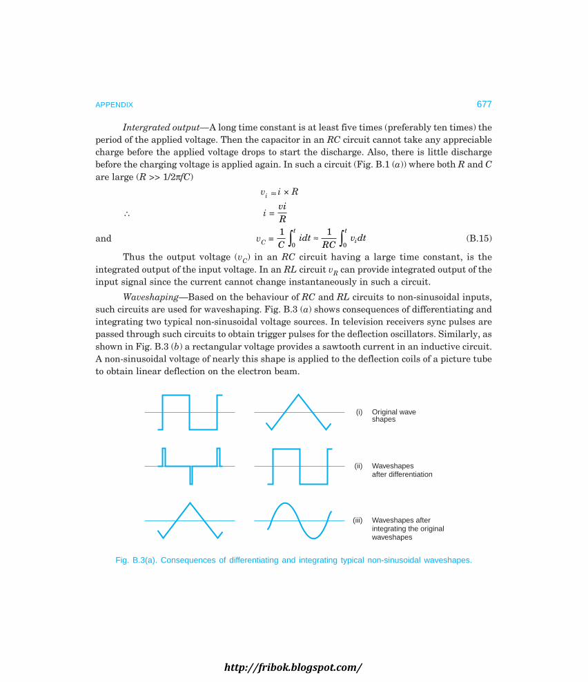
C-4\N-MONO\APPENDIX
APPENDIX 677
Intergrated output—A long time constant is at least five times (preferably ten times) theperiod of the applied voltage. Then the capacitor in an RC circuit cannot take any appreciablecharge before the applied voltage drops to start the discharge. Also, there is little dischargebefore the charging voltage is applied again. In such a circuit (Fig. B.1 (a)) where both R and Care large (R >> 1/2πfC)
vi ≈ i × R
∴ i = viR
and vC = 1 1
00Cidt
RCv dti
tt≈ zz (B.15)
Thus the output voltage (vC) in an RC circuit having a large time constant, is theintegrated output of the input voltage. In an RL circuit vR can provide integrated output of theinput signal since the current cannot change instantaneously in such a circuit.
Waveshaping—Based on the behaviour of RC and RL circuits to non-sinusoidal inputs,such circuits are used for waveshaping. Fig. B.3 (a) shows consequences of differentiating andintegrating two typical non-sinusoidal voltage sources. In television receivers sync pulses arepassed through such circuits to obtain trigger pulses for the deflection oscillators. Similarly, asshown in Fig. B.3 (b) a rectangular voltage provides a sawtooth current in an inductive circuit.A non-sinusoidal voltage of nearly this shape is applied to the deflection coils of a picture tubeto obtain linear deflection on the electron beam.
(i)
(ii)
(iii)
Original waveshapes
Waveshapesafter differentiation
Waveshapes afterintegrating the originalwaveshapes
Fig. B.3(a). Consequences of differentiating and integrating typical non-sinusoidal waveshapes.
http://fribok.blogspot.com/

C-4\N-MONO\APPENDIX
678 MONOCHROME AND COLOUR TELEVISION
vL
0 t
vL = L.diLdt
iL
0 t
Fig. B.3(b). Application of a rectangular voltage toan inductive circuit results in a sawtooth current through it.
http://fribok.blogspot.com/
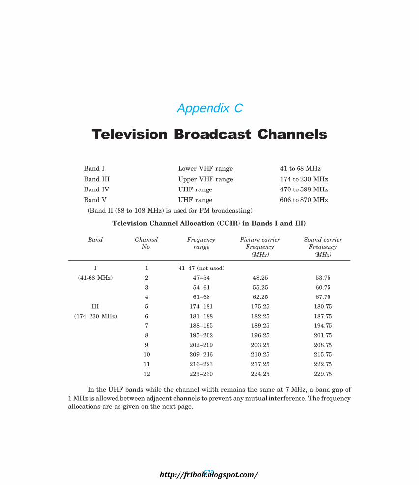
Band I Lower VHF range 41 to 68 MHz
Band III Upper VHF range 174 to 230 MHz
Band IV UHF range 470 to 598 MHz
Band V UHF range 606 to 870 MHz
(Band II (88 to 108 MHz) is used for FM broadcasting)
Television Channel Allocation (CCIR) in Bands I and III)
Band Channel Frequency Picture carrier Sound carrierNo. range Frequency Frequency
(MHz) (MHz)
I 1 41–47 (not used)
(41-68 MHz) 2 47–54 48.25 53.75
3 54–61 55.25 60.75
4 61–68 62.25 67.75
III 5 174–181 175.25 180.75
(174–230 MHz) 6 181–188 182.25 187.75
7 188–195 189.25 194.75
8 195–202 196.25 201.75
9 202–209 203.25 208.75
10 209–216 210.25 215.75
11 216–223 217.25 222.75
12 223–230 224.25 229.75
In the UHF bands while the channel width remains the same at 7 MHz, a band gap of1 MHz is allowed between adjacent channels to prevent any mutual interference. The frequencyallocations are as given on the next page.
679
Appendix C
http://fribok.blogspot.com/

C-4\N-MONO\APPENDIX
680 MONOCHROME AND COLOUR TELEVISION
UHF BAND IV (470–598 MHz) Channels 21–36
Band Channel Frequency Picture Carrier Sound Carrier(UHF) No. range frequency frequency
(MHz) (MHz) (MHz)
IV 21 470 to 478 471.25 476.75Channel 22 478 to 486 479.25 484.75
21–36 23 486 to 494 487.25 492.7524 494 to 502 495.25 500.7525 502 to 510 503.25 508.7526 510 to 518 511.25 516.7527 518 to 526 519.25 524.7528 526 to 534 527.25 532.7529 534 to 542 535.25 540.7530 542 to 550 543.25 548.7531 550 to 558 551.25 556.7532 558 to 566 559.25 564.7533 566 to 574 567.25 572.7534 574 to 582 575.25 580.7535 582 to 590 583.25 588.7536 590 to 598 591.25 596.75
UHF BAND V (606–870 MHz) Channels 37–69
Channel No. Frequency band Channel No. Frequency band(MHz) (MHz)
37 606–614 54 742–75038 614–622 55 750–75839 622–630 56 758–76640 630–638 57 766–77441 638–646 58 774–78242 646–654 59 782–79043 654–662 60 790–79844 662–670 61 798–80645 670–678 62 806–81446 678–686 63 814–82247 686–694 64 822–83048 694–702 65 830–83849 702–710 66 838–84650 710–718 67 846–85451 718–726 68 854–86252 726–734 69 862–87053 734–742
Note : With channel range from a to b MHz, the picture carrier is (a + 1.25) MHz, and sound carrier(b – 1.25) MHz.
http://fribok.blogspot.com/

INTRODUCTION. When this book was under preparation, satellite transmission hadjust begun. As such an introductory write-up on this was included in the text. However, aftera decade or so, satellite television became available all over the world. A suitable section underthe title ‘Television via Satellite’ was then included (Section 10–7) in the chapter on TelevisionApplications.
The transmission reception and distribution of TV signals was all analog till recent pastbut as in other areas of electronics, digital technology has made its impact on television, enablinggradual transition from analog to digital form of signal processing. While books are availabledescribing digital television, this author has also contributed towards digital TV as detailedunder ‘Suggested Further Reading’. However, to enable those not much exposed to recentdevelopments, a review of the entire gamut of TV transmission and reception is attemptedhere without disturbing section 10.7 of the book.
LIMITATIONS OF TERRESTRIAL TRANSMISSION. Conceptually satellite televisionis very much similar to broadcast television. It is a wireless system for delivering televisionprogrammes directly to the viewer’s house or through a Cable network. Both broadcast i.e.terrestrial television and satellite television transmit programmes via a radio signal. However,the main drawback of broadcast television is its limited range. The radio signals from thebroadcasting antenna propagate in a straight line. In order to receive these signals, the receivingantenna has to be in the direct ‘LINE-OF-SIGHT’ of the transmitting antenna. The main obstacleto this is the earth’s curvature which eventually breaks the signal’s line of sight thus preventingreception over long distances.
SATELLITE TV SOLUTION. Satellite television solves the problem of range bytransmitting broadcast signals from satellites orbiting the earth. Since satellites are high inthe sky, signals, can be received over long distances by using special antennas called DishAntennas. The television satellites are in a GEOSYNCHRONOUS orbit meaning that theystay in one place in the sky relative to the earth. Each satellite is launched into space at about7000 miles per hour reaching approximately 22300 miles (i.e. 35887 kms.– usually referred toas 36000 kms) above the earth. At this speed and altitude, the satellite revolves around theplanet (earth) once every 24 hours – the same period of time it takes the earth to make one fullrevolution. In other words, the satellite keeps exact pace with the earth’s rotation. This way,the receiving dish antenna has to be directed only once at the satellite and it will continue topick up signals without any adjustment.
SATELLITE COMMUNICATION SYSTEM. In satellite communication, thetransmitting station sends information to the satellite as RF waves which in turn retransmits
Appendix D
681http://fribok.blogspot.com/

C-4\N-MONO\APPENDIX
682 MONOCHROME AND COLOUR TELEVISION
it to the receiving ground station. The frequencies used for this purpose are in the microwaveband from 3 to 30 GHz (one GHz = 109 Hz) because at these ultra high frequencies, theatmosphere no longer acts as barrier and signals are able to travel out into space and backwithout any obstruction, absorption or deflection. Figure D-1 shows the basic technique ofcommunication by a satellite. The signals from the studio or elsewhere are sent to thetransmission earth station which converts them to the assigned UP-LINK microwave frequencyband. The transmitting dish antenna then beams them in the direction of unseen satellite. Thesatellite is equipped with its own antenna which receives the up-link signals and feeds them toa receiver. The receiver is designed to amplify and change the signals to another base frequencycalled DOWN-LINK frequency. This is done primarily to prevent interference between the up-link and down-link frequencies. The frequency converted wideband signal is then fed to atransmitter located in the satellite which provides additional amplification and retransmits itback to earth through another antenna. The receiving earth station which is located far-awayfrom the transmitting earth station, suitably orients its dish antenna to receive the down linksignal. The picked up signal is given enough amplification and converted back to its originalform as at the sending end source. The band width allotted for up-link and hence down-linktransmission is 500 MHz, wide enough to accommodate about 12 TV channels each originatingfrom a different studio location but combined as a band at the earth transmitting station.
Up link transmitstation location
Transmittingdishantenna
35887 Km(22300 miles)
Receivingdish antenna
Up
link
sign
al
5.9
to6.
4G
Hz
Solar panel
Satellite
Transmittingdish antenna
Dow
nlink
signal
3.7to
4.2G
Hz
Down link receivestation location
Receivingdish antenna
S
Fig. D.1. Signal paths in a satellite communication system.
http://fribok.blogspot.com/

C-4\N-MONO\APPENDIX
APPENDIX 683
The receiving dish antenna’s orientation for each satellite will be different depending onits parking in the sky. Similarly its setting will vary for each location in big countries likeIndia. The idea is that the receiving dish antenna must be in line with the transmitting dishantenna of the satellite for maximum signal pick-up.
SIGNAL RECEPTION, PROCESSING AND DISTRIBUTION. The down-link signalis received at the cable station where several dish antennas are positioned to receive signalsfrom different satellites. These are down converted to the UHF-VHF band, and demodulatedto obtain original video and audio signals. These are then AM modulated on different VHFchannels, amplified and combined in a combiner before feeding to the cable network fordistribution to the subscribers.
DIGITAL TECHNOLOGY AND DATA PROCESSING. Electronic signals can be analogor digital. An analog signal like the output of a microphone can have any amplitude within arange, for different frequency components. In contrast, in a digital system, information isrepresented in discrete or digitized form rather than continuous as in analog. The most commonis the binary form, which means that for any signal only two discrete states are possible whichare normally denoted as ‘0’ and ‘1’. In digital circuits, the ‘0’ state is usually represented by 0volts or a very low voltage and the ‘1’ state is represented by a voltage around 2 to 5 volts. Theusage of only two discrete signal levels results in a very significant noise immunity advantagefor digital circuits. If the noise level at the input is very small, it is sharply attenuated betweenthe input and output while the logic signals are transmitted at full amplitude. This is one ofthe main merits of signal processing by digital means.
The decimal system expresses numbers in powers of ten i.e. to the base 10. For example,134 = 1 × 10² + 3 × 101 + 4 × 100 = 100 + 30 + 4 = 134. The same approach is used in a binarysystem, however, here the base is 2 not 10. As an example decimal number 19 is expressed inthe binary system as 100 11 and read as one, zero, zero, one, one and not ten thousand andeleven. The representation is correct because—
100 11 = 1 × 24 + 0 × 23 + 0 × 22 + 1 × 21 + 1 × 20 = 16 + 0 + 0 + 2 + 1 = 19
Similarly number 25 = 11 00 1 in binary form and 10000 = 1 00 111 000 10 000 as itsbinary equivalent. While it is too big, digital processing of such numbers does not present anyserious problem. This is because of the ease with which a very large number of logic (ON-OFF)elements can be designed and manufactured in a tiny integrated circuit (IC) and the very highspeed and reliability with which digital circuits can operate to carry out desired operations.
DIGITAL SIGNAL PROCESSING. While it is very advantageous to carry out signalprocessing in digital form, the real world is analog. Therefore, analog signals must first beconverted to digital form before processing, and the digital results must be converted back toanalog form for human consumption. For this, special high speed converters have been designed.An A/D (analog to digital) converter converts analog signal to digital form as a binary pulsetrain depending on the amplitude of analog signal at any given instant. Similarly, a D/A (digitalto analog) converter does the reverse to convert the processed digital signal back to analogform.
DIGITAL SATELLITE TV TRANSMISSION AND RECEPTION. Digitization of signalpath has gained importance due to many advantages of the digital system. These include noisesuppression and improved quality of reproduction. Its impact on television has been almost a
http://fribok.blogspot.com/
C-4\N-MONO\APPENDIX
684 MONOCHROME AND COLOUR TELEVISION
complete transition from analog to digital form of signal encoding. Such a transformation hasresulted in improved picture quality and better sound output. For A/D conversion of video andaudio signals their analog forms as obtained from TV camera output and microphonerespectively are sampled at a very fast rate but at fixed discrete levels to obtain correspondingdata streams in terms of 0′s and 1′s which are actually low and high voltage levels causingtogether a square wave nature continuous output stream. These are FM modulated on a suitablecarrier and then up-converted to the allotted micro frequency band before up-linking to thesatellite. Similarly at the receiving end the feeble signals picked up by the receiving stationdish antenna are first down converted to the MHz range and then processed by a digital decoderreceiver to obtain original analog video and audio signals.
At cable stations as explained earlier, these are AM modulated on fixed VHF channelscarriers and combined to deliver as a compact package to the subscriber over the cable network.However, for terrestrial transmission over vast areas as in India, the analog video and audiosignals are again processed and AM modulated before radiation from the transmitting stationslocated in different zones for uniform signal reception by the subscribers. The subscribers usefolded dipole YAGI antenna to receive them. DOOR DARSHAN of India has several of its ownsatellites for delivering its programmes over many countries.
DIRECT SATELLITE BROADCAST (DSB) also called DIRECT-TO-HOME broadcast isnow gaining popularity where the subscriber can directly receive signals from satellites andprocess them to obtain TV signals of any selected channel. A special integrated decoder receiveris used for processing the signal picked up by the house top located Dish antenna.
High Definition Television (HDTV) has also come up where the standards are differentthan the conventional PAL/NTSC systems. Here the aspect ratio is also different to enablewide and enlarged pictures as shown in theatres. The sound output is as good as obtained fromCompact Discs (CDs).
http://fribok.blogspot.com/

ABC (automatic brightness control), 579
ACC (automatic colour control) circuit, 553
AC coupling (video amplifier), 271
Additive colour mixing, 493
ADG (automatic degaussing) circuit, 509, 522
Adjacent channel interference, 154
Aeroplane flutter, 263
AFC (automatic frequency control) tuner, 576
AFC (automatic frequency control) horizontal, 312,320
AFPC (automatic frequency and phase control),557, 577
AFT (automatic fine tuning), 575
AGC (automatic gain control), 144
Alignment of colour receiver, 630
Alignment of FM detector, 624
Alignment of IF section, 462, 621, 623
Alignment of local oscillator, 625
Alignment procedure of a receiver, 618
Alignment sequence (receiver), 618
Alignment of sound IF, 623
Alignment of tuner, 624
AM (amplitude modulation), 54
AM limiter, 404, 405
Analysis of frequency modulation, 63
Antennas, 156, 161, 170
colour TV antenna, 170-173
log periodic, 171
Arcing (EHT), 483
Armstrong FM circuit, 129
Aspect ratio, 16
Astigmatism, 511
Attenuation pads, 178
Audio amplifier (TV sound), 420-425
C-4\N-MONO\INDEX.P65
Automatic brightness control, 579
Automatic colour control, 553
Automatic degaussing, 509, 522
Automatic frequency control
tuner 576
Automatic frequency and phase control, 557
Automatic fine tuning, 575
B+ supply, 482
Back porch, 40
Balun, 177
Bandswitching, 443
Bandwidth (channel), 56
Bandwidth (colour signal), 67
Bandwidth (video amp), 227
Barrel distortion, 513
Beam current limiting, 262
Beam deflection, 76
Beam velocity, 76
Bifilar (IF) transformer, 458
Black and white receiver servicing, 641
Black Level, 33
Blanking Level, 33
Blanking pulses, 38
Block diagram (monochrome receiver), 135, 629
Blooming of picture, 262
Booster amplifier, 578
Booster station (TV), 153
Brightness control, 13, 268, 273
Burst (PAL), 545
Cable television (CATV, MATV, CCTV), 182-186
Camera (TV), 108-111
Camera tubes, 86-103
685http://fribok.blogspot.com/

C-4\N-MONO\INDEX
686 ELEMENTS OF A TELEVISION SYSTEM
image orthicon, 89
plumbicon, 97
silicon diode array vidicon, 99
solid state image scanner, 100
vidicon, 94
Cathode ray oscilloscope, 591-599
Channel bandwidth, 59
Channel bandwidth (colour signal), 67, 530
Channel selection (tuners), 436-441
Characteristic impedance, 175
Choice of (IF) intermediate frequencies, 140-142
Choice of colour subcarrier frequency, 548
Chromaticity diagram, 496
Coaxial cable, 175
Closed circuit television (CCTV), 186
Cochannel interference, 153
Colour bar generator and operation, 606-609
Colour bar pattern generator, 610
Colour difference signals, 500
Colour killer circuit, 554
Colour picture tubes, 505-523
Colour receivers:
NTSC, 541
PAL, 551
SECAM, 559
Colour signal transmission, 528
Colour TV antenna, 170
Colour TV camera, 497
Colour mixing, 493
Colour receiver (block diagram), 630
Colour receiver alignment, 630
Colour receiver servicing, 663
Colour resolution and bandwidth, 27
Comparison of different TV systems, 70
Comparison of positive and negative modulation,121
Compatibility, 490
Complete channel bandwidth, 59
Composite video signal functions, 217
Contrast, 31
Contrast control methods, 254-256
Contrast ratio, 31
DC component of the video signal, 37, 215
DC coupling (video amplifier), 260
DC coupling problems, 262
DC level (video signal), 37, 267
DC insertion, 38
DC reinsertion, 269
DC restorer, 270
Deemphasis network, 122, 123
Deflection amplifiers:
horizontal, 370-375
vertical, 365-388
Deflection yoke, 77
Delay line, 547
Delayed AGC, 285
Demerits of vestigial sideband transmission, 62
Detector video, 142, 210
Differentiator, 42
Digital multimeter, 590
Dipole antenna, 162
Diplexing of VHF antennas, 167
Distortion in amplifiers, 222-225
Electronic band switching, 441
Electronic touch tuning, 573
Encoding colour signal, 540
Equalizing pulses, 45-47
Fault localization (receiver), 640
Flat twin lead cable, 174
Flicker, 21
Folded dipole, 161
Forward AGC, 280
Frame TV, 15, 21
Frequency modulation, 62
channel bandwidth, 66
Frequency response (amp), 224
Gamma of the picture, 31
Gated (keyed) AGC, 283
Ghost interference, 155
Grassman’s law, 494
http://fribok.blogspot.com/

C-4\N-MONO\INDEX
INDEX 687
Grey scale tracking, 523
Ground wave propagation, 150
High frequency compensation, 226-228
Highest modulating frequency, 26
Horizontal Deflection, 389
Horizontal resolution, 26
Horizontal sync details : 39-41
Horizontal sync separation, 298-300
Hybrid receivers, 135
Interlaced scanning, 21
Interlace error, 29
Interleaving (frequency), 529
Interference, 153
Intermediate frequency (choice), 140
Kell factor, 25
Keyed AGC, 283
Log periodic antenna, 171
Low voltage power supply, 473-478
Luminance, 495
Luminance signal, 498
Marker generator, 603
Memory circuit, 571
Merits of frequency modulation, 123
Mixer stage (tuner), 137
Mixing of colours, 493
Modulation of colour difference signals, 530
Modulation of picture tube, 235-239
Modulation (positive and negative), 120
Multimeter, 586-590
NTSC colour subcarrier frequency, 538
Noise cancellation circuits, 286-287
Noise in sync pulses, 300
Nonresonant transmission line, 178
Peak AGC, 281
Phase distortion, 223
Phase modulation, 128
Picture signal transmission, 117
Picture tube-black and white (monochrome), 74-83
Picture tube controls, 82, 143
Plumbicon, 97-98
Positive and negative modulation, 120
Power supplies, 472
Pre-equalizing pulses, 45
Preference of FM over AM for sound signaltransmission, 123
Primary colours, 493
Probes (CRO & VTVM), 597
Pulling-on whites, 40
Pulse train, 48
Quadrature detector (FM), 414
Radio wave propagation, 150
Rainbow colour bar generator, 606
Raster, 17
Ratio detector, 414
RC circuits, 671-676
RC coupled amplifier, 228-229
Reactance modulator, 125-127
Reaction tube, 125
Reactance scanning, 375
Regulators (voltage), 480-482
Resonant and nonresonant lines, 125
SSB transmission, 56
Safety precautions (servicing), 666
Scanning, 17-24
Screen brightness, 80
Side bands, 55, 64
Silicon diode array vidicon, 99
Single ended ratio detector, 414
Sky wave propagation, 150
Smear, 224
Solid state image scanner, 100-101
Sound signal reception, 143
Sound signal separation, 400
http://fribok.blogspot.com/

C-4\N-MONO\INDEX
688 ELEMENTS OF A TELEVISION SYSTEM
Sound signal take-off point and circuits, 142
Sound signal transmission, 122
Standing wave ratio, 176
Stub (transmission line), 177
Subcarrier generation, 556
Switching mode power supply (SMPS), 485
Sync details, 49
Sync processing, 146
Sync separation, 296-300
Synchronous demodulators, 556
Synchronization, 115
Synchronizing pulse generation circuitry, 116
Television broadcasting, 182
Television games, 199-207
Television picture on CRO screen, 597
Television receiver (B & W), 618
Television receiver (colour), 706-715
Television transmitter (B & W), 117
Television test charts (patterns), 626
vectroscope, 611
wobbuloscope, 606
Three colour theory, 493
Tint control, 11, 543
Tone control, 13
Tonal gradation, 31
Transmission lines, 173
Trintron (colour picture tube), 519
Tuners, 430, 441
Vectroscope, 611
Venetian blind effect, 153
Vertical deflection, 346-363
Vertical pulse train, 39, 41, 46, 49
Vertical pulse train functions, 49
VHF antennas, 161-170
Video amplifier
contrast control methods, 254
dc reinsertion, 269
spot killer circuit, 271, 272
widebanding guidelines, 250
Video detector, 210
dc component (video signal), 215
Video IF amplifiers (see IF section)
Video tape recording (VTR), 189-196
Vidicon, 94-100
Viewing distance, 32
View finder, 109
Weighting factors, 533
World TV standards, 70
Zener regulated dc supply, 480
http://fribok.blogspot.com/