Electron backscatter diffraction study of polycrystalline YBa 2Cu 3O 7− δ ceramics
12
Electron backscatter diffraction study of polycrystalline YBa 2 Cu 3 O 7d ceramics Anjela Koblischka-Veneva a,b , Michael R. Koblischka c, * , Petra Simon a , Frank M€ ucklich a , Masato Murakami b a Institute of Functional Materials, Universit€ at des Saarlandes, P.O. Box 151150, D-66041 Saarbr€ ucken, Germany b SRL/ISTEC, Division 3, 1-16-25 Shibaura, Minato-ku, Tokyo 105, Japan c Experimental Physics, Universit€ at des Saarlandes, P.O. Box 151150, D-66041 Saarbr€ ucken, Germany Received 8 August 2001; received in revised form 4 January 2002; accepted 4 January 2002 Abstract The electron backscatter diffraction (EBSD) technique was applied to polycrystalline YBa 2 Cu 3 O 7d ceramics. To obtain good quality EBSD Kikuchi patterns on the ceramic superconductors, a new sample polishing route was es- tablished. Samples with and without KClO 3 -doping were investigated; and the crystallographic orientations of the grains were analyzed using pole figures and EBSD orientation mapping. On the polycrystalline KClO 3 -doped YBa 2 Cu 3 O 7d samples we found two major orientations (0 0 1) and (1 0 0) normal to the sample surface, while the undoped sample did not exhibit any orientation maxima. We ascribe this observation to the effect of a liquid phase due to the KClO 3 -additive during the preparation process. Ó 2002 Elsevier Science B.V. All rights reserved. 1. Introduction The investigation of the microstructure of ceramic, polycrystalline high-T c superconductors plays an important role in the understanding of the magnetic properties, namely the critical current density, j c ðBÞ. The performance of bulk samples of the RE-123 type (i.e. YBa 2 Cu 3 O 7d (YBCO) or NdBa 2 Cu 3 O 7d (NdBCO)) relevant for applica- tions (e.g. microwave resonators, trapped field magnets, fault current limiters and wires) [1] are especially severely limited by the presence of grain boundaries [2] with different misorientation angles. High angle grain boundaries were found early to act as weak-links, but also low angle grain boundaries and subgrain boundaries pose serious problems in large magnetic fields. Therefore, grain boundaries form severe obstactles for the current flow, thus in the past years a lot of effort was in- vested to improve the texture and grain connec- tions within these bulk samples [3,4]. An important step for the improvement of the transport properties of the grain boundaries is given by chemical doping, as described recently by Mannhart and co-workers [5]. By means of doping YBCO thin films with Ca, these authors showed that the current density across the grain bound- aries could rise by a factor of about 6. These in- vestigations were, however, performed on YBCO * Corresponding author. Tel./fax: +49-681-302-4867. E-mail address: [email protected] (M.R. Koblischka). 0921-4534/02/$ - see front matter Ó 2002 Elsevier Science B.V. All rights reserved. PII:S0921-4534(02)01244-3 Physica C 382 (2002) 311–322 www.elsevier.com/locate/physc
-
Upload
uni-saarland -
Category
Documents
-
view
2 -
download
0
Transcript of Electron backscatter diffraction study of polycrystalline YBa 2Cu 3O 7− δ ceramics
Electron backscatter diffraction study of polycrystallineYBa2Cu3O7�d ceramics
Anjela Koblischka-Veneva a,b, Michael R. Koblischka c,*, Petra Simon a,Frank M€uucklich a, Masato Murakami b
a Institute of Functional Materials, Universit€aat des Saarlandes, P.O. Box 151150, D-66041 Saarbr€uucken, Germanyb SRL/ISTEC, Division 3, 1-16-25 Shibaura, Minato-ku, Tokyo 105, Japan
c Experimental Physics, Universit€aat des Saarlandes, P.O. Box 151150, D-66041 Saarbr€uucken, Germany
Received 8 August 2001; received in revised form 4 January 2002; accepted 4 January 2002
Abstract
The electron backscatter diffraction (EBSD) technique was applied to polycrystalline YBa2Cu3O7�d ceramics. To
obtain good quality EBSD Kikuchi patterns on the ceramic superconductors, a new sample polishing route was es-
tablished. Samples with and without KClO3-doping were investigated; and the crystallographic orientations of the
grains were analyzed using pole figures and EBSD orientation mapping. On the polycrystalline KClO3-doped
YBa2Cu3O7�d samples we found two major orientations (0 0 1) and (1 0 0) normal to the sample surface, while the
undoped sample did not exhibit any orientation maxima. We ascribe this observation to the effect of a liquid phase due
to the KClO3-additive during the preparation process.
� 2002 Elsevier Science B.V. All rights reserved.
1. Introduction
The investigation of the microstructure of
ceramic, polycrystalline high-Tc superconductorsplays an important role in the understanding of the
magnetic properties, namely the critical current
density, jcðBÞ. The performance of bulk samples of
the RE-123 type (i.e. YBa2Cu3O7�d (YBCO) or
NdBa2Cu3O7�d (NdBCO)) relevant for applica-
tions (e.g. microwave resonators, trapped field
magnets, fault current limiters and wires) [1] are
especially severely limited by the presence of grain
boundaries [2] with different misorientation angles.
High angle grain boundaries were found early
to act as weak-links, but also low angle grain
boundaries and subgrain boundaries pose seriousproblems in large magnetic fields. Therefore, grain
boundaries form severe obstactles for the current
flow, thus in the past years a lot of effort was in-
vested to improve the texture and grain connec-
tions within these bulk samples [3,4].
An important step for the improvement of the
transport properties of the grain boundaries is
given by chemical doping, as described recently byMannhart and co-workers [5]. By means of doping
YBCO thin films with Ca, these authors showed
that the current density across the grain bound-
aries could rise by a factor of about 6. These in-
vestigations were, however, performed on YBCO
* Corresponding author. Tel./fax: +49-681-302-4867.
E-mail address: [email protected] (M.R.
Koblischka).
0921-4534/02/$ - see front matter � 2002 Elsevier Science B.V. All rights reserved.
PII: S0921-4534 (02 )01244-3
Physica C 382 (2002) 311–322
www.elsevier.com/locate/physc
thin films with a single grain boundary. For the
development of bulk materials, it is therefore ex-
tremely important to study the effects of doping
on bulk, polycrystalline samples aimed for appli-
cations.
In earlier publications, we have reported on thepreparation and characterization of YBCO ce-
ramics doped by various alkali metals (K, Na, Rb)
[6,7]. By means of magnetic measurements (AC
and DC susceptibility, microwave surface resis-
tance) it was shown that in certain concentrations
of the dopant the grain growth and the inter-
granular properties of the samples improved con-
siderably. Therefore, a direct correlation of thelocal microstructure (grain size and orientation)
with the magnetic properties of the samples is a
very important task. An useful tool to achieve this
goal is given by the recently developed electron
backscatter diffraction (EBSD) technique [8–10],
which enables the orientation mapping of granular
samples by means of automatized recording of
Kikuchi patterns [11]. EBSD bridges the two tra-ditional methods of studying crystalline materials,
X-ray crystallography and transmission micro-
scopy, and adds the benefit of high spatial reso-
lution at any point on the surface of a bulk
specimen.
With the necessary equipment, EBSD Kikuchi
patterns can be used to obtain a crystallographic
orientation map of the grains on the surface ofthe specimen. Some preliminary studies using the
EBSD technique on high-temperature supercon-
ductor oxides have already been reported (YBCO
thin [12] and thick films [13] including coated
conductors [14], Tl-1223 [15,16] and Bi-2223 tapes
[17]), but the results were very limited. EBSD
patterns from only a few individual YBCO or
Bi-2223 crystalites were presented and the misori-entation of the Bi-2223 crystalites was semi-quali-
tatively estimated. Therefore, the results cannot
pictorially present the connectivity and crystallo-
graphic orientation distribution of the grains over
a bulk area, which would be essential for a fur-
ther understanding of the growth process of bulk
YBCO samples.
The aim of the present paper is to study thelocal microstructure of polycrystalline KClO3-
doped and undoped YBCO by means of EBSD.
We present EBSD Kikuchi patterns and discuss
the details of the necessary polishing procedure.
2. Experimental procedure
2.1. EBSD technique
Backscatter Kikuchi patterns are generated in a
commercial EBSD system (TSL TeXSEM Labo-
ratories [18]) using a phosphor screen mounted in
a commercial SEM microscope (CamScan Series
4) by back-diffraction of a stationary beam of
high-energy electrons from an almost perfect vol-ume of crystal. An EBSD pattern can be viewed as
a map of the angular relationships between atomic
planes in a crystal. Bragg diffraction occurs in
three dimensions from the lattice planes on either
side of the diverging electron beam, producing two
cones of radiation. When a phosphor screen is
placed to intercept the cones, two conic sections
are captured and appear as a pair of parallel linesknown as Kikuchi lines or Kikuchi bands that
represent the specific lattice planes. In order to
obtain intense Kikuchi patterns, the sample has to
be steeply tilted to about 70� from the horizontal.
To produce a crystallographic orientation map,
the electron beam is scanned over a selected sur-
face area and the resulting Kikuchi patterns are
automatically recognized by means of a modifiedHough transform [19], and indexed by the con-
trolling computer. The patterns are recorded by
means of a low-light CCD video camera, and an
additional background subtraction unit is required
as the Kikuchi pattern is superimposed on the
scattered electrons, which produce a background
about five times larger than the patterns. The data
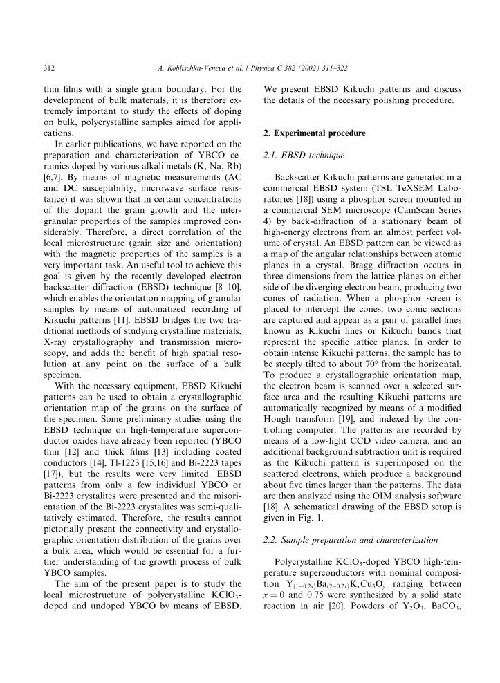
are then analyzed using the OIM analysis software[18]. A schematical drawing of the EBSD setup is
given in Fig. 1.
2.2. Sample preparation and characterization
Polycrystalline KClO3-doped YBCO high-tem-
perature superconductors with nominal composi-
tion Yð1�0:2xÞBað2�0:2xÞKxCu3Oy ranging betweenx ¼ 0 and 0.75 were synthesized by a solid state
reaction in air [20]. Powders of Y2O3, BaCO3,
312 A. Koblischka-Veneva et al. / Physica C 382 (2002) 311–322
CuO, all with a purity 99.99% and KClO3 (more
than 99.9%), were mixed, pressed into pellets andheated at 880 �C for 24 h. The reacted pellets were
reground, pressed again and sintered at 915 �Cfor 20 h, followed by annealing at 600 �C for 14 h,
before being cooled to room temperature. The
samples chosen for this study (x ¼ 0:30) had a
cubic shape (1 � 1 � 1 mm3) and a Tc of 92.9 K,
as determined by AC susceptibility (f ¼ 250 Hz,
Ha ¼ 0:1 mT). Pure samples were prepared forcomparison, and cut to the same shape. Tc of the
pure samples was determined to be 91.3 K.
The phase content, microstructure and mor-
phology of the crystalline grains were character-
ized using X-ray powder diffraction and scanning
electron microscopy (SEM) coupled with an elec-
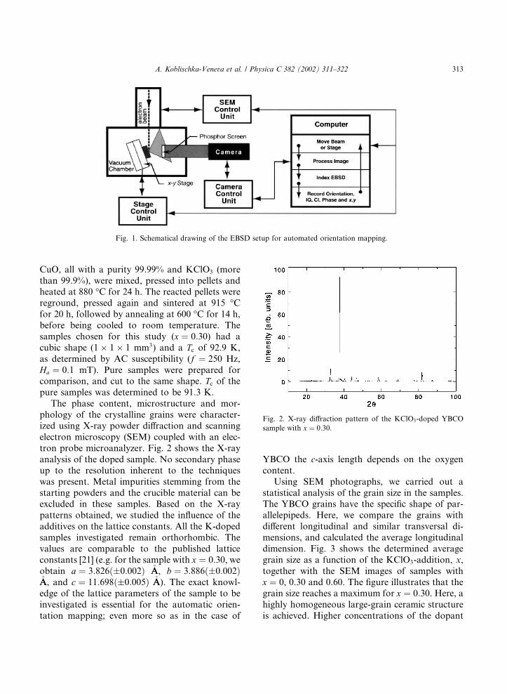
tron probe microanalyzer. Fig. 2 shows the X-ray
analysis of the doped sample. No secondary phaseup to the resolution inherent to the techniques
was present. Metal impurities stemming from the
starting powders and the crucible material can be
excluded in these samples. Based on the X-ray
patterns obtained, we studied the influence of the
additives on the lattice constants. All the K-doped
samples investigated remain orthorhombic. The
values are comparable to the published latticeconstants [21] (e.g. for the sample with x ¼ 0:30, we
obtain a ¼ 3:826ð�0:002Þ �AA, b ¼ 3:886ð�0:002Þ�AA, and c ¼ 11:698ð�0:005Þ �AA). The exact knowl-
edge of the lattice parameters of the sample to be
investigated is essential for the automatic orien-
tation mapping; even more so as in the case of
YBCO the c-axis length depends on the oxygen
content.
Using SEM photographs, we carried out a
statistical analysis of the grain size in the samples.The YBCO grains have the specific shape of par-
allelepipeds. Here, we compare the grains with
different longitudinal and similar transversal di-
mensions, and calculated the average longitudinal
dimension. Fig. 3 shows the determined average
grain size as a function of the KClO3-addition, x,
together with the SEM images of samples with
x ¼ 0, 0.30 and 0.60. The figure illustrates that thegrain size reaches a maximum for x ¼ 0:30. Here, a
highly homogeneous large-grain ceramic structure
is achieved. Higher concentrations of the dopant
Fig. 2. X-ray diffraction pattern of the KClO3-doped YBCO
sample with x ¼ 0:30.
Fig. 1. Schematical drawing of the EBSD setup for automated orientation mapping.
A. Koblischka-Veneva et al. / Physica C 382 (2002) 311–322 313

(xP 0:60) lead to a small grain structure andchanges in the grain boundaries, and thus, de-
coupling of the grains. These results will be com-
pared to the grain sizes determined by EBSD in
Section 3.2.
The sample with x ¼ 0:30 and a pure YBCO
sample were chosen for the following EBSD in-
vestigations.
3. Results and discussion
3.1. Polishing technique of ceramic HTSC for
EBSD
Firstly, we discuss the requirements of the
sample polishing procedure. For use with theEBSD setup, the samples need to have a shiny, flat
surface and preferably, an almost perfect crystal-
lographic structure. The necessary polishing pro-
cedure is evidently somewhat delicate as several
authors have attempted to perform EBSD on bulk
superconducting samples (see for example, Refs.
[22,23]), but failed even though investigations of
the microstructure itself were possible by means oflight microscopy or SEM. This illustrates the high
sensitivity of the EBSD technique, as the back-
scattered electrons are generated from a small
depth under the sample surface, typically between
20 and 200 nm [9,24]. Backscatter Kikuchi pat-
terns have been found to disappear when a thin
foreign surface layer of thickness about two times
the Rutherford elastic mean free path is present at
a given beam energy [24]. Therefore, the polishingprocedure of the bulk ceramic samples plays an
important role to obtain high-contrast Kikuchi
patterns on polycrystalline samples.
For YBCO superconductors, several polishing
recipes are given in metallography journals [25,26],
but it is important to note that the main goal of
such recipes was to observe the microstructure it-
self. In this case, thin surface layers of differentmaterial or distorted YBCO will not be a problem.
However, for EBSD it is crucially important to
avoid such layers. In a former publication [6], we
found in a combined SEM and X-ray analysis of
the sample surfaces of doped YBCO that there is a
low-density surface layer of about 200 lm thick-
ness. This layer must be completely removed in
order to reveal the bulk properties of the sample.Furthermore, embedding the samples into resins is
not wanted for the EBSD measurements. Due to
these reasons, a sample polishing route different to
the standard metallography preparation technique
has to be established.
Magneto-optic (MO) investigations of flux dis-
tributions [27] were successfully performed since
many years on a variety of high-Tc samples, in-cluding polycrystalline samples [28–30]. All these
samples need to be polished, but superconductivity
is not allowed to be affected by the employed
procedure. Two slightly different polishing pro-
cedures were established for use with the MO
imaging: (1) The samples were dry polished on
polishing/lapping papers (3M Inc.) with SiO2
particles with sizes from 9 to 0.3 lm. Only forcleaning of the samples between the polishing
steps, ethanol is employed. (2) The samples were
ground on corundum papers (800–4000 mesh), and
for the last finishing step, a colloidal silica solution
(Struers OP-S) was used on the corresponding
polishing cloths (Struers OP-CHEM). For clean-
ing, again only ethanol is employed. Both methods
produce a very clean, shiny surface and, mostimportantly, the superconducting properties of
the samples are retained, as illustrated in Fig. 4
Fig. 3. The average grain size as a function of the KClO3-
doping, x. The insets present the corresponding SEM images of
polished surfaces as indicated by the arrows.
314 A. Koblischka-Veneva et al. / Physica C 382 (2002) 311–322

presenting a flux patterns obtained by MO imag-
ing on the KClO3-doped sample with x ¼ 0:30 at
T ¼ 50 K. This sample was polished using route
(2). Here, it should be noted that at low temper-atures, the sample does not exhibit the typical
flux pattern of a polycrystalline sample, where the
flux enters individually into the superconducting
grains. More details of these MO investigations
are given in Refs. [31,32].
On the same sample, very intense EBSD Ki-
kuchi patterns were obtained, thus demonstrating
that the same polishing procedure can be em-ployed also for EBSD. Furthermore, this allows to
avoid a carbon coating of the sample surfaces,
which is otherwise common for EBSD investiga-
tions on ceramic samples [33,34].
3.2. EBSD patterns and mapping
In Fig. 5, we present EBSD Kikuchi patternsand indexation of the YBCO samples. Fig. 5(a)
presents the EBSD Kikuchi patterns and index-
ation of the polycrystalline YBCO sample. The
dominating star in the upper middle part of the
Kikuchi pattern is the (1 0 0) direction; the star at
the bottom right is (1 � 10). Fig. 5(b) shows the
EBSD Kikuchi pattern of KClO3-doped YBCO
sample. Here, the (0 0 1) axis is oriented towards
the top right of the pattern with its characteristicfourfold rotation symmetry. Note that the Kikuchi
pattern shows more contrast as compared to the
pure YBCO sample, but is otherwise not different.
By means of EBSD on YBCO thin films, we ver-
ified that there is no visible difference between the
Kikuchi patterns, so the chosen polishing proce-
dure does not introduce defects to the polycrys-
talline sample.Now, we discuss the results of the automated
mapping of EBSD Kikuchi patterns. Firstly, we
present contour pole figures and inverse pole fig-
ures (IPFs) of the samples under study. Pole fig-
ures show the orientation of particular types of
crystallographic poles, with respect to a Cartesian
reference frame in stereographic projection. For
historical reasons, the axes of the reference framehave been labeled ‘‘rolling direction [1 0 0]’’ (RD),
‘‘transverse direction [0 1 0]’’ (TD) and ‘‘normal
direction [0 0 1]’’ (ND). Conventionally, the latter
lies normal to the polished sample surface. In Fig.
6(a), a contour pole figure of the KClO3-doped
YBCO sample is shown in the directions [1 0 0],
[0 0 1] and [0 1 0] . From this figure, it is clearly
visible that the KClO3-doped sample exhibits tex-ture, with the two directions (1 0 0) and (0 0 1)
being dominating.
Fig. 6(b) and (c) shows the corresponding IPFs
of the KClO3-doped and the pure YBCO sample
in all three reference directions [1 0 0], [0 0 1] and
[0 1 0]. On the triangles, the real crystallographic
directions are given. From these figures, we can
deduce that the two orientations (0 0 1) and (1 0 0)are dominant in the KClO3-doped YBCO sample,
which is also visible in the mapping shown in Fig.
7(c). This result is in contrast with the results on
the pure YBCO sample (c), where the grains are
more or less randomly distributed. This observa-
tion confirms our earlier results [35] and provides
an explanation for the improved magnetic prop-
erties as discussed in Refs. [31,32].Fig. 7 presents results of the automated mapping.
A typical map consists of about 10 000–20 000
Fig. 4. MO flux patterns of the KClO3-doped YBCO sample
with x ¼ 0:30 at 50 K and an applied field of 100 mT. The
magnetic field is imaged as bright areas; the Meissner phase
remains dark. Only in the lower part of the image, flux entering
along grain boundaries can be observed. The marker is 500 mm
long.
A. Koblischka-Veneva et al. / Physica C 382 (2002) 311–322 315
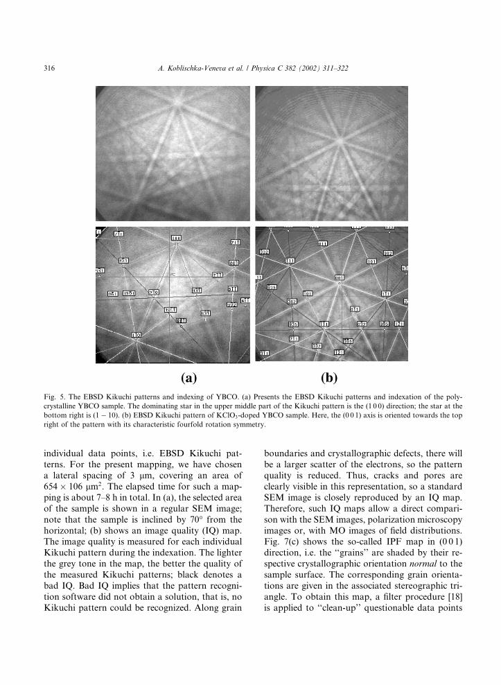
individual data points, i.e. EBSD Kikuchi pat-
terns. For the present mapping, we have chosen
a lateral spacing of 3 lm, covering an area of
654 � 106 lm2. The elapsed time for such a map-
ping is about 7–8 h in total. In (a), the selected area
of the sample is shown in a regular SEM image;
note that the sample is inclined by 70� from the
horizontal; (b) shows an image quality (IQ) map.The image quality is measured for each individual
Kikuchi pattern during the indexation. The lighter
the grey tone in the map, the better the quality of
the measured Kikuchi patterns; black denotes a
bad IQ. Bad IQ implies that the pattern recogni-
tion software did not obtain a solution, that is, no
Kikuchi pattern could be recognized. Along grain
boundaries and crystallographic defects, there will
be a larger scatter of the electrons, so the pattern
quality is reduced. Thus, cracks and pores are
clearly visible in this representation, so a standard
SEM image is closely reproduced by an IQ map.
Therefore, such IQ maps allow a direct compari-
son with the SEM images, polarization microscopy
images or, with MO images of field distributions.Fig. 7(c) shows the so-called IPF map in (0 0 1)
direction, i.e. the ‘‘grains’’ are shaded by their re-
spective crystallographic orientation normal to the
sample surface. The corresponding grain orienta-
tions are given in the associated stereographic tri-
angle. To obtain this map, a filter procedure [18]
is applied to ‘‘clean-up’’ questionable data points
Fig. 5. The EBSD Kikuchi patterns and indexing of YBCO. (a) Presents the EBSD Kikuchi patterns and indexation of the poly-
crystalline YBCO sample. The dominating star in the upper middle part of the Kikuchi pattern is the (1 0 0) direction; the star at the
bottom right is (1 � 10). (b) EBSD Kikuchi pattern of KClO3-doped YBCO sample. Here, the (0 0 1) axis is oriented towards the top
right of the pattern with its characteristic fourfold rotation symmetry.
316 A. Koblischka-Veneva et al. / Physica C 382 (2002) 311–322

Fig. 6. (a) Pole figure and (b) IPF of the KClO3-doped YBCO sample. (c) IPF of the pure YBCO sample. It is clearly visible that the
two orientations (0 0 1) and (1 0 0) are dominant in the KClO3-doped YBCO sample. This result is in contrast with the results on the
pure YBCO sample (c), where the grains are more or less randomly distributed.
A. Koblischka-Veneva et al. / Physica C 382 (2002) 311–322 317

originating from grain boundaries or surface de-
fects. Clean-up level two allowed the removal ofundefined points without altering the grain shapes
significantly.
From such an IPF map, it is clearly visible that
the two orientations, (0 0 1) and (1 0 0) are domi-
nating. This type of map summarizes the crystal-
lographic informations which can be obtained
from an EBSD mapping. Furthermore, we find
that 35% of the grains are of (0 0 1) orientation,54% of (1 0 0), and 0% of (1 1 0) orientation.
Fig. 8 presents an IQ map as in Fig. 7(b), but in
each map (a)–(e) the grain boundaries are indi-
cated in white with distinct levels of misorienta-
tion, i.e. 1–5� (a), 5–15� (b), 15–40� (c), 40–50� (d),
and finally, 60–70� (e). It is visible from this map-
Fig. 7. Results of the automated mapping on the KClO3-doped YBCO sample. (a) SEM image of the sample, inclined by 70� from the
horizontal. (b) Presents an IQ map. The IQ is calculated from the confidence index by the processing software. The lighter the grey tone
in the map, the better the quality of the measured Kikuchi patterns; black denotes a bad IQ. Cracks and pores are clearly visible in this
representation. (c) Shows the so-called IPF map in (0 0 1), direction, i.e. the grains are shaded by their respective crystallographic
orientation normal to the sample surface. The crystallographic orientations are given in the stereographic triangle.
318 A. Koblischka-Veneva et al. / Physica C 382 (2002) 311–322

ping that small angle grain boundaries are present
throughout the selected area. Grain boundaries
with larger angles are located along the crack in
the centre right of the map, and, as an important
result, around the pores in the YBCO matrix. This
grain boundary recognition is an important resultof the automated EBSD mapping. Such EBSD
mapping on superconductors, combined with MO
studies of the same area will enable an exact de-
termination of the nature of the weak links in a
superconducting sample. A further analysis of the
grain boundaries as described in Ref. [36] will be
performed in future experiments.
Fig. 9 presents a grain size histogram of the
KClO3-doped YBCO sample. In this figure, the
grain size as determined by EBSD is given as grainarea in lm2, where no assumption about the grain
shape is made. Here, it is important to note that
the definition of a grain in EBSD measurements
is different from that in e.g. optical microscopy.
Fig. 8. IQ map as in Fig. 7(b), but in each map (a)–(e) the grain boundaries are indicated in white with distinct levels, i.e. 1–5� (a), 5–
15� (b), 15–40� (c), 40–50� (d), and finally, 60–70� (e). Low angle grain boundaries can be found throughout the selected area; high
angle grain boundaries are located mainly around the pores and a crack in the middle of the map.
A. Koblischka-Veneva et al. / Physica C 382 (2002) 311–322 319

Grains in EBSD measurements are formed by analgorithm that groups sets of connected and sim-
ilarly oriented points into grains; thus these grains
do not necessarily correspond to the grains seen in
e.g. optical or standard SEM measurements. From
the grain analysis, the software excludes ‘‘edge
grains’’, which are only partially included in the
map. The average grain area A is calculated to be
397 lm2. The software calculates from this agrain diameter by assuming a circular grain shape,
yielding an average grain size diameter of 22.5 lm.
Comparing this result to our optical analysis pre-
sented in Fig. 3, where an average grain size of 42
lm is obtained, shows that the EBSD procedure
underestimates the grain size as the grains of
YBCO are parallelepipeds, and not circles. How-
ever, calculating the average grain area from theoptical measurements with an average grain width
of 10 lm yields A ¼ 420 lm2, which is indeed
comparable to the EBSD result.
These results clearly demonstrate that EBSD on
bulk high-Tc superconductors is possible to per-
form after a careful polishing of the sample sur-
faces. During our mapping, we have not observed
problems concerning charging of the samples, sothe application of an additional carbon layer is not
required at all; even though the presented maps
take about 7–8 h measurement time. Based on the
present results on doped, polycrystalline samples,
we may say that a main use of the EBSD technique
on bulk high-Tc superconductors will be the rein-
vestigation of the growth process of melt-textured
YBCO, where the results of some investigations
using optical microscopy [37,38] could be extended
considerably. This concerns mainly the formation
of grains and subgrains during the melt-growth,but also the influence of green phase particles (Y-
211) on the growth of the YBCO phase.
The influence of KClO3 on the properties and
microstructure of YBCO was discussed in detail in
our earlier studies [7,39]. We have associated the
effect of KClO3 with the presence of a liquid me-
dium such as KCl and a Cu-rich phase during
the technological process. The present EBSD studynow confirms this; and reveals the increased tex-
ture of the KClO3-doped samples as compared to
the pure YBCO. The increased texture of the
KClO3-doped samples is also manifested in the
flux distributions as shown in Fig. 4. The doped
samples are, therefore, more similar to melt-tex-
tured samples. This also provides an explaination
of the improved magnetic properties of the opti-mally doped samples with x ¼ 0:30 as observed
in Refs. [35,40]. The KClO3-doping is, therefore, a
very important step for the preparation of tech-
nological interesting YBCO superconductors such
as melt-textured bulks and coated conductors.
Together with the results of Mannhart et al. [5],
this shows a pathway to further improve the
properties of YBCO superconductors.
4. Conclusions
We have established a polishing route to suc-
cessful EBSD experiments on polycrystalline su-
perconductors, avoiding any additional coating
with a carbon layer. On KClO3-doped YBCO wefound an increased texture with the (0 0 1) and
(1 0 0) directions dominating, which is a result
of the presence of a liquid phase during the pro-
cessing stage. This observation confirms our ear-
lier results and provides an explanation for the
improved magnetic properties of the optimally
KClO3-doped samples with x ¼ 0:30. EBSD is a
powerful technique to detect the grain orintationsalso in bulk high-Tc superconductors. Therefore,
EBSD will play an important role for the under-
Fig. 9. EBSD grain size (area) histogram of the KClO3-doped
YBCO sample with x ¼ 0:30 for comparison with Fig. 3.
320 A. Koblischka-Veneva et al. / Physica C 382 (2002) 311–322
standing of the growth mechanism of bulk YBCO
samples and the development of larger, bulk melt-
textured samples for applications.
Acknowledgements
AVK and MRK would like to thank the Japa-
nese Science and Technology Agency (STA) for
providing the fellowship for the stay at SRL/IS-
TEC. This work was performed as part of DFG
project no. MU959/6.
References
[1] See e.g. the Proceedings of the 4th EUCAS Conference,
IOP Conf. Ser. 167, 2000.
[2] D.C. Larbalestier, Science 274 (1996) 736.
[3] M. Murakami, in: M. Murakami (Ed.), Melt Processed
High Temperature Superconductors, World Scientific,
Singapore, 1993.
[4] R. Fl€uukiger, G. Grasso, J.-C. Grivel, F. Marti, M. Dhalle,
Y. Huang, Supercond. Sci. Technol. 10 (1997) A68.
[5] J. Mannhart, H. Bielefeldt, B. Goetz, H. Hilgenkamp, A.
Schmehl, C.W. Schneider, R.R. Schulz, Physica C 341–348
(2000) 1393;
A. Schmehl, B. Goetz, R.R. Schulz, C.W. Schneider, H.
Bielefeldt, H. Hilgenkamp, J. Mannhart, Europhys. Lett.
47 (1999) 110;
J. Mannhart, H. Bielefeldt, B. Goetz, H. Hilgenkamp, A.
Schmehl, C.W. Schneider, R.R. Schulz, Phil. Mag. B 80
(2000) 827.
[6] I. Nedkov, A. Veneva, J. Appl. Phys 75 (1994) 6726.
[7] A. Veneva, I. Iordanov, L. Toshev, A. Stoyanova, D.
Gogova, Physica C 308 (1998) 175.
[8] D.J. Dingley, V. Randle, J. Mater. Sci. 27 (1992) 4585.
[9] R.A. Schwarzer, in: A.J. Schwartz, M. Kumar, B.L.
Adams (Eds.), Electron Backscatter Diffraction in Materi-
als Science, Kluwer Academic/Plenum Publishers, New
York, 2000, p. 105.
[10] F.J. Humphreys, J. Microsc. 195 (1999) 170.
[11] S. Kikuchi, Jpn. J. Phys. 5 (1928) 23.
[12] R.J. Fairhurst, H.-J. Zhai, J.K. Meen, D. Elthon, Physica
C 341–348 (2000) 2019.
[13] T.C. Shields, J.S. Abell, A. Drake, in: Proc. Electron
Microscopy and Analysis Group Conference EMAG 95,
Institute of Physics Conference Series 147, Birmingham,
Section 10, p. 425.
[14] A. Goyal, D.P. Norton, D.M. Kroeger, D.K. Christen, M.
Paranthaman, E.D. Specht, J.D. Budai, Q. He, B. Saffian,
F.A. List, D.F. Lee, E. Hartfield, P.M. Martin, R.E.
Klabunde, J. Mathis, C. Park, J. Mat. Res. 12 (1997) 2924;
A. Goyal, S.X. Ren, E.D. Specht, D.M. Kroeger, R.
Feenstra, D. Norton, M. Paranthaman, D.F. Lee, D.K.
Christen, Micron 30 (1999) 463.
[15] A. Goyal, E.D. Specht, D.M. Kroeger, T.A. Mason, D.J.
Dingley, G.N. Riley Jr., M.W. Rupich, Appl. Phys. Lett.
66 (1995) 2903.
[16] J. Claus, G. Borchardt, S. Weber, S. Scherrer, Mater. Sci.
Forum 157–162 (1994) 1161.
[17] T.T. Tan, S. Li, J.T. Oh, W. Gao, H.K. Liu, S.X. Dou,
Supercond. Sci. Technol. 14 (2001) 78.
[18] Orientation Imaging Microscopy software version V2.6,
user manual, TSL, Draper, UT.
[19] N.C. Krieger Lassen, D. Juul Jensen, C. Conradsen,
Mater. Sci. Forum 157–162, Part 1 (1994) 149, N.C.
Krieger Lassen, Ph.D. Thesis, Danish Technical Univer-
sity, Lyngby, 1994 .
[20] A. Veneva, M.R. Koblischka, N. Sakai, M. Murakami,
J. Low Temp. Phys. 117 (1999) 939.
[21] JCPDS powder diffraction, Alphabetical Indexes, file no.
38-1433; 39-486; 39-1434, 1997.
[22] J.A. Alarco, J.D. Riches, J.C. Barry, Physica C 312 (2000)
201.
[23] A. Goyal, E.D. Specht, Z.I. Wang, D.M. Kroeger,
Ultramicroscopy 67 (1997) 35.
[24] J.R. Michael, R.P. Goehner, in: G.W. Bailey, A.J. Garratt-
Reed (Eds.), Proc. 52nd Annual Meeting of the Micro-
scopy Society of America, San Francisco Press Inc., 1994,
p. 596.
[25] U. Sch€aafer, H. J€aager, V. Carle, U. T€aaffner, F. Predel, G.
Petzow, Pract. Met. 28 (1991) 633.
[26] U. Schl€aafer, Pract. Met. 28 (1991) 263.
[27] M.R. Koblischka, R.J. Wijngaarden, Supercond. Sci.
Technol. 8 (1995) 199.
[28] M.R. Koblischka, T. Schuster, H. Kronm€uuller, Physica C
219 (1994) 205.
[29] M.R. Koblischka, T. Schuster, G. Ravi Kumar, in: H.W.
Weber (Ed.), Proc. 7th IWCC, Alpbach, 24.1.–27.1.1994,
Austria, World Scientific, Singapore, 1994, p. 399.
[30] M.R. Koblischka, A. Das, M. Muralidhar, N. Sakai, M.
Murakami, Jpn. J. Appl. Phys. 37 (1998) L1227.
[31] A. Koblischka-Veneva, M.R. Koblischka, M. Murakami,
in: Proc. Int. Workshop Matsue, Japan, ISTEC, Tokyo,
2000, p. 148.
[32] A. Koblischka-Veneva, M.R. Koblischka, M. Murakami,
Proc. 13th International Superconductivity Symposium,
Tokyo, Physica C 357–360 (2001) 201.
[33] J.K. Farrer, J.R. Michael, C.B. Carter, in: A.J. Schwartz,
M. Kumar, B.L. Adams (Eds.), Electron Backscatter
Diffraction in Materials Science, Kluwer Academic/Plenum
Publishers, New York, 2000, p. 299.
[34] M.L. Mulvihill, M.A. G€uulg€uun, E. Bischoff, M. R€uuhle, Z.
Metallkunde 89 (1998) 546;
F. Ernst, M.L. Mulvihill, O. Kienzle, M. R€uuhle, J. Am.
Ceram. Soc. 84 (2001) 1885.
[35] A. Koblischka-Veneva, M.R. Koblischka, K. Ogasawara,
M. Murakami, Supercond. Sci. Technol. 13 (2000) 807.
[36] V. Randle, The measurement of grain boundary geometry,
IOP Publishing, Bristol, 1993.
A. Koblischka-Veneva et al. / Physica C 382 (2002) 311–322 321
[37] P. Diko, Supercond. Sci. Technol. 13 (2000) 1202.
[38] K. Ogasawara, N. Sakai, M. Murakami, Supercond. Sci.
Technol. 13 (2000) 688.
[39] A. Veneva, N. Sakai, K. Waki, M. Murakami, Adv.
Supercond. 11 (1999) 689.
[40] M.R. Koblischka, A. Veneva, M. Murakami, in: T.
Yamashita, K. Tanabe (Eds.), Proc. 12th International
Superconductivity Symposium, Morioka, October 19–21,
1999, Advances in Superconductivity XII, Springer-Verlag,
Tokyo, 2000, p. 245.
322 A. Koblischka-Veneva et al. / Physica C 382 (2002) 311–322


![The formation, transport properties and microstructure of 45° [001] grain boundaries induced by epitaxy modification in YBa 2Cu 3O 7− x thin films](https://static.fdokumen.com/doc/165x107/6315b7dbc32ab5e46f0d6fce/the-formation-transport-properties-and-microstructure-of-45-001-grain-boundaries.jpg)


![Spatially resolved studies of chemical composition, critical temperature, and critical current density of a YBa[sub 2]Cu[sub 3]O[sub 7−δ] thin film](https://static.fdokumen.com/doc/165x107/63406b20b91292f29a0af454/spatially-resolved-studies-of-chemical-composition-critical-temperature-and-critical.jpg)