
Optical properties of CeBO 3 and CeB 3O 6 compounds: first-principles calculations and experimental...
12
Journal of Solid State Chemistry 177 (2004) 89–100 Optical properties of CeBO 3 and CeB 3 O 6 compounds: first-principles calculations and experimental results F. Goubin, a Y. Montardi, b P. Deniard, a X. Rocquefelte, a R. Brec, a and S. Jobic a, a Institut des Mate´riaux Jean Rouxel, UMR 6502 Universite´de Nantes–CNRS, Laboratoire de Chimie des Solides, 2 rue de la Houssinie`re, BP 32229, 44322 Nantes Cedex 03, France b Rhodia Electronics & Catalysis, 52 rue de la Haie Coq, Aubervilliers, 93308, France Received 14 January 2003; received in revised form 22 May 2003; accepted 30 May 2003 Abstract The cerium borates o-CeBO 3 , m-CeBO 3 and CeB 3 O 6 have been shown to be isostructural to their lanthanum derivatives. From diffuse reflectance, electron energy loss spectroscopy (EELS) and band structure calculations, it has been evidenced that a Ce 3+ 4f 25d transition is responsible for weak absorption peaks around 3.5 eV while the O2p2Ce5d charge transfer gives rise to a strong absorption around 7 eV. Starting from self-consistent full potential LAPW calculations, the dielectric tensors of the three compounds were computed and compared to experimental data. It results in a satisfactory fit between the observed and the calculated extinction coefficient k and the index of refraction n: r 2003 Elsevier Inc. All rights reserved. Keywords: Cerium borates; UV absorbers; Optical properties; Diffuse reflectance; EELS; Dielectric function 1. Introduction Europium and/or terbium-doped rare-earth orthobo- rates MBO 3 (M=Sc, Y, La, Gd, Lu) have experienced a remarkable development during the last decade due to their interesting luminescence properties [1,2]. Current investigations often focus more, particularly, on the applications of these materials as phosphors in fluo- rescent lighting and plasma display panel (PDP) [3], where luminescent materials are needed to convert high- energy radiation into visible light. To this end, the (Y,Gd)BO 3 :Eu 3+ materials are widely used as phosphors [4]: with a valence band–conduction band gap above 6 eV, these Eu 3+ activated compounds exhibit an excellent quantum efficiency owing to the perfect fitting between their energy gap and the maximum emission intensity of the Ne–Xe plasma. Potential interest of cerium borates could be an application as UV shields. As f levels are inter-spaced between the valence band (vb) and the conduction band (cb), the absorption threshold might lie in effect around 3 eV. In this context, we have embarked on the investigation of the optical properties of Ce-containing borates as possible UV absorbers. The importance of these studies originates in the fact that in recent years, the consumer market has requested high protection in both UV-B (290–320 nm) and UV-A (320–400 nm) regions. Since the first organic UV absorbers show effective UV-B absorption properties but modest UV-A absorbing capability [5], cosmetic preparation containing nano-particle titanium and zinc oxides appeared as ideal substitutes due to a steep absorption onset at 3.1 and 3.2 eV for TiO 2 and ZnO, respectively, giving a wide absorption range (UV-A and -B) with health compatibility. These properties explain their intensive use by the cosmetic industry today. Unfortunately, these interesting absorption character- istics go along with drawbacks, such as a significant photocatalytic activity for TiO 2 and a high refractive index (2.8 and 2.1 at 530 nm for titanium and zinc oxides, respectively). The former may induce a dete- rioration of the medium [6] in which the mineral is embedded for application (oxidation and degradation of the organic matrix for instance) while the latter induces a whitish aspect. For these reasons, there is a strong motivation to develop new (second generation) UV absorbers. Recall that the major difference between ARTICLE IN PRESS Corresponding author. Fax: 33-2-40-37-39-95. E-mail address: [email protected] (S. Jobic). 0022-4596/03/$ - see front matter r 2003 Elsevier Inc. All rights reserved. doi:10.1016/S0022-4596(03)00322-0
-
Upload
independent -
Category
Documents
-
view
2 -
download
0
Transcript of Optical properties of CeBO 3 and CeB 3O 6 compounds: first-principles calculations and experimental...
Journal of Solid State Chemistry 177 (2004) 89–100
ARTICLE IN PRESS
�Corresp
E-mail a
0022-4596/0
doi:10.1016
Optical properties of CeBO3 and CeB3O6 compounds: first-principlescalculations and experimental results
F. Goubin,a Y. Montardi,b P. Deniard,a X. Rocquefelte,a R. Brec,a and S. Jobica,�
a Institut des Materiaux Jean Rouxel, UMR 6502 Universite de Nantes–CNRS, Laboratoire de Chimie des Solides, 2 rue de la Houssiniere,
BP 32229, 44322 Nantes Cedex 03, FrancebRhodia Electronics & Catalysis, 52 rue de la Haie Coq, Aubervilliers, 93308, France
Received 14 January 2003; received in revised form 22 May 2003; accepted 30 May 2003
Abstract
The cerium borates o-CeBO3, m-CeBO3 and CeB3O6 have been shown to be isostructural to their lanthanum derivatives. From
diffuse reflectance, electron energy loss spectroscopy (EELS) and band structure calculations, it has been evidenced that a Ce3+
4f25d transition is responsible for weak absorption peaks around 3.5 eV while the O2p2Ce5d charge transfer gives rise to a strong
absorption around 7 eV. Starting from self-consistent full potential LAPW calculations, the dielectric tensors of the three
compounds were computed and compared to experimental data. It results in a satisfactory fit between the observed and the
calculated extinction coefficient k and the index of refraction n:r 2003 Elsevier Inc. All rights reserved.
Keywords: Cerium borates; UV absorbers; Optical properties; Diffuse reflectance; EELS; Dielectric function
1. Introduction
Europium and/or terbium-doped rare-earth orthobo-rates MBO3 (M=Sc, Y, La, Gd, Lu) have experienced aremarkable development during the last decade due totheir interesting luminescence properties [1,2]. Currentinvestigations often focus more, particularly, on theapplications of these materials as phosphors in fluo-rescent lighting and plasma display panel (PDP) [3],where luminescent materials are needed to convert high-energy radiation into visible light. To this end, the(Y,Gd)BO3:Eu
3+ materials are widely used as phosphors[4]: with a valence band–conduction band gap above6 eV, these Eu3+ activated compounds exhibit anexcellent quantum efficiency owing to the perfect fittingbetween their energy gap and the maximum emissionintensity of the Ne–Xe plasma. Potential interest ofcerium borates could be an application as UV shields.As f levels are inter-spaced between the valence band(vb) and the conduction band (cb), the absorptionthreshold might lie in effect around 3 eV. In this context,we have embarked on the investigation of the optical
onding author. Fax: 33-2-40-37-39-95.
ddress: [email protected] (S. Jobic).
3/$ - see front matter r 2003 Elsevier Inc. All rights reserved.
/S0022-4596(03)00322-0
properties of Ce-containing borates as possible UVabsorbers.The importance of these studies originates in the fact
that in recent years, the consumer market has requestedhigh protection in both UV-B (290–320 nm) and UV-A(320–400 nm) regions. Since the first organic UVabsorbers show effective UV-B absorption propertiesbut modest UV-A absorbing capability [5], cosmeticpreparation containing nano-particle titanium and zincoxides appeared as ideal substitutes due to a steepabsorption onset at 3.1 and 3.2 eV for TiO2 and ZnO,respectively, giving a wide absorption range (UV-A and-B) with health compatibility. These properties explaintheir intensive use by the cosmetic industry today.Unfortunately, these interesting absorption character-istics go along with drawbacks, such as a significantphotocatalytic activity for TiO2 and a high refractiveindex (2.8 and 2.1 at 530 nm for titanium and zincoxides, respectively). The former may induce a dete-rioration of the medium [6] in which the mineral isembedded for application (oxidation and degradation ofthe organic matrix for instance) while the latter inducesa whitish aspect. For these reasons, there is a strongmotivation to develop new (second generation) UVabsorbers. Recall that the major difference between

ARTICLE IN PRESSF. Goubin et al. / Journal of Solid State Chemistry 177 (2004) 89–10090
pigments and UV absorbers do not lie only in theposition of the absorption threshold but also in thevalue of the refractive index. Hence, light scattering inthe visible region has to be minimized in UV absorbers(low n index), while the opposite is requested forpigment (high n index). Thus, based on this requirement,TiO2 and ZnO have rather to be considered as whitepigments (their UV shielding properties being a combi-nation of absorption and scattering), while Ce-contain-ing borates, provided they present the requested B3 eVabsorption threshold, appear as appropriate materials asUV absorbers (their refractive index being expected tobe lower than 2 [7]).Due to the lack of data on the absorption threshold of
Ce-containing borates, the synthesis of the two allo-tropic varieties of CeBO3 and CeB3O6 has been carriedout by conventional solid state reactions. After structur-al characterization, optical properties have been deter-mined from diffuse reflectance measurement andelectron energy loss spectroscopy (EELS). Ab initiocalculation has been carried out to correlate the crystalstructures and properties and to get some insightsconcerning the variation of the optical constant withthe energy of the incident beam.
2. Experimental
2.1. Synthesis
The two allotropic forms of CeBO3 (m-CeBO3,monoclinic, and o-CeBO3, orthorhombic) and CeB3O6were prepared by the ceramic method from a mixture ofhydrated cerium nitrate (Ce(NO3)3, 6H2O, Prolabo,99.5%) and boric acid (H3BO3, Prolabo, 98%) heatedunder hydrogen (Air Liquide, 99%, B2L/h) flux in analumina boat. 200�C/h heating and cooling rate wereapplied for all the samples. Syntheses in air system-atically led to the formation of a large amount of CeO2.
(a)
o-CeBO3: 2.170 g (5mmol) of Ce(NO3)3, 6H2O and0.334 g (5.4mmol) H3BO3 (B/Ce ratio of 1.08) wereheated at 900�C for 24 h. A homogeneous whitepowder was then obtained which turned out tocontain also a small amount of m-CeBO3. From aRietveld analysis of the X-ray pattern, the impurityweight percentage was calculated at 2.3(2)%.Attempts to prepare pure o-CeBO3 were unsuccess-ful. The use of hydrogen flow (to prevent theoxidation of Ce3+ into Ce4+) made it impossible tocarry out quenching of the sample in air.(b)
m-CeBO3: 2.170 g (5mmol) Ce(NO3)3, 6H2O and0.321 g (5.2mmol) H3BO3 (B/Ce ratio of 1.04) wereheated at 600�C for 1 day. Unfortunately, itcontained white and brown grains. Changes in theratio of the pristine materials, reaction temperatureplateau and/or synthesis duration, did not improvethe color homogeneity of the samples. A microp-robe analysis by energy dispersive X-ray spectro-scopy (EDXS) did not reveal chemical elementsother than Ce and an XRD analysis evidencedneither an amorphous phase, nor a crystallizedimpurity, but only the presence of m-CeBO3. Fromchemical criteria, the occurrence of grains ofdifferent colors remains unexplained.
(c)
CeB3O6: 1.086 g (2.5mmol) Ce(NO3)3, 6H2O and1.854 g (30mmol) H3BO3 (B/Ce ratio of 12) wereheated at 800�C for 1 h. The white powder obtainedwas then washed with distilled water to remove theexcess of boric acid and to obtain pure CeB3O6.2.2. X-ray structure determination
The X-ray powder diffraction patterns were collectedfrom a Siemens D5000 diffractometer without mono-chromator (CuK-L3,2, l ¼ 1:540598 and 1.544390 A;reflection geometry; linear detector with a 0.18�/minsweep speed; 2y range=10–120� for o- and m-CeBO3,13–120� for CeB3O6). The digitization of the powderpattern was carried out with a 0.03� step. All powderswere sieved at 200 mm to obtain a plane sample surfaceand minimize statistical orientation.Based upon the structural arrangements of the o- [8]
and m-LaBO3 [9] and LaB3O6 [10], the cell parametersand the atomic positions of cerium derivatives phaseswere successfully refined with the Rietveld method usingthe JANA2000 crystallographic program [11] (all thestandard uncertainties correspond to the calculationsestimated deviations output multiplied by the Berarfactor [12]) (a ¼ 5:8125ð2Þ A, b ¼ 5:07801ð18Þ A,c ¼ 8:1947ð3Þ A, V ¼ 241:876ð10Þ A3, Z ¼ 4; SG:Pnma, Rp=1.61% and Rwp=2.17% for o-CeBO3;a ¼ 6:3022ð7Þ A, b ¼ 5:0593ð6Þ A, c ¼ 4:1311ð4Þ A,b ¼ 107:528ð8Þ�, V ¼ 125:60ð3Þ A3, Z ¼ 2; SG: P21=c;Rp=2.68% and Rwp=3.56% for m-CeBO3, a ¼9:8993ð5Þ A, b ¼ 8:1234ð5Þ A, c ¼ 7:9321ð4Þ; b ¼40:564ð4Þ�, V ¼ 414:80ð6Þ A3, Z ¼ 4; SG: C2=c; Rp ¼1:82% and Rwp ¼ 2:48% for CeB3O6) [6]. Tables 1 and 2summarize the data collection conditions and therefinement results along with the atomic positions. Fig.1 depicts the observed and calculated patterns and thedifference functions of the studied materials. Note thato-CeBO3 was refined taking into account the occurrenceof m-CeBO3 as impurity (2.3(2)% in weight and that inCeB3O6 case Uiso values for each O atom and each Batom, respectively, were constrained to be equal).Although the refinements were satisfactory, it is to be
noted that the difference functions show a few features,and that the Uiso of O of CeB3O6 are slightly negative.Note also that O(2) of o-CeBO3 and B of CeB3O6 have

ARTICLE IN PRESS
Table 1
Crystal, X-ray data collection and refinement parameters for o-, m-CeBO3 and CeB3O6
Chemical formula CeBO3 CeBO3 CeB3O6
Molecular weight (gmol�1) 198.93 198.93 268.55
Crystal system Orthorhombic Monoclinic Monoclinic
Space group Pnma P21=c C2=c
Color White Light brown White
Cell parameters
a 5.8125(2) A 6.3022(7) A 9.8993(5) A
b 5.07801(18) A 5.0593(6) A 8.1234(5) A
c 8.1947(3) A 4.1311(4) A 7.9321(4) A
b 107.528(8)� 40.564(3)�
V 241.876(10) A3 125.60(3) A3 414.80(6) A3
Z 4 2 4
Halfwidth parametersa
GU 0.115(18) 1.19(17) 0.36(13)
GV 0.023(10) �0.38(12) �0.43(14)GW 0.05(2) 0.23(4)
LX 0.0144(3) 0.0254(8) 0.077(5)
Absorption parameter: flat plate 0.14 0.12 0.12
Impurity-weight percentage 2.3(2)
Reliability factor Rp ¼ 0:0161 Rp ¼ 0:0268 Rp ¼ 0:0182
Rwp ¼ 0:0217 Rwp ¼ 0:0356 Rwp ¼ 0:0248
w2 ¼ 2:21 w2 ¼ 1:05 w2 ¼ 8:18
Refined parameters 38 31 42
aUsing the Voigt function modified by Thompson et al. [34].
Table 2
Fractional atomic coordinates, equivalent isotropic displacement parameters (A2) and standard uncertainties for o-, m-CeBO3 and CeB3O6
Atom X Y Z Uiso
For o-CeBO3Ce 0.2571(8) 1/4 0.5842(2) 0.0044(5)
O(1) 0.410(3) 1/4 0.074(3) 0.013(5)
O(2) 0.4103(18) 0.489(3) 0.3244(19) 0.001(3)
B 0.417(8) 1/4 0.252(7) 0.058(19)
For m-CeBO3Ce 0.7755(4) 1/4 0.6209(8) 0.0049(7)
O(1) 0.376(4) 1/4 0.311(6) 0.014(4)
O(2) 0.179(3) 0.018(2) 0.845(5) 0.014(4)
B 0.215(8) 1/4 �0.001(12) 0.016(15)
For CeB3O6Ce 0 0.0509(4) 1/4 0.006(3)
O(1) 0.863(3) 0.359(2) 0.284(4) �0.001(3)O(2) 0.861(3) 0.431(3) 0.996(3) �0.001(3)O(3) 0.969(3) 0.157(2) 0.986(4) �0.001(3)B(1) 0 0.459(8) 1/4 0.001(8)
B(2) 0.908(6) 0.317(4) 0.074(8) 0.001(8)
F. Goubin et al. / Journal of Solid State Chemistry 177 (2004) 89–100 91
low Uiso values. These small values are to be related tothe strong diffraction and absorption power of Ce.
2.3. DSC and density measurements
To study the stability of m-CeBO3 and o-CeBO3,differential scanning calorimetry (DSC) analyses werecarried out with a Setaram TG-DSC 111, using 79.6 and94.6mg of powder, respectively. The samples wereheated in stainless sealed crucibles up to 820�C at
1�C/min. The densities were measured with a Micro-meritics AccuPyc 1330 automatic pycnometer, with720.9 and 826.3mg sample, respectively, for m-CeBO3and o-CeBO3.
2.4. Diffuse reflectance measurements
The UV–visible diffuse reflectance spectra wererecorded, on finely ground samples, with a Perkin-Elmer Lambda 900 spectrometer with a 0.1 nm
ARTICLE IN PRESS
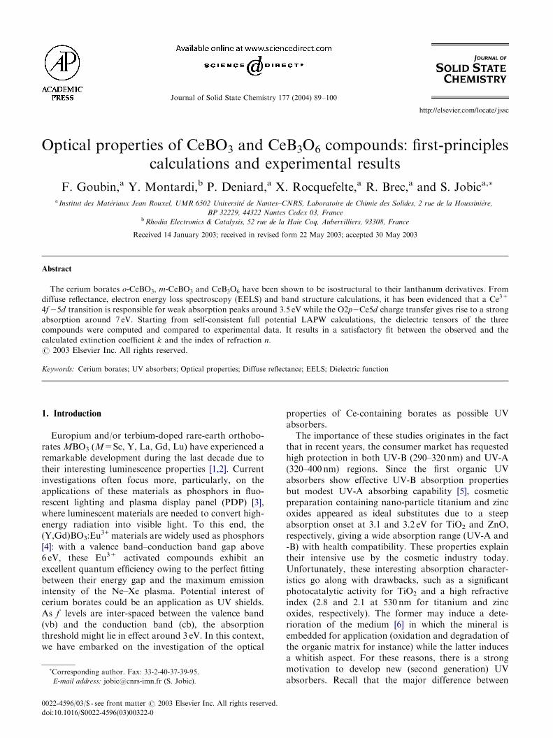
Fig. 1. Diffraction pattern, Rietveld profile and difference pattern of
o-CeBO3 (a), m-CeBO3 (b) and CeB3O6 (c).
F. Goubin et al. / Journal of Solid State Chemistry 177 (2004) 89–10092
resolution. This instrument was equipped with a 150mmdiameter Labsphere integrating sphere and computercontrolled using the UV Winlab software. The reflec-tance vs. wavelength measurements were made in the200–700 nm range (i.e., from 2.07 to 6.20 eV) with aSpectralons sample as reference (100% reflectance).
The absorption ðK=SÞ data were calculated from thereflectance spectra using the K=S ¼ ð12RÞ2=2R
Kubelka-Munk function where RðlÞ; KðlÞ and SðlÞare the reflectance, the absorption coefficient and thescattering coefficient, respectively. This formula ispractically energy independent for particles larger than5 mm [13] which is below the particle size of the samplesused here. The absorption threshold was taken as theintersection point between the energy axis and the lineextrapolated from the linear portion of the absorptionedge in the K=S vs. E (eV) plot (Fig. 2). Due to its colorheterogeneity, the optical properties of m-CeBO3 werenot measured. The Gaussian deconvolution of thediffuse reflectance spectra were carried out with OriginMicrocal Software.
2.5. Electron energy loss spectroscopy (EELS)
EELS characterization of the powders were carriedout at the RHODIA’s Aubervilliers Research Center ona transmission electron microscope (TEM) Philips CM30, LaB6 gun, coupled with a GATAN 666 spectrometercontrolled through ELP3 software. EELS experimentshad two different objectives. First, boron K-edgeelectron loss near edge structure (ELNES) fingerprint(Fig. 3) has proven to be a very rapid and efficient wayto identify the boron’s environment (trigonal or tetra-hedral) in the past [14]. The technique helps thestructural characterization of the phases and permitsthe identification of phase impurities in the powder.Even when not detectable by XRD because of very lowconcentration, phase impurities may be found in TEManalysis. Checking the B-K ELNES fingerprint ensuresthat EELS optical constant measurements were per-formed on the correct phase. Second, EELS was used toderive the optical constant of the phases. Then, theTEM was operated at 100 kV, with an unsaturatedbeam, in order to optimize the spectral resolution. AnFWHM of 0.8 eV is routinely achieved in theseconditions. We used the image-coupling mode, wherethe diffraction pattern is sent in the aperture of thespectrometer. The following parameters were used:entrance aperture diameter 2mm, energy dispersion0.1 eV and acquisition time below 500ms. Acquisition ofspectra was made in nano probe mode on a 10–20 nmarea. Electron diffraction pattern was qualitatively usedto select thin area and avoid crystals which orientationcorresponded to a simple crystallographic axis parallelto the electron beam. The convergence angle (3.5mrad)was high enough to make the analysis non-orientationdependent. Eight spectra were acquired, aligned andsummed together. The acquisition and comparison ofspectra translated on the photodiode array made itpossible to insure that the low intensity feature on thespectra in the energy range 2–5 eV are not due to a‘‘ghost’’ or remnant effect after exposing the photodiode

ARTICLE IN PRESS
2.0 2.5 3.0 3.5 4.0 4.5 5.0 5.5 6.0
K/S
(a.
u.)
Energy (eV)
2.5 3.0 3.5 4.0 4.5 5.0 5.5 6.0 6.5
K/S
(a.
u.)
Energy (eV)(a) (b)
Fig. 2. Kubelka–Munk function versus energy and Gaussian deconvolution in the 2–6.2 eV range for o-CeBO3 (a) and CeB3O6 (b).
190 200 210 220 2300
200
400
600
800
1000
1200
Inte
nsit
y (a
.u.)
Energy loss (eV)
o-CeBO3
CeB3O6
h-SmBO3
Fig. 3. Boron K-edge electron loss near edge structure (ELNES) for
hexagonal SmBO3, o-CeBO3 and CeB3O6.
F. Goubin et al. / Journal of Solid State Chemistry 177 (2004) 89–100 93
array with a zero loss high intensity peak, a problemthat the GATAN 666 spectrometer is sensitive to.Classically, the treatment of the spectra followed four
steps: (i) extraction of data and deconvolution ofmultiple diffusion effects; (ii) correction for acquisitionparameters (convergence and collection angles); (iii)normalization using ‘‘no’’ refractive index extrapolatedto low energy (1.65 is used for borates); (iv) Kramers–Kronig analysis using the numerical integration method.The mathematics behind steps 2 and 3 have beendescribed in detail in Egerton [15] and Montardi et al.[16]. We will insist here on the first step of the procedurewhich is the most important for insuring reliability ofresults. Most of the procedures used rely on themodeling of the zero loss peak using Gaussian andLorenztian components and in removing this modelfrom the raw spectrum. The experience we have with ourequipment is that this method strongly underestimatesthe high energy part of the elastic peak, conducing in anoverestimation of the intensity of the low energy part ofImð�1=eÞ: This effect, detectable below 10 eV, strongly
influences the results below 5 eV. The procedure alsogenerates artifacts in the 0–3 eV region. To overcomethis problem we separated this procedure into two steps.First, we extract the relevant information from the rawspectrum using a modeling of the high energy side of thezero loss using the A:e�r power law imbedded in theELP software for background subtraction. The energywindow (1 eV) used for the modeling was placed belowthe optical gap for the product. Various data can beused for that: known gap, powder color, diffusereflection measurements, etc. The precise position istested for minimum artifact and the useful signal is thenretrieved using the ‘‘background subtraction’’ functionin the ELP program. Second, we computed a model ofthe zero loss peak using the computed thickness functionin ELP: a composite spectrum was then built by addingthe Zero Loss peak model with the extracted data. Thebehavior of this spectrum in ELP’s Fourier ratiodeconvolution procedure to obtain the imaginary partof the dielectric function Imð�1=eÞ gave good results.At the end, since the loss function is a causal response,
the real part of the dielectric function can be calculatedfrom the imaginary part with the Kramers–Kronigrelation:
Re1
eðEÞ
� �¼ 1� 2
pP
ZN
0
Im�1eðEÞ
� �E0
E 02 � E2dE0;
where P is the principal part of the Cauchy integral. Thecomplex dielectric function e ¼ e1 þ ie2 and the complexrefractive index N ¼ n þ ik (with n the refractive indexand k the extinction coefficient) were calculated,according to e1 ¼ n22k2 and e2 ¼ 2nk (cf. Fig. 4).
2.6. Band structure calculations
The full-potential linearized augmented plane wave(FP-LAPW) method implemented in the WIEN2K code[17] was used for band structure calculations. In theLAPW method, the unit cell is divided into two types of

ARTICLE IN PRESS
2 4 6 8 10 12 14 160.0
0.2
0.4
0.6
0.8
1.0
extin
ctio
n co
effi
cien
t k
E (eV)
CeBO 3
CeB3 6O
Fig. 4. Extinction coefficient versus energy in the 2–16 eV range for o-
CeBO3 and CeB3O6.
0 20 40
-10
-5
0
5
10
15
0 5 10 0 10 20 0 1 2
all
Ene
rgy
(eV
)
Ce O B
Fig. 5. Total density of state (DOS) and DOS projected along the
different elements for o-CeBO3.
0 8 16
-10
-5
0
5
10
15
0 2 4 0 4 8 0.0 0.4 0.8
all
Ene
rgy
(eV
)
Ce O B
Fig. 6. Total density of state (DOS) and DOS projected along the
different elements for m-CeBO3.
0 20 40
-10
-5
0
5
10
15
0 5 10 0 10 20 0 2 4
all
Ene
rgy
(eV
)
Ce O B
Fig. 7. Total density of state (DOS) and DOS projected along the
different elements for CeB3O6.
F. Goubin et al. / Journal of Solid State Chemistry 177 (2004) 89–10094
regions, the atomic spheres centered upon nuclear sitesand the interstitial region between the non-overlappingspheres. Inside the atomic spheres, the wave functionsare replaced by atomic-like functions while in theinterspheres region, the wave function of a Bloch stateis expanded in plane waves. The exchange and correla-tion effects were treated within the density functionaltheory (DFT) using the Perdew–Burke–Ernzerhof gen-eralized gradient approximation (GGA) [18]. Themaximum l value in the expansion of the basis set insidethe atomic sphere was 12 for the computation of muffin-tin matrix and 4 for the non-muffin-tin matrix element.The convergence of the basis set was controlled by acutoff parameter Rmt Kmax ¼ 6 where Rmt is thesmallest atomic sphere radius in the unit cell and Kmax
is the magnitude of the largest k vector. The self-consistency was carried out on a 12, 24 and 10 k-pointsin the irreducible Brillouin zone for o-, m-CeBO3 andCeB3O6 respectively, with the following radii
RmtðCeÞ ¼ 2:4 a:u:; RmtðOÞ ¼RmtðBÞ ¼ 1:23 a:u: andGMAX=14Bohr�1(Figs. 5–7).The dielectric function of an anisotropic material is a
complex symmetric second-order tensor which describesthe linear response of an electronic system to an appliedexternal electric field. The imaginary part of thedielectric tensor is directly related to the electronic bandstructure of a solid, so it can be computed from theknowledge of single-particle orbitals and energiesapproximated by the solutions of the Kohn–Shamequations. However, it is a well known fact that DFTcalculations underestimate the band gap. To take thisinto account, a ‘‘scissors operator’’ was used, allowing ashift of the bands situated above the valence band anda rescaling of the matrix elements [19,20]. Hence,assuming the one-electron, rigid band approximation,neglecting electron polarization effects (Koopmans’approximation) and in the limit of linear optics andof the visible–ultraviolet region, the imaginary part
ARTICLE IN PRESS
0 10 20 300
1
2
0 10 20 300.0
0.5
1.0
1.5
0 10 20 300
1
2
3
4
5
refr
activ
e in
dex
n
Energy (eV)
mesured calculated
extin
ctio
n co
effic
ient
k
mesured calculated
Im(ε
)
measured calculatedO2p→Ce5d Ce5p →5d
Ce4f-5d
(a)
(b)
(c)
Fig. 8. Measured and calculated isotropic imaginary part of the
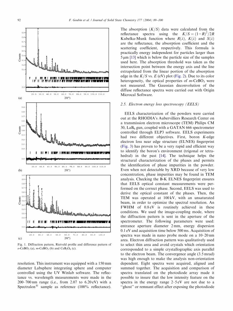
F. Goubin et al. / Journal of Solid State Chemistry 177 (2004) 89–100 95
of a matrix element of the dielectric tensor eab isgiven by [21,22]:
Im eabðoÞ ¼4p2e2
m2ðo� DC=hÞ2Xi;f
ZBZ
2 dk3
ð2p2Þ
ikjpbjfk
� �ikjpajikh i
dðEf ðkÞ þ DC � EiðkÞ � _oÞ
for a vertical transition from a filled initial state ikj i ofenergy EiðkÞ to an empty final state fkj i of energy Ef ðkÞ;with wave vector k: DC is the shifting value of thescissors operator, o the frequency of the incident wave,e the electron charge, m the free electron mass and pa isthe Cartesian components of the momentum operator.As mentioned before, the real and the imaginary partsare linked by a Kramers–Kronig transformation. This isused to obtain the real part e1ðoÞ; a Lorentzianbroadening of 0.05 eV being used. In order to getthe isotropic dielectric function, the componentsof the matrix trace were averaged (i.e., eiso ¼1=3ðexx þ eyy þ ezzÞ). The complex refractive index wasthus calculated with the formulas given above. Fordielectric tensor calculation, the BZ integration wasmade with 60, 108 and 54 independent k-points for o-,m-CeBO3 and CeB3O6, respectively. Finer k-point gridsdid not modify the dielectric tensor values. Moreover,since localized 4f electrons are treated as delocalized onein the Wien code and as no Hubbard term (on-siteelectron repulsion energy) was taken into account forthe dielectric tensor calculation, f2f and O2p2Ce4f
transition contributions, not observed experimentally,were calculated separately and subsequently subtractedfrom the imaginary part of the dielectric function beforea Kramer–Kronig transformation (Figs. 8–10).
dielectric function (a), with Ce 4f-5d, Ce 5p-5d and O2p-Ce5d
transitions contributions, extinction coefficient k (b) and refractive
index n (c) in the 0–35 eV range, for o-CeBO3.
3. Results and discussion3.1. Structural aspects
(a) CeBO3 allotropes: m-CeBO3 and o-CeBO3 crystal-lize in the known H–LaBO3 [23] and aragonite [8]structure types, respectively. The two varieties exhibitthree-dimensional structures built upon [CeO9] polyhe-dra and [BO3] planar triangles. In m-CeBO3, a ceriumpolyhedra is surrounded by ten [CeO9] congenerssharing eight edges and two corners, and by six [BO3]units sharing three edges and three corners. In o-CeBO3,[CeO9] building blocks share six corners and six edgeswith 12 adjacent [CeO9] polyhedra, and three cornersand three edges with six [BO3] triangles. For the twostructures, the Ce–O and B–O distances turn out to besimilar (Table 3) ranging from 2.44(2) to 2.748(11) A,and from 1.32(3) to 1.38(5) A for m-CeBO3(Ce2O=2.588 A, B2O=1.34 A), and from 2.396(18)to 2.720(6) A, and from 1.35(3) to 1.46(6) A for o-CeBO3
(Ce2O=2.566 A, B2O=1.39 A). These distances, al-most identical to those observed in the lanthanumderivatives [8,23], agree well with the sum of theassociated ionic radii ðRðCe3þIX ÞÞ ¼ 1:196 A,ðRðB3þIII ÞÞ ¼ 0:01 A, ðRðO2�
IV ÞÞ ¼ 1:38 A) [24] and withthe charge balance Ce3+B3+O2�3 . Nevertheless, in spiteof similar building entities, the difference in theirstructural arrangement leads to a volume per formulaunit significantly different, that are 63.15(9) A3 and60.469(10) A3 for the monoclinic and the orthorhombicforms, respectively, associated to density values of 5.26and 5.46 (4.4% difference). These values perfectly matchthe measured densities, 5.16 and 5.41, respectively (4.8%difference).The DSC curve for m-CeBO3 exhibits an exothermic
reaction peak at 721�C which corresponds to thetransformation of the low temperature form into thehigh temperature form, i.e., the transition m-CeBO3-
ARTICLE IN PRESS
0 10 20 300
1
2
0 10 20 300.0
0.5
1.0
1.5
0 10 20 300
1
2
3
4
5
refr
activ
e in
dex
n
Energy (eV)
mesured calculated
extin
ctio
n co
effic
ient
k
mesured calculated
Im(ε
)measured calculatedO2p→Ce5d Ce5p →5d
Ce4f-5d
(a)
(b)
(c)
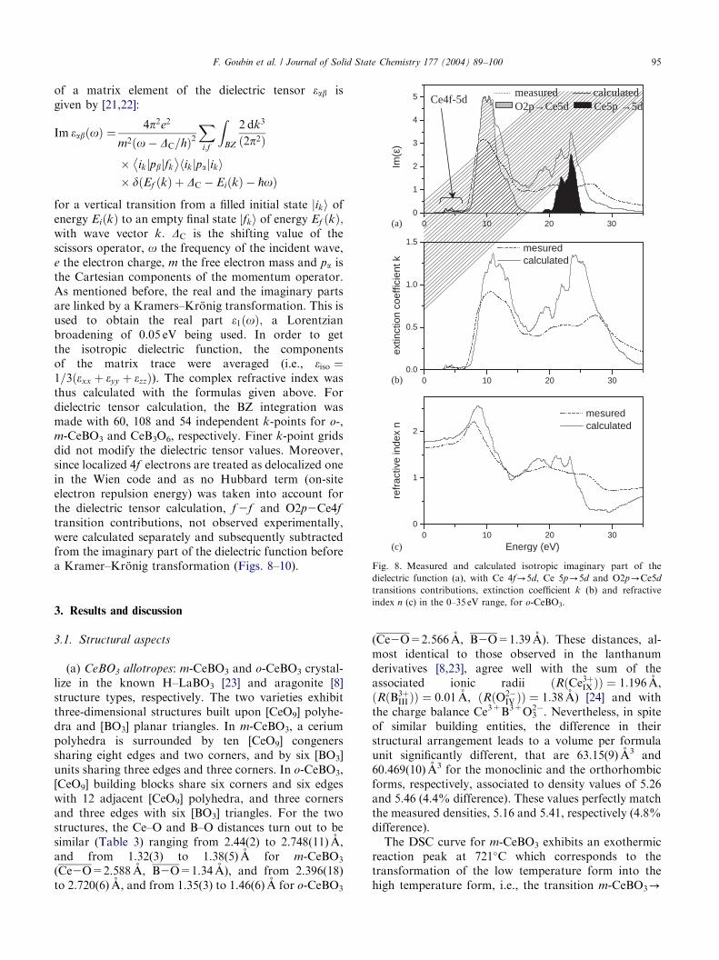
Fig. 9. Same as Fig. 8 (without measured spectrum) for m-CeBO3.
0 10 20 300
1
2
0 10 20 300.0
0.5
1.0
1.5
0 10 300
1
2
3
4
5
refr
activ
e in
dex
n
Energy (eV)
mesured calculated
extin
ctio
n co
effic
ient
k
mesured calculated
Im(ε
)
measured calculatedO2p→Ce5d Ce5p →5d
Ce4f-5d
20(a)
(b)
(c)
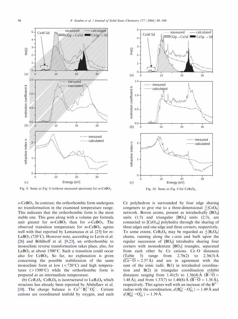
Fig. 10. Same as Fig. 8 for CeB3O6.
F. Goubin et al. / Journal of Solid State Chemistry 177 (2004) 89–10096
o-CeBO3. In contrast, the orthorhombic form undergoesno transformation in the examined temperature range.This indicates that the orthorhombic form is the moststable one. This goes along with a volume per formulaunit greater for m-CeBO3 than for o-CeBO3. Theobserved transition temperature for m-CeBO3 agreeswell with that reported by Lemanceau et al. [25] for m-LaBO3 (720
�C). However note, according to Levin et al.[26] and Bohlhoff et al. [9,23], an orthorhombic tomonoclinic reverse transformation takes place, also, forLaBO3 at about 1500
�C. Such a transition could occuralso for CeBO3. So far, no explanation is givenconcerning the possible stabilization of the samemonoclinic form at low (o720�C) and high tempera-tures (41500�C) while the orthorhombic form isprepared at an intermediate temperature.(b) CeB3O6: CeB3O6 is isostructural to LaB3O6 which
structure has already been reported by Abdullaev et al.[10]. The charge balance is Ce3+B3
3+O2�6 . Ceriumcations are coordinated tenfold by oxygen, and each
Ce polyhedron is surrounded by four edge sharingcongeners to give rise to a three-dimensional 3
N½CeO6�
network. Boron atoms, present as tetrahedrally [BO4]units (1/3) and triangular [BO3] units (2/3), areconnected to [CeO10] polyhedra through the sharing ofthree edges and one edge and three corners, respectively.To some extent, CeB3O6 may be regarded as
1N½B3O6�
chains, running along the c-axis and built upon theregular succession of [BO4] tetrahedra sharing fourcorners with monodentate [BO3] triangles, separatedfrom each other by Ce cations. Ce–O distances(Table 3) range from 2.76(2) to 2.36(3) A(Ce2O ¼ 2:57 A) and are in agreement with thesum of the ionic radii. B(1) in tetrahedral coordina-tion and B(2) in triangular coordination exhibitdistances ranging from 1.41(5) to 1.56(4) A (B2O ¼1:48 A), and from 1.37(7) to 1.40(8) A (B2O ¼ 1:38 A),respectively. This agrees well with an increase of the B3+
radius with the coordination, dðB3þIV2O2�IV Þ ¼ 1:49 A and
dðB3þIII2O2�IV Þ ¼ 1:39 A.

ARTICLE IN PRESS
Table 3
Interatomic distances (A) and, between bracket, corresponding standard uncertainties
o-CeBO3 m-CeBO3 CeB3O6
CeO9 site CeO9 site CeO10 site
Ce–O1 2.396(2) ( 1) Ce–O2 2.44(2) ( 2) Ce–O3 2.36(3) ( 2)Ce–O2 2.459(12) ( 2) Ce–O1 2.46(2) ( 1) Ce–O3 2.49(4) ( 2)Ce–O2 2.563(14) ( 2) Ce–O2 2.532(19) ( 2) Ce–O2 2.61(2) ( 2)Ce–O2 2.609(14) ( 2) Ce–O2 2.697(16) ( 2) Ce–O1 2.631(16) ( 2)Ce–O1 2.720(6) ( 2) Ce–O1 2.748(11) ( 2) Ce–O1 2.76(2) ( 2)
Ce2O 2.566(12) Ce2O 2.588(17) Ce2O 2.57(3)
BO3 site BO3 site BO3 site
B–O2 1.35(3) ( 2) B–O2 1.32(3) ( 2) B2–O3 1.37(7) ( 1)B–O1 1.46(6) ( 1) B–O1 1.38(5) ( 1) B2–O2 1.38(4) ( 1)
B2–O1 1.40(8) ( 1)B2O 1.39(4) B2O 1.34(4)
B2O 1.38(6)
BO4 site
B1–O1 1.41(5) ( 2)B1–O2 1.56(4) ( 2)
B � O 1.48(4)
Note: In italic, average distances ( 1 and 2 indicate the number of equivalent bond distances).
Table 4
Ce 4f–5d diffuse reflectance peaks maxima (eV) for o-CeBO3 and
CeB3O6
CeBO3 CeB3O6
This work Ref. [28] This work Ref. [28]
3.74 3.75 3.78
4.56 4.66 4.37 4.59
5.10 5.15 4.56 4.77
5.34 5.34 5.01 5.04
5.71 5.77 5.66
6.29 6.08
F. Goubin et al. / Journal of Solid State Chemistry 177 (2004) 89–100 97
3.2. Boron-K ELNES characterization
Typical Boron K-edge ELNES spectra of hexagonalSmBO3 [27] and o-CeBO3 are presented in Fig. 3. Themajor difference between the two phases lies in theboron coordination, SmBO3 containing [BO4] buildingblocks while o-CeBO3 contains only [BO3] triangles. Inspite of the proximity of intense Sm–N4.5 or Ce–N4.5peak, the B K-edge beginning at B190 eV is easilyvisible. The B K-edge fine structure in these compoundscan be compared with the reference spectra for B2O3 orBPO4 [14]. BO3 plane trigonal configuration in o-CeBO3is characterized by a first sharp peak at 192 eV followedby a large peak at 205 eV. This fine structure is verysimilar to that of the carbon K-edge fine structure incarbonate where C is surrounded also by 3 oxygenatoms in a plane. In contrast, tetragonal BO4 config-uration in hexagonal SmBO3 is characterized by a singlebroad peak extending from 195 to 205 eV wheredifferent structures can be seen. For CeB3O6 the finestructure presents features characteristic of BO3 andBO4 configurations, which is in agreement with themixed (trigonal/tetragonal) environment of boron atomsas shown by the XRD structural study. Thus ELNESappears as an appropriate technique to probe the boronenvironment.
3.3. Optical properties
The diffuse reflectance spectra (Kubelka–Munktransformed) of o-CeBO3 and CeB3O6 (Fig. 2) can be
viewed as containing five Gaussian-like absorptionbands in the [3–6.5] eV range (Table 4). Due to theirshape and location in energy, these bands can beassigned to 4f25d electronic transitions (see below).The vb to cb charge transfer occurring at energies higherthan 6.5 eV (cf. Section 1) is then not visible on thesespectra.The positions in energy of the absorption bands of o-
CeBO3 agree well with those previously reported for acerium doped lanthanum orthoborate, o-LaBO3:Ce [28](Table 4). This indicates that the local Ce chemicalenvironment is the same in the LaBO3 host lattice as it isin pure o-CeBO3. This absence of the chromatic effectcan be explained in terms of a crystal relaxation aroundCe3+ as already observed for the Y1�xCexPS4 solidsolution (same ionic radius of Y3+ and La3+, 1.06 A,and Ce3+ radius of 1.22 A) [29]. In contrast, our resultsfor CeB3O6 do not match those reported by Dorenbos
ARTICLE IN PRESSF. Goubin et al. / Journal of Solid State Chemistry 177 (2004) 89–10098
et al. [28,30] and Knittel et al. [31] for LaB3O6:Ce3+.
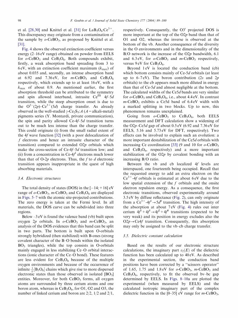
This discrepancy may originate from a contamination ofthe sample by o-CeBO3, as proposed by Knittel et al.[31].Fig. 4 shows the observed extinction coefficient versus
energy (2–16 eV range) obtained on powder from EELSfor o-CeBO3 and CeB3O6. Both compounds exhibit,firstly, a weak absorption band spreading from 3 to6 eV, with an extinction coefficient maximum (kmax) ofabout 0.035 and, secondly, an intense absorption bandat 6.92 and 7.36 eV, for m-CeBO3 and CeB3O6respectively, which extends up to at least 16 eV, with akmax of about 0.9. As mentioned earlier, the firstabsorption threshold can be attributed to the symmetryand spin allowed interband, intrasite CeIII 4f–5d
transition, while the steep absorption onset is due tothe O2�(2p)–Ce3+(5d) charge transfer. As alreadyobserved in the well-studied g-Ce2S3:A (A=alkali-metal)pigments series (Y. Montardi, private communication),the spin and parity allowed Ce-4f–5d transition turnsout to be much less intense than the charge transfer.This could originate (i) from the small radial extent ofthe 4f wave function [32] (with a poor delocalization off electrons and hence an intrasite character of thetransition) compared to extended O2p orbitals whichmake the cross-section of Ce-4f–5d transition low; and(ii) from a concentration in Ce-4f1 electrons much lowerthan that of O-2p electrons. Thus, the f to d electronictransition appears inappropriate in the quest of highabsorbing materials.
3.4. Electronic structures
The total density of states (DOS) in the [�14;+16] eVrange of o-CeBO3, m-CeBO3 and CeB3O6 are displayedin Figs. 5–7 with the atomic site-projected contributions.The zero energy is taken at the Fermi level. In allmaterials, the DOS curve can be subdivided into threeregions.Below –3 eV is found the valence band (vb) built upon
oxygen 2p orbitals. In o-CeBO3 and m-CeBO3, ananalysis of the DOS evidences that this band can be splitin two parts. The bottom is built upon O-orbitalsstrongly hybridized (then stabilized) with B-ones (strongcovalent character of the B–O bonds within the isolatedBO3 triangles), while the top consists in O-orbitalsmainly engaged in less stabilizing Ce–O orbital interac-tions (ionic character of the Ce–O bond). These featuresare less evident for CeB3O6 because of the multipleoxygen environments and because of the occurrence ofinfinite 1
N½B3O6� chains which give rise to more dispersed
electronic states than those observed in isolated [BO3]entities. Moreover, for both CeBO3 forms, all oxygenatoms are surrounded by three cerium atoms and oneboron atom, whereas in CeB3O6, for O1, O2 and O3, thenumber of linked cerium and boron are 2/2, 1/2 and 2/1,
respectively. Consequently, the O30 projected DOS ismore important at the top of the O2p band than that ofO1 and O2, whereas the inverse is observed at thebottom of the vb. Another consequence of the diversityin the O environments and in the dimensionality of theB/O network is the increase of the O2p bandwidth, 6.1and 6.3 eV, for o-CeBO3 and m-CeBO3 respectively,versus 9 eV for CeB3O6.Beyond 1 eV is located the conduction band (cb)
which bottom consists mainly of Ce-5d orbitals (at leastup to 6–7 eV). The boron contribution (2s and 2p
orbitals) to the cb appears much more diluted in energythan that of Ce-5d and almost negligible at the bottom.The calculated widths of the Ce5d bands are very similarfor o-CeBO3 and CeB3O6, i.e., about 4.4 eV. In contrastm-CeBO3 exhibits a Ce5d band of 6.4 eV width witha marked splitting in two blocks. Up to now, thisphenomenon remains unexplained.Going from o-CeBO3 to CeB3O6, both EELS
measurement and DFT calculation show a widening ofthe O2p–Ce5d gap of about 0.5 eV (6.92 and 7.36 eV forEELS, 5.16 and 5.73 eV for DFT, respectively). Twoeffects can be involved to explain such an evolution: amore important destabilization of the Ce5d orbitals withincreasing Ce coordination [33] (9 and 10 for o-CeBO3and CeB3O6, respectively) and a more importantstabilization of the O2p by covalent bonding with anincreasing B/O ratio.Between the vb and cb localized 4f levels are
interspaced, one fourteenth being occupied. Recall thatthe requested energy to add an extra electron on theCe3+-4f orbitals is estimated at about 6 eV due to thelow spatial extension of the f orbitals and the onsiteelectron repulsion energy. As a consequence, the firstelectronic transitions, observed experimentally around3.5 eV by diffuse reflectance (Fig. 2), can only originatefrom a Ce3+-4f1-5d0 transition. The high intensity ofthe absorption at about 7 eV (Fig. 4) rules out intercerium 4f1+4f1-4f2+4f0 transitions (expected to bevery weak) and its position in energy excludes also theO2p-Ce4f transition. Consequently, this absorptionmay only be assigned to the vb–cb charge transfer.
3.5. Dielectric constant calculation
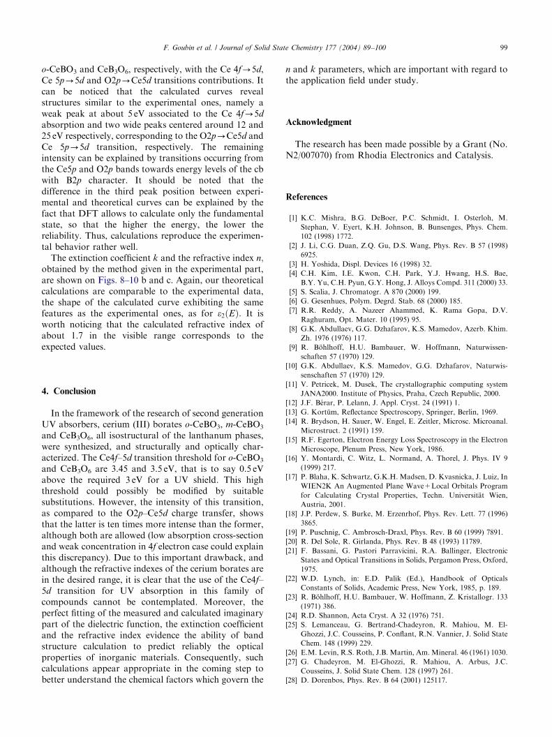
Based on the results of our electronic structurecalculations, the imaginary part e2ðEÞ of the dielectricfunction has been calculated up to 40 eV. As describedin the experimental section, the conduction bandpositions have been corrected by a ‘‘scissors operator’’of 1.65, 1.75 and 1.8 eV for o-CeBO3, m-CeBO3 andCeB3O6, respectively, to fit the observed bv–bc gapdetermined by EELS. In Figs. 8–10a are plotted theexperimental (when measured by EELS) and thecalculated isotropic imaginary part of the complexdielectric function in the [0–35] eV range for m-CeBO3,
ARTICLE IN PRESSF. Goubin et al. / Journal of Solid State Chemistry 177 (2004) 89–100 99
o-CeBO3 and CeB3O6, respectively, with the Ce 4f-5d,Ce 5p-5d and O2p-Ce5d transitions contributions. Itcan be noticed that the calculated curves revealstructures similar to the experimental ones, namely aweak peak at about 5 eV associated to the Ce 4f-5d
absorption and two wide peaks centered around 12 and25 eV respectively, corresponding to the O2p-Ce5d andCe 5p-5d transition, respectively. The remainingintensity can be explained by transitions occurring fromthe Ce5p and O2p bands towards energy levels of the cbwith B2p character. It should be noted that thedifference in the third peak position between experi-mental and theoretical curves can be explained by thefact that DFT allows to calculate only the fundamentalstate, so that the higher the energy, the lower thereliability. Thus, calculations reproduce the experimen-tal behavior rather well.The extinction coefficient k and the refractive index n;
obtained by the method given in the experimental part,are shown on Figs. 8–10 b and c. Again, our theoreticalcalculations are comparable to the experimental data,the shape of the calculated curve exhibiting the samefeatures as the experimental ones, as for e2ðEÞ: It isworth noticing that the calculated refractive index ofabout 1.7 in the visible range corresponds to theexpected values.
4. Conclusion
In the framework of the research of second generationUV absorbers, cerium (III) borates o-CeBO3, m-CeBO3and CeB3O6, all isostructural of the lanthanum phases,were synthesized, and structurally and optically char-acterized. The Ce4f–5d transition threshold for o-CeBO3and CeB3O6 are 3.45 and 3.5 eV, that is to say 0.5 eVabove the required 3 eV for a UV shield. This highthreshold could possibly be modified by suitablesubstitutions. However, the intensity of this transition,as compared to the O2p–Ce5d charge transfer, showsthat the latter is ten times more intense than the former,although both are allowed (low absorption cross-sectionand weak concentration in 4f electron case could explainthis discrepancy). Due to this important drawback, andalthough the refractive indexes of the cerium borates arein the desired range, it is clear that the use of the Ce4f–
5d transition for UV absorption in this family ofcompounds cannot be contemplated. Moreover, theperfect fitting of the measured and calculated imaginarypart of the dielectric function, the extinction coefficientand the refractive index evidence the ability of bandstructure calculation to predict reliably the opticalproperties of inorganic materials. Consequently, suchcalculations appear appropriate in the coming step tobetter understand the chemical factors which govern the
n and k parameters, which are important with regard tothe application field under study.
Acknowledgment
The research has been made possible by a Grant (No.N2/007070) from Rhodia Electronics and Catalysis.
References
[1] K.C. Mishra, B.G. DeBoer, P.C. Schmidt, I. Osterloh, M.
Stephan, V. Eyert, K.H. Johnson, B. Bunsenges, Phys. Chem.
102 (1998) 1772.
[2] J. Li, C.G. Duan, Z.Q. Gu, D.S. Wang, Phys. Rev. B 57 (1998)
6925.
[3] H. Yoshida, Displ. Devices 16 (1998) 32.
[4] C.H. Kim, I.E. Kwon, C.H. Park, Y.J. Hwang, H.S. Bae,
B.Y. Yu, C.H. Pyun, G.Y. Hong, J. Alloys Compd. 311 (2000) 33.
[5] S. Scalia, J. Chromatogr. A 870 (2000) 199.
[6] G. Gesenhues, Polym. Degrd. Stab. 68 (2000) 185.
[7] R.R. Reddy, A. Nazeer Ahammed, K. Rama Gopa, D.V.
Raghuram, Opt. Mater. 10 (1995) 95.
[8] G.K. Abdullaev, G.G. Dzhafarov, K.S. Mamedov, Azerb. Khim.
Zh. 1976 (1976) 117.
[9] R. Bohlhoff, H.U. Bambauer, W. Hoffmann, Naturwissen-
schaften 57 (1970) 129.
[10] G.K. Abdullaev, K.S. Mamedov, G.G. Dzhafarov, Naturwis-
senschaften 57 (1970) 129.
[11] V. Petricek, M. Dusek, The crystallographic computing system
JANA2000. Institute of Physics, Praha, Czech Republic, 2000.
[12] J.F. Berar, P. Lelann, J. Appl. Cryst. 24 (1991) 1.
[13] G. Kortum, Reflectance Spectroscopy, Springer, Berlin, 1969.
[14] R. Brydson, H. Sauer, W. Engel, E. Zeitler, Microsc. Microanal.
Microstruct. 2 (1991) 159.
[15] R.F. Egerton, Electron Energy Loss Spectroscopy in the Electron
Microscope, Plenum Press, New York, 1986.
[16] Y. Montardi, C. Witz, L. Normand, A. Thorel, J. Phys. IV 9
(1999) 217.
[17] P. Blaha, K. Schwartz, G.K.H. Madsen, D. Kvasnicka, J. Luiz, In
WIEN2K An Augmented Plane Wave+Local Orbitals Program
for Calculating Crystal Properties, Techn. Universitat Wien,
Austria, 2001.
[18] J.P. Perdew, S. Burke, M. Erzenrhof, Phys. Rev. Lett. 77 (1996)
3865.
[19] P. Puschnig, C. Ambrosch-Draxl, Phys. Rev. B 60 (1999) 7891.
[20] R. Del Sole, R. Girlanda, Phys. Rev. B 48 (1993) 11789.
[21] F. Bassani, G. Pastori Parravicini, R.A. Ballinger, Electronic
States and Optical Transitions in Solids, Pergamon Press, Oxford,
1975.
[22] W.D. Lynch, in: E.D. Palik (Ed.), Handbook of Opticals
Constants of Solids, Academic Press, New York, 1985, p. 189.
[23] R. Bohlhoff, H.U. Bambauer, W. Hoffmann, Z. Kristallogr. 133
(1971) 386.
[24] R.D. Shannon, Acta Cryst. A 32 (1976) 751.
[25] S. Lemanceau, G. Bertrand-Chadeyron, R. Mahiou, M. El-
Ghozzi, J.C. Cousseins, P. Conflant, R.N. Vannier, J. Solid State
Chem. 148 (1999) 229.
[26] E.M. Levin, R.S. Roth, J.B. Martin, Am. Mineral. 46 (1961) 1030.
[27] G. Chadeyron, M. El-Ghozzi, R. Mahiou, A. Arbus, J.C.
Cousseins, J. Solid State Chem. 128 (1997) 261.
[28] D. Dorenbos, Phys. Rev. B 64 (2001) 125117.

ARTICLE IN PRESSF. Goubin et al. / Journal of Solid State Chemistry 177 (2004) 89–100100
[29] G. Gauthier, Y. Klur, A. Pourpoint, S. Jobic, G. Ouvrard, R. Brec,
D. Huguenin, P. Macaudiere, Int. J. Inorg. Mater. 2 (2000) 717.
[30] D. Dorenbos, J. Lumin. 91 (2000) 155.
[31] M.J. Knitel, D. Dorenbos, C.W.E. van Eijk, B. Plasteig, B. Viana,
A. Kahn-Harari, D. Vivien, Nucl. Instrum. Methods A 443 (2000)
364.
[32] K.J. Kim, B.N. Harmon, W.D. Lynch, D.D. Koelling, Phys. Rev.
B 44 (1991) 8526.
[33] G. Gauthier, S. Jobic, M. Evain, H.-J. Koo, M.-H. Whangbo,
C. Fouassier, R. Brec, Chem. Mater. 15 (2003) 828.
[34] P. Thompson, D.E. Cox, J.B. Hastings, J. Appl. Cryst. 20
(1987) 79.