Role of vanadium in Ni:Al 2O 3 catalysts for carbon dioxide reforming of methane
Upload
univ-paris5Category
view
1download
0
Charge states and optical transitions of vanadiumin Bi4Ge3O12 identified by MCD and ODMR
B. Briat a,*, A. Watterich b, F. Ramaz a, L. Kov�aacs b, B.C. Forget a,N. Romanov c
a Laboratoire d’Optique Physique, ESPCI, 10 rue Vauquelin, 75231 Paris C�eedex 05, Franceb Research Institute for Solid State Physics and Optics, Hungarian Academy of Sciences, Konkoly-Thege M. �uut 29-33,
1121 Budapest, Hungaryc Ioffe Physico-Technical Institute, Russian Academy of Sciences, Polytekhnicheskaia 26, 194021 St. Petersburg, Russia
Received 31 May 2002; accepted 4 June 2002
Abstract
The spectroscopic properties of V-doped Bi4Ge3O12 have been investigated in detail via several complementary
techniques bringing a series of consistent results. The optical absorption spectrum of annealed samples is strongly
modified under UV-illumination and the initial state can be restored optically with visible light. Optical absorption and
magnetic circular dichroism (MCD) demonstrate that a diamagnetic defect is partly destroyed during UV-illumination
while a paramagnetic one is created. The latter shows a very characteristic S-shaped MCD pattern in the near-IR, which
is readily assigned to the 2E! 2T2 internal transition of tetragonal V4þ centers at the Ge sites. This assignment was
further confirmed by optically detected magnetic resonance (ODMR), via the change of the MCD under microwaves at
35 GHz. The g tensor of V4þ was found to be anisotropic with principal values gjj ¼ 1:81� 0:03 and g? ¼ 1:94� 0:02.Two additional MCD bands in the visible spectral region could be attributed to V4þ via ODMR measurements.
Ionization thresholds for holes (V5þ) and electrons (V4þ) were determined by optical absorption experiments and the
V4þ=5þ donor level was positioned 1.9 eV below the conduction band. The presence of the V4þ=3þ acceptor state in the
forbidden band is also suggested.
� 2002 Elsevier Science B.V. All rights reserved.
PACS: 7820.L; 7850; 7630.M; 4270.G
Keywords: Bismuth germanate; Eulytite; Magnetic circular dichroism; EPR; Photorefractive; Photochromic
1. Introduction
Scintillating crystals have been developed for a
long time as a basic component in detectors [1,2]
for high-energy physics and medical imaging. A
typical example is Bi4Ge3O12 which has becomethe main component of high-resolution positron
emission tomography (PET). Single crystals of
this material can be grown with high quality and
in large sizes. Their transparency range goes ap-
proximately from 300 to 6000 nm.
Another very interesting property of Bi4Ge3O12is the photorefraction. In this material, holographic
Optical Materials 20 (2002) 253–262
www.elsevier.com/locate/optmat
*Corresponding author. Tel.: +33-40794583; fax: +33-
43362395.
E-mail address: [email protected] (B. Briat).
0925-3467/02/$ - see front matter � 2002 Elsevier Science B.V. All rights reserved.
PII: S0925-3467 (02 )00066-6
gratings based on the photorefractive effect have
first been induced at 442 nm in samples doped with
chromium [3]. It was later discovered [4] that
undoped samples present similar properties at
wavelengths shorter than 350 nm. Such short
wavelengths are in particular attractive for pho-tolithographic applications since they afford an
increased resolution. Doping Bi4Ge3O12 with Fe
and Mn leads to an enhanced photorefractive res-
ponse under UV-laser (351 nm) excitation [5].
Photorefraction in bulk crystals implies that at
least one deep level is present in the forbidden
band. Photoexcited charge carriers can be trapped
at the same or at a different level. When it occursat a different level, the absorption spectrum may
change and one refers to photochromism. This
effect has been investigated on Bi4Ge3O12 samples
doped with 3d elements such as iron [6,7], man-
ganese [6,8], cobalt [8,9] and chromium [7,10]. In
all samples the effect is optically and thermally [11]
reversible. In parallel, a number of electron para-
magnetic resonance (EPR) studies were carried out[10,12–18] on the same materials, in order to
specify the site and charge state of the doping ions.
In spite of these efforts, extremely little is known
about the charge transfer paths and the energy
levels implied in the photorefractive and photo-
chromic processes. Certainly, it is hard to make
correlations between broad optical absorption
bands in the ultraviolet–visible-near infrared (UV–VIS-near IR) regions and the EPR spectra of
paramagnetic transition metal defects. In the
present work we overcome this difficulty by
optically detected electron paramagnetic reso-
nance (ODMR) via a change of magnetic circular
dichroism (MCD) under resonance conditions
[19]. Basically, the magnetic field dependence of
MCD signals (saturation curve) is recorded inpresence of microwaves. A dip usually occurs in
this curve when the microwaves energy matches
some Zeeman splitting in the ground state.
ODMR measurements at different wavelengths
allow the tagging of MCD bands with the chemical
and structural information attached to EPR-active
defects while MCD-silent absorption bands con-
cern defects in their diamagnetic state.The ODMR technique is applied to vanadium
doped Bi4Ge3O12 which has not been investigated
before. Besides MCD and ODMR data, we shall
show results illustrating the change of the ab-
sorption spectrum under (or after) various sec-
ondary VIS-illuminations. A tentative model for
recharging processes will finally be presented. We
have already conducted a detailed optical, MCDand EPR study on chromium-doped Bi4Ge3O12[10] while preliminary MCD results have been
presented for samples doped with iron [7], man-
ganese and cobalt [8].
2. Experimental details
2.1. Structure and preparation of crystals
The crystal structure (eulytite) of Bi4Ge3O12belongs to the cubic space group I�443d, with fourchemical formulas in the unit cell. Each Ge4þ ion is
coordinated by four oxygen ions arranged in a
tetrahedron, which is slightly compressed along a
C4 axis of the crystal [17]. The local site symmetryat Ge4þ is D2d. Each Bi
3þ ion is coordinated by six
oxygen ions at a site with C3 symmetry, the
threefold axis being along a [1 1 1] direction of the
cubic cell. In this matrix, vanadium is expected to
occur as Vnþ, either with n ¼ 2� 5 at the Ge site orwith n ¼ 2� 3 at the Bi site. For both sites onemust consider different geometries of equivalent
centers in order to explain certain spectroscopicresults.
Single crystals of Bi4Ge3O12 were grown in
Budapest by the diameter controlled Czochralski
method using Bi2O3 and GeO2 powders. The
presence of impurities such as Al, Si, Te and Fe
was demonstrated earlier [20] in undoped Bi4Ge3-
O12 crystals, at the inclusions and cavities, by en-
ergy dispersive X-ray spectrometry (EDS). For thepresent studies 10�3 mol/mol V2O5 was added to
the melt and the V concentration in the crystal
was about 3:4� 10�4 mol/mol, as determined byatomic absorption spectroscopy besides some
other impurities (Fe, Cr, Mn and Zn) in the range
of 10�5–10�6 mol/mol. The crystal samples were
X-ray oriented, cut and polished.
Because of the photosensitivity of the materialwe had to standardize the initial or reference state:
the samples were annealed for 30 min in air at
254 B. Briat et al. / Optical Materials 20 (2002) 253–262
500 �C and then kept in the dark before furthertreatments. Even freshly grown samples should
have been annealed because they might have been
illuminated accidently. These standardized sam-
ples showed each time the same optical absorption:
hereafter the initial state will be designated as an-nealed.
Crystals were studied in the annealed state and
after/under various illuminations with broadband
and interference filters. Most absorption and
MCD experiments were conducted on a sample of
thickness 1.44 mm with the light propagating
along a [1 1 0] axis. Another thinner sample (1.02
mm) oriented perpendicular to [1 1 1] was also usedfor ODMR experiments.
2.2. Instrumentation
Following the practice of chemists [22,23] MCD
is defined as the differential absorbance DA (or
absorption coefficient Da) presented by a samplefor left (rþ) and right (r�) circularly polarizedlight (CPL) propagating along the direction of an
applied magnetic field B. Right-hand CPL means
that an observer receiving the radiation observes a
clockwise rotation of the electric vector tip in a
plane perpendicular to B. Then the evaluation of
the absorption cross-section of left CPL (right
CPL) for an electronic transition from a ground
state component jii to an excited one jji proceedsvia the evaluation of the quantity jhjjmþjiij2ðjhjjm�jiij2), where m� ¼ ð�i=
ffiffiffi
2p
Þðmx � imyÞ arecomponents of the electric dipole moment opera-
tor.
For MCD measurements the sample was im-
mersed in a liquid He cryostat, at the center of a
superconducting magnet providing B up to 3.2 T
at 1.4 K (pumping on the bath). The light origi-nating from a Triax Jobin Yvon monochromator
was passed through a linear polarizer (Glaze-
brook) and then through an infrasil photoelastic
quarter-wave modulator (PEM, home-made),
whose optical axes were placed at a 45� angle tothe axis of the polarizer, in order to create alter-
natively left and right circularly polarized com-
ponents with high-frequency (�50 kHz). Theintensity of the light beam is further chopped
mechanically at low-frequency (1 kHz). In the
present work we used a photomultiplier in UV–
VIS or a silicon photodetector in the near-IR
range. Two separate lock-in amplifiers then pro-
cess the signal arising from this detector and DA isobtained from the ratio of the high-frequency (Vhf )and low-frequency (Vlf ) outputs as DA ¼ CVhf=Vlf .The sign and absolute value of the constant C can
be determined by placing an optically active sam-
ple along the light path and comparing Vhf=Vlf tothe natural circular dichroism measured for the
same sample on a Jobin Yvon or Jasco commercial
instrument. We currently use an alcoholic solution
of camphorquinone or a crystal of a-nickel sul-phate hexahydrate grown in Paris.ODMR in the Q-bands (�35 GHz) was mea-
sured by monitoring MCD signals versus the
magnetic field strength under microwaves (Gunn
diode, 250 mW at maximum) without any cavity.
The sample was placed near an open end of the 35
GHz waveguide. Once a magnetic resonance was
detected, MCD spectra were eventually taken at
the appropriate magnetic field in the presence orabsence of microwaves, their difference providing
an MCD spectrum of a specific paramagnetic cen-
ter (MCD tagged by EPR). For absorption mea-
surements a Cary 05E Varian spectrometer was
used, from �300 K down to 5 K by means of a
cold finger Oxford helium cryostat. ODMR cali-
brations were made with Sn or Ge doped CdTe
since Sn3þCd and Ge3þCd show a sharp line which is
known from classical EPR [21] to correspond to
g ¼ 2:101 and g ¼ 2:145 respectively.
3. Results and discussion
3.1. Optical absorption and MCD
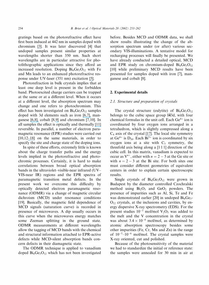
As illustrated in Fig. 1, the optical absorption
spectrum of annealed samples in the UV spectral
region shows a strong shoulder around 3.8 eV,
relatively close to the band gap (4.5 eV at 0 K).
UV-illumination above 3.2 eV, either at 300 K or
at 80 K, with a xenon lamp and a broad band filter
(UG11) covering also the gap region reduces
considerably the magnitude of this band and leadsto the creation of two new shoulders at lower en-
ergies (around 3.5 and 2.8 eV). At �300 K a
B. Briat et al. / Optical Materials 20 (2002) 253–262 255
qualitatively similar result was obtained by usingthe 365 nm (3.4 eV) line of a mercury lamp for 15
min. This demonstrates that band to band excita-
tion is not compulsory for the process to occur.
Another very spectacular effect of our illumina-
tions on Bi4Ge3O12:V is the appearance of a three-
component absorption band in the near-IR region
below 1.8 eV. None of these features occurs in
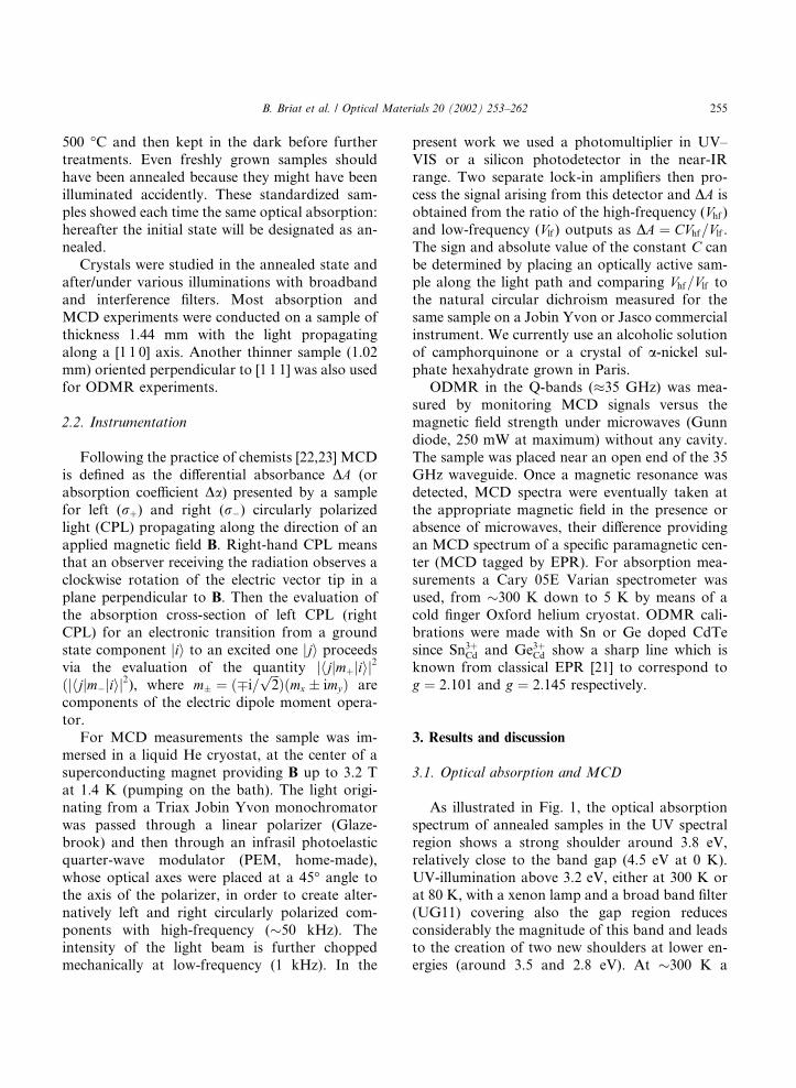
undoped crystals.As shown in Fig. 2, the initial spectrum can be
restored partially with VIS-illumination of suc-
cessively higher energies. Quite clearly the main
features of the difference spectra have signs op-
posite to those found after UV-illumination of the
initial (annealed) sample (Fig. 1). As indicated in
the inset of Fig. 2, the threshold for restoration is
found to be �1.9 eV at �300 K. The kinetics of thebleaching process was followed at 2.73 eV (455
nm) by recording (Fig. 3) the decrease of the ab-
sorbance under a secondary illumination at the
same energy (blue light). A good fit of the data
requires two exponential components, this being
the signature [24] for the participation of (at least)
two deep levels in the charge transfer processes.
Fig. 4 shows the MCD spectra in the visiblespectral region. Above 2.3 eV qualitatively similar
features are observed both in the annealed and
UV-illuminated states. The spectra are dominated
by two strong and broad components (gaussian
shape) peaking around 2.8 eV (Band 1) and 3.5 eV
Fig. 1. Optical absorbance of Bi4Ge3O12:V (thickness 1.44 mm)
at 80 K in the annealed state (a, dotted line) and after UV-
illumination (b, full line). The difference spectrum is shown in
c � a� b (dashed line).
Fig. 2. Optical restoring of the initial absorption at room
temperature. After taking one spectrum after UV-illumination
(a), the sample was illuminated for 20 min with a set of inter-
ference filters at successively higher energies ranging from 1.1 to
2.8 eV, and a new spectrum was taken. Curves b–d illustrate the
differences between each of these spectra and the UV-illumi-
nated one for red (650 nm, 1.8 eV), green (555 nm, 2.23 eV) and
blue (455 nm, 2.73 eV) illuminations respectively. The inset
shows the absorbance modification at 3.85 eV versus the pho-
ton energy of the secondary beam.
Fig. 3. Kinetics of the bleaching process. The absorbance of a
UV-illuminated sample is measured at 455 nm (2.73 eV) with a
weak probe beam of the spectrometer. Once a steady state is
reached (time 0), a more intense pump beam is directed towards
the sample and the decrease of the absorbance is recorded for
30 min (circles). The solid line shows the fit with two expo-
nential functions.
256 B. Briat et al. / Optical Materials 20 (2002) 253–262
(Band 2). They demonstrate the presence of one or
two paramagnetic defects since the MCD of broad
bands gives an insight into the spin polarization in
the ground state [10,23]. We emphasize that the
magnitude of the two components is considerably
smaller (19–25 times) in the annealed as compared
to the UV-illuminated state. No MCD band is
associated with the absorption component (Fig. 1)around 3.8 eV, this proving the diamagnetic
character of the associated defect. Below 2.2 eV we
observe additional weak MCD features in the
annealed state. These are certainly due to Cr4þ
impurities. Comparing the present dichroism
Da ¼ 2:3 DA=l (l is the thickness in cm) with theone measured in [10] for a chromium-doped sam-
ple grown in Madrid, we find that all featuresappear exactly at the same position. The ratio of
intensities is 3:2� 10�3 allowing to deduce chro-mium impurity concentration of 6 ppm (Cr atoms
per 106 host lattice molecules) in the V-doped
sample. In the annealed state we have also ob-
served a relatively sharp negative MCD feature at
2.91 eV (23,500 cm�1) with a vibrational compo-
nent at higher energy (inset of Fig. 4). A com-parison with [7] shows that these MCD signals are
due to a small amount of Fe3þ. In fact chemical
analysis with atomic absorption spectrometry has
also proven (see 2.1) the presence of Cr and Fe
impurities in Bi4Ge3O12:V.
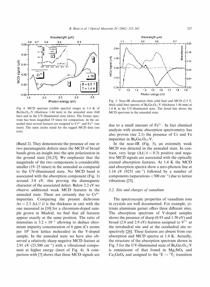
In the near-IR (Fig. 5), an extremely weak
MCD was detected in the annealed state. In con-trast, very large (DA=A � 0:3) positive and nega-tive MCD signals are associated with the optically
created absorption features. At 1.4 K the MCD
and absorption spectra show a zero-phonon line at
1.14 eV (9231 cm�1) followed by a number of
components (separations <300 cm�1) due to lattice
vibrations [25].
3.2. Site and charges of vanadium
The spectroscopic properties of vanadium ions
in crystals are well documented. For example, yt-
trium aluminum garnet offers three different sites.
The absorption spectrum of V-doped samples
shows the presence of sharp (0.93 and 1.50 eV) and
broad (2.0 and 2.9 eV) features assigned to V3þ atthe tetrahedral site and at the octahedral site re-
spectively [26]. These features are absent from our
absorption and MCD spectra at 1.4 K. Actually,
the structure of the absorption spectrum shown in
Fig. 5 for the UV-illuminated state of Bi4Ge3O12:V
is reminiscent of that found in Mg2SiO4 and
Ca2GeO4 and assigned to the2E! 2T2 transition
Fig. 4. MCD spectum (visible spectral range) at 1.4 K of
Bi4Ge3O12:V (thickness 1.44 mm) in the annealed state (full
line) and in the UV-illuminated state (dots). The former spec-
trum has been magnified 19 times for comparison. In the an-
nealed state several features are assigned to Cr4þ and Fe3þ (see
inset). The open circles stand for the tagged MCD data (see
text).
Fig. 5. Near-IR absorption (thin solid line) and MCD (2.5 T,
thick solid line) spectra of Bi4Ge3O12:V (thickness 1.44 mm) at
1.4 K in the UV-illuminated state. The doted line shows the
MCD spectrum in the annealed state.
B. Briat et al. / Optical Materials 20 (2002) 253–262 257
of paramagnetic V4þ at a distorted tetrahedral site
[27]. We shall now provide additional evidence
that the presence of a V4þ=5þ level within the for-
bidden band is responsible for the gross features
observed in our absorption and MCD spectra.
3.3. Magnetic properties of the vanadium defects
At an early stage of this study EPR measure-
ments were carried out at a few temperatures down
to 20 K. Unfortunately, an EPR signal was found
neither in the annealed nor in the UV-illuminated
state. The lack of any kind of paramagnetic V
signal was puzzling. A possible cause was firstthought to be the usually very broad EPR line
width in doped Bi4Ge3O12 crystals. Additionally,51V (abundance 99.75%) has a nuclear spin I ¼7=2, therefore a splitting with eight lines was ex-pected due to the hyperfine interaction of the
electron with the V nucleus, this reducing further
the line intensities. The EPR signal could also be
quenched above a certain temperature, due to astrong vibronic coupling in the 2E ground state of
V4þ. Finally, it was also possible that the EPR
signal was fully saturated, even at 20 K.
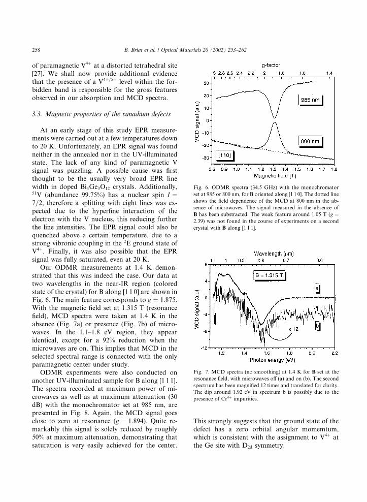
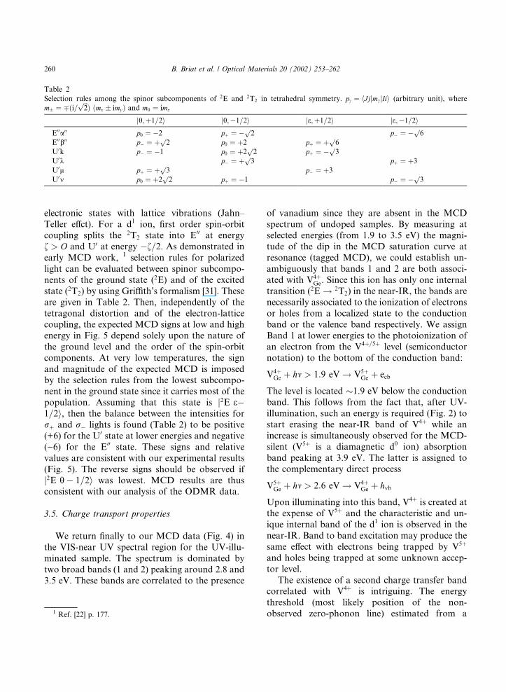
Our ODMR measurements at 1.4 K demon-
strated that this was indeed the case. Our data at
two wavelengths in the near-IR region (colored
state of the crystal) for B along [1 1 0] are shown in
Fig. 6. The main feature corresponds to g ¼ 1:875.With the magnetic field set at 1.315 T (resonance
field), MCD spectra were taken at 1.4 K in the
absence (Fig. 7a) or presence (Fig. 7b) of micro-
waves. In the 1.1–1.8 eV region, they appear
identical, except for a 92% reduction when the
microwaves are on. This implies that MCD in the
selected spectral range is connected with the only
paramagnetic center under study.ODMR experiments were also conducted on
another UV-illuminated sample for B along [1 1 1].
The spectra recorded at maximum power of mi-
crowaves as well as at maximum attenuation (30
dB) with the monochromator set at 985 nm, are
presented in Fig. 8. Again, the MCD signal goes
close to zero at resonance (g ¼ 1:894). Quite re-markably this signal is solely reduced by roughly50% at maximum attenuation, demonstrating that
saturation is very easily achieved for the center.
This strongly suggests that the ground state of the
defect has a zero orbital angular momemtum,
which is consistent with the assignment to V4þ at
the Ge site with D2d symmetry.
Fig. 6. ODMR spectra (34.5 GHz) with the monochromator
set at 985 or 800 nm, for B oriented along [1 1 0]. The dotted line
shows the field dependence of the MCD at 800 nm in the ab-
sence of microwaves. The signal measured in the absence of
B has been substracted. The weak feature around 1.05 T (g ¼2:39) was not found in the course of experiments on a second
crystal with B along [1 1 1].
Fig. 7. MCD spectra (no smoothing) at 1.4 K for B set at the
resonance field, with microwaves off (a) and on (b). The second
spectrum has been magnified 12 times and translated for clarity.
The dip around 1.92 eV in spectrum b is possibly due to the
presence of Cr4þ impurities.
258 B. Briat et al. / Optical Materials 20 (2002) 253–262
Table 1 shows the EPR expectations for a te-
tragonal center (D2d site symmetry) when the
magnetic field is oriented along different symmetry
axes of a cubic crystal.
The EPR of V4þ at a fourfold coordinated D2d
site has been investigated in several zircon-type
crystals [26]. gjj and g? differ by less than 0.15 andthey are both smaller than 2. From the expressions
of g3–g5 given in Table 1, we expect that the mainODMR feature for B oriented along [1 1 1] and
[1 1 0] should be only slightly shifted, the latter
being broader than the former and more asym-
metric. Fig. 8 shows that this is indeed the case.
ODMR signals measured at B // [1 1 1] are broad
unresolved lines with the shape which can be fittedby a mixture of gaussian and lorentzian. The line
shape becomes closer to gaussian with a decrease
of the microwave power. The absence of the re-
solved hyperfine structure of vanadium may be
due to the broadening of the hyperfine compo-
nents because of strong saturation and exchange
interactions. The line shape from a record for[1 1 1] was used to fit ODMR spectra measured for
B along [1 1 0]. A good fit was obtained with two
components (1.325 and 1.282 T) with the intensity
ratio 2:1 which is expected (Table 1) for D2d site
symmetry.
Altogether it is unambiguous that UV-illumi-
nation formed V4þGe ions. Our analysis of the two
([1 1 0] and [1 1 1]) ODMR spectra lead to an esti-mate of the principal values of the g tensor:
gjj ¼ 1:81� 0:03 and g? ¼ 1:94� 0:02.
3.4. Spectroscopic model for V 4þ
According to Griffith [29], the 2E ground state
of a d1 ion in Td symmetry breaks up into two
doublets E0 � h and E00 � e under the combinedaction of the tetragonal field and spin-orbit cou-
pling. Under the approximation that orbitals have
a purely metallic character (ligand field theory),
the predictions concerning g-factors are the fol-lowing [29]:
e : gjj ¼ 2� 8x1 and g ?¼ 2� 2x2
h : gjj ¼ 2 and g? ¼ 2� 6x2
x1 ¼ f=E1 and x2 ¼ f=E2. E1 and E2 stand for theenergies of the two orbital components 2B1 and
2E(D2d notations) of the
2T2 manifold (�8500 cm�1
above 2E) and f is the spin-orbit coupling constantfor V4þ (250 cm�1 [30]). Since E1 � E2 � E1ðE2Þ,one predicts g? > gjj for an e ground state, whilethe converse holds for h. Similar results are ex-pected when the dynamic Jahn–Teller effect is ta-
ken into account [28]. Our experimental g-values
therefore demonstrate that je;�1=2i is the lowestground state component.
We return now to the absorption spectrum and
S-shaped MCD spectrum (UV-illuminated state)
shown in Fig. 5. The overall shape of the former
results from the combined effect of spin-orbit
coupling and the tetragonal distortion in the2T2 excited state, as well as the coupling of the
Fig. 8. The thick and thin solid lines show the ODMR signals
(34.5 GHz) observed at maximum microwave power at 985 nm
for B aligned along a [1 1 0] and [1 1 1] axis respectively. For the
sake of comparison, the former spectrum has been translated of
0.015 T towards higher fields. The [1 1 1] signal measured at
maximum attenuation is shown with a dotted line.
Table 1
Expression of the effective g factors for a tetragonal center in a
cubic matrix
B along Effective g value Intensity
[0 0 1] g1 ¼ gjj 1
g2 ¼ g? 2
[1 1 1] g3 ¼ 3�0:5½g2jj þ 2g2?�0:5
3
[1 1 0] g4 ¼ g? 1
g5 ¼ 2�0:5½g2jj þ g2?�0:5
2
B. Briat et al. / Optical Materials 20 (2002) 253–262 259
electronic states with lattice vibrations (Jahn–Teller effct). For a d1 ion, first order spin-orbit
coupling splits the 2T2 state into E00 at energy
f > O and U0 at energy �f=2. As demonstrated inearly MCD work, 1 selection rules for polarized
light can be evaluated between spinor subcompo-
nents of the ground state (2E) and of the excited
state (2T2) by using Griffith’s formalism [31]. These
are given in Table 2. Then, independently of thetetragonal distortion and of the electron-lattice
coupling, the expected MCD signs at low and high
energy in Fig. 5 depend solely upon the nature of
the ground level and the order of the spin-orbit
components. At very low temperatures, the sign
and magnitude of the expected MCD is imposed
by the selection rules from the lowest subcompo-
nent in the ground state since it carries most of thepopulation. Assuming that this state is j2E e�1=2i, then the balance between the intensities forrþ and r� lights is found (Table 2) to be positive
(+6) for the U0 state at lower energies and negative
()6) for the E00 state. These signs and relative
values are consistent with our experimental results
(Fig. 5). The reverse signs should be observed if
j2E h � 1=2i was lowest. MCD results are thusconsistent with our analysis of the ODMR data.
3.5. Charge transport properties
We return finally to our MCD data (Fig. 4) in
the VIS-near UV spectral region for the UV-illu-
minated sample. The spectrum is dominated by
two broad bands (1 and 2) peaking around 2.8 and3.5 eV. These bands are correlated to the presence
of vanadium since they are absent in the MCDspectrum of undoped samples. By measuring at
selected energies (from 1.9 to 3.5 eV) the magni-
tude of the dip in the MCD saturation curve at
resonance (tagged MCD), we could establish un-
ambiguously that bands 1 and 2 are both associ-
ated with V4þGe. Since this ion has only one internal
transition (2E! 2T2) in the near-IR, the bands are
necessarily associated to the ionization of electronsor holes from a localized state to the conduction
band or the valence band respectively. We assign
Band 1 at lower energies to the photoionization of
an electron from the V4þ=5þ level (semiconductor
notation) to the bottom of the conduction band:
V4þGe þ hm > 1:9 eV! V5þGe þ ecbThe level is located �1.9 eV below the conductionband. This follows from the fact that, after UV-
illumination, such an energy is required (Fig. 2) to
start erasing the near-IR band of V4þ while an
increase is simultaneously observed for the MCD-silent (V5þ is a diamagnetic d0 ion) absorption
band peaking at 3.9 eV. The latter is assigned to
the complementary direct process
V5þGe þ hm > 2:6 eV! V4þGe þ hvb
Upon illuminating into this band, V4þ is created at
the expense of V5þ and the characteristic and un-
ique internal band of the d1 ion is observed in the
near-IR. Band to band excitation may produce the
same effect with electrons being trapped by V5þ
and holes being trapped at some unknown accep-
tor level.
The existence of a second charge transfer bandcorrelated with V4þ is intriguing. The energy
threshold (most likely position of the non-
observed zero-phonon line) estimated from a
Table 2
Selection rules among the spinor subcomponents of 2E and 2T2 in tetrahedral symmetry. pc ¼ hJjjmcjIii (arbitrary unit), wherem� ¼ �ði=
ffiffiffi
2p
Þ ðmx � imyÞ and m0 ¼ imz
jh;þ1=2i jh;�1=2i je;þ1=2i je;�1=2iE00a00 p0 ¼ �2 pþ ¼ �p
2 p� ¼ �p6
E00b00 p� ¼ þp2 p0 ¼ þ2 pþ ¼ þp
6
U0k p� ¼ �1 p0 ¼ þ2p2 pþ ¼ �p3
U0k p� ¼ þp3 pþ ¼ þ3
U0l pþ ¼ þp3 p� ¼ þ3
U0m p0 ¼ þ2p2 pþ ¼ �1 p� ¼ �p3
1 Ref. [22] p. 177.
260 B. Briat et al. / Optical Materials 20 (2002) 253–262
gaussian analysis of the MCD curve (Fig. 4) in the
UV-illuminated state is �2.7 eV. Althought thebands structure in Bi4Ge3O12 does not seem to be
known, it is conceivable that this second MCD
band could concern the ionization of an electron
from the V4þ=5þ level to a level located above thebottom of the conduction band. Alternatively, one
can imagine that an acceptor state V4þ=3þ is lo-
cated slightly above the donor state. We note that
the two types of levels are thought to occur in
vanadium-doped silicon carbide [32]. Band 2 in
Fig. 4 would then be assigned to the ionization of
holes from this second level to the VB.
4. Conclusion
A detailed spectroscopic investigation has been
carried out on vanadium-doped Bi4Ge3O12 single
crystals. In annealed samples vanadium is only
present as V5þGe. Under near band gap illumination
holes are ionized to the valence band and V4þGe iscreated. Optical absorption demonstrates strong
photochromism, being reversed under illumination
with visible light, which ionizes electrons from V4þGeto the conduction band. Other valences of V seem
to be absent from our crystals.
As demonstrated by MCD measurements,
paramagnetic V4þGe shows a very characteristic2E! 2T2 internal band in the near-IR. Both thesign and magnitude of the observed features were
found to be consistent with this interpretation.
MCD was also used to detect EPR optically. Ac-
tually, we have a kind of textbook example for
ODMR since the MCD is unusually drastically
reduced (8% remains) at resonance. This means
that the two components of the lowest doublet in
the 2E ground state are almost equally populatedand this explains why we failed to detect conven-
tional EPR signal at 20 K. An analysis of our data
for two directions of the magnetic field leads to
gjj ¼ 1:81� 0:03 and g? ¼ 1:94� 0:02. From theseresults we conclude that e is the lowest tetragonalcomponent in the ground state.
ODMR was also used to tag two charge
transfer transitions in the visible spectral range ofthe UV-illuminated sample with the V4þGe EPR
signals. From a combination of these results and
optical absorption data, the V4þ=5þ donor state
was located �1.9 eV below the conduction band.The presence of the V4þ=3þ acceptor level �2.7 eVabove the valence band is also suggested by our
MCD/ODMR results. Finally, the presence of
minute amounts of Cr4þ and Fe3þ was demon-strated through the high sensitivity of MCD ex-
periments.
Acknowledgements
This research was supported by the National
Science Research Fund OTKA, Hungary (Grant
No. T22859), the French CNRS and the Center of
Excellence Program (Contract No ICA1-1999-75002). L. Kov�aacs and N. Romanov are gratefulto ESPCI and the City of Paris for the award of a
two-months fellowship. Thanks are also due to H.
Bou Rjeily and B. Farid for their participation to
certain experiments and to O. Szak�aacs for atomicabsorption measurements.
References
[1] B.C. Grabmaier, Crystal scintillators, IEEE Trans. Nucl.
Sci. NS-31 (1984) 372.
[2] P. Lecoq, M. Korzhik, Scintillator developments for high
energy physics and medical imaging, IEEE Trans. Nucl.
Sci. 47 (2000) 1311.
[3] E. Moya, L. Contreras, C. Zaldo, Bi4Ge3O12:Cr: a new
photorefractive material, J. Opt. Soc. Am. B 5 (1988) 1737.
[4] G. Montemezzani, St. Pf€aandler, P. G€uunter, Electro-optic
and photorefractive properties of Bi4Ge3O12 crystals in the
ultraviolet spectral range, J. Opt. Soc. Am. B 9 (1992) 1110.
[5] C. Zaldo, E. Moya, L.F. Magana, L. Kov�aacs, K. Polg�aar,
Optically induced gratings in Fe- and Mn-doped
Bi4Ge3O12 single crystals, J. Appl. Phys. 73 (1993) 2114.
[6] L. Kov�aacs, E. Moya, K. Polg�aar, F.J. L�oopez, C. Zaldo,Photochromic behaviour of iron and manganese doped
single crystal scintillators, Appl. Phys. A 52 (1991) 307.
[7] B. Briat, V. Topa, C. Zaldo, Magnetic circular dichroism
and absorption characterization of Cr- or Fe-doped
Bi4Ge3O12, in: O. Kanert, J.M. Spaeth (Eds.), Defects in
Insulating Materials, World Scientific, London, 1993,
p. 1157.
[8] B. Briat, F. Ramaz, A. Hamri and C. Zaldo, MCD and
absorption study of photochromism of Mn and Co ions in
Bi4Ge3O12, in: Proceedings of EURODIM 94. Seventh
Europhysical Conference on Defects in Insulating Crystals,
July 5–8, 1994, Lyon, (abstract only).
B. Briat et al. / Optical Materials 20 (2002) 253–262 261
[9] C. Zaldo, E. Di�eeguez, On the microscopic origin of the
photochromic and photorefractive behaviour of doped
Bi4Ge3O12 single crystals, Opt. Mater. 1 (1992) 171.
[10] E. Moya, C. Zaldo, F.J. L�oopez, B. Briat, V. Topa, Optical,
Magnetooptical and EPR study of Cr impurities in
Bi4Ge3O12, J. Phys. Chem. Solids 54 (1993) 809.
[11] C. Coya, J.L.G. Fierro, C. Zaldo, Thermal reduction of
sillenite and eulytite single crystals, J. Phys. Chem. Solids
58 (1997) 1461.
[12] F.J. Lopez, E. Moya, C. Zaldo, Characterization of
chromium impurities in Bi4Ge3O12:Cr single crystals, Solid
State Com. 76 (1990) 1169.
[13] D. Bravo, L. Arizmendi, M. Aguilar, F.J. L�oopez, An
electron paramagnetic resonance study of Mn-doped
Bi4Ge3O12, J. Phys. C: Condens. Matter 2 (1990) 10123.
[14] D. Bravo, F.J. L�oopez, The fine-structure spin-Hamiltonian
parameters in an electron paramagnetic resonance study of
Mn-doped Bi4Ge3O12, J. Phys.: Condens. Matter 3 (1991)
7691.
[15] D. Bravo, A. Martin, F.J. L�oopez, EPR characterization of
Co impurities doping Bi4Ge3O12 single crystals, Solid State
Com. 86 (1993) 281.
[16] D. Bravo, F.J. L�oopez, Identification of Cr3þ impurities in
heavily Cr-doped Bi4Ge3O12 single crystals, Solid State
Com. 85 (1993) 415.
[17] A. Martin, D. Bravo, E. Di�eeguez, F.J. L�oopez, Electron
paramagnetic resonance of tetrahedral Fe3þ in Bi4Ge3O12single crystals, Phys. Rev. B 54 (1996) 12915.
[18] D. Bravo, F.J. L�oopez, The EPR technique as a tool for theunderstanding of laser systems. The case of Cr3þ and Cr4þ
ions in Bi4Ge3O12, Opt. Mater. 13 (1999) 141.
[19] See e.g., J.M. Spaeth, J.R. Niklas, R.H. Bartam, in:
Structural Analysis of Point Defects in Solids, Springer-
Verlag, 1992.
[20] L. Malicsk�oo, Complex Microscopic Investigations on the
as-grown quality of Bismuth germanate single crystals,
Acta Phys. Hungarica 61 (2) (1987) 227.
[21] G. Brunthaler, W. Jantsch, U. Kaufmann, J. Schneider,
Electron-spin-resonance analysis of the deep donors lead,
tin, and germanium in CdTe, Phys. Rev. B 31 (1985) 1239.
[22] See e.g., the papers by B. Briat, R.G. Denning, A.J.
McCaffery, P.N. Schatz, P.J. Stephens, in: P. Day (Ed.),
Electronic States of Inorganic Compounds: New Experi-
mental Techniques, D. Reidel Publishing Company,
Dordrecht-Holland/Boston-USA, 1975.
[23] S.B. Piepho, P.N. Schatz, Group Theory in Spectroscopy
with Applications to Magnetic Circular Dichroism, John
Wiley&sons, New York, 1983.
[24] K. B€uuse, Light-induced charge transport processes in
photorefractive crystals, Appl. Phys. B 64 (1997) 273.
[25] P. Beneventi, D. Bersani, P.P. Lottici, L. Kov�aacs, ARaman study of Bi4ðGexSi1�xÞ3O12 crystals, Solid StateCom. 93 (1995) 143.
[26] V.P. Mikhailov, N.V. Kuleshov, N.I. Zhavoronkov, P.V.
Prokoshsin, K.V. Yumashev, V.A. Sandulenko, Optical
absorption and nonlinear transmission of tetrahedral V3þ
(d2) in yttrium aluminium garnet, Opt. Mater. 2 (1993) 267.[27] T.C. Brunold, H.U. G€uudel, A. Kaminskii, Optical spec-
troscopy of V4þ doped crystals of Mg2SiO4 and Ca2GeO4,
Chem. Phys. Lett. 271 (1997) 327.
[28] S. Di Gregorio, M. Greenblatt, J.H. Pifer, M.D. Sturge,
An ESR and optical study of V4þ in zircon-type crystals,
J. Chem. Phys. 76 (1982) 2931.
[29] J.S. Griffith, in: The Theory of Transition Metal Ions,
Cambridge University Press, Cambridge, 1961, p. 343.
[30] B.N. Figgis, in: Introduction to Ligand Fields, Inter-
science, New York, 1966, p. 60.
[31] J.S. Griffith, The irreducible tensor method for molecular
symmetry groups, Prentice Hall, Englewood Cliffs, NJ,
1962.
[32] J. Schneider, H.D. M€uuller, K. Maier, W. Wilkening, F.
Fuchs, A. D€oornen, S. Leibenzeder, R. Stein, Infrared spec-
tra and electron spin resonance of vanadium deep level im-
purities in silicon carbide, Appl. Phys. Lett. 56 (1990) 1184.
262 B. Briat et al. / Optical Materials 20 (2002) 253–262
Copyright © 2022 FDOKUMEN