Radiation impedance of an array of circular capacitive micromachined ultrasonic transducers
Upload
khangminh22Category
view
0download
0

AN ABSTRACT OF THE THESIS OF
Jonah M. Gross for the degree of Master of Science in
Electrical and Computer Engineering presented on March 7, 2013.
Title:
Development of Acoustic Transducers for Use in the Parametric Pumping of Spin Waves
Abstract approved:
Pallavi Dhagat
The work detailed here is the development of simulations and fabrication techniques used
for the construction of thin-film acoustic transducers for use in the parametric pumping
of spin waves. The Mason Model, a 1-D equivalent circuit simulating the responses of
multilayer acoustic transducers, is implemented using ABCD-parameters in MATLAB
to determine the expected response from fabricated devices. The simulation is tested by
varying device parameters and comparing the changes in device resonance response to
those of prior published results. Three-layer thin-film acoustic transducers were also fab-
ricated. These transducers use zinc oxide (ZnO) as a piezoelectric layer with aluminum
(Al) electrodes. Construction is accomplished using the common thin-film fabrication
techniques of sputtering, thermal evaporation, etching, and lift-off patterning processes.
The response of the fabricated transducers is compared to that of the simulated response
by observing the transducer’s resonance frequency and characteristics. These results are
used to validate the simulation and the transducer fabrication process. Finally, their use-
fulness for the design and fabrication of an acoustic spin wave amplification system is
considered.

c©Copyright by Jonah M. Gross
March 7, 2013
All Rights Reserved

Development of Acoustic Transducers for Use in the Parametric Pumping of Spin Waves
by
Jonah M. Gross
A THESIS
submitted to
Oregon State University
in partial fulfillment ofthe requirements for the
degree of
Master of Science
Presented March 7, 2013Commencement June 2013
Master of Science thesis of Jonah M. Gross presented on March 7, 2013.
APPROVED:
Major Professor, representing Electrical and Computer Engineering
Director of the School of Electrical Engineering and Computer Science
Dean of the Graduate School
I understand that my thesis will become part of the permanent collection of Oregon State
University libraries. My signature below authorizes release of my thesis to any reader
upon request.
Jonah M. Gross, Author

ACKNOWLEDGMENTS
Most of all, I would like to thank my loving wife, Alice, who has supported me
through this long and difficult process and never let me give up. My entire family also
deserves much thanks; without your love and support I could not have reached this point.
I would also like to extend an acknowledgment to my advisor, Dr. Dhagat, and a
special thanks to a mentor of mine, Dr. Plant, whose contribution to my education, and
countless others at OSU, has been invaluable.
TABLE OF CONTENTS
Page
1. INTRODUCTION . . . . . . . . . . . . . . . . . . . . . . . . . . . . . . . . . . . . . . . . . . . . . . . . . . . . . 1
2. LITERATURE REVIEW . . . . . . . . . . . . . . . . . . . . . . . . . . . . . . . . . . . . . . . . . . . . . . . 3
2.1 Acoustic Transducers . . . . . . . . . . . . . . . . . . . . . . . . . . . . . . . . . . . . . . . . . . . . . . 3
2.1.1 Resonance . . . . . . . . . . . . . . . . . . . . . . . . . . . . . . . . . . . . . . . . . . . . . . . . . . . . 42.1.1.1 Resonators . . . . . . . . . . . . . . . . . . . . . . . . . . . . . . . . . . . . . . . . . . . 52.1.1.2 Q-Factor . . . . . . . . . . . . . . . . . . . . . . . . . . . . . . . . . . . . . . . . . . . . . 5
2.1.2 Material Properties for Thin Film Bulk Acoustic Resonators . . . . 6
3. FABRICATION . . . . . . . . . . . . . . . . . . . . . . . . . . . . . . . . . . . . . . . . . . . . . . . . . . . . . . . . 8
3.1 Thin-Film Deposition Methods . . . . . . . . . . . . . . . . . . . . . . . . . . . . . . . . . . . . . 8
3.1.1 Thermal Evaporation . . . . . . . . . . . . . . . . . . . . . . . . . . . . . . . . . . . . . . . . . . 83.1.2 Magnetron Sputtering . . . . . . . . . . . . . . . . . . . . . . . . . . . . . . . . . . . . . . . . . 10
3.2 Patterning . . . . . . . . . . . . . . . . . . . . . . . . . . . . . . . . . . . . . . . . . . . . . . . . . . . . . . . . 15
3.2.1 Photolithography. . . . . . . . . . . . . . . . . . . . . . . . . . . . . . . . . . . . . . . . . . . . . . 153.2.1.1 Etching . . . . . . . . . . . . . . . . . . . . . . . . . . . . . . . . . . . . . . . . . . . . . . 153.2.1.2 Lift-off . . . . . . . . . . . . . . . . . . . . . . . . . . . . . . . . . . . . . . . . . . . . . . . 18
3.3 Fabrication Process Flow . . . . . . . . . . . . . . . . . . . . . . . . . . . . . . . . . . . . . . . . . . 19
4. MEASUREMENT & ANALYSIS . . . . . . . . . . . . . . . . . . . . . . . . . . . . . . . . . . . . . . . 23
4.1 Acoustic Transducer Modeling & Measurement . . . . . . . . . . . . . . . . . . . . . . 23
4.1.1 Mason Model Equivalent Circuit . . . . . . . . . . . . . . . . . . . . . . . . . . . . . . . 244.1.1.1 MATLAB Simulation Development . . . . . . . . . . . . . . . . . . . 264.1.1.2 ABCD Parameters . . . . . . . . . . . . . . . . . . . . . . . . . . . . . . . . . . . . 274.1.1.3 Mason Equivalent Circuit Parameters . . . . . . . . . . . . . . . . . . 28
4.1.2 S-Parameters . . . . . . . . . . . . . . . . . . . . . . . . . . . . . . . . . . . . . . . . . . . . . . . . . 314.1.3 Acoustic Transducer Measurement Setup . . . . . . . . . . . . . . . . . . . . . . . 33
5. RESULTS . . . . . . . . . . . . . . . . . . . . . . . . . . . . . . . . . . . . . . . . . . . . . . . . . . . . . . . . . . . . . 35

TABLE OF CONTENTS (Continued)
Page
5.1 Results from Mason Model Simulation . . . . . . . . . . . . . . . . . . . . . . . . . . . . . . 35
5.1.1 Single Piezoelectric Layer Simulation Results . . . . . . . . . . . . . . . . . . 365.1.1.1 Single Piezoelectric Layer with Varying Thickness . . . . . 365.1.1.2 Single Piezoelectric Layer with Varying Termination . . . 38
5.1.2 Simulation Results with Electrode Layers . . . . . . . . . . . . . . . . . . . . . . 405.1.2.1 Three Layer Stack with Varying Electrode Thicknesses . 415.1.2.2 Three Layer Stack with Varying Piezoelectric Thickness 42
5.2 Fabricated Transducer Responses . . . . . . . . . . . . . . . . . . . . . . . . . . . . . . . . . . . 44
5.3 Comparison Between Simulated and Measured Responses . . . . . . . . . . . . 47
5.4 Transducer Simulation Improvements . . . . . . . . . . . . . . . . . . . . . . . . . . . . . . . 50
5.4.1 Series Resistance . . . . . . . . . . . . . . . . . . . . . . . . . . . . . . . . . . . . . . . . . . . . . 515.4.2 Shunt Resistance . . . . . . . . . . . . . . . . . . . . . . . . . . . . . . . . . . . . . . . . . . . . . . 535.4.3 Series Inductance . . . . . . . . . . . . . . . . . . . . . . . . . . . . . . . . . . . . . . . . . . . . . 545.4.4 Acoustic Attenuation in Zinc Oxide . . . . . . . . . . . . . . . . . . . . . . . . . . . . 565.4.5 Acoustic Attenuation in Aluminum . . . . . . . . . . . . . . . . . . . . . . . . . . . . 57
5.5 Improved Simulation Comparison . . . . . . . . . . . . . . . . . . . . . . . . . . . . . . . . . . 59
6. CONCLUSION . . . . . . . . . . . . . . . . . . . . . . . . . . . . . . . . . . . . . . . . . . . . . . . . . . . . . . . . 65
6.1 Summary . . . . . . . . . . . . . . . . . . . . . . . . . . . . . . . . . . . . . . . . . . . . . . . . . . . . . . . . 65
6.2 Future Work . . . . . . . . . . . . . . . . . . . . . . . . . . . . . . . . . . . . . . . . . . . . . . . . . . . . . . 66
BIBLIOGRAPHY . . . . . . . . . . . . . . . . . . . . . . . . . . . . . . . . . . . . . . . . . . . . . . . . . . . . . . . . . 68
APPENDICES . . . . . . . . . . . . . . . . . . . . . . . . . . . . . . . . . . . . . . . . . . . . . . . . . . . . . . . . . . . . 70Appendix A Mason Model MATLAB Code . . . . . . . . . . . . . . . . . . . . . . . . . . . . . . 71
LIST OF FIGURES
Figure Page
2.1 BAW and SAW transducers showing wave propagation direction ineach device. . . . . . . . . . . . . . . . . . . . . . . . . . . . . . . . . . . . . . . . . . . . . . . . . . . . . . . . . . . 4
2.2 A resonant cavity with the first four resonances shown. . . . . . . . . . . . . . . . . . 5
3.1 A schematic view of a thermal evaporation deposition tool. . . . . . . . . . . . . 9
3.2 Deposition from a point source onto a flat substrate results in a thick-ness gradient in the deposited film due to the variation in distance tothe source over the entire substrate. . . . . . . . . . . . . . . . . . . . . . . . . . . . . . . . . . . . 11
3.3 A schematic view of an off-axis, sputter-down deposition chamber.The RF supply is used for insulating targets and the DC supply forconductive targets. The substrate is placed on the rotating stage tomaximize film uniformity. . . . . . . . . . . . . . . . . . . . . . . . . . . . . . . . . . . . . . . . . . . . . 12
3.4 Gun 1 is positioned on-axis with the substrate and will yield a higherdeposition rate. Gun 2 is off-axis and, when paired with a rotatingsubstrate, will result in a film with greater uniformity. . . . . . . . . . . . . . . . . . . 14
3.5 A process using the two types of photoresist, negative and positive, isshown demonstrating the opposite pattern generated with each. . . . . . . . . . 16
3.6 A sample process flow showing how a pattern is transfered to a thinfilm using an etching technique. Photoresist is deposited and patternedon top of the target thin film. It is then exposed to an environment thatremoves the exposed material. . . . . . . . . . . . . . . . . . . . . . . . . . . . . . . . . . . . . . . . . 16
3.7 The two extremes for etch profiles, isotropic and anisotropic. Wetetches will often have an isotropic profile because the etchant reactswith the side walls of the hole being etched, resulting a some horizon-tal direction of the etch. This process, where the material is etched outfrom under the photoresist is known as under cutting. . . . . . . . . . . . . . . . . . . 17
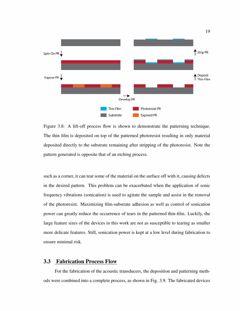
3.8 A lift-off process flow is shown to demonstrate the patterning tech-nique. The thin film is deposited on top of the patterned photoresistresulting in only material deposited directly to the substrate remainingafter stripping of the photoresist. Note the pattern generated is oppositethat of an etching process. . . . . . . . . . . . . . . . . . . . . . . . . . . . . . . . . . . . . . . . . . . . . 19
3.9 A schematic process flow showing the steps taken to create thin-filmacoustic transducers. . . . . . . . . . . . . . . . . . . . . . . . . . . . . . . . . . . . . . . . . . . . . . . . . . 21
3.10 Acoustic Transducer . . . . . . . . . . . . . . . . . . . . . . . . . . . . . . . . . . . . . . . . . . . . . . . . . . 22
LIST OF FIGURES (Continued)
Figure Page
4.1 Mason model equivalent circuit of a piezoelectric layer. . . . . . . . . . . . . . . . . 25
4.2 Mason model equivalent circuit of an acoustic layer. . . . . . . . . . . . . . . . . . . . 25
4.3 Complete Mason eqivalent circuit model for a TFBAR. . . . . . . . . . . . . . . . . 26
4.4 ABCD block interface definitions. . . . . . . . . . . . . . . . . . . . . . . . . . . . . . . . . . . . . 27
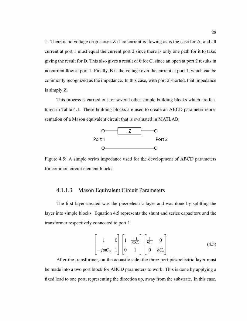
4.5 A simple series impedance used for the development of ABCD param-eters for common circuit element blocks. . . . . . . . . . . . . . . . . . . . . . . . . . . . . . . 28
4.6 Mason equivalent circuit for a piezoelectric layer with aluminum topcontact and short at the air interface. . . . . . . . . . . . . . . . . . . . . . . . . . . . . . . . . . . 30
4.7 Mason equivalent circuit for a piezoelectric layer with aluminum topcontact and short at the air interface rearranged to show two port nature. 30
4.8 Interface definitions for an S-parameter network.. . . . . . . . . . . . . . . . . . . . . . . 32
4.9 (a) Short, (b) open, and (c) 50 Ω load marked on a Smith chart. Thenetwork analyzer must be calibrated to best define these responses. . . . . . 34
5.1 Lone piezoelectric layer simulated with various thicknesses and sub-strates. . . . . . . . . . . . . . . . . . . . . . . . . . . . . . . . . . . . . . . . . . . . . . . . . . . . . . . . . . . . . . . . 36
5.2 (a) S11 and (b) impedance magnitude for a lone ZnO layer of variousthicknesses terminated on both sides by air. . . . . . . . . . . . . . . . . . . . . . . . . . . . . 37
5.3 S11 magnitude for a 1.2 µm thick ZnO layer on various ”substrates.”A high impedance substrate is equivalent to a mounted and immobilesurface and a low impedance represents a free surface. . . . . . . . . . . . . . . . . . 39
5.4 Three layer simulation stack. ZnO piezoelectric layer with two elec-trodes and mounted on a glass substrate. . . . . . . . . . . . . . . . . . . . . . . . . . . . . . . . 40
5.5 S11 magnitude for a 1.2 µm thick ZnO layer with various electrodethicknesses . . . . . . . . . . . . . . . . . . . . . . . . . . . . . . . . . . . . . . . . . . . . . . . . . . . . . . . . . . 41
5.6 S11 magnitude for a transducer stack with 200 nm electrodes with var-ious ZnO layer thicknesses . . . . . . . . . . . . . . . . . . . . . . . . . . . . . . . . . . . . . . . . . . . 43
5.7 Smith chart plots of measured S11 parameters for acoustic transducerswith acoustic resonance highlighted. Measurements are from transduc-ers with ZnO thicknesses of (a) 480 nm, (b) 641 nm, (c) 743 nm and(d) 866 nm with a frequency range of 0.4 GHz - 8 GHz for all devices. . . 45
LIST OF FIGURES (Continued)
Figure Page
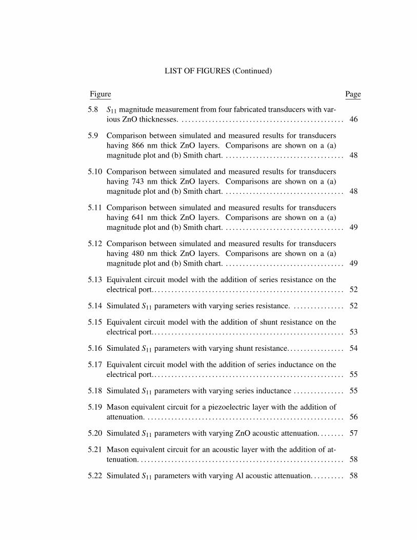
5.8 S11 magnitude measurement from four fabricated transducers with var-ious ZnO thicknesses. . . . . . . . . . . . . . . . . . . . . . . . . . . . . . . . . . . . . . . . . . . . . . . . . 46
5.9 Comparison between simulated and measured results for transducershaving 866 nm thick ZnO layers. Comparisons are shown on a (a)magnitude plot and (b) Smith chart. . . . . . . . . . . . . . . . . . . . . . . . . . . . . . . . . . . . 48
5.10 Comparison between simulated and measured results for transducershaving 743 nm thick ZnO layers. Comparisons are shown on a (a)magnitude plot and (b) Smith chart. . . . . . . . . . . . . . . . . . . . . . . . . . . . . . . . . . . . 48
5.11 Comparison between simulated and measured results for transducershaving 641 nm thick ZnO layers. Comparisons are shown on a (a)magnitude plot and (b) Smith chart. . . . . . . . . . . . . . . . . . . . . . . . . . . . . . . . . . . . 49
5.12 Comparison between simulated and measured results for transducershaving 480 nm thick ZnO layers. Comparisons are shown on a (a)magnitude plot and (b) Smith chart. . . . . . . . . . . . . . . . . . . . . . . . . . . . . . . . . . . . 49
5.13 Equivalent circuit model with the addition of series resistance on theelectrical port. . . . . . . . . . . . . . . . . . . . . . . . . . . . . . . . . . . . . . . . . . . . . . . . . . . . . . . . . 52
5.14 Simulated S11 parameters with varying series resistance. . . . . . . . . . . . . . . . 52
5.15 Equivalent circuit model with the addition of shunt resistance on theelectrical port. . . . . . . . . . . . . . . . . . . . . . . . . . . . . . . . . . . . . . . . . . . . . . . . . . . . . . . . . 53
5.16 Simulated S11 parameters with varying shunt resistance. . . . . . . . . . . . . . . . . 54
5.17 Equivalent circuit model with the addition of series inductance on theelectrical port. . . . . . . . . . . . . . . . . . . . . . . . . . . . . . . . . . . . . . . . . . . . . . . . . . . . . . . . . 55
5.18 Simulated S11 parameters with varying series inductance . . . . . . . . . . . . . . . 55
5.19 Mason equivalent circuit for a piezoelectric layer with the addition ofattenuation. . . . . . . . . . . . . . . . . . . . . . . . . . . . . . . . . . . . . . . . . . . . . . . . . . . . . . . . . . . 56
5.20 Simulated S11 parameters with varying ZnO acoustic attenuation. . . . . . . . 57
5.21 Mason equivalent circuit for an acoustic layer with the addition of at-tenuation. . . . . . . . . . . . . . . . . . . . . . . . . . . . . . . . . . . . . . . . . . . . . . . . . . . . . . . . . . . . . 58
5.22 Simulated S11 parameters with varying Al acoustic attenuation. . . . . . . . . . 58

LIST OF FIGURES (Continued)
Figure Page
5.23 Comparison between improved simulation and measured results fortransducers having 866 nm thick ZnO layers. Comparisons are shownon a magnitude plot(a) and on a Smith chart (b). . . . . . . . . . . . . . . . . . . . . . . . 60
5.24 Comparison between improved simulation and measured results fortransducers having 743 nm thick ZnO layers. Comparisons are shownon a magnitude plot(a) and on a Smith chart (b). . . . . . . . . . . . . . . . . . . . . . . . 61
5.25 Comparison between improved simulation and measured results fortransducers having 641 nm thick ZnO layers. Comparisons are shownon a magnitude plot(a) and on a Smith chart (b). . . . . . . . . . . . . . . . . . . . . . . . 62
5.26 Comparison between improved simulation and measured results fortransducers having 480 nm thick ZnO layers. Comparisons are shownon a magnitude plot(a) and on a Smith chart (b). . . . . . . . . . . . . . . . . . . . . . . . 63
6.1 Diagram showing an integrated acoustic spin wave pump. The trans-ducer presented in this work is patterned onto the YIG spin wave waveg-uide. . . . . . . . . . . . . . . . . . . . . . . . . . . . . . . . . . . . . . . . . . . . . . . . . . . . . . . . . . . . . . . . . . 67
LIST OF TABLES
Table Page
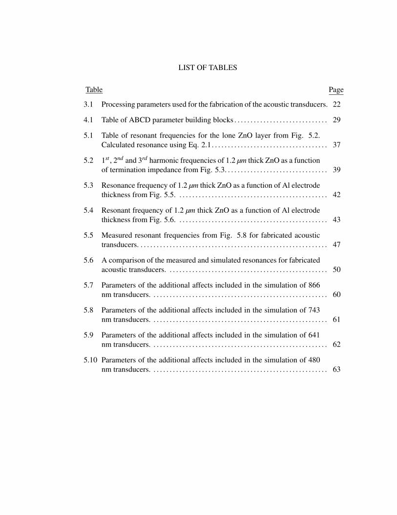
3.1 Processing parameters used for the fabrication of the acoustic transducers. 22
4.1 Table of ABCD parameter building blocks . . . . . . . . . . . . . . . . . . . . . . . . . . . . . 29
5.1 Table of resonant frequencies for the lone ZnO layer from Fig. 5.2.Calculated resonance using Eq. 2.1. . . . . . . . . . . . . . . . . . . . . . . . . . . . . . . . . . . . 37
5.2 1st , 2nd and 3rd harmonic frequencies of 1.2 µm thick ZnO as a functionof termination impedance from Fig. 5.3. . . . . . . . . . . . . . . . . . . . . . . . . . . . . . . . 39
5.3 Resonance frequency of 1.2 µm thick ZnO as a function of Al electrodethickness from Fig. 5.5. . . . . . . . . . . . . . . . . . . . . . . . . . . . . . . . . . . . . . . . . . . . . . . 42
5.4 Resonant frequency of 1.2 µm thick ZnO as a function of Al electrodethickness from Fig. 5.6. . . . . . . . . . . . . . . . . . . . . . . . . . . . . . . . . . . . . . . . . . . . . . . 43
5.5 Measured resonant frequencies from Fig. 5.8 for fabricated acoustictransducers. . . . . . . . . . . . . . . . . . . . . . . . . . . . . . . . . . . . . . . . . . . . . . . . . . . . . . . . . . . 47
5.6 A comparison of the measured and simulated resonances for fabricatedacoustic transducers. . . . . . . . . . . . . . . . . . . . . . . . . . . . . . . . . . . . . . . . . . . . . . . . . . 50
5.7 Parameters of the additional affects included in the simulation of 866nm transducers. . . . . . . . . . . . . . . . . . . . . . . . . . . . . . . . . . . . . . . . . . . . . . . . . . . . . . . 60
5.8 Parameters of the additional affects included in the simulation of 743nm transducers. . . . . . . . . . . . . . . . . . . . . . . . . . . . . . . . . . . . . . . . . . . . . . . . . . . . . . . 61
5.9 Parameters of the additional affects included in the simulation of 641nm transducers. . . . . . . . . . . . . . . . . . . . . . . . . . . . . . . . . . . . . . . . . . . . . . . . . . . . . . . 62
5.10 Parameters of the additional affects included in the simulation of 480nm transducers. . . . . . . . . . . . . . . . . . . . . . . . . . . . . . . . . . . . . . . . . . . . . . . . . . . . . . . 63
DEVELOPMENT OF ACOUSTIC TRANSDUCERS FOR USE IN THEPARAMETRIC PUMPING OF SPIN WAVES
1. INTRODUCTION
Acoustic oscillators have been in use in the field of electronics for decades, with
applications ranging from oscillators for time keeping, to sensors measuring flow rates or
detecting trace gases. This thesis presents the development of thin-film acoustic transduc-
ers for use in creating an acoustic spin wave amplification system. The eventual goal of
this work is to parametrically pump propagating spin waves in a magnetic oxide film (Yt-
trium Iron Garnet); however, the main focus and motivation of this work is the simulation
and fabrication of the transducers needed to accomplish this goal.
Spin waves have been an area of interest for many years, traditionally as a loss
mechanism in magnetic systems or as a purely scientific study into their properties. Re-
cently, however, there has been renewed interest, as they have become a candidate to be
a signal carrying medium and even conduct logic operations [1, 2]. A primary reason for
this interest is the nature of the spin waves. Spin waves are a pure spin current, meaning
the signal is not only carried by the spin of the electron rather than its charge, but the
electrons do not move through the material, resulting in no heat creation. A major draw
back, that the acoustic spin wave pump looks to address, is the high attenuation of spin
waves in most materials. The spin wave pump will act as a repeater in a spin-wave-based
transmission system, allowing signals to propagate over longer distances and to be used
in more operations.
In this work, a simulation implementing the Mason Model [3, 4] is created using
MATLAB to predict the response of acoustic transducers to help in the design process.
The simulation takes into account the multiple layers in the acoustic transducers that affect
2
the response, namely acoustic loading due to electrode layers and physical properties,
such as layer thicknesses and material properties. Transducers are also fabricated and
measured, comparing their response to that predicted by the simulated model.
This thesis is divided into six chapters, this being chapter one and providing an in-
troduction to the project including motivation and project goals. Chapter two presents
background information necessary for the work featured. This includes piezoelectric
acoustic transducers, the physics behind resonators, which is useful in understanding
transducer operation, and a discussion of material properties pertinent to acoustic trans-
ducers, namely the piezoelectric properties of zinc oxide (ZnO). Chapter three discusses
the fabrication processes used in making acoustic transducers in the laboratory, includ-
ing deposition and patterning techniques. Chapter four details the simulation created to
model transducer response to assist in the analysis of the fabricated transducers, as well
as measurement techniques used to measure their response. Chapter five shows the re-
sults observed from experiments conducted on the simulation and the measurements taken
from the fabricated transducers. Finally, chapter six gives a summary of the results and
conclusions drawn from the experiments conducted as well as suggested next steps in the
project of creating an acoustic spin wave pump.

DEVELOPMENT OF ACOUSTIC TRANSDUCERS FOR USE IN THEPARAMETRIC PUMPING OF SPIN WAVES
2. LITERATURE REVIEW
We begin with some necessary background information that will assist with the under-
standing and modeling of thin-film acoustic transducers. Presented here is an overview of
acoustic transducers with details including topology and structure as well as the concepts
of resonance and piezoelectricity. Focus is also given to material properties, namely those
important to piezoelectric materials and their effect on transducer device operation.
2.1 Acoustic Transducers
Acoustic transducers are devices that transform electrical energy to and from acous-
tic energy. The most commonly thought of application is in audio applications, where
microphones and speakers transform audio signals to and from electrical signals. In this
work however, the frequency range is much higher, approximately 1 GHz - 8 GHz. This
frequency range is used as it is where the ranges of acoustic transucers and spin wave ex-
citation/detection experiments overlap. To achive the desired parametric pumping of spin
waves, the acosutic frequency must be twice the spin wave frequency. High frequency
acoustic transducers are used in a wide variety of applications across many disciplines,
including, but not limited to: reference frequency generation, biomolecule detection [5],
ultrasonic imaging, signal processing and gas flow metering [6]. All piezoelectric trans-
ducers can be separated into two main categories based on the wave propagation mode,
Bulk Acoustic Waves (BAW) and Surface Acoustic Waves (SAW) (Fig. 2.1). BAWs
propagate through the interior of a material as either longitudinal (compression) or trans-
verse (shear) waves, while SAWs propagate on the surface and are usually dominated by
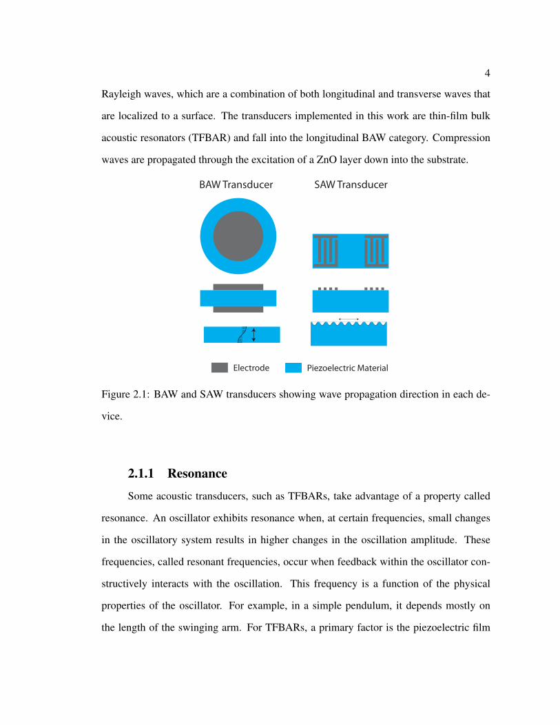
4
Rayleigh waves, which are a combination of both longitudinal and transverse waves that
are localized to a surface. The transducers implemented in this work are thin-film bulk
acoustic resonators (TFBAR) and fall into the longitudinal BAW category. Compression
waves are propagated through the excitation of a ZnO layer down into the substrate.
Piezoelectric MaterialElectrode
BAW Transducer SAW Transducer
Figure 2.1: BAW and SAW transducers showing wave propagation direction in each de-
vice.
2.1.1 Resonance
Some acoustic transducers, such as TFBARs, take advantage of a property called
resonance. An oscillator exhibits resonance when, at certain frequencies, small changes
in the oscillatory system results in higher changes in the oscillation amplitude. These
frequencies, called resonant frequencies, occur when feedback within the oscillator con-
structively interacts with the oscillation. This frequency is a function of the physical
properties of the oscillator. For example, in a simple pendulum, it depends mostly on
the length of the swinging arm. For TFBARs, a primary factor is the piezoelectric film
5
thickness and is important for the design of transducers and determining their frequency
operating point.
2.1.1.1 Resonators
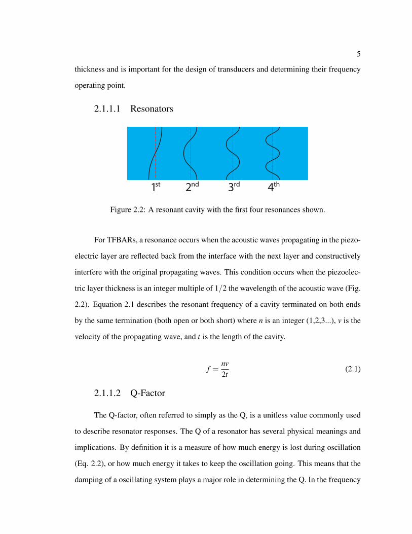
1st
2nd
3rd
4th
Figure 2.2: A resonant cavity with the first four resonances shown.
For TFBARs, a resonance occurs when the acoustic waves propagating in the piezo-
electric layer are reflected back from the interface with the next layer and constructively
interfere with the original propagating waves. This condition occurs when the piezoelec-
tric layer thickness is an integer multiple of 1/2 the wavelength of the acoustic wave (Fig.
2.2). Equation 2.1 describes the resonant frequency of a cavity terminated on both ends
by the same termination (both open or both short) where n is an integer (1,2,3...), v is the
velocity of the propagating wave, and t is the length of the cavity.
f =nv2t
(2.1)
2.1.1.2 Q-Factor
The Q-factor, often referred to simply as the Q, is a unitless value commonly used
to describe resonator responses. The Q of a resonator has several physical meanings and
implications. By definition it is a measure of how much energy is lost during oscillation
(Eq. 2.2), or how much energy it takes to keep the oscillation going. This means that the
damping of a oscillating system plays a major role in determining the Q. In the frequency

6
domain, the Q is defined by the resonance frequency over the width of the resonant peak
(Eq. 2.3) at half power. Higher Q systems not only have lower losses, but also tend
to see larger responses to stimulus. That stimulus however, must fall within a smaller
frequency envelope, making selectivity of the operating more important as the response
falls off more rapidly away from the resonance frequency. In this work, Q-factor is used
as a qualitative tool to analyze effects resonator parameters have on operation.
Q≈ Energy storedEnergy lost per cycle
(2.2)
Q =fr
∆ f(2.3)
2.1.2 Material Properties for Thin Film Bulk Acoustic Resonators
In TFBARs, the material of highest interest is the piezoelectric layer. It is the piezo-
electric effect that allows for the oscillations that cause the acoustic waves. The piezo-
electric effect is caused when an asymmetrical crystal undergoes stress causing a shift in
charge distribution within the crystal lattice, resulting in the generation of an electric field.
This field is due to the unbalanced charge distribution within the crystal lattice creating a
local dipole. These dipoles, when added up over the volume of the piezoelectric material,
cause the buildup of charge on the surface of the material. The inverse-piezoelectric ef-
fect also occurs. When an electric field is applied to the piezoelectric material, dipoles are
generated to counter the applied field, resulting in a deformation of the crystal. The piezo-
electric material of choice for this work is ZnO. Chosen for its ease of use, ZnO’s most
stable form exhibits a Wurtzite crystal structure, which lacks a crystal inversion center,
giving it piezoelectric properties. When designing acoustic transducers, several proper-
ties of the piezoelectric material are important. ZnO, like many piezoelectric material,
exhibits anisotropy in its acoustic and piezoelectric properties. The primary piezoelectric

7
axis for ZnO is in the z-direction, requiring material properties that match. For ZnO,
this corresponds to the 33 crystal direction. The piezoelectric stress constant (e33) relates
the stress on the material to the electric field generated and is the primary piezoelectric
constant. Other material properties important to transducer operation are the elastic stiff-
ness constant (c33) and the material density (ρ). Together, these properties determine
the velocity of acoustic waves propagating through the material and govern the acoustic
properties. The subscripts on the piezoelectric and elastic stiffness constants denote direc-
tionality since these properties are anisotropic. For ZnO these constants are: e33 = 1.34
Cm−2, c33 = 211 GPa, and ρZnO = 5606 kgm−3 [7, 8]. These properties will play a major
role in the simulation that will be discussed in the coming chapters.
DEVELOPMENT OF ACOUSTIC TRANSDUCERS FOR USE IN THEPARAMETRIC PUMPING OF SPIN WAVES
3. FABRICATION
The fabrication of the acoustic transducer devices was accomplished using several
physical vapor deposition (PVD) methods for the creation of thin-films in conjunction
with several patterning techniques. The methods used depend both on the material being
deposited as well as the desired thin-film properties, including size, shape, uniformity,
and crystal orientation. The techniques and methods used in this research are discussed
in the following section.
3.1 Thin-Film Deposition Methods
During the fabrication process, two thin-film deposition methods were used, ther-
mal evaporation and magnetron sputtering. The physics of both methods, as well as their
practical implications are discussed and detailed below.
3.1.1 Thermal Evaporation
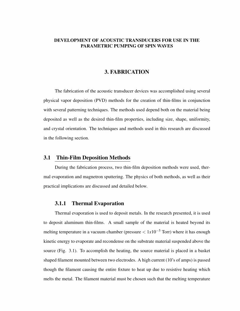
Thermal evaporation is used to deposit metals. In the research presented, it is used
to deposit aluminum thin-films. A small sample of the material is heated beyond its
melting temperature in a vacuum chamber (pressure < 1x10⁻⁵ Torr) where it has enough
kinetic energy to evaporate and recondense on the substrate material suspended above the
source (Fig. 3.1). To accomplish the heating, the source material is placed in a basket
shaped filament mounted between two electrodes. A high current (10’s of amps) is passed
though the filament causing the entire fixture to heat up due to resistive heating which
melts the metal. The filament material must be chosen such that the melting temperature
9
Figure 3.1: A schematic view of a thermal evaporation deposition tool.
is much higher than that of the material to be deposited in order to ensure no disruption
in current flow due to loss of contact. A common filament material used is tungsten as
it has a high melting temperature of 3422 C, as compared to aluminum with a melting
temperature of 666 C.
This evaporating metal acts as a point source within the deposition chamber, mean-
ing that every surface with line of sight to the filament is coated with metal. This has sev-
eral implications. The first, and simplest, is that this process cannot be observed directly,
any window that is used to view the filament to observe when the material is melted will
be coated with evaporated material, i.e., Al, and become opaque. This means that another
method must be used to determine when the metal has melted and begun to evaporate.
There are two methods commonly used to accomplish this, the first and simplest way
is to observe the chamber pressure and watch for a sudden increase which signifies the
vaporization of the metal. This increase is due to the introduction of new particles to the
vacuum environment, the evaporated metal. Thickness can be controlled through charac-
terization of the deposition rate through experimentation and varying the exposure time to
10
get the desired thickness. Another, more elegant (and useful) method uses a quartz crystal
oscillator. For a crystal oscillator, the fact that all surfaces facing the source are coated is
exploited. The oscillator is placed in the chamber exposed to evaporation source. As the
surface of the oscillator is coated, the build up of material causes a change in the oscilla-
tion frequency based on the amount of metal deposited on the oscillator. When placed at
the same distance from the source as the substrate, the crystal oscillator makes it possible
to accurately establish both the deposition rate and the total deposited thickness.
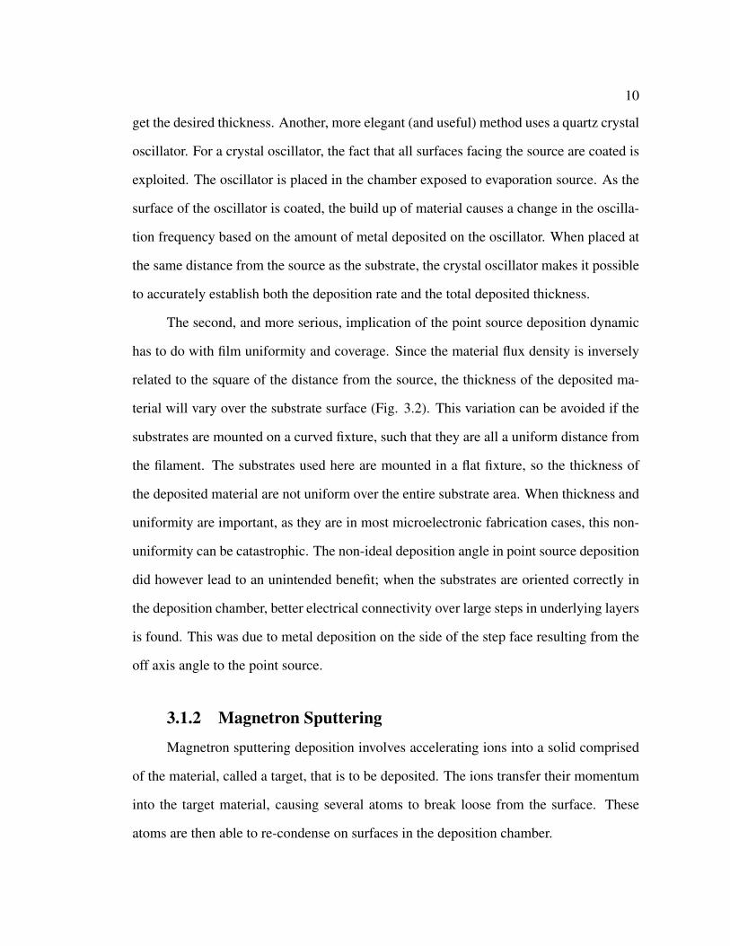
The second, and more serious, implication of the point source deposition dynamic
has to do with film uniformity and coverage. Since the material flux density is inversely
related to the square of the distance from the source, the thickness of the deposited ma-
terial will vary over the substrate surface (Fig. 3.2). This variation can be avoided if the
substrates are mounted on a curved fixture, such that they are all a uniform distance from
the filament. The substrates used here are mounted in a flat fixture, so the thickness of
the deposited material are not uniform over the entire substrate area. When thickness and
uniformity are important, as they are in most microelectronic fabrication cases, this non-
uniformity can be catastrophic. The non-ideal deposition angle in point source deposition
did however lead to an unintended benefit; when the substrates are oriented correctly in
the deposition chamber, better electrical connectivity over large steps in underlying layers
is found. This was due to metal deposition on the side of the step face resulting from the
off axis angle to the point source.
3.1.2 Magnetron Sputtering
Magnetron sputtering deposition involves accelerating ions into a solid comprised
of the material, called a target, that is to be deposited. The ions transfer their momentum
into the target material, causing several atoms to break loose from the surface. These
atoms are then able to re-condense on surfaces in the deposition chamber.
11
Figure 3.2: Deposition from a point source onto a flat substrate results in a thickness
gradient in the deposited film due to the variation in distance to the source over the entire
substrate.
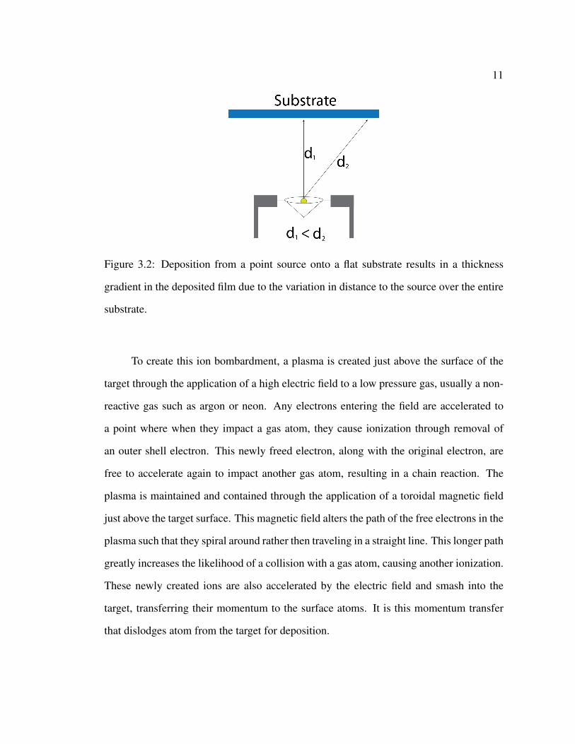
To create this ion bombardment, a plasma is created just above the surface of the
target through the application of a high electric field to a low pressure gas, usually a non-
reactive gas such as argon or neon. Any electrons entering the field are accelerated to
a point where when they impact a gas atom, they cause ionization through removal of
an outer shell electron. This newly freed electron, along with the original electron, are
free to accelerate again to impact another gas atom, resulting in a chain reaction. The
plasma is maintained and contained through the application of a toroidal magnetic field
just above the target surface. This magnetic field alters the path of the free electrons in the
plasma such that they spiral around rather then traveling in a straight line. This longer path
greatly increases the likelihood of a collision with a gas atom, causing another ionization.
These newly created ions are also accelerated by the electric field and smash into the
target, transferring their momentum to the surface atoms. It is this momentum transfer
that dislodges atom from the target for deposition.
12
On the surface of the target, if the target is conductive, electrons will immediately
move to counter the positive charge from the introduced ion. In an insulating target how-
ever, like ZnO, the introduced positive charge is not countered by the targets internal
electron gas, resulting in a buildup of positive charge on the target surface. This buildup
will reduce the effective field between the electrode and the target used to accelerate the
ions into the surface, reducing number of electrons that have enough energy to break loose
target atoms, effectively reducing the sputter rate. To counter this buildup, the target is
biased with an alternating rf voltage. The RF bias accelerates ions into the surface for
sputtering during the negative portion of the cycle, and expels the built up positive charge
on the surface during the positive portion.
Figure 3.3: A schematic view of an off-axis, sputter-down deposition chamber. The RF
supply is used for insulating targets and the DC supply for conductive targets. The sub-
strate is placed on the rotating stage to maximize film uniformity.
Controllable process parameters for RF magnetron sputtering include: gas flow rate
and species, power applied to target, substrate positioning and motion, and deposition
time. Changes in gas flow rate are used to set the chamber operating pressure. This
pressure must be balanced to provide enough gas atoms for a high target bombardment
13
rate while keeping collision of sputtered atoms with neutral gas atoms in the chamber
to a minimum, maintaining a long mean free path. If the mean free path is too short,
the sputtered atoms from the target will collide with gas atoms before they reach the
substrate, altering their path and reducing their energy, thus making it less likely they will
reach the substrate. The use of the magnetic field above the surface of the target greatly
increases the probability of a gas atom becoming ionized and accelerating into the target,
effectively reducing the pressure needed to maintain a plasma above the target. This
allows for a lower operating pressure, which in turn increases the mean free path of the
sputtered atoms, yielding higher deposition rates. A reactive gas can also be introduced
to the chamber to alter the composition of the deposited film. The sputtered atoms react
with the ambient gas during flight creating a different, desired material, for example,
introducing O2 to a sputter chamber with a Zn target to deposit ZnO. This process is
known as reactive sputtering. For this research, O2 is introduced into the sputter chamber
with a ZnO target to reduce the disassociation of the Zn and O atoms during the sputter
process and maintain desired film stoichiometry.
Target power is the amount of power applied into the plasma and is directly related
to the sputter rate. It is a measure of the plasma current flowing due to charged particles
moving through the plasma to bombard the target surface. A higher target power creates
higher bombardment rate, resulting in a higher sputter rate. Practical limitations to target
power come from the supply equipment being used, but also the heat dissipation ability
of the gun and target. Ceramic targets tend to have higher thermal resistances, limiting
the amount of power that can be applied before thermal damage occurs. Care must also
be taken in making changes to the applied power as thermally induced stresses can result
in target cracking and cause permanent damage to the target.
Physical control of the sputter chamber also allows for control over film deposition
properties. The most basic control involves the motion and placement of the substrate.
14
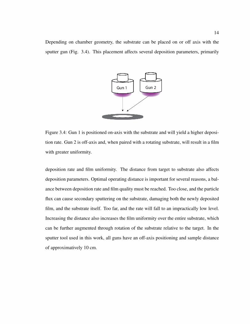
Depending on chamber geometry, the substrate can be placed on or off axis with the
sputter gun (Fig. 3.4). This placement affects several deposition parameters, primarily
Figure 3.4: Gun 1 is positioned on-axis with the substrate and will yield a higher deposi-
tion rate. Gun 2 is off-axis and, when paired with a rotating substrate, will result in a film
with greater uniformity.
deposition rate and film uniformity. The distance from target to substrate also affects
deposition parameters. Optimal operating distance is important for several reasons, a bal-
ance between deposition rate and film quality must be reached. Too close, and the particle
flux can cause secondary sputtering on the substrate, damaging both the newly deposited
film, and the substrate itself. Too far, and the rate will fall to an impractically low level.
Increasing the distance also increases the film uniformity over the entire substrate, which
can be further augmented through rotation of the substrate relative to the target. In the
sputter tool used in this work, all guns have an off-axis positioning and sample distance
of approximatively 10 cm.
15
3.2 Patterning
With deposition techniques established, the deposited films must be patterned into
functional shapes. This is accomplished through the use of photolithography. Patterning
techniques, including etching and lift-off, are described in the following section.
3.2.1 Photolithography
Photolithography is a backbone of modern micro-fabrication technology. It allows
for the transfer of precises patterns into fabrication materials through the selective appli-
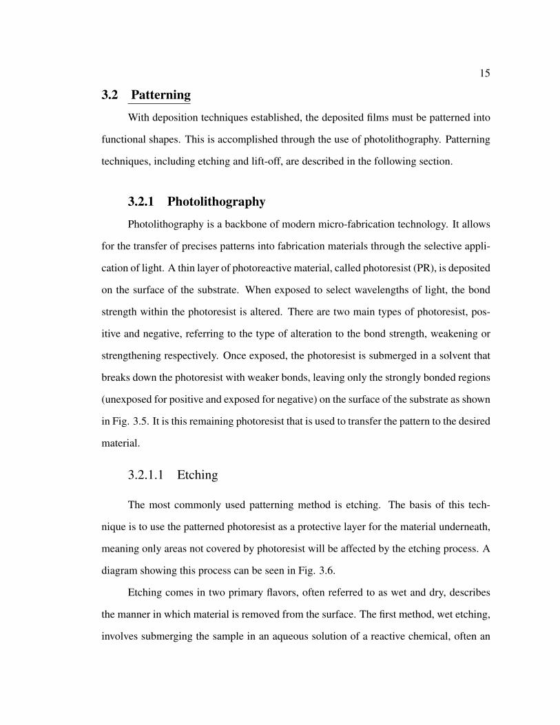
cation of light. A thin layer of photoreactive material, called photoresist (PR), is deposited
on the surface of the substrate. When exposed to select wavelengths of light, the bond
strength within the photoresist is altered. There are two main types of photoresist, pos-
itive and negative, referring to the type of alteration to the bond strength, weakening or
strengthening respectively. Once exposed, the photoresist is submerged in a solvent that
breaks down the photoresist with weaker bonds, leaving only the strongly bonded regions
(unexposed for positive and exposed for negative) on the surface of the substrate as shown
in Fig. 3.5. It is this remaining photoresist that is used to transfer the pattern to the desired
material.
3.2.1.1 Etching
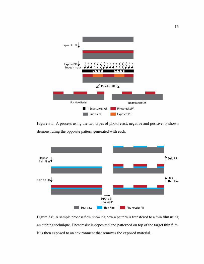
The most commonly used patterning method is etching. The basis of this tech-
nique is to use the patterned photoresist as a protective layer for the material underneath,
meaning only areas not covered by photoresist will be affected by the etching process. A
diagram showing this process can be seen in Fig. 3.6.
Etching comes in two primary flavors, often referred to as wet and dry, describes
the manner in which material is removed from the surface. The first method, wet etching,
involves submerging the sample in an aqueous solution of a reactive chemical, often an
16
Figure 3.5: A process using the two types of photoresist, negative and positive, is shown
demonstrating the opposite pattern generated with each.
Figure 3.6: A sample process flow showing how a pattern is transfered to a thin film using
an etching technique. Photoresist is deposited and patterned on top of the target thin film.
It is then exposed to an environment that removes the exposed material.
17
acid, that will react with and dissolve the material to be etched. Careful selection of this
etchant gives wet etching one of its major advantages; if the etchant reacts with only the
material to be etched, layers can be completely removed without damaging underlying
layers. Wet etching has a major disadvantage however, because the sample is submerged
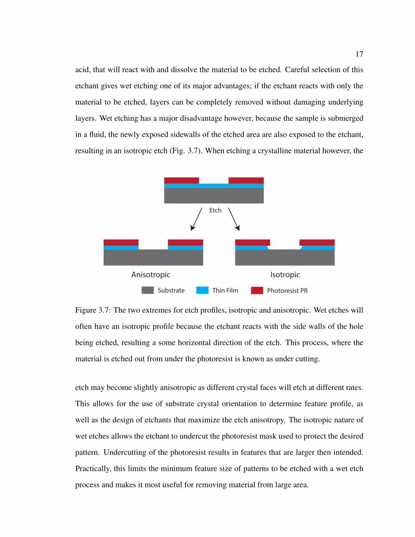
in a fluid, the newly exposed sidewalls of the etched area are also exposed to the etchant,
resulting in an isotropic etch (Fig. 3.7). When etching a crystalline material however, the
Thin FilmSubstrate Photoresist PR
Anisotropic Isotropic
Etch
Figure 3.7: The two extremes for etch profiles, isotropic and anisotropic. Wet etches will
often have an isotropic profile because the etchant reacts with the side walls of the hole
being etched, resulting a some horizontal direction of the etch. This process, where the
material is etched out from under the photoresist is known as under cutting.
etch may become slightly anisotropic as different crystal faces will etch at different rates.
This allows for the use of substrate crystal orientation to determine feature profile, as
well as the design of etchants that maximize the etch anisotropy. The isotropic nature of
wet etches allows the etchant to undercut the photoresist mask used to protect the desired
pattern. Undercutting of the photoresist results in features that are larger then intended.
Practically, this limits the minimum feature size of patterns to be etched with a wet etch
process and makes it most useful for removing material from large area.

18
The other etching process, commonly referred to as dry etching, was not used for
this project so will only be mentioned briefly and with limited detail for completeness of
the discussion. For more information see Silicon Processing for the VLSI Era by Wolf
and Tauber [9]. Dry etching uses ions to chemically or mechanically remove atoms from
the sample surface and has the major advantage of being capable of highly anisotropic
etching. Dry etching techniques tend to have less selectivity than wet etching, increaseing
the likelihood of causing damage to underlying layers. Careful design and application of
dry etching techniques can minimize these effects making it a very valuable and vital
patterning process.
3.2.1.2 Lift-off
Lift-off is essentially the opposite of an etching process. In a lift-off process, the
photoresist is deposited directly on the substrate before the thin-film material to be pat-
terned is deposited. This means that when the thin-film is deposited, some of it will be
on top of the photoresist and only areas lacking photoresist will have material on the
substrate. When the photoresist is removed, only material on the substrate will remain,
leaving the desired pattern (Fig. 3.8).
One of the major advantages to lift-off is the reduction of damage to underlying
layers that can be caused by other etching methods. The only material that needs to be
removed is the photoresist which is designed to be easily removed. There is no need
to develop selective etchants that only remove desired materials and no risk of etching
too deep and removing substrate or underlying material. There are however downsides;
in order for the lift-off process to work, the film being deposited must be thinner than
the photoresist layer, allowing for breakdown of the photoresist under the deposited film.
Another major concern when using lift-off is tearing of the thin-film. With the photoresist
removed, the thin-film on top is free to float away. If the tin film is still attached at a point,
19
Figure 3.8: A lift-off process flow is shown to demonstrate the patterning technique.
The thin film is deposited on top of the patterned photoresist resulting in only material
deposited directly to the substrate remaining after stripping of the photoresist. Note the
pattern generated is opposite that of an etching process.
such as a corner, it can tear some of the material on the surface off with it, causing defects
in the desired pattern. This problem can be exacerbated when the application of sonic
frequency vibrations (sonication) is used to agitate the sample and assist in the removal
of the photoresist. Maximizing film-substrate adhesion as well as control of sonication
power can greatly reduce the occurrence of tears in the patterned thin-film. Luckily, the
large feature sizes of the devices in this work are not as susceptible to tearing as smaller
more delicate features. Still, sonication power is kept at a low level during fabrication to
ensure minimal risk.
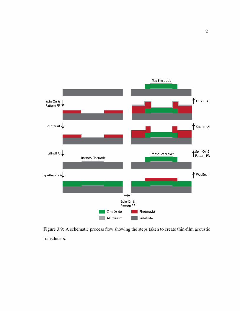
3.3 Fabrication Process Flow
For the fabrication of the acoustic transducers, the deposition and patterning meth-
ods were combined into a complete process, as shown in Fig. 3.9. The fabricated devices

20
consist of a stack of Aluminum(100 nm-200 nm)/Zinc Oxide(600 nm-1200 nm)/Aluminum(100
nm-200 nm). All layer thickness are determined through the use of a step profilometer,
where a needle tip is dragged across the surface of the device, measuring changes in
the surface hight. Initially, the aluminum layers were deposited using thermal evapora-
tion due to its ease and on site access in the OSU cleanroom. Deposition was done in
a Poloron desktop thermal evaporation tool with a chamber pressure of less then 3.5 x
10−5 mTorr, a maximum boat current of 20 A and a coat time up to 30 sec. For later
devices however, a sputtered Al layer is used because of its higher uniformity and thick-
ness control offered by the tool used. This higher level of control was necessary due to
the sensitivity of the acoustic properties of the device to the layer thicknesses. The ZnO
was deposited using a sputter process as well, with an addition of oxygen to the normal
argon chamber gas to keep the oxygen levels within the film from being depleted during
the deposition process. Both materials were deposited using an AJA sputter system with a
chamber pressure of 3.4 mTorr. The ZnO deposition is done in an RF gun with a gas flow
rate of 18 sccm Ar and 2 sccm O2, maintaining the manufacturer recommended 20 sccm
total flow rate, and a target power of 150 W. The substrate is also heated to 200C and
held their for the duration of the ZnO deposition. The Al deposition is done with a DC
gun with a gas flow rate of 20 sccm Ar and a target power of 200 W. The deposition time
is varied to control film thickness, with a ZnO deposition rate of 1.3 nm per minute and a
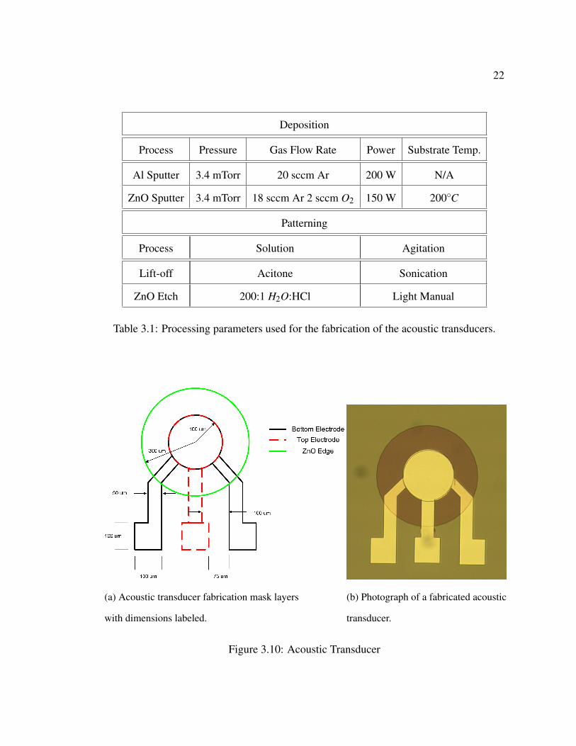
Al rate of 20 nm per minute. Patterning was done in three mask steps, bottom electrode,
ZnO layer, and top electrode (Fig. 3.10a). Both Al electrode layers were patterned using
a lift-off process and the ZnO using a 200:1 H2O:HCl etch. A summary of the processing
parameters used can be found in table 3.1 and a photograph of a transducer fabricated on
glass in Fig. 3.10b.
21
Figure 3.9: A schematic process flow showing the steps taken to create thin-film acoustic
transducers.
22
Deposition
Process Pressure Gas Flow Rate Power Substrate Temp.
Al Sputter 3.4 mTorr 20 sccm Ar 200 W N/A
ZnO Sputter 3.4 mTorr 18 sccm Ar 2 sccm O2 150 W 200C
Patterning
Process Solution Agitation
Lift-off Acitone Sonication
ZnO Etch 200:1 H2O:HCl Light Manual
Table 3.1: Processing parameters used for the fabrication of the acoustic transducers.
(a) Acoustic transducer fabrication mask layers
with dimensions labeled.
(b) Photograph of a fabricated acoustic
transducer.
Figure 3.10: Acoustic Transducer
DEVELOPMENT OF ACOUSTIC TRANSDUCERS FOR USE IN THEPARAMETRIC PUMPING OF SPIN WAVES
4. MEASUREMENT & ANALYSIS
With a method for fabrication of acoustic resonator established, and an understanding
of the basic principles, an experimental setup can be developed to measure and analyze
acoustic resonator devices. At this stage in development, the project is approached in two
parts: development of a simulation to model the transducer operation, and verification
and characterization of fabricated thin-film bulk acoustic transducers. This simulation is
created through the application of an equivalent circuit model of the acoustic system that
can be compared to the observed experimental results. The equivalent circuit model [3, 4],
as well as the experimental techniques and setups used, are explained in this chapter.
4.1 Acoustic Transducer Modeling & Measurement
The second portion of the experiments conducted involves measurement and char-
acterization of the thin-film acoustic transducers discussed in section 3.3. The goal of this
line of experimentation is to verify the successful fabrication and operation of acoustic
transducer devices. This is accomplished by exciting the devices and observing an acous-
tic resonance at the expected frequency. The expected resonance frequency is calculated
based on a 1-D circuit approximation model known as the Mason model. This section
will outline and discuss this model as well as measurement techniques used to analyze
the fabricated devices.
24
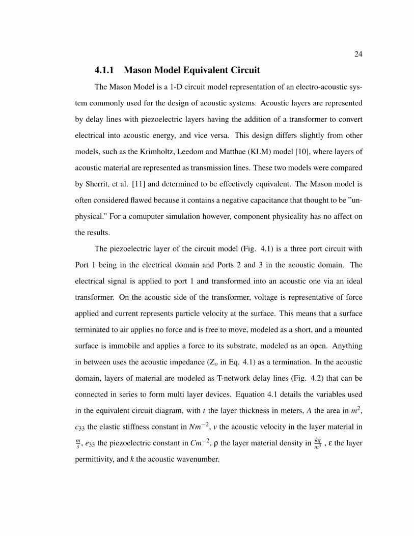
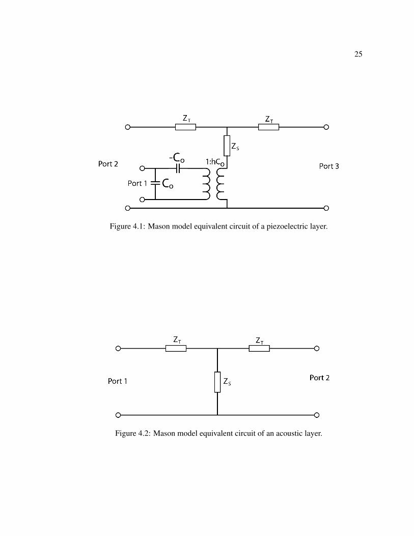
4.1.1 Mason Model Equivalent Circuit
The Mason Model is a 1-D circuit model representation of an electro-acoustic sys-
tem commonly used for the design of acoustic systems. Acoustic layers are represented
by delay lines with piezoelectric layers having the addition of a transformer to convert
electrical into acoustic energy, and vice versa. This design differs slightly from other
models, such as the Krimholtz, Leedom and Matthae (KLM) model [10], where layers of
acoustic material are represented as transmission lines. These two models were compared
by Sherrit, et al. [11] and determined to be effectively equivalent. The Mason model is
often considered flawed because it contains a negative capacitance that thought to be ”un-
physical.” For a comuputer simulation however, component physicality has no affect on
the results.
The piezoelectric layer of the circuit model (Fig. 4.1) is a three port circuit with
Port 1 being in the electrical domain and Ports 2 and 3 in the acoustic domain. The
electrical signal is applied to port 1 and transformed into an acoustic one via an ideal
transformer. On the acoustic side of the transformer, voltage is representative of force
applied and current represents particle velocity at the surface. This means that a surface
terminated to air applies no force and is free to move, modeled as a short, and a mounted
surface is immobile and applies a force to its substrate, modeled as an open. Anything
in between uses the acoustic impedance (Zo in Eq. 4.1) as a termination. In the acoustic
domain, layers of material are modeled as T-network delay lines (Fig. 4.2) that can be
connected in series to form multi layer devices. Equation 4.1 details the variables used
in the equivalent circuit diagram, with t the layer thickness in meters, A the area in m2,
c33 the elastic stiffness constant in Nm−2, v the acoustic velocity in the layer material in
ms , e33 the piezoelectric constant in Cm−2, ρ the layer material density in kg
m3 , ε the layer
permittivity, and k the acoustic wavenumber.
25
Figure 4.1: Mason model equivalent circuit of a piezoelectric layer.
Figure 4.2: Mason model equivalent circuit of an acoustic layer.
26
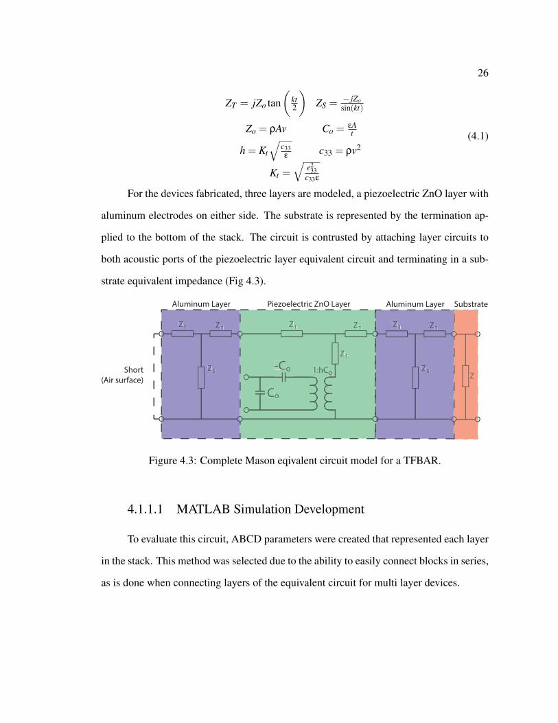
ZT = jZo tan(
kt2
)ZS =
− jZosin(kt)
Zo = ρAv Co =εAt
h = Kt
√c33ε
c33 = ρv2
Kt =
√e2
33c33ε
(4.1)
For the devices fabricated, three layers are modeled, a piezoelectric ZnO layer with
aluminum electrodes on either side. The substrate is represented by the termination ap-
plied to the bottom of the stack. The circuit is contrusted by attaching layer circuits to
both acoustic ports of the piezoelectric layer equivalent circuit and terminating in a sub-
strate equivalent impedance (Fig 4.3).
ZT ZT
ZS
Aluminum Layer
Co
-Co 1:hCo
ZT ZT
ZS
ZT ZT
ZSShort
(Air surface)
Co
-Co 1:hCo
ZT ZT
ZS
ZT ZT
ZS
Aluminum Layer Piezoelectric ZnO Layer
ZT ZT
ZSZZ
Substrate
Figure 4.3: Complete Mason eqivalent circuit model for a TFBAR.
4.1.1.1 MATLAB Simulation Development
To evaluate this circuit, ABCD parameters were created that represented each layer
in the stack. This method was selected due to the ability to easily connect blocks in series,
as is done when connecting layers of the equivalent circuit for multi layer devices.
27
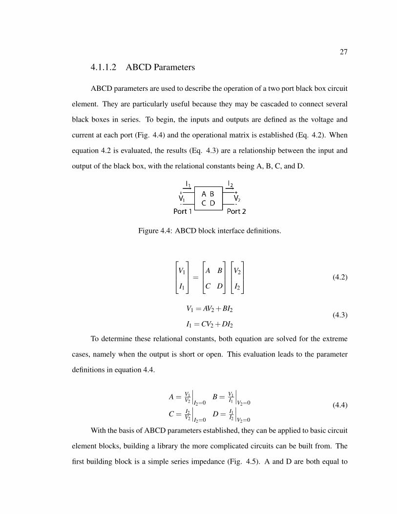
4.1.1.2 ABCD Parameters
ABCD parameters are used to describe the operation of a two port black box circuit
element. They are particularly useful because they may be cascaded to connect several
black boxes in series. To begin, the inputs and outputs are defined as the voltage and
current at each port (Fig. 4.4) and the operational matrix is established (Eq. 4.2). When
equation 4.2 is evaluated, the results (Eq. 4.3) are a relationship between the input and
output of the black box, with the relational constants being A, B, C, and D.
Figure 4.4: ABCD block interface definitions.
V1
I1
=
A B
C D
V2
I2
(4.2)
V1 = AV2 +BI2
I1 =CV2 +DI2
(4.3)
To determine these relational constants, both equation are solved for the extreme
cases, namely when the output is short or open. This evaluation leads to the parameter
definitions in equation 4.4.
A = V1V2
∣∣∣I2=0
B = V1I1
∣∣∣V2=0
C = I2V2
∣∣∣I2=0
D = I1I2
∣∣∣V2=0
(4.4)
With the basis of ABCD parameters established, they can be applied to basic circuit
element blocks, building a library the more complicated circuits can be built from. The
first building block is a simple series impedance (Fig. 4.5). A and D are both equal to
28
1. There is no voltage drop across Z if no current is flowing as is the case for A, and all
current at port 1 must equal the current port 2 since there is only one path for it to take,
giving the result for D. This also gives a result of 0 for C, since an open at port 2 results in
no current flow at port 1. Finally, B is the voltage over the current at port 1, which can be
commonly recognized as the impedance. In this case, with port 2 shorted, that impedance
is simply Z.
This process is carried out for several other simple building blocks which are fea-
tured in Table 4.1. These building blocks are used to create an ABCD parameter repre-
sentation of a Mason equivalent circuit that is evaluated in MATLAB.
Figure 4.5: A simple series impedance used for the development of ABCD parameters
for common circuit element blocks.
4.1.1.3 Mason Equivalent Circuit Parameters
The first layer created was the piezoelectric layer and was done by splitting the
layer into simple blocks. Equation 4.5 represents the shunt and series capacitors and the
transformer respectively connected to port 1.
1 0
− jωCo 1
1 −1
jωCo
0 1
1
hCo0
0 hCo
(4.5)
After the transformer, on the acoustic side, the three port piezoelectric layer must
be made into a two port block for ABCD parameters to work. This is done by applying a
fixed load to one port, representing the direction up, away from the substrate. In this case,

29
1 Z
0 1
1 0
1Z 1
1N 0
0 N
1+ Z1
Z3Z1 +Z2 +
Z1Z2Z3
1Z3
1+ Z2Z3
Table 4.1: Table of ABCD parameter building blocks
30
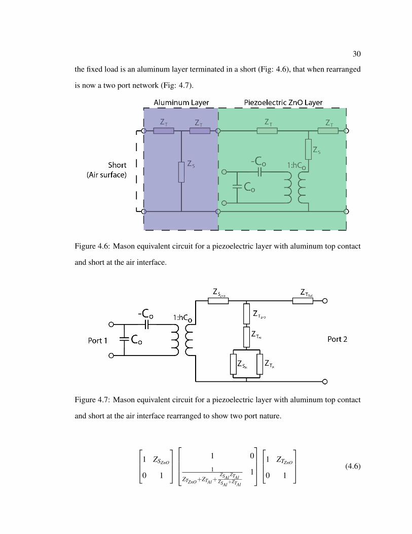
the fixed load is an aluminum layer terminated in a short (Fig: 4.6), that when rearranged
is now a two port network (Fig: 4.7).
Figure 4.6: Mason equivalent circuit for a piezoelectric layer with aluminum top contact
and short at the air interface.
Figure 4.7: Mason equivalent circuit for a piezoelectric layer with aluminum top contact
and short at the air interface rearranged to show two port nature.
1 ZSZnO
0 1
1 0
1
ZTZnO+ZTAl+ZSAl
ZTAlZSAl
+ZTAl
1
1 ZTZnO
0 1
(4.6)

31
The ABCD parameters for the network after the transformer, which includes the
acoustic portion of the piezoelectric layer as well as the top aluminum layer is again
broken down into simple blocks resulting in equation 4.6. With this portion established,
underlying layers can be attached by creating ABCD parameters for the desired layer and
multiplying through in series. For this work however, only a single layer was necessary,
the bottom aluminum contact (Eq. 4.7).
1+ZTAlZSAl
2ZTAl +Z2
TAlZSAl
1ZSAl
1+ZTAlZSAl
(4.7)
With all the building blocks in place, MATLAB is used to evaluate the resulting
ABCD parameters describing the Mason equivalent circuit. In chapter 5 these simulation
results will be discussed and compared with the measured results collected using the setup
outlined in the following section.
4.1.2 S-Parameters
The measurement technique used to characterize and verify the operation of acous-
tic transducers uses a characterization technique called Scattering Parameters, or S-parameters
for short. S-parameters are a tool used to characterize an RF ”black box” networks based
on the signal applied and transmitted from the devices ports where the actual voltage and
current may be difficult to measure practically. Fig. 4.8 and Eq. 4.8 define the inter-
faces to a two port network, with a being inputs and b outputs. S-parameters must also
be defined with a characteristic impedance (Z0). By definition, a port terminated in this
impedance will absorb all of the signal, causing no signal to be reflected back. This means
if port 2 is terminated in Z0 a2 will be zero by definition. Applying this to the expanded
definition matrix (Eq. 4.9), a definition of each parameter can be determined (Eq. 4.10).
When taking measurements, this characteristic impedance must be defined and calibrated
accordingly in order to ensure accurate measurements. Practically, this means connect-
32
ing the measurement tool to predefined loads, usually an open, short and through (open
and short circuit and a matched connection between ports) for a two port measurement or
open, short, load for 1 port.
Figure 4.8: Interface definitions for an S-parameter network.
b1
b2
=
S11 S12
S21 S22
a1
a2
(4.8)
b1 = S11a1 +S12a2
b2 = S21a1 +S22a2
(4.9)
S11 =b1a1
∣∣∣Z2=Z0
S21 =b2a1
∣∣∣Z2=Z0
S12 =b1a2
∣∣∣Z1=Z0
S22 =b2a2
∣∣∣Z1=Z0
(4.10)
Unlike ABCD parameters, S-Parameters can be expanded for any number of ports
by simply expanding the matrix, an N-port network can be represented by an N ×N
matrix of S-parameters. Unlike ABCD parameters however, S-parameters do not lend
themselves to being connected in series. The fact that the output from a ABCD matrix
operation is the input to the next network allows for cascading network by simply multi-
plying each network parameter matrix together. S-parameters on the other hand can not
be cascaded so easily. To overcome this, another type of parameter, transfer parameters
(T-parameters), are used that allow for easy cascading. T-parameters however are not
used in this work and are simply mentioned for completeness. Details of the conversion
between these different parameters can be found in [12].
33
4.1.3 Acoustic Transducer Measurement Setup
When characterizing the acoustic transducers, the reflection parameter, S11, is used
because it allows for the identification of a resonance in the device. With the help of the
Mason Model simulation, the expected location of these resonances is known, but must
be located. This location is visible in the S11 parameter as a dip in response. This dip is
due to electrical energy being more effectively transformed into acoustic energy, with the
resonant frequency being the optimal location. To find this, the measurement setup is very
simple, the one port acoustic transducers are connected to Port 1 of the network analyzer.
The challenge for this measurement comes from the difficulty in connecting to the device,
which as seen in Fig. 3.10a, are small in size. This connection is accomplished using
Cascade Microtech Infinity GSG-150 RF probes on a vibration isolated dual arm probe
station. To allow for probing, contact pads are fabricated (Fig. 3.10a) with dimensions
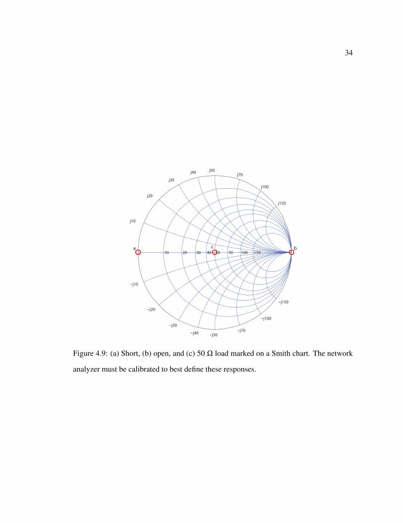
to match the probe spacing. As with all S-parameter measurements, calibration must
be conducted to accurately report the device response. In this case, the probes must be
included in the calibration. A calibration standard is used and consists of three structures,
an open, short, and load. This allows the network analyzer to define the extremes of
possible responses (Fig. 4.9) and map the measurements of the transducers in comparison.
This calibration is done using a Cascade Microtrech-supplied calibration standard. For
this calibration, the reference plane is located at the probe tips, as opposed to the end of
the cables.
34
j150
−j150
j100
−j100
j70
−j70
j50
−j50
j40
−j40
j30
−j30
j20
−j20
j10
−j10
150100705040302010a bc
Figure 4.9: (a) Short, (b) open, and (c) 50 Ω load marked on a Smith chart. The network
analyzer must be calibrated to best define these responses.
DEVELOPMENT OF ACOUSTIC TRANSDUCERS FOR USE IN THEPARAMETRIC PUMPING OF SPIN WAVES
5. RESULTS
With a background in resonators, the fabrication techniques used to make acoustic trans-
ducers and the simulation model established, the outputs can be examined. In this chap-
ter, the input parameters for the Mason Model simulation outlined in section 4.1.1 will
be discussed and the outputs compared to measurements taken from devices made using
the process outlined in section 3.3. Finally, additional physical effects are added to the
simulation to improve the simulation agreement with the measured devices. These ad-
ditions include effects such as series resistance and inductance, and acoustic attenuation
within the transducer structure. The improved simulation results are again compared to
the measured results and show a higher degree of agreement.
5.1 Results from Mason Model Simulation
Several tests are created to validate and characterize the simulation’s operation and
results. Plotted in these tests are the S11 parameters for the simulated device, with dips in
response indicative of an effective transformation of electrical into acoustic energy. The
data is displayed as magnitude plots, highlighting the frequency location and Q-factor of
the acoustic resonances. For these tests, the Q-factor is calculated from a liner plot of the
S11-parameters taking the bandwidth to be the full-width-half-max. The test results fea-
tured in the following sections include: a single piezoelectric layer with varying thickness
and ”substrate,” and a three layer device with varying electrode and ZnO thickness.

36
5.1.1 Single Piezoelectric Layer Simulation Results
The first tests are designed to highlight the piezoelectric layers electro-acoustic
transduction properties and the effects of controllable external parameters, such as layer
thickness and substrate termination.
5.1.1.1 Single Piezoelectric Layer with Varying Thickness
The thickness of the transducer layer has a major effect on the frequency operation
since the fundamental resonance occurs when the acoustic wavelength is equal to twice
the layer thickness, as discussed in section 2.1. Fig. 5.2 is a graph of the magnitude of
the S11 and Z11 response from a single piezoelectric layer device as shown in Fig. 5.1.
Co
-Co 1:hCo
ZT ZT
ZS
Port
Free Surface
“Short” Substrate
Impedance
Figure 5.1: Lone piezoelectric layer simulated with various thicknesses and substrates.
As Fig. 5.2 shows, the resonant frequency follows the expected dependence to layer
thickness based on the acoustic cavity described in section 2.1.1.1. When compared to the
expected resonance frequency based on 1/2 wavelength in ZnO with a velocity of 6135ms ,
there is complete agreement (Table 5.1). The changes in magnitude are a function of the
impedance mismatch between the transducer and probe. As Fig. 5.2 shows, the closeer to
the probe impedance of 50 Ω, the greater the transducer response. The input impedance at
resonance is an important factor to consider when designing transducers as it has a large
effect on the transducers electro-acoustic transduction efficiency.

37
2 2.5 3 3.5 4 4.5 5−10
−9
−8
−7
−6
−5
−4
−3
−2
−1
0
Frequency [GHz]
S11
Mag
nitu
de [d
B]
S11
magnitude for various ZnO thicknesses
700 nm 800 nm 900 nm1000 nm1100 nm1200 nm
(a)
2 2.5 3 3.5 4 4.5 50
50
100
150
200
250
300
Frequency [GHz]
Z11
Mag
nitu
de [Ω
]
Z11
magnitude for various ZnO thicknesses
700 nm 800 nm 900 nm1000 nm1100 nm1200 nm
(b)
Figure 5.2: (a) S11 and (b) impedance magnitude for a lone ZnO layer of various thick-
nesses terminated on both sides by air.
ZnO Thickness Calculated Resonance Simulated Resonance
700 nm 4.38 GHz 4.38 GHz
800 nm 3.83 GHz 3.83 GHz
900 nm 3.41 GHz 3.41 GHz
1000 nm 3.07 GHz 3.07 GHz
1100 nm 2.79 GHz 2.77 GHz
1200 nm 2.56 GHz 2.54 GHz
Table 5.1: Table of resonant frequencies for the lone ZnO layer from Fig. 5.2. Calculated
resonance using Eq. 2.1
38
5.1.1.2 Single Piezoelectric Layer with Varying Termination
The second single layer simulation run is designed to test the effect of the substrate,
or transducer mounting conditions. This can have a major impact on not only the Q-
factor, but also on the mode of resonance. The simulated ZnO layer is mounted with two
extreme conditions, free and fixed, and a realistic glass substrate, all taken to be infinatly
thick, or thick enough that no reflections reach the surface again. The change from free to
mounted on glass shows a reduction in Q-factor and a small change in resonant frequency
(≈ 10 MHz). However, when the surface is fixed, the resonant frequencies of the cavity
are changed. For the free surface case, both sides of the cavity are effectively shorted,
resulting in a resonance occurring when the particle velocity is at a maximum at both
surfaces, as shown in Fig. 2.2, or for wavelengths of vn2t for all n n = 1,2,3... with v the
wave velocity. In the fixed case, the force is at a maximum at the mounted surface while
velocity is maximized at the opposing free surface. This changes the boundary conditions
for the cavity, causing the fundamental resonance to occur when the acoustic wavelength
is four times the layer thickness, as opposed to the other case where it occurs at two times
the thickness. Higher harmonics will continue to occur at 1/2 wavelength intervals, or
for wavelengths of vn4t for odd n n = 1,3,5....
39
0 1 2 3 4 5 6 7 8 9−14
−12
−10
−8
−6
−4
−2
0
Frequency [GHz]
S11
Mag
nitu
de [d
B]
S11
magnitude for various "Substrates"
"High"Glass"Low"
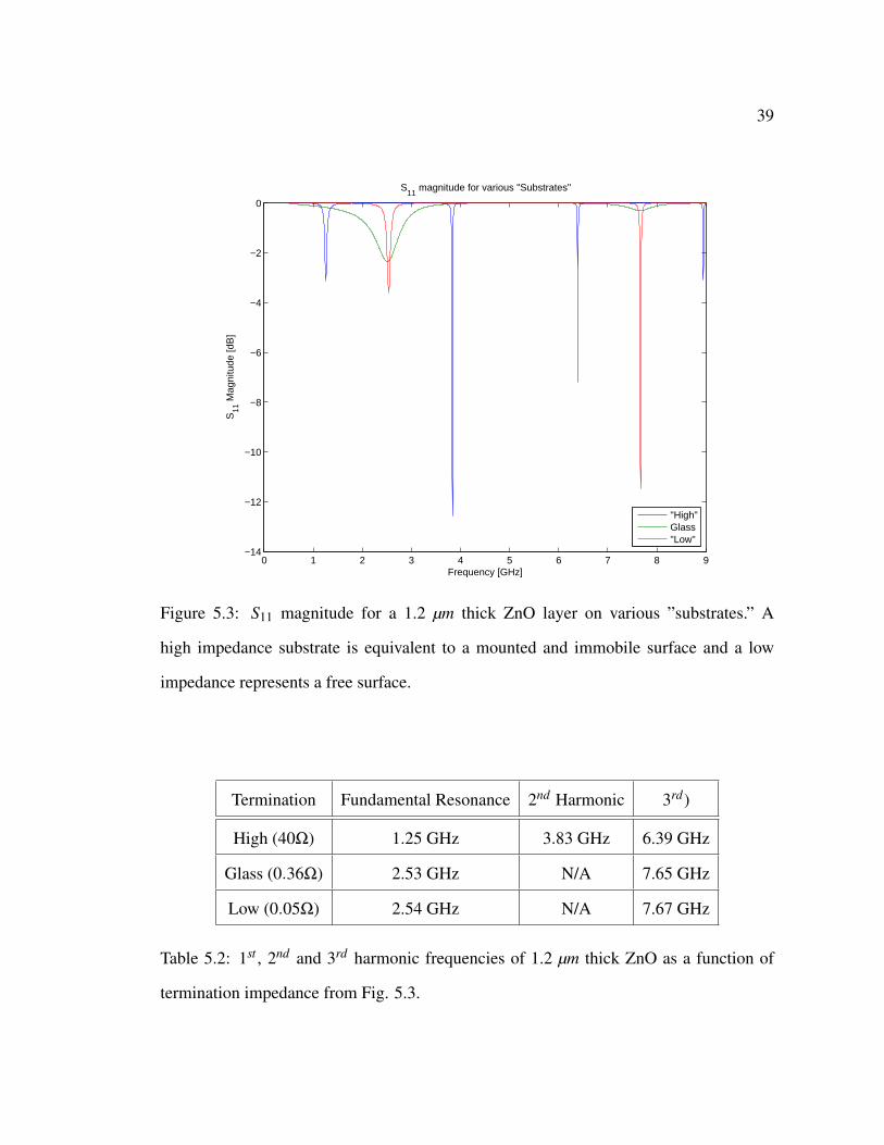
Figure 5.3: S11 magnitude for a 1.2 µm thick ZnO layer on various ”substrates.” A
high impedance substrate is equivalent to a mounted and immobile surface and a low
impedance represents a free surface.
Termination Fundamental Resonance 2nd Harmonic 3rd)
High (40Ω) 1.25 GHz 3.83 GHz 6.39 GHz
Glass (0.36Ω) 2.53 GHz N/A 7.65 GHz
Low (0.05Ω) 2.54 GHz N/A 7.67 GHz
Table 5.2: 1st , 2nd and 3rd harmonic frequencies of 1.2 µm thick ZnO as a function of
termination impedance from Fig. 5.3.
40
While the high impedance resonances occur at the expected 1/2 wavelength inter-
vals, the low impedance termination and the glass substrate are only resonating at the
odd harmonics. This is due to the conditions at the center of the cavity, where the model
approximates the waves propagating from. Since velocity is modeled as away from the
center, the center particles must have no velocity, placing another boundary condition on
the possible resonances. This means that while displacement must be at a maximum at
the surfaces, it must also be minimum at the center, limiting the resonance frequencies to
the odd harmonics, as seen in Fig. 5.3.
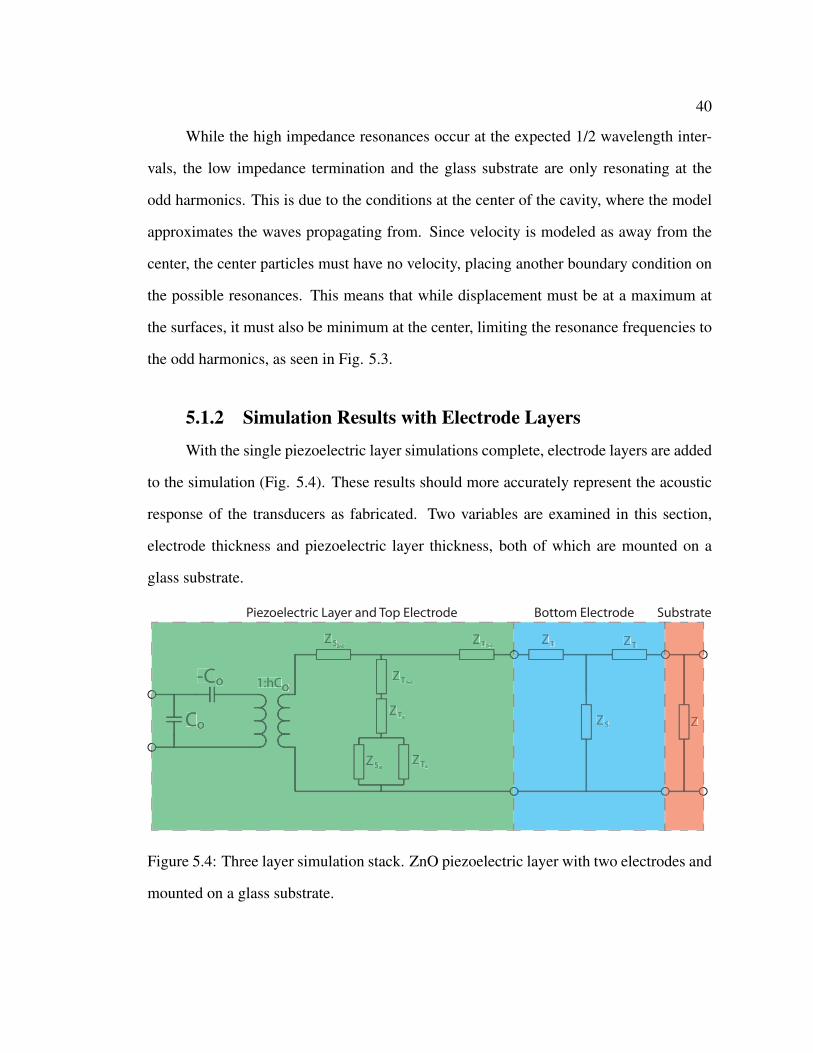
5.1.2 Simulation Results with Electrode Layers
With the single piezoelectric layer simulations complete, electrode layers are added
to the simulation (Fig. 5.4). These results should more accurately represent the acoustic
response of the transducers as fabricated. Two variables are examined in this section,
electrode thickness and piezoelectric layer thickness, both of which are mounted on a
glass substrate.
ZCo
-Co 1:hCoZT
ZTZS
ZT
ZnO
ZnO
ZnO
Al
ZTAlZSAl
ZT ZT
ZSCo
-Co 1:hCoZT
ZTZS
ZT
ZnO
ZnO
ZnO
Al
ZTAlZSAl
ZT ZT
ZS Z
Piezoelectric Layer and Top Electrode Bottom Electrode Substrate
Figure 5.4: Three layer simulation stack. ZnO piezoelectric layer with two electrodes and
mounted on a glass substrate.

41
5.1.2.1 Three Layer Stack with Varying Electrode Thicknesses
The first variable investigated is electrode thickness. With the addition of the elec-
trode layers, the resonance cavity becomes more complicated. There are now more tran-
sitions in acoustic mediums, resulting in more reflections, complicating the resonance
conditions. In Fig. 5.5, the electrode thickness is increased from a minimal 2 nm up to
400 nm, with a middle ground at 200 nm.
0.5 1 1.5 2 2.5 3 3.5 4 4.5 5−3
−2.5
−2
−1.5
−1
−0.5
0
Frequency [GHz]
S11
Mag
nitu
de [d
B]
S11 magnitude for various electrode thicknesses
2nm200nm400nm
Figure 5.5: S11 magnitude for a 1.2 µm thick ZnO layer with various electrode thicknesses
42
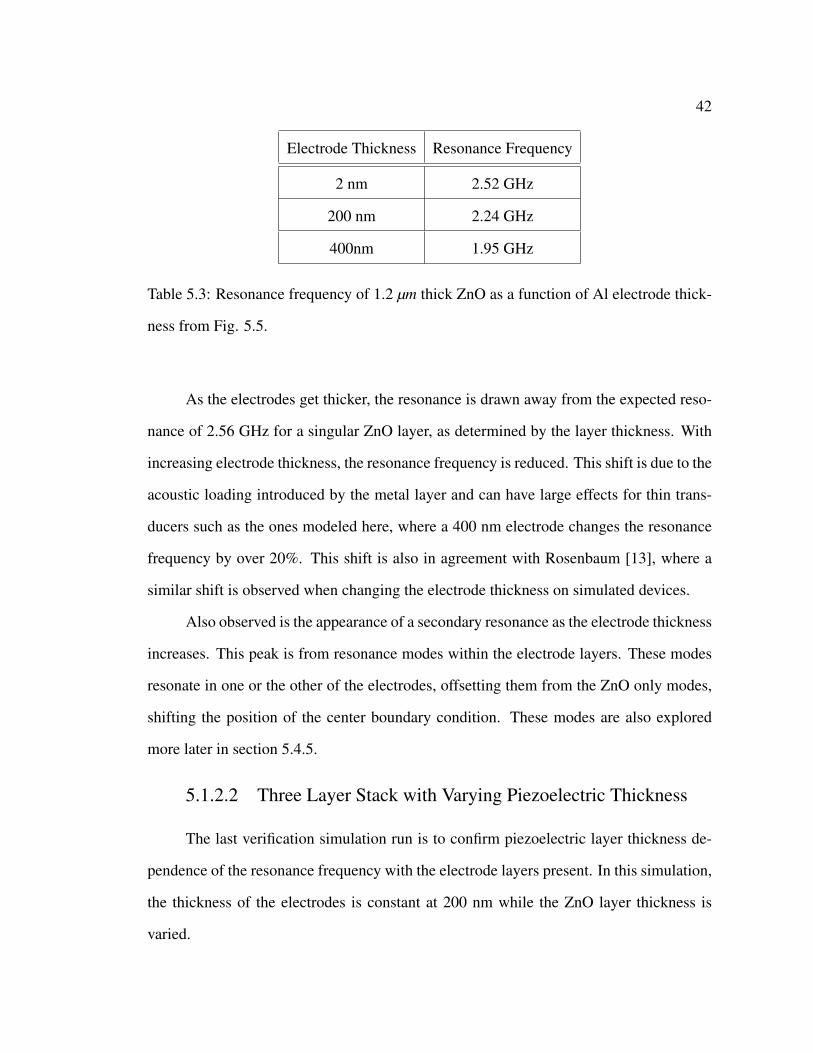
Electrode Thickness Resonance Frequency
2 nm 2.52 GHz
200 nm 2.24 GHz
400nm 1.95 GHz
Table 5.3: Resonance frequency of 1.2 µm thick ZnO as a function of Al electrode thick-
ness from Fig. 5.5.
As the electrodes get thicker, the resonance is drawn away from the expected reso-
nance of 2.56 GHz for a singular ZnO layer, as determined by the layer thickness. With
increasing electrode thickness, the resonance frequency is reduced. This shift is due to the
acoustic loading introduced by the metal layer and can have large effects for thin trans-
ducers such as the ones modeled here, where a 400 nm electrode changes the resonance
frequency by over 20%. This shift is also in agreement with Rosenbaum [13], where a
similar shift is observed when changing the electrode thickness on simulated devices.
Also observed is the appearance of a secondary resonance as the electrode thickness
increases. This peak is from resonance modes within the electrode layers. These modes
resonate in one or the other of the electrodes, offsetting them from the ZnO only modes,
shifting the position of the center boundary condition. These modes are also explored
more later in section 5.4.5.
5.1.2.2 Three Layer Stack with Varying Piezoelectric Thickness
The last verification simulation run is to confirm piezoelectric layer thickness de-
pendence of the resonance frequency with the electrode layers present. In this simulation,
the thickness of the electrodes is constant at 200 nm while the ZnO layer thickness is
varied.
43
0.5 1 1.5 2 2.5 3 3.5 4 4.5 5−3
−2.5
−2
−1.5
−1
−0.5
0
Frequency [GHz]
S11
Mag
nitu
de [d
B]
S11
magnitude for various ZnO thicknesses with 200nm Thick Electrodes
600 nm800 nm1000 nm1200 nm
Figure 5.6: S11 magnitude for a transducer stack with 200 nm electrodes with various
ZnO layer thicknesses
ZnO Thickness Resonance Frequency
600 nm 3.95 GHz
800 nm 3.16 GHz
1000 nm 2.63 GHz
1200 nm 2.24 GHz
Table 5.4: Resonant frequency of 1.2 µm thick ZnO as a function of Al electrode thickness
from Fig. 5.6.
Again, there is a clear, and expected, correlation between the ZnO layer thickness
and the fundamental resonant frequency. We see resonance when the thickness equals
44
1/2 the acoustic wavelength with some apparent lengthening due to loading from the
electrode layers. This effect is important to consider when designing transducers and
matching networks.
We have now established a simulation that represents a three layer acoustic trans-
ducer that can be modeled with the same parameters as transducers fabricated in the clean
room.
5.2 Fabricated Transducer Responses
Following the fabrication procedure discussed in section 3.3, acoustic transduc-
ers using a ZnO piezoelectric layer and Al electrodes were fabricated. In the following
section, the measurement results of these transducers are presented and discussed. All
transducers are fabricated on glass substrates with 200 nm thick electrodes, top and bot-
tom, and varying piezoelectric thicknesses. From the transducers, S11 measurements are
taken and plotted as impedances on Smith charts (Fig. 5.7) and magnitudes on a dB scale
(Fig, 5.8).
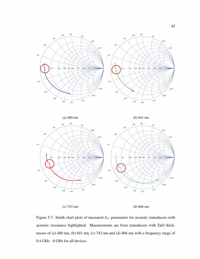
45
j150
−j150
j100
−j100
j70
−j70
j50
−j50
j40
−j40
j30
−j30
j20
−j20
j10
−j10
150100705040302010
(a) 480 nm
j150
−j150
j100
−j100
j70
−j70
j50
−j50
j40
−j40
j30
−j30
j20
−j20
j10
−j10
150100705040302010
(b) 641 nm
j150
−j150
j100
−j100
j70
−j70
j50
−j50
j40
−j40
j30
−j30
j20
−j20
j10
−j10
150100705040302010
(c) 743 nm
j150
−j150
j100
−j100
j70
−j70
j50
−j50
j40
−j40
j30
−j30
j20
−j20
j10
−j10
150100705040302010
(d) 866 nm
Figure 5.7: Smith chart plots of measured S11 parameters for acoustic transducers with
acoustic resonance highlighted. Measurements are from transducers with ZnO thick-
nesses of (a) 480 nm, (b) 641 nm, (c) 743 nm and (d) 866 nm with a frequency range of
0.4 GHz - 8 GHz for all devices.
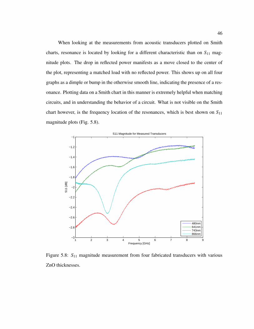
46
When looking at the measurements from acoustic transducers plotted on Smith
charts, resonance is located by looking for a different characteristic than on S11 mag-
nitude plots. The drop in reflected power manifests as a move closed to the center of
the plot, representing a matched load with no reflected power. This shows up on all four
graphs as a dimple or bump in the otherwise smooth line, indicating the presence of a res-
onance. Plotting data on a Smith chart in this manner is extremely helpful when matching
circuits, and in understanding the behavior of a circuit. What is not visible on the Smith
chart however, is the frequency location of the resonances, which is best shown on S11
magnitude plots (Fig. 5.8).
1 2 3 4 5 6 7 8 9−3
−2.8
−2.6
−2.4
−2.2
−2
−1.8
−1.6
−1.4
−1.2
−1
Frequency [GHz]
S11
[dB
]
S11 Magnitude for Measured Transducers
480nm641nm743nm866nm
Figure 5.8: S11 magnitude measurement from four fabricated transducers with various
ZnO thicknesses.
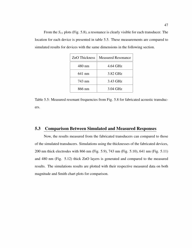
47
From the S11 plots (Fig. 5.8), a resonance is clearly visible for each transducer. The
location for each device is presented in table 5.5. These measurements are compared to
simulated results for devices with the same dimensions in the following section.
ZnO Thickness Measured Resonance
480 nm 4.64 GHz
641 nm 3.82 GHz
743 nm 3.43 GHz
866 nm 3.04 GHz
Table 5.5: Measured resonant frequencies from Fig. 5.8 for fabricated acoustic transduc-
ers.
5.3 Comparison Between Simulated and Measured Responses
Now, the results measured from the fabricated transducers can compared to those
of the simulated transducers. Simulations using the thicknesses of the fabricated devices,
200 nm thick electrodes with 866 nm (Fig. 5.9), 743 nm (Fig. 5.10), 641 nm (Fig. 5.11)
and 480 nm (Fig. 5.12) thick ZnO layers is generated and compared to the measured
results. The simulations results are plotted with their respective measured data on both
magnitude and Smith chart plots for comparison.
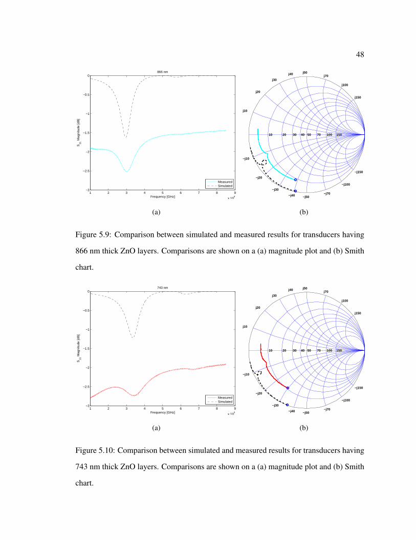
48
1 2 3 4 5 6 7 8 9
x 109
−3
−2.5
−2
−1.5
−1
−0.5
0
Frequency [GHz]
S11
Mag
nitu
de [d
B]
866 nm
MeasuredSimulated
(a)
j150
−j150
j100
−j100
j70
−j70
j50
−j50
j40
−j40
j30
−j30
j20
−j20
j10
−j10
150100705040302010
(b)
Figure 5.9: Comparison between simulated and measured results for transducers having
866 nm thick ZnO layers. Comparisons are shown on a (a) magnitude plot and (b) Smith
chart.
1 2 3 4 5 6 7 8 9
x 109
−3
−2.5
−2
−1.5
−1
−0.5
0
Frequency [GHz]
S11
Mag
nitu
de [d
B]
743 nm
MeasuredSimulated
(a)
j150
−j150
j100
−j100
j70
−j70
j50
−j50
j40
−j40
j30
−j30
j20
−j20
j10
−j10
150100705040302010
(b)
Figure 5.10: Comparison between simulated and measured results for transducers having
743 nm thick ZnO layers. Comparisons are shown on a (a) magnitude plot and (b) Smith
chart.
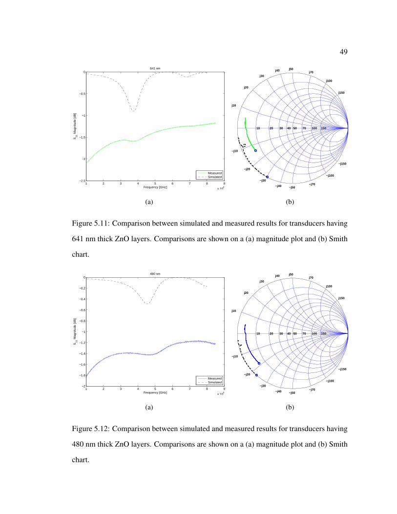
49
1 2 3 4 5 6 7 8 9
x 109
−2.5
−2
−1.5
−1
−0.5
0
Frequency [GHz]
S11
Mag
nitu
de [d
B]
641 nm
MeasuredSimulated
(a)
j150
−j150
j100
−j100
j70
−j70
j50
−j50
j40
−j40
j30
−j30
j20
−j20
j10
−j10
150100705040302010
(b)
Figure 5.11: Comparison between simulated and measured results for transducers having
641 nm thick ZnO layers. Comparisons are shown on a (a) magnitude plot and (b) Smith
chart.
1 2 3 4 5 6 7 8 9
x 109
−2
−1.8
−1.6
−1.4
−1.2
−1
−0.8
−0.6
−0.4
−0.2
0
Frequency [GHz]
S11
Mag
nitu
de [d
B]
480 nm
MeasuredSimulated
(a)
j150
−j150
j100
−j100
j70
−j70
j50
−j50
j40
−j40
j30
−j30
j20
−j20
j10
−j10
150100705040302010
(b)
Figure 5.12: Comparison between simulated and measured results for transducers having
480 nm thick ZnO layers. Comparisons are shown on a (a) magnitude plot and (b) Smith
chart.
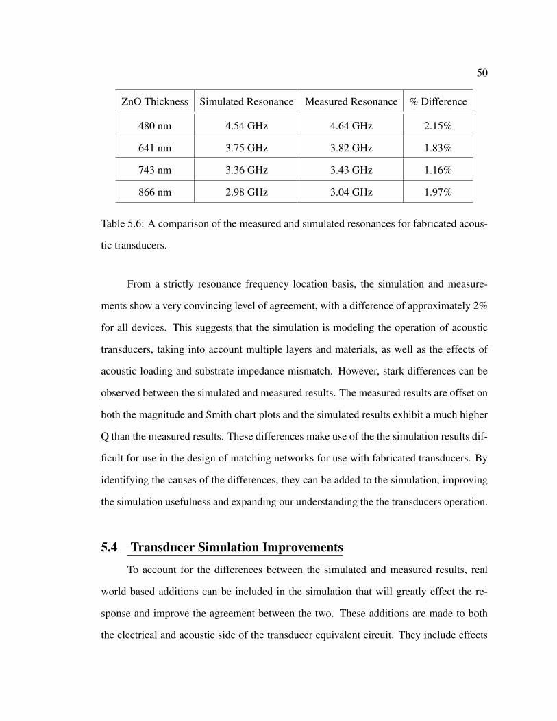
50
ZnO Thickness Simulated Resonance Measured Resonance % Difference
480 nm 4.54 GHz 4.64 GHz 2.15%
641 nm 3.75 GHz 3.82 GHz 1.83%
743 nm 3.36 GHz 3.43 GHz 1.16%
866 nm 2.98 GHz 3.04 GHz 1.97%
Table 5.6: A comparison of the measured and simulated resonances for fabricated acous-
tic transducers.
From a strictly resonance frequency location basis, the simulation and measure-
ments show a very convincing level of agreement, with a difference of approximately 2%
for all devices. This suggests that the simulation is modeling the operation of acoustic
transducers, taking into account multiple layers and materials, as well as the effects of
acoustic loading and substrate impedance mismatch. However, stark differences can be
observed between the simulated and measured results. The measured results are offset on
both the magnitude and Smith chart plots and the simulated results exhibit a much higher
Q than the measured results. These differences make use of the the simulation results dif-
ficult for use in the design of matching networks for use with fabricated transducers. By
identifying the causes of the differences, they can be added to the simulation, improving
the simulation usefulness and expanding our understanding the the transducers operation.
5.4 Transducer Simulation Improvements
To account for the differences between the simulated and measured results, real
world based additions can be included in the simulation that will greatly effect the re-
sponse and improve the agreement between the two. These additions are made to both
the electrical and acoustic side of the transducer equivalent circuit. They include effects

51
such as series and shunt resistance, series inductance, and attenuation within the acoustic
transducer, which was not included in the original simulation. Each of these additions are
added to the simulation individually in the following sections in order identify their ef-
fects before being combined into a final improved simulation. All the simulations are run
holding thickness parameters constant with an 800 nm thick ZnO layer and 200 nm thick
Al electrodes all mounted on glass. S11 magnitudes are plotted on dB scale magnitude
plots, and Z11 results are plotted on 50 Ω characteristic Smith charts.
5.4.1 Series Resistance
The first addition the the Mason model simulation is the inclusion of series resis-
tance. Series resistance can come from many sources in the measurement setup used. The
most likely sources in these experiments are from contact resistance between the probe
tips and the aluminum pads and from resistance within the aluminum, especially at the
connection over the step formed by the ZnO layer when connecting to the top electrode.
The addition of series resistance reduces the reflected signal across all frequencies. This
is seen on the magnitude plot (Fig. 5.14 a) as a frequency independent drop in the S11
response. On the Smith chart representation (Fig. 5.14 b), the plot moves closer to the
center since less power is being reflected, looking like a better matched circuit.
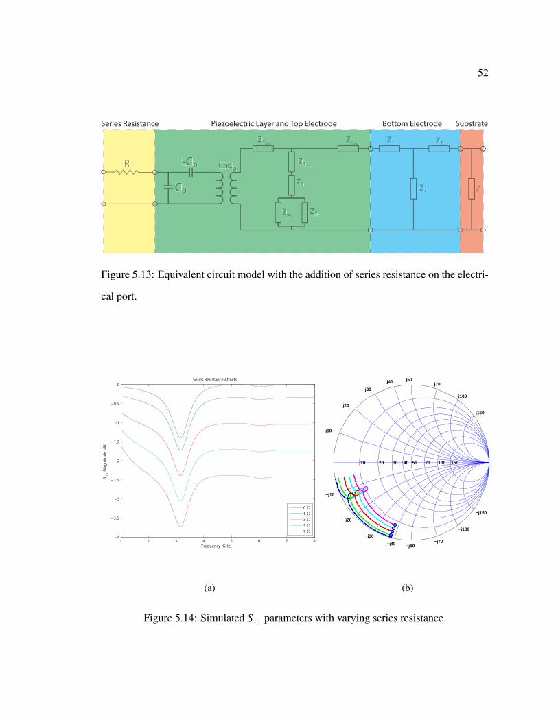
52
ZCo
-Co 1:hCoZT
ZTZS
ZT
ZnO
ZnO
ZnO
Al
ZTAlZSAl
ZT ZT
ZSCo
-Co 1:hCoZT
ZTZS
ZT
ZnO
ZnO
ZnO
Al
ZTAlZSAl
ZT ZT
ZS Z
Piezoelectric Layer and Top Electrode Bottom Electrode Substrate
RR
Series Resistance
Figure 5.13: Equivalent circuit model with the addition of series resistance on the electri-
cal port.
1 2 3 4 5 6 7 8−4
−3.5
−3
−2.5
−2
−1.5
−1
−0.5
0
Frequency [GHz]
S1
1 M
ag
nit
ud
e [
dB
]
Series Resistance A"ects
0 Ω
1 Ω
3 Ω
5 Ω
7 Ω
(a)
j150
−j150
j100
−j100
j70
−j70
j50
−j50
j40
−j40
j30
−j30
j20
−j20
j10
−j10
150100705040302010
(b)
Figure 5.14: Simulated S11 parameters with varying series resistance.
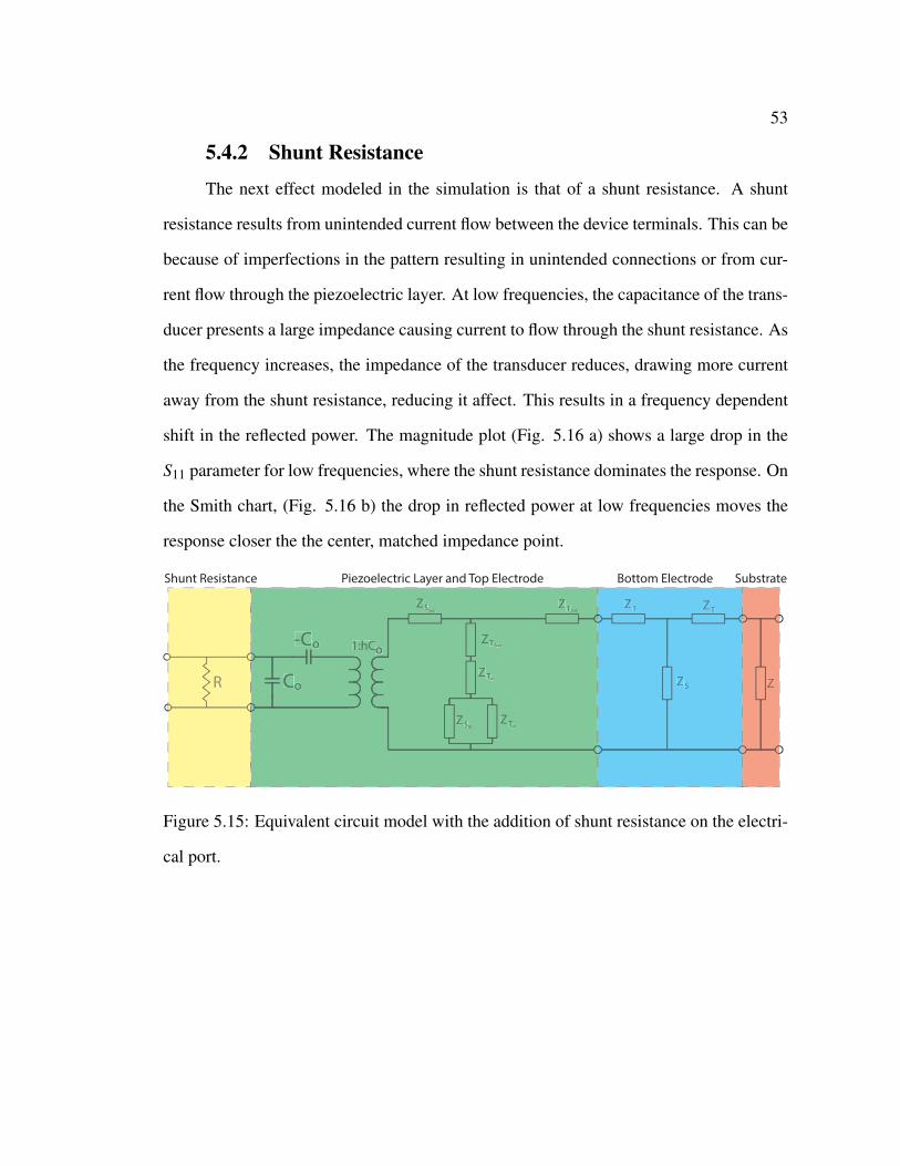
53
5.4.2 Shunt Resistance
The next effect modeled in the simulation is that of a shunt resistance. A shunt
resistance results from unintended current flow between the device terminals. This can be
because of imperfections in the pattern resulting in unintended connections or from cur-
rent flow through the piezoelectric layer. At low frequencies, the capacitance of the trans-
ducer presents a large impedance causing current to flow through the shunt resistance. As
the frequency increases, the impedance of the transducer reduces, drawing more current
away from the shunt resistance, reducing it affect. This results in a frequency dependent
shift in the reflected power. The magnitude plot (Fig. 5.16 a) shows a large drop in the
S11 parameter for low frequencies, where the shunt resistance dominates the response. On
the Smith chart, (Fig. 5.16 b) the drop in reflected power at low frequencies moves the
response closer the the center, matched impedance point.
ZCo
-Co 1:hCoZT
ZTZS
ZT
ZnO
ZnO
ZnO
Al
ZTAlZSAl
ZT ZT
ZSCo
-Co 1:hCoZT
ZTZS
ZT
ZnO
ZnO
ZnO
Al
ZTAlZSAl
ZT ZT
ZS Z
Piezoelectric Layer and Top Electrode Bottom Electrode Substrate
RR
Shunt Resistance
Figure 5.15: Equivalent circuit model with the addition of shunt resistance on the electri-
cal port.

54
1 2 3 4 5 6 7 8−3.5
−3
−2.5
−2
−1.5
−1
−0.5
0
Frequency [GHz]
S1
1 M
ag
nit
ud
e [
dB
]
Series Resistance A"ects
Open
1000 Ω
500 Ω
250 Ω
100 Ω
(a)
j150
−j150
j100
−j100
j70
−j70
j50
−j50
j40
−j40
j30
−j30
j20
−j20
j10
−j10
150100705040302010
(b)
Figure 5.16: Simulated S11 parameters with varying shunt resistance.
5.4.3 Series Inductance
Next, a series inductance is added to the simulation. This inductance comes from
the leads connecting the probe touchdown pads to the transducer. The effect is especially
important as the use of wire bonds in future transducer implementations will contribute a
substantial inductance to the circuit that will need to be included in design considerations.
The addition of a series inductance does not substantially alter the magnitude of the S11
response (Fig. 5.18 a), but does change the measured impedance of the transducer. The
Smith chart (Fig. 5.18 b) shows a rotation toward the inductive half of the graph. This
shift suggests that designed application of series inductance can be used to improve the
impedance matching of the transducer.
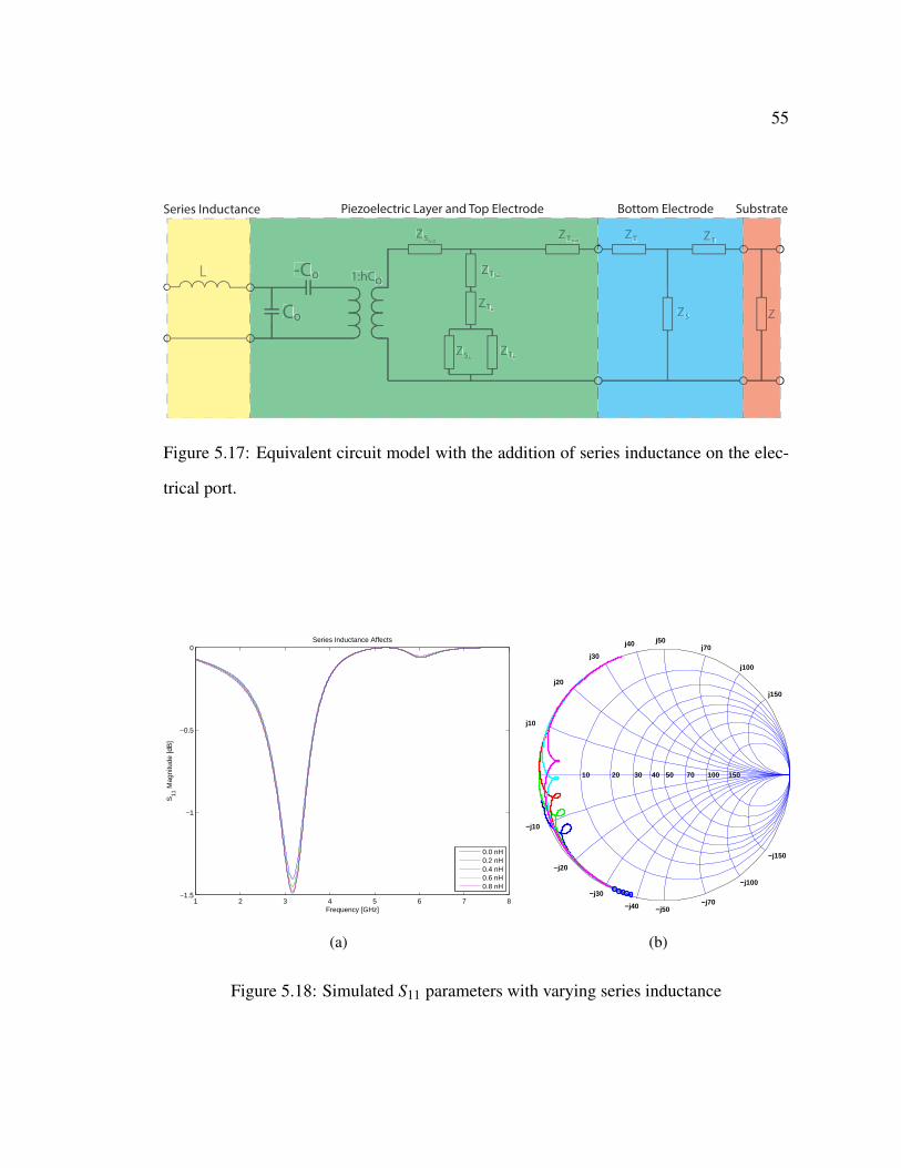
55
ZCo
-Co 1:hCoZT
ZTZS
ZT
ZnO
ZnO
ZnO
Al
ZTAlZSAl
ZT ZT
ZSCo
-Co 1:hCoZT
ZTZS
ZT
ZnO
ZnO
ZnO
Al
ZTAlZSAl
ZT ZT
ZS Z
Piezoelectric Layer and Top Electrode Bottom Electrode Substrate
LL
Series Inductance
Figure 5.17: Equivalent circuit model with the addition of series inductance on the elec-
trical port.
1 2 3 4 5 6 7 8−1.5
−1
−0.5
0
Frequency [GHz]
S11
Mag
nitu
de [d
B]
Series Inductance Affects
0.0 nH0.2 nH0.4 nH0.6 nH0.8 nH
(a)
j150
−j150
j100
−j100
j70
−j70
j50
−j50
j40
−j40
j30
−j30
j20
−j20
j10
−j10
150100705040302010
(b)
Figure 5.18: Simulated S11 parameters with varying series inductance
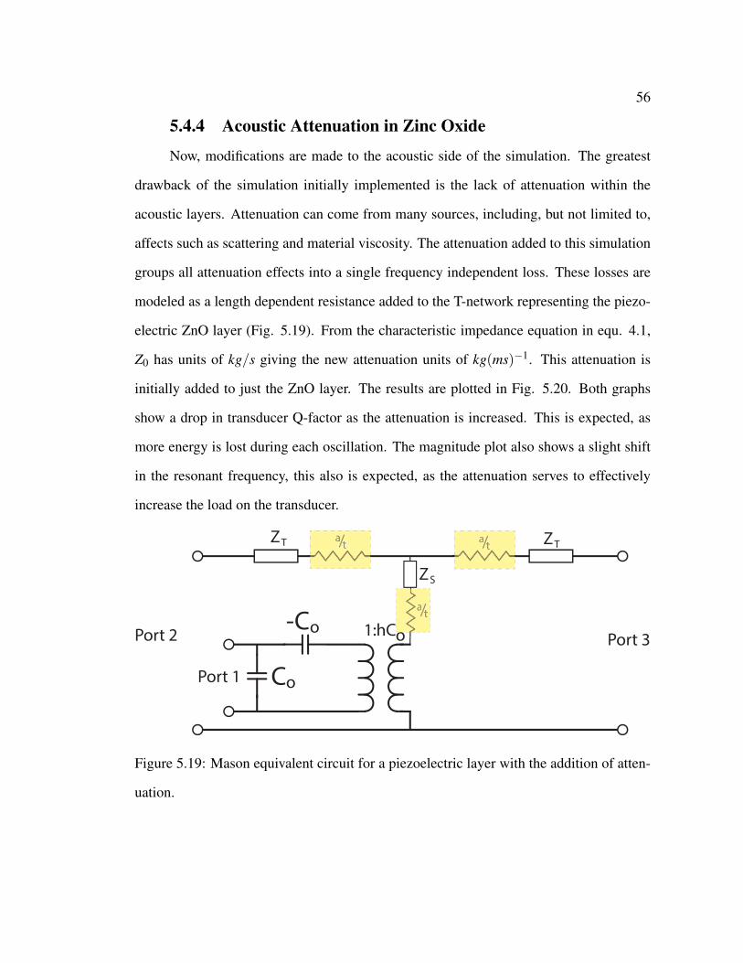
56
5.4.4 Acoustic Attenuation in Zinc Oxide
Now, modifications are made to the acoustic side of the simulation. The greatest
drawback of the simulation initially implemented is the lack of attenuation within the
acoustic layers. Attenuation can come from many sources, including, but not limited to,
affects such as scattering and material viscosity. The attenuation added to this simulation
groups all attenuation effects into a single frequency independent loss. These losses are
modeled as a length dependent resistance added to the T-network representing the piezo-
electric ZnO layer (Fig. 5.19). From the characteristic impedance equation in equ. 4.1,
Z0 has units of kg/s giving the new attenuation units of kg(ms)−1. This attenuation is
initially added to just the ZnO layer. The results are plotted in Fig. 5.20. Both graphs
show a drop in transducer Q-factor as the attenuation is increased. This is expected, as
more energy is lost during each oscillation. The magnitude plot also shows a slight shift
in the resonant frequency, this also is expected, as the attenuation serves to effectively
increase the load on the transducer.
Co
-Co 1:hCo
ZT ZT
ZS
Port 1
Port 2 Port 3
a/ta/a t//
a/ta/a t//
oo
a/ta/a t//
Figure 5.19: Mason equivalent circuit for a piezoelectric layer with the addition of atten-
uation.
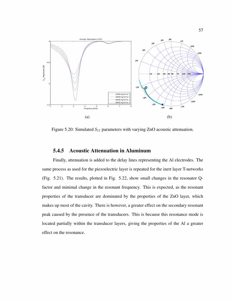
57
1 2 3 4 5 6 7 8−1.5
−1
−0.5
0
Frequency [GHz]
S11
Mag
nitu
de [d
B]
Acoustic Attenuation in ZnO
20000 kg*(m*s)−1
40000 kg*(m*s)−1
60000 kg*(m*s)−1
80000 kg*(m*s)−1
(a)
j150
−j150
j100
−j100
j70
−j70
j50
−j50
j40
−j40
j30
−j30
j20
−j20
j10
−j10
150100705040302010
(b)
Figure 5.20: Simulated S11 parameters with varying ZnO acoustic attenuation.
5.4.5 Acoustic Attenuation in Aluminum
Finally, attenuation is added to the delay lines representing the Al electrodes. The
same process as used for the piezoelectric layer is repeated for the inert layer T-networks
(Fig. 5.21). The results, plotted in Fig. 5.22, show small changes in the resonator Q-
factor and minimal change in the resonant frequency. This is expected, as the resonant
properties of the transducer are dominated by the properties of the ZnO layer, which
makes up most of the cavity. There is however, a greater effect on the secondary resonant
peak caused by the presence of the transducers. This is because this resonance mode is
located partially within the transducer layers, giving the properties of the Al a greater
effect on the resonance.
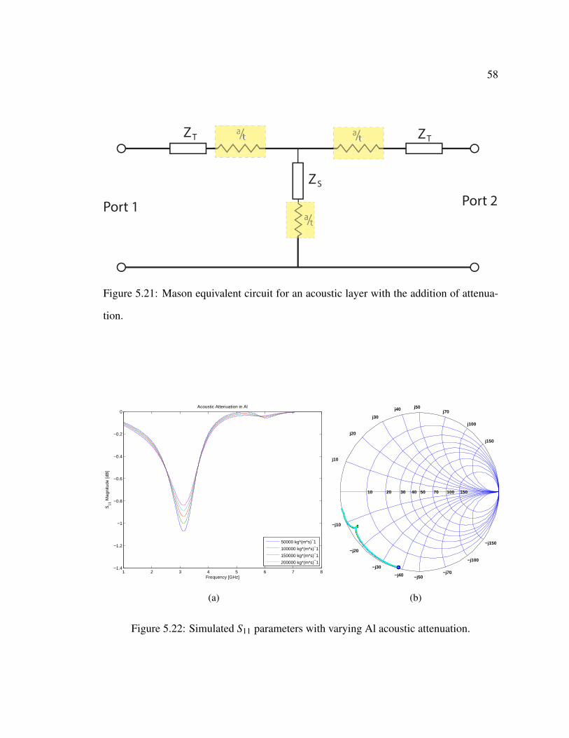
58
ZT ZT
ZS
Port 1Port 2
a/ta/a t// a/t
a/a t//
a/ta/a t//
Figure 5.21: Mason equivalent circuit for an acoustic layer with the addition of attenua-
tion.
1 2 3 4 5 6 7 8−1.4
−1.2
−1
−0.8
−0.6
−0.4
−0.2
0
Frequency [GHz]
S11
Mag
nitu
de [d
B]
Acoustic Attenuation in Al
50000 kg*(m*s)−1
100000 kg*(m*s)−1
150000 kg*(m*s)−1
200000 kg*(m*s)−1
(a)
j150
−j150
j100
−j100
j70
−j70
j50
−j50
j40
−j40
j30
−j30
j20
−j20
j10
−j10
150100705040302010
(b)
Figure 5.22: Simulated S11 parameters with varying Al acoustic attenuation.

59
5.5 Improved Simulation Comparison
With the new affects now included to the simulation, they can be fine tuned to better
match the simulated and measured results. Electrical effects are tuned on an individual
bases while attenuation effects are tuned to best match all cases. This is due to the fact
that all the physical layer properties should be constant for all devices, while the electrical
effects modeled can easily vary from device to device. These parameters are not neces-
sarily the optimized or unique, but serve to demonstrate the presence of the affects in the
fabricated devices and the improved usefulness of the simulation with their additions.

60
1 2 3 4 5 6 7 8 9
x 109
−2.6
−2.4
−2.2
−2
−1.8
−1.6
−1.4
−1.2
Frequency [GHz]
S11
Mag
nitu
de [d
B]
866 nm
MeasuredSimulated
(a)
j150
−j150
j100
−j100
j70
−j70
j50
−j50
j40
−j40
j30
−j30
j20
−j20
j10
−j10
150100705040302010
(b)
Figure 5.23: Comparison between improved simulation and measured results for trans-
ducers having 866 nm thick ZnO layers. Comparisons are shown on a magnitude plot(a)
and on a Smith chart (b).
Simulation Parameter Value Unit
Series Resistance 4.3 Ω
Shunt Resistance 400 Ω
Series Inductance 0.14 nH
ZnO Attenuation 11000 kgms
Al Attenuation 30000 kgms
Table 5.7: Parameters of the additional affects included in the simulation of 866 nm
transducers.
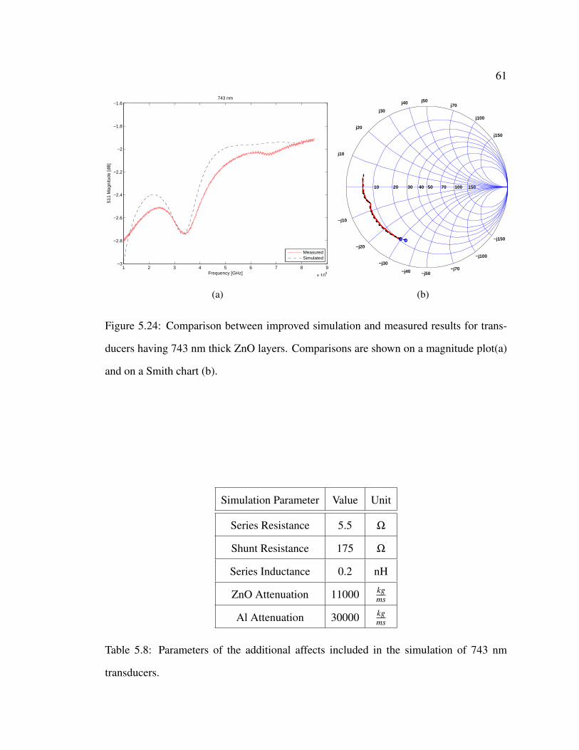
61
1 2 3 4 5 6 7 8 9
x 109
−3
−2.8
−2.6
−2.4
−2.2
−2
−1.8
−1.6
Frequency [GHz]
S11
Mag
nitu
de [d
B]
743 nm
MeasuredSimulated
(a)
j150
−j150
j100
−j100
j70
−j70
j50
−j50
j40
−j40
j30
−j30
j20
−j20
j10
−j10
150100705040302010
(b)
Figure 5.24: Comparison between improved simulation and measured results for trans-
ducers having 743 nm thick ZnO layers. Comparisons are shown on a magnitude plot(a)
and on a Smith chart (b).
Simulation Parameter Value Unit
Series Resistance 5.5 Ω
Shunt Resistance 175 Ω
Series Inductance 0.2 nH
ZnO Attenuation 11000 kgms
Al Attenuation 30000 kgms
Table 5.8: Parameters of the additional affects included in the simulation of 743 nm
transducers.
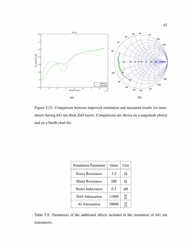
62
1 2 3 4 5 6 7 8 9
x 109
−2.2
−2
−1.8
−1.6
−1.4
−1.2
−1
−0.8
Frequency [GHz]
S11
Mag
nitu
de [d
B]
641 nm
MeasuredSimulated
(a)
j150
−j150
j100
−j100
j70
−j70
j50
−j50
j40
−j40
j30
−j30
j20
−j20
j10
−j10
150100705040302010
(b)
Figure 5.25: Comparison between improved simulation and measured results for trans-
ducers having 641 nm thick ZnO layers. Comparisons are shown on a magnitude plot(a)
and on a Smith chart (b).
Simulation Parameter Value Unit
Series Resistance 3.5 Ω
Shunt Resistance 200 Ω
Series Inductance 0.3 nH
ZnO Attenuation 11000 kgms
Al Attenuation 30000 kgms
Table 5.9: Parameters of the additional affects included in the simulation of 641 nm
transducers.
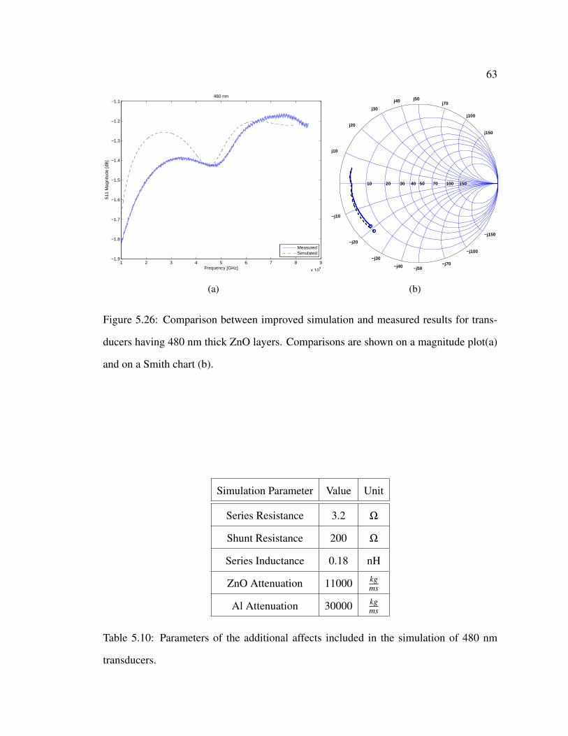
63
1 2 3 4 5 6 7 8 9
x 109
−1.9
−1.8
−1.7
−1.6
−1.5
−1.4
−1.3
−1.2
−1.1
Frequency [GHz]
S11
Mag
nitu
de [d
B]
480 nm
MeasuredSimulated
(a)
j150
−j150
j100
−j100
j70
−j70
j50
−j50
j40
−j40
j30
−j30
j20
−j20
j10
−j10
150100705040302010
(b)
Figure 5.26: Comparison between improved simulation and measured results for trans-
ducers having 480 nm thick ZnO layers. Comparisons are shown on a magnitude plot(a)
and on a Smith chart (b).
Simulation Parameter Value Unit
Series Resistance 3.2 Ω
Shunt Resistance 200 Ω
Series Inductance 0.18 nH
ZnO Attenuation 11000 kgms
Al Attenuation 30000 kgms
Table 5.10: Parameters of the additional affects included in the simulation of 480 nm
transducers.
64
When compared to the initial simulation results, the enhanced simulation shows a
much greater degree of agreement with the measured results. The impedance parameters,
as seen on the Smith charts, show a high level of agreement, making the simulations use
in design of matching networks possible. Some devices still show some differences that
appear clearly in some of the magnitude plots. These could be could be reduced further by
continued tuning of simulation parameters or by the inclusion of more complex effects,
such as frequency dependent attenuation and other higher order phenomenon.
DEVELOPMENT OF ACOUSTIC TRANSDUCERS FOR USE IN THEPARAMETRIC PUMPING OF SPIN WAVES
6. CONCLUSION
The goal of the work presented here was to create a simulation of, and fabricate, thin-film
bulk acoustic transducers for application in the parametric pumping of spin waves. A 1-D
Mason-model-based representation of an acoustic transducer stack was created and sev-
eral acoustic transducers were fabricated and measurements were taken. The conclusions
drawn from this work, along with recommendations for the next steps in the project to
create an acoustic spin wave pump, are presented here.
6.1 Summary
A base Mason model simulation was created using ABCD-parameters in MAT-
LAB was created to model the operation of thin-film acoustic transducers. The model
has been tested and characterized using several experiments, such as simulating a lone
piezoelectric layer and a three layer transducer stack. The results obtained exhibit the
characteristics expected from the transducer being modeled. However when compared to
the results of fabricated transducers, the transducer impedance did not completely agree.
Several additional phenomenon were identified as possible contributing factors the the
disagreement between the simulated and measured results. These additions, series resis-
tance, shunt resistance, series inductance, and acoustic attenuation, when added to the
base model, greatly improved the agreement between the simulated and measured results.
By optimizing these parameters to match measured results, the simulation can also be
used to learn more about fabricated devices, such as attenuation or external electrical ef-
fects, rather then simply predicting device operation prior to fabrication. The equivalent
66
circuit model presented is deemed an accurate model of acoustic transducer response and
is a valuable tool for the design of transducer circuit design. Improvements can still be
made to the simulation, such as a better representation of the acoustic attenuation mech-
anisms. [14] offers a method of representing material properties as complex coefficients
which might improve the results obtained from the simulation.
The fabrication process is also deemed a success. Several devices have been fab-
ricated with varying thicknesses resulting in resonant responses that fall close to a first
order approximation frequency, with the difference accounted for in the simulation by the
presence of acoustic loading caused by the presence of electrodes. This process is ready
for application in the next stages of the acoustic spin wave pump project.
6.2 Future Work
The next step of the project is to integrate the acoustic transducer with a spin wave
excitation/measurement setup (Fig. 6.1). For this stage, acoustic transducers are patterned
onto GGG (Gadolinium Gallium Garnet) substrates with a magnetic Yttrium Iron Garnet
(YIG) thin film on the opposing face. GGG has low acoustic losses and functions as a
cavity forming a High-Overtone Bulk Acoustic Resonator. This resonator will be used to
apply stress and strain the YIG thin film, altering its magnetic properties. These properties
effect the oscillation and propagation of spin waves, and when varied at twice the spin
wave frequency will parametrically pump the propagating spin wave.
This integration process may pose challenges as the spin wave is propagated in
a YIG waveguide whose shape, a thin strip approximately 2-3 mm wide, makes mea-
surement and connections difficult. A spin wave excitation/measurement setup has been
created but was not presented in this work. At this point, the best connection method
available is a wire bond from a stripline patterned on a PCB, allowing for a connection
to the acoustic transducer. This will most likely require the design of a matching net-

67
Spin Wave Propogation
YIGGGG
Al
ZnO
Input
Output Applied Field
YIG- Yittrium Iron Garnet (Y3Fe5O12)GGG - Gadolinium Gallium Garnet (Gd3Ga5O12)ZnO - Zinc OxideAl - Aluminium
Figure 6.1: Diagram showing an integrated acoustic spin wave pump. The transducer
presented in this work is patterned onto the YIG spin wave waveguide.
work to maximize the RF power transfered to the transducer and into acoustic waves.
The transducer itself can most likely be pattered directly onto the YIG substrate using
a shadow mask to pattern the layers since the probe landing pads required for the test
devices described here will not be needed.
68
BIBLIOGRAPHY
1. M. Kostylev, A. Serga, T. Schneider, B. Leven, and B. Hillebrands, “Spin-wavelogical gates,” Applied Physics Letters, vol. 87, no. 15, pp. 153 501 – 153 501–3,2005.
2. T. Schneider, A. Serga, B. Leven, B. Hillebrands, R. Stamps, and M. Kostylev,“Realization of spin-wave logic gates,” Applied Physics Letters, vol. 92, no. 2, pp.022 505–022 505–3, 2008.
3. W. P. Mason, Electromechanical transducers and wave filters. Princeton, NJ: VanNostranc Co., 1948.
4. W. Mason, Physical Acoustics and The Properties of Solids. Princeton, NJ: VanNostranc Co., 1958.
5. G. Guilbault, B. Hock, and R. Schmid, “A piezoelectric immunobiosensor foratrazine in drinking water,” Biosensors and Bioelectronics, vol. 7, no. 6, pp. 411–419, 1992.
6. J. G. Drenthen and G. de Boer, “The manufacturing of ultrasonic gas flow meters,”Flow Measurement and Instrumentation, vol. 12, no. 2, pp. 89 – 99, 2001.
7. J. G. Gualtieri, J. A. Kosinski, and A. Ballato, “Piezoelectric materials for acous-tic wave applications,” IEEE Transactions on Ultrasonics, Ferroelectrics, and Fre-quency Control, vol. 41, no. 1, pp. 53–59, 1994.
8. P. Gopal and N. A. Spaldin, “Polarization, piezoelectric constants, and elastic con-stants of zno, mgo, and cdo,” Journal of Electronic Material, vol. 35, no. 4, 2006.
9. S. Wolf and R. Tauber, Silicon Processing for the VLSI Era, Vol 1: Process Technol-ogy. Sunset Beach CA: Lattice Press, 2000.
10. R. Krimholtz, D. Leedom, and G. Matthaei, “New equivalent circuits for elementarypiezoelectric transducers,” Electronics Letters, vol. 6, no. 12, pp. 398 – 399, 1970.
11. S. Sherrit, S. Leary, B. Dolgin, and Y. Bar-Cohen, “Comparison of the mason andklm equivalent circuits for piezoelectric resonators in the thickness mode,” in Ultra-sonics Symposium, 1999. Proceedings. 1999 IEEE, vol. 2, 1999, pp. 921 – 926.
12. D. A. Frickey, “Conversions between S, Z, Y, h, ABCD, and t parameters which arevalid for complex source and load impedances,” IEEE Transactions on MicrowaveTheory and Techniques, vol. 42, no. 2, pp. 205–211, 1994.
13. J. Rosenbaum, Bilk Acoustic Wave Theory and Devices. 685 Canton Street Nor-wood, MA 02062: Artech House, 1988.

69
14. R. Holland, “Representation of dielectric, elastic, and piezoelectric losses by com-plex coefficients,” IEEE Transactions on Sonics and Ultrasonics, vol. SU-14, no. 1,pp. 18–20, 1967.

70
APPENDICES

A. MASON MODEL MATLAB CODE
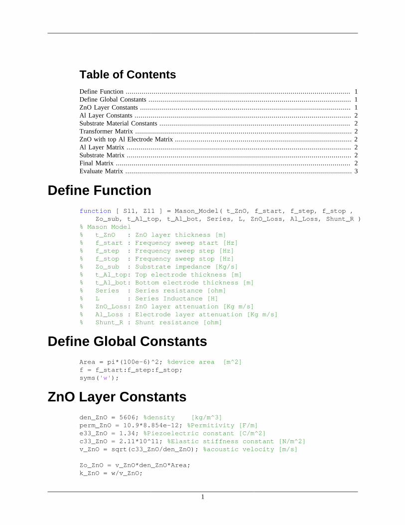
1
Table of ContentsDefine Function ................................................................................................................. 1Define Global Constants ...................................................................................................... 1ZnO Layer Constants .......................................................................................................... 1Al Layer Constants ............................................................................................................. 2Substrate Material Constants ................................................................................................ 2Transformer Matrix ............................................................................................................. 2ZnO with top Al Electrode Matrix ......................................................................................... 2Al Layer Matrix ................................................................................................................. 2Substrate Matrix ................................................................................................................. 2Final Matrix ...................................................................................................................... 2Evaluate Matrix .................................................................................................................. 3
Define Functionfunction [ S11, Z11 ] = Mason_Model( t_ZnO, f_start, f_step, f_stop , Zo_sub, t_Al_top, t_Al_bot, Series, L, ZnO_Loss, Al_Loss, Shunt_R )% Mason Model% t_ZnO : ZnO layer thickness [m]% f_start : Frequency sweep start [Hz]% f_step : Frequency sweep step [Hz]% f_stop : Frequency sweep stop [Hz]% Zo_sub : Substrate impedance [Kg/s]% t_Al_top: Top electrode thickness [m]% t_Al_bot: Bottom electrode thickness [m]% Series : Series resistance [ohm]% L : Series Inductance [H]% ZnO_Loss: ZnO layer attenuation [Kg m/s]% Al_Loss : Electrode layer attenuation [Kg m/s]% Shunt_R : Shunt resistance [ohm]
Define Global ConstantsArea = pi*(100e-6)^2; %device area [m^2]f = f_start:f_step:f_stop;syms('w');
ZnO Layer Constantsden_ZnO = 5606; %density [kg/m^3]perm_ZnO = 10.9*8.854e-12; %Permitivity [F/m]e33_ZnO = 1.34; %Piezoelectric constant [C/m^2]c33_ZnO = 2.11*10^11; %Elastic stiffness constant [N/m^2]v_ZnO = sqrt(c33_ZnO/den_ZnO); %acoustic velocity [m/s]
Zo_ZnO = v_ZnO*den_ZnO*Area;k_ZnO = w/v_ZnO;

2
Al Layer Constantsden_Al = 2700; %Density of Al [Kg/m^3]v_Al = 5000; %Acoustic Velocity in Al [m/s]
Zo_Al = den_Al*v_Al*Area;k_Al = w/v_Al;
Substrate Material Constantsv_glass = 3962; %Acoustic Velocity in Al [m/s]den_glass = 2648; %Density of Glass [Kg/m^3]
Transformer MatrixCo = perm_ZnO*Area/t_ZnO;Kt = sqrt(e33_ZnO^2/(c33_ZnO*perm_ZnO));h = Kt*sqrt(c33_ZnO/perm_ZnO);
Matrix_1 = [1,Series;0,1]*[1,0;1/Shunt_R,1]*[1,1i*w*L;0,1]* [1,0;1i*w*Co,1]*[1,-1/(1i*w*Co);0,1]*[1/(h*Co),0;0,(h*Co)];
ZnO with top Al Electrode MatrixZs_ZnO = -1i*Zo_ZnO/sin(k_ZnO*t_ZnO)+ZnO_Loss*t_ZnO;Zt_ZnO = 1i*Zo_ZnO*tan(k_ZnO*t_ZnO/2)+ZnO_Loss*t_ZnO;
Zs_Al_top = -1i*Zo_Al/sin(k_Al*t_Al_top)+Al_Loss*t_Al_top;Zt_Al_top = 1i*Zo_Al*tan(k_Al*t_Al_top/2)+Al_Loss*t_Al_top;
Matrix_2 = [1,Zs_ZnO;0,1]*[1,0;1/(Zt_ZnO+Zt_Al_top+(Zs_Al_top*Zt_Al_top)/ (Zs_Al_top+Zt_Al_top)),1]*[1,Zt_ZnO;0,1];
Al Layer MatrixZs_Al_bot = -1i*Zo_Al/sin(k_Al*t_Al_bot)+Al_Loss*t_Al_bot;Zt_Al_bot = 1i*Zo_Al*tan(k_Al*t_Al_bot/2)+Al_Loss*t_Al_bot;
Matrix_Al = [1+Zt_Al_bot/Zs_Al_bot,2*Zt_Al_bot+Zt_Al_bot^2/Zs_Al_bot;1/ Zs_Al_bot,1+Zt_Al_bot/Zs_Al_bot];
Substrate MatrixMatrix_sub = [1,0;1/Zo_sub,1];
Final MatrixMatrix_Total=Matrix_1*Matrix_2*Matrix_Al*Matrix_sub;

3
Evaluate MatrixZo = 50;A_M = Matrix_Total(1,1);B_M = -Matrix_Total(1,2);C_M = Matrix_Total(2,1);D_M = -Matrix_Total(2,2);
size = length(f);
A = zeros(size,1);B = zeros(size,1);C = zeros(size,1);D = zeros(size,1);
parfor x = 1:size A(x,1)=subs(A_M,'w',f(:,x)*2*pi); B(x,1)=subs(B_M,'w',f(:,x)*2*pi); C(x,1)=subs(C_M,'w',f(:,x)*2*pi); D(x,1)=subs(D_M,'w',f(:,x)*2*pi);
end
S11 = (A.*Zo+B-C.*Zo.*Zo-D.*Zo)./(A.*Zo+B+C.*Zo.*Zo+D.*Zo);Z11 = A./C;
Published with MATLAB® 7.14
Copyright © 2022 FDOKUMEN