
Design and Control of Power Converters 2019 - Unglue.it
404
Design and Control of Power Converters 2019 Printed Edition of the Special Issue Published in Energies www.mdpi.com/journal/energies Manuel Arias Edited by
-
Upload
khangminh22 -
Category
Documents
-
view
0 -
download
0
Transcript of Design and Control of Power Converters 2019 - Unglue.it

Design and Control of Power Converters 2019
Printed Edition of the Special Issue Published in Energies
www.mdpi.com/journal/energies
Manuel AriasEdited by
Design and Control of Power Converters 2019 • M
anuel Arias

Design and Control of Power Converters 2019


Design and Control of Power Converters 2019
Special Issue Editor
Manuel Arias
MDPI • Basel • Beijing • Wuhan • Barcelona • Belgrade • Manchester • Tokyo • Cluj • Tianjin

Editor
Manuel Arias
University of Oviedo
Spain
Editorial Office
MDPI
St. Alban-Anlage 66
4052 Basel, Switzerland
This is a reprint of articles from the Special Issue published online in the open access journal
Energies (ISSN 1996-1073) (available at: https://www.mdpi.com/journal/energies/special issues/
Design and Control of Power Converters).
For citation purposes, cite each article independently as indicated on the article page online and as
indicated below:
LastName, A.A.; LastName, B.B.; LastName, C.C. Article Title. Journal Name Year, Volume Number,
Page Range.
ISBN 978-3-0365-1563-2 (Hbk)
ISBN 978-3-0365-1564-9 (PDF)
Cover image courtesy of pixabay.com.
© 2021 by the authors. Articles in this book are Open Access and distributed under the Creative
Commons Attribution (CC BY) license, which allows users to download, copy and build upon
published articles, as long as the author and publisher are properly credited, which ensures maximum
dissemination and a wider impact of our publications.
The book as a whole is distributed by MDPI under the terms and conditions of the Creative Commons
license CC BY-NC-ND.

Contents
About the Special Issue Editor . . . . . . . . . . . . . . . . . . . . . . . . . . . . . . . . . . . . . . vii
Preface to ”Design and Control of Power Converters 2019” . . . . . . . . . . . . . . . . . . . . . ix
Pablo Zumel, Cristina Fernandez, Marlon A. Granda, Antonio Lazaro and Andres Barrado
Computer-Aided Design of Digital Compensators for DC/DC Power ConvertersReprinted from: Energies 2018, 11, 3251, doi:10.3390/en11123251 . . . . . . . . . . . . . . . . . . . 1
Jiang You, Mengyan Liao, Hailong Chen, Negareh Ghasemi and Mahinda Vilathgamuwa
Disturbance Rejection Control Method for Isolated Three-Port Converter with Virtual DampingReprinted from: Energies 2018, 11, 3204, doi:10.3390/en11113204 . . . . . . . . . . . . . . . . . . . 23
Sen Zhang, Jianfeng Zhao, Zhihong Zhao, Kangli Liu, Pengyu Wang and Bin Yang
Decoupled Current Controller Based on Reduced Order Generalized Integrator for Three-PhaseGrid-Connected VSCs in Distributed SystemReprinted from: Energies 2019, 12, 2426, doi:10.3390/en12122426 . . . . . . . . . . . . . . . . . . . 37
En-Chih Chang, Chun-An Cheng and Lung-Sheng Yang
Nonsingular Terminal Sliding Mode Control Based on Binary Particle Swarm Optimization forDC–AC ConvertersReprinted from: Energies 2019, 12, 2099, doi:10.3390/en12112099 . . . . . . . . . . . . . . . . . . . 53
Leopoldo Gil-Antonio, Belem Saldivar, Otniel Portillo-Rodrıguez, Juan Carlos Avila-Vilchis,
Panfilo Raymundo Martınez-Rodrıguez and Rigoberto Martınez-Mendez
Flatness-Based Control for the Maximum Power Point Tracking in a Photovoltaic SystemReprinted from: Energies 2019, 12, 1843, doi:10.3390/en12101843 . . . . . . . . . . . . . . . . . . . 67
Muhammad Ishfaq, Waqar Uddin, Kamran Zeb, Imran Khan, Saif Ul Islam, Muhammad Adil Khan and Hee Je Kim
A New Adaptive Approach to Control Circulating and Output Current of Modular Multilevel ConverterReprinted from: Energies 2019, 12, 1118, doi:10.3390/en12061118 . . . . . . . . . . . . . . . . . . . 87
Stefania Cuoghi, Lorenzo Ntogramatzidis, Fabrizio Padula and Gabriele Grandi
Direct Digital Design of PIDF Controllers with ComPlex Zeros for DC-DC Buck ConvertersReprinted from: Energies 2019, 12, 36, doi:10.3390/en12010036 . . . . . . . . . . . . . . . . . . . . 105
Robert Bazdaric, Danjel Voncina and Igor SkrjancComparison of Novel Approaches to the Predictive Control of a DC-DC Boost Converter, Based on HeuristicsReprinted from: Energies 2018, 11, 3300, doi:10.3390/en11123300 . . . . . . . . . . . . . . . . . . . 127
Mahmoud Nassary, Mohamed Orabi, Manuel Arias, Emad M. Ahmed and El-Sayed Hasaneen
Analysis and Control of Electrolytic Capacitor-Less LED Driver Based on Harmonic Injection TechniqueReprinted from: Energies 2018, 11, 3030, doi:10.3390/en11113030 . . . . . . . . . . . . . . . . . . . 143
Daliang Yang, Li Yin, Shengguang Xu and Ning Wu
Power and Voltage Control for Single-Phase Cascaded H-Bridge Multilevel Convertersunder Unbalanced LoadsReprinted from: Energies 2018, 11, 2435, doi:10.3390/en11092435 . . . . . . . . . . . . . . . . . . . 161
v

Triet Nguyen-Van, Rikiya Abe and Kenji Tanaka
MPPT and SPPT Control for PV-Connected Inverters Using Digital Adaptive HysteresisCurrent ControlReprinted from: Energies 2018, 11, 2075, doi:10.3390/en11082075 . . . . . . . . . . . . . . . . . . . 179
Javier Calvente, Abdelali ElAroudi, Roberto Giral, AngelCid-Pastor, Enric Vidal-Idiarteand
Luis Martınez-Salamero
Design of Current Programmed Switching Converters Using Sliding-Mode Control TheoryReprinted from: Energies 2018, 11, 2034, doi:10.3390/en11082034 . . . . . . . . . . . . . . . . . . . 195
Yaqi Wang and Zhigang Liu
Suppression Research Regarding Low-Frequency Oscillation in the Vehicle-Grid CouplingSystem Using Model-Based Predictive Current ControlReprinted from: Energies 2018, 11, 1803, doi:10.3390/en11071803 . . . . . . . . . . . . . . . . . . . 215
Woo-Young Choi and Min-Kwon Yang
High-Efficiency Design and Control of Zeta Inverter for Single-Phase Grid-Connected ApplicationsReprinted from: Energies 2019, 12, 974, doi:10.3390/en12060974 . . . . . . . . . . . . . . . . . . . . 237
Jorge Garcia, Pablo Garcia, Fabio Giulii Capponi and Giulio De Donato
Analysis, Modeling, and Control of Half-Bridge Current-Source Converter for EnergyManagement of Supercapacitor Modules in Traction ApplicationsReprinted from: Energies 2018, 11, 2239, doi:10.3390/en11092239 . . . . . . . . . . . . . . . . . . . 253
Mauricio Dalla Vecchia, Giel Van den Broeck, Simon Ravyts and Johan Driesen
Novel Step-Down DC–DC Converters Based on the Inductor–Diode and Inductor–Capacitor–Diode Structures in a Two-Stage Buck ConverterReprinted from: Energies 2019, 12, 1131, doi:10.3390/en12061131 . . . . . . . . . . . . . . . . . . . 275
Pawel Szczesniak
Challenges and Design Requirements for Industrial Applications of AC/AC Power Converterswithout DC-LinkReprinted from: Energies 2019, 12, 1581, doi:10.3390/en12081581 . . . . . . . . . . . . . . . . . . . 297
Seung-Hwan Lee, Kyung-Pyo Yi and Myung-Yong Kim
6.78-MHz, 50-W Wireless Power Supply Over a 60-cm Distance Using a GaN-Based Full-Bridge InverterReprinted from: Energies 2019, 12, 371, doi:10.3390/en12030371 . . . . . . . . . . . . . . . . . . . . 315
S. M. Rakiul Islam, Sung-Yeul Park, Shaobo Zheng, Song Han and Sung-Min Park
Supervisory Control for Wireless Networked Power Converters in Residential ApplicationsReprinted from: Energies 2019, 12, 1911, doi:10.3390/en12101911 . . . . . . . . . . . . . . . . . . . 335
Huipin Lin, Jin Hu, Xiao Zhou, Zhengyu Lu and Lujun Wang
New DC Grid Power Line Communication Technology Used in Networked LED DriverReprinted from: Energies 2018, 11, 3531, doi:10.3390/en11123531 . . . . . . . . . . . . . . . . . . . 357
Lan Li, Hao Wang, Xiangping Chen, Abid Ali Shah Bukhari, Wenping Cao, Lun Chai and
Bing Li
High Efficiency Solar Power Generation with Improved Discontinuous Pulse Width Modulation(DPWM) Overmodulation AlgorithmsReprinted from: Energies 2019, 12, 1765, doi:10.3390/en12091765 . . . . . . . . . . . . . . . . . . . 373
vi

About the Special Issue Editor
Manuel Arias received an M.Sc. degree in electrical engineering from the University of Oviedo,
Spain in 2005 and a Ph.D. degree from the same university in 2010. In 2007 he joined the University
of Oviedo as an Assistant Professor and since 2016 he has been an Associate Professor at the
same university. His research interests include ac–dc and dc–dc converters, battery-cell equalizers,
and LED lighting.
vii


Preface to ”Design and Control of Power Converters 2019”
In terms of research, power electronics is one of the most prolific fields in the world of electronics. One of the main reasons for this is its relevance for present-day society, which is increasingly concerned with energy-saving and greener energy production. This scenario constitutes a powerful catalyst for research, not only boosting the amount of interesting ideas, solutions, and studies, but also the number of topics that emerge under the umbrella of power electronics. This can be seen in the fact that well-established research topics as varied as renewable energies, battery management, and electric traction coexist—or even merge—with more recent topics such as LED lighting or micro- and nano-grids. Moreover, these topics can be considered as established when compared to others like wide-band-gap devices and electric vehicles, where research is still incipient.
In all of the aforementioned topics, in addition to others, the “design and control of power converters” plays a key role. In this book, representative papers that focus on well-established topics, as well as more recent ones, can be found. This mixture will unquestionably foster new ideas for readers and will help researchers detect solutions that can be migrated from one topic to another, making this book a relevant milestone for any power electronics engineer.
Manuel Arias
Special Issue Editor
ix


energies
Article
Computer-Aided Design of Digital Compensators forDC/DC Power Converters
Pablo Zumel *, Cristina Fernández, Marlon A. Granda, Antonio Lázaro and Andrés Barrado
Grupo de Sistemas Electrónicos de Potencia, Departamento de Tecnología Electrónica, Escuela PolitécnicaSuperior, Universidad Carlos III de Madrid, 28911 Leganes, Madrid, Spain; [email protected] (C.F.);[email protected] (M.A.G.); [email protected] (A.L.); [email protected] (A.B.)* Correspondence: [email protected]; Tel.: +34-916-246-025
Received: 4 October 2018; Accepted: 13 November 2018; Published: 22 November 2018
Abstract: Digital control of high-frequency power converters has been used extensively in recentyears, providing flexibility, enhancing integration, and allowing for smart control strategies. The coreof standard digital control is the discrete linear compensator, which can be calculated in thefrequency domain using well-known methods based on the frequency response requirements(crossover frequency, fc, and phase margin, PM). However, for a given compensator topology, it is notpossible to fulfill all combinations of crossover frequency and phase margin, due to the frequencyresponse of the controlled plant and the limitations of the compensator. This paper studies theperformance space (fc, PM) that includes the set of achievable crossover frequencies and phase marginrequirements for a combination of converter topology, compensator topology, and sensors, takinginto account the effects of digital implementation, such as delays and limit cycling. Regarding limitcycling, two different conditions have been considered, which are related to the design of the digitalcompensator: a limited compensator integral gain, and a minimum gain margin. This approach canbe easily implemented by a computer to speed up the calculations. The performance space providessignificant insight into the control design, and can be used to compare compensator designs, select thesimplest compensator topology to achieve a given requirement, determine the dynamic limitationsof a given configuration, and analyze the effects of delays in the performance of the control loop.Moreover, a figure of merit is proposed to compare the dynamic performance of the different designs.The main goal is to provide a tool that identifies the most suitable compensator design in terms ofthe dynamic performance, the complexity of the implementation, and the computational resources.The proposed procedure to design the compensator has been validated in the laboratory using anactual DC/DC converter and a digital hardware controller. The tests also validate the theoreticalperformance space and the most suitable compensator design for a given dynamic specification.
Keywords: power converters; digital control; design space; frequency domain
1. Introduction
Digital controllers have conquered new areas where analog control was predominant, suchas high-frequency DC/DC converters. Features such as special operation modes [1,2], complexcontrol and modulation strategies [3], self-identification [4], autotuning [5–7], communications [8],compensator flexibility, and technology integration [9–11] are the added values provided bydigital control.
Digital control of high-frequency converters has been approached using different controltechniques. State feedback techniques have been used in [12–14], allowing for the arbitrary placementof the closed loop poles. Full state feedback (inductor current and output voltage) is used in [12]to implement the control law, providing improved performance in a boost converter acting as apower factor corrector. In [13,14], state feedback is applied to multiphase power converters to
Energies 2018, 11, 3251; doi:10.3390/en11123251 www.mdpi.com/journal/energies1

Energies 2018, 11, 3251
ensure current-sharing. These techniques are suitable for keeping different quantities in control,typically current and voltage. Therefore, they can be considered as an alternative in multiple loopcontrol structures.
Reference [15] proposes a time-domain design method. The digital compensator is derived fromspecified rise time and overshoot. In [16], the compensator is designed based on the Internal ModelControl design method used in motor control. In [17], complex zero compensation is used to improvetransient response. In [18], the root locus method is applied to the calculation of a digital controller fora multiphase buck converter.
Frequency domain techniques are very popular when designing analog linear compensators forDC/DC converters [19]. The compensator is calculated by determining the frequency response ofthe plant and the dynamic requirements regarding their crossover frequency ( fc) and phase margin(PM). A classical design approach, such as the K-factor method [20] ensures that the magnitude of theopen-loop gain is 0 dB at the crossover frequency, and the phase of the open-loop gain provides therequired phase margin at that frequency. These design techniques can also be applied to digital linearcompensators, considering the discrete nature of the compensator and its implementation, whichimplies additional factors concerning the analog approach, such as sampling frequency, time delays,and quantization issues. However, the designed controller may not fulfill the expected specificationsdue to the limitations of the design method itself and the digital implementation—that is, there are( fc, PM) combinations which are impossible to reach.
In [21], an autotuning system, illustrated with a buck converter, automatically calculated digitalPI (proportional-integral), PD (proportional-derivative), and PID (proportional integral derivative)compensators. The ( fc, PM) requirements and the knowledge of the converter dynamics issued fromthe autotuning system were the basis for the compensator calculation, but this design approach doesnot consider in detail the attainability of fc and PM requirements. In [22], the digital compensatorwas calculated directly in the z domain, taking a given value of fc and PM as target performance,without a previous analysis of which of their values could be reached with the proposed compensatortype. In [23], the compensator calculation was integrated into the design and optimization process.The design space of the power converter was analyzed considering that the controller was a digitalPID, including saturation effects. Different design spaces were proposed, with each one for a particular( fc, PM) specification.
In all the cited cases, the compensator was calculated from the desired values of ( fc, PM) and therest of the bandwidth was ignored. Thus, due to the frequency response of the system, the open-loopgain may cross 0 dB at frequencies different to the crossover frequency, yielding a design that does notmeet the dynamic specifications and which could even be unstable. Because of this limitation, eachdesign must be checked after its calculations. If the design does not meet the requirements, it is difficultto decide whether to modify the dynamic specifications, change the topology of the compensator, ormodify the sensor.
Thus, it is very interesting and useful for the designer to know the limited set of possible achievabledynamic specifications for a combination of a power converter, compensator, and sensor. This setdetermines the performance space of the controller regarding the achievable crossover frequency, fc,and phase margin, PM.
References [24,25] present studies of the design space of analog compensators. However, thereare issues related to digital implementation that have an impact on the calculation of the design spaceand require further investigation, such as sampling frequency, time delays, and limit cycling [26,27].The consideration of these effects involves additional boundaries and substantially modifies the aspectof the performance space.
This paper proposes a design tool integrating frequency-based design techniques to: (a) determineall the possible solutions without establishing, a priori, the design target ( fc, PM); (b) assess theinfluence of different parameters of the compensator on the dynamic performance of the system;
2

Energies 2018, 11, 3251
(c) determine the simplest compensator design regarding the dynamic performance for a givendynamic specification, the complexity of the implementation and the computational resources.
This work presents the algorithms to calculate this new performance space and analyze theirimpact on the controller design. The graphical representation of the performance space in the axis( fc, PM) can provide the designer with a deep insight on the influence of design parameters throughsensitivity analysis. The contribution of this paper regarding prior work is the exhaustive analysisof the digital compensator design (especially in the case of PID); consideration of the limit cyclingconditions; and experimental validation.
Section 2 deals with the proposed approach to designing the digital compensator, the descriptionof the limit cycling conditions, and the proposal of a criterion to compare the performance ofcompensators that provide the same crossover frequency and phase margin. The performance space isintroduced in Section 3, defined as a set of feasible and stable designs characterized by their dynamicperformance regarding ( fc, PM). Section 4 presents the experimental validation of the proposal.Section 5 summarizes the conclusions of the work.
2. Elements for the Calculation of the Digital Compensator
2.1. Model of the System in the Frequency Domain
There are different approaches to calculating a digital linear compensator to control a powerconverter. One of them is based on the calculation of a continuous compensator that fulfills thedynamic requirements [28,29]. This continuous compensator is discretized by means of conventionalmethods, such as bilinear or Tustin transformation, to obtain the discrete compensator. This approachprovides robustness to the design and confidence for analog designers. However, in some cases, theresulting controller is more complex than required because it includes additional poles that are notnecessary for the digital controller (e.g., high-frequency poles are not required since the controlledquantity is sampled at the switching frequency).
A second approach is based on calculating the exact model of the converter in the discretedomain, obtaining its z transfer function [30,31]. This alternative allows for the direct calculation of thediscrete compensator using conventional design techniques for discrete control systems. However,this modeling technique is less extended among the conventional design procedures.
The approach used in this work is based on the frequency response of every block, with itscontinuous or discrete nature being independent and the frequency range limited to half the switchingfrequency. Although this is an approximation, it works well, as described in later sections, and providesflexibility to the designer. The elements of the block diagram (Figure 1) are as follows:
• The discrete compensator C(ω) is the element to be calculated. Its frequency response is calculatedby the direct substitution of z by ejωτsamp , where τsamp is the sampling period. Despite the samplingperiod τsamp and switching period τ not necessarily being equal, in this work, they are consideredthe same for the sake of simplicity (τsamp = τ);
• Switching power converter Gvd(ω). The more accurate approach to obtaining the frequencyresponse of the power converter (plant) is exact discrete modeling [30,31]. However, goodresults can also be obtained by using averaged modeling techniques [19,32] or experimentalmeasurements. If a continuous averaged model is used, the small alias approach should beensured. In the case of exact discrete modeling or experimental results, the effect of a large rippleis inherently considered;
• Time delay τdelay. All time delays are lumped in a single block despite their origin: modulator [32],analog to digital converter (ADC) and computation. This approximation is valid in most cases.More detailed descriptions could consider the time delay block split in several parts, but thisapproach is numerically equivalent to the consideration of a single block;
• Static gains of modulator (GPWM0) and analog to digital converter (GADC0);• Sensor transfer function GS(ω).
3

Energies 2018, 11, 3251
The key transfer function to calculate the compensator is the uncompensated loop transferfunction TU given in Equation (1), where ω < π/τ. The open-loop transfer function T is defined inEquation (2).
TU(ω) = GPWM0·e−jω·τdelay GADC0Gvd(ω)GS(ω) (1)
T(ω) = TU(ω)C(ω) (2)
2.2. Compensator Calculation
The calculation of the compensator is based on the specified phase margin and crossover frequencyin Equations (3) and (4). Therefore, there are two constraints: the first concerning the definition of thecross-over frequency, fc, since the magnitude of the compensated transfer function has to be equal to 1at fc Equation (3); and the second concerning the definition of phase margin, PM Equation (4).
|TU(ω)·C(ω)| = 1 = 0 dB i f ω = ωc = 2π· fc (3)
arg(TU(ωc)·C(ωc)) = −π + PM (4)
Without loss of generality, two different compensator types are considered: PI (5) and PID (6).
CPI(z) = K
(z − e−2π· fz ·τ
)(z − 1)
= K(z − rz)
(z − 1)(5)
CPID(z) = K
(z − e−2π· fz1·τ
)(z − e−2π· fz2·τ
)(z − 1)z
= K(z − rz1)(z − rz2)
(z − 1)z(6)
C( ) e Gvd( )
GADC0 GS( )
Output Voltage
vo
Duty cycled
Error signal e
C(z) z=ej
Output voltage reference
vref
A/D converter static gain
Sensor
Discrete Compensator
Time delay
Power converter control to output
(plant)
GDPWM0
Digital Pulse Width
Modulator DPWM
+
-
-j · del ay
Figure 1. Block diagram of a switched power converter with digital control.
As previously explained, the compensator is calculated from the frequency response of thedifferent blocks of the system. The frequency response of the compensator depends on the topology(PI or PID) and can be calculated by Equations (7) or (8).
CPI(ω) = CPI(z)|z=ejωτ (7)
CPID(ω) = CPID(z)|z=ejωτ (8)
In the proposed form, the PI regulator has only two parameters (K and fz) that can be determinedusing the constraints (3) and (4). In the case of PI and PID, if the value of fz issued from calculationsis negative or complex, the solution must be discarded since it yields zeros outside the unit circle orcomplex coefficients in the difference equation, respectively.
However, the PID compensator has three parameters (K, fz1 and fz2), while there are only twoconstraints from dynamic requirements ( fc and PM). Therefore, an additional constraint must be
4

Energies 2018, 11, 3251
established to calculate the compensator. In this work, two possibilities are considered as an additionalconstraint to determine the coefficients of a PID compensator:
• PID1: the ratio between the frequency of one of the zeros fz2 and the crossover frequency fc
is given by the designer, as expressed in Equation (9). This approach is a generalization of theproposed calculation criterion given in [33]. In this case, it is possible to derive an analyticalexpression of the compensator design parameters K and fz1 as a function of the uncompensatedtransfer function value at fc, PM, and K1, as depicted in Equations (14)–(16).
fz2
fc= K1 (9)
• PID2: the ratio between the frequency of both zeros is given by the designer, as expressed inEquation (10). When this ratio is equal to one, both zeros are located at the same frequency, andthere are analytical expressions to calculate the compensator parameters Equations (17)–(19).However, for other values of K2, it is not possible to derive analytical expressions to calculatethe parameters directly, because the resulting equation is transcendental. Therefore, numericalmethods are required to solve the nonlinear resulting expressions.
fz2
fz1= K2 (10)
In the following paragraphs, the equations to calculate each of the proposed compensators aresummarized. Thus, the expressions for the calculation of proportional-integral (PI) compensator areEquations (11)–(13). Equation (11) is the transfer function, Equation (12) is the difference equation andEquation (13) is the zero location.
CPI(z) =d(z)e(z)
= K(z − rz)
(z − 1)= K
(1 − rzz−1)(1 − z−1)
(11)
d[n] = d[n − 1] + K·e[n]− K·rz·e[n − 1] (12)
rz = cos(ωcτ)− sin(ωcτ)
tan(
PM − π − arg(TU(jωc)) + atan(
sin(ωcτ)cos(ωcτ)−1
)) (13)
where:rz = e−2π fzτ ; K =
1|ejωc ·τ−e−2π fzτ|
|ejωcτ−1| |TU(ωc)|
Expressions for the calculation of proportional-integral-derivative PID1 compensator areEquations (14)–(16). The transfer function is Equation (14), the difference equation is Equation (15) andEquation (16) provides the location of zero 1 (note that the frequency of the other zero is determinedby the value of K1).
CPID1(z) =d(z)e(z)
= K(z − rz1)(z − rz2)
(z − 1)z= K
(1 − rz1z−1)(1 − rz2z−1)
(1 − z−1)(14)
d[n] = d[n − 1] + K·e[n]− K(rz1 + rz2)·e[n − 1] + K(rz1·rz2)·e[n − 2] (15)
rz1 =B·D − A + (C − B·E)·Kz
(B·E − C − B·Kz)(16)
where:
A = sin(2ωcτ); B = tan(
PM − π + arg(
ejωcτ − 1)+ ωcτ − arg(TU(ωc))
);C = sin(ωcτ);
5

Energies 2018, 11, 3251
D = cos(2ωcτ); E = cos(ωcτ); Kz = e−ωcK1τ ;rz1 = e−2π fz1τ ; rz2 = e−2π fz2τ
K =1
|ejωc ·τ−e−2π fz1τ|·|ejωc ·τ−e−2π fz2τ||ejωcτ−1|·|ejωcτ| |TU(ωc)|
Finally, expressions for the calculation of PID2 compensator are Equations (17)–(19). The transferfunction if Equation (17), the difference equation is Equation (18). Equation (19) is applicable whenboth zeros are located at the same frequency (K2 = 1).
CPID2(z) =d(z)e(z)
= K(z − rz1)(z − rz2)
(z − 1)z= K
(1 − rz1z−1)(1 − rz2z−1)
(1 − z−1)(17)
d[n] = d[n − 1] + K·e[n]− K(rz1 + rz2)·e[n − 1] + K(rz1·rz2)·e[n − 2] (18)
rz = cos(ωcτ)− sin(ωcτ)
tan(
12
(PM − π − arg(TU(jωc)) + atan
(sin(ωcτ)
cos(ωcτ)−1
)+ ωcτ
)) (19)
where:rz = rz1 = rz2= e−2π fzτ ; K =
1|ejωc ·τ−e−2π fzτ|2|ejωcτ−1|·|ejωcτ| |TU(ωc)|
In the case of PID2 compensator with two zeros at different frequency (rz1 �= rz2), a numericalapproach is used to find the frequency of the zeroes.
2.3. Analysis of the Calculated Compensators
The expressions (11)–(19) provide the compensator parameters to meet the requirements of gainand phase only at the crossover frequency. However, as mentioned in the introduction, because of thefrequency response of the plant, the behavior of the open-loop gain at other frequencies can renderthe solution unstable or not feasible, or even result in a different dynamic performance than expected.Thus, it is interesting to analyze these possibilities considering the whole bandwidth of the looptransfer function.
Five combinations of crossover frequency and phase margin have been considered to analyze thedifferent possibilities. The resulting linear compensators yield the open-loop gain transfer functionsillustrated in Figure 2. The plant considered in the calculations is a buck converter (input voltageVin = 12 V, output voltage Vo = 3 V; output inductance LO = 1 × 10⁻⁶ H; output capacitanceCO = 47 × 10−6 F; output power Po = 10 W; switching frequency fsw = 1000 × 103 Hz; total time delaytd = (1/fsw) × 0.5). In the plots, the continuous line represents the theoretical frequency response,while the crosses correspond to the frequency response obtained from time-domain simulations usingthe discrete compensator performing and ACsweep with the commercial simulator PSIM.
Case 1 (target fc = 84 kHz, target PM = 45◦) is a feasible solution, since the magnitude of the
open-loop gain crosses 0 dB only once, the phase crosses −180◦ only when the magnitude is lowerthan 0 dB, and the obtained zero frequency is real and positive.
Case 2 (target fc = 79 kHz, target PM = 15◦) is a conditionally stable solution, because the
phase is lower than −180◦ at frequencies where the magnitude of the open-loop gain is higher than0 dB. The point −1 is outside the Nyquist contour, but a decrease in the gain of the system couldmake the system unstable. Thus, this solution is discarded despite the resulting system not beingformally unstable, and the crossover frequency and phase margin should not be included inside theperformance space.
Case 3 (target fc = 20 kHz, target PM = 75◦) is unstable because the phase is lower than −180◦
when the magnitude is higher than 0 dB. Therefore, this solution must be discarded.
6

Energies 2018, 11, 3251
Mag
nitu
de (d
B)
Pha
se(d
eg)
Figure 2. Open-loop transfer function for different combinations of crossover frequency and phasemargin. Solid line: theoretical freq. response; crossed line: freq. response from the time-domainsimulation with a PSIM simulator.
Case 4 (target fc = 20 kHz, target PM = 75◦) is stable, but the effective crossover frequency
is lower than expected due to the two crossings through 0 dB that appear approximately at 5 kHzand 15 kHz. The result is that the settling time of the system does not correspond with the targetcrossover frequency, and the system is slower than expected. Thus, with this design procedure anddigital compensator, it is not possible to achieve the specified combination of crossover frequency andphase margin. This combination should be considered out of the performance space.
Case 5 (target fc = 1 kHz, target PM = 100◦) is stable, but the effective crossover frequency
is higher than expected. This means that the dynamic response of the system does not match therequirements. Moreover, the effective phase margin is lower. Therefore, this solution is also discarded.
The main conclusion of this analysis is that there are combinations of dynamic specificationsthat yield designs which should be considered out of the performance space. Reasons to discard theresulting designs are as follows:
• The magnitude of the resulting open-loop gain crosses 0 dB more than once: the solution isdiscarded since the effective phase margin is different than expected. Thus, the resulting designdoes not fulfill the dynamic specifications;
• The phase of the resulting open-loop gain crosses −180◦ with a magnitude greater than 0 dB: thesolution is discarded because it is unstable or conditionally stable.
2.4. Limit Cycling Conditions
One of the characteristics of digitally controlled power converters is the limit cycles that canappear under different conditions. This issue is still a subject of research, especially in the case of
7

Energies 2018, 11, 3251
transient conditions; but in the literature, different conditions have been established to avoid limitcycling [26]. Some of them are related to the relative resolution between the PWM (pulse widthmodulator) and the ADC. These are out of the scope of this work, since they do not depend on thecompensator calculation, but rather their hardware implementation. However, there are other twoconditions related to the design of the linear compensator.
The first condition [26,27] is related to the compensator integral gain Ki, defined in Equation (20).The expressions of the integral gain Ki for PI and PID compensators are given in Equations (21) and(22) respectively.
Ki = limz→1
(z − 1)C(z) (20)
Ki = K·(1 − rz) (21)
Ki = K(1 − rz1)(1 − rz2) (22)
This integral gain Ki must be limited in order for a single unit impulse of the error signal toproduce a step change in the controlled quantity (e.g., output voltage). This condition is expressed inEquation (23). Theoretically, the parameter a is equal to 1, but in practice a, safety factor is considered,which can typically be a = 0.5.
0 < TU(ω = 0)·Ki < a (23)
Once the digital compensator is calculated, it is easy to check if it meets Equation (23) to determinewhether the solution should be discarded and considered out of the performance space. However,when analyzing Equations (21) and (22), interesting trends can be identified. In a PI compensator, as Kand rz are directly determined by the constraints imposed by fc and PM, the only possibility to avoidlimit cycling is to change ( fc, PM); that is, to modify the dynamic requirements. On the other hand,in the case of a PID compensator (topologies PID1 and PID2), the additional degree of freedom canbe used to avoid limit cycling without changing the fc and PM requirements, but by changing theparameters of K1 or K2 in Equations (9) and (10).
This effect is illustrated in Figure 3. The plots show the value of TU(ω = 0)·Ki depending on theparameters K1 or K2 and for a given combination of fc and PM. When K1 or K2 are small enough,the plotted product is lower than a = 1, so a limit cycling condition is avoided. The conclusion isthat by decreasing the frequency of one of the PID zeros, the gain of the system at low frequency islimited enough to avoid the integral gain limit cycling. However, one zero at low frequency can resultin a poor low frequency response, as will be shown in the next section. Therefore, a trade-off mustbe found.
(a)
(b)
Figure 3. Analysis of the integral gain limit cycling condition for the PID1 (a) and PID2 (b) compensators.
8

Energies 2018, 11, 3251
The second limit cycling condition refers to the requirement of a minimum gain margin, GM,to avoid limit cycling due to the sampling effect in Equation (24), where the parameter α is thesecurity margin.
GM > 4.2 dB − 20· log(α) (24)
This condition depends essentially on the crossover frequency fc. When a high fc is desired,close to the Nyquist frequency, the gain margin is limited, since the slope of T is limited for a PIDcompensator beyond fc. Thus, changing the value of the PID parameter has a very slight effect onthe GM, since beyond fc, the value of T is very similar even if there are significant differences for lowfrequencies, as illustrated in the open-loop gain displayed in Figure 4a.
2.5. Difference among Solutions with the Same Crossover Frequency and Phase Margin
According to the previous section, for a given fc and PM, there is only one possible design ifall the parameters are fixed: the type of compensator, sampling frequency, parameters K1 or K2, andso forth. Following the previously described criteria, it is possible to determine which designs areincluded in the performance space and which are not. However, it would be interesting to providea method to compare the different solutions and indicate the best one in terms of the complexity ofthe implementation, the computational resources, and so forth. Thus, a PI compensator is preferredto a PID for the same crossover frequency and phase margin, since the difference equation has fewercoefficients (expressions (11)–(19)). The compensator with a lower sampling period is preferred, sinceits implementation needs fewer digital resources.
(a) (b)
Figure 4. (a) Open-loop gain T, corresponding to two different designs of PID2 with the same ( fc, PM)
and different parameter values of K2; (b) error signal in the time domain when a step in the referencevoltage is applied.
However, for the PID compensator, there are different possible designs, since an additional designconstraint is used either in PID1 and PID2. Therefore, a performance index should be established tochoose between compensators with the same architecture and different parameters.
Figure 4 illustrates this issue. Two different PID2 compensators with different values of K2 havebeen calculated. Both achieve the same fc and PM, but their frequency response is different in therest of the bandwidth (Figure 4a). The difference in magnitude is approximately 9 dB in the rangeof 100–1000 Hz for this illustration example. Thus, the transient response for a reference step is alsodifferent. When evaluating the error output voltage signal in the time domain—that is, the difference
9

Energies 2018, 11, 3251
between the output voltage reference (reference signal) and the actual output voltage (measuredcontrolled signal) in Figure 4b, the design with a lower magnitude in the range of 100–1000 Hz exhibitsa longer settling time.
To compare different designs with the same fc and PM as those appearing in Figure 4, theperformance index L is defined in Equation (25). This index is the norm of the difference between theclosed loop transfer function of the system CL( fk) compared with the ideal one, which is equal to 1 atany frequency; fk is the k-th element of the frequency vector, considering that the proposed designapproach is numerical. CL( fk) is obtained from the open-loop transfer function T( fk). A weightingfactor 1
fkis included to give more importance to the low frequency response. The factor fk− fk−1
fmax− fminis
considered to take the non-linear spacing in the frequency vector into account.
L =
√√√√ N
∑k=1
∣∣∣∣(CL( fk)− 1)· 1fk
∣∣∣∣2· fk − fk−1fmax − fmin
=
√√√√ N
∑k=1
∣∣∣∣( T( fk)
1 + T( fk)− 1)· 1
fk
∣∣∣∣2· fk − fk−1fmax − fmin
(25)
The ideal value of this index is L = 0, which means that the closed-loop transfer function isequal to 1. Comparing two different solutions—that is, two different compensators, the best solutioncorresponds to the minimum value of index L. It is difficult to find an exact relationship between theproposed index L and the conventional time domain indexes. However, in all tested cases, a highervalue of L means a higher error in the time domain, as illustrated in Figure 5, where six different PIDdesigns for the same ( fc, PM) are compared. The parameters changing from one design to a differentone are K1 and K2, as defined in Equations (9) and (10) respectively—that is, the separation betweenzeros of the compensator. Designs A have higher values of K1 and K2 than designs B, and both havehigher values of K1 and K2 than designs C. In Figure 5a, the frequency response for the differentdesigns is shown. In this particular case, designs PID2B and PID1B are very similar (for example,PID2B is 0.08 dB greater than PID1B at 400 Hz). In Figure 5b, the RMS (root mean square) valueof the error signal in the time domain is plotted for the six designs, considering an output voltagereference step and normalizing the values to the lowest RMS value. In Figure 5c, the value of theproposed L index normalizing the value to the lower L index value is shown. Although there is nolinear relationship between the time-domain error RMS value and L index value, the lower the L indexvalue, the lower the error RMS value.
Time-response performance indexes are an extended tool to compare compensatorperformance [34]. However, since the presented design approach is based on the frequency domain,it is desirable to establish a performance index based on the frequency response to quickly comparedifferent compensator performances. Note that if the design method requires the comparison of manysolutions, saving computational resource is important.
10

Energies 2018, 11, 3251
(b)
(a) (c)
Figure 5. Comparison of solutions with the same ( fc, PM) pair corresponding to different compensatortypes and parameters. (a) Open-loop transfer function; (b) RMS value of the error signal obtained fromthe simulation; (c) L index obtained from the open-loop transfer function.
3. Determination of the Performance Space ( fc, PM)
The previous section introduced the frequency-based model of the system, the calculation ofdifferent compensator topologies, the criteria to determine whether the designs fulfill the dynamicrequirements, and an index to compare compensators that provide the same dynamic specifications( fc, PM).
However, significant advantages can be obtained if the proposed calculation procedure isautomated and applied to find a performance space in such a way that all the possible combinations of( fc, PM) that can be fulfilled are found. Thus, the performance space is graphically represented in aplot with frequency units in the horizontal axis and phase units in the vertical axis. In [25], this plot iscalled a solution map. In this paper, the design space is the set of parameters of the compensator thathave to be calculated to obtain given results regarding ( fc, PM)—that is, to obtain a given performance.Those parameters of the compensator are, finally, the coefficients of the difference Equations (12),(15) and (18), and the performance is the pair ( fc, PM). In the following paragraphs, an exampleillustrates the generation of the performance space ( fc, PM) and the influence of different factors, suchas the type of compensator and limit cycling conditions. The specifications of the power converterused as our example are as follows: buck topology, input voltage Vin = 12 V, output voltage Vo = 3;output inductance LO = 1 × 10⁻⁶ H; output capacitance CO = 47 × 10−6 F; capacitor equivalent seriesresistance RESRC = 20 × 10−3 Ω; output power Po = 10 W; switching frequency fsw = 1000 × 103 Hz;total time delay td = (1/fsw) × 0.5.
In Figure 6a, the uncompensated open-loop transfer function Tu defined in Equation (1) is shown,including time delays, static gains, and the converter-transfer function (Figure 1). In Figure 6b, thedescribed performance space for the example buck converter and a PID1 compensator is plotted. Limitcycling conditions are not involved in these first calculations. Every point represents a combination
11

Energies 2018, 11, 3251
of fc and PM, and the valid combinations are grouped into different areas, considering the differentpossibilities discussed in Section 2.3:
• The white area corresponds to solutions with non-real or negative frequencies;• The pink area is the set of solutions which are unstable or conditionally stable. This area is
particularly large at high frequencies;• The blue area is the set of valid solutions that corresponds to feasible stable designs with the same
fc and PM as plotted in the performance space.
(a)
(b)
102 103 104 105
Frequency (Hz)
-30
-20
-10
0
10
20
30
40
-200
-150
-100
-50
0
Uncompensated open loop gain Tu
Performance space without considering Limit Cycling conditions(PID2, fz2/fz1=1)
Effective PM or fc different from expected
Unstable or conditionally stableExpected PM and fc
102 103 104 105
Cross over frequency fc(Hz)
0
50
100
150 PMmax limit
PMmin limit
Figure 6. (a) Bode plot of the uncompensated transfer function, Tu; (b) performance space for a PID1compensator, without considering limit cycling conditions.
The chosen plant, in this case, exhibits a relatively high Q—that is, the resonance peak is around10 dB above the low frequency magnitude of the Gvd transfer function. This fact is relevant to producingpairs ( fc, PM) corresponding to cases 2, 3, 4, and 5 in Figure 2.
The algorithm to calculate the performance space is described in the flowchart of Figure 7. It hasbeen elaborated using the theoretical basis provided in Section 2. The maximum PM that can beachieved (PMmax limit in Figure 6b) can be theoretically calculated as the phase of the uncompensatedopen-loop transfer function TU, plus the maximum phase boost that the compensator can provide.On the other hand, there is a limit at low frequencies for the PM (PMmin limit in Figure 6b), determinedby the phase of the uncompensated open-loop transfer function TU and the minimum phase providedby the compensator (−90 degree in any case). These two boundaries are relevant to reduce thecalculations and shorten the calculation time of the performance space [35]. Once the initial limitsof PM have been established, a double sweep is carried out. For each frequency, the value of PMis initialized and the validity conditions are checked, including those described in Section 2.2, 0and 0. If they are met, the value of PM is increased, and the validity conditions are checked again.
12

Energies 2018, 11, 3251
Once a non-valid solution is achieved for a given frequency value, the PM loop is interrupted, and thealgorithm goes to the next frequency value.
Calculation ofvectors
PMminlimit(f)and PMmaxlimit(f)
Calculation PMmin and
PMmax curves
Freq. sweep initfp =fmin
fp <fmax
InitializationPMmin= PMminlimit(fp )
PM=PMmin
PM<PMmaxlimit(fp)
Calculatecompensator(K, fz1, fz2)
ValidityConditions
are met
Increase PM
Store fp, last valid PM as
PMmax(fp)
Increase fp
End
Yes
NoNo
No
Yes
Yes
Figure 7. Flowchart of the procedure to calculate the limits of the performance space ( fc, PM).
The flowchart in Figure 7 describes the procedure to calculate the limits of the performancespace. Moreover, it can be also used to plot the complete performance space ( fc, PM) if PMminlimit(f)and PMmaxlimit(f) are set to the minimum and maximum PM values, respectively, and the validityconditions do not interrupt the loop but are used to classify the solutions.
The most valuable contribution of this algorithm is the ability to analyze all possible designs veryquickly and compare different compensator types or the influence of design parameters. The followingdiscussion illustrates this added value.
Limit cycling conditions are analyzed in Figure 8 in the case of PID compensators. Different typesof compensators and design parameters (ratio of zero frequency, K1, and K2) are considered by runningthe algorithm of Figure 7 once per compensator type and design parameter K1 or K2. Note that limitcycling conditions, as described in Section 2.4, can be easily included in the calculations.
The area limited by the red line in Figure 8 corresponds to the pairs ( fc, PM) that do not meetthe integral gain limit cycling condition. This area is smaller, as the separation between the zerofrequencies increases (ratio fz2/ fz1 for PID2 and ratio fz2/ fc for PID1 decrease). The area limited bythe green line in the plots of Figure 8 is the set of solutions that do not meet the limit cycling conditionreferring to the gain margin. This condition is more related to the frequency itself than to the typeof compensator or the value of its design parameter. No significant gains are obtained when thefrequencies of the zeros are very different.
Merged results for the PID1 and PID2 compensators are shown in Figure 9. Areas limited by redor green lines in Figure 8 are now discarded designs due to the existence of limit cycles. The arealimited by the blue line is the performance space free of limit cycling. In the case of PID2, there isa remarkable difference when the frequency of the zeros changes: the lower the ratio fz2/ fz1, thewider the allowable performance space. The integral gain limit cycling condition has, in this case, thestrongest influence on the allowable designs. PID1 exhibits similar behavior, although the differencesare slightly less significant. Both PID1 and PID2 provide similar results when the ratios fz2/ fz1 or
13
Energies 2018, 11, 3251
fz2/ fc are very small (0.01 in this case). This fact could be used as a criterion to minimize the possibilityof a limit cycle, using a high separation between the frequencies of the zeros (low values of fz2/ fz1,and fz2/ fc). However, the response of the system at low frequencies can be degraded, as depicted inSection 2.5 and as it is confirmed in the experimental measurements. A trade-off should be achievedbetween the reduction of the area with limit cycling due to integral gain and the degradation of thelow-frequency response.
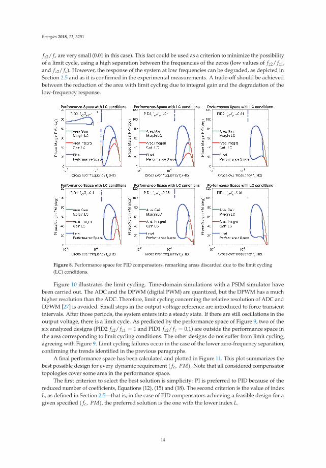
Figure 8. Performance space for PID compensators, remarking areas discarded due to the limit cycling(LC) conditions.
Figure 10 illustrates the limit cycling. Time-domain simulations with a PSIM simulator havebeen carried out. The ADC and the DPWM (digital PWM) are quantized, but the DPWM has a muchhigher resolution than the ADC. Therefore, limit cycling concerning the relative resolution of ADC andDPWM [27] is avoided. Small steps in the output voltage reference are introduced to force transientintervals. After those periods, the system enters into a steady state. If there are still oscillations in theoutput voltage, there is a limit cycle. As predicted by the performance space of Figure 9, two of thesix analyzed designs (PID2 fz2/ fz1 = 1 and PID1 fz2/ fc = 0.1) are outside the performance space inthe area corresponding to limit cycling conditions. The other designs do not suffer from limit cycling,agreeing with Figure 9. Limit cycling failures occur in the case of the lower zero-frequency separation,confirming the trends identified in the previous paragraphs.
A final performance space has been calculated and plotted in Figure 11. This plot summarizes thebest possible design for every dynamic requirement ( fc, PM). Note that all considered compensatortopologies cover some area in the performance space.
The first criterion to select the best solution is simplicity: PI is preferred to PID because of thereduced number of coefficients, Equations (12), (15) and (18). The second criterion is the value of indexL, as defined in Section 2.5—that is, in the case of PID compensators achieving a feasible design for agiven specified ( fc, PM), the preferred solution is the one with the lower index L.
14

Energies 2018, 11, 3251
(a) (b)
Figure 9. Performance space for the two different PID compensators, considering different values ofthe design parameter for each of them: (a) PID1; (b) PID2.
Figure 10. Time response to reference steps for different compensators corresponding to designA (Figure 8). A limit cycle exists for PID1 fz2/fz1 = 1 and PID2 fz2/fc = 0.1, as predicted by theperformance space.
Analyzing this example, the PI is obviously the best solution for a low-frequency requirement.Even if the PID can provide low values of fc, the PI has a simpler implementation that implies lesscalculation in the difference equation. Designs using the PI compensator beyond the resonancefrequency of the plant are limited to low values of PM, which in practice have no significant interest.
The preferred option for values of fc beyond the resonance frequency is the PID2 with two zerosat the same frequency. The limitation due to the integral gain limit cycling condition can be overcomeusing either PID2 or PID1, with higher separation between zero frequencies.
15

Energies 2018, 11, 3251
Phas
e M
argi
n PM
(deg
)
Figure 11. Performance space considering seven different compensators and selecting the best possiblesolution among them for each point of the performance space (fc, PM).
All results presented in this section have been obtained by implementing in Matlab the algorithmto generate the performance space (Figure 7). Apart from the comparison of different compensators,the same procedure can be used to perform a sensitivity analysis of other parameters, such as timedelays and sampling frequency [35].
4. Experimental Validation
An actual prototype has been built and tested in the laboratory to validate the proposed designprocedure, the models, and the assumptions considered in this work. The digital controller hasbeen implemented in a Zybo board, including a Xilinx Zynq-7010 device. An external ADC wasused (ADS7476A), limiting the resolution to 10 bits. The specification of the power converter is asfollows: input voltage Vin = 8 V, output voltage Vo = 4 V; output inductance LO = 76 × 10−6 H; outputcapacitance CO = 100 × 10−6 F; load resistance Ro = 10 Ω; switching frequency fsw = 100 × 103 Hz.The transfer function of the power converter Gvd (Figure 1) has not been calculated, but was measuredwith a frequency response analyzer. Therefore, all parasitic components (inductor and capacitorseries resistances, MOSFET conduction resistance, etc.) are considered in the compensator calculation.The uncompensated loop gain Tu is shown in Figure 12, as well as the performance space, withoutconsidering the limit cycling conditions. There are some differences with the performance spacepresented in Figure 6b due to the differences in the uncompensated open-loop transfer function:
• The total time delay produces a significant phase loss beyond the resonance frequency of theuncompensated open loon gain, limiting the feasible solutions at high frequency (PMmax limit).This phase loss is compensated partially by the effect of the equivalent series resistance of theoutput capacitor;
• The Q factor is lower, and so in the performance space, there are possible solutions at crossoverfrequencies close to the resonance frequency.
The combination of the performance spaces for the different type of compensators and differentdesign parameters is shown in Figure 13. In this case, PI ad PID2 with fz2/ fz1 = 1 are the compensatortopologies that cover the major part of the area of possible designs. The PID1 topology providespossible designs at high fc and low PM, where the PID2 with fz2/ fz1 = 1 does not meet the limitcycling condition regarding the integral gain.
The resulting open-loop gain has been measured in the actual prototype for three dynamicspecifications, named as design point 1, 2, and 3, detailed in Figure 13. For each design point, bothPID1 and PID2 have been designed with fz2/ fc = 0.1 and fz2/ fz1 = 1, respectively. Measurements
16

Energies 2018, 11, 3251
and theoretical predictions are plotted in Figure 14, which match very well, especially near thecrossover frequency. Another interesting comparison between PID1 and PID2 is the magnitude ofthe open-loop gain for the same design point. Bellow the cross-frequency in each case, PID2 reachesa higher magnitude than PID1, which means a lower L index. That is why, in the performancespace plotted in Figure 13, PID2 is a better solution than PID1 for the three illustrated design points.This result is also illustrated in the time-domain waveforms appearing in Figure 15. The outputvoltage has been measured when a voltage reference step is applied. In the left plot, the six differentpossibilities for design-point 3 are shown. Although the same crossover frequency and phase marginare selected for the compared waveforms, the system exhibits a different time-response due to the zerolocation, as shown in previous sections. PID2 with fz2/ fz1= 1 is the fastest response, matching withthe choice to plot the performance space in Figure 13. In the right side of Figure 15, the time-responsefor design-point 1 for a single compensator is shown to illustrate that, despite the high cross-overfrequency, no limit cycles are produced after the transitions, as predicted by the theory.
(a)
(b)
Figure 12. (a) The actual prototype’s uncompensated open loop gain; (b) performance space withoutconsidering limit cycling conditions.
Phas
e M
argi
n PM
(deg
)
Figure 13. Performance space for the actual prototype with the best solution for each point.
17

Energies 2018, 11, 3251
102 103 104
-20
0
20
T transfer functionPID2 fz2/fz1=1
ExperimentalTheoretical
102 103 104
Freq (Hz)
-400
-300
-200
-100
0
fc=2817PM=43Design Point 3
102 103 104
-20
0
20
T transfer functionPID1 fz2/fc=0.1
ExperimentalTheoretical
102 103 104
Freq (Hz)
-400
-300
-200
-100
0
fc=2817PM=43Design Point 3
Figure 14. Comparison between the experimental measurements and the theoretical predictions fordifferent PID compensators, considering the three design points in Figure 13.
(a) (b)
-2 0 2 4 6 8Time (s) 10-3
0
1
2
3
4
5
6
7
Out
put V
olta
ge (V
)
Output voltage Vo forVo reference steps. Desing point 3
PID2 K2=1PID2 K2=0.1PID2 K2=0.01PID1 K1=0.1PID1 K1=0.05PID1 K1=0.01
-0.01 -0.005 0 0.005 0.01 0.015Time(s)
4.8
5
5.2
5.4
5.6
5.8
6
6.2
6.4
Output voltage Vo forVo reference steps. Design Point 1 PID2 fz2/fz1=1
Figure 15. Experimental time-domain waveforms when there is a step in the voltage reference. (a) Stepresponse for different designs with fc = 2817 Hz, PM = 43◦ (Design point 3); (b) step response fordesign-point 1, using 9 bits in the ADC (note that there is no limit cycling).
18

Energies 2018, 11, 3251
5. Conclusions
A frequency-based design approach for the calculation of a digital compensator for DC/DCpower-switching converters has been presented. It is based on the analytical calculation of thecoefficients of the compensator from the dynamic specifications phase margin, PM, and cross-overfrequency, fc, considering the sampling frequency, delay effects, and limit cycling conditions.The approach is focused on the identification of the dynamic specifications that in fact can be achieved,and its graphical representation on a ( fc, PM) axis. Designs that are not feasible, do not fulfillthe requirements, are unstable, or do not meet the limit cycling conditions, are excluded from theperformance space.
The design procedure has been automatized. A simple algorithm can generate all feasible designsand plot the performance space. It allows for the identification of the dynamic limitations of a givenpower converter with a given compensator topology. The most important benefit provided by thisapproach is the ability to perform a quick and straightforward comparison of compensator topologiesor sensitivity analysis of a specific parameter, ensuring the feasibility of the proposed designs.
Three compensator topologies have been considered in the calculations: PI and PID, with twodifferent criteria to establish the frequency of the two zeros (PID1 and PID2). The design procedurehas been applied in a particular example, considering seven different compensator types and choosingthe more suitable design for each point ( fc, PM) using a proposed figure of merit calculated from thefrequency response.
The described analysis based on the performance space also allows for determination ofthe simplest compensator design in terms of the dynamic performance, the complexity of theimplementation, and the computational resources. In the analyzed example, PI is the best option forlow-frequency dynamic requirements. In general, the option covering a larger area in the performancespace is PID with two zeros at the same frequency. However, this performance space can be limitedby the integral limit cycling condition. Other PID designs with separated zeros can overcome thislimitation, but the time response should be assessed. The experimental results of a lab prototype agreewith the theoretical predictions.
Author Contributions: Conceptualization, P.Z., C.F., A.L. and A.B.; Data curation, M.A.G.; Funding acquisition,C.F. and A.B.; Methodology, P.Z. and C.F.; Software, M.A.G.; Validation, M.A.G.; Writing—original draft, P.Z. andC.F.; Writing—review & editing, M.A.G., A.L. and A.B.
Funding: This work has been funded by the Ministerio de Economía, Comercio y Competitividad, Gobierno deEspaña and ERDF funds, through projects DPI2017-88062-R, “Electrónica de Potencia Integrada e Inteligente Parael Control y la Gestión de la Energía en la IIOT” EPIIOT and project DPI2014-53685-C2-1-R, “Storage and EnergyManagement for Hybrid Electric Vehicles based on Fuel Cell, Battery and Supercapacitors”-ELECTRICAR-AG.
Conflicts of Interest: The authors declare no conflict of interest.
References
1. Sathishkumar, P.; Krishna, T.N.; Khan, M.A.; Zeb, K.; Kim, H.J. Digital Soft Start Implementation forMinimizing Start Up Transients in High Power DAB-IBDC Converter. Energies 2018, 11, 956. [CrossRef]
2. Costabeber, A.; Mattavelli, P.; Saggini, S. Digital Time-Optimal Phase Shedding in Multiphase BuckConverters. IEEE Trans. Power Electron. 2010, 25, 2242–2247. [CrossRef]
3. Rodríguez, J.; Lamar, G.D.; Aller, G.D.; Miaja, F.P.; Sebastián, J. Efficient Visible Light CommunicationTransmitters Based on Switching-Mode dc-dc Converters. Sensors 2018, 18, 1127. [CrossRef] [PubMed]
4. Shirazi, M.; Morroni, J.; Dolgov, A.; Zane, R.; Maksimovic, D. Integration of Frequency ResponseMeasurement Capabilities in Digital Controllers for DC/DC Converters. IEEE Trans. Power Electron. 2008,23, 2524–2535. [CrossRef]
5. Shirazi, M.; Zane, R.; Maksimovic, D. An Autotuning Digital Controller for DC/DC Power Converters Basedon Online Frequency-Response Measurement. IEEE Trans. Power Electron. 2009, 24, 2578–2588. [CrossRef]
6. Stefanutti, W.; Mattavelli, P.; Saggini, S.; Ghioni, M. Autotuning of Digitally Controlled DC–DC ConvertersBased on Relay Feedback. IEEE Trans. Power Electron. 2007, 22, 199–207. [CrossRef]
19

Energies 2018, 11, 3251
7. Costabeber, A.; Mattavelli, P.; Saggini, S.; Bianco, A. Digital Autotuning of DC—DC Converters Based on aModel Reference Impulse Response. IEEE Trans. Power Electron. 2011, 26, 2915–2924. [CrossRef]
8. Stefanutti, W.; Saggini, S.; Mattavelli, P.; Ghioni, M. Power Line Communication in Digitally ControlledDC-DC Converters Using Switching Frequency Modulation. IEEE Trans. Ind. Electron. 2008, 55, 1509–1518.[CrossRef]
9. Park, Y.J.; Khan, Z.H.; Oh, S.J.; Jang, B.G.; Ahmad, N.; Khan, D.; Abbasizadeh, H.; Shah, S.A.; Pu, Y.G.;Hwang, K.C.; et al. Single Inductor-Multiple Output DPWM DC-DC Boost Converter with a High Efficiencyand Small Area. Energies 2018, 11, 725. [CrossRef]
10. Xie, K.; Hu, G.; Yi, H.; Lyu, Z.; Xiang, Y. A Novel Digital Control Method of a Single-Phase Grid-ConnectedInverter Based on a Virtual Closed-Loop Circuit and Complex Vector Representation. Energies 2017, 10, 2068.[CrossRef]
11. Thi Kim Nga, T.; Park, S.M.; Park, Y.J.; Park, S.H.; Kim, S.; Van Cong Thuong, T.; Lee, M.; Hwang, K.;Yang, Y.; Lee, K.Y. A Wide Input Range Buck-Boost DC–DC Converter Using Hysteresis Triple-Mode ControlTechnique with Peak Efficiency of 94.8% for RF Energy Harvesting Applications. Energies 2018, 11, 1618.[CrossRef]
12. Jackson, D.K.; Leeb, S.B. A digitally controlled amplifier with ripple cancellation. IEEE Trans. Power Electron.2003, 18, 486–494. [CrossRef]
13. Bae, H.-S.; Yang, J.-H.; Lee, J.-H.; Cho, B.-H. Digital state feedback current control using the pole placementtechnique. J. POWER Electron. 2007, 7, 213–221.
14. Bae, H.S.; Yang, J.H.; Lee, J.H.; Cho, B.H. Digital state feedback control and feed-forward compensation for aparallel module DC-DC converter using the pole placement technique. In Proceedings of the IEEE AppliedPower Electronics Conference and Exposition—APEC, Austin, TX, USA, 24–28 February 2008; pp. 1722–1727.
15. Peretz, M.M.; Ben-Yaakov, S. Time-Domain Design of Digital Compensators for PWM DC-DC Converters.IEEE Trans. Power Electron. 2012, 27, 284–293. [CrossRef]
16. Miao, B.; Zane, R.; Maksimovic, D. Automated digital controller design for switching converters.In Proceedings of the PESC Rec. IEEE Annual Power Electronics Specialist Conference, Recife, Brazil,12–16 June 2005; pp. 2729–2735.
17. Chui, M.Y.; Ki, W.-H.; Tsui, C.-Y. A programmable integrated digital controller for switching converters withdual-band switching and complex pole-zero compensation. IEEE J. Solid-State Circuits 2005, 40, 772–780.[CrossRef]
18. Garcia, O.; de Castro, A.; Soto, A.; Oliver, J.A.; Cobos, J.A.; Cezon, J. Digital control for power supply ofa transmitter with variable reference. In Proceedings of the Twenty-First Annual IEEE Applied PowerElectronics Conference and Exposition, Dallas, TX, USA, 19–23 March 2006; p. 6.
19. Erickson, R.W.; Maksimovic, D. Fundamental of Power Electronics, 2nd ed.; Springer: Berlin, Germany, 2001.20. Venable, H. The K factor: A new mathematical tool for stability analysis and synthesis. In Proceedings of the
Powercon 10, San Diego, CA, USA, 22–24 March 1983; pp. 1–10.21. Corradini, L.; Mattavelli, P.; Stefanutti, W.; Saggini, S. Simplified Model Reference-Based Autotuningfor
Digitally Controlled SMPS. IEEE Trans. Power Electron. 2008, 23, 1956–1963. [CrossRef]22. Yang, C.; Liu, C.; Tsai, C. Direct digital compensator design for switching converters. In Proceedings of the
2010 International Symposium on Next Generation Electronics, Kaohsiung, Taiwan, 18–19 November 2010;pp. 143–146.
23. Bjeletic, A.; Corradini, L.; Maksimovic, D.; Zane, R. Specifications-driven design space boundariesfor point-of-load converters. In Proceedings of the IEEE Applied Power Electronics Conference andExposition—APEC, Fort Worth, TX, USA, 6–11 March 2011; pp. 1166–1173.
24. Martinez, C.; Valdivia, V.; Roldan, A.M.; Lourido, J.; Quesada, I.; Lucena, C.; Zumel, P.; Barrado, A. EfficientCAD tool for power electronics compensator design. In Proceedings of the 2010 IEEE Energy ConversionCongress and Exposition, Atlanta, GA, USA, 12–16 September 2010.
25. Fernández, C.; Lázaro, A.; Zumel, P.; Valdivia, V.; Martínez, C.; Barrado, A. Design space boundaries oflinear compensators applying the k-factor method. In Proceedings of the 2013 Twenty-Eighth Annual IEEEApplied Power Electronics Conference and Exposition (APEC), Long Beach, CA, USA, 17–21 March 2013;pp. 2706–2711.
26. Peterchev, A.V.; Sanders, S.R. Quantization resolution and limit cycling in digitally controlled PWMconverters. IEEE Trans. Power Electron. 2003, 18, 301–308. [CrossRef]
20

Energies 2018, 11, 3251
27. Corradini, L.; Maksimovic, D.; Mattavelli, P.; Zane, R. Amplitude Quantization. In Digital Control ofHigh-Frequency Switched-Mode Power Converters; Wiley-IEEE Press: Piscataway, NJ, USA, 2015; p. 360.
28. Lin, Y.C.; Chen, D.; Wang, Y.T.; Chang, W.H. A Novel Loop Gain-Adjusting Application Using LSB Tuningfor Digitally Controlled DC-DC Power Converters. IEEE Trans. Ind. Electron. 2012, 59, 904–911. [CrossRef]
29. Al-Atrash, H.; Batarseh, I. Digital controller design for a practicing power electronics engineer. In Proceedingsof the APEC 07—Twenty-Second Annual IEEE Applied Power Electronics Conference and Exposition,Anaheim, CA, USA, 25 February–1 March 2007; pp. 34–41.
30. Corradini, L.; Maksimovic, D.; Mattavelli, P.; Zane, R. Discrete-Time Modeling. In Digital Control ofHigh-Frequency Switched-Mode Power Converters; Wiley-IEEE Press: Piscataway, NJ, USA, 2015; p. 360.
31. Maksimovic, D.; Zane, R. Small-Signal Discrete-Time Modeling of Digitally Controlled PWM Converters.IEEE Trans. Power Electron. 2007, 22, 2552–2556. [CrossRef]
32. VandeSype, D.M.; DeGusseme, K.; DeBelie, F.M.L.L.; VandenBossche, A.P.; Melkebeek, J.A. Small-Signalz-Domain Analysis of Digitally Controlled Converters. IEEE Trans. Power Electron. 2006, 21, 470–478.[CrossRef]
33. Corradini, L.; Maksimovic, D.; Mattavelli, P.; Zane, R. Digital Control. In Digital Control of High-FrequencySwitched-Mode Power Converters; Wiley-IEEE Press: Piscataway, NJ, USA, 2015; p. 360.
34. Duarte-Mermoud, M.A.; Prieto, R.A. Performance index for quality response of dynamical systems. ISA Trans.2004, 43, 133–151. [CrossRef]
35. Zumel, P.; Fernandez, C.; Granda, M.A.; Lazaro, A.; Sanz, M.; Barrado, A. Simple method of direct digitaldesign of compensator for DC-DC converters. In Proceedings of the 2016 IEEE 17th Workshop on Controland Modeling for Power Electronics, COMPEL 2016, Trondheim, Norway, 27–30 June 2016.
© 2018 by the authors. Licensee MDPI, Basel, Switzerland. This article is an open accessarticle distributed under the terms and conditions of the Creative Commons Attribution(CC BY) license (http://creativecommons.org/licenses/by/4.0/).
21


energies
Article
Disturbance Rejection Control Method for IsolatedThree-Port Converter with Virtual Damping
Jiang You 1, Mengyan Liao 1, Hailong Chen 2,*, Negareh Ghasemi 3 and Mahinda Vilathgamuwa 4
1 College of Automation, Harbin Engineering University, Harbin 150001, China; [email protected] (J.Y.);[email protected] (M.L.)
2 College of Shipbuilding Engineering, Harbin Engineering University, Harbin 150001, China3 School of Information Technology and Electrical Engineering, The University of Queensland, Brisbane 4072,
Australia; [email protected] School of Electrical Engineering and Computer Science, Queensland University of Technology,
Brisbane 4000, Australia; [email protected]* Correspondence: [email protected]; Tel.: +86-137-9665-8929
Received: 19 October 2018; Accepted: 13 November 2018; Published: 18 November 2018
Abstract: The high-power density and capability of three-port converters (TPCs) in generatingdemanded power synchronously using flexible control strategy make them potential candidates forrenewable energy applications to enhance efficiency and power density. The control performance ofisolated TPCs can be degraded due to the coupling and interaction of power transmission amongdifferent ports, variations of model parameters caused by the changes of the operation point andresonant peak of LC circuit. To address these issues, a linear active disturbance rejection control(LADRC) system is developed in this paper for controlling the utilized TPC. A virtual damping basedmethod is proposed to increase damping ratio of current control subsystem of TPC which is beneficialin further improving dynamic control performance. The simulation and experimental results showthat compared to the traditional frequency control strategy, the control performance of isolated TPCcan be improved by using the proposed method.
Keywords: three-port converter; linear active disturbance rejection control; virtual damping; linearextended state observer
1. Introduction
The demand for three-port converters (TPCs) in renewable energy generation systems is increasingdue to the compact structure of these converters and their ability to handle demanded powersynchronously [1–5]. The TPCs not only facilitate multifunctional and multidirectional regulationfor electrical power transmission but also provide flexibility in power control and power densityenhancement in power conversion systems [6–10].
In an isolated three-port converter, the three windings of an isolated transformer share the samemagnetic core, therefore there are unavoidable couplings of power transmission among the threeports of TPC. Decoupling control methods with proper decoupling factors are usually employed inthree-port converters to achieve two single-input single-output (SISO) subsystems [11–14]. A classicalfrequency control theory is usually utilized to design controllers for each port respectively. Since thesmall signal models employed to design the controllers are produced by linearization of the nonlinearmodel of TPC at a steady-state operating point, the decoupling and dynamic performances of TPCcontrol system can be degraded significantly by the variation of the operating point. Particularly,since the small signal models of TPC depend on a specific operating point, in a transient state process,a heavy change of the operating point parameters may affect decoupling of different ports anddynamic performance of the control system. Generally, the three-port converter is a multiple-input
Energies 2018, 11, 3204; doi:10.3390/en11113204 www.mdpi.com/journal/energies23

Energies 2018, 11, 3204
multiple-output (MIMO) system, several phase-shifting angles and equivalent duty cycles can beused as control signals, and several voltages and currents of different ports can be assigned as theoutput signals. A linear quadratic regulator (LQR) based method is applied in ref. [15] to develop amultivariable controller for a three-port converter. Though the LQR method seems capable of achievingperformance balance of different ports, it has relatively high sensitivity to the accuracy of systemparameters. The parameters of the control models will vary with the change in operating point asthese small signal based models used in the control system design are derived at a specific steady stateoperating point. Also, the design of the parameters of the time domain based LQR method is relativelycomplex compared to the frequency domain design method.
The LADRC method was first proposed by Zhiqiang Gao, and it has advantages of toleratingchanges in model parameters and possesses an inherent decoupling ability that is useful for controlsystem design [16]. In the LADRC method, the influences of model parameter deviations and externalinterferences can all be regarded as a generalized disturbance [17]. Therefore, the linear extendedstate observer (LESO) [18,19] can be used to estimate the state variables and generalized disturbance,and the observed signals are used to synthesize control signal in the control system. Compared toconventional PI controller, the LADRC method is shown to enhance the dynamic performance of thecontrol system in [20].
In order to improve the dynamic control performance of an isolated three-port converter in thisstudy, the LADRC method is employed to decrease negative impact of reactions among different ports,and obtain high control performance under load change conditions.
The rest of the paper is organized as follows. In Section 2, the topology, modulation method,power delivery relationship, and control-oriented small signal models are presented. The design of aLADRC based control system for a three-port converter by utilizing its current and voltage controlsmall signal models, and the proposed virtual damping method to suppress the resonant peak in thecurrent control subsystem are given in Section 3. Also, in this section, the principle and the designprocedure of decoupling control are briefly illustrated for comparison purposes. The simulation andexperiment results are presented in Section 4. Finally, the conclusion is provided in Section 5.
2. Topology and Modeling of TPC
The circuit topology of an isolated TPC is presented in Figure 1a. In this figure, a DC powersupply (e.g., it can be a fuel cell or a photovoltaic cell) is set in Port 1, and the power supply, vd1 isconnected in series with an inductor Ld1, and re represents the equivalent series resistance (ESR) of Ld1.There is 180◦ phase shift between leg A and leg B, and the duty cycles of all switches in Port 1 are setto be 50% and the drive signals of the switches on the same leg are complementary. The Port 2 andPort 3 are connected with load and energy storage (ES) respectively and their switching patterns areas same as the switching mode of Port 1. A simplified equivalent Δ-connected circuit of the TPC bytransferring the related parameters of Port 2 and Port 3 to Port 1 is given in Figure 1b. If the voltagebetween the middle points of leg A and leg B, v1 is defined as a reference, the phase shifts of v2 and v3
relative to v1 are denoted as ϕ12 and ϕ13 respectively, and they are shown in Figure 1c. Moreover, L1,L2, and L3 are equivalent series inductances (including winding leakage inductance and additionalinductance) of the three transformer windings. The expressions of L12, L13, and L23 of the Δ-connectedcircuit shown in Figure 1b are defined by (1).⎧⎪⎨⎪⎩
L12 = L1 + L′2 + L1L′
2/L′3
L23 = L′2 + L′
3 + L′2L′
3/L1
L13 = L′3 + L1 + L1L′
3/L′2
(1)
L′2 and L′
3 are expressed by (2).
L′2 =
N21 L2
N22
, L′3 =
N21 L3
N23
(2)
24

Energies 2018, 11, 3204
Q1
Q4
Q2
Q3
AB
N1vd1
L1Cd1
v1
ids i1
S1
S4
S2
S3
C
D
vd3
L3
v3
id3
i3
K1
K4
K2
K3
E
Fvd2
L2
Cd2v2
id2
i2
Port1
Port3
Port2
RL
P1
P3
P2
L12
P12P1
P3
P2
(a)
(b)
i1
i3
i2i12
i13 i23
φ12
φ13
2π
(c)
N2
N3
id1
Ld1
vc1
ic2
re
io
'3v
1v
'2v
1v '2v
Figure 1. The isolated three-port converter: (a) topology; (b) equivalent Δ-connected circuit;(c) modulation scheme.
In each switching cycle, the total power transmitted between any two ports is approximated to itsfundamental component. Therefore, the Fourier expansion based fundamental component analysismethod is employed for theoretical analysis in this study. By utilizing the equivalent Δ-connectioncircuit in Figure 1b, the power equations of each port can be written as in (3).⎧⎪⎨⎪⎩
P1 = P12 + P13
P2 = −P12 + P23
P3 = −P13 − P23
, (P1 + P2 + P3 = 0) (3)
where ⎧⎪⎪⎪⎪⎪⎨⎪⎪⎪⎪⎪⎩
P12 = 8N1π2 N2ωsL12
Vd1Vd2 sin ϕ12
P13 = 8N1π2 N3ωsL13
Vd1Vd3 sin ϕ13
P23 =8N2
1π2 N2 N3ωsL23
Vd2Vd3 sin(ϕ13 − ϕ12)
(4)
In (4), Vd1, Vd2, and Vd3 are the rated amplitudes of v1, v2, and v3, N1, N2, and N3 are thetransformer winding turns of respective ports, and ωs is the switching angular frequency. Since thesummation of P1, P2 and P3 is kept at zero as shown in (3), that means the power of one port can bedetermined using the powers of the other two ports. From this point of view, the energy storage port isusually taken as an energy buffer that can be charged or discharged determined by the power deliveryand load conditions of Port 1 and Port 2 respectively. According to (3) and (4), the power of Port 1 andPort 2 can be formulated as (5) and (6) respectively.
P1 =8N1Vd1Vd2
π2N2ωsL12sin ϕ12 + P1 =
8N1Vd1Vd3
π2N3ωsL13sin ϕ13 (5)
P2 = −8N1Vd1Vd2 sin ϕ12
π2N2ωsL12+
8N1Vd2Vd3 sin(ϕ13 − ϕ12)
π2N2N3ωsL23(6)
Therefore, the corresponding average currents in each switching cycle can be derived as (7) and(8) respectively.
id1 =P1
Vd1= P1 =
8N1Vd2
π2N2ωsL12sin ϕ12 +
8N1Vd3
π2N3ωsL13sin ϕ13 (7)
id2 =P2
Vd2= −8N1Vd1 sin ϕ12
π2N2ωsL12+
8N21 Vd3 sin(ϕ13 − ϕ12)
π2N2N3ωsL23(8)
25

Energies 2018, 11, 3204
By applying partial differential operation in (7) and (8) respectively, (9) can be obtained for asteady-state operating point A (ϕ120, ϕ130).⎧⎪⎪⎪⎪⎪⎪⎪⎪⎪⎪⎨⎪⎪⎪⎪⎪⎪⎪⎪⎪⎪⎩
G11 = ∂id2∂ϕ12
∣∣∣A= − 8N1Vd1 cos ϕ120
π2 N2 N3ωsL12− 8N2
1 Vd3 cos(ϕ130−ϕ120)
π2 N2 N3ωsL23
G12 = ∂id2∂ϕ13
∣∣∣A=
8N21 Vd3
π2 N2 N3ωsL23cos(ϕ130 − ϕ120)
G21 = ∂id1∂ϕ12
∣∣∣A= 8N1Vd2
π2 N2ωsL12cos ϕ120
G22 = ∂id1∂ϕ13
∣∣∣A= 8N1Vd3
π2 N3ωsL13cos ϕ130
(9)
Consequently, (9) can be simplified as (10).[id2
id1
]=
[G11 G12
G21 G22
][ϕ12
ϕ13
]= GA
[]ϕ12ϕ13
](10)
As shown in (9), besides the circuit parameters, the value of any matrix element in GA, Gxy (x = 1, 2and y = 1, 2) is determined by the steady-state parameters (ϕ120 and ϕ130). And it can be also seenfrom (10) that there are couplings between id1 and id2 caused by G21 and G12.
The small signal linearization model of the three-port converter can be derived as in (11) byapplying KCL and KVL laws in Figure 1.⎧⎪⎪⎪⎪⎨⎪⎪⎪⎪⎩
Cd2dvd2
dt = − vd2RL
− G11 ϕ12 − G12 ϕ13
Ld1didsdt = vd1 − vc1 − re ids
Cd1dvc1dt = ids − G21 ϕ12 − G22 ϕ13
(11)
3. Control Strategy for TPC
3.1. Decoupling Control for TPC
Assuming the matrix, GA given in (10) can be simplified to a diagonal matrix given in (12) byintroducing a decoupling matrix H defined in (13).[
G11 G12
G21 G22
][H11 H12
H21 H22
]=
[G11 00 G22
](12)
H =
[H11 H12
H21 H22
]=
⎡⎣ G11G22G11G22−G12G21
−G12G22G11G22−G12G21
−G11G21G11G22−G12G21
G11G22G11G22−G12G21
⎤⎦ (13)
The decoupling control block diagram is presented in Figure 2. In this figure, Gv and Gc represent thevoltage controller and current controller respectively, which can be synthesized by using Bode plotbased design method in frequency domain. In Figure 2, the open loop transfer functions of the voltageand current control subsystems are Gvo = G11G1 and Gco = G22G2 respectively, the transfer functions ofG1 and G2 are given in (14). The resonant angular frequency of G2 is ωn = 1/
√Ld1Cd1.{
G1(s) =RL
RLCd2s+1G2(s) = 1
Ld1Cd1s2+reCd1s+1(14)
26

Energies 2018, 11, 3204
G11
G21
G22
H11
H12
H21
H22
+
G12
+
+
+
++
+ +
Gv
Gc
-+
-+
G1
G2+-
Hvr
decoupling control
virtual damping
d1id1idd
*d2v*vd
d2v-
vd
dsi -dsid vrvrv
12121112*11 d2id2id d2vvd
dsidsid13*++11
131311
Figure 2. Decoupling control scheme of a three-port converter.
3.2. Virtual Damping Method
For Port 1 in Figure 1, Ld1 and Cd1 are utilized to constitute an LC filter to limit the amplitude of thedouble-switching frequency component of ids and reduce the negative impact of high-frequency ripplecurrent on the power source (e.g., a fuel cell). However, this might cause performance degradationor an instability issue in current control subsystem due to the high resonant peak and a very weakdamping ratio introduced by a pure LC circuit (re = 0) or with a very small value of re shown in (14).Though the resonant phenomenon can be addressed by decreasing the current control bandwidth, thedynamic performance cannot be guaranteed.
The block diagram of the current control subsystem, Gco = G22G2 is presented in Figure 3 accordingto (11). The transfer function, Hvr in Figure 2 is a compensation function that is proposed to implementvirtual damping in this paper. The expression of Hvr is shown in Figure 3. In this figure, rv is the desiredvirtual resistor. If the output of Hvr, which is ϕvr, is moved from the point A to the point B, then, Hvr
in Figure 3 is changed to rv/(s/ωp + 1
), and it makes Hvr a rational fraction. ωp is used to attenuate
the high frequency noise, and if the value of ωp is high enough, then, rv/(s/ωp + 1
) ≈ rv becomesa resistor connected in series with re, and the damping ratio of G2 becomes (r s + rv)/2 ×√
Cd1/Ld1with the introduction of rv as a virtual resistor. In practical applications, the sampled ids is passedthrough Hvr, and then added to the output of the current controller to obtain the final phase shiftbetween Port 1 and Port 3, and the value of ωp can be selected between ωs and ωs/2.
-+
13 dsi
dsi
+--c1vG22
+d1v1
Ld1sre
-
rvCd1sG22(s/ωp+1)
+-
Hvr
A B
vr
Figure 3. Schematic diagram of virtual damping implementation.
3.3. LADRC for TPC
The small signal model shown in (11) can be transformed into two subsystems to implementthe LADRC based control method. The two differential equations for current control subsystem andvoltage control subsystem are given by (15) and (16) respectively.
..ids = − 1
Cd1Ld1ids − re
Ld1
.ids +
G22
Cd1Ld1ϕ12 +
1Ld1
.vd1 + (
G21
Cd1Ld1− bc)ϕ13 + bc ϕ13 = fc + bc ϕ13 (15)
.vd2 = − 1
RLCd2vd2 − G12
Cd2ϕ13 + (−G11
Cd2− bv)ϕ12 + bv ϕ12 = fv + bv ϕ12 (16)
27

Energies 2018, 11, 3204
In (15) and (16), vd2 and ids are taken as the output variables of the two subsystems, ϕ13 and ϕ12 arethe control signals of the current control subsystem and the voltage control subsystem respectively.
ϕ13 is considered as an external disturbance of voltage control subsystem, while ϕ12 is consideredas an external disturbance of the current control subsystem. Furthermore, f c and f v are used torepresent the generalized disturbances that are associated with both inner and outer variable elementsof the two subsystems (e.g., coupling, load, and operating point related parameter changes, etc.). Inpractical situations, the generalized disturbances, f c and f v are usually unknown and cannot be directlymeasured. Therefore, LESO is adopted to evaluate the generalized disturbances and relevant statevariables in the LADRC method.
As for the current control subsystem, xc=[i
ds
.ids fc
]Tis selected as the state vector, the augmented
state space model is formulated by (17){.xc = Acxc + Bc ϕ13 + Ec
.f c
ids = Ccxc(17)
where ⎧⎪⎪⎪⎪⎪⎪⎪⎪⎪⎪⎪⎪⎪⎨⎪⎪⎪⎪⎪⎪⎪⎪⎪⎪⎪⎪⎪⎩
Ac =
⎡⎢⎣ 0 1 00 0 10 0 0
⎤⎥⎦BT
c =[
0 bc 0]
ETc =
[0 0 1
]Cc =
[1 0 0
](18)
The LESO of current control subsystem is constructed by (19).{zc = [Ac − LcCc]zc + [ Bc L c
]wc
yc = zc(19)
where yc= zc =[
zc1 zc2 zc3
]Tis the observed vector of xc. wc =
[ϕ13 ids
]Tand Lc given
in (20) is the observer gain that can be designed using the pole placement method [17].
Lc =[
3ωoc 3ω2oc ω3
oc
]T(20)
where ωoc is the equivalent bandwidth of the observer.It should be noted that the disturbance caused by the resonance of Ld1Cd1 circuit is included
in the generalized disturbance, f c, therefore, the value of ωoc should be at least twice as large as ωn,that means ωoc/ωn ≥ 2 should be satisfied to make the LESO obtain accurate value of f c, otherwise,the control performance might be significantly degraded.
Similarly, the LESO used for voltage control subsystem is presented in (21).{ .zv = [Av − LvCv]zv + [ Bv L v
]wv
yv = zv(21)
28

Energies 2018, 11, 3204
In (21), wv =[
ϕ12 vd2
]. yv = zv =
[zv1 zv2
]Tis the output vector of (21) that corresponds to
xv =[
vd2 fv
]T. And the coefficient matrix in (21) are given in (22).
⎧⎪⎪⎪⎪⎪⎪⎪⎪⎪⎪⎨⎪⎪⎪⎪⎪⎪⎪⎪⎪⎪⎩
Av =
[0 10 0
]
BTv =
[bv 0
]ET
v =[
0 1]
Cv =[
1 0]
(22)
The corresponding gain vector of the voltage LESO, Lv is shown in (23).
Lv =[
2ωov ωov2]T
(23)
Assuming fc and fv can be observed accurately (zc3 = fc, zv2 = fv), and if ϕ13 and ϕ12 in (15) and (16)can be expressed as (24). {
ϕ13 = (uc−zc3)bc
= (uc− fc)bc
ϕ12 = (uv−zv2)bv
= (uv− fv)bv
(24)
The current and voltage control subsystems will be simplified to two simple cascaded integratorssystems shown in (25). { ..
ids = uc.vd2 = uv
(25)
The current and voltage control signals, uc and uv, for this cascaded integrator system can be proposedas (26). {
uc = kpc(urc − zc1)− kdczc2
uv = kpv(urv − zv1)(26)
where kpc, kpv, and kdc are controller parameters, and urc and urv are current and voltagereference signals, respectively. In (26), it can be seen that uc and uv represent equivalent PD(proportional-derivative) and P (proportional) controllers respectively. The closed-loop transferfunctions of the current and voltage control subsystem can be formulated as (27) and (28) whichare obtained by substituting the two equations in (26) into the two equations of (25) respectively.
GcL =kpc
s2 + kdcs + kpc, (kpc = ω2
c , kdc = 2ξωc) (27)
GvL =kpv
s + kpv, (kpv = ωv) (28)
In (27) and (28), ωc and ωv represent equivalent control bandwidths of the two closed-loop controlsubsystems with LADRC method, and ξ is the equivalent damping of the current control subsystem,which should be designed to guarantee smooth current change in transient state process (there is nointense oscillations in dynamic process). It can be seen from (27) and (28) that steady state errors areeliminated in the current and voltage closed-loop control systems (when s = 0, unity gain is obtainedin (27) and (28) respectively) by utilizing (26) as control law. Furthermore, the closed-loop controlperformances of the two subsystems are completely determined by the designed controller parameters(kpc, kpd and kpv) regardless of the changes of model parameters. This is a prominent characteristic ofthe LADRC method. (ω c, ωoc) and (ω v, ωov) are the adjustable LADRC parameters in current and
29

Energies 2018, 11, 3204
voltage control subsystems, respectively. Since LADRC method is observer based, the bandwidth ofthe observer should be kept sufficiently larger than the bandwidth of the control system to realizeeffective compensation. Therefore, the two ratios, αc = ωoc/ωc and αv = ωov/ωv should be largerthan two at least in practical applications to get accurate observed values [21], otherwise, the controlperformance might not be guaranteed.
4. Simulation and Experimental Results
4.1. Simulation Results
In order to verify the theoretical analysis and design results of the proposed method, a simulationmodel of the isolated TPC is developed by using MATLAB/Simulink, and the main parameters of thesimulation model are listed in Table 1.
Table 1. Parameters of The Simulation Model.
Symbol Name Value
vd1 DC input voltage 24 Vvd2 Output voltage 36 Vvd3 Battery voltage 24 VLd1 Input filter inductor 100 μHre Input filter inductor ESR 0.1 Ω
Cd1 Input filter capacitor 1200 μFCd2 Output filter capacitor 1000 μFRL Load resistor 45 Ω/22 Ωf s Switching frequency 20 kHz
The steady-state operating point A (0.620, 0.379) is selected which corresponds to RL = 45 Ω,vd2 = 36 V and ids = 1.3 A, and an extra 0.2 Ω virtual resistor is introduced. The open loop transferfunctions of the two subsystems are obtained by substituting the parameters listed in Table 1 into Gco
and Gvo, respectively. The controllers Gc and Gv, given by (29), are designed for the decoupled currentand voltage subsystems respectively by using the frequency domain design method.⎧⎨⎩ Gc =
5001×10−4s2+s
Gv = 0.2813s+6.251×10⁻⁸s3+2×10⁻⁴s2+s
(29)
The Bode plots of the two subsystems with and without correction are shown in Figures 4aand 4b, respectively.
As can be seen in Figure 4a, the crossover frequency of the corrected current control subsystemwith rv = 0.2 (the curve B) is about 71 Hz, the phase margin is about 81◦, and the gain marginis about 7 dB. The crossover frequency of the corrected voltage control subsystem is about 75 Hz,the phase margin is about 85◦, and the gain margin is about 33 dB. As a comparison, if rv = 0.2 iscancelled, the corrected current control subsystem (the curve C) will be unstable, since the resonantpeak (the corresponding angular frequency is ωn = 2887 rad/s) of the curve C will intersect with 0 dBaxis under this condition.
30

Energies 2018, 11, 3204
Frequency(Hz)(a)
A
B
C
A- rv=0.2Ω without correctionB- rv=0.2Ω with correctionC- rv=0 with correction
Frequency(Hz)
Without correction
With correction
Without correction
With correction
(b)
Figure 4. The bode plots of subsystems by using traditional frequency control method: (a) ids subsystem;(b) vd2 subsystem.
For the control systems with LADRC method, the equivalent control bandwidths of the current andvoltage subsystems are the same, ωc = ωv = 450 rad/s (about 72 Hz) which are close to the designedcrossover frequencies using the traditional frequency domain method. The observer bandwidthsof the current and voltage subsystems are ωoc = 4147 rad/s (about 660 Hz), and ωov = 2000 rad/s(about 318 Hz) respectively. The simulation results are shown in Figure 5.
Figure 5a shows simulation results of vd2 and ids with traditional frequency control under a stepload change condition. As can be seen in Figure 5a, there is an obvious voltage drop (from 36 Vto 35.2 V) at 0.5 s when the load is suddenly changed from 29 W to 52 W that resulted in transientfluctuations in ids (changed from 1.3 A to 1.25 A). When the load is suddenly reduced at 0.7s from52 W to 29 W, current ids transiently increases from 1.3 A to 1.37 A, while vd2 increases to about 36.8 V,and then decreases gradually to its rated value after 100 ms.
Cur
rent
ids/A
Vol
tage
vd2
/V
t/s
vd2
ids
(a)
Cur
rent
ids/A
vol
tage
vd2
/V
ids
vd2
t/s (b)
Figure 5. The simulation results of the system: (a) with traditional frequency control method; (b) withthe LADRC method.
The simulation results of the system with the LADRC method and rv = 0.2 Ω are shown inFigure 5b. In this figure, it can be seen that for the same load change, vd2 drops from 36 V to 35.6 V at0.5 s when the load increased, and it increases from 36 V to 36.4 V at 0.7 s when the load decreases.However, current is changed slightly with respect to the load change. For instance, the current dropsfrom 1.3 A to 1.28 A when the load reduced and it increases from 1.3 A to 1.32 A when the loadis increased. By comparing the result shown in Figure 5, it can be seen that the amplitude of ids
31

Energies 2018, 11, 3204
fluctuation in the system controlled with LADRC is lower than that of the system controlled with thetraditional frequency control method. Also, the transient recovery time of vd2 is much shorter thanthat of the system with the traditional frequency control. These results imply that the information ofthe load change observed by LESO is effectively utilized in the control system.
4.2. Experimental Validation and Analysis
In order to further verify the effectiveness of the proposed method, an experimental platform wasdeveloped as shown in Figure 6. The circuit parameters and load change conditions of the experimentalsystem are similar to the simulation model. The experimental results are shown in Figures 7–11.
HFT
Lead-acid batteries
Power circuits of
TPC
Controlboard
Figure 6. Hardware experiment circuit of the three-port converter.
Figure 7 shows the experimental results, ids, vd2, Δvd2 (fluctuation of vd2) and io achieved for thedeveloped converter controlled with the traditional frequency control method. The results of ids andΔvd2 (vd2 was controlled to 36 V) for a sudden load increase are shown in Figure 7a. As shown inthis figure, there is about 0.24 A drop in ids and 0.8 V drop in vd2 when the load is suddenly changedfrom 29 W to 52 W. Figure 7b shows the current and voltage changes with respect to sudden load dropwhere the current and voltage are increased by about 0.24 A and 0.9 V respectively.
vd2 (1
0V/d
iv)
ids(2
00m
A/d
iv)
Δvd
2(0.5
V/d
iv)
io(1A
/div
)vd
2 (1
0V/d
iv)
ids(2
00m
A/d
iv)
Δvd
2(0.5
V/d
iv)
io(1A
/div
)
vd2
ids
Δvd2
io
vd2
ids
Δvd2
io
100ms/div
10ms/div
Time(ms)
0.8V
240mA
(a)
vd2 (1
0V/d
iv)
ids(2
00m
A/d
iv)
Δvd
2(0.5
V/d
iv)
io(1A
/div
)
vd2 (1
0V/d
iv)
ids(2
00m
A/d
iv)
Δvd
2(0.5
V/d
iv)
io(1A
/div
)
vd2
ids
Δvd2
io
vd2
ids
Δvd2
io
100ms/div
10ms/div
240mA
0.9V
Time(ms)(b)
Figure 7. The experiment results of ids, vd2, Δvd2 and io with the traditional frequency control methodand rv = 0.2 Ω: (a) sudden load increase; (b) sudden load decrease.
32

Energies 2018, 11, 3204
The effect of the proposed virtual resistor method on ids control is conducted by removing andre-adding the virtual resistor with the same current controller used in Figure 7. The experimentalresults are shown in Figure 8a, it can be seen that there are serious oscillations in ids (the current controlsubsystem is unstable in this case as indicated by the curve C in Figure 4 and voltage ripples (Δvd2) ofvd2 are also increased with the same oscillation frequency of ids. While the virtual resistor scheme isre-performed, the oscillation of ids can be suppressed soon, and the amplitude of voltage ripple in vd2becomes lower.
Δvd
2 (0.
2V/d
iv)
ids(5
00m
A/d
iv)
Δvd
2(0.2
V/d
iv)
ids(5
00m
A/d
iv)
Δvd2
ids
Δvd2 Δvd2
ids
ids
500ms/div
10ms/div
Time(ms)
10ms/div
(a)
Δvd2
ids
Δvd2 Δvd2
ids
ids
(b)
Δvd
2 (0.
2V/d
iv)ids
(50
0mA
/div)
Δvd
2(0.2
V/d
iv)ids
(50
0mA
/div)
Δvd2
ids
Δvd2 Δvd2
ids ids
5 0 0ms/d i v
5ms/d i v
T i m e(ms)
5ms/d i v
Figure 8. The experimental results with and without rv = 0.2 Ω virtual resistor (ωn = 2887 rad/s):(a) traditional frequency control; (b) LADRC.
The experimental results of ids, vd2, Δvd2 and io with the LADRC method and rv = 0.2 Ω are shownin Figure 9. As shown in Figure 9a, when the same load increment (23 W) is experienced small changesare observed in ids (changes from 1.3 A to 1.35 A) and vd2 (changes from 36 V to 35.6 V) because ofthe coupling between current and voltage subsystems. As shown in Figure 9b, for a sudden loadreduction, ids is changed from 1.3 A to 1.25 A, and vd2 is increased for about 0.5 V. Also, as illustrated inFigure 9, the fluctuations of ids and vd2 in the transient process with the LADRC method are lower thanthose with the traditional frequency control method as shown in Figure 7, and the voltage transientrecovery time with the LADRC method is much shorter than that with the traditional frequency control.These results indicate that the control system with the LADRC has better decoupling performanceand adaptability to the operating point changes compared to the control system with the traditionalfrequency control.
vd2 (1
0V/d
iv)
ids(2
00m
A/d
iv)
Δvd
2(0.5
V/d
iv)
io(1A
/div
)vd
2 (1
0V/d
iv)
ids(2
00m
A/d
iv)
Δvd
2(0.5
V/d
iv)
io(1A
/div
)
vd2
ids
Δvd2
io
vd2
ids
Δvd2
io
100ms/div
10ms/div
Time(ms)
0.4V
(a)
vd2 (1
0V/d
iv)
ids(2
00m
A/d
iv)
Δvd
2(0.
5V/d
iv)
io(1A
/div
)v d
2 (1
0V/d
iv)
ids(2
00m
A/d
iv)
Δvd
2(0.5
V/d
iv)
io(1A
/div
)
vd2
ids
Δvd2
io
vd2
ids
Δvd2
io
100ms/div
10ms/div0.5V
Time(ms)(b)
Figure 9. The experimental results of ids, vd2, Δvd2 and io with LADRC method, ωn = 2887 rad/s andrv = 0.2 Ω: (a) sudden load increase; (b) sudden load decrease.
33

Energies 2018, 11, 3204
The experimental result with and without 0.2 Ω virtual resistor with LADRC method andωn = 2887 rad/s is presented in Figure 8b. As shown in this figure, there are obvious current oscillationsin ids when rv = 0.2 Ω is removed, since the observer bandwidth (ωoc = 4147 rad/s) is not sufficientlyhigher than the resonant angular frequency of Ld1Cd1 circuit (ωoc/ωn ≈ 1.43 < 2). And it is similar tothe case shown in Figure 8a, the current oscillations can be attenuated effectively if the virtual resistormethod is reused.
For comparison study, the resonant angular frequency of G2(s) in (14) is reduced toωn = 1521 rad/s (by setting Ld1 = 160 μH and Cd1 = 2700 μF), then there is no oscillations in idsas shown in Figure 10, that means ids can be controlled well since the ratio of ωoc/ωn is about 2.73which is larger than two in this case, it means that the impact caused by the resonance of Ld1Cd1 circuitcan be much accurately observed by the LESO.
vd2 (1
0V/d
iv)
ids(0
.2A
/div
)Δ
vd2(0
.5V
/div
)io(
1A/d
iv)
vd2 (1
0V/d
iv)
ids(0
.2A
/div
)Δ
vd2(0
.5V
/div
)io(
1A/d
iv)
vd2
ids
Δvd2
io
vd2
ids
Δvd2
io
100ms/div
10ms/div
0.4V
Time(ms)(a)
vd2 (1
0V/d
iv)
ids(0
.2A
/div
)Δ
vd2(0
.5V
/div
)io(
1A/d
iv)
vd2 (1
0V/d
iv)
ids(0
.2A
/div
)Δ
vd2(0
.5V
/div
)io(
1A/d
iv)
vd2
ids
Δvd2
io
vd2
ids
Δvd2
io
100ms/div
10ms/div0.4V
Time(ms)(b)
Figure 10. The experimental results of ids, vd2, Δvd2 and io with LADRC method, ωn = 1521 rad/s andrv = 0 Ω: (a) sudden load increase; (b) sudden load decrease.
Cur
rent
id3(2
00m
A/d
iv)
Cur
rent
id3(2
00m
A/d
iv)
id3
id3 id3
500ms/div
20ms/div 20ms/div
Time(ms)(a)
Cur
rent
id3(2
00m
A/d
iv)
Cur
rent
id3(2
00m
A/d
iv)
id3
id3 id3
500ms/div
20ms/div 20ms/div
Time(ms)(b)
Figure 11. The experimental results of battery current id3: (a) traditional frequency control; (b) LADRC.
The battery current id3 for the traditional frequency control and LADRC are shown in Figures 11aand 11b, respectively. In Figure 11, it can be seen that not only the overshoot of id3 with the LADRCis relatively lower, but also the transient recovery time of id3 is shorter than that obtained using thetraditional frequency control. This indicates the LADRC method can provide better dynamic balancein the power delivery process. The results shown in Figure 11 have some internal relations with theexperimental results presented in Figures 7 and 9. For instance, compared to Figure 11b with LADRC
34

Energies 2018, 11, 3204
method applied, the battery overshoot current, id3 shown in Figure 11a is larger when traditionalfrequency control method is applied. Larger overshoot current causes significant drop in ids shownin Figure 7a, whereas smaller overshoot of id3 shown in Figure 11b with LADRC resulted in muchsmaller overshoot in ids shown in Figure 9a.
5. Conclusions
The model parameter variation caused by the operating point changes and couplings betweendifferent ports during power delivery in an isolated three-port converter has a negative impact on theconverter control performance. In this study, the LADRC method is employed to control the three-portconverter. In the LADRC method, the possible model parameter uncertainties, load changes and thenegative impact of LC circuit resonance are all expressed as a generalized disturbance that is consideredas a state variable and observed by the LESO which is utilized to synthesize the control signal. In thismethod, the bandwidth of the LESO is sufficiently higher than the equivalent control bandwidth andthe resonant frequency of LC circuit that guarantee the system dynamics and generalized disturbancecan be accurately observed. Therefore, the desired closed-loop control performance that is independentof parameters changes and external disturbances can be obtained. And a virtual resistor basedmethod is proposed to increase damping ratio of the current control subsystem of TPC which isbeneficial to further improve current control performance using LADRC method. The simulation andexperimental results revealed that the proposed method is robust against model parameter changesand external disturbances. Therefore, the dynamic control performance of the three-port converter canbe improved significantly.
Author Contributions: Conceptualization, J.Y., M.L. and H.C.; Validation, M.L., J.Y. and H.C.; Writing-OriginalDraft Preparation, J.Y. and H.C.; Writing-Review & Editing, N.G., M.V. and M.L.
Funding: This work is sponsored by the National Natural Science Foundation of China (No.51479042 and No.51761135013), and the fundamental research funds for the central universities of China (No. HEUCFG201822).
Conflicts of Interest: The authors declare no conflict of interest.
References
1. Tao, H.; Kotsopoulos, A.; Duarte, J.L.; Hendrix, M.A.M. Design of a soft-switched three-port converter withDSP control for power flow management in hybrid fuel cell systems. In Proceedings of the 2005 EuropeanConference on Power Electronics and Applications, Dresden, Germany, 11–14 September 2005.
2. Tao, H.; Duarte, J.L.; Hendrix, M.A.M. A Distributed Fuel Cell Based Generation and Compensation Systemto Improve Power Quality. In Proceedings of the 2006 CES/IEEE 5th International Power Electronics andMotion Control Conference, Shanghai, China, 14–16 August 2006.
3. Ling, Z.; Wang, H.; Yan, K.; Sun, Z. A new three-port bidirectional DC/DC converter for hybrid energystorage. In Proceedings of the 2015 IEEE 2nd International Future Energy Electronics Conference (IFEEC),Taipei, Taiwan, 1–4 November 2015.
4. Tao, H.; Duarte, J.L.; Hendrix, M.A.M. Line-Interactive UPS Using a Fuel Cell as the Primary Source.IEEE Trans. Ind. Electron. 2008, 55, 3012–3021. [CrossRef]
5. Wang, L.; Wang, Z.; Li, H. Optimized energy storage system design for a fuel cell vehicle using a novel phaseshift and duty cycle control. In Proceedings of the 2009 IEEE Energy Conversion Congress and Exposition,San Jose, CA, USA, 20–24 September 2009.
6. Kim, S.Y.; Song, H.S.; Nam, K. Idling Port Isolation Control of Three-Port Bidirectional Converter for EVs.IEEE Trans. Power Electron. 2012, 27, 2495–2506. [CrossRef]
7. Jiang, Y.; Liu, F.; Ruan, X.; Wang, L. Optimal idling control strategy for three-port full-bridge converter.In Proceedings of the 2014 International Power Electronics Conference (IPEC-Hiroshima 2014—ECCE ASIA),Hiroshima, Japan, 18–21 May 2014.
8. Ajami, A.; Asadi Shayan, P. Soft switching method for multiport DC/DC converters applicable in gridconnected clean energy sources. IET Power Electron. 2015, 8, 1246–1254. [CrossRef]
35

Energies 2018, 11, 3204
9. Tao, H.; Duarte, J.L.; Hendrix, M.A.M. Three-Port Triple-Half-Bridge Bidirectional Converter withZero-Voltage Switching. IEEE Trans. Power Electron. 2008, 23, 782–792. [CrossRef]
10. Tao, H.; Kotsopoulos, A.; Duarte, J.L.; Hendrix, M.A.M. A Soft-Switched Three-Port Bidirectional Converterfor Fuel Cell and Supercapacitor Applications. In Proceedings of the 2005 IEEE 36th Power ElectronicsSpecialists Conference, Recife, Brazil, 12 June 2005.
11. Zhao, C.; Kolar, J.W. A novel three-phase three-port UPS employing a single high-frequency isolationtransformer. In Proceedings of the 2004 IEEE 35th Annual Power Electronics Specialists Conference, Aachen,Germany, 20–25 June 2004.
12. Zhao, C.; Round, S.D.; Kolar, J.W. An Isolated Three-Port Bidirectional DC-DC Converter with DecoupledPower Flow Management. IEEE Trans. Power Electron. 2008, 23, 2443–2453. [CrossRef]
13. Tao, H.; Kotsopoulos, A.; Duarte, J.L.; Hendrix, M.A.M. Transformer-Coupled Multiport ZVS BidirectionalDC–DC Converter with Wide Input Range. IEEE Trans. Power Electron. 2008, 23, 771–781. [CrossRef]
14. Wang, L.; Wang, Z.; Li, H. Asymmetrical Duty Cycle Control and Decoupled Power Flow Design of aThree-port Bidirectional DC-DC Converter for Fuel Cell Vehicle Application. IEEE Trans. Power Electron.2012, 27, 891–904. [CrossRef]
15. Falcones, S.; Ayyanar, R. LQR control of a quad-active-bridge converter for renewable integration.In Proceedings of the 2016 IEEE Ecuador Technical Chapters Meeting (ETCM), Guayaquil, Ecuador, 12–14October 2016.
16. Gao, Z. Active disturbance rejection control: From an enduring idea to an emerging technology. In Proceedingsof the 2015 10th International Workshop on Robot Motion and Control (RoMoCo), Poznan, Poland, 24August 2015.
17. Gao, Z. Scaling and bandwidth-parameterization based controller tuning. In Proceedings of the 2003American Control Conference, Denver, CO, USA, 4–6 June 2003.
18. Wang, W.; Gao, Z. A comparison study of advanced state observer design techniques. In Proceedings of the2003 American Control Conference, Denver, CO, USA, 4–6 June 2003.
19. Miklosovic, R.; Radke, A.; Gao, Z. Discrete implementation and generalization of the extended state observer.In Proceedings of the 2006 American Control Conference, Minneapolis, MN, USA, 14–16 June 2006.
20. Sun, B.; Gao, Z. A DSP-based active disturbance rejection control design for a 1-kW H-bridge DC-DC powerconverter. IEEE Trans. Ind. Electron. 2005, 52, 1271–1277. [CrossRef]
21. Zhu, B. Introduction of Active Disturbance Rejection Control, 1st ed.; Beihang University Press: Beijing, China,2017; pp. 42–45.
© 2018 by the authors. Licensee MDPI, Basel, Switzerland. This article is an open accessarticle distributed under the terms and conditions of the Creative Commons Attribution(CC BY) license (http://creativecommons.org/licenses/by/4.0/).
36

energies
Article
Decoupled Current Controller Based on ReducedOrder Generalized Integrator for Three-PhaseGrid-Connected VSCs in Distributed System
Sen Zhang 1, Jianfeng Zhao 1,*, Zhihong Zhao 2, Kangli Liu 1, Pengyu Wang 1 and Bin Yang 1
1 School of Electrical Engineering, Southeast University, Nanjing 210096, China; [email protected] (S.Z.);[email protected] (K.L.); [email protected] (P.W.); [email protected] (B.Y.)
2 Department of Electrical Engineering, School of Automation, Nanjing University of Science and Technology,Nanjing 210094, China; [email protected]
* Correspondence:[email protected]; Tel.: +86-139-5194-3657
Received: 13 May 2019; Accepted: 21 June 2019; Published: 24 June 2019
Abstract: Grid-connected voltage source converters (GC-VSCs) are used for interfacing the distributedpower generation system (DPGS) to the utility grid. Performance of the current loop is a critical issuefor these GC-VSCs. Recently, reduced order generalized integrator (ROGI)-based current controller isproposed, such that AC reference signal of positive or negative sequences can be separately trackedwithout steady-state error, which has the advantage of less computational burden. However, thecross-coupling within the ROGI-based current controller would deteriorate the transient response ofthe current loop. In this paper, a ROGI-based decoupled current controller is proposed to eliminatethe coupling between α-axis and β-axis. Thus, the faster dynamic response performance can beachieved while maintaining the merits of ROGI-based current controller. An optimal gain parameterdesign method for the proposed current controller is presented to improve the stability and dynamicresponse speed of current loop. Simulation and experiments were performed in MATLAB/Simulinkand TMS320C28346 DSP-based laboratory prototype respectively, which validated the proposedtheoretical approach.
Keywords: decoupling; reduced order generalized integrator (ROGI); optimal gain; distributedpower generation system (DPGS); grid-connected voltage source converters (GC-VSCs)
1. Introduction
In recent years, distributed power generation system (DPGS) has attracted increasing attentionwith the aggravation of global energy shortage and environmental issues [1–5]. A typical DPGS isshown in Figure 1; due to the intermittence of renewable energy sources (RESs) such as PV systemsand wind turbines, energy storage systems (ESSs) based on battery and supercapacitor are used tosuppress power fluctuations, which improves the reliability and quality of power supply. Moreover,integrating the electric energy generated by RESs into the power grid is an important way to improvepower generation efficiency. As the typical power electronic interfaces between DPGS and power grid,GC-VSCs have been intensively studied [6,7]. In the grid-connected mode, the voltage and frequencyat the point of common coupling are dictated by strong power grid, the GC-VSC is controlled to behaveas current-controlled converter. Active and reactive power regulation are performed by changing thegrid-connected output current [8,9]. Therefore, accurate and fast control of the grid-connected currentis one of the most critical technologies, which directly affects the power quality [8–13].
Various research has focused on current control of GC-VSCs [4,6–12,14–25], among which the mostwidely studied control method is PI controller [17,19,23,26], which effectively guarantees excellenttracking of AC reference signals and fast dynamic response speed, since AC signals become DC signals
Energies 2019, 12, 2426; doi:10.3390/en12122426 www.mdpi.com/journal/energies37

Energies 2019, 12, 2426
through Park transformation and PI controller could produce infinite gain for DC signals [16,17,26].Nevertheless, d-axis and q-axis current cross-coupling, resulting from the Park transformation, isproportional to the interested control frequency. Actually, the modulation and sampling delay tendto aggravate the coupling and even deteriorate stability of the current loop [17,26]. In addition,resonant controllers are widely used in current loop regulation of GC-VSCs. Proportional-resonant(PR) and vector proportional-integral (VPI) controllers are, respectively, equivalent to conventional PIand complex-vectors PI (cPI) regulators, which are implemented in a positive and negative sequenceSRF simultaneously [17]. It assures perfectly tracking AC reference signals without steady-state errorsfor both sequences [5–7,9,12,14,15,18]. However, the negative-sequence term (i.e., −jωe) of conjugatedpoles introduces two times control frequency fluctuation, bringing slower dynamic response andmore severe cross-coupling [16,26]. Moreover, computational burden increases when multiple orderharmonics need to be tracked simultaneously [21,22].
Figure 1. The configuration of a distributed power generation system.
To overcome the disadvantage of the above controllers, some improved methods are proposed.The method of state-feedback decoupling is proposed in [16], which effectively reduces the axescross-coupling and broadens the bandwidth of current loop. Nevertheless, the decoupling effectivenesscould be affected by the time delay and the accuracy of parameter estimation. The alternativedecoupling method based on cPI controller is less influenced by these two factors [17]. Thus, abetter stability and a faster dynamic response speed of the current loop are achieved. However,the implementation of the aforementioned control algorithms is in SRF and the rotating frametransformation increases the computational burden and complexity. Simultaneously, the error oftransformation calculation would emerge if the PLL is not sufficiently accurate [7,9,26]. Overall, aregulator with zero steady-state error in the stationary frame would have some certain advantagesin terms of implementation [9–12]. ROGI-based current controller, which is named as PCI controllerin [11,12], is proposed with the advantage of less computational burden and improving the bandwidthof harmonics control [21,25]. However, the cross-coupling within the ROGI-based current controller
38

Energies 2019, 12, 2426
would deteriorate the transient response of the current loop. In addition, the stability of the currentloop will decrease when the control frequency is relatively high [23].
In this paper, a ROGI-based decoupled current controller is proposed, which is capable ofsuppressing the cross-coupling and improving the dynamic response speed, while possessing theadvantage of low computation burden and being convenient to implement. An optimal gain methodfor parameter tuning is also presented to maximize the stability of the current loop.
The paper is organized as follows. Coupling of ROGI-based current controller is analyzed inSection 2. Section 3 introduces the proposed ROGI-based decoupled current controller. Specially,the performance of the proposed controller is analyzed through closed-loop frequency response andmathematical derivation, and the optimal parameter design using the root locus is presented. Thesimulation and experimental results are provided to validate the theoretical approach in Section 4.Finally, Section 5 summarizes the work.
2. Coupling Analysis of ROGI-Based Current Controller
The ROGI is proposed in [21], its transfer function in the s-domain can be expressed as
GROGI(s) =1
s ∓ jωe(1)
where ωe is the fundamental frequency and “−/+” denotes the positive/negative sequence.The implementation principle of ROGI is shown in Figure 2a.
(a) ROGI. (b) ROGI-based current controller (PCI).
Figure 2. Implementation principle of ROGI and ROGI-based current controller.
A novel proportional complex integral (PCI) is derived from the principle that zero steady-stateerror can be achieved if the open-loop gain is infinity at the control frequency [10]. Thus, it can bewritten by,
GPCI(s) = kp +ki
s − jωe(2)
where kp is the proportional gain and ki is the integral gain. It is known from Equation (2) that the PCIcontroller is equivalent to ROGI-based current controller in [10,21]. For convenience, the PCI controllerrepresents the ROGI-based current controller in this paper. The implementation principle of PCI isshown in Figure 2b, where it can be seen that PCI controller includes two kp · ωe coupling branches,
39

Energies 2019, 12, 2426
which will deteriorate the transient response of the current loop. Besides, the coupling aggravates asthe control frequency increases.
Figure 3 shows the diagram of PCI-based current closed-loop for GC-VSCs. Gsd(s) = e−sTd
represents the digital control delay, which consists of one and a half sampling time delay [19],Td = 1.5Ts (Ts is the sampling cycle). For a more intuitive sense of the coupling, α-axis and β-axiscurrent response with PCI controller is presented in Figure 4 when a step change occurs in referencecurrent. The reference current i∗αβ decreases from 10 · ejωet to 0 at t = 0.04s, where i∗α = Re{i∗αβ} =10·cos(ωet) and i∗β = Im{i∗αβ} = 10·sin(ωet). In Figure 4a,b, it can be seen that reference current changesin α-axis affects β-axis current, and vice versa. In addition, the coupling will increase with the rising ofthe control frequency.
Figure 3. The diagram of PCI-based current closed-loop for GC-VSCs.
(a) ωe = 2·50·π rad/s (b) ωe = 2·250·π rad/s.
Figure 4. α-axis and β-axis current response with PCI controller.
3. The Proposed ROGI-Based Decoupled Current Controller
To suppress the axes-coupling in the PCI-based current loop. an effective decoupling method withROGI-based decoupled current controller is proposed, which improves dynamic response performanceof the current loop. For convenience, the proposed ROGI-based decoupled current controller is referredto as the D-PCI controller in the following section.
3.1. Structure of the D-PCI Controller
As shown in Figure 2b and the analysis of coupling, the key to effective decoupling is to removethe cross-coupling term kp · ωe. Thus, the structure of the proposed D-PCI current controller is shownin Figure 5. Thus, the transfer function of D-PCI can be expressed as
GD−PCI(s) = kp +ki + jωekp
s − jωe(3)
40
Energies 2019, 12, 2426
Figure 5. Structure of the proposed D-PCI current controller.
Based on Equations (2) and (3), the Bode plot of PCI and D-PCI controllers tuned atωe = 2·π·50 rad/s (i.e., fundamental excitation frequency is 50 Hz) is shown in Figure 6. It canbe seen that both PCI and D-PCI controllers achieve infinite gain at fundamental excitation frequency,which means that precise AC reference signal tracking can be realized. Moreover, D-PCI controller hassuperior performance in suppressing DC reference signal. The magnitude for D-PCI controller is −6.5dB, while PCI controller is 27 dB.
Figure 6. Bode plot of PCI and D-PCI controllers tuned at ωe = 2 · π · 50 rad/s.
Replacing the PCI with D-PCI in Figure 3, α-axis and β-axis current response with D-PCI controlleris presented in Figure 7 when a step change occurs in reference current. In Figure 7a,b, it can be seenthat, regardless of the control frequency, there is almost no coupling between the current of α-axis andβ-axis.
(a) ωe = 2 · 50 · π rad/s (b) ωe = 2·250·π rad/s.
Figure 7. α-axis and β-axes current response with D-PCI controller.
41

Energies 2019, 12, 2426
3.2. Performance Analysis of the D-PCI Controller
From Figure 3 and Equation (3), the output current Iαβ can be derived as
Iαβ(s) =e−sTd ·(kps+ki)
(sL+RL)(s−jωe)+e−sTd ·(kps+ki)I∗αβ(s)− s−jωe
(sL+RL)(s−jωe)+e−sTd ·(kps+ki)eαβ(s) (4)
where
GsCL (s) =
(kps + ki) · e−sTd
(s − jωe) (sL + RL) + (kps + ki) · e−sTd(5)
is the transfer function between Iαβ(s) and I∗αβ(s), and
GsDL(s) = − s − jωe
(sL + RL)(s − jωe) + e−sTd · (kps + ki)(6)
is the transfer function between Iαβ(s) and eαβ(s).If the frequency of I∗αβ(s) (reference input signal) and eαβ(s) (disturbance signal) is equal to ωe,
i.e., s = jωe, then GsCL(jωe) = 1 and Gs
DL(jωe) = 0. It means that D-PCI controller can realize trackingof AC reference signals and suppress AC disturbance signals. Both closed-loop frequency responseand mathematical derivation would be used to evaluate the steady-state tracking performance.
(a) Reference tracking Iαβ(s) / I∗αβ(s).
(b) Disturbance rejection Iαβ(s) / I∗αβ(s).
Figure 8. Bode plot of closed-loop current control based on D-PCI controller.
According to Equations (5) and (6), the closed-loop frequency response curves at different controlfrequencies are shown in Figure 8. The following conclusions can be drawn:
42

Energies 2019, 12, 2426
(1) Since the controller provides infinite gain at the interested control frequency (−50 Hz, 50 Hz,100 Hz, 200 Hz and 500 Hz), unity gain and 0◦ phase lag output current can be achieved, i.e.,Iαβ(s)/I∗αβ(s) = 1 � 0◦, the steady-state error is zero, as shown by “•” in Figure 8a.
(2) As shown by “◦” in Figure 8a, a closed-loop anomalous peak (amplification phenomenon ofoutput current) appears near the control frequency, and, as the control frequency increases, thepeak value becomes larger, e.g., no obvious amplification appears at 50 Hz or 100 Hz, while thepeak value is 1.02 (1.145) times of the unity gain at 215 Hz (540 Hz). It means that the closed-loopanomalous peak will aggravate the transient oscillation and increase the adjustment time andovershoot with the abrupt change of reference signal. Besides, if phase lock angle is inaccurate,the steady-state output current would be amplified.
(3) As shown in Figure 8b, the disturbance signal at the interested control frequency is completelysuppressed, i.e., the magnitude is zero (as shown by “ ”).
The delay compensation method is used to suppress the closed-loop anomalous peak, and Figure 9shows the closed-loop frequency response after delay compensation. It can be seen that the unity gainand 0◦ phase lag output current are achieved at the interested control frequencies, and the closed-loopanomalous peak is completely excluded, as shown by “•” in Figure 9.
Figure 9. Bode plot of current closed-loop with delay compensation with D-PCI controller.
From the analysis of delay compensation above, the influence of time delay can be ignored.According to the internal model control (IMC) method [13], to cancel the pole of Gs
PL(s) by a matchingzero in D-PCI controller, ki/kp = RL/L should be satisfied. Hence, Equation (5) can be simplified intoEquation (7)
GsCL (s) =
Ks − jωe + K
(7)
where K = kp/L is the only degree of freedom of the D-PCI controller. Thus, the reference currenti∗αβ(t) can be expressed by
i∗αβ(t) = Im · cos(ωet) + jIm · sin(ωet) (8)
the output current iαβ(s) is equal to
Iαβ(s) = GsCL(s) · I∗αβ(s) =
Im
s − jωe− Im
s − jωe + K(9)
in the time domain, Equation (9) can be written as
iαβ(t) = Im · (cos ωet − e−Kt) + jIm · (sin ωet − e−Kt) (10)
if t → ∞ in (10), thenlimt→∞
iαβ(t) = Im · cos ωet + jIm · sin ωet = i∗αβ(t) (11)
43

Energies 2019, 12, 2426
It can be seen that D-PCI controller can be used to track ac reference signal without steady-stateerror, and, with the increase of open-loop gain K, the dynamic response becomes faster. The design ofthe parameter K is introduced in the next section.
3.3. Parameter Tuning for the D-PCI Controller
In this section, a parameter design method based on root locus is presented. By comprehensiveanalysis of the IMC method, and as shown in Figure 3, the open-loop transfer function is simplified to
GsOL (s) =
(kps + ki) · Gsd(s)
(s − jωe) (sL + RL)=
K · Gsd(s)
(s − jωe)(12)
Taking the following parameters as an example, both the switching and sampling frequency areset to 10 kHz: L = 5 mH, RL = 0.5 Ω and ωe = 100π rad/s. Figure 10 shows the root locus of currentloop based on D-PCI controller and Figure 10b is a closer view of the dotted line frame in Figure 10a.
(a)
X
(b)
Figure 10. Root locus of current loop based on D-PCI controller: (a) general view; and (b) closer viewof the dotted line frame.
The decay rate σ = Re(pcl) and the damping ratio ξ = σ/ |pcl | are two important indicators toevaluate the system performance. As shown by the closer view in Figure 10b, the open-loop zeroz1
ol and closed-loop pole p1ol overlap with each other, while the effect of p1
ol on system stability anddynamic response is negligible. When K is low (K < Kopt), p3
cl and p4cl are far away from imaginary
axis (Re(p2cl) � Re {(p3
cl),(p4cl)}), p2
cl becomes the dominant closed-loop pole, the system is in anoverdamped state. By increasing K until p2
cl and p3cl overlap (this gain value of K is defined as
Kopt ), the system switches to a state of critical damping (ξ ≈ 1), as shown by “•” in Figure 10a, andthe maximal stability and the fastest dynamic response are obtained simultaneously. If K is increasedfurther, the system becomes underdamped and overshoot occurs in the transient response. At thesame time, the stability decreases because p2
cl and p3cl are closer to the imaginary axis. Consequently,
Kopt is an optimal choice in terms of stability and dynamic response.Figure 11 shows the time-domain simulation of output current with different gains of K when
an abrupt change happens in the reference current. It can be observed that simulation results areconsistent with theoretical analysis based on root locus. Overshoot occurs in the current transientresponse (when K > Kopt) due to the underdamped characteristics. If K < Kopt, the excessive dampingratio limits the dynamic performance (although the overshoot is suppressed). When K = Kopt, there isno overshoot during the transient response. Simulation results are summarized in Table 1, where it canbe seen that K = Kopt is a best choice if overshot and transient response are considered simultaneously.
44

Energies 2019, 12, 2426
Figure 11. Output current response with different gains of K when an abrupt change happens in thereference current.
Table 1. Evaluation for different value of K
Gain (K) Damping Ratio ξ Overshoot Response Speed
K < Kopt ξ > 1 no slowK = Kopt ξ = 1 no fastK > Kopt ξ < 1 have fast
4. Simulation and Experimental Results
To verify the control performance of the proposed D-PCI controller, simulation and experimentalresults are presented in this section. The main parameters for simulation and experiment aresummarized in Table 2.
Table 2. Simulation and experimental setup parameters.
Symbol Parameters Value Unit
Vs Phase-to-phase voltage 380 Vf Grid frequency 50 Hz
Udc DC-link voltage 700 VL Inductance of the L filter 5 mH
RL Equivalent resistance of the L filter 0.05 ΩCdc Capacitor of DC-link 4000 uF
R(P) Active power Load 50(10) Ω(kW)I∗q (Q) Reactive power Load 21.5(10) A(kvar)
fsw Switching frequency 10 kHzfs Sampling frequency 10 kHz
BW Bandwidth of the current loop 600 Hzkip Proportional gain of the current loop 12.3 /kii Integral gain of the current loop 123 /kvp Proportional gain of the voltage loop 0.5 /kvi Integral gain of the voltage loop 29.87 /
Figure 12 shows the double closed-loop control scheme of GC-VSC. The outer loop, whichhas slower dynamics, regulates the DC-link voltage. The inner loop is used to track the referencecurrent, which is the output of the outer loop. In this study, the DC-link voltage was set to 700 V.Comparisons between the proposed and PCI controller were performed in terms of steady-state errorand dynamic response.
45

Energies 2019, 12, 2426
Figure 12. The double closed-loop control scheme of GC-VSC.
4.1. Simulation Results
Figure 13 shows the simulation results of the proposed control strategy. As shown in Figure 13a,the simulation process consisted of several critical time points with load changes, which were used totest the steady-state and dynamic response of the proposed control strategy. Figure 13b–d shows thecloser views of Zoom1, Zoom2 and Zoom3 in Figure 13a.
(a) (b)
(c) (d)
(e) (f)
Figure 13. Simulation results of the proposed control strategy: (a) general view of the DC-link capacitorvoltage and three-phase grid current; (b) three-phase grid current when the GC-VSC operates in thestate of PWM rectifier; (c) three-phase grid current when 10 kW active power is applied; (d) three-phasegrid current when 10 kvar reactive power is added; (e) grid voltage and current of phase A when unitypower control is implemented; and (f) reference current, actual current and current error of phase Awhen load changes.
46
Energies 2019, 12, 2426
In Figure 13b, it can be seen that the DC-link voltage is regulated to 700 V when the GC-VSCoperates in the state of PWM rectifier, which can be replaced by a DC power supply.
Figure 13c shows the transient response of three-phase grid current when 10 kW active powerload is applied. It can be seen that the stability of the grid current is achieved after 10 ms. Actually, thedynamic regulation time is less than 10 ms, since the DC-link voltage drop extends the settling time.The excellent dynamic response performance can be further validated by the results in Figure 13d,when 10 kvar reactive power load is added. There is almost no transient regulation process forgrid current. In fact, since the reactive power is not consumed, the DC-link voltage does not dropsignificantly. Moreover, as shown in Figure 13c,d, negligible overshoot is obtained when using theparameter design method in Section 3.
Figure 13e represents the grid voltage and current of phase A with the unit power factor controlmethod. The phase is exactly the same in steady state, which reflects the tracking ability of the D-PCIcontroller. As shown in Figure 13f, the curves (reference current I∗a and actual Ia) come closest tocoinciding in shape even if a sudden change occurs at 0.4 s, and the current error fluctuates around zero.It shows that the D-PCI controller has the ability to track AC reference signals with zero steady-stateerror and fast dynamic response.
Figure 14 represents the simulation results with PCI controller. The parameters are consistentwith the D-PCI-based control strategy. In Figures 13c and 14a, it can be seen that the dynamic responseof D-PCI is faster than PCI, and the excellent performance can be further observed in Figures 13f and14b. The PCI-based grid current tracks its reference with zero steady-state error after about 30 mswhile it takes about 15 ms for the proposed control strategy.
(a)
(b)
Figure 14. Simulation results of the PCI-based control strategy: (a) three-phase grid current when10 kW active power is applied; and (b) reference current, actual current and current error of phase Awhen load changes.
47

Energies 2019, 12, 2426
4.2. Experimental Results
To further support the theoretical analysis and simulation results, the experimental setup ofGC-VSC was built in the laboratory, as shown in Figure 15. The parameters in experimental setup werethe same as in simulation ones, which are listed in Table 1. Active power load consists of two parallel100 Ω/10 kW resistors. The real-time algorithm was implemented in the hardware controller, based onTMS320C28346 DSP and EP3C16Q240 FPGA, whose output PWM signals are connected to converterby optical fiber. Experimental waveforms were captured by Yokogawa DL850 oscilloscope. Specifically,the hardware controller lacked of digital-to-analog converter and, since the reference current was adigital variable, it could not be directly measured by the oscilloscope. Therefore, real-time data wereacquired by saving memory in Code Composer Studio (Ver.5.5.0) and the waveforms (Figures 16f and17b) were plotted in MATLAB.
Figure 15. Experimental setup of the GC-VSC.
Figures 16 and 17 show the experimental results of the proposed and PCI-based control strategy,which correspond to the simulation results in Figures 13 and 14, respectively. It can be observed thatthe experimental and simulation results match to a great extent. The slight difference is the distortionof grid current, which can be mainly attributed to harmonics contained in the grid voltage.
Figure 16 shows that the excellent stability and fast dynamic response of the proposedD-PCI-based control strategy can be obtained even though the GC-VSC experiences different loadvariation. The superiority can be further verified by the comparative experiments. From the results inFigures 16f and 17b, the following can be concluded: (1) the current error of both strategies tends tozero, which means that tracking of ac reference signal with zero steady-state error can be realized fromboth methods; and (2) the proposed strategy has faster dynamic response, as the error current of thePCI-based strategy restores to zero after about 30 ms while there is almost no dynamic process for theproposed control strategy.
48

Energies 2019, 12, 2426
(a) (b)
(c) (d)
(e) (f)
Figure 16. Experimental results of the proposed control strategy: (a) general view of the DC-linkcapacitor voltage and three-phase grid current; (b) three-phase grid current when the GC-VSC operatesin the state of PWM rectifier; (c) three-phase grid current when 10 kW active power is applied;(d) three-phase grid current when 10 kvar reactive power is added; (e) grid voltage and current ofphase A when unity power control is implemented; and (f) reference current, actual current and currenterror of phase A when load changes.
49

Energies 2019, 12, 2426
(a) (b)
Figure 17. Experimental results of the PCI-based control strategy: (a) three-phase grid current when10 kvar reactive power is applied; and (b) reference current, actual current and current error of phase Awhen load changes.
5. Conclusions
To attenuate the impact of axes cross-coupling caused by PCI controller, a novel D-PCIcontroller-based decoupling method in the stationary frame is proposed to track sinusoidal referencesignals with zero steady-state error and achieve fast dynamic response. Moreover, an optimal gainmethod for parameter tuning is presented for enhancing the stability of the current loop. Comparingwith PCI, the proposed D-PCI controller can obtain faster dynamic response, as well as betterstability performance. Comparative simulations were performed and experimental results betweenthe proposed and PCI controller were compared, which validated the superiority of the proposedD-PCI controller.
Author Contributions: Conceptualization, S.Z. and J.Z.; methodology, S.Z.; software, S.Z.; validation, S.Z., P.W.and B.Y.; data curation, K.L.; writing—original draft preparation, S.Z.; writing—review and editing, Z.Z.; projectadministration, J.Z. and K.L.; and funding acquisition, J.Z.
Funding: This research was funded by the National Natural Science Foundation of China grant number 51877042,the Project of China Postdoctoral Science Foundation grant number 2018M642138 and the Fundamental ResearchFunds for the Central Universities grant number 2242019R20010.
Conflicts of Interest: The authors declare no conflict of interest.
References
1. Bose, B. Global Energy Scenario and Impact of Power Electronics in 21st Century. IEEE Trans. Ind. Electron.2013, 60, 2638–2651. [CrossRef]
2. Arbab-Zavar, B.; Palacios-Garcia, E.; Vasquez, J.; Guerrero, J. Smart Inverters for Microgrid Applications:A Review. Energies 2019, 12, 840. [CrossRef]
3. Molina, M. Energy Storage and Power Electronics Technologies: A Strong Combination to Empower theTransformation to the Smart Grid. Proc. IEEE. 2017, 105, 2191–2219. [CrossRef]
4. Bose, B. Power Electronics, Smart Grid, and Renewable Energy Systems. Proc. IEEE. 2017, 105, 2011–2018.[CrossRef]
5. Pang, B.; Nian, H. Improved Operation Strategy with Alternative Control Targets for Voltage SourceConverter under Harmonically Distorted Grid Considering Inter-Harmonics. Energies 2019, 12, 1236.[CrossRef]
50

Energies 2019, 12, 2426
6. Xie, C.; Zhao, X.; Li, K.; Zou, J.; Guerrero, J.M. A New Tuning Method of Multi-Resonant Current Controllersfor Grid-Connected Voltage Source Converters. IEEE J. Emerg. Sel. Top. Power Electron. 2019, 7, 458–466.[CrossRef]
7. Busada, C.A.; Jorge, S.G.; Solsona, J. A. Resonant Current Controller With Enhanced Transient Response forGrid-Tied Inverters. IEEE Trans. Ind. Electron. 2018, 65, 2935–2944. [CrossRef]
8. Nie, C.; Wang, Y.; Lei, W.; Li, T.; Yin, S. Modeling and Enhanced Error-Free Current Control Strategy forInverter with Virtual Resistor Damping. Energies 2018, 11, 2499. [CrossRef]
9. Holmes, D.G.; Lipo, T.A.; McGrath, B.P.; Kong, W.Y. Optimized Design of Stationary Frame Three Phase ACCurrent Regulators. IEEE Trans. Power Electron. 2009, 24, 2417–2426. [CrossRef]
10. Guo, X.; Guerrero, J.M. General Unified Integral Controller With Zero Steady-State Error for Single-PhaseGrid-Connected Inverters. IEEE Trans. Smart Grid. 2016, 7, 74–83. [CrossRef]
11. Guo, X.Q.; Wu, W.Y. Improved current regulation of three-phase grid-connected voltage-source inverters fordistributed generation systems. IET Renew. Power Gener. 2010, 4, 101–115. [CrossRef]
12. Yuan, X.M.; Merk, W.; Stemmler, H.; Allmeling, J. Stationary-frame generalized integrators for current controlof active power filters with zero steady-state error for current harmonics of concern under unbalanced anddistorted operating conditions. IEEE Trans. Ind. Appl. 2002, 38, 523–532. [CrossRef]
13. Harnefors, L.; Nee, H. Model-based current control of AC machines using the internal model control method.IEEE Trans. Ind. Appl. 1998, 34, 133–141. [CrossRef]
14. Lascu, C.; Asiminoaei, L.; Boldea, I.; Blaabjerg, F. Frequency Response Analysis of Current Controllers forSelective Harmonic Compensation in Active Power Filters. IEEE Trans. Ind. Electron. 2009, 56, 337–347.[CrossRef]
15. Lascu, C.; Asiminoaei, L.; Boldea, I.; Blaabjerg, F. High Performance Current Controller for SelectiveHarmonic Compensation in Active Power Filters. IEEE Trans. Power Electron. 2007, 22, 1826–1835. [CrossRef]
16. Vidal, A.; Freijedo, F.D.; Yepes, A.G. Assessment and Optimization of the Transient Response ofProportional-Resonant Current Controllers for Distributed Power Generation Systems. IEEE Trans.Ind. Electron. 2013, 60, 1367–1383. [CrossRef]
17. Briz, F.; Degner, M.W.; Lorenz, R.D. Analysis and design of current regulators using complex vectors.IEEE Trans. Ind. Appl. 2000, 36, 817–825. [CrossRef]
18. Zmood, D.N.; Holmes, D.G. Stationary frame current regulation of PWM inverters with zero steady-stateerror. IEEE Trans. Power Electron. 2003, 18, 814–822. [CrossRef]
19. Bae, B.; Sul, S.A compensation method for time delay of full-digital synchronous frame current regulator ofPWM AC drives. IEEE Trans. Ind. Appl. 2003, 39, 802–810. [CrossRef]
20. Pérez-Estévez, D.; Doval-Gandoy, J.; Yepes, A.G.; López, Ó. Positive- and Negative-Sequence CurrentController With Direct Discrete-Time Pole Placement for Grid-Tied Converters With LCL Filter. IEEE Trans.Power Electron. 2017, 32, 7207–7221. [CrossRef]
21. Busada, C.A.; Jorge, S.G.; Leon, A.E.; Solsona, J.A. Current Controller Based on Reduced Order GeneralizedIntegrators for Distributed Generation Systems. IEEE Trans. Ind. Electron. 2012, 59, 2898–2909. [CrossRef]
22. Xie, C.; Zhao, X.; Li, K.; Liu, D.; Guerrero, J.M; Vasquez, J.C. Phase Compensated Reduced Order GeneralizedIntegrators for Grid-Tied VSCs With Harmonics Compensation Capability. IEEE Trans. Ind. Appl. 2018, 54,2568–2578. [CrossRef]
23. Hwang, J.G.; Lehn, P.W.; Winkelnkemper, M. A Generalized Class of Stationary Frame-Current Controllersfor Grid-Connected AC–DC Converters. IEEE Trans. Power Del. 2010, 25, 2742–2751. [CrossRef]
24. Jorge, S.G.; Busada, C.A.; Solsona, J.A. Frequency-Adaptive Current Controller for Three-PhaseGrid-Connected Converters. IEEE Trans. Ind. Electron. 2013, 60, 4169–4177. [CrossRef]
25. Jorge, S.G.; Busada, C.A.; Solsona, J. Reduced order generalised integrator-based current controller appliedto shunt active power filters. IET Power Electron. 2013, 7, 1083–1091. [CrossRef]
26. Yepes, A.G.; Vidal, A.; Malvar, J.; López, O.; Doval-Gandoy, J. Tuning Method Aimed at Optimized SettlingTime and Overshoot for Synchronous Proportional-Integral Current Control in Electric Machines. IEEE Trans.Power Electron. 2014, 29, 3041–3054. [CrossRef]
c© 2019 by the authors. Licensee MDPI, Basel, Switzerland. This article is an open accessarticle distributed under the terms and conditions of the Creative Commons Attribution(CC BY) license (http://creativecommons.org/licenses/by/4.0/).
51

energies
Article
Nonsingular Terminal Sliding Mode Control Basedon Binary Particle Swarm Optimization forDC–AC Converters
En-Chih Chang 1, Chun-An Cheng 1 and Lung-Sheng Yang 2,*
1 Department of Electrical Engineering, I-Shou University, No.1, Sec. 1, Syuecheng Rd., Dashu District,Kaohsiung City 84001, Taiwan; [email protected] (E.-C.C.); [email protected] (C.-A.C.)
2 Department of Electrical Engineering, Far East University, No.49, Zhonghua Rd., Xinshi Dist.,Tainan City 74448, Taiwan
* Correspondence: [email protected]; Tel.: +886-6-5979566 (ext. 5410)
Received: 31 March 2019; Accepted: 27 May 2019; Published: 1 June 2019
Abstract: This paper proposes an improved feedback algorithm by binary particle swarm optimization(BPSO)-based nonsingular terminal sliding mode control (NTSMC) for DC–AC converters. TheNTSMC can create limited system state convergence time and allow singularity avoidance. The BPSOis capable of finding the global best solution in real-world application, thus optimizing NTSMCparameters during digital implementation. The association of NTSMC and BPSO extends the designof classical terminal sliding mode to converge to non-singular points more quickly and introduceoptimal methodology to avoid falling into local extremum and low convergence precision. Simulationresults show that the improved technique can achieve low total harmonic distortion (THD) and fasttransients with both plant parameter variations and sudden step load changes. Experimental results ofa DC–AC converter prototype controlled by an algorithm based on digital signal processing have beenshown to confirm mathematical analysis and enhanced performance under transient and steady-stateload conditions. Since the improved DC–AC converter system has significant advantages in trackingaccuracy and solution quality over classical terminal sliding mode DC–AC converter systems, thispaper will be applicable to designers of relevant robust control and optimal control technique.
Keywords: binary particle swarm optimization (BPSO); nonsingular terminal sliding mode control(NTSMC); global best solution; total harmonic distortion (THD); DC–AC converter
1. Introduction
DC–AC converters have been widely applied in renewable energy systems, such as solarphotovoltaic (PV) energy systems, wind turbine generator systems and fuel cell power generationsystems. For example, a solar PV energy system can convert sunlight into usable electrical energy.The simplified solar PV systems include PV panels, DC–DC converters, DC–AC converters and loads.Such system can be designed to yield maximum power delivered to the load. There are two powerconversion stages in this structure, so it can be considered a two-stage system. The DC–DC converter isused to handle maximum power point tracking (MPPT) and regulate the DC load voltage. At the sametime as the grid connection occurs, the power is generated by the PV panel and converted to AC powerby the DC–AC converter. Furthermore, the operation of DC–AC conversion and maximum powerpoint tracking (MPPT) can be combined into a single-stage system using only one DC–AC converter.In various power converter topologies for renewable energy applications, inductor capacitor (LC)filter DC–AC converters are often used as an interface between renewable energy and the grid. Theconverter DC link is connected to the PV panel either directly or through an intermediate DC–DC powerconversion stage. The LC low-pass filter eliminates higher harmonics in the converter’s pulse width
Energies 2019, 12, 2099; doi:10.3390/en12112099 www.mdpi.com/journal/energies53

Energies 2019, 12, 2099
modulation (PWM) output, enabling pure sine. Therefore, even under plant parametric variations andexternal load disturbances, the requirements of high-performance DC–AC converters must involvefast dynamic response and low total harmonic distortion (THD) of the output voltage. In order to meetthese requirements, a proportional plus integral (PI) controller is frequently used; nevertheless, thecontroller may not be able to withstand severe disturbances, thereby degrading the performance of thesystem [1,2]. In order to obtain better tracking accuracy, the different control schemes are discussed inthe research literature [3–7].
The repetitive control related to the H-infinity concept is proposed for the inductor-capacitor-inductor (LCL) grid-tied inverter to achieve near-zero steady-state error and reduce harmonic distortionof the output voltage caused by the nonlinear load. However, this method requires a complex controlalgorithm [3]. A simpler fractional repetitive method is developed for the voltage control of themicrogrid to suppress the generation of harmonics. Although the structure is simple and exhibits arapid dynamic response when the load suddenly changes, the steady-state response is not significantlyimproved [4]. A deadbeat control based on predictive model is proposed to control the grid-connectedinverter. The proposed inverter with nonlinear load shows good steady state, but this method dependslargely on the accuracy of the parameters. The transient performance is somewhat mediocre [5]. Theimproved direct deadbeat voltage control is applied to the closed-loop regulation of an island ACmicrogrid. This method is sensitive to changes in plant parameters, and even if the system exhibits afast dynamic response, it may lead to non-zero steady-state errors [6]. Since the problem of parameteruncertainty and external disturbance can be reduced, it is recommended to combine mu-synthesis withthe H-infinity method for island microgrid control; however, the mu-synthesis algorithm complicatesthe digital implementation and the resulting waveform has visible distortion, especially in strongnonlinear cases [7].
Sliding mode control (SMC) has inherent robustness to system uncertainty and is used as aneffective technique in many different engineering fields [8–10]. The SMC system theory and its relatedsliding surfaces have been widely used in control design for the past 40 years, and the application fieldsare increasing (power system control, aerospace design problems, robot manipulator control) [11–14].The primary purpose of the sliding behavior in the SMC direction allows the system state to tend to apredetermined desired hyperplane, i.e., a sliding surface or slip manifold defined in the state space.Once the state trajectory hits the sliding surface, it enters the sliding mode and stays there; after that, thesystem can achieve its control objectives and can suppress internal parameter changes and external loaddisturbances [15–18]. Of course, the controller of the DC–AC converter is also universally designed bySMC [19–21]. For the single-phase inverter, a fixed switching frequency sliding mode is proposed; thecontrol design adopts the traditional sliding surface, which causes the output voltage distortion undernon-linear load [19]. In order to retrieve the incomplete system dynamics of the grid-connected inverter,a sliding surface based on multi-resonance is designed. Although it can enhance the performanceof steady state and transient, this algorithm is time-consuming calculation [20]. The improved SMCshows the ability to suppress uncertainty interference for voltage regulation in the microgrid, but it hascomplex hardware design and significant jitter [21]. As mentioned above, these classical SMC methodshave problems with non-time-limited convergence and jitter.
In the case of a path tracking system, the invariant characteristics exhibited by the classical SMCare only maintained during the sliding phase, and the tracking trajectory may be affected by externalload disturbances or changes in internal parameters of the arrival phase. Previous research efforts haveattempted to reduce tracking errors and speed up arrival times. The observer can shorten the arrivaltime, but it uses a traditional reduced-order design, resulting in large jitter, which is not desirable indynamic systems [22]. In order to eliminate the phase of arrival, a time varying sliding surface givenby the constraint of zero error under initial conditions is applied to a rotary actuator system. However,it does not conform to the general situation because the initial conditions can be arbitrarily assignedin the actual system [23]. An indirect sliding mode power control method was developed to control
54

Energies 2019, 12, 2099
the grid-connected power converter. Although this method allows the system to slide to the slidingsurface in a suitable short time, there is a phenomenon of jitter around the sliding surface [24].
In recent years, an interesting series of SMC controllers, named nonsingular terminal slidingmode (NTSMC) has allowed finite time convergence, and overcome the singularity problem [25]. TheNTSMC has been well applied in various fields [26,27]. Although the NTSMC can drive the systemstate to converge to the origin within a limited time while still retaining the robustness of the classicalSMC, it has a jitter problem [28]. From a practical point of view, system parameter changes, externalload disturbances, and unmodeled dynamics are difficult to know. If the system uncertainty limit islarge or small, the jitter or steady-state error may occur, and the existence and invariance of the slidingmode cannot be guaranteed. Many studies have used adaptive control methods to tackle the effect ofthe jitter caused by boundary uncertainty. Such solutions effectively reduce the jitter and steady-stateerror, enhancing both transient and steady-state behavior [29–38]. In addition, the NTSMC has thedifficulty in choosing optimal controller parameters particularly in face of large variations of modelparameters and load changes.
In the upcoming era of artificial intelligence, the BPSO method has been widely applied in solvingoptimization problems due to its simplicity, fast execution and high-quality solution [39–43]. For thisreason, the BPSO is used to find the optimal values of the NTSMC parameters, therefore significantlyimproving the control performance and avoiding the tedious trial and error tuning. This improvedtechnique provides another option and potential recommendation as opposed to not adding optimalmethodology in the classical terminal sliding mode or SMC. Although the final performance results ofthe improved system are not superior to the recent THD results of the previous work, it does improvethe TSMC method and produces a systematic optimal tuning for the determination of the controllerparameters. It may be noted that the association of the presented NTSMC and BPSO results in a closedloop feedback DC–AC converter system that has low THD under steady state load and a fast responseunder transient load. Finally, the efficacy of the improved technique is verified by the implementationof a digital signal processing (DSP)-based DC–AC converter system, and the improved system is alsoevaluated by MATLAB/Simulink software.
2. Modeling of DC–AC Converter
Figure 1 depicts a commonly used DC–AC converter consisting of a full-bridge switching elementwith MOSFETs (metal-oxide-semiconductor field-effect transistors), an LC filter and a resistive load.The DC bus voltage Vs is expressed by the output voltage vc, and the load R is represented by theoutput current io. In the case of a situation x1 = vc and x2 =
.vc defined as a state variable, the state
equation of the system can be written as
.x = Ax + Bu (1)
where x =[
x1 x2]T
, A =
[0 1
1/LC 1/RC
], B =
[0 KPWM/LC
]T, and u is the control signal.
When the switching frequency is much higher than the fundamental frequency of the AC output, itcan be considered as the proportional gain KPWM of the PWM full-bridge switching element and isconsistent with Vs/vtr; vtr represents the amplitude of the triangular wave vtr in the PWM. Accordingto (1), the output voltage vc must follow a sinusoidal reference voltage vr. Therefore, the trackingrequest vc(t)→ vr(t) as t→∞ is maintained and the design problem of the DC–AC converter will be
the trajectory tracking control problem. The tracking errors e =[
e1 e2]T
is defined as
e = x− xr (2)
where xr =[
vr.vr]T
.
55

Energies 2019, 12, 2099
sV
G G
G G
oiLi
ci
G G G G
cv
u+
−
trv
+
−
+− R
L
C
cv
Figure 1. Structure of DC–AC converter.
It can be seen from (1) and (2) that the error state equation of the DC–AC converter can beexpressed as { .
e1 = e2.e2 = − 1
LC e1 − 1RC e2 +
KPWMLC u−N
(3)
where N = 1LC vr +
1RC
.vr +
..vr is the disturbance.
From (3), the control signal u must be designed so well that the tracking error e can converge tozero. In fact, the NTSMC is a fine control method with nonsingular fast convergence characteristics.The system (3) using NTSMC will achieve fast finite time convergence, strong robustness and infinitestability. However, when the load on a DC–AC converter is a large step change or uncertainty or even asevere nonlinear environment, a global optimization algorithm for the systematic and optimal choice ofNTSMC parameter values is becoming more important. Based on such a motivation, and the practicalapplication of artificial intelligence method is rapidly becoming a hot topic in engineering and science,it is a good idea to introduce an optimal methodology in the NTSMC design, providing an alternativereference for researchers. Therefore, NTSMC with BPSO method is proposed to improve the transienceand steady-state behaviors of the classical TSMC to provide more accurate tracking. A DC–ACconverter using this improved control design can produce a higher performance AC output voltage.
3. Proposed Control Technique
3.1. Problem Statement
First, a brief summary of the problem statement for a nonlinear system using the classical TSMC,is summarized and an improved technique is then designed. Consider the second-order uncertainnonlinear dynamic systems below:
.x1 = x2.x2 = f (x) + g(x) + b(x)u
(4)
where the system state is x =[
x1 x2]T
, f (x) and b(x) stands for a smooth nonlinear function x, g(x)denotes parameter uncertainty and external disturbance and u represents the control input.
56

Energies 2019, 12, 2099
To achieve finite time convergence of the system state, the following first-order terminal slidingvariable can be defined as
s = x2 + μxγ1 (5)
where μ > 0 is the design constants and 0 < γ = γ1/γ2 < 1 (γ1 and γ2 are positive odd integers).An SMC law u = u+(x), u−(x) for s > 0, s < 0 can be used, which is expressed as driving s to the
sliding mode s = 0 for a limited time. Therefore, system dynamics can be controlled by the followingdifferential equations:
x2 + μxγ1 =.x1 + μxγ1 = 0 (6)
The limited time ts from the initial state x1(0) to zero can be determined by
ts =
∣∣∣x1(0)∣∣∣1−γ
μ(1− γ) (7)
This indicates the convergence of the two system states x1 and x2 the convergence of zero in a finitetime in the NTSMC manifold. Considering the Jacobian matrix J, the system state converges to zerogain in a finite time around the equilibrium x1 = 0.
J =∂
.x1
∂x1= − μγ
x1(1−γ)/γ (8)
From (8), we can obtain the eigenvalues of the first-order approximation matrix as follows.
J→ −∞ when x1 → 0 (9)
It is inferred that the eigenvalue has a tendency of negative infinity at the equilibrium point, that is, thespeed of the system trajectory to the equilibrium becomes infinite, resulting in limited time accessibility.
Thus, for error dynamics (3), the finite-time terminal sliding function can be expressed as
s =.e1 + μeγ1 (10)
Using the (10), the s = 0 and e1 arrive within a limited time. The control law can be designed to ensurethat TSM occurs as follows.
u = ue + us (11)
withue(t) = b−1[a1e1 + a2e2 − μ(γeγ−1
1 · e2)] (12)
us(t) = −b−1[K sgn(s)] , K >∣∣∣N(t)
∣∣∣ (13)
where a1 = 1/LC, a2 = 1/RC, b = KPWM/LC, and ue called the equivalent control component, controlundisturbed plants, such that s = 0 and
.s = 0. The named sliding control component suppresses
system uncertainty. Therefore, the state trajectory will reach the sliding mode s = 0 and performa limited system state convergence time. However, it is worth noting that there are the followingproblems in the equivalent control component: (i) If e2 � 0 when e1 = 0 and 0 < γ < 1, the ue(t) witheγ−1
1 e2 may result in a singularity. This singularity causes the control law to produce an unbounded
control signal, resulting in an unstable closed loop system. (ii) An imaginary number eγ−11 can be
generated in a given situation 0 < γ < 1.
3.2. Control Design
To overcome the singularity problem, the (10) is reconstructed into
s = e1 +1λ
eqp2 (14)
57

Energies 2019, 12, 2099
where λ > 0 and p, q are positive odd numbers (p < q < 2p). Then, a sliding-mode reaching equation.s = −η1s− η2|s|1−γsgn(s) is employed. The control law can be expressed as
u(t) = un f t(t) + us(t) (15)
with
un f t(t) = b−1[a1e1 + a2e2 − λpq
e2− q
p2 ] (16)
us = −b−1[η1s + η2|s|1−γsgn(s)
], η1, η2 > 0, 0 < γ < 1 (17)
where there is no negative index equivalent control un f t, which results in non-singularity, and us
represents the sliding control for compensating the influence of the disturbance. Therefore, the systemstate will be forced to arrive s = 0 and converge in a limited time.
Proof. Choose Lyapunov candidate as
V =12
s2 (18)
Along the dynamic system trajectory (3) and the control law (15), and use (14), the time derivativeV is given as
.V = s
.s
= s(
.e1 +
1λ
qp e
qp−1
2.e2
)
≤ −s(
1λ
qp e
qp−1
2 (η1s + η2|s|1−γ)sgn(s)) (19)
Since eq/p−12 > 0,
.V ≤ 0, the surface of the NTSMC in (19) is allowed to converge to equilibrium in
a limited time. Once s = e1 + λ−1eq/p2 , the state of system (3) will also converge to equilibrium within
a finite time. However, the load may be a large load disturbance that provides inaccurate trackingperformance in the system (3), i.e., the output voltage of the DC–AC converter is not exactly equal tothe desired sinusoidal waveform. It is thus important to find out the optimal values of the NTSMCparameters in the (15) to maintain satisfactory performance of the DC–AC converter. To avoid tedious,time-consuming trial-and-error calculations, and obtain global best solutions, the BPSO method isemployed to get the optimal value of NTSMC parameters. Finally, the combination of the DC–ACconverter in (3) with BPSO method and NTSMC is asymptotically stable, and then achieves finite-timeconvergence to zero of tracking errors. The BPSO algorithm can be used illustrated in (20) and (21).The (20) and (21) show the evolution models of a particle. The speed and position of each particle canbe renovated while flying toward aim.
υt+1i = σ0υ
ti + σ1k1(χ
pbi − χi) + σ2k2(χ
gbi − χi) (20)
χt+1i =
{0 , if rand ≥ Sig(υt+1
i )
1 , if rand < Sig(υt+1i )
(21)
where σ0, σ1 and σ2 denote variables, and k1, k2 indicate random numbers, υi is present flying speed,χi stands for present position, χpb
i is local best position, χgbi represents global best position, and Sig
symbolizes sigmoid function that converts the particle velocity into the probability 1/1 + e−υt+1i . �
4. Simulation and Experimental Results
In order to test the performance and robustness of the improved technique, the simulation andexperimental results of the improved technique were compared to those obtained using the classicalTSMC. The system parameters are as follows: The system parameter are listed as follows: Vs = 200 V,
58

Energies 2019, 12, 2099
vc = 110 Vrms, fo = 60 Hz, vr(t) =√
2 · 110 · sin(2π · 60 · t), fs = 15 kHz, L = 0.12 mH, C = 2 μF,rated load = 12 Ω. Under the abrupt load change from no load to 12 ohm, the simulated resultsobtained using the improved technique and classical TSMC are shown in Figures 2 and 3, respectively.Compared to classical TSMC, the improved technique exhibits a slight voltage drop and allows forfast output voltage recovery to verify its limited time accessibility. Due to the optimal tuning of theBPSO, after an instantaneous voltage dip (7 Vrms), the output voltage with the improved technique canbe restored to the sinusoidal reference voltage, but the classical TSMC results in a large voltage dip(22 Vrms). Figure 4 shows that the improved technique can allow random variations in filter parametersL and C from 10% to 200% and 10% to 200% of the nominal value under a 12 ohm resistive load,respectively; however, the classical TSMC shown in Figure 5 yields the significant oscillations andleads to a descent in system robustness. Table 1 shows the simulated comparison of the voltage dropand %THD of the output voltage for step load and LC variation. A prototype of the DC–AC converterdepicted as Figure 6 is constructed. Figure 7 illustrates the experimental waveform obtained using theimproved technique under the step load from no load to 12 ohm at a 90 degree firing angle.
Figure 2. Simulated waveforms under step load change (load suddenly turn on) for the improvedtechnique (50 V/div; 10 A/div).
Figure 3. Simulated waveforms under step load change (load suddenly turn on) for the classical TSMC(50 V/div; 10 A/div).
59

Energies 2019, 12, 2099
Figure 4. Simulated waveform under LC (inductor capacitor) variation for the improved technique(50 V/div; 10 A/div).
Figure 5. Simulated waveforms under LC variation for the classical terminal sliding mode control(TSMC) (50 V/div; 10 A/div).
Table 1. Simulated output-voltage slump and %THD under step loading and LC variation.
Simulations
Improved techniqueStep loading (Voltage Slump) 7 Vrms
LC variation (%THD) 0.23%
Classical TSMCStep loading (Voltage Slump) 22 Vrms
LC variation (%THD) 15.98%
60

Energies 2019, 12, 2099
Figure 6. Improved algorithm for DSP (digital signal processing)-based implementation.
Figure 7. Experimental waveforms under step loading from no load to full load with the improvedtechnique (100 V/div; 20 A/div; 5 ms/div).
After the fast transient response with a voltage slump, the voltage waveform still keeps hightracking precision. Reversely, the experimental waveform obtained using the classical TSMC plottedin Figure 8 appears a large voltage slump and has a slow recovery time. In other words, the outputvoltage of the improved system due to the action of the BPSO can reach the 110 Vrms reference sinewave after the 8 Vrms small voltage slump, but the output-voltage slump with the classical TSMCis close to 36 Vrms, yielding an unsatisfactory performance in transience. The experimental systemperformance under the value of filter parameter (L and C) be assumed to undergo a random variation,i.e., 10% ~ 200% of nominal value at a 12 ohm resistive load, is investigated. As can be seen, theoutput-voltage of the Figure 9 obtained using the improved technique provides the robust ability ofgreater parameter variation tolerance. However, it is worth noting that a long-time distortion with thesensitivity at the beginning of the waveform exists in the output-voltage with the classical TSMC asshown in Figure 10. Table 2 lists the experimental output-voltage slump and THD values under stepload and LC variation.
61

Energies 2019, 12, 2099
Figure 8. Experimental waveforms under step loading from no load to full load with the classicalTSMC (100 V/div; 20 A/div; 5 ms/div).
Figure 9. Experimental output-voltage under LC variation with the improved technique (100 V/div;5 ms/div).
Figure 10. Experimental output-voltage under LC variation with the classical TSMC (100 V/div;5 ms/div).
Table 2. Experimental output-voltage slump and %THD under step loading and LC variation.
Experiments
Improved techniqueStep loading (Voltage Slump) 8 Vrms
LC variation (%THD) 0.41%
Classical TSMCStep loading (Voltage Slump) 36 Vrms
LC variation (%THD) 11.43%
5. Discussion and Future Research
The improved technique has been proposed for reducing jitter, steady-state error attenuationand greater interference rejection resulting in good system performance. However, in order toadvance future research, we have reviewed a large amount of literature on sliding modes, especially inhigh-order SMC (HOSMC) and adaptive SMC [30–33,38]. The adaptive SMC not only reduces the jitterand steady-state error but also avoids nominal knowledge requirement of the system. The HOSMC
62
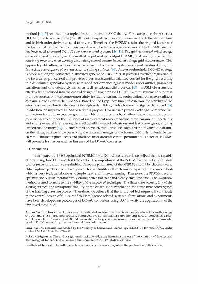
Energies 2019, 12, 2099
method [44,45] reported on a topic of recent interest in SMC theory. For example, in the rth-orderHOSMC, the derivative of the (r− 1)th control input becomes continuous, and both the sliding planeand its high-order derivative need to be zero. Therefore, the HOSMC retains the original features ofthe traditional SMC while producing less jitter and better convergence accuracy. The HOSMC methodhas been used to control DC–AC converter related systems [46–49]. The grid-connected wind energyconversion system is designed by multiple input multiple output HOSMC, so it can adjust active andreactive power, and even develop a switching control scheme based on voltage grid measurement. Thisapproach yields attractive benefits such as robust robustness to system uncertainty, reduced jitter, andfinite time convergence of system states to sliding surfaces [46]. A reverse-threshold HOSMC strategyis proposed for grid-connected distributed generation (DG) units. It provides excellent regulation ofthe inverter output current and provides a perfect sinusoidal balanced current for the grid, resultingin a distributed generator system with good performance against model uncertainties, parametervariations and unmodeled dynamics as well as external disturbances [47]. HOSM observers areeffectively introduced into the control design of single-phase DC–AC inverter systems to suppressmultiple sources of interference/uncertainty, including parametric perturbations, complex nonlineardynamics, and external disturbances. Based on the Lyapunov function criterion, the stability of thewhole system and the effectiveness of the high-order sliding mode observer are rigorously proved [48].In addition, an improved HOSM observer is proposed for use in a proton exchange membrane fuelcell system based on excess oxygen ratio, which provides an observation of unmeasurable systemconditions. Even under the influence of measurement noise, modeling error, parameter uncertaintyand strong external interference, the method still has good robustness and fast convergence, and haslimited time stability [49]. As mentioned above, HOSMC produces high-order derivative constraintson the sliding surface while preserving the main advantages of traditional SMC; it is undeniable thatHOSMC eliminates jitter effects and produces more accurate control performance. Therefore, HOSMCwill promote further research in this area of the DC–AC converter.
6. Conclusions
In this paper, a BPSO optimized NTSMC for a DC–AC converter is described that is capableof producing low THD and fast transients. The importance of the NTSMC is limited system stateconvergence time and no singularities. Also, the parameters of the NTSMC should be chosen well toobtain optimal performance. These parameters are traditionally determined by a trial and error method,which is very tedious, laborious to implement, and time-consuming. Therefore, the BPSO is used tooptimize the NTSMC parameters, yielding better transient and steady-state response. The Lyapunovmethod is used to analyze the stability of the improved technique. The finite time accessibility of thesliding surface, the asymptotic stability of the closed-loop system and the finite time convergenceof the tracking error are proved. Therefore, we believe that the improved technique will contributeto the control design of future artificial intelligence related systems. Simulations and experimentshave been developed on prototypes of DC–AC converters using DSP to verify the applicability of theimproved technique.
Author Contributions: E.-C.C. conceived, investigated and designed the circuit, and developed the methodology.C.-A.C. and L.-S.Y. prepared software resources, set up simulation software, and E.-C.C. performed circuitsimulations. E.-C.C. carried out DC–AC converter prototype, and measured as well as analyzed experimentalresults. E.-C.C. wrote the paper and revised it for submission.
Funding: This research was funded by the Ministry of Science and Technology (MOST) of Taiwan, R.O.C., undercontract MOST 107-2221-E-214-006.
Acknowledgments: The authors gratefully acknowledge the financial support of the Ministry of Science andTechnology of Taiwan, R.O.C., under project number MOST 107-2221-E-214-006.
Conflicts of Interest: The authors declare no conflicts of interest regarding the publication of this article.
63

Energies 2019, 12, 2099
References
1. Jeyraj, S.; Rahim, N.A. Multilevel inverter for grid-connected PV system employing digital PI controller.IEEE Trans. Ind. Electron. 2009, 56, 149–158.
2. Mirzaei, M.; Tibaldi, C.; Hansen, M.H. PI controller design of a wind turbine: Evaluation of the pole-placementmethod and tuning using constrained optimization. J. Phys. Conf. Ser. 2016, 753, 1–7. [CrossRef]
3. Jin, W.; Li, Y.L.; Sun, G.Y.; Bu, L.Z. H-infinity repetitive control based on active damping with reducedcomputation delay for LCL-type grid-connected inverters. Energies 2017, 10, 586.
4. Xie, C.; Zhao, X.; Savaghebi, M.; Meng, L.; Guerrero, J.M.; Quintero, J.C.V. Multirate fractional-order repetitivecontrol of shunt active power filter suitable for microgrid applications. IEEE J. Emerg. Sel. Top. Power Electron.2017, 5, 809–819. [CrossRef]
5. Benyoucef, A.; Kara, K.; Chouder, A.; Silvestre, S. Prediction-based deadbeat control for grid-connectedinverter with L-filter and LCL-filter. Electr. Power Compon. Syst. 2014, 42, 1266–1277. [CrossRef]
6. Kim, J.; Hong, J.; Kim, H. Improved direct deadbeat voltage control with an actively dampedinductor-capacitor plant model in an islanded AC microgrid. Energies 2016, 42, 978. [CrossRef]
7. Bevrani, H.; Feizi, M.R. Robust frequency control in an islanded microgrid: H-infinity and mu-synthesisApproaches. IEEE Trans. Smart Grid 2016, 7, 706–717. [CrossRef]
8. Ren, F.Y.; Lin, C.; Yin, X.H. Design a congestion controller based on sliding mode variable structure control.Comput. Commun. 2005, 28, 1050–1061. [CrossRef]
9. Ignaciuk, P.; Bartoszewicz, A. Congestion Control in Data Transmission Networks: Sliding Mode and Other Designs(Communications and Control Engineering); Springer: New York, NY, USA, 2013.
10. Tan, S.C.; Lai, Y.M.; Tse, C.K. Sliding Mode Control of Switching Power Converters: Techniques and Implementation;Taylor & Francis: Boca Raton, FL, USA, 2012.
11. Yu, X.; Kaynak, O. Sliding mode control with soft computing: A survey. IEEE Trans. Ind. Electron. 2009, 56,3275–3285.
12. Kang, S.W.; Kim, K.H. Sliding mode harmonic compensation strategy for power quality improvement of agrid-connected inverter under distorted grid condition. IET Power Electron. 2015, 8, 1461–1472. [CrossRef]
13. Kaynak, A.B.; Utkin, V.I. Industrial applications of sliding mode: Control Part II. IEEE Trans. Ind. Electron.2009, 56, 3271–3274. [CrossRef]
14. Kayacan, E.; Cigdem, O.; Kaynak, O. Sliding mode control approach for online learning as applied to type-2fuzzy neural networks and its experimental evaluation. IEEE Trans. Ind. Electron. 2012, 59, 3510–3520.[CrossRef]
15. Vardan, M.; Ekaterina, A. Sliding Mode in Intellectual Control and Communication: Emerging Research andOpportunities; IGI Global: Hershey, PA, USA, 2017.
16. Derbel, N.; Ghommam, J.; Zhu, Q.M. Applications of Sliding Mode Control; Springer: Singapore, 2017.17. Yan, X.G.; Spurgeon, S.K.; Edwards, C. Variable Structure Control of Complex Systems: Analysis and Design;
Springer International Publishing: New York, NY, USA, 2017.18. Andreas, R.; Luise, S. Variable-Structure Approaches: Analysis, Simulation, Robust Control and Estimation of
Uncertain Dynamic Processes; Springer International Publishing: New York, NY, USA, 2016.19. Abrishamifar, A.; Ahmad, A.A.; Mohamadian, M. Fixed switching frequency sliding mode control for
single-phase unipolar inverters. IEEE Trans. Power Electron. 2012, 27, 2507–2514. [CrossRef]20. Hao, X.; Yang, X.; Liu, T.; Huang, L.; Chen, W.J. A sliding-mode controller with multiresonant sliding surface
for single-phase grid-connected VSI with an LCL filter. IEEE Trans. Power Electron. 2013, 28, 2259–2268.[CrossRef]
21. Aghatehrani, R.; Kavasseri, R. Sensitivity-analysis-based sliding mode control for voltage regulation inmicrogrids. IEEE Trans. Sustain. Energy 2013, 4, 50–57. [CrossRef]
22. Camila, L.C.; Tiago, R.O.; Jose, P.V.S.C. Output-feedback sliding-mode control of multivariable systemswith uncertain time-varying state delays and unmatched non-linearities. IET Control Theory Appl. 2013, 7,1616–1623.
23. Hung, L.C.; Lin, H.P.; Chung, H.Y. Design of self-tuning fuzzy sliding mode control for TORA system. ExpertSyst. Appl. 2007, 32, 201–212. [CrossRef]
64

Energies 2019, 12, 2099
24. Hemdani, A.; Dagbagi, M.; Naouar, W.M.; Idkhajine, L.; Belkhodja, I.S.; Monmasson, E. Indirect slidingmode power control for three phase grid connected power converter. IET Power Electron. 2015, 8, 977–985.[CrossRef]
25. Liu, J.K.; Wang, X.H. Terminal Sliding Mode Control. In Advanced Sliding Mode Control for Mechanical Systems;Springer: Berlin, Germany, 2011; pp. 137–162.
26. Bhave, M.; Janardhanan, S.; Dewan, L. A finite-time convergent sliding mode control for rigid underactuatedrobotic manipulator. Syst. Sci. Control Eng. 2014, 2, 493–499. [CrossRef]
27. Hong, Y.G.; Yang, G.W.; Cheng, D.Z.; Spurgeon, S. Finite time convergent control using terminal slidingmode. J. Control Theory Appl. 2004, 2, 69–74. [CrossRef]
28. Yu, X.H.; Xu, J.X. Variable Structure Systems with Terminal Sliding Modes. In Variable Structure Systems:Towards the 21st Century; Springer: Berlin, Germany, 2002.
29. Roy, S.; Roy, S.B.; Kar, I.N. Adaptive–robust control of euler–lagrange systems with linearly parametrizableuncertainty bound. IEEE Trans. Control Syst. Technol. 2018, 26, 1842–1850. [CrossRef]
30. Roy, S.; Roy, S.B.; Kar, I.N. A new design methodology of adaptive sliding mode control for a class ofnonlinear systems with state dependent uncertainty bound. In Proceedings of the 2018 15th InternationalWorkshop on Variable Structure Systems (VSS), Graz, Austria, 9–11 July 2018; pp. 414–419.
31. Roy, S.; Kar, I.N. Adaptive-robust control of uncertain euler-lagrange systems with past data: A time-delayedapproach. In Proceedings of the 2016 IEEE International Conference on Robotics and Automation (ICRA),Stockholm, Sweden, 16–21 May 2016; pp. 5715–5720.
32. Roy, S.; Kar, I.N.; Lee, J.; Tsagarakis, N.G.; Caldwell, D.G. Adaptive-robust control of a class of el systemswith parametric variations using artificially delayed input and position feedback. IEEE Trans. Control Syst.Technol. 2019, 27, 603–615. [CrossRef]
33. Roy, S.; Kar, I.N.; Lee, J.; Jin, M.L. Adaptive-robust time-delay control for a class of uncertain euler–lagrangesystems. IEEE Trans. Ind. Electron. 2017, 64, 7109–7119. [CrossRef]
34. Plestan, F.; Shtessel, Y.; Brégeault, V.; Poznyak, A. Sliding mode control with gain adaptation—Applicationto an electropneumatic actuator. Control Eng. Pract. 2013, 21, 679–688. [CrossRef]
35. Plestan, F.; Shtessel, Y.; Brégeault, V.; Poznyak, A. New methodologies for adaptive sliding mode control.Int. J. Control 2010, 83, 1907–1919. [CrossRef]
36. Utkin, V.I.; Poznyak, A.S. Adaptive sliding mode control with application to super-twist algorithm: Equivalentcontrol method. Automatica 2013, 49, 39–47. [CrossRef]
37. Moreno, J.A.; Negrete, D.Y.; González, V.T.; Fridman, L. Adaptive continuous twisting algorithm. Int. J.Control 2016, 89, 1798–1806. [CrossRef]
38. Roy, S.; Lee, J.N.; Baldi, S. A New Continuous-Time Stability Perspective of Time-Delay Control: Introducinga State-Dependent Upper Bound Structure. IEEE Control Syst. Lett. 2019, 3, 475–480. [CrossRef]
39. Alireza, S.; Mozhgan, A. Binary PSO-based dynamic multi-objective model for distributed generationplanning under uncertainty. IET Renew. Power Gener. 2012, 6, 67–78.
40. Lin, C.J.; Chern, M.S.; Chih, M.C. A binary particle swarm optimization based on the surrogate informationwith proportional acceleration coefficients for the 0-1 multidimensional knapsack problem. J. Ind. Prod. Eng.2016, 33, 77–102. [CrossRef]
41. Silva, S.A.; Sampaio, L.P.; Oliveira, F.M.; Durand, F.R. Feed-forward DC-bus control loop applied to asingle-phase grid-connected PV system operating with PSO-based MPPT technique and active power-lineconditioning. IET Proc. Renew. Power Gener. 2017, 11, 183–193. [CrossRef]
42. Babu, T.S.; Ram, J.P.; Dragicevic, T.; Miyatake, M.; Blaabjerg, F.; Rajasekar, N. Particle Swarm OptimizationBased Solar PV Array Reconfiguration of the Maximum Power Extraction Under Partial Shading Conditions.IEEE Trans. Sustain. Energy 2018, 9, 74–85. [CrossRef]
43. Awadallah, M.A.; Venkatesh, B. Bacterial Foraging Algorithm Guided by Particle Swarm Optimization forParameter Identification of Photovoltaic Modules. Can. J. Electr. Comput. Eng. 2016, 39, 150–157. [CrossRef]
44. Emel’yanov, S.V.; Korovin, S.K.; Levant, A. High order sliding modes in control systems. Comput. Math.Model. 1996, 7, 294–318.
45. Levant, A. Higher-order sliding modes, differentiation and output-feedback control. Int. J. Control 2003, 76,924–941. [CrossRef]
65

Energies 2019, 12, 2099
46. Valenciaga, F.; Fernandez, R.D. Multiple-input–multiple-output high-order sliding mode control for apermanent magnet synchronous generator wind-based system with grid support capabilities. IET Renew.Power Gener. 2015, 9, 925–934. [CrossRef]
47. Dehkordi, N.M.; Sadati, N.; Hamzeh, M. A robust backstepping high-order sliding mode control strategy forgrid-connected DG units with harmonic/interharmonic current compensation capability. IEEE Trans. Sustain.Energy 2017, 8, 561–572. [CrossRef]
48. Chen, D.; Jun, Y.; Wang, Z.; Li, S.H. Universal active disturbance rejection control for non-linear systems withmultiple disturbances via a high-order sliding mode observer. IET Control Theory Appl. 2017, 11, 1194–1204.
49. Deng, H.W.; Li, Q.; Chen, W.R.; Zhang, G.R. High-order sliding mode observer based OER control for PEMfuel cell air-feed system. IEEE Trans. Energy Convers. 2018, 33, 232–244. [CrossRef]
© 2019 by the authors. Licensee MDPI, Basel, Switzerland. This article is an open accessarticle distributed under the terms and conditions of the Creative Commons Attribution(CC BY) license (http://creativecommons.org/licenses/by/4.0/).
66

energies
Article
Flatness-Based Control for the Maximum Power PointTracking in a Photovoltaic System
Leopoldo Gil-Antonio 1,2, Belem Saldivar 1,3,*, Otniel Portillo-Rodríguez 1,*,
Juan Carlos Ávila-Vilchis 1, Pánfilo Raymundo Martínez-Rodríguez 4
and Rigoberto Martínez-Méndez 1
1 Faculty of Engineering, Autonomous University of the State of Mexico, Instituto Literario No. 100 Oriente,Toluca 50130, Estado de México, Mexico; [email protected] (L.G.-A.);[email protected] (J.C.Á.-V.); [email protected] (R.M.-M.)
2 Tecnológico de Estudios Superiores de Jocotitlán Carretera Toluca-Atlacomulco km. 44.8,Jocotitlán 50700, Estado de México, Mexico
3 Cátedras CONACYT, Av. Insurgentes Sur 1582, Col. Crédito Constructor, Alcaldía Benito Juárez,Ciudad de México 03940, Mexico
4 School of Sciencies, UASLP, San Luis Potosi 78290, SLP, Mexico; [email protected]* Correspondence: [email protected] (B.S.); [email protected] (O.P.-R.)
Received: 30 March 2019; Accepted: 10 May 2019; Published: 15 May 2019
Abstract: Solar energy harvesting using Photovoltaic (PV) systems is one of the most popularsources of renewable energy, however the main drawback of PV systems is their low conversionefficiency. An optimal system operation requires an efficient tracking of the Maximum Power Point(MPP), which represents the maximum energy that can be extracted from the PV panel. This paperpresents a novel control approach for the Maximum Power Point Tracking (MPPT) based on thedifferential flatness property of the Boost converter, which is one of the most used converters in PVsystems. The underlying idea of the proposed control approach is to use the classical flatness-basedtrajectory tracking control where a reference voltage will be defined in terms of the maximum powerprovided by the PV panel. The effectiveness of the proposed controller is assessed through numericalsimulations and experimental tests. The results show that the controller based on differential flatnessis capable of converging in less than 0.15 s and, compared with other MPPT techniques, such asIncremental Conductance and Perturb and Observe, it improves the response against sudden changesin load or weather conditions, reducing the ringing in the output of the system. Based on the results,it can be inferred that the new flatness-based controller represents an alternative to improve theMPPT in PV systems, especially when they are subject to sudden load or weather changes.
Keywords: MPPT; differential flatness; nonlinear control
1. Introduction
For many years fossil fuels have been the primary source of energy in the world, however theseresources are finite. The threat of climate change due to global warming (caused in part by theburning of fossil fuels) has prompted the search for renewable energy sources such as the sun andthe wind. Solar energy is a sustainable, environmentally friendly, and cost-efficient source of energyavailable around the world, and for this reason solar technologies using photovoltaic (PV) systems havepenetrated the electric power production market, with the additional advantages of working quietlyand with low maintenance cost. Nonetheless, as it has been remarked by [1], the increment in theuse of PV devices in power systems has generated new challenges, such as those related with controlstrategies looking to provide good, even optimal, operating conditions of the PV systems. Moreover,the control strategies need to cope with the fact that the performance of PV systems depends on solar
Energies 2019, 12, 1843; doi:10.3390/en12101843 www.mdpi.com/journal/energies67

Energies 2019, 12, 1843
irradiance, ambient temperature, and load impedance [2]. As in [1], the approach proposed in thispaper is implemented in the open programming environment MATLAB R©/Simulink R©; nevertheless,the focused problem is the application of a novel control strategy (flatness-based) for the MPPT in PVsystems. As mentioned in [3], it is evident that PV components will be essential elements in powerelectrical systems, where their inclusion considers the MPPT control problem as a strategy that ispart of one of the two most important approaches highlighted in literature that corresponds to “theinstallation and operation of an energy storage system (ESS), while keeping the PVs in the maximumpower point tracking (MPPT). . . ” [3]. To the best knowledge of the authors, no flatness-based controlstrategies have been reported to cope with the MPPT problem in PV systems. This paper proposes theuse of a control strategy based on the differential flatness properties of the PV system model to tacklethe MPPT task.
The main drawback of PV systems is their low conversion efficiency. For an optimal operation,it is required for the system to operate at the Maximum Power Point (MPP), which represents themaximum energy that can be extracted from the PV panel. To reach this condition, it is necessaryto use Maximum Power Point Tracking (MPPT) systems. A major challenge in PV systems is tohandle their non-linear characteristics of current-voltage I-V relation that generate a unique MPP inthe power-voltage relation P-V [4]. The MPPT process becomes complicated due to the fact that theP-V relation varies with weather conditions. MPPT methods not only allow an increase in the powerdelivered by PV systems to the load, but they also give rise to a longer operating life of the system [5].
MPPT algorithms are designed so that the PV system adapts to weather changes in such a waythat optimal power is delivered. Typically, these algorithms are integrated into electronic powerconverter systems where their duty cycle is controlled to deliver the maximum available power to theload [6,7]. Several methods to solve the problem of MPPT have been reported in the literature. Amongthem are the Perturb and Observe (P&O) method, the Incremental Conductance (IncCond) algorithm,fuzzy logic-based methods, neural networks techniques, and the sliding mode control. The P&O andIncCond are the most popular algorithms to track the MPP [8–13].
The P&O method is inexpensive and relatively simple; its operation is based on periodic measuresof the voltage and current of the PV system to calculate the MPP. However, its main disadvantage isthat it delivers an oscillatory power around the MPP. Besides, since it is unable to detect if the powervariation is caused by weather effects or by inherent perturbations of the algorithm, the P&O methodmay fail in the presence of abrupt changes of temperature and solar irradiance [14].
The IncCond method is based on the fact that the slope of the P-V curve of a PV system is zerowhen the MPP is reached, positive to the left of the MPP and negative to its right. Based on that,the method calculates the MPP by comparing the instantaneous conductance with the incrementalconductance to modify the required reference voltage. The main disadvantage of the IncCond methodis that the response of the system to reach the MPP under certain conditions can be slow. However,the IncCond technique exhibits less oscillatory behavior around the MPP compared to the P&Omethod [15].
Fuzzy logic-based methods have demonstrated fast convergence and high performance undervarying weather conditions [16–23]. These methods do not require a mathematical model and are ableto handle the system nonlinearities. However, the main disadvantage of these controllers is that theireffectiveness depends on the error calculation and on the definitions of their base rules for the fuzzyinference mechanism. These definitions must be done by a human expert and the effectiveness of thecontrol relies on them.
Neural network-based algorithms require proper training strategies to effectively track theMPP [24–26]. It is worth mentioning that neural networks must be retrained to be applied to differentPV systems since they may have different specifications. Besides this, since the system parameters canbe modified over time, it is necessary to periodically train a neural network to ensure its effectiveness.Furthermore, according to [27,28], the implementation of fuzzy logic and neural network algorithmsmay be complex.
68

Energies 2019, 12, 1843
The sliding mode control technique sends an on-off signal to control the operation of the powerconverter to reach the MPP of the PV system. The commutation function is computed based on the factthat the derivative of the power with respect to the voltage is positive to the left of the MPP, negativeto its right, and zero at the MPP. Conventional sliding mode control techniques have limitations suchas variable operating frequency and the presence of nonzero steady state error [29].
The use of flatness-based control strategies in the area of power electrical systems has beenexplored in the last decade, where some works have reported the use of flatness-based controllersfor power converters. For instance, authors in [30] use a recursive approach were differential flatnessproperties are used to synthesize a controller that guarantees closed-loop asymptotic stability of apower converter connected to a DC motor. Two flatness-based controllers are proposed in [31] fora Boost inverter (two DC-DC Boost converters connected in differential mode to a grid) in orderto control, individually, each of the two output voltages of the Boost converters. A flatness-basedcontrol approach is provided in [32] to achieve the maximum power that is captured by a windgenerator driving a permanent magnet synchronous generator whose mathematical model is flat andis connected to a battery bank using an AC-DC converter. A differential flatness-based controller isproposed in [33] to improve the stability of the converters used in a distributed PV-energy storageDC generation system under the presence of parameter disturbances, while an extremum seekingalgorithm guarantees the tracking of the MPP under irradiance disturbances. Authors in [30–33]validate their flatness-based control strategies through numerical simulations. Nevertheless, as it hasbeen remarked previously, differential flatness-based methods have not been investigated to deal withthe MPPT problem in PV systems.
The main contribution of this paper concerns the use of a novel control strategy to perform thetracking task of the MPP in PV systems. A new methodology that exploits the differential flatnessproperty of the Boost converter allows deriving a MPPT controller for a stand-alone PV systemconstituted by a PV panel and a Boost power converter with resistive load. The strategy is basedon the trajectory tracking flatness-based control approach where a reference voltage is defined interms of the maximum power provided by the PV panel. Like the mentioned works that have useda flatness approach [30–33], the performance of the control law reported in this paper is validatedthrough numerical simulations. Nevertheless, this paper also reports experimental tests confirmingthe controller performance.
The proposed approach is shown to be capable of operating under changing conditions of solarirradiance, temperature, and load, even when the variations are abrupt. This is an important featurethat an efficient MPPT must have since the presence of clouds or trees, for instance, may degradethe performances of certain controllers. The robustness against load variations (normally related inpractice to energy consumption demands) is an important aspect disregarded in most of the existingcontrol techniques. This paper presents also a comparative analysis that shows the benefits of theproposed controller compared to the two most popular methods for the MPPT: P&O and IncCond.The flatness-based controller gives rise to an improved system response regarding the power behavior:before reaching the MPP, less oscillations are shown with the proposed control in contrast to theIncCond, and, once reaching the MPP, unlike the P&O method, no oscillations are exhibited.
This paper is organized as follows: Section 2 presents the mathematical model of the PV systemthat is used in this study. Section 3 details the design of the differential flatness-based controller to trackthe MPP. Section 4 presents the numerical simulations to evaluate the effectiveness of the controllerunder variations of solar irradiance, temperature and load. Besides, a comparative analysis showsthe benefits of the proposed controller compared to the P&O and IncCond methods. In Section 5,the performance of the proposed control approach is validated through experimental tests conductedin a prototype of the system. Finally, Section 6 gives some concluding remarks.
69

Energies 2019, 12, 1843
2. Photovoltaic System Model
The block diagram of the PV system under consideration is shown in Figure 1. The energy sourceof the PV system is constituted by a photovoltaic module, the Boost converter acts as interface betweenthe solar panel and the load, and the MPPT controller allows reaching the available maximum power.Notice that the current IPV and the voltage VPV provided by the PV module are used as inputs to theBoost converter and to the MPPT controller which is also fed with the output voltage v of the converter.The average control signal uav generated by the MPPT controller is sent to the converter.
MPPT
Controller
PV Module
Boost
Converter
IPV
VPV
Load
uav
v
Figure 1. Photovoltaic (PV) system under a Maximum Power Point Tracking (MPPT) controller.
2.1. PV Module Model
A PV module, also known as solar panel, consists of a set of solar cells that are connected inseries or in parallel depending on the application for which the PV module is built. If the solar cellsare connected in series, the voltage of the PV module is increased while the current keeps constant.Conversely, if a parallel connection is considered, the PV module current is increased while the voltageremains constant.
The equivalent circuit that represents a solar cell is constituted by an energy source that representsthe energy generated by the incidence of solar irradiance G which delivers the photogenerated currentIph. This circuit also considers a diode connected in parallel with the energy source, a series resistanceRs that represents the internal resistance to the current flow of the cell and a shunt resistance Rshrepresenting the leakage current (see Figure 2).
Figure 2. Equivalent circuit of a PV cell.
The equivalent circuit of a PV cell is mathematically described by Equations (1)–(3), where it isassumed that Rs << Rsh [34].
IPV = Iph − Io
[exp
(q (VPV + Rs IPV)
KTc A
)− 1]
(1)
In Equation (1), IPV and VPV denote the output current and voltage of the PV cell, respectively,Iph is the current photogenerated by the solar cell, Io is the reverse saturation current of the diode,q is the electron charge (1.602 × 10⁻¹⁹ C), Rs is the internal resistance to the current flow of the cell,K is the Boltzmann constant (1.381 × 10⁻²³ J/K), Tc is the temperature of the cell, and A is the diodeideality factor.
70

Energies 2019, 12, 1843
The photogenerated current Iph is determined by:
Iph =S
Sre f
[ISC + μSC
(Tc − Tre f
)](2)
where S is the solar irradiance, Sre f is the solar irradiance under reference conditions (1000 W/m2),ISC is the short-circuit current, μSC is the coefficient of short-circuit current, and Tre f is the referencetemperature of the photovoltaic cell [35]. The reverse saturation current Io is determined by:
Io = Io,re f
(Tc
Tre f
)3
exp
⎡⎣ qEG
(1
Tre f− 1
Tc
)AK
⎤⎦ (3)
where EG is the semiconductor energy band used in the solar cell and Io,re f represents the referencereverse saturation current given by:
Io,re f =ISC
exp(
VOCNsKTc A
)− 1
(4)
where Ns is the number of cells connected in series and VOC is the open circuit voltage [35]. In view ofEquation (1), the current provided by a PV module is given by:
IPV = Np Iph − Np Io
⎡⎣exp
⎛⎝ q(
VPVNs
+ Rs IPVNp
)KTc A
⎞⎠− 1
⎤⎦ (5)
where Np is the number of cells connected in parallel [36]. The characteristics of the PV moduleRenesola Virtus II JC250M-24/Bb, used in this research work, are plotted in Figures 3a,b and 4. Figure 3ashows the I-V curves for different values of solar irradiance considering a constant temperature of25 ◦C, Figure 3b shows the P-V curves for different values of solar irradiance considering a constanttemperature of 25 ◦C, and Figure 4 shows the I-V curves considering different temperature values anda solar irradiance of 1000 W/m2. Notice that the voltage is most likely to be influenced by temperaturevariations, and the current by solar irradiance changes. As illustrated in Figures 3a,b and 4, high solarirradiance values increase the current, and high temperatures reduce the output voltage of a PV panel.Then, the power conversion capability can be affected under conditions of high temperature and lowsolar irradiance.
Voltage (V)
0 5 10 15 20 25 30 35 40
Curr
ent
(A)
0
1
2
3
4
5
6
7
8
9
10
1000 W/m2
800 W/m2
600 W/m2
400 W/m2
200 W/m2
(a) I-V curves.
Voltage (V)
0 5 10 15 20 25 30 35 40
Pow
er
W()
0
50
100
150
200
250
300
1000 W/m2
2
800 W/m2
600 W/m2
400 W/m2
200 W/m
(b) P-V curves.
Figure 3. Curves of the PV panel Virtus II JC250M-24/Bb under different irradiance levels and aconstant temperature of 25 ◦C.
71

Energies 2019, 12, 1843
0 5 10 15 20 25 30 35 40 450
1
2
3
4
5
6
7
8
9
Volta e (V)g
Cu
rren
t(A
)
100˚C
75˚C
50˚C
25˚C
0˚C
Figure 4. I-V curves of the PV panel Virtus II JC250M-24/Bb under different temperature levels and aconstant irradiance of 1000 W/m2.
2.2. Boost Converter Model
A Boost converter is a DC-DC power converter that increases the voltage from its input source toits output. Figure 5 shows the electronic diagram of a Boost power converter in which the input sourceis the voltage supplied by a photovoltaic panel. This circuit is constituted by a capacitance C, a loadresistance R, and an inductance L. The current across the inductor is denoted by i and the output atthe capacitor terminals by v. Note that i is assumed to be equal to the PV current IPV .
Figure 5. Block diagram of a Boost converter.
Note that the Boost converter includes a switching function u that commutes between twooperation modes. When u = 1 there is no connection between the voltage source VPV and the systemload R. In this case, the system dynamics is described by Equations (6).
dvdt
=− vRC
didt
=VPV
L(6)
When u = 0, there is energy transmission between the power supply and the load, then the systemdynamics is described by Equations (7).
dvdt
=iC− v
RCdidt
=− vL+
VPVL
(7)
Equations (6) and (7) can be unified into the bilinear system defined by Equations (8),
dvdt
=iC(1 − u)− v
RCdidt
=− vL(1 − u) +
VPVL
(8)
where i is the inductor current, v is the output voltage, and VPV is the power supply voltage. The controlinput u represents the switch position function which takes a binary value u ∈ {0,1}.
72

Energies 2019, 12, 1843
In order to design a control law for the Boost converter, an average model must be defined.The average model of the Boost converter is represented by the same Equations (8), but the controlvariable u is redefined as a sufficiently smooth function uav taking values in the real interval [0, 1].Then, the model given in Equations (8) is referred to as average model replacing the switched controlinput u ∈ {0, 1} by the average control input uav ∈ [0, 1].
The steady state value of the current i, for constant values of the input, can be obtained in aparameterized form in terms of the corresponding output voltage equilibrium value v as follows:
i =v2
RVPV(9)
3. Flatness-Based Control Design
In nonlinear systems theory, the flatness property is due to the ability of dynamic systems tosupport an accurate linearization through endogenous feedback. A system that satisfies the flatnessproperty is named a differentially flat system. The main attribute of flat systems is that state andinput variables can be expressed directly (without the integration of a differential equation) in termsof a particular set of variables called flat outputs (or linearizing outputs) and a finite number of theirderivatives [37]. This section presents the main contribution of this paper which is the developmentof a controller based on the differential flatness property of the Boost converter for the MPPT of aPV system.
The flatness property of the Boost converter has been established in [38]. A flat output F can bedetermined by the total energy stored in the system, that is
F =12
(Li2 + Cv2
)(10)
Using Equations (8), the differential parametrization of the states and the input of the Boostconverter are obtained as follows:
i =− RCVPV2L
+ β (11)
v =
√2C
F − LC
(−RCVPV
2L+ β
)(12)
uav =1 − iVPV + 1L V2
PV + 2R2C v2 − F(
1L VPV + 2
RC i)
v(13)
β =12
√(RCVPV
L
)2+
4L(
RCF + 2F)
(14)
The derivation of Equations (11)–(14) is presented in Appendix A. Note that the model defined byEquations (8) is represented by the differential parameterization given by Equations (11)–(14) stated interms of the flat output F and its time derivatives F and F. In Equation (13), VPV is the time derivativeof the output voltage of the PV cell.
The underlying idea of the proposed control approach for the MPPT is to use the classicalflatness-based trajectory tracking control but instead of predefine a reference path, a reference voltagev∗ will be obtained from the maximum power provided by the PV panel. From this reference voltage,using Equation (10), a reference flat output F∗ is constructed. The controller is designed to track thereference signal F∗ with a guaranteed convergence of the error to zero. As shown below, this ensuresan efficient tracking of the MPP.
73

Energies 2019, 12, 1843
The control design is explained as follows. To obtain the reference voltage corresponding to themaximum power provided by the PV panel, the power delivered by the Boost converter PC mustmatch the power supplied by the PV panel PPV , i.e,
PC = PPV (15)
Note that, for a pure resistive load, PC can be written in terms of the output voltage v and the loadresistance R, and PPV can be expressed in terms of IPV and VPV , as shown in Equation (16).
PC =v2
R, PPV = VPV IPV (16)
Then, in view of Equations (15) and (16), the reference voltage v∗ that the controller must take intoaccount to guarantee the tracking of the MPP is given by,
v∗ =√
VPV IPV R (17)
In order to steer the converter output voltage v to the reference voltage v∗ defined in Equation (17),the control must force the flat output F to follow the reference flat output F∗ calculated as:
F∗ = 12
(L(
v∗2
RVPV
)2
+ Cv∗2
)(18)
In order to establish the closed-loop dynamics, in Equation (13), the highest order derivative of the flatoutput is replaced by an auxiliary input μaux = F. Regarding the tracking problem under consideration,the error is defined as e = F − F∗. To guarantee stable closed-loop error dynamics, the auxiliary inputμaux can be defined as:
μaux = F∗ − β1(F − F∗)− β0(F − F∗) (19)
with β0 > 0 and β1 > 0 are constant gains to be determined. Equation (19) allows one to define theerror dynamics as:
e + β1 e + β0e = 0 (20)
which is associated with the characteristic polynomial,
p(s) = s2 + β1s + β0 (21)
For the sake of convenience, the characteristic polynomial can be written in terms of the dampingfactor ζ and the natural frequency ωn as follows,
p(s) = s2 + 2ζωns + ω2n (22)
where ωn > 0 and ζ > 0. Notice that β1 and β0 are determined by
β1 = 2ζωn, β0 = ω2n (23)
The error will asymptotically converge to zero if the gains of the feedback tracking controller arechosen such that the roots of the characteristic polynomial defined in Equation (21) lie in the left halfcomplex plane. The constants β1 and β0 must be chosen accordingly. In view of the parametrization ofthe control input given in Equation (13) and the auxiliary input dynamics defined in Equation (19),
74

Energies 2019, 12, 1843
the flatness-based controller that ensures the tracking of the MPP with an asymptotic convergence ofthe error to zero is given by
uav = 1 − i∗VPV + 1L V2
PV + 2R2C (v
∗)2 − μaux(1L VPV + 2
RC i∗)
v∗(24)
where i∗ is obtained from Equation (11) where β is given in terms of F∗ and F∗. As it was previouslydescribed, the switching function of the Boost converter is able to take binary values, then, the averagecontrol law defined in Equation (24) cannot be directly implemented. As usual practice in this scenario,a Pulse Width Modulation (PWM) has been used for which the average control uav acts as a modulationsignal. Figure 6 presents a schematic diagram illustrating the control system implementation.
Control
FF*
u
μaux
v
RCD
vVPV
Reference
flat output
Auxiliary
input
Flat
Output
Boost
converter
PWM
IPV
uav
Reference
voltage
VPV IPV
IPV
Reference
current
VPV
i*
v*
VPV
F*F*
u
L
Figure 6. MPPT system block diagram.
4. Simulation Results
In this section the performance of the proposed control approach is evaluated through numericalsimulations. The PV system consisting of a photovoltaic module, a Boost converter, a load resistance,and the flatness-based controller is implemented in the MATLAB R©/Simulink R©environment (R2015a,The MathWorks, Inc, Natick, MA, USA). Table 1 shows the characteristics of the Virtus II photovoltaicmodule (JC250M-24/Bb, ReneSola, Shanghai, China) used for this experimental setting.
Table 1. Virtus II Electrical characteristics.
Parameters Value
Maximum Power (PMAX) 250 WCurrent at Maximum Power (IMP) 8.31 AVoltage at Maximum Power (VMP) 30.1 V
Short-Circuit Current (ISC) 8.83 AOpen-Circuit Voltage (VOC) 37.4 V
Table 2 presents the parameters of the Boost power converter and the proposed values of thenatural frequency and the damping factor for the flatness-based controller. Notice that with theproposed values of damping ζ and natural frequency ωn, the controller gains are β0 = 90,000 andβ1 = 60. Then, the roots of the characteristic polynomial given in Equation (21) are s1 = −30 + 2.985jand s2 = −30 − 2.985j. Since the roots lie on the left side of the complex plane, the stability of the errordynamics is ensured, i.e., the error e = F − F∗ asymptotically converges to zero as t → ∞.
75

Energies 2019, 12, 1843
Table 2. Boost converter parameters.
Parameters Value
Capacitance C 470 μFResistance R 12 Ω
PWM operation frequency 45 kHzInductance L 10 mH
Natural frequency ωn 300Damping factor ζ 0.1
Through simulations, the robustness of the differential flatness-based controller under variationsof the solar irradiance, temperature and load is evaluated. To develop such evaluation, four studycases were considered:
Case 1. At 1.1 s, the solar irradiance is increased from 500 W/m2 to 1000 W/m2 within a timeinterval of 0.1 s. A constant temperature of 25 ◦C is considered (see Figure 7c).
Case 2. At 0.8 s, the temperature is increased from 15 ◦C to 25 ◦C within a time interval of 0.1 s.A constant solar irradiance of 800 W/m2 is considered (see Figure 8c).
Case 3. Considering a constant temperature of 25 ◦C, at 0.6 s, the solar irradiance is decreasedfrom 1000 W/m2 to 500 W/m2 within a time interval of 0.5 s. Then, at 1.2 s, the solar irradiance isincreased from 500 W/m2 to 1000 W/m2 within a time interval of 0.5 s. In a different time instant(at 2 s), the temperature increases from 25 ◦C to 40 ◦C within a time interval of 0.1 s (see Figure 9c).
Case 4. A solar irradiance of 1000 W/m2 and a temperature of 25 ◦C are kept constant while theload instantly decreases from 12 Ω to 6 Ω at 0.5 s (see Figure 10c).
In the first three cases, a constant load of 12 Ω is considered.Note that the proposed time scales are short (tests were performed within time intervals less than
3 s). This aims at demonstrating the strength of the proposed approach for the MPPT, i.e., to evaluatethe performance of the flatness-based control law against sudden variations of weather conditions.Clearly, if the controller is efficient in tracking the MPP in spite of the abrupt changes considered inthe study cases described above, it will also have a satisfactory performance under realistic operatingconditions involving smoother variations of solar irradiance and of temperature, occurring withinlonger time intervals.
Figures 7–10 illustrate the performance of the proposed control approach under the conditionsstated above. Table 3 presents the theoretical maximum power for the different values of temperatureand solar irradiance considered in the four study cases. It is important to mention that, theoretically,load variations do not affect the maximum power.
Table 3. Theoretical maximum power.
Solar Radiation (W/m2) Temperature (◦C) PMAX (W)
500 25 125510 23 118800 25 200800 15 210900 45 2031000 25 2501000 40 232
The trajectories generated under the conditions described in Case 1 are depicted in Figure 7.The output power of the Boost converter and the power delivered by the PV panel are shown inFigure 7a. The output voltage of the converter and the current and voltage of the PV panel arepresented in Figure 7b. Figure 7c shows the variation of the solar irradiance. Note that the theoreticalvalues of the maximum power for a constant temperature of 25 ◦C are reached: 125 W for a solarirradiance of 500 W/m2, and 250 W for 1000 W/m2. Observe that, as expected, during the time period
76
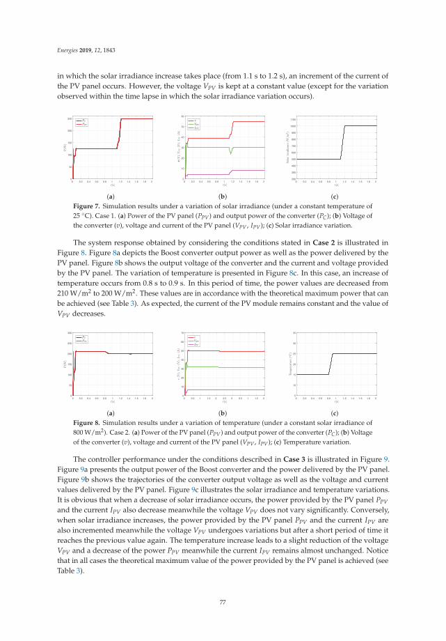
Energies 2019, 12, 1843
in which the solar irradiance increase takes place (from 1.1 s to 1.2 s), an increment of the current ofthe PV panel occurs. However, the voltage VPV is kept at a constant value (except for the variationobserved within the time lapse in which the solar irradiance variation occurs).
0 0.2 0.4 0.6 0.8 1 1.2 1.4 1.6 1.8 2 0
50
100
150
200
250
(a)
v
v
(b)
0 0.2 0.4 0.6 0.8 1 1.2 1.4 1.6 1.8 2 200
300
400
500
600
700
800
900
1000
1100
(c)Figure 7. Simulation results under a variation of solar irradiance (under a constant temperature of25 ◦C). Case 1. (a) Power of the PV panel (PPV) and output power of the converter (PC); (b) Voltage ofthe converter (v), voltage and current of the PV panel (VPV , IPV); (c) Solar irradiance variation.
The system response obtained by considering the conditions stated in Case 2 is illustrated inFigure 8. Figure 8a depicts the Boost converter output power as well as the power delivered by thePV panel. Figure 8b shows the output voltage of the converter and the current and voltage providedby the PV panel. The variation of temperature is presented in Figure 8c. In this case, an increase oftemperature occurs from 0.8 s to 0.9 s. In this period of time, the power values are decreased from210 W/m2 to 200 W/m2. These values are in accordance with the theoretical maximum power that canbe achieved (see Table 3). As expected, the current of the PV module remains constant and the value ofVPV decreases.
0 0.2 0.4 0.6 0.8 1 1.2 1.4 1.6 1.8 20
50
100
150
200
250
300
(a)
0 0.5 1 1.5 2 2.5 0 0.5 1 1.5 2 0
10
20
30
40
50
60
70
(b)
0 0.2 0.4 0.6 0.8 1 1.2 1.4 1.6 1.8 2 5
10
15
20
25
30
35
(c)Figure 8. Simulation results under a variation of temperature (under a constant solar irradiance of800 W/m2). Case 2. (a) Power of the PV panel (PPV ) and output power of the converter (PC); (b) Voltageof the converter (v), voltage and current of the PV panel (VPV , IPV); (c) Temperature variation.
The controller performance under the conditions described in Case 3 is illustrated in Figure 9.Figure 9a presents the output power of the Boost converter and the power delivered by the PV panel.Figure 9b shows the trajectories of the converter output voltage as well as the voltage and currentvalues delivered by the PV panel. Figure 9c illustrates the solar irradiance and temperature variations.It is obvious that when a decrease of solar irradiance occurs, the power provided by the PV panel PPVand the current IPV also decrease meanwhile the voltage VPV does not vary significantly. Conversely,when solar irradiance increases, the power provided by the PV panel PPV and the current IPV arealso incremented meanwhile the voltage VPV undergoes variations but after a short period of time itreaches the previous value again. The temperature increase leads to a slight reduction of the voltageVPV and a decrease of the power PPV meanwhile the current IPV remains almost unchanged. Noticethat in all cases the theoretical maximum value of the power provided by the PV panel is achieved (seeTable 3).
77

Energies 2019, 12, 1843
0 0.5 1 1.5 2 2.5
0
50
100
150
200
250
300
(a)
0 0.5 1 1.5 2 2.5
0
10
20
30
40
50
60
70 v
v
(b)
0 0.5 1 1.5 2 2.5
400
600
800
1000
0 0.5 1 1.5 2 2.5
20
30
40
50
(c)
Figure 9. Simulation results under solar irradiance and temperature variations. Case 3. (a) Power ofthe PV panel (PPV) and output power of the converter (PC); (b) Voltage of the converter (v), voltageand current of the PV panel (VPV , IPV); (c) Solar irradiance and temperature variations.
The controller performance under the conditions described in Case 4 is illustrated in Figure 10.Figure 10a shows the output power of the Boost converter and the power delivered by the PV panel.Figure 10b shows the trajectories of the converter output voltage as well as the voltage and currentvalues delivered by the PV panel. Figure 10c illustrates the load variation. Note that the load isdiminished at 0.5 s leading to minor variations of the signals coming from the PV panel PPV , IPV ,and VPV . However, the output voltage of the Boost converter v is significantly decreased. It isnoteworthy that variations of the load do not prevent the proposed algorithm from successfullytracking the maximum power.
0 0.1 0.2 0.3 0.4 0.5 0.6 0.7 0.8 0.9 10
50
100
150
200
250
300
350
(a)
0 0.1 0.2 0.3 0.4 0.5 0.6 0.7 0.8 0.9 10
10
20
30
40
50
60
70
(b)
0 0.1 0.2 0.3 0.4 0.5 0.6 0.7 0.8 0.9 1 0
5
10
15
(c)Figure 10. Simulation results under a load variation. Case 4. (a) Power of the PV panel (PPV) andoutput power of the converter (PC); (b) Voltage of the converter (v), voltage and current of the PV panel(VPV , IPV); (c) Load variation.
Simulation results highlight the performance of the proposed control approach. Case 1 is definedto demonstrate the robustness of the control law against solar irradiance abrupt changes; Case 2 aimsto show the controller performance under a sudden variation of temperature; Case 3 allows evaluatingthe performance of the controller under abrupt variations of solar irradiance and temperature; finally,Case 4 considers the transit from a lightly loaded system to a heavily loaded one.
Simulation results show that the proposed control scheme is robust against variations ofexternal conditions and that the corresponding values of maximum power are reached in all cases.From Figures 7–10, it can be noticed that the control action takes about 0.1 s to be reflected in thesystem trajectories and that the system reaches the steady state in a very short period of time regardlessthe variation of weather conditions and load. This stabilization time can be considered acceptablesince most of the PV applications do not require a faster response.
As can be seen, the sudden variations of temperature, solar irradiance and load do not degrade theperformance of the flatness-based controller. It can be concluded that the flatness-based controller iseffective in maintaining the output power of the PV panel at the corresponding optimum values.Furthermore, it is robust against variations of external conditions and operates under low orhigh temperatures.
78

Energies 2019, 12, 1843
Comparative Analysis
In order to determine the benefits that the proposed control scheme offers in contrast to the mostpopular MPPT techniques: Perturb and Observe (P&O) and Incremental Conductance (IncCond),numerical simulations were performed. Under the conditions stated in Case 3, the conventionalP&O method (see for instance [12]) and the IncCond with integral regulator (IncCond+IR) algorithmproposed in [39] were evaluated. Figure 11 shows the performance of these three techniques; PP&Ocorresponds to the power obtained with the P&O method, PFBC is the power obtained with theflatness-based control technique proposed in this paper, and PIncCond+IR is the power obtained withthe IncCond+IR algorithm.
0 0.5 1 1.5 2 2.5
0
50
100
150
200
250
300
350
P (
W)
PP&O
PFBC
PIncCond+IR
Figure 11. Comparison of three techniques for the MPPT. Simulation results under conditions statedin Case 3. Red line: power obtained with the Perturb and Observe (P&O) method. Blue line: powerobtained with the flatness-based controller. Black line: power obtained with the IncCond+IR algorithm.
Note that within the time interval where the solar irradiance increase occurs (between 1.2 s and1.7 s), the response produced with the flatness-based approach differs from the ones produced withthe other techniques. However, the theoretical power is reached when the solar irradiance is set at1000 W/m2.
At first glance, it might seem that the three methods have almost the same performance, however,a zoom of Figure 11 shows that, although the time to reach the MPP is almost equal (about 0.13 s),the response obtained with the IncCond+IR method exhibits oscillations of significant magnitudebefore reaching the MPP (see Figure 12a), and that, as expected, the response produced with the P&Otechnique presents small amplitude oscillations around the MPP (see Figure 12b).
0 0.05 0.1 0.15 0.2 0.25 0.3 0.35 0.4 0.45 0.5
100
150
200
250
300
P(W
)
PP&O
PFBC
PIncCond+IR
(a)
0.2 0.201 0.202 0.203 0.204 0.205 0.206 0.207 0.208 0.209 0.21
249
249.5
250
P(W
)
(b)
Figure 12. Zoom of Figure 11. (a) Zoom of Figure 11 between 0 and 0.5 s; (b) Zoom of Figure 11between 0.2 and 0.21 s.
In view of the simulation results, it can be concluded that one important advantage of theproposed approach is that less oscillations are produced before reaching the MPP compared to theIncCond+IR method. Furthermore, the flatness-based method does not give rise to oscillations aroundthe MPP, like the ones observed for the P&O technique.
Another disadvantage of the P&O technique is that its accuracy depends on the perturbation size:if it is small, the method takes more time to reach the MPP, if it is big, the amplitude of the oscillationsaround the MPP increases [26]. This does not occur with the proposed flatness-based method.
79

Energies 2019, 12, 1843
5. Experimental Results
Experimental results obtained with a PV panel Virtus II model JC250M-24/Bb show theperformance of the flatness-based controller under realistic scenarios. For the implementation of thisMPPT controller, a Boost power converter is designed to operate in continuous mode at a switchingfrequency of 45 kHz; the parameter values used in the experimental set up are shown in Table 2.
The MPPT flatness-based control algorithm was implemented with the Simulink Real-Time R©software (R2015a, The MathWorks, Inc, Natick, MA, USA) using a Humusoft R© MF 624 multifunctionI/O card (MF624, Humusoft Ltd., Prague, Czechia) that is installed on a computer with an Intel R©CoreTM processor (i7-2600, 3.40 GHz, Intel, Santa Clara, CA, USA) and 8GB RAM memory (DDR31333 MHz, Hynix, Incheon, Korea). The complete scheme operates at a fixed sampling frequencyof 10 kHz. A PWM generator set to a frequency of 45 kHz is employed. Four analog inputs areused to sense the current IPV and voltage VPV of the PV panel, the output voltage of the converter v,and the current through the load resistor iR, which allows monitoring possible variations of the load.The control system can be described as follows. The input signals IPV and VPV are acquired by sensorsS22P (current) and AMC1100 (voltage) respectively. The average control signal uav adjusts the dutycycle of the PWM generator which activates the MOSFET 19NF20 through the optocoupler circuitIX3180. The auxiliary input μaux defined in Equation (19) is generated with the use of the referencesignal F∗ (derived from the output voltage reference) and the flat output F. The Vantage Pro2TM
weather station is used to measure solar radiation; it is remotely connected with an indicator console.The experimental configuration diagram, the nominal values of the components, and the informationof electronic devices and sensors are shown in Figure 13.
10 mH
470 Fμ 10 �
Figure 13. General scheme of a experimental setup of MPPT.
It is important to mention that the true MPP is unknown during a real-time test under naturalsunlight. This is because the temperature cannot be accurately measured since PV panels have amulticell distribution and an insulated laminated structure [40].
During the development of experiments, temperature differences of more than 5 ◦C were foundin different sections of the PV panel. Higher temperatures were identified near to the edges of the PVpanel due to the heating generated by its laminated structure. To cope with this, approximate valuesof the panel temperature were calculated from the average of the measured temperatures. Based onthese values, the corresponding values of the theoretical maximum power were obtained.
The first experimental test was carried out when a solar irradiance of 510 W/m2 was measuredand an average temperature of 35 ◦C was calculated. Figure 14 shows the closed-loop response of thesystem under these conditions. Figure 14a corresponds to the experimental result and Figure 14b tothe simulation response.
80

Energies 2019, 12, 1843
t[s]0 5 10 15
PPV(W
)
0
20
40
60
80
100
120
140
(a) Experimental result.
0 0.2 0.4 0.6 0.8 1 1.2 1.4 1.6 1.8 2 0
20
40
60
80
100
120
140
(b) Simulation result.
Figure 14. System response under a solar irradiance of 510 W/m2 and an average temperature of 35 ◦C.Power of the PV panel (PPV).
The second test was conducted under a solar irradiance of 900 W/m2 and an average temperatureof 45 ◦C. The system response is shown in Figure 15. Figure 15a corresponds to the experimental resultand Figure 15b to the simulation response.
Notice that, in simulation, the theoretical maximum powers are reached (118 W for the first case,203 W for the second one, see Table 3), meanwhile the powers obtained with the experimental tests arebelow these values (around 110 W for the first case, around 190 W for the second one). As explainedbefore, these differences between the power values are due to the fact that it is impossible to estimateprecisely the true MPP value based on the weather conditions because of the complexity of modulelamination and measurement accuracy [40]. Besides, there are power losses in the connection cablebetween the photovoltaic module and the converter that should be considered. In [41], it is shownthat the theoretical MPP values can be either higher or lower than the practical measured trackingvalues. Despite this, from Figures 14a and 15a it can be inferred that the flatness-based controllerallows delivering all the available power to the load.
t[s]0 5 10 15
PPV(W
)
0
20
40
60
80
100
120
140
160
180
200
220
(a) Experimental result.
0 0.2 0.4 0.6 0.8 1 1.2 1.4 1.6 1.8 2 0
20
40
60
80
100
120
140
160
180
200
220
(b) Simulation result.
Figure 15. System response under a solar irradiance of 900 W/m2 and an average temperature of 45 ◦C.Power of the PV panel (PPV).
6. Conclusions
In this paper a novel control strategy for the MPPT was presented. The differential flatness-basedproperty of the Boost converter is exploited to design a controller that allows an effective tracking ofthe MPP. Numerical simulations were performed in MATLAB R©/Simulink R©to assess the effectivenessof the flatness-based control law against sudden variations of weather conditions and load considered
81

Energies 2019, 12, 1843
in four study cases. For all of them, the theoretical maximum power was reached; it can be concludedthat the sudden variations of temperature, solar irradiance, and load do not degrade the performanceof the proposed MPPT technique. Furthermore, it was shown that the flatness-based technique hassome advantages compared to the P&O method and to the IncCond algorithm related to the PV systemresponse. Simulation results show that the oscillatory behavior around the MPP is avoided with theproposed approach.
Experimental tests were conducted in a prototype of the system consisting of a PV panel Virtus IIJC250M-24/Bb. It was noticed that, during the real-time tests, the temperature is not uniform on thePV panel surface. Differences of more than 5 ◦C were found in different sections of the PV panel. As aresult, the theoretical MPP is unknown. Despite this, from the experimental results, it can be inferredthat the flatness-based controller allows delivering all the available power from the PV panel to theload. In fact, the power experimentally obtained is close to the theoretical maximum power calculatedfrom average values of the panel temperature.
Author Contributions: Investigation, L.G.-A., B.S., O.P.-R.; methodology, B.S., O.P.-R.; resources, O.P.-R., P.R.M.-R.;supervision, B.S.; validation, J.C.Á.-V., R.M.-M., P.R.M.-R.; writing—original draft, L.G.-A.; writing—review andediting B.S., R.M.-M., J.C.Á.-V.
Funding: This research was partially funded by PRODEP (Programa para el Desarrollo Profesional Docente, parael Tipo Superior) grant number ITESJOCO-010.
Conflicts of Interest: The authors declare no conflict of interest.
Appendix A
This section presents the parametrization of the states and control input of the Boost convertermodel derived from the flat output. Consider the flat output given by
F =12
(Li2 + Cv2
)(A1)
Its time derivative is:
F = Lididt
+ Cvdvdt
(A2)
substituting the system dynamics defined by Equations (8) yields,
F = i[−vu + VPV ] + v[iu − vR]
F = iVPV − v2
R(A3)
where:
u = 1 − uav (A4)
The parametrization of i is obtained by substituting v2 (that can be derived from Equation (A3))into Equation (A1),
i = −RCVPV2L
+ β (A5)
where:
β =12
√(RCVPV
L
)2+
4L(
RCF + 2F)
(A6)
82

Energies 2019, 12, 1843
From Equation (A1), one obtains:
v =
√2F − Li2
C(A7)
substituting Equation (A5) into Equation (A7) yields the parametrization of v, which is obtainedas follows:
v =
√2C
F − LC
(−RCVPV
2L+ β
)2(A8)
The second derivative of F is:
F = iVPV + VPVdidt
− 2vR
dvdt
(A9)
Substituting the system dynamics defined by Equations (8) into Equation (A9) yields theparametrization of the average control as follows:
uav = 1 − iVPV + 1L V2
PV + 2R2C v2 − F(
1L VPV + 2
RC i)
v(A10)
References
1. Bueno, P.G.; Hernandez, J.C.; Sanchez-Sutil, F. Stability assessment for transmission systems with largeutility-scale photovoltaic units. IET Renew. Power Gener. 2016, 10, 584–597. [CrossRef]
2. Chu, C.C.; Chen, C.L. Robust maximum power point tracking method for photovoltaic cells: A sliding modecontrol approach. Sol. Energy 2009, 83, 1370–1378. [CrossRef]
3. Hernandez, J.C.; Bueno, P.G.; Sanchez-Sutil, F. Enhanced utility-scale photovoltaic units with frequencysupport functions and dynamic grid support for transmission systems. IET Renew. Power Gener. 2017,11, 361–372. [CrossRef]
4. Rezk, H.; Eltamaly, A.M. A comprehensive comparison of different MPPT techniques for photovoltaicsystems. Sol. Energy 2015, 112, 1–11. [CrossRef]
5. Bahgat, A.B.G.; Helwa, N.H.; Ahmad, G.; El Shenawy, E.T. Maximum power point tracking controller for PVsystems using neural networks. Renew. Energy 2005, 30, 1257–1268.
6. Brunton, S.L.; Rowley, C.W.; Kulkarni, S.R.; Clarkson, C. Maximum power point tracking for photovoltaicoptimization using ripple-based extremum seeking control. IEEE Trans. Power Electron. 2010, 25, 2531–2540.[CrossRef]
7. Mastromauro, R.A.; Liserre, M.; Kerekes, T.; Dell’Aquila, A. A single-phase voltage-controlled grid-connectedphotovoltaic system with power quality conditioner functionality. IEEE Trans. Ind. Electron. 2009,56, 4436–4444. [CrossRef]
8. Babaa, S.E.; Armstrong, M.; Pickert, V. Overview of Maximum Power Point Tracking Control Methods forPV Systems. J. Power Energy Eng. 2014, 2, 59–72. [CrossRef]
9. Hohm, D.P.; Ropp, M.E. Comparative Study of Maximum Power Point Tracking Algorithms. Prog. Photovolt.Res. Appl. 2003, 11, 47–62. [CrossRef]
10. Zainudin, H.N.; Mekhilef, S. Comparison Study of Maximum Power Point Tracker Techniques for PVSystems. In Proceedings of the 14th International Middle East Power Systems Conference, Cairo, Egypt,19–21 December 2010; pp. 750–755.
11. Kollimalla, S.K.; Mishra, M.K. Variable Perturbation Size Adaptive P&O MPPT Algorithm for SuddenChanges in Irradiance. IEEE Trans. Sustain. Energy 2014, 5, 718–728.
12. Elgendy, M.A.; Zahawi, B.; Atkinson, D.J. Operating Characteristics of the P&O Algorithm at HighPerturbation Frequencies for Standalone PV Systems. IEEE Trans. Energy Convers. 2015, 30, 189–198.
83

Energies 2019, 12, 1843
13. Zakzouk, N.E.; Elsaharty, M.A.; Abdelsalam, A.K.; Helal, A.A.; Williams, B.W. Improved PerformanceLow-Cost Incremental Conductance PV MPPT Technique. IET Renew. Power Gener. 2016, 10, 561–574.[CrossRef]
14. Jain, S.; Agarwal, V. A new algorithm for rapid tracking of approximate maximum power point inphotovoltaic systems. IEEE Power Electron. Lett. 2004, 2, 16–19. [CrossRef]
15. Salas, V.; Olías, E.; Barrado, A.; Lázaro, A. Review of the maximum power point tracking algorithms forstand-alone photovoltaic systems. Sol. Energy Mater. Sol. Cells 2006, 90, 1555–1578. [CrossRef]
16. Ngan, M.S.; Tan, C.W. A Study of Maximum Power Point Tracking Algorithms for Stand-alone PhotovoltaicSystems. In Proceedings of the 2011 IEEE Applied Power Electronics Colloquium (IAPEC), Johor Bahru,Malaysia, 18–19 April 2011.
17. Rakhshan, M.; Vafamand, N.; Khooban, M.H. Maximum Power Point Tracking Control of PhotovoltaicSystems: A Polynomial Fuzzy Model-Based Approach. IEEE J. Emerg. Sel. Top. Power Electron. 2018,6, 292–299. [CrossRef]
18. Tang, S.; Sun, Y.; Chen, Y.; Zhao, Y.; Yang, Y.; Szeto, W. An Enhanced MPPT Method CombiningFractional-Order and Fuzzy Logic Control. IEEE J. Photovolt. 2017, 7, 640–650. [CrossRef]
19. Rezaei, A.; Gholamian, S.A. Optimization of New Fuzzy Logic Controller by Genetic Algorithm for MaximumPower Point Tracking in Photovoltaic System. ISESCO J. Sci. Technol. 2013, 9, 9–16.
20. Alajmi, B.N.; Ahmed, K.H.; Finney, S.J.; Williams B.W. Fuzzy-Logic-Control Approach of a ModifiedHill-Climbing Method for Maximum Power Point in Microgrid Standalone Photovoltaic System. IEEE Trans.Power Electron. 2011, 26, 1022–1030. [CrossRef]
21. Dounis, A.I.; Kofinas, P.; Alafodimos, C.; Tseles, D. Adaptive fuzzy gain scheduling PID controller formaximum power point tracking of photovoltaic system. Renew. Energy 2013, 60, 202–214. [CrossRef]
22. Alajmi, B.N.; Ahmed, K.H.; Finney, S.J.; Williams, B.W. A Maximum Power Point Tracking Techniquefor Partially Shaded Photovoltaic Systems in Microgrids. IEEE Trans. Ind. Electron. 2013, 60, 1596–1606.[CrossRef]
23. Ramaprabha, R.; Mathur, B.L. Intelligent Controller based Maximum Power Point Tracking for Solar PVSystem. Int. J. Comput. Appl. 2011, 12, 37–41. [CrossRef]
24. Younis, M.A.; Khatib, T.; Najeeb, M.; Ariffin, A.M. An Improved Maximum Power Point Tracking Controllerfor PV Systems Using Artificial Neural Network. Prz. Elektrotech. Electr. Rev. 2012, 88, 116–121.
25. Syafaruddin; Karatepe, E.; Hiyama, T. Artificial neural network-polar coordinated fuzzy controller basedmaximum power point tracking control under partially shaded conditions. IET Renew. Power Gener. 2009,3, 239–253. [CrossRef]
26. Esram, T.; Chapman, P.L. Comparison of photovoltaic array maximum power point tracking techniques.IEEE Trans. Energy Convers. 2007, 22, 439–449. [CrossRef]
27. Veerachary, M.; Senjyu, T.; Uezato, K. Neural-network-based maximum-power-point tracking ofcoupled-inductor interleaved-boostconverter-supplied PV system using fuzzy controller. IEEE Trans.Ind. Electron. 2003, 50, 749–758. [CrossRef]
28. Subudhi, B.; Pradhan, R. A Comparative Study on Maximum Power Point Tracking Techniques forPhotovoltaic Power Systems. IEEE Trans. Sustain. Energy 2013, 4, 89–98. [CrossRef]
29. Salmi, T.; Bouzguenda, M.; Gastli, A.; Masmoudi, A. MATLAB/Simulink Based Modelling of SolarPhotovoltaic Cell. Int. J. Renew. Energy Res. 2012, 2, 2013–2018.
30. Rigatos, G.; Siano, P.; Ademi, S.; Wira, P. Flatness-Based Control of DC–DC Converters Implemented inSuccessive Loops. Electric Power Compon. Syst. 2018, 46, 673–687. [CrossRef]
31. Renaudineau, H.; Lopez, D.; Flores-Bahamonde, F.; Kuoro, S. Flatness-based control of a boost inverter forPV microinverter application. In Proceedings of the IEEE 8th International Symposium on Power Electronicsfor Distributed Generation Systems, Florianopolis, Brazil, 17–20 April 2017; pp. 1–6.
32. Alhamed Aldwaihi, H.; Delaleau, E. Maximum Power Point Tracker of a Wind Generator Based on theFlatness-Based Control. In Proceedings of the IEEE Energy Conversion Congress and Exposition, Phoenix,AZ, USA, 17–22 September 2011; pp. 883–888.
33. Xue, H.; Li, H.; Wang, Y. Nonlinear Differential Flatness Control of a Distributed PV-ES DC GenerationSystem. WSEAS Trans. Syst. Control 2016, 40, 53–61.
34. Rekioua, D.; Matagne, E. Optimization of Photovoltaic Power Systems—Modelization, Simulation and Control;Springer: London, UK; Dordrecht, The Netherlands; Heidelberg, Germany; New York, NY, USA, 2012.
84

Energies 2019, 12, 1843
35. Kalogirou S.A. Solar Energy Engineering; Elsevier Inc.: San Diego, CA, USA, 2009.36. Granda-Gutiérrez, E.E.; Orta, O.A.; Díaz-Guillén, J.C.; Jimenez, M.A.; Osorio, M.; Gonzleáz, M.A. Modelado
y simulación de celdas y paneles solares. Congreso Internacional de Ingeniería Electrónica ELECTRO 2013,35, 17–22.
37. Fliess, M.; Lévine, J.L.; Martin, P.; Rouchon, P. Flatness and defect of non-linear systems: Introductory theoryand examples. Int. J. Control 1995, 61, 1327–1361. [CrossRef]
38. Sira-Ramírez, H.; Agrawal, S.K. Differentially Flat Systems; Marcel Dekker: New York, NY, USA, 2004.39. Nguyen, D.T.; Goro, F. PV-Active Power Filter Combination Supplies Power to Nonlinear Load and
Compensates Utility Current. IEEE Power Energy Technol. Syst. J. 2016, 2, 32–42. [CrossRef]40. Weidong, X.; Zeineldin, H.H.; Zhang, P. Statistic and Parallel Testing Procedure for Evaluating Maximum
Power Point Tracking Algorithms of Photovoltaic Power Systems. IEEE J. Photovolt. 2013, 3, 1062–1069.41. Fu-Sheng, P.; Ru-Min, C.; Shin, H.K.; Tai-Sheng, L. Performance Evaluation of Parabolic Prediction to
Maximum Power Point Tracking for PV Array. IEEE Trans. Sustain. Energy 2011, 2, 60–68.
c© 2019 by the authors. Licensee MDPI, Basel, Switzerland. This article is an open accessarticle distributed under the terms and conditions of the Creative Commons Attribution(CC BY) license (http://creativecommons.org/licenses/by/4.0/).
85


energies
Article
A New Adaptive Approach to Control Circulating andOutput Current of Modular Multilevel Converter
Muhammad Ishfaq 1,*, Waqar Uddin 1,*, Kamran Zeb 1,2, Imran Khan 1, Saif Ul Islam 1,
Muhammad Adil Khan 3 and Hee Je Kim 1,*
1 Department of Electrical Engineering, Pusan National University Busan, South Korea San 30,ChangJeon Dong, Pusandaehak-ro 63 7 beon-gil 2, Geumjeong-gu, Busan-city-46241, Korea;[email protected] (K.Z.); [email protected] (I.K.); [email protected] (S.U.I.)
2 Department of Electrical and Computer Science, National University of Engineering and Technology,Islamabad City 44000, Pakistan
3 Department of Electrical and Computer Science, Air University, Islamabad City 44000, Pakistan;[email protected]
* Correspondence: [email protected] (M.I.); [email protected] (W.U.);[email protected] (H.J.K.); Tel: +82-10-3462-1990 (H.J.K.)
Received: 1 February 2019; Accepted: 19 March 2019; Published: 22 March 2019
Abstract: This paper addresses the output current and circulating current control of the modularmulti-level converter (MMC). The challenging task of MMCs is the control of output current andcirculating current. Existing control structures for output and circulating current achieve controlobjectives with comparatively complex controllers and the designed parameters for the controller isalso difficult. In this paper, an adaptive proportional integral (API) controller is designed to controlthe output current and the circulating current. The output current is regulated in αβ axes while thecirculating current is regulated in the abc stationary frame to enhance MMC performance. The outputand circulating current control results using an API controller are compared with the conventionalproportional resonant (PR) controller in terms of transient response, stability, optimal performance,and reference tracking for results verification. The API control architecture significantly improvetransient response, stability, and have excellent reference tracking capability. Moreover, it controlsoutput current and converges the circulating current to a desired value. The control structure isdesigned for a three-phase MMC system, simulated and analyzed in MATLAB-Simulink.
Keywords: circulating current; fuzzy; proportional integral; proportional resonant; MMC
1. Introduction
The MMC is becoming an increasingly attractive, competitive, and highly applied technology formedium and high voltage power applications due to its advantages, such as low harmonics, modularstructure, simple scaling, loss reduction in switches, and satisfactory fault management [1–3]. Currently,MMCs have been expanded to many applications [4] such as motor drivers [5], solar/wind powersystems [6–8], energy transmission and distribution systems [9], and static synchronous compensators(STATCOM) [10]. Recently published literature related to MMC targeted current control, voltagecontrol, loss analysis and modulation, dynamic and steady-state models, modeling, and simulationmethods [11–16].
The first structure of the MMC was presented in [17]. Currently, many configurations and controldesigned approaches have been introduced by many researchers for the control objectives, such asbalancing and averaging of SM capacitor voltage, circulating current ripples injection or suppression,and output voltage regulation [18–22]. Figure 1 shows the configuration of a three-phase six arm MMC.
Energies 2019, 12, 1118; doi:10.3390/en12061118 www.mdpi.com/journal/energies87

Energies 2019, 12, 1118
Every arm of the MMC is equipped with a series connected sub module (SM) configuration. The SM,consists of two switches connected with a capacitor, is also depicted in Figure 1.
S
S
1D
2D
Submodule
dc U2
-dc U
2
0
m, a u m, c um, b u
n, a u n, b u n, c u
m, a im, b i m, c i
n, a i n, b i n, c i
u, a i
u, b i
u, c iarmR
armL
0,aR
0,bR
0,cR
0,bL
0,cL
0,aL
SMV
cv
1SM
2SM
NSM
1SM
2SM
NSM
1SM
2SM
NSM
1SM
2SM
NSM
1SM
2SM
NSM
1SM
2SM
NSM
Figure 1. General MMC 3 phase structure.
For the optimal performance of MMC, the control system plays a vital role. The output current iscontrolled to transfer the power to AC grid while the circulating current does not affect the outputof the converter. However, uncontrolled circulating current results in higher losses. The circulatingcurrent problem in each arm of MMC arises due to potential differences in every SM arm and DClink. Reference [23] studied the effects of arm inductance and SM capacitance on the magnitude ofcirculating current. Increases in arm inductance decrease the circulating current, but the circulatingcurrents are not eliminated. The negative sequence component of circulating current rotates at twiceline frequency. A control scheme is proposed in [24] by translating the a-b-c sequence components intodq rotational frame. But this control structure has a limitation because the circulating current also havepositive and zero sequence components along with negative sequence components.
The most common control approach was introduced by Hagiwara and Akagi in [25]. The controlmethod is used to regulate the output current and internal dynamics, i.e., circulating current andinternal energy. However, the ripples in circulating current could not be eliminated effectively bythis control method. Over the past few years, many control schemes for circulating current wereproposed such as dq or rotating frame control for the suppression of 2nd order harmonics [26–28],resonant controllers to eliminate harmonics in unbalanced circumstances [29] and to eliminateintegral harmonics in circulating currents plug in repetitive controllers are used [30,31]. But theabove-mentioned control method is complicated in structure and the controllers are difficult to tunefor system stability and performance.
Some researchers have proposed control methods for controlling both circulating current andoutput current. A PR control strategy is used to control an output current to get the desired outputpower. The output current is 1st harmonic frequency sinusoid [32]. Since after all PR control strategygives an infinite gain at the resonant frequency, any small frequency changes may point to an enormoustracking error from the reference signal. A PI controller in [24] is used to control circulating current
88

Energies 2019, 12, 1118
and a PR controller is also proposed to suppress the circulating current in [33]. However, the designand tuning parameters of the controllers mentioned above may be complicated as obtaining excellentcontrol operation and stability may be a difficult task.
This paper covers two main issues of the MMC—circulating current control and output currentcontrol during normal grid condition. An adaptive PI controller has been used to control both thecirculating and output current control in dq and abc stationary frames. Compared to other controlmethods, the API control scheme has many advantages such as good tracking, transient response,optimal stability performance, wide range operation capability, and adequate control for the MMCduring normal grid condition.
The sections of this paper are organized as Section 2, which describes the operation and modelingof the MMC. Section 3 deals with the control structure design for output and circulating current.The results are discussed in Section 4. While the conclusion is detailed in Section 5.
2. Operation and System Mathematical Modeling
Every SM of an MMC has a capacitor and half bridge connected switches, which gives outputvoltage according to switch ON or OFF position as depicted in Figure 2.
2.1. Switching Operation of the MMC
The insertion or bypassing of N-SM will give, (M + 1) levels of output waveform at everyphase of the MMC. Where N represents No of SM and M represents the levels of output waveform. The switching operation of a single phase MMC is illustrated in Figure 2, using a single lineschematic diagram.
A DC voltage “Udc” is applied at the input of the MMC. The switches are operating in reciprocalfashion in each SM relying on the position ON or OFF. The solid line shows the capacitor is insertedand the dim line shows a capacitor is bypassed in every SM. The insertion and bypassing of thecapacitor will define different levels of voltage at its terminal shown in Figure 2. The capacitor statethat is inserted or bypassed are summarized in Table 1.
Table 1. Capacitor states.
ScenarioCapacitors States in the
Upper ArmCapacitors States in the
Lower ArmOutput Voltage
1 All capacitors are inserted All capacitor bypassed −Udc2
2 One capacitor bypassed andthree capacitors inserted
One capacitor inserted andthree capacitors bypassed −Udc
4
3 Two capacitors bypassedand two capacitors inserted
Two capacitors inserted andtwo capacitors bypassed 0
4 Three capacitors bypassedand one capacitor inserted
Three capacitors insertedand one capacitor bypassed
Udc4
5 Four capacitors bypassedand zero capacitors inserted
Four capacitors inserted andzero capacitors bypassed
Udc2
2.2. System Mathematical Modeling
The mathematical modeling of the MMC is derived from a single-phase equivalent circuit asshown in Figure 3.
89

Energies 2019, 12, 1118
dcU2
dcU4
dc3U4
dcU
dcU2
dcU4
dc3U4
dcU
dcU2
dcU4
dc3U4
dcU
dcU2
dcU4
dc3U4
dcU
dcU2
dcU4
dc3U4
dcU
dc- U4
dc- U2
dc U2
dc U4
dc- U4
dc- U2
dc U2
dc U4
dc- U4
dc- U2
dc U2
dc U4
dc- U4
dc- U2
dc U2
dc U4
dc- U4
dc- U2
dc U2
dc U4
dc U4
dc U4
dc U4
dc U4
dc U4
dc U4
dc U4
dc U4
dc U4
dc U4
dc U4
dc U4
dc U4
dc U4
dc U4
dc U4
dc U4
dc U4
dc U4
dc U4
dc U4
dc U4
dc U4
dc U4
dc U4
dc U4
dc U4
dc U4
dc U4
dc U4
dc U4
dc U4
dc U4
dc U4
dc U4
dc U4
dc U4
dc U4
dc U4
dc U4
1S
2S
1S
2S
1S
2S
1S
2S
1S
2S
1S
2S
1S
2S
1S
2S
1S
2S
1S
2S
1S
2S
1S
2S
1S
2S
1S
2S
1S
2S
1S
2S
1S
2S
1S
2S
1S
2S
1S
2S
1S
2S
1S
2S
1S
2S
1S
2S
1S
2S
1S
2S
1S
2S
1S
2S
1S
2S
1S
2S
1S
2S
1S
2S
1S
2S
1S
2S
1S
2S
1S
2S
1S
2S
1S
2S
1S
2S
1S
2S_dc U
2
dc U2
u, j v u, j v u, j v u, j v u, j v
u v u v u v u v u v
m , u n u m , u n u m , u n u m , u n u m , u n u
m u
n u
Figure 2. Switching operation of the single phase MMC.
By applying the Kirchhoff loop law, the relations for the arm voltages, output current, andcirculating current of the converter are obtained as follow [34]. Where j ε {a, b, c}
− Udc2
+ um,j + Rarmim,j + Larmdim,j
dt+ vu,j = 0 (1)
Udc2
− un,j − Larmdin,j
dt− Rarmin,j + vu,j = 0 (2)
where Larm and Rarm denote arm inductance and arm resistance respectively. Udc represent the entireDC bus terminal voltage. vu,j represent output voltage of converter at point Z. um,j and un,j representssubmodule arm voltages. The upper arm is represented by subscript m while a lower arm is representedby subscript n. Different currents of the MMC are given as
im,j = idi f f ,j +iu,j
2(3)
90

Energies 2019, 12, 1118
in,j = idi f f ,j −iu,j
2(4)
iu,j = im,j − in,j (5)
idi f f ,j =12(im,j + in,j
)(6)
where im,j and in,j represents the upper arm current and lower arm current. iu,j represent the outputcurrent. idi f f ,j represents an internal circulating current. Adding and subtracting (1) and (2) we obtainthe following relation.
vu,j =
(un,j − um,j
2
)︸ ︷︷ ︸
ev,j
− Rarm
2iu,j − Larm
2diu,j
dt(7)
vdi f f ,j =Udc
2− Rarmidi f f ,j −
Larmdidi f f ,j
dt(8)
The ev,j is internal voltage in (7), while vdi f f ,j in (8) is the internal unbalanced voltage of an MMC,and the internal idi f f ,j over phase j ε {a, b, c} can be express as
idi f f ,j =im,j + in,j
2=
Idc3
+ icir,j (9)
where Idc is the dc link current and supposed to be distributed equally in all phases. As a result,the circulating current described in (6) contains 1/3 of the DC link current Idc
3 and icir,j is the ACcomponent of circulating current. The dynamics of an MMC are characterized in Equations (7) and (8).By evaluating Equation (7), the output current iu,j can be controlled by ev,j. Similarly, by evaluatingEquation (8), the internal circulating current idi f f ,j can be controlled by vdi f f ,j. Furthermore, thecapacitor SM internal dynamics with regards to arm voltages and currents are expressed as
CN
dv∑cm,j
dt= ni
m,jim,j (10)
CN
dv∑cn,j
dt= ni
n,jin,j (11)
0
dc U2
m, j u
n, j u
u, j v
u, j idiff, j i
m, j i
n, j i-
dc U2
Figure 3. Single phase equivalent circuit.
The capacitance of an SM capacitor is expressed by C, the number of SM in each half arm isrepresented by N, while capacitor sum voltages in upper and lower arms are represented by v∑
cm,j and
v∑cn,j. Insertion indices of upper and lower arms are represented by ni
m,j and nin,j. Insertion indices ni
m,j
91

Energies 2019, 12, 1118
and nin,j equal to one means the SM capacitor is inserted while insertion indices ni
m,j and nin,j equal to
zero means the SM capacitor is bypassed in corresponding arms. As stated by Equations (8) and (9),the reference calculated for the arm voltages can be expressed as
um,j_re f =Udc
2− ev,j − vdi f f ,j + Rarmidi f f ,j +
Larmdidi f f ,j
dt(12)
un,j_re f =Udc
2+ ev,j − vdi f f ,j + Rarmidi f f ,j +
Larmdidi f f ,j
dt(13)
In (13) the ev,j is calculated from the internal loop current controllers [35], while vdi f f ,j is calculatedfrom the circulating current eliminating controller, which can be used to minimize the three-phasecirculating current in an MMC. It can be concluded from Equations (1), (2), (12), and (13) that iu,j andidi f f ,j could be controlled by manipulating ev,j and vdi f f ,j, respectively.
3. Control Scheme of the MMC
3.1. Adaptive PI Controller Design
The adaptive PI is a hybrid controller in which fuzzy logic (FL) is used to update the gains ofPI for a wide range of operation. The FL makes the processing operation of a PI controller easy ina non-linear system where the system is ill-defined and mathematically poorly designed. The FLpre-processes the controller input (I/P) signal and PI post-process error signal to get the desired outputresponse from the plant.
3.1.1. Fuzzy Controller Architecture
In the real world, problems related to a control system are largely complex, particularly whenimplementation problems are considered. The promising aspect of the fuzzy logic controller (FLC) isthat they incorporate expert knowledge instead of entirely depending upon the exact mathematicalmodel. Moreover, heuristics and intuition knowledge are also incorporated into the control system.Thus, FLC is suitable in applications, where models are ill-defined, not reliable enough, and complex.Essentially, the FLC is an artificial decision maker who works in a closed-loop fashion in real-timeas shown in Figure 4. It collects plant O/P information y(t), matches it with the reference I/P x(t),and decides what the plant I/P v(t) would be to assure performance objectives. The FLC is mainlycomposed of four main phases: rule-base, inference mechanism, fuzzification, and de-fuzzification.
1. The “rule-base” which contains the information of controlling output variables are created inFLC, in the shape of IF-THEN rules, with condition and conclusion.
2. The rules are evaluated in the inference mechanism according to the error. During inferencemechanism, it is concluded which control rules are appropriate at the current situation. Moreover,the choice of I/P to the plant are also enabled in this phase.
3. During the fuzzification, a “crisp” (which are real numbers, not fuzzy sets) or actual timeinformation are collected and reshaped to a fuzzy set using fuzzy expressive terms, expressivevariables, and membership functions. Moreover, I/P is modified and interpreted which are thencompared with the rules defined in the rule-base.
4. The defuzzification transforms the fuzzy outcomes obtained by inference mechanism to real-timeor crisp output utilizing membership functions. There are several available methods fordefuzzification, i.e., mean of maximum, center of minimum, and center of gravity [36,37].
92

Energies 2019, 12, 1118
(t)v 1(t)x
(t)x
(t)x
(t)x
(t)v(t)v
(t)v
(t) v y(t)
Figure 4. Fuzzy controller architecture to controlled plant.
3.1.2. Fuzzy PI Controller
The PI controller has tuning gains parameter kp and ki, respectively. The desired performance ofPI control structure is improved by updating the gains, according to error u(t). The adaptability isattained by employing fuzzy rules, as given below and graphically illustrated in Figure 5.
• If error |u(t)| is zero, then proportional gain kp is large and integral gain ki is small• If error |u(t)| is small, then proportional gain kp is large and integral gain ki is zero.• If error |u(t)| is large, then proportional gain kp is large and integral gain ki is large.
The “crisp inputs” in the form circulating current and output current are fuzzified and shaped toa fuzzy set using membership function. The fuzzy set is evaluated in the rules-base with conditionand conclusion, and concludes which rules are appropriate at the current time. The defuzzificationprocess involves the conversion of the fuzzy outcomes to circulating and output voltages utilizing themembership function. The fuzzy rule selected from the set is defuzzified by using the center of gravitymethod. While the Gaussian membership function (GMF) is used for fuzzification, the GMF uses twovariables, variance σi or standard deviation and center di as:
μ(x) = exp
(−0.5
(xi − di
σi
)2)
(14)
Figure 5. Output–input membership functions.
93

Energies 2019, 12, 1118
The defuzzified output of fuzzy is fed as a gain(Kp, Ki
)to PI. Thus, the PI controller for
controlling the iu,j is mathematically defined as:
e∗vαβ(PI) = Kpu(t) + Ki
∫u(t)dt (15)
The PI controller for controlling the idi f f ,j is mathematically defined as:
v∗di f f ,j(PI) = Kpu(t) + Ki
∫u(t)dt (16)
Whereas u(t) is controller input, e∗vαβ and v∗di f f ,j, controller outputs, kp and ki are controller gainsrespectively. However, the gain’s parameters of a conventional PI controller are constant in (15) and(16), which needs adaptation according to system load disturbance, parameter uncertainties, electricalfaults, and load variations. To achieve adaptation, the designed controller use u(t) signal as an input forself-tuning of gain parameters, i.e., kp and ki, respectively. Fuzzy IF-THEN rules are made as presentedin Table 2. Based on these rules, a decision is performed by the inference engine. The defuzzifiedoutput is obtained by the center of gravity method for U1 and U2.
Table 2. IF-THEN rules employed for gain adaptation.
Input Membership Functions IF-THEN Rules Output Membership Functions
S.No LinguisticTerms Range If Input
|u(t)|Then Output
(kp, ki)Linguistic Terms Range
(1) Zero [0, 0.2] Zero Zero. Large Zero [0, 0.2](2) Small [0.3, 0.7] Small Large. Small Small [0.3, 0.7](3) Large [0.8, 1.0] Large Large. Large Large [0.8, 1.0]
During fuzzification, the error signal, u(t), information is collected and converted/fuzzified tofuzzy set using fuzzy linguistic terms and membership functions and compared with the IF-THENrules defined in the rule-base. The rules are analyzed in the inference mechanism that decides the firingof the dominant rule. The fuzzy outcomes in the shape of U1 and U2 are obtained during defuzzificationusing the center of gravity method and update the gain parameters K1 and K2, respectively. The rulesemployed in rule-base can be graphically illustrated in Figure 6a–c and shows the various scenarios inwhich U1 and U2 are actually computed by the fuzzy controller based on the absolute error. The lineindices which corresponds to inputs can be moved to adjust gains kp and ki, as shown in Figure 6a–c.
So, the adaptation of (15) using the API controller for controlling iu,j is mathematically defined as
e∗vαβ(API) = U1K1u(t) + U2K2
∫u(t)dt (17)
The adaptation of (16) using the API controller for controlling idi f f ,j is mathematically defined as
v∗di f f ,j(API) = U1K1u(t) + U2K2
∫u(t)dt (18)
Whereas U1 and U2 are the fuzzy controller output for the gains kp and ki respectively. While K1
and K2 are used for the representation of updated gains kp and ki as shown in Figure 7.
94

Energies 2019, 12, 1118
u(t)Kp Ki u(t) Kp Ki
(a) (b)
u(t) Kp Ki
(c)
Figure 6. Adaptation of gain values where the: (a) error is zero, (b) error is small, and (c) error is large.
+−
+
+
u (t)
Figure 7. Control structure for error tracking.
3.2. Circulating Current Control
The idi f f ,j can be regulated by vdi f f ,j, therefore, a control scheme is needed to regulate vdi f f ,jfor controlling idi f f ,j to overcome the converter losses. The variable vdi f f ,j is obtained through (8).A feedforward part is added to compensate the voltage drop. Filtering of Udc is not required due tothe lower number of harmonics in DC voltage compared to AC voltage. The control law we obtain
v∗di f f ,j =Udc
2− Ridi f f −
(U1K1u(t) + U2K2
∫u(t)dt
)(i∗di f f ,j − idi f f ,j
)(19)
The reference is forced to get the desired value of circulating current, i.e., P/MUdc. The controlstructure using the API controller is shown in Figure 8.
95

Energies 2019, 12, 1118
Feed forwardterm
m, j i
n, j i
ref P
1dc
MU
dc U2
-R
diffi
diffi
Δ diffi
1
Mdi
diff v1
Figure 8. Circulating current control.
3.3. Output Current Control
The output current can be regulated according to the following equation.
vu,j = ev,j − Rarm
2iu,j − Larm
2diu,j
dt(20)
By evaluating (20), ev,j is the variable which can be regulated to control the output current iu,j.The Equation (20) can be rewritten as⎡⎢⎣ ev,a
ev,bev,c
⎤⎥⎦ =1
2(sLarm + Rarm)
⎡⎢⎣ iu,a
iu,biu,c
⎤⎥⎦+
⎡⎢⎣ vu,a
vu,bvu,c
⎤⎥⎦ (21)
Using the Clarke transformation Equation (20) can be transformed into αβ axis from a-b-c frame(Tabc⇒αβ
).
Tabc⇒αβ =
√23
⎡⎢⎢⎣1 − 1
2 − 12
0√
32 −
√3
2√12
√12
√12
⎤⎥⎥⎦ (22)
For a three-phase balance system Equation (21) can be written[ev,α
ev,β
]=
12(sLarm + Rarm)
[iu,α
iu,β
]+
[vu,α
vu,β
](23)
In control engineering usage vu,αβ is load disturbance which will vary inversely according to shortcircuit ratio [32]. Since vu,αβ is measurable by introducing a feedforward term, the dynamics can beimproved. The control law obtained
e∗v,j =
(U1K1u(t) + U2K2
∫u(t)dt
)(i∗u,j − iu,j
)+ vu,αβ + iu,αβ
R2
(24)
where (i∗u,j − iu,j) error control and the reference for voltage is computed using Equation (24), to controlthe output current. The output current control structure is shown in Figure 9.
96

Energies 2019, 12, 1118
APIController
APIController
ref P
refQ
m, j i
n, j i
u, j i
u, i
u, i
u, v
R
u, v
2
-2
v, je
v, e
v, e
R
Figure 9. Output Current control.
The overall control scheme for controlling the circulating current and output current is shown inFigure 10.
Eq(6)
Eq (12) & (13)
dc U2
m, a u m, c um, b u
n, a u n, b u n, c u
m, a im, b i m, c i
n, a i n, b i n, c i
u, a i
u, b i
u, c iarm
R
armL
1SM
2SM
NSM
1SM
2SM
NSM
1SM
2SM
NSM
1SM
2SM
NSM
1SM
2SM
NSM
1SM
2SM
NSM
0
dc U2
-u, j i
u, iv, j e
m, j u
n, j un, j n
m, j n
diff, j v
dc U
diff, vdiff, jim, j i
n, j i
R
u, v
u, i
v, e
-R
dc U2
0,aR 0,aL
diff, i
diff, ji
Figure 10. Overall control design for output and circulating currents.
4. Results and Discussions
A control design architecture for a three-phase MMC model has been implemented with thehelp of MATLAB-Simulink (2017a, Natick, Massachusetts, MA, USA). The time for simulation isconsidered as 2 s. For better understanding, all the results are magnified. A comparative analysisof the results between the proposed API controller and a conventional PR controller has been made.The capacitor sum voltage and circulating current are the variables which need to be controlled, toreduce MMC losses. Ideally, the circulating current value idi f f should converge to DC input power, i.e.,(
idi f f = PMUdc
). The results of circulating current in Figure 11a,b is compared using the API and a PR
controller. For a better understanding, the results are magnified for time t = 0.6 s to t = 0.8 s using themagnification tool. The API controller result shows that the circulating current value is convergingto the desired value, i.e., 250 A with no oscillations during 0.2 s, showing good result compared to
97

Energies 2019, 12, 1118
the PR controller. While in the case of PR controller the circulating current value is not converging tothe desired value i.e., 250 A and also shows oscillations up to 0.2 s. Which means that the circulatingcurrent is not converged properly. It is also noted that circulating current one phase is exceedingthe desired value, i.e., 250 A throughout the simulation as depicted in Figure 11b. The capacitorsum voltage average value should converge to DC link voltage mean value, i.e., Udc
2 to get a balancedistribution of capacitor sum voltage over desired SM. The capacitor sum voltage of both an upperand a lower arm using the API and a PR controller are analyzed in Figures 12a,b and 13a,b. For abetter explanation, the results are magnified for time t = 0.58 s to t = 0.68 s using the magnification tool.The API controller display proper convergence of capacitor sum voltage to a desired DC link meanvalue for both upper and lower arm. All phase voltages are balanced in magnitude, which shows thebalance distribution of capacitor sum voltage for the required SM in both upper and lower arm. Asopposed to the API controller, the capacitor sum voltage of both upper and lower arms using the PRcontroller showed an imbalance in magnitude and created a trajectory path from 0.2 s to 0.8 s, whichmeant that the capacitor sum value was not totally converged to the desired DC link mean value for abalanced distribution of capacitor voltage in the required SM.
(a) (b)
I c (A)
I diff (A
)
Figure 11. (a) Circulating current using the API controller; (b) circulating current using thePR controller.
(a) (b)
v cm (V
)
v cm (V
)
Figure 12. (a) Capacitor voltage of an upper arm using the API controller; (b) capacitor voltage of anupper arm using the PR controller.
(a) (b)
v cn (V
)
v cn (V
)
Figure 13. (a) Capacitor voltage of a lower arm using the API controller; (b) capacitor voltage of alower arm using the PR controller.
98

Energies 2019, 12, 1118
The dynamics of sum energy for both controllers are shown in Figure 14a,b. For better analysis,the results are magnified for time t = 0.6 s to t = 1 s using the magnification tool. At the start, the APIcontroller shows overreaction. The rules defined in the rule-base are called and the decision is carriedout to fire the dominant rule. The API controller takes only 0.024 s to clear transient, and the referenceis completely tracked at 0.75 s completely without further overshoot, undershoot, steady state error,and ripples. However, in the case of the PR controller, the reference is completely tracked at 1 s.Moreover, the API controller shows a fast and robust response during the transient state. While thesum energy using a PR controller shows slower, oscillatory, and steady-state error. Which means thatthe PR controller response is slower than the proposed API controller. The energy difference meanvalue should be regulated correctly and converged to the zero reference value properly. The energydifference dynamics of the MMC for both controllers are shown in Figure 15a,b. For the result analysis,the results are magnified using the magnification tool for t = 0.65 s to t = 0.8 s. At the start, theproposed API controller shows an overreaction for 0.012 s, because the gains parameters are notupdated. The rules defined in the rule-base are recalled and update the gain parameters of the PIcontroller. Once the parameters are updated, the proposed controller start tracking the referencewithout any further overshoot and converges the delta energy properly to the desired mean value.However, in the PR controller, the delta energy mean value is not converged properly, or showingdisturbance, during time interval 0.65 s to 0.8 s. Moreover, the energy difference of both controllersis nearly close to zero. However, the API controller shows perfectly close convergence to zero andoscillating between positive and negative values giving an average value of zero, which means that theenergy difference is regulated correctly and converged to zero reference value properly. In comparisonto the API, the PR controller in the zoomed window shows that the desired value is showing somedisturbance from 0.6 s to 0.8 s, which means that value is not converging to zero correctly during thementioned time frame or showing a steady state error.
(a) (b)
Figure 14. (a) Sum energy of arms using the API controller; (b) sum energy of arms using thePR controller.
(a) (b)
Wd (J
)
Figure 15. (a) Energy difference of arms using the API controller; (b) energy difference of arms usingthe PR controller.
The output current is transformed in the αβ axis for both controllers shown in Figure 16a,b.For the explanation of results, the results are magnified using the magnification tool for t = 0.6 s to
99

Energies 2019, 12, 1118
t = 0.8 s. For both controllers, the comparison is made on the basis of the performance indices, referencetracking, and transient and steady-state response. The API controller shows better performanceindices, reference tracking, and transient and steady-state response compared to the PR controller.The performance indices are summarized in Table A2 of Appendix A, while converter and grid outputphase voltages are shown in Figures 17a,b and 18a,b for both controllers. For an explanation of theresults, they are magnified using the magnification tool for t = 0.8 s to t = 0.88 s.
(a) (b)
I u (A)
I u (A)
Figure 16. (a) Output current using the API controller; (b) output current using the PR controller.
(a) (b)
Vco
n k(V
)
Vco
n k(V
)
Figure 17. (a) Converter phase voltages using the API controller; (b) converter phase volatges usingthe PR controller.
(a) (b)
v grid
k(V
)
Vgr
id k
(V)
Figure 18. (a) Grid phase voltage using the API controller; (b) grid voltage using the PR controller.
The control structure designed with the API controller is compared with conventional PRcontroller. The comparative analysis of a conventional PR and proposed API controller for controllingthe output and circulating currents shows that the designed controller can track the references.The designed controller is also capable of converging the circulating current to the desired value.With the proposed control structure, the designed controller can converge the DC link voltage meanvalue to Udc
2 for the balance distribution of the capacitor sum voltage in the desired SM. The energydifference in both arms is well regulated by the proposed controller. The proposed API controllershows an improved transient response compared to the PR controller.
100

Energies 2019, 12, 1118
5. Conclusions and Future Work
This paper presents a control structure for controlling the circulating current and output current ofthe MMC during normal grid conditions. The control structure is implemented with an API controller.The control designed structure enables reference tracking, controlled circulating current, output current,the convergence of sum and delta energies to proper values. For validation of the proposed controlstructure, the results of the designed API controller are compared with a conventional PR controlfor verification.
MATLAB-Simulink results for both PR and API controllers shows that the API controller has asuperior performance over the PR controller. The API controller can converge the circulating currentto the desired value. The proposed API controller also shows improved transient response comparedto the PR controller. In addition, the controller assures the reference tracking for sum energy anddelta energy during the transient and steady response ensuring a stable three-phase output voltage.Moreover, the optimal performance achieved for the MMC parameters using the API controller areshown in Table A1 of Appendix A.
However, the designed control structure for circulating current and output current will bevalidated using FPGA or DSP TMS3200F28xx Kits (Texas Instruments, Dallas, TX, USA), Intel8Xc196KC microcontroller (Intel corporation, Santa Clara, CA, USA) and dSPACE Digital SignalControllers boards (DS1104, dSPACE Inc, Michigan, MI, USA). Feedback linearization and optimalcontrol strategies will be designed and compared with conventionally tuned PR control structure.
Author Contributions: H.J.K., M.I., and W.U. conceptualized the main idea of this paper. M.I. implemented themathematical equations, simulation verification, and the analyses. The paper was written by M.I. and reviewedby W.U., K.Z., S.U.I., I.K., and H.J.K. All authors were involved in formulating the final version of this paper.Furthermore, the work was supervised by H.J.K.
Funding: This research work was backed by BK21Plus, “the Creative Human Resource Development Program forIT Convergence”.
Conflicts of Interest: The authors declare no conflict of interest.
Appendix A
Table A1. Converter parameters.
Parameters Values Symbols Units
D.C voltage 200 Udc kVGrid voltage 100 vu kV
Output current 1 iu kAFrequency 50 f HzNo of SM 12 N -
Inductance 50 Larm mHResistance 1.57 Rarm Ω
Capacitance 0.45 C mF
Table A2. Performance indices evaluation.
Performance Indices Elevation ForAPI Controller PR Controller
1ISE 2IAE 3IATE ISE IAE ITAE
Circulatingcurrent
3.714 0.2237 0.1834 1696 23.47 14.633.665 0.2105 0.1836 2247 25.46 14.473.694 0.2200 0.1832 2483 25.31 25.31
Outputcurrent
400.56 5.968 2.915 1022 13.5 8.91320.86 5.658 2.997 50.5 13.1 9.009
1ISE: Integral Square Error, 2IAE: Integral Absolute Error, 3ITAE: Integral of time Absolute Error.
101

Energies 2019, 12, 1118
References
1. Marquardt, R. Modular Multilevel Converter: An universal concept for HVDC-Networks and extendedDC-bus-applications. In Proceedings of the International Power Electronics Conference-ECCE ASIA-IPEC,Sapporo, Japan, 21–24 June 2010; pp. 502–507.
2. Perez, M.A.; Bernet, S.; Rodriguez, J.; Kouro, S.; Lizana, R. Circuit topologies, modeling, control schemes,and applications of modular multilevel converters. IEEE Trans. Power Electron. 2015, 30, 4–17. [CrossRef]
3. Li, Z.; Gao, F.; Xu, F.; Ma, X.; Chu, Z.; Wang, P.; Gou, R.; Li, Y. Power Module Capacitor Voltage BalancingMethod for a ±350-kV/1000-MW Modular Multilevel Converter. IEEE Trans. Power Electron. 2016, 31,3977–3984. [CrossRef]
4. Akagi, H. Classification, terminology, and application of the modular multilevel cascade converter (MMCC).IEEE Trans. Power Electron. 2011, 26, 3119–3130. [CrossRef]
5. Axelrod, B.; Berkovich, Y.; Ioinovici, A. A Medium-Voltage Motor Drive With a Modular. IEEE Trans. PowerElectron. 2003, 3, 1786–1799.
6. Parker, M.A.; Ran, L.; Finney, S.J. Distributed control of a fault-tolerant modular multilevel inverter fordirect-drive wind turbine grid interfacing. IEEE Trans. Ind. Electron. 2013, 60, 509–522. [CrossRef]
7. Gnanarathna, U.N.; Chaudhary, S.K.; Gole, A.M.; Teodorescu, R. Modular multi-level converter basedHVDC system for grid connection of offshore wind power plant. In Proceedings of the 9th IET InternationalConference on AC and DC Power Transmission, London, UK, 19–21 October 2010; p. O53.
8. Swetha, S.P.; Sumangala, B.V. Solar photovoltaic power conversion using modular multilevel inverter.In Proceedings of the International Conference on Emerging Research in Electronics, Computer Science andTechnology (ICERECT), Mandya, India, 17–19 December 2015; pp. 387–391.
9. Kenzelmann, S.; Rufer, A.; Dujic, D.; Canales, F.; de Novaes, Y.R. A versatile DC/DC converter based onmodular multilevel converter for energy collection and distribution. In Proceedings of the IET Conferenceon Renewable Power Generation, Edinburgh, UK, 6–8 September 2011; p. 71.
10. Mohammadi, H.P.; Bina, M.T. A transformerless medium-voltage STATCOM topology based on extendedmodular multilevel converters. IEEE Trans. Power Electron. 2011, 26, 1534–1545.
11. Teeuwsen, S.P. Simplified dynamic model of a voltage-sourced converter with modular multilevel converterdesign. In Proceedings of the IEEE/PES Power Systems Conference and Exposition, Seattle, WA, USA, 15–18March 2009; pp. 1–6.
12. Münch, P.; Liu, S.; Dommaschk, M. Modeling and current control of modular multilevel convertersconsidering actuator and sensor delays. In Proceedings of the 35th Annual Conference of IEEE IndustrialElectronics, Porto, Portugal, 3–5 November 2009; pp. 1633–1638.
13. Nademi, H.; Das, A.; Norum, L. An analytical frequency-domain modeling of a Modular MultilevelConverter. In Proceedings of the 3rd Power Electronics and Drive Systems Technology (PEDSTC), Tehran,Iran, 15–16 February 2012; pp. 86–91.
14. Song, Q.; Liu, W.; Li, X.; Rao, H.; Xu, S.; Li, L. A steady-state analysis method for a modular multilevelconverter. IEEE Trans. Power Electron. 2013, 28, 3702–3713. [CrossRef]
15. Gnanarathna, U.N.; Gole, A.M.; Jayasinghe, R.P. Efficient modeling of modular multilevel HVDC converters(MMC) on electromagnetic transient simulation programs. IEEE Trans. Power Deliv. 2011, 26, 316–324.[CrossRef]
16. Ilves, K.; Antonopoulos, A.; Norrga, S.; Nee, H.P. Steady-state analysis of interaction between harmoniccomponents of arm and line quantities of modular multilevel converters. IEEE Trans. Power Electron. 2012,27, 57–68. [CrossRef]
17. Marquardt, R. Stromrichterschaltungen Mit Verteilten Energiespeichern. German Patent DE10103031A1,24 January 2001.
18. Siemaszko, D.; Antonopoulos, A.; Ilves, K.; Vasiladiotis, M.; Ängquist, L.; Nee, H.P. Evaluation of controland modulation methods for modular multilevel converters. In Proceedings of the International PowerElectronics Conference-ECCE ASIA, Sapporo, Japan, 21–24 June 2010; pp. 746–753.
19. Hagiwara, M.; Akagi, H. PWM control and experiment of modular multilevel converters. In Proceedings ofthe IEEE Power Electronics Specialists Conference, Rhodes, Greece, 15–19 June 2008; pp. 154–161.
102

Energies 2019, 12, 1118
20. Gemmell, B.D.; Dorn, J.; Retzmann, D.; Soerangr, D. Prospects of multilevel VSC Technologies for powertransmission. In Proceedings of the IEEE/PES Transmission and Distribution Conference and Exposition,Chicago, IL, USA, 21–24 April 2008; pp. 1–16.
21. Rodríguez, J.; Lai, J.S.; Peng, F.Z. Multilevel inverters: A survey of topologies, controls, and applications.IEEE Trans. Ind. Electron. 2002, 49, 724–738. [CrossRef]
22. Glinka, M.; Marquardt, R. A new AC/AC multilevel converter family. IEEE Trans. Ind. Electron. 2005, 52,662–669. [CrossRef]
23. Tu, Q.; Xu, Z.; Huang, H.; Zhang, J. Parameter design principle of the arm inductor in modular multilevelconverter based HVDC. In Proceedings of the International Conference on Power System Technology,Hangzhou, China, 24–28 October 2010; pp. 1–6.
24. Tu, Q.; Xu, Z.; Xu, L. Reduced Switching-frequency modulation and circulating current suppression formodular multilevel converters. IEEE Trans. Power Deliv. 2011, 26, 2009–2017.
25. Hagiwara, M.; Akagi, H. Control and Experiment of Pulsewidth-Modulated Modular Multilevel Converters.IEEE Trans. Power Electron. 2009, 24, 1737–1746. [CrossRef]
26. Bahrani, B.; Debnath, S.; Saeedifard, M. Circulating Current Suppression of the Modular Multilevel Converterin a Double-Frequency Rotating Reference Frame. IEEE Trans. Power Electron. 2016, 31, 783–792. [CrossRef]
27. Perez, M.A.; Lizana, F.R.; Rodriguez, J. Decoupled current control of modular multilevel converter for HVDCapplications. In Proceedings of the IEEE International Symposium on Industrial Electronics, Hangzhou,China, 28–31 May 2012; pp. 1979–1984.
28. Li, Z.; Wang, P.; Chu, Z.; Zhu, H.; Luo, Y.; Li, Y. An Inner Current Suppressing Method for Modular MultilevelConverters. IEEE Trans. Power Electron. 2013, 28, 4873–4879. [CrossRef]
29. Yang, S.; Wang, P.; Tang, Y.; Zagrodnik, M.; Hu, X.; Tseng, K.J. Circulating Current Suppression in ModularMultilevel Converters With Even-Harmonic Repetitive Control. IEEE Trans. Ind. Appl. 2018, 54, 298–309.[CrossRef]
30. Zhang, M.; Huang, L.; Yao, W.; Lu, Z. Circulating Harmonic Current Elimination of a CPS-PWM-BasedModular Multilevel Converter with a Plug-in Repetitive Controller. IEEE Trans. Power Electron. 2014, 29,2083–2097. [CrossRef]
31. He, L.; Zhang, K.; Xiong, J.; Fan, S. A Repetitive Control Scheme for Harmonic Suppression of CirculatingCurrent in Modular Multilevel Converters. IEEE Trans. Power Electron. 2015, 30, 471–481. [CrossRef]
32. Sharifabadi, K.; Harnefors, L.; Nee, H.P.; Norrga, S.; Teodorescu, R. Design, Control and Application of ModularMultilevel Converters for HVDC Transmission Systems, 1st ed.; John Wiley & Sons: West Sussex, UK, 2016;pp. 157–158. ISBN 9781118851562.
33. Debnath, S.; Saeedifard, M. A New Hybrid Modular Multilevel Converter for Grid Connection of LargeWind Turbines. IEEE Trans. Sustain. Energy 2013, 4, 1051–1064. [CrossRef]
34. Antonopoulos, A.; Angquist, L.; Nee, H.-P. On dynamics and voltage control of the Modular MultilevelConverter. In Proceedings of the 13th European Conference on Power Electronics and Applications,Barcelona, Spain, 8–10 September 2009; pp. 1–10.
35. Tu, Q.; Xu, Z.; Zhang, J. Circulating current suppressing controller in modular multilevel converter.In Proceedings of the 36th Annual Conference on IEEE Industrial Electronics Society, Glendale, AZ, USA,7–10 November 2010; pp. 3198–3202.
36. Zeb, K.; Saleem, K.; Mehmood, C.A.; Uddin, W.; Ur Rehman, M.Z.; Haider, A.; Javed, M.A. Performanceof adaptive PI based on fuzzy logic for Indirect Vector Control Induction Motor drive. In Proceedings ofthe 2nd International Conference on Robotics and Artificial Intelligence (ICRAI), Rawalpindi, Pakistan,1–2 November 2016; pp. 93–98.
37. Zeb, K.; Din, W.; Khan, M.; Khan, A.; Younas, U.; Busarello, T.; Kim, H. Dynamic Simulations of AdaptiveDesign Approaches to Control the Speed of an Induction Machine Considering Parameter Uncertainties andExternal Perturbations. Energies 2018, 11, 2339. [CrossRef]
© 2019 by the authors. Licensee MDPI, Basel, Switzerland. This article is an open accessarticle distributed under the terms and conditions of the Creative Commons Attribution(CC BY) license (http://creativecommons.org/licenses/by/4.0/).
103


energies
Article
Direct Digital Design of PIDF Controllers withComPlex Zeros for DC-DC Buck Converters
Stefania Cuoghi 1, Lorenzo Ntogramatzidis 1, Fabrizio Padula 1 and Gabriele Grandi 2,*
1 School of Electrical Engineering, Computing and Mathematical Sciences, Curtin University, Bentley 6102,Western Australia, Australia; [email protected] (S.C.); [email protected] (L.N.);[email protected] (F.P.)
2 Department of Electrical, Electronic, and Information Engineering, University of Bologna, 40136 Bologna, Italy* Correspondance: [email protected]; Tel.: +39-051-2093-571
Received: 22 November 2018; Accepted: 18 December 2018; Published: 23 December 2018
Abstract: This paper presents a new direct digital design method for discrete proportional integralderivative PID + filter (PIDF) controllers employed in DC-DC buck converters. The consideredcontroller structure results in a proper transfer function which has the advantage of being directlyimplementable by a microcontroller algorithm. Secondly, it can be written as an Infinite ImpulseResponse (IIR) digital filter. Thirdly, the further degree of freedom introduced by the low pass filterof the transfer function can be used to satisfy additional specifications. A new design procedure isproposed, which consists of the conjunction of the pole-zero cancellation method with an analyticaldesign control methodology based on inversion formulae. These two methods are employed toreduce the negative effects introduced by the complex poles in the transfer function of the buckconverter while exactly satisfying steady-state specifications on the tracking error and frequencydomain requirements on the phase margin and on the gain crossover frequency. The proposedapproach allows the designer to assign a closed-loop bandwidth without constraints imposed by theresonance frequency of the buck converter. The response under step variation of the reference value,and the disturbance rejection capability of the proposed control technique under load variations arealso evaluated in real-time implementation by using the Arduino DUE board, and compared withother methods.
Keywords: buck converter; inversion formulae; phase margin; gain crossover frequency
1. Introduction
Many industrial applications need the transformation of a constant DC voltage source to a constantvalue even under load variation, such as photovoltaic systems, mobile power supply equipment,DC supply systems, etc. The buck converter is one of the most widely utilized DC-DC converters,because of its simplicity, high efficiency, and low cost, see e.g., [1], and therefore each improvementhas potentially a major economic and commercial impact. However, the presence of its nonlinearcharacteristics in the switching behavior and the saturation of the duty cycle render the outputvoltage control a challenging task. Numerous control strategies have been proposed for the voltageregulation of the buck converter. Each of them has advantages and disadvantages, and the selectionof the most appropriate one depends mainly on the design task at hand. A brief review of themain digital control techniques can be found in [2]. Among these, the non-linear sliding modecontrol, which leads to fast transient response under load variation and high robustness, is worthmentioning [3,4]. However, the control performance is reduced by the introduction of high frequencyoscillations around the sliding surface, the so-called chattering. Another practical alternative for thevoltage regulation of the buck converter is the fuzzy logic control. This non-linear adaptive techniqueprovides a robust performance under parameter variations and load disturbances, and can operate
Energies 2019, 12, 36; doi:10.3390/en12010036 www.mdpi.com/journal/energies105

Energies 2019, 12, 36
with noise and disturbance of different natures. However, these controllers are traditionally designedby trial-and-error, and this, combined with the rich architecture of the controller, constitutes a majordrawback in carrying out stability and performance analysis, as well as transfer function and smallsignal analysis [5]. By contrast, classical linear proportional integral/proportional integral derivtive(PI/PID) control techniques are widely used by industrial practitioners for their simplicity in thedesign and implementation, and still by far play a major role. In fact, PID control is often takenas a benchmark for comparison with new strategies since it provides a good compromise amongvarious types of performance indices, including voltage tracking and disturbance rejection, whileguaranteeing a satisfactory robustness to small variations of the parameters of the buck converter [1].Many PID-based strategies have also been combined with non-linear techniques to improve theclosed-loop performance [2,3,6–10]. However, in the vast majority of the cases, the PID controlleris designed in the continuous-time and then, for its practical implementation, it is converted to thediscrete-time, see [10–12].
A common approach to the control feedback design involving PID controllers is to consider theideal (improper) PID transfer function, which is non-causal. By contrast, the discretization of the idealPID controller results in a casual, thus feasible, discrete transfer function. This explains why, in thiscontext, the discretization appears to be critical. Indeed, frequency domain specifications assigned inthe continuous-time domain can be affected by large undesired variations due to the discretization ofthe controller. Another critical issue in the design of PID controllers for the buck converter is causedby the presence of a resonance peak in the transfer function of the process. In fact, the resonanceusually constrains the assignability of the closed-loop bandwidth, which has to be either well below theresonance frequency, or well above. The former solution is usually discarded since, for obvious reasons,it leads to poor performance. However, the latter is typically associated to a very large bandwidth,which is likely to induce severe saturation in the control variable.
This paper presents a new direct design technique for the discrete PID + filter (PIDF) controllerswith complex conjugate zeros. Our method hinges on the classical pole-zero cancellation method [10]combined with the so-called discrete “inversion formulae” [13–18]. In the aforementioned designprocedure, two parameters of the PIDF controller are used to achieve pole/zero compensation,as in [10], and the remaining two degrees of freedom are used to exactly meet specifications onthe phase margin and gain crossover frequency with the use of the inversion formulae. The designapproach based on these formulae was first presented for lead, lag and PID controllers in [13–18].In this paper we introduce a new set of inversion formulae for the design of the time constant of thediscrete PIDF controller.
Thanks to the closed-form design of the filter, which guarantees sufficiently large stability marginseven in the presence of uncertainty, our method ensures a satisfactory performance in a neighborhoodof the operating point.
The approach based on the inversion formulae results in a proper discrete PIDF controller whichis directly implementable on a microcontroller, and which exactly satisfies the design requirementsin the discrete domain. Thus, unlike the other techniques described above, the specifications areguaranteed to remain exactly satisfied even when considering the discrete implementation of thecontroller. Note that we avoid indirect tuning procedures and the inherent trial-and-error nature ofgraphical tuning techniques based on Bode, Nyquist and Nichols plots.
The procedure presented here is analytical in nature, and can be carried out in finite terms viasimple equations which are dependent upon the sampling time of the analog-to-digital converter.
The structure of the discrete PIDF controller is obtained from a continuous-time PIDF [19]transfer function through the matched pole-zero mapping discretization method [20]. In this way,the cancelation results in a discrete transfer function, and therefore the controller can be directlydesigned in the z-domain.
Simulations and comparisons with other methods show the effectiveness of this new controlstrategy, which can accommodate plant uncertainties and also, importantly, load variations.
106

Energies 2019, 12, 36
The proposed method has been first simulated in MATLAB Simulink® and then tested in a real-timedigital implementation using the Atmel SAM3X8E microcontroller based on the ARM® Cortex®
-M3 processor on an Arduino Due board. The experimental results have been analyzed and comparedwith classical PID control solutions.
The paper is organized as follows. The digital control schemes and discrete buck converter modelare described in Section 2. In Section 3, we propose the discrete PIDF controller with complex conjugatezeros. The control problem and the proposed design solution are presented in Section 4. We describe thesimulated and experimental results of the proposed DC-DC buck converter control and the performancecomparison with other methods in Section 5. Conclusions and remarks will end the paper.
2. Digital Control Schemes and Discrete Buck Converter Model
The DC-DC buck converter is a step-down switching converter extensively described, e.g., in [21].The block scheme of the digital voltage mode control and the buck converter circuit considered in this paperare shown in Figure 1. It is assumed that the converter operates in continuous-conduction mode (CCM).
Figure 1. Switching DC-DC converter with digital voltage-mode control.
In the buck converter scheme, Vout is the output voltage, Vin is the input voltage, L is thefilter inductance, C is the filter capacitance, R is the load resistance, RL and RC denote, respectively,the parasitic series resistances of the inductor and capacitor. Moreover, rn(z) represents the referencedigital signal, while yn(z) denotes the sampled output of the process. The sampled signal is obtainedby the analog-to-digital converter (ADC) with sampling period Ts. The tracking error signal en(z)= rn(z)−yn(z) is processed by a discrete-time compensator C(z) to generate the control signal dn(z).The Digital Pulse Width Modulator (DPWM) converts dn(z) into the corresponding analog duty cyclewith values between 0 and 1 according to the desired ratio of Vout/Vin, and modulates the PWM signalto drive the buck converter switch.
The transfer function of the discrete plant model G(z) is the Z-transform of the product of thecontinuous-time converter transfer function G(s) and the transfer function of the zero-order hold:
H0(s) =1 − e−sTs
s
with sampling period Ts:G(z) = Z[H0(s)G(s)]. (1)
Notice that in the hardware device the output voltage of the buck converter is driven into theadmissible range of the ADC input voltage by a constant sensor gain H; the resulting output signal ofthe ADC is then multiplied by the factor 1/H to be compared with the reference value rn. In (1) the
107

Energies 2019, 12, 36
factors H·(1/H) = 1 have been simplified and omitted. According to the buck converter averaged modeland Equation (2) of [21], the transfer function of the buck converter:
G(s) =Vout(s)
d(s)= Vin
(1 + s
ωo
)(
1 + 2ξωn
s + s2
ωn2
) (2)
is a second-order low-pass filter, with a left-half complex plane zero introduced by the equivalentseries resistance of the filter capacitance.
The mathematical averaged model is obtained by the following input/state/output equations,where the diode and transistor conduction losses have been neglected [22].[
diLdt
dVCdt
]︸ ︷︷ ︸
.x(t)
=
[ −RLL − RRC
L(R+RC)−R
L(R+RC)R
C(R+RC)−1
C(R+RC)
]︸ ︷︷ ︸
A
[iLVC
]︸ ︷︷ ︸
x(t)
+
[VinL0
]︸ ︷︷ ︸
B
d(t),
Vout(t) =[
RRCR+RC
RR+RC
]︸ ︷︷ ︸
C
[iLVC
]︸ ︷︷ ︸
x(t)
,
where:
ωn =1√
LC R+RCR+RL
, ωo =1
RCC, ξ =
ωn
2
(RCC +
RRLC + L(R + RL)
). (3)
The discrete model of the buck converter is:
G(z) = Vin(1 − a − bc)z + e−2ξωnTs − a + bc
z2 − 2az + e−2ξωnTs, (4)
where:
a = e−ξωnTs cos(ωnTs
√1 − ξ2
), (5)
b = e−ξωnTs sin(ωnTs
√1 − ξ2
), (6)
c =ξωo −ωn
ωo√
1 − ξ2, (7)
and it can be obtained by applying the definition of the Z-transform to the series plants H0(s)G(s)H.Notice that G(z) is characterized the following two complex conjugate poles:
z1,2 = e(−ξ±j√
1−ξ2)ωnTs .
Indeed, from (1) it follows that:
G(z) = Z[
1 − e−Tss
sG(s)
]=(
1 − z−1)
Z[
G(s)s
]=
Vinωn2
ω0
(1 − z−1
)Z[R(s)],
where:R(s) =
s +ωo
s(s2 + 2ξωns +ωn2). (8)
108

Energies 2019, 12, 36
Expanding R(s) into partial fractions we have:
R(s) = ωoωn2
1s − ωo
ωn2
(s+ξωn)+
(ξωn−ωn2
ωo
)s2+2ξωns+ωn2
= ωoωn2
1s − ωo
ωn2(s+ξωn)
(s+ξωn)2+ωn2(1−ξ2)
= − ξωo−ωn
ωn2√
1−ξ2ωn
√1−ξ2
(s+ξωn)2+ωn2(1−ξ2)
.
Applying the standard manipulation theorems of the Z-transform to R(s) we have:
R(z) = ωoωn2
zz−1 − ωo
ωn2z2−e−ξωnTs cos(ωnTs
√1−ξ2)z
z2−2e−ξωnTs cos(ωnTs
√1−ξ2)z+e−2ξωnTs
− ξωo−ωn
ωn2√
1−ξ2
e−ξωnTs sin(ωnTs
√1−ξ2)z
z2−2e−ξωnTs cos(ωnTs
√1−ξ2)z+e−2ξωnTs
.
It follows that (8) can be written as:
G(z) = Vin − Vin(z − e−ξωnTs cos(ωnTs
√1 − ξ2))(z − 1)
z2 − 2e−ξωnTs cos(ωnTs√
1 − ξ2)z + e−2ξωnTs
− Vinξωo −ωn
ωo2√
1 − ξ2
e−ξωnTs sin(ωnTs√
1 − ξ2)z
z2 − 2e−ξωnTs cos(ωnTs√
1 − ξ2)z + e−2ξωnTs,
which can be rewritten as in (4) using (5)–(7).
3. The Proposed Discrete PIDF Controller with Complex Conjugate Zeros
The controller presented in this paper is a discrete PIDF controller, described by the followingtransfer function:
C(z) = Kiz2 − 2δdωdz +ωd
2
(z − 1)(
z − ωnβd
) . (9)
when:ωd = e− δ
τ Ts , δd = cos(
Tsτ
√1 − δ2
), βd = e(β−δ) Ts
τ ,
Ki = 2kiτβ1+e−
βTsτ
1+2e− δτ Ts cos
(Tsτ
√1−δ2
)+e− 2δ
τ Ts,
the controller (9) represents the discrete pole-zero mapping transformation with the sampling periodTs of the following continuous-time PIDF controller:
C(s) = Ki1 + 2δτs + (τs)2
s(
1 + τβ s) . (10)
Here Ki is the integral gain, δ is the damping ratio and 1/τ is the natural frequency of the controllerzeros, and:
β =K∞
τKi
is a parameter that depends on the high frequency controller gain, which is defined as:
K∞ = lims→∞
C(s).
109

Energies 2019, 12, 36
The PIDF controller (10) is equivalent to the classical parallel PIDF controller:
C(s) = Kp
(1 +
1sTi
+sTd
1 + sTf
). (11)
In fact, equivalent parameters for (11) can be obtained from δ, β, Ki, τ by equating (10) and (11):the resulting proportional gain, and the integral, the derivative and the filter time constants are shownin the following Equation (12):
Kp = Kiτ
β(2δβ− 1), Ti =
τ
β(2δβ− 1), Td =
τ
β
(β2
2δβ− 1− 1
), Tf =
τ
β. (12)
Notice that when β > 1 and δ ≥ 1 the PIDF controller (10) reduces to a series PID controller, when0 < β < 1 the PIDF controller has complex conjugate zeros, and when β = 1 and δ = 1 the PIDF controllerbecomes a PI controller, see [19].
Interestingly, the controller (9) can be written as a digital biquadratic filter:
C(z) =b0 + b1z−1 + b2z−2
1 + a1z−1 + a2z−2 , (13)
where:b0 = Ki, b1 = −2Kiδdωd, b2 = Kiωd
2,
a1 = −(ωdβd
+ 1)
, a2 = ωdβd
,
which has the clear advantage of being directly implementable on a microcontroller by using thedifference equation:
d[n] =2
∑i=0
bie[n − i]−2
∑j=1
ajd[n − j]. (14)
4. The Design Problem and the Proposed Design Solution
For control design purposes, the control system scheme can be simplified as in Figure 2, whereG(z) and C(z) are given by (1) and (9), respectively, while L(z) denotes the loop gain transfer functionL(z) = C(z)G(z).
Figure 2. Block scheme of the digital control system.
4.1. Pole/Zero Compensation Method
The PIDF controller (9) introduces a pair of complex conjugate zeros, which can be placed toachieve pole/zero compensation. The PIDF parameters can be selected as follows:
ωd = e−ξωnTs , δd = cos(ωnTs
√1 − ξ2
), (15)
where ξ and ωn are the parameters of the buck converter described in (3). In this way, the transferfunction of the controller can be factorized into two parts. The zeros and the integrator:
z2 − 2δdωdz +ωd2
z − 1(16)
110

Energies 2019, 12, 36
are completely determined by the zero/pole cancellation. The remaining factor is:
C(z) =Ki
z − ωdβd
(17)
and it comprises the parameters that are yet to be assigned. Thus, we can consider a new controlproblem where the controller is C(z), while the former factor is part of the plant, whose transferfunction then becomes:
G(z) = G(z)z2 − 2δdωdz +ωd
2
z − 1.
4.2. Discrete Inversion Formulae Method
The design method based on the so-called “inversion formulae” consists in a set of closed-formexpressions that deliver the parameters of the controller to exactly satisfy specifications on the gaincrossover frequency ωg, phase margin Φm and/or gain margin Gm. In most cases, these specificationsare satisfied if the frequency response associated with the loop gain transfer function:
L(ejωTs) = C(ejωTs) G(ejωTs)
at frequency ωg satisfies: ∣∣∣L(ejωgTs)∣∣∣ = 1, ∠L(ejωgTs) = Φm + π . (18)
In other words, the design method based on the inversion formulae is a way of constraining theloop gain polar plot to cross a specific point of the complex plane. In practice, in the vast majority of thesituations that are interesting in practice this goal alone is sufficient to guarantee that the specificationson the phase (or gain) margin and crossover frequency are met, see [15] for further details.
The classical feedback design problem is to find a controller C(z) that satisfies the steady-state azero position error specification, and such that the gain crossover frequency and the phase margin ofthe loop gain transfer function L(z) are, respectively, ωg and Φm.
The first step of the design method consists in guaranteeing that the steady-state requirementis met. In most situations, the pole at z = 1 of the controller is sufficient to automatically satisfy thesteady-state requirements. However, in some cases, the number of poles at z = 1 of the plant and thesingle pole at z = 1of the controller are not sufficient to meet the desired static requirements, and thefactor Ki in (9) must be chosen accordingly. For example, this is the case of a type-0 plant as theconsidered buck converter when the steady-state specifications not only require zero position error,but also that the velocity error (i.e., the tracking error in the response of a ramp) be equal to (or smallerthan) a given non-zero constant. In the considered case specifications on the steady-state error do notlead to constraints in the value of the integral constant. Let L(z) =C(z)G(z) be the loop gain transferfunction. We define:
Mgde f= M(ωg) = 1/
∣∣∣G(ejωgTs)∣∣∣, (19)
ϕgde f= ϕ(ωg) = Φm − π−∠G(ejωgTs). (20)
The solvability of the feedback design problem amounts to solving the complex equation:
L(ejωgTs) = ej(Φm−π)
in the unknowns Ki > 0 and βd > 0. The closed-form solution to this problem is given in thefollowing theorem:
111

Energies 2019, 12, 36
Theorem 1. The values of Ki and βd that solve the control problem are given by the following expressions:
βd =ωd
sin(ωgTs)
tan(ϕg)+ cos(ωgTs)
, (21)
Ki = −Mg sin(ϕg) sin(ωgTs)
(1 +
1tan2(ϕg)
). (22)
Proof. From (18), the controller (17) has to be designed in such a way that:
C(ejωgTs) = Mgejϕg = Mg(cosϕg + j sinϕg), (23)
holds. The frequency response of (17) for ω = ωg can be written in Cartesian form as:
C(ejωgTs) =Ki
ejωgTs − ωdβd
. (24)
Equating (24) and (23) directly leads to (21) and (22). �
Remark 1. It is easy to verify that the parameters βd and Ki in (21) and in (22) are positive if and only if:
tan(ωgTs) > − tan(ϕg) (25)
and one of the following conditions holds:
•ωg ∈[0, π
2Ts
]and ϕg ∈
[π, 3
2π],
•ωg ∈[
π2Ts
, πTs
]and ϕg ∈
[32π, 2π
],
•ωg ∈[πTs
, 3π2Ts
]and ϕg ∈ [π2 ,π
],
•ωg ∈[
3π2Ts
, 2πTs
]and ϕg ∈ [0, π
2],
or:tan(ωgTs) < − tan(ϕg) (26)
and one of the following conditions holds:
•ωg ∈[0, π
2Ts
]and ϕg ∈
[32π, 2π
],
•ωg ∈[
π2Ts
, πTs
]and ϕg ∈
[π, 3
2π],
•ωg ∈[πTs
, 3π2Ts
]and ϕg ∈ [0, π
2],
•ωg ∈[
3π2Ts
, 2πTs
]and ϕg ∈ [π2 ,π
].
Note that, if one of the previous conditions fails, the required frequency-domain constraints areinfeasible. In other words, the devised inversion formulae provide a solution whenever a feasiblesolution exists.
It is worth stressing that the proposed approach is based on closed-form expressions that delivera discrete-time PIDF controller that satisfies exactly the design specification. This is clearly a majoradvantage since the imposed stability margin is guaranteed, and it is not subject to variations inducedby the discretization method.
112

Energies 2019, 12, 36
5. Design of the Buck Converter
5.1. Design Problem
The aim of this section is to apply the proposed designed procedure to the buck converter circuitwith the parameters given in Table 1. The steady state requirement is zero position error, while thephase margin and the gain crossover frequency of the open loop frequency response are required to beequal to Φm = 85◦ and ωg = 1600 rad/s, respectively.
Table 1. Circuit parameters of the buck converter.
Parameter Symbol Value Units
Input voltage Vin 20 VReference voltage Vref 12 VFilter Capacitance C 100 μFFilter Inductance L 680 μHLoad resistance R 20 ΩESR of capacitor RC 170 mΩESR of inductor RL 173 mΩ
5.2. Proposed Solution Using Discrete-Time PIDF Controller
The discrete plant (4) of the buck converter with the parameters given in Table 1 and with samplingperiod Ts equal to 5 × 10⁻⁵ s is:
G(z) =0.603 z + 0.1122
z2 − 1.916z + 0.9513. (27)
The same result can be obtained using the zero-order-hold discretization method on the transferfunction of the continuous time averaged model (2):
G(s) =Vout(s)
d(s)=
5001s + 2.942 × 10⁸
s2 + 998.1s + 1.471 × 10⁷ . (28)
The steady-state requirements are automatically satisfied by the pole at z = 1 of the discrete PIDFcontroller. Its zeros can be designed to cancel the complex poles of G(z) at 0.96 ± j 0.18 by selectingδd = 0.982 and ωd = 0.97 rad/s in (9). It follows that:
G(z) =0.603 z + 0.1122
z − 1. (29)
The complex value G(e jωgTs) = 8.94 e j 1.54 determines the gain Mg = 1/8.94 = 0.11 that thecontroller has to introduce at frequency ωg, and the phase ϕg = 85◦ + 180◦ + 88.4◦ = 353.4◦ of thecontroller at ωg needed to satisfy the design specification on the phase margin. The parameters of thePIDF controller (9) that solves the problem are βd = 3.22, Ki= 0.078, and follow directly from (21–22).The resulting PIDF transfer function is:
C(z) =0.0781z2 − 0.1496z + 0.0743
z2 − 1.303z + 0.3033, (30)
which can also be rewritten as:
C(z) =b0 + b1z−1 + b2z−2
1 + a1z−1 + a2z−2 , (31)
with a1 = −1.303, a2 = 0.3033, b0 = 0.0781, b1 = −0.1496, b2 = 0.0743. Applying this discrete controller,the design requirements are exactly satisfied, as one can observe by the Nyquist and Bode plots ofthe open loop frequency response L(e jωTs) shown in red in Figures 3 and 4. The step response of the
113

Energies 2019, 12, 36
controlled system is plotted in red in Figure 5 showing the effectiveness of the control in the timedomain. Notice that selecting a different value of the sampling time Ts causes the complex conjugatepoles of the discrete plant to shift in the complex plane. In this case, new values of δd and ωd can becomputed according to (9) as functions of Ts to exactly cancel the shifted poles.
Figure 3. The Nyquist plot of the frequency response of the buck converter (green), and of the openloop frequency response with the discrete-time inversion formulae (red).
Figure 4. Bode diagrams of the frequency response of the buck converter (green), and of the open loopfrequency response with the discrete-time inversion formulae (red).
114
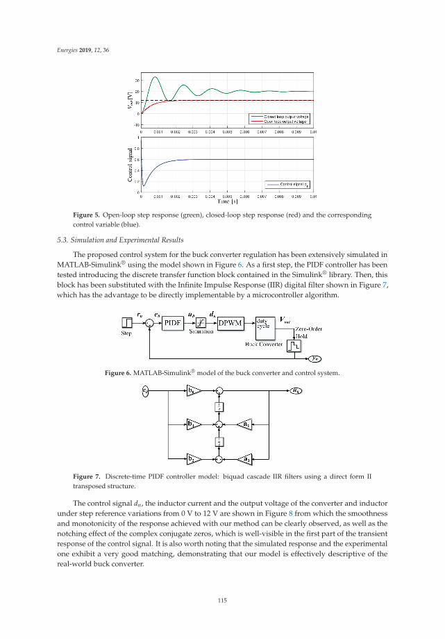
Energies 2019, 12, 36
Figure 5. Open-loop step response (green), closed-loop step response (red) and the correspondingcontrol variable (blue).
5.3. Simulation and Experimental Results
The proposed control system for the buck converter regulation has been extensively simulated inMATLAB-Simulink® using the model shown in Figure 6. As a first step, the PIDF controller has beentested introducing the discrete transfer function block contained in the Simulink® library. Then, thisblock has been substituted with the Infinite Impulse Response (IIR) digital filter shown in Figure 7,which has the advantage to be directly implementable by a microcontroller algorithm.
Figure 6. MATLAB-Simulink® model of the buck converter and control system.
Figure 7. Discrete-time PIDF controller model: biquad cascade IIR filters using a direct form IItransposed structure.
The control signal dn, the inductor current and the output voltage of the converter and inductorunder step reference variations from 0 V to 12 V are shown in Figure 8 from which the smoothnessand monotonicity of the response achieved with our method can be clearly observed, as well as thenotching effect of the complex conjugate zeros, which is well-visible in the first part of the transientresponse of the control signal. It is also worth noting that the simulated response and the experimentalone exhibit a very good matching, demonstrating that our model is effectively descriptive of thereal-world buck converter.
115

Energies 2019, 12, 36
Figure 8. Simulated control signal, inductor current and output voltage under step variation of thereference value from 0 V to 12 V using the proposed control method.
An experimental hardware device has been built to verify the proposed method for the DC-DCbuck converter. It is composed by the buck converter and an Arduino Due development board, basedon a 32-bit Atmel SAM3X8E ARM® Cortex® M3 CPU, see Figure 9. The main components of the buckconverter circuit have been selected as shown in Table 1.
Figure 9. Physical realization of the buck converter.
An interrupt routine is generated every Ts = 5 × 10⁻⁵ s. This routine starts the ADC conversionof the output signal of the converter and computes the duty cycle of the PWM control signal. Figure 10represents the difference Equation (14) of the PIDF controller using the Direct-Form II Transposedstructure of a Biquad Cascade IIR Filter shown in Figure 7.
Figure 10. The Biquad Cascade IIR Filter algorithm.
The output voltage of the converter and inductor current IL under step reference variations from0 V to 12 V are shown in Figure 11. The measure of IL has been obtained using the analog transducerLEM 6−NP with a 5V supply and a galvanic isolation between the primary and the secondary circuit.The experimental results confirm the behavior already observed in the simulations: the output voltagereaches the desired value in a monotonic fashion, and the inductor current remains always well below
116

Energies 2019, 12, 36
the saturation value. A zoom of the inductor current sensor output in steady-state condition is shownin Figure 12 from which the regularity of the PWM duty cycle when the system has reached the newsteady-state can be observed. This is a consequence of the selected bandwidth, which is large enoughto obtain a fast set point tracking, but narrow enough to avoid the amplification of high frequencynoise and discontinuities due to the PWM behavior. Note that assigning such bandwidth withoutcancelling the complex conjugate poles would result in large oscillations due to the presence of theresonance peak in the closed-loop system.
Figure 11. Experimental result using PIDF and the proposed method: inductor current sensor outputand converter output signal under reference step variation from 0 V to 12 V.
Figure 12. Experimental result using PIDF: zoom of the inductor current sensor output insteady-state condition.
5.4. Comparison with Other Methods
There are various design techniques for determining the parameters of a PID controller when themathematical model of the plant is explicitly available. For a comparison with the proposed designmethod, three classical PID tuning techniques have been considered, see Table 2.
Table 2. PID parameters.
Control Kp Ki Kd
IMC-Chien 0.033 958.7 6.519 × 10⁻⁵
Pole placement 0.55 247.1, 7.353 × 10⁻⁵
Pole-zero cancellation 0.02 294.7 2.004 × 10⁻⁵
The first controller has been obtained using the Internal Model Control IMC-Chien methoddescribed in [23], and by neglecting the capacitor and inductor resistances in (2). The second has beenobtained by placing one zero of the PID controller an octave below the cut-off frequency, approximatelyat 480 rad/s, while the other zero has been placed at 7 × 10³ rad/s, see [12]. The third controllerhas been obtained by selecting the PID zeros to approximately cancel the complex conjugate polesof the converter at the cut-off frequency and a phase margin equal to 95◦, see [10]. The considered
117

Energies 2019, 12, 36
continuous-time PID controllers have been simulated via the Simulink® PID(s) block which implementsa PID controller in the form:
CPID(s) = Kp +Kis+ Kd
N1 + N/s
. (32)
The MATLAB-Simulink® PID(s) model uses a lowpass filter in the derivative term to obtain aproper transfer function. The default value of the coefficient N in the filter is set at 100. Using thisvalue in (32), all the considered PID controls generate large oscillations during the step responsetransient. These oscillations are considerably reduced by setting the coefficient N of the filter to thevalue N = 200,000. It is clear that the time constant of the filter is a critical component in the design of aPID controller and that a systematic design method should be taken into account. Accordingly, in ourmethod, the time constant of the filter is selected to achieve the desired closed-loop system performance,and it is not designed by using trial-and-error, empiric or rule-of-thumb methods.
For the practical implementation of the controller on the Arduino board, the continuous-timePID controllers are converted to the discrete-time by using the backward Euler’s integrationmethod, as suggested in [10]. The discrete control algorithm will therefore implement the causaldifference equation:
d[n] = Kpe(n) + KiTs
n
∑i=0
e(n) +KdTs
[e(n)− e(n − 1)].
Moreover, an anti-windup filter based on the conditional integration method (see [24] for details)has been implemented in order to minimize the detrimental effect of the large saturation resultingfrom the techniques listed in Table 3.
Table 3. Phase margin variations from continuous to discrete-time control using backward Euler’sdiscretization method.
PID Control
Phase Margin
Continuous-TimeDiscrete-Time
N = 100,000 N = 200,000
IMC-Chien 90◦ 47.5◦ 50.5◦Pole placement 98.6◦ 26.3◦ 29.5◦
Pole-zero cancellation 95.7◦ 65.2◦ 67.6◦
The simulated step responses of these three methods in the continuous-time are shown in Figure 13.The simulated step response using the IMC-Chien method is very fast, with a settling time of 0.2 ms.However, the peak of the resulting control signal is approximately 80.
Figure 13. Cont.
118

Energies 2019, 12, 36
Figure 13. Simulated step responses using IMC-Chien method, the pole placement method andpole-zero control method in the continuous-time case: output voltages and control signals.
On the other hand, the saturation of the duty cycle range [0,1] leads to an oscillatory behavior inthe experimental output voltage, see Figure 14b. In fact, the resulting settling time is 20 times greaterthan the one obtained in the simulated test. Moreover, a steady-state ripple in the output voltage andin the inductor current is present because of the excessively aggressive tuning.
The simulated continuous-time step response using the pole placement method exhibits a risetime of 8.1 × 10⁻⁵ s, a settling time of 4.2 ms, and an overshoot equal to 6%. As in the previous case,the control signal reaches a very high value, in this case with a peak of nearly 180. The converter signalsobtained using this control method in the experimental hardware device are shown in Figure 14c.The main drawback of this type of control is the large steady-state ripple in the output voltage, see [10].This is due to an excessively large closed-loop bandwidth that results in an aggressive control actionwhich tries to compensate the high frequency noise. The saturation of the duty cycle in the range[0,1] leads to an ON-OFF behavior in the hardware device and high power dissipation both duringthe transient response and in the maintenance of the steady-state. Note also that the voltage ripple isunsuitable for most sensitive electronic equipment and the resulting current may cause heating anddamage of capacitors over time, see [25].
The simulated continuous-time step response using the pole-zero cancellation method has arise time of 4.1 × 10⁻⁴ s, a settling time of 0.7 ms. The peak of the control signal is 48, which isconsiderably lower than the ones obtained with the previously described techniques, but still ordersof magnitude above the saturation level. The corresponding experimental results are shown inFigure 14d. Notice that the steady-state output ripple is not present using this type of control becauseof the less aggressive tuning of the parameters, which also results in a lower peak of the control variable.However, the non-linear saturation of the control signal is not considered in (2). As a consequence,the zeros of the controller only partially compensate the oscillatory effects of the buck converter polesin the transient period. It follows that the settling time rises to 4 ms in practice, and the experimentaloutput voltage exhibits an oscillatory behavior with an overshoot of 20–30%.
Figure 14. Cont.
119

Energies 2019, 12, 36
(a)
(b)
(c)
Time [10 3 s] Time [10 4 s]
(d)
Figure 14. Inductor current and output voltage under step variation of reference value from 0 V to12 V and zoom of inductor current and inductor current at steady-state using: (a) Inversion Formulae,(b) IMC-Chien, (c) Pole Placement, and (d) Pole Zero methods.
Compared to all the considered methods, the proposed control procedure leads to a good matchingbetween simulated and experimental results, due to the design which is carried out directly in discrete-timevia closed-form formulae. As such, the phase margin that we obtain with the discrete PIDF controller isexactly the design one. On the contrary, other approaches are based on the design of the controller in thediscrete domain, and eventually, on the discretization of the obtained continuous controller. However, thisresults in a discrete controller that often delivers a phase margin considerably different from the one that
120

Energies 2019, 12, 36
would have ideally been obtained in the continuous time, see Table 2, where the phase margins obtainedfrom the considered methods and a discrete PID of the following form are presented:
PID = Kp + KiTsz
z − 1+ Kd
N1 + NTs
zz−1
.
5.5. The Proposed Control under Output Load and Converter Parameters Variations
For the widespread diffusion of a control technique in practical applications, robustness toparameter variation and model uncertainty is clearly a key feature. For this reason, we study thebehavior of the output voltage under different load resistance variations. Experimental results ofthe step load testing under different output loads (10 Ω, 20 Ω and 30 Ω) are shown in Figure 15a.Notice that the output voltage presents an almost overlapping behavior in the three considered cases,confirming that the control is not affected by load variation in the range ±50% of the nominal value,see Table 1. Other experimental results on load variations from 20 Ω to 10 Ω and from 20 Ω to30 Ω in steady-state condition are shown in Figure 15b. Notice that the proposed control systempromptly stabilizes the voltage output with negligible undershoot and overshoot, thus providinga good performance in the case of load variations. Moreover, the set-point step response remainsvirtually the same irrespectively of the load resistance.
Time [s] (a)
Time [s] (b)
Figure 15. (a) Step responses under different output loads (10 Ω, 20 Ω and 30 Ω), (b) inductor currentand output voltage under load variation from 20 Ω to 30 Ω (blue), and from 20 Ω to 10 Ω (red).
While load variations are due to normal operations of the buck converter, other parameters ofthe circuit of the converter, such as the inductance and capacitance, may vary as well as a result ofthe uncertainties affecting the production of the electrical components. In particular, the resonancefrequency is directly related to the inductance and capacitance. In fact, since R>>RC and R>>RL,in practice we have:
ωn ∼= 1√LC
.
Therefore, the inductor current and the output voltage under variations of the capacitor andinductor in the buck converter are also studied, and the results are shown in Figures 16 and 17.The proposed system delivers a good robust performance under parameter variations, and a monotonicresponse is obtained with all the considered combinations.
121

Energies 2019, 12, 36
Figure 16. Step responses with the proposed design procedure when the model value of the capacitoris 100 μF−20%, 100 μF+20%.
Figure 17. Step responses with the proposed design procedure when the model value of the inductor isset to 680 μH−10% and 680 μH+10%.
6. Conclusions
A new design framework for the control of buck converters has been presented in this paper.The proposed methodology is based on the discrete PIDF controller, and hinges on a direct designprocedure that can be easily implemented in any non-specific platform. Indeed, the proposed methodologydelivers a closed-form solution to meet suitable phase margin and gain crossover frequency values withouta simulation environment. Moreover, the proposed design procedure and the discrete control algorithmare simple, they require small tuning times and they can be implemented by inexpensive microcontrollers.
Numerical and experimental verifications confirm that the proposed method goes well beyondthe well-known zero/pole cancellation strategy and other control methods available in the literature.Indeed, the proposed approach enables the designer to assign an arbitrary bandwidth, which istherefore no longer constrained by the resonant peak. This aspect leads to a double benefit. On theone hand, this method avoids an excessively large bandwidth, which would result in noise/rippleamplification and ultimately in an increase in power consumption and a decrease in the component life.On the other hand, this method avoids the discretization problem that derives from discretizinga controller which assigns a bandwidth that is too large with respect to the sampling period.This, in particular, avoids detrimental effects on the stability margin due to the discretization.Moreover, experimental results confirm that the selection of large phase margin with the directproposed method delivers a good system performance under load variations and plant uncertainties.
122

Energies 2019, 12, 36
Author Contributions: S.C. provided for theoretical developments, simulations and experimental tests, L.N. andF.P. contributed to theoretical developments and manuscript organization, G.G. contributed to experimentalresults and manuscript finalization.
Funding: This research received no external funding.
Conflicts of Interest: The authors declare no conflict of interest.
Abbreviations
The following abbreviations and symbols are used in this manuscript:
ADC Analog-to-digital converterCCM Continuous-conduction modeDC Direct currentDC-DC Direct current to direct currentDPWM Digital pulse width modulatorESR Equivalent series resistanceIIR Infinite impulse response (digital filter)IMC Internal model controlPI Proportional-integral (controller)PID Proportional-integral-derivative (controller)PIDF PID + filterPWM Pulse width modulationList of Symbolsai, bi PIDF coefficientsC Buck converter capacitanceC(s), C(z) Continuous and discrete-time controller transfer functionD Control signalE Tracking errorG(s), G(z) Continuous and discrete-time plant modelGm Gain marginH Constant sensor gainH0(s) Zero-order hold transfer functioniL Buck converter inductor currentKd Controller derivative gainKi Controller integral gainK∞ High frequency controller gainKp Controller proportional gainL Buck converter inductanceL(s), L(z) Continuous and discrete-time loop gain transfer functionN Filter coefficientR Output load resistanceRC ESR of buck converter capacitorRL ESR of buck converter inductorrn Reference digital signalTd Derivative time constant of the controllerTf Filter time constant of the controllerTi Integral time constant of the controllerTs Sampling periodu0 Output signal of IIR filterVC Buck converter capacitor voltageVin Buck converter input voltageVout Buck converter output voltageVref Reference voltageyn Sampled output of the process
123

Energies 2019, 12, 36
δ Damping ratio of the controller zerosΦm Phase marginξ Buck converter damping ratioωg Gain crossover frequencyωn Buck converter natural frequency1/τ Natural frequency of the controller zeros
References
1. Yang, J.; Wu, B.; Li, S.; Yu, X. Design and qualitative robustness analysis of an DOBC approach for DC-DCbuck converters with unmatched circuit parameter perturbations. IEEE Trans. Circuits Syst. 2016, 63, 551–560.[CrossRef]
2. Liu, Y.F.; Meyer, E.; Liu, X. Recent developments in digital control strategies for DC/DC switching powerconverters. IEEE Trans. Power Electron. 2009, 24, 2567–2577.
3. Al-Hosani, K.; Malinin, A.; Utkin, V.I. Sliding mode PID control of buck converters. In Proceedings of the2009 European Control Conference (ECC), Budapest, Hungary, 23–26 August 2009; pp. 2740–2744.
4. Roshan, Y.M.; Moallem, M. Control of nonminimum phase load current in a boost converter using outputredefinition. IEEE Trans. Power Electron. 2014, 29, 5054–5062. [CrossRef]
5. Perry, A.G.; Feng, G.; Liu, Y.F.; Sen, P.C. A design method for PI-like fuzzy logic controllers for DC–DCconverter. IEEE Trans. Ind. Electron. 2007, 54, 2688–2696. [CrossRef]
6. Mantz, R.J.; Tacconi, E.J. Complementary rules to Ziegler and Nichols’ rules for a regulating and trackingcontroller. Int. J. Control 1989, 49, 1465–1471. [CrossRef]
7. Son, Y.I.; Kim, I.H. Complementary PID controller to passivity-based nonlinear control of boost converterswith inductor resistance. IEEE Trans. Control Syst. Technol. 2012, 20, 826–834. [CrossRef]
8. Kapat, S.; Krein, P.T. Formulation of PID control for DC–DC converters based on capacitor current:A geometric context. IEEE Trans. Power Electron. 2012, 27, 1424–1432. [CrossRef]
9. Sira-Ramirez, H. Nonlinear PI controller design for switchmode DC-to-DC power converters. IEEE Trans.Circuits Syst. 1991, 38, 410–417. [CrossRef]
10. Guo, L.; Hung, J.Y.; Nelms, R.M. PID controller modifications to improve steady-state performance of digitalcontrollers for buck and boost converters. In Proceedings of the Seventeenth Annual IEEE Applied PowerElectronics Conference and Exposition, Dallas, TX, USA, 10–14 March 2002; Volume 1, pp. 381–388.
11. Guo, L.; Hung, J.Y.; Nelms, R.M. Digital controller design for buck and boost converters using root locustechniques. In Proceedings of the IECON 2003 29th Annual Conference of the IEEE Industrial ElectronicsSociety, Roanoke, VA, USA, 2–6 November 2003; Volume 2, pp. 1864–1869.
12. Guo, L.; Hung, J.Y.; Nelms, R.M. Evaluation of DSP-based PID and fuzzy controllers for DC–DC converters.IEEE Trans. Ind. Electron. 2009, 56, 2237–2248.
13. Marro, G.; Zanasi, R. New formulae and graphics for compensator design. In Proceedings of the 1998 IEEEInternational Conference on Control Applications, Trieste, Italy, 4 September 1998; Volume 1, pp. 129–133.
14. Zanasi, R.; Cuoghi, S.; Ntogramatzidis, L. Analytical and graphical design of lead–lag compensators.Int. J. Control 2011, 84, 1830–1846. [CrossRef]
15. Ntogramatzidis, L.; Ferrante, A. Exact tuning of PID controllers in control feedback design. IET ControlTheory Appl. 2011, 5, 565–578. [CrossRef]
16. Zanasi, R.; Cuoghi, S. Direct methods for the synthesis of PID compensators: Analytical and graphicaldesign. In Proceedings of the IECON 2011 37th Annual Conference of the IEEE Industrial Electronics Society,Melbourne, Australia, 7–10 November 2011; pp. 552–557.
17. Cuoghi, S.; Ntogramatzidis, L. Direct and exact methods for the synthesis of discrete-timeproportional–integral–derivative controllers. IET Control Theory Appl. 2013, 7, 2164–2171. [CrossRef]
18. Cuoghi, S.; Ntogramatzidis, L. New inversion formulae for PIDF controllers with complex zeros for DC-DCbuck converter. In Proceedings of the IECON 2011 42th Annual Conference of the IEEE Industrial ElectronicsSociety, Florence, Italy, 23–26 October 2016; pp. 235–240.
19. Kristiansson, B.; Lennartson, B. Robust tuning of PI and PID controllers: Using derivative action despitesensor noise. IEEE Control Syst. Mag. 2006, 26, 55–69.
20. Dorf, R.C.; Bishop, R.H. Modern Control Systems; Pearson: Upper Saddle River, NJ, USA, 2011.
124

Energies 2019, 12, 36
21. Severns, R.P.; Bloom, G. Modern DC-to-DC Switchmode Power Converter Circuits; Springer: New York, NY,USA, 1985.
22. Abbas, G.; Abouchi, N.; Pillonnet, G. Optimal state-space controller for power switching converter.In Proceedings of the IEEE Asia Pacific Conference on Circuits and Systems, Kuala Lumpur, Malaysia,6–9 December 2010; pp. 867–870.
23. Panda, R.C.; Yu, C.C.; Huang, H. PID tuning rules for SOPDT systems: Review and some new results.ISA Trans. 2004, 43, 283–295. [CrossRef]
24. Visioli, A. Practical PID Control; Springer: London, UK, 2006.25. Mohan, N.; Undeland, T.M. Power Electronics: Converters, Applications, and Design; John Wiley and Sons:
Hoboken, NJ, USA, 2007.
© 2018 by the authors. Licensee MDPI, Basel, Switzerland. This article is an open accessarticle distributed under the terms and conditions of the Creative Commons Attribution(CC BY) license (http://creativecommons.org/licenses/by/4.0/).
125


energies
Article
Comparison of Novel Approaches to the PredictiveControl of a DC-DC Boost Converter, Basedon Heuristics
Robert Baždaric *, Danjel Voncina and Igor Škrjanc
Faculty of Electrical Engineering, University of Ljubljana, Tržaška 25, Ljubljana 1000, Slovenia;[email protected] (D.V.); [email protected] (I.Š.)* Correspondence: [email protected]; Tel.: +386-1-4768-466
Received: 24 September 2018; Accepted: 16 November 2018; Published: 26 November 2018
Abstract: This paper introduces novel approaches to the predictive control of a DC-DC boostconverter and a comparison of the controllers built that consider all of the current objectives andminimize the complexity of the online processing. The primary concern is given to the applicabilityof the inclined methods for systems that are physically small but considered physically fast processes.Although the performed methodologies are simulated and applied to a DC-DC boost converter,they can have broader applicability for different switched affine systems as a subgroup of the hybridsystems. The introduced methods present an alternative way of building the process model basedon the fuzzy identification that contributes to the final objective: the applicability of the predictivemethods for fast processes.
Keywords: switched affine systems; hybrid systems; fuzzy identification; fuzzy modeling;two degrees of freedom; fuzzy model predictive control
1. Introduction
Predictive control has strict conjunction with the rendering of a proper mathematical model thatwill be used to determine a successor step of our control algorithm. Subsequently, the modelingparadigm must become the core issue in projecting the predictive control algorithm of thecyber-physical and the physical processes in general. Even though the process is purely natural,meaning it is a naturally continuous system, influenced by the control algorithm, it will undoubtedlyevolve into the Hybrid System (HS). That is why this study points out the results from the aspects ofHS controls in the field of Switched Affine Systems (SAS). Nowadays, the majority of power electronicsuses a kind of Pulse Energy Conversion or Converters (PEC) in rendering the power sources or controlsignals. Consequently, these systems are in the group of SAS.
In this study, an alternative approach to modeling a DC-DC boost converter has been provided,and our SAS example is taken into consideration as a good representative of the aforementioned field.A renaissance of the HS theory occurred in 1990s. Simultaneously, the emerging of heuristic controlprinciples happened: neural networks and fuzzy control. The findings of those two mostly separatelydeveloped fields will be integrated into the new approaches of the model-based predictive control ofSAS. It is necessary to highlight that from the corner of the HS theory, the PEC is analytically definableand well posed [1]. From the aspects of applicability, we promote the transformation of HS to thepurely continuous, although this principle is found to be incomplete by the HS theory [1]. This ismainly disproven by the inapplicability of the particular HS approaches to fast physical processes.Therein, the assumption that each particular physical process can be presented by Discrete HybridAutomata (DHA) does not hold. In referring to the qualitative mathematical theory [2], and the need inDHA to synchronize all of the dynamic events, one faces the problem of multiple dynamics that cannot
Energies 2018, 11, 3300; doi:10.3390/en11123300 www.mdpi.com/journal/energies127

Energies 2018, 11, 3300
be unified simply. In previous work [3,4], the modeling was put into the focus and given possiblesolutions from the physical aspects of the system. First, in [3], the main problem is transferred to theidea of infinity horizon principle. It is comparable with the Model Predictive Control (MPC) infinitehorizon, but it should not be mistaken for it. Second, in [4], the problem is grasped with an idea of twodynamics and unified into one by fuzzy logic (FL).
Some previous academic work have provided remarkable results in applying the advanced controlalgorithms for the relatively simple example of SAS: a DC-DC boost converter [5–13]. As a result,this article underlines the complexity of the controls of the DC-DC boost converter. This complexityhas to be known in order to form a more solid basis for understanding the necessity for the advancedcontrol algorithm. The assigned objectives in the control of DC-DC boost converters are the maincomplexity issue. Consequently, in this study, the standard objectives have been provided, as well asadditionally extended with the objective of the applicability issue. The objectives are:
• Robustness to the wide system’s parameter changes [PCR]• Short response period and similar to all different operating points [SR]• Optimality related to constraints [OPT]• Stability [S]• Minimization of the nonlinear phenomena for the selected robustness [NFM]• Applicability to the systems with fast refresh rate. [A]
The above-mentioned has to determine the reason for finding a new and advanced approachthat can integrate all of the objectives, even though established and notable approaches alreadyexist [5,7,11]. Those methodologies are successful in newer releases [14,15], but are still a continuationin a way similarly improving the main and present issues, the processing complexity, and the systemdiscontinuity. The originators of the modeling principles in their releases [5,6,16] direct the modelingto the direction of identification, because of the compelling interest in minimizing the processingcomplexity. We see that there is still a possibility to improve the well-articulated problems ofsystem discontinuity and processing complexity by reducing the prediction horizon [17], whichis the fundamental stability pillar of the MPC in general. Also, generally for the HS, it is essential tobear in mind that distributing or decoupling the modeling complexity into the several and less complexHS models might be the solution, i.e., current, voltage and feedback; however, then the synchronizationof those models to the one and overall DHA should not be endangered [1]. Considering that the mainfundament of this study is the presentation of Identification-Based (IDB) modeling and a comparisonof those modeling-based control algorithms, Figure 1 presents it in a broader view. In contrastto typical and basic model representatives in HS [1], i.e., Piece Wise Affine (PWA) models, LinearComplementarity (LC) models, Extended Linear Complementarity models (ELC), Mixed LogicalDynamical (MLD), and Max-Min-Plus-Scaling (MMPS), the Identification-Based (IDB) modelingrepresents a new group of models rendered by different identification approaches and algorithmsthat partly identify the uncertainties in HS models or completely, as in the example of this study.Additionally, and to achieve the selected objectives, the new approach will contain the model-basedpredictive control strategy reformulated to accommodate the above-mentioned nonlinear system’sdynamics problem. As a continuation of previous work [3,4], this study will concentrate more on thecomparison of controllers that are rendered by the novel methodologies in seeking more advancedcontrol solutions. Additionally, the subsequent discussion has to contribute to a better understandingof the novelty in the predictive controls that can be widely exploited. Originally, the main goal was toprovide a more compact and applicable solution for the DC-DC boost converter that can be integratedinto different, more complex, and practical problems. The main complexity is here grasped in thesystem’s model structure and performed offline. The lifted modeling accuracy that is gained by theidentification of a constructed process on the site can help in distinguishing and diagnosing otherprocess problems, as discussed in [18]. In contrast, it can block the nonlinearities produced by thesemiconductors realistically, and not be injected by the trivial nonlinear switching functions, but still
128

Energies 2018, 11, 3300
be compact in forming the overall model for the more complex examples in [19,20]. It will be allbased on assumptions that the system states are measurable and the switching period Ts is fixed.Subsequently, Section 2 provides a discussion of the distinctive problems in the modeling of SASthat contributes to the complexity and places the novel solution into the methodology frames thatare of crucial importance for the understanding of latter compared controllers. Section 3 presentsthe successfully applied methods and comparison of the achieved results, and Section 4 contains theshort conclusion.
Figure 1. Established types of hybrid models and novel modeling in a Hybrid System (HS).
2. Novel Modeling Paradigm and Predictive Control of a DC-DC Boost Converter, Minimizationof Online Processing
Predictive control must be the main strategy in achieving the robustness and optimality of the finalcontrol algorithm of a DC-DC boost converter. Optimality in the controls of the DC-DC boost convertermust be seen through the system’s constraints. The main constraints are the voltage source E(t),the inductor current iL(t) and duty cycle d(t). In Figure 2, a principal electronic circuit of a DC-DCboost converter is presented, and assigning the mentioned circuit constraints additionally including theconverter’s voltage set point s, the output voltage vo, the load current iR and the capacitor’s voltage vc.
Figure 2. DC-DC boost converter circuit diagram.
To predict a successor control signal of a new control algorithm, a process model has to be known,as well as measured or observed antecedent data. In our case the process model is a mathematicalmodel of the system presented in Figure 2. Mostly, and as already mentioned, in the broader literatureof DC-DC boost converters, several different models are known. Based on the authors’ opinions andknowledge about this particular system, the following distinctive and established methodologiesare available:
• Small and large signal modeling [12,13]
129

Energies 2018, 11, 3300
• Poincaré mapping in discontinuous conduction mode (DCM) [7]• HS based modeling; Mixed Logical Dynamical and Linear Complementarity [11,21,22].
Those modeling principles address most of the modeling problems of a DC-DC boost converter,but from the control theory point of view and applicability, there is room for improvement. It is unlikelythat the answer or a predefined block that precisely models our natural process could be found inthe modern computer toolboxes. Looking from the simulation side and finally from the control side,different natural processes can be similar. Furthermore, the modeling formalisms are prone to upgrades.A good example is HS formalisms and their development [1]. In the high refresh-rate systems,and before developing the control algorithm, the awareness about proven anomalies that can producea significant impact on our control algorithm must be present. In the example of a DC-DC boostconverter, we highlight the three most distinctive ones:
• Anomalies caused by the system nature [1,2]• Anomalies caused by the modeling formalisms [23,24]• Anomalies caused by the control algorithm itself [2,7].
A DC-DC boost converter is a cyber-physical process, which by its nature has a controllableswitching process that automatically groups it in SAS as a subgroup of HS. If the switching event wouldbe a time-wise insignificantly short in comparison with the discretization, or if the switching event isjust occasionally appearing, then the importance might be minimized or simply distinguished by onebit of information. Otherwise, the significance of that event has to be reconsidered. The pulse widthmodulation (PWM) of our example is exactly the core issue in the control of a DC-DC boost converter,and subsequently, it has to be viewed through the mentioned existence of the possible anomalies.
The switching event over the semiconductors is burdened with the sticking and grazingeffects over the switching manifolds [2]. For the selected physical system, these anomalies areconsidered natural.
In an application in which we use the HS formalisms, we must be aware of the typical anomaliesas “Live lock” and “Zeno” effect [1,2,23,24].
Conclusively, when the control algorithm is in operation, the awareness of the nonlinearityphenomena recognized in bifurcations and chaos come into focus and must be treated by the controlalgorithm itself.
An elevation of the grade of modeling accuracy, in order to avoid previously mentioned anomalies,raises the complexity of the model and consequently the control algorithm, but it is of great importancein the stability of predictive control. Additionally, at the same time, it minimizes the nonlinearityphenomena. The mentioned complex view on modeling and the contemporary minimization ofthe limited time of processing bring this discussion to an alternative solution that integrates andconciliates two from the first sight disputable extremes. In our previous work [3,4], as the answeron demanding tasks, the fuzzy logic-based control algorithms successfully provide the possiblesolution for expressed complexity, and these will be compared here, including the two additional MPCcontrollers that are not yet presented, but are based on the same modeling principle. The fuzzy logic isnot used traditionally [9,10,25] in a way to formulate the nonlinear gain interpolation, but differentlyto approximate the complex system model and answer positively to all of the objectives that havebeen collected together. The modeling benefits that are basically derived from the fuzzy systemidentification are threefold.
First, apart from the HS structure, in this way the system can be interpreted as a purelycontinuous system; in the worst-case scenario, it maintains the same grade of accuracy as the HSmodeling approach.
Second, it provides the final model that is a more compact solution and minimizes the onlineprocessing burden of the control algorithm.
130

Energies 2018, 11, 3300
Third, in practical solutions, and because it is based on identification, this modeling principleprovides the physical characteristics of the electronic circuits in real operation, which overcomes allpossible theoretical miscalculations at once.
To understand the novelty of subsequently compared control algorithms, and to frame themodeling methodologies to the unique approach in studies of a DC-DC boost converter, we highlightthe main idea. The most distinct characteristic of the new control algorithms is found in thenon-analytical but heuristically-based modeling of a DC-DC boost converter. The source modelsare Takagi-Sugeno (T-S) fuzzy models derived from the mathematically transferred and normedspace of measured system states [3,4]. Thus, naturally, the process of measuring, or in the simulationenvironment the numerical integration, transfers the originally and analytically two-dimensionalstate space problem of the DC-DC boost converter states xa = [vc iL]
T in the six-dimensionalx = [vo iL E R d t]T normed vector space (V, ‖ · ‖). The newly formed and augmented pseudo-Banachspace is derived from the Lebesgue 2 norming of the process variables ‖ · ‖, which is expressed by
‖xi‖Lp =1t
(∫|xi|pdt
) 1p= xi, f or p = 2 and i ∈ [1, 4]. (1)
In the above-developed space, the new methodologies perform a different grey box fuzzyidentification process to derive the final fuzzy model of a DC-DC boost converter.
The physical process constraints due to the electrical components that were used in the electriccircuit presented in Figure 2 will be the main experimental foundation in forming the Fuzzy Universesof Discourses Xi and Y, of regression vectors and the scaled duty cycle for each particular identificationprocess subsequently explained. In Expression (2), the universes are formed from the excited DHAsimulation model of a DC-DC boost converter to provide the necessary robustness, including thediscontinuous conduction mode (DCM) and the continuous conduction mode (CCM) of a DC-DCboost converter:
vo = x1 ∈ X1 = [0 V, 700 V]
iL = x2 ∈ X2 = [0 A, 1030 A]
E = x3 ∈ X3 = [10 V, 16 V]
R = voiR
= x4 ∈ X4 = [10 Ω, 32 Ω]
du = y ∈ Y = [0.015 · d, 0.985 · d] = [0.65, 0.0.1].
(2)
2.1. Fuzzy Model Structure of the Two Degrees of Freedom Controller, the Prediction andProcessing Minimization
Baždaric et al. in [3] demonstrated the FL identification powerful tool in reconstructing all of thesystem’s possible steady states. It is done in the wide range of operating points that are defined byaltering different process parameters in combinations and providing the expected real and extremesystem conditions.
In the five-dimensional normed space (excluding the time) (V(−1), ‖ · ‖), the modeling provides afuzzy model, which is expressed by Equation (3):
xd4= [vo iL E R]T ⇔ x
f (x|θ) = ∑bj=1 (aj,0+aj,1x1+...+aj,4x4)μHj (x)
∑bj=1 μ
Hj (x)
dFEM = F(xd4) = f (x|θ)
(3)
that relates the system states and process parameters. In Equation (3), the aj,0 is the member (realnumber) of the fuzzy model parameter matrix θ in the jth row and the first column, while the μHj
denotes specially jth c-clustering defined membership function from the b number of clusters [3].Four measured variables of the regression vector x will give information about the process parameters’
131

Energies 2018, 11, 3300
change. Instantly and from the previous offline identification process, the fuzzy model relates alinear contribution of inputs, as the T-S consequence functions (3), to the infinity horizon steady dutycycle dFEM.
The model in Equation (3) is a basis for the predictive control of a DC-DC boost converter. As aderived model, Equation (3) is not a dynamic system model, it is used in [3] in the feed-forward line ofthe optimized PI controller. The resulting control law is
du(t) = 1Ta
∫dFEM(kTs)dt + dPI(t) Ta − current constraint based tuning parameter
dFEM(k) = F(xd4(k)) = F(s(k), IL, E(k), vo(k)
iR(k))
(4)
where dPI denotes the output from the PI controller. The control signal du is a scaled duty cycle d(t)for the used PWM. The IL in Equation (4) is the infinity horizon prediction of the steady-state inductorcurrent iL, corresponding to the load current iR and the model based reconstructed efficiency ratio.
The control law will guarantee as fast as possible response of a DC-DC boost converter in findingthe steady state for a new possible operating point, mostly limited only by the maximum inductorcurrent. As the new predicted steady state is just an approximation with the projected maximumprocess/model error, the optimized PI controller will be in function to compensate the steady stateerror. Here, the optimized PI controller’s main function is to regulate the process operation near theoperating point, where this type of linear controller was found to be the most effective. The posedcontrol solution agrees with all the previously mentioned objectives and forms the Two Degrees ofFreedom controller. Thus, the controller predicts the new steady duty cycle instantly and based onthe measured process parameters. The fuzzy model dFEM(k) = F(xd4
(k)) is an explicit model as thesolution of Equation (3) and does not need calculation of the inverse matrix to fulfill the controller’sprediction. It is a Fuzzy Model-Based predictive control that can be compared with the MPC in a senseof infinity horizon prediction [3]. This feature drastically minimizes the controller’s processing time.
2.2. Fuzzy Model Structure of the Fuzzy Model Predictive Control (FMPC) Controllers and theirProcessing Minimization
Furthermore, Baždaric et al. in [4] demonstrated the FL identification powerful tool inreconstructing the system’s dynamic model. In the similarly developed normed space (V, ‖ · ‖)as the one in [3], but now 6-dimensional, including the time, the FL identification and modeling willprovide the alternative to the analytically derived model of a DC-DC converter. Slightly different thanin Equations (2) and (3), the derived fuzzy model will be constructed from the aspects that vo is theoutput and du is an input with the corresponding universes. Moved from the HS theory, but also fromthe traditional “averaged switched model”, this fuzzy model renders all benefits of the alternativemodeling as mentioned earlier.
As stated in [4], the fuzzy model F(ϕk) is expressed by
ym(k + 1) = F(ϕk) = β(ϕ2(k))θ1ϕ1(k)T
ϕ1(k) = [vo(k) vo(k − 1) iL(k) du(k) 1]ϕ2(k) = [E(k) vo(k)/iR(k) iL(k)].
(5)
In the Equations (5) the ϕ1(k) denotes a first-grade and ϕ2(k) a second-grade regression vector.Furthermore, θ1 denotes the parameter matrix of the 1st-grade identification, and β(ϕ2(k)) ∈ Rp
(p-number of fuzzy rules) is the vector of normalized degrees of fulfillment [4]. The mentioned vectoris the compact expression of the T-S Fuzzy System that consists of Gaussian membership function in theprocess of fuzzification, the product as the conjunction function in the premise and the center-averagedefuzzification. The new type of Fuzzy Model that is now expressing the DC-DC boost converter isa T-S fuzzy nonlinear interpolation of p-linear models identified in the first-grade of identificationand further forming the T-S consequence functions. The novelty is that the linear models in thedifferent operating points are not analytically driven, and those are devised by the Least-Squares
132

Energies 2018, 11, 3300
(LS) identification process in the wider neighborhood of the operating point. Furthermore, this typeof approach minimizes the number of rules in the fuzzy rule base and additionally smoothes thenonlinear interpolation [4]. Equation (6) presents the final state space expression of the DC-DC boostconverter, where the matrixes Ami , Bmi , Rmi are the LS identified matrixes in the neighborhood ofthe i-th operating point and w(k) is the unit step function that is used to integrate the identificationprocess error.
xm(k + 1) =p∑
i=1[Ami xm(k) + Bmi du(k) + Rmi w(k)]βi(ϕ2(k))
βi(ϕ2(k) ∈ [0, 1]p∑
i=1βi(ϕ2(k) = 1 i = 1, . . . , p xm = [vo(k) vo(k − 1)]T
(6)
As the typical and compared MPC controllers have the time variable inner models (kTs), the statespace form evolves in a more compact form, as provided in Model (7):
Amk =
[am1k am2k
1 0
]Bmk =
[am4k
0
]
Rmk =
[am3k iL(k) + am5k
0
]Cmk = [1 0] Dmk = 0xm(k + 1) = Amk xm(k) + Bmk du(k) + Rmk w(k)ym(k) = Cmk xm(k) + Dmk ym(k) = Cmk xm(k).
(7)
Herein, am(k) = [am1(k)am2(k)am3(k)am4(k)am5(k)] = β(ϕ2(k))θ1 denotes the compact vector ofthe fuzzy model coefficients at the time k. Those coefficients are profiling our novel FMPC algorithmsin the controls of a DC-DC boost converter. As Section 3 compared FMPCs that, after the modeling part,are built typically (reference model, preceding horizon principle and filtering) [26,27], the control lawswill be omitted. Here, we present the cost functions J(k) and the suppression factor λ that have beenused to form the compared MPC algorithms:
• Fuzzy Dynamic Matrix Control (FDMC)
J(k) =Nu
∑j=1
qj(ym( k + j|k )− r( k + j|k ))2 +Nu−1
∑j=0
λj+1(k)Δu( k + j|k )2. (8)
• Fuzzy Generalized Predictive Control (FGPC)
J(k) =Nu∑
j=1xJ
T( k + j|k )Γ(j)xJ( k + j|k )
xJ(k) =
[xJ1(k)xJ2(k)
]=
[yp(k + 1)− r(k + 1)
λΔu(k)
] (9)
• Fuzzy Predictive Functional Control (FPFC)
J(u, k) =nH
∑j=1
(r( k + Hj∣∣k )− ym( k + Hj
∣∣k ))2+
nH
∑j=1
λj2(k)u( k + j − 1|k )Tu( k + j − 1|k ). (10)
During the control horizon Nu, the FDMC cost function (8) minimizes the error between themodel-based prediction ym and first-order reference model r, which is additionally weighted bythe state weighting factor q. The control signal u (8) is suppressed by the suppression factor λ.In Equation (9), we see the augmented model state vector xJ which contains the filtered output from
133

Energies 2018, 11, 3300
the second order filter yp [22] and no state weighing factor. The FPFC cost function in Equation (10)is different and additionally minimizes the computation burden, as it calculates for nH a number ofcoincidence points H during the control horizon and minimizes the vector of the control signals forthose points u [4,21,22]. It is important to add that the suppression factor λ, when comparing FMPCs,is the inner model-based adaptive and time variable factor λ(k) = aSUPP · ym(k + 1) · u(k)−1, whereaSUPP denotes the tuning coefficient [4].
To demonstrate a minimization of the online processing done in [4] by the state space dimensionreduction, the model state space matrixes that are presented in the MLD model in [28] are provided:
A =
⎡⎢⎣ Ad3 02x1 02x2
02x2 02x1 02x2
01x2 1 01x2
⎤⎥⎦
B2 =
⎡⎢⎢⎢⎣02x1 Bd2 − Bd3 Bd1 − Bd3 Bd4 − Bd3
0 1 0 00 0 1 00 0 0 0
⎤⎥⎥⎥⎦B3 =
[I2x2 I2x2 I2x2 02x1
03x2 03x2 03x2 03x1
]B1 = 05x1
C =[
1 0 0 0 0]
D1 = 0 D2 = 01x4 D3 = 01x7
x(k + 1) = Ax(k) + B1u(k) + B2δ(k) + B3z(k)y(k) = Cx(k) + D1u(k) + D2δ(k) + D3z(k)E2δ(k) + E3z(k) ≤ E1u(k) + E4x(k) + E5.
(11)
The state-space equations in Model (11) present the final solution in the MLD approach, whichconsists of the characteristic state space matrixes A, B, C, D, where the A, B are derived from theintermediate matrixes Adi
, Bdias the result of discretization processes during the Ts time. Thus,
in Model (11), the state vector x consists of the inductor current and output voltage, the input isprovided by δ as the five-dimensional vector of logic variables, and z is the MLD seven-dimensionalauxiliary variables’ vector. The matrixes Ei form the set of selected inequalities as the subject to theoptimization [28].
It is obvious that in the examples in which we use the Model Predictive Control (MPC),a dimension of the state space model matrixes (A in Model (11) and Amk in Model (7)) has the extremeimpact on the online processing time. Thus, Amk ∈ R2x2 in comparison with the A ∈ R5x5 simplifiesthe final model predictive state matrix. For the n horizon prediction, the model predictive state matrixis Amp ∈ Rn·nr x nc , if the nr and nc are the number of rows and columns, respectively, of the originalmodel state matrix.
3. Simulation Results of the Novel Control Methods and Their Comparison
Although in this study a Discrete Hybrid Automata (DHA) and the equivalent model of aDC-DC boost converter are considered to be the online processing time complex, it is a recommendedbasis for forming the simulation model of the MATLAB/SIMULINK platform [29]. For the novelcontrol methods, it is a source in exploring the identification methodologies and later applicationto the physical processes. Thus, the developed methods will be simulated and applied to theDHA-developed simulation model. A minimum discretization or the sampling time in modelingthe PWM, and switching events of the semiconductors, is set to 1 μs while a DC-DC boost convertermodel sampling time Ts is 333 μs. The simulation process was not done in real time; we left enoughtime to process the DHA simulation model itself together with the developed control algorithms.To provide a meaningful comparison, we use the test parameters or system events that are appliedin [3]. The selection of the operating points and the process parameter change have to prove the
134

Energies 2018, 11, 3300
robustness of the control algorithms driven from the minimum borders of a DCM to the maximumborders of the CCM of a DC-DC boost converter. In this comparison, we will also present theMPC-developed methods that were not found to be sufficiently compact, and their processing timewas short enough to be applied in the physical experiment of [4]. Subsequently, the Fuzzy GeneralizedPredictive Control (FGPC) algorithm, the Fuzzy Dynamic Matrix Control (FDMC), the Fuzzy PredictiveFunctional Control (FPFC), the optimized PI control, and finally the Two Degrees of Freedom (TDOF)control will be tested for the same combination of the system parameters’ change, and their dynamicsand steady states will be subsequently compared.
The simulation block diagrams of discussing control algorithms can be found in [3,4]. The FMPCmethods are based on the same internal model (7) as described in Section 2.2 and [4]. Furthermore,a TDOF control methodology is described in Section 2.1 and [3], and an optimized PI controller asthe reference to all of the comparisons is described in both articles. The latter control solution isintentionally chosen to simplify any of the following comparisons, as its construction is based purelyon the standard toolbox of the used simulation platform [29] and optimized by the Integral of the TimeWeighted Absolute Error (ITAE) criterion.
In Figure 3a, the response of the most favored predictive control solution FPFC is presented.It comes from the online processing time span and aggressiveness in the transition time. The onlineprocessing time is again proportionally related to the number of the prediction points, but in thenature of this MPC method, it is the reduction of coinciding points by the implementation of basisfunctions [26]. Furthermore, in the figure, there is the curve of the inductor current function thatdemonstrates a controller’s controlled manner of the most critical constraint of the DC-DC boostconverter. Separately from Figure 3a, Figure 3b presents the manipulated or controlling parameter thatis a duty cycle of a DC-DC boost converter.
(a)
(b)
Figure 3. Simulation results: (a) Controlled variable by the Fuzzy Predictive Functional Control(FPFC) controller vo (MSRE = 0.0023 for 129601 samples related to the reference) and coil current iL;(b) Manipulated variable from the FPFC controller (duty cycle) du = [0.01, 0.66] range 98.5 ÷ 1.5%.
135

Energies 2018, 11, 3300
In the sequel, the result of the simulation process for the FGPC, FDMC, the optimized PI, and theTDOF method is presented in Figures 4–7 respectively.
(a)
(b)
Figure 4. Simulation results: (a) Controlled variable by the Fuzzy Generalized Predictive Control(FGPC) controller vo (MSRE = 0.0044 for 129601 samples related to the reference) and coil current iL;(b) Manipulated variable from the FGPC controller (duty cycle) du = [0.01, 0.66] range 98.5 ÷ 1.5%.
In Figure 4, the FGPC responses are significantly slower and have a slightly worse mean squarerelative error (MSRE) in comparison with the FPFC. We see that even the second-order filter integratedinto the prediction model and filtering the model output did not significantly improve the steadystate stability, but it reduces the aggressiveness in the response. The small, steady-state chatteringin the last two changes of system parameters assign the border of the controller’s robustness. It iswell-suppressed by the adaptive controller’s control signal suppression factor. Similarly, the FDMCsimulation in Figure 6 presents the slightly faster response in the transitions and a worse MSRE, but inSection 2, it is explained that it has less of a processing time burden due to the absence of the modeloutput filter.
From the results, the similarities related to the aggressiveness in the transitions and the accuracy inthe steady-state of the applied FMPC methods are noticeable. The best performance is experienced withthe FPFC in Figure 3, and other methods can be compared to that reference. Closer to the performanceof the FPFC is the FDMC. The FGPC has been found to be a bit coarser in the steady state, but on someoccasions, such as a system start, it is faster in the response. As expected, the optimized PI controller inFigure 6 is slower in transitions, especially for the operating points far from the center of the performedoptimization for the time periods in which the lower system gains have been experienced.
136

Energies 2018, 11, 3300
(a)
(b)
Figure 5. Simulation results: (a) Controlled variable by the Fuzzy Dynamic Matrix Control (FDMC)controller vo (MSRE = 0.0062 for 129601 samples related to the reference) and coil current iL;(b) Manipulated variable from the FDMC controller (duty cycle) du = [0.01, 0.66] range 98.5 ÷ 1.5%.
(a)
Figure 6. Cont.
137

Energies 2018, 11, 3300
(b)
Figure 6. Simulation results: (a) Controlled variable by the Optimized PI controller vo (MSRE = 0.0220for 129601 samples related to the reference) and coil current iL; (b) Manipulated variable from theoptimized PI controller (duty cycle) du = [0.01, 0.66] range 98.5 ÷ 1.5%.
(a)
(b)
Figure 7. Simulation results: (a) Controlled variable by the Two Degrees of Freedom (TDOF) controllervo (MSRE = 0.0015 for 129601 samples related to the reference) and coil current iL; (b) Manipulatedvariable from the TDOF controller (duty cycle) du = [0.01, 0.66] range 98.5 ÷ 1.5%.
Different from the aforementioned, the TDOF methodology that is presented in Figure 7 performsas the fastest in transitions, but during that particular time, the control algorithm cannot attenuate thegradient of change, and on some occasions, it violates the reference point. This scenario is initiated bythe error of the identified steady state, which is filtered out by the receding horizon strategy in otherFMPCs. In contrast, the TDOF algorithm will certainly demand significantly less processor time ofexecution. From that point of view, the optimized PI controller will use the shortest time of execution,
138

Energies 2018, 11, 3300
but it is not the robust solution, and in some occasions, it cannot reach the reference value beforeanother is selected (see Figure 6).
Figure 8 presents all methods together and additionally simplifies the comparison.
(a)
(b)
Figure 8. Simulation results: (a) Controlled variable vo compared for all methods; (b) Manipulatedvariable du compared for all methods.
The overall comparison is quantified by the time of response and the MSRE that can be seen inTable 1.
Table 1. Comparison of the performances for the applied controllers based on 129601 samples ofsimulation for the 1.3 s of the simulation duration.
Controller MSRE rta [s] 1 tst [s] 2
FPFC 0.0023 0.0038 0.0110TDOF 0.0015 0.0099 0.0728FDMC 0.0062 0.0207 0.0256FGPC 0.0044 0.0331 0.0103
Opt_PI 0.0220 0.0429 3 NA 4
1rta is an averaged response time while the controller reaches 0.03 of the relative error to the reference, excluding the
start time; 2 tst is the controllers’ start time; 3 the time valid only for two comparable responses, 4 NA- non-applicable.
The above successful results led to the selection of the FPFC method as the most favored andcomprehensive solution to be applied in the experimental test of the real DC-DC boost converter.Table 2 presents the controller’s scores related to the assigned objectives in Section 1.
139

Energies 2018, 11, 3300
Table 2. The table of achieved objectives stated in Section 1.
Controller PCR SR OPT S NFM A
FPFC Y Y SO ES Y ATDOF Y Y ITAEO ES Y AFDMC Y M SO ES Y MFGPC Y M SO ES Y M
Opt_PI N NA ITAEO ES N A
Y-yes, N-no, NA-non-applicable, M-moderate, SO-suboptimal, ITAEO-ITAE criterion optimality, ES-experimentalstability, A-applicable.
Referring [4], our experimental results prove the assigned objectives mentioned in the Introductionand in Section 2 for the FPFC as the controller with the highest score.
4. Conclusions
The primary objective of this article was the new control methodology in the direction ofimplementing the most recently developed strategies for systems that are physically small, butcomplex in their behavior. That task required the fundamental decomposition of the problem andthe learning of the most basic system’s behavior. Differently from here, most of the known methodsperformed on this particular problem employ the analytical methodology in forming the model-basedsolution [5]. In this study, the model is identified with fuzzy logic. Additionally to widely knownobjectives, the developed modeling allows the forming of control solutions that conciliate the method’scomplexity with applicability to the physical processes.
The novel controllers presented are developed with the intention of reducing the online processingcomplexity. This intention guides the development of two different control methodologies. Both of thecontrol methodologies utilize model-based predictive control. In the case of TDOF control, the problemwas decomposed in a way to compensate for the main drawback of the numerically optimized linearcontroller, which is recognized for its robustness for a wider range of the process parameters’ change.
The transition period in TDOF methodology is fast, but it sometimes overshoots the referencepoint, depending on the positivity of the system/model error at that operating point. To synthesizethe solution that is considered to be a dynamic model-based prediction, and to rectify the overshoots,a fuzzy model-based MPC solution is derived. In this study, it is shown that for the reasonablelonger processing time, the FMPC successfully follows the aggressiveness of the TDOF controller andthe contemporary reference model. Furthermore, the modern predictive control methodology herepresented has suboptimal control over the complete transition period and the smooth, steady state ofthe system. Therefore, in general, the presented FMPCs provide the MPC methodologies that apply tothe fast response systems.
Further research will go in the direction of implementing these methodologies into the morecomplex SAS, as well as continuing to implement the qualitative mathematical theory in designingand exploring the new control methodologies.
Author Contributions: Investigation, R.B.; Methodology, R.B.; Software, R.B.; Supervision, I.Š.; Validation, D.V.;Writing—original draft, R.B.
Funding: This research received no external funding.
Conflicts of Interest: The authors declare no conflict of interest.
References
1. Lunze, J.; Lamnabhi-Lagarrigue, F. Handbook of Hybrid Systems Control: Theory, Tools, Applications; CambridgeUniversity Press: New York, NY, USA, 2009.
2. Di Bernardo, M.; Budd, C.J.; Champneys, A.R.; Kowalczyk, P. Piecewise-Smooth Dynamical Systems—Theoryand Applications; Springer: London, UK, 2008.
140

Energies 2018, 11, 3300
3. Baždaric, R.; Škrjanc, I.; Matko, D. Two Degrees of Freedom in the Control of a DC-DC Boost Converter,Fuzzy Identified Explicit Model in Feed-forward Line. J. Intell. Robot. Syst. 2016, 82, 479–483. [CrossRef]
4. Baždaric, R.; Matko, D.; Leban, A.; Voncina, D.; Škrjanc, I. Fuzzy model predictive control of a DC-DC boostconverter based on non-linear model Identification. Math. Comput. Model. Dyn. Syst. 2017, 23, 116–134.[CrossRef]
5. Mariéthoz, S.; Almér, S.; Bâja, M.; Beccuti, A.G.; Patino, D.; Wernrud, A.; Buisson, J.; Cormerais, H.; Geyer, T.;Fujioka, H.; et al. Comparison of Hybrid Control Techniques for Buck and Boost DC-DC Converters.IEEE Trans. Control Syst. Technol. 2010, 18, 1126–1145. [CrossRef]
6. Beccuti, A.G.; Papafotiou, G.; Frasca, R.; Morari, M. Explicit Hybrid Model Predictive Control of the dc-dcBoost Converter. In Proceedings of the 2007 IEEE Power Electronics Specialists Conference (PECS), Orlando,FL, USA, 17–21 June 2007; pp. 2503–2509.
7. Tse, C.K. Flip Bifurcations and Chaos in Three-State Boost Switching Regulators. IEEE Trans. Circuits Syst. IFundam. Theory Appl. 1994, 41, 16–23. [CrossRef]
8. Chen, Y.; Tse, C.K.; Wong, S.C.; Qiu, S.S. Interaction of Fast-Scale and Slow-Scale Bifurcation in Current-ModeControlled DC/DC Converters. Int. J. Bifurc. Chaos 2007, 17, 1609–1622. [CrossRef]
9. Guesmi, K.; Essounbouli, N.; Hamzaoui, A.; Zaytoon, J.; Manamanni, N. Shifting Nonlinear Phenomena in aDC-DC Converter Using Fuzzy Logic Controller; IMACS, Elsevier: Amsterdam, The Netherlands, 2007.
10. Mehran, K.; Giaouris, D.; Zahawi, B. Stability Analysis and Control of Nonlinear Phenomena in BoostConverters Using Model-Based Takagi–Sugeno Fuzzy Approach. IEEE Trans. Circuits Syst. I Regul. Pap.2010, 57, 200–212. [CrossRef]
11. Vasca, F.; Iannelli, L.; Kanat Camlibel, M.; Frasca, R. A New Perspective for Modeling Power ElectronicConverters: Complementarity Framework. IEEE Trans. Power Electron. 2009, 24, 456–468. [CrossRef]
12. Middlebrook, R.D. Small-Signal Modeling of Pulse-Width Modulated Switched-Mode Power Converters.Proc. IEEE 1988, 76, 343–354. [CrossRef]
13. Erickson, R.W.; Cuk, S.; Middlebrook, R.D. Large-Signal Modelling and Analysis of Switching Regulators.In Proceedings of the 1982 IEEE Power Electronics Specialists Conference (PESC), Cambridge, MA, USA,14–17 June 1982; pp. 240–250.
14. Seok-Kyoon, K.; Chang, R.P.; Jung-Su, K.; Young Il, L. A Stabilizing Model Predictive Controller for VoltageRegulation of a DC/DC Boost Converter. IEEE Trans. Control Syst. Technol. 2014, 22, 2016–2023.
15. Errouissi, R.; Al-Durra, A.; Muyeen, S.M. A Robust Continuous-Time MPC of a DC–DC Boost ConverterInterfaced With a Grid-Connected Photovoltaic System. IEEE J. Photovolt. 2016, 6, 1619–1629. [CrossRef]
16. Alessio, A.; Bemporad, A. A Survey on Explicit Model Predictive Control. In Nonlinear Model PredictiveControl; Lecture Notes in Control and Information Sciences Book Series; Springer: Berlin/Heidelberg,Germany, 2009; Volume 384, pp. 345–369.
17. Cheng, L.; Acuna, P.; Aguilera, R.P.; Jiang, J.; Wei, S.; Fletcher, J.E.; Lu, D.D.C. Model Predictive Control forDC–DC Boost Converters With Reduced-Prediction Horizon and Constant Switching Frequency. IEEE Trans.Power Electron. 2018, 33, 9064–9075. [CrossRef]
18. Li, J.; Zhang, Z.; Li, B. Sensor Fault Detection and System Reconfiguration for DC-DC Boost Converter.Sensors 2018, 18, 1375. [CrossRef] [PubMed]
19. García-Rodríguez, V.H.; Silva-Ortigoza, R.; Hernández-Márquez, E.; García-Sánchez, J.R.; Taud, H. DC/DCBoost Converter–Inverter as Driver for a DC Motor: Modeling and Experimental Verification. Energies 2018,11, 2044. [CrossRef]
20. Hernández-Márquez, E.; Avila-Rea, C.A.; García-Sánchez, J.R.; Silva-Ortigoza, R.; Silva-Ortigoza, G.;Taud, H.; Marcelino-Aranda, M. Robust Tracking Controller for a DC/DC Buck-BoostConverter–Inverter–DC Motor System. Energies 2018, 11, 2500. [CrossRef]
21. Bemporad, A.; Morari, M. Control of systems integrating logic, dynamics, and constraints. Automatica 1999,35, 407–427. [CrossRef]
22. Geyer, T.; Papafotiou, G.; Morari, M. On the Optimal Control of Switch-Mode DC-DC Converters.In Proceedings of the 7th International Workshop on Hybrid Systems: Computation and Control,Philadelphia, PA, USA, 25–27 March 2004; pp. 342–356.
23. Lygeros, J. Lecture Notes on Hybrid Systems; GR-26500; Department of Electrical and Computer EngineeringUniversity of Patras: Patras, Greece, 2004.
141

Energies 2018, 11, 3300
24. Lygeros, J.; Johansson, K.H.; Simic, S.N.; Zhang, J.; Shankar Sastry, S. Dynamical Properties of HybridAutomata. IEEE Trans. Autom. Control 2003, 48, 2–17. [CrossRef]
25. El Beid, S.; Doubabi, S. DSP-Based Implementation of Fuzzy Output Tracking Control for a Boost Converter.IEEE Trans. Ind. Electron. 2014, 61, 196–209. [CrossRef]
26. Maciejowski, J.M. Predictive Control; Prentice-Hall: Englewood Cliffs, NJ, USA, 2002.27. Stoorvogel, A.A.; van den Boom, T.J.J. Model Predictive Control; DISC, Course Lecture Notes: Delft,
The Netherlands, 2010.28. Hejri, M.; Mokhtari, H. Hybrid Modeling and Control of a DC-DC Boost Converter via Extended Mixed
Logical Dynamical Systems (EMLDs). In Proceedings of the 5th Power Electronics, Drive Systems andTechnologies Conference (PEDSTC), Tehran, Iran, 5–6 February 2014; pp. 373–378.
29. The MathWorks Inc. MATLAB; Version 7.8.0.347 (R2009a); The MathWorks Inc.: Natick, MA, USA, 2009.
© 2018 by the authors. Licensee MDPI, Basel, Switzerland. This article is an open accessarticle distributed under the terms and conditions of the Creative Commons Attribution(CC BY) license (http://creativecommons.org/licenses/by/4.0/).
142
energies
Article
Analysis and Control of Electrolytic Capacitor-LessLED Driver Based on Harmonic Injection Technique
Mahmoud Nassary 1,*, Mohamed Orabi 1, Manuel Arias 2, Emad M. Ahmed 1 and
El-Sayed Hasaneen 1
1 APAERC, Faculty of Engineering, Aswan University, 81542, Aswan, Egypt;[email protected] (M.O.); [email protected] (E.M.A.);[email protected] (E.-S.H.)
2 Departamento de Ingeniería Eléctrica, Electrónica, de Computadores y Sistemas University of Oviedo,33204 Gijón, Spain; [email protected]
* Correspondence: [email protected]; Tel.: +20-111-410-8083
Received: 24 September 2018; Accepted: 1 November 2018; Published: 5 November 2018
Abstract: AC-DC LED drivers may have a lifespan shorter than the lifespan of LED chips ifelectrolytic capacitors are used in their construction. Using film capacitors solves this problembut, as their capacitance is considerably lower, the low-frequency ripple will increase. Solving thisproblem by limiting the output ripple to safe values is possible by distorting the input current usingharmonic injection technique, as long as these harmonics still complies with Power Factor Regulations(Energy Star). This harmonic injection alleviates the requirements imposed to the output capacitorin order to limit the low-frequency ripple in the output. This idea is based on the fact that LEDscan be driven by pulsating current with a limited Peak-To-Average Ratio (PTAR) without affectingtheir performance. By considering the accurate model of LEDs, instead of the typical equivalentresistance, this paper presents an improved and more reliable calculation of the intended harmonicinjection. Wherein, its orders and values can be determined for each input/output voltage to obtainthe specified PTAR and Power Factor (PF). Also, this harmonic injection can be simply implementedusing a single feedback loop, its control circuit has features of wide bandwidth, simple, single-loopand lower cost. A 21W AC-DC buck converter is built to validate the proposed circuit and the derivedmathematical model and it complies with IEC61000 3-2 class D standard.
Keywords: pulsating output current; light emitting diode (LED); peak to average ratio (PTAR);power factor correction; harmonic injection; modelling; feedback loop control
1. Introduction
LED technology has several merits over conventional lamps such as: high-efficiency, very longlifespan (approximately 100,000 h [1]), lower power consumption, low maintenance cost andinstantaneous switch-on [2,3]. Besides, the LEDs are environmentally friendly. Regarding theirefficiency, CREE claimed to be the first company to break the 300 lumens per watt barriers (still beingthe highest level achieved) [4]. Moreover, lighting consumes 20% of the electrical energy in theindustrial countries pushing forward the replacement of conventional lighting with LED lighting.
The critical part that defines the LED lamp lifespan is the driver. One-stage AC-DC LED driversnormally use a bulky electrolytic capacitor to balance power between the pulsating input and theconstant output, minimizing the double line frequency current ripple [5]. This capacitor limits thelifespan of the LED lamp to its own lifespan, typically between 1000 and 10,000 h, considerablylower than the lifespan of LEDs [6]. In addition, the lifespan of the E-Caps follows the 10-degree-lawthat states that it decreases by a factor of 2 for each +10 ◦C temperature increase. Even assuming
Energies 2018, 11, 3030; doi:10.3390/en11113030 www.mdpi.com/journal/energies143

Energies 2018, 11, 3030
this, operation at 85 ◦C only pushes its lifespan to 20,000 h. Consequently, eliminating the E-Cap ismandatory and many research efforts have been made in this direction.
Wound and soft winding film capacitors can be used instead of E-Caps due to their longlifespan [7]. However, their energy density is low and that increases the output voltage and theoutput current ripple of the LED driver. This causes a depraved effect on the LED chip. The lightperceived by humans’ eyes is proportional to its average value because the light ripple is filtered aslong as its frequency is higher than a few hundreds of hertz. Nonetheless, increasing LED peak current(as a consequence of the ripple) results in a change in the chromaticity coordinates, color correlatedtemperature (CCT), color rendering index (CRI), flux and efficacy degradation, so LED light is perceivedas bluish-white [8,9].
Several studies proposed different topologies and control circuits to enable using low-densitycapacitors with limited LED peak current under a defined ratio called PTAR. The most effective wayis harmonic injection technique. The idea is to inject predefined harmonics into the input current tolimit the PTAR of the output LED current while observing PF regulations. Figure 1a–c shows differentharmonics combinations for the LED current [10,11] with the result of a lower PTAR if those harmonicsare wisely selected. First, Figure 1a shows the double line frequency output current in dashed lineand the third harmonic order in dashed-dot line. The combination result is shown as a solid line and,as can be seen, its PTAR is lower than in the case of the first harmonic. Second, Figure 1b shows thedouble line frequency output current combined with the fifth harmonics. In this case, the resultingPTAR is higher than in the case of the first harmonic alone. Finally, Figure 1c shows the double linefrequency output current combined with the third harmonics and the fifth harmonics. In this case,the PTAR is the lowest of the three cases. As more harmonic orders are injected, the combination haslower PTAR. However, it is very important to define the amplitudes that lead to the lowest PTARwhile keeping the input PF within the regulation limits.
(a) (b) (c)
Figure 1. Different cases of the output current waveforms and its circuit diagram under harmonicinjection [10,11]. (a) Combination of double and third line harmonics orders; (b) Combination of doubleand fifth line harmonics orders; (c) Combination of double, third and fifth line harmonics orders.
In [12], a two-stage LED driver is introduced. The first stage is a high frequency boost converterthat operates at discontinuous conduction mode (DCM) as a pre-regulator PF correction (PFC) andinjecting the 3rd harmonics into the input current. The second stage is a Flyback converter for regulatingthe LEDs current. The design replaced the storage E-Cap with film one; however, three 47-μF capacitorsconnected in parallel are still needed.
More harmonics are injected in the input current in [10,11]. The developed circuit is a single stageAC-DC Flyback converter. It has only a 0.47-μF film capacitor in its output. However, the modelanalysis introduced in [10] was based only on a resistive load model without considering the accurateLED chip model. As a consequence, the theoretical analysis and the experimental results were not wellmatched. Practical results show a PTAR of 1.43 for the output LED current instead of the designed oneof only 1.34. Also, the presented controller included a feedforward loop with a multiplier and a dividerthat increase the complexity and the cost. In [13], limiting the PTAR of the LED current is achieved byusing two loops, feedback and feedforward. Results recorded a PTAR of less than 1.34 by injecting more
144

Energies 2018, 11, 3030
harmonics orders. Again, the LED model consists of the equivalent resistor, which results in inaccuracy.In [14,15] a feedforward circuit was proposed to generate a distorted sinusoidal reference signal thatcontains the required injected harmonics to limit the PTAR. The implemented circuit included onemicrocontroller in the current loop with two voltage sensors and one current sensor in addition to themultiplier circuit. It uses a look-up table with a normalized value to generate the reference signal forthe duty cycle. Moreover, injecting only the third harmonic resulted in a higher PTAR compared to theprevious approaches. Similar results can be found in [16], wherein a feedforward loop for harmonicinjection in addition to PLL, multiplier and divider circuits are used. A similar strategy was proposedin [17], which reduces the electrolytic output capacitor to almost 24.2% by using an Active RippleCompensation (ARC). In [18] the same methodology was used to reduce the electrolytic capacitanceby 46.3% by using a different ARC technique.
Harmonics injection is not only method to eliminate the E-cap. Ripple cancelation method can bealso used to maintain the same purpose. This technique is based on adding a bidirectional converterconnected in parallel or series to the output capacitor in order to cancel the double line frequencyof the current ripple produced from decreasing the output capacitance as shown in Figure 2 [19].By controlling the bidirectional converter to absorb the double line harmonics, the output inductorLo and output capacitor Co are used only to filter the high frequency harmonics in the outputcurrent [20,21]. Consequently, E-cap is eliminated and can be replaced with small capacitance.
Co
Lo
Caux
Figure 2. Parallel type of ripple cancellation circuit diagram [19].
Thus, many of these methods are using double stage with more than two semiconductors switches.Cost-wise is still not considered in this technique by using many components counts and using complexcontrol circuits as well.
In [22], a boost converter was used as a pre-regulator to act as a PFC and it was cascaded withLLC resonant converter. Wherein, the frequency modulation technique is used in the control circuit.The behavior of the control circuit acts to vary the frequency when the line voltage changes. It generatesthe highest frequency at the peak of the line voltage. Therefore, the output current peak is expected todecrease. This kind of technique is suffering from many components counts in power stage and theimplementation of the complex controller circuit.
Ripple cancellation technique can maintain the lowest LED current peak. However, the maindisadvantage is using an extra converter to absorb the low frequency ripple current and using extracapacitor as shown in Figure 2. Therefore, it increases the component counts and circuit complexity.
Passive LED driver is considered one of the E-cap less topologies. In [23,24], four different passiveLED driver topologies were proposed. The first type used valley-fill circuit to keep a high PF. It useda high inductance value of 1.47 H at the input, another bulky inductor value of 1.9 H at the outputstage and two output capacitors in the valley fill circuit with a value of 20 μF polypropylene capacitors.The second type was done by making a modification in the valley-fill circuit. It has the same structureof the first type, in addition to the two output polypropylene capacitors in the valley-fill circuit with
145

Energies 2018, 11, 3030
a value of 20 μF. The third type was proposed without using the valley-fill circuit. This circuit wasconsidered the most cost-effective one among all passive LED driver types as it used less componentcounts than the previous two types. The fourth type used a bulky inductor for the input stage with thesame value of the first type. Also, it used a coupled inductor and one capacitor to filter the outputcurrent ripples.
Passive LED drive is only considered a cost-effective solution in a high-power application wheresize and cost of this passive elements are not considerable. Wherein, the usage of the bulky inductorinstead of the bulky electrolytic capacitor increases the LED driver footprint.
In conclusion, prior researches have the following limitations:
• Using additional control loop circuit to inject harmonics increases the component count.Consequently, the LED lamp cost will increase, limiting its penetration to the market, especially inthe case of single-stage solution.
• The best practical result is a PTAR of 1.43 in nominal conditions which is still a high value.• Using an inaccurate model of the LED chip (i.e., replacing it by a simple resistor), leads to a
deviation between the practical results and mathematical ones.
This paper introduces a step forward to modify the harmonic injection techniques to be simplerand more economic through using just one feedback loop, that can achieve the target PTAR and PF bymeans of using an accurate model for LED chip.
2. Modelling of E-Cap-Less Converter for LED Applications
AC-DC buck converter operating in DCM without electrolytic capacitor is the simplest topologyfor implementing an AC-DC LED driver because high PF can be achieved with the converter operatingas a resistor emulator. Figure 3 shows the LED driver circuit of the converter under study. The LED ismodeled as a series branch of three components: a small dynamic resistor re, a DC source representingthe knee voltage Vknee and an ideal diode. Although this is the standard model of a diode, it has notbeen normally used in AC-DC LED driver design in favor of just the typical and simple equivalentresistance. As will be shown, more accurate results will be obtained in the implementation of theharmonic injection technique for reducing the PTAR if the complex model is considered.
inre
ct
+
-
Co
L
Q1
D1
LLED
re
Vknee
+
Figure 3. AC-DC E-Cap-less buck converter.
To simplify the analysis of the converter operation, elements such as diode D1, MOSFET (switch Q1),capacitor Co, and inductor L are considered ideal. The buck converter operates with an input voltageequal to a rectified line voltage (whose pulsation is 2ωL). The input current follows the input voltageas long as the input voltage is higher than the output one, defined by the required LED forward voltage(Vf ). Figure 4a shows the rectified input voltage, inductor current and output current which startsincreasing at Tc and reaches zero again at Te. Their values can be expressed as follows:
Tc =
∣∣∣sin−1(
VoVinp
)∣∣∣ωL
=
∣∣∣sin−1(M)∣∣∣
ωL, (1)
146

Energies 2018, 11, 3030
Te =TL2
− Tc. (2)
where Vinp is the peak value of the input voltage, Vo is the output voltage (LED voltage), M is theconversion ratio of the converter and TL is the period of the input voltage. It should be mentioned thatthe output voltage is assumed to be constant to simplify the calculation.
(a) (b)
1
0
With harmonics Injection
Without harmonics Injection
Figure 4. LED driver based buck converter for E-Cap less waveforms with and without harmonicsinjections. (a) Sketch for the rectified input voltage (vinrect(t)) and inductor current (iL) withoutharmonics injection. (b) The Duty cycle shape with and without harmonics injection.
2.1. Period 1: (Tc ≤ t ≤ Te)
For period 1, the rectified voltage can be expressed as:
vinrect(t) = Vinp∣∣sin(ωLt)
∣∣. (3)
By referring to Figure 3, the inductor voltage during the on state of Q1 can be expressed as:
vL = LdiLdt
= vinrect(t)− Vo. (4)
The instantaneous peak inductor current, as shown in Figure 4a, is equal to ΔiL as the converteroperates at DCM, and can be expressed as:
iPK(t) =vinrect(t)− Vo
LFsd(t). (5)
where d(t) is constant in each switching period, and Fs is the switching frequency.
147

Energies 2018, 11, 3030
Also, the maximum peak inductor current over the line cycle can be calculated at the peak lineinput voltage Vinp as:
IPK =Vinp − Vo
LFsDm. (6)
where Dm is the maximum duty cycle.The instantaneous input current, averaged over each switching period, can be expressed as:
iinrect(t) =12
iPK(t)d(t) =vinrect(t)− Vo
2LFsd(t)2. (7)
where iinrect(t) is the instantaneous rectified current averaged over the switching period.By ignoring the converter losses, the instantaneous input and output power are equal (over a
switching period):po(t) = pin(t), (8)
Voio(t) = vinrect(t)iinrect(t). (9)
where po(t) is the output power and pin(t) is the input power. By referring to (7) and substituting itinto (9) the expression for the output current can be expressed as:
io (t) =vinrect(t)− Vo
2LFsVod2
vinrect(t). (10)
From (10), the instantaneous duty can be expressed as:
d(t) =
√2LFsVoio(t)
vinrect(t)(vinrect(t)− Vo). (11)
Referring to (11), the duty cycle in DCM depends on the power stage inductance L, switchingfrequency Fs, output current io(t), the input voltage vinrect(t) and the output voltage Vo.
2.2. Period 2: (0 ≤ t < Tc and Te < t ≤ TL/2)
As explained in the section above, Equation (11) represents the derived control duty cycle for thesystem under study during the main conduction period (Tc ≤ t ≤ Te). Here the duty cycle equation forthe remaining part of the period will be derived.
The converter operates in DCM, where the conversion ratio M can be given as:
Conversion ratio (M) =2
1 +√
1 + 4kd2
. (12)
where k = 2LRTs
and R is the equivalent load seen by the converter.By replacing M by d in (12) to obtain the boundary between the DCM and CCM, so the duty cycle
equals 1 − K.Combing period 1 and 2, using (11) and (12), the duty cycle is derived over the full range as:
d(t) =
⎧⎪⎪⎨⎪⎪⎩1 − K 0 ≤ t < Tc√
2LFSVoio(t)vinrect(t)(vinrect(t)−Vo)
Tc ≤ t ≤ Te
1 − K Te < t ≤ TL2
(13)
148

Energies 2018, 11, 3030
3. Modeling of Proposed E-Cap Less Converter under Harmonic Injection
Harmonic injection will be used to limit the PTAR of the output current. Equation (13) gives theduty cycle of the LED system under study. It is clear that the duty cycle is a function of the instantaneousoutput LED current and the input rectified voltage. If the output LED current is considered a dc value,the duty cycle shape will be as sketched in Figure 4b with orange line. This results in a PTAR of 2for pure restive loads and even higher for real LEDs. Injecting harmonics into the current will implymodifying the duty cycle shape as shechted in Figure 4b with black line. In this section, a detailedstudy for the required harmonic injection components to limit the PTAR while keeping the target PFwill be presented.
3.1. LED Output/Input Currents’ Harmonics Relations
Figure 4a shows that the LED current during the positive half-line cycle can be expressed as:
io(t) =
⎧⎪⎪⎪⎨⎪⎪⎪⎩0 0 ≤ t < Tc
Io0 −∞∑
n=1Io(2n) cos 2nωLt Tc ≤ t ≤ Te
0 Te < t ≤ TL/2
(14)
where Io0 is the DC component, Io(2n) is the peak value of the harmonic component with order n. It isworth to note that if n = 1, this refers to conventional system without harmonic injection.
Io(2n) is a function of the conversion ratio M, resulting from the integration over the periodTc ≤ t ≤ Te, where Tc is a function of M as derived in (1). Therefore, from (3), (7), (9) and (14) the inputcurrent can be derived as:
iin(t) =Vo
Vinpsin(ωLt)
(Io0 −
∞
∑n=1
Io(2n)cos2nωLt
). (15)
Using a trigonometric expansion and Chebyshev polynomials to simplify the input currentequation [25]:
iin(t) =2 Vo
Vinp
{Io0sinωLt +
∞
∑n=1
(((Io0 −
n
∑x=1
Io(2x)
)sin(2n + 1)ωLt
)}(16)
The Fourier series expansion of the input current is a sum of sinusoidal waveforms with differentamplitudes and different frequencies:
iin(t) =∞
∑n=1
Ii(2n−1)sin(2n − 1)ωLt. (17)
where Ii(2n−1) is the peak value for the nth order harmonic component. By comparing (16) and (17),the relation between the input and output currents harmonics can be obtained:
Ii(2n−1) = 2Vo
Vinp
(Io0 −
n
∑x=2
Io(2(n−1))
). (18)
3.2. Designed Operating Regions under Target PF and PTAR
From (14), there are multiple combinations of harmonics that can be injected to limit the PTARwhile keeping the same PF and the same LED average current (Io0). Therefore, a MATLAB script tosweep all possible combinations for the output current harmonics can be used. The target are thoseharmonic combinations that lead to minimum PTAR while keeping a PF greater than 0.9.
149
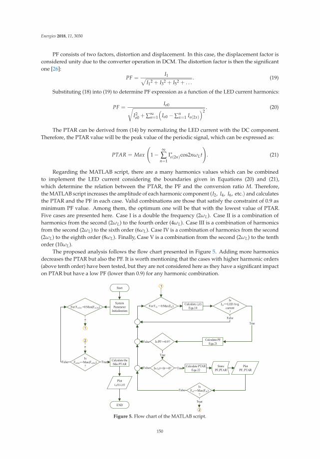
Energies 2018, 11, 3030
PF consists of two factors, distortion and displacement. In this case, the displacement factor isconsidered unity due to the converter operation in DCM. The distortion factor is then the significantone [26]:
PF =I1√
I12 + I32 + I52 + . . .
. (19)
Substituting (18) into (19) to determine PF expression as a function of the LED current harmonics:
PF =Io0√
I2o0 + ∑∞
n=1
(Io0 − ∑n
x=1 Io(2x)
)2. (20)
The PTAR can be derived from (14) by normalizing the LED current with the DC component.Therefore, the PTAR value will be the peak value of the periodic signal, which can be expressed as:
PTAR = Max
(1 −
∞
∑n=1
I∗o(2n)cos2nωLt
). (21)
Regarding the MATLAB script, there are a many harmonics values which can be combinedto implement the LED current considering the boundaries given in Equations (20) and (21),which determine the relation between the PTAR, the PF and the conversion ratio M. Therefore,the MATLAB script increases the amplitude of each harmonic component (I2, I4, I6, etc.) and calculatesthe PTAR and the PF in each case. Valid combinations are those that satisfy the constraint of 0.9 asminimum PF value. Among them, the optimum one will be that with the lowest value of PTAR.Five cases are presented here. Case I is a double the frequency (2ωL). Case II is a combination ofharmonics from the second (2ωL) to the fourth order (4ωL). Case III is a combination of harmonicsfrom the second (2ωL) to the sixth order (6ωL). Case IV is a combination of harmonics from the second(2ωL) to the eighth order (8ωL). Finally, Case V is a combination from the second (2ωL) to the tenthorder (10ωL).
The proposed analysis follows the flow chart presented in Figure 5. Adding more harmonicsdecreases the PTAR but also the PF. It is worth mentioning that the cases with higher harmonic orders(above tenth order) have been tested, but they are not considered here as they have a significant impacton PTAR but have a low PF (lower than 0.9) for any harmonic combination.
n
n
True
Figure 5. Flow chart of the MATLAB script.
150

Energies 2018, 11, 3030
It is in this script where using the real model of the LED rather than the typical equivalentresistance makes the conversion ratio to have a significant impact on PTAR and PF. Figure 6 shows thePTAR under Case V as a function of M while keeping the PF equals to 0.9. It should be mentionedthat each point of the graph is obtained by the MATLAB script, which means that the minimum PTARis shown. As illustrated in this graph, for a PTAR of less than 1.43, the accepted conversion ratio islimited to 0.2. This explain the mismatch in the results obtained by [10,11], where 1.43 was obtainedexperimentally, while 1.34 was targeted in the theoretical model. Also, this result clarifies the limitationof the conversion ratio in harmonic injection techniques. Using curve fitting, a relation between thePTAR and the conversion ratio M is found:
PTAR = −373.3M4 + 265.3 M3 − 59.47 M2 + 5.677 M + 1.142. (22)
Figure 6. Curve fitted for different values for conversion ratio (M) and Peak to Average Ratio (PTAR).
4. Proposed Control Circuit and Simple Implementation
Taking the benefits described in the previous section, the control loop that reshapes the requiredLED current will be derived in this section using a straightforward control block. The harmoniccombinations obtained from the MATLAB script for the output LED current. The duty cycle can beexpressed as a Fourier series expansion using the curve fitting as:
d(t) = D0 −∞
∑n=1
D(2n)cos2nωLt. (23)
The duty cycle defined in (23) can be obtained by means of the proposed feedforward loop,which allows the chosen harmonic components to pass through. This reshapes the input and outputcurrents as desired. Figure 7 shows the proposed closed-loop control for the LED driver. As can beseen, only a single feedback loop is implemented. The loop compensator, taking advantage of thepreviously explained harmonic injections optimization, should adjust the duty cycle according to theharmonics obtained from the MATLAB script.
151

Energies 2018, 11, 3030
Figure 7. Closed system block configuration of DCM converter.
The loop compensator gain can be computed by dividing each order value of duty cycle harmonics,(24) by the output LED current harmonics, (14). The gain plot of the compensator output can beexpressed in logarithmic scale as:
Gc =Vcomp
Ve=
Vcomp
Vre f − Rsensio=
VPWMD(s)Vre f − Rsens Io(s)
. (24)
The results obtained with (25) states that this proposed reshaping block (compensation) is basedon the division of the duty cycle by the output LED current harmonics.
5. Case Study
To validate the derived mathematical model and the proposed control, a case study will beanalyzed in this section. The system parameters will be as follows:
• Nominal input voltage Vin = 220 VAC ± 10%.• Line frequency fL = 50 Hz.• Output voltage Vo = 60 V.• Average output power po = 21 W.• Output current IO = 350 mA.• Switching frequency fs = 100 kHz.• Input filter capacitor Cin = 47 nF.• Input filter inductor Lin = 560 μH.• Output filter capacitor Cout = 0.47 μF.• Output filter inductor L = 270 μH.• Series inductor with LED LLED = 100 μH.
It should be noted that the extra series inductor with LED is used to act as a low pass filter toattenuate the switching frequency harmonics and preventing it to flow through the LED chips.
5.1. Determination of the Targeted Injected Harmonics’ Order Values
Firstly, using (23), the PTAR is determined for the selected conversion ratio M (in this caseM = 0.27) For Vin = 220VAC ± 10% (198 V, 220 V, 244 V) and 60 V output voltage, the PTAR is foundto be 1.44, 1.41, and 1.38, respectively. It is important to highlight the advantage of this model wherethe designer can decide from the beginning of the design process if this resulting PTAR is acceptableor not and if another acceptable conversion ratio M has to be chosen.
152

Energies 2018, 11, 3030
Secondly, the MATLAB script is used to calculate the values of the required harmonics tobe injected in the output current so that the predefined PTAR is obtained and the PF regulationsare observed. Figure 8 shows the output LED current for different harmonic combination cases,as explained in the previous section. It can be shown that the peak value of the output currentdecreases gradually as the injected harmonic orders increases, while having the same LED currentaverage. Figure 9 shows the input current under the same conditions. Table 1 illustrates the PTAR andthe PF for each case. It is clear that Case V (with harmonics up to the tenth order) is the best one as thelowest PTAR is obtained for nominal input voltage (220 V).
Figure 8. The LED current waveforms under different harmonics order combinations at 220Vin.
Figure 9. The input current waveform under different harmonics order combinations at 220Vin.
Table 1. PTAR and PF values at different cases, Vin = 220 V.
Harmonics Case I Case II Case III Case IV Case V
PF 0.983 0.979 0.963 0.9163 0.90PTAR 2.28 1.713 1.541 1.431 1.41
153

Energies 2018, 11, 3030
5.2. Design Control Values for Single Multifunction Block (SMFB)
Once the LED current harmonics are obtained from MATLAB script, their values can be substitutedin (14) in order to have the output LED current with its injected harmonic. Then, this output LEDcurrent is substituted into the duty cycle Equation (13). The resulting duty cycle is drawn and thenthe curve fitted as shown in Figure 10. Through this curve fitting, the Fourier components of the dutycycle waveform are obtained. Using (24), the results for the obtained gain, from the division of theduty cycle harmonics to the output LED harmonics, is plotted and fitted in Figure 11a.
Dut
y C
ycle
d(t)
Figure 10. Duty cycle curve fitting.
It is possible to study the required features for this reshape SMFB with the results shown inFigure 11a. The required gain for the loop compensator is almost flat during the frequency range of100 Hz–500 Hz, which is the frequency range for harmonic injection. As this analysis is concernedwith the frequency range of the harmonic injection, it does not discuss the frequency range above this500 Hz. However, this can follow regular design rules (i.e., having a low-pass filter with bandwidth inthe range of one tenth of the switching frequency).
(a) (b)
Figure 11. (a) Model of the bode plot. (b) Bode diagram of the system transformation function.
A simple implementation for this proposed SMFB can be an integrator and a pole before thedouble line frequency, in addition to an extra pole below one tenth of the switching frequency tofilter undesired harmonics component. One critical point is that the required phase should be zero
154

Energies 2018, 11, 3030
within the 100 Hz–500 Hz range to keep the line current and line voltage in phase (displacement PFrequirement).
To summarize, the compensator parameters for this system can be summarized as:
1. Integrator for regulation purpose.2. One zero at a frequency lower than one tenth of twice the line frequency to flat the gain and keep
the phase angle to zero.3. One pole between the last injected harmonic (>500 Hz, in this case) and one tenth of the switching
frequency to filter undesired high frequency harmonics.
The transfer function of the described system can be presented as:
Gc =K(
1 + sWz
)s(
1 + sWp
) =C1R2s + 1
C1C2R1R2s2 + (C1R1 + C2R2)s. (25)
Figure 11b shows the described system bode plot with the integrator, one zero at one hertz,and one pole at 4 kHz. One advantage of the proposed system is that it has a higher bandwidth,which introduces better dynamics than conventional systems with usually 10 Hz bandwidth.
The SMFB functions are summarized in Figure 12 regulation for the LED average current,duty cycle reshaping, harmonics injection and output current reshaping.
SMFB
Duty Cycle ReshapingRegulation LED Current ReshapingHarmonics Injection
OO O
Figure 12. Single Multifunction Block (SMFB) functions.
6. Simulation & Experimental Results
To validate the proposed idea, simulation and experimentation are carried out. Figure 13adescribes the circuit diagram used in both simulation and practice. It consists of the EMI filter,the rectifier bridge, and the buck converter. The buck converter switch is AOT22N50 500 V, 22 AN-Channel MOSFET and the diode is ES1J which is 1 A, 200 V Surface Mount Super-Fast Rectifier.The converter has a small output film capacitor to increase the lifetime of the LED driver. Small seriesresistor Surface Mount Rsems = 0.5 Ω 1% 0.5 W is inserted to sense the output current for thecontrol circuit.
The compensator is a Type II, as shown in Figure 13b Due to the simplicity of the control circuit,a generic PWM controller can be used, the UC3825a IC from Texas Instrument with a few surfacemount technology (SMT) components. The compensator capacitors and resistors can be calculatedusing (25). Table 2 shows the compensator values.
Table 2. The compensator value.
Component R1 R2 C1 C2
Value 100 k Ω 200 k Ω 1 uF 220 pF
155
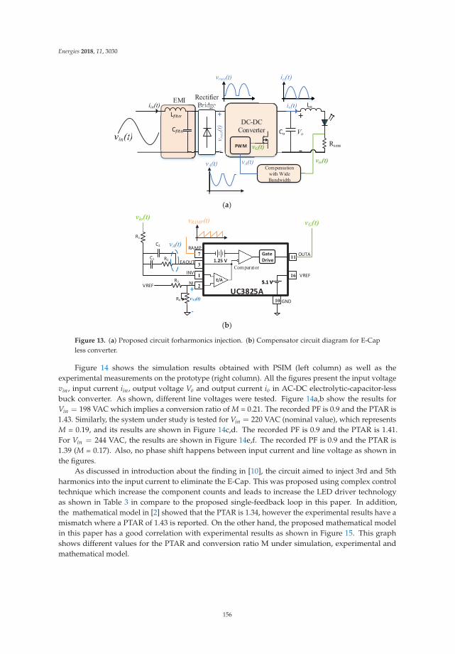
Energies 2018, 11, 3030
(a)
(b)
CoCCo
+
-
+
-
Lo
Lfilter
Cfilter
PWM
Gate Drive
UC3825A
VREF
GND
OUTARAMP
INV
EAOUT
VREF5.1 V5.1 V
1.25 V
C2
C1
R1
R2
R3
R4
E/ANI+
-
Figure 13. (a) Proposed circuit forharmonics injection. (b) Compensator circuit diagram for E-Capless converter.
Figure 14 shows the simulation results obtained with PSIM (left column) as well as theexperimental measurements on the prototype (right column). All the figures present the input voltagevin, input current iin, output voltage Vo and output current io in AC-DC electrolytic-capacitor-lessbuck converter. As shown, different line voltages were tested. Figure 14a,b show the results forVin = 198 VAC which implies a conversion ratio of M = 0.21. The recorded PF is 0.9 and the PTAR is1.43. Similarly, the system under study is tested for Vin = 220 VAC (nominal value), which representsM = 0.19, and its results are shown in Figure 14c,d. The recorded PF is 0.9 and the PTAR is 1.41.For Vin = 244 VAC, the results are shown in Figure 14e,f. The recorded PF is 0.9 and the PTAR is1.39 (M = 0.17). Also, no phase shift happens between input current and line voltage as shown inthe figures.
As discussed in introduction about the finding in [10], the circuit aimed to inject 3rd and 5thharmonics into the input current to eliminate the E-Cap. This was proposed using complex controltechnique which increase the component counts and leads to increase the LED driver technologyas shown in Table 3 in compare to the proposed single-feedback loop in this paper. In addition,the mathematical model in [2] showed that the PTAR is 1.34, however the experimental results have amismatch where a PTAR of 1.43 is reported. On the other hand, the proposed mathematical modelin this paper has a good correlation with experimental results as shown in Figure 15. This graphshows different values for the PTAR and conversion ratio M under simulation, experimental andmathematical model.
156

Energies 2018, 11, 3030
Table 3. comparison between the proposed circuit and [10].
CircuitPTAR
Mathematical
PTARExperimental
Control Circuit Component Count No. ControlLoopsOp-Amp Multiplier Divider
[10] 1.34 1.43 4 1 1 2Proposed 1.41 1.41 2 - - 1
Line Voltage
Line Current
LED Voltage
LED Current
Line Voltage
Line Current
LED Voltage
LED Current
Line Voltage
Line Current
LED Voltage
LED Current
Figure 14. Simulation and prototype waveform results of input voltage vin, input current iin,LED output voltage Vo and output LED current io in buck converter.
157

Energies 2018, 11, 3030
Figure 15. Obtained PTAR at different values for conversion ratio (M) from mathematical model,practical and simulation.
An AC-DC power converter should be complied with EN 61000-3-2 standard. This standard forlimiting the harmonics current level of the electronics equipment which is injected by different loadsback to the grid. Figure 16 shows a comparison between the input current values for the proposedcircuit and the maximum values for EN 61000-3-2 Class D standard. This class should be complied forthe lighting equipment with an input power smaller or equal than 25 W. The figure verifies that theproposed circuit is compliance with EN 61000-3-2 standard [27].
Figure 16. Comparison between the proposed Input current values and maximum level for EN61000-3-2 Class D standard.
The proposed solution has the features of single feedback loop with low component counts forE-cap less LED solution under limited PTAR, by its turn lower cost solution. Within test, there was norecord for visible flicker. However, flicker issue requires more investigation due to the increase in theLED current modulation percentage [28].
158

Energies 2018, 11, 3030
7. Conclusions
This paper has proposed the use of the complete LED model instead of the simple equivalentresistance. Its relevance and influence on the design, on the PF and on the PTAR are explored.The proposed model is derived under harmonic injection technique and it determines the requiredharmonic to limit the LED current PTAR and keep the input PF higher than 0.9. Based on the derivedmodel, a reshape control block is proposed and implemented using a second-order compensator witha single feedback loop. This circuitry can be applied to different converters topologies such as Flybackconverter. Results show a good agreement between simulation and experimentation. Results concludethat there is a specified range for the conversion ratio so the target PTAR can be achieved with whilecomplying with ENERGY STAR and EN 61000-3-2 Class D standard.
Author Contributions: M.N. conceived and designed the experiments, performed the experiments, analyzedthe data, and wrote the paper. M.O. define the concept, review results, supervision and manage the project.M.A. review results, revised and edited the manuscript. E.M.A., E.-S.H. co-supervised the work.
Funding: This research received no external funding.
Conflicts of Interest: The authors declare no conflict of interest.
References
1. Machine, W. Lifetime of White LEDs; US Department of Energy: Washington, DC, USA, 2009.2. Wang, Y.; Alonso, J.M.; Ruan, X. A Review of LED Drivers and Related Technologies. IEEE Trans. Ind. Electron.
2017, 64, 5754–5765. [CrossRef]3. Gebreel, A.; Nassary, M.; Bakr, A. Low Cost Low Voltage Low Power Integrated LED Driver; LAP LAMBERT
Academic Publishing: Saarbruggen, Germany, 2016.4. Cree First to Break 300 Lumens-Per-Watt Barrier. CREE, 26 March 2014. Available online: http://www.cree.
com/ (accessed on 2 November 2018).5. Cheng, C.A.; Cheng, H.L.; Chung, T.Y. A Novel Single-Stage High-Power-Factor LED Street-Lighting Driver
With Coupled Inductors. IEEE Trans. Ind. Appl. 2014, 50, 3037–3045. [CrossRef]6. Fortunato, M. Ensure Long Lifetimes from Electrolytic Capacitors: A Case Study in LED Light
Bulbs. Maximintegrated, 29 May 2013. Available online: www.maximintegrated.com (accessed on2 November 2018).
7. Montanari, D.; Saarinen, K.; Scagliarini, F.; Zeidler, D.; Niskala, M.; Nender, C. Film Capacitors forAutomotive and Industrial Applications. October 2008. Available online: www.kemet.com (accessed on2 November 2018).
8. Almeida, P.S.; Nogueira, F.J.; Guedes, L.F.A.; Braga, H.A.C. An experimental study on the photometricalimpacts of several current waveforms on power white LEDs. In Proceedings of the XI Brazilian PowerElectronics Conference, Praiamar, Brazil, 11–15 September 2011; pp. 728–733.
9. Almeida, P.S.; Bender, V.C.; Braga, H.A.C.; Costa, M.A.D.; Marchesan, T.B.; Alonso, J.M. Static and DynamicPhotoelectrothermal Modeling of LED Lamps Including Low-Frequency Current Ripple Effects. IEEE Trans.Power Electron. 2015, 30, 3841–3851. [CrossRef]
10. Wang, B.; Ruan, X.; Yao, K.; Xu, M. A Method of Reducing the Peak-to-Average Ratio of LED Current forElectrolytic Capacitor-Less AC–DC Drivers. IEEE Trans. Power Electron. 2010, 25, 592–601. [CrossRef]
11. Ruan, X.; Yao, B.W.K.; Wang, S. Optimum Injected Current Harmonics to Minimize Peak-to-Average Ratio ofLED Current for Electrolytic Capacitor-Less AC–DC Drivers. IEEE Trans. Power Electron. 2011, 26, 1820–1825.[CrossRef]
12. Gu, L.; Ruan, X.; Xu, M.; Yao, K. Means of Eliminating Electrolytic Capacitor in AC/DC Power Supplies forLED Lightings. IEEE Trans. Power Electron. 2009, 24, 1399–1408. [CrossRef]
13. Nassary, M.; Orabi, M.; Ahmed, E.; Hasaneen, El.; Gaafar, M. Control Circuit Optimization forElectrolytic Capacitor-Less LED Driver. In Proceedings of the IEEE MEPCON Conference, Cairo, Egypt,19–21 December 2017.
159

Energies 2018, 11, 3030
14. Lamar, D.G.; Sebastian, J.; Arias, M.; Fernandez, A. On the Limit of the Output Capacitor Reduction inPower-Factor Correctors by Distorting the Line Input Current. IEEE Trans. Power Electron. 2012, 27, 1168–1176.[CrossRef]
15. Lamar, D.G.; Sebastián, J.; Arias, M.; Fernández, A. Reduction of the Output Capacitor in Power FactorCorrectors by Distorting the Line Input Current. In Proceedings of the 2010 Twenty-Fifth Annual IEEEApplied Power Electronics Conference and Exposition (APEC), Palm Springs, CA, USA, 21–25 February 2010;pp. 196–202.
16. Rezaei, K.; Golbon, N.; Moschopoulos, G. A New Control Scheme for an AC-DC Single-stage Buck-BoostPFC Converter with Improved Output Ripple Reduction and Transient Response. In Proceedings of theAPEC 2014, Beijing, China, 10–12 November 2014; pp. 1866–1873.
17. Soares, G.M.; Alonso, J.M.; Braga, H.A.C. Investigation of the Active Ripple Compensation Technique toReduce Bulk Capacitance in Off-line Flyback-Based LED Drivers. IEEE Trans. Power Electron. 2018, 33,5206–5214. [CrossRef]
18. Soares, G.M.; Almeida, P.S.; Alonso, J.M.; Braga, H.A.C. Capacitance Minimization in Offline LED DriversUsing an Active-Ripple-Compensation Technique. IEEE Trans. Power Electron. 2017, 32, 3022–3033. [CrossRef]
19. Yang, Y.; Ruan, X.; Zhang, L.; He, J.; Ye, Z. Feed-Forward Scheme for an Electrolytic Capacitor-Less AC/DCLED Driver to Reduce Output Current Ripple. IEEE Trans. Power Electron. 2014, 29, 5508–5517. [CrossRef]
20. Wang, S.; Ruan, X.; Yao, K.; Tan, S.C.; Yang, Y.; Ye, Z. A Flicker-Free Electrolytic Capacitor-Less AC–DC LEDDriver. IEEE Trans. Power Electron. 2012, 27, 4540–4548. [CrossRef]
21. Lee, K.W.; Hsieh, Y.H.; Liang, T.J. A Current Ripple Cancellation Circuit for Electrolytic Capacitor-lessAC-DC LED Driver. In Proceedings of the 2013 Twenty-Eighth Annual IEEE Applied Power ElectronicsConference and Exposition (APEC), Long Beach, CA, USA, 17–21 March 2013; pp. 1058–1061.
22. Shen, Y.C.; Liang, T.J.; Tseng, W.J.; Chang, H.H.; Chen, K.H.; Lu, Y.J.; Li, J.S. Non-Electrolytic Capacitor LEDDriver with Feedforward Control. In Proceedings of the IEEE Energy Conversion Congress and Exposition(ECCE), Montreal, QC, Canada, 20–24 September 2015; pp. 3223–3230.
23. Hui, S.Y.; Li, S.N.; Tao, X.H.; Chen, W.; Ng, W.M. A Novel Passive Offline LED Driver With Long Lifetime.IEEE Trans. Power Electron. 2010, 25, 2665–2672. [CrossRef]
24. Chen, W.; Li, S.N.; Hui, S.Y.R. A Comparative Study on the Circuit Topologies for Offline PassiveLightEmitting Diode (LED) Drivers with Long Lifetime & High Efficiency. In Proceedings of the IEEEEnergy Conversion Congress and Exposition, Atlanta, GA, USA, 12–16 September 2010; pp. 724–730.
25. Kreyszig, E. Advanced Engineering Mathematics, 7th ed.; Wiley: Hoboken, NJ, USA, 1992.26. Robert, W. Erickson and Dragan Maksimovic, Fundamentals of Power Electronics, 2nd ed.; Springer
Science+Business Media, LLC: New York, NY, USA, 2001.27. European Power Supply Manufacturers Association. Harmonic Current Emissions: Guidelines to the Standard
EN 61000-3-2; EPSMA: Winchester, UK, 2010.28. IEEE Recommended Practices for Modulating Current in HighBrightness LEDs for Mitigating Health Risks to
Viewers; IEEE Std: Piscataway, NJ, USA, 2015; pp. 1–80.
© 2018 by the authors. Licensee MDPI, Basel, Switzerland. This article is an open accessarticle distributed under the terms and conditions of the Creative Commons Attribution(CC BY) license (http://creativecommons.org/licenses/by/4.0/).
160

energies
Article
Power and Voltage Control for Single-PhaseCascaded H-Bridge Multilevel Convertersunder Unbalanced Loads
Daliang Yang 1,*, Li Yin 1, Shengguang Xu 2 and Ning Wu 3
1 College of Electrical Engineering, Guangxi University, Nanning 530004, China; [email protected] Liuzhou Power Supply Bureau, Gxuangxi Power Grid Corporation, Liuzhou 545005, China;
[email protected] Electric Power Research Institute, Guangxi Power Grid Corporation, Nanning 530023, China;
[email protected]* Correspondence: [email protected]; Tel.: +86-0771-3232264
Received: 31 August 2018; Accepted: 11 September 2018; Published: 14 September 2018
Abstract: The conventional control method for a single-phase cascaded H-bridge (CHB) multilevelconverter is vector (dq) control; however, dq control requires complicated calculations and additionaltime delays. This paper presents a novel power control strategy for the CHB multilevel converter.A power-based dc-link voltage balance control is also proposed for unbalanced load conditions.The new control method is designed in a virtual αβ stationary reference frame without coordinatetransformation or phase-locked loop (PLL) to avoid the potential issues related to computationalcomplexity. Because only imaginary voltage construction is needed in the proposed control method,the time delay from conventional imaginary current construction can be eliminated. The proposedmethod can obtain a sinusoidal grid current waveform with unity power factor. Compared withthe conventional dq control method, the power control strategy possesses the advantage of a fastdynamic response. The stability of the closed-loop system with the dc-link voltage balance controlleris evaluated. Simulation and experimental results are presented to verify the accuracy of the proposedpower and voltage control method.
Keywords: cascaded H-bridge (CHB); dc-link voltage balance control; multilevel converter;power control; single-phase system
1. Introduction
Multilevel converters have gained increasing attention as of late. Commonly used multilevelconverters include cascaded H-bridge (CHB), flying capacitor, and neutral-point-clamped converters [1].Among these, the CHB converter has advantages of simple implementation, high reliability, and lowharmonics [2], hence, it has been widely researched in academia and industry, particularly in relation tostatic synchronous compensators [3], solid-state transformers [4], and active power filters [5].
Many control schemes have been proposed to enable the pulse width modulation (PWM) converterto achieve a high power factor and near-sinusoidal grid current [6]. These strategies can be broadlyclassified into two categories: direct power control (DPC) and direct current control (DCC).
DPC was originally proposed by Ohnishi [7], whose method directly controls the active andreactive power of the PWM converter using three-phase instantaneous power theory. Comparedwith DCC, DPC has advantages of simple structure, fast dynamic response, high efficiency, and wideapplicability [8]. Currently, many advanced DPC strategies have been proposed, such as predictiveDPC (P-DPC) [9], deadbeat DPC [10], and slide-mode DPC [11]. In the single-phase PWM convertersystem, instantaneous power estimation is more complicated than in the three-phase system,which limits the development of DPC schemes in single-phase systems [12].
Energies 2018, 11, 2435; doi:10.3390/en11092435 www.mdpi.com/journal/energies161

Energies 2018, 11, 2435
DCC methods have been frequently used with the PWM converter. The most commonly usedDCC method utilizes vector control theory (dq control) [13–16]. Coordination transformation is neededin dq control to change the ac signals into dc signals [17]. The grid voltage phase angle is essential in thecoordinate transformation; therefore, a phase-locked loop (PLL) is employed to synchronize the outputvoltage with the grid voltage vector [18]. To accurately obtain the information on the grid voltageincluding the amplitude and phase angle, some advanced PLLs have been proposed, such as hybridfiltering technique-based PLL [19], grid sequence separator PLL [20], frequency-fixed SOGI-basedPLL [21], and repetitive learning-based PLL [22]. However, the computational complexity of coordinatetransformation and PLL increases the calculation burden of the embedded processor like the digitalsignal processor (DSP) [23]. Therefore, the development of a convenient control method without PLLor coordination transformation is appealing. Recently proposed control methods of the CHB converterare based on model-predictive control (MPC) [24,25]. However, three major problems arise in theMPC scheme used for the CHB converter. First, the calculation burden persists in the MPC methodbecause the number of switching states increases exponentially as more H-bridges are added [26].The second one is the MPC system sensitiveness problem like sensitive to the parameter [27]. The thirdproblem is that under unbalanced load conditions, the MPC strategy cannot provide a proper controlfunction [28].
It is exceedingly difficult to implement the dq control scheme in the single-phase CHBconverter system; imaginary orthogonal current and voltage signals must be created for coordinatetransformation (αβ to dq) because only one physical axis is accessible [29]. In dq control, the imaginaryorthogonal current signal is essential in acquiring the dc current signals id and iq for the innercurrent loop [30]. Thus, an imaginary current construction module is required to produce theimaginary orthogonal current signal [31]. Although the performance of conventional imaginarycurrent construction under the steady state is mostly acceptable, the time delay tends to slow downthe system dynamic response and result in further distortion [32,33].
The control scheme performance of the CHB converter in the single-phase system depends ontwo key factors: sinusoidal grid current waveform with unity power factor and balanced dc-linkvoltages [34,35]. Therefore, the CHB multilevel converters need a control method to balance thedc-link voltages, especially when the dc-side loads are unbalanced. In [36,37], the dc-link voltageswere controlled using individual capacitor voltage controllers. In [38], the presented voltage balancecontrol method uses a weighting factor to adjust the dc-link voltages. In [39], two voltage-balancingtechniques were presented, allowing for much more efficient regulation of dc-link voltages. However,these voltage balanced control methods are all based on ac voltage reference duty cycle regulation;a power-based dc-link voltage balance controller has not been analyzed in detail.
In the conventional dq control strategy, the current calculation is complicated and additionaltime delay is required. For optimization purposes, a power control method without coordinatetransformation, PLL or conventional imaginary current construction is introduced and applied tocontrol the single-phase CHB multilevel converter system. Moreover, a power-based dc-link voltagebalance control scheme is presented to make the proposed power control strategy available underunbalanced load conditions. This power and voltage control method can achieve a sinusoidal gridcurrent waveform and balanced dc-link voltages. Several experimental tests were conducted tocompare dynamic responses of the presented control scheme with those of the classical dq controlmethod. The proposed voltage balance controller is verified as well.
The remainder of this paper is organized as follows: in Section 2, principles of the proposedcontrol scheme and dc-link voltage balance controller are discussed, and the stability of the closed-loopsystem with the dc-link voltage balance controller is evaluated. Section 3 presents the simulationresults. Experimental results are addressed in Section 4. The proposed control method is discussed inSection 5. Finally, relevant conclusions are drawn in Section 6.
162

Energies 2018, 11, 2435
2. Control Method Principles
2.1. Model of the Cascaded H-Bridge Multilevel Converter
Figure 1 presents the topology of a two-cell CHB system in which us is the grid voltage, isa isthe grid current, uc is the ac side voltage, L and RL denote the filter inductor and line resistance,respectively,. udc1 and udc2 represent the dc-link voltages of the first and second H-bridge, and udc_sumis the total dc-link voltage (udc1 + udc2). R1 and R2 are the resistive loads connected to the dc side ofeach H-bridge.
Figure 1. Two-cell single-phase CHB converter.
The mathematical model of the CHB converter is as follows:{L disa
dt = us − uc − RLisa
udc_sum = udc1 + udc2(1)
To simplify analysis of system stability, according to Equation (1), a small-signal model of thestationary reference frame (αβ frame) was built, as illustrated in Figure 2. Here, usα equals us, and usβ
is the orthogonal signal of us; u~sα and u~
sβ represent the small-signal ac variation of usα and usβ;u~
dc1 and u~dc2 denote the small-signal ac variation of udc1 and udc2; isα equals isa, and isβ is the
orthogonal signal of isa; i~sα and i~sβ represent the small-signal ac variation of isα and isβ; Isα and Isβ
stand for the quiescent operating point of isα and isβ; Dα1, Dα2, Dβ1, and Dβ2 are the duty cycles of thefirst and second H-bridge; and d~
α1, d~α2, d~
β1, and d~β2 represent the small-signal ac variation of Dα2,
Dβ1, and Dβ2.
~su α
~si α ~ ~ ~ ~
1 1 1 1 2 2 2 2dc dc dc dcu d D u u d D uα α α α+ + +
~ ~ ~ ~1 1 1 1 2 2 2 2dc dc dc dcu d D u u d D uβ β β β+ + +
~ ~1 1
~ ~1 1
s s
s s
d I D i
d I D iα α α α
β β β β
+ +
+~
1dcu1C
~su β
~si β
~ ~2 2
~ ~2 2
s s
s s
d I D i
d I D iα α α α
β β β β
+ +
+
~2dcu
2C
Figure 2. Small-signal model of two-cell single-phase CHB converter in αβ frame coordination.
163

Energies 2018, 11, 2435
2.2. Principle of the Proposed Power Control Method
The main function of CHB multilevel converter is to obtain active power and reactive power fromthe grid to satisfy load needs. For the CHB converter, the essence of controlling the grid current as wellas the dc-link voltage is control of the input and output power. By rapidly and effectively controllingthe active and reactive power, the converter can achieve strong dynamic and static characteristics.
In the three-phase CHB converter system, the active power p and reactive power q can bedescribed as: [
pq
]=
[usα usβ
u∗sα u∗
sβ
][isα
isβ
](2)
where u*sα = usβ, u*
sβ = −usα.Only one phase physical variable is available in the single-phase CHB converter system;
a second-order generalized integrator (SOGI) block is needed to introduce the imaginary signal.The virtual αβ stationary reference frame is depicted in Figure 3, the α-axis coincides with the a-axis,and the β-axis is orthogonal to the α-axis.
( )α
βb
c 0
Figure 3. Schematic diagram of virtual αβ coordinate axis.
In the single-phase CHB converter system, p and q can be described as follows:[pq
]=
13
[usα usβ
u∗sα u∗
sβ
][isα
isβ
](3)
p* and q* are defined as the active power and reactive power reference, respectively; i*sα and i*sβ
represent the current reference.Equations (4) and (5) are shown as follows according to Equation (3), and the coefficient calculation
of the proposed power control is shown in Equation (6):[i∗sα
i∗sβ
]=
3usα ∗ u∗
sβ − u∗sα ∗ usβ
[u∗
sβ −usβ
−u∗sα usα
][p∗
q∗
](4)
[i∗sα
i∗sβ
]=
⎡⎣ 3u∗sβ
usα∗u∗sβ−u∗sα∗usβ
p∗ + −3usβ
usα∗u∗sβ−u∗sα∗usβ
q∗−3u∗
sαusα∗u∗
sβ−u∗sα∗usβp∗ + 3usα
usα∗u∗sβ−u∗sα∗usβ
q∗
⎤⎦ (5)
⎧⎨⎩ k1 =3u∗
sβ
usα∗u∗sβ−u∗sα∗usβ
k2 =−3usβ
usα∗u∗sβ−u∗sα∗usβ
(6)
If the grid voltage is sinusoidal, then the result of usα * u*sβ + u*
sα * u*sβ is constant; p* is controlled
by the outer power loop; q* is constant because it is given directly; therefore the frequency and phase ofthe current references isα and isβ are consistent with the instantaneous grid voltage, and the real-timetracking can be achieved. Notably, only i*sα is used as the current reference, because the CHB multilevelconverter is used on a single-phase system.
164

Energies 2018, 11, 2435
2.3. Presentation of Proposed Dc-Link Balance Controller
Figure 4 presents the conventional dc-link voltage balance controller. In this approach, the dutycycles of each ac voltage reference u*
a1 and u*a2 are modified separately to keep the voltages balanced,
and the scheme is suitable for the dq method. A power-based dc-link voltage balance controlleradjusting the ac current reference duty cycle is introduced in this paper to regulate the individualH-bridge dc-link voltage.
1udΔ
2udΔ
Figure 4. Conventional voltage balance controller [37].
If the dc-link voltage of each H-bridge is unbalanced (mainly via load imbalance), then the powerof these H-bridges becomes uneven. To keep the dc-link voltage balanced, the uneven power shouldbe extracted from the grid. Δdp1 and Δdp2 are used as the compensation values to eliminate unevenpower. Δdp1 and Δdp2 are calculated by the voltage balance controller:{
Δdp1 = (Kp +Kis )(ure f − udc1) · udc1
Δdp2 = (Kp +Kis )(ure f − udc2) · udc2
(7)
where Kp and Ki represent the proportional and integral coefficient of the proportional-integral (PI)controller, respectively, and uref is the voltage reference of every H-bridge cell.
The presented voltage balance controller is shown in Figure 5, which modifies the duty cycles ofeach ac current reference i*sa1 and i*sa2 individually to reduce the dc voltage imbalance. The currentreference for each H-bridge can be calculated according to Equations (8)–(10):{
i∗sα1 = Δdi∗sa1 + i∗sα
i∗sα2 = Δdi∗sa2 + i∗sα(8)
{i∗sα1 = Δdp1(k1 + k2) + p∗k1 + q∗k2
i∗sα2 = Δdp2(k1 + k2) + p∗k1 + q∗k2(9)
{i∗sα1 = k1(Δdp1 + p∗) + k2(Δdp1 + q∗)i∗sα2 = k1(Δdp2 + p∗) + k2(Δdp2 + q∗)
(10)
1pdΔ
2pdΔ
* 1 1 21 ( )pi sad d k kΔ = Δ +
* 2 1 22 ( )pi sad d k kΔ = Δ +
Figure 5. Proposed voltage balance controller.
165

Energies 2018, 11, 2435
2.4. Proposed Power Control of the Cascaded H-Bridge Multilevel Converter
The overall control topology of the proposed control method is depicted in Figure 6. The main ideaof the proposed control is to obtain command signals in the orthogonal αβ frame; as such, the dc-linkvoltages can be balanced.
su α su β
*p
1 2dc dcu u+
1dcu
2dcu
saisu
sai2* refu *
1sai*
2sai
su
*q
sai
−
+ *1au
*2au
1dcu 2dcu
Figure 6. Proposed power and voltage control of CHB converter.
The control system is formed as a double closed-loop control structure using the inner currentloop and the outer power loop.
The inner current loop is implemented in the orthogonal αβ frame. Compared with classicalsingle-phase dq schemes, the current calculation of the proposed control method is simpler because nocoordinate transformation, PLL, or conventional imaginary current construction is needed. However,the current references i*sa1 and i*sa2 are ac variables. To track the current references with zero error inthe stationary frame and achieve high tracking accuracy when the grid frequency fluctuates, rather thanrelying on conventional PI controllers or a repetitive controller [40], proportional-plus-resonant (PR)controllers are utilized in the current loop.
As for the outer power loop, a PI controller is used to adjust the total dc-link voltage udc_sum(udc1 + udc2). The active power p* is generated by multiplying the output of the PI controller by thetotal dc-link voltage udc_sum. Reactive power reference q* is given directly.
The detailed control topology of the power and voltage control module is shown in Figure 7.Current reference i*sa1 of the first H-bridge and i*sa2 of the second H-bridge are acquired through thedc-link voltage balance control block; these current references are controlled independently. Deviationvalues between the grid current isa and the current references are input into the PR regulators separately,and the modulation voltage signals u*
a1 and u*a2 are generated for the first and second H-bridge.
Carrier phase-shifted PWM (CPS-PWM) technology is adopted to generate five-level voltage, achievingmulti-level modulation. Furthermore, if the reactive power reference q* is set to zero, then a unitypower factor can be achieved.
su α
su βsu
si α
si β
1dcu 2dcu
Figure 7. Power and voltage control module.
166

Energies 2018, 11, 2435
2.5. Stability Analysis of the Power and Voltage Control Scheme
Assume that the parameters of the H-bridges are identical, such that the dc-link voltageudc1 = udc2 = udc. The double-loop control diagram presented in Figure 6 can thus be transformed asillustrated in Figure 8. In Figure 8, GV is the voltage gain of CHB, GPIV is the voltage PI regulator,K is the conversion coefficient between p* and i*sa, GqPR is the current PR regulator, GTPWM is thetransfer function of the PWM modulator, GIV is the transfer function of the voltage to output currenti*sa, and GVI is the transfer function of the current to output voltage udc. GIV and GVI can be deducedfrom the small-signal model shown in Figure 2.
*p sai∗ +
sai su+−− sai p dcudcuΔrefu +
−dcu
PIVG dcu K qPRG TPWMG IVG1K
1
dcu VIG
Figure 8. Basic double-loop controller structure diagram of the proposed power control.
The closed-loop transfer function can be expressed as follows:
GV =GPIV GqPRGTPWMGIV GVI
1 + GPIV GqPRGTPWMGIV GVI(11)
One bridge of the CHB converter can be simplified according to Figure 9 per Thevenin law.However, the dc-link voltage unbalance problem in CHB remains under the unbalanced load condition;therefore the voltage balance control module should be added. Figure 10 shows the Theveninequivalent circuit with the dc-link voltage balance module, where Z1 is the load impedance, Zio isthe impedance between the input and output of CHB, M is the gain of the voltage balance controlmodule, G1 is the conversion coefficient of power to voltage, and iout is the output current. In this caseG1 = 1/(GPIV * udc).
Taking the first H-bridge as an example:
G1[p∗ + (ure f − udc1)M]GV = Zioudc1Z1
+ udc1 (12)
udc1 =GV G1
Zio/Z1 + 1 + GV G1Mp∗ + GV G1M
Zio/Z1 + 1 + GV G1Mure f (13)
Because Z1 >> Zio, GG1M represents the gain in the basic double-loop controller with the dc-linkvoltage balance module from Equation (13); the Bode plot is shown in Figure 11. The amplitude marginis 12.7 dB, the cut-off frequency is 272 Hz, the phase margin is 105◦, and the cross-over frequency is78 Hz. All roots of (Zio/Z1 + 1 + GG1M) are on the left half-complex plane, ensuring stability of thesystem with the voltage balance control module.
refu
ioZ outi
V refG u 1Z
Figure 9. Thevenin equivalent circuit of the basic double-loop.
167

Energies 2018, 11, 2435
Figure 10. Thevenin equivalent circuit with the voltage balance module controller.
Figure 11. Bode plot of the basic double-loop controller with the dc-link voltage balance module.
3. Simulation Results
The CHB converter system shown in Figure 1 was modelled in the MATLAB/Simulink R2015a(MATLAB/Simulink R2015a, MathWorks, Natick, MA, USA) software environment to verify the powerand voltage control scheme. The main system parameters used for simulation are shown in Table 1.
Table 1. Parameters Used For Simulation.
Parameter Symbol Simulation Value
Grid voltage rms value us 220 VGrid frequency fg 50 Hz
Input inductance L 3.0 mHdc-link total voltage Udc 400 Vdc-link capacitance C1, C2 4700 μF
dc-link load resistance R1, R2 10 Ω, 15 ΩSwitching frequency fsw 10 kHz
Inner current loop control parameters P, R, wc 0.5, 100, 6.28Outer power loop control parameters P, I 0.1, 8
168

Energies 2018, 11, 2435
3.1. Proposed Power Control Scheme Simulation
Figures 12–14 show the simulation results with unbalanced loads, where R1 = 10 Ω and R2 = 15 Ω.Figure 12a displays the grid voltage and grid current waveform in the steady state, revealing that theunity power factor was achieved.
(a) (b)
Figure 12. Simulation waveforms of CHB converter in steady state: (a) Grid voltage and grid current;(b) Five-level voltage staircase waveform.
(a) (b)
Figure 13. q* changed from 0 var to 1500 var: (a) Dynamic response of the grid current;(b) Dynamic response of the reactive power.
(a) (b)
Figure 14. q* changed from 0 var to −1500 var: (a) Dynamic response of the grid current;(b) Dynamic response of the reactive power.
Figure 12b shows the ac side five-level staircase voltage. Dynamic responses of the proposedmethod under sudden reactive power change conditions are shown in Figures 13 and 14. In these,the active power reference p* is governed by the outer power loop, and the reactive power reference q*
is changed from 0 to −1500 var and 0 to 1500 var at 0.34 s.
3.2. Power-Based Voltage Balance Control Simulation
In this simulation, the initial loads of two H-bridges were 15 Ω resistors. At 1.0 s, the resistor ofthe first H-bridge declined to 10 Ω. Two distinct cases were considered. In Figure 15a, the voltagebalance control module was not utilized, and the dc-link voltages became different after the loadchange. The second H-bridge, whose resistor was unchanged, demonstrated higher dc-link voltage
169

Energies 2018, 11, 2435
than the first H-bridge. Figure 15b shows the dc-link voltages with the voltage balance controlmethod. Using the proposed voltage balance control module, the dc-link voltages returned to theinitial value (200 V).
(a) (b)
Figure 15. Simulated response of dc-link voltages when load changed: (a) Without voltage balancecontrol; (b) With voltage balance control.
4. Experimental Results
4.1. Experimental Prototype
A single-phase five-level CHB converter experimental platform was adopted to validate thepresented power and voltage control scheme, as shown in Figure 16.
Figure 16. Platform of the experiments.
Two H-bridge converters with serially connected inputs formed the ac side of the experimentalsetup. The dc output of each converter fed the loads. The converter was interfaced to the gridthrough a coupling transformer and a voltage regulator to ensure safety during the experiments.The secondary-side voltage of the regulator was set to 80 V (rms), while the dc-link voltage referencesudc1 and udc2 were set to 50 V. The grid voltage, grid current, ac side voltage, and dc-link voltages weremeasured using the outer high-performance hall sensors. A TMS320F28377D DSP processor boardwas utilized to implement the control algorithm. Measured voltage and current signals were fed backto the DSP processor board employing a built-in, 16-bit analog-digital conversion module. The powerfactor and total harmonic distortion (THD) of the grid current were measured via a Fluke 435 powerquality analyzer.
4.2. Steady State
Figure 17 depicts the experimental waveforms of the grid voltage us (200 V/division), the gridcurrent isa (20 A/division), the dc-link voltage of the first H-bridge udc1 (20 V/division), and the acside voltage uc (100 V/division) for the proposed scheme in the steady state, where loads R1 and R2 inFigure 1 are 10 Ω and 15 Ω, separately. When the reactive power reference q* was set to zero, the grid
170

Energies 2018, 11, 2435
current was in phase with the grid voltage, so the unity power factor was achieved. The THD of thegrid current in the steady state was 4.3%, indicated in Figure 18. Moreover, this method was foundto compensate for the reactive power: CHB converters can generate or absorb reactive power to thepower grid when the reactive power reference is positive or negative. In Figure 19, the grid currentwas leading the grid voltage; thus, the CHB converter was generating reactive power to the system.In Figure 20, the grid current was lagging the voltage, and the CHB converter was absorbing reactivepower from the system.
Figure 17. Experimental waveforms of CHB converter in steady state.
Figure 18. THD of grid current in steady state.
Figure 19. Experimental grid currents of CHB capacitive mode.
171

Energies 2018, 11, 2435
Figure 20. Experimental grid currents of CHB inductive mode.
4.3. Dynamic Response Compared with dq Control
Currently, the most popular control method for the single-phase CHB converter is dq control.Several experiments were carried out to compare conventional dq control with the proposed controlmethod. These experiments tested the dynamic responses of the systems under sudden power changeconditions. In these tests, the total dc-link voltage udc_sum was kept at 100 V, and the system wasconnected to two resistive loads where R1 is 10 Ω and R2 is 15 Ω, respectively. The dynamic of thed-axis current i*d in the dq control was managed by the outer voltage loop, and active power p* in theproposed scheme was controlled by the outer power loop. Therefore, only step changes in the reactivecurrent reference i*q in the dq control and reactive power reference q* in the proposed control wereapplied to evaluate the dynamic control performance of each. Differences in the dynamic performanceof the dq control scheme and the proposed control method are illustrated in Figures 21–28.
The total dc-link voltage udc_sum is 100 V; i*q and q* are given directly in each control method.Reactive power reference q* equals udc_sum * i*q (100 * i*q). For instance, when the step change of i*q is5 A, the step change of q* equals 100 * i*q (500 var); when the step change of i*q is −5 A, the step changeof q* equals 100 * i*q (−500 var).
As shown, the transient responses of the proposed power control method (less than 1 ms) werefaster than the dq control method (more than 5 ms). In the dq control method, a time delay of 1/4 in thefundamental period arose from classical imaginary current construction.
Grid current and five-level staircase voltage continuous distortions also appeared in the dq controlmethod due to conventional imaginary current construction.
Figure 21. i*q changed from 0 A to 5 A (dq control method).
172

Energies 2018, 11, 2435
Figure 22. q* changed from 0 var to 500 var (proposed control method).
Figure 23. i*q changed from 0 A to −5 A (dq control method).
Figure 24. q* changed from 0 var to −500 var (proposed control method).
173

Energies 2018, 11, 2435
Figure 25. i*q changed from 5 A to −5 A (dq control method).
Figure 26. q* changed from 500 var to −500 var (proposed control method).
Figure 27. i*q changed from −5 A to 5 A (dq control method).
174

Energies 2018, 11, 2435
Figure 28. q* changed from −500 var to 500 var (proposed control method).
4.4. Voltage Balance Control
Besides grid current control, balance control of the dc-link voltages is another important issue.A dc-link voltage balance control method based on power was adopted to render the proposed powercontrol strategy applicable to the CHB converter under unbalanced load conditions.
Unbalanced load experimental tests were conducted to verify the voltage-balancing performanceof the presented scheme. In these experiments, the load resistor of the first H-bridge R1 was steppedfrom 15 Ω to 10 Ω whereas that of the second H-bridge R2 was maintained at 15 Ω. In Figure 29a,when the load resistors were changed, the dc-link voltage of the first H-bridge udc1 (10 V/division)declined from 50 V to 45 V, and that of the second H-bridge udc2 (10 V/division) increased from 50 Vto 55 V. Figure 29b shows that when the voltage balance controller was adopted, the dc-link voltagescould be controlled to 50 V when the load resistors were changed. Thus, the accuracy of the presenteddc-link voltage balance control method was confirmed.
(a) (b)
Figure 29. Experimental response of dc-link voltages when load changed: (a) Without voltage balancecontroller, (b) With voltage balance controller.
5. Discussion
The proposed power and voltage control method offers many advantages including no coordinatetransformation, PLL, or conventional imaginary current construction. Moreover, it was found toexhibit faster transient responses and lower distortions compared with the conventional dq controlmethod, as illustrated in Figures 21–28.
The natural frame control scheme presented in [23] also shows the advantages of no coordinatetransformation, PLL, or conventional imaginary current construction. Differ from the natural frame
175

Energies 2018, 11, 2435
control scheme, the proposed scheme connects power control with current control through theinstantaneous power theory. Besides, the proposed voltage balance control module is based onpower, in which the power compensation values are used to eliminate the uneven power in activepower p and reactive power q.
Even so, this control strategy has some limitations: First, although classical imaginary currentconstruction is not necessary, the creation of an imaginary voltage component cannot be avoided.Therefore, an algorithm can be developed to reduce the time delay caused by imaginary voltageconstruction. Second, only the steady grid voltage condition was considered here, although abnormaloperating states (e.g., grid voltage distortion) exist; thus, the control method should be optimized tomake it applicable to such states.
6. Conclusions
A power control method is introduced for the single-phase CHB multilevel converter in this paper.A power-based dc-link voltage balance control module is also presented to eliminate the differentdc-link voltages caused by the unbalanced loads.
The proposed power and voltage control method is designed in a virtual αβ stationary referenceframe without coordinate transformation or phase-locked loop. So, the complicated calculation issuecan be avoided. What is more, conventional imaginary current construction is not necessary. Problemslike time delay can also be avoided. The inner loop current calculation is simplified compared with theconventional dq control scheme. Stability of the proposed control scheme can be guaranteed throughthe analysis based on small-signal model.
Simulation and experimental results were presented to verify the effectiveness of the proposedcontrol method. In the steady state, the proposed method can obtain the sinusoidal grid current andunity power factor under unbalanced load conditions. Upon comparing the dynamic response of thepresented control strategy with that of the dq control scheme, the conducted experiments indicate thatthe salient feature of the proposed scheme is as follows: the proposed scheme maintains a fast dynamicresponse advantage over the conventional dq control method. This approach has been shown to beuseful for the single-phase CHB multilevel converter system. The proposed control scheme can also beutilized with other multilevel converter systems.
Author Contributions: The individual contribution of each co-author with regards to the reported research andwriting of the paper is as follows. D.Y. conceived the idea, L.Y. carried out the experiments and analyzed the data,and all authors wrote the paper.
Acknowledgments: This study is partly supported by the National Nature Science Foundation of China(No. 61861003).
Conflicts of Interest: The authors declare no conflict of interest.
Nomenclature
CHB Cascaded H-bridgePWM Pulse Width ModulationDPC Direct Power ControlDCC Direct Current ControlP-DPC Predictive DPCPLL Phase-Locked LoopDSP Digital Signal ProcessorMPC Model-Predictive ControlSOGI Second-Order Generalized IntegratorPI Proportional-IntegralPR Proportional-plus-ResonantCPS-PWM Carrier, Phase-Shifted PWMTHD Total Harmonic Distortion
176

Energies 2018, 11, 2435
References
1. Noman, A.M.; Al-Shamma’a, A.A.; Addoweesh, K.E.; Alabduljabbar, A.A.; Alolah, A.I. Cascaded MultilevelInverter Topology Based on Cascaded H-Bridge Multilevel Inverter. Energies 2018, 11, 895. [CrossRef]
2. Aquila, A.D.; Liserre, M.; Monopoli, V.G.; Rotondo, P. Overview of PI-based solutions for the control ofDC buses of a single-phase H-bridge multilevel active rectifier. IEEE Trans. Ind. Appl. 2008, 44, 857–866.[CrossRef]
3. Yu, Y.; Konstantinou, G.; Townsend, C.D.; Agelidis, V.G. Comparison of zero-sequence injection methods incascaded H-bridge multilevel converters for large-scale photovoltaic integration. IET Renew. Power Gener.2017, 11, 603–613. [CrossRef]
4. Wang, L.; Zhang, D.; Wang, Y.; Wu, B.; Athab, H.S. Power and voltage balance control of a novel three-phasesolid-state transformer using multilevel cascaded H-bridge inverters for microgrid applications. IEEE Trans.Power Electron. 2016, 31, 3289–3310. [CrossRef]
5. Yang, Z.; Sun, J.; Li, S.; Huang, M.; Zha, X.; Tang, Y. An adaptive carrier frequency optimization methodfor harmonic energy unbalance minimization in a cascaded H-bridge-based active power filter. IEEE Trans.Power Electron. 2018, 33, 1024–1037. [CrossRef]
6. Song, W.; Ma, J.; Zhou, L.; Feng, X. Deadbeat predictive power control of single-phase three-levelneutral-point-clamped converters using space-vector modulation for electric railway traction. IEEE Trans.Power Electron. 2016, 31, 721–732. [CrossRef]
7. Ohnishi, T. Three PWM converter/inverter by means of instantaneous active and reactive power control.In Proceedings of the International Conference on Industrial Electronics, Control and Instrumentation.(IECON 1991), Kobe, Japan, 28 October–1 November 1991; pp. 819–824.
8. Wang, X.; Sun, D. Three-vector-based low-complexity model predictive direct power control strategy fordoubly fed induction generators. IEEE Trans. Power Electron. 2017, 32, 773–782. [CrossRef]
9. Kim, I.; Chan, R.; Kwak, S. A voltage level based predictive direct power control for modular multilevelconverter. IEEE Trans. Power Appl. 2017, 11, 784–792.
10. Cheng, C.; Nian, H.; Wang, X.; Sun, D. Dead-beat predictive direct power control of voltage source inverterswith optimised switching patterns. IET. Power Electron. 2017, 10, 1438–1451. [CrossRef]
11. Ma, H.; Xie, Y.; Shi, Z. Improved direct power control for Vienna-type rectifiers based on sliding modecontrol. IET. Power Electron. 2016, 9, 427–434. [CrossRef]
12. Ma, J.; Song, W.; Wang, S.; Feng, X. Model predictive direct power control for single phase three-level rectifierat low switching frequency. IEEE Trans. Power Electron. 2018, 33, 1050–1062. [CrossRef]
13. Behrouzian, E.; Bongiorno, M. Investigation of negative-sequence injection capability of cascaded H-bridgeconverters in star and delta configuration. IEEE Trans. Power Electron. 2017, 32, 1675–1683. [CrossRef]
14. Adam, G.P.; Abdelsalam, I.A.; Ahmed, K.H.; Williams, B.W. Hybrid multilevel converter with cascadedH-bridge cells for HVDC applications: Operating principle and scalability. IEEE Trans. Power Electron. 2015,30, 65–77. [CrossRef]
15. Wang, X.; He, Z.; Yang, J. Electric Vehicle Fast-Charging Station Unified Modeling and Stability Analysis inthe dq Frame. Energies 2018, 11, 1195. [CrossRef]
16. Liu, J.; Liu, Z. Harmonic Analyzing of the Double PWM Converter in DFIG Based on Mathematical Model.Energies 2017, 10, 2087. [CrossRef]
17. Gu, Y.; Wang, Y.; Xiang, X.; Li, W.; He, X. Improved virtual vector control of single-phase inverter based onunified model. IEEE Trans. Energy Convers. 2014, 29, 611–618. [CrossRef]
18. Zheng, X.; Xiao, L.; Wang, Z.; Lei, Y.; Wang, C. Control strategy without phase-locked loop based oncoordinate transformation for three-phase AC/DC converter. IET. Power Electron. 2015, 8, 1701–1709.[CrossRef]
19. Li, Y.; Yang, J.; Wang, H.; Ge, W.; Ma, Y. A Hybrid Filtering Technique-Based PLL Targeting Fast and RobustTracking Performance under Distorted Grid Conditions. Energies 2018, 11, 973. [CrossRef]
20. Hamed, H.A.; Abdou, A.F.; Bayoumi, E.; EL-Kholy, E.E. Effective design and implementation of GSS-PLLunder voltage dip and phase interruption. IET. Power Electron. 2018, 11, 1018–1028. [CrossRef]
21. Xiao, F.; Dong, L.; Li, L.; Liao, X. A frequency-fixed SOGI-based PLL for single-phase grid-connectedconverters. IEEE Trans. Power Electron. 2017, 21, 1713–1719. [CrossRef]
177

Energies 2018, 11, 2435
22. Sahoo, S.; Prakash, S.; Mishra, S. Power quality improvement of grid-connected DC microgrids usingrepetitive learning-based PLL under abnormal grid conditions. IEEE Trans. Ind. Appl. 2018, 54, 82–90.[CrossRef]
23. Yang, D.; Wu, N.; Yin, L.; Lu, Z. Natural frame control of single-phase cascaded H-bridge multilevel converterbased on fictive-phases construction. IEEE Trans. Ind. Electron. 2018, 54, 3848–3857. [CrossRef]
24. Chan, R.; Kwak, S. Improved Finite-Control-Set Model Predictive Control for Cascaded H-Bridge Inverters.Energies. 2018, 11, 355. [CrossRef]
25. Zhang, Y.; Wu, X.; Yuan, X.; Wang, Y.; Dai, P. Fast model predictive control for multilevel cascaded H-bridgeSTATCOM with polynomial computation time. IEEE Trans. Ind. Electron. 2016, 63, 5231–5243. [CrossRef]
26. Qi, C.; Chen, X.; Tu, P.; Wang, P. Deadbeat control for a single-phase cascaded H-bridge rectifier with voltagebalancing modulation. IET Power Electron. 2018, 11, 610–617. [CrossRef]
27. Song, W.; Deng, Z.; Wang, S.; Feng, X. A Simple Model Predictive Power Control Strategy for Single-PhasePWM Converters With Modulation Function Optimization. IEEE Trans. Power Electron. 2016, 31, 5279–5289.[CrossRef]
28. Blahnik, V.; Kosan, T.; Peroutka, Z.; Talla, J. Control of a single-phase cascaded H-bridge active rectifierunder unbalanced load. IEEE Trans. Power Electron. 2018, 33, 5519–5527. [CrossRef]
29. Somkun, S.; Chunkag, V. Unified unbalanced synchronous reference frame current control for single-phasegrid-connected voltage source converters. IEEE Trans. Ind. Electron. 2016, 63, 5425–5436. [CrossRef]
30. Sha, D.; Xu, G.; Xu, Y. Utility direct interfaced charger/discharger employing unified voltage balance controlfor cascaded H-bridge units and decentralized control for CF-DAB modules. IEEE Trans. Ind. Electron. 2017,64, 7831–7841. [CrossRef]
31. Ebrahimi, M.; Khajehoddin, S.; Ghartemani, M.K. Fast and robust single-phase dq current controller forsmart inverter applications. IEEE Trans. Power Electron. 2016, 31, 3968–3976. [CrossRef]
32. Shi, J.; Gou, W.; Yuan, H.; Zhao, T.; Huang, A.Q. Research on voltage and power balance control for cascadedmodular solid-state transformer. IEEE Trans. Power Electron. 2011, 26, 1154–1166. [CrossRef]
33. Farivar, G.; Townsend, C.D.; Hredzak, B.; Pou, J.; Agelidis, V.G. Low-capacitance cascaded H-bridgemultilevel STATCOM. IEEE Trans. Power Electron. 2016, 32, 1744–1754. [CrossRef]
34. Qi, C.; Chen, X.; Tu, P.; Wang, P. Cell-by-cell-based finite-control- set model predictive control for asingle-phase cascaded H-bridge rectifier. IEEE Trans. Power Electron. 2018, 33, 1654–1665. [CrossRef]
35. Moeini, A.; Wang, S. A DC Link Sensor-Less Voltage Balancing Technique for Cascaded H-Bridge MultilevelConverters with Asymmetric Selective Harmonic Current Mitigation-PWM. IEEE Trans. Power Electron. 2018,33, 7571–7581. [CrossRef]
36. Farivar, G.; Hredzak, B.; Agelidis, V.G. Decoupled control system for cascaded H-bridge multilevel converterbased STATCOM. IEEE Trans. Ind. Electron. 2016, 63, 322–331. [CrossRef]
37. Zhao, T.; Wang, G.; Bhattacharya, S.; Huang, A.Q. Voltage and power balance control for a cascaded H-bridgeconverter-based solid-state transformer. IEEE Trans. Power Electron. 2013, 28, 1523–1532. [CrossRef]
38. Chen, H.; Wu, P.; Lee, C.; Wang, C.; Yang, C.; Cheng, P. A flexible DC voltage balancing control based on thepower flow management for star-connected cascaded H-bridge converter. IEEE Trans. Ind. Appl. 2016, 2,4946–4954. [CrossRef]
39. Moeini, A.; Wang, S. The state of charge balancing techniques for electrical vehicle charging stations withcascaded H-bridge multilevel converters. In Proceedings of the IEEE Applied Power Electronics Conferenceand Exposition—APEC, San Antonio, TX, USA, 4–8 March 2018; pp. 637–644.
40. Yang, Y.; Zhou, K.; Wang, H.; Blaabjerg, F.; Wang, D.; Zhang, B. Frequency adaptive selective harmoniccontrol for grid-connected inverters. IEEE Trans. Power Electron. 2015, 30, 3912–3924. [CrossRef]
© 2018 by the authors. Licensee MDPI, Basel, Switzerland. This article is an open accessarticle distributed under the terms and conditions of the Creative Commons Attribution(CC BY) license (http://creativecommons.org/licenses/by/4.0/).
178

energies
Article
MPPT and SPPT Control for PV-Connected InvertersUsing Digital Adaptive Hysteresis Current Control
Triet Nguyen-Van *, Rikiya Abe and Kenji Tanaka
Internet of Energy Laboratory, Department of Technology Management for Innovation, the University of Tokyo,Tokyo 113-8656, Japan; [email protected] (R.A.); [email protected] (K.T.)* Correspondence: [email protected]
Received: 8 July 2018; Accepted: 6 August 2018; Published: 9 August 2018
Abstract: Most PV systems are usually controlled by a Maximum Power Point Tracking (MPPT)algorithm to maximize the generated electrical power. However, the maximum power is oftenunstable and depends on the solar irradiance and temperature. This makes it difficult to controlthe power grid supply-demand balance due to fluctuations caused by the increase of renewableand variable PV systems. This paper proposes a new control algorithm for a PV-connected invertercalled Specified Power Point Tracking (SPPT) control in addition to the conventional MaximumPower Point Tracking (MPPT) control. The PV system is controlled to generate the maximum poweror a specified power depending on the electricity transactions comes from the electricity tradingsystem. A high-speed FPGA-based digital adaptive hysteresis current control method, which hasfast and stable response and simple structure comparing with the popular Sine-triangle Pulse WidthModulation (SPWM) method, is proposed to implement the MPPT and SPPT control. The adaptivehysteresis current band is calculated adaptively to improve a disadvantage of the classical fixedband hysteresis current control on the varying switching frequency. A reference current used in theadaptive hysteresis current control is calculated such that the output power of the PV-connectedinverter is maximized in the MPPT control or is maintained at a given value in the SPPT control.The experimental and simulation results show that the PV-connected inverter under the proposedcontrol algorithm generates the desired power almost exactly and yields stable and fast responsedespite the varying irradiance.
Keywords: PV-connected inverter; MPPT; SPPT; adaptive hysteresis current control
1. Introduction
Nowadays, renewable energy has become a solution to address the energy security concerns andemission standards of most countries. Photovoltaic (PV) energy systems have gained tremendousattention as one of the most promising renewable energy sources due to their advantages on the powerscalability, simple installation, and low operating cost [1]. In most PV systems, the PV arrays areusually controlled by a Maximum Power Point Tracking (MPPT) algorithm to maximize the generatedelectrical power [2]. However, the Maximum Power Point (MPP) of the PV panel is unstable and varieswith solar irradiance and temperature. This may cause problems such as voltage rise and protectionproblems in the utility grid [3]. Furthermore, it is difficult to control the supply-demand balancewith the current power grid architecture due to fluctuations caused by the increase of renewable andvariable energy generations like PV systems [4,5].
In Japan, at the end of August 2014, 1,368,749 PV projects with the total power of 69.4 GW had beenapproved. At that time, Kyushu Electric Power Company had approved PV generators with a capacityof 17.76 GW, which surpassed its maximum demand in summer (15.2 GW). The power company wasunable to accept more PV energy and had to suspend responses to applications for grid connection
Energies 2018, 11, 2075; doi:10.3390/en11082075 www.mdpi.com/journal/energies179

Energies 2018, 11, 2075
contracts for new PV projects. After that, the same issue has been raised with other power companiesin Japan, such as Hokkaido Electric Power (HEPCO), Tohoku Electric Power, Shikoku Electric Power,and Okinawa Electric Power [6]. There is still a limit for the current power grid to accept the increasingPV generators.
In order to maintain the reliability of the current power grid while accepting more and morepenetration of renewable energy, such as PV, a new power system concept called digital grid hasbeen proposed [7]. The digital grid enhances the current grid by dividing a large-scale synchronizedpower system into some smaller size power systems called digital grid cell. The digital grid cellsconnect together, to the current grid, and other distributed generations via a digital grid router (DGR).In this work, in order to reduce the effect of the demand-supply balance problem caused by the PVgenerators in the digital grid system, we propose a control algorithm for the PV-connected invertercalled Specified Power Point Tracking (SPPT) control in addition to the conventional MPPT control.The control of the PV generator is decided based on the electricity transactions that the DGR receivesfrom the electricity trading system.
Three major classes of current control techniques have been developed over the last fewdecades: predictive dead-beat, sine-triangle pulse width modulation (SPWM), and hysteresis currentcontrol [8]. While the predictive dead-beat control technique tends to give accurate responses, it iscomplicated for implementation and its accuracy depends on the accuracy of the predictive model [9].The asynchronous SPWM is the most popular technique and is being used in most MPPT controlalgorithms in PV systems, such as perturb and observe (P&O), or incremental conductance (InC) [10,11],however, it requires complicated proportional-integral (PI) regulators with undesirable delays. Onthe other hand, the hysteresis current control has simple structure, fast response, and independentof the inverter system parameters [12]. Because a low sampling frequency may lead to a large ripplecurrent overshoot from the hysteresis current band, a digital hysteresis current control usually requiresAD converters with sufficiently high sampling frequency to contain the ripple current within theband accurately [13]. A high sampling frequency at MHz level may be difficult for implementationon conventional microcontrollers and digital signal processors (DSPs), however, such high samplingfrequency is beyond the scope of the field programmable gate array (FPGA), which can executecalculations stably at a high frequency and is becoming more and more popular in many electronicsapplications [14,15].
The basic implementation of hysteresis current control bases on the switching signal derivedby comparing the actual current and the tolerance band of the reference current. In classicalhysteresis current control, the hysteresis current band is fixed to a certain value, which makes theswitching frequency vary to contain the current within the band. This leads to unwanted heavyinterference among the phases in the three-phase system. In order to solve this problem, an adaptivehysteresis current control technique has been developed and applied to control the grid-connected andstand-alone multi-functional inverter of the DGR [16,17]. In this study, we propose the novel SPPTcontrol in addition to the conventional MPPT for the PV-connected multi-functional inverter, and amethod to implement the control algorithms by a high-speed FPGA-based digital adaptive hysteresiscurrent control.
This paper is organized as follows: Section 2 introduces the concepts of digital grid and digital gridrouter. The digital adaptive hysteresis current control technique is presented in Section 3. Section 4presents the MPPT and SPPT control algorithm for the PV-connected inverter using the adaptivehysteresis current control. In Section 5, the experimental and simulation results are shown to illustratethe performances of the proposed method. Conclusions are given in Section 6.
2. Digital Grid Router
The main concept of the digital grid is dividing a large synchronous grid into smaller segmentedgrid cells, which connect together, to the current grid, and other distributed generations via the DGRas shown in Figure 1 [18]. The DGR controls power flow of the equipment within a cell based on the
180

Energies 2018, 11, 2075
trading results receiving from the electricity trading system. The DGR also plays a role of a shockabsorber so that intermittent renewable energy sources in digital grid cells will not affect the main grid.It can be used to support the stability of the main grid via energy storage such as batteries. The DGR iscomposed of multi-functional inverters connected to a common DC bus as shown in Figure 2. Eachinverter may connect to a grid, load, PV panel, battery, or a DC sub-grid.
Figure 1. Digital grid system with electricity trading using block-chain.
Figure 2. Structure of the digital grid router.
The electricity trading within the digital grid bases on the demand and the supply ability in eachdigital grid cell, whose states are sent to the trading system on the cloud by a communication network.The smart-contracts using block-chain technology enable the electricity transactions to be operatedautomatically with the trading algorithm likes Zaraba method [19] in stock markets. This powergrid system is expected to produce a free-electricity market between decentralized grids and enablethe power grid to be adaptive to the instability due to peak-demand cutting and demand-responsematching issues.
3. Adaptive Hysteresis Current Control
Consider a single-phase half-bridge inverter circuit as shown in Figure 3. The inverter has twoconstant and balanced DC sources, each of which has a value of Vdc. Parameters L, Lg, and C.
Represent the hysteresis inductance, output inductance, and capacitance of the ripple currentfilter, respectively. Let the output current io of the inverter be controlled by switch devices S1 and S2
to track a given reference current iref The adaptive hysteresis current control is employed as shownbelow [16].
Define the current error Δi(t) as:
181

Energies 2018, 11, 2075
Δi(t) = iL(t)− ire f (t), (1)
where iL(t) and ire f (t) are the hysteresis current and the reference currents at the instant t. Consider aninstant t0, when the hysteresis current iL starts to cross the lower hysteresis band, and the switch S1
is switched on. Assume that the switch S1 is switched on during [t0, t1), and is switched off during[t1, t2) intervals as shown in Figure 4.
Figure 3. Single-phase half-bridge inverter circuit.
Figure 4. Adaptive hysteresis current band.
A dynamic equation for the hysteresis current can be written as:
LdiL(t)
dt= vdc(t)− vo(t), (2)
for t0 ≤ t ≤ t2, where vo is the instantaneous output voltage and vdc(t) is the inverter input DC voltageelaborated as:
vdc(t) =
{Vdc i f S1 is On−Vdc i f S1 is O f f
. (3)
Define the slopes of the hysteresis current in the on and off switching periods by.Ion and
.Io f f
respectively. By assuming that the output voltage vo is slowly varying during the switching modulationperiod [t0, t2] , the hysteresis current slopes can be expressed by:
son =diL(t)
dt=
Vdc − vo(t0)
L(4)
for t ∈ [t0, t1), and:
so f f =diL(t)
dt=
−Vdc − vo(t0)
L(5)
for t ∈ [t1, t2).
182

Energies 2018, 11, 2075
The current errors at t1 and t2 are given by:
Δi(t1) =iL(t1)− ire f (t1)
=ire f (t0) + Δi(t0) + sonTon − ire f (t1)(6)
Δi(t2) =iL(t2)− ire f (t2)
=ire f (t0) + Δi(t0) +(
sonTon + so f f To f f
)− ire f (t2)
(7)
where:Ton = t1 − t0, (8)
To f f = t2 − t1. (9)
The reference current ire f (t) is slowly varying during the modulation period, such that it can beapproximated as:
ire f (t1) = ire f (t0) + dire f (t0)Ton, (10)
ire f (t2) = ire f (t0) + dire f (t0)(
Ton + To f f
), (11)
where dire f (t0) is derivative of the reference current ire f (t) with respect to t at t = t0.Substituting Equations (10) and (11) into Equations (6) and (7), we can write the current errors
Δi(t1), and Δi(t2) as:Δi(t1) = Δi(t0) + s′onTon, (12)
Δi(t2) =Δi(t0) + s′onTon + s′o f f To f f
=Δi(t1) + s′o f f To f f, (13)
where s′on, s′o f f are given as:
s′on = son − dire f (t0) =Vdc − vo(t0)
L− dire f (t0), (14)
s′o f f = so f f − dire f (t0) =−Vdc − vo(t0)
L− dire f (t0). (15)
Let fsw is a desired constant switching frequency. In the adaptive hysteresis current controlmethod, the hysteresis current band Δib(t0) is derived by using the following conditions:
Δi(t1)− Δi(t0) = 2Δib(t0), (16)
Δi(t2)− Δi(t1) = −2Δib(t0), (17)
Ton + To f f = Tsw, (18)
where Tsw = 1/ fsw. Substituting Equations (16)–(18) into Equations (12) and (13), we can derive thehysteresis current band as:
Δib(t0) =1
2 fsw
sonso f f
so f f − son. (19)
By substituting Equations (14) and (15) into Equation (19), the hysteresis current band in Equation(19) can also be written in the form of:
Δib(t0) =1
4L fswVdc
{Vdc
2 −[vo(t0) + Ldire f (t0)
]2}
. (20)
For a digital control system, where the measured voltage and current is sampled by analog/digitalconverters, the hysteresis current band under zero-order-holds (ZOHs) can be written by:
183

Energies 2018, 11, 2075
Δib(t) =1
4L fswVdc
{Vdc
2 −[vo(kTsp
)+ Ldire f
(kTsp
)]2}
, (21)
where kT ≤ t < (k + 1)T and T is a sampling interval.
4. Hysteresis Current Control for PV-Connected Inverter
Consider a half-bridge inverter circuit with a PV panel connected between the output and thenegative voltage of the inverter as shown in Figure 5. The voltage of the PV panel can be calculatedfrom the output voltage vo of the inverter as:
V = vo + Vdc. (22)
The algorithms for MPPT and SPPT controls are described below.
Figure 5. PV connected inverter circuit.
4.1. Algorithm for MPPT Control
Figure 6 shows voltage-current and voltage-power characteristic curves of the PV panel.The maximum power point (MPP) can be determined by a point, at which the derivative of outputpower P with respect to the voltage V is zero, i.e.:
dPdV
= 0. (23)
Consider a digital control system, where the measured voltage and current are sampled byanalog/digital converters with a sampling interval T. Let sampled-values of the voltage and currentof the PV at a sampled instant kT are Vk and Ik. Then, the power Pk at instant kT is calculated as:
Pk = Vk Ik. (24)
The derivative of the power with respect to the voltage at instant kT for the sampled-value can bewritten by:
dPdV
∣∣∣∣k=
ΔPkΔVk
=Pk − Pk−1Vk − Vk−1
. (25)
The algorithm for hysteresis current control tracking the MPP is as below:
1 : if ΔPkΔVk
= 02 : ire f _k = ire f _k−13 : else
4 : if ΔPΔV > 0
5 : ire f _k = ire f _k−1 + δi6 : else
7 : ire f _k = ire f _k−1 − δi
184

Energies 2018, 11, 2075
where δi > 0 is a step-size of the reference current. It should be noted that due to the definition fordirection of the output current from the inverter as shown in Figure 5, the reference current in this casetakes only negative value.
The MPP divides the characteristics of the PV panel into two areas: positive power derivativedP/dV and negative power derivative dP/dV as shown in Figure 6. When the state of the PV panel isin the positive power derivative area, the reference current is decreased. On the contrary, when the stateof the PV panel is in the negative power derivative area, the reference current is increased by a step-sizeδi. This process is continued until the state of the PV arrives the MPP. At the MPP, the reference currentis unchanged. While the reference current is changed by the definite step-size δi, the output powerof the PV panel may not identify to the MPP exactly. In order to avoid an oscillation of the referencecurrent at the steady stay around the MPP, the MPP can be replaced by a maximum power bandwidth.Then, the MPPT algorithm can be revised as below.
1 : if∣∣∣ ΔPk
ΔVk
∣∣∣ ≤ δPM
2 : ire f _k = ire f _k−13 : else
4 : if ΔPΔV > δPM
5 : ire f _k = ire f _k−1 + δi6 : else
7 : ire f _k = ire f _k−1 − δi
where δP > 0 is the bandwidth of the MPP.
Figure 6. Characteristic PV and MPPT control curves.
4.2. Algorithm for SPPT Control
Let the PV-connected inverter is controlled to generate a given specified power Ps, which isassumed to be less than the generable maximum power. There are two points on the characteristiccurves of the PV panel can generate the given power Ps as shown in Figure 7.
185

Energies 2018, 11, 2075
Figure 7. Characteristic PV and SPPT control curves.
However, in order to reduce the power loss, the point in the positive power derivative area,which has smaller current, is preferred. The algorithm tracking the specified power point (SPP) is asbelow:
1 : if Pk = Ps
2 : ire f _k = ire f _k−13 : else
4 : if (k < Ps)P ∩(
ΔPΔV < 0
)5 : ire f _k = ire f _k−1 − δi6 : else
7 : ire f _k = ire f _k−1 + δi
The reference current is unchanged when the output power equals to the given power Ps. Whenthe output power is less than the given power Ps and the state of the PV panel is in the negative powerderivative area of the SPP, the reference current is increased. In the other cases, the reference current isdecreased by the step-size δi. This process is continued until the state of the PV panel arrives the SPP.By the same way of the MPPT control, in order to avoid an oscillation of the reference current at thesteady state around the SPP, the SPP can be replaced by a specified power bandwidth. Then, the SPPTalgorithm can be revised as below:
1 : if |Pk − Ps| ≤ δPS2 : ire f _k = ire f _k−13 : else
4 : if (Pk < Ps − δPS) ∩(
ΔPΔV < 0
)5 : ire f _k = ire f _k−1 − δi6 : else
7 : ire f _k = ire f _k−1 + δi
where δPS > 0 is the specified power bandwidth.
186

Energies 2018, 11, 2075
5. Experimental Results
5.1. Grid-Connected PV System
Consider a DGR composed of two multi-functional inverters with a common DC bus, which iscomposed of electrolytic capacitors C1 and C2 as shown in Figure 8. The first inverter connects to aPV panel and another one connects to an AC power grid. The grid-connected inverter is controlledto maintain the voltages of capacitors C1 and C2 at a given constant value Vdc_re f . The PV-connectedinverter sends the power generated by the PV panel to the common DC bus, and the grid-connectedinverter sends that power from the common DC bus to the grid.
Figure 8. Grid-connected PV panel circuit.
Let v1 and v2 are the voltages of capacitors C1 and C2. The grid has a voltage of vg. In this work,the grid-connected inverter is controlled by using the adaptive hysteresis current control presented insession 3 with the reference current is calculated as [18]:
ire f (kT) = −kt
(2Vdc_re f − (v1(kT) + v2(kT))
)vg(kT)√2Vg
+ kb(v1(kT)− v2(kT)), (26)
where kt, kb > 0 are the control gains, which tune the speed of the response, Vg is an effective value ofthe grid voltage vg.
5.2. Simple Model for PV Panel
Due to space constraints of the laboratory, a simple electrical circuit composing of a DC powersource and a variable resistor as shown in Figure 9 is used to emulate the PV panel. The voltage-currentand voltage-power characteristics of this PV model are as below.
The output power P of this PV model is calculated as:
P = VI. (27)
Using Kirchhoff’s rule for the circuit shown by Figure 9, we have:
VDC = V + RI. (28)
Substituting Equation (28) into Equation (27), we can write the output power P as:
P =1R
V(VDC − V). (29)
The voltage-current and voltage-power characteristic curves of the PV model given by Equations(28) and (29) can be figured by Figure 10. The maximum power point can be determined as:
187

Energies 2018, 11, 2075
Vmax =VDC
2, (30)
Imax =VDC2R
, (31)
Pmax =VDC
2
4R. (32)
Figure 9. Electrical model for PV panel.
Figure 10. Voltage-current and voltage-power characteristic curves of the PV model.
In Figure 10, it can be seen that the value of the variable resistor R may change the voltage-powerand voltage-current characteristics of the PV model. Thus, the variable resistor R can be used toemulate the variation of the solar irradiance. Although the PV model showed in Figure 9 emulatesonly the basic voltage-current and voltage-power characteristics of the PV panel, it is efficient for thepurpose of evaluating the MPPT and SPPT algorithms for the PV control.
5.3. Experimental Results
The proposed control algorithm for the PV-connected inverter has been assessed by using aprototype of the DGR, which is composed of two multi-functional inverters connected by the circuitshown in Figure 8. The experimental setup is shown by Figure 11. Each inverter has a rated power of300 W. The circuit parameters of the inverters are given by: L = 2.2 mH, Lg = 1.1 mH, and C = 6.8 μF.The reference voltage of the DC bus Vdc_re f is set at 175 V. The analog/digital converter (ADC) has thesampling frequency of 4 MHz. The switching transistors in the inverter circuit are IGBT devices withthe dead-time at 1.5 μ sec. The constant switching frequency in the adaptive hysteresis current controlis at 20 kHz. The control algorithm is implemented on a FPGA board, which has a clock frequency of160 MHz. The grid has an AC voltage of 100 V and frequency of 50 Hz. The DC power source of thePV model VDC in Figure 10 is at 250 V. The step-size δi of the reference current is at 0.1 A.
188

Energies 2018, 11, 2075
Table 1 shows experimental result data for the MPPT control with various solar irradiances, whichis emulated by the variable resistor in the PV model. The output power of the PV-connected invertermatches with the maximum power of the PV model calculated using Equation (32) almost exactly.
Table 2 shows experimental result for the same system controlled by SPPT algorithm with thespecified power of Ps = 150 W. The output power of the inverter is kept at the specified power Ps
regardless to the variation of the solar irradiance. Figure 12 shows the voltage and current responsesof the grid-connected and PV-connected inverters controlled by the MPPT algorithm with the solarirradiance emulating resistor R at 80 W. Figure 13 shows the responses of the same inverter controlledby the SPPT algorithm. In all the tested cases including that for different value of R, the PV-connectedinverter generates a power, which exactly matches the desired power. The grid-connected invertersends the power generated from the PV-connected inverter to the grid and keeps the voltage of thecommon DC bus at constant. The voltage and current responses of the both inverters are stable for alltested cases.
Table 1. Experimental result data for MPPT control.
ResistorR [Ω]
MeasuredCurrent I [A]
MeasuredVoltage V [V]
MeasuredPower P [W]
CalculatedPower P [W]
100 1.19 131 155 15680 1.38 140 194 19560 1.87 136 254 260
Table 2. Experimental result data for SPPT control.
ResistorR [Ω]
MeasuredCurrent I [A]
MeasuredVoltage V [V]
MeasuredPower P [W]
SpecifiedPower Ps [W]
100 0.9 161 14515080 0.76 191 144
60 0.72 208 148
Figure 11. Experimental DGR circuit.
Figures 14 and 15 show the responses of the inverters with the MPPT control when the solarirradiance emulating resistor R changes from 60 W to 100 W and contrarily from 100 W to 60 W,respectively. The experimental results show that the proposed control algorithm yields responses,which are stable and adapt to the variation of the solar irradiance quickly.
Simulations have been carried out to compare the proposed MPPT algorithm using adaptivehysteresis current control with other common MPPT algorithms based on SPWM technique by using
189

Energies 2018, 11, 2075
Matlab-Simulink. Figures 16–19 shown the responses of the PV panel for the proposed MPPT,the perturb and observe (P&O) [20], and the incremental conductance (InC) [21], and fractionalopen-circuit voltage (FOCV) [22] algorithms, respectively. While the P&O and the InC algorithms yieldunstable responses with oscillations when the irradiance changes, the proposed and FOCV algorithmsgive smooth and fast responses without oscillation. However, the proposed algorithm is simpler thanthe FOCV algorithm, which is based on complicated calculations using a PI regulator.
Figure 12. Responses of grid-connected and PV-connected inverters under MPPT control with R = 80 Ω.
Figure 13. Responses of grid-connected and PV-connected inverters under SPPT control with R = 80 Ω.
190

Energies 2018, 11, 2075
Figure 14. Responses of grid-connected and PV-connected inverters under MPPT control when theresistor R changes from 60 W to 100 W.
Figure 15. Responses of grid-connected and PV-connected inverters under MPPT control when theresistor R changes from 100 W to 60 W.
Figure 16. Responses of the proposed MPPT control with the varying irradiance.
191

Energies 2018, 11, 2075
Figure 17. Responses of the P&O control with the varying irradiance.
Figure 18. Responses of the InC control with the varying irradiance.
192
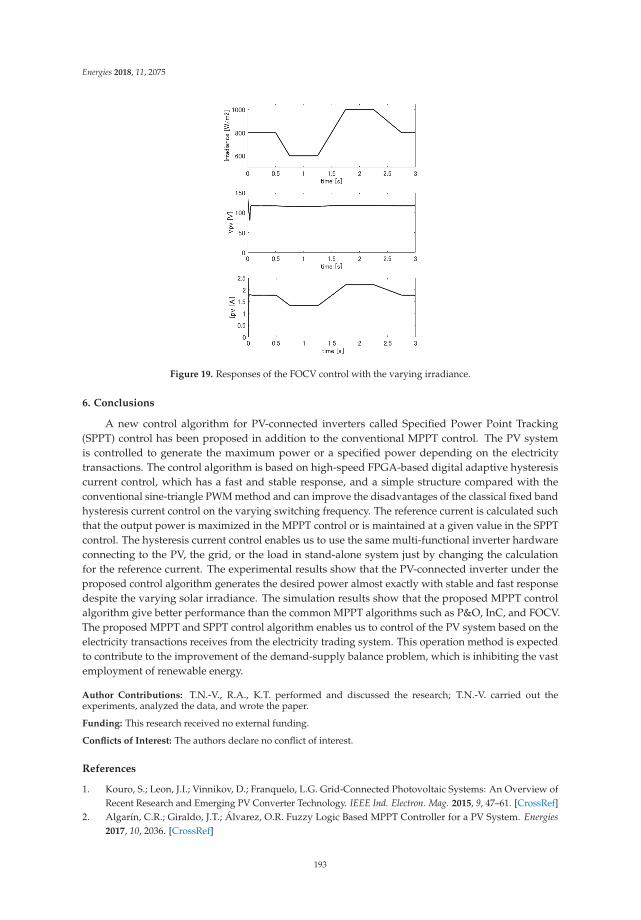
Energies 2018, 11, 2075
Figure 19. Responses of the FOCV control with the varying irradiance.
6. Conclusions
A new control algorithm for PV-connected inverters called Specified Power Point Tracking(SPPT) control has been proposed in addition to the conventional MPPT control. The PV systemis controlled to generate the maximum power or a specified power depending on the electricitytransactions. The control algorithm is based on high-speed FPGA-based digital adaptive hysteresiscurrent control, which has a fast and stable response, and a simple structure compared with theconventional sine-triangle PWM method and can improve the disadvantages of the classical fixed bandhysteresis current control on the varying switching frequency. The reference current is calculated suchthat the output power is maximized in the MPPT control or is maintained at a given value in the SPPTcontrol. The hysteresis current control enables us to use the same multi-functional inverter hardwareconnecting to the PV, the grid, or the load in stand-alone system just by changing the calculationfor the reference current. The experimental results show that the PV-connected inverter under theproposed control algorithm generates the desired power almost exactly with stable and fast responsedespite the varying solar irradiance. The simulation results show that the proposed MPPT controlalgorithm give better performance than the common MPPT algorithms such as P&O, InC, and FOCV.The proposed MPPT and SPPT control algorithm enables us to control of the PV system based on theelectricity transactions receives from the electricity trading system. This operation method is expectedto contribute to the improvement of the demand-supply balance problem, which is inhibiting the vastemployment of renewable energy.
Author Contributions: T.N.-V., R.A., K.T. performed and discussed the research; T.N.-V. carried out theexperiments, analyzed the data, and wrote the paper.
Funding: This research received no external funding.
Conflicts of Interest: The authors declare no conflict of interest.
References
1. Kouro, S.; Leon, J.I.; Vinnikov, D.; Franquelo, L.G. Grid-Connected Photovoltaic Systems: An Overview ofRecent Research and Emerging PV Converter Technology. IEEE Ind. Electron. Mag. 2015, 9, 47–61. [CrossRef]
2. Algarín, C.R.; Giraldo, J.T.; Álvarez, O.R. Fuzzy Logic Based MPPT Controller for a PV System. Energies2017, 10, 2036. [CrossRef]
193

Energies 2018, 11, 2075
3. Islam, H.; Mekhilef, S.; Shah, N.B.M.; Soon, T.K.; Seyedmahmousian, M.; Horan, B.; Stojcevski, A.Performance Evaluation of Maximum Power Point Tracking Approaches and Photovoltaic Systems. Energies2018, 11, 365. [CrossRef]
4. Khayyer, P.; Özgüner, Ü. Decentralized Control of Large-Scale Storage-Based Renewable Energy Systems.IEEE Trans. Smart Grid 2014, 5, 1300–1307. [CrossRef]
5. Marwali, M.N.; Dai, M.; Keyhani, A. Robust stability analysis of voltage and current control for distributedgeneration systems. IEEE Trans. Energy Convers. 2006, 21, 516–526. [CrossRef]
6. Yamaya, H.; Ohigashi, T.; Matsukawa, H.; Kaizuka, I.; Ikki, O. PV market in Japan and impacts of gridconstriction. In Proceedings of the IEEE 42nd Photovoltaic Specialist Conference (PVSC), New Orleans, LA,USA, 14–19 June 2015; pp. 1–6.
7. Abe, R.; Taoka, H.; McQuilkin, D. Digital Grid: Communicative Electrical Grids of the Future. IEEE Trans.Smart Grid 2011, 2, 399–410. [CrossRef]
8. Irwin, J.D. Control in Power Electronics: Selected Problems, 1st ed.; Academic Press: New York, NY, USA, 2002.9. Vázquez, G.; Rodriguez, P.; Ordoñez, R.; Kerekes, T.; Teodorescu, R. Adaptive hysteresis band current
control for transformerless single-phase PV inverters. In Proceedings of the 35th Annual Conference of IEEEIndustrial Electronics, Porto, Portugal, 3–5 November 2009; pp. 173–177.
10. Kumar, N.; Hussain, I.; Singh, B.; Panigrahi, B.K. Normal Harmonic Search Algorithm Based MPPT for SolarPV System and Integrated with Grid using Reduced Sensor Approach and PNKLMS Algorithm. IEEE Trans.Ind. Appl. 2018. [CrossRef]
11. Bhatnagar, P.; Nema, R.K. A maximum power point tracking algorithm for photovoltaic systems usingbang-bang controller. J. Renew. Sustain. Energy 2014, 6, 053126. [CrossRef]
12. Buso, S.; Malesani, L.; Mattavelli, P. Comparison of current control techniques for active filter applications.IEEE Trans. Ind. Electron. 1998, 45, 722–729. [CrossRef]
13. Attaianese, C.; Monaco, M.D.; Tomasso, G. High Performance Digital Hysteresis Control for Single SourceCascaded Inverters. IEEE Trans. Ind. Inform. 2013, 9, 620–629. [CrossRef]
14. Nguyen-Van, T.; Abe, R.; Tanaka, K. Stability of FPGA Based Emulator for Half-bridge Inverters Operated inStand-alone and Grid-connected Modes. IEEE Access 2018, 6, 3603–3610. [CrossRef]
15. Schaefer, M.; Hofmann, M.; Raab, S.; Ackva, A. FPGA Based Control of an Three Level Neutral Point ClampedInverter. In Proceedings of the Europe 2017 International Exhibition and Conference for Power Electronics,Intelligent Motion, Renewable Energy and Energy Management, Nuremberg, Germany, 16–18 May 2017;pp. 1–6.
16. Nguyen-Van, T.; Abe, R.; Tanaka, K. A Digital Hysteresis Current Control for Half-Bridge Inverters withConstrained Switching Frequency. Energies 2017, 10, 1610. [CrossRef]
17. Devaraj, D.; Sakthivel, S.; Punitha, K. Modeling of photovoltaic array and simulation of adaptive hysteresiscurrent controlled inverter for solar application. In Proceedings of the 3rd International Conference onElectronics Computer Technology, Kanyakumari, India, 8–10 April 2011; pp. 302–306.
18. Nguyen-Van, T.; Abe, R.; Tanaka, K. Digital Adaptive Hysteresis Current Control for Multi-functionalHalf-bridge Inverters. IEEE Trans. Power Electron. Under Reviewed.
19. Takagi, S. The Japanese equity market: Past and present. J. Bank. Fin. 1989, 13, 537–570. [CrossRef]20. Nedumgatt, J.J.; Jayakrishnan, K.B.; Umashankar, S.; Vijayakumar, D.; Kothari, D.P. Perturb and observe
MPPT algorithm for solar PV systems-modeling and simulation. In Proceedings of the 2011 Annual IEEEIndia Conference, Hyderabad, India, 16–18 December 2011; pp. 1–6.
21. Safari, A.; Mekhilef, S. Incremental conductance MPPT method for PV systems. In Proceedings of the24th Canadian Conference on Electrical and Computer Engineering (CCECE), Niagara Falls, ON, Canada,8–11 May 2011; pp. 345–347.
22. Ahmad, J. A fractional open circuit voltage based maximum power point tracker for photovoltaic arrays.In Proceedings of the 2nd International Conference on Software Technology and Engineering, San Juan, PR,USA, 3–5 October 2010; pp. V1-247–V1-250.
© 2018 by the authors. Licensee MDPI, Basel, Switzerland. This article is an open accessarticle distributed under the terms and conditions of the Creative Commons Attribution(CC BY) license (http://creativecommons.org/licenses/by/4.0/).
194

energies
Article
Design of Current Programmed Switching ConvertersUsing Sliding-Mode Control Theory
Javier Calvente, Abdelali El Aroudi *, Roberto Giral, Angel Cid-Pastor, Enric Vidal-Idiarte and
Luis Martínez-Salamero
Departament d’Enginyeria Electrònica, Elèctrica i Automàtica, Universitat Rovira i Virgili, 43007 Tarragona,Spain; [email protected] (J.C.); [email protected] (R.G.); [email protected] (A.C.-P.);[email protected] (E.V.-I.); [email protected] (L.M.-S.)* Correspondence: [email protected]; Tel.: +34-977-558-522
Received: 19 June 2018; Accepted: 24 July 2018; Published: 6 August 2018
Abstract: This paper presents a comprehensive approach to analyze and design the voltage andcurrent loops of switching DC-DC converters by using sliding-mode control theory. The approachis interchangeably applied to switching converters under current-programmed control with bothfixed and variable frequency modulation. An ideal sliding-mode dynamics model is then obtainedtogether with its circuit schematic representation that can be used for designing the output voltagecompensator, as well as to predict the large signal behavior such as during start-up and under largedisturbances. Simulations and experimental measurements illustrate the theoretical approach for twodifferent examples of switching converters.
Keywords: switching converters; sliding-mode control; current-mode control; hysteresis control
1. Introduction
Switched mode power converters are widely used for power processing in different applicationssuch as in portable devices, solid-state lighting drivers and technologies for renewable energyproduction. With the aim of either regulating an output variable to a desired reference or balancing thevalues of different variables, a control strategy is needed [1–3].
One of the key factors affecting the response of these systems is the control mode used.Conventional Voltage Mode Control (VMC) is a simple single feedback loop with only the outputvoltage as a control variable. However, its first generation version features poor response againstload changes [2]. Current Mode Control (CMC), also known in the literature as current-programmedcontrol [4], utilizes the inductor current as an additional control variable, which improves the transientresponse [2] at the expense of extra cost and more complex controller design. CMC of power convertersis nowadays an extensive design practice due to its intrinsic advantages and the existence of animportant number of dedicated commercial chips that facilitate its implementation. CMC offerssuperior performances over conventional VMC in both parallel operation of power converters [5]and voltage regulation of non-minimum phase switching conversion structures [6]. In the first case,current sharing among the different converters of the parallel ensemble is a relatively simple task forboth static and dynamic sharing [5], while in the second case, CMC is the best solution for an indirectoutput voltage regulation [7].
A usual way of controlling switching converters consist of imposing the duration during which aswitch is maintained closed or open. In CMC, the control strategy must impose switching instantsfor the switches by comparing the inductor current with a desired reference. Under fixed switchingfrequency operation, there are three main types of CMC strategies, namely peak CMC, valley CMCand average CMC. The peak and valley cases are dual, i.e., the internal control loop forces respectivelythe maximum and the minimum value of the current to track the reference given by the voltage control
Energies 2018, 11, 2034; doi:10.3390/en11082034 www.mdpi.com/journal/energies195

Energies 2018, 11, 2034
loop. Average control, in turn, uses the current average value in a switching cycle to track the referencesupplied by the outer loop. Although most commercial ICs of CMC are based on the peak-currentcontrol principle due to its simplicity of implementation, the existence of sub-harmonic oscillations forduty cycles bigger than 50% makes necessary the use of a compensating ramp, which constitutes themain drawback of this technique.
From the seminal paper of Deisch [8] until now, more than three decades have elapsed duringwhich a great number of researchers have contributed to building a solid representation of the dynamicbehavior of the internal loop by means of either continuous or discrete-time models, or a combinationof both. Dozens of papers were reported on this topic during the 1980s, the most representativebeing [4,9]. Some important contributions to this topic were published in the early 1990s [10–12] untilthe subject reached enough maturity to be treated as a chapter in some recent text books [2].
In the last decade, a renewed interest has emerged in variable frequency CMC strategies such asconstant ON-time CMC [13], which, at the expense of a variable switching frequency operation, offershigh efficiency under light load operation and precludes the existence of sub-harmonic oscillations inmost cases. A detailed analysis of the dynamic behavior of this control technique can be found in [14],where the main difference with respect to peak CMC is investigated in the buck converter by means ofan equivalent circuit consisting of the output load and the LC output filter, which is supplied by twocurrent sources with a resistor and a capacitor in parallel.
Variable switching frequency would also result from the insertion of a hysteretic comparatorinstead of the Pulse Width Modulator (PWM) with constant switching frequency in the case ofcurrent programming, or instead of the PWM with constant ON-time duration in the case of constantON-time CMC.
The voltage regulation of DC-DC switching converters using hysteretic control, also calledfree running or bang-bang controlled converters, goes back in time to the early years of modernpower electronics when conditions for stable limit cycles in a buck switching regulator were firstestablished [15,16].
Recently, hysteretic controllers were used in Voltage Regulator Module (VRM) applicationsthat require current control with fast response [17–19], and some commercial chips are alreadyavailable [20].
Traditionally, hysteresis-based control systems have been analyzed by means of frequency domaintechniques like the descriptive function or Tsypkin’s method [21–23].
On the other hand, Sliding-Mode Control (SMC) theory is a time-domain analytical technique thatpredicts with high precision the dynamic behavior of a Variable Structure System (VSS) [24,25]. Powerconverters can be classified as VSSs, and SMC is the natural way to regulate their outputs and deal withtheir dynamical behavior because the generation of chattering, which is intrinsic to the use of SMC,is also inherent to the nature of power converters operation. In other words, the sliding chatteringbecomes converter ripple, which is a physical manifestation of the way a converter absorbs energyfrom the input source, storing it usually in an inductor and then transferring it to an output load.
There are two main results in the SMC theory applicable to switching converters. The first oneis the fact that for single input systems, a suitable Lyapunov function V(x) = 1
2 σ2(x) exists, whereσ(x) is the switching function. If the switching feedback gains are chosen so that V = σσ < 0 in thedomain of attraction, then the state trajectory converges to the surface σ = 0 and is restricted to itfor all subsequent time. The second one provides the ideal sliding-mode dynamics on the switchingsurface. In this case, Filippov’s method [26] and the equivalent control approach yield identical slidingequations when applied to systems that are linear with respect to the control input [27].
These techniques have been used in [28] considering feedback switching conditions of the formσ = xj − K = 0, expressed in terms of a suitable state variable xj that is desired to be regulatedat a suitable level K. They have been employed in output voltage regulation of DC-DC switchingconverters in early works such as in [29–33] and also in some recent contributions to this field suchas [34–38]. In [39], SMC theory has been applied to control paralleled inverters of the buck type and
196

Energies 2018, 11, 2034
in [40,41]. In [42,43], it has been used in the analysis of interleaved boost converters with hystereticcontrol in a ring configuration. In [44], sliding mode control theory was used to synthesize canonicalelements for power processing such as in impedance matching in PV systems and in power factorcorrection. These techniques were also combined with other robust control methods such as fuzzylogic [45] and H∞ [46] for designing these systems.
In the field of switching converters, two different kinds of studies using SMC theory exist inthe literature. The one that uses this theory to design the switching decision and to analyze theideal sliding dynamics and that ultimately uses a hysteretic loop to limit the switching frequency [7].Other works use this theory to derive the equivalent control, and this is used finally to implementa PWM control [32,33]. Actually, with this strategy, all the advantages of SMC are not maintained.Small-signal analysis of sliding mode-controlled switching converters, based on hysteresis modulation,were reported in [47], where Bode plot and root locus analysis were used to reveal the effect of theparameters on the system behavior.
In this paper, on the basis of the equivalent control method, a procedure to design the control loopof DC-DC power converters operating in CMC with both variable and fixed frequency modulationstrategies is proposed. The controller employs one switching function of the form σ = ir − iL, where iLis a converter current and ir is the output of an outer compensating network that processes the outputvoltage error. The paper comprehensively explains the dynamics of switching converters regardless oftheir modulation strategies. In particular, it will be demonstrated that under sliding mode conditions,the behavior of the switching converters under all the control strategies tend to the same dynamicsknown as the ideal sliding mode dynamics when the switching period tends to zero. The advantages,limitations and drawbacks of each strategy in a practical implementation are also discussed. It is worthnoting that in this paper, it is not pretended to control switching converters using sliding mode controlthat ultimately end-up in a variable frequency implementation of the modulator, but the dynamics ofthese systems under both constant and variable frequency modulation schemes are explained by usingsliding mode control theory, while providing circuit equivalent models that can be used for designingthese systems by utilizing conventional frequency-domain methods.
The rest of the paper is organized as follows. The description of the behavior ofcurrent-programmed DC-DC converters is presented in Section 2 in the light of sliding mode controltheory. A small-signal model is used to design the voltage loop by means of linear techniques in thefrequency domain, as well as simulation results on two practical examples of switching converters inSection 3. The examples consist of a boost converter under fixed and variable frequency operationand a buck converter with current-mode hysteretic control and high bandwidth voltage regulation.An experimental validation of the results corresponding to the buck converter is given in Section 4.The application of the approach to single-loop ripple-based voltage mode control is discussed inSection 5. Finally, the conclusions of this work are summarized in Section 6.
2. Sliding-Mode Control of Switching Converters Based on Two-Loop Current Mode Control
In CCM operation, a switching converter is described by a piecewise linear state-space modelthat can be written in the following form:
x(t) =
{A1x(t) + B1w(t) u = 1
A2x(t) + B2w(t) u = 0(1)
where u is a binary signal that can take the values of zero or one. It is assumed that the switchingis instantaneous. x(t) is the vector of state variables, and w(t) is the vector of independent sources.Equation (1) can be expressed as follows:
x(t) = [A1x(t) + B1w(t)]u + [A2x(t) + B2w(t)](1 − u). (2)
197

Energies 2018, 11, 2034
Conventionally, the output variable y is a linear combination of the state variables. However, theapproach is also applicable to the case with a nonlinear switching surface as in high-order boundarycontrol schemes [48]. Hereinafter, let the linear combination of state variables y(t) = cᵀx(t) be theoutput to be controlled, where c is a suitable vector to select the output y(t) from the state variablesx(t). The derivative of the controlled output y(t) is of the form:
y = (m1(x, t) + m2(x, t))u − m2(x, t) (3)
where m1(x, t) and m2(x, t) are the rising and falling slopes of the signal y(t) that can be expressedas follows:
m1(x, t) = cᵀ[A1x(t) + B1w(t)] (4)
m2(x, t) = −cᵀ[A2x(t) + B2w(t)]. (5)
Our interest is in situations where y can be controlled in sliding mode, so that it follows thereference smooth function r(t) (continuous and differentiable). The switching function can be expressedas follows:
σ(x, t) = r(t)− y (6)
along with the following control law (Figure 1):
u =
{1 if σ > 0
0 if σ < 0.(7)
Converter
DC-DC
σ
u
σ
w
y
r +
−
1
Figure 1. Simplified diagram of a DC-DC converter under Current Mode Control (CMC).
For the existence of a sliding regime on the time-variant surface Σ defined by {x|σ(x, t) = 0}, thesliding condition σσ < 0 must be fulfilled, which is equivalent to:
σσ>0 < 0 (8)
σσ<0 > 0. (9)
According to (3), the derivative σ of the switching function σ can be expressed as follows:
σ(x, t) = r(t)− ((m1(x, t) + m2(x, t))u − m2(x, t)). (10)
By using (7), the sliding conditions (8) and (9) are:
σσ>0 = r(t)− m1(x, t) < 0 (11)
σσ<0 = r(t) + m2(x, t) > 0 (12)
or in compact form:− m2(x, t) < r(t) < m1(x, t) (13)
198

Energies 2018, 11, 2034
Equation (13) implies that the rate of change of the signal r must be lower than the absolute valuesof the slopes m1(x, t) and m2(x, t) of the control signal y. This is easily met if the bandwidth of theouter loop is much lower than the switching frequency, as is the case in any practical design. Therefore,under this condition, the trajectory of the system (2) with the control decision (7) will reach the slidingsurface Σ in finite time and stay on it in sliding mode [27].
To maintain the trajectory in this regime, it is necessary to switch continuously at infinitefrequency in the ideal case. This is not an acceptable behavior for DC-DC switching converters,which are designed to operate in a specific switching frequency range. Operating at higher frequencies,the converter efficiency decreases, and the instantaneous switching model (2) is no longer valid.This problem is solved by introducing a boundary layer around Σ and replacing the switchingdecision (7) by:
u =
{1 if σ > +Δ
0 if σ < −Δ(14)
where Δ > 0. With this control law, the switching frequency in sliding-mode will be finite. In turn, thesliding motion will not occur strictly on the surface Σ, but in a neighborhood that meets the condition|σ| ≤ Δ. This means that a certain switching ripple will exist in the output to be controlled and otherstate variables as a penalty of a bounded switching frequency. This is a natural way of exchanging theenergy between the reactive components of the converter.
The ideal sliding-mode dynamics is the behavior of the system (2) in the sliding regime witha control of the form (14) and in the limit case when Δ tends to zero. In order to find the idealsliding-mode equations, the equivalent control method [27] is used. A necessary condition for theexistence of an equivalent control ueq and therefore to apply this method is that u appears explicitly onthe right side of (10), i.e.,
m1(x, t) + m2(x, t) �= 0. (15)
Remark 1. The previous condition is largely related to the fact that the relative degree of the converter u-to-σloop is equal to one. The fast response characterizing CMC is due to this fact. The relative degree of a switchedsystem is the number of differentiations one needs to perform on the switching function σ to make the inputexplicitly appear in its derivative, i.e., the minimum n that satisfies the following equation:
∂
∂udnσ(x, t)
dtn �= 0 (16)
Remark 2. At high frequencies, if the relative degree is one, the system behaves as an integrator, which convertsthe square-wave signal u to a triangular signal σ.
Remark 3. It should be noted that apart from the widely-used hysteresis comparison, any other strategy to limitthe switching frequency can be used without invading the sliding motion. Other possible strategies to limit theswitching frequency are time delays, filtering and clocked switching.
In all the cases, if (15) is accomplished, the equation σ = 0 can be solved with respect to u toobtain the equivalent leading to the following expression:
ueq(x, t) =r(t) + m2(x, t)
m1(x, t) + m2(x, t). (17)
The equivalent control caused by any modulation scheme such as the variable frequency hystereticmodulation and constant switching-frequency peak/valley control methods are the same since theequivalent control corresponds to the ideal sliding dynamics with theoretically infinite switchingfrequency or to the averaged dynamics of the converter under the switching constraints’ imposedprevious modulation strategies. The order of the averaged dynamics or the ideal sliding dynamics
199

Energies 2018, 11, 2034
is reduced due to the relationship imposed between the state variables by the switching constraint.From (17), if m1(x, t) + m2(x, t) �= 0, the equivalent control ueq will exist, and according to (13), itsvalue will be comprised between zero and one. The ideal sliding-mode dynamics is obtained bysubstituting u in (2) by ueq given by (17) and introducing the order reduction due to the constraintσ = 0. In DC-DC converters, the ideal sliding-mode dynamics should have an asymptotically-stableequilibrium point.
Note that u is undetermined when |σ| ≤ Δ; therefore, there is a plurality of controls compatiblewith (14) [49]. For example, in the hysteretic control (Figure 2a), from the moment that thecondition |σ| < Δ is fulfilled, a switching occurs whenever |σ| = Δ. Other examples areconstant-switching-frequency controls [50], such as peak (Figure 2b) and valley (Figure 2c) current,in which time-driven switching occurs periodically, while event-driven switching occurs whenever|σ| = Δ. DC-DC switching converters typically have a periodic behavior in steady-state with twoswitchings per period. In the limit as Δ tends to zero, the periodic solution tends to the equilibriumpoint of the ideal sliding-mode dynamics.
(a) (b) (c)
Figure 2. Evolution of the controlled output and its reference in sliding-mode for three types of controlimplementing (14). (a) Hysteresis control. (b) Peak control at constant switching frequency. (c) Valleycontrol at constant switching frequency.
The DC-DC converter with sliding-mode current control is a system, the control input of which isthe current reference r(t). To regulate the output voltage of the converter, a second slower control loopthat dictates r(t) from the voltage error must be added. The examples considered in the next sectionshow how to design such a controller using the ideal sliding-mode dynamics model.
3. Practical Examples
3.1. Example 1: A Boost Converter under Fixed and Variable Frequency CMC
Let us consider the boost converter depicted in Figure 3a. The state variables are the inductorcurrent iL and the capacitor voltage vo. The independent sources correspond to the input voltage vg(t)and the current id(t), which models load variations. For this example, (2) becomes as follows:
diLdt
=vg(t)
L− vo(1 − u)
L(18)
dvo
dt=
iL(1 − u)C
− vo
RC+
id(t)C
. (19)
200

Energies 2018, 11, 2034
(a)
(b)
Figure 3. Schematic circuit diagram of (a) a Boost converter and (b) its ideal sliding-mode dynamicsmodel under CMC.
Let ir(t) be the current reference. Using the switching function σ = ir(t)− iL together with thecontrol law (7), the sliding condition (13) leads to the following inequality:
vg(t)− vo
L<
dir(t)dt
<vg(t)
L. (20)
When ir(t) is constant, (20) becomes 0 < vg(t) < vo. In this case, starting from zero initialconditions, as soon as vo reaches vg(t), the sliding condition is fulfilled, and after a finite time, thesystem trajectory is constrained in the sliding manifold defined by the constraint ir − iL = 0. Whenir(t) is time varying or state-dependent, according to (17), the equivalent control for this examplebecomes as follows:
ueq =L dir(t)
dt + vo − vg(t)vo
. (21)
After substituting u by ueq in (18) and (19) and using σ = 0 (iL = ir(t)), the system order isreduced, and the following ideal sliding-mode dynamics is obtained:
iL = ir(t) (22)
dvo
dt=
ir(t)[vg(t)− L dir(t)
dt
]Cvo
− vo
RC+
id(t)C
. (23)
Expression (23) also establishes a power balance between the input port and the output port of theboost converter provided that iL = ir. These equations can be represented by means of an equivalentcircuit using a power source [51] to model the nonlinear term (Figure 3b). The ideal sliding-modedynamics (23), with the following constant inputs:
ir(t) = Ir, vg(t) = Vg, id(t) = 0, (24)
has the following equilibrium point:
vo∗ = Vr =
√IrRVg (25)
which is asymptotically stable, as can be demonstrated by means of the Lyapunov function V(vo) =
(1/2)(vo − Vr)2 [52].Note that vo
∗ depends on both the line voltage and the supplied load resistance. That is why aregulation of the voltage vo is needed when disturbances in id(t) and vg(t) take place. The regulationcan be accomplished by adding another external voltage loop and making the current reference ir bethe output of this loop.
201
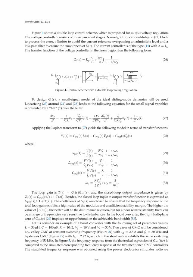
Energies 2018, 11, 2034
Figure 4 shows a double-loop control scheme, which is proposed for output voltage regulation.The voltage controller consists of three cascaded stages. Namely, a Proportional-Integral (PI) blockto process the error, a limiter to avoid the current reference overpassing an admissible level and alow-pass filter to ensure the smoothness of ir(t). The current controller is of the type (14) with Δ = IΔ.The transfer function of the voltage controller in the linear region has the following form:
Gc(s) = Kp
(1 +
ωIs
) 11 + s/ωh
. (26)
Figure 4. Control scheme with a double loop voltage regulation.
To design Gc(s), a small-signal model of the ideal sliding-mode dynamics will be used.Linearizing (23) around (24) and (25) leads to the following equation for the small-signal variablesrepresented by a “hat” (∧) over the letter:
dvo
dt= − 2
CRvo +
Vg
CVrir(t)− LVr
CRVg
dir(t)dt
+Vr
CRVgvg(t) +
1C
id(t). (27)
Applying the Laplace transform to (27) yields the following model in terms of transfer functions:
Vo(s) = Gvir(s) Ir(s) + Gvvg(s)Vg(s) + Gvid(s) Id(s) (28)
where:
Gvir(s) =V(s)Ir(s)
=RVg
2Vr
1 − s/ωz
1 + s/ωp(29)
Gvvg(s) =VV(s)VgV(s)
=Vr
2Vg
11 + s/ωp
(30)
Gvid(s) =VV(s)IdV(s)
=R2
11 + s/ωp
(31)
ωz =RVg
2
LVr2 ; ωp =
2RC
. (32)
The loop gain is T(s) = Gc(s)Gvir(s), and the closed-loop output impedance is given byZo(s) = Gvid(s)/(1 + T(s)). Besides, the closed-loop input to output transfer function is expressed asGvvg(s)/(1 + T(s)). The coefficients of Gc(s) are chosen to ensure that the frequency response of thetotal loop gain exhibits a high value of the modulus and a sufficient stability margin. The higher thevalue of |T(jω)|, the better will be the disturbance rejection, but for a poor relative stability, there canbe a range of frequencies very sensitive to disturbances. In the boost converter, the right half-planezero of Gvir(s) (29) imposes an upper bound on the achievable bandwidth [53].
Let us consider an example of a boost converter with the following set of parameter values:L = 30μH, C = 100μF, R = 10 Ω, Vg = 10 V and Vr = 30 V. Two cases of CMC will be considered,i.e., valley CMC at constant switching frequency (Figure 2c) with IΔ = 2.5 A and fs = 50 kHz andhysteresis CMC (Figure 2a) with IΔ = 2.22 A, which in the steady-state exhibits the same switchingfrequency of 50 kHz. In Figure 5, the frequency response from the theoretical expression of Gvir(jω) iscompared to the simulated corresponding frequency response of the two mentioned CMC controllers.The simulated frequency response was obtained using the power electronics simulator software
202

Energies 2018, 11, 2034
PSIM c©, which has a specific feature to get different types of frequency responses, basically input,output and closed loop gains. The AC sweep module manages the frequency sweep (amplitude, initialfrequency, final frequency, number of points) as in a frequency response analyzer.
-30-25-20-15-10
-505
10
Gai
n (d
B)
constant frequencyhysteretic
ideal sliding
-180
-135
-90
-45
0
0.1 1 10
Pha
se (d
eg)
Frequency (kHz)
Figure 5. Theoretical and simulated frequency responses from the current reference to output voltagein a boost converter.
A good agreement among the three frequency responses can be clearly observed at low frequenciesuntil approximately 5 kHz ( fs/10). The right half-plane zero is located at 6 kHz. Therefore, the controlbandwidth will be placed within the region wherein the three responses almost coincide, and thedesign based on the ideal sliding-mode dynamics model will be valid for the other two cases.
It can be verified in a Bode diagram of T(jω) that choosing ωh = ωz = 37 krad/s, ωI = 1.2 krad/sand Kp = 3.7 A/V, the crossover frequency at 0 dB is fc = 2 kHz, the phase margin is 57◦ and the gainmargin is 10 dB at 6 kHz. The Bode diagrams obtained by simulation for the two cases with finiteswitching frequency show similar results to the ideal case, not only in the loop gain (Figure 6), but alsoin the output impedance (Figure 7). The closed-loop converter response to a step change in id(t) isshown in Figure 8, where the simulated ideal sliding-mode dynamics based on the circuit of Figure3b is compared to the two previous cases of finite switching frequency. The concordance of the threeresponses is in agreement with the frequency results depicted in Figure 7.
-30
-20
-10
0
10
20
Gai
n (d
B)
constant frequencyhysteretic
ideal sliding
-225
-180
-135
-90
1 10
Pha
se (d
eg)
Frequency (kHz)
Figure 6. Theoretical and simulated loop gain Bode plots in a boost converter.
203

Energies 2018, 11, 2034
-30
-25
-20
-15
-10
-5
0
5
10
0.1 1 10
Gai
n (d
B)
Frequency (kHz)
constant frequencyhysteretic
ideal sliding
Figure 7. Theoretical and simulated closed-loop output impedance in a boost converter.
Figure 8. Response of the state variables vo and iL of the boost converter in closed-loop to a step changeof 1.5 A in id(t). Comparison of the ideal sliding-mode dynamics with that corresponding to twodifferent types of control methods at finite switching frequency.
Let us analyze now the time-domain closed-loop converter response from zero initial conditionsand without the presence of any disturbance. Figure 9 depicts the case of valley CMC at constantswitching frequency. The case of hysteresis control is very similar. It is worth mentioning that theinductor current must be limited in the transient-state. The current control ensures that the inequality|ir(t) − iL| ≤ IΔ is satisfied in sliding mode. The limiter of the voltage controller guarantees thatir(t) < IM, so that, in the sliding regime, the inductor current satisfies at any instant the inequalityiL < Imax where Imax = IM + IΔ. In this example, the inductor current must reach at least the valueVr
2/(RVg) = 9 A, which corresponds to the equilibrium point. The maximum current was fixed toImax = 15 A, so that IM = 12.78 A in the case of hysteresis CMC and IM = 12.5 A in the case of valley
204
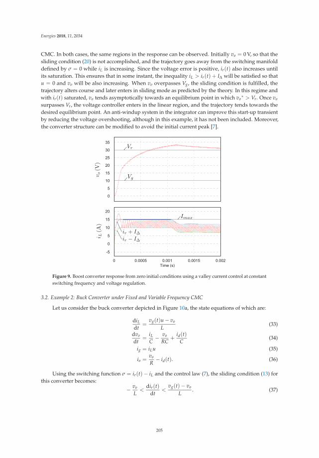
Energies 2018, 11, 2034
CMC. In both cases, the same regions in the response can be observed. Initially vo = 0 V, so that thesliding condition (20) is not accomplished, and the trajectory goes away from the switching manifolddefined by σ = 0 while iL is increasing. Since the voltage error is positive, ir(t) also increases untilits saturation. This ensures that in some instant, the inequality iL > ir(t) + IΔ will be satisfied so thatu = 0 and vo will be also increasing. When vo overpasses Vg, the sliding condition is fulfilled, thetrajectory alters course and later enters in sliding mode as predicted by the theory. In this regime andwith ir(t) saturated, vo tends asymptotically towards an equilibrium point in which vo
∗ > Vr. Once vo
surpasses Vr, the voltage controller enters in the linear region, and the trajectory tends towards thedesired equilibrium point. An anti-windup system in the integrator can improve this start-up transientby reducing the voltage overshooting, although in this example, it has not been included. Moreover,the converter structure can be modified to avoid the initial current peak [7].
Figure 9. Boost converter response from zero initial conditions using a valley current control at constantswitching frequency and voltage regulation.
3.2. Example 2: Buck Converter under Fixed and Variable Frequency CMC
Let us consider the buck converter depicted in Figure 10a, the state equations of which are:
diLdt
=vg(t)u − vo
L(33)
dvo
dt=
iLC
− vo
RC+
id(t)C
(34)
ig = iLu (35)
io =vo
R− id(t). (36)
Using the switching function σ = ir(t)− iL and the control law (7), the sliding condition (13) forthis converter becomes:
− vo
L<
dir(t)dt
<vg(t)− vo
L. (37)
205

Energies 2018, 11, 2034
(a)
(b)
Figure 10. Schematic circuit diagram of (a) a Buck converter and (b) its ideal sliding-mode dynamicsmodel under CMC.
Inequalities (37) are fulfilled for ir(t) constant provided that 0 < vo < vg(t), which are the normaloperating conditions of a buck converter. For this converter, the sliding motion is guaranteed from thestart-up even with zero initial conditions. The ideal sliding-mode dynamics, obtained by means of theequivalent control method, is the following:
iL = ir(t) (38)
dvo
dt=
ir(t)C
− vo
RC+
id(t)C
(39)
ig =ir(t)
[vo + L dir(t)
dt
]vg(t)
(40)
io =vo
R− id(t) (41)
and it can be represented by the circuit illustrated in Figure 10b. The equilibrium point for constantinputs (24), vo
∗ = Vr = IrR is asymptotically stable. Linearizing the ideal sliding-mode dynamicsaround the equilibrium point yields a small-signal model, which is used to design the voltage controlleror to analyze the system stability when an input filter is added.
The voltage loop consists of the current reference Ir(s) to the output voltage Vo(s) transfer function,Gvir(s), i.e.,
Gvir(s) =R
1 + sRC, (42)
and the same controller (26) employed in the previous example. In this converter, Gvir(s) is a minimumphase transfer function. In the ideal case, the loop gain and the control bandwidth can be madeboundlessly high without affecting the system stability. For instance, if a particular value of ωc ischosen and the coefficients of Gc(s) are calculated according to the following criteria:
ωc � 1/(RC); Kp = Cωc; ωI = ωc/4; ωh = 4ωc, (43)
then ωc will be the crossover frequency at 0 dB of the loop gain, the phase margin will be higher than60◦ and the gain margin will be infinite.
However, the sliding condition (37) is a constraint that must be respected. For example, let usassume that the system is in equilibrium and that a step disturbance of amplitude Id in current id(t)is applied at t = 0. If the controller has been designed according to (43), the slope of ir(t) during thetransient-state will be maximal at t = 0.55/ωc approximately, reaching a value of:
dir(t)dt
∣∣∣∣t=0.55/ωc
≈ −0.8 ωc Id (44)
206
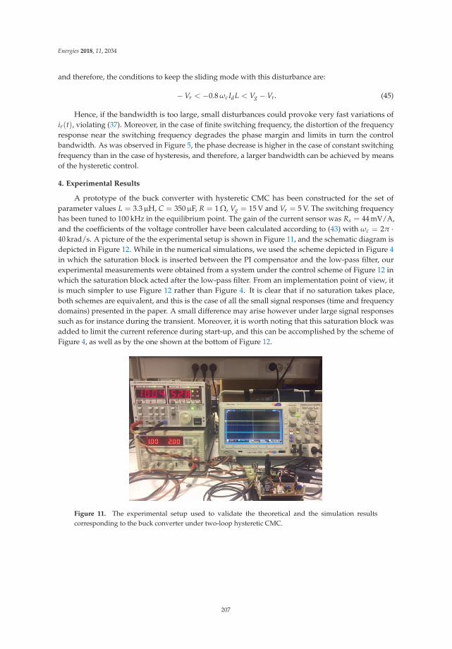
Energies 2018, 11, 2034
and therefore, the conditions to keep the sliding mode with this disturbance are:
− Vr < −0.8 ωc IdL < Vg − Vr. (45)
Hence, if the bandwidth is too large, small disturbances could provoke very fast variations ofir(t), violating (37). Moreover, in the case of finite switching frequency, the distortion of the frequencyresponse near the switching frequency degrades the phase margin and limits in turn the controlbandwidth. As was observed in Figure 5, the phase decrease is higher in the case of constant switchingfrequency than in the case of hysteresis, and therefore, a larger bandwidth can be achieved by meansof the hysteretic control.
4. Experimental Results
A prototype of the buck converter with hysteretic CMC has been constructed for the set ofparameter values L = 3.3μH, C = 350μF, R = 1 Ω, Vg = 15 V and Vr = 5 V. The switching frequencyhas been tuned to 100 kHz in the equilibrium point. The gain of the current sensor was Rs = 44 mV/A,and the coefficients of the voltage controller have been calculated according to (43) with ωc = 2π ·40 krad/s. A picture of the the experimental setup is shown in Figure 11, and the schematic diagram isdepicted in Figure 12. While in the numerical simulations, we used the scheme depicted in Figure 4in which the saturation block is inserted between the PI compensator and the low-pass filter, ourexperimental measurements were obtained from a system under the control scheme of Figure 12 inwhich the saturation block acted after the low-pass filter. From an implementation point of view, itis much simpler to use Figure 12 rather than Figure 4. It is clear that if no saturation takes place,both schemes are equivalent, and this is the case of all the small signal responses (time and frequencydomains) presented in the paper. A small difference may arise however under large signal responsessuch as for instance during the transient. Moreover, it is worth noting that this saturation block wasadded to limit the current reference during start-up, and this can be accomplished by the scheme ofFigure 4, as well as by the one shown at the bottom of Figure 12.
Figure 11. The experimental setup used to validate the theoretical and the simulation resultscorresponding to the buck converter under two-loop hysteretic CMC.
207

Energies 2018, 11, 2034
R
SQ
Figure 12. Schematic circuit diagram of the buck converter with hysteretic CMC and output voltage regulation.
The frequency response of the system being the input vir and the output vo, in the case of an openvoltage loop, has been obtained experimentally, and it is depicted in Figure 13 with the Bode diagramof Gvir(s)/Rs. The experimental frequency response in Figure 13 was obtained by using the Venable3120 FRA. In this particular case, the analog control circuit is the one in Figure 12; with the voltageloop opened, the FRA provides the voltage reference vir, which is composed of a sinusoidal variablefrequency reference and a DC component to polarize the system around the desired steady-stateoperating point. Closed loop gains in Figure 14 were obtained in closed loop using also the Venable3120 FRA; in this case, a wideband medium frequency injection transformer model Bode Box 200-002and two probes to obtain differential measurements are connected to the R4-100 Ω resistor.
Figure 13. Theoretical and experimental frequency responses from current reference vir to outputvoltage vo in the buck converter of Figure 12.
208

Energies 2018, 11, 2034
Figure 14. Theoretical, simulated and experimental Bode diagrams of the voltage loop gain in thebuck converter.
It can be observed that the model based on the ideal sliding-mode dynamics is valid up toalmost one half of the switching frequency. The loop gain has been also measured, and it is shownin Figure 14 with the Bode diagram of Gc(s)Gvir(s)/Rs and with the frequency response obtained bynumerical simulation of the switched model. It can be observed that the experimental closed-loopbandwidth (ωc) hardly deviated from the theoretical one, but the phase margin was reduced from60◦–45◦ due to non-ideal high frequency effects. To match the simulation with the experimental resultsat high frequency, it was necessary to include in the simulation a dynamic model of the current sensor(a low-pass second-order filter with a cutoff frequency of 450 kHz and a damping ratio of 0.7) and puredelays for both control logic circuits and switching elements (300 ns in total). Figures 15 and 16 showrespectively the experimental and simulated response of the converter to a load variation of step typethat satisfies the condition (45) by including these non-ideal effects. Note that signal vσ representingthe switching function is not totally within the hysteresis band due to propagation delays and to thedynamics of the current sensor.
Figure 15. Experimental output voltage response to a load current step in the buck converter from10 A–5 A.
209
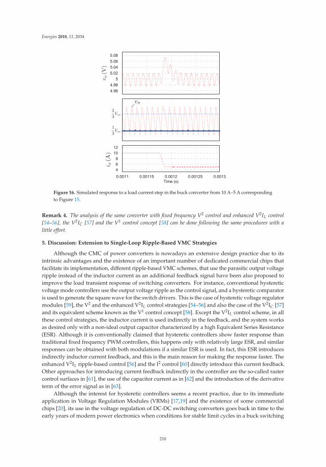
Energies 2018, 11, 2034
4.964.98
55.025.045.065.08
0.0011 0.00115 0.0012 0.00125 0.0013Time (s)
468
1012
Figure 16. Simulated response to a load current step in the buck converter from 10 A–5 A correspondingto Figure 15.
Remark 4. The analysis of the same converter with fixed frequency V2 control and enhanced V2IL control[54–56], the V2IC [57] and the V1 control concept [58] can be done following the same procedures with alittle effort.
5. Discussion: Extension to Single-Loop Ripple-Based VMC Strategies
Although the CMC of power converters is nowadays an extensive design practice due to itsintrinsic advantages and the existence of an important number of dedicated commercial chips thatfacilitate its implementation, different ripple-based VMC schemes, that use the parasitic output voltageripple instead of the inductor current as an additional feedback signal have been also proposed toimprove the load transient response of switching converters. For instance, conventional hystereticvoltage mode controllers use the output voltage ripple as the control signal, and a hysteretic comparatoris used to generate the square wave for the switch drivers. This is the case of hysteretic voltage regulatormodules [59], the V2 and the enhanced V2IL control strategies [54–56] and also the case of the V2IC [57]and its equivalent scheme known as the V1 control concept [58]. Except the V2IL control scheme, in allthese control strategies, the inductor current is used indirectly in the feedback, and the system worksas desired only with a non-ideal output capacitor characterized by a high Equivalent Series Resistance(ESR). Although it is conventionally claimed that hysteretic controllers show faster response thantraditional fixed frequency PWM controllers, this happens only with relatively large ESR, and similarresponses can be obtained with both modulations if a similar ESR is used. In fact, this ESR introducesindirectly inductor current feedback, and this is the main reason for making the response faster. Theenhanced V2IL ripple-based control [56] and the I2 control [60] directly introduce this current feedback.Other approaches for introducing current feedback indirectly in the controller are the so-called rastercontrol surfaces in [61], the use of the capacitor current as in [62] and the introduction of the derivativeterm of the error signal as in [63].
Although the interest for hysteretic controllers seems a recent practice, due to its immediateapplication in Voltage Regulation Modules (VRMs) [17,19] and the existence of some commercialchips [20], its use in the voltage regulation of DC-DC switching converters goes back in time to theearly years of modern power electronics when conditions for stable limit cycles in a buck switching
210

Energies 2018, 11, 2034
regulator were first established [15,16]. Other control schemes that can be placed into the same categoryare boundary control [48,64] and synergetic control [65] strategies.
All the previous strategies can be implemented either with the variable frequency modulationstrategy or a fixed frequency modulation scheme. Variable frequency would result from the use of ahysteretic comparator. It would be also the case for constant ON-time and constant OFF-time strategies.Fixed frequency operation will result from peak CMC (or VMC), valley CMC (or VMC) and averageCMC (or VMC) using a latch and a clock signal in the modulator. The same theory can be appliedinterchangeably to all the previous strategies.
6. Conclusions
A two-loop control design technique for DC-DC switching converters has been presented.The double loop consists of an inner current loop in sliding-mode and an outer voltage regulation loopthat includes a limiter of the current reference.
When the sliding condition is accomplished, the converter enters in sliding mode after a finite time,and the current tracks its reference. The ideal sliding-mode dynamics describes the system behavior,and a small-signal model around the equilibrium point is used to design the voltage regulation loopby means of the frequency response method.
It has to be pointed out that sliding-mode control theory does not specify the nature of theswitching law when |σ| < Δ. Hence, hysteresis control and constant switching frequency control havebeen compared for a boost converter. The frequency response in both cases almost coincides with thetheoretical prediction of the ideal sliding-mode dynamics at low frequencies, the hysteresis controlresponse being much more similar to the ideal case near the switching frequency region. However, inthe example reported here for the boost converter, the most limiting factor in the regulation bandwidthis the right half-plane zero, and for that reason, the closed-loop response in both cases is very similarto the ideal one.
In the example of the buck converter, an expression of the sliding condition in terms of bothvoltage regulation bandwidth and load disturbance amplitude has been derived. A bandwidth of thevoltage loop near one half the switching frequency has been obtained using a hysteretic current modecontroller. In the same example, it has been found that the actual dynamic behavior of the currentsensor and the delay of both switching and control logic circuits can have an appreciable influenceupon the phase margin of the voltage loop.
Author Contributions: Conceptualization, J.C., A.E.A. and L.M.-S; All the authors contributed equally to theother parts of the work.
Funding: This work has been sponsored by the Spanish Agencia Estatal de Investigación (AEI) and theFondo Europeo de Desarrollo Regional (FEDER) under Grants DPI2017-84572-C2-1-R and DPI2016-80491-R(AEI/FEDER, UE).
Conflicts of Interest: The authors declare no conflict of interest.
References
1. El Fadil, H.; Giri, F. Robust nonlinear adaptive control of multiphase synchronous buck power converters.Control Eng. Pract. 2009, 17, 1245–1254. [CrossRef]
2. Erickson, R.W.; Maksimovic, D. Fundamentals of Power Electronics; Kluwer: Alphen aan den Rijn, TheNetherlands, 2001.
3. Yfoulis, C.; Giaouris, D.; Stergiopoulos, F.; Ziogou, C.; Voutetakis, S.; Papadopoulou, S. Robust constrainedstabilization of boost DC-DC converters through bifurcation analysis. Control Eng. Pract. 2015, 35, 67–82.[CrossRef]
4. Middlebrook, R. Topics in multiple-loop regulators and current-mode programming. IEEE Trans.Power Electron. 1987, PE-2, 109–124. [CrossRef]
5. Ramos, R.; Biel, D.; Fossas, E.; Gri, R. Sliding mode controlled multiphase buck converter with interleavingand current equalization. Control Eng. Pract. 2013, 21, 737–746. [CrossRef]
211

Energies 2018, 11, 2034
6. Liu, Y.-F.; Sen, P.C. Large-signal modeling of hysteretic current-programmed converters. IEEE Trans.Power Electron. 1996, 11, 423–430.
7. Martinez-Salamero, L.; Garcia, G.; Orellana, M.; Lahore, C.; Estibals, B. Start-up control and voltageregulation in a boost converter under sliding-mode operation. IEEE Trans. Ind. Electron. 2013, 60, 4637–4646.[CrossRef]
8. Deisch, C.W. Simple switching control method changes power converter into a current source. In Proceedingsof the PESC’78, Power Electronics Specialists Conference, Syracuse, NY, USA, 13–15 June 1978; pp. 300–306.
9. Redl, R.; Sokal, N. Current-mode control, five different types, used with the three basic classes of powerconverters-small-signal ac and large-signal dc characterization, stability requirements, and implementationof practical circuits. In Proceedings of the PESC’85 Record, 16th Annual IEEE, Toulouse, France, 24–28 June1985; pp. 771–785.
10. Perreault, D.; Verghese, G.C. Time-varying effects and averaging issues in models for current-mode control.IEEE Trans. Power Electron. 1997, 12, 453–461. [CrossRef]
11. Ridley, R. A new, continuous-time model for current-mode contro. IEEE Trans. Power Electron. 1991, 6,271–280. [CrossRef]
12. Tan, F.; Middlebrook, R. A unified model for current-programmed converters. IEEE Trans. Power Electron.1995, 10, 397–408. [CrossRef]
13. Yan, Y.; Lee, F.; Mattavelli, P. Comparison of small signal characteristics in current mode control schemes forpoint-of-load buck converter applications. IEEE Trans. Power Electron. 2013, 28, 3405–3414. [CrossRef]
14. Li, J.; Lee, F. New modeling approach and equivalent circuit representation for current-mode control.IEEE Trans. Power Electron. 2010, 25, 1218–1230.
15. Babaa, I.; Wilson, T.; Yu, Y. Analytic solutions of limit cycles in a feedback-regulated converter system withhysteresis. IEEE Trans. Autom. Control 1968, 13, 524–531. [CrossRef]
16. Schweitzer, B.P.; Rosenstein, A.B. Free Running-Switching Mode Power Regulator: Analysis and Design.IEEE Trans. Aerosp. 1964, 2, 1171–1180. [CrossRef]
17. Huerta, S.; Soto, A.; Alou, P.; Oliver, J.; Garcia, O.; Cobos, J. Advanced control for very fast DC-DC convertersbased on hysteresis of the Cout current. IEEE Trans. Circuits Syst. I Regular Pap. 2013, 60, 1052–1061.[CrossRef]
18. Ki, W.-H.; Lai, K.-M.; Zhan, C. Charge balance analysis and state transition analysis of hysteretic voltagemode switching converters. IEEE Trans. Circuits Power Syst. 2011, 58, 1142–1152. [CrossRef]
19. Wen, Y.; Trescases, O. Analysis and comparison of frequency stabilization loops in self-oscillating currentmode dc-dc converters. IEEE Trans. Power Electron. 2013, 28, 4753–4766. [CrossRef]
20. Castilla, M.; Guerrero, J.; Matas, J.; Miret, J.; Sosa, J. Comparative study of hysteretic controllers forsingle-phase voltage regulators. IET Power Electron. 2008, 1, 132–143. [CrossRef]
21. Atre, S.R.; Lele, V.P. Analytic application of Tsypkin’s method relay with hysteresis and dead zone. Proc. Inst.Electr. Eng. 1977, 124, 1241–1242. [CrossRef]
22. Barrado, J.A.; El Aroudi, A.; Valderrama-Blavi, H.; Calvente, J.; Martinez-Salamero, L. Analysis of aself-oscillating bidirectional DC-DC converter in battery energy storage applications. IEEE Trans. Power Deliv.2012, 27, 1292–1300. [CrossRef]
23. Tsypkin, Y.Z. Relay Control Systems; Cambridge Univ. Press: Cambridge, UK, 1984.24. Boiko, I. Variable-structure PID controller for level process. Control Eng. Pract. 2013, 21, 700–707. [CrossRef]25. Utkin, V.; Guldner, J.; Shi, J. Sliding Mode Control in Electro-Mechanical Systems, (Automation and Control
Engineering); CRC Press: Boca Raton, FL, USA, 2009.26. Filippov, A.F. Differential equations with discontinuous right-hand side. Am. Math. Soc. Transl. 1964, 42,
199–231.27. Utkin, V.I. Sliding Modes in Control and Optimization; Springer-Verlag: Berlin, Germany, 1992.28. Sira-Ramirez, H. Sliding motions in bilinear switched networks. IEEE Trans. Circuits Syst. 1987, 34, 919–933.
[CrossRef]29. Bilalovic, F.; Music, O.; Sabanovic, A. Buck converter regulator operating in the sliding mode. In Proceedings
of the 7th Internatinal PCI Conference, Orlando, FL, USA, 19–21 April 1983; pp. 331–340.30. Malesani, L.; Rossetto, L.; Spiazzi, G.; Tenti, P. Performance optimization of Cuk converters by sliding-mode
control. IEEE Trans. Power Electron. 1995, 10, 302–309. [CrossRef]
212

Energies 2018, 11, 2034
31. Spiazzi, G.; Mattavelli, P. Sliding-mode control of switched-mode power supplies. In The Power ElectronicsHandbook; Chapter 8; Lappeenranta University of Technology: Lappeenranta, Finland, 2002.
32. Tan, S.-C.; Lai, Y.; Cheung, M.; Tse, C. On the practical design of a sliding mode voltage controlled buckconverter. IEEE Trans. Power Electron. 2005, 20, 425–437. [CrossRef]
33. Tan, S.-C.; Lai, Y.; Tse, C.; Cheung, M. Adaptive feedforward and feedback control schemes for sliding modecontrolled power converters. IEEE Trans. Power Electron. 2006, 21, 182–192.
34. Chen, Z.; Gao, W.; Hu, J.; Ye, X. Closed-loop analysis and cascade control of a nonminimum phase boostconverter. IEEE Trans. Power Electron. 2011, 26, 1237–1252. [CrossRef]
35. Chen, Z. PI and sliding mode control of a Cuk converter. IEEE Trans. Power Electron. 2012, 27, 3695–3703.[CrossRef]
36. Komurcugil, H. Non-singular terminal sliding-mode control of DC-DC buck converters. Control Eng. Pract.2013, 21, 321–332. [CrossRef]
37. Singh, P.; Hote, Y.; Garg, M. Comments on PI and sliding mode control of a Cuk converter. IEEE Trans.Power Electron. 2014, 29, 1551–1552. [CrossRef]
38. Sira-Ramirez, H.; Luviano-Juarez, A.; Romero, J.C. Robust input-output sliding mode control of the buckconverter. Control Eng. Pract. 2013, 21, 671–678. [CrossRef]
39. Ramos, R.; Biel, D.; Fossas, E.; Guinjoan, F. Interleaving quasi-sliding-mode control of parallel-connectedbuck-based inverters. IEEE Trans. Ind. Electron. 2008, 55, 3865–3873. [CrossRef]
40. Cid-Pastor, A.; Martinez-Salamero, L.; Alonso, C.; Estibals, B.; Alzieu, J.; Schweitz, G.; Shmilovitz, D.Analysis and design of power gyrators in sliding-mode operation. IEE Proc. Electr. Power Appl. 2005, 152,821–826. [CrossRef]
41. Haroun, R.; Cid-Pastor, A.; El Aroudi, A.; Martinez-Salamero, L. Synthesis of canonical elements for powerprocessing in dc distribution systems using cascaded converters and sliding-mode control. IEEE Trans.Power Electron. 2014, 29, 1366–1381. [CrossRef]
42. Cid-Pastor, A.; Giral, R.; Calvente, J.; Utkin, V.; Martinez-Salamero, L. Interleaved converters based onsliding-mode control in a ring configuration. IEEE Trans. Circuits Syst. I Regular Pap. 2011, 58, 2566–2577.[CrossRef]
43. Utkin, V. Sliding mode control of dc/dc converters. J. Frank. Inst. 2013, 350, 2146–2165. [CrossRef]44. Cid-Pastor, A.; Martinez-Salamero, L.; El Aroudi, A.; Giral, R.; Calvente, J.; Leyva, R. Synthesis of loss-free
resistors based on sliding-mode control and its applications in power processing. Control Eng. Pract. 2013,21, 689–699. [CrossRef]
45. Vidal-Idiarte, E.; Martinez-Salamero, L.; Guinjoan, F.; Calvente, J.; Gomariz, S. Sliding and fuzzy control of aboost converter using an 8-bit microcontroller. IET Electr. Power Appl. 2004, 151, 5–11. [CrossRef]
46. Vidal-Idiarte, E.; Martínez-Salamero, L.; Calvente, J.; Romero, A. An H∞ control strategy for switchingconverters in sliding-mode current control. IEEE Trans. Power Electron. 2006, 21, 553–556. [CrossRef]
47. Mattavelli, P.; Rossetto, L.; Spiazzi, G. Small-signal analysis of DC-DC converters with sliding mode control.IEEE Trans. Power Electron. 1997, 12, 96–102. [CrossRef]
48. Chan, M.P.; Mok, P.K.T. A monolithic 2nd-order boundary controller for buck converter with fast transientresponse. In Proceedings of the 2010 IEEE Asia Pacific Conference on Circuits and Systems, Kuala Lumpur,Malaysia, 6–9 December 2010.
49. Biel, D.; Fossas, E. SMC applications in power electronics. Var. Struct. Syst. Princ. Implementation 2004, 66,265–293.
50. Silva, J.; Paulo, S. Fixed frequency sliding mode modulator for current mode PWM inverters. In Proceedingsof the 24th Annual IEEE Power Electronics Specialist Conference—PESC ’93, Seattle, WA, USA, 20–24 June1993; pp. 623–629.
51. Singer, S.; Erickson, R. Power-source element and its properties. IEE Proc. Circuits Devices Syst. 1994, 141,220–226. [CrossRef]
52. Sira-Ramirez, H.; Silva-Ortigoza, R. Control Design Techniques in Power Electronics Devices, Power SystemsSeries; Springer: London, UK, 2006.
53. Doyle, J.; Francis, B.; Tannenbaum, A. Feedback Control Theory; Macmillan Publishing Co.: Basingstoke,UK, 1990.
54. Goder, D.; Pelletier, W.R. V2 Architecture Provides Ultra-Fast Transient Response in Switch Power Supplies;Intertect International: Las Vegas, NV, USA, 1996; pp. 19–23.
213

Energies 2018, 11, 2034
55. Redl, R.; Sun, J. Ripple-based control of switching regulators: an overview. IEEE Trans. Power Electron. 2009,24, 2669–2680. [CrossRef]
56. Sun, J. Characterization and performance comparison of ripple-based control for voltage regulator modules.IEEE Trans. Power Electron. 2006, 21, 346–353.
57. Del Viejo, M.; Alou, P.; Oliver, J.A.; García, O.; Cobos, J.A. V2IC control: A novel control technique with veryfast response under load and voltage steps. In Proceedings of the 2011 Twenty-Sixth Annual IEEE AppliedPower Electronics Conference and Exposition (APEC), Fort Worth, TX, USA, 6–11 March 2011.
58. Cortes, J.; Svikovic, V.; Alou, P.; Oliver, J.; Cobos, J.A. V1 concept: Designing a voltage mode control ascurrent mode with near time-optimal response for Buck-type converters. IEEE Trans. Power Electron. 2015,30, 5829–5841. [CrossRef]
59. Chen, M.; Zhao, M.; Wu, X. A fixed-frequency fast transient response DC-DC controller for VRMs.J. Semiconduct. 2013, 34, 125002. [CrossRef]
60. Yan, Y.; Lee, F.C.; Mattavelli, P.; Liu, P.H. I2 average current mode control for switching converters. IEEE Trans.Power Electron. 2014, 29, 2027–2036. [CrossRef]
61. Pitel, G.E.; Krein, P.T. Minimum-time transient recovery for DC-DC converters using raster control surfaces.IEEE Trans. Power Electron. 2009, 12, 2692–2703. [CrossRef]
62. Kapat, S.; Krein, P.T. Improved time optimal control of a buck converter based on capacitor current.IEEE Trans. Power Electron. 2012, 27, 1444–1454. [CrossRef]
63. Kapat, S.; Krein, P.T. Formulation of PID control for DC-DC converters based on capacitor current:A geometric context. IEEE Trans. Power Electron. 2012, 27, 1424–1432. [CrossRef]
64. Onwuchekwa, C.N.; Kwasinski, A. Analysis of boundary control for buck converters with instantaneousconstant-power loads. IEEE Trans. Power Electron. 2010, 2, 2018–2032. [CrossRef]
65. Santi, E.; Monti, A.; Li, D.; Proddutur, K.; Dougal, R.A. Synergetic control for DC-DC boost converter:Implementation options. IEEE Trans. Ind. Appl. 2003, 39, 1803–1813. [CrossRef]
c© 2018 by the authors. Licensee MDPI, Basel, Switzerland. This article is an open accessarticle distributed under the terms and conditions of the Creative Commons Attribution(CC BY) license (http://creativecommons.org/licenses/by/4.0/).
214

energies
Article
Suppression Research Regarding Low-FrequencyOscillation in the Vehicle-Grid Coupling SystemUsing Model-Based Predictive Current Control
Yaqi Wang and Zhigang Liu *
School of Electrical Engineering, Southwest Jiaotong University, Chengdu 610031, China;[email protected]* Correspondence: [email protected]; Tel.: +86-28-8760-3229
Received: 29 June 2018; Accepted: 6 July 2018; Published: 10 July 2018
Abstract: Recently, low-frequency oscillation (LFO) has occurred many times in high-speed railwaysand has led to traction blockades. Some of the literature has found that the stability of the vehicle-gridcoupling system could be improved by optimizing the control strategy of the traction line-sideconverter (LSC) to some extent. In this paper, a model-based predictive current control (MBPCC)approach based on continuous control set in the dq reference frame for the traction LSC for electricmultiple units (EMUs) is proposed. First, the mathematical predictive model of one traction LSC isdeduced by discretizing the state equation on the alternating current (AC) side. Then, the optimalcontrol variables are calculated by solving the performance function, which involves the differencebetween the predicted and reference value of the current, as well as the variations of the controlvoltage. Finally, combined with bipolar sinusoidal pulse width modulation (SPWM), the wholecontrol algorithm based on MBPCC is formed. The simulation models of EMUs’ dual tractionLSCs are built in MATLAB/SIMULINK to verify the superior dynamic and static performance,by comparing them with traditional transient direct current control (TDCC). A whole dSPACEsemi-physical platform is established to demonstrate the feasibility and effectiveness of MBPCC inreal applications. In addition, the simulations of multi-EMUs accessed in the vehicle-grid couplingsystem are carried out to verify the suppressing effect on LFO. Finally, to find the impact of externalparameters (the equivalent leakage inductance of vehicle transformer, the distance to the powersupply, and load resistance) on MBPCC’s performance, the sensitivity analysis of these parameters isperformed. Results indicate that these three parameters have a tiny impact on the proposed methodbut a significant influence on the performance of TDCC. Both oscillation pattern and oscillation peakunder TDCC can be easily influenced when these parameters change.
Keywords: vehicle-grid coupling system; low frequency oscillation; traction line-side converter(LSC); model-based predictive current control (MBPCC); dSPACE semi-physical verification
1. Introduction
With the rapid development of high-speed railway, alternating current (AC)–direct current(DC)–AC drive electric multiple units (EMUs) and electric locomotives are increasingly putinto operation. Meanwhile, low-frequency oscillation (LFO) accidents have happened in manycountries, such as Norway, Germany, Switzerland, the United States, and France [1–4]. Since 2008,the phenomenon has frequently occurred in China’s high-speed railway depots. The LFO in railwayis characterized by the amplitude fluctuation of grid-side voltage, current, and DC-side voltage,and happens when the multiple vehicles are concentrated in one power supply district and getpower from a traction network [5]. With the larger voltage oscillation peak of the traction network,
Energies 2018, 11, 1803; doi:10.3390/en11071803 www.mdpi.com/journal/energies215

Energies 2018, 11, 1803
the protection logic operation of the line-side converter (LSC) would be triggered and result in thetraction blockade, transformer breakdown, even an arrestor explosion [5,6].
Some testing, modeling, and simulation studies have been conducted to explore the mechanism ofLFO. In [7], the phenomenon of LFO reappeared, and the stability of the traction LSC was analyzed bythe adjustment of proportional integral (PI) controller parameters. Authors in [8] investigated the LFOand proposed an advanced multivariable control concept to avoid occurring stability problems. Basedon the eigenvalues analysis, a detailed modeling plan was presented to investigate the mechanismof LFO [9]. A forbidden region-based criterion was performed to analyze of the critical conditionof LFO [10]. In [11], a small-signal frequency domain model of LSC in a dq reference frame wasestablished, and the impact of controller parameters on the stability of the vehicle-grid couplingsystem was discussed. According to these studies, the vehicle-grid coupling system can be defined asa dynamic stability problem of a large-scale multi-converter system under specific conditions. Manyscholars working with renewable energy plants are dedicated to improving the modeling process oflarge systems to improve their stability and work efficiency, which can provide a good reference forhigh-speed railway [12–16]. The oscillation damping methods in railways could be categorized intotwo types [17]. One is the improvement of the traction network—for example, reducing the equivalentimpedance of the traction network or adding power oscillation damping link. The other is modificationof the vehicle and control, including decreasing of the number of vehicles, adjusting of the controlparameters, and optimizing the control strategy.
Transient direct current control (TDCC) is a traditional control strategy in the traction LSC ofChina Railway high-speed 3 (CRH3) EMUs, which is a linear combination of error proportion andintegral. Its integral feedback can inhibit the constant disturbance, while makes the closed-loop systemunresponsive, and prone to oscillation and controlling quantity saturation. Though the integral linkcan reduce the static errors to a large extent, a tracking static error between the reference value andthe actual value is inevitable in TDCC. This will adversely affect the control performance, such as thedistortion of input electric parameters. In particular, when the number of EMUs accessed in tractionnetwork increases, the distortion will be exacerbated, and may directly lead to LFO.
The most common predictive control methods are generally divided into some types, namelydeadbeat control, hysteresis-based control, trajectory-based control, continuous-control-set modelpredictive control (MPC), and finite-control-set MPC [18]. MPC was originally employed in a processindustry that could easily handle multivariable cases, system constraints, and nonlinearities [19],and some studies have verified its good performance by applying it in the power electronics convertersin renewable energy systems [20], cascaded H-Bridge Inverters [21], and so on. At present, MPCis regarded as one of the most promising control strategies, is starting to be applied to converters.In combination with predictive selection of a voltage-vector’s sequence, predictive direct powercontrol (PDPC) of three-phase converters was proposed, and the effective voltage vector sequencewas selected for next sampling period [22]. Based on a finite set of controls, the model PDPC wasalso proposed, in order to directly control the active and reactive power by forecasting possible futurebehaviors [23–26]. In [27], the generalized predictive control of three-phase rectifiers developed in thedq frame is introduced.
So far, to solve the LFO in a high-speed railway system, the way of adopting the MPC strategy,based on continuous control set in the traction single-phase LSC, has not yet been tried. In addition,the control performance analysis of the proposed method in a vehicle-grid coupling system is alsolacking at present. In this paper, which aims to optimize the control performance in EMUs’ tractionLSCs and handle the LFO in vehicle-grid coupling system, a model-based predictive current control(MBPCC) strategy based on a continuous control set is presented for EMUs’ traction LSC control.Simulation results in MATLAB (R2016b, The MathWorks Incorporated, Natick, MA, USA) andexperimental data in the dSPACE semi-physical platform demonstrate the effectiveness and superiorityof the proposed method. Furthermore, the suppression effect on the LFO is proved in the simulationwhen multi-vehicles are accessed in the reduced-order model of the traction network.
216

Energies 2018, 11, 1803
The paper is organized as follows. In Section 2, the mathematical model of MBPCC based on thetopology structure of one traction LSC of the CRH3 EMUs is deduced. In Section 3, the simulationmodel of EMUs’ dual traction LSCs is built, and a comprehensive simulation verification comparedwith TDCC is performed in order to verify the superiority of the proposed control strategy from severalaspects. In Section 4, a whole dSPACE semi-physical platform is established to certify the controlstrategy’s feasibility in real applications. In Section 5, based on a reduced-order model of the tractionnetwork, the simulation model of seven vehicles accessed in the traction network is constructed toverify the suppression effect of LFO, and the sensibility analysis of parameters under the condition ofseven EMUs accessed in the traction network is discussed, in order to further explore the impact onLFO occurrence and the performance of traction LSCs when system parameters change. The studyidea is shown in Figure 1.
The low frequency oscillation phenomenon in High-speed Railway
The traction drive unit of CRH3 EMUs
The topology of one traction LSC
Mathematical prediction model
The performance function
Conclusion
Simulation comparison from several aspects based on MPBCC and TDCC
dSPACE semi-physical experiment based on MPBCC and TDCC
EMUs dual traction LSC
Multi-EMUs accessed in traction network
Sensibility analysis of parameters
Section 2
Verification of one traction drive unit
Section 5
The two-step prediction
prediction
Simulations of seven vehicles accessed based on MPBCC and TDCC
The optimal control voltages SPWM
Switch signals
Mathematical modelling of
MPBCC
System verification
Section 3 and 4
Figure 1. The study idea of the article.
217

Energies 2018, 11, 1803
2. Model Predictive Control of One Traction Line-Side Converter of China Railway High-Speed3 Electric Multiple Units
2.1. Mathematical Model of One Traction Line-Side Converter
The vehicle-grid coupling system of high-speed railway is composed of the traction networkand the EMUs traction drive system, as shown in Figure 2. In this paper, a CRH3 EMU is set as thestudy object; thus, the topology of the traction drive unit of EMUs is a single-phase two-level structure.When the LFO happens, the EMUs just start up and only supply power for the auxiliary facility byDC-side voltage. Therefore, the inverter and motor can be regarded as a pure resistance, and only partof the rectifier is involved in the equivalent circuit of one traction LSC.
ConverterInverter
Motor
27.5 kV 50Hz
~
NR NL
NuNi
abu dUdC2L2C
loadR
1S 3S
2S 4S
Traction Network
EMUs
Traction LSC
Traction Substation Traction power supply system
Figure 2. Vehicle-grid coupling system.
In the equivalent circuit of EMUs’ traction LSC, LN and RN denote the leakage inductance andleakage resistance of the secondary winding of the vehicle transformer in EMUs, respectively. FourIGBTs (S1, S2, S3, and S4) are used to construct the two-level topology, Cd is the DC-side capacitor,inductance L2 and capacitor C2 compose the second-order filter circuit, and the inverter and motor arereplaced by a pure resistive load Rload.
According to the Kirchhoff voltage law, the relationship between the voltage and current in theAC-side is listed below:
uab = uN − RNiN − LNdiNdt
(1)
where uN , iN , and uab represent the line voltage, line current, and input voltage of the converter,respectively. If the harmonics are neglected, uN , iN , and uab in the dq reference frame are defined asfollows: ⎧⎪⎨⎪⎩
uN = uNd sin(ωt) + uNq cos(ωt)iN = iNd sin(ωt) + iNq cos(ωt)
uab = uabd sin(ωt) + uabq cos(ωt)(2)
218

Energies 2018, 11, 1803
where uNd, iNd, and uabd are the d-axis components of uN , iN and uab. uNq, iNq, and uabq are the q-axiscomponents of uN , iN , and uab, respectively.
Substituting Equation (2) into Equation (1), the mathematical model of one traction LSC can bedescribed as: {
uabd = uNd − RNiNd − LNdiNd
dt + ωLNiNq
uabq = uNq − RNiNq − LNdiNq
dt − ωLNiNd(3)
2.2. Model Predictive Control of One Traction Line-Side Converter
2.2.1. Predictive Model of One Traction Line-Side Converter
Applying the first-order discrete approximation to the mathematical model expressed inEquation (3), a discrete dynamic model of one traction LSC in the dq reference frame is depictedby Equation (4):{
uabd(k) = uNd(k)− RNiNd(k)− LNTs(iNd(k + 1)− iNd(k)) + ωLNiNq(k)
uabq(k) = uNq(k)− RNiNq(k)− LNTs(iNq(k + 1)− iNq(k))− ωLNiNd(k)
(4)
where Ts is the sampling interval. iNd(k) and iNq(k) are the discrete values of iNd and iNq, respectively;iNd(k + 1) and iNq(k + 1) are the one-step predictive discrete values of iNd and iNq, respectively; anduabd(k) and uabq(k) are the discrete values of the control voltages at the k-th sampling instant.
Thus, iNd(k + 1) and iNq(k + 1) can be predicted at the k-th sampling instant:{iNd(k + 1) = (1 − TsRN
LN)iNd(k) + TsωiNq(k)− Ts
LNuabd(k) +
TsLN
uNd(k)iNq(k + 1) = (1 − TsRN
LN)iNq(k)− TsωiNd(k)− Ts
LNuabq(k) +
TsLN
uNq(k)(5)
The relationship between uab(k) and uab(k − 1) is satisfied in the following way:{uabd(k) = uabd(k − 1) + Δuabd(k)uabq(k) = uabq(k − 1) + Δuabq(k)
(6)
where Δuabd(k) represents the variation between uabd(k) and uabd(k − 1), and Δuabq(k) represents thevariation between uabq(k) and uabq(k − 1).
Substituting Equation (6) into Equation (5), then:{iNd(k + 1) = (1 − TsRN
LN)iNd(k) + TsωiNq(k)− Ts
LNuabd(k − 1) + Ts
LNuNd(k)− Ts
LNΔuabd(k)
iNq(k + 1) = (1 − TsRNLN
)iNq(k)− TsωiNd(k)− TsLN
uabq(k − 1) + TsLN
uNq(k)− TsLN
Δuabq(k)(7)
Equation (7) is the prediction model. It should be noted that prediction line current values aredecided by present currents, voltages, and the LSC’s system parameters.
2.2.2. The Two-Step Prediction
In the digital control system, both the computation time delay and sampling time delay surelyexist [28]. Because of the restriction of the hardware and the digital control algorithm, the controlvoltages calculated by the sampling and predictive currents have to be adopted at the (k + 1)-thsampling instant. Therefore, there is one sampling period delay (Td) between the calculated controlvoltage by the controller and the real adopted control voltage, as shown in Figure 3. To eliminate theerror caused by Td, a two-step current prediction is adopted.
219

Energies 2018, 11, 1803
dT
( ) sk T+ ( ) sk T+
dT
( ) sk T+ ( ) sk T+
One-stepprediction
Two-stepprediction
dT
dT
skT
skT
Predict
Predict
Calculate
Calculate
( 1)abu k-
Adopt( )abu k
Adopt( 1)abu k+Adopt
( )abu k
( 1)abu k +/ ( 2)Nd qi k +
( )abu k/ ( 1)Nd qi k +
Figure 3. Control voltage in two switching periods.
When two-step prediction is adopted, iNd(k + 1) and iNq(k + 1) are first predicted at the k-thsampling instant according to Equation (8), and then iNd(k + 2) and iNq(k + 2) are predicted accordingto Equation (9). Thus, the control voltage uabd(k + 1) and uabq(k + 1) can be calculated at the k-thsampling instant, and then adopted to the rectifier at the k+1-th sampling instant. The delay error iscompensated by two-step prediction.
It is worth noting that iNd(k + 1) and iNq(k + 1) are also predicted through two-step predictionat the (k − 1)-th sampling instant. Thus, iNd(k + 1) and iNq(k + 1), which are predicted at the k-thsampling instant, are considered equal to the predicted values at the k−1-th sampling instant. Thus,the control voltage variations Δuabd(k) and Δuabq(k), which exist in the Equation (7), can be set to zero.The prediction Equation (7) can be rewritten as Equation (8). While iNd(k + 2) and iNq(k + 2) are notpredicted before the k-th sampling instant, it cannot be affirmed that the prediction current valuesare equal to the k-th actual current values. The control voltages Δuabd(k + 1) and Δuabq(k + 1) thatdetermine iNd(k + 2) and iNq(k + 2), respectively, cannot be omitted in Equation (9):{
iNd(k + 1) = (1 − TsRNLN
)iNd(k) + TsωiNq(k)− TsLN
uabd(k − 1) + TsLN
uNd(k)iNq(k + 1) = (1 − TsRN
LN)iNq(k)− TsωiNd(k)− Ts
LNuabq(k − 1) + Ts
LNuNq(k)
(8)
{iNd(k + 2) = (1 − Ts RN
LN)iNd(k + 1) + TsωiNq(k + 1)− Ts
LNuabd(k) +
TsLN
uNd(k + 1)− TsLN
Δuabd(k + 1)iNq(k + 2) = (1 − Ts RN
LN)iNq(k + 1)− TsωiNd(k + 1)− Ts
LNuabq(k) +
TsLN
uNq(k + 1)− TsLN
Δuabq(k + 1)(9)
2.2.3. The Design of Performance Function
The key to achieving MPC is to obtain the most effective control quantities by solving theperformance function optimally. In this paper, the optimal control voltage would be obtained.
The performance function is composed of the predicted current components at the (k + 2)-thsampling instant and the control voltage variations, with corresponding weighting coefficients [29].The function is defined as follows:
w(k) = α1[iNd∗(k)− iNd(k + 2)]2 + α2[iNq
∗(k)− iNq(k + 2)]2 + β1Δu2abd(k+ 1) + β2Δu2
abq(k+ 1) (10)
where α1, α2, β1, and β2 represent the weighting coefficients of the line current and voltage variations.There are no analytical or numerical methods or control design theories to adjust these parameters;
currently, they are determined based on empirical procedures. In [30], an approach based onan empirical procedure is presented to obtain suitable weighting factors. When more objectives are
220

Energies 2018, 11, 1803
considered, the weighting coefficients are usually obtained using trial and error procedures and runningtime-consuming simulations [31]. Since the front two components in Equation (10) are both the currentvariables, weighting factors can be considered as the same, as are the back two components. Thus, if two ofweighting coefficients are decided, the other two can also be set, which can be clearly seen from Table A1.
In order to make iNd(k+ 2) and iNq(k+ 2) track their references iNd(k)∗ and iNq(k)
∗, the variationsof the control voltage need to be kept as small as possible. To do this, take the derivative of Equation (10)to find the extreme point, as shown in Equation (11):⎧⎨⎩
∂w(k)∂Δuabd(k+1) = 0
∂w(k)∂Δuabq(k+1) = 0
(11)
Substituting iNd(k + 2) and iNq(k + 2) of Equation (9) and w(k) of Equation (10) into Equation (11),the optimal control variables Δuabd(k+ 1) and Δuabq(k+ 1) can be derived as Equation (12). In addition,the output control voltages uabd(k)
∗ and uabq(k)∗ can be depicted by Equation (13):
⎧⎨⎩ Δuabd(k + 1) = −LN Tsα1T2
s α1+L2N β1
{iNd∗(k)− [(1 − TsRN
LN)iNd(k + 1) + TsωiNq(k + 1)− Ts
LNuabd(k) +
TsLN
uNd(k + 1)]}Δuabq(k + 1) = −LN Tsα2
T2s α2+L2
N β2{iNq
∗(k)− [(1 − TsRNLN
)iNq(k + 1)− TsωiNd(k + 1)− TsLN
uabq(k) +TsLN
uNq(k + 1)]} (12)
{uabd(k)
∗ = uabd(k + 1) = uabd(k) + Δuabd(k + 1)uabq(k)
∗ = uabq(k + 1) = uabq(k) + Δuabq(k + 1)(13)
The optimal control voltages that minimize the performance function are calculated by Equation (13),and then fed to a modulator stage to generate the PWM drive signal g at the k-th instant. An MBPCCcontroller of LSCs can be designed based on the deducing process of prediction model, the delaycompensation, and the solution of performance function. Figure 4 shows the block diagram of theMBPCC. A PI controller is adopted in the voltage loop to regulate the DC-side voltage, and its outputis set as the current d-axis reference iNd(k)
∗. In addition, the q-axis current reference iNq(k)∗ generally
needs to equal zero to achieve the unit power factor.
−
*dudu
( )Ndi k( )Nqi k( )Nqu k
( 2)Nqi k +
( 2)Ndi k +
PI
( )Ni k
( )Nu k
( )abdu k ( )abqu k
*Ndi *
Nqi
( )Ndu k*
abdu*
abqu SPWM g
Current Loop
Outer Voltage Loop
Coordinateconversion
1/ Z1/ Z
dq
The prediction equtation
Optimizationperformance
function
MBPCC
( 1)abdu k +
( 1)abqu k +
*abu
+
_
Figure 4. Block diagram of model-based predictive current control (MBPCC).
When LFO happens in high-speed railways, the fluctuation of the traction network’s voltage willdisturb the performance of the EMUs’ LSC. Currents and voltages of the controller cannot trace wellwith the references, and lead to greater deterioration of fluctuation. MBPCC is a current-controlledstrategy constituted by a prediction model and the performance function. By making the performancefunction minimal, the optimal control variables can be calculated to ensure the prediction current
221

Energies 2018, 11, 1803
value tracking the references. Therefore, it is possible to adopt MBPCC to optimize the performance ofthe converter controller and suppress the LFO.
3. Simulations of One Traction Drive Unit of Electric Multiple Units
To validate the feasibility and effectiveness of the proposed method, simulation verificationsbased on the model of EMUs’ dual traction LSCs, namely the traction drive unit, were carried outfrom several aspects, by comparing with the control performance of traditional TDCC in MATLAB/SIMULINK, respectively. The simulation model of EMUs’ dual traction LSCs was built as shown inFigure 5. The adjustable parameters in the TDCC and MBPCC controllers were regulated into the mostappropriate values, as listed in Tables A1 and A2.
Recifier1
Powergui
L2
C2
Cd
i
v
v
v
+
−
i
2g2a
2b
1g
1a
1b
Recifier2
MBPCC
MBPCC
NiNu
NiNu
1g
2g
du
du
NL
NL
NR
NR
loadRsu
Figure 5. The circuit of electric multiple units’ (EMUs’) dual traction line-side converters (LSCs), basedon MBPCC.
The block diagram of TDCC is shown in Figure 6. The outer voltage control loop uses a PIcontroller to keep the DC-side voltage equal to its reference value, and the PI output provides thereference of input current. The proportional controller of the inner current control loop makes theinput current track its reference value.
Nu
sin tω
cos tω
Nu
Niabu
*NI
*NI
*NI
d d
Np
u iU
sin tω
*du
du
du
Figure 6. Block diagram of transient direct current control (TDCC).
3.1. Start-Operation Process
The start-operation process of EMUs’ dual traction LSCs is divided into three periods—namely,the pre-charge period, the uncontrolled rectifier period, and the nominal load period. In the simulation,the initial time of the three stages was set to 0 s, 0.2 s, and 0.4 s, respectively. To compare MBPCC with
222

Energies 2018, 11, 1803
TDCC, the waveforms of uN and iN , as well as ud are depicted in Figure 7. The performance indexesof the ud of EMUs’ dual traction LSCs are shown in Table 1. Figure 8 shows the fast Fourier transform(FFT) analysis results of the iN with MBPCC and TDCC.
0 0.2 0.4 0.6 0.8 1-2000
-1000
0
1000
2000
0 0.2 0.4 0.6 0.8 10
1000
2000
3000
4000
Volta
ge(V
)Cu
rrent(
A)Vo
ltage
(V)
Time(s)
Time(s)(a)
Pre-charge Uncontrolled rectifier
nominal load
du
NuNi
0 0.2 0.4 0.6 0.8 1-2000-1000
010002000
0 0.2 0.4 0.6 0.8 10
1000
2000
3000
4000
Volta
ge(V
)Cu
rrent
(A)
Volta
ge(V
)
Time(s)
Time(s)(b)
NuNi
du
Pre-charge Uncontrolled rectifier nominal load
Figure 7. Simulation waveforms of uN with iN , as well as ud, using (a) MBPCC and (b) TDCC.
Table 1. Comparison of performance indexes.
Control Overshoot Peak Time Adjustment Time Voltage Fluctuation
MBPCC 3.33% 0.10 s 0.25 s ±10 VTDCC 26.70% 0.12 s 0.40 s ±40 V
In Figure 7, the pre-charge and uncontrolled rectifier periods of TDCC are almost the same asMBPCC’s. When the nominal load is accessed, the ud based on TDCC achieves the reference valueafter 0.4 s, with a large overshoot. However, the ud based on MBPCC achieves stability after 0.25 s,and the overshoot is about 100 V, far less than that of the PI control. The voltage fluctuation range ofMBPCC is only ±10 V, while the voltage fluctuation based on TDCC is larger. In Figure 8, the totalharmonic distortion (THD) of iN based on MBPCC is 4.76%, apparently lower than that of TDCC. In thecontrol system based on MBPCC, there are more high-order harmonics around the odd switchingfrequency, which is considered as a drawback of the control strategy. Overall, MBPCC presents a betterperformance and dynamic response, due to the smaller overshoot, shorter adjustment time, and tiniervoltage fluctuation.
223

Energies 2018, 11, 1803
(a)
(b)
0 500 1000 1500 2000 2500 30000
5
10
15
Frequency (Hz)
Control: TDCCTHD= 5.90%
Mag
(%
of F
unda
men
tal)
Figure 8. FFT results for iN under (a) MBPCC and (b) TDCC.
3.2. Sudden-Load-Change Process
To further validate the dynamic response performance, the simulations under the sudden-load-changecondition were carried out. Figure 9 shows the simulation waveforms of the dynamic response of the ud underthe condition of the load changing suddenly, based on MBPCC and TDCC, respectively. The load changesat 1 s, from 10 Ω to 0.01 Ω. Based on MBPCC, the ud has gone through a period of voltage decline from3000 V to about 2500 V, and returns to 3000 V after 0.5 s, with a ±20 V voltage fluctuation later. In contrast,the ud based on TDCC drops by nearly 800 V, and fluctuates in the range of ±50 V after becoming stableagain. Therefore, it can be concluded that the MBPCC has a better capacity for resisting disturbance than thetransient PI control, because of smaller voltage decline and fluctuation when the load changes suddenly.
0 1 2 3
0
1000
2000
3000
4000
X: 1.045Y: 2489
1.6 2 2.4 2.829002950300030503100
gy
0 1 2
0
1000
2000
3000
4000
X: 1.051Y: 2200
1.6 2 2.4 2.829002950300030503100
Time(s) (b)
Time(s) (a)
Vol
tage
(V)
Vol
tage
(V)
Figure 9. Simulation waveforms of the dynamic response of the ud when the load suddenly changes,with (a) MBPCC and (b) TDCC.
224

Energies 2018, 11, 1803
3.3. Track Performance
At first, we measured iNd∗ when the outer voltage loop plays a role in obtaining the reference
current value. iNd∗ was about equal to 830 A, and iNq
∗ was set to zero. Based on the measured values,we replaced the outer voltage loop by a step signal, to test the track performance while the referencecurrent steps up or down similarly, a step signal replaces the constant module, in order to detect thetrack performance while the reference current iNq
∗ steps up or down.As shown in Figure 10a, iNd decreased with iNd
∗, varying from 830 A to 600 A at 0.3 s, and iNq returnedto zero after a prompt downward fluctuation. In Figure 10b, iNd increases, with iNd
∗ varying from 830 Ato 1000 A, and iNq rapidly returns the setting value iNq
∗ after an upward shock. Similar conditions can beseen in Figure 11, when iNq
∗ varies. In two cases, iNd and iNq can quickly track the reference current valuesof iNd
∗ and iNq∗ in a very short time, regardless of whether iNd
∗ or iNq∗ steps up or down. Thus, MBPCC
could guarantee that the system has good track performance when the reference current value changes.
0.1 0.3 0.5 0.1 0.3 0.5
0.1 0.3 0.5
0
0.1 0.3 0.5
0
Curre
nt(2
00A
/Tab
le)N di
*Ndi
Nqi
Curre
nt(1
00A
/Tab
le)
Time(s)(a)
Time(s) (b)
Time(s) Time(s)
Curre
nt(2
00A
/Tab
le)
Curre
nt(1
00A
/Tab
le)
Figure 10. Simulation waveforms of iNd and iNq when (a) iNd∗ varies from 830 A to 600 A and when
(b) iNd∗ varies from 830 A to 1000 A.
0.1 0.3 0.5 0.1 0.3 0.5
0.1 0.3 0.5
0
0.1 0.3 0.5
0
Curre
nt(2
00A/
Tabl
e)Cu
rrent
(200
A/Ta
ble)
Curre
nt(2
00A/
Tabl
e)Cu
rrent
(200
A/Ta
ble)
Ndi*
Ndi
Nqi*
Nqi
Time(s) (a)
Time(s) (b)
Time(s) Time(s)
Figure 11. Simulation waveforms of iNd and iNq when (a) iNq∗ varies from 0 A to −200 A and (b) when
iNq∗ varies from 0 A to 200 A.
In conclusion, MBPCC presents a better control performance for EMUs’ dual traction LSCs, due tothe smaller overshoot, shorter adjustment time, and tinier voltage fluctuation in the start-operationprocess, as well as its greater capacity for resisting disturbance and better track performance betweenthe actual current and the reference current.
225

Energies 2018, 11, 1803
4. Semi-Physical Test of Electric Multiple Units’ Dual Traction Line-Side Converter
To reflect the real application condition, a whole dSPACE semi-physical experimental platformwas established. The dSPACE semi-physical experimental platform included the dSPACE simulator,the physical control circuit chassis, a power supply, and an external PC, as shown in Figure 12.The dSPACE simulator was used to simulate the circuit topology of EMUs’ dual traction LSCs,and connected with the PC through a network line, so as to import the circuit simulation model fromthe PC to the dSPACE simulator. The physical control circuit chassis was connected to the PC throughthe data cable, in order to achieve the control algorithm program import and debugging. The powersupply was supplied to the physical control circuit chassis.
Power section
Physical control circuit
dSPACE emulator
dSPACE semi-physical test platform
Pulse conversion
APA LCC SMC Switching power supply
SMC
Data cable
Power cable
Analog signal path
Digital signal path
Figure 12. The dSPACE semi-physical experimental platform.
The most important part of the dSPACE semi-physical experimental platform was the physicalcontrol circuit chassis, which was composed of the main five modules, as shown in right-hand sectionof Figure 12:
(1) Switching power supply module: the switching power supply module has the function of a powersupply for the entire physical control circuit chassis.
(2) SMC module: the SMC module realizes the data transmission of the physical control circuit chassisand the outside. After control program is compiled on the computer, the SMC module achievesthe connection with the computer through the data cable, and control strategy is imported intothe physical control circuit chassis.
(3) LCC module: an LCC module contains four internal DSPs, each of which controls a singleconverter. A physical control circuit chassis contains three LCC modules, so it can control sixdual traction LSCs.
(4) APA module: the dSPACE simulation voltage and current signals are transmitted to the APAmodule through the analog signal channel, and the module achieves the signal acquisition of thephysical control circuit chassis.
(5) Pulse conversion module: the pulse conversion module outputs the digital control signal ofEMUs; thus, it can realize the control for EMUs directly.
226

Energies 2018, 11, 1803
Figures 13 and 14 show the simulation waveforms of uN and iN , as well as ud when the systemof dual traction LSCs are tested on the dSPACE semi-physical platform using MBPCC and TDCC,respectively. The numerical value on the abscissa multiplied by 8e−5 represents the simulation time.The process is performed from startup to normal working conditions.
(a)
(b)
Figure 13. Waveforms of uN and iN , as well as ud using MBPCC: (a) the process from startup to normalwork; and (b) normal working conditions.
227

Energies 2018, 11, 1803
(a)
(b)
Figure 14. Waveforms of uN and iN , as well as ud, using TDCC (a) the process from startup to normalwork and (b) under normal working conditions.
The experimental results on the dSPACE semi-physical platform are almost in accordance withthe simulation results in MATLAB. In Figure 13a, the ud based on MPBCC achieves the reference valuewithout the overshoot. As seen in Figure 13b, iN can remain in phase with uN , which means that thedual traction LSCs operate with a unified power factor. Compared with TDCC, as shown in Figure 14,iN based on MBPCC has the smaller harmonic distortion.
5. System Verification
The dSPACE semi-physical experiment when multi-EMUs are accessed in the power supply systemis still a challenge. To verify the suppression effect of LFO and perform further sensibility analyses,
228

Energies 2018, 11, 1803
the simulations of seven EMUs accessed in traction network were performed in MATLAB/SIMULINK.The autotransformer power supply system is mostly adopted in high-speed railways of China.The structure of a traction network is very complicated because of a mass of multi-conductor transmissionlines that are distributed, as well as the mutual coupling effect [5]. Therefore, considering the practicalfactors, such as the skin effect of lines and external disturbances, it is more reasonable to adopta reduced-order method to model the traction network [5,32] than the Thevenin-equivalent methodused in [33]. Avoiding a duplication of effort, the modeling process of the vehicle-grid coupling system isno longer described.
5.1. The Effect of Suppressing Low-Frequency Oscillation
Based on the TDCC controller, when seven vehicles are accessed in the reduced-order model oftraction network, LFO occurs in both voltage and current, as shown in Figure 15. The ud fluctuatesbetween 2600 V and 3600 V. It can also be found that the traction network voltage arrives at the wavecrest while the grid-side current reaches the wave trough. The amplitude fluctuation of voltages andcurrents will influence the performance of the EMUs’ LSC, and even lead to a traction blockade.
0 0.5 1 1.5 20
1000
2000
3000
4000
DC-si
deVo
ltage
(V)
Time(s)(a)
Grid-
side
Volta
ge(V
)
0 0.2 0.4 0.6 0.8 1-4-2024
x 104
0 0.2 0.4 0.6 0.8 1-400-200
0200400
Grid-
side
Curre
nt(A)
Time(s)(b)
Time(s)
Figure 15. Waveforms of seven EMUs accessed with TDCC: (a) ud; and (b) grid-side voltage and current.
By adopting the proposed MBPCC strategy, the system can still achieve stability when the numberof multi-EMUs accessed in the traction network reaches seven. Figure 16 shows the simulation resultswhen seven EMUs are accessed. It can be observed that the LFO does not appear even though vehiclenumbers have reached their critical value. In a stable state, the ud remains stable at about 3000 V,and the voltage deviation is ±10 V. The fluctuations of grid-side voltage and current are small.
229

Energies 2018, 11, 1803
0 0.2 0.4 0.6 0.8 10
1000
2000
3000
4000
DC-
side
Vol
tage
(V)
Time(s)(a)
.
0 0.2 0.4 0.6 0.8 1-4-2024 x 10 4
0 0.2 0.4 0.6 0.8 1
-3000
600300
-600
Grid
-side
Volta
ge(V
)Gr
id-si
deCu
rrent
(A)
Time(s)(b)
Time(s)
Figure 16. Waveforms of seven EMUs accessed with MBPCC: (a) ud and (b) grid-side voltageand current.
5.2. Analysis of System Parameters
The analysis of parameter sensitivity is necessary to find out their influence on the stability ofthe vehicle-grid coupling system. In this paper, in order to find out the effects of different externalparameters on the LFO and the performance of traction LSC, three parameters (the load resistanceRload, equivalent leakage inductance, LN and the distance to power supply D) are discussed whenseven vehicles are accessed in the traction network.
5.2.1. Load Resistance Rload
Figure 17 shows the waveforms of the ud under TDCC and MBPCC, when the load resistanceRload is set as 20, 50, 75, or 100 Ω, respectively. As seen in Table 2 and Figure 17, when the loadresistance Rload varies, both the overshoot and adjustment time of the ud under MBPCC have onlysome tiny variations.
0 0.2 0.4 0.6 0.8 1
2050
751000
2000
4000
6000
0 0.2 0.4 0.6 0.8 1
2050
751000
10002000
3000
4000
DC-si
de
Volta
ge(V
)
DC-si
de
Volta
ge(V
)
Time(s)Time(s)R ( )load Ω
TDCC MBPCC
R ( )load Ω
Figure 17. Waveforms of ud when Rload = 20, 50, 75, or 100 Ω.
230

Energies 2018, 11, 1803
Table 2. Performance of the system.
Item ValueTDCC MBPCC
Oscillation Pattern Oscillation Peak (V) Overshoot (V) Regulation Time (s)
Rload (Ω)
20 Stable 3600 3200 0.2550 Damping [3500, 3350] 3200 0.2575 No - 3200 0.25
100 No - 3200 0.25
LN (H)
0.001 No - 3200 0.250.002 Damping [3500, 3350] 3200 0.250.004 Stable 3600 3200 0.250.006 Stable 3700 3200 0.25
D (km)
10 Damping [3240, 3530] 3200 0.2020 Damping [3240, 3520] 3200 0.2030 Damping [3300, 3520] 3200 0.3040 Stable 3500 3300 0.50
(1) Damping oscillation: the oscillation peak diminishes gradually and returns final to a stable state; (2) Stableoscillation: the oscillation peak abidingly maintains a value [9].
However, LFO happens under TDCC when the load resistance is small. The smaller Rload is,the severer the oscillation is. LFO would not occur once Rload exceeds a value about 75 Ω. Therefore,it can be concluded that the load resistance has fewer effects on the proposed method than TDCC.
5.2.2. Equivalent Leakage Inductance LN
In Figure 18, when the equivalent leakage inductance of vehicle transformer LN varies from0.001 H to 0.006 H, the system under MBPCC maintains an initially good dynamic performance,with little change in the ud’s overshoot and regulation time. Hence, MBPCC can keep good performanceand be unaffected by the change of LN , while TDCC is very sensitive. When LN is set as 0.001 H,the LFO does not happen. With the increase of LN , oscillation appears, and the oscillation peakenlarges gradually.
310−× 310−×N(H)L
N(H)L
Figure 18. Waveforms of ud when LN = 0.001, 0.002, 0.004, and 0.006 H.
5.2.3. Distance to Power Supply D
D represents the distance to the power supply in the traction network. The larger D is, the largerthe equivalent impedance on the line side will be. As seen in Figure 19 and Table 2, with the changeof D, the influence on MBPCC’s control performance is slight, because the overshoot and adjustmenttime change only slightly more than before, and the LFO does not happen.
231

Energies 2018, 11, 1803
0 0.2 0.4 0.6 0.8 1
1020
30400
2000
4000
6000
0 0.2 0.4 0.6 0.8 1
1020
30400
1000
2000
3000
4000
TDCC MBPCCDC
-side
Vo
ltage
(V)
DC-si
de
Volta
ge(V
)
Time(s) Time(s)D(km) D(km)
Figure 19. Waveforms of ud when D = 10, 20, 30, and 40 km.
As for TDCC, the oscillation phenomenon can be observed when D was chosen as 10, 20, 30,and 40 km. The oscillation peak value is about 3500 V at first, and then gradually diminishes in theformer three cases; when D is 40 km, the oscillation peak will be kept at 3500 V. The details are listedin Table 2. It was found that the oscillation peak varies from 3530 V to 3240 V within 1 s when D is10 km, and from 3520 V to 3300 V when D is 30 km. The damping capability of LFO decreases with theincrease of D under TDCC.
Contrasting results show that MBPCC can be almost unaffected by the three parameters, and LFOdoes not happen when these parameters change. However, the performance of TDCC is sensitive tothe three parameters. Both the oscillation pattern and oscillation peak can be easily influenced whenthe parameters change.
6. Conclusions
To optimize the control performance of EMUs’ traction drive units, namely dual traction LSCs,and suppress LFO in vehicle-grid coupling system of high-speed railways, MBPCC is proposed inorder to apply the traction LSC of CRH3 EMUs. After theoretical analysis, simulation verifications,and semi-physical verifications, the performance of MBPCC is demonstrated in comparison to TDCC,and the advantages of each listed below:
(1) Simulation verifications in MATLAB of EMUs’ dual traction LSCs based on MBPCC and TDCCwere implemented from three aspects. The results prove that MBPCC can obtain better dynamicand static performances, such as a smaller THD, tinier overshoot in start-operation process, greatercapacity for resisting disturbance under load changing suddenly, and a better track performance.
(2) Semi-physical verifications in the dSPACE semi-physical experimental platform were realized.The results certified the effectiveness of MBPCC and its superiority in real applications,when compared with TDCC.
(3) When the multi-EMUs were assessed in the reduced-order model of traction network, the resultsshowed that MBPCC can ensure the system’s stability and suppress LFO more efficientlycompared with TDCC.
(4) The influences of different external parameters Rload, LN , and D in the vehicle-grid couplingsystem under MBPCC and TDCC have been discussed in detail. It could be concluded that thesethree parameters have a tiny impact on MBPCC, while they greatly influence the performance ofTDCC. Both the oscillation pattern and oscillation peak under TDCC can be easily influencedwhen parameters change.
The proposed method can be applied for the control of EMUs’ traction LSCs, and providea good effect on the suppression of LFO. Moreover, MBPCC is insensitive to system parameters,which provides greater possibilities for its application. There is some advanced work regardingMBPCC that can be studied in the future. In the aspect of physical verification, multi-EMUs accessed inthe model of the traction network should be realized in order to increase the reliability for suppressingLFO. With respect to algorithm optimization, combining predictive control with the disturbance
232

Energies 2018, 11, 1803
observer can further advance the performance and robustness of the system, which can deal with themodeling errors and uncertainties, disturbances, and sensor noise.
Author Contributions: The individual contribution of each co-author with regards to the reported research andwriting of the paper is as follows. Z.L. and Y.W. conceived the idea, Y.W. performed experiments and data analysis,and all authors wrote the paper. All authors have read and approved the final manuscript.
Funding: This research received no external funding.
Acknowledgments: This study is partly supported by the National Nature Science Foundation of China(No. U1734202, U1434203), China Railway (No. 2015J008-A) and the Sichuan Province Youth Science andTechnology Innovation Team (No. 2016TD0012).
Conflicts of Interest: The authors declare no conflict of interest.
Appendix
The parameters of the traction LSC of CRH3 EMUs under MBPCC and TDCC are listed inTables A1 and A2.
Table A1. Parameters of EMUs’ dual traction LSCs under MBPCC.
System Parameter Value Control Parameter Value
us 25 kV Kiv 0.1LN 0.004 H Kpv 9RN 0.06 Ω α1 1
L20.00084
H α2 1
C2 0.003 F β1 0.0002Cd 0.006 F β2 0.0002Ud 3000 V – –
Rload 10 Ω – –
Table A2. Parameters of EMUs’ dual traction LSCs under TDCC.
System Parameter Value Control Parameter Value
us 25 kV Kiv 0.1LN 0.004 H Kpv 9RN 0.06 Ω G 1
L20.00084
H – –
C2 0.003 F – –Cd 0.006 F – –Ud 3000 V – –
Rload 10 Ω – –
References
1. Menth, S.; Meyer, M. Low frequency power oscillation in electric railway systems. EB Elektrische Bahnen2006, 2, 216–221.
2. Eitzmann, M.; Paserba, J.; Undrill, J. Model development and stability assessment of the Amtrak 25 Hztraction system from New York to Washington DC. In Proceedings of the 1997 IEEE/ASME Joint RailroadConference, Boston, MA, USA, 18–20 March 1997; pp. 21–28.
3. Heising, C.; Fang, J.; Bartelt, R.; Staudt, V.; Steimel, A. Modelling of rotary converter in electrical railwaytraction power-systems for stability analysis. In Proceedings of the Electrical Systems for Aircraft, Railwayand Ship Propulsion, Bologna, Italy, 19–21 October 2010; pp. 1–6.
4. Liu, Z.; Zhang, G.; Liao, Y. Stability research of high-speed railway EMUs and traction network cascadesystem considering impedance matching. IEEE Trans. Ind. Appl. 2016, 5, 4315–4326. [CrossRef]
233

Energies 2018, 11, 1803
5. Zhang, G.; Liu, Z.; Yao, S.; Liao, Y.; Xiang, C. Suppression of low frequency oscillation in traction network ofhigh-speed railway based on auto disturbance rejection control. IEEE Trans. Transp. Electrif. 2016, 2, 244–245.[CrossRef]
6. Liu, J.; Zheng, Y. Resonance mechanism between traction drive system of high-speed train and tractionnetwork. Trans. China Electro Tech. Soc. 2013, 4, 221–227.
7. Wang, H.; Wu, M. Simulation analysis on low-frequency oscillation in traction power supply system and itssuppression method. Power Syst. Technol. 2015, 4, 1088–1095.
8. Heising, C.; Oettmeier, M.; Staudt, V.; Steimel, A.; Danielsen, S. Improvement of low-frequency railwaypower system stability using an advanced multivariable control concept. In Proceedings of the IECON,Porto, Portugal, 3–5 November 2009; pp. 560–565.
9. Danielson, S.; Fosso, O.B.; Molinas, M.; Suul, J.A.; Toftevaag, T. Simplified models of a single-phase powerelectronic inverter for railway power system stability analysis–development and evaluation. Electr. PowerSyst. Res. 2010, 2, 204–214. [CrossRef]
10. Liao, Y.; Liu, Z.; Zhang, G.; Xiang, C. Vehicle-grid system modeling and stability analysis with forbiddenregion-based criterion. IEEE Trans. Power Electron. 2017, 5, 3499–3512. [CrossRef]
11. Wang, H.; Wu, M.; San, J. Analysis of low-frequency oscillation in electric railways based on small-signalmodeling of vehicle-grid system in d-q frame. IEEE Trans. Power Electron. 2015, 9, 5318–5328. [CrossRef]
12. Dabra, V.; Paliwal, K.K.; Sharma, P. Optimization of photovoltaic power system: A comparative study.Prot. Control Mod. Power Syst. 2017, 2, 3. [CrossRef]
13. Liu, J.; Yang, D.; Yao, W.; Fang, R.; Zhao, H.; Wang, B. PV-based virtual synchronous generator with variableinertia to enhance power system transient stability utilizing the energy storage system. Prot. Control Mod.Power Syst. 2017, 2, 429–437. [CrossRef]
14. Agorreta, J.L.; Borrega, M.; López, J.; Marroyo, L. Modeling and control of N-paralleled grid-connectedinverters with LCL filter coupled due to grid impedance in PV plants. IEEE Trans. Power Electron. 2011, 3,770–785. [CrossRef]
15. Hernández, J.C.; De La Cruz, J.; Vidal, P.G.; Ogayar, B. Conflicts in the distribution network protection in thepresence of large photovoltaic plants: The case of ENDESA. Int. Trans. Electr. Energy Syst. 2013, 5, 669–688.[CrossRef]
16. Enslin, J.H.R.; Hulshorst, W.T.J.; Atmadji, A.M.S.; Heskes, P.J.M.; Kotsopoulos, A.; Cobben, J.F.G.; Van derSluijs, P. Harmonic interaction between large numbers of photovoltaic inverters and the distribution network.In Proceedings of the IEEE Bologna Power Tech Conference Proceedings, Bologna, Italy, 23–26 June 2003;pp. 75–80.
17. Wang, H.; Wu, M. Review of low-frequency oscillation in electric railways. Trans. China Electro Tech. Soc.2015, 17, 70–78.
18. Cortés, P.; Kazmierkowski, M.P.; Kennel, R.M.; Quevedo, D.E.; Rodríguez, J. Predictive control in powerelectronics and drives. IEEE Trans. Ind. Electron. 2008, 12, 4312–4324. [CrossRef]
19. Vazquez, S.; Leon, J.I.; Franquelo, L.G.; Rodriguez, J.; Young, H.A.; Marquez, A.; Zanchetta, P. Modelpredictive control: A review of its applications in power electronics. IEEE Ind. Electron. Mag. 2014, 1, 16–31.[CrossRef]
20. Hu, J.; Cheng, K.W.E. Predictive control of power electronics converters in renewable energy systems.Energies 2017, 4, 515. [CrossRef]
21. Chan, R.; Kwak, S. Improved Finite-Control-Set Model Predictive Control for Cascaded H-Bridge Inverters.Energies 2018, 2, 355. [CrossRef]
22. Vazquez, S.; Marquez, A.; Aguilera, R.; Quevedo, D.; Leon, J.I. Predictive optimal switching sequence directpower control for grid-connected converters. IEEE Trans. Ind. Electron. 2015, 4, 2010–2020. [CrossRef]
23. Xia, C.; Liu, T.; Shi, T.; Song, Z. A simplified finite-control-set model-predictive control for power converters.IEEE Trans. Ind. Inf. 2014, 2, 991–1002.
24. Aguilera, R.P.; Lezana, P.; Quevedo, D.E. Finite-control-set model predictive control with improvedsteady-state performance. IEEE Trans. Ind. Inf. 2013, 2, 658–667. [CrossRef]
25. Song, W.; Ma, J.; Zhou, L.; Feng, X. Deadbeat predictive power control of single-phase three-levelneutral point clamped converters using space-vector modulation for electric railway traction. IEEE Trans.Power Electron. 2016, 1, 721–732. [CrossRef]
234

Energies 2018, 11, 1803
26. Song, W.; Deng, Z.; Feng, X. A simple model predictive power control strategy for single-Phase PWMconverters with modulation function optimization. IEEE Trans. Power Electron. 2016, 7, 5279–5289. [CrossRef]
27. Aguilera, R.P.; Quevedo, D.E.; Vázquez, S.; Franquelo, L.G. Generalized predictive direct power controlfor ac/dc converters. In Proceedings of the 2013 IEEE ECCE Asia Downunder, Melbourne, Australia,3–6 June 2013; pp. 1215–1220.
28. Cortés, P.; Rodriguez, J.; Silva, C.; Flores, A. Delay compensation in model predictive current control ofa three-phase inverter. IEEE Trans. Ind. Electron. 2012, 2, 1323–1325. [CrossRef]
29. Ma, H.; Li, Y.; Zheng, Z.; Xu, L.; Wang, K. PWM rectifier using a model predictive control method in thecurrent loop. Trans. China Electro Tech. Soc. 2014, 8, 136–141.
30. Cortes, P.; Kouro, S.; La Rocca, B.; Vargas, R.; Rodriguez, J.; Leon, J.; Vazquez, S.; Franquelo, L. Guidelines forweighting factors design in model predictive control of power converters and drives. In Proceedings of theIEEE International Conference on Industrial Technology, Gippsland, Australia, 10–13 February 2009; pp. 1–7.
31. Zanchetta, P. Heuristic multi-objective optimization for cost function weights selection in finite states modelpredictive control. In Proceedings of the 2011 Workshop on Predictive Control of Electrical Drives and PowerElectronics, Munich, Germany, 14–15 October 2011; pp. 70–75.
32. Leng, Y.; Yang, H.; Wang, Z. A method of suppressing low-frequency oscillation in traction network basedon two-degree-of-freedom internal model control. Power Syst. Technol. 2017, 1, 258–264.
33. Lee, H.M.; Lee, C.M.; Jiang, G. Harmonic analysis of the Korean high-speed railway using the eight-portrepresentation model. IEEE Trans. Power Deliv. 2006, 2, 979–986. [CrossRef]
© 2018 by the authors. Licensee MDPI, Basel, Switzerland. This article is an open accessarticle distributed under the terms and conditions of the Creative Commons Attribution(CC BY) license (http://creativecommons.org/licenses/by/4.0/).
235


energies
Article
High-Efficiency Design and Control of Zeta Inverterfor Single-Phase Grid-Connected Applications
Woo-Young Choi * and Min-Kwon Yang
Division of Electronic Engineering, Chonbuk National University, Jeonju 561-756, Korea; [email protected]* Correspondence: [email protected]; Tel.: +82-063-270-4218
Received: 13 February 2019; Accepted: 11 March 2019; Published: 13 March 2019
Abstract: The conventional zeta inverter has been used for single-phase grid-connected applications.However, it has high switching losses to operate at high switching frequency in the continuousconduction mode (CCM). To address this drawback, this paper suggests a high-efficiency zetainverter using active clamp and synchronous rectification techniques. The proposed inverter utilizesthe active clamp circuit for reducing switching losses. The non-complementary switching scheme isadopted for not only clamping the switch voltage stresses, but also alleviating the circulating energy.In addition, the synchronous rectification is implemented for reducing the body diode conduction ofpower switches. By using the silicon carbide (SiC) metal oxide semiconductor field effect transistors(MOSFETs), the switching performance of the proposed inverter is improved. Its operation principleand control strategy are presented. A 220-W prototype has been designed and tested to evaluate theperformance of the proposed inverter.
Keywords: zeta inverter; active clamp; synchronous rectification; power efficiency
1. Introduction
With the fast growth of renewable energy markets, many single-stage isolated inverters have beendeveloped for single-phase grid-connected applications [1–9]. Among them, the zeta inverter [7–9] hasbeen gaining attention due to the advantages of its low grid current ripple and low circuit componentcount, compared to other single-stage inverters such as flyback inverters [1–4] and Cuk inverters [5,6].Of course, although the zeta inverter has large current ripples at the dc side, similar to the flybackinverter, it has been widely adopted for single-phase photovoltaic applications [7–9] due to its simpleand flexible circuitry.
As the zeta inverter operates at a constant switching frequency, it has two operation modes:discontinuous conduction mode (DCM) and continuous conduction mode (CCM). The DCM zetainverter has been used for low-power applications [7]. The grid current is easily controlled, as itscontrol transfer function for the grid current is linear in DCM [8]. However, as the power levelincreases, the DCM zeta inverter suffers from high conduction losses. The DCM zeta inverters need tobe connected in parallel to alleviate conduction losses.
When the zeta inverter operates in CCM, it can withstand a higher power level than the DCMzeta inverter. The CCM zeta inverter has been suggested in [9]. Figure 1 shows its circuit diagram,which is equivalent to the circuit diagram in [9]. It consists of the primary circuit (SP1, Lm, Llk) and thesecondary circuit (CS, SS1 ~ SS4, Lg). T is a high-frequency transformer, which has the magnetizinginductor Lm and the leakage inductor Llk. The CCM zeta inverter has achieved higher efficiency thanthe DCM zeta inverter by lowering conduction losses [9]. However, the CCM zeta inverter suffers fromhigh switching losses. In the primary circuit, the switch SP1 operates at a high switching frequency toregulate the grid current ig. When SP1 is turned off, a high voltage spike is generated due to the energystored in the leakage inductor Llk, which increases switching losses [10].
Energies 2019, 12, 974; doi:10.3390/en12060974 www.mdpi.com/journal/energies237

Energies 2019, 12, 974
Figure 1. Circuit diagram of the zeta inverter.
The secondary circuit provides the current path to fold the grid voltage vg and gives thefreewheeling path for the grid current ig. The switches SS1 ~ SS4 operate at grid frequency accordingto the polarity of vg. SS2 and SS3 are always turned on for the positive grid cycle, while SS1 and SS4are always turned on for the negative grid cycle. For the positive grid cycle, when SP1 is turnedon, ig flows through SS2 and SS3. As SP1 is turned off, ig flows through SS2, SS3, DS1, and DS4. DS1and DS4 are the body diodes, which are turned on for the freewheeling of ig. However, when SP1 isturned on again, DS1 and DS4 are not turned off instantly due to the slow reverse recovery process [11].The reverse recovery currents of DS1 and DS4 cause high voltage spikes across DS1 and DS4. Theyare also transferred to the primary circuit, which increases the turn-on switching losses of SP1. It isworse when high-voltage silicon (Si) metal oxide semiconductor field effect transistors (MOSFETs) areadopted, because their body diodes have poor reverse recovery characteristics. These drawbacks limitthe practical use of the CCM zeta inverter, despite its advantages.
This paper proposes a high-efficiency zeta inverter to cope with the above-mentioned drawbacks.Figure 2 shows the circuit diagram of the proposed inverter. The active clamp circuit has been used forreducing switching losses in the primary circuit. The active clamp circuit has the auxiliary switch SP2and the clamp capacitor CP. Conventionally, the auxiliary switch SP2 operates complementary to themain switch SP1 [12]. As the energy stored in Llk is absorbed in CP, the switch voltages are clamped toa constant voltage. However, this conventional method increases the circulating current in the primarycircuit. It causes additional power losses due to high circulating energy. To address this drawback,the non-complementary switching scheme [13] has been adopted. In the non-complementary method,SP2 is turned on for a short time before SP1 is turned on. As the leakage energy is recycled withreduced circulating current, power losses associated with the circulating energy can be minimized inthe proposed inverter.
Figure 2. Circuit diagram of the proposed inverter.
238

Energies 2019, 12, 974
In the secondary circuit, the synchronous rectification [14] is used for reducing the body diodeconduction of MOSFETs. With synchronous rectification, SS1 (SS2) and SS4 (SS3) are turned on for thepositive (negative) grid cycle when SP1 is turned off. It allows ig to freewheel through the MOSFETchannels instead of the body diodes. It avoids the body diode conduction, increasing the powerefficiency, because the voltage drop across the on-state resistance of the MOSFET is lower than theforward voltage drop of the body diode [15]. The silicon carbide (SiC) MOSFET has been utilized for thesynchronous rectification of SS1 ~ SS4. Due to the advantages over Si MOSFETs such as wider bandgapand higher electric field capacity [16], it improves the switching performance of the proposed inverter.
This paper is organized as follows. Section 2 describes the operation principle of the proposedinverter in the steady-state condition, along with the analysis of active clamp and synchronousrectification techniques. It also describes the control strategy for the CCM operation of the proposedinverter. Section 3 discusses the experimental results to verify the performance of the proposed inverter.Section 4 presents the conclusion of this paper.
2. Proposed Inverter
2.1. Operation Principle
Figure 3 shows the circuit diagram of the proposed inverter, which shows the reference directionsof currents and voltages. The proposed inverter consists of the primary circuit (SP1, SP2, CP, Lm, Llk)and the secondary circuit (CS, SS1 ~ SS4, Lg). The active clamp circuit consists of SP2 and CP. T isa high-frequency transformer, which has the magnetizing inductor Lm and the leakage inductor Llk.It is assumed that Lm >> Llk. Its turns ratio n is NS / NP. NP is the primary winding turns. NS is thesecondary winding turns. All of the power switches are considered ideal except for their body diodes.Vd is the dc input voltage. vg is the grid voltage. Lm and Lg are large enough so that the currents iLmand ig are continuous during one switching period Ts, respectively. CP and CS are large enough so thatthe voltages VCp and VCs are constant during Ts, respectively. VCs is considered as |vg| because thesecondary circuit provides the current path to fold vg.
Figure 3. Circuit diagram of the proposed inverter with reference directions of currents and voltages.
Figure 4 shows the switching circuit diagrams of the proposed inverter during Ts for the positivegrid cycle. Figure 5 shows the switching waveform diagrams of the proposed inverter during Ts forthe positive grid cycle. Vgate,P1 and Vgate,P2 are the gate signals for SP1 and SP2, respectively. Vgate,S1~ Vgate,S4 are the gate signals for SS1 ~ SS4, respectively. SP1 and SP2 operate with a constant highswitching frequency fs (= 1/Ts). SP2 is turned on for a short time before SP1 is turned on. For thepositive grid cycle, SS2 and SS3 are always turned on. SS1 and SS4 operate complementary to SP1.The proposed inverter has four switching modes during Ts for the positive grid cycle, which areoutlined below.
239

Energies 2019, 12, 974
(a)
(b)
(c)
(d)
Figure 4. Switching circuit diagrams of the proposed inverter during Ts for the positive grid cycle: (a)Mode 1; (b) Mode 2; (c) Mode 3; and (d) Mode 4.
240

Energies 2019, 12, 974
Figure 5. Switching waveform diagrams of the proposed inverter during Ts for the positive grid cycle.
Mode 1 [to–t1]: At t = to, SP1 is turned on. Lm and Llk store the energy from Vd. iLm increaseslinearly at the rate of diLm /dt = Vd /(Lm + Llk). The voltage across the secondary winding ofT is nLmVd /(Lm + Llk). ig increases linearly at the rate of dig /dt = nLmVd /(Lm + Llk) /Lg.
Mode 2 [t1–t2]: At t = t1, DP2 is turned on as SP1 is turned off. The energy stored in Llk is stored inCP. The switch voltage VP1 is clamped to VCp. SS1 and SS4 are turned on in this mode. As the voltage
241

Energies 2019, 12, 974
across the secondary winding of T is vg, iLm decreases linearly at the rate of diLm /dt = −vg /nLm. As igfreewheels through SS1 ~ SS4, ig decreases linearly at the rate of dig /dt = −vg /Lg.
Mode 3 [t2–t3]: At t = t2, DP2 is turned off as iCp becomes zero. The switch voltage VP1 is clampedto Vd + vg /n. The switch voltage VP2 is clamped to VCp + Vd + vg /n. iLm and ig keep decreasinglinearly as in Mode 2.
Mode 4 [t3–t4]: At t = t3, SP2 is turned on for transferring the energy stored in CP to the grid. Theabsorbed leakage energy is recycled to the grid. The switch voltage VP1 is clamped to VCp. iLm and igkeep decreasing linearly as in Mode 2.
From Mode 2 to Mode 4, the following current relations are obtained as iCs = −iS1 − iS3 = −iS2− iS4 and ig = iS2 − iS1 = iS4 − iS3 with respect to the nodes P, N, A, and B. Next, the switching cyclebegins as SP1 is turned on, and SP2, SS1, and SS4 are turned off. For the negative grid cycle, SS1 andSS4 are always turned on. SS2 and SS3 operate complementary to SP1. The operation principle for thenegative grid cycle is not described here, because it can be explained analogously as the operationprinciple for the positive grid cycle.
2.2. Active Clamp Circuit
In the active clamp circuit, SP2 is turned on for a short period before SP1 is turned on. The absorbedleakage energy is recycled as the energy stored in CP is transferred to the grid. Figure 6 shows thedetailed timing diagrams for Vgate,P1, Vgate,P2, and iCp. TON is the turn-on time of SP1. TOFF is theturn-off time of SP1. TDP2 is the turn-on time of DP2. TSP2 is the turn-on time of SP2. As SP2 is turnedon, the capacitor current iCp can be represented as:
iCp(t) = −VCp − Vd −∣∣vg∣∣/n
Llkt. (1)
Figure 6. Detailed timing diagrams for Vgate,P1, Vgate,P2, and iCp.
By the charge balance for the capacitor CP during Ts, the areas A and B for two current waveformsshould be equal to:
12
iP1,PKTDP2 =VCp − Vd −
∣∣vg∣∣/n
2LlkT2
SP2 (2)
where iP1,PK is the peak value of iP1. Supposing that TDP2 = TSP2, the capacitor voltage VCp isrepresented as:
VCp = Vd +
∣∣vg∣∣
n+
LlkiP1,PK
TSP2. (3)
242
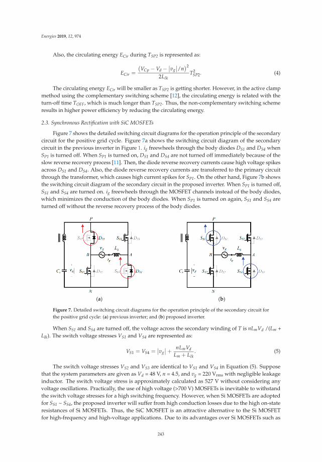
Energies 2019, 12, 974
Also, the circulating energy ECir during TSP2 is represented as:
ECir =
(VCp − Vd −
∣∣vg∣∣/n)2
2LlkT2
SP2. (4)
The circulating energy ECir will be smaller as TSP2 is getting shorter. However, in the active clampmethod using the complementary switching scheme [12], the circulating energy is related with theturn-off time TOFF, which is much longer than TSP2. Thus, the non-complementary switching schemeresults in higher power efficiency by reducing the circulating energy.
2.3. Synchronous Rectification with SiC MOSFETs
Figure 7 shows the detailed switching circuit diagrams for the operation principle of the secondarycircuit for the positive grid cycle. Figure 7a shows the switching circuit diagram of the secondarycircuit in the previous inverter in Figure 1. ig freewheels through the body diodes DS1 and DS4 whenSP1 is turned off. When SP1 is turned on, DS1 and DS4 are not turned off immediately because of theslow reverse recovery process [11]. Then, the diode reverse recovery currents cause high voltage spikesacross DS1 and DS4. Also, the diode reverse recovery currents are transferred to the primary circuitthrough the transformer, which causes high current spikes for SP1. On the other hand, Figure 7b showsthe switching circuit diagram of the secondary circuit in the proposed inverter. When SP1 is turned off,SS1 and SS4 are turned on. ig freewheels through the MOSFET channels instead of the body diodes,which minimizes the conduction of the body diodes. When SP1 is turned on again, SS1 and SS4 areturned off without the reverse recovery process of the body diodes.
(a) (b)
Figure 7. Detailed switching circuit diagrams for the operation principle of the secondary circuit forthe positive grid cycle: (a) previous inverter; and (b) proposed inverter.
When SS1 and SS4 are turned off, the voltage across the secondary winding of T is nLmVd /(Lm +Llk). The switch voltage stresses VS1 and VS4 are represented as:
VS1 = VS4 =∣∣vg∣∣+ nLmVd
Lm + Llk. (5)
The switch voltage stresses VS2 and VS3 are identical to VS1 and VS4 in Equation (5). Supposethat the system parameters are given as Vd = 48 V, n = 4.5, and vg = 220 Vrms with negligible leakageinductor. The switch voltage stress is approximately calculated as 527 V without considering anyvoltage oscillations. Practically, the use of high voltage (>700 V) MOSFETs is inevitable to withstandthe switch voltage stresses for a high switching frequency. However, when Si MOSFETs are adoptedfor SS1 ~ SS4, the proposed inverter will suffer from high conduction losses due to the high on-stateresistances of Si MOSFETs. Thus, the SiC MOSFET is an attractive alternative to the Si MOSFETfor high-frequency and high-voltage applications. Due to its advantages over Si MOSFETs such as
243

Energies 2019, 12, 974
its wider bandgap and higher electric field capacity, it improves the switching performance of theproposed inverter, increasing the power efficiency.
2.4. Control Strategy
Supposing that the leakage inductor is negligible, the volt-second balance for Lg during Ts givesthe following voltage equation as:
nVdDTs − vg(1 − D) Ts = 0 (6)
where D is the duty cycle of SP1. By rearranging Equation (6), we have the relation between vg andVd as:
vg
Vd=
nD1 − D
. (7)
Assuming no power losses in the inverter circuit, we have the relation between id and ig as:
idig
=nD
1 − D(8)
where id is the input current. Suppose that CP keeps the charge balance, id is considered as iP1 duringTs. Then, the following current relations are represented as:
id = iP1 = kDiLm (9)
where k is a proportional factor. From equations (8) and (9), we have the relation between iLm and ig as:
iLm =n
k(1 − D)ig. (10)
The average voltage for Lm during Ts can be represented with respect to the deviation ΔiLm ofiLm as:
VdD −∣∣vg∣∣
n(1 − D) = Lm
ΔiLmTs
. (11)
From Equation (11), D can be represented as:
D =
∣∣vg∣∣∣∣vg
∣∣+ nVd+
n∣∣vg∣∣+ nVd
(LmΔiLm
Ts
). (12)
By using equations (7) and (10), D in Equation (12) can be written as:
D = Dn + Dc =
∣∣vg∣∣∣∣vg
∣∣+ nVd+
nLm
kVdTsΔig (13)
where Dn is the nominal duty cycle, and Dc is the control duty cycle as:
Dn =|vg|
|vg|+nVd=
Vg |sin ωt|Vg |sin ωt|+nVd
,
Dc =nLm
kVdTsΔig.
(14)
Vg is the absolute peak value of vg. ω is the angular frequency of vg. Supposing that vg ismeasured exactly with a phase-locked loop (PLL) [17], Dn plays the role of providing the nominalvoltage compensation. By using Dn, the non-linear system in Equation (11) is transformed to thefirst-order linear system, which can be controlled by the control duty cycle Dc. In order to regulate
244

Energies 2019, 12, 974
the grid current ig with low harmonic currents, Dc is implemented by a proportional-resonant (PR)control [18] whose ideal transfer function CPR (s) is:
CPR(s) = kp +krs
s2 + ω2 (15)
where kp and kr are the PR control gains, respectively. However, it is unable to realize the PR controllerin Equation (15) with an infinite gain. Thus, the following non-ideal transfer function is adopted inpractice as:
CPR(s) = kp +2krωcs
s2 + 2ωcs + ω2 (16)
where ωc is the angular frequency at the cutoff frequency of the controller. In addition, the harmoniccompensators can be added to the PR controller to minimize the harmonic currents for the selectiveharmonic frequencies [19]. Its transfer function CHC (s) is expressed as:
CHC(s) = ∑h=3, 5, 7
2krhωcs
s2 + 2ωcs + (hω)2 (17)
where h is the harmonic order and krh is the resonant control gain for each harmonic frequency. Since thethird, fifth, and seventh harmonics are significant under the grid environment, the third to seventhharmonic compensators are implemented. The harmonic compensators provide high gains at theselected harmonic frequencies, helping minimize the steady-state error and the disturbance by theselected frequency components. Figure 8 shows the control block diagram of the proposed inverter.I*g is the peak magnitude of the current reference i*g. The duty cycle D is generated by summing Dn
and Dc.
Figure 8. Control block diagram of the proposed inverter.
3. Experimental Results
A 220-W prototype system has been designed and tested to evaluate the performance of theproposed inverter. Table 1 shows the system parameters and the circuit components. As a SiC MOSFET,UJC1206k (UnitedSiC) has been used for SS1 ~ SS4. As a digital signal controller, dsPIC30F6015(Microchip) has been used for implementing the current controller and generating the duty cyclesignals for all of the power switches. Figure 9 shows the picture of the prototype system. The prototypesystem includes the power circuit and the control circuit. Even though it is not optimized for thecommercialized level, it is expected that the proposed inverter could achieve high power densityif it is implemented with advanced devices such as gallium nitride (GaN) devices [20] and planartransformers [21].
245

Energies 2019, 12, 974
Table 1. System parameters and circuit components.
Symbol Quantity Value
Vd dc input voltage 48 Vvg grid voltage 60 Hz/220 Vrmsfs switching frequency 50 kHz
Lm magnetizing inductor 60 μHLlk leakage inductor 0.5 μHNP primary winding turns 14NS secondary winding turns 63CP clamp capacitor 1.0 μF
SP1, SP2 primary swiches IXFK150N30P3CS secondary capacitor 1.0 μF
SS1 ~ SS4 secondary switches UJC1206KLg filter inductor 2.0 mH
Figure 9. Picture of the prototype system.
The proposed inverter has been simulated to verify its operation principle. It has been simulatedby the physical security information management (PSIM) software for the system parameters in Table 1.Figure 10 shows the simulation waveforms of the proposed inverter. The steady state operation of theproposed inverter can be verified from Figure 10a–d. Figure 10e,f show the simulation waveforms ofthe proposed inverter in the transient state condition. Figure 10e shows vg and ig as the output powerchanges from 110 W to 220 W. Figure 10f shows vg and ig as the output power changes from 220 W to110 W.
Figure 11 shows the experimental waveforms of the previous inverter in Figure 1. The previousinverter has been designed and tested for the same system parameters as the proposed inverter. It usesthe same circuit components in Table 1, except that STW40N95K5 (STMicroelectronics), as a Si MOSFET,has been adopted for SS1 ~ SS4. Figure 11a shows the gate signal Vgate,P1 and the switch voltage VP1for SP1. When SP1 is turned off, VP1 has a high voltage spike, which results from the energy stored inthe transformer leakage inductor. Figure 11b shows the gate signal Vgate,P1 and the switch current iP1for SP1. When SP1 is turned on, iP1 has a high current spike, which results from the reverse recoverycurrent of the body diodes in the secondary circuit.
246

Energies 2019, 12, 974
(a) (b)
(c)
(e)
(d)
(f)
Figure 10. Simulation waveforms: (a) Vgate,P1, Vgate,P2, VP1, and VP2; (b) Vgate,P1, Vgate,P2, iP1, and iCp;(c) ig, iS2, and iS3; (d) ig, iS1, and iS4; (e) vg and ig from 110 W to 220 W; and (f) vg and ig from 220 W to110 W.
(a) (b)
Figure 11. Experimental waveforms of the previous inverter: (a) Vgate,P1 and VP1; and (b) Vgate,P1
and iP1.
Figure 12 shows the experimental waveforms of the proposed inverter. Figure 12a shows Vgate,P1,Vgate,P2, and VP1. Figure 12b shows Vgate,P1, Vgate,P2, and VP2. As shown in Figure 12a,b, VP1 and
247

Energies 2019, 12, 974
VP2 are maximally clamped to the capacitor voltage VCp. Figure 12c shows Vgate,P1, Vgate,P2, and iP1.The switch current iP1 in Figure 12c has lower current spike than the switch current iP1 in Figure 11bbecause of the synchronous rectification of the secondary circuit. Figure 12d shows Vgate,P1, Vgate,P2,and iCp. It is observed that the capacitor charging and discharging currents are well balanced in theproposed inverter.
(a) (b)
(c) (d)
Figure 12. Experimental waveforms of the proposed inverter: (a) Vgate,P1, Vgate,P2, and VP1; (b) Vgate,P1,Vgate,P2, and VP2; (c) Vgate,P1, Vgate,P2, and iP1; and (d) Vgate,P1, Vgate,P2, and iCp.
Figure 13 shows the experimental waveforms in the secondary circuit for the positive grid cycle.Figure 13a shows VS1 in the previous inverter. It is observed that there is high voltage oscillationacross SS1, which results from the slow reverse recovery process of the body diode of the Si MOSFET.Figure 13b shows Vgate,S1 and VS1 in the proposed inverter. With synchronous rectification, the SiCMOSFET channel has been used for the rectification. It is shown that voltage oscillation across SS1 hasbeen much alleviated due to the fast switching operation of the SiC MOSFET. The switch currents iS1,iS2, iS3, and iS4 are shown from Figure 13c–f with respect to ig in the proposed inverter.
Figure 14 shows the experimental waveforms of the proposed inverter. Figure 14a shows vg andig as the proposed inverter supplies 110 W into the grid. Figure 14b shows vg and ig as the proposedinverter supplies 220 W into the grid. As ig is in phase with vg, the power factor is measured as 0.99 inFigure 14.
Figure 15 shows the measured power efficiency curves. The curve A shows the measuredpower efficiency of the previous inverter. It has achieved the peak efficiency of 93.5% at the ratedpower. The curve B shows the measured power efficiency of the proposed inverter when thesynchronous rectification has been implemented without the active clamp circuit. The proposedinverter has improved the power efficiency, achieving the peak efficiency of 94.2% at the ratedpower. The curve C shows the measured power efficiency of the proposed inverter when bothactive clamp and synchronous rectification techniques have been implemented. The proposed inverterhas achieved the peak efficiency of 95.0% at the rated power by using active clamp and synchronousrectification techniques.
248

Energies 2019, 12, 974
(a) (b) (c)
(d) (e) (f)
Figure 13. Experimental waveforms in the secondary circuit for the positive grid cycle: (a) VS1 in theprevious inverter; (b) Vgate,S1 and VS1 in the proposed inverter; (c) ig and iS2 in the proposed inverter;(d) ig and iS3 in the proposed inverter; (e) ig and iS1 in the proposed inverter; and (f) ig and iS4 in theproposed inverter.
(a) (b)
Figure 14. Experimental waveforms of the proposed inverter: (a) vg and ig as the proposed invertersupplies 110 W into the grid; and (b) vg and ig as the proposed inverter supplies 220 W into the grid.
Figure 15. Measured power efficiency curves.
249

Energies 2019, 12, 974
Figure 16a shows the measured power efficiency curves up to 440 W. The prototype system hasshown the peak efficiency of 95.0% at 220 W. The efficiency decreases gradually as the output powerlevel goes up from 300 W to 440 W. The prototype system has achieved the efficiency of 94.3% at440 W. Figure 16b shows the measured power efficiency curves for 50 kHz and 100 kHz, respectively.As the switching frequency increases, the power efficiency decreases because of the switching losses.In order to improve the power efficiency and the power density further, the circuit design schemeshould be advanced by considering the GaN devices [20] and the planar transformers [21] formegahertz operations.
(a) (b)
Figure 16. Measured power efficiency curves: (a) power efficiency curves up to 440 W; and (b) powerefficiency curves for different switching frequencies.
4. Conclusions
This paper has proposed a high-efficiency zeta inverter using active clamp and synchronousrectification techniques for single-phase grid-connected applications. The operation principle of theproposed inverter has been described. The active clamp and synchronous techniques adopted in theproposed inverter have been explained. The non-complementary switching scheme has been appliedto the active clamp circuit. It effectively reduces the switching losses and circulating current in theprimary circuit. The synchronous rectification with SiC MOSFETs alleviates switching losses in thesecondary circuit. The control strategy for the CCM operation of the proposed inverter has beenpresented. A 220-W prototype system has been designed and tested to evaluate the performance ofthe proposed inverter. Experimental results have shown that the proposed inverter has improved thepower efficiency by reducing switching losses, compared to the previous inverter.
Author Contributions: W.-Y.C. managed the project and wrote the manuscript. M.-K.Y. performed theexperiments, analyzed the data, and edited the manuscript.
Funding: This research was supported by the National Research Foundation of Korea(NRF-2016R1D1A3B03932350). Also, it was supported by research funds of Chonbuk National University in 2018.
Conflicts of Interest: The authors declare no potential conflict of interest.
References
1. Dong, D.; Agamy, M.S.; Harfman-Todorovic, M.; Liu, X.; Garces, L.; Zhou, R.; Cioffi, P. A PV residentialmicroinverter with grid-support function: Design, implementation, and field testing. IEEE Trans. Ind. Appl.2018, 54, 469–481. [CrossRef]
2. Hu, H.; Harb, S.; Kutkut, N.H.; Shen, Z.H.; Batarseh, I. A single-stage microinverter without using electrolyticcapacitors. IEEE Trans. Power Electron. 2013, 28, 2677–2687. [CrossRef]
3. Feng, X.; Wang, F.; Wu, C.; Luo, J.; Zhang, L. Modeling and comparisons of aggregated flyback microinvertersin aspect of harmonic resonances with the grid. IEEE Trans. Ind. Electron. 2019, 66, 276–285. [CrossRef]
250

Energies 2019, 12, 974
4. Lodh, T.; Pragallapati, N.; Agarwal, V. Novel control scheme for an interleaved flyback converter based solarPV microinverter to achieve high efficiency. IEEE Trans. Ind. Appl. 2018, 54, 3473–3482. [CrossRef]
5. Han, B.; Lee, J.S.; Kim, M.S. Repetitive controller with phase-lead compensation for Cuk CCM inverter.IEEE Trans. Ind. Electron. 2018, 65, 2356–2367. [CrossRef]
6. Han, B.; Lai, J.-S.; Kim, M.S. Dynamic modeling and controller design of dual-mode Cuk inverter ingrid-connected PV/TE applications. IEEE Trans. Power Electron. 2018, 33, 8887–8904. [CrossRef]
7. Levin, G.H.; Flores, J.V.; Salton, A.; dos Reis, F.S. Internal model control of the zeta converter for the gridconnection of photovoltaic panels. In Proceedings of the Brazilian Power Electronics Conference, Gramado,Brazil, 27–31 October 2013; pp. 666–671.
8. Viero, R.C.; Lopez, H.F.M.; Zollmann, C.A.; dos Reis, F.S. Dynamic modeling of a sinusoidal inverter based onzeta converter working in DCM for PV arrays. In Proceedings of the Annual Conference on IEEE IndustrialElectronics Society (IECON), Glendale, AZ, USA, 7–10 November 2010; pp. 439–444.
9. Surapaneni, R.K.; Rathore, A.K. A single-stage CCM zeta microinverter for solar photovoltaic AC module.IEEE J. Emerg. Sel. Top. Power Electron. 2015, 3, 892–900. [CrossRef]
10. Murthy-Bellur, D.; Kazimierczuk, M.K. Isolated two-transistor zeta converter with reduced transistor voltagestress. IEEE Trans. Circuits Syst. II Express Briefs 2011, 58, 41–45. [CrossRef]
11. Brown, C.D.; Sarlioglu, B. Reducing switching losses in BLDC motor drives by reducing body diodeconduction of MOSFETs. IEEE Trans. Ind. Appl. 2015, 51, 1864–1871. [CrossRef]
12. Chen, M.; Sun, J. Reduced-order averaged modeling of active-clamp converters. IEEE Trans. Power Electron.2006, 21, 487–494. [CrossRef]
13. Zhang, J.; Huang, X.; Wu, X.; Qian, Z. A high efficiency flyback converter with new active clamp technique.IEEE Trans. Power Electron. 2010, 25, 1775–1785. [CrossRef]
14. Yin, S.; Liu, Y.; Liu, Y.; Tseng, K.J.; Pou, J.; Simanjorang, R. Comparison of SiC voltage source inverters usingsynchronous rectification and freewheeling diode. IEEE Trans. Ind. Electron. 2018, 65, 1051–1061. [CrossRef]
15. Mohammadi, M.; Ordonez, M. Synchronous rectification of LLC resonant converters using homopolaritycycle modulation. IEEE Trans. Ind. Electron. 2019, 66, 1781–1790. [CrossRef]
16. Jordán, J.; Esteve, V.; Sanchis-Kilders, E.; Dede, E.J.; Maset, E.; Ejea, J.B.; Ferreres, A. A comparativeperformance study of a 1200 V Si and SiC MOSFET intrinsic diode on an induction heating inverter. IEEETrans. Power Electron. 2014, 29, 2550–2562. [CrossRef]
17. Han, Y.; Luo, M.; Zhao, X.; Guerrero, J.M.; Xu, L. Comparative performance evaluation oforthogonal-signal-generators-based single-phase PLL algorithms—A survey. IEEE Trans. Power Electron.2016, 31, 3932–3944. [CrossRef]
18. Zmood, D.N.; Holmes, D.G. Stationary frame current regulation of PWM inverters with zero steady-stateerror. IEEE Trans. Power Electron. 2003, 18, 814–822. [CrossRef]
19. Pereira, L.F.A.; Flores, J.V.; Bonan, G.; Coutinho, D.F.; da Silva, J.M.G. Multiple resonant controllers foruninterruptible power supplies-a systematic robust control design approach. IEEE Trans. Ind. Electron. 2014,61, 1528–1538. [CrossRef]
20. Zhang, W.; Huang, X.; Liu, Z.; Lee, F.C.; She, S.; Du, W.; Li, Q. A new package of high-voltage cascadegallium nitride device for megahertz operation. IEEE Trans. Power Electron. 2016, 31, 1344–1353. [CrossRef]
21. Zhao, S.; Li, Q.; Lee, F.C.; Li, B. High-frequency transformer design for modular power conversion frommedium-voltage AC to 400 VDC. IEEE Trans. Power Electron. 2018, 33, 7545–7557. [CrossRef]
© 2019 by the authors. Licensee MDPI, Basel, Switzerland. This article is an open accessarticle distributed under the terms and conditions of the Creative Commons Attribution(CC BY) license (http://creativecommons.org/licenses/by/4.0/).
251


Article
Analysis, Modeling, and Control of Half-BridgeCurrent-Source Converter for Energy Management ofSupercapacitor Modules in Traction Applications
Jorge Garcia 1,*, Pablo Garcia 1, Fabio Giulii Capponi 2 and Giulio De Donato 2
1 LEMUR Group, Department of Electrical Engineering, University of Oviedo, 33204 Gijon, Spain;[email protected]
2 Department of Astronautical, Electrical and Energy Engineering, University of Roma “La Sapienza”,00184 Roma, Italy; [email protected] (F.G.C.); [email protected] (G.D.D.)
* Correspondence: [email protected]; Tel.: +34-985-18-2017
Received: 13 July 2018; Accepted: 21 August 2018; Published: 26 August 2018
Abstract: In this work, an in-depth investigation was performed on the properties of the half-bridgecurrent-source (HBCS) bidirectional direct current (DC)-to-DC converter, used to interface two DC-linkvoltage sources with a high-voltage-rating mismatch. The intended implementation is particularlysuitable for the interfacing of a supercapacitor (SC) module and a battery stack in a hybrid storagesystem (HSS) for automotive applications. It is demonstrated that the use of a synchronous rectification(SR) modulation scheme benefits both the power-stage performance (in terms of efficiency andreliability) and the control-stage performance (in terms of simplicity and versatility). Furthermore,an average model of the converter, valid for every operating condition, is derived and utilized as a toolfor the design of the control system. This model includes the effects of parasitic elements (mainlythe leakage inductance of the transformer) and of the converter snubbers. A 3 kW prototype of theconverter was used for experimental validation of the converter modeling, design, and performance.Finally, a discussion on the control strategy of the converter operation is included.
Keywords: hybrid storage systems; power electronic converters; half-bridge current-source converters;supercapacitors
1. Introduction
Among electrical energy storage passive devices, Supercapacitors (SC) outstand as one of thepreferred solutions when very high power densities and long life cycles are required. These featuresalso are used in Hybrid Storage Systems (HSS), where SC can be combined with other distinct storagedevices, such as electrochemical batteries or fuel cells [1–19]. In these hybrid systems, SC usuallyoperate as power sources, as they provide the required peak power commanded by the load. In turn,the combined device (e.g., the electrochemical battery) work as an energy source, providing thelong-term energy required for the given operating conditions, such as islanding operation or back-upenergy support after a fault ride-through sequence, etc.
The integration of SC into HSS has been covered extensively in the current state-of-the-art,by analyzing the modeling and operation of power electronic topologies, by proposing controlalgorithms and methods, and by investigating hierarchical energy management systems [20–27].Although being the simplest and most inexpensive scheme, the direct connection between the storagesystems prevents to fully exploit the high charging and discharging instant power ratings of SCs. Thisscheme also prevents a tight control on the independent power flows shared among the energy storagedevices [28,29]. Therefore, practically every implemented solution found in the technical literatureincludes a bidirectional direct current (DC)-to-DC converter. These solutions can be categorized into
Energies 2018, 11, 2239; doi:10.3390/en11092239 www.mdpi.com/journal/energies253

Energies 2018, 11, 2239
three different classes: a series connection of the storage devices [6,7], a cascaded connection of thestorage subsystems [8,9], and finally a parallel connection of the storage elements [10–12]. Froma detailed analysis of the technical literature, the parallel configuration, depicted in Figure 1, outstandsas the most practical solution that allows a full control of the power flow sharing scheme requiredfor the application, as well as a complete SC voltage-range utilization, despite that in this case thebidirectional converter needs to be rated for the peak value of the required power [13,14].
Figure 1. Parallel configuration for interfacing supercapacitors (SCs) with primary energy source(battery stack).
The bidirectional boost converter is formed by the typical connection present in a single phaseleg of an inverter. It has two transistors, a series inductor connected between the mid-point of thetransistors and the output, plus two capacitors intended to filter the input and the output of theconverter. This scheme is generally adopted as the simplest and best-known solution. With thisconfiguration, the peak power ratings required by most applications can be ensured by an assembly offew SC connected in series. This structure is also beneficial in terms of balancing the voltage at eachSC module in the assembly. As a consequence, the SC side voltage ratings of the converter are usuallymuch smaller than the voltage levels found at the DC-link. In addition, upon transient variations, theSC side voltage must allow variations from 80 to 20% of the SC ratings, in order to use efficiently thestored energy at the device. On the other side, the voltage at the DC-link may remain almost constant,as to optimize the full system design and operation. Hence, the range of the voltage gain between theinput and the output of the bidirectional converter can typically surpass ratios of 1 to 10 and above,depending on the application.
Therefore, the boost converter is no longer a suitable solution, and so alternative topologies thatallow for a high voltage gain need to be analyzed. Among these options, the most widely used includethe use of a High-Frequency (HF) transformer [30–38]. Studies on the simplest isolated configurations,such as the bidirectional versions of the Flyback converter, the Forward Current-Source converter,the Push-Pull Current-Source converter, and the Half-Bridge Current-Source (HBCS) converter havebeen carried out [33–35]. These comparative analyses were carried out on the basis of the number ofcomponents, the switch stresses at the converters, and other figures of merit such as the utilizationfactor of the magnetic elements. This comparison shows how the bidirectional HBCS DC-to-DCconverter is most suitable in low to medium power applications, for structures that directly interfacethe storage devices. Thus, the HBCS topology is of interest in HSS with storage devices arranged asshown in Figure 1 with the battery directly forming the DC bus at the converter. This is particularlyinteresting in traction applications, for which the weight and size of the full system are major concerns,and variable DC-link systems are considered as a suitable option [28,29].
When a given power profile is demanded by the load, the SC converter must react very quickly,in order to prevent the battery from providing the transient power. Given the current-source behavior
254

Energies 2018, 11, 2239
of the low-voltage side of the HBCS converter, and provided that a tight, fast current control isimplemented by generating the adequate SC current reference, the power delivered by this convertercan successfully protect the battery from delivering fast, high power peaks, thus enhancing theperformance and increasing the reliability of the full system. Other works have investigated thepotential use of power converters for interfacing both the battery and the SC module, leading to morecomplex topologies and control methods [20,24,27,39].
The HBCS topology was introduced in an application to HSS in [11], but the power ratings of thelaboratory demonstrator was only 100 W. Later, a 3 kW setup was reported in [35], being able to operatein open-loop, steady-state, both charging and discharging operation modes. A measured efficiencybeyond 90% was then reported for the full range of operation. The authors in [35] analyzed the staticgain of the HBCS converter, using conventioal switching patterns. Furthermore, they consideredneither the modeling nor the control stage for closed-loop operation of the converter. On the otherhand, the authors of [40,41] showed preliminary research conducted to unify the transfer function ofthe converter acting in a bidirectional operation scheme, as well as the dynamic behavior.
The present work investigates more in depth the performance of the HBCS converter in vehicleapplications. Firstly, a unified control strategy of the converter, on the basis of a synchronous rectificationswitching pattern, is provided. By using this pattern, the converter can be controlled with a simple,unique control law valid for every operating condition. This allows the implementation of a fullbidirectional SC current control, thus enabling a fast, tight power flow control in the storage system.Once this switching pattern is established and validated, the main contribution of this work is theextension of previously existing circuital models of the converter by including non-ideal effects of theparasitic elements in the transformer of the converter, as well as the dissipative effect of the losses in thesystem. The performance of the proposed model was validated through simulations and experimentscarried out on a 3 kW laboratory prototype. The proposed model was also compared against thesimplified ideal model. Finally, this work discusses the control strategy that can be implemented inthe converter. A basic HBCS current loop was analyzed, designed, and implemented, with the aim todemonstrate its feasibility; finally, a discussion on the possibilities of the high-level control strategy isalso included at the end of the paper.
This paper is organized as follows. Section 2 presents the conventional modulation strategyimplemented in the state-of-the-art for the HBCS converter. After that, Section 3 evaluates theSynchronous Rectification (SR) scheme in the converter operation, considering both the chargingand discharging modes of operation. It also demonstrates experimentally the benefits of SR operationfor this topology. Section 4 further discusses the implications of SR in terms of the simplification ofthe control of the converter; most importantly, this section provides an averaged model of the HBCSconverter, suitable to aid in the design of the control stage. Also, this model is validated throughsimulations. Subsequently, in Section 5 the current control algorithm is discussed and tested throughsimulations. This section also deals with the overall control scheme of the system. Section 6 validatesthe full model and the control scheme outlined in the previous sections by showing experimentalresults obtained with a laboratory prototype of a HBCS converter. Finally, Section 7 discusses theconclusions of the research and proposes some future developments.
2. Special Characteristics of the HBCS Converter
Figure 2 shows the HBCS converter. Because this converter is a bidirectional topology,no predefined input or output are established. For the coming discussion, the SC side is also referredto as the Low-Voltage (LV) side, signifying that this side generally has the lower of the rated voltagesinvolved in the analysis. On the other hand, the alternate energy source (i.e., battery) and the DC-linkare referred to as the High-Voltage (HV) side.
255

Energies 2018, 11, 2239
Figure 2. Layout of Half-Bridge Current-Source (HBCS) bidirectional converter. The references for thecurrent and voltage considered for the analysis are shown.
The modulation scheme for the HBCS converter, as presented in [35], is obtained by shiftingthe command pulse waveforms of each switch in the primary- or secondary-side by 180o. Initially,the control parameters implemented at both charging and discharging operation modes were different.In charging mode, where the energy flows to the SC from the DC link side, switches S3 and S4 remainalways turned off. This forces the current to flow only through the diodes of S3 and S4. Figure 3 showsthe main current and voltage instant waveforms of the converter for charging (a) and discharging (b)modes. The switching pattern is defined by establishing the gate-to-emitter voltages of switches S1 toS4, denoted as VGE1–VGE4, respectively. The rest of the waveforms are consistent with the referencesin Figure 2. The modulation of switches S1 and S2 (Figure 3a) is carried out by shifting by 180o thecontrol pulses, considering a given duty ratio, D:
D =TS1 ON
TS, (1)
where TS1 ON is the interval when switch S1 remains turned on and TS is the switching period. In orderto avoid a simultaneous conduction of switches S1 and S2 at the battery side, and given that theswitching pattern requires a fixed 180◦ phase shift between the firing signals of VGE1 and VGE2, D isrestricted to 0 < D < 0.5. The voltage gain between the LV and HV sides, GCHRGE, is
GCHRGE =VSC
VBAT= D · N2
N1, (2)
where N1 and N2 are the primary- and secondary-side number of turns of the HF transformer,respectively; VSC is the voltage across the SC; and VBAT is the DC-link voltage, that is, the batteryvoltage according to its state of charge. The magnetizing inductance of the transformer is neglected,because it is assumed that it is very high.
Figure 4 shows the current paths for the different switching modes of the converter, during theSC charging operation scheme. When switch S1 is turned on and S2 is turned off (Figure 4a), a positivecurrent IP flows flows through the primary side, considering the references in Figure 2. Current flowsthrough the portion of the secondary winding connected to switch S3, the output filter, and the SC; thus,the anti-parallel diode of switch S3 carries the secondary-side current. Figure 4b, in turn, shows theswitching mode when both transistors S1 and S2 are turned off. The inductor current IL splits equallybetween the two parts of the secondary winding, flowing through the anti-parallel diodes of S3 and S4.Finally, Figure 4c depicts the current paths when S2 is turned on and S1 is turned off. This mode issimilar to that shown in Figure 4a but considers the 180◦ phase shift between S1 and S2.
During the discharging mode, the energy flows back to the DC-link from the the SC. In this case,the switches under control are S3 and S4, while S1 and S2 are kept continuously turned off. Again,the modulation of S3 and S4 is implemented through a 180o shifting scheme, while the turn-on intervals
256

Energies 2018, 11, 2239
are kept equal. Figure 3b shows the key waveforms obtained for this operation mode. The independentparameter for this mode, D′, is defined as:
D′ = TS3 ONTS
, (3)
where TS3 ON is the interval when S3 is turned on. The constraint for this parameter is now 0.5 < D′ < 1,thus forcing an overlap in the conduction of S3 and S4. This overlapping is required because of thecurrent-source behavior of the LV side of the converter. For this topology, unless at least one switch inthe pair S3–S4 is turned on, an abrupt interruption of the current flowing through the inductor wouldlead to a dangerous overvoltage across the magnetic element, that might damage the converter. For thedischarging operation mode, the voltage gain can be defined as:
GDISCHRGE =VBATVSC
=1
1 − D′N1
N2. (4)
Figure 3. Main voltage (black) and current (red) waveforms of the half-bridge current-source (HBSC)for charging (a) and discharging (b) operation modes.
The switching modes for discharging the SC are represented in Figure 5. The current path whenS4 is turned off and S3 is turned on is shown in Figure 5a. On the other hand, Figure 5b shows thecurrent flowing through the switches when both S3 and S4 are turned on. Finally, it can be seen inFigure 5c how the current flows when switch S4 is turned on and S3 remains off. A close look atFigure 5a–c shows that the current paths are the same as those shown in Figure 4a–c, respectively, butwith the directions of the currents reversed.
257

Energies 2018, 11, 2239
Figure 4. Switching modes of the half-bridge current-source (HBCS) converter operating duringsupercapacitor (SC) charging operation mode. (a) Switch S1 on and switch S2 off. (b) Both switches S1
and S2 off. (c) Switch S1 off and switch S2 on.
By using the control laws stated in Equations (2) and (4), both the charging and dischargingcontrol strategies can be easily designed. However, this modulation pattern requires the calculationof two independent control parameters, defined as the duty cycles of S1 and S3, depending on theoperation mode under consideration, given by charging and discharging modes, respectively. Thisapproach, though, yields to some issues at the boundary between these operation modes, giventhat the switches that must be controlled change abruptly. Therefore, if both control schemes areimplemented independently, a smooth transition between modes of operation is prevented. However,this issue is easily avoided provided that SR is implemented. This SR pattern is introduced in thenext section for the HBCS converter. The benefits for the control of the converter are discussed in theforthcoming sections.
258
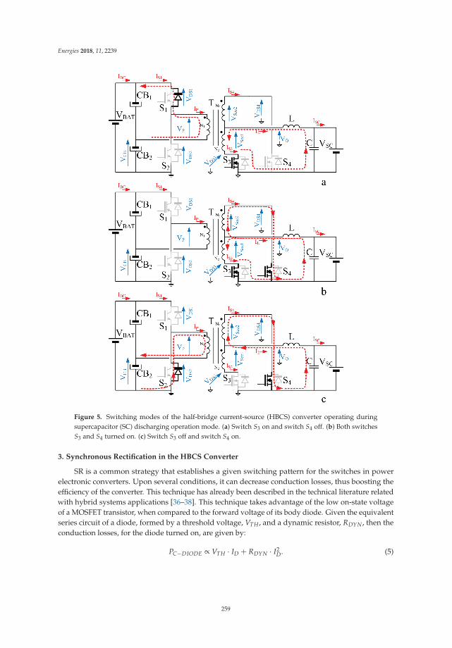
Energies 2018, 11, 2239
Figure 5. Switching modes of the half-bridge current-source (HBCS) converter operating duringsupercapacitor (SC) discharging operation mode. (a) Switch S3 on and switch S4 off. (b) Both switchesS3 and S4 turned on. (c) Switch S3 off and switch S4 on.
3. Synchronous Rectification in the HBCS Converter
SR is a common strategy that establishes a given switching pattern for the switches in powerelectronic converters. Upon several conditions, it can decrease conduction losses, thus boosting theefficiency of the converter. This technique has already been described in the technical literature relatedwith hybrid systems applications [36–38]. This technique takes advantage of the low on-state voltageof a MOSFET transistor, when compared to the forward voltage of its body diode. Given the equivalentseries circuit of a diode, formed by a threshold voltage, VTH , and a dynamic resistor, RDYN , then theconduction losses, for the diode turned on, are given by:
PC−DIODE ∝ VTH · ID + RDYN · I2D. (5)
259

Energies 2018, 11, 2239
Moreover, the conduction losses in a MOSFET can be expressed as:
PC−MOSFET ∝ RDS ON · I2D, (6)
where RDS ON is the drain-to-source on-resistance of the channel. As a result of an analysis of theequivalent circuit of the switch, the current tends to flow through the path with a lower voltage drop.In the HBCS converter depicted at Figure 2, S3 and S4 have already been implemented as MOSFETswitches, with inherent anti-parallel body diodes. As a consequence, SR can be directly applied.
In order to validate the performance of the SR switching pattern, a reference design is consideredfor a 3 kW HBCS converter. The main characteristics of the setup are detailed in Table 1.
Table 1. Characteristics of half-bridge current-source (HBCS) design.
Parameter Max. Min.
SC voltage 45 V 25 VHV DC-link voltage 350 VSwitching frequency 20 kHzSC discharge-mode duty ratio 0.75 0.55SC charge-mode duty ratio 0.45 0.25Output power (SC disch. mode) 3 kW 1.6 kWOutput power (SC chrg mode) 3 kW 1.6 kWSC current 65 A −65 ATransformer turns ratio 3.5:1:1
Figure 6 shows a graphical representation of the expression of the drain-to-source voltage, VDS,as well as the power dissipated through conduction losses, PCOND, both as a function of the currentflowing through the drain of the transistor, ID. These power and voltage values are given for both thetransistor and diode elementary devices. For this study, the actual values given in the datasheets ofthe real components selected, in this case the SKM121AR power MOSFET modules from SEMIKRON,have been used. The dotted black line shows the voltage at the MOSFET as a function of the currentID. This line shows the typical load line of a resistive component. As a consequence, the powerdissipated as a function of the ID in the MOSFET is given by a quadratic relationship expressed inEquation (6), drawn as a filled black line in Figure 6. The voltage drop across the diode, in turn,is shown as an horizontal dotted gray line. The power dissipated in the diode, as a function of thecurrent ID, therefore follows a linear behavior, represented by a filled gray line. As can be seen, bothpower characteristics, those of the MOSFET and the diode, have an intersection point labeled as ILIM.For ID current values below ILIM, the MOSFET losses are smaller than the diode losses, and thereforethe synchronous rectification implies higher efficiencies compared to the standard switching pattern.For the real values of the devices under consideration, ILIM is equal to
ILIM = 70 A. (7)
From Table 1, the maximum value of the SC current, which is also the maximum currents allowedto flow through S3 and S4, has a value of 65 A. Therefore, and considering Figure 6, the conductionlosses at the secondary side of the converter operating in charging mode will be decreased, providedthat SR is implemented as the switching pattern. As a consequence, the whole efficiency of theconverter will increase. It must be notice that in this case the switches at the DC link side have beenimplemented by means of IGBT switches. Therefore, and given that for this switch technology thecurrent flowing from the emitter to the collector can only flow through the anti-parallel diode (and notthrough the transistor itself, as in the previous case), the use of a SR scheme during the SC dischargemode will not mean a decrease in the converter losses. In any case, a critical point for this analysis isto state that SR can still be used in this mode of operation without affecting the performance of theconverter. This issue will be discussed in Section 4.
260

Energies 2018, 11, 2239
Figure 6. Drain-to-source voltage (VDS, dashed lines) and conduction losses (PCOND, filled lines) forboth diode conduction (gray) and MOSFET conduction (black), for the half-bridge current-source(HBCS) prototype.
A first set of experiments was carried to validate the feasibility of the SR switching patternimplementation in the HBCS converter. For this validation, and in order to register the steady-stateoperation of the converter, the setup was configured to supply a resistive load from a voltage source.The values of measured efficiencies in charging operation mode, for the standard and the SR schemes,are given in Figure 7. Three different resistive loads (1.0, 0.67 and 0.5 Ω, respectively), were used in themeasurements. The voltage at the power source was kept constant at 300 VDC. Due some practicalconstraints at the experimental setup, the voltage levels at the LV side were limited to three values,VSC = 25 V, VSC = 30 V, and VSC = 34 V. From the plots at Figure 7, it can be deduced an increase in theconverter efficiency in all cases.
Figure 7. Graphical relationship of experimental efficiency measurements between standard andsynchronous rectification switching schemes, as a function of load resistance. (a) VSC = 25 V.(b) VSC = 30 V. (c) VSC = 34 V.
4. Full Model of the Converter under Synchronous Rectification
As a result of the use of SR, the HV and LV side switches, S1–S2 and S3–S4, present complementarycontrol signals. In particular, the gating signals of S3 and S4, are the complementary signals of S1 andS2, respectively, as it was sketched in the waveforms shown in Figure 3a,b. This condition defines anobvious relationship upon SR scheme between the values of the parameter D of switches S1–S2 and D′
of switches S3–S4. This can be expressed as
D = 1 − D′ . (8)
As a result, a single, independent control parameter can be established for every operation modein the converter, given that the remaining parameters are calculated automatically. This parameter isthe duty ratio of switch S1, noted by D. Equation (8), together with Equations (2) and (4), determines
261
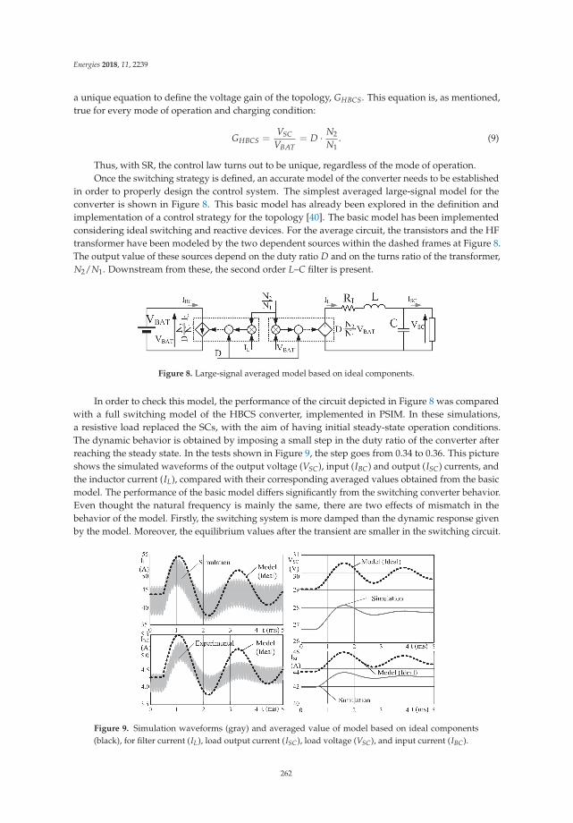
Energies 2018, 11, 2239
a unique equation to define the voltage gain of the topology, GHBCS. This equation is, as mentioned,true for every mode of operation and charging condition:
GHBCS =VSC
VBAT= D · N2
N1. (9)
Thus, with SR, the control law turns out to be unique, regardless of the mode of operation.Once the switching strategy is defined, an accurate model of the converter needs to be established
in order to properly design the control system. The simplest averaged large-signal model for theconverter is shown in Figure 8. This basic model has already been explored in the definition andimplementation of a control strategy for the topology [40]. The basic model has been implementedconsidering ideal switching and reactive devices. For the average circuit, the transistors and the HFtransformer have been modeled by the two dependent sources within the dashed frames at Figure 8.The output value of these sources depend on the duty ratio D and on the turns ratio of the transformer,N2/N1. Downstream from these, the second order L–C filter is present.
Figure 8. Large-signal averaged model based on ideal components.
In order to check this model, the performance of the circuit depicted in Figure 8 was comparedwith a full switching model of the HBCS converter, implemented in PSIM. In these simulations,a resistive load replaced the SCs, with the aim of having initial steady-state operation conditions.The dynamic behavior is obtained by imposing a small step in the duty ratio of the converter afterreaching the steady state. In the tests shown in Figure 9, the step goes from 0.34 to 0.36. This pictureshows the simulated waveforms of the output voltage (VSC), input (IBC) and output (ISC) currents, andthe inductor current (IL), compared with their corresponding averaged values obtained from the basicmodel. The performance of the basic model differs significantly from the switching converter behavior.Even thought the natural frequency is mainly the same, there are two effects of mismatch in thebehavior of the model. Firstly, the switching system is more damped than the dynamic response givenby the model. Moreover, the equilibrium values after the transient are smaller in the switching circuit.
Figure 9. Simulation waveforms (gray) and averaged value of model based on ideal components(black), for filter current (IL), load output current (ISC), load voltage (VSC), and input current (IBC).
262

Energies 2018, 11, 2239
In order to solve this disagreement between the model and the switching circuit, an improvedmodel has been developed. This model firstly accounts for the effects of the parasitic resistors ofthe transformer, the RDS of the transistors at the HV side, and the snubbers. These effects are jointlymodeled by a series resistance, Rloss, which adds a dissipative term in the model that contributes toincrease the damping factor. However, the most significant effect is due to the leakage inductanceof the transformer, depicted in Figure 10. Some waveforms are depicted in Figure 11 to describe thecontribution of this leakage inductance in the full model. For simplicity in this analysis, the overallprimary side leakage inductance is obtained as the sum of the measured primary- and reflectedmeasured secondary-side leakage inductances.
Figure 10. Half-bridge current-source (HBCS) converter equivalent circuit, including the overallleakage inductor at the primary side of the transformer.
Figure 11. (a) Switching waveforms with ideal transformer. (b) Switching waveforms with overallleakage inductor at the primary side.
The waveform sequence starts when S1 and S2 are turned off, and thus there is no current flowingthrough the primary side of the transformer. In this situation, the output inductor current splits equallythrough the diodes at switches S3 and S4. At time t0, S1 is turned on, forcing the primary side voltage,VP, to be half the voltage across the battery:
VP =VBAT
2. (10)
The high inductance of the filter, L, causes IL to keep flowing practically unchanged to the load.For the ideal transformer in Figure 11a, the current immediately flows through S1, and thus the diodes
263

Energies 2018, 11, 2239
of S3 and S4 are instantly turned-off. As a consequence, the secondary side voltages at the transformerinstantly are equal to:
VSec1 = VSec2 =VBAT
2N2
N1. (11)
Nonetheless, for the real transformer case depicted in Figure 10, the leakage inductance preventsthe secondary side current to change instantly (Figure 11b). Upon this situation current keeps flowingthrough the secondary sides of the transformer, S3 and S4. The secondary side voltages remain nullimmediately after turning on S1, and thus the voltage at the leakage inductor equals the primary-sidevoltage. This issue affects the operation of the system. For instance, in charging mode, both HV-sideswitches, S1 and S2, are in the off-state just before S1 is turned on. It can be seen in Figures 2 and 3athat each diode at the secondary side carries half IL, while the voltages at the primary side, VP, and atthe common node of the secondary windings, VO, are null:
IS3 = IS4 = − IL(t)2
= − IL2
, (12)
V0 = 0, (13)
VP = 0. (14)
Equation (12) describes as well that the inductor current is considered as constant withina switching interval. When S1 turns on at t0, and given that current keeps on flowing throughthe LV side diodes, then the voltage VP does not vary. Instead, because VDS1 equals zero, the voltage atthe primary side of the real transformer (i.e., considering the parasitic inductance), VPR, equals half thevoltage at the battery:
VPR =VBAT
2. (15)
Therefore, the values of the voltage across the leakage inductor, VLk, and the current at the primaryside of the transformer, ILk, can be calculated as:
VLk =VBAT
2, (16)
ILk = IPR =1
LLk
VBAT2
· t. (17)
As mentioned previously, the overall leakage inductance LLk takes into account the measuredleakage inductor at the primary (LLkPri
) and secondary (LLkSec ) sides of the real transformer, referred tothe primary side:
LLk = LLkPri+
LLkSec
2
(N1
N2
)2. (18)
Upon these conditions, the inductance LLk is linearly charged. The currents through S3 and S4 aregiven by:
IS3 = − IL2− IPR
2N1
N2, (19)
IS4 = − IL2+
IPR2
N1
N2. (20)
264

Energies 2018, 11, 2239
At instant t1, IS4 is null, turning S4 off, and thus from this instant the current IL equals the currentthrough the body diode of S3:
IS3 = −IL, (21)
IS4 = 0. (22)
As a consequence, the dead time td, defined as the interval between instants t0 and t1,
td = t1 − t0 (23)
is the time it takes for the current IS3 to reach −IL after S1 is turned on. This condition can beexpressed as:
−IL2
− 12
N1
N2
VBAT2
1LLk
(t1 − t0) = −IL(t). (24)
The explicit expression for td can thus be obtained:
td = 2 · N2
N1
IL(t)VBAT
· LLk. (25)
It is important to note that td represents a completely different behavior in the full model whencompared to the basic one. For the basic model, when switch S1 is turned on, VO equals to half thebattery voltage, obviously referred to the secondary side. Instead, for the full model, VO is zero duringtd just after turning S1 on, and then reaches the same VBAT/2 for the rest of the interval when S1
remains turned on. This situation affects the final voltage gain at the topology, given that the effectiveduty ratio of the converter, De f f , is actually smaller for the full model than for the basic one. This De f fcan be defined now as:
De f f =D1 · TS − td
TS. (26)
As it can be deduced from Equation (25), the expression of the dead time is a non-linear functionof a manifold of system parameters. Hence, the resulting model that takes this td into account isa non-linear model. The large-signal circuital model that considers td (and also Rloss) is shown inFigure 12. Additionally, the Equivalent Series Resistor, ESRC, of the filter capacitor C has been included.
Figure 12. Full averaged large-signal model based on real components, parasitic elements, and snubbers.
The full average model has been simulated and compared with the switching circuit, in order toevaluate its performance. These simulations, shown in Figure 13, have been carried out in the sameconditions that were established for the previous simulations of the basic model shown in Figure 9.
265

Energies 2018, 11, 2239
It can be seen how the new complete model tracks much more accurately the simulated waveforms atthe switching model, again for a duty step from 0.34 to 0.36. Therefore it can be concluded that thedynamic behavior of the HBCS converter with the proposed SR scheme is truly represented by theobtained full model.
Figure 13. Simulation waveforms (gray) and averaged value of model based on the parameters ofreal components (black), for filter current (IL), load output current (ISC), load voltage (VSC) and inputcurrent (IBC).
An important remark on this behavior ir that this response corresponds to a second order system,as it is expected from a resistive load at the output of the L–C filter at the LV side. In the proposedapplication, the load is an assembly of SC. If this assembly is considered as an ideal pure capacitiveload, given that the capacitance value of these devices is very large, then the output voltage wouldremain constant during the transient, and thus the dynamic behavior of the output voltage can bedisregarded. For a more realistic approach, the SC assembly will be modeled by an equivalent circuitformed by a series resistor and the SC capacitor. Still, the SC will present a very large capacitancevalue, and therefore it behaves practically as a DC voltage source. Thus, the AC small signal model ofthe SC is given by the series resistor only, and the behavior of the full system is again corresponding toa second order system.
At this point, a small-signal model can be derived. Figure 14 shows the model that emerges afterlinearizing and perturbing the large signal full model, which has the following parameters:
R1 =tdTS
(27)
R2 =2 · D · LLkPri
TS
(N2
N1
)2(28)
K1 =N2
N1· IL
(1 − td
TS
)(29)
K2 = 2 · tdTS
· D · N2
N1(30)
K3 =N2
N1· VBAT − 2 · I2
L · LLkPri
TS
(N2
N1
)2(31)
Figure 14. Full Small Signal Model of the system.
266

Energies 2018, 11, 2239
This last model finally allows the design and tuning of the control system, since the mostsignificant dynamics of the system are taken into account. The second order behavior of the system,represented in the previous analysis, can be also derived from this model. In fact, the output voltage toduty ratio transfer function, can be calculated as:
vSC
d
∣∣∣∣vBAT=0
=K3 · R0
R0 + ESRC· 1 + s · C · ESRC
REQ + R0
R0 + ESRC+ s ·
[L
R0 + ESRC+ C ·
(REQ +
R0 · ESRCR0 + ESRC
)]+ s2 · L · C
(32)
where
REQ = R2 + Rloss + RL (33)
5. Proposed Control Scheme for the HBCS Converter
An adequate design of the control stage of the converter is needed in order to ensure the requiredpower flows in the hybrid storage system under consideration [20–29]. In order to obtain the desiredoperating performance of the system, a High Level Control System provides the instant powerreferences that each storage device must supply to the DC link. From this power reference, the HVcurrent value of the HBCS converter, I∗BC can be calculated. This scheme is depicted in Figure 15 [40].
Figure 15. Control Strategy for the HBCS converter.
Considering that the final control parameter is the inductor current, IL, the converter control stagecovers two different aspects: Firstly, it is required that this stage generates a reference for such current,I∗L , starting from the HV side current, I∗BC. In addition, it implements a feedback control loop for suchinductor current.
5.1. Feedback Control Loop for the SC current
This inductor current control loop is shown in Figure 16a. It must be noticed how the averagevalue of IL equals the average value of ISC. In order to design and tune the regulator, the inductorvoltage to inductor current transfer function G(s) can be defined as:
G(s) =1
RL + s · L(34)
For the current loop, a standard PI regulator has been designed. This regulator is tuned using thezero-pole cancellation method, and setting the desired bandwidth of the current loop. The regulatorconsists of a pure integrator and a zero that cancels the pole given by the inductance L and the ESR ofthe filter inductor, RL. This ensures that the final bandwidth of the controlled system can be designedto a target value. The characteristic frequency of this zero might change upon eventual variations ofthe equivalent series resistor due temperature excursions, ageing, or even manufacturing tolerances.
267

Energies 2018, 11, 2239
However, assuming an adequate design of this inductor filter, then the ESR of this magnetic elementwill be relatively small; therefore, the variations in this parameter will not significantly affect thefinal performance of the controlled system. Once the regulator is tuned, the final implementationneeds to obtain the expression of the duty ratio, D, from the control action of the current loop,CA. Considering Equations (25) and (26) and Figure 12, the relationship between D and VL canbe calculated:
VL = De f f · N2
N1· VBAT − VSC = D ·
(1 − td
TS
)N2
N1· VBAT − VSC. (35)
Finally,
D =N1
N2· VL + VSC
Vbat − N2
N1· 2 · IL · LLkPri
TS
. (36)
Figure 16b shows the implemented control scheme. The shaded box implements Equation (36),obtaining the duty ratio D from the control action of the current loop, CA, which is VL. Figure 17shows simulations of the performance of this inner loop for a bandwidth of 500 Hz. This plot providesa sequence of current steps as a reference to the current loop, I∗L . It can be seen how the actual currentvalue tracks perfectly the reference. Moreover, the current can swiftly change its direction, changingautomatically from charging to discharging operation modes, even for large relative current steps.This feature is a consequence of using the discussed SR modulation scheme in the topology.
Figure 16. Inner control loop approach (a) for designing and tuning the regulator and (b) forimplementing the control scheme.
Figure 17. Simulation of inductor current IL (gray, upper plot) and supercapacitor (SC) voltage VSC
(black, lower plot) during step changes in the commanded current (black, lower plot). Positive currentcorresponds to charging mode, negative to discharging mode.
5.2. Generation of the SC Current Reference
The complete control scheme is shown in Figure 18. An external estimator stage is designed togenerate the feedback loop current reference, I∗L, from the original I∗BC reference. The relationshipbetween the HV-side current and the inductor current can be obtained from the model in Figure 14 as
268

Energies 2018, 11, 2239
iBC = K1 · d +1
R1· vBAT +
(N2
N1· D − K2
)· iL, (37)
iBC
iL
∣∣∣∣∣ d=0vBAT=0
=N2
N1· D − K2. (38)
The value of the inductor current reference, I∗L, is estimated from the HV-side current, I∗BC,by means of the model, as is given in Equation (38). Other control strategies based on additionalfeedback loops, such as a cascaded control loop to generate the inductor current reference, wouldimply a more complex implementation of the controller, in terms of computation, number of sensors,filtering and signal conditioning stages, and so on. In addition, they would provide a decrease in thedynamics, given that the external loop dynamics requires a bandwidth significantly smaller than thatof the inner loop, in order to ensure a good overall performance.
Figure 18. Complete control scheme for the half-bridge current-source (HBCS) converter.
6. Experimental Results
Figure 19 shows a 3 kW laboratory prototype of the HBCS, used in this work for the practicaldemonstration of the system performance. The main characteristics of the setup are detailed in Table 1.Preliminary results of the performance of this setup were reported in [35].
Figure 19. Laboratory prototype of the half-bridge current-source (HBCS) converter.
Figure 20 shows the experimental waveform of the converter, with the same operating conditionsas reported in Figure 9. It can be seen how the experimental waveforms were very similar to thesimulated waveforms for the switching converter. It also can be seen how the ideal model failed totrack the real waveforms properly.
Similarly, Figure 21 compares the proposed complete model, including the effects of the parasiticleakage inductance of the transformer and the resistance to account for the losses, against theexperimental waveforms, resembling the conditions stated for Figure 13. This validates the obtainedmodel for the HBCS converter, as the complete model tracked the real converter waveformsvery accurately.
269

Energies 2018, 11, 2239
Figure 20. Experimental waveforms (gray) and averaged value of model based on ideal components(black, dashed), for filter current (IL), load output current (ISC), load voltage (VSC), and inputcurrent (IBC).
Figure 21. Experimental waveforms (gray) and averaged value of model based on real components(black), for filter current (IL), load output current (ISC), load voltage (VSC), and input current (IBC).
In order to validate experimentally the implementation of the control scheme, a series of currentreference steps were implemented in the converter. The reference steps that were provided to thesimulations, shown in Figure 17, were also supplied to the laboratory prototype. Figure 22 shows theperformance of the experimental setup. It can be seen how the real converter performed as expected,thus validating the converter control scheme.
Figure 22. Inductor current IL (black, upper plot) and supercapacitor (SC) voltage VSC (black, lowerplot) during step changes in the commanded current I∗L (referenced by dashed gray lines). Positivecurrent corresponds to charging mode, negative to discharging mode.
270

Energies 2018, 11, 2239
In order to check the dynamics of the inner control loop, a detailed experimental response of oneof such current steps is shown in Figure 23.
Figure 23. Inductor current IL (black) and reference I∗L (grey) during one step change.
7. Conclusions and Future Developments
This research has demonstrated the feasibility of the HBCS converter as a bidirectional powerconverter for HSS systems in traction applications, where the DC-link is directly connected to thebattery bank. The main topics covered include the analysis and design of the power and controlstages, the modeling including parasitic elements of the topology, and a validation procedure througha laboratory prototype.
As a first contribution, it has been demonstrated that the use of SR is a suitable switching schemein the converter, given the demonstrated benefits in the efficiency and the enhancement in the controlsystem implementation. By means of this switching pattern, a full, bidirectional power flow controlcan be simply implemented in the converter. Moreover, this feature is obtained at no cost, since therequired hardware elements to implement SR pattern are present in the conventional HBCS topology.
Another key contribution is to include the parasitic elements in the topology aiming to obtaina highly representative circuital model of the converter. This model has been demonstrated by meansof simulations and through experiments in a 3 kW laboratory setup. With the information derivedfrom this dynamic model, the design of the control stage for the HSS can be easily implemented. Thisresearch also has provided a design example of a current control loop in order to govern the powerflow in the HSS outlined.
A series of future developments arise from this research. One of these developments is theimplementation of the HSS in a full powertrain for vehicle applications, including the integration ofthe HBCS converter control with the complete high-level control system. Another development coversthe optimization of the converter power topology and control system, including the definition of thecontrol strategy for the complete system. Additionally, the extension of the application of the HBCSconverter to other types of loads (e.g., inductive loads) can be considered in future research.
Author Contributions: J.G. and F.G.C. conceived the research and designed and performed the experiments; allthe authors analyzed the data and contributed to the discussion and conclusions.
Funding: This work has been partially supported by the Innovation Development and Research Office (MEC),Spanish Government, under Research Grants ENE2013-44245-R, Project “Microholo” and ENE2016-77919, Project“Conciliator”, and by the European Union through ERFD Structural Funds (FEDER). This work has been co-fundedby the Campus of International Excellence (CEI) of the University of Oviedo, Spain, as a Mobility Grant forAcademics in 2013, partially funded by the Gijon City Hall, by resolution of BOPA 156, 6-VII-2013.
Conflicts of Interest: The authors declare no conflict of interest.
271

Energies 2018, 11, 2239
Abbreviations
The following abbreviations are used in this manuscript:
CA Control actionDC Direct currentESR Equivalent series resistorLV Low-voltageHBCS Half-bridge current-sourceHF High-frequencyHSS Hybrid storage systemHV High-voltageIGBT Insulated-gate bipolar transistorMOSFET Metal-oxide-semiconductor field-effect transistorSC SupercapacitorSR Synchronous rectification
References
1. Ostadi, A.; Kazerani, M.; Chen, S.K. Hybrid Energy Storage System (HESS) in vehicular applications:A review on interfacing battery and ultra-capacitor units. In Proceedings of the 2013 IEEE TransportationElectrification Conference and Expo (ITEC), Detroit, MI, USA, 16–19 June 2013; pp. 1–7.
2. Amjadi, Z.; Williamson, S.S. Digital Control of a Bidirectional DC/DC Switched Capacitor Converter forHybrid Electric Vehicle Energy Storage System Applications. IEEE Trans. Smart Grid 2014, 5, 158–166.[CrossRef]
3. Kuperman, A.; Mellincovsky, M.; Lerman, C.; Aharon, I.; Reichbach, N.; Geula, G.; Nakash, R. SupercapacitorSizing Based on Desired Power and Energy Performance. IEEE Trans. Power Electron. 2014, 29, 5399–5405.[CrossRef]
4. Cohen, I.J.; Kelley, J.P.; Wetz, D.A.; Heinzel, J. Evaluation of a Hybrid Energy Storage Module for PulsedPower Applications. IEEE Trans. Plasma Sci. 2014, 42, 2948–2955. [CrossRef]
5. Farooque, M.; Maru, H.C. Fuel cells-the clean and efficient power generators. Proc. IEEE 2001, 89, 1819–1829.[CrossRef]
6. Di Napoli, A.; Caricchi, F.; Crescimbini, F. Fuel cells-the clean and efficient power generators. In Proceedingsof the 6th European Conference on Power Electronics, Seville, Spain, 19–21 September 1995.
7. Mestre, P.; Astier, S. Application of supercapacitors and influence of the drive control strategies on theperformances of on electric vehicle. In Proceedings of the 15th Electric Vehicle Symposium (EVS-15),Bruxelles, Belgium, 29 September–3 October 1998.
8. Grbovic, P.J.; Delarue, P.; Moigne, P.L.; Bartholomeus, P. Modeling and Control of the Ultracapacitor-BasedRegenerative Controlled Electric Drives. IEEE Trans. Ind. Electron. 2011, 58, 3471–3484. [CrossRef]
9. Schmidt, M. EV Mini-Van Featuring Series Conjunction of Ultracapacitors and Batteries for Load Levelingof its Batteries. In Proceedings of the 15th Electric Vehicle Symposium (EVS-15), Bruxelles, Belgium,29 September–3 October 1998.
10. Itani, K.; Bernardinis, A.D.; Khatir, Z.; Jammal, A.; Oueidat, M. Regenerative Braking Modeling, Control,and Simulation of a Hybrid Energy Storage System for an Electric Vehicle in Extreme Conditions. IEEE Trans.Transp. Electr. 2016, 2, 465–479. [CrossRef]
11. King, R.; Schwartz, J.; Cardinal, M.; Garrigan, K. Development and system test of high efficiencyultracapacitor/battery electronic interface. In Proceedings of the 15th Electric Vehicle Symposium (EVS-15),Bruxelles, Belgium, 29 September–3 October 1998.
12. Di Napoli, A.; Crescimbini, F.; Solero, L.; Caricchi, F.; Giulii Capponi, F. Multiple-input DC-DC powerconverter for power-flow management in hybrid vehicles. In Proceedings of the Conference Record of the2002 IEEE Industry Applications Conference, 37th IAS Annual Meeting (Cat. No.02CH37344), Pittsburgh,PA, USA, 13–18 October 2002; Volume 3, pp. 1578–1585.
13. Di Napoli, A.; Giulii Capponi, F.; Solero, L. Power Converter Arrangements with Ultracapacitor Tank forBattery Load Leveling in EV Motor Drives. In Proceedings of the 8th European Conference on PowerElectronics, Lausanne, Switzerland, 7–9 September 1999.
272

Energies 2018, 11, 2239
14. Herath, N.; Binduhewa, P.; Samaranayake, L.; Ekanayake, J.; Longo, S. Design of a dual energy storagepower converter for a small electric vehicle. In Proceedings of the 2017 IEEE International Conference onIndustrial and Information Systems (ICIIS), Peradeniya, Sri Lanka, 15–16 December 2017; pp. 1–6.
15. Kouchachvili, L.; Yaïci, W.; Entchev, E. Hybrid battery/supercapacitor energy storage system for the electricvehicles. J. Power Sources 2018, 374, 237–248. [CrossRef]
16. Song, Z.; Li, J.; Hou, J.; Hofmann, H.; Ouyang, M.; Du, J. The battery-supercapacitor hybrid energy storagesystem in electric vehicle applications: A case study. Energy 2018, 154, 433–441. [CrossRef]
17. Cabrane, Z.; Ouassaid, M.; Maaroufi, M. Analysis and evaluation of battery-supercapacitor hybrid energystorage system for photovoltaic installation. Int. J. Hydrogen Energy 2016, 41, 20897–20907. [CrossRef]
18. Hernández, J.; Sanchez-Sutil, F.; Vidal, P.; Rus-Casas, C. Primary frequency control and dynamic grid supportfor vehicle-to-grid in transmission systems. Int. J. Electr. Power Energy Syst. 2018, 100, 152–166. [CrossRef]
19. Thounthong, P.; Piegari, L.; Pierfederici, S.; Davat, B. Nonlinear intelligent DC grid stabilization for fuel cellvehicle applications with a supercapacitor storage device. Int. J. Electr. Power Energy Syst. 2015, 64, 723–733.[CrossRef]
20. Sun, L.; Feng, K.; Chapman, C.; Zhang, N. An Adaptive Power-Split Strategy for Battery-SupercapacitorPowertrain-Design, Simulation, and Experiment. IEEE Trans. Power Electron. 2017, 32, 9364–9375. [CrossRef]
21. Bougrine, M.; Benalia, A.; Delaleau, E.; Benbouzid, M. Minimum time current controller design fortwo-interleaved bidirectional converter: Application to hybrid fuel cell/supercapacitor vehicles. Int. J.Hydrogen Energy 2018, 43, 11593–11605. [CrossRef]
22. He, H.W.; Xiong, R.; Chang, Y.H. Dynamic Modeling and Simulation on a Hybrid Power System for ElectricVehicle Applications. Energies 2010, 3, 1821–1830. [CrossRef]
23. Shah, N.; Czarkowski, D. Supercapacitors in Tandem with Batteries to Prolong the Range of UGV Systems.Electronics 2018, 7, 6. [CrossRef]
24. Zhang, Q.; Deng, W. An Adaptive Energy Management System for Electric Vehicles Based on Driving CycleIdentification and Wavelet Transform. Energies 2016, 9, 341. [CrossRef]
25. Passalacqua, M.; Lanzarotto, D.; Repetto, M.; Marchesoni, M. Advantages of Using Supercapacitors andSilicon Carbide on Hybrid Vehicle Series Architecture. Energies 2017, 10, 920. [CrossRef]
26. Wang, Y.; Hu, H.; Zhang, L.; Zhang, N.; Sun, X. Real-Time Vehicle Energy Management System Based onOptimized Distribution of Electrical Load Power. Appl. Sci. 2016, 6, 285. [CrossRef]
27. Wang, B.; Xu, J.; Wai, R.J.; Cao, B. Adaptive Sliding-Mode With Hysteresis Control Strategy for SimpleMultimode Hybrid Energy Storage System in Electric Vehicles. IEEE Trans. Ind. Electron. 2017, 64, 1404–1414.[CrossRef]
28. Thounthong, P.; Rael, S. The benefits of hybridization. IEEE Ind. Electron. Mag. 2009, 3, 25–37. [CrossRef]29. Lai, J.; Nelson, D.J. Energy Management Power Converters in Hybrid Electric and Fuel Cell Vehicles.
Proc. IEEE 2007, 95, 766–777. [CrossRef]30. Trovão, J.P.; Silva, M.A.; Dubois, M.R. Coupled energy management algorithm for MESS in urban EV.
IET Electr. Syst. Transp. 2017, 7, 125–134. [CrossRef]31. Jain, M.; Daniele, M.; Jain, P.K. A bidirectional DC-DC converter topology for low power application.
IEEE Trans. Power Electron. 2000, 15, 595–606. [CrossRef]32. Kazimierczuk, M.K.; Vuong, D.Q.; Nguyen, B.T.; Weimer, J.A. Topologies of bidirectional PWM dc-dc power
converters. In Proceedings of the IEEE 1993 National Aerospace and Electronics Conference-NAECON 1993,Dayton, OH, USA, 24–28 May 1993; Volume 1, pp. 435–441.
33. Giulii Capponi, F.; Cacciato, F. Using Super Capacitors in Combination with Bi-Directional DC/DCConverters for Active Load Management in Residential Fuel Cell Applications. In Proceedings of the1st European Symposium on Supercapacitors (ESSCAP’04), Belfort, France, 4–5 November 2004.
34. Cacciato, M.; Caricchi, F.; Giulii Capponi, F.; Santini, E. A critical evaluation and design of bi-directionalDC/DC converters for super-capacitors interfacing in fuel cell applications. In Proceedings of the ConferenceRecord of the 2004 IEEE Industry Applications Conference, 39th IAS Annual Meeting, Seattle, WA, USA,3–7 October 2004; Volume 2, pp. 1127–1133.
35. Giulii Capponi, F.; Santoro, P.; Crescenzi, E. HBCS Converter: A Bidirectional DC/DC Converter forOptimal Power Flow Regulation in Supercapacitor Applications. In Proceedings of the 2007 IEEE IndustryApplications Annual Meeting, New Orleans, LA, USA, 23–27 September 2007; pp. 2009–2015.
273

Energies 2018, 11, 2239
36. Zhang, Y.; Guo, Z.; Zhang, Y.; Zhan, T.; Jin, L. Active battery/ultracapacitor hybrid energy storage systembased on soft-switching bidirectional converter. In Proceedings of the 2013 International Conference onElectrical Machines and Systems (ICEMS), Busan, South Korea, 26–29 October 2013; pp. 2177–2182.
37. Wai, R.J.; Duan, R.Y. High-Efficiency Bidirectional Converter for Power Sources with Great Voltage Diversity.IEEE Trans. Power Electron. 2007, 22, 1986–1996. [CrossRef]
38. Yamamoto, K.; Hiraki, E.; Tanaka, T.; Nakaoka, M.; Mishima, T. Bidirectional DC-DC converter withfull-bridge/push-pull circuit for automobile electric power systems. In Proceedings of the 2006 37th IEEEPower Electronics Specialists Conference, Jeju, South Korea, 18–22 June 2006; pp. 1–5.
39. Dusmez, S.; Hasanzadeh, A.; Khaligh, A. Comparative Analysis of Bidirectional Three-Level DC DCConverter for Automotive Applications. IEEE Trans. Ind. Electron. 2015, 62, 3305–3315. [CrossRef]
40. Garcia, J.; Giulii Capponi, F.; Borocci, G.; Garcia, P. Control strategy for Bidirectional HBCS Converter forsupercapacitor applications. In Proceedings of the 2014 IEEE 23rd International Symposium on IndustrialElectronics (ISIE), Istanbul, Turkey, 1–4 June 2014; pp. 1794–1799.
41. Garcia, J.; Garcia, P.; Giulii Capponi, F.; Borocci, G.; De Donato, G. Analysis, modeling and control ofhalf-bridge current-source converter for supercapacitor applications. In Proceedings of the 2014 IEEE EnergyConversion Congress and Exposition (ECCE), Pittsburgh, PA, USA, 14–18 September 2014; pp. 3786–3793.
c© 2018 by the authors. Licensee MDPI, Basel, Switzerland. This article is an open accessarticle distributed under the terms and conditions of the Creative Commons Attribution(CC BY) license (http://creativecommons.org/licenses/by/4.0/).
274

energies
Article
Novel Step-Down DC–DC Converters Based on theInductor–Diode and Inductor–Capacitor–DiodeStructures in a Two-Stage Buck Converter
Mauricio Dalla Vecchia 1,2,*, Giel Van den Broeck 1,2, Simon Ravyts 1,2 and Johan Driesen 1,2
1 Departement Elektrotechniek, KU Leuven, Kasteelpark Arenberg 10, 3001 Leuven, Belgium;[email protected] (G.V.d.B.); [email protected] (S.R.);[email protected] (J.D.)
2 EnergyVille, Thor Park 8310, 3600 Genk, Belgium* Correspondence: [email protected]
Received: 14 January 2019; Accepted: 19 March 2019; Published: 22 March 2019
Abstract: This paper explores and presents the application of the Inductor–Diode andInductor-Capacitor-Diode structures in a DC–DC step-down configuration for systems that requirevoltage adjustments. DC micro/picogrids are becoming more popular nowadays and the study ofpower electronics converters to supply the load demand in different voltage levels is required.Multiple strategies to step-down voltages are proposed based on different approaches, e.g.,high-frequency transformer and voltage multiplier/divider cells. The key question that motivates theresearch is the investigation of the aforementioned Inductor–Diode and Inductor–Capacitor–Diode,current multiplier/divider cells, in a step-down application. The two-stage buck converter is used asa study case to achieve the output voltage required. To extend the intermediate voltage level flexibilityin the two-stage buck converter, a second switch was implemented replacing a diode, which gives anextra degree-of-freedom for the topology. Based on this modification, three regions of operation aretheoretically defined, depending on the operational duty cycles δ2 and δ1 of switches S2 and S1. Theintermediate and output voltage levels are defined based on the choice of the region of operation andare mapped herein, summarizing the possible voltage levels achieved by each configuration. Thepaper presents the theoretical analysis, simulation, implementation and experimental validation of aconverter with the following specifications; 48 V/12 V input-to-output voltage, different intermediatevoltage levels, 100 W power rating, and switching frequency of 300 kHz. Comparisons betweenmathematical, simulation, and experimental results are made with the objective of validating thestatements herein introduced.
Keywords: DC–DC converter; experimental verification; Inductor–Diode; Inductor–Capacitor–Diode;nonisolated; step-down; two-stage buck converter; voltage regulation
1. Introduction
In the last century, AC systems predominated as the most widespread method for energygeneration, transmission, and distribution. For regular AC generation, large power plants, e.g.,coal, hydro, and nuclear, have been used to centrally generate energy. Alternatives, such as wind andsolar generation, are more frequently being installed to decentralize the energy production and lowerthe CO2 emitted by the energy production [1,2].
Wind farms (AC generation) are more common in remote regions (on and off-shore) where thewind is conducive for generation. Solar (DC generation), on the other hand, started to become viablefor application in high populated areas where the sun irradiation is high enough to achieve maximumpower generation. DC systems started to be developed and implemented in pilot projects and real
Energies 2019, 12, 1131; doi:10.3390/en12061131 www.mdpi.com/journal/energies275

Energies 2019, 12, 1131
applications because they have proved to be more efficient than AC systems in terms of transformationsteps [3], costs [4], and power transfer capability [5]. Applications of DC system such as in micro-and nanogrids [6,7], datacenters [8,9], and aircrafts, where redundancy and backup is mandatory, arecurrently on the rise. DC system technology can also be implemented in isolated/remote/emergingregions [10]. In these systems, redundancy normally is indispensable in order to keep the systemoperational even if a component and/or a converter fails. Furthermore, DC loads are commonespecially in low voltage/low power applications, for instance, in computer and battery chargers, USBand USB-C ports, and LED lights. These type of loads are commonly found in offices and residences.
Discussions among the voltage levels that are implemented in these systems are extensivelypresented in the literature [11], for instance, with a voltage between 350 and 400 V for distributionin unipolar or bipolar [6,12,13] DC configurations to supply high power equipments. The 48 V levelis [14,15] normally adopted as an intermediate bus stage to supply the low voltage/low power loadsaforementioned. The 48 V level is also getting more common in battery systems for Electric Vehicles(EV), and it is considered for residential applications due to its user safety approach.
A DC picogrid, based on state-of-the-art architectures [3,6,16], is depicted in Figure 1,which emulates a building and/or residence with a DC grid implementation. In this grid,a bipolar DC network is realized (P0N poles), which has the possibility of injecting the energygenerated by the panels in the AC grid or, alternatively, directly supply DC loads bypassing theDC–AC–DC transformation.
A lot of effort has been spent to propose new topologies and systems to interconnect PVgeneration in AC or DC grids with, respectively, microinverters [17–19] and microconverters (DCpower optimizers) [20–24] which, in essence, are step-up converters since the PV panel output voltageis lower than the AC grid or DC bus voltages. The control aspects of this system and MPPT strategiesare common subjects in the literature [20,25–27].
Different strategies to step-up the voltage have been studied and proposed in the literature,such as: isolated step-up topologies [17,21,28], coupled-inductor, nonisolated topologies [29–35],nonisolated topologies with Capacitor–Diode/switch structure [19,36–38], nonisolated topologieswith Inductor–Diode/switch [39,40] and nonisolated topologies with Capacitor–Diode/switchand Inductor–Diode/switch structures [41,42]. These structures are known, respectively, asswitched-capacitors and switched-inductors. An adaptation of the Inductor–Diode structure isproposed in [43], where a capacitor replaces one diode and changes the gain of the structure for step-upapplications. Each of the above-mentioned strategies to step-up voltages has its advantages anddisadvantages. For instance, isolated topologies and coupled inductor topologies have the flexibility of,based on the turns ratio of the magnetic device, select the suitable output voltage requirement, althoughit is known that these magnetic components are, together with heatsinks, the bulkiest componentsin a converter. Switched capacitor and switched inductors do not bring this flexibility once the gainis defined based on the operational duty cycle of the active switches. Inductors are more reliablecomponents than capacitors, giving an advantage in terms of reliability, while capacitors are morecompact and more suited for high power density applications.
In step-down conversion ratio converters, the Capacitor–Diode/switch structures are commonlyused to improve the step-down ratio of the converters [44–46]. On the other hand, the implementationof an Inductor–Diode/switch and Inductor–Capacitor–Diode structures in the step-down conversionratio is not extensively discussed in the literature, with few exceptions that explore both step-upand step-down structures [39]. The structures evaluated in this paper are shown in Figure 2. TheInductor–Diode structure shown in Figure 2 can offer a redundant path if one diode of the structurefails in open-circuit, as proposed in [47]. In steady-state, the inductors can be considered as currentsources and, due to the structure operability discussed in Section 4, mitigate the implementation ofcurrent sensors for control purposes, since the current balance between the inductors is naturallyachieved without any control strategy (switched-inductor characteristic). The only sensor that mightbe consider for implementation is a voltage sensor, if the application requires a regulated and constant
276

Energies 2019, 12, 1131
output voltage level for the entire load range of operation. For instance, a contraction technique wasproposed to control a regular step-down converter [48].
With these considerations, the objective of this paper is to investigate the influence of theInductor–Diode (ID) and Inductor–Capacitor–Diode (ICD) structures in the step-down conversionstage from 48 V to 12 V input-to-output voltage. The main contributions of this paper are (1) an analysisof the influence of the ID and ICD structures in a step-down conversion system; (2) the presentationof a full theoretical analysis of the converters generated; (3) applying the ID and ICD structures in aquadratic buck converter; (4) analyzing the intermediate voltage level behavior for different operationalpoints, showing the intermediate voltage flexibility of the circuit, which is beneficial for a voltageregulation point of view; (5) creating a flexible test bench to be able to validate the proposed convertersand; (6) experimentally validatation with waveforms of the topologies studied in the paper.
The paper is organized as follows; Section 2 presents the analysis of the ID and ICD structure in aregular single-stage buck converter and its impact on the gain of the converter. Section 3 presents thetwo-stage buck converter, known as quadratic buck converter [49], to enable the converter applying theID and ICD structures to achieve the required output voltage levels. The operational principle of thetopologies generated by the proposed intra-exchangeability is explained in Section 4. Section 5 exploresthe simulation results of the proposed topologies, showing the intermediate and output voltage levelsthat are obtained for each possible configuration. Section 6 describes the experimental test benchbuilt for further validation, showing experimental waveforms that validate the theoretical analysispresented in Sections 3 and 4. Section 7 presents the main conclusions and future work suggestions.
2. Impact of Inductor–Diode and Inductor–Capacitor–Diode Structures in a Step-Down Converter
This section has the objective of investigating the influence of the ID and ICD structure in astep-down buck converter. Inductor I, shown in Figure 3, is replaced by ID and ICD structures and thePWM modes are described herein. The main difference between the ID and ICD structures is that thecapacitor of the ICD is also charged during the magnetization of the inductors. When discharging, thecapacitor also discharges, providing energy to the load. The capacitor stores part of the energy that isdelivered to the load, which helps decrease the size of the inductors, since less energy is stored in theirmagnetic field. Additionally, the capacitor changes the voltage applied across the inductors duringdemagnetization, which changes the gain of the structures, as described herein.
Figure 1. A basic DC picogrid, highlighting the PV generation and DC step-up conversion; the bipolarDC network (P0N); the battery energy storage system (BESS); and the DC loads supplied by DC–DCstep-down converters.
277

Energies 2019, 12, 1131
Figure 2. (a) Inductor–Diode (ID) structure and its charge and discharge modes and (b)Inductor–Capacitor–Diode (ICD) structure and its charge and discharge modes.
Figure 3. DC–DC Buck Converter with Point-of-Connection 1 (PoC1) to interchange inductor (I),Inductor–Diode (ID) and Inductor–Capacitor–Diode (ICD) structures.
2.1. PWM Mode 1
In this PWM mode, the switch S1 commutates from ‘open’ to ‘close’, changing the equivalentcircuit of the converter. The equivalent circuit for this mode is shown in Figure 4a,b for the ID and ICDapplications in PoC1, respectively. During this mode, the voltage applied in the inductor terminalsVL1 and VL2 is positive, due to the step-down mechanism, and energy is magnetically stored in theinductors during the process. The voltage applied across the inductors terminals has the same level(internally in ID and ICD structures), which leads to similar current level in the inductors of thestructures. In the ID structure, the inductors store energy during this PWM Mode while in the ICDstructure the inductors and the capacitor of the structure store energy.
2.2. PWM Mode 2
In this PWM mode, the switch S1 commutates from ‘close’ to ‘open’. The equivalent circuit forthis mode is shown in Figure 4c,d for the ID and ICD structures, respectively. During this PWM mode,the voltage applied across the inductors terminals VL1 and VL2 is negative, since diode D1 is forwardbiased, leading to a demagnetization of these inductors. The current across both inductors is equal asthese components are in series, which guarantees the same negative voltage level across the inductorsof the structures during the demagnetization. The demagnetization mechanism for both structuresis similar, since in both structures the inductors are connected in series and the same current flowsthrough the passive components.
278

Energies 2019, 12, 1131
From the above PWM mode analysis, the theoretical voltage profile for all the inductors in bothstructures are presented in (1). These equations are applied in (2) to obtain the conversion gain of thestructures, in steady-state.
ID ICD{VL1 = VL2 = VIN − VOUT during δ1
VL1 = VL2 = −VOUT2 during (1 − δ1)
{VL1 = VL2 = VC1 = VIN − VOUT during δ1
VL1 = VL2 = VIN2 − VOUT during (1 − δ1)
(1)
VL =∫ TS
0vLdt = 0 (2)
2.3. Theoretical Gain in Continuous Conduction Mode
To obtain the theoretical voltage gain profile of the topologies, operation in steady-state isconsidered, which allows the application of (1) in (2) to obtain the ideal gain of the structures.After some mathematical manipulation, the theoretical expression that represents the gain of theInductor–Diode (ID) and Inductor–Capacitor–Diode (ICD) structures, respectively, is graphicallyrepresented in Figure 5. From Figure 5, it is noticed that the operational voltage range tackled in thispaper cannot be realized with the ICD structure, since its gain range is, ideally, between [0.5 ; 1]. Toovercome this, the quadratic buck converter—a nonlinear step-down converter generated by two buckconverters connected in series with each other—as depicted in Figure 6, is the base topology used togenerate the converters proposed in this paper. This converter presents an intermediate stage, givingan extra degree of freedom for implementation, since two voltage levels are generated in the sameconverter and both can be used to supply loads.
Only one switch is implemented on the power stage of the conventional quadratic buck, whichhas the benefit of control strategy simplification; and the intermediate voltage level is in the functionof the duty cycle applied to switch S1. If a second switch is introduced in the power stage, the degreeof freedom for voltage regulation in the intermediate stage is guaranteed by the duty cycle of thesecond switch S2, although the control strategy might increase in complexity, if applicable. Since theobjective of the topologies is to improve the flexibility of the conversion ratio and the overall system,the quadratic buck with two switches is the converter that will be extensively explored in the nextsection, together with the intra-exchangeable PoC structures presented in Figure 3.
3. Double-Switch Two-Stage Quadratic Buck Converter for Voltage Regulation
As previously mentioned, the two-stage buck converter, most known as quadratic buck converter,is the base topology used for the intra-exchangeable methodology used herein for testing multipleconfigurations, based on the ID and ICD structures, applied for voltage regulation. Since a secondstage is now implemented in the power circuit, the intra-exchangeability increases the amount oftopologies that can be generated. More specifically, with three structures and two stages, the numberof topologies generated is 32 = 9, where only the conventional quadratic buck is already exploredin the literature. Figure 6 exemplifies the possible configurations that can be obtained from theproposed intra-exchangeability between a regular inductor (I) and the ID and ICD structures. Whenan I structure is connected to PoC1 and PoC2, the regular quadratic buck is obtained. In total, ninetopologies are generated from this method and, since two switches are implemented in the powerstage with independent duty cycles, three regions of operation can be explored and will be brieflydiscussed herein. The regions of operation are highlighted in Figure 6, named as region 1, when dutycycle δ2 is higher than duty cycle δ1; region 2, when δ1 is higher than δ2; and region 3, when both dutycycles are equal. The switch realization is based on a MOSFET with an antiparallel diode, as shown inFigure 6.
279

Energies 2019, 12, 1131
Figure 4. (a) PWM mode 1 for ID structure; (b) PWM mode 1 for ICD structure; (c) PWM mode 2 forID structure, and (d) PWM mode 2 for ICD structure.
Figure 5. Continuous conduction mode graphical gain representation.
3.1. Region 1 (δ2 > δ1)
Operating in Region 1, the two stages of the quadratic buck structure operate independently,leading to intermediate and output voltages, depending on the duty cycles δ2 and δ1. The intermediatevoltage across capacitor Cinter depends on the structure connected in PoC2 and the duty cycle δ2 tocommand switch S2. The output voltage, on the other hand, depends on both structures connectedin PoC2 and PoC1, since the intermediate voltage level is the input voltage of the first stage. Theequations presented in Figure 5 are reused to find the intermediate and output voltages generated bythis integration. Table 1 summarize the analysis, showing the theoretical gain profile of the intermediatestage and output stage in function of the input voltage of the circuit and the duty cycle of switches S1
and S2. For instance, if the ID structure is applied in PoC1 and the I structure in PoC2, the intermediateand output voltages of the circuit are, respectively, related to equations δ2 and δ2
2δ11+δ1 , , which means
that the intermediate voltage is regulated by the nominal set point of the duty cycle applied in S2 andthe output voltage depends on the duty cycles applied to S1 and S2. The analysis considers that theduty cycles are independent, and with no phase-shift between each other.
3.2. Region 2 (δ2 < δ1)
Operating in this region, the second stage of the quadratic buck depends on the first stage, sincethe duty cycle of switch S1 is higher than the duty cycle of switch S2. Consequently, the intermediatecapacitor continues to discharge even if the switch S2 is in ‘off’-state (due to the antiparallel diodebetween drain-source points of S2). In this operational region, the duty cycle δ1 defines the intermediate
280
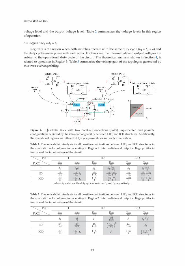
Energies 2019, 12, 1131
voltage level and the output voltage level. Table 2 summarizes the voltage levels in this regionof operation.
3.3. Region 3 (δ2 = δ1 = δ)
Region 3 is the region when both switches operate with the same duty cycle (δ2 = δ1 = δ) andthe duty cycles are in phase with each other. For this case, the intermediate and output voltages aresubject to the operational duty cycle of the circuit. The theoretical analysis, shown in Section 4, isrelated to operation in Region 3. Table 3 summarize the voltage gain of the topologies generated bythis intra-exchangeability.
Figure 6. Quadratic Buck with two Point-of-Conncetions (PoCs) implemented and possibleconfigurations achieved by the intra-exchangeability between I, ID, and ICD structures. Additionally,the operational regions for different duty cycle possibilities and switch realization.
Table 1. Theoretical Gain Analysis for all possible combinations between I, ID, and ICD structures inthe quadratic buck configuration operating in Region 1. Intermediate and output voltage profiles infunction of the input voltage of the circuit.
PoC2
PoC1 I ID ICDVinterVIN
VOUTVIN
VinterVIN
VOUTVIN
VinterVIN
VOUTVIN
I δ2 δ2δ1 δ2 δ22δ1
1+δ1δ2 δ2
1+δ12
ID 2δ21+δ2
2δ21+δ2
δ12δ2
1+δ2
2δ21+δ2
2δ11+δ1
2δ21+δ2
2δ21+δ2
1+δ12
ICD 1+δ22
1+δ22 δ1
1+δ22
1+δ22
2δ11+δ1
1+δ22
1+δ22
1+δ12
where δ2 and δ1 are the duty cycle of switches S2 and S1, respectively.
Table 2. Theoretical Gain Analysis for all possible combinations between I, ID, and ICD structures inthe quadratic buck configuration operating in Region 2. Intermediate and output voltage profiles infunction of the input voltage of the circuit.
PoC2
PoC1 I ID ICDVinterVIN
VOUTVIN
VinterVIN
VOUTVIN
VinterVIN
VOUTVIN
I δ1 δ21 δ1
2δ21
1+δ1δ1 δ1
1+δ12
ID 2δ11+δ1
2δ21
1+δ1
2δ11+δ1
(2δ1
1+δ1
)2 2δ11+δ1
δ1
ICD 1+δ12
1+δ12 δ1
1+δ12 δ1
1+δ12
(1+δ1
2
)2
281

Energies 2019, 12, 1131
Table 3. Theoretical Gain Analysis for all possible combinations between I, ID, and ICD structures inthe quadratic buck configuration operating in Region 3. Intermediate and output voltage profiles infunction of the input voltage of the circuit.
PoC2
PoC1 I ID ICDVinterVIN
VOUTVIN
VinterVIN
VOUTVIN
VinterVIN
VOUTVIN
I δ δ2 δ 2δ1+δ δ δ δ 1+δ
2
ID 2δ1+δ
2δ1+δ δ 2δ
1+δ
(2δ
1+δ
)2 2δ1+δ
2δ1+δ
1+δ2
ICD 1+δ2
1+δ2 δ 1+δ
21+δ
22δ
1+δ1+δ
2
(1+δ
2
)2
Although nine different topologies are realized in this analysis, only six different output voltageprofiles are obtained, since the topologies I-ID/ID-I, I-ICD/ICD-I and ID-ICD/ICD-ID provide thesame output voltage profile, while different intermediate voltage profiles are observed. Figure 7 showsthe graphical representation of the output voltage profiles presented in Table 3. It is noticed that, dueto the equations of the voltage profile shown in Figure 5, the highly nonlinear behavior of the quadraticbuck converter is attenuated when the ID or ICD structures are used in one of the PoCs. The gain ofthe topologies, mathematically expressed in Table 3 and graphically in Figure 7, is less nonlinear ifcompared with the conventional quadratic converter, which is interesting for control purposes. Theseconverters, however, are not suitable for applications that require high step-down capability, sincethe ID and ICD structures decrease the step-down capability of the structure, as shown in Figure 5for application in a regular buck and Figure 7 in the quadratic version. Although the component partcount increases for ID and ICD implementation, it also increases the flexibility to achieve multipleintermediate voltage levels to supply different loads.
On comparison of Table 2, related to region 2, and Table 3, related to region 3, it is noticed thatthe gain of the structures are the same. As mentioned in the previous subsection, this behavior occursbecause the antiparallel diode of switch S2 continue to conduct even if switch S2 is in ‘off’-state untilswitch S1 commutates from ‘close’ to ‘open’. This analysis concludes that operational regions 2 and3 generate similar PWM modes and, consequently, the same intermediate and output voltage levelswhile region 1 is distinguished by the independence between the stages. Section 4 will further discussthe operational principle of the double switch quadratic buck with ID and ICD structures, for operationin Region 3.
4. Operational Principle of the Double Switch Quadratic Buck Converter in Region 3
Similar to Section 2, where the one-stage I, ID, and ICD topologies have been introduced, thissection introduces the PWM modes of the two-stage I, ID, and ICD topologies, where the PWM signalremains the same. The phase shift between δ2 and δ1 is considered zero (in phase with each other) forthe specific analysis but if differs from zero, the gain behavior shown in Tables 1–3 will differ, since thephase-shift will influence the PWM stages and, consequently, the gain of the structures. The equivalentcircuit for the first and second stages, considering all the possibilities between the exchangeablecircuits, are present in Figure 8a,b, respectively. In order to evaluate the main characteristics of thetopologies, the equivalent circuits presented in Figure 8 are used to mathematically evaluate thevoltage and current stresses in all power components. This information is crucial to further dimensionthe components for practical implementation.
The voltage stress across each power semiconductor are extracted from the PWM mode stages inFigure 8 and summarized in Table 4. The voltage stress across switch S1 and diode D1 is affected by thestructure applied in PoC2, for instance, if the I structure is applied to PoC2, the voltage stress acrossswitch S1 is defined by (1 + δ)VIN , while if the ID structure is applied in PoC2, the voltage stress acrossswitch S1 is defined by equation (1+3δ)
(1+δ)VIN . Similarly, the voltage stress across diodes D3/D5/D7,
connected to PoC1, are related to the structure connected in PoC1. For instance, maintaining PoC2
282

Energies 2019, 12, 1131
fixed with the ID structure, if the ID structure is connected to PoC1, the voltage across the diodesD3/D5 is expressed by δ2
(1+δ)2 VIN and, if PoC1 is changed for an ICD structure, the voltage across
diodes D3/D5 is expressed by δ(1+δ)
VIN . Switch S2 and diode D2 stresses are independent on thestructures and are equal to the input voltage VIN. The voltage stress across diodes D3-D4-D5-D6-D7-D8,which are the diodes implemented in the ID and ICD structures, are related to the operational dutycycle, input voltage, and in which PoC the structures are implemented.
Similarly, the PWM modes also provide the RMS current stress in each power semiconductor.To evaluate the RMS current stress in all components, equation (3) is introduced, where ix1 is thecurrent that the semiconductor conducts during the first PWM mode and ix2 is the current conductedduring the second PWM mode. Applying (3), the current stress in each semiconductor is characterizedand presented in Table 5. Different than the voltage stress, the current stress of switches S2 and D2
depend on the structure connected to PoC2 but are independent of the structure connected to PoC1.
For instance, the RMS current stress across switch S2 is expressed by IIN(1−δ)δ
√1δ if the I structure is
connected to PoC2, and expressed by IIN(1−δ)2δ
√1δ if the ID structure is connected. It is also noticed that
the current is independent on PoC1, in this case.The analysis abovementioned is important in order to select the components for experimental
validation, since the RMS current and voltage stress are the most important characteristics to selectMOSFETs and diodes. The next section presents a numerical simulation for the proposed converterperformed in PLECS (4.0.2, Plexim GmbH, Zurich, Switzerland).
ixRMS =
√1
TS
(∫ DTS
0i2x1dt +
∫ TS
DTS
i2x2dt)
(3)
Figure 7. Continuous conduction mode graphical gain representation.
283

Energies 2019, 12, 1131
Figure 8. (a) Equivalent circuit for PoC 2 and PoC 1 applying I, ID, and ICD structures during the firstPWM mode and (b) equivalent circuit for PoC 2 and PoC 1 applying I, ID, and ICD structures duringthe second PWM mode.
Table 4. Voltage stress sum up for all power semiconductors in the power stage. Equations are infunction of the input voltage.
S1 S2 D1 D2 D3/D5 D4/D6 D7 D8
PoC2-PoC1 I-I
-
-
-
- I-ID
I-ICD - ID-I
-
ID-ID
ID-ICD -
ICD-I
-
- ICD-ID
ICD-ICD -
284

Energies 2019, 12, 1131
Table 5. RMS Current stress sum up for all power semiconductors in the power stage. Equations are infunction of the input current.
S1 S2 D1 D2 D3/D5 D4/D6 D7 D8
PoC2-PoC1
I-I
-
-
-
- I-ID
I-ICD -
ID-I
-
ID-ID
ID-ICD -
ICD-I
-
- ICD-ID
ICD-ICD -
5. Numerical Simulations
A numerical simulation was carried out to show the available intermediate voltage levels whenan output voltage of 12 V is set as standard output voltage. The 12 V voltage level can supply lowvoltage/low power loads to, for instance, LEDs or to charge small batteries (unidirectional power flowto charge, since the topologies are unidirectional); this is one of the main reasons to fix the outputvoltage on this level. The simulation and experimental parameters are presented in Table 6.
Different intermediate voltage levels are generated, depending on the structure connected inPoC2 and the operational duty cycle of the converter, as shown in Table 3. The simulation modelwas develop in PLECS. The only configuration that is not able to be simulated and experimentallyvalidated in this paper is the ICD-ICD structure, since the input/output voltage level is 48 V/12 Vand the theoretical gain of this structure is 0.25 < ICD-ICD < 1, making it impossible to provide therequired output voltage.
A simulation is performed for each configuration and the results are shown in Figure 9. Theconventional quadratic buck with I-I is show in Figure 9a, generating an intermediate voltage levelof 24 V. According to Table 3, the I-ID and ID-I configurations generates the same output voltage butdifferent intermediate voltage levels for operation with the same duty cycle. This behavior is provedvia simulation and presented in Figure 9b,d, where the voltage level of 20.25 V (I-ID) and 28.5 V (ID-I)are obtained for a duty cycle of 42.2%.
Similarly, the topologies I-ICD and ICD-I operate with the same duty cycle (36.6%) andinput/output voltages, however the intermediate voltage level changes since is applied differentstructures in PoC2. Simulation results shown in Figure 9c,g confirm the analysis, since an intermediatevoltage of 17.6 V (I-ICD) and 32.8 V (ICD-I) are obtained and available to supply loads in differentvoltage ranges in a flexible way. The structures ID-ICD and ICD-ID are also evaluate via simulationfor similar input/output voltages. Intermediate voltages of 19.2 V (ID-ICD) and 30 V (ICD-ID) areobtained and shown in Figure 9f,h, respectively, validating the theoretical analysis presented in Table 3.Additionally, the last configurations present similar overall gain (δ) with the regular buck converter,however they present an additional voltage level that can be used to supply additional loads indifferent voltage levels. The drawback of the structure, compared with the conventional buck, is thecomponent part count, since the number of inductors and diodes in the power stage increase.
Finally, the ID–ID structure is briefly discussed herein. Figure 9e shows the voltage levels obtainedfrom simulation. Similarly with the conventional I-I quadratic buck, an intermediate voltage level
285

Energies 2019, 12, 1131
of 24 V is obtained, however an operational duty cycle of 33.3% is used to match the desired outputvoltage of 12 V.
The simulations were performed with a switching frequency of 300 kHz (switching periodof 3.33 μs), since this frequency was used to calculate the I, ID, and ICD inductances for furtherimplementation of the structures. All the inductances were select to present a 20% ripple current limitacross the inductors in nominal power. A summary of the theoretical inductor current expressions ineach scenario is present in Table 7, in function of the input current IIN. From the PWM mode stagesdiscussed in the previous section and shown in Figure 8a,b, the inductors of the ID and ICD structurescharge its terminals in parallel and discharge in series, which guarantees natural balance between theinternal currents of the structure. This characteristic enable the non-use of current sensors to controlthe inductor current, since this control is guarantee directly by the ID and ICD structures, also knownas switched-inductor structures. The drawback, as previously mentioned, is the increase in the numberof components in the power stage.
With the objective of validating the equations shown in Table 7, a comparison between thetheoretical analysis and numerical simulation results was performed and shown in Table 8. Theinput/output voltage of the circuit is 48 V/12 V and a rated input power of 100 W. The differentconfigurations operate with their respective duty cycles to generate an output voltage of 12 V(check Figure 7 for duty cycle). The comparison shows that the theoretical equations match thesimulation results, which proves the validity of the equations to select the correct inductances forexperimental verification.
Table 6. Simulated and experimental parameters for validation.
Variable Symbol Value/Model
Input Voltage VIN 48 V
Output Voltage VOUT 12 V
Input Power PIN 100 W
Output Capacitance COUT 20 uF
Switching Frequency fs 300 kHz
Switch Technology S1/S2STMicroeletronics
100 V 0.0145 Ohm typ 30 A
Table 7. Theoretical expressions for current across the inductors of the structures.
PoC2-PoC1 IL2 IL4 IL1 IL3
I-IIINδ
-IINδ2 -
I-ID IIN2δ2
I-ICD IINδ(1+δ)
ID-IIIN2δ
IIN(1+δ)2δ2 -
ID-ID IIN(1+δ)4δ2
ID-ICD IIN2δ
ICD-I IIN(1+δ)
2IINδ(1+δ) -
ICD-ID IINδ(1+δ)
286

Energies 2019, 12, 1131
Table 8. Inductor current comparison: theoretical/simulation.
PoC2-PoC1IL2 IL4 IL1 IL3
theo./sim. theo./sim. theo./sim. theo./sim.
I-I 4.16 A/4.164 A-
8.32 A/8.324 A -
I-ID 4.95 A/4.955 A 5.868 A/5.871 A
I-ICD 5.628 A/5.662 A 4.12 A/4.12 A
ID-I 2.464 A/2.465 A 8.304 A/8.306 A -
ID-ID 3.093 A/3.098 A 6.191 A/6.201 A
ID-ICD 4.1 A/4.096 A 4.1 A/4.096 A
ICD-I 1.515 A/1.517 A 8.281 A/8.272 A -
ICD-ID 1.65 A/1.643 A 6.601 A/6.567 A
6. Experimental Verification and Test Bench
6.1. Region 2 (δ2 < δ1)/Region 3 (δ2 = δ1 = δ)
This subsection will discuss the results obtained for operation in Region 3 (δ2 = δ1 = δ). Thetopologies, discussed in Sections 3 and 4, were realized for further validation. A test bench was builtfor experimental verification of the configurations discussed herein. Figure 10 shows the test benchsetup, together with a simplified bench schematic. It is shown in Figure 10 that a function generator(equipment (4)) is used to generate the PWM signals to drive S1 and S2. The experimental resultsshown herein are in open-loop operation, without a control strategy to regulate the intermediate andoutput voltage levels. Figure 11 shows the converter realization (middle) surrounded by the PoCs(PoC2 and PoC1) developed for each configuration (the inductors were selected based on the 20%maximal current ripple for each structure).
The PoCs, developed to test the different configurations, were designed separately following theplug-n-play methodology. As shown in the converter realization in Figure 11, the PoC2 and PoC1 areactual points of connection, where different external boards are connected to test different inductorconfigurations (I, ID, and/or ICD). Points 1 and 2, for PoC2, and 3 and 4, for PoC1, are available toconnect the external PoCs. Additionally, Table 6 present the parameters defined for the experimentalsetup, in which the switching frequency of 300 kHz was select to simulate and experimental validation.
When comparing the waveforms presented in Figure 9a–h (simulation) and in Figure 12a–h(experimental), it can be seen that the voltage levels in all topologies are similar in shape (DC shape)and in amplitude. Figures 9 and 12 present the input, intermediate, and output voltages of theconverter for the following configurations (PoC2-PoC1); (a) I-I, (b) I-ID, (c) I-ICD, (d) ID-I, (e) ID–ID,(f) ID-ICD, (g) ICD-I, and (h) ICD-ID. Small deviations are observed between the amplitude values insimulation and in the experimental waveforms due to the nonidealities inherent in the componentsselected to build the prototype. We also noticed that spikes of voltage appears in all voltage levels.This behavior is common in circuits that operate in high frequency, since internal parasitics of thecomponents and also the parasitic inductances related to tracks and soldering points start to becomeprominent. Additionally, the commutation between ‘on’- and ‘off’-stages of switches S1 and S2 alsogenerate internal oscillations in the circuit.
287

Energies 2019, 12, 1131
(a)
(b)
(c)
(d)
(e)
(f)
(g)
(h)
Figure 9. Simulation results showing the different intermediate voltage levels obtained by exchangingthe structures for an input/output voltage of 48 V/12 V. PoC2-PoC1: (a) I-I; (b) I-ID; (c) I-ICD; (d) ID-I;(e) ID–ID; (f) ID-ICD; (g) ICD-I; and (h) ICD-ID, respectively.
288
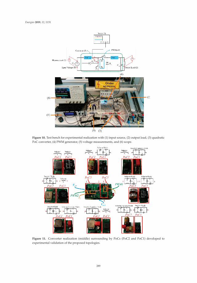
Energies 2019, 12, 1131
Figure 10. Test bench for experimental realization with (1) input source, (2) output load, (3) quadraticPoC converter, (4) PWM generator, (5) voltage measurements, and (6) scope.
Figure 11. Converter realization (middle) surrounding by PoCs (PoC2 and PoC1) developed toexperimental validation of the proposed topologies.
289
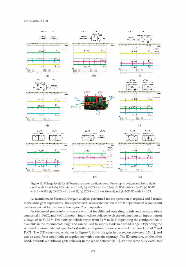
Energies 2019, 12, 1131
Figure 12. Voltage levels for different structures configurations. From top to bottom and left to right:(a) I-I with δ = 0.5; (b) I-ID with δ = 0.422; (c) I-ICD with δ = 0.366; (d) ID-I with δ = 0.422; (e) ID-IDwith δ = 0.333; (f) ID-ICD with δ = 0.25; (g) ICD-I with δ = 0.366 and; and (h) ICD-ID with δ = 0.25.
As mentioned in Section 3, the gain analysis performed for the operation in region 2 and 3 resultsin the same gain expressions. The experimental results shown herein are for operation in region 3, butcan be extended for the case when region 2 is in operation.
As discussed previously, is was shown that for different operating points and configurationsconnected in PoC2 and PoC1, different intermediate voltage levels are obtained for an input/outputvoltage of 48 V/12 V. This voltage, which varies from 33 V to 18 V depending the configuration, isavailable in the intermediate stage and can be used to supply loads in a broad range. Depending therequired intermediate voltage, the best suited configuration can be selected to connect in PoC2 andPoC1. The ICD structure, as shown in Figure 5, limits the gain in the region between [0.5 ; 1], andcan be used for a small voltage regulations with a certain accuracy. The ID structure, on the otherhand, presents a nonlinear gain behavior in the range between [0 ; 1]. For the same duty cycle, this
290

Energies 2019, 12, 1131
structure can be used to achieve gains in between the regular buck with I structure and the buck withICD structure, with the disadvantage of a nonlinear gain.
6.2. Region 1 (δ2 > δ1)
For operation in region 1, an extra PWM mode is performed between the normal PWM modes1 and 2, during the switching period. This extra PWM mode guarantee the independence betweenstages 1 and 2, leading to the gain presented in Table 1 for all possible PoC configurations. We noticedthat the intermediate gain depends only on the duty cycle δ2, while the output gain is relate to dutycycles of both stages, since the converters are cascade connected.
Figure 13 shows the PWM modes for operation in region 1 for the I-ICD configuration.Nevertheless, this analysis can be extended for all configurations. As previously mentioned, anextra PWM mode arises during the switching period (PWM mode 2 in this analysis). Switch S1—thecomponent which is subject to the greatest voltage stress among the power components—as highlightedin Table 4, blocks only the intermediate voltage level during the switch transient between ‘on’ and ‘off’while when operates in regions 2 and 3, the switch blocks the sum between the intermediate voltageand the input voltage. This phenomenon enables the reduction of switching losses in this componentonce the voltage that the component blocks during the switching transient has a lower value comparedwith the normal operation, although the maximum voltage that the switch needs to block remains inthe same level as shown in Table 4.
Figure 14 presents an experimental verification of the stages discussed previously and shown inFigure 13. Figure 14a presents a waveform with the significant voltage levels of the circuit. As expected,an intermediate voltage of 19.5 V is achieved for a duty cycle of 40% applying the I structure in PoC2.Additionally, Figure 14a also presents the second voltage regulation stage made by the ICD structureconnected in PoC1, operating with a duty cycle of 25%, in which a voltage of 11.2 V is achieved at theoutput of the converter. Figure 14b presents the PWMs applied to the circuit and its switching period,together with the input/output voltage of the circuit. As expected, input and output voltages are inaccordance with the theoretical analysis above presented.
Finally, Figure 14c shows the experimental results of the voltage stress across the activesemiconductors S1 and S2. For the same duty cycle abovementioned, the voltage stress across switchS2 is independent of the operational duty cycle and equal to the input voltage, as shown in Figure 14c.Additionally, the stress across switch S1 was also evaluated and presented in Figure 14c. It is verifiedthat, as theoretically explained, the voltage that the switch blocks during transition between ‘on’ and‘off’ stages is the intermediate voltage across Cinter, although the maximum voltage stress is related tothe sum of input and intermediate voltages (verify PWM mode 3 between points 2–3 in Figure 13).Moreover, the switching losses generated by the overlap between current and voltage during thetransition time decrease due to the lower blocking voltage during this transition. For operation inregion 1, the addition of switch S2 with independent duty cycle improves the flexibility of the systemand decreases the switching losses across switch S1.
291

Energies 2019, 12, 1131
Figure 13. PWM modes with the equivalent circuits during one switching period when δ2 > δ1.
Figure 14. Experimental results for operation in region 1 for operation with δ2 = 0.4 and δ1 = 0.25 andswitching frequency of 300 kHz: (a) input, intermediate and output voltages; (b) input and outputvoltages together with the respective duty cycles; and (c) PWMs and voltage stress across switches S1
and S2.
As discussed previously, the introduction of the ID and ICD structures in a step-downconfiguration (one-stage buck or quadratic buck) enable the possibility to change the voltage levelof these structures. When applied in a one-stage buck converter, the ICD structure present similarvoltage gain
(1+D
2
)as the converter proposed in [50]. The structures, however, present different
functionalities, since the abovementioned structure is a switched capacitor based converter with oneswitch, three diodes, one inductor, and three capacitors in the power stage while the structure, hereinpresented, is a switched inductor based topology with one switch, three diodes, two inductors, andone capacitor in the power stage. In terms of component part count number, the one-stage ICDstructure present lower amount of components compared with the switched capacitor version thatpresent similar gain [50]. The ID structure, on the other hand, presents a nonlinear step-down behaviorwith one extra diode and one less capacitor in the power stage (compared with the above-mentionedconverters).
The ID structure is also explored in step-up configurations [39] and, when applied in a step-downstructure, it changes the structure to a one composed by two inductors and two diodes, which leads toa gain of D
1+D , performing a higher step-down ratio them the ID structure. A topology with differentswitched capacitor/inductor structure is proposed for similar voltage gains [44] Comparing thesetopologies with the quadratic-buck configuration applying the ID and I structures (see Table 3), thegain of these structures is 2D∗D
1+D . The proposed structures, although implement more components in
292

Energies 2019, 12, 1131
the power stage, present a higher step-down ratio for duty cycles lower than 0.5. For duty cycles above0.5, the proposed converter present lower step-down capability with higher component part count.
The one-stage buck converter present similar gain (D) compared with the quadratic buck applyingID and ICD structures in PoC1 or PoC2 (see Table 3). For a component part count point of view, theconventional buck converter present more benefits compared to the structures above-mentioned, sincethe conventional buck converter present the lowest part count structure for a DC–DC step-downconfiguration. On the other hand, the converters proposed herein present multiple output ports, e.g.,intermediate and output voltages, and, according to the analysis presented herein, if a second switchS2 is implemented, these voltage levels can be independently regulated (operation in Region 1), whichis beneficial for an application point of view.
The major advantage that the topologies proposed herein have is the flexibility to adjust theintermediate voltage level according with the project specifications. The experimental results presentedin Figures 12 and 14 show that, for the same input/output voltage, different intermediate voltage levelscan be obtained depending on the operational regions (Region 1, 2, or 3) and the structure appliedto PoC1 and PoC2. The main disadvantage, however, is the number of components in the powerstage. When applied in a quadratic buck converters, the ID and ICD structures increase the number ofsemiconductor and magnetics in the power stage. This feature is undesired in some applications thatpower density is required, since extra space is required to place all the components. As previouslymentioned, the ID and ICD structures are suited for lower voltage regulations and are not applicable ifhigh step-down conversion ratios are required.
7. Conclusions
The analysis in this paper shows the influence of the ID and ICD structures, previously appliedin step-up topologies, in a step-down configuration from 48 V to 12 V input-to-output voltage. Toachieve the required voltage levels, a quadratic buck structure was implemented since the first analysisshowed that the ID and ICD structures have a lower voltage regulation capability compared with theconventional I structure and, if a single stage buck converter is considered for application, the ICDstructure cannot achieve the required output voltage level.
A complete theoretical analysis with PWM stages for all possible regions of operation, voltagegain, voltage/current profiles, and simulation is shown for all possible configurations generatedby the substitution of the structures in PoC2 and PoC1. Voltage and current stress were evaluatedfor dimensioning and component selection to subsequently build the prototype for experimentalvalidation. The analysis showed that the ID and ICD structures change the voltage and current profiledepending on which PoC is connected. It is proven that the addition of a second switch S2, togetherwith the operation in Region 1, decreases the voltage stress during turn-off of switch S1. The mainadvantage of the proposed approach is that the intermediate voltage level can be selected accordingto the application, since switch S2 is implemented and the ID and ICD structures provide differentvoltage profiles that can be desired for specific operational duty cycles.
The main advantages of the proposed topologies compared to the conventional buck and quadraticbuck converters are as follows.
(1) The addition of the second switch S2 and the possibility to choose between I, ID, and ICDstructures to connect in PoC2 and PoC1, increase the flexibility of the circuit, resulting in a broadrange of intermediate and output voltage levels.
(2) The circuits with ID and/or ICD feature diode and inductor redundancy, which leads to lowercurrent stress and a fail-safe structure, after all, if one diode/inductor fails in open-circuit, thesystem can still maintain its functionality but with limited power.
(3) The implementation of S2 also increase the number of regions of operation, since region 1 is nowa possible region of operation. In this region, the blocking voltage of switch S1 decreases fromVIN + Vinter to only Vinter, as shown in Section 6.
293

Energies 2019, 12, 1131
A test bench was assembled and experimental results showing that the ID and ICD structurescan be used for small voltage adjustments in a step-down application were presented. Simulation andexperimental waveforms were presented to validate the theoretical analysis in Section 4. The ID andICD proved to be effective structures for applications where small voltage adjustments are required,but did not prove being useful solutions when a high step-down voltage level is required due to itsgain characteristics.
8. Patent
A patent related to this work was filled in on the 15th of May 2018, with application numberGB1807795.8 at the UKIPO (reference [47]).
Author Contributions: M.D.V.: Conceptualization, Investigation, Methodology, Validation, andWriting—Original Draft. G.V.d.B and S.R.: Validation and Revision. J.D.: Supervisor, Resources, and Revision.
Funding: M.D.V. and S.R. were partially funded by the EFRO SALK Solsthore Project. G.V.d.B was funded by aPh.D. grant of Research Foundation Flanders (FWO).
Conflicts of Interest: The authors declare no conflicts of interest.
References
1. Vovos, P.N.; Kiprakis, A.E.; Wallace, A.R.; Harrison, G.P. Centralized and Distributed Voltage Control: Impacton Distributed Generation Penetration. IEEE Trans. Power Syst. 2007, 22, 476–483. [CrossRef]
2. Ault, G.W.; McDonald, J.R.; Burt, G.M. Strategic analysis framework for evaluating distributed generationand utility strategies. IEE Proc.-Gener.Transm. Distrib. 2003, 150, 475–481. [CrossRef]
3. Kumar, D.; Zare, F.; Ghosh, A. DC Microgrid Technology: System Architectures, AC Grid Interfaces,Grounding Schemes, Power Quality, Communication Networks, Applications, and Standardizations Aspects.IEEE Access 2017, 5, 12230–12256. [CrossRef]
4. Sannino, A.; Postiglione, G.; Bollen, M.H.J. Feasibility of a DC network for commercial facilities. IEEE Trans.Ind. Appl. 2003, 39, 1499–1507. [CrossRef]
5. Starke, M.; Li, F.; Tolbert, L.M.; Ozpineci, B. AC vs. DC distribution: Maximum transfer capability. InProceedings of the 2008 IEEE Power and Energy Society General Meeting—Conversion and Delivery ofElectrical Energy in the 21st Century, Pittsburgh, PA, USA, 20–24 July 2008; pp. 1–6.
6. Dragicevic, T.; Lu, X.; Vasquez, J.C.; Guerrero, J.M. DC Microgrids—Part II: A Review of Power Architectures,Applications, and Standardization Issues. IEEE Trans. Power Electron. 2016, 31, 3528–3549. [CrossRef]
7. Han, J.; Oh, Y.-S.; Gwon, G.-H.; Kim, D.-U.; Noh, C.-H.; Jung, T.-H.; Lee, S.-J.; Kim, C.-H. Modeling andAnalysis of a Low-Voltage DC Distribution System. Resources 2015, 4, 713–735. [CrossRef]
8. Salato, M.; Ghisla, U. Optimal power electronic architectures for DC distribution in datacenters. InProceedings of the 2015 IEEE First International Conference on DC Microgrids (ICDCM), Atlanta, GA,USA, 25–27 May 2015; pp. 245–250.
9. Wang, C.; Jain, P. A quantitative comparison and evaluation of 48V DC and 380V DC distribution systemsfor datacenters. In Proceedings of the 2014 IEEE 36th International Telecommunications Energy Conference(INTELEC), Vancouver, BC, Canada, 28 September–20 October 2014; pp. 1–7.
10. Madduri, P.A.; Poon, J.; Rosa, J.; Podolsky, M.; Brewer, E.A.; Sanders, S.R. Scalable DC Microgrids for RuralElectrification in Emerging Regions. IEEE J. Emerg. Sel. Top. Power Electron. 2016, 4, 1195–1205. [CrossRef]
11. Tan, K.; Song, X.; Peng, C.; Liu, P.; Huang, A.Q. Hierarchical protection architecture for 380V DC datacenter application. In Proceedings of the 2016 IEEE Energy Conversion Congress and Exposition (ECCE),Milwaukee, WI, USA, 18–22 September 2016; pp. 1–8.
12. Kakigano, H.; Miura, Y.; Ise, T. Low-Voltage Bipolar-Type DC Microgrid for Super High Quality Distribution.IEEE Trans. Power Electron. 2010, 25, 3066–3075. [CrossRef]
13. den Broeck, G.V.; Breucker, S.D.; Beerten, J.; Zwysen, J.; Vecchia, M.D.; Driesen, J. Analysis of three-levelconverters with voltage balancing capability in bipolar DC distribution networks. In Proceedings of the 2017IEEE Second International Conference on DC Microgrids (ICDCM), Nuremberg, Germany, 27–29 June 2017;pp. 248–255.
294

Energies 2019, 12, 1131
14. Anand, S.; Fernandes, B.G. Optimal voltage level for DC microgrids. In Proceedings of the IECON 2010—36thAnnual Conference on IEEE Industrial Electronics Society, Glendale, CA, USA, 7–10 November 2010;pp. 3034–3039.
15. Moussa, S.; Ghorbal, M.J.B.; Slama-Belkhodja, I. DC voltage level choice in residential remote area. InProceedings of the 2018 9th International Renewable Energy Congress (IREC), Hammamet, Tunisia,20–22 March 2018; pp. 1–6.
16. Francés, A.; Asensi, R.; García, Ó.; Prieto, R.; Uceda, J. Modeling Electronic Power Converters in Smart DCMicrogrids—An Overview. IEEE Trans. Smart Grid 2018, 9, 6274–6287. [CrossRef]
17. Keshani, M.; Adib, E.; Farzanehfard, H. Micro-inverter based on single-ended primary-inductance convertertopology with an active clamp power decoupling. IET Power Electron. 2018, 11, 73–81. [CrossRef]
18. Liao, C.Y.; Lin, W.S.; Chen, Y.M.; Chou, C.Y. A PV Micro-inverter With PV Current Decoupling Strategy.IEEE Trans. Power Electron. 2017, 32, 6544–6557. [CrossRef]
19. Ahmed, M.E.S.; Orabi, M.; Abdelrahim, O.M. Two-stage micro-grid inverter with high-voltage gain forphotovoltaic applications. IET Power Electron. 2013, 6, 1812–1821. [CrossRef]
20. Sajadian, S.; Ahmadi, R. Distributed Maximum Power Point Tracking Using Model Predictive Control forPhotovoltaic Energy Harvesting Architectures Based on Cascaded Power Optimizers. IEEE J. Photovolt. 2017,7, 849–857. [CrossRef]
21. Vinnikov, D.; Chub, A.; Liivik, E.; Roasto, I. High-Performance Quasi-Z-Source Series Resonant DC/DCConverter for Photovoltaic Module-Level Power Electronics Applications. IEEE Trans. Power Electron. 2017,32, 3634–3650. [CrossRef]
22. Bergveld, H.J.; Büthker, D.; Castello, C.; Doorn, T.; de Jong, A.; van Otten, R.; de Waal, K. Module-LevelDC/DC Conversion for Photovoltaic Systems: The Delta-Conversion Concept. IEEE Trans. Power Electron.2013, 28, 2005–2013. [CrossRef]
23. Ravyts, S.; Vecchia, M.D.; Zwysen, J.; van den Broeck, G.; Driesen, J. Comparison Between an InterleavedBoost Converter Using Si MOSFETs Versus GaN HEMTs. In Proceedings of the PCIM Europe 2018,International Exhibition and Conference for Power Electronics, Intelligent Motion, Renewable Energyand Energy Management, Nuremberg, Germany, 5–7 June 2018; pp. 1–8.
24. Ravyts, S.; Vecchia, M.D.; Zwysen, J.; den Broeck, G.V.; Driesen, J. Study on a cascaded DC-DC converterfor use in building-integrated photovoltaics. In Proceedings of the 2018 IEEE Texas Power and EnergyConference (TPEC), College Station, TX, USA, 8–9 February 2018; pp. 1–6.
25. Mei, Q.; Shan, M.; Liu, L.; Guerrero, J.M. A Novel Improved Variable Step-Size Incremental-Resistance MPPTMethod for PV Systems. IEEE Trans. Ind. Electron. 2011, 58, 2427–2434. [CrossRef]
26. Thangavelu, A.; Vairakannu, S.; Parvathyshankar, D. Linear open circuit voltage-variable step-size-incrementalconductance strategy-based hybrid MPPT controller for remote power applications. IET Power Electron. 2017,10, 1363–1376. [CrossRef]
27. Tiwari, R.; Krishnamurthy, K.; Neelakandan, R.B.; Padmanaban, S.; Wheeler, P.W. Neural Network BasedMaximum Power Point Tracking Control with Quadratic Boost Converter for PMSG—Wind EnergyConversion System. Electronics 2018, 7, 20. [CrossRef]
28. Zhang, Y.; Li, X.; Dong, Z.; Liu, Y.f.; Liu, J. High step-up isolated DC-DC converter with multi-celldiode-capacitor network. In Proceedings of the 2017 IEEE Applied Power Electronics Conference andExposition (APEC), Tampa, FL, USA, 26–30 March 2017; pp. 114–120.
29. Spiazzi, G.; Biadene, D.; Marconi, S.; Bevilacqua, A. Non-isolated High Step-up DC-DC Converter withMinimum Switch Voltage Stress. IEEE Trans. Power Electron. 2019, 34, 1470–1480. [CrossRef]
30. Schmitz, L.; Martins, D.C.; Coelho, R.F. High Step-Up Non-Isolated ZVS/ZCS DC-DC Converter forPhotovoltaic Thin-Film Module Applications. IEEE J. Emerg. Sel. Top. Power Electron. 2019, 7, 565–575.[CrossRef]
31. Schmitz, L.; Martins, D.C.; Coelho, R.F. Generalized High Step-Up DC-DC Boost-Based Converter with GainCell. IEEE Trans. Circuits Syst. I Regul. Pap. 2017, 64, 480–493. [CrossRef]
32. Wong, Y.-S.; Chen, J.-F.; Liu, K.-B.; Hsieh, Y.-P. A Novel High Step-Up DC-DC Converter with CoupledInductor and Switched Clamp Capacitor Techniques for Photovoltaic Systems. Energies 2017, 10, 378.[CrossRef]
33. Gao, Y.; Liu, H.; Ai, J. Novel High Step-Up DC–DC Converter with Three-Winding-Coupled-Inductors andIts Derivatives for a Distributed Generation System. Energies 2018, 11, 3428. [CrossRef]
295

Energies 2019, 12, 1131
34. Pop-Calimanu, I.-M.; Lica, S.; Popescu, S.; Lascu, D.; Lie, I.; Mirsu, R. A New Hybrid Inductor-Based BoostDC-DC Converter Suitable for Applications in Photovoltaic Systems. Energies 2019, 12, 252. [CrossRef]
35. Chen, S.-J.; Yang, S.-P.; Huang, C.-M.; Chou, H.-M.; Shen, M.-J. Interleaved High Step-Up DC-DC ConverterBased on Voltage Multiplier Cell and Voltage-Stacking Techniques for Renewable Energy Applications.Energies 2018, 11, 1632. [CrossRef]
36. Jalilzadeh, T.; Rostami, N.; Babaei, E.; Maalandish, M. Non-Isolated Topology for High Step-Up DC-DCConverters. Available online: https://ieeexplore.ieee.org/document/8390878 (accessed on 14 January 2019).
37. Rodic, M.; Milanovic, M.; Truntic, M.; Ošlaj, B. Switched-Capacitor Boost Converter for Low Power EnergyHarvesting Applications. Energies 2018, 11, 3156. [CrossRef]
38. Tran, V.-T.; Nguyen, M.-K.; Choi, Y.-O.; Cho, G.-B. Switched-Capacitor-Based High Boost DC-DC Converter.Energies 2018, 11, 987. [CrossRef]
39. Hu, Y.; Li, K.; Yin, Z.; Ioinovici, A. Switched-inductor-based non-isolated large conversion ratio, lowcomponents count DC-DC regulators. In Proceedings of the 2015 IEEE Energy Conversion Congress andExposition (ECCE), Montreal, QC, Canada, 20–24 September 2015; pp. 1398–1405.
40. Ranjana, M.S.B.; Kulkarni, R.M.; Anita, K.; Pooja, C. Non isolated switched inductor SEPIC convertertopologies for photovoltaic boost applications. In Proceedings of the 2016 International Conference onCircuit, Power and Computing Technologies (ICCPCT), Nagercoil Andaman and Nicobar Islands, India,18–19 March 2016; pp. 1–6.
41. Li, D.; Loh, P.C.; Zhu, M.; Gao, F.; Blaabjerg, F. Generalized Multicell Switched-Inductor andSwitched-Capacitor Z-Source Inverters. IEEE Trans. Power Electron. 2013, 28, 837–848. [CrossRef]
42. Salvador, M.A.; Lazzarin, T.B.; Coelho, R.F. High Step-Up DC/DC Converter with Active Switched-Inductorand Passive Switched-Capacitor Networks. IEEE Trans. Ind. Electron. 2018, 65, 5644–5654. [CrossRef]
43. Qu, K.; Feng, M.; Zhao, J. Inductor-capacitor structure for getting high step-up converter. Electron. Lett. 2016,52, 1403–1404. [CrossRef]
44. Xiong, S.; Wong, S.C.; Tan, S.C.; Tse, C.K. A Family of Exponential Step-Down Switched-Capacitor Convertersand Their Applications in Two-Stage Converters. IEEE Trans. Power Electron. 2014, 29, 1870–1880. [CrossRef]
45. Han, J.; von Jouanne, A.; Temes, G.C. A New Approach to Reducing Output Ripple inSwitched-Capacitor-Based Step-Down DC-DC Converters. IEEE Trans. Power Electron. 2006, 21, 1548–1555.[CrossRef]
46. Uno, M.; Kukita, A. PWM Switched Capacitor Converter with Switched-Capacitor-Inductor Cell forAdjustable High Step-Down Voltage Conversion. IEEE Trans. Power Electron. 2019, 34, 425–437. [CrossRef]
47. Dalla Vecchia, M.; Driesen, J. Quadratic Buck Converter. UKIPO Patent GB1807795, 14 May 2018.48. Angulo-Garcia, D.; Angulo, F.; Osorio, G.; Olivar, G. Control of a DC-DC Buck Converter through Contraction
Techniques. Energies 2018, 11, 3086. [CrossRef]49. Demian, A.E.; Treviso, C.H.G.; Gallo, C.A.; Tofoli, F.L. Non-isolated DC-DC converters with wide conversion
range used to drive high-brightness LEDs. In Proceedings of the 2009 Brazilian Power Electronics Conference,Bonito, MS, Brazil, 27 September–1 October 2009; pp. 598–605.
50. Vecchia, M.D.; Lazzarin, T.B. A hybrid switched capacitor dc-dc buck converter. In Proceedings of the2015 IEEE 13th Brazilian Power Electronics Conference and 1st Southern Power Electronics Conference(COBEP/SPEC), Fortaleza, CE, Brazil, 29 November–2 December 2015; pp. 1–6.
© 2019 by the authors. Licensee MDPI, Basel, Switzerland. This article is an open accessarticle distributed under the terms and conditions of the Creative Commons Attribution(CC BY) license (http://creativecommons.org/licenses/by/4.0/).
296

energies
Review
Challenges and Design Requirements for IndustrialApplications of AC/AC Power Converterswithout DC-Link
Pawel Szczesniak
Institute of Electrical Eng., University of Zielona Góra, 65-516 Zielona Góra, Poland;[email protected]; Tel.: +48-68-328-2253
Received: 29 March 2019; Accepted: 22 April 2019; Published: 25 April 2019
Abstract: AC/AC converters that do not have a DC energy storage element, such as a matrix chopperand a matrix converter, are increasingly becoming alternatives to conventional two-stage AC/DC/ACconverters and thyristor choppers. In such systems, the main DC-link capacitor does not exist, so thesystem provides more reliable operation and makes it possible to reduce the financial costs of itsconstruction. It should be noted that AC/AC converters without an energy storage element in a formof DC-link capacitors have not been implemented on an industrial scale. The reasons involve technicalaspects and cost components. The main aim of this paper is to present some of the challenges andselected design requirements for industrial applications of AC/AC high reliability power converters.
Keywords: power electronic converter; AC/AC converter; matrix converter; reliability
1. Introduction
The development of power electronic converters has led to them being applied in various areasof life, such as: industrial and household applications, renewable energies, Flexible AC transmissionsystems and micro grids, as well as automotive and transport applications. In the development of powerconverter topologies, much more attention is being paid to the, reliability [1,2] efficiency and robustnessof power electronics converters [3–6]. Automotive industry and transport have very strict reliabilityrequirements in power electronics systems due to safety requirements. Moreover, the industrial andenergy sectors are striving for improvement in the efficiency and robustness of power electronicssystems. Likewise, home solutions are often designed as economical and sustainable eco-friendlydevices. Additionally, some novel devices have a smaller size, and have achieved higher power densityand robustness for very high loads. This is a general trend in all areas of technology. High powerdensity, higher switching frequency, and reduced overall dimensions of passive components andpower electronic converters are possible due to the use of power transistors made using silicon carbide(SiC) or gallium nitride (GaN) technology [7–10].
In low-voltage industrial systems, the most commonly used topology is the unidirectionalAC/DC/AC converter. The bidirectional (four-quadrant) structure of such a converter is a systemcalled a back-to-back converter (B2B) (Figure 1) [11]. The power stage of converters contains powertransistors with a heatsink and heat dissipation system, a DC-link capacitor, an input filter to provide aunit input power factor, and measurement and control units. In medium-voltage industrial systems,multilevel converters with DC-link are commonly used [12,13]. Multilevel converters offer numerousadvantages compared with the two-level converter, e.g., better power quality and lower switchinglosses, low transistor voltage stress, and high voltage capability. It is evident that the multilevelconverters will be used for medium voltage or high power electronic systems. However, in generalterms, it can be concluded that the two-level converters will be used in low-voltage systems withlower power. In addition, the specialized design of low voltage power electronics converters using
Energies 2019, 12, 1581; doi:10.3390/en12081581 www.mdpi.com/journal/energies297
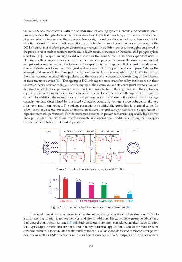
Energies 2019, 12, 1581
SiC or GaN semiconductors, with the optimization of cooling systems, enables the construction ofpower plants with high efficiency or power densities. In the last decade, apart from the developmentof power electronics devices, there has also been a significant development of capacitors used in DCcircuits. Aluminum electrolytic capacitors are probably the most common capacitors used in theDC-link circuits of modern power electronic converters. In addition, other technologies employed inthe production of such capacitors are the multi-layer ceramic structure or the metallized-polypropylenestructure [11]. Despite the significant reduction in the dimensions of modern capacitors used inDC circuits, these capacitors still constitute the main component increasing the dimensions, weight,and price of power converters. Furthermore, the capacitor is the component that is most often damageddue to disturbances from the power grid and as a result of improper operation. Figure 2 shows theelements that are most often damaged in circuits of power electronic converters [1,2,14]. For this reason,the most common electrolytic capacitors are the cause of the premature shortening of the lifespanof the converter device [11]. The ageing of DC-link capacitors is manifested by the increase in theirequivalent series resistance RESR. The heating up of the electrolyte and its consequent evaporation anddeterioration of electrical parameters is the most significant factor in the degradation of the electrolyticcapacitor. One of the main reasons for the increase in capacitor temperature is the ripple of the capacitorcurrent. In addition, the second most critical parameter for the failure of the capacitor is its voltagecapacity, usually determined by the rated voltage or operating voltage, surge voltage, or allowedshort-term maximum voltage. The voltage parameter is so critical that exceeding its nominal values fora few tenths of a second can cause an immediate failure or significantly accelerate the degradation ofcapacitor nominal parameters. For the presented reasons, in power converters, especially high powerones, particular attention is paid to environmental and operational conditions affecting their lifespan,with special emphasis on DC-link capacitors.
Figure 1. Two-level back-to-back converter with DC-link.
Figure 2. Distribution of faults in power electronic converters [14].
The development of power converters that do not have large capacitors in their structure (DC-link)is an interesting solution to reduce their cost and size. In addition, this can achieve greater reliability andthus extend their operating time [15–18]. Such converters are often considered an alternative solutionfor atypical applications and are not found in many industrial applications. One of the main reasonsconcerns technical aspects related to the small number of available and dedicated semiconductor powerdevices, as well as DSP processors with a sufficient number of PWM outputs and A/D converters.
298

Energies 2019, 12, 1581
An additional difficulty is undoubtedly the complex algorithms for modulation of the switch controlfunction and transistor current commutation.
AC/AC converters without DC-link capacitors have several topologies with different functionalities.One of the main functionalities is the possibility to change the frequency of the output current/voltage(fL = const [16], fL = var [15–18]). In addition, different structures of AC/AC converters are distinguished,such as direct and indirect (with a fictitious DC-link) topology. An example of an AC/AC converterwithout an intermediate circuit capacitor and fL = const is a matrix controller (matrix chopper), whereasfL = var is a matrix converter.
This paper will present a review of current commercial applications of the AC/AC converters whosetopologies do not have a DC energy storage element (capacitor or inductor). Particular attention willbe paid to the technological issues and barriers concerning the design of such converters. In addition,possible construction solutions as well as potential applications will be indicated. The originality of thisresearch is in the presentation of requirements and challenges for practical or future-proof applicationsof AC/AC high-reliability power converters. The paper includes (1) a review of semiconductor powerelements dedicated to the discussed converters, (2) an indication of expectations regarding integratedintelligent modules and new SiC technologies, and (3) an indication of the development of moderncontrol techniques (e.g., model predictive control (MPC)). In addition, new application possibilities ofthe discussed converters in AC power systems, (e.g., compensators for voltage changes) are indicatedand their beneficial properties are discussed.
2. Description of Selected Topologies
The analysis presented in the article will be based on topologies of two converters: a matrixcontroller (chopper) and a matrix converter. Based on these, the main design problems and limitationsrelated to the available components and the industrial application will be indicated.
One of the basic applications of AC/AC choppers, as an alternative to thyristor choppers, is inelectric drive systems used as a soft-start for an AC motor. Issues with industrial temperature controland lighting intensity control are the further areas of AC/AC chopper application. A schematic diagramof the three phase AC/AC matrix controller power circuit is presented in Figure 3a [16]. The systemconsists of six bidirectional switches. Three switches are connected to the input terminals, while theother three are connected in parallel to the load. Control of the switches is carried out by means of thePWM signal (Figure 3b), and a duty cycle determines the RMS value of the output voltage. In addition,the choppers have an input low-pass filter to eliminate the higher harmonics components of the currentdrawn by the converter, which result from the frequency of the PWM signal. The second kind ofstructure based on the chopper shown in Figure 3a is the matrix-reactance chopper, which also enablesthe increase in amplitude of the output voltage [19] as well as various other types of compensators forAC voltage fluctuations in the power grid [20,21].
(a) (b)
Figure 3. AC/AC controller: (a) main circuit; (b) voltage time waveforms.
299

Energies 2019, 12, 1581
The main advantages of the AC/AC chopper compared to the classic thyristor chopper arederived from the sinusoidal current drawn from the mains, and the use of LC output filters to obtainsinusoidal output voltages. Such properties allow one to work with the unit input power factor anduse these choppers in systems of electricity conditioners [20,21]. The high switching frequency ofthe power transistors makes it possible to minimize the sizes for the input and output LC passivefilters. The disadvantage of chopper devices is the increased internal losses resulting from the largenumber of power transistors and the necessity of using additional snubber devices on each of thepower electronics switches or of using overvoltage protection of bidirectional switches with a clampcircuit [16,22].
The most widely known of frequency converters (fL = var) without DC-link is the matrix converter(MC) in its direct topology shown in Figure 4a [15–18,22–24]. Generally, in three-phase systems,the MC consists of nine bidirectional switches connected in a matrix—each input is connected to eachoutput. Similar to the matrix controller, there is an input low pass filter in the MC topology that fulfillsidentical functions. MC output voltages are formed from pieces of input voltages, shown in Figure 4b,as exemplary experimental time waveforms.
(a) (b)
Figure 4. Matrix converter: (a) main circuit; (b) voltage time waveforms.
The MC is a four-quadrant topology with adjustable input power factor and a sinusoidal shape ofinput and output currents. In addition, the MC is a fully semiconductor device without large capacitorcircuit capacitors. Similarly to chopper devices, there is a necessity to use additional overvoltageprotection of bidirectional switches with a clamp circuit, where small capacitors accumulatingcommutation voltage spikes should be used. The disadvantages of the MC are the large number ofpower transistors and the associated complex control and switching strategies. In addition, the voltagegain of MCs does not exceed 0.866, which, for applications in variable speed drives, requires the use ofmotors with lower rated voltages.
In both MC and AC/AC chopper topologies, the main elements are bi-directional power electronicswitches. These switches allow switching of both the positive and negative sine wave of the supplyvoltage and, in the case of the MC, the bi-directional power flow. Bidirectional switches, as will bediscussed in the next section, have a configuration of transistors and diodes other than those usedin classical, commonly used voltage inverters. Therefore, the commercial development of availablebidirectional switches in various configurations is important for the development of AC/AC converterswithout DC-link circuits.
3. Design, Construction, and Implementation Barriers
The development of AC/AC converters encounters problems related to misunderstanding thespecificity of their operation, especially in the context of MCs. In this chapter, basic constructionproblems and development barriers related to technological differences in relation to commonly used
300
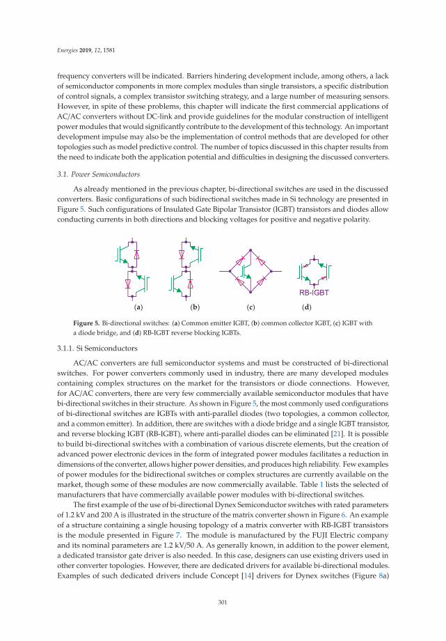
Energies 2019, 12, 1581
frequency converters will be indicated. Barriers hindering development include, among others, a lackof semiconductor components in more complex modules than single transistors, a specific distributionof control signals, a complex transistor switching strategy, and a large number of measuring sensors.However, in spite of these problems, this chapter will indicate the first commercial applications ofAC/AC converters without DC-link and provide guidelines for the modular construction of intelligentpower modules that would significantly contribute to the development of this technology. An importantdevelopment impulse may also be the implementation of control methods that are developed for othertopologies such as model predictive control. The number of topics discussed in this chapter results fromthe need to indicate both the application potential and difficulties in designing the discussed converters.
3.1. Power Semiconductors
As already mentioned in the previous chapter, bi-directional switches are used in the discussedconverters. Basic configurations of such bidirectional switches made in Si technology are presented inFigure 5. Such configurations of Insulated Gate Bipolar Transistor (IGBT) transistors and diodes allowconducting currents in both directions and blocking voltages for positive and negative polarity.
(a) (b) (c) (d)
Figure 5. Bi-directional switches: (a) Common emitter IGBT, (b) common collector IGBT, (c) IGBT witha diode bridge, and (d) RB-IGBT reverse blocking IGBTs.
3.1.1. Si Semiconductors
AC/AC converters are full semiconductor systems and must be constructed of bi-directionalswitches. For power converters commonly used in industry, there are many developed modulescontaining complex structures on the market for the transistors or diode connections. However,for AC/AC converters, there are very few commercially available semiconductor modules that havebi-directional switches in their structure. As shown in Figure 5, the most commonly used configurationsof bi-directional switches are IGBTs with anti-parallel diodes (two topologies, a common collector,and a common emitter). In addition, there are switches with a diode bridge and a single IGBT transistor,and reverse blocking IGBT (RB-IGBT), where anti-parallel diodes can be eliminated [21]. It is possibleto build bi-directional switches with a combination of various discrete elements, but the creation ofadvanced power electronic devices in the form of integrated power modules facilitates a reduction indimensions of the converter, allows higher power densities, and produces high reliability. Few examplesof power modules for the bidirectional switches or complex structures are currently available on themarket, though some of these modules are now commercially available. Table 1 lists the selected ofmanufacturers that have commercially available power modules with bi-directional switches.
The first example of the use of bi-directional Dynex Semiconductor switches with rated parametersof 1.2 kV and 200 A is illustrated in the structure of the matrix converter shown in Figure 6. An exampleof a structure containing a single housing topology of a matrix converter with RB-IGBT transistorsis the module presented in Figure 7. The module is manufactured by the FUJI Electric companyand its nominal parameters are 1.2 kV/50 A. As generally known, in addition to the power element,a dedicated transistor gate driver is also needed. In this case, designers can use existing drivers used inother converter topologies. However, there are dedicated drivers for available bi-directional modules.Examples of such dedicated drivers include Concept [14] drivers for Dynex switches (Figure 8a)
301

Energies 2019, 12, 1581
and Semicron drivers and transistors presented in Figure 8b,c. These are examples of bi-directionalswitches. In the catalogues of other semiconductor companies, such solutions are found often andwith increasing frequency. Based on the above review, it can be said that the number of dedicatedcomponents is gradually increasing over time. It should be noted that, without systematic growthof proposals for new, dedicated components for the design and construction of AC/AC converters,there will be no significant development of these topologies. The main direction of developmentshould be to reduce component costs and increase their reliability.
(a) (b)
Figure 6. MC construction: (a) Dynex 1.2 kV/200 A IGBT; (b) a built-in MC structure in the control cabinet.
(a) (b)
Figure 7. Matrix-connected RB-IGBTs module: (a) photograph; (b) topology structure.
(a) (b)
(c)
Figure 8. A photograph of the IGBTs with dedicated drivers: (a) Dynex IGBT with Concept driver;(b,c) Semicron drivers and IGBTs.
302

Energies 2019, 12, 1581
Table 1. Available, selected commercial modules with bidirectional switches.
Switch Model Characteristic Manufacturer Number of Bidirectional Switches
DIM200MBS12-A 1.2 kV/200 A DYNEX 1DIM400PBM17-A 1.7 kV/400 A DYNEX 1DIM600EZM17-E 1.7 kV/600 A DYNEX 1
SK 60GM123 1.7 kV/60 A SEMICRON 1SKM 150GM12T4G 1.2 kV/60 A SEMICRON 1
SML150MAT12 1.2 kV/150 A SEMELAB 3SML300MAT06 0.6 kV/300 A SEMELAB 3
18MBI50W-120A 1.2 kV/ 50A FUJI 918MBI100W-060A 0.6 kV/100 A FUJI 918MBI100W-120A 1.2 kV/100 A FUJI 918MBI200W-060A 0.6 kV/200 A FUJI 9
3.1.2. SiC Semiconductors
Thanks to the development of semiconductor power electronics with silicon carbide (SiC),which has certain advantageous features such as high temperature operation, low losses, and higherswitching speeds, a full power electronic converter structure has also been developed. Moreover,thanks to the semi-conductor being made using SiC technology, a further improvement in the converterspower density can be achieved. Because this is a technology that has not fully achieved technologicalmaturity, there are some problems in the implementation of power converters with SiC devices due tothe high speed of switching devices and the design of devices for the gate drive.
The most promising SiC devices are the normally-off SiC JFET, SiC MOSFET, and SiC BJTs.The bi-directional switch topologies in SiC technology are shown in Figure 9. Potential improvementsregarding the efficiency and performance of SiC components in the context of bi-directional powerelectronics switches are reported in [24–27]. As demonstrated by existing research, the use of transistorsmade in SiC technology enables a significant increase in the efficiency of converters for switchingfrequencies of several dozen kHz. Sample results illustrating the beneficial properties of SiC transistors,taken from [24], are presented in Figure 10.
(a) (b) (c)
Figure 9. Main topologies for SiC bi-directional switches: (a) common drain anti-paralleled JFET,(b) common source anti-paralleled SiC MOSFET, and (c) common emitter anti-paralleled SiC BJT.
303

Energies 2019, 12, 1581
(a) (b)
Figure 10. Illustration of the beneficial properties of the use of SiC transistors, taken from [24], presentsthe efficiency of a two-phase to single-phase 2.5 kW MC in Si and SiC technology (a) as a function ofswitching frequency at Tc = 125 ◦C and (b) as a function of power at fs = 100 kHz, Tc = 125 ◦C.
3.2. Control Units
The MC power stage circuit is made up from a table of nine bi-directional switches which providesa total of 18 transistors. The specificity of the MC construction also requires the generation of aPWM switching sequence. In addition, special attention should be paid to maintaining a safe currentcommutation strategy when the transistors are switched. An additional difficulty in the modulationprocess of the transistors control functions is the distribution of control pulses in a single periodof the control sequence TSeq. Since there are three bidirectional switches connected in one outputbranch (six transistors) and two or three of them cannot be switched on simultaneously, the switchingsequence will be responsible for three switching operations during one period TSeq (Figure 11a). In theclassic bridge voltage inverter, for a single branch, there are two transistors working alternately.A pair of complementary control signals are then generated and are negated in relation to eachother (Figure 11b). In addition, additional dead times (dead-band) are used to ensure correct currentcommutation. Modern DSP processors and microcontrollers have built-in PWM modulators thatgenerate complementary control signals that occur in classic bridge voltage inverters with built-in deadtime generation functions [28]. The control implementation for the matrix converter using built-inPWM modulators is not simple and requires either multiple-core systems (at least two) or additionallogic circuits. It is also possible to solve this problem using software I/O outputs instead of built-inPWM modulator procedures. These are, of course, more complicated solutions than in the classicbranches of the inverter bridge.
(a) (b)
Figure 11. Distribution of control pulses in a single period of the control sequence TSeq: (a) in the phaseleg of a matrix converter, (b) in the phase leg of a classical inverter.
In addition to the algorithm for the modulation of switch control signals in the MC, it is necessaryto use complex current switching algorithms for transistors. Several commutation strategies canbe found in the scientific literature [17,21], where the most widely known is the four-step currentcommutation strategy. In this method, the current direction in the output line is used to determineswitching sequences of transistors. The commutation process for one output phase is shown in
304
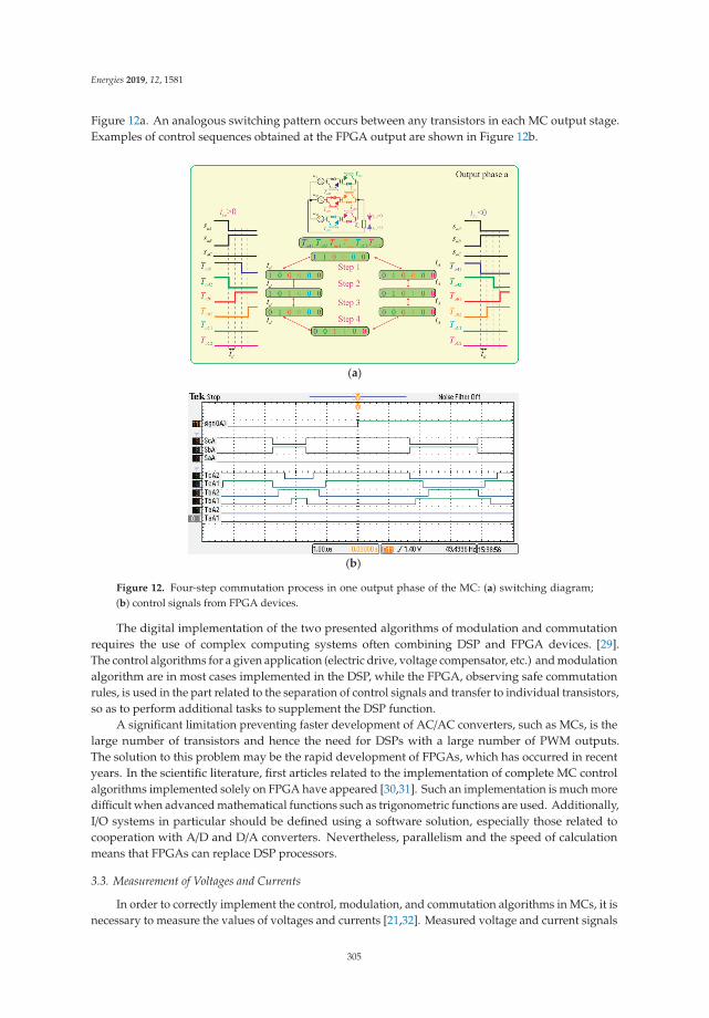
Energies 2019, 12, 1581
Figure 12a. An analogous switching pattern occurs between any transistors in each MC output stage.Examples of control sequences obtained at the FPGA output are shown in Figure 12b.
(a)
(b)
Figure 12. Four-step commutation process in one output phase of the MC: (a) switching diagram;(b) control signals from FPGA devices.
The digital implementation of the two presented algorithms of modulation and commutationrequires the use of complex computing systems often combining DSP and FPGA devices. [29].The control algorithms for a given application (electric drive, voltage compensator, etc.) and modulationalgorithm are in most cases implemented in the DSP, while the FPGA, observing safe commutationrules, is used in the part related to the separation of control signals and transfer to individual transistors,so as to perform additional tasks to supplement the DSP function.
A significant limitation preventing faster development of AC/AC converters, such as MCs, is thelarge number of transistors and hence the need for DSPs with a large number of PWM outputs.The solution to this problem may be the rapid development of FPGAs, which has occurred in recentyears. In the scientific literature, first articles related to the implementation of complete MC controlalgorithms implemented solely on FPGA have appeared [30,31]. Such an implementation is much moredifficult when advanced mathematical functions such as trigonometric functions are used. Additionally,I/O systems in particular should be defined using a software solution, especially those related tocooperation with A/D and D/A converters. Nevertheless, parallelism and the speed of calculationmeans that FPGAs can replace DSP processors.
3.3. Measurement of Voltages and Currents
In order to correctly implement the control, modulation, and commutation algorithms in MCs, it isnecessary to measure the values of voltages and currents [21,32]. Measured voltage and current signals
305

Energies 2019, 12, 1581
are used, among others, in (1) semisoft commutation strategies, (2) fault detections, (3) modulationprocess (e.g., SVM), (4) phase-locked loop (PLL) units, (5) current loops in control algorithms, and (6)the clamp protection circuit. The measuring transducers should ensure galvanic isolation between themeasured signals and the components of the control system and match the level of signals to the A/Dconverters. The most popular voltage and current measurement devices are LEM type transducers [33].Of course, there are also many other manufacturers of this type of device, e.g., ABB, Honeywell, AllegroMicrosystems, and Chen Young [34]. Transducer devices are quite expensive, so the measurement ofvoltages or currents can also be made on the basis of differential and isolated amplifiers, which arecheaper. Devices with galvanic isolation use optical, capacitive, or inductive insulation barriers.Table 2 presents examples of voltage and current measuring amplifiers as well as selected types oftransducers [34].
Table 2. Selected available voltage and current measurement amplifiers and transducers.
Model Isolation/Operation Manufacturer Type
HCPL-7860 Optic Avago Technologies CurrentHCPL-786J Optic Agilent CurrentHCPL-7800 Optic Avago Technologies Current
ISO124 capacitive Texas Instruments Current/VoltageISO120/121 capacitive Burr-Brown Corporation Current/Voltage
INA270 difference amplifier Texas Instruments CurrentLM358 difference amplifier Texas Instruments CurrentAD8210 difference amplifier Analog Devices Current.
ACS752SCA-100 magnetic Allegro MicroSystems CurrentACS756xCB magnetic Allegro MicroSystems Current
LV-25 magnetic LEM VoltageLTS 25-NP magnetic LEM Current
MP25P1 magnetic ABB CurrentVS500B magnetic ABB Voltage
One of the more precise issues related to the measurement of currents in AC/AC converters isthe detection of its direction needed to ensure correct commutation of the tan resistors [21]. Due tothe inductive nature of the load and the switched output voltage, the currents in the circuits ofAC/AC converters contain higher harmonics. Therefore, accurate determination of the currentdirection is an issue requiring either advanced software algorithms or additional electronic circuits.The software solution for determining the current direction can be implemented using the networkvoltage synchronization algorithms (PLL) [35]. It is also possible to use an additional electric circuitthat will perform the function of determining the current direction in a hardware manner. An exampleof such a solution based on a zero-crossing detector is shown in Figure 13 [36].
Figure 13. Circuit diagram of the zero-crossing detector.
3.4. Commercialization of Prototype Solutions
The first major challenge for AC/AC converters without a DC-link element is the commercializationof the semiconductor components and other elements necessary for their design and implementation.
306
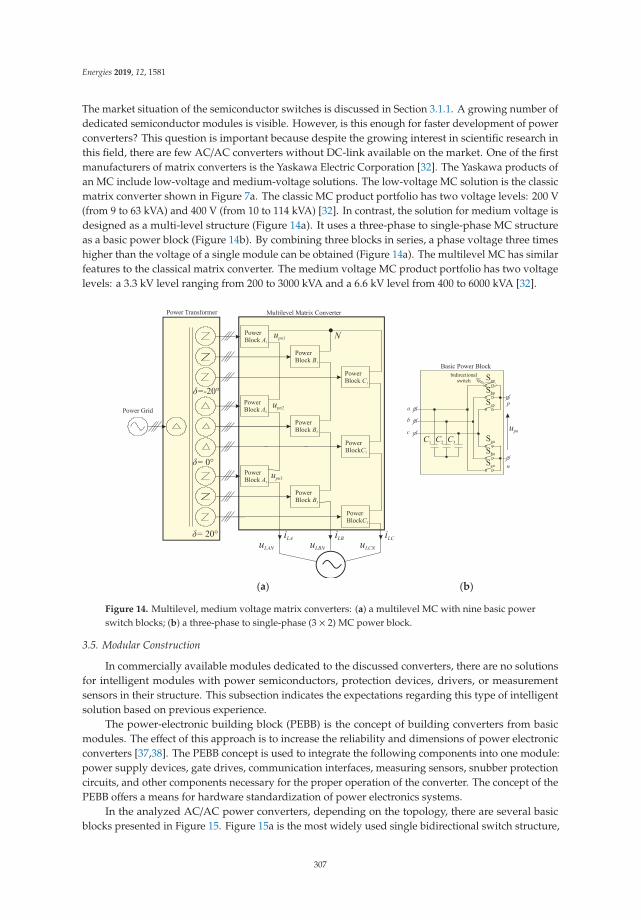
Energies 2019, 12, 1581
The market situation of the semiconductor switches is discussed in Section 3.1.1. A growing number ofdedicated semiconductor modules is visible. However, is this enough for faster development of powerconverters? This question is important because despite the growing interest in scientific research inthis field, there are few AC/AC converters without DC-link available on the market. One of the firstmanufacturers of matrix converters is the Yaskawa Electric Corporation [32]. The Yaskawa products ofan MC include low-voltage and medium-voltage solutions. The low-voltage MC solution is the classicmatrix converter shown in Figure 7a. The classic MC product portfolio has two voltage levels: 200 V(from 9 to 63 kVA) and 400 V (from 10 to 114 kVA) [32]. In contrast, the solution for medium voltage isdesigned as a multi-level structure (Figure 14a). It uses a three-phase to single-phase MC structureas a basic power block (Figure 14b). By combining three blocks in series, a phase voltage three timeshigher than the voltage of a single module can be obtained (Figure 14a). The multilevel MC has similarfeatures to the classical matrix converter. The medium voltage MC product portfolio has two voltagelevels: a 3.3 kV level ranging from 200 to 3000 kVA and a 6.6 kV level from 400 to 6000 kVA [32].
(a) (b)
Figure 14. Multilevel, medium voltage matrix converters: (a) a multilevel MC with nine basic powerswitch blocks; (b) a three-phase to single-phase (3 × 2) MC power block.
3.5. Modular Construction
In commercially available modules dedicated to the discussed converters, there are no solutionsfor intelligent modules with power semiconductors, protection devices, drivers, or measurementsensors in their structure. This subsection indicates the expectations regarding this type of intelligentsolution based on previous experience.
The power-electronic building block (PEBB) is the concept of building converters from basicmodules. The effect of this approach is to increase the reliability and dimensions of power electronicconverters [37,38]. The PEBB concept is used to integrate the following components into one module:power supply devices, gate drives, communication interfaces, measuring sensors, snubber protectioncircuits, and other components necessary for the proper operation of the converter. The concept of thePEBB offers a means for hardware standardization of power electronics systems.
In the analyzed AC/AC power converters, depending on the topology, there are several basicblocks presented in Figure 15. Figure 15a is the most widely used single bidirectional switch structure,
307

Energies 2019, 12, 1581
which consists of two active switches and two diodes anti-parallel with them. Practical implementationof such a basic block can be realized by using power electronic switches with the dedicated driversystems that are shown in Figure 8. Figure 15b shows a basic structure for a single leg of the matrixconverter structure. This basic block may be used for the construction of both the classical MC(Figure 4a) as well as the multilevel MC (Figure 14). Two prototypes of power module in suchconfigurations as SML150MAT12 and SML300MAT06 are proposed and presented in Table 1. Anotherbasic block from Figure 15c is the arrangement of a three-to-single phase MC, which can be used in amultilevel MC (Figure 14) or can be operated as a rectifier [39]. The most complex block power is thewhole structure of the MC in a single device shown in Figure 15d. Manufacturers of semiconductorpower devices offer several of these dedicated structures, as shown in Table 1.
(a) (b) (c)
(d)
Figure 15. Common switching structures for power-electronic building blocks (PEBBs) in AC/AC powerconverters (a) single bidirectional switch structure, (b) single output phase of MC switch configuration,(c) two phase of MC switch configuration, (d) three phase of MC switch configuration.
3.6. The Development of Modulation Methods
The development of varied technologies is related to the possibility of following the evolvingtrends in technology. In this subsection, it is shown that, in the discussed topologies, it is possible toimplement recent commonly developed methods of predictive control.
Modulation strategies in AC/AC converters without capacitors in the intermediate circuit arenot a simple issue due to the high number of transistors. AC/AC choppers have much simplermodulation strategies. Most modulation techniques have been determined for classical, direct MCs,and they are presented in a review article [22]. In recent years, MPC has been the best developedmethod of modulation. At discrete time Td, MPC examines a model of a controlled system andpredicts its condition in the next step. The configuration of converter switches is selected to ensurea minimum value of the cost function [40]. Scientific publications with MPC of an MC show better
308

Energies 2019, 12, 1581
achievements in the quality of current and voltage waveforms, torque ripple, and internal switchingpower losses [30,41,42]. An example MPC scheme for the MC is shown in Figure 16, and this exampleis one that minimizes the cost function related to the accuracy of shaping the output current andthe input power factor. Development of predictive control methods in AC systems without DC-linkcapacitors is a future area of extensive conceptual and implementation research.
Figure 16. Model predictive control (MPC) of an MC with minimalization of the output current ripplesand input power factor (reactive power).
The AC/AC chopper modulation algorithms are not complicated and are based only on the changein the control pulse duty factor. Research on control algorithms is mainly related to increasing efficiency,identifying faults, and optimizing their operation during component failures. New system structuresare also being developed that produce significantly better properties regarding efficiency and powerdensity [43,44].
4. Novel Applications of AC/AC Converters without DC-Link Capacitor
The classic application of frequency converters such as the matrix converter is to variable speedelectric drives, while the AC/AC choppers are used in applications such as industrial process heating,the control of lighting intensity, or the soft-start of an induction AC motor. These applications areubiquitously described in the literature and will not be analyzed in this article.
New potential areas for the application of choppers and AC/AC frequency converters without aDC-link circuit are in such devices as compensators for voltage fluctuations in the electric power gridand power flow controllers [19,45,46]. An example of such a compensator with a power flow controlfunction is the hybrid transformer (HT) with a matrix converter or a matrix chopper [45,46], which isshown in Figure 17. The HT contains two main units: (1) a conventional three-phase transformer withtwo pairs of secondary windings and (2) a three-phase AC/AC converter. The first pair of outputwindings supplies the converter, whereas the second pair is connected in series with the outputterminals of the converter. The compensating voltage is generated at the output of the converter.The output voltage of the whole HT is the sum of the power converter output voltage and the secondsecondary winding voltage of the transformer. The output terminals of the HT are connected witha sensitive load or a protected small industrial plant. The disadvantage of the HT is the necessityof using transformers with two pairs of secondary windings. Furthermore, under normal supplyvoltage conditions, the inverter can be switched off, resulting in this part of the transformer generatingadditional power losses.
A hybrid transformer with a matrix chopper allows compensation only for the amplitude ofthe supply voltage; using a matrix converter, it is possible to compensate for both symmetrical andasymmetrical voltage changes as well as harmonic distortions. As an example, to illustrate thebeneficial properties of an HT with an MC, the results of the MPC algorithm (Figure 18) are presented
309
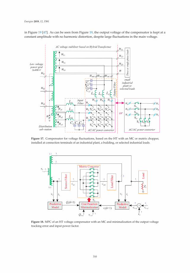
Energies 2019, 12, 1581
in Figure 19 [47]. As can be seen from Figure 19, the output voltage of the compensator is kept at aconstant amplitude with no harmonic distortion, despite large fluctuations in the main voltage.
Figure 17. Compensator for voltage fluctuations, based on the HT with an MC or matrix chopper,installed at connection terminals of an industrial plant, a building, or selected industrial loads.
Figure 18. MPC of an HT voltage compensator with an MC and minimalization of the output voltagetracking error and input power factor.
310

Energies 2019, 12, 1581
Figure 19. Results of compensations of electric power grid voltage fluctuation using an HT with an MCand MPC control (author’s simulation results); red – voltage phase 1, blue – voltage phase 2, green –voltage phase 3.
If such an HT were connected to a dual-source network, it would be possible to regulate thepower flow in the system by changing the phase angle of the compensator output voltage [46]. As canbe seen from the above applications, AC/AC converters without a DC-link capacitor can be used innon-standard applications in low voltage power grids.
The main requirements for devices installed in the power system are a high reliability and a highefficiency factor. For an AC/AC converter, the parts most sensitive to damage are the power electronicelements. The installed converters should permit continuous work even after the occurrence of a faultin the power electronic converter, ensuring greater reliability. The reliability is high if the load canwork with source voltage parameters (or slightly modified) even when damage has occurred in thepower electronic part [19]. In this case, the bypass circuits should be used to disconnect or short-circuitthe defective converter. In Figure 20, the single phase equivalent models of example AC/AC converterswithout a DC-link capacitor installed in the power system are presented. In the case of damage tothe power electronic unit (AC/AC), the topologies based on the configuration shown in Figure 20a,b,could still operate with source (vS) parameters, after activation of the additional bypass switch. In thecase of the configuration shown in Figure 20c, the reliability can be assessed as low. In the event ofdamage to the AC/AC converter, the whole circuit must be turned off, because it is unable to continueto operate. As a result, all receivers connected to the load side have to be shut off.
(a) (b) (c)
vSZL
LOAD
n
n
vc
vS ZL
LOAD
n
vc
n
vLvLZL
LOAD vL
vS
Figure 20. Single phase equivalent models of AC/AC converters installed in the power grid, (a,b) highreliability configurations, (c) low reliability configuration.
5. Conclusions
The presented converter offers a number of important benefits. However, such devices are stillnot widely used. Their application at the industrial level has been halted due to the fact that there are anumber of challenges that must be overcome. This article has identified the challenges faced by thedesigners of such systems. The main aim of this article was to identify the problems that need to beaddressed by research to enable the use of such converters without DC energy storage elements.
The main barrier to the development of AC/AC converters is due to the small number of availablesemiconductor power components. In addition, there are virtually no solutions in the form of intelligentmodules that also include gate drivers and systems providing additional measuring and protection
311

Energies 2019, 12, 1581
functions. It should be pointed out that minimizing the size of AC/AC converters without a DC-linkcircuit will become possible as a result of the development of modules which will be dedicated andoptimized in terms of functionality, size, and performance of intelligent power modules. Anotherconstraint is met in the complex algorithms for the modulation and commutation of transistors,which requires the construction of complex systems most often equipped with DSP and FPGA. Inaddition, the complexity of the above-mentioned algorithms also involves the use of additionalelectronic circuits, such as current flow detectors or a clamp protection circuit.
Finally, the article identifies the application possibilities of the analyzed topologies in modernpower systems. The potential of modern control algorithms based on MPC has also been indicated.Comparative analysis shows that the use of such algorithms produces very good properties in voltageor current signal shapes.
Funding: This research received no external funding.
Conflicts of Interest: The authors declare no conflict of interest.
References
1. Yang, Y.; Wang, H.; Sangwongwanich, A.; Blaabjerg, F. Design for Reliability of Power Electronic Systems.In Power Electronics Handbook, 4th ed.; Butterworth-Heinemann: Oxford, UK, 2018; pp. 1423–1440.
2. Chung, H.S.-H.; Wang, H.; Blaabjerg, F.; Pecht, M. Reliability of Power Electronic Converter Systems;The Institution of Engineering and Technology: London, UK, 2015.
3. Sang, Z.; Mao, C.; Lu, J.; Wang, D. Analysis and Simulation of Fault Characteristics of Power Switch Failuresin Distribution Electronic Power Transformers. Energies 2013, 6, 4246–4268. [CrossRef]
4. Fischer, K.; Pelka, K.; Puls, S.; Poech, M.-H.; Mertens, A.; Bartschat, A.; Tegtmeier, B.; Broer, C.; Wenske, J.Exploring the Causes of Power-Converter Failure in Wind Turbines based on Comprehensive Field-Data andDamage Analysis. Energies 2019, 12, 593. [CrossRef]
5. Choi, U.M.; Blaabjerg, F.; Lee, K.B. Study and Handling Methods of Power IGBT Module Failures in PowerElectronic Converter Systems. IEEE Trans. Power Electron. 2015, 30, 2517–2533. [CrossRef]
6. Kamel, T.; Biletskiy, Y.; Chang, L. Fault Diagnoses for Industrial Grid-Connected Converters in the PowerDistribution Systems. IEEE Trans. Ind. Electron. 2015, 62, 6496–6507. [CrossRef]
7. Peftitsis, D.; Rabkowski, J. Gate and Base Drivers for Silicon Carbide Power Transistors: An Overview.IEEE Trans. Power Electron. 2016, 31, 7194–7213. [CrossRef]
8. Marzoughi, A.; Burgos, R.; Boroyevich, D. Characterization and Performance Evaluation of the State-of-the-Art3.3 kV 30 A Full-SiC MOSFETs. IEEE Trans. Ind. Appl. 2019, 55, 575–583. [CrossRef]
9. Zhang, L.; Yuan, X.; Wu, X.; Shi, C.; Zhang, J.; Zhang, Y. Performance Evaluation of High-Power SiC MOSFETModules in Comparison to Si IGBT Modules. IEEE Trans. Power Electron. 2019, 34, 1181–1196. [CrossRef]
10. Jones, E.A.; Wang, F.F.; Costinett, D. Review of Commercial GaN Power Devices and GaN-Based ConverterDesign Challenges. IEEE J. Emerg. Sel. Top. Power Electron. 2016, 4, 707–719. [CrossRef]
11. Wang, H.; Blaabjerg, F. Reliability of capacitors for DC-Link applications in power electronic converters—Anoverview. IEEE Trans. Ind. Appl. 2014, 50, 3569–3578. [CrossRef]
12. Yun, G.; Cho, Y. Active Hybrid Solid State Transformer Based on Multi-Level Converter Using SiC MOSFET.Energies 2019, 12, 66. [CrossRef]
13. Zhu, Q.; Dai, W.; Guan, L.; Tan, L.; Li, Z.; Xie, D. A Fault-Tolerant Control Strategy of Modular MultilevelConverter with Sub-Module Faults Based on Neutral Point Compound Shift. Energies 2019, 12, 876. [CrossRef]
14. Volosencu, C. System Reliability; Intech Open: Rijeka, Croatia, 2017.15. Kolar, J.W.; Friedli, T.; Rodriguez, J.; Wheeler, P.W. Review of three-phase PWM AC–AC converter topologies.
IEEE Trans. Ind. Electron. 2011, 58, 4988–5006. [CrossRef]16. Szczesniak, P.; Kaniewski, J.; Jarnut, M. AC/AC power electronic converters without DC energy storage:
A review. Energy Convers. Manag. 2015, 92, 483–497. [CrossRef]17. Zhang, J.; Li, L.; Dorrell, D.G. Control and applications of direct matrix converters: A review. Chin. J. Electr.
Eng. 2018, 4, 18–27.18. Empringham, L.; Kolar, J.W.; Rodriguez, J.; Wheeler, P.W.; Clare, J.C. Technological issues and industrial
application of matrix converters: A review. IEEE Trans. Ind. Electron. 2013, 60, 4260–4271. [CrossRef]
312

Energies 2019, 12, 1581
19. Kaniewski, J.; Fedyczak, Z.; Szczesniak, P. AC voltage transforming circuits in power systems. Electr. Rev.2015, 91, 8–17.
20. Kaniewski, J.; Szczesniak, P.; Jarnut, M.; Benysek, G. Hybrid voltage sag/swell compensator. A review ofAC/AC converters. IEEE Ind. Electron. Mag. 2015, 9, 37–48. [CrossRef]
21. Szczesniak, P.; Kaniewski, J. Power electronics converters without DC energy storage in the future electricalpower network. Electr. Power Syst. Res. 2015, 129, 194–207. [CrossRef]
22. Andreu, J.; Kortabarria, I.; Ormaetxea, E.; Ibarra, E.; Martin, J.L.; Apiñaniz, S. A step forward towards thedevelopment of reliable matrix converters. IEEE Trans. Ind. Electron. 2012, 59, 167–183. [CrossRef]
23. Rodriguez, J.; Rivera, M.; Kolar, J.W.; Wheeler, P.W. A review of control and modulation methods for matrixconverters. IEEE Trans. Ind. Electron. 2012, 59, 58–70. [CrossRef]
24. Safari, S.; Castellazzi, A.; Wheeler, P. Experimental and Analytical Performance Evaluation of SiC PowerDevices in the Matrix Converter. IEEE Trans. Power Electron. 2014, 29, 2584–2596. [CrossRef]
25. Empringham, L.; de Lillo, L.; Schulz, M. Design Challenges in the Use of Silicon Carbide JFETs in MatrixConverter Applications. IEEE Trans. Power Electron. 2014, 29, 2563–2573. [CrossRef]
26. Trentin, A.; de Lillo, L.; Empringham, L.; Wheeler, P.; Clare, J. Experimental Comparison of a Direct MatrixConverter Using Si IGBT and SiC MOSFETs. IEEE J. Emerg. Sel. Top. Power Electron. 2015, 3, 542–554.[CrossRef]
27. Trentin, A.; Empringham, L.; de Lillo, L.; Zanchetta, P.; Wheeler, P.; Clare, J. Experimental EfficiencyComparison Between a Direct Matrix Converter and an Indirect Matrix Converter Using Both Si IGBTs andSiC mosfets. IEEE Trans. Ind. Appl. 2016, 52, 4135–4145. [CrossRef]
28. Buccella, C.; Cecati, C.; Latafat, H. Digital Control of Power Converters—A Survey. IEEE Trans. Ind. Inform.2012, 8, 437–447. [CrossRef]
29. Kobravi, K.; Iravani, R.; Kojori, H.A. Three-Leg/Four-Leg Matrix Converter Generalized ModulationStrategy—Part II: Implementation and Verification. IEEE Trans. Ind. Electron. 2013, 60, 860–872. [CrossRef]
30. Gulbudak, O.; Santi, E. FPGA-Based Model Predictive Controller for Direct Matrix Converter. IEEE Trans.Ind. Electron. 2016, 63, 4560–4570. [CrossRef]
31. Wisniewski, R.; Bazydło, G.; Szczesniak, P.; Wojnakowski, M. Petri Net-Based Specification of Cyber-PhysicalSystems Oriented to Control Direct Matrix Converters with Space Vector Modulation. IEEE Access 2019, 7,23407–23420. [CrossRef]
32. Yamamoto, E.; Hara, H.; Uchino, T.; Kawaji, M.; Kume, T.J.; Kang, J.-K.; Krug, H.-P. Development of MCsand its Applications in Industry. IEEE Ind. Electron. Mag. 2011, 5, 4–12. [CrossRef]
33. Oancea, C.D.; Dinu, C. LEM transducers interface for voltage and current monitoring. In Proceedings of the9th International Symposium on Advanced Topics in Electrical Engineering (ATEE’15), Bucharest, Romania,7–9 May 2015; pp. 949–952.
34. Sozanski, K. Digital Signal Processing in Power Electronics Control Circuits, 2nd ed.; Springer: London, UK, 2017.35. Bobrowska-Rafal, M.; Rafal, K.; Jasinski, M.; Kazmierkowski, M.P. Grid synchronization and symmetrical
components extraction with PLL algorithm for grid connected power electronic converters—A review. Bull.Pol. Acad. Sci. Tech. Sci. 2011, 59, 485–497. [CrossRef]
36. Irmak, E.; Colak, I.; Kaplan, O.; Guler, N. Design and application of a novel zero-crossing detector circuit.In Proceedings of the International Conference on Power Engineering, Energy and Electrical Drives, Malaga,Spain, 11–13 May 2011.
37. Iyer, A.R.; Kandula, R.P.; Moghe, R.; Hernandez, J.E.; Lambert, F.C.; Divan, D. Validation of the Plug-and-PlayAC/AC Power Electronics Building Block (AC-PEBB) for Medium-Voltage Grid Control Applications.IEEE Trans. Ind. Appl. 2014, 50, 3549–3557. [CrossRef]
38. Laka, A.; Barrena, J.A.; Chivite-Zabalza, J.; Rodriguez, M.A. Analysis and Improved Operation of aPEBB-Based Voltage-Source Converter for FACTS Applications. IEEE Trans. Power Deliv. 2013, 28, 1330–1338.[CrossRef]
39. You, K.; Xiao, D.; Rahman, M.F.; Uddin, M.N. Applying Reduced General Direct Space Vector ModulationApproach of AC/AC Matrix Converter Theory to Achieve Direct Power Factor Controlled Three-PhaseAC-DC Matrix Rectifier. IEEE Trans. Ind. Appl. 2014, 50, 2243–2257. [CrossRef]
40. Rodríguez, J.; Cortes, P. Predictive Control of Power Converters and Electrical Drives; John Wiley & Sons:Hoboken, NJ, USA, 2012.
313

Energies 2019, 12, 1581
41. Zhang, J.; Norambuena, M.; Li, L.; Dorrell, D.; Rodriguez, J. Sequential Model Predictive Control ofThree-Phase Direct Matrix Converter. Energies 2019, 12, 214. [CrossRef]
42. Rivera, M.; Rojas, C.; Rodriguez, J.; Wheeler, P.W.; Wu, B.; Espinoza, J.R. Predictive Current Control withInput Filter Resonance Mitigation for a Direct Matrix Converter. IEEE Trans. Power Electron. 2011, 26,2794–2803. [CrossRef]
43. Khan, A.A.; Cha, H.; Ahmed, H.F. High-Efficiency Single-Phase AC–AC Converters Without CommutationProblem. IEEE Trans. Power Electron. 2016, 31, 5655–5665. [CrossRef]
44. Khan, A.A.; Cha, H.; Kim, H. Three-Phase Three-Limb Coupled Inductor for Three-Phase Direct PWMAC–AC Converters Solving Commutation Problem. IEEE Trans. Ind. Electron. 2016, 63, 189–201. [CrossRef]
45. Kaniewski, J.; Fedyczak, Z.; Benysek, G. AC voltage sag/swell compensator based on three-phase hybridtransformer with buck-boost matrix-reactance chopper. IEEE Trans. Ind. Electron. 2014, 61, 3835–3846.[CrossRef]
46. Szczesniak, P.; Kaniewski, J. Hybrid transformer with matrix converter. IEEE Trans. Power Deliv. 2016, 31,1388–1396. [CrossRef]
47. Szczesniak, P.; Tadra, T.; Kaniewski, J.; Fedyczak, Z. Model predictive control algorithm of AC voltagestabilizer based on hybrid transformer with a matrix converter. Electr. Power Syst. Res. 2019, 170, 222–228.[CrossRef]
© 2019 by the author. Licensee MDPI, Basel, Switzerland. This article is an open accessarticle distributed under the terms and conditions of the Creative Commons Attribution(CC BY) license (http://creativecommons.org/licenses/by/4.0/).
314

energies
Article
6.78-MHz, 50-W Wireless Power Supply Over a 60-cmDistance Using a GaN-Based Full-Bridge Inverter
Seung-Hwan Lee 1, Kyung-Pyo Yi 2 and Myung-Yong Kim 2,*
1 School of Electrical and Computer Engineering, University of Seoul, Seoul 02504, Korea;[email protected]
2 Smart Electrical & Signaling Division, Korea Railroad Research Institute, Uiwang 16105, Korea;[email protected]
* Correspondence: [email protected]; Tel.: +82-31-460-5515
Received: 3 January 2019; Accepted: 21 January 2019; Published: 24 January 2019
Abstract: An inductive wireless power transfer system is proposed as a power supply for an on-linemonitoring system for an overhead catenary. Because of the high voltage (25 kVrms) applied to thecatenary, galvanic isolation was required to supply power to the attached monitoring system. Theproposed wireless power system was able to transmit 50 W over a distance of 60 cm at 6.78 MHz.Design methodologies for the transmitter and the receiver coils, 6.78-MHz GaN-based full-bridgeinverter, and rectifier are proposed in this paper. Pareto optimality, a multi-objective optimizationtechnique, was used to determine optimal solutions in terms of efficiency and copper usage. A 100-W,6.78-MHz full-bridge inverter was developed using 100 V, 35 A, E-HEMT GaN MOSFETs. Because ofthe high operating frequency, two factors were considered in the design of the full-bridge inverter,(1) close placement of the gate driver and the switch to minimize parasitic inductance and theresulting fluctuation of the drive signal and (2) effective heat dissipation from the switches andgate drivers for a high power rating. In addition, a full-wave rectifier was built using Schottkybarrier diodes with a reverse recovery time of a few tens of nano-seconds. The developed wirelesspower system was experimentally evaluated. The measured coil-to-coil efficiency was 77%, and themeasured efficiencies of the inverter and the rectifier were 92% and 93%, respectively. The overallsystem efficiency was 57% for a transfer of 47 W. Finally, the dependences of the efficiency on thedistance, operating frequency, and load were evaluated.
Keywords: wireless power transfer; inductive power transfer; Pareto optimality; coil design;magnetics design; GaN-based inverter and converter
1. Introduction
Applications of inductive wireless power transfer (WPT) technology have transitioned from Wlevel biomedical devices to MW level transportation systems [1–8]. Among the various applications,application that the WPT system is useful as a power supply: an on-line monitoring system for ahigh-voltage catenary (see Figure 1a) [9]. Because of the high-voltage (25 kVrms) of the catenary, themonitoring system cannot obtain power from a low-voltage grid (110 Vrms or 220 Vrms) without havinga sufficient insulation or isolation gap. According to [10], the minimum isolation distance between a25-kVrms overhead wire and ground is 25 cm (30-cm isolation distance is recommended). This is thereason that the lengths of the insulators used for 25-kVrms catenaries are longer than 30 cm (60 cmor longer insulators are common). Therefore, any system that supplies a low voltage power to the25-kVrms catenary needs to transmit power over the lengths of the insulators.
Energies 2019, 12, 371; doi:10.3390/en12030371 www.mdpi.com/journal/energies315

Energies 2019, 12, 371
(a)
(b)
Figure 1. Configurations of the target catenary monitoring system and the WPT system: (a) Targetsystem configuration; (b) Block diagram of the wireless power transfer system.
Previously, a 12-V, 12-Ah Pb-battery and a photovoltaic (PV) battery charger were used as anenergy source. The PV charger was attached to an arm of a support pole (see Figure 1a). It solved thehigh voltage isolation problem. However, the size and weight of the PV module required to supplysufficient power (larger than 50 W) to the monitoring system were too large and heavy to be installedon the arm.
Instead of the PV module, an inductive WPT system was proposed that is able to wirelesslytransmit energy over the insulator in [11,12]. According to [13], the inductive WPT system was moreefficient compared to other technologies like a capacitive WPT system or a far-field power radiatingsystem. The distance between the coils of the target WPT system was over 60 cm and output powerwas 50 W. The operating frequency of the system was 6.78 MHz (the highest frequency allowed for aWPT system [14]) to achieve efficient power transmission for this large air-gap. Because of the highoperating frequency and large output power, the development of low-loss transmitter and receivercoils and a high efficiency 6.78-MHz inverter are required to construct an effective WPT system. Therehave been many previous studies that worked on such large air-gap, MHz frequencies WPT systems.
Sample et al. proposed a 7.65-MHz, 70-cm distance WPT system in 2011 [15]. The authors usedtwo circular coils with diameters of 59 cm as a transmitter and a receiver. The measured coil-to-coilefficiency was 70% at 30 W, 70-cm power transmission. The main focus of the paper was to determinethe optimal operating frequencies depending on the change of the distance between the coils. Duongand Lee published a paper demonstrating 30-mW transmission over a distance of 60 cm with a peakefficiency of 46% [16]. In this paper, the main focus of the paper was a mathematical analysis ofthe coil-to-coil system using an equivalent circuit modeling technique. Lee et al. proposed a coildesign methodology for a large air-gap system in [17]. The design methodology identified a feasibledesign space as its first step. Then the coil-to-coil efficiency, copper usage, control stability, and otherperformance metrics were calculated in the entire design space, and a weighted sum of the metricswas calculated to determine an optimal design for the transmitter and the receiver coils. Based on theproposed methodology, a 95% coil-to-coil efficiency was achieved at a distance of 30 cm and 3.74-MHz
316

Energies 2019, 12, 371
operation. However, these aforementioned papers did not consider the feasibility and efficiency ofMHz operation inverters, even though it is challenging to build an efficient high-power converter atthese high frequencies.
The literature [18–22] focused on the development of high efficiency MHz switching class-Eamplifiers for loosely-coupled WPT systems. Class-E amplifiers are very common in radio-frequency(RF) application since the amplifier requires only one low-side switch for power conversion. However,the class-E inverter requires a bulky DC inductor, and the optimal circuit parameters (e.g., shuntcapacitances) are highly dependent on the operating conditions (load, duty cycle, and operatingfrequency, etc.) [23]. Therefore, the class-E inverter requires fine tuning of the circuit parametersdepending on the load and operation conditions.
Instead of the class-E inverter, recent rapid evolution of large bandgap semiconductor switches(Silicon-carbide (SiC) and Gallium-nitride (GaN) Metal-Oxide-Semiconductor Field-Effect Transistor(MOSFET)) and their gate drivers have enabled significant advancement of radio-frequency half-and full-bridge switch-mode inverters. Multiple papers reported on GaN-based full-bridge invertersfor WPT systems in 2017 [24–26]. Zhao et al. proposed a multi-frequency pulse-width-modulation(MFPWM) scheme which was implemented using a GaN-based full-bridge inverter [24]. UsingMFPWM, an inverter can simultaneously transmit power to two receivers that operate at 100 kHzand at 6.78 MHz. Since the focus of the research was the transmission of power to multiplereceivers, rather than improvement of the inverter efficiency using GaN switches, the efficiencyof the developed inverter was not sufficiently high to be used for a system operating at a few tensof Watts. Bonache-Samaniego et al. proposed a self-oscillating resonant converter that operates at6.78 MHz [25]. The gate signals of the developed full-bridge inverter’s GaN switches were generatedusing the sensed current of the resonant tank. The proposed system was useful in the construction of alow cost and simple inverter. However, it was not suitable for the control of the operating frequency,duty, or power level. Xue and Zhang demonstrated a 50-W, 6.78-MHz, 90% efficiency GaN-basedinverter for a WPT system. The main focus of the paper was the design of a filter network to achieve awider zero-voltage-switching (ZVS) range and higher efficiency at light loads. The research used a13.56-MHz oscillator and a D-flip-flop to generate a 6.78-MHz gate drive signal. The output powerwas controlled using a phase-shift control of the legs of the inverter based on a phase delay element.
In this paper, a novel 50-W, 60-cm distance wireless power system operating at a frequencyof 6.78 MHz is proposed. The design and fabrication methodologies for the transmitter and thereceiver coils, a 100-W, 6.78-MHz H-bridge inverter using GaN switches, and a 50-W, 6.78-MHzfull-wave rectifier design are investigated. The power level and efficiency of the proposed systemwere experimentally evaluated. In the first part of the paper, design methodology for the transmitterand receiver coil is proposed using a Pareto optimality, a multi-objective optimization technique.The designed coils are fabricated on a printed-circuit-board (PCB) for ease of mass-production. Thedominant sources of losses of the PCB coils are identified and the methods for fabrication of low-losscoils at 6.78-MHz frequencies are presented. The details of a 100-W, 6.78-MHz operating E-HEMTGaN-based H-bridge inverter is explained in the following section. The H-bridge inverter is developedto supply power to the transmitter coil. The gate signals of the switches are controlled using acommercial 32-bit digital-signal-processor, and the details of the PCB layout techniques for low parasiticinductance and an effective heat dissipation are discussed. Finally, the performance evaluation of thedeveloped system is presented using experimental results. Efficiencies and losses of each componentof the system are measured and compared. Also, the dependence of the DC-to-DC efficiency on thedistance, load, and operating frequency is evaluated with the test-bed.
2. Target System Configuration
A photo of the target catenary monitoring system is shown in Figure 1a. The catenary monitoringsystem has multiple sensors that were installed on the catenary, a data acquisition (DAQ) system thatgathers information from the sensors and wirelessly transmits the information to a data center, and a
317

Energies 2019, 12, 371
battery pack as an energy source. A WPT system that can transmit 50 W over a 60-cm distance (thelength of the insulator) is proposed. A schematic of the proposed WPT system is shown in Figure 1b.The proposed WPT system collects power from a 220-Vrms single-phase grid and converts it to DCwith a diode rectifier. Then, it is converted to a 6.78-MHz AC voltage and supplied to the transmitter(TX) coil using a GaN-based H-bridge inverter. The induced voltage of a receiver coil that is weaklycoupled to the transmitter is rectified and supplied to the battery using a full-wave diode rectifier. Thedesign details of the transmitter and the receiver coils, 6.78-MHz resonant inverter, and receiver siderectifier are described in following sections.
3. Development of Transmitter and Receiver coils
3.1. Transmitter and Receiver coil Design
There were three main constraints with regard to the design of the transmitter (TX) and thereceiver (RX) coils; (1) the maximum sizes of the TX and RX coils were limited to 40 cm × 40 cm, (2)the minimum distance between the TX and RX coil was 60 cm. (3) the required output power was 50W, and load resistance was 6 Ω. For full utilization of the given space, square coils were assumed forthe TX and RX coils as shown in Figure 2. The design parameters to be determined for a square coilwere the inner diameter (din), turn spacing (s), width of the turn (w), and the number of turns of thetransmitter and the receiver coils (ntx and nrx). The design spans for the parameters are summarized inTable 1.
Table 1. Design spans of transmitter and receiver coils.
Parameters Design Limits Parameters Design Limits
Inner diameter, din 10–30 cm Trace width, w 1–2.5 cmTurn spacing, s 0.5–2 cm # of turns, n 1–8 turns
Pareto optimality [27], a multi-objective optimization theory, was applied in the coil designprocess. The maximization of the power transfer efficiency (η) and minimization of the total usage ofthe copper (m) were two objectives during optimization. The power transfer efficiency and total massof the copper depending on the coil shape change were calculated using (1) [28] and (2).
η =1
1 + R2RL
+(
RL+R2ω0 M
)2 R1RL
(1)
mass (m) = ρ ∗ l ∗ w ∗ t (2)
where, ω0 is the operating frequency of the system, M is the mutual inductance between the transmitterand the receiver, R1 and R2 are the equivalent series resistances (ESRs) of the transmitter and thereceiver coils, respectively, RL is the load resistance of the system, ρ is the density of the copper, l, wand t are the total length, width, and the thickness of the coil trace, respectively. The mutual inductanceand the ESRs of the TX and RX coils were calculated for each combination of the inner diameter,turn-spacing, width of the turn, and the number of the turns. The mutual inductance was calculatedusing a numerical integration of the flux linkage between the coils. According to [29], the z-directionalmagnetic field intensity at point P (Hz) generated by a square transmitter coil follows (3).
Hz =I
4π
ntx
∑i=1
∮ d→l i ×→
r i
r3i
, λ =nrx
∑k=1
∮μ0Hz dAk, M =
λ
I(3)
Then, the total flux linkage (λ) at the receiver coil and resulting mutual inductance (M) can becalculated. Hz is the z-directional magnetic field intensity at point P, I is the current flowing in the
transmitter coil, ntx is the number of turns of the transmitter coil, d→l i is the infinitesimal displacement
318

Energies 2019, 12, 371
vector of i-th turn of the transmitter and→r i is a direction vector from d
→l i to the point (see Figure 3),
dAk is the infinitesimal area element in k-th turn of the receiver coil, μ0 is the permeability of air, λ
is the total flux linkage at receiver coil, and M is the resulting mutual inductance. The ESRs of thetransmitter and the receiver coils were calculated using (4).
R =l
σδw(4)
where l is the total length of the coil, w is the width of the trace of the coil, σ is the conductivityof copper, and δ (= 25.4 μm) is the skin-depth of the copper at 6.78 MHz. Figure 4 shows a η − mdistribution in the entire coil design space.
Figure 2. Geometric design parameters of the square coils.
Figure 3. H-field calculation diagram.
Figure 4. Pareto front of the WPT system.
From the figure, it should be noted that the WPT coils with the same total mass of copper havevery different efficiencies depending on their design. For example, the first WPT system (identifiedby the cyan triangular point in Figure 4 had an 8-turn transmitter coil with a 10 cm inner diameter,40 cm outer diameter, 6 mm of turn spacing, and 13 mm turn width. The receiver of the first WPTsystem was a 1-turn coil with a 10 cm inner diameter, 12.6 cm outer diameter, 6 mm of turn spacing,and 13 mm turn width. The second WPT system (identified by green circular point in Figure 4 had a3-turn transmitter coil with a 30 cm inner diameter, 40 cm outer diameter, 5 mm of turn spacing and13 mm turn width. Its receiver coil was a 3-turn with a 30 cm inner diameter, 40 cm outer diameter,
319

Energies 2019, 12, 371
5 mm of turn spacing, and 13 mm turn width. The total mass of both systems was 60 g; however, thepower transfer efficiency of the first system was 2.4% at 60 cm of air-gap while the efficiency of thesecond system was 82%.
Since the goal function was to maximize the efficiency while minimizing copper usage,non-dominated solutions (Pareto front) were located at the upper left corner of the plot. The brownline in the figure represents the Pareto front. Among the non-dominated solutions, one of the solutionswith 87% efficiency and 110 g of copper usage was selected for the TX and RX coil design. This solutionis denoted as a magenta X in the plot. It is notable that the decision was made for high efficiency ratherthan low copper mass. The selected design parameters for the TX and RX coils are summarized inTable 2.
Table 2. Selected design of the transmitter and receiver coils.
Parameters Transmitter Coil Receiver Coil
Inner diameter din 18 cm 12 cmOuter diameter dout 39.8 cm 39.6 cmTurn spacing, s 0.7 cm 0.7 cmTrace width, w 2.2 cm 2.2 cmTrace thickness 71 μm 71 μmNumber of turns, n 4 5Substrate thickness 1.6 mm 1.6 mm
3.2. Finite Element Analysis of Transmitter and Receiver
The selected design was evaluated by finite element analysis (FEA) results using the full-wavesimulation software ANSYS HFSS (19.0, ANSYS, Canonsburg, PA, USA) and ANSYS DESIGNER (19.0,ANSYS, Canonsburg, PA, USA). Figure 5a shows a simulation model of the WPT system and Figure 5bshows the resulting coil-to-coil efficiency vs. operating frequency for a 6 Ω load. The theoreticalefficiency was calculated using (1). It should be noted that the theoretical and the simulated results arein good agreement with each other.
Legend: Theoretical efficiency Simulated Efficiency (coil only) Simulated Efficiency (coil on IS680 substrate)
(a) (b)
Figure 5. Finite element simulation model and simulated efficiencies: (a) FEA model;(b) Simulated efficiency.
3.3. High Q coil Fabrication
Because of the large diameter and a small number of turns of the TX and RX coils, the coils werefabricated using a PCB for ease of mass-production. Fabrication of a high-quality factor transmitterand the receiver coils on the PCB is discussed in a previous paper [12]. A summary of the previouspaper is provided in this chapter. At high frequencies, especially in the MHz frequency ranges, thereduction of three primary types of losses was important to achieve high quality factor (Q-factor) coilson the PCB. These include skin-effect loss, proximity-effect loss, and dielectric loss. Because of thetarget WPT system’s high operating frequency, skin- and proximity-effect losses were critical in theprocess of analyzing the Ohmic loss of the copper trace. In addition, the dielectric loss of the PCB
320

Energies 2019, 12, 371
substrate was important in determining the entire loss of the PCB coil because it can dominate otherlosses when the coil is not designed properly. According to the full-wave simulation results in [12], thedielectric loss was approximately 10 times greater than the Ohmic loss when the PCB substrate was avery common material, FR-4. A low dissipation factor PCB material (IS680 [30]) was very effective inreducing dielectric loss (see Table 3). Figure 6a,b show the distributions of the dielectric losses at thetransmitter and the receiver coils when they transfer 50 W to a load.
Table 3. Comparison of material properties of FR-4 and IS680.
Parameters FR-4 IS680
Relative permittivity 4.8 3.2Loss tangent 0.017 0.0032
Dielectric strength 20 kV/mm 30 kV/mmThermal conductivity 0.29 W/m/K 0.32 W/m/K
(a)
s (b)
Figure 6. Configuration of the WPT system: (a) Dielectric loss density-FR4; (b) Dielectricloss density-IS680.
It should be noted that the transmitter and receiver coils using FR-4 substrates have much higherdielectric losses compared to the losses associated with the coils using the IS680 substrates. For furtherreduction of the dielectric loss, compensation capacitors were distributed in the middle of the coilwindings as shown in Figure 7. This was helpful in reducing the electric field intensities between theadjacent turns and additional improvements of the Q-factors of the coils [12]. Figure 7 shows photosof the printed transmitter and receiver coils on IS680 substrates with distributed capacitors.
Circuit parameters of the transmitter and the receiver coils were measured using an impedanceanalyzer and were compared with theoretical and simulation results. Table 4 shows a summary of
321
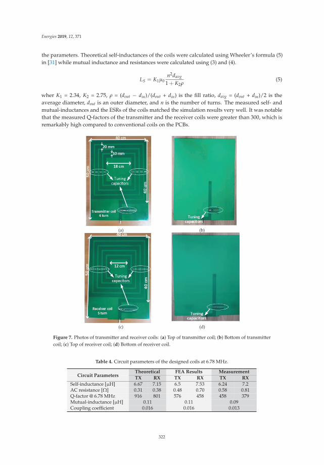
Energies 2019, 12, 371
the parameters. Theoretical self-inductances of the coils were calculated using Wheeler’s formula (5)in [31] while mutual inductance and resistances were calculated using (3) and (4).
LS = K1μ0n2davg
1 + K2ρ(5)
wher K1 = 2.34, K2 = 2.75, ρ = (dout − din)/(dout + din) is the fill ratio, davg = (dout + din)/2 is theaverage diameter, dout is an outer diameter, and n is the number of turns. The measured self- andmutual-inductances and the ESRs of the coils matched the simulation results very well. It was notablethat the measured Q-factors of the transmitter and the receiver coils were greater than 300, which isremarkably high compared to conventional coils on the PCBs.
(a) (b)
(c) (d)
Figure 7. Photos of transmitter and receiver coils: (a) Top of transmitter coil; (b) Bottom of transmittercoil; (c) Top of receiver coil; (d) Bottom of receiver coil.
Table 4. Circuit parameters of the designed coils at 6.78 MHz.
Theoretical FEA Results MeasurementCircuit Parameters
TX RX TX RX TX RX
Self-inductance [μH] 6.67 7.15 6.5 7.53 6.24 7.2AC resistance [Ω] 0.31 0.38 0.48 0.70 0.58 0.81Q-factor @ 6.78 MHz 916 801 576 458 458 379Mutual-inductance [μH] 0.11 0.11 0.09Coupling coefficient 0.016 0.016 0.013
322

Energies 2019, 12, 371
3.4. Coil-to-Coil Power Transfer Performance
From the full-wave simulation results, an efficiency in excess of 81% was expected for a 50-Wpower transfer. To experimentally evaluate the fabricated coils, they were tuned using ceramiccapacitors. The resulting tuned frequencies of the coils were measured using a network analyzer,E5061B (Keysight). Figure 8 shows the measured magnitude of the scattering parameters (S-parameters)of the transmitter and the receiver coils when they were 60 cm away from each other. S11 (blue line)and S22 (green line) had their minimum values at the tuned frequency, 6.87 MHz. S21 (red line), thetransmission coefficient, was also maximized at the tuned frequency. This tuned frequency was 1.3%higher than the target frequency of 6.78 MHz, but this tuning frequency error was ignored in theexperiment because the error has a negligible impact on the peak power transfer efficiency as shownin Figures 9 and 10. Moreover, a GaN-based H-bridge inverter that will be explained in a followingsection could adjust its output frequency in 0.01-MHz steps.
The coil-to-coil efficiency was measured using two different tests. The first measurement wasperformed using the E5061B and its real-time WPT coil analysis software that can simulate coil-to-coilefficiency in real-time with arbitrary load settings based on the measured S-parameters of the resonantcoils [32]. Using the S-parameters of the coils, the input and output power, efficiency, and the inputimpedance of the coil-to-coil system were simulated in real-time. The simulation results are shownin Figure 9. The blue and red lines show the input and the output power of the coils when the inputvoltage of the transmitter coil is set to 20 Vrms and a virtual load of 6 Ω is connected to the receiver coil.As shown in the figure, the peak power transfer efficiency was approximately 77% when the operatingfrequency was 6.87 MHz with input and output powers of 84 W and 65 W, respectively. This resultwas a little lower than the FEA results in Figure 5b. This is because the measured ESRs of the coilswere a little higher than the simulated results of the FEA as shown in Figure 7.
Figure 8. Measured S-parameters of the transmitter and receiver coils.
The coil-to-coil efficiency was evaluated experimentally as well. Using a variable frequencyH-bridge inverter, the power transfer efficiency between the transmitter and the receiver coils wasmeasured at various frequencies. In regard to the measurement of the coil-to-coil efficiency, anoscilloscope (HDO8108A, TeledyneLecroy, Chestnut Ridge, NY, USA) with a 12-bit ADC resolution,10 GS/s sample rate, 1 GHz bandwidth, a differential voltage probe (HVD3605A, TeledyneLecroy,Chestnut Ridge, NY, USA) and a current probe (CP031, TeledyneLecroy, Chestnut Ridge, NY, USA)with a measurement bandwidth of 100 MHz (14 times higher than 6.87 MHz) were used. The measured
323

Energies 2019, 12, 371
efficiency is plotted in Figure 10. A peak power transfer efficiency occurred when the operatingfrequency was 6.86 MHz, which was very close to the result in Figure 9. The peak value was 77%,which was very similar to the real-time simulated results in Figure 9. These results demonstrate thevalidity of the coil design and fabrication methodologies described in Sections 3.1 and 3.3.
Figure 9. Real-time simulation results using Keysight’s WPT analysis software (with 20 Vrms inputvoltage and 6 Ω load resistance setting).
Measurement conditions:
Distance: 60 cm Input voltage: 20 Vrms Load: 6
Figure 10. Measured coil-to-coil efficiency with 6 Ω load resistor.
4. 6.78-MHz, 100-W, 92% Efficiency H-Bridge Inverter
In order to supply 50 W using the 77% efficient transmitter and receiver coils, the development ofa high efficiency, 6.78-MHz, 100-W, H-bridge inverter was investigated. Four GS61004B, 100-V, 35-A,enhancement mode HEMT (High-electron-mobility transistor) GaN switches (GaN Systems, Ottawa,ON, Canada), and two TI’s LM5113 half-bridge drivers (TI, Dallas, TX, USA) were used. A TI’s 32-bitmicrocontroller, TMS320F28377S (TI, Dallas, TX, USA), was used as a gate signal generator and apower controller. The details of the developed inverter are presented in the following sections.
4.1. PCB Layout
After multiple failures in an attempt to develop a high-frequency inverter, the authors discoveredthat the PCB layout of the driver and GaN switches were the most important factors in determiningits performance. Two features are of notable importance in the PCB design. The first is a parasitic
324

Energies 2019, 12, 371
inductance between the gate driver and the GaN switch. Due to the high operating frequency(6.78 MHz), parasitic inductances between the gate drivers and the switches form resonance circuitswith the input capacitances of the GaN switches. This resulted in unwanted ringing of the gate drivesignal. This ringing caused undesirable on/off and failures of the GaN switches.
The second aspect to be considered is a heat dissipation of the GaN switches to achieve highpower generation (100 W) compared to the size of the switch package. The GS61004B switch wasdesigned to sink heat to the bottom side of its package, especially through its source pad. Per itsdatasheet, the required PCB pattern under its source and drain pin is over 25 × 25 mm2 for optimumheat dissipation. However, this large pad requirement leads to a large gap between the gate driver andthe GaN switch and resulted in a large parasitic inductance between the driver and switch. Figure 11ashows the initial PCB layout of the inverter that focused on the heat dissipation of the four switches.In this initial design, the PCB pattern under the source pin of the switches was 25 mm × 25 mm. Toavoid additional thermal burden on the PCB, the gate drivers (LM5113) were positioned 4 cm awayfrom the GaN switches. However, this 4-cm separation caused significant ringing of the gate drivesignal and the operation of the GaN switches was not stable even at 0.5 MHz.
(a) (b) (c)
(d) (e) (f)
Figure 11. Configuration of the WPT system: (a) Initial design; (b) Revised design; (c) Fabricatedinverter; (d) Bottom side ground plane; (e) Assembled heatsink and a fan; (f) Thermal image of theinverter at 81-W output.
Figure 11b shows a revised version of the inverter. The gate drivers were placed 0.8 cm above theswitches and only 5 mm × 5 mm of the PCB pattern was allocated to the source pin of the high-sideGaN switch. With this compact layout of the driver and switches, the gate signal ringing problem waseliminated. However, the revised version did not allocate sufficient pad area for heat dissipation of theswitches. Instead of a large pad, a heat sink was installed at the bottom layer of the PCB in this revisedversion. The ground plane at the bottom layer of the PCB was uncovered as shown in Figure 11c. Thegenerated heat from the switches and gate drivers was transferred to this bottom plane and cooledusing a heat sink that was assembled with a fan (see Figure 11d). A thermal image of the fabricatedinverter is shown in Figure 11e. The maximum temperature rise of the GaN switch’s package was15 ◦C compared to its initial temperature when the inverter output power was 81 W. Figure 12 shows a
325

Energies 2019, 12, 371
measured input and output voltages and currents of the inverter with 25 Vrms input voltage and 6 Ωload. The measured input power was 88 W and output power was 81 W. Therefore, the efficiency ofthe resonant inverter was 92%.
Figure 12. Input and output power of the H-bridge inverter. Measurement conditions: distance: 60 cm,input voltage: 25 Vrms, load: 6 Ω.
4.2. Switch Control
The gate drive signals of the inverter were digitally controlled using a TI’s 200-MHz, 32-bitmicrocontroller unit (MCU), TMS320F28377S. The resolution of a PWM (Pulse width modulation)module of the MCU was 5 ns when the system clock was 200 MHz. The PWM module was able togenerate pulses with periods of 145 ns (6.67 MHz) or 150 ns (6.89 MHz) with a single count change.PWM signals in the frequency range of 6.67 MHz to 6.89 MHz could not be generated. However,the target WPT system had very high Q coils and the transmitted power and efficiency were verysensitive to the operating frequency as shown in Figure 9. Therefore, the regular PWM module was notsuitable for 6.78-MHz operation. Instead of the regular PWM module, a high-resolution pulse widthmodulation (HRPWM) module capable of enhancing the resolution of the PWM to 180 ps was used forfine adjustment of the PWM frequency. Using the HRPWM, it was possible to change the operatingfrequency in 0.01-MHz steps. Phase-shift control and frequency control of the inverter switches wereeasily implemented using the MCU. Figure 13 shows a photo of the entire assembled inverter board.
Figure 13. A photo of the assembled H-bridge inverter.
326

Energies 2019, 12, 371
5. Receiver Side Full-Wave Rectifier Design
The series-tuned receiver coil was coupled to a full-bridge rectifier. The rectifier diodes were100-V, 8-A, Schottky barrier diodes (PMEG100V080ELPD from NXP, Eindhoven, Netherlands) witha 10-ns reverse recovery time when the forward current is 0.5 A. To minimize unwanted parasiticinductances and capacitances that can alter the tuning frequency of the RX coil, four diodes wereplaced very close to the BNC terminals. Two low-side diodes were connected on top of the PCB andhigh-side diodes were connected at the bottom of the PCB as shown in Figure 14a. Multiple ceramiccapacitors and two polymer aluminum capacitors were used as a filter. The diodes were designed forheat dissipation through its cathode pad. Therefore, a heat sink was installed at the rectifier’s positiveDC plane as shown in Figure 14b.
(a)
(b)
Figure 14. Photos of full-wave rectifier: (a) Top-view (b) Side-view.
6. Experimental Evaluation
6.1. Experimental Setup
Figure 15 shows a configuration of the test-bed. The H-bridge inverter was connected to thetransmitter resonant tank through a coaxial cable (16 AWG, American wire guage) with a BNCtermination. Also, the receiver coil was connected to the diode rectifier with the same coaxial cableand termination. A Chroma’s DC electronic load, 63102 (Chroma, Foothill Ranch, CA, USA) was usedwith a constant resistor mode setting.
Figure 15. Configuration of the test-bed.
327
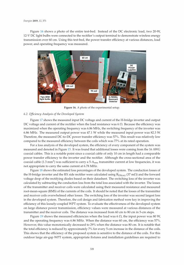
Energies 2019, 12, 371
Figure 16 shows a photo of the entire test-bed. Instead of the DC electronic load, two 20-W,12-V DC light bulbs were connected to the rectifier’s output terminal to demonstrate wireless energytransmission over 60 cm. Using this test-bed, the power transfer efficiency at various distances, loadpower, and operating frequency was measured.
Figure 16. A photo of the experimental setup.
6.2. Efficiency Analysis of the Developed System
Figure 17 shows the measured input DC voltage and current of the H-bridge inverter and outputDC voltage and current of the rectifier when the load resistance was 6 Ω. Because the efficiency wasmaximized when the operating frequency was 6.86 MHz, the switching frequency of the inverter was6.86 MHz. The measured output power was 47.1 W while the measured input power was 82.3 W.Therefore, the measured DC-to-DC power transfer efficiency was 57%. This result was relatively lowcompared to the measured efficiency between the coils which was 77% at its rated operation.
For a loss analysis of the developed system, the efficiency of every component of the system wasmeasured and denoted in Figure 15. It was found that additional losses were coming from the 16 AWGcoaxial cables. This is a notable point since a coaxial cable of only 10 cm in length had a comparablepower transfer efficiency to the inverter and the rectifier. Although the cross-sectional area of thecoaxial cable (1.3 mm2) was sufficient to carry a 5-Arms transmitter current at low frequencies, it wasnot appropriate to carry the same current at 6.78 MHz.
Figure 18 shows the estimated loss percentages of the developed system. The conduction losses ofthe H-bridge inverter and the RX side rectifier were calculated using RDS(on) (37 mΩ) and the forwardvoltage drop of the rectifying diodes based on their datasheet. The switching loss of the inverter wascalculated by subtracting the conduction loss from the total loss associated with the inverter. The lossesof the transmitter and receiver coils were calculated using their measured resistance and measuredroot-mean-square (RMS) of the currents of the coils. It should be noted that the losses of the transmitterand receiver coils overwhelmed other losses. The switching loss of the inverter was second largest lossin the developed system. Therefore, the coil design and fabrication method were key in improving theefficiency of this loosely-coupled WPT system. To evaluate the effectiveness of the developed systemon large distance power transmission, efficiency values were measured at various distances of thetransmitter and the receiver coils. The distance was increased from 60 cm to 80 cm in 5-cm steps.
Figure 19 shows the measured efficiencies when the load was 6 Ω, the input power was 80 W,and the operating frequency was 6.86 MHz. When the distance was 60 cm, the efficiency was 57%.However, this value monotonically decreased to 29% when the distance was 80 cm. It is notable thatthe total efficiency is reduced by approximately 7% for every 5-cm increase in the distance of the coils.This shows that the efficiency of the proposed system is sensitive to the distance of the coils. For thisoutdoor large air-gap WPT system, appropriate fixtures and installation guidelines are required to
328

Energies 2019, 12, 371
prevent a significant degradation of its performance due to wind and other severe weather conditions.The impact of the operating frequency on the efficiency of the test-bed was also evaluated as shown inFigure 20. The measured overall efficiency was also maximized when the operating frequency was6.86 MHz. The efficiency decreased as the operating frequency moved away from the tuned frequency.The efficiency was decreased to 38% when the operating frequency was 6.94 MHz. This is 0.08 MHzhigher than the tuned frequency. This result demonstrates that fine control of the inverter operatingfrequency is a critical factor of power transfer efficiency.
Figure 17. Measured input and output DC voltages and currents at the rated output power.Measurement conditions: distance: 60 cm, operating frequency = 6.86 MHz, load: 6 Ω.
329

Energies 2019, 12, 371
Figure 18. Estimated percentage losses of the developed system.
Measurement conditions:
RL = 6 Pin = 80 W f = 6.86 MHz
Figure 19. Efficiency dependent on distance.
Measurement conditions: RL = 6 Pin = 80 W
Figure 20. Efficiency dependence on frequency.
Finally, the impact of load resistance on the efficiency of the system was evaluated. Figure 21 showsthe result of an efficiency vs. load resistance plot. When the load resistance has a rated value RL = 6 Ω,the power transfer efficiency is maximized to 57%. As the load resistance increased or decreased, thepower transfer efficiency decreased, and the efficiency is only 35% when the load resistance is 30 Ω.This plot shows that there is an optimal load resistance for a maximum power transmission.
330

Energies 2019, 12, 371
Measurement conditions: f = 6.86 MHz
Figure 21. Efficiency dependence on load resistance.
7. Conclusions
In this paper, a new 6.78-MHz, 50-W, over 60 cm wireless power transfer system is proposed.The design and fabrication methodologies for the coils, a GaN-based 6.78-MHz H-bridge inverter,and a rectifier were explained. Using a multi-objective optimization method, Pareto optimality, thetransmitter and the receiver coil were determined to a 4-turn and a 5-turn, 40 cm × 40 cm squarecoils. The selected transmitter and receiver coils were fabricated on a PCB. It was shown that thedielectric loss of the PCB substrate can dominate Ohmic loss of copper traces at MHz frequencies. APCB substrate with very low dissipation factor was used to reduce the dielectric loss of the coils. Thefabricated coils had over 350 Q-factors at 6.78 MHz. The peak coil-to-coil efficiency for the WPT systemwas 77% at 60 cm air-gap.
In addition, a 6.78-MHz, 100-W, 92% efficiency, GaN-based H-bridge inverter was developed.Two important points were considered in the development of the inverter: a low parasitic inductanceof the gate drive circuit and a good heat dissipation of the GaN switch at its rated output power.Parasitic inductances between the gate drivers and GaN switches caused significant ringing of theon/off signals and poor operation performances even at sub-MHz frequencies. A close positioning ofthe gate driver to the switch was the key for 6.78-MHz operation. However, the congregating of thegate drivers and switches was inferior in cooling and heat dissipation of the inverter. To resolve thethermal issues, the ground plane at the bottom of the PCB was uncovered, and a heatsink with a fanwas attached to the PCB. The fabricated 6.78-MHz resonant inverter had a 92% efficiency and the peaktemperature was lower than 45 ◦C at its rated output. Using a high-resolution PWM module of theTI’s MCU, the switching signals could be changed in 0.01-MHz steps. This was very helpful in finetuning of the high Q-factor coils. Using a full-wave rectifier that was built using four Schottky barrierdiodes, the induced voltage and current of the receiver coil were converted to DC values.
The measured DC-to-DC efficiency of the developed WPT system was 57% when the outputpower was 47 W. The efficiencies of individual components of the system were measured and lossyparts were identified. The impacts of the coil distance, operating frequency, and load resistance onthe power transfer efficiency were also evaluated. As the distance increased from 60 cm to 80 cm,the efficiency decreased from 57% to 29% (about a half of the initial value). Therefore, the distancewas important in the efficiency of the WPT system. Also, the efficiency decreased from 57% to 38%when the operating frequency was increased from 6.86 MHz to 6.94 MHz (a change of only 0.08 MHz).Finally, the dependence of efficiency on the load resistance was tested. It was shown that there wasan optimal load value that maximizes the efficiency, and this value was determined to be 6 Ω, whichcorresponds to the target-rated load resistance of the developed system.
Author Contributions: Conceptualization, S.-H.L. and M.-Y.K.; methodology, S.-H.L. and M.-Y.K.; softwareanalysis, K.-P.Y.; validation, S.-H.L., K.-P.Y., and M.-Y.K..; formal analysis, S.-H.L.; investigation, M.-Y.K.,
331

Energies 2019, 12, 371
writing—original draft preparation, S.-H.L.; writing—review and editing, K.-P.Y. and M.-Y.K.; supervision,M.-Y.K..; project administration, S.-H.L. and K.-P.Y.; funding acquisition, S.-H.L. and M.-Y.K..
Funding: This research was supported by the 2016 Research Fund of the University of Seoul awardedto Seung-Hwan Lee. This work was also supported by a grant (18RTRP-B097048-04) from the RailroadTechnology Development Program funded by Ministry of Land, Infrastructure and Transport (MOLIT) of Koreangovernment and Korea Agency for Infrastructure Technology Advancement (KAIA) awarded Kyung-Pyo Yi andMyung-Yong Kim.
Conflicts of Interest: The authors declare no conflict of interest.
References
1. RamRakhyani, A.K.; Mirabbasi, S.; Chiao, M. Design and Optimization of Resonance-Based Efficient WirelessPower Delivery Systems for Biomedical Implants. IEEE Trans. Biomed. Circuits Syst. 2011, 5, 48–63. [CrossRef][PubMed]
2. Salim, A.; Baldi, A.; Ziaie, B. Inductive link modeling and design guidelines for optimum power transfer inimplantable wireless microsystems. In Proceedings of the 25th Annual International Conference of the IEEEEngineering in Medicine and Biology Society (IEEE Cat. No. 03CH37439), Cancun, Mexico, 17–21 September2003; Volume 4, pp. 3368–3371.
3. Lenaerts, B.; Puers, R. An inductive power link for a wireless endoscope. Biosens. Bioelectron. 2007, 22,1390–1395. [CrossRef] [PubMed]
4. Ko, Y.D.; Jang, Y.J. The optimal system design of the online electric vehicle utilizing wireless powertransmission technology. IEEE Trans. Intell. Transp. Syst. 2013, 14, 1255–1265. [CrossRef]
5. Kim, J.H.; Lee, B.S.; Lee, J.H.; Lee, S.H.; Park, C.B.; Jung, S.M.; Lee, S.G.; Yi, K.P.; Baek, J. Developmentof 1-MW Inductive Power Transfer System for a High-Speed Train. IEEE Trans. Ind. Electron. 2015, 62,6242–6250. [CrossRef]
6. Guidi, G.; Suul, J.A.; Jenset, F.; Sorfonn, I. Wireless Charging for Ships: High-Power Inductive Charging forBattery Electric and Plug-In Hybrid Vessels. IEEE Electrif. Mag. 2017, 5, 22–32. [CrossRef]
7. Lee, S.H.; Kim, J.H.; Lee, J.H. Development of a 60 kHz, 180 kW, over 85% efficiency inductive power transfersystem for a tram. Energies 2016, 9, 1075. [CrossRef]
8. Wang, Z.; Wei, X.; Dai, H. Design and Control of a 3 kW Wireless Power Transfer System for Electric Vehicles.Energies 2015, 9, 10. [CrossRef]
9. Park, Y.; Cho, Y.H.; Lee, K.; Jung, H.; Kim, H.; Kwon, S.; Park, H. Development of an FPGA-based OnlineCondition Monitoring System for Railway Catenary Application. In Proceedings of the World Congress onRailway Research (WCRR), Seoul, Korea, 18–22 May 2008; p. 143.
10. Korea Rail Network Authority. Railway Design Guidelines and Handbooks: Guidace on Overhead Line Clearances(KR E-03140); Korea Rail Network Authority: Daejeon, Korea, 2012.
11. Lee, S.-H.; Lee, J.-H.; Yi, K.-P. A New Design Methodology for a 1 Meter Distance, 6.78 MHz Wireless PowerSupply System for Telemetries. In Proceedings of the IEEE Energy Conversion Congress and Exposition,ECCE 2016, Milwaukee, WI, USA, 18–22 September 2016.
12. Lee, S.-H.; Yi, K.-P. Development of 50 W High Quality Factor Printed Circuit Board Coils for a 6.78 MHz, 60cm Air-gap Wireless Power Transfer System. J. Korean Soc. Railw. 2016, 19, 468–479. [CrossRef]
13. Lee, S.-H. Design Methodologies for Low Flux Density, High Efficiency, kW Level Wireless Power TransferSystems with Large Air Gaps. Ph.D. Dissertation, University of Wisconsin-Madison, Madison, WI, USA,2013.
14. AirFuelAllience. AirFuel Resonant Wireless Power Transfer (WPT) System Baseline System Specifications;AirFuelAllience: Beaverton, OR, USA, 2017.
15. Sample, A.P.; Meyer, D.A.; Smith, J.R.; Member, S.; Meyer, D.A.; Smith, J.R. Analysis, Experimental Results,and Range Adaptation of Magnetically Coupled Resonators for Wireless Power Transfer. IEEE Trans.Ind. Electron. 2011, 58, 544–554. [CrossRef]
16. Duong, T.P.; Lee, J.-W. Experimental Results of High-Efficiency Resonant Coupling Wireless Power TransferUsing a Variable Coupling Method. IEEE Microw. Wirel. Compon. Lett. 2011, 21, 442–444. [CrossRef]
17. Lee, S.-H.; Lorenz, R.D. A Design Methodology for Multi-kW, Large Airgap, MHz Frequency, WirelessPower Transfer Systems. In Proceedings of the IEEE Energy Conversion Congress and Exposition: EnergyConversion Innovation for a Clean Energy Future (ECCE 2011), Phoenix, AZ, USA, 17–22 September 2011.
332

Energies 2019, 12, 371
18. Calder, R.J.; Lee, S.H.; Lorenz, R.D. Efficient, MHz Frequency, Resonant Converter for Sub-Meter (30 cm)Distance Wireless Power Transfer. In Proceedings of the 2013 IEEE Energy Conversion Congress andExposition, ECCE 2013, Denver, CO, USA, 15–19 September 2013; pp. 1917–1924.
19. Akuzawa, Y.; Tsuji, K.; Matsumori, H.; Ito, Y.; Ezoe, T.; Sakai, K. A 95% Efficient Inverter with 300-W PowerOutput for 6.78-MHz Magnetic Resonant Wireless Power Transfer System. In Proceedings of the 2015 IEEEMTT-S International Microwave Symposium, Phoenix, AZ, USA, 17–22 May 2015; pp. 60–62.
20. Sakai, K.; Ito, Y.; Ezoe, T.; Akuzawa, Y. A 99%-Efficiency GaN Converter for 6.78 MHz Magnetic ResonantWireless Power Transfer System. J. Eng. 2014, 2014, 598–600.
21. Yang, J.-R.; Kim, J.; Park, Y.-J. Class E Power Amplifiers using High-Q Inductors for Loosely CoupledWireless Power Transfer System. J. Electr. Eng. Technol. 2014, 9, 569–575. [CrossRef]
22. Narayanamoorthi, R.; Juliet, A.V.; Chokkalingam, B.; Padmanaban, S.; Leonowicz, Z.M. Class E PowerAmplifier Design and Optimization for the Capacitive Coupled Wireless Power Transfer System inBiomedical Implants. Energies 2017, 10, 1409.
23. Grebennikov, A. Load Network Design Techniques for Class E RF and Microwave Amplifier. High Freq.Electron. 2004, 3, 18–32.
24. Zhao, C.; Costinett, D. GaN-Based Dual-Mode Wireless Power Transfer Using Multifrequency Programmed.IEEE Trans. Ind. Electron. 2017, 64, 9165–9176. [CrossRef]
25. Bonache-Samaniego, R.; Olalla, C.; Martinez-Salamero, L.; Maksimovic, D. 6.78 MHz Self-Oscillating ParallelResonant Converter Based on GaN Technology. In Proceedings of the 2017 IEEE Applied Power ElectronicsConference and Exposition (APEC), Tampa, FL, USA, 26–30 March 2017; pp. 1594–1599.
26. Xue, L.; Zhang, J. Single-stage 6.78 MHz Power-Amplifier Design using High-Voltage GaN Power ICs forWireless Charging Applications. In Proceedings of the 2017 IEEE Applied Power Electronics Conference andExposition (APEC), Tampa, FL, USA, 26–30 March 2017; pp. 3743–3750.
27. Ngatchou, P.; Zarei, A.; El-Sharkawi, A.; El-Sharkawi, M.A. Pareto Multi Objective Optimization. InProceedings of the 13th International Conference on Intelligent Systems Application to Power Systems,Arlington, VA, USA, 6–10 November 2005; pp. 84–91.
28. Lee, S.H.; Lee, B.S.; Lee, J.H. A New Design Methodology for A 300-Kw, Low Flux Density, Large Air Gap,Online Wireless Power Transfer System. IEEE Trans. Ind. Appl. 2016, 52, 4234–4242. [CrossRef]
29. Fotopoulou, K.; Flynn, B.W. Wireless Power Transfer in Loosely Coupled Links: Coil Misalignment Model.IEEE Trans. Magn. 2011, 47, 416–430. [CrossRef]
30. Isola IS680. Available online: http://www.isola-group.com/products/all-printed-circuit-materials/is680/(accessed on 3 August 2018).
31. Mohan, S.S.; Hershenson, M.D.M.; Boyd, S.P.; Lee, T.H. Simple Accurate Expressions for Planar SpiralInductances. IEEE J. Solid-State Circuits 1999, 34, 1419–1420. [CrossRef]
32. Keysight E5061B-006 Wireless Power Transfer Analysis. Available online: https://www.keysight.com/en/pd-2571977-pn-E5061B/wireless-power-transfer-analysis?cc=US&lc=eng (accessed on 19 August 2018).
© 2019 by the authors. Licensee MDPI, Basel, Switzerland. This article is an open accessarticle distributed under the terms and conditions of the Creative Commons Attribution(CC BY) license (http://creativecommons.org/licenses/by/4.0/).
333


energies
Article
Supervisory Control for Wireless Networked PowerConverters in Residential Applications†
S. M. Rakiul Islam 1,*, Sung-Yeul Park 1, Shaobo Zheng 2, Song Han 2 and Sung-Min Park 3
1 Electrical and Computer Engineering Department, University of Connecticut, Storrs, CT 06269, USA;[email protected]
2 Computer Science Engineering Department, University of Connecticut, Storrs, CT 06269, USA;[email protected] (S.Z.); [email protected] (S.H.)
3 Electrical and Electronic Engineering Department, Hongik University, Sejong-si 30016, Korea;[email protected]
* Correspondence: [email protected]; Tel.: +1-860-486-0915† This paper is an extended version of our paper published in the 2017 IEEE Applied Power Electronics
Conference and Exposition (APEC), Tampa, FL, USA, 26–30 March 2017.
Received: 25 March 2019; Accepted: 13 May 2019; Published: 18 May 2019
Abstract: This paper presents a methodology to design and utilize a supervisory controller fornetworked power converters in residential applications. Wireless networks have been interfaced tomultiple power factor correction (PFC) converters which are proposed to support reactive power.Unregulated reactive power support from PFC converters could cause reactive power deficiencyand instability. Therefore, a supervisory controller is necessary to govern the operation of PFCconverters. WiFi and WirelessHART networks have been used to implement the supervisorycontroller. Different nodes of the power network are connected by wireless communication links tothe supervisory controller. Asynchronous communication links latency and uncertain states affectthe control and response of the PFC converters. To overcome these issues, the supervisory controllerdesign method has been proposed based on the system identification and the Ziegler-Nichols rule.The proposed supervisory controller has been validated by using a hardware-in-the-loop (HIL) testbed. The HIL testbed consisted of an OP4510 simulator, a server computer, Texas Instrument-DigitalSignal Controllers (TI-DSCs), WiFi and WirelessHART modules. Experimental results show that theproposed supervisory controller can help to support and govern reactive power flow in a residentialpower network. The proposed method of controller design will be useful for different small-scalepower and wireless network integration.
Keywords: networked power converters; PFC converters; reactive power resources; supervisorycontroller; HIL Testbed
1. Introduction
According to the US Department of Energy, residential loads have consumed 20.44% of thetotal energy in 2017 [1]. Residential loads consume both active and reactive power. Reactive powerdemand in a home is usually fulfilled from the grid. Recently, power factor correction converters havebeen integrated into some of the residential appliance, which minimizes reactive power consumptionfrom the grid [2–5]. A recent study shows that additional reactive power could be supported fromrenewable resources and power factor correction (PFC) converters in residential applications [6,7].However, unregulated reactive power support from PFC converters could cause reactive powerdeficiency and instability. To utilize the additional reactive power resources in a residential powernetwork, a supervisory controller is necessary. A supervisory controller should monitor and control thereactive power flow in the residential power network. This paper presents a methodology to design
Energies 2019, 12, 1911; doi:10.3390/en12101911 www.mdpi.com/journal/energies335

Energies 2019, 12, 1911
a supervisory controller which governs reactive power flow in a residential power network. Wirelessnetworks were used to implement the proposed supervisory controller.
The supervisory controller for large power and energy management systems are well establishedtechnology. It is known as supervisory control and data acquisition (SCADA) [8]. Because of thescalability, SCADA is not an appropriate tool to control reactive power flow in a small residential powernetwork. Distributed controllers for power converters have been developed using communicationnetwork [9,10]. It has potential for wireless network integration but does not provide a centralizedsolution for reactive power management. A supervisory controller has been validated using an FPGAfor power converters in Reference [11]. Reference [11] has only a single controller for multipleconverters, which manages all PWM signals without a communication network. Other powerand energy management systems have been implemented using fuzzy logic, distributed, modelpredictive and supervisory controller in References [12–17]. However, these solutions don’t givethe opportunity to control power flow using a communication network in a residential application.As a result, a solution has been proposed by assuming that there are reactive power resources as wellas a communication network available in the residential applications [18,19].
The possible energy sources in residential applications include utility grid, solar panel, windgenerator, stored energy, and so forth. These energy sources supply both active and reactive power.In the residential applications, energy is consumed by different kinds of loads , which includehigh-consumption applications such as HVAC systems, ovens or refrigerators, along with low-powerdevices such as televisions and light fixtures. Conventional residential loads consume both activepower, P and reactive power, Q. However, smart loads which use PFC converters could contributereactive power, Q, rather than consuming [6]. Examples of smart loads include HVAC systems, electricvehicle (EV) chargers, computers, televisions and other digital appliances [20–22]. Typically, this isaccomplished through the use of boost PFC converters [23,24]. As a result, these appliances have thereadily available converters to support reactive power. The main role of these converters is to supplyspecified current and voltage to the appliances. However, these converters can contribute a specifiedamount of reactive power to the grid without hampering their main functionality.
Recent advances in technology has has trended towards connecting residential appliances tonetworks. The connectivity to networks and management of appliance features is represented by smarttechnologies and Internet of Things [21]. The connectivity to appliances has been implemented usingWiFi, WirelessHART, Bluetooth, Zigbee and Ethernet [25–28]. By using this connectivity, some specificparameters of power converters can be monitored and controlled [19].
Appliances as reactive power resources and the connection to a wireless network facilitatesthe opportunity to implement supervisory controller. However, the reactive power managementsystem now becomes more complex because of the integration of power network and wirelessnetwork. This system has multiple power nodes which are connected by communication links.Multiple wireless communication links have different delays, asynchronous latency and uncertainty.These factors affects the operation of PFC converters which ultimately affects the reactive powermanagement system. Due to the system complexity and delays, the top-level supervisory controllercan’t be designed accurately using a conventional state space averaging method. To address thisissue, a system identification-based supervisory controller design method has been proposed in thispaper. The proposed method considers uncertainty, complexity and delays. It uses the Ziegler-Nicholsrule to design a proportional-integral (PI) controller. The proposed supervisory controller has beenimplemented in a server computer and validated using an hardware in the loop (HIL) test bed set up.
The HIL test bed was built to simulated a residential power network in real-time using OPAL-RTOP4510 [29]. The power converters of have been controlled by Texas Instrument Digital SignalControllers (TI DSC) [30]. WirelessHART and Wi-Fi networks were used for connectivity [31,32]. Levelshifting and scaling circuit were built to make the TI DSC compatible for OP4510.
Multiple tests were conducted using the HIL test bed to validate the feasibility and compatibilityof the supervisory controller. The performance of the supervisory controller has been evaluated by
336

Energies 2019, 12, 1911
analyzing the dynamic response for reactive power support. Test results show that PFC converters cansupport reactive power to the residential application in different conditions with the help of an optimalsupervisory controller. Section 2 of this paper describes the proposed scenario for this power network.Section 3 describes the proposed supervisory controller design method. HIL testbed and experimentalresults are presented in Sections 4 and 5, respectively.
2. Networked Power Converters
Considering the wireless connectivity to smart residential appliances, a scenario for a residentialpower network has been proposed in the following.
2.1. Power Network Configuration
The proposed residential power network configuration is shown in Figure 1 which has bothconventional lagging load and PFC connected smart loads. A supervisory controller has beenimplemented in the power network using wireless nodes. Figure 1 shows the active and reactive powersupplies from grid. Conventional loads with a lagging power factor are represented by a single blockin Figure 1. Three separate PFC connected smart loads are distributed and are assumed to contributereactive power. Based on the active and reactive power supply and consumption, the balanced powercondition could be described by (1) and (2).
Pg = PL +N
∑n=1
Pn (1)
Qg = QL −N
∑n=1
Qn (2)
where, Pg is the active power consumption from grid, Qg is the reactive power consumption fromgrid, PL is the active power consumption of conventional residential loads, QL is the reactive powerconsumption of conventional residential loads, Pn is the active power consumption of PFC connectedloads, Qn is the reactive power consumption or contribution of PFC connected loads.Here, n denotesthe PFC number and N is the number of available PFC connected resources. The reactive powerresources and loads are described pictorially in Figure 1 for N = 3.
Figure 1. Reactive power resources in wireless networked residential loads.
337

Energies 2019, 12, 1911
2.2. PFC Connected Smart Residential Load
PFC converters for the appliance in Figure 1 can support reactive power. The circuit configurationfor a PFC converter supporting reactive power is shown in Figure 2. Bridgeless unidirectionalsingle phase boost PFC converter topology has been used in Figure 2. This converter has twodiodes, D1, D2 and two semiconductor switches, Q1, Q2, input inductor, L and DC bus capacitor, C.The detailed analysis of the circuit is available in References [6,7,33]. Each converter is controlled byusing a PFC controller. It generates complementary pulse width modulated (PWM) signals for Q1
and Q2 [34].The controller for PFC converter can supply a specified amount of reactive power.
Figure 2. Circuit diagram of a bridgeless ac-dc boost power factor correction (PFC) converter.
This type of PFC controller is shown in Figure 3. The controller takes Q∗ as reactive powerreference and contributes Q to the power network.
Figure 3. Control diagram of a bridgeless ac-dc boost PFC converter.
The controller initially maintains the proper DC bus voltage and in-phase current.Then, by controlling current, it makes the PFC converter the leading load and contributes reactivepower to the network. This controller uses both feedback and feedforward terms to maintain innercurrent and outer voltage loops. Output current, DC link voltage and reactive power measurementsare used as feedback signals for PI controllers. Phase angle, ωt, is determined by phase lock loop (PLL)using grid voltage, Vg .Feedback and feedforward duty cycle values are added before the generationof PWM signals.
The inner current loop is the fastest control loop in this controller and maintains leading-phasecurrent based on the compensation angle, θcom and the output of the voltage control. DC voltagefeedback control is maintained by a PI controller, voltage reference, V∗
dc and feedback Vdc. The θcom
is determined by using a PI controller and reactive power feedback. A sinusoidal signal isreconstructed using PLL and a cosine function. The reactive power compensation loop has 2 keyEquations (3) and (4).
338

Energies 2019, 12, 1911
Qerr(t) = Q∗(t)− Q(t) (3)
θcom(s) = (kp +kis)Qerr(s) (4)
The DC output voltage is maintained by generating current reference, I(s), using (5) and (6).
Vdcerr (t) = V∗dc(t)− VDC(t) (5)
I(s) = (kp +kis)Vdcerr (s) (6)
AC current reference, i∗s , is obtained by I, ωt and θcom.
i∗s (t) = I × cos(ωt − θcom) (7)
Error in the inner current loop is calculated by applying the following equation.
ierr(t) = i∗s (t)− is(t) (8)
Current error is compensated by feedback duty, d f b, using (9).
d f b(s) = (kp +kis)ierr(s) (9)
Feedforward duty, d f b is generated from (10).
d f f (s) = 1 − Vg
Vdc(10)
Finally, feedback and feedforward duty is added to generate PWM signal.
d(s) = d f b(s) + d f f (s) (11)
The detailed description and design of the PFC controller for reactive power support is availablein Reference [6]. The waveforms of input current, duty and PWM switching signal are shown Figure 4.
Figure 4. Waveforms during PFC switching.
339

Energies 2019, 12, 1911
2.3. Wireless Network and Supervisory Reactive Power Control
To improve the overall power factor in the proposed scenario, a supervisory controller hasbeen included in Figure 1 using the wireless connectivity. The proposed power network has threePFC converters.These PFC converter can contribute a specified amount of reactive power Q∗ asdiscussed in Section 2. However, reactive power demand could change with time. In demand-varyingconditions, the supervisory controller identifies the reactive power demand and maintains equalamount of reactive power support from the PFC converters. If the load demand for reactive powerincreases, the supervisory controller ensures more reactive power. On the other hand, if the loaddemand decreases, the supervisory controller decreases reactive power supplied. Through thismethod, the supervisory controller tries to maintain unity power factor for the proposed scenario.It is recommended to maintain the grid’s power factor (p. f .) as close to 1.00 possible [35]. From thedefinition of power factor, the following equation can be written.
p. f . = cosφ =Pg√
P2g + Q2
g
(12)
From (12), it is clear that the power factor will be unity if and only if Qg = 0. In that case,the condition of (2) becomes the condition of (13).
QL =N
∑n=1
Qn (13)
In dynamic conditions, (13) can be expressed by (14).
Qg(t) = QL(t)−N
∑n=1
Qn(t) (14)
where, t represents time. The grid reactive power is minimized by making Qg(t) close to 0. To minimizeQg(t), the supervisory control technique was applied as shown in Figure 5. In this proposed technique,a proportional integral (PI) controller is used to compensate Qg(t) to 0.
The supervisory controller is shown in Figure 5 and named as supervisor. Supervisor is comprisedof a PI controller, reference and distributor. Qre f is set to zero, so that Qg become zero. From thedifference of the Qre f and Qg, the error is generated. Based on the error, the PI controller sets a referenceof total reactive power demand, Qd. Qd is total reactive power that need to be fulfilled by all availablePFC converters. Using a distributor, this demand is distributed and assigned to individual PFCcontrollers. Individual PFC controllers get command for reactive power references of Q∗
1, Q∗2, ..., Q∗
N .The commands are obtained though wireless network. After performing the control, PFC converterscontribute Q1, Q2, ..., QN amounts of reactive power to the power network. Individual PFC converterhas individual local control loops to maintain reactive power support. These local controllers get thereference from supervisory controller based on their capacity.
The response time, wireless communication delay and capacity of the PFC converters are factorsof the supervisory control design consideration. The supervisor is a single input multiple output(SIMO) system. The power network of the smart home is considered as a multiple input single outputsystem (MISO). The whole system is a single input single output (SISO) feedback system. A hostprogram maintains the supervisory controller. A varmeter measures reactive power consumption fromthe grid, Qg. Qg is the feedback for the supervisory controller.
340

Energies 2019, 12, 1911
Figure 5. Supervisory control for reactive power resources using wireless connectivity.
3. Supervisory Controller Design
The supervisory controller governs the distributed PFC connected loads using wirelesscommunication link and a server. The response of the supervisory controller is slower than theindividual PFC controllers. The control system configuration, design challenges and solution arediscussed below.
3.1. Control System Configuration
The functional block diagram of the supervisory reactive power control scheme is shownin Figure 5 for the power network of Figure 1. Figure 5 describes the role of the supervisor which iscomprised of a PI controller and a distributor. To design the proper PI controller, the system should beanalyzed in the control system perspective. By that manner, supervisory reactive power compensationsystem can be modeled as in the control system as shown in Figure 6.
Figure 6. Control block diagram for reactive power compensation with multiple PFCs.
In the control block diagram, W1, W2 and W3 are the weighting factors of the distributor. Gdelay_n(s)is the transfer function of the communication delay due to wireless links. Gload is the transfer functionfor conventional loads. Gp1(s), Gp2(s) and Gp3(s) are transfer functions of the PFC convertersincluding their controllers for reactive power compensation. To design the proper PI controller,all PFC converters, delays and loads transfer functions have been put together and considered as plant,Gplant(s). The output of the PI controller determines the reactive power demand, Qd. The transferfunction of the overall feedback loop can be written as in (15).
341

Energies 2019, 12, 1911
H(s) =GPI(s)Gdelay_4(s)Gplant(s)
1 + GPI(s)Gdelay_4(s)Gplant(s)(15)
For asynchronous unequal delays and dynamic loading conditions the transfer function of theplant can be written as in (16).
Gplant(s) = Gload(s)− tr
⎛⎜⎝⎛⎜⎝W1 0 0
0 W2 00 0 W3
⎞⎟⎠⎛⎜⎝Gdelay_1(s) 0 0
0 Gdelay_2(s) 00 0 Gdelay_3(s)
⎞⎟⎠⎛⎜⎝Gp1(s) 0 0
0 Gp2(s) 00 0 Gp3(s)
⎞⎟⎠⎞⎟⎠ (16)
where, Gplant(s) =Qg(s)Qd(s)
, Gp1(s) = Q1(s)Q∗
1(s), Gp2(s) = Q2(s)
Q∗2(s)
, Gp3(s) = Q3(s)Q∗
3(s). tr denotes trace of the
matrix. Although Equations (15) and (16) are seem like deterministic representation of the feedbacksystem, the dynamic nature of Gplant(s) can cause this representation to yield inaccurate results.Gplant(s), changes with the change of Gload(s), Gdelay(s), Gp1(s), Gp2(s) , Gp3(s) , W1, W2 and W3
. Gload(s) changes with the change of load demand. The response of Gp1(s), Gp2(s) and Gp3(s) aremutually independent and asynchronous because of the different command schedules for different PFCconverters. The transfer functions for Gp1(s), Gp2(s) and Gp3(s)) can be determined from Section 2.2.Gdelay(s) is the reason for multiple phase shifts between commands. W1, W2 and W3 are variable withrespect to the capacity of the PFC converters. As a result, Gplant(s) has uncertainty, non-linearity andmultiple asynchronous phase shifts in dynamic conditions.
3.2. System Identification
Because of the uncertainty, non-linearity and asynchrony, accurate Gplant can’t be determinedfrom (16) at any instant. So, alternative method is proposed to get the transfer function responsecharacteristics. System identification method is applied to get the characteristic of the system.The system has been identified for Gplant, Gp1, Gp2 and Gp3 by applying step input and measuringsettling time. The settling time is the main feature that has been used to design supervisory controllerconsidering it is an asynchronous distributed system. The settling time depends on the transferfunction of the system.
3.3. Solution for Multiple Asynchronous Phase Shift
Different settling time, wireless communication delay time and overall response time for theproposed supervisory control system are explained by timing diagram in Figure 7. The timeslots t1,t2 and t3 are communication delay time for PFCs; in other words those are settling time of Gdelay_n.After these time slots PFCs execute their received command from supervisory controller within theirsettling times. The received commands are reference amount of reactive power assigned for theindividual PFC converters. The necessary times for reactive power compensation of PFC’s are t1_s ,t2_s and t3_s; in other words these are settling time of Gp1, Gp2 and Gp3. tw is a flexible waiting timebefore getting reactive power measurement from varmeter.
tg is the communication time slot assigned for varmeter to send data to supervisor. The optimalvalue of tw and tg are determined by from the experiments. The value of t1_s , t2_s , t3_s , tw and tg aredetermined by system identification method as discussed in Section 3.2. The overall value of t1, t2 andt3 depends on the communication link and should be determined with certainty. The value of tw canbe adjusted to ensure certainty of the response. All the time slots are added in (17) to get the minimumoptimal sample time, Ts, for the supervisory controller.
Ts = tw + tg + t1 +N=3
∑n=1
tn_s (17)
342

Energies 2019, 12, 1911
Figure 7. Time slots consideration for supervisory controller design.
3.4. PI Controller Design
The minimum sample time, Ts, is used to design the discrete PI controller. The block diagram forthe discrete PI controller is shown in Figure 8a. The integrator for the PI controller has a sample timeof Ts. The output of the PI controller is Qd, which is the reactive power demand from all of the PFCconverters. Since the system has certainty of response using the sampling time of Ts, Ziegler-Nicholsrule can be used to design PI compensator for this system [36–38]. Using the rule, the values of Kp andKi are determined by (18) and (19) for the ultimate gain Ku.
Kp = 0.5Ku (18)
Ki = 0.45Ku (19)
For the wireless communication, communication time is much higher than response time of PFCconverters that is, t1 >> t1_s . The value of ultimate gain Ku is 1 for such system.
∫
Figure 8. Detail diagram of supervisory control (a) proportional-integral (PI) controller (b) Distributor.
3.5. Distributor Design
The value of the Qd is distributed by the weighting factors W1, W2 and W3. The weighting factorsare determined from the maximum reactive power support capacities (Q1_max, Q2_max and Q3_max) ofthe PFC converters. The value of weighting factors can be determined from (20).
Wn =Qn_max
Q1_max + Q2_max + Q3_max(20)
343
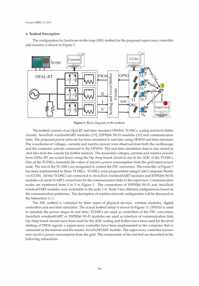
Energies 2019, 12, 1911
4. Testbed Description
The configuration for hardware-in-the-loop (HIL) testbed for the proposed supervisory controllerand scenario is shown in Figure 9.
1
0
2
3
5
4
Figure 9. Block diagram of the testbed.
The testbed consists of an Opal-RT real-time simulator OP4510, TI-DSCs, scaling and level shiftercircuits, AwiaTech wirelessHART modules [39], ESP8266 Wi-Fi modules [40] and communicationlinks. The proposed power network has been simulated in real-time using OP4510 real-time simulator.The waveforms of voltages, currents and reactive power were observed from both the oscilloscopeand the computer console connected to the OP4510. The real time simulation data is also stored in.mat files from the console for further analysis. The measured voltages, currents and reactive powersfrom OPAL-RT are scaled down using the Op-Amp based circuit to use in the ADC of the TI-DSCs.One of the TI-DSCs transmits the value of reactive power consumption from the grid input powernode. The rest of the TI- DSCs are designated to control the PFC converters. The controller of Figure 3has been implemented to those TI-DSCs. TI-DSCs were programmed using Code Composer Studiov.6 (CCS6). All the TI-DSCs are connected to AwiaTech wirelessHART modules and ESP8266 Wi-Fimodules via serial (UART) connections for the communication links to the supervisor. Communicationnodes are numbered from 0 to 5 in Figure 9. The connections of ESP8266 Wi-Fi and AwiaTechwirelessHART modules were switchable in the node 1–4. Node 5 has different configurations based onthe communication preference. The description of wireless network configuration will be discussed inthe Subsection 4.3.1.
The HIL testbed is validated by three types of physical devices: wireless modules, digitalcontrollers and real time simulator. The actual testbed setup is shown in Figure 10. OP4510 is usedto simulate the power stages in real time; TI-DSCs are used as controllers of the PFC converters;AwiaTech wirelessHART or ESP8266 Wi-Fi modules are used as interface of communication link;Op-Amp based circuits have been used for the ADC scaling and buffers have been used for the levelshifting of PWM signals; a supervisory controller have been implemented in the computer that isconnected to the internet and the master AwiaTechHART module. The supervisory controller ensureszero reactive power consumption from the grid. The components of the test bed are described in thefollowing subsections.
344

Energies 2019, 12, 1911
Figure 10. Hardware in the loop testbed set up.
4.1. Hardware Description
4.1.1. Real Time Simulator
The power stages of the PFC converters, loads, measurement of voltage and current and activeand reactive power are simulated in real-time (RT) using OPAL-RT real-time simulator, OP4510.It has 128 I/O channels, a quad core INTEL Xeon 3.3 GHz processor as well as a Kintex 7 FPGA forsub-microsecond simulation time steps [41]. Each core of the processor has the capability to simulateup to 20 μs time step. The system is compatible with Simulink and the SimPowerSystems library.The OP4510 is also connected to an oscilloscope to monitor voltage, current and reactive power in realtime. For this testbed, analog values of voltages and currents are routed from the FPGA based modelto the DAC channels directly. The PWM signals are interfaced with digital input pins which drive theFPGA based modesl of IGBTs. These two steps ensure sub-microsecond RT simulation. The reactivepower is calculated using Fourier transform in the CPU core at a step of 25 μs and later routed toDAC channels.
4.1.2. ADC Scaling and Level Shifting Circuit
The analog output signals for V, I and Qs are ±16 V in OP4510. The ADC level of TI-DSCs islimited to 0–3.3 V. To interpret and match the analog signal level properly, Op-Amp (TL082C) basedscaling and offsetting circuits have built. The GPIO of TI-DSC has a logic level of 3.3 V and OP4510takes 5 V PWM input. As a result, a 74HC240D IC has been used as a buffer for level shifting. The levelshifting and ADC scaling circuit has been built up in the same PCB as shown in Figure 10. The PCB alsohas connectivity to Opal-RT by two DB37 connectors and connect TI-DSCs with the 20 pin connectors.This circuit has 32 analog and 32 digital re-routable channels. The ADC scaling and level shiftingcircuit is shown in Figure 11.
345
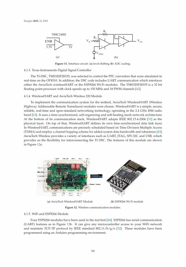
Energies 2019, 12, 1911
Figure 11. Interface circuit: (a) level shifting (b) ADC scaling.
4.1.3. Texas Instruments Digital Signal Controller
The TI-DSC, TMS320F28335, was selected to control the PFC converters that were simulated inreal-time on the OP4510. In addition, the DSC code includes UART communication which interfaceseither the AwiaTech wirelessHART or the ESP8266 Wi-Fi modules. The TMS320F28335 is a 32 bitfloating point processor with clock speeds up to 150 MHz and 18 PWM channels [42].
4.1.4. WirelessHART and AwiaTech Wireless 220 Module
To implement the communication system for the testbed, AwiaTech WirelessHART (WirelessHighway Addressable Remote Transducer) modules were chosen. WirelessHART is a simple, secure,reliable, real-time and open-standard networking technology, operating in the 2.4 GHz ISM radioband [43]. It uses a time-synchronized, self-organizing and self-healing mesh network architecture.At the bottom of its communication stack, WirelessHART adopts IEEE 802.15.4-2006 [31] as thephysical layer. On top of that, WirelessHART defines its own time-synchronized data link layer.In WirelessHART, communications are precisely scheduled based on Time Division Multiple Access(TDMA) and employ a channel hopping scheme for added system data bandwidth and robustness [43].AwiaTech Wireless provides a variety of interfaces such as UART, JTAG, SPI/I2C and USB, whichprovides us the flexibility for interconnecting the TI DSC. The features of this module are shownin Figure 12a.
(a) AwiaTech WirelessHART Module (b) ESP8266 Wi-Fi module
Figure 12. Wireless communication modules.
4.1.5. WiFi and ESP8266 Module
Four ESP8266 modules have been used in the test bed [40]. ESP8266 has serial communication(UART) features as in Figure 12b. It can give any microcontroller access to your WiFi networkand maintain TCP/IP protocol by IEEE standard 802.11/b/g/e [32]. These modules have beenprogrammed using an Arduino programming environment.
346

Energies 2019, 12, 1911
4.2. Software Components Description
4.2.1. TI DSC Code Architecture
The PFC controller has a 20 μs sample time. It generates a 50 kHz PWM signal. One interrupt hasbeen used to compute ADC values, scaling, controller operation and the PWM update. For the lowspeed communication links, a polling method has been used. The communication function is executedin an infinite while loop. All the functions are executed within a 20 μs window.
The ADC interrupt and controller computations consume only 12 μs and the remaining 8 μsis designated for communication through UART. Figure 13 describes the interrupt and whileloop structure.
(b)
Power Converter Controller (12μs)
Communication (8μs)
Interrupt (20μs)
Main Routine
Initialization
While(1)
Communication
Interrupt
ADC Conversion
ADC scaling
Phase lock
Voltage control
Current controlTheta control
PWM update(a)
Interrupt sub-routine
Figure 13. (a) Code structure of TI DSC (b) Execution time of code sections.
4.2.2. Host Program
AwiaTech wireless provides a Java package “Host” which is encapsulated within a series of APIs,enabling users to write programs which process all the data acquired from WirelessHART network.Based on these APIs, “Host” software is customized as an interface between the wireless networkand the supervisory controller. This design separates communication and control, which providesscalability to use other wireless communication technologies without modifying the controller code.In addition, this architecture enables the convenient use of other languages. The host program hasbeen modified using TCP/IP link as well. The TCP/IP link has been used to maintain communicationlinks to the ESP8266.
4.2.3. Supervisory Controller Implementation
The supervisory controller gives the control signal to the power converters. It is also capable ofcollecting data from the input port of the power network. The algorithm for the supervisory controlleris written in C++ code and later called from the JAVA platform which maintains communicationfunctions. The supervisory controller has a low speed proportional integral controller with a limiterand distributor as discussed in Section 3.
4.2.4. Dataflow
A complete dataflow is presented in Figure 14. The data flow in the test bed is composed of8 steps, starting from a TI DSC and ending in a TI DSC. First, a TI-DSC sends a HART-IP commandcontaining data to the AwiaTech wireless (device) through UART. Second, AwiaTech wireless forwardsthis command to the access point based on WirelessHART standard. Third, the access point sends datato a desktop running Host and Gateway software with UART over USB using a FTDI chip. Fourth,
347

Energies 2019, 12, 1911
after Host receives the data, it forwards it to the supervisory controller. For the WiFi network, HART-IPhas been decoded at ESP8266 and sent to the AP and host through the Wi-Fi. Our Host program willexchange messages with the controller through Stdin and Stdout. The dataflow in the other directionwill follow the same steps in reverse.
DSP Device Gateway & HostAP Supervisor
Controller1
8
2
7
3
6
4
5
UART WirelessHART/ WiFi Stdin/Stdout
Figure 14. Dataflow between TI DSC and supervisory controller.
4.3. Communication Link Description
4.3.1. Wireless Communication Set Up
The communication network topology for WiFi and WirelessHART has been shown in Figure 15.Either all ESP8266 or all AwaiaTech modules are connected to the TI-DSC through UART.
The UART to module connections are switchable for Wi-Fi and wirelessHART. Four AwiaTech modulesmaintain communication links with a fifth AwiaTech wireless module, which is connected to a hostcomputer, where the supervisory controller is running.
On the other hand ESP8266 is connected to the internet via Wi-Fi and a router. The supervisorycontroller can use internet to control the PFC converters for Wi-Fi network preference. Multipleunidirectional PFC converters contribute reactive power support by following a reference command bya supervisory controller via wireless modules. Real-time algorithms or strategies for energy and powermanagement systems can validate their performance in this testbed. The network topology in ourexperiments is shown in Figure 16, the blue circles are devices connected to TI DSCs; the yellow circleis the access point and the red circle is the gateway. A dotted line indicates the wireless communicationthrough WirelessHART or WiFi. The solid line indicates the wired communication through USB orEthernet. The numbers on the lines show the signal strength of the wireless links. The Figure 16 showsall the components in our network and their unique IDs, types and scan periods.
(a) (b)
Figure 15. Wireless network topologies for testbed (a) WirelessHART (b) WiFi.
348

Energies 2019, 12, 1911
Figure 16. Wireless network topology.
4.3.2. Integrity of the Specification
The Figure 17 shows an example of simplified network schedule which is shared with all thedevices and the access point in the network. The super-frame size is 500 ms and two up-links anddown-links for each device are statically allocated inside one superframe. In Figure 17, a time slot isrepresented by a small square with a number and an arrow. For example, 2 ↑ means the time slot isscheduled for Device 2 as an up-link. The wireless message exchanging sequence is shown in Figure 17.At the beginning of a super-frame, the TI-DSC sends measurement to Device 1.
Host & Gateway
DSP
Device 1
Device 4
Access Point
...
2↑
4↓2↑
1↓
3↓
3↓
3↑
2↑
1↑3↓ 3↑
2↓
3↑
4↑
4↓
3↑
2↑ 2↓
3↑ 1↑ 2↓
1↑ 2↓
2↑
4↑
1↑
2↑
1↑ 4↑
2↑
3↑
SuperFrame (500ms)
4↑
4↓
3↑
4↑
3↑4↑
1↑
3↓4↑ 1↑1↑
4↑ 1↓
2↓
1↑
4↓
1↓
3↓
3↑
2↑
2↓
2↑
1↓
1↓
4↓ 3↓ 4↓
1↓
4↑
Figure 17. Communication schedule configuration.
349

Energies 2019, 12, 1911
Then Device 1 sends the data to an access point within its own timeslot. After receiving the data,the access point sends the data to the host. Next, the Host software will send what it just received tothe supervisor controller for calculation. After that, the controller will send data back to control the TIDSC. It will go through the path in reverse. The access point will get the data and wait for the time slotallocated for Device 1. Once the time slot arrives, the access point sends the data down to Device 1and then Device 1 sends data to the TI-DSC through UART. Theoretically, if we set the super-framelength to be 500 ms and within one super-frame and we allocate two time slots as up-links, the smallestsampling period would be 250 ms. However, due to the noisy wireless environment, we chose a muchlarger sampling rate and super-frame length. From the wireless link test, we were able to make thesuper-frame size 1.5 s without any data loss.
5. Experimental Results
The test bed has been implemented to validate the supervisory controller for reactive powersupport using the proposed power network of Figure 1. OP4510 has simulated the power network inreal-time. It takes PWM signal as input and gives analog signals as output. Rest of the components areactual physical device in the HIL test bed. Multiple tests have been conducted to validate the idea ofreactive power support and supervisory controller.
5.1. Reactive Power Compensation in a Single PFC Converter
Reactive power has been supported by applying controller of Figure 3 to a PFC converter.The wave form of voltage and current in a PFC converter for different conditions has been capturedusing an oscilloscope and shown in the following figure. The waveforms are collected from the analogoutput of the OP4510 real-time simulator. PFC 1 has been built up as in the circuit of Figure 2 usingrL = 1 mΩ, L = 2 mH, C = 2000 μF and rC = 2 mΩ. PFC 1 is rated for Vin = 120 V(rms), f = 60 Hz,Pout = 1.1 kW, Vout = 250 V(DC) and RLoad = 56.79753 Ω. Different power conversion criteria for PFC1 under conditions of Figure 18 are shown in the Table 1.
Figure 18a shows the input current and voltage waveforms without applying any control thatis, current flows through the diode only.
Figure 18. Input voltage and current waveforms in PFC 1: (a) no controller, (b) in phase controller,θ ≈ 0 and (c) leading phase controller, θ < 0.
Table 1. Power conversion in PFC 1 for different conditions.
Conditions Pin Qin T HDVg T HDIs Vout(DC) Poutat Figure 18 ( W) ( VAR) (%) ( %) ( Volt) ( W)
a 428 125 0 90 154 396
b 1680 57 0 1.5 250 1100
c 1656 −272 0 8.5 250 1100
350

Energies 2019, 12, 1911
This condition has very poor performance and can not fulfil the rated conditions. It has very hightotal harmonic distortion (THD) for the input current. After applying the reactive power compensationalgorithm of Figure 3, voltage and current are almost in phase as in Figure 18b. Reactive power hasnot been injected for this case that is, reactive power reference is zero, Q∗
1 = 0. Although Q∗1 is equal to
zero but, Q1 is not exactly zero because of delays, offset and measurement errors. In this case, currentdistortion is minimum. Leading phase of current has been achieved as in Figure 18c as Q∗
1 has been setto negative values. Hence, reactive power has been supported by PFC 1. In this case, the current isnot a pure sine wave at zero crossing because of zero crossing distortion. The distortion phenomenonhas been considered to determine the maximum capacity of reactive power support (Qmax1) for PFC 1.Since, the household load is very small with respect to grid, the voltage supply has been consideredto be coming from an infinite bus. As a result, distortion for input voltage, THDVg is zero in therealtime simulation.
5.2. Reactive Power Support Using Supervisory Controller
After setting up the communication networks successfully, the HIL test was conducted for theproposed residential power network. For the proposed scenario, rated grid voltage is 120 V(rms),60 Hz. Conventional load is 1500 VA with 0.8 power factor that is, PL = 1200 W, QL = 900 VAR. Ratedoutput voltage, Vout, of all three PFCs is 250 V(DC). Output power, Pout, rating of the PFC’s are 1.1 kW,1.5 kW and 1.7 kW.
Weighting factors used in supervisory controller W1, W2 and W3 are 0.25, 0.35 and 0.4 respectively.Reactive power has been supported by the PFC converters to the load as shown in the in Figure 19.In this case, real-time simulation has been conducted for communication and control sample time,Ts = 4 s. Supervisory controller engagement time has been set as reference, T = 0, on the time axis.Logged data from OP4510 shows that reactive power consumption from grid Qg becomes 0 VARwithin 75 s of applying the controller. The initial and final value of the reactive power for the grid,the load and the PFCs is shown in the Table 2.
Qg
Q1 Q2Q3
Time (seconds)
Reac
tive
Pow
er (V
AR)
Figure 19. Reactive power support by 3 PFC converters and supervisory controller.
Table 2. Reactive power in different nodes of the proposed power network.
StateTime Qg QL Q1 Q2 Q3
(s) (VAR) (VAR) (VAR) (VAR) (VAR)
Initial 0 1025 900 44 33 48
Final 75 0 900 −225 −305 −371
5.3. Reactive Power Support in Different Conditions
The performance of the supervisory controller has been tested for different conditions.
351

Energies 2019, 12, 1911
5.3.1. Variation of Load
The designed supervisory controller has been tested for loading conditions of (PL = 1350 W,QL = 654 VAR), (PL = 1200 W, QL = 900 VAR) and (PL = 1050 W, QL = 1072 VAR). For all loadingconditions, Qg become 0 VAR within 75 s.
5.3.2. Variation of Wireless Network
The supervisory controller was tested using WirelessHART and Wi-Fi. It compensated gridreactive power for both networks as shown in Figure 20a.
(a) (b) (c)
Figure 20. Performance of supervisory controller: (a) network variation, (b) sampling time variationand (c) gain variation.
5.3.3. Sampling Time Variation
The effect of different communication sampling times has been evaluated in Figure 20b. For fourand six second sampling times, supervisory controller regulated Qg to 0 VAR. The higher the samplingtime, the slower the response time for overall reactive power compensation. Minimum stablecommunication and control sampling time for this system has been measured to be 1.5 s. This samplingtime has been used for optimal controller.
5.3.4. Gain Variation and Optimal Controller
To verify the optimal supervisory controller, the response of reactive power compensation hasbeen compared for different ku, kp and ki gains. The response has been judged by settling time,overshoot, undershoot and stability. Figure 20c shows performance of supervisory controller withdifferent gains. This controller has used Ts = 1.5 s communication sampling time. The settling timeand other factors of performance for the PI compensator are shown in Table 3.
Table 3. Supervisory controllers performance with different PI gains.
Ku Kp Ki Stability Settling Time Comments
0.1 0.05 0.045 Stable 250 s Very slow response
0.5 0.25 0.225 Stable 75 s slow response
0.8 0.4 0.36 Stable 45 s Good response
1 0.5 0.45 Stable 40 s Optimum response
2 1 0.9 Marginally stable 20 sUndershoots happen, large steady stateerror, inject Q to grid
5 2.5 2.25 Unstable –Undershoots happen, large steady stateerror, distributor failure
10 5 4.5 Unstable – Completely unstable
352

Energies 2019, 12, 1911
5.4. Reactive Power Support in Dynamic Load
Different load profiles of Table 4 have been applied to test the supervisory controller. Reactivepower demand were changed as the load changed.
Load profile 1 has been applied for the conditions of Figure 21a,c. Load profile 2 has been appliedand results have been gathered in Figure 21b. The PFC converters used for Figure 21a,b have thepower rating(Pout) of P1 = 1.1 kW, P2 = 1.5 kW and P3 = 1.7 kW. The maximum reactive power supplycapacity of those PFC converters are Qmax1 = −300 VAR, Qmax2 = −400 VAR and Qmax3 = −600 VAR.Qmax1, Qmax2 and Qmax3 have determined the weighting factors W1, W2 and W3 by (20). Load profile 1is based on the power factor change and load profile 2 is based on apparent power demand increment.
Dynamic response of Figure 21c used load profile 1 but it used identical 3 PFC converters.In this case, P1 = 1.5 kW, P2 = 1.5 kW, P3 = 1.5 kW, Qmax1 = −400 VAR, Qmax2 = −400 VAR,and Qmax3 = −400 VAR. As a result, reactive power contribution from PFC converters is equal atdifferent times in the real time simulation.
Load profiles have been implemented by changing the loads using an external switch. As a resultthere is a transient reactive power spike and an unequal load profile duration. For all of theseconditions, the optimal controller has been used, which ensured the stable and quickest response.THDVg and THDIg have also been recorded for all the tests. THDVg for all the tests is 0% as the gridhas been considered as an ideal voltage source in the real-time simulation. THDIg has varied between4% to 10.65% for all the loading conditions after the settling times. It was observed that an increase inreal and reactive power consumption ratio correlated with a decrease in THDIg .
Time (second)
Time (second)
Time (second)
Reac
tive
Pow
er (V
AR)
Reac
tive
Pow
er (V
AR)
Reac
tive
Pow
er (V
AR)
Reac
tive
Pow
er (V
AR)
Reac
tive
Pow
er (V
AR)
Appa
rent
Pow
er (V
A)
QL
Qg
Qg
Qg
QL
SL
Q1 Q2 Q3
Q1 Q2 Q3
Q1 Q2 Q3
(a)
(b)
(c)
Figure 21. Reactive power support in dynamic loads: (a) load profile 1, (b) load profile 2 and (c) Loadprofile 1 with equal reactive power support capability.
353

Energies 2019, 12, 1911
Table 4. Load profiles for dynamic performance test.
Load Profile 1
Loading SL PL QL PowerStage (VA) (W) (VAR) Factor
1 1500 1350 654 0.9
2 1500 1200 900 0.8
3 1500 1050 1072 0.7
4 1500 900 1200 0.6
Load Profile 2
Loading SL PL QL PowerStage (VA) (W) (VAR) Factor
1 900 720 540 0.8
2 1200 960 720 0.8
3 1500 1200 900 0.8
4 2000 1600 1200 0.8
6. Conclusions
The PFC converters are considered as reactive power resources in this paper. The supervisorycontroller is proposed to manage those resources. The WiFi and WirelessHART have provided theinterface between the supervisory controller and reactive power resources. The optimal sampling timeof the supervisory controller has been determined by various tests. The optimal gain is explainedtheoretically and validated experimentally. The dynamic performance of the supervisory controller hasbeen validated using different load profiles with the reactive power demand, PFC capacity and loadvariations. The HIL test results prove the concept and feasibility of additional reactive power supportfrom PFC converters in residential applications. The proposed controller design method will be usefulfor other small-scale power and wireless network integration.
Author Contributions: All the authors contributed substantially to the manuscript.Contributions of each authorare as follows: conceptualization, S.M.R.I. and S.-Y.P.; methodology, S.M.R.I., S.-M.P. and S.Z.; software, S.M.R.I.and S.Z.; validation, S.M.R.I. and S.-Y.P.; formal analysis, S.M.R.I.; investigation, S.M.R.I.; resources, S.M.R.I. andS.-M.P.; data curation, S.M.R.I.; writing—original draft preparation, S.M.R.I.; writing—review and editing, S.M.R.I.and S.-Y.P.; visualization, S.M.R.I.; supervision, S.-Y.P. and S.H.; project administration, S.-Y.P.; funding acquisition,S.-Y.P.
Funding: This research was funded by National Science Foundation OF FUNDER grant number 1446157.
Acknowledgments: This work was supported by the National Science Foundation under grant no. 1446157.However, any opinions, findings, conclusions or recommendations expressed here in are those of the authors anddo not necessarily reflect the views of the National Science Foundation.
Conflicts of Interest: The authors declare no conflict of interest. The funders had no role in the design of thestudy; in the collection, analyses or interpretation of data; in the writing of the manuscript or in the decision topublish the results.
References
1. The U.S. Energy iNformation Administration Report 2017: Energy Consumption by Sector. Available online:https://www.eia.gov/totalenergy/data/monthly/pdf/sec2_3.pdf (accessed on 17 May 2019).
2. Dixon, J.; Moran, L.; Rodriguez, J.; Domke, R. Reactive Power Compensation Technologies: State-of-the-ArtReview. Proc. IEEE 2005, 93, 2144–2164. [CrossRef]
3. Bing, Z.; Chen, M.; Miller, S.K.T.; Nishida, Y.; Sun, J. Recent Developments in Single-Phase Power FactorCorrection. In Proceedings of the 2007 Power Conversion Conference, Nagoya, Japan, 2–5 April 2007;pp. 1520–1526. [CrossRef]
354

Energies 2019, 12, 1911
4. Mansouri, M.; Kaboli, S.H.A.; Selvaraj, J.; Rahim, N.A. A review of single phase power factor correctionA.C.-D.C. converters. In Proceedings of the 2013 IEEE Conference on Clean Energy and Technology (CEAT),Lankgkawi, Malaysia, 18–20 November 2013; pp. 389–394. [CrossRef]
5. Nallusamy, S.; Velayutham, D.; Govindarajan, U.; Parvathyshankar, D. Power quality improvement ina low-voltage DC ceiling grid powered system. IET Power Electron. 2015, 8, 1902–1911. [CrossRef]
6. Park, S.M.; Park, S. Versatile Control of Unidirectional AC–DC Boost Converters for Power Quality Mitigation.IEEE Trans. Power Electron. 2015, 30, 4738–4749. [CrossRef]
7. Ivaldi, J.; Park, S.; Park, S. Integration strategy for bidirectional and unidirectional converters aiming forzero power pollution in residential applications. In Proceedings of the 2015 9th International Conference onPower Electronics and ECCE Asia (ICPE-ECCE Asia), Seoul, Korea, 1–5 June 2015; pp. 1756–1761. [CrossRef]
8. Radvanovsky, R.; Brodsky, J. Handbook of SCADA/Control Systems Security; CRC Press: Boca Raton,FL, USA, 2013.
9. Nasirian, V.; Yadav, A.P.; Lewis, F.L.; Davoudi, A. Distributed Assistive Control of Power Buffers in DCMicrogrids. IEEE Trans. Energy Convers. 2017, 32, 1396–1406. [CrossRef]
10. Azidehak, A.; Yousefpoor, N.; Bhattacharya, S. Control and synchronization of distributed controllers inmodular converters. In Proceedings of the IECON 2014—40th Annual Conference of the IEEE IndustrialElectronics Society, Dallas, TX, USA, 29 October–1 November 2014; pp. 3644–3650. [CrossRef]
11. Gutierrez, A.; Chamorro, H.R.; Jimenez, J.F. Supervisory control for interleaved boost converters usingHiLeS-designer. In Proceedings of the 2014 16th European Conference on Power Electronics and Applications,Lappeenranta, Finland, 26–28 August 2014; pp. 1–6. [CrossRef]
12. Shen, J.; Khaligh, A. A Supervisory Energy Management Control Strategy in a Battery/UltracapacitorHybrid Energy Storage System. IEEE Trans. Transp. Electrif. 2015, 1, 223–231. [CrossRef]
13. Babakmehr, M.; Harirchi, F.; Alsaleem, A.; Bubshait, A.; Simões, M.G. Designing an intelligent low powerresidential PV-based Microgrid. In Proceedings of the 2016 IEEE Industry Applications Society AnnualMeeting, Portland, OR, USA, 2–6 October 2016; pp. 1–8. [CrossRef]
14. Gabbar, H.A.; El-Hendawi, M.; El-Saady, G.; Ibrahim, E.A. Supervisory controller for power managementof AC/DC microgrid. In Proceedings of the 2016 IEEE Smart Energy Grid Engineering (SEGE),Oshawa, ON, Canada, 21–24 August 2016; pp. 147–152. [CrossRef]
15. Hosseinzadeh, M.; Salmasi, F.R. Robust Optimal Power Management System for a Hybrid AC/DCMicro-Grid. IEEE Trans. Sustain. Energy 2015, 6, 675–687. [CrossRef]
16. AlBadwawi, R.; Issa, W.; Abusara, M.; Tapas, M. Supervisory Control for Power Management of an IslandedAC Microgrid Using Frequency Signalling-Based Fuzzy Logic Controller. IEEE Trans. Sustain. Energy 2018, 1.[CrossRef]
17. Kothari, D.P.; Singh, B.; Pandey, A. Fuzzy supervisory controller for improved voltage dynamics in powerfactor corrected converter. In Proceedings of the 2002 IEEE Internatinal Symposium on Intelligent Control,Vancouver, BC, Canada, 30–30 October 2002; pp. 93–97.
18. Islam, S.M.R.; Maxwell, S.; Hossain, M.K.; Park, S.; Park, S. Reactive power distribution strategy using powerfactor correction converters for smart home application. In Proceedings of the 2016 IEEE Energy ConversionCongress and Exposition (ECCE), Milwaukee, WI, USA, 18–22 September 2016; pp. 1–6. [CrossRef]
19. Islam, S.M.R.; Maxwell, S.; Park, S.; Zheng, S.; Gong, T.; Han, S. Wireless networked dynamic control testbedfor power converters in smart home applications. In Proceedings of the 2017 IEEE Applied Power ElectronicsConference and Exposition (APEC), Tampa, FL, USA, 26–30 March 2017; pp. 1196–1202. [CrossRef]
20. Harper, R. (Ed.) The Connected Home: The Future of Domestic Life; Springer: Cambridge, UK, 2011.21. Kayas, O. How to Smart Home: A Step by Step Guide for Smart Homes & Building Automation, 5th ed.;
Key Concept Press: Wyk, Germany, 2017.22. White, R.M. How to Calculate Electrical Loads and Design Power Systems; CreateSpace Independent Publishing
Platform: Scotts Valley, CA, USA, 2011.23. Murray, A.; Li, Y. Motion Control Engine Achieves High Efficiency with Digital PFC Integration in Air
Conditioner Applications. In Proceedings of the 2006 IEEE International Symposium on Electronics and theEnvironment, Scottsdale, AZ, USA, 8–11 May 2006; pp. 120–125. [CrossRef]
24. Fasugba, M.A.; Krein, P.T. Gaining vehicle-to-grid benefits with unidirectional electric and plug-inhybrid vehicle chargers. In Proceedings of the 2011 IEEE Vehicle Power and Propulsion Conference,Chicago, IL, USA, 6–9 September 2011; pp. 1–6. [CrossRef]
355

Energies 2019, 12, 1911
25. Gungor, V.C.; Lu, B.; Hancke, G.P. Opportunities and Challenges of Wireless Sensor Networks in Smart Grid.IEEE Trans. Ind. Electron. 2010, 57, 3557–3564. [CrossRef]
26. Gungor, V.C.; Sahin, D.; Kocak, T.; Ergut, S.; Buccella, C.; Cecati, C.; Hancke, G.P. Smart Grid Technologies:Communication Technologies and Standards. IEEE Trans. Ind. Inform. 2011, 7, 529–539. [CrossRef]
27. Yarali, A. Wireless Mesh Networking technology for commercial and industrial customers. In Proceedingsof the 2008 Canadian Conference on Electrical and Computer Engineering, Niagara Falls, ON, Canada,4–7 May 2008; pp. 000047–000052. [CrossRef]
28. Luan, W.; Sharp, D.; Lancashire, S. Smart grid communication network capacity planning for power utilities.In Proceedings of the IEEE PES T D 2010, New Orleans, LA, USA, 19–22 April 2010; pp. 1–4. [CrossRef]
29. Technologies OPAL-RT. OP4510 RT-LAB-RCP/HIL SYSTEMS User Guide. Available online: https://www.opal-rt.com/simulator-platform-op4510/ (accessed on 17 May 2019).
30. Texas Instruments Inc. TMS320F28335, TMS320F28334,TMS320F28332, TMS320F28235, TMS320F28234,TMS320F28232 Digital Signal Controllers (DSCs) Data Manual. Available online: http://www.ti.com/lit/ds/symlink/tms320f28335.pdf (accessed on 17 May 2019).
31. IEEE Standards. IEEE 802.15.4 WPAN TG. Available online: www.ieee802.org/15/pub/TG4.html(accessed on 17 May 2019).
32. IEEE Standards. IEEE 802.11TM WIRELESS LOCAL AREA NETWORKS. Available online: http://www.ieee802.org/11/ (accessed on 17 May 2019).
33. Mohan, N. Power Electronics: Converters, Applications, and Design; John Wiley and Sons: New York,NY, USA, 2002.
34. Monmasson, E. Power Electronic Converters: PWM Strategies and Current Control Techniques; John Wiley andSons: New York, NY, USA, 2013.
35. Chang, J.M.; Pedram, M. Power Optimization and Synthesis at Behavioral and System Levels Using FormalMethods; Springer: New York, NY, USA, 1999.
36. Ogata, K. Modern Control Engineering; Pearson: New York, NY, USA, 2009.37. Ziegler, J.; Nichols, N. Optimum settings for automatic controllers. Trans. ASME 1942, 64, 759–768.
[CrossRef]38. Co, T.B. Ziegler-Nichols Closed Loop Tuning. Available online: http://pages.mtu.edu/~tbco/cm416/zn.
html (accessed on 17 May 2019).39. AwiaTech. Advancing Wireless Industrial Automation. Available online: http://www.AwiaTech.com
(accessed on 17 May 2019).40. SparkFun Electronics. ESP8266 WiFi Module, Datasheet. Available online: https://www.sparkfun.com/
products/13678 (accessed on 17 May 2019).41. Xilinx. Kintex 7 FPGA Product Table. Available online: http://www.xilinx.com/support/documentation/
selection-guides/kintex7-product-table.pdf (accessed on 17 May 2019).42. Texas Instruments Inc. TMS320x2833x, 2823x High Resolution Pulse Width Modulator (HRPWM).
Available online: http://www.ti.com.cn/cn/lit/ug/sprug02b/sprug02b.pdf (accessed on 17 May 2019).43. Nixon, M. A Comparison of WirelessHARTTM and ISA100. 11a. Available online: https://www.
emerson.com/documents/automation/a-comparison-of-wirelesshart-isa100-11a-en-42598.pdf (accessed on17 May 2019).
c© 2019 by the authors. Licensee MDPI, Basel, Switzerland. This article is an open accessarticle distributed under the terms and conditions of the Creative Commons Attribution(CC BY) license (http://creativecommons.org/licenses/by/4.0/).
356

energies
Article
New DC Grid Power Line CommunicationTechnology Used in Networked LED Driver
Huipin Lin 1, Jin Hu 2, Xiao Zhou 1, Zhengyu Lu 1 and Lujun Wang 3,*
1 College of Electrical Engineering, Zhejiang University, Hangzhou 310027, China;[email protected] (H.L.); [email protected] (X.Z.); [email protected] (Z.L.)
2 Zhejiang Dabong Technology Co., Ltd., Hangzhou 311100, China; [email protected] Hubei Key Laboratory for High-Efficiency Utilization of Solar Energy and Operation Control of Energy
Storage System, Hubei University of Technology, Wuhan 430068, China* Correspondence: [email protected]; Tel.: +86-571-8795-1625
Received: 9 November 2018; Accepted: 15 December 2018; Published: 18 December 2018
Abstract: In order to reduce the cost and improve the reliability, real-time performance, and installationconvenience of remote-controlled light-emitting diode (LED) lighting systems, a networked LEDdriving technology based on the direct current (DC) grid power line carrier is proposed. In thissystem, an alternating current (AC)/DC bus converter converts the mains into a DC bus with multipledistributed LED drive powers on the DC bus. The AC/DC bus converter receives the user’s controlcommand and modulates it into the DC bus voltage. The DC bus waveform changes to a square wavecontaining the high and low changes of the address information and command information. The LEDdrive power of the corresponding address receives energy from the DC bus and demodulates thecommands, such as turning the lights on and off, dimming, etc., and performs the action. In orderto make the waveform of the AC/DC bus converter have better rising and falling edge, this paperadopts the half-bridge topology with variable modal control. In the modulation process, the circuitworks in buck mode and boost mode. Distributed LED drivers have DC/DC circuits and very simpledemodulation circuits that dissipate energy and information from the DC bus. Through experiments,the technology not only simplifies the use of communication technology in application, but alsoreduces the application difficulty.
Keywords: PLC; bus converter; DC bus; LED driver
1. Introduction
With the rapid development of light-emitting diode (LED) technology, it is widely predictedthat LED will become a new generation of lighting sources. Smart network control is a hot researchtopic in the field of LED lighting applications. In this application, multiple LED devices generallyform an intelligent lighting system through a network, and the LED devices can usually be remotelycontrolled. In addition to road lighting for large-scale applications [1–4], most of these smart LEDlighting systems are often used indoors or outdoors, and the scale is small [5–7].
Figure 1 shows a case for a small-scale LED smart lighting system, such as for commerciallighting, home lighting, landscape lighting, wall washers, high pole lights, etc. In these applications,the number of lamps is small, the distance between two adjacent LED light sources is relatively close,and a computer is typically used to remotely control turning on, turning off, and dimming the lights.
Energies 2018, 11, 3531; doi:10.3390/en11123531 www.mdpi.com/journal/energies357

Energies 2018, 11, 3531
Control center
Power line
LED driver
LEDdriver
LEDdriver
Small-scale smart LED lighting system1.Short distance between the power supplies .2.Small number of power supplies.
Led wall washer
Landscape light
Smart commercial lighting system
Smart home lighting system
Smart Road Lighting Pole
Figure 1. Common small networked control light-emitting diode (LED) smart lighting system.
In this small LED smart lighting system, communication between LED drivers is necessary toachieve control. Which communication technology is used determines the real-time performanceand reliability of control in the system, while at the same time it also affects the cost, installation,and maintenance. Figure 2 shows descriptions of several common traditional lighting systemcommunication schemes and their characteristics. These small LED lighting systems require alower-cost solution, however, for 0–10 V, pulse-width modulation (PWM) control, digital addressablelighting interface (DALI) [8–14] and other remote-control schemes, and additional communicationlines must be laid, which is unfavorable for installation and maintenance and costs more. Power linecommunication (PLC) [15–18] and the remote-control scheme of micropower wireless communicationhave advantages in practical applications due to the convenient installation. However, the cost of sucha solution is still high, which is not conducive to its promotion. Table 1 lists the characteristics of thesefour options.
Control Center
Power line
Power circuit
Dimming interface
Control circuitIsolated
transferring
L
N
0~10V or PWM control line
LED driver LED driver
Control line signal GND
Power circuit
Dimming interface
Control circuitIsolated
transferring
Control Center
Power lineL
N
DA(Digital line)DA(Digital line)
Power circuit
DALI interface circuit
Control circuitIsolated
transferring
Power circuit
DALI interface circuit
Control circuitIsolated
transferring
LED driver LED driver
(a) (b)
Control Center
Power lineL
N
Power circuit
Control circuit
PLC module
Power circuit
Control circuit
PLC module
220VAC mains sine wave modulated by control signal
LED driver LED driver
Control Center
Power lineL
N
Power circuit
Wireless module
Control circuit
Power circuit
Wireless module
Control circuit
LED driver LED driver
(c) (d)
Figure 2. Common traditional remote control schemes: (a) 0–10 V or pulse-width modulation (PWM);(b) digital addressable lighting interface (DALI); (c) traditional alternating current (AC) grid powerline communication; (d) traditional wireless.
358

Energies 2018, 11, 3531
Table 1. Features of common traditional remote control schemes.
Remote Control Scheme Control Lines Installation Cost
0–10 V or PWM 2 Lines Complex HighDALI 2 Lines Complex High
Power line communication (PLC) No Very simple HighWireless No Simple High
From the perspective of installation, the micropower wireless communication scheme needsto consider factors such as antenna and electromagnetic interference, which is greatly affected byspace, and the PLC scheme is simpler. If the PLC solution can be further simplified, the cost andinstallation aspects are more advantageous. However, the traditional PLC solution is mainly usedfor alternating current (AC) mains grid, such as remote meter reading [19–21] and other applications.In the AC mains grid, PLC technology is relatively mature, and it is difficult to have major technologicalbreakthroughs in a short period of time. It is difficult to reduce costs significantly. If power electronicscan be used to transmit information while energy is being converted, the PLC module in Figure 2cmay no longer be needed and the system cost may be greatly reduced. In the AC mains grid, since theexisting transmission and distribution schemes are already very mature, it is difficult to implementcommunication using power electronics technology. However, if a direct current (DC) grid or an ACmicrogrid is constructed, it is easy to realize communication while transmitting DC power in the grid.
The LED lighting system based on DC grid has received attention. In [22] an indoor LED smartlighting system was proposed based on DC grid, as shown in Figure 3. The system uses an AC/DCconverter to change AC mains to DC bus, and a number of distributed DC/DC LED drivers areconnected to the DC bus. The system implements intelligent control and energy saving, but with theDALI communication protocol, a separate control line is still required. A similar DC bus architecture isalso proposed in [23].
Figure 3. Traditional LED lighting system technology based on direct current (DC) grid: (a) Traditionalnetworked LED system based on DC grid; (b) Traditional DC grid PLC technology; (c) the drive signalwaveform of host switch M and the waveform of bus voltage Ubus.
PLC in the DC grid has also been studied in recent years, and this technology can eliminatethe control line in Figure 3a. A novel DC PLC solution was proposed in [24], which is cheaper forsmall-scale power line communication applications. Figure 3b,c show the basic principle, as shownin the waveform: when the host switch M is turned on, the voltage Ubus goes high, representinglogic 1. When switch M is turned off, voltage Ubus goes low, representing logic 0. The circuit worksin the structure of the buck circuit, and the energy is stored in the output capacitor C of the slave.The change of the voltage Ubus during the energy transfer is detected by the slave, and the simultaneoustransmission of energy and signals is realized. However, due to the influence of parasitic parameters
359

Energies 2018, 11, 3531
on the transmission line, the switching device of the circuit is subject to greater voltage stress than theconventional buck circuit.
Some papers have proposed DC PLC schemes [25–29], but they all need additional communicationlines. They bring larger parasitic parameters and cause front-stage metal-oxide-semiconductor fieldeffect transistor (MOSFET) high current spikes and damage when the MOSFETs are working athigh frequency. So the front-stage MOSFETs need better performance requirements. They are morecomplicated if used for LEDs.
In order to overcome the problems of the above two types of research, this paper proposes aremotely controlled LED lighting system similar to the DC grid structure of Figure 3a, but with thecontrol line omitted. In this system, an AC/DC bus converter converts the mains into a DC bus,and multiple distributed LED drivers are connected to the DC bus. The AC/DC DC bus converterreceives the user’s control command and modulates it into the DC bus voltage. The DC bus waveformchanges to a square wave containing the high and low changes of the address information and thecommand information. The LED driving power source corresponding to the address receives energyfrom the DC bus and demodulates commands such as turning on the light, turning off the light,dimming, etc. In order to make the waveform of AC/DC DC bus converter have better rising andfalling edge, this paper adopts the half-bridge topology with variable modal control. In the modulationprocess, the circuit works in buck mode and boost mode. Distributed LED drivers have DC/DCcircuits and very simple demodulation circuits that dissipate energy and information from the DC bus.
With this remote control scheme, the following problems are solved:
1. Compared with 0–10 V, PWM, and DALI controlled systems, the communication line is omitted.2. The traditional AC mains PLC module is saved, and the signal transceiving function is realized
by power electronic technology.3. Compared with the existing DC PLC technology, the influence of power line on communication
is greatly reduced, and communication reliability is improved.
Compared with the conventional schemes described above, this scheme is simpler and costs less.This paper verifies the feasibility of this technology by experiments.
2. Light-Emitting Diode (LED) Networked Drive Technology Based on Direct Current (DC) GridPower Line Communication (PLC)
2.1. System Architecture
The specific architecture of the LED lighting system proposed in this paper is shown in Figure 2a.It includes a control center, an AC/DC bus converter, a DC bus, and a distributed LED driver.The control center sends control signals to the LEDs to the AC/DC bus converter. This type oftechnology is relatively mature and can be used for wireless communication such as a General PacketRadio Service (GPRS). The bus converter converts the AC mains into a DC bus voltage vbus with amaximum value of 48 V, and modulates the information to be transmitted into the bus voltage to makeit high and low DC levels. The high voltage represents logic 1 and the low voltage represents logic 0.The DC bus is the transmission line, and the distributed LED driver as the load extracts energy fromthe DC bus drives the LED light source and demodulates the signal from the bus.
2.2. New DC Power Line Carrier Energy and Information Demodulation Principle
The master/slave communication mode is between the AC/DC bus converter and the distributedLED driving power source. The former is the master, the latter is the slave, and the DC bus is used asthe medium to provide energy and transfer information to the slave.
The LED driver power supply includes three parts: an energy demodulation circuit, a signaldemodulation circuit, and a DC/DC converter. The energy and signal demodulation circuits are bothhalf-wave rectification circuits, as shown in Figure 4a. Taking the jth LED driving power supply in
360

Energies 2018, 11, 3531
Figure 4a as an example, the energy demodulating circuit is connected in series with the DC/DCconverter, and the output of the signal demodulating circuit is connected to the control circuit of theDC/DC converter. The difference between the two is that the energy demodulation circuit’s outputcapacitance Cpj has a large capacitance value. When the vbus voltage is 0, the energy of the DC/DCconverter of the latter stage can still be supplied for a period of time, that is, vpj is maintained withinthe allowable ripple voltage range to keep the circuit working properly.It remains stable for a longtime; the output capacitance value Csj of the latter is small. When the vbus voltage is 0, vsj is dischargedthrough the resistor Rsj and quickly falls to 0, so that the change of vsj is consistent with the change ofvbus. Taking the waveform in Figure 4b as an example, the process of demonstrating a remote dimmingoperation has the following stages:
t1: The output of the AC/DC bus converter is 48 V DC, and the load is full power. During thistime, the bus converter receives the jth LED drive power dimming command from the control centerto address Aj.
t1–t2: The bus converter modulates the information into the DC bus, and the bus voltage vbuschanges to the waveform shown in Figure 4b. All LED drive power supplies receive the command,but only the jth addresses Aj. The drive power source executes the dimming command. The totalpower on the busbar drops from time t3 when the command is executed. The communication protocolcan adopt a mature scheme such as RS232 or a custom scheme.
Figure 4. Networked control LED system based on DC grid PLC: (a) system architecture diagram;(b) system key waveforms.
2.3. Working Principle of Bus Converter Based on Variable Modal Control
The key device for system energy and information modulation is the AC/DC bus converter.Figure 5a,b shows a schematic diagram and the corresponding buck and boost working modes.The circuit is divided into two stages. The first stage is a power factor correction (PFC) circuit toachieve a high power factor. The output is a fixed DC voltage Vg as the input of the second stage.
The second stage is a half-bridge circuit, the output is a DC bus, and the DC bus is connected toseveral LED driving power sources. The LED driving power can be regarded as the active load of thesecond-stage half-bridge circuit, and the total equivalent power is pLED. D1 and D2 are body diodesof the half-bridge circuit MOSFETs M1 and M2, respectively. The control circuit has a single-chipmicrocomputer (MCU), which samples the output voltage vbus through the sampling resistors R1 andR2, and RBoostcs and RBuckcs are sampling resistors, respectively sampling the inductor currents inboost and buck modes.
In different situations, the half-bridge circuit operates in buck mode or boost mode. Figure 5cshows the main waveforms of these two modes.
t0–t1: The AC/DC bus converter does not send a signal to the LED driver, and its output voltageis constant DC 48 V. The upper tube M1 is operated as a high-frequency switch, the lower tube M2
is stopped, the half-bridge circuit operates in buck mode as shown in Figure 5a, and the body diode
361

Energies 2018, 11, 3531
D2 of the M2 acts as a freewheeling diode of the buck circuit. The bus converter charges capacitor C2,which supplies energy to the distributed LED driver.
t1–t11: The bus converter receives the command and modulates it into the bus voltage vbus,causing it to change to high and low DC levels. Defining the signal Sin passed, when Sin is logic 0,the bus converter operates in boost mode, and when Sin is logic 1, the bus converter operates in buckmode. When in boost mode, the upper tube M1 stops working, and M2 operates as a high-frequencyswitch. The body diode D1 of the M1 operates as a freewheeling diode of the boost circuit, as shown inFigure 5b. At this time, the energy on the bus voltage vbus across the output capacitor C2 is quicklytransferred to the half-bridge input capacitor C1, and the level rapidly drops to zero. Since the LEDdriving power supply in Figure 4a has diodes Dpj and Dsj, the change in bus voltage does not affectthe energy and signal demodulating circuits in the LED driving power supply.
Figure 5. Work principles of bus converter: (a) circuit principle of buck mode; (b) circuit principle ofboost mode; (c) working waveform.
The half-bridge circuit adopts different working modes, so that in buck mode, the bus voltagevbus across capacitor C2 can rise rapidly; in boost mode, the bus voltage vbus across capacitor C2 canbe quickly reduced. There are three advantages to using this method of variable mode control:
(1) The bus voltage vbus changes rapidly, which is beneficial to improve the signal transmissionspeed and facilitate the operation of the signal demodulation circuit in the LED driver.
(2) If there is no boost mode, the bus converter should make the busbar low voltage and can onlyrely on the load to discharge naturally. However, in the case of light load of the bus converter,especially when the load is turned off, when the bus converter is equivalent to no-load, the DCbus voltage vbus drops to 0, which takes a long time, and the energy storage of the LED drivingpower capacitor Cpj may not last so long. Boost mode allows the bus to quickly go low underlight load conditions.
(3) Since boost mode feeds back the energy of output capacitor C2 to input capacitor C1, it can beused again next time, so the energy utilization efficiency in the communication process is higher.
362

Energies 2018, 11, 3531
t12–: After the drive power supply executes the dimming command, the total pbus power on thebus is reduced.
As shown in Figure 5a,b, it is divided into two modes, buck and boost. Due to the poor reverserecovery performance of the body diode of the MOSFET, the circuit uses boundary current mode(BCM) regardless of buck or boost mode. The control circuits of both modes are controlled by STL6562. In buck mode, M2 is always off and its body diode D2 operates as a freewheeling diode of thebuck circuit. In the main circuit, the signal ZCDBuck that controls M1 turn-on, the peak current signalCSBuck that controls M1 turn-off, and the output voltage signal VoBuck are sampled into the buck circuitcontroller. In boost mode, M1 is always off, and its body diode D1 acts as a freewheeling diode of theboost circuit. In the main circuit, the signal ZCDBoost that controls M2 turn-on and the peak currentsignal CSBoost that controls M2 turn-off are sampled into the boost control circuit.
In the t4–t10 time of Figure 5c, the specific working waveforms of the two working modes aregiven. At time t4, the transmitted signal Sin is still high, ENBuck is high, and ENBoost is low, indicatingthat the circuit is in buck mode, M1 is operational, M2 is disabled, and its drive signal Vg2 is alwayslow. The body diode D2 of M2 operates as a freewheeling diode of the buck circuit. The energy flow ofthe circuit flows from capacitor C1 to C2, as shown in Figure 5a.
vg − vbus = LiLpk
t5 − t4(1)
where iLpk is the peak value of the inductor current during this period.t5–t6: M1 is turned off, the inductor current drops, the body diode D2 of M2 continues to flow,
CSBoost is negative voltage, and the half-bridge midpoint voltage Vds2 is low. The voltage and currentin the circuit satisfy Equation (2), and the circuit gain relationship still satisfies the law of the buckcircuit, as in Equation (3).
vbus = LiLpk
t6 − t5(2)
vbus =t5 − t4
t6 − t4· vg (3)
t6–t7: The circuit repeats the working process of the t4–t6 switching cycle until time t7, the transmissionsignal Sin becomes low level, ENBuck is low, and ENBoost is high, indicating that the circuit is in boostmode; M2 can work, M1 is disabled, and its drive signal Vg1 is always low. The body diode D1 of M1
operates as a freewheeling diode of the boost circuit. The energy flow of the circuit flows as shown inFigure 5b from capacitor C2 to C1.
t7–t8: M2 is turned on, the inductor current rises in the reverse direction, CSBuck is negativevoltage, and the half-bridge midpoint voltage Vds2 is low. The voltage and current in the circuit satisfythe law of the general boost circuit, as shown in Equation (4).
vbus = L−iLpk
t8 − t7(4)
t8–t9: M2 is turned off, the inductor current drops, the body diode D1 of M1 continues to flow,CSBuck is negative voltage, and the half-bridge midpoint voltage Vds2 is high. The voltage and currentin the circuit satisfy Equation (5), and the circuit gain relationship still satisfies the law of the boostcircuit, as in Equation (6).
vg − vbus = L−iLpk
t9 − t8(5)
vg =t9 − t7
t9 − t8· vbus (6)
t9–t10: The circuit repeats the working process of the t7–t9 switching cycle until t10, because thevoltage on C2 is already very low, meaning that most of the energy on C2 is fed back to C1.
363

Energies 2018, 11, 3531
The working principle of the bus converter described above is that the modal control of thecircuit realizes the transformation of the high and low levels on capacitor C2 to achieve the purpose ofsimultaneously transmitting energy and information.
2.4. Distributed LED Drive Power DC/DC Converter Working Principle
The distributed LED drive power directly drives the light source and demodulates thecommunication information from the DC bus. The driving power source is divided into an energydemodulating circuit, an information demodulating circuit, and a DC/DC converter. The principlesof the first two have already been introduced. Here, the working principle of the DC/DC converteris introduced.
In theory, there are many solutions for implementing the DC/DC converter of the driving powersupply. This paper introduces the principle of demodulation energy and information by taking thebuck circuit as an example. Figure 6 shows the schematic and key waveforms of the DC/DC converterin the distributed drive power supply of Figure 4a.
Figure 6. Principle of distributed drive power DC/DC converter: (a) schematic diagram; (b) key waveform.
The DC/DC converter uses a buck circuit and operates in a critical mode. Due to the criticalmode, the output current io and the peak value iLDpk of the inductor current iLD satisfy the followingrelationship:
io =12
iLDpk (7)
According to Equation (7), the output current io can be made constant by controlling iLDpk to beconstant. The control circuit is implemented by chip L6562. The specific working process is as follows:
t1–t2: The enable signal EN given by the microcontroller allows the DC/DC converter to operate.The MOSFET MD is turned on and the inductor current rises. The voltage and current in the circuitmeet the following equation:
Vp − vo =Ld · iLDpk
t2 − t1(8)
t2–t3: At time t2, the voltage on the sampling resistor RCS reaches the threshold value Vref ofcomparator comp1, comp1 gives a positive level, and the output level of the RS flip-flop becomeslow, so that the MD is turned off. At this time, the diode DD starts freewheeling, and the inductorcurrent decreases. At time t3, since the inductor current drops to zero, the ZCD voltage drops, and thecomparator comp2 output is high, causing the RS flip-flop output to be high, and the drive circuitstarts driving the MD to conduct and begins to enter the next switching cycle. During this period,the voltage and current in the circuit satisfy Equation (9), and the circuit gain relationship still satisfiesthe law of the buck circuit, as in Equation (10).
364

Energies 2018, 11, 3531
vo =Ld · iLDpk
t3 − t2(9)
vo =t2 − t1
t3 − t1· Vp (10)
The t3–t4 circuit repeats the switching cycle state of t1–t3. It should be pointed out that Vref is givenby the single-chip circuit and Vref changes, according to Equation (7); the output current also changes.
t4–t7: The single-chip circuit receives the dimming command from the bus converter, reduces theVref voltage, and reduces the output current io of the DC/DC converter.
t7: The single-chip circuit receives the shutdown command from the bus converter, turns theenable signal EN to low, the DC/DC converter stops working, and the output current is zero.
Through the working principles described above, the distributed LED driving power supply candrive the LED load according to the command sent by the bus converter.
3. Experimental Verification
The principles of system operation were introduced in the previous section, and the workingprocess of the bus converter and distributed LED driver power supply is analyzed in detail. In order toverify the technology mentioned in this section, this paper establishes a verification system as shownin Figure 4a. The physical diagram is shown in Figure 7. System parameters are shown in Table 2.
Bus converter
Transmission line
Distributed driver
Figure 7. Picture of demo system.
Table 2. System key parameters.
Bus Converter
Quantity 1Input voltage 220 V/50 HzPFC voltage 400 V
Output voltage maximum 48 VTotal power maximum 30 W
Communication baud rate 9600
Distributed LED Driver
Quantity 3Single rated power 10 W
Single load structure3 W LED3 series
3 parallelSingle load rated current 700 mA
3.1. Bus Converter Working Principle Verification
The main task of the bus converter is to convert the AC mains into the bus of the DC grid. Duringthe transition, the DC grid output voltage is modulated into a signal that is communicated to thedistributed LED drive power source, allowing both signal and energy to be delivered simultaneously.This experiment mainly verifies this function.
365

Energies 2018, 11, 3531
Figure 8 shows the input and output waveforms of the bus converter. It can be seen that under the220 V AC mains, the bus converter converts it into a 48 V DC bus vbus. After the communication signalSin is modulated into the vbus, the Sin changes, and the vbus also changes in the same waveform toachieve simultaneous transmission of energy and information. Due to the presence of the PFC circuit,the power factor is approximately 1, and the input voltage and current waveforms are approximatelythe same.
CH4
CH2
vin
iin
vbus
CH1:500V/div CH2:20V/div CH4:200mA/div
CH1
20ms
Figure 8. Input and output waveforms of bus converter.
According to the above description, when the DC bus voltage vbus is high, the bus converter is inbuck mode, and the output vbus is high. When vbus is low, in order to quickly reduce the voltage of thebus converter output capacitor C2, the bus converter goes into boost mode, so that the C2 energy isquickly transferred to the bus converter input capacitor C1 for continued use in the next cycle. Figure 9shows the main waveforms of the modal transformation. The pass signal Sin is the same as the enablesignal of buck mode. It can be seen from the waveform that in steady state, the bus converter operatesin buck mode, the signal Sin is high, the drive Vg1 of the upper tube M1 is working, the drive Vg2 of thelower tube M2 is low, and the output voltage vo is constantly 48 V. When the bus converter receivesthe command, it modulates the signal Sin into the output bus, causing it to become a square wave withthe same high and low conversion as Sin. At this time, buck and boost modes of the bus converter areswitched according to the transmission signal.
4ms
vg2
Sin
vbus
CH3
CH1
CH4
CH2CH3:5V/div CH4:10V/divCH1:50V/div CH2:10V/div
vg1
Figure 9. Main waveforms of bus converter during steady state and communication.
The output transformer of the bus converter is continuously charged and discharged during thesignal modulation process. It is essentially the energy flow relationship between the input capacitanceC1 of the bus converter and the output capacitor C2. Figure 10 shows the experimental relationshipof energy flow. It can be seen from Figure 10 that in buck mode, the buck sampling resistor voltagevBuckcs is positive, the boost sampling resistor voltage vBoostcs is negative, and the bus converter outputcapacitor C2 is charged. In boost mode, the buck sampling resistor voltage vBuckcs is negative, the boostsampling resistor voltage vBoostcs is positive, and the bus converter output capacitor C2 energy istransferred to the input capacitor C1.
366
Energies 2018, 11, 3531
CH3
CH1
CH4
CH2CH3:1V/div CH4:1V/divCH1:20V/div CH2:10V/div
vg2
vg1
vboostcs
vbuckcs
4ms
Figure 10. Energy flow relationship in the process of bus converter modal transformation.
As mentioned above, since the bus converter needs to use a body diode of a MOSFET of half-bridgetopology as a freewheeling tube in either buck or boost mode, the reverse recovery capability of theMOSFET body diode is poor, in order to reduce this. The effect is that the circuit uses a criticalmode. Figure 11a,b shows the key waveforms of the bus converter in buck and boost mode duringcommunication. In buck mode, the sampling resistor voltage vBuckcs and the half-bridge midpointvoltage vds2 are visible, and the circuit operates in a critical mode, avoiding the loss caused by thereverse recovery of the body diode D2 of the lower tube M2. In boost mode, the sampling resistorvoltage vboostcs and the half-bridge midpoint voltage vds2 are visible, and the circuit operates in acritical conduction mode, avoiding the loss caused by the reverse recovery of the body diode D1 of theupper MOSFET M1. This experiment verifies the working principle of the bus converter.
20us
vds2
vbuckcs
CH3
CH1
CH2CH3:500mV/divCH1:50V/div CH2:200V/div
vo
(a)
40usvds2
vg2
vboostcsCH3
CH1
CH4
CH2CH3:1V/div CH4:10V/divCH1:50V/divCH2:200V/div
vo
(b)
Figure 11. Critical conduction mode waveforms of the bus converter under (a) buck mode and(b) boost mode.
3.2. Distributed LED Driver Power Supply Working Principle Verification
The main task of the distributed LED drive power source is to receive the energy of the DC busand demodulate the information. This experiment mainly verifies this function.
367

Energies 2018, 11, 3531
Figure 12 shows the main waveforms of the energy and information demodulation of thedistributed LED driver power supply during communication. It can be seen from Figure 6 thatwhen the enable signal EN is 1, the MOSFET MD starts to work. As shown in Figure 12, vgs isa high-low level transition of the driving signal of the MOSFET MD, enabling the distributed LEDdriver to operate, so that the bus voltage vbus is high level. At this time through the modulation anddemodulation of the signal circuit, so that vs is also high level, and in the energy circuit, vp is also highlevel output. When the enable signal EN is 0, the MOSFET MD stops working. At this time, the drivingsignal vgs of MD is kept low. At this time, in the signal circuit, vs is also low, and in the energy circuit,due to the capacitance of Cp, as shown in the figure, is slightly dropped and can be maintained withinthe allowable ripple voltage range to keep the circuit working properly.
4ms vs
vbus
vp
vgs
CH4
CH1
CH2
CH3
CH1:50V/div CH2:40V/div CH3:10V/div CH2:5V/div
Figure 12. Distributed LED drive power energy and information.
In this section, the distributed LED driver power supply uses a critical conduction mode buckcircuit, and the output current io is a constant current source. Figure 13 shows the operating waveformof the drive power supply. vcs is the voltage of sampling resistance Rcs, Rcs is used to sample thecurrent flowing through it. Figure 6a shows, when MD is turned on, the current of inductor LD flowsthrough Rcs. vgs is the drive signal of MD, and vds is the voltage between drain and source of MD.
The circuit operates in a critical conduction mode, avoiding the loss caused by the reverse recovery ofthe body diode D1 of the upper MOSFET M1, and reducing circuit losses.
8us
io
vgs
vcs
vds
CH3
CH1
CH4
CH2
CH3:500mA/divCH1:20V/div CH4:1V/divCH2:50V/div
Figure 13. Critical conduction mode waveforms of distributed LED driver.
The LED driving power supply executes the command after demodulating the information on theDC bus. Figure 14 shows the waveform of the action performed after a drive power supply receives alight-off command. When the bus converter receives the command from the control center, it meansto turn off the light, so that vbus changes as shown in Figure 14, this signal represents the command
368

Energies 2018, 11, 3531
“LED off at a certain address”. Through the modulation and demodulation of the circuit, the signal ispassed through the signal conditioning circuit to the LED driver at an address as shown in Figure 6a,so that it performs the light-off action, as shown in the CS waveform, and finally becomes a low level.
CS
vbus
vs
CH3
CH1
CH4
CH2
CH3:1.4A/divCH1:50V/div CH4:10V/divCH2:50V/div
vp
10ms
Figure 14. Execution command waveforms of distributed LED driver.
4. Conclusions
With common traditional lighting system remote control schemes like 0–10 V, PWM control, andDALI, two additional communication lines must be used, which brings installation inconvenience andcosts more. Traditional PLC or wireless technologies do not need two communication lines. Althoughthey are easy to install, they are not easy to popularize because of their high cost. A DC power gridbased on the new power line carrier technology proposed in this paper enables the LED driving powersource to have not only energy conversion capability, but also communication capability by usingpower electronics to realize communication technology. In order to realize the communication functionof the driving power source, the proposed system includes a bus converter and a distributed drivingpower source. The bus converter modulates the information into the DC bus through variable modalcontrol, from which the distributed drive power demodulates energy and information. In contrast with0–10 V, PWM control, and DALI, this technology does not need communication lines, it is easier toinstall, and the cost is lower. Compared with the traditional PLC, its communication circuit is simpler,so the cost is lower. Compared with wireless technology, the radio frequency module can be omitted,so the cost is decreased and the installation is simpler. This technology not only simplifies the use ofcommunication technology in application, but also reduces the difficulty of application. The prototypesystem validated the effectiveness of the technology. It is possible that this technology can also be usedin other applications besides LED.
Author Contributions: Conceptualization, H.L. and J.H.; methodology, H.L.; software, H.L.; validation, H.L.,J.H. and Z.L.; formal analysis, X.Z.; investigation, H.L.; resources, L.W.; data curation, J.H.; writing—originaldraft preparation, H.L.; writing—review and editing, H.L. and J.H.; visualization, H.L.; supervision, J.H.; projectadministration, Z.L.; funding acquisition, L.W.
Funding: This research was funded by National Natural Science Foundation Youth Project of China, grantnumber 51607060.
Conflicts of Interest: The authors declare no conflict of interest.
369

Energies 2018, 11, 3531
Nomenclature
Vbus DC bus voltageibus DC bus currentpbus DC bus input powervpj Output capacitance voltage of the energy storage part in the jth LED DC/DC driverCpj Output capacitance of the energy storage part in the jth LED DC/DC drivervsj Output capacitance voltage of the signal demodulation part in the jth LED DC/DC driverCsj Output capacitance of the signal demodulation part in the jth LED DC/DC drivervthj Comparator reference of the signal demodulation part in the jth LED DC/DC driverRsj Csj Discharge resistance of the signal demodulation part in the jth LED DC/DC driverSo The input signal from the signal demodulation part to MCU in the jth LED DC/DC driverAj The address of the jth LED DC/DC driverC1 Input capacitance of the bus converterC2 Output capacitance of the bus converterVg Output voltage of PFC in the bus convertervg1 Drive signal of the bridge’s upper MOSFET in the bus convertervg2 Drive signal of the bridge’s lower MOSFET in the bus converterCSboost Peak current signal in Boost modeCSbuck Peak current signal in Buck modeRboostcs Sampling resistance of Boost modeRbuckcs Sampling resistance of Buck modeZCDbuck Control signal that M1 is turn onZCDboost Control signal that M2 is turn offVobuck Feedback signal of sampling output voltage in Buck modeiL Inductor current in the bus converterR1 Sampling resistorR2 Sampling resistorSin Signal transmitted by the bus converterVbuckcs Voltage across the sampling resistor Rbuckcs in buck modeVboostcs Voltage across the sampling resistor Rboostcs in boost modeVds2 The midpoint voltage of bridge in the bus converterENbuck Enable signal of Buck modeENboost Enable signal of Boost modeio Output current of the LED DC/DC driveriLD The current of inductance LD in the LED DC/DC driveriLDpk The current peak of inductance LD in the LED DC/DC driverVp Output capacitance voltage of the energy storage part in the LED DC/DC driverCp Output capacitance of the energy storage part in the LED DC/DC driverVs Output capacitance voltage of the signal demodulation part in the LED DC/DC driverCs Output capacitance of the signal demodulation part in the LED DC/DC driverVth Comparator reference of the signal demodulation part in the LED DC/DC driverRs Cs Discharge resistance of the signal demodulation part in the LED DC/DC driverLD Inductance of the LED DC/DC driverCD Output capacitor of the LED DC/DC drivervo Output voltage of the LED DC/DC driverRcs Sampling resistance of the LED DC/DC driverEN Enable signal of L6562 in the LED DC/DC driverVref Comparator reference of L6562’s comp1 in the LED DC/DC driverVrefzcd Comparator reference of L6562’s comp2 in the LED DC/DC driverVds Voltage between drain and source of MD
370

Energies 2018, 11, 3531
References
1. Yan, W.; Hui, S.Y.R.; Chung, H.S. Energy Saving of Large-Scale High-Intensity-Discharge Lamp LightingNetworks Using a Central Reactive Power Control System. IEEE Trans. Ind. Electron. 2009, 56, 3069–3078.[CrossRef]
2. Djuretic, A.; Kostic, M. Actual energy savings when replacing high-pressure sodium with LED luminaires instreet lighting. Energy 2018, 157, 367–378. [CrossRef]
3. Beccali, M.; Bonomolo, M.; Leccese, F.; Lista, D.; Salvadori, G. On the impact of safety requirements, energyprices and investment costs in street lighting refurbishment design. Energy 2018, 165, 739–759. [CrossRef]
4. Jin, H.; Jin, S.; Chen, L.; Cen, S.; Yuan, K. Research on the Lighting Performance of LED Street Lights withDifferent Color Temperatures. IEEE Photonics J. 2015, 7, 1–9. [CrossRef]
5. Gentile, N.; Govén, T.; Laike, T. A field study of fluorescent and LED classroom lighting. Light. Res. Technol.2016, 1–20. [CrossRef]
6. Fantozzi, F.; Leccese, F.; Salvadori, G.; Rocca, M.; Garofalo, M. LED Lighting for Indoor Sports Facilities: CanIts Use Be Considered as Sustainable Solution from a Techno-Economic Standpoint? Sustainability 2016, 8,618. [CrossRef]
7. Perdahci, C.; Akin, H.C.; Cekic, O. A comparative study of fluorescent and LED lighting in industrialfacilities. In Proceedings of the 2018 7th International Conference on Clean and Green Energy (ICCGE 2018),Paris, France, 7–9 February 2018.
8. Liang, Y.; Yimin, C.; Baorong, C. Integrated analog dimming controller for 0–10 V dimming system.In Proceedings of the 2013 10th China International Forum on Solid State Lighting (ChinaSSL), Beijing,China, 10–12 November 2013; pp. 147–149.
9. Dai, G.N.; Dai, B.L. Application of DALI Bus in Large High-end Lighting. Jiangsu Constr. 2016, 6, 113–115.[CrossRef]
10. Wang, S.; Liu, Y.; Yuan-Lin, C.; Jyun-Yan, C. Development of DALI-based electronic ballast with energysaving control for ultraviolet lamps. In Proceedings of the 2010 8th IEEE International Conference onIndustrial Informatics, Osaka, Japan, 13–16 July 2010; pp. 214–219.
11. Bellido-Outeirino, F.J.; Flores-Arias, J.M.; Domingo-Perez, F.; Gil-de-Castro, A.; Moreno-Munoz, A.Building lighting automation through the integration of DALI with wireless sensor networks. IEEE Trans.Consum. Electron. 2012, 58, 47–52. [CrossRef]
12. Liang, T.J.; Huang, J.F.; Yadav, P.K. Design and implementation of dimmable LED control circuit with DALIprotocol. In Proceedings of the 2016 IEEE International Conference on Power and Energy (PECon), Nice,France, 28–29 November 2016; pp. 121–126.
13. Wang, P. A Design of DALI Illumination System Based on RS-485. China Illum. Eng. J. 2012, 23. [CrossRef]14. Khalilian, H.; Farzanehfard, H.; Adib, E.; Esteki, M. Analysis of a New Single-Stage Soft-Switching
Power-Factor-Correction LED Driver With Low DC-Bus Voltage. IEEE Trans. Ind. Electron. 2018, 65,3858–3865. [CrossRef]
15. Vallbè, B.; Balcells, J.; Bogónez-Franco, P.; Mata, J.; Gago, X. Immunity of power line communications (PLC)in disturbed networks. In Proceedings of the 2011 IEEE International Symposium on Industrial Electronics,Gdansk, Poland, 27–30 June 2011; pp. 1621–1625.
16. Han, R.; Yang, C.; Chen, X.; Han, X.; Zhang, J.; Li, C. Design of an Intelligent White-OLED Lighting Systemusing power line communication. In Proceedings of the 2012 2nd International Conference on ConsumerElectronics, Communications and Networks (CECNet), YiChang, China, 21–23 April 2012; pp. 3191–3194.
17. Beer, A.S.d.; Emleh, A.; Ferreira, H.C.; Vinck, A.J.H. Effects of LED lamps on the power-line communicationschannel. In Proceedings of the 2013 IEEE 17th International Symposium on Power Line Communicationsand Its Applications, Johannesburg, South Africa, 24–27 March 2013; pp. 209–213.
18. Amarsingh, A.A.; Latchman, H.A.; Yang, D. Narrowband Power Line Communications: Enabling the SmartGrid. IEEE Potentials 2014, 33, 16–21. [CrossRef]
19. Kubota, H.; Suzuki, K.; Kawakimi, I.; Sakugawa, M.; Kondo, H. High frequency band dispersed-tone powerline communication modem for networked appliances. IEEE Trans. Consumer Electron. 2006, 52, 44–50.[CrossRef]
20. Mak, S.T. TWACS®, A Power Line Communication Technology for Power Distribution Network Controland Monitoring. IEEE Trans. Power Deliv. 1986, 1, 66–72. [CrossRef]
371

Energies 2018, 11, 3531
21. Ferreira, H.C.; Grove, H.M.; Hooijen, O.; Vinck, A.J.H. Power line communications: An overview.In Proceedings of the IEEE AFRICON’96, Stellenbosch, South Africa, 27–27 September 1996; Volume 552,pp. 558–563.
22. Tan, Y.K.; Huynh, T.P.; Wang, Z. Smart Personal Sensor Network Control for Energy Saving in DC GridPowered LED Lighting System. IEEE Trans. Smart Grid 2013, 4, 669–676. [CrossRef]
23. Cardesín, J.; García-Llera, D.; López-Corominas, E.; Calleja, A.J.; Ribas, J.; Gacio, D. Low cost intelligentLED driver for public Lighting Smart Grids. In Proceedings of the 2013 International Conference on NewConcepts in Smart Cities: Fostering Public and Private Alliances (SmartMILE), Gijon, Spain, 11–13 December2013; pp. 1–6.
24. Wu, J.; Li, C.; He, X. A novel power line communication technique based on power electronics circuittopology. In Proceedings of the 2010 Twenty-Fifth Annual IEEE Applied Power Electronics Conference andExposition (APEC), Palm Springs, CA, USA, 21–25 Feberary 2010; pp. 681–685.
25. Lin, Z.; Du, J.; Wu, J.; He, X. Novel communication method between power converters for DC micro-gridapplications. In Proceedings of the 2015 IEEE First International Conference on DC Microgrids (ICDCM),Atlanta, GA, USA, 7–10 June 2015; pp. 92–96.
26. Wang, R.; Du, J.; Hu, S.; Wu, J.; He, X. An embedded power line communication technique for DC-DCDistributed Power System based on the switching ripple. In Proceedings of the 2014 International PowerElectronics and Application Conference and Exposition, Shanghai, China, 5–8 November 2014; pp. 811–815.
27. Du, J.; Wu, J.; Wang, R.; Lin, Z.; He, X. DC Power-Line Communication Based on Power/Signal DualModulation in Phase Shift Full-Bridge Converters. IEEE Trans. Power Electron. 2017, 32, 693–702. [CrossRef]
28. Wu, J.; Zong, S.; He, X. Power/signal time division multiplexing technique based on power electroniccircuits. In Proceedings of the 2011 Twenty-Sixth Annual IEEE Applied Power Electronics Conference andExposition (APEC), Fort Worth, TX, USA, 6–11 March 2011; pp. 1710–1714.
29. Li, C.; Wu, J.; He, X. Realization of a general LED lighting system based on a novel Power LineCommunication technology. In Proceedings of the 2010 Twenty-Fifth Annual IEEE Applied Power ElectronicsConference and Exposition (APEC), Palm Springs, CA, USA, 21–25 Feberary 2010; pp. 2300–2304.
© 2018 by the authors. Licensee MDPI, Basel, Switzerland. This article is an open accessarticle distributed under the terms and conditions of the Creative Commons Attribution(CC BY) license (http://creativecommons.org/licenses/by/4.0/).
372

energies
Article
High Efficiency Solar Power Generationwith Improved Discontinuous Pulse WidthModulation (DPWM) Overmodulation Algorithms
Lan Li 1, Hao Wang 1, Xiangping Chen 2,3,*, Abid Ali Shah Bukhari 4, Wenping Cao 4,*,
Lun Chai 1 and Bing Li 1
1 College of Electrical and Power Engineering, Taiyuan University of Technology, Shanxi 030024, China;[email protected] (L.L.); [email protected] (H.W.); [email protected] (L.C.);[email protected] (B.L.)
2 Electrical Engineering School, Guizhou University, Guiyang 550025, China3 Faculty of Engineering, Cardiff University, Cardiff CF24 3AA, UK4 School of Engineering and Applied Science, Aston University, Birmingham B4 7ET, UK;
[email protected]* Correspondence: [email protected] (X.C.); [email protected] (W.C.)
Received: 26 February 2019; Accepted: 7 May 2019; Published: 9 May 2019
Abstract: The efficiency of a photovoltaic (PV) system strongly depends on the transformation processfrom solar energy to electricity, where maximum power point tracking (MPPT) is widely regarded as apromising technology to harvest solar energy in the first step. Furthermore, inverters are an essentialpart of solar power generation systems. Their performance dictates the power yield, system costsand reliable operation. This paper proposes a novel control technology combining discontinuouspulse width modulation (DPWM) and overmodulation technology to better utilize direct current (DC)electrical power and to reduce the switching losses in the electronic power devices in conversion.In order to optimize the performance of the PV inverter, the overmodulation region is refined fromconventional two-level space vector pulse width modulation (SVPWM) control technology. Then,the turn-on and turn-off times of the switching devices in different modulation areas are deducedanalytically. A new DPWM algorithm is proposed to achieve the full region control. An experimentalplatform based on a digital signal processing (DSP) controller is developed for validation purposes,after maximum power is achieved via a DC/DC converter under MPPT operation. Experimentalresults on a PV system show that the DPWM control algorithm lowers the harmonic distortion ofthe output voltage and current, as well as the switching losses. Moreover, better utilization of theDC-link voltage also improves the PV inverter performance. The developed algorithm may also beapplied to other applications utilizing grid-tie power inverters.
Keywords: DPWM; MPPT; photovoltaic power system
1. Introduction
Currently, there is great concern about global warming due to the rapid depletion of fossil fuels [1].Thus, the utilization of renewable energy has received increasing attention in industry and researchcommunities. Solar energy is one of the most promising renewable energy sources in the world,and photovoltaic (PV) power generation systems are a growing area for research and development [2].
Conventionally, the efficiency of direct-coupled PV systems could be very low due to the highdependence on the irradiance and temperature conditions. This can be overcome by continuouslytracking the maximum power point (MPP) of the system at varied conditions of irradiance andtemperature [3–5]. This method is known as maximum power point tracking (MPPT). In order to
Energies 2019, 12, 1765; doi:10.3390/en12091765 www.mdpi.com/journal/energies373

Energies 2019, 12, 1765
realize MPPT, DC/DC converters are commonly used in the PV power system. Moreover, the PVmodules are usually connected in series to raise the output direct current (DC) voltage and, in parallel,to increase the output power. However, this will lead to a multi-peak effect, which poses a challenge tomaintain the equal terminal voltage across PV modules.
On the other hand, inverters are a key component in solar photovoltaic systems, and theirperformance determines the power yield, system costs and reliable operation [6–8]. Most PV invertersadopt a two-level control technique based on the space vector pulse width modulation (SVPWM).The multi-peak effect potentially increases the switching losses in the power switching devices [9–12].In order to reduce this effect, a synchronous pulse width modulation (PWM) method is often utilizedin cascaded inverters [13]. When the DC voltage is low, an overmodulation control mode is adoptedfor the two inverters. Therefore, a T-type three-level overmodulation strategy is developed [14–16].By doing so, PV inverters can still achieve maximum power point tracking (MPPT) which can prolongthe running time of PV inverters and improve the output power. However, these technologies increasethe complexity and the cost of photovoltaic power generation systems, as well as the switching lossesand total harmonic distortion (THD) of the PV systems [17–20].
In this paper, a new discontinuous pulse width modulation (DPWM) scheme is proposed toachieve optimal control of PV inverters along with MPPT in a boost DC/DC converter. It combinesDPWM and overmodulation to reduce device conducting periods, based on two-level SVPWMcontrol technology [21]. As a result, the device power losses are reduced effectively. Moreover,the overmodulation segment control method can also reduce the harmonic distortion of the outputvoltage and improve the DC-link voltage utilization. Thereby, the overall system efficiency willbe increased.
The contents are organized as follows: An equivalent circuit of a PV power system under anMPPT scheme is presented in Section 2, followed by the introduction of a DPWM overmodulationalgorithm in Section 3. Section 4 demonstrates both simulation and experimental results in detail.The key findings are summarized in Section 5.
2. Equivalent Circuit of a PV Power System
Figure 1 shows the structure of a typical photovoltaic system. The MPPT control of PV panels isachieved by a DC/DC converter, which can also maintain the voltage stability of the DC bus. The PVinverter (DC/AC converter) can achieve the active/reactive power control.
Figure 1. Structure of the photovoltaic (PV) power.
2.1. Perturbation and Observation (P&O) MPPT Algorithm
Conventionally, MPPT is embedded in a converter to determine the duty cycle that maximizes thePV power yield [22]. A perturbation and observation method (P&O) is used to find the maximumpower point [23] by altering the array terminal voltage and then comparing the PV output power withits previous value. If the power increases while voltage increases, the PV array is operating in the correctdirection; otherwise, the operational point should be adjusted to its the opposite direction [24,25].The main advantage of P&O lies in its simplicity. This method shows its effectiveness, provided thatsolar irradiation does not change very quickly. As shown in Figure 2, there are four operational points,
374

Energies 2019, 12, 1765
A, B, C and D. From point A to point B, the PV power increases while the voltage of point B is higherthan that of point A. Therefore, the next perturbation voltage keeps increasing, or vice versa. If theoperation starts from point C to D, PV power decreases while the voltage of point C is higher than thevoltage of point D. The next operation should be changed to the opposite direction. Therefore, the nextperturbation reduces the voltage so as to redirect the trajectory towards the maximum power point.Accordingly, four scenarios are summarized in Table 1.
Figure 2. Maximum power point tracking (MPPT) from different trajectories.
Table 1. Trajectory analysis with perturbation and observation (P&O) MPPT.
No. Scenario Example Route Action
1 Pcurrent > Pprevious & Vcurrent > Vprevious A→ B Increase voltage
2 Pcurrent > Pprevious & Vcurrent < Vprevious D→ C Decrease voltage
3 Pcurrent< Pprevious & Vcurrent >Vprevious C→ D Decrease voltage
4 Pcurrent < Pprevious & Vcurrent < Vprevious B→ A Increase voltage
A boost DC/DC converter is adopted to adjust the terminal voltage by regulating the duty ratio D.It will therefore incur the change of the equivalent power output which in turn realizes the maximumpower output of a PV array. A flowchart of the P&O method is shown in Figure 3.
Figure 3. Flowchart of the P&O method for MPPT.
375

Energies 2019, 12, 1765
2.2. A Boost DC-DC Converter and the Equivalent Circuit
In this study, a boost converter is adopted to operate the voltage via changing D. A boost converteris expected to connect with the output of PV arrays to produce the equivalent output voltage equalto the voltage Vmpp at the maximum power point, with equivalent resistance equal to Rmpp with thecurrent Impp over the output circuit, as shown in Figure 4. Selecting a proper DC-DC converter withreasonable circuit parameters is essential.
Figure 4. Equivalent circuit including a PV array and a boost DC-DC converter.
To design a boost converter for a PV system, key elements in the selection include the inductanceof an inductor L′, the capacitance of an input capacitor Ci, the input resistance Rmpp, capacitance ofan input capacitor Ci, and the load resistance RO. The purpose of this boost converter is to realizethe equivalent circuit resistance to Rmpp. Therefore, the maximum output power under the currentcondition can be produced via this boost converter from a PV array.
The maximum power point resistance Rmpp is calculated based on the maximum powerpoint voltage Vmpp and the maximum power point current Impp by using a simple calculation inEquation (1). RO can be calculated by Equation (2). The duty ratio D can be derived from Equation (3).Assuming there is no power loss in circuit, an energy balance equation can be established (Equation (4)).
Rmpp =Vmpp
Impp(1)
RO =Rmpp
(1−D)2 (2)
Or D = 1−√
Rmpp
RO(3)
pmpp =V2
mpp
Rmpp=
V2O
RO(4)
OrV2
mpp
V2O
=Rmpp
RO(5)
Equation (5) presents the relationship between resistance and voltage. The output voltage iscalculated from Equation (5) to Equation (6).
VO = Vmpp
√RO
Rmpp(6)
The inductance can be estimated by many methods [26,27]. A general calculation is given byEquation (7).
L′ =Vmpp·D
Impp·γIL· f (7)
376

Energies 2019, 12, 1765
where f and γIL refer to the switching frequency and the inductor current ripple factor.Input capacitor Ci can be calculated according to Equation (8).
Ci =D
8·L·γVmpp· f 2 (8)
Output capacitor CO can be calculated according to Equation (9) [28].
CO =D
RO·γVO· f (9)
where the current ripple factor γIL and the voltage ripple factors γVmpp, γVO are refined within 5%.
2.3. Division of the Overmodulation Area
Figure 5 presents the main circuit topology of the three-phase grid-tie inverter, where Ud is theDC-link voltage, ia, ib, and ic are the inverter output currents, L is the filter inductance, and R is thefilter inductance equivalent series resistance, respectively.
ai
bi
ci
L
L
L
R
CdUau
bu
cu
R
R
Figure 5. Topology of the three-phase grid-tie inverter.
In the inverter, the on-state of the upper arm switches and the off-state of the lower arm switchesare defined as “1”; otherwise, they are “0”. Therefore, the three bridge arms of the inverter haveeight switch states, corresponding to eight basic voltage space vectors: u0(000), u1(100), u2(110),u3(010), u4(011), u5(001), u6(101) and u7(111). The SVPWM modulation voltage vector and the sectordistribution of the PV inverter are demonstrated in Figure 6. The amplitude of u1~u6 is 2
3 Ud, and thephase angles of u1~u6 differ by 60◦.
u
u
uu
u
u
vv T
ToutU
α
Figure 6. Space voltage vectors and sector distribution.
According to the volt-second balance principle:
Uout·Ts = u1·T1 + u2·T2 (10)
where Uout is the given output voltage vector, T1 is the action time for u1, T2 is the action time for u2,and Ts is the switching period.
377

Energies 2019, 12, 1765
The output space rotating vector with a constant rotating speed and a constant amplitude isachieved by the vector addition of adjacent vectors. The output range is in the inscribed circle of theregular hexagon constituted by the vectors u1 ∼ u6, which are also known as the linear modulationareas. The maximum amplitude of the output phase voltage is given by:
um_line =2·Ud
3· cos 30◦ = Ud√
3(11)
If the PV inverter is controlled by the six-step wave mode outside of the linear modulation area,the amplitude of the phase voltage can be obtained [29].
um_max =2·Udπ
(12)
The region from outside the linear modulation area to the six-step maximum output voltage areais called the overmodulation area. The modulation coefficient m is defined as:
m =π·Uout
2·Ud(13)
There are three different regions as per the modulation coefficient. In the linear modulationarea, m < 0.907; in the overmodulation area I, 0.907 < m < 0.952; in the overmodulation area II,0.952 < m < 1. Figure 7 shows the trajectory of the synthesized voltage vector in the overmodulationareas. The simplified formulas for overmodulation areas I and II are given by [30–33].
αr =π
6− arccos
(Ud√3·Uout
)(14)
⎧⎪⎪⎪⎨⎪⎪⎪⎩αh = 6.40·m− 6.09 (0.952 ≤ m < 0.9800)αh = 11.57·m− 11.34 (0.9800 ≤ m < 0.9975)αh = 48.96·m− 48.43 (0.9975 ≤ m < 1)
(15)
Take sector I for example. In overmodulation area I, the rotational speed of the output voltagevector remains constant and the amplitude is limited by the hexagon. The vertex of the trajectoryfollows the thick solid line of ABCD. In overmodulation area II, the rotation speed of the outputvoltage vector changes and the amplitude is limited. When α < αh, the output voltage vector is u1.When αh ≤ α < π3 − αh, the trajectory of the output voltage vector is the BC solid line. When α ≥ π3 − αh,the output voltage vector is u2. When αh = π
6 , the output voltage vector traces at the vertex of theregular hexagon, and the modulation coefficient is the maximum (m = 1). The remaining sectors arethe same.
(a) (b)
m <
m≤ <
α
rα
u
u
rα
m <
αhα
m≤ ≤
u
u
hα
Figure 7. Synthesized voltage vector locus. (a) Overmodulation area I; (b) Overmodulation area II.
378

Energies 2019, 12, 1765
2.4. Full Modulation Region Voltage Vector
The key to controlling the voltage vector in the full modulation area is to determine the actiontime of the voltage vector according to the modulation coefficient m.
Take sector I for example again: Uout is synthesized by two basic voltage space vectors u1(100)and u2(110) and it is known that u1 = 2
3 Ud, u2 = 23 Ud·ejπ3 . According to the sine theorem:
Uout
sin 2π3
=u1· T1
Ts
sin(π3 − α
) = u2· T2Ts
sin(α)(16)
The action time T1 and T2 can be further calculated. When T1 + T2 < Ts, the zero vector u0(000) oru7(111) is used to fill the remaining time T0.
(1) SVPWM linear modulation area (m < 0.907)It can be obtained from Equation (16):
⎧⎪⎪⎪⎪⎨⎪⎪⎪⎪⎩T1 =
√3·Ts· Uout
Ud· sin(π3 − α
)T2 =
√3·Ts· Uout
Ud· sin(α)
T0 = Ts − T1 − T2
(17)
(2) Overmodulation area I (0.907 ≤ m < 0.952)(i) When 0 ≤ α ≤ αγ or π3 −αγ ≤ α ≤ π3 , T1, T2 and T0 are calculated in the same way as Equation (17).(ii) When αγ ≤ α < π3 − αγ, ⎧⎪⎪⎪⎪⎪⎪⎨⎪⎪⎪⎪⎪⎪⎩
T1 = Ts· sin(π3 −α)
sin(π3 +α)
T2 = Ts· sin(α)sin(π
3 +α)T0 = 0
(18)
(3) Overmodulation area II (0.952 ≤ m < 1)(i) When 0 ≤ α < αh,
T1 = Ts, T2 = 0, T0 = 0 (19)
(ii) When αh ≤ α < π3 − αh,
γ =π6· (α− αh)(π6 − αh
)⎧⎪⎪⎪⎪⎪⎪⎨⎪⎪⎪⎪⎪⎪⎩
T1 = Ts· sin(π3 −γ)
sin(π3 +γ)
T2 = Ts· sinγsin(π
3 +γ)T0 = 0
(20)
(iii) When π3 − αh ≤ α < π
3 ,T1 = 0, T2 = Ts, T0 = 0 (21)
3. DPWM Overmodulation Algorithm
In traditional SVPWM modulation algorithms, A, B, and C from the given voltage vector Uout arecalculated from the α− β coordinate plane.
⎧⎪⎪⎪⎨⎪⎪⎪⎩A = UβB = Uα· sin 60◦ −Uβ· cos 60◦C = −Uα· sin 60◦ −Uβ· cos 60◦
(22)
379

Energies 2019, 12, 1765
where Uα and Uβ are the α, β components of Uout in the α − β coordinate plane, respectively. S isdefined as:
S = sign(A) + 2·sign(B) + 4·sign(C) (23)
Thus, the relationship between sectors N and S can be obtained, as shown in Table 2.
Table 2. Relationship between S and N.
S 1 2 3 4 5 6
Sector N II VI I IV III V
As for the DPWM scheme, the switches are controlled only by the zero vector u0 or u7 in atriangular carrier cycle, as shown in Figure 8. u7 is selected in the 60◦ range centred around the basicvectors u1, u3 and u5, while u0 is selected in other sectors. The DPWM sector number and its actionconditions are tabulated in Table 3. There are twelve 30◦ sectors in the DPWM, as compared to sixsectors in conventional SVPWM.
u
u
uu
u
u
Figure 8. The sector distribution of the discontinuous width pulse modulation (DPWM).
Table 3. DPWM sector number and its action conditions.
Action condition Sector N S for the 30◦ Sector
UβUα < tan
(π6
) I 3 (True) 9 (False)
IV 10 (True) 4 (False)
Uα > 0 II 1 (True) 7 (False)
V 6 (True) 12 (False)
UβUα < − tan
(π6
) III 11 (True) 5 (False)
VI 2 (True) 8 (False)
As for the DPWM modulation, the power devices switch four times in one sector because onlyu0 or u7 is used as the zero vector in one sector. Meanwhile, for the SVPWM modulation, the powerdevices switch six times in one sector because the vectors u0 and u7 are simultaneously applied(each action time is T0/2).
Therefore, the switching frequency of the power devices in the DPWM modulation is reducedby one-third compared to the SVPWM modulation, and the switching sequence of the first sector isshown in Figure 9. According to the literature [34], the switching losses of the inverter power deviceinclude turn-on loss Pon and turn-off loss Po f f :
Pon =18·Ud·trN·
I2CM
ICN· fs (24)
380

Energies 2019, 12, 1765
Po f f = Ud·ICM·t f N· fs·(
13π
+1
24· ICMICN
)(25)
where trN and t f N are the turn-on time and turn-off time, respectively; fs is the switching frequency ofpower devices; ICN is the forward current of IGBT; ICM is the amplitude of the sinusoidal current.
Switching losses are proportional to fs according to Equations (26) and (27), so the switchinglosses of the DPWM modulation can be reduced by one-third compared to the switching losses of theSVPWM modulation.
u uu u u uu u u u u
B
C
A
TT
u
T T
sT sT
T T
(a)
u
A
B
C
u u u u u u u
T T T T
sT(b)
Figure 9. Switching sequences. (a) DPWM; (b) SVPWM.
4. Simulation and Experimental Validation of the Proposed Scheme
A PV inverter experimental test rig based on digital signal processing (DSP) is developed to verifythe DPWM control algorithm as Figure 10a shown. DSP takes a high-performance 32-bit fixed-pointTMS320F2812 as the controller (clock frequency 150 MHz, working voltage 3.3 V, Texas InstrumentsIncorporated, TX, USA); its chip contains 128 K 16-bit FLASH, 16-way 12-bit A/D conversion, twoevent managers and so on. Experimental tests are carried out by five photovoltaic panels (as shown inFigure 10b) in series under an ambient temperature of 25 ◦C and a daylight illuminance of 1000 W/m2;the parameters of a single photovoltaic module are presented in Table 4. The output voltage range ofthe DC/DC converter (5 kW) is 100-400 V. The power module model of the DC/AC converter (2 kW) isPM30RSF060 (as shown in Figure 10c), and its maximum switching frequency is 20 kHz.
Before the proposed system is validated by the experimental tests, an MPPT algorithm with theassociated equivalent circuit is simulated.
381

Energies 2019, 12, 1765
Table 4. Photovoltaic module parameters.
Open-CircuitVoltage (V)
Short-CircuitCurrent (A)
Max Voltage (V) Max Current (A) Max Power (W)
45.2 5.36 37.1 5.11 190
(a)
(b) (c)
Figure 10. Experimental system. (a) Test rig; (b) Photovoltaic modules; (c) DC/AC converter.
4.1. Simulation Results of Different Varied Solar Irradiations
In a PV power system, the weather conditions, such as cloudy, rainy, dust, etc., will influencethe power conversion. In most applications in this field, solar irradiation is considered as one of themost important factors in power generation, where weather variation will be mostly reflected in solarirradiation. We therefore test the PV power system performance as the solar irradiation varies. A seriesof waveforms in Figure 11 provides the auto-tracking process when the MPPT algorithm works withthe DC/DC converter. Through the DC/DC converter, the output DC voltage of photovoltaic modulesis kept at 140 V while the duty ratio D is 0.735 in the reference condition. In order to validate theperformance of a DC/DC converter with the MPPT algorithm, varied solar irradiations are applied tothe PV array. The performance is shown in Figure 11a–d.
As Figure 11a–d show, the current, the voltage and the power of the PV panel spontaneouslyfollow the rapid variation of the solar irradiation. The proposed PV power system reaches the targetof maximal utilisation of solar energy with limited oscillation, which in turn validates the excellentperformance of the MPPT scheme applied in this investigation.
382

Energies 2019, 12, 1765
(a)
(b)
(c)
(d)
Figure 11. The performance of the DC/DC converter with varied solar irradiation. (a) Varied solarirradiation; (b) the output voltage at maximum power point (MPP); (c) the output current at MPP;(d) the output power at MPP.
4.2. DC/AC under the DPWM scheme
The DC/AC converter runs with a three-phase symmetrical resistive load (RL = 40 Ω, LL = 10 mH).The switching period is selected as Ts = 0.0002 s. The test waveforms are collected by the Tektronixoscilloscope TDS2024 (Test equipment Solutions Ltd, Berkshire, UK).
The control algorithm is designed to implement the proposed DPWM scheme. The flow chart ofthe DPWM algorithm can be obtained according to Equations (17)-(21), as shown in Figure 12.
383

Energies 2019, 12, 1765
Figure 12. Flowchart of the proposed DPWM regions algorithm.
The transformation sequence of the DPWM overmodulation sector is shown in Figure 13.
Figure 13. Sector transformation sequence.
The SVPWM modulation waveform in the linear modulation area and the DPWM modulationwaveform with different modulation coefficients are shown in Figure 14.
384

Energies 2019, 12, 1765
(a) (b)
(c) (d)
Figure 14. Modulation waveforms under different modulation schemes. (a) Space vector pulse widthmodulation (SVPWM); (b) DPWM (m = 0.778); (c) DPWM (m = 0.916); (d) DPWM (m = 1).
It can be seen from the figures that as the modulation coefficient increases, the peak of the DPWMmodulation wave is gradually flattened and finally operates in the square wave operation state, therebyachieving linear control of the inverter output fundamental voltage over the entire modulation range.
When the modulation coefficient m = 0.92, the output pulse waveforms of TMS320F2812 underdifferent strategies are shown in Figure 15. The waveforms of the output phase voltage and current arepresented in Figure 16 and the spectral analysis results of the current are shown in Figure 17.
(a)
Figure 15. Cont.
385

Energies 2019, 12, 1765
(b)
Figure 15. Pulse waveforms under different modulation schemes. (a) SVPWM; (b) DPWM.
(a)
(b)
Figure 16. Output voltage and current waveforms. (a) SVPWM; (b) DPWM.
(a) (b)
Figure 17. Spectral analysis results of the current. (a) SVPWM; (b) DPWM.
From Figures 15–17, it can be seen that the upper and lower arms are not operated in the one-thirdperiod under the proposed strategy. Compared with the switching control pulse of conventionalSVPWM with the same carrier frequency, the switching time is reduced by one-third. The switching
386

Energies 2019, 12, 1765
losses can be effectively reduced so as to increase the efficiency. The harmonic contents of the loadcurrent measured by the spectrum analyzer are presented in Figure 17 and Table 5.
Table 5. Harmonic contents in the load current.
Harmonics SVPWM DPWM
5th 3.55% 0.93%7th 4.84% 3.68%
11th 1.61% 0THD 6.58% 4.40%
Clearly, the amplitude of the 5th, 7th and 11th harmonics under the DPWM modulation strategyare lower than that of the SVPWM modulation strategy. The THD of the conventional SVPWMmodulation strategy is 6.58%, while that of the DPWM overmodulation strategy is reduced to 4.4%.The current waveforms of the proposed DPWM algorithm are close to sinusoidal, and it appears tohave a higher utilization ratio of the DC voltage than the SVPWM. In turn, this leads to reducedswitching losses and improved THD.
5. Conclusions
This paper has proposed a high-efficiency PV power generation system by combining an MPPTalgorithm and a new control technology evolving from DPWM and overmodulation. It can realize themodulation of a full area on the basis of traditional SVPWMs. A DC/DC converter with an invertersimulation model and an experimental test rig are developed to justify the proposed method. The maincontributions of this work are:
(i) A P&O MPPT algorithm is applied to a boost DC/DC converter so as to effectively harvest solarenergy and transform to DC electricity;
(ii) A novel control technology is proposed, combining discontinuous pulse width modulation(DPWM) and overmodulation technology to better utilize the DC-link voltage.
(iii) It has been shown by measurements that through implementing this algorithm, the switchinglosses in the power electronic devices are reduced.
(iv) The test results have confirmed that the DPWM overmodulation algorithm can effectively reduceharmonic distortion of the three-phase output voltage and current. It has also improved theconversion efficiency of photovoltaic systems.
(v) The proposed technology is simple to implement in practical PV inverters as there are noalterations to existing hardware design. It may also be applied to other grid-tie inverters toimprove their performance.
Author Contributions: In this article, L.L. and W.C. conceived and designed the system; H.W., L.C. and B.L.performed the experiments; A.A.S.B. and X.C. built the simulation models; X.C. and L.L. analyzed data and wrotethe paper.
Funding: This study is funded by the Royal Society of the UK, National Natural Science Foundation of China(NSFC 51867007, 51867005) and the Shanxi Province Natural Science Foundation of China.
Conflicts of Interest: The authors declare no conflict of interest.
Nomenclature
α Angle between the output voltage vector and the horizontal axis
αγAngle between the intersection of the output voltage vector and the hexagon boundary,and the vertex of hexagon
αh Control angle to determine how long the output voltage vector stays at the vertex of hexagonγIL Current ripple factor of the inductorγVO Voltage ripple factor of the inductor
387

Energies 2019, 12, 1765
Ci, Capacitance of the input capacitor in DC/DC converterCo, Capacitance of the output capacitor in DC/DC converterD Duty ratio of DC/DC converterf Switching frequency of a DC/DC converteria, ib, ic Inverter output currentsImpp Equivalent output current at maximum power pointL Filter inductanceLL Symmetrical load inductanceL′ Inductance of a DC/DC converterm Modulation coefficientN Sectorpmpp Maximum power of a PV moduleR Filter inductanceRL Symmetrical load resistanceRmpp Equivalent resistance at maximum power pointRO Load resistance of the DC/DC converterS Sector numberT1,T2, T0 Action time of adjacent fundamental voltage vectors and zero vectorTs Switching periodu0 ∼ u7 Basic voltage space vectorsUα,Uβ Two components of the output voltage vector in the α− β coordinatesUd DC-link voltageum Amplitude of the phase voltageum_max Maximum phase voltage in linear modulation areaUout Output voltageVmpp Equivalent output voltage at maximum power pointVO Load voltage of the DC/DC convertertrN Turn-on timet f N Turn-off timefs Switching frequency of power devicesICN Forward current of IGBTICM Amplitude of the sinusoidal current
References
1. Bukhari, S.A.A.S.; Cao, W.P.; Soomro, T.A.; Guanhao, D. Future of microgrids with distributed generationand electric vehicles. In Development and Integration of Microgrids; Cao, W.P., Yang, J., Eds.; InTech: Rijeka,Croatia, 2017.
2. Aly, M.; Ahmed, E.M.; Shoyama, M. Modulation Method for Improving Reliability of Multilevel T-typeInverter in PV Systems. IEEE J. Emerg. Sel. Top. Power Electron. 2019. [CrossRef]
3. Gosumbonggot, J.; Fujita, G. Global Maximum Power Point Tracking under Shading Condition and HotspotDetection Algorithms for Photovoltaic Systems. Energies 2019, 12, 225. [CrossRef]
4. Baimel, D.; Tapuchi, S.; Levron, Y.; Belikov, J. Improved Fractional Open Circuit Voltage MPPT Methods forPV Systems. Electronics 2019, 8, 321. [CrossRef]
5. Afzal Awan, M.M.; Mahmood, T. A Novel Ten Check Maximum Power Point Tracking Algorithm for aStandalone Solar Photovoltaic System. Electronics 2018, 7, 327. [CrossRef]
6. Boobalan, S.; Dhanasekaran, R. Hybrid topology of asymmetric cascaded multilevel inverter with renewableenergy sources. In Proceedings of the 2014 International Conference on Advanced Communication Controland Computing Technologies (ICACCCT), Ramanathapuram, India, 8–10 May 2014; pp. 1046–1051.
7. Ali, W.H.; Cofie, P.; Fuller, J.H.; Lokesh, S.; Kolawole, E.S. Performance and efficiency simulation study of asmart-grid connected photovoltaic system. Energy Power Eng. 2017, 9, 71. [CrossRef]
8. Djokic, S.; Langella, R.; Meyer, J.; Stiegler, R.; Testa, A.; Xu, X. On evaluation of power electronic devicesefficiency for nonsinusoidal voltage supply and different operating power. IEEE Trans. Instrum. Meas. 2017,66, 2216–2224. [CrossRef]
388

Energies 2019, 12, 1765
9. Zhang, X.; Li, J.; Zhao, W.; Tao, L. Review of high efficiency photovoltaic inverter. Chin. J. Power Sources 2016,4, 931–934.
10. Wilkinson, S.; Gilligan, C. PV Inverter Service Plans & Extended Warranties Report—2013; HIS Technology:London, UK, 2013.
11. Suresh, K.; Prasad, M.V. Performance and evaluation of new multilevel inverter topology. Int. J. Adv.Eng. Technol. 2012, 2, 485–494.
12. Zhu, X. Three level and efficiency of photovoltaic Inverter. Electr. Age 2016, 8, 46–47.13. Griva, G.; Oleschuk, V. Synchronous operation of dual-inverter-based photovoltaic system with low
DC-voltages. In Proceedings of the 2010 International Conference on Electrical Machines (ICEM), Rome,Italy, 6–8 September 2010; pp. 1–6.
14. Park, Y.; Sul, S.K.; Hong, K.N. Overmodulation strategy for current control in photovoltaic inverter. IEEE Trans.Ind. Appl. 2016, 1, 322–331. [CrossRef]
15. Chen, W.; Sun, H.; Gu, X.; Xia, C. Synchronized space-vector PWM for three-level VSI with lower harmonicdistortion and switching frequency. IEEE Trans. Power Electron. 2016, 31, 6428–6441. [CrossRef]
16. Beig, A.; Kanukollu, S.; Hosani, K.; Dekka, A. Space-vector-based synchronized three-level discontinuousPWM for medium-voltage high-power VSI. IEEE Trans. Ind. Electron. 2014, 61, 3891–3901. [CrossRef]
17. Mathew, J.; Mathew, K.; Azeez, N.B.; Rajeevan, P.P.; Gopakumar, K. A hybrid multilevel inverter systembased on dodecagonal space vectors for medium voltage IM drives. IEEE Trans. Power Electron. 2013,28, 3723–3732. [CrossRef]
18. Carrasco, G.; Silva, C.A. Space vector PWM method for five-phase two-level VSI with minimum harmonicinjection in the overmodulation region. IEEE Trans. Ind. Electron. 2013, 5, 2042–2053. [CrossRef]
19. Holmes, D.; Lipo, T. Pulse Width Modulation for Power Converters: Principles and Practice; Wiley IEEE Press:Piscataway, NJ, USA, 2003.
20. Elmelegi, A.; Aly, M.; Ahmed, E.M. Developing Phase-Shift PWM-Based Distributed MPPT Techniquefor Photovoltaic Systems. In Proceedings of the 2019 International Conference on Innovative Trends inComputer Engineering (ITCE), Aswan, Egypt, 2–4 February 2019; pp. 492–497.
21. Faranda, R.; Sonia, L. Energy comparison of MPPT techniques for PV Systems. WSEAS Trans. Power Syst.2008, 3, 446–455.
22. Espi, J.M.; Castello, J. A Novel Fast MPPT Strategy for High Efficiency PV Battery Chargers. Energies 2019,12, 1152. [CrossRef]
23. Tan, B.; Ke, X.; Tang, D.; Yin, S. Improved Perturb and Observation Method Based on Support VectorRegression. Energies 2019, 12, 1151. [CrossRef]
24. Narendiran, S. Grid tie inverter and mppt—A review. In Proceedings of the IEEE 2013 InternationalConference on Power and Computing Technologies (ICCPCT), Nagercoil, India, 20–21 March 2013.
25. Mohan, N.; Undeland, T.M.; Robbins, W.P. Power Electronics: Converters, Applications, and Design; John, Wiley& Sons: Hoboken, NJ, USA, 2003.
26. Razman, A.; Tan, C.W. Design of boost converter based on maximum power point resistance for photovoltaicapplications. Sol. Energy 2018, 160, 322–335.
27. Femia, N.; Petrone, G.; Spagnuolo, G.; Vitelli, M. Optimization of Perturb and Observe Maximum PowerPoint Tracking Method. IEEE Trans. Power Electron. 2005, 20, 963–973. [CrossRef]
28. Wu, X.; Liu, W.; Ruan, Y.; Zhang, L. SVPWM over-modulation algorithm and its application in two-levelInverter. Electr. Mach. Control 2015, 1, 76–81.
29. Wu, D.; Xia, X.; Zhang, Z.; Li, C. A SVPWM overmodulation method based on three-phase bridge armcoordinates. Trans. China Electrotech. Soc. 2015, 1, 150–158.
30. Zhou, X.W.; Liu, W.G.; Lang, B.H. Study on generalized discontinuous PWM algorithm and harmonic.Small Spec. Electr. Mach. 2007, 11, 5–7.
31. Jia, L.; Li, H.M.; Liang, J. Research on switching losses of an inverter under discontinuous PWM strategies.Mech. Electr. Eng. Mag. 2006, 1, 51–53.
32. Liang, W.H.; Du, X.T.; You, L.R. Realization of expend linear modulation area and overmodulation algorithmin SVPWM. Power Electron. 2013, 5, 10–12.
389

Energies 2019, 12, 1765
33. Fan, S.L.; Zhao, J.A. Novel overmodulation method based on optimized SPWM. Power Electron. 2013,6, 26–28.
34. Mao, P.; Xie, S.J.; Xu, Z.G. Switching transients model and loss analysis of IGBT module. Proc. Chin. Soc.Electr. Eng. 2010, 15, 40–47.
© 2019 by the authors. Licensee MDPI, Basel, Switzerland. This article is an open accessarticle distributed under the terms and conditions of the Creative Commons Attribution(CC BY) license (http://creativecommons.org/licenses/by/4.0/).
390

MDPISt. Alban-Anlage 66
4052 BaselSwitzerland
Tel. +41 61 683 77 34Fax +41 61 302 89 18
www.mdpi.com
Energies Editorial OfficeE-mail: [email protected]
www.mdpi.com/journal/energies


MDPI St. Alban-Anlage 66 4052 Basel Switzerland
Tel: +41 61 683 77 34 Fax: +41 61 302 89 18
www.mdpi.com ISBN 978-3-0365-1564-9