Fragmented condensation in Bose-Hubbard trimers with tunable tunnelling
Upload
independentCategory
view
8download
0
INSTITUTE OF PHYSICS PUBLISHING NANOTECHNOLOGY
Nanotechnology 15 (2004) R1–R6 PII: S0957-4484(04)67819-6
TOPICAL REVIEW
Charging and quantum size effects intunnelling and optical spectroscopy ofCdSe nanorodsOded Millo1,3, David Katz1, Dov Steiner1, Eli Rothenberg2,Taleb Mokari2, Miri Kazes2 and Uri Banin2
1 Racah Institute of Physics and the Centre for Nanoscience and Nanotechnology,The Hebrew University of Jerusalem, Jerusalem 91904, Israel2 Institute of Chemistry and the Centre for Nanoscience and Nanotechnology,The Hebrew University of Jerusalem, Jerusalem 91904, Israel
E-mail: [email protected]
Received 13 August 2003, in final form 8 October 2003Published 14 November 2003Online at stacks.iop.org/Nano/15/R1 (DOI: 10.1088/0957-4484/15/1/R01)
AbstractWe summarize our correlated scanning tunnelling microscopy and opticalspectroscopy investigations of the electronic level structure andsingle-electron charging effects in CdSe quantum rods. Both optical andtunnelling spectra show that the level structure depends primarily on roddiameter and not on length. With increasing diameter, the bandgap and theexcited state level spacings shift to the red. The level structure is assignedusing a multi-band effective-mass model. The tunnelling spectra alsoexhibit, depending on the tunnel-junction parameters, single-electroncharging effects that yield information on the degeneracy of the electronicstates.
1. Introduction
Colloidal semiconductor nanocrystals are a model systemthat manifests the transition from the molecular limit to thebulk solid-state regime [1–3]. Their size-tunable electronicproperties yield significant potential applications ranging fromopto-electronic nano-devices [4–6] to biological fluorescencetagging [7]. Shape control of such colloidally preparednanostructures has been recently achieved by modifyingthe synthesis to obtain rod shaped particles—quantum rods(QRs) [8, 9]. QRs exhibit electronic and optical propertiesthat differ from quantum dots (QDs). For example, unlikethe spherical dots, QRs demonstrate linearly polarizedemission [10, 11] leading also to polarized lasing [5]. Inaddition to size and shape, nanocrystals’ charging may alsosignificantly influence their electrical and optical properties.In our recent work [12] we combined optical and tunnellingspectroscopies on CdSe QRs and correlated the experimental
3 Author to whom any correspondence should be addressed.
data with the level structure calculated using a multi-bandeffective-mass model for an infinite potential well. However,the experimental set-up in both optical and tunnellingmeasurements was tuned so as to avoid QR charging.
In this paper we present further studies of the electroniclevel structure of CdSe QRs, and its dependence onrod length and diameter, by correlating tunnelling andoptical spectroscopic data with calculations performed fora finite potential-well model. Additionally, tunnellingexperiments and simulations investigating single-electroncharging phenomena were performed in order to resolve thedegeneracy of different QR energy levels, as done previouslyfor QDs [2, 13]. Our study provides significant insight intothe evolution of the electronic structure from zero-dimensionalQDs to one-dimensional quantum wires.
The combination of scanning-tunnelling and opticalspectroscopies has proven to be a powerful approachto decipher the level structure of spherical nanocrystalQDs [2, 14]. While in the optical spectra, allowedvalence band (VB) to conduction band (CB) transitions are
0957-4484/04/010001+06$30.00 © 2004 IOP Publishing Ltd Printed in the UK R1

Topical Review
Figure 1. TEM images of two CdSe QR samples with averagelength × diameter of (a) 29 nm × 3.7 nm and (b) 33 nm × 6.5 nm.The scale bar is 100 nm.
(a)
HOPG
tipV
(c)
QR
R1, C1
R2, C2
V
(b)
Au
DT
QR
tipV
Figure 2. Schematic diagram of the DBTJ configurations used toacquire the tunnelling spectra. The QR in (a) is deposited directlyon HOPG, while that in (b) is anchored to a gold substrate via DTmolecules. The equivalent circuit is shown in (c).
detected [15, 16], in tunnelling spectroscopy the CB and VBstates can be separately probed, providing complementaryinformation on the level structure [2, 13, 17–19]. Moreover,single-electron charging effects may yield information onthe degeneracy of the electronic states. Such data canprovide an important benchmark for theoretical models of thelevel structure in strongly quantum-confined nanostructures,as was demonstrated for spherical QDs [20–22]. Multi-band effective-mass approaches [15, 16, 23], atomisticpseudo-potential theory [20] and semi-empirical tight-bindingmodelling [21, 22] were used to describe measured QD size-dependent level spectra. Recently, both multi-band effective-mass theory [24] and the pseudo-potential approach [25, 26]were applied to calculate the size-dependent energy levels inQRs.
2. Experimental section
CdSe QRs were grown using the well developed methodsof colloidal nanocrystal synthesis, resulting in rods that areovercoated by organic ligands [8, 27, 28]. The growth processwas monitored by the absorption spectra taken during thesynthesis, and terminated upon reaching the desired QR size.Good control over the QR shape and size distribution wasachieved, as portrayed in figure 1, which presents transmissionelectron microscope (TEM) images of two different QRsamples. The size distribution of the rods was determinedfrom such images, by measuring at least 200 particles for eachsample, and was found to be on the order of ±10% for thediameters and ±15% for the lengths.
For the scanning tunnelling microscopy (STM) measure-ments the QRs were deposited on a conducting substrateapplying two different methods, resulting in two distinct sam-ple configurations. The tunnelling spectra (dI/dV versus Vcharacteristics) were measured at 4.2 K by positioning thetip above a single QR, thus forming a double-barrier tunneljunction (DBTJ) configuration. In the first deposition method,
Figure 3. STM topographic images of CdSe QRs deposited onHOPG (a), and attached to gold via DT molecules (b). Image (a)shows a cluster of rods, about 25 nm long and 4 nm in diameter, andthe inset focuses on a single QR. Image (b), 200 × 200 nm2 in size,exhibits both clusters and isolated QRs, with sizes around30 × 5 nm2. The surface morphology of the bare gold film ispresented in the inset (300 × 280 nm2), in which atomic steps anddislocations typical of Au(111) surfaces are seen.
which is illustrated in figure 2(a), the QRs were spin-coatedon highly oriented pyrolitic graphite (HOPG) from a highly di-luted QRs–hexane (or toluene) solution to obtain a ‘QR/HOPGconfiguration’. The tip was retracted far away from the QR,thus suppressing single-electron charging effects [13, 14, 19].In addition, CB (VB) states appear at positive (negative) sam-ple bias and the peak separations are close to the real QRlevel spacing. The second method is presented in figure 2(b),in which the QRs were anchored to an atomically smoothgold surface via hexane dithiol (DT) molecules, yielding the‘QR/DT/Au configuration’. These DT molecules increase theQR–substrate distance, and the tunnelling rate in this junctiontypically becomes slower in comparison to the tip–QR junc-tion. Consequently, single-electron charging effects becomesignificant [2, 3] , as opposed to what is typically observedfor the QR/HOPG system. Moreover, the peak separationswere often much larger than the real QR level spacing, due tothe effect of voltage division between the two tunnelling junc-tions [13, 18, 19] . In both methods, as shown theoreticallyfor QDs, the applied voltage does not much affect the levelspectrum [21, 22, 29]. Hence, the dI/dV versus V spectrayield direct information on the QR level structure and single-electron charging effects.
Low-temperature (T = 10 K) optical spectroscopy wasmeasured on QRs embedded in a free-standing polymer film, inparticular photoluminescence excitation (PLE) measurements,which probe the size-dependent absorption level structureof nanocrystals. Here, one measures the excitation spectrausing a narrow detection window on the blue side of theinhomogeneously broadened photoluminescence (PL) peak.The detection window selects a subset of the inhomogeneoussample, and sharply structured excitation spectra wereobtained. The measurements were carried out on differentQR samples where the rod diameter and length were variedsystematically.
3. Results and discussion
Figure 3(a) presents STM images of QRs deposited on HOPGsubstrates (measured at 4.2 K). Clusters of QRs were oftenobserved, showing their tendency to aggregate on the HOPGsurface (consistent also with the TEM images), but in manycases isolated single QRs were also found (see the inset).
R2

Topical Review
-3 -2 -1 0 1 2 3
CB3CB2CB1VB1
(25 X 4)
dI/d
V (
arb.
u.)
Sample Bias (V)
(60 X 4)
(30 X 5)
(24 X 5)
(30 X 5.5)
(55 X 5.5)
(60 X 6)
(a)
0.0 0.3 0.6 0.9 1.2
Inte
nsi
ty (
arb
. u
.)
C
B
A
I
II III
PLE
(b)0.0 0.4 0.8 1.2
III
D
E
F
Energy (eV)
Figure 4. (a) dI/dV versus V tunnelling spectra at 4.2 K for CdSeQRs deposited on HOPG. The QR dimensions (length × diameter)are marked above each curve in nanometres. For clarity, the spectrawere shifted horizontally to position the bandgap symmetricallyrelative to zero bias. CB1, CB2 and CB3 at positive bias, and VB1at negative bias, denote the main peaks of the spectra that areaddressed in the text. (b) PLE spectra at 10 K for six CdSe QRsamples: (A) 60 nm × 6.7 nm, Edet = 2.00 eV; (B) 30 nm × 6.5 nm,Edet = 2.01 eV; (C) 11 nm × 5.8 nm, Edet = 2.03 eV; (D)31 nm × 3.8 nm, Edet = 2.25 eV; (E) 21 nm × 3.7 nm,Edet = 2.16 eV; (F) 11 nm × 3.2 nm, Edet = 2.25 eV, with the zeroenergy representing the position of the detection window, Edet .Relevant optical transitions are denoted as I, II and III. The structureabove 0.7 eV results from overlapping peaks of the excitation lampthat could not be completely normalized out.
Figure 3(b) presents an STM image of QRs on a gold substrate.These substrates were smooth at the atomic level, thus enablingone to clearly identify the adsorbed rods. The gold surfaceexhibited large terraces, atomic-height steps and dislocationsrunning along the 〈110〉 directions, typical of (111) orientedgold films (see inset). The images in figure 3(b) were acquiredat room temperature, where the tip–sample drift was too largefor reliable measurements of local single-rod I–V tunnellingspectra. Only at cryogenic temperatures were STM imagesand spectroscopy of isolated CdSe QRs realized on both goldand HOPG.
3.1. Size-dependent QR level structure
In order to study the length and diameter dependence of the QRelectronic level structure, various samples were investigatedwith average QR dimensions ranging from 3.5 to 7 nm indiameter and from 10 to 60 nm in length, with aspect ratiosvarying between 3 and 12.
We first describe our single QR tunnelling spectrameasured in the QR/HOPG configuration (see figure 2(a)),where charging effects are suppressed and the spectra yield(nearly) direct information on the energy levels. These spectrademonstrate that the QR level structure, in particular thebandgap, depends primarily on the diameter of the QRs, andnot on their length. This behaviour is depicted in figure 4(a),showing tunnelling spectra measured on QRs of differentdiameters and lengths. Most significantly, the region ofsuppressed tunnelling conductance (null density of states)around zero bias, associated with the quasi-particle energygap, is red shifted upon QR thickening from about 2.4 eVin the upper curve (d = 4 nm) to about 2.1 eV in the lowercurve (d = 6 nm). This trend was not observed as clearlyfor the spacing between the CB ground state (CB1) and the
1.5 2.0 2.5 3.0 3.5
2.0
2.2
2.4
2.6
2.8
Ene
rgy
(eV
)
Radius (nm)10 20 30 40 50 60
Leng th (nm )
(a) (b)
Figure 5. Energy gap versus QR radius (a) and QR length (b). Thetunnelling data (empty squares, size digitized due to radiiuncertainty) and the model (solid and dashed curves represent finiteand infinite potential wells, respectively) correspond to the energyseparations VB1–CB1. The optical data (solid circles) weredetermined from the first absorption peak and corrected for theelectron–hole Coulomb interaction; see the text.
first excited state (CB2). Level CB3 was observed in about50% of the measured rods, where the current did not reachthe saturation limit before resolving this level. Some of thespectra contain additional small peaks that could be attributedto excited longitudinal states, having nodes along the QR axis.
The VB is considerably more dense and complex andits level structure was not reliably resolved in our tunnellingspectra; thus we only denote the first (ground state) peakas VB1. Further insight regarding the QR level structure,including the excited VB levels, is gained by correlating thetunnelling spectra with allowed optical VB to CB transitions,and both measurements with theoretical calculations.
We now turn to discuss the optical spectroscopymeasurements. The optical absorption spectra also showedthat the bandgap red-shifts with increasing diameter and hasno significant variation with rod length, as reflected in thepositions of the absorption onset and PL peak (see [30] andfigure 5). The PLE spectra presented in figure 4(b) are lessstructured as compared with those measured on QDs [15] dueto the increased sources of inhomogeneous broadening in rodsand due to the intrinsically less discrete level structure. Astriking feature is the nearly identical level structure observedfor the three QR samples of large diameter (traces A–C), whichdiffers significantly from the spectra measured on the thinnerrods (traces D–F), although in each group the aspect ratio variesfrom 3 to about 6. This shows clearly that not only does thebandgap of the rods depend mainly on the diameter, but alsothe excited optical transitions. This property demonstrates thequasi-one-dimensionality of the QRs in the range studied here,in the sense that the QR radius is smaller than the bulk excitonBohr radius in CdSe (5.7 nm), while the length is larger. Thus,strong confinement pertains for the radial direction only, whileweak confinement is approached for the axial direction. Wenote here that for InAs rods, where the Bohr radius is muchlarger (∼32 nm), the bandgap decreased systematically withincreasing QR length (up to a few tens of nanometre) [9].
To accompany the experimental results and to assist intheir interpretation, we used an effective-mass approximationapproach in order to calculate the electronic structure ofthe QRs, following the formalism developed by Sercel andVahala for quantum wires [31]. The same basis functions asin [31] were employed, using the following notation for thequantum numbers: n, the principal number, and Fz and Lz , the
R3
Topical Review
projections of the total and envelope angular momenta alongthe z axis, respectively. Here Fz = Jz + Lz where J is thezone centre Bloch angular momentum of the bulk bands. Thefinite length of the rods brings about an additional quantumnumber denoted by m (associated with the number of nodesalong the QR axis, m−1), replacing the continuous wavevectorkz in [31], and accordingly the eigenfunction is multiplied by afactor exp(imz). Within this model, and for the m = 1 states,CB1 (Lz = 0) is twofold (spin) degenerate, while higher CBstates (|Lz | > 0) are fourfold degenerate, as Lz can acceptpositive and negative values.
More details about the calculations, and results for aninfinite potential well, are given in [12]. Also the modelexhibits a much stronger dependence of the energy levelson radius as compared to length. We denote hereafter thefirst three m = 1 CB states as CB1, CB2 and CB3. Thecalculated (lowest) VB levels were divided into three groups ofclosely spaced (effectively degenerate) states denoted as VB1,VB2 and VB3. We note that each of these levels containscontributions of various Lz components, resulting in weakselection rules for optical transitions, thus complicating theassignment of the optical spectra.
In figure 5(a) we compare the radial dependence ofthe measured bandgaps (optical and tunnelling) with ourtheoretical calculations. The gap extracted from the opticalmeasurements (solid circles) and the gap identified in thetunnelling data (empty squares) are plotted along with thecalculated energy gap, VB1 − CB1. In order to comparewith the quasi-particle (tunnelling) gap, the measured excitonic(optical) gap was corrected for the electron–hole Coulombinteraction. As a first approximation, we modified theexpression given in [32] for QDs, 1.8e2/kr (where k is thedielectric constant), to take into account the fact that strongconfinement holds primarily for the radial dimension of theQRs. We thus replace the radius, r , by (r 2a0)
1/3 where a0
is the bulk CdSe Bohr radius, 5.7 nm. A relatively goodagreement between the calculated and measured energy gaps isfound for both tunnelling and optical experiments. However,the tunnelling gaps are higher in energy, as was previouslyobserved for QDs [2]. This can be ascribed to the effect ofvoltage division in the DBTJ, namely, to the non-vanishingvoltage drop on the QR–substrate junction, enlarging themeasured level spacing [13, 18, 19], and to the overestimatedQR radii measured by STM due to convolution with the tip [2].
In figure 5(b) we plot the measured bandgaps as a functionof QR length. It is evident that both optical and tunnelling gapsdo not show any clear dependence on QR length (in contrast tothe dependence on radius). The scatter in the data, partly dueto variations in the diameters for rods of similar length, masksany possible (small) length dependence.
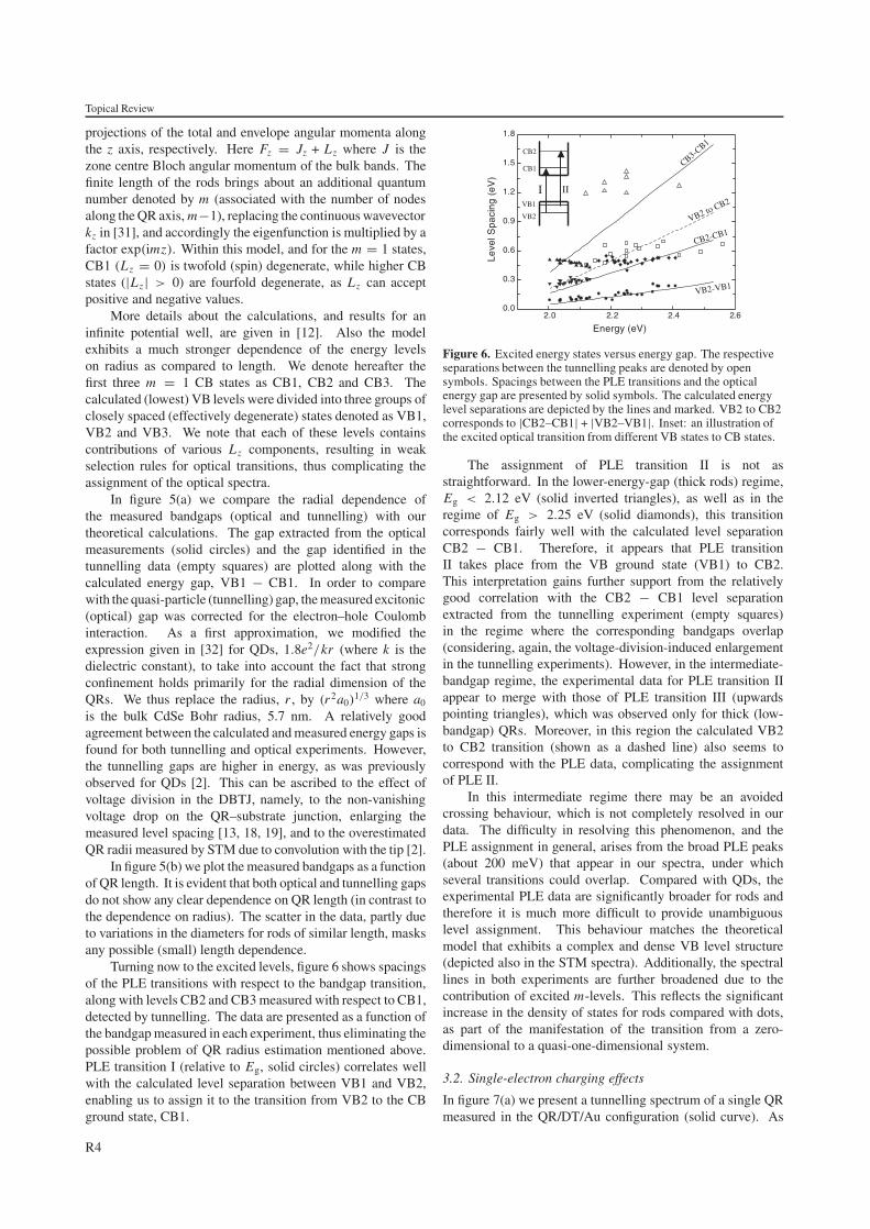
Turning now to the excited levels, figure 6 shows spacingsof the PLE transitions with respect to the bandgap transition,along with levels CB2 and CB3 measured with respect to CB1,detected by tunnelling. The data are presented as a function ofthe bandgap measured in each experiment, thus eliminating thepossible problem of QR radius estimation mentioned above.PLE transition I (relative to Eg, solid circles) correlates wellwith the calculated level separation between VB1 and VB2,enabling us to assign it to the transition from VB2 to the CBground state, CB1.
2.0 2.2 2.4 2.60.0
0.3
0.6
0.9
1.2
1.5
1.8
Leve
l Spa
cing
(eV
)
Energy (eV)
VB2-VB1
CB2-CB1
CB3-CB1
VB2 to CB2VB1
VB2
CB1
CB2
I II
Figure 6. Excited energy states versus energy gap. The respectiveseparations between the tunnelling peaks are denoted by opensymbols. Spacings between the PLE transitions and the opticalenergy gap are presented by solid symbols. The calculated energylevel separations are depicted by the lines and marked. VB2 to CB2corresponds to |CB2–CB1| + |VB2–VB1|. Inset: an illustration ofthe excited optical transition from different VB states to CB states.
The assignment of PLE transition II is not asstraightforward. In the lower-energy-gap (thick rods) regime,Eg < 2.12 eV (solid inverted triangles), as well as in theregime of Eg > 2.25 eV (solid diamonds), this transitioncorresponds fairly well with the calculated level separationCB2 − CB1. Therefore, it appears that PLE transitionII takes place from the VB ground state (VB1) to CB2.This interpretation gains further support from the relativelygood correlation with the CB2 − CB1 level separationextracted from the tunnelling experiment (empty squares)in the regime where the corresponding bandgaps overlap(considering, again, the voltage-division-induced enlargementin the tunnelling experiments). However, in the intermediate-bandgap regime, the experimental data for PLE transition IIappear to merge with those of PLE transition III (upwardspointing triangles), which was observed only for thick (low-bandgap) QRs. Moreover, in this region the calculated VB2to CB2 transition (shown as a dashed line) also seems tocorrespond with the PLE data, complicating the assignmentof PLE II.
In this intermediate regime there may be an avoidedcrossing behaviour, which is not completely resolved in ourdata. The difficulty in resolving this phenomenon, and thePLE assignment in general, arises from the broad PLE peaks(about 200 meV) that appear in our spectra, under whichseveral transitions could overlap. Compared with QDs, theexperimental PLE data are significantly broader for rods andtherefore it is much more difficult to provide unambiguouslevel assignment. This behaviour matches the theoreticalmodel that exhibits a complex and dense VB level structure(depicted also in the STM spectra). Additionally, the spectrallines in both experiments are further broadened due to thecontribution of excited m-levels. This reflects the significantincrease in the density of states for rods compared with dots,as part of the manifestation of the transition from a zero-dimensional to a quasi-one-dimensional system.
3.2. Single-electron charging effects
In figure 7(a) we present a tunnelling spectrum of a single QRmeasured in the QR/DT/Au configuration (solid curve). As
R4
Topical Review
-2 -1 0 10 1 2 3 2
Sample Bias (V)
CB2
CB1
VB1
Theo.
Exp.
-3 -2 -1
Sample Bias (V)
432121
Exp.
Theo.
VB1
CB1
CB2
dI/d
V (
arb
. u.)
(a) (b)
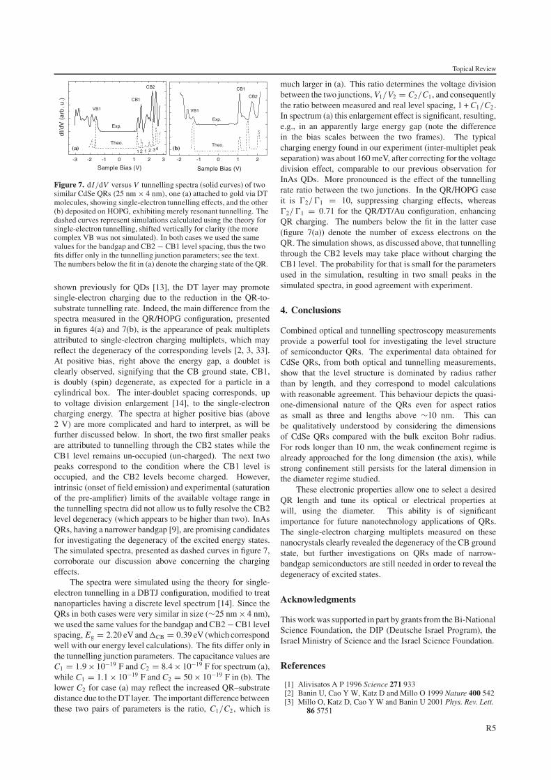
Figure 7. dI/dV versus V tunnelling spectra (solid curves) of twosimilar CdSe QRs (25 nm × 4 nm), one (a) attached to gold via DTmolecules, showing single-electron tunnelling effects, and the other(b) deposited on HOPG, exhibiting merely resonant tunnelling. Thedashed curves represent simulations calculated using the theory forsingle-electron tunnelling, shifted vertically for clarity (the morecomplex VB was not simulated). In both cases we used the samevalues for the bandgap and CB2 − CB1 level spacing, thus the twofits differ only in the tunnelling junction parameters; see the text.The numbers below the fit in (a) denote the charging state of the QR.
shown previously for QDs [13], the DT layer may promotesingle-electron charging due to the reduction in the QR-to-substrate tunnelling rate. Indeed, the main difference from thespectra measured in the QR/HOPG configuration, presentedin figures 4(a) and 7(b), is the appearance of peak multipletsattributed to single-electron charging multiplets, which mayreflect the degeneracy of the corresponding levels [2, 3, 33].At positive bias, right above the energy gap, a doublet isclearly observed, signifying that the CB ground state, CB1,is doubly (spin) degenerate, as expected for a particle in acylindrical box. The inter-doublet spacing corresponds, upto voltage division enlargement [14], to the single-electroncharging energy. The spectra at higher positive bias (above2 V) are more complicated and hard to interpret, as will befurther discussed below. In short, the two first smaller peaksare attributed to tunnelling through the CB2 states while theCB1 level remains un-occupied (un-charged). The next twopeaks correspond to the condition where the CB1 level isoccupied, and the CB2 levels become charged. However,intrinsic (onset of field emission) and experimental (saturationof the pre-amplifier) limits of the available voltage range inthe tunnelling spectra did not allow us to fully resolve the CB2level degeneracy (which appears to be higher than two). InAsQRs, having a narrower bandgap [9], are promising candidatesfor investigating the degeneracy of the excited energy states.The simulated spectra, presented as dashed curves in figure 7,corroborate our discussion above concerning the chargingeffects.
The spectra were simulated using the theory for single-electron tunnelling in a DBTJ configuration, modified to treatnanoparticles having a discrete level spectrum [14]. Since theQRs in both cases were very similar in size (∼25 nm × 4 nm),we used the same values for the bandgap and CB2 − CB1 levelspacing, Eg = 2.20 eV and �CB = 0.39 eV (which correspondwell with our energy level calculations). The fits differ only inthe tunnelling junction parameters. The capacitance values areC1 = 1.9 × 10⁻¹⁹ F and C2 = 8.4 × 10⁻¹⁹ F for spectrum (a),while C1 = 1.1 × 10⁻¹⁹ F and C2 = 50 × 10−19 F in (b). Thelower C2 for case (a) may reflect the increased QR–substratedistance due to the DT layer. The important difference betweenthese two pairs of parameters is the ratio, C1/C2, which is
much larger in (a). This ratio determines the voltage divisionbetween the two junctions, V1/V2 = C2/C1, and consequentlythe ratio between measured and real level spacing, 1 + C1/C2.In spectrum (a) this enlargement effect is significant, resulting,e.g., in an apparently large energy gap (note the differencein the bias scales between the two frames). The typicalcharging energy found in our experiment (inter-multiplet peakseparation) was about 160 meV, after correcting for the voltagedivision effect, comparable to our previous observation forInAs QDs. More pronounced is the effect of the tunnellingrate ratio between the two junctions. In the QR/HOPG caseit is �2/�1 = 10, suppressing charging effects, whereas�2/�1 = 0.71 for the QR/DT/Au configuration, enhancingQR charging. The numbers below the fit in the latter case(figure 7(a)) denote the number of excess electrons on theQR. The simulation shows, as discussed above, that tunnellingthrough the CB2 levels may take place without charging theCB1 level. The probability for that is small for the parametersused in the simulation, resulting in two small peaks in thesimulated spectra, in good agreement with experiment.
4. Conclusions
Combined optical and tunnelling spectroscopy measurementsprovide a powerful tool for investigating the level structureof semiconductor QRs. The experimental data obtained forCdSe QRs, from both optical and tunnelling measurements,show that the level structure is dominated by radius ratherthan by length, and they correspond to model calculationswith reasonable agreement. This behaviour depicts the quasi-one-dimensional nature of the QRs even for aspect ratiosas small as three and lengths above ∼10 nm. This canbe qualitatively understood by considering the dimensionsof CdSe QRs compared with the bulk exciton Bohr radius.For rods longer than 10 nm, the weak confinement regime isalready approached for the long dimension (the axis), whilestrong confinement still persists for the lateral dimension inthe diameter regime studied.
These electronic properties allow one to select a desiredQR length and tune its optical or electrical properties atwill, using the diameter. This ability is of significantimportance for future nanotechnology applications of QRs.The single-electron charging multiplets measured on thesenanocrystals clearly revealed the degeneracy of the CB groundstate, but further investigations on QRs made of narrow-bandgap semiconductors are still needed in order to reveal thedegeneracy of excited states.
Acknowledgments
This work was supported in part by grants from the Bi-NationalScience Foundation, the DIP (Deutsche Israel Program), theIsrael Ministry of Science and the Israel Science Foundation.
References
[1] Alivisatos A P 1996 Science 271 933[2] Banin U, Cao Y W, Katz D and Millo O 1999 Nature 400 542[3] Millo O, Katz D, Cao Y W and Banin U 2001 Phys. Rev. Lett.
86 5751
R5
Topical Review
[4] Klimov V, Mikhailovsky A, Xu S, Malko A,Hollingsworth J A, Leatherdale C A, Eisler H J andBawendi M G 2000 Science 290 314
[5] Kazes M, Lewis D Y, Ebenstein Y, Mokari T andBanin U 2002 Adv. Mater. 14 317
[6] Tessler N, Medvedev V, Kazes M, Kan S H and Banin U 2002Science 295 1506
[7] Bruchez M, Moronne M, Gin P, Weiss S andAlivisatos A P 1998 Science 281 2013
[8] Peng X G, Manna L, Yang W D, Wickham J, Scher E,Kadavanich A and Alivisatos A P 2000 Nature404 59
[9] Kan S H, Mokari T, Rothenberg E and Banin U 2003 Nat.Mater. 2 155
[10] Hu J T, Li L S, Yang W D, Manna L, Wang L W andAlivisatos A P 2001 Science 292 2060
[11] Chen X, Nazzal A, Goorskey D, Xiao M, Peng Z A andPeng X 2001 Phys. Rev. B 64 5304
[12] Katz D, Wizansky T, Millo O, Rothenberg E, Mokari T andBanin U 2002 Phys. Rev. Lett. 89 86801
Katz D, Wizansky T, Millo O, Rothenberg E, Mokari T andBanin U 2002 Phys. Rev. Lett. 89 199901 (erratum)
[13] Katz D, Millo O, Kan S H and Banin U 2001 Appl. Phys. Lett.79 117
[14] Banin U and Millo O 2003 Annu. Rev. Phys. Chem. 54 465[15] Norris D J and Bawendi M G 1996 Phys. Rev. B 53 16338[16] Banin U, Lee C J, Guzelian A A, Kadavanich A V,
Alivisatos A P, Jaskolski W, Bryant G W, Efros Al L andRosen M 1998 J. Chem. Phys. 109 2306
[17] Chen S, Ingram R S, Hostetler M J, Pietron J J, Murray R W,Schaaff T G, Khoury J T, Alvarez M M andWhetten R L 1998 Science 280 2098
[18] Bakkers E P A M and Vanmaekelbergh D 2000 Phys. Rev. B62 R7743
[19] Bakkers E P A M, Hens Z, Zunger A, Franceschetti A,Kouwenhoven L P, Gurevich L andVanmaekelbergh D 2001 Nano Lett. 1 551
[20] Franceschetti A and Zunger A 2000 Phys. Rev. B 62 2614[21] Lee S, Kim J, Jonsson L, Wilkins J W, Bryant G W and
Klimeck G 2002 Phys. Rev. B 66 235307[22] Niquet Y M, Delerue C, Allan G and Lannoo M 2002 Phys.
Rev. B 65 165334[23] Ekimov A I, Hache F, Schanneklein M C, Ricard D,
Flytzanis C, Kudryavtsev I A, Yazeva T V, Rodina A V andEfros Al L 1993 J. Opt. Soc. Am. B 10 100
[24] Li X Z and Xia J B 2002 Phys. Rev. B 66 115316[25] Hu J T, Wang L W, Li L S, Yang W and Alivisatos A P 2002
J. Phys. Chem. 106 2447[26] Li J and Wang L W 2002 Nano Lett. 3 101[27] Manna L, Scher E C and Alivisatos A P 2000 J. Am. Chem.
Soc. 122 12700[28] Peng Z A and Peng X 2001 J. Am. Chem. Soc. 123 1389[29] Tews M and Pfannkuche D 2002 Phys. Rev. B 65 073307[30] Li L S, Hu J T, Yang W D and Alivisatos A P 2001 Nano Lett.
1 349[31] Sercel P C and Vahala K J 1990 Phys. Rev. B 42 3690[32] Brus L E 1984 J. Chem. Phys. 9 4403[33] Millo O, Katz D, Cao Y W and Banin U 2000 Phys. Rev. B 61
16773
R6
Copyright © 2022 FDOKUMEN