
Subwavelength imaging at infrared frequencies using an array of metallic nanorods
Upload
sungkyunkwanCategory
view
3download
0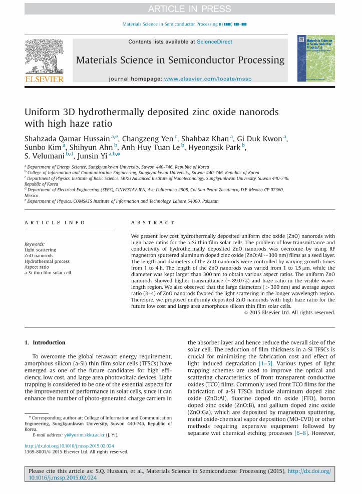
Contents lists available at ScienceDirect
Materials Science in Semiconductor Processing
Materials Science in Semiconductor Processing ] (]]]]) ]]]–]]]
http://d1369-80
n CorrEngineeKorea.
E-m
Pleas10.10
journal homepage: www.elsevier.com/locate/mssp
Uniform 3D hydrothermally deposited zinc oxide nanorodswith high haze ratio
Shahzada Qamar Hussain a,e, Changzeng Yen c, Shahbaz Khan a, Gi Duk Kwon a,Sunbo Kim a, Shihyun Ahn b, Anh Huy Tuan Le b, Hyeongsik Park b,S. Velumani b,d, Junsin Yi a,b,n
a Department of Energy Science, Sungkyunkwan University, Suwon 440-746, Republic of Koreab College of Information and Communication Engineering, Sungkyunkwan University, Suwon 440-746, Republic of Koreac Department of Physics, Institute of Basic Science, SKKU Advanced Institute of Nanotechnology, Sungkyunkwan University, Suwon 440-746,Republic of Koread Department of Electrical Engineering (SEES), CINVESTAV-IPN, Ave Politecnico 2508, Col San Pedro Zacatenco, D.F. Mexico CP 07360,Mexicoe Department of Physics, COMSATS Institute of Information and Technology, Lahore 54000, Pakistan
a r t i c l e i n f o
Keywords:Light scatteringZnO nanorodsHydrothermal processAspect ratioa-Si thin film solar cell
x.doi.org/10.1016/j.mssp.2015.02.02401/& 2015 Elsevier Ltd. All rights reserved.
esponding author at: College of Informationring, Sungkyunkwan University, Suwon 4
ail address: [email protected] (J. Yi).
e cite this article as: S.Q. Hussain,16/j.mssp.2015.02.024i
a b s t r a c t
We present low cost hydrothermally deposited uniform zinc oxide (ZnO) nanorods withhigh haze ratios for the a-Si thin film solar cells. The problem of low transmittance andconductivity of hydrothermally deposited ZnO nanorods was overcome by using RFmagnetron sputtered aluminum doped zinc oxide (ZnO:Al �300 nm) films as a seed layer.The length and diameters of the ZnO nanorods were controlled by varying growth timesfrom 1 to 4 h. The length of the ZnO nanorods was varied from 1 to 1.5 mm, while thediameter was kept larger than 300 nm to obtain various aspect ratios. The uniform ZnOnanorods showed higher transmittance (�89.07%) and haze ratio in the visible wave-length region. We also observed that the large diameters (4300 nm) and average aspectratio (3–4) of ZnO nanorods favored the light scattering in the longer wavelength region.Therefore, we proposed uniformly deposited ZnO nanorods with high haze ratio for thefuture low cost and large area amorphous silicon thin film solar cells.
& 2015 Elsevier Ltd. All rights reserved.
1. Introduction
To overcome the global terawatt energy requirement,amorphous silicon (a-Si) thin film solar cells (TFSCs) haveemerged as one of the future candidates for high effi-ciency, low cost, and large area photovoltaic devices. Lighttrapping is considered to be one of the essential aspects forthe improvement of performance in solar cells, since it canenhance the number of photo-generated charge carriers in
and Communication40-746, Republic of
et al., Materials Scienc
the absorber layer and hence reduce the overall size of thesolar cell. The reduction of film thickness in a-Si TFSCs iscrucial for minimizing the fabrication cost and effect oflight induced degradation [1–5]. Various types of lighttrapping schemes are used to improve the optical andscattering characteristics of front transparent conductiveoxides (TCO) films. Commonly used front TCO films for thefabrication of a-Si TFSCs include aluminum doped zincoxide (ZnO:Al), fluorine doped tin oxide (FTO), borondoped zinc oxide (ZnO:B), and gallium doped zinc oxide(ZnO:Ga), which are deposited by magnetron sputtering,metal oxide-chemical vapor deposition (MO-CVD) or othermethods requiring expensive equipment followed byseparate wet chemical etching processes [6–8]. However,
e in Semiconductor Processing (2015), http://dx.doi.org/
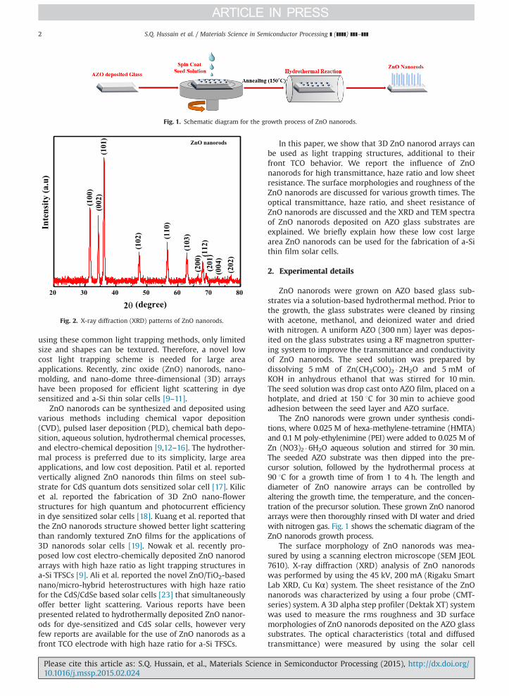
Fig. 1. Schematic diagram for the growth process of ZnO nanorods.
20 30 40 50 60 70 80
(202
)(0
04)
Inte
nsity
(a.u
)
2θ (degree)
(201
)(112
)(2
00)
(103
)(110
)
(102
)
(101
)(0
02)
(100
)
ZnO nanorods
Fig. 2. X-ray diffraction (XRD) patterns of ZnO nanorods.
S.Q. Hussain et al. / Materials Science in Semiconductor Processing ] (]]]]) ]]]–]]]2
using these common light trapping methods, only limitedsize and shapes can be textured. Therefore, a novel lowcost light trapping scheme is needed for large areaapplications. Recently, zinc oxide (ZnO) nanorods, nano-molding, and nano-dome three-dimensional (3D) arrayshave been proposed for efficient light scattering in dyesensitized and a-Si thin solar cells [9–11].
ZnO nanorods can be synthesized and deposited usingvarious methods including chemical vapor deposition(CVD), pulsed laser deposition (PLD), chemical bath depo-sition, aqueous solution, hydrothermal chemical processes,and electro-chemical deposition [9,12–16]. The hydrother-mal process is preferred due to its simplicity, large areaapplications, and low cost deposition. Patil et al. reportedvertically aligned ZnO nanorods thin films on steel sub-strate for CdS quantum dots sensitized solar cell [17]. Kilicet al. reported the fabrication of 3D ZnO nano-flowerstructures for high quantum and photocurrent efficiencyin dye sensitized solar cells [18]. Kuang et al. reported thatthe ZnO nanorods structure showed better light scatteringthan randomly textured ZnO films for the applications of3D nanorods solar cells [19]. Nowak et al. recently pro-posed low cost electro-chemically deposited ZnO nanorodarrays with high haze ratio as light trapping structures ina-Si TFSCs [9]. Ali et al. reported the novel ZnO/TiO2-basednano/micro-hybrid heterostructures with high haze ratiofor the CdS/CdSe based solar cells [23] that simultaneouslyoffer better light scattering. Various reports have beenpresented related to hydrothermally deposited ZnO nanor-ods for dye-sensitized and CdS solar cells, however veryfew reports are available for the use of ZnO nanorods as afront TCO electrode with high haze ratio for a-Si TFSCs.
Please cite this article as: S.Q. Hussain, et al., Materials Scienc10.1016/j.mssp.2015.02.024i
In this paper, we show that 3D ZnO nanorod arrays canbe used as light trapping structures, additional to theirfront TCO behavior. We report the influence of ZnOnanorods for high transmittance, haze ratio and low sheetresistance. The surface morphologies and roughness of theZnO nanorods are discussed for various growth times. Theoptical transmittance, haze ratio, and sheet resistance ofZnO nanorods are discussed and the XRD and TEM spectraof ZnO nanorods deposited on AZO glass substrates areexplained. We briefly explain how these low cost largearea ZnO nanorods can be used for the fabrication of a-Sithin film solar cells.
2. Experimental details
ZnO nanorods were grown on AZO based glass sub-strates via a solution-based hydrothermal method. Prior tothe growth, the glass substrates were cleaned by rinsingwith acetone, methanol, and deionized water and driedwith nitrogen. A uniform AZO (300 nm) layer was depos-ited on the glass substrates using a RF magnetron sputter-ing system to improve the transmittance and conductivityof ZnO nanorods. The seed solution was prepared bydissolving 5 mM of Zn(CH3COO)2 �2H2O and 5 mM ofKOH in anhydrous ethanol that was stirred for 10 min.The seed solution was drop cast onto AZO film, placed on ahotplate, and dried at 150 1C for 30 min to achieve goodadhesion between the seed layer and AZO surface.
The ZnO nanorods were grown under synthesis condi-tions, where 0.025 M of hexa-methylene-tetramine (HMTA)and 0.1 M poly-ethylenimine (PEI) were added to 0.025 M ofZn (NO3)2 �6H2O aqueous solution and stirred for 30 min.The seeded AZO substrate was then dipped into the pre-cursor solution, followed by the hydrothermal process at90 1C for a growth time of from 1 to 4 h. The length anddiameter of ZnO nanowire arrays can be controlled byaltering the growth time, the temperature, and the concen-tration of the precursor solution. These grown ZnO nanorodarrays were then thoroughly rinsed with DI water and driedwith nitrogen gas. Fig. 1 shows the schematic diagram of theZnO nanorods growth process.
The surface morphology of ZnO nanorods was mea-sured by using a scanning electron microscope (SEM JEOL7610). X-ray diffraction (XRD) analysis of ZnO nanorodswas performed by using the 45 kV, 200 mA (Rigaku SmartLab XRD, Cu Kα) system. The sheet resistance of the ZnOnanorods was characterized by using a four probe (CMT-series) system. A 3D alpha step profiler (Dektak XT) systemwas used to measure the rms roughness and 3D surfacemorphologies of ZnO nanorods deposited on the AZO glasssubstrates. The optical characteristics (total and diffusedtransmittance) were measured by using the solar cell
e in Semiconductor Processing (2015), http://dx.doi.org/
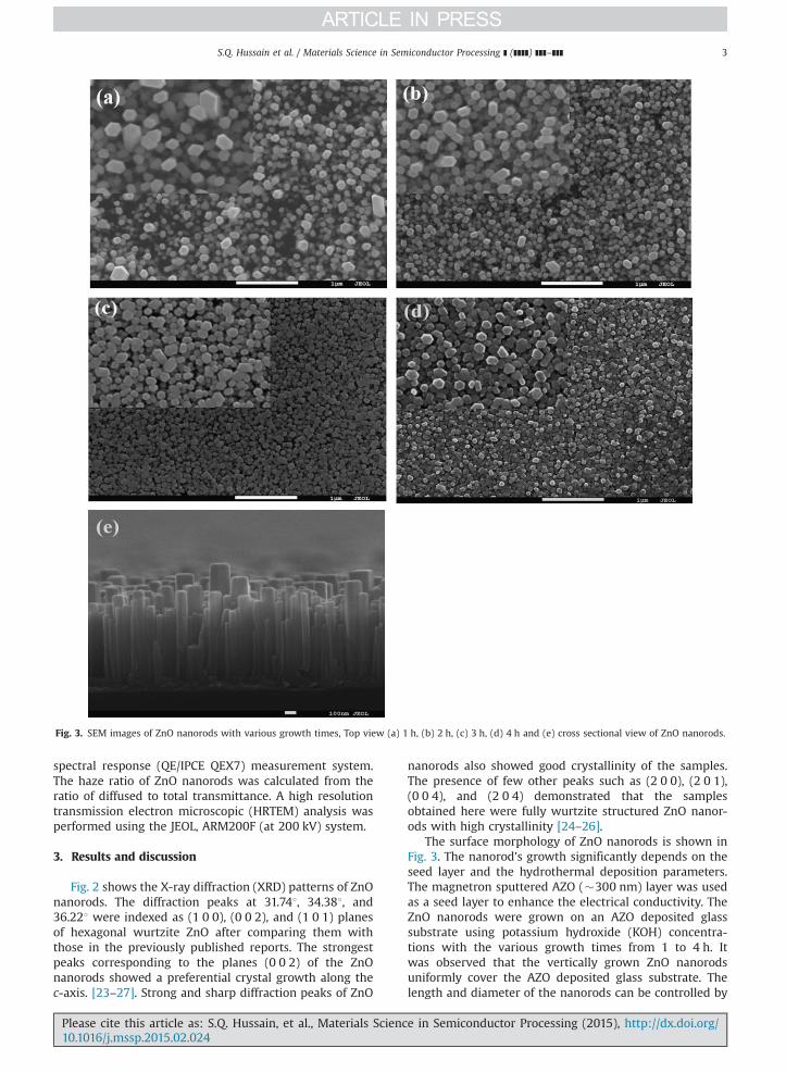
Fig. 3. SEM images of ZnO nanorods with various growth times, Top view (a) 1 h, (b) 2 h, (c) 3 h, (d) 4 h and (e) cross sectional view of ZnO nanorods.
S.Q. Hussain et al. / Materials Science in Semiconductor Processing ] (]]]]) ]]]–]]] 3
spectral response (QE/IPCE QEX7) measurement system.The haze ratio of ZnO nanorods was calculated from theratio of diffused to total transmittance. A high resolutiontransmission electron microscopic (HRTEM) analysis wasperformed using the JEOL, ARM200F (at 200 kV) system.
3. Results and discussion
Fig. 2 shows the X-ray diffraction (XRD) patterns of ZnOnanorods. The diffraction peaks at 31.741, 34.381, and36.221 were indexed as (1 0 0), (0 0 2), and (1 0 1) planesof hexagonal wurtzite ZnO after comparing them withthose in the previously published reports. The strongestpeaks corresponding to the planes (0 0 2) of the ZnOnanorods showed a preferential crystal growth along thec-axis. [23–27]. Strong and sharp diffraction peaks of ZnO
Please cite this article as: S.Q. Hussain, et al., Materials Scienc10.1016/j.mssp.2015.02.024i
nanorods also showed good crystallinity of the samples.The presence of few other peaks such as (2 0 0), (2 0 1),(0 0 4), and (2 0 4) demonstrated that the samplesobtained here were fully wurtzite structured ZnO nanor-ods with high crystallinity [24–26].
The surface morphology of ZnO nanorods is shown inFig. 3. The nanorod's growth significantly depends on theseed layer and the hydrothermal deposition parameters.The magnetron sputtered AZO (�300 nm) layer was usedas a seed layer to enhance the electrical conductivity. TheZnO nanorods were grown on an AZO deposited glasssubstrate using potassium hydroxide (KOH) concentra-tions with the various growth times from 1 to 4 h. Itwas observed that the vertically grown ZnO nanorodsuniformly cover the AZO deposited glass substrate. Thelength and diameter of the nanorods can be controlled by
e in Semiconductor Processing (2015), http://dx.doi.org/

S.Q. Hussain et al. / Materials Science in Semiconductor Processing ] (]]]]) ]]]–]]]4
varying the reaction time, temperature, and concentrationof the precursor [20]. Fig. 3(a)–(d) shows the top view ofthe ZnO nanorods surface morphologies for a growth time
Fig. 4. Alpha step profile height of the ZnO nanorods.
Fig. 5. Tunnelling electron microscopic (T
Please cite this article as: S.Q. Hussain, et al., Materials Scienc10.1016/j.mssp.2015.02.024i
from 1 to 4 h. The vertically aligned ZnO nanorods showedaverage diameters of 300–400 nm, with an average lengthof 1.2 μm (aspect ratio �3). The ZnO nanorods becomedenser with the increase of growth times from 1 to 4 h.The cross sectional view of ZnO nanorods is shown in Fig. 3(e). The growth time plays an important role in controllingthe surface morphology of ZnO nanostructures, asreported by Guo et al. [21]. Huang et al. reported thatZnO nanorods with small diameters and large lengths canimprove the performance of dye sensitized solar cells [22].
The profile height and inset 3D alpha step profilerimage of the ZnO nanorods are shown in Fig. 4. Theroughness and 3D surface morphology of ZnO nanorodswere measured by scanning a surface area of 100�100 mm2. ZnO nanorods showed relatively high rms rough-ness of 292.77 nm. An excellent agreement was shown bythe 3D profiler image and profile height of ZnO nanorodssurface morphology [29–32].
Fig. 5 shows the high resolution transmission electronmicroscopic (HRTEM) images of ZnO nanorods. Fig. 5(b)and 5(d) shows the selected area electron diffraction(SAED) pattern of the ZnO nanorod, illustrating that the
EM) images of the ZnO nanorods.
e in Semiconductor Processing (2015), http://dx.doi.org/
400 600 800 10000
20
40
60
80
100Total
Growth time (hrs) As deposited
ZnO Nanorods _1 hr
ZnO Nanorods_2 hrs
ZnO Nanorods_3 hrs
ZnO Nanorods_4 hrs
Tra
nsm
ittan
ce (%
)
Wavelength (nm)
400 600 800 10000
20
40
60
80
100Growth time (hrs)
Haz
e ra
tio (%
)
Wavelength (nm)
As deposited
ZnO Nanorods _4 hrs
ZnO Nanorods _3 hrs
ZnO Nanorods _1 hr
ZnO Nanorods _2 hrs
Fig. 6. Optical characteristics (a) total transmittance and (b) haze ratio ofZnO nanorods as a function of growth time.
0
20
40
60
80
432
Shee
t res
ista
nce
(sq
)
Growth time (hrs)As deposited 1
Ω⁄
Fig. 7. Sheet resistance of the ZnO nanorods for various growth times.
Please cite this article as: S.Q. Hussain, et al., Materials Scienc10.1016/j.mssp.2015.02.024i
S.Q. Hussain et al. / Materials Science in Semiconductor Processing ] (]]]]) ]]]–]]] 5
individual nanorod was single crystalline in nature andpreferentially grew along the [0 0 0 2] direction (the caxis). The sharp dark spots in the SAED pattern furtherconfirm that the individual ZnO nanorod was singlecrystalline in nature. The TEM images clearly showed thatthe ZnO nanorods were high-quality single crystals with-out visible defects within the area of observation[20,24,25].
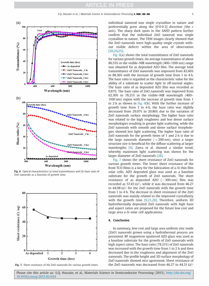
Fig. 6(a) shows the total transmittance of ZnO nanorodsfor various growth times. An average transmittance of about86.53% in the visible–NIR wavelength (400–1100 nm) rangewas obtained for as deposited AZO film. The average totaltransmittance of ZnO nanorods was improved from 82.66%to 88.36% with the increase of growth time from 1 to 4 h.The haze ratio is regarded as the characteristic value for theability of a substrate to scatter light to off-normal angles.The haze ratio of as deposited AZO film was recorded as0.87%. The haze ratio of ZnO nanorods was improved from62.30% to 78.21% in the visible–NIR wavelength (400–1100 nm) region with the increase of growth time from 1to 2 h as shown in Fig. 6(b). With the further increase ofgrowth time from 3 to 4 h, the haze ratio was slightlydecreased from 29.07% to 20.86% due to the variation ofZnO nanorods surface morphology. The higher haze ratiowas related to the high roughness and less dense surfacemorphologies resulting in greater light scattering, while theZnO nanorods with smooth and dense surface morpholo-gies showed less light scattering. The higher haze ratio ofZnO nanorods for the growth times of 1 and 2 h is due tothe large nanorods diameter (4200 nm), since a largerstructure size is beneficial for the diffuse scattering at largerwavelengths [9]. Zaera et al. showed a similar trend,whereby maximum light scattering was shown for thelarger diameter of ZnO nanorods [28].
Fig. 7 shows the sheet resistance of ZnO nanorods forvarious growth times. The lower sheet resistance of thefront TCO films is a key for the fabrication of a-Si thin filmsolar cells. AZO deposited glass was used as a baselinesubstrate for the growth of ZnO nanorods. The sheetresistance of as deposited AZO (�300 nm) film wasrecorded as 57.43 Ω/□, while it was decreased from 46.27to 44.98 Ω/□ for the ZnO nanorods with the growth timefrom 1 to 4 h. The decrease in sheet resistance of the ZnOnanorods was mainly related to the improved crystallinitywith the growth time [9,21,28]. Therefore, uniform 3Dhydrothermally deposited ZnO nanorods with high hazeand aspect ratios are proposed for the future low cost andlarge area a-Si solar cell applications.
4. Conclusion
In summary, low cost and large area uniform zinc oxide(ZnO) nanorods grown using a hydrothermal process arepresented. RF magnetron sputtered AZO glass was used asa baseline substrate for the growth of ZnO nanorods withhigh aspect ratios. The haze ratio (78.21%) of ZnO nanorodswas increased with the growth time from 1 to 2 h and thendecreased due to the roughness and alignment of the ZnOnanorods. The profile height and 3D surface morphology ofZnO nanorods showed nice agreement. Sheet resistance ofthe ZnO nanorods was decreased from 46.27 to 44.31 Ω/□
e in Semiconductor Processing (2015), http://dx.doi.org/
S.Q. Hussain et al. / Materials Science in Semiconductor Processing ] (]]]]) ]]]–]]]6
with the increase of growth time from 1 to 4 h due to goodwurtzite structure and high degree of crystallinity.Furthermore, our results revealed that the ZnO nanorodswith larger diameters (4200 nm) and length (�2 mm) arebeneficial for light scattering at wider wavelengths. There-fore, ZnO nanorods with higher light scattering propertiesand good electrical conductivity are proposed for futurelow cost and large area a-Si thin film solar cells.
Acknowledgments
This work was supported by the New & RenewableEnergy Technology Development Program of the KoreaInstitute of Energy Technology Evaluation and Planning(KETEP) grant funded by the Korea Government Ministryof Trade, Industry & Energy (No. 20113020010010). One ofthe authors, S. Velumani, wishes to thank the Ministry ofScience, ICT & Future Planning (MSIP) for their support(141S-6-3-0641).
References
[1] H. Tan, E. Psomadaki, O. Isabella, M. Fischer, P. Babal, R. Vasudevan,M. Zeman, A.H.M. Smets, Appl. Phys. Lett. 103 (2013) 173905.
[2] V. Jovanov, U. Palanchoke, P. Magnus, H. Stiebig, J. Hüpkes,P. Sichanugrist, M. Konagai, S. Wiesendanger, C. Rockstuhl,D. Knipp, Opt. Express 21 (2013) A595–A606.
[3] S.Q. Hussain, S. Ahn, H. Park, G. Kwon, J. Raja, Y. Lee, N. Balaji, H. Kim,A.H.T. Le, J. Yi, Vacuum 94 (2013) 87–91.
[4] S.T. Hwang, C.B. Park, Trans. Electr. Electron. Mater. 11 (2010) 81–84.[5] S.Q. Hussain, S. Kim, S. Ahn, N. Balaji, Y. Lee, J.H. Lee, J. Yi, Sol. Energy
Mater. Sol. Cells 122 (2014) 130–135.[6] H. Park, J. Lee, H. Kim, D. Kim, J. Raja, J. Yi, Appl. Phys. Lett. 102 (2013)
191602–191605.[7] B. Janthong, Y. Moriya, A. Hongsingthong, P. Sichanugrist,
M. Konagai, Sol. Energy Mater. Sol. Cells 119 (2013) 209–213.
Please cite this article as: S.Q. Hussain, et al., Materials Scienc10.1016/j.mssp.2015.02.024i
[8] A. Hongsingthong, T. Krajangsang, B. Janthong, P. Sichanugrist,M. Konagai, in: Proceedings of the 37th IEEE Photovoltaic SpecialistsConference (PVSC), 2011, pp. 000791–000794.
[9] R.E. Nowak, M. Vehse, O. Sergeev, K. Maydell, C. Agert, Sol. EnergyMater. Sol. Cells 125 (2014) 305–309.
[10] C. Battaglia, J. Escarre, K. Soderstrom, M. Charriere, M. Despeisse,F.J. Haug, C. Ballif, Nat. Photonics 5 (2011) 535–538.
[11] J. Zhu, C.-M. Hsu, Z. Yu, S. Fan, Y. Cui, Nano Lett. 10 (2010) 1979–1984.[12] X. Liu, X. Wu, H. Cao, R.P.H. Chang, J. Appl. Phys. 95 (2004)
3141–3147.[13] S. Choopun, H. Tabata, T. Kawai, J. Cryst. Growth 274 (2005) 167–172.[14] R. Shabannia, H.A. Hassan, Mater. Lett. 90 (2013) 156–158.[15] N. Lepot, M.K.V. Bael, H.V.D. Rul, J. D’Haen, R. Peeters, D. Franco,
J. Mullens, Mater. Lett. 61 (2007) 2624–2627.[16] I. Shakir, Z. Ali, J. Bae, J. Park, D.J. Kang, RSC Adv. 4 (2014) 6324–6329.[17] S.B. Patil, A.K. Singh, Electrochim. Acta 56 (2011) 5693–5701.[18] B. Kilic, T. Günes, I. Besirli, M. Sezginer, S. Tuzemen, Appl. Surf. Sci.
318 (2014) 32–36.[19] Y. Kuang, K.H.M. van der Werf, Z.S. Houweling, M.D. Vece, R.E.
I. Schropp, J. Non-Cryst. Solids 358 (2012) 2209–2213.[20] M. Raja, N. Muthukumarasamy, D. Velauthapillai, R. Balasundaraprabhu,
S. Agilan, T.S. Senthil, Sol. Energy 106 (2014) 129–135.[21] M. Guo, P. Diao, S. Cai, J. Solid State Chem. 178 (2005) 1864–1873.[22] Q. Huang, L. Fang, X. Chen, M. Saleem, J. Alloy. Compd. 509 (2011)
9456–9459.[23] Z. Ali, I. Shakir, D.J. Kang, J. Mater. Chem. A 2 (2014) 6474–6479.[24] L.Y. Lin, M.H. Yeh, C.P. Lee, C.Y. Chou, R. Vittal, K.C. Ho, Electrochim.
Acta 62 (2012) 341–347.[25] X. Liu, X. Wu, H. Cao, R.P.H. Chang, J. Appl. Phys. 95 (2004)
3141–3147.[26] Y. Kuang, K.H.M. van der Werf, Z.S. Houweling, M.D. Vece, R.E.
I. Schropp, J. Non-Cryst. Solids 358 (2012) 2209–2213.[27] Z. Ali, S.N. Cha, J.I. Sohn, I. Shakir, C. Yan, J.M. Kim, D.J. Kang, J. Mater.
Chem. 22 (2012) 17625–17629.[28] R.T. Zaera, J. Elias, C.L. Clément, Appl. Phys. Lett. 93 (2008)
233119–233122.[29] M.L. Addonizio, A. Spadoni, A. Antonaia, Appl. Surf. Sci. 287 (2013)
311–317.[30] F.H. Wang, C.F. Yang, Y.H. Lee, Nanoscale Res. Lett. 9 (2014) 97–103.[31] W.T. Yen, Y.C. Lin, J.H. Ke, Appl. Surf. Sci. 257 (2010) 960–968.[32] J. Raja, K. Jang, S.Q. Hussain, S. Chatterjee, S. Velumani, N. Balaji, J. Yi,
Appl. Phys. Lett. 106 (2015) 033501–033504.
e in Semiconductor Processing (2015), http://dx.doi.org/
Copyright © 2022 FDOKUMEN