Atomic-scale three-dimensional phononic crystals with a very low thermal conductivity to design...
10
Jean-Numa Gillet 1 e-mail: [email protected] Yann Chalopin Sebastian Volz 2 e-mail: [email protected] Laboratoire d’Energétique Moléculaire et Macroscopique, Combustion and Centre National de la Recherche Scientifique (EM2C, CNRS UPR 288), Ecole Centrale Paris, Grande Voie des Vignes, 92295 Châtenay-Malabry Cedex, France Atomic-Scale Three-Dimensional Phononic Crystals With a Very Low Thermal Conductivity to Design Crystalline Thermoelectric Devices Superlattices with thermal-insulating behaviors have been studied to design thermoelec- tric materials but affect heat transfer in only one main direction and often show many cracks and dislocations near their layer interfaces. Quantum-dot (QD) self-assembly is an emerging epitaxial technology to design ultradense arrays of germanium QDs in silicon for many promising electronic and photonic applications such as quantum com- puting, where accurate QD positioning is required. We theoretically demonstrate that high-density three-dimensional (3D) arrays of molecular-size self-assembled Ge QDs in Si can also show very low thermal conductivity in the three spatial directions. This physical property can be considered in designing new silicon-based crystalline thermo- electric devices, which are compatible with the complementary metal-oxide- semiconductor (CMOS) technologies. To obtain a computationally manageable model of these nanomaterials, we investigate their thermal-insulating behavior with atomic-scale 3D phononic crystals: A phononic-crystal period or supercell consists of diamond-cubic (DC) Si cells. At each supercell center, we substitute Si atoms by Ge atoms in a given number of DC unit cells to form a boxlike nanoparticle (i.e., QD). The nanomaterial thermal conductivity can be reduced by several orders of magnitude compared with bulk Si. A part of this reduction is due to the significant decrease in the phonon group veloci- ties derived from the flat dispersion curves, which are computed with classical lattice dynamics. Moreover, according to the wave-particle duality at small scales, another reduction is obtained from multiple scattering of the particlelike phonons in nanoparticle clusters, which breaks their mean free paths (MFPs) in the 3D nanoparticle array. How- ever, we use an incoherent analytical model of this particlelike scattering. This model leads to overestimations of the MFPs and thermal conductivity, which is nevertheless lower than the minimal Einstein limit of bulk Si and is reduced by a factor of at least 165 compared with bulk Si in an example nanomaterial. We expect an even larger decrease in the thermal conductivity than that predicted in this paper owing to multiple scattering, which can lead to a ZT much larger than unity. DOI: 10.1115/1.3072927 Keywords: quantum dot, nanoparticle, phononic crystal, superlattice, thermal conductivity, thermoelectric device 1 Introduction The design of new semiconducting materials with an ultralow thermal conductivity is currently one of the most active areas of research in solid-state physics 1–16. Indeed, the energy- conversion performance of a thermoelectric material is given by its thermoelectric figure of merit ZT, which varies as the inverse of , since ZT = S 2 T / , where S, , and T are the Seebeck coef- ficient, electrical conductivity, and absolute temperature of the material, respectively 1. Superlattices, which consist of periodic layers of thin films, have been extensively studied to design ma- terials with ZT 1. Indeed, because of phonon confinement and reflection on layer interfaces, the thermal conductivity of a super- lattice can be several orders of magnitude smaller than that of a bulk material 2,7,10. The same behavior has also been observed in one-dimensional nanowires and two-dimensional 2D nano- composites 3–6. However, because of two major drawbacks, the design of a material with a ZT superior to the alloy limit usually fails with the superlattices 1. First, a lattice mismatch can occur between the different layers of a superlattice as in the Ge/Si su- perlattices. This mismatch leads to the formation of cracks and dislocations, which reduces and avoids the increase in ZT com- pared with the alloy limit. Second, the superlattices mainly de- crease heat conduction in the perpendicular direction to the thin- layer interfaces, which is not convenient in designing three– dimensional 3D thermoelectric devices. Phononic crystals were inspired by the remarkable optical prop- erties of photonic crystals. These materials have recently received an increasing interest because they show band gaps of acoustic 1 Corresponding author. Present address: Department of Physics, Institut d’Electronique, de Microélectronique et de Nanotechnologie IEMN, CNRS UMR 8520, Université des Sciences et Technologies de Lille 1, Av. Poincaré, BP 60069, 59652 Villeneuve d’Ascq Cedex, France. 2 Present address: Institute of Industrial Science IIS, University of Tokyo, Center for International Research on MicroMechatronics CIRMM, and Centre National de la Recherche Scientifique, LIMMS, UMI CNRS 2820-IIS, Dw 304, 4-6-1 Komaba, Meguro-ku, Tokyo 153-8505, Japan. Contributed by the Heat Transfer Division of ASME for publication in the JOUR- NAL OF HEAT TRANSFER. Manuscript received May 23, 2008; final manuscript received October 27, 2008; published online February 20, 2009. Review conducted by Robert D. Tzou. Journal of Heat Transfer APRIL 2009, Vol. 131 / 043206-1 Copyright © 2009 by ASME Downloaded From: http://heattransfer.asmedigitalcollection.asme.org/ on 09/16/2014 Terms of Use: http://asme.org/terms
-
Upload
independent -
Category
Documents
-
view
1 -
download
0
Transcript of Atomic-scale three-dimensional phononic crystals with a very low thermal conductivity to design...
M
1
trciofi
d85
flM
N
OD
J
Downloaded Fr
Jean-Numa Gillet1
e-mail: [email protected]
Yann Chalopin
Sebastian Volz2
e-mail: [email protected]
Laboratoire d’Energétique Moléculaire etacroscopique, Combustion and Centre National
de la Recherche Scientifique(EM2C, CNRS UPR 288),
Ecole Centrale Paris,Grande Voie des Vignes,
92295 Châtenay-Malabry Cedex, France
Atomic-Scale Three-DimensionalPhononic Crystals With a VeryLow Thermal Conductivity toDesign CrystallineThermoelectric DevicesSuperlattices with thermal-insulating behaviors have been studied to design thermoelec-tric materials but affect heat transfer in only one main direction and often show manycracks and dislocations near their layer interfaces. Quantum-dot (QD) self-assembly isan emerging epitaxial technology to design ultradense arrays of germanium QDs insilicon for many promising electronic and photonic applications such as quantum com-puting, where accurate QD positioning is required. We theoretically demonstrate thathigh-density three-dimensional (3D) arrays of molecular-size self-assembled Ge QDs inSi can also show very low thermal conductivity in the three spatial directions. Thisphysical property can be considered in designing new silicon-based crystalline thermo-electric devices, which are compatible with the complementary metal-oxide-semiconductor (CMOS) technologies. To obtain a computationally manageable model ofthese nanomaterials, we investigate their thermal-insulating behavior with atomic-scale3D phononic crystals: A phononic-crystal period or supercell consists of diamond-cubic(DC) Si cells. At each supercell center, we substitute Si atoms by Ge atoms in a givennumber of DC unit cells to form a boxlike nanoparticle (i.e., QD). The nanomaterialthermal conductivity can be reduced by several orders of magnitude compared with bulkSi. A part of this reduction is due to the significant decrease in the phonon group veloci-ties derived from the flat dispersion curves, which are computed with classical latticedynamics. Moreover, according to the wave-particle duality at small scales, anotherreduction is obtained from multiple scattering of the particlelike phonons in nanoparticleclusters, which breaks their mean free paths (MFPs) in the 3D nanoparticle array. How-ever, we use an incoherent analytical model of this particlelike scattering. This modelleads to overestimations of the MFPs and thermal conductivity, which is neverthelesslower than the minimal Einstein limit of bulk Si and is reduced by a factor of at least 165compared with bulk Si in an example nanomaterial. We expect an even larger decrease inthe thermal conductivity than that predicted in this paper owing to multiple scattering,which can lead to a ZT much larger than unity. �DOI: 10.1115/1.3072927�
Keywords: quantum dot, nanoparticle, phononic crystal, superlattice, thermalconductivity, thermoelectric device
Introduction
The design of new semiconducting materials with an ultralowhermal conductivity � is currently one of the most active areas ofesearch in solid-state physics �1–16�. Indeed, the energy-onversion performance of a thermoelectric material is given byts thermoelectric figure of merit ZT, which varies as the inversef �, since ZT=S2�T /�, where S, �, and T are the Seebeck coef-cient, electrical conductivity, and absolute temperature of the
1Corresponding author. Present address: Department of Physics, Institut’Electronique, de Microélectronique et de Nanotechnologie �IEMN, CNRS UMR520�, Université des Sciences et Technologies de Lille 1, Av. Poincaré, BP 60069,9652 Villeneuve d’Ascq Cedex, France.
2Present address: Institute of Industrial Science �IIS�, University of Tokyo, Centeror International Research on MicroMechatronics �CIRMM�, and Centre National dea Recherche Scientifique, LIMMS, UMI CNRS 2820-IIS, Dw 304, 4-6-1 Komaba,
eguro-ku, Tokyo 153-8505, Japan.Contributed by the Heat Transfer Division of ASME for publication in the JOUR-
AL OF HEAT TRANSFER. Manuscript received May 23, 2008; final manuscript receivedctober 27, 2008; published online February 20, 2009. Review conducted by Robert
. Tzou.ournal of Heat Transfer Copyright © 20
om: http://heattransfer.asmedigitalcollection.asme.org/ on 09/16/2014 Ter
material, respectively �1�. Superlattices, which consist of periodiclayers of thin films, have been extensively studied to design ma-terials with ZT�1. Indeed, because of phonon confinement andreflection on layer interfaces, the thermal conductivity of a super-lattice can be several orders of magnitude smaller than that of abulk material �2,7,10�. The same behavior has also been observedin one-dimensional nanowires and two-dimensional �2D� nano-composites �3–6�. However, because of two major drawbacks, thedesign of a material with a ZT superior to the alloy limit usuallyfails with the superlattices �1�. First, a lattice mismatch can occurbetween the different layers of a superlattice as in the Ge/Si su-perlattices. This mismatch leads to the formation of cracks anddislocations, which reduces � and avoids the increase in ZT com-pared with the alloy limit. Second, the superlattices mainly de-crease heat conduction in the perpendicular direction to the thin-layer interfaces, which is not convenient in designing three–dimensional �3D� thermoelectric devices.
Phononic crystals were inspired by the remarkable optical prop-erties of photonic crystals. These materials have recently received
an increasing interest because they show band gaps of acousticAPRIL 2009, Vol. 131 / 043206-109 by ASME
ms of Use: http://asme.org/terms
w�scl�ar�acot
mgeqtiaaansedtro
cGsowdwubs3bbhsgtpati
tapmpcditc
pcptm
0
Downloaded Fr
ave propagation owing to their periodic elastic structures17–26�. Usual phononic crystals are fabricated with a periodictructure of elastic rods—for 2D crystals �17–21� or beads for 3Drystals �22–26�—within a solid matrix or a fluid. However, theattice constant of these elastic structures is usually of the order of
1 mm. Therefore, band gaps cannot occur at frequencies thatre higher than �1 MHz in the dispersion curves of those mate-ials. Recently, colloidal crystals with a lattice constant of
1 �m, which are made up of mesoscopic particles dispersed incontinuous medium, have been used to obtain 3D phononic
rystals showing band gaps at hypersonic frequencies of the orderf �1 GHz �26�, which remains too low in designing solid-statehermoelectric materials.
Due to their compatibility with the present complementaryetal-oxide-semiconductor �CMOS� technologies, self-assembled
ermanium quantum dots �QDs� in a silicon matrix constitute anmerging epitaxial technology in designing room-temperatureuantum devices that operate with single electrons, holes, or pho-ons �27–35�. Because accurate positioning of the QDs is requiredn designing electronic and photonic architectures for a number ofpplications such as quantum computing, lithographic patterningnd liquid precursors have been already used to fabricate periodicrrays of self-assembled Ge QDs in Si with a size smaller than 10m. Their 3D fabrication can also be achieved by epitaxial layeruperposition but shows very few cracks and dislocations differ-ntly from the Ge/Si superlattices. Moreover, with their necessaryown-scaling in the design of ultracompact quantum device archi-ectures with enhanced quantum effects, major efforts are cur-ently achieved to fabricate ultradense Ge QD arrays with a sizef only some nanometers.
In this paper, using a model ordered nanomaterial, we theoreti-ally demonstrate that high-density 3D arrays of self-assemblede QDs with a size and spacing of some nanometers in Si can
how thermal conductivity, which can be much smaller than thatf bulk Si in the three spatial directions. This significant resultas obtained from an atomistic model based on classical latticeynamics as well as semiclassical Boltzmann transport equationith the relaxation-time approximation. The model nanomaterialsed for our demonstration consists of a 3D periodic array of Geoxlike nanoparticles �i.e., the QDs� with a size and spacing ofome nanometers in Si. This nanomaterial forms an atomic-scaleD phononic crystal with a lattice constant equal to a given num-er of interatomic distances. In this 3D nanomaterial, we computey classical lattice dynamics flat dispersion curves in the terra-ertz range with miniband gaps. These flat branches result inmall phonon group velocities. This significant reduction in theroup velocities compared with bulk Si cannot be obtained withhe traditional continuum elastic models, which are based on thelane-wave decomposition as well as the finite-element �FEM�nd finite-difference time-domain �FDTD� methods �36�. Indeed,hese models cannot capture the discrete behavior of the atomsnside each nanomaterial supercell and between the supercells.
The wavelike effect of the small phonon group velocities is nothe only cause of the decrease in the thermal conductivity in ourtomic-scale 3D phononic crystal. Indeed, owing to the wave-article duality at small scales, an additional ensemble effect ofultiple scattering of the particlelike phonons exists in our
hononic crystal and increases the total scattering probability ac-ording to the Matthiessen rule. This probabilistic effect, which isue to multiple reflections and diffusions of the phonon-particlenterference functions arising in 3D nanoparticle clusters, breakshe MFPs and constitutes another reduction factor of the thermalonductivity in our phononic crystal.
We show that the thermal conductivity of the atomic-scale 3Dhononic crystal can be decreased by a factor of at least 165ompared with bulk Si in an example nanomaterial. At room tem-erature, we obtain an upper limit of only 0.95 W/mK for thehermal conductivity of a phononic crystal where each supercell is
ade up of a nanoparticle of 344 Ge atoms inside a cage of 656 Si
43206-2 / Vol. 131, APRIL 2009
om: http://heattransfer.asmedigitalcollection.asme.org/ on 09/16/2014 Ter
atoms. This value is lower than the classical Einstein limit of 0.99W/mK for disordered bulk Si �37�. However, the present modelpredicts an overestimation of the thermal conductivity. Indeed, toobtain this upper limit, the cross sections of the scatterers areconsidered independent of each other in an incoherent-scatteringanalytical model based on a perturbation quantum theory �38�. Aneven larger reduction in the thermal conductivity is expected whenmultiple-scattering effects will be taken into account.
The thermal-insulating behavior of high-density 3D arrays ofmolecular-size self-assembled Ge QDs, which are investigatedfrom the model of the atomic-scale 3D phononic crystal, is animportant property in designing new thermoelectric devices with alarge ZT and using very large scale integration �VLSI� technolo-gies borrowed from CMOS microelectronics. Indeed, thesesilicon-based nanomaterials are crystalline, and their power factor�S2�� can be increased by doping with no significant modificationof their thermal conductivity �36�. Possible applications concernthe design of new energy-conversion devices, which could beused, for instance, in highly efficient hybrid �thermal/electric� en-gines for automobiles or Peltier refrigerators for domestic use aswell as in the power management of microelectronic portable de-vices with an extremely high-density of transistors, which is notpossible with other recently proposed thermoelectric nanomateri-als because they are not CMOS-compatible �1�.
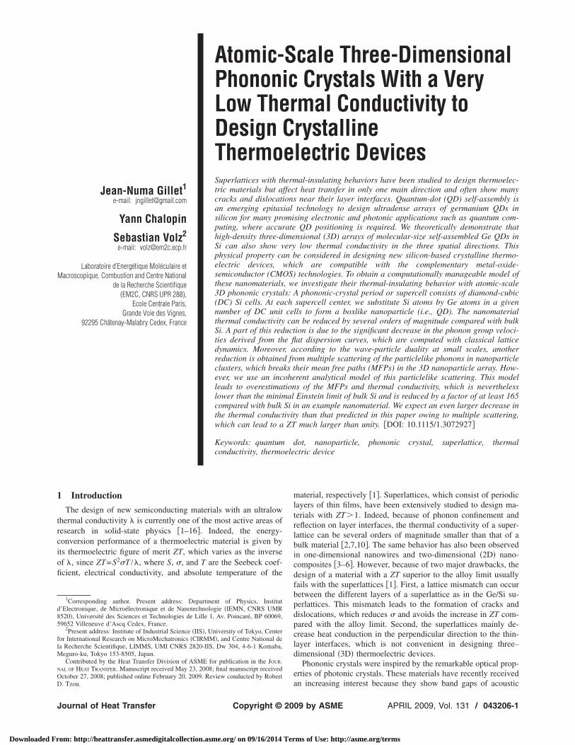
2 Dispersion CurvesAs shown in Fig. 1�a�, we use atomic-scale 3D phononic crys-
tals with a lattice constant of several interatomic distances asmodel nanomaterials to investigate the thermal properties of high-density 3D arrays of molecular-size self-assembled Ge QDs in Si.A period of our atomic-scale 3D phononic crystal consists of N�N�N=N3 diamond-cubic �DC� cells of Si atoms forming acubic supercell. While larger nanostructures can be envisioned, werestrict to N=5 in this paper owing to the computational cost ofclassical lattice dynamics �as well as by didacticism�. Therefore,each supercell is composed of 125 DC unit cells, and our nano-material has a lattice constant d=5�0.5431 nm=2.7155 nm.Since the number of atoms per Si unit cell is 8, the total number ofatoms forming a supercell is 125�8=1000. At each supercellcenter, we substitute a cluster of Si atoms by Ge atoms to obtain a3D periodic heterostructure Ge/Si. In three possible atomic con-figurations, we substitute the Si atoms contained in M �M �M=M3 cells at each supercell center by Ge atoms to form boxlikeGe nanoparticles of different sizes with M =1, 2, or 3. When M=1, the central cell of each supercell contain 28 Ge atoms, whichare surrounded by 972 Si atoms in the 124 other cells. When M=2, each supercell has 2�2�2=8 cells of 126 Ge atoms at itscenter and 117 peripheral cells of 874 Si atoms. As shown in Fig.1�b�, when M =3, each supercell is composed of 344 Ge atoms atits center forming a boxlike nanoparticle of 3�3�3=27 cells,which are surrounded by 98 cells of 656 Si atoms. In Fig. 1�b�, theGe and Si atoms in a supercell are colored black and gray, respec-tively. The periodic spatial repetition of supercells forms anatomic-scale 3D phononic crystal, as shown in Fig. 1�a�.
We use classical lattice dynamics for atomistic computation ofthe dispersion curves of the atomic-scale 3D phononic crystal.This discrete model is usually based on the harmonic approxima-tion of the energy function between two neighbor atoms �39�.However, to obtain a more realistic model, we use the Stillinger–Weber potential to describe the potential energy of the interactionbetween two and three neighbor atoms �40,41�. Moreover, weoptimize the equilibrium positions of the atoms in the lattice as afunction of the respective masses of the Si and Ge atoms. Eachphononic crystal shows 3000 dispersion curves, since we have 3�1000=3000 vibration degrees of freedom in a supercell withN=5. To obtain the 3000 dispersion curves, we use the generalutility lattice program �GULP� �42�. Since the dispersive effect of
each atom in a supercell is considered in this discrete model, weTransactions of the ASME
ms of Use: http://asme.org/terms
ospw2ioptdob
3
bcac�s�
F3dobtnse6t
J
Downloaded Fr
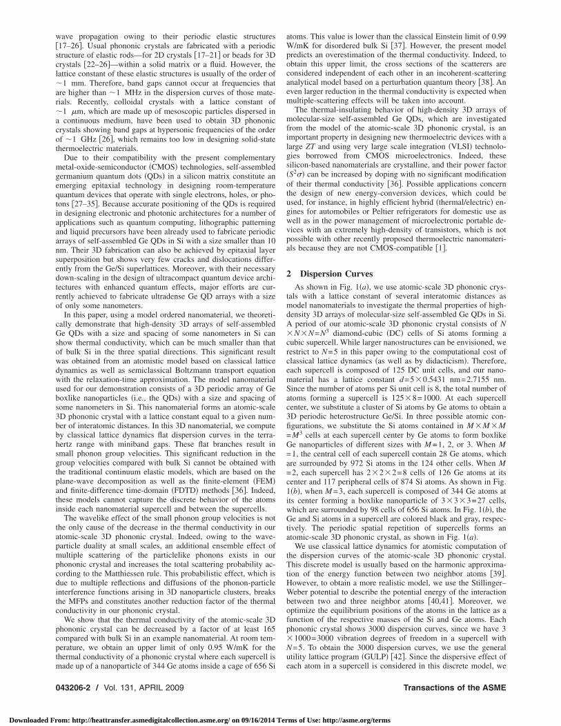
btain dispersion curves in the terrahertz range for the atomic-cale 3D phononic crystal. Figure 2 shows 80 of the 3000 com-uted dispersions curves of an atomic-scale 3D phononic crystalith the parameters N=5 and M =3 �schematized in Fig. 1�. The997 curves of the optical folded modes are very flat, which resultn very low group velocities since they are obtained by derivationf the branches with respect to the wave-vector amplitude in aarticular direction. By using the atomic-scale 3D phononic crys-al, we can therefore reduce heat conduction in the three spatialirections. As discussed in Secs. 3–5, the thermal conductivity ofur nanomaterial therefore is much lower than that of its relatedulk material.
Thermal-Conductivity ModelWith a general equation �Eq. �2��, which does not use the De-
ye approximation, we obtain the thermal conductivity � of a 3Drystalline material from its phonon relaxation times as well as itscoustic and optical dispersion curves, which were computed bylassical lattice dynamics. The mathematical demonstration of Eq.2� is given in the Appendix. We derive this equation from aemiclassical formulation of the heat flux qx in a given direction x
ig. 1 Schematics at two different scales of an atomic-scaleD phononic crystal with N=5 and M=3. In the continuous me-iumlike drawing in „a…, the nanoparticles with an edge lengthf 3a=1.6293 nm and spacing of d=5a=2.7155 nm are showny periodic black cubes with highlighted edges. In „a…, the cen-
ral transparent cube with bold thick edges displays one of theanomaterial supercells. The discrete mediumlike drawing of aupercell is presented in „b…, where the 344 Ge atoms formingach boxlike nanoparticle in „a… are colored in black while the56 peripheral Si atoms are colored in gray in the remainder ofhe supercell.
43,44�. For a 3D crystalline material, this heat flux, which is
ournal of Heat Transfer
om: http://heattransfer.asmedigitalcollection.asme.org/ on 09/16/2014 Ter
carried by the phonons with the energies ��k,m, angular frequen-cies �k,m, and group-velocity vectors vk,m, can be determinedfrom the following summation over all possible phonon modes�k ,m�:
qx =1
V�m=1
Nm
�k
��k,mnk,mvk,m · x̂ �1�
In Eq. �1�, �=h / �2�� is the reduced Planck constant, V is thematerial volume, and m is the index of one branch of the Nmdispersion curves to which the mode �k ,m� belongs with a wavevector k and a nonequilibrium number of phonons nk,m. Then, asshown in the Appendix, we obtain the following equation for �with the relaxation-time approximation of the semiclassical Bolt-zmann transport equation:
� =1
3�m=1
Nm �0
kmax
lk,mvk,m��k,m
�nk,m�0�
�Tgkdk �2�
where Nm=3000 for the atomic-scale 3D phononic crystals withthe parameter N=5, nk,m
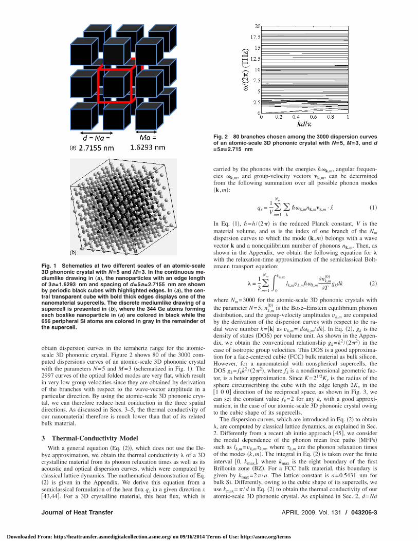
�0� is the Bose–Einstein equilibrium phonondistribution, and the group-velocity amplitudes vk,m are computedby the derivation of the dispersion curves with respect to the ra-dial wave number k= �k� as vk,m= �d�k,m /dk�. In Eq. �2�, gk is thedensity of states �DOS� per volume unit. As shown in the Appen-dix, we obtain the conventional relationship gk=k2 / �2�2� in thecase of isotropic group velocities. This DOS is a good approxima-tion for a face-centered cubic �FCC� bulk material as bulk silicon.However, for a nanomaterial with nonspherical supercells, theDOS gk= fkk
2 / �2�2�, where fk is a nondimensional geometric fac-tor, is a better approximation. Since K=21/2Kx is the radius of thesphere circumscribing the cube with the edge length 2Kx in the�1 0 0� direction of the reciprocal space, as shown in Fig. 3, wecan set the constant value fk=2 for any k, with a good approxi-mation, in the case of our atomic-scale 3D phononic crystal owingto the cubic shape of its supercells.
The dispersion curves, which are introduced in Eq. �2� to obtain�, are computed by classical lattice dynamics, as explained in Sec.2. Differently from a recent ab initio approach �45�, we considerthe modal dependence of the phonon mean free paths �MFPs�such as lk,m=vk,mk,m, where k,m are the phonon relaxation timesof the modes �k ,m�. The integral in Eq. �2� is taken over the finiteinterval �0, kmax�, where kmax is the right boundary of the firstBrillouin zone �BZ�. For a FCC bulk material, this boundary isgiven by kmax=2� /a. The lattice constant is a=0.5431 nm forbulk Si. Differently, owing to the cubic shape of its supercells, weuse kmax=� /d in Eq. �2� to obtain the thermal conductivity of our
Fig. 2 80 branches chosen among the 3000 dispersion curvesof an atomic-scale 3D phononic crystal with N=5, M=3, and d=5a=2.715 nm
atomic-scale 3D phononic crystal. As explained in Sec. 2, d=Na
APRIL 2009, Vol. 131 / 043206-3
ms of Use: http://asme.org/terms
iaccwNt
tqctgnim
lop
l
a
Itim�tsc
F†
s=t
0
Downloaded Fr
s the edge length of a supercell, where N is the number of inter-tomic distances forming this length. As a consequence, in thease of our atomic-scale 3D phononic crystals, the dispersionurves are integrated with Eq. �2� over the finite interval �0, � /d�,hich corresponds to half of the first folded BZ. Because we set=5 in this paper, the size of the folded BZ is one-tenth of that of
he bulk Si since �2� /a� / �� /d�=2N=10.Equation �2� is different from a preceding formulation of the
hermal conductivity where integration is over the angular fre-uency � instead of the wave number k, which is not trivial toompute �44�. In this formulation, prior to integration, an addi-ional nonanalytical model would be required to obtain the DOS� as a function of �, since the Debye approximation �vgk isot valid for our atomic-scale 3D phononic crystal. Indeed, evenn the isotropic case, the following assumption �where vg is the
ode group velocity�:
g�d� =k2
2�2
dk
d�d�
1
2�2
�2
vg3 d� �3�
eads to a wrong DOS g� �per volume unit� in our nanomaterialwing to its large number of optical dispersion curves �2997 com-ared with only 3 acoustic curves when N=5�.
From Eq. �2�, we can define an effective value l� of the MFPs
k,m in order to quantify their effect on the thermal conductivity:
��T� =1
3l�Cv� with Cv� = �
m=1
Nm �0
kmax
vk,m��k,m
�nk,m�0�
�Tgkdk
nd
l� =3�
Cv�=
�m=1
Nm �0
kmax
lk,mvk,m��k,m
�nk,m�0�
�Tgkdk
�m=1
Nm �0
kmax
vk,m��k,m
�nk,m�0�
�Tgkdk
�4�
n Eq. �4�, the average product Cv� depends on the absoluteemperature T but is independent of the phonon MFPs. This factors analog to the Cv product in the classical formula of � for a bulk
aterial, which is based on the kinetic theory and given bybulk= �1 /3�lbulkCv where lbulk is the effective phonon MFP, C is
he specific heat capacity, and v is the speed of sound. For bulkemiconductors, the lattice thermal conductivity in Eq. �2� can be
ig. 3 2D view in the reciprocal plane formed by the directions1 0 0‡ and †0 1 0‡ of a cube with the edge length 2Kx. Themallest sphere circumscribing this cube has a radius K21/2Kx, which explains the use of the constant geometric fac-
or of fk=2 in the DOS gk in Eq. „2….
onsidered as the total thermal conductivity used to compute ZT,
43206-4 / Vol. 131, APRIL 2009
om: http://heattransfer.asmedigitalcollection.asme.org/ on 09/16/2014 Ter
since the electronic thermal conductivity �e is negligible in thecase of a usual doping �36�.
4 Scattering Relaxation TimesTo compute the thermal conductivity of our atomic-scale 3D
phononic crystal with Eq. �2�, we use an analytical model of thetotal phonon relaxation times k,m= lk,m /vk,m of the modes �k ,m�,which are derived from the Matthiessen rule and scattering crosssections in a phonon-particle approach. Only resistive scatteringprocesses are considered since our nanomaterial is semiconduct-ing. Therefore, according to the Matthiessen rule, 1 /k,m is pro-portional to the summation of three scattering probabilities as
1
k,m=
1
k,m�d� +
1
k,m�u� +
1
k,m�p� �5�
For a high-purity nanomaterial, the scattering probability relatedto the relaxation time k,m
�d� in Eq. �5� due to punctual defects andisotopes is a second-order effect, which can be neglected com-pared with the summation of the two other probabilities that isproportional to 1 /k,m
�u� +1 /k,m�p� . To compute the relaxation time
k,m�u� of the Umklapp process �or U-process�, we use a common
formulation given in Refs. �46,47� with the average Grüneisenparameter =1.5 of bulk Si, so that 1 /k,m
�u� bu�T��k,m2 /vk,m
2 ,where the empirical function bu�T� of T is independent of thephonon band structure, and the Debye approximation is not used.A power dependence in �� �where � is an integer� of theU-process probability was verified in a FCC crystal using molecu-lar dynamics in a recent paper �48�.
In Eq. �5�, k,m�p� is the particlelike relaxation time due multiple
scattering of the corpuscular phonons at the atomic scale. Indeed,the duality principle in quantum mechanics stipulates that a par-ticle can exhibit both wave- and particlelike properties at smallscales. Therefore, the wave function of a corpuscular phonon inour atomic-scale 3D phononic crystal must be a solution of theSchrödinger equation. In this perspective, multiple scattering of acorpuscular phonon in our nanomaterial can be approximatelyviewed as a stochastic walk, with multiple deflection, tunneling,and confinement probabilities, in a 3D periodic potential-energylandscape. Solving this multiple-scattering quantum problem toobtain the scattering cross section requires computation of thepseudoparticle wave function for all scattering paths �49�, whichcan be computationally intractable because the number of possiblepaths can be infinite in three dimensions. An approximate methodto obtain the multiple-scattering cross section �k
�p� as a function ofk must be used.
In this paper, we use the perturbation approach developed byKim and Majumdar �38� to obtain an approximate analyticalmodel of �k
�p�. Indeed, the square amplitude �c2�q ,q���2 of thematrix element, which couples the annihilation and creation quan-tum operators of the incoming and scattered particles �with thewave vectors q and q�, respectively� in the perturbed HamiltonianH�, is related to the scattering relaxation time, as shown by Kle-mens and co-workers �50–52�. This approach considers an indi-vidual scatterer and is therefore valid for incoherent �or indepen-dent� scattering where the scatterers can be considered as far fromeach other, so that they do not interact with each other. This ab-sence of interaction is different from multiple scattering arising inour atomic-scale 3D phononic crystal. However, the use of anincoherent-scattering model leads to an underestimate �k,m
�inc�
��k,m�p� of the phonon-particle cross section, which enables us to
compute an upper limit �max of the thermal conductivity in ouratomic-scale 3D phononic crystal with Eq. �2�. Indeed, thephonon-particle relaxation time should obey, for any mode �k ,m�,
�inc� �p�
the following inequality k,m �k,m becauseTransactions of the ASME
ms of Use: http://asme.org/terms
wap
r
s
Tio
wDp�ip
a
Io�
rcttfmifta�aesStdtb
ck=tFa�sdQh
J
Downloaded Fr
1/k,m�inc� = �k,m
�inc�vk,m �6�
here =1 /d3 is the nanoparticle volumic density. In the case of3D nanoparticle array, where nanoparticles deviates from the
eriodicity with, for instance, a mean characteristic nanoparticle
adius R̄ and standard deviation �R, �k,m�inc� has to be weighted by a
tatistical distribution w�R , R̄ ,�R�, so that
�̄k,m�inc� =
�0
Rcutoff
�k,m�inc��R�w�R,R̄,�R�dR
�0
Rcutoff
w�R,R̄,�R�dR
�7�
he spatially averaged cross section �̄k,m�inc� has to be used in Eq. �6�
nstead of �k,m�inc� when the 3D nanoparticle array is not fully peri-
dic.We first consider the incoherent cross section �k
�inc� obtainedith the analytical model in Ref. �38� in the framework of theebye approximation. Therefore, �k
�inc� is independent of thehonon-branch index m and connects the Rayleigh-type far-field�k
�far field�� and near-geometrical ��k�near geom�� cross sections aris-
ng when k→0 and k→�, respectively, with the following inter-olation:
1
�k�inc� =
1
�k�far field� +
1
�k�near geom� with
�k�far field�/G = �4h1��,�A/A,�K/K�
nd
�k�near geom�/G = 2h2��,�A/A,�K/K� �8�
n Eq. �8�, we find back the traditional fourth-power dependencef the Rayleigh cross section �k
�far field���4 when k→0, where=kR is the size parameter for a scatterer with the characteristic
adius R. Moreover, �k�near geom�=2G=2�R2 is the geometrical
ross section, which becomes independent of k when k→� and iswice the projected area G of the scatterer according to the extinc-ion paradox �38,53�. The nondimensional trigonometric-typeunctions h1 and h2 in Eq. �8� depend on � as well as the atomicass A and elastic constant K of the matrix in which the scatterer
s embedded with an atomic mass and elastic constant that differrom those of the matrix by the quantities �A and �K, respec-ively �38�. To compute the incoherent cross section �k
�inc�, wepply Eq. �8� to a Ge nanoparticle of volume Vp= �Ma�3 withA /A= �AGe−ASi� /ASi=1.5849 where AGe=72.61 and ASi=28.09re the atomic masses in atomic mass unit �AMU� of the Gembedded scatterer and Si matrix, respectively. The ratio �K /K ismall compared with �A /A for a Ge nanoparticle embedded in ai matrix since it is computed as �C11 /C110.24, where C11 is
he first diagonal element of the Si elastic tensor and �C11 is theifference between those of Si and Ge. Owing to mass conserva-ion, the equivalent spherical radius R of each Ge nanoparticle, toe used in Eq. �8�, is defined as R= �3 / �4���1/3 Ma=0.6204 Ma.
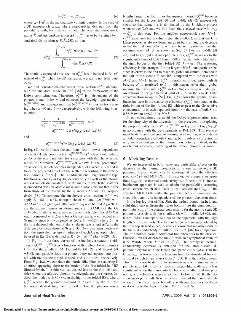
In Fig. 4�a�, the three curves of the incoherent-scattering effi-iency Qk
�inc�=�k�inc� /G as a function of the reduced wave number
d /� for the smallest �M =1�, middle �M =2�, and largest �M3� Ge nanoparticle sizes in a phononic-crystal supercell are plot-
ed with the dashed-dotted, dashed, and solid lines, respectively.rom Fig. 4�a�, we conclude that particlelike phonon scattering isn effect appearing close to the border of the first folded half BZlimited by the first thin vertical dashed line in the plot left-handide� where the allowed phonon wavelengths are the shortest. In-eed, the modes with k�� /d in the high-order folded BZs, where
k�inc� reaches the geometrical limit of 2 �given by the thin top
orizontal dashed line�, are forbidden. For the phonon wave-ournal of Heat Transfer
om: http://heattransfer.asmedigitalcollection.asme.org/ on 09/16/2014 Ter
lengths larger than four times the supercell period, Qk�inc� becomes
smaller for the largest �M =3� and middle �M =2� nanoparticlesizes, so that scattering is dominated by the Umklapp processwhen k�� / �2d� and we find back the classical case with k,m
k,m�u� in this zone. For the smallest nanoparticle size �M =1�,
Qk�inc� never reaches a value higher than 0.0332, so that the Um-
klapp process is always dominant as in bulk Si, and the decreasein the thermal conductivity will not be so impressive than thatobtained when M =3 �as shown in Sec. 5�. For the middle �M=2� and largest �M =3� nanoparticle sizes, Qk
�inc� increases to thesignificant values of 0.3161 and 0.8819, respectively, obtained atthe right border of the first folded BZ �k=� /d�. The scatteringefficiency is the strongest for the largest �M =3� nanoparticle size,since its curve is the first to reach its global maximum �obtained inthe half of the second folded BZ� compared with the cases withM =2 and M =1. Indeed, Qk
�inc� monotonically decreases with Mbecause N is restricted to 5 in this paper. After their globalmaxima, the three curves Qk
�inc� in Fig. 3�a� converge with dampedoscillations to the geometrical limit of 2, as in the van de Hulstapproximation in optics �54�. Fig. 4�b� shows the gradual quasi-linear increase in the scattering efficiency Qk=�/d
�inc� computed at theright border of the first folded BZ with respect to the Ge relativeconcentration x in each supercell from 0 �in the case of bulk Si� to0.8819 �when x=0.344 or M =3�.
In our calculations, we avoid the Debye approximation, usedfor the simplicity of the discussion in the precedent, by replacingthe proportionality factor k4 in �k
�far field� in Eq. �8� by ��k,m /vk,m�4
in accordance with the developments in Ref. �38�. This replace-ment leads to an incoherent-scattering cross section, which showsa modal dependency of both k and m, but involves a correction ofonly some percentage of the thermal conductivity. Indeed, in theincoherent approach, scattering of the optical phonons is minor.
5 Modeling ResultsWe are interested in both wave- and particlelike effects on the
decrease in the thermal conductivity in our atomic-scale 3Dphononic crystal, which can be investigated from the effectiveproduct Cv� and MFP l�. In this paper, we compute an upperlimit �max of the thermal conductivity as a function of T since anincoherent approach is used to obtain the particlelike scatteringcross section, which also leads to an overestimate l�max of theeffective MFP. Differently, the predicted Cv� is more realisticsince this quantity is independent of the phonon relaxation times.
In the log-log plot of Fig. 5�a�, the dashed-dotted, dashed, andsolid thick curves �from the top to bottom� are the computed up-per limits �max of the thermal conductivity for the atomic-scale 3Dphononic crystals with the smallest �M =1�, middle �M =2�, andlargest �M =3� nanoparticle sizes in the supercells with the edgelength 5a, respectively. The top circles �which are interpolated bythe thin top dashed curve� denote experimental measurements ofthe thermal conductivity of bulk Si from Ref. �46� for comparison.The thin bottom dashed horizontal line references to the classicalEinstein limit for disordered bulk Si with an asymptotical value of0.99 W/mK when T�300 K �37�. The strongest thermal-conductivity decrease is obtained for the atomic-scale 3Dphononic crystal with the largest nanoparticle size �M =3�. In thelatter, �max is lower than the Einstein limit for disordered bulk Siat usual to high temperatures from T=260 K to the melting point.This limit is not beaten by the nanomaterials with smaller nano-particle sizes �M =1 and 2�. Indeed, particlelike scattering is lesssignificant when the nanoparticles become smaller, and the pho-non group velocities increase as well. Below T=20 K, the de-creasing slope of bulk Si is faster than those of the nanomaterialswhen T is reduced, since boundary scattering becomes predomi-
nant owing to the large effective MFP of bulk Si.APRIL 2009, Vol. 131 / 043206-5
ms of Use: http://asme.org/terms
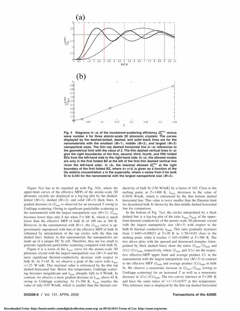
updgUtblHp�dmg
pmb=dicov
0
Downloaded Fr
Figure 5�a� has to be matched up with Fig. 5�b�, where thepper-limit curves of the effective MFPs of the atomic-scale 3Dhononic crystals are displayed in a log-log plot by the dashed-otted �M =1�, dashed �M =2�, and solid �M =3� thick lines. Aradual decrease in l�max is observed for an increased T owing tomklapp scattering. Owing to significant particlelike scattering in
he nanomaterial with the largest nanoparticle size �M =3�, l�max
ecomes lower than only 8 nm when T�300 K, which is muchower than the effective MFP of bulk Si of 100 nm at 300 K.owever, in the nanomaterial with M =1, the l�max curve is ap-roximately superposed with that of the effective MFP of bulk Siobtained by interpolation of the top circles with the thin topashed line�. Indeed, in this nanomaterial, the nanoparticles areade up of a unique DC Si cell. Therefore, they are too small to
enerate significant particlelike scattering compared with bulk Si.Figure 6 is a zoom of the �max curve for the atomic-scale 3D
hononic crystal with the largest nanoparticle size �M =3� and theost significant thermal-conductivity decrease with respect to
ulk Si. At T=65 K, we observe a peak of the curve with �max1.23 W /mK. This maximal value is referenced by the thin topashed horizontal line. Below this temperature, Umklapp scatter-ng becomes insignificant and �max abruptly falls to 0 W/mK. Inontrast, we observe a more gradual decrease in �max above 65 Kwing to Umklapp scattering. At T=300 K, �max reaches the
Fig. 4 Diagrams in „a… of the incohwave number k for three atomic-scdisplayed by the dashed-dotted, dananomaterials with the smallest „Mnanoparticle sizes. The thin top dasthe geometrical limit with the value ogive the right boundaries of the firstBZs from the left-hand side to the rigare only in the first folded BZ at the„from the left-hand side…. In „b…, thboundary of the first folded BZ, wheGe relative concentration x in the suSi to 0.344 for the nanomaterial with
alue of only 0.95 W/mK, which is smaller than the thermal con-
43206-6 / Vol. 131, APRIL 2009
om: http://heattransfer.asmedigitalcollection.asme.org/ on 09/16/2014 Ter
ductivity of bulk Si �156 W/mK� by a factor of 165. Close to themelting point, at T=1400 K, �max decreases to the value of0.5038 W/mK, which is referenced by the thin bottom dashedhorizontal line. This value is twice smaller than the Einstein limitfor disordered bulk Si shown by the thin middle dashed horizontalline for comparison.
In the bottom of Fig. 7�a�, the circles interpolated by a thickdashed line is a log-log plot of the ratio �max /�bulk of the upper-limit thermal conductivity of the atomic-scale 3D phononic crystalwith the largest nanoparticle size �M =3� with respect to thebulk-Si thermal conductivity �bulk. This ratio gradually increasesfrom 1 /4401=0.00023 at T=20 K to 1 /50=0.02 close to themelting point, while it reaches 1 /165=0.0061 at T=300 K. Thetwo above plots with the upward and downward triangles �inter-polated by thick dashed lines� show the ratios l�max / l�bulk andCv� / Cv�bulk, respectively, where l�max and Cv� are the respec-tive effective-MFP upper limit and average product Cv in thenanomaterial with the largest nanoparticle size �M =3� in contrastto the effective MFP l�bulk and average product Cv�bulk in bulkSi. We observe a monotonic increase in l�max / l�bulk �owing toUmklapp scattering� for an increased T as well as a monotonicdecrease in Cv� / Cv�bulk. The two curves intersect at T=300 Kand have the same ratios of 1 /13=0.077 at this temperature.
nt-scattering efficiency Qk„inc… versus
3D phononic crystals: The curvesd, and solid black lines are for the, middle „M=2…, and largest „M=3…horizontal line in „a… references toThe thin dashed vertical lines in „a…cond, third, fourth, and fifth folded
hand side. In „a…, the allowed modesof the first thin dashed vertical lineaximal allowed Qk
„inc… at the right=� /d, is given as a function of the
cells, where x varies from 0 for bulklargest nanoparticle size „M=3….
erealeshe=1…hedf 2., seht-lefte mre kperthe
This reference ratio is displayed by the thin top dashed horizontal
Transactions of the ASME
ms of Use: http://asme.org/terms
lpowc
ect
J
Downloaded Fr
ine. At higher temperatures, we observe that the Cv� decreasesredominantly over that of l�max. At T�300 K, we obtain thepposite case owing to the predominance of particlelike overavelike effects. The ratio Cv� / Cv�bulk converge to a horizontal
urve, which is almost superposed to the thin dashed horizontal
Fig. 5 Diagrams in „a… of the upperversus temperature T for three atocurves displayed by the dashed-dottethe nanomaterials with the smallest=3… nanoparticle sizes, respectively.in „a… is a reference to the Einstein lSi…. The top circles interpolated by thmeasurements of the thermal conduthe upper limits Šl‹max of the effectidashed-dotted, dashed, and solid blM=2, and M=3, respectively. The todashed line give the curve of the eff
Fig. 6 Diagram of the upper limits �temperature T for the atomic-scalenanoparticle size „M=3…. This curveof 1.23 W/mK, which is referenced bThe middle and bottom thin dashedEinstein limit of 0.99 W/mK „for dis
=0.50 W/mK „for the nanomaterial… closournal of Heat Transfer
om: http://heattransfer.asmedigitalcollection.asme.org/ on 09/16/2014 Ter
reference line, when T�300 K. Indeed, the average specific heatcapacities of both nanomaterial and bulk Si converge to the sameconstant classical limit at high temperatures while the group ve-locities are assumed to be independent of T.
From the bottom to the top of Fig. 7�b�, we display the semilog
its �max of the thermal conductivityc-scale 3D phononic crystals: Thedashed, and solid black lines are for=1…, middle „M=2…, and largest „Mthin bottom dashed horizontal line
t of 0.99 W/mK „for disordered bulkin top dashed line are experimental
ity of bulk Si for comparison. In „b…,MFP versus T are displayed by the
lines for nanomaterials with M=1,circles interpolated by the thin topive MFP of bulk Si for comparison.
x of the thermal conductivity versusphononic crystal with the largest
ws a peak at T=65 K with the valuethe thin top horizontal dashed line.rizontal lines are references to theered bulk Si… and upper limit �max
limmid,„M
Theimie thctivveackp
ma3D
shoyho
ord
e to the melting point, respectively.APRIL 2009, Vol. 131 / 043206-7
ms of Use: http://asme.org/terms
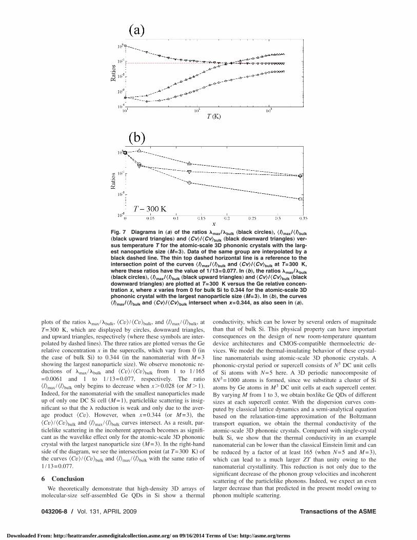
pTaprtsd=Iunatccst1
6
m
0
Downloaded Fr
lots of the ratios �max /�bulk, Cv� / Cv�bulk, and l�max / l�bulk, at=300 K, which are displayed by circles, downward triangles,nd upward triangles, respectively �where these symbols are inter-olated by dashed lines�. The three ratios are plotted versus the Geelative concentration x in the supercells, which vary from 0 �inhe case of bulk Si� to 0.344 �in the nanomaterial with M =3howing the largest nanoparticle size�. We observe monotonic re-uctions of �max /�bulk and Cv� / Cv�bulk from 1 to 1 /1650.0061 and 1 to 1 /13=0.077, respectively. The ratio
l�max / l�bulk only begins to decrease when x�0.028 �or M �1�.ndeed, for the nanomaterial with the smallest nanoparticles madep of only one DC Si cell �M =1�, particlelike scattering is insig-ificant so that the � reduction is weak and only due to the aver-ge product Cv�. However, when x=0.344 �or M =3�, theCv� / Cv�bulk and l�max / l�bulk curves intersect. As a result, par-iclelike scattering in the incoherent approach becomes as signifi-ant as the wavelike effect only for the atomic-scale 3D phononicrystal with the largest nanoparticle size �M =3�. In the right-handide of the diagram, we see the intersection point �at T=300 K� ofhe curves Cv� / Cv�bulk and l�max / l�bulk with the same ratio of/13=0.077.
ConclusionWe theoretically demonstrate that high-density 3D arrays of
Fig. 7 Diagrams in „a… of the ratios„black upward triangles… and ŠCv‹ /ŠCsus temperature T for the atomic-scest nanoparticle size „M=3…. Data ofblack dashed line. The thin top dashintersection point of the curves Šl‹mwhere these ratios have the value of„black circles…, Šl‹max/Šl‹bulk „black updownward triangles… are plotted at Ttration x, where x varies from 0 for bphononic crystal with the largest nanŠl‹max/Šl‹bulk and ŠCv‹ /ŠCv‹bulk interse
olecular-size self-assembled Ge QDs in Si show a thermal
43206-8 / Vol. 131, APRIL 2009
om: http://heattransfer.asmedigitalcollection.asme.org/ on 09/16/2014 Ter
conductivity, which can be lower by several orders of magnitudethan that of bulk Si. This physical property can have importantconsequences on the design of new room-temperature quantumdevice architectures and CMOS-compatible thermoelectric de-vices. We model the thermal-insulating behavior of these crystal-line nanomaterials using atomic-scale 3D phononic crystals. Aphononic-crystal period or supercell consists of N3 DC unit cellsof Si atoms with N=5 here. A 3D periodic nanocomposite of8N3=1000 atoms is formed, since we substitute a cluster of Siatoms by Ge atoms in M3 DC unit cells at each supercell center.By varying M from 1 to 3, we obtain boxlike Ge QDs of differentsizes at each supercell center. With the dispersion curves com-puted by classical lattice dynamics and a semi-analytical equationbased on the relaxation-time approximation of the Boltzmanntransport equation, we obtain the thermal conductivity of theatomic-scale 3D phononic crystals. Compared with single-crystalbulk Si, we show that the thermal conductivity in an examplenanomaterial can be lower than the classical Einstein limit and canbe reduced by a factor of at least 165 �when N=5 and M =3�,which can lead to a much larger ZT than unity owing to thenanomaterial crystallinity. This reduction is not only due to thesignificant decrease of the phonon group velocities and incoherentscattering of the particlelike phonons. Indeed, we expect an evenlarger decrease than that predicted in the present model owing to
ax/�bulk „black circles…, Šl‹max/Šl‹bulk
bulk „black downward triangles… ver-3D phononic crystals with the larg-e same group are interpolated by ahorizontal line is a reference to thel‹bulk and ŠCv‹ /ŠCv‹bulk at T=300 K,3=0.077. In „b…, the ratios �max/�bulkd triangles… and ŠCv‹ /ŠCv‹bulk „black0 K versus the Ge relative concen-Si to 0.344 for the atomic-scale 3D
article size „M=3…. In „b…, the curveswhen x=0.344, as also seen in „a….
�mv‹
aleth
edax/Š1/1war=30ulkopct
phonon multiple scattering.
Transactions of the ASME
ms of Use: http://asme.org/terms
A
Tp�d
A
damp
witkss
wpE
wtclso
bzdtgb�fm
wemo
J
Downloaded Fr
cknowledgmentWe acknowledge the French Research National Agency �ANR�
hermaEscape under the program PNANO for its financial sup-ort as well as the Centre National de la Recherche ScientifiqueCNRS�. We also thank Professor J.D. Gale and his group for theevelopment of GULP under a free license.
ppendixUsing a semiclassical formulation �43,44�, the heat flux qx in a
irection x, which is carried by the phonons with the energy ��k,mnd group-velocity vector vk,m can be determined for a crystallineaterial with a volume V by the following summation over all
ossible phonon modes �k ,m�:
qx =1
V�m=1
Nm
�k
��k,mnk,mvk,m · x̂ �A1�
here �=h / �2�� is the reduced Planck constant, and m is thendex of one branch of the Nm dispersion curves to which belongshe mode �k ,m� with a number of phonons nk,m and wave vector. However, in the relaxation-time approximation �43,44�, theemiclassical Boltzmann transport equation in the steady stateimplifies to
nk,m�0� − nk,m
k,m= vk,m · �nk,m �A2�
here we take into consideration the modal dependence of thehonon relaxation times k,m. In Eq. �A2�, nk,m
�0� is the Bose–instein equilibrium distribution:
nk,m�0� =
1
exp���k,m
kBT − 1
�A3�
here kB is the Boltzmann constant. Moreover, a simplification inhe advection term in Eq. �A2�, given by �nk,m=�T��nk,m
�0� /�T�, isommonly used in the steady state for a material with dimensionsarger than the effective phonon MFP �44,55,56�. Therefore, byubstitution of Eq. �A2� into Eq. �A1� and noting vk,m= �vk,m�, webtain
qx = −dT
dx
1
V�m
�k
k,m�vk,m cos ��2��k,m
�nk,m�0�
�T�A4�
ecause the equilibrium term in nk,m�0� from Eq. �A2� produces a
ero heat flux �since v−k,m=−vk,m�, and the heat flux is in the xirection so that �T= �dT /dx�x̂. In Eq. �A4�, � is the angle be-ween vk,m and the heat flux direction. If we consider isotropicroup velocities, which is a common approximation �44�, vk,m cane considered as independent of the wave-vector orientation� ,�� in spherical coordinates. This simplification is acceptableor materials with several isotropic directions. Using this approxi-ation, Eq. �A4� becomes
qx = −dT
dx
1
V�m
V
�2��3�0
kmax
k2dkk,m�vk,m�2��k,m
�nk,m�0�
�T
��0
2�
d��0
�
sin �d��cos ��2
=−dT
dx
1
3�m�
0
kmax
k,m�vk,m�2��k,m
�nk,m�0�
�T
k2
2�2dk �A5�
here k= �k�, and �2��3 /V is the k-space volume occupied byach mode. In Eq. �A5�, the integration is limited by the maxi-um wave number kmax, which corresponds to the right boundary
f the first BZ. From Eq. �A5�, we can derive the thermal conduc-
ournal of Heat Transfer
om: http://heattransfer.asmedigitalcollection.asme.org/ on 09/16/2014 Ter
tivity � from the Fourier law: qx=−��dT /dx�. We consider themode dependence of the phonon MFP lk,m, which is given by thefollowing relationship: k,m= lkm /vk,m. Therefore, from Eq. �A5�,we obtain the following relationship for �:
� =1
3�m�
0
kmax
lk,mvk,m��k,m
�nk,m�0�
�Tgkdk �A6�
where the group velocities vk,m are computed from the dispersioncurves as vk,m= �d�k,m /dk�, and the DOS per volume unit is gk=k2 / �2�2� for a bulk material in the isotropic approximation.Equation �A6� is the same as Eq. �2�.
References�1� Kim, W., Zide, J., Gossard, A., Klenov, D., Stemmer, S., Shakouri, A., and
Majumdar, A., 2006, “Thermal Conductivity Reduction and ThermoelectricFigure of Merit Increase by Embedding Nanoparticles in Crystalline Semicon-ductors,” Phys. Rev. Lett., 96, p. 045901.
�2� Chen, G., 1999, “Phonon Wave Heat Conduction in Thin Films Superlattices,”ASME J. Heat Transfer, 121�4�, pp. 945–953.
�3� Hochbaum, A. I., Chen, R., Delgado, R. D., Liang, W., Garnett, E. C., Najar-ian, M., Majumdar, A., and Yang, P., 2008, “Enhanced Thermoelectric Perfor-mance of Rough Silicon Nanowires,” Nature �London�, 451, pp. 163–167.
�4� Boukai, A. I., Bunimovich, Y., Tahir-Kheli, J., Yu, J.-K., Goddard, W. A., III,and Heath, J. R., 2008, “Silicon Nanowires as Efficient Thermoelectric Mate-rials,” Nature �London�, 451, pp. 168–171.
�5� Volz, S., and Chen, G., 1999, “Molecular Dynamics Simulation of ThermalConductivity of Silicon Nanowires,” Appl. Phys. Lett., 75�14�, pp. 2056–2058.
�6� Yang, R., and Chen, G., 2004, “Thermal Conductivity Modeling of PeriodicTwo-Dimensional Nanocomposites,” Phys. Rev. B, 69, p. 195316.
�7� Chiritescu, C., Cahill, D. G., Nguyen, N., Johnson, D., Bodapati, A., Keblin-ski, P., and Zschack, P., 2007, “Ultralow Thermal Conductivity in Disordered,Layered WSe2 Crystals,” Science, 315, pp. 351–353.
�8� Hsu, K. F., Loo, S., Guo, F., Chen, W., Dyck, J. S., Uher, C., Hogan, T.,Polychroniadis, E. K., and Kanatzidis, M. G., 2004, “Cubic AgPbmSbTe2+m:Bulk Thermoelectric Materials With High Figure of Merit,” Science, 303, pp.818–821.
�9� Harman, T. C., Taylor, P. J., Walsh, M. P., and LaForge, B. E., 2002, “QuantumDot Superlattice Thermoelectric Materials and Devices,” Science, 297, pp.2229–2232.
�10� Venkatasubramanian, R., Siivola, E., Colpitts, T., and O’Quinn, B., 2001,“Thin-Film Thermoelectric Devices With High Room-Temperature Figures ofMerit,” Nature �London�, 413, pp. 597–602.
�11� Volz, S., Lemonnier, D., and Saulnier, J. B., 2001, “Clamped Nanowire Ther-mal Conductivity Based on Phonon Transport Equation,” Microscale Thermo-phys. Eng., 5, pp. 191–207.
�12� Jeng, M.-S., Yang, R., Song, D., and Chen, G., 2008, “Modeling the ThermalConductivity and Phonon Transport in Nanoparticle Composites Using MonteCarlo Simulation,” ASME J. Heat Transfer, 130, p. 042410.
�13� Chen, G., and Shakouri, A., 2002, “Heat Transfer in Nanostructures for Solid-State Energy Conversion,” ASME J. Heat Transfer, 124�2�, pp. 242–342.
�14� Yu, C., Saha, S., Zhou, J., and Shi, L., 2006, “Thermal Contact Resistance andThermal Conductivity of a Carbon Nanofiber,” ASME J. Heat Transfer,128�3�, pp. 234–239.
�15� Liu, W., and Asheghi, M., 2006, “Thermal Conductivity Measurements ofUltra-Thin Single Crystal Silicon Layers,” ASME J. Heat Transfer, 128�1�,pp. 75–83.
�16� Bulusu, A., and Walker, D. G., 2007, “Modeling of Thermoelectric Propertiesof Semi-Conductor Thin Films With Quantum and Scattering Effects,” ASMEJ. Heat Transfer, 129�4�, pp. 492–499.
�17� Bonello, B., Charles, C., and Ganot, F., 2007, “Lamb Waves in Plates Coveredby a Two-Dimensional Phononic Film,” Appl. Phys. Lett., 90, p. 021909.
�18� Sun, J.-H., and Wu, T.-T., 2006, “Propagation of Surface Acoustic WavesThrough Sharply Bent Two-dimensional Phononic Crystal Waveguides Usinga Finite-Difference Time-Domain Method,” Phys. Rev. B, 74, p. 174305.
�19� Wu, T.-T., Hsu, C.-H., and Sun, J.-H., 2006, “Design of a Highly MagnifiedDirectional Acoustic Source Based on the Resonant Cavity of Two-Dimensional Phononic Crystals,” Appl. Phys. Lett., 89, p. 171912.
�20� Wu, T.-T., Huang, Z.-G., and Lin, S., 2004, “Surface and Bulk Acoustic Wavesin Two-Dimensional Phononic Crystal Consisting of Materials With GeneralAnisotropy,” Phys. Rev. B, 69, p. 094301.
�21� Khelif, A., Choujaa, A., Benchabane, S., Djafari-Rouhani, B., and Laude, V.,2004, “Guiding and Bending of Acoustic Waves in Highly Confined PhononicCrystal Waveguides,” Appl. Phys. Lett., 84�22�, pp. 4400–4402.
�22� Chen, H., Luo, X., and Ma, H., 2007, “Scattering of Elastic Waves by ElasticSpheres in a NaCl-Type Phononic Crystal,” Phys. Rev. B, 75, p. 024306.
�23� Yang, S., Page, J. H., Liu, Z., Cowan, M. L., Chan, C. T., and Sheng, P., 2004,“Focusing of Sound in a 3D Phononic Crystal,” Phys. Rev. Lett., 93, p.024301.
�24� Yang, S., Page, J. H., Liu, Z., Cowan, M. L., Chan, C. T., and Sheng, P., 2002,
“Ultrasound Tunneling Through 3D Phononic Crystals,” Phys. Rev. Lett., 88,APRIL 2009, Vol. 131 / 043206-9
ms of Use: http://asme.org/terms
0
Downloaded Fr
p. 104301.�25� Liu, Z., Chan, C. T., Sheng, P., Goertzen, A. L., and Page, J. H., 2000, “Elastic
Wave Scattering by Periodic Structures of Spherical Objects: Theory and Ex-periment,” Phys. Rev. B, 62�4�, pp. 2446–2457.
�26� Tommaseo, G., Petekidis, G., Steffen, W., Fytas, G., Schofield, A. B., andStefanou, N., 2007, “Hypersonic Acoustic Excitations in Binary ColloidalCrystals: Big Versus Small Hard Sphere Control,” J. Chem. Phys., 126, p.014707.
�27� Yakimov, A. I., Dvurechenskii, A. V., and Nikiforov, A. I., 2006, “GermaniumSelf-Assembled Quantum Dots in Silicon for Nano- and Optoelectronics,” J.Nanoelectron. Optoelectron., 1�2�, pp. 119–175.
�28� Guise, O., Yates, J. T., Jr., Levy, J., Ahner, J., Vaithyanathan, V., and Schlom,D. G., 2005, “Patterning of Sub-10-nm Ge Islands on Si�100� by DirectedSelf-Assembly,” Appl. Phys. Lett., 87, p. 171902.
�29� Berbezier, I., Karmous, A., Ronda, A., Sgarlata, A., Balzarotti, A., Castrucci,P., Scarselli, M., and De Crescenzi, M., 2006, “Growth of Ultrahigh-DensityQuantum-Confined Germanium Dots on SiO2 Thin Films,” Appl. Phys. Lett.,89, p. 063122.
�30� Gray, J. L., Hull, R., and Floro, J. A., 2006, “Periodic Arrays of EpitaxialSelf-Assembled SiGe Quantum Dot Molecules Grown on Patterned Si Sub-strates,” J. Appl. Phys., 100, p. 084312.
�31� Kiravittaya, S., Heidemeyer, H., and Schmidt, O. G., 2005, “Lateral Quantum-Dot Replication in Three-Dimensional Quantum-Dot Crystals,” Appl. Phys.Lett., 86, p. 263113.
�32� Kar, G. S., Kiravittaya, S., Stoffel, M., and Schmidt, O. G., 2004, “MaterialDistribution Across the Interface of Random and Ordered Island Arrays,”Phys. Rev. Lett., 93, p. 246103.
�33� Karmous, A., Cuenat, A., Ronda, A., Berbezier, I., Atha, S., and Hull, R.,2004, “Ge Dot Organization on Si Substrates Patterned by Focused IonBeam,” Appl. Phys. Lett., 85, pp. 6401–6403.
�34� Zhong, Z., Halilovic, A., Fromherz, T., Schäffler, F., and Bauer, G., 2003,“Two-Dimensional Periodic Positioning of Self-Assembled Ge Islands on Pre-patterned Si �001� Substrates,” Appl. Phys. Lett., 82�26�, pp. 4779–4781.
�35� Lee, H., Johnson, J. A., He, M. Y., Speck, J. S., and Petroff, P. M., 2001,“Strain-Engineered Self-Assembled Semiconductor Quantum Dot Lattices,”Appl. Phys. Lett., 78�1�, pp. 105–107.
�36� Khitun, A., Balandin, A., Liu, J. L., and Wang, K. L., 2000, “In-Plane LatticeThermal Conductivity of a Quantum-Dot Superlattice,” J. Appl. Phys., 88�2�,pp. 696–699.
�37� Cahill, D. G., Watson, S. K., and Pohl, R. O., 1992, “Lower Limit to theThermal Conductivity of Disordered Crystals,” Phys. Rev. B, 46�10�, pp.6131–6140.
�38� Kim, W., and Majumdar, A., 2006, “Phonon Scattering Cross Section of Poly-
dispersed Spherical Nanoparticles,” J. Appl. Phys., 99, p. 084306.43206-10 / Vol. 131, APRIL 2009
om: http://heattransfer.asmedigitalcollection.asme.org/ on 09/16/2014 Ter
�39� Dove, M. T., 1993, Introduction to Lattice Dynamics �Cambridge Topics inMineral Physics and Chemistry Vol. 4�, Cambridge University Press, Cam-bridge, UK.
�40� Jian, Z., Kaiming, Z., and Xide, X., 1990, “Modification of Stillinger–WeberPotentials for Si and Ge,” Phys. Rev. B, 41�18�, pp. 12915–12918.
�41� Chalopin, Y., Gillet, J.-N., and Volz, S., 2008, “Predominance of ThermalContact Resistance in a Silicon Nanowire on a Planar Substrate,” Phys. Rev. B,77�23�, p. 233309.
�42� http://www.ivec.org/GULP/.�43� Ziman, J. M., 1960, “Electrons and Phonons: The Theory of Transport Phe-
nomena in Solids,” Oxford Classic Texts in the Physical Sciences, OxfordUniversity Press, Oxford, UK.
�44� Majumdar, A., 1993, “Microscale Heat Conduction in Dielectric Thin Films,”ASME J. Heat Transfer, 115�1�, pp. 7–16.
�45� Vo, T. T. M., Williamson, A. J., Lordi, V., and Galli, G., 2008, “AtomisticDesign of Thermoelectric Properties of Silicon Nanowires,” Nano Lett., 8�4�,pp. 1111–1114.
�46� Glassbrenner, C. J., and Slack, G. A., 1964, “Thermal Conductivity of Siliconand Germanium From 3 K to the Melting Point,” Phys. Rev., 134�4A�, pp.A1058–A1069.
�47� Slack, G. A., and Galginaitis, S., 1964, “Thermal Conductivity and PhononScattering by Magnetic Impurities in CdTe,” Phys. Rev., 133�1A�, pp. A253–A268.
�48� McGaughey, A. J. H., and Kaviany, M., 2004, “Quantitative Validation of theBoltzmann Transport Equation Phonon Thermal Conductivity Model Underthe Single-Mode Relaxation Time Approximation,” Phys. Rev. B, 69, p.094303.
�49� Feynman, R. P., and Hibbs, A. R., 1965, Quantum Mechanics and Path Inte-grals, McGraw-Hill, New York.
�50� Klemens, P. G., 1955, “The Scattering of Low-Frequency Lattice Waves byStatic Imperfections,” Proc. Phys. Soc., London, Sect. A, 68, pp. 1113–1128.
�51� Klemens, P. G., 1958, Solid State Physics, Vol. 7, F. Seitz and D. Turn, eds.,Academic, New York.
�52� Turk, L. A., and Klemens, P. G., 1974, “Phonon Scattering by Impurity PlateletPrecipitates in Diamond,” Phys. Rev. B, 9�10�, pp. 4422–4428.
�53� Bohren, C. F., and Huffman, D. R., 1998, Absorption and Scattering of Lightby Small Particles, Wiley, New York.
�54� van de Hulst, H. C., 1981, Light Scattering by Small Particles, Dover, NewYork.
�55� Berman, R., Foster, E. L., and Ziman, J. M., 1956, “The Thermal Conductivityof Dielectric Crystals: The Effect of Isotopes,” Proc. R. Soc. London, Ser. A.,237, pp. 344–354.
�56� Kittel, C., 2005, Introduction to Solid State Physics, 8th ed., Wiley, New York.
Transactions of the ASME
ms of Use: http://asme.org/terms