
Appendix A Solutions to Chapter Exercises - Springer
44
A Appendix A Solutions to Chapter Exercises
-
Upload
khangminh22 -
Category
Documents
-
view
6 -
download
0
Transcript of Appendix A Solutions to Chapter Exercises - Springer

A Appendix A
Solutions to Chapter Exercises

A
A Solutions to Chapter Exercises ................................267 Chapter 2: Netlist and System Partitioning.......................................... 267 Chapter 3: Chip Planning..................................................................... 270 Chapter 4: Global and Detailed Placement ......................................... 273 Chapter 5: Global Routing.................................................................... 276 Chapter 6: Detailed Routing................................................................. 280 Chapter 7: Specialized Routing ........................................................... 284 Chapter 8: Timing Closure ................................................................... 292

267
A Solutions to Chapter Exercises
Chapter 2: Netlist and System Partitioning
Exercise 1: KL Algorithm Maximum gains and the swaps of nodes with positive gain per iteration i are given. i = 1: g1 = D(a) + D(f ) – 2c(a,f ) = 2 + 1 – 0 = 3 swap nodes a and f, G1 = 3. i = 2: g2 = D(c) + D(e) – 2c(c,e) = -2 + 0 – 0 = -2 swap nodes c and e, G2 = 1. i = 3: g3 = D(b) + D(d) – 2c(b,d) = -1 + 0 – 0 = -1 swap nodes b and d, G3 = 0. Maximum gain is Gm = 3 with m = 1. Therefore, swap nodes a and f. Graph after Pass 1 (right).
a
b
c
e
d
f
A
B
Exercise 2: Critical Nets and Gain During the FM Algorithm (a) Table recording (1) the cell moved, (2) critical nets before the move, (3) critical
nets after the move, and (4) which cells require a gain update.
Cell moved
Critical nets before the move
Critical nets after the move
Which cells require a gain update
a -- N1 b b -- N1 a c -- N1 d d N3 N1,N3 c,h,i e N2 N2 f,g f N2 N2 e,g g N2 N2 e,f h N3 N3 d,i i N3 N3 d,h
(b) Gains for each cell. g1(a) = 0 g1(b) = 0 g1(c) = 0 g1(d) = 0 g1(e) = -1 g1(f ) = -1 g1(g) = -1 g1(h) = 1 g1(i) = 0
A. B. Kahng et al., VLSI Physical Design: From Graph Partitioning to Timing Closure,DOI 10.1007/978-90-481-9591-6, © Springer Science+Business Media B.V. 2011

268 A Solutions to Chapter Exercises
Exercise 3: FM Algorithm Pass 2, iteration i = 1 Gain values: g1(a) = -1, g1(b) = -1, g1(c) = 0, g1(d) = 0, g1(e) = -1. Cells c and d have maximum gain value g1 = 0. Balance criterion after moving cell c: area(A) = 4. Balance criterion after moving cell d: area(A) = 1. Cell c meets the balance criterion better. Move cell c, updated partitions: A1 = {d}, B1 = {a,b,c,e}, with fixed cells {c}. Pass 2, iteration i = 2 Gain values: g2(a) = -2, g2(b) = -2, g2(d) = 2, g2(e) = -1. Cell d has maximum gain g2 = 2, area(A) = 0, balance criterion is violated. Cell e has next maximum gain g2 = -1, area(A) = 9, balance criterion is met. Move cell e, updated partitions: A2 = {d,e}, B2 = {a,b,c}, with fixed cells {c,e}. Pass 2, iteration i = 3 Gain values: g3(a) = 0, g3(b) = -2, g3(d) = 2. Cell d has maximum gain g3 = 2, area(A) = 5, balance criterion is met. Move cell d, updated partitions: A3 = {e}, B3 = {a,b,c,d}, with fixed cells {c,d,e}. Pass 2, iteration i = 4 Gain values: g4(a) = -2, g4(b) = -2. Cells a and b have maximum gain g4 = -2. Balance criterion after moving cell a: area(A) = 7. Balance criterion after moving cell b: area(A) = 9. Cell a meets the balance criterion better. Move cell a, updated partitions: A4 = {a,e}, B4 = {b,c,d}, with fixed cells {a,c,d,e}. Pass 2, iteration i = 5 Gain values: g5(b) = 1. Balance criterion after moving b: area(A) = 11. Move cell b, updated partitions: A5 = {a,b,e}, B5 = {c,d}, with fixed cells {a,b,c,d,e}. Find best move sequence <c1 … cm> G1 = g1 = 0 G2 = g1 + g2 = -1 G3 = g1 + g2 + g3 = 1 G4 = g1 + g2 + g3 + g4 = -1 G5 = g1 + g2 + g3 + g4 + g5 = 0

Chapter 2: Netlist and System Partitioning 269
Maximum positive gain = 1 occurs when m = 3. Cells c, e and d are moved. The result after Pass 2 is illustrated on the right. N1
N2
N3
N4
N5B
Aa
b c
d
e
Exercise 4: System and Netlist Partitioning One key difference is that traditional min-cut partitioning only accounts for mini-mizing net costs across k partitions. FPGA-based partitioning involves first deter-mining the number of devices and then minimizing the total communication be-tween devices as well as the device logic. For instance, traditional min-cut partitioning does not distinguish how many devices a p-pin net is split across. Fur-thermore, min-cut partitioning does not account for FPGA reconfigurability.
Exercise 5: Multilevel FM Partitioning One major advantage is scalability. Traditional FM partitioning scales to ~200 nodes whereas multilevel FM can efficiently handle large-scale modern designs. The coarsening stage clusters nodes together, thereby reducing the number of nodes that FM interacts with. FM produces near-optimal solutions for netlists with fewer than 200 nodes, but solution quality deteriorates for larger netlists. In contrast, multilevel FM produces great solution quality without sacrificing large amounts of runtime.
Exercise 6: Clustering Nodes that have either single connections to multiple other nodes or multiple con-nections to a single node are candidates for clustering. If a net net is contained within a single partition, then net does not contribute to the cut cost of the partition. If net spans multiple partitions, then one option is to place net’s cluster in the parti-tion where net’s net weight is the greatest. Another option is to limit the size of the clusters such that the individual nodes of net are clustered within each partition.
Gm

270 A Solutions to Chapter Exercises
Chapter 3: Chip Planning
Exercise 1: Slicing Trees and Constraint Graphs
Slicing Tree H
h
i
c d e
f
g
a
b
V
HH
V
V V V
Vertical Constraint Graph (VCG) Horizontal Constraint Graph (HCG) t
a
b
e
c
d
s
hg
f
i
t
b
f e
c
ds
a
ihg
Exercise 2: Floorplan-Sizing Algorithm (a) Shape functions for blocks a (left), b (center) and c (right).
1
3
w
h
3 a
1
1
3
w
h
3
3
b
14b
4
1
b
3 4
4
1
1w
h
4
4
11
4c
4
1
c

Chapter 3: Chip Planning 271
(b) Shape function of the floorplan. Horizontal composition: Determine h(a,b)(w) of blocks a and b.
1
3
w
h
3 4
ha(w) hb(w) wbwa w(a,b)
1 + 3 = 4 3
w
h
4
h(a,b)(w)
2
1 + 1 = 2
2
4
1
4
Vertical composition: Determine h((a,b),c)(w) and the minimum-area corner points. The minimum area of ((a,b),c) is 16, with dimensions either being h((a,b),c) = 8 and w((a,b),c) = 2, or h((a,b),c) = 8 and w((a,b),c) = 4.
4
4
1
1w
h
3
2
hc(w)h(a,b)(w)hc h(a,b)
1 + 3 = 4
4 + 4 = 8
h((a,b),c)
4
4
w
h
2
h((a,b),c)
8 82
8
4 4
Construct floorplans by backtracing the shape functions of hc(w), h(a,b)(w), ha(w) and hb(w) to determine the dimensions of each block. The following shows the backtrace for the corner point (2,8) from h((a,b),c)(w).
4
4
w
h
2
8
h(a,b) = 4
c
a,b 3
w
h
2
4hc = 4
wa = 1wb = 1
c
b a
1 4
1 4
1 3
1 The following shows the backtrace for the corner point (4,4) from h((a,b),c)(w).
c
4
4
w
h
2
8
h(a,b) = 3a,b
3
w
h
4
hc = 1wa = 1wb = 33
1
31
cb a
4 1
3 3
1 3

272 A Solutions to Chapter Exercises
Exercise 3: Linear Ordering Algorithm Iteration
# Block New
Nets Terminating
Nets gain Continuing
Nets 0 a N1,N2,N3,N4 -- -4 -- 1 b
cd e
N5,N6N5
N5,N6--
N2-- N4N1
-1 -1 -1 +1
-- N3N3--
2 b c d
N5,N6N5
N5,N6
N2--N4
-1 -1 -1
-- N3N3
3 b c
-- --
N2,N6 N3
+2+1
N5N5
4 c -- N3, N5 +2 -- For each iteration, bold font denotes the block with the maximum gain. Iteration 0: set block a as the first block in the ordering. Iteration 1: block e has maximum gain. Set as the second block in the ordering. Iteration 2: blocks b, c and d all have maximum gain of -1. Blocks b and d each have one terminating net. Block d has a higher number of continuing nets. Set block d as the third block in the ordering. Iteration 3: block b has maximum gain. Set as the fourth block in the ordering. Iteration 4: set block c as the fifth (last) block in the ordering. The linear ordering that heuristically minimizes total net cost is <a e d b c>.
a e d b c
N2
N3
N1
N4
N5
N6
Exercise 4: Non-Slicing Floorplans There are many possible non-slicing floorplans using four blocks a-d. The following is one such solution.
b
dc
a

Chapter 4: Global and Detailed Placement 273
Chapter 4: Global and Detailed Placement
Exercise 1: Estimating Total Wirelength (a) Tree representations of the five-pin net. Minimum-Length Chain Minimum Spanning Tree Steiner Minimum Tree
e
d
b a
c
e
d
b a
c
e
d
b a
c (b)
neteM edewnetL )()()(
LChain(net) = w(d,e) · dM(d,e) + w(d,c) · dM(d,c) + w(c,b) · dM(c,b) + w(b,a) · dM(b,a) = 2·3 + 2·4 + 2·2 + 2·2 = 22 LMST(net) = w(d,e) · dM(d,e) + w(e,b) · dM(e,b) + w(c,b) · dM(c,b) + w(b,a) · dM(b,a) = 2 3 + 2 3 + 2 2 + 2 2 = 20 LSMT(net) = w(d,e,b) · dM(d,e,b) + w(c,b) · dM(c,b) + w(b,a) · dM(b,a) = 2 5 + 2 2 + 2 2 = 18
Exercise 2: Min-Cut Placement After the initial partitioning (vertical cut cut1): Cells left of cut1: L = {c,d,f,g}, cells right of cut1: R = {a,b,e}. Cut cost: L-R = 1. Possible solutions after the second partitioning (two horizontal cuts cut2L and cut2R): Top Left: TL = {c,g}, Bottom Left: BL = {d,f }. Cut cost: TL-BL = 2. Top Right: TR= {a}, Bottom Right: BR = {b,e}. Cut cost: TR-BR = 1. After the third partitioning (four vertical cuts cut3TL, cut3BL, cut3TR and cut3BR), one possible result is
bcut2L
cut1cut3BL cut3BR
a
d
c gcut2R
cut3TL cut3TR
ef
The maximum number of nets that cross an edge P(e) = 2, and the edge capacity (e) = 2. Therefore, since (P) = 1, the design is estimated to be fully routable.

274 A Solutions to Chapter Exercises
Exercise 3: Force-Directed Placement Solve for xa
0 and xb0:
000
021
0),(
0),(
0
0
5.08
442240202
),()2,()1,(),()2,()1,(
),(
),(
bbb
bInIn
jac
jacj
a
xxx
bacInacInacxbacxInacxInac
jac
xjac
x
00
20
0),(
0),(
0
0
5.05.0224
22024
),()2,(),(),()2,(),(
),(
),(
aa
OutIna
jbc
jbcj
b
xx
OutbcInbcabcxOutbcxInbcxabc
jbc
xjbc
x
3/2)5.0(5.05.05.05.0
5.0 0000
00
bbab
ba xxxx
xx
3/1)3/2(5.05.0 00ba xx
Rounded, xa0 0 and xb
0 1. Solve for ya
0 and yb0:
00
021
0),(
0),(
0
0
5.05.042240222
),()2,()1,(),()2,()1,(
),(
),(
bb
bInIn
jac
jacj
a
yy
bacInacInacybacyInacyInac
jac
yjac
y
00
20
0),(
0),(
0
0
5.025.0224
12024
),()2,(),(),()2,(),(
),(
),(
aa
OutIna
jbc
jbcj
b
yy
OutbcInbcabcyOutbcyInbcyabc
jbc
yjbc
y
3/2)5.05.0(5.025.05.025.0
5.05.0 0000
00
bbab
ba yyyy
yy
6/5)3/2(5.05.05.05.0 00ba yy
Rounded, ya0 1 and yb
0 1.

Chapter 4: Global and Detailed Placement 275
The ZFT-positions for gates a and b are (0,1) and (1,1), respectively.
0
1 2
1
2 In1
In2
Outa b
0
Exercise 4: Global and Detailed Placement Global placement assigns cells or moveable blocks to bins of a coarse grid. In con-trast, detailed placement moves cells within each grid bin such that cells do not mutually overlap (legalization). Typically, placement is split into two steps to ensure scalability. Legalization requires a large amount of runtime and cannot be applied after every iteration of global placement. A much faster method is to assign blocks to grid bins first and, when all blocks have been assigned, legalize afterward. Fur-thermore, detailed placement can be easily performed in parallel, as each grid bin can be processed independently. Typically, the placement process is split into two parts to ensure scalability.
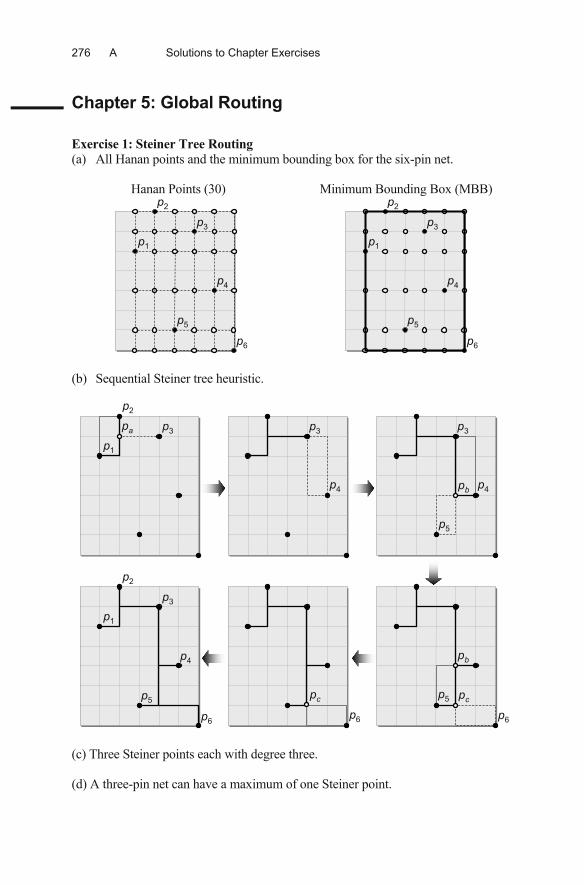
276 A Solutions to Chapter Exercises
Chapter 5: Global Routing
Exercise 1: Steiner Tree Routing (a) All Hanan points and the minimum bounding box for the six-pin net.
Hanan Points (30) Minimum Bounding Box (MBB)
p1
p2
p3
p4
p5
p6
p1
p2
p3
p4
p5
p6 (b) Sequential Steiner tree heuristic.
p1
p2
p3
p4
p5
pa p3
p4
p3
pb
p5
p6
pb
pc
p6
pc
p1
p2
p3
p5
p6
p4
(c) Three Steiner points each with degree three.
(d) A three-pin net can have a maximum of one Steiner point.

Chapter 5: Global Routing 277
Exercise 2: Global Routing in a Connectivity Graph After routing net A.
3,21
3,62
0,13
0,24
0,55
2,26
2,27
A B
B A
After routing net B.
2,11
2,52
0,03
0,14
0,45
1,16
1,17
A B
B A
The given placement is routable.
Exercise 3: Dijkstra’s Algorithm
[a]
<a> [b] (2,2)
<a> [d] (3,2)
<d> [e] (4,3)
<e> [f] (5,6)
<d> [g] (8,5)
<h> [i] (8,6)
<e> [h] (6,4)
<f> [c] (6,7)
Group 2 Group 3
<a> [b] (2,2)<a> [d] (3,2)
<b> [c] (8,7)<b> [e] (7,5)
<d> [e] (4,3)<d> [g] (8,5)
<h> [i] (8,6)
<e> [f] (5,6)<e> [h] (6,4)
<f> [i] (9,8)
d g
b e h
c f i
s
t
(3,2)
(8,6)
(4,3)
(6,4)
<h> [g] (9,5)
<f> [c] (6,7)
a

278 A Solutions to Chapter Exercises
Exercise 4: ILP-Based Global Routing For net A, the possible routes are two L-shapes (A1,A2).
A
A
A2
A1
Net Constraints xA1 + xA2 1
Variable Constraints 0 xA1 1 0 xA2 1
For net B, the possible routes are two L-shapes (B1,B2).
B1
B2B
B
Net Constraints xB1 + xB2 1
Variable Constraints 0 xB1 1 0 xB2 1
For net C, the possible routes are two L-shapes (C1,C2).
C1
C2
C
C
Net Constraints xC1 + xC2 1
Variable Constraints 0 xC1 1 0 xC2 1
Horizontal Edge Capacity Constraints: G(0,0) ~ G(1,0) : xC1 (G(0,0) ~ G(1,0)) = 1 G(1,0) ~ G(2,0) : xC1 (G(1,0) ~ G(2,0)) = 1 G(2,0) ~ G(3,0) : xB1 (G(2,0) ~ G(3,0)) = 1 G(3,0) ~ G(4,0) : xB1 (G(3,0) ~ G(4,0)) = 1 G(0,1) ~ G(1,1) : xA2 (G(0,1) ~ G(1,1)) = 1 G(1,1) ~ G(2,1) : xA2 (G(1,1) ~ G(2,1)) = 1 G(2,1) ~ G(3,1) : xB2 (G(2,1) ~ G(3,1)) = 1 G(3,1) ~ G(4,1) : xB2 (G(3,1) ~ G(4,1)) = 1 G(0,2) ~ G(1,2) : xC2 (G(0,2) ~ G(1,2)) = 1 G(1,2) ~ G(2,2) : xC2 (G(1,2) ~ G(2,2)) = 1 G(0,3) ~ G(1,3) : xA1 (G(0,3) ~ G(1,3)) = 1 G(1,3) ~ G(2,3) : xA1 (G(1,3) ~ G(2,3)) = 1 Vertical Edge Capacity Constraints: G(0,0) ~ G(0,1) : xC2 (G(0,0) ~ G(0,1)) = 1 G(2,0) ~ G(2,1) : xB2 + xC1 (G(2,0) ~ G(2,1)) = 1 G(4,0) ~ G(4,1) : xB1 (G(4,0) ~ G(4,1)) = 1 G(0,1) ~ G(0,2) : xA2 + xC2 (G(0,1) ~ G(0,2)) = 1 G(2,1) ~ G(2,2) : xA1 + xC1 (G(2,1) ~ G(2,2)) = 1 G(0,2) ~ G(0,3) : xA2 (G(0,2) ~ G(0,3)) = 1 G(2,2) ~ G(2,3) : xA1 (G(2,2) ~ G(2,3)) = 1

Chapter 5: Global Routing 279
Objective Function: Maximize xA1 + xA2 + xB1 + xB2 + xC1 + xC2 The solution is routable with routes A2, B1, and C1 (right). A
BA
BC1
C
C
A2
B1
Exercise 5: Shortest Path with A* Search Remove the top right obstacle yields the following A* search progression.
12
345
O
O
s
t
6
Exercise 6: Rip-Up and Reroute Estimated memory usage is O(m2 · n). The number of net segments per net is O(m2). Since the number of nets is n, the tight upper bound of memory usage is O(m2 · n).

280 A Solutions to Chapter Exercises
Chapter 6: Detailed Routing
Exercise 1: Left-Edge Algorithm (a) Sets S(col): Maximal S(col):
S(a) = {A,B} S(b) = {A,B,C} S(b) = {A,B,C} S(c) = {A,C,D} S(c) = {A,C,D} or S(d) = {A,C,D} S(d) = {A,C,D} S(e) = {C,D,E} S(e) = {C,D,E} S(f) = {D,E,F} S(f) = {D,E,F} S(g) = {E,F} S(h) = {F}
Minimum number of required tracks = |S(b)| = |S(c)| = |S(d)| = |S(e)| = |S(f )| = 3. (b) Horizontal constraint graph (HCG) and vertical constraint graph (VCG).
Horizontal Constraint Graph (HCG)
A D E
B C F
Vertical Constraint Graph (VCG)
A
B
C
D
E
F
(c) Routed channel.
A B A 0 E D 0 F
curr_track = 1
j = 2
j = 3
B C D A C F E 0

Chapter 6: Detailed Routing 281
Exercise 2: Dogleg Left-Edge Algorithm (a) Vertical constraint graph (VCG) without net splitting.
A
B
C
D
E (b) After splitting nets A, C and D: {A1,A2,A3,B,C1,C2,D1,D2,E}.
D1
A A B 0 A D
B C A C E0
a b c d e f
C1
BC2
A1 A2
g hC E
A3
E
D D
D2
Sets S(col): S(a) = {A1} S(b) = {A1,A2,B} S(c) = {A2,B,C1} S(d) = {A2,A3,C1} S(e) = {A3,C1,C2} S(f ) = {C2,D1,E} S(g) = {C2,D1,D2,E}S(h) = {D2,E}
Maximal S(col): S(b) = {A1,A2,B} S(c) = {A2,B,C1} S(d) = {A2,A3,C1} S(e) = {A3,C1,C2} S(g) = {C2,D1,D2,E}
(c) Vertical constraint graph (VCG) after net splitting.
A1
B
D2
E
A2 A3
C1
C2
D1

282 A Solutions to Chapter Exercises
(d) Without net splitting, the instance is not routable because of the cycle D-E-D in the VCG from (a). With net splitting, the instance is routable. The minimum number of tracks needed = |S(c)| = |S(g)| = 3.
(e) Track assignment: curr_track = 1 Consider nets A1, A2 and A3. Assign A1 first because it is the leftmost in the zone representation. Nets A2 and A3 do not cause a conflict. Therefore, assign A2 and A3 to curr_track. Remove nets A1, A2 and A3 from the VCG. curr_track = 2 Consider nets B and C2. Assign B first because it is the leftmost in the zone represen-tation. Net C2 does not cause a conflict. Therefore, assign C2 to curr_track. Remove nets B and C2 from the VCG. curr_track = 3 Consider nets C1 and D1. Assign C1 first because it is the leftmost in the zone repre-sentation. Net D1 does not cause a conflict. Therefore, assign D1 to curr_track. Re-move nets C1 and D1 from the VCG. curr_track = 4 and curr_track = 5 Nets E and D2 are assigned to curr_track = 4 and curr_track = 5. The channel with routed nets is illustrated below.
A A B 0 A D C E
curr_track = 1
j = 2
j = 3
j = 4
j = 5
0 B C A C E D D
Exercise 3: Switchbox Routing The switchbox has six columns a-f from left to right, and six tracks 1-6 from bottom to top. The following are the steps carried out at each column. Column a: Assign net F to track 1. Assign net B to track 6. Extend nets F (track 1), G (track 2), A (track 3) and B (track 6). Column b: Connect the top pin A and bottom pin A to net A on track 3. Extend nets F (track 1), G (track 2) and B (track 6).

Chapter 6: Detailed Routing 283
Column c: Connect the bottom pin F to net F on track 1. Connect the top pin C to track 3. Extend nets G (track 2), C (track 3) and B (track 6). Column d: Connect the bottom pin G to net G on track 2. Connect the top pin E to track 4. Extend nets G (track 2), C (track 3), E (track 4) and B (track 6). Column e: Connect the bottom pin D with track 1. Connect the top pin B to net B on track 6. Assign net G to track 5. Extend nets D (track 1), C (track 3), E (track 4) and G (track 5). Column f: Connect the top pin D to net D on track 1. Extend the nets on tracks 2, 3, 4 and 5 to their corresponding pins.
0 A F G D 0
0
B
F
A
G
0
0
G
E
C
D
0
0 A C E B DColumns b c d e fa
Trac
ks
1
5
4
3
2
6
Exercise 4: Manufacturing Defects In a congested region, connections are more likely to detour, which increases the usage of vias. Therefore, vias are more likely to occur. Likewise, since wires are packed more closely, shorts are more likely in congested regions. Opens are also more likely because detoured connections are longer. Antenna effects are, a priori, less likely in congested regions because fewer connections use long straightline segments on low metal layers. However, routing congestion makes it more difficult to fix antenna violations.
Exercise 5: Modern Challenges in Detailed Routing See reference [6.17] - G. Xu, L.-D. Huang, D. Pan and M. Wong, “Redundant-Via Enhanced Maze Routing for Yield Improvement”, Proc. Asia and South Pacific Design Autom. Conf., 2005, pp. 1148-1151.
Exercise 6: Non-Tree Routing One advantage of non-tree routing is that the redundant wires mitigate the impact of opens. However, redundant routing increases the total wirelength of the design. Excessive wirelength, especially in congested regions, pushes wires closer to each other, increasing the incidence of shorts. More information on non-tree routing can be found in [6.12] - A. Kahng, B. Liu and I. M ndoiu, “Non-Tree Routing for Reli-ability and Yield Improvement”, Proc. Intl. Conf. on CAD, 2002, pp. 260-266.

284 A Solutions to Chapter Exercises
Chapter 7: Specialized Routing
Exercise 1: Net Ordering Without history costs, there is no indication how much demand a given edge or track has over time. In contrast, congestion only shows how often a track is used in the recent past, e.g., the previous or current iteration. That is, without any previous knowledge of rip-up and reroute iterations, a router has very limited knowledge about which tracks are frequently used. Therefore, net ordering is the primary method in which to alleviate congestion. Exercise 2: Octilinear Maze Search Octilinear maze search is similar to BFS and Dijkstra’s algorithm in the sense that it can find the shortest path between two points. However, octilinear maze search and BFS only run on graphs with equal edge weights, such as a grid, while Dijkstra’s can run on graphs with non-negative weights. On a grid, octilinear maze search expands in eight directions, whereas BFS expands in four directions. Dijkstra’s algorithm expands in all directions of outgoing edges. In general, on a grid, Dijkstra’s algorithm is expanded in the four cardinal directions.
Algorithm Input Output Runtime Octilinear
maze searchgraph with equal
weights Shortest path based on
octilinear distance O(|V| + |E|)
BFS graph with equal weights
Shortest path based on Manhattan distance
O(|V| +|E|)
Dijkstra’s algorithm
graph with non-negative weights
Shortest path based on edge weights
O(|V| log |E|)
Exercise 3: Method of Means and Medians (MMM) (a) Clock tree constructed by MMM.
7856
81414884242)-( 81 ssxc
7856
86868121222)-( 81 ssyc
Route s0 to u1 (7,7). After dividing by the median, s1-s4 are in one set, and s5-s8 are in another set.
s1 s2s0
s5
s6
s7
s8
s3 s4
u1

Chapter 7: Specialized Routing 285
34
124
4242)-( 41 ssxc
7428
4121222)-( 41 ssyc
Route u1 to u2 (3,7). After dividing by the median, s1 and s2 are in one set, and s3 and s4 are in another set.
114
444
141488)-( 85 ssxc
7428
46868)-( 85 ssyc
Route u1 to u3 (11,7). After dividing by the median, s5 and s7 are in one set, and s6 and s8 are in another set.
s1 s2s0
s5
s6
s7
s8
s3 s4
u1u2 u3
326
242)-( 21 ssxc
224
222)-( 21 ssyc
326
242)-( 43 ssxc
122
242
1212)-( 43 ssyc
Route u4 (3,2) and u5 (3,12) to u2. 11
222
2148),( 75 ssxc
82
162
88),( 75 ssyc
112
222148),( 86 ssxc
62
122
66),( 86 ssyc
Route u6 (11,8) and u7 (11,6) to u3.
s1 s2s0
s5
s6
s7
s8
s3 s4
u1u2 u3
u5
u4
u6
u7
Route sinks s1 and s2 to u4. Route sinks s3 and s4 to u5. Route sinks s5 and s7 to u6. Route sinks s6 and s8 to u7.
s1 s2s0
s5
s6
s7
s8
s3 s4
u1u2 u3
u5
u6
u7
u4

286 A Solutions to Chapter Exercises
(b) Topology of the clock tree generated by MMM
s1 s2 s3 s4 s5 s7 s6 s8
s0
u1
u2 u3
u4 u5 u6 u7
(c) Total wirelength and skew of the clock tree T generated by MMM. L(T) = total number of grid edges = 42. tLD(s0,s1) = tLD(s0,s2) = tLD(s0,s3) = tLD(s0,s4) = tLD(s0,s1-s4) = 16 tLD(s0,s5) = tLD(s0,s6) = tLD(s0,s7) = tLD(s0,s8) = tLD(s0,s5-s8) = 14 skew(T) = |tLD(s0,s1-s4) –tLD(s0,s5-s8)| = |16 – 14| = 2. Exercise 4: Recursive Geometric Matching (RGM) Algorithm (a) Clock tree constructed by RGM. Perform min-cost geometric matching over sinks s1-s8. Since C(s1) = C(s2), tLD(Ts1) = tLD(Ts2). There-fore, the tapping point u1 is the midpoint of the segment (s1~s2). Similar arguments can be made for (s3~s4), (s5~s6) and (s7~s8).
s1 s2s0
s5
s6
s7
s8
s3 s4
u1
u2
u3 u4
Perform min-cost geometric matching over internal nodes u1-u4. Since tLD(Tu1) = tLD(Tu2), the tapping point u5 is the midpoint of the segment (u1~u2). Simi-lar arguments can be made for (u3~u4).
s1 s2s0
s5
s6
s7
s8
s3 s4
u1
u2
u3 u4u5 u6

Chapter 7: Specialized Routing 287
Perform min-cost, geometric matching over internal nodes u5 and u6. For tapping point u7 on (u5~u6),
tLD(Tu5) + tLD(u5,u7) = tLD(Tu6) + tLD(u7,u6)
tLD(u5,u7) = L(u5,u7), and tLD(u7,u6) = L(u7,u6). Since L(u5,u7) + L(u7,u6) = L(u5,u6) = 8,
tLD(u7,u6) = L(u5,u6) – L(u5,u7)
s1 s2s0
s5
s6
s7
s8
s3 s4
u1
u2
u3 u4u5 u6u7
tLD(Tu5) = L(u5,s1) + t(s1) = L(u5,s2) + t(s2) = L(u5,s3) + t(s3) = L(u5,s4) + t(s4) = 6. tLD(Tu6) = L(u6,s5) + t(s5) = L(u6,s6) + t(s6) = L(u6,s7) + t(s7) = L(u6,s8) + t(s8) = 4. Combing all above equations, L(u5,u7) = 3 and L(u7,u6) = 5. Route s0 to u7. (b) Topology of the clock tree generated by RGM.
s1 s2 s3 s4 s5 s6 s7 s8
s0
u7
u5 u6
u1 u2 u3 u4
(c) Total wirelength and skew of the clock tree T generated by MMM. L(T) = total number of grid edges = 39. tLD(s0,s1) = tLD(s0,s2) = tLD(s0,s3) = tLD(s0,s4) = tLD(s0,s5) = tLD(s0,s6) = tLD(s0,s7) = tLD(s0,s8) = 16. Since the delay from s0 to all sinks is the same, skew(T) = 0.

288 A Solutions to Chapter Exercises
Exercise 5: Deferred-Merge Embedding (DME) Algorithm (a) Merging segments. Find ms(u2) from sinks s1 and s3, and ms(u3) from sinks s2 and s4.
s3
s1
s0
s2
s4
ms(u3)
ms(u2)
Find ms(u1) from merging segments ms(u2) and ms(u3).
s3
s1
s0
s2
s4
ms(u1)
(b) Embedded clock tree. Connect s0 to u1. Based on trr(u1), connect ms(u2) and ms(u3) to u1.
s3
s1
s0
s2
s4u1

Chapter 7: Specialized Routing 289
Based on trr(u2), route u2 to sinks s1 and s3. Based on trr(u3), route u3 to sinks s2 and s4. s1
s0
s2
s4u1u2 u3
s3
Exercise 6: Exact Zero Skew (a) Location of internal nodes u1, u2 and u3. Find x- and y-coordinates for u2 – on segment between s1 and s3. tED(s1) = 0, tED(s3) = 0, C(s1) = 0.1, C(s3) = 0.3, = 0.1, = 0.01 L(s1,s3) = |xs1
xs3| + |ys1
ys3| = |2 4| + |9 1| = 10
7.05.0
35.0)3.01.01001.0(101.0
21001.03.0101.0)00(
))()().((),(2
),()(),())()((
313131
3133113
~ 21 sCsCssLssL
ssLsCssLststz
EDED
us
z s1 ~ u2
· L(s1,s3) = 0.7 10 = 7, x- and y-coordinates for u2 = (4,4). Find the capacitance C(u2). C(s1) = 0.1, C(s3) = 0.3, = 0.01, L(s1,s3) = 10 C(u2) = C(s1) + C(s3) + · L(s1,s3) = 0.1 + 0.3 + 0.01 10 = 0.5 Find the delay tED(Tu2
). tED(s1) = 0, tED(s3) = 0, zs1 ~ u2
= 0.7, zu2 ~ s3 = 1 zs1 ~ u2
= 1 0.7 = 0.3 R(s1 ~ u2) = · zs1 ~ u2
· L(s1,s3) = 0.1 · 0.7 · 10 = 0.7 C(s1 ~ u2) = · zs1 ~ u2
· L(s1,s3) = 0.01 · 0.7 · 10 = 0.07 R(u2 ~ s3) = · zu2 ~ s3
· L(s1,s3) = 0.1 · 0.3 · 10 = 0.3 C(u2 ~ s3) = · zu2 ~ s3
· L(s1,s3) = 0.01 · 0.3 · 10 = 0.03

290 A Solutions to Chapter Exercises
0945.0
03.0203.03.0)()(
2)~()~(
01.0207.07.0)()(
2)~()~()(
3332
32
1121
212
stsCsuCsuR
stsCusCusRut
ED
EDED
Find the x- and y-coordinates of u3 – on segment between s2 and s4. tED(s2)= 0, tED(s4) = 0, C(s2) = 0.2, C(s4) = 0.2, = 0.1, = 0.01, L(s2,s4) = 8
5.0384.0192.0
)2.02.0801.0(81.02
801.02.081.0)00(
))()(),((),(2
),()(),())()((
424242
4244224
~ 32 sCsCssLssL
ssLsCssLststz
EDED
us
zs2 ~ u3
· L(s2,s4) = 0.5 8 = 4, x- and y-coordinates for u3 = (10,7). Find the capacitance C(u3). C(s2) = 0.2, C(s4) = 0.2, = 0.01, L(s2,s4) = 8 C(u3) = C(s2) + C(s4) + · L(s2,s4) = 0.2 + 0.2 + 0.01 8 = 0.48 Find the delay tED(u3). tED(s2) = 0, tED(s4) = 0, zs2 ~ u3
= 0.5, zu3 ~ s4 = 1 zs2 ~ u3
= 1 0.5 = 0.5 R(s2 ~ u3) = · zs2 ~ u3
· L(s2,s4) = 0.1 · 0.5 · 8 = 0.4 C(s2 ~ u3) = · zs2 ~ u3
· L(s2,s4) = 0.01 · 0.5 · 8 = 0.04 R(u3 ~ s4) = · zu3 ~ s4
· L(s2,s4) = 0.1 · 0.5 · 8 = 0.4 C(u3 ~ s4) = · zu3 ~ s4
· L(s2,s4) = 0.01 · 0.5 · 8 = 0.04
088.0
02.0204.04.0)()(
2)~()~(
02.0204.04.0)()(
2)~()~()(
4443
43
2232
323
stsCsuCsuR
stsCusCusRut
ED
EDED
Find the x- and y-coordinates of u1 – on segment between u2 and u3. tED(u2) = 0.0945, tED(u3) = 0.088, C(u2) = 0.5, C(u3) = 0.48, = 0.1, = 0.01 L(u2,u3) = |xu2
xu3| + |yu2
yu3| = |4 10| + |4 7| = 9

Chapter 7: Specialized Routing 291
484.0963.0466.0
)48.05.0901.0(91.02
901.048.091.0)0945.0088.0(
))()(),((),(2
),()(),())()((
323232
3233223
~ 12 uCuCuuLuuL
uuLuCuuLututz
EDED
uu
zu2 ~ u1
· L(u2,u3) = 0.484 9 4.36, x- and y-coordinates for v1 = (8.36,4). (b) Elmore delay from u1 to every sink s1-s4. tED(u2) = 0.0945, tED(u3) = 0.088, C(u2) = 0.5, C(u3) = 0.48, zu2 ~ u1
= zu1 ~ u2 0.484, zu1 ~ u3
= 1 – zu2 ~ u1 0.516
R(u1 ~ u2) = · zu1 ~ u2
· L(u2,u3) = 0.1 · 0.484 · 9 = 0.4356 C(u1 ~ u2) = · zu1 ~ u2
· L(u2,u3) = 0.01 · 0.484 · 9 = 0.04356 R(u1 ~ u3) = · zu1 ~ u3
· L(u2,u3) = 0.1 · 0.516 · 9 = 0.4644 C(u1 ~ u3) = · zu1 ~ u3
· L(u2,u3) = 0.01 · 0.516 · 9 = 0.04644
322.0
088.048.02
04644.04644.0
)()(2
)~()~(
),(),(
0945.05.02
04356.04356.0
)()(2
)~()~(
),(),()-,(
3331
31
4121
2221
21
3111411
utuCuuCuuR
sutsut
utuCuuCuuR
sutsutssut
ED
EDED
ED
EDEDED
Exercise 7: Bounded-Skew DME Feasible regions are marked as follows.
s3
s1
s0s2
s4
u1 u3
u2

292 A Solutions to Chapter Exercises
Chapter 8: Timing Closure
Exercise 1: Static Timing Analysis (a) Timing graph.
(0.15)
(0.15)
(0.75)
(0.3)
(0.1)
(0.2)
(0.1)
(0.4)
(0.25)
(0.3)
(0)
a (0)
b (0)
c (0)
x (1)
y (2)
z (2)
f (0)w (2)s
(b) Actual arrival times.
(0.15)
(0.15)
(0.75)
(0.3)
(0.1)
(0.2)
(0.1)
(0.4)
(0.25)
(0.3)
(0)
a (0)
b (0)
c (0)
x (1)
y (2)
z (2)
f (0)w (2)s
A 0 A 0.15
A 0
A 0.3
A 3.4
A 1.3
A 2.6
A 5.5 A 5.75

Chapter 8: Timing Closure 293
(c) Required arrival times.
(0.15)
(0.15)
(0.75)
(0.3)
(0.1)
(0.2)
(0.1)
(0.4)
(0.25)
(0.3)
(0)
a (0)
b (0)
c (0)
x (1)
y (2)
z (2)
f (0)w (2)s
R -0.75 R -0.6
R -0.1
R 0.05
R 2.65
R 0.55
R 2.35
R 4.75 R 5
(d) Slacks.
(0.15)
(0.15)
(0.75)
(0.3)
(0.1)
(0.2)
(0.1)
(0.4)
(0.25)
(0.3)
(0)
a (0)
b (0)
c (0)
x (1)
y (2)
z (2)
f (0)w (2)s
S -0.75 S -0.75
S -0.1
S -0.25
S -0.75
S -0.75
S -0.25
S -0.75 S -0.75

294 A Solutions to Chapter Exercises
Exercise 2: Timing-Driven Routing (a) Minimum spanning tree with radius(T) = 13 and cost(T) = 30.
s0
5
66
6
3
4
(b) Shortest-paths tree with radius(T) = 8 and cost(T) = 39.
s0
5
66
8
7
7
(c) PD-tradeoff spanning tree ( = 0.5) with radius(T) = 9 and cost(T) = 35.
s0
5
66
3
8
7

Chapter 8: Timing Closure 295
Exercise 3: Buffer Insertion for Timing Improvement With Fig. 8.12, the delay of each gate can be calculated with its load capacitance. Buffer y always has a load capacitance of 2.5 fF. Buffer y with size A: vB has load capacitance = 2.5 fF, which results in t(vB) = 30 ps. AAT(c) = t(vB) + t(yA) = 30 + 35 = 65 ps. Buffer y with size B, vB has load capacitance = 3 fF, which results in t(vB) = 33 ps. AAT(c) = t(vB) + t(yB) = 33 + 30 = 63 ps. Buffer y with size C: vB has load capacitance = 4 fF, which results in t(vB) = 39 ps. AAT(c) = t(vB) + t(yC) = 39 + 27 = 66 ps. The best size for buffer y is B.
Exercise 4: Timing Optimization 1. Delay budgeting: assigning upper bounds on timing or length for nets. These
limits restrict the maximum amount of time a signal travels along critical nets. However, if too many nets are constrained, this can lead to wirelength degrada-tion or highly-congested regions.
2. Physical synthesis, such as gate sizing and cloning. Sizing up gates can improve the delay on specific paths at the cost of increased area and power. Cloning can mitigate long interconnect delays by duplicating gates or signals at locations closer to the desired location.
Exercise 5: Cloning vs. Buffering Cloning is more advantageous than buffering when the same timing-critical signal is needed in multiple locations that are relatively far apart. The signal can just be re-produced locally. This can save on area and routing resources. Buffering can be more advantageous than cloning since buffers do not increase the upstream capaci-tance of the gate, which is helpful in terms of circuit delay and power.
Exercise 6: Physical Synthesis Buffer removal (vs. buffer insertion): If the placement or routing of the buffered net changes, some buffers may no longer be necessary to meet timing constraints. Alter-natively, buffers can be removed if the net is not timing-critical or has positive slack. Gate downsizing (vs. gate upsizing): If the path that goes through the gate can be slowed down without slack violations, then the gate can be downsized. Merging (vs. cloning): If the netlist, placement or routing of the design changes, some nodes could be removed due to redundancy. For all three transforms, increasing the area can cause illegality (overlap) in the placement. Therefore, the reverse transforms can be necessary to meet area con-straints or relax timing for non-critical paths.

B Appendix B
Example CMOS Cell Layouts

B
B Example CMOS Cell Layouts.....................................299

299
B Example CMOS Cell Layouts Inverter
VDD
GND
ZBI
ZBI
01ZB10I
Inverter
65 nm, standard fanout 2x standard fanout 4x standard fanout
40 nm, 1x, 2x, 4x standard fanout
Buffer
ZI
VDD
GND
ZI
10Z10I
Buffer
65 nm 40 nm
contact
p/n diffusion
metal layer 1
polysilicon
p-typetransistor
n-typetransistor
n-well
A. B. Kahng et al., VLSI Physical Design: From Graph Partitioning to Timing Closure,DOI 10.1007/978-90-481-9591-6, © Springer Science+Business Media B.V. 2011

300 B Example CMOS Cell Layouts
NAND gate (2-input)
A1 ZBA2
VDD
GND
A2A1
ZB
110
011
11ZB00A210A1
NAND
65 nm, standard fanout 65 nm, 2x standard fanout
40 nm, 1x and 2x standard fanout
VDD
GND
A1
NOR gate (2-input)
A1ZB
A2
A2ZB
010
011
01ZB00A210A1
NOR
65 nm, standard fanout 65 nm, 2x standard fanout
40 nm, 1x and 2x standard fanout

B Example CMOS Cell Layouts 301
B1B2
ZBA
AND-OR-Invert (AOI) gate (2-1)
0111
0011
0101
0001
1010B21
00
0
10
11ZB
10B100A
AOI
ZBB2
B1
A
VDD
GND
65 nm, standard fanout 65 nm, 2x standard fanout
40 nm, 1x and 2x standard fanout

303
Index
# . See lambda
A A* search algorithm, 154 AAT. See actual arrival time ACM. See Association for Computing
Machinery ACM Transactions on Design Automation
of Electronic Systems (TODAES), 4 actual arrival time (AAT), 222, 225 acyclic graph, 25 adaptive body-biasing, 258 admissibility criterion, 154 algorithm, 20 algorithm complexity, 20 Altera, 50 analog circuit, 3 analytic placement, 110 analytic technique, 103 AND logic gate, 12 antenna effect, 10, 27, 186, 258 antenna rule checking, 10, 27, 258 APlace, 122 application-specific integrated circuit
(ASIC), 3 architectural design, 7 area routing, 191 array-based design, 11 Asia and South Pacific Design Automation
Conference (ASP-DAC), 4 ASIC. See application-specific integrated
circuit ASP-DAC. See Asia and South Pacific
Design Automation Conference aspect ratio, 59 Association for Computing Machinery
(ACM), 4
B balance criterion, 43 ball grid array (BGA), 11 base cell, 43 BEAVER, 182 benchmark, 23 best-first search, 23 BFS. See breadth-first search BGA. See ball grid array bidirectional A* search algorithm, 154 big-Oh notation, 20 binary tree, 61 bipartitioning, 36 bisection, 105 block, 27, 34, 57 Boltzmann acceptance criterion, 79 Boolean restructuring, 249 bounded skew, 201 bounded-radius, bounded-cost (BRBC)
algorithm, 240 bounded-skew tree (BST), 201 bounding box, 59, 97 BoxRouter, 156, 160 branch-and-bound, 123 BRBC. See bounded-radius, bounded-cost
algorithm breadth-first search (BFS), 23, 154 BST. See bounded-skew tree buffer, 245 buffering, 245, 253
C Cadence Design Systems, 6 Capo, 122 cell, 27, 34 cell connectivity, 28 cell gain, 42 cell library, 12 cell spreading, 121 cell-based design, 11 CG. See conjugate gradient method chain move, 115
A. B. Kahng et al., VLSI Physical Design: From Graph Partitioning to Timing Closure,DOI 10.1007/978-90-481-9591-6, © Springer Science+Business Media B.V. 2011

304 Index
channel, 13, 133, 169 channel connectivity graph, 139 channel definition, 136 channel ordering, 136 channel routing, 169, 175 channel-less gate array, 16 chip planning, 57, 253 circuit design, 3, 8 clique, 98, 121 clock buffer, 213 clock net, 198 clock routing, 9, 197, 253 clock signal, 197 clock tree embedding, 198 clock tree topology, 198 cloning, 246 cluster growth, 73 clustering, 48 clustering ratio, 48 coarsening, 47 combinational logic, 223 complete graph, 25, 98 component, 27 conjugate gradient (CG) method, 111 connected graph, 25 connection cost, 28 connectivity, 60 connectivity degree, 28 connectivity graph, 28 connectivity matrix, 29 connectivity-preserving local
transformations (CPLT), 182 constraint, 19 constraint-graph pair, 62 constructive algorithm, 22 contact, 16, 27 continuing net, 74 corner point, 69 coupling capacitance, 19 CPLT. See connectivity-preserving local
transformations critical net, 43 critical path, 60, 228, 233 critical-sink routing tree (CSRT), 243 crosspoint assignment, 140 CSRT. See critical-sink routing tree cut cost, 37 cut edge, 35 cut net, 42
cut set, 35, 42 cut size, 37, 100 cutline, 100 cycle, 24 cyclic graph, 25
D DAC. See Design Automation Conference DAG. See directed acyclic graph DATE. See Design, Automation and Test in
Europe deadspace, 76 DeFer, 70 deferred-merge embedding (DME)
algorithm, 208 degree, 24 Delaunay triangulation, 195 delay budgeting, 229, 236, 253 delay-locked loop, 197 depth-first search (DFS), 23 Design Automation Conference (DAC), 4 design for manufacturability (DFM), 160 design methodology constraint, 19 design productivity gap, 5 design rule, 16, 17, 186 design rule checking (DRC), 10, 27, 257 Design, Automation and Test in Europe
(DATE), 4 detailed placement, 9, 96, 111, 122, 253 detailed placement optimization goal, 96 detailed routing, 9, 132, 169, 253 deterministic algorithm, 22 Deutsch Difficult Example, 184 DFM. See design for manufacturability DFS. See depth-first search diffusion layer, 16 Dijkstra’s algorithm, 137, 149, 241 DIP. See dual in-line package directed acyclic graph (DAG), 25, 224 directed graph, 24 divide-and-conquer strategy, 33 DME. See deferred-merge embedding
algorithm dogleg routing, 178 DRC. See design rule checking dual in-line package (DIP), 11 dynamic programming, 124

Index 305
E early-mode analysis, 231 ECO. See Engineering Change Order ECO-System, 124 EDA. See Electronic Design Automation edge, 24, 41 edge weight, 149 electrical constraint, 19, 191 electrical equivalence, 83 electrical rule checking (ERC), 10, 27, 258 electromigration, 19, 87, 186 Electronic Design Automation (EDA), 4 Elmore delay, 199, 230 Elmore routing tree (ERT) algorithm, 242 Engineering Change Order (ECO), 257 equipotential, 83 ERC. See electrical rule checking ERT. See Elmore routing tree algorithm Euclidean distance, 29, 110, 192 exact zero skew algorithm, 206 external pin assignment, 82
F fab, 10 fabrication, 10 fall delay, 228 false path, 222, 229 fanin tree design, 247 fanout, 131 fanout tree design, 248 FastPlace, 122 FastPlace-DP, 124 FastRoute, 160 feedthrough cell, 13, 137 FGR, 160 Fiduccia-Mattheyses (FM) algorithm, 41 field-programmable gate array (FPGA), 3,
15, 50 finite state machine (FSM), 223 fixed-die routing, 131 fixed-outline floorplanning, 60 flip-chip, 11 floorplan, 61 floorplan repair, 81 floorplan representation, 63 floorplan sizing, 69 floorplan tree, 61
floorplanning, 9, 57, 253 floorplanning optimization goal, 59 FLUTE, 142, 156 FM algorithm. See Fiduccia-Mattheyses
algorithm force-directed placement, 112, 120 foundry, 10 FPGA. See field-programmable gate array FSM. See finite state machine full-custom design, 11, 136 functional design, 8 functional equivalence, 83
G gain, 37, 43 gate array, 15 gate decomposition, 249 gate delay, 224 gate node convention, 225 gate sizing, 244, 255 gate-array design, 138 GDSII Stream format, 10, 26 geometry constraint, 19, 191 global minimum, 78 global placement, 9, 96, 103, 110, 253 global placement optimization goal, 96 global routing, 9, 132, 253 global routing flow, 140 global routing grid cell, 133, 169 global routing optimization goal, 136 GND. See ground net graph, 24 greedy algorithm, 23, 77 grid graph, 139 ground net (GND), 12, 28, 57, 86
H half-perimeter wirelength (HPWL), 97, 237 Hamiltonian path, 87 Hanan grid, 142 hard block, 58 hardware description language (HDL), 8 HCG. See horizontal constraint graph HDI. See high-density interconnect HDL. See hardware description language heuristic algorithm, 21 high-density interconnect (HDI), 4

306 Index
hill-climb, 78 hMetis, 49 hold-time constraint, 221 horizontal composition, 71 horizontal constraint, 171 horizontal constraint graph (HCG), 62, 172 horizontal cut, 61 H-tree, 203 hyperedge, 24, 35 hypergraph, 24, 35, 41
I I/O pin, 82 I/O placement, 57, 253 IC. See integrated circuit ICCAD. See International Conference on
Computer-Aided Design IEEE. See Institute of Electrical and
Electronic Engineers IEEE Transactions on Computer-Aided
Design of Integrated Circuits and Systems (TCAD), 4
ILP. See integer linear programming Institute of Electrical and Electronic
Engineers (IEEE), 4 integer linear programming (ILP), 81, 155 integrated circuit (IC), 3 integrated timing-driven placement, 237 intellectual property (IP), 58, 254 intercell routing, 15 interconnect, 4, 15 internal pin, 83 internal pin assignment, 83 International Conference on Computer-
Aided Design (ICCAD), 4 International Technology Roadmap for
Semiconductors (ITRS), 5 intracell routing, 15 intrinsic delay, 245 INV (inverter) logic gate, 12 IP. See intellectual property ISPD Global Routing Contest, 160 iterative algorithm, 22 ITRS. See International Technology
Roadmap for Semiconductors
K Kernighan-Lin (KL) algorithm, 36 KL algorithm. See Kernighan-Lin algorithm Kruskal’s algorithm, 98 k-way partitioning, 34, 41
L lambda ( ), 18 late-mode analysis, 229 layer, 27 layer assignment, 161, 253, 256 layout generator, 9 layout layer, 16 layout optimization, 9, 19 layout versus schematic (LVS), 10, 27, 258 LCS. See longest common subsequence leaf, 25, 61 Lee’s algorithm, 197 left-edge algorithm, 175 legalization, 81, 122, 253 linear delay, 199 linear ordering, 74 linear programming (LP), 81, 124, 155, 202,
237 linearization, 121 load-dependent delay, 245 local minimum, 78 logic design, 8, 26, 253 logic synthesis, 3 logical effort, 249 longest common subsequence (LCS), 65 lookup table (LUT), 15 loop, 24 LP. See linear programming LUT. See lookup table LVS. See layout versus schematic
M macro cell, 14, 27 MaizeRouter, 160 Manhattan arc, 208 Manhattan distance, 29, 97, 192 mask, 17, 258 MCM. See multi-chip module Mentor Graphics, 6 mesh routing, 89

Index 307
method of means and medians (MMM), 204
microprocessor, 11 midway routing, 140 MILP. See mixed-integer linear
programming min-cut placement, 104 minimum feature size, 258 minimum overlap, 18 minimum separation, 18 minimum spanning tree (MST), 26, 59 minimum width, 17 mixed-integer linear programming (MILP),
81 MLPart, 49 MMM. See method of means and medians modern global routing, 160 modern placement, 120 module, 27 monotone chain, 98 Monte-Carlo simulation, 214 Moore’s Law, 4 mPL6, 122 MST. See minimum spanning tree multi-chip module (MCM), 3, 133 multi-commodity flow, 51 multigraph, 24 multilevel partitioning, 47 multi-pin net, 97, 141
N NAND logic gate, 12 NCR. See negotiated congestion routing near zero-slack algorithm, 232 negotiated congestion routing (NCR), 162 net, 28, 41, 131 net constraint, 236 net ordering, 132, 147, 193 net weight, 99, 133, 234 net weighting, 234 net-based timing-driven placement, 234 netlist, 8, 28, 131 netlist partitioning, 33, 57 netlist restructuring, 246, 255 new net, 74 node, 24 nonlinear optimization, 120 non-slicing floorplan, 61
non-tree routing, 186 NOR logic gate, 12 NP-hard, 21, 36, 70 NTHU-Route, 160 NTUgr, 160
O objective function, 18 octilinear maze search, 197 octilinear Steiner minimum tree (OSMT),
195 open, 186 optimization problem, 18 OR logic gate, 12 order, 20 OSMT. See octilinear Steiner minimum tree OTC routing. See over-the-cell routing overlap rule, 18 over-the-cell (OTC) routing, 13, 134, 169,
182
P packaging, 11 PACKER, 182 pad, 27 partition, 34 partition-based algorithm, 103 partitioning, 9 partitioning algorithm, 36 partitioning optimization goal, 35 path, 24 path-based timing-driven placement, 233 path-delay constraint, 224 pattern routing, 161 PCB. See printed circuit board PCB Design Conference West, 4 performance-driven design flow, 250 PGA. See pin grid array phase-locked loop, 197 physical design, 3, 8, 26 physical synthesis, 222, 244, 253, 256 physical verification, 10, 27 pin, 27 pin assignment, 57, 82 pin distribution, 43 pin grid array (PGA), 11 pin node convention, 225, 248

308 Index
pin ordering, 132 pin swapping, 248 planar routing, 87 poly. See polysilicon polysilicon (poly), 16 power and ground routing, 9, 86 power net (VDD), 12, 28, 57, 86 power planning, 57, 86 preferred routing direction, 185 Prim’s algorithm, 141, 241 Prim-Dijkstra (PD) tradeoff, 241 PrimeTime, 199 printed circuit board (PCB), 3, 133 process, voltage and temperature (PVT)
variation, 212 push-and-shove, 158 PVT. See process, voltage and temperature
variation
Q quadratic placement, 110, 120 quadratic wirelength, 110
R random walk, 79 RAT. See required arrival time RAT tree problem, 243 ratio factor, 42 RDR. See restricted design rule rebudgeting, 230 rectangular dissection, 61 rectilinear minimum spanning tree (RMST),
26, 98, 141 rectilinear routing, 141 rectilinear Steiner arborescence (RSA), 99 rectilinear Steiner minimum tree (RSMT),
26, 99 rectilinear Steiner tree (RST), 141 recursive geometric matching (RGM)
algorithm, 205 refinement, 48 register-transfer level (RTL), 8 Rent’s rule, 33 replication, 246 required arrival time (RAT), 222, 226 resolution enhancement technique (RET),
259
restricted design rule (RDR), 259 RET. See resolution enhancement technique retiming, 258 RGM. See recursive geometric matching
algorithm ripple move, 115 rip-up and reroute, 158 rise delay, 228 RMST. See rectilinear minimum spanning
tree root, 25 routability, 101, 137 routing column, 133, 170 routing congestion, 101, 131 routing region, 138, 169 routing track, 133, 170 RSA. See rectilinear Steiner arborescence RSMT. See rectilinear Steiner minimum
tree RTL. See register-transfer level
S semi-custom design, 11 separation rule, 18 sequence pair, 62 sequential element, 223 sequential machine, 223 setup constraint, 221, 227 shape curve, 69 shape function, 69 sheet resistance, 17 short, 186 Sidewinder, 156 signal, 28 signal delay, 60, 103, 199, 221 signal integrity, 19, 229 signoff, 10, 224, 253, 257 Silicon Valley, 4 simulated annealing, 77, 117 single-trunk Steiner tree (STST), 99 sink node, 98 size rule, 17 skew, 200, 224 skew bound, 201 slack, 222 slew, 10 slicing floorplan, 61 slicing floorplan tree, 61

Index 309
slicing tree, 61 SMT. See Steiner minimum tree soft block, 58 solution quality, 23 SOR. See successive over-relaxation
method source node, 98, 149 spanning tree, 25 SPICE, 199 spreading force, 121 SSTA. See statistical STA STA. See static timing analysis standard cell, 27 standard-cell design, 12, 137 star, 98, 121 static timing analysis (STA), 222 statistical STA (SSTA), 229 Steiner minimum tree (SMT), 26 Steiner point, 26, 99, 141 Steiner tree, 26 stochastic algorithm, 22, 79, 103 storage element, 223 streaming out, 10 structured ASIC, 16 STST. See single-trunk Steiner tree suboptimality, 23 successive over-relaxation (SOR) method,
111 supply net, 28, 57, 87 switchbox, 15, 134, 139, 169, 180 switchbox connectivity graph, 139 switchbox routing, 169, 180 Synopsys, 6 system partitioning, 50 system specification, 7
T tapeout, 10 TCAD. See IEEE Transactions on
Computer-Aided Design of Integrated Circuits and Systems
technology constraint, 19, 191 terminal propagation, 108 terminating net, 74 testing, 11 Tetris algorithm, 123 tilted rectangular region (TRR), 209 TimberWolf, 118
timing budgeting, 229, 244 timing closure, 9, 221 timing constraint, 233 timing correction, 244, 253, 256 timing path, 224 timing-driven optimization, 221, 254 timing-driven placement, 233, 253, 256 timing-driven routing, 239, 253, 257 TNS. See total negative slack TODAES. See ACM Transactions on
Design Automation of Electronic Systems
top-level assembly, 14 top-level floorplan, 58 topological ordering, 226 topological pin assignment, 84 total negative slack (TNS), 233 transistor-level layout, 3 tree, 25 TRR. See tilted rectangular region
U uncoarsening, 48 uncut net, 42 undirected graph, 24 useful skew, 201, 258
V variable-die routing, 131 variation, 212 variation model, 213 VCG. See vertical constraint graph VDD. See power net verification, 3 Verilog, 8 vertex. See node vertical composition, 71 vertical constraint, 171 vertical constraint graph (VCG), 62, 173 vertical cut, 61 very large-scale integration (VLSI), 3 VHDL, 8 via, 16, 27 via doubling, 186 virtual buffering, 255 VLSI. See very large-scale integration VLSI design flow, 7

310 Index
VLSI design style, 11
W wafer-level chip-scale packaging (WLCSP),
11 weighted wirelength, 99 wheel, 61 wire bonding, 11 wire delay, 224 wire sizing, 213 wire snaking, 213 wirelength, 59, 239 wirelength estimation, 97 WISER, 184 WLCSP. See wafer-level chip-scale
packaging WNS. See worst negative slack worst negative slack (WNS), 233
X Xilinx, 50 X-routing, 195
Y Y-routing, 195
Z zero skew, 201 zero-force target (ZFT), 112 zero-skew tree (ZST), 201 zero-slack algorithm (ZSA), 229 ZFT. See zero-force target zone representation, 172 ZSA. See zero-slack algorithm ZST. See zero-skew tree