
Chapter 10: Bipolar Junction Transistors: Operation, Circuit ...

Arab J Sci Eng (2014) 39:547–555DOI 10.1007/s13369-013-0821-9
RESEARCH ARTICLE - PHYSICS
Analytical Model of Multi-junction Solar Cell
Muhammad Babar · Arslan A. Rizvi ·Essam A. Al-Ammar · Nazar H. Malik
Received: 1 September 2012 / Accepted: 31 January 2013 / Published online: 9 November 2013© King Fahd University of Petroleum and Minerals 2013
Abstract Multi-junction solar cells (MJSCs) are a currenttrend in the field of solar cells and form the backbone of con-centrated photovoltaic systems. They are an attractive optionbecause of their high efficiency, better power production andcost effectiveness. The aim of this paper is to present a generalmathematical model of MJSC, suitable for computer simu-lation. This model investigates cell characterization curvesincluding current density and power curves as a function ofvoltage for different concentration levels and number of junc-tions. The effect of varying material properties of junctionsand tunneling layers is also analyzed. Two different typesof MJSCs have been tested on the model, including InGaP–GaAs dual-junction solar cell with tunneling layer of InGaPand InGaP–GaAs–Ge triple-junction solar cell with tunnel-ing layers of GaAs. Paper also presents the simulation resultswhich are in agreement with practical conclusions.
Keywords Concentrated photovoltaic · Modelingsimulation · Multi-junction solar cell · Tunnel junction
M. Babar (B) · E. A. Al-Ammar · N. H. MalikDepartment of Electrical Engineering, King Saud University,Riyadh 11421, Saudi Arabiae-mail: [email protected]; [email protected]
M. BabarInstitute of Industrial and Manufacturing Engineering, PNEC,National University of Science and Technology, Karachi, Pakistan
A. A. RizviSustainable Energy Technologies, King Saud University,Riyadh 11421, Saudi Arabiae-mail: [email protected]
1 Introduction
Recent research in the new generation of solar cells has ledto use of large solar spectrum for better efficiency. Multi-junction solar cell (MJSC) is a combination of different typesof photovoltaic junctions stacked over one another via homo-junctions, intrinsic materials or tunnel junctions. Differentsolar cells having different bandgap energies and physicalproperties are combined to efficiently capture and converta large range of photon wavelengths into useful electricalpower. Presently, MJSCs are capable of generating approx-imately twice as much power as the conventional solar cellof the same area [1–6].
The studies show that much higher efficiencies can beachieved by increasing the number of solar cell layers [1].This involves concept of concentrated photovoltaic (CPV) inwhich light is concentrated over the panel via reflectors. Thesolar concentration level is usually divided into four regions.As the concentration level increases, Multi-junction does notonly face tracking and thermal management issues, but alsothe resultant increase in current densities also influences thestability of the tunnel junction [7–11].
123
548 Arab J Sci Eng (2014) 39:547–555
Multi-junction solar cells have a higher theoretical conver-sion efficiency as compared to other photovoltaic technolo-gies [12]. Recently, solar cell has beaten its previous record ofefficiency, i.e., 40.7 % ,which was achieved with a MJSC byBoeing Spectrolab Inc. in December 2006 [13] and now SolarJunction (San Jose, California, US) has announced a newworld-record conversion efficiency of 44 % for a production-ready solar photovoltaic (PV) cell using its multi-junctiontechnology [14]. The individual subcells of a multi-junctioncell are interconnected via Esaki interband tunnel diodes[15,16]. They feature both low electrical resistivity and highoptical transmissivity. These are the key issues for connect-ing the cells monolithically [15,17,18]. In [19], Guter exper-imentally investigated and characterized tunnel diodes usedin monolithic III–V MJSCs and in [20], Hermle discussedin detail the effect of tunneling current in MJSCs. In [21],Jung reported fabrication of InGaP tunnel diode in tandemcells. In [22], Takamoto performed microscopic analysis ofGaInP/GaAs tandem cell and reported its efficiency withGaInP tunnel Junction. In [23], Ahmed reported improvedstructure of GaAs tunnel junction which allows it to workon higher temperatures as well. There are many publica-tions concerning the microscopic electrical to molecular levelmodeling and experimental viewpoints on MJSC.
A large number of models are required for observing theperformance characteristics of MJSC. Moreover, all modelsare not compatible with each other. This makes the selectionquite hard and perplexing. The paper proposes an alterna-tive strategy and methodology for modeling to determineperformance characteristics of MJSC for different environ-mental conditions. Firstly, this paper discusses fundamentalfeatures of MJSC. Then, the MJSC design and performanceare presented and the comparison between the different tun-nel layers is discussed. Paper further discusses in detail thephysical model of MJSC and implements the proposed modelin Simulink/MATLAB. Finally, the paper concludes withsimulation results of MJSCs.
2 Multi-Junction Solar Cell Structure
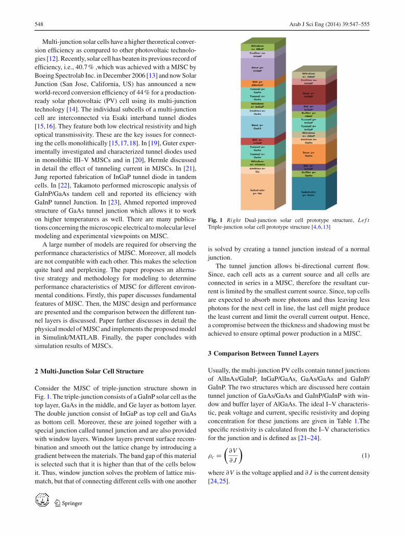
Consider the MJSC of triple-junction structure shown inFig. 1. The triple-junction consists of a GaInP solar cell as thetop layer, GaAs in the middle, and Ge layer as bottom layer.The double junction consist of InGaP as top cell and GaAsas bottom cell. Moreover, these are joined together with aspecial junction called tunnel junction and are also providedwith window layers. Window layers prevent surface recom-bination and smooth out the lattice change by introducing agradient between the materials. The band gap of this materialis selected such that it is higher than that of the cells belowit. Thus, window junction solves the problem of lattice mis-match, but that of connecting different cells with one another
Fig. 1 Right Dual-junction solar cell prototype structure, Le f tTriple-junction solar cell prototype structure [4,6,13]
is solved by creating a tunnel junction instead of a normaljunction.
The tunnel junction allows bi-directional current flow.Since, each cell acts as a current source and all cells areconnected in series in a MJSC, therefore the resultant cur-rent is limited by the smallest current source. Since, top cellsare expected to absorb more photons and thus leaving lessphotons for the next cell in line, the last cell might producethe least current and limit the overall current output. Hence,a compromise between the thickness and shadowing must beachieved to ensure optimal power production in a MJSC.
3 Comparison Between Tunnel Layers
Usually, the multi-junction PV cells contain tunnel junctionsof AlInAs/GaInP, InGaP/GaAs, GaAs/GaAs and GaInP/GaInP. The two structures which are discussed here containtunnel junction of GaAs/GaAs and GaInP/GaInP with win-dow and buffer layer of AlGaAs. The ideal I–V characteris-tic, peak voltage and current, specific resistivity and dopingconcentration for these junctions are given in Table 1.Thespecific resistivity is calculated from the I–V characteristicsfor the junction and is defined as [21–24].
ρc =(
∂V
∂ J
)(1)
where ∂V is the voltage applied and ∂ J is the current density[24,25].
123
Arab J Sci Eng (2014) 39:547–555 549
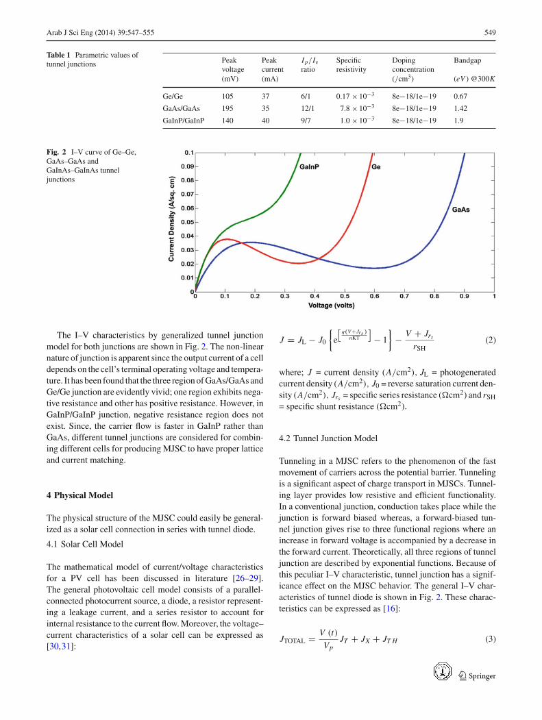
Table 1 Parametric values oftunnel junctions Peak Peak Ip/Iv Specific Doping Bandgap
voltage current ratio resistivity concentration(mV) (mA) (/cm3) (eV ) @300K
Ge/Ge 105 37 6/1 0.17 × 10⁻³ 8e−18/1e−19 0.67
GaAs/GaAs 195 35 12/1 7.8 × 10⁻³ 8e−18/1e−19 1.42
GaInP/GaInP 140 40 9/7 1.0 × 10⁻³ 8e−18/1e−19 1.9
Fig. 2 I–V curve of Ge–Ge,GaAs–GaAs andGaInAs–GaInAs tunneljunctions
The I–V characteristics by generalized tunnel junctionmodel for both junctions are shown in Fig. 2. The non-linearnature of junction is apparent since the output current of a celldepends on the cell’s terminal operating voltage and tempera-ture. It has been found that the three region of GaAs/GaAs andGe/Ge junction are evidently vivid; one region exhibits nega-tive resistance and other has positive resistance. However, inGaInP/GaInP junction, negative resistance region does notexist. Since, the carrier flow is faster in GaInP rather thanGaAs, different tunnel junctions are considered for combin-ing different cells for producing MJSC to have proper latticeand current matching.
4 Physical Model
The physical structure of the MJSC could easily be general-ized as a solar cell connection in series with tunnel diode.
4.1 Solar Cell Model
The mathematical model of current/voltage characteristicsfor a PV cell has been discussed in literature [26–29].The general photovoltaic cell model consists of a parallel-connected photocurrent source, a diode, a resistor represent-ing a leakage current, and a series resistor to account forinternal resistance to the current flow. Moreover, the voltage–current characteristics of a solar cell can be expressed as[30,31]:
J = JL − J0
{e
[q(V +Jrs )
nKT
]− 1
}− V + Jrs
rSH(2)
where; J = current density (A/cm2), JL = photogeneratedcurrent density (A/cm2), J0 = reverse saturation current den-sity (A/cm2), Jrs = specific series resistance (�cm2) and rSH
= specific shunt resistance (�cm2).
4.2 Tunnel Junction Model
Tunneling in a MJSC refers to the phenomenon of the fastmovement of carriers across the potential barrier. Tunnelingis a significant aspect of charge transport in MJSCs. Tunnel-ing layer provides low resistive and efficient functionality.In a conventional junction, conduction takes place while thejunction is forward biased whereas, a forward-biased tun-nel junction gives rise to three functional regions where anincrease in forward voltage is accompanied by a decrease inthe forward current. Theoretically, all three regions of tunneljunction are described by exponential functions. Because ofthis peculiar I–V characteristic, tunnel junction has a signif-icance effect on the MJSC behavior. The general I–V char-acteristics of tunnel diode is shown in Fig. 2. These charac-teristics can be expressed as [16]:
JTOTAL = V (t)
VpJT + JX + JT H (3)
123
550 Arab J Sci Eng (2014) 39:547–555
where;
JT = Jpe1− V (t)
Vp
JX = JveA2(V (t)−Vv)
JT H = JseqV (t)
kT −1
Here, JTOTAL = total current density of the tunnel diode,JT = closed-form expression of the tunneling current densitywhich describes the behavior particular to the tunnel diode,JX = the excess tunneling current density, JTH = normal diodecharacteristic equation, Jp = peak current density, Vp = peakvoltage, Jv = valley current density, Vv = valley voltage, A2
= excess current prefactor, Js = saturation current density, q= charge of an electron, k = Boltzmann’s constant and T =temperature in degree Kelvin.
It should be noted that Jp and Vp are strongly influencedby the doping concentration and doping profile of the mate-rial. The forward voltage of this device is the same as that ofa diode. Thus,
VF = kT
qln
(NA ND)
n2i
(4)
where; VF = forward voltage, NA = acceptor concentration,ND = donor concentration, ni = intrinsic carrier concentration[31,32].
The valley current depends on the peak current density ofthe tunnel layer. Normally, the ratio of GaAs peak currentdensity and valley current density is 1
12 , while the Ge tun-neling layer has a ratio of 1
6 and GaInP tunneling layer hasa ratio of 7
9 . Moreover, the junction capacitance of tunneljunction can be expressed as [16]:
C j =
⎧⎪⎪⎪⎪⎪⎪⎪⎪⎨⎪⎪⎪⎪⎪⎪⎪⎪⎩
CT0(1− Vj
φ
)� if − Vj > 0
CT0 +Vj
(CT0 Vj +
CT0φ
)
1+e10(V j −0.8φ)
+ CT0
�0.2
(e10(0.8φ−V j)−1
) if − Vj < 0
(5)
where; Vj = voltage across tunnel junction, CT0 = zero biasdepletion capacitance, � = built-in barrier potential and φ =capacitance power law parameter.
5 Multi-Junction Model
The solar cell in proposed model is the collective representa-tion of all photovoltaic junctions having short-circuit currentas its series-matched current as discussed earlier. Further-more, the collective model also incorporates series and par-allel resistances, whereas the open-circuit voltage is the sumof the junction voltages.
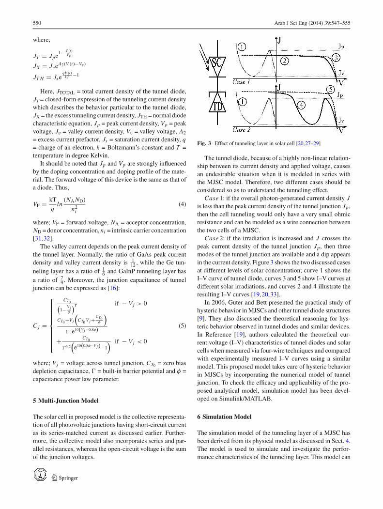
Fig. 3 Effect of tunneling layer in solar cell [20,27–29]
The tunnel diode, because of a highly non-linear relation-ship between its current density and applied voltage, causesan undesirable situation when it is modeled in series withthe MJSC model. Therefore, two different cases should beconsidered so as to understand the tunneling effect.
Case 1: if the overall photon-generated current density Jis less than the peak current density of the tunnel junction Jp,then the cell tunneling would only have a very small ohmicresistance and can be modeled as a wire connection betweenthe two cells of a MJSC.
Case 2: if the irradiation is increased and J crosses thepeak current density of the tunnel junction Jp, then threemodes of the tunnel junction are available and a dip appearsin the current density. Figure 3 shows the two discussed casesat different levels of solar concentration; curve 1 shows theI–V curve of tunnel diode, curves 3 and 5 show I–V curves atdifferent solar irradiations, and curves 2 and 4 illustrate theresulting I–V curves [19,20,33].
In 2006, Guter and Bett presented the practical study ofhysteric behavior in MJSCs and other tunnel diode structures[9]. They also discussed the theoretical reasoning for hys-teric behavior observed in tunnel diodes and similar devices.In Reference [19], authors calculated the theoretical cur-rent voltage (I–V) characteristics of tunnel diodes and solarcells when measured via four-wire techniques and comparedwith experimentally measured I–V curves using a similarmodel. This proposed model takes care of hysteric behaviorin MJSCs by incorporating the numerical model of tunneljunction. To check the efficacy and applicability of the pro-posed analytical model, simulation model has been devel-oped on Simulink/MATLAB.
6 Simulation Model
The simulation model of the tunneling layer of a MJSC hasbeen derived from its physical model as discussed in Sect. 4.The model is used to simulate and investigate the perfor-mance characteristics of the tunneling layer. This model can
123
Arab J Sci Eng (2014) 39:547–555 551
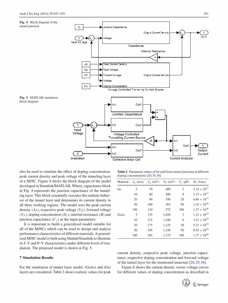
Fig. 4 Block diagram of thetunnel junction
Fig. 5 MATLAB simulationblock diagram
also be used to simulate the effect of doping concentration,peak current density and peak voltage of the tunneling layerof a MJSC. Figure 4 shows the block diagram of the modeldeveloped in Simulink/MATLAB. Where, capacitance blockin Fig. 4 represents the junction capacitance of the tunnel-ing layer. This block essentially executes the realistic behav-ior of the tunnel layer and determines its current density inall three working regions. The model uses the peak currentdensity (JP ), respective peak voltage (VP ), forward voltage(VF ), doping concentration (Dc), internal resistance (R) andjunction capacitance (C j ) as the input parameters.
It is important to build a generalized model suitable forall of the MJSCs which can be used to design and analyzeperformance characteristics of different materials. A general-ized MJSC model is built using Matlab/Simulink to illustrateits I–V and P–V characteristics under different levels of irra-diation. The proposed model is shown in Fig. 5.
7 Simulation Results
For the simulation of tunnel layer model, (GaAs) and (Ge)layers are considered. Table 2 shows realistic values for peak
Table 2 Parametric values of Ge and GaAs tunnel junctions at differentdoping concentrations [20,35,36]
Material Jp (mA) Vp (mV) VF (mV) C j (pF) Dc (/cm3)
Ge 5 70 480 3 2.14 × 10¹⁷
10 80 500 8 3.15 × 10¹⁷
20 90 540 20 6.80 × 10¹⁷
50 100 565 50 1.10 × 10¹⁸
100 110 575 100 1.33 × 10¹⁸
GaAs 5 135 1,050 3 1.23 × 10¹⁵
10 115 1,100 8 3.23 × 10¹⁵
20 175 1,125 20 5.22 × 10¹⁵
50 195 1,150 50 8.45 × 10¹⁵
100 205 1,175 100 1.37 × 10¹⁶
current density, respective peak voltage, junction capaci-tance, respective doping concentration and forward voltageof the tunnel layer for the mentioned materials [24,25,34].
Figure 6 shows the current density versus voltage curvesfor different values of doping concentration as described in
123
552 Arab J Sci Eng (2014) 39:547–555
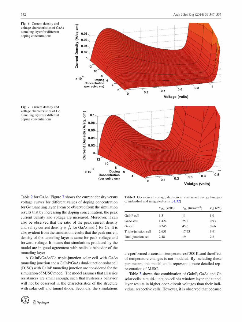
Fig. 6 Current density andvoltage characteristics of GaAstunneling layer for differentdoping concentrations
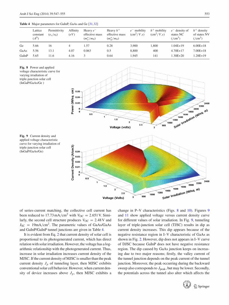
Fig. 7 Current density andvoltage characteristics of Getunneling layer for differentdoping concentrations
Table 2 for GaAs. Figure 7 shows the current density versusvoltage curves for different values of doping concentrationfor Ge tunneling layer. It can be observed from the simulationresults that by increasing the doping concentration, the peakcurrent density and voltage are increased. Moreover, it canalso be observed that the ratio of the peak current densityand valley current density is 1
12 for GaAs and 16 for Ge. It is
also evident from the simulation results that the peak currentdensity of the tunneling layer is same for peak voltage andforward voltage. It means that simulations produced by themodel are in good agreement with realistic behavior of thetunneling layer.
A GaInP/GaAs/Ge triple-junction solar cell with GaAstunneling junction and a GaInP/GaAs dual-junction solar cell(DJSC) with GaInP tunneling junction are considered for thesimulation of MJSC model. The model assumes that all seriesresistances are small enough, such that hysteresis behaviorwill not be observed in the characteristics of the structurewith solar cell and tunnel diode. Secondly, the simulations
Table 3 Open-circuit voltage, short-circuit current and energy bandgapof individual and integrated cells [31,32]
VOC (volts) ISC (mA/cm2) Eg (eV)
GaInP cell 1.3 11 1.9
GaAs cell 1.424 25.2 0.93
Ge cell 0.245 45.6 0.66
Triple-junction cell 2.651 17.73 3.91
Dual-junction cell 2.48 19 2.8
are performed at constant temperature of 300 K, and the effectof temperature changes is not modeled. By including theseparameters, this model could represent a more detailed rep-resentation of MJSC.
Table 3 shows that combination of GaInP, GaAs and Gesolar cells in multi-junction cell via window layer and tunnellayer results in higher open-circuit voltages than their indi-vidual respective cells. However, it is observed that because
123
Arab J Sci Eng (2014) 39:547–555 553
Table 4 Major parameters for GaInP, GaAs and Ge [31,32]
Lattice Permittivity Affinity Heavy e− Heavy h+ e− mobility h+ mobility e− density of h+ densityconstant (es/e0) (eV ) effective mass effective mass (cm2/V .s) (cm2/V .s) states NC of states NV(A0) (m∗
e/m0) (m∗h/m0) (/cm3) (/cm3)
Ge 5.66 16 4 1.57 0.28 3,900 1,800 1.04E+19 6.00E+18
GaAs 5.56 13.1 4.07 0.063 0.5 8,800 400 4.70E+17 7.00E+18
GaInP 5.65 11.6 4.16 3 0.64 1,945 141 1.30E+20 1.28E+19
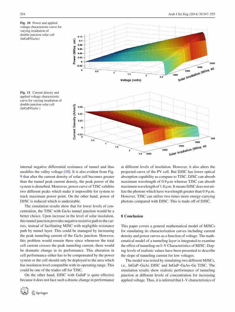
Fig. 8 Power and appliedvoltage characteristic curve forvarying irradiation oftriple-junction solar cell(InGaP/GaAs/Ge )
Fig. 9 Current density andapplied voltage characteristiccurve for varying irradiation oftriple-junction solar cell(InGaP/GaAs/Ge)
of series-current matching, the collective cell current hasbeen reduced to 17.73 mA/cm2 with VOC = 2.651 V. Simi-larly, the second cell structure produces VOC = 2.48 V andISC = 19mA/cm2. The parametric values of GaAs/GaAsand GaInP/GaInP tunnel junctions are given in Table 4.
It is evident from Eq. 2 that current density of solar cell isproportional to its photogenerated current, which has directrelation with solar irradiation. However, the voltage has a log-arithmic relationship with the photogenerated current. Thus,increase in solar irradiation increases current density of theMJSC. If the current density of MJSC is smaller than the peakcurrent density Jp of tunneling layer, then MJSC exhibitsconventional solar cell behavior. However, when current den-sity of device increases above Jp, then MJSC exhibits a
change in P–V characteristics (Figs. 8 and 10). Figures 9and 11 show applied voltage versus current density curvefor different values of solar irradiation. In Fig. 9, tunnelinglayer of triple-junction solar cell (TJSC) results in dip ascurrent density increases. This dip appears because of thenegative resistance region in I–V characteristic of GaAs asshown in Fig. 2. However, dip does not appears in I–V curveof DJSC because GaInP does not have negative resistanceregion. The dip caused by GaAs junction keeps on increas-ing due to two major reasons; firstly, the valley current ofthe tunnel junction depends on the peak current of the tunneljunction. Moreover, the peak occurring during the backwardsweep also corresponds to Jpeak, but may be lower. Secondly,the potentials across the tunnel also alter which affects the
123
554 Arab J Sci Eng (2014) 39:547–555
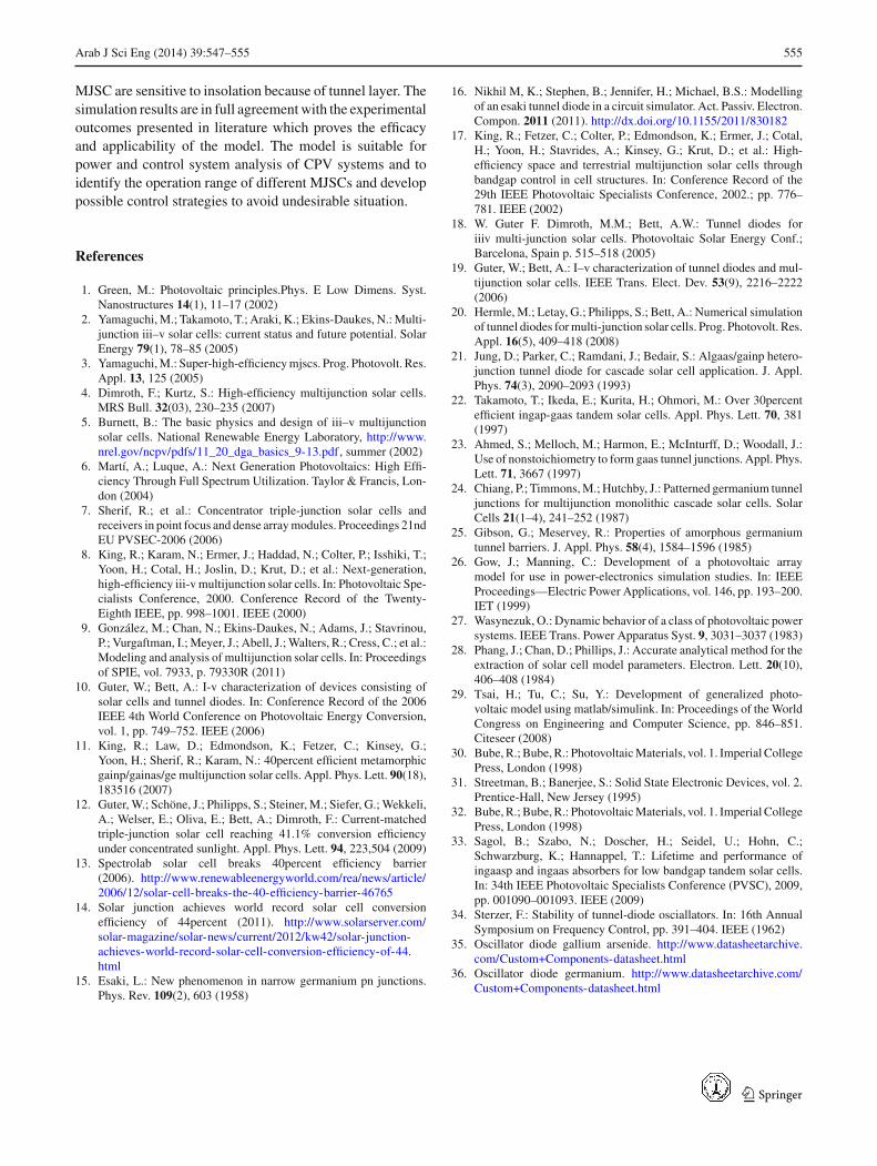
Fig. 10 Power and appliedvoltage characteristic curve forvarying irradiation ofdouble-junction solar cell(InGaP/GaAs)
Fig. 11 Current density andapplied voltage characteristiccurve for varying irradiation ofdouble-junction solar cell(InGaP/GaAs )
internal negative differential resistance of tunnel and thusmodifies the valley voltage [10]. It is also evident from Fig.9 that after the current density of solar cell becomes greaterthan the tunnel peak current density, the peak power of thesystem is disturbed. Moreover, power curve of TJSC exhibitstwo different peaks which make it impossible for system totrack maximum power point. On the other hand, power ofDJSC is reduced which is undesirable.
The simulation results show that for lower levels of con-centration, the TJSC with GaAs tunnel junction would be abetter choice. Upon increase in the level of solar insolation,this tunnel junction provides negative resistive path to the car-ries, instead of facilitating MJSC with negligible resistancepath by tunnel layer. This could be managed by increasingthe peak tunneling current of the GaAs junction. However,this problem would remain there since whenever the totalcell current crosses the peak tunneling current, there wouldbe dramatic change in its performance. This alteration incell performance either has to be compensated by the powersystem or the cell should only be deployed to the area whichhas insolation level compatible with its operating range. Thiscould be one of the trades-off for TJSC.
On the other hand, DJSC with GaInP is quite effectivebecause it does not face such a drastic change in performance
at different levels of insolation. However, it also alters theprojected curve of the PV cell. But DJSC has lower opticalabsorption capability as compare to TJSC. DJSC can absorbmaximum wavelength of 0.9 µm whereas TJSC can absorbmaximum wavelength of 1.8 µm. It means DJSC does not uti-lize the photons which have wavelength greater than 0.9 µm.However, TJSC can utilize two times more energy-carryingphotons compared with DJSC. This is trade-off of DJSC.
8 Conclusion
This paper covers a general mathematical model of MJSCsfor simulating its characterization curves including currentdensity and power curves as a function of voltage. The math-ematical model of a tunneling layer is integrated to examinethe effect of tunneling on I–V Characteristics of MJSC. Dop-ing levels of realistic values have been presented to describethe slope of tunneling current for low voltages.
The model was tested by simulating two different MJSCs,i.e., InGaP–GaAs DJSC and InGaP–GaAs–Ge TJSC. Thesimulation results show realistic performance of tunnelingjunction at different levels of concentration for increasingapplied voltage. Thus, it is inferred that I–V characteristics of
123
Arab J Sci Eng (2014) 39:547–555 555
MJSC are sensitive to insolation because of tunnel layer. Thesimulation results are in full agreement with the experimentaloutcomes presented in literature which proves the efficacyand applicability of the model. The model is suitable forpower and control system analysis of CPV systems and toidentify the operation range of different MJSCs and developpossible control strategies to avoid undesirable situation.
References
1. Green, M.: Photovoltaic principles.Phys. E Low Dimens. Syst.Nanostructures 14(1), 11–17 (2002)
2. Yamaguchi, M.; Takamoto, T.; Araki, K.; Ekins-Daukes, N.: Multi-junction iii–v solar cells: current status and future potential. SolarEnergy 79(1), 78–85 (2005)
3. Yamaguchi, M.: Super-high-efficiency mjscs. Prog. Photovolt. Res.Appl. 13, 125 (2005)
4. Dimroth, F.; Kurtz, S.: High-efficiency multijunction solar cells.MRS Bull. 32(03), 230–235 (2007)
5. Burnett, B.: The basic physics and design of iii–v multijunctionsolar cells. National Renewable Energy Laboratory, http://www.nrel.gov/ncpv/pdfs/11_20_dga_basics_9-13.pdf, summer (2002)
6. Martí, A.; Luque, A.: Next Generation Photovoltaics: High Effi-ciency Through Full Spectrum Utilization. Taylor & Francis, Lon-don (2004)
7. Sherif, R.; et al.: Concentrator triple-junction solar cells andreceivers in point focus and dense array modules. Proceedings 21ndEU PVSEC-2006 (2006)
8. King, R.; Karam, N.; Ermer, J.; Haddad, N.; Colter, P.; Isshiki, T.;Yoon, H.; Cotal, H.; Joslin, D.; Krut, D.; et al.: Next-generation,high-efficiency iii-v multijunction solar cells. In: Photovoltaic Spe-cialists Conference, 2000. Conference Record of the Twenty-Eighth IEEE, pp. 998–1001. IEEE (2000)
9. González, M.; Chan, N.; Ekins-Daukes, N.; Adams, J.; Stavrinou,P.; Vurgaftman, I.; Meyer, J.; Abell, J.; Walters, R.; Cress, C.; et al.:Modeling and analysis of multijunction solar cells. In: Proceedingsof SPIE, vol. 7933, p. 79330R (2011)
10. Guter, W.; Bett, A.: I-v characterization of devices consisting ofsolar cells and tunnel diodes. In: Conference Record of the 2006IEEE 4th World Conference on Photovoltaic Energy Conversion,vol. 1, pp. 749–752. IEEE (2006)
11. King, R.; Law, D.; Edmondson, K.; Fetzer, C.; Kinsey, G.;Yoon, H.; Sherif, R.; Karam, N.: 40percent efficient metamorphicgainp/gainas/ge multijunction solar cells. Appl. Phys. Lett. 90(18),183516 (2007)
12. Guter, W.; Schöne, J.; Philipps, S.; Steiner, M.; Siefer, G.; Wekkeli,A.; Welser, E.; Oliva, E.; Bett, A.; Dimroth, F.: Current-matchedtriple-junction solar cell reaching 41.1% conversion efficiencyunder concentrated sunlight. Appl. Phys. Lett. 94, 223,504 (2009)
13. Spectrolab solar cell breaks 40percent efficiency barrier(2006). http://www.renewableenergyworld.com/rea/news/article/2006/12/solar-cell-breaks-the-40-efficiency-barrier-46765
14. Solar junction achieves world record solar cell conversionefficiency of 44percent (2011). http://www.solarserver.com/solar-magazine/solar-news/current/2012/kw42/solar-junction-achieves-world-record-solar-cell-conversion-efficiency-of-44.html
15. Esaki, L.: New phenomenon in narrow germanium pn junctions.Phys. Rev. 109(2), 603 (1958)
16. Nikhil M, K.; Stephen, B.; Jennifer, H.; Michael, B.S.: Modellingof an esaki tunnel diode in a circuit simulator. Act. Passiv. Electron.Compon. 2011 (2011). http://dx.doi.org/10.1155/2011/830182
17. King, R.; Fetzer, C.; Colter, P.; Edmondson, K.; Ermer, J.; Cotal,H.; Yoon, H.; Stavrides, A.; Kinsey, G.; Krut, D.; et al.: High-efficiency space and terrestrial multijunction solar cells throughbandgap control in cell structures. In: Conference Record of the29th IEEE Photovoltaic Specialists Conference, 2002.; pp. 776–781. IEEE (2002)
18. W. Guter F. Dimroth, M.M.; Bett, A.W.: Tunnel diodes foriiiv multi-junction solar cells. Photovoltaic Solar Energy Conf.;Barcelona, Spain p. 515–518 (2005)
19. Guter, W.; Bett, A.: I–v characterization of tunnel diodes and mul-tijunction solar cells. IEEE Trans. Elect. Dev. 53(9), 2216–2222(2006)
20. Hermle, M.; Letay, G.; Philipps, S.; Bett, A.: Numerical simulationof tunnel diodes for multi-junction solar cells. Prog. Photovolt. Res.Appl. 16(5), 409–418 (2008)
21. Jung, D.; Parker, C.; Ramdani, J.; Bedair, S.: Algaas/gainp hetero-junction tunnel diode for cascade solar cell application. J. Appl.Phys. 74(3), 2090–2093 (1993)
22. Takamoto, T.; Ikeda, E.; Kurita, H.; Ohmori, M.: Over 30percentefficient ingap-gaas tandem solar cells. Appl. Phys. Lett. 70, 381(1997)
23. Ahmed, S.; Melloch, M.; Harmon, E.; McInturff, D.; Woodall, J.:Use of nonstoichiometry to form gaas tunnel junctions. Appl. Phys.Lett. 71, 3667 (1997)
24. Chiang, P.; Timmons, M.; Hutchby, J.: Patterned germanium tunneljunctions for multijunction monolithic cascade solar cells. SolarCells 21(1–4), 241–252 (1987)
25. Gibson, G.; Meservey, R.: Properties of amorphous germaniumtunnel barriers. J. Appl. Phys. 58(4), 1584–1596 (1985)
26. Gow, J.; Manning, C.: Development of a photovoltaic arraymodel for use in power-electronics simulation studies. In: IEEEProceedings—Electric Power Applications, vol. 146, pp. 193–200.IET (1999)
27. Wasynezuk, O.: Dynamic behavior of a class of photovoltaic powersystems. IEEE Trans. Power Apparatus Syst. 9, 3031–3037 (1983)
28. Phang, J.; Chan, D.; Phillips, J.: Accurate analytical method for theextraction of solar cell model parameters. Electron. Lett. 20(10),406–408 (1984)
29. Tsai, H.; Tu, C.; Su, Y.: Development of generalized photo-voltaic model using matlab/simulink. In: Proceedings of the WorldCongress on Engineering and Computer Science, pp. 846–851.Citeseer (2008)
30. Bube, R.; Bube, R.: Photovoltaic Materials, vol. 1. Imperial CollegePress, London (1998)
31. Streetman, B.; Banerjee, S.: Solid State Electronic Devices, vol. 2.Prentice-Hall, New Jersey (1995)
32. Bube, R.; Bube, R.: Photovoltaic Materials, vol. 1. Imperial CollegePress, London (1998)
33. Sagol, B.; Szabo, N.; Doscher, H.; Seidel, U.; Hohn, C.;Schwarzburg, K.; Hannappel, T.: Lifetime and performance ofingaasp and ingaas absorbers for low bandgap tandem solar cells.In: 34th IEEE Photovoltaic Specialists Conference (PVSC), 2009,pp. 001090–001093. IEEE (2009)
34. Sterzer, F.: Stability of tunnel-diode osciallators. In: 16th AnnualSymposium on Frequency Control, pp. 391–404. IEEE (1962)
35. Oscillator diode gallium arsenide. http://www.datasheetarchive.com/Custom+Components-datasheet.html
36. Oscillator diode germanium. http://www.datasheetarchive.com/Custom+Components-datasheet.html
123
Copyright © 2022 FDOKUMEN