
Comprehensive analytical model for locally contacted rear surface passivated solar cells
13
Comprehensive analytical model for locally contacted rear surface passivated solar cells Andreas Wolf, a Daniel Biro, Jan Nekarda, Stefan Stumpp, Achim Kimmerle, Sebastian Mack, and Ralf Preu Fraunhofer Institute for Solar Energy Systems, Heidenhofstr. 2, D-79110 Freiburg, Germany Received 2 August 2010; accepted 28 September 2010; published online 28 December 2010 For optimum performance of solar cells featuring a locally contacted rear surface, the metallization fraction as well as the size and distribution of the local contacts are crucial, since Ohmic and recombination losses have to be balanced. In this work we present a set of equations which enable to calculate this trade off without the need of numerical simulations. Our model combines established analytical and empirical equations to predict the energy conversion efficiency of a locally contacted device. For experimental verification, we fabricate devices from float zone silicon wafers of different resistivity using the laser fired contact technology for forming the local rear contacts. The detailed characterization of test structures enables the determination of important physical parameters, such as the surface recombination velocity at the contacted area and the spreading resistance of the contacts. Our analytical model reproduces the experimental results very well and correctly predicts the optimum contact spacing without the use of free fitting parameters. We use our model to estimate the optimum bulk resistivity for locally contacted devices fabricated from conventional Czochralski-grown silicon material. These calculations use literature values for the stable minority carrier lifetime to account for the bulk recombination caused by the formation of boron-oxygen complexes under carrier injection. © 2010 American Institute of Physics. doi:10.1063/1.3506706 I. INTRODUCTION Solar cells that feature a passivated rear surface with local contacts enable higher conversion efficiencies com- pared to conventional devices with a full area aluminium back surface field BSF. 1,2 Approaches that use local con- tacts, like the passivated emitter and rear cell structure 3 re- duces both recombination and parasitic absorption at the rear surface. In this structure a large area fraction of the rear surface, typically more than 95%, is covered with a dielectric surface passivation layer. Only small openings in the passi- vation layer are used for the local contacts. Two opposing effects determine the optimum rear sur- face metallization fraction f of a locally contacted device. On one hand, increasing f reduces the current crowding at the local contacts and thereby the Ohmic losses. On the other hand, a higher metallization fraction increases the recombi- nation losses, due to a much higher surface recombination velocity SRV at the metallized area compared to the passi- vated regions. Furthermore, not only the metallization frac- tion but also the size and distribution of the local contacts affect the performance. 4–6 In the past advanced multidimensional numeric modeling 7–11 and one dimensional simulations using effec- tive parameters 4,5 were successfully used by various groups in order to analyze this type of structure. However, such simulations require a high calculation effort and are time consuming. Kray et al. 12,13 presented an analytical approach by combining empirical and analytical equations, but the model only covers the calculation of the open circuit voltage and the fill factor of the device, neglecting the impact of a varying rear surface recombination on the short circuit cur- rent density. In this work we present a simple, comprehensive analyti- cal model that permits the optimization of the rear surface metallization geometry of a locally contacted device cover- ing all relevant device parameters. The model is imple- mented using a spreadsheet calculator, which enables a simple use and further extension of the model. Experimental results for industrially manufactured locally contacted solar cells verify the predictions of the model for a base resistivity between 0.5 and 4 cm. Finally, we apply the model to predict the optimum base resistivity for locally contacted de- vices fabricated from conventionally pulled Czochralski Cz silicon, thereby accounting for bulk recombination related to boron-oxygen defect formation. 14–16 II. COMPREHENSIVE MODEL FOR LOCALLY CONTACTED SOLAR CELLS Our approach combines established models to calculate the optimum rear contact pattern for a locally contacted de- vice using a given set of predefined parameters. Table I lists these physical input parameters. This set of parameters then permits the calculation of the conversion efficiency in depen- dence of the rear contact geometry and other relevant device and material parameters. A. Current voltage characteristics We use the well known two diode model 17 to describe the illuminated current-voltage IV curve of the device. The a Electronic mail: [email protected]. JOURNAL OF APPLIED PHYSICS 108, 124510 2010 0021-8979/2010/10812/124510/13/$30.00 © 2010 American Institute of Physics 108, 124510-1
-
Upload
independent -
Category
Documents
-
view
2 -
download
0
Transcript of Comprehensive analytical model for locally contacted rear surface passivated solar cells

Comprehensive analytical model for locally contacted rear surfacepassivated solar cells
Andreas Wolf,a� Daniel Biro, Jan Nekarda, Stefan Stumpp, Achim Kimmerle,Sebastian Mack, and Ralf PreuFraunhofer Institute for Solar Energy Systems, Heidenhofstr. 2, D-79110 Freiburg, Germany
�Received 2 August 2010; accepted 28 September 2010; published online 28 December 2010�
For optimum performance of solar cells featuring a locally contacted rear surface, the metallizationfraction as well as the size and distribution of the local contacts are crucial, since Ohmic andrecombination losses have to be balanced. In this work we present a set of equations which enableto calculate this trade off without the need of numerical simulations. Our model combinesestablished analytical and empirical equations to predict the energy conversion efficiency of alocally contacted device. For experimental verification, we fabricate devices from float zone siliconwafers of different resistivity using the laser fired contact technology for forming the local rearcontacts. The detailed characterization of test structures enables the determination of importantphysical parameters, such as the surface recombination velocity at the contacted area and thespreading resistance of the contacts. Our analytical model reproduces the experimental results verywell and correctly predicts the optimum contact spacing without the use of free fitting parameters.We use our model to estimate the optimum bulk resistivity for locally contacted devices fabricatedfrom conventional Czochralski-grown silicon material. These calculations use literature values forthe stable minority carrier lifetime to account for the bulk recombination caused by the formation ofboron-oxygen complexes under carrier injection. © 2010 American Institute of Physics.�doi:10.1063/1.3506706�
I. INTRODUCTION
Solar cells that feature a passivated rear surface withlocal contacts enable higher conversion efficiencies com-pared to conventional devices with a full area aluminiumback surface field �BSF�.1,2 Approaches that use local con-tacts, like the passivated emitter and rear cell structure3 re-duces both recombination and parasitic absorption at the rearsurface. In this structure a large area fraction of the rearsurface, typically more than 95%, is covered with a dielectricsurface passivation layer. Only small openings in the passi-vation layer are used for the local contacts.
Two opposing effects determine the optimum rear sur-face metallization fraction f of a locally contacted device. Onone hand, increasing f reduces the current crowding at thelocal contacts and thereby the Ohmic losses. On the otherhand, a higher metallization fraction increases the recombi-nation losses, due to a much higher surface recombinationvelocity �SRV� at the metallized area compared to the passi-vated regions. Furthermore, not only the metallization frac-tion but also the size and distribution of the local contactsaffect the performance.4–6
In the past advanced multidimensional numericmodeling7–11 and one dimensional simulations using effec-tive parameters4,5 were successfully used by various groupsin order to analyze this type of structure. However, suchsimulations require a high calculation effort and are timeconsuming. Kray et al.12,13 presented an analytical approachby combining empirical and analytical equations, but themodel only covers the calculation of the open circuit voltage
and the fill factor of the device, neglecting the impact of avarying rear surface recombination on the short circuit cur-rent density.
In this work we present a simple, comprehensive analyti-cal model that permits the optimization of the rear surfacemetallization geometry of a locally contacted device cover-ing all relevant device parameters. The model is imple-mented using a spreadsheet calculator, which enables asimple use and further extension of the model. Experimentalresults for industrially manufactured locally contacted solarcells verify the predictions of the model for a base resistivitybetween 0.5 and 4 � cm. Finally, we apply the model topredict the optimum base resistivity for locally contacted de-vices fabricated from conventionally pulled Czochralski �Cz�silicon, thereby accounting for bulk recombination related toboron-oxygen defect formation.14–16
II. COMPREHENSIVE MODEL FOR LOCALLYCONTACTED SOLAR CELLS
Our approach combines established models to calculatethe optimum rear contact pattern for a locally contacted de-vice using a given set of predefined parameters. Table I liststhese physical input parameters. This set of parameters thenpermits the calculation of the conversion efficiency in depen-dence of the rear contact geometry and other relevant deviceand material parameters.
A. Current voltage characteristics
We use the well known two diode model17 to describethe illuminated current-voltage �IV� curve of the device. Thea�Electronic mail: [email protected].
JOURNAL OF APPLIED PHYSICS 108, 124510 �2010�
0021-8979/2010/108�12�/124510/13/$30.00 © 2010 American Institute of Physics108, 124510-1

two diode model represents a quite strong simplification ne-glecting for example the impact of injection dependent bulkand surface recombination. Therefore it should be used care-fully, having its limitations in mind. Nevertheless, it permitsa simple analytic description adequate for common devicesoperating at low level injection conditions. The IV curve isgiven by
J = − JPh + J01�exp�V − JRS
Vth� − 1
+ J02�exp�V − JRS
2Vth� − 1 +
V − JRS
RP. �1�
Here JPh is the photogenerated current density, J01 and J02 arethe first and second diode dark saturation current densities,RS and RP denote the global series and parallel resistance,and Vth=25.69 mV is the thermal voltage at a temperature of25 °C. An iteration of Eq. �1� yields the IV-curve for a givenset of parameters JPh, J01, J02, RS, and RP and allows to findthe maximum power point �Jmpp,Vmpp�, the open circuit volt-age VOC, and the short circuit current density JSC, which isusually close to JPh. These values then give the fill factor
FF =JmppVmpp
JSCVOC, �2�
and the conversion efficiency
� =JmppVmpp
Plight, �3�
with Plight being the power density of the incident illumina-tion that induces the photogenerated current JPh.
Recombination in the emitter and the base both contrib-ute to the dark saturation current density of the first diodeJ01. Assuming linear superposition, the saturation currentdensities for the two regions add up to give J01=J0e+J0b. Thesecond diode saturation current density J02 describes nonideal behaviour caused by recombination in the space chargeregion or recombination at unpassivated or damaged regions
of the junction.17,18 The quantities J02 and J0e do not dependon the rear surface metallization geometry. The base darksaturation current density19
J0b =qDni
2
NdopLeff,OC, �4�
is calculated from elementary charge q, the minority carrierdiffusion constant D, the intrinsic carrier concentration ni,the base doping density Ndop, and the effective diffusionlength Leff,OC for open circuit conditions. A general definitionof the effective diffusion length reads19
Leff = L
1 +SeffL
Dtanh�W
L�
SeffL
D+ tanh�W
L� , �5�
which involves the bulk diffusion length L, the device thick-ness W, and the effective SRV at the rear surface Seff. Thiseffective SRV depends on the metallization geometry and isdefined in such way, that it yields the correct saturation cur-rent of the locally contacted device when used in combina-tion with equations for one-dimensional transport.20,21 Thisdefinition permits a one dimensional analytical descriptioninstead of time consuming two or three dimensional numeri-cal simulations.
B. Effective rear SRV
The literature provides several models for the above de-fined effective SRV of a locally contacted solar cell.Fischer20 derived an equation by using the formal equiva-lence between the minority carrier concentration under for-ward injection and the electrostatic potential for the majoritycarriers of the identical structure. The latter is related to theseries resistance under nonilluminated conditions, giving
TABLE I. Input parameters of the device model.
Parameter Unit Description
� � cm Resistivity of base materialW �m Device thicknessL �m Minority carrier bulk diffusion lengthJ0e fA /cm2 Emitter dark saturation current densityJ02 nA /cm2 Second diode saturation current densityRS,front � cm2 Lumped series resistance from emitter and front contactsRP � cm2 Global parallel resistanceSpass cm/s SRV at the passivated rear surfaceSmet cm/s SRV at the metallized rear surface�inj ¯ Injection factor yielding the SRV for short circuit conditionsf ¯ Rear surface metallization fractionRS,back,dark � cm2 Global dark series resistance of rear contactRS,back,light � cm2 Global illuminated series resistance of rear contactM ¯ Fraction of front surface shaded by contact grid�JSC,Emitter mA /cm2 Short circuit current density loss due to emitter recombination
124510-2 Wolf et al. J. Appl. Phys. 108, 124510 �2010�

Seff,Fischer =D
WRS,back,dark
�W+
D
fWSmet− 1�−1
+Spass
1 − f. �6�
Here Spass denotes the SRV at the passivated area, Smet theSRV at the metallized area, f the metallization fractionand RS,back,dark / ��W� the global, normalized dark series resis-tance of the rear contact with � being the base resistivity.Fischer’s model assumes an infinite bulk diffusion length L,Spass�Smet, and an emitter with a vanishing lateral resistanceyielding an equipotential front surface. Equation �6� showedgood agreement with the three-dimensional transport modelof Rau.20,22
Plagwitz and Brendel21 extended Fischer’s model byconsidering two parallel diodes, one for the passivated andone for the metallized area. This approach reflects the largescale case, where the spacing of the contacts is large com-pared to the device thickness. Plagwitz and Brendel intro-duced the dark series resistance of the complementary struc-
ture R̃S,back,dark, that is a structure solely contacted at thepassivated area, resulting in
Seff,P&B =D
W�RS,back,dark
�W+
D
fWSmet�−1
+ R̃S,back,dark
�W+
D
�1 − f�WSpass�−1�−1
− 1�−1
. �7�
Their work also includes an experimental verification of themodel for both point- and stripe-shaped contacts.
In a later publication23 Plagwitz introduced a further ex-tension by interpolating between the large scale case fromEq. �7� and the small scale case, which considers a spatiallyhomogeneous minority carrier concentration at the rear sur-face,
Seff,small scale = �1 − f�Spass + fSmet. �8�
Both the model of Fischer and Plagwitz assume an infinitebulk diffusion length, however their application is suggestedif LW is valid.21 Moreover, the validity of Fischer’s modelis limited to the case SmetSpass. Both restrictions are over-come by a model recently presented by Saint-Cast et al.24
Seff,Saint-Cast =
�1 − f�Spass +RS,back,darkSpassf + �D
RS,back,darkSmetf + �DfSmet
1 +L
Dtanh�W
L� Spass − �1 − f�Spass −
RS,back,darkSpassf + �D
RS,back,darkSmetf + �DfSmet�
. �9�
For infinite bulk diffusion length and Spass=0, Eqs. �6�, �7�,and �9� all yield equivalent results.
Figure 1 illustrates the effective SRV of a point-contacted surface as a function of the contact radius r for aconstant metallization fraction of f =0.01 calculated usingthe above described models and the dark resistance modelfrom Eqs. �11� and �12� below. Here, the rear surface metal-lization fraction is
f =�r2
AC=
�r2
LP2 , �10�
where LP is defined as the effective point contact distancewith AC=LP
2 being the area per contact. For the considered
case, the difference between the original model from Fischerand the modified version of Plagwitz and Brendel is small.Both reach the small scale limit for very small contact radiir�0.1 �m. The same holds for Eq. �9�. For the chosen pa-rameters and infinite bulk diffusion length Eq. �9� yields re-sults that deviate less than 2% from Fischer’s original model.In contrast, the interpolation from Plagwitz approaches thesmall scale case for significantly larger structure size ofr�10 �m.
The deviations between the individual models reveal thatthe physical meaning of parameters obtained from fitting anyof these models to experimental data is limited. Neverthe-less, these equations still enable the parameterization of the
0.1 1 10 100 10000
200
400
600
800
1000
120010 100 1000 10000
f � ����Smet � ��� ��Spass � �� ��W � ��� ��� � � ��D � � �� ��
������� ������ LP ����
����� ���� ���
�������� �� ��!�� ��������
"��� ��
Effectivesurfacerecomb.vel.S eff(cm/s)
������� �!�# r ����
$��%� �����&���
FIG. 1. Analytically calculated effective SRV for a point contacted devicewith a f =1% metallized rear surface plotted against the contact radius rusing different models: Fischer’s original model �Ref. 20� from Eq. �6�, themodel of Plagwitz and Brendel �Ref. 21� from Eq. �7�, the interpolationfrom Plagwitz �Ref. 23�, the small scale limit from Eq. �8�, and the versionof Saint-Cast et al. �Ref. 24�. from Eq. �9� assuming LW. The appliedparameters are displayed in the graph, Eqs. �11� and �12� are used forRS,back,dark, the upper axis shows the contact spacing LP.
124510-3 Wolf et al. J. Appl. Phys. 108, 124510 �2010�

effective SRV in dependence of the metallization geometry,as shown by several authors.4,12,21,23 In this work we applyFischer’s original model, since it is represented by a quitesimple equation and shows only minor deviations from moreadvanced models.
C. Dark and illuminated series resistance
The literature provides several equations for the spread-ing resistance of contacts of different geometry.20,24–27 Forexample, a frequently used equation for the spreading resis-tance of point contacts is the expression28
Rspread =�
2�rarctan�2W
r� , �11�
of Cox and Strack, which is also applied in this work. Thisempiric equation deviates less than 8% from the exact nu-meric solution.20,29 Fischer presented an approach yieldingthe base resistance of a point contacted device20
RS,back,dark = RspreadLP2 + �W1 − exp�−
W
LP�� . �12�
This expression interpolates between wide contact spacingLPW with RS,back,dark=RspreadLP
2 and narrow contact spacingLP�W with RS,back,dark approaching �W. Section III A belowinvestigates this interpolation in more detail. Equations �11�and �12� do not require the knowledge of the exact distribu-tion of the local contacts, i.e., it is not distinguished betweena square, a hexagonal or any other contact pattern. However,the use of spreading resistance models that include the unitcell of the individual contact27 would allow to calculate theresistance and thus the effective SRV for different contactpatterns. However, in this work we do not include the impactof the contact pattern.
Both, front and back of the cell contribute to the globalseries resistance of the device,
RS = RS,front + RS,back,light. �13�
The lumped series resistance from the emitter and the frontcontacts RS,front is independent of the rear surface metalliza-tion whereas RS,back,light describes the resistance in depen-dence of the rear contact geometry. It should be noted thatfor Eq. �13� a series resistance model for an illuminated de-vice should be used, if available, whereas the models for theeffective SRV, that is Eqs. �6�, �7�, and �9�, require the seriesresistance RS,back,dark under dark conditions. Here we assumeRS,back,light=RS,back,dark, which is a reasonable approximationfor typical geometries with a device thickness above 150 �m and low level injection conditions.8,13 For higherinjection levels, the increased conductivity due to excess car-riers should be considered.30,31
D. Photogenerated current density
This work applies a simple approach for the calculationof the photogenerated current density that was introduced byFischer.20 The model approximates the cumulated generationdepth profile in a silicon solar cell under illumination with asunlike spectrum by
Jgen�z� = �1 − M��Jgen,front + Jgen,exp 11 − exp�−z
L1��
+ Jgen,exp 21 − exp�−z
L2�� + Jgen,hom
z
W .
�14�
The first term Jgen,front quantifies generation directly at thefront surface at z=0. The second and third term each repre-sent an exponentially decreasing generation with an absorp-tion length of L1=4 �m and L2=25 �m, respectively. Thefourth term Jgen,hom covers homogeneous generation. Thefactor �1−M� accounts for shading by the front metallizationgrid. The four quantities Jgen,front, Jgen,exp 1, Jgen,exp 2, andJgen,hom depend on the optical properties of the device, aswell as on basic device characteristics such as doping andthickness. Appendix A describes the one-time derivation ofthe four parameters using optical simulations including anempiric description of the thickness dependence of the ho-mogeneous generation Jgen,hom.
Once these factors are known, the photogenerated cur-rent density
JPh = �1 − M��Jgen,front − �JSC,emitter +Jgen,exp 1
�1 + L1/Leff,SC�
+Jgen,exp 2
�1 + L2/Leff,SC�+ Jgen,hom
Lcol,SC
W , �15�
follows from the effective diffusion length Leff,SC, undershort circuit conditions, the loss in short circuit current den-sity due to emitter recombination �JSC,emitter, and the collec-tion diffusion length Lcol,SC also for short circuit conditions.The collection diffusion length is defined as32
Lcol = L
SeffL
Dcosh�W
L� − 1� + sinh�W
L�
SeffL
Dsinh�W
L� + cosh�W
L� , �16�
where Lcol /W is the fraction of collected carriers in the caseof homogeneous generation.
The models for the effective SRV from Sec. II B werederived assuming open circuit conditions.20 Here we alsoapply these models to calculate the short circuit current den-sity by Eq. �15�. To account for a modified surface recombi-nation under short circuit conditions, we introduce an injec-tion factor �inj that scales the SRV at short circuit,
Seff,SC = �inj Seff,OC, �17�
to that at open circuit-conditions Seff,OC. Here, �inj=1 corre-sponds to an injection-independent SRV. For the calculationof the photogenerated current density, we apply Eq. �15� andinsert the injection factor for calculating the collection diffu-sion length Lcol,SC from Eq. �16� and the effective diffusionlength Leff,SC from Eq. �5� both for short circuit conditions.Any injection dependence of the bulk recombination is ne-glected, the same holds for the impact of the injection depen-dent SRV on the FF.33
124510-4 Wolf et al. J. Appl. Phys. 108, 124510 �2010�

Now, the two diode model from Eq. �1� allows the cal-culation of the conversion efficiency in dependence of thegeometry parameters of the local rear contacts and other ma-terial and device parameters listed in Table I. The materialconstants, as the minority carrier diffusion constant D, theintrinsic carrier concentration ni, and the doping densityNdop, are calculated from the base doping type and resistivity.Appendix B describes their calculation in the case of p-typesilicon.
III. EXPERIMENTAL VERIFICATION
In this work, the laser fired contact �LFC� technology34
is applied to form the local rear contacts. Therefore the dem-onstration of the model assumes point-shaped contacts with afixed predefined contact radius r. However, our approach caneasily be adapted for contacts of any geometry, if a quanti-tative description of the spreading resistance is available �seeSec. II C�. For the considered case of point contacts with afixed radius r, the only free parameter is the effective pointcontact spacing LP=�AC with AC being the area dedicated toone contact.
A. Dark series resistance of the base
The fabrication of resistance test structures permits theverification of the above described base series resistancemodels for local contacts formed by the LFC technology. Forthis purpose boron-doped float zone �FZ� silicon wafers areoxidized in a quartz tube furnace yielding a 100 nm thickoxide layer. Wet chemical etching then removes the oxidelayer from one side of the wafer followed by electron beamevaporation of a 2 �m thick Al-layer onto the same surface.Annealing ensures a low contact resistance between the Allayer and the Si bulk. Subsequently, the second surface, thatstill features the oxide layer, is metallized identically. Thenthe wafers are cleaved into smaller pieces, thereby avoidingthe formation of parasitic conductive paths around thesample edge, and a laser alloys local contacts through theAl-covered oxide layer using different contact spacings fordifferent samples. This LFC process is limited to a 1 cm2
large area of the sample. Optical microscope images revealthat the geometry of the individual contacts is similar for allapplied contact spacing values. Again, the effective contactspacing LP follows from the average area per contactAC=LP
2. The inset of Fig. 2 illustrates the sample structure. Avoltmeter enables the determination of the resistance R1 be-fore and R2 after the application of the LFCs. Only sampleswith a high initial resistance R1 10 � are used. The resis-tance per LFC35
RLFC = NLFC 1
R2−
1
R1�−1
, �18�
then follows from the number of contacts NLFC, thereby ne-glecting the finite contact resistance between the Si bulk andthe full area Al layer. IV measurements show ohmic behav-iour of these structures for current densities up to200 mA /cm2. Moreover, annealing at 350 °C for 5 min af-ter LFC formation does not show any significant impact onRLFC.
Inserting Eq. �11� into Eq. �12� and dividing by the areaper contact LP
2 gives the resistance per contact
Rsingle contact =�
2�rarctan�2W
r�
+�W
LP2 1 − exp�−
W
LP�� . �19�
Again, the small contribution from a nonzero contact resis-tance between Si and Al at the local contact is neglected.
Figure 2 illustrates the dependence of RLFC on the con-tact spacing LP for a sample with �=11.2 � cm. For largecontact spacing RLFC approaches a constant value, which isconsistent with Eq. �19�. For smaller contact spacing RLFC
increases. However, this increase is not as strong as predictedby Eq. �19�. We therefore suggest to modify Eq. �19� byintroducing two more dimensionless parameters, � and �,yielding the empirical equation
Rsingle contact = Rspread + �W
LP2 − Rspreadf�
1 − exp�− � W
LP�1 − f����� . �20�
Apparent from Fig. 2, the use of �=�=0.5 gives a goodagreement with the experimental data. Besides the two in-serted parameters � and �, the modification from Eq. �19�to Eq. �20� affects the prefactor of the second term by sub-tracting Rspread f and the argument of the exponential func-tion by inserting �1− f� in the denominator. These two modi-fications force the series resistance to reach the limitRS,back,dark=�W for the fully metallized case f =1, whereasthe original model from Eq. �19� reaches this limit for
100 1000400
800
1200
1600
500
This workα = β = 0.5
ρ = 11.2 ΩcmW = 335 μmr = 45 μm
ResistancepercontactR L
FC(Ω)
Contact spacing LP (μm)
Original modelfrom Fischer
200
FIG. 2. �Color online� Measured resistance per LFC �symbols� plotted vsthe contact spacing. The sample thickness is W= �340�10� �m, the resis-tivity �= �11.2�0.6� � cm. The dashed line represents Fischer’s originalmodel from Eq. �19� whereas the solid line refers to the modified version ofthis work by Eq. �20�. Both cases assume a contact radius of r=45 �m. Theoriginal model from Fischer deviates from the measured values for smallcontact spacing. Using Eq. �20� with �=�=0.5 instead reproduces the ex-perimental data quite well. The inset schematically illustrates the samplestructure.
124510-5 Wolf et al. J. Appl. Phys. 108, 124510 �2010�

LP=0, where the density of local contacts tends to infinity.The symbols in Fig. 3 represent the resistance RLFC ob-
tained for different bulk resistivity values usingLP=1000 �m. As expected from Eqs. �20� and �11�, we finda linear dependence between RLFC and the base resistivity �,with the latter determined from four point probe measure-ments. A fit of Eqs. �11� and �20� ��=�=0.5� to the experi-mental data with the contact radius r as the only free param-eter yields r=42.6 �m. This value agrees well with the sizeof the alloyed area found on optical microscope images. Theslightly smaller radius compared to the data from Fig. 2 withr=45 �m and the result r=46 �m found by Kray andGlunz12 originates from the use of different laser parametersfor the LFC formation. For comparison, the dashed line inFig. 3 represents the case for r=46 �m.
B. Effective SRV
For the parameterization of the effective SRV in depen-dence of the metallization fraction, symmetric lifetime teststructures are prepared, as described in Ref. 12. Various bo-ron doped p-type FZ Si wafers of 125125 mm2 �pseu-dosquare� size with a resistivity ranging from 0.5 to11.2 � cm serve as the starting material. After a wet chemi-cal cleaning sequence a 100 nm thick oxide is grown in aquartz tube furnace followed by electron beam evaporationof a 2 �m thick layer of aluminium onto both surfaces. Alaser cuts the wafers into 44 cm2 large samples. Bothsample surfaces then receive LFCs, thereby varying the ef-fective contact spacing LP from sample to sample, includingreference samples without LFCs. Subsequently, a postmetal-lization anneal is performed at 350 °C for 5 min. Please notethat these conditions represent a reduced thermal budgetcompared to optimum annealing parameters, which usuallyapply temperatures above 400 °C. However, devices thatfeature screen printed contacts �see Sec. III C� require lower
annealing temperatures to prevent a deterioration of the frontcontacts.36 A wet chemical bath then removes the metal lay-ers which enables the determination of the SRV by means ofthe quasi steady-state photoconductance �QSSPC�technique.37 The effective carrier lifetime �eff is evaluated atan injection density of �n=51014 cm−3, representing opencircuit conditions. The SRV38
S =W
2� 1
�eff−
1
�bulk�−1
−W2
D�2−1
�21�
follows from the sample thickness W, the Augerrecombination-limited bulk carrier lifetime39 �bulk, and thediffusion constant D �see Appendix B�. An uncertainty of10% is assumed for the lifetime measurements.
It must be mentioned that the models from Sec. II Bassume an equipotential front surface, a condition that is notfulfilled by the symmetric samples analyzed in this work.The use of nonsymmetric samples where one surface featuresa diffused emitter would match the assumptions of the mod-els. However, symmetric samples are easier to fabricate andallow simple extraction of the SRV from the QSSPC mea-surement.
Figure 4 shows the effective SRV determined for thesymmetric test structures with different contact spacings andbase resistivities by means of Eq. �21�. For small contactspacing the metallized area fraction and thus the effectiveSRV increase. Moreover, lower resistivities yield higheroverall SRVs, as already observed by other authors.12,40
For a parameterization of the experimental data, we ap-ply Fischer’s original model, that is Eq. �6� together with thedark series resistance from Eqs. �11� and �12�. Using the dark
0 2 4 6 8 10 120
100
200
300
400
500
600
700
r � '( ��
r � '��( ��
LP� ���� ��
W � )'� ��ResistancepercontactR L
FC(Ω)
��� ����*��+ � ����
FIG. 3. Measured resistance per contact �symbols� for LFCs formed onsamples with different resistivity values. The sample thickness isW= �340�10� �m, the contact spacing LP= �1000�32� �m. The linearcorrelation from Eqs. �11� and �20� is confirmed, a fit to the data �solid line�gives r=42.6 �m. The dashed line represents the correlation forr=46 �m.
0 200 400 600 800 10003E94E95E96E97E98E99E1E101
102
103
� ��
� � ��� ��
Effectivesurfacerecomb.vel.S eff(cm/s)
�� �� �� ���� LP ����
�� ��
� ��
����
Spass
FIG. 4. Effective SRV measured for symmetric lifetime test structures �sym-bols� plotted vs the contact spacing. The samples feature a bulk resistivitybetween �0.5�0.1� and �11.2�0.6� � cm. Reference samples without con-tacts yield the SRV at the passivated area Spass �right hand side�. The linesrepresent fits of Eq. �22� using a predefined fixed radius rrecomb=70 �m forthe recombination active area and one Smet-value for each curve as the onlyfree parameter. Predefined radii rrecomb between 50 and 100 �m all give agood agreement with the experimental data. Figure 5 illustrates the depen-dence of the resulting Smet-values on the assumed radius rrecomb.
124510-6 Wolf et al. J. Appl. Phys. 108, 124510 �2010�

resistance model from Eq. �20� introduced in this work in-stead of the original model would allow a parameterizationas well. However, the use of the original model ensures com-parability with literature values for the obtained parameters.
Inserting Eqs. �10�–�12� into Eq. �6� yields
Seff =D
W LP
2
2�rrecombWarctan� 2W
rrecomb� − exp�−
W
LP�
+DLP
2
�rrecomb2 WSmet
�−1
+Spass
1 −�rrecomb
2
LP2
, �22�
where rrecomb denotes the radius of the recombination activearea. This equation is now fitted to the experimental datausing one Smet-value for each of the four bulk resistivities asthe only free parameter. Parameters, which are fixed for eachmaterial, are the diffusion constant D �see Appendix B�, thesample thickness W, and the SRV at the passivated area Spass
that follows from the reference samples which do not receiveLFCs �right hand side of Fig. 4�. One radius rrecomb is usedfor all four curves.
This radius for the recombination model rrecomb is a cru-cial parameter in Eq. �22�. Leaving rrecomb as a free param-eter results in rrecomb=59 �m and a Smet-value that tends toinfinity for the highly doped sample with �=0.5 � cm,which impedes a meaningful parameterization of the experi-mental data. The use of predefined fixed radii rrecomb in therange of 60–100 �m all yield finite Smet-values and give asimilar good match to the experimental data. A more precisedetermination of rrecomb by fitting the Eq. �22� to our dataseems thus not possible, although Kray and Glunz observedgood agreement to their data using rrecomb=46 �m,12 how-ever, different annealing conditions were used.
On the other hand, the need for the use of an increasedradius for the recombination model rrecomb compared to theresistance model rresist�45 �m might be due to laser in-
duced damage of the passivation or the Si bulk in the vicinityof the alloyed area.41,42 In fact, the radius of the “outer cra-ter” of the LFC-contact, as defined by Kray and Glunz,12 isin the range of 60–80 �m.
Figure 5 illustrates how the parameter Smet extractedfrom the fit depends on the doping �acceptor� density NA andthe predefined fixed radius rrecomb of the recombination ac-tive area. The assumed radius strongly affects the resultingSmet yielding lower SRVs for larger contact radii. However,Eq. �22� gives similar effective SRVs for all applied combi-nations of rrecomb and Smet. Thus, using solely the SRV Smet
determined from such fits does not give the full information.The dark saturation current per contact35
I0b,contact =qDni
2
NA 1
2�rrecombarctan� 2W
rrecomb�
+D
�rrecomb2 Smet
�−1
, �23�
that we recently introduced, quantifies the recombination atthe contact by including both rrecomb and Smet. Assumingcontact radii rrecomb between 45 and 100 �m the extractedSRVs for �=1 � cm range from Smet=7104 cm /s toSmet=2103 cm /s �see Fig. 5�. In contrast, the dark satura-tion current per contact I0b,contact determined for the rrecomb
and Smet combinations by means of Eq. �23� varies by only3%.
The increase in Smet with the doping density NA origi-nates from the reduced ratio NA /NA,BSF compared to the dop-ing density NA,BSF of the local BSF at the alloyed LFCs.12,43
For homogeneous doping levels, analytical calculations pre-dict S�NA /NA,BSF,43 equivalent to a doping-independentdark saturation current. Kray and Glunz suggested an expo-nential function12
Smet = S0 + S1 exp��metNA� , �24�
to describe the dependence of Smet on the doping density. Thesolid lines in Fig. 5 represent fits of Eq. �24� that give asatisfying agreement. However, for an increasing predefinedcontact radius rrecomb, the curve flattens and a power law40
S = S0NA
N0��
�25�
with �=0.55 �dotted line in Fig. 5� gives a quite good agree-ment for the lowly doped samples ��1 � cm. Originally,this power law was introduced by Cuevas to describe thedependence of the SRV at thermal oxide passivated surfaceson the doping density.40
C. Complete solar cell model
For verifying the complete device model presentedin this work, solar cells with an oxide-passivated rear surfaceand local LFCs are fabricated from FZ Si wafers witha nominal resistivity of 0.5, 1, and 4 � cm and125125 mm2 �pseudosquare� size. Figure 6 illustrates theprocess sequence. After thinning the wafers to 200 �m ina KOH etching solution and subsequent wet chemical clean-ing a 300 nm thick thermal oxide layer is grown in a
1015 1016 1017102
103
104
105
���������� �����
�NA
����
��� ��
�� ��
�� ��
SR
Vm
etal
lized
areaS m
et(c
m/s
)rrecomb
� �� ��
����� ������ NA ��� !"
FIG. 5. SRV at the metallised area Smet vs the base doping density. Thesymbols represent the values extracted from the fits of Eq. �22� shown inFig. 4 using different predefined fixed radii rrecomb for the recombinationactive area. The solid lines are exponential fits using Eq. �24�, whereas thedotted line shows a power law dependence from Eq. �25�.
124510-7 Wolf et al. J. Appl. Phys. 108, 124510 �2010�

H2O-rich atmosphere using a quartz tube furnace. Wetchemical etching then removes the oxide layer from one sideof the wafer using an etch-resist mask for protecting the ox-ide at the rear surface. A KOH/isopropanol-solution then tex-tures the front surface with random pyramids while the re-maining oxide masks the rear surface. In the next step aPOCl3 tube furnace diffusion process enables the formationof a phosphorus-diffused emitter with a sheet resistance of65 � /sq. During diffusion, again the thermal oxide masksthe rear surface. A subsequent HF bath removes the phospho-silicate glass. The duration of this step is adjusted to result ina thickness of about 100 nm for the rear oxide layer. Thefront surface is then coated with a SiNX antireflection �AR�layer by means of plasma enhanced chemical vapor deposi-tion �PECVD�. Screen printing forms the front grid contactfollowed by contact firing in a conveyor belt furnace. Sub-sequently, electron beam evaporation deposits a 2 �m thickAl-layer onto the rear surface and a laser alloys the localLFCs, thereby varying the contact spacing. Finally the cellsare annealed in forming gas at 350 °C for 5 min, which areconditions optimized for devices that feature an oxide-passivated rear surface and screen printed front contacts.36
Due to the geometry of the sample holder, the Al rearcontact does not cover the whole rear surface of the cell. Toevaluate the potential of a full area rear contact, the cells arescribed by a laser and subsequently cleaved removing about2 mm of the wafer edge. The resulting cell area is 140 cm2.The illuminated IV measurements are performed using anindustrial cell tester equipped with a flash lamp. The resultsare scaled to standard testing conditions,44 including a spec-tral mismatch correction �spectrum AM1.5G, IEC60904-3:2008�, which is performed for one cell and applied to thewhole batch.
Figure 7 presents the measured IV data plotted versus theeffective contact spacing LP for �=1 � cm. Here, two dif-ferent types of material are applied, shiny etched �filled sym-bols� and as-cut wafers �open symbols�. For the as-cut ma-terial, the KOH etch performed for thinning the wafers alsoremoves the saw damage. Apparent from Fig. 7, no signifi-cant difference is observed for the two different surfaces. Asexpected, VOC and JSC increase with LP, due to a reduced
metallization fraction and thus reduced surface recombina-tion. The FF reduces for larger contact spacing since theresistance losses increase. These trends form a maximum atLP=600 �m for the conversion efficiency. Similar trends areobserved for a bulk resistivity of 0.5 and 4 � cm, as shownin Fig. 8.
The verification of the model requires the knowledge ofseveral parameters, as listed in Table I. For determining thebulk diffusion length and the SRV of the passivated area,control samples are processed together with the solar cells.For these samples the single sided oxide removal is omittedyielding a symmetric structure with both surfaces passivatedby a layer of thermal oxide. These samples then go throughthe complete fabrication process shown in Fig. 6, includingcontact firing. After the final annealing step, wet chemicaletching removes the Al-layers from both surfaces, which per-mits the determination of the effective carrier lifetime at the
Alkaline texture
POCl3 emitter diffusion 65 Ω/sq.
Wet chemical cleaning
Growth of ~300 nm thick thermal oxide
Oxide removal from front surface
SiNX deposition (front surface)
PSG removal
Al deposition by e-gun evaporation (rear surface)
Contact firing
Local rear contact formation (LFC)
Screen printing of front contacts
FZ-Wafers 0.5, 1, and 4 Ωcm resistivityWafer thinning in KOH solution
Annealing
Laser scribing and edge cleaving
FIG. 6. Process sequence for the fabrication of silicon solar cells that featurescreen printed front contacts and a thermal oxide passivated rear surfacewith local laser alloyed contacts.
300 600 900 120035
36
37
38
16
17
18
19
620
625
630
635
300 600 900 120072
74
76
78� � ���� ��
��
����
����
����
����
�JSC
���
���
�
�� �� �� ���� LP����
� � ���� ��
�
!���
��
�����
����
"�
�#�
$��
���
����
�!%
� ��V O
C��
&�
� � ���� ��
'�%%
� ��
�FF
�#�
� � ���� ��
�� �� �� ���� LP����
FIG. 7. IV parameters measured for the locally contacted solar cells fabri-cated from shiny etched �filled symbols� and as-cut �open symbols� FZmaterial �1 � cm resistivity� by means of the process sequence shown inFig. 6. The data are scaled to standard testing conditions �Ref. 44� �spectrumAM1.5G, IEC60904-3:2008�. The solid lines represent the analytical modelof this work using the parameters from Tables II and III.
300 600 900 1200 1500
15
16
17
18
19
200 400 600 800
15
16
17
18
19
Conversionefficiency�(%)
Conversionefficiency�(%)
� � ���� ��
�� �� �� ���� LP����
� � ��� ��
�� �� �� ���� LP����
FIG. 8. Conversion efficiency measured for the locally contacted solar cellsfabricated from shiny etched FZ material of 0.5 and 4.4 � cm resistivity bymeans of the process sequence shown in Fig. 6. The data are scaled tostandard testing conditions �Ref. 44� �spectrum AM1.5G, IEC60904-3:2008�. The solid lines represent the analytical model of this work using theparameters from Tables II and III.
124510-8 Wolf et al. J. Appl. Phys. 108, 124510 �2010�
end of the fabrication process �eff,1 by a QSSPC measure-ment. Then HF-etching removes the oxide layers and bothsurfaces are subsequently passivated by a PECVD-layer ofhydrogenated SiNXOY with a SiNX capping layer.45 The nextQSSPC-measurement gives the passivated lifetime �eff,2.The SRV of the SiNXOY /SiNX-passivation stackSstack=12 cm /s is determined from 1 � cm FZ referencesamples with known bulk carrier lifetime. AssumingSstack=12 cm /s for all PECVD-passivated samples enablesthe determination of the bulk carrier lifetime �bulk and bulkdiffusion length L=�D�bulk at the end of the fabrication pro-cess from �eff,2 by means of Eq. �21�. Moreover, the knowl-edge of �bulk permits the calculation of the SRV of the oxidepassivation Spass at the end of the fabrication process from�eff,1. The results are listed in Table II. Due to a processfailure during thermal oxidation, a reduced passivation qual-ity is reached in this batch with Spass between 100 and 200cm/s. Later batches reached significantly lower SRVs ofdown to 50 cm /s.46 The results from Sec. III B give theSRV at the metallized area �see Table II�, assuming a radiusof rrecomb=70 �m for the recombination active area. Foreach material the injection factor �inj is estimated fromthe QSSPC data for the symmetric samples �Sec. III B�by comparing the SRV at an injection density of�n=21013 cm−3 �short circuit� to that at�n=51014 cm−3 �open circuit�. We find factors between�inj=1.8 and �inj=2.8, which increase with doping density.A similar trend was observed by Aberle et al.33,47 andGlunz et al.48
Table III presents the applied device parameters. Anemitter dark saturation current density of 350 fA /cm2 isextracted from QSSPC measurements using nonmetallized,SiNX-coated, and contact-fired symmetric emitter samples.
To account for increased recombination at the metallizedfront surface we add 150 fA /cm2 yielding a global value ofJ0e=500 fA /cm2. A second diode saturation current densityof J02=10 nA /cm2 is assumed. The lumped series resistancefor the front side constitutes of the emitter sheet resistance,the contact resistance between the emitter and the metal fin-gers, and the finger resistance. For the considered batch avalue of RS,front=0.65 � cm2 is calculated from measure-ments of the sheet, contact, and finger resistance. The highparallel resistance of RP=50 k� cm2 does not affect the FF.A radius of rrecomb=70 �m is used for the recombinationactive area, consistent with the Smet-values from Table II. Forthe resistance model we assume rres=45 �m �see Sec.III A�. Microscope images reveal that the front grid shadesapproximately M =7.5% of the front surface. The shortcircuit current loss due to emitter recombination�JSC,emitter=0.7 mA /cm2 follows from an analysis of the in-ternal quantum efficiency of the fabricated devices.20 Theparameters for the optical model are determined as describedin Appendix A using reflectance data from the current batch.
The solid lines in Figs. 7 and 8 represent the predictionsof the analytical model using the parameters from Tables IIand III �left column�. We apply Fischer’s original modelfrom Eq. �22� with rrecomb=70 �m for the effective SRV andthe adapted spreading resistance from Eqs. �11� and �20�with rres=45 �m and �=�=0.5 for the series resistanceRS,back,light. The model shows a good agreement with the ex-perimental data and seems to give an upper limit for themeasured IV parameters. No fitting is used to adjust themodel to the experimental data, instead the majority of theinput parameters are derived from device characterization oranalysis of test structures.
In conclusion, the analytical model presented in thiswork is able to correctly predict the optimum contact spacingfor locally contacted devices. Moreover, the model gives acomprehensive analytical description of the complete device,which permits the optimization of several material and de-vice parameters and enables the estimation of the conversionefficiency limits for certain boundary conditions.49 As an ex-ample, Sec. IV covers the optimum base doping level forlocally contacted devices fabricated from conventional oxy-gen contaminated Cz silicon.
TABLE II. Material parameters used for the experimental verification of themodel shown in Figs. 7 and 8.
Parameter Unit Material A Material B Material C
� � cm 0.55 1.06 4.4L �after cell process� �m 1100 1200 3400Spass �after cell process� cm/s 100 200 140Smet �for rrecomb=70 �m� cm/s 2.2104 6200 2300�inj ¯ 2.8 2.2 1.8
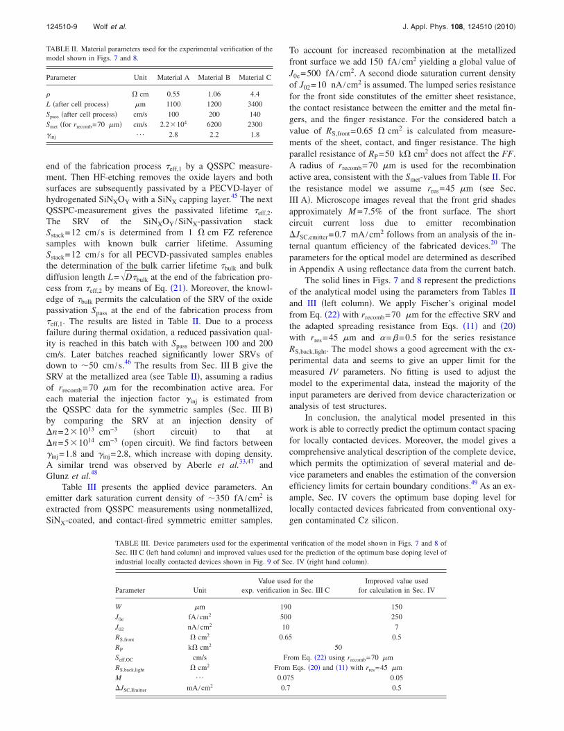
TABLE III. Device parameters used for the experimental verification of the model shown in Figs. 7 and 8 ofSec. III C �left hand column� and improved values used for the prediction of the optimum base doping level ofindustrial locally contacted devices shown in Fig. 9 of Sec. IV �right hand column�.
Parameter UnitValue used for the
exp. verification in Sec. III CImproved value used
for calculation in Sec. IV
W �m 190 150J0e fA /cm2 500 250J02 nA /cm2 10 7RS,front � cm2 0.65 0.5RP k� cm2 50Seff,OC cm/s From Eq. �22� using rrecomb=70 �mRS,back,light � cm2 From Eqs. �20� and �11� with rres=45 �mM ¯ 0.075 0.05�JSC,Emitter mA /cm2 0.7 0.5
124510-9 Wolf et al. J. Appl. Phys. 108, 124510 �2010�

IV. OPTIMUM BASE DOPING LEVEL FOR INDUSTRIALLOCALLY CONTACTED STRUCTURES
Locally contacted solar cells require a high base dopinglevel to reduce series resistance losses that originate fromcurrent crowding at the local contacts, as described in Sec.III A. On the other hand for conventional Cz-grown material,light induced degradation due to the formation of boron-oxygen complexes reduces the bulk diffusion length.14–16
Since this effect scales with the boron concentration, lowresistivity material typically shows reduced bulk carrier life-time compared to the Auger lifetime limit. The two describedphysical effects define the optimum resistivity range thatshould be applied for the fabrication of locally contactedsolar cells from Cz silicon material.
In this work we use our model to calculate the depen-dence of the conversion efficiency on the base doping levelof a locally contacted device made from Cz silicon. We applythe parameterization of Bothe et al. for the boron-oxygencomplex recombination limited bulk carrier lifetime,50
�B–O
1 �s= 2 7.675 1045 NA
1 cm−3�−0.824
�Oi�1 cm−3�−1.748
, �26�
where �Oi� denotes the interstitial oxygen concentration. Thefactor two accounts for the improvement of the bulk carrierlifetime due to the fabrication process.14,50 We use the intrin-sic carrier lifetime limit given by Kerr and Cuevas39 assum-ing �n=51014 cm−3 �open circuit� to calculate the bulkcarrier lifetime for FZ material as a reference.
Again, we apply Fischer’s model from Eq. �22� withrrecomb=70 �m and use the parameterization from Eq. �24�for the SRV at the metallized area �see Fig. 5, rrecomb
=70 �m�. Equation �25� gives the SRV at the passivatedsurface. We adapt the parameters S0, N0, and � to the experi-mental Spass-data shown in Fig. 4 �right hand side�. Moreoverwe assume a linear dependence of the injection factor
�inj = 1.67 + 3.89 10−17 NA
1 cm−3 , �27�
on the doping concentration NA as observed for the data fromTable II. Table IV summarizes all applied equations and pa-rameters.
For the device we use improved parameters compared tothe values used in Sec. III C in order to demonstrate thepotential of an industrial locally contacted structure. We as-
sume that for example the use of a selective emitter structurewould reduce the emitter recombination and a sophisticatedfront metallization lowers the shadowing and the series re-sistance losses. The applied parameters are listed in Table III�right hand column�.
Figure 9 presents the analytically calculated conversionefficiency plotted versus the base resistivity for a 150 �mthick device. For each resistivity, the optimum contactspacing is used. For some relevant data points the contactspacing is specified. We analyze three types of material, in-trinsically limited FZ silicon and Cz silicon with an intersti-tial oxygen concentration of �Oi�=11018 cm−3 as well as�Oi�=61017 cm−3, where the latter is commonly referredto as a lower limit for conventionally pulled Cz ingots.
For high quality FZ material, where Auger-recombination limits the bulk carrier lifetime, our model pre-dicts an optimum resistivity level of 0.5 � cm enablingconversion efficiencies of 20% for an industrial LFC device.The low resistivity reduces the series resistance losses, how-ever, increased bulk and surface recombination start to over-compensate the gain in FF for even lower resistivity values.
When recombination at boron-oxygen defect centers
TABLE IV. Material parameters used for the prediction of the optimum base doping level of industrial locallycontacted devices shown in Fig. 9.
Parameter Unit Value
L �mFrom L=�D�bulk using �bulk=�B–O from Eq. �26� for Cz material and
the intrinsic limit from Ref. 39 with �n=51014 cm−3 for FZ siliconSpass cm/s From Eq. �25� using S0=20 cm /s, N0=1.91015 cm−3, and �=0.4
Smet cm/sFrom Eq. �24� using S0=−10602 cm /s, S1=11495 cm /s,
and �met=310−17 cm3
�inj ¯ From Eq. �27�
1 2 3 4 518.0
18.5
19.0
19.5
20.0 W � ��� ��J0e � ��� ���
LP� ��� ��
�� ��������O
i� � ����������
�Oi� � ����������
�� �������
Conversionefficiency�(%)
!�" #"���$�%�$& � '��(
LP� ��� ��
LP� ��� ��
FIG. 9. Analytically calculated conversion efficiency of a 150 �m thicklocally contacted p-type device vs the base resistivity. Different models forthe doping dependent bulk carrier lifetime are applied: The intrinsic limit�Ref. 39� reveals the efficiency potential for the use of FZ Si, whereas theinterstitial oxygen concentration �Oi� controls the lifetime in the case of CzSi by Eq. �26�. For each resistivity, the optimum contact spacing is used.The short vertical lines specify the contact spacing for some relevant datapoints.
124510-10 Wolf et al. J. Appl. Phys. 108, 124510 �2010�

dominates in the bulk, higher resistivity values should beused. Depending on the interstitial oxygen concentration, aresistivity between 1 and 2 � cm should give the highestconversion efficiencies.
Recently, large area LFC solar cells fabricated from0.5 � cm FZ silicon reached efficiencies of 19.6% �Ref. 51�whereas stable efficiencies of 18.6% were achieved using2 � cm Cz silicon in a different approach.52 Thus, the pre-dictions of our calculation seem quite realistic.
For thinner devices the optimum resistivity shifts tolower values, since bulk recombination becomes less impor-tant. Please note that for resistivity values below 0.5 � cmand above 4 � cm the SRVs Smet and Spass, as well as theinjection factor �inj are extrapolated from the experimentaldata using the above described empiric equations. Thus, forthis resistivity range, the predictions of the model comealong with a higher uncertainty.
V. SUMMARY
We present a comprehensive analytical model for solarcells that feature local rear contacts. The model applies ef-fective parameters that enable the use of simple equations forone-dimensional transport, as already described in the litera-ture. However, in contrast to previously published work, ourmodel includes the impact of the rear surface recombinationon the short circuit current density and gives a completeanalytic description of the whole device. Thus, our modelenables the fast calculation of the energy conversion effi-ciency for different rear surface metallization geometries us-ing a spreadsheet calculator omitting the need of time-consuming numeric simulations.
Experimental results for rear surface passivated solarcells with local laser alloyed contacts �contact radius of 45 �m� verify the model for metallization fractions rang-ing from 0.3% to 7% and bulk resistivity values between 0.5and 4 � cm. No fitting is used to verify the model. Instead,the detailed characterization of the devices and appropriatetest structures permits the determination of all relevant ma-terial and device parameters. The radius for the recombina-tion active area is a crucial parameter; the SRV at the contactstrongly depends on the assumed contact size. Moreover, animproved empiric description of the series resistance for nar-row contact spacing is presented and confirmed by experi-mental data. Finally, we apply the model to estimate the op-timum base doping level for locally contacted solar cellsfabricated from conventional boron-doped Cz silicon. Thesecalculations account for carrier recombination at boron-oxygen complexes and predict an optimum bulk resistivity of1 to 2 � cm, depending on the interstitial oxygen concen-tration.
ACKNOWLEDGMENTS
We gratefully acknowledge fruitful discussions with ourcolleague S. Glunz and the partners of the LFC-Clusterproject. This work is supported by the German Federal Min-istry for the Environment, Nature Conservation and NuclearSafety under Project Nos. 0327572 and 0329849B.
APPENDIX A: CUMULATED GENERATION PROFILEAs outlined above, the determination of the four factors
in Eq. �14� requires the one-time use of optical simulations.Here, we use the device simulation program PC1D �Ref. 53�to calculate the cumulated generation profile of a crystallineSi cell with a random pyramid textured front surface. Theprogram applies the AM1.5G �IEC60904-3:2008� spectrum.The reflectance measured for a textured and phosphorus-diffused sample covered with a SiNX-AR layer serves as thefront reflectance. Since the simulation requires only the pri-mary reflection at the front surface Rfront, the experimentalcurve has to be corrected for the escape-reflection that origi-nates from the finite sample thickness. Therefore, the experi-mental data are cut off at a wavelength of 950 nm and thereflection measured at longer wavelengths is replaced by theextrapolation of a linear fit, which is performed in the rangeof 850–950 nm. Besides the front reflectance Rfront, the opti-cal model of PC1D requires parameters for the internal reflec-tion. Table V lists these values, which represent a texturedmonocrystalline Si device with a dielectrically passivatedrear surface. The small impact of a varying metallizationfraction on the internal rear reflection54 is neglected.
Table VI gives the factors for Eq. �14� as determinedfrom fitting to the above described device simulations. Thehomogeneous generation depends on the device thicknessand doping level. By simulations with varying device thick-ness and emitter- and the base doping, we derived the em-piric parameterization
TABLE V. Optical parameters used for calculating the generation profile fora random pyramid textured, rear surface passivated silicon device by meansof the device simulation program PC1D �Ref. 53�.
Parameter Value
Rfront,external Experimental data, IR-extrapolated
First bounce Subsequent bounceRfront,internal 90% �diffuse� 90% �diffuse�Rback,internal 94% �specular� 92% �specular�
TABLE VI. Factors for the cumulated generation profile from Eq. �14� asdetermined from optical simulations assuming a random pyramid texturedand AR-coated front surface and a dielectric rear surface passivation. Thethickness-dependent homogeneous generation follows from Eq. �A1�. Theparameters for the simulations are listed in Table V. The parameterizationholds for a device thickness between 50 and 500 �m.
Parameter Unit Value
Jgen,front mA /cm2 5.1Jgen,exp 1 mA /cm2 23.2Jgen,exp 2 mA /cm2 8.4L1 �m 4L2 �m 25Jhom,0 mA /cm2 0.5Jhom,log mA /cm2 1.0Jhom,exp mA /cm2 6.5L3 �m 1L4 �m 21
124510-11 Wolf et al. J. Appl. Phys. 108, 124510 �2010�

Jgen,hom = Jhom,0 − JFCA,emitter − JFCA,base + Jhom,log ln�W
L3�
+ Jhom,exp exp�−W
L4� . �A1�
This equation accounts for free carrier absorption �FCA� inthe base and the emitter, assuming linear dependence on theinverse emitter sheet resistance 1 /Rsheet for the latter,
JFCA,emitter
1 mA/cm2 = 8.2 1 �/sq
Rsheet. �A2�
The contribution of the base to the FCA is accounted as wellusing
JFCA,base
1 mA/cm2 =NA
1 10−17 cm−30.018 65
+ 6.32 10−4 W
1 �m
+ 3.807 10−7 W2
1 �m2� . �A3�
All parameters for Eqs. �14� and �A1� are listed in Table VI.
APPENDIX B: CARRIER MOBILITY AND INTRINSICCARRIER CONCENTRATION
The acceptor doping concentration NA and the base re-sistivity �=1 / �qNA�h� are linked by the elementary charge qand the majority �hole� mobility �h that follows from
� = �minTn�1 +
��max − �min�Tn�2
1 + NA
NrefTn�3��Tn
�4 , �B1�
using the model from the device simulation program PC1D.53
Table VII lists the parameters used to calculate the mobilityof both majority �holes� and minority carriers �electrons� at atemperature of 25 °C by means of Eq. �B1�. Klaassen pro-vides a more comprehensive description of the carriermobility,55,56 which will be implemented for future applica-tions. However, for the applied temperature of 25 °C and theconsidered p-type doping range, the deviations betweenKlaassen’s model and Eq. �B1� are below 12% for the elec-tron mobility and almost negligible for the hole mobility.
Since the mobility depends on the doping concentration,a recursive calculation would be required to determine NA
from � by means of Eq. �B1�. Instead of a recursive loop theparameterization introduced by Sinton57
log� NA
1 cm−3� = �n=0
4
Cn�log� �
1 � cm�n
, �B2�
is applied in this work using the parameters C0 to C4 fromTable VIII. For base resistivities between 0.1 and 100 � cmthis parameterization deviates less than 0.3% from the mo-bility model given by Eq. �B1�. Once NA is known, the elec-tron diffusion constant D=�ekBT /q follows from the Ein-stein relation using the electron mobility �e from Eq. �B1�and Table VII.
For high doping levels band gap narrowing �BGN� ef-fects should be considered yielding an effective intrinsic car-rier concentration that varies with NA. Here we use the pa-rameterization of the intrinsic carrier concentration given bySproul and Green58
ni,eff = C T
1 K�1.706
exp�Eg�T,NA�2kBT
� . �B3�
The temperature- and doping-dependent band gap of SiEg�T ,NA� applied in this work is59
Eg,�T,NA� = A + B T
1 K� + �Eg,�T,NA� �B4�
using A=1.206 eV and B=−2.7310−4 eV �for 250 K�T�415 K� as well as the temperature-dependent BGNmodel �Eg�T ,NA� of Schenk.60 Since later publicationsshowed that the measurements by Sproul and Green58 wereinfluenced by BGN,61 we multiply their result by a factor of0.9688 giving C=1.589109 cm−3 in Eq. �B3�. In the caseof intrinsic silicon ��Eg=0� Eqs. �B3� and �B4� yieldni,eff=9.65109 cm−3 for T=300 K, as suggested by Alter-matt et al.,61 and ni,eff=8.26109 cm−3 for standard testingconditions at T=298.15 K.
1O. Schultz, A. Mette, M. Hermle, and S. W. Glunz, Prog. Photovoltaics16, 317 �2008�.
2K. A. Münzer, A. Froitzheim, R. E. Schlosser, R. Tölle, and M. G. Win-stel, Proceedings of the 21st European Photovoltaic Solar Energy Confer-ence, Dresden, Germany, 4–6 Sept., 2006, p. 538.
3A. W. Blakers, A. Wang, A. M. Milne, J. Zhao, and M. A. Green, Appl.Phys. Lett. 55, 1363 �1989�.
4C. Mader, J. Müller, S. Gatz, T. Dullweber, and R. Brendel, Proceedingsof the 35th IEEE Photovoltaic Specialists Conference, Honolulu, Hawaii,20–25 June, 2010 �in press�.
5H. Plagwitz, M. Schaper, J. Schmidt, B. Terheiden, and R. Brendel, Pro-
TABLE VII. Parameters for calculating the electron and hole mobility inp-type Si at T=25 °C after Eq. �B1� �Ref. 53�.
Symbol UnitValue for hole
�majority� mobilityValue for electron
�minority� mobility
Tn ¯ 0.9938�max cm2 /V s 470 1417�min cm2 /V s 37.4 160Nref cm−3 2.821017 5.601016
� ¯ 0.642 0.647�1 ¯ �0.570�2 ¯ �2.230 �2.330�3 ¯ 2.400�4 ¯ �0.146
TABLE VIII. Dimensionless parameters for calculating the acceptor dopingconcentration NA from the resistivity � by means of Eq. �B2� �Ref. 57� forT=25 °C.
Parameter Value
C0 16.173C1 �1.084C2 0.0673C3 �0.0324C4 0.0066
124510-12 Wolf et al. J. Appl. Phys. 108, 124510 �2010�

ceedings of the 31st IEEE Photovoltaic Specialists Conference, Orlando,Florida, 3–7 Jan., 2005, p. 999.
6M. Schöfthaler, U. Rau, W. Füssel, and J. H. Werner, Proceedings of the23rd IEEE Photovoltaic Specialists Conference, Louisville, Kentucky,10–14 May, 1993, p. 315.
7A. G. Aberle, G. Heiser, and M. A. Green, J. Appl. Phys. 75, 5391 �1994�.8P. P. Altermatt, G. Heiser, A. G. Aberle, A. Wang, J. Zhao, S. J. Robinson,S. Bowden, and M. A. Green, Prog. Photovoltaics 4, 399 �1996�.
9K. R. Catchpole and A. W. Blakers, Proceedings of the 16th EuropeanPhotovoltaic Solar Energy Conference, Glasgow, UK, 1–5 May, 2000, p.1719.
10K. R. Catchpole and A. W. Blakers, Sol. Energy Mater. Sol. Cells 73, 189�2002�.
11S. Sterk and S. W. Glunz, in Simulation of Semiconductor Devices andProcesses, Vol. 5, edited by S. Selberherr, H. Stippel, and E.Strasser,�Springer, New York, 1993�, p. 393.
12D. Kray and S. W. Glunz, Prog. Photovoltaics 14, 195 �2006�.13D. Kray and K. R. McIntosh, Phys. Status Solidi A 206, 1647 �2009�.14S. W. Glunz, S. Rein, J. Y. Lee, and W. Warta, J. Appl. Phys. 90, 2397
�2001�.15J. Schmidt and K. Bothe, Phys. Rev. B 69, 024107 �2004�.16J. Schmidt and A. Cuevas, J. Appl. Phys. 86, 3175 �1999�.17A. Goetzberger, B. Voß, and J. Knobloch, Sonnenenergie: Photovoltaik
�Teubner, Stuttgart, 1994�.18K. R. McIntosh, Ph.D. thesis, University of New South Wales, 2001.19A. L. Fahrenbruch and R. H. Bube, Fundamentals of Solar Cells �Aca-
demic, New York, 1983�.20B. Fischer, Ph.D. thesis, University of Konstanz, 2003.21H. Plagwitz and R. Brendel, Prog. Photovoltaics 14, 1 �2006�.22U. Rau, Proceedings of the 12th European Photovoltaic Solar Energy Con-
ference, Amsterdam, The Netherlands, 11–15 April, 1994, p. 1350.23H. Plagwitz, Ph.D. thesis, University of Hannover, 2007.24P. Saint-Cast, M. Rüdiger, A. Wolf, M. Hofmann, J. Rentsch, and R. Preu,
J. Appl. Phys. 108, 013705 �2010�.25B. Gelmont and M. S. Shur, Solid-State Electron. 36, 143 �1993�.26B. Gelmont, M. S. Shur, and R. J. Mattauch, Solid-State Electron. 38, 731
�1995�.27S. Karmalkar, P. V. Mohan, P. H. Nair, and R. Yeluri, IEEE Trans. Electron
Devices 54, 1734 �2007�.28R. H. Cox and H. Strack, Solid-State Electron. 10, 1213 �1967�.29R. D. Brooks and H. G. Mattes, Bell Syst. Tech. J. 50, 775 �1971�.30F. Granek, M. Hermle, D. Huljic, O. Schultz-Wittmann, and S. W. Glunz,
Prog. Photovoltaics. 17, 47 �2009�.31S. Kluska, F. Granek, M. Rüdiger, M. Hermle, and S. W. Glunz, Sol.
Energy Mater. Sol. Cells 94, 568 �2010�.32R. Brendel and U. Rau, Solid State Phenom. 67–68, 81 �1999�.33A. G. Aberle, S. J. Robinson, A. Wang, J. Zhao, S. R. Wenham, and M. A.
Green, Prog. Photovoltaics 1, 133 �1993�.34E. Schneiderlöchner, R. Preu, R. Lüdemann, S. W. Glunz, and G. Willeke,
Proceedings of the 17th European Photovoltaic Solar Energy Conference,Munich, Germany, 22–26 October, 2001, p. 1303.
35J. F. Nekarda, S. Stumpp, L. Gautero, M. Hörteis, A. Grohe, D. Biro, andR. Preu, Proceedings of the 24th European Photovoltaic Solar EnergyConference, Hamburg, Germany, 21–25 Sept., 2009, p. 1411.
36S. Kontermann, A. Wolf, D. Reinwand, A. Grohe, D. Biro, and R. Preu,
Prog. Photovoltaics 17, 554 �2009�.37R. A. Sinton, A. Cuevas, and M. Stuckings, Proceedings of the 25th IEEE
Photovoltaic Specialists Conference, Washington, DC, 13–17 May, 1996,p. 457.
38A. B. Sproul, J. Appl. Phys. 76, 2851 �1994�.39M. J. Kerr and A. Cuevas, J. Appl. Phys. 91, 2473 �2002�.40A. Cuevas, M. Stuckings, J. Lau, and M. Petravic, Proceedings of the 14th
European Photovoltaic Solar Energy Conference, Barcelona, Spain, 30June–4 July, 1997, p. 2416.
41F. Granek, M. Hermle, B. Fleischhauer, A. Grohe, O. Schultz, S. W.Glunz, and G. Willeke, Proceedings of the 21st European PhotovoltaicSolar Energy Conference, Dresden, Germany, 4–8 Sept., 2006, p. 777.
42S. W. Glunz, E. Schneiderlöchner, D. Kray, A. Grohe, H. Kampwerth, R.Preu, and G. Willeke, Proceedings of the 19th European Photovoltaic So-lar Energy Conference, Paris, France, 7–11 June, 2004, p. 408.
43M. P. Godlewski, C. R. Baraona, and H. W. Brandhorst, Jr., Proceedings ofthe 10th IEEE Photovoltaic Specialists Conference, Palo Alto, California,13–15 Nov., 1973, p. 40.
44A. Krieg, A. Weil, E. Schäffer, J. Hohl-Ebinger, W. Warta, and S. Rein,Proceedings of the 22nd European Photovoltaic Solar Energy Conference,Milan, Italy, 3–7 Sept., 2007, p. 368.
45J. Seiffe, L. Weiss, M. Hofmann, L. Gautero, and J. Rentsch, Proceedingsof the 23rd European Photovoltaic Solar Energy Conference, Valencia,Spain, 1–5 Sept., 2008, p. 1700.
46S. Mack, A. Wolf, E. A. Wotke, A. Lemke, B. Holzinger, T. Dimitrova, D.Biro, and R. Preu, Proceedings of the 24th European Photovoltaic SolarEnergy Conference, Hamburg, Germany, 21–25 Sept., 2009, p. 1574.
47A. G. Aberle, S. W. Glunz, A. W. Stephens, and M. A. Green, Prog.Photovoltaics 2, 265 �1994�.
48S. W. Glunz, A. B. Sproul, W. Warta, and W. Wettling, J. Appl. Phys. 75,1611 �1994�.
49S. W. Glunz, J. Benick, D. Biro, M. Bivour, M. Hermle, D. Pysch, M.Rauer, C. Reichel, A. Richter, M. Rüdiger, C. Schmiga, A. Wolf, and R.Preu, Proceedings of the 35th IEEE Photovoltaic Specialists Conference,Honolulu, Hawaii, 20–25 June, 2010 �in press�.
50K. Bothe, R. Sinton, and J. Schmidt, Prog. Photovoltaics 13, 287 �2005�.51C. Schmiga, M. Rauer, M. Rüdiger, K. Meyer, J. Lossen, H.-J. Krokosz-
inski, M. Hermle, and S. W. Glunz, Proceedings of the 25th EuropeanPhotovoltaic Solar Energy Conference, Valencia, Spain, 6–10 Sept., 2010�in press�.
52A. Wolf, E. A. Wotke, A. Walczak, S. Mack, B. Bitnar, C. Koch, R. Preu,and D. Biro, Proceedings of the 35th IEEE Photovoltaic Specialists Con-ference, Honolulu, Hawaii, 20–25 June, 2010 �in press�.
53D. A. Clugston and P. A. Basore, Proceedings of the 26th IEEE Photovol-taic Specialists Conference, Anaheim, California, 29 Sept.-3 October,1997, p. 207.
54D. Kray, M. Hermle, and S. W. Glunz, Prog. Photovoltaics 16, 1 �2008�.55D. B. M. Klaassen, Solid-State Electron. 35, 953 �1992�.56D. B. M. Klaassen, Solid-State Electron. 35, 961 �1992�.57R. Sinton, Sinton Instruments, http://www.sintoninstruments.com/58A. B. Sproul and M. A. Green, J. Appl. Phys. 73, 1214 �1993�.59M. A. Green, J. Appl. Phys. 67, 2944 �1990�.60A. Schenk, J. Appl. Phys. 84, 3684 �1998�.61P. P. Altermatt, A. Schenk, F. Geelhaar, and G. Heiser, J. Appl. Phys. 93,
1598 �2003�.
124510-13 Wolf et al. J. Appl. Phys. 108, 124510 �2010�