
AlGaAs tunnel junction for high efficiency multi-junction solar cells: Simulation and measurement of...
6
AlGaAs TUNNEL JUNCTION FOR HIGH EFFICIENCY MULTI-JUNCTION SOLAR CELLS: SIMULATION AND MEASUREMENT OF TEMPERATURE-DEPENDENT OPERATION Jeffrey F. Wheeldon 1 , Christopher E. Valdivia 1 , Alex Walker 1 , Gitanjali Kolhatkar 1 ,Trevor J. Hall 1 , Karin Hinzer 1 Denis Masson 2 , Simon Fafard 2 Abdelatif Jaouad 3 , Artur Turala 3 , Richard Arès 3 , Vincent Aimez 3 1 Centre for Research in Photonics, University of Ottawa, Ottawa, ON, Canada 2 Cyrium Technologies Inc., Ottawa, ON, Canada 3 Centre de Recherche en Nanofabrication et en Nanocaractérisation CRN², Université de Sherbrooke, Sherbrooke, QC, Canada ABSTRACT AlGaAs tunnel junctions are shown to be well-suited to concentrated photovoltaics where temperatures and current densities can be dramatically higher than for 1-sun flat-panel systems. Detailed comparisons of AlGaAs/AlGaAs tunnel junction experimental measurements over a range of temperatures expected during device operation in concentrator systems are presented. Experimental and simulation results are compared in an effort to decouple the tunnel junction from the overall multi-junction solar cell. The tunnel junction resistance is experimentally studied as a function of the temperature to determine its contribution to overall efficiency of the solar cell. The current-voltage behavior of the isolated TJ shows that as the temperature is increased from 25°C to 85°C, the resistance decreases from ~4.7×10 -4 Ω∙cm 2 to ~0.3×10 -4 Ω∙cm 2 for the operational range of a multi-junction solar cell under concentration. INTRODUCTION Multi-junction (MJ) solar cells fabricated from III-V semiconductors have conversion efficiencies that significantly outperform their single-junction (1J) counterparts [1]. The p-n junction of the 1J solar cell can only achieve high power conversion efficiencies for a limited range of photon energies lying close to the energy gap between the valence and conduction bands. In contrast, MJ solar cells are composed of tandem p-n junctions, where the bandgap of each subcell is tailored to a different range of photon energies. Hence, MJ solar cells are able to efficiently capture photons over a much wider spectral range, resulting in experimentally-measured conversion efficiencies up to 40.7% [2] and 40.8% [3] using the AM1.5D spectrum under high concentration. Fig. 1(a) shows an example of a triple-junction (3J) solar cell, presently the most common type of multi-junction design in commercial use. The tandem p-n junctions of a state-of-the-art MJ solar cell are monolithically integrated into a multi-layered device that imposes the challenge of conducting current between the subcells. This challenge is addressed by introducing tunnel junctions (TJ) that connect the p terminal of one subcell to the n terminal of an adjacent subcell. The TJ itself is a heavily doped n-p junction with doping concentrations typically >10 19 cm -3 , shown schematically in Fig. 1(b). For successful device operation, a TJ must be transparent to the wavelengths absorbed in the subsequent subcells, and it must form a low-resistance contact to ensure a minimal voltage drop. Due to the high cost of multi-junction devices, terrestrial systems couple these solar cells with concentrating optics such as mirrors or lenses. By collecting light over a large area and concentrating it onto an area typically 500× smaller, a significant reduction in semiconductor device area is required. However, in these concentrator systems the photocurrent can surpass 10 A/cm 2 and operating temperatures can approach 80°C or more, depending on the ambient temperature, concentration ratio, and concentrator design. In previous studies, temperature has been shown to have a significant effect on the performance of a solar cell [4]. Due to the importance of the TJ current-voltage characteristics in the overall conversion efficiency, this paper presents the comparison of AlGaAs/AlGaAs TJ experimental measurements and simulation results over a range of temperatures expected during device operation in concentrator systems. Experimental and simulation results are compared in an effort to decouple the TJ from the overall MJ solar cell. In contrast to other research examining GaAs/GaAs TJ [5]-[6], these investigations focus on AlGaAs/AlGaAs TJ structures, extending our prior results which examined the effect of simulation parameter variations on the current-voltage behavior [7]. The addition of Al allows the designer greater flexibility in the optimization of the device – alongside the control of doping concentration and layer thickness, the Al mole fraction can be used to align the energy bands of the tunnel junction with respect to the adjacent junction energy bands for optimized current tunneling between two junctions. EXPERIMENT Tunnel junctions, designed by Cyrium Technologies Inc., were MOCVD-grown on a Ge wafer. The n-doped GaInAs layer was lattice-matched to Ge via the introduction of ~1% In content. Two highly doped AlxGa1-xAs (x < 0.2) layers form the p-n junction, surrounded by AlxGa1-xAs buffer layers with lower dopant concentration. The top is finally capped by a GaInAs layer. This epitaxial structure is depicted schematically in
-
Upload
nanophotonics -
Category
Documents
-
view
0 -
download
0
Transcript of AlGaAs tunnel junction for high efficiency multi-junction solar cells: Simulation and measurement of...

AlGaAs TUNNEL JUNCTION FOR HIGH EFFICIENCY MULTI-JUNCTION SOLAR CELLS: SIMULATION AND MEASUREMENT OF TEMPERATURE-DEPENDENT
OPERATION
Jeffrey F. Wheeldon 1, Christopher E. Valdivia
1, Alex Walker
1, Gitanjali Kolhatkar
1,Trevor J. Hall
1, Karin Hinzer
1
Denis Masson 2, Simon Fafard
2
Abdelatif Jaouad 3, Artur Turala
3, Richard Arès
3, Vincent Aimez
3
1 Centre for Research in Photonics, University of Ottawa, Ottawa, ON, Canada
2 Cyrium Technologies Inc., Ottawa, ON, Canada 3 Centre de Recherche en Nanofabrication et en Nanocaractérisation CRN², Université de Sherbrooke, Sherbrooke, QC, Canada
ABSTRACT
AlGaAs tunnel junctions are shown to be well-suited to concentrated photovoltaics where temperatures and current densities can be dramatically higher than for 1-sun flat-panel systems. Detailed comparisons of AlGaAs/AlGaAs tunnel junction experimental measurements over a range of temperatures expected during device operation in concentrator systems are presented. Experimental and simulation results are compared in an effort to decouple the tunnel junction from the overall multi-junction solar cell. The tunnel junction resistance is experimentally studied as a function of the temperature to determine its contribution to overall efficiency of the solar cell. The current-voltage behavior of the isolated TJ shows that as the temperature is increased from 25°C to 85°C, the resistance decreases from ~4.7×10
-4 Ω∙cm
2 to ~0.3×10
-4 Ω∙cm
2 for the operational
range of a multi-junction solar cell under concentration.
INTRODUCTION
Multi-junction (MJ) solar cells fabricated from III-V
semiconductors have conversion efficiencies that significantly outperform their single-junction (1J) counterparts [1]. The p-n junction of the 1J solar cell can
only achieve high power conversion efficiencies for a limited range of photon energies lying close to the energy gap between the valence and conduction bands. In contrast, MJ solar cells are composed of tandem p-n
junctions, where the bandgap of each subcell is tailored to a different range of photon energies. Hence, MJ solar cells are able to efficiently capture photons over a much wider spectral range, resulting in experimentally-measured conversion efficiencies up to 40.7% [2] and 40.8% [3] using the AM1.5D spectrum under high concentration. Fig. 1(a) shows an example of a triple-junction (3J) solar cell, presently the most common type of multi-junction design in commercial use.
The tandem p-n junctions of a state-of-the-art MJ solar cell are monolithically integrated into a multi-layered device that imposes the challenge of conducting current between the subcells. This challenge is addressed by introducing tunnel junctions (TJ) that connect the p terminal of one subcell to the n terminal of an adjacent subcell. The TJ itself is a heavily doped n-p junction with doping concentrations typically >10
19 cm
-3, shown
schematically in Fig. 1(b). For successful device operation, a TJ must be transparent to the wavelengths absorbed in the subsequent subcells, and it must form a low-resistance contact to ensure a minimal voltage drop.
Due to the high cost of multi-junction devices, terrestrial systems couple these solar cells with concentrating optics such as mirrors or lenses. By collecting light over a large area and concentrating it onto
an area typically 500× smaller, a significant reduction in
semiconductor device area is required. However, in these concentrator systems the photocurrent can surpass 10 A/cm
2 and operating temperatures can approach 80°C
or more, depending on the ambient temperature, concentration ratio, and concentrator design. In previous studies, temperature has been shown to have a significant effect on the performance of a solar cell [4].
Due to the importance of the TJ current-voltage characteristics in the overall conversion efficiency, this paper presents the comparison of AlGaAs/AlGaAs TJ experimental measurements and simulation results over a range of temperatures expected during device operation in concentrator systems. Experimental and simulation results are compared in an effort to decouple the TJ from the overall MJ solar cell. In contrast to other research examining GaAs/GaAs TJ [5]-[6], these investigations focus on AlGaAs/AlGaAs TJ structures, extending our prior results which examined the effect of simulation parameter variations on the current-voltage behavior [7]. The addition of Al allows the designer greater flexibility in the optimization of the device – alongside the control of doping concentration and layer thickness, the Al mole fraction can be used to align the energy bands of the tunnel junction with respect to the adjacent junction energy bands for optimized current tunneling between two junctions.
EXPERIMENT
Tunnel junctions, designed by Cyrium Technologies
Inc., were MOCVD-grown on a Ge wafer. The n-doped GaInAs layer was lattice-matched to Ge via the introduction of ~1% In content. Two highly doped AlxGa1-xAs (x < 0.2) layers form the p-n junction,
surrounded by AlxGa1-xAs buffer layers with lower dopant concentration. The top is finally capped by a GaInAs layer. This epitaxial structure is depicted schematically in

10 μm
70 μm
Fig. 2: Scanning electron microscope image of an isolated TJ mesa structure (D10L70). The mesa structure dimensions are: top contact (center square), 70 μm ×
70 μm (L70), which covers the TJ layers; and side gap (between center square and outer ring), 10 μm width
(D10). The outer dimensions are 200 μm × 200 μm.
Fig. 1(b), where the doping concentrations and thicknesses can be varied to optimize the device performance.
The devices were then fabricated at the Université de Sherbrooke, forming a mesa structure depicted in Fig. 1(c). The scanning electron microscope image of Fig. 2 lists the main dimensions of a fabricated device, including the top contact width and side gap between contacts which are 70 µm and 10 µm, respectively, in this example. The TJ structures were fabricated by standard photolithography and chemical etching in a self-aligned process, using the metallic contacts as a mask for etching of the mesas that contain the TJ heterostructures. The center mesas were fabricated first by photolithography
using the positive-tone resist Shipley S1813 spun on previously deposited Microchem LOR-A lift-off resist layer. The surface of TJ structure was cleaned and deoxidized in HCl:H2O (1:1) for 30 s prior to metallization. The metallization of the top emitter contacts with Ti (5 nm) and Au (150 nm) was done by e-beam evaporator and followed by lift-off. The mesas containing the TJ have been etched in H3PO4:H2O2:H2O (3:1:40), using the emitter Au/Ti contacts as a mask. The collector contacts (outer ring) were fabricated by the same procedure in a second step of lithography. They consist of 30 nm and 150 nm layers of Ti and Au, respectively. The OAI 200 mask aligner used was capable of aligning features with a precision of 2 µm. The samples were then annealed for 1 minute at 300-350°C under N2 atmosphere in order to diminish the specific resistance of the contacts.
The electrical performance of the TJ mesa structures are investigated using a four-wire remote sensing measurement technique. Measurements are recorded under dark, temperature-controlled conditions. Where not otherwise specified, the measurement temperature was held at 25.0±0.1°C. A typical measurement of the current-voltage (IV) behavior of the TJ mesa structure is depicted
in Fig. 3(a). The region of interest for solar cell operation is dominated by the tunneling current peak, which covers the region between V = 0 to 0.8 V for this device. For
comparison, a 40%-efficient MJ solar cell operating at 500× concentration may produce ~7 A/cm
2, placing the TJ
operating point very near the origin in practice. An optimal TJ will have a large initial slope (low resistance) near the origin and a primary current-density peak much greater than the maximum short-circuit current-density, Jsc, of the
MJ solar cell under concentrated illumination. To calibrate the numerical simulations (discussed in
the next section), the IV characteristics are measured over
a much larger voltage range than required for solar cell operation. Investigation of the entire tunneling peak allows greater understanding of the device operation, opportunities for optimization, and estimations of
(a) (b) (c)
Bottom contact
p++ AlxGa1-xAs t1
n++ AlxGa1-xAs t1
p+ AlxGa1-xAs t2
n+ AlxGa1-xAs t2
p GaInAs t3
n GaInAs t4
Side View
Top contact
Top View
Fig. 1: (a) Triple-junction solar cell with GaInP/InGaAs/Ge subcells connected by tunnel junctions, as in [1];
(b) expanded view of a single tunnel junction, where the epitaxial material (x < 0.2), the relative doping
concentrations, and the thickness are listed for each layer; (c) side and top views of the experimental test mesa structure of an isolated tunnel junction. Schematics are not to scale.

fabrication values such as active doping concentration. For solar cells, increasing the slope near the origin (which represents the TJ conductance) is of particular importance to reduce electrical losses and maximize light-to-electrical conversion efficiency.
The experimental IV characteristics of Fig. 3(a) can be
separated into three distinct regions: the initial slope region (of primary concern for solar cell operation); a negative differential resistance (NDR) region; and the diffusion current region (a combination of diffusion current and to a lesser extent, excess current). Measurements of the initial slope and diffusion current regions provide an accurate IV behavior of the TJ mesa structure.
In contrast, in the NDR region of the tunnel junction IV
behavior – the voltage range in the shaded area of Fig. 3(a) – nonlinear oscillations prevent direct measurement of the downward slope of the tunneling peak [8], resulting in a plateau-like profile. The curve of Fig. 3(a) is an average over the oscillations, acquired using an 84 ms integration time at each data point. An oscilloscope was therefore used to measure the voltage across a small resistor connected in series with the TJ, providing the current as a function of time with a sample rate of 1 MSa/s, plotted in Fig. 3(b) for three distinct operating points. At voltage biases of 590 mV (near the peak of the tunneling current) and 820 mV (near the valley bottom after the tunneling current), the device current is time-independent. The third bias point shown is at 740 mV which is within the NDR region and reveals time-dependent current oscillations. Away from the center of the NDR region, the oscillations are less periodic and become intermittent near the edges. Nonetheless, throughout the NDR region the oscillation magnitude remains unchanged, extending between the current values at the tunneling peak (~960 A/cm
2) and
valley (~140 A/cm2). Different tunnel junctions with this
setup have exhibited oscillation frequencies ranging from 1-5 kHz.
As a result of these oscillations a number of characteristics of the TJ current-voltage profile are obscured, most notably the precise magnitudes of the primary peak and valley minimum, the value of the NDR, and a possible secondary peak (discussed further in the next section). Other authors have noted that these issues within the NDR region can be overcome in some cases using different techniques [8]-[9], although this has not yet been demonstrated for these devices. The measurement limitations at the peak and valley currents can be understood using the load-line analysis for a tunnel diode with a series resistance [9], which in this case has a significant contribution from the mesa structure itself. The experimental IV profile represents the isolated TJ plus the
resistances inherent in the mesa structure which will not be present in a full solar cell device. The mesa structure includes extra resistances in the cap layers, lateral perimeter resistance (dependent on the side gap), and metal-semiconductor contacts (dependent on the top contact size). Four-wire transmission line model (TLM) measurements determined the contact resistances to be on the order of 0.5 mΩ∙cm
2, and the total added resistance
of the mesa structure to be ~12 Ω. Additionally, a typical solar cell for a concentrator system will have a significantly larger area on the order of 1 cm
2, thus reducing the
magnitude of the total resistances.
SIMULATION
Computer simulations of the isolated TJ are performed
using Synopsys Sentaurus, a commercial semiconductor device simulator [10]. Within this program, Maxwell’s equations and carrier transport equations are solved self-consistently throughout the highly-doped four-layer structure (p+, p++, n++, n+) depicted in Fig. 1(b). For the voltage region relevant to solar cells, carrier transport is
(a)
Fig. 3: (a) Current-voltage behavior of a tunnel junction mesa structure at 25°C, using a 84 ms averaging time for each measurement point; (b) time-dependent current oscillations (1 MSa/s), shown for the voltage bias points highlighted in (a), before (590 mV), in the middle (740 mV), and after (820 mV) the negative differential resistance region, highlighted by the shaded area.
NDR Region (b)

Fig. 4: Energy band diagram for the AlGaAs/AlGaAs tunnel junction at 0 V bias, where the electron and hole quasi-Fermi levels are superimposed and the depletion region is highlighted by the shaded area.
Fig. 5: Current-voltage characteristics of an AlGaAs/AlGaAs tunnel junction at 25°C: Sentaurus simulation (black line); Sentaurus simulation with a nonlinear series resistance Rs = (6.4 – 0.002∙J)∙10
-4 Ω∙cm
2
added analytically (blue dashed line) to match the initial slope of the experimental data (red dashed and dotted line).
dominated by inter-band tunneling [11]. This inter-band tunneling is simulated using a nonlocal model based on Ieong et al. [12], previously shown to provide the most accurate results [5]. Displayed in Fig. 4 is the numerically simulated energy band diagram at zero voltage bias, clearly displaying the degenerate (i.e. heavily doped with impurities) p++ and n++ layers on either side of the depletion region (potential barrier through which carriers tunnel) that form the tunnel junction structure. For this simulation at zero voltage bias, the depletion region was determined to be approximately 14 nm wide. Furthermore we see that the quasi-Fermi levels for the electrons and
the holes are within the conduction band and valence band, respectively, as expected for the degenerate layers.
Numerical simulations of an isolated AlGaAs/AlGaAs TJ are compared to experimentally measured IV
characteristics in Fig. 5. The overall shape of the simulated curve in Fig. 5 is generally similar to the expected shape, including the appearance of a primary current peak followed by a current valley, and completed by an exponential rise in the diffusion region. For the initial slope of the simulated data to match the experimental results, a nonlinear series resistance is added analytically to the simulation data (following [5]-[6] for GaAs/GaAs TJ), in this case Rs = (6.4 – 0.002∙J)∙10
-4 Ω∙cm
2, where J is the current density, calculated using the
TJ cross-sectional area of 70×70 µm2. This represents
resistance within the experimental setup not accounted for in the simulation, including that of the more complex geometry of the TJ mesa structure equaling a total resistance of ~13 Ω which is very close to the experimentally determined value of ~12 Ω. Under some conditions, TLM measurements have shown a nonlinear IV curve, which indicates that the nonlinear component of the mesa series resistance may be caused by a nonlinear contact resistance.
A significant discrepancy between simulation and measurement is observed in the diffusion region of Fig. 5 which is due in large part to the omission of excess current from the simulation model [13]. This exponentially-increasing current is expected to raise the valley current above zero after the tunneling peak, greatly improving the fit to the measured devices. Fitting the simulated data with a parallel resistance also serves to shift the valley and diffusion currents upwards, although doing so without the inclusion of the excess current overestimates the contribution of the parallel resistance to the operation of the device and incorrectly adjusts the slope in the diffusion current region.
As discussed in our previous work [6], the simulated IV
characteristics of the TJ can vary greatly depending on the parameter set chosen, such as the dopant concentrations and the scaling factors for the effective Richardson constant (gc, gv). For the simulations within this paper the following parameters were chosen: the doping concentrations in each layer are reduced to 73% of their nominal values to represent the active dopant
concentration; the scaling factors of the effective Richardson constants are set to gc = 0.21 and gv = 0.4 [14]; the effective mass scaling factors of the electrons and the holes in AlGaAs were set to the appropriate values for
the molar concentration (x < 0.2) [15]. Choosing the
correct parameters for a simulation to match experimental data is complicated by many factors, such as the uncertainty of doping concentrations, layer thickness, diffusion, and intermixing at the various interfaces. As mentioned above, the mesa structure itself adds resistance to the experimental data, and is complicated by the finite fabrication resolution which causes variations in the dimensions of the mesa structures. Furthermore, as noted by other authors [5], several different parameter sets will result in similar initial slopes in the IV curve.
Depletion Region
(~14 nm)
h Quasi-Fermi Level
Conduction Band Energy Valence Band Energy e Quasi-Fermi Level
p++ n++ n+ p+
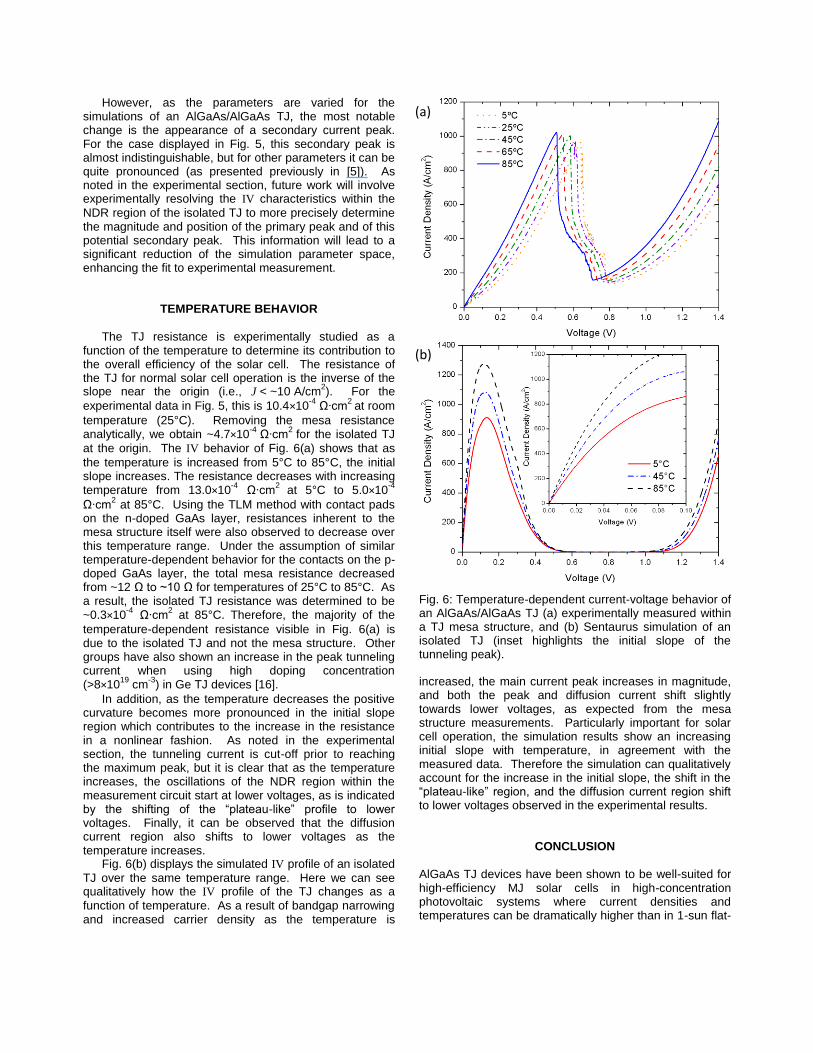
However, as the parameters are varied for the simulations of an AlGaAs/AlGaAs TJ, the most notable change is the appearance of a secondary current peak. For the case displayed in Fig. 5, this secondary peak is almost indistinguishable, but for other parameters it can be quite pronounced (as presented previously in [5]). As noted in the experimental section, future work will involve experimentally resolving the IV characteristics within the
NDR region of the isolated TJ to more precisely determine the magnitude and position of the primary peak and of this potential secondary peak. This information will lead to a significant reduction of the simulation parameter space, enhancing the fit to experimental measurement.
TEMPERATURE BEHAVIOR
The TJ resistance is experimentally studied as a
function of the temperature to determine its contribution to the overall efficiency of the solar cell. The resistance of the TJ for normal solar cell operation is the inverse of the slope near the origin (i.e., J < ~10 A/cm
2). For the
experimental data in Fig. 5, this is 10.4×10⁻⁴
Ω∙cm2
at room
temperature (25°C). Removing the mesa resistance analytically, we obtain ~4.7×10
-4 Ω∙cm
2 for the isolated TJ
at the origin. The IV behavior of Fig. 6(a) shows that as
the temperature is increased from 5°C to 85°C, the initial slope increases. The resistance decreases with increasing temperature from 13.0×10
-4 Ω∙cm2
at 5°C to 5.0×10⁻⁴
Ω∙cm2 at 85°C. Using the TLM method with contact pads
on the n-doped GaAs layer, resistances inherent to the mesa structure itself were also observed to decrease over this temperature range. Under the assumption of similar temperature-dependent behavior for the contacts on the p-doped GaAs layer, the total mesa resistance decreased from ~12 Ω to ~10 Ω for temperatures of 25°C to 85°C. As a result, the isolated TJ resistance was determined to be ~0.3×10
-4 Ω∙cm2 at 85°C. Therefore, the majority of the
temperature-dependent resistance visible in Fig. 6(a) is due to the isolated TJ and not the mesa structure. Other groups have also shown an increase in the peak tunneling current when using high doping concentration (>8×10
19 cm
-3) in Ge TJ devices [16].
In addition, as the temperature decreases the positive curvature becomes more pronounced in the initial slope region which contributes to the increase in the resistance in a nonlinear fashion. As noted in the experimental section, the tunneling current is cut-off prior to reaching the maximum peak, but it is clear that as the temperature increases, the oscillations of the NDR region within the measurement circuit start at lower voltages, as is indicated by the shifting of the “plateau-like” profile to lower voltages. Finally, it can be observed that the diffusion current region also shifts to lower voltages as the temperature increases.
Fig. 6(b) displays the simulated IV profile of an isolated
TJ over the same temperature range. Here we can see qualitatively how the IV profile of the TJ changes as a
function of temperature. As a result of bandgap narrowing and increased carrier density as the temperature is
Fig. 6: Temperature-dependent current-voltage behavior of an AlGaAs/AlGaAs TJ (a) experimentally measured within a TJ mesa structure, and (b) Sentaurus simulation of an isolated TJ (inset highlights the initial slope of the tunneling peak).
increased, the main current peak increases in magnitude, and both the peak and diffusion current shift slightly towards lower voltages, as expected from the mesa structure measurements. Particularly important for solar cell operation, the simulation results show an increasing initial slope with temperature, in agreement with the measured data. Therefore the simulation can qualitatively account for the increase in the initial slope, the shift in the “plateau-like” region, and the diffusion current region shift to lower voltages observed in the experimental results.
CONCLUSION
AlGaAs TJ devices have been shown to be well-suited for high-efficiency MJ solar cells in high-concentration photovoltaic systems where current densities and temperatures can be dramatically higher than in 1-sun flat-
(a)
(b)
panel systems. Experimental measurements of the IV
curve within the NDR region are hindered due to nonlinear oscillations, and the resistances of the mesa structure must be subtracted to isolate the TJ behavior. Nonetheless, experiment reveals isolated TJ resistances
of ~4.7×10⁻⁴
Ω∙cm2 and ~0.3×10
-4 Ω∙cm
2 at 25°C and
85°C, respectively, which are qualitatively confirmed via simulation. The temperature-dependence of the TJ IV curve has a much greater effect than the temperature-dependence of the mesa structure, and this confirms the suitability of the TJ for high-concentration applications. The comparison between experiment and simulation provides a greater understanding of the TJ performance and limitations, reveals sources of added resistance in the experimental setup, and confirms the applicability of the TJ model.
REFERENCES
[1] R. R. King, D. C. Law, K. M. Edmondson, C. M. Fetzer, G. S. Kinsey, H. Yoon, D. D. Krut, J. H. Ermer, R. A. Sherif and N. H. Karam, "Advances in high-efficiency III-V multijunction solar cells", Advances in OptoElectronics, 2007, pp. 29523.
[2] R. R. King, D. C. Law, K. M. Edmondson, C. M. Fetzer, G. S. Kinsey, H. Yoon, R. A. Sherif and N. H. Karam, "40% efficient metamorphic GaInP/GaInAs/Ge multijunction solar cells", Appl. Phys. Lett., 90, 2007, pp. 183516.
[3] J. F. Geisz, D. J. Friedman, J. S. Ward, A. Duda, W. J. Olavarria, T. E. Moriarty, J. T. Kiehl, M. J. Romero, A. G. Norman and K. M. Jones, "40.8% efficient inverted triple-junction solar cell with two independently metamorphic junctions", Appl. Phys. Lett., 93, 2008, pp. 123505.
[4] V. K. Narasimhan, C. E. Valdivia, N. Yastrebova, J. Fafard, V. Tatsiankou, F. Le Jean, T. J. Hall and K. Hinzer, "Performance analysis of III-V triple-junction concentrator solar cells under varying temperature and intensity", IEEE Lasers and Electro-Optics Society (LEOS) Annual Meeting, 2008, pp. MK2.
[5] M. Hermle, G. Létay, S. P. Philipps and A. W. Bett, "Numerical simulation of tunnel diodes for multi-junction solar cells", Progress in Photovoltaics: Research and Applications, 16, 2008, pp. 409-418.
[6] W. Guter and A. W. Bett, "I-V characterization of tunnel diodes and multijunction solar cells", IEEE Trans. Electron Dev., 53, 2006, pp. 2216-2222.
[7] V. K. Narasimhan, N. Yastrebova, C. E. Valdivia, D. Masson, S. Fafard, A. Jaouad, R. Arès, V. Aimez, T. J. Hall and K. Hinzer, "Effect of parameter variations on the current-voltage behaviour of AlGaAs tunnel junction
model", Proc. of IEEE, 1st Microsystems and Nanoelectronics Research Conference, 2008, pp. 165-168.
[8] J. F. Young, B. M. Wood, H. C. Liu, M. Buchanan, D. Landheer, A. J. SpringThorpe and P. Mandeville, "Effect of circuit oscillations on the dc current-voltage characteristics of double barrier resonant tunneling structures", Appl. Phys. Lett., 52, 1988, pp. 1398-1400.
[9] A. Förster, "Resonant tunneling diodes: The effect of structural properties on their performance", in Advances in Solid State Physics 33, vol. 33, Springer, 1993, pp. 37-62.
[10] Synopsys Inc., "Synopsys Sentaurus Device User’s Manual", Synopsys Inc., Switzerland, Tech. Rep. Release A-2007.12, 2007.
[11] L. Esaki, "New Phenomenon in Narrow Germanium Para-Normal-Junctions", Phys. Rev., 109, 1958, pp. 603-604.
[12] M. Ieong, P. M. Solomon, S. E. Laux, H. S. P. Wong and D. Chidambarrao, "Comparison of raised and schottky source/drain MOSFETs using a novel tunneling contact model", Electron Devices Meeting, 1998. IEDM '98 Technical Digest., International, 1998, pp. 733-736.
[13] S. M. Sze, Physics of Semiconductor Devices. Wiley-Interscience, 1969, pp. 812.
[14] Synopsys Inc., "Simulation of Triple-Junction GaInP/GaAs/InGaAs Solar Cells with Transfer Matrix Method", Synopsys Inc., Tech. Rep. Release A-2008.09, 2008.
[15] S. Adachi, "GaAs, AlAs, and AlxGa1-xAs: Material parameters for use in research and device applications", J. Appl. Phys., 58, 1985, pp. R1-R29.
[16] R. M. Minton and R. Glicksman, "Theoretical and experimental analysis of germanium tunnel diode characteristics", Solid-State Electronics, 7, 1964, pp. 491-500.