Towards Understanding Junction Degradation in Cadmium Telluride Solar Cells
10
Towards understanding junction degradation in cadmium telluride solar cells Marco Nardone Citation: Journal of Applied Physics 115, 234502 (2014); doi: 10.1063/1.4883368 View online: http://dx.doi.org/10.1063/1.4883368 View Table of Contents: http://scitation.aip.org/content/aip/journal/jap/115/23?ver=pdfcov Published by the AIP Publishing Articles you may be interested in Effect of chlorine activation treatment on electron beam induced current signal distribution of cadmium telluride thin film solar cells J. Appl. Phys. 114, 163518 (2013); 10.1063/1.4827204 Hybrid polymer solar cell based on cadmium selenide quantum dots AIP Conf. Proc. 1536, 213 (2013); 10.1063/1.4810176 Organic/inorganic hybrid pn-junction between copper phthalocyanine and CdSe quantum dot layers as solar cells J. Appl. Phys. 112, 044507 (2012); 10.1063/1.4747835 Enhanced performance of hybrid solar cells using longer arms of quantum cadmium selenide tetrapods Appl. Phys. Lett. 99, 223515 (2011); 10.1063/1.3662839 Single-crystal II-VI on Si single-junction and tandem solar cells Appl. Phys. Lett. 96, 153502 (2010); 10.1063/1.3386529 [This article is copyrighted as indicated in the article. Reuse of AIP content is subject to the terms at: http://scitation.aip.org/termsconditions. Downloaded to ] IP: 129.1.90.94 On: Mon, 07 Jul 2014 15:58:02
Transcript of Towards Understanding Junction Degradation in Cadmium Telluride Solar Cells

Towards understanding junction degradation in cadmium telluride solar cellsMarco Nardone
Citation: Journal of Applied Physics 115, 234502 (2014); doi: 10.1063/1.4883368 View online: http://dx.doi.org/10.1063/1.4883368 View Table of Contents: http://scitation.aip.org/content/aip/journal/jap/115/23?ver=pdfcov Published by the AIP Publishing Articles you may be interested in Effect of chlorine activation treatment on electron beam induced current signal distribution of cadmium telluridethin film solar cells J. Appl. Phys. 114, 163518 (2013); 10.1063/1.4827204 Hybrid polymer solar cell based on cadmium selenide quantum dots AIP Conf. Proc. 1536, 213 (2013); 10.1063/1.4810176 Organic/inorganic hybrid pn-junction between copper phthalocyanine and CdSe quantum dot layers as solar cells J. Appl. Phys. 112, 044507 (2012); 10.1063/1.4747835 Enhanced performance of hybrid solar cells using longer arms of quantum cadmium selenide tetrapods Appl. Phys. Lett. 99, 223515 (2011); 10.1063/1.3662839 Single-crystal II-VI on Si single-junction and tandem solar cells Appl. Phys. Lett. 96, 153502 (2010); 10.1063/1.3386529
[This article is copyrighted as indicated in the article. Reuse of AIP content is subject to the terms at: http://scitation.aip.org/termsconditions. Downloaded to ] IP:
129.1.90.94 On: Mon, 07 Jul 2014 15:58:02
Towards understanding junction degradation in cadmium telluride solar cells
Marco Nardonea)
Department of Environment and Sustainability, Bowling Green State University, Bowling Green, Ohio 43403,USA
(Received 6 April 2014; accepted 3 June 2014; published online 17 June 2014)
A degradation mechanism in cadmium telluride (CdTe/CdS) solar cells is investigated using
time-dependent numerical modeling to simulate various temperature, bias, and illumination stress
conditions. The physical mechanism is based on defect generation rates that are proportional to
nonequilibrium charge carrier concentrations. It is found that a commonly observed degradation
mode for CdTe/CdS solar cells can be reproduced only if defects are allowed to form in a
narrow region of the absorber layer close to the CdTe/CdS junction. A key aspect of this
junction degradation is that both mid-gap donor and shallow acceptor-type defects must be
generated simultaneously in response to photo-excitation or applied bias. The numerical
approach employed here can be extended to study other mechanisms for any photovoltaic
technology. VC 2014 AIP Publishing LLC. [http://dx.doi.org/10.1063/1.4883368]
I. INTRODUCTION
The stability of thin-film photovoltaic modules remains
rather unpredictable compared to their crystalline counter-
parts.1 That uncertainty needs to be minimized if such low-
cost alternatives are to provide a significant portion of solar
electricity on a global scale.2 Similar reliability issues will
be faced by more advanced technologies that have yet to hit
the market. Predicting degradation is complicated by the fact
that it depends not only on the type of stress (light, tempera-
ture, bias, atmospheric conditions, and combinations thereof)
but also on fabrication details and transient effects. Inherent
nonuniformities (more pronounced in thin films) lead to vari-
able degradation even in devices that have been fabricated
and stressed in identical conditions. A better understanding
of the fundamental mechanisms of degradation is required to
improve stability and reduce the uncertainty in product life-
times. Understanding cell-level degradation is an essential
aspect of this challenge.
A common yet unexplained degradation mode in cad-
mium telluride (CdTe) cells is significant losses in open cir-
cuit voltage (Voc) and fill factor (FF) while the short circuit
current (Jsc) tends to remain stable (or increases in some
cases).3–5 In this work, numerical modeling is employed to
investigate a mechanism of defect generation caused by
excess charge carrier concentrations. This type of mecha-
nism has been widely investigated for other types of semi-
conductors, but remains relatively unexplored in CdTe. Our
time-dependent simulation tool is used to predict the tempo-
ral changes in performance metrics (i.e., observed degrada-
tion “modes”) under various conditions of bias, illumination,
and temperature. As such, our results serve as a semi-
quantitative guide towards understanding the underlying
cause of this particular degradation mode. We focus on
CdTe here, but our approach can be extended to any type of
PV device.
Over the past several decades, experimental studies
have uncovered important correlations between device rec-
ipes, stress conditions, and performance degradation in thin-
film PV including CdTe solar cells,3–18 hydrogenated amor-
phous silicon (a-Si:H),19–22 and Cu(In,Ga)Se2 (CIGS).23–25
The degree of understanding varies with each technology
but, in all cases, more quantitative analyses are required to
link observed correlations with underlying mechanisms.
Since we focus on CdTe devices here, an overview of experi-
mental data is provided for context.
In what follows, we will only consider uniform degrada-
tion mechanisms—those that can be described purely in one
dimension. They determine the evolution of performance in
terms of temporal changes in device parameters, such as dop-
ant/defect concentrations, carrier concentrations, and contact
barriers, as functions of position along the transversal direction
of the device while ignoring the lateral directions. Though
cells are never 1D, we may glean some important physics
from this approach. Superimposed and coupled with that 1D
perspective are nonuniform degradation mechanisms. Their
effects are 3D by nature and are related to shunting and weak
micro-diodes (regions of low Voc, but not shunted).11,26–29
Such nonuniformities are unavoidable in thin film technology
due to their unique physics and can have a significant impact
on device degradation by robbing current from a large area of
the cell or creating hot spot (runaway) instabilities.30
Nonuniform degradation is beyond the scope of the present
work.
In the previous work, 1D numerical modeling was used to
fit experimental data on photo-induced degradation in a-
Si:H22,31 to a model based on defect generation proportional to
recombination rate.32 The same model is considered herein for
the case of CdTe and shown to be an unlikely mechanism for
these devices. Numerical methods have also been employed to
study the metastable behavior of intrinsic defects in CIGS.33
To our knowledge, the work presented here is the first to
employ an explicit time-dependent solver for this type of prob-
lem; that capability is enabled by our customization of the lat-
est version of COMSOL Multiphysics.34 This simulation toola)[email protected]
0021-8979/2014/115(23)/234502/9/$30.00 VC 2014 AIP Publishing LLC115, 234502-1
JOURNAL OF APPLIED PHYSICS 115, 234502 (2014)
[This article is copyrighted as indicated in the article. Reuse of AIP content is subject to the terms at: http://scitation.aip.org/termsconditions. Downloaded to ] IP:
129.1.90.94 On: Mon, 07 Jul 2014 15:58:02
enables coupling to other physical processes such as ion diffu-
sion or tunneling/hopping transport. Broadly speaking, such
couplings will allow us to explore what stability phenomena
can or cannot be explained by a 1D, time-dependent model.
Extensions to 2D and 3D are also possible.
Ultimately, device stability is measured in terms of the
efficiency variation over time, gðtÞ ¼ VocjJscjFF=Ps, where
Ps is the input solar power. Degradation “modes” are the
observed temporal changes in performance, including the
metrics of Voc, Jsc, and FF, as well as JV curve features such
as rollover and dark/light crossover. Quantitative physical
models should elucidate the link between the observed
modes and the underlying degradation mechanism(s).
This paper is organized as follows. The general numeri-
cal modeling approach is presented in Sec. II and it is appli-
cation to a specific case of CdTe-based PV is described in
Sec. III, which includes details of the baseline cell, an over-
view of experimental findings, and a description of the deg-
radation mechanisms investigated herein. The results of the
degradation simulations are presented in Sec. IV. A discus-
sion of the results in the context of experimental observa-
tions for CdTe is presented in Sec. V followed by concluding
remarks in Sec. VI.
II. MODELING APPROACH
Studying degradation requires the use of a time-
dependent model. Changes in device parameters evolve over
time in response to stress-related conditions. For example,
the models considered here track the formation of defects as
a function of excess charge carriers, the concentrations of
which depend on light, bias, and temperature (cf. Sec. III C).
The time-dependent degradation model is coupled to the
semiconductor equations and the set of partial differential
equations are solved numerically for the dependent variables
of electron concentration, n, hole concentration, p, electric
potential V, and the degradation parameter of interest (defect
concentration, N, in this case). From there, any of the typical
performance metrics are readily calculated as functions of
time.
The simulation tool employed here is based on the cus-
tomization of COMSOL Multiphysics 4.4 (most recent ver-
sion).34 The semiconductor module in v4.4 is the first that
employs the numerical methods necessary for handling heter-
ostructures in a robust way. The Poisson equation is solved in
conjunction with the continuity equations for electron and
hole drift-diffusion currents. Either finite volume or finite ele-
ment spatial discretization methods can be employed. The
most reliable approach is to use the finite volume method
with the Scharfetter-Gummel scheme for the continuity equa-
tions. (It is typically used in semiconductor modeling soft-
ware.) The stationary solver is based on Newton’s method
which can be set to solve the system of equations as fully
coupled or segregated. Time-dependent problems are solved
using the backward differentiation formulas (BDF) method
and small signal analysis can be used to simulate capacitance
diagnostics which require the application of a small AC bias.
A review of the applicable numerical methods is available in
Ref. 35.
There are several advantages of using this platform over
existing PV software, including higher dimensional capabil-
ities, coupling to other physics modes (e.g., optical, thermal,
etc.), time-dependent and small signal analysis solvers, con-
trol of the fundamental equations, and seamless links to aux-
iliary software such as MatLab. However, it is not set up for
PV applications and our customization has added: (i) calcu-
lation of the photo-generation rate based on solving
Maxwell’s equations for any incident spectrum; (ii) calcula-
tion of defect occupancies based on capture/emission statis-
tics; and (iii) proper accounting of charged defects in the
space charge term of the Poisson equation. The input param-
eters are those that are typical of semiconductor modeling
(e.g., band gaps, electron affinities, doping, etc.) and our cus-
tomized PV outputs include standard measures such as band
diagrams, carrier concentrations, JV, and QE, (CV and Cf are
in the process of being added). While existing PV software,
such as AMPS36 and SCAPS,37 remain invaluable to the PV
research community, the COMSOL package adds many use-
ful features at a reasonable cost.
Our approach is to conduct a systematic study of degra-
dation by comparing the model predictions to available ex-
perimental data. We investigate the effects of a specific
degradation mechanism by varying stress conditions and cal-
culating the predicted time-dependent metrics, g(t), Voc(t),Jsc(t), and FF(t). The other standard PV measures can be
exhaustively analysed as well for comparison with data for
real devices stressed under similar conditions. As with all
simulators, given the large number of parameters, it is impor-
tant to employ a judicious alteration of input values. Another
issue is that more than one degradation mechanism may be
at play in real devices and distinguishing their effects may
be difficult; the approach described here may help to deter-
mine the contributions from concurrent mechanisms.
A key concern is the convergence of the numerical
solver; it becomes more of an issue as defect concentrations
increase. The COMSOL package has proven to be very reli-
able in most circumstances and the ability to ramp-up any
parameter to minimize the effects of nonlinearities in the
equations allows one to work around most convergence
issues.
III. CASE STUDY
A. Baseline cell and stress conditions
This case study focuses on CdTe PV cells based on the
Gloeckler baseline model. The cell has a superstrate structure
with layers SnO2/CdS/CdTe of thicknesses 500 nm, 25 nm,
and 4000 nm, respectively [see Ref. 38 for a detailed list of pa-
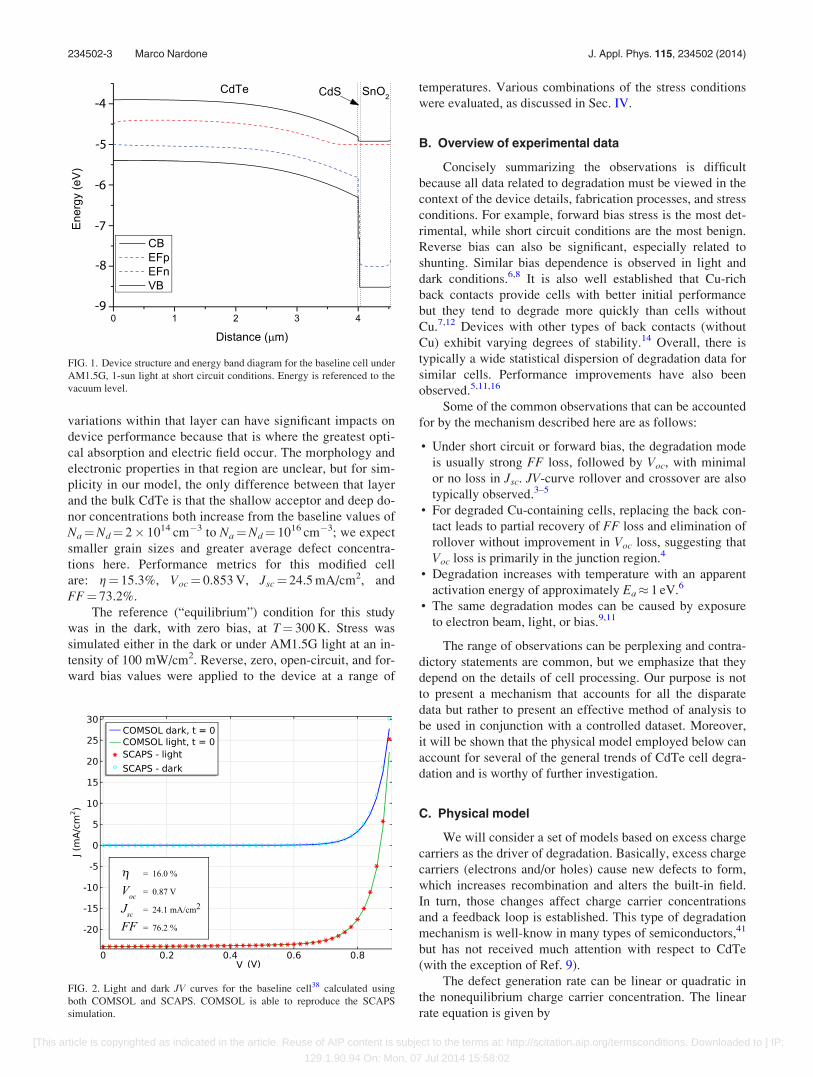
rameters]. Fig. 1 shows the basic structure and band diagram.
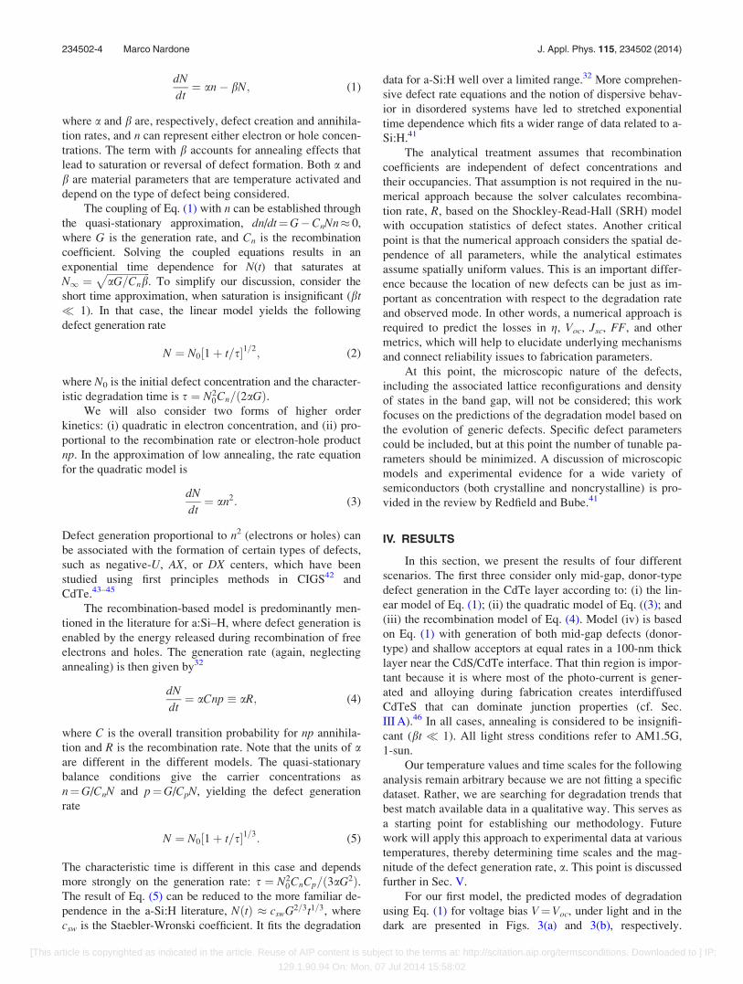
The correspondence between light and dark JV curves calcu-
lated using COMSOL and the well-established PV software
package SCAPS37 is shown in Fig. 2. Performance metrics for
this cell are: g¼ 16.0%, Voc¼ 0.87 V, Jsc¼ 24.1 mA/cm2, and
FF¼ 76.2%.
We also consider a slight variation of the baseline cell
by adding a 100 nm-thick layer between the CdS and CdTe
to represent the CdTe1�xSx material that forms during the
common CdTe cell fabrication process.39,40 Small
234502-2 Marco Nardone J. Appl. Phys. 115, 234502 (2014)
[This article is copyrighted as indicated in the article. Reuse of AIP content is subject to the terms at: http://scitation.aip.org/termsconditions. Downloaded to ] IP:
129.1.90.94 On: Mon, 07 Jul 2014 15:58:02
variations within that layer can have significant impacts on
device performance because that is where the greatest opti-
cal absorption and electric field occur. The morphology and
electronic properties in that region are unclear, but for sim-
plicity in our model, the only difference between that layer
and the bulk CdTe is that the shallow acceptor and deep do-
nor concentrations both increase from the baseline values of
Na¼Nd¼ 2� 1014 cm�3 to Na¼Nd¼ 1016 cm�3; we expect
smaller grain sizes and greater average defect concentra-
tions here. Performance metrics for this modified cell
are: g¼ 15.3%, Voc¼ 0.853 V, Jsc¼ 24.5 mA/cm2, and
FF¼ 73.2%.
The reference (“equilibrium”) condition for this study
was in the dark, with zero bias, at T¼ 300 K. Stress was
simulated either in the dark or under AM1.5G light at an in-
tensity of 100 mW/cm2. Reverse, zero, open-circuit, and for-
ward bias values were applied to the device at a range of
temperatures. Various combinations of the stress conditions
were evaluated, as discussed in Sec. IV.
B. Overview of experimental data
Concisely summarizing the observations is difficult
because all data related to degradation must be viewed in the
context of the device details, fabrication processes, and stress
conditions. For example, forward bias stress is the most det-
rimental, while short circuit conditions are the most benign.
Reverse bias can also be significant, especially related to
shunting. Similar bias dependence is observed in light and
dark conditions.6,8 It is also well established that Cu-rich
back contacts provide cells with better initial performance
but they tend to degrade more quickly than cells without
Cu.7,12 Devices with other types of back contacts (without
Cu) exhibit varying degrees of stability.14 Overall, there is
typically a wide statistical dispersion of degradation data for
similar cells. Performance improvements have also been
observed.5,11,16
Some of the common observations that can be accounted
for by the mechanism described here are as follows:
• Under short circuit or forward bias, the degradation mode
is usually strong FF loss, followed by Voc, with minimal
or no loss in Jsc. JV-curve rollover and crossover are also
typically observed.3–5
• For degraded Cu-containing cells, replacing the back con-
tact leads to partial recovery of FF loss and elimination of
rollover without improvement in Voc loss, suggesting that
Voc loss is primarily in the junction region.4
• Degradation increases with temperature with an apparent
activation energy of approximately Ea� 1 eV.6
• The same degradation modes can be caused by exposure
to electron beam, light, or bias.9,11
The range of observations can be perplexing and contra-
dictory statements are common, but we emphasize that they
depend on the details of cell processing. Our purpose is not
to present a mechanism that accounts for all the disparate
data but rather to present an effective method of analysis to
be used in conjunction with a controlled dataset. Moreover,
it will be shown that the physical model employed below can
account for several of the general trends of CdTe cell degra-
dation and is worthy of further investigation.
C. Physical model
We will consider a set of models based on excess charge
carriers as the driver of degradation. Basically, excess charge
carriers (electrons and/or holes) cause new defects to form,
which increases recombination and alters the built-in field.
In turn, those changes affect charge carrier concentrations
and a feedback loop is established. This type of degradation
mechanism is well-know in many types of semiconductors,41
but has not received much attention with respect to CdTe
(with the exception of Ref. 9).
The defect generation rate can be linear or quadratic in
the nonequilibrium charge carrier concentration. The linear
rate equation is given by
FIG. 1. Device structure and energy band diagram for the baseline cell under
AM1.5G, 1-sun light at short circuit conditions. Energy is referenced to the
vacuum level.
FIG. 2. Light and dark JV curves for the baseline cell38 calculated using
both COMSOL and SCAPS. COMSOL is able to reproduce the SCAPS
simulation.
234502-3 Marco Nardone J. Appl. Phys. 115, 234502 (2014)
[This article is copyrighted as indicated in the article. Reuse of AIP content is subject to the terms at: http://scitation.aip.org/termsconditions. Downloaded to ] IP:
129.1.90.94 On: Mon, 07 Jul 2014 15:58:02
dN
dt¼ an� bN; (1)
where a and b are, respectively, defect creation and annihila-
tion rates, and n can represent either electron or hole concen-
trations. The term with b accounts for annealing effects that
lead to saturation or reversal of defect formation. Both a and
b are material parameters that are temperature activated and
depend on the type of defect being considered.
The coupling of Eq. (1) with n can be established through
the quasi-stationary approximation, dn/dt¼G�CnNn� 0,
where G is the generation rate, and Cn is the recombination
coefficient. Solving the coupled equations results in an
exponential time dependence for N(t) that saturates at
N1 ¼ffiffiffiffiffiffiffiffiffiffiffiffiffiffiffiffiffiaG=Cnb
p. To simplify our discussion, consider the
short time approximation, when saturation is insignificant (bt� 1). In that case, the linear model yields the following
defect generation rate
N ¼ N0 1þ t=s½ �1=2; (2)
where N0 is the initial defect concentration and the character-
istic degradation time is s ¼ N20Cn=ð2aGÞ.
We will also consider two forms of higher order
kinetics: (i) quadratic in electron concentration, and (ii) pro-
portional to the recombination rate or electron-hole product
np. In the approximation of low annealing, the rate equation
for the quadratic model is
dN
dt¼ an2: (3)
Defect generation proportional to n2 (electrons or holes) can
be associated with the formation of certain types of defects,
such as negative-U, AX, or DX centers, which have been
studied using first principles methods in CIGS42 and
CdTe.43–45
The recombination-based model is predominantly men-
tioned in the literature for a:Si–H, where defect generation is
enabled by the energy released during recombination of free
electrons and holes. The generation rate (again, neglecting
annealing) is then given by32
dN
dt¼ aCnp � aR; (4)
where C is the overall transition probability for np annihila-
tion and R is the recombination rate. Note that the units of aare different in the different models. The quasi-stationary
balance conditions give the carrier concentrations as
n¼G/CnN and p¼G/CpN, yielding the defect generation
rate
N ¼ N0 1þ t=s½ �1=3: (5)
The characteristic time is different in this case and depends
more strongly on the generation rate: s ¼ N20CnCp=ð3aG2Þ.
The result of Eq. (5) can be reduced to the more familiar de-
pendence in the a-Si:H literature, NðtÞ � cswG2=3t1=3, where
csw is the Staebler-Wronski coefficient. It fits the degradation
data for a-Si:H well over a limited range.32 More comprehen-
sive defect rate equations and the notion of dispersive behav-
ior in disordered systems have led to stretched exponential
time dependence which fits a wider range of data related to a-
Si:H.41
The analytical treatment assumes that recombination
coefficients are independent of defect concentrations and
their occupancies. That assumption is not required in the nu-
merical approach because the solver calculates recombina-
tion rate, R, based on the Shockley-Read-Hall (SRH) model
with occupation statistics of defect states. Another critical
point is that the numerical approach considers the spatial de-
pendence of all parameters, while the analytical estimates
assume spatially uniform values. This is an important differ-
ence because the location of new defects can be just as im-
portant as concentration with respect to the degradation rate
and observed mode. In other words, a numerical approach is
required to predict the losses in g, Voc, Jsc, FF, and other
metrics, which will help to elucidate underlying mechanisms
and connect reliability issues to fabrication parameters.
At this point, the microscopic nature of the defects,
including the associated lattice reconfigurations and density
of states in the band gap, will not be considered; this work
focuses on the predictions of the degradation model based on
the evolution of generic defects. Specific defect parameters
could be included, but at this point the number of tunable pa-
rameters should be minimized. A discussion of microscopic
models and experimental evidence for a wide variety of
semiconductors (both crystalline and noncrystalline) is pro-
vided in the review by Redfield and Bube.41
IV. RESULTS
In this section, we present the results of four different
scenarios. The first three consider only mid-gap, donor-type
defect generation in the CdTe layer according to: (i) the lin-
ear model of Eq. (1); (ii) the quadratic model of Eq. ((3); and
(iii) the recombination model of Eq. (4). Model (iv) is based
on Eq. (1) with generation of both mid-gap defects (donor-
type) and shallow acceptors at equal rates in a 100-nm thick
layer near the CdS/CdTe interface. That thin region is impor-
tant because it is where most of the photo-current is gener-
ated and alloying during fabrication creates interdiffused
CdTeS that can dominate junction properties (cf. Sec.
III A).46 In all cases, annealing is considered to be insignifi-
cant (bt � 1). All light stress conditions refer to AM1.5G,
1-sun.
Our temperature values and time scales for the following
analysis remain arbitrary because we are not fitting a specific
dataset. Rather, we are searching for degradation trends that
best match available data in a qualitative way. This serves as
a starting point for establishing our methodology. Future
work will apply this approach to experimental data at various
temperatures, thereby determining time scales and the mag-
nitude of the defect generation rate, a. This point is discussed
further in Sec. V.
For our first model, the predicted modes of degradation
using Eq. (1) for voltage bias V¼Voc, under light and in the
dark are presented in Figs. 3(a) and 3(b), respectively.
234502-4 Marco Nardone J. Appl. Phys. 115, 234502 (2014)
[This article is copyrighted as indicated in the article. Reuse of AIP content is subject to the terms at: http://scitation.aip.org/termsconditions. Downloaded to ] IP:
129.1.90.94 On: Mon, 07 Jul 2014 15:58:02
Performance metrics were normalized to the baseline values
and the defect generation rate was set to a¼ 1 s�1 (a serves as
a fitting parameter so an arbitrary rate can be used here with-
out loss of generality). Bias in the dark was held at V¼ 0.86 V
(resulting in a forward current of J� 10 mA/cm2).
Fig. 3(a) indicates that by the time efficiency decreases
by 18% under illumination, FF decreases by about 11%
while Voc and Jsc exhibit nearly equal losses of 3%–4%. The
dark results show a very similar trend but with 12.5% loss in
efficiency in the same time period as the light stress case. As
expected from the data, degradation caused by light and bias
stresses are the same, only the rate is accelerated in the light
due to the high concentration of photo-excited carriers. In
other words, allowing the dark conditions to continue for a
longer time would likely render the two scenarios equivalent.
This may have important practical applications since it
would allow for accelerated life testing with dark bias rather
than light, eliminating the need for cooling or a light source.
The latter would only apply to the type of degradation mech-
anism studied here (i.e., driven by injected carriers).
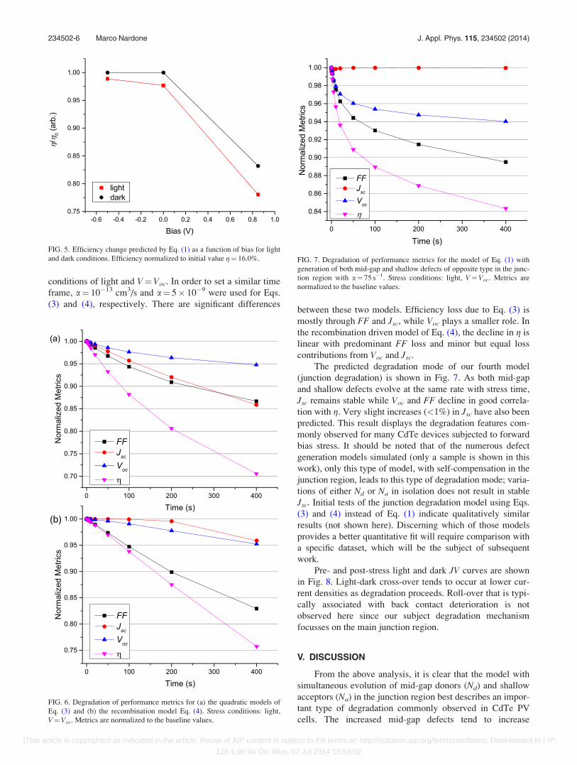
A useful feature of the numerical approach is the exten-
sive predictive capability. For example, Fig. 4 shows the
defect evolution and recombination rates within the CdTe
layer according to Eq. (1) over the course of light stressing.
The graphs clearly indicate how both mid-gap defect concen-
trations and recombination rates increase in correspondence
with the nonequilibrium minority carrier concentration pro-
file; most of the defects are formed near the CdTe/CdS junc-
tion. That defect profile causes the degradation modes
illustrated in Fig. 3(a).
Light and dark stress conditions were also evaluated at
short circuit SC and reverse bias (RB, V¼�0.5 V) conditions.
The results are summarized in Fig. 5 with t¼ 500 s and
a¼ 1 s�1 in each case. Again it is evident that performance
loss is slightly accelerated in the light compared to the dark
but the trends are the same. The greatest degradation rate
occurs under forward bias in the dark or near Voc under light.
Very little degradation was observed for the SC and RB con-
ditions, which is to be expected since excess charge carriers
are quickly swept away by the strong electric field. Significant
degradation which is often observed under reverse bias is not
seen here.
A comparison of the degradation behavior for the quad-
ratic models of Eqs. (3) and (4) is shown in Fig. 6, with stress
FIG. 3. Degradation of performance metrics predicted by Eq. (1) with
a¼ 1 s�1. Simulated for stress conditions: (a) AM1.5 G illumination, 100
mW/cm2 intensity, V¼Voc; (b) dark, V¼ 0.86 V. Results are normalized to
the baseline values g¼ 16.0%, Voc¼ 0.87 V, Jsc¼ 24.1 mA/cm2,
FF¼ 76.2%.
FIG. 4. The evolution of (a) mid-gap, donor-type defect concentration and
(b) SRH recombination rates in the CdTe layer according to Eq. (1) under
light stress. The time range corresponds to that in Fig. 3.
234502-5 Marco Nardone J. Appl. Phys. 115, 234502 (2014)
[This article is copyrighted as indicated in the article. Reuse of AIP content is subject to the terms at: http://scitation.aip.org/termsconditions. Downloaded to ] IP:
129.1.90.94 On: Mon, 07 Jul 2014 15:58:02
conditions of light and V¼Voc. In order to set a similar time
frame, a¼ 10�13 cm3/s and a¼ 5� 10�9 were used for Eqs.
(3) and (4), respectively. There are significant differencesbetween these two models. Efficiency loss due to Eq. (3) is
mostly through FF and Jsc, while Voc plays a smaller role. In
the recombination driven model of Eq. (4), the decline in g is
linear with predominant FF loss and minor but equal loss
contributions from Voc and Jsc.
The predicted degradation mode of our fourth model
(junction degradation) is shown in Fig. 7. As both mid-gap
and shallow defects evolve at the same rate with stress time,
Jsc remains stable while Voc and FF decline in good correla-
tion with g. Very slight increases (<1%) in Jsc have also been
predicted. This result displays the degradation features com-
monly observed for many CdTe devices subjected to forward
bias stress. It should be noted that of the numerous defect
generation models simulated (only a sample is shown in this
work), only this type of model, with self-compensation in the
junction region, leads to this type of degradation mode; varia-
tions of either Nd or Na in isolation does not result in stable
Jsc. Initial tests of the junction degradation model using Eqs.
(3) and (4) instead of Eq. (1) indicate qualitatively similar
results (not shown here). Discerning which of those models
provides a better quantitative fit will require comparison with
a specific dataset, which will be the subject of subsequent
work.
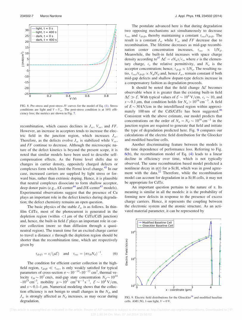
Pre- and post-stress light and dark JV curves are shown
in Fig. 8. Light-dark cross-over tends to occur at lower cur-
rent densities as degradation proceeds. Roll-over that is typi-
cally associated with back contact deterioration is not
observed here since our subject degradation mechanism
focusses on the main junction region.
V. DISCUSSION
From the above analysis, it is clear that the model with
simultaneous evolution of mid-gap donors (Nd) and shallow
acceptors (Na) in the junction region best describes an impor-
tant type of degradation commonly observed in CdTe PV
cells. The increased mid-gap defects tend to increase
FIG. 5. Efficiency change predicted by Eq. (1) as a function of bias for light
and dark conditions. Efficiency normalized to initial value g¼ 16.0%.
FIG. 6. Degradation of performance metrics for (a) the quadratic models of
Eq. (3) and (b) the recombination model Eq. (4). Stress conditions: light,
V¼Voc. Metrics are normalized to the baseline values.
FIG. 7. Degradation of performance metrics for the model of Eq. (1) with
generation of both mid-gap and shallow defects of opposite type in the junc-
tion region with a¼ 75 s�1. Stress conditions: light, V¼Voc. Metrics are
normalized to the baseline values.
234502-6 Marco Nardone J. Appl. Phys. 115, 234502 (2014)
[This article is copyrighted as indicated in the article. Reuse of AIP content is subject to the terms at: http://scitation.aip.org/termsconditions. Downloaded to ] IP:
129.1.90.94 On: Mon, 07 Jul 2014 15:58:02
recombination, which causes declines in Jsc, Voc, and FF.
However, an increase in acceptors tends to increase the elec-
tric field in the junction region, which increases Jsc.
Therefore, as the defects evolve Jsc is stabilized while Voc,
and FF continue to decrease. Although the microscopic na-
ture of the defect kinetics is beyond the present scope, it is
noted that similar models have been used to describe self-
compensation effects. As the Fermi level shifts due to
changes in carrier density, oppositely charged defects or
complexes form which limit the Fermi level change.45 In our
case, increased carriers are supplied by light stress or for-
ward bias, rather than extrinsic doping. Hence, it is plausible
that neutral complexes dissociate to form shallow acceptor,
deep donor pairs (e.g., AX-center44 and DX-center43 models).
Experimental observations suggest that the presence of Cu
plays an important role in the defect kinetics during degrada-
tion; the defect chemistry remains an open question.
The basic physics of the stable Jsc is as follows. In thin-
film CdTe, most of the photocurrent is generated in the
depletion region (within <1 lm of the CdTe/CdS junction)
and, hence, the built-in field E plays an important role in car-
rier collection (more so than diffusion through a quasi-
neutral region). The transit time for an excited charge carrier
to travel a distance x through the depletion region should be
shorter than the recombination time, which are respectively
given by
sdrif t ¼ x=ðlEÞ and srec ¼ ðrvthNdÞ�1: (6)
The condition for efficient carrier collection in the high-
field region, sdrift � srec, is only weakly satisfied for typical
parameters of cross-section r� 10�14–10�12 cm2, thermal ve-
locity vth� 107 cm/s, mid-gap state concentration Nd� 1014
–1015 cm–3, mobility l� 102 cm2 V�1 s�1, E � 104 V=cm,
and x� 0.1–1 lm. Numerical modeling shows that the collec-
tion efficiency is not benign to small changes in the Nd, and
Jsc is strongly affected as Nd increases, as may occur during
degradation.
The postulate advanced here is that during degradation
two opposing mechanisms act simultaneously to decrease
srec and sdrift, thereby maintaining a constant srec/sdrift. The
result is a constant Jsc while Voc and FF decrease due to
recombination. The lifetime decreases as mid-gap recombi-
nation center concentration increases, srec / 1/Nd.
Meanwhile, the built-in field increases with space charge
density according to47 DE ¼ eNax=�s, where e is the elemen-
tary charge, �s the relative permittivity, and Na is the
acceptor concentration; hence, sdrift / 1/Na. The resulting ra-
tio, srec/sdrift / Na/Nd and, hence Jsc, remain constant if both
mid-gap defects and shallow dopant-type defects increase in
a compensatory fashion as degradation proceeds.
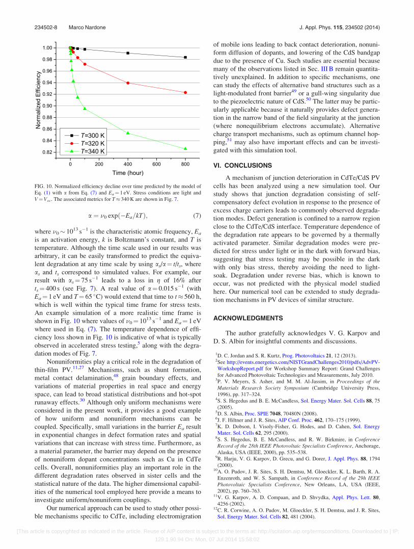
It should be noted that the field change DE becomes
observable when it is greater than the existing built-in field
DE E. With typical values of E � 104 V=cm; �s � 10, and
x� 0.1 lm, that condition holds for Na> 1016 cm�3. A field
of E� 30 kV/cm in the interdiffused region within approxi-
mately 100 nm of the CdS/CdTe has been suggested.46
Consistent with the above estimate, our model predicts that
concentrations on the order of Na ¼ Nd � 1016 cm�3 in the
junction region are required to generate that field and initiate
the type of degradation predicted here. Fig. 9 compares our
calculations of the electric field distribution for the Gloecker
and modified baseline cells.
Another discriminating feature between the models is
the time dependence of performance loss. Referring to Fig.
6(b), the recombination model of Eq. (4) leads to a linear
decline in efficiency over time, which is not typically
observed. The same recombination based model predicted a
nonlinear decay in g(t) for a-Si:H, which was in good agree-
ment with the data.22 Therefore, while the recombination
model can account for degradation in a-Si:H cells, it may not
be appropriate for CdTe.
An important question pertains to the nature of a. Its
meaning is similar in all the models: it is the probability of
forming new defects in response to the presence of excess
charge carriers. Hence, it represents the coupling between
the electronic system and the atomic structure. As an acti-
vated material parameter, it can be represented by
FIG. 8. Pre-stress and post-stress JV curves for the model of Eq. (1). Stress
conditions are light and V¼Voc. The post-stress condition is at 16% effi-
ciency loss; the metrics are shown in Fig. 7.
FIG. 9. Electric field distributions for the Gloeckler38 and modified baseline
cells. AM1.5G, 1-sun light, V¼ 0 V.
234502-7 Marco Nardone J. Appl. Phys. 115, 234502 (2014)
[This article is copyrighted as indicated in the article. Reuse of AIP content is subject to the terms at: http://scitation.aip.org/termsconditions. Downloaded to ] IP:
129.1.90.94 On: Mon, 07 Jul 2014 15:58:02
a ¼ �0 expð�Ea=kTÞ; (7)
where �0� 1013 s�1 is the characteristic atomic frequency, Ea
is an activation energy, k is Boltzmann’s constant, and T is
temperature. Although the time scale used in our results was
arbitrary, it can be easily transformed to predict the equiva-
lent degradation at any time scale by using as/a¼ t/ts, where
as and ts correspond to simulated values. For example, our
result with as¼ 75 s�1 leads to a loss in g of 16% after
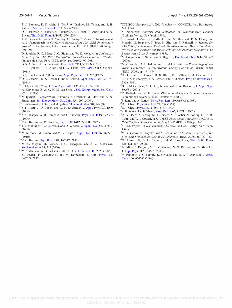
ts¼ 400 s (see Fig. 7). A real value of a¼ 0.015 s�1 (with
Ea¼ 1 eV and T¼ 65 C) would extend that time to t� 560 h,
which is well within the typical time frame for stress tests.
An example simulation of a more realistic time frame is
shown in Fig. 10 where values of �0¼ 1013 s�1 and Ea¼ 1 eV
where used in Eq. (7). The temperature dependence of effi-
ciency loss shown in Fig. 10 is indicative of what is typically
observed in accelerated stress testing,5 along with the degra-
dation modes of Fig. 7.
Nonuniformities play a critical role in the degradation of
thin-film PV.11,27 Mechanisms, such as shunt formation,
metal contact delamination,48 grain boundary effects, and
variations of material properties in real space and energy
space, can lead to broad statistical distributions and hot-spot
runaway effects.30 Although only uniform mechanisms were
considered in the present work, it provides a good example
of how uniform and nonuniform mechanisms can be
coupled. Specifically, small variations in the barrier Ea result
in exponential changes in defect formation rates and spatial
variations that can increase with stress time. Furthermore, as
a material parameter, the barrier may depend on the presence
of nonuniform dopant concentrations such as Cu in CdTe
cells. Overall, nonuniformities play an important role in the
different degradation rates observed in sister cells and the
statistical nature of the data. The higher dimensional capabil-
ities of the numerical tool employed here provide a means to
investigate uniform/nonuniform couplings.
Our numerical approach can be used to study other possi-
ble mechanisms specific to CdTe, including electromigration
of mobile ions leading to back contact deterioration, nonuni-
form diffusion of dopants, and lowering of the CdS bandgap
due to the presence of Cu. Such studies are essential because
many of the observations listed in Sec. III B remain quantita-
tively unexplained. In addition to specific mechanisms, one
can study the effects of alternative band structures such as a
light-modulated front barrier49 or a gull-wing singularity due
to the piezoelectric nature of CdS.50 The latter may be partic-
ularly applicable because it naturally provides defect genera-
tion in the narrow band of the field singularity at the junction
(where nonequilibrium electrons accumulate). Alternative
charge transport mechanisms, such as optimum channel hop-
ping,51 may also have important effects and can be investi-
gated with this simulation tool.
VI. CONCLUSIONS
A mechanism of junction deterioration in CdTe/CdS PV
cells has been analyzed using a new simulation tool. Our
study shows that junction degradation consisting of self-
compensatory defect evolution in response to the presence of
excess charge carriers leads to commonly observed degrada-
tion modes. Defect generation is confined to a narrow region
close to the CdTe/CdS interface. Temperature dependence of
the degradation rate appears to be governed by a thermally
activated parameter. Similar degradation modes were pre-
dicted for stress under light or in the dark with forward bias,
suggesting that stress testing may be possible in the dark
with only bias stress, thereby avoiding the need to light-
soak. Degradation under reverse bias, which is known to
occur, was not predicted with the physical model studied
here. Our numerical tool can be extended to study degrada-
tion mechanisms in PV devices of similar structure.
ACKNOWLEDGMENTS
The author gratefully acknowledges V. G. Karpov and
D. S. Albin for insightful comments and discussions.
1D. C. Jordan and S. R. Kurtz, Prog. Photovoltaics 21, 12 (2013).2See http://events.energetics.com/NISTGrandChallenges2010/pdfs/AdvPV-
WorkshopReport.pdf for Workshop Summary Report: Grand Challenges
for Advanced Photovoltaic Technologies and Measurements, July 2010.3P. V. Meyers, S. Asher, and M. M. Al-Jassim, in Proceedings of theMaterials Research Society Symposium (Cambridge University Press,
1996), pp. 317–324.4S. S. Hegedus and B. E. McCandless, Sol. Energy Mater. Sol. Cells 88, 75
(2005).5D. S. Albin, Proc. SPIE 7048, 70480N (2008).6J. F. Hiltner and J. R. Sites, AIP Conf. Proc. 462, 170–175 (1999).7K. D. Dobson, I. Visoly-Fisher, G. Hodes, and D. Cahen, Sol. Energy
Mater. Sol. Cells 62, 295 (2000).8S. S. Hegedus, B. E. McCandless, and R. W. Birkmire, in ConferenceRecord of the 28th IEEE Photovoltaic Specialists Conference, Anchorage,
Alaska, USA (IEEE, 2000), pp. 535–538.9R. Harju, V. G. Karpov, D. Grecu, and G. Dorer, J. Appl. Phys. 88, 1794
(2000).10A. O. Pudov, J. R. Sites, S. H. Demtsu, M. Gloeckler, K. L. Barth, R. A.
Enzenroth, and W. S. Sampath, in Conference Record of the 29h IEEEPhotovoltaic Specialists Conference, New Orleans, LA, USA (IEEE,
2002), pp. 760–763.11V. G. Karpov, A. D. Compaan, and D. Shvydka, Appl. Phys. Lett. 80,
4256 (2002).12C. R. Corwine, A. O. Pudov, M. Gloeckler, S. H. Demtsu, and J. R. Sites,
Sol. Energy Mater. Sol. Cells 82, 481 (2004).
FIG. 10. Normalized efficiency decline over time predicted by the model of
Eq. (1) with a from Eq. (7) and Ea¼ 1 eV. Stress conditions are light and
V¼Voc. The associated metrics for T� 340 K are shown in Fig. 7.
234502-8 Marco Nardone J. Appl. Phys. 115, 234502 (2014)
[This article is copyrighted as indicated in the article. Reuse of AIP content is subject to the terms at: http://scitation.aip.org/termsconditions. Downloaded to ] IP:
129.1.90.94 On: Mon, 07 Jul 2014 15:58:02
13T. J. Berniard, D. S. Albin, B. To, J. W. Pankow, M. Young, and S. E.
Asher, J. Vac. Sci. Technol. B 22, 2423 (2004).14D. L. B€atzner, A. Romeo, M. Terheggen, M. D€obeli, H. Zogg, and A. N.
Tiwari, Thin Solid Films 451-452, 536 (2004).15T. A. Gessert, S. Smith, T. Moriatry, M. Young, S. Asher, S. Johnston, and
A. L. Fahrenbruch, in Conference Record of the 31st IEEE PhotovoltaicSpecialists Conference, Lake Buena Vista, FL, USA (IEEE, 2005), pp.
291–294.16D. S. Albin, R. G. Dhere, S. C. Glynn, and W. K. Metzger, in Conference
Record of the 34th IEEE Photovoltaic Specialists Conference (PVSC),Philadelphia, PA, USA (IEEE, 2009), pp. 001903–001908.
17D. S. Albin and J. A. del Cueto, Proc. SPIE 7773, 77730N (2010).18R. L. Graham, D. S. Albin and L. A. Clark, Proc. SPIE 8112, 81120V
(2011).19D. L. Staebler and C. R. Wronski, Appl. Phys. Lett. 31, 292 (1977).20D. L. Staebler, R. S. Crandall, and R. Wilson, Appl. Phys. Lett. 39, 733
(1981).21L. Chen and L. Yang, J. Non-Cryst. Solids 137-138, 1185 (1991).22A. Klaver and R. A. C. M. M. van Swaaij, Sol. Energy Mater. Sol. Cells
92, 50 (2008).23M. Igalson, P. Zabierowski, D. Przado, A. Urbaniak, M. Edoff, and W. N.
Shafarman, Sol. Energy Mater. Sol. Cells 93, 1290 (2009).24P. Zabierowski, U. Rau, and M. Igalson, Thin Solid Films 387, 147 (2001).25J. T. Heath, J. D. Cohen, and W. N. Shafarman, J. Appl. Phys. 95, 1000
(2004).26V. G. Karpov, A. D. Compaan, and D. Shvydka, Phys. Rev. B 69, 045325
(2004).27V. G. Karpov and D. Shvydka, Proc. SPIE 7412, 74120L (2009).28T. J. McMahon, T. J. Berniard, and D. S. Albin, J. Appl. Phys. 97, 054503
(2005).29M. Nardone, M. Simon, and V. G. Karpov, Appl. Phys. Lett. 96, 163501
(2010).30V. G. Karpov, Phys. Rev. B 86, 165317 (2012).31M. N. Meytin, M. Zeman, B. G. Budaguan, and J. W. Metselaar,
Semiconductors 34, 717 (2000).32M. Stutzmann, W. B. Jackson, and C. C. Tsai, Phys. Rev. B 32, 23 (1985).33K. Decock, P. Zabierowski, and M. Burgelman, J. Appl. Phys. 111,
043703 (2012).
34COMSOL MultiphysicsVR
, 2013, Version 4.4, COMSOL, Inc., Burlington,
MA, USA.35S. Selberherr, Analysis and Simulation of Semiconductor Devices
(Springer Verlag, New York, 1984).36S. Fonash, J. Arch., J. Cuiffi, J. Hou, W. Howland, P. McElheny, A.
Moquin, M. Rogosky, T. Tran, H. Zhu, and F. Rubinelli, A Manual forAMPS-1D for Windows 95/NT—A One-Dimensional Device SimulationProgram for the Analysis of Microelectronic and Photonic Structures (The
Pennsylvania State University, 1997).37M. Burgelman, P. Nollet, and S. Degrave, Thin Solid Films 361-362, 527
(2000).38M. Gloeckler, A. L. Fahrenbruch, and J. R. Sites, in Proceedings of 3rd
World Conference on Photovoltaic Energy Conversion, Osaka, Japan
(IEEE, 2003), pp. 491–494.39D. H. Rose, F. S. Hasoon, R. G. Dhere, D. S. Albin, R. M. Ribelin, X. S.
Li, Y. Mahathongdy, T. A. Gessert, and P. Sheldon, Prog. Photovoltaics 7,
331 (1999).40B. E. McCandless, M. G. Engelmann, and R. W. Birkmire, J. Appl. Phys.
89, 988 (2001).41D. Redfield and R. H. Bube, Photoinduced Defects in Semiconductors
(Cambridge University Press, Cambridge, 1996).42S. Lany and A. Zunger, Phys. Rev. Lett. 100, 016401 (2008).43D. J. Chadi, Phys. Rev. Lett. 72, 534 (1994).44D. J. Chadi, Phys. Rev. B 59, 15181 (1999).45S. H. Wei and S. B. Zhang, Phys. Rev. B 66, 155211 (2002).46R. G. Dhere, Y. Zhang, M. J. Romero, S. E. Asher, M. Young, B. To, R.
Noufi, and T. A. Gessert, in 33rd IEEE Photovoltaic Specialists Conference,PVSC’08, San Diego, California, May 11–16 (IEEE, 2008), pp. 1–5.
47S. Sze, Physics of Semiconductor Devices, 2nd ed. (Wiley, New York,
1981).48V. G. Karpov, D. Shvydka, and Y. Roussillon, in Conference Record of the
31st IEEE Photovoltaic Specialists Conference (IEEE, 2005), pp. 437–440.49G. Agostinelli, D. L. B€atzner, and M. Burgelman, Thin Solid Films
431-432, 407 (2003).50M. Mitra, J. Drayton, M. L. C. Cooray, V. G. Karpov, and D. Shvydka,
J. Appl. Phys. 102, 034505 (2007).51M. Nardone, V. G. Karpov, D. Shvydka, and M. L. C. Attygalle, J. Appl.
Phys. 106, 074503 (2009).
234502-9 Marco Nardone J. Appl. Phys. 115, 234502 (2014)
[This article is copyrighted as indicated in the article. Reuse of AIP content is subject to the terms at: http://scitation.aip.org/termsconditions. Downloaded to ] IP:
129.1.90.94 On: Mon, 07 Jul 2014 15:58:02