Synthesis, processing, and thermoelectric properties of bulk nanostructured bismuth telluride...
6
Synthesis, processing, and thermoelectric properties of bulk nanostructured bismuth telluride (Bi 2 Te 3 ) Mohsin Saleemi, a Muhammet S. Toprak, * a Shanghua Li, a Mats Johnsson b and Mamoun Muhammed a Received 10th August 2011, Accepted 10th October 2011 DOI: 10.1039/c1jm13880d Bismuth telluride (Bi 2 Te 3 ) is the best-known commercially used thermoelectric material in the bulk form for cooling and power generation applications at ambient temperature. However, its dimensionless figure-of-merit-ZT around 1 limits the large-scale industrial applications. Recent studies indicate that nanostructuring can enhance ZT while keeping the material form of bulk by employing an advanced synthetic process accompanied with novel consolidation techniques. Here, we report on bulk nanostructured (NS) undoped Bi 2 Te 3 prepared via a promising chemical synthetic route. Spark plasma sintering has been employed for compaction and sintering of Bi 2 Te 3 nanopowders, resulting in very high densification (>97%) while preserving the nanostructure. The average grain size of the final compacts was obtained as 90 5 nm as calculated from electron micrographs. Evaluation of transport properties showed enhanced Seebeck coefficient (120 mVK 1 ) and electrical conductivity compared to the literature state-of-the-art (30% enhanced power factor), especially in the low temperature range. An improved ZT for NS bulk undoped Bi 2 Te 3 is achieved with a peak value of 1.1 at 340 K. 1. Introduction Thermoelectric (TE) materials have been the topic of intensive research due to their unique dual capability of directly converting heat into electricity or electrical power into cooling or heating. These materials can play an important role in reducing carbon emission by converting waste heat into electricity. 1 Bismuth telluride (Bi 2 Te 3 ) and its alloys are the best-known TE materials for ambient temperature applications. 2 The performance of TE energy conversion devices depends upon the dimensionless figure of merit (ZT) which is defined as: ZT ¼ S 2 s k T (1) where T is the temperature, S is the Seebeck coefficient, s is the electronic conductivity and k is the total thermal conductivity which is the sum of electronic (k e ) and lattice thermal (k L ) conductivities. 3 There have been continual efforts to improve the ZT values since 1950s, but the peak ZT value of commercial TE materials based on Bi 2 Te 3 has increased only marginally, from about 0.6 to about 1 at ambient temperature. 4 During the past decade, the interest in TE materials was revived by the utilization of nanotechnology tools in this field. By nanostructuring, s and k can be de-coupled; s or S can be enhanced by changing the density of the states 5 and k can be greatly reduced by increased phonon scattering at the grain boundaries. 6 Theoretical predic- tions from the Dresselhaus group 7,8 and the following experi- mental studies on low dimensional nanostructures, superlattices of Bi 2 Te 3 /Sb 2 Te 3 , 9 quantum dots of PbTe/PbSnSeTe 10 and quantum well structures of PbTe/Pb 1x Eu x Te 11 have shown higher ZT (2–2.5), 9,11 due to the quantum confinement effect. These advanced low-dimensional nano-architectures are not practical for industrial-scale commercial use because they are fabricated by atomic layer deposition techniques such as molecular beam epitaxy, making them feasible for small scale or high-end applications and rather expensive for large area/scale applications. 5 There are also a lot of difficulties associated with TE module/device fabrication technology using these materials. 12 Therefore, there is still great need for high-performance TE materials based on the bulk form. Bismuth telluride (Bi 2 Te 3 ) and its alloys are the best TE materials available today near room temperature with the high- est ZT as reported recently. 13 The ZT 1 barrier for bulk Bi 2 Te 3 TE alloys is broken by Poudel et al. 14 and Heremans et al. 15 Poudel reported that Sb doped nanocrystalline Bi x Sb (2x) Te 3 synthesized by a conventional mechanical alloying method fol- lowed by ball milling and sintering by a conventional hot- pressing technique exhibited a peak ZT of 1.4 at 373 K. 14 Their synthesis method is scalable however the energy cost is relatively high and the chance to introduce the impurities is higher. Furthermore, the conventional hot-pressing technique applied for sintering the powder causes significant grain growth accom- panied with recrystallization and/or diffusion. To address these issues, a novel compaction method spark plasma sintering (SPS) a Division of Functional Materials, Royal Institute of Technology (KTH), Electrum 229, Isafjordsgatan 22, SE-16 440 Kista, Sweden. E-mail: [email protected]; Tel: +4687908344 b Department of Materials and Environmental Chemistry, Stockholm University, SE-106 91 Stockholm, Sweden. E-mail: mats.johnsson@mmk. su.se; Fax: +468152187; Tel: +468162169 This journal is ª The Royal Society of Chemistry 2012 J. Mater. Chem., 2012, 22, 725–730 | 725 Dynamic Article Links C < Journal of Materials Chemistry Cite this: J. Mater. Chem., 2012, 22, 725 www.rsc.org/materials PAPER Published on 09 November 2011. Downloaded by KUNGL TEKNISKA HOGSKOLAN on 19/08/2013 15:30:46. View Article Online / Journal Homepage / Table of Contents for this issue
-
Upload
independent -
Category
Documents
-
view
3 -
download
0
Transcript of Synthesis, processing, and thermoelectric properties of bulk nanostructured bismuth telluride...

Dynamic Article LinksC<Journal ofMaterials Chemistry
Cite this: J. Mater. Chem., 2012, 22, 725
www.rsc.org/materials PAPER
Publ
ishe
d on
09
Nov
embe
r 20
11. D
ownl
oade
d by
KU
NG
L T
EK
NIS
KA
HO
GSK
OL
AN
on
19/0
8/20
13 1
5:30
:46.
View Article Online / Journal Homepage / Table of Contents for this issue
Synthesis, processing, and thermoelectric properties of bulk nanostructuredbismuth telluride (Bi2Te3)
Mohsin Saleemi,a Muhammet S. Toprak,*a Shanghua Li,a Mats Johnssonb and Mamoun Muhammeda
Received 10th August 2011, Accepted 10th October 2011
DOI: 10.1039/c1jm13880d
Bismuth telluride (Bi2Te3) is the best-known commercially used thermoelectric material in the bulk
form for cooling and power generation applications at ambient temperature. However, its
dimensionless figure-of-merit-ZT around 1 limits the large-scale industrial applications. Recent studies
indicate that nanostructuring can enhance ZT while keeping the material form of bulk by employing an
advanced synthetic process accompanied with novel consolidation techniques. Here, we report on bulk
nanostructured (NS) undoped Bi2Te3 prepared via a promising chemical synthetic route. Spark plasma
sintering has been employed for compaction and sintering of Bi2Te3 nanopowders, resulting in very
high densification (>97%) while preserving the nanostructure. The average grain size of the final
compacts was obtained as 90 � 5 nm as calculated from electron micrographs. Evaluation of transport
properties showed enhanced Seebeck coefficient (�120 mVK�1) and electrical conductivity compared to
the literature state-of-the-art (30% enhanced power factor), especially in the low temperature range. An
improved ZT for NS bulk undoped Bi2Te3 is achieved with a peak value of �1.1 at 340 K.
1. Introduction
Thermoelectric (TE) materials have been the topic of intensive
research due to their unique dual capability of directly converting
heat into electricity or electrical power into cooling or heating.
These materials can play an important role in reducing carbon
emission by converting waste heat into electricity.1 Bismuth
telluride (Bi2Te3) and its alloys are the best-known TE materials
for ambient temperature applications.2 The performance of TE
energy conversion devices depends upon the dimensionless figure
of merit (ZT) which is defined as:
ZT¼ S2s
kT (1)
where T is the temperature, S is the Seebeck coefficient, s is the
electronic conductivity and k is the total thermal conductivity
which is the sum of electronic (ke) and lattice thermal (kL)
conductivities.3 There have been continual efforts to improve the
ZT values since 1950s, but the peak ZT value of commercial TE
materials based on Bi2Te3 has increased only marginally, from
about 0.6 to about 1 at ambient temperature.4 During the past
decade, the interest in TE materials was revived by the utilization
of nanotechnology tools in this field. By nanostructuring, s and k
can be de-coupled; s or S can be enhanced by changing the
aDivision of Functional Materials, Royal Institute of Technology (KTH),Electrum 229, Isafjordsgatan 22, SE-16 440 Kista, Sweden. E-mail:[email protected]; Tel: +4687908344bDepartment of Materials and Environmental Chemistry, StockholmUniversity, SE-106 91 Stockholm, Sweden. E-mail: [email protected]; Fax: +468152187; Tel: +468162169
This journal is ª The Royal Society of Chemistry 2012
density of the states5 and k can be greatly reduced by increased
phonon scattering at the grain boundaries.6 Theoretical predic-
tions from the Dresselhaus group7,8 and the following experi-
mental studies on low dimensional nanostructures, superlattices
of Bi2Te3/Sb2Te3,9 quantum dots of PbTe/PbSnSeTe10 and
quantum well structures of PbTe/Pb1�xEuxTe11 have shown
higher ZT (2–2.5),9,11 due to the quantum confinement effect.
These advanced low-dimensional nano-architectures are not
practical for industrial-scale commercial use because they are
fabricated by atomic layer deposition techniques such as
molecular beam epitaxy, making them feasible for small scale or
high-end applications and rather expensive for large area/scale
applications.5 There are also a lot of difficulties associated with
TE module/device fabrication technology using these materials.12
Therefore, there is still great need for high-performance TE
materials based on the bulk form.
Bismuth telluride (Bi2Te3) and its alloys are the best TE
materials available today near room temperature with the high-
est ZT as reported recently.13 The ZT 1 barrier for bulk Bi2Te3TE alloys is broken by Poudel et al.14 and Heremans et al.15
Poudel reported that Sb doped nanocrystalline BixSb(2�x)Te3synthesized by a conventional mechanical alloying method fol-
lowed by ball milling and sintering by a conventional hot-
pressing technique exhibited a peak ZT of 1.4 at 373 K.14 Their
synthesis method is scalable however the energy cost is relatively
high and the chance to introduce the impurities is higher.
Furthermore, the conventional hot-pressing technique applied
for sintering the powder causes significant grain growth accom-
panied with recrystallization and/or diffusion. To address these
issues, a novel compaction method spark plasma sintering (SPS)
J. Mater. Chem., 2012, 22, 725–730 | 725

Publ
ishe
d on
09
Nov
embe
r 20
11. D
ownl
oade
d by
KU
NG
L T
EK
NIS
KA
HO
GSK
OL
AN
on
19/0
8/20
13 1
5:30
:46.
View Article Online
has been introduced.16 In the SPS technique a pulsed direct
current is conducted through the graphite die under hydrostatic
uniaxial pressure, which consolidates the material. SPS has been
generally recognized as a better sintering technique than
conventional hot-press since it requires relatively shorter
dwelling times because of faster heating rates under high pres-
sure.17 This technique can achieve very high densification that
approaches to theoretical density18 while preserving the nano-
structures during the sintering process.19
Bi2Te3 has shown high potential in improving the ZT during
the last decade because of novel structural modification and
advanced processing strategies. Nanoscale TE material can be
synthesized by several methods including vapour deposition,
pulsed laser ablation, mechanical alloying and conventional
powder metallurgy routes.20 These methods are expensive and
face scale up challenges. Many solution-based methods are
established by using organic precursors for the production of
nanocrystalline Bi2Te3.21,22 Nevertheless, their peak ZT value is
low (in the range of 0.6) due to the presence of organic residues
coming from solvents or stabilizing ligands.23,24 Ritter had
proposed a two-step process for the preparation of poly-
crystalline Bi2Te3 by reduction of bismuth and tellurium
oxides.25,26
In our previous works we reported the enhancement of TE
transport properties of bulk skutterudites (based on CoSb3family) by nanostructuring.27–29 In this paper we focus on the
large scale synthesis of nanostructured undoped bulk NS Bi2Te3materials by employing a novel bottom-up solution-based
chemical approach. A precursor material with the desired
composition and high production yield has been synthesized.
Thermochemical processes via calcination and reduction (under
H2 gas) steps produced the final material. Detailed consolidation
of prepared NS material was studied by SPS and transport
properties of compacted bulk NS Bi2Te3 are presented.
2. Experimental
2.1 Synthesis
The synthesis method was tailored from the chemical alloying
method we have reported earlier.30 Thermodynamic modeling
was performed prior to the synthesis to select the pH range for
the co-precipitation of Bi and Te. Modeling results showed co-
precipitates of bismuth oxide (BiONO3) and tellurium oxide
(TeO2) appear in the pH range of 2–3. All reagents used in this
work were of analytical grade. Bismuth nitrate pentahydrate (Bi
(NO3)2$5H2O, 99.99%, Merck) and tellurium oxide (TeO2,
99.999%, Sigma-Aldrich) were used as starting materials for the
co-precipitation process. Both chemicals were weighed according
to the stoichiometry (Bi2Te3) and separate metal ion solutions of
1 M were prepared by dissolving them in concentrated HNO3
(65 wt%). A stock solution of 3 M sodium hydroxide (NaOH)
was prepared for the pH adjustment. Both metal ion solutions
were mixed in a burette (solution 1) and another burette was
filled with NaOH solution (solution 2). Solutions 1 and 2 were
mixed simultaneously at room temperature under controlled
hydro-dynamic conditions and complete co-precipitation was
obtained by stirring the suspension for 15 minutes. Obtained
white precipitates were filtered off, washed sequentially with de-
726 | J. Mater. Chem., 2012, 22, 725–730
ionized water and ethanol and then dried in an oven at 80 �Covernight. Dried precursor was calcined in a furnace at 250 �Cfor thermo-mechanical grinding. In the end, the oxides of
bismuth and tellurium were reduced in 99% pure hydrogen gas
(H2) at 400�C for 2 hours.
2.2 Characterization
X-Ray powder diffraction (XRD) was performed on a Philips
X’pert pro super diffractometer with Cu Ka (l ¼ 1.5418 �A). A
Zeiss Ultra 55 scanning electron microscope was used for scan-
ning electron microscopy (SEM) and energy-dispersive X-ray
(EDX) analysis (at a standard working distance of 8 mm and an
accelerating voltage of 20 kV) analysis. A JEOL TEM-2100F
field-emission microscope was employed for transmission elec-
tron microscopy (TEM) and selected-area electron diffraction
(SAED) analysis at an accelerating voltage of 200 kV. Samples
for TEM were prepared by dropping few drops of the ground
Bi2Te3 pellet dispersed in ethanol on C coated TEM grids.
Particle and grain size analyses were performed on several
micrographs counting a minimum of 300 particles per grain.
2.3 Spark plasma sintering
Spark plasma sintering (SPS) was performed under argon
atmosphere by using Dr Sinter 2050 SPS (Sumitomo Coal
Mining Co., Tokyo, Japan). Graphite sheet was used to cover the
graphite die with an inside diameter of 12mm. Typically 2–3 g of
Bi2Te3 was loaded into the die during the sintering experiments.
Different SPS parameters for the compaction of Bi2Te3 were
optimized by applying different pressures, holding times and
temperatures. All the samples were prepared with a constant
heating rate of 50 �C min�1, temperature in the range of 375–450�C, and pressure range was 50–70 MPa. Different holding times
from 0 to 4 minutes were applied to check their effect on relative
densities and grain size. Compacted pellets were mechanically
ground and polished by using three different grades of sand
paper in a sequence of 1000, 2500 and 4000.
2.4 Thermoelectric transport property measurements
The thermoelectric properties were measured in the temperature
range of 325–475 K. The Seebeck coefficient and electrical
conductivity were measured on compacted samples by temper-
ature gradient and four probe methods, respectively.31 A laser
flash apparatus, Netzsch LFA 427, was employed to obtain the
thermal diffusivity and a differential scanning calorimeter
(DSC), Netzsch DSC404, was used to measure the specific heat,
Cp. Thermal conductivity was calculated by the product of
thermal diffusivity, specific heat and measured density.
3. Results and discussion
The synthesis method developed here is tailored from the
chemical alloying method that we have reported in our earlier
work, after optimization of the co-precipitation conditions. In
order to design the new route for the synthesis of the precursor,
thermodynamic modeling was performed by Chemical Equilib-
rium Diagrams software.32 Fig. 1(a) and (b) show the modeling
results of H+, Bi3+, NO3�, Na+ and Te4+ systems. According to
This journal is ª The Royal Society of Chemistry 2012

Fig. 1 Thermodynamic modeling of metal nitrate precursors for: (a) bismuth precipitates and (b) tellurium precipitates.
Fig. 2 SEM micrographs of reduced Bi2Te3 powder.Fig. 3 XRD patterns of (a) calcined (B and * are oxide phases of
bismuth JCPDS# 27-0050 and tellurium JCPDS# 01-0870 nanopowder,
respectively) and (b) reduced Bi2Te3 nanopowder (JCPDS# 85-0439).
Fig. 4 SEM fractographs of SPS compacted Bi2Te3 samples consoli-
dated under different conditions: (a) reduced Bi2Te3 powder; sintered
powders at 400 �C for a holding time of (b) 0 min, (c) 2 min and (d) 4 min.
Publ
ishe
d on
09
Nov
embe
r 20
11. D
ownl
oade
d by
KU
NG
L T
EK
NIS
KA
HO
GSK
OL
AN
on
19/0
8/20
13 1
5:30
:46.
View Article Online
the results a complete co-precipitation reaction of bismuth oxy-
nitrate (BiONO3) and tellurium oxide (TeO2) is expected in the
pH range of 2–4. Further decomposition of BiONO3 gives
bismuth oxide in the final product. The precipitated powder was
exposed to thermochemical treatment including calcination and
reduction steps. After optimization of the co-precipitation,
calcination, and reduction steps, a large batch up to 30 grams of
NS bismuth telluride could be obtained with a yield of more than
90 percent. The presented method is a bottom-up strategy,
allowing fast processing and consumes fewer chemicals, which is
also superior to physical methods such as ball-milling, since it
offers better control over impurities, size, size distribution, and
morphology of the nanoparticles. More importantly, the new
method developed in this work rendered smaller particle size with
fine plate-like morphology (Fig. 2) of NS bismuth telluride
compared to the earlier reported method.33 Observed hexagonal
plate-like morphology may originate from the crystal habit of
hexagonal Te crystals, forming by the reduction of TeO2 under
H2, which in turn form the final desired Bi2Te3 phase upon
reaction with in situ formed Bi atoms.
XRD patterns of as-synthesized nanopowder at different
processing steps are shown in Fig. 3. After calcination, the XRD
pattern given in Fig. 3(a) was indexed to Bi2O3 (JCPDS no. 27-
0050) and TeO2 (JCPDS no. 01-0870) phases, respectively, which
shows that the decomposition of Bi precursor has taken place.
Peak broadening originates from the small crystallite size of the
This journal is ª The Royal Society of Chemistry 2012
materials; using the Scherrer equation, the crystallite size was
estimated to be ca. 70 nm for TeO2 and 10 nm for Bi2O3 in the
calcined powder mixture. All the diffraction peaks of the reduced
samples (Fig. 3(b)) were indexed to pure rhombohedral Bi2Te3
J. Mater. Chem., 2012, 22, 725–730 | 727

Fig. 5 XRD patterns of (a) reduced bulk Bi2Te3; sintered powders at
400 �C for (b) 0 min and (c) 4 min holding time.
Publ
ishe
d on
09
Nov
embe
r 20
11. D
ownl
oade
d by
KU
NG
L T
EK
NIS
KA
HO
GSK
OL
AN
on
19/0
8/20
13 1
5:30
:46.
View Article Online
phases (JCPDS no. 85-0439) with an average crystallite size
estimated to be 50 � 5 nm from peak broadening. Further SEM
analysis of the reduced Bi2Te3 nanopowder in Fig. 4(a) shows
plate-like morphology with an average particle size of 80 � 5 nm
and thickness of 5–10 nm. Energy dispersive X-ray spectroscopy
(EDS) confirmed the atomic ratio between Bi and Te to be 2 : 3 in
accordance with the desired stoichiometry.
In order to perform screening of SPS parameters on the
compaction of nanopowder, it is essential that nanopowders
have the same history, which requires fabrication of large
quantities of the same material with the same purity and particle
size. As there is no detailed information available in the literature
on the optimum SPS consolidation conditions for bulk NS
Bi2Te3 we performed a series of experiments to optimize the SPS
parameters. The critical parameters are sintering temperature,
pressure and holding time to optimize SPS consolidation to
obtain highly compacted powder. The holding time at a partic-
ular temperature and sintering temperature were altered while
the pressure was kept constant at 70 MPa. Table 1 lists the
experimental results of SPS compacted samples from NS Bi2Te3,
relative density and average grain size of NS Bi2Te3 before and
after sintering is also reported. The density of compacted samples
was measured by the Archimedes principle. The compaction
density increases at higher holding time and temperature, as
shown in Table 1. The grain size also increased by increasing the
holding time, as shown in Fig. 4(b)–(d). However, the grain size
first slightly decreased when the temperature was increased from
375 �C to 400 �C, then increased dramatically when the
temperature was increased again from 400 �C to 450 �C. Veryhigh densification (>97%) was achieved for most of the condi-
tions except for the sample sintered at 375 �C with no holding
time. SEM micrographs of these compact samples were taken
from the cleaved surfaces and are shown in Fig. 4(b)–(d). The
average grain size increased to �300 nm with an increase of
holding time at a sintering temperature of 400 �C. After opti-
mization, a protocol containing a sintering temperature of
400 �C, 70 MPa pressure, and no holding time was established as
the best sintering conditions for as-prepared NS bulk Bi2Te3.
With this protocol, a very high densification (97% of theoretical
density) and a smallest grain size of 90 � 5 nm have been ach-
ieved after SPS which was not significantly larger than the
particle size of 80 � 5 nm before SPS. The SPS technique in this
work has been demonstrated successfully in maintaining nano-
Table 1 Sintering conditions, relative densities and average grain size of SP
Sample. no.Sinteringtemperature/�C
Pressure/MPa
Holdingtime/min
Relative densitcm�3
1 375 70 0 7.022 375 70 4 7.623a 400 70 0 6.274 400 70 2 7.645 400 70 4 7.626 425 70 0 7.607 425 70 4 7.648 450 70 0 7.659 450 70 4 7.66
a Sample on which TE transport property measurements are performed.
728 | J. Mater. Chem., 2012, 22, 725–730
sized grains while achieving a high densification, which is not
possible by a conventional hot-pressing technique as reported by
Poudel et al.14,34 The XRD pattern of the compact shown in
Fig. 5 confirmed that no new phases were introduced by SPS,
however relative peak intensity on certain planes has been
changed as reported earlier by L.D. Zhao et al.35 For example,
Fig. 5(b) and (c) show peaks from planes (220), (011) and (208),
which are not obvious in the reduced samples presented in Fig. 5
(a). This indicates that extended grain growth has taken place in
these crystal planes in agreement with earlier report.35
The detailed morphology and phase of the nano-grains after
sintering at 400 �C with no holding time were examined by TEM
and few micrographs are presented in Fig. 6. Sintered NS-Bi2Te3exhibits thin plate-like morphology with nano-sized and highly
crystalline grains. The indexed selected area diffraction pattern
(SAED), inset of Fig. 6(a), confirms that it is polycrystalline and
the inter-planar distance calculated from the SAED pattern as
well as those measured from high-resolution TEM micrographs
are in agreement with d values obtained from XRD peaks.
TE transport property measurements have been performed on
a sample sintered at 400 �C for 0 min holding time. SPS conditions
resulting in the highest relative density values obtained which is
97% of the theoretical density. These compaction conditions
preserve the grain size at the nanoscale (below 100 nm). This
sample was selected to study the effect of compacted nano-
structures on transport properties. Fig. 7 shows the temperature
dependence of S, s, the power factor (S2s), k, and ZT, in the
Sed Bi2Te3 samples
y/gDensification(theoreticaldensity ¼ 7.73 g cm�3)
Particle size beforesintering/nm
Grain size aftersintering/nm
91.25% 100 + 20 160 � 1598.96% 100 + 20 230 � 2597.29% 80 + 5 90 � 1598.22% 80 + 5 160 � 2099.96% 80 + 5 200 � 2098.32% 110 � 25 170 � 2598.83% 110 � 25 200 � 1598.97% 110 � 25 300 � 2099.10% 110 � 25 380 � 25
This journal is ª The Royal Society of Chemistry 2012
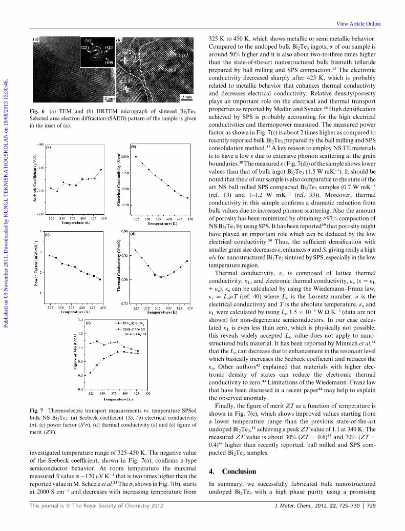
Fig. 6 (a) TEM and (b) HRTEM micrograph of sintered Bi2Te3.
Selected area electron diffraction (SAED) pattern of the sample is given
in the inset of (a).
Fig. 7 Thermoelectric transport measurements vs. temperature SPSed
bulk NS Bi2Te3: (a) Seebeck coefficient (S), (b) electrical conductivity
(s), (c) power factor (S2s), (d) thermal conductivity (k) and (e) figure of
merit (ZT).
Publ
ishe
d on
09
Nov
embe
r 20
11. D
ownl
oade
d by
KU
NG
L T
EK
NIS
KA
HO
GSK
OL
AN
on
19/0
8/20
13 1
5:30
:46.
View Article Online
investigated temperature range of 325–450 K. The negative value
of the Seebeck coefficient, shown in Fig. 7(a), confirms n-type
semiconductor behavior. At room temperature the maximal
measured S value is�120 mVK�1 that is two times higher than the
reportedvalue inM.Scheele et al.23Thes, shown inFig. 7(b), starts
at 2000 S cm�1 and decreases with increasing temperature from
This journal is ª The Royal Society of Chemistry 2012
325 K to 450 K, which shows metallic or semi metallic behavior.
Compared to the undoped bulk Bi2Te3 ingots, s of our sample is
around 50% higher and it is also about two-to-three times higher
than the state-of-the-art nanostructured bulk bismuth telluride
prepared by ball milling and SPS compaction.13 The electronic
conductivity decreased sharply after 425 K, which is probably
related to metallic behavior that enhances thermal conductivity
and decreases electrical conductivity. Relative density/porosity
plays an important role on the electrical and thermal transport
properties as reported byMedlin and Synder.36High densification
achieved by SPS is probably accounting for the high electrical
conductivities and thermopower measured. The measured power
factor as shown in Fig. 7(c) is about 2 times higher as compared to
recently reported bulk Bi2Te3 prepared by the ball milling and SPS
consolidation method.37A key reason to employ NS TEmaterials
is to have a low k due to extensive phonon scattering at the grain
boundaries.38Themeasuredk (Fig. 7(d)) of the sample shows lower
values than that of bulk ingot Bi2Te3 (1.5 W mK�1). It should be
noted that the k of our sample is also comparable to the state of the
art NS ball milled SPS compacted Bi2Te3 samples (0.7 W mK�1
(ref. 13) and 1–1.2 W mK�1 (ref. 33)). Moreover, thermal
conductivity in this sample confirms a dramatic reduction from
bulk values due to increased phonon scattering. Also the amount
of porosity has been minimized by obtaining >97% compaction of
NSBi2Te3 by using SPS. It has been reported39 that porositymight
have played an important role which can be deduced by the low
electrical conductivity.38 Thus, the sufficient densification with
smaller grain size decreases k, enhancess andS, giving really a high
s/k for nanostructuredBi2Te3 sinteredbySPS, especially in the low
temperature region.
Thermal conductivity, k, is composed of lattice thermal
conductivity, kL, and electronic thermal conductivity, ke (k ¼ kL+ ke). ke can be calculated by using the Wiedemann–Franz law,
ke ¼ LosT (ref. 40) where Lo is the Lorentz number, s is the
electrical conductivity and T is the absolute temperature. ke and
kL were calculated by using Lo 1.5 � 10�8 W U K�2 (data are not
shown) for non-degenerate semiconductors. In our case calcu-
lated kL is even less than zero, which is physically not possible;
this reveals widely accepted Lo value does not apply to nano-
structured bulk material. It has been reported by Minnich et al.41
that the Lo can decrease due to enhancement in the resonant level
which basically increases the Seebeck coefficient and reduces the
ke. Other authors42 explained that materials with higher elec-
tronic density of states can reduce the electronic thermal
conductivity to zero.43 Limitations of the Wiedemann–Franz law
that have been discussed in a recent paper44 may help to explain
the observed anomaly.
Finally, the figure of merit ZT as a function of temperature is
shown in Fig. 7(e), which shows improved values starting from
a lower temperature range than the previous state-of-the-art
undoped Bi2Te3,13 achieving a peakZT value of 1.1 at 340 K. The
measured ZT value is about 30% (ZT ¼ 0.6)33 and 70% (ZT ¼0.4)44 higher than recently reported, ball milled and SPS com-
pacted Bi2Te3 samples.
4. Conclusion
In summary, we successfully fabricated bulk nanostructured
undoped Bi2Te3 with a high phase purity using a promising
J. Mater. Chem., 2012, 22, 725–730 | 729

Publ
ishe
d on
09
Nov
embe
r 20
11. D
ownl
oade
d by
KU
NG
L T
EK
NIS
KA
HO
GSK
OL
AN
on
19/0
8/20
13 1
5:30
:46.
View Article Online
chemical synthetic route—feasible for large-scale production.
SPS has been effectively used and optimized for the consolida-
tion of bulk NS Bi2Te3, yielding a very high densification (>97%)
without significant grain growth. Fine plate-like NS Bi2Te3 with
a particle size of �80 nm and a grain size of �90 nm has been
obtained and showed improved TE transport properties.
Transport measurements showed increased Seebeck coefficient
and electrical conductivity, which resulted in about 30%
improved power factor. A figure of merit ZT of 1.1 at 340 K is
achieved, that is slightly higher than the state-of-the-art reported
value for undoped Bi2Te3, especially at ambient temperatures.
This is attributed to the high electrical conductivity, Seebeck
coefficient as well as reduced thermal conductivity.
Acknowledgements
The authors are grateful to Dr C. Stiewe, Dr D. Platzek, and Dr
E. Muller from German Aerospace Center (DLR) for the ther-
moelectric measurements and to Dr Wubeshet Sahle for TEM
analysis.
References
1 L. E. Bell, Science, 2008, 321(5359), 1457–1461.2 CRC Handbook of Thermoelectrics, ed. D. M. Rowe, CRC, BocaRaton, FL, USA, 1995.
3 Thermoelectric Handbook: Macro to Nano, ed. D. M. Rowe, CRCPress, Boca Raton, FL, USA, 2006.
4 M. S. Dresselhaus, G. Chen, M. Y. Tang, R. Yang, H. Lee, D. Wand,Z. Ren, J. P. Fleurial and P. Gonga, Adv. Mater., 2007, 19(8), 1043–1057.
5 M. G. Kanatzidis, Chem. Mater., 2010, 22(3), 648–659.6 G. J. Snyder and E. S. Toberer, Nat. Mater., 2008, 7, 105–114, Rev.Art.
7 L. D. Hicks and M. S. Dresselhaus, Phys. Rev. B: Condens. Matter,1993, 47, 16631–16634.
8 L. D. Hicks and M. S. Dresselhaus, Phys. Rev. B: Condens. Matter,1993, 47, 12727–12731.
9 T. C. Harman, P. J. Taylor, M. P. Walsh and B. E. Laforge, Science,2002, 297(5590), 2229–2232.
10 R. Venkatasubramanian, E. Siivola, T. Colpitts and B. O’quinn,Nature, 2001, 413(6856), 597–602.
11 L. D. Hicks, T. C. Harman, X. Sun andM. S. Dresselhaus, Phys. Rev.B: Condens. Matter, 1996, 53(16), 10493–10496.
12 J. R. Szczech, J. M. Higgins and S. Jin, J. Mater. Chem., 2011, 21,4037–4055.
13 F. Yu, J. Zhang, D. Yu, J. He, Z. Liu and B. Xo, J. Appl. Phys., 2009,105(094303), 1–5.
14 B. Poudel, Q. Hao, Y. Ma, Y. C. Lan, A. Minnich, B. Yu, X. Yan,D. Z. Wang, A. Muto, D. Vashaee, X. Y. Chen, J. M. Liu,M. S. Dresselhaus, G. Chen and Z. F. Ren, Science, 2008, 320(5876), 634–638.
15 J. P. Heremans, V. Jovovic, E. S. Toberer, A. Saramat, K. Kurosaki,A. Charoenphakdee, S. Yamanaka and G. J. Snyder, Science, 2008,321(5888), 554–557.
730 | J. Mater. Chem., 2012, 22, 725–730
16 Z. A.Munir, U. Anselmi-Tamburini andM. Ohyanagi, J.Mater. Sci.,2006, 41, 763–777.
17 Z. Shen, M. Johnsson, Z. Zhao and M. Nygren, J. Am. Ceram. Soc.,2002, 85(8), 1921–1927.
18 S. K. Bux, J. P. Fleurial and R. B. Kaner, Chem. Commun., 2010, 46,8311–8324.
19 W. Jun, T. Xinfeng, L. Haiqiang, Y. Xiuli and Z. Qingjie, J. WuhanUniv. Technol., Mater. Sci. Ed., 2006, 21(4), 126.
20 P. Vaquerio and A. V. Powell, J. Mater. Chem., 2010, 20, 9577–9584.
21 A. Purkayastha, S. Kim, D. D. Gandhi, P. G. Ganesan, T. Borca-Tasciuc and G. Ramanath, Adv. Mater., 2006, 18, 2958–2963.
22 M. R. Dirmyer, J. Martin, G. S. Nolas, A. Sen and J. V. Badding,Small, 2009, 5(8), 933–937.
23 M. Scheele, N. Oeschler, K. Meier, A. Kornowski, C. Klinke andH. Weller, Adv. Funct. Mater., 2009, 19, 3476–3483.
24 M. E. Anderson, S. S. N. Bharadway and R. E. Schaak, J. Mater.Chem., 2010, 20, 8362–8367.
25 J. J. Ritter, Inorg. Chem., 1994, 33, 6419–6420.26 J. J. Ritter and M. Pichai, Inorg. Chem., 1995, 34, 4278–4280.27 C. Stiewe, Z. He, D. Platzek, G. Karpinski, E. Muller, S. Li,
M. Toprak and M. Muhammed, Materialwiss. Werkstofftech., 2007,9, 38.
28 S. Li, Z. He, M. Toprak, C. Stiewe, E. Mueller and M. Muhammed,Phys. Status Solidi RRL, 2007, 6, 259–261.
29 M. Toprak and M. Muhammed, in CRC Thermoelectrics Handbook,CRC Press, Boca Raton, 2006.
30 M. Toprak, Y. Zhang and M. Muhammed, Mater. Lett., 2003, 4(4460), 1–7.
31 M. Toprak, C. Stiewe, D. Platzek, S. Williams, L. Bertini, E. M€uller,C. Gatti, Y. Zhang, M. Rowe and M. Muhammed, Adv. Funct.Mater., 2004, 14(12), 1189–1196.
32 I. Puigdomenech, TRITA-00K-3130, Dept. Inorg. Chem., RoyalInstitute of Technology, SE-10044, Stockholm, Sweden.
33 D. H. Kim, C. Kim, D. W. Ha and H. Kim, J. Alloys Compd., 2011,501, 5211–5215.
34 W. Xie, X. Tang, Y. Yan, Q. Zhang and T.M. Tritt,Appl. Phys. Lett.,2009, 94(102111), 1–3.
35 L. D. Zhao, B.-P. Zhang, J.-F. Li, H. L. Zhang and W. S. Liu, SolidState Sci., 2008, 10(5), 651–658.
36 D. L. Medlin and G. J. Synder, Curr. Opin. Colloid Interface Sci.,2009, 14, 226–235.
37 C. H. Kuo, C. S. Hwang, M. S. Jeng, W. S. Su, Y. W. Chou andJ. R. Ku, J. Alloys Compd., 2010, 496(1–2), 687–690.
38 E. J. Winder, A. B. Ellis and G. C. Lisensky, J. Chem. Educ., 1996, 73(10), 940–946.
39 H. Lee, D. Vashaee, D. Z. Wang, M. S. Dresselhaus, Z. F. Ren andG. Chen, J. Appl. Phys., 2010, 107(094308), 1–7.
40 M. G. Kanatzidis, T. P. Hogan and S. D. Mahanti, Chemistry,Physics and Materials Science of Thermoelectric Materials: BeyondBismuth Telluride, Kluwer Academic/plenum publisher, New York,2003.
41 A. J. Minnich, M. S. Dresselhaus, Z. F. Ren and G. Chen, EnergyEnviron. Sci., 2009, 2, 466–479.
42 G. D. Mahan and J. O. Sofo, Proc. Natl. Acad. Sci. U. S. A., 1996, 93,7436–7439.
43 T. E. Humphery and H. Linke, Phys. Rev. Lett., 2005, 94(096601), 1–4.
44 Z. Zhang, P. A Sharma, E. J. Lavernia and N. Yang, J. Mater. Res.,2011, 26, 475–484.
This journal is ª The Royal Society of Chemistry 2012