Silver gallium telluride (AgGaTe2) single crystal: Synthesis, accelerated crucible rotation-Bridgman...
6
Silver gallium telluride (AgGaTe2) single crystal: Synthesis, accelerated crucible rotation-Bridgman growth and characterization K. Aravinth, G. Anandha Babu n , P. Ramasamy Centre for Crystal Growth, SSN College of Engineering, Kalavakkam 603110, India article info Keywords: Bridgman growth Characterization X-ray diffraction abstract A silver gallium telluride single crystal of diameter 12 mm and length 80 mm was successfully grown by the vertical Bridgman method using accelerated crucible rotation technique. To confirm the unit cell parameters of the grown silver gallium telluride (AgGaTe 2 ) crystal, single crystal X-ray diffraction studies were carried out. AgGaTe 2 has been studied using differential scanning calorimetry and is found to have supercooling of 13 1C. AgGaTe 2 shows Fourier transform infrared transmission in the spectral range of 6000–500 cm 1 . The composition of Ag, Ga and Te in the grown crystal was measured with energy dispersive X-ray analysis spectroscopy. The optical band gap for AgGaTe 2 is 1.8 eV. In the positron lifetime measurements, the average lifetime 267 ps corresponds to vacancy clusters in AgGaTe 2 crystal. Hall measurements confirm p-type nature of AgGaTe 2 . & 2014 Elsevier Ltd. All rights reserved. 1. Introduction Ternary compounds of types A II B IV C 2 V and A I B III C 2 VI have attracted considerable attention because of their interesting semiconducting, electrical, structural, and optical properties. Compared to their binary analogues (III–V and II–VI com- pounds) ternary compounds have higher energy gaps and lower melting points because of which they are considered to be important in crystal growth studies and device applica- tions [1]. AgGaS 2 and AgGaSe 2 are ternary semiconducting compounds that crystallize in chalcopyrite structure whose non-linear optical properties have been used for many years to convert the frequency of solid-state and CO 2 lasers into the mid-infrared spectral region. AgGaSe 2 has a large non-linear coefficient (d 36 39 pm/V) and excellent transmission in the mid-IR (1–18 μm) range. Continuation of this trend, by substituting Te for Se, should result in an additional 3-fold increase in d 36 and a transparency range that is further red- shifted but still desirable for mid-IR laser application [2]. The chalcopyrite structure is similar to the zinc blende non- centrosymmetric, leading to non-zero second order nonlinear susceptibility, χ (2) . Silver gallium telluride (AgGaTe 2 ) is of chalcopyrite structure and it belongs to the I 42d space group and is black in colour at room temperature and its melting point is 724 1C [3]. The material has a direct band gap of 1.32 eV. The value is well adapted to the solar spectrum and together with a high absorption coefficient, these materials are very attractive for thin film solar cells [4–7]. Most chalcopyrites also possess essential property, birefringence, which is the result of a uniaxial tetragonal distortion (c/a) from their underlying diamond like face-centered cubic structure. The distortion ranges from 0% to 10% and it is usually described by c/a, the ratio of its lattice parameters. The unit cell is tetragonal due to some uniaxial distortion of the lattice cell (c/a a2), causing additional interesting aniso- tropy of the physical properties. In particular, sufficient biref- ringence is needed to achieve the phase matching condition for nonlinear optical devices. The c/a ratio of AgGaTe 2 crystal Contents lists available at ScienceDirect journal homepage: www.elsevier.com/locate/mssp Materials Science in Semiconductor Processing http://dx.doi.org/10.1016/j.mssp.2014.02.039 1369-8001 & 2014 Elsevier Ltd. All rights reserved. n Corresponding author. Fax: þ91 44 27469700. E-mail address: [email protected] (G. Anandha Babu). Materials Science in Semiconductor Processing 24 (2014) 44–49
Transcript of Silver gallium telluride (AgGaTe2) single crystal: Synthesis, accelerated crucible rotation-Bridgman...

Contents lists available at ScienceDirect
Materials Science in Semiconductor Processing
Materials Science in Semiconductor Processing 24 (2014) 44–49
http://d1369-80
n CorrE-m
journal homepage: www.elsevier.com/locate/mssp
Silver gallium telluride (AgGaTe2) single crystal: Synthesis,accelerated crucible rotation-Bridgmangrowth and characterization
K. Aravinth, G. Anandha Babu n, P. RamasamyCentre for Crystal Growth, SSN College of Engineering, Kalavakkam 603110, India
a r t i c l e i n f o
Keywords:Bridgman growthCharacterizationX-ray diffraction
x.doi.org/10.1016/j.mssp.2014.02.03901 & 2014 Elsevier Ltd. All rights reserved.
esponding author. Fax: þ91 44 27469700.ail address: [email protected] (G. Anand
a b s t r a c t
A silver gallium telluride single crystal of diameter 12 mm and length 80 mm wassuccessfully grown by the vertical Bridgman method using accelerated crucible rotationtechnique. To confirm the unit cell parameters of the grown silver gallium telluride(AgGaTe2) crystal, single crystal X-ray diffraction studies were carried out. AgGaTe2 hasbeen studied using differential scanning calorimetry and is found to have supercooling of13 1C. AgGaTe2 shows Fourier transform infrared transmission in the spectral range of6000–500 cm�1. The composition of Ag, Ga and Te in the grown crystal was measuredwith energy dispersive X-ray analysis spectroscopy. The optical band gap for AgGaTe2 is1.8 eV. In the positron lifetime measurements, the average lifetime 267 ps corresponds tovacancy clusters in AgGaTe2 crystal. Hall measurements confirm p-type nature of AgGaTe2.
& 2014 Elsevier Ltd. All rights reserved.
1. Introduction
Ternary compounds of types AIIBIVC2Vand AIBIIIC2
VIhave
attracted considerable attention because of their interestingsemiconducting, electrical, structural, and optical properties.Compared to their binary analogues (III–V and II–VI com-pounds) ternary compounds have higher energy gaps andlower melting points because of which they are considered tobe important in crystal growth studies and device applica-tions [1]. AgGaS2 and AgGaSe2 are ternary semiconductingcompounds that crystallize in chalcopyrite structure whosenon-linear optical properties have been used for many yearsto convert the frequency of solid-state and CO2 lasers into themid-infrared spectral region. AgGaSe2 has a large non-linearcoefficient (d36�39 pm/V) and excellent transmission in themid-IR (1–18 μm) range. Continuation of this trend, bysubstituting Te for Se, should result in an additional 3-fold
ha Babu).
increase in d36 and a transparency range that is further red-shifted but still desirable for mid-IR laser application [2]. Thechalcopyrite structure is similar to the zinc blende non-centrosymmetric, leading to non-zero second order nonlinearsusceptibility, χ(2). Silver gallium telluride (AgGaTe2) is ofchalcopyrite structure and it belongs to the I42d space groupand is black in colour at room temperature and its meltingpoint is 724 1C [3]. The material has a direct band gap of1.32 eV. The value is well adapted to the solar spectrum andtogether with a high absorption coefficient, these materialsare very attractive for thin film solar cells [4–7]. Mostchalcopyrites also possess essential property, birefringence,which is the result of a uniaxial tetragonal distortion (c/a)from their underlying diamond like face-centered cubicstructure. The distortion ranges from 0% to 10% and it isusually described by c/a, the ratio of its lattice parameters.The unit cell is tetragonal due to some uniaxial distortion ofthe lattice cell (c/aa2), causing additional interesting aniso-tropy of the physical properties. In particular, sufficient biref-ringence is needed to achieve the phase matching conditionfor nonlinear optical devices. The c/a ratio of AgGaTe2 crystal

5 10 15 20 25 30 35 40 45 50600
620
640
660
680
700
720
740
760
Tem
pera
ture
( oC
)
Distance (cm)
724 oC711 oC
3 oC/cm
Fig. 1. Temperature profile of two zone vertical Bridgman furnace.
Fig. 2. As grown AgGaTe2 crystal.
K. Aravinth et al. / Materials Science in Semiconductor Processing 24 (2014) 44–49 45
is found to be 1.90 from X-ray diffraction studies. As the valueis significantly different from 2.0, AgGaTe2 is expected to havesubstantial birefringence [8–10].
In the compound semiconducting crystals, like binary andternary, one of the most important complicated parametersto be controlled is the stoichiometry. Non-stoichiometryenhances the generation of intrinsic point defects that con-tributes to compensation level, type of conductivity, carrierconcentration, absorption behaviour etc. It promotes thegeneration, multiplication and three dimensional movementof dislocations. Finally, the incorporation of the excess com-ponent at the interphase in the form of inclusions and thenucleation of second phase in the form of precipitates duringthe cooling process of the as grown crystal can impair thewafer and device quality markedly [11]. Our present workfocused on the synthesis, growth and characterization ofAgGaTe2. In order to minimize the growth challenges men-tioned above, we followed a relatively lower temperaturesynthesis method. The method was used to synthesise highpurity AgGaTe2 at 745 1C, which is slightly above its meltingpoint (724 1C). It reduces the material losses. The composi-tion is maintained to its starting stoichiometric ratio. Thesynthesised material and grown crystals were characterizedby single crystal X-ray diffraction (SXRD), powder X-raydiffraction (PXRD), differential scanning calorimetry (DSC),Fourier transform infrared (FTIR), UV–vis–NIR, energy dis-persive X-ray analysis spectroscopy (EDS), Hall measurementand positron annihilation studies.
2. Experimental procedure
2.1. Synthesis of AgGaTe2
The following elements were used without furtherpurification: Ag (99.9999%), Ga (99.9999%), Te (99.99%) Alfamake. AgGaTe2 was synthesised from stoichiometry amountwith the mole ratio 1:1:2 of Ag, Ga and Te. In order toprevent deviation from stoichiometry resulting from allpossible volatile losses of tellurium during initial steps, theexcess 1% of Te was chosen as the starting composition. Thestarting materials were loaded into a quartz ampoule withan inner diameter of 19 mm and then sealed at2�10�6 mbar. The ampoule was placed in a muffle furnaceinclined at an angle of 451 and rotated at 3 rpm for uniformmelt mixing. It is heated to 500 1C within 60 h, held for 24 h,subsequently heated to 745 1C at the rate of 6 1C/h and heldfor 24 h. This process was repeated several times between500 1C and 745 1C. After completion of several cycles, theampoule was adjusted carefully to be inclined at 201 toprevent the quartz cracking. Finally the furnace was cooledto room temperature at the rate of 15 1C/h.
2.2. Single crystal growth of AgGaTe2
AgGaTe2 single crystal of size 80 mm length and 12mmdiameter was grown by the vertical Bridgman techniqueusing the synthesised polycrystalline material of the titlecompound in a high quality conical quartz ampoule in twozone tubular furnace. The conical bottom of the ampoule wasused to encourage the spontaneous nucleation and propaga-tion of a single grain. Preceding crystal growth, the silica
ampoule charged with polycrystalline material was continu-ously evacuated and then sealed at 2�10�6 millibar pres-sure. The well-sealed charged ampoule was hanged in thevertical Bridgman furnace from the top of the setup in the hotzone of the furnace cavity where it was heated gradually upto745 1C, 20 1C above the melting point of AgGaTe2 at the rateof 15 1C/h and held at this temperature for 24 h. The tem-perature profile of the furnace is shown in Fig. 1. Temperaturegradient of the growth interface was kept at 3 1C/cm in thefurnace. The ampoule was allowed to move downwards alongthe axis of the furnace cavity with a rate of 5 mm/day. Theampoule was also rotated by ACRT mode at 15 rpm periodi-cally to ensure complete homogeneity of the melt. Thisimprovement in the crystal growth process helps in improv-ing crystal quality. After the entire melt had traversed throughthe growth face, the temperature of the furnace was cooled toroom temperature at a very slow rate of about 5 1C/h. The asgrown single crystal is shown in Fig. 2. The cut and polishedAgGaTe2 crystal wafer is shown in Fig. 3.
2.3. Instrument for characterization
To confirm the crystal structure and lattice parametersof the grown AgGaTe2 single crystal, a small piece of thecrystal was subjected to SXRD using Enraf (Bruker) NoniusCAD40 diffractometer with graphite monochromatedMoKα radiation (λ¼0.71073 1). X-ray powder diffractionanalysis was performed using a Xpert-Pro diffractometerwith continuous X-ray wavelength of 1.54 1 (CuKα) with 2θ

0 20 40 60 80 1000
200
400
600
800
1000
1200
1400
Inte
nsity
(cps
)
(112
)
(220
) (204
)(3
12)
(116
)
(400
)
2θ (degree)
Fig. 4. PXRD pattern of AgGaTe2 single crystal.
100 200 300 400 500 600 700 800-0.2
-0.1
0.0
0.1
0.2
0.3 Heating Cooling
Temperature (oC)
Hea
t flo
w (W
/g)
-0.5
-0.4
-0.3
-0.2
-0.1
0.0
0.1
0.2M.P
F.P
Fig. 5. DSC curve for the heating and cooling process of AgGaTe2 crystal.
100
K. Aravinth et al. / Materials Science in Semiconductor Processing 24 (2014) 44–4946
values from 101 to 901. DSC measurements were performed ina simultaneous DSC-TGA STA 449 F3 made by NETZSCHcompany. About 15.0 mg of polycrystalline sample of AgGaTe2was placed in Al2O3 crucible and heated (and cooled) at a rateof 10 1C/min between 30 1C and 800 1C under flowing N2 gas.The FTIR transmittance of the AgGaTe2 single crystal wasmeasured using Alpha Bruker FTIR Spectrometer with wavenumber range from 500 to 6500 cm�1. The above spectralstudies were obtained using a crystal of 2 mm thickness. The1 mm thick cut and polished AgGaTe2 single crystal was usedfor UV absorption studies. The absorption of the AgGaTe2crystal was measured by Shimadzu UV–vis spectrophot-ometer for the wavelength range of 200–900 nm with slitwidth 2 nm and scan speed 240 nm/min. The composition ofthe AgGaTe2 sample was determined using scanning electronmicroscope (Hitachi S34200) linked to an energy dispersivespectrometer (EDS) INCA Energy 250 from Oxford Instru-ments using an accelerating voltage of 20 kV. The EDS consistsof a Link Pentafet X-ray detector with an energy resolutionquoted as 133 eV at 5.9 keV, and an INCA Microanalysis SuiteVersion software package. A 22Na source is used to injectpositrons into the AgGaTe2 sample. Lifetime measurementinvolves a coincidence setup of two BaF2 detectors to measurethe time difference between the 1.27MeV de-excitationgamma ray coming from the 22Na source, and the 511 keVγ ray originating from positron annihilation in the sample. Theenergy resolution of the high purity Ge detector used is1.0970.01 keV at 511 keV, resulting in a high sensitivity tochanges in material properties from surface to depth. Themotion of the electron-positron pair prior to annihilationcauses a Doppler broadening of the 511 keV annihilation lineand can be characterized by the line shape parameters S andW. The usefulness of these parameters may be illustrated byan S–W plot, which allows one to conclude whether thechanges are due to change in concentration or type of a defect[12,13]. The Hall measurement was carried out using Van derPauw type (Ecopia-HMS 3000) at room temperature with apermanent magnet of 0.57 T.
3. Results and discussion
SXRD analysis revealed that the grown AgGaTe2 singlecrystal belongs to tetragonal system with unit cell dimen-sions a¼6.314 (1) Å; b¼6.314 (1) Å; c¼12.00 (3) Å andV¼482 (8) Å3. The values are in good agreement withreported values [14]. PXRD patterns of AgGaTe2 single crystal
Fig. 3. Cut and polished AgGaTe2 crystal wafer.
at room temperature are shown in Fig. 4. The XRD pattern isconsistent with AgGaTe2 and no peak attributable to possibleimpurities is observed. Bragg's reflections for AgGaTe2 crystalare observed in XRD pattern at 2θ values of 24.71, 40.201,41.551, 47.801, and 49.881 representing (112), (220), (204),(312), (116) and (400) planes of AgGaTe2 respectively. DSCwas used to study the heat flow rate during melting andfreezing phase transitions. In melt growth methods super-cooling state of solution may cause a severe problem, the
1000 2000 3000 4000 5000 6000
50
Wavenumber (cm-1)
Tran
smitt
ance
(%)
Fig. 6. FTIR transmittance spectrum of AgGaTe2 crystal.
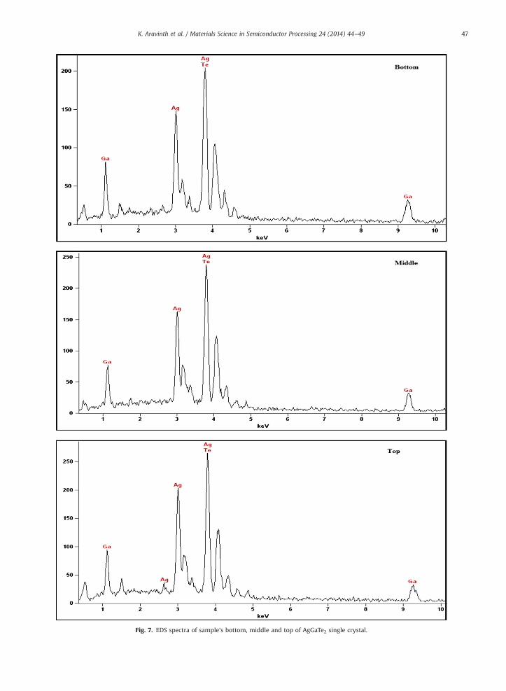
Fig. 7. EDS spectra of sample's bottom, middle and top of AgGaTe2 single crystal.
K. Aravinth et al. / Materials Science in Semiconductor Processing 24 (2014) 44–49 47

1.3 1.4 1.5 1.6 1.7 1.8 1.9 2.0hν (eV)
(αhν
)2eV
2 (a
.u)
Fig. 8. UV–vis spectrum (a), and the plots of (ahv)2 versus hv (b) ofAgGaTe2 crystal.
K. Aravinth et al. / Materials Science in Semiconductor Processing 24 (2014) 44–4948
presence of the large degree of super-cooling allows multi-nuclei formation. The thermograms of AgGaTe2 crystal areshown in Fig. 5. This shows the endothermic peak at 724 1Cwhich is the melting point of the compound. This is followedby an exothermic reaction (during cooling) with peak at711 1C. The FTIR transmission spectrum is as shown inFig. 6. The transmission is above 30% for AgGaTe2 singlecrystal in the wave number region 500–6000 cm�1. Theuniformity of the composition was investigated by EDS. Thesemi-quantitative measurements were performed for theaxial composition of the sample of AgGaTe2. In the EDSspectra of AgGaTe2 obtained from sample's bottom, middleand top (Fig. 7), Ag, Ga and Te elements are detectable. Theatomic percentages of the Ag, Ga and Te elements for thesample's bottom, middle and top are given in Table 1. It isseen that the crystal was Ag deficient, gallium, tellurium richthrough out of the ingot and no other phases were observedin EDS measurements. From this we conclude that theaverage stoichiometric composition of grown single crystalwas AgGaTe2. Roy et.al., have reported that last to freezeregion of the horizontal Bridgman method grown AgGaTe2crystal has higher Ga concentration when compared toAg and Te [15], but in the present investigation last to freezeregion of the vertical Bridgman method grown crystal hashigher Te concentration compared to Ag and Ga. The Tecontent increases gradually along the axial distribution of thecrystal due to Te segregation. The fundamental absorptionedge lies at around 640 nm at room temperature. Fig. 8(a)shows the absorption spectra of AgGaTe2 single crystal. Thevalue of the band gap was obtained using the followingrelationship [16]:
ðahvÞ2 ¼ kðhv�EgÞ ð1ÞThe band gap energy of AgGaTe2 is shown in Fig. 8(b).
The band gap energy was found to be 1.8 eV. The cut andpolished piece of AgGaTe2 crystal of 1 mm thickness wasused for electrical measurements. The positive sign of theHall coefficient confirms the p-type conductivity. The mea-sured parameters are Hall coefficient (3.85�103 cm3/C),resistivity (6.55 Ω cm), mobility (5.87�102 cm2/V s), bulkconcentration (1.62�1015/cm3) and conductivity (1.53�10�1/Ω cm) of the grown AgGaTe2 crystal.
Positron lifetime and Doppler broadening measurementswere carried out on AgGaTe2 crystal. In AgGaTe2 single crystalthe group VI atom vacancies should act as donors, whereasthe group I and III atom vacancies should be acceptors. In areal crystal, defects can trap positrons. Two or more lifetimeswere found in the positron lifetime spectra. τ1 indicates thepositron lifetime of monovacancy-type defects and τ2 indi-cates the positron lifetime of multivacancy-type defects or thelarger vacancy-type defects. From the observed experimental
Table 1Elemental concentration obtained from EDS measurement of AgGaTe2single crystal.
Scanned area Ag L (at%) Ga K (at%) Te L (at%)
Bottom 23.35 25.97 50.68Middle 23.57 25.14 51.29Top 23.09 25.06 51.85Average 23.33 25.39 51.27
spectrum two positron lifetime components i.e., first compo-nent τ1�226.7 ps (bulk annihilation) with 81.2% intensity andsecond component τ2�445.4 ps with 18.2% intensity wereobserved. Bulk annihilation lifetime for common semiconduc-tors is of the order of 200 ps [13]. This is also evidenced by theobservation that the second lifetime component with con-siderable intensity corresponds to presence of vacancy clus-tering and void formation in the sample. The mean lifetime iscalculated as τmE266.740 ps using the relation [17]
τm ¼ ðτ1I1þτ2I1Þ=ðI1þ I2Þ ð2Þ
Doppler broadening S-parameter value is found to be 0.6446and W-parameter is 0.0136.
4. Conclusion
Single crystals of AgGaTe2 have been grown by the verticalBridgman growth method. The unit cell parameters of theAgGaTe2 were confirmed by SXRD studies. The melting andfreezing temperature of AgGaTe2 crystal were 724 1C and711 1C respectively. EDS measurement of the different regionsof the grown crystal showed the composition uniformity ofthe ingot. FTIR studies showed that transmittance is 30%throughout the mid-IR region from 1.5 to 20 mm. the absorp-tion edge lies at 640 nm. The band gap energy was calculatedto be 1.8 eV for AgGaTe2 single crystal. Themeasured electricalproperties of cut and polished AgGaTe2 crystal at roomtemperature are Hall coefficient (3.85�103 cm3/C), resistivity(6.55Ω cm) and conductivity (1.53�10�1/Ω cm). Positronannihilation spectroscopy measurements on as grown crystalindicate the strong presence of vacancy clustering and voidformation.
Acknowledgement
The authors are thankful to Prof. K. Ramamurthi, Schoolof Physics, Bharathidasan University, Trichy, for Hall mea-surement studies and Dr. G. Amarendra, MSG, IGCAR,Kalpakkam, for Positron Annihilation Studies.
K. Aravinth et al. / Materials Science in Semiconductor Processing 24 (2014) 44–49 49
References
[1] A.C. Verma, S.R. Bhardwaj, Phys. Status Solidi B 243 (2006)2858–2863.
[2] Y. Mori, K. Takarabe, S. Iwamoto, K. Masumoto, Phys. Status Solidi B198 (1996) 427–431.
[3] H. Hahn, G. Frank, W. Klinger, G. Storger, Z. Anorg. Allg. Chem. 271(1953) 153–170.
[4] N.N. Konstantinova, Yu. V. Rud, Sov. Phys. Semicond. 23 (1989)999–1101.
[5] S. Mostafa Hosseinpour-Mashkani, Fatemeh Mohandes, MasoudSalavati-Niasari, K. Venkateswara-Rao, Mater. Res. Bull. 47 (2012)3148–3159.
[6] S. Mostafa Hosseinpour-Mashkani, Masoud Salavati-Niasari,Fatemeh Mohandes, K. Venkateswara-Rao, Mater. Sci. Semicond.Process. 16 (2013) 390–402.
[7] S. Mostafa Hosseinpour-Mashkani, K. Venkateswara-Rao, in: Pro-ceeding of the International Conference on Nanoscience, Engineer-ing and Technology, IEEE conference proceedings, 11, 2011, 653–655.
[8] M.C. Ohmer, J.L. Goldstein, D.E. Zelmon, A.W. Saxler, J. Appl. Phys. 86(1999) 94–99.
[9] A. Burger, J.O. Ndap, Y. Cui, U. Roy, J. Cryst. Growth 225 (2001)505–511.
[10] P.G. Schuemann, S.D. Setzler, T.M. Pollak, J. Cryst. Growth 211 (2000)242–246.
[11] P. Rudolph, Cryst. Res. Technol. 38 (2003) 542–554.[12] A.P. Mills Jr., Positron Spectroscopy of Solids, in: A. Dupasquier,
A.P. Mills Jr. (Eds.), IOS press, Amsterdam, 1995, pp. 209–258.[13] R. Krause-Rehberg, H.S. Leipner, Springer, 1999.[14] M. Guittard, J. Rivert, A. Mazurier, S. Jaulmes, P.H. Fourcroy, Mater.
Res. Bull. 23 (1988) 217–225.[15] U.N. Roy, B. Mekonen, O.O. Adetunji, F. Kochari, Y. Cui, A. Burger,
J.T. Goldstein, J. Cryst. Growth 241 (2002) 135–140.[16] M.K.R. Khan, R.M. Azizar, M. Shahjahan, M.M. Rahman, M.A. Hakim,
Curr. Appl. Phys. 10 (2010) 790–796.[17] M. Premila, S. Abhaya, R. Rajaraman, T.R. Ravindran, G. Amarendra,
C.S. Sundar, J. Non-cryst. Solids 358 (2012) 1014–1018.