Electrochemical Modified Electrodes Based on Metal‐Salen Complexes
Upload
independentCategory
view
4download
0
Pergamon
Ekcrrochimica Arm. Vol. 42, No. 19. pp. 2861-2879. 1997 s(; 1997 Published by Elsevier Science Ltd. All rights reserved
Printed in Great Britain PII: s00&468q97)00107-2 00134686/97 $17.04 + 0.00
Influence of surface pretreatment of bismuth and cadmium electrodes to the electric double layer and adsorption characteristics of organic
compounds
E. Lust,“* A. JBnes,” K. Lust,” V. Sammelselgb and P. Miidla’
“Institute of Physical Chemistry, University of Tartu, 2 Jakobi Street, EE-2400 Tartu, Estonia blnstitute of Physics, Estonian Academy of Sciences, 142 Riia Street, EE-2400 Tartu, Estonia
CInstitute of Applied Mathematics, University of Tartu, 2 Liivi Street, EE-2400 Tartu, Estonia
(Received 1 September 1996; in revised form 19 December 1996)
Abstract-Influence of the surface structure of electrodes on the electric double layer properties, as well as on the adsorption characteristics of various organic compounds has been investigated by cyclic voltammetry, impedance and electron microscopic methods at variously prepared Bi, Sb and Cd electrodes. The systematic trends of the influence of surface roughness and energetic inhomogeneity on the electric double layer characteristics (value of differential capacity, potential of diffuse minimum, Parsons-Zobel factor, inner layer capacity, roughness function) have been established. The dependencies of the shape of adsorption-desorption maxima of organic compounds and other adsorption parameters (values of attraction interaction, adsorption equilibrium constant, shape of adsorption isotherm) on the electrode surface structure have been investigated. The Debye-length dependent roughness function has been calculated. The approximate values of the linear parameter of homogeneous regions, which prevail at the surface of polycrystalline electrodes have been calculated using various theoretical models. The established values of linear parameters of homogeneous regions have been compared with the characteristics obtained from the electron microscopic studies. 0 1997 Published by Elsevier Science Ltd
Key tvords: Bi, Sb, Cd, polycrystal, monocrystal, surface treatment, surface roughness, organic adsorption.
1. INTRODUCTION
The phase boundary structure and adsorption properties, as well as the kinetics of various interfacial reactions at solid surfaces significantly depend not only on the chemical composition of electrode material, but also on the morphology of the surface studied [l-5]. The atomic level STM investigations at quasi-perfect silver single crystal planes, electrolyti- cally grown in glass or Teflon capillaries [6, 71, show that at the surface of quasi-perfect Ag(OOl) plane the monoatomic steps exist. At the surface of so-called real single crystal macro- and micro-electrodes (prepared either by thermal, chemical or electrochem- ical pretreatment, by vapor deposition techniques) a
*Author to whom correspondence should be addressed.
great density of crystal imperfections exists, especially emergence points of edge and screw dislocations, which lead to the appearance of mono- and multi-atomic steps and a relatively high surface corrugation [8-lo]. Accordingly, no matter how careful the surface preparation of a solid electrode is, the surface of real solid electrode is always to some extent inhomogeneous. The surface roughness of solid material is a universal phenomena and it exists always and everywhere. As a consequence the electric double layer (cdl) and adsorption parameters (for example, the values of zero charge potential, capacity of inner layer, interaction parameter in adsorption isotherm, adsorption equilibrium constant, maximum surface excess, Gibbs energy of adsorption, etc) obtained for polycrystalline (PC) electrodes have intermediate or apparent values [l-5, 1 I-121. Some of the edl and electrochemical kinetic parameters, being
EA 42 19 B 2861
2862 E. Lust et al.
extensive quantities, have to be referred to the geometric unit area of the surface, in the case of inhomogeneous solid surfaces, and have apparent values. Therefore the question of obtaining the “true” working surface area of electrodes will have a great importance.
In electrochemistry three main in situ methods for obtaining the surface roughness R = Sr,d~/Sg~,, (where .%,I and S,,,, are the working surfaces and geometrical areas determined, respectively) have been used [13]: (1) differential capacity measurements in the region of ideal polarizability of electrodes, applied in Parsons-Zobel [14], ValetteHamelin [15] and other methods [16]; (2) mass transfer process under diffusion control with assumption of homogeneous current distribution [ 13, 171; (3) adsorption of radio-active organic compounds (radio tracer adsorp- tion technique) or reactant monolayer (Hz, 02 or metals) at electrode surface and following electro- chemical reaction [13, 18, 191. According to [l-5, 13- 191, the value of R depends on the method used, and therefore more systematic investigations are indis- pensable.
In many cases the experimental data cannot be rationalized only in terms of surface roughness and energetic inhomogeneity, as the roughness can be the reason of new characteristic lengths, which may compete with other typical lengths, inducing the rise of new functional dependences for charge carrier concentration and potential distribution. The deter- mination of the solvent and ionic concentration (charge carriers) distribution, as well as the electron density profile at metal-electrolyte, metal-semicon- ductor-electrolyte and semiconductor-electrolyte phase boundaries is an important step towards a complete description of the interfacial phenomena.
Up to now the physical content of the modern theories on the PC structure of solid electrode surface involves its modeling description as a combination of different monocrystalline faces [ 15,2&27]. Thus, the differential capacity of a PC electrode is obtained by the superposition of the corresponding C(E)-curves for individual faces exposed at the surface of PC electrode:
CFt’(E) = REX/C,(E), (1)
where Ci(E) refer to unit area of the true surface and CppP refer to unit area of the apparent surface of the electrode. As shown in [ 14, 15,20-281, the coefficient R can characterize the geometric roughness, with which the size of the surface area and differential capacity have been measured. But for solid electrodes, R also reflects the energetic inhomogeneity of the surface caused by the fact that crystallograph- ically different grains (single crystal planes), grain boundaries and other crystallographic defects are exposed at the surfaces of solid polycrystalline electrodes, as well as at the surface of real single crystal planes.
It must be noted that in the general case it is useful to distinguish the microscopic and macroscopic values of roughness factor R and the share of planes X at a polycrystalline (PC) electrode surface [25]. The microscopic value of R would characterize the “true” geometrical roughness and the share of ideally flat single crystal planes at the surface of a PC electrode R = ZiXif;, where 1; and Xi are the roughness and share of the ideally smooth single crystal plane i, respectiveIy. If we at the first approximation assume that the PC electrode surface consists only of the homogeneous regions, of which the edl characteristics are similar to the real monocrystalline planes (not ideally smooth), then the values of macroscopic roughness factor fEcr = XIX,. The methods for obtaining the R and X values have been discussed in
~51. As a first approximation, the edl models for PC
electrodes may be classified in two groups [ 152 I-261. The first group considers the PC electrode surface as one consisting only of relatively large monocrys- talline regions with linear parameter ,v* + 10 nm (y*, so-called characteristic length), which corresponds to macropolycrystallinity. Within these regions both the compact and the diffuse layers at different homo- geneous areas can be viewed as independent ones, and accordingly
c&’ = R%XiCHiCD,/(CH, + CD,), (2)
where Cui and Co* are the inner layer and diffuse layer capacities for the plane i, respectively. Therefore this is the so-called model of independent diffuse layers (IDL). In terms of the second group of models, the polycrystalline surface consists only of very small crystallites with linear parameter y*, which sizes are comparable with the edl parameters in moderate electrolyte concentrations [22-251. In the case of such electrodes, compact layers at different monocrys- talline areas are considered to be independent, but the diffuse layer is common for the entire surface of a PC electrode and depends on the total charge density bpc = REiXiui, averaged over the PC electrode surface, and capacitance CR can be obtained by the equation:
C&P = CD(6)RCtXiCH, CD(~) + RZX,CH,’
This model is known as the model of the common diffuse layer (CDL) [22]. As shown in [23, 241, both models can describe only some limiting cases and the exposition for the total capacity of the PC electrode (equivalent circuit) investigated depends on the relationship among the three lengths:
(1) the characteristic size of the individual planes at a PC electrode surface y*;
(2) the effective screening length in the bulk of the diffuse layer near the face i (!oi(ai))
lo, = fo(a,) = a/[ 1 + (+*)‘]“‘, (4)
The influence of surface pretreatment on Bi and Cd electrodes 2863
where lo is the Debye screening length and a* = .zRT/2nFIg
(3) &,, where E is the bulk dielectric constant of the solvent and the length I”, = l/4&~, is determined by the capacity of the compact layer of the face i.
According to the theoretical analysis [23,24] the CDL model is valid for PC electrodes with very small grains (y* < 5 -+ 10 nm) first of all with a moderate difference of (E, =o), for the faces (AE, = 0 = 0.1 + 0.15 V) and for very dilute electro- lyte solutions (c I 0.01 M) near the point of total zero charge, ie if the value of y* is much less than two of the three lengths: I’* <E&II = &, 1~1, lo*. For other cases the model of IDL would be valid.
According to the results of electron diffraction studies [27-291, the surface of solid bismuth drop electrode with the remelted surface (Bios)R consists of the comparatively large homogeneous surface regions with Miller indexes (OOl), (I 11) and (101). The analysis shows that 70-90% of the whole surface of (BioE)R is covered by the segments, of which the linear parameter J’* > 10 nm. But between the large homogeneous areas there are aggregates, which consist of many very small crystallites, of which the size is probably smaller than the effective Debye screening lengths. Therefore, the structure of the edl at such segments of (BioE)R is described by the CDL model and the total capacity of (BiDE)R at E = const. can be expressed by the relations
” XCH,CD,
“” = R ,;, CH, + CD,
+ ‘%,,I (5)
X nt + I + ,p = 1, “I 1 X,=1, m>n. I=,#+,
The results of computer simulation [27] of many experimental C$J’(E)-curves for various (BioE)R show that the standard deviation &AC) of Ccd;e(E)-curves from c$(E)-curves is smaller, if we use equation (5) instead of (2) or (3). According to the computer simulation of C(E)-curves, it must be noted that l&30% of the whole surface of (BioE)R is covered with small crystallites (y* < 10 nm). The experimen- tal investigations and computer simulation of experimental C(E)-curves for the wedge-shape two-plane model PC electrode (wme) show that the share of small crystallites at the surface of wme is not over 5-10% [26,28]. The influence of the base boundaries between the individual monocrystalline regions at a PC electrode surface on the edl capacity has been theoretically discussed in [24].
A new approach to the double layer capacity properties on rough electrodes was given in the papers of A. A. Kornyshev, M. Urbakh and L. I. Daikhin [30,31]. In this theory the conception of Debye-length dependent roughness factor, ie the roughness function which determines the deviation of capacitance from the Gouy-Chapman result for a flat interface, has been worked out. It was shown that an analytical expression for the roughness is available in the case of weak Euclidean roughness and two parameters-mean square height and the correlation length are important in this theory. The effect of anisotropy of the roughness profile has been investigated in [31]. This method is based on the double layer capacity measurements in the solutions where the Debye-length is varied by the change of electrolyte concentration, as well as by variation of surface charge density of the electrode. It is evident that the new method [30, 311 for studying surface roughness might be most reliably tested by electron microscopy in uhv, in situ STM or some optical methods, based on the recent advances in surface science. However, the classical impedance (capacity) measurements remain one of the major tools in studying the interfacial properties. Indeed, the capacity and related characteristics are very sensitive to the specific properties on the contact region when the electric potential changes in a distance compar- able with edl thickness. For typical ionic concen- trations, the depth of the field penetration into the electrolyte solution at the potential of diffuse minimum of C(E)-curves is comparable to the dimensions of the interfacial region. Thus, the electrical properties of the electrochemical interface (the capacitance in the equilibrium case) are very sensitive to its structure. Therefore the adequate interpretation of impedance data is one of the central points in electrochemistry.
This article concentrates on the comprehensive experimental studies of the influence of the surface structure (pretreatment) of Bi, Sb and Cd electrodes on the electric double layer (cdl) parameters in aqueous and nonaqueous surface inactive electrolyte solutions and of the influence of the crystallographic effects on the adsorption characteristics of organic molecules.
2. EXPERIMENTAL
The electrodes for single crystal experiments were bismuth, antimony and cadmium single crystals, grown in the Institute of Problems of Microelec- tronics Technology and Superpure Materials (Rus- sian Academy of Sciences) by a modified Czochralski (Vertical Bridgman) method (Bi) [32] or by the Horizontal Bridgman method (Sb, Cd) [32,33]. The crystal growth, the characterisation techniques and other experimental problems have already been discussed in [21,22, 32-341. The chemicals and solvents-water, methanol (MeOH), ethanol (EtOH)
2864 E. Lust et al.
and acetonitril (AN) were purified according to [4, 34, 351.
The cdl differential admittance was measured in the range from 60 to 21,000 Hz by using an impedance bridge P-568. The cyclic voltammetric curves were recorded by the polarographic analyzer PA-2. Chronocoulometry was performed with a system characterized in [4,34]. Pulses were recorded from variable E (-0.95 to - 1.70 V) as the starting potential, at which the electrode was held for 5-60 s before each step to ET = - 1.7 V. The charge-time curves with a time scale in a 100 ms range were extrapolated to t = 0 as described elsewhere [36, 371.
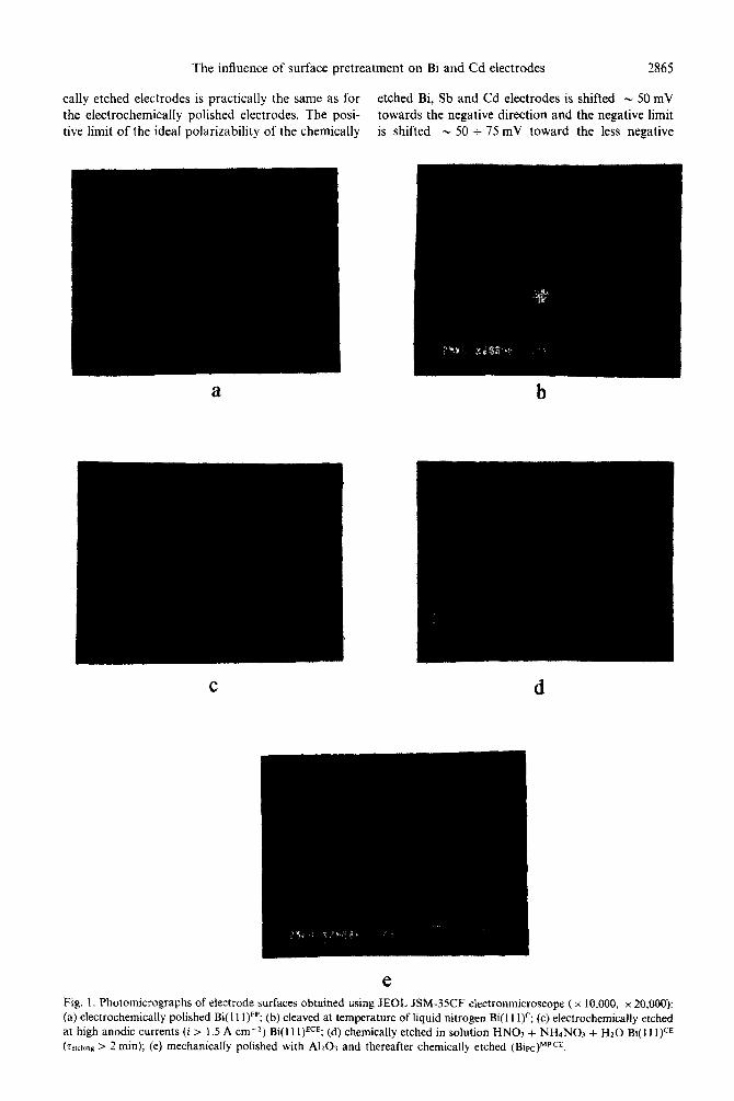
For additional characterization of the working surface of electrodes, an electron microscopic analysis using a JEOL-JSM-35CF at the SE1 regime was carried out (40,000 x max).
According to Fig. l(a), the surface of electrochem- ically polished (EP) single crystal plane electrodes is practically smooth within the range of sensitivity of electron microscopy. The same conclusion is vahd in the case of electrochemically polished non-singular (stepped at the atomic level) single crystal planes of Bi(2TT), Sb(2ff), Cd(l121) and Cd(lTOI) planes. The surfaces of these electrodes consist of small terraces with linear parameter y* w I-10 nm and from atomic steps (l-3 atomic layers). The surface of the nonsingular plane is a typical example of a weakly disorbed solid surface. In some experiments the planes Bi( 1 1 1 )‘, Sb( 111)’ and Cd(OO0 1)’ cleaved at the temperature of liquid nitrogen were investigated. According to the data of Fig. l(b), on the cut surface of Bi( 111)’ and Sb(l11)’ there are thinly scattered break steps, the distance between which is very large. In the case of Cd(OOOl)‘, the distance between these break steps is somewhat smaller. In some experiments the edl properties at electrochemically etched surfaces of Bi( 11 I)ECE, Bi(OO1)ECE, Cd(OO0 l)ECE and Sb( 11 l)ECE were investigated. The electrochemical etching of Bi( 1 I l)ECE and Sb( 11 l)ECE was carried out in KJ-HCI aqueous solution at anodic currents i > 1.5 A cme2. The analysis of many experiments shows that for the etching times T < 2 minutes, the edl and adsorption parameters depend on this time, but at r > 2 minutes, the influence of the time of etching to the edl and adsorption characteristics is very weak. The main aim of the electrochemical etching was to produce a weakly disordered surface, ie to prepare the polycrystalline surface with self-similar fractals at the electrode surface. According to the electron micro- scopic studies, there are surface pittings (triangles) with linear parameter x _ 1 pm at the surface of Bi(l1 I)ECE. Between the pittings the surfaces of Bi( 1 I I)ECE and Sb( 11 l)ECE seem to be practically smooth. The statistical analysis of many electrodes, prepared by the electrochemical etching at high anodic currents, shows that f5% of the whole surface is covered by the pittings. To increase the concentration of defects at the electrode surface, the self-made massive single crystal Bi and Sb electrodes,
grown by the Horizontal Bridgman method in Tartu, have been used. At the surface of electrochemically treated self-made Bi( 11 I)ECE and Sb( 11 l)ECE elec- trodes there are 5525% of surface defects (Fig. I(c)).
In some experiments the edl and adsorption characteristics of organic compounds at chemically etched in the mixture HNO3 + NH4N03 + HZ0 Bi( 11 l)CE, Sb( 1 I l)CE, Bi(OO1)CE, Cd(OOO1)CE, Cd( 10TO)CE and Cd( 1 lzO)cE have been investigated. According to Fig. l(d), additionally to the surface pittings (triangles) with linear parameter x _ I pm, a great number of various surface defects at the surface of chemically treated Bi, Sb and Cd (self-made massive Bi and Sb monocrystals) electrodes exists. In some experiments, the mechanically polished (with AlzO,) and thereafter chemically etched PC Bi (Bior)MPCE electrodes have been investigated (Fig. l(e)). At the first approximation, the surface of a PC electrode prepared in such a way can be described as a uniformly inhomogeneous surface.
The experimental edl and adsorption character- istics for variously prepared electrodes have been compared with the data for solid bismuth drop electrodes with remelted surface (Binr)R [2], as well as with the data for wedge shape two-plane model polycrystalline PC-Bi electrodes (wme) with conceded and therefore to some extent known crystallographic and energetic inhomogeneity of surface [26-281. In some experiments the solid Bi drop electrodes without any additional remelting of the surface (Binr)WR have been used. According to the electron microscopic studies, at the surface of (Binr)WR, the homogeneous areas are smaller and the concentration of surface defects is noticeably higher than at (Bior)R.
3. RESULTS AND DISCUSSION
3.1. Cyclic voitammograms (CVs)
The CVs for different single crystal Bi, Sb and Cd electrodes were recorded in neutral aqueous NaF, LiC104 and acidified LiClO4 solutions and non- aqueous LiClO4 solutions. In the NaF aqueous solutions the Bi single crystal electrodes are ideally polarizable in the range of potentials - 1.60 V < E < -0.50 V [4, 38, 391, and the single crystal Sb electrodes are ideally polarizable in the range of - 1.45 V < E < -0.45 V [39]. All potential values presented in this work are measured in the scale of saturated calomel electrode (see). The Cd planes are ideally polarizable in the range of - 1.70 V < E < - 0.90 V [38]. In the aqueous LiC104 solutions the anodic limit of ideal polarizability is shifted -200 mV to the positive direction. In the acetonitrilic and methanolic LiClO4 solutions the single crystal Bi electrodes are ideally polarizable in the range of - 1.80 V < E < -0.25 V [34,38,39] and in the ethanolic and isopropanolic solutions in the limits - 1.60 V < E < -0.05 V. The potential range of ideal polarizability of cut and electrochemi-
The influence of surface pretreatment on Bi and Cd electrodes 2865
tally etched electrodes is practically the same as for etched Bi, Sb and Cd electrodes is shifted N 50 mV the electrochemically polished electrodes. The posi- towards the negative direction and the negative limit tive limit of the ideal polarizability of the chemically is shifted 5 50 + 75 mV toward the less negative
d
e Fig. 1. Photomicrographs of electrode surfaces obtained using JEOL JSM-35CF electronmicroscope ( x 10,000, x 20,000): (a) electrochemically polished Bi(l1 l)EP; (b) cleaved at temperature of liquid nitrogen Bi(l I l)c; (c) electrochemically etched at high anodic currents (i > 1.5 A cme2) Bi(ll1) “e; (d) chemically etched in solution HNOJ + NHINOJ + Hz0 Bi(l1 I)CE
(Terchlng z 2 min); (e) mechanically polished with Al103 and thereafter chemically etched (Bip~)~~~~.
2866 E. Lust et al.
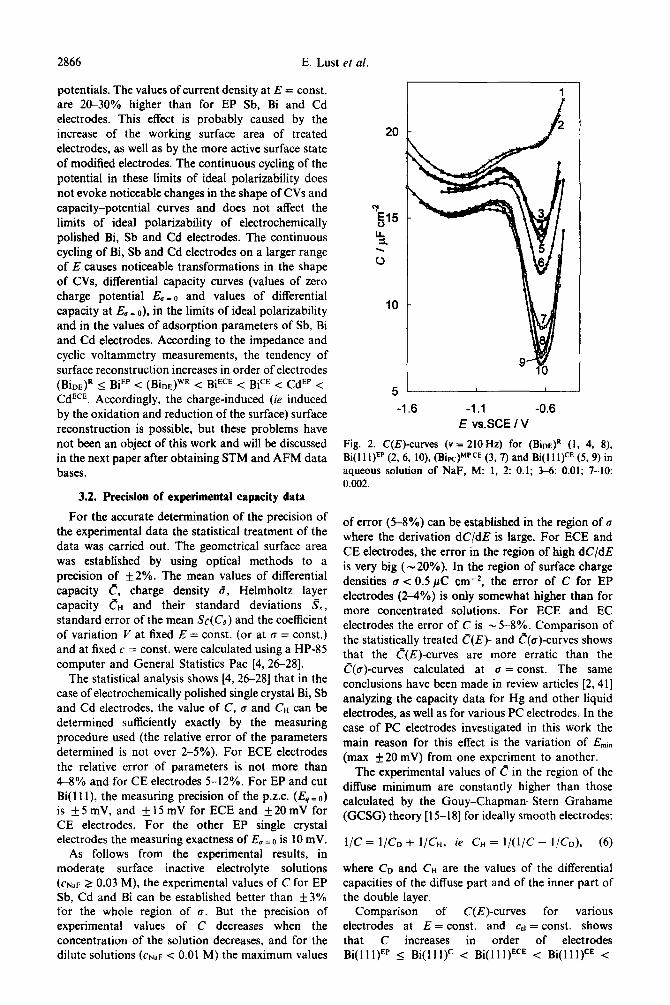
potentials. The values of current density at E = const. are 2&30% higher than for EP Sb, Bi and Cd electrodes. This effect is probably caused by the increase of the working surface area of treated electrodes, as well as by the more active surface state of modified electrodes. The continuous cycling of the potential in these limits of ideal polarizability does not evoke noticeable changes in the shape of CVs and capacity-potential curves and does not affect the limits of ideal polarizability of electrochemically polished Bi, Sb and Cd electrodes. The continuous cycling of Bi, Sb and Cd electrodes on a larger range of E causes noticeable transformations in the shape of CVs, differential capacity curves (values of zero charge potential E,,o and values of differential capacity at E,, = o), in the limits of ideal polarizability and in the values of adsorption parameters of Sb, Bi and Cd electrodes. According to the impedance and cyclic voltammetry measurements, the tendency of surface reconstruction increases in order of electrodes (Bio# < BiEP < (BIDE) WR < BiECE <: BiCE < CdEP < CdECE. Accordingly, the charge-induced (ie induced by the oxidation and reduction of the surface) surface reconstruction is possible, but these problems have not been an object of this work and will be discussed in the next paper after obtaining STM and AFM data bases.
3.2. Precision of experimental capacity data
For the accurate determination of the precision of the experimental data the statistical treatment of the data was carried out. The geometrical surface area was established by using optical methods to a precision of +2%. The mean values of differential capacity c, charge density 6, Helmholtz layer capacity Cu and their standard deviations $, standard error of the mean Sc(Ca) and the coefficient of variation Y at fixed E = const. (or at 0 = const.) and at fixed c = const. were calculated using a HP-85 computer and General Statistics Pat [4, 26-281.
The statistical analysis shows [4, 26-281 that in the case of electrochemically polished single crystal Bi, Sb and Cd electrodes, the value of C, r~ and Cu can be determined sufficiently exactly by the measuring procedure used (the relative error of the parameters determined is not over 225%). For ECE electrodes the relative error of parameters is not more than 48% and for CE electrodes 5-12%. For EP and cut Bi(l1 l), the measuring precision of the p.z.c. (E,= 0) is + 5 mV, and + I5 mV for ECE and &20 mV for CE electrodes. For the other EP single crystal electrodes the measuring exactness of E, = 0 is 10 mV.
As follows from the experimental results, in moderate surface inactive electrolyte solutions (czar 2 0.03 M), the experimental values of C for EP Sb, Cd and Bi can be established better than f3% for the whole region of CT. But the precision of experimental values of C decreases when the concentration of the solution decreases, and for the dilute solutions (CM+F c 0.01 M) the maximum values
20
IO
-1.6 -1.1 -0.6 E vs.SCE 1 V
Fig. 2. C(E)-curves (v = 210 Hz) for (Bi# (1, 4, 8), Bi(l1 l)EP (2, 6, lo), (BipC)MPCE (3, 7) and Bi(l1 l)CE (5, 9) in aqueous solution of NaF, M: 1, 2: 0.1; 3-6: 0.01; 7-10: 0.002.
of error Q-8%) can be established in the region of 0 where the derivation dC/dE is large. For ECE and CE electrodes, the error in the region of high dC/dE is very big (- 20%). In the region of surface charge densities u < 0.5 PC cm-*, the error of C for EP electrodes (2-4%) is only somewhat higher than for more concentrated solutions. For ECE and EC electrodes the error of C is -5--g%. Comparison of the statistically treated C(E)- and C(a)-curves shows that the C(E)-curves are more erratic than the C(c)-curves calculated at u = const. The same conclusions have been made in review articles [2,41] analyzing the capacity data for Hg and other liquid electrodes, as well as for various PC electrodes. In the case of PC electrodes investigated in this work the main reason for this effect is the variation of E,,,,. (max +20 mV) from one experiment to another.
The experimental values of c in the region of the diffuse minimum are constantly higher than those calculated by the Gouy-Chapman-Stern-Grahame (GCSG) theory [15-l 81 for ideally smooth electrodes:
l/C = L/CO + l/cH, ie CH = l/(1/C- I/CD), (6)
where Co and Cu are the values of the differential capacities of the diffuse part and of the inner part of the double layer.
Comparison of C(E)-curves for various electrodes at E = const. and ccl = const. shows that C increases in order of electrodes Bi(lll)EP I Bi(lll)c < Bi(lll)ECE < Bi(lll)CE <
The influence of surface pretreatment on Bi and Cd electrodes 2867
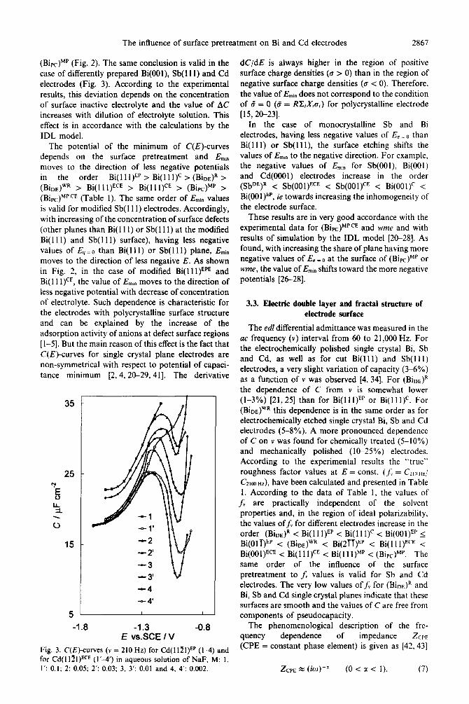
(BipC)MP (Fig. 2). The same conclusion is valid in the case of differently prepared Bi(OOl), Sb( 1 I 1) and Cd electrodes (Fig. 3). According to the experimental results, this deviation depends on the concentration of surface inactive electrolyte and the value of AC increases with dilution of electrolyte solution. This effect is in accordance with the calculations by the IDL model.
The potential of the minimum of C(E)-curves depends on the surface pretreatment and E,,,,, moves to the direction of less negative potentials
the ginr)wR
order Bi( 11 l)EP > Bi(l1 I)c > (Bin# > > Bi(lll)ECE > Bi(ll l)CE > (BipC)MP >
(BipC)MPCE (Table 1). The same order of Emi, values is valid for modified Sb( I 11) electrodes. Accordingly, with increasing of the concentration of surface defects (other planes than Bi( 111) or Sb( 111) at the modified Bi(l11) and Sb(l11) surface), having less negative values of E,, = o than Bi(ll1) or Sb(ll1) plane, Emi” moves to the direction of less negative E. As shown in Fig. 2, in the case of modified Bi(1 I l)EPE and Bi( 11 l)CE, the value of E,,,,, moves to the direction of less negative potential with decrease of concentration of electrolyte. Such dependence is characteristic for the electrodes with polycrystailine surface structure and can be explained by the increase of the adsorption activity of anions at defect surface regions [l-5]. But the main reason of this effect is the fact that C(E)-curves for single crystal plane electrodes are non-symmetrical with respect to potential of capaci- tance minimum [2,4,20-29,411. The derivative
35
25
Z 0 LL Zt_
2
15
5
-4
-4’
-1.8 -1.3 -0.8 E vs.SCE IV
Fig. 3. C(E)-curves (V = 210 Hz) for Cd(l l?!l)EP (l-4) and for Cd(l121)EcE (1’4’) in aqueous solution of NaF, M: I, I’: 0.1; 2: 0.05; 2’: 0.03; 3, 3’: 0.01 and 4, 4’: 0.002.
dC/dE is always higher in the region of positive surface charge densities (a > 0) than in the region of negative surface charge densities (a < 0). Therefore, the value of E,,. does not correspond to the condition of d = 0 (8 = RXiXiai) for polycrystalline electrode [15, 20-231.
In the case of monocrystalline Sb and Bi electrodes, having less negative values of E, = 0 than Bi(l11) or Sb( 1 I l), the surface etching shifts the values of E,,,,, to the negative direction. For example, the negative values of E,,,,, for Sb(OOl), Bi(001) and Cd(0001) electrodes increase in the order (SbDE)R < Sb(OO1)ECE < Sb(OO1)CE <: Bi(OO1)C < Bi(OO1)EP, ie towards increasing the inhomogeneity of the electrode surface.
These results are in very good accordance with the experimental data for (Bipc)MPCE and wme and with results of simulation by the IDL model [20-281. As found, with increasing the share of plane having more negative values of E,, = o at the surface of (BipC)MP or wme, the value of E,,,,, shifts toward the more negative potentials [26-281.
3.3. Electric double layer and fractal structure of electrode surface
The edl differential admittance was measured in the UC frequency (v) interval from 60 to 21,000 Hz. For the electrochemically polished single crystal Bi, Sb and Cd, as well as for cut Bi(ll1) and Sb( 111) electrodes, a very slight variation of capacity (3-6%) as a function of v was observed [4, 341. For (Bin# the dependence of C from v is somewhat lower (l-3%) [21,25] than for Bi(lll)EP or Bi(lll)c. For (Bius)WR this dependence is in the same order as for electrochemically etched single crystal Bi, Sb and Cd electrodes (5-g%). A more pronounced dependence of C on v was found for chemically treated (S-IO%) and mechanically polished (l&25%) electrodes. According to the experimental results the “true” roughness factor values at E = const. (f; = CzloHr/ C2100 Hz), have been calculated and presented in Table 1. According to the data of Table 1, the values of
f;, are practically independent of the solvent properties and, in the region of ideal polarizabihty, the values off;. for different electrodes increase in the order (BinE)R < Bi(l1 I)EP < Bi(ll1)’ < Bi(OO1)EP I Bi(OIT)EP < (Binr)WR < Bi(2TT)EP < Bi(l1 l)ECE < Bi(OOI)ECE ’ < B~(lll)~~ < Bi(lll)MP < (Bipc) MP. The same order of the influence of the surface pretreatment to f;, values is valid for Sb and Cd electrodes. The very low values off;, for (Binr)R and Bi, Sb and Cd single crystal planes indicate that these surfaces are smooth and the values of C are free from components of pseudocapacity.
The phenomenological description of the fre- quency dependence of impedance ZCPE
(CPE = constant phase element) is given as [42,43]
&pa z (iw)-’ (O<cc< 1). (7)
2868
Table 1.
E. Lust et al.
Electric double layer characteristics for Sb, Bi and Cd electrodes
Solvent Electrode - &w” (see) (VI Ci!p
(pF cm-*)
Hz0
MeOH
AN
Bi( I I I)EP 0.655 Bi(lll)c 0.650 Bi(l I l)ECE 0.630 Bi(l I l)CE 0.620 Bi(l I l)MPCE 0.625 (Bio# 0.625 (BioE)WR 0.620 Bi(OOl)EP 0.595 Bi(OOl)ECE 0.610 Bi(OOl)CE 0.615 Cd(OO0 l)Ep 0.95 Cd(OOOl)C 0.97 Cd(OO0 l)ECE 0.97 Cd(OO0 l)CE I .oo Cd( I I TO)EP I .02 Cd( I 1 TO)ECE 0.99 Sb(l I l)EP 0.46 Sb(lll)c 0.45 Bi(l I l)EP 0.52 Bi(OOl)EP 0.45 (Bio# 0.49 Bi( I 1 l)EP 0.50 Bi(OOl)EP 0.42 (BioE)R 0.47
I .04 I .06 1.09 I.11 I.15 I .02 I .08 I .07 I.16 1.20 1.04 1.06 I .09 I.11 I .06 I .08 I .06 I .08 I .03 I .05 I.01 I .05 1.02 I.01
1.04 2.03 25.6 I .06 2.04 28.9 I .08 2.05 29. I I.10 2.07 33.8 1.20 2.11 32.0 I.01 2.01 25.8 I.11 2.05 25.5 I .06 2.05 28.4 I.13 2.07 29.1 I.15 2.08 28.8 I .09 2.05 38.0 I.11 2.07 37.0 I .20 2.06 37.1 1.25 2.10 35.0 I.14 2.06 48.6 1.28 2.09 59.6 I .06 2.04 23.6 I .09 2.06 38.9 1.05 2.03 19.8 1.07 2.04 23.0 I .03 2.01 22.2 I .06 2.04 14.8 0.98 2.01 17.4 I.15 - 15.0
D, fractal dimension, dimensionless parameter. EP, electropolished surface. c, cleaved at the temperature of liquid nitrogen surface. ECE, electrochemically etched surface. CE, chemically etched surface. MPCE, mechanically polished and thereafter chemically etched surface. (Bio#, remelted solid drop Bi electrode. (BiDE)WR, solid drop Bi electrode without additional remelting of surface.
The CPE angle cp is related to a as:
fp = $1 - a).
The value c( = 1 corresponds to normal capacitive behaviour. Recently some new ideas have been put forward to explain the so-called constant phase element CPE [42,43]. The main position is that the deviations from the ideal behaviour are caused by surface roughness of a special kind, today commonly denoted by the term “fractal” [42,43]. The so-called fractal dimension D introduced by Mandelbrot [43] is a formal quantity which attains a value between 2 and 3 for a fractal structure and reduces to 2 when the surface is flat. D is related to LX by
CI = l/(D - I). (9)
The established values of D, presented in Table 1, show that the surfaces of (Bir# and electrochemi- tally polished Bi, Sb and Cd single crystal electrodes are practically smooth. The slightly higher values of
D for the cut electrodes indicate that the surface of electrodes, cleaved at the temperature of liquid nitrogen, is to some extent geometrically and energetically inhomogeneous. Somewhat higher val- ues of D have been established for ECE electrodes. The surfaces of ECE Bi, Sb and Cd electrodes are relatively flat in comparison with the surfaces of chemically treated and mechanically polished elec- trodes.
3.4. Parsons-Zobel plots
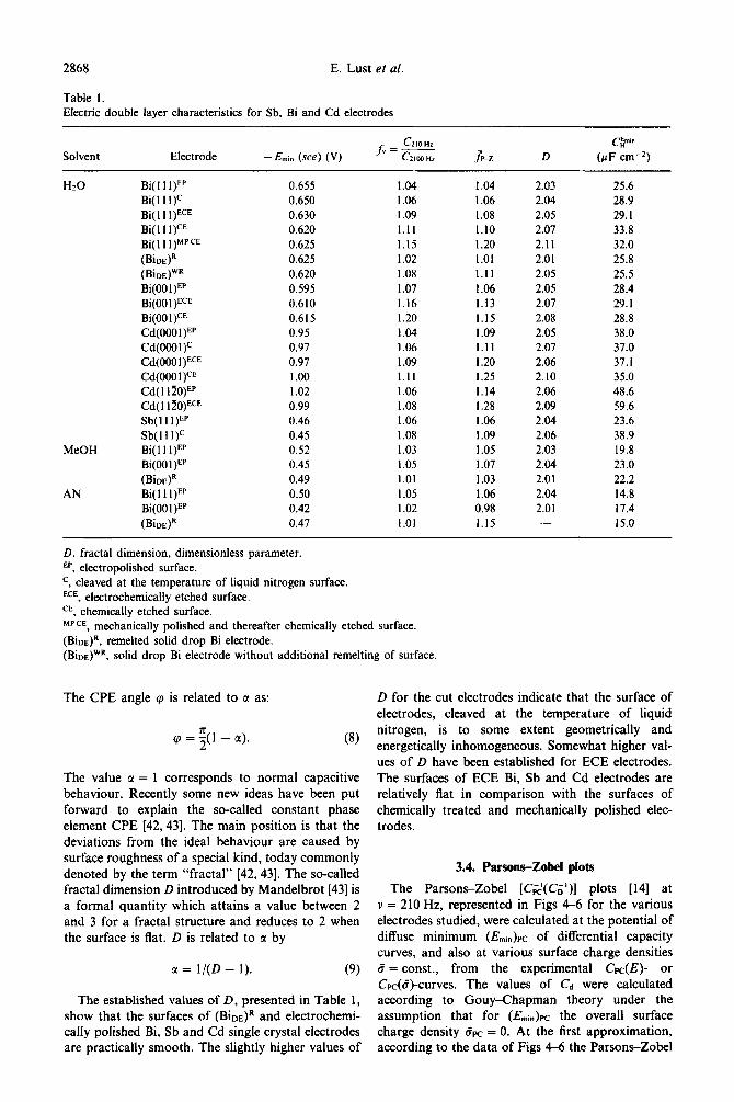
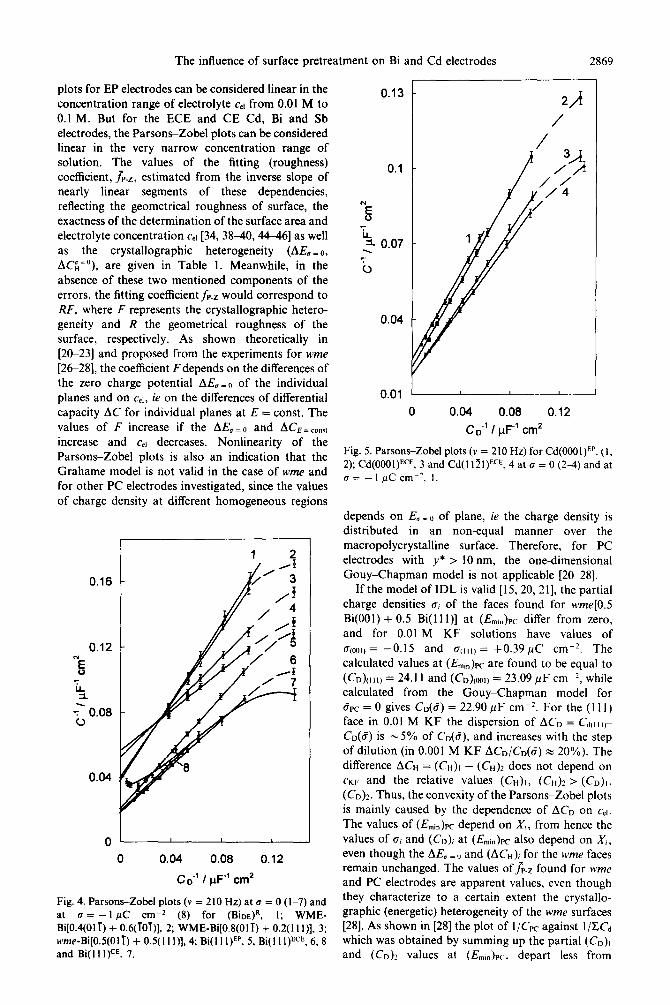
The Parsons-Zobel [C$(C;‘)] plots [14] at v = 210 Hz, represented in Figs 4-6 for the various electrodes studied, were calculated at the potential of diffuse minimum (Emin)Pc of differential capacity curves, and also at various surface charge densities d = const., from the experimental C&E)- or C&b)-curves. The values of Cd were calculated according to Gouy-Chapman theory under the assumption that for (Emin)K the overall surface charge density bpc = 0. At the first approximation, according to the data of Figs 4-6 the Parsons-Zobel
The influence of surface pretreatment on Bi and Cd electrodes 2869
plots for EP electrodes can be considered linear in the concentration range of electrolyte ccl from 0.01 M to 0.1 M. But for the ECE and CE Cd, Bi and Sb electrodes, the Parsons-Zobel plots can be considered linear in the very narrow concentration range of solution. The values of the fitting (roughness) coefficient, &.z, estimated from the inverse slope of nearly linear segments of these dependencies, reflecting the geometrical roughness of surface, the exactness of the determination of the surface area and electrolyte concentration ccl [34, 38-40,44-46] as well as the crystallographic heterogeneity (A& = 0, AC;=“), are given in Table 1. Meanwhile, in the absence of these two mentioned components of the errors, the fitting coefficient fp_z would correspond to RF, where F represents the crystallographic hetero- geneity and R the geometrical roughness of the surface, respectively. As shown theoretically in [20-231 and proposed from the experiments for wme [2628], the coefficient Fdepends on the differences of the zero charge potential AE,=o of the individual planes and on celr ie on the differences of differential capacity AC for individual planes at E = const. The values of F increase if the AE,=o and ACEcconst increase and ccl decreases. Nonlinearity of the Parsons-Zob-el plots is also an indication that the Grahame model is not valid in the case of wme and for other PC electrodes investigated, since the values of charge density at different homogeneous regions
0.16
0.12
z
4
-; 0.06
0.04
0- 0 0.04 0.06 0.12
C 6’ I pF“ cm2
Fig. 4. Parsons-Zobel plots (v = 210 Hz) at 0 = 0 (l-7) and at 0 = -1 PC cm-* (8) for (BiDE)R, 1; WME- Bi[0.4(01T) + 0.6(TOT)], 2; WME-Bi[O.B(OIT) + 0.2(1 I I)], 3; wme-Bi[OS(OlT) + 0.5(1 I l)], 4; Bi(l I l)EP, 5, Bi(l1 l)ECE, 6, 8 and Bi( II I)CE, 7.
0.1
0.04
0.01 ’ I I I
0 0.04 0.08 0.12
CD-’ I pF_’ cm2
Fig. 5. Parsons-Zobel plots (v = 210 Hz) for Cd(OOOl)EP, (1, 2); Cd(OOOl)ECE, 3 and Cd( I ITl)EcE, 4 at u = 0 (24) and at a = -I jL cm-‘, I.
depends on E, =O of plane, ie the charge density is distributed in an non-equal manner over the macropolycrystalline surface. Therefore, for PC electrodes with y* > 10 nm, the one-dimensional Gouy-Chapman model is not applicable [2Ck28].
If the model of IDL is valid [15, 20, 211, the partial charge densities 6, of the faces found for wme[OS
Bi(OO1) + 0.5 Bi(l1 l)] at (E,,&c differ from zero, and for 0.01 M KF solutions have values of ~(OOI, = -0.15 and ~~111) = +0.39 PC cm-‘. The calculated values at (Em,,& are found to be equal to (C’O)~~~~, = 24.11 and (Co)(~l, = 23.09 PF cm-‘, while calculated from the Gouy-Chapman model for do = 0 gives C,(c) = 22.90 PF cm-2. For the (I 1 I) face in 0.01 M KF the dispersion of ACD = Cd(ll,y CD(~) is -5% of CD(~), and increases with the step of dilution (in 0.001 M KF ACo/Co(c) z 20%). The difference AC” = (CH)I - (CH)2 does not depend on CKF and the relative values (CH)I, (CH)? > (CO),, (C,)z. Thus, the convexity of the Parsons-Zobel plots is mainly caused by the dependence of ACD on tel. The values of (Emin)Pc depend on X,, from hence the values of 0; and (CO), at (E,,,,“)Pc also depend on X,, even though the AE, = o and (ACH)~ for the wme faces remain unchanged. The values of&-Z found for wme and PC electrodes are apparent values, even though they characterize to a certain extent the crystallo- graphic (energetic) heterogeneity of the wme surfaces [28]. As shown in [28] the plot of l/Cm against l/x& which was obtained by summing up the partial (CD), and (CD)? values at (E,,,,“)Pc. depart less from
2870 E. Lust et al.
linearity, and the obtained values of fxc, insignifi- cantly differ from unity (fxc, = 1.01-1.03). In the case of ECE and CE electrodes, this procedure is very complicated, because only very approximate values of the share of various planes exposed at the PC surface can be established by the computer simu- lation of the experimental Crc(E)-curves.
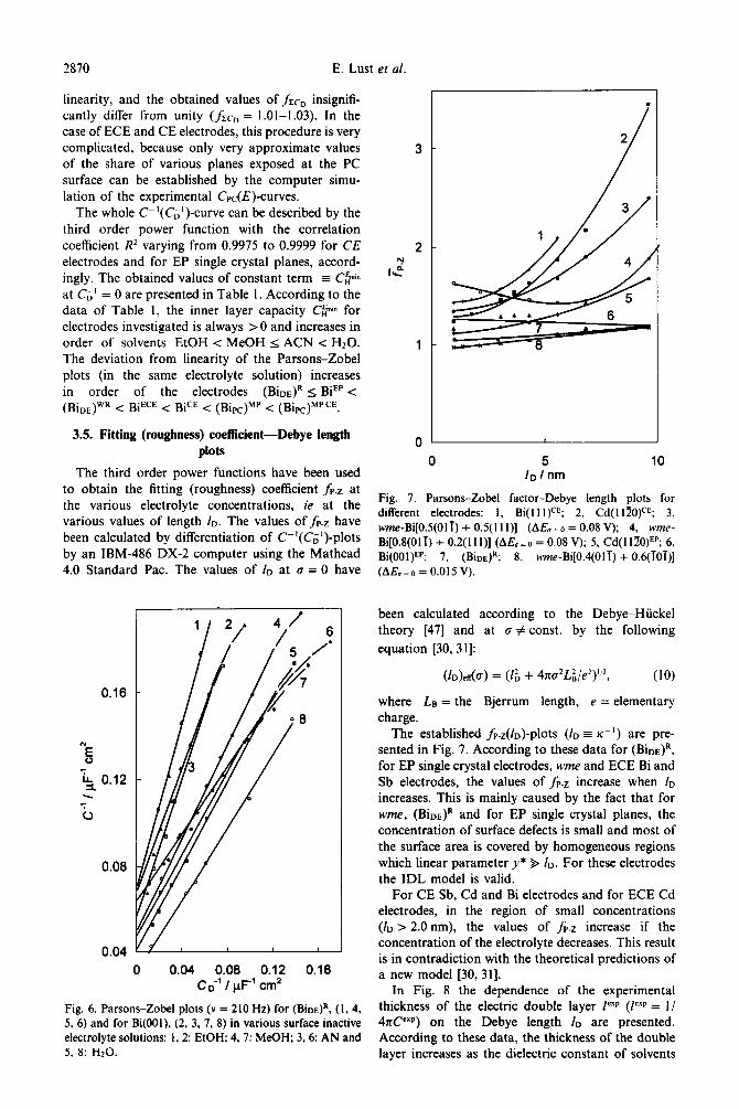
The whole C-‘(Cc’)-curve can be described by the third order power function with the correlation coefficient R2 varying from 0.9975 to 0.9999 for CE electrodes and for EP single crystal planes, accord- ingly. The obtained values of constant term = CF at C;’ = 0 are presented in Table 1. According to the data of Table 1, the inner layer capacity CF for electrodes investigated is always > 0 and increases in order of solvents EtOH < MeOH I ACN < H20. The deviation from linearity of the Parsons-Zobel plots (in the same electrolyte solution) increases in order of the electrodes (Bioa)R < BiEP < (Binr)WR < BiECE < BiCE < (BipC)MP < (BipC)MPCE.
3.5. Fitting (roughness) coefficient-Debye length plots
The third order power functions have been used to obtain the fitting (roughness) coefficient fp_r at the various electrolyte concentrations, ie at the various values of length In. The values 0ffp.Z have been calculated by differentiation of C-r(C;‘)-plots by an IBM-486 DX-2 computer using the Mathcad 4.0 Standard Pac. The values of lo at Q = 0 have
0.16
0.06
0.04
0 0.64 0.06 0.12 0.16 Co-’ I pF_’ cm2
Fig. 6. Parsons-Zobel plots (v = 210 Hz) for (BioE)R, (I, 4, 5, 6) and for Bi(OOl), (2, 3, 7, 8) in various surface inactive electrolyte solutions: I, 2: EtOH; 4, 7: M&H; 3, 6: AN and 5, 8: HzO.
3 -
2 - hl ri I*,
1 -
0 5 10 lDlnm
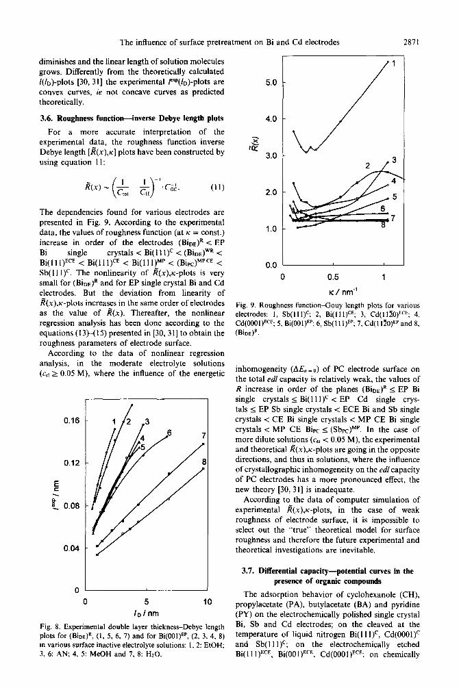
Fig. 7. Parsons-Zobel factor-Debye length plots for different electrodes: I, Bi(l I I)CE; 2, Cd(ll?!O)CE; 3, wme-Bi[OS(Oli) + OS( I I I)] (A& = 0 = 0.08 V); 4, wme- Bi[O.S(Ol i) + 0.2( I I I)] (A& = 0 = 0.08 V); 5, Cd( I IZO)EP; 6, Bi(OOI)EP; 7, (Bios)R; 8, wme-Bi[0.4(0lT) + 0.6(]OT)] (A&so = 0.015 V).
been calculated according to the Debye-Hiickel theory [47] and at c # const. by the following
equation [30, 311:
&)&a) = (I& + 4na2L:/e2)“*, (10)
where La = the Bjerrum length, e = elementary charge.
The established fp.z(ln)-plots (lo = K-‘) are pre- sented in Fig. 7. According to these data for (Bin#, for EP single crystal electrodes, wme and ECE Bi and Sb electrodes, the values of fp.~ increase when lo increases. This is mainly caused by the fact that for wme, (Bin# and for EP single crystal planes, the concentration of surface defects is small and most of the surface area is covered by homogeneous regions which linear parameter y* $ In. For these electrodes the IDL model is valid.
For CE Sb, Cd and Bi electrodes and for ECE Cd electrodes, in the region of small concentrations (ro > 2.0 nm), the values of fp.~ increase if the concentration of the electrolyte decreases. This result is in contradiction with the theoretical predictions of a new model [30, 311.
In Fig. 8 the dependence of the experimental thickness of the electric double layer fenp (leap = I/ 4sCe”P) on the Debye length lo are presented. According to these data, the thickness of the double layer increases as the dielectric constant of solvents
The influence of surface pretreatment on Bi and Cd electrodes 2871
diminishes and the linear length of solution molecules grows. Differently from the theoretically calculated 1(/n)-plots [30, 3 l] the experimental P”P(lu)-plots are convex curves, ie not concave curves as predicted theoretically.
3.6. Roughness functiobinverse Debye length plots
For a more accurate interpretation of the experimental data, the roughness function-inverse Debye length [&x),K] plots have been constructed by using equation 11:
B(x) - &- & ( ) -I
.C$. (11) LO,
The dependencies found for various electrodes are presented in Fig. 9. According to the experimental data, the values of roughness function (at K = const.) increase in order of the electrodes (Binr)R < EP Bi single crystals < Bi(ll1)’ < (Bina)WR < Bi( 11 l)ECE < Bi(lll)CE < Bi(lll)MP < (Bipc) MPCE <
Sb(l1 l)c. The nonlinearity of &x)+-plots is very small for (BiuE)R and for EP single crystal Bi and Cd electrodes. But the deviation from linearity of a(x)+-plots increases in the same order of electrodes as the value of w(x). Thereafter, the nonlinear regression analysis has been done according to the equations (13)-( 15) presented in [30, 3 l] to obtain the roughness parameters of electrode surface.
According to the data of nonlinear regression analysis, in the moderate electrolyte solutions (ccl 2 0.05 M), where the influence of the energetic
0.16
0.12
z
< 0.06
0 5 10
lDlnm
Fig. 8. Experimental double layer thickness-Debye length plots for (BinE)R, (1, 5, 6, 7) and for Bi(OO1)EP, (2, 3, 4, 8) in various surface inactive electrolyte solutions: 1, 2: EtOH; 3, 6: AN; 4, 5: MeOH and 7. 8: H20.
0.0 -
0 0.5 1
K / nm-’
Fig. 9. Roughness functionClouy length plots for various electrodes: I, Sb(ll l)c; 2, Bi(l lI)cE; 3, Cd(llTO)ECE; 4, Cd(OOOl)ECE; 5, Bi(OOl)EP; 6, Sb(l I l)EP; 7, Cd(l lZO)EP and 8, (BiDE)R.
inhomogeneity (A&=0) of PC electrode surface on the total edf capacity is relatively weak, the values of R increase in order of the planes (Bior)R I EP Bi single crystals I Bi( 11 l)c < EP Cd single crys- tals I EP Sb single crystals < ECE Bi and Sb single crystals < CE Bi single crystals < MP CE Bi single crystals < MP CE BipC I (SbpC)MP. In the case of more dilute solutions (cer < 0.05 M), the experimental and theoretical &x),rc-plots are going in the opposite directions, and thus in solutions, where the influence of crystallographic inhomogeneity on the edl capacity of PC electrodes has a more pronounced effect, the new theory [30, 311 is inadequate.
According to the data of computer simulation of experimental k(x)+-plots, in the case of weak roughness of electrode surface, it is impossible to select out the “true” theoretical model for surface roughness and therefore the future experimental and theoretical investigations are inevitable.
3.7. Differential capacity-potential curves in the presence of organic compounds
The adsorption behavior of cyclohexanole (CH), propylacetate (PA), butylacetate (BA) and pyridine (PY) on the electrochemically polished single crystal Bi, Sb and Cd electrodes; on the cleaved at the temperature of liquid nitrogen Bi(l1 l)c, Cd(OOO1)C and Sb(ll1)‘; on the electrochemically etched Bi(l1 l)ECE, Bi(OO1)ECE, Cd(OOOl)ECE; on chemically
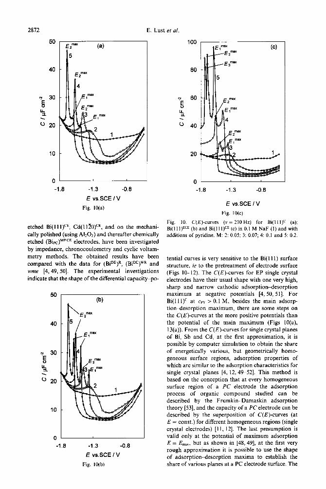
2872
50 - nmx (a)
E2 max
4
I
-1.8 -1.3 -0.8
E vs.SCE IV
Fig. IO(a)
E. Lust et al.
etched Bi( 11 l)CE, Cd( 1 I?!O)CE, and on the mechani- cally polished (using AllOj) and thereafter chemically etched (Bir.c)MPCE electrodes, have been investigated by impedance, chronocoulometry and cyclic voltam- metry methods. The obtained results have been compared with the data for (BiDE)R, (BiDE)WR and wme [4,49, 501. The experimental investigations indicate that the shape of the differential capacity-po-
(W
-1.8 -1.3 -0.8
E vs.SCE I V
Fig. IO(b)
80
20
0
-1.8 -1.3 -0.8
E vs.SCE I V
Fig. 10(c)
Fig. 10. C(E)-curves (v = 210 Hz) for Bi(lll)c (a); Bi(l1 I)ECE (b) and Bi(l I I)CE (c) in 0.1 M NaF (1) and with additions of pyridine, M: 2: 0.05; 3: 0.07; 4: 0.1 and 5: 0.2.
tential curves is very sensitive to the Bi( 111) surface structure, ie to the pretreatment of electrode surface (Figs 10-12). The C(E)-curves for EP single crystal electrodes have their usual shape with one very high, sharp and narrow cathodic adsorptiondesorption maximum at negative potentials [4, 50, 511. For Bi(l1 l)c at cpy > 0.1 M, besides the main adsorp- tiondesorption maximum, there are some steps on the C(E)-curves at the more positive potentials than the potential of the main maximum (Figs 10(a), 13(a)). From the C(E)-curves for single crystal planes of Bi, Sb and Cd, at the first approximation, it is possible by computer simulation to obtain the share of energetically various, but geometrically homo- geneous surface regions, adsorption properties of which are similar to the adsorption characteristics for single crystal planes [4, 12,49-521. This method is based on the conception that at every homogeneous surface region of a PC electrode the adsorption process of organic compound studied can be described by the Frumkin-Damaskin adsorption theory [53], and the capacity of a PC electrode can be described by the superposition of C(E)-curves (at E = const.) for different homogeneous regions (single crystal electrodes) [I 1, 121. The last presumption is valid only at the potential of maximum adsorption E = Em,,, but as shown in [48,49], at the first very rough approximation it is possible to use the shape of adsorption-desorption maxima to establish the share of various planes at a PC electrode surface. The
The influence of surface pretreatment on Bi and Cd electrodes 2873
more correct method was given in [54]. According to the results of a computer simulation, the share of plane Bi(OO1) at the cut surface Bi(l1 l)c is 3-8% (A = + 5%).
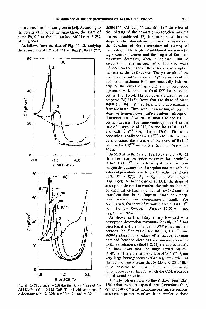
As follows from the data of Figs 10-12, studying the adsorption of PY and CH at (Bine)R, Bi(l1 l)ECE,
60 (a)
-1.8 -1.3 -0.8 E vs.SCE I V
80
60
1.8 -1.3 -0.8
E vs.SCE IV
Fig. 11. C(E)-curves (v = 210 Hz) for (BipC)MP (a) and for Cd(l l?O)ECE (b) in 0.1 M NaF (I) and with additions of cyclohexanole. M: 2: 0.02; 3: 0.07; 4: 0.1 and 5: 0.2.
Bi(OO1)ECE, Cd( 1 220)ECE and Bi( 11 I)CE the effect of the splitting of the adsorption-desorption maxima has been established [52]. It must be noted that the shape of adsorption-desorption maxima depends on the duration of the electrochemical etching of electrodes, 7. The height of additional maximum (at c,~~ = const.) increases and the height of the main maximum decreases, when 7 increases. But at rEcE 2 3 min, the increase of 7 has very weak influence on the shape of the adsorption-desorption maxima at the C(E)-curves. The potentials of the main more-negative maximum EF, as well as of the additional maximum E;““, are practically indepen- dent of the values of rrcr and are in very good agreement with the potentials of E”“” for individual planes (Fig. 13(b)). The computer simulation of the prepared Bi( 111) EPE shows that the share of plane Bi(OO1) at Bi( 1 I l)EPE surface, X1, is approximately from 0.2 to 0.4. Thus, with the increasing of tEcE, the share of homogeneous surface regions, adsorption characteristics of which are similar to the Bi(001) plane, increases. The same tendency is valid in the case of adsorption of CH, PA and BA at Bi( 11 I)ECE and Cd( I lZO)ECE (Fig. 11(b), 13(e)). The same conclusion is valid for Bi(OO1)ECE where the increase of rEcE causes the increase of the share of Bi( 111) plane at Bi(OOl)ECE surface (TEcE 2 3 mitt, xc! I I) - 15- 30%).
According to the data of Fig. IO(c), at cry 2 0.1 M the adsorption-desorption maximum for chemically etched Bi( 11 I)CE electrode is split into the three independent adsorption-desorption maxima with the values of potentials very close to the individual planes of Bi. E”“” ~ E”“” I E”‘” 1 E”“” B,tlll, and EY - Gh, (Fig. ‘13(c)). Asl(lyhe tase of an ECE, the shape of adsorptiondesorption maxima depends on the time of chemical etching rcE, but at 7cE 2 2 min the transformations in the shape of adsorptiondesorp- tion maxima are comparatively small. For rcr = 3 min, the share of various planes at Bi( II l)CE is: Xe,,ll,, - 50-40%, Xaicml, * 25530% and Xa,,,,,n - 25-30%.
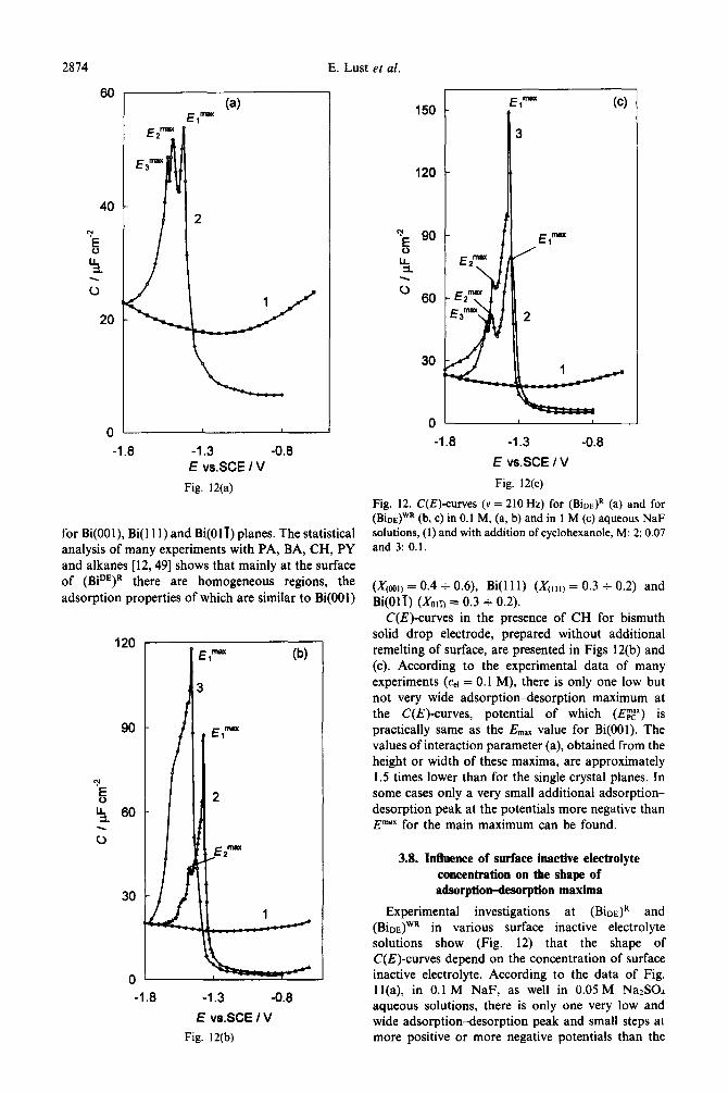
As shown in Fig. 11(a), a very low and wide adsorption-desorption maximum for (BipC)MPCE has been found and the potential of Em”* is intermediate between the E”“” values for Bi(lll), Bi(Oli) and Bi(001) planes. The values of attraction constant obtained from the width of these maxima according to the calculation method [ 12, 13) are approximately 2.5 times lower than for single crystal planes [4,48,49]. Therefore, at the surface of (Bii’c)MPCE, not very large homogeneous surface segments exist. At the first moment it seems that by MP and CE of Bipc it is possible to prepare the more uniformly inhomogeneous surface for which the CDL electrode model would be valid.
The adsorption studies at (BinE)R show (Figs 12(a), 13(d)) that there are exposed three (sometimes four) energetically different homogeneous surface regions, adsorption properties of which are similar to those
2874
60
E. Lust et al.
-1.6 -1.3 -0.8 E vs.SCE I ‘J
Fig. 12(a)
for Bi(OOl), Bi(ll1) and Bi(OlT) planes. The statistical analysis of many experiments with PA, BA, CH, PY and alkanes [12,49] shows that mainly at the surface of (BiDE)R there are homogeneous regions, the adsorption properties of which are similar to Bi(OO1)
%
I;I, 60
2
-1.8 -1.3 -0.8
E vs.SCE IV
Fig. 12(b)
El mU (c)
30
0
-1.8 -1.3 -0.6
E vs.SCE IV
Fig. 12(c)
Fig. 12. C(E)-curves (v = 210 Hz) for (Bio# (a) and for (Bio#‘R (b, c) in 0.1 M, (a, b) and in 1 M (c) aqueous NaF solutions, (1) and with addition of cyclohexanole, M: 2: 0.07 and 3: 0.1.
(Xcwi, = 0.4 t 0.6), Bi(ll1) (&ii, = 0.3 + 0.2) and Bi(OlT) (&m = 0.3 + 0.2).
C(E)-curves in the presence of CH for bismuth solid drop electrode, prepared without additional remelting of surface, are presented in Figs 12(b) and (c). According to the experimental data of many experiments (Q = 0.1 M), there is only one low but not very wide adsorptiondesorption maximum at the C(E)-curves, potential of which (ET) is practically same as the E,,,,, value for Bi(001). The values of interaction parameter (a), obtained from the height or width of these maxima, are approximately 1.5 times lower than for the single crystal planes. In some cases only a very small additional adsorption- desorption peak at the potentials more negative than E”“” for the main maximum can be found.
3.8. Influence of surface inactive electrolyte concentration on the shape of adsorptiodesorption maxima
Experimental investigations at (Bior)R and (Bior)WR in various surface inactive electrolyte solutions show (Fig. 12) that the shape of C(E)-curves depend on the concentration of surface inactive electrolyte. According to the data of Fig. 1 l(a), in 0.1 M NaF, as well in 0.05 M NalS04 aqueous solutions, there is only one very low and wide adsorption-desorption peak and small steps at more positive or more negative potentials than the
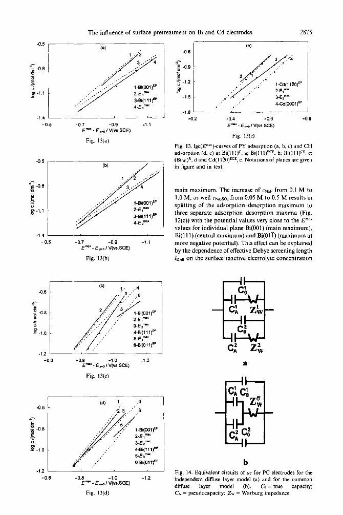
The influence of surface pretreatment on Bi and Cd electrodes 2875
(a)
l-Bi(OO1)EP
2-E ,-
3-Bi(l1 l)EP
4-E?-
-0.7 -0.9 E- - E,, I V(vs.SCE)
Fig. 13(a)
-1.1
-1.4 1 I
-0.5 -0.7 -0.9 -t.t Emu - E ,+, I V(vs.SCE)
Fig. 13(b)
-0.6 - @) I,. ,4
-0.6 -0.6 -1.0 -1.2 E- - Ed I V(vs.SCE)
Fig. 13(c)
-0.6 I
2 ; -0.6
- I E Z 0 I
8 - -1.0
I -1.2 I
-0.6
(d) 1 ,a -4
,,$ 3 ,~s’s_6
i-Bi(OO1)EP
2-E,-
3-E*-
4-Bi(l1 l)EP
5‘E3-
&Bi(Ol OEP
-0.6 -1.0 -1.2 E- - E-0 / V(vs.SCE)
Fig. 13(d)
2 -0.9
a E y -1.2 -
-1.5 - ,*’ ,’
: -1.6 ’ I
-0.2 -0.4 -0.6 -0.8
E- - E,o IV(vs.SCE)
Fig. 13(e)
Fig. 13. Igc(E”““)-curves of PY adsorption (a, b, c) and CH
adsorption (d, e) at Bi(l1 l)c, a; Bi(l1 I)ECE, b; Bi(l1 I)cE, c; (BioE)R, d and Cd(l ITO)ECE, e. Notations of planes are given in figure and in text.
main maximum. The increase of C~+F from 0.1 M to 1 .O M, as well cNaSso4 from 0.05 M to 0.5 M results in splitting of the adsorption4esorption maximum to three separate adsorption4esorption maxima (Fig. 12(c)) with the potential values very close to the Em”” values for individual plane Bi(OO1) (main maximum), Bi( 111) (central maximum) and Bi(OlT) (maximum at more negative potential). This effect can be explained by the dependence of effective Debye screening length ID,~~ on the surface inactive electrolyte concentration
a
b Fig. 14. Equivalent circuits of ac for PC electrodes for the independent diffuse layer model (a) and for the common diffuse layer model (b). CO = true capacity; CA = pseudocapacity; ZW = Warburg impedance.
E. Lust et al.
(at o=O, in 0.1 M NaF lo=0.96nm and in l.OM NaF /o = 0.22 nm). Therefore, the linear parameters of surface regions, exposed additionally to the large Bi(OO1) planes at the surface of (BioE)WR must be in the same order (-0.5 nm) as the effective Debye screening length (calculated by equation (10)) at which the CDL model replaces the IDL. The same conclusion is valid for the adsorption of CH at (BipC)MP electrodes. In the case of (BiDE)R and EP single crystal Bi, Cd and Sb electrodes, as well as for wme and (Bipc)ECE, the influence of surface inactive electrolyte concentration to the shape of adsorption- desorption maxima is weak and the effects established are in good correspondence with the theoretical predictions of [53, 541.
3.9. Influence of the frequency on the shape of adsorption-desorption maxima and on the linear
parameters of homogeneous regions at a PC electrode surface
As shown in [54], if the diffusion of an organic compound is slow and thus the rate determining process of adsorption of organic compound at the electrode surface, the adsorption process at two different types of PC electrode surface can be described by the models presented in Fig. 14. In Fig. 14: (C,)i = (aa/aE)r = true capacity of the double layer of homogeneous region i; (CA)i = adsorption pseudocapacity (additional capacity) of region i; (Zw)i = Warburg impedance for the region i, and (Zwy’ = common Warburg impedance of the mi-
80
80
P 0 LL
z40
0 ,
-1.8 -1.4 -1.2 E vs.SCE IV
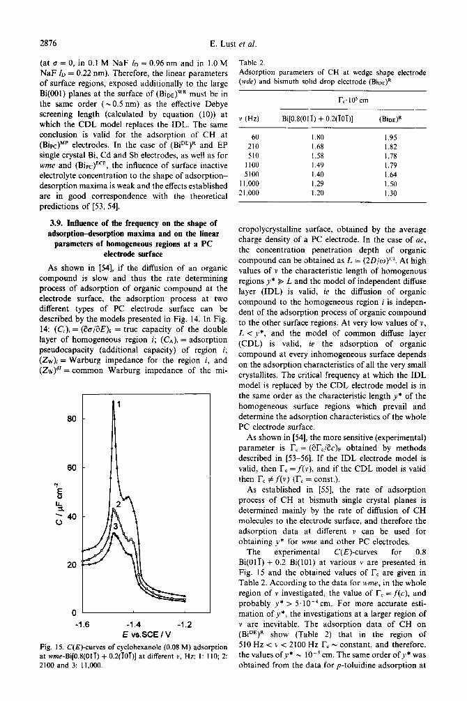
Fig. 15. C(E)-curves of cyclohexanole (0.08 M) adsorption at wme-Bi[O.S(OlT) + o.~(ToT)] at different v, Hz: 1: I IO; 2: 2100 and 3: 11.000.
Table 2. Adsorption parameters of CH at wedge shape electrode (wde) and bismuth solid drop electrode (BioE)R
l-,. IO5 cm
v (Hz) Bi[O.S(Oli) + o.z(ioT)] (Bio#
60 1.80 I .95 210 I .68 1.82 510 1.58 I .78
II00 I .49 1.79 5100 I .40 1.64
I 1,000 I .29 I.50 21,000 1.20 1.30
cropolycrystalline surface, obtained by the average charge density of a PC electrode. In the case of ac, the concentration penetration depth of organic compound can be obtained as L = (~D/o)“~. At high values of v the characteristic length of homogenous regions y* % L and the model of independent diffuse layer (IDL) is valid, ie the diffusion of organic compound to the homogeneous region i is indepen- dent of the adsorption process of organic compound to the other surface regions. At very low values of v, L<y*, and the model of common diffuse layer (CDL) is valid, ie the adsorption of organic compound at every inhomogeneous surface depends on the adsorption characteristics of all the very small crystallites. The critical frequency at which the IDL model is replaced by the CDL electrode model is in the same order as the characteristic length y* of the homogeneous surface regions which prevail and determine the adsorption characteristics of the whole PC electrode surface.
As shown in [54], the more sensitive (experimental) parameter is I-, = @I-,/&), obtained by methods described in [53-561. If the IDL electrode model is valid, then Tc =f(v), and if the CDL model is valid then I-, #f(v) (r, = const.).
As established in [55], the rate of adsorption process of CH at bismuth single crystal planes is determined mainly by the rate of diffusion of CH molecules to the electrode surface, and therefore the adsorption data at different v can be used for obtaining y* for wme and other PC electrodes.
The experimental C(E)-curves for 0.8 Bi(OlT) + 0.2 Bi(lOl) at various v are presented in Fig. 15 and the obtained values of Tc are given in Table 2. According to the data for wme, in the whole region of v investigated, the value of Tc =f(c), and probably y* > 5. 10e4 cm. For more accurate esti- mation of y*, the investigations at a larger region of v are inevitable. The adsorption data of CH on (BiDE)R show (Table 2) that in the region of 510 Hz < v < 2100 Hz r, * constant, and therefore, the values of y * _ 10M5 cm. The same order ofy* was obtained from the data for p-toluidine adsorption at
The influence of surface pretreatment on Bi and Cd electrodes 2877
(BiDE)R [54]. The experimental investigations of CH adsorption at Bi(1 I I)ECE, Bi(l1 l)CE and (BipC)MP are in progress now and the results will be discussed in our next publications.
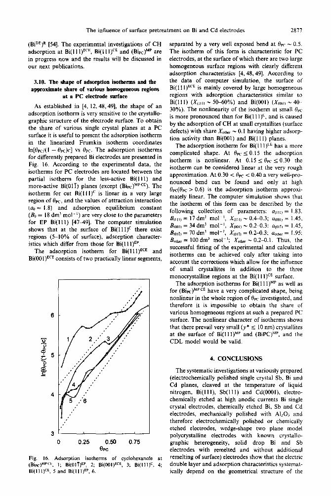
3.10. The shape of adsorption isotherms and the approximate share of various homogeneous regions
at a PC electrode surface
As established in [4, 12,48,49], the shape of an adsorption isotherm is very sensitive to the crystallo- graphic structure of the electrode surface. To obtain the share of various single crystal planes at a PC surface it is useful to present the adsorption isotherm in the linearized Frumkin isotherm coordinates In[&/(l - &)c] vs 0~. The adsorption isotherms for differently prepared Bi electrodes are presented in Fig. 16. According to the experimental data, the isotherms for PC electrodes are located between the partial isotherm for the less-active Bi(ll1) and more-active Bi(O1 f) planes (except (BiK)MP CE). The isotherm for cut Bi(i 11)’ is linear in a very large region off&, and the values of attraction interaction (no = 1.8) and adsorption equilibrium constant (Bo = I8 dm-’ mol-‘) are very close to the parameters for EP Bi(l11) [47-49]. The computer simulation shows that at the surface of Bi(l1 l)c there exist regions (S-10% of surface), adsorption character- istics which differ from those for Bi(l1 l)EP.
The adsorption isotherm for Bi(l1 l)ECE and Bi(OO1)ECE consists of two practically linear segments,
, 1
0.25 0.50 @PC
0.75
Fig. 16. Adsorption isotherms of cyclohexanole at (Birc)MPCE, I; Bi(OIT)EP, 2; Bi(OOI)ECE, 3; Bi(l I l)c, 4; Bi(l I l)CE, 5 and Bi(l I l)EP, 6.
separated by a very well exposed bend at 6~ - 0.5. The isotherm of this form is characteristic for PC electrodes, at the surface of which there are two large homogeneous surface regions with clearly different adsorption characteristics [4,48,49]. According to the data of computer simulation, the surface of Bi(lll) ECE is mainly covered by large homogeneous regions with adsorption characteristics similar to Bi(l11) (X,I,I, - 50-60%) and Bi(001) (X,W, - 40- 30%). The nonlinearity of the isotherm at small epc is more pronounced than for Bi( 1 I l)c, and is caused by the adsorption of CH at small crystallites (surface defects) with share Xotser - 0.1 having higher adsorp- tion activity than Bi(OO1) and Bi( 111) planes.
The adsorption isotherm for Bi(l1 I)CE has a more complicated shape. At 0pc I 0.15 the adsorption isotherm is nonlinear. At 0.15 I 0pc < 0.30 the isotherm can be considered linear at the very rough approximation. At 0.30 < 0~ < 0.40 a very well-pro- nounced bend can be found and only at high fIpc(&c > 0.6) is the adsorption isotherm approxi- mately linear. The computer simulation shows that the isotherm of this form can be described by the following collection of parameters: u(rll, = 1.83, Burr) = 17 dm3 mol-‘, &III) N 0.40.3; a(o~r) = 1.45, B~oo,, = 34 dm3 mol-‘, X,,,, - 0.24.3; a,Ol~) = 1.45, &olrj = 70 dm3 mol-‘, Xcolrj = 0.24.3; aother = 1.95; B other = 100 dm3 mol-‘; .&her - 0.2-0.1. Thus, the successful fitting of the experimental and calculated isotherms can be achieved only after taking into account the corrections which allow for the influence of small crystallites in addition to the three monocrystalline regions at the Bi(l1 l)CE surface.
The adsorption isotherms for Bi( 11 l)MP as well as for (BipC)MPCE have a very complicated shape, being nonlinear in the whole region of 6~ investigated, and therefore it is impossible to obtain the share of various homogeneous regions at such a prepared PC surface. The nonlinear character of isotherms shows that there prevail very small (y* < 10 nm) crystallites at the surface of Bi(l1 l)MP and (BiPC)MP, and the CDL model would be valid.
4. CONCLUSIONS
The systematic investigations at variously prepared (electrochemically polished single crystal Sb, Bi and Cd planes, cleaved at the temperature of liquid nitrogen, Bi( 11 I), Sb( 111) and Cd(OOOl), electro- chemically etched at high anodic currents Bi single crystal electrodes, chemically etched Bi, Sb and Cd electrodes, mechanically polished with Al203 and therefore electrochemically polished or chemically etched electrodes, wedge-shape two plane model polycrystalline electrodes with known crystallo- graphic heterogeneity, solid drop Bi and Sb electrodes with remelted and without additional remelting of surface) electrodes show that the electric double layer and adsorption characteristics systemat- ically depend on the geometrical structure of the
2878 E. Lust et al.
electrode surface (roughness) and energetic inhom- ogeneity of the electrode surface. It was found that the value of differential capacity at the potential of diffuse minimum increases (ccl = const.) if the surface roughness increases in the order of electrodes (Bior)R < EP single crystal < cut single crys- tal < ECE single crystal < (Binr)WR < CE single crystal < MP single crystal < MP and CE PC. The deviation from linearity of Parsons-Zobel plots, as well as the values of Parsons-Zobel factor fr.z increase in the same order. The formally found values of the inner layer capacity and roughness factor (fitting coefficient) increase in the same order of electrodes. In the case of ECE, CE and MP electrodes it is impossible to establish the “correct” values of the fitting coefficient f&, at which the &(a)-curves would have a smooth shape. The computer simulation of the electric double layer and adsorption data of many electrodes shows that in the case of (Bina)R, EP single crystal planes, ECE single crystal planes and CE single crystal planes, the independent diffuse layer (IDL) model is valid. The linear parameter of homogeneous surface regions which prevail at the surface of EP, ECE and (BiDE)R electrodes y* $ 10 nm. Probably, the surface of MP CE polycrystalhne electrodes and (BinE)WR consists mainly of many very small crystallites, which y* I 10 nm, and therefore for these electrodes the common diffuse layer (CDL) model might be valid.
The so-called “Debye length dependent roughness function” has been calculated, and using the non-linear regression analysis the various surface roughness models (sinusoidal corrugation, random Gaussian roughness, periodical system of linear defects, rectangular grating, proposed in [30,3 l]), have been simulated.
As found in the case of an EP single crystal, the surface roughness is very small and it is impossible to choose the “true” surface roughness model. The experimental data for MP and MP CE electrodes show that in the concentrated electrolyte solutions (0.05 M I c I 0.1 M) the model of random Gaussian roughness or the periodic system of linear defects [30] would be valid. It must be noted that the further experimental investigations of differently prepared PC electrodes in various electrolyte solutions and theoretical simulations of experimental results using various roughness models should be done for a more substantiated conclusion.
ACKNOWLEDGEMENTS
This work was supported in part by the Estonian Science Foundation under grant No. 612. The authors would like to thank Professors A. A. Kornyshev, M. A. Urbakh and L. I. Daikhin for the stimulative theoretical discussions and the referee for the very useful discussion.
REFERENCES
1. A. Hamelin, T. Vitanov, E. Sevastyanov and A. Popov, J. Electroanal. Chem. 145, 225 (1983).
2. M. A. Vorotyntsev, in J. O’M. Bockris, B. E. Conway and R. E. White (eds), Modern Aspects of Electro- chemistry, Vol. 17, p. 131, Plenum Press, New York (1986).
3. J. Lipkowski and L. Stolberg, in J. Lipkowski and P. N. Ross (eds), Molecular Adsorption at Metal Electrodes, VCH, New York (1992).
4. E. J. Lust, K. K. Lust and A. A.-J. JHnes, Russ. J. Electrochem. 31, 807 (1995).
5. R. R. Adzic, in J. O’M Bockris, B. E. Conway and R. E. White (eds), Modern Aspecrs of Electrochemisrry, Vol. 22, p. 163, Plenum Press, New York (1986).
6. G. Stoikov, E. Budevski, W. Obretenov and W. Lorenz, J. Electroanal. Chem. 349, 355 (1993).
7. M. Hoptner, W. Obretenov, K. Jiittner, W. J. Lorenz, G. Stoikov, V. Bostanov and E. Budevski, Surface Sci. 248, 225 (1991).
8. X. Gao, A. Hamelin and M. W. Weaver, Phys. Rev. Left. 67, 616 (1991).
9. A. Hamelin. Nanoscale Probes of the SolidlLiauid Inrerface (Edited by A. A. Gewirth and H. Siegen- thaler), NATO AS1 Series E: Applied Sciences, Kluwer Academic Publishers 288, 285 (1995).
IO. J. R. La Graff and A. A. Gewirth, Nanoscale Probes of the Solid/Liquid Interface (Edited by A. A. Gewirth and H. Siegenthaler), NATO ASI Series E: Applied Sciences, Kluwer Academic Publishers 288, 83 (1995).
I I. V. V. Batrakov and B. B. Damaskin, J. Elecfroanal. Chem. 65, 361 (1975).
14. R. Parsons and F. R. G. Zobel, J. Electroanal. Chem. 9, 333 (1965).
15.
16.
17. 18.
19. 20.
21.
22.
23.
24. 25.
26.
27.
28.
29.
30.
31.
G. Valette and A. Hamelin, J. Elecrroanal. Chem. 45, 301 (1973). D. I. Leikis, K. V. Rybalka, E. S. Sevastyanov and A. N. Frumkin, J. Electroanal. Chem. 46, I61 (1973). A. J. Bard, Anal. Chem. 33, II (1961). V. E. Kazarinov, D. Horani, Yu. B. Vasilyev, V. N. Andreyev, Irogi nauki i rekhniki. Elektrokhimiya 22, 97 (1985). R. H. Burshtein, Elektrokhimiya 3, 349 (1967). N. B. Grigoryev, Dokl. Akad. Nauk SSSR 229, 647 (1976). U. V. Palm, M. P. Parnoja and N. B. Grigoryev, Elektrokhimiya 13, 1074 (1977). 1. A. Bagotskaya, M. D. Levi and B. B. Damaskin, J. Electroanal. Chem. 115, 189 (1980). M. A. Vorotyntsev. J. Electroanal. Chem. 123, 379 (1981). M. A. Vorotyntsev, Elektrokhimiya 17, 1018 (1981). M. A. Vorotyntsev, Proc. 6th Symp. on Double Layer and Adsorption at Solid Electrodes, Tartu, p. 59 (1981). E. J. Lust and U. V. Palm, Sov. Electrochem. Engl. fr. 22, 535 (1986). E. Lust, M. Salve and U. Palm, Sov. Electrochem. Engl. tr. 23, 520 (1987). E. J. Lust and U. V. Palm, Sov. Electrochem. Engl. tr. 24, 524 (1988). U. V. Palm and B. B. Damaskin, Itogi Nauki i Tekhniki. Electrokhimiya 12, 99 (1977). L. 1. Daikhin, A. A. Kornyshev and M. A. Urbakh, Phys. Rev. E 53, 6192 (1996). L. 1. Daikhin, A. A. Kornyshev and M. A. Urbakh, Proc. of the Baltic Conf. on Interfacial Electrochem- istry, Tartu, p. 57 (1996).
12. A. R. Alumaa, E. J. Lust, N. A. Paltusova and U. V. Palm, Elektrokhimiya 19, 1582 (1983).
13. S. Trasatti and 0. Petrii, Elektrokhimiya 29, 557 (1993).
The influence of surface pretreatment on Bi and Cd electrodes 2879
32. V. N. Vigdorovich, G. A. Ukhlimov, V. V. Marychev 43. B. B. Mandelbrot, The Fractal Geometry qj. Nature. and V. P. Shumyalov, Sbornik Nauchnykh Trudov po Freeman, San Francisco (1982). Problemam Mikroelektroniki. Khimiko-Tekhnologich- 44. A. Hamelin and L. Stoicoviciu. J. Elecrroanal. Chem. eskaya Seriya. Collection of Scientific Papers- on 236, 267 (1987). Microelectronics. Ser. Chemical Technology. Mosk. 45. A. Hamelin and L. Stoicoviciu, J. Elecrroanal. Chem. Inst. Elekrronnoi Tekhniki 8, 24 (1972). 271, 15 (1989).
33. A. P. Korotkov, E. B. Bezlepkina, B. B. Damaskin and E. F. Golov. Hektrokhimiva 22, 1298 (1985).
34. E. J. Lust. A. A.-J. Janes, K. K.‘Lust and J. J. Ehrlich. Russ. J. Electrochem. 32, 597 (1996).
35. D. D. Perrin and W. L. F. Armanego, PuriJication qf Laboratory Chemicals, 3rd ed., Pergamon Press, Oxford, New York (1986).
36. V. Semevsky, P. Plrsimlgi, M. Vaartndu and A. Alumaa. Proc. 9th Symp. on Double Layer and Adsorption at Solid Electrodes, Tartu, p. 175 (1991).
37. J. Richer and J. Lipkowski. J. Elecrroanal. Chem. 251, 217 (1988).
38. E. Lust, K. Lust and A. Janes, J. Eleciroanal.vt. Chem. 413, Ill (1996).
39. E. J. Lust, K. K. Lust and A. A.-J. Janes, Russ. J. Elecrrochem. 31, 807 (1995).
40. M. Salve and U. Palm, Trans. Tarru Sate I/nip. 332,71 ( 1974).
41. M. A. Vorotyntsev, Ilogi nauki i tekhniki. Elek- trokhimiya, 21, 3 (1984).
42. L. Nyikos and T. Pajkossy, Elecrrochim. Acta 30, 1533 (1985).
46. A. Hamelin, J. Electroanal. Chem. 329, 247 (1992). 47. D. Debye and W. Hiickel, Ph.vsik. Z. 24, 305 (1924). 48. E. J. Lust and U. V. Palm, Sot. Electrochem. 22, 383
(1986). 49. E. Lust and U. Palm, Trans. Tartu Uniwrsir~ 757, 105
(1986). 50. E. Lust, A. JPnes, P. Miidla and K. Lust. J.
Electroanalyt. Chem. 425 (1997) 25. 51. E. J. Lust and U. V. Palm. Ser. Elecrrochem. 21, 1304
(1985). 52. M. Salve, A. Alumaa and U. Palm. Tram Tarru Unit>.
289, 54 (1971). 53. B. B. Damaskin, 0. A. Petrii and V. V. Batrakov,
Adsorprion of Organic Compounds on Electrodes. Plenum Press, New- York (197i).
54. M. D. Levi. M. A. Vorotvntsev and V. E. Kazarinov. Proc. of the 7th Symp., Double Layer and Adsorption at Solid Electrodes. VII, Tartu, p. I86 (1985).
55. E. Lust and U. Palm, Sot,. Elecfrochrmistr~~ Engl Tr. 24, 227 (1988).
56. A. R. Alumaa and U. V. Palm, Trans. Turtu Unit. 378, 68 (1976).
Copyright © 2022 FDOKUMEN