
Three-dimensional Numerical Simulation on Stilling Basin of ...
Upload
khangminh22Category
view
0download
0
W&M ScholarWorks W&M ScholarWorks
Dissertations, Theses, and Masters Projects Theses, Dissertations, & Master Projects
2001
A Numerical Simulation and Statistical Modeling of High Intensity A Numerical Simulation and Statistical Modeling of High Intensity
Radiated Fields Experiment Data Radiated Fields Experiment Data
Laura Smith College of William & Mary - Arts & Sciences
Follow this and additional works at: https://scholarworks.wm.edu/etd
Part of the Applied Mathematics Commons, and the Statistics and Probability Commons
Recommended Citation Recommended Citation Smith, Laura, "A Numerical Simulation and Statistical Modeling of High Intensity Radiated Fields Experiment Data" (2001). Dissertations, Theses, and Masters Projects. Paper 1539626330. https://dx.doi.org/doi:10.21220/s2-g0yc-bs97
This Thesis is brought to you for free and open access by the Theses, Dissertations, & Master Projects at W&M ScholarWorks. It has been accepted for inclusion in Dissertations, Theses, and Masters Projects by an authorized administrator of W&M ScholarWorks. For more information, please contact [email protected].

A NUMERICAL SIMULATION AND STATISTICAL MODELING
OF HIGH INTENSITY RADIATED FIELDS EXPERIMENT DATA
A Thesis
Presented to
The Faculty o f the Department o f Mathematics
The College o f William and Mary in Virginia
In Partial Fulfillment
O f the Requirement for the Degree of
Master o f Arts
by
Laura Smith
2001

APPROVAL SHEET
This thesis is submitted in partial fulfillment of
the requirements for the degree of
Master of Arts
(7iy'YL ClLaura J. Smith
Approved, April 2001
Mark K. Hinders Department of Applied Science
Rex K. Kincaid
argaret K. Schaefer ( j%
ichael W. Trosset

TABLE OF CONTENTS
Page
ACKNOWLEDGEMENTS iv
LIST OF TABLES v
LIST OF FIGURES vi
ABSTRACT ix
CHAPTER I. INTRODUCTION 2
CHAPTER II. DESCRIPTION OF OPEN LOOP 6EXPERIMENTS
CHAPTER III. DESCRIPTION OF 19ELECTROMAGNETIC MODEL
CHAPTER IV. STATISTICAL MODELING OF 49OPEN LOOP EXPERIMENT DATA
CHAPTER V. CONCLUSION 70
APPENDIX A 72
APPENDIX B 73
BIBLIOGRAPHY 74
iii

ACKNOWLEDGEMENTS
The writer wishes to express her sincere appreciation to Professor Mark Hinders, under whose guidance this investigation was conducted, for his patient guidance and criticism throughout the investigation. The author is also indebted to Professors Rex Kincaid, Margo Schaefer, and Mike Trosset for their careful reading and criticism o f this manuscript.

LIST OF TABLES
Table
1.
2 .
3.
4.
5.
6 .
7.
Page
Passive filters selectively removed for the 13open loop experiments
Examples o f pre-selected reference voltage values 14sent to the flight controller
Effects of passive filter 15(a) Passive filter on(b) Passive filter off
Open loop experiment test matrix 17
Distributions used to fit the open loop experiment 52data, along with their probability density functions
Mean and variance combinations used to determine 59the least square error value with the lowest value
Field strengths extrapolated at each frequencies 62
V

LIST OF FIGURES
Figure Page
1. Equipment used to collect open loop data 7
2. Picture o f flight controller placed in reverberation 9chamber to collect data
3. Picture of flight simulation hardware 10
4. Picture o f outside o f reverberation chambers 12
5. Flowchart for the specialized calibration procedure 16
6. Partial open loop experiment data file collected 18
7. Field incident at angle 0 on a wire over a ground 21plane (parallel polarization)
8. Table generated using EMCad software package 22
9. Graph o f data using EMCad software package 23
10. Circuit wire over a metal ground plane 26
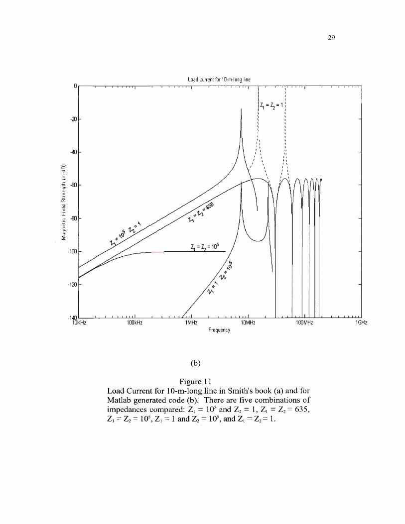
11. Load current for 10-m-long line(a) Smith's book 28(b) Matlab generated code 29
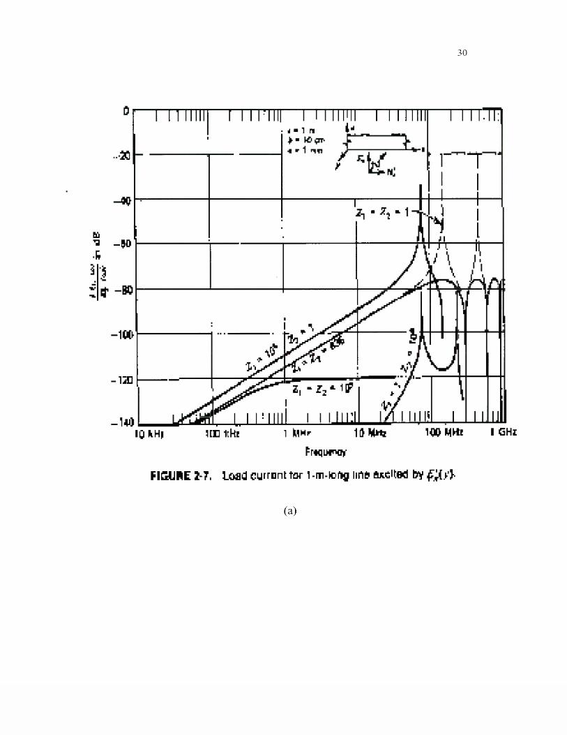
12. Load current for 1-m-long line(a) Smith's book 30(b) Matlab generated code 31
13. Load voltage for wire over ground plane in terms of 32total magnetic field from Albert Smith's book
14. Plot o f radiated susceptibility o f cables using Emcad 33software package
VI

LIST OF FIGURES
Figure
15.
16.
17.
18.
19.
20 .
2 1 .
22 .
23.
24.
25.
26.
27.
Page
Load voltage for wire over ground plane in terms o f 34total magnetic field using Matlab generated code (with A. Smith's book parameters)
Load voltage for wire over ground plane in terms of 36total magnetic field using Matlab generated code (with actual open loop test parameters)
Plot of radiated susceptibility o f cables using Emcad 37software package (with open loop test parameters)
Varying height of wire over ground plane 39
Varying line length 40
Open loop test data for rate o f climb/descent at 450 MHz 43
Plot of rate of climb/descent signal at 450 MH 44(all processors)
Plot o f rate of climb/descent signal at 450 MHz 45(processor one)
Plot of rate of climb/descent signal at 450 MHz 46(unsorted)
Plot of rate of climb/descent signal at 450 MHz 47(unsorted and scaled y-axis)
Plot of rate of climb/descent signal at 450 MHz 48(unsorted vs. sorted)
Subplot of open loop test data 50
Subplots o f open loop test data with good representation 53of normal distribution overlays
Vll

LIST OF FIGURES
Figure Page
28. Subplots of open loop test data with poor representation 54of normal distribution overlays
29. Subplots of open loop test data with normal distribution 55and with better fit achieved with a multiplication factorincluded
30. Subplots of open loop test data with least square 58error overlays
31. New mean and variance parameters generated from 60the least square error value
32. Typical plot generated by Matlab's basic fitting interface 64
33. Typical plot of extrapolated variances using Matlab's 66basic fitting interface
34. Mean/median computed using Matlab's data statistics tool 67
35. Subplot o f normal distribution using the extrapolated variance and mean for the frequency and field strength represented
(a) 650, 700, 750 800 v/m 68(b) 850, 900, 950, 1000 v/m 69
Vll l

ABSTRACT
Tests are conducted on a quad-redundant fault tolerant flight control computer to establish upset characteristics o f an avionics system in an electromagnetic field. A numerical simulation and statistical model is described in this work to analyze the open loop experiment data collected in the reverberation chamber at NASA LaRC as a part of an effort to examine the effects o f electromagnetic interference on fly-by-wire aircraft control systems.
By comparing thousands o f simulation and model outputs, we first identify the models that best describe the data and then perform systematic statistical analysis on the data. We then combine all o f these efforts which culminate in an extrapolation of values which are in turn used to support previous efforts used in evaluating the data.

A NUMERICAL SIMULATION AND STATISTICAL MODELING
OF HIGH INTENSITY RADIATED FIELDS EXPERIMENT DATA

CHAPTER I
INTRODUCTION
When flight first began, pilots controlled aircraft through direct force. The
pilots moved control sticks and rudder pedals linked to cables and pushrods that
physically moved the control surfaces such as the wings and tail of the plane.
However, as power and speed of flight increased, more force was needed to
control the aircraft and therefore hydraulically boosted controls were incorporated
into the aircraft. In the 1960's, the idea o f flying aircraft with electronic flight
control systems was introduced. Wires replaced cables and pushrods, which in
turn gave the aircraft designers greater flexibility in the size and placement of
components to control the aircraft. A fly-by-wire system would be smaller, more
reliable, and in military aircraft the systems would be much less vulnerable to
battle damage [1]. A fly-by-wire aircraft would be more responsive to pilot
control inputs with the results being improved performance and design o f a more
efficient, safer aircraft. The quality of flight was greatly improved with this
instantaneous sensing o f pilot inputs.
Fly-by-wire systems are safer because o f their redundancies. They are
more maneuverable because computers can command more frequent adjustments
than a human can. Fly-by-wire is also more cost efficient because it is lighter and
2

3
takes up less space than the hydraulic system, which in turn either reduces the
amount o f fuel needed or increases the amount of passengers/cargo the aircraft
can carry [2].
However, with this new concept o f fly-by-wire comes awareness that the
system, which now uses individual wires instead of cable bundles, is also more
vulnerable to certain environmental conditions. Planes flying through adverse
operating environments experience a phenomenon known as electromagnetic
interference (EMI). There are many factors, man made and natural, that can
contribute to these phenomena including [3]:
radar,- lightning,
AM/FM/TV broadcast stations,industrial, scientific, and medical (ISM) equipment,automobile ignitions,personnel electrostatic discharge,esoteric nuclear electromagnetic pulse (NEMP), andpower supply noise and switching transients inside electronicequipment
The electromagnetic interference phenomena dealing with wavelengths, namely
radar and AM/FM/TV broadcast stations, have become known as HIRF, High
Intensity Radiated Fields. HIRF is a non-ionizing electromagnetic energy that is
external to the aircraft. HIRF can cause adverse effects to the electronic
equipment onboard the aircraft that in turn may affect the safety of flight and
landing [4]. Electromagnetic fields may cause electrical signals to be induced on
the aircraft's wiring and these signals can propagate to other electronic equipment,
which may cause a functional error known as upset [5].

4
Upset phenomena that can be caused by electromagnetically induced
signals include [6, 7, 8, 9, 10, 11]:
change in data values o f the input/output circuitry,logic changes on the data bus, address bus, and control lines o f theprocessors,logic changes in registers of the central processing unit (CPU) o f the processors, andlogic changes in the arithmetic logic unit (ALU) within the CPU of the processors
Upset phenomena such as these can interfere with normal operation of the
processors within a control computer and result in control law calculation errors
that can affect performance and reliability at the closed loop system level [5].
Aircraft systems, critical and essential, are vulnerable to atmospheric
electricity hazards [12]. The number o f electrical/electronic systems aboard an
aircraft is increasing. These systems are vulnerable to electromagnetic fields
caused by HIRF and need to be certified to ensure they have the proper
electromagnetic shielding needed to protect the systems. For the case of
lightning, there is a potential problem of the electromagnetic field produced if the
aircraft is struck by lightning. The electromagnetic field may cause voltage
and/or current transients to be induced into the electronic equipment. These
transients can be produced in two different ways: the aircraft's interior may be
penetrated by the electromagnetic field or the structural IR (current-resistance)
voltage may rise due to current flow on the aircraft. These are referred to as
indirect effects because they may not physically damage the aircraft [12].

5
Electromagnetic fields can also penetrate inside the electronic equipment through
imperfect seams, leaky connector apertures, and cracks in the protective shielding.
Due to the increase o f reliance on the electronic equipment of an aircraft
for flight, adequate protection measures need to be designed and incorporated into
the systems to ensure safe flight. Another factor that needs to be considered for
ensuring flight safety is the possibility of reduced electromagnetic shielding by
replacing the aircraft's metal skin with one made of composite materials.
One of the goals of this thesis is to develop and validate a mathematical
model of electromagnetic fields coupling into our test equipment. We then want
to use this model to extrapolate/predict measurements outside of the data set that
we have in order to determine the level of field strength that can be applied
without damaging the test equipment. In Chapter 2 the open loop calibration
experiments and the resulting data are described, in Chapter 3 an electromagnetic
model is described, and in Chapter 4 a statistical analysis o f the open loop data is
explained.

CHAPTER II
DESCRIPTION OF OPEN LOOP EXPERIMENTS
The Closed Loop Systems Laboratory at the National Aeronautics and
Space Administration (NASA) Langley Research Center (LaRC) has been
established to study the effects o f high intensity radiated fields on complex
avionic systems and control system components. Linked with the High Intensity
Radiated Fields Laboratory, also at LaRC, tests are being conducted on a quad-
redundant fault tolerant flight controller to establish upset characteristics o f an
avionics system in an electromagnetic field. This section o f the thesis describes
the open loop calibration experiments and the data collected [13].
A block diagram in Figure 1 represents the equipment used to collect the
open loop experiment data [14]. The flight controller consists o f four independent
processors. Each processor has a 1750 processor, 48 Kbytes of EPROM
(Erasable Programmable Read Only Memory), 2 Kbytes of scratchpad RAM
(Random Access memory), and 8 Kbytes o f sharable RAM. All input/output is
memory mapped into a 2 Kbyte space. Although digital in design, the flight
controller receives sensor inputs and sends actuator command outputs via analog
voltages. These signals are interfaced to the flight controller via nine shielded
6
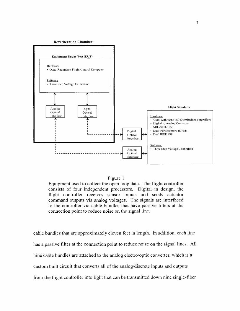
7
Reverberation Chamber
E quip m ent U nder T est (E U T )
AnalogOpticalInterface
DigitalOpticalInterface
Hardware
SoftwareThree Step V oltage Calibration
Quad-Redundant Flight Control Computer
DigitalOpticalInterface
A nalogOpticalInterface
Software
Hardware
Three Step V oltage Calibration
VM E with three 68040 em bedded controllers Digital to A nalog Converter M IL-STD-1553 Dual-Port M em ory (DPM )Dual IEEE 488
Figure 1Equipment used to collect the open loop data. The flight controller consists o f four independent processors. Digital in design, the flight controller receives sensor inputs and sends actuator command outputs via analog voltages. The signals are interfaced to the controller via cable bundles that have passive filters at the connection point to reduce noise on the signal line.
cable bundles that are approximately eleven feet in length. In addition, each line
has a passive filter at the connection point to reduce noise on the signal lines. All
nine cable bundles are attached to the analog electro/optic converter, which is a
custom built circuit that converts all o f the analog/discrete inputs and outputs
from the flight controller into light that can be transmitted down nine single-fiber

optic lines. This permits a safe, noise-free method o f transmitting the signals in
and out of the electromagnetic containment chamber.
In addition to the analog lines, a MIL-STD-1553 interface is available.
These four coaxial lines are bussed into a custom-built fiber optic converter. This
interface can be used for digital input/output to close the control loop.
A picture of the equipment set up for the open loop experiments is shown
in Figure 2. The flight control computer, also known as the equipment under test
(EUT), is placed on a syrofoam block in the middle of the chamber. The large
paddle on the left stirs the electromagnetic fields to obtain a statistically near
homogeneous radiation environment during testing. The probes that measure the
field strength inside the chamber are on stands to the left and right of the flight
controller. The source o f power and signals are transferred through the cables that
are connected to the bulkhead, which is the panel on the right-hand wall. The
antenna on the right emits the radiation into the chamber through one o f the cables
connected to the bulkhead. The equipment that controls the radiation output is
located in a separate control room outside o f the containment chamber. The
signals are passed to the larger box on the floor which is the analog electro/optic
converter. This is where the signals are converted to optical signals to be passed
through the bulkhead. The smaller box on top of the converter is the 1553
interface that is used when closed loop tests are performed.

9
Figure 2Flight controller placed in reverberation chamber to collect data. The controller is placed on a styrofoam block in the middle of the chamber. The large paddle to the left stirs the electromagnetic fields to near homogeneous radiation. The antenna on the right is used to radiate the equipment under test. The probes, on the left and right o f the controller, are used to measure the field strengths within the chamber. The signals are passed to the larger box on the floor which is the analog electro/optic converter. This is where the signals are converted to optical signals to be passed through the bulkhead (the panel on the wall to the right). The smaller box on top of the converter is the 1553 interface that is used for closed loop testing.
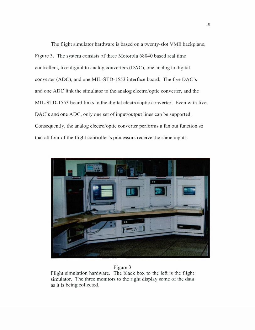
10
The flight simulator hardware is based on a twenty-slot VME backplane,
Figure 3. The system consists of three Motorola 68040 based real time
controllers, five digital to analog converters (DAC), one analog to digital
converter (ADC), and one MIL-STD-1553 interface board. The five DAC’s
and one ADC link the simulator to the analog electro/optic converter, and the
MIL-STD-1553 board links to the digital electro/optic converter. Even with five
DAC’s and one ADC, only one set of input/output lines can be supported.
Consequently, the analog electro/optic converter performs a fan out function so
that all four of the flight controller’s processors receive the same inputs.
Figure 3Flight simulation hardware. The black box to the left is the flight simulator. The three monitors to the right display some of the data as it is being collected.

The electromagnetic containment chamber is a 13 x 23 x 9Vi foot mode-
stirred reverberation chamber located in the High Intensity Radiated Fields
Laboratory at LaRC [15]. Figure 4 shows a picture of the outside of the
containment chambers. These are enclosed steel rooms that have been tested to
ensure that no radiation leaks outside o f the chamber. The door is pneumatic in
nature and has a seal that expands after the door is shut to ensure proper shielding.
In essence, this is like a large microwave oven that provides a near homogeneous
radiation environment. Using this type o f containment chamber enables the flight
controller to be exposed equally from all angles, so that the angle of incidence for
maximum susceptibility does not need to be found.
For the open loop experiments, two special conditions were implemented.
First, the passive filters were selectively removed. This allowed the long
electrical signal lines to couple electromagnetic energy into the flight controller.
These filters are extremely efficient at keeping the flight controller radiation tight,
so by removing specific combinations of filters the flight controller processor
could be weakened to the radiated energy. These combinations are shown in
Table 1. The ninth cable cannot be removed because this supplies power to the
flight control computer.

12
Figure 4Outside look at reverberation chambers with pneumatic seals to ensure no radiation leaks outside of the chamber during testing. There are three various sized chambers, a control room, and a high-power amplifier room available at the facility.
The second special condition was that the flight simulation software was
removed and the flight simulator was reprogrammed with a special calibration
procedure. This procedure sent pre-selected reference voltages to each processor
in the flight controller. The received voltages were then stored for comparison to
the sent reference voltage.

13
Table 1Passive filters selectively removed for the open loop experiments. Removal o f the filters allowed the signal lines to couple electromagnetic energy into the flight controller. The filters are extremely efficient at keeping radiation out o f the flight controller, so removing these combinations weakened the system to radiated energy. The ninth cable cannot be removed because this supplies power to the flight control computer.
F ilters Removed Test Objective
1,5 Weaken Processor 1
2 ,6 Weaken Processor 2
3 ,7 Weaken Processor 3
4 ,8 Weaken Processor 4
1,2, 3, 4 Upper connector matrix crosstalk effects
5, 6, 7, 8 Lower connector matrix crosstalk effects
The maximum and minimum voltages were calculated for each analog
signal line and three critical points were then defined. They are fifty percent of
the maximum voltage, the zero point, and fifty percent of the minimum voltage as
shown in Table 2. Appendix A lists the actual reference voltages sent for each
signal.
One hundred percent o f the maximum and minimum values were never
sent to the controller because with the added energy from the electromagnetic
fields, the cumulative effect could have exceeded the hardware’s specifications

14
Table 2Examples of pre-selected reference voltages sent to the flight controller. Three critical points defined.
Voltage Level +15 to -15 v +10 to 0 volts
50% of Max +7.5 +5
Zero 0 0
50% of Min -7.5 0
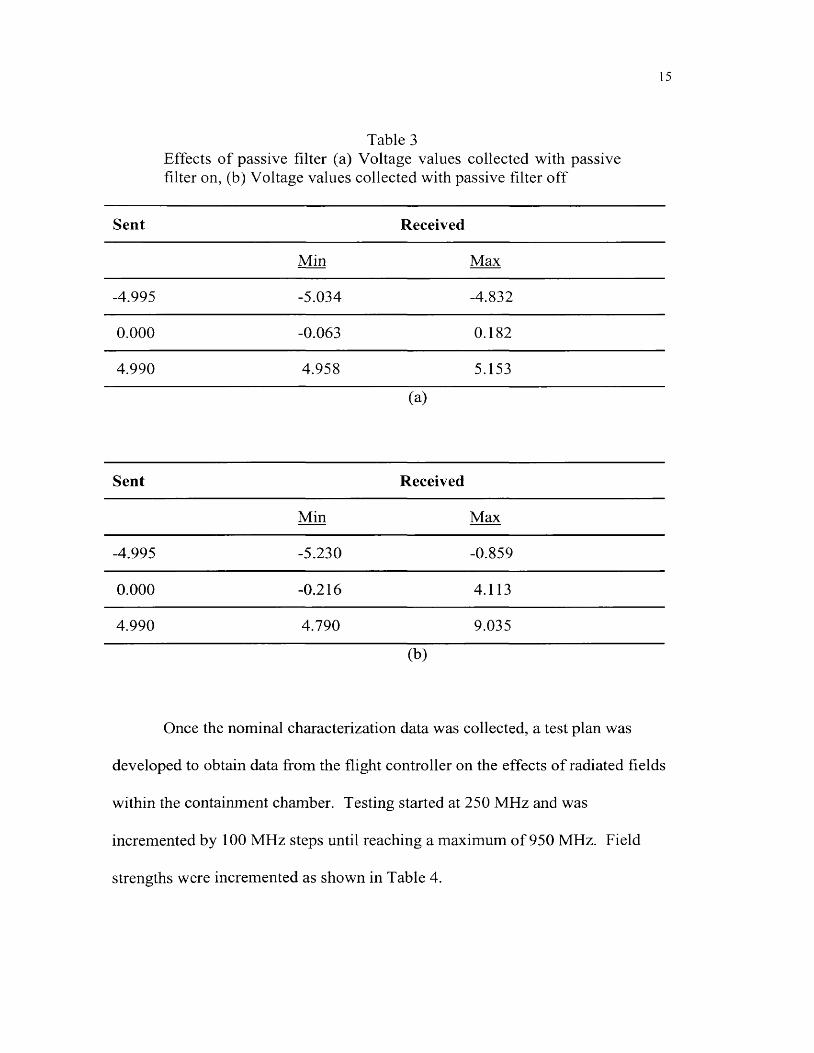
and resulted in component damage. Table 3 shows the effect the passive filters
have on the system. The values shown reflect the overall maximum and
minimum voltages collected during testing.
When the passive filters remain on the cables, there may be a nominal
amount o f radiation that enters the system that could minimally affect the voltage
values received, see Table 3a. However, when the passive filters are removed,
there is an extreme change in the data collected, see Table 3b, which could have
led to equipment damage if the threshold had been exceeded.
Figure 5 shows the flowchart for the automated calibration procedure. For
a single run of the program 525,000 voltages were collected. The program was
run for each o f the six filter combinations listed in Table 1 which nets a total of
3,150,000 data points per test.
15
Table 3Effects of passive filter (a) Voltage values collected with passive filter on, (b) Voltage values collected with passive filter off
Sent Received
Min Max
-4.995 -5.034 -4.832
0.000 -0.063 0.182
4.990 4.958 5.153
(a)
Sent Received
Min Max
-4.995 -5.230 -0.859
0.000 -0.216 4.113
4.990 4.790 9.035
(b)
Once the nominal characterization data was collected, a test plan was
developed to obtain data from the flight controller on the effects of radiated fields
within the containment chamber. Testing started at 250 MHz and was
incremented by 100 MHz steps until reaching a maximum of 950 MHz. Field
strengths were incremented as shown in Table 4.

16
Third time through?
Increment to next voltage
level.
Collect 1,000 samples for each of the four
processors.
Set all lines to -50% voltage.
Yes
Store 3,000 samples x 35 lines x 5 voltage
values as a file.
Figure 5Flowchart for the specialized calibration procedure. This procedure sends pre-selected reference voltages (50% of the maximum voltage, the zero point, and 50% of the minimum voltage) to each processor in the flight controller. The received voltages are then stored for comparison to the sent reference voltage.
The procedure followed for testing was to start at the lowest frequency and
continue increasing the field strength to the highest level on Table 4, each time
collecting the 3,150,000 data points described previously. However, tests were

17
not conducted at all frequency/field strength pairs. The test was halted if a large
number of observed voltages violated a predetermined threshold, typically one
percent above normal system drift. This test procedure was used for the indicated
test configurations referenced in Table 1.
Table 4Open loop experiment test matrix. The procedure started at the lowest frequency and continued increasing the field strength to the highest level shown and then increased to the next frequency level. The test was halted if a large number o f observed voltages violated a predetermined threshold (typically one percent above normal system drift).
Field Strengthv/m
50 100 150 200 300 400 450 500 550 600250 X X X X350 X X X X450 X X X X X X X X
Frequency 550 X X X X X X X XMHz 650 X X X X X X X X
750 X X X X X X X X850 X X X X X X X X950 X X X X X X X X
Values were stored in an ASCII file with five columns, one for the
reference voltage sent and one column for voltages collected at each of the four
processors. Each data file included one thousand samples for each o f the three
reference voltage groups. Figure 6 shows a partial data file collected. Due to the
overwhelming amount of data collected, one of the first tasks was to develop a
data management scheme. This scheme involved standardizing file conventions

18
such as file naming, data format, and data variables collected from the tests. It
also involved storing the data to a medium that was accessible to all users, and
creating web pages that list the unique test parameters and the directory locations
of all files.
noflt 1 /550cw /100vm/sr4phidts.dat Voltage Sent Received PI
- 4 . 9 9 5
- 4- 4- 5
- 4- 4- 4- 5- 5- 4- 5- 5- 4
0 0 0 1
Received P20 1 30 1 30 2 7
- 5- 5
- 5- 5
- 5- 5
- 5- 5- 5
- 5- 5
0 1 0 1
0 1 0 10 1 0 3 0 1 0 00 2 0 1 0 0 0 10 2 0 1 0 1 0 10 1 0 1 0 1 0 1
0 1 0 1
0 1 0 1
Received P3- 5 0 0 6
0 0 0 2
0 0 0 0
0 1 0 1 0 0 0 2 0 0 0 0 0 0 0 0
- 5 . 0 0 6
0 0 0 0 0 0 0 1 0 1 0 0
Received P4
o 1 o o
o o 0 0
0 0 0 0
0 1 9 9
Figure 6Partial open loop experiment data file collected. This is an ASCII file with five columns, one for the reference voltage and one for voltages collected at each of the processors. There were one thousand samples collected for the voltage received at each reference voltage group (total o f three thousand samples per data file).

CHAPTER III
DESCRIPTION OF ELECTROMAGNETIC MODEL
In order to perform analysis on the open loop experiment data, a software
package was purchased. We chose to use EMCad from CKC Laboratories, which
represents the industry's first electromagnetic compatibility (EMC) computer
program for compliance assessment. The software is designed to evaluate black
box systems where the inputs are known, the outputs can be measured, but there is
no knowledge of the internal components o f the system.
EMCad is a computer software program that performs calculations for
electromagnetic compatibility analysis. The software is composed of four basic
program modules: radiated emissions, radiated susceptibility, crosstalk analysis,
and filter simulation. Each o f these modules uses a basic electromagnetic
compatibility model that incorporates user-defined inputs to characterize the
model for the specific analysis application. The software program presents the
data calculations in terms o f regulatory specifications, military or commercial,
that are selected by the user.
19

20
EMCad currently has the following analysis packages available [16]:
radiated emissions from printed circuit boardsradiated emissions from cables and interconnectscross-talk on printed circuit boardscross-talk on cables and interconnectsradiated susceptibility o f wires over ground planeradiated susceptibility o f printed circuit boardsradiated susceptibility analysis for plane wave illumination,illumination from nearby sourceconducted emissions analysisconducted susceptibility analysis
Our particular application will benefit from the analysis package dealing with
radiated susceptibility analysis for plane wave illumination from nearby source.
EMCad’s radiated susceptibility analysis is well suited for assisting in DO-160D
compliance [17] as well as special HIRF conditions set forth by the Federal
Aviation Administration for civil avionics [12].
The radiated susceptibility module predicts the amount of external plane
wave radiated field energy that couples to interconnecting wires and cables. The
EMCad program calculates the voltage induced across the interconnection load as
a function o f frequency. The calculation results can be displayed in table and/or
graph format.
The radiated susceptibility module uses the following equation for
prediction [16] and is represented by Figure 7:
I _ e M 5 e_ ^ i}[(i _ cos2ps)+ jsin2ps] (Eq. 1)

21
where:I = current induced in victim load from external field E = electric field strength of external plane wave field b = distance o f wire to the ground plane (h = b/2) s = length of wireZ0 = characteristic impedance o f interconnection (Zc in Figure 7) Zi = victim circuit load impedance (ZA in Figure 7)Z2 = victim circuit source impedance (ZB in Figure 7)D = (Z0 Z, + Z0 Z2)cosps + j(Z02 + Z lZ2)sinps P = 2tt IX
E'(x,z)
777777777777777777777777777?z = 0
■777777777777777777777.z=sGround Plane
Field incident at angle 8 on a wire over a ground plane (parallel polarization).
Figure 7.Field incident at angle 0 on a wire over a ground plane (parallel polarization)
The user specifies the physical characteristics of the interconnection wire
or cable and EMCad calculates the values for input into the above equation. The
user-specified parameters include wire distance above ground, wire gauge or
diameter, wire length, shielded or unshielded wire, load and source impedance,
applied field strength if modulation is desired, and choice of horizontal or vertical
applied field. EMCad then calculates the voltage induced at the circuit load and

22
presents the final results in table and/or graph forms. The table format, Figure 8,
shows the various frequency components o f the induced voltage and the
amplitude of the induced voltage in both dBpV and volts. The graph format,
Figure 9, displays the induced voltage amplitude versus frequency.
SMCADl (TM) vS.40 1/22/92 CKC LABORATORIES, INC
RADIATED SUSCEPTIBILITY - PLANE WAVE ILLUMINATION OF CABLE
DATE 03-14-2001 TIME 10:29:17ANALYSIS DONE FOR :PROJECT NAME :SIGNAL NAME :DATB OP ANALYSIS :ANALYSIS DON2 BY :
DISTANCE TO GROUND - > 1 m e t ersCONDUCTOR DIAMETER - > . 00006 METERSCONDUCTOR LENGTH - > 7 METERSAPPLIED FIELD (VOLTS/MBTKR} -> 250 VOLTS/METERSOURCE IMPEDANCE - > so ohm sLOAD IMPEDANCE SO OHMSCALCULATED Z0 - s 865 OHMSHORIZONTALLY POLARIZED PLANE: w a v bSHIELDING -> S 60 S. E. at 1 MHz
RADIATED SUSCEPTIBILITY plana wav#10 HIGHEST READINGS
FREQUENCY INDUCED V VOLTAGE LEVELMHz dBuV in. volt a
74.00939 122 1.345614100.0092 l2l 1.1662282 26 .0074 122 1.345612374.0068 122 1.34561440D.006S 121 1.166265526.006& 122 1.345612674.0067 122 1.345614700.0057 121 1.166269825.0067 122 1.345612974.0067 122 1.345614
Figure 8Table generated using EMCad software package. The first section of the table allows the user to enter project information if wanted. The second section of the table lists the user-specified parameters. The third section of the table list the ten highest readings calculated by the software package and displays the frequency of the induced voltage and the induced voltage in both dBpV and volts.
23
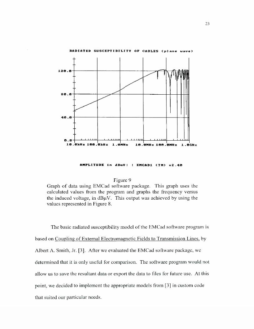
RA1>I AXED SUSCEPTIBILITY OF CABLES (plane wave)
88.0
40 .0
0 _ 0 --------------- 1------1---- 1 .1 I H I . 1____L ...I ..I I I I I J_
10.0kHz 100.0kHz 1.0MHz 10.0MHz 100.0MHz 1.0GHz
AMPLITUDE in dBuU : : EMCAD1 <TM> v 2 .40
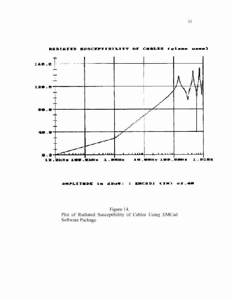
Figure 9Graph o f data using EMCad software package. This graph uses the calculated values from the program and graphs the frequency versus the induced voltage, in dBpV. This output was achieved by using the values represented in Figure 8.
The basic radiated susceptibility model o f the EMCad software program is
based on Coupling of External Electromagnetic Fields to Transmission Lines, by
Albert A. Smith, Jr. [3]. After we evaluated the EMCad software package, we
determined that it is only useful for comparison. The software program would not
allow us to save the resultant data or export the data to files for future use. At this
point, we decided to implement the appropriate models from [3] in custom code
that suited our particular needs.

24
We chose models with emphasis on the practical solutions of problems
involving the excitation of currents on wires and cables by natural and man-made
sources of electromagnetic fields. Electromagnet fields inside electronic
equipment induce noise on the interconnecting wires and cables. The fields may
originate from sources inside the box or from external sources. If the induced
noise exceeds the susceptibility threshold voltage of the circuit, malfunction can
result [3]. The problem is to find VL, the noise appearing across the right-hand
termination Zb in Figure 7.
Our interest is in being able to deal quantitatively with the coupling o f
electromagnetic fields to transmission lines. Because [3] is filled with abundant
application data in the form o f solved examples and spectrum profiles, with
sufficient theoretical detail to permit the results being extended to a wide variety
o f problems, we follow that treatment closely below.
In particular, we outline the theory of excitation o f a two-wire transmission
line illuminated by an external electromagnetic field. Using the method of images,
solutions for a wire over a ground plane are developed by analogy with the two-
wire line. The coupling equations are solutions of differential equations which
include the source terms due to the incident fields [3].
The differential mode current along an isolated two-wire transmission line
is found using transmission line theory, whereas the common mode current must
be obtained by the methods of linear antenna theory. Most transmission lines are
parallel to a conducting ground plane or to earth and are not isolated. When this

25
is the case, the common mode current distribution along the line can be obtained
from transmission line theory by treating the line and its image in the ground
plane as a two-wire transmission line open circuited at both ends [3]. For this
method, the distance to the ground plane must be much greater than the conductor
spacing. All the conductors in the cable are treated as a single wire, with diameter
equal to the overall diameter o f the cable, and it is assumed that the current is
divided equally among the conductors in the cable.
The equations o f interest, along with the numerical values, from Smith's
book follow:
Vl(co) = Htot jl 2071 sin ph P y (3cosph Q (Eq. 2)
where
P = sinps + j
7
2R© RAC A sinps + A
2Rcosps
Q = 1 R A1+ AR
o COZoc o sp s -B J
- R a C aC Q + A AR
sinPsb y
+ J cor a(Ca + C B)cosPs +03 R aC aC bZ 0 2R
v2 R b+ sinps
With the following parameters:
s = 0 .5m (line length)h = 5 mm (height o f wire over ground plane) a = 0.25 mm (wire diameter)RA = 20 Q CA= lO pf RB= 100,000 Q CB= lO pf Z0 = 525

26
V l represents the no ise voltage appearing across the right hand
termination impedance in Figure 10. In the above equations the variables are
described as:
P = 2tiIX (phase constant of line)X — w avelength co = 2 n ff = frequency, hertz
GroundP lan e
Circuit wire over a m etal ground plane.
Figure 10Circuit wire over a metal ground plane.
Once we had identified the model we thought was applicable to our
situation, a wire over a ground plane, we needed to find a software package that
would allow us to manipulate and save the data as needed. Matlab, a high-
performance language for technical computing, was determined to have all the
qualities needed to simulate the data. At this point, we had to make sure Matlab
was capable o f modeling the equations from [3].

27
The initial analysis started with generating Matlab code for some o f the
equations in Smith's book and then visually comparing the simulated output to
that o f the book. Figure 11 and Figure 12 compare Smith's output to that of
Matlab for two different line geometries and five combinations of load
impedances using Eq. 1 in this thesis. The two sets of outputs are very similar so
at this point we were assured that Matlab was capable of performing the necessary
simulations.
Next we visually compared another plot from Smith's book with the
Matlab output, using Eq. 2 in this thesis, to further ensure we had coded the model
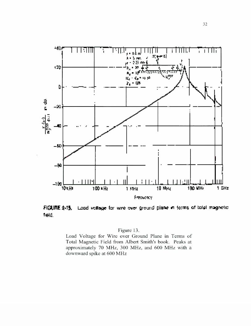
correctly. Figure 13 shows the output from Smith's book. Figure 14 and Figure
15 show the outputs, using the numerical values from Smith's example, from the
EMCad software and the Matlab code, respectively. Looking at the output from
the EMCad software package, we can see that the shape of the plot is different
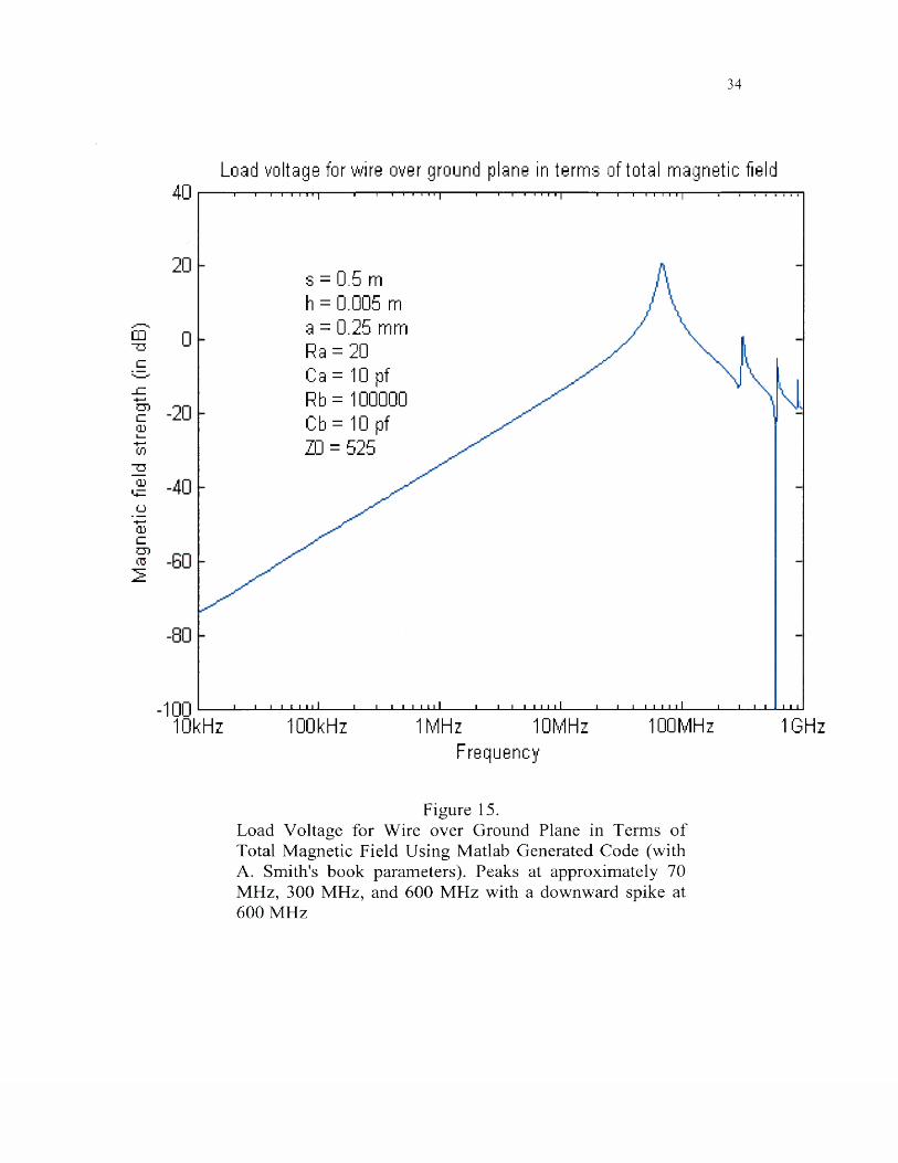
from that of [3]. Comparing Figure 13 and Figure 15, Smith vs. Matlab, we see
that they both peak at approximately 70 MHz, 300 MHz, and 600 MHz. There is
also a downward peak at 600 MHz in both figures. We were trying to assure that
the Matlab code was working properly and could be used to simulate the data.
Because the shapes of these curves are similar, we have a good starting point.

28
-M
9
h#4 4
- 1®
-120 TTT p
1 WHifr*qi>wcy
FIQJRE S4- Ld kJ currerfl 10r 1 Qm Jima hn« ftMited by t ; ( y )•
(a )
Mag
neti
c Fi
eld
Stre
ngth
(in
dB
)
29
Load current for 10-m-long line
-100
-120
-1401GHz1MHz 10MHz 100MHz10KHz 100kHz
Frequency
(b)
Figure 11Load Current for 10-m-long line in Smith's book (a) and for Matlab generated code (b). There are five combinations o f impedances compared: Zj = 105 and Z2 = 1, Zi - Z2 = 635, Zj = Z2 = 105, Z, = 1 and Z2 = 105, and Z x - Z 2~ 1.
qn i^
B
30
a
-90
- 1®
-13D
-14J)
■ 1 1 1 m u1
f 1 1 m m 1 t \ i i i i i i 1 1 M i n iM - 1 n i - >■ L
I 11 I T T
' ’ " f I TIl
•1 ■ r>* P s
J I
h
T ".
A # 1
1 1
- - - - - - -
_ _ _ U j u m ' T l . 1 I M I I l
z , - r z * i F
I I l i l i l
*, /* /wi / 1 m i f 1 I I ,11
IQ PlH| lEBItkl 1 MHf 1t> M«ZFntqurxrp-
FIGURE 2-7, L&fld c u rre n t to r l-m -taftfl lin t fijtd ted by £*(>'}■
1® MHz I GHz
(a )

Mag
neti
c Fi
eld
Stre
ngth
(in
dB
)
31
Load current for 1-m-long line
-100
Z, = Zj = 635-120
-140100MHz 1GHz10KHz 100kHz 1MHz 10MHz
Frequency
(b)
Figure 12Load Current for 1 -m-long line in Smith's book (a) and for Matlab generated code (b). There are five combinations of impedances compared: Z x - 105 and Z2 = 1, Z, = Z2 = 635, Z, = Z2 = 105, Z, = 1 and Z2 = 105, and Z, = Z2= 1.
32
-JO
-50
- lf t ]1 GHz1 MHl
f-FPOWrKY
■F-H3URE Load irtiBrisjt tar wirt me* Qrcund 1erm& of bol̂ il magnelicW d.
Figure 13.Load Voltage for Wire over Ground Plane in Terms of Total Magnetic Field from Albert Smith's book. Peaks at approximately 70 MHz, 300 MHz, and 600 MHz with a downward spike at 600 MHz
33
RflSTAVXD o r £ * l L t a * *>l « ■ » w a n !
1 2 t . 0
ID .WHHt 1W P . H f W t l . B C H Sl f l . B K M s 1 W .« ]« M X
AM^llTiJPC 1*1 d B u « ; : m r . o u j <?n> mji . «
Figure 14.Plot of Radiated Susceptibility of Cables Using EMCad Software Package
Mag
netic
fie
ld
stre
ngth
(in
dB)
34
Load voltage for wire over ground plane in terms of total magnetic field40 ------ 1------1—1—1 1 1 ttj 1--- 1—i—....... 1---- 1—i—i i i i i |------- 1-1—i—i i i i i |—
s = 0.5 m h = 0.005 m a = 0.25 mm Ra = 20 Ca = 10 pf Rb = 100000 Cb = 10 pf ZD = 525
'j QQ _____ i i__i i i i 111_____ i___i i i i i 111_____ i___i i i i i i 11_____i i i i i i i 11______i___i i i I i 11
10kHz 100kHz 1MHz 10MHz 100MHz 1GHzFrequency
Figure 15.Load Voltage for Wire over Ground Plane in Terms of Total Magnetic Field Using Matlab Generated Code (with A. Smith's book parameters). Peaks at approximately 70 MHz, 300 MHz, and 600 MHz with a downward spike at 600 MHz

35
Once the comparisons of Matlab vs. Smith outputs were done, and we
were confident the Matlab code was working properly, we changed the
parameters in the Matlab code to see the affects of varying the parameters. For
the first set o f changes to the parameters, we investigated the output of the open
loop test parameters. This involved changing the line length from 0.5 m to 7 m,
the height of the wire over the ground plane from 5 mm to 1 m, the wire diameter
from 0.25 mm to 0.06 mm, the input resistance from 20 Q to 50 Q, and the output
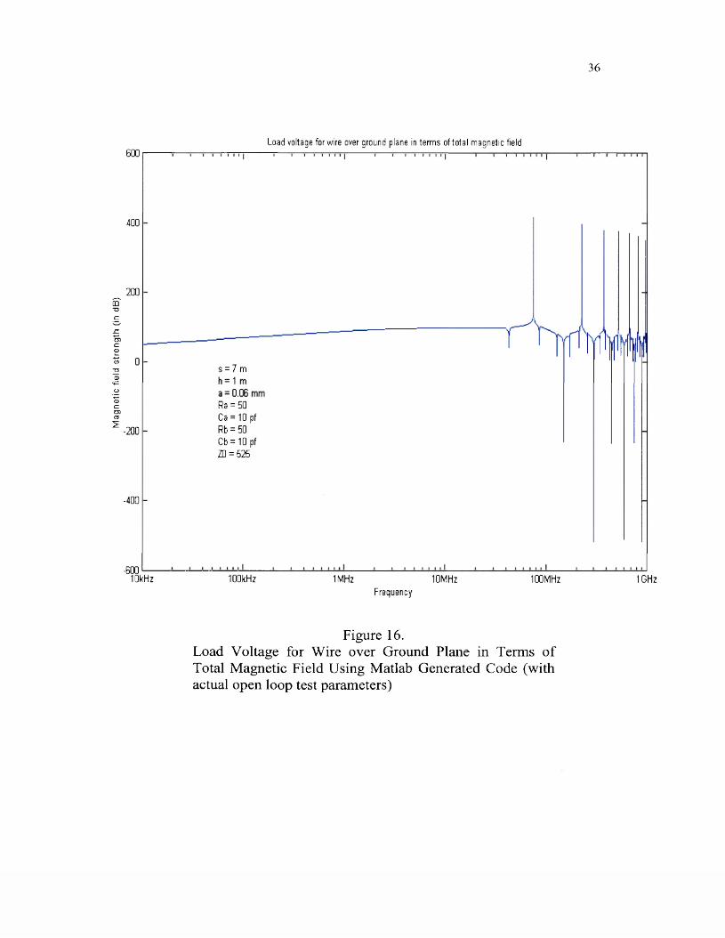
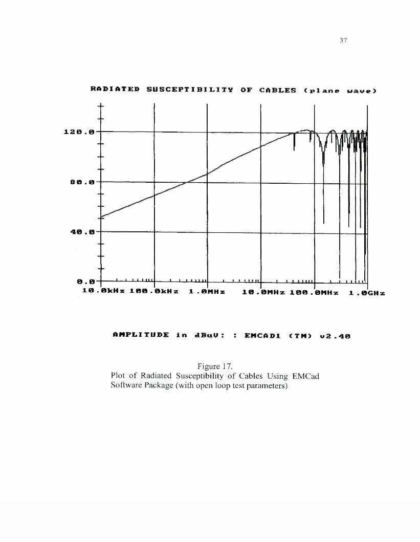
resistance from 100,000 Q to 50 Q. Figure 16 and Figure 17 show the output of
the Matlab code and the EMCad software package using these test
parameters, respectively. On both figures, the first minimum in the plot appears
at approximately 40 MHz. The EMCad software output does not have the sharp
upward peaks that have previously appeared in both Smith's and Matlab's outputs.
This further supports our earlier decision to find a more powerful software tool, o f
which we chose Matlab.
Since we were looking for a way to characterize the variations in the
output of the model using different parameters, we started changing the
parameters individually to see the effects o f the various parameters. After
plotting numerous variations of the parameters, we discovered that varying the
line length and/or the height of the wire over the ground plane were the two
parameters that most affected the outputs. Figure 18 and Figure 19 show several
Mag
neti
c fie
ld
stre
ngth
(in
dB
)
36
Load voltage for wire over ground plane in terms of total m agnetic field600
400
200
s = 7 m
Ra = 50 Ca = 10 pf Rb = 50 Cb = 10 pf ZD = 525
-200
-400
-6 0 0 1— 10kHz 100kHz 10MHz1MHz 100MHz 1GHz
Frequency
Figure 16.Load Voltage for Wire over Ground Plane in Terms of Total Magnetic Field Using Matlab Generated Code (with actual open loop test parameters)
37
R A D I A T E D S U S C E P T I B I L I T Y OF C A B L E S ( p l a n e w a v e >
1 2 0 . O
80 . O
0 . 0 ------------- 1— i— i . i m i ----------- 1— i— i. 1 . 1 1 1 1 l
10.0kHz 100.0kHz 1.0MHz lO.ONHz lOO.OHHz 1.0GHz
A M P L I T U D E in d B u U : E H C A D 1 (TM) v 2 .40
Figure 17.Plot of Radiated Susceptibility o f Cables Using EMCad Software Package (with open loop test parameters)

38
different values for each of the parameters. These two cases were analyzed in
closer detail to determine the effect produced by varying the parameters. We
observed many different factors including the distance between peaks, the
amplitude of the peaks, whether the peaks were up or down, etc. Once we did
this, we deemed the model we had chosen too simple for the complexity o f our
work. At this point, we ventured forward to analyzing the open loop test data.
In order to compare the output of our EM model to the test data, we have
explored thousands of reduced representations o f the data to look for
characteristic trends in the behavior o f the model that correlate with trends in the
features of the
test data. The following, Figure 20 through Figure 25, represent some o f the
different ways the test data has been looked at.
In the following six figures there is one signal represented, this signal is
"hdof' which is the rate of climb/descent. This signal was chosen arbitrarily, but
is a good representation for all of the signals. For a list o f the signals collected
and their description, see Appendix B.
This analysis began with collecting the increasing field strengths,
sequentially, for one frequency (450 MHz in this particular case) into one large
file. This was done so we could manipulate the test data in different ways to see
if there were any trends that became apparent. Figure 20 is a plot o f the larger
file. There were three reference voltages sent for each field strength and this is
what causes the step-like appearance in the plot. As the field strength increases,

Mag
neti
c fie
ld st
reng
th
(in dB
)
39
Load voltage for wire over ground plane in terms of total magnetic field magenta: 1m, red: 2m, black: 3m, blue: 4m, green: 5m
500
s = 1 0 m , a = 0.06 mm, Ra = $0 Ca = 0.102 pf, Rb = 50, Cb = 0.102 pf
-500
-1000 —
150MHz5 0 0 1----
450MHz 550MHz 650MHz250MHz 350MHz
-500
-1000 -----150MHz5 0 0 1----
650MHz250MHz 350MHz 450MHz 550MHz
-500
-1000 -----150MHz50 0 ,----
650MHz250MHz 350MHz 450MHz 550MHz
-500
-1000 -----150MHz50 0 ,----
550MHz 650MHz250MHz 350MHz 450MHz
-500
-1000 -----150MHz 550MHz 650MHz250MHz 350MHz 450MHz
Frequency
Figure 18Varying height of wire over ground plane. The subplots represent increasing the height. As the height over the ground plane was increased, the plots took on different shapes. There were new peaks introduced throughout each plot.

Mag
neti
c fie
ld
stre
ngth
(in
dB)
40
Load voltage for wire over ground plane in terms of total magnetic field magenta: 1.5m, red: 2.5m , black: 3.5m, blue: 4.5m, green: 6.5m
200
h = 0.1 m. a = 0.06 mm Ra = 50 Ca = 0.102 pf, Rb = 5, Cb = 0.102 pf-200
-400 ----150MHz 250MHz 350MHz 450MHz 550MHz 650MHz
150MHz 200
250MHz 350MHz 450MHz 550MHz
150MHz 250MHz 350MHz 450MHz 550MHz
650MHz
650MHz200
-200
-400 ----150MHz 250MHz 350MHz 450MHz 550MHz 650MHz
150MHz 250MHz 350MHz 450MHzFrequency
550MHz 650MHz
Figure 19Varying line length. The subplots represent increasing the line length. By increasing the line length, the plots changed. The position o f the peaks changed and new peaks were introduced.

41
the bounds o f the voltage values collected deviate further from that of the
reference voltage sent. Figure 21 shows three subplots, one for each reference
voltage sent. In this figure, all o f the processors are represented in each subplot
with black representing the reference voltage sent, blue represents processor one
(filter removed), red is processor two, green is processor three, and magenta is
processor four.
The plots become very busy which makes it difficult to depict what is
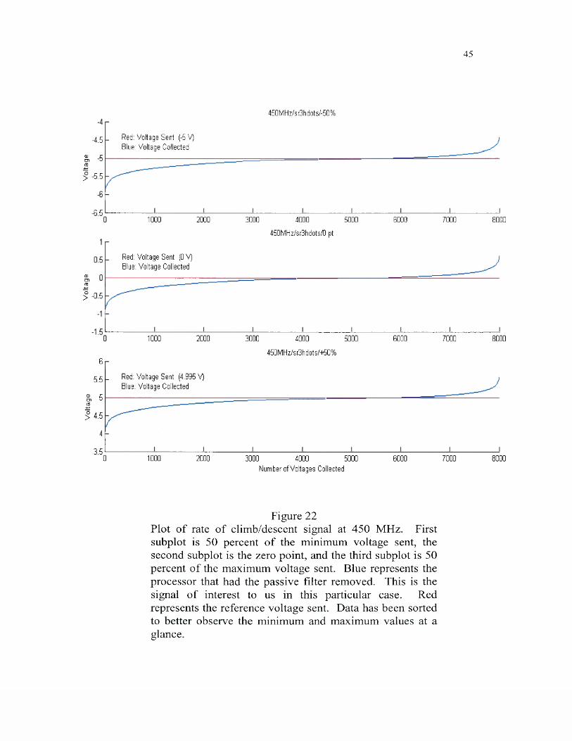
actually happening. Therefore, in Figure 22 only processor one is plotted since it
is the one with the passive filter removed and the one of interest.
In all three subplots it appears that the majority o f the voltages collected,
represented in blue, were lower than the reference voltage sent, represented in red.
This figure is only representative of the 100 v/m field strength.
Since none of these figures seem to show any trend that was detected in
the EM model, we plotted the test data by field strengths. Figure 23 has eight
subplots, one for each field strength that was collected at 450 MHz. All of these
subplots are representative o f fifty percent o f the minimum voltage sent, which
was chosen arbitrarily. In Figure 23, as the field strength increases, the data
values collected deviate further from the reference voltage value. However, in the
bottom subplot, the voltages collected do not look as if they are deviating as
much. This is due to the fact that Matlab automatically generates the y-axis
which varies slightly for these eight subplots. Figure 24 represents the same data
as Figure 23 with all eight subplots scaled to the same y-axis.

42
Figure 25 has sixteen subplots. The eight subplots in the left-hand column
are the same as in Figure 24 and the eight subplots in the right-hand column
represent the same data with the values sorted. These subplots are used to show
how the test data differs from the reference voltage sent.
As seen in Figure 20 through Figure 25, there appears to be no correlation
between the simulation model created previously, Figure 16, and the open loop
test data so we had to come up with another approach to analyzing the data. At
this time we decided to perform a systematic statistical analysis on the data in
order to uncover trends in the data that could be compared to the Matlab results.

Vo
ltag
e
43
450M H z/sr3hdo ts
550v/m 600v/m100v/m 200v/m 300v/m 400v/m 450v/m DuOv/m
1 1.5Number of V oltages Collected x 10
Figure 20Open loop test data for rate o f climb/descent at 450 MHz. The step-like features are created by the increasing field strengths. As the field strength increases, the bounds o f the collected voltages deviate further from the sent voltage.

Vol
tage
V
olta
ge
Vo
ltag
e
44
450 M H z/s r3 h d ot s/-50 %
black: reference sentblue: P1 (no filter)red: P2, green: P3, magenta: P4
-4.5
■5.5
■6.55000 6000 7000 80001000 2000 3000 4000
450M Hz/sr3hdots/0 pt
black: reference sentblue: P1 (no filter)red: P2, green: P3, magenta: P4
•0.5
80004000450M H z /s r3 h d ot s/+50 %
5000 6000 70001000 2000 3000
6black: reference sentblue: P1 (no filter)red: P2, green: P3, magenta: P4
5.5
5
4.5
4
3.56000 7000 80001000 2000 3000 4000 50000
Number of Voltages Collected
Figure 21Plot of rate of climb/descent signal at 450 MHz. First subplot is 50 percent o f the minimum voltage sent, the second subplot is the zero point, and the third subplot is 50 percent o f the maximum voltage sent. Blue represents the processor that had the passive filter removed. This is the signal o f interest to us in this particular case. Black represents the reference voltage sent. Red, green, and magenta represent the processors that still have the passive filters on. Data has been sorted to better observe the minimum and maximum values at a glance.
Vol
tage
V
olta
ge
Vo
ltag
e
45
450MHz/sr3hdots/-50%
Red: Voltage Sent (-5 V) Blue: Voltage Collected
-4.5
•5.5
•6.51000 2000 3000 4000
450MHz/sr3hdotsyO pt5000 6000 7000 8000
Red: Voltage Sent (OV) Blue: Voltage Collected
•0.5
1000 2000 3000 4000450MHz/sr3hdots/+50%
5000 6000 7000 8000
6
Red: Voltage Sent (4.995 V) Blue: Voltage Collected
5.5
5
4.5
4
3.5 0 1000 2000 3000 4000 5000 6000 7000 8000Number of Voltages Collected
Figure 22Plot of rate o f climb/descent signal at 450 MHz. First subplot is 50 percent o f the minimum voltage sent, the second subplot is the zero point, and the third subplot is 50 percent of the maximum voltage sent. Blue represents the processor that had the passive filter removed. This is the signal of interest to us in this particular case. Red represents the reference voltage sent. Data has been sorted to better observe the minimum and maximum values at a glance.

400v
/m
300v
/m
200v
/m
100v
/m
46
450 M H z /s r3 h d ot s/-50 %Unsorted Data
-4.5
100 200 300 400 500 600 700 900 1000
_____ I_______I_______I_______I_______I_______I_______I_______I_______I_____•0 100 200 300 400 500 600 700 800 900
— r~ 1000
-5.5 100 200 300 400 500 600 700 800 900 1000
100 200 300 400 500 600 700 900 1000
100 200 300 400 500 600 700 800 900 1000
100 200 300 — r~ 400 500 600 700 800 900 1000
100 200 300 400 500 600 700 800 900 1000
100 200 300 400 500 600Number ofV oltages Collected
700 900 1000
Figure 23Plot of rate of climb/descent signal at 450 MHz. Each of the eight subplots represent different field strengths, they are in ascending order. Matlab automatically generates the y-axis so it may differ for each subplot. As the field strength increases, the signal begins to deviate further from the reference voltage sent.

600v
/m
550v
/m
500v
/m
450v
/m
400v
/m
300v
/m
200v
/m
100v
/m
47
450MHz/sr3hdots/-50%Unsorted Data
0_ _ _ _ _ _ _ 100 200 300 400 500 600 700 800 900 1000
100 200 300 400 500 600 700
J_ _ _ _ _ _ _ _ I_ _ _ _ _ _ _ _ I_ _ _ _ _ _ _ _ L100 200 300 400 500 600 700 800 900 1000
- - - - - - - - - - 1- - - - - - - - - - - - - 1- - - - - - - - - - - - - 1- - - - - - - - - - - - - 1- - - - - - - - - - - - - T -- - - - - - - - - - 1- - - - - - - - - - - - - 1- - - - - - - - - - - - - 1- - - - - - - - - - - - - 1- - - - - - - - - - - - -
0 100 200 300 400 500 600 700 800 900 1000 1 1 1 1 1 1 1 1----------
______ i______ 1______ i______ i_______i____ :__i______ i______ i______ i__:____0 100 200 300 400 500 600 700 800 900 1000------------- 1------------- 1------------- 1------------- r~--------- ^ ----------- 1------------- 1------------- 1------------- 1-------------
_4 0 100 200 300 400 500 600 700 800 900"i----------------r
_4 0 100 200 300 400 500 600 700 800 900 1000
100 200 300 400 500 600 700 800 900 1000Number ofVoltages Collected
Figure 24Plot of rate of climb/descent signal at 450 MHz. Each of the eight subplots represent different field strengths, they are in ascending order. Matlab automatically generates the y-axis, but in this plot, the y-axis has been scaled to be the same for each subplot. As the field strength increases, the signal begins to deviate further from the reference voltage sent.

600v
/m
550v
/m
500v
/m
450v
/m
400v
/m
300v
/m
200v
/m
100v
/m
48
450M H z/s r3 h d ot s/-50 %Unsorted Data
200 400 600 800 1000
* —isA* v .-.yrr***
-4 0 200 400 600 800 1000
_1_ _ _ _ _ _ _ _ _ _ _ _ _ _ _ _ L_ _1________________ L_
,0 200 400 600 800 1000-4 ------- 1------- 1------- 1------- 1-------
0 200 400 8QQ 1000
J ________________ L_
.0 200 400 800 moo
J ________________ L
200 400 moo moo
m 200 400 600 800 1000
0 200 400 600 800 1000
450MHz/sr3hdots/-50%Sorted Data
200 400 600 800 1000
600 800 1000
600 800 000
200 400 600 800 1000
200 400 600 800 1000
200 400 600 800 1000
200 400 600 800 1000
200 400 600 800 1000
Figure 25Plot o f rate o f climb/descent signal at 450 MHz. Each of the eight rows o f subplots represent different field strengths, they are in ascending order. Matlab automatically generates the y-axis so they may differ for each subplot. As the field strength increases, the signal begins to vary more from the reference voltage sent. The left column represents the unsorted data while the right column represents the data after being sorted.
100v/m
200v/m
300v/m
400v/m
450v/m
SDOv/m
550v/m
600v/m

CHAPTER IV
STATISTICAL MODELING OF OPEN LOOP EXPERIMENT DATA
In order to compare our simulation output to the open loop test data, a
reduced representation for the latter was required as well. Therefore, the first
thing we did was to plot the data for all frequency/field strength combinations.
Figure 26 shows a typical plot o f the test data for an arbitrarily chosen signal.
Each subplot represents a different set o f data for the signal. The columns depict
the reference voltage sent while the rows are the increasing field strengths. The
first column o f subplots represents fifty percent of the minimum voltage sent, the
second column represents the zero point, and the third column represents fifty
percent o f the maximum voltage. For comparison sake, all column axes have the
same values.
The first row shows the three reference voltage levels at one field strength.
Each subsequent row shows an increasing field strength at the same voltage level
as that above it. As the field strength increases, the plots tend to flatten out and
the data begins to spread over a broader voltage range. This trend appears in all
o f the test data examined.
49

# of
occ
ura
nce
s
5 0
-50% ref
300
| 200 LO
100
0-0.365-0.36-0.355-0.35-0.345-0.34
-0.365-0.36-0.355-0.35-0.345-0.34
250MHz/spl (P1)0 ref 450% ref
h li 400I
400\
, 200200
—1----- 1----- 1— Zj---- i----- 1----- n CD
S
. , . J. 1- 0.02 -0.01
300
200
100
0-0.365-0.36-0.355-0.35-0.345-0.34
300
n 200
100
0-0.365-0.36-0.355-0.35-0.345-0.34
0.01
400
200
0 L-0.02 -0.01 0 0.01
400
200
0- 0.02 -0.01 0 0.01
- 0.02 -0.01 0 0.01
Voltage
0.33 0.335 0.34 0.345 0 .350 .355
400
200
0.33 0.335 0.34 0.345 0 .350 .355
400
200
0.33 0.335 0.34 0.345 0 .350 .355
400300
C 400o 200 o 200CM 200100
0 -̂--1 •> o0.33 0.335 0.34 0.345 0.35 0.355
Figure 26.Subplot of open loop test data. The columns represent the reference voltage sent while the rows represent the (increasing) field strengths. All column axes have the same values for ease o f comparison. As the field strength increases, the data spreads over a broader range.

51
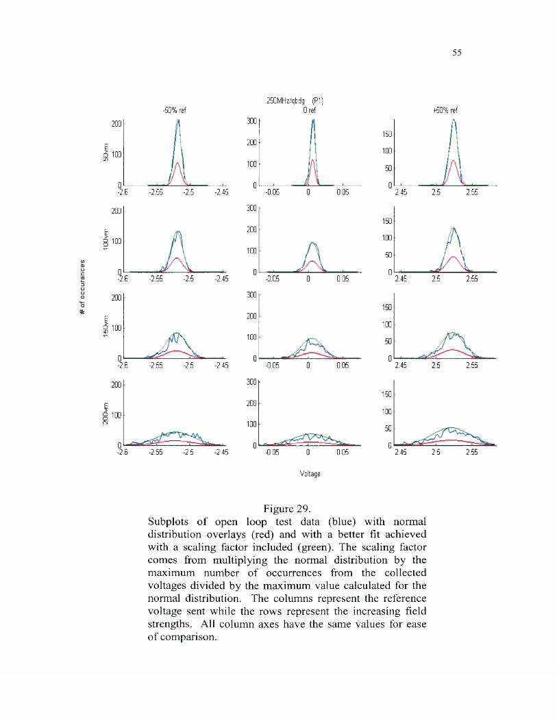
Because the data had no well-defined shape, we decided to fit distribution
curves to it. The distributions that we fit to the data include the Uniform, Normal,
Weibull, Rayleigh, Beta, Gamma, Exponential, and Pareto distributions [18, 19].
The distributions fit to the data, along with their associated probability density
functions, are shown in Table 5. The curve that appeared to best fit the data
overall was produced by the normal distribution and therefore from this point
forward our work will concentrate on the normal distribution. The equation used
to find the normal distribution, as defined in Table 5, has x as the voltage value, p
the mean o f the data, and a the variance o f the data.
Figure 27 shows the same data as Figure 26 with the normal distribution
curve (red) overlaying the data values (blue). For this particular signal, the
normal distribution has a good fit. There were some signals in which the normal
distribution did not fit the data as well, see Figure 28. However, the normal
distribution visually appeared to be the best fit o f the distributions tried. Upon
studying the patterns o f the data with the distribution overlay curves, it became
apparent that there was a scaling factor needed in some cases. Figure 29 shows a
plot with the original test data (blue), the normal distribution curve (red), and the
normal distribution curve with a scaling factor incorporated (green). The scaling
factor that was used came from multiplying the normal distribution by the
maximum number o f occurrences from the collected voltages divided by the
maximum value calculated for the normal distribution. This new curve fits the
data much better and will be used in further analysis.

52
Table 5.Distributions used to fit the open loop experiment data, along with their probability density functions.
D istribution Probability density function
Uniformf(x 1 ,
— « d A \ U.b - a0 , elsewhere
Normalf(x
J -(x-n)2
= --- e 2a~ , — GC < X < g o ;
V27ia— oo < x < oo, CT > 0
Weibullf(x _ _^Lx a-le ^ , x > 0 ; a, 9 > 0
e a0 , elsewhere
Rayleighf(x x M= — ev x > 0
a
Betaf(x = - f e - - 7-^ x ° - ' ( l - x r , 0 < x < l ; a , P > 0 r(a)r(p)
0 , elsewhere
Gamma r ( r = x r_1e_xdx, r > 0
Exponentialf(x
1 —= —e x , x > 0 , 0 > 0
X0 , elsewhere
Paretof(x
q= -------—— 0 < x < q o , 0 < 9 < oo
( i + * r

# of
occ
ura
nce
s
5 3
-50% ref
300
> 2 0 0
100
-0.365-0.36-0.355-0.35-0.345-0.34
300
200
100
0-0.365-0.36-0.355-0.35-0.345-0.34
300
I 200o
100
-0.365-0.36-0.355-0.35-0.345-0.34
300
□ 200
100
-0.365-0.36-0.355-0.35-0.345-0.34
250MHz/spl (P1)Oref
0 0.01
400
200
0 L-0.02 -0.01 0 0.01
- 0.02 -0.01 0 0.01
■+50% ref
0.33 0.335 0.34 0.345 0.35 0.355
400
200
0.33 0.335 0.34 0.345 0.35 0.355
0.33 0.335 0.340.345 0.35 0.355
400
400
200200
. 0 ________ 0-0.02 -0.01 0 0.01
Voltage
0.33 0.335 0.34 0.345 0.35 0.355
Figure 27.Subplots o f open loop test data (blue) with good representation of normal distribution overlays (red). The columns represent the reference voltage sent while the rows represent the increasing field strengths. All column axes have the same values for ease of comparison.

# of
occ
ura
nce
s
5 4
200
Eo 100
0-2.6
200
g 100fN
-50% ref250MHz/qbdg (P1)
Oref
-2.55
0 ^ ^-2.6 -2.55
-2.5 -2.45
300
200
100
0-0.05
300
200
100
-2.5 -2.450 L ^
-0.05
0.05
300200
200
S 100100
-2.55 -2.5 -2.45 -0.05 0.05
300200
200
S 100100
-2.6 -2.55 -2.5 -2.45 -0.05 0.05
0 0.05
Voltage
150
100
50
0
+50% ref
150
100
2.45 2.55
150
2.45 2.55
100
2.552.45
Figure 28.Subplots of open loop test data (blue) with poor representation of normal distribution overlays (red). However, the normal distribution seems to be a good fit if it had higher amplitude. The columns represent the reference voltage sent while the rows represent the increasing field strengths. All column axes have the same values for ease o f comparison.
200v
m
1S0v
m
lOO
vrn
50vm
200
100
-2.6
-50% ref250MHz/qbdg (P1)
Oref
-2.55 -2.5 -2.45
300
200
100
0-0.05 0.05
300200
200
100100
-2.6 -2.55 -2.5 -2.45 -0.05 0.05
300200
200
100100
-2.6 -2.55 -2.5 -2.45 -0.05 0.05
300200
200
100100
-2.55-2.6 0.05-2.5 -2.45 -0.05
150
100
50
02.45
150
100
50
02.45
+50% ref
150
100
2.45 2.55
\
2.5 2.55
100
2.552.45
2.5 2.55
Voltage
Figure 29.Subplots o f open loop test data (blue) with normal distribution overlays (red) and with a better fit achieved with a scaling factor included (green). The scaling factor comes from multiplying the normal distribution by the maximum number of occurrences from the collected voltages divided by the maximum value calculated for the normal distribution. The columns represent the reference voltage sent while the rows represent the increasing field strengths. All column axes have the same values for ease o f comparison.

56
At this point we have met the first goal of the thesis which was to develop
and validate a mathematical model of the electromagnetic fields coupling into our
equipment. The model we will now use is defined as:
' -(x-f*)2 '
f(x)a 1
VTtict2 a ‘ (Eq. 3)
where
a = maximum number o f occurrences from the collected voltages (3 = maximum value previously calculated for the normal distribution x = collected voltages p = mean o f collected voltages a = standard deviation o f collected voltages
We will now focus on the second goal o f the thesis which is to use the
model to extrapolate/predict measurements that are outside of the data we have.
The first effort of this statistical analysis involved finding the least square error
(LSE) using the equation:
L = Z [y i - p ( x i ) ] 2 (Eq. 4 )i=l
where y is the test data and p(x) is the calculated normal distribution value [18].
The method of least squares chooses solutions with coefficients that
minimize the sum of the squares of the vertical distances from the data points,
which are presumed to be polynomial [18]. The best fit polynomial is the one
with coefficients that minimize the function L. Figure 30 shows a representative
plot where the least square error was calculated for each field strength and

57
reference voltage for one particular frequency and signal. The text in the
individual subplots indicates which set of parameters best fit the curve, as
described in Table 6 . Some data have better LSE estimates than others do, while
the one that is represented in the subplots is the best (lowest value) fit o f the least
square error combinations that were tried.
There were numerous LSE parameters to look at. Many different means
and variances were calculated and compared to find the lowest value o f the LSE.
The LSE that is displayed in the subplots is the value that was then used to find
"new" parameters for some extrapolation techniques to be applied to the test data.
Table 6 describes the mean and variance combinations used to test different LSEs.
The first column is the least squares numbering scheme where 'x' represents
which reference voltage was used and ’#' is a number from 0 to 15.
Once the LSE with the lowest value was determined, the mean and
variance that supported that LSE were saved to two different four-dimensional
matrices (field strength x reference voltage x signal x frequency) using Matlab
code. Using these new parameters we plotted the values for all o f the field
strengths for one frequency and signal to graphs. Figure 31 shows a typical graph
o f the new parameters. The top subplot represents the variances collected using
the LSE method. Since all of the reference voltages have similar variances, this is
a good indicator that our analysis was done properly. The bottom subplot
represents the means collected. This particular signal had minimal fluctuation in

# of
occ
ura
nce
s
58
-50% ref200
I 100in
L10
-0.59 -0.58 -0.57 -0.56 -0.55
200
S 100 L14
-0.59 -0.58 -0.57 -0.56 -0.55
200
£o 100 L14
I— I______ L
200
| 100CN
-0.59 -0.58 -0.57 -0.56 -0.55
L14
-0.59 -0.58 -0.57 -0.56 -0.55
250MHz/tas (P1)Oref
300
200
100
0 _i I_
-0.03 -0.02 -0.01 0 0.01
300
200 L24
100
-0.03 -0.02 -0.01 0.01
300
200
100
0
300
200
100
0
L24
- J _ _ _ _ _ _ _ _ _ _ L
-0.03 -0.02 -0.01 0 0.01
L24
-0.03 -0.02 -0.01 0 0.01
Voltage
+50% ref
150
100
150
100
50
00.53 0.54 0.55 0.56 0.57
150
100
150
100
50
00.53 0.54 0.55 0.56 0.57
Figure 30.Subplots of Open Loop Test Data with Least Square Error Overlays. The least square error was calculated for each field strength and reference voltage. The text within the subplot indicates which set of parameters best fit the curve. The columns represent the reference voltage sent while the rows represent the (increasing) field strengths. All column axes have the same values for ease o f comparison.

59
Table 6
Mean and variance combinations used to determine the least square error value with the lowest value, the best fit. The least square error is represented by the reference voltage (x) and the mean/variance combination used (#).
Lx# M ean V ariance
0 mean o f matrix variance of matrix1 mean o f matrix sample variance
2 mean o f matrix variance of non-repeated matrix
3 midpoint o f matrix variance of matrix4 midpoint o f matrix sample variance
5 midpoint o f matrix variance of non-repeated matrix
6 midpoint o f sorted, non-repeated matrix
variance of matrix
7 midpoint o f sorted, non-repeated matrix
sample variance
8 midpoint o f sorted, non-repeated matrix
variance of non-repeated matrix
9 mean o f non-repeated matrix variance of matrix
1 0 mean o f non-repeated matrix sample variance
1 1 mean o f non-repeated matrix variance of non-repeated matrix
1 2 voltage with most occurrences variance of matrix
13 voltage with most occurrences sample variance
14 voltage with most occurrences variance of non-repeated matrix
15 *amp factor maximum voltage variance of non-repeated values

Var
ian
ce
60
sr4hdots@650 MHz blue:-50%, red:0, green:+50%
0.012
0.01
0.008
0.006
0.004
0.002
00 700 800 900 1000100 200 300 400 500 600
Field Strength
-B B- -B □
v v v---------v— v— v— ¥— V_ J ____________ I____________ I____________ I____________ I____________ I____________ I____________ I____________ I____________ I100 200 300 400 500 600 700 800 900 1000
Field Strength
Figure 31.New mean and variance parameters generated from the least square error value. All three reference voltages for each field strength are represented in each subplot. Blue is 50% o f the minimum voltage, red is the zero point, and green is 50% o f the maximum voltage. The top subplot represents the variances generated from the LSE method and the bottom subplot represents the means generated from the LSE method.

61
the means collected. All of the graphs produced where then studied to determine
what direction to take for further analysis.
The means found from the least square method seemed to vary only
slightly for most o f the signals so we first concentrated on how to extrapolate the
variance. At first, we tried extrapolating data by hand from the new parameters
found from the LSE. This involved plotting the data and then using a pencil and
ruler to project the curve. The variances of the field strengths were plotted on a
'jscale automatically generated by Matlab, which was usually on a factor o f 10' or
greater, and on a 0 to 1 scale. Both of these techniques produced the same eight
signals as having the most noticeable movement. This hand plotting technique
was tedious and became unwieldy after a few attempts. The next step was to find
an automated computer tool that would find the extrapolated values for us. Upon
looking further in Matlab's capabilities, a tool was found that was semi
automated. It involved plotting the variances found when generating the least
square errors and using a window-driven menu to extrapolate the values to the
predetermined level o f lOOOv/m. The values we wanted to extrapolate depended
on the frequency that was being examined as shown in Table 7. The variances
were extrapolated using the "Basic Fitting Interface" [20] and the means were
produced by the "Data Statistics Tool" [21] provided in Matlab.
The basic fitting interface allows the data to be fit using an interpolant or a
polynomial (up to degree 10). It allowed us to plot multiple fits simultaneously so
that we could compare them for the given data set. It also let us examine the

62
numerical residual o f a fit, to evaluate the fit, and to save the evaluated results to a
Matlab variable. The results o f the numerous basic fitting interface computations
were usually cubic in nature, but there were several that were linear or quadratic.
The best fit was determined by examining the numeric value o f the norm o f the
residuals and the residual plots. The fit residuals are defined as the difference
between the ordinate data point and the resulting fit for each abscissa
Table 7Field strengths extrapolated at each frequency.
Frequency (MHz) Extrapolated Field Strengths (v/m)
250 300, 400, 500, 600, 700, 800, 900, 1000
350 300, 400, 500, 600, 700, 800, 900, 1000
450 650, 700, 750, 800, 850, 900, 950, 1000
550 650, 700, 750, 800, 850, 900, 950, 1000
650 650, 700, 750, 800, 850, 900, 950, 1000
750 650, 700, 750, 800, 850, 900, 950, 1000
850 650, 700, 750, 800, 850, 900, 950, 1000
950 650, 700, 750, 800, 850, 900, 950, 1000

63
data point [20]. The norm of the residuals is a measure of the goodness of fit,
where a smaller value indicates a better fit than a larger value. During this
analysis, several o f the fits had negative values when extrapolated and it was
necessary to return to the basic fitting interface and consider a different fit. Once
the best fit was determined, the fit was extrapolated (using the values found in
Table 7) by using the basic fitting interface tool. These data values were then
saved as variables in the Matlab workspace and were used for further analysis.
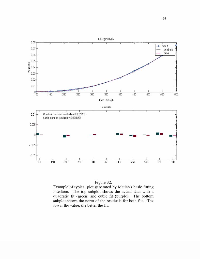
Figure 32 shows an example o f a typical result from the basic fitting
interface tool. The top subplot shows the test data, a quadratic fit, and a cubic fit.
Matlab automatically color codes the graphs and the legends for ease o f analysis.
The two fits are very close and must have another step introduced in order to find
the best fit. Using the basic fitting interface tool, we can expand the analysis to
include the residuals, this is represented in the bottom subplot of Figure 32. This
subplot shows a plot o f the residuals with the value of the norm o f the residuals.
As stated before, the lower the value o f the norm of the residual, the better the fit.
Therefore, in this case, because the norm of the residual for the cubic fit was
lower than that o f the quadratic fit, the cubic fit was used to extrapolate the values
o f the variance.
Var
ian
ce
64
hdot@ 450 MHz0.08
data 1 quadratic cubic
0.07
0.06
0.05
0.04
0.03
0.02
0.01
100 150 200 250 300 350 400 450 500 550 600
Field Strength
residuals
0.01
0.005
0
-0.005
-0.01
100 150 200 250 300 350 400 450 500 550 600
i i rQuadratic: norm of residuals = 0 .0023252 Cubic: norm of residuals = 0.0018201
Figure 32.Example o f typical plot generated by Matlab's basic fitting interface. The top subplot shows the actual data with a quadratic fit (green) and cubic fit (purple). The bottom subplot shows the norm of the residuals for both fits. The lower the value, the better the fit.

65
Figure 33 shows the extrapolated values in the top subplot. The '+' marks
show the previously calculated variances using the least square error technique,
while the 'O' marks show the values that were extrapolated using the basic fitting
interface tool. These values were calculated with the tool and then stored in a
Matlab variable for use later in the analysis.
The means were computed using the "Data Statistics Tool" in Matlab.
This involved using the window-driven tool and saving the results to a Matlab
workspace variable. Figure 34 shows a plot with the mean and median o f the test
data plotted. Again, the figures in Matlab are color coded so that we could see the
results much easier. The upper dotted line (red) in the figure represents the
median while the lower dotted line (green) is the mean. In most cases, the median
seemed to represent the test data better and was used for the mean value in further
analyses.
Once all o f the data (variances and means) had been saved to the Matlab
workspace, we could use our developed mathematical model to plot the normal
distribution using these extrapolated values. Figure 35 shows plots o f the normal
distribution using the extrapolated values for the mean and variance. These plots
follow the same trend that was mentioned before, as the field strength increases,
the data becomes flatter and spreads out over a broader voltage range.
This data has been examined and we have determined that we can increase
the field strength up to 1000 v/m without damaging the equipment. Therefore, at
this point we have accomplished the objectives of this thesis.

Var
ian
ce
66
hdot@ 450 MHz
data 0cubic0.25
0.15
0.05
100 200 1000300 400 500 600 700 800 900Field Strength
residuals
0.01Cubic: norm of residuals = 0.0018201
0.005
-0.005
- 0.01550 600100 150 400 450 500200 250 300 350
Figure 33.Example of typical plot o f extrapolated variances using Matlab's basic fitting interface. The top subplot is the extrapolated variances while the bottom subplot shows the norm o f the residual.
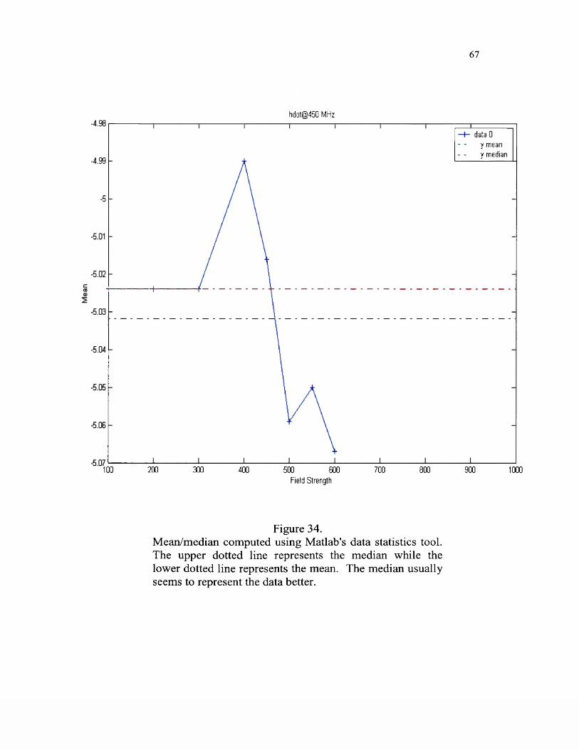
hdot@ 450 MHz
data 0 y mean y median
100 200 900 1000300 400 500 600 700 800Field Strength
Figure 34.Mean/median computed using Matlab’s data statistics tool. The upper dotted line represents the median while the lower dotted line represents the mean. The median usually seems to represent the data better.
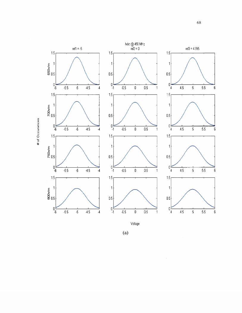
# of
Occ
ura
nce
s
68
refl = -51.5
0.5
0-6 -5.5 -5 -4.5 ■4
-5.5 -4.5
1.5
-5.5 -4.5
1.5
0.5
0-6 -5.5 ■5 -4.5 •4
hdot @ 450 MHzref2 = 0 ref3 = 4.995
-0.5
1.5 1.5T
0.5
04.5 5 5.5 6-0.5 4
1.5
0.5
05.5 654 4.5
1.5
0.5
0-0.5 0 0.5
1.5
0.5
05 5.5 64 4.5
1.5
0.5
0-0.5 0 0.5
Voltage
(a)
# of
Occ
ura
nce
s
6 9
hdot @ 450 MHzrefl = -5 ref2 = 0 refi = 4.995
1.5
0•6 ■5.5 ■5 -4.5 ■4
1.5
0.5
0-0.5 0 0.5
1.5
0.5
04.5 5 5.54 6
1.5
0.5
0-6 -5.5 ■5 -4.5 ■4
1.5
0.5
04.5 5 5.5 64
1.5
0.5
0-0.5 0 0.5
1.5
m 0.5
0-6 -5.5 ■5 -4.5 ■4
1.5
0.5
04.5 5 5.5 64
1.5
0.5
0•1 -0.5 0 0.5
1.5
Eo□° 0.5
0-6 -5.5 ■5 -4.5 ■4
1.5
0.5
0-0.5 0 0.5
Voltage
1.5
0.5
04 4.5 5 5.5 6
(b)
Figure 35Subplots o f normal distribution using the extrapolated variance and mean for the frequency and field strength represented. The columns represent the reference voltage sent while the rows represent the (increasing) field strengths. All column axes have the same values for ease o f comparison, (a) 650, 700, 750, 800 v/m (b) 850, 900, 950, 1000 v/m.

CHAPTER V
CONCLUSIONS
To perform numerical simulations on the open loop experiment data, we
purchased the EMCad software package from CKC Laboratories. This software
package represents industry's first electromagnetic compatibility computer
program for compliance assessment. However, after evaluation of the software,
we determined that the software did not allow us to manipulate the data as
expected. At this point we implemented the appropriate models from [3] using
Matlab, a high-performance language for technical computing, to meet our
particular needs.
After comparison o f numerous simulated outputs, we decided that there
was no particular advantage to the simulation so we started analyzing the open
loop test data. Upon comparing numerous reduced representations of the data to
our EM model, we concluded that there was no obvious correlation between the
data and the simulation outputs. At this point, we deemed the EM model we had
chosen too simple for the complexity o f our test data. Therefore, our next effort
was to perform a systematic statistical analysis on the data in order to uncover
trends in the data that could be compared to the Matlab results.

71
We plotted thousands of representations of the open loop data for
comparison. We discovered a trend in the data that warranted fitting distribution
curves to the data. Because the data had no well-defined shape, we fit the
selected distribution curves to the data and found that the normal distribution had
the best overall fit. We determined that the normal distribution needed a scaling
factor and developed a mathematical model. Using the normal distribution as our
standard, we next calculated the least square error. The mean and variance that
supported the least square error with the lowest value were plotted for all field
strengths for one frequency and signal. These plots were used to extrapolate the
variances using the "Basic Fitting Interface" and the means using the "Data
Statistics Tool" provided in Matlab. The variables found using these tools were
saved to the Matlab workspace for use in further analysis.
Using the extrapolated values for the variances and means, we used the
developed mathematical model to plot the normal distribution for the field
strengths that had been extrapolated. These plots followed the same trend as the
test data: as the field strength increases, the amplitude o f the voltage tends to
flatten and the voltage range covers a broader region. Examining the extrapolated
plots led us to the conclusion that we can perform more tests and increase the
field strength to the predetermined field strength of 1 0 0 0 v/m without damaging
our equipment.
72
APPENDIX A
Reference voltages sent for each signal
Signal M in 0 Maxcas -4.7800 0 4.7750delac -5.0000 0 5.0000delec -5.0000 0 5.0000delrc -5.0000 0 5.0000deltc -5.0000 0 5.0000epr -4.6880 0 4.6830eta -4.3850 0 4.3800gamma -2.8810 0 2.8760gse -2.5000 0 2.4980hddot -2.5000 0 2.4980hdot -5.0000 0 4.9950phidg -5.0000 0 4.9950phidt -4.9950 0 4.9900psidt -4.4970 0 4.4920qbdg -2.5000 0 2.4980ralt -4.9900 0 0
rbdg -2.4950 0 2.4930spl -2.9100 0 2.9050spr -2.9100 0 2.9050tas -4.7800 0 4.7750tbax -0.9910 0 0.9890thrtrm -5.0000 0 4.9950tk -4.4970 0 4.4920vele -2.8710 0 2.8660vein -1.2500 0 1.2490vgs -2.5000 0 2.4980vgsdt -5.0000 0 4.9950ycg -1.2490 0 1.2480

73
APPENDIX B
Signal names and descriptions
FORTRAN B737 A utoland Sim ulator Variables (Partial List)
variable name descriptioncas calibrated airspeed in knotsdelac aileron command in degrees (+ right wing dowtdelec elevator command in degrees (+ nose down)delrc rudder command in degrees (+ yaw left)deltc throttle command in degrees (always +)epr engine pressure ratioeta localizer error in degrees (+ right)gamma flight path angle in degreesgse glide slope error in degrees (+ above beam)hddot vertical acceleration in fps2
hdot rate-of-climb/descent (+/-) in fpsphidg roll angle in degreesphidt roll rate, 1-axis in radians/secondpsidt yaw rate, 1-axis in radians/secondqbdg pitch rate, body axis in degrees/secondralt runway altitude in feetrbdg yaw rate, body axis in degrees/secondspl left spoiler in degrees (+ spoiler up)spr rt. spoiler in degrees (+ spoiler up)tas true airspeed in knotstbax is 1 . if auto stab is driving, else 0 .thrtrm trim throttle position in degreestk track angle in degreesvele east inertial velocity in fpsvein north inertial velocity in fpsvgs ground speed in fpsvgsdt ground acceleration in fps2
yes a/c y-position in ft (+ right of center line)

74
BIBLIOGRAPHY
1. NASA Facts, Dryden Flight Research Center, "F- 8 Digital Fly-By-Wire",http://www.dfrc.nasa.gov/EAO/FactSheets/F_8 DFBWFACTS.html, February 26, 2001 at 10:28 a.m.
2. Dryden Flight Research Center, "Digital Fly-By-Wire",http://www.dfrc.nasa.gov/Projects/f8 /home.html, February 26, 2001 at 10:29 a.m.
3. Albert A. Smith, Jr., Coupling of External Electromagnetic Fields toTransmission Lines, 2nd edition, Interference Control Technologies, Inc., 1989.
4. Gerald Fuller, "Understanding HIRF", Avionics Communications Inc., 1995.
5. Celeste M. Belcastro, "Detecting Upset in Fault Tolerant Control ComputersUsing Data Fusion Techniques", Dissertation submitted to Drexel University, December 1994.
6 . Celeste M. Belcastro, "Digital System Upset - The Effects of SimulatedLightning-Induced Transients on a General Purpose Microprocessor", NASA TM-84652, 1983.
7. Celeste M. Belcastro, "Data and Results o f a Laboratory Investigation ofMicroprocessor Upset Caused by Simulated Lightning-Induced Analog Transients", NASA TM-85821, 1984.
8 . Bruce T. Clough, "Microwave Induced Upset on a Digital Flight ControlComputer", Digital Avionics Systems Conference, Fort Worth, TX, 1993.
9. A Davidoff, M. Schmid, R. Trapp, G. Masson, "Monitors for Upset Detectionin Computer Systems", Proceedings of the International Aerospace and Ground Conference on Lightning and Static Electricity, Fort Worth, TX, 1983.
10. G. M. Masson, R. E. Glaser, "Intermittent/Transient Faults in DigitalSystems", NASA CR-169022, 1982.
11. R. J. Hanson, "Subsystem EMP Strength Verification Methods: UpsetDetection and Evaluation for Military Subsystems", WL-TR-89-19, August 1989.

75
12. FAA Advisory Circular 20-136, "Protection of Aircraft Electrical/ElectronicSystems against the Indirect Effects of Lightning", March 1990.
13. Laura J. Smith and Daniel M. Koppen, "Determination o f Upper DestructiveLimit for HIRF Experiments on a Fault Tolerant Flight Control Computer," 18th DASC Proceedings, October 1998.
14. Daniel M. Koppen, "Open Loop HIRF Experiments Performed on a FaultTolerant Flight Control Computer," AIAA/IEEE 16th DASC Proceedings, October 1997.
15. Reuben A. Williams, "The NASA High-Intensity Radiated FieldsLaboratory," AIAA/IEEE 16th DASC Proceedings, October 1997.
16. EMCad, CKC Laboratories, http://www.ckc.com, February 26, 2001at 10:33 a.m.
17. RTCA/DO-160D, "Environmental Conditions and Test Procedures forAirborne Equipment", Draft 8 (Final Draft), March 2000.
18. Richard J. Larsen and Morris L. Marx, An Introduction to MathematicalStatistics and Its Applications, 2nd edition, Prentice-Hall, 1986.
19. George C. Canavos, Applied Probability and Statistical Methods, Little,Brown and Company Limited, 1984.
20. MathWorks, Inc., "Using Matlab," Version 6 , The MathWorks, Inc., 2000.
21. MathWorks, Inc., "Using Matlab Graphics," Version 6 , The MathWorks, Inc.,2000 .

76
VITA
Laura Jean Smith
The author was bom in Cocoa-Rockledge, Florida on February 2, 1962.
She graduated from Parkway North Senior High School in St. Louis, Missouri in
June 1980. She received her Associate in Applied Science in Electronics from
Thomas Nelson Community College in August 1984 and received her Bachelor of
Science degree in Mathematics, with a minor in Physics, from Christopher
Newport University in May 1993. The author has been employed by NASA
Langley Research Center in Hampton, Virginia as a cooperative education student
from October 1983 to August 1984, as an apprentice student from August 1984 to
October 1987, as an electronics technician from October 1987 to July 1996, and
as an aerospace technologist from July 1996 to present. The author began taking
graduate courses at the College o f William and Mary in August 1994, and in July
1995 she was accepted as a graduate student in the Department of Mathematics at
the College o f William and Mary.
Copyright © 2022 FDOKUMEN