
Black carbon physical and optical properties across northern ...
Upload
khangminh22Category
view
3download
0
1
1.7 eV 3.1 eV
Positronemission tomographyDiffraction
Display Business
Communication
_

2
4. Optical Properties
A. Maxwell’s Equations and Light Propagation in Continuous Media
B. Classical Model of Materials Response
C. Quantum Phenomena: Absorption
D. Quantum Phenomena: Luminescence
The optical properties are essentially light-matter interactions – how the light interacts and exchanges
energies with matters. The main driving force is the electric field in the light that gives rise to the
motion of electron and ions inside the matter. Therefore, there are three key players in the optical
properties: light, electron, and ion (or to be more precise, ionic vibration). They can be treated
classically or quantum mechanically depending on how we deal with the energy quantization. We
will first start with the simple classical theory, and extend the theory to include quantum effects.
References)
Bube Chap. 8
Griffith “Electrodynamics”
Fox, “Optical properties of solids”
Kasap, “Electronic materials and devices”

3
4A. Maxwell’s Equations and Light Propagation in Continuous Media1. Maxwell’s Equations in Media
2. Light Propagation in Dielectric Media
3. Optical Absorption in Dissipative Media
Maxwell’s equations with charge and current sources in vacuum (SI units)
This is called microscopic version of Maxwell’s equations. Within the material, one can still
apply this form of Maxwell’s equation by treating all the ions and electrons explicitly. However,
this is unnecessarily complicated because we are mostly interested in macroscopic fields (with
atomic details washed out). In this case, a more convenient approach is to describe the response
of materials in terms of continuous polarization and magnetization. In fact, historically, the
electromagnetism was developed long before the advent of atomic theory. Being ignorant of
atomistic picture, the continuous media was the best concept that they can imagine. In the
following chapters, we will introduce these four Maxwell’s equations one by one, and describe
how the equation changes within the theory of continuous media.
Ñ×E =r
e0
Ñ×B = 0
Ñ´E = -¶B
¶t
Ñ´B = m0
J + e0
¶E
¶t
æ
èçö
ø÷
ε0: vacuum permittivity = 8.854×10⁻¹² F/m
μ0: vacuum permeability = 4π×10 −7 H/m
White Board

4
Maxwell’s First Equation: Gauss Law
q
r′r
E(r) =q
4pe0d 2
d d = r - ¢rE(r)
When there are multiple point charges as in the right, the electric
field is a vector sum of electric fields from each charge.
E(r) =1
4pe0
qi
4pe0di
2di
i
å
d = r – r′
More generally, for continuous distribution of charge density ρ(r) ,
E(r) =r( ¢r )
4pe0
¢d2
¢dò d ¢V
O
When there is a point charge q at r’, the electric field at r is given as follows:
When we put a charge Q at r, the force experiences a
force of QE.
di
d'
dV′
4A.1. Maxwell’s Equations in Media

5
Ñ×E(r) =r(r)
e0
or simply Ñ×E =r
e0
This is Gauss’ law in differential form.
E ×dSS
ò =1
e0
Qenc
=1
e0
r(r)dVV
ò
E ×dSS
ò = Ñ×EdVV
ò
The Gauss’law is a consequence of 1/r2 dependence of electrical force. It states that
This is an integral version of Gauss’s law. In order to change it into
the differential form, we apply the divergence theorem for E field.
Since the relation holds for any volume,
Therefore, Ñ×EdVV
ò =1
e0
r(r)dVV
ò
where Qenc is the total charge inside the volume V that is enclosed
by the surface S.
in vacuum White Board

6
P = 1
V [p
1+ p
2+ ...+ p
N]
P = e0cE χ: Electric Susceptibility
Since the media is isotropic and homogeneous, χ is a scalar that do not vary in space. There
are various sources of polarization but for now we assume that there is only one type of
polarization source.
Now we consider electric fields inside the matter. The medium can include units that are polarized
and produce induced dipole moments under electric fields E. (The electric fields also give rise to
currents which generates B fields.) There several microscopic origins that contribute to the induced
dipole moment and the following figure shows the electronic polarization.
That is to say, P is the total dipole moment per volume. In the continuum theory, P is
macroscopically averaged and so do not fluctuate at the atomic scale.
Unless E is too high, the polarization increases linearly with E.
Here we assume that the medium is homogeneous and isotropic. If there are N polarizable
units in a certain volume V and each unit has dipole moments of pi. The polarization Pof the medium is defined as:
= Zex
___ ____
White Board
_
_____

7
One consequence of the dielectric polarization is that it weakens the electric field by effectively
generating polarization charge or bound charge. This is most easily understood in the parallel
capacitor charged with free surface charge density of σf.
+
+
+
+
+
+
+
+
-
-
-
-
-
-
-
-
-
+σf-σf
E =s
f
e0
+
+
+
+
+
+
+
+
-
-
-
-
-
-
-
-
-
− + − + − +
− + − + − +
− + − + − +
− + − + − +
− + − + − +
− + − + − +
+
+
+
+
+
+
+
+
-
-
-
-
-
-
-
-
-
-
-
-
-
-
+
+
+
+
+
+σf -σf-σp +σp
E =(s
f-s
p)
e0
=
So what is σp? Take a cylinder with the surface area A and the length of L (thickness of
dielectric medium). If the number density of the dipole is n,
nAL = NSNL
= NS
L
d
NS
= nAd
sp
= qNS
A= nqd = P
− + − + − +
− + − + − +
− + − + − +
− + − + − +
− + − + − +
− + − + − +
Area ANS
NL
L
− +
− +
− +
− +
− +
− +
− +
-q qd
Or more simply, the total dipole moment inside the cylinder is
ALP = AspL® P = s
p
Note that we made
distinction between free and
polarization charges. They
are all charges that can
generate electric fields but
they are treated differently
within the classical
electrodynamics.
V = E d

8
In general, the electrostatic potential by P(r) within a volume V is equivalent to that by the
surface charge σb at the surface of V and the charge density ρb within V with σb and ρb given as
follows:
It can be easily shown that in the parallel capacitor with uniform and constant P, σb = P and ρb = 0.
E =s
f-s
p
e0
=s
f- P
e0
=s
f- e
0cE
e0
e0(1+ c )E = s
f
E =s
f
e0(1+ c )
=s
f
e0er
where εr = 1 + χ is called the dielectric constant. ε0εr = ε is the permittivity of the material. The
reduction of field intensity due to the polarization is called dielectric screening. The electric field
generated by purely free charges (excluding polarization charges) is called the displacement D. In
the parallel capacitor,
D = sf= e
re
0E = eE = e
0(1+ c)E = e
0E + P
D = Ε + 4pP = εΕ
Bound charge by divergence
- - -- - -- - -
=
Relative permittivity?
White Board

9
Ñ×D = rf
The Maxwell’s first equation is written in matter as follows:
In homogeneous and isotropic media, εr is a constant throughout the material.
Ñ×D =Ñ×(ere
0E) = e
re
0Ñ×E = r
f® Ñ×E =
rf
e0er
Ñ×E =r
e0
=r
f+ r
b
e0
Ñ×D =Ñ× e0E + P( ) = r
f+ r
b- r
b= r
f
(Maxwell’s first equation in media; this applies not only to homogeneous and
isotropic media but also to any material)
Should be free charge
White Board____

10
Maxwell’s Second Equation: Gauss’s Law for Magnetism
The magnetic field is generated by currents or magnets.
Unlike electric fields, there is no point source or
monopole in magnetism such as isolated N or S poles,
and opposing poles always exist in pairs. All lines of
forces are closed and divergence of magnetic field
always zero.
Ñ×B = 0 White Board__

11
Maxwell’s third equation: Faraday’s law of induction (Maxwell-Faraday equation)
F º B ×dsS
ò
From Stokes’ theorem,
\Ñ´E = -¶B
¶t
dS
dlTherefore, the Faraday’s law is mathematically
written as
Since the electromotive force is the line integration
of E along the loop,
(skip---)

12
Maxwell’s fourth equation: Ampere’s circuital law with Maxwell’s addition
Ñ´B = m0
J + e0
¶E
¶t
æ
èçö
ø÷
The fourth Maxwell’s equation concerns how the magnetic field is generated.
The first term on the right-hand side is the Ampere’s circuital law.
In some cases, Ampere’s law leads to a paradoxical result. For
instance, in the right example for a capacitor, consider the line
integral of B along the path P, which results in a certain value.
For the surface integral on S1, the current flows through it so the
the first term gives the consistent value, confirming the Ampere’s
law. However, for the surface integral on S2, no real current flows
into any area of S2, so the surface integral is zero, which is not
correct. To make things fully consistent, Maxwell proposed that
the time derivative of the electric fields play like currents (the
second term on the right). This is called the displacement current.
In the capacitor example, as the current flows, the charges are
accumulated on the plate and electric field increases between the
plates, which produces the displacement current in the same
direction of I.
Or by applying Stokes’ theorem,
C

13
Let’s consider how this form changes in magnetic continuous media. For magnetic materials,
B fields effectively induces tiny magnets located at each atomic site whose origin will be
discussed in the following chapter for magnetic property.
Let’s consider a simple solenoid surrounding a magnetic substance.
When n is the number of coils per unit length with current I
flowing through them, a uniform magnetic field of B0 is
generated inside the solenoid with the magnitude of B0 = μ0nI.
(nI is the current per unit length.) A material medium inserted
into the solenoid develops atomic magnets or equivalently
current loops that distribute uniformly throughout the
medium. If the magnetic moment of each loop is μmi, a
magnetization M is defined as the total magnetic moment per
unit volume. If there are N atoms in the small volume ΔV.
Magnetic moment and the
corresponding current loop.

14
The cross-sectional figure indicates that elementary
current loops result in surface currents. There is no
internal current as adjacent currents on neighboring
loops are in opposite directions.
Im: magnetization current on the surface per unit length.
Total magnetic moment = (Total current)×(Cross-
sectional area) = Im ℓ A
Total magnetic moment = M(volume) = Mℓ A
Equating the two total magnetic moments, we find
The field B in the material inside the solenoid is due to the
conduction current I through the wires (B0 = μ0nI) and the
magnetization current Im on the surface of the magnetized
medium (μ0 Im = μ0M), or B = B0 + μ0M
B = B0 + m0M
Magnetizing field or magnetic field intensity H: field due to external free current
H =1
m0
B0 =1
m0
B - M
B = m0 H + M( )
=
(In fact, all the
circles should be the
same.)

15
In general, the magnetic field from a given magnetization M(r) is equal to the magnetic field
generated by the following two bound currents:
(Bound current density)
(Bound surface current density)
16
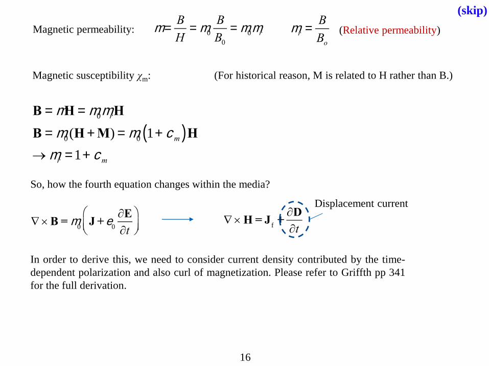
Magnetic permeability: m =B
H= m0
B
B0
= m0mr (Relative permeability)mr =B
Bo
Magnetic susceptibility χm: (For historical reason, M is related to H rather than B.)
B = mH = m0mrH
B = m0(H + M) = m0 1+ cm( )H
® mr = 1+ cm
Ñ´H = Jf
+¶D
¶t
So, how the fourth equation changes within the media?
Ñ´B = m0
J + e0
¶E
¶t
æ
èçö
ø÷
In order to derive this, we need to consider current density contributed by the time-
dependent polarization and also curl of magnetization. Please refer to Griffth pp 341
for the full derivation.
Displacement current
(skip)

17
Maxwell’s Equations
Ñ×D = rf
Ñ×B = 0
Ñ´E = -¶B
¶t
Ñ´H = Jf
+¶D
¶t
(D = ere
0E
B = m0mrH)
Ñ×E =r
e0
Ñ×B = 0
Ñ´E = -¶B
¶t
Ñ´B = m0
J + e0
¶E
¶t
æ
èçö
ø÷
Microscopic and universalInside the media in general
Homogeneous and
isotropic media (εr and
μr are position-
independent scalars)
Ñ×E =r
f
ere
0
Ñ×H = 0
Ñ´E = -m0mr
¶H
¶t
Ñ´H = sE + ere
0
¶E
¶t
Jf
= sE( )
εr and μr are tensors that
depend on spatial positions
White Board

18
Griffith
_______________________________________________________________________
______________________________________________________
________________________
__
__________________________________________
-191106(수)
_________
_________________

19
utilize the relationship: Ñ´Ñ´E = Ñ(Ñ×E) -Ñ2E
Ñ´E = -mrm
0
¶H
¶t, Ñ×E = 0
Ñ´ -mrm
0
¶H
¶t
æ
èçö
ø÷= -Ñ2E
- mrm
0
¶t(Ñ´ H) = -Ñ2
E
Substitute Ñ´ H = ere
0
¶E
¶t+sE
- ere
0mrm
0
¶2E
¶t2- m
rm
0s
¶E
¶t= -Ñ2
E
Ñ×E =r
f
ere
0
= 0
Ñ×H = 0
Ñ´E = -m0mr
¶H
¶t
Ñ´H = sE + ere
0
¶E
¶t
We consider a homogeneous and isotropic medium without free charges. In most materials, interior
free charges are rare (in metals they exist at the surface).
Ñ2E = e
re
0mrm
0
¶2E
¶t2+ m
rm
0s¶E
¶t
Ñ2H = e
re
0mrm
0
¶2 H
¶t2+ m
rm
0s¶H
¶t
Wave Equations for Light in Matter

20
In insulators, the conductivity is zero (σ = 0).
E = E0ei(k×r-wt ) , H = H
0ei(k×r-wt )
w
k= v
p=
1
ere
0mrm
0
=c
ermr
where c =1
e0m
0
: light velocity in vacuum (3´108 m/s)
Ñ2E = e
re
0mrm
0
¶2E
¶t2 , Ñ2
H = ere
0mrm
0
¶2H
¶t2
We look for the plane-wave solution:
Ñ×E = ik ×E0ei(k×r-wt ) = ik ×E
Ñ2E = - k ×k( )E0ei(k×r-wt ) = -k 2E
¶2E
¶t2= -w 2E
vp
= vg
=c
ermr
= v
n =c
v= e
rmr or v =
c
nRefractive index
Slope = vp = vgFor non-dispersive medium, εr and μr are constants with respect
to ω or k, and the phase and group velocities are the same.
Using
One can show that
For most materials, χm is much smaller than 1, so μr = 1 + χm ~1. Therefore, the refractive index is
determined by the dielectric constant.
n = er
4A.2. Light Propagation in Non-Dissipative Dielectric Media
_____
__ __
_____
__________
(No Imaginary Dielectric Constant)

21
Ñ×E = 0® ik ×E0ei(k×r-wt ) = 0® k ×E
0= 0® k ^ E
0
Ñ×H = 0® k ^ H0
Ñ´E = -m0mr
¶H
¶t® ik ´E
0ei(k×r-wt ) = im
0mrwH
0ei(k×r-wt ) ®E
0^ H
0& kE
0= m
0mrwH
0
Ñ´H = ere
0
¶E
¶t®E
0^ H
0
E = E0ei(k×r-wt ) , H = H
0ei(k×r-wt )
The results here also apply to the electromagnetic wave in vacuum (εr = μr = 1)
The intensity of light I is the
energy flowing per unit area per
second:
I =cne
0
2E
2
Additional information can be obtained by inserting plane-wave solution into Maxwell’s equation
_
22
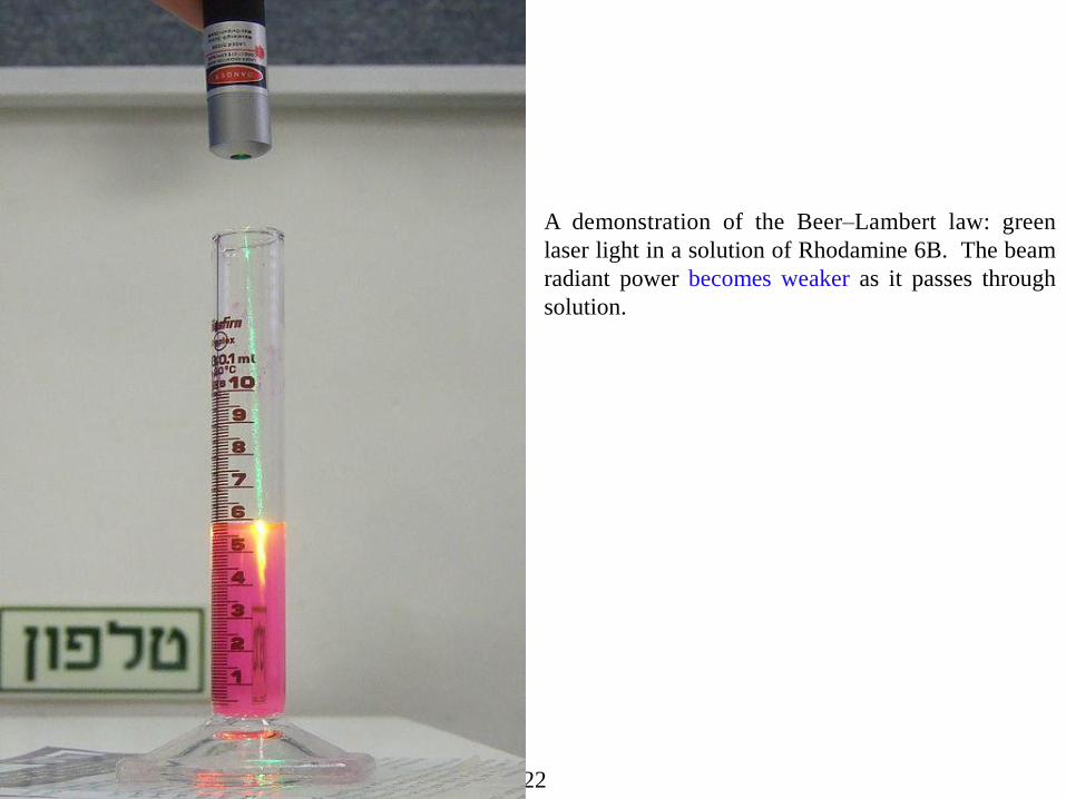
A demonstration of the Beer–Lambert law: green
laser light in a solution of Rhodamine 6B. The beam
radiant power becomes weaker as it passes through
solution.

23
As the electromagnetic wave propagates through a medium, its
intensity decays because light energy is absorbed by the
medium and results in mostly heat dissipation.
Attenuation of Photons
I = I0exp(-a z)
I : intensity
a: absorption coefficient (cm-1 or m-1)
The attenuation of an electromagnetic wave in passing through a medium with absorption is
usually expressed in terms of an optical absorption coefficient 𝛼 as the above equation.
1/α is the length over which the light intensity decays by 1/e and it is called as the
attenuation length or absorption length.
Implementing various microscopic mechanisms that affect polarization and conductivity
into Maxwell’s equation leads to a dispersion relation that goes beyond the linear and real-
valued relationship between ω and k, becoming non-linear and complex-valued. This is can be
efficiently handled by generalizing the dielectric constant and hence refractive index to be
complex functions of ω:
(Beer’s law aka Beer-Lamber law)
where κ is called extinction coefficient, and n is the (normal) refractive index.
4A.3. Optical Absorption in Dissipative Media
_____
__ __ ___

24
Let’s assume that the light propagates along z
direction
For the light intensity,
I =cne
0
2E
2
=cne
0
2E
0
2e-
2kw
cz
= I0e-a z
\a =2kw
c= 2k k
0=
4pk
l0
In terms of complex dielectric constant that relates to the microscopic process,
e1= n2 -k 2 , e
2= 2nk
n =1
2e
1+ e
1
2 + e2
2( )1/2
k =1
2-e
1+ e
1
2 + e2
2( )1/2
Experimentally, n and κ are routinely measured by, for example, ellipsometry. Theoretically, ε1 and ε2
are directly obtained by considering microscopic mechanism.
l =2p
k
Velocity = c/nl
0=
2p
k0
Vacuum
__ _____

25
Relations between Optical Parameters
Dielectric Constant
Refractive Index
Extinction Coefficient
Absorption Coefficient
μr = 1 + χm ~ 1
κ

26
Reflection at the Interface
Suppose that the light is propagating along the z-axis.
The boundary conditions at the interface between two dielectrics tell us that the tangential components
of the electric and magnetic fields are continuous at the interface (z=0). Since the electric field on the
left side is the sum of incident and reflected beams and all electric fields and magnetic fields are parallel
or antiparallel,
(*)
Ei= e
x
i xei(kz-wt )
Hi= H
y
i yei(kz-wt )
Er= e
x
r xei(-kz-wt )
Hr= -H
y
r yei(-kz-wt )
Et= e
x
t xei( ¢k z-wt )
Ht= H
y
t yei( ¢k z-wt )
First, all the waves oscillate with the same angular frequency ω. Since the velocity of the
transmitted wave is c/n, this means that the wave length is λ/n when λ is the wavelength in the
vacuum.
(skip)

27
Since μr ~ 1 for most materials, (*) becomes
=(n-1)2 +k 2
(n+1)2 +k 2T (transmittance) = 1 – R
(**)
Using (*) and (**), one can eliminate εxt
The reflectivity R is the ratio of intensity between incident and reflected beams. Since the
intensity is proportional to n|E0|2,
These formulas can be also used for real refractive index by simply setting κ = 0. One thing to note is
that when the light reflected on a more dense media (n2 > n1), the field direction is reversed. (This is
similar to fixed-end reflection (고정단반사).)
R = Ir/Ii, T = It/Ii
(skip)

28
We have overviewed the ingredients necessary for describing the propagation of light in the material.
The interaction between light and matter was dumped into
conductivity and polarizability (σ and ε). In the section, we will derive these two
quantities from the microscopic picture. In doing so, we stick to the classical picture before fully
considering quantum effects in the next section.
We start with the observation that since the wavelength is typically much longer than the mean free
path (unless we are concerned with X-ray or γ-ray), typically longer than 100 nm, electrons feel the
electric field as spatially uniform. Therefore, in discussing response of electrons or ions at r0 under
E(r,t), we may assume that they are under a constant electric field of E(r0,t). Another thing to consider
is that σ and ε vary with the frequency of the external field. That is to say, σ(ω) and
ε(ω). Combining these two things, the current density at r is given by J(r,ω) = σ(ω)E(r,ω).
4Β. Classical Model of Materials Response1. Free electrons within Drude model
2. Lorentz Model and Polarization
Cu at 300 K
v τ = 35 nm
τ = 25 fs
ppt 3A-9

29
AC Conductivity
We first consider metallic systems in which substantial numbers of free electrons exist. As the name
suggests, these are systems in which the electrons experience no restoring force from the medium when
driven by the electric field of a light wave. The relevant materials are metals or doped semiconductors. We
first assume that there are only free electrons and no polarizable medium.
In the previous chapter, we have seen that free electrons are subject to collisions characterized by the
collision time τ and electrons accelerate under external field between the collision. Let’s recast this process
in terms of the average momentum p(t) of electrons at time t (with randomly oriented p(t)). Τhe average
velocity is v(t) = p(t)/m where m is the (effective) electron mass and the current density is J(t) = -nep(t)/m.
When electrons are subject to a certain force f(t) that depends on time but not on position, within the
relaxation time approximation,
p(t + dt) = p(t) -dt
tp(t) + f (t)dt
p(t + dt) - p(t) = -dt
tp(t) + f (t)dt
dp(t)
dt= -
p(t)
t+ f (t)
Note that 1/τ corresponds to the mean probability per
unit time that an electron is scattered (or mean frequency
of collisions).
- dt/τ is the probability to scatter during dt.
- dt/τ p(t) is the momentum lost due to scattering.
- f(t)dt is the impulse that is equal to the momentum
change.
4B.1. Free Electrons within Drude Model

30
i) No field: f = 0
f (t) = -eEx
ii) A constant (time-independent) electric field = DC (direct-current) field
dp(t)
dt= 0® p(t) = -etEx
J =ne2t
mEx®s =
ne2t
m: DC conductivity
dp(t)
dt= -
p(t)
t® p(t) = p(0)e-t/t
We will solve this for various situations.
That is to say, the momentum decays or relaxes over the time scale of τ. Hence comes the
name “relaxation” time for τ
If we look for the steady-state solution:
which we know already.

31
iii) The usefulness of this equation comes with the uniform but time-varying field (or AC
(alternating current) field), E(t) = E0cos(ωt). This corresponds to the electric field in the light or
electric fields in the parallel capacitor connected to the alternating currents. Mathematically, it is
much more convenient to introduce the complex form.
E(t) = Re E0e- iwté
ëùû
p(t) = Re p0e- iwté
ëùû
dp(t)
dt= -
p(t)
t- eE(t)
® -iwp0
= -p
0
t- eE
0
p0
=-eE
0
1/ t - iw
J0
= -nep
0
m=ne2 / mE
0
1/ t - iw= s (w )E
0
s (w ) =ne2 / m
1/ t - iw=ne2t / m
1- iwt=
s0
1- iwt: AC conductivity
s0
=ne2t
m: DC conductivity
n: carrier concentration per volume
n: refractive index
______________
Under AC field, the conductivity
becomes a complex number.

32
(skip)

33
Plasmon = Plasma Oscillation = Nature of Charge Density Wave
In the absence of external field,
the positive ions and electrons
distributed homogeneously and
net charge is zero everywhere.
Under the external field (Eex), free electrons displace by the same distance (x) that is proportional
to the relaxation time. As a result, surface charges develop at the boundary of the material.
Eex+ + + + + + + +
- - - - - - - - x
The opposite surface charges attract each other, exerting
forces that try to restore the position of electrons to the
equilibrium (x = 0). The force on the electron is
F = -eEint
= -es
e0
= -enex
e0
= -ne2
e0
x
F = ma = md 2x
dt2= -
ne2
e0
x (harmonic oscillator)
d 2x
dt2= -
ne2
e0mx® Angular frequency =
ne2
e0m
= wp
Eint
In general, when electron density is not uniform, it gives rise to
net charges with different polarities and electrostatic attraction
among them acts as the restoring force, which results in the
resonance frequency at ωp.
wp2 = 4p ne2/ m*
_
34
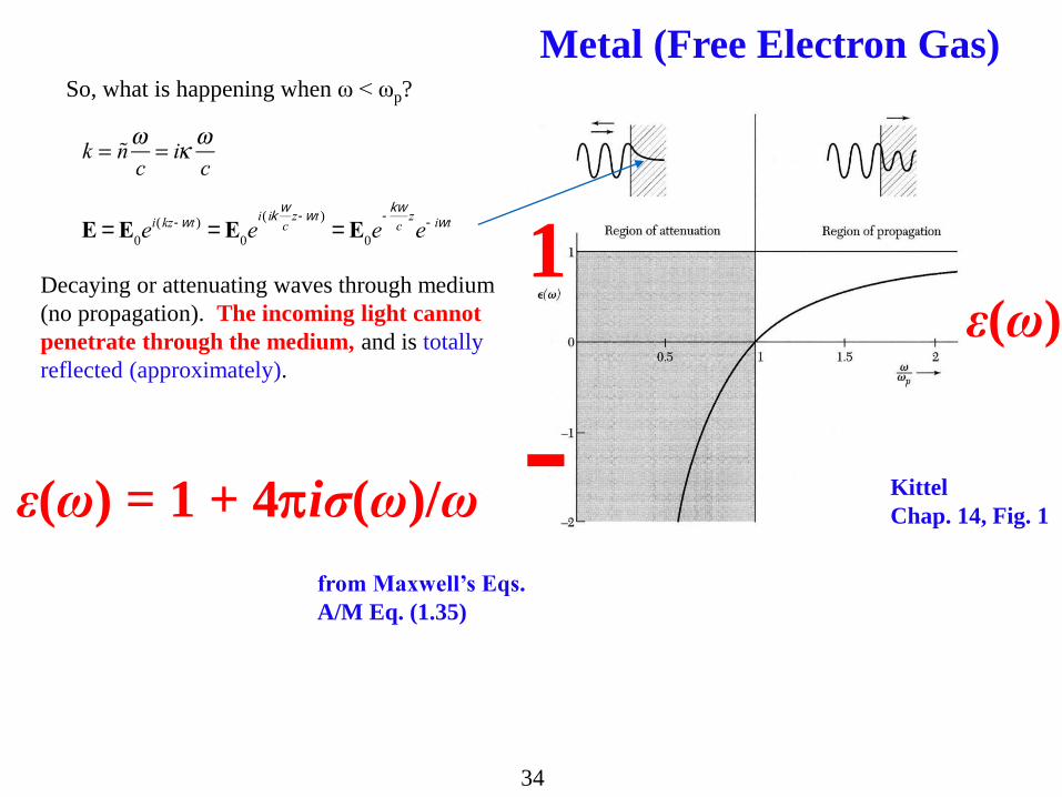
So, what is happening when ω < ωp?
E = E0ei(kz-wt ) = E
0ei( ik
w
cz-wt )
= E0e
-kw
cz
e- iwt
Decaying or attenuating waves through medium
(no propagation). The incoming light cannot
penetrate through the medium, and is totally
reflected (approximately).
ε(ω) = 1 + 4piσ(ω)/ω
from Maxwell’s Eqs.
A/M Eq. (1.35)
1
- Kittel
Chap. 14, Fig. 1
ε(ω)
Metal (Free Electron Gas)

_eV
E ~ 10 eV
f ~ 1015 Hz
Pt = 22.9 eV
Au = 16.0 eV
Ag = 9.2 eV
-191111(월)
____
Kittel
Chap. 14, Table 2

36
Visible
“Ultraviolet transparency of metals”
This is why metals like silver and
aluminium are shiny and have been
used for making mir ro rs fo r
centuries.
Band theory is needed to explain
why some metals (e.g. copper and
gold) are coloured.
Schematic Figure

37
Ñ2E = e
0m
0
¶2E
¶t2+ m
0s
¶E
¶t
Using E = E0ei(k×r-wt )
-k 2E
0= -e
0m
0w 2
E0- im
0s (w )wE
0
k 2 = e0m
0w 2 + im
0s (w )w =
w 2
c21+is (w )
e0w
æ
èç
ö
ø÷
Therefore, under AC field, the conductivity becomes a complex number. How does this
affect the light propagation? We plug this relation into the Maxwell equation in media.
We have seen in the previous section that the general dispersion relation can be handled conveniently in
terms of complex refractive index or dielectric constant.
Therefore,
By defining wp
=ne2
e0m
: plasma frequency
= 1-wp
2
w 2
w 2t 2
1+w 2t 2+ i
wp
2
w 2
wt
1+w 2t 2
= e1(w ) + ie
2(w )
(Plasma is a medium with equal concentration of positive and negative charges, of which at least
one charge type is mobile.)
Reflections for metals(skip)
38
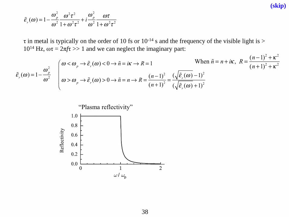
τ in metal is typically on the order of 10 fs or 10-14 s and the frequency of the visible light is >
1014 Hz, ωτ = 2πfτ >> 1 and we can neglect the imaginary part:
“Plasma reflectivity”
(skip)

39
(skip)

40
E = E0ei(kz-wt ) = E
0ei((n+ik )
w
cz-wt )
= E0e
-kw
cz
ei(nw
cz-wt )
Skin Depth
The length over which the current density decays by 1/e in comparison to that at
surface is called the skin depth (δ). Since J ∝ E,
At low frequencies (ω << 1/τ and ωp). In this case, ε2 >> ε1 and
d =c
kw=c
w
2e0w
s0
=2
s0wm
0_ __ ~5 nm in Pt at 4 eV

41
Therefore, the AC electric fields can only penetrate a short distance into a
conductor and the current tends to flow through a narrow skin region.
This is called the skin effect. This is an important phenomena in
engineering AC currents through a wire. This is why 3-wire cable is used
as power transmission cable rather than one single cable.
Skin depth is due to the circulating eddy
currents (arising from a changing H field)
cancelling the current flow in the center of
a conductor and reinforcing it in the skin.
Top view
Source: wikipedia
(skip)

42
In transparent electronics, the metallic wire tends to degrade the transparency by
reflecting visible light. By using Ag nanowires or nanoparticles, one can effectively
make the conducting part transparent.
(skip)

43
In materials, there are several sources of
polarization. First, we focus on the polarization
by electrons bound to nucleus. This can be well
captured by the Lorenz model with certain
resonance frequencies. For simplicity, let’s
assume that one electron vibrates.
4B.2. Lorentz Model and Polarization
md 2x
dt2+mg
dx
dt+mw
0
2x = -eE(t) γ: damping rate
Using the complex notation, E(t) = E0e- iwt , x(t) = x
0e-iwt
-mw 2x0e- iwt - imgw x
0e- iwt +mw
0
2x0e- iwt = -eE
0e- iwt
x0
=-eE
0/ m
w0
2 -w 2 - igw
If the number density of dipoles are N, the polarization P is given by
P = -Nex =Ne2
m
1
w0
2 -w 2 - igwE
0e- iwt =
Ne2
m
1
w0
2 -w 2 - igwE(t)
In general¾ ®¾¾¾ P =
Ne2
m
1
w0
2 -w 2 - igwE
This gives the dielectric susceptibility:
P = e0cE® c =
Ne2
e0m
1
w0
2 -w 2 - igw
Now we turn our attention to the polarization in the dielectric medium.

44
er(w ) = 1+ c = 1+
Ne2
e0m
1
w0
2 -w 2 - igw
e1(w ) = 1+
Ne2
e0m
w0
2 -w 2
w0
2 -w 2( )2
+ gw( )2
, e2(w ) =
Ne2
e0m
gw
w0
2 -w 2( )2
+ gw( )2
The medium is polarized when ω is lower than ω0 but when ω becomes much higher than ω0, the
oscillator does not exhibit any dielectric polarization. This is because the oscillator cannot
follow the field change. Consequently, the refractive index steps down as ω crosses ω0.
11+Ne2
e0mw
0
2
Energy is lost or absorbed by
the medium most strongly at the
resonant frequency. This is
called the dielectric loss.
1
____
Electronic Polarization
_
_

45
IR region (In fact, the lattice polarization is involved in this spectral range)
(skip)

46
Multiple oscillators
In materials, there are several sources of polarization. Even within the electronic polarization, there
exist modes with different resonance frequencies. In such case, each oscillator respond to the external
field independently and so the total polarization is the sum of contribution from every oscillator.
In fact, the oscillator responds with different sensitivity, which is effectively considered
by the oscillator strength fj:
In the next pages, we will examine polarization mechanisms other than the electronic one.
(skip)

47
(a) A NaCl chain in the NaCl crystal
without an applied field. Average or
net dipole moment per ion is zero.
(b) In the presence of an applied field
the ions become slightly displaced
which leads to a net average dipole
moment per ion.
Other Polarization Mechanisms: Ionic Polarization
This corresponds to the optical mode. Therefore, the resonance frequency in the ionic
polarization corresponds to the optical frequency (~10 THz) that corresponds to infrared (IR) .
Those phonon modes that can respond to IR are called to be IR-active. The lattice absorption by
the IR-active phonon modes is specifically called the Reststrahlen (German: residual rays)
absorption.
On the other hand, the polarization by the acoustic mode is possible (piezoelectric response) but its
magnitude is much smaller than for the optical mode.

48
4 THz = 75 μm
5 THz = 60 μm
Phonon dispersion of CdTe
κκ
(skip)

49
(skip)

50
(a) A HCl molecule possesses a permanent dipole moment p0.
(b) In the absence of a field, thermal agitation of the molecules results in zero net average
dipole moment per molecule.
(c) A dipole such as HCl placed in a field experiences a torque that tries to rotate it to align p0
with the field E.
(d) In the presence of an applied field, the dipoles try to rotate to align with the field against
thermal agitation. There is now a net average dipole moment per molecule along the field.
Other Polarization Mechanisms: Dipolar PolarizationIn materials such as water, the molecules have permanent dipole moments even before the
application of external field. However, they are randomly distributed so the average dipole moment
(pav) is equal to zero.
Under the external field, the dipole moment tends to align parallel to the field while the magnitude
remains to be same. This results in the finite pav. The following figure is on the example of HCl
liquid.

51
p =1
3
p0
2E
kT= a
dE
p0: permanent dipole moment
αd: polarizability
dp(t)
dt= -
p(t)-adE(t)
t d
p(t + dt) = p(t) -dt
t dp(t) -a dE1( )
dp(t)
dt= -
p(t)-adE1
t d
In general, for the time-varying AC field of E(t)
1
1
Schematic Figure Only
Dipolar Polarization
E(t)
P(t)

52
The response of the dipole under AC field can be treated in complex notation as usual:
E(t) = E0e- iwt , p(t) = p
0e- iwt
dp(t)
dt= -
p(t) -adE(t)
td
® -iw p0
= -p
0-a
dE
0
td
p0
=adE
0
1- iwtd
\ p(t) =ad
1- iwtd
E(t)
If N is the number density of dipolar molecules, P = Np(t) =Na
d
1- iwtd
E, c=Na
d
e0
1
1- iwtd
The relaxation time characterizes the resonance frequency in dipolar
polarization. The difference is that ε1(ω) decreases monotonically
rather than sharp oscillation as in the Lorentz oscillator.
1+Na
d
e0
ε1(ω)
ε2(ω)
Schematic Figure Only
Dipolar Polarization

53
http://www1.lsbu.ac.uk/water/microwave_water.html
2.4 GHz for microwave oven
τd ~ 100 ps (water) and ~ ms (ice)
Schematic Figure Only
Dipolar Polarization

54
http://www.philiplaven.com/p20.html
Dielectric constant of water
?
(skip)

55
(a) A crystal with equal number of mobile positive ions (ex. H+, Li+) and fixed negative ions. In
the absence of a field, there is no net separation between all the positive charges and all the
negative charges.
(b) In the presence of an applied field, the mobile positive ions migrate toward the negative charges
and positive charges in the dielectric. The dielectric therefore exhibits interfacial polarization.
(c) Grain boundaries and interfaces between different materials frequently give rise to
Interfacial polarization.
Other Polarization Mechanisms: Interfacial Polarization
The relaxation time for the interfacial polarization is much longer than
the dipolar relaxation time. Therefore, the dielectric loss occurs at
much lower frequencies.
Schematic Figure
~100 mm

56
The frequency dependence of the real and imaginary parts of the dielectric constant
in the presence of interfacial, dipolar, ionic, and, electronic polarization mechanisms.
Optical dielectric
constant (ε∞)
Static dielectric
constant (ε0):
f < 10 GHz
ε1
ε2
__
~THz ~eV~GHz~Hz
___
__real
imaginary

57
(skip)

58
For refractive index of various materials, see
https://www.filmetrics.com/refractive-index-database
Electronic oscillator
Ionic part
(skip)

59
4C. Quantum Phenomena: Absorption0. Vertical Transition and Photon Absorption
1. Interband Transition: Semiconductor
2. Interband Transition: Metal
3. Exciton
4. Free Carrier Absorption
5. Solute (Impurity) Absorption
6. Plasmon
7. Restrahlen Absorption
The classical theory of polarization and conductivity gave good account of light-matter interactions on
a macroscopic scale. Nevertheless, fine details are not fully captured by this approach, which requires
consideration of quantum effects.
By the quantum effects we mean the band structure for electrons and particle nature for waves (photon
for electromagnetic waves and phonon for lattice vibrations). The light-matter interactions are
essentially among these three parties. The quantum process explicitly describes how electrons absorb
or emit photons, possibly together with absorption or emission of phonons. Therefore, it directly
relates to the absorption and emission process within the material. We will first focus on the photon
absorption.

60
Since the photon and phonon are bosons, they can be created or annihilated. In Chap. 3B, we have
seen that in the electron-phonon collision, the energy and crystal-momentum conservations should
be satisfied in the collision process. The same principle applies to the interaction involving the
photon: the energy and momentum should be conserved. (The crystal momentum for electrons or
phonons.) For instance, suppose that an electron in (ni,ki) absorbs one photon with (ω, k) and
occupy a new state (nf,kf) which should be empty before the transition (due to the Pauli exclusion
principle). The related conservation laws are:
This to say, k is so small that kf is essentially identical to ki.
This corresponds to the vertical transition as shown in the
band diagram. This is because the light is so light
(massless) that it can deliver meaningful momentum. The
transition should be between different bands, and so it is
interband transition. As a result, electron-hole pair is
created. Note that the transition requires that the final state
is empty because of Pauli exclusion principle.
-0.2 0 0.2
18
20
22
24
26
28
30
-0.2 0 0.2
18
20
22
24
26
28
30
Photon
ħω = ΔΕΔE
k (Å −1)
Conservation laws for photon absorption
4C.0. Vertical Transition and Photon Absorption
_____________ _________ ________

61
The absorption of photon occurs in a probabilistic way that follows the Fermi golden rule. Suppose
that a packet of photons are passing through the medium. After they pass over a certain length, say
1 μm, some percentage of photons are absorbed and lost from the packet. For the next travel over
the same length, the same percentage of the remaining photons will be absorbed. In this way, the
intensity of light that is equal to the number photons, is reduced exponentially, which is nothing but
the Beer’s law.
The absorption coefficient is typically in the range of 103-105 cm-1 for semiconductors. That is to
say, for a photon to be absorbed, it should travel at least 100 nm, going past over hundreds of lattice
sites and electrons. This means that the absorption probability is rather low.
This also implies that multi-photon absorption process in which several photons are
simultaneously absorbed by one electronic transition happens in a much lower chance than single-
photon absorption.
In the next sections, we will examine electronic transitions in various situations.
Upon the photon absorption, the group velocity instantly changes. Why? The momentum transfer from the rigid lattice?
Thicknesses of
Solar Cells
Water Splitting
LED
-191113(수)

62
4C.1. Interband Transition: Semiconductor
The insulators have an energy gap between occupied and unoccupied states. This means that the
photon is not absorbed by electrons with its energy below the energy gap.
For the direct-bandgap material such as GaAs and InAs, the absorption starts right from the
bandgap if photon energy ħω is equal to Eg. The absorption creates one electron in the conduction
band bottom and one hole in the valence band top.
With higher photon energies, more electron-hole pairs are available for the absorption because
DOS increases with the square-root of electron or hole energies. This increases the absorption
coefficient as more transitions can happen.
Direct Bandgap
JDOS: why depends only on square root? If the transition can happen over any two states then JDOS should be the square of square-root. However,
for the vertical transition, only one state is available for the transition for the given valence state. Therefore, JDOS still follows square root.
__
Free Electron Model(spin-up or spin-down)

63
GaAsAbsorption Edge
Eg(T)

64
For the indirect-bandgap material such as Si, the absorption at the bandgap cannot be accomplished
solely by one photon because the momentum is not conserved. However, the absorption is allowed if one
additional phonon absorbed or emitted to conserve the momentum. The energy of phonon is typically small
(~THz), so it does not affect much the energy conservation between photon and electron. The
simultaneous involvement of photon and phonon corresponds to the second-order process, and the
transition rate is much lower than for the vertical (direct) transition involving only one photon. At higher
energies, the vertical transition starts to occur and absorption coefficient increases rapidly as in the direct-
bandgap material.
Evert
It can be shown that
Note that dependence on energy is different from the
direct absorption.Phonon Absorption (Photon +
Phonon = Electron Transition)
Phonon Emission (Photon =
Phonon + Electron Transition)
Indirect Bandgap
Energy delivered
by photon
Momentum
delivered by
phonon
In detail, the phonon can be absorbed or emitted.

65
- The absorption is much more efficient in direct-bandgap material.
- This is why solar cells with high efficiency employs direct-gap material such as GaAs.
- But, GaAs is much more expensive than Si.
OptoelectronicsBandgap Engineering of Si
for a Direct Bandgap?

66
Phonon emission is possible at all temperatures, but phonon absorption is only possible if
phonons are thermally excited. Therefore, at 291 K, the absorption occurs at energies
even lower than Eg. In contrast, at very low temperatures at 20 K, little phonons are
available such that the absorption can start by emitting phonons. At 20 K, the onset
energy is 0.76 eV while the energy is known to be 0.74 eV at this temperature. The
energy difference of 0.02 eV well corresponds to the phonon energy at L point.
Eg
(300K)
Eg
(20K)
Germanium also has an indirect gap.
Direct
transitionIndirect
transition
(skip)

67
Phonon dispersion of Ge
(skip)

68
4C.2. Interband Transition: Metals • Aluminum
From the band structure, we can see that numerous
electronic transitions are possible at various
energy values. This results in the reduced
reflectivity of the experimental data compared to
the near-perfect plasma reflectivity. Note that this
electronic transition is completely independent
from the plasma oscillations, and it occurs within
the attenuation length from the surface.
In the dash-boxed region, the occupied and
unoccupied bands are separated by ~1.5 eV with a
similar dispersion. Therefore, many electrons are
available for the absorption specifically at this
energy, leading to a strong absorption. This
explains the reflectivity dip at 1.5 eV.
1.5 eV
1.5 eV
1.5 eV

69
~4 eV
~2 eV
• Cu (Ag and Au) Calculated Band Structure of Cu
The noble metals such as Cu, Ag, and Au
have the same d10s1 valence configuration
and share similar band structures: the fully
occupied and flat d bands lie a few eVs
below the Fermi level while the s1 electron
form the dispersive, free-electron s band.
Unlike Al, the interband transition within
the free electron band occurs at high
energies above the visible light (~4 eV).
Rather, the absorption starts from the
occupied d band to unoccupied s band
which has the threshold energy of ~2 eV
(560 nm) in the case of Cu, and absorptions
at higher energies are all available because
d band is flat while s band is dispersive.
Because of this, the reflectivity of Cu
sharply drops as the photon energy
increases above ~2 eV. Therefore, photons
from red to yellow are strongly reflected.
d
s

70
For Ag, the absorption edge is around 4 eV, so it can reflect the whole range of visible light. This is
consistent with the experimental reflectivity. The same explanation applies to Au. The characteristic
reflectance can explain the color of noble metals.
Al
Cu
Ag
Au
Ag
Au

71
4C.3. Exciton
A Bound Electron-Hole Pair
The electron and hole pair can be generated by, for instance, photon absorption.
If they occupy conduction and valence edges, respectively, they are spatially
delocalized and move independently from each other.
However, because of opposite charges, they attract and orbit around each other
and can form a more stable bound state. This is called the exciton.
- Free to move together through the crystal.
- Weakly bound, with an average electron-hole distance
large in comparison with the lattice constant.

72
Exciton
Since the electron-hole separation is so large, it is a good approximation to average over the detailed
structure of the atoms in between the electron and hole, and consider the particles to be moving in a
uniform dielectric material. We can then model the free exciton as a hydrogen-like system. We
just need two modifications: first, the electron-hole pair interacts within the dielectric medium so the
static dielectric constant (εr = ε0) is used. Second, unlike the proton, the effective mass of hole is
similar to that of electron, so the reduced mass (μ) should be used.
Since the exciton binding energy is very small for Wannier exciton, it easily break at room temperatures.
EH,n
= -me4
8eo
2h2n2= -
RH
n2= -
13.6
n2eV
Eex,n
= -me4
8er
2eo
2h2n2= -
m
m
1
er
2
RH
n2= -
RX
n2
1
m=
1
me
*+
1
mh
*
rn
=m
mern2a
0= n2a
X
(Hydrogen atom)
(Exciton)
The size of exciton is calculated from the orbital size in the
hydrogen
~25 meV ~5 nm

73
Example)
Homework______ __________________
_________________________________________________
_______________ _________________________
-191118(월)
_

74
Excitons exhibiting just
below the bandgap energy.
Eg = 1.521 eV
at 21 K

75
• Miscellaneous DiscussionFor the exciton to be formed, the electron and hole should have similar group velocities. If not, the
exciton will break instantly because electron and hole move in different directions. This means that
the exciton forms stably at the k point where the valence and conduction bands have similar slopes.
In the typical band structure shown in the below, this happens only at the band edge points (typically
k = 0).
The exciton is also a kind of (quasi)particle so it can move
freely in the lattice. The energy levels in the previous slide
assume that the kinetic energy of exciton is zero. If we add
the kinetic energy to these stationary exciton levels,
which results in curved exciton levels shown in the left.
These dispersive exciton levels are also responsible for the enhanced absorption right above the absorption edge
compared to the pure interband transition (see the dashed vertical arrow in the previous slide); the transition to this
moving exciton is more probable because of the large wavefunction overlap (see vertical arrows in the above figure).
(skip)

76
Frenkel exciton
In large band gap materials with small dielectric
constants and large effective masses, the exciton
radius becomes comparable to the interatomic
spacing. In these materials, we observe small-size
Frenkel excitons rather than Wannier excitons. The
binding energy ranges from 0.1 eV to several eVs,
and so the exciton is stable at room temperatures.
Excitons in alkali halides belong to the Frenkel
exciton.
Frenkel excitons can also be observed in many
molecular crystals and organic thin film structures.
On the right is the absorption spectrum of pyrene
(C16 H10) single crystals at room temperature.
The excitons in molecular solids are important in
the OLED technology.
The exciton effects become more pronounced for
low dimensional materials such as quantum dot in
which the Coulomb interaction between electron
and hole is less screened than 3D materials.
(skip)

77
4C.4. Free Carrier Absorption
In doped semiconductors, the free carriers in the conduction or
valence bands can absorb the photons, undergoing intraband
transitions with higher kinetic energies. In order to conserve the
momentum, this process should involve phonon generation or
creation, i.e., scattering. In fact, free carrier absorption can be
described within the classical Drude model.
Free carrier absorption of GaAs vs. wavelength at
different doping levels, 296 K. Conduction electron
concentrations are:
1: 1.3×1017cm-3
2: 4.9×1017cm-3
3: 1.0×1018cm-3
4: 5.4×1018cm-3
The free carrier absorption occurs at IR region.
Absorption Edge (Eg = 1.43 eV = 0.87 μm)
TCOTransparent Conducting Oxide

TCO Woojin
Transparent Conducting Oxide Research/Industry
79
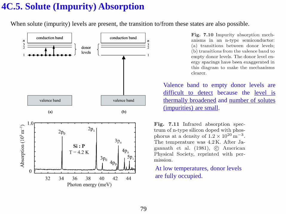
At low temperatures, donor levels
are fully occupied.
Valence band to empty donor levels are
difficult to detect because the level is
thermally broadened and number of solutes
(impurities) are small.
4C.5. Solute (Impurity) Absorption
When solute (impurity) levels are present, the transition to/from these states are also possible.

80
4C.6. PlasmonWe have seen that free electrons oscillate with characteristic frequency called the plasma frequency.
According to quantum mechanics, the energy of plasma oscillation is quantized like other waves, and each
energy quanta is called the plasmon.
When the oscillation occurs inside the material, it is called bulk plasmon. As can be seen in the figure,
the bulk plasma oscillation is longitudinal, so it couples with photon very weakly. (Imagine generating
waves inside the water.)
If the charge oscillation occurs at the metal surface, like one we have seen in the plasma reflectivity, the
energy quanta is called the surface plasmon. This surface wave can be both longitudinal and transverse
(imagine making waves on the water surface). Therefore, the surface plasmon can strongly couple with
photon, which leads to a number of interesting applications in nanophotonics. This field is called
plasmonics.
− Excess Electron Region
+ Depleted Electron Region
Electric-Field Direction
Bulk Plasmon
Bulk plasmon energy can be
detected by electron energy-loss
spectroscopy
Surface Plasmon
NanophotonicsSolar Cells, Water Splitting, LED, etc.

81
Metal-Induced Solar Cells
Solar Cell Changwoo
Henry J. Snaith’s Group
(Univ. of Oxford)
Nano Letters (2011)
_____________________
Research/Industry

82
4C.7. Reststrahlen Absorption
The photons can interact with phonons. We have already discussed the
classical version of photon-phonon interaction in the ionic polarization. The
interaction was qualitatively described within the Lorentz model. For the
quantitative discussion, one needs to elaborate on the detailed interactions
mechanism between IR-active lattice oscillations and electromagnetic
waves which is beyond the current scope.
In a quantum picture, the interaction is collision process between photon
and phonon. Like electron-photon collision, the energy and momentum
should be conserved. This leads to the selection rule within the phonon
dispersion. It is seen that only optical branch can interact with the
photon in order to conserve both energy and momentum. (Light is much
faster than any sound wave!)
Since the interaction occurs mainly near the zone center with the energy of
IR photon, the particle nature is not so strong in photon-phonon interaction
and the classical picture gives good account of most absorption spectrum.
Phonon Dispersion
Raman Spectroscopy
THz
-191120(수)

83
4D. Quantum Phenomena: Luminescence1. General Discussion
2. Interband Luminescence
3. Luminescence Centers
4. Stimulated Emission
In semiconductors, the electron-hole pair generated by the photon absorption entails other interestingphenomena, which are called optoelectronic effects. In semiconductors, the electron-hole pair increasesthe carrier density and results in the increase in conductivity, which is called photoconductivity. Thephotoconductivity is exploited in detecting the photon of certain frequencies (photo detector).
The electron-hole pairs are eventually annihilated such that the system goes back to the originalequilibrium state. If this relaxation is achieved by emitting a photon, the radiative emission process iscalled luminescence. (This is like atoms emit light by spontaneous emission when electrons in excitedstates drop down to a lower level by radiative transitions.) The luminescence is used in variousoptoelectronic devices, most notably light-emitting diodes (LEDs).
The physical processes involved in luminescence are more complicated than those in absorption. This isbecause the generation of light by luminescence is intimately tied up with the energy relaxationmechanisms in the solid.
We first discuss on the spontaneous emission in which electron-hole pair recombine spontaneouslywithout stimuli from ambient photons. (It is like emission in the dark room.)
When the photon density or light intensity is very high, the stimulated emission becomes significant,which is used in laser.

84
4D.1. General Discussion
τR = A–1 : radiative lifetime = [radiative recombination rate]-1
The luminescence efficiency (quantum efficiency) is the ratio of the photon number
to the total number of excited electrons:
When N electrons are excited into higher energy states, they
recombine with holes in lower energy states through various
mechanisms with certain rates. For radiative decay process, the
number changes according to the following differential equation.
Here A corresponds to the transition rate. The solution is
There exist nonradiative processes that also lead to the decay of electron-hole pairs. If 1/τNR is
the nonradiative recombination rate for these processes,
Number Efficiency
Not the Energy Efficiency
(in solar cell, energy efficiency)
- - - - - - - - - - - - - - - -
- - - - - - - - - - - - - - - - - - - - - - - -

85
Nonradiative Recombination
Trap-Assisted Recombination:The trap is a defect level that forms deep inside the
bandgap. It is caused by defects such as vacancies,
interstitials, grain boundaries, dislocations, or external
defects like dopants. Unlike shallow levels, it is highly
localized over a only a few atomic sites. Since the
translational symmetry is broken near the defect site,
any k state can drop to the trap. The transition into
the deep level is dominantly mediated by emission of
phonons. Besides the nonradiative decay, the trap can
also act as the carrier trapping center, degrading the
electrical conductivity.
Auger Recombination:The energy from the recombination is transferred to
another electron in the conduction band.
The reverse of Auger recombination is called the impact ionization in which high-
speed electron collide with another electron, creating electron-hole pair.
Electron-hole pairs can also recombine through nonradiative procedures. The followings are two
well-known types of nonradiative decay.
Nonradiative Recombination
Trappling and Detrapping
__

86
4D.2. Interband Luminescence
When an electron in one band and hole in another band
recombine and emits a photon, it is called interband
luminescence. This is reverse of the interband absorption.
Since the momentum of the photon is negligible compared to the
momentum of the electron, the electron and hole that recombine
must have the same k vector, like in absorption process.
Therefore, the optical transition between the valence and
conduction bands of typical direct gap semiconductors occur
with high probabilities. The radiative lifetime will be short,
with typical values in the range 10−8 ~10−9 s. The interband
luminescence is also called the electron-hole recombination.
In the case of indirect semiconductor, the radiative decay
should be accompanied by phonon that conserve the momentum.
Like absorption, this process is highly inefficient with long τR.
Instead they can recombine through traps, just producing
phonons. This is why indirect-gap material such as Si is not used
in the optoelectronic applications. Instead III-V compound
semiconductor is widely used.
Direct gap
Indirect gapRadiative Recombination Rate = [Radiative Lifetime]-1
Nonradiative Recombination Rate = [Nonradiative Lifetime]-1
87
Example)
(skip)

88
Photoluminescence
Photoluminescence (PL) means the re-emission
of light after absorbing a photon of higher
energy.
The electron–phonon coupling in most solids
is very strong and these scattering events take
place on time scales as short as ∼100 fs
(i.e.∼10−13 s). This is much faster than the
radiative lifetimes which are in the nanosecond
range, and the electrons are therefore able to
relax to the bottom of the conduction band
long before they have had time to emit photons.
The same conditions apply to the relaxation of
the holes in the valence band.
Therefore, while the absorption occurs over the
broad energy range higher than energy gap, PL
is peaked at around the band gap.
EF,n
EF,p
InOut
e
h

89
When the extra carriers are not too much
(the external light is weak), the distribution
of electrons and holes before the emission
follow the Boltzmann distribution with
separate quasi Fermi levels. The
luminescence intensity is then given by:
Since electrons and holes are thermally equilibrated by phonons, their distribution follows the Fermi-
Dirac distribution within their bands under the separate Fermi levels, so called quasi Fermi level. In
the previous slide, EF,n and EF,p are the quasi Fermi levels for electron and hole, respectively. The mass
action law does not hold in this non-equilibrium condition.
Thus, the spectrum rises sharply at Eg and then falls
off exponentially with a decay constant of kT due to
the Boltzmann factor. We thus expect a sharply
peaked spectrum of width ∼kT starting at Eg. This is
confirmed by PL spectrum in GaAs in the right.
(skip)

90
Electroluminescence (p-n Junction)
Electroluminescence is the process by which luminescence is generated while an electrical
current flows through an optoelectronic device. The light-emitting diodes (LEDs) based on the
p-n junction are most well known.
Built-in potential
When p-type and n-type semiconductors are joined seamlessly, the electrons and holes move, creating
dipoles at the interface. This creates the electrostatic potential step and adjust the Fermi level in p-type
and n-type region. At the interface, the depletion layer is formed in which carriers are scarce.
When a bias of Eg/e is applied, the electrons and holes diffuse to the depletion region. This creates a
region in the junction where both electrons and holes are present in the same spatial point. As the electron
and hole recombine through interband luminescence, photons with the energy of Eg (approximately) are
emitted.
E = −∇Ф
- - - - - - - - - - - - - - - - - - - - - - - - - - - - - - - - - - - - - - - - - - -
× ×
V = 0

Depletion Layer
Ashcroft, Solid State Physics
_______
_______
____
ρ (x)
Ф (x)
_______
Research

Carrier Density at a p-n Junction
Ashcroft, Solid State Physics
Equilibrium
Forward bias
Reverse bias
Research

93
Electron-Hole Recombination of a p-n Junction
Kittel, Solid State Physics (Chapter 17).
Electron Energy
×
×
Research
94
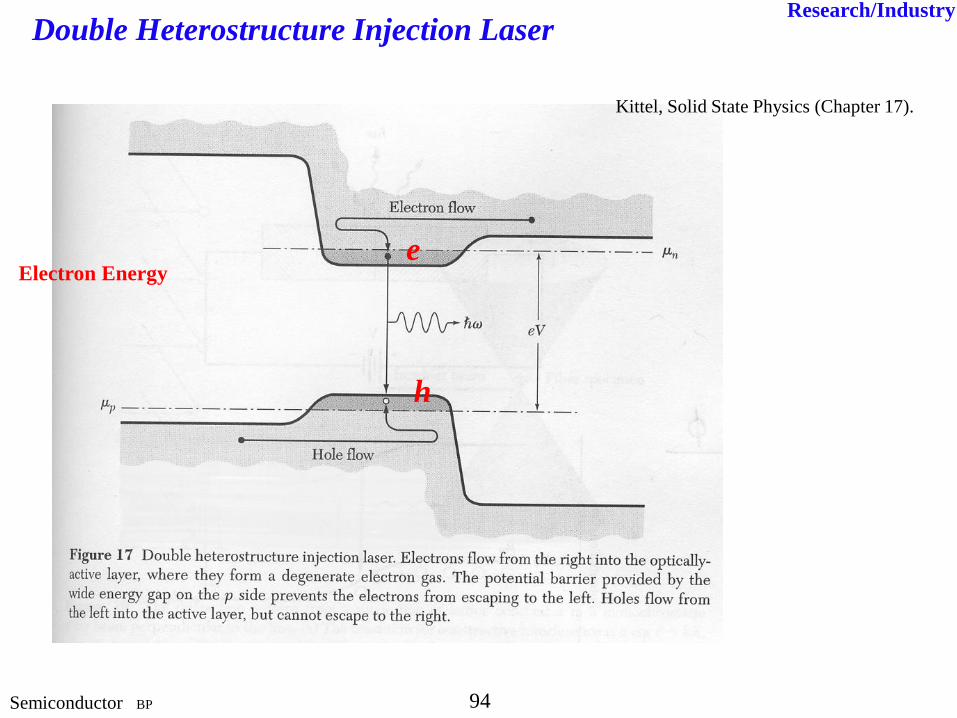
Double Heterostructure Injection Laser
Semiconductor BP
Kittel, Solid State Physics (Chapter 17).
h
e
Research/Industry
Electron Energy

95
The full width at half maximum of the
emission line is 58 meV, which is about
twice kT at 293 K.
LED can produce a monochromatic light (single color).
(skip)

96
Cathodoluminescence
Cathodoluminescence is the phenomenon by which light
is emitted from a solid in response to excitation by
cathode rays, that is electron beams (e-beams).
Cathodoluminescence is extensively used in cathode ray
tubes, and it is also a powerful research tool. The basic
processes occur when an e-beam strikes a crystal. The
electrons in the e-beam are called primary electrons,
and have an energy which is determined by the applied
voltage, which might typically be 1-100 kV. The
electrons that penetrate the surface transfer their energy
to the crystal by exciting electron-hole pairs. These
electrons and holes are created high up in their bands,
and emit photons in all directions with energy of Eg after
having relaxed to the bottom of their bands. It is these
photons that comprise the cathodoluminescence signal.
Cathodoluminescence
X-Ray Source
Diffraction, Tomography, etc.
Secondary Electrons
Scanning Electron Microscopy (SEM)

97
4D.3. Luminescence CentersIn many materials, there are defects or dopants that are
optically active. They are called the luminescence centers.
For example, the pure diamond is a wide bandgap material
and so it is transparent and does not emit any light.
However, when boron impurities are present, it becomes
blue diamond. They are called as color centers.
Another example is the oxygen vacancy. ZnO has a
bandgap of 3.4 eV so it should be transparent. However,
depending on the amount of oxygen vacancies, it takes
certain colors as shown in the right. Synthetic ZnO crystals. Red and
green are associated with different
concentrations of oxygen vacancies.
1E
extrinsic luminescence
intrinsic luminescence
Eg E'
In phosphors, various dopants are
intentionally introduced in solids
to emit photons at certain
frequency.
Jewel

98
4D.4. Stimulated Emission
So far, all the luminescence was spontaneous emission. While the electron in the conduction band
waits for recombination with hole in the valence band for about nanoseconds, if there are photons
passing by, the recombination process is stimulated. The resulting photon is coherent (in phase)
with the ambient photons. This is called stimulated emission.
Such stimulated emission becomes significant
with increasing electron populations in higher
energy states. By increasing the current density
in LED and optical mirrors to confine photons,
one can make laser diode which performs better
than LED. (The acronym ‘laser’ stands for
‘Light Amplification by Stimulated Emission of
Radiation’.)Why the laser is so strong? For spontaneous emission, there is a limit
increasing the light intensity simply by increasing current density. In
stimulated emission, the recombination can be enhanced by the ambient
light.
____
____ ____
____ ___
___ ___

99
n-type
p-type
Dark Flux & 0 V
- - - - - -- - - -
+ + + + + ++ + +
+
-
n-type
p-type
- - - - - -- - - -
+ + + + + ++ + + +
-
-
-
Short-Circuit
Current (Jsc)
electron flow
- - - - - -- - - -
+ + + + + ++ + + +
n-typep-typeqVoc
Open-Circuit
Voltage (Voc)
-
+ +
- - - - - -- - - -
+ + + + + ++ + + +
Maximum Power
Point (Pmax)
-
+work atresistor- -
electron flow n-type p-type
+
-
+
: electron
: hole
Energy Band of p-n Junction Solar Cell
Solar Cell Changwoo
Research/Industry

100
Tailoring Absorption (CdSe QDs)
Multiple-Electron Generation
V. I. Klimov, Los Alamos National Lab
Nano Lett. (2008).
http://gizmodo.com
E.H. Sargent, University of Toronto (Canada)
Nature Photonics (2011).
Nozik, NREL
Science (2011).
Advantage of Quantum Dot as a Sensitizer Material
Solar Cell Jongmin
Research/Industry
-191125(월)
Copyright © 2022 FDOKUMEN