Electronic defect states at annealed metal∕ 4H–SiC interfacesa)
Upload
khangminh22Category
view
1download
0
Electronic and Optical Properties of Surface-Anchored
Metal-Organic Frameworks
Zur Erlangung des akademischen Grades eines
DOKTORS DER NATURWISSENSCHAFTEN
(Dr. rer. nat.)
Fakultät für Chemie und Biowissenschaften
Karlsruher Institut für Technologie (KIT) - Universitätsbereich
genehmigte
DISSERTATION
von
M.Sc. Jianxi Liu
aus
Wuwei, P. R. China
Dekan: Prof. Dr. Peter Roesky
Referent: Prof. Dr. Christof Wöll
Korreferent: Prof. Dr. Stefan Bräse
Tag der mündlichen Prüfung: 14.07.2015


This thesis was carried out under the supervision of Prof. Dr. Christof Wöll at the Institute
of Functional Interfaces (IFG) in Karlsruhe Institute of Technology (KIT). This thesis is
submitted for Doctor of Philosophy degree at Karlsruhe Institute of Technology, and has
not been submitted in any other university for any degree.
I hereby declare that the thesis is my original work and has been written by me unless
stated otherwise in the body of the thesis, and I have faithfully and properly cited all
sources used in the thesis. I followed the standing rules of the “Universität Karlsruhe (TH)”
to ensure good scientific practice as amended time for time.
Karlsruhe, 01.06.2015
Jianxi Liu

Dedicated
To
My Loving Mother

I
Abstract
Crystalline, continuous and monolithic surface-anchored metal-organic framework
(SURMOF) thin films were fabricated using liquid-phase epitaxial (LPE) methods. The
thickness of these thin films was controlled and showed, over respective fabrication
processes, a high degree of precision. The high quality nanoporous thin film materials
were further used for the fabrication of electronic, optoelectronic and photonic devices.
Understanding the electric transport in SURMOFs is essential, both from a fundamental
perspective and with regards to the future development of MOF based electronic devices.
In this respect, a series of HKUST-1 [Cu3(BTC)2] SURMOF thin films were integrated in
a mercury-drop-based tunneling junction. The transport properties of these SURMOFs
were shown to be analogous to those of hybrid metal-organic molecular wires, as
manifested by a very low value of the tunneling decay constant (β ≈ 0.006 Å-1). Together
with their insulating behavior, they also seem to display a linear correlation between the
thickness of the film and the measured increased resistance. Upon loading ferrocene (Fc)
in pores of HKUST-1, a noticeable increase in transport current was observed. A transport
model and ab-initio electronic structure calculations were used and revealed a hopping
transport mechanism that relates the changes upon Fc loading to the SURMOF films.
Furthermore, HKUST-1 SURMOFs with different crystallographic growth directions were
successfully produced on different self-assembled monolayers (SAMs) modified gold
electrodes by means of LPE methodology. Then, cyclic voltammetry (CV) experiments
were carried out to study the electrochemical behavior of these SURMOFs in an aprotic
ionic liquid (IL). The method proved to be highly suitable for investigating the changes in
electric conductivity of the SURMOFs upon filling their pores with a small electroactive
molecule, here Fc. Additionally, cyclic voltammetry methods provided valuable insights
for the determination of the film quality.
In addition to the improved electrical conductivity of MOFs, other properties such as
visible light absorption and photocurrent generation were attained by choosing suitable
organic ligands with specific properties. Porphyrin was used as an electron donor to
fabricate SURMOFs. The well-defined stacking of the highly ordered photoelectroactive
molecules on the electrodes enabled the realization of the artificial light harvester and an
effective transformation into photocurrent. Monolithic, homogenous films deposited on

II
fluorine-doped tin oxide (FTO) substrates, which can act as electrodes, were used in a
home-made photoelectrochemical cell for evaluating the photocurrent generation capacity
of the material.
Furthermore, thanks to promising properties useful for optical sensor and photonic device
integration, monolithic dielectric mirrors were fabricated by stacking layers of SURMOF
HKUST-1 and indium tin oxide (ITO) on a modified Si-substrate. The highly porous
SURMOF layers were deposited again using a versatile LPE method, while the ITO layer
was sputter-deposited using magnetron sputtering. The SURMOF-based hybrid photonic
band gap (PBG) materials exhibited a high optical quality (reflectivity of 80%) and were
color tunable over the whole visible range by varying the layer thicknesses accordingly.
The optical sensing capabilities of these PBG materials were demonstrated by
investigating the chemo-responsive optical sensing upon exposure to different organic
solvents.
Finally, the monolithic Prussian blue (PB) thin films were deposited on a conductive
substrate through a layer-by-layer or LPE method, as well as through a spin-coating
process. Even after several redox cycles, the high stability and the crystallinity as well as
the high orientation remained unchanged, as confirmed by characterization of the
SURMOF thin films. The reversible change from a blue colored to a transparent film also
demonstrates the potential of these porous materials as components for electrochromic
devices.

III
Zusammenfassung
Kristalline, kontinuierliche sowie monolithische Oberflächen können als Dünnfilme in
Form von verankerten metallorganischen Gerüstverbindungen (SURMOF) mit Hilfe des
Flüssigphasen-Epitaxie Verfahrens (LPE) hergestellt werden. Die Dicke solcher dünnen
SURMOF-Filme kann gezielt mit dem LPE Verfahren eingestellt werden. Die so
hergestellten nanoporösen SURMOF Filme wurden für die Herstellung von elektronischen,
optoelektronischen sowie photonischen Bauelementen verwendet.
Das Verständnis des elektrischen Transports in SURMOF-Netzwerken ist äußerst wichtig,
sowohl aus einer fundamentaler Sicht als auch im Hinblick auf die künftige Entwicklung
MOF-basierter Anwendungen. In diesem Zusammenhang wurden eine Reihe von
HKUST-1 [Cu3(BTC)2] SURMOF Filme mit Hilfe der Quecksilbertropfen-basierten
Tunnelkontakt Methode untersucht. Die Transporteigenschaften dieser SURMOFs
scheinen denen der hybridmetallorganischen molekularen Drähten zu ähneln; was durch
einen sehr niedrigen Wert der Tunnel-Abklingkonstante aufgezeigt werden konnte (β ≈
0.006 Å-1). Zusammen mit ihrem Isolationsverhalten konnte weiterhin auch gezeigt
werden, dass sie einen konstanten, linearen Anstieg des Widerstands bei zunehmender
Filmdicke besitzen. Beim Beladen mit Ferrocen (Fc) in die freien Poren von HKUST-1
wurde eine deutliche Zunahme des Transportstroms gemessen. Ein Transportmodell sowie
ab-initio Elektronenstrukturrechnungen wurden verwendet, wobei ein
Hopping-Transportmechanismus beschrieben werden kann.
Weiterhin konnten HKUST-1 SURMOFs mit unterschiedlich kristallographischen
Wachstumsrichtungen erfolgreich auf modifizierten Goldelektroden mittels der
LPE-Methode abgeschieden werden. Anschliessend wurde an den Filmen cyclische
Voltametrie (CV) durchgeführt, um das elektrochemische Verhalten dieser SURMOFs in
einer aprotischen ionischen Flüssigkeit (ILs) zu untersuchen. Diese Methode erwies sich
als äußerst geeignet, um Veränderungen der elektrischen Leitfähigkeit der SURMOFs
beim Füllen der MOF Poren z.B. mit kleinen elektroaktiven Molekülen wie Ferrocene zu
ermitteln. Außer der Verbesserung der elektrischen Leitfähigkeit von MOFs, wurden unter
anderem Photostrommessungen durch Auswahl geeigneter organischer Liganden
durchgeführt. Hierbei wurden Porphyrin-Liganden als Elektronen-Donor-Systeme
verwendet, um gezielt neuartige SURMOFs herzustellen. Durch die wohldefinierte
Stapelung solcher hoch-geordneter photoelektroaktiver Porphyrin-Moleküle auf den
IV
verschiedenen Elektroden konnte bereits erfolgreich ein erstes Photovoltaic (PV) Device
dazu entwickelt werden.
Des Weiteren konnten auch erste optische Sensoren aus photonischen Halbleiter-
SURMOF Strukturen entwickelt werden. Diese di-elektrischen HKUST-1/ITO Spiegel
werden durch Stapeln von LPE gesprühten SURMOF (HKUST-1) Schichten und
gesputterten Indiumzinnoxid (ITO) Filmen auf Si-Substrat hergestellt. Diese SURMOF
basierenden Hybrid PBG Materialien zeigten eine hohe optische Qualität
(Reflektionsvermögen von ca. 80%) und ihre Farbe kann durch die Wahl der Schichtdicke
varriert werden. Die PBG Materialien wurden weiterhin als chemo-responsive optische
Sensoren verwendet, dabei wurde die Wechselwirkung mit verschiedenen organischen
Lösemitteln untersucht.
Zuletzt wurden elektroaktive sowie elektrochrome monolithische Preußisch Blau (PB)
Dünnfilme auf leitfähigen TCO Substraten/Elektroden hergestellt. Für die Herstellung
wurde die Layer-by-Layer Methode, das LPE Sprühverfahren sowie auch Spin-Coating
eingesetzt. Selbst nach mehreren Redox-Zyklen während der electrochromen
Schaltvorgängen, blieben sowohl die Kristallinität als auch die Orientierung unverändert
erhalten. Die reversible Änderung von einer blauen hin zu einer transparenten Schicht
weist auf die potentielle Verwendung von elektochromen und monolitischen
PB-Materialien als Komponenten für zukünftige optoelektronische Bauelemente hin.

V
Table of Contents
Abstract ............................................................................................................. I
Zusammenfassung......................................................................................... III
Table of Contents ............................................................................................ V
1 Introduction ................................................................................................ 1
1.1 Metal-organic frameworks (MOFs) ..................................................................... 1
1.1.1 Synthesis of MOFs .......................................................................................... 2
1.1.2 Properties and applications of MOFs .............................................................. 5
1.2 Preparation of MOF thin films and their device applications ......................... 10
1.2.1 Direct solvothermal deposition ..................................................................... 10
1.2.2 Solvothermal mother solution method .......................................................... 12
1.2.3 Spin-coating method ..................................................................................... 13
1.2.4 Gel-layer synthesis ........................................................................................ 14
1.2.5 Electrochemical deposition ........................................................................... 15
1.2.6 Langmuir-Blodgett (LB) method .................................................................. 17
1.2.7 Liquid phase epitaxy (LPE) method ............................................................. 18
1.3 Surface-anchored metal-organic frameworks (SURMOFs) ............................ 20
1.3.1 Dipping method ............................................................................................ 20
1.3.2 Spraying method ........................................................................................... 21
1.3.3 Pump method ................................................................................................ 21
1.3.4 Quartz crystal microbalance (QCM) method ................................................ 22
1.4 Motivation ............................................................................................................. 23
2 Methods and General Experimental Information ................................ 26

VI
2.1 Characterization methods and instrumental information ............................... 26
2.1.1 X-ray diffraction (XRD) ............................................................................... 26
2.1.2 Ultraviolet-visible (UV-vis) spectroscopy .................................................... 32
2.1.3 Fourier transform infrared (FTIR) spectroscopy .......................................... 34
2.1.4 Raman spectroscopy ..................................................................................... 40
2.1.5 Spectroscopic ellipsometry (SE) ................................................................... 41
2.1.6 Scanning electron microscopy (SEM) .......................................................... 43
2.1.7 Atomic force microscopy (AFM).................................................................. 44
2.1.8 Time-of-flight secondary ion mass spectrometry (ToF-SIMS) ..................... 46
2.1.9 Mercury-drop-based tunneling junction ....................................................... 47
2.1.10 Electrochemical methods ............................................................................ 49
2.2 Materials, general experiments ........................................................................... 50
2.2.1 Materials ....................................................................................................... 50
2.2.2 Preparation of SAMs .................................................................................... 51
2.2.3 Production of SURMOFs .............................................................................. 53
2.3 Theoretical analysis .............................................................................................. 54
3 Electronic Properties of SURMOFs and Their Applications .............. 55
3.1 Electric transport properties of HKUST-1 and the effect of Fc loading ......... 55
3.1.1 Background ................................................................................................... 55
3.1.2 Preparation of HKUST-1 SURMOFs and Fc loading ................................... 56
3.1.3 Characterization of the pristine and Fc-loaded HKUST-1 SURMOFs ......... 57
3.1.4 Assembling the mercury-drop-based tunneling junction .............................. 66
3.1.6 Theoretical analysis of charge transport mechanism .................................... 74
3.1.7 Conclusion .................................................................................................... 77
3.2 Electrochemical studies on HKUST-1 and the Fc mediated conductivity ...... 78
VII
3.2.1 Background ................................................................................................... 78
3.2.2 Preparation of HKUST-1 SURMOFs on SAMs and Fc loading .................. 79
3.2.3 Out-of-plane XRD characterization .............................................................. 79
3.2.4 IRRAS characterization ................................................................................ 81
3.2.5 AFM morphology and scratching characterization ....................................... 82
3.2.6 CV study on HKUST-1 SURMOFs grown on different SAMs .................... 85
3.2.7 Conclusion .................................................................................................... 92
3.3 Photoelectrochemical properties of porphyrin based SURMOF thin films ... 93
3.3.1 Background ................................................................................................... 93
3.3.2 Preparation of the porphyrin-based SURMOF thin films ............................. 94
3.3.3 XRD characterization.................................................................................... 94
3.3.4 Photoelectrochemical measurements ............................................................ 96
3.3.6 Conclusion .................................................................................................... 99
4 Optical Properties of SURMOFs and Their Device Applications ..... 100
4.1 SURMOF-based Bragg reflectors and their optical sensing properties ....... 100
4.1.1 Background ................................................................................................. 100
4.1.2 Fabrication of the monolithic SURMOF-based Bragg stack ...................... 101
4.1.3 Characterization of the SURMOF-based Bragg stack ................................ 103
4.1.4 Optical properties of the SURMOF/ITO hybrid PBG material ................... 111
4.1.5 Chemo-responsive optical sensing of the SURMOF/ITO hybrid PBG ....... 117
4.1.6 Conclusion .................................................................................................. 121
4.2 Prussian blue films and their electrochromic switching behavior ................ 123
4.2.1 Background ................................................................................................. 123
4.2.2 Preparation of PB thin films on the functionalized conductive substrate ... 124
4.2.3 Characterization of the PB thin films ......................................................... 124

VIII
4.2.4 Electrochromic switching of the PB thin films ........................................... 127
4.2.5 Conclusion .................................................................................................. 136
5 Conclusion and Outlook ........................................................................ 137
List of Abbreviations .................................................................................... 140
References ..................................................................................................... 143
Publications .................................................................................................. 160
Acknowledgements ...................................................................................... 161

1 Introduction
- 1 -
1 Introduction
1.1 Metal-organic frameworks (MOFs)
Metal-organic frameworks (MOFs), also known as porous coordination polymers (PCPs),
are crystalline three-dimensional (3D) networks with well-defined pores formed through
the interconnection of metal ions or clusters by organic ligands (Figure 1.1).[1-5] MOFs
have been classified as a relatively new class of coordination materials even though the
very first reference about the coordination polymers can be dated back to 1959.[6] In the
time after, the research done and reported in this area was rather limited. However since
1991s, more than 20000 MOF structures[2] have been reported and studied,[7] owing a
more systematical design and construction approach.
Figure 1.1 Scheme of a typical cubic topology of MOF structure by connecting the metal nodes and organic linkers.
Comparing with common porous materials such as activated carbons and zeolites, MOFs
exhibit many characteristic features which also make these materials more and more
attractive. These highly ordered frameworks display permanent porosity, and their pore
size can be tuned from several angstroms to several nanometers.[8] Their surface area are
typically ranging from 1000 to 10000 m2 g-1, and their density can be as low as 0.13 g
cm-3.[2] Their structures and targeted properties can be designed by careful selection of the
composing metal centers and different functional linkers, integrating both inorganic and
organic properties in one material. These remarkable properties have made MOFs to be
largely investigated as potentially suitable host architectures for a variety of different
applications, ranging from gas storage,[9, 10] separation,[11, 12] catalysis,[13, 14] sensing[15] and
drug delivery,[16] to name a few.

1 Introduction
- 2 -
1.1.1 Synthesis of MOFs
1.1.1.1 Methods
Multiple methods have been employed for synthesizing MOFs for the last 2 decades, such
as hydrothermal and solvothermal methods,[17-19] ultrasonic methods,[20] microwave
synthesis,[21] electrochemical synthesis,[22] mechanochemical synthesis.[23] Among them,
the hydrothermal and solvothermal methods are the most commonly used techniques
which are characterized by a slow diffusion process. The reactions take place in closed
vessels containing the starting materials and solvent under controlled temperature, and
occasionally pressure is applied by increasing the temperature above the boiling point of
the solvent. The MOFs produced by this method have normally a good thermal stability,
since the reactions carried out with conventional heating methods typically last up to
several days.[24]
Exploring different synthesis methods is important for producing MOFs for all kinds of
applications, because different methods can lead to different structures, particle sizes and
morphologies, as well as reaction time, yields, etc.[25]
1.1.1.2 Parameters
MOFs are inorganic-organic hybrid networks made from the inorganic metal ions or
clusters and the organic ligands, so their pore geometries and size, as well as
functionalities can be tailored depending on the metal centers and different functional
linkers used.
The designing of the metal clusters, also called as secondary building units (SBUs) is an
important step in MOF synthesis, as the topologies describing the units can be common to
several structures.[26] Once the synthesis of the SBUs is formed, the linking geometries are
established. This can be used to predict and direct the construction of MOFs in targeting
defined topological networks. The organic ligands act as a bridge between SBUs in the
networks, and can also be designed for providing further properties like rigidity or other
structural features. The construction of MOFs with predetermined structural topologies
also results from the orientation and distribution of the chelating groups of the organic
linker. Overall, the final topology of MOFs is determined by the combination of both, the
inorganic nodes (as connectors) and the organic ligands (as linkers).[27]
Furthermore, the MOF synthesis offers a high degree of flexibility by varying the

1 Introduction
- 3 -
inorganic and organic compositions as well as other conditions like the concentration of
starting materials, pH value, solvent, temperature, pressure and the reaction time.[25] These
conditions can influence the structures, yields, particle sizes and morphologies.
1.1.1.3 Post synthetic modification (PSM)
Post synthetic modification (PSM) is a method for further functionalizing or modifying a
framework after its synthesis, and provides additional ways of controlling the structures
and properties of MOFs.[28, 29] PSM can modify both the inorganic metal nodes and
organic linkers without altering the main structure and overall stability of the frameworks.
Due to the possibility of introducing different types of functional groups as well as varying
the number of functional groups into the framework, PSM can be advantageous compared
to a prefunctionalization approach.[28]
For instances, MOF-5 (Zn4O(BDC)3, BDC = 1,4-benzenedicarboxylate) crystals can
undergo metal center exchange, to produce the Ni-based MOF-5 analogue.[30] The amino
groups (-NH2) on several MOF linkers have been shown to be accessible to further PSM
reaction. IRMOF-3 (IR = Iso-reticular) constructed from Zn4O SBUs and NH2–BDC
(2-amino-1,4-benzenedicarboxylic acid) linkers can be modified with alkyl anhydrides to
generate a series of alkyl functionalized MOFs with identical framework structures.[31]
Azide-modified dicarboxybenzene ligand on MOFs offers a robust platform for
azide-alkyne click PSM reaction.[32]
1.1.1.4 MOF composites
MOF composites composed of MOFs and at least another constituent (including other
MOFs) are hybrid materials with properties different from the individual MOF or the other
materials.[1] The concept could not only extend the physical and chemical properties of
MOFs, but also enhance the overall performance that is not provided by the individual
components alone.
Furthermore, weak points in MOF properties such as poor chemical or mechanical
stability in humid environment in water could also be overcome. For example, MOF
composites have been successfully made with metal nanoparticles/nanorods, oxides,
polymers, biomolecules, and so on.[33, 34] Consequently, the remarkable characteristics of
the MOF composites resulting from the synergistic combination of different components
make them suitable for a wide range of applications. The MOF composites possess also
high degree of synthetic flexibility.
1 Introduction
- 4 -
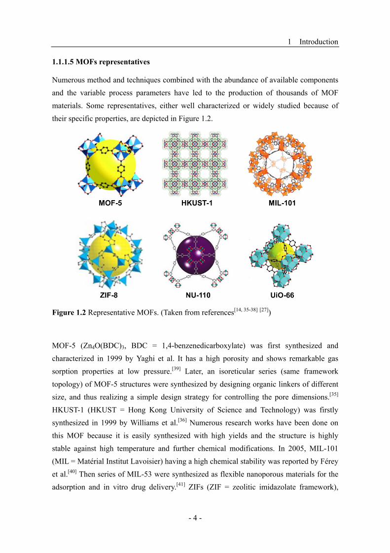
1.1.1.5 MOFs representatives
Numerous method and techniques combined with the abundance of available components
and the variable process parameters have led to the production of thousands of MOF
materials. Some representatives, either well characterized or widely studied because of
their specific properties, are depicted in Figure 1.2.
Figure 1.2 Representative MOFs. (Taken from references[14, 35-38] [27])
MOF-5 (Zn4O(BDC)3, BDC = 1,4-benzenedicarboxylate) was first synthesized and
characterized in 1999 by Yaghi et al. It has a high porosity and shows remarkable gas
sorption properties at low pressure.[39] Later, an isoreticular series (same framework
topology) of MOF-5 structures were synthesized by designing organic linkers of different
size, and thus realizing a simple design strategy for controlling the pore dimensions.[35]
HKUST-1 (HKUST = Hong Kong University of Science and Technology) was firstly
synthesized in 1999 by Williams et al.[36] Numerous research works have been done on
this MOF because it is easily synthesized with high yields and the structure is highly
stable against high temperature and further chemical modifications. In 2005, MIL-101
(MIL = Matérial Institut Lavoisier) having a high chemical stability was reported by Férey
et al.[40] Then series of MIL-53 were synthesized as flexible nanoporous materials for the
adsorption and in vitro drug delivery.[41] ZIFs (ZIF = zeolitic imidazolate framework),

1 Introduction
- 5 -
especially ZIF-8, have attracted much attention because of their great chemical and
thermal stability.[37] NU-110 (NU = Northwestern University) has the highest surface area
and pore volume reported yet, and shows great hydrogen uptake property.[38] UiO-66 (UiO
= Universitetet i Oslo) has also a good hydrothermal stability and can undergo a large
number of functionalization by PSM.[42]
1.1.2 Properties and applications of MOFs
The physical and chemical properties arising from the metal components, organic linkers,
and their combination give various MOF structures, a high porosity (greater than 50%),
various pore sizes and shapes (several angstroms to several nanometers with various
geometry), a high surface area (from 1000 to 10000 m2 g−1), a consequent pore volume
(up to 4.4 m3 g−1), a significant thermal stability (typically exceeding 200 °C).[2] These
specific properties have led to the development of different applications, with some of the
most significant (gas storage and separation, catalysis, sensing and drug delivery)
described in the following.
1.1.2.1 Gas storage and separation
One of the most widely investigated properties of MOFs is gas adsorption or capture
because of the high storage capacity. Particularly, fuel gases storage such as hydrogen and
methane, but also carbon dioxide capture have been receiving much attention. The
hydrogen adsorption capacity of MOFs relies mainly on the surface area and pore
volume,[43] but can also be optimized by the inclusion of open metal sites and lighter
metals.[44] Gas separation capacity of MOFs generally depends on both the pore size and
the affinity of MOFs to the targeted gases.[2]
MOF UTSA-76a has been reported to have high methane uptake capacity whit ∼260 cm3
cm−3, and a record high methane storage working capacity of ∼200 cm3 cm−3 (between 5–
65 bar). The origin of such high working capacity is attributed to the active pyrimidine
groups of the linkers.[45] MOF-210 has reported to have the very highest BET
(Brunauer-Emmett-Teller) surface areas with 6240 m3 g−1, and its carbon dioxide storage
capacity is 2870 mg g−1.[46]
The multivariate MOFs (MTV-MOFs) have been synthesized by a complex arrangements
of several functional groups within the pores. Instead of forming separate domains during
the synthesis, MTV-MOFs incorporate the different functionalities by specifically mixing

1 Introduction
- 6 -
the linkers. As shown in Figure 1.3, various MTV-MOF-5 type structures have been
constructed from BDC (1,4-benzenedicarboxylate acid) and its derivatives -NH2, -Br,
-(Cl)2, -NO2, -(CH3)2, -C4H4, -(OC3H5)2, and -(OC7H7)2 and contain up to eight distinct
functionalities in one phase. The properties of MTV-MOFs are not simply the linear sum
of its individual components. For instances, MTV-MOF-5-EHI (a member of
MTV-MOF-5 series) exhibits up to a 400% better selectivity for carbon dioxide over
carbon monoxide compared to its single linker MOFs materials.[47]
Figure 1.3 MOF materials that combine sets of different links with different functional groups (upside); molecular structures of the different linkers: from left to right, BDC (1,4-benzenedicarboxylate acid), NH2-BDC, Br-BDC, (Cl)2-BDC, NO2-BDC, (CH3)2-BDC, C4H4-BDC, (OC3H5)2-BDC, and (OC7H7)2-BDC links (downside). (Taken from ref.[47])
1.1.2.2 Catalysis
MOFs can be turned into catalyst matrix through different approaches: either directly
through synthesizing the MOFs with active building blocks, metal nodes or specifically
designed complex organic linker, or directly, by having the catalyst species loaded within
the pores or grafted on the organic ligand or SBU by PSM.[13, 14] Figure 1.4 presents two
cases of MOF-based catalytic reactions strategies from metal nodes and from
functionalized linkers, respectively.
The first example of catalysis in MOFs was reported by Fujita et al. in 1994 on the
cyanosilylation of aldehydes in Cd-based MOF, Cd(4,4’-bpy)2(NO3)2 (bpy = bipyridine).
The reaction of benzaldehyde and cyanotrimethylsilane successfully gives
2-(trimethylsiloxy)phenylacetonitrile with a yield of 77% and a shape selectivity of the
catalysis reaction is observed.[48]

1 Introduction
- 7 -
HKUST-1, Cu3(BTC)2 (BTC = 1,3,5-benzene tricarboxylate), based catalysis reaction was
reported on the metal sites. By activation (removal of solvent from the pores), the open
metal sites are exposed and can act as Lewis acid catalysts.[49]
Figure 1.4 Representative strategies to construct of MOF-based catalysts; (a) a synthetic strategy for MOF-based metal node catalysts, (b) a synthetic strategy for PSM of the MOF linker to give a catalytically active center. (Taken from ref.[13])
Chiral MOFs, LCu2(solvent)2 (L is a chiral tetracarboxylate ligand derived from
1,1′-bi-2-naphthol), have been constructed and give the same structures but different open
channel sizes. They provide an ideal platform for generating heterogeneous catalysts by
postsynthetic grafting of the Ti(IV) complex onto the chiral dihydroxy groups. The
resulting materials has proven to be highly active asymmetric catalysts for converting
aromatic aldehydes into chiral secondary alcohols.[50]
By taking advantage of the porosity properties of MOFs, guest species can be loaded
within the pores. The palladium loaded MOF-5 has been shown to have a high catalytic
activity during the selective hydrogenation of styrene to ethyl benzene.[51]
1.1.2.3 Sensing
The highly porous structures and well-defined pores and channels in MOFs also provide
an adequate matrix for accommodating analyte molecules, and at the same time,
supporting specific recognition and selective sensing process.[52] Typically, monitoring
changes in the electrical, photophysical, or mechanical behaviors of the MOFs material
can translate into measuring a sensed signal.[15]

1 Introduction
- 8 -
The most widely explored type of MOF sensor to date is based on luminescent
frameworks. The luminescence based sensing has been applied to various fields and use
the MOFs emission properties for the detection of small molecules, volatile organic
compounds, ionic species, as well as explosives and explosive-like molecules or even
temperature changes (fluorescent thermometers), and also for biosensing and imaging.[53]
For example, [(WS4Cu4)I2(dptz)3] (dptz = 3,6-di-(pyridin-4-yl)-1,2,4,5-tetrazine) MOF has
been synthesized and shown to have a solvatochromic behavior: a large shift in the
absorption spectrum in response to a change in absorbing solvent can be observed (Figure
1.5). The material shows a negative solvatochromic effect with increasing solvent polarity
(blue shift of the absorption band). [54]
Figure 1.5 Visible spectra and photograph of MOF crystals containing solvents as condensed vapors. A negative vapochromic effect is observed for both hydroxylic and nonhydroxylic solvent vapors. (Taken from ref.[54])
1.1.2.4 Drug delivery
Owing the tunability of the structure and porosity toward enhanced drug interaction and
loading, but also their biocompatibility and bioelimination features, MOFs are well suited
to serve as carriers for drug delivery and imaging. They can absorb and release large
amounts of therapeutics as tested with ibuprofen, nitric oxide, and procainamide.[55]
Scale-down MOF particles to the nanometer range could make them nanocarriers of high
efficiency.[56]

1 Introduction
- 9 -
Designing longer organic linkers for MOF synthesis could provide larger pores, to offer a
larger storage space and a greater number of adsorption sites in MOFs. The IRMOF-74-I
to IRMOF-74-XI are a series of isoreticular series of MOF-74 structures with pore
apertures ranging from 14 to 98 angstroms (the biggest pore so far), as presented in Figure
1.6. The permanent porosity and high thermal stability (up to 300 °C) make these MOFs
excellent candidates for applications in gas adsorption, catalysis as well as delivery. It was
found that activated IRMOF-74-IV is able to take up vitamin B12, and an oligoethylene
glycol-functionalized IRMOF-74-VII and IRMOF-74-IX can let natural proteins pass
through them.[8]
Figure 1.6 Chemical structures of the organic linkers used for synthesizing the series of IRMOF-74, and the perspective views (left top) of a single one-dimensional channel with pore aperture of 98 Å for IRMOF-74-XI (from linker XI). (Taken from ref.[8])
Flexible nanoporous MIL-53, [MIII(OH)(BDC)x] (MIII = Al, Cr, Fe, BDC =
1,4-benzenedicarboxylate), have been used as controlled delivery systems because of the
breathing phenomenon of the structure. Figure 1.7 depicts the effect with the drug
adsorption and delivery of Ibuprofen (α-p-isobutylphenyl-propionic acid) by MIL-53(Cr)
MOFs, and the process can be controlled by changing of the temperature.[41]

1 Introduction
- 10 -
Figure 1.7 Schematic representation of the breathing effect of the MIL-53(Cr) upon dehydration-hydration; the three states are MIL53-lt (lt = low temperature), MIL53-Ibu (Ibu represents the adsorption of Ibuprofen), MIL53-ht (ht = high temperature). (Taken from ref.[41])
1.2 Preparation of MOF thin films and their device applications
Compared to the conventional solvothermal process yielding MOF powders,[57] the
preparation or processing of MOF films, membranes, or composites are getting more and
more critical when considering implementation in devices for sensing, electronics, energy
production, or optical applications.[33, 58, 59]
Numerous methods have been developed for processing MOFs as thin films. One of the
main strategies for producing MOF film is based on the MOF powder synthesis by a
solvothermal method. The MOF films are prepared either during the reaction or after the
synthesis by processing the MOF powder. These methods include direct solvothermal
deposition,[60] solvothermal mother solution method[61] and spin-coating method.[62] There
are also other distinctive methods such as gel-layer synthesis,[63] electrochemical
deposition,[64] Langmuir-Blodgett (LB)[65] and Liquid phase epitaxy (LPE) method.[66] The
differences between these various methods for the film preparation originate not only from
the type of substrate used, but also from the properties of the depositing procedure and the
related applications.[67] Some of the typical methods for preparation of MOF films as well
as the characteristic MOF device application are introduced in the following.
1.2.1 Direct solvothermal deposition
The direct solvothermal deposition method provides a facile way for the fabrication of
strongly adhering, homogeneous, and crystalline MOF films.[68, 69] With this method, the
MOF films are deposited during solvothermal process by inserting the desired substrates
1 Introduction
- 11 -
into the precursor solution. The substrates need to be functionalized prior use. The nature
of the substrate surface, especially its acid/base properties, has little influence on whether
or not a film can grow, or on the morphology and overall quality of the MOF films.[70]
ZIF-8 films grown on glass or silicon substrate have been prepared by a solvothermal
deposition method and have been investigated as selective sensors for chemical vapors
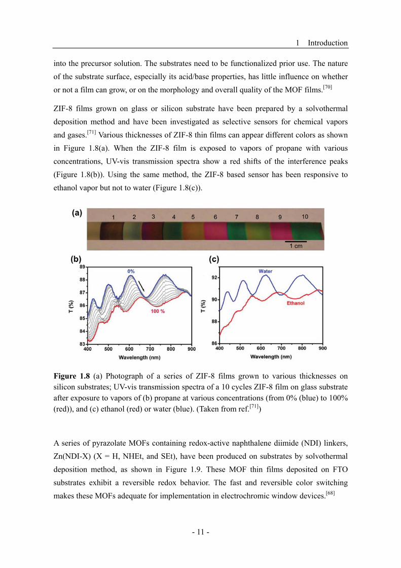
and gases.[71] Various thicknesses of ZIF-8 thin films can appear different colors as shown
in Figure 1.8(a). When the ZIF-8 film is exposed to vapors of propane with various
concentrations, UV-vis transmission spectra show a red shifts of the interference peaks
(Figure 1.8(b)). Using the same method, the ZIF-8 based sensor has been responsive to
ethanol vapor but not to water (Figure 1.8(c)).
Figure 1.8 (a) Photograph of a series of ZIF-8 films grown to various thicknesses on silicon substrates; UV-vis transmission spectra of a 10 cycles ZIF-8 film on glass substrate after exposure to vapors of (b) propane at various concentrations (from 0% (blue) to 100% (red)), and (c) ethanol (red) or water (blue). (Taken from ref.[71])
A series of pyrazolate MOFs containing redox-active naphthalene diimide (NDI) linkers,
Zn(NDI-X) (X = H, NHEt, and SEt), have been produced on substrates by solvothermal
deposition method, as shown in Figure 1.9. These MOF thin films deposited on FTO
substrates exhibit a reversible redox behavior. The fast and reversible color switching
makes these MOFs adequate for implementation in electrochromic window devices.[68]

1 Introduction
- 12 -
Figure 1.9 Synthesis of Zn(NDI-X) (X=H, NHEt, and SEt) MOF and the simulated structure (top); optical images of the macroscopic films of the series of Zn(NDI-X) MOF on FTO (fluorine-doped tin oxide) substrates. (Taken from ref.[68])
Furthermore, a free standing MIL-53 membrane has been formed under mild
hydrothermal condition by sacrificing AAO (anodized aluminum oxide) membrane to
coordinate with H2BDC (BDC = 1,4-benzenedicarboxylate acid). The thickness of the
membrane is equivalent with that of the AAO film. The free standing MIL-53 membrane
has shown good mechanical strength and specific properties for gas separation. The free
standing MOF membranes could have more important applications since they are not
bound to any substrates.[72]
1.2.2 Solvothermal mother solution method
The solvothermal mother solution method is based on the solvothermal MOF synthesis
process. First, MOF powders have to be synthesized by solvothermal method. Then, by
filtering off the large crystals from the reaction mixture, the fresh mother solution is
obtained. Finally, the MOF films are constructed by depositing the MOF crystals through
incubating the functionalized substrates in the mother solution for different periods of
time.[61, 73]

1 Introduction
- 13 -
Continuous MOF-5 (Zn4O(BDC)3, BDC = 1,4-benzenedicarboxylate) thin films have been
synthesized by the solvothermal mother solution method on a glassy carbon electrode
(GCE) with 4-carboxyphenyl as a covalent linker. As shown in Figure 1.10, the MOF-5
thin films on GCE substrates have been used as a photoelectrochemical sensor for the
detection of ascorbic acid.[74]
Figure 1.10 (a) Schematic illustration of the MOF-5 film fabricated on a GCE. (b) Photocurrent responses of the MOF-5 film at 0 V to a light excitation, (inset: linear curve); 0.1 M NBu4ClO4 in acetonitrile, with the presence of 0, 50, 100, 200, 400, 600, 800, 1000, 1200, and 1400 μmol L-1 ascorbic acid (from bottom to top), was used as electrolyte. (Taken from ref.[74])
1.2.3 Spin-coating method
Spin coating is widely used to produce a layer or film to a base material because it is a
very fast process and extremely homogenous and thin films can be obtained. The thickness
of the films can be controlled by varying the coating cycles, the substrate rotation speed
1 Introduction
- 14 -
and the concentration of the deposited solid in the precursor suspensions.[75] One
disadvantage of this method is that the prepared films are not strongly bound to the
substrate.
A MOF film by spin-coating method results from the deposition of the MOF powder
particles, synthesized by solvothermal method, onto the desired substrate from the
precursor solution.[62] Many MOF thin films have been prepared by this method to be used
in device applications.
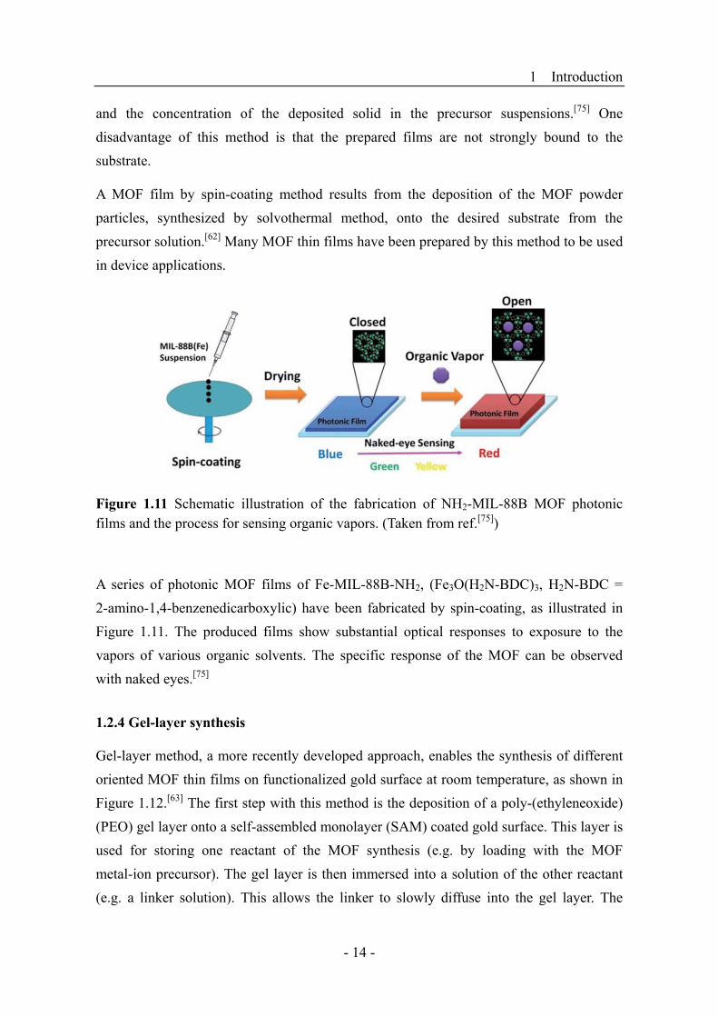
Figure 1.11 Schematic illustration of the fabrication of NH2-MIL-88B MOF photonic films and the process for sensing organic vapors. (Taken from ref.[75])
A series of photonic MOF films of Fe-MIL-88B-NH2, (Fe3O(H2N-BDC)3, H2N-BDC =
2-amino-1,4-benzenedicarboxylic) have been fabricated by spin-coating, as illustrated in
Figure 1.11. The produced films show substantial optical responses to exposure to the
vapors of various organic solvents. The specific response of the MOF can be observed
with naked eyes.[75]
1.2.4 Gel-layer synthesis
Gel-layer method, a more recently developed approach, enables the synthesis of different
oriented MOF thin films on functionalized gold surface at room temperature, as shown in
Figure 1.12.[63] The first step with this method is the deposition of a poly-(ethyleneoxide)
(PEO) gel layer onto a self-assembled monolayer (SAM) coated gold surface. This layer is
used for storing one reactant of the MOF synthesis (e.g. by loading with the MOF
metal-ion precursor). The gel layer is then immersed into a solution of the other reactant
(e.g. a linker solution). This allows the linker to slowly diffuse into the gel layer. The

1 Introduction
- 15 -
MOF nucleation is directed at the interface with the substrate. The gel-layer method is
promising for applications of functional MOF thin films with controlled orientations.
Figure 1.12 Representation of the gel-layer approach for fabrication of uniquely oriented nanoscale MOF films. A SAM functionalized Au substrate is loaded with the poly(ethylene glycol) gel layer containing metal salt (metal ions in red) and covered with a solution containing the linker molecules (blue). (Taken from ref.[63])
1.2.5 Electrochemical deposition
Electrochemical deposition is an effective and versatile method for growing uniform MOF
thin films on conductive substrate surfaces.[22, 76] The electrochemical deposition of MOF
film has been introduced by researchers at BASF.[64] HKUST-1 films on copper electrode
were produced by applying an anodic voltage in a linker solution of BTC (1,3,5-benzene
tricarboxylate).
Figure 1.13 Schematic illustration of the preparation of a biphasic MOF thin films (mixed film) at cathodic potential, El (El < Em < Eh). (Taken from ref.[77])
Biphasic MOF thin films, (Et3NH)2Zn3(BDC)4 and (Zn4O(BDC)3 (the latter is also know
as MOF-5, BDC = 1,4-benzenedicarboxylate), have been formed on an electrode by

1 Introduction
- 16 -
cathodic electrodeposition at room temperature (Figure 1.13). The deposited MOFs can be
either the mixed film or the bilayer film of the two materials owning to the applied
potential. This method for MOFs synthesis enable the direct surface functionalization of
conductive substrate.[77]
Electrophoretic deposition is another well-established technique for thin films fabrication
based on electrochemical techniques, especially used for depositing charged nanoparticles
onto a conductive substrate.[78]
Figure 1.14 shows the scheme of the electrophoretic deposition process of MOFs film. For
this method, the charged MOF particles are first synthesized. A direct current (DC) electric
field is then applied on the electrode in a suspension of the charged MOF particles in a
nonpolar solvent. This results in the deposition of a MOF film. The fabrication of
patterned MOF film is obtained by creating patterned structures of photoresist using
photolithography: the MOF films are deposited on the exposed conductive areas using the
electrophoretic deposition method (Figure 1.14(b)).[78]
Figure 1.14 (a) Schematic illustration of the electrophoretic deposition method for MOFs film growth; the charged MOF particles are attracted to the oppositely charged electrode by applying an electric field. (b) Schematic illustration the procedures for the patterning of MOF film by electrophoretic deposition. (Taken from ref.[78])
By using the electrophoretic deposition method, several representative MOFs (such as
NU-1000,[79] UiO-66,[80] HKUST-1[36] and MIL-53[81]) films have been deposited on
conductive substrates, and the patterned MOF structures have also been successfully
grown on electrodes. The deposited NU-1000 films thus obtained show a reversible redox
behavior thanks to its pyrene based linkers.[78]

1 Introduction
- 17 -
1.2.6 Langmuir-Blodgett (LB) method
The Langmuir-Blodgett (LB) method for the fabrication of MOF thin film was developed
by H. Kitagawa and co-workers.[65] It is a facile bottom-up method for the deposition of a
perfect and preferentially oriented MOF nanofilm on a solid surface at ambient
temperature. The NAFS-1 MOF, CoTCPP-py-Cu, thin film (CoTCPP stands for
5,10,15,20-tetrakis(4-carboxyphenyl)porphyrinato-cobalt(II)) depicted in Figure 1.15,
have been deposited with the individual sheets being highly ordered. The thin layers are
integrated one after another by a horizontal dipping process onto the substrate with
intermediate rinsing. The dipping and rinsing repetition leads to the sequential
layer-by-layer growth of NAFS-1 with any desired thickness.[65]
Figure 1.15 Top: molecular structure of the precursors (CoTCPP, 1; py, 2), (where TCPP = 5,10,15,20-tetrakis(4-carboxyphenyl)porphyrin, py = pyridine), and the 2D array of the CoTCPP-py-Cu (NAFS-1) MOF. Bottom: Schematic illustration of the Langmuir-Blodgett method for the fabrication of NAFS-1 MOF thin film. (Taken from ref.[65])

1 Introduction
- 18 -
1.2.7 Liquid phase epitaxy (LPE) method
Liquid-phase epitaxy (LPE) method relies on the stepwise, layer-by-layer adsorption of
coordinating metal ions and organic ligands from the liquid phase on well-defined
substrates.[82] As schematized in Figure 1.16, a functionalized substrate is immersed
according a sequential and stepwise procedure into the distinct solutions of metal
precursor and organic ligand. The immersions are alternated with rinsing step with solvent
to remove excess reactants.
Figure 1.16 Schematic illustration of the layer-by-layer approach for the growth of MOFs thin film on SAM functionalized substrates. The method is conducted by repeating the immersion of the substrate into the distinct solutions of metal precursor and organic ligand. (Taken from ref.[83])
Shekhah et al.[66] have first prepared such MOF thin film on SAM coated Au surface. The
produced HKUST-1 films have been shown to be highly crystalline and to have a well
controlled orientation.
Figure 1.17 (a) HKUST-1 MOF thin film deposited on microcantilever. (b) Temporal response of the microcantilever piezoresistive sensor to different concentration of water vapor diluted in N2, the concentration of water was increased from bottom (black line) to top (violet). (Taken from ref.[84])

1 Introduction
- 19 -
In an application study, HKUST-1 thin films have deposited on a microcantilever surface
by the LPE method, and the stress-induced chemical recognition has been detected for a
variety of gases (Figure 1.17). It has been found that the energy of molecular adsorption
within the nanoporous of HKUST-1 can be efficiently converted to mechanical energy
demonstrating the system to be a highly responsive, reversible, and selective sensor.[84]
Figure 1.18 (a) Scheme of the optically triggered release of guest molecules from two-component MOF thin films. (b) Triggered release of the guest molecule (butanediol) from the photoswitchable MOF thin film determined by quartz crystal microbalance. The red arrow indicates beginning of the release by irradiating with light at 560 nm. (Taken from ref.[85])
A two-component MOF film has been synthesized on solid surfaces by LPE method. As
shown in Figure 1.18, the bottom layer, Cu2(BPDC)2(BiPy) MOF (BPDC =
biphenyl-4,40-dicarboxylic acid; BiPy = 4,40-bipyridine) can be grown on substrate to
serve as a reservoir, and another layer, Cu2(AB-BPDC)2(BiPy) MOF (AB-BPDC =
2-azobenzene 4,40-biphenyldicarboxylic acid), can be grown atop to serve as a valve
which can be, at wish, opened or closed. This “MOF-on-MOF” system permits an
optically triggered release of guest molecules. By irradiating at a specific wavelength, the
photoswitchable linkers of the outer layer are switched between a trans or cis
conformation state. This either obstructs or clears the outer layer pores and the loaded
guest molecules can be released through this optically controlled process.[85]
1 Introduction
- 20 -
1.3 Surface-anchored metal-organic frameworks (SURMOFs)
Surface-anchored metal-organic frameworks, SURMOFs, refer to these homogenous and
perfectly oriented MOF thin films prepared by the stepwise LPE method.[67, 82] The
SURMOF thickness is normally in the nanometer range (but can also be in micrometer
range with a larger number of deposition cycles), and their growth orientation can be
controlled by suitably functionalizing the substrate surface.
Self-assembled monolayers (SAMs) are the most favored choice for the surface
functionalization in SURMOFs preparation processes because of their long-range
two-dimensional (2D) order, various accessible functional end groups, practical processing,
and the available methods for selective surface patterning (e.g. by microcontact printing or
photolithography).
Different LPE based techniques have been developed to achieve homogeneous SURMOF
thin films provide a true control over their thickness and growth direction. Up to now, four
types of the distinctive LPE methods have been described. Those includes the dipping
method,[66] the spraying method,[86] the pump method,[87] and the quartz crystal
microbalance (QCM) method.[88, 89]
1.3.1 Dipping method
As mentioned in the previous section (section 1.2.7), the first LPE deposited MOF thin
film has been HKUST-1 material and has been obtained by the dipping method.[66] For this
method, four different containers are usually required for: (I) a metal source solution, (II) a
rinsing solution after metal solution application, (III) an organic ligand solution, and (IV)
a rising solution after ligand exposure. A functionalized substrate is immersed into each
container sequentially (from I to IV). The incubation time in metal precursor and organic
ligand solutions can span several to tens of minutes, and each rinsing step less than ten
seconds, so each deposition cycle requires approximately 0.5–1.5 hours. The final film
thickness is well controlled by the number of cycle repetition applied. The prepared
SURMOFs are usually highly crystalline and have a well controlled orientation and film
thickness. However, the process is rather labor intensive and time consuming.
Recently, an automatization of dipping method using a robotic system has been
developed.[90] The system is an automated and computer controlled robot which performs
the dipping process and has proven reliable for SURMOF production.

1 Introduction
- 21 -
1.3.2 Spraying method
The spraying method is more recent LPE method based on a layer-by-layer fabrication
process, and is applied for the production of monolithic, oriented, and crystalline
SURMOF films on solid substrates.[86] There are also four steps for each deposition cycle.
First, the metal solution is sprayed on the substrate (step 1), then the rinsing solvent is
applied (step 2), followed by the ligand solution (step 3) and again the rinsing solvent
(step 4). The number of spraying cycles determines the final thickness of the constructed
SURMOF thin film.
The spraying method allows SURMOFs to be grown as a faster pace than with the dipping
process, and the thickness of SURMOF films obtained can easily reach the micrometer
range. The spraying process is also completely automated by computer control, as
depicted in Figure 1.19. This high-throughput technique allows preparing SURMOF films
with a thickness of 1 µm within a few hours only.
Figure 1.19 Scheme of the spraying method for SURMOF fabrication; (1) Gas supply, (2) gas flow controller, (3) three-way valve gas distributor, (4) solutions storage containers (A, B, C represent the different solution), (5) sample holder and the sample, (6) dosing valves, (7) spray chamber, (8) PC. (Taken from ref.[86])
1.3.3 Pump method
The pump method is also a program controlled system with extra functionalities to control
the temperature in the range of -20–100 °C (20–100 °C when using ethanol as a
solvent).[87] The pump method for SURMOF fabrication is schematized in Figure 1.20.

1 Introduction
- 22 -
For this method, the solution of metal precursor, rinsing solvent, organic ligand, and again
rinsing are sequentially pumped into the sample cell. The SURMOF fabrication results by
repeating the immersion cycles. Long incubation times are also required for the pump
method; this method is then normally used to prepare comparatively thinner SURMOF
films (less than 100 nm).
Figure 1.20 Scheme of the pump method for SURMOF fabrication. The solutions are sequentially pumped into the substrate containing cell. The solutions are a metal precursor and an organic ligand solutions and a rinsing solvent (e.g. ethanol) for intermediate rinsing. The fabrication is done by repeating these immersion cycles. (Taken from ref.[87])
1.3.4 Quartz crystal microbalance (QCM) method
Quartz crystal microbalance (QCM) is an extremely sensitive mass variation detector
(with ng sensitivity) and has been used to analyze mass changes or thickness of thin films
on rigid surfaces under vacuum, gaseous, or liquid environment.[91] QCM system based
method for the preparation of SURMOF film is an automated real-time deposition process
monitoring based on the layer-by-layer growth.[89] The technique with the film deposition
on the quartz sensor (growth on a surface in terms of adsorption) monitors the changes of
the resonance frequency of the sensor, allowing any fabrication processes, adsorption or
desorption (through rinsing) to be directly observed.
A scheme of an in-situ SURMOF thin film preparation inside a QCM cell is presented in
Figure 1.21. The solutions (metal precursor source, rinsing solvent, and organic ligand

1 Introduction
- 23 -
solution) are sequentially flushed through the cell to grow the SURMOF. The fabrication
is achieved by repeating these cycles. One advantage with this method is that the prepared
SURMOF thin films on quartz crystal sensors can be directly used for further monitoring
of phenomena such as occurring in adsorption/desorption and diffusion application.
Figure 1.21 Scheme of in-situ SURMOFs preparation inside the cell of a quartz crystal microbalance (QCM). The solutions are sequentially flown through the cell for the SURMOF growth. The applied solutions are a metal precursor source, an organic ligand solution, and a solvent for intermediate rinsing.
1.4 Motivation
For developing MOFs implementing devices, a method that provides robust anchoring of
MOF thin films on substrate with a high quality and a low defect density is required.[58, 89]
The sequential stepwise LPE deposition method has been confirmed to form compact
SURMOF thin films with well-defined and oriented crystals.[67] It is thus a promising
technique to produce various SURMOF and/or SURMOF-based hybrid materials with a
series of different thickness, whereby their dielectric, optical, and mechanical properties,
with the film used as coatings, offer a sound basis for future industrial applications and
device developments.
MOFs based electronic devices have attracted gradually more attentions,[59, 92-94] especially
in the area of batteries,[95, 96] fuel cells[97] and capacitors.[98] In the latter case, MOFs act
either as an active electronic component by being involved in the charge transport, or as a
porous scaffolds matrix with a structure supporting role. So far, the electrical conductivity
1 Introduction
- 24 -
of MOFs has only received little attention. Investigating the electronic conductivity of the
MOF thin films becomes then critical for the application of these materials in the area of
electronic devices. The tenability of the electrical conductivity of SURMOFs can be
potentially used for the development of advanced electronic devices and sensor.
The mercury-drop-based tunneling junction has been shown to be a very efficient method,
to study the electric transport properties of SAMs[99] or organic chains doped with metal
centers assembled on a conductive substrate,[100] This is due to several advantages when
considering the deposition of metallic top electrode on thin films or surface anchored
molecular wires. The deposition of metallic top electrodes on SURMOF scaffolds may
also produce defect or introduce the penetrating metallic element during the deposition
process. In this regard, the mercury-drop method was selected and used in the present
work to investigate the electric transport properties of SURMOF thin films.
To improve the electrical conductivity and to exploit MOFs as factual components of
electronic devices, one effective strategy is to take advantage of the high porous quality of
the SURMOFs and to load electroactive guest molecules into the nm-size pores of the
framework.[101, 102] In this thesis, the Fc (ferrocene) molecules were used to be loaded in
high quality SURMOF thin films. The effect of the guest loading on the electrical
properties was then investigated by the mercury-drop method. Furthermore, by means of
electrochemical studies, the conductivity of thicker SURMOF thin films with the effect of
Fc loading were also studied.
In terms of availability of suitable electroactive organic ligands,[103, 104] the other strategy
for developing novel electronic, optical and photoactive microporous materials with
MOFs is through processing MOFs into compact and defect free MOF thin films.[105]
Porphyrin, a well-studied photoelectroactive molecule, allowed an effective way for
fabrication of MOF thin films by stacking of the high ordered ligands in the
MOF-frameworks on electrodes. The artificial light harvester and photocurrent generation
was realized through these porphyrin-based MOF thin films.
Furthermore, hybrid nanostructured materials, comprising of organic/metalorganic thin
films and inorganic metal oxide materials, are inherently multi-functional, and are
promising for a wide range of new applications.[59, 106, 107] Along with the properties of
monolithic, high crystalline and greatly oriented SURMOF thin films, the hybrid
organic/inorganic materials were confirmed to be promising for optical sensor and
photonic device applications.

1 Introduction
- 25 -
To summarize, the main objectives of this thesis are: (i) the preparation of high quality
SURMOF thin films with well controlled orientation on well-defined substrates, (ii) the
investigation of the electrical, optical, as well as photoelectrical properties of these
SURMOF thin films; (iii) and by taking advantage of these properties, the fabrication of
SURMOFs based devices, and evaluation of their performance.

2 Methods and General Experimental Information
- 26 -
2 Methods and General Experimental Information
2.1 Characterization methods and instrumental information
In the first section of this chapter, the techniques which were used for the characterization
of produced thin films and coatings are introduced, with a theoretical background.
Information about the instrumentation, as well as specific measurement processes are also
described. The relevant techniques include X-Ray Diffraction (XRD), Ultraviolet-Visible
(UV-Vis) spectroscopy, Fourier Transform Infrared (FTIR) spectroscopy, Raman
spectroscopy, Spectroscopic Ellipsometry (SE), Scanning Electron Microscopy (SEM),
Atomic Force Microscopy (AFM), Time-of-Flight Secondary Ion Mass Spectrometry
(ToF-SIMS), mercury-drop-based tunneling junction, Cyclic Voltammetry (CV), and
Pulsed Amperometric Detection (PAD).
2.1.1 X-ray diffraction (XRD)
X-ray diffraction (XRD) is the most commonly used method to elucidate the structures of
materials, to confirm or determine the crystal structures and orientation, but also to
measure the size, shape and internal strain/stress of small crystalline regions, and
measuring the average layer distances. So it is also a routinely used method for MOFs
and/or SURMOFs.
2.1.1.1 Theoretical background
X-rays are electromagnetic radiation with wavelengths in the range 0.1-10 Å, which were
discovered in 1895 by the German physicist Wilhelm Conrad Röntgen (Nobel Prize for
physics in 1901) and were so named because their nature was unknown at the time. Since
the X-ray wavelengths have the same order of magnitude as the interatomic distances in
condensed phases, X-rays are frequently used to study the internal (crystalline) structure
of materials.[108]
When a crystal is hit with monochromatic X-rays at certain incident angles, the beam is
scattered by the electrons of the atoms without change in wavelength, and intense
reflected X-rays are produced when the wavelengths of the scattered X-rays interfere
constructively. When the constructive interference occurs, the diffracted X-rays will leave
the crystal at an angle equal to that of the incident beam. The phenomenon is called X-ray
diffraction.[109]

2 Methods and General Experimental Information
- 27 -
2.1.1.2 The application of Bragg’s law
A schematic representation of X-ray scattering from a crystalline material is shown in
Figure 2.1. With respect to the equidistant hkl lattice-planes and the interplanar distance
dhkl of the material, an X-ray photon with wavelength λ and incident on the crystal at an
angle (θ) reflects at atom z from the surface of a substance. This photo will travel a lesser
distance than another, from the same packet, which reflects from farther plane of atoms
(atom B in the figure) inside the crystal. Constructive interference will then be observed
for the X-rays that are reflected from the lattice planes at the specular angle, if the path
length difference between X-rays scattered from different hkl-planes is an integer (n)
times the wavelength (λ). The general relation between the waves of the incident X-rays,
angle of incidence and spacing between the crystal lattice planes of atoms is known as
Bragg's Law,[109] and is expressed in eq. (2−1):
2 sinn d (2−1)
This expression explains how the cleavage faces of a crystal reflect X-rays according to
the angle of incidence and the X-ray wave interference.
Figure 2.1 Schematic representation of X-ray scattering from a crystalline material, and the reflection geometry and trigonometry used for deriving the Bragg's Law. The lower beam (2) must travel the extra distance (AB + BC) to continue traveling parallel and adjacent to the top beam (1). (Adapted from ref.[110])
Bragg's Law may also be interpreted graphically in a practical way using reflection
geometry and trigonometry, as shown in Figure 2.1. With the incident angle equal to the
reflecting angle, the necessary conditions to make the phases of the beams coincide are
that incident X-rays have to be in phase and parallel at the point where of incidence. The

2 Methods and General Experimental Information
- 28 -
beam strikes first at atom z of the top layer. It penetrates deeper to a lower layer and is
scattered by atom B. If the two reflected beams travel farther adjacent and parallel, they
will have path length difference equating AB + BC. This additional distance must be an
integral (n) multiple of the wavelength (λ) for the phases of the two beams to be identical
(shown as eq. (2−2)); if not in phase the produced ray will be feint:
n AB BC (2−2)
Recognizing d (same with dhkl) as the hypotenuse of the right triangle ABZ, simple
trigonometry relates d and θ to the distance (AB + BC). The distance AB being opposite to
θ one gets:
sinAB d (2−3)
Because AB = BC eq. (2−2) becomes,
2n AB (2−4)
Substituting eq. (2−3) in eq. (2−4), eq. (2−1) was gotten, which is the final expression of
Bragg’s law.
Bragg’s law identifies the angles of the incident radiation relative to the lattice planes for
which diffraction peaks occurs, and the condition for constructive interference of the
X-rays scattered from a defined set of parallel lattice planes.
2.1.1.3 X-ray diffractometer
Most diffractometers used in material science are based on the reflection geometry. In this
case, the source and detector are on the same side of the sample and the scattered X-rays
are reflected onto the detector. This is known as the Bragg-Brentano type geometry as
shown in Figure 2.2.
The main components of diffractometer are the X-ray tube, the incident-beam optics, the
sample holder, the receiving-side optics, and the detector. The source is typically an X-Ray
tube. The incident-beam optics control the beams output by the X-ray source, and
manipulate it into a monochromatic, narrow, and parallel form focused on to the sample.
The sample holder keeps the specimen fixed in the right position during the experiment.
The receiving-side optics retrieves the diffracted X-rays from the sample, which includes
the anti-scatter slit and detector slits and a monochromators for focusing of the beam onto
the detector. The detector transforms the diffracted X-rays to electronic signals.

2 Methods and General Experimental Information
- 29 -
Figure 2.2 The scheme of typical Bragg-Brentano type geometry for X-ray diffractometer, mainly including X-ray tube, Incident-beam optics (divergence slit), Sample holder, receiving-side optics (antiscatter slit, detector slit and monochromator) and detector. (Taken from ref.[111])
2.1.1.4 The diffraction patterns
Diffraction occurs when incident X-rays are scattered by a periodic array of atoms in
crystal materials, producing constructive interference at specific angles. The resulting
diffraction pattern of a crystal, comprising both the peak positions and signal intensities
(Figure 2.3), provides structure information about the lattice parameters of the sample.
The size, shape, and orientation of the unit cell can be known by the diffraction pattern
analysis.[109]
Figure 2.3 Information content of a XRD pattern: peak position, intensity and profile (peak shape, FWHM, integral breadth). (Adapted from ref.[112])
2 Methods and General Experimental Information
- 30 -
The unit cell parameters of crystalline materials are determined from the angular positions
of the Bragg reflections. In large, perfect crystals, there is always a ‘‘deeper’’ lattice plane
for which a path length distance of 0.5 λ is valid. As shown in Figure 2.1, if only two rows
of atoms were involved for scattering of the X-rays, the signal intensity from constructive
to destructive interference would be a sine-squared function of θ. However, with more
atoms rows involved, the constructive interference peaks become very sharp with mostly
destructive interference and low reflectivity in between. This sharpening of the peaks as
the number of rows increases is very similar to the sharpening of the diffraction peaks
from a diffraction grating as the number of slits increases.[110]
There are two different ways of characterizing the width of a reflection peak. The
conventional FWHM (full width at half maximum) describes the width of the diffraction
peak (in radians) at half height between the background and peak maximum. The integral
breadth, B(2θ), has to be applied if crystallite size should be precisely analyzed, and can
be interpreted as the width of a rectangle having the same area and height of the peak
(Figure 2.3).[111]
If a sample had large, strain-free and perfect crystallites, the diffraction peaks of the XRD
pattern would be extremely narrow. However, real crystals exhibit structural imperfections
which cause nonhomogeneous strain distribution. As a consequence, the diffraction lines
can broaden. This can also result from instrumental factors and other material properties,
such as size of crystalline domains, shape of the crystalline domains and size distribution.
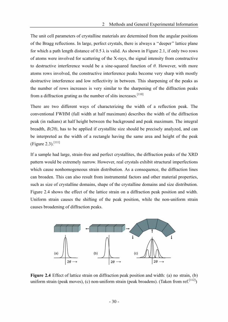
Figure 2.4 shows the effect of the lattice strain on a diffraction peak position and width.
Uniform strain causes the shifting of the peak position, while the non-uniform strain
causes broadening of diffraction peaks.
Figure 2.4 Effect of lattice strain on diffraction peak position and width: (a) no strain, (b) uniform strain (peak moves), (c) non-uniform strain (peak broadens). (Taken from ref.[112])
2 Methods and General Experimental Information
- 31 -
2.1.1.5 Thin films XRD measurement
For powder XRD measurements, the sample is piled to produce a random orientation
distribution of crystallites, so that there is always population for which the orientation
permits diffraction. In this process, all the diffraction peaks will possible be measured.
However, when a sample is “thin film”, the two-dimensionally formed by the sample
surface, leads to more difficult measurements because of the different characteristics of the
thin film and the additional mechanical constraints.[113]
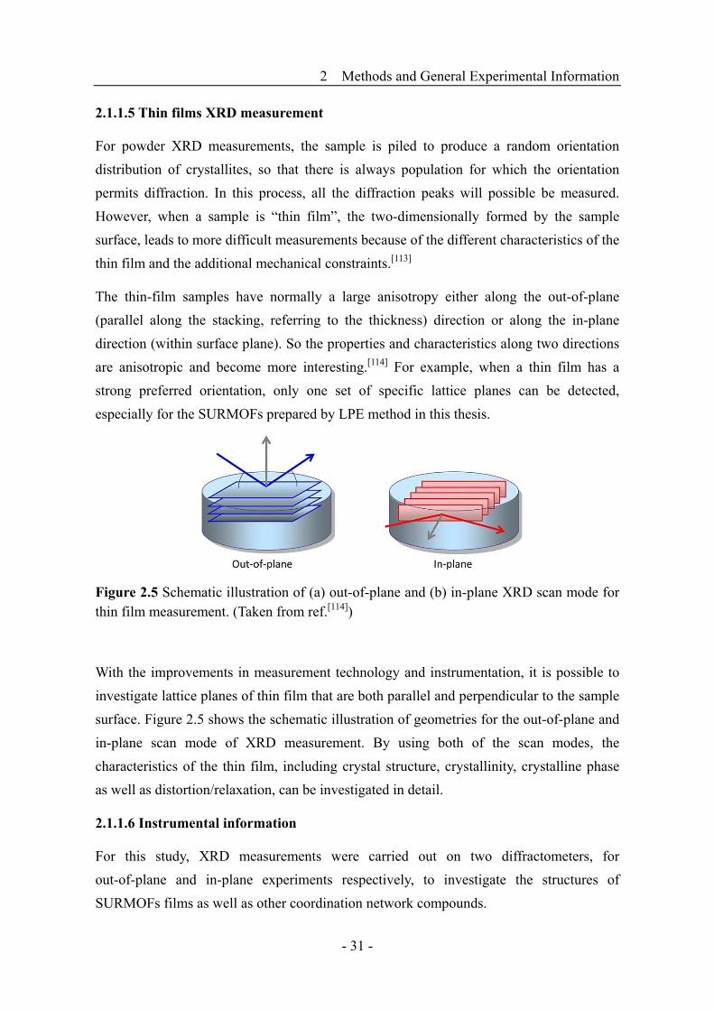
The thin-film samples have normally a large anisotropy either along the out-of-plane
(parallel along the stacking, referring to the thickness) direction or along the in-plane
direction (within surface plane). So the properties and characteristics along two directions
are anisotropic and become more interesting.[114] For example, when a thin film has a
strong preferred orientation, only one set of specific lattice planes can be detected,
especially for the SURMOFs prepared by LPE method in this thesis.
Figure 2.5 Schematic illustration of (a) out-of-plane and (b) in-plane XRD scan mode for thin film measurement. (Taken from ref.[114])
With the improvements in measurement technology and instrumentation, it is possible to
investigate lattice planes of thin film that are both parallel and perpendicular to the sample
surface. Figure 2.5 shows the schematic illustration of geometries for the out-of-plane and
in-plane scan mode of XRD measurement. By using both of the scan modes, the
characteristics of the thin film, including crystal structure, crystallinity, crystalline phase
as well as distortion/relaxation, can be investigated in detail.
2.1.1.6 Instrumental information
For this study, XRD measurements were carried out on two diffractometers, for
out-of-plane and in-plane experiments respectively, to investigate the structures of
SURMOFs films as well as other coordination network compounds.
2 Methods and General Experimental Information
- 32 -
Out-of-plane XRD was carried out on a Bruker D8 Advance in θ–θ geometry equipped
with a Si-strip detector (PSD Lynxeye©) using Cu Kα1,2 radiation (λ = 0.15419 nm). On
the tube side a variable divergence slit set to V12 (variable slit opening with 12 mm
sample spot size) and on the receiving side a 2.5° Soller slit was used.
In-plane XRD was carried out on a Bruker D8 Discover in θ-2θ geometry equipped with a
quarter Eulerian cradle, tilt-stage, 2.3° Soller-slits on both sides, a Göbel-mirror, and a
PSD Lynxeye®, utilizing also the Cu Kα1,2 radiation (λ = 0.15419 nm).
2.1.2 Ultraviolet-visible (UV-Vis) spectroscopy
Ultraviolet-visible (UV-Vis) spectroscopy is usually used to determine the concentration,
according to Lambert-Beer law, of a solute absorber, such as transition metal ions, highly
conjugated organic compounds, and biological macromolecules. The wavelengths of
UV-Vis absorption bands can also be correlated with electronic transitions of matters,
which are valuable in determining the functional groups (Chromophores) within a
molecule.
2.1.2.1 Theoretical background
UV-Vis refers to the absorption or the reflectance spectroscopy in the UV-Vis spectral
region, which is conventionally divided into three sub-domains termed low UV (185–400
nm), visible (400–700 nm) and near infrared (700–1100 nm). The UV-Vis spectra of the
analyte represent the interaction between the radiation in UV region and matter, and
measure the absorbance, transmittance, or reflection (for thin films) as a function of
wavelength. The UV-Vis spectra show only a few broad absorbance bands because of the
limited electronic transitions of the atoms.[115]
In the UV–Vis region of the electromagnetic spectrum, molecules undergo electronic
transitions.[116] Organic compounds represent the majority of the materials studied in the
UV–vis range. The observed electronic transitions in an organic compounds involve
electrons engaged in σ or π or non-bonding n (atoms with lone pairs, such as O, N, S, Cl,
etc.) electron orbitals, as shown in Figure 2.6. The more excitable the electrons of a
sample are (e.g. lower energy gap between the bonding and the antibonding), the longer
the wavelength of light it can absorb is.
σ → σ* transition: an electron in a bonding σ orbital is excited to the corresponding
antibonding orbital. Specifically, the saturated hydrocarbons contain this type of bonding

2 Methods and General Experimental Information
- 33 -
in the near UV region. And the absorption maxima of this transition are not seen in typical
UV–vis spectra.
n → σ* transition: saturated compounds containing n electrons (non-bonding electrons)
are capable to be excited to the σ antibonding orbital. These transitions usually need less
energy than σ → σ* transitions, which can be excited by wavelengths of 150–250 nm.
π → π* transition: an electron in a bonding π orbital is excited to the corresponding
antibonding orbital. These transitions need an unsaturated group in the molecule to
provide the π electrons, and can be excited by the region 200–700 nm.
n → π* transition: an n electron (non-bonding electrons) is excited to an antibonding π*
orbital. This transition is usually observed in molecules containing a hetero-atom carrying
lone electron pairs as part of an unsaturated system.
Numerous inorganic compounds contains electrons engaged in d orbitals which are
responsible for transitions of weak absorption located in the visible region (d → d
transition), and are generally responsible for the color of the materials. Furthermore, the
electrons transfer between two metal sites differing only in their oxidation state is named
intervalence charge transfer (anion → anion transition). The intense blue color of
Prussian Blue results from intervalence charge transfer, which is associated with the
energy of the transfer of electrons from Fe(II) to Fe(III).[117, 118]
Figure 2.6 Electron transitions of organic compounds in UV-Vis spectroscopy. (Taken from ref.[119])

2 Methods and General Experimental Information
- 34 -
2.1.2.2 Instrumental information
UV-VIS absorption and angle dependent reflectance measurements were performed on a
Cary 5000 UV-VIS-NIR Spectrometer (Agilent Technologies, USA). UV-VIS absorption
measurements were done in transmission mode. The angle dependent reflectance
measurements were carried out with a computer controlled Agilent UMA® specular
reflectance accessory, which is specially designed for absolute reflectance (%R)
measurements at variable angles of incidence. (Results relating to this technique are
presented in Chapter 4).
In-situ spectral reflectometry was performed by using a spectrometer (NanoCalc 2000)
equipped with a combined halogen and deuterium light source (DH-2000 FHS,
Mikropack). Four optical fibers are equipped in one wire, where fiber 1 and 2 led to the
lamp and illuminated beam (2 mm diameter spots) onto the sample surface. Additionally,
this equipment was also used for the time dependent chemo-responsive optical sensing
under Glove-box conditions, where the sorption/detection reflectometry studies were
performed by exposing with organic vapours (Results relating to this technique are
presented in Chapter 4).
2.1.3 Fourier transform infrared (FTIR) spectroscopy
Infrared (IR) spectroscopy is a reliable and powerful technique widely used for the
identification and structural analysis, based on the vibrations of chemical bonds of the
atoms, in both organic and inorganic chemistry. The samples for IR characterization can
be solid, liquid, gas, as well as the interfacial species.[120]
2.1.3.1 Theoretical background
Analytical infrared studies are based on the absorption (or reflection) of the
electromagnetic radiation with a wavelength between 1 and 25 μm. This spectral range is
sub-divided into three smaller areas, the near-infrared (near-IR, 1–2.5 μm), the
mid-infrared (mid-IR, 2.5–50 μm) and the far-infrared (far-IR, beyond 25 μm). However,
because the near-IR is poor in specific absorption bands and the far-IR requires the use of
specialized optics and sources, these spectral ranges are not used as widely as the mid-IR
region which provides more information on the structures of compounds.[116]
Due to the many advantages of Fourier transform infrared (FTIR) spectroscopy, such as
multiplex (information from all wavelengths is collected simultaneously) and throughput

2 Methods and General Experimental Information
- 35 -
(interferometer throughput is determined only by the diameter of the collimated beam
coming from the source), almost every spectrometer used today in mid-infrared
spectroscopy is of the Fourier-transform type.[120]
Infrared absorption by molecules results from the transitions between quantized
vibrational energy states. Molecular vibrations can range from the simple coupled motion
of the two atoms of a diatomic molecule to the much more complex combination of each
atom motion in a large polyfunctional molecule. Vibrations can involve either a change in
bond length (stretching) or bond angle (bending).
Figure 2.7 Stretching and bending vibrational modes for the linear CO2 molecule. (Taken from ref.[121])
For molecules with N number of atoms in them, linear molecules have 3N–5 degrees of
vibrational modes (CO2 is shown as an example in Figure 2.7), whereas nonlinear
molecules have 3N–6 degrees of vibrational modes (H2O is shown as an example in
Figure 2.8). In order for a vibrational mode in a molecule to be "IR active", it must be
associated with changes in the dipole.[116]
Figure 2.8 Stretching and bending vibrational modes for nonlinear H2O molecule. (Taken from ref.[121])
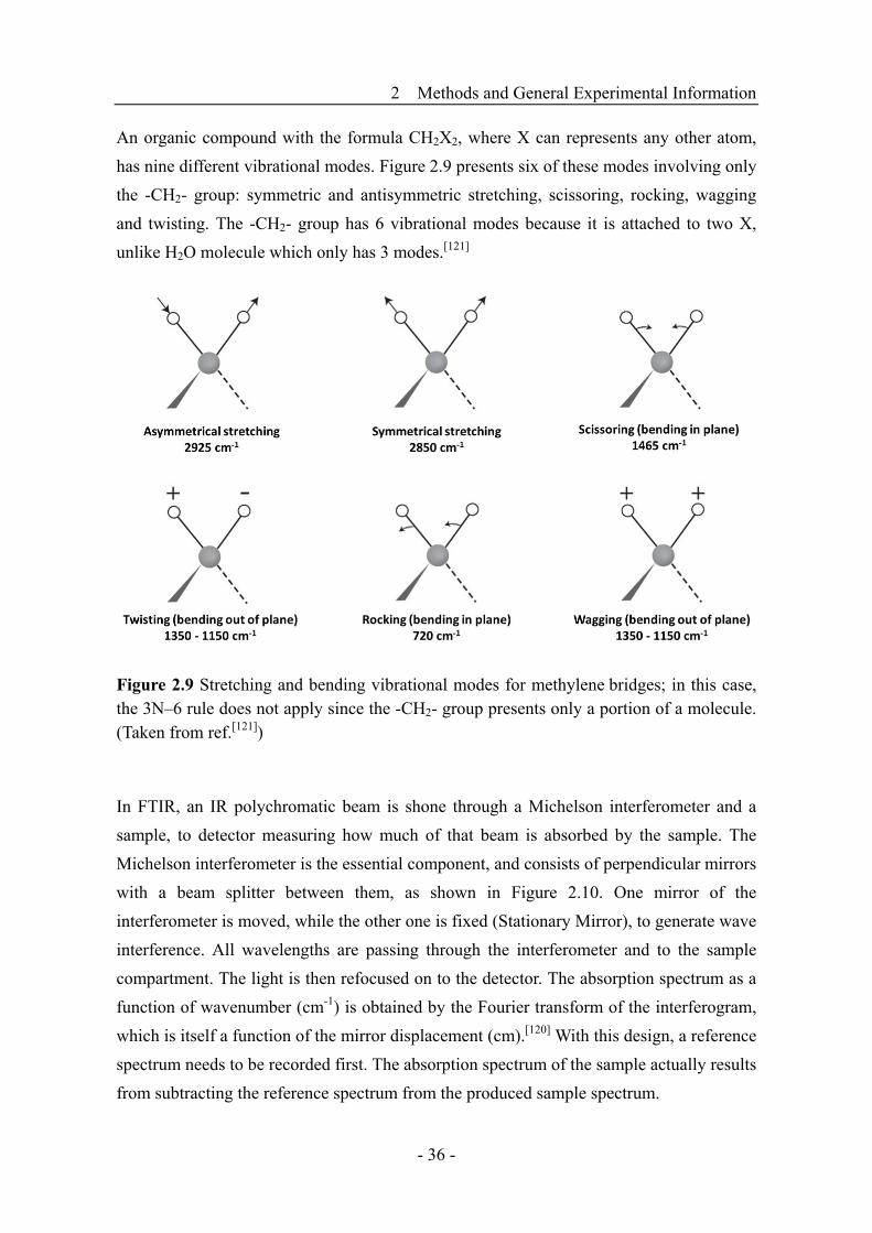
2 Methods and General Experimental Information
- 36 -
An organic compound with the formula CH2X2, where X can represents any other atom,
has nine different vibrational modes. Figure 2.9 presents six of these modes involving only
the -CH2- group: symmetric and antisymmetric stretching, scissoring, rocking, wagging
and twisting. The -CH2- group has 6 vibrational modes because it is attached to two X,
unlike H2O molecule which only has 3 modes.[121]
Figure 2.9 Stretching and bending vibrational modes for methylene bridges; in this case, the 3N–6 rule does not apply since the -CH2- group presents only a portion of a molecule. (Taken from ref.[121])
In FTIR, an IR polychromatic beam is shone through a Michelson interferometer and a
sample, to detector measuring how much of that beam is absorbed by the sample. The
Michelson interferometer is the essential component, and consists of perpendicular mirrors
with a beam splitter between them, as shown in Figure 2.10. One mirror of the
interferometer is moved, while the other one is fixed (Stationary Mirror), to generate wave
interference. All wavelengths are passing through the interferometer and to the sample
compartment. The light is then refocused on to the detector. The absorption spectrum as a
function of wavenumber (cm-1) is obtained by the Fourier transform of the interferogram,
which is itself a function of the mirror displacement (cm).[120] With this design, a reference
spectrum needs to be recorded first. The absorption spectrum of the sample actually results
from subtracting the reference spectrum from the produced sample spectrum.

2 Methods and General Experimental Information
- 37 -
Figure 2.10 Schematic diagram of a Michelson interferometer configured for FTIR. The median ray is presented by the solid line, and the extremes of the collimated beam are presented by the dashed line. (Taken from ref.[120])
2.1.3.2 Infrared reflection absorption spectroscopy (IRRAS)
Infrared reflection absorption spectroscopy (IRRAS) is a powerful surface specific
spectroscopic method for the investigation of absorbed monolayers, thin films, and
coatings placed on a highly reflective surface. In an IRRAS experiment, the sample is
investigated in reflection geometry under grazing incidence (typically 80°). The sensitivity
of this method can be significantly enhanced by employing the polarization modulation
technique (PM).[122]
2.1.3.2.1 Polarization and grazing incidence
A linearly polarized light can be defined by the sum of two orthogonal components, the s-
and p-polarized light, as shown in Figure 2.11(a). The p-polarized light is parallel to the
plane of incidence, while the s-polarized light is perpendicular to the plane of incidence
(parallel to the surface).[123]
Figure 2.11(b) presents phase shift of the s- and p-polarized radiations as the function of
incident angle (θ) at a clean metal surface. It can be seen that the s-polarized light
undergoes a uniform phase shift of 180° for all angles of incidence (from 0 to 90°),
resulting in a nearly total cancellation of the amplitude at the surface (destructive

2 Methods and General Experimental Information
- 38 -
interference) and giving a vanishing electric field at the surface. There is then no
consequent electric field parallel to the surface. However, the phase shift of p-polarized
light is strongly dependent on the angle of incidence and reaches 90° at higher degree,
which results in amplitude addition (constructive interference). Thus it is necessary to
perform IRRAS experiments at a high angle of incidence (close to grazing incidence), due
to the fact that the large electric field is established to interact with the dipole moment of
the vibrations perpendicular to surface at this incidence.[123]
Figure 2.11 (a) Scheme of the incident IR beam (at the angle of θ) reflected by the metallic surface (yellow), the incidence plane (perpendicular light blue plane) is defined by the incident and the reflected light path, and the p (red) and s (blue) component of the polarized IR radiation; (b) phase shift of the s (ds) and p (dp) component radiations versus angle of incidence θ at a clean metal surface. (Adapted from ref.[123])
Figure 2.12 Calculated reflectivity differences between the clean substrate (R0) and the adsorbate-covered substrate (RF) for different substrate materials as a function of the light incidence angle for p-polarized radiation (solid lines) and s-polarized radiation (broken lines) at 3000 cm-1. (Taken from ref.[122])
Figure 2.12 presents the calculated reflectivity differences (R0–RF) for various substrate
materials (R0) after being covered with adsorbate (RF) and as a function of the light
incidence angle for p- and s-polarized radiation. It can be seen that the adsorbate on

2 Methods and General Experimental Information
- 39 -
metallic surface interact with the p-polarized fraction of light, and the intensity reaches the
maximum at large angles of incidence (88°) for the p-polarized light, but not with the
s-polarized one.[122]
2.1.3.2.2 Surface selection rule
As mentioned previously, only the p-component radiation interacts with the surface of
sample (Figure 2.12(a)). Consequently, only the active vibrations, having a component of
the dynamic dipole polarized along the normal to the sample/substrate interface, can be
detected by IRRAS. These results give the so‐called “surface selection rule”, which is
used to study the molecular orientation of thin films or monolayers deposited on metal or
dielectric substrates.[120]
Figure 2.13 illustrates the situation with electric fields of the incident IR light with both
perpendicular (red) and parallel (blue) components, and the transition dipole moment
(TDM) of molecules and the mirrors charges on metallic surface. Only vibrations with a
dipole moment perpendicular to the surface are excited, because the surface electric field
is enhanced by the electric field resulted from the induced mirror charges in the metallic
substrate surface. The displacement of the dipole moment depends on the absorbed
molecules perpendicular or parallel to substrate surface.
Figure 2.13 Schematic drawing of IR surface selection rule on metallic surface.
2.1.3.3 Instrumental information and conditions relating this work
The IRRA spectra were acquired using the infrared spectrometer Bruker VERTEX 80. The
absorption band positions are given in wave numbers ν in cm-1, with a resolution of 2 cm-1.
All the IRRA spectra were recorded in grazing incidence reflection mode at an angle of
incidence amounting to 80° relative to the surface normal using liquid nitrogen cooled
mercury cadmium telluride (MCT) narrow band detectors. Perdeuterated hexadecanethiol
SAMs on Au/Si were used for background measurements.

2 Methods and General Experimental Information
- 40 -
2.1.4 Raman spectroscopy
Raman spectroscopy is a form of vibrational spectroscopy, and is complementary to IR
absorption spectroscopy. As mentioned in the previous section, the vibrational states of a
molecule can be probed through infrared spectroscopy, because the vibrational transitions
typically require an amount of energy that corresponds to the infrared region of the
spectrum. However, molecules which have no net dipole moment (such as N2 and O2) are
not observable in the IR spectra, and functional groups with symmetric bonds (such as -S–
S-, -C–S-, -C=C-) give weak responses in the IR spectra.[124]
Figure 2.14 Energy-level diagram showing the different vibration states involved in Raman signal, ΔE = absorbance. The line thickness is roughly proportional to the signal strength from the different transitions.
Raman spectroscopy involves shining a monochromatic light source (i.e. laser) on a
sample and analyzing the scattered light. When light is scattered from a molecule, the
majority of the scattered light is of the same frequency as the excitation source (incoming
light); this is known as Rayleigh or elastic scattering, as shown in Figure 2.14. However, a
small fraction of light (approximately 10-5 % of the incident light intensity) is scattered
with a shift in energy (or wavelength) due to interactions between the incident light and
the vibrational energy levels of the molecules in the sample. The resulting inelastically
scattered light can be of either lower (Stokes) or higher (anti-Stokes) energy than the
incoming light.[125]

2 Methods and General Experimental Information
- 41 -
Plotting the intensity of this “shifted” light versus frequency results in a Raman spectrum
of the sample. Generally, Raman spectra are plotted relative to the laser frequency used
such that the Rayleigh band lies at 0 cm-1. On this scale, the band positions will lie at
frequencies that correspond to the energy levels of different functional group vibrations
due to an interaction of light with the molecule.
The excitation wavelength used in Raman spectroscopy can range from the near infrared
to the ultraviolet. However, the choice of the wavelength should be done carefully,
because the wavelength could possibly destroy the sample by absorption or induce
resonance and fluorescence if it is not chosen well. For materials that show fluorescence,
it is vital to choose a longer wavelength that will minimize this effect, otherwise the weak
Raman interaction will be swamped because the high intensity of fluorescence could make
the detector overload. Whereas shorter wavelength lasers (higher energy) can be useful for
penetrating certain samples where fluorescence is not a problem.[125]
In this thesis, the Raman spectra were recorded with a Bruker Senterra Raman microscope
(Bruker Optics, Ettlingen, Germany) using a green laser at 532 nm for excitation. The 2D
Raman-Map characterization was performed on the same instrument. The analysis of the
data was done with the Bruker evaluation software OPUS 7.2.
2.1.5 Spectroscopic ellipsometry (SE)
Ellipsometry is a very sensitive optical technique that uses polarized light to probe the
thickness and dielectric properties of a thin film sample. Upon analyzing the change of
polarization of the light reflected off a sample, ellipsometry can yield information about
layers that are thinner than the wavelength of the probing light itself.[126]
Spectroscopic ellipsometry (SE) refers to ellipsometric measurements that are carried out
at various wavelengths of the incident beam, which covers the visible range (VIS) and
parts of both the ultraviolet (UV) and the near infrared (NIR) range of the electromagnetic
spectrum. SE can provide information about not only single layers, but also thick layers,
complex materials and multilayer systems. Due to its great versatility, SE is an established
technique for thin film analyses, as well as the quality controls in industrial fabrication.
A schematic of an ellipsometry measurement is shown in Figure 2.15. The incident light is
a linear polarized light with both p- and s-components, which is produced by a polarizer.
The light undergoes amplitude and phase changes for both p- and s-components upon
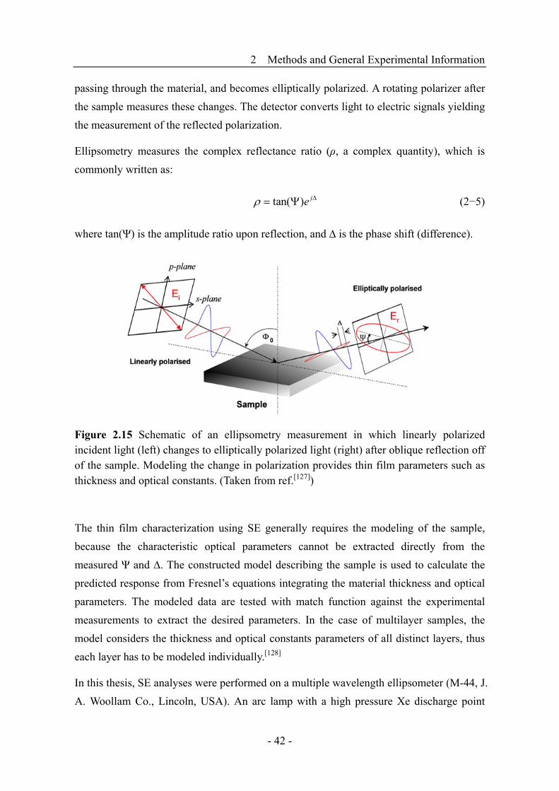
2 Methods and General Experimental Information
- 42 -
passing through the material, and becomes elliptically polarized. A rotating polarizer after
the sample measures these changes. The detector converts light to electric signals yielding
the measurement of the reflected polarization.
Ellipsometry measures the complex reflectance ratio (ρ, a complex quantity), which is
commonly written as:
tan( ) je (2−5)
where tan(Ψ) is the amplitude ratio upon reflection, and ∆ is the phase shift (difference).
Figure 2.15 Schematic of an ellipsometry measurement in which linearly polarized incident light (left) changes to elliptically polarized light (right) after oblique reflection off of the sample. Modeling the change in polarization provides thin film parameters such as thickness and optical constants. (Taken from ref.[127])
The thin film characterization using SE generally requires the modeling of the sample,
because the characteristic optical parameters cannot be extracted directly from the
measured Ψ and ∆. The constructed model describing the sample is used to calculate the
predicted response from Fresnel’s equations integrating the material thickness and optical
parameters. The modeled data are tested with match function against the experimental
measurements to extract the desired parameters. In the case of multilayer samples, the
model considers the thickness and optical constants parameters of all distinct layers, thus
each layer has to be modeled individually.[128]
In this thesis, SE analyses were performed on a multiple wavelength ellipsometer (M-44, J.
A. Woollam Co., Lincoln, USA). An arc lamp with a high pressure Xe discharge point

2 Methods and General Experimental Information
- 43 -
source was used. Modeling, fitting, and regression analyses of the ellipsometric data were
performed using the software provided by the manufacturer (WVASETM). For the photo
band gap simulations, the program WINCPC for Woollam M-44 ellipsometer was used.
2.1.6 Scanning electron microscopy (SEM)
The scanning electron microscope (SEM) is a type electron microscope with broad
applications in the study of solid materials. The SEM is mainly used to image at
high-resolution the shapes of objects (morphology), but can also be used to show the
spatial variations in chemical compositions (density). SEM is then usefull to investigate
the morphology, the structure, and the orientation of crystals in thin film materials.[129]
SEM uses a focused beam of high-energy electrons to interact with atoms in the sample
and generate various signals at the surface of sample. These signals include secondary
electrons (SE), backscattered electrons (BSE), diffracted backscattered electrons (EBSD),
photons (here characteristic X-rays), visible light and heat.[129] Though rarely a single
machine would be equipped with all necessary detectors, various information about the
sample can be obtained by collecting and analyzing these signals:
(i) Secondary electrons and backscattered electrons are commonly used for imaging: the
morphology and topography of samples are acquired from SE, and the composition
contrasts in multiphase samples (i.e. for rapid phase discrimination) are acquired from
BSE;
(ii) Diffracted backscattered electrons are used to determine crystal structures and
orientations of minerals;
(iii) Characteristic X-rays are used for elemental analysis, referring to energy-dispersive
X-ray spectroscopy (EDS).
Figure 2.16 shows a scheme of a SEM setup. The SEM column and sample chamber are
under vacuum. This allow the electrons to travel freely from the electron beam source to
the sample and then to the detectors. An incident electron beam (energy is ranging from
0.1 keV to 40 keV) is generated from an electron gun above the sample chamber by
thermal emission, with a heated tungsten filament, or with a field emission cathode. The
electrons are focused to a spot about 0.4 to 5 nm in diameter by a series of electromagnetic
lenses in column. Scanning coils near the end of the column direct and position the
focused beam onto the targeted sample surface.[129]
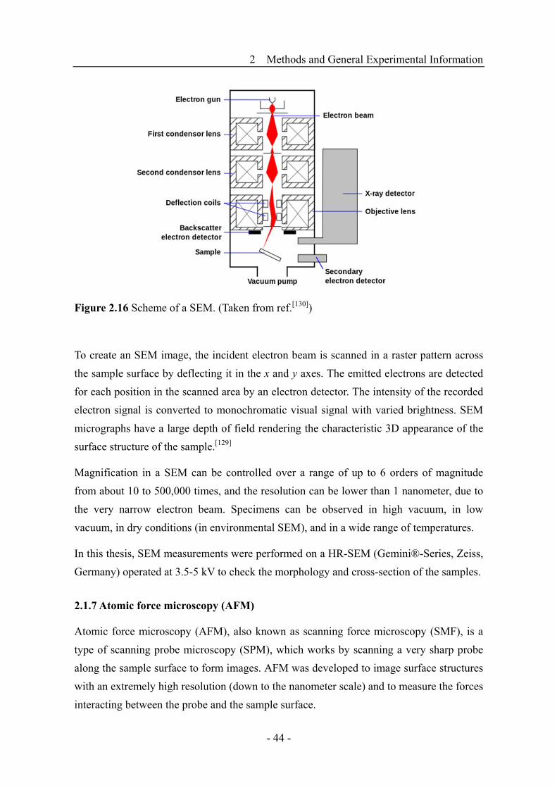
2 Methods and General Experimental Information
- 44 -
Figure 2.16 Scheme of a SEM. (Taken from ref.[130])
To create an SEM image, the incident electron beam is scanned in a raster pattern across
the sample surface by deflecting it in the x and y axes. The emitted electrons are detected
for each position in the scanned area by an electron detector. The intensity of the recorded
electron signal is converted to monochromatic visual signal with varied brightness. SEM
micrographs have a large depth of field rendering the characteristic 3D appearance of the
surface structure of the sample.[129]
Magnification in a SEM can be controlled over a range of up to 6 orders of magnitude
from about 10 to 500,000 times, and the resolution can be lower than 1 nanometer, due to
the very narrow electron beam. Specimens can be observed in high vacuum, in low
vacuum, in dry conditions (in environmental SEM), and in a wide range of temperatures.
In this thesis, SEM measurements were performed on a HR-SEM (Gemini®-Series, Zeiss,
Germany) operated at 3.5-5 kV to check the morphology and cross-section of the samples.
2.1.7 Atomic force microscopy (AFM)
Atomic force microscopy (AFM), also known as scanning force microscopy (SMF), is a
type of scanning probe microscopy (SPM), which works by scanning a very sharp probe
along the sample surface to form images. AFM was developed to image surface structures
with an extremely high resolution (down to the nanometer scale) and to measure the forces
interacting between the probe and the sample surface.

2 Methods and General Experimental Information
- 45 -
Basically, in a standard AFM in oscillation mode, the tip of a cantilever (made of Si or
Si3N4) is brought into proximity of a sample surface with two piezoelectric elements
generating the relative movement between the cantilever and the sample, as shown in
Figure 2.17. While the sharp tip of the cantilever moves over the sample, the cantilever
itself bends according to the surface interaction. The deflection is detected by a laser beam
which is reflected from the backside of cantilever onto a set of position sensitive
photodiodes. By setting the constant tip-sample distance or oscillating amplitude in a
feedback principle as it scans over the surface, the surface morphology can be
reconstructed from the signal applied to the piezoelectric elements. Generally, the imaging
modes of AFM are in contact modes and tapping mode (the cantilever is vibrated or
oscillated at a given frequency) depending on the application.[131]
Figure 2.17 Scheme of an AFM. (Taken from ref.[132])
Comparing to other high resolution microscopy (such as SEM and TEM), AFM has
several great advantages. One is that AFM can image almost any type of surface,
including conductor, insulator as well as biological samples. It is also simple to operate in
most environments, such as under atmospheric (or other gases), vacuum conditions or
liquid immersion (aqueous solutions as well as other solvents) of the sample. AFM can
provide a 3D surface profile with a resolution at a sub-Angstrom along the z direction
(height resolution) and down to1 nm on X-Y directions (lateral resolution).
In this thesis, Tapping-mode AFM was used to measure the morphology and thickness of
the SURMOF films on a Multimode AFM (Bruker, Germany) with a “J” scanner. (Results
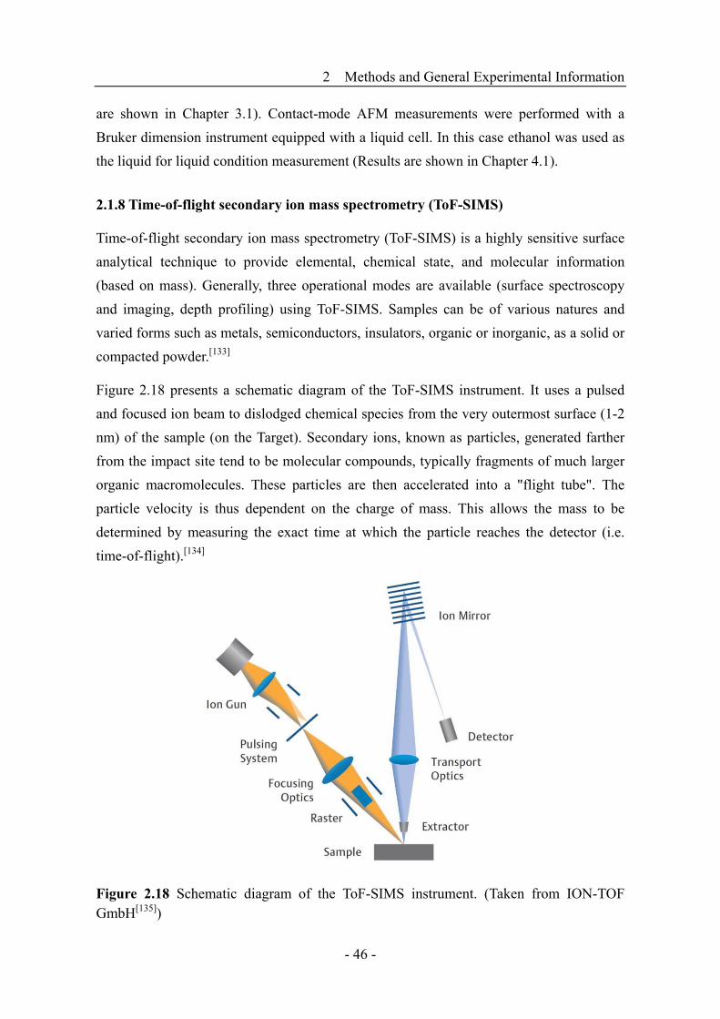
2 Methods and General Experimental Information
- 46 -
are shown in Chapter 3.1). Contact-mode AFM measurements were performed with a
Bruker dimension instrument equipped with a liquid cell. In this case ethanol was used as
the liquid for liquid condition measurement (Results are shown in Chapter 4.1).
2.1.8 Time-of-flight secondary ion mass spectrometry (ToF-SIMS)
Time-of-flight secondary ion mass spectrometry (ToF-SIMS) is a highly sensitive surface
analytical technique to provide elemental, chemical state, and molecular information
(based on mass). Generally, three operational modes are available (surface spectroscopy
and imaging, depth profiling) using ToF-SIMS. Samples can be of various natures and
varied forms such as metals, semiconductors, insulators, organic or inorganic, as a solid or
compacted powder.[133]
Figure 2.18 presents a schematic diagram of the ToF-SIMS instrument. It uses a pulsed
and focused ion beam to dislodged chemical species from the very outermost surface (1-2
nm) of the sample (on the Target). Secondary ions, known as particles, generated farther
from the impact site tend to be molecular compounds, typically fragments of much larger
organic macromolecules. These particles are then accelerated into a "flight tube". The
particle velocity is thus dependent on the charge of mass. This allows the mass to be
determined by measuring the exact time at which the particle reaches the detector (i.e.
time-of-flight).[134]
Figure 2.18 Schematic diagram of the ToF-SIMS instrument. (Taken from ION-TOF GmbH[135])

2 Methods and General Experimental Information
- 47 -
Surface imaging provided by ToF-SIMS is the spatial distribution of different species to
yield surface reactivity maps. And depth distribution information is obtained by
combining TOF-SIMS measurements with ion milling (sputtering) to characterize a thin
film structure. The high mass resolution and high mass range makes this system adequate
for both elemental and molecular surface analysis.
In this thesis, ToF-SIMS was performed on a TOF.SIMS5 instrument (ION-TOF GmbH,
Münster, Germany). This spectrometer is equipped with a Bi cluster primary ion source
and a reflection type time-of-flight analyzer.
2.1.9 Mercury-drop-based tunneling junction
The mercury-drop (Hg-drop) method, introduced by Rampi and Whitesides, is usually
used to study electric transport properties of SAMs on a conductive substrate.[136-140] A
schematic diagram of the mercury drop setup is given in Figure 2.19 (a). The passivated
mercury drop is extruded from an appropriately modified Hamilton syringe and gently
positioned on top of the sample, and the process for approaching of the Hg-drop to sample
surface is shown in Figure 2.19 (b). Then current-voltage (I-V) curves are measured to
investigate the electrical properties of the samples.
Figure 2.19 (a) Schematic diagram of the mercury-drop junction setup. (b) Images of the Hg-drop; the process, from (i) to (iv), shows how is the Hg-drop getting contact with sample surface with the final contact area is about 600 μm in diameter.
This Hg-drop method provides several advantages compared to the application of solid
metallic electrodes to investigate the electrical properties of surface anchored molecular
wires or thin films. Firstly, this method is compatible with a wide range of organic
structures that might otherwise be damaged by the deposition of the metals electrodes atop.

2 Methods and General Experimental Information
- 48 -
Secondly, the assembly of the Hg-based junction is rather simple and does not require
sophisticated and expensive equipment for electrodes evaporation. Finally, the Hg-drop
surface is free of structural features and gently adapts to the topography of the film to be
investigated. All these characteristics are advantageous for the study of the SURMOFs.
In this thesis, the electrical properties of SURMOF thin films were measured by using a
mercury-drop setup built by the team of Prof. Zharnikov,[99] as shown in Figure 2.20. A
mercury drop (around 600 μm in diameter) is extruded from a gastight Hamilton syringe,
whose plunger metallic core is connected to a Keithley 2635A source meter through a
tungsten wire. The drop of Hg was first passivated with hexadecanethiol (C16H33-SH,
HDT) to avoid amalgamation and short circuit. It was then gently contacted to the bottom
electrode in a cell filled with HDT in hexadecane. A CMOS camera with a Macro lens
(The Imaging Source DMK22AUC03 1/3 in. Micron with MR 8/O) was used to observe
the deposition of Hg-drop. From the sideway view of the junction, the diameter of
Hg-drop was measured and hence the contact area value calculated. The SAMs or
SURMOF thin film samples were used as bottom electrodes, which were connected with
the source meter by means of a metal clip and a suitable cable connector.
Figure 2.20 The mercury-drop junction setup; the numbers represent as follows: 1. Top electrode connected with the Hamilton syringe (Hg-drop electrode), 2. Bottom electrode connected with the sample inside the spectroscopic cell, 3. The ground electrode, 4. A spectroscopic cell to contain the sample in solution, 5. The screw for Z-direction differential drive of mercury-drop, 6. The sample stage for X-Y direction drives, 7. LED backlight, 8. Camera, 9. The state for X, Y and Z direction drives of camera.

2 Methods and General Experimental Information
- 49 -
2.1.10 Electrochemical methods
Electrochemistry is the branch of physical chemistry concerned with the interrelation of
electrical and chemical effects. A part of this research area includes the study of electric
energy production by chemical reactions, or the chemical reaction caused by the passage
of an electric current. There are various extremely important electrochemical processes,
encompassing different phenomena (e.g., electrophoresis and corrosion), devices (electro
analytical sensors, electrochromic displays, batteries, and fuel cells), and technologies (the
electroplating of metals).[141]
An electrochemical experiment always involves a reduction-oxidation (redox) process
which takes place at the interface of an electrode, and involves the electron transfer to or
from a molecule or ion changing its oxidation state. Current flows through the electrodes
as a result of the electrons movement. An electrolyte is a phase in which charge is carried
by ions.
The typical three-electrode system consists of a working electrode, a counter electrode and
a reference electrode. Working electrode is the electrode on which the reaction of interest
is occurring. It can consist of materials ranging from inert metals (such as gold, silver or
platinum) to inert carbon and film electrodes. Counter electrode is used to provide a circuit
over which the electrical current is expected to flow. It is often made of an
electrochemically inert material, such as gold, platinum, or carbon. The reference
electrode is the electrode which has a stable and well-known electrode potential. By using
the reference electrode, the current between the working and the counter electrode, and the
voltage between the reference and the working electrode can be monitored. It can be, for
example, a saturated calomel electrode (SCE), a silver/silver chloride (Ag/AgCl) electrode,
or a normal hydrogen electrode (NHE). A pseudo-reference electrode (or quasi-reference
electrode) is also used (such as Pt) if the common reference electrodes are not applicable.
There are many electrochemical techniques possible depending on the specific
experimental requirements. Voltammetry is basically referred to a technique where the
potential of the working electrode is controlled and the resulting current flow is measured.
The most general applications are cyclic voltammetry (CV) and pulsed amperometric
detection (PAD). For CV method, the working electrode potential is linearly scanned over
time in either the negative or positive direction; after the set potential is reached, the
potential is ramped in the opposite direction to return to the initial potential. This cycle of
ramped potential application can be repeated as many times as desired. For the PAD
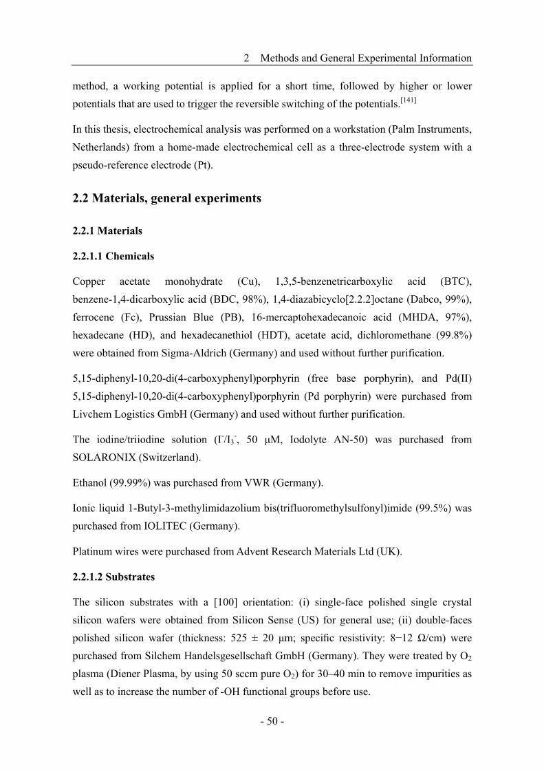
2 Methods and General Experimental Information
- 50 -
method, a working potential is applied for a short time, followed by higher or lower
potentials that are used to trigger the reversible switching of the potentials.[141]
In this thesis, electrochemical analysis was performed on a workstation (Palm Instruments,
Netherlands) from a home-made electrochemical cell as a three-electrode system with a
pseudo-reference electrode (Pt).
2.2 Materials, general experiments
2.2.1 Materials
2.2.1.1 Chemicals
Copper acetate monohydrate (Cu), 1,3,5-benzenetricarboxylic acid (BTC),
benzene-1,4-dicarboxylic acid (BDC, 98%), 1,4-diazabicyclo[2.2.2]octane (Dabco, 99%),
ferrocene (Fc), Prussian Blue (PB), 16-mercaptohexadecanoic acid (MHDA, 97%),
hexadecane (HD), and hexadecanethiol (HDT), acetate acid, dichloromethane (99.8%)
were obtained from Sigma-Aldrich (Germany) and used without further purification.
5,15-diphenyl-10,20-di(4-carboxyphenyl)porphyrin (free base porphyrin), and Pd(II)
5,15-diphenyl-10,20-di(4-carboxyphenyl)porphyrin (Pd porphyrin) were purchased from
Livchem Logistics GmbH (Germany) and used without further purification.
The iodine/triiodine solution (I-/I3-, 50 μM, Iodolyte AN-50) was purchased from
SOLARONIX (Switzerland).
Ethanol (99.99%) was purchased from VWR (Germany).
Ionic liquid 1-Butyl-3-methylimidazolium bis(trifluoromethylsulfonyl)imide (99.5%) was
purchased from IOLITEC (Germany).
Platinum wires were purchased from Advent Research Materials Ltd (UK).
2.2.1.2 Substrates
The silicon substrates with a [100] orientation: (i) single-face polished single crystal
silicon wafers were obtained from Silicon Sense (US) for general use; (ii) double-faces
polished silicon wafer (thickness: 525 ± 20 μm; specific resistivity: 8−12 Ω/cm) were
purchased from Silchem Handelsgesellschaft GmbH (Germany). They were treated by O2
plasma (Diener Plasma, by using 50 sccm pure O2) for 30–40 min to remove impurities as
well as to increase the number of -OH functional groups before use.

2 Methods and General Experimental Information
- 51 -
The gold substrates were obtained from Georg Albert PVD (Silz, Germany). They were
prepared by thermal evaporation of 100 nm of gold (99.99% purity) onto polished single
crystal silicon (100) wafers (Silicon Sense) using a 5 nm titanium adhesion layer. The
evaporated films were polycrystalline, with grains having predominantly a [111]
orientation. The as-deposited Au substrates were kept in Ar filled containers until use.
The fluorine doped tin oxide (FTO) coated glasses and Pt coated FTO substrates (used for
counter electrode) were purchased from SOLARONIX (Switzerland). In order to clean the
surface and generate -OH groups on it, the FTO glass was washed in acetone and ethanol
separately for 10 min and in an ultrasonic bath. Then plasma treatment under O2 was
applied for 30–40 min before use.
The indium tin oxide (ITO, 10% SnO2 and 90% In2O3) substrate was purchased from Kurt
J. Lesker (UK). It was treated by O2 plasma (Diener Plasma, by using 50 sccm pure O2)
for 30 min to remove impurities as well as to increase the number of -OH functional
groups before use. The QCM sensors were purchased from LOT-ORIEL (UK).
2.2.2 Preparation of SAMs
2.2.2.1 MHDA (16-mecaptohexadecanoic acid) SAM
Gold substrates were immersed into an ethanolic solution of MHDA (20 μM, in 90%
ethanol and 10% acetic acid) for 72 hours at room temperature while kept in the dark.
Thereafter, the substrates were rinsed with ethanol and dried under a N2 stream to obtain
MHDA SAM. The SAMs were prepared shortly before use. A schematic representation is
shown in Figure 2.21.
Figure 2.21 Schematic representation of the MHDA SAM on gold.

2 Methods and General Experimental Information
- 52 -
2.2.2.2 CMMT (9-carboxy-10-(mercaptomethyl) triptycene) SAM
Gold substrates were immersed into an ethanolic solution (20 μM) of CMMT for 72 hours
at room temperature in the dark. Thereafter, the substrates were rinsed with ethanol and
dried with an N2 stream to obtain CMMT SAM. The SAMs were prepared shortly before
use. A schematic representation is shown in Figure 2.22.
Figure 2.22 Schematic representation of the CMMT SAM on gold.
2.2.2.3 TPMTA (4'-carboxyterphenyl-4-methanethiol) SAM
Gold substrates were immersed into an ethanolic solution (20 μM, in 90% ethanol and 10%
acetic acid) of TPMTA for 72 hours at room temperature and in the dark. Thereafter, the
substrates were rinsed with ethanol and dried with an N2 stream to obtain the TPMTA
SAM. The SAMs were prepared shortly before use. A schematic representation is shown
in Figure 2.23.
Figure 2.23 Schematic representation of the TPMTA SAM on gold.
2 Methods and General Experimental Information
- 53 -
2.2.3 Production of SURMOFs
2.2.3.1 HKUST-1 grown on SAMs (CMMT, MHDA and TPMTA) modified Au
substrates
The liquid phase epitaxy (LPE) grown HKUST-1 SURMOFs with different thickness were
prepared on SAMs (CMMT, MHDA and TPMTA ) modified Au substrates by the spraying
method according to the procedure reported in the literature.[86] Copper acetate (1 mM in
ethanol) and 1,3,5-benzenetricarboxylic acid (BTC, 0.1 mM in ethanol) were alternately
sprayed on the target SAMs (CMMT, MHDA and TPMTA ) for 15 and 20 s, respectively.
After the spraying of each component, the coordination of reactant was allowed for
another 25 s before the target was abundantly rinsed with ethanol to remove any
unselectively bound material. The alternatively spraying of the metal and linker solutions
(i.e. a cycle) was then repeated 5, 7, 10, 15 and 20 times to produce HKUST-1 SURMOFs
samples of specific thickness.
2.2.3.2 HKUST-1 grown on Silicon or ITO substrates
The liquid phase epitaxy (LPE) grown HKUST-1 SURMOFs with different thickness were
prepared on Silicon and ITO substrates by the spraying method described previously.
Copper acetate (1 mM in ethanol) and 1,3,5-benzenetricarboxylic acid (BTC, 0.1 mM in
ethanol) were alternately sprayed on the targeted Silicon or ITO substrates for 20 and 30 s,
respectively. After the spraying of each component, 25 s was allowed for further
coordination of the reactant before the target was abundantly rinsed with ethanol to
remove any unselectively bound material. The spraying of the metal and linker solutions
was then repeated 20, 26, 34, and 40 cycles to get HKUST-1 SURMOFs samples, each
with a different thickness.
2.2.3.3 Porphyrin-based SURMOF 2 grown on FTO substrate
A concentration of 20 μM 5,15-diphenyl-10,20-di(4-carboxyphenyl)porphyrin (free base
porphyrin) or Pd(II) 5,15-diphenyl-10,20-di(4-carboxyphenyl)porphyrin (Pd porphyrin) in
ethanol (spray time: 25 s, waiting time: 35 s) and a concentration of 1 mM zinc acetate in
ethanol (spray time: 15 s, waiting time: 35 s) were sequentially deposited onto the
substrates in a layer-by-layer fashion. In between, pure ethanol was used for rinsing to
remove unreacted or byproducts species from the surface (rinsing time: 5 s). The thickness
of the sample was controlled by the number of deposition cycles. All the samples were
prepared at room temperature.
2 Methods and General Experimental Information
- 54 -
2.3 Theoretical analysis
Theoretical calculations were contributed by Prof. Fabian Pauly and Mr. Andreas Irmler
from University of Konstanz.
In order to gain insight into the electronic structure of HKUST-1, density functional theory
(DFT) calculations were done with the program package TURBOMOLE.[142] The
def-TZVP basis set and the B3-LYP hybrid functional with empirical dispersion
corrections was used.[143, 144] It has been shown that this exchange-correlation functional
leads to a good description of the fragments of the HKUST-1 MOF.[145]
In order to understand the charge transport mechanism in SURMOFs and to explain the
shallow dependence of conductance on length, one-dimensional (1D) toy model was
established to describe the transition from tunneling to hopping conduction.[146] The
SURMOF is modeled by a 1D chain. The chain sites correspond to the Cu2 centers, and
the coupling of adjacent sites (only nearest neighbor couplings are considered) is via the
benzene moiety of the trimesic acid linker. It takes dephasing into account by connecting
each chain site to an external, phase-randomizing reservoir.
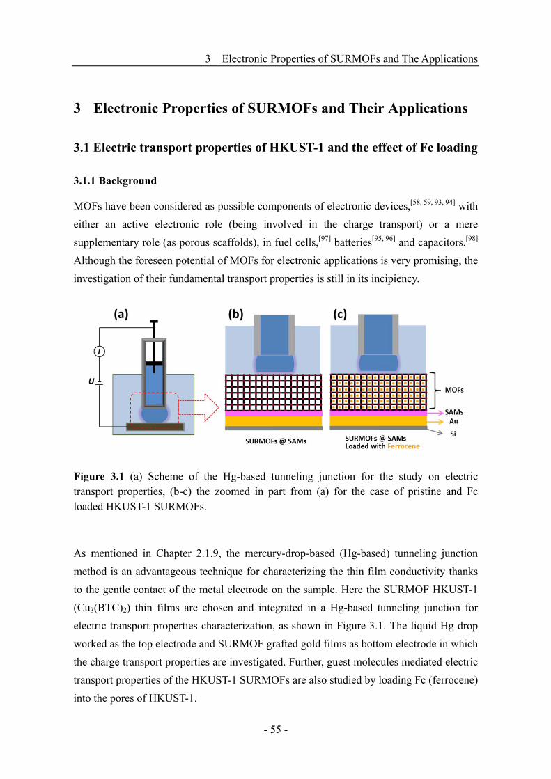
3 Electronic Properties of SURMOFs and The Applications
- 55 -
3 Electronic Properties of SURMOFs and Their Applications
3.1 Electric transport properties of HKUST-1 and the effect of Fc loading
3.1.1 Background
MOFs have been considered as possible components of electronic devices,[58, 59, 93, 94] with
either an active electronic role (being involved in the charge transport) or a mere
supplementary role (as porous scaffolds), in fuel cells,[97] batteries[95, 96] and capacitors.[98]
Although the foreseen potential of MOFs for electronic applications is very promising, the
investigation of their fundamental transport properties is still in its incipiency.
Figure 3.1 (a) Scheme of the Hg-based tunneling junction for the study on electric transport properties, (b-c) the zoomed in part from (a) for the case of pristine and Fc loaded HKUST-1 SURMOFs.
As mentioned in Chapter 2.1.9, the mercury-drop-based (Hg-based) tunneling junction
method is an advantageous technique for characterizing the thin film conductivity thanks
to the gentle contact of the metal electrode on the sample. Here the SURMOF HKUST-1
(Cu3(BTC)2) thin films are chosen and integrated in a Hg-based tunneling junction for
electric transport properties characterization, as shown in Figure 3.1. The liquid Hg drop
worked as the top electrode and SURMOF grafted gold films as bottom electrode in which
the charge transport properties are investigated. Further, guest molecules mediated electric
transport properties of the HKUST-1 SURMOFs are also studied by loading Fc (ferrocene)
into the pores of HKUST-1.

3 Electronic Properties of SURMOFs and The Applications
- 56 -
3.1.2 Preparation of HKUST-1 SURMOFs and Fc loading
The HKUST-1 SURMOFs were prepared onto Au surface functionalized with CMMT
SAMs (CMMT = [9-carboxy-10-(mercaptomethyl) triptycene], the details about the SAM
preparation are described in the Chapter 2.2) by using the well-established LPE spraying
method (Chapter 2.3). As already mentioned (Chapter 1.2.7), the advantage of the
sequential step-by-step method is the preparation of films of adjustable thickness through
varying the number of spraying cycles. For this study, 5, 7 and 10 spray cycles were
applied to prepare different thickness of HKUST-1 SURMOFs, and the produced
thickness was measured by means of AFM as described below.
One of the characteristics of MOFs and SURMOFs is their porosity, hence their ability to
act as host for small molecules. In the context of electronic applications, it has been
demonstrated that certain guests can modulate and increase the conductivity of the hosting
framework.[101, 102, 147] For example, the electrical transport properties of HKUST-1 films
can be enhanced by inserting electroactive species and small molecules, such as iodine[147]
or TCNQ[102] into the framework’s cavities. The loading leads to a huge increase of the
conductivity in comparison to the undoped films (about 2 orders of magnitude after iodine
loading[147] and six orders of magnitude after TCNQ[102]). In both cases, the increase in
electrical conductivity has been explained through the strong interaction between the
MOFs and the guest molecules.
Ferrocene molecules have also been used for electroactive guest loading. For instance,
electrical transport properties of oriented HKUST-1 thin films have been studied on the
basis of cyclic voltammetry experiments.[101] It was also found that the conductivity of
HKUST-1 is improved after Fc loading. The explanation is that Fc molecules act as redox
mediators, and the Fc molecules immobilized in the pores of the framework trigger a
charge hopping transport mechanism.
In this part, HKUST-1 SURMOF thin films with different thickness were used for Fc
loading. The loading was conducted according to the literature.[101] Firstly, the activation
of SURMOFs, to remove residual solvent molecules trapped inside the pores for achieving
efficient loading, is required. The pristine HKUST-1 SURMOF thin films were placed in a
small vessel and heated to 60 °C in air for 20 minutes for solvent evaporation. Thereafter
the samples were exposed immediately to a vapor of Fc at room temperature for 72 hours
for the loading.

3 Electronic Properties of SURMOFs and The Applications
- 57 -
3.1.3 Characterization of the pristine and Fc-loaded HKUST-1 SURMOFs
3.1.3.1 XRD of the HKUST-1 before and after Fc loading
All the films of HKUST-1 SURMOF were characterized by out-of-plane XRD after
preparation. For XRD measurement, scans were set from 5° to 20° (2θ) with a step width
of 0.024° and 16.4 seconds per step. In order to compare the measured intensity for
different spray cycles, the same sample was used for each XRD measurement. In all cases,
the obtained SURMOF films exhibited the expected high orientation along [111] with high
quality (Figure 3.2, black line), as shown by the presence of the characteristic (111), (222)
and (333) peaks (with 2θ of 5.84°, 11.67° and 17.54°, respectively).
Figure 3.2 Out-of-plane XRD data of HKUST-1 SURMOFs, pristine (black) and Fc-loaded (red). From top to bottom: 10, 7, and 5 spraying cycles.
XRD results of the ferrocene loaded HKUST-1 SURMOFs are also presented in Figure 3.2
(red). After loading with Fc, a decrease in the intensity of the (222) peak and an increase
in the intensity of the (333) peak occurred, as shown in Figure 3.2. The changes in the
relative intensities of the (222) and (333) peaks can be attributed to the changes in
structure form factor associated with incorporation of Fc molecules in the pores of
HKUST-1, since the Fc which loaded in the pores of HKUST-1 has also strong scatter of
X-rays.[109]
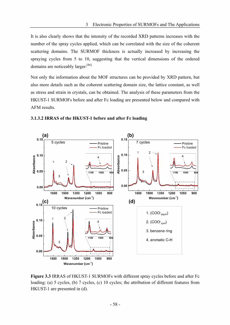
3 Electronic Properties of SURMOFs and The Applications
- 58 -
It is also clearly shows that the intensity of the recorded XRD patterns increases with the
number of the spray cycles applied, which can be correlated with the size of the coherent
scattering domains. The SURMOF thickness is actually increased by increasing the
spraying cycles from 5 to 10, suggesting that the vertical dimensions of the ordered
domains are noticeably larger.[86]
Not only the information about the MOF structures can be provided by XRD pattern, but
also more details such as the coherent scattering domain size, the lattice constant, as well
as stress and strain in crystals, can be obtained. The analysis of these parameters from the
HKUST-1 SURMOFs before and after Fc loading are presented below and compared with
AFM results.
3.1.3.2 IRRAS of the HKUST-1 before and after Fc loading
Figure 3.3 IRRAS of HKUST-1 SURMOFs with different spray cycles before and after Fc loading: (a) 5 cycles, (b) 7 cycles, (c) 10 cycles; the attribution of different features from HKUST-1 are presented in (d).

3 Electronic Properties of SURMOFs and The Applications
- 59 -
The IRRAS of all the HKUST-1 SURMOF thin films with different spray cycles
(representing different thickness which was confirmed by AFM, as described below) were
checked before and after Fc loading (Figure 3.3).
Figure 3.3(a-c) shows the IRRAS of HKUST-1 SURMOF thin films with different spray
cycles before and after Fc loading. It can be clearly seen from the spectra that the intensity
of IRRAS increases with the number of the spraying cycles applied. That means the more
spray cycles are applied the thicker the SURMOFs are grown; this results in the
contribution to the IRRAS intensity. But the band positions as well as the relative intensity
of the different features are rather identical and correspond to the same HKUST-1
SURMOF structures.
The characteristic absorption bands of the pristine HKUST-1 SURMOF thin films are
attributed as following: the band at 1656 cm-1 is attributed to COOasym; 1619, 1595 and
1564 cm-1 attributed to benzene ring; 1455 and 1386 cm-1 attributed to COOsym; 1112 and
940 cm-1 attributed to aromatic C-H. After loading with ferrocene (red curves) a new
absorption band at 1004 cm-1 was observed, and originated the C-H in-plane bending of
the ferrocene ring.
3.1.3.3 Characterization of film thicknesses by AFM before and after Fc loading
A tapping-mode AFM measurement was performed to measure the thickness of the
HKUST-1 SURMOF thin films. The applied cantilever is a NSC18 (Mikromasch HQ),
and the scan rate was 0.4 Hz at a 70 × 70 μm scan size under ambient laboratory
conditions (21-24 °С).
In order to have an internal reference for the height measurement, a small area of the
SURMOF samples was removed by chemical etching (immersion into nitric acid 0.2 mM
for about 2 s, then immediately rinsed with ethanol and dried under N2 stream), leaving
the gold surface underneath exposed.
Figure 3.4 depicts the AFM topographic images of the produced depth (left) of HKUST-1
SURMOF thin films with different spraying cycles and the corresponding cross-section
analysis (right). The difference in height between this area and the area with the SURMOF
has been used to measure the sample thickness, as shown in Figure 3.4(a-c), resulting in
the thickness of HKUST-1 SURMOFs of 45.6 ± 6.4 nm, 58.3 ± 6.3 nm, and 71.6 ± 9.9 nm
for the 5, 7, and 10 spraying cycles, respectively.
The same procedures were followed to measure the thickness of the ferrocene loaded
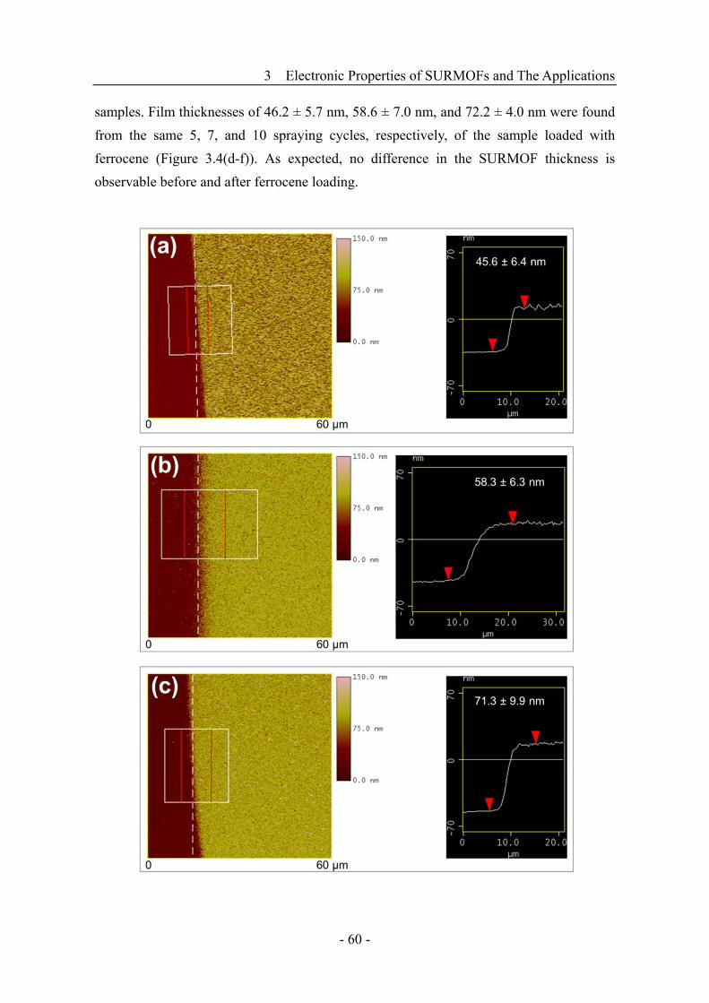
3 Electronic Properties of SURMOFs and The Applications
- 60 -
samples. Film thicknesses of 46.2 ± 5.7 nm, 58.6 ± 7.0 nm, and 72.2 ± 4.0 nm were found
from the same 5, 7, and 10 spraying cycles, respectively, of the sample loaded with
ferrocene (Figure 3.4(d-f)). As expected, no difference in the SURMOF thickness is
observable before and after ferrocene loading.
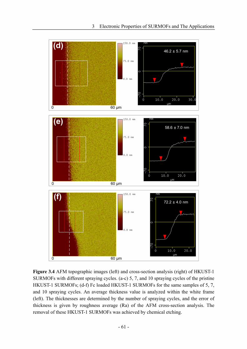
3 Electronic Properties of SURMOFs and The Applications
- 61 -
Figure 3.4 AFM topographic images (left) and cross-section analysis (right) of HKUST-1 SURMOFs with different spraying cycles. (a-c) 5, 7, and 10 spraying cycles of the pristine HKUST-1 SURMOFs; (d-f) Fc loaded HKUST-1 SURMOFs for the same samples of 5, 7, and 10 spraying cycles. An average thickness value is analyzed within the white frame (left). The thicknesses are determined by the number of spraying cycles, and the error of thickness is given by roughness average (Ra) of the AFM cross-section analysis. The removal of these HKUST-1 SURMOFs was achieved by chemical etching.
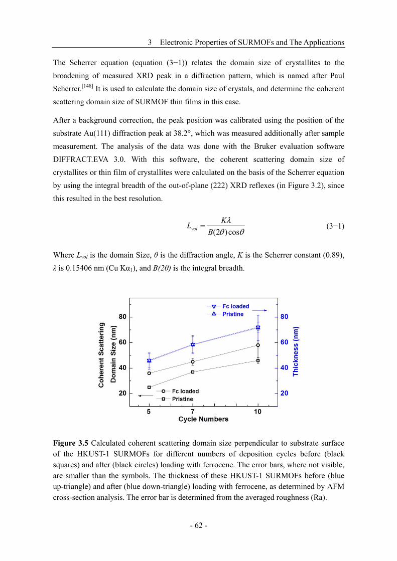
3 Electronic Properties of SURMOFs and The Applications
- 62 -
The Scherrer equation (equation (3−1)) relates the domain size of crystallites to the
broadening of measured XRD peak in a diffraction pattern, which is named after Paul
Scherrer.[148] It is used to calculate the domain size of crystals, and determine the coherent
scattering domain size of SURMOF thin films in this case.
After a background correction, the peak position was calibrated using the position of the
substrate Au(111) diffraction peak at 38.2°, which was measured additionally after sample
measurement. The analysis of the data was done with the Bruker evaluation software
DIFFRACT.EVA 3.0. With this software, the coherent scattering domain size of
crystallites or thin film of crystallites were calculated on the basis of the Scherrer equation
by using the integral breadth of the out-of-plane (222) XRD reflexes (in Figure 3.2), since
this resulted in the best resolution.
cos)2(B
KLvol (3−1)
Where Lvol is the domain Size, θ is the diffraction angle, K is the Scherrer constant (0.89),
λ is 0.15406 nm (Cu Kα1), and B(2θ) is the integral breadth.
Figure 3.5 Calculated coherent scattering domain size perpendicular to substrate surface of the HKUST-1 SURMOFs for different numbers of deposition cycles before (black squares) and after (black circles) loading with ferrocene. The error bars, where not visible, are smaller than the symbols. The thickness of these HKUST-1 SURMOFs before (blue up-triangle) and after (blue down-triangle) loading with ferrocene, as determined by AFM cross-section analysis. The error bar is determined from the averaged roughness (Ra).
3 Electronic Properties of SURMOFs and The Applications
- 63 -
Since the instrumental contribution to the line broadening was considered, but no
stress/strain contributions were added, the calculated coherent scattering domain size
represents a lower limit. The described procedure for domain size analysis was carried out
for both the pristine and Fc loaded HKUST-1 SURMOF samples. As shown in Figure 3.5,
the calculated domain sizes after Fc loading appears dramatically increased for each of the
spraying cycle samples. And it can also be clearly seen that the estimated film thickness
(referring to the domain size) of SURMOFs is indeed lower than those measured by AFM.
However the Scherrer equation is not applicable to all kinds of crystallites, but only to
those grains smaller than about 0.1 to 0.2 μm. Most importantly, not only the domain size
contributes to the width of a diffraction peak, but also factors like instrumental effects,
inhomogeneous strain, as well as imperfection of crystal lattice can broaden the measured
diffraction peak.
These results indicate that not the physical thicknesses of these SURMOF thin films are
different before and after the Fc loading, but rather the calculated domain sizes of Fc
loaded HKUST-1 SURMOFs appear much larger than in the respective pristine samples.
Comparing the precise lattice constants with the effect of Fc loading is thus necessary, and
the results are shown in the following section.
3.1.3.4 Determination of the lattice constants for the pristine and Fc loaded HKUST-1 SURMOFs
The precise lattice constants were determined by applying the interpolation method of
Taylor and Sinclair equation (3−2).[109] In this equation, αhkl is unknown and is determined
by equation (3−3) adapting to cubic crystal system, and the layer distance d is determined
by the Bragg equation (3−4). After background correction, the Cu Kα2 contribution was
stripped, and the peak position was calibrated using the Au(111) standard diffraction peak
at 38.2°. Then the peak positions (i.e. the diffraction angles) were determined by the
Bruker evaluation software DIFFRACT.EVA 3.0.
2 2
0
cos cos(0.5 )
sinhkla S a
(3−2)
2 2 2
2 2
1
hkl
h k l
d a
(3−3)
2 sind (3−4)

3 Electronic Properties of SURMOFs and The Applications
- 64 -
Where αhkl is the lattice constant, h,k,l is the set of Miller indices, S is the slope, θ is the
diffraction angle, α0 is the precise lattice constant, d is the layer distance, and λ is 0.15406
nm (Cu Kα1).
As discussed in the previous section, the observed peak shift in the XRD patterns (Figure
3.2 and Figure 3.6 (a)) indicates a lattice expansion. That means the ordering of the (111)
planes of the HKUST-1 SURMOFs is increased after Fc loading. This occurs as a
consequence of the allocation of ferrocene molecules inside the pores.
Figure 3.6 (a) Zoom in on the (333) Bragg peak of the XRD pattern to monitor the shift to lower 2θ values after the Fc loading; (b) calculated lattice constant a0 of the cubic HKUST-1 SURMOFs for different number of deposition cycles before (black squares) and after (red circles) loading with ferrocene. The error bar is estimated to be 2 standard deviations.
However, as presented in Figure 3.6 (b), the calculated lattice constants by Taylor and
Sinclair equation showed no significant change for the pristine and Fc loaded HKUST-1

3 Electronic Properties of SURMOFs and The Applications
- 65 -
SURMOFs. So the determination of the lattice constants showed that the loading with
ferrocene is not responsible for an expansion of the framework, but rather for an increased
ordering of the coherent scattering domains.
3.1.3.5 Stability of the HKUST-1 SURMOFs in the experimental condition
Since the electric transport properties of these HKUST-1 SURMOFs were measured by a
mercury-drop method in 1 mM hexadecanethiol (C16H33-SH, HDT) solution in
hexadecane (Details of the method are described in Chapter 2.1.9, and results are
presented in the next section), it is necessary and important to investigate the stability of
the SURMOF thin film under these experimental conditions during the electrical
properties measurement.
The stability of the HKUST-1 SURMOF over time in hexadecane (with 1 mM HDT) was
checked by immersion the sample for different periods of time (up to 20 hours), and the
out-of-plane XRD measurement was applied to check the stability of the SURMOF
structures. It can be seen from Figure 3.7 that the intensity of XRD peaks of the measured
HKUST-1 SURMOF sample does not change during the 20 h immersion in the HDT
solution. The positions as well as the relative intensities of the peaks show also no change.
The results proved that the HKUST-1 SURMOF thin film is stable under the given
experimental condition.
Figure 3.7 Out-of-plane XRD data of a 10 spraying cycles HKUST-1 SURMOF thin film sample before and after immersion in HDT solution in hexadecane after various amounts of time (from 1 to 20 h).

3 Electronic Properties of SURMOFs and The Applications
- 66 -
3.1.4 Assembling the mercury-drop-based tunneling junction
The electric transport properties of the pristine and guest molecules loaded HKUST-1
SURMOFs with various thicknesses were measured on the Hg-drop setup. (Setup built by
the team of Prof. Zharnikov from University of Heidelberg. Details about the setup are
described in Chapter 2.1.9).
The tunneling junction was assembled as reported in the literature.[99] The top electrode is
a drop of mercury which is normally passivated with HDT (C16H33-SH) to avoid
amalgamation and short circuit.[136, 139, 149] The bottom electrodes are the SAMs modified
gold substrate, the series of HKUST-1 SURMOF thin films with [111] orientation with
respect to the gold surface, and the same SURMOF thin films after ferrocene loading. The
measurements were conducted in a cell filled with HDT in hexadecane. A scheme of the
mercury-drop-based tunneling junction (Hg/HDT//HKUST-1/CMMT/Au) for
investigation of HKUST-1 SURMOF thin films grown on CMMT SAM is shown in
Figure 3.8.
Figure 3.8 Scheme of the Hg-based tunneling junction for investigation of HKUST-1 SURMOF thin films grown on CMMT SAM. (a) Crystal structure of the HKUST-1 SURMOF grown on gold surface with [111] orientation. Oxygen, carbon, and copper atoms are coded in red, blue, and black color, respectively. (b) Schematic illustration of the contact area between the two electrodes: Hg as top electrode is passivated with a SAM of HDT, while the SURMOF thin film grown on a CMMT modified Au substrate serves as bottom electrode. The molecular formula of HDT and CMMT are presented on the right side.
Right before the measurements, the Hg-drop was prepared according to the standard
protocol by immersion in 10 mM HDT solution in hexadecane for 10-15 min. The HDT
passivated Hg-drop was then gently positioned on bottom electrode (the SAMs and

3 Electronic Properties of SURMOFs and The Applications
- 67 -
HKUST-1 SURMOF samples). 1 mM HDT solution in hexadecane was used to increase
the stability of the drop and avoid amalgamation.[137] The whole setup was placed on a
vibration isolation table and put inside a home-built Faraday cage to reduce vibrations and
electrical noise, respectively.
To get the statistical and reliable results from the Hg-drop method, 3 different samples,
and 5 different positions for each sample, were used for each of the tunneling junction
system. For each position, 4-6 I-V (current-voltage) curves were recorded. All the recorded
I-V curves were used, unless they displayed conductance values resembling a metal-metal
contact that would reveal a rupture or amalgamation of the Hg-drop. In the plots, the
average extracted from all the recorded curves was plotted. Data points were collected
using a voltage ramp with a step size of 49 mV (between 0.01 V and 0.5 V) and a time
interval of at least 5 s between individual steps.
3.1.4.1 Measuring the current flowing through the built junctions
The reliability of the set-up has to be checked before investigating the SURMOF thin
films. Since the studies on electric transport properties of SAMs have shown to be a very
efficient by using the Hg-drop method.[99, 136-138, 149-151] CMMT SAM on Au substrate as
the bottom electrode was measured for checking the system as well as comparing with
other junctions.
The current flowing through the Hg/HDT//CMMT/Au junction was measured by
sweeping the bias voltage (V) in the negative (-0.5 V to -0.01 V) and positive range (0.01
V to 0.5 V). The contact area of the extruded Hg drop was observed with an optical
microscope after depositing on top of the electrode, which has to be evaluated to calculate
the current density J under the applied voltage V. Figure 3.9(a) shows the semilog plot of
the current density J under the applied voltage V. The green line in the plot is the J-V
curve of the CMMT SAM on Au electrode, and the marked blue star represents the current
density at a bias voltage of 0.5 V for a nitrile-substituted phenylthiol (NC-OPE1) SAM for
the sake of comparison, which is taken from reference.[99] It can be seen that the measured
current density of CMMT SAMs is in good agreement with those reported for NC-OPE1
SAMs of comparable thickness, which confirmed a well grafted SAM layer.
Thereafter the HKUST-1 SURMOF thin films were assembled in the junctions
(Hg/HDT//HKUST-1/CMMT/Au) at the same conditions. The semilog plot of the current
density J vs V for different thicknesses of HKUST-1 SURMOFs is shown in Figure
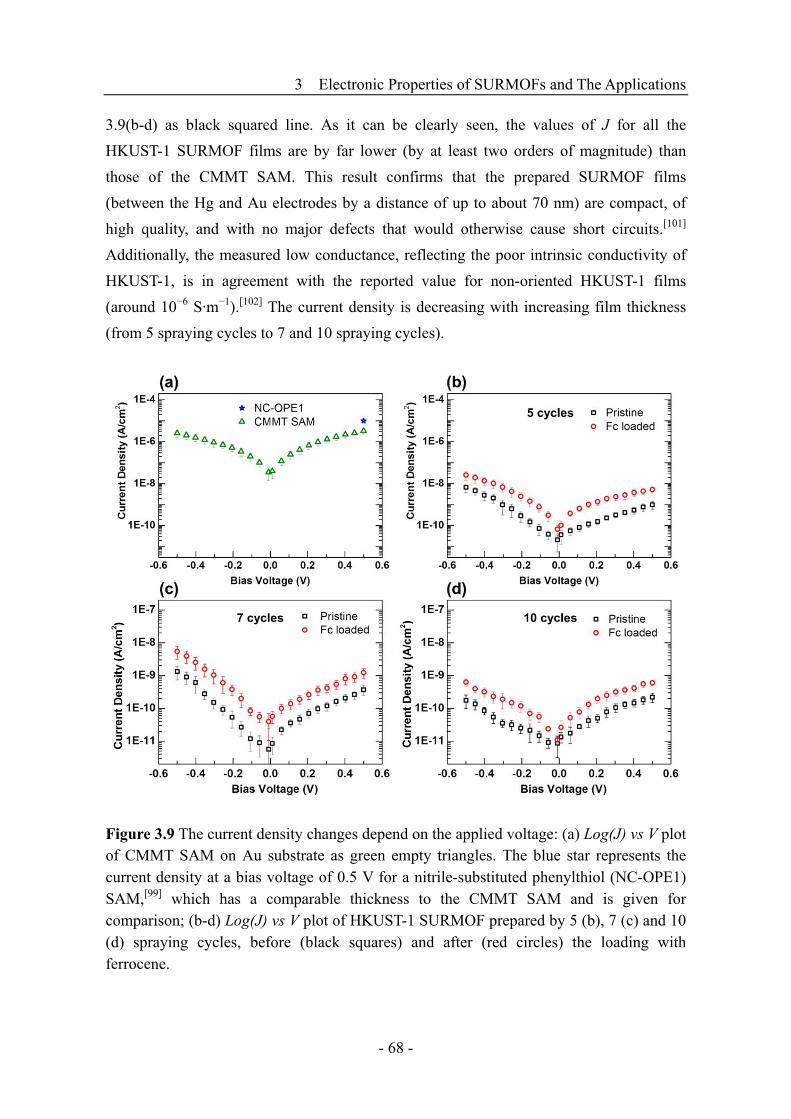
3 Electronic Properties of SURMOFs and The Applications
- 68 -
3.9(b-d) as black squared line. As it can be clearly seen, the values of J for all the
HKUST-1 SURMOF films are by far lower (by at least two orders of magnitude) than
those of the CMMT SAM. This result confirms that the prepared SURMOF films
(between the Hg and Au electrodes by a distance of up to about 70 nm) are compact, of
high quality, and with no major defects that would otherwise cause short circuits.[101]
Additionally, the measured low conductance, reflecting the poor intrinsic conductivity of
HKUST-1, is in agreement with the reported value for non-oriented HKUST-1 films
(around 10−6 S·m−1).[102] The current density is decreasing with increasing film thickness
(from 5 spraying cycles to 7 and 10 spraying cycles).
Figure 3.9 The current density changes depend on the applied voltage: (a) Log(J) vs V plot of CMMT SAM on Au substrate as green empty triangles. The blue star represents the current density at a bias voltage of 0.5 V for a nitrile-substituted phenylthiol (NC-OPE1) SAM,[99] which has a comparable thickness to the CMMT SAM and is given for comparison; (b-d) Log(J) vs V plot of HKUST-1 SURMOF prepared by 5 (b), 7 (c) and 10 (d) spraying cycles, before (black squares) and after (red circles) the loading with ferrocene.

3 Electronic Properties of SURMOFs and The Applications
- 69 -
In order to study the conductivities of these HKUST-1 SURMOFs with the effect of Fc
loading, the Hg/HDT//Fc-HKUST-1/CMMT/Au junctions were built under the same
condition as described above. The current flowing through the junctions of Fc loaded
HKUST-1 SURMOFs were measured for the same thicknesses (5, 7 and 10 spraying
cycles) as in the case of the pristine HKUST-1 SURMOFs. As it can be seen in Figure
3.9(b-d) red colored plots, the J values are always larger for the Fc-loaded HKUST-1
SURMOFs than for the corresponding pristine HKUST-1 SURMOFs. It was found that
the loading with ferrocene results in an increase of the current density. Analyzing the
values at the highest bias voltage (0.5 V), the current densities of the ferrocene loaded
HKUST-1 SURMOF thin films are increased by a factor of 5.4, 3.3, and 2.8 for the
samples obtained with 5, 7, and 10 spraying cycles, respectively.
Figure 3.10 The current density vs voltage depends on applied forces during the electric conductivity measurement, as seen here on a 10 deposition cycle HKUST-1 SURMOF film: (a) Log(J) vs V plot with small (black squares) and high (red circles) applied force on the pristine sample, and (b) the corresponding Fc loaded sample. At the bottom of each plot, the microscope images of the Hg drop extruded from the gastight Hamilton syringe are shown.
Furthermore, a specific characteristic of the Hg-drop method is the possibility to tune the
force applied on the bottom electrode to investigate the role of pressure on the
conductance. Taking advantage of the property, the current density as a function of the

3 Electronic Properties of SURMOFs and The Applications
- 70 -
bias voltage between the mercury drop and HKUST-1 SURMOFs have been tested by
varying the pressure applied through the drop on the SURMOF (Figure 3.10). At the
bottom of each plot, the microscope images of the Hg drop extruded from the gastight
Hamilton syringe showed the shape of Hg. As it can be seen, the diameter of the drop
increases as well as the area touched by the mercury by applying a higher force. No
significant changes in the value of the current could be measured, thus suggesting that the
prepared HKUST-1 films are robust. This exemplifies the very favorable mechanical
properties of monolithic SURMOF thin films already demonstrated by indentation
experiments.[152]
3.1.4.2 Analyzing of the electric transport properties of the HKUST-1 SURMOFs
before and after ferrocene loading
Insight into the charge transport mechanism within the MOFs could be obtained by taking
advantage of the deployed setup combined with the possibility to adjust SURMOFs film
thickness. Correlation between the measured current density J at a fixed voltage (or the
measured conductance G per area A, where G·V/A=J) with the thickness of the probed
film were investigated. As shown in Figure 3.11, an overview over the transport data (from
Figure 3.9) is presented, where the values of the current densities for the HKUST-1
SURMOFs are plotted against the film thicknesses at the bias voltage of 0.5 V before
(black squares) and after (red circles) loading with ferrocene.
Figure 3.11 Logarithm of current density at 0.5 V depends on thickness of HKUST-1 SURMOF thin films, pristine (black empty squares) and after Fc loading (red empty circles). The green triangle marks the current density for the CMMT SAM.
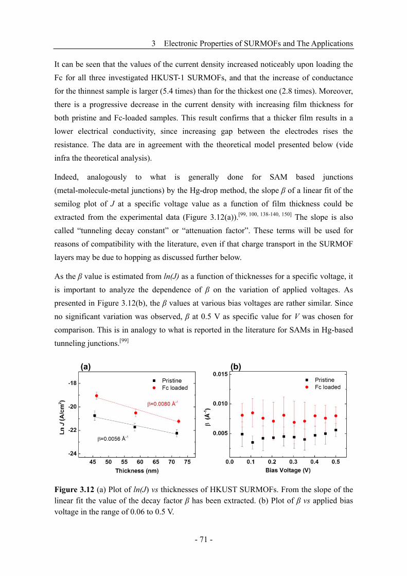
3 Electronic Properties of SURMOFs and The Applications
- 71 -
It can be seen that the values of the current density increased noticeably upon loading the
Fc for all three investigated HKUST-1 SURMOFs, and that the increase of conductance
for the thinnest sample is larger (5.4 times) than for the thickest one (2.8 times). Moreover,
there is a progressive decrease in the current density with increasing film thickness for
both pristine and Fc-loaded samples. This result confirms that a thicker film results in a
lower electrical conductivity, since increasing gap between the electrodes rises the
resistance. The data are in agreement with the theoretical model presented below (vide
infra the theoretical analysis).
Indeed, analogously to what is generally done for SAM based junctions
(metal-molecule-metal junctions) by the Hg-drop method, the slope β of a linear fit of the
semilog plot of J at a specific voltage value as a function of film thickness could be
extracted from the experimental data (Figure 3.12(a)).[99, 100, 138-140, 150] The slope is also
called “tunneling decay constant” or “attenuation factor”. These terms will be used for
reasons of compatibility with the literature, even if that charge transport in the SURMOF
layers may be due to hopping as discussed further below.
As the β value is estimated from ln(J) as a function of thicknesses for a specific voltage, it
is important to analyze the dependence of β on the variation of applied voltages. As
presented in Figure 3.12(b), the β values at various bias voltages are rather similar. Since
no significant variation was observed, β at 0.5 V as specific value for V was chosen for
comparison. This is in analogy to what is reported in the literature for SAMs in Hg-based
tunneling junctions.[99]
Figure 3.12 (a) Plot of ln(J) vs thicknesses of HKUST SURMOFs. From the slope of the linear fit the value of the decay factor β has been extracted. (b) Plot of β vs applied bias voltage in the range of 0.06 to 0.5 V.

3 Electronic Properties of SURMOFs and The Applications
- 72 -
With respect to those of SAMs[99, 136-139, 149, 150] consisting of short, purely organic
molecular wires, the obtained attenuation factor β of the pristine HKUST-1 (ca 0.006 Å-1)
is extremely low, but it is consistent values found for “longer” organic molecular wires[139]
or metal-organic molecular wires of a length up to 40 nm.[100] In these latter systems,
low-lying energy states have been provided by incorporating easily oxidizable metal
centers in the organic backbone; those appears involved in a multistep charge hopping
mechanism to yield a linear increase of the resistance with the length (or conductance vs
inverse length).[100] However, for the Fc loaded SURMOF samples, a similar dependence
of the current density values on the film thickness as for the pristine samples was observed,
as presented in Figure 3.12(a). It can be seen that the evaluated β value of the Fc loaded
HKUST-1 is slightly increased (ca 0.008 Å-1). The β values at various bias voltages are
quite similar for both the pristine and Fc loaded HKUST-1 SURMOFs Figure 3.12(b), and
appears, within the error bars, to barely change.
Figure 3.13 (a) Plot of the resistance times area (R·A) as a function of film thickness (L) of HKUST-1 SURMOFs, pristine (black squares) and after Fc loading (red circles). The data is obtained as V/J at V=0.5 V (where R·A = V/J). Straight lines show fits according to R·A=Rc·A+ρ·L, from which the resistivity ρ can be extracted. (b) Plot of ρ vs applied bias voltage in the range of 0.06 to 0.5 V.
As mentioned previously, the conductance G per area A is related to J by G·V/A=J, so the
resistance (R) can be defined in R = V/A·J. Since a linear relation R·A=Rc·A+ρ·L (where
Rc is the contact resistance, ρ is the resistivity, and L is the film thickness) can be used to
estimate the resistivity (ρ), the resistance times area (R·A) vs film thickness (L) of
HKUST-1 SURMOFs at 0.5 V can be plotted as in Figure 3.13 (a). A high resistivity ρ of
6.8·1012 Ω·m was obtained for the pristine HKUST-1 SURMOFs from the linear fit. For

3 Electronic Properties of SURMOFs and The Applications
- 73 -
this assembled junction, R is the resistance of the whole Hg/HDT//HKUST-1/CMMT/Au
system. It consists of the resistance of the SURMOF film ρ·L/A of thickness L and any
other resistances in series with the system that are summarized with the contact resistance
Rc. This contact resistance will contains for instance contributions from transport through
the HDT and CMMT layers combined in the junction, as described in the schematic
illustration of Figure 3.8. Since only the thickness of the SURMOF films has been varied
for this system, Rc in other parts of the system may arise from hopping, tunneling or mixt
phenomena. The results are compatible with the linear ohmic increase as expected for a
charge hopping mechanism.
For the Fc loaded SURMOFs as shown in the Figure 3.13(a) red plot, the data is again
compatible with a linear increase of the resistance with the film thickness. However, the
resistivity ρ of 2.8·1012 Ω·m is lower than that of the pristine sample by a factor of around
2.5. The results also support the charge hopping mechanism as leading conduction
mechanism for the Fc-loaded HKUST-1 SURMOFs. Figure 3.13 (b) presents the behavior
of ρ for different bias voltages V, which shows a comparatively stable resistivity for both
pristine and Fc loaded HKUST SURMOFs.
The linear, algebraic increase of resistance of the HKUST-1 SURMOFs with film
thickness (Figure 3.11) is generally not compatible with the exponential increase of the
resistance with the sample thickness which is expected for coherent tunneling. Attempts to
fit the data with the exponential decay law G=Gc·exp(-β·L) yield β values as low as 0.006
Å-1 for pristine HKUST-1 SURMOFs (Figure 3.12(a)). This corresponds to an effective
tunneling barrier φ of 0.034 meV, if β=2(2meφ)1/2/ħ (with the electron mass me) is use.[153]
Such a vanishingly small tunneling barrier would imply a good conduction due to
molecular states being in resonance with the Fermi level of the
Hg/HDT//HKUST-1/CMMT/Au system, an assumption which is not valid here. Thus
coherent tunneling does not adequately describe the data. Considering the reported
insulating behavior[101, 102] together with the measured high resistivity, an off-resonant
hopping transport in the HKUST-1 films has been concluded. Nevertheless, a slight
increase (0.008 Å-1) of the β values for the Fc loaded HKUST-1 SURMOFs was observed.
The slightly larger beta value for the Fc loaded samples led to a decrease of the
conductance ratio with the increase of film thickness. The better conductivity measured
after the Fc loading suggests that the ferrocene had an effect on the electronic properties of
HKUST-1. This appears in agreement with the proposed theoretical model, where an
increase towards the Fc loaded case is proposed (see below the theoretical analysis).

3 Electronic Properties of SURMOFs and The Applications
- 74 -
3.1.6 Theoretical analysis of charge transport mechanism
Theoretical calculations were contributed by Prof. Fabian Pauly and Mr. Andreas Irmler
from University of Konstanz. The detailed analyses are presented in ref;[154] here only a
short description and discussion is given.
3.1.6.1 Electronic structure analysis
To gain insight into the electronic structure of HKUST-1, density functional theory (DFT)
calculations were performed. For a fragment with six Cu2 centers, the frontier orbitals
were either localized on one (or maximally two) of these centers or on the organic linker.
Therefore a minimal unit with two Cu2 centers connected by an organic linker was studied.
For the linkage of the Cu2 centers in the MOF, four oxygen pairs are connected to each of
the metallic nodes. In this situation, there are low-lying unoccupied states at energies of
around -5.1 eV. For this reason each Cu2 center was saturated with two ethanol molecules.
In the experiments, they are available due to the ethanol solutions used in the synthesis.
They are strongly bound with a binding energy of around 2 eV per ethanol. The chosen
geometry and frontier orbitals are presented in Figures 3.14 and Figure 3.15.
Figure 3.14 DFT calculations on MOF structure: (a) Investigated fragment with two Cu2 centers connected by the organic linker. Each Cu2 is saturated with two ethanol molecules. (b,c) Two possible configurations of ferrocene inside the MOF.
To determine the influence of Fc on the electronic structure of the MOF, one Fc molecule
was added inside the pore. The Fc approaches the border of the pore in the geometry
optimization process when added to the middle. Different configurations of the Fc relative
to the MOF were studied. The geometry shown in Figure 3.14(b) seems to be the most
favorable position, where the carbon rings of the Fc are parallel to those of the
benzene-based linkers through π-π stacking interactions, leading to occupied states within
the band gap of the MOF in terms of the electronic structure.
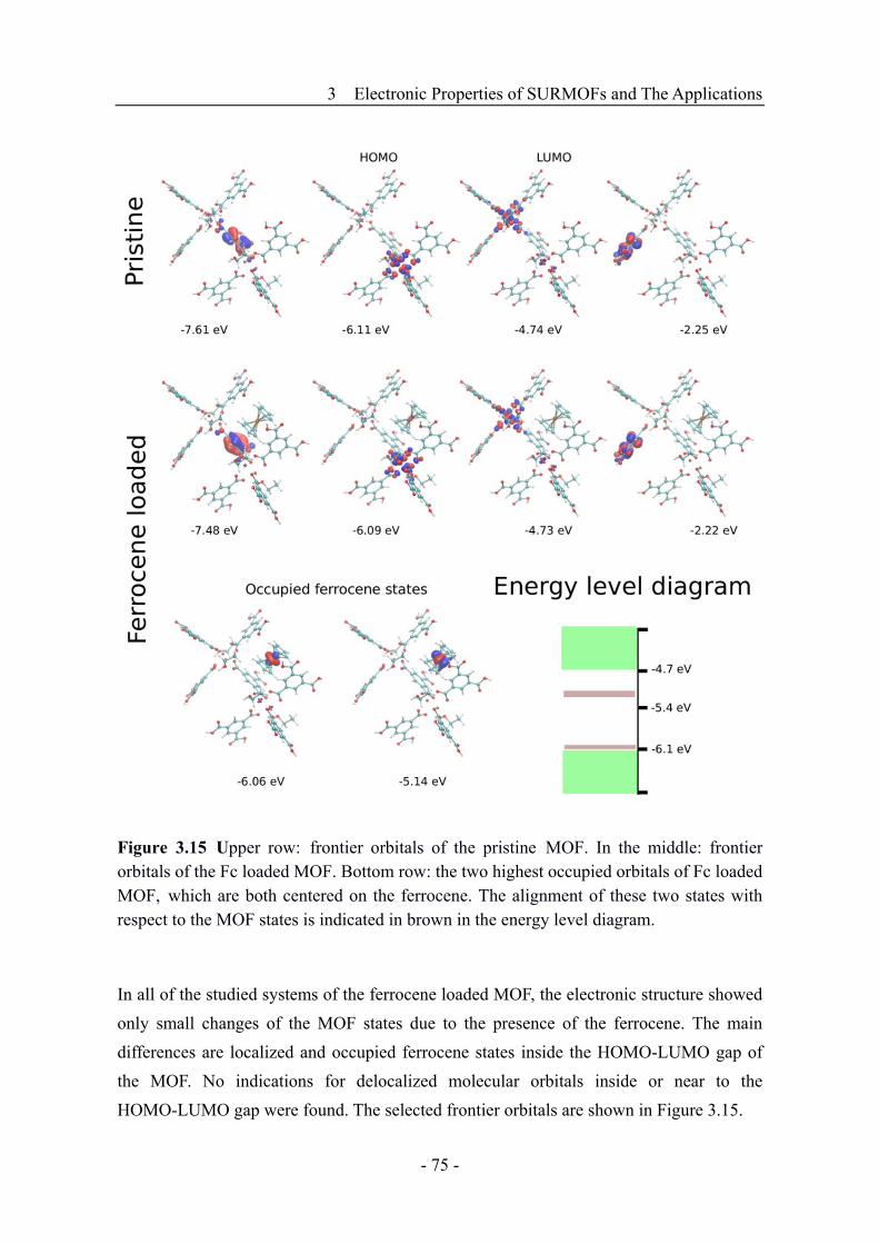
3 Electronic Properties of SURMOFs and The Applications
- 75 -
Figure 3.15 Upper row: frontier orbitals of the pristine MOF. In the middle: frontier orbitals of the Fc loaded MOF. Bottom row: the two highest occupied orbitals of Fc loaded MOF, which are both centered on the ferrocene. The alignment of these two states with respect to the MOF states is indicated in brown in the energy level diagram.
In all of the studied systems of the ferrocene loaded MOF, the electronic structure showed
only small changes of the MOF states due to the presence of the ferrocene. The main
differences are localized and occupied ferrocene states inside the HOMO-LUMO gap of
the MOF. No indications for delocalized molecular orbitals inside or near to the
HOMO-LUMO gap were found. The selected frontier orbitals are shown in Figure 3.15.
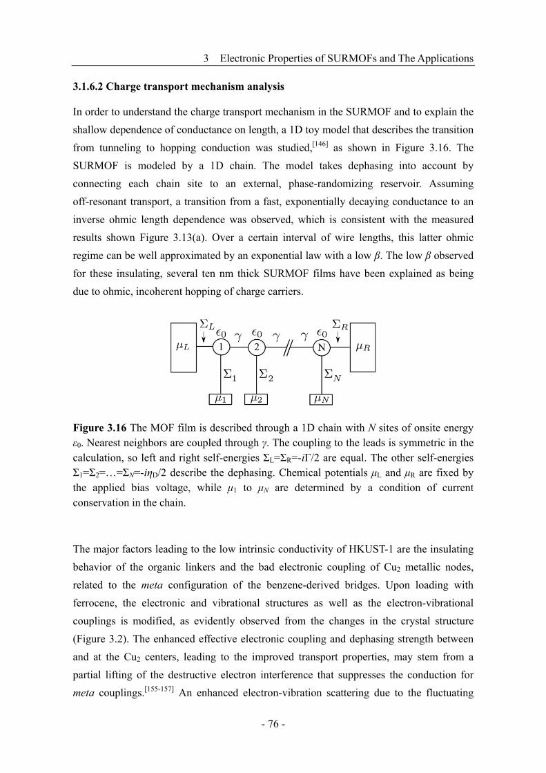
3 Electronic Properties of SURMOFs and The Applications
- 76 -
3.1.6.2 Charge transport mechanism analysis
In order to understand the charge transport mechanism in the SURMOF and to explain the
shallow dependence of conductance on length, a 1D toy model that describes the transition
from tunneling to hopping conduction was studied,[146] as shown in Figure 3.16. The
SURMOF is modeled by a 1D chain. The model takes dephasing into account by
connecting each chain site to an external, phase-randomizing reservoir. Assuming
off-resonant transport, a transition from a fast, exponentially decaying conductance to an
inverse ohmic length dependence was observed, which is consistent with the measured
results shown Figure 3.13(a). Over a certain interval of wire lengths, this latter ohmic
regime can be well approximated by an exponential law with a low β. The low β observed
for these insulating, several ten nm thick SURMOF films have been explained as being
due to ohmic, incoherent hopping of charge carriers.
Figure 3.16 The MOF film is described through a 1D chain with N sites of onsite energy ε0. Nearest neighbors are coupled through γ. The coupling to the leads is symmetric in the calculation, so left and right self-energies ΣL=ΣR=-iΓ/2 are equal. The other self-energies Σ1=Σ2=…=ΣN=-iηD/2 describe the dephasing. Chemical potentials μL and μR are fixed by the applied bias voltage, while μ1 to μN are determined by a condition of current conservation in the chain.
The major factors leading to the low intrinsic conductivity of HKUST-1 are the insulating
behavior of the organic linkers and the bad electronic coupling of Cu2 metallic nodes,
related to the meta configuration of the benzene-derived bridges. Upon loading with
ferrocene, the electronic and vibrational structures as well as the electron-vibrational
couplings is modified, as evidently observed from the changes in the crystal structure
(Figure 3.2). The enhanced effective electronic coupling and dephasing strength between
and at the Cu2 centers, leading to the improved transport properties, may stem from a
partial lifting of the destructive electron interference that suppresses the conduction for
meta couplings.[155-157] An enhanced electron-vibration scattering due to the fluctuating

3 Electronic Properties of SURMOFs and The Applications
- 77 -
interactions of the ferrocene molecules on top of the trimesic acid bridges can induce a
decoherence that reduces the destructive interference. In addition, a changed charge
rearrangement at the interfaces due to the ferrocene-related states may modify the charge
injection barrier.
3.1.7 Conclusion
In conclusion, HKUST-1 SURMOF thin films were prepared on CMMT SAM modified
Au substrates along the [111] orientation and then loaded with ferrocene molecules as
small organic electroactive guest entities. The Fc loading was confirmed by IRRAS and
out-of-plane XRD. Interestingly, the out-of-plane XRD measurements showed an
enhanced ordering of the layer sequences of the (111) planes of the HKUST-1 SURMOFs
through the incorporation of ferrocene. However, the lattice constant had no significant
change before and after the ferrocene loading.
By assembling a mercury-based tunneling junction with the prepared various thickness
HKUST-1 SURMOF thin films, either with the pristine ones or the Fc loaded ones, the
charge transport properties of these films were investigated. It was found that the
conductance of the SURMOF films decreased by increasing the film thickness. However,
the low value of the attenuation factor (β ≈ 0.006 Å-1) indicates the extremely shallow
dependence of the measured current density on film thickness, and has been understood in
terms of a linear, ohmic increase of resistance with length in the incoherent charge
hopping regime. For the effect of Fc loading inside the pores of HKUST-1 SURMOFs, the
conductance was tuned to be higher than the corresponding pristine ones at identical same
thickness. So the decrease in overall resistance with Fc loading and its weaker increase
with film thickness indicate a reduction in the charge injection barrier and an improved
electronic coupling between metal nodes. Theoretical analysis by DFT calculations was
applied to help understanding the charge transport mechanism.
Part of the results in this section has been published in ACS Appl. Mat. Interfaces by
Jianxi Liu et al.(2015) as ref.[154]
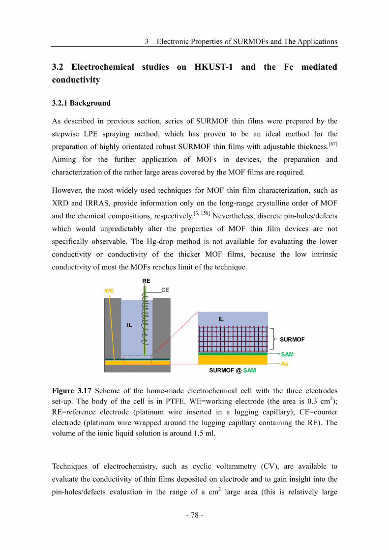
3 Electronic Properties of SURMOFs and The Applications
- 78 -
3.2 Electrochemical studies on HKUST-1 and the Fc mediated
conductivity
3.2.1 Background
As described in previous section, series of SURMOF thin films were prepared by the
stepwise LPE spraying method, which has proven to be an ideal method for the
preparation of highly orientated robust SURMOF thin films with adjustable thickness.[67]
Aiming for the further application of MOFs in devices, the preparation and
characterization of the rather large areas covered by the MOF films are required.
However, the most widely used techniques for MOF thin film characterization, such as
XRD and IRRAS, provide information only on the long-range crystalline order of MOF
and the chemical compositions, respectively.[3, 158] Nevertheless, discrete pin-holes/defects
which would unpredictably alter the properties of MOF thin film devices are not
specifically observable. The Hg-drop method is not available for evaluating the lower
conductivity or conductivity of the thicker MOF films, because the low intrinsic
conductivity of most the MOFs reaches limit of the technique.
Figure 3.17 Scheme of the home-made electrochemical cell with the three electrodes set-up. The body of the cell is in PTFE. WE=working electrode (the area is 0.3 cm2); RE=reference electrode (platinum wire inserted in a lugging capillary); CE=counter electrode (platinum wire wrapped around the lugging capillary containing the RE). The volume of the ionic liquid solution is around 1.5 ml.
Techniques of electrochemistry, such as cyclic voltammetry (CV), are available to
evaluate the conductivity of thin films deposited on electrode and to gain insight into the
pin-holes/defects evaluation in the range of a cm2 large area (this is relatively large

3 Electronic Properties of SURMOFs and The Applications
- 79 -
compared to other methods such as AFM[88, 159] and Hg-method[136, 139, 150]). MOFs thin
films grown, with a well-defined crystallographic orientation and controlled thickness, on
a conductive substrate can be directly used as working electrodes and provide great
experimental advantages.
In this part, CV was used to study the electrochemical properties of HKUST-1 SURMOFs
that were used as working electrodes in a home-made cell, as depicted Figure 3.17. An
aprotic ionic liquid (IL) [BMIM] [NTf2]), (1-butyl-3-methylimidazolinium
bis(trifluoronethylsulfonyl)imide), was used as solvent and supporting electrolyte. The
electroactive ferrocene was used as redox probe. In order to study the electrical properties
of the SURMOFs with the effect of guest loading, the ferrocene molecules were loaded
into the nanopores of HKUST-1 SURMOFs. Meanwhile, the presence of pin-holes/defects
could be evaluated from CV measurements which offer a swift method for observing the
conductive quality of SURMOF thin films.
3.2.2 Preparation of HKUST-1 SURMOFs on SAMs and Fc loading
The possibility to control the crystallographic growth direction for SURMOFs is
particularly appealing. This obtained varying the chemical functionality of the active
ending groups present on the SAM template surface as well as their surface density.[160]
HKUST-1 SUMOFs have been prepared on CMMT and TPMTA
(4'-carboxyterphenyl-4-methanethiol) SAMs modified gold electrodes (named as
SAM1/MOF and SAM2/MOF, respectively) by means of the LPE spraying method
(Chapter 2.2.3). The loading of Fc was conducted from the vapor phase for both
SAM1/MOF and SAM2/MOF using the same conditions as described in Chapter 3.1.
3.2.3 Out-of-plane XRD characterization
Out-of-plane XRD has been performed to check the crystallinity for both the pristine and
Fc loaded HKUST-1 SURMOFs. The XRD pattern in Figure 3.18 (black plot) shows a
good crystallographic orientation for SAM1/MOF with the two peaks at 2θ=11.80° and
2θ=17.70° corresponding to the main diffraction peaks (222) and (333), but a less
pronounced orientation for SAM2/MOF (Figure 3.19, black plot) was observed. After
loading with ferrocene, in the case of SAM1/MOF-Fc (in red), the XRD pattern showed
that the (222) peak was substantial decreased and (333) was slightly increased comparing
to the unloaded samples (Figure 3.18). The change in the relative intensities of the (222)

3 Electronic Properties of SURMOFs and The Applications
- 80 -
and (333) after Fc loading can be interpreted as coming from the strong scattering of the
loaded iron from the ferrocene, and because the structure form factor is changed after
loading. The changes were also observed from the XRD pattern of SAM2/MOF after Fc
loading, in which the relative intensities of the (002) and (004) reflexes appeared
differently (Figure 3.19).
Figure 3.18 Out-of-plane XRD of the pristine (SAM1/MOF, black) and Fc-loaded (SAM1/MOF-Fc, red) HKUST-1 SURMOF grown on CMMT SAM. The relative intensities of the (222) and (333) reflexes are changed after loading.
Figure 3.19 Out-of-plane XRD of the pristine (SAM2/MOF, black) and Fc-loaded (SAM2/MOF-Fc, red) HKUST-1 SURMOF grown on TPMTA SAM. The relative intensities of the (002) and (004) reflexes are changed by the loading.
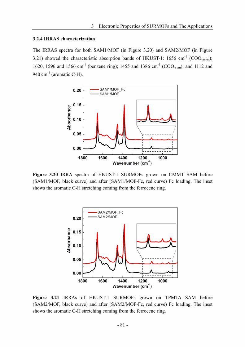
3 Electronic Properties of SURMOFs and The Applications
- 81 -
3.2.4 IRRAS characterization
The IRRAS spectra for both SAM1/MOF (in Figure 3.20) and SAM2/MOF (in Figure
3.21) showed the characteristic absorption bands of HKUST-1: 1656 cm-1 (COO-asym);
1620, 1596 and 1566 cm-1 (benzene ring); 1455 and 1386 cm-1 (COO-sym); and 1112 and
940 cm-1 (aromatic C-H).
Figure 3.20 IRRA spectra of HKUST-1 SURMOFs grown on CMMT SAM before (SAM1/MOF, black curve) and after (SAM1/MOF-Fc, red curve) Fc loading. The inset shows the aromatic C-H stretching coming from the ferrocene ring.
Figure 3.21 IRRAs of HKUST-1 SURMOFs grown on TPMTA SAM before (SAM2/MOF, black curve) and after (SAM2/MOF-Fc, red curve) Fc loading. The inset shows the aromatic C-H stretching coming from the ferrocene ring.
3 Electronic Properties of SURMOFs and The Applications
- 82 -
After loading with ferrocene, a new absorption band at 1004 cm-1, attributed to the C-H
in-plane bending of the ferrocene ring appeared for HKUST-1 SURMOFs grown on both
SAM1 (CMMT) and SAM2 (TPMTA). In addition, the broad band around 1109 cm-1
(insets in Figure 3.20 and Figure 3.21) is the sum of the band at 1107 cm-1 (asymmetric
ferrocene ring breathing) and that at 1112 cm-1 (in plane C-H stretching of the pristine
HKUST-1).
3.2.5 AFM morphology and scratching characterization
AFM morphology and scratching characterization were contributed by Prof. Carmen Ocal
and Mr. Markos Paradinas from Autonomous University of Barcelona (UAB, Spain).
The morphology and thickness of the HKUST-1 SURMOF thin films were measured by
AFM in contact mode under low humidity conditions (<5 % RH, obtained by a continuous
N2 flux) using a commercial head and electronics from Nanotec. In order to determine the
thicknesses of the SURMOF thin films, AFM scratching method was employing[161] by
removing the grown MOF material from the surface until reaching the Au surface of the
substrate with a Si tip on medium stiffness cantilevers (k=2.8 N/m, Nanosensors). The
imaging force was set to below 10 nN, while a force in the range of 400-700 nN was
applied to scratch sample.
Before the scratching procedure, a large scan size was used firstly, for imaging the
morphology of the SURMOFs and choosing the area for scratch, by using either a
dynamic non-contact mode or a low force contact mode to avoid film damage. Then, the
scan size was reduced to a smaller region that was repeatedly imaged at a higher load
(typically 400-500 nN). The applied scratching forces are high enough to eliminate the
SURMOF but in a moderate manner (under load control) to avoid undesired removal of
the gold film. During this process, an unstable topographic signal indicates the start of
MOF materials removal. Lateral force signals were continuously recorded to detect
structural differences within the SURMOF as well as to determine the instant when the
underlying Au surface is reached to stop the process.
3.2.5.1 AFM morphology of Au surface
Since the SAMs (CMMT and TPMTA) used for SURMOFs preparation would not affect
the morphology of Au surface, the underneath Au substrate was firstly characterized as a
reference for identifying the moment when the AFM tip reaches the substrate layer during

3 Electronic Properties of SURMOFs and The Applications
- 83 -
the scratching. As it can be seen in Figure 3.22, the Au surface of the substrate consists of
a homogeneous distribution of small grains which provide the smooth surface (roughness
of 1.8 nm).
Figure 3.22 Topographic AFM images of Au surface (100 nm Au on Si) taken as a reference for the scratching experiments. The image at the right panel corresponds to the area marked in the large image (5 μm × 5 μm). The surface roughness calculated is RMS=1.8 nm.
3.2.5.2 AFM scratching of HKUST-1 grown on CMMT (SAM1/MOF-Fc)
As mentioned in Chapter 3.1, the thickness of SURMOFs would not change by Fc loading,
so the AFM scratching experiments were done only on Fc loaded HKUST-1 SURMOF
samples.
Figure 3.23(a) shows the morphology of HKUST-1 SURMOF grown on CMMT SAM
(SAM1/MOF-Fc). The crystallites exhibit a flat top surface with a clear triangular shape
indicating a predominant [111] orientation in agreement with the XRD data (Figure 3.18).
The scratching process was performed in the smaller area as seen in the middle of Figure
3.23(c). The image presented in Figure 3.23(b) shows the morphology of the scanned
sample, which were taken during the scratching experiment. The same gold grains were
circled in both images used as a reference when reaching the substrate; the dashed lines in
each image indicate the material removal front. A continuous and rather homogeneous
MOF layer was found (regions below the dash line Figure 3.23(b) underlying the top
crystallites but before reaching the Au substrate. The results elucidated that the crystallites
were not positioned directly on the SAMs but rather on top of a continuous and
homogeneous layer of HKUST-1. After the scratching experiment, the scanned area was
set to the original size (same as Figure 3.23(a)) for imaging the topographic changes and

3 Electronic Properties of SURMOFs and The Applications
- 84 -
measuring the thickness. Figure 3.23(d) shows the depth profile of the SAM1/MOF-Fc.
The average vertical dimension of the crystallites is 20 nm on top, and the underlying
homogeneous MOF film exhibits a thickness of 70 ± 5 nm.
Fig. 3.23 Topographic AFM images of SAM1/MOF-Fc before (a) and after (c) removal of the MOF material from sample (square in the middle). (b) Selected images taken during
the scratching (500 nN load). Ellipse marked areas are Au surface. Dashed lines indicate the removal front (for details see text). (d) Depth profile of the HKUST-1 SURMOF after scratching along the line in (c).
3.2.5.3 AFM scratching of HKUST-1 grown on TPMTA (SAM2/MOF-Fc)
AFM morphology and scratching procedures were performed on the HKUST-1 SURMOF
thin film grown on TPMTA SAM with identical conditions as previously used. Figure
3.24(a-b) present the surface morphology scans of the ferrocene loaded HKUST-1
(SAM2/MOF-Fc). The circled crystallites in Figure 3.24(a) show some presenting a flat
triangular surface (red circles) and others a squared base pyramids shape (blue circles)
likely corresponding to mixed [111] and [001] orientations, respectively. This observation
is in accordance with the XRD measurements (Figure 3.19). These crystallites lay on top
of a rather flat and homogeneous layer of SURMOF.
Figure 3.24(c) presents a topographic AFM image of the SAM2/MOF-Fc after a scratch

3 Electronic Properties of SURMOFs and The Applications
- 85 -
experiment. Part of the removed MOF accumulated at the borders of the scratched region
and contributed to the jumping lines in the image. The depth profile shown in Figure
3.24(d) follows the white line in Figure 3.24(c), and was used to determine the film
thickness. It can be seen that the average vertical dimension of the crystallites on top is
35 nm, and the underlying homogeneous MOF film exhibits a thickness of 75 ± 5 nm.
Figure 3.24 Topographic AFM image of the SAM2/MOF-Fc before (a-b) and after (c) removal of the MOF material from sample (square in the middle); (d) depth profile of the HKUST-1 SURMOF after scratching experiment along the white line seen in (c).
3.2.6 CV study on HKUST-1 SURMOFs grown on different SAMs
The cyclic voltammetry (CV) experiments were carried out in a home-made
electrochemical cell (Figure 3.17) using a standard three electrode setup. The reference
electrode and counter electrode were made of platinum wires (diameter 0.25 mm). The
SAMs and HKUST-1 SURMOFs coated gold substrates with and without Fc loading were
used as working electrodes (area 0.3 cm2); they have been classified and named as
following:
(i) CMMT series: SAM1, SAM1/MOF, SAM1/MOF-Fc;
(ii) TPMTA series: SAM2, SAM2/MOF, SAM2/MOF-Fc.

3 Electronic Properties of SURMOFs and The Applications
- 86 -
Carrying out CV experiments using these oriented and crystalline SURMOFs grown on
metal substrates as working electrode is still challenging and the solvent and supporting
electrolyte are to be chosen carefully since MOFs are water sensitive and could react with
the applied solutions during the measurement. As liquid supporting electrolyte, the aprotic
ionic liquid [BMIM] [NTf2] meets all requirements, because the ionic components do not
interfere with the coordination bonds in the HKUST-1 SURMOF and preserve it from
losing its crystalline structure.[101] Moreover, as several other known ILs,[162] the used
[BMIM][NTf2] is a good supporting electrolyte also because of its electrochemical
inertness (i.e. its wide potential window, larger than the one of the electroactive species
under study) and its high conductivity (being completely ionic). Ferrocene has been used
as the redox probe, and was dissolved in IL by adding a small amount of ethanol for
solubility reasons (5mM, in 4/96 EtOH/[BMIM][NTf2]).
The CV measurements were conducted in IL (5 mM Fc, 4% ethanol) at the potential
window from -0.35 to +0.55 V vs Pt, while the scan rate was varied (20 mV/s, 50 mV/s,
100 mV/s). After the CV measurements, the samples were routinely checked by XRD, and
showed no observable loss of the crystalline structure.
3.2.6.1 CV measurement of HKUST-1 grown on SAM1 (CMMT)
CV of CMMT SAM was performed at first before measuring the HKUST-1 grown on this
SAM (SAM1/MOF). When the SAM1 was used as working electrodes, a reversible
diffusion and limited Nernstian process was observed (Figure 3.25, top).
The anodic peak, corresponding to the formation of ferrocenium by oxidation of ferrocene,
appears at 0.190 V at the scan rate of 20 mV/s. The cathodic peak, corresponding to the
formation of ferrocene by reduction of ferrocenium, appears at 0.124 V. The exact
separation (∆E) of the oxidation and reduction peaks (66 mV) is very close to the
theoretical value of 59 mV, which is determined according to the Nernst equation. By
increasing the scan rate from 20 mV/s to 100 mV/s, the current density was increased
accordingly but no shift in the anodic or cathodic peaks (no change in ∆E) was observed.
Figure 3.25 (bottom part) shows the plot of the anodic peak current density as a function
of square root of the scan rate with a linear trend observable for SAM1, in analogy to
SAM MHDA behavior under similar conditions.[161] It was found that CMMT SAM would
not block the electrode for CV measurement.

3 Electronic Properties of SURMOFs and The Applications
- 87 -
Figure 3.25 Top: CV of CMMT SAM in the presence of 5 mM Fc in [BMIM] [NTf2] with 4% ethanol. Bottom: linear dependence of the anodic peak current density with the square root of the scan rates shown by the linear fit (red line).
Then CV of HKUST-1 SURMOF grown on CMMT modified Au electrode was carried out
by applying the SAM1/MOF as working electrode, as shown in Figure 3.26. Under the
same experimental conditions as for SAM1, a very low current was measured (1.3 μA/cm2
at 0.55V) at the scan rate of 20 mV/s. The extremely low current is an indication of the
insulating behavior of HKUST-1, which has the effect of blocking the electrode for CV
measurement. The absence of pin-holes or defects can be concluded for the HKUST-1
SURMOF; otherwise, the diffused Fc would show redox peaks.[163] However, after the
HKUST-1 was loaded with ferrocene molecules (SAM1/MOF-Fc), the CV showed a
(quasi)linear increase in the measured current density. A highest current density value of
40 μA/cm2 was observed at 0.55 V at a scan rate of 20 mV/s. By increasing the scan rate
from 20 mV/s to 100 mV/s, an essentially identical current density vs potential was
observed (in Figure 3.27), and indicates an ohmic behavior of the Fc loaded HKUST-1
SURMOFs. Also no pin- holes or defects were introduced by the loading of Fc.

3 Electronic Properties of SURMOFs and The Applications
- 88 -
Figure 3.26 CV of pristine (blue) and Fc loaded (orange) HKUST-1 SURMOF grown on CMMT SAM (SAM1/MOF and SAM1/MOF-Fc) at the scan rate 20 mV/s.
Figure 3.27 CV of SAM1/MOF-Fc at different scan rates.
3.2.6.2 CV measurement of HKUST-1 grown on SAM2 (TPMTA)
The CV of TPMTA SAM was also performed first before measuring the HKUST-1
SURMOF grown on TPMTA (SAM2/MOF), as shown in Figure 3.28 (top). When SAM2
was used as working electrode, a reversible diffusion limited Nernstian process was

3 Electronic Properties of SURMOFs and The Applications
- 89 -
observed. The anodic peak appeared at 0.200 V, while the cathodic one appeared at 0.103
V. The exact separation (∆E) of the oxidation and reduction peaks (97 mV) was not well
defined but still relatively close to the theoretical value of 59 mV.
By increasing the scan rate from 20 to 100 mV/s, no shift in the anodic or cathodic peaks
(no change in ∆E) was observed, as shown in Figure 3.28 (bottom). The plot of the current
density vs the square root of scan rate also displays a linear trend for SAM2. Compared to
SAM1 (CMMT), the SAM2 (TPMTA) has a comparatively larger ∆E, but the positions of
the voltage peak do not vary as a function of the scan rate; this also refers a reversible
redox behavior. The SAM2 might have a slight interference on the electrode but have,
before all, no blocking effect during CV measurement.
Figure 3.28 Top: Cyclic voltammetry of TPMTA SAM in the presence of 5 mM Fc in [BMIM] [NTf2] in a 4% of ethanol. Bottom: linear dependence of the anodic current density peak with the square root of the scan rate.
Thereafter, the CV of HKUST-1 SURMOF grown on TPMTA (SAM2/MOF) was
measured, as shown in Figure 3.29. When SAM2/MOF was used as working electrode
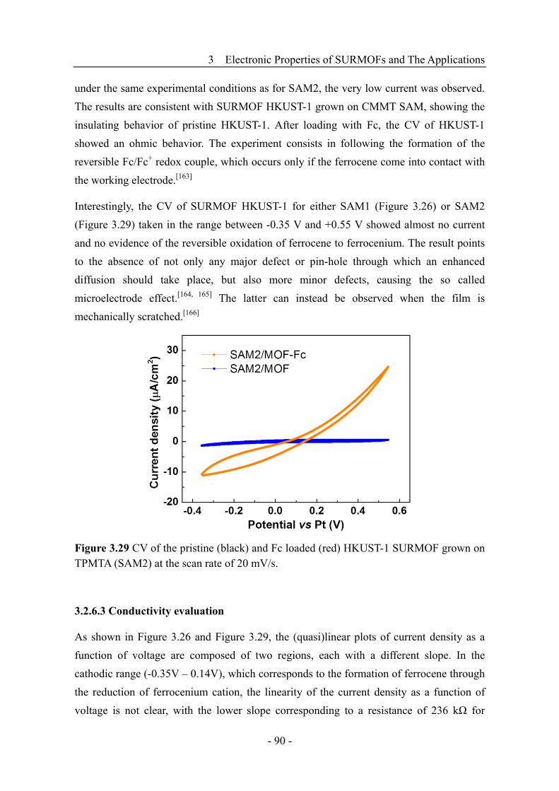
3 Electronic Properties of SURMOFs and The Applications
- 90 -
under the same experimental conditions as for SAM2, the very low current was observed.
The results are consistent with SURMOF HKUST-1 grown on CMMT SAM, showing the
insulating behavior of pristine HKUST-1. After loading with Fc, the CV of HKUST-1
showed an ohmic behavior. The experiment consists in following the formation of the
reversible Fc/Fc+ redox couple, which occurs only if the ferrocene come into contact with
the working electrode.[163]
Interestingly, the CV of SURMOF HKUST-1 for either SAM1 (Figure 3.26) or SAM2
(Figure 3.29) taken in the range between -0.35 V and +0.55 V showed almost no current
and no evidence of the reversible oxidation of ferrocene to ferrocenium. The result points
to the absence of not only any major defect or pin-hole through which an enhanced
diffusion should take place, but also more minor defects, causing the so called
microelectrode effect.[164, 165] The latter can instead be observed when the film is
mechanically scratched.[166]
Figure 3.29 CV of the pristine (black) and Fc loaded (red) HKUST-1 SURMOF grown on TPMTA (SAM2) at the scan rate of 20 mV/s.
3.2.6.3 Conductivity evaluation
As shown in Figure 3.26 and Figure 3.29, the (quasi)linear plots of current density as a
function of voltage are composed of two regions, each with a different slope. In the
cathodic range (-0.35V – 0.14V), which corresponds to the formation of ferrocene through
the reduction of ferrocenium cation, the linearity of the current density as a function of
voltage is not clear, with the lower slope corresponding to a resistance of 236 kΩ for

3 Electronic Properties of SURMOFs and The Applications
- 91 -
SAM1/MOF-Fc, and 224 kΩ for SAM2/MOF-Fc. However, in the anodic range (0.14V –
0.55V), which corresponds to the formation of ferrocenium cation through the oxidation
of ferrocene, the current density as a function of voltage dependence is linear with the
slope of the CV recorded at a scan rate of 20 mV/s. The resistances corresponding to the
slopes are then 45.5 kΩ for SAM1/MOF-Fc, and 63 kΩ for SAM2/MOF-Fc.
As analyzed previously by AFM scratching experiments, the average vertical dimension of
the crystallites is 20 nm and 35 nm for SAM1/MOF-Fc and SAM2/MOF-Fc,
respectively, whereas the underlying HKUST-1 films exhibit a thickness of 70 ± 5 nm for
SAM1/MOF-Fc and 75 ± 5 nm for SAM2/MOF-Fc. By using the thickness of the
homogeneous SURMOF layer as determined by AFM and the electrochemical cell area,
the room temperature conductivity values (σ) of the Fc loaded HKUST-1 SURMOFs
grown on both SAMs were calculated. For SAM1/MOF-Fc, the conductivity of σa = (5.1 ±
0.3) × 10-10 S cm-1 and in σc = (9.9 ± 0.2) × 10-11 S cm-1 at the anodic and cathodic ranges
were obtained, respectively. This corresponds to conductivity values for SAM2/MOF-Fc
of σa = (4.0 ± 0.3) × 10-10 S cm-1 and σc = (1.1 ± 0.1) × 10-10 S cm-1. The calculated
resistance and conductance of these SURMOF thin films are presented in Table 3.1.
Nevertheless, these conductivity values are a lower limit because only the homogenous
and continuous HKUST-1 layers were considered in the calculations.
Table 3.1 Cathodic and anodic conductivity of the HKUST-1 SURMOFs.
Cathodic range
-0.35 V – 0.14 V Anodic range: 0.14V – 0.55 V
R /kΩ σc /S cm-1 R /kΩ σa /S cm-1
SAM1/MOF-Fc (CMMT)
236 (9.9±0.2) × 10-11 45.5 (5.1±0.3) × 10-10
SAM2/MOF-Fc (TPMTA)
224 (1.1±0.1) × 10-10 63.0 (4.0±0.3) × 10-10
Indeed, if contributions from the on top grown crystallites (mean vertical size 20 nm and
35 nm for SAM1/MOF-Fc and SAM2/MOF-Fc, respectively) are considered, an upper
value of conductivity σa = 6.6 x 10⁻¹⁰ S cm-1 (SAM1/MOF-Fc) and σa = 5.8 x 10⁻¹⁰ S cm-1
(SAM2/MOF-Fc) are obtained, respectively. These values are in good agreement with the
electric conductivity values measured for the SAM1/MOF-Fc films upon their integration
in a Hg-based tunneling junction.[167]

3 Electronic Properties of SURMOFs and The Applications
- 92 -
3.2.7 Conclusion
It was demonstrated that the LPE method is a suitable process to produce crystalline and
defect-free films of HKUST-1 on different SAMs (CMMT and TPMTA) and that the film
quality was independent of the crystallographic orientation of the film. Cyclic
voltammetry method was used to study the electrochemical behavior of these HKUST-1
SURMOFs and showed that the SURMOFs act as an insulating barrier for the redox of an
electroactive molecule dissolved in the supporting electrolyte solution. It was also proved
that by loading the HKUST-1 framework with Fc, its insulating behavior was switched
into a conductive one, with the characteristics of an ohmic resistor.

3 Electronic Properties of SURMOFs and The Applications
- 93 -
3.3 Photoelectrochemical properties of porphyrin based SURMOF thin
films
3.3.1 Background
To improve the electrical conductivity of MOFs, two strategies have been followed so far.
One consists in the loading of electroactive guest molecules into the nanopores of the
framework,[101, 102] the other in the utilization of redox active organic linkers.[104, 168] The
idea of choosing suitable organic ligands with special properties is promising not only for
enhancing the electric property, but also for easily fabricating new functional MOF
materials which should expand the application of MOFs as device components.
In plants, porphyrins (like chlorophyll) play a central role in the natural photosynthesis
process: they transform, rather effectively, solar energy into chemical energy. Inspired by
nature, the porphyrin derivatives have been used as light harvester in dye sensitized solar
cells (DSSCs), and manages also, to a certain extent, an efficient conversion of solar
energy into electric energy.[169, 170] The production of the highly ordered array of
porphyrins, as in nature, could possibly improve the efficiency in device applications
where the MOF structure offers the possibility of integrating this photoactive moieties as
organic linkers.
Figure 3.30 Schematic drawing of the photoelectrochemical setup equipped with three-electrode cell and LED light system for the photocurrent measurement. The distance between the two electrodes is 1 cm and the active area is 0.79 cm2.

3 Electronic Properties of SURMOFs and The Applications
- 94 -
In this part, porphyrin-based SURMOFs were prepared on transparent and conductive
FTO (fluorine doped tin oxide) substrates by LPE spraying method, named “porphyrin
SURMOF 2” (SURMOF 2 = 2D surface-anchored metal-organic frameworks). As shown
in Figure 3.30, these monolithic, homogenous films deposited on FTO substrates acting as
electrodes were applied directly in a home-made photoelectrochemical cell for
photocurrent generation studies with a typical three-electrode system.
3.3.2 Preparation of the porphyrin-based SURMOF thin films
Two kinds of porphyrin ligands were used to produce the SURMOFs in the present work;
one is a free base porphyrin, and the other is Pd porphyrin (molecular structures are
presented in Figure 3.32(d)). The Porphyrin-based SURMOFs were fabricated using the
LPE spraying method (Chapter 2.2.3). Figure 3.31 shows the SEM morphology and
cross-section analysis of the 30 spraying cycles samples. It can be seen that the films are
homogeneous with a thickness of about 300 nm for both free base porphyrin Zn-SURMOF
2 and Pd porphyrin Zn-SURMOF 2. The thickness of about 10 nm per deposition cycle
was estimated from the SEM cross-section images.
Figure 3.31 Top view and cross-section SEM images of (a) free base porphyrin Zn-SURMOF 2 and (b) Pd porphyrin Zn-SURMOF 2 grown on FTO substrates. For both samples, the thickness of 300 nm has been obtained in 30 spraying cycle.
3.3.3 XRD characterization
“SURMOF 2”, comprising the so called paddle-wheel units, is a MOF structure typically
stacked between copper or zinc paddle-wheel and dicarboxylic acid ligands to yield an
overall P4 symmetry.[171], The proposed structures of free base porphyrin Zn-SURMOF 2
and Pd porphyrin Zn-SURMOF 2 are presented in Figure 3.32. The porphrin structures are
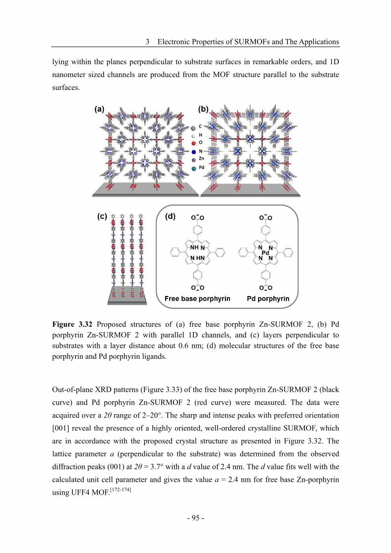
3 Electronic Properties of SURMOFs and The Applications
- 95 -
lying within the planes perpendicular to substrate surfaces in remarkable orders, and 1D
nanometer sized channels are produced from the MOF structure parallel to the substrate
surfaces.
Figure 3.32 Proposed structures of (a) free base porphyrin Zn-SURMOF 2, (b) Pd porphyrin Zn-SURMOF 2 with parallel 1D channels, and (c) layers perpendicular to substrates with a layer distance about 0.6 nm; (d) molecular structures of the free base porphyrin and Pd porphyrin ligands.
Out-of-plane XRD patterns (Figure 3.33) of the free base porphyrin Zn-SURMOF 2 (black
curve) and Pd porphyrin Zn-SURMOF 2 (red curve) were measured. The data were
acquired over a 2θ range of 2–20°. The sharp and intense peaks with preferred orientation
[001] reveal the presence of a highly oriented, well-ordered crystalline SURMOF, which
are in accordance with the proposed crystal structure as presented in Figure 3.32. The
lattice parameter a (perpendicular to the substrate) was determined from the observed
diffraction peaks (001) at 2θ = 3.7° with a d value of 2.4 nm. The d value fits well with the
calculated unit cell parameter and gives the value a = 2.4 nm for free base Zn-porphyrin
using UFF4 MOF.[172-174]

3 Electronic Properties of SURMOFs and The Applications
- 96 -
Figure 3.33 Out-of-plane XRD of the free base porphyrin Zn-SURMOF 2 (black) and Pd porphyrin Zn-SURMOF 2 (red) films grown on FTO substrates.
3.3.4 Photoelectrochemical measurements
In natural systems, these light-harvesting molecules are typically stacked to yield extended
columns through which the absorbed sunlight energy is transported in the form of excitons.
Charge separation, i.e. the dissociation of the exciton to yield an electron (e) and a hole (h)
is achieved at a target chlorophyll pigment center.[175] Here, the assembled regular arrays
of photoactive molecules, porphyrin-based SURMOFs, were assembled into
photoelectrochemical cell for the photocurrent generation measurement.
The photocurrent measurements were carried out on an electrochemical workstation, and a
home-made photoelectrochemical cell using three-electrode system was applied, as shown
in Figure 3.30. 50 μM iodine/triiodine solution (I-/I3- in acetonitrile) was used as redox
components. Amperometric detection method was used to monitor the current, and the
applied bias voltage was controlled at 0.06 V vs Pt wire electrode (as reference electrode).
The free base porphyrin Zn-SURMOF 2 and Pd porphyrin Zn-SURMOF 2 thin films
produced on FTO glasses were used as the working electrode, a Pt coated FTO substrate
as counter electrode, and a Pt wire as the reference electrode.
Measurements were taken under illumination from fiber coupled LEDs system (Prizmatix).
The illumination wavelength at 365, 400, 455, 530 and 640 nm were chosen for shining
the porphyrin-based SURMOF samples during photocurrent generation measurement. The

3 Electronic Properties of SURMOFs and The Applications
- 97 -
output power was measured using Ophir Nova II power meter with PD-300-UV sensor.
The output power was 112 mW for LED 365 nm, 65 mW for LED 400 nm, 135 mW for
LED 455 nm, 55 mW for LED 530 nm and 102 mW for LED 640 nm. The area of light
irradiation was 0.79 cm2. All experiments were carried out at room temperature.
Figure 3.34 Photocurrent action data of (a) bare FTO substrate, (b) free base porphyrin Zn-SURMOF 2 on FTO substrate (in blue) and bare FTO (in black, for comparison), (c) Pd porphyrin Zn-SURMOF 2 on FTO substrate (in red) and bare FTO (in black), and (d) photocurrent generation of bare FTO substrate and porphyrin-based SURMOFs at various illuminating wavelengths of 365 nm, 400 nm, 455 nm, 530 nm and 640 nm.
First, an on-off photocurrent action of the FTO substrate and porphyrin-based SURMOF
films (both films with a thickness of about 300 nm) at various illuminating wavelengths
(365 nm, 400 nm, 455 nm, 530 nm and 640 nm) were measured, as illustrated in Figure
3.34(a-c). The photocurrent depending on illuminating wavelengths is summed up in
Figure 3.34(d). It can be seen that the generated photocurrent from FTO substrate is very
low comparing to the porphyrin-based SURMOFs, and decreases with increasing the
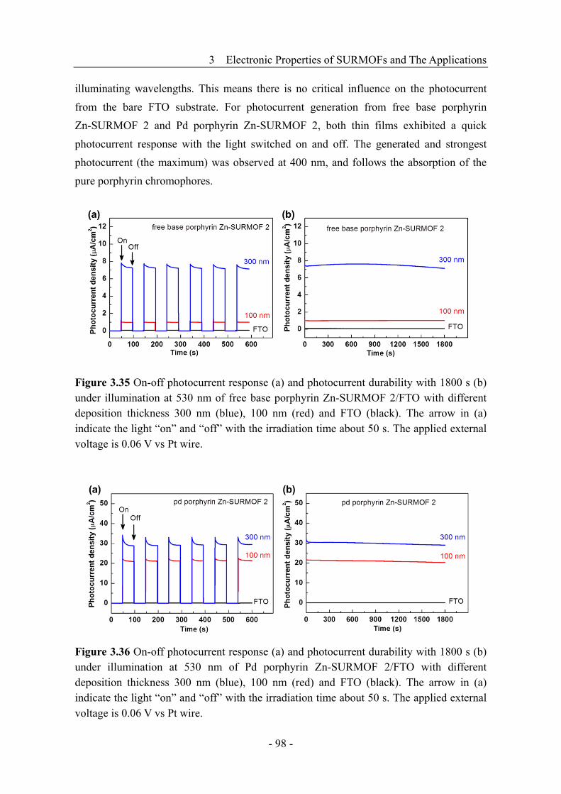
3 Electronic Properties of SURMOFs and The Applications
- 98 -
illuminating wavelengths. This means there is no critical influence on the photocurrent
from the bare FTO substrate. For photocurrent generation from free base porphyrin
Zn-SURMOF 2 and Pd porphyrin Zn-SURMOF 2, both thin films exhibited a quick
photocurrent response with the light switched on and off. The generated and strongest
photocurrent (the maximum) was observed at 400 nm, and follows the absorption of the
pure porphyrin chromophores.
Figure 3.35 On-off photocurrent response (a) and photocurrent durability with 1800 s (b) under illumination at 530 nm of free base porphyrin Zn-SURMOF 2/FTO with different deposition thickness 300 nm (blue), 100 nm (red) and FTO (black). The arrow in (a) indicate the light “on” and “off” with the irradiation time about 50 s. The applied external voltage is 0.06 V vs Pt wire.
Figure 3.36 On-off photocurrent response (a) and photocurrent durability with 1800 s (b) under illumination at 530 nm of Pd porphyrin Zn-SURMOF 2/FTO with different deposition thickness 300 nm (blue), 100 nm (red) and FTO (black). The arrow in (a) indicate the light “on” and “off” with the irradiation time about 50 s. The applied external voltage is 0.06 V vs Pt wire.

3 Electronic Properties of SURMOFs and The Applications
- 99 -
Then, the on-off photocurrent response and photocurrent durability measurement of the
free base porphyrin Zn-SURMOF 2/FTO and Pd porphyrin Zn-SURMOF 2/FTO under
illumination at 530 nm (in the visible light region) were performed (Figure 3.35 and
Figure 3.36). For both cases, the different thicknesses of the MOF films were evaluated,
referring to 300 nm (blue) and 100 nm (red) in the figures. It can be seen that the
generated photocurrent increases as the increase of film thickness for both free base and
Pd porphyrin based SURMOFs. In the 30 min duration, both samples showed a stable
generation of photocurrent. The metalloporphyrin based MOF (Pd porphyrin
Zn-SURMOF 2) had however a higher photocurrent comparing to the free base porphyrin
Zn-SURMOF 2 of same thickness.
3.3.6 Conclusion
The highly oriented porphyrin-based SURMOF films, free base porphyrin Zn-SURMOF 2
and Pd porphyrin Zn-SURMOF 2, were prepared on the transparent and conductive FTO
substrates using a LPE spraying method. The XRD data showed that these crystalline thin
films grew only along the [001] orientation. By assembling these porphyrin-based
SURMOF films on a home-made photoelectrochemical cell, photocurrent generation was
performed at various illuminating wavelengths, and the maximum photocurrent was
observed at 400 nm for both free base and Pd porphyrin Zn-SURMOF 2. The
porphyrin-based MOFs also showed remarkable photocurrent generation efficiency in the
visible light region through Pd porphyrin Zn-SURMOF 2 exhibited an enhanced
photocurrent generation compared to the free base porphyrin Zn-SURMOF 2.
This section is based on a publication in Angew. Chem. Int. Ed. by Jinxuan Liu et al.(2015)
as ref.[176]

4 Optical Properties of SURMOFs and Their Device Applications
- 100 -
4 Optical Properties of SURMOFs and Their Device
Applications
4.1 SURMOF-based Bragg reflectors and their optical sensing properties
4.1.1 Background
Photonic band gap (PBG) materials, also known as photonic crystals, are periodic
dielectric or metallo-dielectric materials conceived to control the propagation of photons
within a defined frequency range.[177, 178] Bragg stacks (BS) are one-dimensional photonic
crystals fabricated by alternately stacking transparent layers with different refractive index
(RI),[179, 180] as schematized in Figure 4.1. Such PBG materials consist typically of two
different metal oxides,[181] but other materials such as polymers[180] have also been
successfully employed. One of the particularly interesting classes of materials for the
fabrication of such PBG materials is metal-organic frameworks.
Figure 4.1 Scheme of the Bragg stack reflector. The structure is formed from the multiple thin layers stacked together at z-direction on a substrate. The “rainbow” represents incoming visible light, and the orange arrow represents the reflected light. Only specific frequency range of light is reflected in such a BS system.
MOFs, being highly porous crystallized materials, are drawing further attention in the area
of optical and photonic device applications because of their versatile syntheses and
produced properties (low density, high surface area and pore volume, high thermal
stability, amongst others).[2, 3] The refractive index of MOFs can be tailored to be
exceptionally low.[182] This makes these materials ideally suited as components for PBG
materials. In previous works, polycrystalline MOF-based PBG materials have been

4 Optical Properties of SURMOFs and Their Device Applications
- 101 -
fabricated by spin-coating of ZIF-8 MOF-nanoparticles on TiO2 porous layers. Upon
loading with different alcohols, the optical properties of the yielding multilayered Bragg
stacks change.[183] Nevertheless, a higher optical performance, necessary for a device
application, requires the MOFs to be homogenous. This is not the case with the reported
process, which, in a way, is by “piling up” MOF nanoparticles.
SURMOFs prepared by LPE spraying method have proven to be rather homogenous thin
films with high crystallinity and a well controlled thickness by adjusting the number of
spraying cycles. These monolithic SURMOF thin films exhibit low defect densities[101] as
well as an excellent mechanical stability.[152]
Figure 4.2 Scheme of the SURMOF-based PBG materials (2 bilayer system of ITO/HKUST-1).
In this part, SURMOF HKUST-1 and ITO thin films were applied in a multilayered PBG
system (the Bragg reflector), as shown in Figure 4.2. The homogenous and highly oriented
HKUST-1 SURMOFs were prepared on silicon substrate by the LPE spraying method,
while the intermediate ITO (indium tin oxide) layers were deposited by magnetron
sputtering, in the multilayered Bragg reflectors. These PBG materials were color tunable
over the whole visible range, depending on the thickness of the corresponding layers, and
displayed very high optical performance. The optical sensing capabilities employing the
chemo-responsive optical signal were characterized by exposing the Bragg reflectors to
various organic solvent. Such SURMOF-based PBG materials provide a basis for the
future development of photonic and color-coded chemical sensing devices.
4.1.2 Fabrication of the monolithic SURMOF-based Bragg stack
The SURMOF-based Bragg stack is a monolithic, multilayered hybrid stacks obtained by
alternately depositing SURMOF (HKUST-1) and ITO (indium tin oxide) layers on a
4 Optical Properties of SURMOFs and Their Device Applications
- 102 -
modified Si substrate. First, HKUST-1 SURMOF layer was deposited by using LPE
spraying method (as described previously) with thicknesses ranging from 80 to 135 nm on
the Si substrate. Subsequently, an ITO (indium tin oxide) layer was deposited using
magnetron sputtering to thicknesses ranging from 62 to 100 nm. The multilayered hybrid
stacks were fabricated by repeating the two processes.
The magnetron sputtering method is a kind of physical vapor deposition (PVD) technique.
A thin film of ITO was sputtered through a top down approach from an ITO sputter
substrate (the source, SnO2/In2O3=1/9, Kurt J Lesker, UK) in a sputtering chamber. The
ITO films were deposited using a r.f. (radio frequency) sputtering setup with a 3″ION’ X
planar magnetron source (TFC, Grafenberg, DE) mounted on a standard double-cross
recipient equipped with a pre-sputter shutter and a sample positioner allowing for various
working distances (150–200 mm) between the magnetron and the substrate. The base
pressure was below 5×10⁻⁶ mbar to achieve a sufficient purity. The gas inlet was equipped
with an MKS mass-flow control system (MKS Instruments Deutschland GmbH, Germany)
providing a constant operating pressure of 2.5×10⁻³ mbar of 80 vol.% Ar and 20 vol.% O2
for reactive sputtering. The r.f. sputtering power was 66 W (PFG 300 power supply,
Hüttinger, Germany) leading to deposition rates of about 66 nm/h.
Before producing the SURMOF-based Bragg stack, the silicon substrates (thickness: 525
± 20 μm; specific resistivity: 8−12 Ω/cm; from Silchem Handelsgesellschaft GmbH DE)
with a [100] orientation were treated by O2 plasma (Diener Plasma; gas flow: 50 sccm,
pure O2) for 30−40 min to remove impurities as well as to increase the number of OH
functional groups and the hydrophilicity. Various thicknesses of the HKUST-1 SURMOF
layers were then deposited on pretreated/modified Si substrates using the LPE spraying
method (experimental details are presented in Chapter 2.2.3). The desired thickness of
the individual HKUST-1 SURMOF layers were adjusted by changing the number of
distinct LPE spraying cycles; e.g., 20 spraying cycles for HKUST-1 SURMOFs resulted in
a total thickness of 80 nm, 26 spraying cycles in 96 nm, 34 spraying cycles in 115 nm, and
40 spraying cycles in 135 nm, as presented in Figure 4.3.
Then various thicknesses of the ITO thin films were deposited on the freshly prepared
HKUST-1 SURMOF layers. The corresponding thickness of sputtered ITO layers
depending on the sputtering time for each bilayer system is also presented in Figure 4.3.
Thereafter, the next layers of HKUST-1 SURMOF were deposited on the freshly sputtered
ITO layers. Due to the presence of OH-groups freed through the O2 plasma treatment of

4 Optical Properties of SURMOFs and Their Device Applications
- 103 -
the Si substrate or freshly deposited ITO layers, the growth of subsequent HKUST-1
SURMOF layers was achieved using the same LPE method. This process (SURMOF
deposition by LPE method conditions, and ITO deposition by magnetron sputtering
method) was repeated until the desired number of Bragg stack (HKUST-1/ITO bilayer)
was obtained.
Figure 4.3 Thicknesses of the sprayed HKUST-1 SURMOF layers as a function of the number of LPE spraying cycles, and the corresponding thicknesses of sputtered ITO layer as a function of the sputtering time for each of these bilayer systems, e.g. HKUST-1/ITO (80 nm/62 nm; 96 nm/73 nm; 115 nm/85 nm and 135 nm/100 nm).
Control over the respective fabrication processes allowed tuning the thickness of the
multilayered stacks with a high degree of precision. In the present study, four different
types of multilayered stacks were fabricated on Si substrate with each stack comprising 5
bilayer. The SURMOF-based Bragg stacks (multilayered HKUST-1/ITO systems) were
produced maintaining thicknesses of 80 nm/62 nm, 96 nm/73 nm, 115 nm/85 nm and 135
nm/100 nm, respectively.
4.1.3 Characterization of the SURMOF-based Bragg stack
4.1.3.1 XRD of the multilayered Bragg stack
XRD patterns were measured for these multilayered SURMOF-based Bragg stacks after
preparation to check their crystallinity and compactness. The XRD patterns obtained for

4 Optical Properties of SURMOFs and Their Device Applications
- 104 -
the various thicknesses (80, 96, 115 and 135 nm) of HKUST-1 SURMOF thin films
deposited on ITO layers are presented in Figure 4.4(a). The XRD patterns of Si substrate
and sputtered ITO thin film on Si were measured for comparison and peak position
calibration in Figure 4.4(b).
Figure 4.4 Out-of-plane XRD analysis of (a) various thicknesses of the fifth layers of the HKUST-1 SURMOFs deposited on the freshly sputtered ITO layers in the multilayered HKUST-1/ITO systems, and (b) Si substrate and the sputtered ITO thin films on Si substrate.
The prepared samples with various thicknesses of HKUST-1 SURMOFs were grown with
mixed orientation. The diffraction peaks with 2θ of around 17.4°, 34.2°, and 53.9°
attributed to the (002), (220), and (222) peaks of HKUST-1, respectively; and the peak at

4 Optical Properties of SURMOFs and Their Device Applications
- 105 -
around 21.5° was attributed to sputtered ITO thin film.[184] The results indicate the
presence of crystalline SURMOF thin films. The intensity of HKUST-1 SURMOFs
increased with increasing film thickness. This shows that the epitaxial growth HKUST-1
retains a similar orientation for crystallites.
Figure 4.5 Out-of-plane XRD patterns of the different layers of (a) HKUST-1 and (b) ITO thin film for a multilayered SURMOF-based Bragg stacks.
Figure 4.5 shows the XRD patterns of various layers of HKUST-1 and ITO thin film for
the multilayered ITO/HKUST-1 system. The first layer of the Bragg stacks was a
HKUST-1 thin film grown on Si substrate, so the peak of ITO (211) is not observed on the
first layer (1 layer) XRD pattern in Figure 4.5(a). The first ITO layer was sputtered on top
of the freshly deposited HKUST-1 SURMOF. After the preparation of the first bilayer (one

4 Optical Properties of SURMOFs and Their Device Applications
- 106 -
ITO layer on top of the HKUST-1 SURMOF layer), another layer of HKUST-1 SURMOF
was deposited on top of the sputtered ITO. A new peak (at around 21.5°) attributed to ITO
(211) was then observed on the second layer of HKUST-1 SURMOF (2 layers). The
intensity of HKUST-1 refraction index increased gradually with the numbers of the bilayer,
because all of the deposited HKUST-1 layers contribute to the intensity of XRD patterns.
The intensity of ITO (211) peaks were also observed to increase. The XRD patterns of the
different layers HKUST-1 SURMOFs showed a similar crystalline orientation on both the
Si and ITO surfaces. As shown in Figure 4.5(b), the XRD peak intensity of the sputtered
ITO layers also increased with the number of ITO layers.
Figure 4.6 (a) comparing the peak intensity (net area) of various layers of HKUST-1 (222) and ITO (211), which were taken from Figure 4.5. The lines are corresponding to the respective linear fit. (b) Domain size Lvol of the various layers of HKUST-1 thin films calculated by the Scherrer equation and Williamson-Hall plot.
Further analysis of the XRD peak intensities (net area) of various layers of HKUST-1 (222)
and ITO (211) are presented in Figure 4.6(a). It can be seen that the intensities increase
with the number of layers. The rate of intensity change between ITO and HKUST-1 is
about 7.09; this value has a good consistency with the rate of density for these two
materials where ITO/HKUST-1 equals to 7.24.
As mentioned in Chapter 2.2.1 about the XRD method, not only the coherent scattering
domain size but also the inhomogeneous strain can broaden the diffraction peak. Scherrer
equation and Williamson-Hall plot analysis were used to evaluate the coherent scattering
domain size of the various layers of HKUST-1 SURMOF. With the Scherrer equation

4 Optical Properties of SURMOFs and Their Device Applications
- 107 -
(equation (3-1)), introduced in Chapter 3.1.3, the domain size was calculated with an
average of all refractive peaks, but without considering stress/strain. Williamson-Hall plot
is a method used for determining the coherent scattering domain size and stress/strain of
crystals according to (4−1).[185]
sin4cos)( 0volL
KbB (4−1)
Where B is the integral breadth, b is the instrumental width, θ is the diffraction angle, K is
the Scherrer constant (0.89), λ is 0.15406 nm (Cu Kα1), Lvol is the domain Size, and ε0 is
the lattice constant mismatch (the stress/strain).
As presented in Figure 4.6(b), the coherent scattering domain size of HKUST-1 SURMOF
thin films calculated by both the methods shows a quite similar value of approximately 58
nm for all the different layers (from 1 to 5 bilayer). Since the instrumental contribution to
the line broadening was considered, and no stress/strain contributions were added, the
calculated domain size by Scherrer equation represents a lower limit. However, for the
domain size of HKUST-1 SURMOFs analyzed by Williamson-Hall plot, all of the (002),
(220) and (222) reflections were considered.[186] The consistent and lesser scattering
values confirmed the homogeneity of the HKUST-1 SURMOF thin films in the hybrid
PBG materials.
4.1.3.2 HR-SEM cross-section analysis of the multilayered Bragg stack
Figure 4.7 shows the cross-sectional SEM images of the various multilayered Bragg stacks.
The homogenous stacking of the distinct material layers can be seen in both, the 3 bilayer
and 5 bilayer samples. The ITO layers showed a better resolution comparing with
HKUST-1 SURMOF layers because of its higher conductivity and density.
In this case, focused ion beam (FIB) cutting method was used to reprocess the
multilayered Bragg stack samples for the cross-section analysis. The FIB-cutting analysis
was done by using a dual beam focused ion beam microscope (Zeiss AURIGA 60)
equipped with a Ga+ ion gun and a high resolution field emission SEM (FESEM). For
milling of the samples, an acceleration voltage of 30 kV (beam current of 20 nA) was
applied. The final milling step was done at 30 kV and 600 pA. FESEM imaging was
performed at 5 kV, using an In-Lens detector.

4 Optical Properties of SURMOFs and Their Device Applications
- 108 -
As presented in Figure 4.8, the HR-SEM cross-section analysis of a 5 bilayer
(HKUST-1/ITO = 135 nm/100 nm) SURMOF-based Bragg stack for the samples prepared
by both mechanical break-apart and FIB-cutting.
Figure 4.7 HR-SEM cross-sections of the multilayered SURMOF-based Bragg stacks. (a) 5 bilayer HKUST-1/ITO (80 nm/62 nm); (b) 5 bilayer HKUST-1/ITO (115 nm/85 nm); (c-d) 3 and 5 bilayer HKUST-1/ITO (135 nm/100 nm).
Figure 4.8 HR-SEM cross-section analysis of a 5 bilayer (HKUST-1/ITO = 135 nm/100 nm) SURMOF-based Bragg stack for the samples prepared by both mechanical break-apart (a) and FIB-cutting (b). The FIB-cutting may lead to a partially evaporation of the HKUST-1 layers, therefore the observed macro-porous structures is an artefact due to the FIB-cutting process.

4 Optical Properties of SURMOFs and Their Device Applications
- 109 -
During FIB-cutting, parts of materials from HKUST-1 layer were lost by thermal
evaporation, and led to the observed macro-porous morphology as seen in Figure 4.8(b).
Comparing the two cross-section images revealed the FIB-cutting being more
cross-section analysis advantageous as it provided clearer images with more defined layer
thickness and a better contrast between the different materials.
4.1.3.3 ToF-SIMS analysis of the multilayered Bragg stack
ToF-SIMS measurements were performed on the SURMOF-based Bragg stacks for a
thorough investigation of the multilayered PBG systems. During the measurement,
ultra-high vacuum (UHV) base pressure kept lower than 5×10⁻⁹ mbar. For high mass
resolution, the source was operated in the “high current bunched” mode providing short
Bi3+ primary ion pulses (the length of 1.1 to 1.3 ns allowed for high mass resolution) at 25
keV and a lateral resolution of approximately 4 μm. Spectra were calibrated from the
omnipresent C+, CH+, CH2+, CH3+, Si+, Cu+ and 113In+ corresponding peaks.
For the depth profiling, a dual beam analysis was performed. The primary ion source was
performed with the same conditions as mentioned above. An oxygen sputter gun was used
to erode the sample. The obtained 5-dimensional data sets (x and y positions, sputter ion
dose density, m/z, and count rate) are presented as x/y-area integrated ion intensities over
ion dose density or as 3D rendering. Due to different sputter rates of the layers no linear
depth scale is provided.
Figure 4.9 shows a 3D reconstruction of a 2 bilayer HKUST-1/ITO (135 nm/100 nm) PBG
Bragg stack based on specific ion signals from ToF-SIMS depth profiling. For this
analysis a 500×500 µm2 region was continuously analyzed using the Bi3+ ion source,
while a concentric area of 800×800 µm2 was eroded with a 2 keV oxygen sputter beam up
to a final dose density of 6.3×1017 cm-2 ions. In the ToF-SIMS images in Figure 4.9 the
HKUST-1 layers are depicted as Cu with 65Cu and Cu2 signals characterizing the MOF
layers, and with In3O+ together with other InxOy species characterizing the ITO layers.
SIMS depth profiling confirmed a homogeneous and continuous layer system.
Figure 4.10 shows an intensity profile of In3O2+, Cu+, and Si+ from a 5 bilayer
HKUST-1/ITO (135 nm/100 nm) system. For this analysis a 100×100 µm2 region was
continuously analyzed using the Bi3+ ion source (64×64 pixel), while a concentrical area
of 250×250 µm2 was eroded with a 1 keV oxygen sputter beam up to a final dose density
of 2.3×1018 cm-2 ions. 63Cu, as shown in Figure 4.10, as well as 65Cu and Cu2 signals

4 Optical Properties of SURMOFs and Their Device Applications
- 110 -
characterize the MOF layers. In3O2, together with other InxOy species characterize the ITO
layers in negative polarity Secondary Ion Mass Spectra. As seen from this graph both
layers can be clearly distinguished and exhibit a regular depth distribution.
Figure 4.9 3D reconstruction of a 2 bilayer HKUST-1/ITO stack deposited on silicon substrate using ToF-SIMS depth profile data. Top left, blue: Si+; top right, green: Cu+; lower left, orange: In3O
+; lower right: combined overlay.
Figure 4.10 ToF-SIMS depth profile of a 5 bilayer HKUST-1/ITO stack performed with oxygen (1 keV) erosion. Orange: In3O2
+, green Cu+, blue Si+.

4 Optical Properties of SURMOFs and Their Device Applications
- 111 -
Although the ITO layers were thinner than the MOF layers, the plotting of secondary ion
count rates over the applied sputter ion dose provided a nearly symmetrical profile for all
10 layers due to the different erosion rates of the materials this until the silicon substrate
was finally reached. As shown in Figure 4.10, rising and falling flanks for the In3O2+
signals are nearly symmetrical without any strong tailings towards the deeper layers. In
case of the multiatomic fragment In3O2-, no forward implantation artifacts emerged. In
case of Cu, a slight forward implantation tendency was observed at the tailings on the
trailing sides of the profile plots. Due to a partial doping of individual copper atoms into
the substrate material (Si), the lowest MOF layer exhibited an anomalous signal.
4.1.4 Optical properties of the SURMOF/ITO hybrid PBG material
The solvent-free HKUST-1 has a reported refractive index (n) of n = 1.39 (at 200 °C)[182]
at a wavelength of 750 nm. Such a low RI is in a good agreement with the static dielectric
constant (n ≈ 1.30) predicted by Seifert and co-workers.[187] By exposing the activated or
dry HKUST-1 thin films to moisture or ethanol (EtOH) atmosphere, its refractive index
increases to n = 1.55−1.6.[182]
The spectroscopic ellipsometry measurements of the freshly produced the ITO and the
HKUST-1 SURMOF thin film were performed in a wavelength range of 410–750 nm with
a fixed incidence angle of 75° aligned on silicon substrates, as shown in Figure 4.11.
Figure 4.11 Spectroscopic ellipsometry data of the ITO and the HKUST-1 SURMOF thin film measured at ambient conditions; the ITO and HKUST-1 SURMOF indicate the high RI and low RI component in the multilayered PBG materials.
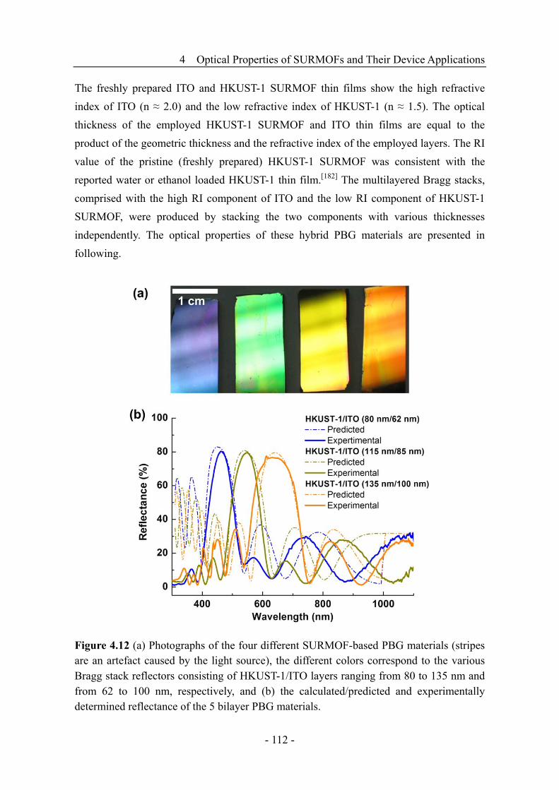
4 Optical Properties of SURMOFs and Their Device Applications
- 112 -
The freshly prepared ITO and HKUST-1 SURMOF thin films show the high refractive
index of ITO (n ≈ 2.0) and the low refractive index of HKUST-1 (n ≈ 1.5). The optical
thickness of the employed HKUST-1 SURMOF and ITO thin films are equal to the
product of the geometric thickness and the refractive index of the employed layers. The RI
value of the pristine (freshly prepared) HKUST-1 SURMOF was consistent with the
reported water or ethanol loaded HKUST-1 thin film.[182] The multilayered Bragg stacks,
comprised with the high RI component of ITO and the low RI component of HKUST-1
SURMOF, were produced by stacking the two components with various thicknesses
independently. The optical properties of these hybrid PBG materials are presented in
following.
Figure 4.12 (a) Photographs of the four different SURMOF-based PBG materials (stripes are an artefact caused by the light source), the different colors correspond to the various Bragg stack reflectors consisting of HKUST-1/ITO layers ranging from 80 to 135 nm and from 62 to 100 nm, respectively, and (b) the calculated/predicted and experimentally determined reflectance of the 5 bilayer PBG materials.

4 Optical Properties of SURMOFs and Their Device Applications
- 113 -
Four different types of SURMOF-based PBG materials were produced and 5 bilayer were
stacked for each type. As shown in Figure 4.12(a), the color of blue, green, yellow and
orange from the images corresponds to various bilayer (HKUST-1/ITO) systems having
the thickness of 80 nm/62 nm; 96 nm/73 nm; 115 nm/85 nm and 135 nm/100 nm
respectively. Figure 4.12(b) presents the reflectance measurement of the hybrid PBG
materials with a 5 bilayer stack. A comparison of the experimental optical reflectivity data
with the simulated reflectivity plots revealed the exceptional optical quality of the
SURMOF-based hybrid PBG. In all cases, the predicted and measured reflectivity match
very well. Furthermore, the reflectivity maximum reached about 80%, exceeding the value
reported for the system based on ZIF-8/TiO2 and ZIF-8/Pt.[183]
Figure 4.13 (a) Angular dependence reflectance of the 5 bilayer HKUST-1/ITO (135 nm/100 nm) hybrid PBG (orange) and (b) the corresponding contour plot, the spectra were recorded from 20° to 75° incidence with 5° increment.

4 Optical Properties of SURMOFs and Their Device Applications
- 114 -
The angular dependence reflectance was measured with an incidence ranging from 25° to
75° (with 5° increment). The specular reflectance of each samples was measured with a
spectral bandwidth from 200 to 800 nm (size 2.5 × 2.5 cm). The data collection,
evaluation and graphical analysis were carried out on the software (Cary WinUV®)
provided by Agilent. Figure 4.13(a) shows an angular dependence reflectance of a 5
bilayer hybrid PBG material (HKUST-1/ITO = 135 nm/100 nm, orange colored) at
variable angles of incidence. By starting with a high reflectance above 80% at around 635
nm and at 20° incidence, the PBG showed an angle dependent decrease of the maximum
reflectance. The blue shift of the PBG to smaller values was observed by lowering the
angle of incidence stepwise with a 5° increment during the angular reflectance
measurements.
The contour plot of the angular dependence reflectance is presented in Figure 4.13(b),
which showed the reflectance changes corresponding to incidence angles in a 2D image.
The highest reflectance (in red color) is shifted to lower wavelength by increasing the
incidence angle. Furthermore, the corresponding 3D plot of the 5 bilayer PBG material is
shown in Figure 4.14. The 3D plot represents the reflectance of the stack corresponding to
the wavelength and incidence angles of the beam. The iridescence can be simply
demonstrated by tilting the macroscopic samples at different angles.
Figure 4.14 3D plot of the 5 bilayer HKUST-1/ITO (135 nm/100 nm) hybrid PBG material (orange), angular dependence reflectance was recorded from 20° to 75° incidence with 5° increment.

4 Optical Properties of SURMOFs and Their Device Applications
- 115 -
As shown in Figure 4.15 and Figure 4.16, the angular dependence reflectance values of the
other two 5 bilayer hybrid PBG materials were also presented at variable angles of
incidence: the yellow colored Bragg reflector (HKUST-1/ITO = 115 nm/85 nm) (Figure
4.15(a)) and the blue colored Bragg reflector (HKUST-1/ITO = 80 nm/62 nm) (Figure
4.16 (a)). The angle-dependent decrease of the reflectance maximum as well as the blue
shift to smaller values of the PBG were also detected in these SURMOF-based PBG
materials by lowering the angle of incidence stepwise with a 5° increment. The
corresponding contour plots of the angular dependence reflectance on the yellow and blue
colored hybrid PBG materials are presented in Figure 4.15(b) and Figure 4.16(b).
Figure 4.15 (a) Angular dependence reflectance of the 5 bilayer HKUST-1/ITO (115 nm/85 nm) hybrid PBG material (yellow) and (b) the corresponding contour plot, the spectra were recorded from 20° to 75° incidence with 5° increment.

4 Optical Properties of SURMOFs and Their Device Applications
- 116 -
Figure 4.16 (a) Angular dependence reflectance of the 5 bilayer HKUST-1/ITO (80 nm/62 nm) hybrid PBG material (blue), and (b) the corresponding contour plot, the spectra were recorded from 20° to 75° incidence with 5° increment.
With the advantageous flexibility for chemical functionalization, post synthesis, as well as
the MOFs capacity for loading other functional guests, the SURMOF-based devices
provides an adequate system for optical or light induced switching[85] or for charge
transport properties.[101] In the present study, such multilayered SURMOF-based Bragg
stacks provided the basis for the fabrication of photonic, color-coded hybrid PBG
materials, which could act further as chemical sensing devices. In the next part, the porous
nature of the HKUST-1 SURMOFs integrated inside the multilayered PBG systems was
exploited and modulated for adjusting the optical constant. These properties could be
directly used for optical sensing.

4 Optical Properties of SURMOFs and Their Device Applications
- 117 -
4.1.5 Chemo-responsive optical sensing of the SURMOF/ITO hybrid PBG
Having a thermal stability typically exceeding 200 °C and other advantageous
mechanical,[39] dielectric,[188] or optical[182] properties, MOF coatings provide the base
functions for numerous applications. Loading the pores with appropriate guest molecules
can modulate their electrical and optical properties,[85, 102] which is particularly interesting
for optical sensing.[71] The significant change in refractive index resulting from loading
guest molecules in the nanopores of HKUST-1[182] allows a direct the realization of a
sensor, and at the same time, the sorption behavior of the MOF material can be
quantitatively and accurately determined.
Activation and drying of the SURMOF/ITO multilayered PBG material led to a
pronounced change in their PBG behavior, including a significant reduction of scattered
light at the blue edge of the PBG as shown in Figure 4.16. This is consistent with the
removal of excess water/solvent molecules from the HKUST-1 crystal structure. The dry
or activated process resulted then in an improved optical quality of the PBG material, by
increasing the fringe visibility and generating sharp PBG edges.
Figure 4.16 PBG blue edge changes after heating at ≈200 °C for 1−2 h for the effect of dry or activation and EtOH loading on the multilayered PBG material.
As shown in Figure 4.17, a reflectance measurement was performed on a 5 bilayer
HKUST-1/ITO (135 nm/100 nm) stack for a direct optical sensing of ethanol (EtOH) and
tested the reliability of the system as an optical device.
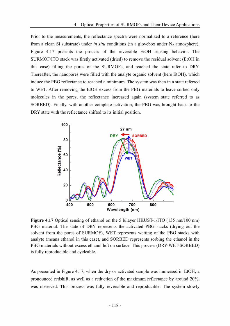
4 Optical Properties of SURMOFs and Their Device Applications
- 118 -
Prior to the measurements, the reflectance spectra were normalized to a reference (here
from a clean Si substrate) under in situ conditions (in a glovebox under N2 atmosphere).
Figure 4.17 presents the process of the reversible EtOH sensing behavior. The
SURMOF/ITO stack was firstly activated (dried) to remove the residual solvent (EtOH in
this case) filling the pores of the SURMOFs, and reached the state refer to DRY.
Thereafter, the nanopores were filled with the analyte organic solvent (here EtOH), which
induce the PBG reflectance to reached a minimum. The system was then in a state referred
to WET. After removing the EtOH excess from the PBG materials to leave sorbed only
molecules in the pores, the reflectance increased again (system state referred to as
SORBED). Finally, with another complete activation, the PBG was brought back to the
DRY state with the reflectance shifted to its initial position.
Figure 4.17 Optical sensing of ethanol on the 5 bilayer HKUST-1/ITO (135 nm/100 nm) PBG material. The state of DRY represents the activated PBG stacks (drying out the solvent from the pores of SURMOF), WET represents wetting of the PBG stacks with analyte (means ethanol in this case), and SORBED represents sorbing the ethanol in the PBG materials without excess ethanol left on surface. This process (DRY-WET-SORBED) is fully reproducible and cycleable.
As presented in Figure 4.17, when the dry or activated sample was immersed in EtOH, a
pronounced redshift, as well as a reduction of the maximum reflectance by around 20%,
was observed. This process was fully reversible and reproducible. The system slowly
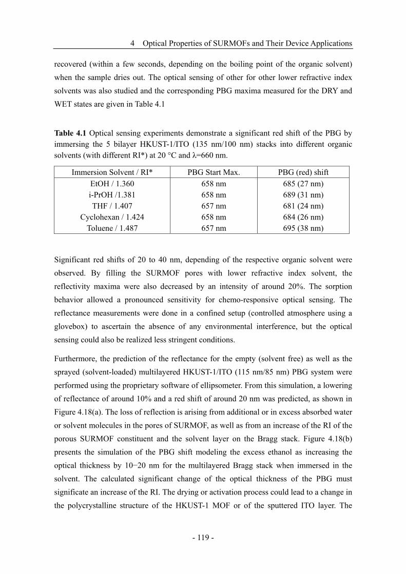
4 Optical Properties of SURMOFs and Their Device Applications
- 119 -
recovered (within a few seconds, depending on the boiling point of the organic solvent)
when the sample dries out. The optical sensing of other for other lower refractive index
solvents was also studied and the corresponding PBG maxima measured for the DRY and
WET states are given in Table 4.1
Table 4.1 Optical sensing experiments demonstrate a significant red shift of the PBG by immersing the 5 bilayer HKUST-1/ITO (135 nm/100 nm) stacks into different organic solvents (with different RI*) at 20 °C and λ=660 nm.
Immersion Solvent / RI* PBG Start Max. PBG (red) shift
EtOH / 1.360 i-PrOH /1.381 THF / 1.407
Cyclohexan / 1.424 Toluene / 1.487
658 nm 658 nm 657 nm 658 nm 657 nm
685 (27 nm) 689 (31 nm) 681 (24 nm) 684 (26 nm) 695 (38 nm)
Significant red shifts of 20 to 40 nm, depending of the respective organic solvent were
observed. By filling the SURMOF pores with lower refractive index solvent, the
reflectivity maxima were also decreased by an intensity of around 20%. The sorption
behavior allowed a pronounced sensitivity for chemo-responsive optical sensing. The
reflectance measurements were done in a confined setup (controlled atmosphere using a
glovebox) to ascertain the absence of any environmental interference, but the optical
sensing could also be realized less stringent conditions.
Furthermore, the prediction of the reflectance for the empty (solvent free) as well as the
sprayed (solvent-loaded) multilayered HKUST-1/ITO (115 nm/85 nm) PBG system were
performed using the proprietary software of ellipsometer. From this simulation, a lowering
of reflectance of around 10% and a red shift of around 20 nm was predicted, as shown in
Figure 4.18(a). The loss of reflection is arising from additional or in excess absorbed water
or solvent molecules in the pores of SURMOF, as well as from an increase of the RI of the
porous SURMOF constituent and the solvent layer on the Bragg stack. Figure 4.18(b)
presents the simulation of the PBG shift modeling the excess ethanol as increasing the
optical thickness by 10−20 nm for the multilayered Bragg stack when immersed in the
solvent. The calculated significant change of the optical thickness of the PBG must
significate an increase of the RI. The drying or activation process could lead to a change in
the polycrystalline structure of the HKUST-1 MOF or of the sputtered ITO layer. The
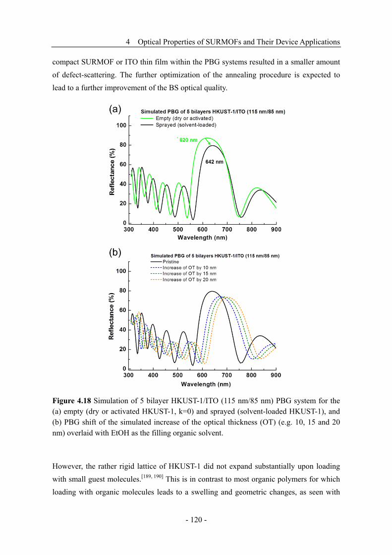
4 Optical Properties of SURMOFs and Their Device Applications
- 120 -
compact SURMOF or ITO thin film within the PBG systems resulted in a smaller amount
of defect-scattering. The further optimization of the annealing procedure is expected to
lead to a further improvement of the BS optical quality.
Figure 4.18 Simulation of 5 bilayer HKUST-1/ITO (115 nm/85 nm) PBG system for the (a) empty (dry or activated HKUST-1, k=0) and sprayed (solvent-loaded HKUST-1), and (b) PBG shift of the simulated increase of the optical thickness (OT) (e.g. 10, 15 and 20 nm) overlaid with EtOH as the filling organic solvent.
However, the rather rigid lattice of HKUST-1 did not expand substantially upon loading
with small guest molecules.[189, 190] This is in contrast to most organic polymers for which
loading with organic molecules leads to a swelling and geometric changes, as seen with

4 Optical Properties of SURMOFs and Their Device Applications
- 121 -
the swelling of thin polymer film by toluene vapor.[191] To confirm the absence of
pronounced geometrical changes of the SURMOF-base hybrid PBG materials, in situ
AFM on film thickness was performed upon loading guest molecules. This is a substantial
advantage with SURMOFs since the built-up of mechanical stress within the Bragg stack
heterostructures during the loading is avoided. As seen with the in situ AFM
measurements of Figure 4.19, the thickness of the 5 bilayer Bragg stack remained
unchanged upon immersion into EtOH from 987 nm (Air) to 985 nm (in EtOH).
Figure 4.19 Thicknesses of a 5 bilayer PBG materials for the effect of guest molecule (solvent) loading by in situ AFM measurement. The thickness of the BS is 987 nm in air (a) and 985 nm in EtOH (b).
The sorption and desorption studies can be described in a dynamic way. The modulation
and shifting of the PBG (activated/dried and solvent filled HKUST-1) are consistent with
the prediction/simulation. The differences between the experimental and calculated
reflectance spectra were explained by the existing variation of thicknesses along the
various sputtered ITO and LPE sprayed HKUST-1 films. Additional effects, like the
surface and eventually interface roughness losses due to scattering and reflections, can be
considered.
4.1.6 Conclusion
The combination of a LPE spraying process (yielding high quality SURMOF films) with
an ITO sputtering process allowed the successful fabrication of high quality optical
devices on a square centimeter scale. In these hybrid systems, the SURMOF HKUST-1
acted as the low RI material while the sputtered ITO was the high RI material. By
4 Optical Properties of SURMOFs and Their Device Applications
- 122 -
controlling the thicknesses of the produced HKUST-1 and ITO layers, the obtained
SURMOF-based hybrid PBG material was color-tunable over the whole visible range. The
monolithic multilayered (HKUST-1/ITO) Bragg stacks mounted on a Si substrate showed
an outstanding optical quality with low scattering losses as manifested by a reflectance of
around 80% at the maximum PBG wavelength.
The SURMOF-based hybrid PBG materials provided a tunable platform with promising
application as chemo-responsive optical sensing devices. The optical properties of the
PBG materials showed pronounced changes during loading or unloading. Those changes
were specific to the guest molecules probed. The reflection band shifts (≈20−40 nm
depending on the organic molecule) were not only easily quantified by simple colorimetric
methods but also directly observable by the naked eye. The process was further proved by
in situ AFM investigations to originate from a RI modification as virtually, the thickness
of the sample remained constant during the sorption/desorption process.
Part of the results in this section has been published in Chem. Mater. by Jianxi Liu et
al.(2015) as ref.[192]

4 Optical Properties of SURMOFs and Their Device Applications
- 123 -
4.2 Prussian blue films and their electrochromic switching behavior
4.2.1 Background
Metal-organic complexes[193, 194] and coordination network compounds (CNC)[195, 196] have
been extensively used in optoelectronic devices, like display/window application or
organic light emitting diodes (OLEDs). Prussian Blue (PB, Fe4III[FeII(CN)6]3), a
particularly interesting CNC example, has been extensively investigated for its optical,
magnetic and electrical and dielectric properties.[197-199]
PB crystallizes in a simple cubic structure with cyanide ligands (C≡N) coordinating Fe2+
(low spin) and Fe3+ (high spin) ions in an alternating and highly ordered cubic unit cell.[196]
A PB-type structure is shown in Figure 4.20.[200] These electron transfer properties as well
as the electric conductivity and redox properties of PB are of huge interest for the
fabrication of CNC based functional materials. The epitaxial preparation of monolithic
films of PB enables determining the orientation dependent properties of such molecular
magnetic materials. However, monolithic PB thin films produced on transparent
conductive oxides (TCO), such as indium tin oxide (ITO) and fluorine doped tin oxide
(FTO), electrodes have not been reported, and only the electrodeposition of epitaxial PB
thin films on Au substrates (110)[201] has been reported so far.
Figure 4.20 Representation of a cubic PB-type structure (FeІІ, FeІІІ, C and N are coded in yellow, red, black and blue; interstitial open sites are in purple). (Taken from ref.[200])
In this part, thin films of crystalline and highly oriented Prussian Blue were fabricated on
conductive substrate by the means of layer-by-layer or LPE spraying method, as well as
through spin-coating process. The monolithic PB thin films were coated not only on gold

4 Optical Properties of SURMOFs and Their Device Applications
- 124 -
substrates but also on TCO substrates, and were then used without any further
modification in an electrochemical cell to emulate as a device. The blue color of PB arises
from a broad absorption band at around 700 nm, while the reduced state of this material,
Prussian white (PW), is transparent. This redox process was shown to be reversible during
electrochromic (EC) switching cycles, with the crystallinity as well as the high orientation
remaining intact.
4.2.2 Preparation of PB thin films on the functionalized conductive substrate
PB thin films were prepared on MHDA SAM functionalized Au substrate as described in
Chapter 2.2.2, and hydroxylated ITO or Si substrates by means of layer-by-layer spraying
and spin-coating methods. A PB solution was prepared as following: PB powder was
dissolved in H2O/EtOH (1/9, v/v) mixture to a concentration of 1% (wt%), and an
ultrasonic bath was used for 20 min to help dissolving the PB before preparing of the
sample. The conductive substrates (ITO and Au) and semiconductor (Si) substrate
pretreated to support PB thin films. Surface functionalization or modification of these
substrates is the key to increase the quality of the films. ITO and Si substrates were
pretreated by either O2 plasma or UV-Ozone irradiation for 20-30 min to remove any
organic impurities and produce hydroxylate groups on the substrate surface.
For the layer-by-layer spraying method, the functional substrates were placed on the
sample holder and subsequently sprayed with above mentioned PB solution for 15 s, with
20 s waiting time between the spraying steps. The number of spraying cycles determines
the final thickness of the deposited PB film. After 50 cycles, blue colored films were
obtained. For the spin-coating method, a few drops (50-100 μL) of the solution were
dropped onto the functional substrates at room temperature and spun at 4000 rpm for 30 s
for each layer preparation.
4.2.3 Characterization of the PB thin films
4.2.3.1 XRD patterns of the prepared PB thin films
All of the prepared PB thin films were characterized by XRD. As shown in Figure 4.21,
the PB thin films were grown on the Au, ITO, and Si substrates with a [00l] orientation, as
proven by the presence of the characteristic (002), (004) and (006) Bragg peaks (with 2θ
of around 17.4°, 34.2° and 53.9°, respectively). The XRD pattern of powder PB is
presented in Figure 4.21(a) for comparison.

4 Optical Properties of SURMOFs and Their Device Applications
- 125 -
Figure 4.21 XRD of spin-coated PB thin film (black) deposited on (a) hydroxylated ITO substrate (blue) and the PB powder (grey), and (b) MHDA modified Au as well as Si substrates; XRD of layer-by-layer sprayed PB thin film (black) deposited on (c) ITO and (d) MHDA modified Au substrates.

4 Optical Properties of SURMOFs and Their Device Applications
- 126 -
The orientation of the produced PB thin films was also independent of the used
preparation methods. The results confirmed the successfully production of crystalline and
highly oriented Prussian Blue thin films on the various substrates, with no
polycrystallinity as seen in PB powder XRD pattern.
4.2.3.2 HR-SEM cross-section analysis of the prepared PB thin films
To check the continuity, compactness, and homogeneity, as well as to estimate the physical
thickness of the PB thin films prepared on the substrates, HR-SEM cross-sectional
measurements were performed.
Figure 4.22 HR-SEM images of (a) 50 cycles of the sprayed PB thin films on MHDA modified Au substrate, and (b-d) 1, 3 and 5 layers of spin-coated PB thin film on MHDA modified Au substrate.
As presented in Figure 4.22, the thickness of sprayed PB thin film on MHDA modified Au
substrate (50 cycles) is approximately 100 nm (Figure 4.22(a)), while the thickness of the
various layers spin-coated PB thin films on MHDA modified Au substrates are about 50
nm (for the 1 layer PB), 150 nm (for the 3 layers PB) and 250 nm (for the 5 layers PB)
(Figure 4.22(b-d)). The observed morphology and thickness did not show any change after
the electrochemical redox switching process. The monolithic PB thin films prepared on
transparent and conductive ITO substrates were directly used for electrochromic switching
investigation.
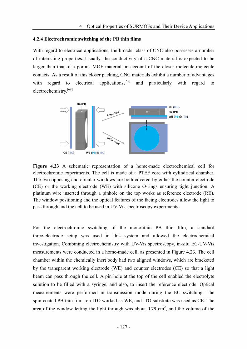
4 Optical Properties of SURMOFs and Their Device Applications
- 127 -
4.2.4 Electrochromic switching of the PB thin films
With regard to electrical applications, the broader class of CNC also possesses a number
of interesting properties. Usually, the conductivity of a CNC material is expected to be
larger than that of a porous MOF material on account of the closer molecule-molecule
contacts. As a result of this closer packing, CNC materials exhibit a number of advantages
with regard to electrical applications,[58] and particularly with regard to
electrochemistry.[69]
Figure 4.23 A schematic representation of a home-made electrochemical cell for electrochromic experiments. The cell is made of a PTEF core with cylindrical chamber. The two opposing and circular windows are both covered by either the counter electrode (CE) or the working electrode (WE) with silicone O-rings ensuring tight junction. A platinum wire inserted through a pinhole on the top works as reference electrode (RE). The window positioning and the optical features of the facing electrodes allow the light to pass through and the cell to be used in UV-Vis spectroscopy experiments.
For the electrochromic switching of the monolithic PB thin film, a standard
three-electrode setup was used in this system and allowed the electrochemical
investigation. Combining electrochemistry with UV-Vis spectroscopy, in-situ EC-UV-Vis
measurements were conducted in a home-made cell, as presented in Figure 4.23. The cell
chamber within the chemically inert body had two aligned windows, which are bracketed
by the transparent working electrode (WE) and counter electrodes (CE) so that a light
beam can pass through the cell. A pin hole at the top of the cell enabled the electrolyte
solution to be filled with a syringe, and also, to insert the reference electrode. Optical
measurements were performed in transmission mode during the EC switching. The
spin-coated PB thin films on ITO worked as WE, and ITO substrate was used as CE. The
area of the window letting the light through was about 0.79 cm2, and the volume of the

4 Optical Properties of SURMOFs and Their Device Applications
- 128 -
electrolyte solution around 0.4 mL (40 mM KCl aqueous solution). A platinum wire was
used as reference electrode.
4.2.4.1 Electrochromic switching of a 1 layer PB thin film
To define the trigger potential for switching the electrochromic smart window, the cyclic
voltammetry (CV) measurement was carried out with the described electrochemical and
photospectroscopic cell. As seen in Figure 4.24(a), a reversible redox reaction was
observed from the spin-coated PB thin film deposited on ITO substrate. The anodic peak
at –0.065 V contributed to the oxidation of Fe2+ to Fe3+, and reciprocally the cathodic peak
at –0.290 V for the reduction.
Figure 4.24 (a) CV of the spin-coated 1 layer PB thin film deposited on ITO substrate at the scan rate of 100 mV/s; (b) the waveform of the used PAD technique at the applied potential of Eox= +0.1 V and Ere= –0.4 V (downside) and the corresponding current density (upside) for the reversible electrochromic switching; (c-d) the zoomed-in area in (b), corresponding to one segment of the PAD at the applied potential of Ere= –0.4 V (c) and Eox= +0.1 V (d).

4 Optical Properties of SURMOFs and Their Device Applications
- 129 -
Figure 4.24(b) presents 10 cycles of reversible electrochromic switching of the
spin-coated 1 layer PB thin film deposited on ITO substrate by employing the pulsed
amperometric detection (PAD) method. A potential was applied to trigger the reversible
switching ON and OFF of the electrochromic smart window in the same EC-system, and
the current intensity was recorded during the switching. As presented in Figure 4.24(c-d),
the time corresponding to complete color change (from blue to transparent, and inversely)
of the smart window was around 5 seconds, with a switching time of roughly 1 second
which corresponded to a rapid decrease of the current.
Figure 4.25 (a) UV-Vis spectra of the spin-coated 1 layer PB thin film for 10 cycles EC switching by PAD method at the applied potential Eox= 0.1 V and Ere= –0.4 V; (b) UV-Vis absorbance (took from (a) at 694 nm) of the PB thin film in the oxidized and reduced states, showing a stable and reversible redox behavior.

4 Optical Properties of SURMOFs and Their Device Applications
- 130 -
As shown in Figure 4.25(a) on a spin-coated 1 layer PB thin film while applying a
negative bias voltage (–0.4 V), the PB thin film was reduced to PW (K4Fe4II[FeII(CN)6]3)
and changed to a the transparent state, whereas with a positive bias voltage (0.1 V) the PB
thin film was oxidized to a mixed-valence component PB which provided a strong and
blue color to the thin film. The blue color of the oxidized state represents the mixed
valence of Fe ions in Fe4III[FeII(CN)6]3 and is based on a metal-to-metal charge transfer
transition from the C-coordinated Fe2+ ions across the C≡N organic ligand to
N-coordinated Fe3+ ions.
The potentials were switched alternatively for cycling the electrochromic color change,
while UV-Vis spectra were recorded in between and at interval with each potential switch.
The cycling behavior of PB thin films during EC switching can be directly observed
spectroscopically thanks to the in-situ EC-UV-Vis experimental set-up. Figure 4.25(b)
presents the changes of the absorbance (at 694 nm) during cycling of EC switching. No
fatigue effect of the optical or electrical properties were observed after 10 switching cycles
with the applied potential. This shows the stability, reversibility and reproducibility of the
PB thin film during EC switching.
4.2.4.2 Electrochromic switching of a 5 layers PB thin film
Figure 4.26 (a) UV-Vis spectra of the spin-coated 5 layers PB film after EC switching at the oxidized and reduced states; (b) picture of EC cell composed out of ITO-PB/KCl-Pt/ITO for the oxidized (upside) and reduced (downside) PB film.
4 Optical Properties of SURMOFs and Their Device Applications
- 131 -
To further study the electrochromic behavior, thicker film, the spin-coated 5 layers PB
film (the thickness is around 250 nm as mentioned previously) was tested. Figure 4.26(a)
shows the UV-Vis spectra of the 5 layer film after EC switching. A significant change in
the optical absorption properties were observed between the oxidized and reduced states
of the PB thin film. The optical images taken for both the oxidized and reduced PB thin
film shows the obvious color change (Figure 4.26(b))
4.2.4.3 XRD analysis of the PB thin films after EC switching
The crystal structure of the oxidized and reduced states of PB thin film by EC switching
was characterized by XRD. Prussian Blue crystallizes in the cubic space group #221
Pm3m.[202] The powder XRD data of PB is presented in Figure 4.21(a), and was used also
for the refinement of the crystal structure. In order to solve a structure from the powder
diffraction measurement, extracting as many (hkl)-peaks and intensity values as possible is
necessary to have a precise analysis. The Pawley method is known to produce very precise
lattice parameter,[203] and represents a procedure which is widely used for the refinement
of the crystal structure crystal unit cell from a powder pattern. For this method, the
knowledge of the crystal structure of the material is not required, and a list of indexed
intensities is obtained at the end of the refinement. The lattice parameter ao of 1.0221 ±
0.0003 nm was calculated by lattice cell refinement following the Pawley method. The
obtained standard deviation can be viewed as a lower estimation (as discussed on many
User-meetings dealing with the Rietveld method).
Comparing with the XRD patterns of PB powder in Figure 4.21, the deposited PB
revealed the presence of a crystalline film oriented along the [00l] direction without
showing any other (hkl)-peak, and the intensity of all the (00l) peaks was high enough for
further analysis. By measuring the specific angular ranges of the (00l) peak-series (with
l=2,4,6,8) of the PB thin film in detail, the coherent scattering domain size as well as
stress/strain PB thin films were analyzed according to the Williamson-Hall method as
described in previous section.[185] Most importantly, the Williamson-Hall method was also
applied to analyze the changes of domain size and the stress/strain for both the oxidized
and reduced states of PB thin films with the effect of EC switching.
The XRD patterns of the (002), (004) and (006) peaks of the oxidized and reduced PB film
are presented in Figure 4.27(a-c), and were recorded after EC switching. It can be seen
that the positions of the (00l) peak-series were shifted to a higher 2θ after reduction of the
PB to be PW; this represents a contraction of the lattice structure. The reversible

4 Optical Properties of SURMOFs and Their Device Applications
- 132 -
oxido-reduction led to a reversible change in the XRD peak position. Figure 4.27(d)
presents the Williamson-Hall plot analysis by considering all the refraction peaks at the
oxidized and reduced states expect for the (006) peak of the reduced PB because of the
weak intensity, so it is a rough evaluation. In the plot, FWHM at Y-axis represents B-b
(where B is the integral breadth, b is the instrumental width), and the instrumental
contribution to the line broadening was considered.
Figure 4.27 (a-c) XRD of the (002), (004) and (006) peaks of the oxidized (black) and reduced (red) Prussian Blue thin film deposited on ITO; (d) Williamson-Hall plots of the (00l) peak-series of oxidized (full symbol in black, l=2,4,6,8) and for the reduced sample (open symbol in red, l=2,4,6), the (006) peak of the reduced PB was not considered for the fitting because of the weak intensity.
Williamson-Hall plot showed that the coherent scattering domain size (Lvol) of the
oxidized and reduced PB is 82 nm an 81 nm, respectively. And the unit cells (ao) of these
two states, oxidized PB (ao = 1.0205 ± 0.0003 nm) and reduced PB (ao = 1.0151 ± 0.0001

4 Optical Properties of SURMOFs and Their Device Applications
- 133 -
nm), show a difference of 0.0054 nm. This is equivalent to a 0.5% dynamic change of the
unit cell parameters during the EC switching process. The stress/strain parameter εo (~
Δd/d, with d lattice space parameter) remained constant at 0.5% during EC switching. No
significant change of the domain size (Lvol) and the stress/strain (εo) were observed after 30
to 40 redox cycles of the PB film by EC switching. This shows the dynamic, fully
reversible, and flexible expansion and contraction of the unit cells (±0.0054 nm) between
the PB (FeІІ–C≡N···Fe3+) and PW (FeІІ–C≡N···Fe2+) structures of the film.
4.2.4.4 IRRAS analysis of the PB thin film after EC switching
The PB films deposited on MHDA modified Au substrate was characterized by infrared
after EC switching. The IRRA spectra of spin-coated 3 layers PB film is shown in Figure
4.28(a). The strongest band at around 2120 cm-1 corresponds to a C≡N group vibration
from PB. When the PB is reduced, this band appears at around 2120 cm-1. A shift of ≈14
cm-1 was observed between the oxidized and reduced states of the PB, which resulted from
the change in the valence state in the Fe-ion to which the C≡N groups are bound.
Figure 4.28 IRRAS of the oxidized and reduced states of spin-coated 3 layers PB thin film on MHDA modified Au substrate.
The observed red-shift in the IR spectra for the oxidized and reduced PB corresponds to
changing the FeІІ–C≡N···Fe3+ bridge into FeІІ–C≡N···Fe2+ bridge. This significant red-shift
to a longer wavelength can be explained with the reduction of trivalent Fe-ions to their
reduced state decreasing the influence on the bonding.[204] The reduction of Fe3+ to be Fe2+
and the incorporation of K+ ions in the lattice led to the contraction of the whole cubic-unit

4 Optical Properties of SURMOFs and Their Device Applications
- 134 -
cell (from PB to PW) of around 0.5 %, which was determined by XRD analysis. The
vibrational spectroscopy as well as data from XRD measurements can be described in a
coherent manner in regard to the change of PB into PW. So apart from IR, the Raman
spectroscopy analysis was also performed on these films.
4.2.4.5 Raman spectra analysis of the PB thin film after EC switching
The PB films deposited on MHDA modified Au substrates were characterized through
Raman measurements after EC switching. Raman spectra were recorded using a green
laser at 532 nm for excitation. The integration time was 60 s with 3 co-additions.
Figure 4.29 (a) Raman spectra of the oxidized and reduced states of spin-coated 3 layers PB thin film on MHDA modified Au substrate; (b) 2D Raman-Map of the half-oxidized and half-reduced PB thin film; the interface in the middle of the image shows the two states (oxidized and reduced) of the film, and the inner area shows the integration result of the C≡N band between 2132 and 2108 cm-1 as marked in (a).

4 Optical Properties of SURMOFs and Their Device Applications
- 135 -
Figure 4.29(a) presents the Raman spectra of the oxidized and reduced states of
spin-coated 3 layer PB thin films. A typical band at 2156 cm-1 corresponding to the
vibration of C≡N group was observed on the PB thin films, and this band had no shift
through EC switching. However, a new band at 2123 cm-1 appeared after the reduction of
the PB film. This change revealed the conversion of PB (FeІІ–C≡N···Fe3+) to PW (FeІІ–
C≡N···Fe2+).[204, 205]
2D Raman-Map characterization gives specific band information with lateral resolved
resolution, which enables the mapping of the specific band by integrating all the spectra at
each point of a large area. To record Raman spectra for both the oxidized and reduced PB
films, and to give the laterally resolved mapping, the two states of the film have to be
integrated in one sample. This requirement was done by using an electrochemical cell, as
presented in Figure 4.30, for full-oxidation and thereafter half-reduction.
Figure 4.30 Schematic representation of the electrochemical cell for full-oxidation and thereafter half-reduction of the PB film to get an interface of the two states (oxidized and reduced states). The half-oxidized and half-reduced PB thin film is developed for 2D Raman-Map.
The 2D Raman mapping was recorded on 17 x 17 mm2 spots, as shown in the highlighted
area in Figure 4.29(b). The data analysis was done with the Bruker Spectrometer provided
software (OPUS 7.2). Before integration on the assigned areas, the Raman spectra were
normalized (min - max) for a band at 2156 cm-1. The integration time was 60 seconds with
3 co-additions. A baseline correction was conducted (concave rubber band correction;
numbers of iterations 24 and 64 baseline points).
By integrating the Raman spectra of the PB film between 2132 and 2108 cm-1 recorded
from the inner area in Figure 4.30, the image of 2D Raman-map was produced (Figure
4 Optical Properties of SURMOFs and Their Device Applications
- 136 -
4.29(b)) with a clear difference between oxidized and reduced states of the PB film. The
green color represents the reduced state whereas blue represents the oxidized state of PB
thin film.
4.2.5 Conclusion
Crystalline and highly oriented thin films of Prussian Blue, a coordinative network
compound, were produced on various substrates by layer-by-layer and spin-coating
methods. The substrates used are made of either conductive ITO or Au, or semiconductor
Si. The monolithic PB thin films prepared on transparent and conductive ITO substrate
was used directly as electrodes to fabricate an electrochromic smart window device. By
applying an electrical potential, the PB film was switched between a strong blue and a
transparent state. The oxidized and reduced states, PB (FeІІ–C≡N···Fe3+) and PW (FeІІ–
C≡N···Fe2+), of the film were characterized by XRD, IR and Raman measurements. The
monolithic PB thin films were shown to be robust and stable during the EC switching for
multiple times, and demonstrated a reversible electrochromic behavior. The research
showed a simple way to fabricate optoelectronic and display devices.
Part of the results in this section has been published in Opt. Express by Jianxi Liu et
al.(2015) as ref.[206]

5 Conclusion and Outlook
- 137 -
5 Conclusion and Outlook
1. A series of HKUST-1 SURMOFs with different thickness were successfully produced
on a CMMT SAM template along their [111] crystallographic orientation. Then, the guest
molecules, ferrocene, were loaded within the nanometer size pores. IRRAS and
out-of-plane XRD were used and confirmed the guest loading. To explore and reveal the
transport properties of SURMOFs, notably their charge transport mechanism, HKUST-1
SURMOF films of different thicknesses were reproducibly incorporated in Hg-based
tunneling junction set-up. The extremely shallow dependence of the current density on the
film thickness, as indicated by a low value of the attenuation factor (β ≈ 0.006 Å-1), were
understood in terms of a linear, ohmic increase of resistance with length in the incoherent
charge hopping regime. The decrease in overall resistance and its weaker increase with
film thickness, measured after incorporation of ferrocene inside the pores of HKUST-1
SURMOFs, indicated a reduction in the charge injection barrier and an improved
electronic coupling between metal nodes.
Assembling of SURMOF films in tunneling junctions showed to be effective and
permitted the investigation of their transport properties. It also offered the possibility to
gain insights into the effect of small electroactive molecules. Further studies using
SURMOFs of different chemical composition or crystallographic orientation, as well as
different guest molecules, is also interesting and important and would be conveniently
realized by using such tunneling junctions. This would provide fundamental results on
electric transport properties within MOFs and paves the way for their future integration in
electronic devices.
2. SURMOFs with different orientation were produced on CMMT and TPMTA modified
gold electrodes. The electric properties of these porous and crystalline SURMOF coatings
deposited on gold working electrode were characterized using cyclic voltammetry
experiments by using an ionic liquid as inert supporting electrolyte and ferrocene as redox
active probe. The pristine HKUST-1 SURMOFs demonstrated an insulating behavior, and
a high quality compact films structures. An extremely low density of defects or pin-holes
was then concluded also in relation with the AFM scratching experiment. Furthermore,
electroactive ferrocene molecules were used as guests in HKUST-1 SURMOFs for
enhancing its electrical conductivity, as this was proven by CV experiments.

5 Conclusion and Outlook
- 138 -
Following the present strategy, the relevant electrochemical characterization of other
SURMOFs is to be studied. Especially, the relation between electrochemical behavior of
SURMOFs and their crystalline orientation, pore sizes, or the immobilized electroactive
guests within could be bridged.
3. Crystalline and porous porphyrin-based SURMOFs were prepared on transparent and
conductive FTO substrates by the LPE spraying method. The photocurrent generation
properties of the highly oriented and ordered porphyrin-based SURMOF thin films as
electrodes were investigated using a photoelectrochemical cell. Comparing to free base
porphyrin Zn-SURMOF 2, the enhancement of the photocurrent efficiency was observed
on Pd porphyrin Zn-SURMOF 2.
The strategy for stacking of the high ordered photoelectroactive molecules offers a great
opportunity towards developing solar cell conversion and artificial photocatalysis
applications. Since the crystalline lattices fabricated here were highly porous, these
SURMOFs are likely to achieve higher performances by loading further the pores with
charge-donating or charge-accepting molecules.
4. Multilayered hybrid materials, obtained by the combination of a LPE spraying process,
yielding high quality SURMOFs (HKUST-1), with an ITO sputtering process, were
fabricated on a Si substrate with a high quality for optical application on a centimeter scale.
By modifying the individual layer thicknesses of porous SURMOF (low RI layer) and
conductive ITO (high RI layer) alternatively, the resulting SURMOF-based hybrid PBG
materials were produced with color tunable over the whole visible range. The monolithic
Bragg stacks were characterized and displayed an outstanding optical quality with low
scattering losses as manifested by a reflectance of around 80% at the maximum PBG
wavelength. The SURMOF-based hybrid PBG materials presented here also provided a
tunable platform with regard to developing chemo-responsive optical sensing devices.
Pronounced changes of the optical properties of the PBG materials were measured by
simply loading and unloading specific guest molecules within the nanopores of the
framework in the hybrid PBG systems.
Due to their high optical quality, the SURMOF-based PBG device could be further
extended to other (water stable, faster response, as well as with variable color options)
monolithic systems. SURMOFs produced by LPE process are suitable for large scales
industrial device applications. The possible realization of wider systems would provide the
development of robust SURMOF-based, photonic color-coded chemical sensors and

5 Conclusion and Outlook
- 139 -
nano-photonic devices with broad perspectives.
5. Thin films of the porous coordination network compounds (CNC), Prussian blue (PB),
were produced on various substrates (Au, ITO and Si) by means of a layer-by-layer or
LPE, as well as through spin-coating process. The monolithic PB thin films, coated on
transparent and conductive ITO substrates, were then used directly without any further
modification in an electrochemical cell as electrodes to constitute an electrochromic
device. By applying a potential in electrochemistry cell, the PB thin film were switched
between two states, referred to the blue colored PB (FeІІ–C≡N···Fe3+) and transparent PW
(FeІІ–C≡N···Fe2+); these states were fully characterized by XRD, IR and Raman
measurements.
The highly oriented, crystalline and monolithic CNC thin films were shown to be robust,
stable, and could be switched multiple times. This demonstrates a simple way to produce
cost-efficiently optoelectronic and display devices or smart window materials. Further
monolithic CNC materials with improved properties to eventually yield materials with
“tunable porosity” and “tunable potential barriers” are in progress.

List of Abbreviations
- 140 -
List of Abbreviations
1D One-dimensional
2D Two-dimensional
3D Three-dimensional
AFM Atomic force microscopy
BS Bragg stacks
BTC 1,3,5-benzenetricarboxylic acid
[BMIM] [NTf2] 1-butyl-3-methylimidazolinium bis(trifluoronethylsulfonyl)imide
CE Counter electrode
CMMT 9-carboxy-10-(mercaptomethyl) triptycene
CNC Coordination network compound
CV Cyclic voltammetry
DC Direct current
DFT Density functional theory
EC Electrochromic
EtOH Ethanol
FC Ferrocene
FIB Focused ion beam
FTIR Fourier transform infrared
FTO Fluorine doped tin oxide
FWHM Full width at half maximum
HD Hexadecane
HDT Hexadecanethiol
List of Abbreviations
- 141 -
HR-SEM High-resolution scanning electron microscope
HKUST-1 Hong-Kong University structure 1
HOMO Highest occupied molecular orbital
IL Ionic liquid
IR Infrared
IRRAS Infrared reflection absorption spectroscopy
ITO Indium tin oxide
I-V Current-voltage
LED Light-emitting diode
LPE Liquid-phase epitaxy
LUMO Lowest unoccupied molecular orbital
MCT Mercury cadmium telluride
MHDA 16-mecaptohexa-decanoic acid
MOF Metal-organic frameworks
NIR Near infrared
OLEDs Organic light emitting diodes
PAD Pulsed amperometric detection
PB Prussian Blue
PBG Photonic band-gap
PCP Porous coordination polymer
PW Prussian white
QCM Quartz crystal microbalance
RE Reference electrode
RI Refractive index
RMS Root mean square

List of Abbreviations
- 142 -
SAM Self-assembled monolayer
SE Spectroscopic ellipsometry
SEM Scanning electron microscopy
SFM Scanning force microscopy
Si Silicon
SPM Scanning probe microscopy
SURMOF Surface-anchored metal-organic frameworks
SURMOF 2 2 dimensional surface-anchored metal-organic framework
TCO Transparent conductive oxides
TCNQ Tetracyano-quinodimethane
TDM Transition dipole moment
TEM Transmission electron microscopy
TPMTA 4'-carboxyterphenyl-4-methanethiol
ToF-SIMS Time-of-flight secondary ion mass spectrometry
UV-Vis Ultraviolet-visible
WE Working electrode
XRD X-ray diffraction

References
- 143 -
References
[1] Zhu, Q. L.; Xu, Q. Metal-Organic Framework Composites. Chem. Soc. Rev. 2014, 43, 5468-5512.
[2] Furukawa, H.; Cordova, K. E.; O'Keeffe, M.; Yaghi, O. M. The Chemistry and Applications of Metal-Organic Frameworks. Science 2013, 341, 974.
[3] Férey, G. Hybrid Porous Solids: Past, Present, Future. Chem. Soc. Rev. 2008, 37, 191-214.
[4] Kitagawa, S.; Kitaura, R.; Noro, S. Functional Porous Coordination Polymers. Angew. Chem., Int. Ed. 2004, 43, 2334-2375.
[5] Yaghi, O. M.; O'Keeffe, M.; Ockwig, N. W.; Chae, H. K.; Eddaoudi, M.; Kim, J. Reticular Synthesis and the Design of New Materials. Nature 2003, 423, 705-714.
[6] Kinoshita, Y.; Matsubara, I.; Higuchi, T.; Saito, Y. The Crystal Structure of Bis(Adiponitrilo)Copper(I) Nitrate. Bull. Chem. Soc. Jpn. 1959, 32, 1221-1226.
[7] Hoskins, B. F.; Robson, R. Design and Construction of a New Class of Scaffolding-Like Materials Comprising Infinite Polymeric Frameworks of 3-D-Linked Molecular Rods - a Reappraisal of the Zn(CN)2 and Cd(CN)2 Structures and the Synthesis and Structure of the Diamond-Related Frameworks [N(CH3)4][CuIZnII(CN)4] and CuI[4,4',4'',4'''-Tetracyanotetraphenylmethane]BF4.XC6H5NO2. J. Am. Chem. Soc. 1990, 112, 1546-1554.
[8] Deng, H. X.; Grunder, S.; Cordova, K. E.; Valente, C.; Furukawa, H.; Hmadeh, M.; Gandara, F.; Whalley, A. C.; Liu, Z.; Asahina, S.; Kazumori, H.; O'Keeffe, M.; Terasaki, O.; Stoddart, J. F.; Yaghi, O. M. Large-Pore Apertures in a Series of Metal-Organic Frameworks. Science 2012, 336, 1018-1023.
[9] He, Y. B.; Zhou, W.; Qian, G. D.; Chen, B. L. Methane Storage in Metal-Organic Frameworks. Chem. Soc. Rev. 2014, 43, 5657-5678.
[10] Suh, M. P.; Park, H. J.; Prasad, T. K.; Lim, D. W. Hydrogen Storage in Metal-Organic Frameworks. Chem. Rev. 2012, 112, 782-835.
[11] Peng, Y.; Li, Y. S.; Ban, Y. J.; Jin, H.; Jiao, W. M.; Liu, X. L.; Yang, W. S. Metal-Organic Framework Nanosheets as Building Blocks for Molecular Sieving Membranes. Science 2014, 346, 1356-1359.
[12] Gu, Z. Y.; Yang, C. X.; Chang, N.; Yan, X. P. Metal-Organic Frameworks for Analytical Chemistry: From Sample Collection to Chromatographic Separation. Acc. Chem. Res. 2012, 45, 734-745.

References
- 144 -
[13] Yoon, M.; Srirambalaji, R.; Kim, K. Homochiral Metal-Organic Frameworks for Asymmetric Heterogeneous Catalysis. Chem. Rev. 2012, 112, 1196-1231.
[14] Lee, J.; Farha, O. K.; Roberts, J.; Scheidt, K. A.; Nguyen, S. T.; Hupp, J. T. Metal-Organic Framework Materials as Catalysts. Chem. Soc. Rev. 2009, 38, 1450-1459.
[15] Kreno, L. E.; Leong, K.; Farha, O. K.; Allendorf, M.; Van Duyne, R. P.; Hupp, J. T. Metal-Organic Framework Materials as Chemical Sensors. Chem. Rev. 2012, 112, 1105-1125.
[16] Horcajada, P.; Gref, R.; Baati, T.; Allan, P. K.; Maurin, G.; Couvreur, P.; Férey, G.; Morris, R. E.; Serre, C. Metal-Organic Frameworks in Biomedicine. Chem. Rev. 2012, 112, 1232-1268.
[17] Shi, D. B.; Ren, Y. W.; Jiang, H. F.; Cai, B. W.; Lu, J. X. Synthesis, Structures, and Properties of Two Three-Dimensional Metal-Organic Frameworks, Based on Concurrent Ligand Extension. Inorg. Chem. 2012, 51, 6498-6506.
[18] Phan, A.; Doonan, C. J.; Uribe-Romo, F. J.; Knobler, C. B.; O'Keeffe, M.; Yaghi, O. M. Synthesis, Structure, and Carbon Dioxide Capture Properties of Zeolitic Imidazolate Frameworks. Acc. Chem. Res. 2010, 43, 58-67.
[19] Tranchemontagne, D. J.; Hunt, J. R.; Yaghi, O. M. Room Temperature Synthesis of Metal-Organic Frameworks: MOF-5, MOF-74, MOF-177, MOF-199, and IRMOF-0. Tetrahedron 2008, 64, 8553-8557.
[20] Son, W. J.; Kim, J.; Kim, J.; Ahn, W. S. Sonochemical Synthesis of MOF-5. Chem. Commun. 2008, 6336-6338.
[21] Klinowski, J.; Paz, F. A. A.; Silva, P.; Rocha, J. Microwave-Assisted Synthesis of Metal-Organic Frameworks. Dalton Trans. 2011, 40, 321-330.
[22] Li, M. Y.; Dincă, M. Reductive Electrosynthesis of Crystalline Metal-Organic Frameworks. J. Am. Chem. Soc. 2011, 133, 12926-12929.
[23] Yan, D. P.; Gao, R.; Wei, M.; Li, S. D.; Lu, J.; Evans, D. G.; Duan, X. Mechanochemical Synthesis of a Fluorenone-Based Metal Organic Framework with Polarized Fluorescence: An Experimental and Computational Study. J. Mater. Chem. C 2013, 1, 997-1004.
[24] Khan, N. A.; Jhung, S. H. Synthesis of Metal-Organic Frameworks (MOFs) with Microwave or Ultrasound: Rapid Reaction, Phase-Selectivity, and Size Reduction. Coord. Chem. Rev. 2015, 285, 11-23.
[25] Stock, N.; Biswas, S. Synthesis of Metal-Organic Frameworks (MOFs): Routes to Various MOF Topologies, Morphologies, and Composites. Chem. Rev. 2012, 112, 933-969.

References
- 145 -
[26] Tranchemontagne, D. J.; Mendoza-Cortes, J. L.; O'Keeffe, M.; Yaghi, O. M. Secondary Building Units, Nets and Bonding in the Chemistry of Metal-Organic Frameworks. Chem. Soc. Rev. 2009, 38, 1257-1283.
[27] Lu, W. G.; Wei, Z. W.; Gu, Z. Y.; Liu, T. F.; Park, J.; Park, J.; Tian, J.; Zhang, M. W.; Zhang, Q.; Gentle, T.; Bosch, M.; Zhou, H. C. Tuning the Structure and Function of Metal-Organic Frameworks via Linker Design. Chem. Soc. Rev. 2014, 43, 5561-5593.
[28] Tanabe, K. K.; Cohen, S. M. Postsynthetic Modification of Metal-Organic Frameworks-A Progress Report. Chem. Soc. Rev. 2011, 40, 498-519.
[29] Wang, Z. Q.; Cohen, S. M. Postsynthetic Modification of Metal-Organic Frameworks. Chem. Soc. Rev. 2009, 38, 1315-1329.
[30] Brozek, C. K.; Dincă, M. Lattice-Imposed Geometry in Metal-Organic Frameworks: Lacunary Zn4O Clusters in MOF-5 Serve as Tripodal Chelating Ligands for Ni2+. Chem. Sci. 2012, 3, 2110-2113.
[31] Tanabe, K. K.; Wang, Z. Q.; Cohen, S. M. Systematic Functionalization of a Metal-Organic Framework Via a Postsynthetic Modification Approach. J. Am. Chem. Soc. 2008, 130, 8508-8517.
[32] Wang, Z. B.; Liu, J. X.; Arslan, H. K.; Grosjean, S.; Hagendorn, T.; Gliemann, H.; Bräse, S.; Wöll, C. Post-Synthetic Modification of Metal-Organic Framework Thin Films Using Click Chemistry: The Importance of Strained C-C Triple Bonds. Langmuir 2013, 29, 15958-15964.
[33] Bradshaw, D.; Garai, A.; Huo, J. Metal-Organic Framework Growth at Functional Interfaces: Thin Films and Composites for Diverse Applications. Chem. Soc. Rev. 2012, 41, 2344-2381.
[34] Uemura, T.; Yanai, N.; Kitagawa, S. Polymerization Reactions in Porous Coordination Polymers. Chem. Soc. Rev. 2009, 38, 1228-1236.
[35] Eddaoudi, M.; Kim, J.; Rosi, N.; Vodak, D.; Wachter, J.; O'Keeffe, M.; Yaghi, O. M. Systematic Design of Pore Size and Functionality in Isoreticular MOFs and Their Application in Methane Storage. Science 2002, 295, 469-472.
[36] Chui, S. S. Y.; Lo, S. M. F.; Charmant, J. P. H.; Orpen, A. G.; Williams, I. D. A Chemically Functionalizable Nanoporous Material [Cu3(TMA)2(H2O)3]n. Science 1999, 283, 1148-1150.
[37] Banerjee, R.; Phan, A.; Wang, B.; Knobler, C.; Furukawa, H.; O'Keeffe, M.; Yaghi, O. M. High-Throughput Synthesis of Zeolitic Imidazolate Frameworks and Application to CO2 Capture. Science 2008, 319, 939-943.
[38] Farha, O. K.; Eryazici, I.; Jeong, N. C.; Hauser, B. G.; Wilmer, C. E.; Sarjeant, A.
References
- 146 -
A.; Snurr, R. Q.; Nguyen, S. T.; Yazaydin, A. O.; Hupp, J. T. Metal-Organic Framework Materials with Ultrahigh Surface Areas: Is the Sky the Limit? J. Am. Chem. Soc. 2012, 134, 15016-15021.
[39] Li, H.; Eddaoudi, M.; O'Keeffe, M.; Yaghi, O. M. Design and Synthesis of an Exceptionally Stable and Highly Porous Metal-Organic Framework. Nature 1999, 402, 276-279.
[40] Férey, G.; Mellot-Draznieks, C.; Serre, C.; Millange, F.; Dutour, J.; Surble, S.; Margiolaki, I. A Chromium Terephthalate-Based Solid with Unusually Large Pore Volumes and Surface Area. Science 2005, 309, 2040-2042.
[41] Horcajada, P.; Serre, C.; Maurin, G.; Ramsahye, N. A.; Balas, F.; Vallet-Regi, M.; Sebban, M.; Taulelle, F.; Férey, G. Flexible Porous Metal-Organic Frameworks for a Controlled Drug Delivery. J. Am. Chem. Soc. 2008, 130, 6774-6780.
[42] Kim, M.; Cohen, S. M. Discovery, Development, and Functionalization of Zr(IV)-Based Metal-Organic Frameworks. CrystEngComm 2012, 14, 4096-4104.
[43] Rowsell, J. L. C.; Yaghi, O. M. Effects of Functionalization, Catenation, and Variation of the Metal Oxide and Organic Linking Units on the Low-Pressure Hydrogen Adsorption Properties of Metal-Organic Frameworks. J. Am. Chem. Soc. 2006, 128, 1304-1315.
[44] Rowsell, J. L. C.; Yaghi, O. M. Strategies for Hydrogen Storage in Metal-Organic Frameworks. Angew. Chem., Int. Ed. 2005, 44, 4670-4679.
[45] Li, B.; Wen, H. M.; Wang, H. L.; Wu, H.; Tyagi, M.; Yildirim, T.; Zhou, W.; Chen, B. L. A Porous Metal-Organic Framework with Dynamic Pyrimidine Groups Exhibiting Record High Methane Storage Working Capacity. J. Am. Chem. Soc. 2014, 136, 6207-6210.
[46] Furukawa, H.; Ko, N.; Go, Y. B.; Aratani, N.; Choi, S. B.; Choi, E.; Yazaydin, A. O.; Snurr, R. Q.; O'Keeffe, M.; Kim, J.; Yaghi, O. M. Ultrahigh Porosity in Metal-Organic Frameworks. Science 2010, 329, 424-428.
[47] Deng, H. X.; Doonan, C. J.; Furukawa, H.; Ferreira, R. B.; Towne, J.; Knobler, C. B.; Wang, B.; Yaghi, O. M. Multiple Functional Groups of Varying Ratios in Metal-Organic Frameworks. Science 2010, 327, 846-850.
[48] Fujita, M.; Kwon, Y. J.; Washizu, S.; Ogura, K. Preparation, Clathration Ability, and Catalysis of a 2-Dimensional Square Network Material Composed of Cadmium(II) and 4,4'-Bipyridine. J. Am. Chem. Soc. 1994, 116, 1151-1152.
[49] Alaerts, L.; Seguin, E.; Poelman, H.; Thibault-Starzyk, F.; Jacobs, P. A.; De Vos, D. E. Probing the Lewis Acidity and Catalytic Activity of the Metal-Organic Framework [Cu3(BTC)2] (BTC = Benzene-1,3,5-Tricarboxylate). Chem. Eur. J. 2006, 12, 7353-7363.
References
- 147 -
[50] Ma, L. Q.; Falkowski, J. M.; Abney, C.; Lin, W. B. A Series of Isoreticular Chiral Metal-Organic Frameworks as a Tunable Platform for Asymmetric Catalysis. Nat. Chem. 2010, 2, 838-846.
[51] Sabo, M.; Henschel, A.; Froede, H.; Klemm, E.; Kaskel, S. Solution Infiltration of Palladium into MOF-5: Synthesis, Physisorption and Catalytic Properties. J. Mater. Chem. 2007, 17, 3827-3832.
[52] Liu, D. M.; Lu, K. D.; Poon, C.; Lin, W. B. Metal-Organic Frameworks as Sensory Materials and Imaging Agents. Inorg. Chem. 2014, 53, 1916-1924.
[53] Hu, Z. C.; Deibert, B. J.; Li, J. Luminescent Metal-Organic Frameworks for Chemical Sensing and Explosive Detection. Chem. Soc. Rev. 2014, 43, 5815-5840.
[54] Lu, Z. Z.; Zhang, R.; Li, Y. Z.; Guo, Z. J.; Zheng, H. G. Solvatochromic Behavior of a Nanotubular Metal-Organic Framework for Sensing Small Molecules. J. Am. Chem. Soc. 2011, 133, 4172-4174.
[55] Huxford, R. C.; Della Rocca, J.; Lin, W. B. Metal-Organic Frameworks as Potential Drug Carriers. Curr. Opin. Chem. Biol. 2010, 14, 262-268.
[56] Horcajada, P.; Chalati, T.; Serre, C.; Gillet, B.; Sebrie, C.; Baati, T.; Eubank, J. F.; Heurtaux, D.; Clayette, P.; Kreuz, C.; Chang, J. S.; Hwang, Y. K.; Marsaud, V.; Bories, P. N.; Cynober, L.; Gil, S.; Férey, G.; Couvreur, P.; Gref, R. Porous Metal-Organic-Framework Nanoscale Carriers as a Potential Platform for Drug Delivery and Imaging. Nat. Mater. 2010, 9, 172-178.
[57] Chen, X. M.; Tong, M. L. Solvothermal in situ Metal/Ligand Reactions: A New Bridge between Coordination Chemistry and Organic Synthetic Chemistry. Acc. Chem. Res. 2007, 40, 162-170.
[58] Falcaro, P.; Ricco, R.; Doherty, C. M.; Liang, K.; Hill, A. J.; Styles, M. J. Mof Positioning Technology and Device Fabrication. Chem. Soc. Rev. 2014, 43, 5513-5560.
[59] Stavila, V.; Talin, A. A.; Allendorf, M. D. Mof-Based Electronic and Optoelectronic Devices. Chem. Soc. Rev. 2014, 43, 5994-6010.
[60] Hermes, S.; Schroder, F.; Chelmowski, R.; Wöll, C.; Fischer, R. A. Selective Nucleation and Growth of Metal-Organic Open Framework Thin Films on Patterned COOH/CF3-Terminated Self-Assembled Monolayers on Au(111). J. Am. Chem. Soc. 2005, 127, 13744-13745.
[61] Biemmi, E.; Scherb, C.; Bein, T. Oriented Growth of the Metal Organic Framework Cu3(BTC)2(H2O)3·XH2O Tunable with Functionalized Self-Assembled Monolayers. J. Am. Chem. Soc. 2007, 129, 8054-8055.
[62] Gascon, J.; Aguado, S.; Kapteijn, F. Manufacture of Dense Coatings of Cu3(BTC)2
References
- 148 -
(HKUST-1) on Alpha-Alumina. Microporous Mesoporous Mater. 2008, 113, 132-138.
[63] Schoedel, A.; Scherb, C.; Bein, T. Oriented Nanoscale Films of Metal-Organic Frameworks by Room-Temperature Gel-Layer Synthesis. Angew. Chem. Int. Ed.. 2010, 49, 7225-7228.
[64] Mueller, U.; Schubert, M.; Teich, F.; Puetter, H.; Schierle-Arndt, K.; Pastré, J. Metal-Organic Frameworks-Prospective Industrial Applications. J. Mater. Chem. 2006, 16, 626-636.
[65] Makiura, R.; Motoyama, S.; Umemura, Y.; Yamanaka, H.; Sakata, O.; Kitagawa, H. Surface Nano-Architecture of a Metal-Organic Framework. Nat. Mater. 2010, 9, 565-571.
[66] Shekhah, O.; Wang, H.; Kowarik, S.; Schreiber, F.; Paulus, M.; Tolan, M.; Sternemann, C.; Evers, F.; Zacher, D.; Fischer, R. A.; Wöll, C. Step-by-Step Route for the Synthesis of Metal-Organic Frameworks. J. Am. Chem. Soc. 2007, 129, 15118-15119.
[67] Shekhah, O.; Liu, J.; Fischer, R. A.; Wöll, C. Mof Thin Films: Existing and Future Applications. Chem. Soc. Rev. 2011, 40, 1081-106.
[68] Wade, C. R.; Li, M. Y.; Dincă, M. Facile Deposition of Multicolored Electrochromic Metal-Organic Framework Thin Films. Angew. Chem., Int. Ed. 2013, 52, 13377-13381.
[69] Kung, C. W.; Wang, T. C.; Mondloch, J. E.; Fairen-Jimenez, D.; Gardner, D. M.; Bury, W.; Klingsporn, J. M.; Barnes, J. C.; Van Duyne, R.; Stoddart, J. F.; Wasielewski, M. R.; Farha, O. K.; Hupp, J. T. Metal-Organic Framework Thin Films Composed of Free-Standing Acicular Nanorods Exhibiting Reversible Electrochromism. Chem. Mater. 2013, 25, 5012-5017.
[70] Zacher, D.; Baunemann, A.; Hermes, S.; Fischer, R. A. Deposition of Microcrystalline [Cu3(BTC)2] and [Zn2(BDC)2(Dabco)] at Alumina and Silica Surfaces Modified with Patterned Self Assembled Organic Monolayers: Evidence of Surface Selective and Oriented Growth. J. Mater. Chem. 2007, 17, 2785-2792.
[71] Lu, G.; Hupp, J. T. Metal-Organic Frameworks as Sensors: A ZIF-8 Based Fabry-Perot Device as a Selective Sensor for Chemical Vapors and Gases. J. Am. Chem. Soc. 2010, 132, 7832-7833.
[72] Zhang, Y. L.; Gao, Q. M.; Lin, Z.; Zhang, T.; Xu, J. D.; Tan, Y. L.; Tian, W. Q.; Jiang, L. Constructing Free Standing Metal Organic Framework MIL-53 Membrane Based on Anodized Aluminum Oxide Precursor. Scientific Reports 2014, 4, 4947.
[73] Scherb, C.; Schodel, A.; Bein, T. Directing the Structure of Metal-Organic Frameworks by Oriented Surface Growth on an Organic Monolayer. Angew. Chem., Int. Ed. 2008, 47, 5777-5779.

References
- 149 -
[74] Hou, C. T.; Peng, J. Y.; Xu, Q.; Ji, Z. P.; Hu, X. Y. Elaborate Fabrication of MOF-5 Thin Films on a Glassy Carbon Electrode (GCE) for Photoelectrochemical Sensors. RSC Advances 2012, 2, 12696-12698.
[75] Hu, Z. H.; Tao, C. A.; Liu, H. P.; Zou, X. R.; Zhu, H.; Wang, J. F. Fabrication of an NH2-MIL-88b Photonic Film for Naked-Eye Sensing of Organic Vapors. J. Mater. Chem. A 2014, 2, 14222-14227.
[76] Ameloot, R.; Stappers, L.; Fransaer, J.; Alaerts, L.; Sels, B. F.; De Vos, D. E. Patterned Growth of Metal-Organic Framework Coatings by Electrochemical Synthesis. Chem. Mater. 2009, 21, 2580-2582.
[77] Li, M. Y.; Dincă, M. Selective Formation of Biphasic Thin Films of Metal-Organic Frameworks by Potential-Controlled Cathodic Electrodeposition. Chem. Sci. 2014, 5, 107-111.
[78] Hod, I.; Bury, W.; Karlin, D. M.; Deria, P.; Kung, C. W.; Katz, M. J.; So, M.; Klahr, B.; Jin, D. N.; Chung, Y. W.; Odom, T. W.; Farha, O. K.; Hupp, J. T. Directed Growth of Electroactive Metal-Organic Framework Thin Films Using Electrophoretic Deposition. Adv. Mater. 2014, 26, 6295-6300.
[79] Mondloch, J. E.; Bury, W.; Fairen-Jimenez, D.; Kwon, S.; DeMarco, E. J.; Weston, M. H.; Sarjeant, A. A.; Nguyen, S. T.; Stair, P. C.; Snurr, R. Q.; Farha, O. K.; Hupp, J. T. Vapor-Phase Metalation by Atomic Layer Deposition in a Metal-Organic Framework. J. Am. Chem. Soc. 2013, 135, 10294-10297.
[80] Katz, M. J.; Brown, Z. J.; Colon, Y. J.; Siu, P. W.; Scheidt, K. A.; Snurr, R. Q.; Hupp, J. T.; Farha, O. K. A Facile Synthesis of UiO-66, UiO-67 and Their Derivatives. Chem. Commun. 2013, 49, 9449-9451.
[81] Loiseau, T.; Serre, C.; Huguenard, C.; Fink, G.; Taulelle, F.; Henry, M.; Bataille, T.; Férey, G. A Rationale for the Large Breathing of the Porous Aluminum Terephthalate (MIL-53) Upon Hydration. Chem. Eur. J. 2004, 10, 1373-1382.
[82] Betard, A.; Fischer, R. A. Metal-Organic Framework Thin Films: From Fundamentals to Applications. Chem. Rev. 2012, 112, 1055-1083.
[83] Shekhah, O. Layer-by-Layer Method for the Synthesis and Growth of Surface Mounted Metal-Organic Frameworks (SURMOFs). Materials 2010, 3, 1302-1315.
[84] Allendorf, M. D.; Houk, R. J. T.; Andruszkiewicz, L.; Talin, A. A.; Pikarsky, J.; Choudhury, A.; Gall, K. A.; Hesketh, P. J. Stress-Induced Chemical Detection Using Flexible Metal-Organic Frameworks. J. Am. Chem. Soc. 2008, 130, 14404-14405.
[85] Heinke, L.; Cakici, M.; Dommaschk, M.; Grosjean, S.; Herges, R.; Bräse, S.; Wöll, C. Photoswitching in Two-Component Surface-Mounted Metal-Organic Frameworks: Optically Triggered Release from a Molecular Container. ACS Nano 2014, 8, 1463-1467.

References
- 150 -
[86] Arslan, H. K.; Shekhah, O.; Wohlgemuth, J.; Franzreb, M.; Fischer, R. A.; Wöll, C. High-Throughput Fabrication of Uniform and Homogenous MOF Coatings. Adv. Funct. Mater. 2011, 21, 4228-4231.
[87] Arslan, H. K.; Shekhah, O.; Wieland, D. C.; Paulus, M.; Sternemann, C.; Schroer, M. A.; Tiemeyer, S.; Tolan, M.; Fischer, R. A.; Wöll, C. Intercalation in Layered Metal-Organic Frameworks: Reversible Inclusion of an Extended pi-System. J. Am. Chem. Soc. 2011, 133, 8158-8161.
[88] Munuera, C.; Shekhah, O.; Wang, H.; Wöll, C.; Ocal, C. The Controlled Growth of Oriented Metal-Organic Frameworks on Functionalized Surfaces as Followed by Scanning Force Microscopy. Phys. Chem. Chem. Phys. 2008, 10, 7257-7261.
[89] Stavila, V.; Volponi, J.; Katzenmeyer, A. M.; Dixon, M. C.; Allendorf, M. D. Kinetics and Mechanism of Metal-Organic Framework Thin Film Growth: Systematic Investigation of HKUST-1 Deposition on QCM Electrodes. Chem. Sci. 2012, 3, 1531-1540.
[90] Gu, Z.-G.; Pfriem, A.; Hamsch, S.; Breitwieser, H.; Wohlgemuth, J.; Heinke, L.; Gliemann, H.; Wöll, C. Transparent Films of Metal-Organic Frameworks for Optical Applications. Microporous Mesoporous Mater. 2015, 211, 82-87.
[91] Sauerbrey, G. Verwendung von Schwingquarzen zur Wägung dünner Schichten und zur Mikrowägung. Zeitschrift Fur Physik 1959, 155, 206-222.
[92] Allendorf, M. D.; Schwartzberg, A.; Stavila, V.; Talin, A. A. A Roadmap to Implementing Metal-Organic Frameworks in Electronic Devices: Challenges and Critical Directions. Chem. Eur. J. 2011, 17, 11372-11388.
[93] D'Alessandro, D. M.; Kanga, J. R. R.; Caddy, J. S. Towards Conducting Metal-Organic Frameworks. Aust. J. Chem. 2011, 64, 718-722.
[94] Morozan, A.; Jaouen, F. Metal Organic Frameworks for Electrochemical Applications. Energy Environ. Sci. 2012, 5, 9269-9290.
[95] Wu, D. F.; Guo, Z. Y.; Yin, X. B.; Pang, Q. Q.; Tu, B. B.; Zhang, L. J.; Wang, Y. G.; Li, Q. W. Metal-Organic Frameworks as Cathode Materials for Li-O2 Batteries. Adv. Mater. 2014, 26, 3258-3262.
[96] Zhang, Z. Y.; Yoshikawa, H.; Awaga, K. Monitoring the Solid-State Electrochemistry of Cu(2,7-AQDC) (AQDC = Anthraquinone Dicarboxylate) in a Lithium Battery: Coexistence of Metal and Ligand Redox Activities in a Metal-Organic Framework. J. Am. Chem. Soc. 2014, 136, 16112-16115.
[97] Sadakiyo, M.; Yamada, T.; Kitagawa, H. Rational Designs for Highly Proton-Conductive Metal-Organic Frameworks. J. Am. Chem. Soc. 2009, 131, 9906-9907.

References
- 151 -
[98] Liu, B.; Shioyama, H.; Jiang, H. L.; Zhang, X. B.; Xu, Q. Metal-Organic Framework (MOF) as a Template for Syntheses of Nanoporous Carbons as Electrode Materials for Supercapacitor. Carbon 2010, 48, 456-463.
[99] Querebillo, C. J.; Terfort, A.; Allara, D. L.; Zharnikov, M. Static Conductance of Nitrile-Substituted Oligophenylene and Oligo(Phenylene Ethynylene) Self-Assembled Monolayers Studied by the Mercury-Drop Method. J. Phys. Chem. C 2013, 117, 25556-25561.
[100] Tuccitto, N.; Ferri, V.; Cavazzini, M.; Quici, S.; Zhavnerko, G.; Licciardello, A.; Rampi, M. A. Highly Conductive Similar to 40-nm-Long Molecular Wires Assembled by Stepwise Incorporation of Metal Centres. Nat. Mater. 2009, 8, 41-46.
[101] Dragasser, A.; Shekhah, O.; Zybaylo, O.; Shen, C.; Buck, M.; Wöll, C.; Schlettwein, D. Redox Mediation Enabled by Immobilised Centres in the Pores of a Metal-Organic Framework Grown by Liquid Phase Epitaxy. Chem. Commun. 2012, 48, 663-665.
[102] Talin, A. A.; Centrone, A.; Ford, A. C.; Foster, M. E.; Stavila, V.; Haney, P.; Kinney, R. A.; Szalai, V.; El Gabaly, F.; Yoon, H. P.; Leonard, F.; Allendorf, M. D. Tunable Electrical Conductivity in Metal-Organic Framework Thin-Film Devices. Science 2014, 343, 66-69.
[103] Kobayashi, Y.; Jacobs, B.; Allendorf, M. D.; Long, J. R. Conductivity, Doping, and Redox Chemistry of a Microporous Dithiolene-Based Metal-Organic Framework. Chem. Mater. 2010, 22, 4120-4122.
[104] Narayan, T. C.; Miyakai, T.; Seki, S.; Dincă, M. High Charge Mobility in a Tetrathiafulvalene-Based Microporous Metal-Organic Framework. J. Am. Chem. Soc. 2012, 134, 12932-12935.
[105] Leong, C. F.; Chan, B.; Faust, T. B.; D'Alessandro, D. M. Controlling Charge Separation in a Novel Donor-Acceptor Metal-Organic Framework via Redox Modulation. Chem. Sci. 2014, 5, 4724-4728.
[106] Mitzi, D. B. Thin-Film Deposition of Organic-Inorganic Hybrid Materials. Chem. Mater. 2001, 13, 3283-3298.
[107] Mitzi, D. B.; Prikas, M. T.; Chondroudis, K. Thin Film Deposition of Organic-Inorganic Hybrid Materials Using a Single Source Thermal Ablation Technique. Chem. Mater. 1999, 11, 542-544.
[108] Dinnebier, R. E.; Friese, K. Modern XRD Methods in Mineralogy. Max-Planck-Institute for Solid State Research, Stuttgart. FRG.
[109] Klug, H. P.; Alexander, L. E. X-Ray Diffraction Procedures for Polycrystalline and Amorphous Materials. John Wiley & Sons 1954, New York.

References
- 152 -
[110] Tilley, R. J. D. Crystals and Crystal Structures. John Wiley & Sons 2006, England.
[111] Introduction to Powder X-Ray Diffraction. 2001, Bruker AXS.
[112] Weidenthaler, C. Pitfalls in the Characterization of Nanoporous and Nanosized Materials. Nanoscale 2011, 3, 792-810.
[113] Inaba, K. X-Ray Thin-Film Measurement Techniques. The rigaku Journal 2010, 24, 10-15.
[114] Kobayashi, S. X-Ray Thin-Film Measurement Techniques. The rigaku Journal 2010, 26, 3-9.
[115] Skoog, D. A.; Holler, F. J.; Crouch, S. R. Principles of Instrumental Analysis. Thomson Brooks/Cole 2007, Belmont.
[116] Rouessac, F.; Rouessac, A. Chemical Analysis: Modern Instrumentation Methods and Techniques, 2nd Edition. John Wiley & Sons 2007, Chichester.
[117] Nassau, K. The Physics and Chemistry of Color, 2nd Ed. John Wiley & Sons 2001, New York.
[118] Gorel'skii, S. I.; Kim, T. G.; Klimova, T. P.; Kotov, V. Y.; Lokshin, B. V.; Perfil'ev, Y. D.; Sherbak, T. I.; Tsirlina, G. A. Outer-Sphere Anion-Anion Charge Transfer in a Solid Hexacyanoferrate. Mendeleev Commun. 2000, 86-87.
[119] Faust, B. Modern Chemical Techniques: Background Reading for Chemistry Teachers. Unilever 2010, 92-95.
[120] Griffith, P. R.; de Haseth, J. A. Fourier Transform Infrared Spectrometry, 2nd Ed. John Wiley & Sons 2007, New Jersey.
[121] Infrared Spectroscopy: Theory. University of Colorado. Department of Chemistry and Biochemistry. Http://orgchem.colorado.edu/Spectroscopy/irtutor/tutorial.html. Link is taken at 10/05/2015.
[122] Kattner, J.; Homann, H. External Reflection Spectroscopy of Thin Films on Dielectric Substrates, in Handbook of Vibrational Spectroscopy. John Wiley & Sons 2002, Chichester.
[123] Hoffmann, F. M. Infrared Reflection-Absorption Spectroscopy of Adsorbed Molecules. Surf. Sci. Rep 1983, 3, 107-192.
[124] Sheppard, N. The Historical Development of Experimental Techniques in Vibrational Spectroscopy, in Handbook of Vibrational Spectroscopy. John Wiley & Sons 2002, Chichester.
[125] Gardiner, D. J.; Graves, P. R. Practical Raman Spectroscopy. Springer 1989,

References
- 153 -
Heidelberg.
[126] Fujiwara, H. Spectroscopic Ellipsometry: Principles and Applications. John Wiley & Sons 2007, Tokyo.
[127] Surface and Interface Physics, School of Physics, Trinity College Dublin. Https://www.Tcd.Ie/Physics/Surfaces/Ellipsometry2.Php. Link is taken at 10/05/2015.
[128] Ellipsometry Solutions. J. A. Woollam, Co.
Http://www.jawoollam.com/tutorial_1.html. Link is taken at 10/05/2015
[129] Goldstein, J. I.; Newbury, D. E.; Joy, D. C.; Lyman, C. E.; Echlin, P.; Lifshin, E.; Sawyer, L.; Michael, J. R. Scanning Electron Microscopy and X-Ray Microanalysis. Springer 2003, New York.
[130] SEM. Http://En.Wikipedia.Org/Wiki/Scanning_Electron_Microscope. Link is taken at 10/05/2015.
[131] Binnig, G.; Quate, C. F.; Gerber, C. Atomic Force Microscope. Phys. Rev. Lett. 1986, 56, 930-933.
[132] Casero, E.; Vazquez, L.; Parra-Alfambra, A. M.; Lorenzo, E. AFM, SECM and QCM as Useful Analytical Tools in the Characterization of Enzyme-Based Bioanalytical Platforms. Analyst 2010, 135, 1878-1903.
[133] Vickerman, J. C.; Briggs, D. Tof-Sims: Surface Analysis by Mass Spectrometry, 2nd Ed. SurfaceSpectra, Manchester and IM Publications 2013, Chichester.
[134] Belu, A. M.; Graham, D. J.; Castner, D. G. Time-of-Flight Secondary Ion Mass Spectrometry: Techniques and Applications for the Characterization of Biomaterial Surfaces. Biomaterials 2003, 24, 3635-3653.
[135] ION-TOF GmbH. Https://www.iontof.com/. Link is taken at 10/05/2015.
[136] Rampi, M. A.; Schueller, O. J. A.; Whitesides, G. M. Alkanethiol Self-Assembled Monolayers as the Dielectric of Capacitors with Nanoscale Thickness. Appl. Phys. Lett. 1998, 72, 1781-1783.
[137] Haag, R.; Rampi, M. A.; Holmlin, R. E.; Whitesides, G. M. Electrical Breakdown of Aliphatic and Aromatic Self-Assembled Monolayers Used as Nanometer-Thick Organic Dielectrics. J. Am. Chem. Soc. 1999, 121, 7895-7906.
[138] Holmlin, R. E.; Haag, R.; Chabinyc, M. L.; Ismagilov, R. F.; Cohen, A. E.; Terfort, A.; Rampi, M. A.; Whitesides, G. M. Electron Transport through Thin Organic Films in Metal-Insulator-Metal Junctions Based on Self-Assembled Monolayers. J. Am. Chem. Soc. 2001, 123, 5075-5085.
[139] Rampi, M. A.; Whitesides, G. M. A Versatile Experimental Approach for

References
- 154 -
Understanding Electron Transport through Organic Materials. Chem. Phys. 2002, 281, 373-391.
[140] Tran, E.; Rampi, M. A.; Whitesides, G. M. Electron Transfer in a Hg-SAM//SAM-Hg Junction Mediated by Redox Centers. Angew. Chem., Int. Ed. 2004, 43, 3835-3839.
[141] Bard, A. J.; Faulkner, L. R. Electrochemical Methods: Fundamentals and Applications, 2nd Ed. John Wiley & Sons 2001, New York.
[142] Turbomole 6.5, Turbomole Gmbh Karlsruhe, http://www.turbomole.com. Turbomole Is a Development of the University of Karlsruhe and Forschungszentrum Karlsruhe 1989-2007, Turbomole Gmbh since 2007.
[143] Schafer, A.; Huber, C.; Ahlrichs, R. Fully Optimized Contracted Gaussian-Basis Sets of Triple Zeta Valence Quality for Atoms Li to Kr. J. Chem. Phys. 1994, 100, 5829-5835.
[144] Grimme, S.; Antony, J.; Ehrlich, S.; Krieg, H. A Consistent and Accurate ab initio Parametrization of Density Functional Dispersion Correction (DFT-D) for the 94 Elements H-Pu. J. Chem. Phys. 2010, 132, 154104.
[145] St Petkov, P.; Vayssilov, G. N.; Liu, J. X.; Shekhah, O.; Wang, Y. M.; Wöll, C.; Heine, T. Defects in MOFs: A Thorough Characterization. ChemPhysChem 2012, 13, 2025-2029.
[146] Damato, J. L.; Pastawski, H. M. Conductance of a Disordered Linear-Chain Including Inelastic-Scattering Events. Phys. Rev. B 1990, 41, 7411-7420.
[147] Lee, D. Y.; Shinde, D. V.; Yoon, S. J.; Cho, K. N.; Lee, W.; Shrestha, N. K.; Han, S. H. Cu-Based Metal-Organic Frameworks for Photovoltaic Application. J. Phys. Chem. C 2014, 118, 16328-16334.
[148] Patterson, A. L. The Scherrer Formula for X-Ray Particle Size Determination. Phys. Rev. 1939, 56, 978-982.
[149] Grave, C.; Tran, E.; Samori, P.; Whitesides, G. M.; Rampi, M. A. Correlating Electrical Properties and Molecular Structure of Sams Organized between Two Metal Surfaces. Synth. Met. 2004, 147, 11-18.
[150] Holmlin, R. E.; Ismagilov, R. F.; Haag, R.; Mujica, V.; Ratner, M. A.; Rampi, M. A.; Whitesides, G. M. Correlating Electron Transport and Molecular Structure in Organic Thin Films. Angew. Chem., Int. Ed. 2001, 40, 2316-2320.
[151] Chabinyc, M. L.; Chen, X. X.; Holmlin, R. E.; Jacobs, H.; Skulason, H.; Frisbie, C. D.; Mujica, V.; Ratner, M. A.; Rampi, M. A.; Whitesides, G. M. Molecular Rectification in a Metal-Insulator-Metal Junction Based on Self-Assembled Monolayers. J. Am. Chem.

References
- 155 -
Soc. 2002, 124, 11730-11736.
[152] Bundschuh, S.; Kraft, O.; Arslan, H. K.; Gliemann, H.; Weidler, P. G.; Wöll, C. Mechanical Properties of Metal-Organic Frameworks: An Indentation Study on Epitaxial Thin Films. Appl. Phys. Lett. 2012, 101,101910.
[153] Untiedt, C.; Yanson, A. I.; Grande, R.; Rubio-Bollinger, G.; Agrait, N.; Vieira, S.; van Ruitenbeek, J. M. Calibration of the Length of a Chain of Single Gold Atoms. Phys. Rev. B 2002, 66, 085418.
[154] Liu, J.; Wachter, T.; Irmler, A.; Weidler, P. G.; Gliemann, H.; Pauly, F.; Mugnaini, V.; Zharnikov, M.; Wöll, C. Electric Transport Properties of Surface-Anchored Metal-Organic Frameworks and the Effect of Ferrocene Loading. ACS Appl. Mat. Interfaces 2015, 7, 9824-9830.
[155] Mayor, M.; Weber, H. B.; Reichert, J.; Elbing, M.; von Hanisch, C.; Beckmann, D.; Fischer, M. Electric Current through a Molecular Rod - Relevance of the Position of the Anchor Groups. Angew. Chem., Int. Ed. 2003, 42, 5834-5838.
[156] Aradhya, S. V.; Meisner, J. S.; Krikorian, M.; Ahn, S.; Parameswaran, R.; Steigerwald, M. L.; Nuckolls, C.; Venkataraman, L. Dissecting Contact Mechanics from Quantum Interference in Single-Molecule Junctions of Stilbene Derivatives. Nano Lett. 2012, 12, 1643-1647.
[157] Arroyo, C. R.; Frisenda, R.; Moth-Poulsen, K.; Seldenthuis, J. S.; Bjornholm, T.; van der Zant, H. S. J. Quantum Interference Effects at Room Temperature in OPV-Based Single-Molecule Junctions. Nanoscale Res. Lett. 2013, 8, 1-6.
[158] Feigelman, M.; Pokrovsky, V. Long-Range Order and Diffraction of X-Ray Waves on Multilayered Crystalline Films. J. Phys. 1981, 42, 125-131.
[159] Shekhah, O.; Wang, H.; Paradinas, M.; Ocal, C.; Schupbach, B.; Terfort, A.; Zacher, D.; Fischer, R. A.; Wöll, C. Controlling Interpenetration in Metal-Organic Frameworks by Liquid-Phase Epitaxy. Nat. Mater. 2009, 8, 481-484.
[160] Liu, J. X.; Shekhah, O.; Stammer, X.; Arslan, H. K.; Liu, B.; Schupbach, B.; Terfort, A.; Wöll, C. Deposition of Metal-Organic Frameworks by Liquid-Phase Epitaxy: The Influence of Substrate Functional Group Density on Film Orientation. Materials 2012, 5, 1581-1592.
[161] Horcas, I.; Fernandez, R.; Gomez-Rodriguez, J. M.; Colchero, J.; Gomez-Herrero, J.; Baro, A. M. WSXM: A Software for Scanning Probe Microscopy and a Tool for Nanotechnology. Rev. Sci. Instrum. 2007, 78, 013705.
[162] Rogers, R. D.; Seddon, K. R. Ionic Liquids--Solvents of the Future? Science 2003, 302, 792-793.

References
- 156 -
[163] Le, A. D.; Yu, L. Irreversible Redox Reactions of Ferrocene/Ferrocenium on Self-Assembled Monolayer Modified Gold Electrode in Ionic Liquid BMIMBF4. J. Electrochem. Soc. 2011, 158, F10-F14.
[164] Miller, C.; Cuendet, P.; Gratzel, M. Adsorbed .omega.-Hydroxy Thiol Monolayers on Gold Electrodes: Evidence for Electron Tunneling to Redox Species in Solution. J. Phys. Chem. 1991, 95, 877-886.
[165] Finklea, H. O.; Snider, D. A.; Fedyk, J.; Sabatani, E.; Gafni, Y.; Rubinstein, I. Characterization of Octadecanethiol-Coated Gold Electrodes as Microarray Electrodes by Cyclic Voltammetry and AC-Impedance Spectroscopy. Langmuir 1993, 9, 3660-3667.
[166] Mugnaini, V.; Tsotsalas, M.; Bebensee, F.; Grosjean, S.; Shahnas, A.; Bräse, S.; Lahann, J.; Buck, M.; Wöll, C. Electrochemical Investigation of Covalently Post-Synthetic Modified Surgel Coatings. Chem. Commun. 2014, 50, 11129-11131.
[167] Guo, W.; Liu, J. X.; Weidler, P. G.; Liu, J. X.; Neumann, T.; Danilov, D.; Wenzel, W.; Feldmann, C.; Wöll, C. Loading of Ionic Compounds into Metal-Organic Frameworks: A Joint Theoretical and Experimental Study for the Case of La3+. Phys. Chem. Chem. Phys. 2014, 16, 17918-17923.
[168] Sun, L.; Miyakai, T.; Seki, S.; Dincă, M. Mn2(2,5-Disulfhydrylbenzene-1,4- Dicarboxylate): A Microporous Metal-Organic Framework with Infinite (-Mn-S-)(Infinity) Chains and High Intrinsic Charge Mobility. J. Am. Chem. Soc. 2013, 135, 8185-8188.
[169] Dou, L. T.; You, J. B.; Hong, Z. R.; Xu, Z.; Li, G.; Street, R. A.; Yang, Y. 25th Anniversary Article: A Decade of Organic/Polymeric Photovoltaic Research. Adv. Mater. 2013, 25, 6642-6671.
[170] Seo, D. K.; Hoffmann, R. Direct and Indirect Band Gap Types in One-Dimensional Conjugated or Stacked Organic Materials. Theor. Chem. Acc. 1999, 102, 23-32.
[171] Liu, J. X.; Lukose, B.; Shekhah, O.; Arslan, H. K.; Weidler, P.; Gliemann, H.; Bräse, S.; Grosjean, S.; Godt, A.; Feng, X. L.; Mullen, K.; Magdau, I. B.; Heine, T.; Wöll, C. A Novel Series of Isoreticular Metal Organic Frameworks: Realizing Metastable Structures by Liquid Phase Epitaxy. Scientific Reports 2012, 2, 921.
[172] Higashino, T.; Imahori, H. Porphyrins as Excellent Dyes for Dye-Sensitized Solar Cells: Recent Developments and Insights. Dalton Trans. 2015, 44, 448-463.
[173] Martin, K. E.; Wang, Z. C.; Busani, T.; Garcia, R. M.; Chen, Z.; Jiang, Y. B.; Song, Y. J.; Jacobsen, J. L.; Vu, T. T.; Schore, N. E.; Swartzentruber, B. S.; Medforth, C. J.; Shelnutt, J. A. Donor-Acceptor Biomorphs from the Ionic Self-Assembly of Porphyrins. J. Am. Chem. Soc. 2010, 132, 8194-8201.
[174] Ng, K. K.; Lovell, J. F.; Vedadi, A.; Hajian, T.; Zheng, G. Self-Assembled

References
- 157 -
Porphyrin Nanodiscs with Structure-Dependent Activation for Phototherapy and Photodiagnostic Applications. ACS Nano 2013, 7, 3484-3490.
[175] Zhou, H.; Li, X. F.; Fan, T. X.; Osterloh, F. E.; Ding, J.; Sabio, E. M.; Zhang, D.; Guo, Q. X. Artificial Inorganic Leafs for Efficient Photochemical Hydrogen Production Inspired by Natural Photosynthesis. Adv. Mater. 2010, 22, 951-956.
[176] Liu, J.; Zhou, W.; Liu, J.; Howard, I.; Kilibarda, G.; Schlabach, S.; Coupry, D.; Addicoat, M.; Yoneda, S.; Tsutsui, Y.; Sakurai, T.; Seki, S.; Wang, Z.; Lindemann, P.; Redel, E.; Heine, T.; Wöll, C. Photoinduced Charge-Carrier Generation in Epitaxial MOF Thin Films: High Efficiency as a Result of an Indirect Electronic Band Gap? Angew. Chem., Int. Ed. 2015, 54, 7441-7445.
[177] Williams, M. J.; Cho, S. M.; He, S. S.; Lucovsky, G. Hydrogenated Amorphous Silicon-Nitrogen Alloys, a-Si,N:H: A Candidate Alloy for the Wide-Band Gap Photo-Active Material in Tandem Photovoltaic (PV) Devices. J. Non-Cryst. Solids 1993, 166, 67-70.
[178] Rai, M.; Singh, S. K.; Mishra, K.; Shankar, R.; Srivastava, R. K.; Rai, S. B. Eu3+-Activated CaGa2O4 Wide Band Gap (WBG) Material for Solar Blind UV Conversion: Fluorescence and Photo-Conductivity Performance. J. Mater. Chem. C 2014, 2, 7918-7926.
[179] Choi, S. Y.; Mamak, M.; von Freymann, G.; Chopra, N.; Ozin, G. A. Mesoporous Bragg Stack Color Tunable Sensors. Nano Lett. 2006, 6, 2456-2461.
[180] Wang, Z. H.; Zhang, J. H.; Xie, J.; Wang, Z. Y.; Yin, Y. S.; Li, J. X.; Li, Y. F.; Liang, S.; Zhang, L.; Cui, L. Y.; Zhang, H.; Yang, B. Polymer Bragg Stack as Color Tunable Photonic Paper. J. Mater. Chem. 2012, 22, 7887-7893.
[181] Kemling, J. W.; Qayi, A. J.; Bailey, R. C.; Suslick, K. S. Nanostructured Substrates for Optical Sensing. J. Phys. Chem. Lett. 2011, 2, 2934-2944.
[182] Redel, E.; Wang, Z. B.; Walheim, S.; Liu, J. X.; Gliemann, H.; Wöll, C. On the Dielectric and Optical Properties of Surface-Anchored Metal-Organic Frameworks: A Study on Epitaxially Grown Thin Films. Appl. Phys. Lett. 2013, 103, 091903.
[183] Hinterholzinger, F. M.; Ranft, A.; Feckl, J. M.; Ruhle, B.; Bein, T.; Lotsch, B. V. One-Dimensional Metal-Organic Framework Photonic Crystals Used as Platforms for Vapor Sorption. J. Mater. Chem. 2012, 22, 10356-10362.
[184] Terzini, E.; Thilakan, P.; Minarini, C. Properties of ITO Thin Films Deposited by RF Magnetron Sputtering at Elevated Substrate Temperature. Mater. Sci. Eng. B 2000, 77, 110-114.
[185] Williamson, G. K.; Hall, W. H. X-Ray Line Broadening from Filed Aluminium and Wolfram. Acta Metallurgica 1953, 1, 22-31.
References
- 158 -
[186] Fischei-Cripps, A. C. The Sharpness of a Berkovich Indenter. J. Mater. Res. 2010, 25, 927-934.
[187] Zagorodniy, K.; Seifert, G.; Hermann, H. Metal-Organic Frameworks as Promising Candidates for Future Ultralow-K Dielectrics. Appl. Phys. Lett. 2010, 97, 251905.
[188] Eslava, S.; Zhang, L. P.; Esconjauregui, S.; Yang, J. W.; Vanstreels, K.; Baklanov, M. R.; Saiz, E. Metal-Organic Framework ZIF-8 Films as Low-Kappa Dielectrics in Microelectronics. Chem. Mater. 2013, 25, 27-33.
[189] Schoenecker, P. M.; Carson, C. G.; Jasuja, H.; Flemming, C. J. J.; Walton, K. S. Effect of Water Adsorption on Retention of Structure and Surface Area of Metal-Organic Frameworks. Ind. Eng. Chem. Res. 2012, 51, 6513-6519.
[190] Rezk, A.; Al-Dadah, R.; Mahmoud, S.; Elsayed, A. Characterisation of Metal Organic Frameworks for Adsorption Cooling. Int. J. Heat Mass Transfer 2012, 55, 7366-7374.
[191] Walheim, S.; Boltau, M.; Mlynek, J.; Krausch, G.; Steiner, U. Structure Formation via Polymer Demixing in Spin-Cast Films. Macromolecules 1997, 30, 4995-5003.
[192] Liu, J.; Redel, E.; Walheim, S.; Wang, Z.; Oberst, V.; Liu, J.; Heissler, S.; Welle, A.; Moosmann, M.; Scherer, T.; Bruns, M.; Gliemann, H.; Wöll, C. Monolithic High Performance Surface Anchored Metal−Organic Framework Bragg Reflector for Optical Sensing. Chem. Mater. 2015, 27, 1991-1996.
[193] Zhang, X.; Zhang, Z. Y.; Zhao, H. H.; Mao, J. G.; Dunbar, K. R. A Cadmium Tcnq-Based Semiconductor with Versatile Binding Modes and Non-Integer Redox States. Chem. Commun. 2014, 50, 1429-1431.
[194] Fernandez, C. A.; Martin, P. C.; Schaef, T.; Bowden, M. E.; Thallapally, P. K.; Dang, L.; Xu, W.; Chen, X. L.; McGrail, B. P. An Electrically Switchable Metal-Organic Framework. Scientific Reports 2014, 4, 6114.
[195] Xia, L.; McCreery, R. L. Structure and Function of Ferricyanide in the Formation of Chromate Conversion Coatings on Aluminum Aircraft Alloy. J. Electrochem. Soc. 1999, 146, 3696-3701.
[196] Brunschwig, B. S.; Creutz, C.; Sutin, N. Optical Transitions of Symmetrical Mixed-Valence Systems in the Class II-III Transition Regime. Chem. Soc. Rev. 2002, 31, 168-184.
[197] Wang, J. M.; Sun, X. W.; Jiao, Z. H. Application of Nanostructures in Electrochromic Materials and Devices: Recent Progress. Materials 2010, 3, 5029-5053.

References
- 159 -
[198] Itaya, K.; Uchida, I. Nature of Intervalence Charge-Transfer Bands in Prussian Blues. Inorg. Chem. 1986, 25, 389-392.
[199] Robin, M. B. Color and Electronic Configurations of Prussian Blue. Inorg. Chem. 1962, 1, 337-342.
[200] Pintado, S.; Goberna-Ferron, S.; Escudero-Adan, E. C.; Galan-Mascaros, J. R. Fast and Persistent Electrocatalytic Water Oxidation by Co-Fe Prussian Blue Coordination Polymers. J. Am. Chem. Soc. 2013, 135, 13270-13273.
[201] Nakanishi, S.; Lu, G. T.; Kothari, H. M.; Bohannan, E. W.; Switzer, J. A. Epitaxial Electrodeposition of Prussian Blue Thin Films on Single-Crystal Au(110). J. Am. Chem. Soc. 2003, 125, 14998-14999.
[202] Buser, H. J.; Schwarzenbach, D.; Petter, W.; Ludi, A. Crystal-Structure of Prussian Blue - Fe4[Fe(CN)6]3.XH2O. Inorg. Chem. 1977, 16, 2704-2710.
[203] Pawley, G. S. Unit-Cell Refinement from Powder Diffraction Scans. J. Appl. Crystallogr. 1981, 14, 357-361.
[204] Khorami, H. A.; Botero-Cadavid, J. F.; Wild, P.; Djilali, N. Spectroscopic Detection of Hydrogen Peroxide with an Optical Fiber Probe Using Chemically Deposited Prussian Blue. Electrochim. Acta 2014, 115, 416-424.
[205] Pitarch, A.; Alvarez-Perez, A.; Castro, K.; Madariaga, J. M.; Queralt, I. Raman Analysis Assessed by Fourier-Transformed Infrared and X-Ray Fluorescence Spectroscopies: A Multi-Analytical Approach of Ancient Chromolithographs from the 19th Century. J. Raman Spectrosc. 2012, 43, 411-418.
[206] Liu, J.; Zhou, W.; Walheim, S.; Wang, Z.; Lindemann, P.; Heissler, S.; Liu, J.; Weidler, P. G.; Schimmel, T.; Wöll, C.; Redel, E. Electrochromic Switching of Monolithic Prussian Blue Thin Film Devices. Opt. Express 2015, 23, 13725.

Publications
- 160 -
Publications
[1] Liu, J.; Wachter, T.; Irmler, A.; Weidler, P. G.; Gliemann, H.; Pauly, F.; Mugnaini, V.; Zharnikov, M.; Wöll, C. Electric Transport Properties of Surface-Anchored Metal-Organic Frameworks and the Effect of Ferrocene Loading. ACS Appl. Mat. Interfaces 2015, 7, 9824-9830.
[2] Liu, J.; Redel, E.; Walheim, S.; Wang, Z.; Oberst, V.; Liu, J.; Heissler, S.; Welle, A.; Moosmann, M.; Scherer, T.; Bruns, M.; Gliemann, H.; Wöll, C. Monolithic High Performance Surface Anchored Metal−Organic Framework Bragg Reflector for Optical Sensing. Chem. Mater. 2015, 27, 1991-1996.
[3] Liu, J.; Zhou, W.; Walheim, S.; Wang, Z.; Lindemann, P.; Heissler, S.; Liu, J.; Weidler, P. G.; Schimmel, T.; Wöll, C.; Redel, E. Electrochromic Switching of Monolithic Prussian Blue Thin Film Devices. Opt. Express 2015, 23, 13725-13733.
[4] Liu, J.; Zhou, W.; Liu, J.; Howard, I.; Kilibarda, G.; Schlabach, S.; Coupry, D.; Addicoat, M.; Yoneda, S.; Tsutsui, Y.; Sakurai, T.; Seki, S.; Wang, Z.; Lindemann, P.; Redel, E.; Heine, T.; Wöll, C. Photoinduced Charge-Carrier Generation in Epitaxial MOF Thin Films: High Efficiency as a Result of an Indirect Electronic Band Gap? Angew. Chem., Int. Ed. 2015, 54, 7441-7445.
[5] Guo, W.; Liu, J.; Weidler, P. G.; Liu, J.; Neumann, T.; Danilov, D.; Wenzel, W.; Feldmann, C.; Wöll, C. Loading of Ionic Compounds into Metal-Organic Frameworks: A Joint Theoretical and Experimental Study for The Case of La3+. Phys. Chem. Chem. Phys. 2014, 16, 17918-17923.
[6] Best, J. P.; Michler, J.; Liu, J.; Wang, Z.; Tsotsalas M.; Maeder X.; Röse S.; Oberst, V.; Liu, J.; Walheim, S.; Gliemann, H.; Weidler, P. G.; Redel, E.; Wöll, C. Nanomechanical investigation of thin-film electroceramic/metal-organic-framework multilayers. Submitted.
[7] Wang, Z.; Nminibapiel, D.; Shrestha, P.; Liu, J.; Guo, W.; Weidler, P. G.; Baumgart, H.; Wöll, C.; Redel, E. Nanomechanical investigation of thin-film electroceramic/metal-organic-framework multilayers. Submitted.
[8] Liu, J.; Paradinas, M.; Heinke, L.; Buck, M.; Ocal, C.; Mugnaini, V.; Wöll, C. Film quality and electronic properties of surface anchored metal-organic frameworks as revealed by cyclic voltammetry. To be submitted.
[9] Liu, J.; Wachter, T.; Weidler, P. G.; Gliemann, H.; Mugnaini, V.; Zharnikov, M.; Wöll, C. Guest Molecules Modulated Electrical Conductivity of Surface-Anchored Metal-Organic Frameworks: the Effect of TCNQ Loading. In preparation.

Acknowledgements
- 161 -
Acknowledgements
Firstly, I would like to express my deepest sense of gratitude to my supervisor, Prof. Dr.
Christof Wöll, who offered me not only the opportunity to study and work at the KIT, but
also his support and encouragement during my Ph.D study. Without his supervision and
kind help, I could not have finished this thesis.
I would also like to thank Prof. Dr. Stefan Bräse for accepting to be the co-referee of my
thesis. I really appreciate the time and effort he dedicated to my thesis.
Many thanks also go to Dr. Hartmut Gliemann, Dr. Peter G. Weidler, Stefan Heissler and
Dr. Alexander Welle for kindly providing me a lot of help, valuable suggestions, and
constructive discussions during my time at the IFG. Your training and teaching have
greatly enriched my knowledge and will benefit me in my future career.
I am especially grateful to Dr. Veronica Mugnaini, Dr. Engelbert Redel and Dr. Jinxuan
Liu for their assistance and support during my Ph.D study, as well as for their
contributions to my publications. The collaboration with you has extended my expertise in
different research areas. I am also very grateful to Dr. Pierre Tremouilhac for helping with
the proofreading and the correction of my thesis.
I would also like to thank my other colleagues, Peter Lindemann, Wencai Zhou, Wei Guo,
Peter Krolla-Sidenstein, Dr. Zhengbang Wang, Dr. Lars Heinke, Chengwu Yang, Dr.
Zhigang Gu, Dr. Manuel Tsotsalas, Sophia Schmitt, Silvana Röse, Weiwei Qin, Dr. Carlos
Azucena, Jonas Wohlgemuth, Stefanie Sellheim-Ret, Astrid Biedermann, for their help
and valuable discussion. I have really enjoyed the moments shared with you during my
time working and living in Germany.
I greatly appreciate the external collaborations with, Dr. Stefan Walheim, Markus
Moosmann, Torsten Scherer from the Institute of Nanotechnology (INT), Vanessa Oberst
and Dr. Michael Bruns from the Institute of Applied Materials (IAM), Tobias Wächter,
Chia-I Hung and Prof. Michael Zharnikov from the University of Heidelberg, Andreas
Irmler and Prof. Fabian Pauly from the University of Konstanz, Prof. Manfred Buck from
the University of St Andrews, as well as Markos Paradinas and Prof. Carmen Ocal from
the Autonomous University of Barcelona, for their supports.
I give my heartfelt thanks to my family for their endless love and support throughout my

Acknowledgements
- 162 -
entire life, in particular to my beloved wife, Huidan, for believing in me and being by my
side even though we have been separated by such a long distance for many years. Without
you I would not have been able to accomplish so much. I am overjoyed to be together with
you to pursue our happiness. Many thanks also to my friends for supporting me. The hope
and encouragement from all of you make up all of my momentum.
Finally, I gratefully acknowledge the financial support provided by the China Scholarship
Council (CSC), as well as the priority program SPP 1362 of the German Research
Foundation (DFG).
Copyright © 2022 FDOKUMEN