Chapter 4 Optical Sources
103
Chapter 4 Optical Sources Optical Sources
-
Upload
khangminh22 -
Category
Documents
-
view
4 -
download
0
Transcript of Chapter 4 Optical Sources

Chapter 4
Optical SourcesOptical Sources

Contents
• Review of Semiconductor Physics
• Light Emitting Diode (LED)
- Structure, Material,Quantum efficiency, LED
Power, Modulation
• Laser Diodes
- structure, Modes, Rate Equation,Quantum- structure, Modes, Rate Equation,Quantum
efficiency, Resonant frequencies, Radiation pattern
• Single-Mode Lasers
- DFB (Distributed-FeedBack) laser, Distributed-
Bragg Reflector, Modulation
• Light-source Linearity
• Noise in Lasers

Considerations with Optical
Sources
• Physical dimensions to suit the fiber
• Narrow radiation pattern (beam width)
• Linearity (output light power proportional • Linearity (output light power proportional to driving current)
• Ability to be directly modulated by varying driving current
• Fast response time (wide band)
• Adequate output power into the fiber
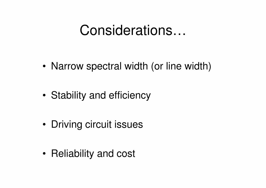
Considerations…
• Narrow spectral width (or line width)
• Stability and efficiency• Stability and efficiency
• Driving circuit issues
• Reliability and cost

Semiconductor Light Sources
• A PN junction (that consists of direct band gap
semiconductor materials) acts as the active or
recombination region.
• When the PN junction is forward biased, • When the PN junction is forward biased,
electrons and holes recombine either radiatively
(emitting photons) or non-radiatively (emitting
heat). This is simple LED operation.
• In a LASER, the photon is further processed in a
resonance cavity to achieve a coherent, highly
directional optical beam with narrow linewidth.
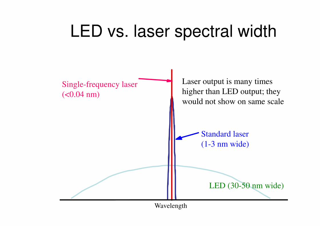
LED vs. laser spectral width
Single-frequency laser
(<0.04 nm)
Laser output is many times
higher than LED output; they
would not show on same scale
Standard laser
(1-3 nm wide)
LED (30-50 nm wide)
Wavelength
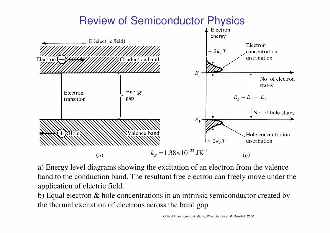
Review of Semiconductor Physics
a) Energy level diagrams showing the excitation of an electron from the valence
band to the conduction band. The resultant free electron can freely move under the
application of electric field.
b) Equal electron & hole concentrations in an intrinsic semiconductor created by
the thermal excitation of electrons across the band gap
-123 JK 1038.1 −×=Bk
Optical Fiber communications, 3rd ed.,G.Keiser,McGrawHill, 2000

n-Type Semiconductor
a) Donor level in an n-type semiconductor.
b) The ionization of donor impurities creates an increased electron
concentration distribution.
Optical Fiber communications, 3rd ed.,G.Keiser,McGrawHill, 2000

p-Type Semiconductor
a) Acceptor level in an p-type semiconductor.
b) The ionization of acceptor impurities creates an increased hole
concentration distributionOptical Fiber communications, 3rd ed.,G.Keiser,McGrawHill, 2000

Intrinsic & Extrinsic Materials
• Intrinsic material: A perfect material with no impurities.
• Extrinsic material: donor or acceptor type
)2
exp(Tk
Enpn
B
g
i −∝==
ly.respective ionsconcentrat intrinsic & hole electron, theare && inpn
e.Temperatur is energy, gap theis TEg
[4-1]
• Extrinsic material: donor or acceptor type
semiconductors.
• Majority carriers: electrons in n-type or holes in p-type.
• Minority carriers: holes in n-type or electrons in p-type.
• The operation of semiconductor devices is essentially
based on the injection and extraction of minority
carriers.
2
inpn = [4-2]

The pn Junction
Electron diffusion across a
pn junction creates a barrier
potential (electric field)
in the depletion region.
Optical Fiber communications, 3rd ed.,G.Keiser,McGrawHill, 2000

Reverse-biased pn Junction
Optical Fiber communications, 3rd ed.,G.Keiser,McGrawHill, 2000
A reverse bias widens the depletion region, but allows minority carriers to move
freely with the applied field.

Forward-biased pn Junction
Optical Fiber communications, 3rd ed.,G.Keiser,McGrawHill, 2000
Lowering the barrier potential with a forward bias allows majority carriers to
diffuse across the junction.

Ek
Ec
Ev
Conduction
Band (CB)
Ec
Ev
CB
The E-k Diagram The Energy Band
Diagram
Empty ψk
Occupied ψh+
e-
Eg
e-
h+
hυhυ
Valence
Band (VB)
Direct Band Gap Semiconductors
kš /a–š /a
Occupied ψk
h+ h+
VB
Band (VB)
The E-k diagram of a direct bandgap semiconductor such as GaAs. The E-kcurve consists of many discrete points with each point corresponding to apossible state, wavefunction ψk(x), that is allowed to exist in the crystal.
The points are so close that we normally draw the E-k relationship as acontinuous curve. In the energy range Ev to Ec there are no points (ψk(x)
solutions).
© 1999 S.O. Kasap, Optoelectronics (Prentice Hall)

Indirect Band Gap Semiconductors
E
CB
k–k
Direct Bandgap
E
CB
VB
Indirect Bandgap, Eg
k–k
kcb
E
k–k
Phonon
Eg
Ec
Ev
Ec
Ev
kvb VB
CB
Er
Ec
Ev
Photon
VB
k–k
(a) GaAs
k–k
(b) Si
k–k
(c) Si with a recombination center
vb
(a) In GaAs the minimum of the CB is directly above the maximum of the VB. GaAs istherefore a direct bandgap semiconductor. (b) In Si, the minimum of the CB is displaced fromthe maximum of the VB and Si is an indirect bandgap semiconductor. (c) Recombination ofan electron and a hole in Si involves a recombination center .
© 1999 S.O. Kasap, Optoelectronics (Prentice Hall)

Periodic table

Light-Emitting Diodes (LEDs)
• For photonic communications requiring data rate 100-200 Mb/s with multimode fiber with tens of microwatts, LEDs are usually the best choice.
• LED configurations being used in photonic communications:
1- Surface Emitters (Front Emitters)
2- Edge Emitters
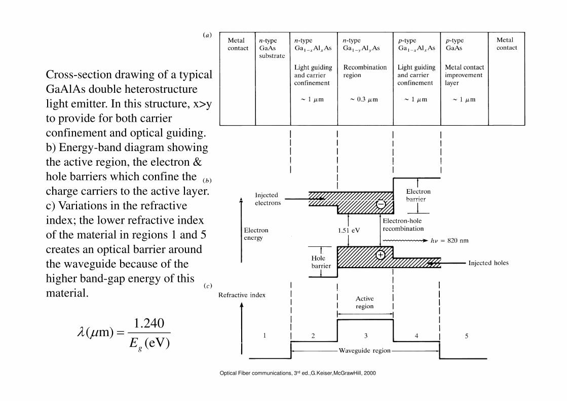
Cross-section drawing of a typical
GaAlAs double heterostructure
light emitter. In this structure, x>y
to provide for both carrier
confinement and optical guiding.
b) Energy-band diagram showing
the active region, the electron &
hole barriers which confine the
charge carriers to the active layer.
c) Variations in the refractive
Optical Fiber communications, 3rd ed.,G.Keiser,McGrawHill, 2000
c) Variations in the refractive
index; the lower refractive index
of the material in regions 1 and 5
creates an optical barrier around
the waveguide because of the
higher band-gap energy of this
material.
)eV(
240.1m)(
gE=µλ

Surface-Emitting LED
Optical Fiber communications, 3rd ed.,G.Keiser,McGrawHill, 2000
Schematic of high-radiance surface-emitting LED. The active region is limitted
to a circular cross section that has an area compatible with the fiber-core end face.

Edge-Emitting LED
Schematic of an edge-emitting double heterojunction LED. The output beam is
Lambertian in the plane of junction (θ|| = 120º) and highly directional perpendicular to
pn junction (θ⊥ = 30º) . They have high quantum efficiency & fast response.
Optical Fiber communications, 3rd ed.,G.Keiser,McGrawHill, 2000

Light Source Material
• Most of the light sources contain III-V ternary & quaternary compounds.
• by varying x it is possible to control the band-gap energy and thereby the emission wavelength over the range of 800 nm to 900 nm. The spectral width is around 20 to 40 nm.
• By changing 0<x<0.47; y is approximately 2.2x, the emission wavelength can be controlled over the range of 920 nm to 1600 nm. The spectral width varies from 70 nm to
AsAlGa xx1−
y1yxx1 PAsGaIn −−
920 nm to 1600 nm. The spectral width varies from 70 nm to 180 nm when the wavelength changes from 1300 nm to 1600 nm. These materials are lattice matched.
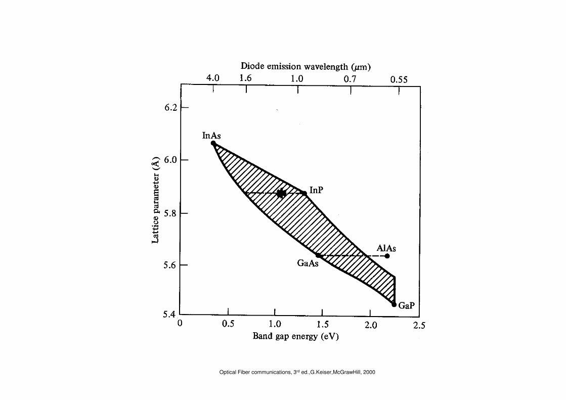
Optical Fiber communications, 3rd ed.,G.Keiser,McGrawHill, 2000

Spectral width of LED types
Optical Fiber communications, 3rd ed.,G.Keiser,McGrawHill, 2000

Rate equations, Quantum Efficiency & Power of
LEDs
• When there is no external carrier injection, the excess density decays exponentially due to electron-hole recombination.
• n is the excess carrier density,
τ/0)( tentn
−= [4-4]
densityelectron excess injected initial :0n
• Bulk recombination rate R:
• Bulk recombination rate (R)=Radiative recombination rate + nonradiative recombination rate
lifetime.carrier :
densityelectron excess injected initial :0
τ
n
τn
dt
dnR =−= [4-5]

)1rate(ion recombinat venonradiati )1( rateion recombinat radiative
)1( rateion recombinatbulk
r nrnrr /τR/τR
/τR
=+=
==
With an external supplied current density of J the rate equation for the electron-hole
recombination is:
)( n
qd
J
dt
tdn
τ−= [4-6]
regionion recombinat of thickness: electron; theof charge : dq
qddt τ
In equilibrium condition: dn/dt=0
qd
Jn
τ= [4-7]

rnrr
nr
nrr
r
RR
R
ττ
τττ
η =+
=+
=int
Internal Quantum Efficiency & Optical Power
[4-8]
region active in the efficiency quantum internal :intη
Optical power generated internally in the active region in the LED is:Optical power generated internally in the active region in the LED is:
ληνη
q
hcIh
q
IP intintint == [4-9]
region active current to Injected :
power, optical Internal :int
I
P
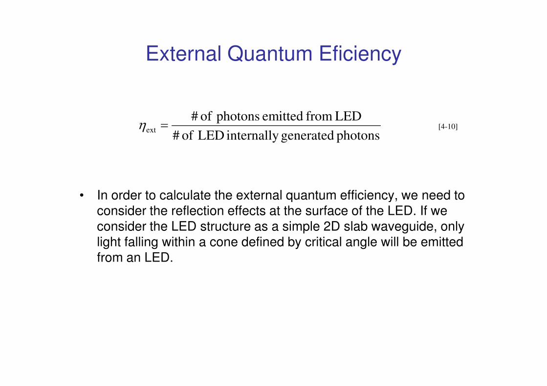
External Quantum Eficiency
• In order to calculate the external quantum efficiency, we need to
photons generated internally LED of #
LED from emitted photons of #ext =η [4-10]
• In order to calculate the external quantum efficiency, we need to consider the reflection effects at the surface of the LED. If we consider the LED structure as a simple 2D slab waveguide, only light falling within a cone defined by critical angle will be emitted from an LED.
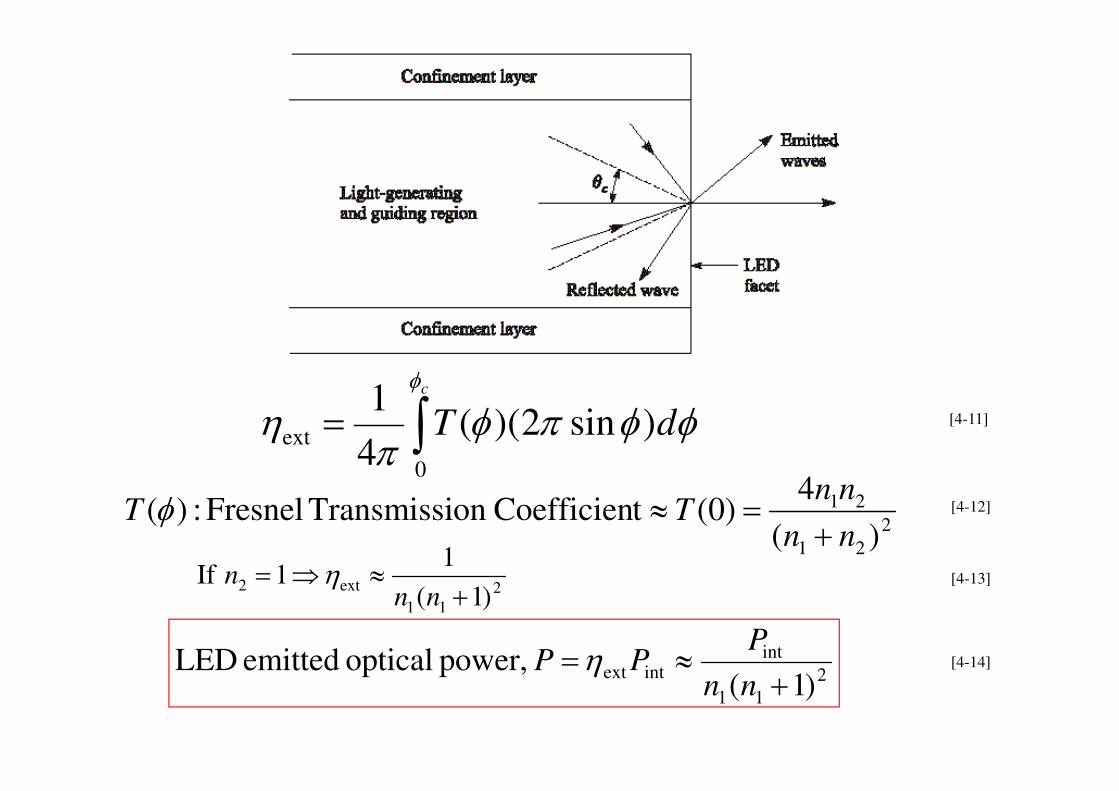
φc1∫ φφπφ
πη dT
c
)sin2()(4
1
0
ext ∫= [4-11]
2
21
21
)(
4)0(tCoefficienon Transmissi Fresnel :)(
nn
nnTT
+=≈φ [4-12]
2
11
ext2)1(
11 If
+≈⇒=
nnn η [4-13]
2
11
intintext
)1( power, optical emitted LED
+≈=
nn
PPP η [4-14]

Modulation of LED
• The frequency response of an LED depends on:
1- Doping level in the active region
2- Injected carrier lifetime in the recombination region, .
3- Parasitic capacitance of the LED
• If the drive current of an LED is modulated at a frequency of ω
the output optical power of the device will vary as:
0)(P
P ω = [4-15]
iτ
• Electrical current is directly proportional to the optical power, thus we can define electrical bandwidth and optical bandwidth, separately.
2
0
)(1)(
i
PP
ωτω
+= [4-15]
current electrical : power, electrical:
)0(log20
)0(10log BW Electrical
IP
I
)I(
P
)P(
=
=
ωω[4-16]

=
=
)0(
)(log10
)0(
)(log10 BW Optical
I
I
P
P ωω[4-17]
P : optical power, I : detected electric current, I ∝ P
Optical Fiber communications, 3rd ed.,G.Keiser,McGrawHill, 2000

Drawbacks & Advantages of LED
Drawbacks
• Large line width (30-40 nm)
• Large beam width (Low coupling to the fiber)fiber)
• Low output power
• Low E/O conversion efficiency
Advantages
• Robust
• Linear

LASER (Light Amplification by the Stimulated Emission of Radiation)
• Laser is an optical oscillator. It comprises a resonant optical amplifier whose output is fed back into its input with matching phase. Any oscillator contains:
1- An amplifier with a gain-saturated mechanism
2- A feedback system
3- A frequency selection mechanism3- A frequency selection mechanism
4- An output coupling scheme
• In laser, the amplifier is the pumped active medium, such as biased semiconductor region, feedback can be obtained by placing active medium in an optical resonator, such as Fabry-Perot structure, two mirrors separated by a prescribed distance. Frequency selection is achieved by resonant amplifier and by the resonators, which admits certain modes. Output coupling is accomplished by making one of the resonator mirrors partially transmitting.

Lasing in a pumped active medium
• In thermal equilibrium the stimulated emission is essentially negligible, since the density of electrons in the excited state is very small, and optical emission is mainly because of the spontaneous emission. Stimulated emission will exceed absorption only if the population of the excited states is greater than that of the ground state. This condition is known as Population Inversion. Population inversion is achieved by Population Inversion. Population inversion is achieved by various pumping techniques.
• In a semiconductor laser, population inversion is accomplished by injecting electrons into the material to fill the lower energy states of the conduction band.

Pumped active medium
• Three main process for laser action:
1- Photon absorption
2- Spontaneous emission
3- Stimulated emission
Optical Fiber communications, 3rd ed.,G.Keiser,McGrawHill, 2000
Energy
absorbed from
the incoming
photon
Random
release of
energy
Coherent
release of
energy
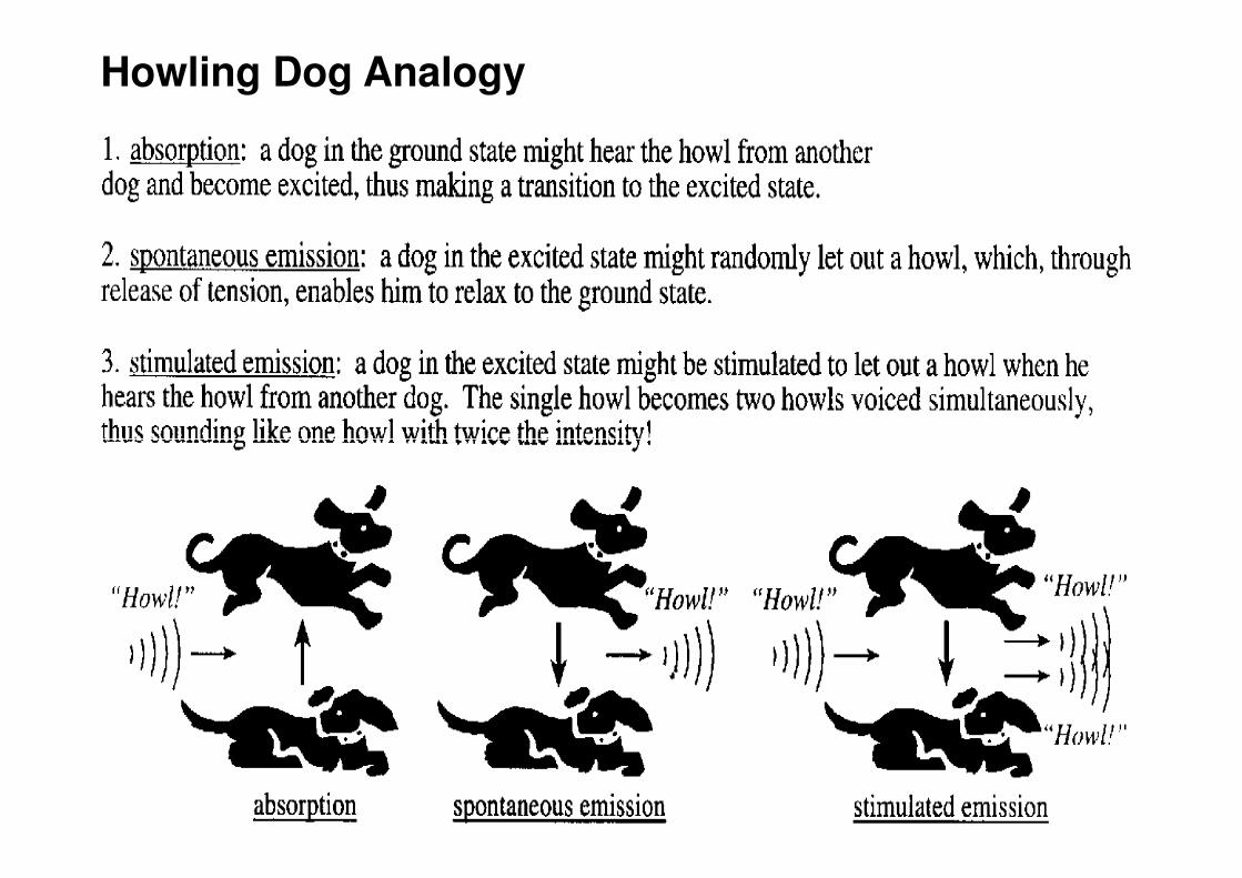
Howling Dog Analogy

In Stimulated Emission incident
and stimulated photons will
have
• Identical energy � Identical
wavelength � Narrow linewidthwavelength � Narrow linewidth
• Identical direction � Narrow beam
width
• Identical phase � Coherence and
• Identical polarization

Stimulated Emission


Fabry-Perot Resonator
A
B
L
M1 M2 m = 1
m = 2
m = 8
Relative intensity
υ
δυm
υm υm + 1υm - 1
(a) (b) (c)
R ~ 0.4
R ~ 0.81 υf
1,2,3,.. :modesResonant == mmkL πSchematic illustration of the Fabry-Perot optical cavity and its properties. (a) Reflectedwaves interfere. (b) Only standing EM waves, modes, of certain wavelengths are allowed
in the cavity. (c) Intensity vs. frequency for various modes. R is mirror reflectance and
lower R means higher loss from the cavity.
© 1999 S.O. Kasap, Optoelectronics (Prentice Hall)
)(sin4)1(
)1(22
2
kLRR
RII inctrans +−
−= [4-18]
R: reflectance of the optical intensity, k: optical wavenumber
1,2,3,.. :modesResonant == mmkL π

Mirror Reflections
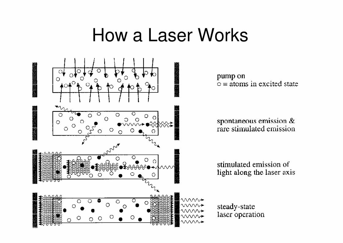
How a Laser Works

Laser Diode
• Laser diode is an improved LED, in the sense that uses stimulated
emission in semiconductor from optical transitions between distribution
energy states of the valence and conduction bands with optical
resonator structure such as Fabry-Perot resonator with both optical
and carrier confinements.
Optical Fiber communications, 3rd ed.,G.Keiser,McGrawHill, 2000

Laser Diode Characteristics
• Nanosecond & even picosecond response time (GHz BW)
• Spectral width of the order of nm or less
• High output power (tens of mW)
• Narrow beam (good coupling to single mode fibers)
• Laser diodes have three distinct radiation modes namely, • Laser diodes have three distinct radiation modes namely, longitudinal, lateral and transverse modes.
• In laser diodes, end mirrors provide strong optical feedback in longitudinal direction, so by roughening the edges and cleaving the facets, the radiation can be achieved in longitudinal direction rather than lateral direction.

DFB(Distributed FeedBack) Lasers
• In DFB lasers, the optical resonator structure is due to the incorporation
of Bragg grating or periodic variations of the refractive index into
multilayer structure along the length of the diode.
Optical Fiber communications, 3rd ed.,G.Keiser,McGrawHill, 2000
The optical feedback is provided by fiber Bragg Gratings ���� Only one wavelength get positive feedback

Laser Operation & Lasing Condition
• To determine the lasing condition and resonant frequencies, we should focus on the optical wave propagation along the longitudinal direction, z-axis. The optical field intensity, I, can be written as:
)()(),( ztjezItzI βω −= [4-19]
• Lasing is the condition at which light amplification becomes possible by virtue of population inversion. Then, stimulated emission rate into a given EM mode is proportional to the intensity of the optical radiation in that mode. In this case, the loss and gain of the optical field in the optical path determine the lasing condition. The radiation intensity of a photon at energy varies exponentially with a distance z amplified by factor g, and attenuated by factor according to the following relationship:
νh
α

( )[ ]zhhgIzI )()(exp)0()( ναν −Γ= [4-20]
1R 2R
Z=0 Z=L
( )[ ])2()()(exp)0()2( 21 LhhgRRILI ναν −Γ= [4-21]
1n
2n
( )[ ])2()()(exp)0()2( 21 LhhgRRILI ναν −Γ= [4-21]
2
21
21 t,coefficien absorption effective :
tcoefficiengain :g factor,t confinemen Optical :
+−
=
Γ
nn
nnRα
Lasing Conditions:
1)2exp(
)0()2(
=−
=
Lj
ILI
β[4-22]

Threshold gain & current density
+=Γ
21
1ln
2
1
RRLgth α
thgg ≥ :iff lase"" tostartsLaser
[4-23]
For laser structure with strong carrier confinement, the threshold current
Density for stimulated emission can be well approximated by:
thth Jg β= [4-24]
onconstructi device specificon dependsconstant :β

Optical output vs. drive current
Optical Fiber communications, 3rd ed.,G.Keiser,McGrawHill, 2000

Semiconductor laser rate equations
• Rate equations relate the optical output power, or # of photons per unit
volume, , to the diode drive current or # of injected electrons per
unit volume, n. For active (carrier confinement) region of depth d, the
rate equations are:
Φ
lossphoton emission sspontaneouemission stimulatedratePhoton ++=
Φ−+Φ=
ΦRCn
dt
d
ph
sp τ
[4-25]
emission stimulatedionrecombinat sspontaneouinjectionrateelectron
lossphoton emission sspontaneouemission stimulatedratePhoton
++=
++=
Φ−−= Cnn
qd
J
dt
dn
spτ
[4-25]
densitycurrent Injection
timelifephoton
mode lasing theintoemission sspontaneou of rate
process absorption &emission optical theofintensity theexpressingt Coefficien
:
:
:
:
J
R
C
ph
sp
τ

Threshold current Density & excess electron density
• At the threshold of lasing: 0 ,0/ ,0 ≈≥Φ≈Φ spRdtd
th
ph
ph nC
nCn =≥⇒≥Φ−Φ⇒τ
τ1
0/ 25]-[4 eq. from [4-26]
• The threshold current needed to maintain a steady state threshold
concentration of the excess electron, is found from electron rate
equation under steady state condition dn/dt=0 when the laser is just
about to lase:
sp
thth
sp
thth nqdJ
n
qd
J
ττ=⇒−= 0 [4-27]

Laser operation beyond the threshold
• The solution of the rate equations [4-25] gives the steady state photon density, resulting from stimulated emission and spontaneous emission as follows:
thJJ >
τspphth
ph
s RJJqd
ττ
+−=Φ )( [4-28]

External quantum efficiency
• Number of photons emitted per radiative electron-hole pair recombination above threshold, gives us the external quantum efficiency.
)(
g
gthiext
αηη
−=
• Note that:
)mA(
)mW(]m[8065.0
dI
dP
dI
dP
E
q
g
g
th
µλ== [4-29]
%40%15 %;70%60 −≈−≈ exti ηη

Laser Resonant Frequencies
• Lasing condition, namely eq. [4-22]:
• Assuming the resonant frequency of the mth
,...3,2,1 ,2L2 1)2exp( ==⇒=− mmLj πββ
λπ
βn2
=• Assuming the resonant frequency of the mth mode is: λ
β =
1,2,3,... 2
== mLn
mcmν
LnLn
cmm
22
2
1
λλννν =∆⇔=−=∆ −
[4-30]
[4-31]

Spectrum from a Laser Diode
widthspectral: 2
)(exp)0()(
2
0 σσλλ
λ
−−= gg [4-32]
Laser Diode Structure & Radiation Pattern
• Efficient operation of a laser diode requires reducing the # of lateral modes, stabilizing the gain for lateral modes as well as lowering the threshold current. These are met by structures that confine the optical wave, carrier concentration and current flow in the lateral direction. The important types of laser diodes are: gain-induced, positive index guided, and negative index gain-induced, positive index guided, and negative index guided.

High-refractive-
index regions
Low-refractive-
index regionsLow-refractive-
index regions
(a) gain-induced guide (b)positive-index waveguide (c)negative-index waveguide
Unstable, two-
peaked beamCan made single-mode laser

Laser Diode with buried heterostructure (BH)
Single Mode Laser
• Single mode laser is mostly based on the index-
guided structure that supports only the fundamental
transverse mode and the fundamental longitudinal
mode. In order to make single mode laser we have
four options:
1- Reducing the length of the cavity to the point 1- Reducing the length of the cavity to the point
where the frequency separation given in eq[4-31] of
the adjacent modes is larger than the laser transition
line width. This is hard to handle for fabrication and
results in low output power.
2- Vertical-Cavity Surface Emitting laser (VCSEL)
3- Structures with built-in frequency selective grating
4- tunable laser diodes
.

VCSEL

Frequency-Selective Laser Diodes:
Distributed Feedback (DFB) Laser
Λ
m
neB
Λ=
2λ [4-33]Bragg wavelength
λB : effective refractive index; m : order of the grating

Output spectrum symmetrically
distributed around Bragg
wavelength
in an idealized DFB laser diode
)2
1(
2
2
+±= mLn ee
B
B
λλλ
[4-35]
Le : effective grating length;
m (=0,1,2) : mode order m (=0,1,2) : mode order
A. Yariv, P. Yeh, Photonics: Optical Electronics in Modern Communications, Oxford, 2007

Frequency-Selective laser Diodes:
Distributed Feedback Reflector (DBR) laser

Frequency-Selective Laser Diodes:
Distributed Reflector (DR) Laser
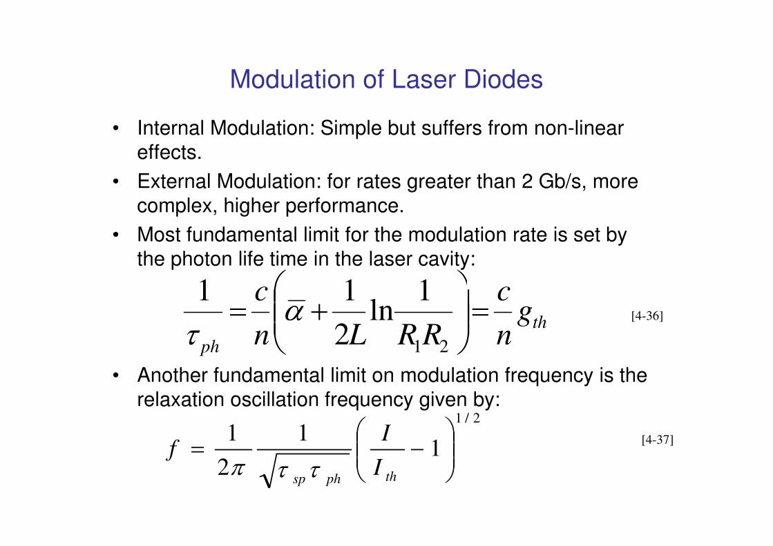
Modulation of Laser Diodes
• Internal Modulation: Simple but suffers from non-linear
effects.
• External Modulation: for rates greater than 2 Gb/s, more
complex, higher performance.
• Most fundamental limit for the modulation rate is set by
the photon life time in the laser cavity:
cc 111
• Another fundamental limit on modulation frequency is the
relaxation oscillation frequency given by:
th
ph
gn
c
RRLn
c=
+=
21
1ln
2
11α
τ[4-36]
2/1
11
2
1
−=
thphspI
If
ττπ[4-37]

Relaxation oscillation peak

Pulse Modulated laser
• In a pulse modulated laser, if the laser is completely turned off after each pulse, after onset of the current pulse, a time delay, given by:
dt
−+=
)(ln
p
dIII
It τ [4-38]
−+ )( thBp III
current Bias :
amplitude pulseCurrent : timelifecarrier :
B
p
I
Iτ

Linearity of Laser
Information carrying
electrical signal s(t)
LED or Laser diode
modulator
Optical putput power:
P(t)=P[1+ms(t)]


Nonlinearity
...2coscos)(
cos)(
210 +++=
=
tAtAAty
tAtx
ωωω
x(t) Nonlinear function y=f(x) y(t)
Nth order harmonic distortion:
1
log20A
An

Intermodulation Distortion
∑ ±±=+=
⇒+=
nm
mn m,ntnmBty
tAtAtx
,
21
2211
2,...1,0, )cos()(
coscos)(
ωω
ωω
Harmonics:Harmonics:
21 , ωω mn
Intermodulated Terms:
,...2,2, 212121 ωωωωωω ±±±

Laser Noise
• Modal (speckle) Noise: Fluctuations in the distribution of energy among various modes.
• Mode partition Noise: Intensity fluctuations in the longitudinal modes of a laser diode, main source of noise in single mode fiber systems.
• Reflection Noise: Light output gets reflected back from the fiber joints into the laser, couples with lasing modes, changing their joints into the laser, couples with lasing modes, changing their phase, and generate noise peaks. Isolators & index matching fluids can eliminate these reflections.
A speckle pattern
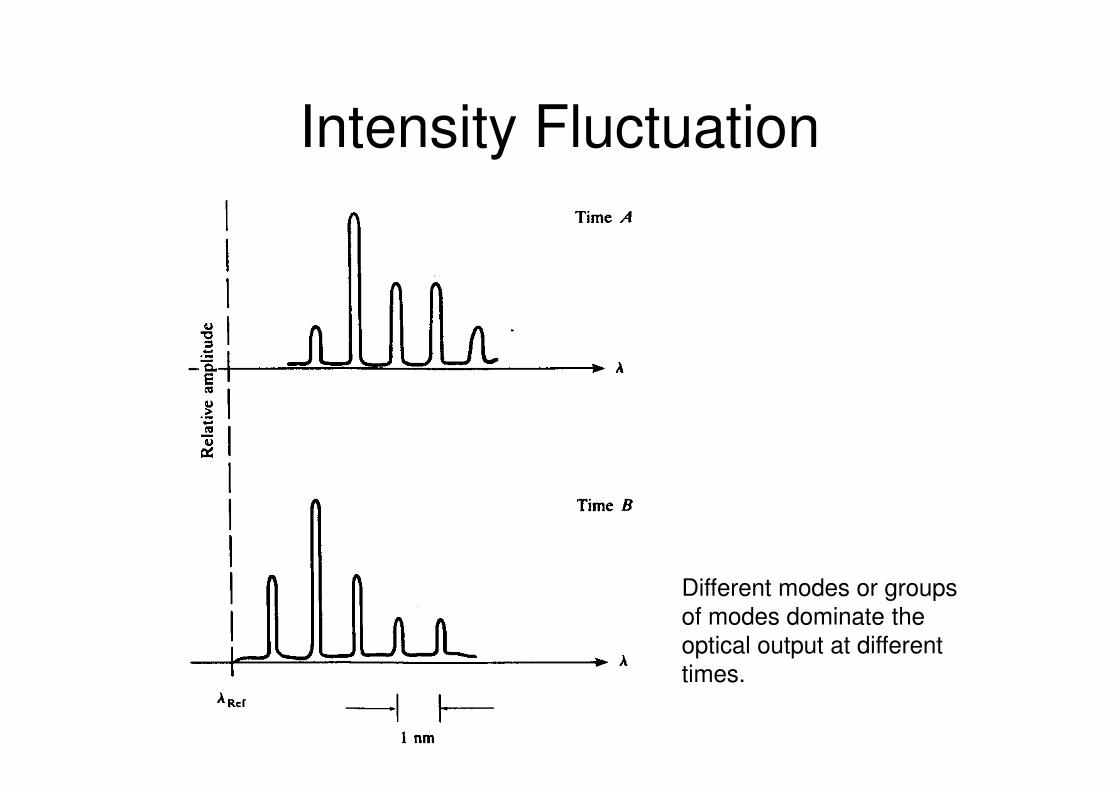
Intensity Fluctuation
Different modes or groups
of modes dominate the
optical output at different
times.
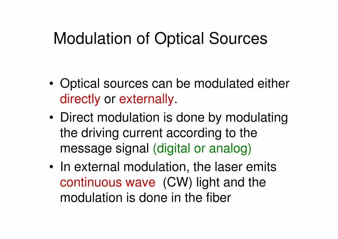
Modulation of Optical Sources
• Optical sources can be modulated either directly or externally.
• Direct modulation is done by modulating • Direct modulation is done by modulating the driving current according to the message signal (digital or analog)
• In external modulation, the laser emits continuous wave (CW) light and the modulation is done in the fiber

Why Modulation
• A communication link is established by
transmission of information reliably
• Optical modulation is embedding the information
on the optical carrier for this purposeon the optical carrier for this purpose
• The information can be digital (1,0) or analog (a
continuous waveform)
• The bit error rate (BER) is the performance
measure in digital systems
• The signal to noise ratio (SNR) is the
performance measure in analog systems

Parameters to characterize
performance of optical
modulation

Important parameters used to characterize and compare different
modulators
• Modulation efficiency: Defined differently depending on if we modulate intensity, phase or frequency. For intensity it is defined as (Imax – Imin)/Imax.
• Modulation depth: For intensity modulation it is • Modulation depth: For intensity modulation it is defined in decibel by 10 log (Imax/Imin).
• Modulation bandwidth: Defined as the high frequency at which the efficiency has fallen by 3dB.
• Power consumption: Simply the power consumption per unit bandwidth needed for (intensity) modulation.

Types of Optical Modulation
• Direct modulation is done by superimposing the modulating (message) signal on the driving current
• External modulation is done after the light • External modulation is done after the light is generated; the laser is driven by a dc current and the modulation is done after that separately
• Both these schemes can be done with either digital or analog modulating signals


RF in
Bias Current
Bias Tee
LaserDiode
PhotoDetector
F ibre
L inkRF
out
Direct Modulation
• The message signal (ac) is superimposed on
the bias current (dc) which modulates the
laser
• Robust and simple, hence widely used
• Issues: laser resonance frequency, chirp,
turn on delay, clipping and laser nonlinearity

Optical Output vs. Drive Current of a
Laser

Direct Analog Modulation
LED LASER
Modulation index (depth) '
BIIm ∆=
BB II ='thBB III −='

Analog LED Modulation
Note:
No threshold
current
�No clipping�No clipping
�No turn on
delay
Laser Digital Modulation
Ith
I1
P(t)
Optical Power
(P)
Current (I)I(t)
t
t
I2
−−
=th
spdII
IIt
2
12lnτ

Turn on Delay (lasers)
• When the driving current suddenly jumps from low (I1 < Ith) to high (I2 > Ith) , (step input), there is a finite time before the laser input), there is a finite time before the laser will turn on
• This delay limits bit rate in digital systems
• Can you think of any solution?
−−
=th
spdII
IIt
2
12lnτ

• Input current
– Assume step input
• Electron density
– steadily increases until
threshold value is
reached
I1
I2
reached
• Output optical power
– Starts to increase only
after the electrons
reach the threshold
Turn on Delay(td)
Resonance Freq.(fr)

Frequency Response of a Laser
Resonance
Frequency
(fr) limits the
highest possible
modulation
frequencyfrequency
Useful Region

Laser
Analog
Modulation P(t)
)](1[)( tmsPtP t +=
S(t)
Here s(t) is the modulating signal,P(t): output optical powerPt: mean value

The modulated spectrum
Transfer function of the fiber
Optical Carrier
Modulation
Depth ~ 0.2
λλo=1310 nm
0.02 nm
(3.6 GHz)
RF Subcarrier
RF Bandwidth
Two sidebands each separated by modulating frequency
Twice the RF frequency

Limitations of Direct Modulation• Turn on delay and resonance frequency are the
two major factors that limit the speed of digital laser modulation
• Saturation and clipping introduces nonlinear distortion with analog modulation (especially in distortion with analog modulation (especially in multi carrier systems)
• Nonlinear distortions introduce second and third order intermodulation products
• Chirp: Laser output wavelength drift with modulating current is also another issue, resulting in line broadening.

Chirp

The Chirped Pulse
A pulse can have a frequency that varies in time.
This pulse increases its frequency linearly in time (from red to blue).
In analogy to bird sounds, this pulse is called a "chirped" pulse.

Temperature variation of the threshold current
0/)(
TT
zth eITI =

External Optical Modulation
EOM
RF in
PhotoDetector
LaserDiode
F ibre
L ink
RFout
• Modulation and light generation are separated
• Offers much wider bandwidth � up to 60 GHz
• More expensive and complex
• Used in high end systems

External Modulated Spectrum
• Typical spectrum is double side band
• However, single side band is possible which is useful at extreme RF frequencies

Mach-Zehnder Interferometers

Mach- Zehnder modulator

Mach- Zehnder modulator


Characteristics of Mach-
Zehnder modulator

Electro- absorption (EA)
modulator

Integration of EA modulator with
LD
Quantum well (QW) Laser: laser diode whose active region is so narrow that quantum
confinement occurs

Characteristics of EA modulator