Foliage and Grass as Fuel Pellets–Small Scale Combustion of ...
Upload
nitsilcharCategory
view
3download
0
This article appeared in a journal published by Elsevier. The attachedcopy is furnished to the author for internal non-commercial researchand education use, including for instruction at the authors institution
and sharing with colleagues.
Other uses, including reproduction and distribution, or selling orlicensing copies, or posting to personal, institutional or third party
websites are prohibited.
In most cases authors are permitted to post their version of thearticle (e.g. in Word or Tex form) to their personal website orinstitutional repository. Authors requiring further information
regarding Elsevier’s archiving and manuscript policies areencouraged to visit:
http://www.elsevier.com/authorsrights
Author's personal copy
Structural, electrical and optical properties of sinteredSnO2 pellets
N. Kumari a, A. Ghosh a,b, S. Tewari c, A. Bhattacharjee a,n
a NIT Silchar, Silchar-788010, Assam, Indiab Don Bosco College, Tura, Meghalaya, Indiac Karimganj College, Karimganj, Assam, India
a r t i c l e i n f o
Available online 18 February 2013
Keywords:
SnO2
Dielectric studies
A.C. conductivity
a b s t r a c t
Tin dioxide (SnO2) powder was prepared by the co-precipitation method using SnCl2
solution as a precursor. The powder was then pelletized and sintered. Structural
characterization of the samples with XRD confirmed that all the pellets were of SnO2
having polycrystalline nature with the crystallite size of the order of 90 nm. SEM-EDAX
was used to confirm the morphology and composition of the samples. The measurements
of electrical properties were carried out in the frequency range of 100 Hz to 100 kHz at
various fixed temperatures from 40 1C to 160 1C. The a.c. conductivity and the dielectric
constant were found to be dependent on both frequency and temperature. The frequency
and temperature dependent conduction properties of SnO2 are found to be in accordance
with correlated barrier hoping model. Infrared and visible spectroscopic studies show
that a strong vibration band characteristic of the SnO2 stretching mode was present at
around 620 cm�1 and the samples exhibited optical transmittance in the visible range.
& 2013 Elsevier Ltd. All rights reserved.
1. Introduction
Tin dioxide (SnO2) is a very important n-type semi-conductor with a wide band gap (Eg¼3.6 eV at 300 K) andalso an indirect band gap of 2.3 eV, reported by Kim et al.[1–2]. It is a key functional material having high chemicalstability and excellent optical and electrical propertieswhich find multifaceted technological applications.It belongs to the important family of transparent con-ducting oxide (TCO) materials that combine high electri-cal conductivity with high optical transparency in thevisible range of the electromagnetic spectrum [2]. Due to itsfavorable properties, this material finds many technologicallyimportant applications such as transparent electrodes fordisplays, solar cells, gas sensors, heating elements for elec-tromagnetic shielding, antistatic surfaces, smart windowsand other optoelectronic devices [3,4]. The requirement of
the modern day technology is to get materials with higherelectrical conductivity. Often for TCO, the highest possibleconductivity is sought from an oxide semiconductor. Manybinary TCO’s already possess a high conductivity due tointrinsic defects i.e., oxygen deficiency makes them intoconductors [5,6]. The FET mobility of conduction electronsin n-type SnO2 is 160 cm2/V/s [7]. In this n-type widebandgap semiconductor the material conductivity is verysensitive to the surface states in the temperature rangebetween 25 1C and 400 1C. Besides that, SnO2 surface exhibitsgood adsorption and deadsorption phenomenon, and exhi-bits high reactivity mainly due to the availability of freeelectrons in its conduction band and the presence of surfaceand bulk oxygen vacancies and active chemisorbed oxygen.The considerable improvement of such operating parametersas sensor signal, selectivity, stability and the rate of sensorresponse can be achieved by optimization of chemical,structural, and the bulk and surface properties of appliedmetal oxide [8]. The relationship between the synthesiscondition, microstructure, electric and frequency dependentproperties of undoped SnO2 has been widely investigated bycarefully controlling the preparation parameters and by
Contents lists available at SciVerse ScienceDirect
journal homepage: www.elsevier.com/locate/mssp
Materials Science in Semiconductor Processing
1369-8001/$ - see front matter & 2013 Elsevier Ltd. All rights reserved.
http://dx.doi.org/10.1016/j.mssp.2013.01.018
n Corresponding author. Tel.: þ91 9435522284;
fax: þ91 3842224797.
E-mail address: [email protected] (A. Bhattacharjee).
Materials Science in Semiconductor Processing 16 (2013) 905–914
Author's personal copy
incorporation of additives catalyst promoters and/or by sur-face functionalization. In general, tin oxide plays an impor-tant role in increasing the reaction rate of gas molecule andcan be sensitized to different gases by judicious choice ofoperating temperature microstructure modification and bythe use of dopants and catalysts [9]. Though studies on d.c.conductivity in SnO2 material have received considerableattention of researchers [10–13], there have been only a fewstudies on their a.c. transport properties [14,15]. The fabrica-tion of devices based on SnO2 material requires a betterunderstanding of its transport properties. The a.c. measure-ments are an important means for studying the dynamicproperties such as conductance, capacitance and dielectricloss of the semiconducting and dielectric materials. Theyprovide information about the interior of the materials in theregion of relatively low conductivity [16]. These measure-ments also help to distinguish between localized and freeband conduction. In the case of localized conduction, the a.c.conductivity increases with frequency, while in the freeband conduction the conductivity decreases with frequency[17–20].
In this paper we report the a.c. transport mechanism ofSnO2 prepared by co-precipitation method where stan-nous chloride is used as a precursor and ammonia solu-tion as a precipitating agent. By using this method we canprepare large quantities of the sample and this methodproves to be extremely cost effective. The basic purpose ofthis work is not only to report the variations in thedifferent electrical parameters but also explain thesechanges in the light of existing theories. A clear under-standing of the frequency dependent parameters alongwith an underlying theory/model helps to develop agreater understanding of their system so that it can beused in a better and more dynamic device application.In this paper we report a detailed study on the synthesisand a.c. response of the SnO2 pellets. We have conductedthe dielectric study for sintered SnO2 pellets in undopedform. The variation of impedance (Z), capacitance (Cp),phase angle (y) and dielectric loss tangent (tan d) withfrequency at a different temperatures ranging from 40 1Cto 160 1C have been conducted. The results are analyzedin the light of the existing theories with a view to under-stand the conduction mechanism involved.
2. Experimental
2.1. Preparation of SnO2 pellets
SnO2 powder was prepared by the co-precipitationmethod where stannous chloride is used as a precursorand ammonia solution as a precipitating agent. After theformation of precipitate, hydrolysis method was used forchloride removal. In this process, 2 g (0.1 M) of stannouschloride dehydrate is dissolved in 100 ml of water. Aftercomplete dissolution, 4 ml of ammonia solution is addedto the above aqueous solution with continuous stirring for20 min. A white gel like precipitate is immediatelyformed. It is allowed to settle for 12 h. Then it is filteredand washed two to three times with distilled water. Theobtained precipitate is dried for 24 h at 70 1C. The driedpowder is crushed and heated at 600 1C for 4 h. The
resulting mass was then crushed into fine powder formand pelletized at a pressure of approximately 13 MPa toform cylindrical pellets by means of dye and punchmethod. These pellets were sintered at around 850 1Cfor 12 h in air. Sintered pellets were then polished intodiscs of 13 mm in diameter and 2 mm in thickness.
2.2. Characterization techniques
Structural analysis of the pellets was made usingPanalytical X’pert Pro X-ray diffractometer with Cu-Ka(l¼0.15418 nm) as X-ray source at 40 kV and 30 mA withscanning angle (2y) ranging from 201 to 901.
The observed XRD pattern was analyzed using X-pertHighscore software. It was found to match with the ICDD-Powder diffraction pattern (JCPDS file no.71-0652).
For a.c. measurements, the flat faces of the pellets werecoated with a thin layer of highly conducting silver pastefor making the good electrical contacts. The pellet wasthen mounted on a homemade two probe assembly whichwas inserted coaxially inside a resistance heated furnace.The temperature of the pellets was monitored using achromel–alumel thermocouple with the help of an Omegadigital multimeter and further verified by inserting athermometer in the furnace. The a.c. measurement ofcapacitance (Cp), impedance (Z), phase angle (y) andtangent loss (tan d) are carried out using a HIOKI LCRmeter (model:3522-50 HIOKI Japan) Hitester with an a.c.bias of 0.1 mV. Throughout the measurements, the pelletswere allowed to equilibrate at each temperature for morethan 30 min for thermal stability.
Morphological study of the samples was carried outusing an instrument HITACHI model no. S4800 FESEM forSEM images and EDAX for composition of materials. Thetransmission spectra were recorded using Perkin ElmerFTIR Spectrophotometer.
3. Results and discussion
3.1. Structural characterization
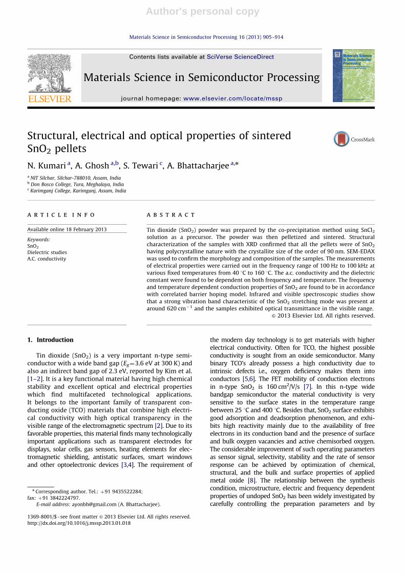
The XRD profile for the powder samples showedasymmetry due to lattice strain [21]. The lattice strain isreported to be reduced when the sample is sintered above600 1C. For reducing the lattice strain we sintered thepellets at 850 1C for 24 h as per the optimization processreported [21], and the XRD patterns was recorded for theSnO2 pellets. The asymmetry was visibly reduced in thediffraction pattern of the sintered pellets. The XRD patternof SnO2 pellets is shown in Fig. 1. The raw data obtainedwas corrected for background, Ka2 stripped, fitted andrefined.
From the diffraction pattern we can conclude thatformation of polycrystalline SnO2 takes place with peaksalong the plane (1 1 0), (1 0 1), (2 0 0), (2 1 1), (2 2 0),(0 0 2), (3 1 0) and (2 0 2). The highest intensity peak isalong the plane (1 1 0) followed by (1 0 1) and (2 1 1). Thecrystallite size D is calculated by using the Debye–Scherrer
N. Kumari et al. / Materials Science in Semiconductor Processing 16 (2013) 905–914906
Author's personal copy
formula,
D¼0:89lbcos y
ð1Þ
where l is the wavelength of incident X-ray (l¼0.1541 nm),b is the half of maximum line width, y is the angle at whichmaximum peak occurs. The crystallite size is found to be ofthe order of 90 nm.
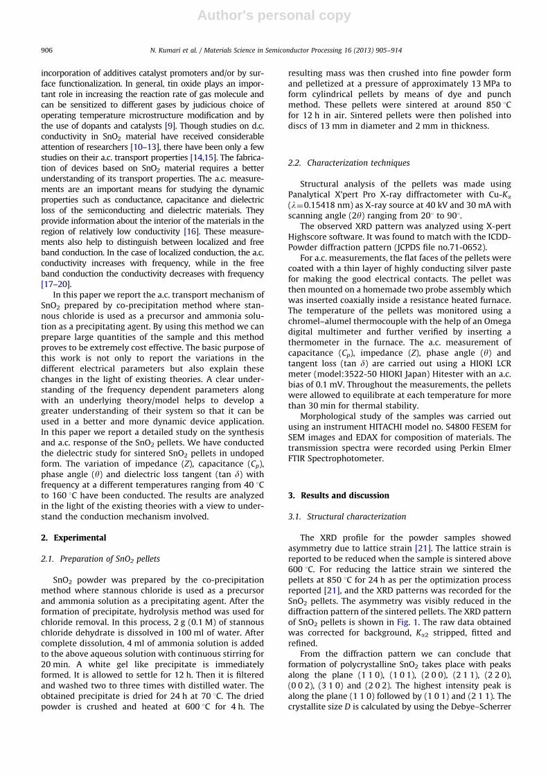
The SEM micrographs are presented in Fig. 2. It isobserved from the micrographs that particle size is of theorder of E90 nm or smaller as predicted from the XRDdata. The SEM image also shows that the particles tend toagglomerate and exhibit a varied distribution in terms ofparticle shape, though the size and texture remains moreor less uniform. Along with SEM, EDAX was alsoperformed on this sample which confirmed that thesample is composed of Sn and O only. No other impuritieswere reported in EDAX.
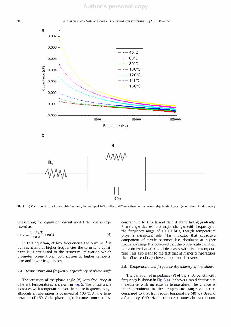
3.2. Temperature and frequency dependency of capacitance
The results for the variation of capacitance (C) withfrequency are shown in Fig. 3(a). From the graph we
observe that the capacitance decreases in the frequencyrange 0–5 kHz for the entire temperature range of 40–160 1C. After this range the capacitance becomes almostconstant from 5 kHz to 10 kHz. It is also observed that thechange is more pronounced at higher temperatures com-pared to lower temperatures. This trend is as per theexpected behaviour that the capacitance shows depen-dence on temperature. The capacitance of the pellets thatare considered in this paper may be expressed in terms of,
C ¼ere0A
dð2Þ
where, C is the capacitance, e is the permittivity of thedielectric medium, A is the area of pellet and d is thicknessof pellet. The capacitance characteristics described aresimilar to those reported elsewhere [22,23]. The generalvariations of capacitance with both frequency and tem-perature can be explained by using the equivalent circuitmodel proposed by these workers, which consists of a fixedcapacitive element C in parallel with a resistive element R,both elements in series with a low value resistance R1 asshown in the circuit diagram in Fig. 3(b). The modelassumes that the contacts are ohmic and do not formSchottky barriers at the surface [23].
The temperature dependent behaviour of capacitancemay be expressed as,
1
C
@C
@T¼
1
k
@k
@Tþ
d
A
@d
@T
A
dð3Þ
where, ð1=CÞð@C=@TÞ is the temperature co-efficient ofcapacitance and ð1=kÞð@k=@TÞ is the temperature depen-dence of dielectric constant. The term ðd=AÞð@d=@TÞðA=dÞ
accounts for any change in dimensions that may occurdue to thermal expansion. Capacitance should decreasewith increasing frequency. This effect is confirmed in theC versus F plot shown in Fig. 3(a).
3.3. Temperature and frequency dependency of dielectric
loss (tan d)
The change in dielectric loss (tan d) with frequency isalso seen in the Fig. 4. From this graph we observe thattan d is very high at lower frequencies and falls rapidlyupto 10 kHz. Beyond that, the value of tan d remainsalmost constant from 10 kHz to 100 kHz. It is alsoobserved that with rise in temperature, the change inthe values of the loss is comparatively high in the range100 Hz to 10 kHz and the change becomes somewhatlower thereafter. The value of tan d shows a decrease withincrease in frequency of the a.c. signal for the pelletsunder study. It is also observed that the value of tan dincreases to higher values at high temperature withincreasing frequency. The value of tan d represents thepower dissipation in SnO2. Fig. 4 represents decrease inloss at low frequencies followed by a loss minimum; andthen an increase in the loss is observed at the higherfrequencies. This observed frequency dependent loss hasbeen found according to the equivalent circuit model pro-posed elsewhere [23] which comprises a capacitive elementC in parallel with a resistive element R1, both elements inseries with a low value resistance R (as shown in Fig. 3(b)).
20 30 40 50 60 70 80 90 100
0
100
200
300
400
(312
)(3
30)
(222
)(4
00)(321
)
(202
)
(110
)
(301
)(1
12)
(310
)(0
02)(2
20)
(211
)
(200
)(1
01)
Position 2θ (degree)
Inte
nsity
(a.u
.)
SnO
Fig. 1. XRD spectra of SnO2 pellet.
Fig. 2. Scanning electron microscopy micrograph for the sample
(undoped SnO2 powder).
N. Kumari et al. / Materials Science in Semiconductor Processing 16 (2013) 905–914 907
Author's personal copy
Considering the equivalent circuit model the loss is exp-ressed as
tan d¼1þR1=R
oCRþoCR ð4Þ
In this equation, at low frequencies the term o�1 isdominant and at higher frequencies the term o is domi-nant. It is attributed to the structural relaxation whichpromotes orientational polarization at higher tempera-ture and lower frequencies.
3.4. Temperature and frequency dependency of phase angle
The variation of the phase angle (y) with frequency atdifferent temperatures is shown in Fig. 5. The phase angleincreases with temperature over the entire frequency rangealthough an aberration is observed at 100 1C. At the tem-perature of 160 1C the phase angle becomes more or less
constant up to 10 kHz and then it starts falling gradually.Phase angle also exhibits major changes with frequency inthe frequency range of 10–100 kHz, though temperatureplays a significant role. This indicates that capacitivecomponent of circuit becomes less dominant at higherfrequency range. It is observed that the phase angle variationis maximized at 40 1C and decreases with rise in tempera-ture. This also leads to the fact that at higher temperaturesthe influence of capacitive component decreases.
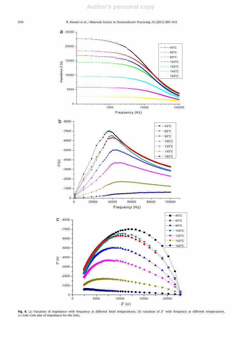
3.5. Temperature and frequency dependency of impedance
The variation of impedance (Z) of the SnO2 pellets withfrequency is shown in Fig. 6(a). It shows a rapid decrease inimpedance with increase in temperature. The change ismore prominent in the temperature range 80–120 1Ccompared to that from room temperature (40 1C). Beyonda frequency of 40 kHz, impedance becomes almost constant
1000 10000 1000000.000
0.001
0.002
0.003
0.004
0.005
0.006
0.007
40°C 60°C 80°C 100°C 120°C 140°C 160°C
Cap
acita
nce
(μF)
Frequency (Hz)
Fig. 3. (a) Variation of capacitance with frequency for undoped SnO2 pellet at different fixed temperatures, (b) circuit diagram (equivalent circuit model).
N. Kumari et al. / Materials Science in Semiconductor Processing 16 (2013) 905–914908

Author's personal copy
from temperature range 20–140 1C. So we may generalizeand say that Z varies inversely with frequency. This typeof behavior is an indication of thermally activated andfrequency dependent conduction. The general features ofthe plots are similar to that observed for an RC circuit inparallel, where the impedance varies with inverse offrequency.
Impedance is a far more general concept comparedto resistance because it takes phase difference intoconsideration. In a.c. the resistance, R is replaced by theZ which is sum of resistance and reactance. Impedance isgiven by,
Z ¼ Z0 þZ00 ð5Þ
where, Z0 is the real part and is expressed as Re(Z)¼Z0 ¼9Z9cosy and Z00 is imaginary part of Z expressed asIm(Z)¼Z00 ¼9Z9siny, where y being the phase angle.
Fig. 6(b) shows variation of Z00 with frequency atdifferent temperatures. These plots are found to exhibitDebye peaks at different temperatures. The peak maximashift to the higher frequency side with increasing tem-perature. The angular frequencies o of the peak maximais given by the reciprocal of the relaxation time, i.e.,om¼1/t¼1/(RC). Since the value of R decreases with risein temperature, therefore om is an increasing function oftemperature. Similar results have also been reportedelsewhere in the case of sintered ZnO pellets [24].
The plotting of these graphs in complex plane is knownas Cole–Cole plot as shown in Fig. 6(c). These plots aresingle semicircular arcs with their centres lying below thereal axis at a particular angle of depression and have a non-zero intersection with the real axis in the high frequencyregion. A single semicircular arc observed in compleximpedance plots suggests an electrical equivalent circuitcomposed of a resistance R and a capacitance C connectedin parallel (Fig. 3b). It is observed that the size of the plotsshrink with the increase of temperature. Reduction in sizeof the plots is attributed to decrease in the value of R withrise in temperatures. Generally, the grain boundaries areeffective in low frequency region while the grains areeffective in high frequency region. Thus, the semicirculararc appearing in the low frequency region corresponds tothe grain boundary contribution this type of behaviour ofimpedance is also reported by Chandra Bose et al. [25] haveinvestigated the room temperature complex impedancespectra of nanocrystalline SnO2 samples and observed theimpedance spectra as depressed single semicircular arcs.
0000010000100010
2
4
6
8 40°C 60°C 80°C 100°C 120°C 140°C 160°C
Loss
tang
ent (
tan δ
)
Frequency (Hz)
Fig. 4. Variation of dielectric loss (tan d) with frequency at different fixed temperatures.
1000 10000 100000-60
-50
-40
-30
-20
-10
0
40°C 60°C 80°C 100°C 120°C 140°C 160°C
Pha
se a
ngle
(θ)
Frequency (Hz)
Fig. 5. Variation of phase angle with frequency at different fixed
temperatures.
N. Kumari et al. / Materials Science in Semiconductor Processing 16 (2013) 905–914 909
Author's personal copy
1000 10000 1000000
5000
10000
15000
20000
25000
40°C
60°C
80°C
100°C
120°C
140°C
160°C
Impe
danc
e Z
(Ω)
F requency (Hz)
0 20000 40000 60000 80000 1000000
-1000
-2000
-3000
-4000
-5000
-6000
-7000
-8000
Z''(Ω
)
Frequency (Hz)
40°C
60°C
80°C
100°C
120°C
140°C
160°C
0 5000 10000 15000 200000
-1000
-2000
-3000
-4000
-5000
-6000
-7000
-8000
Z'' (
Ω)
Z ' (Ω )
40°C
60°C
80°C
100°C
120°C
140°C
160°C
Fig. 6. (a) Variation of impedance with frequency at different fixed temperatures, (b) variation of Z00 with frequency at different temperatures,
(c) Cole–Cole plot of impedance for the SnO2.
N. Kumari et al. / Materials Science in Semiconductor Processing 16 (2013) 905–914910
Author's personal copy
3.6. Frequency and temperature dependency of dielectric
constant (er)
The dielectric constant or relative permittivity er iscalculated by using Eq. (2) which is simplified as
er ¼Cd
e0Að6Þ
where C is the capacitance, d the thickness of pellets ande0 is the permittivity of free space (8.854�10�12 F/m)and A is area of pellet.
The dielectric constant er as shown in Fig. 7 exhibits anincrease with temperature but shows a decrease withfrequency. This can be explained in terms of two differentprocesses as explained below. It is well known that thereare two prominent dielectric polarization mechanisms thatcontribute to the enhanced behavior of nanomaterials;rotation direction polarization (RDP) process and spacecharge polarization (SCP) process. We suggest that boththese processes contribute to the enhancement of dielec-tric response of the SnO2 nanoparticles. First RDP processprovides an important contribution for the higher dielec-tric constant er of the SnO2 nanoparticles. As observed intypical n-type semiconductors, there is a large amount ofoxygen vacancies acting as shallow donors in SnO2 nano-particles [26,27]. Positive oxygen vacancies together withnegative oxygen ions give a large number of dipoles. Thesedipoles rotate in an external electric field, giving rise therotation direction polarization occurring in the interfacesof n-type SnO2 nanoparticles.
On the other hand, SCP process plays its own part in oursample. Generally, nanostructured materials have about 1019
interfaces/cm3, which is much higher compared to that ofbulk solids [28]. The value of dielectric constant er of SnO2
nanoparticles is very high as compared to that of bulk SnO2
which is reported at room temperature [29]. The interfaces
with a large volume fraction in the nanostructured com-pacted samples contain a large amount of defects, suchas micro-porosities, dangling bonds and vacancy clusters.
1000 10000 100000
0
20000
40000
60000
80000
100000
120000
140000
160000
180000
200000
220000
40°C
60°C
80°C
100°C
120°C
140°C
160°C
Die
lect
ric c
onst
ant (
ε )
Frequency(Hz)
Fig. 7. Variation of dielectric constant (er) with frequency at different fixed temperatures.
1000 10000 100000
0
200
400
600
800
1000
1200
1400
Die
lect
ric c
onst
ant (
ε r)Frequency (Hz)
40°C (At room temperature)
Fig. 8. Variation of dielectric constant with frequency at room tempera-
ture for SnO2 pellet.
Table 1The maximum values of dielectric con-
stant (er) 40 1C for SnO2 at various
frequencies.
Frequency
(Hz)
Dielectric constant
(er)
100 67.5
1,000 27.4
10,000 14.5
50,000 10.1
100,000 10.4
N. Kumari et al. / Materials Science in Semiconductor Processing 16 (2013) 905–914 911
Author's personal copy
These defects can cause a change of positive and negativespace charge distributions in interfaces [29,30]. Negative andpositive spaces in interfaces move towards positive andnegative poles of the electric field, respectively. As they aretrapped by defects, newer dipole moments will form andSCP process will occur in the sample. Because the volumefraction of the interfaces of nano-size sample is larger thanthat of bulk materials, SCP is stronger than that in the bulkmaterials. Thus, er of the SnO2 nanoparticles is higher thanthat of bulk. Nevertheless, in the high frequency range,dielectric response of RDP and SCP cannot keep up withthe electrical field frequency variation, resulting in the rapiddecrease of er in SnO2 nanoparticles [29–31].
In our case, er exhibits an increase with temperature butshows a decrease with frequency. Dielectric constant er atroom temperature is shown in Fig. 8. Value of dielectricmagnitude is also given in Table 1 by which we clearlyobserved the decrease in dielectric constant with rise infrequency. It can be explained that as the temperatureincreases, the dipoles comparatively become free and theyrespond to the applied electric field. Thus polarizationincreases and hence the dielectric constant also increaseswith the increase of temperature. Dielectric loss increa-ses with rise in temperature and the phase angle alsoincreases with temperature confirming our above justifica-tions which is discussed in Sections 3.3 and 3.4.
0 20000 40000 60000 80000 100000
0.00014
0.00016
0.00018
0.00020
0.00022
0.00024
0.00026
0.00028
0.00030
0.00032
0.00034
a.c.
con
duct
ivity
, σac
(Ω-m
)-1
Frequency (Hz)
At room temperature
100 1000 10000 1000001E-7
1E-6
1E-5
40°C 60°C 80°C 100°C 120°C 140°C 160°C
a.c.
con
duct
ivity
, σac
(Ω-m
)-1
Frequency, f (Hz)
Fig. 9. (a) Variation of a.c. conductivity with frequency of SnO2 pellet at room temperature, (b) variation of a.c. conductivity (sa.c.) with frequency at
different temperatures.
N. Kumari et al. / Materials Science in Semiconductor Processing 16 (2013) 905–914912

Author's personal copy
3.7. Frequency and temperature dependency of a.c.
conductivity (sac)
The variation of a.c. conductivity of SnO2 nano parti-cles with frequency at room temperature is as shown inFig. 9(a). It shows an increase in a.c. conductivity withfrequency with variable slopes in different ranges. A commonfeature to all the amorphous semiconductors is that the a.c.conductivity sac increases with frequency according to theexpression [32,33]
sac ¼ stðoÞ�sdc ¼ AoS ð7Þ
where sac is a.c. conductivity, A is constant independent offrequency, s is frequency exponent whose value denoted as0oso1 and o is angular frequency.
The a.c. conductivity–temperature relationship isexpressed as
sac ¼ s0exp�E
kTð8Þ
where symbols having their usual meanings.Further, we found that the a.c. conductivity increases
with increase in temperature shown in Fig. 9(b). Theexponent(s) vs. temperature graph can be shown inFig. 10 at different frequency ranges. This type of behaviorrepresents variable type of hopping conduction whichfound to be in accordance with Elliot [34] correlatedbarrier hopping model of conduction within certain tem-perature and frequency regimes [35]. At lower temperaturea.c. conductivity increases with rise in frequency and slopecan be determined by (lnsac/lno) graph, and it behaves asa single polaron model but with rise in temperature itbehaves with several hopping process. The best suitablemodel for our sample is described by the CBH model underwhich the slope ranges in between 0.7 and 1 at roomtemperature and is found to decrease with increase intemperature [36]. In such a case, the Columbic barriercreated between two carrier sites or oxygen vacancies isstrongly affected by temperature and the frequency of theexternal field, which is a typical feature for a rutile typeSnO2 nanoparticles.
4. Optical study
FT-IR Spectroscopy has been employed to study theinfluence of sintering on Sn–O bonding. FT-IR transmis-sion spectra have been recorded in the range 1000–400 cm�1 and the results are shown in Fig. 11. Fromtransmission spectra Sn–O stretching bond has beenshown at approximately wave number 620 cm�1 in thevisible ranges. This type of stretching of Sn–O stretchingphenomena is in good agreement with other authors forSnO2 [37–41] A highly intense broad band has beenobserved at around 490 cm�1 for the pure SnO2 corre-sponding to the formation of Sn–O bond. Similar types ofbehaviour are reported for Zn–O nanoparticles by otherauthors [42,43]. Some other peaks were also observed at329 cm�1, 410 cm�1, 429 cm�1, 454 cm�1. A detailedstudy of these observations will be reported soon indifferent papers.
5. Conclusion
Nanocrystalline Tin dioxide (SnO2) powder is preparedby a co-precipitation method, pelletized and sintered. TheXRD of the sample confirmed that the prepared powder isindeed SnO2. XRD and SEM investigations revealed thatthe crystallite size was of the order of 90 nm. Further,EDAX was used to confirm the composition which showedonly the presence Sn and O and no any other impurities/contaminants were indicated. The capacitance (CP),tangent loss (tan d), impedance (Z) and phase angle (y)were measured by using the LCR meter. Dielectric con-stant (er) and a.c. conductivity (sac) were calculated byusing above data. The capacitance and dielectric loss anddielectric constant were found to decrease with increasein frequency. However, it was observed that the magni-tude of capacitance was higher at higher temperatures. Incase of phase angle both frequency and temperature playsa major role. This is indicative of the simultaneousexistence of two different processes of polarization. FirstRDP process provides a contribution for the high dielectricconstant (er). As a result newer dipoles are formed due tomovement of charges in interfaces leads to SCP process.The dielectric constant decreases with frequency whereas
0 20 40 60 80 100 120 140 160 180
0.20
0.25
0.30
0.35
0.40
0.45
0.50
0.55
0.60
100 Hz to 10 kHz frequency range 10 kHz to 100 kHz frequency range
s
Temperature (°C)
Fig. 10. Variation of exponent(s) with temperature at different frequency
range.
0001005
100
120
Undoped SnO2
(620)
Tran
smitt
ance
(arb
uni
t)
Wavenumber (cm )
Fig. 11. FTIR image of SnO2.
N. Kumari et al. / Materials Science in Semiconductor Processing 16 (2013) 905–914 913
Author's personal copy
it shows an increase in magnitude across the differenttemperature. The trend in the charge of dielectric beha-viour clearly indicates both the polarization mechanism(RDP and SCP). The trend shown by a.c. conductivity up to60 kHz shows a behaviour which is different from thetrend that is shown after 60 kHz. This change in trend at aparticular frequency corresponds to the different hoppingprocesses occurring at different temperatures. At lowertemperatures the single polaron hopping process is exhib-ited and at higher temperatures the behavior of thesample is consistent with the CBH model.
The Cole–Cole plots for impedance are found to besingle semicircular arcs with non-zero intersection at thereal axis and decreasing in size with rise of temperatureindicating multiple relaxation processes. From transmis-sion spectra Sn–O stretching bond has been shown atwave number 620 cm�1 in the visible range. Our sampleshowed optical transmittance in the visible region and astrong Sn–O stretching mode was observed somehow at620 cm�1.
Acknowledgements
The authors would like to thank Prof U.K. Mohanty,Department of Material Science, NIT Rourkela and Dr. S. Bal,Department of Physics, NIT Silchar for their help in obtainingthe SEM-EDAX data.
References
[1] H. Kim, C.M. Gilmore, A. Pique, J.S. Horwitz, H. Mattoussi,H. Murata, Z.H. Kafafi, D.B. Chrisey, Journal of Applied Physics 86(1999) 6451.
[2] G. Guzman, G. Dhamani, B. Puetz, J. Aegerter, Thin Solid Films 50(0040-6090) (2006) 281–285.
[3] S. Sindhu, M.R. Anantharaman, B.U. Thampi, K.A. Malini, P. Kurian,Material Science 25 (2002) 599.
[4] V. Vasu, A. Subramanyan, Thin Solid Films 193 (1990) 973.[5] J.F. Wagner, Science 300 (2003) 1245.[6] R.L. Hoffman, B.J. Norris, J.F. Wagner, Applied Physics Letters 82
(2003) 733.[7] R.E. Presley, C.L. Munsee, C.-H. Park, D. Hong, J.F. Wager,
D.A. Keszler, Journal of Physics D: Applied Physics 37 (2004)2810.
[8] Y. Shimizu, T. Maekawa, Y. Nakamura, M. Egashira, Sensors andActuators B: Chemical 46 (1998) 163.
[9] G. Sberveglieri, Sensors and Actuators B: Chemical 6 (1992) 239.
[10] J. Ni, X. Zhao, X. Zheng, J. Zhao, B. Liu, Acta Materialia 57 (2009) 278.[11] A.V. Gaponov, A.B. Glot, Journal of Materials Science: Materials in
Electronics 21 (2010) 331.[12] A.B. Glot, A.V. Gaponov, A.P. Sandoval-Garcı�a, Physica B: Condensed
Matter 405 (2010) 705.[13] F. Hernandez-Ramirez, A. Tarancon, O. Casals, E. Pellicer, J. Rodriguez,
A. Romano-Rodriguez, J.R. Morante, S. Barth, S. Mathur, PhysicalReview B: Condensed Matter 76 (2007) 085429.
[14] P.R. Bueno, S.A. Pianaro, E.C. Pereira, L.O.S. Bulhoes, E. Longo,J.A. Varela, Journal of Applied Physics 84 (1998) 3700.
[15] L.L. Diaz-Flores, R. Ramirez-Bon, A. Mendoza-Galvan, E. Prokhorov,J. Gonzalez-Hernandez, Journal of Physics and Chemistry of Solids64 (2003) 1037.
[16] C.G. Granqvist, A. Hultaker, Thin Solid Films 411 (2002).[17] Y.W. Hong, J.H. Kim, Ceramics International 30 (2004) 1307.[18] M. Andres-Verges, A.R. West, Journal of Electroceramics 1 (1997)
125.[19] J. Jose, M.A. Khadar, Nanostructured Materials 11 (1999) 1091.[20] E.J. Abram, D.C. Sinclair, A.R. West, Journal of Electroceramics 10
(2003) 165.[21] R. Ramamoorthy, S. Ramasamy, D. Sundararaman, Journal of
Materials Research 14 (1999) 90.[22] G. Sberveglieri, Sensors and Actuators B: Chemical 6 (1992) 239.[23] A. Goswami, A.P. Goswami, Thin Solid Films 16 (1973) 175.[24] P.P. Sahay, S. Tewari, R.K. Nath, S. Jha, M. Shamsuddin, Journal of
Materials Science 43 (2008) 4534.[25] A. Chandra Bose, P. Balaya, P. Thangadurai, S. Ramasamy, Journal of
Physics and Chemistry of Solids 64 (2003) 659.[26] P. Boguslawski, E.L. Briggs, J. Bernholc, Physical Review B: Con-
densed Matter 51 (1995) 17255.[27] P. Perlin, T. Suski, H. Teisseyre, Physical Review Letters 75 (1995)
296.[28] W.Y. Wang, Y.P. Xu, D.F. Zhang, X.L. Chen., Materials Research
Bulletin 36 (2001) 2155.[29] H. Frohlick, Theory of Dielectrics, Oxford University press, 1956.[30] M. Ghosh, C.N.R. Rao, Chemical Physics Letters 393 (2004) 493.[31] C.M. Liu, X.T. Zu, W.L. Zhou, Journal of Physics: Condensed Matter
18 (2006) 6001.[32] H. Frohlick, Theory of Dielectrics, Oxford University press, 1956.[33] S.R. Elliott, Ibid. 36 (1977) 1291.[34] S.R. Elliott, Philosophical Magazine 37 (1978) 135.[35] S.Z.A. Zaidi, J. Beynon, C.B. Steele, Journal of Materials Science 32
(1997) 3921–3924.[36] S. R. Elliott Solid State Ionics 27 (1988).[37] N.M.A. Hadia, S.V. Ryabtsev, P.V. Seredin, E.P. Domashevskaya,
Physica B: Condensed Matter 405 (2010) 313–317.[38] E.W. Thornton, P.G. Harrison, Journal of the Chemical Society,
Faraday Transactions 71 (1975) 461.[39] P.G. Harrison, A. Guest, Journal of the Chemical Society, Faraday
Transactions 85 (1989) 1897.[40] G. Centi, F. Trifiro, Catalysis Reviews 28 (1986) 165.[41] D. Amalric-Popescu, F. Bozon-Verduraz, Catalysis Letters 64 (2000)
125.[42] N. Vigneshwaran, S. Kumar, A.A. Kathe, P.V. Varadarajan, V. Prasad,
Nanotechnology 17 (2006) 5087.[43] Sonal Singhal, Japinder Kaur, Tsering Namgyal, Rimi Sharma,
Physica B: Condensed Matter 407 (2012) 1223–1226.
N. Kumari et al. / Materials Science in Semiconductor Processing 16 (2013) 905–914914
Copyright © 2022 FDOKUMEN