Growth, Optical Properties and Applications of Thin Film ...
206
Growth, Optical Properties and Applications of Thin Film Diamond Steven Evans Department of Electronic and Electrical Engineering University College London This thesis is submitted for the degree of Doctor of Philosophy University College London April 2020
-
Upload
khangminh22 -
Category
Documents
-
view
2 -
download
0
Transcript of Growth, Optical Properties and Applications of Thin Film ...

Growth, Optical Properties and
Applications of Thin Film Diamond
Steven Evans
Department of Electronic and Electrical Engineering
University College London
This thesis is submitted for the degree of
Doctor of Philosophy
University College London April 2020

Declaration
I confirm that the work presented in this thesis is my own. Where information has
been derived from other sources, I confirm that this has been indicated.
Steven Evans
April 2020

Acknowledgements
Firstly, I would like to thank Rohit Khanna for his help and enthusiasm for the
numerous electronics projects I undertook over the course of this PhD. I would also
like to thank Erin Vehstedt for teaching me the fundamentals of printed circuit board
fabrication.
Additionally, I would like to thank all the members of the Diamond Electronics
Group at UCL who have helped me throughout the last four years. I greatly appreciate
the many useful discussions I have had with Alex Pakpour-Tabrizi and also the
assistance Maeve McLaughlin provided acquiring some of the scanning electron
microscope images that are presented in this thesis.
Finally, I would also like to acknowledge the contributions of my supervisor,
Professor Richard Jackman and thank Qioptiq for providing the funding for this work.

Abstract
Diamond’s chemical inertness and high transparency over a wide wavelength range
makes it ideal for many optical applications. However, one of the drawbacks of using
diamond is that 29% of the incident light is reflected and so additional methods
must be used to increase or alter the transmission properties. One technique that
achieves this is by coating the optical component with another material with a suitable
refractive index.
Recent developments in the synthesis of diamond using plasma enhanced chem-
ical vapour deposition have allowed the fabrication of relatively uniform and pinhole
free thin films making it possible to use it as part of an optical system. However, the
method of deposition makes it difficult to incorporate into standard processes where
multiple layers of different materials are required.
In this thesis, the optical properties of thin membranes made of nanocrystalline
diamond are evaluated and modified by coating the membranes with dielectric layers.
Applications of these composite films are examined as part of a tunable lens, where
the deformable membrane that adjusts the focal length is made of a double layer
antireflection coating, to increase the transmission at a set wavelength. Additionally,
the use of these membranes as very thin beam splitters has been explored and
measurements taken to show how these components can be used to modify the
polarisation state of the transmitted and reflected light. Ways to determine more
complicated coating structures are then examined and some novel coating structures
are presented which could be used to coat a diamond optical component.

5
Impact Statement
Optical components are a necessary part of modern society. Lenses have allowed
people to explore both small and large scale objects on Earth and in space. In
recent decades, developments in synthesising diamond and the increase in its avail-
ability have meant that a larger number of devices made from diamond have been
considered. Diamond shows enormous potential for improving the capabilities of
many existing optical systems. This is partly due to diamond’s exceptional chemical
resistance and thermal conductivity but also because of its wide transparency range.
This means it is a suitable material for use over a very wide spectral range enabling
multi-spectral imaging. A significant downside of using diamond is its cost. In order to
reduce the cost, more applications for its use must be found to increase its demand.
In this thesis, thin films of diamond have been tested to see if they are suitable for a
number of optical applications. Additionally, novel coatings have been designed to
tailor the transmission properties of diamond for multi-spectral imaging.
In microscopy, the need for systems consisting of many lenses makes equipment
complex and large. Thin films of diamond are suitable for creating tunable focus
length lenses which can significantly decrease the number of optical elements
required. In addition, the speed with which the focal length can change makes it
suitable for the dynamic in-situ imaging of biological processes which are typically
not stationary. This could help increase the understanding of fast acting biological
processes. Additionally, during this research a number of automated experimental
measuring systems have been designed which will allow for further work to be
carried out more expediently.
The number of possible combinations of materials and thicknesses makes design-
ing complicated thin film coating structures a very difficult problem. In this research,
a software program that uses genetic algorithms to design coatings from a range
of different materials has been developed. This work has increased the complexity
6
and scope of thin film structures that have been tested using genetic algorithms and
provides the coating designer with another tool.
The global optical coating market is currently valued at around $10 billion[1] with
applications including telecommunications, solar power and consumer electronics
expected to grow significantly over the coming years. It has been shown in this work
that thin film diamond could be a useful addition to the available coating materials
partly due to its transparency but also due to its material strength.

7
List of abbreviations
AFM . . . . . . . . . . . Atomic force microscopy
AR. . . . . . . . . . . . . Antireflection
CIE . . . . . . . . . . . . Commission Internationale de l’Éclairage
CVD . . . . . . . . . . . Chemical vapour deposition
DAQ . . . . . . . . . . . Data acquisition device
DC . . . . . . . . . . . . Direct current
EMA. . . . . . . . . . . Effective medium approximation
FFT. . . . . . . . . . . . Fast Fourier transformation
HPHT . . . . . . . . . High pressure high temperature
ITO . . . . . . . . . . . . Indium tin oxide
LWIR . . . . . . . . . . Long wavelength infrared
MEMS . . . . . . . . . Micro-electro-mechanical systems
MW. . . . . . . . . . . . Microwave
MWPECVD . . . . Microwave plasma enhanced chemical vapour deposition
NIRIM . . . . . . . . . National Institute for Research in Inorganic Materials
NCD. . . . . . . . . . . Nanocrystalline diamond
ND . . . . . . . . . . . . Nanodiamond
PAO . . . . . . . . . . . Polyalphaolefin
PDMS . . . . . . . . . Polydimethylsiloxane
RGB. . . . . . . . . . . Red green blue
RF. . . . . . . . . . . . . Radio frequency
RMS. . . . . . . . . . . Root mean square
SEM. . . . . . . . . . . Scanning electron microscopy
SWIR. . . . . . . . . . Short wavelength infrared
UV. . . . . . . . . . . . . Ultraviolet
VCSEL . . . . . . . . Vertical cavity surface-emitting laser

Table of contents
Abstract 4
Impact Statement 5
List of abbreviations 7
List of figures 12
List of tables 16
1 Introduction 17
2 The Properties of Diamond 22
2.1 Diamond structure . . . . . . . . . . . . . . . . . . . . . . . . . . . . 22
2.2 Diamond synthesis and growth . . . . . . . . . . . . . . . . . . . . . 23
2.2.1 High pressure high temperature (HPHT) synthesis . . . . . . 24
2.2.2 Chemical vapour deposition of diamond . . . . . . . . . . . . 24
2.2.3 Diamond nucleation and nanodiamonds . . . . . . . . . . . . 26
2.3 Diamond properties . . . . . . . . . . . . . . . . . . . . . . . . . . . 29
2.3.1 Thermal properties of diamond . . . . . . . . . . . . . . . . . 29
2.3.2 Mechanical properties of diamond . . . . . . . . . . . . . . . 32
2.3.3 Optical properties of diamond . . . . . . . . . . . . . . . . . . 34
3 Experimental Methods 39

Table of contents 9
3.1 Fabrication . . . . . . . . . . . . . . . . . . . . . . . . . . . . . . . . 39
3.1.1 Diamond growth by chemical vapour deposition . . . . . . . . 39
3.1.2 Sputtering . . . . . . . . . . . . . . . . . . . . . . . . . . . . . 40
3.2 Characterisation . . . . . . . . . . . . . . . . . . . . . . . . . . . . . 42
3.2.1 Ultraviolet-visible spectroscopy . . . . . . . . . . . . . . . . . 42
3.2.2 Raman spectroscopy . . . . . . . . . . . . . . . . . . . . . . 45
3.2.3 Photoluminescence spectroscopy . . . . . . . . . . . . . . . 46
3.2.4 Atomic force microscopy (AFM) . . . . . . . . . . . . . . . . . 47
3.2.5 Stylus profilometry . . . . . . . . . . . . . . . . . . . . . . . . 50
3.2.6 Spectroscopic ellipsometry . . . . . . . . . . . . . . . . . . . 50
3.2.7 Scanning electron microscopy(SEM) . . . . . . . . . . . . . . 52
4 Diamond Growth and Dielectric Colour 54
4.1 Introduction . . . . . . . . . . . . . . . . . . . . . . . . . . . . . . . . 54
4.2 Calculating film reflectance and transmittance . . . . . . . . . . . . . 56
4.2.1 Colour in optical coatings . . . . . . . . . . . . . . . . . . . . 61
4.3 Determining thickness of diamond using colour . . . . . . . . . . . . 64
4.4 Conclusions . . . . . . . . . . . . . . . . . . . . . . . . . . . . . . . . 75
5 Tunable Nanocrystalline Diamond Lenses 77
5.1 Introduction . . . . . . . . . . . . . . . . . . . . . . . . . . . . . . . . 77
5.1.1 Diamond as a membrane material . . . . . . . . . . . . . . . 82
5.2 Antireflection coatings . . . . . . . . . . . . . . . . . . . . . . . . . . 85
5.2.1 Single layer theory . . . . . . . . . . . . . . . . . . . . . . . . 86
5.2.2 Double layer theory . . . . . . . . . . . . . . . . . . . . . . . 87
5.2.3 Application to tunable lens and material selection . . . . . . . 89
5.3 Experimental methods . . . . . . . . . . . . . . . . . . . . . . . . . . 96
5.4 Results and discussion . . . . . . . . . . . . . . . . . . . . . . . . . 97
5.4.1 Optical transmission . . . . . . . . . . . . . . . . . . . . . . . 101
5.4.2 Surface analysis . . . . . . . . . . . . . . . . . . . . . . . . . 103

Table of contents 10
5.4.3 Raman spectroscopy . . . . . . . . . . . . . . . . . . . . . . 107
5.4.4 Photoluminescence . . . . . . . . . . . . . . . . . . . . . . . 109
5.5 Conclusion . . . . . . . . . . . . . . . . . . . . . . . . . . . . . . . . 113
6 Pellicle Beamsplitters Made From Nanocrystalline Diamond 115
6.1 Introduction . . . . . . . . . . . . . . . . . . . . . . . . . . . . . . . . 115
6.1.1 Dielectric coatings on pellicles . . . . . . . . . . . . . . . . . 119
6.2 Pellicle design considerations . . . . . . . . . . . . . . . . . . . . . . 122
6.2.1 Transmitted intensity . . . . . . . . . . . . . . . . . . . . . . . 122
6.2.2 Polarisation state changes . . . . . . . . . . . . . . . . . . . 126
6.3 Experimental methods . . . . . . . . . . . . . . . . . . . . . . . . . . 129
6.4 Results and discussion . . . . . . . . . . . . . . . . . . . . . . . . . 134
6.4.1 Wavelength dependent transmission properties . . . . . . . . 136
6.4.2 Polarisation properties of the membranes . . . . . . . . . . . 147
6.5 Conclusions . . . . . . . . . . . . . . . . . . . . . . . . . . . . . . . . 150
7 Optical Thin Film Optimisation Using Genetic Algorithms 152
7.1 Introduction . . . . . . . . . . . . . . . . . . . . . . . . . . . . . . . . 152
7.2 Background theory . . . . . . . . . . . . . . . . . . . . . . . . . . . . 155
7.2.1 Optimising thin film structures . . . . . . . . . . . . . . . . . . 156
7.2.2 Genetic algorithms . . . . . . . . . . . . . . . . . . . . . . . . 157
7.3 Algorithm implementation for optimising thin film structures . . . . . 161
7.4 Results . . . . . . . . . . . . . . . . . . . . . . . . . . . . . . . . . . 162
7.4.1 Multi-spectral infrared antireflection coating . . . . . . . . . . 164
7.4.2 Non-polarising beam splitter . . . . . . . . . . . . . . . . . . 168
7.5 Conclusion . . . . . . . . . . . . . . . . . . . . . . . . . . . . . . . . 173
8 Conclusions and Future Work 175
References 181

Table of contents 11
Appendix A Programs 199
A.1 Thin film colour . . . . . . . . . . . . . . . . . . . . . . . . . . . . . . 199
A.2 Transmission with angle LabView program . . . . . . . . . . . . . . . 205

List of figures
2.1 Diamond and graphite crystal structure . . . . . . . . . . . . . . . . . 23
2.2 How the renucleation rate depends on the methane concentration . 28
2.3 SEM of nanocrystalline diamond . . . . . . . . . . . . . . . . . . . . 29
2.4 Delamination of a NCD film on silicon . . . . . . . . . . . . . . . . . 30
2.5 Thermal expansion of silicon and diamond . . . . . . . . . . . . . . . 31
2.6 Optical transmission through 1mm diamond window . . . . . . . . . 35
2.7 Refractive index of diamond . . . . . . . . . . . . . . . . . . . . . . . 37
3.1 Model of MWPECVD reactor . . . . . . . . . . . . . . . . . . . . . . 41
3.2 Sputtering process chamber . . . . . . . . . . . . . . . . . . . . . . . 43
3.3 Optical processes that can occur in a material . . . . . . . . . . . . . 44
3.4 Raman scattering processes . . . . . . . . . . . . . . . . . . . . . . 46
3.5 Photoluminescence spectroscopy processes . . . . . . . . . . . . . 47
3.6 How AFM measurements proceed . . . . . . . . . . . . . . . . . . . 49
3.7 Ellipsometry measuring system . . . . . . . . . . . . . . . . . . . . . 52
4.1 Typical layer model for diamond grown on silicon . . . . . . . . . . . 56
4.2 Multilayer stack of materials on a substrate . . . . . . . . . . . . . . 58
4.3 The emission spectra of a fluorescent lamp . . . . . . . . . . . . . . 61
4.4 The CIE XYZ colour space functions . . . . . . . . . . . . . . . . . . 63
4.5 Program flowchart for calculating the expected colour of a thin film . 66
4.6 The colour of a thin film of NCD on silicon against its thickness . . . 67
4.7 The colour of a thin film of NCD on silicon . . . . . . . . . . . . . . . 68

List of figures 13
4.8 The colour of a thin film of thicker NCD on silicon . . . . . . . . . . . 69
4.9 Colour of NCD films on silicon for different thicknesses . . . . . . . . 70
4.10 Stylus profilometry of NCD on silicon with a scratch . . . . . . . . . . 70
4.11 The colour of a thin film of NCD on silicon against its thickness at
varying angles for s polarised light . . . . . . . . . . . . . . . . . . . 71
4.12 The colour of a thin film of NCD on silicon against its thickness at
varying angles for p polarised light . . . . . . . . . . . . . . . . . . . 71
4.13 How the reflected intensity of p and s polarised light changes by
varying the incident angle . . . . . . . . . . . . . . . . . . . . . . . . 73
4.14 The colour of thin film of NCD and other materials layered on silicon
against its thickness . . . . . . . . . . . . . . . . . . . . . . . . . . . 74
5.1 Side view of a tunable lens . . . . . . . . . . . . . . . . . . . . . . . 79
5.2 Transmission through a single NCD layer on liquid. . . . . . . . . . . 84
5.3 Single layer antireflection coating . . . . . . . . . . . . . . . . . . . . 87
5.4 Double layer antireflection coating . . . . . . . . . . . . . . . . . . . 88
5.5 Schuster diagram for a two layer antireflection coating . . . . . . . . 90
5.6 Antireflection coating with an increasing thickness of diamond . . . . 92
5.7 Refractive index and absorption coefficient of a variety of materials . 93
5.8 Reflectance of a ZnO film on NCD on liquid . . . . . . . . . . . . . . 95
5.9 ZnO of different thicknesses sputtered onto silicon . . . . . . . . . . 97
5.10 Colour of thin film ZnO on silicon . . . . . . . . . . . . . . . . . . . . 97
5.11 Tunable lens schematic . . . . . . . . . . . . . . . . . . . . . . . . . 98
5.12 Uncoated and coated membrane . . . . . . . . . . . . . . . . . . . . 99
5.13 Photo of tunable lens . . . . . . . . . . . . . . . . . . . . . . . . . . . 99
5.14 Colour chart of 83nm thick ZnO on NCD on silicon . . . . . . . . . . 100
5.15 Thermal expansion coefficient of ZnO . . . . . . . . . . . . . . . . . 100
5.16 Transmission properties of a tunable lens . . . . . . . . . . . . . . . 103
5.17 Reflectance from membrane surface against wavelength . . . . . . . 104

List of figures 14
5.18 SEM of diamond membrane with 83nm of ZnO sputtered onto the
surface . . . . . . . . . . . . . . . . . . . . . . . . . . . . . . . . . . 105
5.19 SEM of diamond membrane with ZnO sputtered onto the surface at
an angle . . . . . . . . . . . . . . . . . . . . . . . . . . . . . . . . . . 106
5.20 AFM of ZnO on NCD membrane . . . . . . . . . . . . . . . . . . . . 108
5.21 Raman spectrum of ZnO on NCD membrane . . . . . . . . . . . . . 110
5.22 Raman spectrum of ZnO on NCD membrane over reduced wavelength
range . . . . . . . . . . . . . . . . . . . . . . . . . . . . . . . . . . . 110
5.23 Raman spectrum of ZnO on NCD membrane between 50-500cm−1 . 111
5.24 Photoluminescence of NCD membrane . . . . . . . . . . . . . . . . 112
6.1 A cube beam splitter . . . . . . . . . . . . . . . . . . . . . . . . . . . 116
6.2 Ghosting from a thick beam splitter . . . . . . . . . . . . . . . . . . . 118
6.3 Optical bus diagram . . . . . . . . . . . . . . . . . . . . . . . . . . . 120
6.4 Structure of the pellicle with coating . . . . . . . . . . . . . . . . . . 122
6.5 How the transmission depends on the pellicle thickness . . . . . . . 124
6.6 How the transmission depends on the ZnO thickness on 200nm thick
NCD . . . . . . . . . . . . . . . . . . . . . . . . . . . . . . . . . . . . 125
6.7 How the transmission depends on the ZnO thickness against angle . 127
6.8 The displacement of a beam of light passing through a plate . . . . . 128
6.9 How psi and delta change with diamond thickness at 45° for a bilayer
pellicle . . . . . . . . . . . . . . . . . . . . . . . . . . . . . . . . . . . 130
6.10 How psi and delta change with wavelength at 45° for a bilayer pellicle 131
6.11 How delta depends on ZnO thickness against angle . . . . . . . . . 132
6.12 Measuring the properties of a pellicle beam splitter . . . . . . . . . . 133
6.13 Flowchart of the processes taking place in LabView program . . . . 135
6.14 Photo of a NCD membrane coated with ZnO . . . . . . . . . . . . . 136
6.15 Predicted colour for a 100nm thick ZnO layer on NCD . . . . . . . . 137
6.16 Colour of a ZnO film on NCD on silicon . . . . . . . . . . . . . . . . 138
6.17 Experimental optical transmission through a bilayer membrane . . . 139

List of figures 15
6.18 Scattering from a rough surface . . . . . . . . . . . . . . . . . . . . . 140
6.19 Theoretical optical transmission through a bilayer membrane . . . . 142
6.20 Theoretical optical transmission through a bilayer membrane at vary-
ing angles . . . . . . . . . . . . . . . . . . . . . . . . . . . . . . . . . 143
6.21 Experimental results of how the transmitted intensity of p and s po-
larised light changes by varying the incident angle . . . . . . . . . . 145
6.22 The maximum angle possible through the pellicle . . . . . . . . . . . 146
6.23 Cross section of a hole with angle of incidence . . . . . . . . . . . . 147
6.24 Polarisation properties of the thin film membranes . . . . . . . . . . 149
7.1 Genetic algorithm flowchart . . . . . . . . . . . . . . . . . . . . . . . 163
7.2 Genetic algorithm crossover process . . . . . . . . . . . . . . . . . . 164
7.3 Elite structure of multi-spectral coating after each generation . . . . 166
7.4 Short and long wave antireflection coating . . . . . . . . . . . . . . . 167
7.5 Short and long wave reflectance plotted against incidence angle . . 167
7.6 Cost of elite layer structure after each generation . . . . . . . . . . . 170
7.7 Structure of elite layer after each generation . . . . . . . . . . . . . . 171
7.8 Reflectance of the non-polarising beam splitter . . . . . . . . . . . . 171
7.9 Delta of the non-polarising beam splitter . . . . . . . . . . . . . . . . 172
8.1 Reflectivity of a possible future coatings . . . . . . . . . . . . . . . . 177
A.1 LabView program for controlling rotation and measurement . . . . . 206

List of tables
5.1 Sputtering parameters for the deposition of ZnO films on NCD mem-
branes. The thickness of the sputtered ZnO was measured using
ellipsometry and have an error of ±1nm. . . . . . . . . . . . . . . . . 96
5.2 Raman shifts for ZnO . . . . . . . . . . . . . . . . . . . . . . . . . . 109

Chapter 1
Introduction
Lenses have been used for many centuries as a magnification aid. The first recorded
lenses were made from polished crystals such as quartz, with glass becoming more
common after the middle ages[2]. In recent decades the variety of applications
for lenses have increased dramatically, with uses ranging from night vision[3] and
laser machining[4] to astronomy[5]. The choice of a suitable material to make a
lens depends on the region of the electromagnetic spectrum where the material
is transparent and how easily it can be manufactured. For example, germanium,
silicon and zinc selenide are ideal for applications at infrared wavelengths and fused
silica is a good option for parts of the ultraviolet region. Other properties such as the
durability and thermal conductivity can be important depending on its intended use.
Diamond is a material that excels at these latter properties, however, the difficulty in
machining diamond and its cost has limited its use to specialised applications that
require the lens to withstand high light intensities[6].
The first lens made of diamond was manufactured by Pritchard in 1824 in re-
sponse to the need for microscope lenses with low dispersion but also a high
refractive index[7]. A high refractive index was desired since it is less prone to
spherical aberration. Issues with cost and defects in the natural stone used meant
that the lenses were not economically viable and later developments in achromatic
systems replaced the need for a material such as diamond. Subsequently, the use

18
of diamond as a material for lenses was largely unexplored, it was only after the
development of synthetic methods to produce diamond that interest was renewed[6].
These methods significantly increased the size and types of optical components
that can be manufactured with diamond. Windows made of polycrystalline diamond
have been used for high power CO2 lasers since the 1990s[6] and sizes up to
135mm are commercially available[8]. The strength and high thermal conductivity
of diamond more than compensate for it having a larger absorption coefficient than
ZnSe, which is widely used in windows for the infrared spectral range. Diamond’s
refractive index is also less dependent on temperature compared to ZnSe further
reducing the distortion through variations in the refractive index[9]. These distortions
can appear in systems that are not in thermal equilibrium or that are required to
operate in a wide variety of environmental conditions.
The use of diamond is not without problems, including the time and cost to polish
it and difficulties in finding materials that are compatible with the conditions required
to produce it synthetically. Chemical vapour deposition (CVD) diamond is typically
grown at temperatures exceeding 700°C which limits materials it can be deposited
onto, excluding materials such as plastics for example. Recent attempts at making
diamond lenses have focussed on trying to resolve some of the issues mentioned
above. Woerner et al. tried to overcome the need to polish one side of a diamond
plano-convex lens by first shaping a sacrificial silicon mould that diamond was then
grown into[10]. The growth side was then polished and the silicon etched away. The
individual lenses were then separated from each other by laser cutting. Unfortunately,
the silicon mould can not be reused and a new one needs to be made for each
lens, however, the material and processing costs of silicon are significantly less
than diamond. One issue with this method is that the thermal expansion of both
silicon and diamond need to be taken into account in order to create the desired
surface profile. The temperature across the substrate also needs to be kept as
homogeneous as possible to reduce distortions in the desired surface profile, which
requires the reactor to be carefully designed. An alternative method of producing

19
a refractive lens utilises plasma etching[11, 12]. This is achieved by patterning a
photoresist into cylinders on a flat piece of diamond and reflowing it to produce an
array of photoresist that is lens shaped. This pattern can then be transferred into the
diamond by plasma etching to produce a microlens array[13]. However, this method
is not suitable for producing thick lenses and requires plasma processing which is
expensive.
Due to the expense and slow growth rates of optical quality CVD diamond,
ways to reduce the amount of diamond required in a lens have been investigated.
Diffractive lenses use diffraction in order to create the desired optical effect and
only need a material thickness of the order of the wavelength of light to achieve
this[14]. However, in order to produce free-standing elements that do not deform
under their own weight, the addition of some supporting material may be required.
Additionally, the shape of these diffractive components is highly complex and the
manufacturing process can require many steps. Examples of diamond being used
as a diffractive optical element have been demonstrated with the primary application
being for high power CO2 lasers. An example of this has been demonstrated by
Kononenko et al. where a diamond plate was microstructured using selective laser
ablation of the surface to produce a diffractive optic of focal length 25mm[15]. This
method produces an optic with diffraction efficiency just 1-2% below the theoretical
maximum. Other methods to produce diamond diffractive optics include making
moulds from silicon using either plasma etching[16] or diamond turning. Diamond
can then be deposited onto the mould, the top surface polished flat and the silicon
etched away[17]. However, the diamond turning tool wears out relatively quickly
when machining silicon, increasing the cost of manufacture[18].
CVD diamond optical components are commercially available from a number
of companies, e.g. Element Six[19] and Diamond Materials[20]. Both offer optical
windows, prisms, membranes and lenses in their product range. The targeted
applications of these components include spectroscopy, high power lasers and
microwave gyrotron tubes. Diamond is the material of choice for these applications

20
due to its wide transmission spectrum which can reduce the number of optical
components required in the system. Additionally, its high thermal conductivity allows
it to be used in high power applications and its high tensile strength means that thin
membranes with wide apertures can be fabricated.
It has been a specific aim of this thesis to identify and develop novel uses of
thin film diamond membranes for optical applications. This has been achieved by
investigating their suitability for use as tunable lenses and by looking at a largely
experimentally unexplored area of thin beam splitters.
This thesis is structured as follows. A review of the structure and properties
of diamond is presented in chapter 2 with particular attention paid to the optical
properties. An overview of the history of diamond growth detailing the different
ways that diamond has been synthesised is also provided. Chapter 3 outlines the
experimental methods that will be used throughout this thesis and will detail how the
techniques work and also what considerations are necessary when they are applied
to diamond.
Diamond growth and methods to accurately measure the thickness of thin films
are explored in chapter 4. Equations and computer programs used throughout this
thesis to describe the transmission and reflection of light through a layered stack of
materials will be explained. A qualitative method for determining the thickness of a
film by observing the colour will be extended for use with diamond films. This will
include how the colour changes in relation to the observation angle of the film. This
can provide a fast and accurate estimate of film thicknesses below 400nm without
the need for complicated instruments.
Chapters 5 and 6 explore possible applications for suspended diamond mem-
branes. Firstly, their use as a deformable membrane for a tunable lens will be
considered. It will be demonstrated how the transmission properties can be tailored
to reduce the reflected light from the interface at a wavelength of choice. Increasing
the transmission through a lens is necessary to create a more efficient optical system.
The manufacturing methods will also be scrutinised to explore how they could be

21
optimised to improve the imaging properties. Next the suitability of these membranes
as a pellicle beam splitter will be tested, with applications to beam sampling and
adjusting the polarisation state of light. This will involve coating the membranes
with dielectric layers in order to adjust the transmission properties. Chapter 7 will
then theoretically extend the complexity of the coating structures by increasing the
number of layers and optimising the structure using genetic algorithms. Several
optical components will then be examined and compared to the literature available.
Finally, in chapter 8, the conclusions from this thesis are examined and areas
where this work could be taken in the future are explored.
The novel contributions to the literature that are demonstrated in this work are
based around tailoring the transmission through diamond membranes using optical
interference. In previous work, interference from the diamond membrane is noted as
an inconvenience that is observed in the optical spectra. Here it will be shown how it
can be beneficial and increase the usefulness of a device. This is done by showing
how the membrane in a tunable lens can not only deform to change the focal length
but also act as an antireflection coating with a transmission that can be tailored for
the situation. The applications for such a device are in imaging fast moving samples
or samples that have a large depth that would normally require manually focusing
over the sample. Additionally, using the same principle, a bilayer membrane that
incorporates diamond will be tested as a beam splitter. The advantage of using
a thin membrane as a beam splitter is that the deviation of the initial path of the
beam is minimal. This makes it useful for applications such as an optical bus. There
is a constant need to test algorithms on new and different problems. Currently,
genetic algorithms have been used to design optical coatings, however, only low
layer number examples exist in the literature and they also only consider a fixed
number of parameters. In this work the algorithm will be extended to design coatings
will a variable number of layers.

Chapter 2
The Properties of Diamond
This chapter briefly describes the progress that has been made in the production
of synthetic diamond and the development of nanodiamonds which has allowed
thinner films of diamond to be deposited. The material properties of diamond that
are relevant to the work in this thesis are also reviewed using the available literature.
2.1 Diamond structure
Carbon’s electron configuration allows it to form into a wide variety of different
structures. One such allotrope of carbon is diamond, where the orbitals are sp3
hybridised and each carbon atom is covalently bonded to another carbon atom.
Graphite, another allotrope of carbon, is formed of carbon sheets where the carbon
orbitals are sp2 hybridised. These sheets are held together by weak van de Waals
bonds, making it easy for the planes to slip past each other. The differences between
these structures can help explain why diamond is much harder than graphite and
why graphite is an electrical conductor and diamond is an insulator. The structures
of diamond and graphite are shown in figure 2.1[21].
Natural diamonds are formed under high pressure and temperature in the Earth’s
mantle and require billions of years to form into large crystals which can be classified
according to the concentration of impurities they contain [23–25]. Type I diamonds

2.2 Diamond synthesis and growth 23
Fig. 2.1 The crystal structure of diamond (left) and graphite (right). The black spheresrepresent individual carbon atoms and the white cylinders are the joining covalentbonds. The sp3 bonding in diamond results in the atoms forming a tetrahedral shape,whereas the sp2 bonds in graphite results in planar carbon layers connected byunhybridised pz orbitals. Drawn using CrystalMaker[22].
contain nitrogen impurities whereas type II contain few nitrogen impurities. Each
type has subcategories depending on the arrangement of impurities in the lattice
and the concentration of other impurities such as boron. This classification system
is primarily used in the gem trade.
2.2 Diamond synthesis and growth
At room temperature and pressure the thermodynamically stable allotrope of carbon
is graphite[26]. However, due to the large activation energy barrier, diamond does not
undergo a phase change to graphite and so is described as metastable. This means
that diamond can be synthesised under conditions where it is the thermodynamically
stable phase and then as long as the conditions change fast enough, the diamond
will not revert to graphite as it cools. This is the principle behind the high pressure
high temperature synthesis method.

2.2 Diamond synthesis and growth 24
2.2.1 High pressure high temperature (HPHT) synthesis
Early attempts at creating synthetic diamond involved attempting to recreate the
conditions that are present during the formation of natural diamond. The first
commercial synthetic diamond was grown using a high pressure high temperature
(HPHT) method and was conducted by researchers at General Electric[27, 28]. They
successfully managed to create diamonds up to 0.25 carats (1 carat = 0.2g) in size.
This was achieved by placing graphitic carbon, with a catalyst and a seed diamond
between two anvils and then using a press to increase the pressure to above 10GPa,
while keeping the temperature above 2000°C. The catalyst aids in the breakup of
carbon bonds which then dissolve into the catalyst at pressures where diamond is
the thermodynamically stable phase. These carbon atoms can then transport to the
diamond seed, increasing its size. This method has a number of limitations which
can result in a high impurity content in the diamond. Contamination can come from
numerous sources, such as from impure precursors and the reaction vessel[29].
One way to reduce the residual nitrogen impurity content is to include a getter in
the chamber which can reduce the nitrogen impurity concentration in the diamond
product to less than 0.1ppm. Without a getter, the concentration can be in the range
of 10-200ppm, giving the diamond a yellowish tint. This has the disadvantage that
the growth rate needs to be lower in order to avoid the inclusion of metal impurities
from the getter.
2.2.2 Chemical vapour deposition of diamond
Around the same time that the first HPHT diamonds were synthesised, attempts were
made to produce diamond using chemical vapour deposition. This process works at
pressures below that of standard atmospheric pressure and the first success was
reported in a patent in 1962[30]. It was demonstrated that layers of carbon atoms
could be deposited onto the surface of a hot diamond seed crystal[31]. To verify that
new diamond had been deposited, the gas was enriched with a 13C isotope and the

2.2 Diamond synthesis and growth 25
sample subsequently measured to ascertain if it was present. However, during the
process, a lot of graphite was also deposited which required repeated removal in
a high pressure hot autoclave filled with hydrogen gas, so it was not commercially
viable.
Later developments[32–35] in the 1960s and 70s found that the presence of
hydrogen in the reaction chamber allowed a significant increase in the amount of
diamond produced. By the early 1980s, researchers at the National Institute for
Research in Inorganic Materials (NIRIM)[36] had built a hot filament reactor which
could grow diamond heterogeneously on silicon and molybdenum at rates up to
1µm/hr. A year later, the same researchers developed another technique to grow
diamond using a microwave plasma reactor[37]. These two methods, hot filament
and microwave plasma, remain the two most common techniques used today to
grow diamond using CVD. A major advantage of using microwaves rather than a hot
filament to excite the plasma is that there is no contamination from the filament and
hence higher quality diamond films can be grown. Also, since there is no filament to
react with, a wider range of gases, for example oxygen, can be used in the growth
process.
Microwave plasma enhanced chemical vapour deposition (MWPECVD) systems
for diamond growth use microwave power (typically of frequency 2.45GHz for re-
search reactors) to create a plasma from a mixture of low pressure gases. The gas
combination used varies depending on the reactor and the desired properties. A
commonly used mixture is CH4 with a concentration between 0.5-5% in a H2 atmo-
sphere. The use of hydrogen is important as it preferentially etches the graphitic
carbon that is deposited at the same time with approximately 104 hydrogen atom
recombinations per site for each addition of a carbon atom[38]. Other gas mixtures
including argon, oxygen and carbon dioxide have also been reported for the pro-
duction of diamond and the addition of boron, nitrogen or phosphorous containing
compounds can be used as dopants[39–41]. The pressures involved are typically

2.2 Diamond synthesis and growth 26
around 10-150 Torr and the temperatures exceed 700°C, however, examples exist
where diamond is produced at much lower temperatures[42].
A large number of reactions and processes take place in the plasma and a
number of studies have been performed to elucidate the most favourable conditions
for the growth of diamond. The results of these experiments can be summarised
in a plot called the Bachmann triangle diagram[43]. It is a ternary gas phase
compositional diagram that can be used to work out which gas ratios favour the
deposition of diamond. It was the product of numerous experimental studies using
different reactors with atmospheres of varying carbon, hydrogen and oxygen ratios.
Many studies, experimental and numerical, have been performed in order to work
out what growth species are responsible for the formation of diamond. The evidence
suggests that CH•3 is the radical that contributes most to the growth of diamond[44–
46], with smaller contributions coming from other radicals. The substrate used is also
important and it has been demonstrated that diamond can grow on a wide variety of
substrates such as silicon, molybdenum, tungsten, nickel and titanium[47]. It can help
the film adhere better if the material is capable of forming a carbide, though it is not
essential and can be detrimental if the substrate is too reactive with carbon. If carbon
is too soluble in the substrate, carbide layers that are hundreds of micrometers thick
can form which can significantly change the mechanical properties[48].
2.2.3 Diamond nucleation and nanodiamonds
On highly polished heterogeneous substrates there are few nucleation sites on which
diamond can grow. Diamond growth on these substrates is usually proceeded by
the growth of an amorphous carbon, metal carbide or graphite layer which can
provide the necessary nucleation sites[49]. Nucleation rates on polished hetero-
geneous substrates are low due to the high surface energy of diamond and the
low sticking probability of the precursors onto the substrate[50]. For the formation
of fully coalesced thin films the nucleation density needs to be increased. One
method to increase the nucleation site density is to abrade the substrate surface with

2.2 Diamond synthesis and growth 27
diamond grit leaving scratches and fragments of diamond on the substrate, aiding
nucleation[51]. Another method is to place the substrate in a solution of diamond
dust and use ultrasound sonication to agitate the solution causing diamond particles
to be embedded in the substrate[52]. Both these techniques have the downside that
they damage the substrate and mechanically abrading the surface is not suitable for
complex 3D substrates.
A more recent technique is to use ultrasonic agitation of the substrate in a solution
of much smaller diamond particles called nanodiamonds, which can be synthesised
from the explosives trinitrotoluene and hexogen. When they are exploded inside
a reaction vessel, the pressures and temperatures in the shock wave reach the
conditions required for the formation of very small diamond particles made from
the carbon in the explosives. The nanodiamonds are typically just 3-5nm in size
because of the short synthesis period, which needs to be performed in a water
or inert gas environment in a specialised reaction chamber to stop the diamond
being oxidised[53]. The cooling rate also has to be sufficient so that when the
temperature of the explosive products decreases, the diamond does not undergo a
phase transition into graphite[54]. The resulting explosion products are contaminated
with impurities, for example from the reaction vessel and there is also a significant
amount of carbon containing products that are not diamond, therefore, the solution
needs to chemically purified. Additionally, the products are usually aggregated
together in agglomerates that can be up to several micrometers in size and so must
be broken down into the individual 3-5nm NDs[55]. Methods such as mechanically
breaking them apart using zirconia milling beads[56] or by annealing them in air
and then undergoing centrifugation have been used to produce mono-disperse
solutions[57].
An advantage of using nanodiamonds to coat substrates is that diamond can
be grown onto 3D textured substrates and the smaller nucleation sites increase
the nucleation density allowing for much thinner pinhole free films to be made[58].

2.2 Diamond synthesis and growth 28
Additionally the reduction in the roughness of the nucleation side makes it possible
to use them for optical applications without the need for subsequent polishing.
As a film of polycrystalline diamond grows, the individual crystals compete against
each other, the size and shape of these crystals depends on the gas composition
used[59]. Figure 2.2 shows how the structure of a diamond film depends on the
methane concentration. Higher methane concentrations increase the amount of
renucleation making the grain sizes smaller and therefore more sp2 carbon is present.
Whereas a lower methane concentration suppresses renucleation, allowing the
crystals to grow significantly larger.
Fig. 2.2 At a lower methane concentration, renucleation is suppressed and the grainsgrown much larger as in the top image. A higher methane concentration results insmaller grain sizes, as in the bottom image and therefore there is a larger fractionof sp2 carbon present. Larger grain sizes also tend to make the surface rougher.Adapted from [60].
Figure 2.3 shows an SEM image of nanocrystalline diamond grown by MW-
PECVD with 1% methane in hydrogen for 100 hours at a temperature above 800°C.
Numerous grains of diamond can be observed of varying sizes, with most between
10-20µm in size. The grains compete with each other while growing and make the

2.3 Diamond properties 29
surface significantly rougher as the film gets thicker. The texture of the diamond also
shows which crystallographic planes preferentially grow[61].
Fig. 2.3 Scanning electron microscope image of microcrystalline diamond fromdiamond grown with 1% methane in hydrogen after 100 hours, as produced by theauthor.
2.3 Diamond properties
2.3.1 Thermal properties of diamond
Diamond has one of the lowest coefficients of thermal expansion, α, of any material
and also has a high thermal conductivity, making it resistant to thermal shocks.
However, since nanocrystalline diamond is grown at elevated temperatures (typically
around 800°C), issues arise when growing films on a substrate with mismatched
thermal expansion. This can result in the sample bending when it cools and can
cause the film to delaminate or crack, so it is important to try and minimise the
films stress. An example of this is demonstrated in figure 2.4 which shows the

2.3 Diamond properties 30
delamination of a NCD film that was grown by MWPECVD on top of silicon. The
surface of the NCD is fairly rough as can be seen by the difference between the
reflectivity of the silicon substrate and the NCD.
Fig. 2.4 Delamination of a film of NCD on a silicon substrate of 25.4mm diameter.The film was grown with a methane concentration of 1% by the author. The lightersections at the edge of the film show where the NCD film has separated from thesubstrate.
To reduce the likelihood of films cracking or delaminating, the thermal expansion
coefficients of the substrate and diamond need to be considered. One of the first
reports to measure the thermal expansion coefficient of CVD grown polycrystalline
diamond over a range of temperatures was performed by Pickrell et al.[62]. They
found by measuring the expansion of a 500µm thick film, which was grown with a
concentration of methane <1%, that α was similar to the value reported for natural
diamond. Other studies, on a 300µm thick sample, measured the thermal expansion
coefficient to be higher than the single crystal value [63]. However, the growth condi-
tions for the diamond sample were not given, but it was noted that the unpolished
samples ‘looked black to the eye’, which could indicate the presence of a significant

2.3 Diamond properties 31
fraction of sp2 carbon. These results are presented in figure 2.5 along with the
thermal expansion coefficient of silicon for comparison.
Fig. 2.5 Thermal expansion coefficient data for diamond and silicon taken fromSlack and Bartram[64]. The data for CVD diamond was taken from Pickrell[62] andMoelle[63]. The differences in the data for diamond can be accounted for by thedifferent composition of diamond that was tested and variations in experimentalmethods.
Pickrell’s data showed that the thermal expansion coefficient of diamond crosses
that of silicon at around 650°C. This means that the thermal stress is maximal for
diamond grown on silicon at this temperature and then cooled to room temperature.
The stress is highest at this growth temperature since the difference in thermal
expansion between the two materials is maximal over this temperature change. The
crossover point is likely to be at a lower temperature if there is a larger fraction of
sp2 carbon present.

2.3 Diamond properties 32
Measuring the thermal expansion coefficient of NCD films of order 10 microns or
less is exceedingly hard using the method of dilatometry which was used to get the
data in the examples above. Therefore, attempts have been made to relate other
characterisation techniques, such as Raman spectroscopy, to the thermal expansion
coefficient. Alers et al. used classical Grüneisen theory to relate the Raman shift to
the thermal expansion coefficient of diamond[65]. They grew 1µm thick films and
measured the Raman shift against temperature and fitted it to the data produced by
Pickrell et al. They found that there is a relation between the two properties, however,
the method was unable to independently verify the thermal expansion coefficient.
For several applications involving high power, a high thermal conductivity is
required so that heat can be removed quickly preventing damage to the device.
Diamond has one of the highest thermal conductivities of any material making it
ideal for use as a heat spreader. Values ranging from 8-20W/cm K (at room temper-
ature) have been measured for diamond grown by CVD. The variation in thermal
conductivity is caused by varying the methane concentration used in the growth,
with higher methane concentrations resulting in a lower thermal conductivity[66].
The thermal conductivity of CVD diamond also shows some anisotropy due to the
columnar nature of the diamond as it grows[67].
2.3.2 Mechanical properties of diamond
The high stiffness and hardness of diamond make it ideal for several applications.
Major markets exist for diamond for producing cutters and inserts for the drilling
industry along with polishing slurries[68]. The mechanical properties also make
it suitable for high-Q and high frequency micromechanical resonators and for the
fabrication of cantilevers for scanning force microscopy[69]. A devices mechanical
properties are also dependent on its geometry and since polycrystalline diamond
grows as columnar crystals, the surface can be very rough. To achieve a smoother as
grown film can be achieved by making the grain size smaller, however, the properties
of synthetic diamond are highly dependent on the grain size. This is due to there

2.3 Diamond properties 33
being a large number of atoms at the grain boundaries where the bonds are either
hydrogen terminated, broken or are a form of sp2 carbon[70]. Furthermore, the
mechanical properties are also affected by flaws in the crystal such as impurities
that occur during synthesis[71].
Numerous methods have been used to determine the Young’s modulus and
Poisson ratio of diamond, such as Brillouin scattering[72], ultrasonic pulse[73] and
bulge testing membranes[74]. Bulge testing of diamond is achieved by placing a
circular membrane of radius r and thickness t under a differential pressure p which
causes a deflection h. The peak tensile stress σ is then equal to[75]
σ =pr2
4ht(2.1)
this condition holds as long as the deflection is much less than the radius of the
membrane. The strain ϵ in the membrane is equal to[76]
ϵ =βh2
r2(2.2)
where β is a number that depends on the shape of the deflection. These two
equations can then be used to find the Young’s modulus.
Klein et al. used the bulge testing method with a 16µm thick membrane and
9.53mm radius on a piece of MWPECVD diamond and found the elastic modulus to
equal around 1220GPa, which is comparable to the value found for single crystal
diamond[74].
It has been shown that the Young’s modulus is dependent on the methane
concentration and the microwave power density. Williams et al. used the bulge test
method on free standing diamond membranes that had been grown under a variety
of plasma conditions. They found that the higher the methane concentration used to
grow the diamond, the higher the deflection of a membrane when the same pressure
was applied[77]. It was also shown that at a high power density, an increase in
2.3 Diamond properties 34
the methane concentration from 0.5% to 20% results in a reduction in the Young’s
modulus from 1100GPa to around 700GPa.
Another important mechanical property of diamond is its high tensile strength.
This resistance to breaking under stress means that very thin membranes with a wide
open aperture can be manufactured using diamond. The tensile strength of CVD
diamond has been measured to be between 180 and 5190MPa[78]. The grain size
and non-diamond carbon content significantly affect the value that is measured. In
general, increasing the grain size and reducing the non-diamond content increases
the tensile strength.
2.3.3 Optical properties of diamond
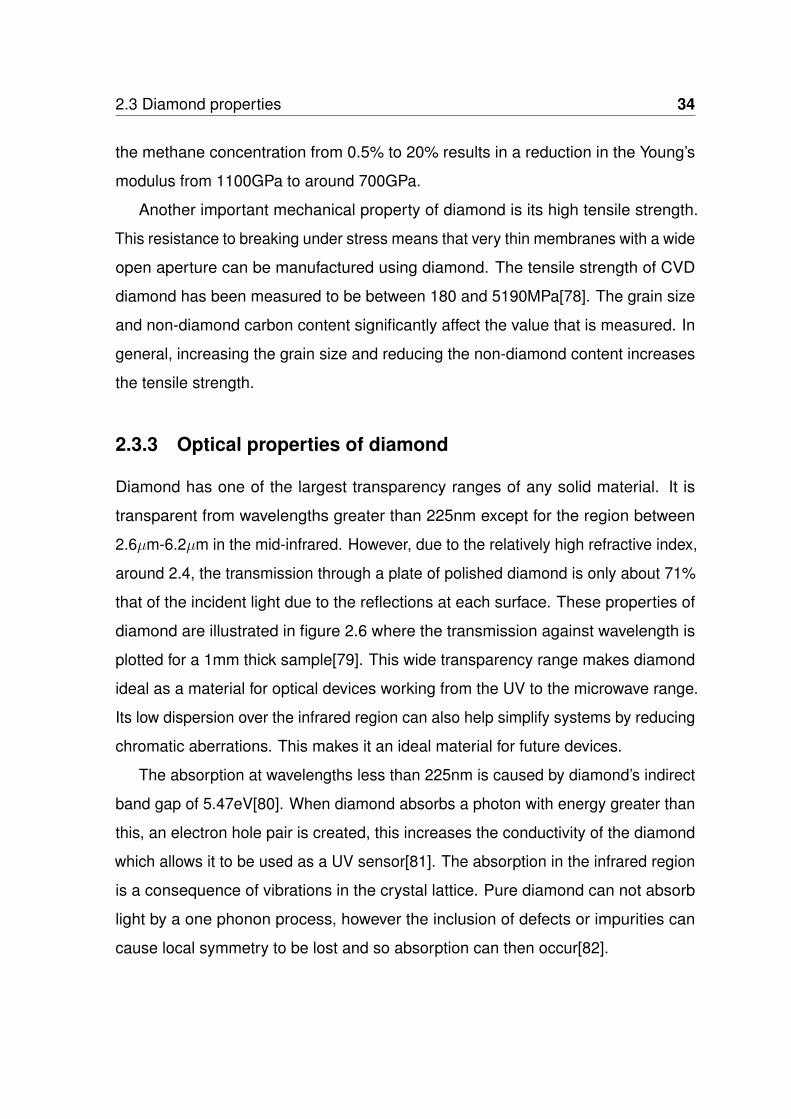
Diamond has one of the largest transparency ranges of any solid material. It is
transparent from wavelengths greater than 225nm except for the region between
2.6µm-6.2µm in the mid-infrared. However, due to the relatively high refractive index,
around 2.4, the transmission through a plate of polished diamond is only about 71%
that of the incident light due to the reflections at each surface. These properties of
diamond are illustrated in figure 2.6 where the transmission against wavelength is
plotted for a 1mm thick sample[79]. This wide transparency range makes diamond
ideal as a material for optical devices working from the UV to the microwave range.
Its low dispersion over the infrared region can also help simplify systems by reducing
chromatic aberrations. This makes it an ideal material for future devices.
The absorption at wavelengths less than 225nm is caused by diamond’s indirect
band gap of 5.47eV[80]. When diamond absorbs a photon with energy greater than
this, an electron hole pair is created, this increases the conductivity of the diamond
which allows it to be used as a UV sensor[81]. The absorption in the infrared region
is a consequence of vibrations in the crystal lattice. Pure diamond can not absorb
light by a one phonon process, however the inclusion of defects or impurities can
cause local symmetry to be lost and so absorption can then occur[82].

2.3 Diamond properties 35
Impurities in diamond can have a significant effect on the optical properties,
causing the colour to change[83, 84]. For example, the absorption of light in different
regions of the visible spectrum causes lightly boron doped diamond to be slightly
blue and light nitrogen doping can make it slightly yellow. Heavy boron doping can
even make the diamond opaque[85]. Additional absorption in the infrared can also
be observed, for example, type I diamonds have an absorption band in the infrared
between 8 and 13µm[86].
Fig. 2.6 Transmission spectra for a 1.0mm optical grade CVD diamond window. Dataadapted from reference [79]. The data has not been corrected for reflection losses.
A key parameter in the design of an optical system is the optical dispersion
properties of the materials it contains. This is a wavelength dependent property
and is responsible for splitting light of different colours through uncorrected lenses
and prisms. The refractive index of diamond is plotted in figure 2.7 from 225nm
up to 10µm. The dispersion properties of diamond are usually modelled using
the Sellmeier equation, which is a semi-empirical model first proposed in 1871[87].
It is not easily applied when modelling semiconductors or metals and it was an

2.3 Diamond properties 36
improvement on modelling the dispersion over a wider wavelength range than a
previously used model, the Cauchy model.
The Sellmeier equation is given in its most general form in equation 2.3, where
the wavelength, λ and constant, Ci have units of nm.
n2(λ) = 1 +∑i
Biλ2
λ2 − Ci
(2.3)
For diamond, the formula reduces to equation 2.4[88], however, other values
for Bi have been proposed[89]. The coefficients are found by fitting the equations
to experimental data, however the refractive index in reference[89] only includes
one term in the summation and was only fitted up to the short wave infrared. In the
following work, equation 2.4 will be used since in later chapters, the long wavelength
infrared region will also be of interest.
n2(λ) = 1 +0.3306λ2
λ2 − 175.02+
4.3356λ2
λ2 − 106.02(2.4)
Studies of the refractive index of CVD grown diamond have found that it can
be different to natural diamond[92]. Yin et al. found that increasing the CH4/H2
ratio during diamond growth causes the refractive index of the resulting film to
decrease[93]. While Potocky et al. measured a refractive index of 2.34, which was
independent of the substrate temperature used when growing the diamond[94]. The
lower refractive index than would be expected for natural diamond can be explained
using an effective medium approximation. The refractive index of the non-diamond
carbon is lower than that of diamond with a value that depends on its bonding and
whether it is hydrogenated, with studies measuring values ranging around 1.6-1.8 at
800nm[93]. Hence, as the fraction of non-diamond carbon increases the refractive
index of NCD decreases. Additionally, the inclusion of too much sp2 bonded carbon
can cause greater absorption of light, which could be detrimental when used in high
power systems.

2.3 Diamond properties 37
Fig. 2.7 Refractive index of diamond from multiple sources[88, 90, 91]. The sharpincrease in the refractive index below roughly 300nm is due to the presence of anelectronic transition at around 225nm.

2.3 Diamond properties 38
In summary, the material properties of diamond are highly dependent on the
conditions used during synthesis. For this thesis a high transparency is required
and so the optical properties are the most important to optimise. This requires that
the films are smooth to reduce scattering and also that there is a low fraction of sp2
bonded carbon.

Chapter 3
Experimental Methods
This chapter details the experimental methods that will be used throughout this
thesis and focuses on the generic techniques that are commonly used for fabrication
and characterisation of thin films. Experimental methods which are specific to this
thesis, where measuring systems have been specifically designed for this research
are discussed in later chapters.
3.1 Fabrication
3.1.1 Diamond growth by chemical vapour deposition
Diamond can be grown at low pressures (under 200 torr) using microwave plasma
enhanced chemical vapour deposition. A typical reactor type is shown in figure 3.1,
which shows a cross section of the inside of reactor, including a moveable stage
and microwave waveguides. Samples are typically held within a molybdenum holder
that is placed on a water cooled stage. Microwave power enters from the top of the
chamber and a plasma is formed in the lower pressure area below a quartz window
and above the substrate. The temperature is measured using a Williamson dual
wavelength pyrometer which is able to measure the temperature of the surface of the
sample through the plasma[95]. Additionally, the pyrometer can be used to measure

3.1 Fabrication 40
in situ growth rates by interference caused by the growing film and observing the
period of the signal.
In order to grow nanocrystalline diamond a substrate, typically silicon or quartz
is first coated with nanodiamonds (NDs), which can be achieved by sonicating the
substrate in a solution of NDs. The small 5-10nm particles adhere to the substrate
and provide the seed crystals, which act as nucleation sites for diamond to grow
from. The NDs attach to the substrate via van de Waals forces and can be removed
by lightly scraping the surface, so care is required while handling the samples.
Growing optical quality diamond requires that the methane concentration in the
plasma is low and high seeding densities are required in order for the nucleation
surface to have an optical finish. If the methane concentration is too high, then
renucleation takes places. As shown previously in figure 2.2 the average seed size
is smaller if the NCD is allowed to renucleate which also increases the sp2 fraction,
reducing the transparency of the diamond. Lowering the methane concentration or
reducing the pressure can also decrease the growth rate[96].
3.1.2 Sputtering
Sputter deposition is a process where a thin film can be deposited by bombarding
a target with high energy ions and subsequently directing the ejected particles
towards a substrate. Sputtering of the target can be achieved by either using a
direct current (DC) or radio frequency (RF) power source to excite a plasma. In
DC plasmas the cathode voltage is typically in the range -300 to -600V leading to
high average energies of the sputtered atoms[97]. An RF source is required when
the target is insulating in order to stop charging the target’s surface. Typically an
argon atmosphere is used as it is inert and so will not react with the target, however,
reactive sputtering can also be performed by including other gases.
In order to increase the sputtering rate, a high density of ions needs to be pro-
duced, this can be achieved by raising the pressure. However, increasing the number
of gas ions increases the scattering of the sputtered atoms away from the substrate

3.1 Fabrication 41
Fig. 3.1 Drawing of a commercial diamond growth reactor, ASTEX PDS-18, usedfor the growth of diamond films in this thesis. 2.45GHz microwaves enter through awaveguide at the top right of the chamber and are directed into the chamber wherea hydrogen/methane plasma forms which deposits diamond. Microwave powers upto 5kW are available in this system.

3.2 Characterisation 42
and so can reduce the deposition rate. The mass of the atoms also affects how
much they are scattered, with heavier atoms scattering less. Therefore, in a target
containing more than one element, the deposited film will contain less of the lighter
element. The addition of a reactive gas, for example oxygen if you are depositing
from an oxide target, can be used to alter the stoichiometry of the deposited film[98].
The resulting films mostly have a columnar structure and the presence of voids can
be reduced by choosing appropriate deposition parameters[99].
One method to increase the density of ions close to the target is to apply a
magnetic field in that region[100]. This is called magnetron sputtering and it allows
the plasma to be kept further away from the substrate. Figure 3.2 shows the
arrangement that is typical for a sputtering system. It is common to hold the substrate
upside down so particles in the chamber do not fall onto it. The sputtering gases are
continuously fed into the chamber and pumped out at a rate that keeps the pressure
constant.
The deposition rate can be measured in situ by numerous methods such as a
quartz film thickness monitor crystal or a sample could be measured ex situ and the
deposition rate for the process parameters used to calculate the deposition rate.
3.2 Characterisation
3.2.1 Ultraviolet-visible spectroscopy
Knowledge of the transmission through a sample is necessary in order to construct
any optical system. Ultraviolet-visible spectroscopy can be used to measure the
transmission windows of optical components. In this work it will be used to test the
optical transparency of thin membranes which have a transmission that is dependant
on the deposition conditions used during fabrication.
Light incident on a material can undergo numerous processes including refraction,
absorption, scattering and luminescence. Refraction causes the ray to bend as the

3.2 Characterisation 43
Fig. 3.2 Sputtering of a thin film involves generating a plasma above a sputteringtarget and then directing the ejected particles towards a substrate. The substrate isrotated in order to increase the uniformity of the film and the gases are injected nextto the target.
light velocity is changed and absorption causes the light intensity to be attenuated.
Absorption occurs when the photon energy equals that of an energy transition in the
material. Scattering causes the direction of light to deviate from its initial trajectory in
many different directions and it can attenuate the measured transmitted light. It can
be either elastic if the energy of the photon is unchanged or inelastic if the energy
does change. Luminescence involves light being spontaneously emitted from an
excited atom in all directions, usually with a different energy. These processes are
highly dependent on the wavelength of the incident light. Figure 3.3 demonstrates
the processes involved when light is incident onto a material.
Ultraviolet-visible spectroscopy (UV-Vis) measures the transmission, reflectance
and absorption of light from a sample in the ultraviolet and visible spectrum. This
region is dominated by electronic transitions and so this technique can be used to
find the band gap of materials. The wavelengths the sample absorb affects what
colour the sample appears and it can be used to measure reaction rates for solutions

3.2 Characterisation 44
that change colour. Multiple light sources (typically a deuterium or tungsten lamp)
are required to cover the whole ultra violet and visible range and to increase the
signal to noise ratio[101].
The attenuation of light travelling through a sample can be described by the
Beer-Lambert law[102], equation 3.1. Where I0 is the incident light intensity, I(z) is
the transmitted intensity, α is the absorption coefficient and z is the distance the light
has travelled through the sample.
I(z) = I0e−αz (3.1)
Fig. 3.3 Processes involved when light is incident onto a material. Reflection occursdue to a difference in refractive index at an interface. There are two interfaces in thediagram where reflection can take place, only the first reflection is shown for clarity.Scattering can occur due to surface roughness and differences in refractive index,which can be caused by temperature differences or non-uniform materials. Emissionresults from the light first being absorbed into the sample and re-emitted in a randomdirection. The wavelength of light can also change during this process.

3.2 Characterisation 45
3.2.2 Raman spectroscopy
Gaining information about the composition of a sample can be achieved in several
ways. Techniques such as mass spectroscopy and x-ray photoelectron spectroscopy
can give you information about the elemental composition of a sample, however, for
the devices fabricated in this work the elemental composition is already known. What
is unknown is the bonding that exists between the atoms. Since the bonding in the
samples are optically active, they can be probed by several optical techniques. The
techniques used in this work will be Raman and photoluminescence spectroscopy
which can be used to work out the bonding structure in the sample. Raman spec-
troscopy is partially useful as it can be used to measure the amount of sp2 or sp3
carbon present. In this work a Renishaw inVia Raman microscope was used with a
532nmm wavelength.
When light is incident on a molecule, the molecule can be excited into a virtual
short lived energy state. When the photon is emitted the sample can either return
to the energy level it originally had, which is called Rayleigh scattering or it can
inelastically scatter, which is called Raman scattering[103]. If the molecule is pro-
moted to a higher energy state this is called Stokes scattering and if it is reduced it is
called anti-Stokes scattering. Anti-Stokes scattering can occur due to the molecule
having thermal energy and hence some molecules will be in an excited state, at
room temperature it is expected that Stokes scattering will produce a larger response
than anti-Stokes. However, as the temperature increases anti-Stokes scattering will
increase relative to Stokes scattering, for most cases when taking measurements
only the Stokes scattering is recorded as it provides a better signal to noise ratio.
Figure 3.4 shows how Raman spectroscopy involves an indirect transition be-
tween vibrational energy states via a virtual state, whereas infrared absorption
involves a direct transition. Therefore, the wavelength of light used to excite the
molecule is typically in the UV to near infrared region and so the energy differ-
ence between the energy states of the molecule is given by the difference between
the wavelength of the incident laser and the Raman scattered light. The intensity

3.2 Characterisation 46
of the scattered light is proportional to the fourth power of the frequency of light
used[104]. The units typically used when plotting data are wavenumbers, cm−1,
which represents the shift from the incident photon energy.
In order to measure the Raman spectrum, a laser is focused onto a material and
the resulting scattered light is observed. The scattered light is first filtered to remove
the intense wavelength corresponding to the Rayleigh scattered light and then it’s
passed through a monochromater, which splits the light onto a detector array for
logging. This spectrum can then be used to identify the nature of the chemical bonds
in the sample. The energy of the chemical bond is related to the mass of the atoms
making the bond and the strength of the bond. Increasing the mass reduces the
frequency of the oscillation and so bonds with heavier elements are more likely to
have lower wavenumbers in the Raman spectrum.
Fig. 3.4 Processes involved during Raman scattering, adapted from [103]. Rayleighscattering is the dominant scattering process, Stokes scattering results in themolecule being promoted to a higher energy vibrational state and anti-Stokes scat-tering results in it going into a lower energy state.
3.2.3 Photoluminescence spectroscopy
Photoluminescence spectroscopy is a non-destructive technique that is used to gain
information about the electronic structure of a sample. When a photon is absorbed

3.2 Characterisation 47
by a material it can excite an electron into a higher energy state. When the electron
relaxes to a lower energy state a photon can be emitted which has a different energy
to the incident photon. The energy of the photon relates to the difference in energy
between the two electron states. The sample is usually excited with a laser and
the scattered light is then directed through a Rayleigh filter to remove the laser
wavelength. The resulting spectra is then passed through a monochromator and the
intensity measured on a detector[102].
Photoluminescence spectroscopy can be used to determine a number of proper-
ties such as the band gap, the presence of impurities or defects and the recombina-
tion mechanisms. Figure 3.5 shows a simplified diagram of the processes that occur
during photoluminescence.
Fig. 3.5 A photon with energy greater than the band gap is absorbed and excitesan electron into the conduction band leaving a hole in the valence band. Theelectron then relaxes, by a series of non-radiative transitions(light grey arrows)before recombining by emission of a photon with a lower energy. The horizontallines represent the energy states in the valence(bottom) and conduction(top) bands.
3.2.4 Atomic force microscopy (AFM)
Measuring the surface roughness of a sample is important for optical application
since it causes optical scattering. High roughness can have a detrimental effect on

3.2 Characterisation 48
the measured optical transmission spectra since a proportion of the light is scattered
away from the detector. Measuring the surface roughness will be achieved in this
work using a Bruker Dimension Icon AFM.
AFM is an experimental technique used to study the shape of a surface by
measuring the surface height over an area. This is achieved by bringing a very
sharp tip which is attached to the end of a cantilever very close to a sample. As
the tip is moved across the sample, the cantilever is bent upwards or downwards,
following the profile of the sample. The bending is measured by illuminating the
back of the cantilever with a laser beam and directing the reflected light onto a quad
photodiode, which can determine the movement of the cantilever. This is achieved
by measuring the difference in the signal intensity between the four photodetector
elements which can be used to calculate the deflection of the cantilever or the torsion
in the cantilever[105]. Since samples will usually have some tilt, AFMs employ a
feedback loop that controls the height of the cantilever to keep the pressing force
roughly constant, this is achieved using a scanner piezo tube[106].
AFMs usually work in either contact or tapping mode. In contact mode, the tip is
in contact or close proximity with the sample with either a constant or variable force.
It is then rastered across the sample to form the image. Tapping mode involves
vibrating the cantilever near its fundamental resonance frequency, with many cycles
occurring per pixel location, a time averaged interaction can then be determined.
Electrostatic forces from the sample cause the amplitude to change, the height of
the tip is then adjusted in order to keep the amplitude constant. Tapping mode is
commonly used when the sample is soft or does not adhere well to the substrate
(such as nanodiamonds seeded onto silicon).
The forces involved between the tip and the sample are a combination of van
der Waals and electrostatic forces. Van de Waals forces depend on the distance
between the interfaces with the interaction force being repulsive when they are
very close together and an attractive force when the separation increases past a
certain point. The magnitude of the force drops sharply with distance and is weak in

3.2 Characterisation 49
Fig. 3.6 AFM uses a cantilever with a very sharp tip on the end to scan across asample while keeping the distance or force constant to map the topography. Thedeflection of the cantilever is calculated by measuring the deflection of a laser spotreflected off the back of the cantilever onto a split 2 by 2 photodetector array.
comparison to the strength of chemical bonds. Electrostatic forces can arise when
the substrate or tip is insulating and so a charge can be present on the surface
or if they are conducting and a voltage is applied. This can result in longer range
interactions than van de Waals forces.
The initial image data received from taking measurements usually requires some
postprocessing to produce meaningful information. This includes accounting for
tilts in the sample or a curvature that is regularly induced during film deposition.
Additionally, the angles on the AFM tips limit the aspect ratio that can be measured
for deep trenches or hills and it can be a problem when imaging nanodiamonds
seeded on silicon[60].
The surface roughness of an AFM image is usually calculated using a deviation
from the mean height of a sample. Two common methods[107] for describing the
surface roughness are the arithmetic average height(Ra), equation 3.2 and the root
mean square roughness(Rq), equation 3.3,

3.2 Characterisation 50
Ra =1
n
n∑i=1
|yi| (3.2)
Rq =
√√√√ 1
n
n∑i=1
y2i (3.3)
where yi is the height deviation from the arithmetic mean and n is the number of
height measurements made.
3.2.5 Stylus profilometry
A profilometer is a device that is used to measure the surface profile of a sample.
Numerous types of profilometer exist with varying methods used to measure to-
pography, one such example is a white light interferometer. In this thesis a stylus
profilometer will be used which works in a similar way to an AFM. A sharp stylus is
moved in contact across a sample and the displacement of the stylus is measured
and used to work out the height of the sample across a scan line.
This allows for a non-optical method to measure the thickness of a thin film
coating. In this work, a Dektak XT surface profiler is used to measure the thickness
of several nanocrystalline samples where a portion of the nanodiamond seeds on
the substrate are removed before growth, creating a step that the stylus can scan
over.
3.2.6 Spectroscopic ellipsometry
Measuring the thickness of a film can be achieved using a Stylus profilometer
however this requires a step in the coating. In this work, ellipsometry will also be
used to measure the thickness of a thin film non-destructively. The results presented
in this work were taken using a Horiba MM-16 and additionally a Semilab SE-2000
which was used to measure the change in phase on transmission through the

3.2 Characterisation 51
samples. Measuring the phase change is important for the creation of non-polarising
beam splitters.
Ellipsometry measures how the polarisation state of light changes when it is
reflected off a sample. This reflected light is usually elliptically polarised, which is
where the name originates from. The results of measuring the change in polarisation
can be used to fit properties such as the refractive index, layer thickness and compo-
sition to a model. As ellipsometry is an indirect technique, careful consideration is
needed in choosing the model and prior information about the nature of the sample
is required. Additionally, it is a fast and non-destructive technique and since it only
relies on the ratio of light intensities it does not require a reference beam as in
UV-Vis.
The value that is directly measured during ellipsometry is the amplitude ratio
tan(Ψ) and phase difference ∆ between the s and p polarisations of light as in
equation 3.4, the measurement is performed typically over a range of wavelengths
from the ultraviolet to infrared region.
ρ =rprs
= tan(Ψ)ei∆ (3.4)
Ellipsometry requires that the sample to be measured is relatively flat, typically
surface roughness needs to be less than 30% of the wavelength of light used,
otherwise the light is depolarised significantly. Measurements are usually taken at
an incident angle between 70-80° which maximises the signal[108].
There are several different configurations for an ellipsometer, with some rotating
the analyser and others rotating the polariser or the modulator if present. Modern
ellipsometers allow measurements to be taken over the whole wavelength spectrum
at the same time by using a holographic diffraction grating on the output head to split
the incident light, this allows for real time measurements of processes.

3.2 Characterisation 52
Fig. 3.7 A typical configuration of an ellipsometer is shown. Unpolarised broadbandlight is first polarised and directed at the sample. It is reflected off the sampleand then it goes through a modulator and analyser. The light is then split by amonochromator onto a detector. The data can then be collected and analysed.
3.2.7 Scanning electron microscopy(SEM)
Scanning electron microscopy is used to image the surface of a sample to a res-
olution far exceeding that which can be measured optically. In this work, it will be
used to image the surface of nanocrystalline diamond and sputtered zinc oxide thin
films. The resolution that can be achieved can be used to measure crystal sizes
and also to see the columnar structures that are common with sputtering and CVD
growths. The SEM images that are displayed in this work where taken using a Carl
Zeiss XB1540 microscope.
Scanning electron microscopes map a sample by focussing a beam of electrons
onto its surface and then raster scanning across it. The electrons interact with
the sample and its response is measured. The basic components in a SEM are
firstly an electron gun made of either a tungsten filament or LaB6 cathode which
produce electrons by thermionic emission. These electrons are then accelerated to
an energy up to tens of kiloelectron volts. This beam is then focussed by a series
of electrostatic lenses and positioned onto the sample by further scan coils. This
is typically performed under high vacuum in order to minimise scattering of the
electrons.

3.2 Characterisation 53
SEMs can image under several different modes of operation. Secondary electron
imaging involves measuring the emitted electrons with energies below 50eV. Their
low energy means that the electrons can only travel short distances in the sample
of less than 10nm. Secondary electrons generated deeper than this are usually
trapped within the material hence this mode of operation images the region just
below the surface of the sample. The secondary electrons contain information about
the surface topography and chemistry of the sample and can produce images with a
resolution below 1nm. It is possible to visualise the topography of a sample because
the yield of secondary electrons is dependent on the angle between the incident
beam and the surface. Areas with a large angle between the incident beam and the
surface normal tend to be brighter as do surfaces that face towards the detector[109].
A second mode of imaging is to measure the backscattered electrons which
are defined as electrons that are emitted from the sample with an energy greater
than 50eV, they are either reflected or backscattered from the sample. The yield
of backscattered electrons increases with the atomic number of the atoms in the
sample and so the brightness of the image is dependent on the element being
imaged. This means it can be used to quickly identify regions with a high and a low
atomic number.
When using an SEM to image a sample, artefacts from the imaging process need
to be taken into account. These artefacts occur due to charging of the sample and
damage to the sample from the electron beam. Environmental SEMs exist which
operate at a higher pressure which are useful for samples that charge while being
imaged[110]. It is also common to sputter coat samples with a thin layer of gold in
order to stop electrostatic charges from building up.

Chapter 4
Diamond Growth and Dielectric
Colour
4.1 Introduction
Having an accurate measurement of the thickness of a thin film is important for
applications involving optical coatings, where small errors in the thickness can cause
significant changes in the transmission properties. Several methods exist that can
accurately measure thin film thicknesses, ellipsometry is an example of such a
characterisation technique. Ellipsometry requires a suitable model to fit to the data
since it does not measure the thickness directly, meaning a lot of information needs
to be known about the sample before it can be used appropriately. For example initial
guesses are required about the layer structure, the refractive index of the materials
and the thicknesses of the films. The fitting can either be performed using a known
refractive index from other experimental data or it can be modelled using a function
such as the Cauchy or Sellmeier dispersion formula.
Numerous papers have demonstrated ellipsometry models for diamond films
grown by CVD[111–113]. Different layer structures have been considered, however,
complications arise due to the unknown composition of the film which is highly
dependent on the grain size and the non-diamond content. Additionally, it has been

4.1 Introduction 55
reported that a SiC layer forms at the interface between the silicon and the diamond
during growth by bias enhanced nucleation which can be around 9nm thick[114].
Producing a suitable model is further complicated by the surface roughness of the
film. This is usually treated by incorporating a layer that uses an effective medium
approximation (EMA) [115], where a fraction of the layer is diamond and the other
air. Figure 4.1 shows an example of such a layer structure. The bulk of the film can
have a varying fraction of diamond and non diamond carbon which depends on the
growth conditions, this layer can also be treated using an EMA between the two
components.
Another method that is commonly used to determine the thickness of a thin
film is by measuring the light intensity reflected from the film. If the film is thin then
regression analysis can be used to fit a model to the spectrum. If the film is thick then
fast Fourier transformation (FFT) analysis can be performed. At least one complete
oscillation is required to use the FFT method, therefore the minimum thickness, dmin,
of a single film it can measure is given by
dmin =1
2((n(λmin)/λmin)− (n(λmax)/λmax))(4.1)
where n(λ) is the refractive index at wavelength λ[116].
Complications arise when using this method if the incidence angle is not 0° since
the polarisation state changes on reflection and so it must be accounted for in the
model. Consequentially, if a microscope is used to focus the light onto the sample,
the aperture angle needs to be known, since the incident angle will not be normal to
the sample[117].
A more qualitative approach that can give a good approximation for the thickness
of a thin film of material of order 100nm is by observing its colour. This method is only
suitable for films that are transparent over a significant portion of the visible spectrum
as it relies on optical interference to produce the observed colour. An advantage
of using this technique is that it provides a quick and non-destructive method of
estimating film thickness without the need for expensive equipment such as an

4.2 Calculating film reflectance and transmittance 56
Fig. 4.1 A typical layer model for diamond grown by CVD on silicon is given by asurface roughness layer, a bulk region of nanocrystalline diamond, a layer of SiCand the silicon substrate. The bulk region contains a mixture of diamond and sp2
carbon. More complicated models that include a layer of silicon oxide at the siliconinterface have also been considered.
ellipsometer. However, it does suffer from the same problems that ellipsometers
have and requires a significant amount of prior information about the film and
the source of illumination. Additionally, the spacial resolution on many common
ellipsometers can be poor since it is limited by the spot size of the beam, which can
be a couple millimetres in diameter. Therefore, if the thickness of a sample varies
too quickly, observing the colour can provide more accurate results. The aim of this
chapter is to develop a suitable model to calculate the expected colour that would be
observed for a variety of layer structures. This will then be used to explain results
that are observed in later chapters.
4.2 Calculating film reflectance and transmittance
In order to find the perceived colour of a thin film, the fraction of light reflected, as
a function of its wavelength, needs to be calculated. For a multilayer stack this is
achieved by first calculating the Fresnel equations at each boundary for the two

4.2 Calculating film reflectance and transmittance 57
polarisation states. The equations are dependent on the complex refractive index
of the materials and angles the light travels through it. Throughout this thesis the
complex refractive index, nj, will be defined as in equation 4.2
nj(λ) = nj(λ)− ikj(λ) (4.2)
where nj and kj are the real and imaginary parts of the refractive index. The
Fresnel reflection coefficients[118] for the s and p polarised light between layers j
and j − 1 are then given by equations 4.3 and 4.4
rjs =nj−1cos(ϕj−1)− njcos(ϕj)
nj−1cos(ϕj−1) + njcos(ϕj)(4.3)
rjp =njcos(ϕj−1)− nj−1cos(ϕj)
njcos(ϕj−1) + nj−1cos(ϕj)(4.4)
where ϕj are the complex angles of incidence for layer j. These angles are
determined using Snell’s law, as shown in equation 4.5, for all layers j.
n0sin(ϕ0) = njsin(ϕj) (4.5)
In order to determine the reflection and transmission properties of a sample,
first a model needs to be constructed of the layers and the refractive indices of the
materials. For complex multilayer stacks (a typical broadband antireflection coating
can have 10-20 layers) of more than two layers, adding the reflections from each
layer becomes impractical. Figure 4.2 shows the case of an m layer coating on
a substrate where only the first few reflections are shown, but it can be seen that
it becomes increasingly complex as additional layers are added. Using a matrix
approach reduces the complexity and makes it easy to increase the number of layers.
There are numerous methods that can be used to create a model, here the matrix
method of Hayfield and White[119] which was later expanded upon by Azzam and
Bashara will be used[120].
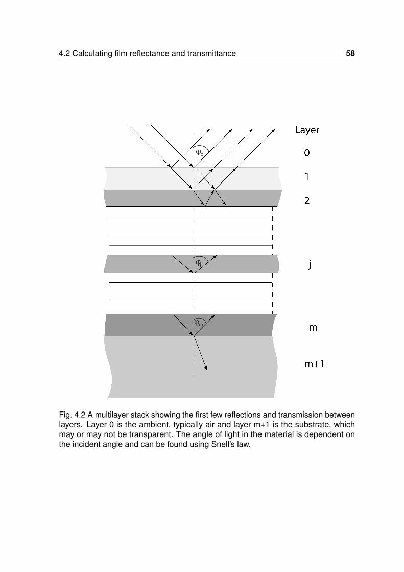
4.2 Calculating film reflectance and transmittance 58
Fig. 4.2 A multilayer stack showing the first few reflections and transmission betweenlayers. Layer 0 is the ambient, typically air and layer m+1 is the substrate, whichmay or may not be transparent. The angle of light in the material is dependent onthe incident angle and can be found using Snell’s law.

4.2 Calculating film reflectance and transmittance 59
Firstly, it is assumed that every material is homogeneous and isotropic and that
the incident light is monochromatic and either s or p polarised. The light travelling
through the multilayer stack between two planes parallel to the layers can then be
related by a 2× 2 matrix. If you choose to locate the two planes to lie an infinitesimal
distance on either side of a boundary, then the resulting matrix that describes the
transition at the interface is given by equation 4.6. If you locate the two planes on
the boundaries at either end of one layer then the resulting matrix is given by 4.8.
Where β is the phase thickness of the layer, d is the thickness, λ is the wavelength
and ϕj is the angle in that layer that is calculated using Snell’s law. rab and tab are
the Fresnel reflection and transmission coefficients at the ab interface respectively.
Iab = (1/tab)
1 rab
rab 1
(4.6)
β =2πdn
λcos(ϕj) (4.7)
L =
eiβ 0
0 e−iβ
(4.8)
For a stack with N layers, the scattering matrix is found by multiplying the matrices
for all interfaces and propagation through the sample in order as in equation 4.9.
S =
(m∏i=1
Ij−1,jLj
)Im+1 (4.9)
For a one layer stack, which is relevant to the following discussion, this reduces
to
S = I01L1I12 (4.10)

4.2 Calculating film reflectance and transmittance 60
The complex Fresnel reflection and transmission coefficients for the entire stack
can then be found from equations 4.11 - 4.14, where the numbers e.g. S21s etc. are
given by the elements in the matrix S for the respective polarisations.
rs =S21s
S11s
(4.11)
rp =S21p
S11p
(4.12)
ts =1
S11s
(4.13)
tp =1
S11p
(4.14)
Using the equations above the reflectance and transmittance can be calculated
for a single layer film on a substrate
R =r01 + r12e
−i2β
1 + r01r12e−i2β(4.15)
T =t01t12e
−iβ
1 + r01r12e−i2β(4.16)
Equation 4.15 has a simple solution if the thickness of the layer is a quarter
optical thickness of the incident light at normal incidence. This will be the subject of a
subsequent chapter where this result is used to produce a double layer antireflection
coating.
The results above also can be used to calculate the parameters that are measured
when performing ellipsometry in either reflection or transmission as described in
equations 4.17 and 4.18.
ρr =rprs
(4.17)

4.2 Calculating film reflectance and transmittance 61
ρt =tpts
(4.18)
4.2.1 Colour in optical coatings
The colour observed in a thin film is caused by interference effects which enhances
or reduces the amount of light that is reflected or transmitted. To predict the colour
observed, a number of factors such as the spectrum of the light source that is used,
the viewing angle, the refractive index of the materials and the layer structure need
to be known.
Fig. 4.3 The emission spectra of one of the fluorescent lamps located in the labora-tory, measured using an Ocean Optics HR2000+ high resolution spectrometer.
Since the films are in general not luminescent an external source of light is
required and so the colour of the film is highly dependent on this illumination source.
Figure 4.3 shows the emission spectrum of a fluorescent lamp, which is in common
use to light research laboratories and so is the most useful illumination source for
this analysis. As can be seen, there are several peaks, which are dependent on the

4.2 Calculating film reflectance and transmittance 62
type of phosphor used to coat the inside of the glass tube[121]. In comparison an
incandescent lamp exhibits a broad spectrum where the peak intensity is dependent
on the temperature of the filament.
An important consideration for determining the perceived colour is the response
of the human eye to different wavelengths of light. Colour is a human response that
relies on the eye’s reaction to the wavelengths of light, this can differ depending on the
individual. The human eye has three types of cone cells that have a peak sensitivity
in different parts of the visible spectrum and are responsible for distinguishing colours.
These cone cell are called the S, M and L for the short, middle and long wavelengths
of light respectively[122]. A consequence of only having three colour sensors is that
two light sources, which have different spectral power distributions, can appear the
same colour.
The procedure used in this thesis to determine the colour of a thin film will be
the same as that outlined by Henrie et al.[123]. They calculated the expected colour
of silicon nitride and silicon oxide films on silicon for different film thicknesses. In
order to calculate the perceived colour, the reflected intensity needs to be calculated
as a function of wavelength and then the response of the eye and the incident light
wavelength spectrum taken into account. This is achieved by applying the CIE colour
matching functions[124] in order to find the XYZ parameters shown in equations
4.19, 4.20 and 4.21. The CIE colour space provides a relationship between the
wavelengths in the visible spectrum and the colour that the human eye perceives.
The CIE colour spectrum defines Y as the luminance and is closely related to the
sensitivity of the M cone which is perceived as green. The Z parameter is related to
the S cone or a blue response and the X parameter is a linear combination of the
response from all the cones.
X =
∫ ∞
0
R(λ)P0PiXλ(λ)dλ (4.19)

4.2 Calculating film reflectance and transmittance 63
Fig. 4.4 The CIE XYZ colour space functions, data taken from the CIE 1964 XYZcolour space[124].
Y =
∫ ∞
0
R(λ)P0PiYλ(λ)dλ (4.20)
Z =
∫ ∞
0
R(λ)P0PiZλ(λ)dλ (4.21)
R(λ) is the reflected intensity, P0 is the total incident power, Pi is the spectrum of
the incident light source and Xλ(λ), Yλ(λ) and Zλ(λ) are the CIE colour matching
functions. Figure 4.4 shows a plot of the spectral sensitivity of the CIE colour
matching functions against wavelength, which are used to calculate the three X,Y
and Z parameters. In order to display colours suitable for RGB monitors, the XYZ
parameters need to be converted into RGB parameters, this is achieved using a set
of linear equations given by

4.3 Determining thickness of diamond using colour 64
R′
G′
B′
= M
X
Y
Z
(4.22)
where M is a 3×3 matrix that depends on the RGB working space and reference
white, here we will be using the sRGB colour space, therefore
M =
3.2406 −1.5372 −0.4986
−0.9689 1.8758 0.0415
0.0557 −0.2040 1.0570
(4.23)
These values need to be scaled by the display gamma given by equation 4.24,
for p = R’, G’ or B’[125]. This transformation can lead to values that are less than
zero or greater than one. This is due to some colours, present in the XYZ space, not
being present in the RGB colour space. In order to account for this any values below
0 are set equal to 0 and those above 1 are set to 1.
pRGB =
12.92p, p<=0.00313.
1.055p1/2.4 − 0.055, p>0.00313.(4.24)
4.3 Determining thickness of diamond using colour
There are several advantages of using the colour of a thin film to measure its
thickness. One significant advantage is that the cost is minimal as it requires no
special hardware. A second advantage over other methods such as ellipsometry is
that the spatial resolution can be much higher. The spot size on many ellipsometers
can be several millimetres in size and hence the film needs to have a uniform
thickness over the area measured for the results to be reliable. Many ellipsometers
can measure very small spot sizes (less than 30µm[126]), however, this is usually
achieved using focusing optics which causes the beam of light to no longer hit the
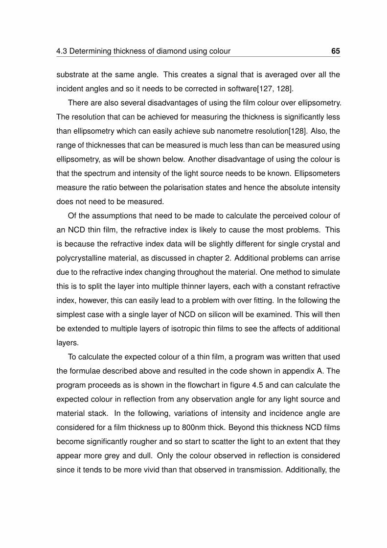
4.3 Determining thickness of diamond using colour 65
substrate at the same angle. This creates a signal that is averaged over all the
incident angles and so it needs to be corrected in software[127, 128].
There are also several disadvantages of using the film colour over ellipsometry.
The resolution that can be achieved for measuring the thickness is significantly less
than ellipsometry which can easily achieve sub nanometre resolution[128]. Also, the
range of thicknesses that can be measured is much less than can be measured using
ellipsometry, as will be shown below. Another disadvantage of using the colour is
that the spectrum and intensity of the light source needs to be known. Ellipsometers
measure the ratio between the polarisation states and hence the absolute intensity
does not need to be measured.
Of the assumptions that need to be made to calculate the perceived colour of
an NCD thin film, the refractive index is likely to cause the most problems. This
is because the refractive index data will be slightly different for single crystal and
polycrystalline material, as discussed in chapter 2. Additional problems can arrise
due to the refractive index changing throughout the material. One method to simulate
this is to split the layer into multiple thinner layers, each with a constant refractive
index, however, this can easily lead to a problem with over fitting. In the following the
simplest case with a single layer of NCD on silicon will be examined. This will then
be extended to multiple layers of isotropic thin films to see the affects of additional
layers.
To calculate the expected colour of a thin film, a program was written that used
the formulae described above and resulted in the code shown in appendix A. The
program proceeds as is shown in the flowchart in figure 4.5 and can calculate the
expected colour in reflection from any observation angle for any light source and
material stack. In the following, variations of intensity and incidence angle are
considered for a film thickness up to 800nm thick. Beyond this thickness NCD films
become significantly rougher and so start to scatter the light to an extent that they
appear more grey and dull. Only the colour observed in reflection is considered
since it tends to be more vivid than that observed in transmission. Additionally, the

4.3 Determining thickness of diamond using colour 66
Fig. 4.5 A flowchart describing the process that is used to calculate the expectedcolour of a thin film stack of optically thin films. The wavelength dependence of allrelevant properties is taken account of as well as the polarisation state of the incidentlight.

4.3 Determining thickness of diamond using colour 67
reflected colour relies less on the background and it does not require the use of a
transparent substrate so is more useful in a laboratory environment.
Figure 4.6 shows the results of changing the thickness of a diamond film on
silicon against the intensity of the light source. The angle of incidence was chosen to
equal 0° making the s and p polarisations indistinguishable. However, experimentally
observing the colour at normal incidence is difficult, since the detector and light
source would need to be in the same place. The refractive index was chosen to be
equal to that of natural diamond.
Fig. 4.6 How the colour of a film of NCD on silicon varies with its thickness andthe intensity of the light source at normal incidence. At normal incidence the twopolarisation states are indistinguishable. It can also be observed that certain colourscan not be generated with a single layer of NCD such as red.
To compare the experimental results, several thin films of diamond have been
grown. To grow the films, silicon with a (100) orientation was first cleaned at 70°C
in an NH4:H2O2:H2O solution in the ratio 1:1:5. The silicon was then ultrasonicated
with hydrogen terminated mono-dispersed nanodiamond seeds in a solution and

4.3 Determining thickness of diamond using colour 68
subsequently rinsed with deionised water. The substrate was then dried and placed
into the MWPECVD system. The methane concentration was kept constant for all
samples at 1% in order to keep the fraction of sp2 carbon low and hence improve
the optical transparency. A flow rate of 400sccm was used and the microwave power
was ramped up quickly to 3200W, the pressure was also ramped up to 110 Torr
along with the power. The temperature on the substrate surface was measured using
a dual wavelength pyrometer (Williamson Pro92). This allows the measurement of
the temperature through the plasma. The temperature was measured at between
700-800°C with the variation caused by the temperature ramping up and interference
from the film effecting the reading on the pyrometer. Images of the results of these
growths can be seen in figures 4.7, 4.8 and 4.9. The process time for the first sample
was 30 minutes and the later 1 hour.
Fig. 4.7 The colours in the image suggest that the NCD gets thicker the furthertowards the edge you are from around 170nm in the centre to roughly 270nm at theedge. The size of the sample is 10mm by 10mm.
At thicknesses greater than 350nm a repeating pattern of green and pink lines
is observed, this is also observed experimentally as in figure 4.8. These fringes
are caused by the thickness of the NCD layer not being uniform. This can be
caused by an uneven temperature on the sample during diamond growth[129]. As
polycrystalline diamond grows thicker the surface becomes significantly rougher.
This causes an increase in the amount of light that is scattered and so as the film
gets thicker the colours become less visible.
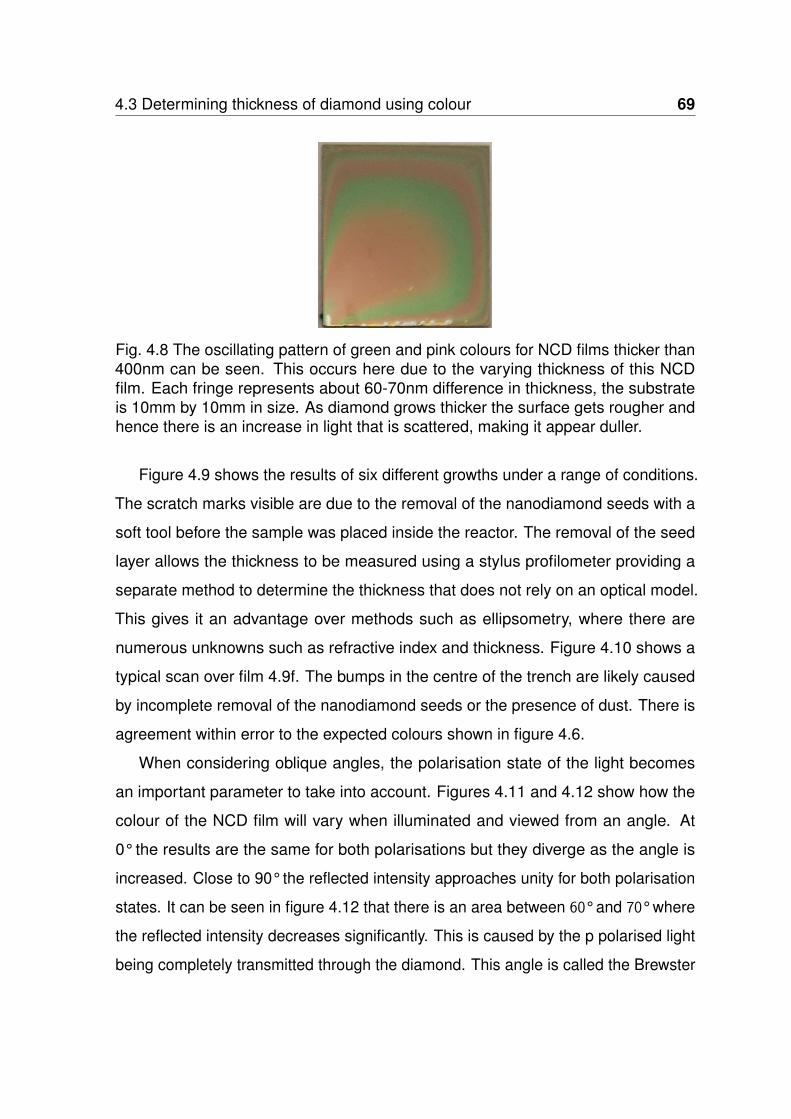
4.3 Determining thickness of diamond using colour 69
Fig. 4.8 The oscillating pattern of green and pink colours for NCD films thicker than400nm can be seen. This occurs here due to the varying thickness of this NCDfilm. Each fringe represents about 60-70nm difference in thickness, the substrateis 10mm by 10mm in size. As diamond grows thicker the surface gets rougher andhence there is an increase in light that is scattered, making it appear duller.
Figure 4.9 shows the results of six different growths under a range of conditions.
The scratch marks visible are due to the removal of the nanodiamond seeds with a
soft tool before the sample was placed inside the reactor. The removal of the seed
layer allows the thickness to be measured using a stylus profilometer providing a
separate method to determine the thickness that does not rely on an optical model.
This gives it an advantage over methods such as ellipsometry, where there are
numerous unknowns such as refractive index and thickness. Figure 4.10 shows a
typical scan over film 4.9f. The bumps in the centre of the trench are likely caused
by incomplete removal of the nanodiamond seeds or the presence of dust. There is
agreement within error to the expected colours shown in figure 4.6.
When considering oblique angles, the polarisation state of the light becomes
an important parameter to take into account. Figures 4.11 and 4.12 show how the
colour of the NCD film will vary when illuminated and viewed from an angle. At
0° the results are the same for both polarisations but they diverge as the angle is
increased. Close to 90° the reflected intensity approaches unity for both polarisation
states. It can be seen in figure 4.12 that there is an area between 60° and 70° where
the reflected intensity decreases significantly. This is caused by the p polarised light
being completely transmitted through the diamond. This angle is called the Brewster

4.3 Determining thickness of diamond using colour 70
(a) (b) (c)
(d) (e) (f)
Fig. 4.9 Illustration of how the colour depends on the film thickness of NCD on siliconof size 10mm×10mm. The scratches were made intentionally on some of the filmsby selective removal of nanodiamond seeds before deposition, in order to get asecondary estimate of the film thickness using a stylus profilometer. The resultsfrom this were for b)170±10nm d)350±20nm f)200±10nm.
Fig. 4.10 Example stylus profilometry of film 4.9f. The pit was created by selectivelyremoving the nanodiamond seed layer by lightly scratching the surface, the film wasthen grown in a CVD plasma system. Spikes in the trench are caused by incompleteremoval of nanodiamond seeds or other particles.

4.3 Determining thickness of diamond using colour 71
Fig. 4.11 Illustration of how the colour of an NCD film on silicon varies with itsthickness and the angle it is observed from in reflection. The illumination intensity iskept constant and is s polarised.
Fig. 4.12 Illustration of how the colour of an NCD film on silicon varies with itsthickness and the angle it is observed from in reflection. The illumination intensity iskept constant and is p polarised.

4.3 Determining thickness of diamond using colour 72
angle and it can be found using equation 4.25. The Brewster angle for diamond is
equal to around 67° but will vary slightly depending on the wavelength of interest.
θB = arctan
(nt
ni
)(4.25)
When a substrate is absorbing then there is also a minimum in the reflected
intensity of the p polarised light, however, it is non-zero and so is called the pseudo-
Brewster angle[130, 131].
Figure 4.13 shows the polarisation dependent reflectance against angle for three
different wavelengths in the visible spectrum for a number of NCD film thicknesses.
The reflectances were calculated using a slight modification of the program described
previously. Many of the features described for the colour charts can also be seen
in these graphs, such as the drop in the reflectivity of the p polarised light at
the Brewster angle and that the polarisation states are equivalent at 0° and 90°.
Additionally, it can be observed that the number of oscillations increases as the film
thickness increases.
In CVD grown films of diamond, the layer structure is likely to be more complicated
than that considered above and is likely to contain an additional layer at the interface
between the substrate and the diamond. Additionally, there will also be a certain
amount of surface roughness if it has not been polished. To calculate the refractive
index of the surface roughness layer an effective medium approximation can be used
[132, 133]. The fraction of each material in the EMA needs to be known which adds
another variable, making parameter fitting more difficult.
Figure 4.14 demonstrates how the colour of a several multilayer thin films varies
depending on the layer structure. The materials tested include silicon oxide, silicon
carbide below the diamond and a surface roughness layer above the diamond layer.
The surface roughness is calculated using a material fraction of half diamond and
half air. A silicon oxide layer could be present due the surface of the silicon substrate
being oxidised and a silicon carbide layer can be formed during growth.

4.3 Determining thickness of diamond using colour 73
(a) Film thickness = 50nm (b) Film thickness = 100nm
(c) Film thickness = 200nm (d) Film thickness = 300nm
(e) Film thickness = 400nm (f) Film thickness = 600nm
Fig. 4.13 How the reflected intensity of p(dotted) and s(dashed) polarised light variesfor different incident angles and wavelength on an NCD film on silicon.

4.3 Determining thickness of diamond using colour 74
Fig. 4.14 The colour that is observed is dependent on the materials and thicknessesof the layers at normal incidence. The thickness of NCD (or SiO2 for the first image)is plotted against its colour for a variety of thin film material layers. The thicknessesdisplayed above the layer structure show the values of the layers that were keptconstant. The thickness of silicon is set as infinite and only the surface roughness(S.R) is considered, the other layers are assumed to be flat.

4.4 Conclusions 75
From the chart it can be seen that the use of a SiC interface layer has less of
an affect to the film colour than SiO2 which can be attributed to its refractive index,
which is significantly more absorbing[134]. The charts demonstrate how sensitive
the colour is to a change in the layer structure around 150nm to 220nm and how the
layer structure needs to be taken account in order to reliably use this technique. A
SiO2 and SiC thickness of 50nm are shown for comparison, however thicknesses of
this magnitude are unlikely to occur during diamond growth. From these diagrams
estimates of diamond thickness to within 10nm are possible without the need of
expensive machines for films up to 350nm.
4.4 Conclusions
This chapter has laid out the theoretical background for predicting the transmission
and reflection of light from a thin film stack. It has also used this to enable the
calculation of the expected colour of these films to allow for a qualitative estimation
of the thickness of a film. Angles of observation of the film other than normal have
also been considered and it is shown that there are slight differences in the colour
with angle for the different polarisations of light. There is also a significant decrease
in the reflected light for p polarised light at an angle around the Brewster angle as
would be expected.
While this technique for measuring thickness can not compete with the accuracy
obtained from ellipsometry, there are certain situations where ellipsometry fails.
Many ellipsometers have mapping functions that allow entire wafers to be analysed,
however, if the variation in thickness is large compared to the spot size then the
ellipsometer will be sampling over a range of thicknesses. This can not be handled
well using the fitting software provided with most ellipsometers which assume a
uniform thickness for each layer. Two of the examples above, figures 4.7 and 4.8,
have a large variation of thickness which would cause problems using an ellipsometer
that does not have a very small spot size. This is further complicated since the beam

4.4 Conclusions 76
from an ellipsometer on incidence with the sample will be longer than it is wide and
also may not have a uniform intensity across the beam. This is where analysing the
colour provides an advantage and can significantly increase the resolution that can
be achieved. However, it is only useful where there is only one unknown thickness.
In a multilayer stack where more than one layer is unknown, then the solution can
be ambiguous.
The results and program designed in this chapter will be used throughout this
thesis to predict the transmission properties of thin film layered membranes, which
are applied to the area of tunable lenses and beam splitters. The colour charts will
also be used to estimate the thickness of a number of NCD films.

Chapter 5
Tunable Nanocrystalline Diamond
Lenses
5.1 Introduction
An optical system usually changes its focal length by the mechanical displacement
of one or more of the optical components in the system relative to another. Tunable
optics can circumvent this by changing properties of a single component such as its
shape or refractive index while it’s in use. They are fast and can continuously change
the focal length of the system over a wide range which makes them advantageous
for imaging moving objects. Tunable lenses have been applied to areas such as
3D imaging of objects under a microscope, where a quick method of changing the
focal length is needed. Usually 3D microscope imaging requires the mechanical
movement of the sample relative to the rest of the system which limits the imaging
speed. The ability to image quickly is crucial in some biological applications, where
samples move or can be damaged if exposed to light for too long[135].
A tunable optical component needs to be made of a highly transparent soft
material; this is usually a liquid or a solid polymer that deforms easily. One of
the simplest examples is a drop of fluid that is placed onto a dielectric insulating
layer. The curvature of the droplet is dependent on the surface energies between

5.1 Introduction 78
the interfaces, which can be controlled by changing the materials used and the
termination of the bonds on the surface. Applying a voltage between the droplet and
the substrate alters the surface energies and can change the radius of curvature
causing the droplet to spread and wet more of the surface. This also adjusts the
contact angle that is observed between the droplet and the substrate. These systems
lack channels or other structures that are typical in microfluidic based systems
making them highly reconfigurable, however for optical applications, transparent
electrodes are required which limits the number of materials that are available[136].
The relation between the contact angle and the voltage is given by equation
5.2[137] which is an extension to Young’s equation, equation 5.1.
γLV cos(θ0) = γSV − γSL (5.1)
cos(θV )− cos(θ0) =ϵ0ϵr
2dγLVV 2 (5.2)
where γLV , γSV and γSL are the interfacial energies between the liquid/vapour,
solid/vapour and solid/liquid respectively. θV is the contact angle when a potential
V is applied, θ0 is the contact angle when no potential is applied, d and ϵr are the
thickness and relative permittivity of the dielectric layer respectively[138, 139]. These
equations show that changing the applied voltage can adjust the focal length to that
desired by the user. To be practical the lensing droplet is usually surrounded by
a conducting liquid which provides the electrical contact, avoiding shadowing that
would be caused by a metal contact. The two fluids are chosen such that they are
immiscible and also have similar densities so that the affect of gravity is minimised if
the lens is orientated vertically[140]. Actuation frequencies greater than 1kHz have
been demonstrated on a microlens array[141].
A different method of manufacturing a tunable lens is to use a deformable
transparent membrane to contain the optical fluid. The pressure in the fluid can
then be varied causing the membrane to expand or contract. Figure 5.1 shows

5.1 Introduction 79
an example of how such a system could be realised. Fluid can be moved into
or out of the chamber by a number of actuation mechanisms creating a lens that
can be either plano-concave or plano-convex. If both surfaces are made from a
deformable membrane, biconvex and biconcave lenses can be produced. Sugiura et
al. demonstrated an early example of a fluid filled optical lens using a polystyrene
membrane 30µm thick and 27mm in diameter with a dimethyl silicone oil of refractive
index equal to 1.6 performing the lensing[142]. A syringe was used to actuate
the membrane which was observed to form in a paraboloid shape, which can be
approximated as spherical close to the centre of the lens. However, it was found
that gravity caused a significant distortion to the lens, which limits the orientation it
can be used to image reliably in. Another disadvantage of using a liquid lens over a
glass lens is that it is more susceptible to temperature changes and so temperature
sensors are sometimes fitted to commercial units to enable calibration[143].
Fig. 5.1 The pressure in this tunable lens can be altered by pushing more fluid into orout of the chamber, causing the membrane to deform. Actuation can be performedusing a syringe pump, which can accurately move fluid into and out of the chamber.Feedback can be performed by the addition of a pressure sensor.
Microlens arrays made from polydimethylsiloxane (PDMS) membrane have also
been investigated for applications in dynamic imaging and adaptive optics[144].
The membranes tested were 40µm thick and had a diameter of 200µm and were
fabricated using a soft lithographic process. This allowed the focal length to be

5.1 Introduction 80
tunable between hundreds of microns to several millimetres. The liquid was chosen
so that it had a larger refractive index than PDMS (nPDMS = 1.41). A pneumatic
pump was used to actuate the membranes, however, there was a 10% variation in
the thickness of the PDMS across the wafer. This would cause the membranes to
deflect different amounts depending on the location making it unsuitable for imaging.
Other problems, such as the membrane swelling when it was exposed to the oil was
due to the material choice. This restricts the type of fluid that can be used as the
refracting medium.
Methods to increase the manufacturing efficiency and reduce the cost have been
researched in order to reduce the need for specialist equipment. One approach is
to create a master mould for the membranes and then spin coat it with PDMS, the
mould is then removed and can be reused. The film can then be glued to a fluid
chamber creating the tunable lens[145].
If the glass back plate on the back of the lens is replaced by another membrane
biconcave and biconvex tunable lenses can be realised. Lenses made using this
principle have achieved focal lengths ranging between -75.9 to -3.3mm and 75.9 to
3.1mm[146]. The concave or convex shape can be achieved by either applying a
positive or negative pressure to the system. A disadvantage of this system is that
the two membranes can not be independently actuated and so their thicknesses
must be accurately controlled. This can be overcome by changing the pressure on
the external side of one of the chambers, however, this increases the complexity.
Different curvatures on each surface can also be realised by having a different
membrane thickness for each membrane.
The shape that a membrane deforms to under an applied pressure is incredibly
important for imaging applications. The analytical formula for bending of a thin
circular membrane is given by
p =c1t
r2σ0z +
c2f(v)
r4E
1− vz3 (5.3)

5.1 Introduction 81
where p is the pressure, z is the maximum deflection, σ0 is the residual stress, E
is the Young’s modulus ν is the Poisson ratio, t is the thickness and r is the radius of
the membrane. c1, c2 and f(v) are coefficients that are dependent on the geometry
of the lens[147]. Other shapes, such as cylindrical, can produce magnifications that
differ in the horizontal and vertical direction[148].
Liquid lenses have also been proposed as a non-mechanical method of steering
beams in one and two dimensions. This is achieved by moving the incident beam
away from the optical axis and so causing a deflection. The degree to which the
beam is deflected can be changed by altering the curvature of the lens, however,
this also moves the position where the beam is focused to a minimum and so
secondary lenses are required in order to correct for this[149]. Beam steering can
be achieved by a number of other methods such as using a rotating prism[150],
scanning mirrors[151] or MEMS mirrors[152]. However, these methods all require
the mechanical rotation or displacement of one or more parts which can shorten its
working lifetime.
Tunable lenses that use a deformable membrane to perform the lensing can be
purchased commercially. For example, Optotune produces a number of tunable
lenses that can be either electrically or mechanically driven[153]. They range from
plano-convex to plano-concave in shape and allow for a range of focal lengths using
an elastic polymer membrane. The standard range has a clear aperture from 3mm
to 20mm and can include temperature sensors so that corrections can be made
automatically if the temperature changes. A fluid with a refractive index of 1.3 and
low dispersion is used as standard, however other fluids are available. The actuators
allow for a fast change in focal length and response times vary between 2.5-20ms.
In general, thin membranes allow for a larger tunable focus range, however, this also
increases the wavefront error. Thicker membranes are also less sensitive to effects
from gravity if the lenses optical axis is orientated horizontally.

5.1 Introduction 82
5.1.1 Diamond as a membrane material
Diamond’s transparency over a wide wavelength range, high refractive index and low
dispersion make it suitable for many optical applications[154]. Additionally, it shows
good wear and chemical resistance, which gives it an advantage over PDMS which
is known to swell in a number of fluids[155]. Tunable optics have been previously
presented that use NCD for the deformable membrane that is actuated[156]. To
achieve this NCD of thickness 150nm was grown on top of silicon and then a circular
hole was etched through the back of the silicon substrate. This left a suspended
membrane that could then be attached to a system that pressurised it, deforming
the membrane. The curvature of the lens, which had a diameter between 1-2mm,
could be tuned to give a focal length between 3.5mm and infinity. The elasticity of
the membrane could be changed by varying the concentration of methane used
during growth of the NCD, however, there was a decrease in the optical transmission
through the membrane with an increase in the methane concentration.
It has also been demonstrated that boron doped diamond with a layer of alu-
minium nitride on top can be actuated using the piezoelectric properties of AlN to
cause deformations in the membrane[157, 158]. Zuerbig et al. produced AlN and
doped NCD membranes with diameters between 0.8-3mm by depositing the materi-
als onto silicon and then etching the backside using deep reactive ion etching of the
silicon wafer. Electrodes were then patterned onto the surface to allow actuation of
the piezoelectric material. It was demonstrated that there were significant differences
between the transmission spectra of the AlN, NCD and bilayer AlN/NCD membranes.
These micro lenses were demonstrated as a potential option for a wave front filter or
for aberration correction. The number of materials used for coatings that are optically
transparent and conductive is limited and they are commonly made from indium tin
oxide (ITO). Boron doped NCD allows for a thin transparent conductive layer while
still keeping many of the properties of undoped diamond. However, the transparency
decreases with an increase in the boron concentration as more light is absorbed at

5.1 Introduction 83
higher wavelengths in the visible region[159]. The conductivity of the boron doped
diamond can also be adjusted by changing the doping concentration[160].
One issue with using a thin film as the membrane material is that they are optically
coherent and hence cause interference fringes. This means that a significant
proportion of light can be reflected and adjusting the membrane thickness, for
example, to adjust how much the film bends under a set pressure will also adjust
the amount of light that is reflected. Figure 5.2 shows how much light is reflected
from the single layer of diamond on a medium with refractive index of 1.5 in air
(calculated using the program developed in the previous chapter). It can be seen
that small changes in the thickness of the membrane can cause a significant change
in the amount of light reflected off the surface. The minimum reflected intensity is
around 4% and the maximum is around 35%, which will cause significant issues
when trying to fabricate lens made with NCD. It also shows that is not possible to
reduce the reflection down to 0% with just a single layer of diamond. This is the
case for any substrate with a refractive index that is smaller than diamond, which
due to diamond’s high refractive index limits the available materials dramatically. The
steep gradients centred on 107nm, 170nm, etc. cause a separate issue where slight
deviations in the thickness of the deposited film will cause significant changes in the
transmitted light. This increases the complexity of fabrication and would make it hard
to consistently produce lenses with the same properties. Additionally, the reflectance
is a wavelength dependent property and so different colours will be reflected with
different intensities.
There are several advantages of using polycrystalline thin film diamond as a
membrane. Its high transparency means that it is ideal for use over a wide wavelength
range and its chemical inertness means that it can be used in harsh environments.
Additionally, diamond’s high tensile strength means that thin membranes with wide
apertures can be fabricated. The disadvantages of using diamond are that it is
comparatively expensive and it is difficult to incorporate into standard thin film
deposition processes. Additionally, creating uniform thin films requires careful control

5.1 Introduction 84
of the growth conditions and the resulting membranes require care while handling.
Another disadvantage is that thicker membranes require polishing so that optical
scattering is reduced, which further increases the cost and manufacturing time.
Fig. 5.2 The theoretical reflection from a membrane made of diamond in air on asubstrate of refractive index equal to 1.5. The thickness of the diamond is adjustedand plotted against the expected reflectance. The wavelength of light is kept constantat 665nm. The structure is as in figure 5.3 with n0 = 1.0, n1 = nNCD and nsub=1.5.
The purpose of this chapter is to attempt to overcome the problems that occur
due to these interference effects by adjusting the membrane to contain more than
one layer of material turning the membrane into an antireflection (AR) coating. This
will allow the lens designer to chose a wavelength where the reflectance is minimal
and then pick the appropriate materials and thicknesses required. This will allow for
a significant increase in the optical efficiency of a system that contains one or more
tunable lens elements. In the following, the theory behind antireflection coatings for
one and two layers will be first discussed and then a suitable material chosen to be

5.2 Antireflection coatings 85
coated onto diamond in order to minimise the reflectance for a set wavelength. The
method and results of making the membrane will then be presented.
5.2 Antireflection coatings
When light travels into a medium that has a different refractive index, a proportion
of the light is reflected at the boundary. In optical systems that contain numerous
optical elements, a significant amount of light will not reach the detector. To reduce
this effect, antireflection coatings are used on the optical elements to increase the
transmission. Antireflection coatings have many uses such as for increasing the
efficiency of solar panels, cameras and eye glasses.
There are numerous strategies that have been used to reduce the reflection
from a medium. One method can be observed in the natural world from the eyes
of moths. A moth’s eye has many bumps across its surface that have dimensions
smaller than the wavelength of light[161, 162]. This adaptation occurred in order to
stop reflections from the surface alerting predators to the moth’s location. These
’moth eye’ structures have been replicated onto materials used in optical systems
and can reduce the reflection over a broadband of wavelengths[163, 164].
Since reflections are caused when there is a step change in the refractive index,
a second method to reduce reflection is to gradually change the refractive index of a
coating from the refractive index of air to that of the substrate[165]. It is possible to
reduce the reflection for a broadband of wavelengths at multiple angles of incidence
using this technique.
A third method to reduce reflection is to use interference in thin films coated
onto the surface of the substrate. These coatings can be treated mathematically by
considering a wave of linearly polarised light incident on a thin film and then applying
appropriate boundary conditions at the different interfaces. The equations for the
reflection coefficients can be found using the procedure outlined in chapter 4. By

5.2 Antireflection coatings 86
only considering light incident normal to a coating of one or two layers, some simple
equations can be obtained for evaluating the best material to use as an AR coating.
Of the methods described, the use of thin film interference is most appropriate for
the tunable lens system due to the thinness of the diamond film. Moth eye structures
on diamond have been demonstrated, however they are fabricated using a plasma
etching process[166] or depositing into a pre-etched mould[167]. The presence
of grain boundaries in NCD makes plasma etching difficult since the grains are
preferentially etched[168] and a mould can only texture one surface.
5.2.1 Single layer theory
The simplest interference coating is one thin layer of material deposited onto the
substrate surface. This is demonstrated in figure 5.3 where only the first few re-
flections are shown off each interface. It is assumed that the individual layers are
isotropic, homogeneous and have a negligible absorption in the relevant wavelength
range. Only light that is incident normal to the substrate is considered, this has the
simplification of not needing to know the angle of light in each layer and additionally
the two polarisation states are indistinguishable. For the simple case of a single
film, the reflection coefficient at normal incidence is given for refractive index np,
wavelength λp, k0 = 2π/λ0 and thickness dp of layer p by
r1 =n1(n0 − ns)cos(k0d1) + i(n0ns − n1
2)sin(k0d1)
n1(n0 + ns)cos(k0d1) + i(n0ns + n12)sin(k0d1)
(5.4)
which when multiplied by its complex conjugate to get the reflectance, and
using an odd multiple of the quarter wave optical thickness for d1 gives the simple
equation[169]
R1 =(n0ns − n1
2)2
(n0ns + n12)2
(5.5)
which equals zero when

5.2 Antireflection coatings 87
Fig. 5.3 Single layer antireflection coating on substrate showing only first few reflectedrays for simplicity. The different reflected rays interfere with each other with anamount which depends on the refractive index and the thickness of the layer. Thesubstrate is assumed to be semi-infinite and so no reflections are expected from thefar side.
n12 = n0ns (5.6)
Since the thin film can only have a thickness equal to a quarter wave at one
wavelength, the reflectance is only zero at this wavelength (and odd multiples,
assuming constant refractive index over that wavelength band). Also, equation 5.6
shows that for a lens in air, the refractive index of the AR coating must be less than
the substrate. Therefore more than one layer is required if the substrate has a lower
refractive index than the coating.
5.2.2 Double layer theory
The simplest multilayer antireflection coating has only two layers. Figure 5.7 shows
the structure of a substrate coated in two thin film layers of refractive index np
and thickness dp in an ambient n0 which will typically be air. Only one side of
the substrate is considered as the substrate is assumed to have infinite thickness
and hence there are no reflections from the second surface. There are several

5.2 Antireflection coatings 88
ways to calculate what coating produces a minimum in the reflection of a two layer
system. Graphical methods exist to help visualise the process, however for more
than two layers it becomes much more difficult. Additionally, the equations become
increasingly complex and so a matrix method is usually used which can be treated
in a number of ways[170]. Throughout this thesis transmission and reflection will be
treated as described in chapter 4.
Fig. 5.4 Double layer antireflection coating on a substrate with thickness d1 and d2
and refractive index n1 and n2. Only the coating on the top surface is shown here,but in an optical system both sides would be coated. The thickness and refractiveindices are varied in order to change the transmission properties.
For a two layer AR coating, when the optical thickness of a layer is set to an odd
multiple of a quarter optical wavelengths (dr = mλ/4nr), the formula reduces to a
fairly simple expression given by
R2 =(n0n2
2 − nsn12)2
(n0n22 + nsn1
2)2(5.7)
which is equal to zero when
(n2
n1
)2
=ns
n0
(5.8)
This allows the designer to chose materials with the appropriate refractive indices
to minimise the amount of light reflected.

5.2 Antireflection coatings 89
5.2.3 Application to tunable lens and material selection
There are a number of constraints when designing an antireflection coating, such
as the choice of materials and hence what possible refractive indices are available.
As will be shown below, there is more than one combination of materials that can
minimise the reflection. However, in this thesis one of the materials is set as an NCD
layer due to its elastic properties that have demonstrated the ability to produce very
thin membranes. The ratio between the thickness of the film and the diameter of the
membrane is of order 104 which makes the membrane very fragile. The thickness
can be adjusted such that it is an odd integer number of quarter optical thicknesses
for the design wavelength. For a single layer antireflection coating, with diamond
as the coating in air, using equation 5.6 above would require the liquid to have a
refractive index around 5.76. The refractive indices of liquids are limited roughly to
the range 1.1-1.8 and so to reduce the reflectivity to zero, a multilayer antireflection
coating is required. The simplest feasible layer structure is a double layer, with NCD
as the lower layer, hence in the equation to find the minimum reflectance, n2 is fixed
as the refractive index of diamond.
The choice of liquid is important since it is the material that acts as the lens. In
order to increase the optical power of the lens a liquid with a high refractive index is
required. The refractive index of some common salt solutions in water NaCl, KCl and
CaCl2 have a refractive index that is dependent on the concentration in the range
1.33-1.39[171]. Some commonly used oils have refractive indices around 1.5[172]
and there exist immersion liquids with refractive indices over 2.0[173]. Some of these
liquids can be toxic and since the membrane is fragile the lenses would need to be
carefully handled which could limit its potential applications.
In this research the design wavelength for the minimum in the reflection coefficient
has been fixed at 665nm, which corresponds to the wavelength of a common red
laser diode. Designing the lens for use as a common laser has been adopted since
the transmission is only maximised for a set wavelength and so using a double layer
AR coating is only suitable for monochromatic sources. Even though the reflection

5.2 Antireflection coatings 90
is minimised for one wavelength, this is all that is required for a monochromatic
source and by changing the shape of the lens from circular to square, rectangular,
etc the laser beam can be shaped[174]. There are many applications that require the
beam to have a different intensity profile such as laser material processing and fibre
injection[175]. In the following only a circular geometry will be considered, however,
the coating structure is independent of the geometry.
Fig. 5.5 Schuster diagram for a two layer antireflection coating of constant n0 = 1.0,ns = 1.50 plotting the refractive indices of the AR coating against each other. Theshaded regions represent areas where it is possible to achieve a reflectance of zero.The blue dotted line is the refractive index of diamond, the point that intersects withthe black line on the right represents the case of a double quarter layer antireflectioncoating and the intersection point on the left represents the case of a single layerantireflection coating where the diamond thickness has been reduced to zero.

5.2 Antireflection coatings 91
A graphical method that can aid in choosing materials is a Schuster diagram
[176]. A Schuster diagram plots the refractive index n1 against n2 and lines and
regions are plotted which give permissible solutions that minimise the reflectance.
The case of a substrate with a refractive index of 1.5 in air is shown in figure 5.5,
with the refractive index of diamond shown by the dotted blue line. The sloped line
gives solutions which are quarter wave layers. Solutions to achieve a reflectance of
zero for diamond are given by points on the blue dotted line in the shaded region.
While this method provides a quick way to work out permissible combinations of
materials it does not directly inform the designer about the required thickness of the
two layers.
There are several factors involved in selecting a suitable material as an AR
coating including durability, chemical resistance, refractive index, cost and how well
it adheres to other materials. In this project the ideal material has a refractive index
of around 1.9 as shown in figure 5.6. In this figure the reflectance has been plotted
for a double layer AR coating for different thicknesses of NCD. The thickness of the
material will affect how much pressure is required to deform the membrane, with
thinner membranes requiring a lower pressure. However, if the membrane is too
thin it will break very easily, hence multiple odd numbers of quarter wave optical
thickness can be used to provide greater durability. This is achieved by increasing
the value of m, the number of quarter waves in the material. It is observed that
as m increases the curve narrows around the design wavelength, therefore, the
tolerance on the thickness of the film is also reduced. Increasing the thickness of
the diamond layer would also increase the deposition time three fold or more and
since synthesising diamond is an energy intensive process it could increase the cost
considerably.
Figure 5.7 shows a range of materials that are commonly used in optical design
and thin film coating. The refractive index is given for a wavelength of 665nm and
the relative absorption coefficient is demonstrated by how shaded the section is. It
can be observed that most of the materials are highly transparent over the visible

5.2 Antireflection coatings 92
Fig. 5.6 The reflectance of a double layer antireflection coating in air on one surfaceas the thickness of layer 2 is increased. For n1 = 1.93, n2 = 2.4 ns = 1.5 at wavelength665nm. d1 is held constant at 83nm while d2 is varied. For m = 1 d2 = 69nm, m =3 d2 = 207nm, m = 5 d2 = 346nm, where m is the number of quarter wave opticalthicknesses of the NCD layer. For now dispersion is ignored and the reflectance iscalculated for a normal angle of incidence. The values for thickness are found byapplying the formulas above for the refractive indices given.

5.2 Antireflection coatings 93
Fig. 5.7 The refractive index n and absorption coefficient k at 665nm for a varietyof materials. The darker areas of the shaded plots show where the absorptioncoefficient, k is larger. It can be seen that most of the materials in the visiblespectrum are transparent. Data taken from a variety of sources and depositionmethods [177–179].

5.2 Antireflection coatings 94
range. The most suitable materials given the above specifications are ZnO and
HfO2. However, the refractive index is also highly dependent on the deposition
method, with single crystal values being slightly different to sputtered materials. For
example, it has been reported that ZnO deposited by filtered cathode vacuum arc
has a refractive index of 1.91[180]. Elsewhere it has been reported that the refractive
index ranges from 1.85 to 1.99 at 600nm, and is highly dependent on the sputtering
RF power, with lower powers producing the lower refractive index[181]. However,
these numbers will vary considerably depending on the reactor and other process
parameters used.
In this work ZnO will be used as the top layer in the coating and polyalphaolefin
(PAO) will be used as the liquid lensing material. ZnO is chosen over HfO2 even
though HfO2 is transparent over a wider region since we are currently only interested
in one wavelength and ZnO was more readily available at the time of processing.
PAO has a refractive index of 1.466 which is close to that of the glass plate used
as the flat second surface of the tunable lens, hence reflections at this surface
are significantly reduced[182]. The refractive indices of these materials are slightly
different to the ideal design requirements, however, there are limitations with regard
to the available materials. Figure 5.8 shows how the reflectance from this structure
varies depending on the thickness of the NCD layer, the ZnO layer is fixed at 83nm.
It can be seen that there are numerous locations where the reflectance is reduced
to zero. These minima correspond to the locations where the optical thickness of
the NCD layer is an odd multiple of the quarter optical thickness at 665nm. This
is consistent with the values in figure 5.6 which were recorded for slightly different
refractive indices. The maxima are also at a lower peak compared to figure 5.2 and
the gradients are not as steep (since the amplitude is less) and so there is a greater
tolerance if the thickness of the film is slightly different to the intended thickness.
Depositing a set thickness of ZnO is easier compared to a set thickness of diamond
due to the different methodology that can be utilised.
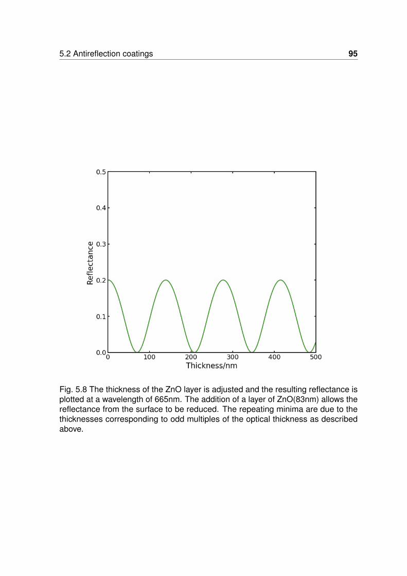
5.2 Antireflection coatings 95
Fig. 5.8 The thickness of the ZnO layer is adjusted and the resulting reflectance isplotted at a wavelength of 665nm. The addition of a layer of ZnO(83nm) allows thereflectance from the surface to be reduced. The repeating minima are due to thethicknesses corresponding to odd multiples of the optical thickness as describedabove.

5.3 Experimental methods 96
5.3 Experimental methods
A set of 2mm diameter, 200nm thick NCD membranes, suspended on 10mm by
10mm silicon was purchased from Delaware Diamond Knives (DDK). In order to
change the transmission properties of the films, ZnO was sputtered for varying
amounts of time in order to get different thicknesses. The sputtering was performed
in a Lesker PVD75 with a ZnO sputtering target in an argon and oxygen atmosphere.
The addition of oxygen was used since oxygen atoms from the target are lighter
than zinc and therefore are scattered away from the substrate more frequently. In
order to maintain a stoichiometric ratio, additional oxygen in the sputtering chamber
is required. A piece of silicon was placed in the chamber at the same time as the
membranes in order to get a more reliable measurement of the thickness of material
using ellipsometry. Pictures of three films of ZnO on silicon are shown in figure 5.9.
Comparing these pictures with figure 5.10 shows that there is agreement between
the predicted and observed colours.
Table 5.1 shows the films that were sputtered using a range of parameters. In this
section only the 83nm ZnO film on NCD will be explored, with the others examined
later on in chapter 6 for testing how well they perform as beam splitters.
Sample Pressure/Torr RF Power/W Ar Flow/sccm O2 Flow/sccm Thickness/nmA 9 80 30 6 17B 12 130 42 8.5 27C 12 130 42 8.5 52D 9 150 31.6 6.3 83E 9 150 31.6 6.3 100
Table 5.1 Sputtering parameters for the deposition of ZnO films on NCD membranes.The thickness of the sputtered ZnO was measured using ellipsometry and have anerror of ±1nm.
In order to measure the transmission properties the membranes were glued
onto a piece of acrylic 2mm thick which had a hole cut through the centre and a
channel so that it could be filled with fluid. A glass plate was glued to the back of the

5.4 Results and discussion 97
(a) 52nm (b) 83nm (c) 100nm
Fig. 5.9 Pictures of ZnO sputtered onto silicon with different thicknesses measuredusing ellipsometry. The areas at the edge were masked and so do not have any ZnOon top.
Fig. 5.10 The colour of a thin film of ZnO deposited onto a silicon substrate is plottedagainst its thickness.
acrylic to create an enclosed chamber with one point of entrance. This allows for the
attachment of a pump or other source that can apply a pressure. Measurements of
the transmission were carried out with the tunable lens arranged vertically so that air
bubbles were removed from the area that was being measured. Figure 5.11 shows
a schematic of how the packages were made.
5.4 Results and discussion
Optical microscope images of the films before and after sputtering of ZnO are shown
in figure 5.12. One observable feature is that the colour on the silicon backed
sections is not the same on either end of the film. This suggests that the thickness
is not constant across the film.
The expected colours for a 83nm ZnO film on a variable thickness of NCD on
silicon is shown in figure 5.14 using the same program that was detailed in chapter

5.4 Results and discussion 98
Fig. 5.11 The top and side view of the tunable lens. The cross section of the lens isshown for the line AB. The lens can be filled with fluid through the channel at the top.The fluid is chosen to have a refractive index similar to that of the glass plate.
4. Comparing this colour chart with the microscope images would be inappropriate
since the spectrum of the light source in the microscope is different to that of a
fluorescent lamp. Additionally, the method the camera in the microscope uses and
any colour balance the software uses is also unknown. Figure 5.13 shows a photo
of the filled tunable lens. There is good agreement (to within 10nm) with the colour
chart and it suggests that the thickness in the transparent centre section is around
200nm thick.
One significant issue with using the membranes as tunable lenses is that as
can be seen from figure 5.12a, the membranes are not circular as a result of the
fabrication process. This would severely limit how useful they would be at imaging
and would cause significant distortion. Another issue that would cause problems
is that the sputtering process has caused the membrane to wrinkle. The wrinkles
are much larger than the wavelength of light of interest and would cause severe
distortion if the membranes are used in imaging.

5.4 Results and discussion 99
(a) Uncoated membrane (b) Coated membrane
Fig. 5.12 Uncoated and coated membranes; the coated membrane has 83nm ofZnO sputtered on top. No liquid is currently present in the chamber. The imagewas created by stitching together multiple images taken using an optical microscope,some of the shading is an artefact of this process. The wavelength spectrum andcolour correction used in the microscope software are unknown and so the coloursin this image should not be compared with the colour charts produced elsewhere.
Fig. 5.13 A photograph of the tunable lens with a NCD/ZnO membrane, with fluidin chamber. Many of the wrinkles are removed by the presence of the fluid. Thesharp lines in the top and bottom sections of the chip are caused by the mountingtechnique in the sputtering chamber which stopped ZnO being deposited in theseareas.

5.4 Results and discussion 100
Fig. 5.14 Colour chart for a layer stack of a constant thickness of ZnO (83nm) on topof a variable thickness of NCD on silicon. The medium is air and the observationangle is normal to the surface. The horizontal axis shows how the colour changesaccording to the thickness of the NCD layer. Calculated using program presented ina previous chapter.
Fig. 5.15 Thermal expansion coefficient of diamond[64] and ZnO[183].The twoexpansion coefficients for ZnO are due to having a Wurtzite lattice structure.

5.4 Results and discussion 101
Wrinkled membranes of NCD have been observed in the literature when the
silicon is back etched away and methods have been developed to reduce the thermal
stress on cooling down from deposition temperatures[184]. This is complicated by
the thermal expansion being temperature dependent as shown in figure 2.5 so the
deposition conditions need to be tailored to ensure that the stress is not too low so
that the membrane can buckle. Studies to produce pressure sensors made of boron
doped diamond on glass have also observed wrinkles forming when the membrane
is released[185].
The cause of the wrinkling in the membranes presented above is due to com-
pressive stress that occur once the sample is cooled down after sputtering. Heating
of the substrate comes from numerous sources including the heat of condensation
of an atom, the kinetic energy of the sputtered atom, radiation from surfaces and the
plasma[186]. Even though magnetron sputtering is designed to reduce the heating
of the substrate by localising the plasma away from the substrate.
Determining the temperature of the sample is complicated by the sample not
being backed by silicon on the suspended section during deposition. Therefore, the
temperature in the suspended section is likely to be much hotter during deposition
as the heat can not as easily be conducted away. The thinness of the material also
means that it would heat up significantly faster.
In order to allow gas to escape from under the membrane only two edges of
the membrane were taped. This has the disadvantage that the substrate is not
coated in all areas and so the stresses caused by the film deposition are likely
to be asymmetric. The presence of wrinkling is highly detrimental to most optical
applications, however demonstrating the increase in transmission for the design
wavelength will be largely unaffected.
5.4.1 Optical transmission
The optical transmission for the lens is shown in figure 5.16 for the case of when the
lens is not deformed. The peak in the transmission can be seen to be around 665nm

5.4 Results and discussion 102
as was intended and the transmission at this wavelength is equal to 93 ± 1%. There
will be losses due to reflection at the liquid/glass interface and the glass/air interface
as well since the glass was not coated. At the liquid/glass interface the reflection
will be small since the refractive indices are close in value, however, at the glass/air
interface the reflection losses will equal around 4%, which can be found by applying
equation 5.9.
R =∣∣∣n1 − n2
n1 + n2
∣∣∣2 (5.9)
where n1 and n2 are the refractive indices for glass and air respectively. Other
losses can be accounted for by scattering, absorption and differences between the
material’s refractive index compared to the ideal value. The sub-band gap absorption
from the ZnO layer and the absorption from the liquid can also be observed from
below 400nm. However, since the film is so thin, some light still manages to pass
through the membrane below this wavelength.
Measuring the optical system without the coating is made difficult by the lensing
material being made from a liquid. The UV-Vis characterisation equipment available
are all oriented so that the optical axis is horizontal. However, the transmission
through the system without the coating can be found using the refractive index of the
liquid and equation 5.9 for each surface. This gives a roughly constant transmission
of 92% over the region where the liquid is transparent.
Increasing the transmissions could be achieved by coating the glass with an AR
coating or by using a second double layer membrane as the second surface. This
could be used to produce a biconvex or biconcave lens.
Errors caused by the angle of incidence not being normal to the lens do not
change the transmission significantly when close to 0°, however, due to the thickness
of the lens, it could cause the beam to refract away from the detector, reducing the
intensity incident on it. This can be reduced by decreasing the distance between the
lens and the detector or by increasing the size of the detector. Figure 5.17 shows
the theoretically predicted reflectance from the membrane for incident angles of 0°,

5.4 Results and discussion 103
Fig. 5.16 Optical transmission properties of the tunable lens at normal incidence.The liquid is PAO and the membrane is made of a double layer antireflection coatingmade from ZnO(83nm) and NCD(200nm) whose thickness is tailored to produce amaximum in the transmission at 665nm. The other side of the lens in made fromglass.
20°, and 45°. It is observed that there is a very small change in the reflectance when
the angle deviates slightly from 0°. However there is a considerable change when
the angle is increased significantly beyond this.
5.4.2 Surface analysis
For optical applications the surface roughness is an important parameter to try and
minimise. If the surface is too rough then the incident light will be scattered. Figure
5.18 shows an SEM image of the sputtered membrane with the ZnO sputtered
film and underlying NCD surfaces visible. This distinction was created due to the
mounting procedure in the chamber, where part of the substrate was obscured
preventing ZnO being deposited. Figure 5.19 shows the same film but from the side
on a membrane that broke. The flat area at the bottom is made from silicon, the next
layer is NCD and the layer at the top is ZnO. The layers of NCD and ZnO are clearly
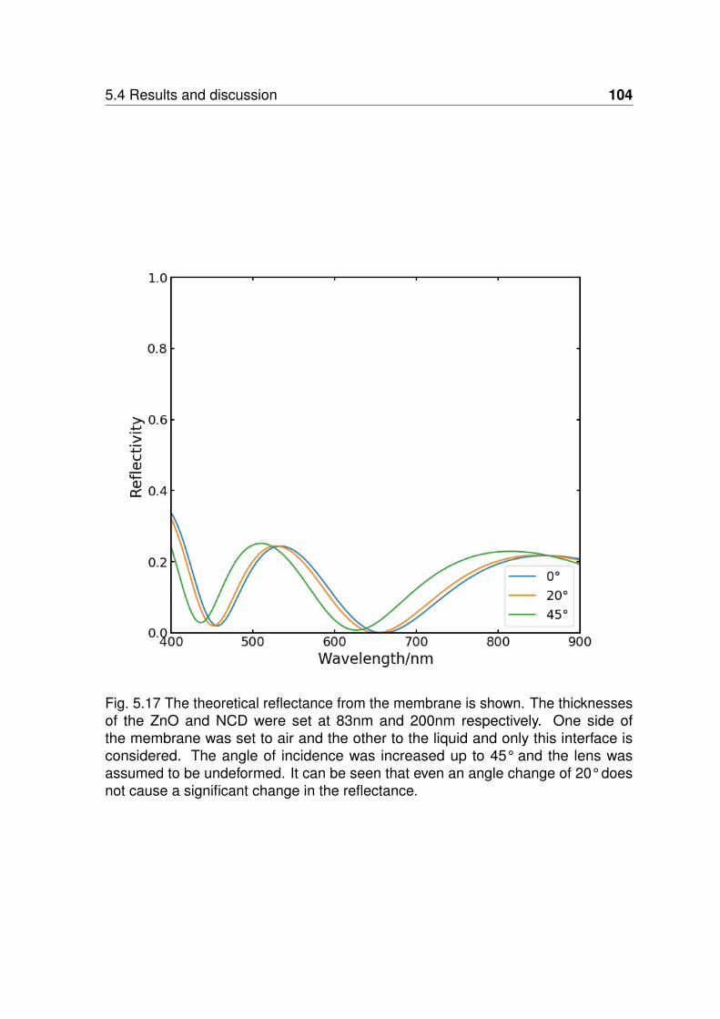
5.4 Results and discussion 104
Fig. 5.17 The theoretical reflectance from the membrane is shown. The thicknessesof the ZnO and NCD were set at 83nm and 200nm respectively. One side ofthe membrane was set to air and the other to the liquid and only this interface isconsidered. The angle of incidence was increased up to 45° and the lens wasassumed to be undeformed. It can be seen that even an angle change of 20° doesnot cause a significant change in the reflectance.

5.4 Results and discussion 105
distinguished and the columnar growth structure that is typical of sputtering and
diamond CVD can be seen[187]. The separation that occurred when the membrane
broke indicates that the adhesion between the layers is less than inside the material
itself.
Fig. 5.18 SEM of ZnO sputtered onto the NCD membrane. The material at the topright is the surface of the NCD, that at the bottom left is the surface of the ZnO. Thisboundary was formed due to the mounting method in the sputtering system and islocated above the silicon support.
Figure 5.20 shows a typical AFM image of a ZnO film sputtered on top of NCD.
The AFM was operated in tapping mode with a silicon tip. Measurements of the root
mean square surface roughness, calculated using equation 3.2, were taken before
and after deposition of the zinc oxide layer. The surface roughness was measured
and averaged over five scans in different locations on the sample, the roughness on
the NCD layer was found to equal 4.2 ± 0.6nm and the roughness after deposition

5.4 Results and discussion 106
Fig. 5.19 SEM image of ZnO sputtered onto the NCD membrane at an angle of54°. The image was taken from a membrane that broke and the sections of the filmpeeled away from each other. The surface at the bottom is the silicon support, thenext layer is the NCD and the layer at the top is the zinc oxide. The crystal structureof the NCD can be seen.

5.4 Results and discussion 107
of ZnO was 4.9 ± 0.5nm, demonstrating a slight increase in the roughness of the
surface. A height profile along the white line is also provided and it can be seen that
there are some significant peaks. Comparing the mean square roughness and the
roughness layer that are used in optical models requires some knowledge of the
surface profile. For example, assume that in the optical model the surface has a
triangular form and that there is a half air and half diamond volume fraction. Then a
mean square roughness of 4.2 ± 0.6nm equates to a 15 ± 2nm thickness layer in
the optical model that was described in the previous chapter.
5.4.3 Raman spectroscopy
There are numerous different types of bonds in polycrystalline diamond due to the
presence of grain boundaries, therefore, the Raman spectrum is highly dependent
on the deposition conditions. Carbon based materials other than diamond are likely
to cause absorption of light in the film and hence reduce its transmission and so
the growth conditions need to be optimised to reduce this. Conditions that favour
smaller grains will increase the amount of sp2 bonding and hydrogen content, due to
the increase in the volume of the grain boundaries. Low methane concentrations
suppress the re-nucleation rate and so there will be less sp2 carbon. The Raman
spectra for diamond is also dependent on the wavelength of light used for excitation
and so this needs to be taken into account when comparing the spectra[188].
Figure 5.21 shows the Raman spectrum taken of the coated membrane positioned
over the silicon support using a laser with a wavelength of 532nm as the exciting
light source. The sharp peak at 520cm−1 and the broader peak around 950cm−1 are
due to first and second order scattering from the silicon[189], the other peaks around
1400cm−1 are due to the NCD layer. Measurements were taken at five different
locations on the sample and no major difference was observed. Figure 5.22 shows
a scaled plot taken at the same location as figure 5.21 and the same laser intensity
focussing just on the peaks corresponding to the NCD. The peak at 1332cm−1 is
due to first order scattering in diamond[190]. Diamond also has a second peak at

5.4 Results and discussion 108
Fig. 5.20 AFM image of ZnO deposited on NCD membrane and the height profilealong the white line from the AFM image. The data was taken using tapping modewith a silicon tip.

5.4 Results and discussion 109
2450cm−1, however, this has a weaker response and so is not observed in figure
5.21. Graphite exhibits peaks at 1357cm−1 and 1580cm−1 which are called the D
and G band respectively. These peaks shift slightly in NCD due to changes in the
crystalline nature of the material to an amorphous state. The peaks near 1130cm−1
and 1450cm−1 are believed to be caused by the presence of hydrogen and sp2
carbon at the grain boundaries[191, 192].
Zinc oxide has several expected Raman peaks as shown in table 5.2. Peaks
that would have been caused by ZnO could not be observed above the noise in the
spectrum taken with NCD. Instead the piece of silicon that was added during the
sputtering process (so only silicon and ZnO was present) was analysed. As can be
seen from figure 5.23 there is a peak at 435cm−1 which is the only peak from table
5.2 that could be identified. The shift from the value in table 5.2 could be due to the
stress in the film[193]. However, silicon also shows a peak around this area and it
can not be ruled out that silicon is responsible for it[194]. The other peaks that are
visible are due to silicon and the presence of the filter used to remove the Rayleigh
scattered light.
Symmetry Raman shift/cm−1
E2 101A1 381E1 407E2 437A1 574E1 583
Table 5.2 Expected Raman shifts and symmetries for ZnO[195]
5.4.4 Photoluminescence
The photoluminescence spectra was taken using a laser with a wavelength of
405nm(3.06eV). This is not high enough in energy to excite electrons across the

5.4 Results and discussion 110
Fig. 5.21 Raman spectra of ZnO coated onto the NCD membrane over silicon. Thepeaks that should appear for ZnO are hard to see above the noise. The dominantpeak is from the silicon substrate with a small peak for the D band of diamond justvisible.
Fig. 5.22 This is the same spectrum as figure 5.21 but the scale has been changedto concentrate on the peaks that are associated with nanocrystalline diamond.

5.4 Results and discussion 111
Fig. 5.23 Raman spectra of ZnO coated onto bare silicon wafer that was placedinto the sputtering chamber at the same time as deposition was performed ontothe membrane. The sharp increase and sudden drop in intensity below 100cm−1 iscaused by the Rayleigh scattered light and filter. The peak at 435cm−1 is possiblydue to ZnO and is the only peak from ZnO that could be distinguished from the noise,however, it could also be caused by silicon[194]. The peak at 302cm−1 is caused bysilicon.

5.4 Results and discussion 112
band gap of ZnO or diamond which have values of 5.5eV and 3.3eV[196] respectively,
however, it can be used to test energy gaps less than this.
Figure 5.24 shows the photoluminescence spectra for the membrane. A broad
peak is observed between 500nm-700nm, which is due to the presence of electronic
states in the diamond band gap. These states are likely caused by the presence
of defects in the grains and dislocations in the diamond. The locations of the two
broad peaks observed are consistent with previous reports for NCD[197, 198]. It can
not been seen above the noise if there are peaks at 575 and 637nm, which would
indicate that nitrogen vacancy centres are present[69].
Fig. 5.24 Photoluminescence of membrane under illumination from a 405nm laser.

5.5 Conclusion 113
5.5 Conclusion
The design and manufacture of a tunable lens which has a deformable membrane
that also acts as an antireflection coating has been tested. It has been demonstrated
that it is possible to increase the transmission significantly, for a wavelength of choice,
through the system. However, for wavelengths other than the design wavelength,
the reflection losses can be fairly high, in the region of 20-30% in the visible range.
This can be reduced by the addition of more layers in the antireflection coating,
however, this will reduce the amount the film can be deflected and increases the
fabrication complexity. One advantage of adding more layers is that the membrane
could become less fragile and so increase the areas where it could be applied.
It has been found that the methods of manufacture are inadequate for the lens to
be used in imaging applications since the film wrinkled. Additionally, better methods
of fabrication are required in order to get a significantly more circular shaped lens.
The current method, etching through a couple hundred microns of silicon, makes it
difficult to maintain the desired geometry throughout the etching process.
In order to reduce wrinkling of the films, the two films should be deposited first
before the substrate is back etched. However, this would require further processing
to ensure that the ZnO was not etched at the same time as the Si. Other methods
could involve supporting the membrane with a third material during sputtering that
could easily be removed afterwards. Pre-stressing the membrane before sputtering
could also help reduce the wrinkling.
The tunable aspect of the lenses has not been investigated in this work since
the wrinkling of the surface makes measuring the deformation difficult. Additionally,
attempting to remove the fluid from one of the samples caused the membrane to
break before a deformation measurement could be taken. Another problem that was
encountered during this work was the low number of samples made repeating the
experiment difficult. Future work should consider other materials and increase the
number of layers in the coating structure.

5.5 Conclusion 114
Since the membranes were not circular and producing circular membranes of
the required precision would be very difficult the next chapter will explore how the
membranes could be used for applications where the geometry is not as important.

Chapter 6
Pellicle Beamsplitters Made From
Nanocrystalline Diamond
6.1 Introduction
Splitting light into multiple parts is a feature of much experimental research. One
early example is the Michelson-Morley experiment, performed in 1887, which used a
beam splitter to split incident light into two components. This experiment, among
others, was used as evidence against the existence of an aether[199]. One method
to create a beam splitter is to use two prisms which are stuck together with an
optical adhesive. The thickness of this adhesive is adjusted such that half of the
light is reflected and the other transmitted for a chosen wavelength. The amount
of light reflected will also depend on the polarisation state of light and methods
have been developed to produce non-polarising beam splitters[200, 201]. Figure
6.1 shows an example of a cube beam splitter showing the incoming and outgoing
light rays, which are split at the prism’s interface. Beam splitters can also be used
to efficiently polarise light, one example is a Glan-Taylor prism[202]. This beam
splitter works by making the two prisms out of birefringent material and hence the
two polarisation states experience a different refractive index. The angle of the prism
is chosen such that one polarisation state is totally internally reflected and the other

6.1 Introduction 116
transmitted. It can be used as the polariser in ellipsometers and it is typically much
more efficient than using a film polariser[108]. A second way to split light is by using
a half-silvered mirror, this is usually a piece of glass with a very thin layer of metal
deposited by thermal evaporation. Losses caused by absorption in the coating can
be significant and the metal can oxidise causing a variation in its properties over
time. Additionally, certain metals which do not oxidise, such as gold and platinum,
have absorption, reflection and transmission properties that are highly wavelength
dependent reducing their usefulness[203].
Fig. 6.1 Use of a cube beam splitter to split light into multiple parts. Two triangularprisms are cemented together with an optically transparent adhesive. Light istransmitted or reflected at the interface and they can be either polarising or non-polarising.
Beam splitters also have numerous uses beyond scientific equipment and are
common in a number of commercial devices. One such example is the use of semi
transparent thin mirrors as a component in cameras that allows the user to see
through the viewfinder at the same time as the camera image sensor is illuminated.
This has the advantage of not interrupting the view through the viewfinder while an
image is being taken[204]. It also has fewer moving parts and so can reduce the vi-

6.1 Introduction 117
bration that would occur from using a moving mirror. It has the disadvantage of being
fragile and so needs to be protected from dust and shocks from the environment.
Since the pellicle beam splitters are so thin, they are highly susceptible to vi-
brations. Kwon et al. demonstrated a stroboscopic phase-shifting interferometry
method that could be used to measure the deformation of a pellicle mirror while
being sonically actuated[205]. They measured the deformation at 50µs intervals
using a 20ns laser pulse while it was actuated by a tweeter. The distortions in the
mirror were fairly significant which would have detrimental effects for imaging in
environments with a lot of vibration.
One of the simplest forms of beam splitter is a plate beam splitter which is simply
a piece of transparent glass placed at an angle in a beam of light. A portion of the
incident light is reflected due to the mismatched refractive indices between the plate
and the medium. Dichroic coatings can be applied to the surface of the beam splitter
in order to tailor which wavelengths of light and at what intensity are transmitted[206].
Figure 6.2 shows an example of a plate beam splitter. It can be seen that the
optical path of a ray is refracted in the material and then emerges from the other
side of the plate. Reflections occur at each interface and the reflection from the
second interface in the material can add to the reflection from the first interface
but displaced slightly. This displacement increases with the thickness d, and for
imaging applications can cause ghosting. Ghosting produces an image with a slightly
fainter image of the original overlaid but shifted from the original. In order to reduce
the effects of ghosting, coatings can be applied to each surface to minimise the
reflections, however a simpler method to reduce the effects of ghosting is to make
the beam splitter much thinner[207].
Pellicle beamsplitters are very thin (usually between 2-10µm) supported mem-
branes, typically made out of nitrocellulose, that can be used to split an incident
light beam into two separate beams. They’re used in applications such as beam
sampling and splitting and they have the advantage that since they are so thin
ghosting is practically eliminated. However they are susceptible to vibrations from

6.1 Introduction 118
Fig. 6.2 A plate beam splitter where the incident light undergoes multiple reflectionsinside. Ghosting is a problem where internal reflections cause the reflected image tobe displaced from the original, this can cause issues in imaging applications. Onlythe first reflection is shown for simplicity, however, multiple reflections and ghostswill be observed with decreasing intensity.
the environment and are very delicate, so are difficult to clean [208]. Additionally,
the films are commonly made from a hygroscopic material and so can not be used
in high humidities.
Diamond is chemically resistant and so does not suffer from some of the problems
that nitrocellulose does and thin films of NCD have been considered previously for
use as a beam splitter . Chardonnet et al. fabricated diamond membranes between
1-2µm thick for use as a polariser[209]. By stacking four membranes orientated at
the Brewster angle they were able to achieve an extinction ratio of 0.0002 which
compares favourably to a grid polariser which can only achieve a typical extinction
ratio of 0.01. The membranes were tested for their damage threshold from a CO2
laser and it was found that they could resist power densities up to 5kW/cm2, however,
the roughness of the films and impurities in the diamond limited their application to
infrared wavelengths.

6.1 Introduction 119
6.1.1 Dielectric coatings on pellicles
Since pellicles are so thin, even if the material that is used for the pellicle absorbs
light at a certain wavelength a significant proportion of the light can still transmit
through it. This means that they can be used over a wider wavelength range than
would be expected from just looking at the absorption coefficients, however, they
do suffer from problems caused by thin film interference. The transmission and
polarisation properties of pellicles can be altered by coating them in dielectric layers
of materials with a different refractive index.
It has been shown by Azzam and Mahmoud that a tilted bilayer pellicle can act
as a transmission quarter wave retardation plate[210]. This allows the creation of
simple linear to circular (and the reverse) polarisers. Usually circular polarisers are
created using a birefringent crystal such as calcite or quartz. An advantage of using
the pellicle is that is produces little deviation in the transmitted beam. Azzam et
al. have also presented bilayer pellicles as a component in a division of amplitude
photopolarimeter, which can be used to measure the four components of the Stokes
vector simultaneously[211]. Measuring the Stokes vector allows for unpolarised or
partially polarised light to be described[108]. In this research, the materials and
thickness of a bilayer pellicle were optimised to create a 50:50 beam splitter for two
wavelengths, one in the infrared and one in the visible. The design was only treated
theoretically and only considered using a nitrocellulose membrane which meant a
constraint on the thickness of this film to greater than 1µm. A second layer on top
of the nitrocellulose was then made from either germanium or gallium phosphide
for the infrared and visible cases respectively. These materials were chosen due to
their high refractive indices of 4.1 for germanium and 3.308 for gallium phosphide at
the design wavelengths[212]. However, they both needed to be operated at incident
angles greater than 60°, reducing the width of the beam that can be passed.
The change in polarisation state that occurs when the incident light is not nor-
mal to the surface is cause by the s and p polarisations having different complex
reflection coefficients. This can cause a detrimental effect in certain systems such

6.1 Introduction 120
as interference filters and directional couplers. Saleh considered a symmetrical
dielectric structure surrounded by the same material, which was either air or two
prisms[213]. It was suggested that in order to produce a symmetric layer solution,
with no polarisation dependence, at least three layers are needed.
Fig. 6.3 In an optical bus a set power of light needs to be reflected from each beamsplitter. To achieve this the reflectivity of the next beam splitter must be greater thanthe previous. This requires each beam splitter to have a different coating structure.
Coated pellicles have been proposed for optical bus applications. In these
systems there is a requirement to precisely split an input optical signal without
changing the optical mode. Figure 6.3 shows the case of four beam splitters sampling
an input beam, which can be directed towards a detector or other component.
If a 10mW beam was incident and each tap directed 1mW away the first beam
splitter would need to split 10% (1mW/10mW), the next would need to split 11.1%
(1mW/9mW), the third would split 12.5% (1mW/8mW) and so on. There would
also need to be an additional bus that would be used to transmit data back to the
host. The reflectivities of each beam splitter are given by equation 6.1, where Rx is
the reflectivity of the xth beam splitter and e is a measure of the propagation loss
between the beam splitters[214]. Optical buses have an advantage over copper
wires since they consume little power, are immune to electromagnetic interference
and impedance matching can be achieved using antireflective coatings. Additionally,
they remove the need for an optical to electrical conversion which can reduce delay
times.

6.1 Introduction 121
Rx =R1∏x
m=2(1−Rm−1)em−1
=R1
1 +R1 − xR1
for x>1 and e=1(6.1)
Low loss, polarisation insensitive pellicle beam splitters with thicknesses less
than 20 microns have been fabricated with a high data rate transmission of 10Gb/s
which could interconnect seven to eight modules. The pellicle needed to be non-
polarising since the vertical cavity surface-emitting laser (VCSEL) that was used
as a light source has a random polarisation state. The pellicle was made from a
250nm supported membrane made from Si3N4 which had a multilayer (15 layers)
interference coating applied to it in order to achieve the required reflectivity and
transmission properties. This made the whole structure around 2 microns thick[214].
There are several advantages of using diamond as a beam splitter. The wide
transmission window makes diamond ideal for use in many optical applications.
Additionally, diamond’s high tensile strength means that thin membranes with wide
apertures can be fabricated. Conveniently, the thickness of these membranes are
around that required in optical interference coatings. Diamond membranes can be
bought commercially with standard thicknesses of 50nm to 1µm with a 5mm clear
aperture attached to a 1cm sq silicon frame[215]. The disadvantages of diamond is
its cost and also incorporating the CVD deposition process into other optical coating
techniques.
The aim of this chapter is to test thin film beam splitters made from nanocrystalline
diamond and also alter the transmission properties by coating the films with another
dielectric material. These films will be tested for their transmission properties
against the angle of incidence and wavelength. The change in the polarisation state
on transmission through the membrane will also be considered. The method of
fabrication of the samples discussed in this chapter along with an analysis of the
material properties have been covered previously in chapter 5.

6.2 Pellicle design considerations 122
6.2 Pellicle design considerations
There are a large number of combinations of materials that can be chosen to make
a pellicle beam splitter. As in the previous chapter, NCD will be used and a coating
of ZnO applied since it has already been shown to adhere without delamination or
cracking. Only a bilayer membrane will be considered since it has been shown in
the previous chapter that increasing the thickness of the sputtered coating too much
causes the film to wrinkle. Figure 6.4 shows a diagram of the structure that will be
considered in the following.
Fig. 6.4 The structure of the beam splitter that will be analysed in the followingconsists of a layer of ZnO and NCD on top of a silicon substrate. The NCD is firstgrown onto the silicon and then ZnO is sputtered on top. Optical measurements aretaken through the transparent section in the centre and the thickness of the ZnOlayer is varied.
6.2.1 Transmitted intensity
The transmitted intensity is highly dependent on the wavelength of light tested, the
refractive indices and the thickness of film. Figure 6.5 shows how the transmitted
intensity changes as the thickness of a film of diamond in air is increased and was
calculated using the program described previously. As expected, for all wavelengths
and incident angles, the transmission through a 0nm film is 100% as this represents
the case when there is no film. At normal incidence the two polarisation states
are indistinguishable and so lie on top of each other on the plot, but as the angle

6.2 Pellicle design considerations 123
increases they separate and the s polarisation state is reflected more. Close to the
Brewster angle, the p polarisation state is almost completely transmitted as shown
in figure 6.5c. The points where the transmission is maximal is given by integer
multiples of the half wavelength optical thickness and the minimum point by odd
multiples of the quarter wavelength optical thickness at normal incidence. It can also
been seen that at certain thicknesses (at the inflection points) a small change in the
thickness can cause a large change in the transmitted intensity. This can cause a
problem when providing tolerances for the design at these thicknesses.
The addition of a layer of ZnO on top of the NCD changes the optical transmission
properties considerably. Figure 6.6 shows the effect of increasing the thickness of
a layer of ZnO deposited onto a NCD layer 200nm thick for the two polarisation
states at three different angles. As before at 70° there is a large increase in the
transmission of the p polarised light, however, the transmission is less than for the
case when there is no ZnO layer. This is caused by ZnO having a Brewster angle
that is further away from 70° than diamond. For optical bus applications mentioned
previously, the last beam splitter in the bus would need a 50% split ratio. This is
the lowest ratio required for the transmittance of any element and so the full range
required for the bus can be achieved with either the uncoated and coated elements
for all the wavelengths shown. A small but useful advantage of adding the ZnO
layer is that the curves are broadened slightly which increases the tolerance on the
thicknesses deposited.
Beam splitters are placed at an angle in the optical axis in order to direct the
reflected light away from the oncoming beam. The amount of light reflected is highly
dependent on the angle the beam splitter makes with the incident light. Typically
beam splitters are placed at an angle of 45°. Figure 6.7 shows the theoretically
predicted transmission of the bilayer membranes with a varying thickness of ZnO on
top of 200nm of NCD. Three different wavelengths are considered for both polari-
sation states. Both polarisation states start at the same point at 0° since they are
indistinguishable at this angle and also end together at 90°. The transmitted intensity

6.2 Pellicle design considerations 124
(a) Incident angle = 0°
(b) Incident angle = 45°
(c) Incident angle = 70°
Fig. 6.5 Transmission intensity of an NCD film in air depending on its thickness. Threedifferent wavelengths (shown in legend) are considered for p(dotted) and s(dashed)polarised light, at normal incidence the two polarisation states are indistinguishable.The incident angle of the light is increased from 0° to 70°.

6.2 Pellicle design considerations 125
(a) Incident angle = 0°
(b) Incident angle = 45°
(c) Incident angle = 70°
Fig. 6.6 Transmission intensity of bilayer films of ZnO and NCD with a constant200nm NCD thickness. The thickness of the ZnO layer is given by the value on thex axis. Three different wavelengths (shown in legend) are considered for p(dotted)and s(dashed) polarised light, at normal incidence the two polarisation states areindistinguishable.

6.2 Pellicle design considerations 126
for the p polarised light increases as the angle is increased up to a maximum around
the Brewster angle. Since the transmitted intensities for the different polarisation
states tend to diverge, an unpolarised beam of light will become slightly polarised
passing through the beam splitter. This principle can be used in order to create a
thin film polariser and stacking several filters together could increase how polarised
the light is.
An additional use of these thin films is as a variable attenuator which alters the
transmission intensity by changing the angle of incidence. The light intensity could
be varied over a wide range from, for example, around 70% to less than 20% (taking
the usable angle range as 0°-70°) in the case of s polarised light as in figure 6.7a
for green light and figure 6.7b for red and blue light. P polarised light, for the wider
system, could also have the same range by rotating the membrane over its other
axis. Additionally, due to the thinness of the membrane the deviation of the light from
the original path will be minimal as the membrane rotates, making optical alignment
much simpler. Figure 6.8 shows how the beam deviates from its original direction
after passing through a plate beam splitter. An advantage of using diamond is that
even at a glancing incident angle, the light in the diamond only has an angle to the
normal of around 25° reducing how far the beam is displaced compared to a beam
splitter made of a lower refractive index material. Another feature of this system is
that the reflected light could be measured in order to calibrate it while the system
is being used, however this would become difficult at angles close to 0° or 90°.
Increasing the range over which this system can be used as a variable attenuator
could be achieved by optimising the thicknesses however, this will not be considered
further in this work.
6.2.2 Polarisation state changes
On transmission through a dielectric coating at an angle the polarisation state of the
light will change. There are two conventions commonly used for the polarisation of re-
flected light. The s and p polarisations have no phase difference at normal incidence

6.2 Pellicle design considerations 127
(a) ZnO thickness = 0nm
(b) ZnO thickness = 50nm
(c) ZnO thickness = 100nm
Fig. 6.7 Variation of the transmitted intensity of p(dotted) and s(dashed) polarisedlight for different incident angles and wavelengths for a membrane of 200nm NCDwith varying thicknesses of ZnO.

6.2 Pellicle design considerations 128
Fig. 6.8 A beam of light passing through a plate will have its position shifted (beamwalk-off) by a displacement that is dependent on the angle the plate is to the incidentbeam. This can cause issues aligning an optical system if the plate rotates and itcan be minimised by making the plate as thin as possible. A 100µm plate can causea deviation of around 30µm at 45° if made from glass with a refractive index around1.5. Diamonds higher refractive index reduces this significantly.
in the Abelès convention and they differ by 180° in the Mueller convention[216].
There is no difference between the conventions for light which is transmitted through
a material which is most relevant to the following discussion.
To find the phase change when light is transmitted through the beam splitter,
equation 6.2 can be used, where δp and δs are the phase differences after reflecting
or transmission through the surface for the two polarisation states respectively. A
method for calculating ρt was discussed in chapter 4 and the program described
there will be used to calculate the phase properties in the following.
ρt =tpts
= tan(Ψ)ei∆ =|tp||ts|
ei(δp−δs) (6.2)
As can be seen in figures 6.9 and 6.10 the phase difference at 45° does not
exceed 15° for a range of thicknesses and wavelengths. Ψ has been included here,
however, since it is derived from the ratio of the transmission, it has already been
discussed above and so is left for reference.

6.3 Experimental methods 129
Figure 6.11 shows the theoretical change in ∆ with angle for an NCD layer with
a variable thickness of ZnO applied. It can be observed that at certain angles and
wavelengths the pellicle acts as an eighth wave polariser with a ∆ of 45°. Stacking
two of these together would create a quarter wave polariser which is used to create
circularly polarised light. For other incident angles the pellicle is unpolarising with ∆
= 0.
6.3 Experimental methods
The different pellicles that will be experimentally tested are listed in table 5.1 along
with the process parameters used to fabricate them. They are each bilayers with a
roughly constant layer of NCD and a varying thickness of ZnO. The layer structure is
as shown in figure 6.4 which differs from the tunable lens in that there is no liquid
causing refraction. Measurements of the polarisation state change were performed
using a Semilab SE-2000 variable angle ellipsometer.
In order to test the transmission and reflection properties of the films against
angle, a custom experimental set up was designed. Light from a laser diode of
wavelength 665nm was focussed, using a lens, towards the centre of the pellicle
beam splitter which could be rotated. A dichroic film polariser, with polarisation
efficiency greater than 99% was placed in the beam to produce p and s polarised
light. The pellicle was placed onto a mount which allowed it to rotate along with one
of the detectors. The rotation was performed using a stepper motor with a step size
of 1.8° and was measured over the range 15° up to 74.4°. Angles lower or higher
than this were limited due to impacting with either the light source or the second
detector. Figure 6.12 shows a schematic of the setup. In order to keep detector 1 in
the correct position to collect reflected light, the detector mount was geared in order
to rotate twice the angle that the pellicle rotates. The photodiode detectors were
chosen to be large (10mm×10mm) so that errors caused by misalignment were
reduced. The photocurrent generated in the photodiodes was converted to a voltage
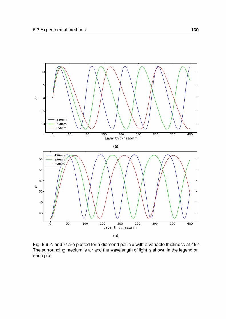
6.3 Experimental methods 130
(a)
(b)
Fig. 6.9 ∆ and Ψ are plotted for a diamond pellicle with a variable thickness at 45°.The surrounding medium is air and the wavelength of light is shown in the legend oneach plot.
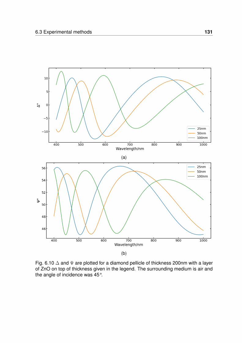
6.3 Experimental methods 131
(a)
(b)
Fig. 6.10 ∆ and Ψ are plotted for a diamond pellicle of thickness 200nm with a layerof ZnO on top of thickness given in the legend. The surrounding medium is air andthe angle of incidence was 45°.

6.3 Experimental methods 132
(a) ZnO thickness = 0nm
(b) ZnO thickness = 50nm
(c) ZnO thickness = 100nm
Fig. 6.11 How delta varies against angle for a NCD membrane of constant thickness200nm with varying thicknesses of ZnO as given in the caption on each figure. Thewavelengths plotted are given in the legend.

6.3 Experimental methods 133
Fig. 6.12 Schematic of a pellicle membrane, for every degree of rotation by the pelliclethe detector moves two degrees in order to collect the reflected light. A film polariseris used in order to select the p or s polarisation states from a monochromated lightsource.

6.4 Results and discussion 134
so it could be measured by an analogue to digital converter. Measurement taking
was automated using the custom LabView program presented in appendix A and the
program proceeded as described in the flowchart in figure 6.13. Interfacing between
the LabView program and the stepper motor was a National Instruments USB-6009
data acquisition device (DAQ) which logged the intensity of light at each detector
and also controlled the advance of the stepper motor. Between the DAQ and the
stepper motor were a number of transistors in order to provide the necessary power
to drive the motor.
6.4 Results and discussion
Figure 6.14 shows a photo of one of the membranes (sample E) which was fabricated
as described in the previous chapter. This membrane had a 100nm thick layer of ZnO
coated onto an approximately 200nm thick membrane made from NCD with a silicon
support. As discussed in chapter 4 the colour that is observed due to interference
in a thin film is dependent on its thickness. Due to the uneven thickness of the
NCD membrane the colour of the film changes over its surface. The sharp change
in colour that can be observed on either side of the membrane is caused by the
mounting technique that was used during sputtering, which masks these outer areas
from being coated by ZnO. It can be seen that the membrane has wrinkled, which
was observed when the ZnO layer was 83nm or 100nm thick, smaller thicknesses
caused no observable wrinkling. The wrinkling is caused by the mismatched thermal
expansion coefficients when the membrane cools after it has been sputtered and is
likely to cause scattering which would be detrimental for optical applications.
Figure 6.15 shows the expected colour of a ZnO film of thickness 100nm on a
variable thickness of NCD. Comparing this to figure 6.14 it can be seen that the line
AB is where it would be expected that the thickness of the NCD was 200nm. The
NCD thickness across the sample appears to range from 170nm at the top of the
photo to 210nm at the bottom, with the central portion being around 190nm thick.

6.4 Results and discussion 135
Fig. 6.13 The LabView program works by first taking the input parameters such asfile name and the angle range that the measurement will be taken over. Then it takesa reading and advances the stepper motor while logging the data. The stepper motorcoils are energised in the order of the binary numbers on the right of the flowchart.Cycling through the states is achieved by applying 2x (mod 15) to the previous statex. This gave a resolution of 1.8° per step.

6.4 Results and discussion 136
Comparing the outer section of the photo where ZnO was not deposited with
figure 4.14 also provides similar conclusions. It is very difficult to image a sample
at 0° since both the source and the camera need to be in the same line of sight,
therefore imaging has to be done off axis. Figure 6.16 shows the expected colour for
a range of thicknesses of ZnO on a 200nm NCD layer on a silicon substrate. It can
be seen that there is very little change in the expected colour at small angles away
from normal and that at these angles there is little difference due to the polarisation
state.
Fig. 6.14 Photo of a 200nm thick NCD membrane with 100nm of ZnO sputtered inthe central section. The areas were there is an abrupt change in colour is causedby the masking that was used. The application of the ZnO coating has caused themembrane to wrinkle. The width of the silicon support is 10mm×10mm.
6.4.1 Wavelength dependent transmission properties
The results of measuring the optical transmission properties of the bilayer mem-
branes are shown in figure 6.17. There is a clear shift in the position of the peaks,
which move towards higher wavelengths for an increase in the amount of ZnO de-
posited. Below 400nm there is a large difference between the transmission between

6.4 Results and discussion 137
Fig. 6.15 The colour of a bilayer film on silicon made from ZnO of constant thickness100nm and a variable thickness of NCD on the x axis.
sample D and E and sample A and B. This is caused by more sub-band gap light
being absorbed in the ZnO layer due to its greater thickness. It also suggests that
the penetration depth is of order 100nm which is one order of magnitude less than
that reported for single crystal ZnO[196]. This is expected, especially if there is not
a stoichiometric ratio of zinc and oxygen atoms in the film[217].
Surface roughness can cause a significant decrease in transmitted light from
scattering, the amount scattered is wavelength dependent with shorter wavelengths
more readily scattered[218]. One method to model the scattering from a thin film is
to modify the Fresnel coefficients at each interface by a Debye-Waller factor. These
modified Fresnel coefficients are given by
rj,j+1 = r(0)j,j+1exp
{− 2(Sλ
)2n2j
}(6.3)
rj+1,j = r(0)j+1,jexp
{− 2(Sλ
)2n2j+1
}(6.4)
tj,j+1 = t(0)j,j+1exp
{−(12
)(Sλ
)2(nj+1 − nj)
2}
(6.5)
tj+1,j = t(0)j+1,jexp
{−(12
)(Sλ
)2(nj − nj+1)
2}
(6.6)
where, for example r(0)j,j+1 is the unmodified Fresnel coefficient for the interface
between the j and j+1 layers. nj are the refractive indices, λ the wavelength and

6.4 Results and discussion 138
(a) s polarised light
(b) p polarised light
Fig. 6.16 The colour, in reflection, of a ZnO film of varying thickness on NCD ofthickness 200nm on a silicon substrate for s and p polarised light. The s and ppolarisations are indistinguishable at normal incidence as observed for colours closeto the x axis. The change in colour observed between 60-70° is caused by it beingclose to the Brewster angle.

6.4 Results and discussion 139
(a) Angle of incidence = 0°
(b) Angle of incidence = 45°
Fig. 6.17 The experimentally measured transmission through a two layer suspendedmembrane made of ZnO and NCD (NCD thickness roughly constant at around200nm) at normal incidence. The thickness of the sputtered ZnO is given in thelegend. The sharp drop at 400nm is caused by the increased thickness of ZnOabsorbing more light. Sample C broke before the measurement could be taken.

6.4 Results and discussion 140
S = 2πσ, where σ is the root mean square (RMS) roughness[219]. However, using
equation 6.5 to calculate the modified Fresnel coefficients using the roughness
values measured by AFM in chapter 5 only reduces the transmission by at most
0.01. If the only factor contributing to the difference between the theoretical and the
measured was the surface roughness, then the surface roughness would need to
be about 25nm RMS at each interface. Therefore, there must be factors other than
scattering resulting from surface roughness contributing to the decrease.
In an experimental setting, the intensity that the detector would measure would
be dependent on its size or other restricting aperture in the system as more scattered
light could be collected. This is demonstrated in figure 6.18 where an incident light
beam is scattered from a rough surface. If the detector is large then a significant
amount of scattered light could also be collected and cause the measured intensity
to be higher than expected.
Fig. 6.18 Light incident onto a rough surface will elastically scatter off the surface.Depending on the roughness the light intensity in the specular beam can be severelyattenuated. Transmitted light would also show similar problems from scattering.
The theoretically expected intensity is compared with the experimentally mea-
sured intensity for two of the samples in figure 6.19. The experimentally found

6.4 Results and discussion 141
intensity is less than that predicted for both cases and they diverge more at lower
wavelengths. The most appropriate thickness of diamond is slightly less than 200nm
for both cases, however, this will vary depending on the exact location on the pellicle
the measurement was taken.
The errors that occur due to misalignment of the membrane are considered in
figure 6.20. It can be seen that a fairly large deviation of 20° causes only a slight
change in the position of the curve, moving the peak by about 5nm. This means that
errors caused by angles that deviate slightly away from normal incidence are small.
However, the errors are expected to increase significantly for angles much larger
than this. Other differences from the theoretically calculated transmittance can occur
due to differences in the refractive index compared with single crystal material.
Figure 6.21 shows the experimental results of the transmission and reflection of
light passing through the pellicle when the angle of incidence is varied. A wavelength
of 665nm was used to test both polarisation states. The smallest angle tested
was 15° and the largest was 74°. Similar trends between the experimental and
theoretical predictions can be observed as in figure 6.7. The transmitted intensity
for both polarisation states start together and then diverge with the p polarised
transmission increasing up to a maximum before decreasing. The transmission
reaches a maximum near the Brewster angle and then decreases. The sum of the
reflected and transmitted intensities is less than 100% in all cases which is to be
expected. The sharp fall in transmission at 70° for the p polarised light in figure 6.21e
is due to the difficultly in passing light through the sample when the aperture narrow.
Figure 6.22 shows how at high angles the silicon support can have a detrimental
effect on the usable area and will cause the light to be deflected away from both
detectors. This problem can be reduced by making the supporting structure taper
away from the membrane.
An additional problem that can occur when the membrane is rotated away from
the optical axis, is that the projected area of the transparent section decreases. This
is demonstrated in figure 6.23 where it can be seen that there is a small decrease in

6.4 Results and discussion 142
(a) ZnO thickness = 17nm
(b) ZnO thickness = 100nm
Fig. 6.19 The theoretical transmission through a two layer suspended membranemade of ZnO and NCD at normal incidence. The thickness of ZnO was kept constantat either 17nm or 100nm and the NCD was varied to equal 190nm, 200nm or 210nm.The experimental results for the corresponding sample are also shown.

6.4 Results and discussion 143
(a) ZnO thickness = 17nm
(b) ZnO thickness = 100nm
Fig. 6.20 The theoretical transmission through a two layer suspended membranemade of ZnO and NCD at varying angle of incidence. The thickness of ZnO is shownin the caption and the NCD thickness was equal to 195nm. The experimental resultsfor each sample is also shown. Unpolarised light was simulated by combining equalproportions of s and p polarised light.

6.4 Results and discussion 144
(a) Sample A, ZnO thickness = 17nm
(b) Sample B, ZnO thickness = 27nm
(c) Sample C, ZnO thickness = 52nm

6.4 Results and discussion 145
(d) Sample D, ZnO thickness = 83nm
(e) Sample E, ZnO thickness = 100nm
Fig. 6.21 How the transmitted intensity of p(dotted) and s(dashed) polarised lightvaries for different incident angles for the different membranes. The thickness of theZnO layer is given in the caption below each plot. The wavelength of light used was665nm. The red lines are the transmitted intensity, grey the reflected and green isthe sum of the both the reflected and transmitted light.

6.4 Results and discussion 146
Fig. 6.22 The maximum angle through the pellicle will be limited by the supportstructure. This can be improved by having a support with walls that are tapered awayfrom the membrane.
area up to 45° and then a much larger decrease for angles above this. The projected
diameter of the window decreases as cos(ϕ) so has halved by 60° and by 80° is
reduced to just 17% of the original width. This makes alignment much more difficult
and so the light beam needs to be focussed to the smallest diameter possible. If the
beam is misaligned then more of the light will be incident onto the section that is
backed by silicon. This will cause a decrease in the expected transmission, but an
increase in the reflected light and will limit its practical range.
When comparing the experimental transmission data to that theoretically pre-
dicted, discrepancies can occur due to errors in the experimental set up such as
how accurately the membrane is aligned. If the light beam is not positioned at
the centre of the rotational axis of the membrane then the point of incidence will
move across the membranes surface. Since the membranes do not have a uniform
thickness of NCD, this will alter the transmission properties. Differences between
theory and experiment also appear due to differences in the refractive index used in

6.4 Results and discussion 147
the calculation. The refractive index is dependent on the deposition method and will
not be the same as that for a single crystal.
Fig. 6.23 Cross section of a hole viewed normally to it. As the hole is rotated thecross sectional area reduces significantly making it impractical to use at large angles.
6.4.2 Polarisation properties of the membranes
The polarisation properties for the bilayer membranes in transmission at a 45°
angle are shown in figure 6.24. The thickness of the NCD layer for the theoretical
prediction was chosen from the best fit found from the measurements above with
values ranging from 190-200nm. Similar trends are seen as discussed with the
transmission properties, where at shorter wavelengths the experimentally found
results diverge from the calculated results which would be caused by scattering
from the surface and also absorption coefficients that have not been modelled. The
theoretical values are plotted down to the lowest wavelength that refractive index data
was available. Ψ is the ratio of the intensity of the p and s polarisations expressed
as an angle. Values above 45° indicate that the p polarisation has a higher intensity
than the s polarisation, which is also observed in figure 6.21. It can also be seen in
from sample D and E where the absorption from the ZnO becomes significant below
400nm.

6.4 Results and discussion 148
(a) Sample A (17nm)
(b) Sample B (27nm)

6.4 Results and discussion 149
(c) Sample D (83nm)
(d) Sample E (100nm)
Fig. 6.24 The polarisation properties of the membranes placed at a 45° angle to theincident light are shown. Sample C broke before a measurement could be taken.

6.5 Conclusions 150
6.5 Conclusions
Nanocrystalline diamond thin film membranes have been tested for their suitability
as a beam splitter. It was shown that the full range of transmission ratios required for
an optical bus can be achieved with just a single or bilayer pellicle. The experimental
equipment necessary to measure the transmission and reflection with angle has
been built and used to test the membranes. The addition of a coating of ZnO of
varying thickness has been tested to see how it alters the transmission and reflection
properties of the membrane. It was found that if the thickness of the ZnO is too
high then the membrane wrinkles which causes a detrimental impact on the optical
properties by encouraging scattering. The membranes were found to have an uneven
thickness of NCD and this was analysed using the observed colour to determine an
estimate of the thickness variation.
It has been demonstrated that for s polarised light a two layer film structure made
from NCD and ZnO could be a simple component in an optical bus. However, the
fabrication process needs to be improved. A set thickness of diamond was chosen
as a substrate to aid in manufacturing costs, since it is more difficult to deposit the
required thickness accurately using MWPECVD than by sputtering. The NCD used
here would also need to have been polished to decrease the surface roughness. A
disadvantage of this system is that the light would need to be polarised first which
would waste a proportion of the light incident on the system.
Several limitations were encountered while taking experiments. Due to the fragility
of the membranes and the limited number of samples, a baseline measurement
without the ZnO coating was not taken. Additionally, this meant that materials other
than ZnO were not tested as a different coating on top of the diamond layer. More
samples would have also allowed for more experimentation into the cause and
possible reduction to the wrinkling that was observed.

6.5 Conclusions 151
In order to create a non-polarising beam splitter over a wide wavelength range
significantly more layers would be required. Methods to calculate and synthesise
such coatings will be explored in the next chapter.

Chapter 7
Optical Thin Film Optimisation Using
Genetic Algorithms
7.1 Introduction
The research so far in this thesis has only considered simple cases of thin film
coating structures due to fabrication limitations. However, significant changes to
the transmission and phase properties can be achieved by using more than two
layers. Examples of optical interference coatings include edge filters, band pass
filters, antireflection and beam splitters[220]. However, as the number of layers
increases, it becomes increasingly difficult to find suitable structures analytically,
therefore optimisation algorithms have to be used.
As the number of layers increases, the number of possible layer structures
increases exponentially. For example, assuming that the coating materials are
different to the substrate and medium, for a 10 layer stack there are two possible
material arrangements as shown in 7.1 where H (high) and L (low) are the two
materials. Clearly when only two materials are considered, there are only two
possible arrangements no matter how many layers there are.
HLHLHLHLHL or LHLHLHLHLH (7.1)

7.1 Introduction 153
However, as soon as the number of materials increases to three, for 10 layers,
the number of possible arrangements increases to 1,536 and with four materials
the number of arrangements increases to 78,732. For 20 layers with four materials
the number of possible arrangements is 4,649,045,868. In general, when the
coating materials are different to the medium and substrate, the number of possible
arrangements is given by
no. of arrangements = r(r − 1)p−1 (7.2)
where r is the number of materials and p is the number of layers.
In addition to choosing the material structure the thicknesses of each layer still
need to be determined. The computing time required to exhaustively optimise such
structures is enormous. Additionally, the materials that are used need to be selected
from those that are available. If you have q materials to choose from, the number of
ways to select r materials is given by
no. of combinations =
(q
r
)=
q!
r!(q − r)!(7.3)
so if there are 20 materials available choosing just three produces 1140 possible
combinations, choosing four provides 4845. It would be expected that increasing
the number of materials in a coating would increase the performance of the optical
filters that could be created. It could also reduce the total thickness of the coating,
reducing manufacturing time and cost. However, practically the number of layers
is limited by the deposition chamber which may not have the necessary space to
accommodate a large number of material targets. In practice, constraints such as
the optical transparency, durability and compatibility with other materials, significantly
limit the combinations that can be used.
Clearly, in order to find a suitable layer structure, some simplifications are required.
For complicated problems the optical designer might choose a starting point using a
structure that is known to produce results close to that which is required and then

7.1 Introduction 154
refine the structure for the exact problem. Limits are also placed on the minimum
and maximum thicknesses of the layers. The minimum thickness will depend on the
thickness monitoring method used and also what can be practically deposited. During
the deposition, errors in the deposition thickness will accumulate as the number of
layers increase, which needs to be accounted for by the monitoring system and can
put a limit on the maximum thickness[221]. Additionally, it might be expected that
materials that have refractive indices that are not too similar could produce better
results, however, this will also be compounded by the varying dispersion properties.
The properties will also depend on the deposition method and there are numerous
methods used to produce optical films with each having different advantages and
disadvantages. For example, atomic layer deposition can produce films with very
high spectral performance, however it is slow and costly. Whereas evaporative
coatings are cheaper, however the spectral performance is low. Sputtering offers
a compromise between spectral performance and cost while also having a faster
process time[222].
For a three material system, it has been proposed that the intermediate material
should have a refractive index that is the square root of the product of the other
two[223]. Other requirements such as the substrate material, the intended envi-
ronment, thin film stresses and material hardness may limit the available materials.
All these issues need to be taken into account by the optical designer and then
computational methods are used to refine a layer structure so that its transmission
properties are within the tolerances specified.
In this chapter, common methods that have been used to determine suitable
structures for a multilayer thin film coating will be reviewed. Then a program that
has been written for this thesis that uses genetic algorithms to synthesis a variety of
coating structures will be described. It will test to see if structures with fewer layers
can help to minimise the merit function when the number of layers is increased.
A novel coating structure for diamond will be presented and the results from this

7.2 Background theory 155
program will be compared to existing methods to see if any improvements have been
made.
7.2 Background theory
Finding the best solution to a complicated function is common throughout most
engineering disciplines. Many methods have been developed in order to find the
set of parameters that either minimise or maximise a function[224]. They can be
broadly classified into zero, first and second order optimisation methods depending
on whether they use the first or second derivative of the function to be optimised
or neither. Additionally, the algorithms differ in how fast they operate and if they
are adapted to find a local or global solution. In general, both local and global
optimisation are used in a global optimisation problem since global optimisation
procedures tend to be slow at converging to a local minimum.
Many problems require the solution to a multi-objective function, this can cause
issues since the objectives could be competing. A common method to account for
more than one objective is to weight the individual objectives and then sum the
resulting merit functions together. This leads to the Pareto optimal solution which is
the set of solutions which can not be improved without penalising one or more of the
other objectives[225]. This is a common problem in thin films where you might need
to optimise the reflectance for both polarisation states and also the phase properties
of a coating.
Many optimisation methods are inappropriate for solving the thin film optimisation
problem since there are many local minima and the number of layers may be variable.
Additionally, since the choice of refractive index is a categorical variable, standard
methods of optimisation which require a continuous variable can not be used.

7.2 Background theory 156
7.2.1 Optimising thin film structures
Many commercial thin film software packages provide several different methods to
optimise a layer structure[226]. A very common method for the design of optical
coatings is to use the needle optimisation technique. The needle optimisation
technique first proposed in 1982 has been demonstrated to produce exceptional
results[227]. It starts from an arbitrary design and provides a non-local general
purpose synthesis method to optimise the merit function. The needle optimisation
technique proceeds by first setting a starting design of one or more layers and a
starting thickness. A thin layer (needle) of a material is then inserted into the system
at an optimal location determined by the algorithm. The refractive index of this
layer is chosen from a list of available materials so that the merit function value is
decreased the most. The addition of a needle increases the total number of layers
by two if it is added in the middle of a layer and by one if it is added at either end.
The process is repeated until there are no more suitable locations where a needle
can be added or the size of the needle is too small[228, 229].
Once the needle optimisation has terminated, a gradual evolution (not to be con-
fused with evolutionary strategies that are mention below) process can be performed
where a new layer is added, which increases the total optical thickness. The needle
optimisation algorithm is then run again on the new structure. While the addition
of a new layer by gradual evolution tends to make the merit function value worse,
after running the needle algorithm on the new structure, typically the merit function
value is improved[230]. The merit function chosen depends on the problem being
solved, but is typically the sum of the squares or the absolute differences between
the model and the desired spectral response.
Another common method that can be used to synthesise an optical coating is the
flip-flop method. The flip-flop method proceeds by starting from an overall thickness
and then dividing it into a large number of individual layers of either a high or low
index. A merit function is found for the system where the trigonometric function in
the constitute matrices that represent each layer can be simplified using a small

7.2 Background theory 157
argument approximation. This approximation is only appropriate when the layers
are much smaller than the wavelength of light used and speeds up the computation
time considerably. The refractive index of each layer is set to either the high or
low value and the merit function value calculated, keeping the best. The algorithm
then proceeds onto the next layer and the process is repeated. Several passes are
made over all the layers and eventually the system stabilises[231]. Extensions can
be made to the method to allow for more than three materials and also to include
dispersion and absorbing layers[232].
Additionally, there are numerous methods that are used in order to find the
global minimum of a function that have been in some way inspired by the natural
environment[233]. Those that have been applied to the optical coating problem in-
clude genetic algorithms[234], simulated annealing[235], ant colony optimisation[236],
particle swarm optimisation[237] and memetic algorithms[238]. However, only ge-
netic algorithms will be mentioned in any detail in the following section.
A commonly noted result from all the optimisation methods it that there is a
minimum total optical thickness of the coating, independent of the design method,
required for a solution[231]. For the methods described above, it is impossible
to prove that a global minimum has been found, (unless it is already known by
other means) however, they usually produce results that are satisfactory for simple
problems. In the following, genetic algorithms will be briefly reviewed and examples
from the literature will be provided as to how they have been used to design optical
coatings. Improvements to the existing approaches will then be suggested and
evaluated.
7.2.2 Genetic algorithms
Genetic algorithms use a population of potential solutions where each potential
solution has a set of parameters (chromosomes) that undergo a number of processes
that converge the population to a better solution. They were invented by J. H. Holland
in 1975 and have undergone a number of improvements since then[239]. The

7.2 Background theory 158
algorithm usually starts from a randomly generated population which is subsequently
evaluated against a merit function. The individual solutions can then crossover with
a probability based on their merit so that better individuals crossover more frequently.
This means that characteristics that are beneficial are transferred into the offspring
and the algorithm can explore a different area of the solution space.
In general, the crossover procedure can be described as follows; two solutions
(the parents) with parameters xi and yi are selected as in 7.4,
(x0, x1, x2, x3, x4, ........, xp−1, xp) and (y0, y1, y2, y3, y4, ........, yp−1, yp) (7.4)
a random point is then selected (in this example the 3rd element) between the
two solutions and all the parameters beyond this point are swapped creating the
following offspring,
(x0, x1, x2, y3, y4, ........, yp−1, yp) and (y0, y1, y2, x3, x4, ........, xp−1, xp) (7.5)
Mutation of the parameters is also performed on the population in order to
change the values slightly. If there was no mutation, the only numbers available
to the algorithm would be the set generated in the initial population. The merit
of the new population is then evaluated and a subset of the population is chosen.
Numerous methods exist to select the population for the next generation, for example
tournament selection and roulette wheel selection[240]. The process then repeats for
a set number of generations or until another criteria, such as reaching a satisfactory
merit function value. Genetic algorithms have the ability to get out of local minima
making them ideal for complex merit functions, however, they generally find solutions
surrounding the minima. Therefore once the genetic algorithm has finished another
algorithm is used to ensure that the solution is in the local minimum[241].

7.2 Background theory 159
The process of the genetic algorithm can be described using a program de-
scription language. Variations on the exact order exist depending on the problem,
however the general procedure is as follows,
BEGIN
Generate initial population of solutions
REPEAT
Evaluate merit function values for population
REPEAT
Select two potential solutions
Crossover pair of solutions
UNTIL Offspring population size reached
Combine parent and offspring solutions together
Mutate randomly selected values in population
Evaluate merit function values for population
Select solutions for next generation
UNTIL Max number of generations reached OR tolerance reached
Locally optimise best solution
END
Genetic algorithms have been applied as a tool to design of optical coatings
previously, with several papers appearing in the 1990s and early 2000s. However,
most examples limit the number of materials to two which, as discussed above,
greatly simplifies the problem since the refractive index of each layer does not
change as the algorithm proceeds. It is also realistic to be able to exhaustively
search just the two possible material arrangements for a constant layer number.
An advantage of using genetic algorithms is that they can easily accommodate
continuous and discrete variables such as the thicknesses and refractive indices
respectively. Additionally, they do not need a starting point, however, a good guess
at the range of thicknesses for the initial population is required. These starting

7.2 Background theory 160
thicknesses depend on the wavelength of light and also the desired reflectance
response. Since genetic algorithms can synthesise and also refine a design they are
particularly suitable for systems where there are no models available to produce a
starting structure. Genetic algorithms also do not require the derivative of the merit
function, which can be computationally expensive when there are many parameters.
Encoding an optimisation problem such as a thin film coating problem can be
done in a number of ways. One such way is to represent all the variables as
binary strings which converts every parameter that is being optimised into its binary
representation and joins these strings together[234, 242]. An issue with using a
binary string representation of the variables is that, for example, flipping the most
significant bit during mutation can cause the variable to double or halve in size. It is
best if small variations in the parameters are performed which is why Gray codes
are generally a superior choice of representation[243, 244].
Other examples of genetic algorithms have used a continuous variable for the
refractive index, which would be difficult to synthesise and would require the co-
deposition of two or more materials[245]. Alternatively, a continuous variable can be
used during the genetic algorithm which can then be converted into a two material
solution during refinement[246]. Since the conversion is not exact it loses accuracy
during this refinement.
A significant downside of using genetic algorithms for thin film optimisation occurs
when you want to consider a variable number of layers. One method that has been
used in order to vary the number of layers is the introduction of a "zero material type".
This representation means that if a layer is assigned the material type of zero (where
others are assigned 1,2,3 etc), it is removed, additionally if two adjacent layers have
the same material they are combined together. Layers can be added by the reverse
process of a zero layer changing to a non-zero layer[247]. A second method is to
allow the crossover, and mutation processes to proceed and when the algorithm
has completed, combine the layers which have the same material adjacent to them
together[238]. This means that while the algorithm is running, adjacent layers made

7.3 Algorithm implementation for optimising thin film structures 161
from the same material do not need to combine, simplifying the algorithm. All the
examples given use different merit functions and are used to synthesise coatings that
have different reflectance properties, making them difficult to compare. While there
are many benefits to using genetic algorithms for the thin film interference problem,
they are rarely used. The most common method used by the optical designer to
synthesise coatings is the needle method.
7.3 Algorithm implementation for optimising thin film
structures
In this research, a program has been written that uses a genetic algorithm to
synthesise the layer structure for a number of thin film optical coatings. The genetic
algorithm proceeds as shown in figure 7.1. Firstly, a population of random layer
structures (chromosomes) with a variable but small length (100-400nm) is generated.
The merit function value of each layer stack is then found for the desired wavelength
dependent response, using the program described in chapter 4 and appendix A,
to find the Fresnel reflection coefficients. Rank selection[240] is used to choose
which stacks to crossover and proceeds as in figure 7.2. Variables are swapped in
pairs comprised of the refractive index and layer thickness. A random location is
selected in the chromosome and all variable pairs beyond this point are moved over
to the other chromosome to produce the two offspring. Multiple crossover operations
can take place on the same two parent chromosomes. Mutation of the non-elite
chromosomes is performed and then the chromosomes are randomly selected and
additional layers are added at random locations. The merit function is then found
for this expanded population set and tournament selection is used to find the next
generation. This process is then repeated until a certain number of generations
have been performed. The elite solution in the population is then locally optimised to

7.4 Results 162
ensure that it is in a local minimum. The whole process was parallelised so it could
take advantage of multi-core computers.
The merit function used for the algorithm is given by equation 7.6 which sums
the absolute differences between the target reflection, Rtarget, and the calculated
reflectance, R(n(λk), d, λk, ϕ). A similar expression is used when optimising a multi-
objective merit function, where additional summation terms are added. For example
R, the reflectance can be replaced with ∆T , the phase change on transmission.
Weights need to be applied for each of the objectives in order to appropriately scale
them and this is achieved using trial and error.
f(n(λ), d, λ, ϕ) =∑k
|(R(n(λk), d, λk, ϕ)−Rtarget)| (7.6)
Differences between the algorithm used in this work and examples given in the
literature include: a strict enforcement that no two adjacent layers can be made from
the same material, additional optical thickness can be added after each generation,
use of a variable layer length, no restrictions to the number of materials that can be
applied and a requirement that mutation of the refractive index preserves the optical
thickness of the layer.
7.4 Results
So far in this work, diamond has been considered as part of an optical coating with a
thickness of order 100nm. The CVD deposition method required to produce diamond
limits which materials it can be deposited on[248]. Additionally, since the diamond
deposition process requires a layer of nanodiamonds to produce a coalesced thin
film, it would need to be removed from the deposition chamber in order to deposit
the seed layer. This added step would significantly increase the amount of time
required, since the substrate would need to be removed from vacuum repeatedly,
also increasing the risk of contamination. This means that putting more than one

7.4 Results 163
Fig. 7.1 The genetic algorithm proceeds as shown in the flowchart. First a set ofinitial layer structures are randomly generated, the merit function value is then foundfor each potential solution. A number of processes are then performed and thepopulation is re-evaluated. A new population is then selected and the process isrepeated until a number of generations have taken place.
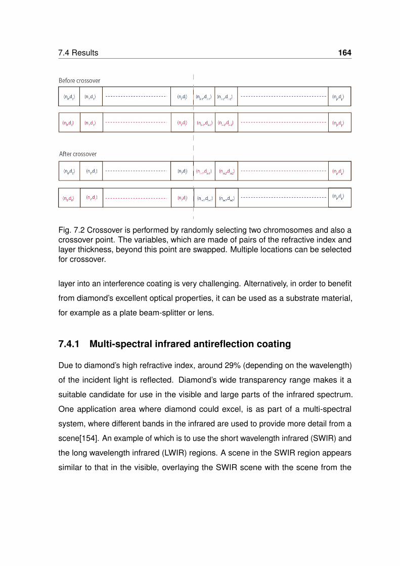
7.4 Results 164
Fig. 7.2 Crossover is performed by randomly selecting two chromosomes and also acrossover point. The variables, which are made of pairs of the refractive index andlayer thickness, beyond this point are swapped. Multiple locations can be selectedfor crossover.
layer into an interference coating is very challenging. Alternatively, in order to benefit
from diamond’s excellent optical properties, it can be used as a substrate material,
for example as a plate beam-splitter or lens.
7.4.1 Multi-spectral infrared antireflection coating
Due to diamond’s high refractive index, around 29% (depending on the wavelength)
of the incident light is reflected. Diamond’s wide transparency range makes it a
suitable candidate for use in the visible and large parts of the infrared spectrum.
One application area where diamond could excel, is as part of a multi-spectral
system, where different bands in the infrared are used to provide more detail from a
scene[154]. An example of which is to use the short wavelength infrared (SWIR) and
the long wavelength infrared (LWIR) regions. A scene in the SWIR region appears
similar to that in the visible, overlaying the SWIR scene with the scene from the

7.4 Results 165
LWIR can enhance hot objects and help the observer identify the important parts of
a scene.
Choosing suitable materials for coating diamond depends on numerous fac-
tors, such as the transparency, durability and the adhesion properties[249]. Y2O3
has been used as a coating on diamond for increasing the transmission in the
8-10µm wavelength range, however an AlN interface layer was added to increase
the adhesion[250]. The Y2O3 coating helps prevent the oxidation of the diamond
at temperatures above 750°C, hence it can be used in air in high speed flight[251].
Other coatings on diamond made from different transition metal oxides have been
tested with varying adhesion and optical performance[252]. However, it has been
demonstrated that Y2O3 has a better transparency above 10µm than other common
oxides[253].
There are only a handful of materials suitable for the SWIR and LWIR regions. A
common substrate material for these regions is either ZnS or ZnSe. Coatings for the
region around 1064nm and 7.5-10.5µm ranges made of ZnS, Y2O3 and YF3 have
been demonstrated for coating onto a ZnSe window[254]. A theoretical transmittance
above 98.5% was achieved in the 7.5-10.5µm range and a peak transmittance of
99.7% was achieved at 1064nm. However, the experimentally observed values were
less than this. Y2O3 was used as an outer layer to protect the other films.
The aim in the following is to design a broadband antireflection coating for the
wavelength ranges 900-1400nm and 8-10µm. These regions are chosen since
diamond is transparent at these wavelengths and additionally the atmosphere is
also transparent[255]. The material choice for this wavelength region is very limited.
Thorium fluoride is one example of a low index material that is used in the infrared
wavelength region, however, since it is radioactive and highly toxic it can not be
used for many applications[256]. Alternative low refractive index materials that
are commonly used in the specified wavelength range include YF3 and YbF3. In
the following, the materials that are chosen are YbF3, Y2O3 and ZnS using the
wavelength dependent refractive indices from references [179] and [257].

7.4 Results 166
Figure 7.3 shows the results from running the genetic algorithm synthesis code
to minimise the reflectance in the 900-1400nm and 8-10µm, regions. After each
generation the layer structure that has the lowest merit function value is displayed
across the horizontal axis. As the algorithm progresses there are sudden changes
in the layer structure as the algorithm explores the solution space before eventually
converging to a solution. It can be seen that there are some thin layers in the film,
between 5-10nm thick. If there are practical limitations which limits their deposition,
they can be removed manually and the resulting structure refined to minimise the
merit function. The final structure has 19 layers but can be reduced to 12 layers if
the thin layers are removed, without significantly changing the reflectance.
Fig. 7.3 The structure of the elite coating after each generation has finished. Thelayer nearest the substrate is located on the left and the layer nearest the medium ison the right. The materials that were used for the coating are shown in the legend,the substrate was diamond and the medium was air.
The reflectance that this coating produces is shown in figure 7.4. It can be
observed that the reflectance across the wavelength range 900nm-1400nm is below
0.5% and the mean reflection is 0.26%. While in the 8-10µm range the reflectance
is below 1% and the mean reflection is 0.34%. The Y2O3 coating becomes more
absorbing beyond 10µm which limits its use above this range, however, the amount
of light it absorbs is highly dependent on the deposition method and also the total
thickness of the material used in the coating.

7.4 Results 167
(a) Short wavelength infrared (b) Long wavelength infrared
Fig. 7.4 The reflectance for the two wavelength bands of interest found using the ge-netic algorithm. The reflectance is below 0.5% for almost all of the short wavelengthinfrared region and below 1% for the long wavelength infrared region. The substratematerial is diamond and the angle of incidence is normal to the surface.
(a) Short wavelength infrared (b) Long wavelength infrared
Fig. 7.5 The reflectance for the two wavelength bands of interest plotted against theangle of incidence. Note the different scales in the legend for the two plots. The lightis unpolarised.

7.4 Results 168
Coatings on lenses need to have a low reflectance across a range of angles in
order to collect as much light as possible from a scene. Figure 7.5 shows how the
reflectance from the coating varies with angle and wavelength. It can be observed
that the reflectance is below 0.5% over almost the whole region in the SWIR and
below 1% over most of the LWIR range. It should be noted that the scales on the
two plots are different.
Only the theoretical reflectance is treated here, it is left for further study if this
coating could be fabricated since there are likely to be issues with thin film stress.
Also, the materials used may not adhere well to the diamond’s surface. There will
also be a variation caused by the refractive index of the materials being different to
the values used in the program, since it depends on the deposition method.
7.4.2 Non-polarising beam splitter
Comparing methods of generating optical coatings is complicated by designers using
different merit functions and varying target designs. Additionally, in order to speed up
computation, it is beneficial to reduce the number of points where the merit function
is evaluated. This is particularly necessary for genetic algorithms since a population
of solutions needs to be evaluated. However, due to the oscillatory nature of most
solutions, it can make the merit function arbitrarily low. This can also make the
comparison of merit function values more difficult.
In order to compare methods and designs, a number of competitions have been
proposed. One recent competition (2007) was to synthesise a coating for a non-
polarising beam splitter[201]. The criteria for the competition were as follows,
Angle of incidence: 45°
Centre wavelength: 550nm
Rs = Rp ± 2%
40% ≤ Rs , Rp ≤ 60%
∆R , ∆T = 0 ± 1°

7.4 Results 169
Where Rs, Rp are the reflectance from the surface for the s and p polarisation
states. ∆R and ∆T are the phase difference between the polarisation states upon
reflection and transmission through the coating. The solutions were evaluated as to
how far around the central wavelength of 550nm they maintained the criteria. There
were several materials to choose from, but only up to three could be used in the
final design. There was no limit on the total number of layers or optical thickness,
however, a minimum was placed on an individual layer thickness of 5nm. The
winning solution to the problem achieved a centred bandwidth of 61.7nm, with a total
thickness of 15148nm and 214 layers. The design method that was used by most of
the designers was the needle optimisation method from a variety of starting designs.
In the following the algorithm designed in this research will be used to attempt to
solve the non-polarising beam splitter problem.
To accommodate the more complex criteria the genetic algorithm was modified
with an adaptive penalty term to the merit function. The penalty term, which includes
contributions from the bounds in the above criteria, is multiplied by a factor which
increases as the genetic algorithm progresses. A penalty term is needed since there
are two types of optimisation function; one is the ideal solution and the second is the
tolerance that must be fulfilled if the solution is to be accepted. The method chosen
in the following is to increase the merit function value when the solution passes
outside the bounds of the problem while leaving it unchanged if the solution is within
its bounds. Figure 7.6 shows how the target and penalty terms of the elite solution
in the population evolve as the algorithm progresses. There is initially a very high
merit function value since the initial population is randomly generated. However, as
the algorithm progresses the target and penalty terms significantly reduce.
The structure of the elite solution in the population after each generation is shown
in figure 7.7. Since the merit function was more complicated, a larger number of
generations were required than in the previous example. It is observed that there
are very quick changes in the elite layer structure in the population as it searches
the solution space at the start of the algorithm. Areas where the algorithm became

7.4 Results 170
Fig. 7.6 The target and penalty terms of the elite layer is plotted against the genera-tion. The two terms are combined to make the merit function value which penalisesthe target value as the algorithm progresses.
stuck in a local minimum are characterised by the layer structure not changing for
many generations. The final layer structure is given by the last line at the bottom of
the figure. It is expected that greater improvement could be made if the algorithm
was allowed to run for more generations since the population had not converged,
however, as can be seen in figure 7.6 the rate of change in the merit function
decreases dramatically.
The results from the completion of the algorithm are shown in figures 7.8 and
7.9. Figure 7.8 shows how the reflectance from the film changes with wavelength.
The objective was to keep the reflectance of the two polarisation states within 2%,
which is achieved over the whole range shown. Figure 7.9 shows how ∆R and ∆T
change with wavelength. The objective was to keep ∆R and ∆T between ± 1°. It
can be seen that ∆R achieves this objective over a larger range than ∆T . The final
centred bandwidth around 550nm equalled 19.4nm and the total coating thickness
was 1901nm.
The results presented here have a centred bandwidth that is less than the
competition winner, which used the needle optimisation approach. However, the

7.4 Results 171
Fig. 7.7 The structure of the elite solution in the population after each generation isplotted. The material used in each layer is given in the legend. The refractive indexof each material is; F=1.38, M=1.8, H=2.35. Dispersion is ignored in this example.
Fig. 7.8 The reflectance from one surface of a non-polarising beam splitter for bothpolarisation states. The necessary criteria for the reflection are fulfilled over a largerrange than shown, however, ∆T is not fulfilled.

7.4 Results 172
Fig. 7.9 The phase difference between the s and p polarisations in transmission andreflection of a non-polarising beam splitter. The criteria for ∆R are fulfilled over arange greater than shown. ∆T is the limiting criteria in this example.
thickness of the coating presented here is significantly less than all bar one of the
entries to the competition. The entry which was closest to the coating synthesised in
this work, had a centred bandwidth of 22nm, however, it required a coating thickness
of over 4000nm. There are a number of reasons why genetic algorithms may not
be the best single approach to resolving this specific problem. One issue is that the
winning solution in the competition requires 214 layers. Since genetic algorithms
require a population of solution which can run to thousands, increasing the number
of layers significantly slows down finding the merit function. Each new layer adds
another two matrices that needs to be multiplied to the matrix of the previous layers.
This means that genetic algorithms may not be the optimal method to solve the
problem if a fast solution time is required. However, since finding the merit function
value can be distributed across many processors, it could be practical if there is
sufficient computing power available.

7.5 Conclusion 173
7.5 Conclusion
In this chapter, a novel approach for using genetic algorithms to synthesise opti-
cal thin film coatings was developed. This algorithm was used to synthesise an
antireflection coating for a diamond substrate in the infrared spectrum. There is a
lot of interest in using diamond for optical lenses and its transparency over a wide
wavelength range makes it an ideal material for multi-spectral applications. The
coating achieved a broadband reduction in the reflectance to less than 1% over
the whole region of interest and a mean reflectance of 0.26% and 0.34% for the
short and long wavelength infrared regions respectively. It is expected that using
more layers or increasing the optical thickness could increase the wavelength range
of the antireflection coating. The wavelength range considered in this research
was limited by the available literature data of the refractive indices of the materials
considered. It is expected that the dispersion properties would also depend on the
deposition method used. It remains to be seen if the coating structure designed
in this work could be manufactured since it is possible that the adhesion between
the diamond and the first layer could be weak or the film could delaminate or crack.
However, since the coatings described are not very thick and the coating materials
are commonly used, it is feasible the coating could be easily manufactured.
Comparing the algorithm described above to the needle method, which is one of
the most common thin film synthesis methods, showed that the genetic algorithm
produces less optimal results for the case of a non-polarising beam splitter. However,
there are many different types of optical coatings that can be considered and the
method outlined in this chapter could provide a complementary approach that could
synthesise a starting design that could then be further refined.
The worth of using genetic algorithms as opposed to the other common algo-
rithms comes from not needed to specify the total thickness of the coating as a
starting parameter. Both the needle method and the flip flop method require a set
starting thickness. Hence, using genetic algorithms removes a highly strict constraint.

7.5 Conclusion 174
However, there are also a lot of disadvantages such as the computing power required
for the large population of solutions. Additionally, the algorithm needs to be run
several times due to the random starting conditions and processes that occur.
When synthesising optical coatings, one objective is to produce the lowest
possible merit function value, however, it may not be the most practical solution.
Examples where additional conditions need to be met include in coating plastic
substrates[258] or coatings designed for high temperatures[259]. These coatings
usually require that the coating is scratch resistant or does not degrade/oxidise easily.
The advantage of the procedure outlined above is that any layer can be fixed to a
certain material or design thickness while allowing every other layer to vary.
Another advantage of the approach described in this work is the ability to add
layers and hence optical thickness by an amount determined by the genetic algorithm.
Previous approaches have relied on setting a range of starting thicknesses, which
could only be changed by mutation. A disadvantage of this approach is that for
complex problems with many layers, the amount of computing power required
increases significantly. In summary, genetic algorithms provide a useful addition to
the optical designer which complements other design methods.

Chapter 8
Conclusions and Future Work
In this thesis, thin film nanocrystalline diamond has been studied as a potential
material for a range of optical components. Applications involving tunable lenses and
beam splitters have been examined and the transmission properties through these
components have been tailored to adjust the intensity of light transmitted. Minimising
reflection losses is important if a lens is included in a larger optical systems, where
the transmission properties of the system degrade significantly if the reflections from
the surfaces are too high. Additionally, in this work a novel approach using genetic
algorithms has been demonstrated that is able to synthesis optical interference
coatings. Using this program a coating was designed to minimise the reflection from
a diamond optical component for two regions of the infrared spectrum.
To explain some of the phenomena that appeared during this research a program
was written that calculates the colour that would be observed from a thin film
multilayer stack. This was used in order to explain the different colours that are
seen in many films and also to estimate the thickness of the film. Observing the
colour provides a quick and qualitative way of estimating the thickness of a film
without the need for an expensive piece of equipment. The program can also
calculate the expected transmission or reflection through a surface, however, it is
limited to calculating optically thin materials. This means that it can only calculate
the transmission through one surface of a lens. The program could be extended

176
by including the transmission through an optically incoherent layer so that the
transmission through beam splitters and lenses could be treated through the whole
component, not just one surface.
In chapter 5, a tunable lens was fabricated that used the deformable membrane
as an antireflection coating. It was designed to minimise the reflection at one
wavelength. This can be useful for monochromatic sources such as lasers and it is
possible to tune the thicknesses of the films to reduce the reflection to zero at any
wavelength required. However, it is less useful if you are trying to image a scene,
since the reflections at some wavelength could be very large. By increasing the
number of layers in the antireflection coating to four, the reflection losses can be
reduced to less than 1% over most of the visible spectrum. This is illustrated in
figure 8.1 where a coating is presented that is made from layers of MgF2, NCD and
SiO2. The total thickness of the membrane would equal 405nm which is slightly
more than the membrane considered in chapter 5. Whether this coating could be
fabricated is left to further work, however, the temperatures that are typical for CVD
of diamond are less than the melting points of SiO2 and MgF2[260]. Therefore it
might be possible to deposit NCD onto these materials. However, the fabrication
method might be difficult and stresses present could cause the film to delaminate
or crack. Cracking will be an issue especially when a pressure is applied and the
membrane is deformed.
A major problem to overcome is the removal of wrinkles from the thin films that
appeared after they had been sputtered. The presence of wrinkles limits the optical
applications of the films significantly. It would be inappropriate to use it in a system
designed for imaging, but it could be useful for beam sampling applications, where
only the intensity is important. One potential method to remove the wrinkles would
be to make the diamond film more stressed. This could be achieved by changing
the deposition temperature during diamond growth. A second method would be to
deposit the ZnO onto the diamond before the silicon is back etched. This would help

177
Fig. 8.1 The theoretical reflectivity of two coatings against wavelength. Coating Ais the same as was discussed in chapter 5. Coating B is a new coating proposalwith four layers. From the air interface working towards the refracting liquid (n=1.5)the layers are made from MgF2, NCD, SiO2, MgF2 with thicknesses 100nm, 115nm,90nm, 100nm respectively[261].

178
reduce the temperature of the film while is being sputtered since there would be
more silicon to dissipate the heat.
A future study could look to see if the sputtering process damages the surface
of the diamond. The use of oxygen gas in the sputtering chamber could damage
the surface of the diamond even though magnetron sputtering keeps the plasma
localised away from the substrate. It would also be interesting to test the adhesion of
different sputtered materials onto diamond. The ZnO used in this thesis was found
to adhere fairly well but it is not commonly used as part of an optical interference
coating.
The deflection properties of the membrane were not tested in this work due to
the wrinkling of the membrane. Once the problem of wrinkling has been overcome, a
study should be performed to see how the addition of layers affects the deformation
of the membrane under pressure. This would help determine the range of focal
lengths that can be achieved and therefore how practical such a device would be.
In addition, the imaging properties and the wavefront error of the lens should be
measured. Also, the speed with which the device can change its focal length should
be measured and compared with other methods of changing the focal length.
This research also examined how coating an NCD membrane with varying
thicknesses of ZnO changes their transmission properties. The bilayer membranes
fabricated were tested as beam splitters. Experimental systems were built that
allowed the transmitted and reflected intensities of the membranes to be quickly
measured against the incident angle. It was found that summing the reflected and
transmitted light did not equal the incident light, suggesting that some of the incident
light was lost to scattering or absorption in the membrane. The experimental system
designed in this work could be extended to include a wider range of wavelengths with
the addition of a broad spectrum light source and a monochromator. Comparing the
transmission properties of the membranes with that theoretically predicted showed
that there was agreement with the theory at longer wavelengths. However, at shorter
wavelengths the films were found to absorb a significant proportion of light.

179
One aim of this work was to see if an NCD membrane could be successfully
coated with material without breaking or deforming. It was hoped that the NCD
would have enough strength so that it could be coated on both sides, without the
need to be removed from the deposition chamber. However, the wrinkling of the film
when the thickness of ZnO was increased proved that this was not possible. If the
fabrication method was improved so that wrinkling did not occur, by using more than
two layers the transmission and reflection properties from the membrane could be
tailored.
A future study could measure the signal loss and eye diagram[262] of the beam
splitter to test how useful it would be as an optical tap in an optical bus. This
would also test the signal degradation and the fan-out of the system. One future
application where coated NCD membranes could be useful is in analogue optical
computing[263, 264]. These systems can be created by increasing the number
of layers on the membrane so that mathematical functions such as second order
differentiation can be performed on an input waveform. Diamond could be useful
in such a device as its high tensile strength could increase the size of the open
aperture.
In chapter 7, a genetic algorithm was written that was used to synthesise an
antireflection coating and a non-polarising beam splitter coating. It was found that
the needle method is better at synthesising a non-polarising beam splitter than the
algorithm developed in this work. While only two types of optical coating types were
considered, there are many other thin film structures that could be explored; such
as band pass filters[265] and dielectric mirrors[266]. The ability of the algorithm
to add optical thickness means that the requirements for the starting parameters
are less stringent so it can easily adapt to the problem. It would be interesting to
see if further improvement to the optical coating structure optimised by the genetic
algorithm could be improved by using the needle method on the solution. The needle
method is used to find locations where a needle can be inserted that reduces the

180
merit function value and so would be able to determine if the genetic algorithm had
become stuck in a local minimum.
A future addition to the genetic algorithm program could take inspiration from the
flip-flop method, discussed earlier, where the coating is split into small equal sized
layers. In this approach, the coating would be split into a much larger number of
parameters, meaning that the crossover process could occur at a fixed thickness in
the coating as opposed to a fixed layer number. This could improve the performance,
however, it increases the computational complexity.
While diamond is an excellent choice of material in the infrared, it has one major
limitation, it absorbs light in the mid-infrared wavelength region. This means that
in a multi-spectral sensing system, this region can not be transmitted through the
diamond optical component and so is lost. One way this could be overcome is to
design a coating that is highly transmissive in the SWIR and LWIR regions, but
reflective in the mid-infrared region. This would split the light so that the three
regions of the infrared could be sensed and more information about a scene could
be resolved. The disadvantage is that the system would require three separate
detectors which could make it inconveniently large.
In summary, it has been shown that diamond has the potential to act as a suitable
material for a number of optical applications. However, there are still a number of
challenges to overcome in fabricating thin membrane optical components.

References
[1] Research B. Optical Coatings: Technologies and Global Markets; 2017.
[2] Plantzos D. Crystals and lenses in the Graeco-Roman world. AmericanJournal of Archaeology. 1997;p. 451–464.
[3] Kallhammer J. The road ahead for car night-vision. Nature Photonics.2006;5:12–13.
[4] Cohen M, Unger B, Milkosky J. Laser machining of thin films and integratedcircuits. Bell System Technical Journal. 1968;47(3):385–405.
[5] Ren D, Allington-Smith JR. Apochromatic lenses for near-infrared astronomicalinstruments. Society of Photo-Optical Instrumentation Engineers; 1999. .
[6] Massart M, Union P, Scarsbrook G, Sussmann RS, Muys PF. CVD-growndiamond: a new material for high-power CO2 lasers. In: 27th Annual BoulderDamage Symposium: Laser-Induced Damage in Optical Materials: 1995. vol.2714. International Society for Optics and Photonics; 1996. p. 177–185.
[7] Nuttall R, Frank A. Jewel lenses – a historical curiosity. New Scientist.1972;53:92–93.
[8] Technologies ES. The Element Six CVD Diamond Handbook;.
[9] Godfried HP, Coe SE, Hall C, Pickles CSJ, Sussmann RS, Tang X, et al. Use ofCVD diamond in high-power CO2 lasers and laser diode arrays. In: AdvancedHigh-Power Lasers. vol. 3889. International Society for Optics and Photonics;2000. p. 553–564.
[10] Woerner E, Wild C, Mueller-Sebert W, Koidl P. CVD-diamond optical lenses.Diamond and Related Materials. 2001;10(3-7):557–560.
[11] Karlsson M, Nikolajeff F. Diamond micro-optics: microlenses and antire-flection structured surfaces for the infrared spectral region. Optics Express.2003;11(5):502–507.
[12] Choi H, Gu E, Liu C, Griffin C, Girkin J, Watson I, et al. Fabrication ofnatural diamond microlenses by plasma etching. Journal of Vacuum Science& Technology B: Microelectronics and Nanometer Structures Processing,Measurement, and Phenomena. 2005;23(1):130–132.

References 182
[13] Hutley M. Optical techniques for the generation of microlens arrays. Journalof Modern Optics. 1990;37(2):253–265.
[14] Faklis D, Morris GM. Spectral properties of multiorder diffractive lenses.Applied Optics. 1995;34(14):2462–2468.
[15] Kononenko VV, Konov VI, Pimenov SM, Prokhorov AM, Pavel’ev VS, Soifer VA.Diamond diffraction optics for CO2 lasers. Quantum Electronics. 1999;29(1):9.
[16] Nikolajeff FK, Karlsson M. Diamond optics: fabrication and applications. In:Micromachining Technology for Micro-Optics and Nano-Optics II. vol. 5347.International Society for Optics and Photonics; 2003. p. 38–44.
[17] Björkman H, Rangsten P, Hjort K. Diamond microstructures for opticalmicro electromechanical systems. Sensors and Actuators A: Physical.1999;78(1):41–47.
[18] Durazo-Cardenas I, Shore P, Luo X, Jacklin T, Impey S, Cox A. 3D characterisa-tion of tool wear whilst diamond turning silicon. Wear. 2007;262(3-4):340–349.
[19] Element Six. Enable extreme performance photonics; 2015.
[20] Diamond Materials. Diamond Materials company brochure; 2020.
[21] Callister WD, Rethwisch DG, et al. Materials science and engineering: anintroduction. vol. 7. John Wiley & Sons New York; 2007.
[22] Palmer D, Conley M. CrystalMaker. CrystalMaker Software, Bicester, England.2007;.
[23] Robertson R, Fox JJ, Martin A. Two types of diamond. Philosophical Trans-actions of the Royal Society of London Series A, Containing Papers of aMathematical or Physical Character. 1933;232(707-720):463–535.
[24] Sutherland G, Blackwell D, Simeral W. The problem of the two types ofdiamond. Nature. 1954;174(4437):901.
[25] Field JE. The properties of natural and synthetic diamond. Academic Press;1992.
[26] Bundy F, Bassett W, Weathers M, Hemley R, Mao H, Goncharov A. Thepressure-temperature phase and transformation diagram for carbon; updatedthrough 1994. Carbon. 1996;34(2):141–153.
[27] Bundy F, Hall HT, Strong H, Jun RW. Man-made diamonds. Nature.1955;176(4471):51.
[28] Bovenkerk H, Bundy F, Hall H, Strong H, et al. Preparation of diamond. Nature.1959;184(4693):1094.
[29] Sumiya H, Satoh S. High-pressure synthesis of high-purity diamond crystal.Diamond and Related Materials. 1996;5(11):1359–1365.

References 183
[30] Eversole WG. Synthesis of diamond; 1962. US Patent 3,030,187.
[31] Hazen RM. The diamond makers. Cambridge University Press; 1999.
[32] Deryaguin B, Fedoseev D, Lukyanovich V, Spitzin B, Ryabov V, Lavrentyev A.Filamentary diamond crystals. Journal of Crystal Growth. 1968;2(6):380–384.
[33] Angus JC, Will HA, Stanko WS. Growth of diamond seed crystals by vapordeposition. Journal of Applied Physics. 1968;39(6):2915–2922.
[34] Deryagin B, Spitsyn B, Builov L, Klochkov A, Gurodetski A, Smolyaninov A.Synthesis of diamond on non-diamond substrates. vol. 231; 1976. p. 333–335.
[35] Deryaguin B, Fedoseev D. The synthesis of diamond at low pressure. ScientificAmerican. 1975;233(5):102–109.
[36] Matsumoto S, Sato Y, Kamo M, Setaka N. Vapor deposition of diamond parti-cles from methane. Japanese Journal of Applied Physics. 1982;21(4A):L183.
[37] Kamo M, Sato Y, Matsumoto S, Setaka N. Diamond synthesis from gas phasein microwave plasma. Journal of Crystal Growth. 1983;62(3):642–644.
[38] Angus JC, Argoitia A, Gat R, Li Z, Sunkara M, Wang L, et al. Chemical vapourdeposition of diamond. Philosophical Transactions of the Royal Society ofLondon Series A: Physical and Engineering Sciences. 1993;342(1664):195–208.
[39] Swain GM, Ramesham R. The electrochemical activity of boron-doped poly-crystalline diamond thin film electrodes. Analytical Chemistry. 1993;65(4):345–351.
[40] Jin S, Moustakas T. Effect of nitrogen on the growth of diamond films. AppliedPhysics Letters. 1994;65(4):403–405.
[41] Koizumi S, Kamo M, Sato Y, Ozaki H, Inuzuka T. Growth and characterizationof phosphorous doped {111} homoepitaxial diamond thin films. AppliedPhysics Letters. 1997;71(8):1065–1067.
[42] Stiegler J, Lang T, Nyga M, Von Kaenel Y, Blank E, et al. Low temperaturelimits of diamond film growth by microwave plasma-assisted CVD. Diamondand Related Materials. 1996;5(3-5):226–230.
[43] Bachmann PK, Hagemann HJ, Lade H, Leers D, Picht F, Wiechert DU, et al.Diamond chemical vapor deposition: gas compositions and film properties.MRS Online Proceedings Library Archive. 1994;339.
[44] Harris SJ, Martin LR. Methyl versus acetylene as diamond growth species.Journal of Materials Research. 1990;5(11):2313–2319.
[45] Harris SJ. Mechanism for diamond growth from methyl radicals. AppliedPhysics Letters. 1990;56(23):2298–2300.
References 184
[46] Butler JE, Woodin RL. Thin film diamond growth mechanisms. Phil Trans RSoc Lond A. 1993;342(1664):209–224.
[47] Lu Z, Heberlein J, Pfender E. Process study of thermal plasma chemical vapordeposition of diamond, Part I: Substrate material, temperature, and methaneconcentration. Plasma Chemistry and Plasma Processing. 1992;12(1):35–53.
[48] May PW. CVD diamond: a new technology for the future? Endeavour.1995;19(3):101–106.
[49] Liu H, Dandy DS. Studies on nucleation process in diamond CVD: an overviewof recent developments. Diamond and related Materials. 1995;4(10):1173–1188.
[50] Jiang X, Klages CP, Rösler M, Zachai R, Hartweg M, Füsser HJ. Depositionand characterization of diamond epitaxial thin films on silicon substrates.Applied Physics A. 1993;57(6):483–489.
[51] Suzuki K, Sawabe A, Yasuda H, Inuzuka T. Growth of diamond thin films by dcplasma chemical vapor deposition. Applied Physics Letters. 1987;50(12):728–729.
[52] Iijima S, Aikawa Y, Baba K. Early formation of chemical vapor depositiondiamond films. Applied Physics Letters. 1990;57(25):2646–2648.
[53] Danilenko VV. On the history of the discovery of nanodiamond synthesis.Springer; 2004.
[54] Aleksenskii A, Baidakova M, Vul AY, Davydov VY, Pevtsova YA. Diamond-graphite phase transition in ultradisperse-diamond clusters. Physics of theSolid State. 1997;39(6):1007–1015.
[55] Krueger A. The structure and reactivity of nanoscale diamond. Journal ofMaterials Chemistry. 2008;18(13):1485–1492.
[56] Krüger A, Kataoka F, Ozawa Maa, Fujino T, Suzuki Y, Aleksenskii A, et al.Unusually tight aggregation in detonation nanodiamond: identification anddisintegration. Carbon. 2005;43(8):1722–1730.
[57] Aleksenskiy A, Eydelman E, Vul AY. Deagglomeration of detonation nanodia-monds. Nanoscience and Nanotechnology Letters. 2011;3(1):68–74.
[58] Sumant AV, Gilbert P, Grierson DS, Konicek AR, Abrecht M, Butler JE, et al.Surface composition, bonding, and morphology in the nucleation and growthof ultra-thin, high quality nanocrystalline diamond films. Diamond and RelatedMaterials. 2007;16(4-7):718–724.
[59] Jeon ID, Park CJ, Kim DY, Hwang NM. Effect of methane concentration onsize of charged clusters in the hot filament diamond CVD process. Journal ofCrystal Growth. 2001;223(1-2):6–14.

References 185
[60] Williams O, Nesladek M, Daenen M, Michaelson S, Hoffman A, Osawa E, et al.Growth, electronic properties and applications of nanodiamond. Diamond andRelated Materials. 2008;17(7-10):1080–1088.
[61] Silva F, Bénédic F, Bruno P, Gicquel A. Formation of< 110> texture duringnanocrystalline diamond growth: an X-ray diffraction study. Diamond andRelated Materials. 2005;14(3-7):398–403.
[62] Pickrell D, Kline K, Taylor R. Thermal expansion of polycrystalline dia-mond produced by chemical vapor deposition. Applied Physics Letters.1994;64(18):2353–2355.
[63] Moelle C, Klose S, Szücs F, Fecht H, Johnston C, Chalker P, et al. Mea-surement and calculation of the thermal expansion coefficient of diamond.Diamond and Related Materials. 1997;6(5-7):839–842.
[64] Slack GA, Bartram S. Thermal expansion of some diamondlike crystals.Journal of Applied Physics. 1975;46(1):89–98.
[65] Alers P, Hintermann H, Hayward I. Correlations between Raman scatteringand thermal expansion behavior for CVD and natural diamond. Thin SolidFilms. 1995;259(1):14–17.
[66] Sukhadolau A, Ivakin E, Ralchenko V, Khomich A, Vlasov A, Popovich A.Thermal conductivity of CVD diamond at elevated temperatures. Diamondand related materials. 2005;14(3-7):589–593.
[67] Graebner J, Jin S, Kammlott G, Bacon B, Seibles L, Banholzer W. Anisotropicthermal conductivity in chemical vapor deposition diamond. Journal of appliedphysics. 1992;71(11):5353–5356.
[68] Scott D. The history and impact of synthetic diamond cutters and diamondenhanced inserts on the oil and gas industry. Industrial Diamond Review.2006;1:48.
[69] Philip J, Hess P, Feygelson T, Butler J, Chattopadhyay S, Chen K, et al. Elastic,mechanical, and thermal properties of nanocrystalline diamond films. Journalof Applied Physics. 2003;93(4):2164–2171.
[70] Siegel RW, Fougere GE. Mechanical properties of nanophase materials. In:Nanophase materials. Springer; 1994. p. 233–261.
[71] Sumiya H, Toda N, Satoh S. Mechanical properties of synthetic type IIadiamond crystal. Diamond and Related Materials. 1997;6(12):1841–1846.
[72] Grimsditch M, Ramdas A. Brillouin scattering in diamond. Physical Review B.1975;11(8):3139.
[73] McSkimin H, Andreatch Jr P. Elastic moduli of diamond as a function ofpressure and temperature. Journal of Applied Physics. 1972;43(7):2944–2948.

References 186
[74] Klein CA, Cardinale GF. Young’s modulus and Poisson’s ratio of CVD diamond.Diamond and Related Materials. 1993;2(5-7):918–923.
[75] Roark RJ, Young WC. Formulas for stress and strain. McGraw-Hill; 1975.
[76] Beams J. Structure and properties of thin films. Wiley, New York, 1970) p.1959;183.
[77] Williams OA, Kriele A, Hees J, Wolfer M, Müller-Sebert W, Nebel C. HighYoung’s modulus in ultra thin nanocrystalline diamond. Chemical PhysicsLetters. 2010;495(1-3):84–89.
[78] Olson D, Reynolds G, Virshup G, Friedlander F, James B, Partain L. Tensilestrength of synthetic chemical-vapor-deposited diamond. Journal of appliedphysics. 1995;78(8):5177–5179.
[79] Coe S, Sussmann R. Optical, thermal and mechanical properties of CVDdiamond. Diamond and Related Materials. 2000;9(9-10):1726–1729.
[80] Clark C, Dean P, Harris P. Intrinsic edge absorption in diamond. Proceedingsof the Royal Society of London Series A Mathematical and Physical Sciences.1964;277(1370):312–329.
[81] Monroy E, Omnès F, Calle F. Wide-bandgap semiconductor ultraviolet pho-todetectors. Semiconductor Science and Technology. 2003;18(4):R33.
[82] Clark C, Davey S. One-phonon infrared absorption in diamond. Journal ofPhysics C: Solid State Physics. 1984;17(6):1127.
[83] Walker J. Optical absorption and luminescence in diamond. Reports onProgress in Physics. 1979;42(10):1605.
[84] Wilks J, Wilks E. Properties and applications of diamond. Butterworth-Heinemann Oxford; 1991.
[85] Bustarret E, Gheeraert E, Watanabe K. Optical and electronic propertiesof heavily boron-doped homo-epitaxial diamond. Physica Status Solidi (a).2003;199(1):9–18.
[86] Lax M, Burstein E. Infrared lattice absorption in ionic and homopolar crystals.Physical Review. 1955;97(1):39.
[87] Sellmeier W. Zur Erkarung der abnormen Farbenfolge im Spectrum einiger.Substanzen. Annalen der Physik und Chemie. 1871;219:272–282.
[88] Peter F. Über Brechungsindizes und Absorptionskonstanten des Diamantenzwischen 644 und 226 mµ. Zeitschrift für Physik A Hadrons and Nuclei.1923;15(1):358–368.
[89] Turri G, Webster S, Chen Y, Wickham B, Bennett A, Bass M. Index of refractionfrom the near-ultraviolet to the near-infrared from a single crystal microwave-assisted CVD diamond. Optical Materials Express. 2017;7(3):855–859.

References 187
[90] Rösch S. Die Optik des Fabulit, die Farbe des Brewsterwinkels und das Farb-spielmoment. Optica Acta: International Journal of Optics. 1965;12(3):253–260.
[91] Edwards DF, Ochoa E. Infrared refractive index of diamond. JOSA.1981;71(5):607–608.
[92] Bi XX, Eklund P, Zhang J, Rao A, Perry T, Beetz C. Optical properties ofchemical-vapor-deposited diamond films. Journal of Materials Research.1990;5(4):811–817.
[93] Yin Z, Akkerman Z, Yang B, Smith F. Optical properties and microstructure ofCVD diamond films. Diamond and Related Materials. 1997;6(1):153–158.
[94] Potocky S, Kromka A, Potmesil J, Remes Z, Polackova Z, Vanecek M. Growthof nanocrystalline diamond films deposited by microwave plasma CVD systemat low substrate temperatures. Physica Status Solidi (a). 2006;203(12):3011–3015.
[95] Daenen M, Williams OA, D’Haen J, Haenen K, Nesládek M. Seeding, growthand characterization of nanocrystalline diamond films on various substrates.Physica Status Solidi (a). 2006;203(12):3005–3010.
[96] Li X, Perkins J, Collazo R, Nemanich RJ, Sitar Z. Investigation of the effect ofthe total pressure and methane concentration on the growth rate and qualityof diamond thin films grown by MPCVD. Diamond and Related Materials.2006;15(11-12):1784–1788.
[97] Window B. Recent advances in sputter deposition. Surface and Coatingstechnology. 1995;71(2):93–97.
[98] Demiryont H, Sites JR, Geib K. Effects of oxygen content on the opticalproperties of tantalum oxide films deposited by ion-beam sputtering. AppliedOptics. 1985;24(4):490–495.
[99] Thornton JA. The microstructure of sputter-deposited coatings. Journal of Vac-uum Science & Technology A: Vacuum, Surfaces, and Films. 1986;4(6):3059–3065.
[100] Kinbara A. Sputtering. WILEY-VCH Verlag GmbH & Co KGaA; 2003. .
[101] Perkampus HH. UV-VIS Spectroscopy and its Applications. Springer Science& Business Media; 2013.
[102] Fox M. Optical Properties of Solids. Oxford University Press; 2010.
[103] Smith E, Dent G. Modern Raman Spectroscopy - A Practical Approach, JohnWiley and Sons;.
[104] Bischel W, Black G. Wavelength dependence of Raman scattering crosssections from 200-600 nm. In: AIP Conference proceedings. vol. 100. AIP;1983. p. 181–187.

References 188
[105] Dimension icon with ScanAsyst Instruction Manual; 2010.
[106] Haugstad G. Atomic Force Microscopy: Understanding Basic Modes andAdvanced Applications. John Wiley & Sons, Inc; 2012.
[107] Gadelmawla E, Koura M, Maksoud T, Elewa I, Soliman H. Roughness param-eters. Journal of Materials Processing Technology. 2002;123(1):133–145.
[108] Fujiwara H. Spectroscopic ellipsometry: principles and applications. JohnWiley & Sons; 2007.
[109] Lyman CE, Newbury DE, Goldstein J, Williams DB, Romig Jr AD, ArmstrongJ, et al. Scanning electron microscopy, X-ray microanalysis, and analyticalelectron microscopy: a laboratory workbook. Springer Science & BusinessMedia; 2012.
[110] 2. In: Scanning Beam Methods. Wiley-Blackwell; 2007. p. 305–497. Availablefrom: https://onlinelibrary.wiley.com/doi/abs/10.1002/9783527614561.ch2.
[111] Gupta S, Weiner BR, Morell G. Spectroscopic ellipsometry studies of nanocrys-talline carbon thin films deposited by HFCVD. Diamond and Related Materials.2001;10(11):1968–1972.
[112] Mistrik J, Janicek P, Taylor A, Fendrych F, Fekete L, Jager A, et al. Spectro-scopic ellipsometry characterization of nano-crystalline diamond films pre-pared at various substrate temperatures and pulsed plasma frequencies usingmicrowave plasma enhanced chemical vapor deposition apparatus with linearantenna delivery. Thin Solid Films. 2014;571:230–237.
[113] Thomas EL, Mandal S, Macdonald JE, Dane TG, Rawle J, Cheng CL, et al.Spectroscopic ellipsometry of nanocrystalline diamond film growth. ACSOmega. 2017;2(10):6715–6727.
[114] Stoner B, Ma GH, Wolter S, Glass J. Characterization of bias-enhancednucleation of diamond on silicon by invacuo surface analysis and transmissionelectron microscopy. Physical Review B. 1992;45(19):11067.
[115] Aspnes D, Theeten J, Hottier F. Investigation of effective-medium modelsof microscopic surface roughness by spectroscopic ellipsometry. PhysicalReview B. 1979;20(8):3292.
[116] Quinten M. A Practical Guide to Optical Metrology for Thin Films. John Wiley& Sons; 2012.
[117] Houta F, Quinten M. Layer Thickness Determination: The influence of theaperture of a measuring head. Optik & Photonik. 2015;10(4):54–56.
[118] Jellison Jr G. Data analysis for spectroscopic ellipsometry. Thin Solid Films.1993;234(1-2):416–422.
[119] Passaglia E, Stromberg RR, Kruger J. Ellipsometry in the Measurement ofSurfaces and Thin Films: Symposium Proceedings. vol. 256. US NationalBureau of Standards; 1964.

References 189
[120] Azzam R, Bashara N. Ellipsometry and Polarized Light. North-Holland; 1977.
[121] Elvidge CD, Keith DM, Tuttle BT, Baugh KE. Spectral identification of lightingtype and character. Sensors. 2010;10(4):3961–3988.
[122] Bodrogi P, Khan T. Illumination, color and imaging: evaluation and optimizationof visual displays. John Wiley & Sons; 2012.
[123] Henrie J, Kellis S, Schultz SM, Hawkins A. Electronic color charts for dielectricfilms on silicon. Optics Express. 2004;12(7):1464–1469.
[124] de L’Eclairage CI. Colorimetry, official recommendations of the internationalcommission on illumination. Publication CIE. 1976;.
[125] Tooms MS. Colour reproduction in electronic imaging systems: photography,television, cinematography. John Wiley & Sons; 2016.
[126] Kinoshita A, Kitamura F, Horie M, Yoshida T. Spectroscopic ellipsometerwith the smallest measurement spot. In: Metrology, Inspection, and ProcessControl for Microlithography XIX. vol. 5752. International Society for Opticsand Photonics; 2005. p. 874–881.
[127] Richter U. Application of the degree of polarization to film thickness gradients.Thin Solid Films. 1998;313:102–107.
[128] Csermely Z, Horvath Z, Hanyecz I. Lugosi L. Spectroscopic EllipsometryAnalyzer–SEA user’s reference manual. Budapest–Hungary: Semilab Co.2012;.
[129] Ando Y, Tachibana T, Kobashi K. Growth of diamond films by a 5-kW microwaveplasma CVD reactor. Diamond and Related Materials. 2001;10(3-7):312–315.
[130] Kim S, Vedam K. Analytic solution of the pseudo-Brewster angle. JOSA A.1986;3(11):1772–1773.
[131] Azzam R, Thonn TF. Pseudo-Brewster and second-Brewster angles ofan absorbing substrate coated by a transparent thin film. Applied Optics.1983;22(24):4155–4165.
[132] Aspnes D, Theeten J, Hottier F. Investigation of effective-medium modelsof microscopic surface roughness by spectroscopic ellipsometry. PhysicalReview B. 1979;20(8):3292.
[133] Fujiwara H, Koh J, Rovira P, Collins R. Assessment of effective-mediumtheories in the analysis of nucleation and microscopic surface roughnessevolution for semiconductor thin films. Physical Review B. 2000;61(16):10832.
[134] Larruquert JI, Pérez-Marín AP, García-Cortés S, Rodríguez-de Marcos L,Aznárez JA, Méndez JA. Self-consistent optical constants of SiC thin films.JOSA A. 2011;28(11):2340–2345.
[135] Fischer RS, Wu Y, Kanchanawong P, Shroff H, Waterman CM. Microscopy in3D: a biologist’s toolbox. Trends in Cell Biology. 2011;21(12):682–691.

References 190
[136] Pollack MG, Shenderov AD, Fair R. Electrowetting-based actuation of dropletsfor integrated microfluidics. Lab on a Chip. 2002;2(2):96–101.
[137] Verheijen H, Prins M. Reversible electrowetting and trapping of charge: modeland experiments. Langmuir. 1999;15(20):6616–6620.
[138] Young T, et al. III. An essay on the cohesion of fluids. Philosophical transactionsof the Royal Society of London. 1805;95:65–87.
[139] Lester G. Contact angles of liquids at deformable solid surfaces. Journal ofColloid Science. 1961;16(4):315–326.
[140] Ren H, Xu S, Wu ST. Effects of gravity on the shape of liquid droplets. OpticsCommunications. 2010;283(17):3255–3258.
[141] Murade C, Van Der Ende D, Mugele F. High speed adaptive liquid microlensarray. Optics Express. 2012;20(16):18180–18187.
[142] Sugiura N, Morita S. Variable-focus liquid-filled optical lens. Applied Optics.1993;32(22):4181–4186.
[143] Leuenberger D, Optotune A, Voigt FF. Focus-Tunable Lenses Enable 3-DMicroscopy; 2015.
[144] Chronis N, Liu GL, Jeong KH, Lee LP. Tunable liquid-filled microlens arrayintegrated with microfluidic network. Optics Express. 2003;11(19):2370–2378.
[145] Chen J, Wang W, Fang J, Varahramyan K. Variable-focusing microlenswith microfluidic chip. Journal of Micromechanics and Microengineering.2004;14(5):675.
[146] Agarwal M, Gunasekaran R, Coane P, Varahramyan K. Polymer-based variablefocal length microlens system. Journal of Micromechanics and Microengineer-ing. 2004;14(12):1665.
[147] Timoshenko SP, Woinowsky-Krieger S. Theory of plates and shells. McGraw-hill; 1959.
[148] Pätz D, Leopold S, Hoffmann M, Sinzinger S. Tunable anamorphotic imagingsystem based on fluidic cylindrical lenses. In: 2014 International Conferenceon Optical MEMS and Nanophotonics. IEEE; 2014. p. 25–26.
[149] Zohrabi M, Cormack RH, Gopinath JT. Wide-angle nonmechanical beamsteering using liquid lenses. Optics Express. 2016;24(21):23798–23809.
[150] Fountain WD, Knopp CF. System for scanning a surgical laser beam; 1995.US Patent 5,391,165.
[151] Wehr A, Lohr U. Airborne laser scanning—an introduction and overview.ISPRS Journal of photogrammetry and Remote Sensing. 1999;54(2-3):68–82.
[152] Holmström ST, Baran U, Urey H. MEMS laser scanners: a review. Journal ofMicroelectromechanical Systems. 2014;23(2):259–275.

References 191
[153] Optotune. Enable extreme performance photonics; 2020.
[154] Thompson NA. Optical design of common aperture, common focalplane, multispectral optics for military applications. Optical Engineering.2013;52(6):061308.
[155] Lee JN, Park C, Whitesides GM. Solvent compatibility of poly(dimethylsiloxane)-based microfluidic devices. Analytical Chemistry.2003;75(23):6544–6554.
[156] Kriele A, Williams OA, Wolfer M, Brink D, Müller-Sebert W, Nebel CE.Tuneable optical lenses from diamond thin films. Applied Physics Letters.2009;95(3):031905.
[157] Zuerbig V, Pletschen W, Hees J, Sah R, Kirste L, Heidrich N, et al. Transparentdiamond electrodes for tunable micro-optical devices. Diamond and RelatedMaterials. 2013;38:101–103.
[158] Zuerbig V, Paetz D, Pletschen W, Hees J, Sah R, Kirste L, et al. Piezo-actuatedtunable diamond/AlN micro lenses. In: 2013 Transducers & EurosensorsXXVII: The 17th International Conference on Solid-State Sensors, Actuatorsand Microsystems (TRANSDUCERS & EUROSENSORS XXVII). IEEE; 2013.p. 2317–2320.
[159] Sobaszek M, Bogdanowicz R, Siuzdak K, Cirocka A, Zieba P, Gnyba M, et al.Optical and electrical properties of ultrathin transparent nanocrystalline boron-doped diamond electrodes. Optical Materials. 2015;42:24–34.
[160] May P, Ludlow W, Hannaway M, Heard P, Smith J, Rosser K. Raman and con-ductivity studies of boron-doped microcrystalline diamond, facetted nanocrys-talline diamond and cauliflower diamond films. Diamond and Related Materials.2008;17(2):105–117.
[161] Clapham P, Hutley M. Reduction of lens reflexion by the “Moth Eye” principle.Nature. 1973;244(5414):281.
[162] Wilson S, Hutley M. The optical properties of’moth eye’antireflection surfaces.Optica Acta: International Journal of Optics. 1982;29(7):993–1009.
[163] Sun CH, Jiang P, Jiang B. Broadband moth-eye antireflection coatings onsilicon. Applied Physics Letters. 2008;92(6):061112.
[164] Chen Q, Hubbard G, Shields PA, Liu C, Allsopp DW, Wang WN, et al. Broad-band moth-eye antireflection coatings fabricated by low-cost nanoimprinting.Applied Physics Letters. 2009;94(26):263118.
[165] Southwell WH. Gradient-index antireflection coatings. Optics Letters.1983;8(11):584–586.
[166] Harker AB, DeNatale JF, Hood PJ, Flintoff JF. Method of fabricating of diamondmoth-eye surface; 1994. US Patent 5,334,342.

References 192
[167] Ralchenko V, Khomich A, Baranov A, Vlasov I, Konov V. Fabrication of CVDdiamond optics with antireflective surface structures. Physica Status Solidi (a).1999;174(1):171–176.
[168] Zou Y, Ma K, Zhang W, Ye Q, Yao Z, Chong Y, et al. Fabrication of diamondnanocones and nanowhiskers by bias-assisted plasma etching. Diamond andRelated Materials. 2007;16(4-7):1208–1212.
[169] Hecht E. Optics. Addison-Wesley; 2002.
[170] Moys B. The theory of double-layer antireflection coatings. Thin Solid Films.1974;21(1):145–157.
[171] Tan CY, Huang YX. Dependence of refractive index on concentration andtemperature in electrolyte solution, polar solution, nonpolar solution, andprotein solution. Journal of Chemical & Engineering Data. 2015;60(10):2827–2833.
[172] Fukuta M, Yanagisawa T, Miyamura S, Ogi Y. Concentration measurement ofrefrigerant/refrigeration oil mixture by refractive index. International Journal ofRefrigeration. 2004;27(4):346–352.
[173] West C. Immersion liquids of high refractive index. Am Mineral. 1936;21:245–249.
[174] Pätz D, Sinzinger S, Leopold S, Hoffmann M. Imaging systems with aspheri-cally tunable micro-optical elements. In: Imaging Systems and Applications.Optical Society of America; 2013. p. ITu1E–4.
[175] Dickey FM, Holswade SC, Lizotte TE, Shealy DL. Laser beam shaping appli-cations. CRC Press; 2005.
[176] Schuster K. Anwendung der Vierpoltheorie auf die Probleme der optischenReflexionsminderung, Reflexionsverstärkung und der Interferenzfilter.(Mit 2Abbildungen). Annalen der Physik. 1949;439(6):352–356.
[177] Bond W. Measurement of the refractive indices of several crystals. Journal ofApplied Physics. 1965;36(5):1674–1677.
[178] Park Y, Schneider J. Index of refraction of ZnO. Journal of Applied Physics.1968;39(7):3049–3052.
[179] Kruschwitz JDT, Pawlewicz WT. Optical and durability properties of infraredtransmitting thin films. Applied Optics. 1997;36(10):2157–2159.
[180] Yang Y, Sun X, Chen B, Xu C, Chen T, Sun C, et al. Refractive indices oftextured indium tin oxide and zinc oxide thin films. Thin Solid Films. 2006;510(1-2):95–101.
[181] Ismail A, Abdullah M. The structural and optical properties of ZnO thin filmsprepared at different RF sputtering power. Journal of King Saud University-Science. 2013;25(3):209–215.

References 193
[182] Praveena M, Guha K, Ravishankar A, Biswas SK, Bain CD, Jayaram V. Totalinternal reflection Raman spectroscopy of poly (alpha-olefin) oils in a lubricatedcontact. RSC Advances. 2014;4(42):22205–22213.
[183] Ibach H. Thermal expansion of silicon and zinc oxide (II). Physica StatusSolidi (b). 1969;33(1):257–265.
[184] Garg D, Monk VA, Mueller CF. Diamond membranes for X-ray lithography;1992. US Patent 5,146,481.
[185] Drijkoningen S, Janssens S, Pobedinskas P, Koizumi S, Van Bael M, HaenenK. The pressure sensitivity of wrinkled B-doped nanocrystalline diamondmembranes. Scientific Reports. 2016;6:35667.
[186] Thornton JA. Substrate heating in cylindrical magnetron sputtering sources.Thin Solid Films. 1978;54(1):23–31.
[187] Williams OA, Daenen M, D’Haen J, Haenen K, Maes J, Moshchalkov V, et al.Comparison of the growth and properties of ultrananocrystalline diamond andnanocrystalline diamond. Diamond and Related Materials. 2006;15(4-8):654–658.
[188] Leeds S, Davis T, May P, Pickard C, Ashfold M. Use of different excitationwavelengths for the analysis of CVD diamond by laser Raman spectroscopy.Diamond and Related Materials. 1998;7(2-5):233–237.
[189] Parker Jr J, Feldman D, Ashkin M. Raman scattering by silicon and germanium.Physical Review. 1967;155(3):712.
[190] Knight DS, White WB. Characterization of diamond films by Raman spec-troscopy. Journal of Materials Research. 1989;4(2):385–393.
[191] Ferrari A, Robertson J. Origin of the 1 1 5 0- cm- 1 Raman mode in nanocrys-talline diamond. Physical Review B. 2001;63(12):121405.
[192] Kuzmany H, Pfeiffer R, Salk N, Günther B. The mystery of the 1140 cm- 1Raman line in nanocrystalline diamond films. Carbon. 2004;42(5-6):911–917.
[193] Chen K, Lai Y, Lin J, Song K, Chen L, Huang C. Micro-Raman for diamondfilm stress analysis. Diamond and Related Materials. 1995;4(4):460–463.
[194] Temple PA, Hathaway C. Multiphonon Raman spectrum of silicon. PhysicalReview B. 1973;7(8):3685.
[195] Damen TC, Porto S, Tell B. Raman effect in zinc oxide. Physical Review.1966;142(2):570.
[196] Srikant V, Clarke DR. On the optical band gap of zinc oxide. Journal of AppliedPhysics. 1998;83(10):5447–5451.
[197] Obraztsova ED, Korotushenko K, Pimenov S, Ralchenko V, Smolin A, Konov V,et al. Raman and photoluminescence investigations of nanograined diamondfilms. Nanostructured Materials. 1995;6(5-8):827–830.

References 194
[198] Preclíková J, Trojánek F, Kromka A, Rezek B, Dzurnák B, Maly P. Ultrafastphotoluminescence of nanocrystalline diamond films. Physica Status Solidi(a). 2008;205(9):2154–2157.
[199] Shankland RS. Michelson-morley experiment. American Journal of Physics.1964;32(1):16–35.
[200] De Sterke C, Van der Laan C, Frankena H. Nonpolarizing beam splitter design.Applied Optics. 1983;22(4):595–601.
[201] Tilsch M, Hendrix K. Optical interference coatings design contest 2007:triple bandpass filter and nonpolarizing beam splitter. Applied Optics.2008;47(13):C55–C69.
[202] Archard J, Taylor A. Improved Glan-Foucault prism. Journal of ScientificInstruments. 1948;25(12):407.
[203] Dimmick GL. Light divider; 1946. US Patent 2,392,978.
[204] Suda Y, Oikawa M, Terashima J. Image capture apparatus with optical finder;2011.
[205] Kwon OY, Shough DM, Williams RA. Stroboscopic phase-shifting interferome-try. Optics Letters. 1987;12(11):855–857.
[206] Macneille SM. Beam splitter; 1946. US Patent 2,403,731.
[207] Levine D, Monser GJ. Polarization, ghost, and shading effects in dichroicbeam splitters. JOSA. 1961;51(7):783–789.
[208] Michael Bass. Handbook of Optics. vol. 1. McGraw-Hill; 1995.
[209] Chardonnet C, Bernard V, Daussy C, Gicquel A, Anger E. Polarization proper-ties of thin films of diamond. Applied Optics. 1996;35(34):6692–6697.
[210] Azzam R, Mahmoud FA. Tilted bilayer membranes as simple transmissionquarter-wave retardation plates. JOSA A. 2001;18(2):421–425.
[211] Azzam RM, De A, Sudradjat FF. Bilayer pellicle and bilayer-coated prism beam-splitters for the division-of-amplitude photopolarimeter. Optical Engineering.2005;44(7):073802.
[212] Tropf WJ, Thomas ME, Harris TJ. Properties of crystals and glasses. Hand-book of Optics. 1995;2:33–61.
[213] Saleh A. Polarization-independent, multilayer dielectrics at oblique incidence.The Bell System Technical Journal. 1975;54(6):1027–1049.
[214] Tan MR, Rosenberg P, Yeo JS, McLaren M, Mathai S, Morris T, et al. Ahigh-speed optical multidrop bus for computer interconnections. IEEE Micro.2009;29(4):62–73.
[215] Applied Diamond. Thin diamond membrane data sheet; 2016.

References 195
[216] Spiller E. Phase conventions in thin film optics and ellipsometry. AppliedOptics. 1984;23(18):3036–3037.
[217] Bachari E, Baud G, Amor SB, Jacquet M. Structural and optical properties ofsputtered ZnO films. Thin Solid Films. 1999;348(1-2):165–172.
[218] Yin Z, Tan H, Smith F. Determination of the optical constants of dia-mond films with a rough growth surface. Diamond and Related Materials.1996;5(12):1490–1496.
[219] Katsidis CC, Siapkas DI. General transfer-matrix method for optical multilayersystems with coherent, partially coherent, and incoherent interference. AppliedOptics. 2002;41(19):3978–3987.
[220] Macleod HA, Macleod HA. Thin-film optical filters. CRC press; 2010.
[221] Tikhonravov AV, Trubetskov MK, Amotchkina TV. Investigation of the effect ofaccumulation of thickness errors in optical coating production by broadbandoptical monitoring. Applied Optics. 2006;45(27):7026–7034.
[222] Vandendriessche S. No One-Size-Fits-All Approach to Selecting OpticalCoatings. PHOTONICS SPECTRA. 2016;50(12):36–40.
[223] Thelen A. Design of optical interference coatings. McGraw-Hill Companies;1989.
[224] Baldick R. Applied optimization: formulation and algorithms for engineeringsystems. Cambridge University Press; 2006.
[225] Censor Y. Pareto optimality in multiobjective problems. Applied Mathematicsand Optimization. 1977;4(1):41–59.
[226] Kruschwitz J. Software tools speed optical thin-film design. Laser Focus World.2003;39(6):157–166.
[227] Tikhonravov A. Synthesis of optical coatings using optimality conditions.Vestnik MGU, Physics and Astronomy Series. 1982;23(6):91–93.
[228] Tikhonravov AV, Trubetskov MK. Development of the needle optimization tech-nique and new features of OptiLayer design software. In: Optical InterferenceCoatings. vol. 2253. International Society for Optics and Photonics; 1994. p.10–20.
[229] Tikhonravov AV, Trubetskov MK, DeBell GW. Application of the needleoptimization technique to the design of optical coatings. Applied Optics.1996;35(28):5493–5508.
[230] Tikhonravov A, Trubetskov M, DeBell G. Optical coating design approachesbased on the needle optimization technique. Applied Optics. 2007;46(5):704–710.
[231] Dobrowolski J. Comparison of the Fourier transform and flip-flop thin-filmsynthesis methods. Applied Optics. 1986;25(12):1966–1972.

References 196
[232] Dobrowolski J, Kemp R. Flip-flop thin-film design program with enhancedcapabilities. Applied Optics. 1992;31(19):3807–3812.
[233] Chiong R. Nature-inspired algorithms for optimisation. vol. 193. Springer;2009.
[234] Rabinovitch K, Toker G. Genetic algorithm and thin-film design. In: OpticalThin Films IV: New Developments. vol. 2262. International Society for Opticsand Photonics; 1994. p. 163–174.
[235] Boudet T, Chaton P, Herault L, Gonon G, Jouanet L, Keller P. Thin-film designsby simulated annealing. Applied Optics. 1996;35(31):6219–6226.
[236] Guo X, Zhou H, Guo S, Luan X, Cui W, Ma Y, et al. Design of broadbandomnidirectional antireflection coatings using ant colony algorithm. OpticsExpress. 2014;22(104):A1137–A1144.
[237] Rabady RI, Ababneh A. Global optimal design of optical multilayer thin-filmfilters using particle swarm optimization. Optik. 2014;125(1):548–553.
[238] Shi Y, Li W, Raman A, Fan S. Optimization of multilayer optical filmswith a memetic algorithm and mixed integer programming. ACS Photonics.2017;5(3):684–691.
[239] Holland J. Adaptation in natural and artificial systems: an introductory analysiswith application to biology. Control and artificial intelligence. 1975;.
[240] Goldberg DE, Deb K. A comparative analysis of selection schemes used ingenetic algorithms. In: Foundations of genetic algorithms. vol. 1. Elsevier;1991. p. 69–93.
[241] Renders JM, Flasse SP. Hybrid methods using genetic algorithms for globaloptimization. IEEE Transactions on Systems, Man, and Cybernetics, Part B(Cybernetics). 1996;26(2):243–258.
[242] Li D, Watson AC. Optical thin film optimization design using genetic algorithms.In: 1997 IEEE International Conference on Intelligent Processing Systems(Cat. No. 97TH8335). vol. 1. IEEE; 1997. p. 132–136.
[243] Caruana RA, Schaffer JD. Representation and hidden bias: Gray vs. bi-nary coding for genetic algorithms. In: Machine Learning Proceedings 1988.Elsevier; 1988. p. 153–161.
[244] Kotlikov E, Tropin A, Shalin V. Designing optical coatings by means of geneticalgorithms. Journal of Optical Technology. 2014;81(11):692–696.
[245] Schubert MF, Mont FW, Chhajed S, Poxson DJ, Kim JK, Schubert EF. Designof multilayer antireflection coatings made from co-sputtered and low-refractive-index materials by genetic algorithm. Optics Express. 2008;16(8):5290–5298.
[246] Martin S, Rivory J, Schoenauer M. Synthesis of optical multilayer systemsusing genetic algorithms. Applied Optics. 1995;34(13):2247–2254.

References 197
[247] Hageman J, Wehrens R, Van Sprang H, Buydens L. Hybrid genetic algorithm–tabu search approach for optimising multilayer optical coatings. AnalyticaChimica Acta. 2003;490(1-2):211–222.
[248] Goeke RS. Thin Films Deposition Methods Tutorial. Sandia National Lab.(SNL-NM), Albuquerque, NM (United States); 2014.
[249] Mollart TP, Lewis KL, Wort CJ, Pickles CSJ. Coatings technology for CVDdiamond optics. In: Window and Dome Technologies and Materials VII. vol.4375. International Society for Optics and Photonics; 2001. p. 199–205.
[250] Yan F, Liu Z, Liu W. The preparation and properties of Y2O3/AlN anti-reflection films on chemical vapor deposition diamond. Thin Solid Films.2011;520(2):734–738.
[251] McGeoch S, Placido F, Gou Z, Wort C, Savage J. Coatings for the protection ofdiamond in high-temperature environments. Diamond and Related Materials.1999;8(2-5):916–919.
[252] Mollart T, Lewis K. Transition metal oxide anti-reflection coatings for airbornediamond optics. Diamond and Related Materials. 2001;10(3-7):536–541.
[253] Korenstein R, Cremin P, Varitimos T, Tustison RW. Optical properties of durableoxide coatings for infrared applications. In: Window and Dome TechnologiesVIII. vol. 5078. International Society for Optics and Photonics; 2003. p. 169–178.
[254] Xiong C, Yang L, Li Q. 1.06 µM/LWIR dual band antireflection coatingsfor optical windows. In: 3rd International Symposium on Advanced OpticalManufacturing and Testing Technologies: Advanced Optical ManufacturingTechnologies. vol. 6722. International Society for Optics and Photonics; 2007.p. 67223E.
[255] Elder T, Strong J. The infrared transmission of atmospheric windows. Journalof the Franklin Institute. 1953;255(3):189–208.
[256] Cole C, Jones PS, Gibson DR. Nonradioactive infrared coatings for single-andmultispectral applications. In: Developments in Optical Component Coatings.vol. 2776. International Society for Optics and Photonics; 1996. p. 72–83.
[257] Li H. Refractive index of ZnS, ZnSe, and ZnTe and its wavelength andtemperature derivatives. Journal of Physical and Chemical Reference Data.1984;13(1):103–150.
[258] Schulz U, Schallenberg UB, Kaiser N. Antireflection coating design for plasticoptics. Applied Optics. 2002;41(16):3107–3110.
[259] Martin Jr RL, Rancourt JD. Optical coatings for high temperature applications;1987. US Patent 4,663,557.
[260] Duncanson A, Stevenson R. Some properties of magnesium fluoride crystal-lized from the melt. Proceedings of the Physical Society. 1958;72(6):1001.

References 198
[261] Dobrowolski JA. In: Optical Properties of films and coatings. McGraw-Hill;1995. .
[262] Breed G. Analyzing signals using the eye diagram. High Frequency Electronics.2005;4(11):50–53.
[263] Silva A, Monticone F, Castaldi G, Galdi V, Alù A, Engheta N. Performingmathematical operations with metamaterials. Science. 2014;343(6167):160–163.
[264] Youssefi A, Zangeneh-Nejad F, Abdollahramezani S, Khavasi A. Analogcomputing by Brewster effect. Optics Letters. 2016;41(15):3467–3470.
[265] Epstein LI. The design of optical filters. JOSA. 1952;42(11):806–810.
[266] Babic DI, Corzine SW. Analytic expressions for the reflection delay, penetrationdepth, and absorptance of quarter-wave dielectric mirrors. IEEE Journal ofQuantum Electronics. 1992;28(2):514–524.

Appendix A
Programs
A.1 Thin film colour
"""Contains the Functions used to calculate the colours of thin filmsunder reflected light from a user specified source"""
import numpy as npimport scipy as spfrom scipy.optimize import curve_fitimport dispersionEq as dEimport optical as opimport matplotlib.pyplot as pltimport matplotlib
#import dataCIEXYZ = ’CIE XYZ 1964.txt’
wavelength = np.linspace(380,780, 401)
#import CIEXYZ datacie_data = np.loadtxt(CIEXYZ, skiprows = 0)#wavelength = ex_data[:,0]wav = cie_data[:,0]Xl = cie_data[:,1]Yl = cie_data[:,2]Zl = cie_data[:,3]
#interpolate data to same values as wavelength

A.1 Thin film colour 200
Xl = np.interp(wavelength, wav, Xl)Yl = np.interp(wavelength, wav, Yl)Zl = np.interp(wavelength, wav, Zl)
#import incident light spectrumlab_spec = np.loadtxt(’Lab_spectra_average.txt’, skiprows = 1)
wave = lab_spec[:,0]lab = lab_spec[:,1]
P1 = np.interp(wavelength, wave, lab)P1 = P1/(np.trapz(P1,wavelength))
#refractive index using experimental datan_Si_raw = np.loadtxt(’Si.txt’, skiprows = 1)n_Si = np.interp(wavelength, n_Si_raw[:,0], n_Si_raw[:,1]-1.0j*n_Si_raw[:,2])
n_ZnO_raw = np.loadtxt(’ZnO.txt’, skiprows = 1)n_ZnO = np.interp(wavelength, n_ZnO_raw[:,0], n_ZnO_raw[:,1]-1.0j*n_ZnO_raw[:,2])
n_Air = np.ones(len(wavelength))
def rho_theory(wavelength, layer_thickness, dispersion_coefficients):#calculate refractive index for dispersion equationsn_Diam = dE.sellmeier(wavelength, 0.3306, 4.3356, 0, 175**2, 106**2, 0)n = np.stack((n_Air, n_Diam, n_Si), axis=1)d = np.array([np.inf, layer_thickness, np.inf]) #thickness in nm
#find Fresnel coefficients and Snell anglesphi = op.snell(n, phi0)fres_coef = op.fresnel(n, phi)#generate scattering matrix using method of Hayfield and Whitescat_matrix = op.scatter(wavelength, d, n, phi, fres_coef)return(scat_matrix)
num_values = 2000thick_total = 200
thick_range = np.linspace(0, thick_total, num_values)#create empty image to populateimage = np.zeros([num_values, num_values, 3], dtype = np.uint8)
P0 = 1.5incident_ang = 90angle_max = np.deg2rad(incident_ang)angle_range = np.linspace(0, angle_max, num_values)

A.1 Thin film colour 201
for idy, phi0 in enumerate(angle_range):for idx, thickness in enumerate(thick_range):
a = rho_theory(wavelength, thickness, 0)#reflects = np.absolute(a[0])**2reflectp = np.absolute(a[1])**2#transs = np.absolute(a[2])**2#transp = np.absolute(a[3])**2
X = np.trapz(reflectp*P0*P1*Xl, wavelength)Y = np.trapz(reflectp*P0*P1*Yl, wavelength)Z = np.trapz(reflectp*P0*P1*Zl, wavelength)
#convert to RGBM = np.array([[3.2406, -1.5372, -0.4986],[-0.9689, 1.8758, 0.0415],[0.0557, -0.2040, 1.0570]])
sRGBprime = M.dot(np.array([X,Y,Z]))sRGB = np.array([0,0,0], dtype = float)
#perform gamma correctionfor i in np.where(sRGBprime <= 0.0031308):
sRGB[i] = 255for i in np.where(sRGBprime > 0.0031308):
sRGB[i] = ((1+0.055)* sRGBprime[i]**(1.0/2.4)) - 0.055
#convert to 255 bitssRGB = np.round(255*sRGB)image[idy, idx, :] = sRGB
extent1 = (0,thick_total,0,incident_ang)
matplotlib.rcParams.update({’font.size’: 14})fig, ax = plt.subplots(figsize = (10,8))ax.set(adjustable=’box-forced’)ax.imshow(image, origin=’lower’, extent = extent1, aspect = ’auto’)ax.set_xlabel("Film thickness/nm", fontsize = 16)ax.set_ylabel("Angle/degrees", fontsize = 16)
plt.show()
"""dispersionEq.pyThis file contains the dispersion equations for the refractive index

A.1 Thin film colour 202
of different materials"""
import numpy as npimport scipy as sp
def cauchy(wav, B, C, D):"""returns the refractive index against wavelength given Cauchyinput parameters"""
n = B + C/wav**2 + D/wav**4
return(n)
def sellmeier(wav, B1, B2, B3, C1, C2, C3):"""returns the refractive index against wavelength given Sellmeierinput parameters"""
wav2 = wav**2n2 = 1+B1*wav2/(wav2-C1)+B2*wav2/(wav2-C2)+B3*wav2/(wav2-C3)n = np.sqrt(n2)return(n)
"""optical.pyContains the functions for calculating optical parameterssee Azzam and Bashara"""
import numpy as npimport scipy as sp
#calculate the complex snell anglesdef snell(n, phi0):
"""Takes an array of complex refractive indices and returnsthe complex angles, phi0 is the incident angle in thefirst layerEach column in n is the refractive index against wavelengthfor a different layer in order from the top of the stack"""

A.1 Thin film colour 203
#create zeros array of same shape as nphi = np.zeros(np.array(n.shape), dtype=complex)
for k in range(0, n.shape[1]):phi[:,k] = sp.arcsin(n[:,0] * sp.sin(phi0)/ n[:,k])
return(phi)
def fresnel(n, phi):"""returns the Fresnel reflection coefficients for thes and p polarisations in each layer in an array"""
#find arrays values minus first valuesn_i = n[:,:-1] #incident layersn_t = n[:,1:] #transmitted layersphi_i = phi[:,:-1] #incident layer anglesphi_t = phi[:,1:] #transmitted layer angles
#find Fresnel reflection coefficientsrs = (n_i*sp.cos(phi_i) - n_t*sp.cos(phi_t))/\(n_i*sp.cos(phi_i) + n_t*sp.cos(phi_t))
rp = (n_t*sp.cos(phi_i) - n_i*sp.cos(phi_t))/\(n_i*sp.cos(phi_t) + n_t*sp.cos(phi_i))
ts = (2*n_i*sp.cos(phi_i))/(n_i*sp.cos(phi_i) + n_t*sp.cos(phi_t))tp = (2*n_i*sp.cos(phi_i))/(n_i*sp.cos(phi_t) + n_t*sp.cos(phi_i))return(rs, rp, ts, tp)
def scatter(wavelength, d, n, phi, fres_coef):"""Calculates the scattering matrix using the method ofHayfield and White, returns the reflection and transmissioncoefficients"""v = 2*np.pi*np.outer(1/wavelength, d)b = v*n*np.cos(phi)
#matrix for reflection at the interface#create blank array of 2 by 2 matrices removes last reflectionIs = np.ones(np.array(n.shape+(2,2))-[0,1,0,0], dtype=complex)Is[:,:,0,1] = fres_coef[0]Is[:,:,1,0] = fres_coef[0]
Ip = np.ones(np.array(n.shape+(2,2))-[0,1,0,0], dtype=complex)Ip[:,:,0,1] = fres_coef[1]

A.1 Thin film colour 204
Ip[:,:,1,0] = fres_coef[1]
ts = np.ones(np.array(n.shape+(1,))-[0,1,0], dtype=complex)ts[:,:,0] = fres_coef[2]
tp = np.ones(np.array(n.shape+(1,))-[0,1,0], dtype=complex)tp[:,:,0] = fres_coef[3]
#create transfer matrix subtract 2 for air and substrateL = np.zeros(np.array(n.shape+(2,2))-[0,2,0,0], dtype=complex)L[:,:,0,0] = np.exp(1.0j*b[:,1:-1])L[:,:,1,1] = np.exp(-1.0j*b[:,1:-1])
#initiate scattering matricesidentity = np.eye(2, dtype=complex)Ss = np.repeat(identity[np.newaxis,:,:], len(wavelength), axis=0)Sp = np.repeat(identity[np.newaxis,:,:], len(wavelength), axis=0)
#calculate scattering matrixfor layer in range(0,len(d)-2):
#calculate the scattering matrix for each layerSsd = matrix2x2(wavelength, Is[:,layer,:,:], L[:,layer,:,:])Spd = matrix2x2(wavelength, Ip[:,layer,:,:], L[:,layer,:,:])Ss = matrix2x2(wavelength, Ss, Ssd)Sp = matrix2x2(wavelength, Sp, Spd)
s = np.ones((2,2), dtype=complex)ts_prod = np.prod(ts, axis=1)tp_prod = np.prod(tp, axis=1)
ts_prod = s*ts_prod[:,None]tp_prod = s*tp_prod[:,None]
#last Fresnel reflection layerSs = matrix2x2(wavelength, Ss, Is[:,len(d)-2,:,:])/ts_prodSp = matrix2x2(wavelength, Sp, Ip[:,len(d)-2,:,:])/tp_prod
Rs = Ss[:,1,0]/Ss[:,0,0]Rp = Sp[:,1,0]/Sp[:,0,0]Ts = 1/Ss[:,1,0]Tp = 1/Sp[:,1,0]return(Rs, Rp, Ts, Tp)
def matrix2x2(wavelength, mat1, mat2):"""Dot product for complex numbers not the same as matrix

A.2 Transmission with angle LabView program 205
multiplication"""mat = np.zeros((len(wavelength),2,2), dtype=complex)mat[:,0,0] = mat1[:,0,0]*mat2[:,0,0] + mat1[:,0,1]*mat2[:,1,0]mat[:,0,1] = mat1[:,0,0]*mat2[:,0,1] + mat1[:,0,1]*mat2[:,1,1]mat[:,1,0] = mat1[:,1,0]*mat2[:,0,0] + mat1[:,1,1]*mat2[:,1,0]mat[:,1,1] = mat1[:,1,0]*mat2[:,0,1] + mat1[:,1,1]*mat2[:,1,1]return(mat)
A.2 Transmission with angle LabView program

A.2 Transmission with angle LabView program 206
Fig. A.1 The LabView program that was used to control the rotating stage and tomeasure the light intensity from the two photodetectors.