Supporting information Efficient photocatalytic carbon monoxide ...

Subscriber access provided by LIBRARY OF CHINESE ACAD SCI
The Journal of Physical Chemistry C is published by the American Chemical Society.1155 Sixteenth Street N.W., Washington, DC 20036
Article
Nitrogen-Doped In2
O3
Thin Film Electrodes for Photocatalytic Water SplittingKarla R. Reyes-Gil, Enrique A. Reyes-Garca, and Daniel Raftery
J. Phys. Chem. C, 2007, 111 (39), 14579-14588• DOI: 10.1021/jp072831y • Publication Date (Web): 12 September 2007
Downloaded from http://pubs.acs.org on March 9, 2009
More About This Article
Additional resources and features associated with this article are available within the HTML version:
• Supporting Information• Links to the 6 articles that cite this article, as of the time of this article download• Access to high resolution figures• Links to articles and content related to this article• Copyright permission to reproduce figures and/or text from this article

Nitrogen-Doped In2O3 Thin Film Electrodes for Photocatalytic Water Splitting
Karla R. Reyes-Gil, Enrique A. Reyes-Garcı´a, and Daniel Raftery*Department of Chemistry, Purdue UniVersity, West Lafayette, Indiana 47907
ReceiVed: April 11, 2007; In Final Form: June 26, 2007
New visible-light photocatalysts were prepared by doping In2O3 with nitrogen from ethylenediamine(NH2(CH2)2NH2) or ammonium chloride (NH4Cl) as the nitrogen source. Nitrogen-doped In2O3 powder preparedfrom NH2(CH2)2NH2 shows a rhombic structure and a substitutional N-doping, while the powder preparedfrom NH4Cl shows a cubic structure and NHx in interstitial sites. N-doping extended the light absorption ofIn2O3 to the visible region (λ < ∼650 nm), narrowing the band gap from 3.5 eV to approximately 2.0 eV.The photocurrent densities of N-doped In2O3 electrodes are at least double those of undoped In2O3 andapproximately 50 times better than N-doped TiO2 electrodes in the visible region, although optimization willbe needed to deliver high photocurrents. This present work shows that In2O3 can be suitably doped to producea promising photocatalyst with improved photoelectrochemical properties for solar hydrogen conversionapplications.
1. Introduction
An increased awareness of environmental issues and limitedoil reserves has led to a new focus on the development of cleanand renewable energy sources. Solar-driven water splitting (solarhydrogen conversion) represents an almost ideal energy source;however, the discovery of new and more efficient photocatalystsfor water splitting is still very challenging. Since the pioneeringwork by Fujishima and Honda demonstrating that crystallineTiO2 could split water to produce H2 and O2 after UVphotoexcitation,1 wide band gap semiconductor n-type metaloxides have been extensively analyzed for water splitting dueto their good stability, nontoxicity, low cost, and catalyticactivity. However, the overall efficiency of metal oxide semi-conductors is still too low for commercial use due to their poormatch to the solar spectrum. Although impressive results havebeen obtained recently with other metal oxides, specificallyWO3
2-4 and Fe2O3,5,6 TiO2 has been the most widely studiedmaterial in the field of solar hydrogen conversion for more thanthree decades. Initially, a variety of transition metals (such asV,7-10 Fe,8,10 Cr,8,10-12 and others) were employed to dopetitanium dioxide (TM-TiO2) in order to reduce the band gapand allow it to absorb visible light. However, the photocurrentgenerated in thin films of these materials has not improved,irrespective of the metal ion used. TM-TiO2 materials have notyet been shown to be suitable for efficient water splittingreactions due to rapid electron-hole recombination and/orthermal instability.7,13-15
New results using anion doping appears to be very promisingfor reducing the large band gap of metal oxides.16-23 Inparticular, nitrogen doping has attracted much attention for thedevelopment of visible-light photocatalysts. The most widelyinvestigated N-doped materials to date are TiO2-xNx,23-32 inwhich the optical absorption becomes red-shifted into the visiblerange (λ > 380 nm), while the material retains the stability ofthe host metal oxide. N-doped TiO2 has displayed efficientphotocatalytic oxidation of organic compounds using wave-
lengths up to 550 nm.23 While there is agreement that N-dopingof metal oxides leads to visible-light photoactivity, there aredifferent explanations regarding how N-doping achieves thisactivity. In particular, two different mechanisms have beenproposed which involved either interstitial or substitutionalN-doping. The interstitial N-doping is likely to be a NOx
33,34
or NHx28 species, which was attributed to the visible-light
response.28,33,34 We recently reported a15N solid-state NMR(SSNMR) study of N-doped TiO2 providing further evidencesupporting the interstitial N-doping of TiO2.35 The SSNMRresults indicate the formation of various amino functionalitiesof the type NHx in interstitial sites, while after calcination athigh temperature these nitrogen species oxidize to form nitrate(NO3
-).35 However, since the work by Asahi in 2001,23 severaltheoretical modeling and experimental studies of N-doped TiO2
have supported substitutional doping, in which O atoms arepartially substituted for N atoms in the metal oxide.23,30 Mostof the X-ray photoelectron spectroscopy (XPS) investigationsobserved the N-bonding environment as nitridic (Ti-N) oroxynitridic (Ti-N-O or Ti-O-N). Recently, an electronparamagnetic resonance (EPR) and density functional theory(DFT) study consolidated both mechanisms, indicating thatnitrogen species present in N-doped TiO2 can be present in bothsubstitutional and interstitial sites depending on the syntheticmethod used.36 Our work also points to the presence of multipledoping species in the material.35
While N-doped TiO2 is by far the most characterized anion-doped metal oxide, good activity under solar conditions for watersplitting has not yet been demonstrated successfully. A few otherexamples of N-doped metal oxides investigated for watersplitting can be found, such as Ta2O5-xNx, but their performanceis not significantly better than TiO2-xNx.37,38 Another exampleis WO3, which has also been doped with nitrogen during thesputtering process to lower the band gap to 2.2 eV, and thismaterial shows distinct promise for further development.However, to date, no spontaneous water splitting has beenachieved without the use of co-catalysts.4 So far, the most activephotocatalysts developed for water splitting are primarilytransition metal oxides composed of octahedrally coordinated
* To whom correspondence should be addressed. Phone: (765) 494-6070. E-mail: [email protected].
14579J. Phys. Chem. C2007,111,14579-14588
10.1021/jp072831y CCC: $37.00 © 2007 American Chemical SocietyPublished on Web 09/12/2007

d0 metal ions (Ti4+, Zr4+, Ta5+, and Nb5+).39 Some of the mostrecent examples of the titanates, zirconates, tantalates, andniobates are M-doped La2Ti2O7 (M ) Cr, Fe),40 R2Ti2O7 andR3MO7 (R ) Y, Yb, Gd, La; M ) Nb, Ta),41,42 and Sr2M2O7
(M ) Nb, Ta).43 However, their syntheses require hightemperatures to induce the necessary degree of crystallinity, andall have mostly been used in combinations of co-catalysts suchas NiO and RuO2 for the hydrogen evolution.
Recently, the class of materials formally having d10 electronicconfigurations (In3+, Ga3+, Ge4+, Sn4+, and Sb5+) have beeninvestigated in an attempt to develop new photocatalysts forwater splitting. The electronic configurations of d0 and d10 aresimilar in their absence of d electron participation in photoex-citation, which appears to be an important key to theirphotocatalytic activity.39 Although it would seem that d10 indiumcould potentially form a useful photocatalyst, to date few kindsof In3+-containing photocatalysts have been reported for watersplitting including RuO2-loaded MIn2O4 (M ) Ca, Sr, Ba),LnInO3 (Ln ) La, Nd), and Sr1-xMxIn2O4 (M ) Ca, Ba).44,45
However, the activities of the aforementioned indates are usuallylow under visible-light irradiation. In2O3 has an excellentconductivity and stability in aqueous systems, and its interfacialband edges are likely positioned to drive the necessary redoxreactions, which is an important requirement for photoelectro-chemical cells.46 An important drawback for the potential useof In2O3 for water splitting under solar illumination is its largeband gap (3.7 eV), and consequently, In2O3 has not beenextensively studied for water splitting. There is only a singlerecent report of In(OH)ySz,47 and its photoelectrochemicalproperties have not been measured. The other reported approachfor reducing the band gap of In2O3 has been to synthesizecompound semiconductor systems, and only a few exampleshave been reported for water splitting, including (In2O3(ZnO)m,48
TiO2/In2O3,49 In2O3/In2S3,50 and Cr-doped Ba2In2O5/In2O351).
The use of sacrificial reagents has been required in all thesecases.
In the present paper, we report the synthesis, characterization,and photoelectrochemical analysis of N-doped In2O3 nanopar-ticles, a novel photocatalyst for water splitting. To our knowl-edge, In2O3 has not been doped with N before. Our approachto doping In2O3 with nitrogen in order to reduce its wide bandgap is based on the consideration that the d0 (TiO2) and d10
(In2O3) metal oxides have similar electronic configurations andband structures. Our hypothesis is that the N-doping mechanism,in which O 2p orbitals are mixed with N 2p orbitals, is similarin TiO2 and In2O3 due to the fact that both valence bands areformed by the oxygen 2p orbitals, and there is no involvementof the d electrons in the photoexcitation process (see Figure1).44,52 Characterization results described below support thishypothesis in showing that N-doping effectively increases the
visible absorption of In2O3 thin film electrodes in a similarfashion to TiO2 electrodes. In addition, XPS results suggest thatthe N anions have been incorporated into the In2O3 lattice bydifferent doping mechanisms (substitutional and interstitial)depending on the nitrogen source used. In the photoelectro-chemical analyses, the N-doped In2O3 electrodes were comparedwith undoped In2O3 as well as N-doped TiO2, and showed betterphotocurrent densities under UV-visible and visible irradiationwithout any co-catalysts or promoters.
2. Experimental Methods
2.1. Synthesis.Indium oxide nanoparticles were fabricatedby a sol-gel route based on solvothermal reactions usingethylenediamine (en) [NH2(CH2)2NH2] (Aldrich) or ammoniumchloride (am) [NH4Cl] (Alfa Aesar) to form N-doped In2O3.InCl3 (1.0 g) (Strem) and deionized water (2 mL) were mixedin a Teflon-lined stainless steel autoclave of 250 mL capacity.After InCl3 had dissolved, the N-source solution was thentransferred into the autoclave and stirred rapidly. NH4Cl wasdissolved in ethanol (20 mL) to form a solution. The autoclavewas heated at 190°C for 24 h. The white precipitate was thenfiltered and washed with ethanol and water. Finally, the powderswere dried and calcinated in air at 500°C for a period of 2 h(heating rate) 2 °C/min). For the synthesis of undoped In2O3,the intermediates In(OH)3 and InOOH have been identifiedpreviously.53 The hydrolysis reaction of In3+ carried out in thissolvothermal system formed In(OH)3. Due to its thermalinstability, In(OH)3 further decomposed to form InOOH, a whiteprecipitate. For the N-doped In2O3, the powder’s color changedto bright yellow after calcination.
N-doped TiO2 powders used for comparison were synthe-sized in our lab, and the details of this synthesis have beendescribed in our previous work.54 Briefly, 30 mL, 0.100 mol,of Ti(OiPr)4 in isopropyl alcohol (95:5) solution was addeddropwise to 50 mL of 28 wt % NH3(l) (Lancaster) in 300 mLof deionized water. The white precipitate was stirred for 15 minand acidified by the addition of 2 mL of 70% HNO3 and heatedfor 18 h at 80°C. The sol obtained was allowed to age in looselycapped containers until all the solvents evaporated. Calcinationof the synthesized powder was carried out in air for a period of1 h at 425°C (heating rate) 2 °C/min).
2.2. Thin Film Electrodes.P25 TiO2 and In2O3 commercialpowders (both from Alfa Aesar) were used as controls. All thinfilm electrodes were prepared following the same generalprocedure.54 A 0.04 g sample of the powders was dispersed in1 mL of deionized water ultrasonically to form an aqueous sol.A 0.5 mL volume of acetylacetone and 2 drops of Triton(surfactant source) were added to the sol to enhance the finalfilm porosity and facilitate the film’s spreadability over glass.Although the particles were not stable for a long period inaqueous basic solution, they could be stabilized in the form ofan aqueous sol sufficiently to allow the film preparation. Thethin film electrodes were prepared on conductive fluorine tinoxide (FTO) glass by doctor-blading techniques.55 The cleanedFTO glass (water, methanol, and acetone ultrasonic bath) wascovered on two parallel edges with adhesive tape to control thethickness of the film and to provide a noncoated area forelectrical contact. The aqueous sol was applied to the centersection of FTO and distributed with a glass rod. After eachcoating, the films were dried at 60°C in air for 10 min. Theelectrodes were coated three times in order to increase the filmthickness. Finally, the films were calcined at 500°C for 2 h inair. The electrical contact was made on one of the noncoatededges. A copper wire was attached to the FTO using silver
Figure 1. Energy positions (in eV) with respect to the vacuum levelfor the conduction and valence band edges (white and black rectangles,respectively), of TiO2 and In2O3.52
14580 J. Phys. Chem. C, Vol. 111, No. 39, 2007 Reyes-Gil et al.

epoxy, and the metallic contact was then covered with epoxyresin to isolate it from the electrolyte solution. A glass rod wasattached to the back of the conductive glass using epoxy resinfor positioning purposes in the photoelectrochemical cell. Thethin film electrodes were resistant and stable against corrosionin the electrolyte solution during the whole photoelectrochemicalanalysis.
2.3. Characterization.X-ray diffraction (XRD), IR, and XPSanalyses were performed on the powders after the calcinationprocess. XRD analysis was performed under Cu KR radiation,and the crystalline size was calculated from X-ray line broaden-ing using the Scherer equation. IR spectra were collected usinga Perkin-Elmer FT-IR spectrometer. The powder samples werecombined with Nujol (paraffin oil) to make a mull andsandwiched between zinc selenide plates before being placedin the spectrometer. XPS survey and high-resolution scans werecollected with a Kratos Axis ULTRA X-ray photoelectronspectrometer, and CASAXPS software was used to analyze theXPS data.56 UV-visible absorption spectroscopy was performedon the films using a Cary 300 UV-vis spectrophotometer.Assuming the materials are indirect semiconductors, as is thecase for N-doped TiO2, a plot of the modified Kubelka-Munkfunction [F(R)E]1/2 vs the energy of absorbed lightE shouldyield a straight line and the band gap energy can be determinedfrom the intercept.57 The film thickness and morphology weredetermined using cross-sectional and surface scanning electronmicroscopy (SEM) images, respectively. All imaging was doneusing an FEI NOVA nanoSEM field emission SEM. Surfaceimages were acquired using the TLD (through-the-lens) detectorat 7-8 kV, a 3.5-3.9 working distance, and magnifications of1-100K when viewed at 30× 26 cm. All samples were coatedwith Pt prior to imaging the surface at high vacuum. The glasswas fractured and mounted in a vice holder for cross-sectionalviewing to determine thicknesses.
2.4. Photoelectrochemical Measurements.A three electrodepotentiostat system was used to measure the photoelectroncurrent, which allowed the measurement of the e- and h+ pairformation as a function of the externally applied potentialnecessary for water splitting. The photoelectrodes were placedin the electrolyte (1.0 M KOH), while potentiostatic control wasmaintained with a Bioanalytical Systems CV-27 potentiostat.Platinum foil was used as the counter electrode and Ag/AgClas the reference electrode. The illumination source employedwas a 300 W Xe arc lamp directed at the quartz photoelectro-chemical cell with an intensity of 0.13 W/cm2 simulating thereported total solar irradiance of 0.1366 W/cm2.58 The intensityof the lamp was measured using a photodiode detector (OPHIRModel PD300). A water filter was used to remove the IR energyand avoid overheating. A 1 cm2 region of the photoelectrodesurface was illuminated with intermittent light exposure. Thephotocurrent densities were calculated using the differencebetween the light-off (dark current) and light-on currentsacquired consecutively.
3. Results and Discussion
3.1. XRD. Peaks in the XRD spectra for the N-doped In2O3
powders (Figure 2a,b) show a considerable broadening relativeto those for undoped In2O3 powder (Figure 2c). The averagecrystal size calculated using the Scherer equation for N-dopedIn2O3 powders synthesized from am and en is 18 and 19 nm,respectively and is 27 nm for undoped In2O3 powders. The XRDpatterns for P25 TiO2 powder and N-doped TiO2 powder areshown in Figure 2d and Figure 2e, respectively. The averagecrystal sizes are 30 and 20 nm for the P25 TiO2 and N-doped
TiO2 powders, respectively. The peak broadening observed asa consequence of N-doping has been previously reported.59 Onlya small variation in intensity was observed, indicating that thecrystallinity and the film thickness are similar for all the dopedand undoped films.60
Indium oxide has two crystalline structures: the cubicbixbyite-type structure, and the rhombohedral or corundumstructure. Under normal conditions In2O3 crystallizes in the cubicform, even when it has been prepared by different methods:calcination, laser ablation, or spray pyrolysis. The rhombohedralstructure is a high-pressure phase and consequently has beenrarely produced. In both structures the cations are 6-coordinatedand the anions are 4-coordinated, the cation-anion distancesare nearly identical, and the densities are similar.61 However,the rhombic phase exhibits better physical properties than thecubic phase, such as a more stable conductivity, that result froma better packing of the anion layers.62 XRD analysis shows thatN-doped In2O3 powder synthesized from NH4Cl and the In2O3
commercial powder have a well-defined cubic structure. Thepowders are finely polycrystalline and are highly oriented along(222) at 2θ ) 30.56°, with a single phase of In2O3. However,the samples prepared with en show a rhombic phase. InNcharacteristic peaks are not observed in any of the N-dopedIn2O3. The XRD patterns of the N-doped TiO2 powder displayedwell-defined TiO2 anatase phase and no evidence of TiN wasfound.54 This result is in good agreement with most N-dopedTiO2 studies, where at low doping levels no sign of TiN or anyother peaks other than those of TiO2 were observed.60 All theN-doped materials preserve the crystal structure of the hostmaterials (TiO2 or In2O3). With N-doping in interstitial or evensubstitutional sites, the desired crystal phase integrity of the hostmaterial is expected to be conserved due to the small change inion size from O to N that limits the disturbance in the crystallattice. However, at high dopant concentrations, the perturbationor destruction of the host lattice could occur, potentiallydecreasing the photocatalytic activity.63
3.2. IR. Paraffin oil was used as a mulling agent because itis chemically inert and has a relatively uncomplicated IR
Figure 2. XRD patterns for (a) (en) N-doped In2O3, (b) (am) N-dopedIn2O3, (c) undoped In2O3 powders, (d) N-doped TiO2, and (e) undopedTiO2 electrodes. The label “C” denotes cubic phase and “Rh” therhombohedral phase of In2O3. The label “A” denotes anatase phaseand “R” the rutile phase of TiO2.
Nitrogen-Doped In2O3 Thin Film Electrodes J. Phys. Chem. C, Vol. 111, No. 39, 200714581

spectrum, with major peaks at 2950-2800, 1465-1450, and1380-1370 cm-1. The spectra for the three In2O3 powders(undoped commercial In2O3, (en) N-doped In2O3, and (am)N-doped In2O3) do not show the presence of any major peaksbesides those of paraffin oil. The IR results thus indicate a lackof any organic residues from the initial reagents or solvents, aswould be expected given the high temperatures used in thecalcination process (500°C). The IR spectra are presented asSupporting Information Figure S1.
3.3. XPS.3.3.1. Atomic Ratios.We have examined three areasof the XPS spectrum: the In 3d region (440-450 eV, Figure3B), the O 1s region (525-535 eV, Figure 3C), and the N 1sregion (395-405 eV, Figure 3D). The positions and atomicratios of In, O, and N are summarized in Table 1. The atomicratios were determined using the XPS high-resolution peaks,taking into account the sensitivity factor (RSF) for each element.The N atomic ratio was 1.0%, 4.0%, and 6.5% for In2O3
commercial, (am) N-doped In2O3, and (en) N-doped In2O3
powder, respectively. The N presence found in the undopedIn2O3 sample is attributed to superficial environmental con-tamination, as has been reported previously for undoped TiO2
films.23 The nitrogen excess of the doped materials comes fromthe precursor reagents (am and en). The N-doped TiO2 powderwas also analyzed by XPS (Figure 4) and was found to contain2.4% N.
3.3.2. C 1s Core LeVel. The survey spectra of all the In2O3
powders confirmed the presence of In, O, N, and C. The bindingenergies (BEs) were calibrated using the C 1s energy of 284.6eV. As shown in Figure 3, a single C 1s peak was observed inall three spectra and attributed to adventitious carbon that seemsto exhibit an unavoidable presence on all air-exposed materials.This result is in good agreement with the IR spectra and supportsthe absence of carbon impurities resulting from the organicreagents and solvents used in the synthesis.
Figure 3. XPS high-resolution spectra of (A) C 1s, (B) In 3d, (C) O 1s, and (D) N 1s core levels for (a) (en) N-doped In2O3, (b) (am) N-dopedIn2O3, and (c) In2O3 commercial powders. Intensity scales for (a) and (b) data are the same as for (c) in each figure, but are offset for ease ofvisualization.
TABLE 1: Binding Energies and Atomic Ratios for In, O, and N in N-Doped In2O3 and In2O3 Powders and for Ti, O, and N inN-Doped TiO2
In 3d5/2 O 1s N 1s
powder BE (eV) atom %a BE (eV) atom %a BE (eV) atom %a
(a) (en) N-doped In2O3 442.4 43.2 529.0 50.2 398.0 6.5(b) (am) N-doped In2O3 443.9 45.6 529.3 50.4 399.6 4.0(c) In2O3 commercial 443.9 47.2 529.3 51.9 399.6 1.0
Ti 2p3/2 O 1s N 1s
powder BE (eV) atom %a BE (eV) atom %a BE (eV) atom %a
(d) N-doped TiO2 458.7 31.8 529.7 65.8 399.4, 406.6 2.4
a The atomic percent (atom %) of each element was determined using XPS high-resolution data and normalization by the following sensitivityfactors (RSF): 13.32 for In 3d5/2, 2.93 for O 1s, 1.80 for N 1s, and 5.22 for Ti 2p2/3.
14582 J. Phys. Chem. C, Vol. 111, No. 39, 2007 Reyes-Gil et al.

3.3.3. In 3d/Ti 2p Core LeVel. As shown in Figure 3B, the In3d5/2 peak for the commercial In2O3 and (am) N-doped In2O3
appears at 443.9 eV, very similar to the value reported in theliterature (443.8 eV).64,65 However, the (en) N-doped In2O3
sample shows a shift to lower BE (442.4 eV), close to the regionreported for InN.65 The creation of InN as secondary productof our synthesis is ruled out due to the presence of the singleIn 3d5/2 peak, which, according to the XRD data, was identifiedas In2O3 in the rhombohedral phase. Instead, this BE shiftsuggests a reduction of the In cation valence state due to asubstitutional doping. When N replaces O, the valence state ofIn3+ is reduced to In2+, causing the BE of the In 3d5/2 peak toshift to lower energy. This situation has been seen, for instance,in the In bonding to oxygen in In2O3 that results in a higher BEthan In bonding to nitrogen in InN.66 This is also consistent forTiO2 and substitutional N-doped TiO2, in which the lower BEof the Ti 2p3/2 peak after nitrogen treatment can be attributedto nitrogen substitutional doping.29,67 Sathish et al. explainedthat this lower BE shift suggests that N-substitution modifiesthe electronic interaction of Ti with the oxygen anions.67 As Nis less electronegative than O, the electron density around the
anions decreases, increasing the electron density around thecations.67 For the N-doped TiO2 synthesized in our lab, the Ti2p3/2 peak at 458.5 eV was found (Figure 4A), in goodagreement with the value reported in the literature for TiO2.28
No BE shift in the Ti peak was observed, indicating aninterstitial doping for this material.
3.3.4. O 1s Core LeVel. Figure 3C shows that the O 1s corelevel is composed of at least two components. The peakpositions and intensities are reliably determined by a standardcurve fitting procedure using CASAXPS software.56 The O 1ssignal at 529.3 eV is assigned to In2O3 according to theliterature,64 while the signal at 530.8 eV is probably due tooxygen in surface hydroxyl groups.68 (en) N-doped In2O3
samples show a shift to lower energy (529.0 eV) for the O 1speak that is assigned to In2O3. This shift is similar to resultsfound for substitutional N-doped TiO2 samples, in which theP25 TiO2 sample shows an O 1s peak at 530.8 eV, versus ashift to 530.0 eV that is observed for the nitrogen-doped TiO2
samples.29 As can be seen in Figure 3C-a, an additional peak at527.55 eV was observed for the (en) N-doped In2O3 samples.An O 1s peak at such a low binding energy has also beenobserved for B/F co-doped TiO2, but remains unassigned.69 Forthe N-doped TiO2 synthesized in our lab, two components wereidentified (Figure 4B). The signals at 529.7 and 531.1 eV areassigned to TiO2 and hydroxyl groups, respectively.
3.3.5. N 1s Core LeVel. The XPS high-resolution spectra ofN 1s show one peak at 399.6 eV and another at 398.0 eV for(am) N-doped In2O3 and (en) N-doped In2O3 powder, respec-tively (see Figure 3D). The difference of 1.6 eV between thesetwo N 1s peaks correlates with the theoretical calculations ofthe relative values for the N 1s state in substitutional versusinterstitial sites with a higher core level BE for the interstitialsite.36 These calculations also compare well with the experi-mentally observed peaks for N-doped TiO2, one at∼397 eV(attributed to substitutional N) and the other at>399 eV(interstitial N). In light of this correlation and the XPS spectraof In 3d and O 1s core levels discussed previously, we canattribute the peaks at 398.0 and 399.6 eV to substitutional andinterstitial doping, respectively.
To determine the N species present in the N-doped In2O3
powders, the BEs for N species in different environments aresummarized in Table 2. Both peaks appear at higher BEs thanthe typical energy for InN (397 eV)66 and at lower BEs thanfree or adsorbed N species on metal oxides. The N 1s peak at399.6 eV for (am) N-doped In2O3 can be attributed to NHxlocated in interstitial sites due to the excellent match with aprevious study.28 The possibility of NO in interstitial sites asreported for Sato et al.70 could not be ruled out due to theproximity of these two experimental values (399.6 and 400 eV),although highly oxidized N species such as NO2 and NO3 (405and 408 eV, respectively71) are improbable. For (en) N-dopedIn2O3, the peak at 398.0 eV corresponds to N species signifi-cantly more reduced than those of (am) N-doped In2O3,diminishing the possibility of NHx or NOx species being presentand suggesting the presence of the N anion. The identification
Figure 4. XPS high-resolution spectra of (A) Ti 2p, (B) O 1s, and(C) N 1s core levels for N-doped TiO2 powder.
TABLE 2: Binding Energies (in eV) for N Species in Selected Metal Oxide Environments
BE (eV) of adsorbed N species on metal oxides BE (eV) of N species in N-doped TiO2
adsorbed amines on TiO277 adsorbed NOx on ZnO71 interstitial substitutional
NH3 400.1 NO 400-402 NHx28 399.6 Ti-N bond23,36 396-397
CH3CH2NH2 400.6 NO2 404-405 NO70 400 N- in O-Ti-N67 398.2CH3-NH2
+-CH3 401.1 NO3 407-408 Ti-O-N29 400.7Ti-N-O59,78 401.3
Nitrogen-Doped In2O3 Thin Film Electrodes J. Phys. Chem. C, Vol. 111, No. 39, 200714583

of substitutional N species based only on the XPS results hasbeen very controversial.67,72,73For substitutional N-doped TiO2materials, a peak around 397 eV has been detected and attributedto a Ti-N bond by several authors;23,24,31however, that peakis not always observed. Burda et al. attributed the signals athigher BEs (401.329 and 400.7 eV59) to “a minimal structurefragment within the TiO2 lattice in which nitrogen is likelyconnected in some manner to Ti, and, as well to other atoms(Ti or O) to complete its valency.”72 Sathish et al. reported asingle peak at 398.2 eV, which was attributed to the anionicN- in O-Ti-N linkages.67 The authors explained that this valueis a little higher than the BE of TiN (∼397 eV) because theelectron density on nitrogen is reduced for the oxygen in theTiO2 lattice. However, they ruled out the possibility of a directinteraction of N and O in the lattice (Ti-O-N and/or Ti-N-Olinkages), because this might cause a significant BE incrementof the N 1s peak (>400 eV). The discrepancies in the XPSfindings of N-doped TiO2 materials could be due to differ-ences in preparation procedures that largely affect nitrogenXPS spectral features.36 Our synthetic method is similar to thatof Sathish et al. in the choice of the metal precursors(TiCl3 and InCl3) and the temperature range of calcination inair (400-500°C). Also, our XPS results for (en) N-doped In2O3
sample show similar lower BE shifts for the metal cation andthe single N 1s peak at 398.0 eV, which are very close toSathish’s result of 398.2 eV for N-doped TiO2. Based on theseXPS results, we believe the peak at 398.0 eV can be assignedto anionic N- in O-In-N linkages.
For the N-doped TiO2 synthesized in our lab, two N peakswere found at 406.6 and 399.4 eV (Figure 4C). According tothe BE reported (Table 2), the bigger peak at 406.6 eV isassigned to NO3 and the smaller peak at 399.4 eV to NHx ininterstitial sites. In a previous article, we reported a15N SSNMRstudy of N-doped TiO2, as synthesized in this work.35 TheSSNMR results indicate the formation of various aminofunctionalities of the type NHx in interstitial sites, while aftercalcination at high temperature (>550°C) these nitrogen speciesoxidize to form nitrate (NO3-).35 At 500 °C, the temperatureused in this work, both N species (NHx and NO3
-) were detectedusing SSNMR, with NO3- being predominant.35 The XPSresults of the present work are in good agreement with ourprevious SSNMR study, providing further evidence to supportthe interstitial N-doping of TiO2.
In summary, the XPS spectra show that samples preparedusing en show low BEs for the In 3d5/2 and O 1s peaks comparedto those in undoped In2O3, indicating that N atoms are perturbingthe lattice. Comparing our data with N-doped TiO2 data reportedin the literature, we can conclude that the shifts to low BEs for(en) N-doped In2O3 powder are probably due to a substitutionaldoping. The high-resolution spectra of N 1s show a peak at398.0 eV for the samples prepared using en, probably due to anonstoichiometric O-In-N arrangement. For the samplesprepared using NH4Cl, no corresponding shifts are observed inIn and O peaks, but the presence of an N 1s peak at 399.6 eVindicates that N species (probably NHx species) are in theinterstitial spaces. In light of these XPS findings, we suggestthat N anions have been incorporated into the lattice of In2O3
nanoparticles in different ways (substitutional and interstitial),depending on the N source used.
The important role played by the different N sources couldbe explained by the chemical properties of each N-containingreagent and how these properties affect the hydrolysis of In3+.Ethylenediamine is a chelating agent and strongly combines withwater to form hydrogen bonds. It also likely coordinates with
In3+ to form an ethylenediamine-ion complex.53 Thus, thehydrolysis rate of In3+ to form In2O3 is decreased considerablysuch that a reaction between indium and nitrogen can becomepossible. On the other hand, NH4Cl is a water-soluble saltwithout any chelating properties. The hydrolysis of In3+ to formIn2O3 is highly favorable and much faster than any reactionbetween indium and nitrogen. Lacking the association providedby the chelating agent, the formation of In2O3 is not impededby NH4Cl. After the formation of In2O3, the NHx are probablylocalized in interstitial sites.
3.4. SEM. To evaluate the spectroscopic and photoelectro-chemical properties of N-doped In2O3 materials, thin filmelectrodes were made from the synthesized doped powders andfrom commercial powders (P25 TiO2 and In2O3) used ascontrols. As shown in Figure 5, the thin film prepared fromeither (en) (Figure 5a) or (am) (Figure 5b) N-doped In2O3
powders appears to have more tightly aggregated small crystalsin a fairly confluent coating than the thin films prepared fromIn2O3 commercial powder (Figure 5c). The cross-sectionalimages showed varied thicknesses from about 0.5 to 1.5µmwith a 1.0 µm average. The powder agglomeration and theresolution do not permit a quantitative determination of thecrystal size, but SEM evidence indicating the larger size forthe commercial powder is in agreement with the XRD patterns.
3.5. UV-Visible Absorption Spectra. All the UV-visiblespectra for N-doped In2O3 thin films show that the incorporationof N into the In2O3 host matrix clearly leads to a red shift inthe optical response and a concomitant reduction of the bandgap energy, as shown in Figure 6A. The absorption onset of(am) N-doped In2O3 and (en) N-doped In2O3 electrodes is 690and 600 nm, respectively, compared to 380 nm for the undopedIn2O3 electrodes. The band gaps determined from the Kubelka-
Figure 5. SEM surface images of thin films made from (a) (en)N-doped In2O3, (b) (am) N-doped In2O3, and (c) In2O3 commercialpowders.
14584 J. Phys. Chem. C, Vol. 111, No. 39, 2007 Reyes-Gil et al.

Munk function57 show a significant narrowing for the N-dopedIn2O3 compared to the undoped In2O3 (Figure 6B). The bandgap of (am) N-doped In2O3 is in the range of 1.9-2.1 eV, andfor (en) N-doped In2O3 it is in the range of 2.4-2.7 eV, whilethe band gap of undoped In2O3 is around 3.5 eV. The UV-visible spectrum for our N-doped TiO2 sample was reportedpreviously, showing an absorption maximum centered at 435nm and the absorption onset at about 550 nm.35
These observed red shifts in absorption and the band gapnarrowing can be attributed to N-doping, but how N atomschange the band structure of the metal oxide host is still quitecontroversial. Asahi and co-workers claim that the visible-lightsensitivity of N-doped TiO2 is due to the narrowing of the bandgap by mixing the N 2p and O 2p states.23 Irie and co-workerssuggest that an isolated and narrow energy band formed abovethe valence band is responsible for the visible-light responserather than a narrowing of the band gap.24 Other authors disagreeabout the role of substitutional doping and attribute the beneficialdoping effect to NOx impurities33 or NHx located in an interstitialsite in the TiO2 lattice.28 Di Valentin and co-workers computedthe electronic band structures for both N-doped model systems(substitutional and interstitial doping sites) that could formlocalized states in the band gap.36 They found that substitutionalN states lie just above the valence band, while interstitial Nstates lie higher in the band gap region. Excitation from theseoccupied high-energy states to the conduction band can accountfor the optical absorption edge shift toward the visible region.36
Our experimental results are in good agreement with those ofthe Di Valentin study, as we observe a larger shift toward thevisible region for (am) N-doped In2O3 electrodes, which we
attribute to an interstitial doping. However, we see little to noevidence of a distinct interband state from the UV-vis data.Our previous work on N-doped TiO2 indicates that suchmaterials may be complicated by the presence of several typesof N-dopants and sites.35
3.6. Photoelectrochemical Measurements.In addition to achanged optical response, the photoelectrochemical analysisshows that N-doped In2O3 materials have favorable photoactivitywithout sacrificial reagents or co-catalysts. N-doped In2O3 thinfilm electrodes were compared with electrodes made from In2O3
commercial particles, P25 TiO2 powder, and N-doped TiO2powder. The results of the photoelectrochemical experimentsacquired as a function of applied potential using 1.0 M KOHas the electrolyte and irradiated using UV-vis light aresummarized in Figure 7A. The photocurrent densities for theN-doped In2O3 electrodes obtained were at least triple thosefor the undoped In2O3 electrodes with equivalent film thickness(∼1 µm according to the SEM images). All dark currents werebelow 10 µA. As the experimental conditions (electrolytesolution, room temperature, and UV-vis light intensity) werekept constant, the enhancement of the photoactivity can beattributed to nitrogen doping. As shown in Figure 7A, the (en)N-doped In2O3 photoelectrodes show better photoactivity underUV-vis, indicating that the substitutional doping results in abetter photocurrent than interstitial doping without sacrificialreagents.
In addition, the photocurrents for the N-doped In2O3 elec-trodes are higher than those for the N-doped TiO2 electrodesby a factor of more than 10 under UV-vis irradiation. Part ofthis enhancement is due to the hosts’ properties. Although TiO2
has a lower band gap, undoped In2O3 electrodes show betterphotocurrent density than undoped TiO2 electrodes. Thisunexpected result is in good agreement with the study byPozanyak et al. regarding the structural, optical, and photoelec-trochemical properties of TiO2 versus In2O3.49 The electricalconductivity measurements showed that In2O3 particles havebetter conductivity and a significantly lower intrinsic resistivitythan TiO2. This good conductivity helps to preserve theseparation of electrons and holes, reducing the recombinationlosses and improving the photocurrents of In2O3 electrodes.Another fact is that the N concentration in doped In2O3 materialsis higher than in doped TiO2 according to the XPS results (Table1), although all the samples are considered highly doped (>2%N). More studies are needed to determine how the dopantconcentration affects the photoelectrochemical properties. Previ-ous work has reported that high N concentrations in TiO2
materials reduce their photoactivity.63
To verify that N-doping increases the efficiency under visi-ble illumination, a 378 nm cutoff filter was used to remove theUV light. Figure 7B shows that the photocurrent densities ofN-doped In2O3 electrodes are double those for undopedIn2O3, although they are reduced significantly compared to theUV-vis irradiation. While N-doped In2O3 appears to be about50 times better than N-doped TiO2 under visible-light irradiation,the N-doping effect in In2O3 and TiO2 hosts is relatively similar,resulting in a doubling of the photocurrents compared to therespective undoped hosts.
In addition to increasing the visible-light absorption, anotherimportant step in achieving the goal of improved photoactivityis to avoid e-/h+ recombination, which reduces the efficiencyof the surface photochemistry.74 The addition of sacrificialreagents, such as methanol, to the electrolyte has been used inthe past to reduce the e-/h+ recombination rate.75 The effect ofmethanol addition to the electrolyte was investigated by varying
Figure 6. (A) UV-vis spectra and (B) transformed diffuse reflectancespectra for (a) (en) N-doped In2O3, (b) (am) N-doped In2O3, and (c)undoped In2O3 thin film electrodes.
Nitrogen-Doped In2O3 Thin Film Electrodes J. Phys. Chem. C, Vol. 111, No. 39, 200714585
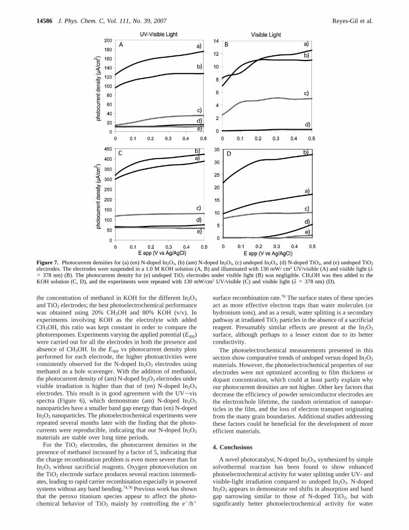
the concentration of methanol in KOH for the different In2O3
and TiO2 electrodes; the best photoelectrochemical performancewas obtained using 20% CH3OH and 80% KOH (v/v). Inexperiments involving KOH as the electrolyte with addedCH3OH, this ratio was kept constant in order to compare thephotoresponses. Experiments varying the applied potential (Eapp)were carried out for all the electrodes in both the presence andabsence of CH3OH. In theEapp vs photocurrent density plotsperformed for each electrode, the higher photoactivities wereconsistently observed for the N-doped In2O3 electrodes usingmethanol as a hole scavenger. With the addition of methanol,the photocurrent density of (am) N-doped In2O3 electrodes undervisible irradiation is higher than that of (en) N-doped In2O3
electrodes. This result is in good agreement with the UV-visspectra (Figure 6), which demonstrate (am) N-doped In2O3
nanoparticles have a smaller band gap energy than (en) N-dopedIn2O3 nanoparticles. The photoelectrochemical experiments wererepeated several months later with the finding that the photo-currents were reproducible, indicating that our N-doped In2O3
materials are stable over long time periods.For the TiO2 electrodes, the photocurrent densities in the
presence of methanol increased by a factor of 5, indicating thatthe charge recombination problem is even more severe than forIn2O3 without sacrificial reagents. Oxygen photoevolution onthe TiO2 electrode surface produces several reaction intermedi-ates, leading to rapid carrier recombination especially in poweredsystems without any band bending.74,76Previous work has shownthat the peroxo titanium species appear to affect the photo-chemical behavior of TiO2 mainly by controlling the e-/h+
surface recombination rate.76 The surface states of these speciesact as more effective electron traps than water molecules (orhydronium ions), and as a result, water splitting is a secondarypathway at irradiated TiO2 particles in the absence of a sacrificialreagent. Presumably similar effects are present at the In2O3
surface, although perhaps to a lesser extent due to its betterconductivity.
The photoelectrochemical measurements presented in thissection show comparative trends of undoped versus doped In2O3
materials. However, the photoelectrochemical properties of ourelectrodes were not optimized according to film thickness ordopant concentration, which could at least partly explain whyour photocurrent densities are not higher. Other key factors thatdecrease the efficiency of powder semiconductor electrodes arethe electron/hole lifetime, the random orientation of nanopar-ticles in the film, and the loss of electron transport originatingfrom the many grain boundaries. Additional studies addressingthese factors could be beneficial for the development of moreefficient materials.
4. Conclusions
A novel photocatalyst, N-doped In2O3, synthesized by simplesolvothermal reaction has been found to show enhancedphotoelectrochemical activity for water splitting under UV- andvisible-light irradiation compared to undoped In2O3. N-dopedIn2O3 appears to demonstrate red shifts in absorption and bandgap narrowing similar to those of N-doped TiO2, but withsignificantly better photoelectrochemical activity for water
Figure 7. Photocurrent densities for (a) (en) N-doped In2O3, (b) (am) N-doped In2O3, (c) undoped In2O3, (d) N-doped TiO2, and (e) undoped TiO2electrodes. The electrodes were suspended in a 1.0 M KOH solution (A, B) and illuminated with 130 mW/ cm2 UV/visible (A) and visible light (λ> 378 nm) (B). The photocurrent density for (e) undoped TiO2 electrodes under visible light (B) was negligible. CH3OH was then added to theKOH solution (C, D), and the experiments were repeated with 130 mW/cm2 UV/visible (C) and visible light (λ > 378 nm) (D).
14586 J. Phys. Chem. C, Vol. 111, No. 39, 2007 Reyes-Gil et al.

splitting. The characterization results, specifically XPS, showthat nitrogen has been incorporated into the lattice of In2O3 insubstitutional and interstitial doping mechanisms depending onthe N source used. However, further in-depth experiments areneeded to understand completely the structural nature of thesenitrogen doping species. Previous work by our research grouphas shown that NMR has great potential to provide much-neededinsights for these dopant species.35,69 Additional 15N NMRexperiments are under way to further elucidate the structure ofthese N-doped In2O3 materials. Studies are also being conductedto design thicker electrodes and to investigate the effects of aniondopant concentration on the visible absorption and the photo-activity under visible light. Additional anion doping studies mayprovide promising avenues for the development of highlyefficient photocatalysts for solar hydrogen conversion usinglarge band gap d10 metal oxides.
Acknowledgment. Financial support by the National ScienceFoundation (CHE-0616748) and the Purdue Research Founda-tion is gratefully acknowledged. The authors thank DebbySherman, Life Science Microscopy Facility Manager at PurdueUniversity, for the acquisition of SEM images. The authors alsothank Dr. D. Zemlyanov of the Surface Analysis Laboratory inthe Birck Nanotechnology Center/Discovery Park at PurdueUniversity for acquisition of the XPS spectra. D.R. is a memberof the Purdue Energy Center at Discovery Park.
Supporting Information Available: IR spectra of undopedcommercial In2O3, (en) N-doped In2O3, and (am) N-doped In2O3
powders. This material is available free of charge via the Internetat http://pubs.acs.org.
References and Notes
(1) Fujishima, A.; Honda, K.Nature1972, 238, 37.(2) Santato, C.; Ulmann, M.; Augustynski, J.J. Phys. Chem. B2001,
105, 936.(3) Santato, C.; Ulmann, M.; Augustynski, J.AdV. Mater. 2001, 13,
511.(4) Paluselli, D.; Marsen, B.; Miller, E. L.; Rocheleau, R. E.Electro-
chem. Solid-State Lett.2005, 8, G301.(5) Sartoretti, C. J.; Alexander, B. D.; Solarska, R.; Rutkowska, I. A.;
Augustynski, J.; Cerny, R.J. Phys. Chem. B2005, 109, 13685.(6) Duret, A.; Gratzel, M.J. Phys. Chem. B2005, 109, 17184.(7) Klosek, S.; Raftery, D.J. Phys. Chem. B2001, 105, 2815.(8) Di Paola, A.; Marci, G.; Palmisano, L.; Schiavello, M.; Uosaki,
K.; Ikeda, S.; Ohtani, B.J. Phys. Chem. B2002, 106, 637.(9) Sene, J. J.; Zeltner, W. A.; Anderson, M. A.J. Phys. Chem. B
2003, 107, 1597.(10) Reddy, E. P.; Sun, B.; Smirniotis, P. G.J. Phys. Chem. B2004,
108, 17198.(11) Ghosh, A. K.; Maruska, H. P.J. Electrochem. Soc.1977, 124, 1516.(12) Borgarello, E.; Kiwi, J.; Gra¨tzel, M.; Pelizzetti, E.; Visca, M.J.
Am. Chem. Soc.1982, 104, 2996.(13) Tafalla, D.; Salvador, P.; Benito, R. M.; Salvador, P.J. Electrochem.
Soc.1990, 137, 1810.(14) Siripala, W.; Ivanovskaya, A.; Jaramillo, T. F.; Baeck, S.; McFar-
land, E. W.Sol. Energy Mater. Sol. Cells2003, 77, 229.(15) Jia, H.; Zhang, Y.; Chen, X.; Shu, J.; Luo, X.; Zhang, Z.; Yu, D.
Appl. Phys. Lett.2003, 82, 4146.(16) Khan, S. U. M.; Al-Shahry, M.; Ingler Jr., W. B.Science2002,
297, 2243.(17) Sakthivel, S.; Kisch, H.Angew. Chem., Int. Ed.2003, 42, 4908.(18) Noworyta, K.; Augustynski, J.Elelectrochem. Solid-State Lett.2004,
7, E31.(19) Luo, H.; Takata, T.; Lee, Y.; Zhao, J.; Domen, K.; Zhao, J.; Yan,
Y. Chem. Mater.2004, 16, 846.(20) Neumann, B.; Bogdanoff, P.; Tributsch, H.; Sakthivel, S.; Kisch,
H. J. Phys. Chem. B2005, 109, 16579.(21) Park, J. H.; Kim, S.; Bard, A. J.Nano Lett.2006, 6, 24.(22) Barnes, P. R. F.; Randeniya, L. K.; Murphy, A. B.; Gwan, P. B.;
Plumb, I. C.; Glasscock, J. A.; Grey, I. E.; Li, C.DeV. Chem. Eng. Miner.Process.2006, 14, 51.
(23) Asahi, R.; Morikawa, T.; Ohwaki, T.; Aoki, K.; Taga, Y.Science2001, 293, 269.
(24) Irie, H.; Watanabe, Y.; Hashimoto, K.J. Phys. Chem. B2003, 107,5483.
(25) Burda, C.; Lou, Y.; Chen, X.; Samia, A. C. S.; Stout, J.; Gole, J.L. Nano Lett.2003, 3, 1049.
(26) Yin, S.; Yamaki, H.; Komatsu, M.; Zhang, Q.; Wang, J.; Tang,Q.; Saito, F.; Sato, T.J. Mater. Chem.2003, 13, 2996.
(27) Diwald, O.; Thompson, T. L.; Goralski, E. G.; Walck, S. D.; Yates,J. T. J.J. Phys. Chem. B2004, 108, 52.
(28) Diwald, O.; Thompson, T. L.; Zubkov, T.; Goralski, E. G.; Walck,S. D.; Yates, J. T. J.J. Phys. Chem. B2004, 108, 6004.
(29) Chen, X.; Burda, C.J. Phys. Chem. B2004, 108, 15446.(30) Miyauchi, M.; Ikezawa, A.; Tobimatsu, H.; Irie, H.; Hashimoto,
K. Phys. Chem. Chem. Phys.2004, 6, 865.(31) Sano, T.; Negishi, N.; Koike, K.; Takeuchi, K.; Matsuzawa, S.J.
Mater. Chem.2004, 14, 380.(32) Aita, Y.; Komatsu, M.; Yin, S.; Sato, T.J. Solid State Chem.2004,
177, 3235.(33) Sato, S.Chem. Phys. Lett.1986, 123, 126.(34) Sakatani, Y.; Nunoshige, J.; Ando, H.; Okusako, K.; Koike, H.;
Takata, T.; Kondo, J. N.; Hara, M.; Domen, K.Chem. Lett.2003, 32, 1156.(35) Reyes-Garcia, E. A.; Sun, Y.; Reyes-Gil, K.; Raftery, D.J. Phys.
Chem. C2007, 111, 2738.(36) Di Valentin, C.; Pacchioni, G.; Selloni, A.; Livraghi, S.; Giamello,
E. J. Phys. Chem. B2005, 109, 11414.(37) Nakamura, R.; Tanaka, T.; Nakato, Y.J. Phys. Chem. B2005, 109,
8920.(38) Murase, T.; Irie, H.; Hashimoto, K.J. Phys. Chem. B2004, 108,
15803.(39) Inoue, Y.Chem. Ind.2006, 108, 623.(40) Hwang, D. W.; Kim, H. G.; Lee, J. S.; Kim, J.; Li, W.; Oh, S. H.
J. Phys. Chem. B2005, 109, 2093.(41) Abe, R.; Higashi, M.; Sayama, K.; Abe, Y.; Sugihara, H.J. Phys.
Chem. B2006, 110, 2219.(42) Abe, R.; Higashi, M.; Zou, Z.; Sayama, K.; Abe, Y.; Arakawa, H.
J. Phys. Chem. B2004, 108, 811.(43) Kudo, A.; Kato, H.; Nakagawa, S.J. Phys. Chem. B2000, 104,
571.(44) Sato, J.; Saito, N.; Nishiyama, H.; Inoue, Y.J. Phys. Chem. B2001,
105, 6061.(45) Sato, J.; Saito, N.; Nishiyama, H.; Inoue, Y.J. Phys. Chem. B2003,
107, 7965.(46) Nozik, A. J.Annu. ReV. Phys. Chem.1978, 29, 189.(47) Li, Z.; Dong, T.; Zhang, Y.; Wu, L.; Li, J.; Wang, X.; Fu, X.J.
Phys. Chem. C2007, 111, 4727.(48) Kudo, A.; Mikami, I.Chem. Lett.1998, 1027.(49) Poznyak, S. K.; Talapin, D. V.; Kulak, A. I.J. Phys. Chem. B2001,
105, 4816.(50) Hara, K.; Sayama, K.; Arakawa, H.Sol. Energy Mater. Sol. Cells
2000, 62, 441.(51) Wang, D.; Zou, Z.; Ye, J.Chem. Mater.2005, 17, 3255.(52) Xu, Y.; Schoonen, M. A. A.Am. Mineral.2000, 85, 543.(53) Yu, D.; Yu, W.; Wang, D.; Qian, Y.Thin Solid Films2002, 419,
166.(54) Reyes-Gil, K.; Reyes-Garcia, E.; Raftery, D.J. Electrochem. Soc.
2006, 153, A1296.(55) Gratzel, M. J. Sol-Gel Sci. Technol.2001, 22, 7.(56) Fairley, N.; Carrick, A.The Casa Cookbook, Part I: Recipes for
XPS Data Processing; Acolyte Science: Knutsford, 2005.(57) Sakthivel, S.; Janczarek, M.; Kisch, H.J. Phys. Chem. B2004,
108, 19384.(58) Willson, R. C.Sol. Phys. (Hist. Arch.)1981, 74, 217.(59) Gole, J. L.; Stout, J. D.; Burda, C.; Lou, Y.; Chen, X.J. Phys.
Chem. B2004, 108, 1230.(60) Yates, H. M.; Nolan, M. G.; Sheel, D. W.; Pemble, M. E.J.
Photochem. Photobiol., A2006, 179, 213.(61) Gurlo, A.; Ivanovskaya, M.; Barsan, N.; Weimar, U.Inorg. Chem.
Commun.2003, 6, 569.(62) Sorescu, M.; Diamandescu, L.; Tarabasanu-Mihaila, D.; Teodorescu,
V. S. J. Mater. Sci.2004, 39, 675.(63) Okato, T.; Sakano, T.; Obara, M.Phys. ReV. B 2005, 72, 115124.(64) Donley, C.; Dunphy, D.; Paine, D.; Carter, C.; Nebesny, K.; Lee,
P.; Alloway, D.; Armstrong, N. R.Langmuir2002, 18, 450.(65) Maruyama, T.; Yorozu, K.; Noguchi, T.; Seki, Y.; Saito, Y.; Araki,
T.; Nanishi, Y.Phys. Status Solidi C2003, 0, 2031.(66) Lee, I. J.; Kim, J.-Y.; Shin, H.-J.J. Appl. Phys.2004, 95,
5540.(67) Sathish, M.; Viswanathan, B.; Viswanath, R. P.; Gopinath, C. S.
Chem. Mater.2005, 17, 6349.(68) Asai, N.; Inoue, Y.; Sugimura, H.; Takai, O.J. Electrochem. Soc.
1999, 146, 2365.
Nitrogen-Doped In2O3 Thin Film Electrodes J. Phys. Chem. C, Vol. 111, No. 39, 200714587

(69) Reyes-Garcia, E.; Sun, Y.; Raftery, D.J. Phys. Chem. C, accepted,2007.
(70) Sato, S.; Nakamura, R.; Abe, S.Appl. Catal., A 2005, 284,131.
(71) Rodriguez, J. A.; Jirsak, T.; Dvorak, J.; Sambasivan, S.; Fischer,D. J. Phys. Chem. B2000, 104, 319.
(72) Burda, C.; Gole, J.J. Phys. Chem. B2006, 110, 7081.(73) Gopinath, C. S.J. Phys. Chem. B2006, 110, 7079.(74) Thompson, T. L.; Yates, J. T., Jr.J. Phys. Chem. B2005, 109,
18230.
(75) Wahl, A.; Ulmann, M.; Carroy, A.; Jermann, B.; Dolata, M.;Kedzierzawski, P.; Chatelain, C.; Monnier, A.; Augustynski, J.J. Elec-troanal. Chem.1995, 396, 41.
(76) Ulmann, M.; de Tacconi, N. R.; Augustynski, J.J. Phys. Chem.1986, 90, 6523.
(77) Farfan-Arribas, E.; Madix, R. J.J. Phys. Chem. B2003, 107, 3225.
(78) Chen, X.; Lou, Y.; Samia, A. C. S.; Burda, C.; Gole, J. L.AdV.Funct. Mater.2005, 15, 41.
14588 J. Phys. Chem. C, Vol. 111, No. 39, 2007 Reyes-Gil et al.
Copyright © 2022 FDOKUMEN