Design of Functionally Stacked Channels of Oxide Thin-Film ...
14
Citation: Yang, J.S.; Jung, S.H.; Kim, D.S.; Choi, J.H.; Suh, H.W.; Lee, H.H.; Lee, K.W.; Cho, H.K. Design of Functionally Stacked Channels of Oxide Thin-Film Transistors to Mimic Precise Ultralow-Light-Irradiated Synaptic Weight Modulation. Micromachines 2022, 13, 526. https://doi.org/10.3390/mi13040526 Academic Editor: Hyuck-In Kwon Received: 15 March 2022 Accepted: 25 March 2022 Published: 26 March 2022 Publisher’s Note: MDPI stays neutral with regard to jurisdictional claims in published maps and institutional affil- iations. Copyright: © 2022 by the authors. Licensee MDPI, Basel, Switzerland. This article is an open access article distributed under the terms and conditions of the Creative Commons Attribution (CC BY) license (https:// creativecommons.org/licenses/by/ 4.0/). micromachines Article Design of Functionally Stacked Channels of Oxide Thin-Film Transistors to Mimic Precise Ultralow-Light-Irradiated Synaptic Weight Modulation Ji Sook Yang 1,† , Sung Hyeon Jung 1,† , Dong Su Kim 1 , Ji Hoon Choi 1 , Hee Won Suh 1 , Hak Hyeon Lee 1 , Kun Woong Lee 1 and Hyung Koun Cho 1,2, * 1 School of Advanced Materials Science and Engineering, Sungkyunkwan University (SKKU), 2066 Seobu-ro, Jangan-gu, Suwon 16419, Gyeonggi-do, Korea; [email protected] (J.S.Y.); [email protected] (S.H.J.); [email protected] (D.S.K.); [email protected] (J.H.C.); [email protected] (H.W.S.); [email protected] (H.H.L.); [email protected] (K.W.L.) 2 Research Center for Advanced Materials Technology, Sungkyunkwan University (SKKU), 2066 Seobu-ro, Jangan-gu, Suwon 16419, Gyeonggi-do, Korea * Correspondence: [email protected]; Tel.: +82-31-290-7364 † These authors contributed equally to this work. Abstract: To utilize continuous ultralow intensity signals from oxide synaptic transistors as artificial synapses that mimic human visual perception, we propose strategic oxide channels that optimally uti- lize their advantageous functions by stacking two oxide semiconductors with different conductivities. The bottom amorphous indium–gallium–zinc oxide (a-IGZO) layer with a relatively low conductivity was designed for an extremely low initial postsynaptic current (PSC i ) by achieving full depletion at a low negative gate voltage, and the stacked top amorphous indium–zinc oxide (a-IZO) layer improved the amplitude of the synaptic current and memory retention owing to the enhancement in the persistent photoconductivity characteristics. We demonstrated an excellent photonic synapse thin-film transistor (TFT) with a precise synaptic weight change even in the range of ultralow light intensity by adapting this stacking IGZO/IZO channel. The proposed device exhibited distinct ΔPSC values of 3.1 and 18.1 nA under ultralow ultraviolet light (350 nm, 50 ms) of 1.6 and 8.0 μW/cm 2 . In addition, while the lowest light input exhibited short-term plasticity characteristics similar to the “volatile-like” behavior of the human brain with a current recovery close to the initial value, the increase in light intensity caused long-term plasticity characteristics, thus achieving synaptic memory transition in the IGZO/IZO TFTs. Keywords: artificial photonic synapse; thin film transistor; amorphous oxide semiconductor; ultralow light intensity; stacking structure 1. Introduction Since the human brain is capable of high integration and high-efficiency information processing, neuromorphic computing has attracted interest as a next-generation computing system that can replace the existing von Neumann computing [1,2]. In the human ner- vous system, the brain contains ≈10 11 neurons and ≈10 15 synapses, which are essential for processing complex problems, and the neuromorphic system combines memory and computation [3]. In neuroscience, synaptic plasticity fundamentally supports the brain in processing incoming information at high efficiencies and performing parallel opera- tions [4,5]. Therefore, it is crucial to mimic synaptic functions to implement neuromorphic computation systems with proper devices. Artificial synaptic devices, in which the synap- tic weight can be controlled using external stimuli, have been reported to perform basic synaptic functions [6,7]. Over the past few decades, two-terminal devices have been explored as the building blocks of neuromorphic systems, such as resistance random access memory (RRAM) [8,9], Micromachines 2022, 13, 526. https://doi.org/10.3390/mi13040526 https://www.mdpi.com/journal/micromachines
-
Upload
khangminh22 -
Category
Documents
-
view
2 -
download
0
Transcript of Design of Functionally Stacked Channels of Oxide Thin-Film ...

�����������������
Citation: Yang, J.S.; Jung, S.H.; Kim,
D.S.; Choi, J.H.; Suh, H.W.; Lee, H.H.;
Lee, K.W.; Cho, H.K. Design of
Functionally Stacked Channels of
Oxide Thin-Film Transistors to Mimic
Precise Ultralow-Light-Irradiated
Synaptic Weight Modulation.
Micromachines 2022, 13, 526.
https://doi.org/10.3390/mi13040526
Academic Editor: Hyuck-In Kwon
Received: 15 March 2022
Accepted: 25 March 2022
Published: 26 March 2022
Publisher’s Note: MDPI stays neutral
with regard to jurisdictional claims in
published maps and institutional affil-
iations.
Copyright: © 2022 by the authors.
Licensee MDPI, Basel, Switzerland.
This article is an open access article
distributed under the terms and
conditions of the Creative Commons
Attribution (CC BY) license (https://
creativecommons.org/licenses/by/
4.0/).
micromachines
Article
Design of Functionally Stacked Channels of Oxide Thin-FilmTransistors to Mimic Precise Ultralow-Light-Irradiated SynapticWeight ModulationJi Sook Yang 1,†, Sung Hyeon Jung 1,†, Dong Su Kim 1 , Ji Hoon Choi 1, Hee Won Suh 1, Hak Hyeon Lee 1 ,Kun Woong Lee 1 and Hyung Koun Cho 1,2,*
1 School of Advanced Materials Science and Engineering, Sungkyunkwan University (SKKU),2066 Seobu-ro, Jangan-gu, Suwon 16419, Gyeonggi-do, Korea; [email protected] (J.S.Y.);[email protected] (S.H.J.); [email protected] (D.S.K.); [email protected] (J.H.C.);[email protected] (H.W.S.); [email protected] (H.H.L.); [email protected] (K.W.L.)
2 Research Center for Advanced Materials Technology, Sungkyunkwan University (SKKU),2066 Seobu-ro, Jangan-gu, Suwon 16419, Gyeonggi-do, Korea
* Correspondence: [email protected]; Tel.: +82-31-290-7364† These authors contributed equally to this work.
Abstract: To utilize continuous ultralow intensity signals from oxide synaptic transistors as artificialsynapses that mimic human visual perception, we propose strategic oxide channels that optimally uti-lize their advantageous functions by stacking two oxide semiconductors with different conductivities.The bottom amorphous indium–gallium–zinc oxide (a-IGZO) layer with a relatively low conductivitywas designed for an extremely low initial postsynaptic current (PSCi) by achieving full depletionat a low negative gate voltage, and the stacked top amorphous indium–zinc oxide (a-IZO) layerimproved the amplitude of the synaptic current and memory retention owing to the enhancement inthe persistent photoconductivity characteristics. We demonstrated an excellent photonic synapsethin-film transistor (TFT) with a precise synaptic weight change even in the range of ultralow lightintensity by adapting this stacking IGZO/IZO channel. The proposed device exhibited distinct ∆PSCvalues of 3.1 and 18.1 nA under ultralow ultraviolet light (350 nm, 50 ms) of 1.6 and 8.0 µW/cm2.In addition, while the lowest light input exhibited short-term plasticity characteristics similar to the“volatile-like” behavior of the human brain with a current recovery close to the initial value, theincrease in light intensity caused long-term plasticity characteristics, thus achieving synaptic memorytransition in the IGZO/IZO TFTs.
Keywords: artificial photonic synapse; thin film transistor; amorphous oxide semiconductor; ultralowlight intensity; stacking structure
1. Introduction
Since the human brain is capable of high integration and high-efficiency informationprocessing, neuromorphic computing has attracted interest as a next-generation computingsystem that can replace the existing von Neumann computing [1,2]. In the human ner-vous system, the brain contains ≈1011 neurons and ≈1015 synapses, which are essentialfor processing complex problems, and the neuromorphic system combines memory andcomputation [3]. In neuroscience, synaptic plasticity fundamentally supports the brainin processing incoming information at high efficiencies and performing parallel opera-tions [4,5]. Therefore, it is crucial to mimic synaptic functions to implement neuromorphiccomputation systems with proper devices. Artificial synaptic devices, in which the synap-tic weight can be controlled using external stimuli, have been reported to perform basicsynaptic functions [6,7].
Over the past few decades, two-terminal devices have been explored as the buildingblocks of neuromorphic systems, such as resistance random access memory (RRAM) [8,9],
Micromachines 2022, 13, 526. https://doi.org/10.3390/mi13040526 https://www.mdpi.com/journal/micromachines
Micromachines 2022, 13, 526 2 of 14
ferroelectric memory [10,11], and phase-change memory (PCM) [12,13]. Although thesetwo-terminal devices have demonstrated excellent capacity for basic neural functions, thehuman brain contains more synapses than neurons, which implies that multiterminaldevices are in high demand for complex functions. However, to conduct filament forma-tion, two-terminal devices such as an RRAM encounter problems of sneak path currentgeneration and high voltage requirement for write/read operations, causing high energyloss inconsistent with the high energy-efficiency aspect of neuromorphic computing [8].Alternatively, in recent years, three-terminal thin-film transistor (TFT) synaptic devices,which are more similar to biological neural systems, have been proposed to realize synapticfunctions [14–20]. The conductance of the proposed TFT synaptic devices can be contin-uously modulated by the third terminal using various input pulse conditions. Moreover,these devices can implement signal transmission and self-learning simultaneously andprovide a platform for creating multiterminal circuits that can imitate biological neuronswith many synaptic connections.
In recent years, indium–gallium–zinc oxide (IGZO)-based TFT devices have beendeveloped to mimic synaptic functions [14,17–20]. a-IGZO has been commercialized in flatpanel displays owing to its unique electron-transport properties [21–24]. Most synapticdevices using a-IGZO TFTs use electrical signals to stimulate the devices, which is similarto the action potential in biological systems [19,20]. In particular, the persistent photocon-ductivity (PPC) of a-IGZO can be used to mimic human memory characteristics; thus, it iswidely applied in photonic synapse transistors for artificial visual systems [14]. Moreover,the human brain precisely controls synaptic weight, which is defined as the connectionstrength between the axon terminal and dendrites; thus, learning and memory behav-iors appear differently under various light stimuli. The excitatory postsynaptic current(EPSC) is expressed as the change in synaptic weight by neurotransmitters released fromthe synaptic cleft. Thus, different intensities of light cause changes in synaptic weight,which affects the increase or decrease in the EPSC amplitude [25]. In addition, the gradualdecay of EPSCs after light stimulation is removed. The ratio of the PSCi to the remainingcurrent owing to the PPC phenomenon is defined as the non-volatile memory of the lightstimulus [26]. Biological synapses that can precisely control synaptic weight have differentEPSC amplitudes and memory characteristics for a wide range of light stimuli. This impliesthat synaptic transistors mimicking biological synapses should achieve optimal synapticplasticity over a wide range of light intensities.
However, there are still technical limitations to using a-IGZO TFTs as photonic synapsedevices for artificial visual systems. As mentioned above, the a-IGZO film provides aneffective pathway for the transport of photogenerated carriers as a channel layer withrelatively prominent electrical conductivity. Thus, the optical synaptic characteristics ofa-IGZO TFTs, such as short-term plasticity (STP) and long-term plasticity (LTP), have beendemonstrated by controlling the input optical signals [14,17,18]. The reported photonicsynapse devices have primarily focused on the modulation of synaptic plasticity usingoxide-based transistors that can mimic the basic functions of biological synapses. Sincemost photonic synapse devices use only a high light intensity as the presynaptic stimulus,a single-layer a-IGZO TFT can easily obtain a distinguishable neuromorphic performancefor the input light [14,17,18]. However, from the perspective of input light with an ultralowintensity [27], the a-IGZO channel layer does not have sufficient conductivity to discretizevarious input lights. Therefore, an increase in the conductivity of the channel layer isnecessary to attain the ability to discriminate individual light intensities in a wide rangeof light stimuli, including ultralow intensities. However, the problem of suppressing theoff-current is encountered when high-conductivity materials are used as the channel layerof TFTs [28].
In this study, we created a functional stacking structure of IGZO/IZO as synaptictransistors, which exhibited a high optical synaptic performance to mimic an artificial visualsystem. In the bilayer IGZO/IZO TFT system, both a-IGZO and a-IZO films were usedas combined channels to achieve appropriate charge transport behavior and the designed

Micromachines 2022, 13, 526 3 of 14
memory characteristics, demonstrating the characteristics of an innovative synaptic devicecapable of effectively mimicking important synaptic functions such as EPSC, paired-pulsefacilitation (PPF), STP, and LTP. The fabricated devices induce a distinct synaptic weightchange even under low-intensity light irradiation from 1.6 to 8.0 µW/cm2, resulting in high-resolution EPSC for a wide spectrum of light. The consecutive synaptic weight changes ofthe artificial synapse in response to various stimuli can be considered as data treatmentthat is very similar to a biological synapse. This paper presents the possibility of simulatinghighly efficient human visual memory in neuromorphic computing systems by utilizing aphotonic synapse transistor that can recognize successive synaptic weight changes underultralow-intensity light.
2. Experimental Details2.1. Fabrication of n-Type a-IGZO and a-IZO Thin-Film Transistors
a-IGZO TFTs with a bottom-gate configuration were fabricated on SiO2/Si substrates.Here, a-IGZO (In:Ga:Zn = 2:1:2 atomic ratio, 15 nm) and a-IZO (In:Zn = 7:3 atomic ratio,15 nm) channel layers were deposited using radio-frequency sputtering (150 W, 3 mTorr,room temperature). For the a-IZO films, different Ar/O2 ratios of 30/0, 28/2, and 25/5were used to control the electrical properties. The active channel layers were defined usingconventional photolithography and a wet-chemical etching process (HCl/DI water = 1/5),which was followed by thermal annealing (200 ◦C, 1 h, air) in a furnace. Source/drain Mo(100 nm) electrodes were deposited by direct-current magnetron sputtering (65 W, 3 mTorr)at room temperature and defined using a lift-off process. The channel width (W) and length(L) of the fabricated a-IGZO and a-IZO TFTs were 500 and 50 µm, respectively.
2.2. Electrical Characterization
The electrical behavior of the transistors was characterized using 4145B (HP) and4200-SCS (Keithley) semiconductor parameter analyzers at room temperature. To evaluate theelectrical performance of the transistors from the transfer curve, the field-effect mobility (µFE)
and subthreshold swing (SS) were calculated using the equations µFE =
[L
WCoxVD
dIDdVD
]and SS =
[(dlogID
dVG
)max
]−1, respectively. In addition, the threshold voltage (Vth) was
manifested in the (ID)1/2 − VG plots. The Vth was determined by the constant currentmethod (gate voltage at current level of L/W × 10 nA). Bias (VG = −10 V) and illumination(UV light, 350 nm, 8.0 µW/cm2) stress tests were performed at constant VD of 0.1 V. Bias(VG = −10 V) and illumination (UV light, 350 nm, 8.0 µW/cm2) stress tests were performedat a constant VD of 0.1 V. The synaptic behaviors were characterized using 4155C (HP) atroom temperature with external UV light pulse (350 nm, 1.6–8.0 µW/cm2). The appliedlight pulses were controlled by an arbitrary function generator (Tektronix AFG 31000), andthe illumination intensity was calibrated precisely using a silicon photodetector.
3. Results and Discussion3.1. Synaptic Behavior by Optical Modulation in Biological/Artificial Visual System
A general biological synapse receives the light of various wavelengths and intensitiesemitted or reflected from an object through the retina, which are converted into varioustypes of electrical signals and transmitted to the brain, and then, visual perception executesthe occurrence of information processing. At this time, for visual perception, such as thedispersion of color and complex patterns, the delicate processing of the optical signaltransmitted to the brain is a very important step [29,30]. Scheme 1a describes the signaltransduction system between the pre-neuron and post-neuron in detail during informationprocessing of the biological synapse system. To transmit the received stimulus, the neuro-transmitters (red), which have the most important role, transmit a signal to the synaptic cleftbetween neurons. When a nerve impulse reaches the presynaptic neuron and Ca2+ (purple)flows into the axon terminal simultaneously, neurotransmitters are released through rapid

Micromachines 2022, 13, 526 4 of 14
exocytosis and bind to the neurotransmitter receptor or ligand-gated ion channels, resultingin the transmission of electrical signals [3,25]. By controlling the number of emitted neuro-transmitters, the electrical signal generated by the received stimulus opens ion channels bybinding to a specific receptor; thus, diffusion results from the concentration gradient of ionssuch as K+ or Na+ (green) inside and outside the synapse and causes a change in synapticweight. The number of neurotransmitters contains various pieces of information aboutthe stimulus received from the outside, and information learning and memory processingare performed through signal transmission accordingly. Biological synapses can efficientlydistinguish various wavelengths and intensities of stimuli by controlling the number ofneurotransmitters formed by the received stimuli.
Micromachines 2022, 13, 526 4 of 15
stimulus, the neurotransmitters (red), which have the most important role, transmit a signal to the synaptic cleft between neurons. When a nerve impulse reaches the presynaptic neuron and Ca2+ (purple) flows into the axon terminal simultaneously, neurotransmitters are released through rapid exocytosis and bind to the neurotransmitter receptor or ligand-gated ion channels, resulting in the transmission of electrical signals [3,25]. By controlling the number of emitted neurotransmitters, the electrical signal generated by the received stimulus opens ion channels by binding to a specific receptor; thus, diffusion results from the concentration gradient of ions such as K+ or Na+ (green) inside and outside the synapse and causes a change in synaptic weight. The number of neurotransmitters contains various pieces of information about the stimulus received from the outside, and information learning and memory processing are performed through signal transmission accordingly. Biological synapses can efficiently distinguish various wavelengths and intensities of stimuli by controlling the number of neurotransmitters formed by the received stimuli.
Scheme 1. Mechanism of synaptic weight change for visual information processing: Schematic diagrams for (a) the control of neurotransmitters induced by optical signals in the biological synapse and (b) the artificial photonic synapse oxide TFT mimicking the biological synapse.
Currently, electronic devices with various structures are being used to imitate the continuous characteristics of the accepted stimulus of the biological synapse, and among them, a three-terminal transistor structure based on an amorphous oxide semiconductor
Scheme 1. Mechanism of synaptic weight change for visual information processing: Schematicdiagrams for (a) the control of neurotransmitters induced by optical signals in the biological synapseand (b) the artificial photonic synapse oxide TFT mimicking the biological synapse.
Currently, electronic devices with various structures are being used to imitate thecontinuous characteristics of the accepted stimulus of the biological synapse, and amongthem, a three-terminal transistor structure based on an amorphous oxide semiconductor(AOS) is being considered to function as a synaptic cleft. First, oxide semiconductorshave high electron mobilities and very low off-current densities, enabling low powerconsumption and fast transfer rates similar to biological synapses [31,32]. In addition,owing to the existence of countless localized sub-gap defect states in the bandgap, a uniquePPC phenomenon in which the changed conductance state is continuously maintained canbe produced, even when the accepted stimulus is removed. Consequently, a long-term

Micromachines 2022, 13, 526 5 of 14
retention function can be implemented by simply inducing conductance change [14]. Withthe use of a three-terminal device, it is possible to maximize synaptic characteristics as wellas lower power consumption by reducing off-current levels, which can be achieved by theformation of a depletion layer at the oxide/gate insulator interface under a continuousnegative gate voltage. As described in Scheme 1b, for an ideal artificial synapse, thephotocarriers generated by the intensity of the received stimulus mimic neurotransmittersof the biological synapse system. Thus, because the number of photocarriers due to achange in conductance determines the synaptic weight, previous studies applied materialswith good absorbance to increase the photocarriers or various material combinations toincrease photogeneration efficiency by reducing the recombination loss with the properband alignment [14,33–35]. Although the artificial synapse devices studied have imitatedthe performance of biological synapses in various ways, a high-resolution system that candistinguish each successive synaptic weight is still extremely difficult, particularly whenthe received stimulus intensity is very low or ultralow.
3.2. Ideal Artificial Synapse Device for Optical Signal Detection
Scheme 2a shows the change in the output EPSC according to the change in the inputlight when the photonic synapse can operate with a high-resolution system close to thebiological synapse. Thus, the synaptic weight change expressed by the input light inthe presynaptic neuron of the photonic synapse can be confirmed through the signal ofthe output EPSC, and the conductance change from different photocarrier generationscauses a change in PSCmax at each output EPSC. Therefore, having different PSCmax valuesaccording to the stimulus intensity means that the operation of the photonic synapse canefficiently discriminate the synaptic weight change of the stimulus. The most importantcharacteristic of an artificial synapse system is the variation of photocarriers produced byreceiving external stimuli to generate a noticeable continuous change in the correspondingsynaptic weight. However, because the photocarriers generated at ultralow intensitiesare extremely low, the change in synaptic weight is subtle, making it difficult to clearlydistinguish the signals. Thus, although the received stimulus is continuous, the dataextracted through information processing can be described continuously. Scheme 2b depictsreal and ideal EPSC profiles when light pulses with intensities ranging from ultralow tolow are incident on the photonic synapse. The ideal EPSC must represent a differentiatedPSCmax even for a low-intensity stimulus, but the real EPSC does not demonstrate a changein the PSCmax signal with respect to ultralow light intensity. Thus, a dramatic changein synaptic weight must be implemented even at a continuous ultralow intensity withthe following characteristics: (i) an extremely low current level (PSCi state) before theexternal stimulus (fully depleted layer), (ii) an increase in the synaptic weight for successivestimuli, and (iii) continuous memory retention through the separation of the generatedphotocarriers. Previous studies presented results under high intensities of the receivedstimulus (>mW/cm2) and large intensity differences between the stimuli [14,17,18]. Toincrease the synaptic weight and lower the off-current level in the PSCi state simultaneously,oxide semiconductor films with low conductivity must be preferentially used, and theymust be sufficiently thin to form a full depletion layer with a low gate voltage. In contrast,oxide semiconductors with good conductivity are indispensable to maximizing synapticweight and for the rapid transport of photocarriers generated from the stimuli.
Thus, we propose new oxide channels strategically utilizing each function by stackingtwo oxide semiconductors with different conductivities, resulting in the recognition of con-tinuous ultralow-intensity signals from oxide synaptic transistors (Scheme 2c). Therefore,we fabricated a double-layer channel structure consisting of a-IGZO for a low PSCi currentand a-IZO with good conductivity for a high synaptic current and fast transport. In general,many reports on stacking structure channels have focused high electrical performancesaiming at mobility enhancement. Our IGZO/IZO TFT used as a photonic synapse has theadvantage of achieving appropriate channel conductivity with low off-current, synapticweight change, and memory retention.

Micromachines 2022, 13, 526 6 of 14Micromachines 2022, 13, 526 6 of 15
Scheme 2. Schematic diagrams showing (a) ideal output (EPSC) characteristics under different input (light) intensities and (b) ideal/real synaptic current variations under modulating light intensities. (c) Effect of channel layer properties and stacking sequence on postsynaptic current variations.
Thus, we propose new oxide channels strategically utilizing each function by stack-ing two oxide semiconductors with different conductivities, resulting in the recognition of continuous ultralow-intensity signals from oxide synaptic transistors (Scheme 2c). Therefore, we fabricated a double-layer channel structure consisting of a-IGZO for a low PSCi current and a-IZO with good conductivity for a high synaptic current and fast transport. In general, many reports on stacking structure channels have focused high elec-trical performances aiming at mobility enhancement. Our IGZO/IZO TFT used as a pho-tonic synapse has the advantage of achieving appropriate channel conductivity with low off-current, synaptic weight change, and memory retention.
3.3. Electrical Characterization of a-IGZO and a-IZO TFTs Figure 1a,b show the transfer characteristics of the fabricated bottom-gate a-IGZO
and a-IZO TFTs, measured at drain voltages (VD) of 0.1–10 V. The a-IGZO (In:Ga:Zn = 2:1:2) and a-IZO (In:Zn = 7:3) films were deposited with a thickness of 15 nm at Ar/O2 = 28:2 and post-thermally annealed at 200 °C for 1 h. As shown in Figure 1a, the a-IGZO TFT exhibited excellent transfer characteristics with a remarkably low off-current level of ap-proximately 10–12 A, Vth of 0.18 V, SS of 0.22 V dec−1, μFE of 8 cm2 V−1 s−1, and on/off ratio of 108. In addition, the a-IGZO TFT with a considerably low SS value can be switched from the off-state to the on-state with only a low VG. We extract the interface defect density (Dit) using Equation (1): 𝐷 = ∙ − 1 , (1)
where Ci is the capacitance of the dielectric, q is the magnitude of electron charge, k is the Boltzmann constant, and T is temperature in Kelvin. As mentioned above, the SS value of the a-IGZO TFT is 0.22 V dec−1, and the calculated Dit is 2.9 × 1011 cm−2 eV−1. The small Dit value indicated excellent interfacial properties. Furthermore, the Vth shift in hysteresis characteristic demonstrating the interface states was negligible (Figure S1a). As shown in Figure S1b, the positive Vth shift of the a-IGZO TFT under positive bias stress for 3600 s
Scheme 2. Schematic diagrams showing (a) ideal output (EPSC) characteristics under different input(light) intensities and (b) ideal/real synaptic current variations under modulating light intensities.(c) Effect of channel layer properties and stacking sequence on postsynaptic current variations.
3.3. Electrical Characterization of a-IGZO and a-IZO TFTs
Figure 1a,b show the transfer characteristics of the fabricated bottom-gate a-IGZO anda-IZO TFTs, measured at drain voltages (VD) of 0.1–10 V. The a-IGZO (In:Ga:Zn = 2:1:2) anda-IZO (In:Zn = 7:3) films were deposited with a thickness of 15 nm at Ar/O2 = 28:2 andpost-thermally annealed at 200 ◦C for 1 h. As shown in Figure 1a, the a-IGZO TFT exhibitedexcellent transfer characteristics with a remarkably low off-current level of approximately10–12 A, Vth of 0.18 V, SS of 0.22 V dec−1, µFE of 8 cm2 V−1 s−1, and on/off ratio of 108.In addition, the a-IGZO TFT with a considerably low SS value can be switched from theoff-state to the on-state with only a low VG. We extract the interface defect density (Dit)using Equation (1):
Dit =Ciq2
(q·SS
kTln10− 1)
, (1)
where Ci is the capacitance of the dielectric, q is the magnitude of electron charge, k is theBoltzmann constant, and T is temperature in Kelvin. As mentioned above, the SS valueof the a-IGZO TFT is 0.22 V dec−1, and the calculated Dit is 2.9 × 1011 cm−2 eV−1. Thesmall Dit value indicated excellent interfacial properties. Furthermore, the Vth shift inhysteresis characteristic demonstrating the interface states was negligible (Figure S1a).As shown in Figure S1b, the positive Vth shift of the a-IGZO TFT under positive biasstress for 3600 s was as small as 3.0 V. Different types of metal cations have differentoxygen affinities, which cause different chemical bonds between the metal and oxygen,affecting the carrier concentration in the channel layer. The gallium (Ga) ions in the a-IGZO compound have a higher oxygen affinity than indium (In), which provides strongchemical metal–oxygen bonding, thereby reducing the amount of excess free carriersgenerated through VO compared with a-IZO with high In content [36]. In contrast, theperformance values of the a-IZO TFT with high carrier concentration were Vth = −5.39 V,SS = 0.27 V dec−1, µFE = 16.7 cm2 V−1 s−1, and on/off ratio = 107. Compared withthe a-IGZO TFT, it had a relatively high mobility but exhibited high off-current levelcharacteristics of approximately 10–11 A (Figure 1b). Although the a-IGZO and a-IZOfilms were prepared at the same low temperature of 200 ◦C, they exhibited noticeable
Micromachines 2022, 13, 526 7 of 14
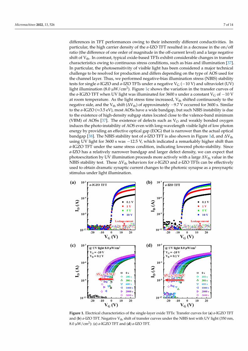
differences in TFT performances owing to their inherently different conductivities. Inparticular, the high carrier density of the a-IZO TFT resulted in a decrease in the on/offratio (the difference of one order of magnitude in the off-current level) and a large negativeshift of Vth. In contrast, typical oxide-based TFTs exhibit considerable changes in transfercharacteristics owing to continuous stress conditions, such as bias and illumination [37].In particular, the photosensitivity of visible light has been considered a major technicalchallenge to be resolved for production and differs depending on the type of AOS used forthe channel layer. Thus, we performed negative-bias illumination stress (NBIS) stabilitytests for single a-IGZO and a-IZO TFTs under a negative VG (−10 V) and ultraviolet (UV)light illumination (8.0 µW/cm2). Figure 1c shows the variation in the transfer curves ofthe a-IGZO TFT when UV light was illuminated for 3600 s under a constant VG of −10 Vat room temperature. As the light stress time increased, Vth shifted continuously to thenegative side, and the Vth shift (∆Vth) of approximately −9.7 V occurred for 3600 s. Similarto the a-IGZO (≈3.5 eV), most AOSs have a wide bandgap, but such NBIS instability is dueto the existence of high-density subgap states located close to the valence-band minimum(VBM) of AOSs [37]. The existence of defects such as VO and weakly bonded oxygeninduces the photo-instability of AOS even with long-wavelength visible light of low photonenergy by providing an effective optical gap (EOG) that is narrower than the actual opticalbandgap [38]. The NBIS stability test of a-IZO TFT is also shown in Figure 1d, and ∆Vthusing UV light for 3600 s was −12.5 V, which indicated a remarkably higher shift thana-IGZO TFT under the same stress condition, indicating lowered photo-stability. Sincea-IZO has a relatively narrower bandgap and larger defect density, we can expect thatphotoexcitation by UV illumination proceeds more actively with a large ∆Vth value in theNBIS stability test. These ∆Vth behaviors for a-IGZO and a-IZO TFTs can be effectivelyused to obtain dramatic synaptic current changes to the photonic synapse as a presynapticstimulus under light illumination.
Micromachines 2022, 13, 526 8 of 15
Figure 1. Electrical characteristics of the single-layer oxide TFTs: Transfer curves for (a) a-IGZO TFT and (b) a-IZO TFT. Negative Vth shift of transfer curves under the NBIS test with UV light (350 nm, 8.0 μW/cm2): (c) a-IGZO TFT and (d) a-IZO TFT.
3.4. EPSC Characteristics of a-IGZO and a-IZO TFTs Consequently, the negative shift in ∆Vth causes an abrupt change in the transfer char-
acteristic from the off-state region to the subthreshold region under a constant VG, and simultaneous light illumination can result in an exponential increase in the synaptic cur-rent. Therefore, to clearly distinguish light stimuli within the ultralow intensity range, we strategically induced a significant change in the transfer characteristics from the off-state to the subthreshold region, promoting an effective increase in the synaptic current. As shown in Figure 2a,b, we designed an applied voltage of VG = −10 V and external pulse stimulation to 350 nm UV light, and the EPSC characteristics of the photonic synapse tran-sistors with a-IGZO and a-IZO single channels were evaluated in the ultralow intensity range. Here, a light of 1.6–8.0 μW/cm2 was irradiated with very fine intensity intervals of 100 ms. As shown in Figure 2a, when ultralow intensity light was applied, the photocur-rent of the a-IGZO synaptic transistor exhibited almost the same at ≈10 pA level despite the difference in light intensity. This indicated that subtle changes in the light intensity were not distinguished by the synaptic weight. Thus, we confirmed that the a-IGZO TFT has the advantage of a very low PSCi owing to a considerably low off-current level but cannot achieve a noticeable increase in the synaptic current under ultralow-intensity light. In addition, the memory retention of the PPC phenomenon was almost identical. In con-trast, for the a-IZO TFT (Figure 2b), we observed that the change in synaptic weight was relatively clear, and memory retention on light intensity was distinct, which was at-tributed to the high conductivity of the a-IZO and large Vth shift through light illumina-tion. However, this high conductivity resulted in a high off-current level (high PSCi) be-fore light illumination. The high off-current level of the a-IZO TFT slightly attenuated the
Figure 1. Electrical characteristics of the single-layer oxide TFTs: Transfer curves for (a) a-IGZO TFTand (b) a-IZO TFT. Negative Vth shift of transfer curves under the NBIS test with UV light (350 nm,8.0 µW/cm2): (c) a-IGZO TFT and (d) a-IZO TFT.

Micromachines 2022, 13, 526 8 of 14
3.4. EPSC Characteristics of a-IGZO and a-IZO TFTs
Consequently, the negative shift in ∆Vth causes an abrupt change in the transfercharacteristic from the off-state region to the subthreshold region under a constant VG,and simultaneous light illumination can result in an exponential increase in the synapticcurrent. Therefore, to clearly distinguish light stimuli within the ultralow intensity range,we strategically induced a significant change in the transfer characteristics from the off-stateto the subthreshold region, promoting an effective increase in the synaptic current. Asshown in Figure 2a,b, we designed an applied voltage of VG = −10 V and external pulsestimulation to 350 nm UV light, and the EPSC characteristics of the photonic synapsetransistors with a-IGZO and a-IZO single channels were evaluated in the ultralow intensityrange. Here, a light of 1.6–8.0 µW/cm2 was irradiated with very fine intensity intervals of100 ms. As shown in Figure 2a, when ultralow intensity light was applied, the photocurrentof the a-IGZO synaptic transistor exhibited almost the same at ≈10 pA level despite thedifference in light intensity. This indicated that subtle changes in the light intensity werenot distinguished by the synaptic weight. Thus, we confirmed that the a-IGZO TFT hasthe advantage of a very low PSCi owing to a considerably low off-current level but cannotachieve a noticeable increase in the synaptic current under ultralow-intensity light. Inaddition, the memory retention of the PPC phenomenon was almost identical. In contrast,for the a-IZO TFT (Figure 2b), we observed that the change in synaptic weight was relativelyclear, and memory retention on light intensity was distinct, which was attributed to thehigh conductivity of the a-IZO and large Vth shift through light illumination. However, thishigh conductivity resulted in a high off-current level (high PSCi) before light illumination.The high off-current level of the a-IZO TFT slightly attenuated the effect of increasing thesynaptic current through the Vth shift by the applied bias and light stress.
Micromachines 2022, 13, 526 9 of 15
effect of increasing the synaptic current through the Vth shift by the applied bias and light stress.
Figure 2. Photonic performances of the TFTs irradiated with UV light (1 pulse) of varying light in-tensities: (a) a-IGZO TFT and (b) a-IZO TFT. The EPSC data for (c) a-IGZO TFT and (d) a-IZO TFT stimulated with identical UV light pulses with time intervals of 200 ms.
Thus, the capability of detecting continuous signals under exposure to ultralow in-tensity light with fine intervals is closely related to the conductivity of the channel layers. One of the most important synaptic functions in the memory behavior of biological syn-apses is PPF, which is a typical memory characteristic in which the PSC of the next stim-ulus is effectively increased by the previous stimulus when the next stimulus is input close to the previous stimulus. This PPF can be defined as the ratio of the amplitude between the first and second PSCs, and it can be described by Equation (2) [25]: 𝑃𝑃𝐹 = 100%, (2)
where A1 and A2 denote EPSCs expressed by the first and second applied light pulses, respectively, and they are calculated through the difference between PSCi and PSCmax in-creased by each light pulse. The PPF mimicked by the a-IGZO TFT under UV light pulses of ultralow intensity (1.6 μW/cm2) is shown in Figure 2c. The same two UV light pulses were incident on the a-IGZO channel at a time interval (Δt) of 200 ms, and the synaptic current was read with a VD of 0.1 mV. The EPSC increased when the second UV light pulse was higher than the first one, and the calculated PPF of the a-IGZO TFT was 144%. The EPSC changes induced by continuous pulses with a short interval time were very similar to the characteristics of short-term synaptic behaviors observed in biological synapses. The PPF value of the a-IZO TFT under the same measurement conditions was 159%, which was relatively higher than that of the a-IGZO TFT (Figure 2d). The improvement in the
Figure 2. Photonic performances of the TFTs irradiated with UV light (1 pulse) of varying lightintensities: (a) a-IGZO TFT and (b) a-IZO TFT. The EPSC data for (c) a-IGZO TFT and (d) a-IZO TFTstimulated with identical UV light pulses with time intervals of 200 ms.
Micromachines 2022, 13, 526 9 of 14
Thus, the capability of detecting continuous signals under exposure to ultralow inten-sity light with fine intervals is closely related to the conductivity of the channel layers. Oneof the most important synaptic functions in the memory behavior of biological synapsesis PPF, which is a typical memory characteristic in which the PSC of the next stimulus iseffectively increased by the previous stimulus when the next stimulus is input close to theprevious stimulus. This PPF can be defined as the ratio of the amplitude between the firstand second PSCs, and it can be described by Equation (2) [25]:
PPF =
(A2
A1
)× 100%, (2)
where A1 and A2 denote EPSCs expressed by the first and second applied light pulses,respectively, and they are calculated through the difference between PSCi and PSCmaxincreased by each light pulse. The PPF mimicked by the a-IGZO TFT under UV light pulsesof ultralow intensity (1.6 µW/cm2) is shown in Figure 2c. The same two UV light pulseswere incident on the a-IGZO channel at a time interval (∆t) of 200 ms, and the synapticcurrent was read with a VD of 0.1 mV. The EPSC increased when the second UV light pulsewas higher than the first one, and the calculated PPF of the a-IGZO TFT was 144%. TheEPSC changes induced by continuous pulses with a short interval time were very similarto the characteristics of short-term synaptic behaviors observed in biological synapses. ThePPF value of the a-IZO TFT under the same measurement conditions was 159%, whichwas relatively higher than that of the a-IGZO TFT (Figure 2d). The improvement in thePPF characteristics can be attributed to the increase in the second EPSC peak, which wasinfluenced by the degree of current retention of the first EPSC peak.
3.5. Modulation of the Ar/O2 Ratio for Enhancing Photonic Performances
From these EPSC characteristics of the a-IGZO and a-IZO TFTs under ultralow intensityillumination, an alternative channel layer structure that enables both significant synapticweight change and memory behavior should be suggested to perform an effective synapticfunction as a synaptic transistor. In particular, the change in the synaptic weight of thephotonic synapse transistor is predominantly determined by the photocarrier generationand recombination process of the channel layer in the on/off states of the applied light.The photocarrier dynamics in the channel layer are divided into light illumination (lightON), light removal (light OFF), and time elapsed (memory retention) stages. First, in thelight ON stage, photocarriers are created by electron–hole pair generation and ionizationof oxygen defects, inducing an abrupt change in the synaptic weight via a rapid increasein conductance (Figure 3a). Thus, to induce a large change in the synaptic weight, theconductance should be increased and read quickly via more photoexcitation reactions. Asshown in Figure 3b, after the light was removed, the generated photocarriers disappearedthrough the recombination process, and the conductance of the channel gradually decreased.However, the photocarriers related to the ionized VO contributing to the PPC phenomenonwere still located in the conduction band even after a certain period had elapsed; thus,it exhibited a retention phenomenon that did not return to the PSCi current, which isdefined as memory retention, indicating memory-like behavior (Figure 3c). This memorymodulation is an important factor in the neuromorphic system, and as the number ofdefects in the oxide semiconductor increases, it can result in PPC characteristics thatare advantageous for realizing non-volatile memory. Finally, we observed that the non-volatile synaptic plasticity function can be successfully implemented when the increasedEPSC was retained via VO photoionization based on a low PSCi and the considerablegeneration of photocarriers. To fully satisfy these requirements, bilayer stacking synaptictransistors can demonstrate both synaptic weight change and memory behavior withexcellent characteristics by effectively using the advantageous functions between a-IGZOand a-IZO films. As shown in Figure S2a–c, the transfer characteristics of the IGZO/IZOTFT exhibited good performances and the negative shift of Vth as the Ar/O2 ratio increased.Compared with the results of a-IGZO TFT (Figure 1a), the proposed IGZO/IZO TFT

Micromachines 2022, 13, 526 10 of 14
exhibited the enhanced mobility as well as the maintenance of low off-state current. TheIGZO/IZO TFT fabricated at Ar/O2 of 30/0 showed the best performance with SS of0.27 V dec−1 and µFE of 12.4 cm2 V−1 s−1 (Figure S2d). Although the a-IZO with relativelyhigh conductivity was used in the stacked structure, the electrical mobility exhibits anappropriate value between the performances of a-IGZO and a-IZO TFTs. In addition,the TFT devices often suffer from anomalous hump phenomenon in subthreshold regionof transfer curves. This behavior is closely related to the charge traps at the interface,resulting in the degradation of SS. However, the IGZO/IZO TFT showed a steep SS withoutdeterioration despite the bilayer stacking of two channel materials. Consequently, it wasfound that the a-IZO contributed to the improvement of the conductivity in the stackedchannel, and the a-IGZO served as the main channel for charge transport. Figure 3d showsthe variation in the EPSC signals according to the Ar/O2 ratio during a-IZO deposition ofthe IGZO/IZO double layer. Here, the Ar/O2 ratio was set to 30/0, 28/2, and 25/5, andall three PSC characteristics revealed a very low off-current level. This result indicatedthat the a-IGZO channel layers were fully depleted under the gate voltage conditions.Since a decrease in the oxygen partial pressure increases the VO concentration of the a-IZOfilm, it can induce more photoionization and stronger PPC under the same light stimuli.In addition, the EPSC characteristics of the IGZO/IZO TFT exhibited a higher synapticcurrent under light illumination and a higher remaining current in the light OFF stageas the oxygen partial pressure in the a-IZO deposition decreased. As a result, for theIGZO/IZO bilayer TFT, the bottom layer is used to attain the low off-current, and the toplayer plays a key role for effective charge transport. A large amount of VO in the channelwas effectively ionized by UV light, and numerous photocarriers were released, leaving theremaining photocarriers even after the light OFF owing to the strong PPC phenomenon,causing an increase in memory characteristics. We obtained a very low PSCi currentthrough the low-conductivity a-IGZO and achieved an effective improvement in synapticcurrent and memory characteristics by controlling the Ar/O2 ratio of the high-conductivitya-IZO. This memory behavior can be enhanced by intensifying synaptic connections viarepeated stimulation, which is strongly affected by the number and frequency of externalstimulations. Figure 3e shows the EPSC changes depending on the pulse number for theIGZO/IZO TFT (Ar/O2 = 30/0 for a-IZO), indicating an effective synaptic current increase.The pulsed UV illumination conditions (350 nm, 1.6 µW/cm2, w: 100 ms, ∆t: 200 ms) wereidentical, and the pulse numbers were measured from 1 to 15. When pulse number 1was applied to the synaptic transistor, the synaptic current temporarily increased andthen rapidly decreased. However, as the stimulus was repeatedly applied at 200 msintervals, photogenerated carriers in the channel could not be fully recombined because ofthe contribution of the strong PPC effect, and the synaptic current continuously increasedwith repeated accumulation. In addition, although the current gradually decreased afterlight OFF, sufficient memory retention with a high synaptic current was clearly detected,even after a long period. The characteristics of consistently maintaining synaptic weightproduced by repetitive stimuli are ultimately similar to LTP, in which stimulus informationis stored for a long time [39]. Consequently, successive pulses applied at a high rateinduce non-volatile memory characteristics. The decrease in the information forgettingrate and memory enhancement depending on the repetitions of stimulation means that theIGZO/IZO double-layer TFT can be applied as a synaptic device that can mimic humanbrain memory. The memory characteristics of a synaptic device influenced by the pulsenumber can be quantitatively analyzed using memory retention (Mt). Mt is normalized tothe synaptic current after the stimulus is removed. By comparing the amount of remainingsynaptic current for several EPSCs measured under different conditions, the non-volatilememory characteristics can be identified using Equation (3) [39]:
Mt = (PSCt − PSCi)/(PSCmax − PSCi), (3)
where PSCt is the postsynaptic current at a specific time t, PSCi is the initial value of thecurrent without light stimulation, and PSCmax is the highest value of the postsynaptic

Micromachines 2022, 13, 526 11 of 14
current. Figure 3f shows a continuous increase in Mt with an increase in the pulse number.When passing 20 s after the decay of synaptic current, a one-time pulse input of a 100 ms UVlight (350 nm, 1.6 µW/cm2) exhibited a relatively low Mt of 41%. Pulse number 1 exhibiteda rapid current decrease compared with the decay characteristics of the EPSC from thesamples experiencing multiple pulse numbers of >1. However, when the 15th pulse numberwas applied, it exhibited a high Mt of approximately 73% under the same 20 s condition.Thus, the volatile and non-volatile characteristics of memory can be distinguished usingpulse numbers. When an external light stimulus is provided at short intervals, the PPCeffect in photonic synapses depends on the repetition number of the stimulus and affectsmemory behavior.
Micromachines 2022, 13, 526 12 of 15
Figure 3. Schematic band diagrams of oxide semiconductors under (a) light ON, (b) light OFF, and (c) retention conditions. (d) Variation in EPSC signals from the TFTs with the a-IZO films prepared using different Ar/O2 ratios. (e) EPSC characteristics by pulse number variation from the IGZO/IZO (Ar/O2 = 30:0 for a-IZO) synaptic transistors with a light pulse width of 100 ms. (f) STP and LTP behaviors of memory retention caused by different pulse numbers.
3.6. Emulation of Synaptic Behavior with IGZO/IZO Photonic Synapse Transistor As shown in Figure 4a–d, we attempted to confirm the change in synaptic weight in
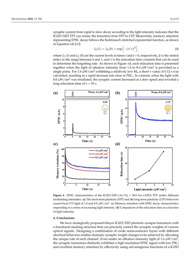
the IGZO/IZO synaptic transistors with respect to the light intensity, where ultralow in-tensity light was used as an external stimulus. Figure 4a shows the result of applying a single light pulse of ultralow intensity (1.6 μW/cm2) for a very short time of 50 ms to the device with a double-layer structure, obtaining ∆𝑃𝑆𝐶(= 𝑃𝑆𝐶 − 𝑃𝑆𝐶 ) of 3.1 nA. For a single light pulse of low intensity of 8.0 μW/cm2, a high synaptic current corresponding to ∆PSC of 18.1 nA was induced (Figure 4b). Despite maintaining an extremely low PSCi with the input of ultralow-intensity light, a high synaptic current increase resulted in a change in the synaptic weight. As a result, the suggested IGZO/IZO TFT with double-layer structure exhibited synaptic performances of excellently reading input light signals with an ultralow intensity range, and memory characteristics with distinct signal differ-ences were also achieved. The dependence of Mt on light intensity is shown in Figure 4c. The memory level of the synaptic transistor was effectively driven by controlling the light intensity. The result under the lowest light input of 1.6 μW/cm2 illustrated that the in-creased current level returned very close to the initial value of PSCi, indicating STP char-acteristics similar to the “volatile-like” behavior of the human brain. However, as the light intensity increased, LTP characteristics indicating a slow current decrease were observed. STP and LTP behaviors are considered as the key factors in the memory performance of synapse devices. The change in synaptic current from rapid to slow decay according to the light intensity indicates that the IGZO/IZO TFT can mimic the transition from STP to LTP. Meanwhile, memory retention representing EPSC decay follows the Kohlrausch stretched exponential function, as shown in Equation (4) [40]: 𝐼 (𝑡) = 𝐼 (0) exp [−(𝑡/𝜏) ], (4)
where ID (t) and ID (0) are the current levels at times t and t = 0, respectively, β is the stretch index in the range between 0 and 1, and τ is the relaxation time constant that can be used to determine the forgetting rate. As shown in Figure 4d, each relaxation time is presented together when the light of ultralow intensity from 1.6 to 8.0 μW/cm2 is provided as a single
Figure 3. Schematic band diagrams of oxide semiconductors under (a) light ON, (b) light OFF, and(c) retention conditions. (d) Variation in EPSC signals from the TFTs with the a-IZO films preparedusing different Ar/O2 ratios. (e) EPSC characteristics by pulse number variation from the IGZO/IZO(Ar/O2 = 30:0 for a-IZO) synaptic transistors with a light pulse width of 100 ms. (f) STP and LTPbehaviors of memory retention caused by different pulse numbers.
3.6. Emulation of Synaptic Behavior with IGZO/IZO Photonic Synapse Transistor
As shown in Figure 4a–d, we attempted to confirm the change in synaptic weightin the IGZO/IZO synaptic transistors with respect to the light intensity, where ultralowintensity light was used as an external stimulus. Figure 4a shows the result of applying asingle light pulse of ultralow intensity (1.6 µW/cm2) for a very short time of 50 ms to thedevice with a double-layer structure, obtaining PSC(= PSCmax − PSCi) of 3.1 nA. For asingle light pulse of low intensity of 8.0 µW/cm2, a high synaptic current correspondingto ∆PSC of 18.1 nA was induced (Figure 4b). Despite maintaining an extremely low PSCiwith the input of ultralow-intensity light, a high synaptic current increase resulted in achange in the synaptic weight. As a result, the suggested IGZO/IZO TFT with double-layerstructure exhibited synaptic performances of excellently reading input light signals with anultralow intensity range, and memory characteristics with distinct signal differences werealso achieved. The dependence of Mt on light intensity is shown in Figure 4c. The memorylevel of the synaptic transistor was effectively driven by controlling the light intensity. Theresult under the lowest light input of 1.6 µW/cm2 illustrated that the increased current levelreturned very close to the initial value of PSCi, indicating STP characteristics similar to the“volatile-like” behavior of the human brain. However, as the light intensity increased, LTPcharacteristics indicating a slow current decrease were observed. STP and LTP behaviors areconsidered as the key factors in the memory performance of synapse devices. The change in
Micromachines 2022, 13, 526 12 of 14
synaptic current from rapid to slow decay according to the light intensity indicates that theIGZO/IZO TFT can mimic the transition from STP to LTP. Meanwhile, memory retentionrepresenting EPSC decay follows the Kohlrausch stretched exponential function, as shownin Equation (4) [40]:
ID(t) = ID(0)× exp[−(t/τ)β
], (4)
where ID (t) and ID (0) are the current levels at times t and t = 0, respectively, β is the stretchindex in the range between 0 and 1, and τ is the relaxation time constant that can be usedto determine the forgetting rate. As shown in Figure 4d, each relaxation time is presentedtogether when the light of ultralow intensity from 1.6 to 8.0 µW/cm2 is provided as asingle pulse. For 1.6 µW/cm2 exhibiting a relatively low Mt, a short τ value of 0.12 s wascalculated, resulting in a rapid decrease rate close to PSCi. In contrast, when the light with8.0 µW/cm2 was irradiated, the synaptic current decreased at a slow speed and revealed along relaxation time of τ = 35 s.
Micromachines 2022, 13, 526 13 of 15
pulse. For 1.6 μW/cm2 exhibiting a relatively low Mt, a short τ value of 0.12 s was calcu-lated, resulting in a rapid decrease rate close to PSCi. In contrast, when the light with 8.0 μW/cm2 was irradiated, the synaptic current decreased at a slow speed and revealed a long relaxation time of τ = 35 s.
Figure 4. EPSC characteristics of the IGZO/IZO (Ar/O2 = 30:0 for a-IZO) TFT under different modu-lating intensities: (a) The short-term plasticity (STP) and (b) long-term plasticity (LTP) behaviors caused from UV light of 1.6 and 8.0 μW/cm2. (c) Memory retention with EPSC decay characteristics responding to a series of increasing light intensity. (d) Comparison of the relaxation time as a func-tion of light intensity.
4. Conclusions We have strategically proposed bilayer IGZO/IZO photonic synapse transistors with
a functional stacking structure that can precisely control the synaptic weights of various optical signals. Designing a combination of oxide semiconductor layers with different electrical behaviors enables dramatic synaptic weight changes to be achieved by allocating the unique role of each channel. Even under an ultralow-intensity light of 1.6 μW/cm2, the synaptic transistors distinctly exhibited a high-resolution EPSC signal with low PSCi and excellent memory retention by effectively using advantageous functions of a-IGZO and a-IZO films. In addition, the fundamental synaptic function was successfully emulated in response to various optical stimuli such as EPSC, PPF, STP, and LTP. Furthermore, the decrease in the information forgetting rate and memory enhancement depending on the repetitions of stimulation implied that the IGZO/IZO transistors revealed their potential as a synaptic device capable of mimicking the function of the human brain memory. The proposed IGZO/IZO photonic synapse transistors are expected to create the foundation for the development of next-generation neuromorphic computing systems for visual in-formation processing.
Figure 4. EPSC characteristics of the IGZO/IZO (Ar/O2 = 30:0 for a-IZO) TFT under differentmodulating intensities: (a) The short-term plasticity (STP) and (b) long-term plasticity (LTP) behaviorscaused from UV light of 1.6 and 8.0 µW/cm2. (c) Memory retention with EPSC decay characteristicsresponding to a series of increasing light intensity. (d) Comparison of the relaxation time as a functionof light intensity.
4. Conclusions
We have strategically proposed bilayer IGZO/IZO photonic synapse transistors witha functional stacking structure that can precisely control the synaptic weights of variousoptical signals. Designing a combination of oxide semiconductor layers with differentelectrical behaviors enables dramatic synaptic weight changes to be achieved by allocatingthe unique role of each channel. Even under an ultralow-intensity light of 1.6 µW/cm2,the synaptic transistors distinctly exhibited a high-resolution EPSC signal with low PSCiand excellent memory retention by effectively using advantageous functions of a-IGZO

Micromachines 2022, 13, 526 13 of 14
and a-IZO films. In addition, the fundamental synaptic function was successfully emulatedin response to various optical stimuli such as EPSC, PPF, STP, and LTP. Furthermore,the decrease in the information forgetting rate and memory enhancement dependingon the repetitions of stimulation implied that the IGZO/IZO transistors revealed theirpotential as a synaptic device capable of mimicking the function of the human brainmemory. The proposed IGZO/IZO photonic synapse transistors are expected to create thefoundation for the development of next-generation neuromorphic computing systems forvisual information processing.
Supplementary Materials: The following supporting information can be downloaded at: https://www.mdpi.com/article/10.3390/mi13040526/s1, Figure S1: (a) Hysteresis characteristics of a-IGZOTFT measured under forward (−30 V to 30 V) and reverse (30 V to −30 V) sweeping. (b) Transfer charac-teristics of a-IGZO TFT under continuous positive bias stress (PBS) with VG of 30 V; Figure S2: Transfercharacteristics of the IGZO/IZO TFTs under various Ar/O2 ratio: (a) Ar/O2 = 25/5, (b) Ar/O2 = 28/2,(c) Ar/O2 = 30/0. (d) Summary of electrical performances of the IGZO/IZO TFT.
Author Contributions: J.S.Y. and S.H.J. contributed equally to this work. Conceptualization, J.S.Y.and S.H.J.; methodology, D.S.K., J.H.C. and H.H.L.; validation, H.W.S. and K.W.L.; writing—originaldraft preparation, J.S.Y. and S.H.J.; writing—review and editing, H.K.C. All authors have read andagreed to the published version of the manuscript.
Funding: This research was supported by the Basic Science Research Program through the National Re-search Foundation of Korea (NRF) funded by the Ministry of Education (No. 2019R1A6A1A03033215,No. 2021M3F3A2A03017955, and No. 2021R1A2C3011870).
Conflicts of Interest: The authors declare no conflict of interest.
References1. Merolla, P.A.; Arthur, J.V.; Alvarez-Icaza, R.; Cassidy, A.S.; Sawada, J.; Akopyan, F.; Jackson, B.L.; Imam, N.; Guo, C.; Nakamura,
Y.; et al. A million spiking-neuron integrated circuit with a scalable communication network and interface. Science 2014, 345,668–673. [CrossRef]
2. Zidan, M.A.; Strachan, J.P.; Lu, W.D. The future of electronics based on memristive systems. Nat. Electron. 2018, 1, 22–29.[CrossRef]
3. Ho, V.M.; Lee, J.-A.; Martin, K.C. The cell biology of synaptic plasticity. Science 2011, 334, 623–628. [CrossRef]4. Abbott, L.F.; Regehr, W.G. Synaptic computation. Nature 2004, 431, 796–803. [CrossRef]5. Zhang, T.; Yang, K.; Xu, X.; Cai, Y.; Yang, Y.; Huang, R. Memristive devices and networks for brain-inspired computing. Phys.
Status Solidi RRL 2019, 13, 1900029. [CrossRef]6. Fang, L.; Dai, S.; Zhao, Y.; Liu, D.; Huang, J. Light-stimulated artificial synapses based on 2D organic field-effect transistors. Adv.
Electron. Mater. 2020, 6, 1901217. [CrossRef]7. Park, H.-L.; Lee, Y.; Kim, N.; Seo, D.-G.; Go, G.-T.; Lee, T.-W. Flexible neuromorphic electronics for computing, soft robotics, and
neuroprosthetics. Adv. Mater. 2020, 32, 1903558. [CrossRef]8. Chen, S.; Lou, Z.; Chen, D.; Shen, G. An artificial flexible visual memory system based on an UV-motivated memristor. Adv. Mater.
2018, 30, 1705400. [CrossRef]9. Zhou, F.; Zhou, Z.; Chen, J.; Choy, T.H.; Wang, J.; Zhang, N.; Lin, Z.; Yu, S.; Kang, J.; Wong, H.-S.P.; et al. Optoelectronic resistive
random access memory for neuromorphic vision sensors. Nat. Nanotechnol. 2019, 14, 776–782. [CrossRef]10. Xue, F.; He, X.; Wang, Z.; Retamal, J.R.D.; Chai, Z.; Jing, L.; Zhang, C.; Fang, H.; Chai, Y.; Jiang, T.; et al. Giant ferroelectric
resistance switching controlled by a modulatory terminal for low-power neuromorphic in-memory computing. Adv. Mater. 2021,33, 2008709. [CrossRef]
11. Song, S.; Ham, W.; Park, G.; Kho, W.; Kim, J.; Hwang, H.; Kim, H.-B.; Song, H.; Ahn, J.-H.; Ahn, S.-E. Highly stable artificialsynapses based on ferroelectric tunnel junctions for neuromorphic computing applications. Adv. Mater. Technol. 2022, 2022,2101323. [CrossRef]
12. Boybat, I.; Gallo, M.L.; Nandakumar, S.R.; Moraitis, T.; Parnell, T.; Tuma, T.; Rajendran, B.; Leblebici, Y.; Sebastian, A.; Eleftheriou,E. Neuromorphic computing with multi-memristive synapses. Nat. Commun. 2018, 9, 2514. [CrossRef] [PubMed]
13. Jiao, F.; Chen, B.; Ding, K.; Li, K.; Wang, L.; Zeng, X.; Rao, F. Monatomic 2D phase-change memory for precise neuromorphiccomputing. Appl. Mater. Today 2020, 20, 100641. [CrossRef]
14. Cho, S.W.; Kwon, S.M.; Kim, Y.-H.; Park, S.K. Recent progress in transistor-based optoelectronic synapses: From neuromorphiccomputing to artificial sensory system. Adv. Intell. Syst. 2021, 3, 2000162. [CrossRef]
15. Xiang, D.; Liu, T.; Zhang, X.; Zhou, P.; Chen, W. Dielectric engineered two-dimensional neuromorphic transistors. Nano Lett. 2021,21, 3557–3565. [CrossRef] [PubMed]

Micromachines 2022, 13, 526 14 of 14
16. Liu, Q.; Zhao, C.; Zhao, T.; Liu, Y.; Mitrovic, I.Z.; Xu, W.; Yang, L.; Zhao, C.Z. Ecofriendly solution-combustion-processed thin-filmtransistors for synaptic emulation and neuromorphic computing. ACS Appl. Mater. Interfaces 2021, 13, 18961–18973. [CrossRef]
17. Alquraishi, W.; Sun, J.; Qiu, W.; Liu, W.; Huang, Y.; Jin, C.; Gao, Y. Mimicking optoelectronic synaptic functions in solution-processed In–Ga–Zn–O phototransistors. Appl. Phys. A 2020, 126, 431. [CrossRef]
18. Li, H.K.; Chen, T.P.; Liu, P.; Hu, S.G.; Liu, Y.; Zhang, Q.; Lee, P.S. A light-stimulated synaptic transistor with synaptic plasticityand memory functions based on InGaZnOx–Al2O3 thin film structure. J. Appl. Phys. 2016, 119, 244505. [CrossRef]
19. Yang, Y.; Wen, J.; Guo, L.; Wan, X.; Du, P.; Feng, P.; Shi, Y.; Wan, Q. Long-term synaptic plasticity emulated in modified grapheneoxide electrolyte gated IZO-based thin-film transistors. ACS Appl. Mater. Interfaces 2016, 8, 30281–30286. [CrossRef]
20. Kim, Y.-M.; Kim, E.-J.; Lee, W.-H.; Oh, J.-Y.; Yoon, S.-M. Short-term and long-term memory operations of synapse thin-filmtransistors using an In–Ga–Zn–O active channel and a poly(4-vinylphenol)–sodium β-alumina electrolytic gate insulator. RSCAdv. 2016, 6, 52913–52919. [CrossRef]
21. Nomura, K.; Ohta, H.; Takagi, A.; Kamiya, T.; Hirano, M.; Hosono, H. Room-temperature fabrication of transparent flexiblethin-film transistors using amorphous oxide semiconductors. Nature 2004, 432, 488–492. [CrossRef]
22. Jeon, S.; Ahn, S.-E.; Song, I.; Kim, C.J.; Chung, U.-I.; Lee, E.; Yoo, I.; Nathan, A.; Lee, S.; Ghaffarzadeh, K.; et al. Gated three-terminal device architecture to eliminate persistent photoconductivity in oxide semiconductor photosensor arrays. Nat. Mater.2012, 11, 301–305. [CrossRef] [PubMed]
23. Kim, J.; Kim, Y.; Kwon, O.; Kim, T.; Oh, S.; Jin, S.; Park, W.; Kwon, J.-D.; Hong, S.-W.; Lee, C.-S.; et al. Modulation of synapticplasticity mimicked in Al nanoparticle-embedded IGZO synaptic transistor. Adv. Electron. Mater. 2020, 6, 1901072. [CrossRef]
24. Kim, Y.K.; Ahn, C.H.; Yun, M.G.; Cho, S.W.; Kang, W.J.; Cho, H.K. Periodically pulsed wet annealing approach for low-temperatureprocessable amorphous InGaZnO thin film transistors with high electrical performance and ultrathin thickness. Sci. Rep. 2016, 6,26287. [CrossRef] [PubMed]
25. John, R.A.; Liu, F.; Chien, N.A.; Kulkarni, M.R.; Zhu, C.; Fu, Q.; Basu, A.; Liu, Z.; Mathews, N. Synergistic gating of electro-iono-photoactive 2D chalcogenide neuristors: Coexistence of hebbian and homeostatic synaptic metaplasticity. Adv. Mater. 2018, 30,1800220. [CrossRef]
26. Hao, D.; Zhang, J.; Dai, S.; Zhang, J.; Huang, J. Perovskite/organic semiconductor-based photonic synaptic transistor for artificialvisual system. ACS Appl. Mater. Interfaces 2020, 12, 39487–39495. [CrossRef]
27. Yang, B.; Lu, Y.; Jiang, D.; Li, Z.; Zeng, Y.; Zhang, S.; Ye, Y.; Liu, Z.; Ou, Q.; Wang, Y.; et al. Bioinspired multifunctional organictransistors based on natural chlorophyll/organic semiconductors. Adv. Mater. 2020, 32, 2001227. [CrossRef] [PubMed]
28. Hsu, C.-C.; Chen, H.-P.; Ting, W.-C. Correlation between carrier concentration distribution, I–V and C–V characteristics ofa-InGaZnO TFTs. J. Disp. Technol. 2016, 12, 328–337. [CrossRef]
29. Du, J.; Xie, D.; Zhang, Q.; Zhong, H.; Meng, F.; Fu, X.; Sun, Q.; Ni, H.; Li, T.; Guo, E.-j.; et al. A robust neuromorphic vision sensorwith optical control of ferroelectric switching. Nano Energy 2021, 89, 106439. [CrossRef]
30. Seo, S.; Jo, S.-H.; Kim, S.; Shim, J.; Oh, S.; Kim, J.-H.; Heo, K.; Choi, J.-W.; Choi, C.; Oh, S.; et al. Artificial optic-neural synapse forcolored and color-mixed pattern recognition. Nat. Commun. 2018, 9, 5106. [CrossRef] [PubMed]
31. Wu, Q.; Wang, J.; Cao, J.; Lu, C.; Yang, G.; Shi, X.; Chuai, X.; Gong, Y.; Su, Y.; Zhao, Y.; et al. Photoelectric plasticity in oxide thinfilm transistors with tunable synaptic functions. Adv. Electron. Mater. 2018, 4, 1800556. [CrossRef]
32. Jung, S.H.; Ahn, C.H.; Kim, Y.B.; Kim, D.S.; Deshpande, N.G.; Cho, H.K. Inactivation of low-temperature-induced numerousdefects at the electrode/channel interfaces using ultrathin Al2O3 layers. Microelectron. Eng. 2019, 216, 111049. [CrossRef]
33. Kwon, S.M.; Cho, S.W.; Kim, M.; Heo, J.S.; Kim, Y.-H.; Park, S.K. Environment-adaptable artificial visual perception behaviorsusing a light-adjustable optoelectronic neuromorphic device array. Adv. Mater. 2019, 31, 1906433. [CrossRef] [PubMed]
34. Yu, J.J.; Liang, L.Y.; Hu, L.X.; Duan, H.X.; Wu, W.H.; Zhang, H.L.; Gao, J.H.; Zhuge, F.; Chang, T.C.; Cao, H.T. Optoelectronicneuromorphic thin-film transistors capable of selective attention and with ultra-low power dissipation. Nano Energy 2019, 62,772–780. [CrossRef]
35. Cho, S.W.; Kwon, S.M.; Lee, M.K.; Jo, J.-W.; Heo, J.S.; Kim, Y.-H.; Cho, H.K.; Park, S.K. Multi-spectral gate-triggered heterogeneousphotonic neuro-transistors for power-efficient brain-inspired neuromorphic computing. Nano Eng. 2019, 66, 104097. [CrossRef]
36. Tak, Y.J.; Yoon, D.H.; Yoon, S.; Choi, U.H.; Sabri, M.M.; Ahn, B.D.; Kim, H.J. Enhanced electrical characteristics and stability viasimultaneous ultraviolet and thermal treatment of passivated amorphous In−Ga−Zn−O thin-film transistors. ACS Appl. Mater.Interfaces 2014, 6, 6399–6405. [CrossRef] [PubMed]
37. Bang, J.; Matsuishi, S.; Hosono, H. Hydrogen anion and subgap states in amorphous In–Ga–Zn–O thin films for TFT applications.Appl. Phys. Lett. 2017, 110, 232105. [CrossRef]
38. Kim, J.; Bang, J.; Nakamura, N.; Hosono, H. Ultra-wide bandgap amorphous oxide semiconductors for NBIS-free thin-filmtransistors. APL Mater. 2019, 7, 022501. [CrossRef]
39. Ohno, T.; Hasegawa, T.; Tsuruoka, T.; Terabe, K.; Gimzewski, J.K.; Aono, M. Short-term plasticity and long-term potentiationmimicked in single inorganic synapses. Nat. Mater. 2011, 10, 591–595. [CrossRef] [PubMed]
40. Kakalios, J.; Street, R.A.; Jackson, W.B. Stretched-exponential relaxation arising from dispersive diffusion of hydrogen inamorphous silicon. Phys. Rev. Lett. 1987, 59, 1037–1040. [CrossRef] [PubMed]