LDC0851 Stacked Coil Design Considerations - Texas ...
13
1 SNOA982 – February 2018 Submit Documentation Feedback Copyright © 2018, Texas Instruments Incorporated LDC0851 Stacked Coil Design Considerations Application Report SNOA982 – February 2018 LDC0851 Stacked Coil Design Considerations Luke Lapointe ABSTRACT The LDC0851 inductive switch uses two inductor coils as the sensor inputs that are either arranged side by side or stacked. A stacked coil design refers to placing two coils on top of each other, which can be a useful coil arrangement for minimizing PCB area or creating a unidirectional sensor. This application report discusses the benefits and tradeoffs of a stacked coil design, including key factors to consider when trying to maximize sensing range. Contents 1 Introduction ................................................................................................................... 2 2 Benefits and Tradeoffs of Stacked vs Side-by-Side Coils ............................................................. 2 3 Stack Coil Design Considerations ........................................................................................ 6 4 Prototyping and Debugging ............................................................................................... 11 5 Conclusion .................................................................................................................. 12 List of Figures 1 Stacked and Side-by-Side Coil Arrangements........................................................................... 2 2 PCB Area Comparison for Stacked vs Side-by-Side Coils ............................................................. 2 3 Unidirectional Sensing for Stacked Coils ................................................................................. 3 4 Stacked vs Side-by-Side Coil Switching Distance....................................................................... 4 5 Schematic-Layout Equivalence of a PCB Inductor ..................................................................... 5 6 Number of Required PCB Layers for Side-by-Side and Stacked Coils............................................... 5 7 Stacked Coil Orientation for Four Layers ................................................................................. 6 8 Stacked Coil Orientation for Eight Layers ................................................................................ 6 9 Effect of Poor vs Good Separation Between Coils ...................................................................... 7 10 Key Dimensions for Stacked Sensor PCB Construction ............................................................... 8 11 Switching Distance vs. Coil Separation .................................................................................. 8 12 Switching Distance vs Coil Diameter...................................................................................... 8 13 Fixed Distance Reference Target for Stacked Coils ................................................................... 9 14 2-Layer Stacked Coil, Top Layer (LSENSE) ........................................................................... 10 15 2-Layer Stacked Coil, Bottom Layer (LREF) ........................................................................... 10 16 Example WEBENCH Coil Layout ....................................................................................... 11 17 Prototyping Stacked Coils With LDC0851EVM ........................................................................ 11 18 Coil Connections for Impedance Measurements....................................................................... 12 List of Tables 1 Stacked Coil vs Side-by-Side Coil Summary ........................................................................... 12
-
Upload
khangminh22 -
Category
Documents
-
view
1 -
download
0
Transcript of LDC0851 Stacked Coil Design Considerations - Texas ...
1SNOA982–February 2018Submit Documentation Feedback
Copyright © 2018, Texas Instruments Incorporated
LDC0851 Stacked Coil Design Considerations
Application ReportSNOA982–February 2018
LDC0851 Stacked Coil Design Considerations
LukeLapointe
ABSTRACTThe LDC0851 inductive switch uses two inductor coils as the sensor inputs that are either arranged sideby side or stacked. A stacked coil design refers to placing two coils on top of each other, which can be auseful coil arrangement for minimizing PCB area or creating a unidirectional sensor. This applicationreport discusses the benefits and tradeoffs of a stacked coil design, including key factors to consider whentrying to maximize sensing range.
Contents1 Introduction ................................................................................................................... 22 Benefits and Tradeoffs of Stacked vs Side-by-Side Coils ............................................................. 23 Stack Coil Design Considerations ........................................................................................ 64 Prototyping and Debugging ............................................................................................... 115 Conclusion .................................................................................................................. 12
List of Figures
1 Stacked and Side-by-Side Coil Arrangements........................................................................... 22 PCB Area Comparison for Stacked vs Side-by-Side Coils............................................................. 23 Unidirectional Sensing for Stacked Coils ................................................................................. 34 Stacked vs Side-by-Side Coil Switching Distance....................................................................... 45 Schematic-Layout Equivalence of a PCB Inductor ..................................................................... 56 Number of Required PCB Layers for Side-by-Side and Stacked Coils............................................... 57 Stacked Coil Orientation for Four Layers................................................................................. 68 Stacked Coil Orientation for Eight Layers ................................................................................ 69 Effect of Poor vs Good Separation Between Coils ...................................................................... 710 Key Dimensions for Stacked Sensor PCB Construction ............................................................... 811 Switching Distance vs. Coil Separation .................................................................................. 812 Switching Distance vs Coil Diameter...................................................................................... 813 Fixed Distance Reference Target for Stacked Coils ................................................................... 914 2-Layer Stacked Coil, Top Layer (LSENSE) ........................................................................... 1015 2-Layer Stacked Coil, Bottom Layer (LREF) ........................................................................... 1016 Example WEBENCH Coil Layout ....................................................................................... 1117 Prototyping Stacked Coils With LDC0851EVM ........................................................................ 1118 Coil Connections for Impedance Measurements....................................................................... 12
List of Tables
1 Stacked Coil vs Side-by-Side Coil Summary ........................................................................... 12
Keepout Region
(½ d)Coil Region
(d)
Stacked Coil Design Side-by-Side Coil Design
Keepout
Region
Keepout
Region
Keepout Region
(½ d)Keepout Region
(½ d)Coil Region
(d)Keepout Region
(½ d)Coil Region
(d)Keepout Region
(½ d)
Conductive Target
d
Reference Coil(LREF)
Sense Coil(LSENSE)
Side-by-Side
d
Conductive Target
Reference Coil(LREF)
Sense Coil(LSENSE)
Stacked
Introduction www.ti.com
2 SNOA982–February 2018Submit Documentation Feedback
Copyright © 2018, Texas Instruments Incorporated
LDC0851 Stacked Coil Design Considerations
TrademarksWEBENCH is a registered trademark of Texas Instruments.All other trademarks are the property of their respective owners.
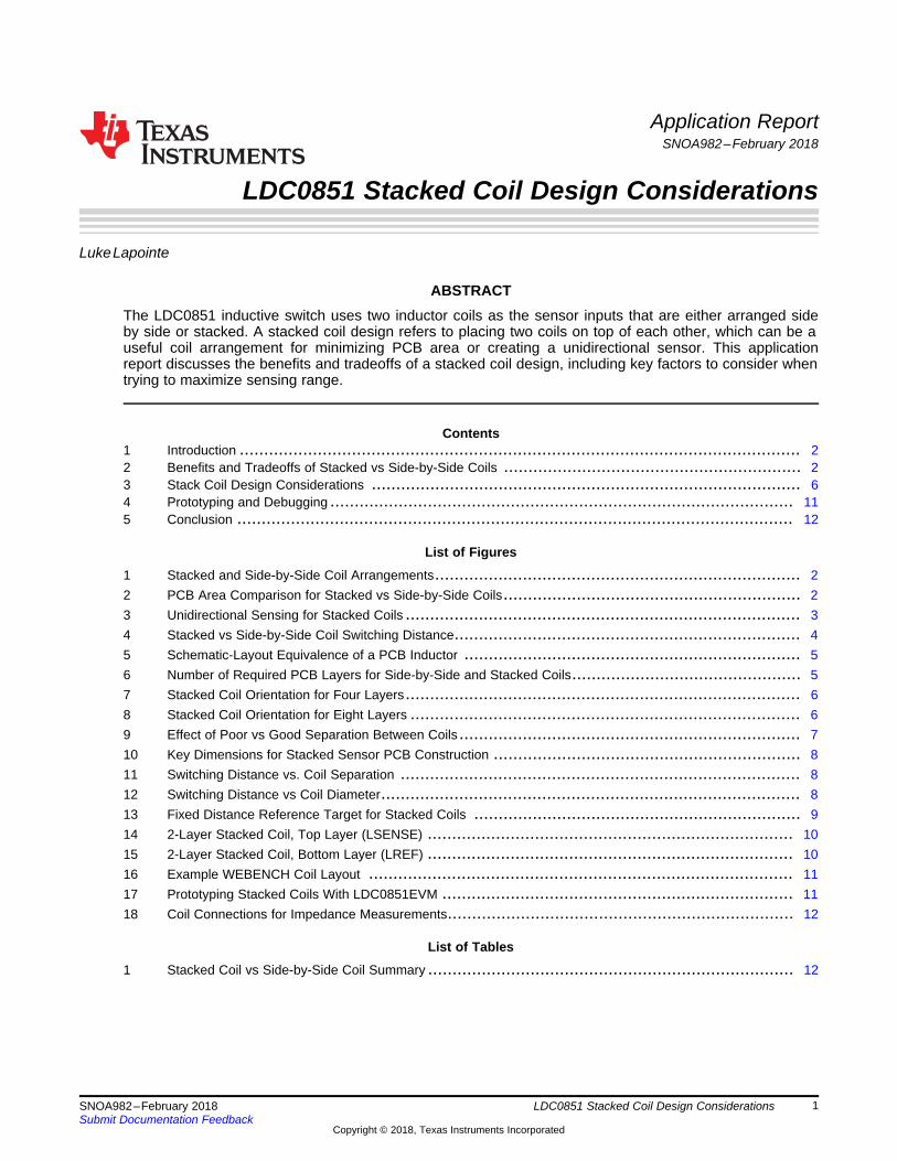
1 IntroductionThe LDC0851 is an inductive switch that uses two channels for sensing and comparing inductance,LSENSE and LREF. The sensors are typically constructed on a PCB as spiral inductors that are sensitiveto the proximity of nearby conductive objects. These inductor coils can either be arranged side by side orstacked on top of another as shown in Figure 1.
Figure 1. Stacked and Side-by-Side Coil Arrangements
A side-by-side coil arrangement is the most common, and it offers many advantages in terms of sensingrange and ease of construction. If placing two coils side by side often requires more PCB space than isavailable, however, a stacked coil arrangement is preferred. A stacked coil configuration works with theLDC0851 more effectively than other LDC devices, because it internally disconnects the inactive channelinstead of shorting it to ground. If the inactive channel was instead grounded or shorted, then a closedpath would be created for eddy currents to form directly under the active sensing coil, which woulddramatically reduce the sensing range.
2 Benefits and Tradeoffs of Stacked vs Side-by-Side Coils
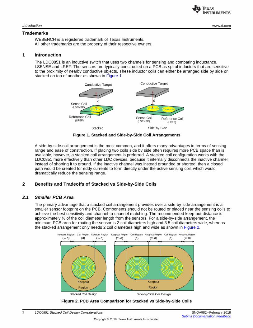
2.1 Smaller PCB AreaThe primary advantage that a stacked coil arrangement provides over a side-by-side arrangement is asmaller sensor footprint on the PCB. Components should not be routed or placed near the sensing coils toachieve the best sensitivity and channel-to-channel matching. The recommended keep-out distance isapproximately ½ of the coil diameter length from the sensors. For a side-by-side arrangement, theminimum PCB area for routing the sensor is 2 coil diameters high and 3.5 coil diameters wide, whereasthe stacked arrangement only needs 2 coil diameters high and wide as shown in Figure 2.
Figure 2. PCB Area Comparison for Stacked vs Side-by-Side Coils
LSENSE LREFLCOM
Differential LDC Core
LDC0851
Output
LS
LR
+
-
Sense Coil
Ref Coil
Inductance Converter
Inductance Converter
Target Distance
LR
LS
L0
dswitch
Coi
l Ind
ucta
nce
Output High
(LS > LR)
Output Low(LS < LR)O
utpu
t Sta
te
Switching occurs when LS < LR
LSENSE LREFLCOM
Differential LDC Core
LDC0851
Output
LS
LR
+
-
Sense Coil
Ref Coil
Inductance Converter
Inductance Converter
Target Distance
LR
LS
0
Coi
l Ind
ucta
nce
Output High (LS > LR)
Out
put S
tate
L
Switching does not occur!
LS never drops below LR
Metal Target Approaches from LSENSE Side
Metal Target Approaches from LREF Side
www.ti.com Benefits and Tradeoffs of Stacked vs Side-by-Side Coils
3SNOA982–February 2018Submit Documentation Feedback
Copyright © 2018, Texas Instruments Incorporated
LDC0851 Stacked Coil Design Considerations
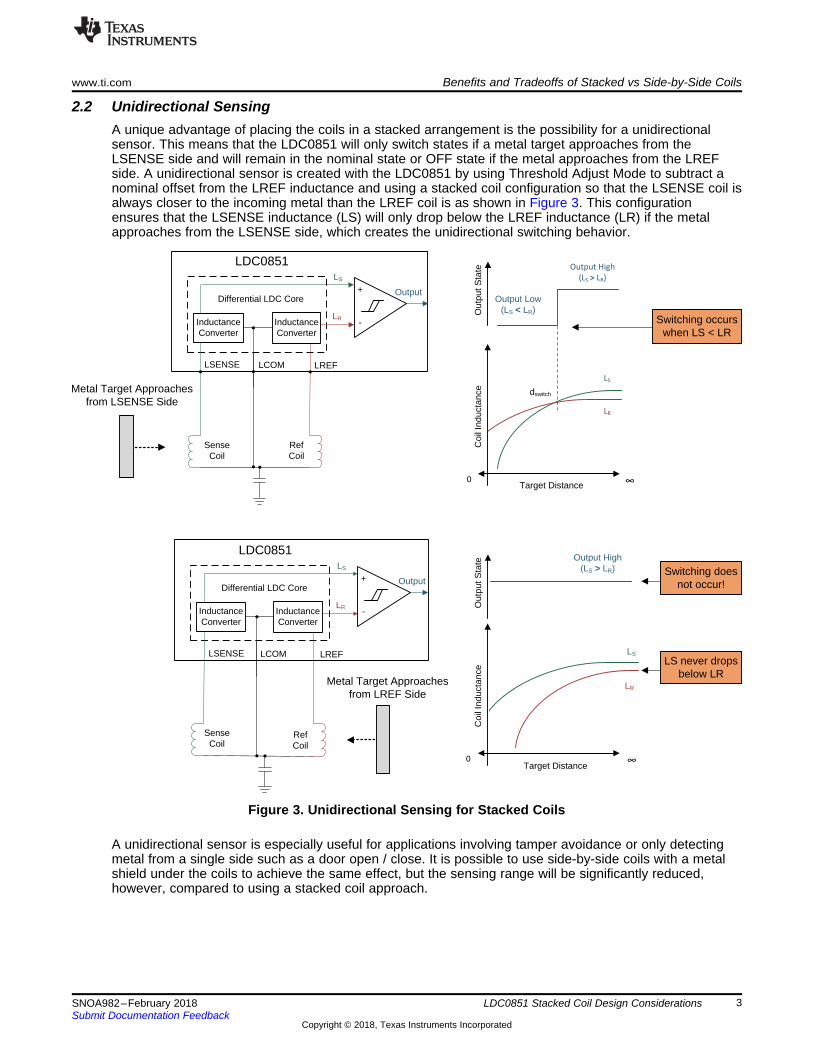
2.2 Unidirectional SensingA unique advantage of placing the coils in a stacked arrangement is the possibility for a unidirectionalsensor. This means that the LDC0851 will only switch states if a metal target approaches from theLSENSE side and will remain in the nominal state or OFF state if the metal approaches from the LREFside. A unidirectional sensor is created with the LDC0851 by using Threshold Adjust Mode to subtract anominal offset from the LREF inductance and using a stacked coil configuration so that the LSENSE coil isalways closer to the incoming metal than the LREF coil is as shown in Figure 3. This configurationensures that the LSENSE inductance (LS) will only drop below the LREF inductance (LR) if the metalapproaches from the LSENSE side, which creates the unidirectional switching behavior.
Figure 3. Unidirectional Sensing for Stacked Coils
A unidirectional sensor is especially useful for applications involving tamper avoidance or only detectingmetal from a single side such as a door open / close. It is possible to use side-by-side coils with a metalshield under the coils to achieve the same effect, but the sensing range will be significantly reduced,however, compared to using a stacked coil approach.
LS
�0
Output High (LS > LR)
dswitch
(ADJ = 1)
Output Low(LS < LR)
Coi
l Ind
ucta
nce
Out
put S
tate
Target Distance
Adjusted LR
(ADJ=1)
dswitch §�30% dcoil
LS
�dswitch §�40% dcoil0
Coi
l Ind
ucta
nce
Target Distance
Adjusted LR (ADJ=1)
Out
put S
tate Output High
(LS > LR)
Output Low(LS < LR)
RefCoil
Sense Coil
Side-by-side configuration
RefCoil
Sense Coil
Stacked configuration
Switching occurs at shorter distance
Switching occurs at maximum distance
Metal Target
Metal Target
LSENSELREF
LCOM
Both coils sense approaching target
LSENSE
LREF
LCOM
Only sense coil sees target
Benefits and Tradeoffs of Stacked vs Side-by-Side Coils www.ti.com
4 SNOA982–February 2018Submit Documentation Feedback
Copyright © 2018, Texas Instruments Incorporated
LDC0851 Stacked Coil Design Considerations
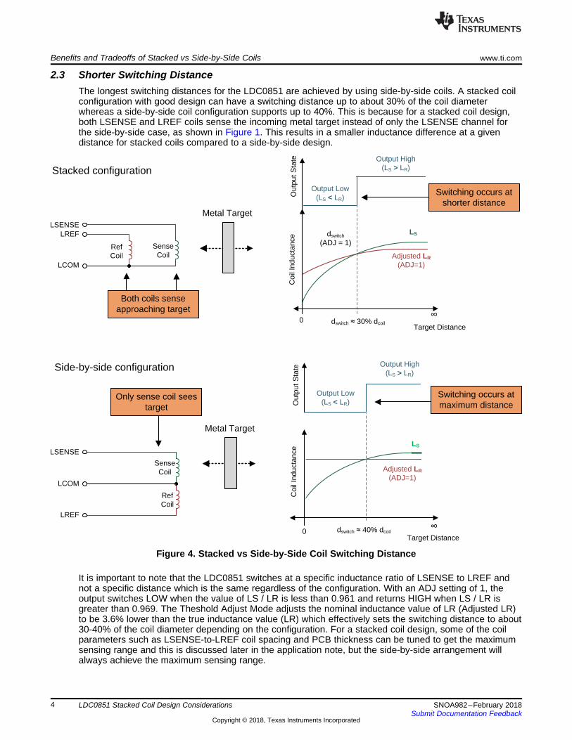
2.3 Shorter Switching DistanceThe longest switching distances for the LDC0851 are achieved by using side-by-side coils. A stacked coilconfiguration with good design can have a switching distance up to about 30% of the coil diameterwhereas a side-by-side coil configuration supports up to 40%. This is because for a stacked coil design,both LSENSE and LREF coils sense the incoming metal target instead of only the LSENSE channel forthe side-by-side case, as shown in Figure 1. This results in a smaller inductance difference at a givendistance for stacked coils compared to a side-by-side design.
Figure 4. Stacked vs Side-by-Side Coil Switching Distance
It is important to note that the LDC0851 switches at a specific inductance ratio of LSENSE to LREF andnot a specific distance which is the same regardless of the configuration. With an ADJ setting of 1, theoutput switches LOW when the value of LS / LR is less than 0.961 and returns HIGH when LS / LR isgreater than 0.969. The Theshold Adjust Mode adjusts the nominal inductance value of LR (Adjusted LR)to be 3.6% lower than the true inductance value (LR) which effectively sets the switching distance to about30-40% of the coil diameter depending on the configuration. For a stacked coil design, some of the coilparameters such as LSENSE-to-LREF coil spacing and PCB thickness can be tuned to get the maximumsensing range and this is discussed later in the application note, but the side-by-side arrangement willalways achieve the maximum sensing range.
PCB
Layers 1, 2 Sense Coil
Layers 3,4 Reference Coil
Target
PCB
Sense Coil Reference Coil
Target
Schematic of Inductor
Pin1
Pin2
Layout of Inductor
Pin1
Pin2
Via required in center to complete the inductor
www.ti.com Benefits and Tradeoffs of Stacked vs Side-by-Side Coils
5SNOA982–February 2018Submit Documentation Feedback
Copyright © 2018, Texas Instruments Incorporated
LDC0851 Stacked Coil Design Considerations
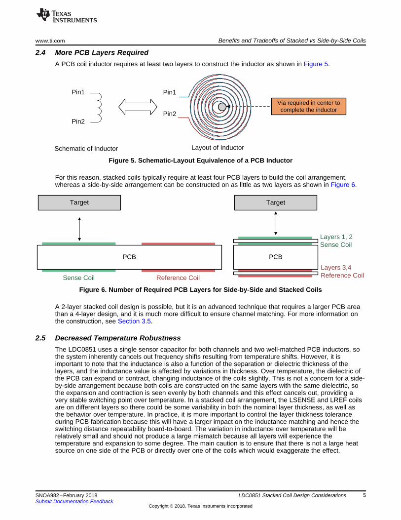
2.4 More PCB Layers RequiredA PCB coil inductor requires at least two layers to construct the inductor as shown in Figure 5.
Figure 5. Schematic-Layout Equivalence of a PCB Inductor
For this reason, stacked coils typically require at least four PCB layers to build the coil arrangement,whereas a side-by-side arrangement can be constructed on as little as two layers as shown in Figure 6.
Figure 6. Number of Required PCB Layers for Side-by-Side and Stacked Coils
A 2-layer stacked coil design is possible, but it is an advanced technique that requires a larger PCB areathan a 4-layer design, and it is much more difficult to ensure channel matching. For more information onthe construction, see Section 3.5.
2.5 Decreased Temperature RobustnessThe LDC0851 uses a single sensor capacitor for both channels and two well-matched PCB inductors, sothe system inherently cancels out frequency shifts resulting from temperature shifts. However, it isimportant to note that the inductance is also a function of the separation or dielectric thickness of thelayers, and the inductance value is affected by variations in thickness. Over temperature, the dielectric ofthe PCB can expand or contract, changing inductance of the coils slightly. This is not a concern for a side-by-side arrangement because both coils are constructed on the same layers with the same dielectric, sothe expansion and contraction is seen evenly by both channels and this effect cancels out, providing avery stable switching point over temperature. In a stacked coil arrangement, the LSENSE and LREF coilsare on different layers so there could be some variability in both the nominal layer thickness, as well asthe behavior over temperature. In practice, it is more important to control the layer thickness toleranceduring PCB fabrication because this will have a larger impact on the inductance matching and hence theswitching distance repeatability board-to-board. The variation in inductance over temperature will berelatively small and should not produce a large mismatch because all layers will experience thetemperature and expansion to some degree. The main caution is to ensure that there is not a large heatsource on one side of the PCB or directly over one of the coils which would exaggerate the effect.
ClockwiseSpiral IN on Layer 6
Counter-Clockwise Spiral OUT on Layer 2
ClockwiseSpiral IN on Layer 1
Via from Layer 5 to Layer 6
Via from Layer 1 to Layer 2
LCOM
Via from Layer 2 to Layer 3
LSENSE
Counter-ClockwiseSpiral OUT on Layer 4
ClockwiseSpiral IN on Layer 3
Via from Layer 3 to Layer 4
Counter-Clockwise Spiral OUT on Layer 7
Clockwise Spiral IN on Layer 8
Via from Layer 7 to Layer 8LREF
Via from Layer 6 to Layer 7
Via from Layer 5 to Layer 4Inner two layers have
same orientation
Counter-Clockwise Spiral OUT on Layer 5
LSLCLR
Counter-Clockwise Spiral OUT on Layer 2
Clockwise Spiral IN on Layer 1
Via from Layer 1 to Layer 2LCOM
Via from Layer 2 to Layer 3
LSENSE
Counter-Clockwise Spiral OUT on Layer 3
Clockwise Spiral IN on Layer 4
Via from Layer 3 to Layer 4
LSLCLR
LREF
Inner two layers have same orientation
Stack Coil Design Considerations www.ti.com
6 SNOA982–February 2018Submit Documentation Feedback
Copyright © 2018, Texas Instruments Incorporated
LDC0851 Stacked Coil Design Considerations
3 Stack Coil Design Considerations
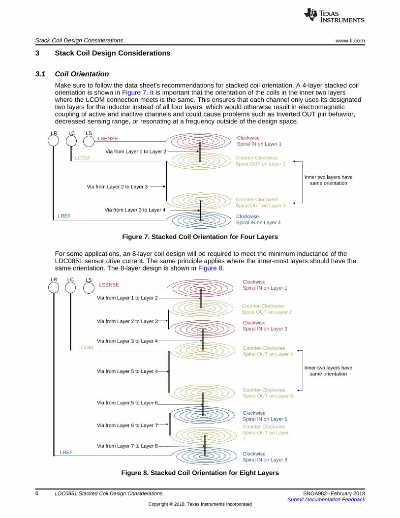
3.1 Coil OrientationMake sure to follow the data sheet's recommendations for stacked coil orientation. A 4-layer stacked coilorientation is shown in Figure 7. It is important that the orientation of the coils in the inner two layerswhere the LCOM connection meets is the same. This ensures that each channel only uses its designatedtwo layers for the inductor instead of all four layers, which would otherwise result in electromagneticcoupling of active and inactive channels and could cause problems such as Inverted OUT pin behavior,decreased sensing range, or resonating at a frequency outside of the design space.
Figure 7. Stacked Coil Orientation for Four Layers
For some applications, an 8-layer coil design will be required to meet the minimum inductance of theLDC0851 sensor drive current. The same principle applies where the inner-most layers should have thesame orientation. The 8-layer design is shown in Figure 8.
Figure 8. Stacked Coil Orientation for Eight Layers

Target Distance
LS
Output High (LS > LR)
Output Low(LS < LR)
Coi
l Ind
ucta
nce
Out
put S
tate
LR
�0
Target Distance
LS
0
Output High (LS > LR)
Output Low(LS < LR)
Coi
l Ind
ucta
nce
Out
put S
tate
LR
�
Very short distance between coils
Good seperation between coils
RefCoil
Sense Coil
Metal TargetLSENSE
LREF
LCOM
Poor Coil Separation
Good Coil Separation
RefCoil
Sense Coil
Metal TargetLSENSE
LREF
LCOM
Switching occurs at very short distance
Reference coil begins to sense metal at a much
farther distance
Switching occurs at much longer distance
www.ti.com Stack Coil Design Considerations
7SNOA982–February 2018Submit Documentation Feedback
Copyright © 2018, Texas Instruments Incorporated
LDC0851 Stacked Coil Design Considerations
3.2 MatchingCoil matching is critical to get the maximum sensing range for both a side-by-side and stacked coilarrangement. When using the ADJ setting of 1, the LDC0851 output switches low when the inductanceratio of LSENSE / LREF is less than 0.961 and switches high when LSENSE / LREF is greater than 0.969.This is roughly a 4% inductance shift for the output to switch low and then a 0.8% inductance hysteresis toswitch off. For a good stacked coil design this translates to about 30% of the coil diameter for theswitching distance. If the coils are mismatched by 1%, this could translate to the switching distancedecreasing to 20%. Therefore it is important to follow the guidelines mentioned in this application note andto ensure good matching in the layout. The main source of mismatch is the routing between the sensorsand the pins of the LDC0851. It is important to keep the trace routing symmetric in terms of length and notto induce additional parasitic capacitances by routing signals beneath the traces. Occasionally the sensoris located remotely from the main PCB and is connected by wires. In this case, use twisted pair andshielded cables if possible and keep the length to a minimum. This will ensure the greatest matchingbetween the LSENSE and LREF channels and keep the switching distance consistent from board toboard.
3.3 Sensor SeparationThe PCB stackup and sensor separation has a large impact on the switching distance for a stacked coildesign. It is important to minimize the amount of inductance shift that occurs on LREF when the metal isapproaches the LSENSE coil because the LDC0851 switching point is determined by a fixed inductanceratio between LSENSE and LREF and not directly distance. Designs with a larger separation in distancebetween LREF and LSENSE will have a much larger separation in inductance for a given distance andhence longer switching distance than a design with thin separation as shown in Figure 9.
Figure 9. Effect of Poor vs Good Separation Between Coils
Coil Diameter (mm)
Sw
itchi
ng D
ista
nce
(mm
)
0 20 40 60 80 1000
5
10
15
20
25
30
35
40
45
D002
Side-by-Side, dsep = infStacked, dsep = 3mmSide-by-Side, dsep = 1.2 mm
Coil Separation (dsep/dcoil%)
Sw
itchi
ng D
ista
nce
(%)
0 10 20 30 40 50 60 70 80 90 1000
5
10
15
20
25
30
35
40
45
50
D001
Switch ONSwitch OFF
Layers 1, 2 Sense Coil
Layers 3,4 Reference Coil
dsep
dcoil
h
Stack Coil Design Considerations www.ti.com
8 SNOA982–February 2018Submit Documentation Feedback
Copyright © 2018, Texas Instruments Incorporated
LDC0851 Stacked Coil Design Considerations
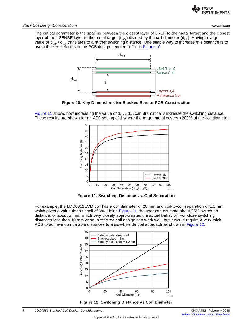
The critical parameter is the spacing between the closest layer of LREF to the metal target and the closestlayer of the LSENSE layer to the metal target (dsep) divided by the coil diameter (dcoil). Having a largervalue of dsep / dcoil translates to a farther switching distance. One simple way to increase this distance is touse a thicker dielectric in the PCB design denoted at “h” in Figure 10.
Figure 10. Key Dimensions for Stacked Sensor PCB Construction
Figure 11 shows how increasing the value of dsep / dcoil can dramatically increase the switching distance.These results are shown for an ADJ setting of 1 where the target metal covers >200% of the coil diameter.
Figure 11. Switching Distance vs. Coil Separation
For example, the LDC0851EVM coil has a coil diameter of 20 mm and coil-to-coil separation of 1.2 mmwhich gives a value dsep / dcoil of 6%. Using Figure 11, the user can estimate about 25% switch ondistance, or about 5 mm, which very closely approximates the actual behavior. For close switchingdistances less than 10 mm or so, a stacked coil design can work well, but it would require a very thickPCB to achieve comparable distances to a side-by-side coil approach as shown in Figure 12.
Figure 12. Switching Distance vs Coil Diameter
Metal Target Approaches from LSENSE Side
Metal-to-Sensor Distance
LR
LS
LSENSELREF LCOM
�0
dswitch = dref
Coi
l Ind
ucta
nce
Output High (LS > LR)
Output Low(LS < LR)O
utpu
t Sta
te
Sense Coil
Ref Coil
Reference target a fixed distance from LREF coil
dref dswitch
Switching occurs when metal target reaches same
distance as reference target (dswitch = dref)
www.ti.com Stack Coil Design Considerations
9SNOA982–February 2018Submit Documentation Feedback
Copyright © 2018, Texas Instruments Incorporated
LDC0851 Stacked Coil Design Considerations
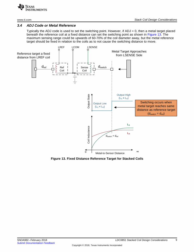
3.4 ADJ Code or Metal ReferenceTypically the ADJ code is used to set the switching point. However, if ADJ = 0, then a metal target placedbeneath the reference coil at a fixed distance can set the switching point as shown in Figure 13. Themaximum sensing range could be upwards of 60-70% of the coil diameter away, but the metal referencetarget should be fixed in relation to the coils as to not cause the switching distance to move.
Figure 13. Fixed Distance Reference Target for Stacked Coils
Stack Coil Design Considerations www.ti.com
10 SNOA982–February 2018Submit Documentation Feedback
Copyright © 2018, Texas Instruments Incorporated
LDC0851 Stacked Coil Design Considerations
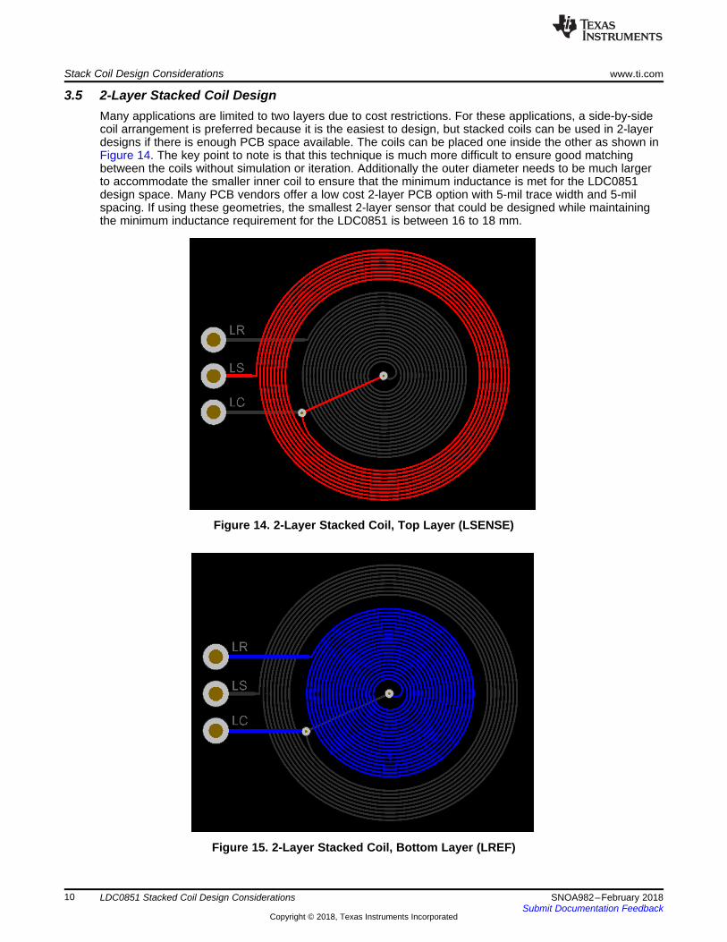
3.5 2-Layer Stacked Coil DesignMany applications are limited to two layers due to cost restrictions. For these applications, a side-by-sidecoil arrangement is preferred because it is the easiest to design, but stacked coils can be used in 2-layerdesigns if there is enough PCB space available. The coils can be placed one inside the other as shown inFigure 14. The key point to note is that this technique is much more difficult to ensure good matchingbetween the coils without simulation or iteration. Additionally the outer diameter needs to be much largerto accommodate the smaller inner coil to ensure that the minimum inductance is met for the LDC0851design space. Many PCB vendors offer a low cost 2-layer PCB option with 5-mil trace width and 5-milspacing. If using these geometries, the smallest 2-layer sensor that could be designed while maintainingthe minimum inductance requirement for the LDC0851 is between 16 to 18 mm.
Figure 14. 2-Layer Stacked Coil, Top Layer (LSENSE)
Figure 15. 2-Layer Stacked Coil, Bottom Layer (LREF)
www.ti.com Stack Coil Design Considerations
11SNOA982–February 2018Submit Documentation Feedback
Copyright © 2018, Texas Instruments Incorporated
LDC0851 Stacked Coil Design Considerations
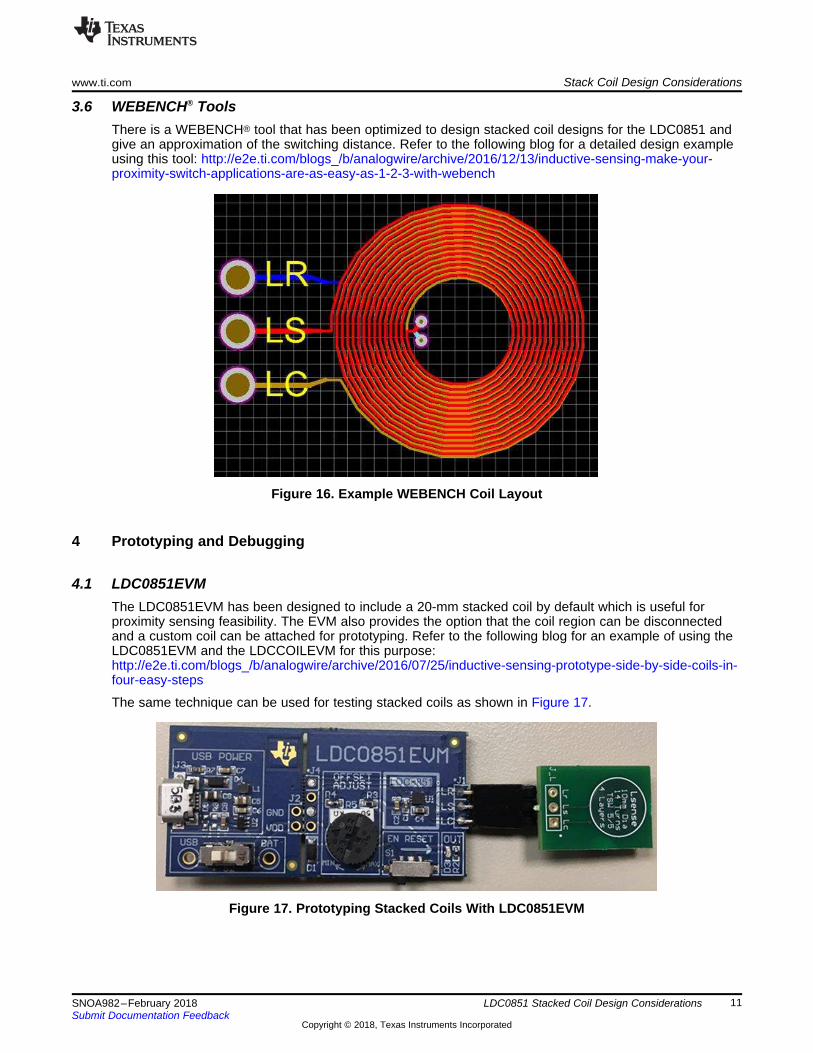
3.6 WEBENCH® ToolsThere is a WEBENCH® tool that has been optimized to design stacked coil designs for the LDC0851 andgive an approximation of the switching distance. Refer to the following blog for a detailed design exampleusing this tool: http://e2e.ti.com/blogs_/b/analogwire/archive/2016/12/13/inductive-sensing-make-your-proximity-switch-applications-are-as-easy-as-1-2-3-with-webench
Figure 16. Example WEBENCH Coil Layout
4 Prototyping and Debugging
4.1 LDC0851EVMThe LDC0851EVM has been designed to include a 20-mm stacked coil by default which is useful forproximity sensing feasibility. The EVM also provides the option that the coil region can be disconnectedand a custom coil can be attached for prototyping. Refer to the following blog for an example of using theLDC0851EVM and the LDCCOILEVM for this purpose:http://e2e.ti.com/blogs_/b/analogwire/archive/2016/07/25/inductive-sensing-prototype-side-by-side-coils-in-four-easy-steps
The same technique can be used for testing stacked coils as shown in Figure 17.
Figure 17. Prototyping Stacked Coils With LDC0851EVM
LR
LC
LS
Impedance Analyzer
LR
LC
LS
Impedance Analyzer
Prototyping and Debugging www.ti.com
12 SNOA982–February 2018Submit Documentation Feedback
Copyright © 2018, Texas Instruments Incorporated
LDC0851 Stacked Coil Design Considerations
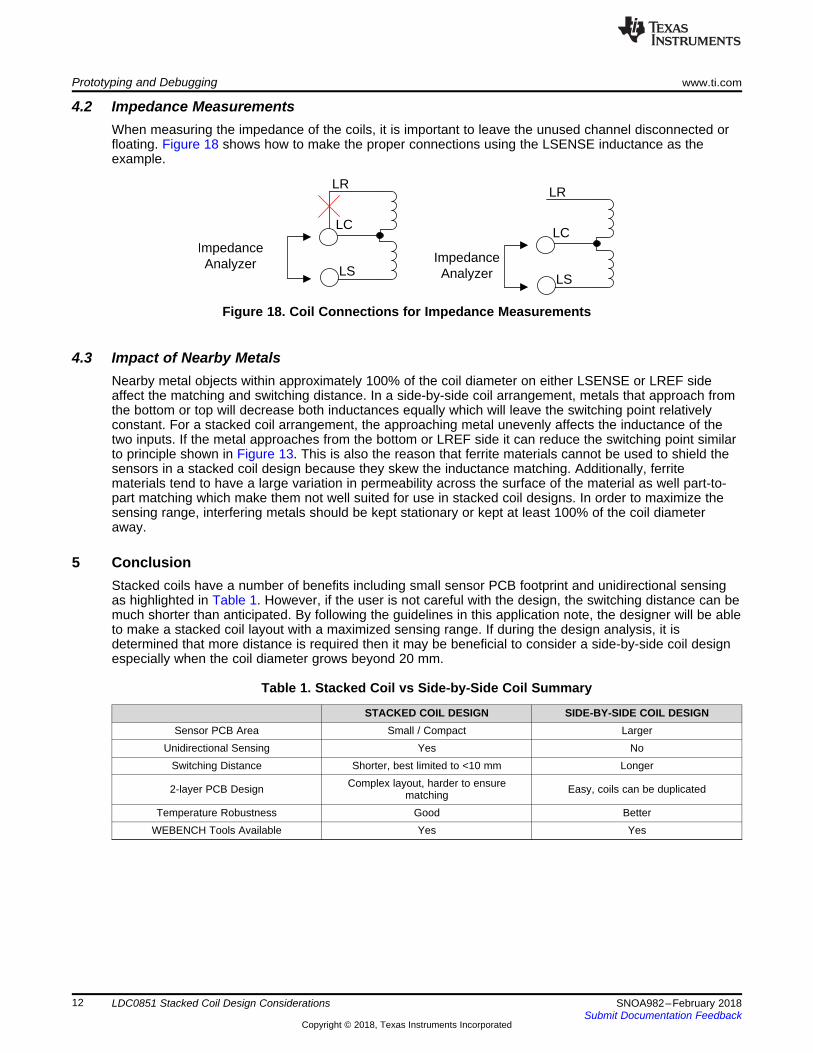
4.2 Impedance MeasurementsWhen measuring the impedance of the coils, it is important to leave the unused channel disconnected orfloating. Figure 18 shows how to make the proper connections using the LSENSE inductance as theexample.
Figure 18. Coil Connections for Impedance Measurements
4.3 Impact of Nearby MetalsNearby metal objects within approximately 100% of the coil diameter on either LSENSE or LREF sideaffect the matching and switching distance. In a side-by-side coil arrangement, metals that approach fromthe bottom or top will decrease both inductances equally which will leave the switching point relativelyconstant. For a stacked coil arrangement, the approaching metal unevenly affects the inductance of thetwo inputs. If the metal approaches from the bottom or LREF side it can reduce the switching point similarto principle shown in Figure 13. This is also the reason that ferrite materials cannot be used to shield thesensors in a stacked coil design because they skew the inductance matching. Additionally, ferritematerials tend to have a large variation in permeability across the surface of the material as well part-to-part matching which make them not well suited for use in stacked coil designs. In order to maximize thesensing range, interfering metals should be kept stationary or kept at least 100% of the coil diameteraway.
5 ConclusionStacked coils have a number of benefits including small sensor PCB footprint and unidirectional sensingas highlighted in Table 1. However, if the user is not careful with the design, the switching distance can bemuch shorter than anticipated. By following the guidelines in this application note, the designer will be ableto make a stacked coil layout with a maximized sensing range. If during the design analysis, it isdetermined that more distance is required then it may be beneficial to consider a side-by-side coil designespecially when the coil diameter grows beyond 20 mm.
Table 1. Stacked Coil vs Side-by-Side Coil Summary
STACKED COIL DESIGN SIDE-BY-SIDE COIL DESIGNSensor PCB Area Small / Compact Larger
Unidirectional Sensing Yes NoSwitching Distance Shorter, best limited to <10 mm Longer
2-layer PCB Design Complex layout, harder to ensurematching Easy, coils can be duplicated
Temperature Robustness Good BetterWEBENCH Tools Available Yes Yes
IMPORTANT NOTICE FOR TI DESIGN INFORMATION AND RESOURCES
Texas Instruments Incorporated (‘TI”) technical, application or other design advice, services or information, including, but not limited to,reference designs and materials relating to evaluation modules, (collectively, “TI Resources”) are intended to assist designers who aredeveloping applications that incorporate TI products; by downloading, accessing or using any particular TI Resource in any way, you(individually or, if you are acting on behalf of a company, your company) agree to use it solely for this purpose and subject to the terms ofthis Notice.TI’s provision of TI Resources does not expand or otherwise alter TI’s applicable published warranties or warranty disclaimers for TIproducts, and no additional obligations or liabilities arise from TI providing such TI Resources. TI reserves the right to make corrections,enhancements, improvements and other changes to its TI Resources.You understand and agree that you remain responsible for using your independent analysis, evaluation and judgment in designing yourapplications and that you have full and exclusive responsibility to assure the safety of your applications and compliance of your applications(and of all TI products used in or for your applications) with all applicable regulations, laws and other applicable requirements. Yourepresent that, with respect to your applications, you have all the necessary expertise to create and implement safeguards that (1)anticipate dangerous consequences of failures, (2) monitor failures and their consequences, and (3) lessen the likelihood of failures thatmight cause harm and take appropriate actions. You agree that prior to using or distributing any applications that include TI products, youwill thoroughly test such applications and the functionality of such TI products as used in such applications. TI has not conducted anytesting other than that specifically described in the published documentation for a particular TI Resource.You are authorized to use, copy and modify any individual TI Resource only in connection with the development of applications that includethe TI product(s) identified in such TI Resource. NO OTHER LICENSE, EXPRESS OR IMPLIED, BY ESTOPPEL OR OTHERWISE TOANY OTHER TI INTELLECTUAL PROPERTY RIGHT, AND NO LICENSE TO ANY TECHNOLOGY OR INTELLECTUAL PROPERTYRIGHT OF TI OR ANY THIRD PARTY IS GRANTED HEREIN, including but not limited to any patent right, copyright, mask work right, orother intellectual property right relating to any combination, machine, or process in which TI products or services are used. Informationregarding or referencing third-party products or services does not constitute a license to use such products or services, or a warranty orendorsement thereof. Use of TI Resources may require a license from a third party under the patents or other intellectual property of thethird party, or a license from TI under the patents or other intellectual property of TI.TI RESOURCES ARE PROVIDED “AS IS” AND WITH ALL FAULTS. TI DISCLAIMS ALL OTHER WARRANTIES ORREPRESENTATIONS, EXPRESS OR IMPLIED, REGARDING TI RESOURCES OR USE THEREOF, INCLUDING BUT NOT LIMITED TOACCURACY OR COMPLETENESS, TITLE, ANY EPIDEMIC FAILURE WARRANTY AND ANY IMPLIED WARRANTIES OFMERCHANTABILITY, FITNESS FOR A PARTICULAR PURPOSE, AND NON-INFRINGEMENT OF ANY THIRD PARTY INTELLECTUALPROPERTY RIGHTS.TI SHALL NOT BE LIABLE FOR AND SHALL NOT DEFEND OR INDEMNIFY YOU AGAINST ANY CLAIM, INCLUDING BUT NOTLIMITED TO ANY INFRINGEMENT CLAIM THAT RELATES TO OR IS BASED ON ANY COMBINATION OF PRODUCTS EVEN IFDESCRIBED IN TI RESOURCES OR OTHERWISE. IN NO EVENT SHALL TI BE LIABLE FOR ANY ACTUAL, DIRECT, SPECIAL,COLLATERAL, INDIRECT, PUNITIVE, INCIDENTAL, CONSEQUENTIAL OR EXEMPLARY DAMAGES IN CONNECTION WITH ORARISING OUT OF TI RESOURCES OR USE THEREOF, AND REGARDLESS OF WHETHER TI HAS BEEN ADVISED OF THEPOSSIBILITY OF SUCH DAMAGES.You agree to fully indemnify TI and its representatives against any damages, costs, losses, and/or liabilities arising out of your non-compliance with the terms and provisions of this Notice.This Notice applies to TI Resources. Additional terms apply to the use and purchase of certain types of materials, TI products and services.These include; without limitation, TI’s standard terms for semiconductor products http://www.ti.com/sc/docs/stdterms.htm), evaluationmodules, and samples (http://www.ti.com/sc/docs/sampterms.htm).
Mailing Address: Texas Instruments, Post Office Box 655303, Dallas, Texas 75265Copyright © 2018, Texas Instruments Incorporated