
Optical modeling and simulation of thin-film Cu(In,Ga)Se2 solar cells
30
University of Ljubljana Faculty of Electrical Engineering Optical Optical modeling modeling and and simulation simulation of of thin thin - - film film Cu(In,Ga)Se Cu(In,Ga)Se 2 2 solar cells solar cells J. Krc 1 , A. Campa 1 , G. Cernivec 1 , J. Malmström 2 , M. Edoff 2 , F. Smole 1 and M. Topic 1 1 University of Ljubljana, Faculty of Electrical Engineering, Tržaška 25 Si-1000 Ljubljana, Slovenia 2 Uppsala University, Ǻngström Solar Center, P.O. Box 534, SE-75120 Uppsala, Sweden
-
Upload
independent -
Category
Documents
-
view
1 -
download
0
Transcript of Optical modeling and simulation of thin-film Cu(In,Ga)Se2 solar cells
University of LjubljanaFaculty of Electrical Engineering
Optical Optical modelingmodeling andand simulationsimulation ofofthinthin--film film Cu(In,Ga)SeCu(In,Ga)Se22 solar cellssolar cells
J. Krc1, A. Campa1, G. Cernivec1, J. Malmström2,M. Edoff2, F. Smole1 and M. Topic1
1University of Ljubljana, Faculty of Electrical Engineering,Tržaška 25 Si-1000 Ljubljana, Slovenia
2Uppsala University, Ǻngström Solar Center,P.O. Box 534, SE-75120 Uppsala, Sweden
2
University of LjubljanaFaculty of Electrical Engineering
Outline
• Introduction
• Optical modeling of thin-film solar cells
• Optical simulator SunShine
• ResultsOptical simulation of thin Cu(In,Ga)Se2 solar cells
• Conclusions
3
University of LjubljanaFaculty of Electrical Engineering
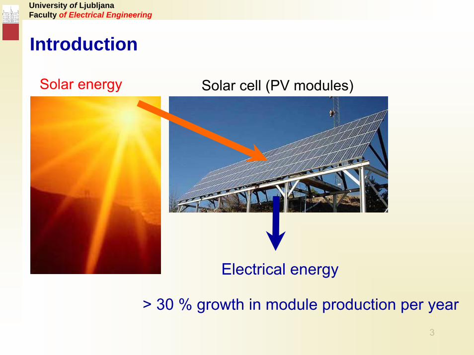
Introduction
Electrical energy
Solar energy Solar cell (PV modules)
> 30 % growth in module production per year
4
University of LjubljanaFaculty of Electrical Engineering
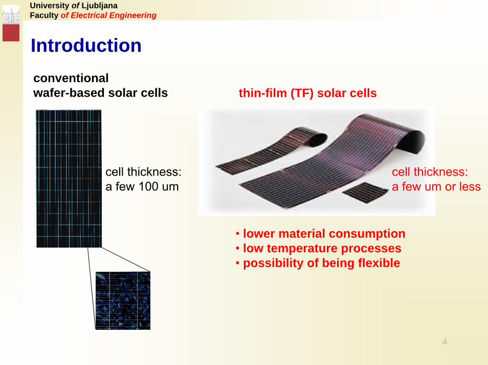
Introductionconventionalwafer-based solar cells thin-film (TF) solar cells
• lower material consumption• low temperature processes• possibility of being flexible
cell thickness:a few 100 um
cell thickness:a few um or less
5
University of LjubljanaFaculty of Electrical Engineering
Introduction
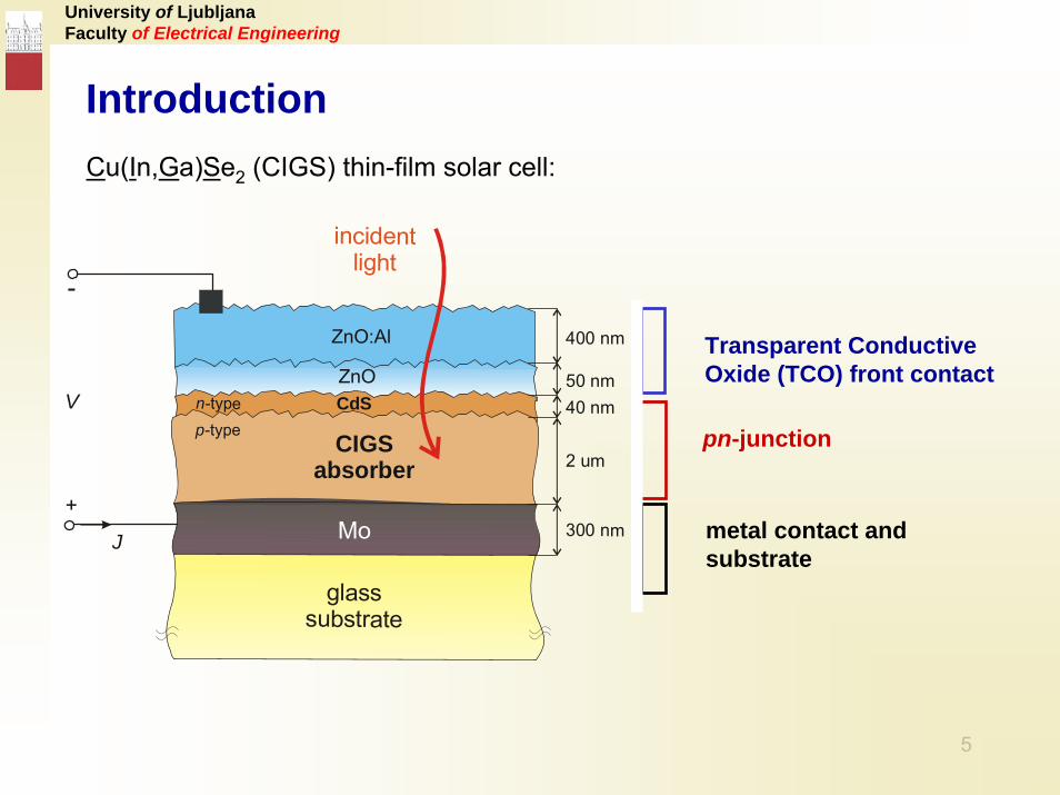
Mo
glasssubstrate
CIGSabsorber
ZnOCdS
ZnO:Al
incidentlight
n-typep-type
2 um
-
+
V
J
40 nm50 nm
400 nm
300 nm
Cu(In,Ga)Se2 (CIGS) thin-film solar cell:
Transparent ConductiveOxide (TCO) front contact
pn-junction
metal contact andsubstrate
6
University of LjubljanaFaculty of Electrical Engineering
Introduction
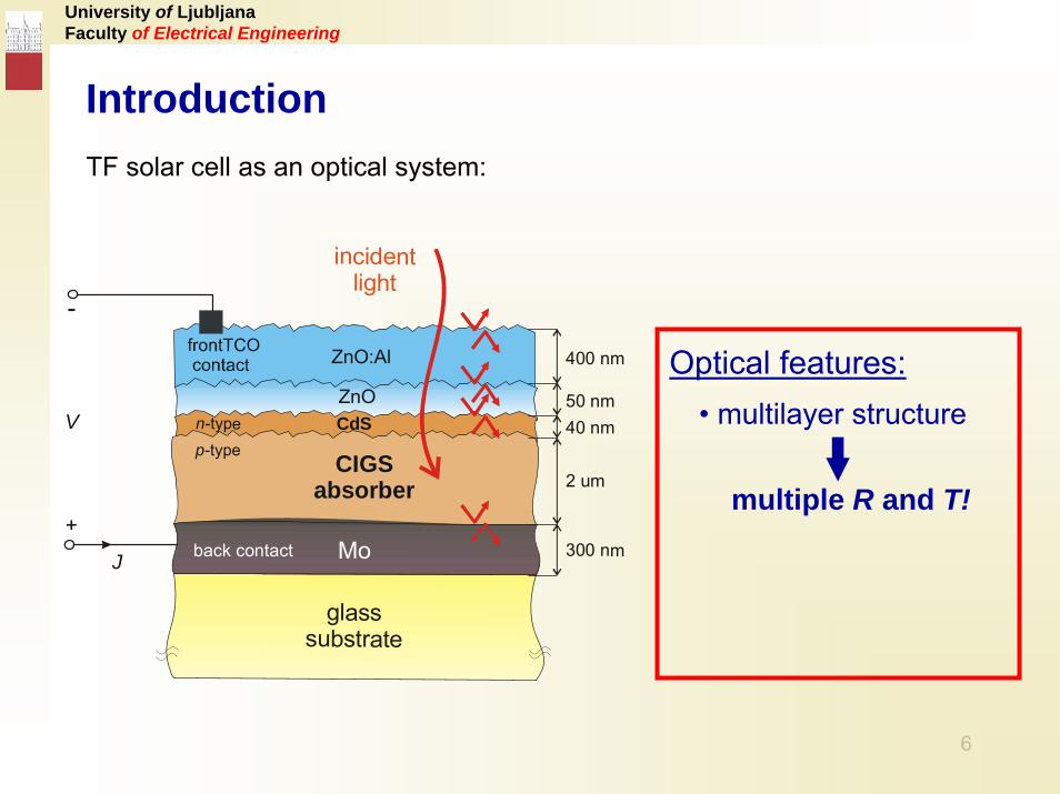
Mo
glasssubstrate
CIGSabsorber
ZnOCdS
ZnO:Al
incidentlight
back contact
n-typep-type
2 um
-
+
V
J
40 nm50 nm
400 nm
300 nm
Optical features:• multilayer structure
multiple R and T!
TF solar cell as an optical system:
7
University of LjubljanaFaculty of Electrical Engineering
Introduction
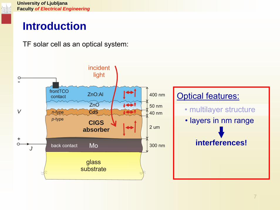
Mo
glasssubstrate
CIGSabsorber
ZnOCdS
ZnO:Al
incidentlight
back contact
n-typep-type
2 um
-
+
V
J
40 nm50 nm
400 nm
300 nm
• multilayer structure• layers in nm range
interferences!
TF solar cell as an optical system:
Optical features:
8
University of LjubljanaFaculty of Electrical Engineering
Introduction
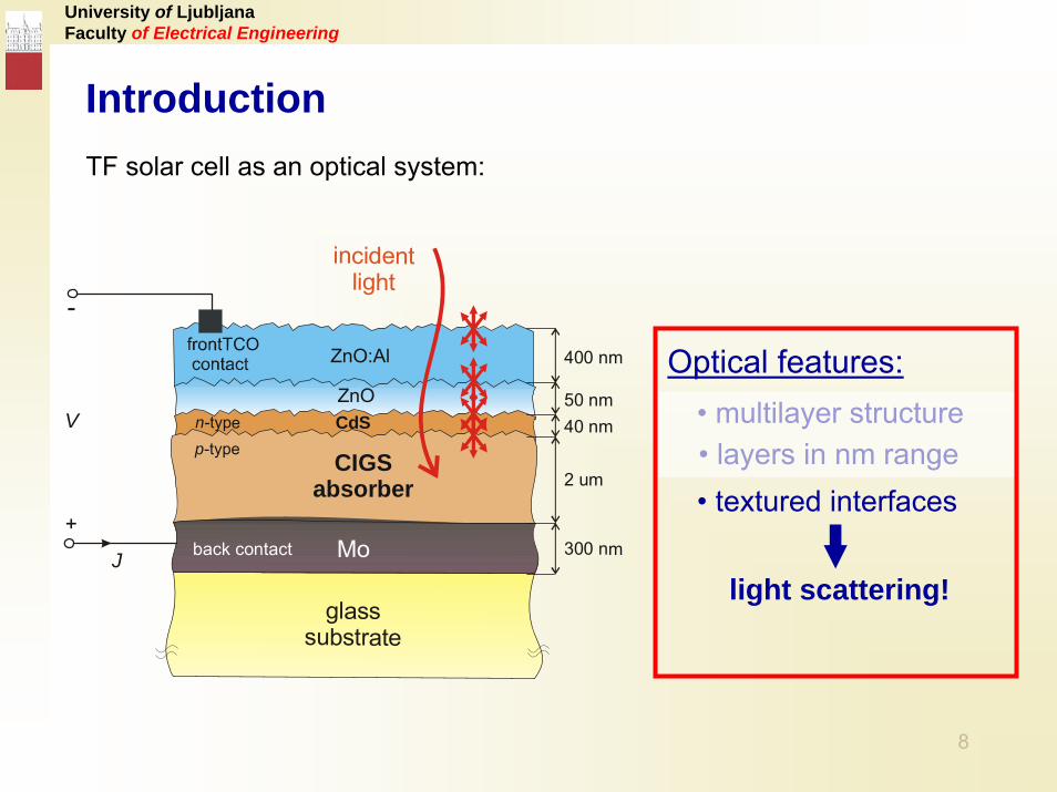
• multilayer structure• layers in nm range• textured interfaces
Mo
glasssubstrate
CIGSabsorber
ZnOCdS
ZnO:Al
incidentlight
back contact
n-typep-type
2 um
-
+
V
J
40 nm50 nm
400 nm
300 nm
light scattering!
TF solar cell as an optical system:
Optical features:
9
University of LjubljanaFaculty of Electrical Engineering
Optical modeling of TF solar cells
10
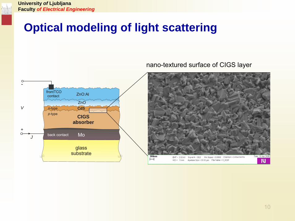
University of LjubljanaFaculty of Electrical Engineering
Mo
glasssubstrate
CIGSabsorber
ZnOCdS
ZnO:Al
back contact
n-typep-type
-
+
V
J
nano-textured surface of CIGS layer
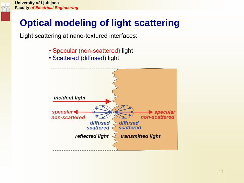
Optical modeling of light scattering
11
University of LjubljanaFaculty of Electrical Engineering
• Specular (non-scattered) light• Scattered (diffused) light
Light scattering at nano-textured interfaces:
Optical modeling of light scattering
12
University of LjubljanaFaculty of Electrical Engineering
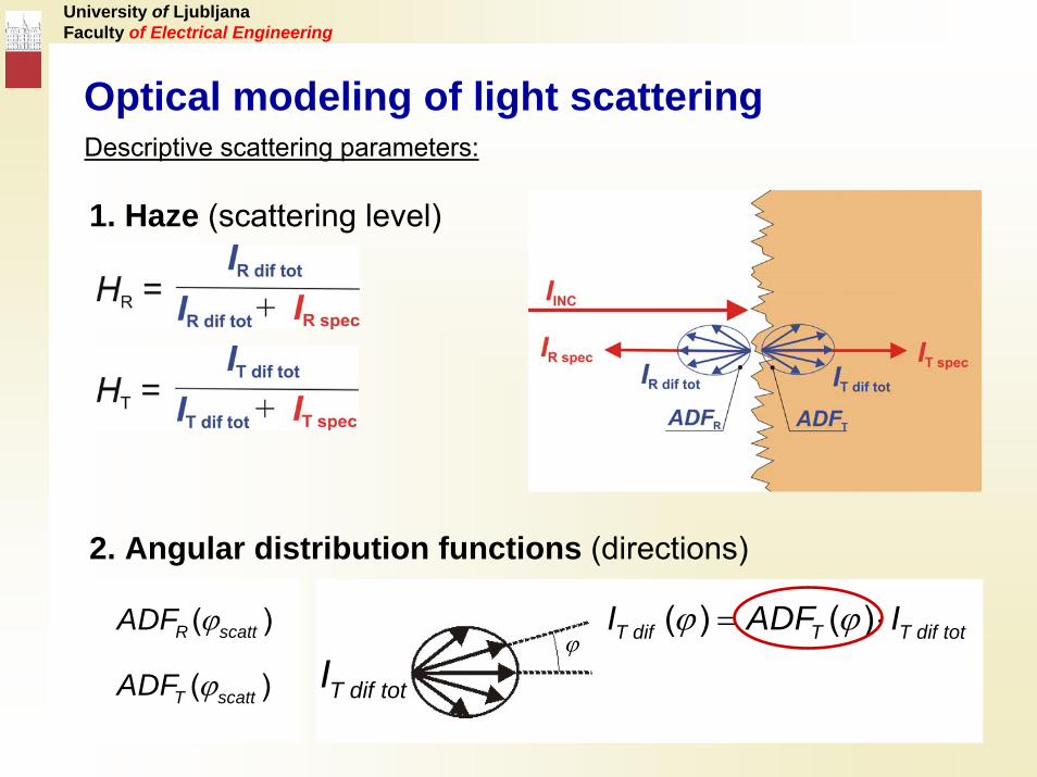
Descriptive scattering parameters:
( )R scattADF ϕ
( )T scattADF ϕ
( ) ( )T dif T T dif totI ADF Iϕ ϕ= ⋅ϕ
T dif totI
1. Haze (scattering level)
2. Angular distribution functions (directions)
Optical modeling of light scattering
13
University of LjubljanaFaculty of Electrical Engineering
Optical simulator SunShine
14
University of LjubljanaFaculty of Electrical Engineering
Optical simulator SunShine
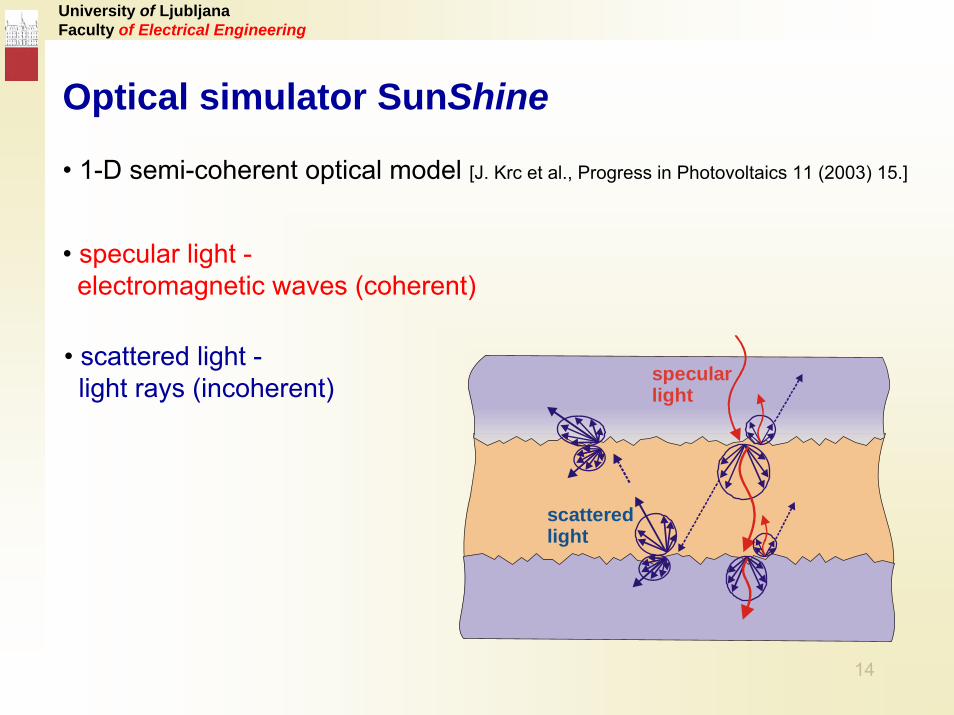
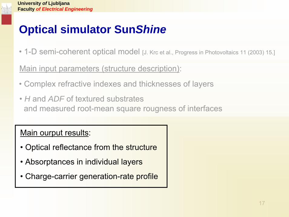
• 1-D semi-coherent optical model [J. Krc et al., Progress in Photovoltaics 11 (2003) 15.]
scatteredlight
specularlight
• specular light -electromagnetic waves (coherent)
• scattered light -light rays (incoherent)
15
University of LjubljanaFaculty of Electrical Engineering
Optical simulator SunShine
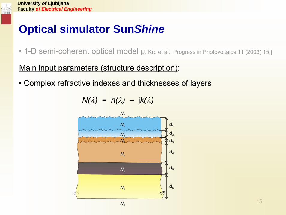
• 1-D semi-coherent optical model [J. Krc et al., Progress in Photovoltaics 11 (2003) 15.]
• Complex refractive indexes and thicknesses of layers
N(λ) = n(λ) – jk(λ)
Main input parameters (structure description):
d1
N5
N1
N2
N3
N4
N6
N0
N0
d2
d3
d4
d5
d6
16
University of LjubljanaFaculty of Electrical Engineering
Optical simulator SunShine
• 1-D semi-coherent optical model [J. Krc et al., Progress in Photovoltaics 11 (2003) 15.]
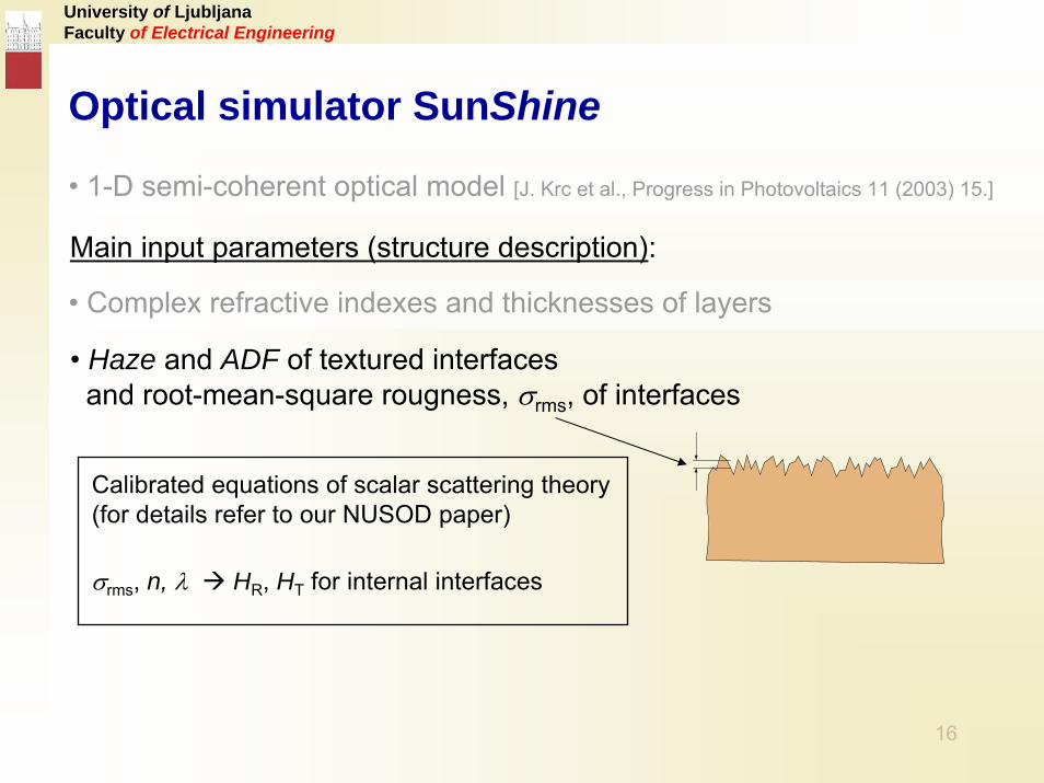
• Complex refractive indexes and thicknesses of layers
Main input parameters (structure description):
• Haze and ADF of textured interfacesand root-mean-square rougness, σrms, of interfaces
Calibrated equations of scalar scattering theory(for details refer to our NUSOD paper)
σrms, n, λ HR, HT for internal interfaces
17
University of LjubljanaFaculty of Electrical Engineering
Optical simulator SunShine
• 1-D semi-coherent optical model [J. Krc et al., Progress in Photovoltaics 11 (2003) 15.]
• Complex refractive indexes and thicknesses of layers
Main input parameters (structure description):
• H and ADF of textured substratesand measured root-mean square rougness of interfaces
Main ourput results:
• Optical reflectance from the structure
• Absorptances in individual layers
• Charge-carrier generation-rate profile
18
University of LjubljanaFaculty of Electrical Engineering
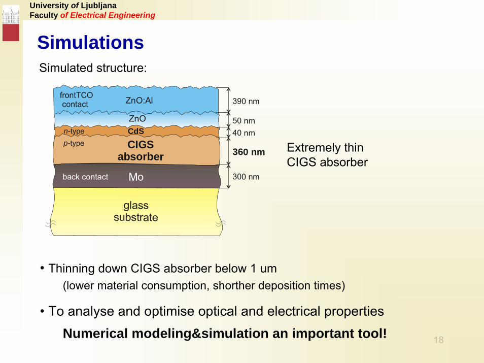
Simulations
Mo
glasssubstrate
CIGSabsorber
ZnOCdS
ZnO:Al
back contact
n-typep-type
360 nm
40 nm50 nm
390 nm
300 nm
(lower material consumption, shorther deposition times)
• To analyse and optimise optical and electrical propertiesNumerical modeling&simulation an important tool!
• Thinning down CIGS absorber below 1 um
Extremely thinCIGS absorber
Simulated structure:

19
University of LjubljanaFaculty of Electrical Engineering
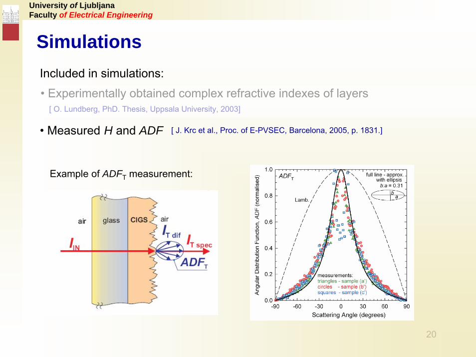
SimulationsIncluded in simulations:
• Experimentally obtained complex refractive indexes of layers[ O. Lundberg, PhD. Thesis, Uppsala University, 2003]
n k
Wavelength, λ (nm)400 600 800 1000 1200
Ref
ract
ive
inde
x, n
0.0
0.5
1.0
1.5
2.0
2.5
3.0
3.5
CIGS
CdS
Wavelength, λ (nm)400 600 800 1000 1200
Ext
inct
ion
coef
ficie
nt, k
1e-6
1e-5
1e-4
1e-3
1e-2
1e-1
1e+0
1e+1
CIGS
CdS
20
University of LjubljanaFaculty of Electrical Engineering
SimulationsIncluded in simulations:
• Experimentally obtained complex refractive indexes of layers[ O. Lundberg, PhD. Thesis, Uppsala University, 2003]
• Measured H and ADF [ J. Krc et al., Proc. of E-PVSEC, Barcelona, 2005, p. 1831.]
Example of ADFT measurement:

21
University of LjubljanaFaculty of Electrical Engineering
Simulation results
22
University of LjubljanaFaculty of Electrical Engineering
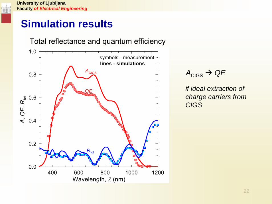
Simulation results
Wavelength, λ (nm)400 600 800 1000 1200
A, Q
E, R
tot
0.0
0.2
0.4
0.6
0.8
1.0symbols - measurementlines - simulations
QE
Rtot
ACIGS ACIGS QE
if ideal extraction ofcharge carriers fromCIGS
Total reflectance and quantum efficiency
23
University of LjubljanaFaculty of Electrical Engineering
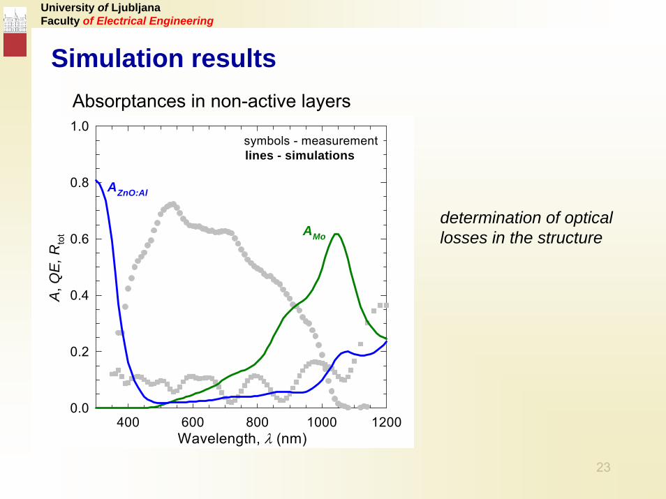
Simulation results
Wavelength, λ (nm)400 600 800 1000 1200
A, Q
E, R
tot
0.0
0.2
0.4
0.6
0.8
1.0symbols - measurementlines - simulations
AZnO:Al
AMo
determination of opticallosses in the structure
Absorptances in non-active layers
24
University of LjubljanaFaculty of Electrical Engineering
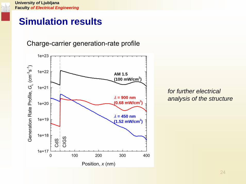
Simulation results
for further electricalanalysis of the structure
Position, x (nm)
0 100 200 300 400
Gen
erat
ion
Rat
e P
rofil
e, G
L (cm
-3s-1
)
1e+17
1e+18
1e+19
1e+20
1e+21
1e+22
1e+23C
dS
CIG
S
λ = 450 nm (1.52 mW/cm2)
λ = 900 nm (0.68 mW/cm2)
AM 1.5 (100 mW/cm2)
Charge-carrier generation-rate profile
25
University of LjubljanaFaculty of Electrical Engineering
Conclusions
• good agreement in sim. and meas. total reflectance of thin CIGS solar cell
• calibration of the simulator with realistic optical parameters (refractiveindexes, scattering and others) is important
• starting point for optical optimisation and electrical analysis of the structure

26
University of LjubljanaFaculty of Electrical Engineering
Further workcombined optical + electrical analysis of the structure
SunShine&Aspin simulators
External characteristics and parameters of the solar cell:
Voltage, V (V)0.0 0.1 0.2 0.3 0.4 0.5 0.6 0.7
Cur
rent
den
sity
, J (m
A/c
m2 )
-24
-20
-16
-12
-8
-4
0
JSC = 21.0 mA/cm2 21.1 mA/cm2
VOC = 592 mV 595 mV
FF = 0.68 0.65Eff. = 8.1 % 8.2 %
measurement(symbols)
simulation(line)
Wavelength, λ (nm)400 600 800 1000 1200
QE
0.0
0.2
0.4
0.6
0.8
1.0symbols - measurementline - opt. + el. simulation
QE
see extended NUSOD paper submitted to OQE
27
University of LjubljanaFaculty of Electrical Engineering
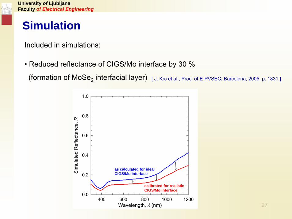
SimulationIncluded in simulations:
• Reduced reflectance of CIGS/Mo interface by 30 %
(formation of MoSe2 interfacial layer) [ J. Krc et al., Proc. of E-PVSEC, Barcelona, 2005, p. 1831.]
Wavelength, λ (nm)400 600 800 1000 1200
Sim
ulat
ed R
efle
ctan
ce, R
0.0
0.2
0.4
0.6
0.8
1.0
as calculated for idealCIGS/Mo interface
calibrated for realisticCIGS/Mo interface
28
University of LjubljanaFaculty of Electrical Engineering
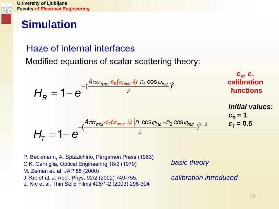
Simulation
Haze of internal interfaces
1 2 2...34 cos cos( )
1rms inc outn n
TH eπσ ϕ ϕ
λ⋅ −
−= −
214 cos( )1
rms incn
RH eπσ ϕ
λ⋅
−= −
cR(σrms, λ)
cT(σrms, λ)
cR, cTcalibrationfunctions
J. Krc et al. J. Appl. Phys. 92/2 (2002) 749-755.J. Krc et al. Thin Solid Films 426/1-2 (2003) 296-304
M. Zeman et. al. JAP 88 (2000)basic theory
calibration introduced
Modified equations of scalar scattering theory:
C.K. Carniglia, Optical Engineering 18/2 (1979)P. Beckmann, A. Spizzichino, Pergamon Press (1963)
initial values:cR = 1cT = 0.5
29
University of LjubljanaFaculty of Electrical Engineering
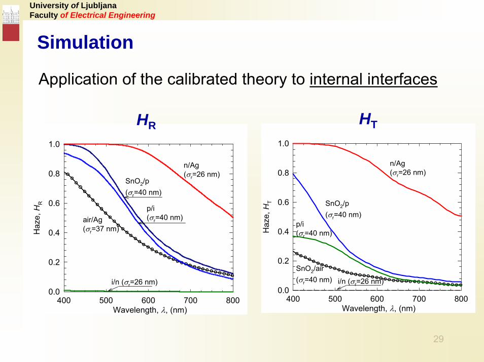
Simulation
Wavelength, λ, (nm)400 500 600 700 800
Haz
e, H
T
0.0
0.2
0.4
0.6
0.8
1.0
n/Ag(σr=26 nm)
SnO2/air(σr=40 nm) i/n (σr=26 nm)
p/i(σr=40 nm)
SnO2/p(σr=40 nm)
Wavelength, λ, (nm)400 500 600 700 800
Haz
e, H
R
0.0
0.2
0.4
0.6
0.8
1.0
n/Ag(σr=26 nm)
SnO2/p(σr=40 nm)
i/n (σr=26 nm)
air/Ag(σr=37 nm)
p/i(σr=40 nm)
HR HT
Application of the calibrated theory to internal interfaces

30
University of LjubljanaFaculty of Electrical Engineering