Novel Cu–Cu Bonding Technique: The Insertion Bonding Approach
10
IEEE TRANSACTIONS ON COMPONENTS, PACKAGING AND MANUFACTURING TECHNOLOGY, VOL. 1, NO. 12, DECEMBER 2011 1885 Novel Cu–Cu Bonding Technique: The Insertion Bonding Approach Chukwudi Okoro, Paresh Limaye, Rahul Agarwal, Bart Vandevelde, Eric Beyne, and Dirk Vandepitte Abstract—A novel low-temperature Cu–Cu bonding approach called the insertion bonding technique has been developed. This technique hinges on the introduction of a tangential pressure at the metal–metal interface, which leads to a high localized plastic deformation that is essential for bond formation. Through finite element modeling studies, it is observed that the insertion bonding technique results in a significantly larger plastic deformation in comparison to the conventional bonding technique under the same bonding conditions. First experimental studies of the inser- tion bonding technique were performed and it is observed that an electrically yielding Cu–Cu joint is achieved at a low bonding temperature of 100 °C. This shows that the insertion bonding technique holds much promise for low-temperature Cu–Cu bonding. Index Terms—3-D Stacking, Cu–Cu bonding, finite element modeling, interconnect, through-silicon via. I. I NTRODUCTION 3 -D integration of devices with via middle or 3-D-stacked integrated circuit (3-D-SIC) type of through silicon via (TSV) integration has been one of the more recent focus of the semiconductor industry for miniaturization and perfor- mance enhancement. While there are different techniques for achieving interconnection between the different chip tiers, Cu– Cu thermocompression bonding of Cu-TSVs to landing pads is one of the low-cost approaches previously explored [1]. Cu–Cu thermo-compression bonding process is a solid-state diffusion bonding process by which two nominally flat sur- faces are joined at an elevated temperature by applying an interfacial pressure [2]. This means that bonds are formed by the interdiffusion of atoms and grain growth between the two surfaces that are in contact [3]. However, different parameters influence bond formation such as, the bonding time, bonding surface roughness, bonding temperature, annealing tempera- ture, annealing time, bonding pressure, and the contamination level of the contacting surfaces [3]–[6]. Manuscript received November 1, 2010; revised May 18, 2011; accepted May 21, 2011. Date of publication September 6, 2011; date of current version December 21, 2011. Recommended for publication by Associate Editor B. Dang upon evaluation of reviewers’ comments. C. Okoro is with the Interuniversity Microelectronics Center, Leuven 3001, Belgium. He is also with the Department of Mechanical Engi- neering, Katholieke Universiteit, Leuven 3000, Belgium (e-mail: chuk- [email protected]). P. Limaye, R. Agarwal, B. Vandevelde, and E. Beyne are with the Interuniversity Microelectronics Center, Leuven 3001, Belgium (e-mail: [email protected]; [email protected]; [email protected]; [email protected]). D. Vandepitte is with Katholieke Universiteit, Leuven 3000, Belgium (e- mail: [email protected]). Color versions of one or more of the figures in this paper are available online at http://ieeexplore.ieee.org. Digital Object Identifier 10.1109/TCPMT.2011.2158547 Studies have shown that a minimum bonding temperature of 350 °C is required for the achievement of Cu–Cu bonds [5]. However, such a high bonding temperature budget results in the buildup of high thermal stresses in the stacked dies, which is a reliability concern [7]–[10]. This therefore warrants for an alternative low-temperature bonding method, so as to control the overall thermal budget of the stacked chip. Some studies have already been reported [3], [11]–[13] in which Cu–Cu bonds were achieved at bonding temperatures below 250 °C. However, most of these methods are not compatible with the 3-D-IC process flow. In this paper a low-temperature CMOS compatible Cu–Cu bonding approach called the insertion bonding technique is studied and finite element method (FEM) is used to assess the feasibility of this proposed bonding technique, this is followed by experimental validation studies. II. I NSERTION BONDING TECHNIQUE CONCEPT The concept of insertion bonding technique hinges on the introduction of a tangential pressure at the metal–metal interface, which leads to high localized plastic deformation that is essential for bond formation [4]. This means that the applied tangential load results in a high localized pressure due to the reduced contact area. Since the applied load is tangential, shear deformation is initiated, resulting in high plastic deformation, as the deviatoric stress components are essential for the initiation of plastic deformation. In this technique, a top chip having an extruding metal bump structure mates with the bottom chip which has a sloped metalized groove (Fig. 1) where: Ø t = diameter of the top metal bump; H t = height of the top metal bump; Ø b = diameter of the bottom of the substrate groove; Ø bt = diameter of the top of the substrate groove; T m = height of the bottom metal. This mating groove is characterized by a sloped metal sidewall, in which the diameter of the bottom of the sloped groove (Ø b ),3 μm, is less than the diameter of the top chip metal bump (Ø t ),5 μm. And the top diameter of the groove (Ø bt ) is slightly larger, 8 μm, than the diameter of the top chip metal bump (Ø t ), with an amount that compensates for the alignment tolerances in placing the bumped top chip on the mating bottom chip. III. FINITE ELEMENT MODEL DESCRIPTION FEM using MSC Marc software is performed to prove the feasibility and the merits of insertion bonding over the con- ventional bonding technique where a flat bonding pad is used. 2156–3950/$26.00 © 2011 IEEE
-
Upload
independent -
Category
Documents
-
view
1 -
download
0
Transcript of Novel Cu–Cu Bonding Technique: The Insertion Bonding Approach

IEEE TRANSACTIONS ON COMPONENTS, PACKAGING AND MANUFACTURING TECHNOLOGY, VOL. 1, NO. 12, DECEMBER 2011 1885
Novel Cu–Cu Bonding Technique: The InsertionBonding Approach
Chukwudi Okoro, Paresh Limaye, Rahul Agarwal, Bart Vandevelde, Eric Beyne, and Dirk Vandepitte
Abstract— A novel low-temperature Cu–Cu bonding approachcalled the insertion bonding technique has been developed. Thistechnique hinges on the introduction of a tangential pressure atthe metal–metal interface, which leads to a high localized plasticdeformation that is essential for bond formation. Through finiteelement modeling studies, it is observed that the insertion bondingtechnique results in a significantly larger plastic deformation incomparison to the conventional bonding technique under thesame bonding conditions. First experimental studies of the inser-tion bonding technique were performed and it is observed thatan electrically yielding Cu–Cu joint is achieved at a low bondingtemperature of 100 °C. This shows that the insertion bondingtechnique holds much promise for low-temperature Cu–Cubonding.
Index Terms— 3-D Stacking, Cu–Cu bonding, finite elementmodeling, interconnect, through-silicon via.
I. INTRODUCTION
3 -D integration of devices with via middle or 3-D-stackedintegrated circuit (3-D-SIC) type of through silicon via
(TSV) integration has been one of the more recent focusof the semiconductor industry for miniaturization and perfor-mance enhancement. While there are different techniques forachieving interconnection between the different chip tiers, Cu–Cu thermocompression bonding of Cu-TSVs to landing padsis one of the low-cost approaches previously explored [1].Cu–Cu thermo-compression bonding process is a solid-statediffusion bonding process by which two nominally flat sur-faces are joined at an elevated temperature by applying aninterfacial pressure [2]. This means that bonds are formed bythe interdiffusion of atoms and grain growth between the twosurfaces that are in contact [3]. However, different parametersinfluence bond formation such as, the bonding time, bondingsurface roughness, bonding temperature, annealing tempera-ture, annealing time, bonding pressure, and the contaminationlevel of the contacting surfaces [3]–[6].
Manuscript received November 1, 2010; revised May 18, 2011; acceptedMay 21, 2011. Date of publication September 6, 2011; date of current versionDecember 21, 2011. Recommended for publication by Associate Editor B.Dang upon evaluation of reviewers’ comments.
C. Okoro is with the Interuniversity Microelectronics Center, Leuven3001, Belgium. He is also with the Department of Mechanical Engi-neering, Katholieke Universiteit, Leuven 3000, Belgium (e-mail: [email protected]).
P. Limaye, R. Agarwal, B. Vandevelde, and E. Beyne are with theInteruniversity Microelectronics Center, Leuven 3001, Belgium (e-mail:[email protected]; [email protected]; [email protected];[email protected]).
D. Vandepitte is with Katholieke Universiteit, Leuven 3000, Belgium (e-mail: [email protected]).
Color versions of one or more of the figures in this paper are availableonline at http://ieeexplore.ieee.org.
Digital Object Identifier 10.1109/TCPMT.2011.2158547
Studies have shown that a minimum bonding temperatureof 350 °C is required for the achievement of Cu–Cu bonds [5].However, such a high bonding temperature budget results inthe buildup of high thermal stresses in the stacked dies, whichis a reliability concern [7]–[10]. This therefore warrants for analternative low-temperature bonding method, so as to controlthe overall thermal budget of the stacked chip.
Some studies have already been reported [3], [11]–[13] inwhich Cu–Cu bonds were achieved at bonding temperaturesbelow 250 °C. However, most of these methods are notcompatible with the 3-D-IC process flow. In this paper alow-temperature CMOS compatible Cu–Cu bonding approachcalled the insertion bonding technique is studied and finiteelement method (FEM) is used to assess the feasibility of thisproposed bonding technique, this is followed by experimentalvalidation studies.
II. INSERTION BONDING TECHNIQUE CONCEPT
The concept of insertion bonding technique hinges onthe introduction of a tangential pressure at the metal–metalinterface, which leads to high localized plastic deformationthat is essential for bond formation [4]. This means that theapplied tangential load results in a high localized pressuredue to the reduced contact area. Since the applied load istangential, shear deformation is initiated, resulting in highplastic deformation, as the deviatoric stress components areessential for the initiation of plastic deformation.
In this technique, a top chip having an extruding metalbump structure mates with the bottom chip which has a slopedmetalized groove (Fig. 1) where:
Øt = diameter of the top metal bump;Ht = height of the top metal bump;Øb = diameter of the bottom of the substrate groove;Øbt = diameter of the top of the substrate groove;Tm = height of the bottom metal.
This mating groove is characterized by a sloped metal sidewall,in which the diameter of the bottom of the sloped groove(Øb), 3 μm, is less than the diameter of the top chip metalbump (Øt ), 5 μm. And the top diameter of the groove (Øbt )is slightly larger, 8 μm, than the diameter of the top chipmetal bump (Øt ), with an amount that compensates for thealignment tolerances in placing the bumped top chip on themating bottom chip.
III. FINITE ELEMENT MODEL DESCRIPTION
FEM using MSC Marc software is performed to prove thefeasibility and the merits of insertion bonding over the con-ventional bonding technique where a flat bonding pad is used.
2156–3950/$26.00 © 2011 IEEE

1886 IEEE TRANSACTIONS ON COMPONENTS, PACKAGING AND MANUFACTURING TECHNOLOGY, VOL. 1, NO. 12, DECEMBER 2011
Ht
Tm
∅t
∅bt
∅b
∅bt
> ∅t
∅t > ∅
b
Fig. 1. Schematic drawing of the insertion bonding technique.
TABLE I
MATERIAL PROPERTIES IMPLEMENTED IN FEM
Material Young’s Poisson CTE Yield Strength
Modulus (GPa) Ratio (ppm/°C) (MPa)
Silicon 169 0.26 2.3 -
SiO2 75 0.17 0.5 -
Copper 117 0.35 16.7 [15]
An axisymmetric model is used, as well as the implementationof the contact analysis feature. In order to avoid singularityand convergence errors due to large deformation, elementremeshing feature is used. Additionally, the frictional forcebetween the two mating parts is accounted for, a coefficientof friction of 0.45 is used [14].
Temperature and force profiles are used to account for thethermo-compression process, this is shown in Fig. 2. Thisbonding profile is applied on a chip area of 112.4 mm2. FromFig. 2, it can be observed that the applied force and bondingtemperature are ramped up to their peak conditions in 3 min,this is followed by a hold at the maximum condition for15 min. Then, the applied force is released instantaneously,while it takes a longer time for the cooling of the structureback to room temperature (RT). The applied force is evenlydistributed over the area of the top chip.
Since only a single bond is modeled, the equivalent appliedload has to be determined. It is known that a nominal forceof 300 N is applied on a chip of 10.6 × 10.6-mm area,where 5% of its area is occupied by Cu-TSVs. Based onthis knowledge the force applied on a single Cu-TSV can becalculated from (1)
Fper via = Fchip(0.25π D2v ia)
(0.05Achip)(1)
where:Fper via = Force (N) applied on a single Cu-TSV;Fchip = Total force (N) applied on the whole chip area;Dv ia = Diameter (μm) of the Cu-TSV;Achip = Total chip area.This means that for a single Cu-TSV of 5-μm diameter,
and with an applied total force of 300 N and a chip area of112.4 mm2, a calculated force of 1.05 mN is applied.
320
270
220
120
Bon
ding
Tem
pera
ture
(˚C
)
App
lied
Forc
e (N
)
Applied Force
Bonding Temperature
Bonding Temperature (mins)
120
70
20
300
350
250
200
150
100
50
00 10 20 30 40
Fig. 2. Nominal bonding profile used in the achievement of Cu-Cu bondingfor 3-D chip stacking. This bonding profile is applied on a chip area of112.4 mm2.
250
200
150
Yie
ld S
tres
s (M
Pa)
Temperature (˚C)
100
50
00 100 200 300 400 500
Fig. 3. Temperature-dependent yield stress of copper adapted from [15].
In this model, silicon and silicon oxide materials are mod-eled as elastic materials, copper is modeled as an elastic–plastic material having temperature dependent yield strengthfrom [15] as shown in Fig. 3.
The values of the used material properties for FEM model-ing are shown in Table I.
A parametric study of the bonding temperature (RT-350 °C)and applied force (150–600 N) is done for both insertion bond-ing and the conventional bonding techniques. The nominalvalues of 300 °C, 300 N, respectively, are used for the bondingtemperature and applied force. These nominal values werechosen since Cu–Cu bonds using the conventional bondingtechnique are known to be formed under such conditions [6].A sidewall slope angle of 18 °C is used for the bond pad, asits thickness is kept to a constant thickness of 2 μm for theinsertion bonding technique. A fixed landing pad depth (Tm)of 10 μm, recessed Cu-TSV of 8 μm, and a bottom diameter(Øb) of 3 μm are used. A 3-D representation of the usedmodels is shown in Fig. 4.

OKORO et al.: NOVEL CU–CU BONDING TECHNIQUE 1887
Copper
zy
x
zy
x
Silicon
(a) (b)
SiO2
Fig. 4. 3-D representation of the (a) insertion bonding and (b) conventionalbonding techniques.
It is worth stating that bond formation, which is an inter-diffusion process, is influenced by many interlinked oper-ating mechanisms such as surface diffusion, creep, plasticdeformation, grain boundary diffusion, and interface diffu-sion [2], [16]. However, in this paper, plastic deformationin the mating region is the only considered yardstick usedfor adjudging bond formation. Since bond formation takesplace at the contact regions between the mating surfaces,the studied plastic deformation is within this region. Forthis purpose, for the conventional bonding approach only thestress and plastic deformation results within the initial 100 nmof the recessed Cu-TSV are taken into account. While forthe insertion bonding technique, only the elements at thecontacting region are considered.
All plastic deformation analysis presented in this paper weredone at the end of the bonding process (after bonding), whenthe applied force and temperature have been removed, whichmeans that at this point the applied force is zero with thetemperature being 20 °C.
Additionally, in the presented results, two different contactareas where calculated.
1) Contact Area: This is the total area of the recessed Cu-TSV that is in contact with the bond pad. This is essen-tial since the contact area is known to be inversely pro-portional to electrical resistance. It gives a comparativeindication of the anticipated electrical resistance trend.
2) Plastically Deformed Contact Area: This is the areaof the recessed Cu-TSV that is in contact with the bondpad that is plastically deformed and meets the assumedplastic deformation threshold for bond formation. Thisis based on the premises that plastic deformation is arequirement for the formation of bonds between matingsurfaces.
IV. RESULTS AND DISCUSSIONS
A. Plastic Deformation Analysis
Fig. 5 illustrates the deformation in the recessed TSV forthe insertion bonding and the conventional bonding techniques
0.58
3.4e-03
3.2e-03
2.9e-03
2.6e-03
2.3e-03
2.0e-03
1.7e-03
1.4e-03
1.1e-03
8.3e-04
5.3e-04
z
r
(a) (b)Total Equivalent Plastic strain
0.52
0.46
0.40
0.35
0.29
0.23
0.17
0.12
0.06
0.00
Fig. 5. Plastic deformation achieved in the recessed TSV at the nominalbonding temperature (300 °C) and force (300 N) for the (a) insertion bondingand (b) conventional bonding techniques. Analysis performed at the end ofthe bonding process.
0.52
0.45
0.38
0.31
0.24
0.17
0.03
εzz
εrr ε
θθε
rz
0.10
–0.04
–0.11
–0.18
(a) (b) (c) (d)
z
r
Plastic Strain
Fig. 6. Plastic strain components for the insertion bonding technique.(a) Axial plastic strain. (b) Radial plastic strain. (c) Circumferential plasticstrain. (d) Shear plastic strain. Analysis performed at the end of the bondingprocess.
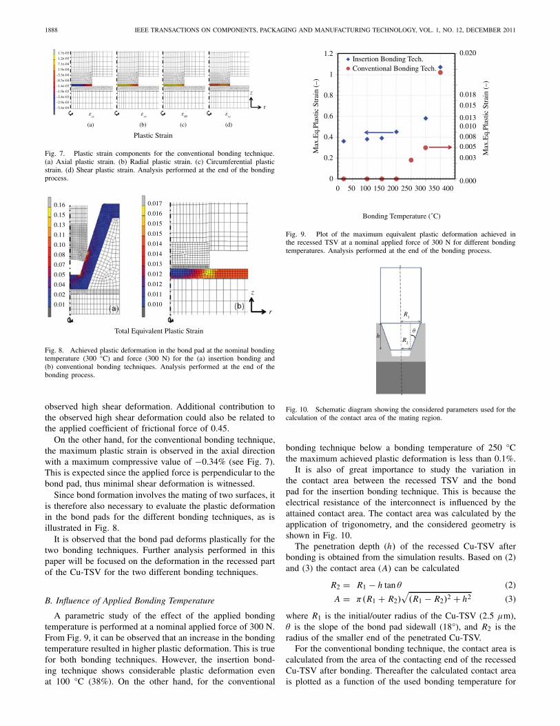
at the nominal bonding temperature (300 °C) and appliedforce (300 N). It is observed that under the same bondingtemperature and applied force, the maximum achieved plasticdeformation for the insertion bonding (58%) is more thantwo orders of magnitude larger than the conventional bondingtechnique (0.34%). This observed high equivalent plastic strainin the insertion bonding technique is due to the smallermating contact area and the use of a tangential landing pad.The smaller contact area results in the localization of theapplied pressure, while the tangential bond pad increases thedeviatoric stress components, which results in a larger plasticdeformation.
The resulting plastic strain components are shown in Figs. 6and 7 for the insertion bonding and the conventional bondingtechniques, respectively. It is observed that the highest con-tributor to the observed equivalent plastic strain in Fig. 5(a)for the insertion bonding technique is the shear plastic straincomponent with a maximum plastic strain value of 0.52.This means that the mating parts are deformed more in theshear direction due to the tangential inclination of the bondpad, which results in high localized pressure, leading to the
1888 IEEE TRANSACTIONS ON COMPONENTS, PACKAGING AND MANUFACTURING TECHNOLOGY, VOL. 1, NO. 12, DECEMBER 2011
1.7e-03
1.2e-03
7.1e-04
1.9e-04
–3.3e-04
–8.5e-04
–1.4e-03
–1.9e-03
–2.4e-03
–2.9e-03
–3.4e-04
εzz
εrr
(a) (b)
εθθ
(c)
εrz
(d)
z
r
Plastic Strain
Fig. 7. Plastic strain components for the conventional bonding technique.(a) Axial plastic strain. (b) Radial plastic strain. (c) Circumferential plasticstrain. (d) Shear plastic strain. Analysis performed at the end of the bondingprocess.
0.16
0.15
0.13
0.11
0.10
0.08
0.07
0.05
0.04
0.02
0.01
0.017
z
Total Equivalent Plastic Strain
r
0.016
0.015
0.015
0.014
0.014
0.013
0.012
0.012
0.011
0.010
Fig. 8. Achieved plastic deformation in the bond pad at the nominal bondingtemperature (300 °C) and force (300 N) for the (a) insertion bonding and(b) conventional bonding techniques. Analysis performed at the end of thebonding process.
observed high shear deformation. Additional contribution tothe observed high shear deformation could also be related tothe applied coefficient of frictional force of 0.45.
On the other hand, for the conventional bonding technique,the maximum plastic strain is observed in the axial directionwith a maximum compressive value of −0.34% (see Fig. 7).This is expected since the applied force is perpendicular to thebond pad, thus minimal shear deformation is witnessed.
Since bond formation involves the mating of two surfaces, itis therefore also necessary to evaluate the plastic deformationin the bond pads for the different bonding techniques, as isillustrated in Fig. 8.
It is observed that the bond pad deforms plastically for thetwo bonding techniques. Further analysis performed in thispaper will be focused on the deformation in the recessed partof the Cu-TSV for the two different bonding techniques.
B. Influence of Applied Bonding Temperature
A parametric study of the effect of the applied bondingtemperature is performed at a nominal applied force of 300 N.From Fig. 9, it can be observed that an increase in the bondingtemperature resulted in higher plastic deformation. This is truefor both bonding techniques. However, the insertion bond-ing technique shows considerable plastic deformation evenat 100 °C (38%). On the other hand, for the conventional
1.2
1
0.8
Max
.Eq.
Plas
tic S
trai
n (–
)
Insertion Bonding Tech.
Bonding Temperature (˚C)
Conventional Bonding Tech.
0.6
0.4
0.2
00 50 100 150 200 250 300 350 400
0.020
0.018
0.015
Max
.Eq.
Plas
tic S
trai
n (–
)
0.0130.010
0.0080.005
0.003
0.000
Fig. 9. Plot of the maximum equivalent plastic deformation achieved inthe recessed TSV at a nominal applied force of 300 N for different bondingtemperatures. Analysis performed at the end of the bonding process.
R1
R2
hθ
Fig. 10. Schematic diagram showing the considered parameters used for thecalculation of the contact area of the mating region.
bonding technique below a bonding temperature of 250 °Cthe maximum achieved plastic deformation is less than 0.1%.
It is also of great importance to study the variation inthe contact area between the recessed TSV and the bondpad for the insertion bonding technique. This is because theelectrical resistance of the interconnect is influenced by theattained contact area. The contact area was calculated by theapplication of trigonometry, and the considered geometry isshown in Fig. 10.
The penetration depth (h) of the recessed Cu-TSV afterbonding is obtained from the simulation results. Based on (2)and (3) the contact area (A) can be calculated
R2 = R1 − h tan θ (2)
A = π(R1 + R2)√
(R1 − R2)2 + h2 (3)
where R1 is the initial/outer radius of the Cu-TSV (2.5 μm),θ is the slope of the bond pad sidewall (18°), and R2 is theradius of the smaller end of the penetrated Cu-TSV.
For the conventional bonding technique, the contact area iscalculated from the area of the contacting end of the recessedCu-TSV after bonding. Thereafter the calculated contact areais plotted as a function of the used bonding temperature for

OKORO et al.: NOVEL CU–CU BONDING TECHNIQUE 1889
Insertion Bonding
Bonding Temperature (˚C)
Con
tect
Are
a (μ
m2 )
Conventional Bonding
03
6
9
12
15
18
21
24
27
50 100 150 200 250 300 350 400
Fig. 11. Relationship between the contact area of the mating region andthe applied bonding temperature for the insertion bonding and conventionalbonding techniques. Analysis performed at the end of the bonding process.
Min. Eq. Plastis Strain: 1%
Plas
tical
ly D
efor
med
Con
tact
Are
a (μ
m2 )
Bonding Temperature (˚C)
5
4
3
2
1
0
50 100 150 200 250 300
Min. Eq. Plastis Strain: 5%
Min. Eq. Plastis Strain: 10%
Min. Eq. Plastis Strain: 15%
Min. Eq. Plastis Strain: 20%
Fig. 12. Calculated plastically deformed contact area at different bondingtemperatures for different assumed threshold values. Analysis performed atthe end of the bonding process.
the insertion bonding and the conventional bonding techniquesas shown in Fig. 11.
Fig. 11 shows that the contact area with the insertionbonding technique increases exponentially with the increase inthe applied bonding temperature. This is due to the increasein the plastic deformation resulting from the reduction in theyield strength of Cu with temperature. Therefore, under aconstant applied force, the recessed TSV penetrates deeperinto the grooved bond pad at higher temperature than for lowertemperatures. On the other hand, for the conventional bondingtechnique, a minimal impact of the bonding temperatureon the achieved contact area is observed (see Fig. 11). Asignificant change in the contact area is only observed forbonding temperatures above 250 °C, due to the limited plasticdeformation at lower temperatures.
Also From Fig. 11 we observe that for bonding temper-atures above around 320 °C, the contact area achieved bythe insertion bonding approach becomes greater than thatachieved by the conventional approach. This also means that ata bonding temperature of 320 °C the electrical resistance of the
1
0.1
0.01
Max
. Eq.
Pla
stic
Str
ain
(–)
Applied Force (N)
Insertion Bonding
Conventional Bonding
0.001100 200 300 400 500 600
Fig. 13. Plot of the maximum equivalent plastic deformation achieved inthe recessed TSV at a nominal applied temperature of 300 °C for differentapplied forces. Analysis performed at the end of the bonding process.
insertion bonding technique will become comparable to that ofits counterpart. However, this crossover bonding temperature(320 °C) is considerably high, and defeats the motivation fora more novel low-temperature bonding approach.
Additionally, for the insertion bonding technique, the plasticdeformation in the Cu-TSV at its mating region with thebond pad can be represented in terms of their cumulativearea, other than only considering their maximum equivalentplastic strain values as presented in Fig. 9. However, since thebond formation is a complicated and interlinked mechanism,the minimum amount of plastic deformation required for theformation of a Cu–Cu bond is not known. Therefore, theassumption of a minimum plastic deformation value for bondformation, considered as threshold value, could be parame-terized as illustrated in Fig. 12. The plastically deformedcontact area is calculated by highlighting the mating elementsin the recessed Cu-TSV that meets the set plastic deformationthreshold value, this is followed by the calculation of theirarea.
From Fig. 12 we observe that for lower threshold equiva-lent plastic strain values, the plastically deformed contactingarea increases. Additionally, a similar trend is observed forthe different chosen threshold values, as the contact areaincreased with the applied bonding temperature. This trendalso correlates with the results based on the maximum plasticstrain values (see Fig. 9). However, the calculated plasticallydeformed area is shown to be lower than the total contact areaas shown in Fig. 11. For instance, for a plastic deformationthreshold of 1%, the plastically deformed contact area is about5 μm2 at 300 °C, while the total contact area shown in Fig. 11for the same bonding temperature is 15 μm2. This thereforemeans that a seamless bond formation may not be expectedall through the contacting area, since some of the contactingregions may not have deformed plastically.
C. Influence of Applied Force
A parametric study of the applied force at a constant bond-ing temperature of 300 °C is performed. It can be observed

1890 IEEE TRANSACTIONS ON COMPONENTS, PACKAGING AND MANUFACTURING TECHNOLOGY, VOL. 1, NO. 12, DECEMBER 2011
Insertion Bonding
Applied Force (N)
Con
tect
Are
a (μ
m2 )
Conventional Bonding
0
10
15
20
25
30
5
150 200 250 300 350 400 450 500 550 600
Fig. 14. Relationship between the contact area of the mating region and theapplied force for the insertion bonding and conventional bonding techniques.Analysis performed at the end of the bonding process.
that an increase in the applied force leads to a higher attainedmaximum equivalent plastic strain at the contacting Cu-TSVas shown in Fig. 13. This trend is a consequence of theincrease in the applied pressure upon the application of higherforces which results in an increased plastic deformation ofthe contact region. However, the insertion bonding approachcan be observed to result in two orders of magnitude largermaximum plastic deformation than the conventional bondingtechnique. This is attributed to the fact that the contact areabetween the mating parts is much smaller for the insertionbonding technique than the conventional bonding technique.This leads to higher contact pressure, leading to higher plasticdeformation in the former technique. This also means thatCu–Cu bonding using the insertion bonding approach canbe achieved at lower bonding force, as considerable plasticdeformation (around 44%) is observed for an applied force of150 N. Additionally, increase in the applied force is shown tolead to an increased contact area as is illustrated in Fig. 14.This is because higher applied forces result in an increasedpenetration of the recessed Cu-TSV in the sloped bond pad,thereby leading to an increased contact area.
While minimal variation of the contact area with respectto the applied force is observed for the conventional bondingapproach, this is not true for the insertion bonding approach,in which the contact area is observed to increase with theapplied force. For the considered conditions, at an appliedforce of about 470 N, the contact area of the insertion bondingapproach becomes greater than its counterpart.
D. Influence of Sidewall Slope of Bond Pad
Another parameter that is worth investigating for the inser-tion bonding approach is the sidewall slope of the bond pad.In this paper, the sidewall slope of the bond pad is varied,while the applied force and temperature are kept constant at300 N and 300 °C, respectively.
It is observed that steeper sidewall slopes resulted in anincrease in the plastically deformed mating area, as could beseen in Fig. 15. This is due to the increased total contacting
Min. Eq. Plastis Strain: 1%
θ
Plas
tical
ly D
efor
med
Con
tact
Are
a (μ
m2 )
Sidewall Slope (˚)
Bottom Chip
12
10
8
4
6
2
00 1510 25 30205 35
Min. Eq. Plastis Strain: 5%
Min. Eq. Plastis Strain: 10%
Min. Eq. Plastis Strain: 15%
Min. Eq. Plastis Strain: 20%
Fig. 15. Influence of bond pad sidewall slope on the achieved plasticallydeformed contact area for the insertion bonding technique at a bondingtemperature and force of 300 °C and 300 N, respectively, for differentthreshold values of plastic deformation. Analysis performed at the end ofthe bonding process.
Con
tact
Are
a (μ
m2 )
Sidewall Slope (˚)
40
35
30
15
20
25
5
10
00 1510 25 30205 35 40
θ
Bottom Chip
Fig. 16. Influence of sidewall slope on the achieved contact area for theinsertion bonding technique at a bonding temperature and force of 300 °C and300 N, respectively. Analysis performed at the end of the bonding process.
mating area with respect to the sidewall slope as can beobserved in Fig. 16. Since more area is in contact, the areathat plastically deforms also increases.
The increase in the contact area with stepper sidewallslope (Fig. 16) also translates to a decrease in the electricalresistance of the interconnect, since resistance is inverselyrelated to the contact area.
This finding opens an additional window of opportunity forthe possible further optimization of the bond quality of theinsertion bonding technique. However, the choice of sidewallslope is limited by the achievable alignment tolerance of thepick-and-place tool used for the stacking process, the tool usedfor this paper (FC 150 bonder) has an alignment tolerance of1.5 μm.
V. EXPERIMENTAL DEMONSTRATION OF INSERTION
BONDING TECHNIQUE
Based on the encouraging results from the FEM analysisof the insertion bonding technique, an experimental studyis pursued. The fabrication of the top chip for the insertion

OKORO et al.: NOVEL CU–CU BONDING TECHNIQUE 1891
(a) (b) (c)
(d)(e)(f)
(g)
ResistPassivationCopperSilicon
Fig. 17. Processing steps used for the formation of the sloped bond pad onthe bottom chip for the insertion bonding approach.
bonding approach is the same as that used in the conventionalbonding approach which has been discussed in detail in [17].However, in this case, the Cu-TSV is recessed to a length ofaround 10 μm.
It is worth noting that the conditions used in this experi-mental demonstration are somewhat different from that sim-ulated. All the afore-presented studies were performed usingnominal values of 300 °C and 300 N, respectively, for thebonding temperature and force, which were based on theconditions used for the conventional bonding technique. Thepresented experimental results were achieved at a bondingtemperature and force of 100 °C and 500 N, respectively.However, similar bond pad thickness and slope were used.Additionally, the bonding temperature and the applied forceused in the experiment were considered in the FEM parametricstudies.
A. Process Flow for Formation of Insertion Bonding Bond Pad
The fabrication process for the bond pad on the lower chipis entirely a different procedure from that used in the conven-tional bonding technique, and the process flow is illustrated inFig. 17.
In the insertion bonding approach, the following steps areused.
1) A Cu metal line is deposited on a 200-mm wafer[Fig. 17(a)].
2) By the sputtering process, a passivation layer of siliconoxide (8 μm) is overlaid on the wafer [Fig. 17(b)].
3) This is followed by the deposition of a photoresist[Fig. 17(c)] and its subsequent patterning.
4) A tapered groove is then formed in the deposited siliconoxide layer by dry etching process [Fig. 17(e)].
5) Photoresist layer is striped off from the surface of thesilicon oxide [Fig. 17(f)].
6) By electrodeposition or by plasma vapor depositionprocess, a conformal layer of copper (2 μm) is deposited
5/24/20101:22:55 PM
HV5 00 KV
Spot 4 00
Mag 13.966x
WD 5.3 mm
det TLD
modeSE 100c 50 MPa mm spot
5 μm
5/24/20101:22:55 PM
HV5 00 KV
Spot 4 00
Mag 13.966x
WD 5.3 mm
det TLD
modeSE 100c 50 MPa mm spot
5 μm
5/24/20101:21:44 PM
HV5.00 KV
Spot 4.0
Mag 6 687x
WD 5.3 mm
det TLD
modeSE 100c 50 MPa mm spot
10 μm
Fig. 18. Scanning electron microscopy (SEM) images showing the morphol-ogy of Cu–Cu bonding of dies achieved by the insertion bonding approach ata bonding temperature and force of 100 °C and 500 N, respectively.
over the silicon oxide, thereby forming a metalized bondpad [Fig. 17(g)] used for the insertion bonding approach.
7) Wafers are diced into chip areas of 10.6 × 10.6 mm2.It is worth noting that the presented experimental results in thesucceeding sections are a first demonstration of the insertionbonding technique.
B. Morphology of Achieved Cu–Cu Joints
In preparation for the bonding process, the samples werecleaned in a citric acid–based cleaning solution called MS6020solution to remove Cu oxide on the mating surfaces. After-ward, by using the SET FC150 flip chip bonder, die-to-diebonding is achieved. For this paper, a bonding temperatureand force of 100 °C and 500 N, respectively, were applied.This bonding process is achieved under the presence of thecleaning agent, MS6020. After the stacking of the chips hasbeen achieved, the samples were embedded in epoxy andwere later on ground and polished for SEM inspection. Across-sectional image of the joints is shown in Fig. 18. Thisfigure shows that the Cu–Cu bond is achieved at 100 °C.However, a closer look reveals that parts of the bond interfacebetween the recessed Cu-TSV and the landing pad can beclearly seen as is illustrated in the inserted image on the right.This means that since diffusion bonding is a thermally drivenprocess, the applied temperature of 100 °C may not have beensufficient to activate all the different essential bond formationmechanisms such as surface diffusion, plastic deformation,creep, grain boundary diffusion, and interface diffusion. Also,the presence of oxides at the interface may have contributedto the hampering of bond formation.
C. Electrical Resistance Measurement of Cu–Cu Joints
Having achieved a mechanical bond at a low bondingtemperature of 100 °C, it is then imperative to measure theirelectrical resistance, as these interconnects are responsible forthe transmission of electrical signal through the different tiersof the stacked chips. However, the test demonstrators usedin this paper were designed only for the achievement of amechanical Cu–Cu joint. This means that metal lines for themeasurement of electrical resistance across the interconnectbetween the chip hierarchies were not included.

1892 IEEE TRANSACTIONS ON COMPONENTS, PACKAGING AND MANUFACTURING TECHNOLOGY, VOL. 1, NO. 12, DECEMBER 2011
Fig. 19. SEM image illustrating the measurement of the electrical resistanceof the cross-sectioned Cu–Cu joints via nanoprobing technique.
1 2 3 4 5
Res
ista
nce
(m�
)
Cu-Cu Joints achieved at a bonding temperature of 100˚C
700
600
500
400
300
200
100
0
Fig. 20. Resistance measurement of Cu–Cu bonds formed by the insertionbonding technique. (Resistance measurement is done on a cross-sectionedsample.)
In order to overcome this setback, and still obtain anelectrical resistance measurement of the joints, nanoprobingsystem is used and the measurement was done on the cross-section of the bonded interconnect as shown in Fig. 19. Forthis measurement, a four-point measurement was conducted tominimize the influence from the contact resistance, in whichtwo of the probes were placed at the top region of the Cu-TSV in the top chip, while the remaining two probes wereplaced on the bond pad in the bottom chip (see Fig. 19). Inthis paper, an initial measurement of the resistance of the Cu-TSV before the formed joint is performed so as to determinethe resistance of the Cu-TSV itself, which is found to be about30 m�. Afterward, the measurements were performed acrossthe stacked chip. In this paper, five joints were measured,which are presented in Fig. 20.
From Fig. 20 we see that an electrically yielding Cu–Cubond is achieved by the insertion bonding approach. However,a high average resistance value of 584 m� is observed, ascompared to the standard 5-μm diameter Cu-TSV resistance ofaround 20 m� observed for the conventional Cu–Cu bondingtechnique achieved at a bonding temperature and force of300 °C and 300 N, respectively [18]. This high resistancemay have arisen due to the limited contact area between therecessed Cu-TSV and the sloped bond pad, which may haveoccurred due to the low bonding temperature (100 °C).
The fact that the nanoprobe measurement is performed oncross-sectioned samples instead of full diameter Cu-TSVs willalso contribute to the resistance of the joints. This furthermeans that the resistance measurement will also be dependenton how much the Cu-TSV is polished, therefore, Cu-TSVs thatare polished beyond or below their center will influence theresistance values. And it is difficult to ascertain exactly howmuch of the cross-section is remaining after polishing andthe percentage of the cross-section bonded to the bond pad.Also, the presence of oxides at the interface may have had animpact on the resistance measurement. And finally, since thenanoprober is not the conventional tool for measuring resis-tance of such structure, the positioning and the probe needlesthemselves could contribute to the high resistance of the joints.
Future work is planned to entail the performance of thedesign of the experiment for the determination of optimalconditions for the achievement of quality Cu–Cu joint havingacceptable resistance values. This will be performed usingelectrical demonstrator with daisy chains, as opposed to themechanical demonstrator used in this first study.
VI. CONCLUSION
In this paper, a new bonding technique called the insertionbonding approach was studied. This was achieved by con-ducting both numerical and experimental studies. From FEManalysis, it was found that the insertion bonding approachresults in a much higher plastic deformation of the matingparts, the recessed Cu-TSV and the sloped bond pad, than theconventional bonding technique. This observed higher plasticdeformation is due to the increase in shear deformation and thesmaller initial contact area that results in high pressure, whichis initiated by the use of a tangential bond pad. Parametricstudy of the influence of the bonding temperature showedthat the magnitude of the attained plastic deformation andthe mating contact area for the insertion bonding techniqueincreases exponentially with the applied bonding temperature.This is due to the increase in plastic deformation resulting fromthe reduction in the yield strength of Cu with temperature.
Similarly, a study of the influence of the applied forceshowed that the plastic deformation for the different bondingtechniques scaled with the applied force. This is because thepressure on the contacting region increases with the appliedforce, thereby resulting in an increased plastic deformation ofthe recessed Cu-TSV. Additionally, the contact area and theplastically deformed contact area can be greatly increased bythe use of a steeper bond pad.
First experimental studies done at a bonding temperatureof 100 °C showed that a promising Cu–Cu joint via insertionbonding approach can be achieved. SEM image of the jointsreveals that bond is formed in some areas of the joint, while inother areas the bond interface can be clearly seen. Electricalresistance measurement showed that an electrically yieldingCu–Cu joint is achieved by the insertion bonding technique.However the average joint resistance is found to be about584 m�. This high resistance value is attributed to the limitedcontact area, the low bonding temperature, the measurementmethod and the possible presence of Cu oxide at the bond
OKORO et al.: NOVEL CU–CU BONDING TECHNIQUE 1893
interface. Based on this paper, the insertion bonding techniquecan be regarded as a potential solution for low-temperatureCu–Cu bonding.
REFERENCES
[1] A. Jourdain, P. Soussan, B. Swinnen, and E. Beyne, “Electricallyyielding collective hybrid bonding for 3-D stacking of ICs,” in Proc.59th Electron. Comp. Technol. Conf., San Diego, CA, May 2009, pp.11–13.
[2] B. Derby and E. R. Wallach, “Theoretical model for diffusion bonding,”Metal Sci., vol. 16, no. 1, pp. 49–56, Jan. 1982.
[3] C. S. Tan, D. F. Lim, S. G. Singh, S. K. Goulet, and M. Bergkvist,“Cu–Cu diffusion bonding enhancement at low temperature by surfacepassivation using self-assembled monolayer of alkane-thiol,” Appl. Phys.Lett., vol. 95, no. 19, pp. 192108-1–192108-3, Nov. 2009.
[4] G. Q. Wu, Z. F. Li, G. X. Luo, H. Y. Li, and Z. Huang, “Dynamic simula-tion of solid-state diffusion bonding,” Mater. Sci. Eng. A, vols. 452–453,pp. 529–535, Apr. 2007.
[5] K. N. Chen, C. S. Tan, A. Fan, and R. Reif, “Morphology and bondstrength of copper wafer bonding,” Electrochem. Solid-State Lett., vol. 7,no. 1, pp. G14–G16, 2004.
[6] W. Ruythooren, S. Stoukatch, K. Lambrinou, P. de Moor, and B.Swinnen, “Direct Cu-Cu thermo-compression bonding for 3-D-stackedIC integration,” in Proc. Int. Symp. Microelectron., San Diego, CA, Oct.2006, pp. 1–6.
[7] C. Okoro, M. Gonzalez, B. Vandevelde, B. Swinnen, G. Eneman, S.Stoukatch, and E. Beyne, “Analysis of the induced stresses in siliconduring thermcompression Cu-Cu bonding of Cu-through-vias in 3-D-SIC architecture,” in Proc. 57th Electron. Comp. Technol. Conf., Reno,NV, May–Jun. 2007, pp. 249–255.
[8] Y. I. Kim, K. H. Yang, and W. S. Lee, “Thermal degradation of DRAMretention time: Characterization and improving techniques,” in Proc.42nd Annu. IEEE Int. Rel. Phys. Symp., Phoenix, AZ, Apr. 2004, pp.667–668.
[9] Y. Mori, K. Ohyu, K. Okonogi, and R. Yamada, “The origin of variableretention time in DRAM,” in Proc. Int. Electron Dev. Meet., WashingtonD.C., Dec. 2005, pp. 1034–1037.
[10] P. J. Restle, J. W. Park, and B. F. Lloyd, “DRAM variable retentiontime,” in Proc. Int. Electron Dev. Meet., San Francisco, CA, Dec. 1992,pp. 807–810.
[11] T. H. Kim, M. M. R. Howlader, T. Itoh, and T. Suga, “Room temperatureCu-Cu direct bonding using surface activated bonding method,” J. Vac.Sci. Technol., vol. 21, no. 2, pp. 449–453, 2003.
[12] P.-I. Wang, T. Karabacak, J. Yu, H.-F. Li, G. G. Pethuraja, S. H. Lee,M. Z. Liu, J.-Q. Lu, and T.–M. Lu, “Low temperature copper-nanorodbonding for 3-D integration,” in Proc. Mater. Res. Soc., vol. 970. 2007,p. T04.
[13] P.-I. Wang, S. H. Lee, T. C. Parker, M. D. Frey, T. Karabacak, J.-Q.Lu, and T.-M. Lu, “Low temperature wafer bonding by copper nanorodarray,” Electrochem. Solid-State Lett., vol. 12, no. 4, pp. H138–H141,2009.
[14] T. Liu, “Sliding friction of Copper,” Air Force Materials Laboratory,Wright-Patterson AFB, OH, Tech. Memo. ASRCN-63-51, 1963.
[15] J. Zarbakhsh, T. Detzel, R. Huang, M. Leicht, P. Nelle, and S. Woehlert,“Prediction of wafer bow through thermomechanical simulation ofpatterned hard coated copper films,” in Proc. 9th Int. Conf. ThermalMech. Multi-Phys. Simul. Exper. Microelectron. Micro-Syst., Freiburgim Breisgau, Germany, Apr. 2008, pp. 179–183.
[16] A. Hill and E. R. Wallach, “Modelling solid-state diffusion bonding,”Acta Metall., vol. 37, no. 9, pp. 2425–2437, Sep. 1989.
[17] B. Swinnen, W. Ruythooren, P. De Moor, L. Bogaerts, L. Carbonell,K. De Munck, B. Eyckens, S. Stoukatch, D. S. Tezcan, Z. Tokei, J.Vaes, J. Van Aelst, and E. Beyne, “3-D integration by Cu-Cu thermo-compression bonding of extremely thinned bulk-Si die containing 10 μmpitch through-Si vias,” in Proc. Int. Electron Dev. Meet., San Francisco,CA, Dec. 2006, pp. 1–4.
[18] G. Van der Plas, P. Limaye, A. Mercha, H. Oprins, C. Torregiani, S.Thijs, D. Linten, M. Stucchi, K. Guruprasad, D. Velenis, D. Shinichi,V. Cherman, B. Vandevelde, V. Simons, I. De Wolf, R. Labie, D. Perry,S. Bronckers, N. Minas, M. Cupac, W. Ruythooren, J. Van Olmen, A.Phommahaxay, M. de P. de Broeck, A. Opdebeeck, M. Rakowski, B. DeWachter, M. Dehan, M. Nelis, R. Agarwal, W. Dehaene, Y. Travaly, P.Marchal, and E. Beyne, “Design issues and considerations for low-cost3-D TSV IC technology,” in Proc. IEEE Int. Solid-State Circuits Conf.,San Francisco, CA, Feb. 2010, pp. 148–149.
Chukwudi Okoro received the Bachelors degree inmaterials and metallurgical engineering from FederalUniversity of Technology, Owerri, Nigeria, in 2001,the Masters degree in microsystems integration tech-nology from Chalmers University of Technology,Gothenburg, Sweden, in 2006, and the Ph.D. degreein mechanical engineering from Katholieke Univer-siteit Leuven, Leuven, in affiliation with the Interuni-versity Microelectronics Center (IMEC), Leuven,Belgium, in 2010.
He is currently with the National Institute of Stan-dards and Technology as a Post-Doctoral Researcher. Prior to joining IMECin 2006, he did a six-month internship at the National Physical Laboratory,Middlesex, U.K., where he studied the fatigue behavior of lead-free solders.His current research interests include 3-D stacking of chips, interconnects,material characterization, and thermomechanical analysis.
Paresh Limaye author photograph and biography not available at the time ofpublication.
Rahul Agarwal received the B.E. degree in elec-tronics engineering from Nagpur University, Maha-rashtra, India, in 2001, and the M.S. and Ph.D.degrees in electrical engineering from the Universityof South Florida, Tampa, in 2003 and 2007, respec-tively.
He has been working as a Scientist in the Instituteof Microelectronics (IME), Singapore, since 2010.Before joining IME, he worked as a Researcherin the Interuniversity Microelectronics Center, Leu-ven, Belgium. His current research interests include
microelectromechanical systems design, fabrication and packaging, develop-ment of microsensors, stacking approaches for 3-D wafer-level packaging and3-D stacked integrated circuits using die-to-die or die-to-wafer approaches,and 3-D integration for advance packaging.
Bart Vandevelde received the Masters degree inmechanical engineering from the Katholieke Univer-siteit Leuven, Leuven, Belgium, in June 1994, andthe Ph.D. degree in thermomechanical modeling forelectronic packages from the Interuniversity Micro-electronics Center (IMEC), Leuven, in March 2002.
He is currently responsible for the Packaging-Level Reliability Research Team at IMEC. He hasmany publications in the field of thermal and ther-momechanical modeling and characterization foradvanced integrated circuit packaging technologies.
Dr. Vandevelde is a co-founder and member of the organization committeefor the IEEE international conference on Thermal, Mechanical and Multi-physics Simulation and Experiments in Microelectronics and Microsystems.

1894 IEEE TRANSACTIONS ON COMPONENTS, PACKAGING AND MANUFACTURING TECHNOLOGY, VOL. 1, NO. 12, DECEMBER 2011
Eric Beyne received the graduate degree in electri-cal engineering and the Ph.D. degree in applied sci-ences both from the Katholieke Universiteit Leuven,Leuven, Belgium, in 1983 and 1990, respectively.
He has been with the Interuniversity Microelec-tronics Center (IMEC), Leuven, since 1986. Cur-rently, he is a Scientific Director of advanced pack-aging and interconnect and the Program Directorof IMEC’s 3-D System Integration Affiliation Pro-gram.
Dr. Beyne is a Strategic Director for Region 8(Europe) of the IEEE Components, Packaging and Manufacturing TechnologySociety, the President of the International Microelectronics and PackagingSociety (IMAPS)-Benelux Committee, and a member of the IMAPS-EuropeLiaison Committee.
Dirk Vandepitte received the graduate degree fromGhent University, Ghent, Belgium, in 1985, andthe Ph.D. degree in mechanical engineering fromthe Katholieke Universiteit Leuven (K.U.Leuven),Leuven, Belgium, in 1990.
He was with Fokker Space and Systems (currentlyDutch Space), Leiden, The Netherlands, and since1992, he has been a Professor at the Departmentof Production, Machine Design and Automation,K.U.Leuven. He specializes in light-weight struc-tures. He is the Chairman of the Leuven Research
Center for Aero and Space Science, Technology and Applications, Leuven.